MD E9000W Service Manual GB MDE9000W
User Manual: MDE9000W
Open the PDF directly: View PDF ![]() .
.
Page Count: 100
MD-E9000W
CONTENTS
Page
SAFETY PRECAUTION OF MD SECTION FOR SERVICE MANUAL..............................................................................2
SAFETY PRECAUTION OF CD SECTION FOR SERVICE MANUAL ..............................................................................3
VOLTAGE SELECTION..................................................................................................................................................... 3
AC POWER SUPPLY CORD AND AC PLUG ADAPTOR ................................................................................................. 3
SPECIFICATIONS ............................................................................................................................................................. 4
NAMES OF PARTS ........................................................................................................................................................... 5
OPERATION MANUAL ...................................................................................................................................................... 7
DISASSEMBLY ................................................................................................................................................................ 10
REMOVING AND REINSTALLING THE MAIN PARTS ................................................................................................... 13
TEST MODE .................................................................................................................................................................... 15
ADJUSTMENT ................................................................................................................................................................. 19
ERROR MESSAGE LIST ................................................................................................................................................. 29
EEPROM WRITING PROCEDURE ................................................................................................................................. 30
BLOCK DIAGRAM ........................................................................................................................................................... 34
WIRING SIDE OF P.W.BOARD ....................................................................................................................................... 38
SCHEMATIC DIAGRAM .................................................................................................................................................. 48
VOLTAGE ........................................................................................................................................................................ 60
NOTES ON SCHEMATIC DIAGRAM .............................................................................................................................. 61
TYPES OF TRANSISTOR AND LED............................................................................................................................... 61
WAVEFORMS OF CD CIRCUIT ...................................................................................................................................... 62
WAVEFORMS OF MD CIRCUIT ..................................................................................................................................... 63
TROUBLESHOOTING ..................................................................................................................................................... 65
FUNCTION TABLE OF IC................................................................................................................................................ 73
FL DISPLAY..................................................................................................................................................................... 86
PARTS GUIDE/EXPLODED VIEW
SERVICE MANUAL
SHARP CORPORATION
No. S8155MDE9000/
• In the interests of user-safety the set should be restored to its
original condition and only parts identical to those specified should
be used.
This document has been published to be used
for after sales service only.
The contents are subject to change without notice.
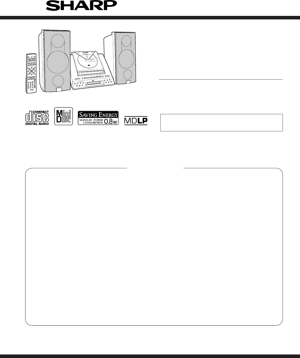
MD-E9000W MD Compact Component System consisting
of MD-E9000W (main unit) and CP-E9000H (speaker
system).
MD COMPACT COMPONENT SYSTEM
MODEL MD-E9000W
MD-E9000W
– 2 –
SAFETY PRECAUTION OF MD SECTION FOR SERVICE MANUAL
The AEL (Accessible Emission Level) of the laser power output is less than class 1 but the laser component is capable of emitting radiation
exceeding the limit for Class 1. Therefore it is important that the following precautions are observer during servicing to protect your eyes
against exposure to the laser beam.
1) When the unit case cover is removed and LOADING SW (SW1932) is turned on and then PLAY SW (SW1934 mechanism PWB) is turned
on in a few second.
The laser will light for several second to detect a disk.
2) The laser power output of the pickup unit and replacement service parts are all factory preset before shipment.
Do not attempt to readjust the laser pickup unit during replacement or servicing.
3) Under no circumstances stare into the pickup lens at any time.
4) If laser optical unit becomes faulty, replace the complete laser optical unit.
5) CAUTION-Use of controls or adjustments, or performance of procedures other than those specified herein may result in hazardous
radiation exposure.
VARO ! Avattaessa ja suojalukitus ohitettaessa olet alttiina näkymättömälle lasersäteilylle. Älä katso säteeseen.
VARNING! Osynlig laserstralning när denna del är öppnad och spärren är urkopplad. Betrakta ej strälen.
Precaution to be taken when replacing and servicing the laser pickup.
The following precautions must be observed during servicing to protect your eyesvagainst exposure to the laser.
Warning of possible eye damage when repairing:
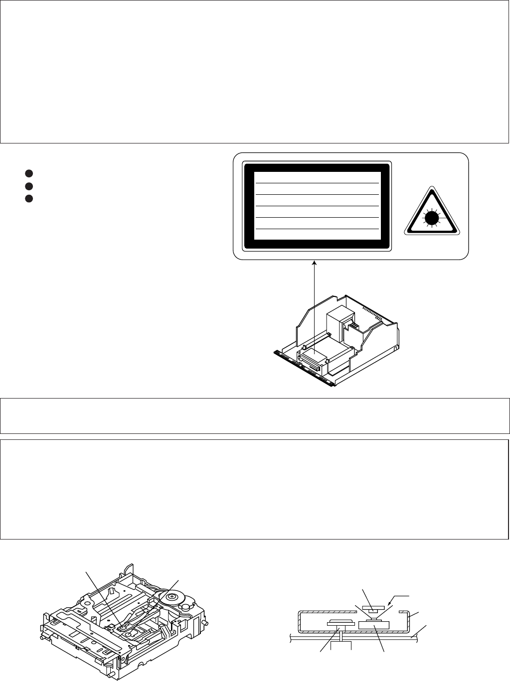
If the AC power plug is connected when the inner cover of the unit is removed, the laser will light up during focus access (about
1 second) (Fig. 2-1).
During this operation, the laser will leak from the opening between the magnetic head and cartridge holder (Fig. 2-2).
In order to protect your eyes, you must not look at the laser during repair.
Before repairing, be sure to disconnect the AC power plug.
Figure 2-1 Figure 2-2
Magnetic Head Optical Pickup
Magnetic Head
Optical PickupSpindle Motor
Laser Beam
Cartridge Holder
Mechanism
Chassis
WARNINGS
Laser Diode Properties
Material: GaAIAs
Wavelength: 785 nm
Pulse time:
Read mode: 0.8 mW Continuous
Write mode: max 10 mW 0.5S
min cycle 1.5S
Repetition
CAUTION-INVISIBLE LASER RADIATION WHEN OPEN AND INTERLOCKS
DEFEATED. AVOID EXPOSURE TO BEAM.
VARNING-OSYNLIG LASERSTRÅLNING NÄR DENNA DEL ÄR ÖPPNAD OCH
SPÄRRAR ÄR URKOPPLADE. STRLEN ÄR FARLIG.
ADVERSEL-USYNLIG LASERSTRÅLING NÄR DEKSEL ÅPNES OG SIKKERHEDSLÅS
BRYTES. UNNGÅ EKSPONERING FOR STRÅLEN.
VARO! AVATTAESSA JA SUOJALUKITUS OHITETTAESSA OLET ALTTIINA
NÄKYMÄTÖN LASERSÄTEILYLLE. ÄLÄ KATSO SÄTEESEN.
ADVERSEL-USYNLIG LASERSTRÅLING VED ÅBNING. NÅR SIKKERHEDSAFBRYDERE
ER UDE AF FUNKTION. UNDGÅ UDSETTELSE FOR STRÅLING.
VARNING-OSYNLIG LASERSTRÅLNING NÄR DENNA DEL ÄR ÖPPNAD OCH SPÄRREN
ÄR URKOPPLAD. BETRAKTA EI STRÅLEN.
– 3 –
MD-E9000W
Precaution to be taken when replacing and servicing the Laser Pickup.
The AEL (Accessible Emission Level) of Laser Power Output for this model is specified to be lower than Class 1 Requirements.
However, the following precautions must be observed during servicing to protect your eyes against exposure to the Laser
beam.
(1) When the cabinet has been removed, the power is turned on without a compact disc, and the Pickup is on a position outer
than the lead-in position, the Laser will light for several seconds to detect a disc. Do not look into the Pickup Lens.
(2) The Laser Power Output of the Pickup inside the unit and replacement service parts have already been adjusted prior to
shipping.
(3) No adjustment to the Laser Power should be attempted when replacing or servicing the Pickup.
(4) Under no circumstances look directly into the Pickup Lens at any time.
(5) CAUTION - Use of controls or adjustments, or performance of procedures other than those specified herein may result in
hazardous radiation exposure.
WARNINGS
SAFETY PRECAUTION OF CD SECTION FOR SERVICE MANUAL
Laser Diode Properties
Material: GaAIAs
Wavelength: 780 nm
Emission Duration: continuous
Laser Output: max. 0.6 mW
CAUTION-INVISIBLE LASER RADIATION WHEN OPEN. DO NOT STARE INTO BEAM
OR VIEW DIRECTLY WITH OPTICAL INSTRUMENTS.
VARNING-OSYNLIG LASERSTRALNING NAR DENNA DEL AR OPPNAD. STIRRA EJ
IN I STRALEN OCH BETRAKTA EJ STRALEN MED OPTISKA INSTRUMENT.
ADVERSEL-USYNLIG LASERSTRALING VED ABNING. SE IKKE IND I
STRALEN-HELLER IKKE MED OPTISKE INSTRUMENTER.
VARO! AVATTAESSA OLET ALTTIINA NAKYMATON LASERSATEILYLLE. ALA
TUIJOTA SATEESEEN ALAKA KATSO SITA OPTISEN LAITTEEN LAPI.
VARNING-OSYNLIG LASERSTRALNING NAR DENNA DEL AR OPPNAD. STIRRA EJ
IN I STRALEN OCH BETRAKTA EJ STRALEN GENOM OPTISKT INSTRUMENT.
ADVERSEL-USYNLIG LASERSTRALING NAR DEKSEL APNES. STIRR IKKE INN I
STRALEN ELLER SE DIREKTE MED OPTISKE INSTRUMENTER.
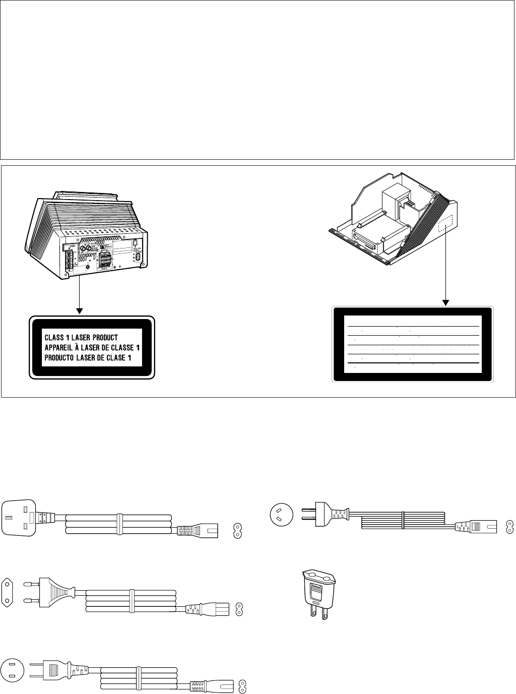
VOLTAGE SELECTION
Before operating the unit on mains, check the preset voltage. If the voltage is different from your local voltage, adjust the voltage
as follows.
Turn the selector with a screwdriver until the appropriate voltage number appears in the window (110 V, 127 V, 220 V or 230 V-240 V AC).
AC POWER SUPPLY CORD AND AC PLUG ADAPTOR
QACCB0012AW00 QACCL0002AW00
QACCE0007AW00
QACCJ0006AW00
QPLGA0004AWZZ
MD-E9000W
– 4 –
FOR A COMPLETE DESCRIPTION OF THE OPERATION OF THIS UNIT, PLEASE REFER
TO THE OPERATION MANUAL.
SPECIFICATIONS
Specifications for this model are subject to change without
prior notice.
MD-E9000W
CP-E9000H
MiniDisc
Type MiniDisc recorder
Signal readout Non-contact, 3-beam semiconductor laser pickup
Rotation speed 400 - 900 rpm CLV, Approx.
Error correction ACIRC (Advanced Cross Interleave Reed-Solomon
Code)
Quantization 20-bit linear (A/D converter)
Coding ATRAC/ATRAC 3 (Adaptive TRansform Acoustic Cod-
ing)
Sampling frequency 44.1 kHz
Recording method Magnetic modulation overwrite method
Frequency response 20 - 20,000 Hz
D/A converter 1-bit D/A converter
Wow and flutter Unmeasurable (less than 0.001% W. peak)
Signal/noise ratio 95 dB (1 kHz)
Dynamic range 90 dB (1 kHz)
Audio channel Stereo: 2 channels (SP, LP2, LP4)
Tuner
Frequency range FM: 88 - 108 MHz
AM: 531 - 1,602 kHz
Type 2-way type speaker system
5 cm (2") Tweeter
10 cm (4") Woofer
Maximum input power 40 W
Rated input power 20 W
Impedance 4 ohms
Dimensions Width: 140 mm (5-9/16")
Height: 300 mm (11-13/16")
Depth: 187 mm (7-3/8")
Weight 1.5 kg (3.3 lbs.)/each
General
Power source AC 110/127/220/230 - 240 V, 50/60 Hz
Power consumption 58 W
Dimensions Width: 230 mm (9-1/16")
Height: 173 mm (6-13/16")
Depth: 290 mm (11-7/16")
Weight 4.1 kg (9.02 lbs.)
Amplifier
Output power MPO: 66 W (33 W + 33 W) (10 % T.H.D.)
RMS: 40 W (20 W + 20 W) (10 % T.H.D.)
RMS: 28 W (14 W + 14 W) (1 kHz, 0.9 % T.H.D.)
Output terminals Speakers: 4 ohms
Headphones: 16 - 50 ohms (recommended: 32 ohms)
Input terminals Auxiliary: 500 mV/47 kohms
CD player
Type Compact disc player
Signal readout Non-contact, 3-beam semiconductor laser pickup
D/A converter 1-bit D/A converter
Frequency response 20 - 20,000 Hz
Dynamic range 90 dB (1 kHz)
– 5 –
MD-E9000W
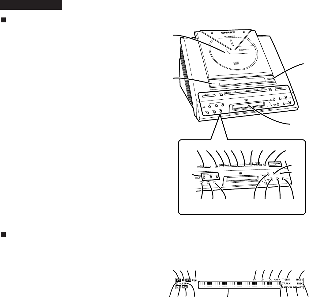
NAMES OF PARTS
MD-E9000W
Front panel
1. CD Compartment
2. Timer Set Indicator
3. Remote Sensor
4. MD Compartment
5. On/Stand-by Button
6. MD Eject Button
7. Tuner (Band) Button
8. Auxiliary Button
9. Extra Bass Button
10. Equalizer Button
11. Memory/Enter Button
12. Display (Demo) Button
13. CD Open/Close Button
14. Volume Up and Down Buttons
15. MD Record Mode Selector Buttons (SP/LP2/LP4)
16. CD/MD Normal Speed Record Button
17. CD/MD High Speed Record Button
18. MD Record Button
19. CD Stop Button
20. CD Play or Pause Button
21. CD/MD Track Up and Fast Forward, Tuner Preset
Up Button
22. CD/MD Track Down and Fast Reverse, Tuner Preset
Down Button
23. MD Stop Button
24. MD Play or Pause Button
1
2
3
4
15
19
16 17 18 21 22 23 24
20
5 7 8 9 10 11 12 13 14
Display
1. Record Indicator
2. Record Pause Indicator
3. High Speed Record Indicator
4. CD/MD Repeat Indicator
5. FM Stereo Mode Indicator
6. FM Stereo Receiving Indicator
7. TOC Indicator
8. Over Indicator
9. Track Edit Indicator
10. Extra Bass Indicator
11. Timer Play/Record Indicator
12. 2 times Long Recording (stereo) Indicator
13. 4 times Long Recording (stereo) Indicator
14. Sleep Indicator
15. Level Meter/Character Information/Frequency Indicator
16. Track Indicator
17. Random Play Indicator
18. Memory Indicator
19. Disc Indicator
1
111213 14 15 16 17 18 19
2567891034
6
MD-E9000W
– 6 –
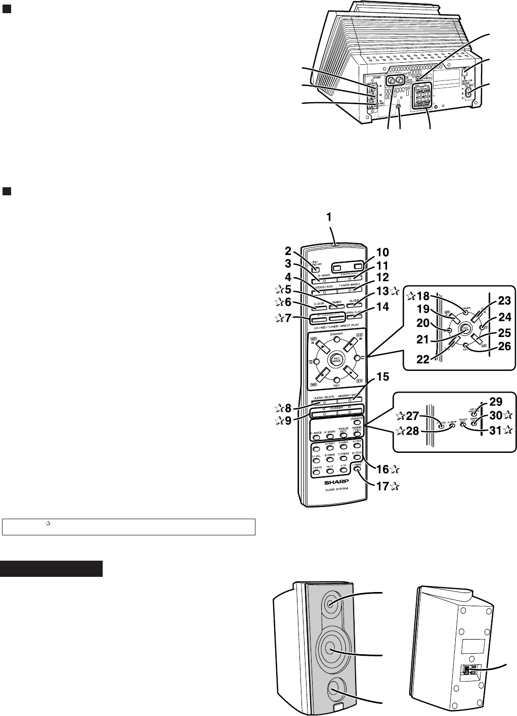
CP-E9000H
Rear Panel
1. AM Aerial Terminal
2. Aerial Earth Terminal
3. FM Aerial Terminal
4. Auxiliary (Audio Signal) Input Sockets
5. Headphone Socket
6. Speaker Terminals
7. Span Selector Switch
8. AC Voltage Selector
9. AC Power Input Socket
46
9
2
3
8
7
1
5
Remote Control
1. Remote Control Transmitter
2. On/Stand-by Button
3. Extra Bass Button
4. Video/Auxiliary Button
5. Timer Button
6. Clock Button
7. Tuning Up and Down Buttons
8. Clear/Delete Button
9. Cursor Buttons
10. Volume Up and Down Buttons
11. Equalizer Mode Selector Button
12. Tuner (Band) Button
13. Sleep Button
14. CD Open/Close Button
15. Memory/Enter Button
16. Character Input/CD, MD Direct Buttons
17. Symbol/Time Button
18. Dimmer Button
19. MD Play or Pause Button
20. CD/MD Fast Reverse, Track Down Button
21. Recording Mode Selector Button
22. MD Stop Button
23. CD Play or Pause Button
24. CD/MD Fast Forward, Track Up Button
25. CD Stop Button
26. MD Record Button
27. CD/MD Play Mode Selector Button
28. Auto Marker Button
29. Display/Character Button
30. Name/TOC Button
31. Track Edit Button
Buttons with “ “ mark in the illustration can be operated on the remote control only.
Other buttons can be operated both on the main unit and the remote control.
1. Tweeter
2. Woofer
3. Bass Reflex Duct
4. Speaker Terminals
1
2
3
4
– 7 –
MD-E9000W
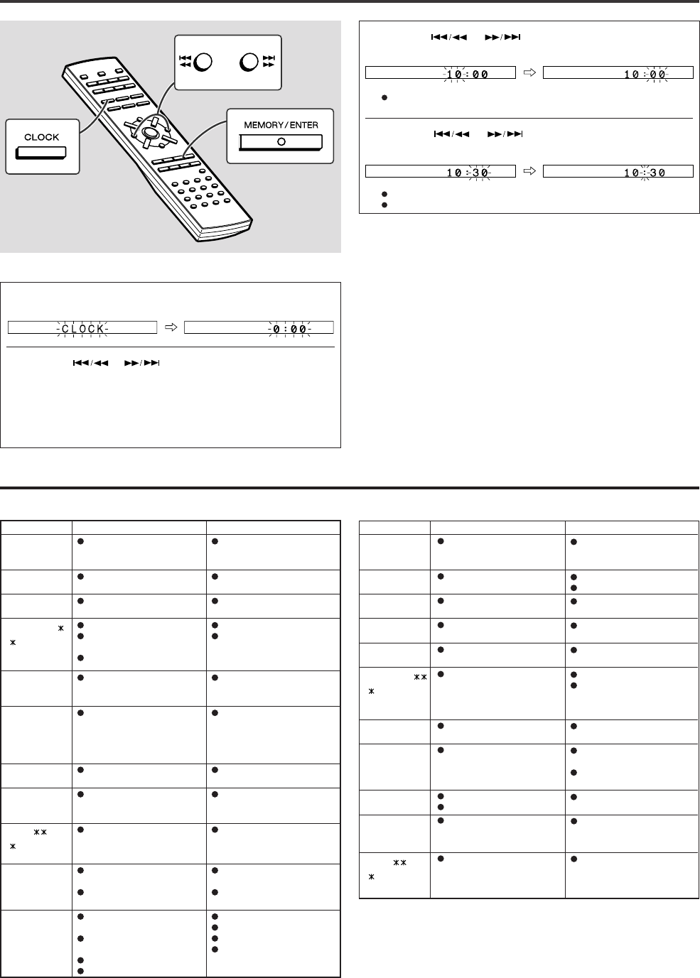
OPERATION MANUAL
This may be operated only with the remote control.
In this example, the clock is set for the 24-hour (0:00) display.
1
Press the CLOCK button and within 10 seconds, press the
MEMORY/ENTER button.
2
Press the or button to select 24-hour or 12-hour
display and then press the MEMORY/ENTER button.
“0:00” →The 24-hour display will appear.
(0:00 - 23:59)
“AM 0:00” →The 12-hour display will appear.
(AM 0:00 - PM 11:59)
“AM 12:00” →The 12-hour display will appear.
(AM 12:00 - PM 11:59)
3
Press the or button to adjust the hour and then
press the MEMORY/ENTER button.
When the 12-hour display is selected, “AM” will change automatically to
“PM”.
4
Press the or button to adjust the minutes and
then press the MEMORY/ENTER button.
The hour will not advance even if minutes advance from “59” to “00”.
The clock starts from “0” second. (Seconds are not displayed.)
To check the time:
Press the CLOCK button.
The time display will appear for about 10 seconds.
Note:
The “CLOCK” or time will flash at the push of the CLOCK button when the AC power
supply is restored after a power failure or unplugging the unit.
Readjust the clock by performing “Setting the Clock” from the beginning.
Setting the Clock
Error Messages
Error messages
BLANK MD
Can’t COPY
Can’t EDIT
Can’t READ
(:Number or
symbol)
Can’t REC
Can’t WRITE
DISC FULL
Er-CD 20
Er-MD
(:Number or
symbol)
EDIT OVER
MD NO DISC
CD NO DISC
Remedy
Replace it with another disc.
Replace the CD.
Change the stop position of the
track and then try editing it.
Replace it with another disc.
Erase the disc and try record-
ing again.
Re-record or replace the
MiniDisc.
Set this unit to the stand-by
mode and try to write the
TOC again. (Remove any
source of shock or vibration
whilst writing.)
Replace the disc with another
recordable disc.
Set this unit to the stand-by
mode and turn the power on
again.
Set this unit to the stand-by
mode and turn the power on
again.
Decrease the number of
tracks.
Replace it with a disc that has
enough time to record.
Load a MiniDisc.
Reload the MiniDisc.
Load a CD.
Reload the CD.
Meaning
Nothing is recorded.
(Neither music nor disc name
is recorded.)
You tried to record from a
copy prohibited CD.
A track cannot be edited.
The disc is damaged.
TOC information cannot be
read.
MiniDisc not specified.
Recording cannot be per-
formed correctly due to vibra-
tion or shock in the unit.
The TOC information could
not be created properly due
to a mechanical shock or to
scratches on the disc.
The disc is out of recording
space.
The CD cover is not working
properly.
A MiniDisc is not working
properly.
You chose 21 or more tracks
for track editing.
The remaining time available
for recording is short.
A MiniDisc has not been
loaded.
The MiniDisc data cannot be
read.
A CD has not been loaded.
The CD data cannot be read.
When an error message is displayed, proceed as follows:
Meaning
The number of characters for
the disc name or track name
exceeds 40.
The data recorded on this
disc is not audio data.
You tried to record on a play-
back-only disc.
The disc is write protected.
The temperature is too high.
TOC information recorded on
the MD does not match the
MiniDisc specifications or it
cannot be read.
There is no space left for re-
cording track numbers.
There is no space left for re-
cording character informa-
tion.
The data contains an error.
MiniDisc not specified.
MiniDisc is not working prop-
erly.
Tuner is not working properly.
Error messages
NAME FULL
NOT AUDIO
PLAYBACK MD
PROTECTED
TEMP OVER
TOC FORM
(:Number or
symbol)
TOC FULL
TOC FULL1
? MD DISC
POWER?
ER-TU
(:Number or
symbol)
Remedy
Shorten the disc or track
name.
Select another track.
Replace the disc.
Replace it with another re-
cordable disc.
Move the write protection tab
back to its original position.
Set this unit to the stand-by
mode and wait for a whilst.
Replace it with another disc.
Erase the disc and try record-
ing again.
Replace it with another re-
cordable disc.
Replace it with another re-
cordable disc.
Erase the needless charac-
ters.
Replace it with another disc.
Set this unit to the stand-by
mode and turn the power on
again.
Set the unit to the stand-by
mode and turn the power on
again.
MD-E9000W
– 8 –
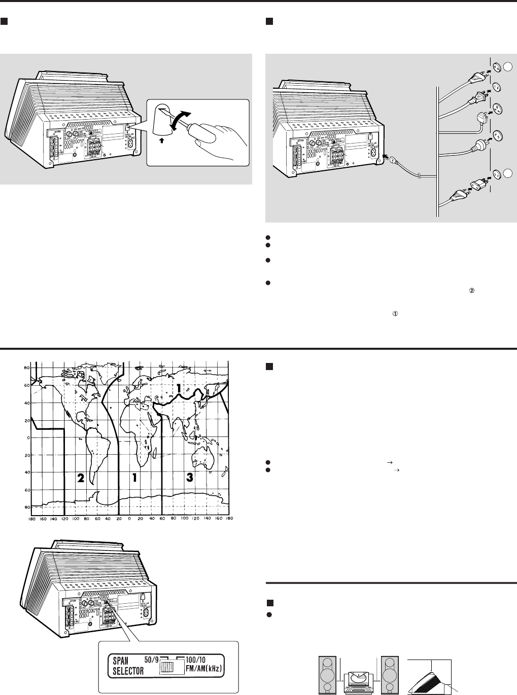
System Connections
System Connections
Setting the AC voltage selector
Check the setting of the AC voltage selector located on the rear panel before plug-
ging the unit into an AC socket. If necessary, adjust the selector to correspond to the
AC power voltage used in your area.
Connecting the AC power lead
After making all connections, plug the unit. If you plug the unit first, the unit will enter
the demonstration mode.
Notes:
Plug the AC power lead into an AC socket, after any connections.
Unplug the AC power lead from the AC socket if the unit is not to be used for a
prolonged period of time.
Never use a power lead other than the one supplied. Use of a power lead other
than the one supplied may cause an electric shock or fire.
AC Plug Adaptor
In areas (or countries) where an AC socket as shown in illustration is used, con-
nect the unit using the AC plug adaptor supplied with the unit, as illustrated. The AC
plug adaptor is not included in areas where the AC wall socket and AC power plug
can be directly connected (see illustration ).
Selector adjustment:
Turn the selector with a screwdriver until the appropriate voltage number appears in
the window (110/127/220/230 - 240V AC).
220 V
RATED LINE
VOLTAGE
1
2
Setting the FM/AM span selector
The International Telecommunication Union (ITU) has established that member coun-
tries should maintain either a 100 kHz or 50 kHz interval between broadcasting fre-
quencies of FM stations and 10 kHz or 9 kHz for AM station. The illustration shows
the 50/9 kHz zones (regions 1 and 3), and the 100/10 kHz zone (region 2).
Before using the unit, set the SPAN SELECTOR switch (on the rear panel) to the
interval (span) of your area.
To change the tuning zone:
1
Unplug the AC power lead from the AC socket.
2
Set the SPAN SELECTOR switch (on the rear panel) as follows.
For 50 kHz FM interval (9 kHz in AM) 50/9
For 100 kHz FM interval (10 kHz in AM) 100/10
3
Plug the AC power lead to the AC socket.
Caution:
This operation will erase all data stored in memory including clock, timer settings,
tuner preset, and CD or MiniDisc programme.
Precautions
Placing the system
Please ensure that the equipment is positioned in a well-ventilated area
and that there is at least 10 cm (4") of free space along the sides and
back.
There must also be a minimum of 20 cm (8") of free space on the top of
the unit.
10 cm (4”) 10 cm (4”) 20 cm (8”)
10 cm (4”)
– 9 –
MD-E9000W
Troubleshooting Chart
Many potential “problems” can be resolved by the owner without calling a service
technician. If something is wrong with this product, check the following before calling
your authorised SHARP dealer or service centre.
Tuner
Symptom
Radio makes unusual noise con-
secutively.
Remote control
Symptom
The remote control does not op-
erate.
Possible cause
Is the stereo system placed near the TV
or computer?
Is the AC power lead located near the
aerial?
Possible cause
Is the stereo system unplugged?
Is the battery polarity incorrect?
Are batteries dead?
Is the distance or angle incorrect?
Does the remote control sensor receive
strong light?
General
Symptom
The clock is not on time.
When a button is pressed, the unit
does not respond.
No sound is heard from the speak-
ers.
Possible cause
Did a power failure occur?
Reset the clock.
Set this unit to the power stand-by mode
and then turn it back on.
Does the unit still malfunction?
Reset it.
Is the volume level set to “0”?
Are the headphones connected?
Are the speaker wires disconnected?
CD player
Symptom
Playback does not start.
Playback stops in the middle or is
not performed properly.
Playback sounds are skipped, or
stopped in the middle of a track.
Possible cause
Is the disc loaded upside down?
Does the disc dissatisfy the standards?
Is the disc distorted or scratched?
Is the unit located near excessive vibra-
tion?
Is the disc very dirty?
Has condensation formed inside the unit?
MiniDisc
Symptom
A recording cannot be made.
Even though a disc has been
loaded, “CD/MD NO DISC” or
“Can’t READ” is displayed.
Playback sounds are skipped.
Possible cause
Is the MiniDisc protected against acci-
dental erasure?
Did you try to make recording on a play-
back-only MiniDisc?
Can you see the "DISC FULL" or "TOC
FULL" message in the display?
Is the unit located near excessive vibra-
tion?
Is the disc very dirty?
Has condensation formed inside the
unit?
Condensation
Sudden temperature changes, storage or operation in an extremely humid environ-
ment may cause condensation inside the cabinet (CD/MD pickup, etc.) or on the
transmitter on the remote control.
Condensation can cause the unit to malfunction.
If this happens, leave the power on with no disc in the unit until normal playback is
possible (about 1 hour). Wipe off any condensation on the transmitter with a soft
cloth before operating the unit.
Troubleshooting Chart
If trouble occurs
When this product is subjected to strong external interference (mechanical shock,
excessive static electricity, abnormal supply voltage due to lightning, etc.) or if it is
operated incorrectly, it may malfunction.
If such a problem occurs, do the following:
1. Set the unit to the stand-by mode and turn the power on again.
2. If the unit is not restored in step 1, unplug and plug in the unit, and then turn the
power on.
Note:
If neither operation above restores the unit, clear all the memory by resetting it.
Clearing all the memory (reset)
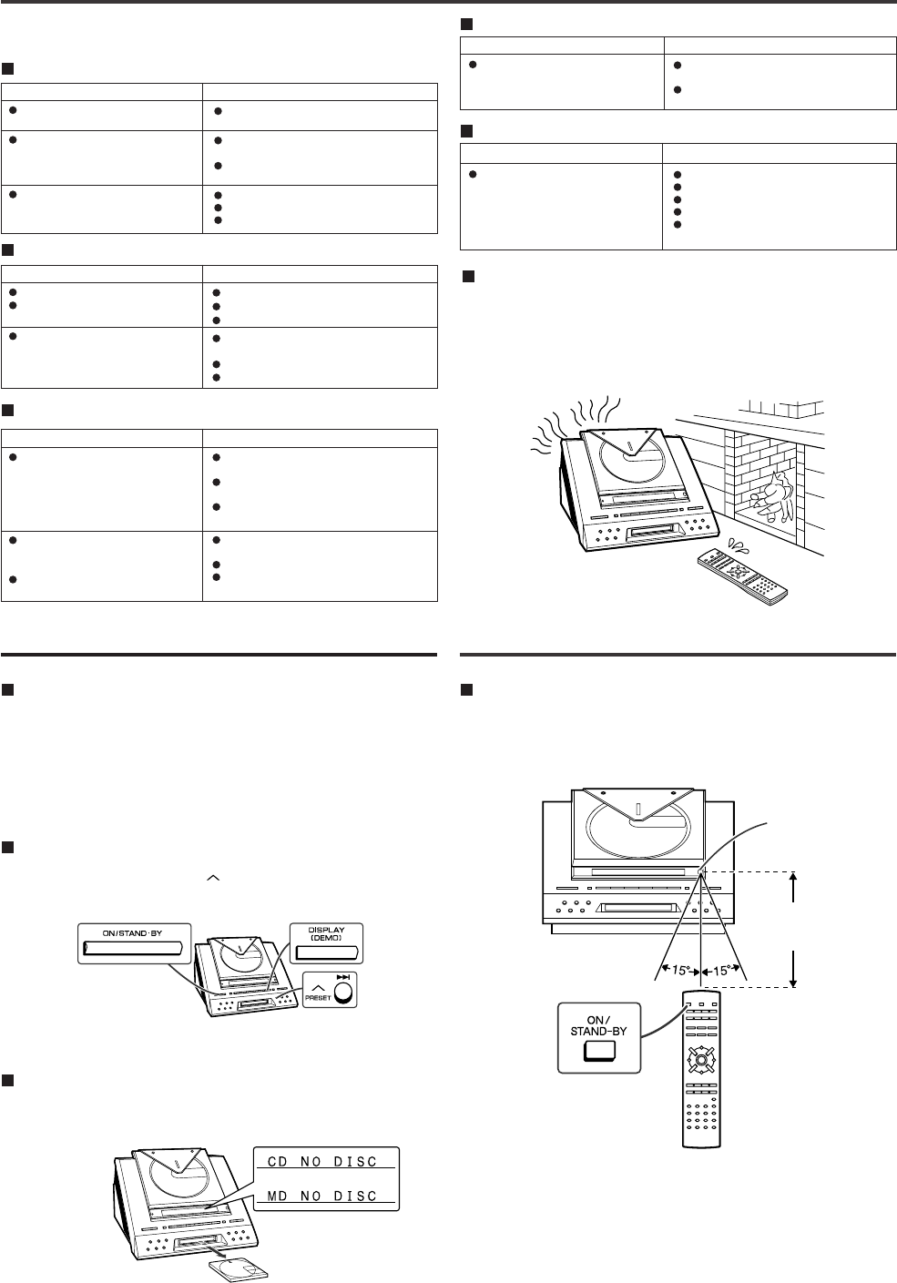
1. Press the ON/STAND-BY button to enter the power stand-by mode.
2. Whilst pressing down the PRESET button and the DISPLAY (DEMO) button,
press the ON/STAND-BY button.
After the “RESET” is displayed for about 1 second, the unit will enter the power
stand-by mode.
Caution:
This operation will erase all data stored in memory including clock, timer settings,
tuner preset, and CD or MiniDisc programme.
Before transporting the unit
Remove the CD and the MiniDisc from the unit. Your unit checks whether there is a
disc inside the unit when the compartment is closed. “NO DISC” appears if no disc is
left. Then, set the unit to the power stand-by mode. Carrying the unit with discs left
inside can damage it.
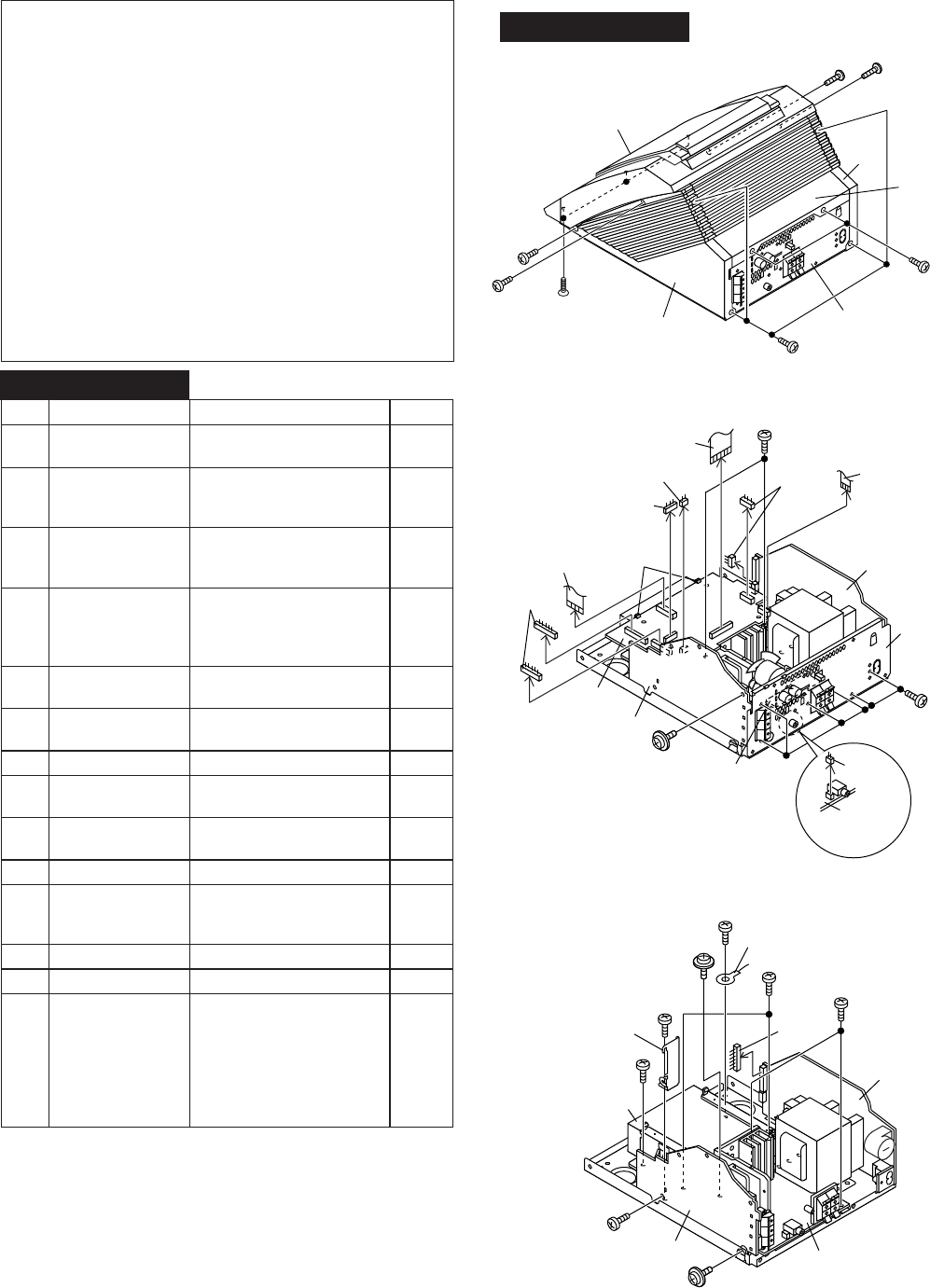
Test of the remote control
Face the remote control directly to the remote sensor on the unit.
The remote control can be used within the range shown below:
Press the ON/STAND-BY button. Does the power turn on? Now, you can enjoy the
music.
Remote Control
0.2 m - 6 m
(8" - 20')
Remote sensor
MD-E9000W
– 10 –
DISASSEMBLY
Figure 10-3
Figure 10-1
1 Side Panel 1. Screw................. (A1) x6 10-1
2. Screw................. (A2) x2
2 Top Cabinet with 1. Screw................. (B1) x6 10-1, 3
Rear Cabinet 2. Flat Cable .......... (B2) x2 10-2
3. Socket................ (B3) x2
3 Rear Panel/Aux 1. Screw................. (C1) x7 10-2
Input PWB with 2. Socket................ (C2) x2
Fan Motor
4 Main PWB 1. Screw................. (D1) x2 10-2
2. Flat Cable .......... (D2) x1
3. Socket................ (D3) x3
4. Hook .................. (D4) x2
5 Tuner PWB 1. Screw................. (E1) x3 10-3
2. Bracket .............. (E2) x1
6 Power Amp. PWB 1. Screw................. (F1) x3 10-3
2. Socket................ (F2) x1
7
MD Mechanism Unit
1. Screw................. (G1) x3 10-3
8 CD Servo PWB 1. Screw ................. (H1) x3 11-1
(Note) 2. Socket................ (H2) x4
9 Display PWB 1. Screw................ (J1) x10 11-1
2. Socket................. (J2) x1
10 Rear Cabinet 1. Screw................. (K1) x2 11-2
11 CD Lid Open/Close 1. Screw ................. (L1) x4 11-2
PWB with CD Lid 2. Cam Plate .......... (L2) x1
Gear Unit Ass'y 3.
CD Lid Lever B ....
(L3) x1
12 LED PWB 1. Screw................ (M1) x1 11-2
13 CD Mechanism 1. Screw ................. (N1) x4 11-2
14 MD Mechanism/ 1. Screw................. (P1) x4 11-3
MD Main PWB 2. MD Mechanism Holder
............................... (P2) x2
3. Screw................. (P3) x8
4. Flat Cable .......... (P4) x1
5. Socket................ (P5) x1
6. Flexible PWB ..... (P6) x1
STEP REMOVAL PROCEDURE FIGURE
MD-E9000W
Note:
After removing the connector for the optical pickup from the
connector, wrap the conductive aluminium foil around the
front end of connector remove to protect the optical pickup
from electrostatic damage.
Figure 10-2
MD-E9000W
Caution on Disassembly
Follow the below-mentioned notes when disassembling
the unit and reassembling it, to keep it safe and ensure
excellent performance:
1. Take compact disc and minidisc out of the unit.
2. Be sure to remove the power supply plug from the wall
outlet before starting to disassemble the unit.
3. Take off nylon bands or wire holders where they need to
be removed when disassembling the unit. After servicing
the unit, be sure to rearrange the leads where they were
before disassembling.
If the screw of the wrong length is applied on the MD
mechanism unit (screw for mounting parts to the MD
mechanism chassis), it may contact the optical pickup
and cause the unit to malfunction.
4. Take sufficient care on static electricity of integrated
circuits and other circuits when servicing. Side Panel
(Right)
Top Cabinet
Rear
Panel
Rear
Cabinet
Side
Panel
(Left)
(A1)x1
ø3x10mm
(A2)x1
ø2.6x8mm
(A1)x1
ø3x10mm (A2)x1
ø2.6x8mm
(B1)x2
ø3x10mm
(A1)x4
ø3x10mm
(B1)x3
ø2.6x8mm
(D1)x2
ø3x10mm
(B3)x2 (B2)x1
Power
PWB
Rear
Panel
(C1)x6
ø3x10mm
(C2)x1
Power
Amp.
PWB
Aux Input
PWB
(C1)x1
ø3x10mm
Tuner
PWB
Main
PWB
(D2)x1
(C2)x1
(D3)x1
(B2)x1 (D4)x2
(D3)x2
MD Mechanism
Unit
Power
PWB
Power Amp.
PWB
Tuner PWB
(G1)x1
ø3x8mm
(E1)x1
ø3x8mm
(E1)x1
ø3x8mm
(F1)x2
ø3x8mm
(F1)x1
ø3x10mm
(E1)x1
ø3x10mm
(G1)x2
ø3x8mm
(B1)x1
ø3x8mm
(E2)x1 (F2)x1
Lug Wire
– 11 –
MD-E9000W
Figure 11-1
(H1)x1
ø2.6x10mm
(J1)x10
ø2.6x10mm
(J2)x1
(H2)x2
(H2)x1
(H2)x1
Rear
Cabinet
Top
Cabinet
CD Servo
PWB
Display
PWB
CD Lid
Open/Close
PWB
(H1)x2
ø2.6x10mm
(L1)x2
ø2.6x10mm
(L1)x2
ø2.6x10mm
(K1)x2
ø2.6x10mm
(N1)x4
ø2.6x10mm
(L2)x1 (L3)x1
Rear
Cabinet
CD Mechanism
Top
Cabinet
(M1)x1
ø2.6x8mm
LED PWB
CD Lid Gear
Unit Ass'y
CD Lid
Open/Close PWB
Figure 11-2
Figure 11-3
(P4)x1
(P5)x1
(P3)x1
ø2x2mm
(P3)x1
ø2x3mm
(P3)x1
ø2x3mm
(P3)x1
ø2x3mm
(P3)x1
ø2x3mm
(P3)x1
ø2x3mm
(P3)x2
ø1.7x3mm
(P1)x2
ø3x6mm
(P1)x2
ø3x6mm
Shield Cover,Top
MD Mechanism
Shield Cover,Side
Shield Cover,Bottom
MD Main PWB
(Note 1)
After removing the flexible PWB for optical pickup from the connector
wrap the front end of flexible PWB in conductive aluminum foil so as
to protect the optical pickup from being damaged electrostatically.
(P2)x1
(P2)x1
(P6)x1
Optical pickup
Flexible PWB (Note 1)
Pull
Pull
MD-E9000W
– 12 –
1 Front Panel 1. Screw................. (A1) x8 12-1
2. Tip ...................... (A2) x4
2 Woofer 1. Screw................. (B1) x4 12-2
3 Tweeter 1. Screw................. (C1) x2 12-2
STEP REMOVAL PROCEDURE FIGURE
CP-E9000H
Figure 12-1
(A1)x4
ø4x20mm
(A1)x4
ø4x20mm
Front Panel
(B1)x4
ø4x12mm
(C1)x2
ø3x10mm
Front Panel
(A2)x2
(A2)x2
Woofer
Tweeter
Figure 12-2
– 13 –
MD-E9000W
REMOVING AND REINSTALLING THE MAIN PARTS
MD MECHANISM SECTION
Perform steps 1 to 4, 7 and 14 of the disassembly method to
remove the MD mechanism. (See pages 10 and 11.)
Caution:
After pulling out the optical pickup connector, wrap the end of
the connector in conductive aluminium foil to prevent the
optical pickup from being destroyed by static electricity.
Figure 13-1
Figure 13-2
Figure 13-4 Figure 13-3
MD Mechanism
(A1)x1
ø1.7x5mm
Magnetic Head
Optical Pickup
(B3)x2
ø1.7x3mm
(B1)x1
ø1.7x6mm
MD Loading Motor
MD Loading
Motor PWB
(B2)x2
(B2)x1
(C1)x2
ø1.4x4.5mm
(C1)x1
ø1.4x5mm
Optical
Pickup
MD Sled Motor
MD Mechanism
Switch PWB
Washer
(D1)x3
ø1.4x3mm
MD Spindle Motor
How to remove the magnetic head
(See Fig. 13-1)
1. Remove the screw (A1) x 1 pc.
Caution:
Take utmost care so that the magnetic head is not damaged
when it is mounted.
How to remove the MD loading motor PWB/MD
loading motor (See Fig. 13-2)
1. Remove the screw (B1) x 1 pc.
2. Remove the Hooks (B2) x 3 pcs., and remove the MD
loading PWB.
3. Remove the screws (B3) x 2 pcs., and remove the MD
loading motor.
How to remove the MD sled motor/optical pickup
(See Fig. 13-3)
1. Remove the screws (C1) x 3 pcs., and remove the MD sled
motor.
2. Remove the optical pickup.
Caution:
Be careful so that the gear is not damaged.
(The damaged gear emits noise during searching.)
How to remove the MD spindle motor
(See Fig. 13-4)
1. Remove the screws (D1) x 3 pcs., and remove the MD
spindle motor.
Caution:
Be careful so that the gear is not damaged.
(The damaged gear emits noise during searching.)
MD-E9000W
– 14 –
CD MECHANISM SECTION
Perform steps 1, 2, 8 and 13 of the disassembly method to
remove the CD mechanism. (See pages 10 and 11.)
Note:
After removing the connector for the optical pickup from the
connector, wrap the conductive aluminium foil around the
front end of connector remove to protect the optical pickup
from electrostatic damage.
How to Remove the CD lid motor
(See Fig. 14-2.)
1. Remove the top cabinet, CD lid open/close PWB and rear
cabinet.
(Refer to the disassembly method on pages 10 and 11.)
2. Remove the screws (B1) x 2 pcs.
3. Remove the CD lid motor.
How to remove the pickup (See Fig. 14-1)
1. Remove the CD mechanism cover, paying attention to the
pawls (A1) x 4 pcs.
2. Remove the screws (A2) x 2 pcs., to remove the shaft (A3)
x 1 pc.
3. Remove the stop washer (A4) x 1 pc., to remove the gear
(A5) x 1 pc.
4. Remove the pickup.
Caution:
Be careful not to damage the gear.
(If the gear is damaged, noise is heard when searching.)
(A2)x2
ø2.6x6mm
(A1)x4
Shaft
(A3)x1
Gear
(A5)x1
Stop Washer
(A4)x1
CD Mechanism Cover
CD Mechanism
Pickup
Figure 14-1
(B1)x2
ø2x4mm
CD Lid Gear
Unit Ass'y
CD Lid Motor
Figure 14-2

– 15 –
MD-E9000W
TEST MODE
From power off state to TEST mode
During power off, hold down CD OPEN/CLOSE button and PRESET UP button and then press ON/STAND-BY button.
It will show micom version display. "Y2K1 X.XX"
Press direct button to enter the test mode.
TEST MODE DIRECT KEY
CD CD PLAY
MD DISPLAY MD STOP
KEY X-BASS
TUNER TUNER
Cancelling the TEST mode
To cancel, press ON/STAND-BY button and it will display. "COMPLETE"
MD TEST mode
During power off, hold down EQUALIZER button and PRESET UP button and then press ON/STAND-BY button.
TEST MODE
1. CD test
Outline: It is impossible to read setting value after automatic adjustment (Use for judgement a difference between initial value)
Pickup forcement operation
Move to inner, move to outer, LD ON/OFF
TEST mode entering method
Press CD PLAY button from TEST mode menu.
After enter to CD TEST mode
1) Direct power on at CD function
2) DSP initialize process
3) Transmit command correspond to button input
Validation Button: CD PLAY, CD STOP, SKIP UP, SKIP DOWN, ON/STAND-BY, DISPLAY, VOLUME UP, VOLUME
DOWN
1. CD PLAY : STEP of CD operation
STEP1: CD PLAY button from STOP condition , LD ON
STEP2: CD PLAY button from STEP1, FOCUS ON
STEP3: CD PLAY button from STEP2, CLV SERVO ON
STEP4: CD PLAY button from STEP3, TRACKING SERVO ON
STEP5: CD PLAY button from STEP4, SUB-CODE READING and DISPLAY
* Direct to STEP5 if press CD PLAY button more than 1 sec
2. CD STOP : STOP from PLAY operation (STOP from each STEP)
Return to NORMAL DISPLAY (PARAMETER DISPLAY)
3. SKIP UP : Force pickup to forward direction
4. SKIP DOWN : Force pickup to reverse direction
Slide STOP after PICKUP IN switch ON
5. MD STOP : Access automatic adjustment (Present PICKUP point)
6. ON/STAND-BY : TEST mode cancel
7. DISPLAY : Read parameter register when CD STOP
8. VOLUME UP/DOWN : Normal volume control
Adjustment value reading
Read the following item every DISPLAY button input during stop.
Return to normal display if press CD STOP button.
Item Display RAM Address
Focus gain _ _ F G : × × 0×5C h
Focus offset F O F F : × × 0×9F h
Tracking balance T B A L : × × 0×4D h
Tracking gain _ _ T G : × × 0×5D h
Tracking offset T O F F : × × 0×AF h
RF Levelshift R F L S : × × 31××
Monitor setting value (××) when transmit command 31××

MD-E9000W
– 16 –
CD PLAY B2 Servo adjustment mode
NORMAL EDIT B4 Recording mode
HIGH EDIT F2 Other mode
MD REC A8 Menu change at each mode
MD PLAY A2 Menu access
MD STOP A7 Menu stop
SKIP UP AA Slide to outer
SKIP DOWN AC Slide to inner
VOLUME UP F3 Adjustment value +1
VOLUME DOWN F4 Adjustment value -1
CD STOP F5 Display change
ON/STAND-BY 1F+D1 MD test mode
LOAD-SW ON B5 Access loading operation
MD EJECT B3 Eject operation
3. MD test mode
a. Communication start after proceed MD reset process
b. Power ON at MD function
c. Transmit command correspond to each button during button input (min 5 transmission)
Display: Display all 10 characters which transmitting from text area by MD command
d. Eject and loading is same as normal operation
e. Change to MD non adjustment mode by ON/STAND-BY button
f. MD no adjustment mode is like procedure below
1) Transmit power off command (1F) to MD
2) Wait until function bit: 00 (POWER OFF) confirmation
3) MD micom reset
4) Transmit non automatic adjustment test mode command (D1) until change to MD mode (E0) after communication start
5) Display 1, 3, 5, 7 segment according to music calender data when MD mode E0
6) Normal operation for next step
Reference
To cancel non automatic adjustment mode, need to do either reset or power failure MD micom will start normal mode operation
if not receive non adjustment mode command when recover from power failure.
Button Name Function
Button and command when MD TEST mode
Command
High (double) speed mode
It is possible to change between high speed/normal speed by pressing HIGH EDIT/NORMAL EDIT button during stop.
"HIGH" mark will light up when high speed mode.
Actual operation is just only sending 1 time/2 time speed operation command other is same with normal speed.
When change from high speed to normal speed, it will set normal speed parameter and RF amp.
– 17 –
MD-E9000W
KEY Segment
5. KEY test (Function: Key and last display)
Function: Key and last display
Power off after lighting up the odd number grids, even numbered grids and lighting up FL pipe segment which corresponded
to KEY until TEST MODE is cancelled.
TEST MODE
LIGHT UP ODD
NUMBERED GRID
1.0 sec TIMER
(WAIT)
1.0 sec TIMER
(WAIT)
LIGHT OFF
KEY INPUT
LIGHT UP EVEN
NUMBERED GRID
KEY INPUT =
"POWER"?
It does the display which was
allocated for the key while each
KEY INPUT was pressed.
NO
YES
POWER OFF.
TEST CANCEL.
Notice: 1. REMOCON input during test mode is invalid.
2. Volume "0"
Segment light up when pressed correspond key
MD EJECT ALL LIGHT UP AUX OVER
SP TUNER ST &
LP2 LP2 CD EJECT TOC
LP4 LP4 VOLUME UP RDS
NORMAL EDIT GROUP VOLUME DOWN PTY
HIGH EDIT HIGH CD STOP TP &
MD REC REC CD PLAY TA
MEMORY MEMORY MD STOP DISC
DISPLAY RANDOM MD PLAY TRACK &
X-BASS BASS SKIP UP EON &
EQUALIZER T-EDIT SKIP DOWN TI & SLEEP
KEY Segment
MD-E9000W
– 18 –
9. TUNER MEMORY CLEAR (Write in operation manual)
Work : Clear all TUNER PRESET MEMORY
Input : During POWER ON at TUNER function, press CLEAR/DELETE button more than 3 sec.
10. SOFTWARE RESET (Open to the user by manual explanation)
Function: — Software RESET.
— All the function condition will be initialize.
— After display "RESET", power will off.
Input: During POWER OFF, press DISPLAY + SKIP UP + ON/STAND-BY button
Operation: 1. If start from ECO, ON the AC RELAY (micom high speed)
2. Clear All RAM except HCMS RAM
3. INITALIZE all function condition
4. "RESET" display for 2 sec
5. Change to POWER OFF (DEMO MODE — default)
PRESET CLR?
COMPLETE
10 sec
1.5 sec
Press MEMORY/ENTER button to confirm the request.
finish.
"RESET" display
R E S E T
8. TUNER test
Set TUNER PRESET MEMORY according to below condition for each destination.
Condition
Function : TUNER
Band : FM MONO
Frequency : LOW FREQUENCY
Volume : LAST MEMORY
Preset G-EQ : LAST
PRESET LIST
1 FM 87.5 MHz FM 87.50 MHz
2 FM 108.0 MHz FM 108.00 MHz
3 FM 90.0 MHz FM 90.00 MHz
4 FM 106.0 MHz FM 106.00 MHz
5 FM 98.0 MHz FM 98.00 MHz
6 AM 530 kHz AM 531 kHz
7 AM 1620 kHz AM 1602 kHz
8 AM 600 kHz AM 603 kHz
9 AM 1400 kHz AM 1404 kHz
10 AM 990 kHz AM 990 kHz
SPN P: L SPN P: H
– 19 –
MD-E9000W
• FM RF
Signal generator: 1 kHz, 40 kHz dev., FM modulated
ADJUSTMENT
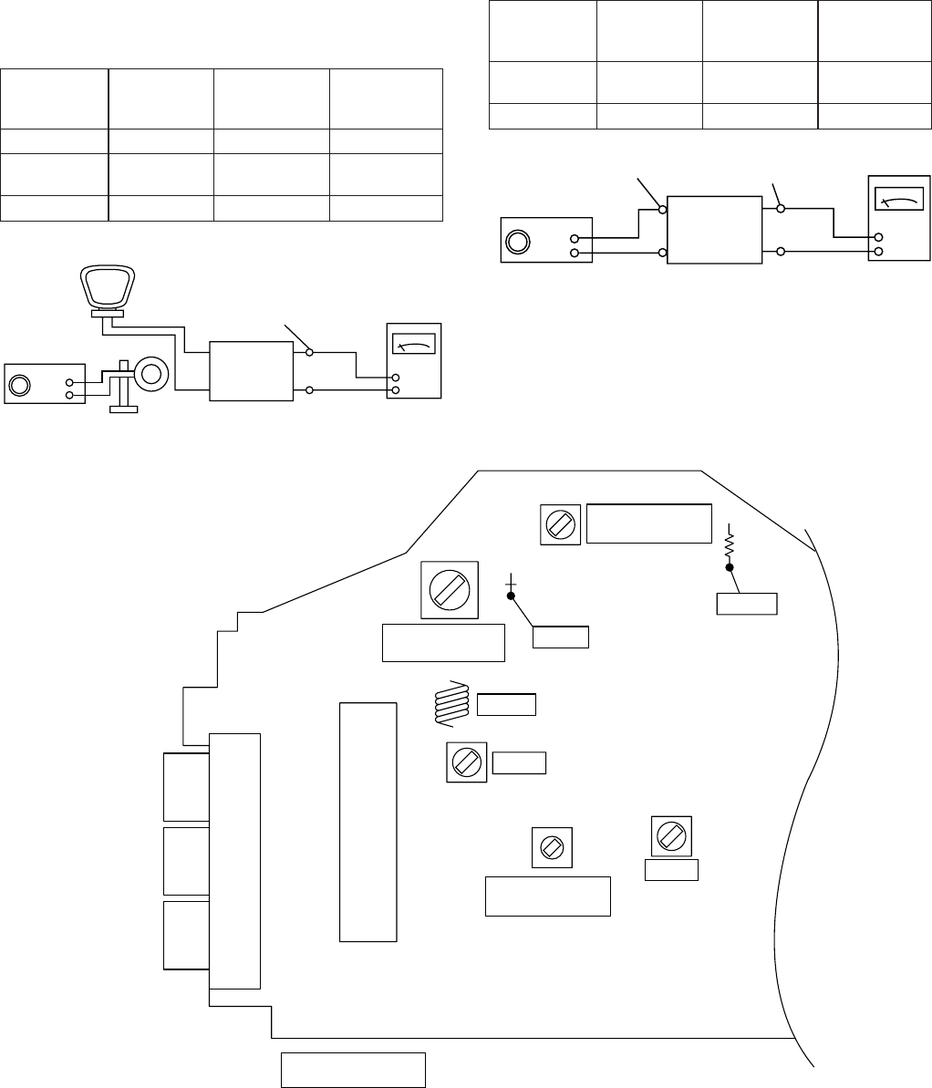
Figure 19-3 ADJUSTMENT POINTS
Test Stage Frequency Frequency
Display Setting/
Adjusting
Parts
• AM IF/RF
Signal generator: 400 Hz, 30 %, AM modulated
TUNER SECTION
fL: Low-range frequency
fH: High-range frequency
AM IF 450 kHz 1,602 kHz T351
AM Band — 531 kHz (fL): T306
Coverage 1.1 ± 0.1 V
AM Tracking 990 kHz 990 kHz (fL): T303
SO301
ANTENNA
TERMINAL
IC301
T303
L312
T302
T301 T351
TP301
TP302
T306
R336
TUNER PWB
FM IF
AM BAND
COVERAGE fL
FM BAND
COVERAGE fL
R357
AM IF
FM RF
AM TRACKING
fL
GND
AM Loop Antenna
AM Signal Oscillator
IF: Speaker Terminal
Frequency Cover: TP301 Electric
Voltmeter
UNIT
Figure 19-1 AM IF/FREQUENCY COVER
Test Stage Frequency Frequency
Display Setting/
Adjusting
Parts
FM Band — 87.50 MHz (fL): T301
Coverage 1.3 ± 0.8 V
FM RF 98.00 MHz 98.00 MHz L312
GND
SO301 Speaker Terminal
Frequency Cover: TP301
UNIT
Electric
Voltmeter
FM Signal Oscillator
Figure 19-2 FM FREQUENCY COVER
MD-E9000W
– 20 –
MD SECTION
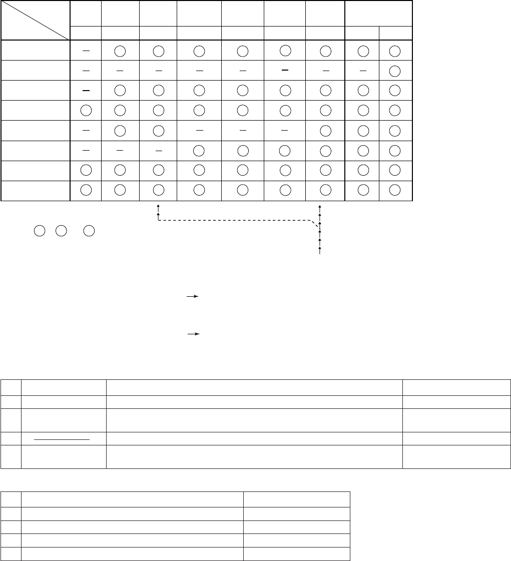
Enter the test mode, adjust or set as shown in the following table according to the repair operations.
1. Preparation for adjustment
Test disc
Type Test disc Part No.
1 High reflection disc TGYS1 (SONY) [for Playback] RRCDT0101AFZZ
2 Low reflection disc MiniDisc for checking the recording operation ––––––––––––
(commercially available MD)
3 Head Adjusting transparent RRCDT0103AFZZ
4 Low reflection disc Pre-adjustment disc [TEAC Test MD] 88GMMD-213AS or
88GMMD-318
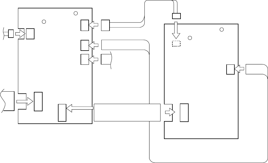
Extension Cable (See Fig. 28)
Type Part No.
1 Extension PWB for servicing RUNTK0581AFZZ
2 Extension Connector (2 Pin) QCNWK0059AFZZ
3 Extension Flat Cable (9 Pin) QCNWK0132AFZZ
4 Extension Flat Cable (28 Pin) QCNWK0108AFZZ
PICK replacement
HEAD replacement
MECHANISM
replacement
MAIN PWB
assembly replacement
MD microcomputer
replacement
MD LSI replacement
RF IC replacement
EEPROM IC
replacement
TEMP
basic
setting
TEMP
Execution item
required
Repair
operations
number to and
" – " is an item that you don't have to execute.
The EEPROM writing result is shown at the end of the test mode
Although "SET" was written normally, it was not written in the "YOBI COMPLETE" state.
Peform "AUTO-YOBI" adjustment. After making a normal adjustment,
write the preliminary adjustment into the EEPROM.
OK_EEPROM: "SET" and "YOBI COMPLETE" were written normally
WR_EEPROM:
NG_EEPROM: "SET" could not be written.
indicate the order of inplementation.
Checking
EEPROM
setting
EEPROM_SET
AUTO-YOBI
adjustment
AUTO-
adjustment
AUTO-AFB
adjustment
AUTO_YOBI AUTO_ADJ AUTO_AFB
TEST-CANCEL
Writing the
EEPROM
setting
TEST-CANCEL
Writing the
EEPROM
setting
TEST-PLAY
Operation check
TEST-REC
Check the connection between the MD microcomputer and the EEPROM.
1
1
1
1
1
1
1
2
2
2
1
2
2
2
3
3
3
2
3
3
4
4
4
3
4
4
5
5
5
4
5
5
6
6
6
5
2
6
6
7
7
7
89
6
4
8
1
8
9
9
9
3
7
7
8
8
8
– 21 –
MD-E9000W
1. EJECT mode • TEMP setting (of EEPROM setting)
• CONTROL setting (of EEPROM setting)
• Setting of laser power (record/playback power)
2. AUTO pre-adjustment mode • Automatic pre-adjustment is performed.
3. AUTO adjustment mode • Automatic adjustment is performed. (After adjustment the grating adjustment mode is set.)
4. AUTO AFB adjustment mode • Focus adjustment is performed.
• RESULT sub-mode • Therefore do not set this mode since it is not necessary for the service.
• RESULT mode (final adjustment)
• MANUAL pre-adjustment mode
• MANUAL adjustment mode
• MANUAL AFB adjustment mode
• ERROR DATA
5. EEPROM setting mode • Various coefficients of digital servo are changed manually.
6. TEST-PLAY mode • Continuous playback from the specified address is performed.
• C1 error rate measurement, ADIP error rate measurement.
7. TEST-REC mode • Continuous recording from the specified address is performed.
8. INNER mode • The position where the INNER switch is turned on is measured.
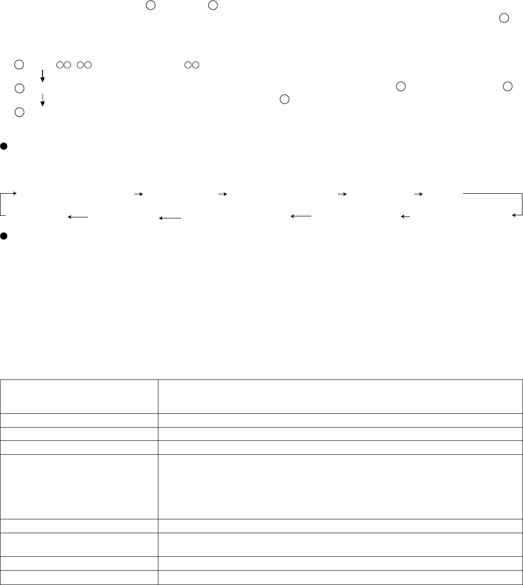
2. Test Mode
Test mode setting method
1. While pressing the EQUALIZER button and PRESET UP button at the same time, and press the ON/STAND-BY button.
(The unit changes over from the A state to the B state.)
2. Insert the playback-only disc 1 (high reflection disc) or the recordable disc 2 (low reflection disc). (State is changed to C .)
Above procedures will set the unit to the test mode.
A tsm 22 e: TEST MODE represents version of MD microcomputer.
STOP state
B EJECT
C AUT AJST
Entering the specific mode
Whenever the CD PLAY/PAUSE button is pressed, the mode is changed.
If the REC button is pressed instead, the mode will change in the opposite order.
Cancel of test mode
The data is written on EEPROM by pressing the POWER button. Then, if the power is turned off once, the unit returns to the
normal state.
* Before pressing the POWER button, be sure to perform the AUTO preliminary adjustment, AUTO adjustment and AUTO AFB
adjustment, and confirm that they are completed.
* After the value of EEPROM is changed or the AUTO pre-adjustment, AUTO adjustment, and AUTO AFB adjustment are
performed again, write on EEPROM by pressing the POWER button. (When the POWER button is pressed, data is written
on EEPROM.)
* When the value of EEPROM has been changed, write the data on EEPROM once. To perform adjustment using the data, set
the unit to the TEST mode again, perform AUTO pre-adjustment, AUTO adjustment, and AUTO AFB adjustment, and then
write the data again on EEPROM.
• Test Mode
(When the MD STOP button is pressed in the C state, the indication A is
restored. To restore C again, press the CD PLAY/PAUSE button.)
AUTO YOBI AUTO AJST RST YOBI
AUT AFB
EEPROM_SET MNU AFB MNU YOBI
MNU AJST
ERR DATA
(ERRER DATA)
(AUTO prelimirary adjustment) (AUTO adjustment) (Advanced AFB adjustment) (RESULT
YOBI)
RESULT
(MANUAL pre-adjustment)
(MANUAL adjustment)
(MANUAL AFB adjustment)
(EEPROM setting)
MD-E9000W
– 22 –
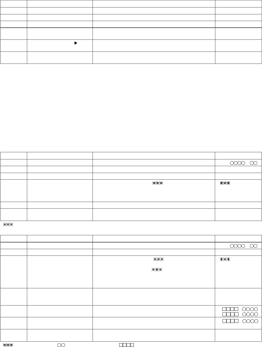
1. EJECT mode
Step 1 Test mode EJECT state [ _ _ E J E C T _ _ _ ]
Step 2 Press the CD STOP button. Playback power output state [ p p w _ _ _ _ _ _ _ ]
Step 3 Press the CD STOP button. Rec power output state [ r p w _ _ _ _ _ _ _ ]
Step 4 Press the CD STOP button. Therefore do not set this mode since it is not necessary [ x p w _ _ _ _ _ _ _ ]
for the service.
Step 5 Press the NORMAL CD MD TEMP setting of EEPROM setting
EDIT button. (The TEMP setting reference of the EEPROM.)
Step 6 Press the DISPLAY (DEMO) CONTROL setting of EEPROM setting
button. (The CONTROL setting reference of the EEPROM.)
Step No. Setting Method Remarks Display
* Normally, the voltage at pin 3 of IC1401 becomes as follows:
Playback power output (ppw): Approx. DC 0.2 V
Recording power output (rpw): Approx. DC 1.8 V
Confirmation of pickup laser power
It is possible to confirm in the record/playback mode with the aid of laser power meter. However, since the laser power meter
measurement is characterized with dispersion, obtained data are used only for confirmation.
Reference data (at room temperature 25 °C)
Playback (ppw): 0.72 ± 0.1 mW
Record (rpw): 5.5 ± 0.5 mW
Note:
Never see directly the laser light. Otherwise your eyes are injured.
2. AUTO pre-adjustment mode (Low reflection disc only)
With the pre-adjustment disc (MMD213AS or MMD-318)
Step No. Setting Method Display
Step 1 Test mode STOP state [ t s m e ]
Step 2 Press once the CD PLAY button. AUTO adjustment menu [ A U T O _ A J S T _ ]
Step 3 Press the MD REC button. AUTO pre-adjustment menu [ _ A U T _ Y O B I _ ]
Step 4 Press once the MD PLAY button. • During automatic adjustment changes as follows. [ : _ _ _ _ _ _ ]
HAo→ • • • • • • • • • →TCO
End of adjustment If adjustment is OK, Step 5.
If adjustment is NG, Step 6.
Step 5 Press the MD STOP button. STEP 2 [ _ C O M P L E T E _ ]
Step 6 Adjustment value output [ C a n ' t _ A D J . ]
Press the MD STOP button. STEP 2 AUTO adjustment menu
• : Adjustment name
Remarks
3. AUTO adjustment mode
Step No. Setting Method Remarks Display
Step 1 Test mode STOP state [ t s m e ]
Step 2 Press once the CD PLAY button. AUTO adjustment menu [ A U T O _ A J S T _ ]
Step 3 Press once the MD PLAY button. • In case of high reflection disc changes as follows. [ : _ _ _ _ _ _ ]
PEG→HAG
• In case of low reflection disc changes as follows.
PEG→LAG
End of adjustment If adjustment is OK, Step 4.
If adjustment is NG, Step 7.
Step 4 For grating adjustment [ _ C O M P L E T E _ ]
Press the MD PLAY button. STEP 5 * Note 1
Press the
MD STOP
button. STEP 2
Step 5 Continuous playback (pit section) Confirmation of C1 error
[ s c ]
Continuous playback (groove section)
[ a c ]
Step 6 Press the CD STOP button. Conformation of ADIP error (Low reflection only)
[ a a ]
Press the
MD STOP
button. STEP 2 AUTO adjustment menu
Step 7 Adjustment value output [ C a n ' t _ A D J . ]
Press the
MD STOP
button. STEP 2 AUTO adjustment menu
• : Adjustment name, : Measurement value, : Address
* Note 1:
Depending on the disc, "#COMPLETE_" may be displayed, which means that the ON position of the INNER switch cannot be
identified clearly. In this case, check the switch in the INNER mode using the specified disc. However, this is not a problem in AUTO
adjustment.
– 23 –
MD-E9000W
Step 1 Test mode STOP state [ t s m e ]
Step 2 Press the CD PLAY button eight times. [ E E P R O M_ S E T ]
Step 3 Press the MD PLAY button. [ _ _ F o c u s _ _ _ ]
Step 4 Press the MD PLAY button. [F G _ _ _ _ _ _ ]
Step 5 Press the CD PLAY button. [F G 2 _ _ _ _ _ ]
Step 6 Press the CD PLAY button. [F F 0 _ _ _ _ _ ]
Step 7 Press the CD PLAY button. [F F 1 _ _ _ _ _ ]
Step 8 Press the CD PLAY button. [F F 2 _ _ _ _ _ ]
Step 9 Press the CD PLAY button. [F Z H L E V _ _ ]
Step 10 Press the CD PLAY button. [F O K L E V h _ ]
Step 11 Press the CD PLAY button. [F O K L E V L _ ]
Step 12 Press the CD PLAY button. [F O S T n _ _ _ ]
Step 13 Press the CD PLAY button. [D S C J G _ _ _ ]
4. AUTO AFB adjustment mode
Step No. Setting Method Remarks Display
Step 1 Test mode STOP state [ t s m e ]
Step 2
Press the CD PLAY button two times.
AUTO AFB adjustment menu [ _ A U T _ A F B _ _ ]
Step 3 Press once the MD PLAY button. [A F B _ ]
Step 4 Adjustment value output [ _ ]
Press the
MD STOP
button. STEP 2 AUTO AFB adjustment
• , : Measurement value
Step No. Setting Method Display
• : Setting value
5. EEPROM setting mode
a) Focus setting
b) Spin setting
Step No. Setting Method Display
Step 1 Test mode STOP state [ t s m e ]
Step 2 Press the CD PLAY button eight times. [ E E P R O M_ S E T ]
Step 3 Press the MD PLAY button. [ _ _ F o c u s _ _ _ ]
Step 4 Press the CD PLAY button. [ _ S p i n d l e _ _ ]
Step 5 Press the MD PLAY button. [S P G _ _ _ _ _ ]
Step 6 Press the CD PLAY button. [S P G _ i n _ _ ]
Step 7 Press the CD PLAY button. [S P G _ m i d _ ]
Step 8 Press the CD PLAY button. [S P G _ o u t _ ]
Step 9 Press the CD PLAY button. [S P G M _ _ _ _ ]
Step 10 Press the CD PLAY button. [S P 1 _ _ _ _ _ ]
Step 11 Press the CD PLAY button. [S P 2 _ _ _ _ _ ]
Step 12 Press the CD PLAY button. [S P 2 2 _ _ _ _ ]
Step 13 Press the CD PLAY button. [S P 3 _ _ _ _ _ ]
Step 14 Press the CD PLAY button. [S P 4 _ _ _ _ _ ]
Step 15 Press the CD PLAY button. [S P 5 _ _ _ _ _ ]
Step 16 Press the CD PLAY button. [S P 5 2 _ _ _ _ ]
Step 17 Press the CD PLAY button. [S P D L I M _ _ ]
Step 18 Press the CD PLAY button. [S P K L E V m _ ]
• : Setting value
MD-E9000W
– 24 –
Step No. Setting Method Display
c) Tracking setting
Step 1 Test mode STOP state [ t s m e ]
Step 2 Press the CD PLAY button eight times. [ E E P R O M_ S E T ]
Step 3 Press the MD PLAY button. [ _ _ F o c u s _ _ _ ]
Step 4 Press the CD PLAY button two times. [ _ T r a c k i n g _ ]
Step 5 Press the MD PLAY button. [T G _ _ _ _ _ _ ]
Step 6 Press the CD PLAY button. [T G 2 _ _ _ _ _ ]
Step 7 Press the CD PLAY button. [T F 0 _ _ _ _ _ ]
Step 8 Press the CD PLAY button. [T F 1 _ _ _ _ _ ]
Step 9 Press the CD PLAY button. [T F 2 _ _ _ _ _ ]
Step 10 Press the CD PLAY button. [F T 3 _ _ _ _ _ ]
Step 11 Press the CD PLAY button
.
[S V C N T 4 _ _ ]
Step 12 Press the CD PLAY button. [T R B L V o _ _ ]
Step 13 Press the CD PLAY button [T R B L V t _ _ ]
Step 14 Press the CD PLAY button [T R K L V o _ _ ]
Step 15 Press the CD PLAY button [T R K L V t _ _ ]
Step 16 Press the CD PLAY button [T D P W o _ _ _ ]
Step 17 Press the CD PLAY button [T D P W t _ _ _ ]
Step 18 Press the CD PLAY button [S L C T o _ _ _ ]
Step 19 Press the CD PLAY button [S L C T t _ _ _ ]
Step 20 Press the CD PLAY button. [S L C T m _ _ _ ]
Step 21 Press the CD PLAY button. [T C R S C 1 P _ ]
Step 22 Press the CD PLAY button. [T C R S C 0 h _ ]
Step 23 Press the CD PLAY button. [T C R S C 0 L _ ]
Step 24 Press the CD PLAY button. [T C R S C H h _ ]
Step 25 Press the CD PLAY button. [T C R S C H L _ ]
Step 26 Press the CD PLAY button. [C O T L V p _ _ ]
Step 27 Press the CD PLAY button. [C O T L V r _ _ ]
Step 28 Press the CD PLAY button. [J P i n t _ _ _ ]
Step 29 Press the CD PLAY button. [K I K 1 0 _ _ _ ]
• : Setting value
d) Sled setting
Step No. Setting Method Display
Step 1 Test mode STOP state [ t s m e ]
Step 2 Press the CD PLAY button eight times. [ E E P R O M_ S E T ]
Step 3 Press the MD PLAY button. [ _ _ F o c u s _ _ _ ]
Step 4 Press the CD PLAY button three times. [ _ _ _ S l e d _ _ _ ]
Step 5 Press the MD PLAY button. [S L G _ _ _ _ _ ]
Step 6 Press the CD PLAY button. [S L 2 _ _ _ _ _ ]
Step 7 Press the CD PLAY button. [S L D L I M _ _ ]
Step 8 Press the CD PLAY button. [S L D L E V _ _ ]
Step 9 Press the CD PLAY button. [S L K L V k _ _ ]
Step 10 Press the CD PLAY button. [S L K L V t _ _ ]
Step 11 Press the CD PLAY button. [S L K L V m _ _ ]
Step 12 Press the CD PLAY button. [S L B K m _ _ _ ]
Step 13 Press the CD PLAY button. [S L K r i o _ _ ]
Step 14 Press the CD PLAY button. [S L K r o i _ _ ]
Step 15 Press the CD PLAY button. [S L K l i o _ _ ]
Step 16 Press the CD PLAY button. [S L K l o i _ _ ]
Step 17 Press the CD PLAY button. [I N N E R 1 _ _ ]
Step 18 Press the CD PLAY button. [I N N E R u _ _ ]
Step 19 Press the CD PLAY button. [E J _ W A I T _ ]
• : Setting value
– 25 –
MD-E9000W
e) TEMP setting
Step 1 EJECT state (or state without mechanism) [ _ _ E J E C T _ _ _ ]
Step 2 Press the NORMAL CD MD EDIT button. [ T E M P_ _ ]
• : Setting value, : Measurement value
f) CONTROL setting
Step 1 Test mode STOP state [ t s m e ]
Step 2 Press the CD PLAY button eight times. [ E E P R O M_ S E T ]
Step 3 Press the MD PLAY button. [ _ _ F o c u s _ _ _ ]
Step 4 Press the CD PLAY button five times. [ _ C o n t r o l _ _ ]
Step 5 Press the MD PLAY button. [C O N T R L 1 _ ]
Step 6 Press the CD PLAY button. [C O N T R L 2 _ ]
Step 7 Press the CD PLAY button. [A D J T T M _ _ ]
Step 8 Press the CD PLAY button. [H D E Q A D _ _ ]
Step 9 Press the CD PLAY button. [L D E Q A D _ _ ]
Step 10 Press the CD PLAY button. [G D E Q A D _ _ ]
Step 11 Press the CD PLAY button. [G D E Q A D 2 _ ]
Step 12 Press the CD PLAY button. [H D E Q B C _ _ ]
Step 13 Press the CD PLAY button. [L D E Q B C _ _ ]
Step 14 Press the CD PLAY button. [G D E Q B C _ _ ]
Step 15 Press the CD PLAY button. [G D E Q B C 2 _ ]
Step 16 Press the CD PLAY button. [H A L S G _ _ _ ]
Step 17 Press the CD PLAY button. [L A L S G _ _ _ ]
Step 18 Press the CD PLAY button
.
[G A L S G _ _ ]
Step 19 Press the CD PLAY button
.
[H A L S O F S _ ]
Step 20 Press the CD PLAY button
.
[L A L S O F S _ ]
Step 21 Press the CD PLAY button
.
[G A L S O F S _ ]
Step No. Setting Method Display
Step No. Setting Method Display
• : Setting value
g) ADJUST setting
Step 1 Test mode STOP state [ t s m e ]
Step 2 Press the CD PLAY button eight times. [ E E P R O M_ S E T ]
Step 3 Press the MD PLAY button. [ _ _ F o c u s _ _ _ ]
Step 4 Press the CD PLAY button six times. [A D J S E T _ _ _ _ ]
Step 5 Press the MD PLAY button. [C O K _ _ _ _ _ ]
Step 6 Press the CD PLAY button. [F A T _ _ _ _ _ ]
Step 7 Press the CD PLAY button. [T A T _ _ _ _ _ ]
Step 8 Press the CD PLAY button. [C A T _ _ _ _ _ ]
Step 9 Press the CD PLAY button. [F A B _ _ _ _ _ ]
Step 10 Press the CD PLAY button. [S T R _ _ _ _ _ ]
Step 11 Press the CD PLAY button. [S F S _ _ _ _ _ ]
Step 12 Press the CD PLAY button. [S T C _ _ _ _ _ ]
• : Setting value
Step No. Setting Method Display
MD-E9000W
– 26 –
6. TEST-PLAY mode
Step 1 Test mode STOP state [ t s m e ]
Step 2 Press the NORMAL CD MD TEST-PLAY menu [ T E S T _ P L A Y _ ]
EDIT button.
Step 3 Press the CD STOP button. ADRES setting (Target address initial value is indicated) [ A D R E S _ 0 0 3 2 ]
Press the MD PLAY button.
Step 4 Continuous playback (pit section) (Address + C1 error indication) [s c ]
Continuous playback (groove section)
(Address + C1 error indication) [a c ]
Step 5 Press the CD STOP button. (Address + ADIP error indication) [a a ]
Continuous playback (groove section)
Step 6
Press the MD STOP button
. TEST-PLAY menu [ T E S T _ P L A Y _ ]
Step No. Setting Method
7. TEST-REC mode
Step 1 Test mode STOP state [ t s m e ]
Step 2 Press the NORMAL CD MD TEST-REC menu [ T E S T _ R E C _ _ ]
EDIT button two times.
Step 3 Press the CD STOP button. ADRES setting (indication of address initial value) [ a 0 0 3 2 _ p w ]
Step 4
Press the MD PLAY button.
Continuous recording [ a _ p w ]
Step 5
Press the MD STOP button.
TEST-REC menu [ T E S T _ R E C _ _ ]
Step No. Setting Method Remarks Display
Remarks Display
(For confirmation of the playback ability at the named address.)
With recording mini disk (For confirmation of the playback ability at the named address.)
8. INNER mode
Step 1 Test mode STOP state [ t s m e ]
Step 2 Press the HIGH CD MD EDIT INNER menu [ _ _ I N N E R _ _ _ ]
button.
Step 3
Press the MD PLAY button.
INNER switch position measurement [s c ]
(SUBQ address and C1 error are also indicated.)
Step 4
Press the MD STOP button.
INNER menu [ _ _ I N N E R _ _ _ ]
Step No. Setting Method Remarks Display
• Whenever the NORMAL CD MD EDIT button is pressed in the address setting mode, the address changes as follows.
0 0 3 2 → 0 3 C 0 → 0 7 0 0 → 0 8 A 0 → 0 9 5 0 → 0 0 3 2 → …………
• Whenever the NORMAL CD MD EDIT button is pressed in the address setting mode, the address changes as follows.
0 0 3 2 → 0 3 C 0 → 0 7 0 0 → 0 8 A 0 → 0 9 5 0 → 0 0 3 2 → …………
h) REC bit setting
Step 1 Test mode STOP state [ t s m e ]
Step 2 Press the CD PLAY button eight times. [ E E P R O M_ S E T ]
Step 3 Press the MD PLAY button. [ _ _ F o c u s _ _ _ ]
Step 4 Press the CD PLAY button seven times. [ R E C b i t _ S E T ]
Step 5 Press the MD PLAY button. [ S P _ W R 5 0 _ ]
Step 6 Press the CD PLAY button. [ S P _ W R 5 6 _ ]
Step 7 Press the CD PLAY button. [ S P _ W R 4 4 _ ]
Step 8 Press the CD PLAY button. [ S P _ W R 5 3 _ ]
Step 9 Press the CD PLAY button. [ L P 2 W R 5 0 _ ]
Step 10 Press the CD PLAY button. [ L P 2 W R 5 6 _ ]
Step 11 Press the CD PLAY button. [ L P 2 W R 4 4 _ ]
Step 12 Press the CD PLAY button. [ L P 2 W R 5 3 _ ]
Step 13 Press the CD PLAY button. [ L P 4 W R 5 0 _ ]
Step 14 Press the CD PLAY button. [ L P 4 W R 5 6 _ ]
Step 15 Press the CD PLAY button. [ L P 4 W R 4 4 _ ]
Step 16 Press the CD PLAY button. [ L P 4 W R 5 3 _ ]
Step 17 Press the CD PLAY button. [ R V D _ _ _ _ _ ]
Step No. Setting Method Display
• : Setting value
• : Address
– 27 –
MD-E9000W
Adjustment
Load a high-reflective TYGS1 test disc.
Note:
Adjust the position of the lead-in switch between FF85 to FFD2.
1. Loosen the screw (A1) x 1 pc., fixing the mechanism switch PWB.
2. Retighten the screw while pushing the PWB in the direction of arrow A if the switch position is at FF85 or lower, or in the direction
of arrow B if it is at FFD2 or higher, and measure its position again.
After adjusting the position, fix it with the screw (A1) x 1 pc. (See Fig. 27-1)
Confirmation
Check that the display shows "_COMPLETE_" instead of "#COMPLETE_" in step 4 of the AUTO adjustment mode.
Figure 27-1
Rotating the loading motor forcibly
The loading motor can be rotated forcibly by rotating the VOL
UP/DOWN button while STOP or EJECT in the test mode
appears on the display.
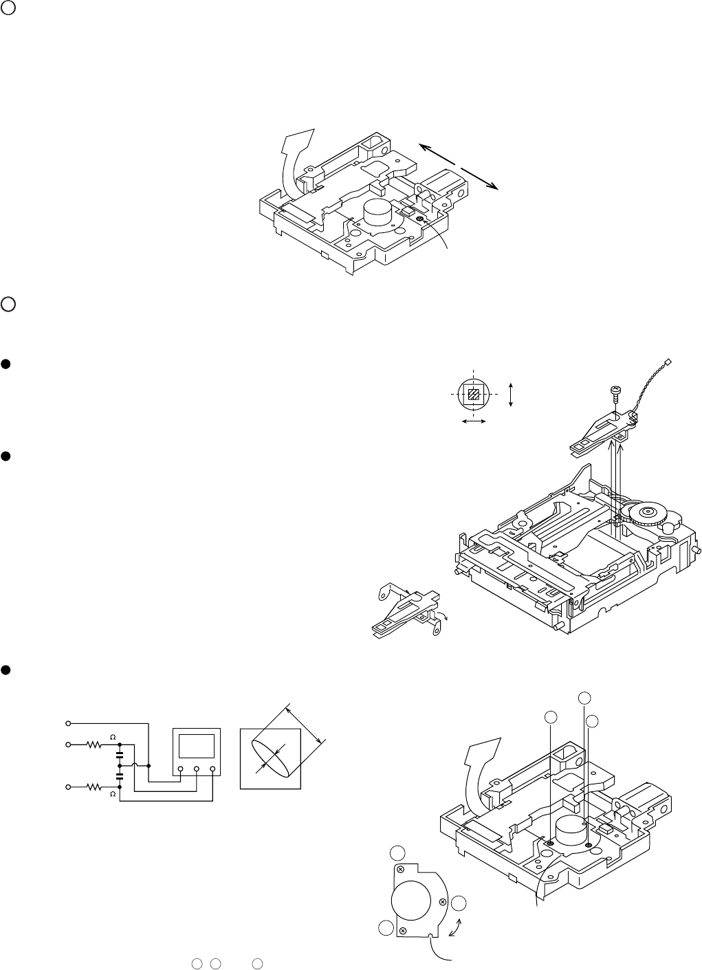
Magnetic head mounting position check
• Check the mounting position whenever the magnetic head
and the optical pickup are replaced.
• Move the optical pickup to the center to adjust the position
easily.
1. Set the transparent disc for checking the head.
2. Press down the magnetic head up shift arm by hand to raise
the magnetic head.
3. View the set from above to check whether the magnetic
head aligns with the optical pickup objective lens.
4. Check that the magnetic head moves up and down smoothly.
(See Fig. 27-2)
Figure 27-2
Figure 27-3 Optical Pickup Grating Deviation
Measuring Method
Mechanism Adjustment
1. Optical pickup grating inspecting method
After auto adjustment (COMPLETE appears) in the test mode
(auto) using the high reflection MD disc TGYS1, adjust the
Lissajou's waveform (x-y) of EOUT to FOUT.
1. Slightly loosen the 3 screws of the spindle motor, adjust
while observing the Lissajou's waveform.
2. After adjustment, tighten screws , , and in numerical
order. (See Fig. 27-4) Figure 27-4
A
B
(A1) X1
Objective
Lens
Radiai
Tangential
direction
Magnetic Head
Head up
-
shift a
r
OSILLOSCOPE
GND CH1 CH2
XY
4 Pin of IC1201
GND (TP1202)
11 Pin of IC1201
EIN (TP1253)
12 Pin of IC1201
FIN (TP1254)
100K
470p
470p
a
b
LISSAJOUS'S WAVEFORM
Less than a:b = 4:1
100K
2
31
2
3
1
adjusting
hple
Check the Lissajou's waveform
shifting the mounting position with
a screwdriver (to be fitted into the
disc motor adjusting hole).
MD-E9000W
– 28 –
Figure 28
From
Magnetic Head
From Mechanism
Switch PWB
2 Pin Extension Connector
QCNWK0059AFZZ
MD Main PWB
28 Pin Extension Flat Cable
QCNWK0108AFZZ
9 Pin Extension Flat Cable QCNWK0132AFZZ
Extension PWB for service
(RUNTK0581AFZZ)
Fit the extension PWB for service to
the mechanism
From
Optical Pickup Unit

– 29 –
MD-E9000W
Can't REC • Errors occurred 10 times continuously in the REC-PLAY • Check for scratch, dust, fingerprints, or black spots on
mode. the disc. Check that the disc is not eccentric or largely
• In the REC-PLAY mode, recording enable cluster became deflected.
0 due to errors.
• Cannot read the address. The unit cannot enter the REC
mode for 20 seconds regardless of repetitive tries.
Can't COPY • During the REC-PAUSE or REC-PLAY mode, the disc was • Check if it is the copy-prohibited disc (Example: CD-R
judged as follows according to the channel status of the etc.).
digital signal input at D-IN:
It is not an audio disc.
It is not for public use.
Due to the inversion of COPY bit on the CD, the
contents cannot be copied.
NO SIG. •
During the REC-PAUSE, REC-PLAY, or CD FUNC playback • Check for an abnormality with the D-IN signal line.
mode, the following occurred responding to the digital signal
input at D-IN:
Digital IN PLL is unlocked.
PLL is locked even if FS is not 44.1 kHz.
TOC FULL • There is no space left for track numbers or character • Replace the disc with the one on which the space for
information (track names, disc name, etc.). recording UTOC is left.
• No recordable space was found when entering the REC-
PAUSE mode.
Can't READ u • FTNO > LTNO has been recognized. • There is an error with UTOC data. Replace the disc.
• FTNO is not 0 or 1.
• Cannot read UTOC recorded on the disc.
TOC FROM a • The start address > end address has been recognized. • There is an error with UTOC data. Replace the disc.
TOC FROM L0-4 • One of UTOC 0-4 data is looping. • There is an error with UTOC data. Replace the disc.
NOT AUDIO • Non-audio data is recorded in the track mode of currently • Select another track number or replace the disc.
selected track number.
? DISC • The ASCII codes data "MINI" of the system ID written in • This is a nonstandard disc. Replace the disc and
TOC is not correct. check.
• The disc type written in TOC does not belong to either of
the pre-master MD, recording MD or hybrid MD.
DISC FULL • No recordable space was found when entering the REC- • Replace the disc with the one on which the recording
PAUSE mode. space for UTOC is left.
PROTECT • You tried recording or editing on a disc with the erase- • Move the tab back to its original position and try
prevention tab moved. recording or editing again.
• You tried editing the track that is write-protected due to the * Try editing other tracks that are not write-protected.
information written in UTOC.
Can't EDIT • Conditions in each editing function have not been satisfied. • The unit is not operated properly. Try again in right
procedures.
TEMP OVER • The temperature inside of the set (MD unit) becomes too • Check the remedy on the troubleshooting chart.
high due to an error. • Is the unit used in a place of high temperature?
Can't READ r • The read data is not correct, or data has not been • There may be an error in TOC or UTOC data or
Can't READ s read properly. scratches on the disc. Replace the disc.
Can't READ w • An error occurred while recording sound data, and
the recording could not be completed.
Can't READ s • The read data is not correct. • TOC information on the disc does not comply with the
Can't READ r • TOC information cannot be read. MD standard. Replace the disc.
• There may be scratches on the disc. Replace the disc.
Can't WRITE • An error occurred while overwriting UTOC, and it could not • There may be scratches on the disc. Replace the disc.
be overwritten properly.
BLANK MD • Although UTOC is read, total number of letters of TNO and •
Check that the disc is a recordable disc by recording on it.
NAME is 0.
Er-MD41 • UTOC can be read but cannot be overwritten. • Is the recording head positioned properly? Check the
connection between the PWB and recording head.
Er-MD80 • EEPROM data is not correct. • Reset the unit and try again. If it does not restore the
unit, replace EEPROM.
Power? • Due to the abnormality with the power supply, MD unit • Reset the unit and try again. If it does not restore the
cannot be operated properly. unit, the power supply circuit is defective. Check the
DC voltage of Q550 E , and Q580 E .
MD error messages ERROR MESSAGE LIST
Error Display Error Message Remarks
MD-E9000W
– 30 –
The details description of mechanism error
Error Display Error Message
E r - M D 1 Cannot eject the disc.
E r - M D 2 The head does not ascend.
E r - M D 3 The head does not descend.
HINF
(93 Pin of IC1401)
= E EJECT complete position < 1.4 V
= M LOAD/EJECT halfway position > 3 V
= L LOAD complete position 2.475 ~ 2.8 V
= D HEAD DOWN position 2.0875 ~ 2.2375 V
EEPROM WRITING PROCEDURE
EEPROM (IC1402) writing procedure
1. Method for setting the reference temperature value
(This setting should be performed quickly at a room
temperature, between 21°C to 29°C when the PWB is not
hot.)
When replacing the EEPROM, wait until it has cooled
down.
Connect the main unit using the single MD main PWB.
Enter the test mode as shown on page 21.
"EJECT"
Press the NORMAL CD MD EDIT button.
"TEMP "
: Measured temperature, : Temperature setting
Find the temperature correction value for the current
ambient temperature on the following table. Adjust the
temperature correction value using the VOLUME UP/
DOWN button.
Ambient Temperature Correction
+ 21.0 °C ~ + 23.2 °C -1 H
+ 23.3 °C ~ + 26.8 °C± 0 H
+ 26.9 °C ~ + 29.0 °C +1 H
An example: When ambient temperature is 22 °C and
measured temperature is 7A H
Temperature setting = 7A H - 01 H
= 79 H
* When the measured temperature fluctuates
between two values, take lower one (if
temperature fluctuates between 7A H and
79 H, take 79 H).
Press the POWER button and write the temperature
setting into the EEPROM.
2. Method for making settings other than the reference
temperature
Install the MD main PWB in the mechanism, and connect
it to the main unit.
Enter the test mode as shown on page 21, and insert a
disc.
"AUTO AJST"
Press the CD PLAY button seven times.
"EEPROM SET"
Set the value according to the EEPROM DATA LIST
using the VOLUME UP/DOWN button.
Press the POWER button, and the settings will be written
into the EEPROM.
Enter the test mode again, perform an "AUTO YOBI
adjustment", and write the results into the EEPROM.
S P G 1 1
H
S P G — i n 6 0
H
S P G — m i d 4 B
H
S P G — o u t 3 B
H
S P G M 9 6
H
S P 1 1 0
H
S P 2 9 3
H
S P 2 2 9 3
H
S P 3 E D
H
S P 4 E E
H
S P 5 2 0
H
S P 5 2 2 0
H
S P D L I M 6 2
H
S P K L E V m 1 6
H
F G 9 B
H
F G 2 B 1
H
F F 0 1 0
H
F F 1 7 0
H
F F 2 E 0
H
F Z H L E V E D
H
F O K L E V h 0 7
H
F O K L E V L 0 9
H
F O S T n 2 C
H
D S C J G 0 D
H
EEPROM DATA LIST (Version : 01)
Focus setting
Item indication Setting
Spin setting
Item indication Setting
– 31 –
MD-E9000W
Tracking setting
Item indication Setting
T G 4 9 H
T G 2 6 B H
T F 0 1 0 H
T F 1 6 B H
T F 2 F 0 H
F T 3 0 8 H
S V C N T 4 0 1 H
T R B L V o 6 2 H
T R B L V t 4 C H
T R K L V o 5 B H
T R K L V t 2 B H
T D P W o 6 7 H
T D P W t 2 1 H
S L C T o 0 0 H
S L C T t 5 0 H
S L C T m 5 3 H
T C R S C I P 1 6 H
T C R S C 0 h 0 0 H
T C R S C 0 L F A H
T C R S C H h 0 2 H
T C R S C H L 0 2 H
C O T L V P 0 A H
C O T L V r 2 8 H
J P i n t 0 0 H
K I K 1 0 6 4 H
Sled setting
Item indication Setting
S L G 4 6 H
S L 2 1 0 H
S L D L I M 7 F H
S L D L E V 1 4 H
S L K L V k 6 0 H
S L K L V t 3 4 H
S L K L V m 6 0 H
S L B K m 0 8 H
S L K r i o 6 4 H
S L K r o i 6 2 H
S L K l i o 6 4 H
S L K l o i 6 0 H
I N N E R 1 8 6 H
I N N E R u D 0 H
E J _ W A I T 7 8 H
C O K 5 8 H
F A T C 0 H
T A T 3 E H
C A T 4 0 H
F A B 6 4 H
S T R 0 B H
S F S 0 D H
S T C 0 D H
Control setting
Item indication Setting
C O N T R L 1 0 8 H
C O N T R L 2 0 1 H
A D J T T M 1 4 H
H D E Q A D 9 2 H
L D E Q A D 8 E H
G D E Q A D 9 1 H
G D E Q A D 2 9 1 H
H D E Q B C 8 C H
L D E Q B C 8 F H
G D E Q B C 8 A H
G D E Q B C 2 8 A H
H A L S G 1 1 H
L A L S G 1 1 H
G A L S G 1 1 H
H A L S O F S F F H
L A L S O F S 0 0 H
G A L S O F S 0 0 H
ADJUST setting
Item indication Setting
REC bit setting
Item indication Setting
S P _ W R 5 0 C 0 H
S P _ W R 5 6 F E H
S P _ W R 4 4 0 0 H
S P _ W R 5 3 1 6 H
L P 2 W R 5 0 8 0 H
L P 2 W R 5 6 2 0 H
L P 2 W R 4 4 8 0 H
L P 2 W R 5 3 0 0 H
L P 4 W R 5 0 B F H
L P 4 W R 5 6 0 2 H
L P 4 W R 4 4 8 0 H
L P 4 W R 5 3 0 0 H
R V D 0 1 H
MD-E9000W
– 32 –
MD power ON time chart
Power-on sequence for the MD unit (when resetting or starting it : no disc)
Power failure recovery interruption input and 3.2 V application to the MD unit
(100 ms)
1.5 ms
30 ms ± 2 ms
3.2 ms
3.2 ms
(10 ms)
Set the system microcomputer to "H" by this point.
13.6 ms
Test mode command transmission period (Until CMD RCV received)
(System side)
POWER-ON
CN1501 ,
CN1501
17
4
18
DVDD
CN1401 ,
12
TRY+/TRY–
BACK UP
CN1501 7
MD-ST
CN1501 6
RESET
CN1501 5
PDOWN
CN1501 8
DSCK
CN1501
19
PCONT0
CN1501
12
DSTB
IC1401
15
MCCK
IC1401
12
RESET
IC1401
80
XRST
TP1800
3.2 V
– 33 –
MD-E9000W
Power-on sequence for the MD unit (when resetting or starting it : DISC IN or disc existence)
Power failure recovery interruption input and 3.2 V application to the MD unit
(100 ms)
600 ms - (approx. 1200 ms + 600 ms)
1.5 ms
30 ms ± 2 ms
3.2 ms
62 ms
3.2 ms
(10 ms)
Set the system microcomputer to "H" by this point.
13.6 ms
Test mode command transmission period (Until CMD RCV received)
(System side)
POWER-ON
CN1501 ,
CN1501
17
4
18
DVDD
CN1401 ,
12
TRY+/TRY–
BACK UP
CN1501 7
MD-ST
CN1501 6
RESET
CN1501 5
PDOWN
CN1501 8
DSCK
CN1501
19
PCONT0
CN1501
12
DSTB
IC1401
15
MCCK
IC1401
12
RESET
IC1401
80
XRST
TP1800
3.2 V
As quick as possible
Disc existence: Mechanism
positioning DISC-IN: LOADING operation
MD-E9000W
– 34 –
Figure 34 BLOCK DIAGRAM (1/4)
+3.2 V
IC1
LC78645NE
CD SERVO
+5V
+B2
M1
SPINDLE
MOTOR
M2
SLED
MOTOR
SPINDLE MOTOR
SLED MOTOR
SW4
PICKUP IN
IC2
LA6548D
FOCUS/
TRACKING/
SPIN/ SLED
DRIVER
VCC
VCC
OUT1
OUT2
–
+
+
–
VREF
MUTE
VOLTAGE
CONSTANT
Q2
+
–
M
Q3
+3.2 V
DRIVER
LASER
Q1
XL1
33.8688 MHz
XIN
XOUT
VDD5
RFVDD
LVDD
ADAVDD
XVDD
RVDD
FIN1
FIN2
TIN1
TIN2
LDS
LDD
VREF
TDO
FDO
SPDO
SLDO
CONT5
CONT1
CONT2
CONT3
CONT4
DOUT
LRCK
BCK
DATA
DRF
RES
WRQ
DO
DI
CLK
CE
3 V5 V
CD RES
CLK
DI
DO
CE
DRF
WRQ
PICKUP UNIT
TRACKING COIL
FOCUS COIL
IC3
TA7291S
TO MD SECTION
IC4
74VHC08F
INVERTER
CNP5
TO DISPLAY SECTION
30 1 15
21
20
10
11
26
25
6
5
1242719292
1
2 2
1
9 7 3 8 5
2
6
1
33
5
4
6
62
11 1
14
10
13
4
1
7 6 5 4 3
2
1
541 18
VDD
38 47 7 8 9 10 79 80 11
26
23
22
21
20
19
28
37
40
50
51
55
56
57
69
75
72717025
39
585960
49
48
68
67
66
65
64
63
62
61
46
VVDD
77
M
M
M904
CD LID
MOTOR
+5 V
LOADING MOTOR
DRIVER
CNS1
+B2 (5V)
+3.2 V
– 35 –
MD-E9000W
Figure 35 BLOCK DIAGRAM (2/4)
66 57 59
DIN
~
31212012 7034
8
3
18 19
23
10
7
25
2
5
629
99
62
16
~
26 29
~
59
~
11 15
15 10
12
~
32 36 42
~
74
70
~
LR
26 24
LR
513
2
40
29
123456789
10 11 12 13 14 15 16 17 18 19 20 21 22 23 24 25 26 27
RESET
SERCH
MD-ST
CDLRCK
CDBCK
CDDATA
DSCK
KDATA
MDDAT
A
DSTB
H.VDD
D.GND
D.GND
DVDD
DVDD
PCONT0
AVCC
L.OUT
AA.GND
R.OUT
H.GND
M.GND
M.GND
C.GND
R.IN
L.IN
DIG IN
+3.2V
+B3 (+3.2V)
+3.2V
+3.2V
(33.8688MHz)
+3.2V
+3.2V
MECHANISM
+B7
(+4.75 ~ +5.25V)
MECHANISM
+B7
HEAD
+B7
(+4.75 ~ +5.25V)
E-F SIGNAL A-B SIGNAL
RF1 RF4 SIGNAL
RF4
RF3
RF2
RF1
F
A
B
E
MD
HEAD
+B7
M
M
M
CN1501
IC1401
IX0410AW
MD SYSTEM
MICROCOMPUTER IC1402
58X2402T
EEPROM
IC1701
UDA1345
AD/DA CONVERTER
IC1202
IX2474AF
4MBIT D-RAM
IC1201
LR37816
ENDEC/ATRAC
IC1101
IR3R58M
RF SIGNAL
PROCESSOR
IC1601
M56788FP
MOTOR DRIVER
M903
LOADING
MOTOR
M902
SLED
MOTOR
M901
SPINDLE
MOTOR
MAGNET HEAD
(RECORD)
SW1932 LOADING
SW1930 WRITE PRO
SW1933 RECORD
SW1934 PLAY
SW1936 LEAD IN
XL1201
MD PICKUP UNIT
IC1300/IC1301/IC1302
HEAD DRIVER
MONITOR
DIODE
LASER DIODE
LIGHT
RECEIVING
SECTION
ERROR SIGNAL
LIGHT
RECEIVING
SECTION
RF
FOCUS
TRACKING
AUDIO IN
AUDIO OUT
MECHANISM
+B7
+3.2V
+3.2V
+2.6V IC1801
XC62EP32
REGULATOR
IC1802
XC62FP26
REGULATOR
3
32
Q1804
REGULATOR
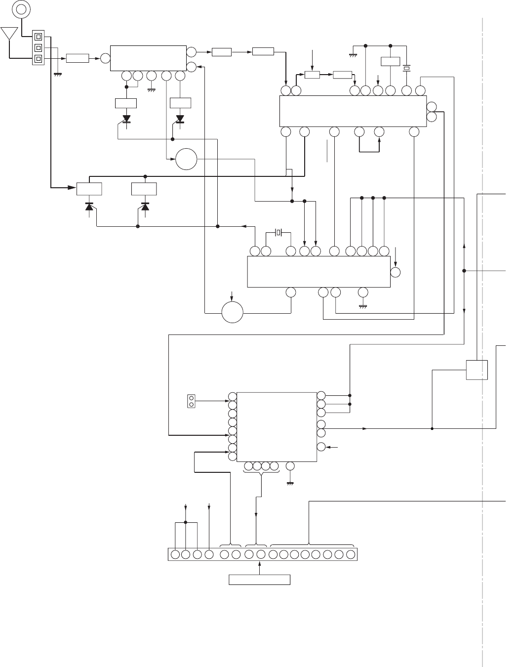
MD-E9000W
– 36 –
Figure 36 BLOCK DIAGRAM (3/4)
CLK
DO
DI
CE
OSC
+B3
+B7
L OUT
R OUT
VDD
LED702
MUTING
Q902
Q901
L IN
R IN
RSELO
LSELO
FROM MD SECTION
CNP451
R
R
L
R
L
JK441
AUX INPUT
+B4
CLK
CE
DI
L
L
L
R
R
R
L
TUNER
CD/MD
IC401
LC75341
AUDIO PROCESSOR
71 6 18 1715
23
28510424222321 19
21
4
24
2
1
81817
11
16
3
15
10
9
7
14
12
13
LED
DRIV
E
+B
FM
+B4
CONSTANT
VOLTAGE
FM
Q360
5
134 6
20 22 111615
IC302
LC72131
PLL(TUNER)
MO/ST
FM/AM
910 21
7
17
+B4
VT
AM BAND
COVERAGE
AM TRACKING
T306
OSC
BUFF
Q302
X352
4.5 MHz
B.P.F
BF301
843
1
5 7
IC301
TA7358AP
FM FRONT END
9
6
T303
FM
OSC
FM RF
FM
OSC
L312 T301
IC303
LA1832S
FM IF DET./FM MPX./AM IF
STEREO
AM RF IN
AM OSC IN
98517
2
113
4
1821 121623 7
FM/AM
OUT
R
L
FM/AM
MPXIN
MO/ST
VCO
FM
DET
FM+B
GND
AM IF
AM MIX
14
15
450 kHz
CF352
AM IF
T351
X351
456 kHz
CF351
+B4
+B4
FM IF FM IF
T302 CF303
SO302
FM ANTENNA
TERMINAL
FM
ANTENNA
AM LOOP
ANTENNA
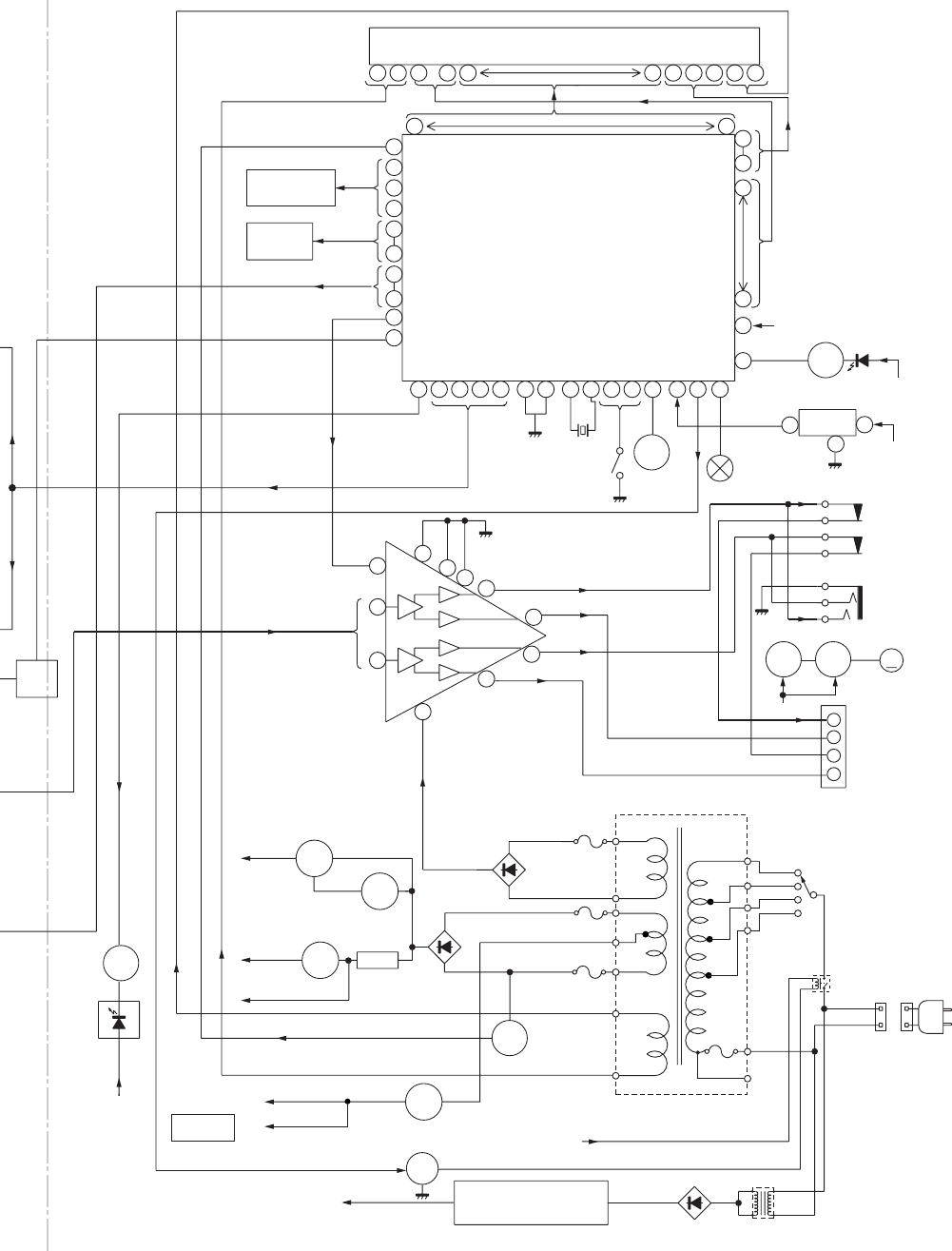
– 37 –
MD-E9000W
Figure 37 BLOCK DIAGRAM (4/4)
SO901
SPEAKER
TERMINAL
JK981
HEADPHONES
IC901
LA4628
POWER AMP.
VF2
+B6
+B6
+B6
+B5
+B2
+B4
+B3
+3.2V
A_+10V
MD+5V
KIA7810AP
VOLTAGE
REGULATOR
VOLTAGE
REGULATOR
VOLTAGE
REGULATOR
VOLTAGE
REGULATOR
Q952
Q942
F802
T2.5A L 250V
Q701
LED701
+B6
+B6
T_STBY
+B6
UNSW +5V
SP_R(–)
SP_R(+)
SP_L(–)
SP_L(+)
P_CONT
–VP
Q871
RESET
Q781
AVSS
LED702
Q702
RLY CONT
RX IN
SPAN
RESET
CD_OPEN
CD_CLOSE
XIN
XOUT
VSS
LED
ILU
DO
CE
CL
DI
P_MUTE
TO CD
SECTION
KEY
SW701-SW723 KEY 3
KEY 2
KEY 1
MUTING
Q902
Q901
UNSW +5V
Q962
AN78L05
VOLTAGE REGULATOR
D873-876
PT871
SUB POWER
TRANSFORMER
PT801
MAIN POWER
TRANSFORMER
RL800
VF1
Q801
SW +5V
CD+B
Q961
+B7 +B1
RX781
REMOTE
SENSOR
D802-D805
D801
M905
FAN MOTOR
M
Q971 Q972
Q951
Q941
F803
T2.5A L 250V
F801
T6.3A L 250V
AC POWER
SUPPLY CORD
VDD
XL701
8.3886 MHz
IC701
IX0395AW
SYSTEM
MICROCOMPUTER
FL701
DISPLAY
7
24
14
4 10 3
12
9
8
11
13
6
1
98
91
99 31 33323536373839404142434445
23
22
15
14
8
4
3
248
50
62615352515021
51
80
205
81
97
21
3
2
1
+
–
–
+
R
R
L
L
R
L
T.F.
+
–
+
–
TO CD
SECTION
SO801
AC INPUT
SOCKET
AC 110/127/220/230-240 V
50/60 Hz
+B5
SW724
OPEN/CLOSE
LED
DRIVER
VOLTAGE
REGULATOR
RELAY
DRIVER
FAN MOTOR DRIVER
L
L
R
R
VEE
230-240 V
220 V
127 V
110 V
SW801
VOLTAGE
SELECTOR
SW441
SPAN
SELECTOR
IC303
LA1832S
FM IF DET./FM MPX./AM IF
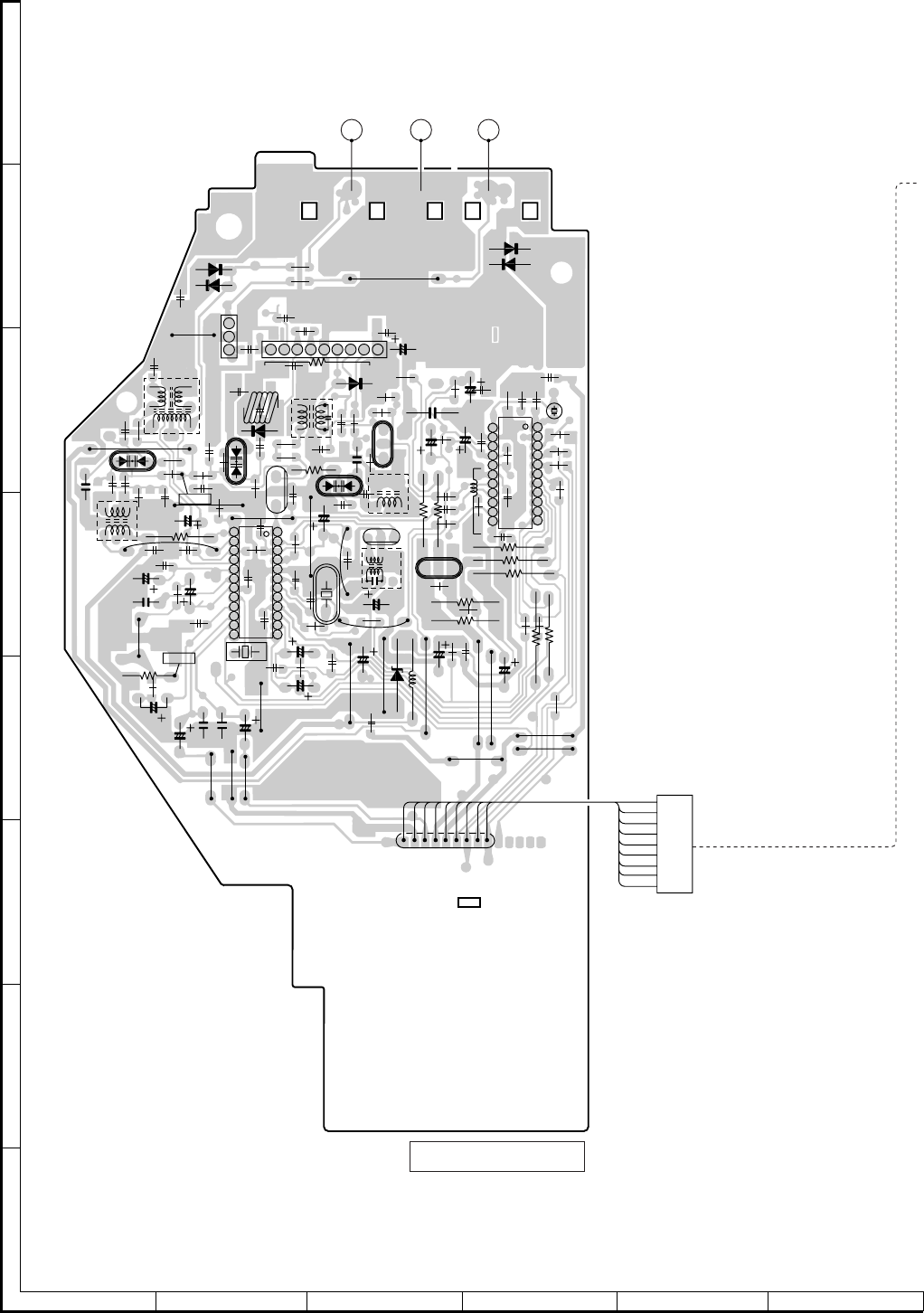
MD-E9000W
– 38 –
Figure 38 WIRING SIDE OF P.W.BOARD (1/10)
A
B
C
D
E
F
G
H
123456
R376
R388
R385
R395
C395
C388
R383
C356
R355
C355
R353
C399
C354
C353
R352
C350
C351
C366
R351
C332
C363
R350
C369
R356
C325
C338
C330
C323
R323
C342 C361
C334
R336
R365
C335
C304
C305
C303
C306
C386
C385
C318
R393
R377
C387
C392
R374
R373
R378
R372
R380
R381
C397
C384
C382
C381
R379
C315
C314
C308
C309
C310
R302
R325
R327
R322
C312
C317
R313
C316
R316
R311
C313
C324
R357
C368
C372
C374
C373
X351
C371
C358
C357
C370
ZD351
L352
C396
BI301
C391
R359
R360
X352
IC302
R368
R384
R387
L351 C394
C307
C380
R391
R392
C393
R382
R375
Q360
T351
CF352
C398
CF351
C352
CF303
IC303
C367
C362
R358
T303
C365
C364
VD301
T306
C331
D302
D301
SO301
FM ANTENNA
TERMINAL
D304
D303
1
2
3
4
5
6
7
8
9
10
11
12
1
2
3
4
5
6
7
8
9
10
11
13
14
15
16
17
18
19
20
21
22
23
24
12
13
14
15
16
17
18
19
20
21
22
E C B
1 2 3
1
2
3
1
2
3
TP301
TP302
TUNER PWB-C1
19
1
2
3
4
5
6
7
8
9
CNS301
RD
WH
BK
WH
BK
WH
BK
WH
BK
AM GND FM 75OHMS
BF301 123456789
IC301
R314
T302
C311
D306
L312
D305
Q302
C320
R309
T301
VD302
B
C
E
VD303
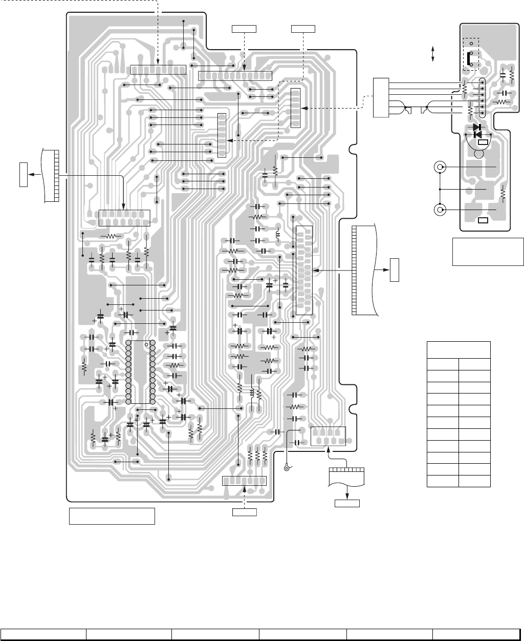
– 39 –
MD-E9000W
Figure 39 WIRING SIDE OF P.W.BOARD (2/10)
78 9 10 11 12
JK441
AUX INPUT
R444
CNP405
CNP406
R460
R402
R401
R403
C406
C404
C405
C407
C403
C411
1
2
3
4
5
6
7
8
9
10
11
12
24
23
22
21
20
19
18
17
16
15
14
13
C402
C414
C412
C413
C416
C415
R414
C418
IC401
R413
C417
C426
C420
C419
C425
C424
C423
C421
C428
C429
R447
R449
R446
R448
C422
CNP402
R463
R462
R461
CNP401
1
18
357
2468
C463
C470
C471
R452
C456
R416
L452
R415
C466 C459
C467
R458 C457
R459
R453
R454
R455
C451 C452
C453 C454
R418
C468
C464
C465
R417
C469
CNP451
R451 C460
C458 C455
L451
C427
R457
C462
C461
R456
CNP404
CNP441
CNP403
R441
C441
C442
R442
BI441
D442
D441
R443 R445
1
73
2
1
6
5
43
2
1
6
5
4
6
5
4
3
2
1
123456789
10 11 12
23456789
2468
1012
13579
11
FFC702
1
12
CNP702
P41 10 - B
TO DISPLAY PWB
FFC703
CNP703
P41 12 - D
TO DISPLAY PWB
CNS402
P44 2 - G
FORM CD SERVO PWB
7654321
MAIN PWB-A1
AUX INPUT
PWB-A2
CNS902
P43 7 - C
FROM
POWER AMP. PWB
CNS901
P43 10 - G
FROM
POWER AMP. PWB
1
1
27
3
5
7
9
11
13
15
17
19
21
23
2
4
6
8
10
12
14
16
18
20
22
24
26 25
27
CW1501
CN1501
P47 9 - A
TO MD MAIN PWB
R-CH
L-CH
WH
BK
WH
WH
BK
PK
PK
BK
WH
1
6
CNS441
SW441
SPAN SELECTOR
10 kHz/100 kHz
9 kHz/50 kHz
TO
MAIN POWER
TRANSFORMER
(251)
BR
COLOR TABLE
RD(R)
OR
YL
GR
BL
VL
GY
WH(W)
BK
PK
BROWN
RED
ORANGE
YELLOW
GREEN
BLUE
VIOLET
GRAY
WHITE
BLACK
PINK
C443
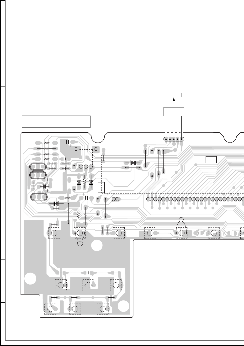
MD-E9000W
– 40 –
Figure 40 WIRING SIDE OF P.W.BOARD (3/10)
A
B
C
D
E
F
G
H
123456
FL701
BI701
D785
D781 RX781
R775
R772
R771
C701
D701
R784
C781
D784
R790
R789
R791
R786
C783
Q781
Q783
Q782
1 2 3
1 2 3
3 2 1
SW708
MD
PLAY/
PAUSE
SW702
VOLUME UP
SW703
CD PLAY/
PAUSE
SW707
MD
STOP
SW701
VOLUME
DOWN
C716
SW704
CD STOP
SW706
PEW/
SKIP DOWN
SW705
FF/
SKIP UP
SW715
CD
OPEN/CLOSE
SW710
DISPLAY
(DEMO)
SW709
MEMORY/
ENTER
SW712
EQUALIZER S
W
X-
CNP871
P42 3 - H
TO POWER PWB
15
12345
CNS701
DISPLAY PWB-B1
321
2
8
293031323334353637383940414243444546474849505152536162
C717
R702
R707 R706
R703 R704
R705
C784
R788
R787
R785
R781
R782
C782 C709
R714
R709
R711
R710
R783
R701
BK
WH
BK
WH
RD
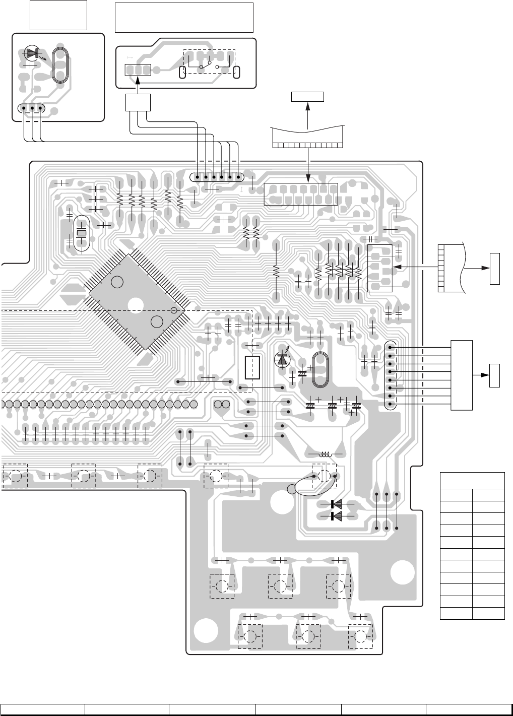
– 41 –
MD-E9000W
Figure 41 WIRING SIDE OF P.W.BOARD (4/10)
78 9 10 11 12
BI704B
LED702
Q702
SW724
OPEN/
CLOSE
CNP704
D782
D783
BI702
CNP703
1
1
8
3
5
7
2
4
6
8
R752
C706
R751
R750
C702 R749
Q701
R748
L781
C703 C708
LED701 R736
XL701
R764
R762
R761
R759
R776
R777
BI704A
CNS704
R754
R753
CNP702
SW711
X-BASS SW713
AUX
SW714
TUNER
(BAND)
SW717
MD EJECT
SW718
LP4
SW723
MD REC
SW719
LP2
SW722
HIGH
SW716
ON/
STAND-BY
SW720
SP
SW721
NORMAL
1
2
3
WH
BK
YL
13
1
6
123
CNP406
P39 7 - C
TO MAIN PWB
1
112
3579
11
2468
10 12
FFC702
1
1
2
3
4
5
6
7
8
8CNS702
CNP5
P44 3 - F
TO CD SERVO PWB
CNP401
P39 11 - G
TO MAIN PWB
3
2
1
FFC703
1256789
10111213141516171819
2021222324252627
28
9
123
RD
BK
WH
BK
WH
BK
WH
BK
WH
BK
RD
WH
BK
YL
C718
R712 R713
R726
R727
R796
R795
R723
R724
R725
R728
R729
R730
R792
R793
R794
R797
R798
R799
R773
C705
C704
C707
R731
R733
R734
R732
R735
R737
R738
R739
R742
R740
R741
C715
C714
R744
R743
R745
R746
R747
C712
C713
R763
1
5
10
15
20
25
35
40
45
55
60 65
7075
80 81
8590
95 100
30
31
50
51
C710
C711
R768
R769
R767
R766
R765
R717 R718 R719
R722 R721 R720
R716
R778
IC701
LED
PWB-B2 CD LID OPEN/CLOSE
PWB-B3
BR
COLOR TABLE
RD(R)
OR
YL
GR
BL
VL
GY
WH(W)
BK
PK
BROWN
RED
ORANGE
YELLOW
GREEN
BLUE
VIOLET
GRAY
WHITE
BLACK
PINK
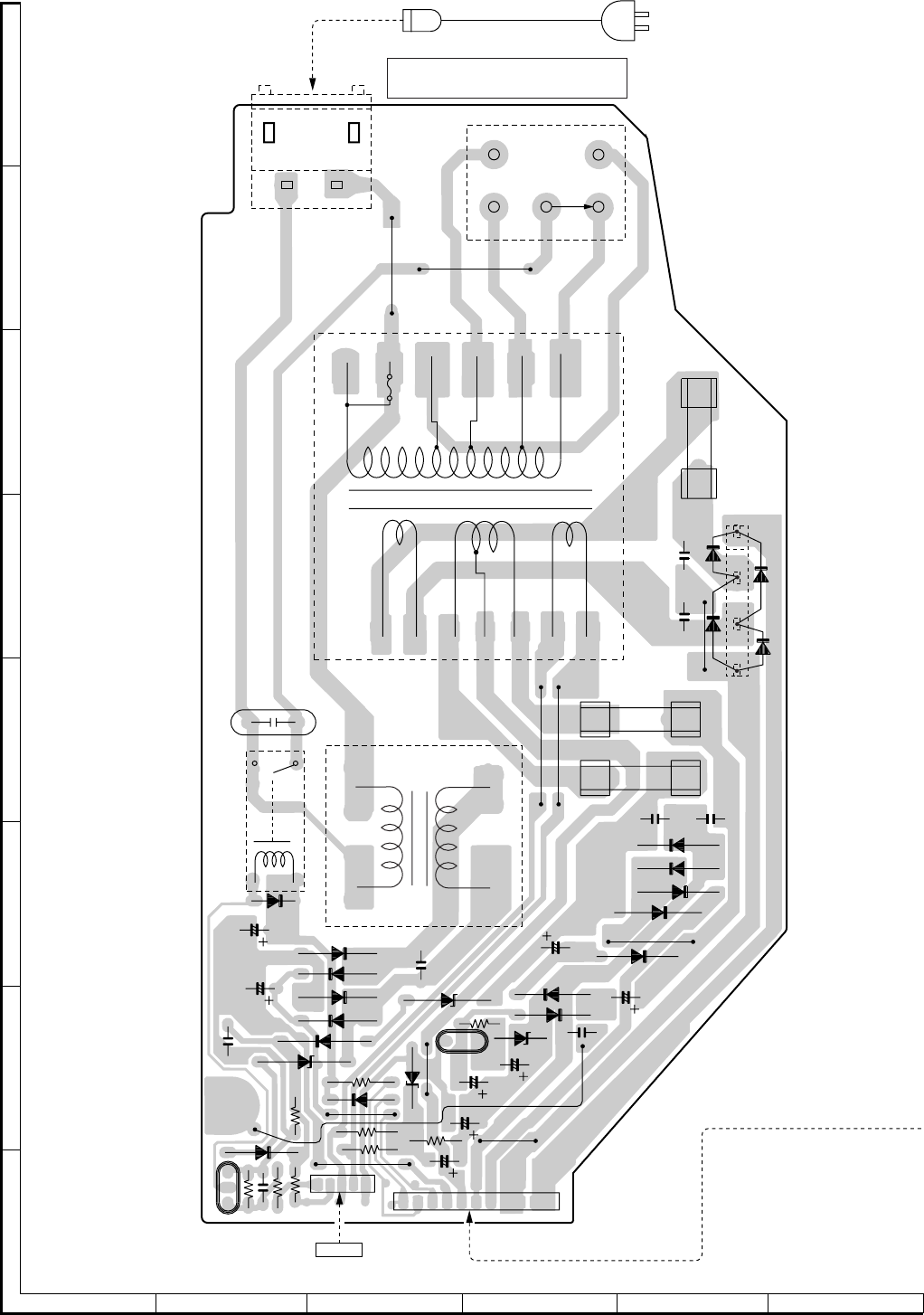
MD-E9000W
– 42 –
Figure 42 WIRING SIDE OF P.W.BOARD (5/10)
A
B
C
D
E
F
G
H
123456
SO801
AC INPUT
SOCKET
AC 110/127/220/230-240 V
50/60Hz
C871
RL800
D871
C874
D875
D876
C873
D873
D874
C811
D809
ZD871
R871
D877
R806
R804
R802
D872
R805
Q871
C875
R873
R872
CNP871
CNS701
P40 5 - C
FROM DISPLAY PWB
CNP903
C810
R803 C809
C807
C808
ZD802
1110987654321
Q801
ZD801
C812
R801 D808
ZD803 C806
D807
D806
C872
C805
D805
D803
D802
D804
C804
C802 C801
D801
C803
PT871
SUB POWER TRANSFORMER
T.F.
110 V
127 V
220 V
230-240 V
PT801
MAIN POWER TRANSFORMER
E
C
B
12345
E C B
F802
T2.5A L 250V
F803
T2.5A L 250V
F801
T6.3A L 250V
AC POWER SUPPLY CORD
POWER PWB-C2
SW801
VOLTAGE SELECTOR
127 V 110 V
220 V 230-240 V
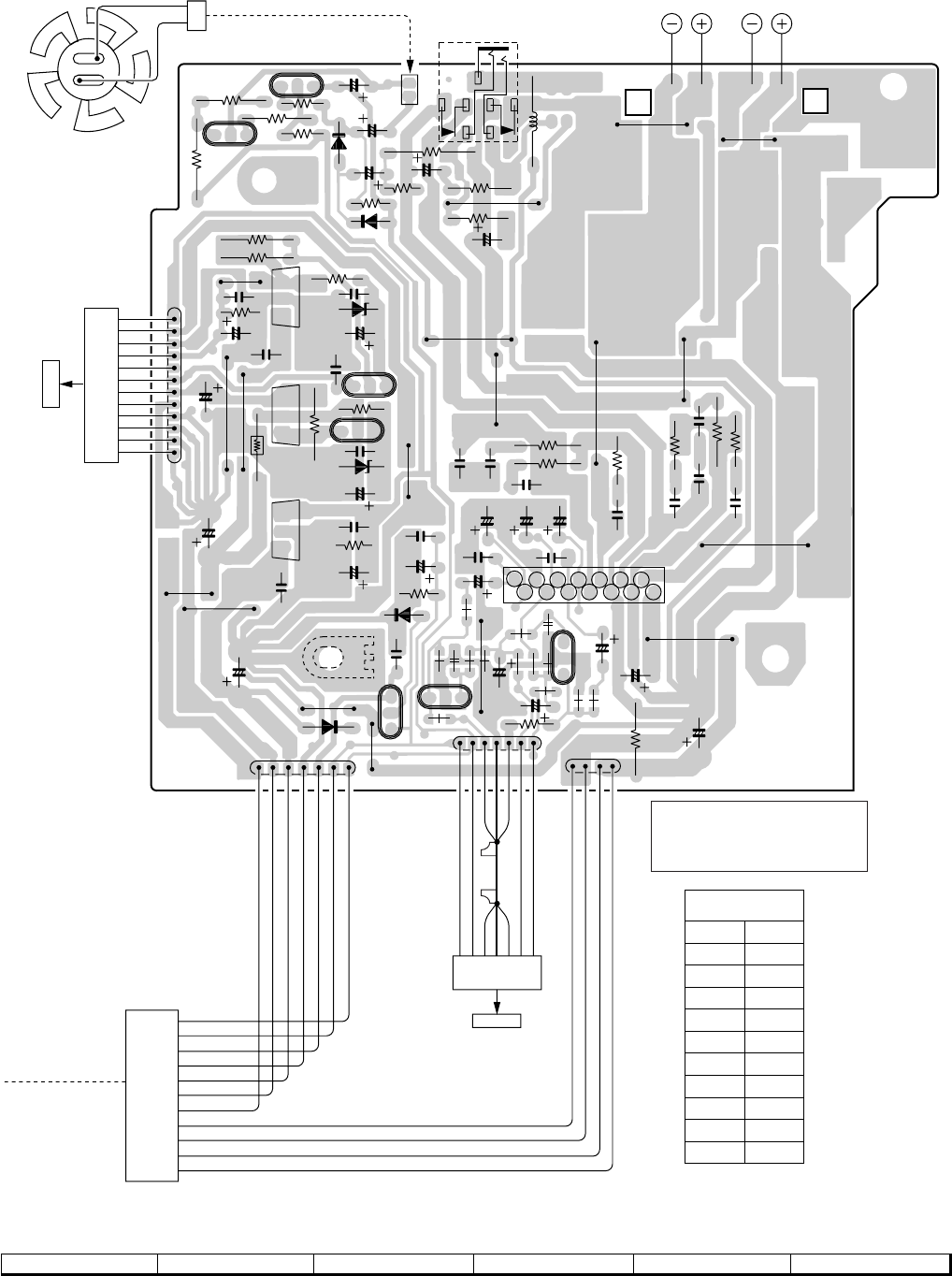
– 43 –
MD-E9000W
Figure 43 WIRING SIDE OF P.W.BOARD (6/10)
78 9 10 11 12
R901
R903
C901
R905
R909
R907
C902
R906
R910
R904
R908
R983
1
2
3
4
5
6
7
8
9
10
11
C949
C961
D961
LUG901
Q962
D962
C964
Q901
C905
R902
C985
Q902
C987
C904
C914
R928
C947
C907 R911
R923
C923 C925
C909
R913
C908 R912
IC901
@
C913
R914
R924
C912
C910
C926
C911
C903
C986
C924
C965
R962
C966
Q952
R941
C942
C941
C955
ZD941
Q942
ZD951
C963
R961
C962
C954
C956
R942
RP941
C951
R952
C952
C953
C948
C943 R975
Q972
R984
R955
R954
R979
Q971
R974
R973
R953
D972
C973
C971
D973
R972
C972
R977 C981
R978
R982
R981
C982
JK981
HEADPHONES
L981
SO901
SPEAKER TERMINAL
BI903B
BI901
BI903A
BI902
Q951
Q941
Q961
CNP971
POWER AMP.
PWB-C3
17
17
14
1
2
3
B
C
E
E C B
BL
BK
WH
BK
WH
BK
WH
BK
BK
RD
RD
PK
BK
WH
PK
BK
WH
RD
BK
BL
WH
1234567
CNS901
CNP404
P39 10 - B
TO MAIN PWB
CNS903 WH
BK
WH
BK
WH
BK
BL
BK
BK
RD
RD
13 5 7 9 11 13
2468
10 12 14
3
2
1
E
C
B
3
2
1
E C B
E C B
E C B
B C E 2
1
R-CH L-CH
1
12
1
2
3
4
5
6
7
8
9
10
11
12
CNS902
RD
WH
BK
WH
BK
WH
BK
WH
BK
WH
BK
WH
CNP403
P39 9 - B
TO MAIN PWB
CNS971
2
1
BR
RD
M905
FAN MOTOR
BR
COLOR TABLE
RD(R)
OR
YL
GR
BL
VL
GY
WH(W)
BK
PK
BROWN
RED
ORANGE
YELLOW
GREEN
BLUE
VIOLET
GRAY
WHITE
BLACK
PINK
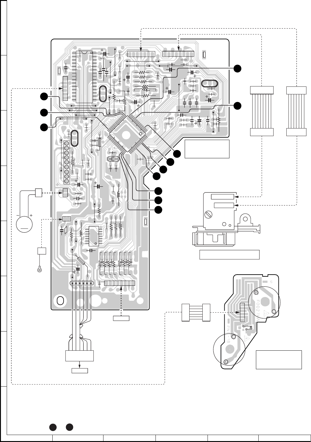
MD-E9000W
– 44 –
Figure 44 WIRING SIDE OF P.W.BOARD (7/10)
A
B
C
D
E
F
G
H
123456
• The numbers 1 to 12 are waveform numbers shown in page 62.
C44
C21
IC4
C23
C22
C18
C19
C20
C31
C32
C61
R50
R49
R24
R23
R20
R56
R19
R53
C42
C14
R13
C58
C57
R11
C1 C3
C54
R12
R10
C5
R9
R35
R36
R15
R16
R17
C9
R14
R55
R18
IC1
1
7
8
14
5
21
1
20
40
41
5
10
15
25
30
35
45
50
55 65
70
75 80
60 61
10
1
2
3
4
5
6
+
+
M
TO MD
MECHANISM
UNIT
C24
C16
C17
R8
C15
C6
C7
C8
C12 C4
R1 C10
R2
R3
Q1
R4
R7 C53
R6 C2
CNP2
CNP1
C45
C47
C46
C48 C63
C13
IC2
CNP4
Q2
R54
R21
Q3
CORE2
XL1
R48
C49 C41
L2
L4
CNP3 C50
R42
R37
R38
R39
R40
C28
C62
R27
R28
R29
R33
R30
R31
R32
C43
1
1
1234567 12345678
2
3
4
5
6
1
2
1
2
21
2345678 CNP5
BI1
CNS402
IC3
1
6
M1
SLED MOTOR
SW4
PICKUP IN
CNP4A
M2
SPINDLE
MOTOR CD MOTOR
PWB-F
1
2
3
4
5
6
1
2
3
4
5
6
RD
WH
GR
WH
GR
WH
CNS4A CNS4B
RD
WH
BR
WH
BR
WH
BR
WH
CNS2A
CNS2B
RD
GR
BR
GR
BR
GR
BR
CNS1A
CNS1B
PICKUP UNIT (306)
CD SERVO
PWB-D
1
5
10
20
25
30
15
16
E
C
B
3
2
1
1
2
3
4
5
6
7
8
9
E C B
CNS702
P41 12 - E
FROM
DISPLAY PWB
CNP402
P39 9 - G
TO MAIN PWB
1 2 3 4 5 6 7 8
1 2 3 4 5 6 7
123456712345678
12345678 1234567
M904
CD LID
MOTOR
1234567
BK
WH
GR
BK
YL
WH
PK
WH
GR
BK
YL
WH
PK
BR
RD
12
CNP6
CNS6
CNS3
CORE1
2
4
3
12
11
10
785
1
6
9
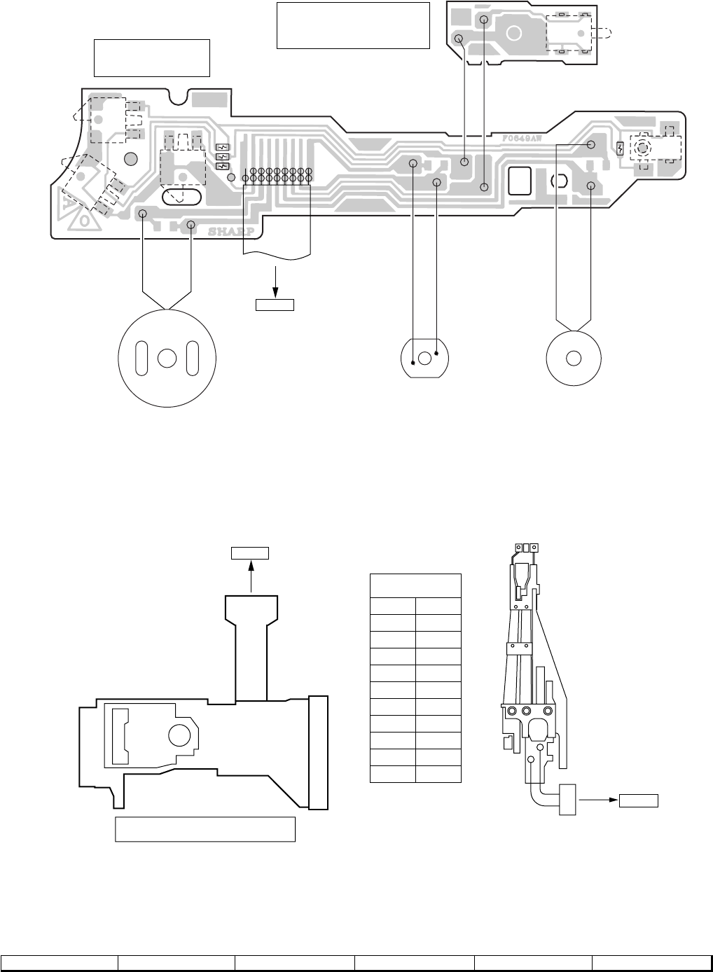
– 45 –
MD-E9000W
Figure 45 WIRING SIDE OF P.W.BOARD (8/10)
78 9 10 11 12
BR
COLOR TABLE
RD(R)
OR
YL
GR
BL
VL
GY
WH(W)
BK
PK
BROWN
RED
ORANGE
YELLOW
GREEN
BLUE
VIOLET
GRAY
WHITE
BLACK
PINK
MD LOADING
PWB-G2
SW1936
LEAD IN
MD MECHANISM
SWITCH PWB-G1
WHBR
GYYL BKRD
R1931
SW1930
WRITE PRO
CW1931
P47 12 - D
TO MD MAIN PWB
CN1401
RD
BK
R1932
R1934
R1933
SW1932
LOADING
SW1933
RECORD
SW1934
PLAY
M903
MD LOADING
MOTOR
M902
MD SLED
MOTOR M901
MD SPINDLE
MOTOR
MD PICKUP UNIT(35)
FLEXIBLE
PWB
P47 7 - F
TO MD MAIN PWB
BK
BK
MAGNET HEAD(34)
RECORD
TO MD MAIN PWB
CN1300
P46 5 - A
CN1101
CW1903
1
2
TP18 TP19
TP1908
TP1909
TP1907
TP1905
TP1906
TP1902
TP1903
TP1904
TP1
TP2
TP3
TP4
TP5
TP6
TP7
TP8
TP9
TP1901
TP10
TP12
TP13
TP17
TP16
TP11
TP14
TP15
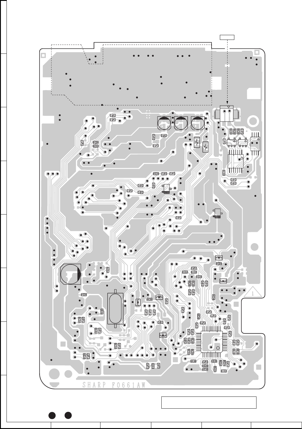
MD-E9000W
– 46 –
Figure 46 WIRING SIDE OF P.W.BOARD (9/10)
A
B
C
D
E
F
G
H
123456
• The numbers 1 to 36 are waveform numbers shown in page 63, 64.
C1616
C1619
C1613
R1618
C1611
R1616
C1603
R1605 C1607
C1206
XL1201
C1602 R1601
L1202
C1260
R1201
R1230
R1203
L1201
C1230
R1207
R1205
L1200
R1231
R1266
C1263
R1102
R1123
C1119
C1264
R1263
C1121 R1125
R1122 R1262C1262
C1265
C1123
R1124
C1122
R1261 C1261
R1120
R1121
C1117
C1118
R1119
C1124
R1118
IC1101
R1264
R1117
R1265
C1115
C1125
L1101
C1107
C1116
L1100
C1113
R1113
C1114
C1112
R1115
R1114 R1116
R1112
C1110 R1110
C1111 R1111
IC1301
D1300
R1301
C1301
IC1300
C1300
IC1302
C1305
R1614
R1612
R1300
C1303
CN1300
Q1807
R1806
C1704
R1809
C1700
R1435
R1802
C1716
Q1501
R1803
R1703
R1701
R1704
C1405
R1705
R1420
R1408
R1403
R1516
R1515
C1721
C1720
R1716
P45 12 - G
TO MAGNET HEAD
CW1903
MD MAIN PWB-E (TOP VIEW)
1
1
2
35
1
2
35
1
12
4
58
1
12
5
10
1520
30
40 45
35
13
24
25
36
37 48
5
10
7
814
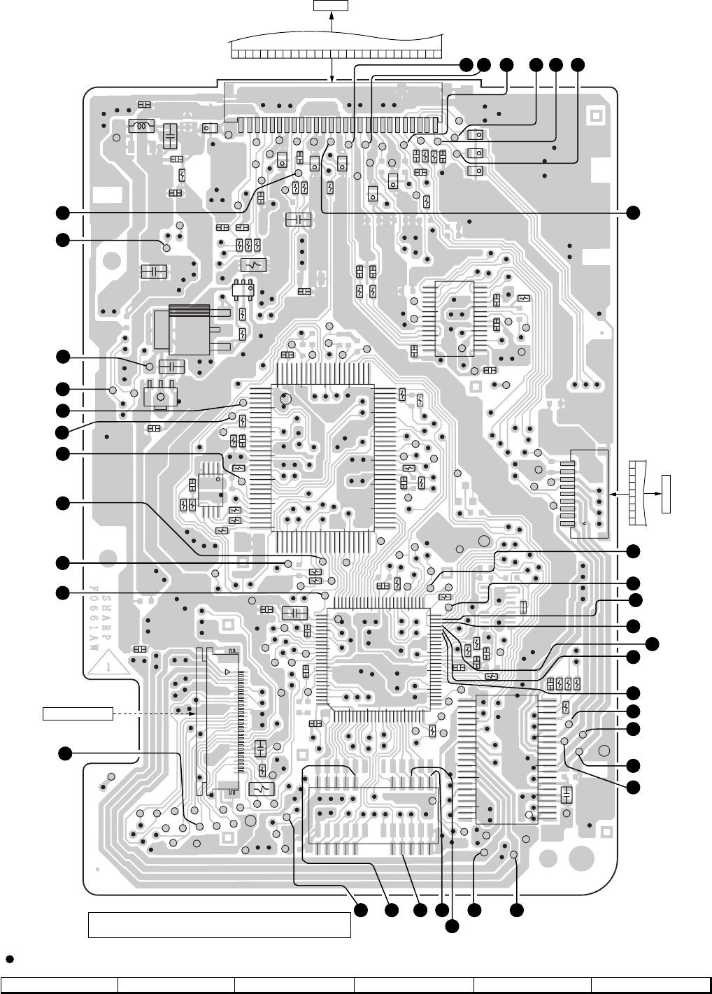
– 47 –
MD-E9000W
Figure 47 WIRING SIDE OF P.W.BOARD (10/10)
78 9 10 11 12
: Through-hole where the top and bottom patterns are connected.
C1161
R1418
CN1101
R1100
C1211
C1100
R1101
C1201
C1202
R1430
R1105
C1200
C1266
IC1202
IC1201
C1205
CK27
R1209
R1211
R1210
C1207
R1215
R1214
C1208
R1217
C1209
IC1601
C1655
R1624
R1621
C1610
R1623
R1622
CN1401
CK26
R1702
C1706 C1715
C1708
IC1701
FL1525
C1524
R1533
R1532
R1535
R1401
C1523
C1703
C1409
C1540
R1441 FL1520
R1443
R1518
C1512 FL1518
R1517
C1510
FL1509
R1529
IC1401
FL1512
R1521
C1530
R1537
C1750
FL1507
C1802
C1407
C1536
R1536
R1534
IC1801
C1404
R1414
R1804
R1807
R1538
R1811
R1407
C1534
R1415
R1417
R1406
IC1402
C1538
R1460
C1403
R1463 R1304
Q1804
IC1802
C1304
C1340
C1801
C1806
C1302
L1300
C1563
C1606
FL1501
CN1501
FL1523
FL1524
CW1501
R1446
13
13
45
TP1301
TP1300
TP1504
TP1502
TP1506
TP1516
TP1510
TP1800
TP1303
TP1302 TP1451
TP1421
TP1401
TP1404
TP1202
TP1133
TP1251TP1250
TP1254
TP1253
TP1252
TP1118
TP1112
TP1103
TP1119
TP1135
TP1116
TP1203
TP1104
TP1117
TP1136
TP1107
TP1108
TP1131
TP1110
TP1109
TP1106
TP1130
TP1111 TP1115
TP1105
TP1102
TP1100
TP1101
TP1200
TP1113
TP1420
TP1201
TP1405
TP1409
TP1422
TP1408
TP1407
TP1403
TP1406
TP1402
TP1415
TP1330
TP1532
TP1509
TP1508
TP1507
TP1515
TP1524 TP1526 TP1520 TP1518
TP1501
TP1519
TP1531
TP1503
TP1522
TP1533
TP1530
TP1525
TP1534
TP1511
TP1505
TP1205
TP1215
TP1207
TP1217
TP1218
TP1209
TP1206
TP1214
TP1210
TP1208
TP1216
TP1204
TP1423
TP1413
TP1411
TP1410
TP1543
TP1542
TP1604
TP1400
TP1703
TP1705
TP1801
TP1700
TP1706
TP1704
TP1600
TP1603
TP1601
TP1602
TP1607
TP1630
TP1121
TP1123
TP1122
TP1120
TP1213
TP1605
TP1412
TP1212
P39 11 - E
TO MAIN PWB
27
27
1
1
CNP451
MD MAIN PWB-E (BOTTOM VIEW)
MD PICKUP UNIT
P49 9 - E
P45 9 - C
TO MD LOADING PWB
CW1931
1
21
20
25
30
35
40
15
10
5
50
51
22
42
1
1
9
1
9
56
20
16
15
10
11
1
175
76
100
80859095
55
60
65
70
30 35 40 45
5
10
15
20
31
35 40 45
50
5
10
15
20
25
75
70
65
60
55
95 90 85
1
14
85
30
80
1
14
10
20
25
28
5
15
81
100
51
28
25
26
CK1
CK2
CK3
1
26 27 35 36 34
2
14
31
30
3
4
5
10
12
13
32
19
17
33
11
8
9
6
7
15 16242325 22
18
20
21
28
29
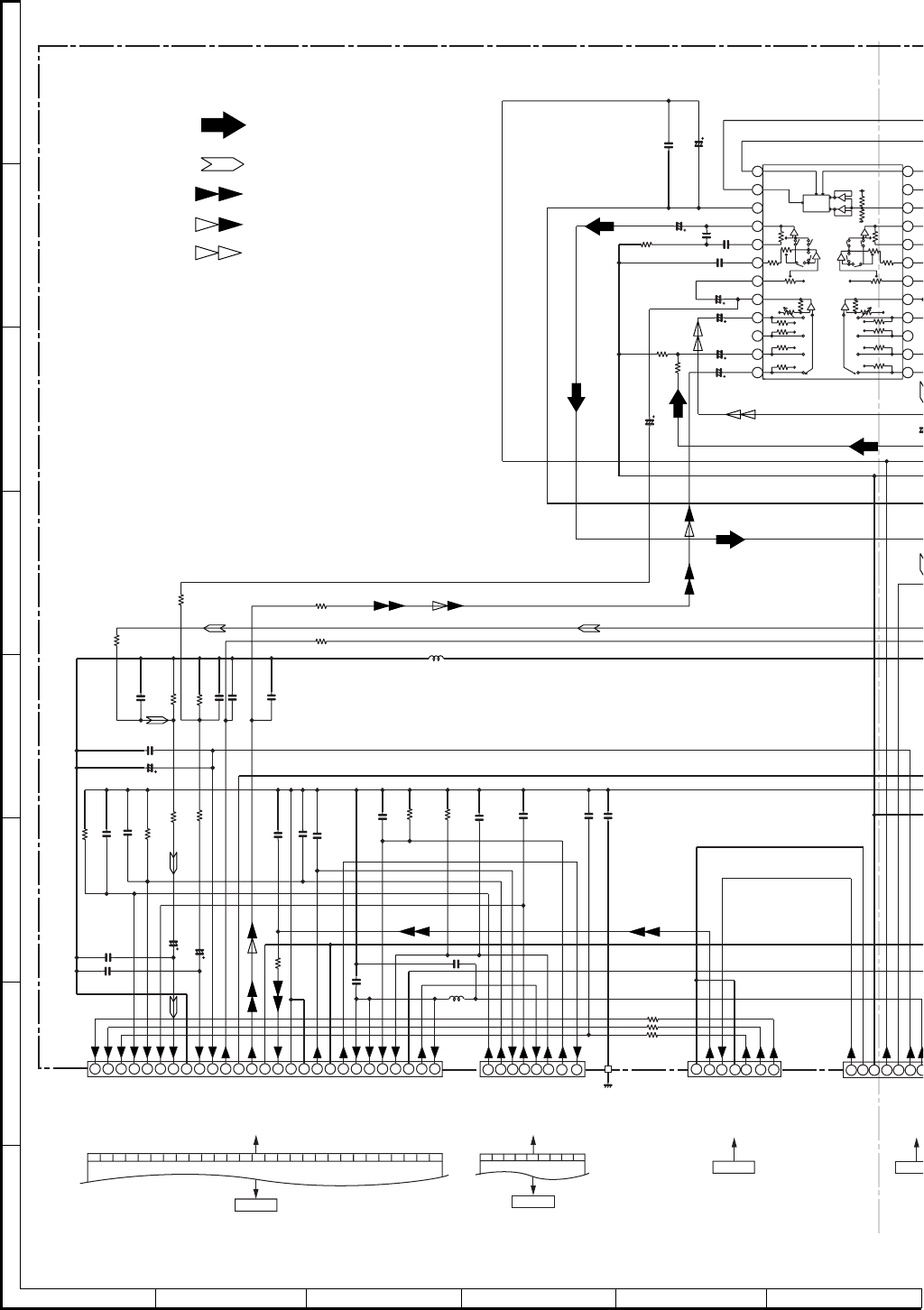
MD-E9000W
– 48 –
Figure 48 SCHEMATIC DIAGRAM (1/12)
A
B
C
D
E
F
G
H
123456
• NOTES ON SCHEMATIC DIAGRAM can be found on page 61.
24
23
22
21
20
19
18
17
16
15
14
13
12
11
10
9
8
7
6
5
4
3
2
1
MD_3.2V
A_GND
D_GND
D_GND
LRCK
BCK
CD DATA
DIGITAL
OUT
MD +D5V
AVCC
(+3.2V)
M GND
M GND
MD DATA
LRCK
BCK
CD DATA
MD DSCK
FAN_CONT
DIG IN
H VDD
MD PCNT
MD DSTB
MD SERCH
MD RESET
MD DATA
MD KDATA
MD ST ID
MD DSCK
PCONTO
H GND
S GND
R OUT
L OUT
R IN
A GND
L IN
5V
5V
D GND
D GND
MD DSTB
MD K DATA
MD SERCH
MD ST
MD RESET
CD+B
CD_GND
A_+10V
CD_+5V
R
B
LBASS
7 6 1 2 3 4 5 1 2 3 4 5 6
7
8 7 6 5 4 3 2 1
21 16
1 5
13 12 26 27 17 20
4
11 10
8
15 14
2
24 19
6
23 22 18
7 9
25
3
DECK
RTRE
LSEL0
–
+
–
+
–
+
–
+
–
+
–
+
–
+
–
+
CCB
INTERFACE
R1
R2
R3
R4
RSEL0
RIN
ROUT
VREF
VDD
CLK
L1
L2
L3
L4
LIN
LTRE
LOUT
VSS
CE
DI
AUX
TUNER
CD/MD
CNS9
P54 1
FRO
M
POWER A
M
CNS402
P57 12 - C
FROM
CD SERVO PWB
CNP703
P51 12 - E
TO DISPLAY PWB
CN1501
P59 12 - G
TO MD MAIN PWB
11827
+
B
+B+B
+B
+
B
+B
+B
+B
+B
TO
MAIN POWER
TRANSFORMER
C402
0.022
C403
100/16
R413
3.9K
C411
1/50 C415
0.12
C413
0.1
R449
2.7K
R447
10K
C429
1/50
C423
1/50
C419
1/50
C417
0.0015(ML)
C421
1/50
IC401
LC75341
AUDIO PROCESSOR
C
4
56
C426
10/16
C425
10/16
L452
0.22µH
R418
100
R416
3.3K
R415
3.3K
R417
100
C468
220P
C467
220P
C469
220P
R459
12K
R458
12K
C466
220P
C465
0.022
C463
0.022
C470
33P
C471
0.01
C462
100P
R452
10K
C456
100P
R454
100
R455
100
C464
220/10
C459
0.01
C458
10P
C460
220P
C461
100P
R456
10K
R457
10K
R453
10K
C457
100P
C453
220P
C454
220P
C452
10/16
C451
10/16
C427
0.022
L451
10µH
R451
100
C455
0.022
CNP451
R463 56
R462 56
R461 56
CNP402
CNP401 CNP403
CW1501 FFC703
FM SIGNAL
RECORD SIGNAL
MD SIGNAL
AUX SIGNAL
CD SIGNAL
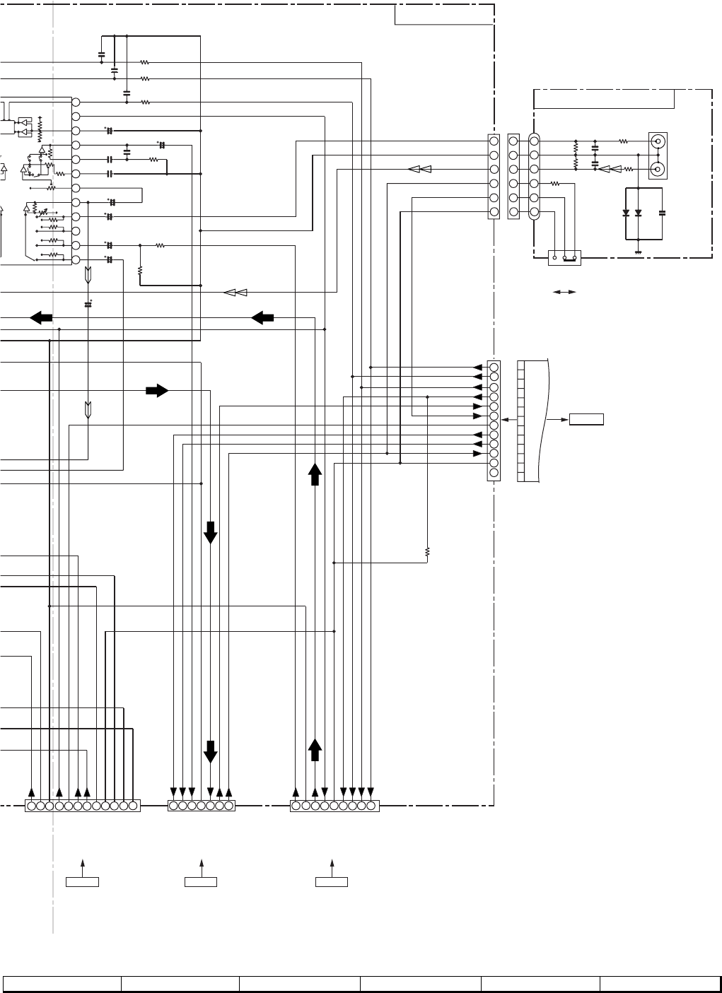
– 49 –
MD-E9000W
Figure 49 SCHEMATIC DIAGRAM (2/12)
78 9 10 11 12
24
23
22
21
20
19
18
17
16
15
14
13
H.GND
M.GND
S.GND
D.GND
MD_3.2V
P_CTRL
A_GND
D_GND
T/V_CLK
TUN DO
T/V_CE
T/V_DI
A+10V
A GND
TUN_L
TUN_R
SW_5V
MD_+D5V
(MD)D_GND
FAN_CONT
TUN_SM
MAIN PWB-A1
P_MUTE
SW-5V
P_CONT
D_GND
CD+B
CD_GND
P_MUTE
A_+10V
A_GND
R_CH
L_CH
UN_SW-5V
FAN_CONT
SPAN
T/V_DI
T/V_CLK
TUN_DO
T/V_CE
RBASS
UNSW_5V
5
7
10
12
11
8
9
1
3
2
4
6
1 2 3 4 5 6 7 8 9
10 11 12
3
1
1
22
3
4
5
6
4
5
6
4
5
6
1
2
3
2 8 9 6 5 74 1 3
6 5 4 3 2 1 7
DECK
RTRE
–
+
+
–
+
–
+
–
+
–
+
–
+
C
CB
E
RFACE
R1
R2
R3
R4
RSEL0
RIN
ROUT
VREF
VDD
CLK
AUX
TUNER
CD/MD
R-CH
L-CH
AUX INPUT PWB-A2
1
12
CNP702
TO DISPLAY PWB
P51 12 - C
CNS301
P53 11 - H
FROM TUNER PWB
CNS901
P54 1 - C
FROM
POWER AMP. PWB
CNS902
P54 1 - D
FROM
POWER AMP. PWB
+B
+B
+B
+B +B
+B
+B
I
C401
C
75341
P
ROCESSOR
R401
1K
R402
1K
R403
1K
C406
560P
C405
560P
C404
560P
C407
22/16 C412
1/50
C414
0.1
C416
0.12 R414
3.9K
R448
2.7K
R446
10K
C428
1/50
C424
1/50
C418
0.0015(ML)
C420
1/50
C422
1/50
C426
10/16
C
NP403 CNP404 CNP405
R460
270K
CNP406
D442
DS1SS133
D441
DS1SS133
C443
0.001
CNP441
R443
27K
JK441
AUX INPUT
R442
8.2K
R444
27K
C442
390P
C441
390P
R441
8.2K
R445
10K
BI441
CNS441
FFC702
SW441
SPAN
SELECTOR
10/100 kHz 9/50 kHz
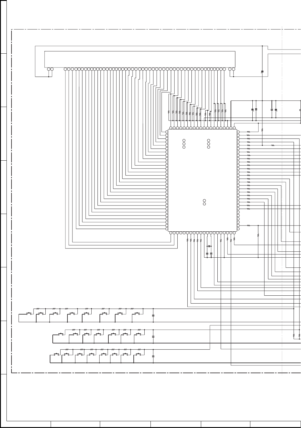
MD-E9000W
– 50 –
Figure 50 SCHEMATIC DIAGRAM (3/12)
A
B
C
D
E
F
G
H
123456
• NOTES ON SCHEMATIC DIAGRAM can be found on page 61.
NO USE
P32
ILU-LE
CD_CLOSE_SW
CD_OPEN_SW
RLY_CONT
MD_SERCH
MD_ST-ID
F
F
G13
G12
G11
G10
G9
G8
G7
G6
G5
G4
G3
G2
G1
P36
P35
P34
P33
P31
P30
P29
P28
P27
P26
P25
P24
P23
P22
P21
P20
P19
P18
P17
P16
P15
P14
P13
P12
P11
P10
P9
P8
P7
P6
S4
P4
P3
P2
P1
F
F
SEG26
SEG27
SEG28
SEG29
SEG30
SEG31
SEG32
SEG33
SEG34
SEG35
DIG0
DIG1
DIG2
DIG3
DIG4
DIG8
RDS_DATA
KEY3
KEY2
CD_CE
SEG16
CD_DI
T/V_DI
DIG11
CD_RESET
P-IN
CD_CL
SEG18
SEG19
SEG20
SEG21
DIG6
DIG7
DIG10
DIG12
TUN SM
RDS_CL
RDS_READY
SPAN
P_DOWN
MD_DSCK
MD_RESET
P_MUTE
SEG7
SEG8
SEG9
SEG10
SEG11
SEG12
SEG13
SEG14
SEG15
SEG22
SEG23
SEG24
SEG25
MD_KDATA
INI
RDS_RST
MD_PCONT
MD_DSTB
MD_DATA
CD_WRQ
CD_DRF
@
CD_DO
P_CONT
RX-IN
XIN
XOUT
VSS
TUN_DO
T/V_CL
T-STBY
NO USE
NO USE
SEG17
SEG6
VCC
SEG5
SEG4
SEG3
SEG2
SEG1
SEG0
VEE
AVSS
VREF
KEY1
T/V_CE
DIG9
DIG5
RESET
FAN_CONT
34
62 61 53 52 51 50 49 48 47 46 45 44 43 42 41 40 39 38 37 36 35 34 33 32 31 30 29 28 27 26 25 24 23 22 21 20 19 18 17 16 15 14 13 12 11 10
5612789
32
64
65
66
67
68
69
70
71
72
73
74
75
76
77
78
78
79
80
79
80
81 82 83 84 85 86 87 88 89 90 91 92 93 94 95 96 97 98 99
100
16
17
18
19
20
21
22
23
24
25
26
27
28
29
30
29
30
31 33 35 36 37 38 39 40 41 42 43 44 45 46 47 48 49 50
51
52
53
54
55
56
57
58
59
1
2
3
1
2
3
4
5
6
7
8
9
12
13
14
15
10
11
60
61
62
63
+B
R793 47K
R799 47K
R798 47K
R797 47K
R796 47K
R795 47K
R792 47K
R730 47K
R729 47K
R728 47K
R726 47K
R727 47K
R725 47K
R723 47K
R724 47K
R794 47K
FL701
R775
820K
C707
0.022
C706
220/6.3
C705
0.022
C704
0.022
C703
1/50
R753 1K
R751 5.6K
R750 5.6K
R749 1K
R748 1K
R747 1K
R746 5.6K
R759 1K
R752 1K
R745 5.6K
R744 1K
R743 1K
R738 1K
R754 1K
R742 1K
R741 1K
R740 1K
R739 1K
R731
1K R771
10K
R772
10K
R732 1K
R733 1K
R734 1K
R735 1K
R736 1K
C701
1/50
R737 1K
C711
18P(CH)
C710
18P(CH)
R769 1K
R762 1K
R761 1K
R763 1K
R764 1K
R765 1K
R766 1K
R767 1K
R768 1K
XL701
8.3886 MHz
R790
10K
R791
10K
R707
100K
SW708
MD
PLAY/PAUSE
SW703
CD PLAY
SW704
CD STOP
SW706
REW/
SKIP DOWN
SW707
MD
STOP
SW701
VOLUME
DOWN
R703
2.7K
R704
4.7K
SW705
FF/SKIP UP
R705
8.2K
R706
18K
SW715
CD
OPEN/CLOSE
R714
18K
SW714
TUNER
(BAND)
R713
8.2K
SW712
EQUALIZER
R712
4.7K
SW713
AUX
R711
2.7K
SW711
X-BASS
R710
1.8K
SW710
DISPLAY
(DEMO)
R702
1.8K R701
680
SW702
VOLUME
UP
R709
680
SW709
MEMORY/
ENTER
SW722
HIGH SW721
NORMAL
R722
100K
SW723
MD
REC
SW719
LP2
R718
2.7K
SW718
LP4
R717
1.8K
SW717
MD
EJECT
R716
680
SW716
ON/STAND-BY
R719
4.7K
R720
8.2K
SW720
SP
R721
18K
IC701
IX0395AW
SYSTEM
MICROCOMPUTER
C716
0.001
C717
0.001
C718
0.001
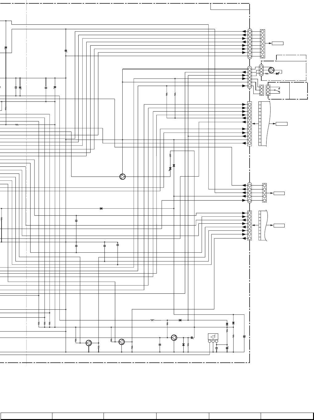
– 51 –
MD-E9000W
Figure 51 SCHEMATIC DIAGRAM (4/12)
78 9 10 11 12
5V
3 2 1
SW_5V
CD_GND
DGND
ILU LED
CD_OPEN_SW
CD_CLOSE_SW
P_CTRL
T/V_CLK
MD_SERCH
MD_ST-ID
MD_DATA
MD_KDATA
MD_DSCK
MD_DSTB
MD_RESET
MD_PCONT
RLY_CONT
FAN_CONT
SPAN
P_MUTE
P_IN
DISPLAY PWB-B1
UN_SW 5V
CD_GND
CD_WRQ
CD_DO
CD_DI
CD_CE
CD_CL
VF1
VF2
–VP
D_GND
SW_5V
CD_DRF
CD_RESET
T/V_DI
T/V_CE
TUN_DO
TUN_SM
1
2
3
1
2
3
1
2
3
6
5
4
3
2
1
12
11
4
3
2
1
6
7
8
9
10
5
1
2
3
4
5
6
7
8
1
2
3
4
5
6
7
8
5
4
3
2
1
5
4
3
2
1
8
7
1
4
3
2
6
5
BACK UP
2
1
3
2
1
3
2
1
3
23
1
1
8
CNP401
TO MAIN PWB
P48 4 - H
CNP871
TO POWER PWB
P55 7 - G
CNP406
TO MAIN PWB
P49 11 - D
CNP5
TO CD SERVO PWB
P57 12 - B
LED PWB-B2
CD LID
OPEN/
CLOSE
PWB-B2
+B
+B
+B +B
+B
+B
+B
1
12
1
2
3
RESET
LED DRIVER
R775
820K
C708
10/25
C707
0.022
C706
220/6.3
C705
0.022
C704
0.022
R771
10K
R772
10K
7
01
/
50 C702
1/50
R777
47K
R776
47K
Q702
KRC102 M
LED702
LNG901CF
BI704A
R778
56
SW724
OPEN/
CLOSE
CNP704CNS704
BI704
CNP702 BI702
CNS702
BI701
CNS701
CNP703
D785
DS1SS133
D701
DS1SS133
R773
2.2K
Q701
KRC102 M
C712
150P
C714
150P C715
150P
C713
150P
LED701
4204SRT7
R790
10K
R788
10K
R791
10K
R789
10K
Q782
KRC111 M
R785
470K
Q783
KRC111 M
R787
470K
L781
100µH
C784
0.022
R784
47K
Q781
KRC107 M
D784
DS1SS133
R783
100K
C783
10/25
D783
DS1SS133 D782
DS1SS133
R782
100
C782
0.022
C781
47/25
RX781
REMOTE
SENSOR
D781
DS1SS133
R781
22K
R786
10K
C709
100P
FFC703
FFC702
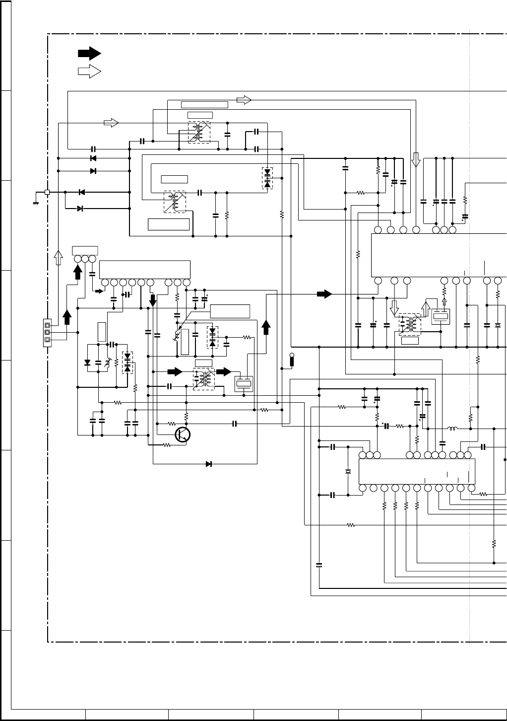
MD-E9000W
– 52 –
Figure 52 SCHEMATIC DIAGRAM (5/12)
A
B
C
D
E
F
G
H
123456
• NOTES ON SCHEMATIC DIAGRAM can be found on page 61.
AM
GND
FM
75OHMS
1 2 3
1 2 3 4 5 6 7 8 9
1 2 3 4 5 6 7 8 9
10 11
22
21
20 19
18 17
16
15 14
13 12
CONT
IF
FM/AM
FM/AM
SD
ST IND
MO/ST
VSS
AOUT
AIN
PD
VDD
FM IN
AM IN
DO
CL
DI
CE
X IN X OUT
IF IN
8 7 6 5 4 3 2 1
22 23 24 19 20 21 18
REG
AM IF IN
GND
SD
STEREO
FM DET
FM/AM OUT
VSM
AM LOW CUT
AM RF IN
AM OSC IN
FM AFC
AM OSC OUT
AM MIX OUT
FM IF IN
TP
3
1
2
3
13
2
AM TRACKING fL
AM ANT.
AM BAND
COVERAGE fL
AM OSC.
FM RF
FM OSC.
FM BAND
COVERAGE fL
FM IF
AM IF
TP301
OSC BUFF
+B
+B
+B
+B
+B
+B
+B
+B
C352 10/50
C350 0.022
D303
DS1SS133
D304
DS1SS133
C325
220P
D306
DS1SS133
C313
22P(CH)
C324
3.9P(UJ)
CF303
T301
C320
0.001
C310
15P
(CH)
R365
10K
R368
22K
BF301
BAND
PASS FILTER
R372 1K
IC302
LC72131
PLL(TUNER)
C364 2.2/50
R302
10
C318
100P
R316
4.7K
R325
47K
R393
1K
R376
1K
R309
10K
C384
0.001
T302
C305
4.7P
(CH)
C314
0.0047
R313
33K
R381
10K
X352
4.5 MHz
C363 0.022
T351
C317
0.001
R311
100K
L312
C332
0.022
C331
0.047
C330
15P(UJ)
C315
0.0047
C304
0.01
R314
22
D305
DS1SS133
R378 1K
R327
33
VD302
SVC211C
T306
C338
0.001
D301
DS1SS133
D302
DS1SS133
CF352
R352
1K
C361 0.022
C362 3.3/50
VD301
SVC348S
R382
150
C353 0.022
X351
C397
0.022
C382
15P(CH)
C366 0.001
R350
2.7K
R323
68K
R322
680
R375
470
C386
330P
R377
47K
C334
18P(UJ)
C335
560P
L351
100µH
C385
0.01
C380
10/50
R379
2.2K
C323
0.022
T303
C393
1/50 R380
1.5K
R373 1K
R374 1K
C306
0.022
C307
10/50
Q302
KTC3194 Y
C387
0.022
C309
0.001
C392
0.001
C394
47/16
C308
4.7P
C316
0.022
C312
0.022
R351
5.6K
C351 0.022
R358
3.9K
C342
0.022
C365 0.022
C367
1/50
R
3
2
7
CF351
C354 0.022
C311
18P
C303
10P(CH)
C381
12P(CH)
R336
10K
IC301
TA7358AP
FM FRONT END
SO301
ANTENNA
TERMINAL
VD303
SVC211C
FM SIGNAL
AM SIGNAL
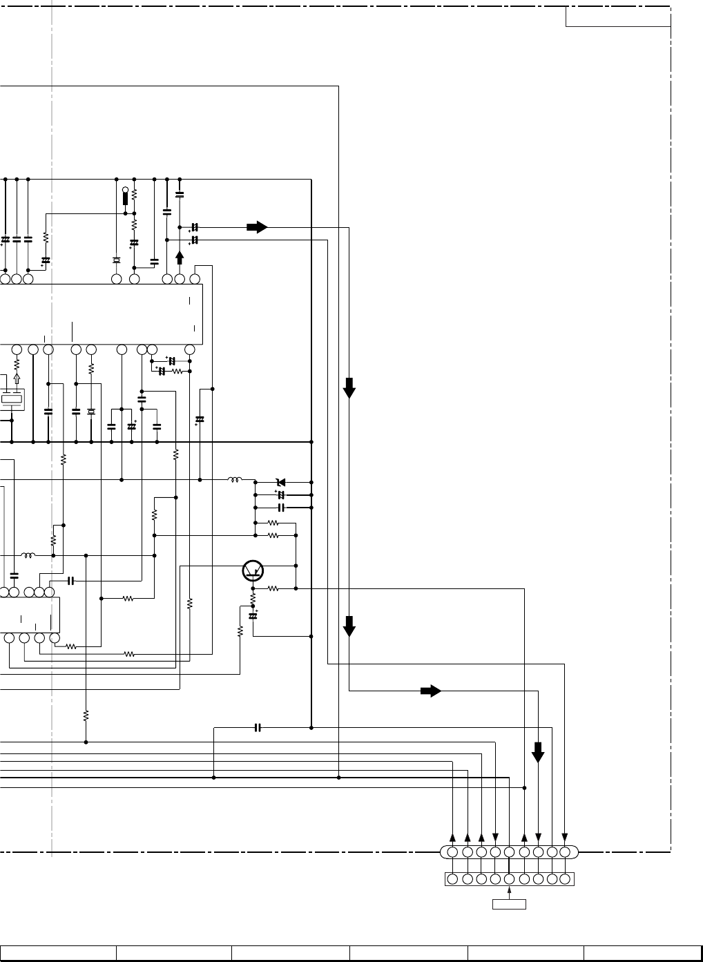
– 53 –
MD-E9000W
Figure 53 SCHEMATIC DIAGRAM (6/12)
78 9 10 11 12
8 9
10 11
16
15 14
13 12
CONT
IF
FM/AM
SD
ST IND
MO/ST
FM IN
AM IN
IF IN
12 11 10
9 8 7 6 5 4
19 20 18 17 16 15 14 13
MO/ST
AM IF IN
GND
SD
STEREO
FM DET
VCC
IF OUT
PHASE
(FM/AM)
PHASE L-CH OUT
R-CH OUT
MPX IN
MPX VCO
FM/AM OUT
VSM
AM LOW CUT
9 8 7 6 5 4 3 2 1
9 8 7 6 5 4 3 2 1
D GND
TV CL
TUN DO
T/V CE
T/V DI
A+10V
TUN-L
A-GND
TUN-R
TP302
13
2
CNP405
P49 9 - H
TO MAIN PWB
TUNER PWB-C1
Q360: CONSTANT VOLTAGE
+B
+B
+B
+B
+B
L352
100µH
R388
3.9K
R368
22K
C364
2
.
2/50
R387
5.6K
C370
1/50
R393
1K
R376
1K
R355
3.3K
R359
1.8K
C369
27P(UJ) C374 0.015
ZD351
DZ5.1BSB
C396
100/16
C395
0.022
R391
270
Q360
KTA1266 GR
R385
5.6K
R392
270
C372
1/50
C355
22P
C371
1/50
C388
0.001
R356
1K
C368
1/50
C398
100/16
C356
0.001
C357
2.2/50
C358
1/50
CF352
3
52
1
K
C353 0.022
C399
0.022
C373
0.015
X351
456 kHz
C366 0.001
R350
2.7K
R357
470K
R383
5.6K
C391
47/16
R384
5.6K
R395
47K
C386
330P
R360
4.7K
R377
47K
L351
100µH
C385
0.01
C387
0.022 C365 0.022
C367
1/50
R353
270
CF351
C354 0.022
IC303
LA1832S
FM IF DET./FM MPX./AM IF
BI301
CNS301
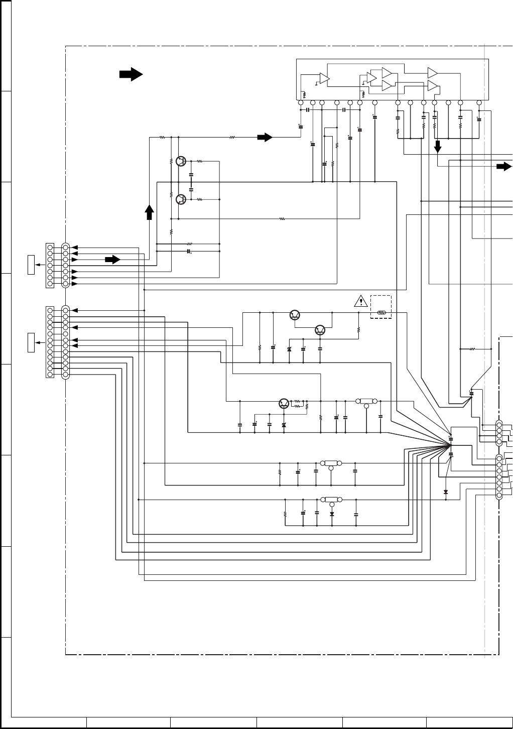
MD-E9000W
– 54 –
A
B
C
D
E
F
G
H
123456
Figure 54 SCHEMATIC DIAGRAM (7/12).
• NOTES ON SCHEMATIC DIAGRAM can be found on page 61.
+3.2V
3 2 1
3 2 1
3 2 1
Vcc
A_GND
(MD)S_GND
(MD)M_GND
(MD)H_GND
A_GND
+B
A_GND
Vcc
D_GND
SW_5V
CD_GND
CD+B
UN-SW_5V
MD_+A3.1V
FAN_CONT
MD_+D5V
(MD) D_GND
+B/2
M_GND
SW_5V
UN-SW_5V
P_CONT
A_GND
R-CH
L-CH
P_MUTE
A_+10V
A_GND
+B
+B
4
3
1
2
2
4
5
3
6
1
7
8
9
10
11
12
2
4
5
3
6
1
7
8
9
10
11
12
6
5
7
4
3
2
1
23 4 5 6 7 8 9
10 11 12 13 14
1
7
6
5
4
3
2
1
7
6
5
4
3
2
1
R
R
R
L
L
L
L
L
R
R
R
L
+
–
–
+
INP1
INP2
GND
VCC1
+OUT2
–OUT2
PWR
GND2
–OUT1
+OUT1
PWR
GND1
NOISE
PREVENT
STANDBY
+5V
CNP404
P49 8 - H
TO MAIN PWB
CNP403
P49 7 - H
TO MAIN PWB
P51 12 - D
TO DISPLAY PWB
+B
+B
+B
+B
+B
+B
+B
+B
+B
+B
+B
+B
+B
+B
+B +B
+B
+B
+B
+B
+B
+B
+B
+B
+B
+B
+B
+B
+B
VOLTAGE
REGULATOR
VOLTAGE
REGULATOR
VOLTAGE
REGULATOR
VOLTAGE
REGULATOR
VOLTAGE
REGULATOR
VOLTAGE
REGULATOR
MUTING
MUTING
BI901
CNS901
R909
22K
C905
47/50
Q902
KTC3199 GR
R901
15K R907
1K
R903
2.7K
Q901
KTC3199 GR
C901
0.001
R905
2.2K
C903
2.2/50
R906
2.2K
R902
15K
R908
1K
C902
0.001
R904
2.7K
C986
0.001 C987
0.001
R983
10K
C985
22/16
C912
100/35
R910
3.3K
C911
100/16
C904
2.2/50
C913
0.47/50
C907
0.1(ML)
R911
1K
C914
100/25
R914
1K
C910
0.1(ML)
R913
1K C909
0.1(ML)
R912
1K C908
0.1(ML)
IC901
LA4628
POWER AMP.
BI903A BI903B
C948
3300/25
C949
6800/16
D961
DS1SS133
UN-SW_REG
R928
2.2K
C947
6800/25
R941
1K
C953
47/25
C952
0.1(ML)
C951
0.1(ML)
RP941
0.5
Posistor
Q942
KTC3199 GR
Q951
KIA7810AP
Q941
KTC2026
R942
47K
C943
470/10
C942
100/16
ZD941
DZ6.8BSA
C941
0.022
R955 220
R952
22K
ZD951
DZ3.6BSB
C954
0.022
C955
100/10
C956
0.022
R954
220
Q952
KTC3203 Y
R953
1.2K
Q962
AN78L05
C963
47/25
D962
DS1SS133
C964
0.1(ML)
R962
10K
C966
47/25
C965
0.1(ML)
Q961
KIA7805AP
R961
10K
C962
0.1(ML)
C961
0.1(ML)
BI902
CNS902
FM SIGNAL
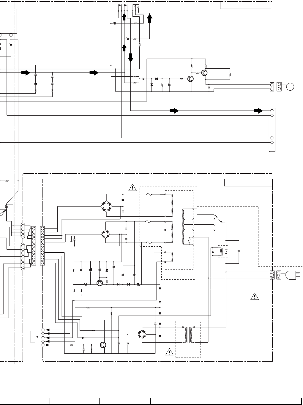
– 55 –
MD-E9000W
Figure 55 SCHEMATIC DIAGRAM (8/12)
78 9 10 11 12
A_GND
Vcc
Vcc
A_GND
–
+ M
A_GND
+B
A_GND
Vcc
P_IN
VF2
VF1
–VP
Vcc
+B
A_GND
A_GND
+B/2
POWER AMP. PWB-C3
1 POWER PWB-C2
SP-L(–)
SP-L(+)
SP-R(+)
SP-R(–)
UN-SW_5V
+B/2
M_GND
SW_5V
AC_RLY
M_GND
SW_5V
UN-SW_REG
UN-SW_5V
1
2 2
1
11
10
9
8
7
6
5
4
3
2
1
11
10
9
8
7
6
5
4
3
2
1
4
3
1
2
6
5
7
4
3
2
1
1
4
2
1
3
5
3
14
L
VCC1
+
+
–
–
AC POWER
SUPPLY CORD
CNS701
P51 12 - D
TO DISPLAY PWB
+B +B
+B
+B
+B
+B
+B
+B
+B
+B +B
+B
+B
+B
+B
+B
+B
+B
+B
+B
+
B
+B
+B
+B
+B
T.F.
Q971, Q972: FAN MOTOR DRIVER
RELAY DRIVER
230-240 V
220 V
127 V
110 V
R911
1K
C914
100/25
C925
0.1(ML)
R923
4.7
C923
0.1(ML)
C926
0.1(ML)
R924
4.7
C924
0.1(ML) R984
47
R979
330
R974
10K
R975
2.2
C973
47/25
Q972
KTA1266 GR
CNP971
R972 33K
C972
47/25
D973
DS1SS133
C971
4.7/50
R977
10K
R973
3.3K
Q971
KTC3203 Y
R978
10K D972
DS1SS133
JK981
HEADPHONES
R982
270
C982
4.7/50
L981
2.2µH
C981
4.7/50
R981
270
SO901
SPEAKER
TERMINAL
M905
FAN
MOTOR
CNS971
SO801
AC INPUT SOCKET
AC 110/127/220/230-240 V
50/60 Hz
D871
DS1SS133
C871
0.0047/250V
SW801
VOLTAGE
SELECTOR
RL800
C805
220/50
C812
0.047
PT801
MAIN POWER
TRANSFORMER
R805
220K
R804
220 R803
12K
R802
220 C810
100/35
D877
DS1SS133
D801
TS6B04GM
C804
0.047
(ML)
C803
0.047
(ML)
D805
RL203F
D802
RL203F
D804
RL203F
D803
RL203F
C802
0.047
(ML)
C801
0.047
(ML)
D806
DS1N404S
C806
220/50
D807
DS1N404S
D808
DS1N404S C807
47/50
C808
47/50
R801
1K ZD801
DZ30BSC
Q801
KTA1266 GR
C809
47/50
ZD802
DZ6.2BSA ZD803
DZ12BSB
R806
47K
R871
220
C874
1000/6.3
Q871
KTC3199 GR
R872
47K
C875
0.022
R873
1K
CNP871
D809
DS1SS133
C873
1000/16
D873
D876
D874
D875
C811
0.0022
C872
0.047
(ML)
ZD871
DZ3.0BSA
D872
DS1SS133
PT871
SUB POWER
TRANSFORMER
F803
T2.5A L 250V
F802
T2.5A L 250V
F801
T6.3A L 250V
CNP903
BI903A BI903B
CNS903
9
48
0
0/25
9
49
0
0/16
UN-SW_REG
R928
2.2K
C947
6800/25
D873~D876:
DS1N404S
MD-E9000W
– 56 –
A
B
C
D
E
F
G
H
123456
Figure 56 SCHEMATIC DIAGRAM (9/12)
• NOTES ON SCHEMATIC DIAGRAM can be found on page 61.
3.2V
3
80 79 78 77 76 75
7
2
26 25 24 23 22 21
20
19
18
20
19
18
17
16
15
14
13
12
11
10
9
8
7
6
5
4
3
2
1
1
30 29 28 27 26 25 24 23 22 21 20 19 18 17 16
15 14 13 12 11 10
9 8 7 6 5 4 3 2 1
SPDO
TDO
FDO
SPDO
SLDO
FDO
SLDO
TDO
LD
VR
GND
PUIN
SL+
SL–
SP–
SP+
TR–
FR
VVDD
PCKIST
VVSS
PDO2SBCK/CONT6
CONT5
CONT4
GPDAC
SLDO
SPDO
FDO
T
REFI
VREF
A
A
JITTC
RFMON
TE
TEC
FE
TIN2
TIN1
FIN2
FIN1
RSVSS
RFVDD
RF
EFMIN
SLCIST
PD
TR–
TR–
FO–
FO+
TR+
TR+
TR+
FO+
FO+
FO–
PD
VR
LD
C
F
B
A
E
VCC
VCC
+
+
–
–
7
6
5
4
3
2
1
7
6
5
4
3
2
1
7
6
5
4
3
2
1
1
2
3
5
6
4
1
2
3
4
5
6
7
1
2
3
4
5
6
1
2
3
4
5
6
1
2
3
4
5
6
1
7
6
3
8
4
5
2
1
7
6
3
8
4
5
2
1
7
6
3
8
4
5
2
6
3
7
1
2
5
8
4
M
M
– + + –
+
– –
+
–
–
+ –
+
– +
+
MUTE REF
VCC
VCC
GND GND
CD
RST
RST
IN
OUT
REG
PICKUP UNIT
Q1: LASER DRIVER
CD MOTOR
PWB-F
+B
+B
+B
+B
+B
+B
+B
+B
+B +B
+B
+B
+B
+B
+B
+B
+B
Q2: CONSTANT
VOLTAGE
CD SIGNAL
C58
680P
C57
680P
C53
4.7/25
R1 8.2K
C1
0.01
C2
47/16
CNP2CNS2ACNS2B
R2
22K
R3 8.2K
R4 8.2K
R7
22K
R6 8.2K C3
0.01
C5
0.001
Q1
KTA1266 GR
R9
3.3
C4
47/16
R8
47
C54 22P
C13
0.22/50
R11
10K
C8
10P
C14
100P
C6 0.047
C7 0.1
C10
100/16
R10
27K
C9
0.0027
R12
330
C12
10/16
C
C16
C
2
C
R14
1.2K
R15 12K
C
2
C
2
R16
680
C15 0.1
C
C
2
LDD
LDS
R
R
4
C47
0.1
C48
0.1
R21
8.2K
R20
8.2K
R19
15K
Q2
KTA1271 Y
C46
0.1
C45
330/10
IC2
LA6548D
IC2
FOCUS/TRACKING/
SPIN/SLED DRIVER
R13
15K
CNP4CNS4ACNS4B
CNP4A
M2
SPINDLE
MOTOR
M1
SLED
MOTOR
SW4
PICKUP IN
CNP1
CNS1ACNS1B
C63
0.001
2
4
1
6
8
5
– 57 –
MD-E9000W
Figure 57 SCHEMATIC DIAGRAM (10/12)
78 9 10 11 12
• The numbers 1 to 12 are waveform numbers shown in page 62.
3.2V
3.2V
5V
5V
5V
3.2V
5V
80 79 78 77 76 75 74 73 72 71 70 69 68 67 66 65 64 63 62 61
60
60
59
58
57
56
55
54
53
52
51
50
49
48
47
46
45
44
43
42
41
43
42
41
40
39 38 37 36 35 34 33 32 31 30 29 28 27 26 25 24 23 22 21
20
19
18
20
19
18
17
16
15
14
13
12
11
10
9
8
7
6
5
4
3
2
1
1
14
13
12
11
10
9
8 7
6
5
4
3
2
1
9 8 7 6 5 4 3 2 1
17 16
15 14
SO
TDO
FDO
SPDO
SLDO
DGND
LRCK
BCK
CDDATA
CD SERVO PWB-D
–
+
FR
VVDD
PCKIST
VVSS
PDO2
PDO1
CONT1
CONT2
CONT3
VSS
VDD5
DRF
*RES
*WRQ
DO
DI
CL
CE
DATA
BCK
LRCK
ASDFIN
ASDACK
ASLRCK
16MOUT
EFLG
C2F
XVSS
FSX/16MIN
XIN
XOUT
XVDD
RVDD
RCHO
RVSS
LVSS
LCHO
LVDD
TEST
DOUT
VDD
VSS
MONI5
MONI4
MONI3
MONI2
MONI1
FSEQ
V/*P
DEFECT
SBCK/FG
SBCK/CONT6
CONT5
CONT4
GPDAC
SLDO
SPDO
FDO
TDO
REFI
VREF
ADAVSS
ADAVDD
JITTC
RFMON
TE
TEC
FE
TIN2
TIN1
FIN2
FIN1
RSVSS
RFVDD
RF
EFMIN
SLCIST
SLCO
DIGITAL
OUT
CD_GND
CD RES
CLK
DI
DO
CE
DRF
WRQ
+5V
1
2
3
4
5
6
1
2
3
4
5
6
4
5
3
1
8
7
6
2
1
2
1
2
2
1 1
2
M
CD
RST
RST
IN
OUT
REG
23
1
+B
+B
+B
+B
+B
+B
+B
+B
+B
+B
+B
+B
+B
+B
+B
+B
+B
+B
+B
+B
+B
:
CONSTANT
VOLTAGE
CNP402
P48 5 - H
TO MAIN PWB
CNS702
P51 12 - B
FROM DISPLAY PWB
5
0
R11
10K
P
7
C9
.
0027
C12
10/16
C24 0.022
C16 2.2/50
IC1
LC78645NE
CD SERVO
C20 100P
C18 100P
R14
1.2K
R15 12K
C22 100P
C23 100P
R17
680
C17
0.047
R16
680
C15 0.1
C19 0.022
C21 100P
LDD
LDS
R53
220 R42
220
Q3
KRC102 M
R56
18K
R54
1K
R55
100K
R23
1K L2
0.82µH
R24
47K
R49
5.6K
R48
2.2
C32
15P
(CH)
C31
15P(CH)
XL1
33.8688 MHz
R37
100
R38
100
R39
100
R18
6.8K
R21
8.2K
R20
8.2K
R19
15K
Q2
KTA1271 Y
C46
0.1
C45
3
30/10
C42
0.022
C41
100/16
C61
0.01
R13
15K
BI1
CNS402
CNP5
C43
100/16
C62
0.001
C44
0.0015
R40
10K
R36 1K
R35 1K
C28 0.047
L4
2.2µH
IC4
74VHC08F
INVERTER
R33 1K
R32 1K
R27 1K
R28 1K
R29 1K
R30 1K
R31 1K
R50
15K
IC3
TA7291S
C49
47/16
C50
0.1 CNS3CNP3
LOADING MOTOR DRIVER
M904
CD LID
MOTOR
CNP6
CNS6
CORE1
CORE2
6
9
3
10 11 12
78
5
MD-E9000W
– 58 –
A
B
C
D
E
F
G
H
123456
• NOTES ON SCHEMATIC DIAGRAM can be found on page 61.
Figure 58 SCHEMATIC DIAGRAM (11/12)
(2.5V)
(1.5V)
(1.5V)
(2.5V)
(0V)
(2.6V)
(2.6V)
(2.6V)
(2.6V)
(0.1V)
(0.1V)
(0V)
(5V)
(2.6V)
(2.6V)
(0.1V)
(0.1V)
(1.4V)
(1.4V)
(5V)
(1.4V)
(1.4V)
(2.5V)
(5V)
(1.4V)
(1.4V)
(2.5V)
0V
0V
0V
0V
3.2V
3.2V
3.2V
3.2V
0V
0V
0V
0V
0V
0V
0V
0V
0.4V
3.2V
0V
3.2V
1.5V
0V
1.6V
3.2V
3.2V
3.2V
3.2V
3.2V
0V
0V
2.9V
0V
0V
3.2V
3.2V
3.2V
3.2V
0V
1.5V
2.6V
0.8V
3.2V
0V
3.2V
0V
0V
0V
0.1V
0V
PIT:3.2V
GROOVE:0V
(3.2V) 0V
HIGH DISC:0V
LOW DISC:3.2V
3.2V
0V
0V
0V
3.2V
3.2V
3.2V
0V
0V
0V
0V
0V
0V
0V
3.2V
3.2V
0V
3.2V
3.2V
3.2V
3.2V
0V
2V
1.8V
2.2V
1.5V
0.7V
+B
+B
+B+B
+B
+B
+B
+B+B
1.3V
1.3V
2.6V
2.6V
1.3V
1.3V
0V
2.6V
1.3V
1.3V
1.3V
1.3V
1.3V
2.5V
1.6V
1.6V
1.6V
1.6V
1.6V
1.6V
1.6V
1.6V
1.6V
0V
0V
0.7V
0.7V
0.7V
1.7V
1.3V
32V
01V
0V
0V
0V
3.2V
3.2V
1.6V
1.6V
1.6V
5V
5V
0V
1.6V
0V
0V
2.5V
2.5V
2.5V
2.5V
2.5V
2.5V
1.6V
1.6V
1.6V
1.2V
1.2V
1.6V
1.6V
1.6V
1.6V
1.6V
0V
3.2V
3.2V
0.9V
5V
5V
5V
0V
0V
1.6V
1.6V
1.6V
2.5V
2.5V
2.5V
2.5V
1.6V
0.7V
0.7V
0.7V
0.7V
1.3V
1.3V
1.3V
1.3V
1.3V
1.3V
1.3V
1.3V
1.3V
1.3V
1.3V
1.3V
1.3V
1.3V
1.3V
1.3V
1.3V
1.3V
1.3V
0.7V
1.5V
LOW DISC:2.6V
HIGH DISC:0V
PIT:2.6V
GROOVE:0V
2.6V
2.6V
1.3V
0V
1.3V
1.3V
0V
1.3V
1.3V
1.3V1.3V
0V
2.6V1.6V
0V
1.3V
1.3V 1.1V
0.7V 0.7V
0V
SW1936
LEAD IN
SW1932
LOADING
SW1933
RECORD
SW1930
WRITE PRO
SW1934
PLAY
C1563
1
C1161
0.001
R1118
330K
R1117
47K
R1115
330K
R1116
47K
C1340
100P(CH)
L1300
4.7µH
IC1300
74ACT02T
HEAD DRIVER
R1304
150
C1606
10
C1304
220P
(CH)
R1125
2.2K
R1122
12K
R1123
12K
R1430
10K
R1435
10K
C1405
680P(CH)
IC1401
IX0410AW
MD SYSTEM
MICROCOMPUTER
R1408
3.3K
C1211
0.1
C1262
220P(CH)
C1261
220P(CH)
C1266
22P
(CH)
C1263
220P(CH)
C1264
220P(CH)
C1265
220P(CH)
R1266 27K
R1261 27K
R1262 27K
R1263 27K
R1264 27K
27K
R1265
C1200
1
R1420
1K
C1407
0.1
L1101 10µH
C1125
1
C1305
68P(CH)
CN1401
R1100
27
R1406
10K
R1460
10K
R1463
10K
C1403
0.1
IC1402
58X2402T
EEPROM
R1401
2.7K
C1616
100/10
C1602
470P
(CH)
R1601
12K
C1603
680P
(CH)
R1605
12K
C1607
1
R1621
6.8K
R1622
22K
R1623
22KC1655
0.01
R1624
6.8K
IC1601
M56788FP
MOTOR DRIVER
C1619
330P(CH)
C1610
4.7
C1613
0.01
R1618
22K
R1616
12K
C1611
0.0047
R1111
100K
IC1101
IR3R58M
RF SIGNAL
PROCESSOR
R1110
680K
R1113
680K
C1122
1
R1121
100K
R1120
560K C1124
0.1
C1121
0.22
C1123
0.1
C1118
0.47 C1119
0.47
R1119
220K
C1117
1
C1116
1
C1115
0.1
C1114
0.1
C1113
1
R1114
12K
C1112
5P
(CH)
C1111
1
C1110
1
D1300
SBE803
R1300
6.8
IC1302
CPH5608
HEAD DRIVER
IC1301
FTD2005
HEAD DRIVER
R1301
10
C1301
0.022
C1300
150P
(CH)
C1302 10
R1403
270
R1407
3.3K
C1404
0.01
R1417
1K
R1418
1K
R1414
220K
R1415
1K
C1303 1
CN1300
R1612
56K
R1614
33K
R1101
1
R1102
10K
L1100
0.47µH
C1100
4.7
R1105
1.2K
C1107
0.022
C1202
1
R1207
39K
R1205
68K
R1203
100K
R1201
56K
C1201
10
IC1202
IX2474AF
4MBIT D-RAM
CW1903
CW1931
R1112
100K
CN1101
R1124
2.2K
M903
LOADING
MOTOR
M902
SLED
MOTOR
M901
SPINDLE
MOTOR
R1931
1K
R1932
470
R1934
180
R1933
560
APCIN
LDON
LDVCC
DGND
B
LVVOUT
SW
+2.8V
APCOUT
DGND
LDVAR
A
COM
RF1
F
E
RF2
RF4
VCC
MP/R
RF3
T-
F-
AGND
F+
T+
LVVIN
DGND
SYS
D
SLO
SLO
SLO
SLO
SLO
V
C
INN
E
G
N
L3DA
T
L3MO
D
L3C
L
CRTRG
S
ADMUTE
TEST0
AVCK1
AVCK2
TEST2
LD–
MUTE
TEST1
RAST
LD+
AVCK3
MINF
TEST-K2
TESTK1
AVCC
VREF
GND
DTEMP
Q/N
SLDRR
SPDRR
TRDRR
FODRR
SYD6
SYD5
SYRS
SYRDX
SYWRX
SYD7
SYD5
SYD6
SYD7
SYWR
SYRD
SYRS
SLDRF
TRDRR
TRDRF
FODRR
AGND1
TCG
AIN
BIN
EIN
FIN
VBAT
WBI
RAA3
RAA2
RAA1
RAA0
RAA10
VDD1
DGND
AVCC2
VREF
TEST2
X176KO
FODRF
VDD2
100
99 98 97 96
30
29
28
27
26
25
24
23
22
21
20
19
18
17
16
15
14
13
12
11
10
9
8
7
6
5
4
3
2
1
EFMO-I
WBO-I
BOUT-IN
AOUT-IN
FOUT-IN
EOUT-IN
ADIPO
AOUT
EOUT
EFMO
ADAGC
RFADD
REFO
FOUT
FIN
EIN
BIN
AIN
TCGI
AGC
REFI
RF4
RF3
RF2
RF1
BIAS
EOUT
BOUT
ADIP
DIFF
SW
and
R
BPF
DISC
SGAIN
DTEMP
PIN
3+4
PITG
NIN
AOUT
1234
1+2
GND1
2-1
ADAGI
ADIPNF
GND2
BIAS
VCC1
DCNF
OPICPW
TCGO
FSW
BSW
ASW
EFMAGC
WBO
VCC2
MODE
BOUT
ESW
SW
AGC
48 47 46 45 44 43 42 41 40 39 38 37
36
35
34
33
32
31
30
29
28
27
26
25
24
23
22
21
20
19
18
17
16
15
14
13
12
11
10
9
8
7
6
5
4
3
2
1
SGAIN
DISC
DTEMP
BIN
AIN
RF3
RF4
RF1
RF2
FIN
EIN
FN
TP
FP
TN
CHASSIS
GND
R/P
3.2V
2.6V
R/P
A0
A1
A2
A3
4M/16M
EEPRO
VCC
VSS
CDB SEL
DSTB
R/P
HDON
DSCK
MDDATA
SYSD3
SYSD2
LDVAR
EEPK
KDATA
XRST
MDRSW
UNLOCK
SGAIN
CIN
SERCH
ST-ID
MCCK
SYSD7
SYSD6
SYSD5
SYSD4
SB
S
DAP
O
LD
O
PCN
T
BYTE
CNVSS
STID OUT
SEACH OUT
DF
S
DF
S
SYRD
SYRS
SYWR
SYSD1
FOK
EEPD
5/3
07/120
DINT
DISC
ADJS
A
FLASH L
SBO
SFSY
SBCK
64M
P-DOWN
DSENSE
FRASH H
LA
S
HFON
DTEMP
CIN
LDVAR
RESET
HDON
MINF MINF
8
7
6
5
4
3
2
1
14 13 12 11 10
98
7654
3
21
5 4 3
2 1 5
4
3 2
1
8
7
6
5
4
3
2
1
LDON
LDVAR
( ):REC MODE
G1
S2
S2
S1
S1
D1
D2 G2
G2
D2
D1
S
G1
T–T+F–F+
HDON
EXT.C
LDOUT
APC
LVV
LDVAR
LDON
GND
VCC
F.COIL
T.COIL
1
2
1
2
89
1011121314
151617
18
19
202122232425262728
71
23456
89
1011121314
151617
18
19
202122232425262728
71
23456
GND
VCC
9
8
7
6
5
4
3
2
1
SP–
SP+
SLD–
SLD+
TRY–
TRY+
SP+
SL–
SL+
SP–
LEAD IN
LD–
LD+
MINF
GND
8
7
6
5
4
3
2
1
SBO
SYD4
SYD5
SYD6
SYD7
SYWR
SYRD
SYRS
FOK
SBCK
DSENSE
SFSY
DINT
RESET
SGAIN
DISC
STID
SERCH
MCCK
CHASSIS
GND
GND
A2
T+
WP
SCL
A0
SDA
VCC
A1
VSS
T-
F+ F– T+ T–
R/P
LEAD IN
MINF
MINF
R/P
HDON
R/P
5034 35 36 37 38 39 40 41 42 43 44 45 46 47 48 4933
32
31
30
29
28
27
26
25
24
23
22
21
20
19
18
17
16
15
14
13
12
11
10
9
8
7
6
5
4
3
2
1
81828384858687888990919293949596979899
100
DSTB
DSCK
KDATA
MDDATA
TRDRR
TN
TP
FP
FN
F-F+
INNSW
42
41
40
39
38
37
36
35
34
32
33
31
30
29
28
27
26
25
24
23
2221
20
19
18
17
16
15
14
13
12
11
10
9
8
7
6
5
4
3
2
1
FODRR
SPDRR
SLDRR
VREF
+
–
+
–
–
+
M
M
M
1.25V
CH3IN
OUT3
IN3–
VBS2
Vm2
IN3+
NC
GND
VM3+
VM3–
VM4–
VM4+
VM5+
VM5-
OUT5
IN5–
IN5+
IN4+
IN4–
OUT4 VREFO
VREF
SS.GND
MUTE2
MUTE1
IN2+
IN2-
OUT2
VM2–
VM2+
GND
VM1+
VM1–
OUT1
IN1–
Vm1
VBS1
IN1+
REGB+
REG+
–
GND
GND
EFMO-I
FOUT-IN
EOUT-IN
BOUT-IN
AOUT-IN
TCG
WBO-I
TCG
I/V
I/V
I/V
I/V
EFMO
78
79
80
51
52
53
3
2
1
30
29
28
VREF
TCG
EOUT-IN
AOUT-IN
BOUT-IN
FOUT-IN
MD LOADING PWB-G2
MD MECHANISM
SWITCH PWB-G1
MD PICKUP UNIT(35)
MAGNET HEAD
(RECORD)
TP1254
TP1253
TP1252
TP1251
TP1250
TP1201
TP1202
TP1200
TP1136
TP1133
TP1135
TP1130
TP1112
TP1117
TP1118
TP1119
TP1105
TP1106
TP1107
TP1108
TP1109
TP1115
TP1110
TP1111
TP1113
TP1123
TP1122
TP1121
TP1120
TP1104
TP1103
TP1102
TP1101
TP1100
TP1330
TP1300
TP1301
TP1907
TP1908
TP1906
TP1905
TP1904
TP1903
TP1902
TP1901
TP1603
TP1602
TP1400
TP1600
TP1604
TP1605
TP1542
TP1543
TP1909
TP1601
TP1630
TP1303
TP1451
TP1401
TP1404
TP1402
TP1403
TP1406
TP1407
TP1408
TP1409
TP1420
TP1405
TP1422
TP1421
TP1607
TP1131
TP1116
TP1302
30 31
4
16
28
8
10
11
9
29
7
17
6
5
13
12
14
15
7
– 59 –
MD-E9000W
78 9 10 11 12
Figure 59 SCHEMATIC DIAGRAM (12/12)
• The numbers 1 to 36 are waveform numbers shown in page 63, 64.
• The numbers 1 to 10 are chart numbers shown in pag 32, 33.
3
.
2V
3.2V
0V
0V
0V
0.1V
0V
PIT:3.2V
GROOVE:0V
(3.2V) 0V
HIGH DISC:0V
LOW DISC:3.2V
3.2V
0V
0V
0V
3.2V
3.2V
3.2V
0V
0V
0V
0V
0V
0V
0V
0.2V
0V
0V
0V
3.2V
3.2V
3.2V
3.2V
3.2V
0V
0V
0V
0V
0V
0V
0V
0V
0V
0V
3.1V
3.2V
3.2V
3.2V
0V
0V
0V
0V
0V
0V
3.2V
3.2V
3.2V
3.2V
0V
2V
1.8V
2.2V
1.5V
0.7V
3.2V
2.6V
0V
3.1V
3.2V
0V 0V
+B+B
+B
+B
+B
+B
+B
+B
+B
+B
+B
+B
+B
5V
0V
0V
0V
3.2V
1.6V
1.6V
1.6V
3.2V
3.2V
3.2V
3.2V
3.2V
0V
0V
1.6V
1.6V
3.2V
0V
3.2V
0V
0V
0V
0V
0V
0V
1.6V
3.2V
1.6V
0V
0.7V
1.1V
1.1V
1.1V
1.1V
2.3V
2.5V
1.8V
1.9V
3.2V
2.3V
3.1V
1.8V
1.3V
1.3V
1.7V
0.7V
0.7V
0.7V
1.3V
1.3V
2.6V
2.6V
1.3V
1.3V
0V
2.6V
1.3V
1.3V
1.3V
1.3V
1.3V
2.5V
1.6V
1.6V
1.6V
1.6V
1.6V
1.6V
1.6V
1.6V
1.6V
0V
0V
0.7V
0.7V
0.7V
1.7V
1.3V
3.2V
0.7V
1.1V
1.1V
1.1V
1.1V
2.3V
2.5V
1.8V
1.9V
1.3V
2.3V
3.1V
1.8V
1.3V
1.3V
2.6V
1.4V
0V
3V
1.6V
0V
0V
0V
0V
3.2V
0V
3.2V
3.2V
3.2V
3.2V
2.5V
0V
1V
1V
1.6V
1.6V
0V
0V
0V
0V
1.6V
1.6V
1.6V
1.6V
1.6V
1.6V
0V
3.2V
3.2V
3.2V
3.2V
0V
0V
1.6V
3.2V
3.2V
0V
3.2V
0.2V
0V
0V
0V
0V
0.1V
0V
0V
0V
3.2V
3.2V
C1524
100P(CH)
C1523
100P(CH)
C1206
0.01
C1260
0.1
CN1501
L1202
0.47µH
C1530
100P(CH)
C1538
100P(CH)
C1536
47P(CH)
C1534
47P(CH)
R1430
10K
R1441
47K
R1443
1K
R1435
10K
IC1401
IX0410AW
MD SYSTEM
MICROCOMPUTER
R1517
47
R1516
220
R1515
220
R1518
47
R1535
1K
R1533
1K
C1230
1R1231
10K
R1230
10K
Q1807
2SD601AR
L1201
0.47µH
L1200
4.7µH
R1701
47K R1702
33K
IC1802
XC62FP26
REGULATOR
C1806
1
C
1211
0.1
C1265
220P(CH)
C1200
1
IC1201
LR37816A
ENDEC/ATRAC
C1721
330P
(CH)
C1720
330P
(CH)
C1409
1
R1705
3.9
Q1501
UN2214 R1532
27K
C1512
100P(CH)
C1510
100P(CH)
R1538
1K
R1537
1K
R1536
1K
R1534
1K
R1521
1K
R1529
220
R1716
100K
IC1701
UDA1345
AD/DA CONVERTER
C1715
0.1
C1708
0.01
C1703
0.1
C1704
47/4
C1750
0.1
C1700
47/4
C1706
0.01
C1716
47/4
R1703
3.9 R1704
3.9
R1803
33K
R1802
56K C1802
10
R1811
1
R1804
390
Q1804
2SB1205
R1806
1
R1809
1
R1807
27K
IC1801
XC62EP32
REGULATOR
R1214
10K
R1210
220
C1208
12P(CH)
R1217
150
XL1201
33.8688 MHz
C1209
12P(CH)
R1215
1M
C1202
1
R1207
39K
R1205
68K
R1203
100K
R1201
56K
C1207
1
R1209
100
R1211
220
C1201
10
C1205
1
IC1202
IX2474AF
4MBIT D-RAM
AA.GND
FL1525
FL1524
FL1523
FL1520
FL1518
FL1512
FL1509
FL1507
FL1501
C1801
10
C1540
150P(CH)
CW1501
R1446
10K
SYSD0
SLOT1
SLOT2
SLOT3
SLOT4
SLOT5
VCC
INNER
GND
L3DATA
L3MODE
L3CLK
CRTRG SW
ADMUTE
TEST0
AVCK1
AVCK2
TEST2
LD–
MUTE
TEST1
RAST
LD+
AVCK3
MINF
TEST-K2
TESTK1
GND
DTEMP
VSSA
VDDA
VINL
VREFA
VINR
VADCN
VADCP
MP1
VDDD
VSSD
MC1
MP2
MP3
SYSCLK
MP4
BCK
WS
DATAO
DATAI
MP5
MC2
AVSS
AVDD
VOUTR
VDDO
VSSO
VREFD
VOUTL
DADATA
ADDATA
LRCK
BCLK
DFCK
I/O1
VCC
RAS
A2
A3
A1
I/O2
A9
WE
A0
A9
A0
A1
A2
A3
D
RR
DRR
DRR
DRR
DFCK
BCLK
LRCK
DGND
VDD3
DOUT
DIN
XO
SYD6
SYD5
SYD4
SYD3
SYD2
SYD1
SYD0
RSTX
SYRS
SYRDX
SYWRX
SYD7
SBSY
SBCK
TEMON
TOTMON
DGND
VDD1
SENSE
MCCK
COUT
DINTX
SFSY
SBO
FOK
XRST
SYD0
SYD1
SYD2
SYD3
SYD4
SYD5
SYD6
SYD7
SYWR
SYRD
SYRS
MD-ST
SERCH
H.GND
R IN
L IN
L OUT
R OUT
AVCC
AA.GND
H.VDD
DVDD
DVDD
D.GND
D.GND
M.GND
M.GND
DSTB
MDDATA
KDATA
DSCK
C GND
RESET
DIGIN
PCONT0
CDDATA
CDBCK
CDLRCK
27
27
26
25
20
19
18
17
16
15
14
13
12
11
10
9
8
7
6
5
4
3
2
21
22
23
24
1
1
DSTB
MDDATA
KDATA
DSCK
CHASSIS GND
DIN
SERCH
STID
RESET
14 15
16
17
18
19
20
21
22
23
24
25
26
27
28
13
12
11
10
9
8
7
6
5
4
3
2
1
L3DATA
L3CLK
L3MODE
75
74
73
53
52
51
25
24
23
3
2
1
X700KO
EFMO
SPDRR
SPDRF
SLDRR
SLDRF
TRDRR
TRDRF
FODRR
RAA7
VDD1
FEMON
DADATA
ADDATA
VXI
CDBCLK
CDLRCK
CDDATA
DIN2
DILOCK
TEST1
TEST0
TCRS
EFMMON
XI
DGND
VPD
AVCC
EFMI
AGND1
TCG
AIN
BIN
EIN
FIN
VBAT
WBI
DGND
RAA4
RAA5
RAA6
RAA8
RAOEX
RACASX
RAD2
RAD3
RAA9
RAA3
RAA2
RAA1
RAA0
ACRCER
PLCK
RAA10
TCRS
VDD1
DGND
AVCC2
VREF
TEST2
X176KO
RARASX
RAWEX
RAD0
FODRF
VDD2
RAD1
100
99 98 97 96 95 94 93 92 91 90 89 88 87 86 85 84 83 82 81 80 79 78 77 76
75
74
73
72
71
70
69
68
67
66
65
64
63
62
61
60
59
58
57
56
55
54
53
52
51
50
49
48
47
46
45
44
43
42
41
40
39
38
37
36
3534
33
32
31
30
29
28
27
26
25
24
23
22
21
20
19
18
17
16
15
14
13
12
11
10
9
8
7
6
5
4
3
2
1
M
O-I
W
BO-I
BOUT-IN
A
OUT-IN
FOUT-IN
EOUT-IN
20
19
18
17
16
15
14
13
1211
10
9876 54321
A9
A8
A7
A6
A5
A4
A0
A1
A2
A3
A6
A4
A5
A7
A8
GND
OE
A5
CAS
A6
I/O4
A8
A4
A7
I/O3
SBSY
LDON
VREF3.2V
VREF3.2V
AA.GND
4M/16M
R/P
SYSD3
SYSD2
LDVAR
EEPK
XRST
SGAIN
SYSD7
SYSD6
SYSD5
SYSD4
SBSY
DAPON
LDON
PCNT0
T
DFS0
DFS1
SYRD
SYRS
SYWR
SYSD1
FOK
EEPD
5/3
07/120
DISC
A/B
FLASH L
SBO
SBCK
64M
FRASH H
LAST
HFON
DTEMP
SBO
SYD4
SYD5
SYD6
SYD7
SYWR
SYRD
SYRS
FOK
SBCK
SGAIN
DISC
51
52
53
54
55
56
57
58
59
60
61
62
63
64
65
66
67
68
69
70
71
72
73
74
75
76
77
78
79
80
50
35 36 37 38 39 40 41 42 43 44 45 46 47 48 49
L3DATA
L3MODE
L3CLK
XRST
SYD0
SYD1
SYD2
SYD3
VREF3.2V
VREF3.2V
UCON3.2V
81828384858687888990919293949596
5
43
2
1
PCNT0 PCNT0
LD–
LD+
T
CG
DSENSE
SBCK
SBO
SBSY
SFSY
FOK
CIN
MCCK
DINT
ADDATA
DADATA
DFCK
BCLK
LRCK
78
79
80
51
52
53
3
2
1
2
13
30
29
28
CNP451
P48 2 - H
TO MAIN PWB
MD MAIN PWB-E
TP1501
TP1503
TP1531
TP1530
TP1533
TP1534
TP1518
TP1522
TP1525
TP1520
TP1519
TP1526
TP1524
TP1502
TP1504
TP1532
TP1516
TP1509
TP1510
TP1511
TP1515
TP1507
TP1508
TP1506
TP1505
D.GND
TP1800
TP1415
TP1700
TP1705
TP1703
TP1210
TP1206
TP1208
TP1205
TP1212
TP1213
TP1215
TP1218
TP1217
TP1216
TP1207
TP1209
TP1254
TP1253
TP1252
TP1251
TP1250
TP1202
TP1200
TP1404
TP1402
TP1403
TP1406
TP1407
TP1408
TP1203
TP1214
TP1410
TP1413
TP1412
TP1411
TP1409
TP1420
TP1405
TP1706
TP1704
TP1801
23
1
REGULATOR
26
33
27
13
22
24
25
23
5
6
32
19
18
21
20
22
1
1
8
7
3
3
4
9
10
34 36
35
CD SIGNAL
RECORD SIGNAL
MD SIGNAL
MD-E9000W
– 60 –
VOLTAGE
2.51 V
0 V
0 V
0 V
0 V
4.62 V
9.89 V
4.69 V
3.6 V
0 V
5.14 V
0 V
5.11 V
2.4 V
2.481 V
0 V
5.16 V
0 V
0 V
9.9 V
0 V
2.509 V
9
8
7
6
5
4
3
2
1
22
21
20
19
18
17
16
15
14
13
12
11
10
PIN
NO. VOLTAGE
IC302
1.3 V
1.8 V
3.1 V
2.3 V
1.3 V
1.7 V
0.7 V
0.7 V
0.7 V
3.2 V
0.7 V
1.1 V
1.1 V
1.1 V
1.1 V
2.3 V
2.5 V
1.8 V
1.9 V
0 V
9
8
7
6
5
4
3
2
1
20
19
18
17
16
15
14
13
12
11
10
PIN
NO. VOLTAGE
IC1202
2.147 V
5.07 V
2.148 V
2.139 V
0 V
5.14 V
5.14 V
3.47 V
5.06 V
4.37 V
3.87 V
3.87 V
2.265 V
1.333 V
1.323 V
2.137 V
0 V
1.203 V
2.217 V
1.20 V
2.12 V
2.12 V
5.06 V
3.54 V
9
8
7
6
5
4
3
2
1
24
23
22
21
20
19
18
17
16
15
14
13
12
11
10
PIN
NO. VOLTAGE
IC303
0 V
0 V
0 V
4.94 V
4.78 V
4.78 V
4.8 V
4.94 V
4.86 V
4.86 V
4.86 V
4.86 V
4.91 V
4.92 V
4.92 V
4.92 V
4.94 V
4.92 V
4.91 V
4.91 V
4.94 V
4.94 V
9.89 V
0 V
9
8
7
6
5
4
3
2
1
24
23
22
21
20
19
18
17
16
15
14
13
12
11
10
PIN
NO. VOLTAGE
IC401
9.14 V
0 V
2.539 V
2.248 V
2.34 V
1.72 V
8.96 V
8.94 V
0 V
8.98 V
0 V
8.95 V
18.64 V
9
8
7
6
5
4
3
2
1
13
12
11
10
PIN
NO. VOLTAGE
IC901
0 V
3.246 V
0 V
3.256 V
3.251 V
3.256 V
0 V
3.256 V
3.253 V
3.252 V
3.256 V
3.253 V
3.257 V
3.257 V
9
8
7
6
5
4
3
2
1
14
13
12
11
10
PIN
NO. VOLTAGE
IC4
(2.6 V)
(2.6 V)
(0.1 V)
(2.6 V)
(2.6 V)
(0.1 V)
(0 V)
(1.4 V)
(0.1 V)
(2.6 V)
(1.4 V)
(0.1 V)
(2.6 V)
(5 V)
9
8
7
6
5
4
3
2
1
14
13
12
11
10
PIN
NO. VOLTAGE
IC1300
(5 V)
(1.4 V)
(1.4 V)
(2.5 V)
(2.5 V)
(1.4 V)
(1.4 V)
(5 V)
8
7
6
5
4
3
2
1
PIN
NO. VOLTAGE
IC1301
0 V
0 V
0 V
0 V
3.2 V
3.2 V
3.2 V
3.2 V
8
7
6
5
4
3
2
1
PIN
NO. VOLTAGE
IC1402
(1.5 V)
(1.5 V)
(2.5 V)
(0 V)
(2.5 V)
5
4
3
2
1
PIN
NO. VOLTAGE
IC1302 0 V
5 V
3.2 V
3.1 V
0 V
5
4
3
2
1
PIN
NO. VOLTAGE
IC1801
9
8
7
6
5
4
3
2
1
PIN
NO. VOLTAGE
IC3
0 V
5.02 V
0.369 V
0 V
0 V
5.02 V
0.436 V
3.32 V
0 V
C
B
E
PIN
NO. VOLTAGE
Q1
3.252 V
0 V
3.239 V
C
B
E
PIN
NO. VOLTAGE
Q2
5.011 V
4.34 V
3.255 V
C
B
E
PIN
NO. VOLTAGE
Q3
0 V
0 V
1.988 V
C
B
E
PIN
NO. VOLTAGE
Q701
0 V
0 V
3.17 V
C
B
E
PIN
NO. VOLTAGE
Q738
0 V
1.302 V
2.435 V
C
B
E
PIN
NO. VOLTAGE
Q782
0 V
0.4 V
3.68 V
B
C
E
PIN
NO. VOLTAGE
Q781
0 V
0 V
3.99 V
C
B
E
PIN
NO. VOLTAGE
Q941
6.55 V
5.94 V
23.49 V
3
2
1
PIN
NO. VOLTAGE
Q951
23.36 V
0 V
9.91 V
3
2
1
PIN
NO. VOLTAGE
Q961
11.57 V
0 V
5.04 V
C
B
E
PIN
NO. VOLTAGE
Q952
3.145 V
8.81 V
3.72 V
C
B
E
PIN
NO. VOLTAGE
Q801
–30.68 V
–31.31 V
–41.8 V
C
B
E
PIN
NO. VOLTAGE
Q871
0 V
0.792 V
0 V
C
B
E
PIN
NO. VOLTAGE
Q360
9.91 V
9.91 V
0 V
3
2
1
PIN
NO. VOLTAGE
IC1802
0 V
2.6 V
3.2 V
1.574 V
1.012 V
1.578 V
1.604 V
3.251 V
0 V
1.641 V
1.637 V
1.636 V
1.636 V
1.64 V
1.62 V
0 V
1.639 V
1.646 V
0 V
0 V
3.252 V
0 V
1.62 V
1.622 V
1.624 V
1.622 V
1.622 V
0.56 V
3.242 V
0 V
0 V
1.074 V
3.255 V
0 V
3.25 V
3.255 V
0 V
1.613 V
0 V
0 V
3.255 V
3.255 V
0 V
9
8
7
6
5
4
3
2
1
30
29
28
27
26
25
24
23
22
21
20
19
18
17
16
15
14
13
12
11
10
40
39
38
37
36
35
34
33
32
31
PIN
NO. VOLTAGE
IC1
3.255 V
0 V
0 V
0 V
0 V
3.255 V
3.255 V
3.255 V
0 V
0 V
0 V
3.255 V
0 V
0 V
0 V
0 V
0 V
3.255 V
3.255 V
0 V
0 V
0 V
0 V
4.74 V
4.99 V
4.09 V
0 V
5 V
0 V
0 V
0 V
0 V
0 V
0.562 V
0 V
3.252 V
3.255 V
3.255 V
0 V
3.239 V
PIN
NO. VOLTAGE
41
54
53
55
56
57
58
59
60
61
62
63
64
65
66
67
68
69
70
52
51
50
49
48
47
46
45
44
43
42
75
74
76
77
78
79
80
73
72
71
1.3 V
2.6 V
1.3 V
0 V
2.6 V
1.3 V
1.3 V
1.3 V
1.3 V
1.3 V
1.3 V
1.3 V
2.6 V
2.6 V
0 V
0 V
1.6 V
1.6 V
1.6 V
1.6 V
1.6 V
1.6 V
1.6 V
1.6 V
1.6 V
0.7 V
0.7 V
0.7 V
1.7 V
1.3 V
3.2 V
0.7 V
1.1 V
1.1 V
1.1 V
1.1 V
2.3 V
0 V
2.5 V
1.8 V
1.9 V
1.3 V
2.3 V
3.1 V
1.8 V
1.3 V
1.3 V
3 V
2.6 V
1.4 V
9
8
7
6
5
4
3
2
1
30
29
28
27
26
25
24
23
22
21
20
19
18
17
16
15
14
13
12
11
10
50
49
48
47
46
45
44
43
42
41
40
39
38
37
36
35
34
33
32
31
PIN
NO. VOLTAGE
IC1201
1.6 V
0 V
0 V
0 V
3.2 V
0 V
0 V
0 V
0 V
3.2 V
0 V
2.5 V
0 V
1 V
1 V
1.6 V
1.6 V
0 V
0 V
1.6 V
1.6 V
1.6 V
0 V
0 V
1.6 V
1.6 V
1.6 V
0 V
3.2 V
3.2 V
3.2 V
3.2 V
0 V
0 V
1.6 V
3.2 V
3.2 V
0 V
3.2 V
0.2 V
0 V
0 V
0 V
0 V
0.1 V
0 V
0 V
3.2 V
3.2 V
0 V
PIN
NO. VOLTAGE
51
64
63
65
66
67
68
69
70
71
72
73
74
75
76
77
78
79
80
62
61
60
59
58
57
56
55
54
53
52
85
84
86
87
88
89
90
91
92
93
94
95
96
97
98
99
100
83
82
81
4.76 V
5.0 V
5.0 V
5.0 V
0 V
0 V
0 V
4.11 V
4.7 V
4.9 V
0 V
0 V
0 V
4.9 V
0 V
0 V
3.201 V
0 V
2.46 V
3.4 V
0 V
3.67 V
3.98 V
4.07 V
0 V
0 V
0 V
0 V
3.135 V
0 V
3.98 V
4.31 V
0 V
0 V
4.21 V
4.61 V
0 V
1.702 V
1.958 V
0 V
0 V
0 V
0 V
0 V
4.07 V
–30.52 V
–30.52 V
–28.08 V
–28.06 V
–28.06 V
9
8
7
6
5
4
3
2
1
30
29
28
27
26
25
24
23
22
21
20
19
18
17
16
15
14
13
12
11
10
50
49
48
47
46
45
44
43
42
41
40
39
38
37
36
35
34
33
32
31
PIN
NO. VOLTAGE
IC701
–28.07 V
–28.05 V
–28.06 V
–28.05 V
–28.05 V
–28.04 V
–27.96 V
–27.56 V
–27.52 V
–27.56 V
–17.36 V
–24.98 V
–22.41 V
–22.37 V
–12.34 V
–14.83 V
–24.98 V
–30.16 V
–30.17 V
–12.27 V
–17.37 V
–24.99 V
–24.99 V
–27.56 V
–12.27 V
–19.87 V
–27.68 V
–22.63 V
–25.19 V
–12.75 V
–25.93 V
–25.90 V
–25.51 V
–27.97 V
0 V
–20.45 V
–22.94 V
–30.53 V
–30.52 V
–12.85 V
4.12 V
–23 V
–25.52 V
–20.70 V
–18.76 V
–23.32 V
–30.96 V
–30.74 V
0 V
0 V
PIN
NO. VOLTAGE
51
64
63
65
66
67
68
69
70
71
72
73
74
75
76
77
78
79
80
62
61
60
59
58
57
56
55
54
53
52
85
84
86
87
88
89
90
91
92
93
94
95
96
97
98
99
100
83
82
81
0 V
0 V
0 V
0.4 V
0 V
0 V
3.2 V
0 V
0 V
0 V
0 V
3.2 V
1.5 V
0 V
1.6 V
3.2 V
3.2 V
3.2 V
3.2 V
0 V
0 V
3.2 V
0 V
0 V
2.9 V
3.2 V
3.2 V
0 V
3.2 V
3.2 V
1.5 V
0 V
2.6 V
0.8 V
3.2 V
3.2 V
0 V
PIT:3.2 V
GROO VE:0 V
0 V
3.2 V
0 V
LOW DISC:3.2 V
HIGH DISC:0 V
0 V
3.2 V
3.2 V
3.2 V
0 V
0 V
0.1 V
0 V
9
8
7
6
5
4
3
2
1
30
29
28
27
26
25
24
23
22
21
20
19
18
17
16
15
14
13
12
11
10
50
49
48
47
46
45
44
43
42
41
40
39
38
37
36
35
34
33
32
31
PIN
NO. VOLTAGE
IC1401
0 V
0 V
0 V
0.2 V
0 V
0 V
0 V
0 V
0 V
0 V
0 V
3.2 V
3.2 V
0 V
3.2 V
3.2 V
3.2 V
0 V
0 V
3.1 V
0 V
0 V
0 V
3.2 V
3.2 V
0 V
0 V
0 V
0 V
3.2 V
0 V
0 V
0 V
3.2 V
0 V
3.2 V
3.2 V
3.2 V
2 V
1.8 V
2.2 V
1.5 V
0.7 V
0 V
0 V
0 V
0 V
3.2 V
3.2 V
0 V
PIN
NO. VOLTAGE
51
64
63
65
66
67
68
69
70
71
72
73
74
75
76
77
78
79
80
62
61
60
59
58
57
56
55
54
53
52
85
84
86
87
88
89
90
91
92
93
94
95
96
97
98
99
100
83
82
81
0.7 V
0.7 V
0.7 V
0.7 V
1.3 V
1.3 V
1.3 V
1.3 V
1.3 V
1.3 V
1.3 V
1.3 V
1.3 V
1.3 V
1.3 V
1.3 V
1.3 V
1.3 V
1.3 V
1.3 V
1.3 V
1.3 V
1.3 V
0.7 V
1.5 V
LOW DISC:2.6 V
HIGH DISC:0 V
PIT:2.6 V
GROO VE:0 V
2.6 V
2.6 V
1.3 V
0 V
1.3 V
1.3 V
0 V
1.3 V
1.3 V
1.3 V
1.3 V
0 V
2.6 V
1.6 V
0 V
1.3 V
1.1 V
0.7 V
1.3 V
0.7 V
0 V
9
8
7
6
5
4
3
2
1
30
29
28
27
26
25
24
23
22
21
20
19
18
17
16
15
14
13
12
11
10
48
47
46
45
44
43
42
41
40
39
38
37
36
35
34
33
32
31
PIN
NO. VOLTAGE
IC1101
0 V
3.2 V
1.6 V
1.6 V
1.6 V
0 V
3.2 V
0 V
0 V
3.2 V
0 V
3.2 V
3.2 V
3.2 V
3.2 V
0 V
1.7 V
0 V
0 V
0 V
0 V
0 V
3.2 V
—
3.2 V
—
0 V
1.6 V
9
8
7
6
5
4
3
2
1
28
27
26
25
24
23
22
21
20
19
18
17
16
15
14
13
12
11
10
PIN
NO. VOLTAGE
IC1701
5.01 V
0 V
1.635 V
1.637 V
2.137 V
2.0 V
0 V
0 V
0 V
2.192 V
2.192 V
1.637 V
1.636 V
3.258 V
4.35 V
3.242 V
3.87 V
1.635 V
1.637 V
2.18 V
2.181 V
0 V
0 V
0 V
2.162 V
2.162 V
1.637 V
1.635 V
1.64 V
5.01 V
9
8
7
6
5
4
3
2
1
28
27
30
29
26
25
24
23
22
21
20
19
18
17
16
15
14
13
12
11
10
PIN
NO. VOLTAGE
IC2
( ): REC MODE
1.6 V
1.6 V
1.6 V
5 V
5 V
0 V
0 V
1.6 V
2.5 V
2.5 V
0 V
2.5 V
2.5 V
2.4 V
2.5 V
1.6 V
1.6 V
1.6 V
1.2 V
1.2 V
1.6 V
9
8
7
6
5
4
3
2
1
21
20
19
18
17
16
15
14
13
12
11
10
PIN
NO. VOLTAGE
IC1601
1.6 V
1.6 V
0 V
3.2 V
3.2 V
1.6 V
1.6 V
0 V
1.6 V
2.5 V
2.5 V
0 V
2.5 V
2.5 V
1.6 V
1.6 V
5 V
5 V
1.6 V
5 V
0.9 V
PIN
NO. VOLTAGE
22
35
34
36
37
38
39
40
41
42
33
32
31
30
29
28
27
26
25
24
23
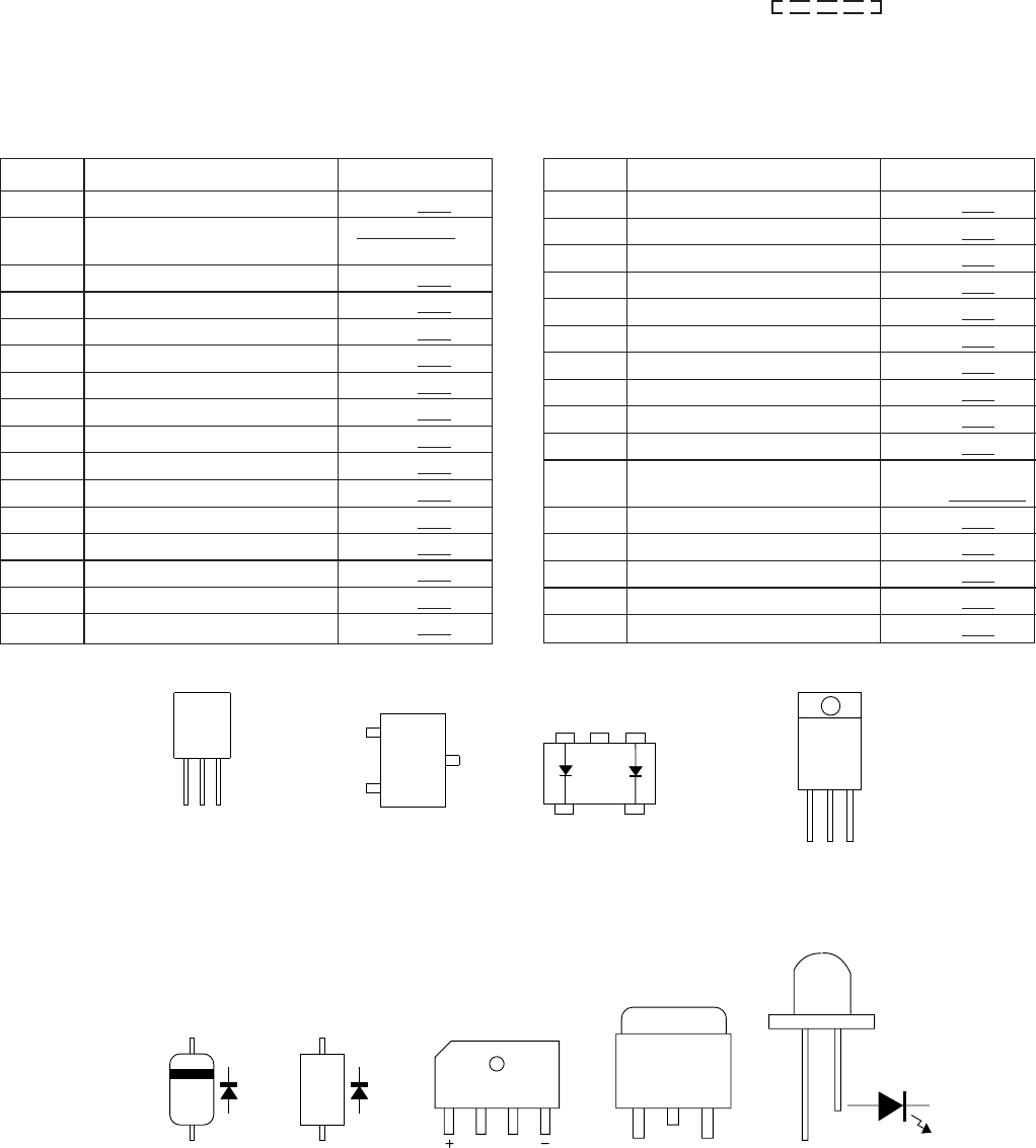
– 61 –
MD-E9000W
SW4 PICKUP IN ON—OFF
SW441 SPAN SELECTOR 9 kHz/50 kHz—
10 kHz/100 kHz
SW701 VOLUME DOWN ON—OFF
SW702 VOLUME UP ON—OFF
SW703 CD PLAY/PAUSE ON—OFF
SW704 CD STOP ON—OFF
SW705 FF/SKIP UP/PRESET UP ON—OFF
SW706
REW/SKIP DOWN/PRESET DOWN
ON—OFF
SW707 MD STOP ON—OFF
SW708 MD PLAY/PAUSE ON—OFF
SW709 MEMORY/ENTER ON—OFF
SW710 DISPLAY (DEMO) ON—OFF
SW711 X-BASS ON—OFF
SW712 EQUALIZER ON—OFF
SW713 AUX ON—OFF
SW714 TUNER (BAND) ON—OFF
• The indicated voltage in each section is the one measured
by Digital Multimeter between such a section and the chas-
sis with no signal given.
1. In the tuner section,
indicates AM
indicates FM stereo
2. In the main section, a tape is being played back.
3. In the deck section, a tape is being played back.
( ) indicates the record state.
4. In the power section, a tape is being played back.
5. In the CD section, the CD is stopped.
• Parts marked with “ 1 ” ( ) are important for
maintaining the safety of the set. Be sure to replace these
parts with specified ones for maintaining the safety and
performance of the set.
NOTES ON SCHEMATIC DIAGRAM
• Resistor:
To differentiate the units of resistors, such symbol as K and
M are used: the symbol K means 1000 ohm and the symbol
M means 1000 kohm and the resistor without any symbol is
ohm-type resistor. Besides, the one with “Fusible” is a fuse
type.
• Capacitor:
To indicate the unit of capacitor, a symbol P is used: this
symbol P means pico-farad and the unit of the capacitor
without such a symbol is microfarad. As to electrolytic
capacitor, the expression “capacitance/withstand voltage”
is used.
(CH), (TH), (RH), (UJ): Temperature compensation
(ML): Mylar type
(P.P.): Polypropylene type
• Schematic diagram and Wiring Side of P.W.Board for this
model are subject to change for improvement without prior
notice.
TYPES OF TRANSISTOR AND LED
SW715 CD OPEN/CLOSE ON—OFF
SW716 ON/STAND-BY ON—OFF
SW717 MD EJECT ON—OFF
SW718 LP4 ON—OFF
SW719 LP2 ON—OFF
SW720 SP ON—OFF
SW721 NORMAL ON—OFF
SW722 HIGH ON—OFF
SW723 MD REC ON—OFF
SW724 OPEN/CLOSE ON—OFF
SW801 VOLTAGE SELECTOR 110 V—127 V—
220 V—230-240 V
SW1930 WRITE PRO ON—OFF
SW1932 LOADING ON—OFF
SW1933 RECORD ON—OFF
SW1934 PLAY ON—OFF
SW1936 LEAD IN ON—OFF
REF. NO DESCRIPTION POSITION
2SD601 AR
UN2214
DS1SS133
B
(3)
E
(1)
C
(2)
TOP
VIEW
SBE803
TOP VIEW
TOP VIEWTOP VIEW
KTA1266 GR
KTA1271 Y
KTC3194 Y
KTC3199 GR
KTC3203 Y
KRC102 M
KRC107 M
KRC111 M
VIEW
FRONT
E C B
(S)(G)(D)
(1)(2)(3)
DS1N404S
543
21
1:Cathode
2:Cathode
3:Anode
4:No Contact
5:Anode
TS6B04GM
AC AC
VIEW
FRONT
FRONT
VIEW
4204SRT7
LNG901CF
2SB1205
FRONT
VIEW
B
C
E
KTC2026
BCE
FRONT
VIEW
REF. NO DESCRIPTION POSITION
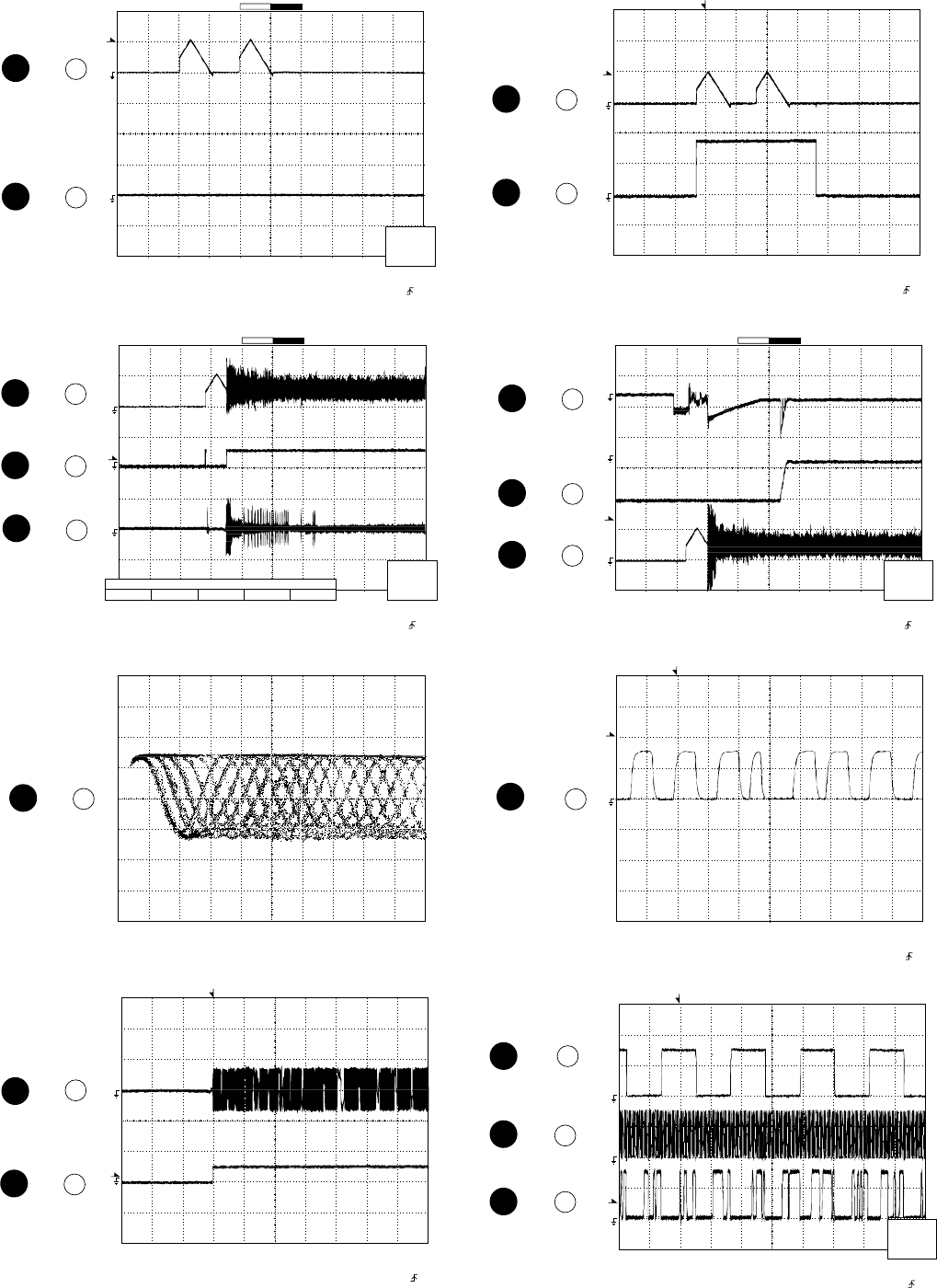
MD-E9000W
– 62 –
T
FDO
TDO
Stopped
CH1=500 mV
DC 10:1 CH3=500 mV
DC 10:1 500 ms/div
(500 ms/div)
NORM: 20 kS/s
1
3
=Record Length=
Smoothing : ON CH1 : 0.000 V
CH2 : 0.0 V
Main : 100 K
Zoom : 2 K
Mode : AUTO
Type : EDGE CH1
Delay : 0.0 ns
Hold off : 0.2 µs
CH3 : 0.000 V
CH4 : 0.00 V
BW : FULL
=Trigger==Filter= =Offset=
CH1
v/DIV
500 mV
1
IC1 21
2
IC1 20
WAVEFORMS OF CD CIRCUIT
T
FDO
DRF
TE
Stopped
CH1=500 mV
DC 10:1 CH2=10 V
DC 10:1 CH3=1 V
DC 10:1 500 ms/div
(500 ms/div)
NORM: 20 kS/s
1
2
3
=Record Length=
Smoothing : ON CH1 : 0.000 V
CH2 : 0.0 V
Main : 100 K
Zoom : 2 K
Mode : AUTO
Type : EDGE CH1
Delay : 0.0 ns
Hold off : 0.2 µs
CH3 : 0.00 V
CH4 : 0.00 V
BW : FULL
=Trigger==Filter= =Offset=
-3 div -1 div 0 div +1 div +3 div
CH Position To
CH2
Position
0.20 div
1
IC1 21
3
IC1 67
4
IC1 15
Vp-p=1.0 V~1.3 V
0.5 mV/div,0.5 µsec/div
5
IC1 4
T
T
TE
DRF
Stopped
CH1=10 V
DC 10:1 CH2=1 V
DC 10:1 100 ms/div
(100 ms/div)
NORM: 100 kS/s
2
1
=Record Length=
Smoothing : ON CH1 : 0.0 V
CH2 : 0.00 V
Main : 100 K
Zoom : 2 K
Mode : NORMAL
Type : EDGE CH1
Delay : 2.924 ms
Hold off : 0.2 µs
CH3 : 0.00 V
CH4 : 0.00 V
BW : FULL
=Trigger==Filter= =Offset=
3
IC1 67
4
IC1 15
T
T
FDO
SPDO
Stopped
CH1=200 mV
DC 10:1 CH2=500 mV
DC 10:1 500 ms/div
1999/04/07 09:51:15
(500 ms/div)
NORM: 20 kS/s
2
1
=Record Length=
Smoothing : ON CH1 : 0.000 V
CH2 : 0.000 V
Main : 100 K
Zoom : 2 K
Mode : NORMAL
Type : EDGE CH2
Delay : 2.924 ms
Hold off : 0.2 µs
CH3 : 0.00 V
CH4 : 0.00 V
BW : FULL
=Trigger=
=Filter= =Offset=
1
IC1 21
6
IC1 22
T
FDO
PDO2
PDO1
Stopped
CH1=500 mV
DC 10:1 CH3=1 V
DC 10:1 CH4=1 V
DC 10:1 500 ms/div
(500 ms/div)
NORM: 20 kS/s
1
4
3
=Record Length=
Smoothing : ON CH1 : 0.000 V
CH2 : 0.0 V
Main : 100 K
Zoom : 2 K
Mode : AUTO
Type : EDGE CH2
Delay : 0.0 ns
Hold off : 0.2 µs
CH3 : 0.00 V
CH4 : 0.00 V
BW : FULL
=Trigger==Filter= =Offset=
CH1
v/DIV
500 mV
1999/04/05 17:33:17
1
IC1 21
7
IC1 73
8
IC1 74
T
T
DOUT
Stopped
CH1=2 V
DC 10:1 500 ns/div
1999/04/07 09:25:28
(500 ns/div)
NORM: 200 MS/s
1
=Record Length=
Smoothing : ON CH1 : 0.00 V
CH2 : 0.00 V
Main : 1 K
Zoom : 100
Mode : NORMAL
Type : EDGE CH1
Delay : 2.887 ms
Hold off : 0.2 µs
CH3 : 0.00 V
CH4 : 0.00V
BW : FULL
=Trigger==Filter= =Offset=
9IC1 39
T
T
DATA
DATACK
LRSY
Stopped
CH1=2 V
DC 10:1 CH2=2 V
DC 10:1 CH3=2 V
DC 10:1 5 µs/div
(5 µs/div)
NORM: 100 kS/s
1
2
3
=Record Length=
Smoothing : ON CH1 : 0.00 V
CH2 : 0.00 V
Main : 5 K
Zoom : 100
Mode : AUTO
Type : EDGE CH3
Delay : 0.0 ns
Hold off : 0.2 µs
CH3 : 0.00 V
CH4 : 0.00 V
BW : FULL
=Trigger==Filter= =Offset=
CH3
v/DIV
2 V
1999/04/05 20:50:17
10
IC1 58
IC1 59
IC1 60
11
12
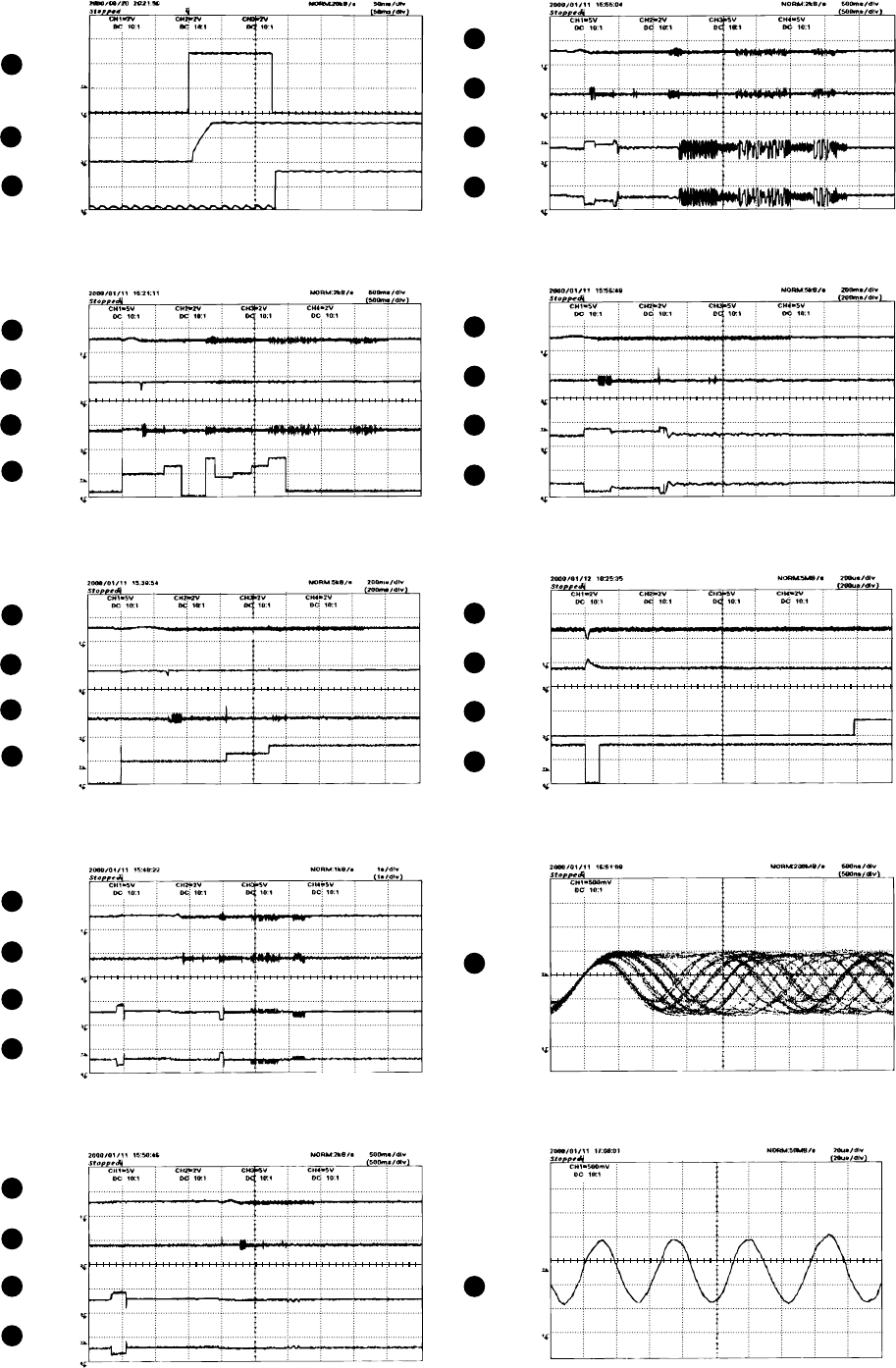
– 63 –
MD-E9000W
WAVEFORMS OF MD CIRCUIT
POWER ON
TOC READ (Low reflection disc)
TOC READ (Low reflection disc)
TOC READ (Low reflection disc) PLAY (Low reflection disc)
PLAY (Low reflection disc)
TOC READ (High reflection disc)
TOC READ (High reflection disc)
TOC READ (High reflection disc)
STOP → PLAY
TP1518
(RESET)
TP1800
(3.2V)
TP1511
(PCONT0)
TP1212
(FEMON)
TP1422
(DSENSE)
TP1420
(FOK)
TP1201
(EFMMON)
TP1135
(ADIPO)
TP1122
(F+)
TP1207
(TEMON)
TP1603
(SP+)
TP1602
(SP-)
TP1122
(F+)
TP1122
(F+)
TP1207
(TEMON)
TP1603
(SP+)
TP1602
(SP-)
1
2
3
4
4
6
10
11
4
6
10
11
4
5
12
13
14
15
5
6
7
4
5
6
7
4
6
8
9
4
6
8
9
TP1122
(F+)
TP1212
(FEMON)
TP1207
(TEMON)
TP1451
(ADJUST)
TP1122
(F+)
TP1212
(FEMON)
TP1207
(TEMON)
TP1451
(ADJUST)
TP1122
(F+)
TP1207
(TEMON)
TP1601
(SLD+)
TP1600
(SLD-)
TP1122
(F+)
TP1207
(TEMON)
TP1601
(SLD+)
TP1600
(SLD-)
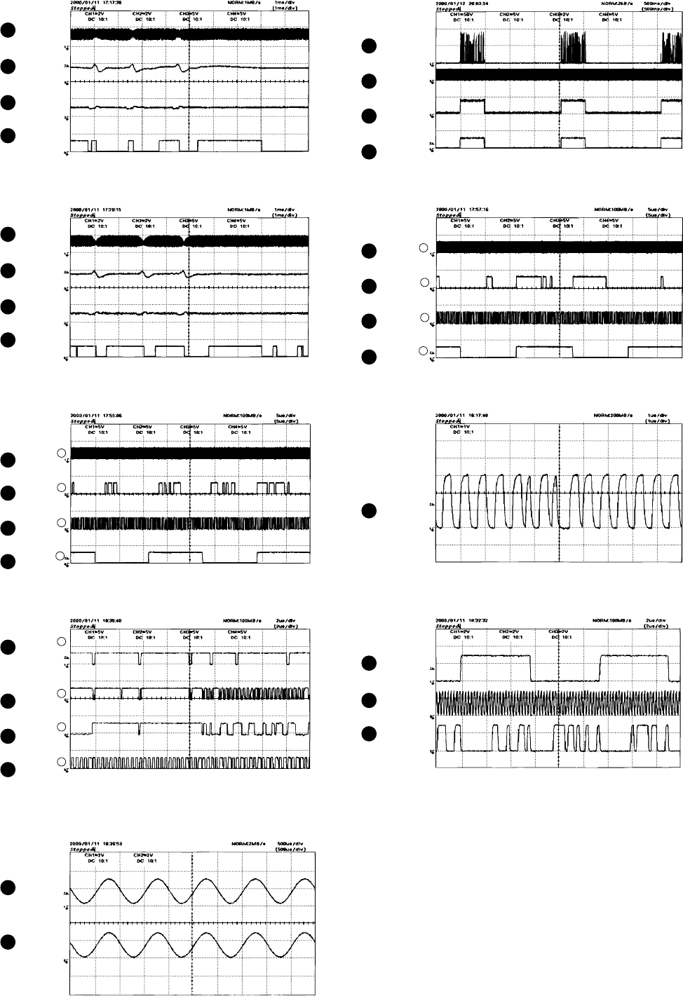
MD-E9000W
– 64 –
REC
Analog REC
Digital REC
Double speed REC
PLAY
PLAY (1 kHz 0 dB)
PLAY
TP1201
(EFMMON)
TP1201
(EFMMON)
TP1530
(CDLRCK)
TP1515
(DIGIN)
TP1533
(CDDATA)
TP1524
(L OUT)
TP1526
(R OUT)
TP1531
(CDBCK)
TP1207
(TEMON)
TP1207
(TEMON)
TP1121
(T+)
TP1421
(CIN)
TP1121
(T+)
TP1421
(CIN)
72
IC1201
(DFCK)
72
IC1201
(DFCK)
TP1300
(REC HEAD)
TP1302
(EFMO)
TP1105
(LDVAL)
TP1113
(R/P)
71
IC1201
(BCLK)
3
IC1202
(WE)
17
IC1202
(CAS)
1
IC1202
(I/01)
6
IC1202
(A0)
70
IC1201
(LRCK)
74
IC1201
(DADATA)
71
IC1201
(BCLK)
70
IC1201
(LRCK)
73
IC1201
(ADDATA)
PLAY (Low reflection disc)
PLAY (High reflection disc)
14 28
29
30
31
18
32
20
21
33
34
35
36
6
16
17
14
6
16
17
18
19
20
21
22
23
24
25
26
27
– 65 –
MD-E9000W
TROUBLESHOOTING
CD SECTION
When the CD does not function
When the CD section does not operate when the objective lens of the optical pickup is dirty, this section may not operate. Clean
the objective lens, and check the playback operation. When this section does not operate even after the above step is taken, check
the following items.
Remove the cabinet and follow the trouble shooting instructions.
"Track skipping and/or no TOC (Table Of Contents) may be caused by build up of dust other foreign matter on the laser pickup
lens. Before attempting any adjustment make certain that the lens is clean. If not, clean it as mentioned below."
Turn off the power, and wipe the lens softly using a cleaning paper moistened with commercially available cleaning solution so
as not to damage it. Be careful not to touch the lens with bare hands.
Dust gradually accumulates on the objective lens during use, and it may degrade performance. To avoid this problem, use a
cleaning disc designed for CD optical pickup lenses.
When a CD cannot be played
1. "E-CD01" is displayed.
(1) Check the power to IC1 (LC78645NE), the presence of the clock signal (33.8688 MHz) and the status of the RESET terminal
(pin 66 on IC1).
(2) Does the pickup move to the PICKUP-IN Switch (SW4) position?
If (1) and (2) are OK, check the system microcomputer (especially the communication line with the DSP).
2. Pressing the CD operation key is accepted, but playback does not occur.
(1) Focus-HF system check
(2) Tracking system check
(3) Spin system check
(4) PLL system check
(5) Others
Parts code
1. CD optical pickup Lens cleaner disc UDSKA0004AFZZ
HOW TO USE
CAUTION
Cleaning fluid
Cleaner disc
Using the brush in the cleaner cap, apply 1 or 2 drops of the cleaning fluid to the
brush on the CD cleaner disc which has the mark next to it.
Place the CD cleaner disc onto the CD disc tray with the brush side down,then
press the play button.
You will hear music for about 20 seconds and the CD player will automatically stop.
If it continuous to turn, press the stop button.
1.
2.
3.
The CD lens cleaner should be effective for 30-50 operations, however if the
brushes become worn out earlier then please the cleaner disc.
If the CD cleaner brushes become very wet then wipe off any excess fluid with a soft
cloth.
Do not drink the cleaner fluid or allow it to come in contact with the eyes. In the
event of this happening then drink and / or rinse with clean water and seek medical
advice.
The CD cleaner disc must not be used on car CD players or on computer CD-ROM
drives.
All rights reserved. Unauthorized duplicating, broadcasting and renting this product
is prohibited by law.
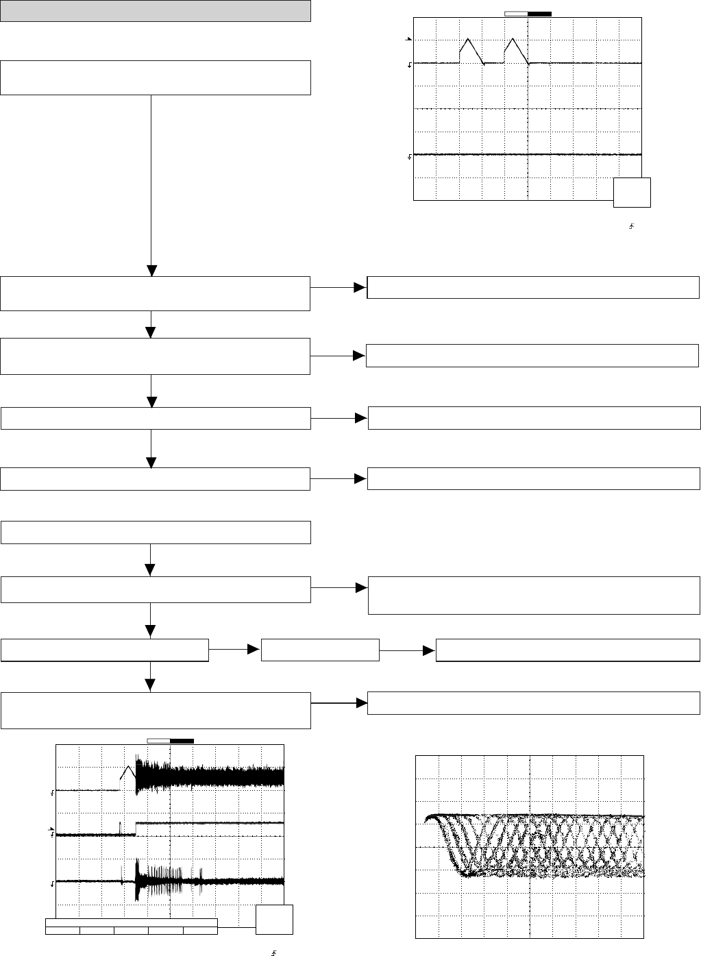
MD-E9000W
– 66 –
If the level is not normal, check around pins 1~4.
1. Is focus servo activated ?
(Waveform drawing Figure 66-2.)
Pins 3~8 on IC1
Check the laser diode driver Q1 peripheral circuit. (IC pin 13)
When a disc is loaded, start playback operation.
2. Does DRF change from "L" to "H" ? Is the disc rotating ?
3. Is the HF waveform normal ?
(Waveform drawing Figure 66-3.)
Check the spin system.
If the disc is spinning and a HF waveform is generated,
DRF will go H.
Figure 66-1
Check the laser diode driver Q1 peripheral circuit.
(1) Focus-HF system check.
Although a CD is inserted and the cover is closed, "NO
DISC" is displayed.
1. Does the pickup move to the PICKUP-IN Switch (SW4)
position ?
Sled motor (M1).
Press the OPEN/CLOSE switch (SW715) without inserting a
disc, and try starting the playback operation.
2. Does the focus (lens) move up and down ?
(Waveform drawing Figure 66-1.) Check the focus peripheral circuit.
3. Is the laser lit ?
Spindle motor (M2).
4. Is the turntable rotating ?
Figure 66-2 Figure 66-3
Yes
Yes
Yes
No
No
No
No
No
No
No
Yes
Yes
No
T
FDO
TDO
Stopped
CH1=500 mV
DC 10:1 CH3=500 mV
DC 10:1 500 ms/div
(500 ms/div)
NORM: 20 kS/s
1
3
=Record Length=
Smoothing : ON CH1 : 0.000 V
CH2 : 0.0 V
Main : 100 K
Zoom : 2 K
Mode : AUTO
Type : EDGE CH1
Delay : 0.0 ns
Hold off : 0.2 µs
CH3 : 0.000 V
CH4 : 0.00 V
BW : FULL
=Trigger==Filter= =Offset=
CH1
v/DIV
500 mV
T
FDO
DRF
TE
Stopped
CH1=500 mV
DC 10:1 CH2=10 V
DC 10:1 CH3=1 V
DC 10:1 500 ms/div
(500 ms/div)
NORM: 20 kS/s
1
2
3
=Record Length=
Smoothing : ON CH1 : 0.000 V
CH2 : 0.0 V
Main : 100 K
Zoom : 2 K
Mode : AUTO
Type : EDGE CH1
Delay : 0.0 ns
Hold off : 0.2 µs
CH3 : 0.00 V
CH4 : 0.00 V
BW : FULL
=Trigger==Filter= =Offset=
-3 div -1 div 0 div +1 div +3 div
CH Position To
CH2
Position
0.20 div
Vp-p=1.0 V~1.3 V
0.5 mV/div,0.5 µsec/div
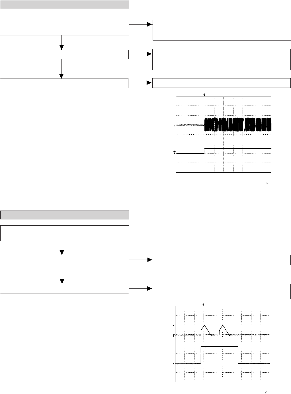
– 67 –
MD-E9000W
The tracking servo is not activated.
Check the peripheral circuits at pins 9 and 10 on IC1, and circuit
around CNP2.
If the waveform shown in Figure 67-1 appears and soon after
NO DISC appears ?
(2) Tracking system check.
Check the TE waveform at pin 15 on IC1.
A normal jump operation cannot be completed or the beginning of
the track cannot be found.
Check the around pin 20 on IC1.
"Initialization" is possible, but play is not possible ?
Data cannot be read. Check the VCO-PLL system.
"Initialization" is not possible.
Figure 67-1
Figure 67-2
Press the OPEN/CLOSE switch without inserting a disc, and
then try starting the play operation.
(3) Spin system check.
The spin driver circuit is OK.
1. The turntable rotates a little ?
(Waveform drawing Figure 67-2.)
Check around pin 22 on IC1, pins 20 and 21 on IC2, and around
CNP4.
2. The turntable doesn't rotate.
No
Yes
No
Yes
Yes
No
T
T
TE
DRF
Stopped
CH1=10 V
DC 10:1 CH2=1 V
DC 10:1 100 ms/div
(100 ms/div)
NORM: 100 kS/s
2
1
=Record Length=
Smoothing : ON CH1 : 0.0 V
CH2 : 0.00 V
Main : 100 K
Zoom : 2 K
Mode : NORMAL
Type : EDGE CH1
Delay : 2.924 ms
Hold off : 0.2 µs
CH3 : 0.00 V
CH4 : 0.00 V
BW : FULL
=Trigger=
=Filter= =Offset=
T
T
FDO
SPDO
Stopped
CH1=200 mV
DC 10:1 CH2=500 mV
DC 10:1 500 ms/div
1999/04/07 09:51:15
(500 ms/div)
NORM: 20 kS/s
2
1
=Record Length=
Smoothing : ON CH1 : 0.000 V
CH2 : 0.000 V
Main : 100 K
Zoom : 2 K
Mode : NORMAL
Type : EDGE CH2
Delay : 2.924 ms
Hold off : 0.2 µs
CH3 : 0.00 V
CH4 : 0.00 V
BW : FULL
=Trigger=
=Filter= =Offset=
MD-E9000W
– 68 –
Is pin 52 (C2F) on IC1 "L" ?
Yes
No
The HF waveform is normal and the time is displayed
normally, but no sound is produced. Or the sound
has dropouts.
(5) Others.
There are too many error flags on a damaged disc which
makes error correction impossible.
Check again using a known good disc.
1. When playing at normal speed
Check the peripheral circuit at pin 39 (DOUT) on IC1 and
the waveform (Figure 68-2).
If OK, Check the MD unit.
When a disc is loaded, start play operation.
(4) PLL system check.
The HF waveform is normal, but the TOC data cannot be
read.
Check the PDO waveform (Figure 68-1).
Check around pins 73~78 on IC1. Figure 68-1
Figure 68-2
T
FDO
PDO2
PDO1
Stopped
CH1=500 mV
DC 10:1 CH3=1 V
DC 10:1 CH4=1 V
DC 10:1 500 ms/div
(500 ms/div)
NORM: 20 kS/s
1
4
3
=Record Length=
Smoothing : ON CH1 : 0.000 V
CH2 : 0.0 V
Main : 100 K
Zoom : 2 K
Mode : AUTO
Type : EDGE CH2
Delay : 0.0 ns
Hold off : 0.2 µs
CH3 : 0.00 V
CH4 : 0.00 V
BW : FULL
=Trigger==Filter= =Offset=
CH1
v/DIV
500 mV
1999/04/05 17:33:17
T
T
DOUT
Stopped
CH1=2 V
DC 10:1 500 ns/div
1999/04/07 09:25:28
(500 ns/div)
NORM: 200 MS/s
1
=Record Length=
Smoothing : ON CH1 : 0.00 V
CH2 : 0.00 V
Main : 1 K
Zoom : 100
Mode : NORMAL
Type : EDGE CH1
Delay : 2.887 ms
Hold off : 0.2 µs
CH3 : 0.00 V
CH4 : 0.00 V
BW : FULL
=Trigger=
=Filter= =Offset=
– 69 –
MD-E9000W
MD SECTION
Preparations
If dusts and foreign materials are accumulated on the pickup lens, playback sounds can be skipped or the TOC (Table of Contents)
can't be displayed. Clean the object lens and check the playback. When lens are dirty, do the following.
Turn off the power and wipe lens softly with a cleaning paper and a little cleaning solution so as not to damage it.
Do not touch lens with bare hands.
If the MD unit doesn't work
If the MD unit doesn't start after cleaning the pickup objects lens, check it as follows.
Check as stated in item "disc Loading is not normal".
No
Is disc loading normal ?
Yes
No Check as stated in item "Playback state cannot be set".
Is playback state set when the MD PLAY/PAUSE button is
pressed ?
Is audio output normal ? Check as stated in item "Audio playback circuit".
No
Is record and playback operations normal ?
Yes
Check as stated in item "Record and playback operations".
No
Yes
• Playback state cannot be set.
Is it impossible to set both high reflection disc and low
reflection disc to playback state ? Yes Check as stated in item "TEST mode check".
No
Only the high reflection disc can be played back.
Yes
Is 2.7 V to 2.8 V applied to the pin 93 of IC1401 with the high
reflection disc inserted ?
Only the low reflection disc can be played back.
Is 2.5 V to 2.6 V (record enabled) or 2.7 V to 2.8 V (record disabled)
applied to the pin 93 of IC1401 with the low reflection disc inserted ?
No
Yes
Yes
After re adjustment check as stated in item "Normal playback".
Check loading motor PWB, and CW1931 and SW1932.
No
Yes No
• Audio playback circuit
Yes
No
Is audio output waveform observed on the pins 15 and 17 of
CN1501 ? Check connection between IC1701 and CN1501.
No
Check the main PWB.
Yes
When sound is not output although the playback time display advances during playback in the normal mode.
Is audio output waveform observed on the pins 24 and 26 of
IC1701 ?
Check the pins 70, 71, 72 and 74 of IC1201, and the pins 12, 16,
17, and 19 of IC1701.
MD-E9000W
– 70 –
• Disc loading is not normal.
Is disc loaded when it is inserted ?
No
Yes
No Check IC1401.
No Check CN1401, CW1931 and SW1932.
Yes
No Check CN1401, CW1931 and IC1601.
Yes
Check M903.
No
Yes
Yes
Is change observed on the pin 19 or 20 of IC1601 ?
Is change observed on the pin 12 or 13 of IC1601 ?
Is ejection performed when the MD eject button is pressed ?
Yes
Disc retracts soon after completion of disc ejection.
Yes
Check SW1932.
Is the pin 9 of CN1401 set to H state ?
Yes
No Check the main PWB and CN1501.
No Check the power PWB, main PWB, and
CN1501.
Is pulse input in the pin 22 of CN1501 when reset power
supply is turned on ?
Is +5 V to +6 V applied to the pins 6 and 7 of CN1501 ?
Yes
No Check IC1201.
No Check the periphery of Q1804 and
IC1401.
Is pulse of 8.4672 MHz applied to the pin 15 of IC1401 ?
Is +3.2 V applied to the pin 62 of IC1401 ?
Yes
No Check IC1401.
Is pulse output from the pin 34 of IC1401 ?
Yes
Yes
– 71 –
MD-E9000W
Yes
• Normal playback
Is initialization performed normally when high reflection disc is
played back ?
Does disc rotate normally?
No No
Check IC1201.
Is lead-in switch turned on in the TEST mode when the pickup is on
the innermost periphery ? (Is the pin 63 of IC1401 on L level ?)
No
No
Check SW1936, soldered joints of mechanism switch PWB, and
periphery of pin 3 of CW1931.
Yes
When it has been confirmed that EEPROM value is normal in the TEST mode
Does the playback time display advance ?
Check the position as stated in item "Lead-in switch position
measurement mode".
• Record and playback operations
Insert the low reflection disc, and after verifying the audio output in the normal mode playback set the record/playback TEST mode.
Is recording performed after displaying TEST REC ?
Yes No Check whether the disc is record-prohibited.
Is RF waveform output to the pin 1 of IC1201 or TP1201
when playback is performed after recording ?
No
Does RF pattern appear on the pin 50 of IC1201 during
recording ?
Yes
No
No Check for IC1201 soldering failure.
Yes
Is output waveform given to the pins 19 and 21 of CN1501 in
AUX input record in the Normal mode ?
Is input waveform given to the pins 3 and 5 of IC1701 ?
Yes
No Check the main PWB.
No Check connection between IC1701 and CN1501.
Check the periphery of IC1701, and the pins 70, 71, 72, and
73 of IC1201.
Yes
Yes
Does the level of pins 3, 26 and 39 of IC1401 in record state
differ from that in playback state ?
Check IC1300 to 1302 and periphery of CN1300.
Check periphery of IC1401.
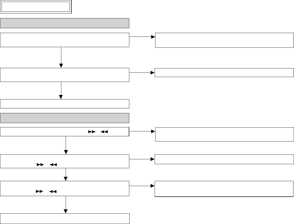
MD-E9000W
– 72 –
• The sled motor does not rotate.
No
Do the pins 23 of IC1201 change with the / button ?
Yes
No
Do the pins 14 and 15 of IC1601 and the pins 1 and 2 of CN1401
change with the / button ? Check IC1601 and soldering of CN1401.
Yes
Does voltage of the + and - terminals on the sled motor
change with the / button ? No Check the soldering connected to the sled motor and for
disconnection.
Yes
Replace the sled motor.
• The spindle motor does not rotate.
Is waveform output from the pins 25 of IC1201 in the step 4 of
AUTO auxiliary adjustment mode of TEST mode ?
Check IC1601, CN1401, and soldering of mechanism switch PWB.
Is waveform output from the pins 9 and 10 of IC1601 and the
pins 5 and 6 of CN1401 ?
Replace with a spindle motor (complete).
No
No
Yes
Yes
Check the pins 25 of IC1201, soldering of peripheral circuit, and
parts.
Check the waveform of pins 23 of IC1201, peripheral parts, and
soldering.
Check in the test mode

– 73 –
MD-E9000W
FUNCTION TABLE OF IC
IC1 VHiLC78645NE1: CD Servo (LC78645NE) (1/2)
1 SLCO Output — Control output.
2 SLCIST Input —
Resistor connection terminal for SLCO output current
setting.
3 EFMIN Input — RF signal input terminal.
4 RF Output — RF signal monitor terminal.
5 RFVDD Input — RF power terminal.
6 RFVSS — — RF earth terminal. To be connected to 0 V.
7 FIN1 Input — A+C signal input terminal.
8 FIN2 Input — B+D signal input terminal.
9 TIN1 Input — E signal input terminal.
10 TIN2 Input — F signal input terminal.
11 VREF Output RFVDD/2 VREF voltage output terminal.
12 REFI Input — Reference supply setting terminal.
13* FE Output ZHI FE signal monitor terminal.
14 TEC Output — LPF capacitor connection terminal for TE signal.
15* TE Output ZHI TE signal monitor terminal.
16* RFMON Output ZHI RF internal signal monitor terminal.
17 JITTC — — Capacitor connection terminal for jitter detection.
18 ADAVDD Input — Power terminal for servo A/D, D/A.
19 ADAVSS — — Earth terminal for serve A/D, D/A. To be connected to 0 V.
20 TDO Output ADAVDD/2 Output terminal for tracking control. D/A output.
21 FDO Output ADAVDD/2 Output terminal for focus control. D/A output.
22 SPDO Output ADAVDD/2 Output terminal for spindle control. D/A output.
23 SLDO Output ADAVDD/2 Output terminal for sled control. D/A output.
24* GPDAC Output ADAVDD/2 Servo D/A general-purpose output terminal.
25 CONT4 Input/Output Input Mode General-purpose I/O terminal 4.
26 CONT5 Input/Output Input Mode General-purpose I/O terminal 5.
27* SBCK/CONT6 Input/Output Input Mode General-purpose I/O terminal 6 or
Subcode reading clock input terminal.
28 SBCK/FG Input — Subcode reading clock input terminal/FG signal input terminal/external
emphasis setting terminal. Terminal functions are set by commands.
When not used, connect to 0 V.
29* DEFECT Output L Defect terminal.
30* V/*P Output H Auto switching monitor output terminal for rough servo phase control.
“H”: rough servo, “L”: phase servo.
31* FSEQ Output L Sync signal detection output terminal.
The status changes to “H” when the sync signal detected in EFM and the
sync signal of internal generation are identified.
32* MONI1 Output L Internal signal monitor terminal 1.
33* MONI2 Output L Internal signal monitor terminal 2.
34* MONI3 Output L Internal signal monitor terminal 3.
35* MONI4 Output L Internal signal monitor terminal 4.
36* MONI5 Output L Internal signal monitor terminal 5.
37 VSS — — Digital system earth terminal. To be connected to 0 V.
38 VDD Input — Digital system power terminal.
39 DOUT Output L Digital OUT output terminal. (EIAJ format)
40 TEST Input L Input terminal for test. To be connected to 0 V.
41 LVDD Input — Power supply for Left channel.
42* LCHO Output LVDD/2 Left channel output.
43 LVSS — — GND for Left channel. Must be connected to 0 V.
Pin No. Function
Terminal Name Input/Output
Setting in Reset
Controlled by commands from the
microcomputer. When not used, set
them as input terminals and connect
to 0 V, or set them as output
terminals and leave open.
In this unit, the terminal with asterisk mark (*) is (open) terminal which is not connected to the outside.
Left channel
D/A converter
For slice level
control.

MD-E9000W
– 74 –
44 RVSS — — GND for Right channel. Must be connected to 0 V.
45* RCHO Output LVDD /2 Right channel output.
46 RVDD Input — Power supply for Right channel.
47 XVDD Input — Power supply for crystal oscillator.
48 XOUT Output — Connected for the 33.8688 MHz crystal oscillator cement.
49 XIN Input —
50 FSX/16MIN Input/Output Input 7.35 kHz Synchronization signal monitor port.
or Clock input port for Digital filter & D/A
51 XVSS — — Crystal GND for crystal oscillator. Must be connected to 0 V.
Oscillator
52* C2F Output H C2 FLAG monitor port.
53* EFLG Output L C1, C2 error corrected monitor port.
54* 16MOUT Output Clock 16.9344 MHz output port.
55 ASLRCK Input — Word clock input port.
(If this port does not use, must be connect to 0 V.)
56 ASDACK Input — Bit clock input port.
(If this port does not use, must be connect to 0 V.)
57 ASDFIN Input —
Left/Right channel data input port.
(If this port does not use, must be connect to 0 V.)
58 LRCK Output L Word clock output port.
59 BCK Output L Digital data Bit clock output port.
60 DATA Output L Left/Right channel data output port.
61 CE Input — Chip enable signal input port.
62 CL Input —
Microcomputer
Data transfer clock input port.
63 DI Input — Interface Data input port.
64 DO Output (H) Data output port. (N-ch. open drain output.)
65 *WRQ Output H Interruption signal output.
66 *RES Input — Chip reset signal input port.
This port must be set LOW after first applied power on.
67 DRF Output L Focus detection output port.
68 VDD5 Input — Power supply for Microprocessor.
69 VSS — — GND for digital circuit. Must be connected to 0 V.
70 CONT3 Input/Output Input General purpose port 1.
71 CONT2 Input/Output Input General purpose port 2.
72 CONT1 Input/Output Input General purpose port 3.
73 PDO1 Output — Internal VCO control phase comparator output port 1.
74 PDO2 Output Input Internal VCO control phase comparator output port 2.
75 VVSS — — GND for internal VCO. Must be connected to 0 V.
76 PCKIST Input — PDO output current adjustment resistor connection port.
77 VVDD Input — Power supply for internal VCO.
78 FR Input — VCO frequency range adjustment port.
79 LDS Input — LASER power detected signal input port.
80 LDD Output — LASER power control signal output port.
IC1 VHiLC78645NE1: CD Servo (LC78645NE) (2/2)
Pin No. Function
Terminal Name Input/Output
Setting in Reset
Right channel
D/A converter
Crystal
Oscillator
Anti-shock
Controlled with serial data command from micro-
computer. When not used, General purpose input/
output terminal 7. Set it as the input terminal and open
it by connecting to 0 V, or set it as the output terminal
and open it.
PLL
In this unit, the terminal with asterisk mark (*) is (open) terminal which is not connected to the outside.
Be sure to supply the same potential to each power terminal. (VVDD, ADAVDD, VDD, LVDD, RVDD, XVDD)
Terminal witch is controlled by the power terminal (VDD5 V) for a microcomputer interface :
CE (61 pin), CL (62 pin), DI (63 pin), DO (64 pin), WRQ (65 pin), RES (66 pin), DRF (67 pin)
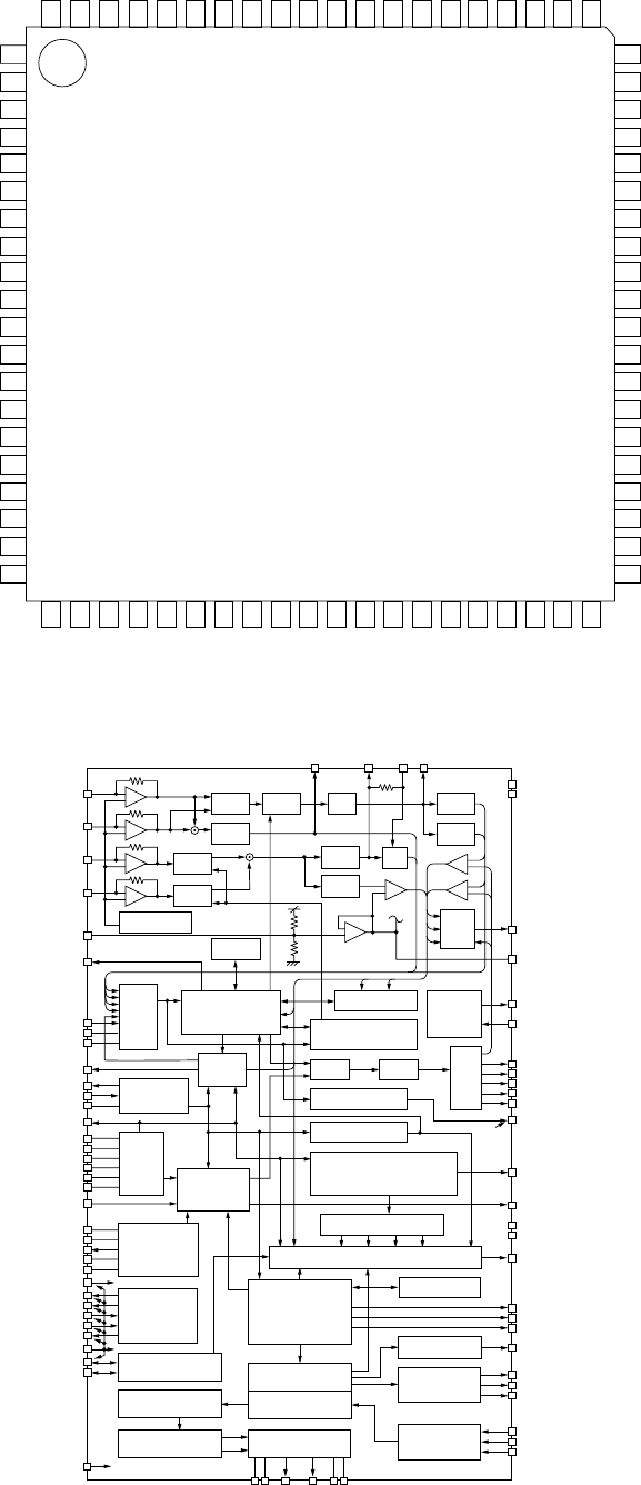
– 75 –
MD-E9000W
Figure 75 BLOCK DIAGRAM OF IC
IC1 VHiLC78645NE1: CD Servo (LC78645NE)
1
2
3
4
5
6
7
8
9
10
11
12
13
14
15
16
17
18
19
20
21 22 23 24 25 26 27 28 29 30 31 32 33 34 35 36 37 38 39 40
80 79 78 77 76 75 74 73 72 71 70 69 68 67 66 65 64 63 62 61
60
59
58
57
56
55
54
53
52
51
50
49
48
47
46
45
44
43
42
41
SLCO
SLCIST
EFMIN
RF
RFVDD
RFVSS
FIN1
FIN2
TIN1
TIN2
VREF
REFI
FE
TEC
TE
RFMON
JITTC
ADAVDD
ADAVSS
TDO
FDO
SPDO
SLDO
GPDAC
CONT4
CONT5
SBCK/CONT6
SBCK/FG
DEFECT
V/*P
FSEQ
MONI1
MONI2
MONI3
MONI4
MONI5
(3.3V)VSS
VDD
DOUT
TEST
LDD
LDS
FR
VVDD
PCKIST
VVSS
PD02
PD01
CONT1
CONT2
CONT3
VSS
VDD5
DRF
*RES
*WRQ
DO
DI
CL
CE
DATA
BCK
LRCK
ASDFIN
ASDACK
ASLRCK
16MOUT
EFLG
C2F
XVSS
FSX/16MIN
XIN
XOUT
XVDD
RVDD
RCH0
RVSS
LVSS
LCHO
LVDD
LC78645NE
+
–
+
–
+
–
+
–
–
–
+
+
MIX
LPF
LPF
LPF
TBAL
TBAL
RAM
LEVEL SET
AGC EQ
SW
PH
BH
+
–
+
–
+
–
+
–
MONI
CONT
A/D
SERVO PROCESSOR
TRACK JUMP
AUTO ADJUST
JITTER
DETECT
1bit DAC
8FS
DIGITAL FILTER
GENERAL-PURPOSE
PORTS
COMMAND
INTERFACE
CLOCK
GENERATOR
CLV,CAV
CONTROL
PLL
VCEC
SLICE LEVEL
CONTROL
APC
S/H
D/A
SW
DRF
RUPTURE DEFECT
FRAME SYNC
DETECT,PROTECT INSERT,
EFN DECODE
VDD
SUBCODE DECODE CRC
MONITOR SIGNAL SELECTOR
RAM
ERROR
CORRECTION
AUDIO CD
AUDIO OUT
SERIAL
OUT
EXTERNAL
AUDIO IN
INTERPOLATION
MUTE
ATTENUATION
DEEMPHSIS
LPF
FIN1
FIN2
TIN1
TIN2
REFI
DETECT
ADIN
ADAVDD
ADAVSS
JITTC
SLCO
EFMIN
SLCIST
PCK
PDO1
PDO2
FR
PCKIST
VVDD
VVSS
SBCK/FG
XIN
XOUT
16MOUT
XVDD
XVSS
*RES
*WRQ
CL
CE
DI
DO
VDD5V
CONT1, 2, 3
TEST
CONT4, 5
SBCK/CONT6
LVDD
LVSS
LCHO
RCHO
RVDD
RVSS
ASDFIN
ASDQCK
ASLRCK
DATA
BCK
LRCK
DOUT
EFLG
C2F
FSK/16MIN
MONI1~5
VSS
VDD
V/*P
FSEQ
DRF
GPDAC
SPD0
SLD0
TD0
FD0
LDS
LDD
VREF
RFMON
RFVSS
RFVDD
RF
TEC
TE
FE
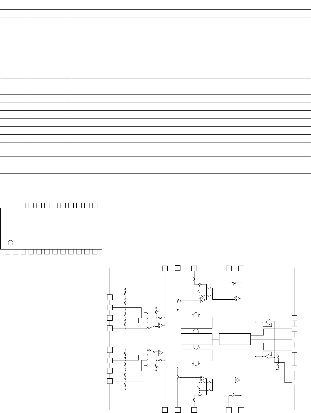
MD-E9000W
– 76 –
IC401 VHiLC75341/-1: Audio Processor (LC75341)
1 DI Serial data and clock input terminal for control.
2 CE Chip enable terminal.
When changing from "H" to "L", data is written in the internal latch and each analog switch is turned on.
Data transmission is enabled at "H" level.
3 VSS Ground terminal.
4 LOUT Bass band filter construction capacitor/resistor connection terminal and bass/treble output terminal.
5 LBASS Bass band filter capacitor and resistor connection terminal.
6 LTRE Treble band filter capacitor connection terminal.
7 LIN L-CH signal input terminal.
8 LSEL0 Input selector output terminal.
9-12 (10*) L4-L1 Input signal terminal.
13-16 (15*) R1-R4 Input signal terminal.
17 RSEL0 Input selector output terminal.
18 RIN R-CH signal input terminal.
19 RTRE Treble band filter capacitor connection terminal.
20 RBASS Bass band filter capacitor and resistor connection terminal.
21 ROUT Bass band filter capacitor/resistor connection terminal and bass/treble output terminal.
22 VREF 0.5 × VDD voltage generation section for analog ground. Connect a capacitor of 10 µF or more between
Vref and AVSS (VSS) as a countermeasure against the power supply ripple.
23 VDD Power supply terminal.
24 CLK Serial data and clock input terminal for control.
Pin No. Terminal Name Function
In this unit, the terminal with asterisk mark (*) is (open) terminal which is not connected to the outside.
Figure 76 BLOCK DIAGRAM OF IC
4
5
678
9
10
11
12
13
14
15
16
17 18 19 20 21
22
23
24
1
2
3
LVref
RVref
CCB
INTERFACE
CONTROL
CIRCUIT
LOGIC
CIRCUIT
CONTROL
CIRCUIT
ROUT
RBASS
RTRE
RIN
RSELO
L1
L2
L3
L4
R1
R2
R3
R4
LOUT
LBASS
LTRE
LIN
LSELO
VSS
CE
DI
CLK
VDD
VREF
24 23 22 21 20 19 18 17 16 15 14 13
123456789101112
LC75341
CLK
VDD
VREF
ROUT
RBASS
RTRE
RIN
RSELO
R4
R3
R2
R1
DI
CE
VSS
LOUT
LBASS
LTRE
LIN
LSEL0
L4
L3
L2
L1

– 77 –
MD-E9000W
Pin No. Input/Output
Terminal Name
Port Name
IC701 RH-iX0395AWZZ: System Microcomputer (IX0395AW)
Remarks
1 P77 P_DOWN Output Power failure control.
2-4 AN6-AN4 KEY1-KEY3 Input Key input.
5 AN3 INI Input Distination setting.
6 AN2 TUN SM Input Tuner signal meter input.
7 P71 T-STBY Output Timer indicator.
8 P70 CD_RESET Output CD reset.
9 PB3 CD_WRQ Input CD sub-q transmission control.
10 PB2 CD_DRF Input CD focus on detection.
11 P57 CD_CE Output CD chip enable.
12 P56 CD_CL Output CD clock.
13 P55 CD_DI Output CD command output.
14 P54 CD_DO Input CD data input.
15 P53 MD_ST-ID Output MD syncro start signal.
16 P52 MD_SERCH Output MD search signal output.
17 P51 MD_PCONT Input MD power lock output.
18 P50 MD_RESET Output MD reset.
19 SRDY1 MD_DSTB Input MD strobe input.
20 SCLK1 MD_DSCK Output MD clock output.
21 SOUT1 MD_KDATA Output MD key data.
22 SIN1 MD_DATA Input MD data input.
23 P63 P_MUTE Output System (Power IC) mute control.
24 P62 P_CONT Output Power IC control.
25* P61 RDS_RDY Input RDS ready output.
26* P60 RDS_RST Output RDS RAM reset.
27* P47 RDS_DATA Input RDS data input.
28* P46 RDS_CLK Output RDS clock output. (Slave mode)
29 INT1 P-IN Input Power failure detection.
30* P44 FAN_CONT Output Fan control.
31 P43 RLY_CONT Output AC relay out control.
32 INT2 RX-IN Input Remocon signal in.
33 P41 SPAN Input Span select input.
34 P40 No use Input Connect to ground.
35 RESET RESET Input Reset input.
36 PB1 CD_OPEN-SW Input CD open sw detection.
37 PB0 CD_CLOSE-SW Input CD close sw detection.
38 XIN XIN Input System clock input. (8.3886 MHz)
39 XOUT XOUT Output System clock output. (8.3886 MHz)
40 VSS VSS Input Ground voltage.
41 P27 TUN_DO Input Tuner data input.
42 P26 T/V_CE Output Tuner chip enable.
43 P25 T/V_CL Output Tuner clock.
44 P24 T/V_DI Output Tuner command output.
45 P23 ILU_LED Output Illumination LED.
46*, 47* P22/DIG18, P21/DIG17 No use Output Open
48-54 DIG16-DIG10 DIG12-DIG6 Output FL digit output.
55-60 D9-D4 DIG5-DIG0 Output FL digit output.
61-64 S35-S32 SEG35-SEG32 Output FL segment output.
65-90 SEG31-SEG6 SEG31-SEG6 Output FL segment output.
91 VCC VCC Input Power supply input.
92-97 SEG5-SEG0 SEG5-SEG0 Output FL segment output.
98 VEE VEE Input Pull down power supply input.
99 AVSS AVSS Input A/D ground.
100 VREF VREF Input A/D voltage.
In this unit, the terminal with asterisk mark (*) is (open) terminal which is not connected to the outside.

MD-E9000W
– 78 –
1 RF1 RF signal input terminal 1. Input of RF signal output of pickup.
2 RF2 RF signal input terminal 2. Input of RF signal output of pickup.
3 RF3 RF signal input terminal 3. Input of RF signal output of pickup.
4 RF4 RF signal input terminal 4. Input of RF signal output of pickup.
5 REFI Reference voltage amplifier input terminal.
6 REFO Reference voltage amplifier output terminal.
7 AOUT Output terminal 1 of signal amplifier for servo (focus servo system).
8 ASW Output terminal 2 of signal amplifier for servo (focus servo system).
9 AIN Reverse input terminal of signal amplifier for servo (focus servo system).
10 BIN Reverse input terminal of signal amplifier for servo (focus servo system)
11 BSW Output terminal 2 of signal amplifier for servo (focus servo system).
12 BOUT Output terminal 1 of signal amplifier for servo (focus servo system).
13 EOUT Output terminal 1 of signal amplifier for servo (tracking servo system).
14 ESW Output terminal 2 of signal amplifier for servo (tracking servo system).
15 EIN Reverse input terminal of signal amplifier for servo (tracking servo system).
16 FIN Reverse input terminal of signal amplifier for servo (tracking servo system).
17 FSW Output terminal 2 of signal amplifier for servo (tracking servo system).
18 FOUT Output terminal 1 of signal amplifier for servo (tracking servo system).
19 EOUT Output terminal 1 of signal amplifier for servo (tracking servo system).
20 BOUT Output terminal 1 of signal amplifier for servo (focus servo system).
21 AOUT Output terminal 1 of signal amplifier for servo (focus servo system).
22 TCGO Group mode: Track cross detection signal amplifier output terminal.
23 TCGI Group mode: Track cross detection signal amplifier input terminal.
24 RFADD Resistance addition output terminal of RF1 - RF4.
25 DTEMP Chip temperature detection terminal.
26 SGAIN Switch section control terminal of amplifier for servo.
27 DISC Pit mode, groove mode selecting control terminal.
28* OPICPW Power output terminal for OPIC.
29 VCC2 Power supply terminal of digital section and power section.
30* WBO Comparator output terminal for binary coded ADIP signal.
31 GND2 GND terminal of digital section and power section.
32 ADIPO ADIP signal pre-amplifier output terminal.
33* ADIPNF ADIP signal AGC amplifier output terminal.
34 ADAGC Smoothing capacitor connection terminal for ADIP signal AGC.
35 ADAGI ADIP signal AGC amplifier input terminal.
36 2-1 Differential signal of RF1, RF2.
37 EFMO RF signal AGC amplifier output terminal.
38 DCNF Smoothing capacitor connection terminal for RF signal AGC amplifier reference voltage.
39 EFMAGC Smoothing capacitor connection terminal for RF signal AGC.
40 VCC1 Analog section power supply terminal.
41 BIAS Bias input terminal.
42 GND1 Analog section GND terminal.
43 NIN RF signal AGC amplifier reverse input terminal.
44 PITG Pit mode: Ground terminal.
45 3 + 4 Groove mode: Resistance addition output terminal of RF3 and RF4.
46 PIN RF signal AGC amplifier non-reverse input terminal.
47 1 + 2 Groove mode: Resistance addition output terminal of RF1 and RF2.
48 1234 Pit mode: Resistance addition output terminal of RF1 - RF4.
IC1101 VHiiR3R58M/-1: RF Signal Processor (IR3R58M)
Pin No. Function
Terminal Name
In this unit, the terminal with asterisk mark (*) is (open) terminal which is not connected to the outside.
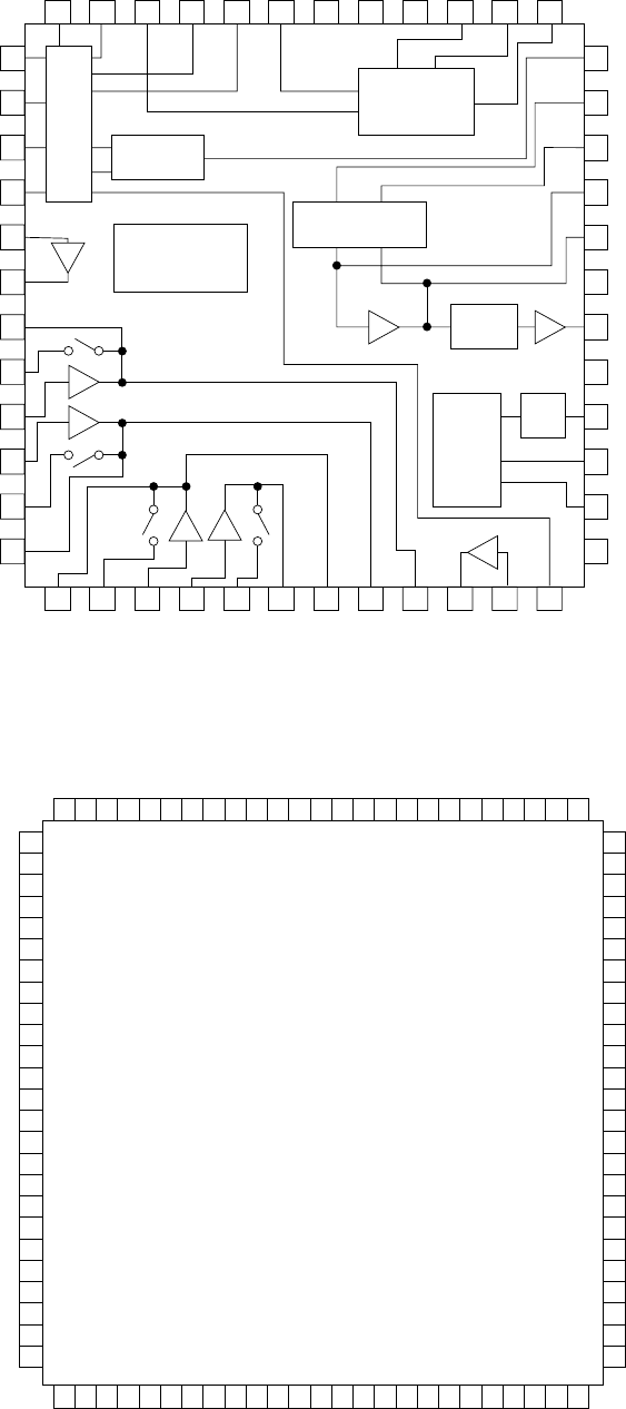
– 79 –
MD-E9000W
IC1201 VHiLR37816A-1: Endec/Atrac (LR37816A)
IC1101 VHiiR3R58M/-1: RF Signal Processor (IR3R58M)
Figure 79 BLOCK DIAGRAM OF IC
MODE
SW
BPF
BIAS
ADIP AGC
DIFF
RESISTOR & SW
EFM AGC
RF1
RF2
RF3
RF4
REFI
REFO
AOUT
ASW
AIN
BIN
BSW
BOUT
2-1
ADAGI
ADAGC
ADIPNF
ADIPO
GND2
WBO
VCC2
OPICPW
DISC
SGAIN
DTEMP
1234
1+2
PIN
3+4
PITG
NIN
GND1
BIAS
VCC1
EFMAGC
DCNF
EFMO
EOUT
ESW
EIN
FIN
FSW
FOUT
EOUT
BOUT
AOUT
TCGO
TCGI
RFADD
1
2
3
4
5
6
7
8
9
10
11
12
36
35
34
33
32
31
30
29
28
27
26
25
48 47 46 45 44 43 42 41 40 39 38 37
13 14 15 16 17 18 19 20 21 22 23 24
76
77
78
79
80
81
82
83
84
85
86
87
88
89
90
91
92
93
94
95
96
97
98
99
100
50
49
48
47
46
45
44
43
42
41
40
39
38
37
36
35
34
33
32
31
30
29
28
27
26
TOTMON
TEMCN
SBCK
SBO
SBSY
SFSY
FCK
SENSE
COUT
MCCK
DINIX
VDD2
DGND
RSTX
SYD0
SYD1
SYD2
SYD3
SYD4
SYD5
SYD6
SYD7
SYWRX
SYRDX
SYRS
EFMO
PLCK
ACRCEF
RAA11
RAD0
RAD1
RAWEX
RARASX
RAA9
RAD3
RAD2
RACASX
DGND
RACEX
RAA8
RAA7
RAA6
RAA5
RAA4
VDD2
RAA10
RAA0
RAA1
RAA2
RAA3
EFMMON
AVCC1
EFM1
AGND1
AVCC2
VREF
WBI
TCG
AIN
BIN
EIN
FIN
VBAT
VDD1
DGND
TEST2
X176KO
FODRF
FODRR
TRDRF
TRDRR
SLDRF
SLDRR
SPDRF
SPDRR
FEMON
DADATA
ADDATA
DFCK
BCLK
LRCK
DGND
PLLBVC
DOUT
DIN
XO
XI
DGND
VDD1
VPO
VXI
CDBCLK
CDLRCK
CDDATA
DIN2
DILOCK
TEST1
TEST0
TCRS
X700KO
123456789
10 11 12 13 14 15 16 17 18 19 20 21 22 23 24 25
75 74 73 72 71 70 69 68 67 66 65 64 63 62 61 60 59 58 57 56 55 54 53 52 51

MD-E9000W
– 80 –
1* EFMMON Output EFM monitor output.
2 AVCC1 Input Analog power supply (for EFM system 8AD, 8DA).
3 EFMI Input EFM signal input from RF amplifier.
4 AGND1 — Analog GND.
5 AVCC2 Input Analog power supply (for servo system, ADIP system 1bit AD).
6 VREF Input Reference voltage input for RF amplifier.
7 WBI Input ADIP wobble signal.
8 TCG Input Track cross signal.
9 AIN Input Focus error signal A.
10 BIN Input Focus error signal B.
11 EIN Input Tracking error signal E.
12 FIN Input Tracking error signal F.
13 VBAT Input Power voltage detection signal for constant voltage servo.
14 VDD1 Input Internal digital power supply.
15 DGND — Digital GND.
16 TEST2 Input Input for test. Connected to GND if used normally.
17* X176KO Output Clock output. f=176.4 kHz (4 fs)
18* FODRF Output Focus servo forward output. PWM.
19 FODRR Output Focus servo reverse output. PWM.
20* TRDRF Output Tracking servo forward output. PWM.
21 TRDRR Output Tracking servo reverse output. PWM.
22* SLDRF Output Slide servo forward output. PWM.
23 SLDRR Output Slide servo reverse output. PWM.
24* SPDRF Output Spindle servo forward output. PWM.
25 SPDRR Output Spindle servo reverse output.
26 RAA3 Output Address output to external D-RAM. ADR3
27 RAA2 Output Address output to external D-RAM. ADR2
28 RAA1 Output Address output to external D-RAM. ADR1
29 RAA0 Output Address output to external D-RAM. ADR0 (LSB)
30* RAA10 Output Address output to external D-RAM. ADR10 (MSB)
31 VDD2 Input Power supply for interface.
32 RAA4 Output Address output to external D-RAM. ADR4
33 RAA5 Output Address output to external D-RAM. ADR5
34 RAA6 Output Address output to external D-RAM. ADR6
35 RAA7 Output Address output to external D-RAM. ADR7
36 RAA8 Output Address output to external D-RAM. ADR8
37 RAOEX Output Data output enable signal output to external D-RAM
38 DGND — Digital GND.
39 RACASX Output Column address strobe signal output to external D-RAM.
40 RAD2 Input/Output Data input and output with external D-RAM. D2
41 RAD3 Input/Output Data input and output with external D-RAM. D3 (MSB)
42 RAA9 Output Address output to external D-RAM. ADR9
43 RARASX Output Low address strobe signal output to external D-RAM.
44 RAWEX Output Data write enable signal output to external D-RAM.
45 RAD1 Input/Output Data input and output with external D-RAM. D1
46 RAD0 Input/Output Data input and output with external D-RAM. D0 (LSB)
47* RAA11 Output Address output to external D-RAM. ADR11 (MSB 64 Mbit)
48* ACRCER Output CRC error flag monitor output of ADIP.
49* PLCK Output Playback mode: EFM PLL clock output.
50 EFM0 Output Recording mode: EFM signal output. Playback mode: C1F (C1 error flag) monitor output.
51* X700KO Output Clock output. f= 705.6 kHz
IC1201 VHiLR37816A-1: Endec/Atrac (LR37816A) (1/2)
Pin No. Function
Terminal Name Input/Output
In this unit, the terminal with asterisk mark (*) is (open) terminal which is not connected to the outside.

– 81 –
MD-E9000W
52* TCRS Output Track cross signal.
53 TEST0 Input Input for test. Connected to GND if used normally.
54 TEST1 Input Input for test. Connected to GND if used normally.
55 DILOCK Output DIN lock detection.
56 DIN2 Input/Output Digital input signal. Expansion port 0.
57 CDDATA Input/Output Data input for dubbing. Expansion output port 1.
58 CDLRCK Input/Output LR clock input for dubbing. Expansion output port 2.
59 CDBCLK Input/Output Bit clock input for dubbing. Expansion output port 3.
60 VXI Input PLL clock input for variable pitch.
61* VPO Output PLL phase error output for variable pitch.
62 VDD1 Input Internal digital power supply.
63 DGND — Digital GND.
64 XI Input Transmit circuit input. 33.8688 MHz
65 XO Output Transmit circuit input. 33.8688 MHz
66 DIN Input Digital input signal.
67* DOUT Output Digital output signal.
68 PLLBVG Output For Internal PLL. Terminal for external capacitor.
69 DGND — Digital GND.
70 LRCK Output L-ch, R-ch selection output of music data.
71 BCLK Output Shift lock of music data.
72 DFCK Output Clock for AD/DA converter digital filter. 256 Fs.
73 ADDATA Input Sound data input.
74 DADATA Output Sound data output.
75* FEMON Output Focus error signal monitor output. Series resistance 10 - 100 kohm built-in.
76* TOTMON Output Total signal monitor output. Series resistance 10 - 100 kohm built-in.
77* TEMON Output Tracking error signal monitor output. Series resistance 10 - 100 kohm built-in.
78 SBCK Input/Output DIN subcode read clock. Expansion port 4.
79 SBO Output DIN subcode serial data. Expansion port 5.
80 SBSY Output DIN subcode block synchronous signal. Expansion port 6.
81 SFSY Output DIN subcode frame synchronous signal. Expansion port 7.
82 FOK Output Focus OK detection signal. “0”: focus OK.
83 SENSE Output Servo condition detection signal.
84 COUT Output Track cross signal output.
85 MCCK Output Clock output for microcomputer.
86 DINTX Output Interrupt request output terminal to system computer interface.
87 VDD2 Input Power supply for interface.
88 DGND — Digital GND.
89 RSTX Input Chip reset input. Reset by L. (Note)
90 SYD0 Input/Output Data bus terminal of system computer interface. (LSB)
91-96 SYD1-SYD6 Input/Output Data bus terminal of system computer interface.
97 SYD7 Input/Output Data bus terminal of system computer interface. (MSB)
98 SYWRX Input Resister write pulse input of system computer interface.
99 SYRDX Input Resister read pulse input of system computer interface.
100 SYRS Input Resister selection input of system computer interface.
IC1201 VHiLR37816A-1: Endec/Atrac (LR37816A) (2/2)
Pin No. Function
Terminal Name Input/Output
Note: Set RSTX to L when turning on the power or after turning on the power.
In this unit, the terminal with asterisk mark (*) is (open) terminal which is not connected to the outside.
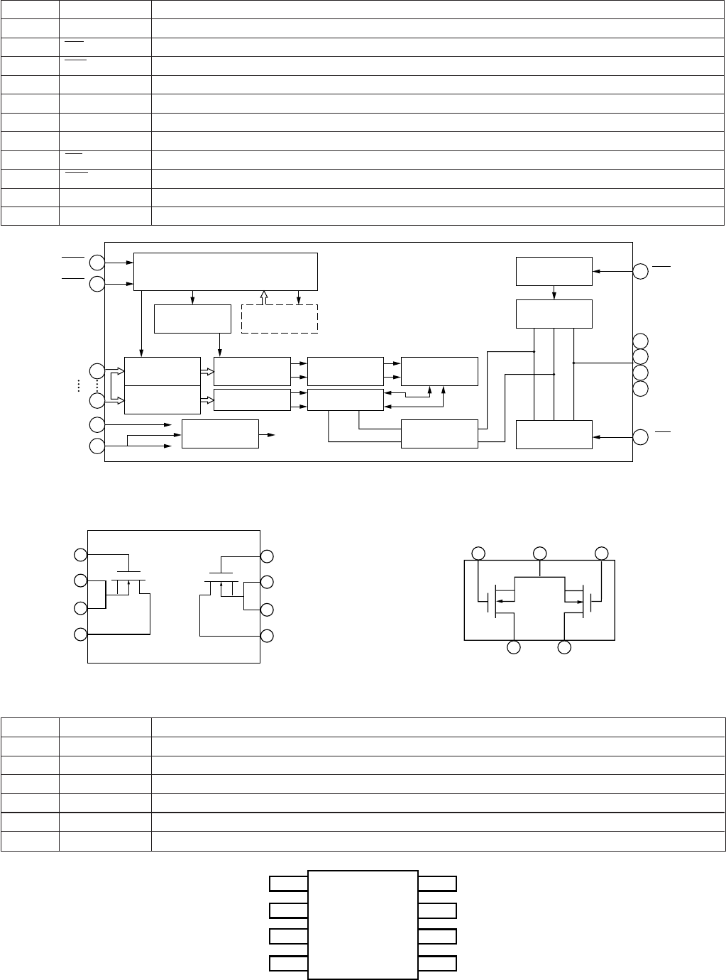
MD-E9000W
– 82 –
IC1202 RH-iX2474AFZZ: 4Mbit D-RAM (IX2474AF)
Pin No. Function
Terminal Name
1, 2 DQ0, DQ1 Data input/Data output.
3 WE Write enable.
4 RAS Row address strobe.
5 A9 Address input.
6-9 A0-A3 Address input.
10 VDD Power (3.3 V)
11-15 A4-A8 Address input.
16 OE Output enable.
17 CAS Column address strobe.
18, 19 DQ2, DQ3 Data input/Data output.
20 VSS Ground (0 V)
IC1301 VHiFTD2005/-1: Head Driver (FTD2005) IC1302 VHiCPH5608/-1: Head Driver (CPH5608)
IC1402 VHi58X2402T-1: EEPROM (58X2402T)
Pin No. Function
Terminal Name
1-3 A0-A2 Device address.
4 VSS Ground
5 SDA Serial data input/output.
6 SCL Serial clock input.
7 WP Write protect.
8 VCC Power supply.
Figure 82-1 BLOCK DIAGRAM OF IC
4
RAS
5
17
15
CAS
A0
A9
WE
DQ0-DQ3
20
VSS VBB
17
CAS
Clock Generator
CBR Refresh
Counter
Row Address
Buffer Memory
Cell
I/O
Selection
Write Clock
Generator
Data Input
Buffer
Data Output
Buffer
Row Address
Buffer
On ChipVBB
Generator
Row Decoder
Column Decoder Sense Amp.
Word Driver
SELF Refresh
Timer
MN42V4400 only
3
OE
16
2
18
19
1
Figure 82-2 BLOCK DIAGRAM OF IC Figure 82-3 BLOCK DIAGRAM OF IC
Figure 82-4 BLOCK DIAGRAM OF IC
D2
S2
S2
G2
D1
S1
S1
G1
5
6
7
8
4
3
2
1
G1 S G2
D1 D2
1 2
345
1
2
3
4
8
7
6
5
A0
A1
A2
VSS
VCC
WP
SCL
SDA

– 83 –
MD-E9000W
1 4M/16M Output 4M/16M DRAM selection input.
2 64M Output 64M DRAM selection input.
3 LDVAR Output LDVAR (laser power adjustment output)
4* ADJS Output ADJS (for automatic adjustment step check)
5 CIN Input CIN (track count signal input)
6* N.C. — Not used.
7 UNLOCK Input ERR input. (UNLOCK of MD LSI monitor PLL)
8 BYTE Input GND
9 CNVSS Input GND
10* STID OUT Output ST-ID output.
11* SEACH OUT Output MD search output.
12 RESET Input RESET input.
13* N.C. Output Clock output.
14 VSS — GND
15 MCCK Input EXTAL (8.4672 MHz)
16 VCC Input +3.15 V
17 P85 Input Input output port P85.
18 DINT Input DINT (Interrupt input from MD-LSI)
19 SFSY Input Subcode communication frame synchro Interrupt input.
20 ST-ID Input ST-ID input. (MD-ON)
21 SERCH Input CD search input. (Synchronous REC interrupt input)
22 MDRSW Output MD RSW output.
23* CDB SEL Output CD BLK SEL output.
24 DSENSE Input DSENSE (servo sense input from MD-LSI)
25 P-DOWN Input P-DOWN (blackout detection)
26 HD ON Output HDON (magnetic head power ON/OFF output)
27 EEPRO Output EEPROM protect release output.
28 HFON Output HFON
29 EEPK Output EEPROM serial clock output.
30 EEPD Input/Output EEPROM data input output.
31 MD DATA Output MD computer data input output.
32 K DATA Input System computer data input.
33 DSCK Input System computer clock input.
34 DSTB Output DSTB (system computer communication possible and during communication)
35* N.C. Output Not used.
36 SBO Input Subcode serial data input.
37 SBCK Output Subcode communication serial clock output.
38 DISC Output DISC
39 R/P Output R/P output. (REC/PLAY selection)
40 FOK Input FOK (focus servo condition monitor input)
41 FLASH L Input Flash write selection.
42 SGAIN Output SGAIN
43 SYRS Output MD LSI resister select signal output.
44 SYRD Output SYRD (MD-LSI read signal output)
45 SYWR Output SYWR (MD-LSI write signal output)
46 FLASH H Input Flash write selection.
47 SYS D7 Input/Output SYS D7 (data bus 7)
48 SYS D6 Input/Output SYS D6 (data bus 6)
49 SYS D5 Input/Output SYS D5 (data bus 5)
50 SYS D4 Input/Output SYS D4 (data bus 4)
51 SYS D3 Input/Output SYS D3 (data bus 3)
IC1401 RH-iX0410AWZZ: MD System Microcomputer (IX0410AW) (1/2)
Pin No. Function
Terminal Name Input/Output
In this unit, the terminal with asterisk mark (*) is (open) terminal which is not connected to the outside.

MD-E9000W
– 84 –
IC1401 RH-iX0410AWZZ: MD System Microcomputer (IX0410AW) (2/2)
Pin No. Function
Terminal Name Input/Output
In this unit, the terminal with asterisk mark (*) is (open) terminal which is not connected to the outside.
52 SYS D2 Input/Output SYS D2 (data bus 2)
53 SYS D1 Input/Output SYS D1 (data bus 1)
54 SYS D0 Input/Output SYS D0 (data bus 0)
55* P37 Output Input output port P37.
56* P36 Output Input/output port P36.
57* P35 Output Input/output port P35.
58* P34 Output Input/output port P34.
59* P33 Output Input/output port P33.
60* P32 Output Input/output port P32.
61 P31 Output Input/output port P31.
62 VCC Input +3.15 V
63 INNSW Input Pick most inner periphery detection input.
64 GND — GND
65 L3 DATA Output L3 DATA (soft serial communication, 2 mode presence, LSB first)
66 L3 MODE Output L3 MODE (soft serial communication, 2 mode presence, LSB first)
67 L3 CLK Output L3 CLK (soft serial communication, 2 mode presence, LSB first)
68* P24 Output Input output port P24.
69* P23 Output Input output port P23.
70 PCNT0 Output PCNT0 output.
71* LAST Output LAST
72 LD ON Output LDON output. (H : ON)
73 A/B Output ANLPTR output. ADC/DAC selection input.
74 SBSY Output Subcode communication block synchro input.
75* DAP ON Output DAPON output. (for CK)
76* DFS0 Output DFS0 output.
77* DFS1 Output DFS1 output.
78 P12 Output Input/output port P12.
79 P11 Output Input/output port P11
80 XRST Output XRST (system reset output)
81* AD MUTE Output ADMUTE output. (for CK)
82 LD+ Output Loading motor + side control output.
83 LD- Output Loading motor - side control output.
84* MUTE Output MUTE output.
85* RAST Output RAST
86* TEST2 Input TEST 2
87* TEST1 Input TEST 1
88* TEST0 Input TEST 0
89 AVCK3 Input AVCK3 (motor driver power monitor input)
90 AVCK2 Input AVCK2 (AD/DA section 3.1 V monitor input)
91 AVCK1 Input AVCK1 (head circuit power monitor input)
92 DTEMP Input DTEMP (temperature detection input)
93 MINF Input MINF (disc type/REC input/mecha position)
94* TEST K1 Input TEST K1
95* TEST K2 Input TEST K2
96 GND — GND
97* N.C. — Not used.
98 VREF Input +3.15 V
99 AVCC Input +3.15 V
100 PR Input Playback/recording unit setting input.
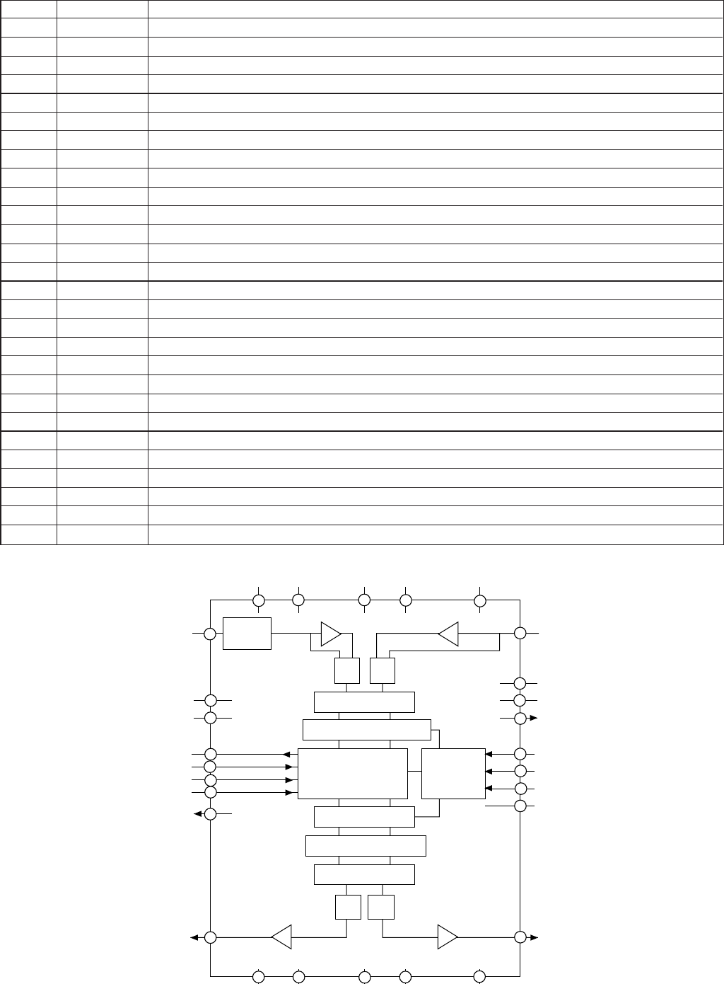
– 85 –
MD-E9000W
1 VSSA (ADC) AD converter analog ground.
2 VDDA (ADC) AD converter analog power.
3 VINL AD converter input. (left)
4 VREF (A) AD converter reference voltage.
5 VINR AD converter input. (right)
6 VADCN AD converter reference voltage N.
7 VADCP AD converter reference voltage P.
8* MC1 Mode control 1. (Pulled-down)
9* MP1 Multipurpose pin 1.
10 VDDD Digital power.
11 VSSD Digital ground
12 SYSCLK System clock 256 fs, 384 fs, 512 fs.
13 MP2 Multipurpose pin 2.
14 MP3 Multipurpose pin 3.
15 MP4 Multipurpose pin 4.
16 BCK Bit clock input.
17 WS Word select input.
18 DATAO Data output.
19 DATAI Data input
20* MP5 Multipurpose pin 5. (Pulled-down)
21* MC2 Mode control 2. (Pulled-down)
22 VSSA (DAC) DA converter analog ground.
23 VDDA (ADC) DA converter analog power.
24 VOUTR DA converter output. (right)
25 VDDO Opeamp power.
26 VOUTL DA converter output. (left)
27 VSSO Opeamp ground.
28 VREF (D) AD converter reference voltage.
IC1701 VHiUDA1345/-1: AD/DA Converter (UDA1345)
Pin No. Function
Terminal Name
In this unit, the terminal with asterisk mark (*) is (open) terminal which is not connected to the outside.
Figure 85 BLOCK DIAGRAM OF IC
VDDA(ADC) VSSA(ADC) VADCP VADCN Vref(A)
VINR
MC1
MC2
MP5
MP2
MP3
MP4
SYSCLK
VOUTR
Vref(D)
VSSA(DAC)
VDDA(DAC)
VSSO
VDDO
VOUTL
MP1
DATAI
WS
BCK
DATAO
VSSD
VDDD
VINL
ADC
0dB/6dB
switch
ADC
DECMATION FILTER
DC-CANCELLATION FILTER
DIGITAL
INTERFACE
L3-BUS
INTERFACE
DSP FEATURES
INTERPOLATION FILTER
NOISE SHAPER
DAC DAC
2
3
4
5
1 7
8
9
6
12
13
14
15
11
17
18
19
10
16
22
23
24
25
21
27 28
20
26
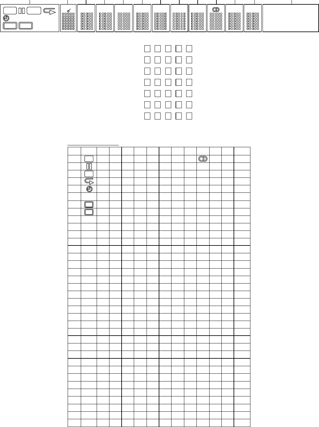
MD-E9000W
– 86 –
FL DISPLAY
FL701: VVKST48GNK/-1
REC
LP2
SLEEP
HIGH
LP4
RDS
Dp
1G 2G 3G
PTY
4G
TP
5G
TA
6G
EON
7G
TI
8G
ST
9G
TOC
11G
OVER
T-EDIT BASS
DISC
MEMORY
TRACK
RANDOM
12G 13G10G
1-1 2-1 3-1 4-1 5-1
1-2 2-2 3-2 4-2 5-2
1-3 2-3 3-3 4-3 5-3
1-4 2-4 3-4 4-4 5-4
1-5 2-5 3-5 4-5 5-5
1-6 2-6 3-6 4-6 5-6
1-7 2-7 3-7 4-7 5-7
[2G~12G]
ANODE CONNECTION
P1
P2
P3
P4
P5
P6
P7
P8
P9
P10
P11
P12
P13
P14
P15
P16
P17
P18
P19
P20
P21
P22
P23
P24
P25
P26
P27
P28
P29
P30
P31
P32
P33
P34
P35
P36
1G
—
—
—
—
—
—
—
—
—
—
—
—
—
—
—
—
—
—
—
—
—
—
—
—
—
—
—
—
2G
Dp
1–1
2–1
3–1
4–1
5–1
1–2
2–2
3–2
4–2
5-2
1–3
2–3
3–3
4–3
5–3
1–4
2–4
3–4
4–4
5–4
1–5
2–5
3–5
4–5
5–5
1–6
2–6
3–6
4–6
5–6
1–7
2–7
3–7
4–7
5–7
3G
1–1
2–1
3–1
4–1
5–1
1–2
2–2
3–2
4–2
5-2
1–3
2–3
3–3
4–3
5–3
1–4
2–4
3–4
4–4
5–4
1–5
2–5
3–5
4–5
5–5
1–6
2–6
3–6
4–6
5–6
1–7
2–7
3–7
4–7
5–7
4G
1–1
2–1
3–1
4–1
5–1
1–2
2–2
3–2
4–2
5-2
1–3
2–3
3–3
4–3
5–3
1–4
2–4
3–4
4–4
5–4
1–5
2–5
3–5
4–5
5–5
1–6
2–6
3–6
4–6
5–6
1–7
2–7
3–7
4–7
5–7
5G
1–1
2–1
3–1
4–1
5–1
1–2
2–2
3–2
4–2
5-2
1–3
2–3
3–3
4–3
5–3
1–4
2–4
3–4
4–4
5–4
1–5
2–5
3–5
4–5
5–5
1–6
2–6
3–6
4–6
5–6
1–7
2–7
3–7
4–7
5–7
6G
1–1
2–1
3–1
4–1
5–1
1–2
2–2
3–2
4–2
5-2
1–3
2–3
3–3
4–3
5–3
1–4
2–4
3–4
4–4
5–4
1–5
2–5
3–5
4–5
5–5
1–6
2–6
3–6
4–6
5–6
1–7
2–7
3–7
4–7
5–7
7G
1–1
2–1
3–1
4–1
5–1
1–2
2–2
3–2
4–2
5-2
1–3
2–3
3–3
4–3
5–3
1–4
2–4
3–4
4–4
5–4
1–5
2–5
3–5
4–5
5–5
1–6
2–6
3–6
4–6
5–6
1–7
2–7
3–7
4–7
5–7
8G
1–1
2–1
3–1
4–1
5–1
1–2
2–2
3–2
4–2
5-2
1–3
2–3
3–3
4–3
5–3
1–4
2–4
3–4
4–4
5–4
1–5
2–5
3–5
4–5
5–5
1–6
2–6
3–6
4–6
5–6
1–7
2–7
3–7
4–7
5–7
9G
1–1
2–1
3–1
4–1
5–1
1–2
2–2
3–2
4–2
5-2
1–3
2–3
3–3
4–3
5–3
1–4
2–4
3–4
4–4
5–4
1–5
2–5
3–5
4–5
5–5
1–6
2–6
3–6
4–6
5–6
1–7
2–7
3–7
4–7
5–7
10G
1–1
2–1
3–1
4–1
5–1
1–2
2–2
3–2
4–2
5-2
1–3
2–3
3–3
4–3
5–3
1–4
2–4
3–4
4–4
5–4
1–5
2–5
3–5
4–5
5–5
1–6
2–6
3–6
4–6
5–6
1–7
2–7
3–7
4–7
5–7
11G
1–1
2–1
3–1
4–1
5–1
1–2
2–2
3–2
4–2
5-2
1–3
2–3
3–3
4–3
5–3
1–4
2–4
3–4
4–4
5–4
1–5
2–5
3–5
4–5
5–5
1–6
2–6
3–6
4–6
5–6
1–7
2–7
3–7
4–7
5–7
12G
1–1
2–1
3–1
4–1
5–1
1–2
2–2
3–2
4–2
5-2
1–3
2–3
3–3
4–3
5–3
1–4
2–4
3–4
4–4
5–4
1–5
2–5
3–5
4–5
5–5
1–6
2–6
3–6
4–6
5–6
1–7
2–7
3–7
4–7
5–7
13G
—
—
—
—
—
—
—
—
—
—
—
—
—
—
—
—
—
—
—
—
—
—
—
—
—
—
—
—
—
—
REC
RDS PTY TP TA EON TI ST TOC
OVER
T-EDIT
BASS
DISC
TRACK
RANDOM
MEMORY
SLEEP
HIGH
LP2
LP4
MD-E9000W
PARTS GUIDE
NOTE:
Parts marked with “1” are important for maintaining the safety of the set.
Be sure to replace parts with specified ones for maintaining the safety and performance of the set.
“HOW TO ORDER REPLACEMENT PARTS”
To have your order filled promptly and correctly, please furnish the
following information.
1. MODEL NUMBER 2. REF. No.
3. PART NO. 4. DESCRIPTION
MARK: SPARE PARTS-DELIVERY SECTION
For U.S.A. only
Contact your nearest SHARP Parts Distributor to order.
For location of SHARP Parts Distributor,
Please call Toll-Free;
1-800-BE-SHARP
Explanation of capacitors/resistors parts codes
Capacitors
VCC ....................... Ceramic type
VCK........................ Ceramic type
VCT ........................ Semiconductor type
VC • • MF ............... Cylindrical type (without lead wire)
VC • • MN............... Cylindrical type (without lead wire)
VC • • TV................ Square type (without lead wire)
VC • • TQ ............... Square type (without lead wire)
VC • • CY ............... Square type (without lead wire)
VC • • CZ ............... Square type (without lead wire)
VC • • • • • • • • • J .. The 13th character represents capacity difference.
("J" ±5%, "K" ±10%, "M" ±20%, "N" ±30%,
"C" ±0.25 pF, "D" ±0.5 pF, "Z" +80-20%.)
If there are no indications for the electrolytic capacitors, error is ±20%.
Resistors
VRD ....................... Carbon-film type
VRS........................ Carbon-film type
VRN ....................... Metal-film type
VR • • MF ............... Cylindrical type (without lead wire)
VR • • MN............... Cylindrical type (without lead wire)
VR • • TV................ Square type (without lead wire)
VR • • TQ ............... Square type (without lead wire)
VR • • CY ............... Square type (without lead wire)
VR • • CZ ............... Square type (without lead wire)
VR • • • • • • • • • J .. The 13th character represents error.
("J" ±5%, "F" ±1%, "D" ±0.5%.)
If there are no indications for other parts, the resistors are ±5%
carbon-film type.
MD-E9000W MD Compact Component System consisting
of MD-E9000W (main unit) and CP-E9000H (speaker
system).
MD COMPACT COMPONENT SYSTEM
MODEL MD-E9000W

PRICE
RANK
DESCRIPTIONNO. PARTS CODE NO. PARTS CODE
PRICE
RANK
DESCRIPTION
MD-E9000W
– 1 –
INTEGRATED CIRCUITS
IC1 VHILC78645NE1 J AY CD Servo,LC78645NE
IC2 VHILA6548D/-1 J AN Focus/Tracking/Spin/Sled Driver,
LA6548D
IC3 VHITA7291S/-1 J AH Loading Motor Driver,TA7291S
IC4 VHI74VHC08F-1 J AE Inverter,74VHC08F
IC301 VHITA7358AP-1 J AG FM Front End,TA7358AP
IC302 VHILC72131/-1 J AP PLL (Tuner),LC72131
IC303 VHILA1832S/-1 J AN FM IF Det./FM Mpx./AM IF,
LA1832S
IC401 VHILC75341/-1 J AM Audio Processor,LC75341
IC701 RH-IX0395AWZZ J AY System Microcomputer,
IX0395AW
IC901 VHILA4628//-1 J AU Power Amp.,LA4628
IC1101 VHIIR3R58M/-1 J AM RF Signal Processor,IR3R58M
IC1201 VHILR37816A-1 J BQ Endec/Atrac,LR37816A
IC1202 RH-IX2474AFZZ J BF 4Mbit D-RAM,IX2474AF
IC1300 VHI74ACT02T-1 J AE Head Driver,74ACT02T
IC1301 VHIFTD2005/-1 J AG Head Driver,FTD2005
IC1302 VHICPH5608/-1 J AH Head Driver,CPH5608
IC1401 RH-IX0410AWZZ J AY MD System Microcomputer,
IX0410AW
IC1402 VHI58X2402T-1 J AF EEPROM,58X2402T
IC1601 VHIM56788FP-1 J AX Motor Driver,M56788FP
IC1701 VHIUDA1345/-1 J AU AD/DA Converter,UDA1345
IC1801 VHIXC62EP32-1 J AE Regulator,XC62EP32
IC1802 VHIXC62FP26P1 J AG Regulator,XC62FP26P
TRANSISTORS
Q1 VSKTA1266GR-1 J AB Silicon,PNP,KTA1266 GR
Q2 VSKTA1271Y/-1 J AC Silicon,PNP,KTA1271 Y
Q3 VSKRC102M//-1 J AC Digital,NPN,KRC102 M
Q302 VSKTC3194Y/-1 J AD Silicon,NPN,KTC3194 Y
Q360 VSKTA1266GR-1 J AB Silicon,PNP,KTA1266 GR
Q701,702 VSKRC102M//-1 J AC Digital,NPN,KRC102 M
Q781 VSKRC107M//-1 J AC Digital,NPN,KRC107 M
Q782,783 VSKRC111M//-1 J AB Digital,NPN,KRC111 M
Q801 VSKTA1266GR-1 J AB Silicon,PNP,KTA1266 GR
Q871 VSKTC3199GR-1 J AB Silicon,NPN,KTC3199 GR
Q901,902 VSKTC3199GR-1 J AB Silicon,NPN,KTC3199 GR
Q941 VSKTC2026//-1 J AF Silicon,NPN,KTC2026
Q942 VSKTC3199GR-1 J AB Silicon,NPN,KTC3199 GR
Q951 VHIKIA7810AP1 J AF Voltage Regulator,KIA7810AP
Q952 VSKTC3203Y/-1 J AC Silicon,NPN,KTC3203 Y
Q961 VHIKIA7805AP1 J AF Voltage Regulator,KIA7805AP
Q962 VHIAN78L05/-1 J AE Voltage Regulator,AN78L05
Q971 VSKTC3203Y/-1 J AC Silicon,NPN,KTC3203 Y
Q972 VSKTA1266GR-1 J AB Silicon,PNP,KTA1266 GR
Q1501 VSUN2214///-1 J AB Digital,NPN,UN2214
Q1804 VS2SB1205++-1 J AF Silicon,PNP,2SB1205
Q1807 VS2SD601AR/-1 J AC Silicon,NPN,2SD601 AR
DIODES
D301~306 VHDDS1SS133-1 J AB Silicon,DS1SS133
D441,442 VHDDS1SS133-1 J AB Silicon,DS1SS133
D701 VHDDS1SS133-1 J AB Silicon,DS1SS133
D781~785 VHDDS1SS133-1 J AB Silicon,DS1SS133
D801 VHDTS6B04GM-1 J AP Silicon,TS6B04GM
D802~805 VHDRL203F//-1 J AE Silicon,RL203F
D806~808 VHDDS1N404S-1 J AB Silicon,DS1N404S
D809 VHDDS1SS133-1 J AB Silicon,DS1SS133
D871,872 VHDDS1SS133-1 J AB Silicon,DS1SS133
D873~876 VHDDS1N404S-1 J AB Silicon,DS1N404S
D877 VHDDS1SS133-1 J AB Silicon,DS1SS133
D961,962 VHDDS1SS133-1 J AB Silicon,DS1SS133
D972,973 VHDDS1SS133-1 J AB Silicon,DS1SS133
D1300 VHDSBE803//-1 J AD Silicon,SBE803
LED701 VHP4204SRT7-1 J AD LED,Red,4204SRT7
LED702 VHPLNG901CF-1 J AS LED,Blue,LNG901CF
ZD351 VHEDZ5R1BSB-1 J AC Zener,5.1V,DZ5.1BSB
ZD801 VHEDZ300BSC-1 J AB Zener,30V,DZ30BSC
ZD802 VHEDZ6R2BSA-1 J AB Zener,6.2V,DZ6.2BSA
ZD803 VHEDZ120BSB-1 J AB Zener,12V,DZ12BSB
ZD871 VHEDZ3R0BSA-1 J AB Zener,3V,DZ3BSA
ZD941 VHEDZ6R8BSA-1 J AC Zener,6.8V,DZ6.8BSA
ZD951 VHEDZ3R6BSB-1 J AB Zener,3.6V,DZ3.6BSB
FILTERS
BF301 RFILR0008AWZZ J AE Band Pass Filter
CF303 RFILF0124AFZZ J AD FM IF,10.7 MHz
CF351 RFILF0003AWZZ J AK FM IF
CF352 RFILA0009AWZZ J AE AM IF
FL1501 RFILN0002AWZZ J AD EMI Filter
FL1507 RFILN0003AWZZ J AD EMI Filter
FL1509 RFILN0003AWZZ J AD EMI Filter
FL1512 RFILN0003AWZZ J AD EMI Filter
FL1518 RFILN0003AWZZ J AD EMI Filter
FL1520 RFILN0003AWZZ J AD EMI Filter
FL1523~1525 RFILN0007AWZZ J AD EMI Filter
TRANSFORMERS
1PT801 RTRNP0354AWZZ J BA Power,Main
1PT871 RTRNP0341AWZZ J AM Power,Sub
T301 RCILB0065AWZZ J AC FM OSC.
T302 RCILI0017AWZZ J AB FM IF
T303 RCILA0052AWZZ J AE AM Tracking
T306 RCILB0058AWZZ J AC AM OSC.
T351 RCILI0019AWZZ J AD AM IF
COILS
L2 VP-XHR82K0000 J AC 0.82 µH,Choke
L4 VP-XH2R2K0000 J AB 2.2 µH,Choke
L312 RCILR0056AWZZ J AB FM RF
L351,352 VP-DH101K0000 J AB 100 µH,Choke
L451 VPADK100KR15K J AE 10 µH
L452 VP-DHR22K0000 J AB 0.22 µH
L781 VP-DH101K0000 J AB 100 µH,Choke
L981 VP-DH2R2K0000 J AB 2.2 µH,Peaking
L1100 VPBNNR47K0000 J AC 0.47 µH
L1101 VPBNN100K0000 J AC 10 µH
L1200 VPBNN4R7K0000 J AC 4.7 µH
L1201,1202 VPBNNR47K0000 J AC 0.47 µH
L1300 RCILC0358AFZZ J AC 47 µH,Choke
VARIABLE CAPACITORS
VD301 VHCSVC348S/-1 J AK Variable Capacitance,SVC348S
VD302,303 VHCSVC211C/-1 J AG Variable Capacitance,SVC211C
VIBRATORS
X351 92LCRSTL1425A J AF Crystal,456 kHz
X352 RCRSP0019AWZZ J AF Crystal,4.5 MHz
XL1 RCRSP0025AWZZ J AK Crystal,33.8688 MHz
XL701 RCRSP0009AWZZ J AK Crystal,8.3886 MHz
XL1201 RCRSC0001AWZZ J AL Crystal,33.8688 MHz
THERMISTOR
1RP941 RH-QX0010AWZZ J AE Posistor,0.5ohms
CAPACITORS
C1 VCTYMN1CY103N J AA 0.01 µF,16V
C2 VCEAZA1CW476M J AB 47 µF,16V,Electrolytic
C3 VCTYMN1CY103N J AA 0.01 µF,16V
C4 VCEAZA1CW476M J AB 47 µF,16V,Electrolytic
C5 VCKYMN1HB102K J AA 0.001 µF,50V
C6 VCTYPA1CX473K J AA 0.047 µF,16V
C7 VCTYPA1CX104K J AB 0.1 µF,16V
C8 VCCSPA1HL100J J AA 10 pF,50V
C9 VCTYMN1CX272K J AA 0.0027 µF,16V
C10 VCEAZA1CW107M J AC 100 µF,16V,Electrolytic
C12 VCEAZA1CW106M J AC 10 µF,16V,Electrolytic
C13 VCEAZA1HW224M J AB 0.22 µF,50V,Electrolytic
C14 VCKYMN1HB101K J AA 100 pF,50V
C15 VCTYPA1CX104K J AB 0.1 µF,16V
C16 VCEAZA1HW225M J AB 2.2 µF,50V,Electrolytic
C17 VCTYPA1CX473K J AA 0.047 µF,16V
C18 VCKYMN1HB101K J AA 100 pF,50V
C19 VCTYMN1EF223Z J AA 0.022 µF,25V
C20~23 VCKYMN1HB101K J AA 100 pF,50V
C24 VCKYPA1HF223Z J AB 0.022 µF,50V
C28 VCTYPA1CX473K J AA 0.047 µF,16V
C31,32 VCCCMN1HH150J J AA 15 pF (CH),50V
C41 RC-EZY107AF1C J AB 100 µF,16V,Electrolytic
MD-E9000W

NO.
PRICE
RANK
DESCRIPTIONPARTS CODE
NO. PARTS CODE
PRICE
RANK
DESCRIPTION
MD-E9000W
C42 VCTYMN1EF223Z J AA 0.022 µF,25V
C43 VCEAZA1CW107M J AC 100 µF,16V,Electrolytic
C44 VCTYMN1CX152K J AA 0.0015 µF,16V
C45 VCEAZA1AW337M J AC 330 µF,10V,Electrolytic
C46~48 VCTYPA1CX104K J AB 0.1 µF,16V
C49 RC-EZY476AF1C J AB 47 µF,16V,Electrolytic
C50 VCTYPA1CX104K J AB 0.1 µF,16V
C53 VCEAZA1EW475M J AC 4.7 µF,25V,Electrolytic
C54 VCCSMN1HL220J J AA 22 pF,50V
C57,58 VCKYMN1HB681K J AA 680 pF,50V
C61 VCKYPA1HF103Z J AB 0.01 µF,50V
C62,63 VCKYPA1HB102K J AA 0.001 µF,50V
C303 VCCCMN1HH100J J AA 10 pF (CH),50V
C304 VCTYMN1CY103N J AA 0.01 µF,16V
C305 VCCCMN1HH4R7C J AA 4.7 pF (CH),50V
C306 VCTYMN1EF223Z J AA 0.022 µF,25V
C307 VCEAZA1HW106M J AB 10 µF,50V,Electrolytic
C308 VCCSMN1HL4R7C J AA 4.7 pF,50V
C309 VCKYMN1HB102K J AA 0.001 µF,50V
C310 VCCCMN1HH150J J AA 15 pF (CH),50V
C311 VCCSPA1HL180J J AA 18 pF,50V
C312 VCTYMN1EF223Z J AA 0.022 µF,25V
C313 VCCCMN1HH220J J AA 22 pF (CH),50V
C314,315 VCTYMN1CX472K J AA 0.0047 µF,16V
C316 VCTYMN1EF223Z J AA 0.022 µF,25V
C317 VCKYMN1HB102K J AA 0.001 µF,50V
C318 VCKYMN1HB101K J AA 100 pF,50V
C320 VCKYBT1HB102K J AA 0.001 µF,50V
C323 VCTYMN1EF223Z J AA 0.022 µF,25V
C324 VCCUMN1HJ3R9K J AA 3.9 pF (UJ),50V
C325 VCKYMN1HB221K J AA 220 pF,50V
C330 VCCUMN1HJ150J J AA 15 pF (UJ),50V
C331 VCKYPA1HF473Z J AB 0.047 µF,50V
C332 VCTYMN1EF223Z J AA 0.022 µF,25V
C334 VCCUMN1HJ180J J AA 18 pF (UJ),50V
C335 VCKYMN1HB561K J AA 560 pF,50V
C338 VCKYMN1HB102K J AA 0.001 µF,50V
C342 VCTYMN1EF223Z J AA 0.022 µF,25V
C350 VCTYBT1EF223Z J AA 0.022 µF,25V
C351 VCTYMN1EF223Z J AA 0.022 µF,25V
C352 VCEAZA1HW106M J AB 10 µF,50V,Electrolytic
C353,354 VCTYMN1EF223Z J AA 0.022 µF,25V
C355 VCCSMN1HL220J J AA 22 pF,50V
C356 VCKYMN1HB102K J AA 0.001 µF,50V
C357 VCEAZA1HW225M J AB 2.2 µF,50V,Electrolytic
C358 VCEAZA1HW105M J AB 1 µF,50V,Electrolytic
C361 VCTYMN1EF223Z J AA 0.022 µF,25V
C362 VCEAZA1HW335M J AB 3.3 µF,50V,Electrolytic
C363 VCTYMN1EF223Z J AA 0.022 µF,25V
C364 VCEAZA1HW225M J AB 2.2 µF,50V,Electrolytic
C365 VCKYPA1HF223Z J AB 0.022 µF,50V
C366 VCKYMN1HB102K J AA 0.001 µF,50V
C367,368 VCEAZA1HW105M J AB 1 µF,50V,Electrolytic
C369 VCCUMN1HJ270J J AA 27 pF (UJ),50V
C370~372 VCEAZA1HW105M J AB 1 µF,50V,Electrolytic
C373,374 VCTYPA1CX153K J AA 0.015 µF,16V
C380 VCEAZA1HW106M J AB 10 µF,50V,Electrolytic
C381 VCCCMN1HH120J J AA 12 pF (CH),50V
C382 VCCCMN1HH150J J AA 15 pF (CH),50V
C384 VCKYMN1HB102K J AA 0.001 µF,50V
C385 VCTYMN1CY103N J AA 0.01 µF,16V
C386 VCKYMN1HB331K J AA 330 pF,50V
C387 VCTYMN1EF223Z J AA 0.022 µF,25V
C388 VCKYMN1HB102K J AA 0.001 µF,50V
C391 RC-EZY476AF1C J AB 47 µF,16V,Electrolytic
C392 VCKYMN1HB102K J AA 0.001 µF,50V
C393 VCEAZA1HW105M J AB 1 µF,50V,Electrolytic
C394 RC-EZY476AF1C J AB 47 µF,16V,Electrolytic
C395 VCTYMN1EF223Z J AA 0.022 µF,25V
C396 RC-EZY107AF1C J AB 100 µF,16V,Electrolytic
C397 VCTYMN1EF223Z J AA 0.022 µF,25V
C398 VCEAZA1CW107M J AC 100 µF,16V,Electrolytic
C399 VCTYMN1EF223Z J AA 0.022 µF,25V
C402 VCKYPA1HF223Z J AB 0.022 µF,50V
C403 RC-EZY107AF1C J AB 100 µF,16V,Electrolytic
C404~406 VCKYPA1HB561K J AA 560 pF,50V
C407 RC-EZY226AF1C J AB 22 µF,16V,Electrolytic
C411,412 RC-EZY105AF1H J AB 1 µF,50V,Electrolytic
C413,414 VCFYHA1HA104J J AB 0.1 µF,50V,Thin Film
C415,416 VCFYHA1HA124J J AB 0.12 µF,50V,Thin Film
C417,418 VCQYKA1HM152K J AB 0.0015 µF,50V,Mylar
C419~424 RC-EZY105AF1H J AB 1 µF,50V,Electrolytic
C425,426 RC-EZY106AF1C J AB 10 µF,16V,Electrolytic
C427 VCKYPA1HF223Z J AB 0.022 µF,50V
C428,429 RC-EZY105AF1H J AB 1 µF,50V,Electrolytic
C441,442 VCKYPA1HB391K J AA 390 pF,50V
C443 VCKYPA1HB102K J AA 0.001 µF,50V
C451,452 RC-EZY106AF1C J AB 10 µF,16V,Electrolytic
C453,454 VCKYPA1HB221K J AA 220 pF,50V
C455 VCKYPA1HF223Z J AB 0.022 µF,50V
C456,457 VCKYPA1HB101K J AA 100 pF,50V
C458 VCCSPA1HL100J J AA 10 pF,50V
C459 VCKYPA1HF103Z J AB 0.01 µF,50V
C460 VCKYPA1HB221K J AA 220 pF,50V
C461,462 VCKYPA1HB101K J AA 100 pF,50V
C463 VCKYPA1HF223Z J AB 0.022 µF,50V
C464 VCEAZA1AW227M J AC 220 µF,10V,Electrolytic
C465 VCKYPA1HF223Z J AB 0.022 µF,50V
C466~469 VCKYPA1HB221K J AA 220 pF,50V
C470 VCCSPA1HL330J J AA 33 pF,50V
C471 VCKYPA1HF103Z J AB 0.01 µF,50V
C701~703 RC-EZY105AF1H J AB 1 µF,50V,Electrolytic
C704,705 VCTYMN1EF223Z J AA 0.022 µF,25V
C706 RC-EZY227AF0J J AB 220 µF,6.3V,Electrolytic
C707 VCTYMN1EF223Z J AA 0.022 µF,25V
C708 RC-EZY106AF1E J AB 10 µF,25V,Electrolytic
C709 VCKYMN1HB101K J AA 100 pF,50V
C710,711 VCCCMN1HH180J J AA 18 pF (CH),50V
C712~715 VCKYMN1HB151K J AA 150 pF,50V
C716~718 VCKYPA1HB102K J AA 0.001 µF,50V
C781 VCEAZA1EW476M J AB 47 µF,25V,Electrolytic
C782 VCTYMN1EF223Z J AA 0.022 µF,25V
C783 RC-EZY106AF1E J AB 10 µF,25V,Electrolytic
C784 VCTYMN1EF223Z J AA 0.022 µF,25V
C801~804 VCQYKA1HM473K J AB 0.047 µF,50V,Mylar
C805,806 VCEAZA1HW227M J AC 220 µF,50V,Electrolytic
C807~809 VCEAZA1HW476M J AB 47 µF,50V,Electrolytic
C810 VCEAZA1VW107M J AC 100 µF,35V,Electrolytic
C811 VCTYPA1EX222K J AA 0.0022 µF,25V
C812 VCKYPA1HF473Z J AB 0.047 µF,50V
1C871 RC-KZ002LAWZZ J AC 0.0047 µF,250V,Ceramic
C872 VCQYKA1HM473K J AB 0.047 µF,50V,Mylar
C873 VCEAZV1CW108M J AD 1000 µF,16V,Electrolytic
C874 VCEAZA0JW108M J AC 1000 µF,6.3V,Electrolytic
C875 VCKYPA1HF223Z J AB 0.022 µF,50V
C901,902 VCKYMN1HB102K J AA 0.001 µF,50V
C903,904 VCEAZA1HW225M J AB 2.2 µF,50V,Electrolytic
C905 VCEAZA1HW476M J AB 47 µF,50V,Electrolytic
C907~910 VCQYKA1HM104K J AB 0.1 µF,50V,Mylar
C911 VCEAZA1CW107M J AC 100 µF,16V,Electrolytic
C912 VCEAZA1VW107M J AC 100 µF,35V,Electrolytic
C913 VCEAZA1HW474M J AB 0.47 µF,50V,Electrolytic
C914 VCEAZA1EW107M J AB 100 µF,25V,Electrolytic
C923~926 VCQYKA1HM104K J AB 0.1 µF,50V,Mylar
C941 VCKYPA1HF223Z J AB 0.022 µF,50V
C942 VCEAZA1CW107M J AC 100 µF,16V,Electrolytic
C943 VCEAZA1AW477M J AC 470 µF,10V,Electrolytic
C947 VCEAZW1EW688M J AL 6800 µF,25V,Electrolytic
C948 VCEAZW1EW338M J AG 3300 µF,25V,Electrolytic
C949 VCEAZW1CW688M J AH 6800 µF,16V,Electrolytic
C951,952 VCQYKA1HM104K J AB 0.1 µF,50V,Mylar
C953 VCEAZA1EW476M J AB 47 µF,25V,Electrolytic
C954 VCKYPA1HF223Z J AB 0.022 µF,50V
C955 VCEAZA1AW107M J AB 100 µF,10V,Electrolytic
C956 VCKYPA1HF223Z J AB 0.022 µF,50V
C961,962 VCQYKA1HM104K J AB 0.1 µF,50V,Mylar
C963 VCEAZA1EW476M J AB 47 µF,25V,Electrolytic
C964,965 VCQYKA1HM104K J AB 0.1 µF,50V,Mylar
C966 VCEAZA1EW476M J AB 47 µF,25V,Electrolytic
C971 VCEAZA1HW475M J AB 4.7 µF,50V,Electrolytic
C972 VCEAZA1EW476M J AB 47 µF,25V,Electrolytic
C973 RC-EZY476AF1E J AB 47 µF,25V,Electrolytic
C981,982 VCEAZA1HW475M J AB 4.7 µF,50V,Electrolytic
C985 VCEAZA1CW226M J AC 22 µF,16V,Electrolytic
C986,987 VCKYPA1HB102K J AA 0.001 µF,50V
C1100 RC-KZ0003AWZZ J AE 4.7 µF,10V
C1107 VCKYCY1CB223K J AA 0.022 µF,16V
C1110,1111 VCKYCY1AF105Z J AB 1 µF,10V
C1112 VCCCCY1HH5R0C J AA 5 pF (CH),50V
C1113 VCKYCY0JB105K J AC 1 µF,6.3V
C1114,1115 VCKYCY1CB104K J AB 0.1 µF,16V
C1116,1117 VCKYCY1AF105Z J AB 1 µF,10V
C1118,1119 VCKYCY1AB474K J AC 0.47 µF,10V
C1121 VCKYCY1AB224K J AB 0.22 µF,10V
– 2 –

PRICE
RANK
DESCRIPTIONNO. PARTS CODE NO. PARTS CODE
PRICE
RANK
DESCRIPTION
MD-E9000W
C1122 VCKYCY1AF105Z J AB 1 µF,10V
C1123,1124 VCKYCY1CB104K J AB 0.1 µF,16V
C1125 VCKYCY1AF105Z J AB 1 µF,10V
C1161 VCKYCY1HB102K J AA 0.001 µF,50V
C1200 VCKYCY1AF105Z J AB 1 µF,10V
C1201 RC-KZ0002AWZZ J AE 10 µF,10V
C1202 VCKYCY1AF105Z J AB 1 µF,10V
C1205 VCKYCY1AF105Z J AB 1 µF,10V
C1206 VCKYCY1CB103K J AA 0.01 µF,16V
C1207 VCKYCY1AF105Z J AB 1 µF,10V
C1208,1209 VCCCCY1HH120J J AA 12 pF (CH),50V
C1211 VCKYCY1EF104Z J AA 0.1 µF,25V
C1230 VCKYCY1AF105Z J AB 1 µF,10V
C1260 VCKYCY1EF104Z J AA 0.1 µF,25V
C1261~1265 VCCCCY1HH221J J AA 220 pF (CH),50V
C1266 VCCCCY1HH220J J AA 22 pF (CH),50V
C1300 VCCCCY1HH151J J AA 150 pF (CH),50V
C1301 VCKYCY1CB223K J AA 0.022 µF,16V
C1302 RC-KZ0002AWZZ J AE 10 µF,10V
C1303 VCKYCY1AF105Z J AB 1 µF,10V
C1304 VCCCCY1HH221J J AA 220 pF (CH),50V
C1305 VCCCCY1HH680J J AA 68 pF (CH),50V
C1340 VCCCCY1HH101J J AA 100 pF (CH),50V
C1403 VCKYCY1EF104Z J AA 0.1 µF,25V
C1404 VCKYCY1CB103K J AA 0.01 µF,16V
C1405 VCCCCY1HH681J J AC 680 pF (CH),50V
C1407 VCKYCY1EF104Z J AA 0.1 µF,25V
C1409 VCKYCY1AF105Z J AB 1 µF,10V
C1510 VCCCCY1HH101J J AA 100 pF (CH),50V
C1512 VCCCCY1HH101J J AA 100 pF (CH),50V
C1523,1524 VCCCCY1HH101J J AA 100 pF (CH),50V
C1530 VCCCCY1HH101J J AA 100 pF (CH),50V
C1534 VCCCCY1HH470J J AA 47 pF (CH),50V
C1536 VCCCCY1HH470J J AA 47 pF (CH),50V
C1538 VCCCCY1HH101J J AA 100 pF (CH),50V
C1540 VCCCCY1HH151J J AA 150 pF (CH),50V
C1563 VCKYCY1AF105Z J AB 1 µF,10V
C1602 VCCCCY1HH471J J AA 470 pF (CH),50V
C1603 VCCCCY1HH681J J AC 680 pF (CH),50V
C1606 RC-KZ0002AWZZ J AE 10 µF,10V
C1607 VCKYCY1AF105Z J AB 1 µF,10V
C1610 RC-KZ0003AWZZ J AE 4.7 µF,10V
C1611 VCKYCY1HB472K J AA 0.0047 µF,50V
C1613 VCKYCY1CB103K J AA 0.01 µF,16V
C1616 VCEAPS107AF1A J AD 100 µF,10V,Electrolytic
C1619 VCCCCY1HH331J J AA 330 pF (CH),50V
C1655 VCKYCY1HF103Z J AB 0.01 µF,50V
C1700 VCEAPS476AF0G J AC 47 µF,4V,Electrolytic
C1703 VCKYCY1EF104Z J AA 0.1 µF,25V
C1704 VCEAPS476AF0G J AC 47 µF,4V,Electrolytic
C1706 VCKYCY1HF103Z J AB 0.01 µF,50V
C1708 VCKYCY1HF103Z J AB 0.01 µF,50V
C1715 VCKYCY1EF104Z J AA 0.1 µF,25V
C1716 VCEAPS476AF0G J AC 47 µF,4V,Electrolytic
C1720,1721 VCCCCY1HH331J J AA 330 pF (CH),50V
C1750 VCKYCY1EF104Z J AA 0.1 µF,25V
C1801,1802 RC-KZ0002AWZZ J AE 10 µF,10V
C1806 VCKYCY1AF105Z J AB 1 µF,10V
RESISTORS
VRD-MN2BD000C J AA 0 ohm,Jumper,ø1.4×3.5mm,Ivory
VRS-CY1JB000J J AA
0 ohm,Jumper,0.8×1.55mm,Green
R1 VRD-ST2CD822J J AA 8.2 kohms,1/6W
R2 VRD-ST2CD223J J AA 22 kohms,1/6W
R3,4 VRD-ST2CD822J J AA 8.2 kohms,1/6W
R6 VRD-ST2CD822J J AA 8.2 kohms,1/6W
R7 VRD-ST2CD223J J AA 22 kohms,1/6W
R8 VRD-ST2CD470J J AA 47 ohms,1/6W
R9 VRD-MN2BD3R3J J AA 3.3 ohms,1/8W
R10 VRD-MN2BD273J J AA 27 kohms,1/8W
R11 VRD-MN2BD103J J AA 10 kohm,1/8W
R12 VRD-MN2BD331J J AA 330 ohms,1/8W
R13 VRD-MN2BD153J J AA 15 kohms,1/8W
R14 VRD-MN2BD122J J AA 1.2 kohms,1/8W
R15 VRD-MN2BD123J J AA 12 kohms,1/8W
R16,17 VRD-MN2BD681J J AA 680 ohms,1/8W
R18 VRD-MN2BD682J J AA 6.8 kohms,1/8W
R19 VRD-MN2BD153J J AA 15 kohms,1/8W
R20 VRD-MN2BD822J J AA 8.2 kohms,1/8W
R21 VRD-ST2CD822J J AA 8.2 kohms,1/6W
R23 VRD-MN2BD102J J AA 1 kohm,1/8W
R24 VRD-MN2BD473J J AA 47 kohms,1/8W
R27~33 VRD-ST2CD102J J AA 1 kohm,1/6W
R35,36 VRD-MN2BD102J J AA 1 kohm,1/8W
R37~39 VRD-ST2CD101J J AA 100 ohm,1/6W
R40 VRD-ST2CD103J J AA 10 kohm,1/6W
R42 VRD-ST2CD221J J AA 220 ohms,1/6W
R48 VRD-RT2HD2R2J J AA 2.2 ohms,1/2W
R49 VRD-MN2BD562J J AA 5.6 kohms,1/8W
R50 VRD-MN2BD153J J AA 15 kohms,1/8W
R53 VRD-MN2BD221J J AA 220 ohms,1/8W
R54 VRD-ST2CD102J J AA 1 kohm,1/6W
R55 VRD-MN2BD104J J AA 100 kohm,1/8W
R56 VRD-MN2BD183J J AA 18 kohms,1/8W
R302 VRD-MN2BD100J J AA 10 ohm,1/8W
R309 VRD-ST2CD103J J AA 10 kohm,1/6W
R311 VRD-MN2BD104J J AA 100 kohm,1/8W
R313 VRD-MN2BD333J J AA 33 kohms,1/8W
R314 VRD-ST2CD220J J AA 22 ohms,1/6W
R316 VRD-MN2BD472J J AA 4.7 kohms,1/8W
R322 VRD-MN2BD681J J AA 680 ohms,1/8W
R323 VRD-MN2BD683J J AA 68 kohms,1/8W
R325 VRD-MN2BD473J J AA 47 kohms,1/8W
R327 VRD-MN2BD330J J AA 33 ohms,1/8W
R336 VRD-MN2BD103J J AA 10 kohm,1/8W
R350 VRD-MN2BD272J J AA 2.7 kohms,1/8W
R351 VRD-MN2BD562J J AA 5.6 kohms,1/8W
R352 VRD-MN2BD102J J AA 1 kohm,1/8W
R353 VRD-MN2BD271J J AA 270 ohms,1/8W
R355 VRD-MN2BD332J J AA 3.3 kohms,1/8W
R356 VRD-MN2BD102J J AA 1 kohm,1/8W
R357 VRD-ST2CD474J J AA 470 kohms,1/6W
R358 VRD-ST2CD392J J AA 3.9 kohms,1/6W
R359 VRD-ST2CD182J J AA 1.8 kohms,1/6W
R360 VRD-ST2CD472J J AA 4.7 kohms,1/6W
R365 VRD-MN2BD103J J AA 10 kohm,1/8W
R368 VRD-ST2CD223J J AA 22 kohms,1/6W
R372~374 VRD-MN2BD102J J AA 1 kohm,1/8W
R375 VRD-ST2CD471J J AA 470 ohms,1/6W
R376 VRD-MN2BD102J J AA 1 kohm,1/8W
R377 VRD-MN2BD473J J AA 47 kohms,1/8W
R378 VRD-MN2BD102J J AA 1 kohm,1/8W
R379 VRD-MN2BD222J J AA 2.2 kohms,1/8W
R380 VRD-MN2BD152J J AA 1.5 kohms,1/8W
R381 VRD-MN2BD103J J AA 10 kohm,1/8W
R382 VRD-ST2EE151J J AA 150 ohms,1/4W
R383 VRD-MN2BD562J J AA 5.6 kohms,1/8W
R384 VRD-ST2CD562J J AA 5.6 kohms,1/6W
R385 VRD-MN2BD562J J AA 5.6 kohms,1/8W
R387 VRD-ST2CD562J J AA 5.6 kohms,1/6W
R388 VRD-MN2BD392J J AA 3.9 kohms,1/8W
R391,392 VRD-ST2EE271J J AA 270 ohms,1/4W
R393 VRD-MN2BD102J J AA 1 kohm,1/8W
R395 VRD-MN2BD473J J AA 47 kohms,1/8W
R401~403 VRD-ST2CD102J J AA 1 kohm,1/6W
R413,414 VRD-ST2CD392J J AA 3.9 kohms,1/6W
R415,416 VRD-ST2CD332J J AA 3.3 kohms,1/6W
R417,418 VRD-ST2CD101J J AA 100 ohm,1/6W
R441,442 VRD-ST2CD822J J AA 8.2 kohms,1/6W
R443,444 VRD-ST2CD273J J AA 27 kohms,1/6W
R445 VRD-ST2CD103J J AA 10 kohm,1/6W
R446,447 VRD-ST2CD103J J AA 10 kohm,1/6W
R448,449 VRD-ST2CD272J J AA 2.7 kohms,1/6W
R451 VRD-ST2CD101J J AA 100 ohm,1/6W
R452,453 VRD-ST2CD103J J AA 10 kohm,1/6W
R454,455 VRD-ST2CD101J J AA 100 ohm,1/6W
R456,457 VRD-ST2CD103J J AA 10 kohm,1/6W
R458,459 VRD-ST2CD123J J AA 12 kohms,1/6W
R460 VRD-ST2CD274J J AA 270 kohms,1/6W
R461~463 VRD-ST2CD560J J AA 56 ohms,1/6W
R701 VRD-MN2BD681J J AA 680 ohms,1/8W
R702 VRD-MN2BD182J J AA 1.8 kohms,1/8W
R703 VRD-MN2BD272J J AA 2.7 kohms,1/8W
R704 VRD-MN2BD472J J AA 4.7 kohms,1/8W
R705 VRD-MN2BD822J J AA 8.2 kohms,1/8W
R706 VRD-MN2BD183J J AA 18 kohms,1/8W
R707 VRD-MN2BD104J J AA 100 kohm,1/8W
R709 VRD-MN2BD681J J AA 680 ohms,1/8W
R710 VRD-MN2BD182J J AA 1.8 kohms,1/8W
R711 VRD-MN2BD272J J AA 2.7 kohms,1/8W
R712 VRD-MN2BD472J J AA 4.7 kohms,1/8W
R713 VRD-MN2BD822J J AA 8.2 kohms,1/8W
R714 VRD-MN2BD183J J AA 18 kohms,1/8W
– 3 –

NO.
PRICE
RANK
DESCRIPTIONPARTS CODE
NO. PARTS CODE
PRICE
RANK
DESCRIPTION
MD-E9000W
R716 VRD-MN2BD681J J AA 680 ohms,1/8W
R717 VRD-MN2BD182J J AA 1.8 kohms,1/8W
R718 VRD-MN2BD272J J AA 2.7 kohms,1/8W
R719 VRD-MN2BD472J J AA 4.7 kohms,1/8W
R720 VRD-MN2BD822J J AA 8.2 kohms,1/8W
R721 VRD-MN2BD183J J AA 18 kohms,1/8W
R722 VRD-MN2BD104J J AA 100 kohm,1/8W
R723~730 VRD-MN2BD473J J AA 47 kohms,1/8W
R731~735 VRD-MN2BD102J J AA 1 kohm,1/8W
R736 VRD-ST2CD102J J AA 1 kohm,1/6W
R737~744 VRD-MN2BD102J J AA 1 kohm,1/8W
R745,746 VRD-MN2BD562J J AA 5.6 kohms,1/8W
R747 VRD-MN2BD102J J AA 1 kohm,1/8W
R748,749 VRD-ST2CD102J J AA 1 kohm,1/6W
R750,751 VRD-ST2CD562J J AA 5.6 kohms,1/6W
R752~754 VRD-ST2CD102J J AA 1 kohm,1/6W
R759 VRD-ST2CD102J J AA 1 kohm,1/6W
R761,762 VRD-ST2CD102J J AA 1 kohm,1/6W
R763 VRD-MN2BD102J J AA 1 kohm,1/8W
R764 VRD-ST2CD102J J AA 1 kohm,1/6W
R765~769 VRD-MN2BD102J J AA 1 kohm,1/8W
R771,772 VRD-ST2CD103J J AA 10 kohm,1/6W
R773 VRD-MN2BD222J J AA 2.2 kohms,1/8W
R775 VRD-ST2CD824J J AA 820 kohms,1/6W
R776,777 VRD-ST2CD473J J AA 47 kohms,1/6W
R778 VRD-MN2BD560J J AA 56 ohms,1/8W
R781 VRD-MN2BD223J J AA 22 kohms,1/8W
R782 VRD-MN2BD101J J AA 100 ohm,1/8W
R783 VRD-MN2BD104J J AA 100 kohm,1/8W
R784 VRD-ST2CD473J J AA 47 kohms,1/6W
R785 VRD-MN2BD474J J AA 470 kohms,1/8W
R786 VRD-ST2CD103J J AA 10 kohm,1/6W
R787 VRD-MN2BD474J J AA 470 kohms,1/8W
R788 VRD-MN2BD103J J AA 10 kohm,1/8W
R789~791 VRD-ST2CD103J J AA 10 kohm,1/6W
R792~799 VRD-MN2BD473J J AA 47 kohms,1/8W
R801 VRD-ST2CD102J J AA 1 kohm,1/6W
R802 VRD-ST2CD221J J AA 220 ohms,1/6W
R803 VRD-ST2CD123J J AA 12 kohms,1/6W
R804 VRD-ST2CD221J J AA 220 ohms,1/6W
R805 VRD-ST2CD224J J AA 220 kohms,1/6W
R806 VRD-ST2CD473J J AA 47 kohms,1/6W
R871 VRD-ST2CD221J J AA 220 ohms,1/6W
R872 VRD-ST2CD473J J AA 47 kohms,1/6W
R873 VRD-ST2CD102J J AA 1 kohm,1/6W
R901 VRD-MN2BD153J J AA 15 kohms,1/8W
R902 VRD-ST2CD153J J AA 15 kohms,1/6W
R903,904 VRD-MN2BD272J J AA 2.7 kohms,1/8W
R905,906 VRD-MN2BD222J J AA 2.2 kohms,1/8W
R907,908 VRD-MN2BD102J J AA 1 kohm,1/8W
R909 VRD-MN2BD223J J AA 22 kohms,1/8W
R910 VRD-MN2BD332J J AA 3.3 kohms,1/8W
R911~914 VRD-ST2CD102J J AA 1 kohm,1/6W
R923,924 VRD-ST2EE4R7J J AA 4.7 ohms,1/4W
R928 VRD-RT2HD222J J AA 2.2 kohms,1/2W
R941 VRD-ST2CD102J J AA 1 kohm,1/6W
R942 VRD-ST2CD473J J AA 47 kohms,1/6W
R952 VRD-ST2CD223J J AA 22 kohms,1/6W
R953 VRD-ST2CD122J J AA 1.2 kohms,1/6W
R954,955 VRD-ST2EE221J J AA 220 ohms,1/4W
R961,962 VRD-ST2CD103J J AA 10 kohm,1/6W
R972 VRD-ST2CD333J J AA 33 kohms,1/6W
R973 VRD-ST2CD332J J AA 3.3 kohms,1/6W
R974 VRD-ST2CD103J J AA 10 kohm,1/6W
R975 VRD-ST2EE2R2J J AA 2.2 ohms,1/4W
R977,978 VRD-ST2CD103J J AA 10 kohm,1/6W
R979 VRD-ST2CD331J J AA 330 ohms,1/6W
R981,982 VRD-ST2EE271J J AA 270 ohms,1/4W
R983 VRD-MN2BD103J J AA 10 kohm,1/8W
R984 VRD-RT2HD470J J AA 47 ohms,1/2W
R1100 VRS-TQ2BB270J J AA 27 ohms,1/8W
R1101 VRS-CY1JB1R0J J AA 1 ohm,1/16W
R1102 VRS-CY1JB103J J AA 10 kohm,1/16W
R1105 VRS-CY1JB122J J AA 1.2 kohms,1/16W
R1110 VRS-CY1JB684F J AA 680 kohms,1/16W
R1111,1112 VRS-CY1JB104F J AA 100 kohm,1/16W
R1113 VRS-CY1JB684F J AA 680 kohms,1/16W
R1114 VRS-CY1JB123J J AA 12 kohms,1/16W
R1115 VRS-CY1JB334F J AA 330 kohms,1/16W
R1116,1117 VRS-CY1JB473F J AA 47 kohms,1/16W
R1118 VRS-CY1JB334F J AA 330 kohms,1/16W
R1119 VRS-CY1JB224J J AA 220 kohms,1/16W
R1120 VRS-CY1JB564J J AA 560 kohms,1/16W
R1121 VRS-CY1JB104J J AA 100 kohm,1/16W
R1122,1123 VRS-CY1JB123J J AA 12 kohms,1/16W
R1124,1125 VRS-CY1JB222J J AA 2.2 kohms,1/16W
R1201 VRS-CY1JB563F J AA 56 kohms,1/16W
R1203 VRS-CY1JB104F J AA 100 kohm,1/16W
R1205 VRS-CY1JB683J J AA 68 kohms,1/16W
R1207 VRS-CY1JB393J J AA 39 kohms,1/16W
R1209 VRS-CY1JB101J J AA 100 ohm,1/16W
R1210,1211 VRS-CY1JB221J J AA 220 ohms,1/16W
R1214 VRS-CY1JB103J J AA 10 kohm,1/16W
R1215 VRS-CY1JB105J J AA 1 Mohm,1/16W
R1217 VRS-CY1JB151J J AA 150 ohms,1/16W
R1230,1231 VRS-CY1JB103F J AA 10 kohm,1/16W
R1261~1266 VRS-CY1JB273J J AA 27 kohms,1/16W
R1300 VRS-CY1JB6R8J J AA 6.8 ohms,1/16W
R1301 VRS-CY1JB100J J AA 10 ohm,1/16W
R1304 VRS-CY1JB151J J AA 150 ohms,1/16W
R1401 VRS-CY1JB272J J AA 2.7 kohms,1/16W
R1403 VRS-CY1JB271J J AA 270 ohms,1/16W
R1406 VRS-CY1JB103J J AA 10 kohm,1/16W
R1407,1408 VRS-CY1JB332J J AA 3.3 kohms,1/16W
R1414 VRS-CY1JB224J J AA 220 kohms,1/16W
R1415 VRS-CY1JB102J J AA 1 kohm,1/16W
R1417,1418 VRS-CY1JB102J J AA 1 kohm,1/16W
R1420 VRS-CY1JB102J J AA 1 kohm,1/16W
R1430 VRS-CY1JB103J J AA 10 kohm,1/16W
R1435 VRS-CY1JB103J J AA 10 kohm,1/16W
R1441 VRS-CY1JB473J J AA 47 kohms,1/16W
R1443 VRS-CY1JB102J J AA 1 kohm,1/16W
R1446 VRS-CY1JB103J J AA 10 kohm,1/16W
R1460 VRS-CY1JB103J J AA 10 kohm,1/16W
R1463 VRS-CY1JB103J J AA 10 kohm,1/16W
R1515,1516 VRS-CY1JB221J J AA 220 ohms,1/16W
R1517,1518 VRS-CY1JB470J J AA 47 ohms,1/16W
R1521 VRS-CY1JB102J J AA 1 kohm,1/16W
R1529 VRS-CY1JB221J J AA 220 ohms,1/16W
R1532 VRS-CY1JB273J J AA 27 kohms,1/16W
R1533~1538 VRS-CY1JB102J J AA 1 kohm,1/16W
R1601 VRS-CY1JB123F J AA 12 kohms,1/16W
R1605 VRS-CY1JB123F J AA 12 kohms,1/16W
R1612 VRS-CY1JB563J J AA 56 kohms,1/16W
R1614 VRS-CY1JB333J J AA 33 kohms,1/16W
R1616 VRS-CY1JB123J J AA 12 kohms,1/16W
R1618 VRS-CY1JB223J J AA 22 kohms,1/16W
R1621 VRS-CY1JB682J J AA 6.8 kohms,1/16W
R1622,1623 VRS-CY1JB223J J AA 22 kohms,1/16W
R1624 VRS-CY1JB682J J AA 6.8 kohms,1/16W
R1701 VRS-CY1JB473J J AA 47 kohms,1/16W
R1702 VRS-CY1JB333J J AA 33 kohms,1/16W
R1703~1705 VRS-CY1JB3R9J J AA 3.9 ohms,1/16W
R1716 VRS-CY1JB104J J AA 100 kohm,1/16W
R1802 VRS-CY1JB563J J AA 56 kohms,1/16W
R1803 VRS-CY1JB333J J AA 33 kohms,1/16W
R1804 VRS-CY1JB391J J AA 390 ohms,1/16W
R1806 VRS-TQ2BB1R0J J AA 1 ohm,1/8W
R1807 VRS-CY1JB273J J AA 27 kohms,1/16W
R1809 VRS-TQ2BB1R0J J AA 1 ohm,1/8W
R1811 VRS-TQ2BB1R0J J AA 1 ohm,1/8W
R1931 VRS-CY1JB102J J AA 1 kohm,1/16W
R1932 VRS-CY1JB471J J AA 470 ohms,1/16W
R1933 VRS-CY1JB561J J AA 560 ohms,1/16W
R1934 VRS-CY1JB181J J AA 180 ohms,1/16W
OTHER CIRCUITRY PARTS
BI1/CNS402 QCNWN1886AWZZ J AH Connector Ass’y,6/7Pin
BI301/CNS301 QCNWN1977AWZZ J AG Connector Ass’y,9/9Pin
BI441/CNS441 QCNWN1887AWZZ J Connector Ass’y,6/6Pin
BI701/CNS701 QCNWN1884AWZZ J AF Connector Ass’y,5/5Pin
BI702/CNS702 QCNWN1885AWZZ J AG Connector Ass’y,8/8Pin
BI704A/B/CNS704
QCNWN1888AWZZ J AG Connector Ass’y,6/3/3Pin
BI901/CNS901 QCNWN1890AWZZ J AH Connector Ass’y,7/7Pin
BI902/CNS902 QCNWN1891AWZZ J AH Connector Ass’y,12/12Pin
BI903A/B/CNS903
QCNWN1892AWZZ J AK Connector Ass’y,7/4/11Pin
CN1101 QCNCWXM28AFZZ J AG Socket,28Pin
CN1300 QCNCM891BAFZZ J AC Plug,2Pin
CN1401 QCNCWYR09AWZZ J AD Socket,9Pin
CN1501 QCNCWYR27AWZZ J AE Socket,27Pin
CNP1 QCNCM704GAWZZ J AC Plug,7Pin
CNP2 QCNCM704HAWZZ J AC Plug,8Pin
CNP3 92LCONE2P53253 J AB Plug,2Pin
– 4 –

PRICE
RANK
DESCRIPTIONNO. PARTS CODE NO. PARTS CODE
PRICE
RANK
DESCRIPTION
MD-E9000W
CNP4 92LCONE6P53253 J AC Plug,6Pin
CNP4A 92LCONE6P53254 J AC Plug,6Pin
CNP5 92LCONE8P53253 J AC Plug,8Pin
CNP6 92LCONE6P53253 J AC Plug,6Pin
CNP401 QCNCWZX08AWZZ J AC Socket,8Pin
CNP402 QCNCM705GAFZZ J AB Plug,7Pin
CNP403 92LCONECP53253 J AD Plug,12Pin
CNP404 92LCONE7P53253 J AC Plug,7Pin
CNP405 92LCONE9P53253 J AC Plug,9Pin
CNP406 QCNCWZX12AWZZ J AC Socket,12Pin
CNP441 92LCONE6P53253 J AC Plug,6Pin
CNP451 QCNCWYP27AWZZ J Socket,27Pin
CNP702 QCNCWZY12AWZZ J AC Socket,12Pin
CNP703 QCNCWZY08AWZZ J AC Socket,8Pin
CNP704 92LCONE3P53253 J AB Plug,3Pin
CNP871 92LCONE5P53254 J AB Plug,5Pin
CNP903 92LCONEBP5267X J AC Plug,11Pin
CNP971 92LCONE2P53253 J AB Plug,2Pin
CNS1A/B QCNWN1976AWZZ J AG Connector Ass’y,7/7Pin
CNS2A/B QCNWN1975AWZZ J AF Connector Ass’y,8/8Pin
CNS3 QCNWN1895AWZZ J AC Connector Ass’y,2Pin
CNS4A/B QCNWN1894AWZZ J AF Connector Ass’y,6/6Pin
CNS6 QCNWN2077AWZZ J Connector Ass’y,2Pin
CNS971 QCNWN1896AWZZ J AC Connector Ass’y,2Pin
CORE1,2 RCORF0015AWZZ J AB Core
CW1501 QCNWN1880AWZZ J AF Flat Cable,27Pin
CW1931 QCNWN1742AWZZ J AE Flat Cable,9Pin
1F801 QFS-D632CAWNI J AC Fuse,T6.3A L 250V
1F802,803 QFS-D252CAWNI J AC Fuse,T2.5A L 250V
FFC702 QCNWN1889AWZZ J AE Flat Cable,12Pin
FFC703 QCNWN1882AWZZ J AD Flat Cable,8Pin
FL701 VVKST48GNK/-1 J AZ FL Display
JK441 QSOCJ0221AWZZ J AD Jack,AUX Input
JK981 QJAKM0004AWZZ J AK Jack,Headphones
LUG901 QLUGP0001AWZZ J AC Lug
M1 92LMTR1854BASY J AP Motor with Gear [Sled]
M2 92LMTR3515CASY J BA Motor with Chassis [Spindle]
M901 RMOTV0038AWZZ J AT MD Spindle Motor Ass’y
M902 92LMTR3167BASY J AP MD Sled Motor Ass’y
M903 92LMTR3167AASY J AN MD Loading Motor Ass’y
M904 RMOTV0027AWZZ J AM CD Lid Motor
M905 RMOTV0027AWZZ J AM Motor,Air Cooling Fan
1RL800 RRLYD0011AWZZ J AE Relay
RX781 VHLN64H380A-1 J AK Remote Sensor,N64H380A
SO301 QTANC0301AWZZ J AH Terminal,Antenna
1SO801 QSOCA0212AWZZ J AD Socket,AC Input
SO901 QTANA0416AWZZ J AE Terminal,Speaker
SW4 QSW-F9001AW01 J AD Switch,Push Type [Pickup In]
SW441 QSW-S0024AWZZ J AE Switch,Slide Type
[Span Selector]
SW701 92LSWICH1401AT J AC Switch,Key Type [Volume Down]
SW702 92LSWICH1401AT J AC Switch,Key Type [Volume Up]
SW703 92LSWICH1401AT J AC Switch,Key Type
[CD Play/Pause]
SW704 92LSWICH1401AT J AC Switch,Key Type [CD Stop]
SW705 92LSWICH1401AT J AC Switch,Key Type
[FF/Skip Up/Preset Up]
SW706 92LSWICH1401AT J AC Switch,Key Type
[REW/Skip Down/Preset Down]
SW707 92LSWICH1401AT J AC Switch,Key Type [MD Stop]
SW708 92LSWICH1401AT J AC Switch,Key Type
[MD Play/Pause]
SW709 92LSWICH1401AT J AC Switch,Key Type [Memory/Enter]
SW710 92LSWICH1401AT J AC Switch,Key Type
[Display (Demo)]
SW711 92LSWICH1401AT J AC Switch,Key Type [X-Bass]
SW712 92LSWICH1401AT J AC Switch,Key Type [Equalizer]
SW713 92LSWICH1401AT J AC Switch,Key Type [Aux]
SW714 92LSWICH1401AT J AC Switch,Key Type [Tuner (Band)]
SW715 92LSWICH1401AT J AC Switch,Key Type
[CD Open/Close]
SW716 92LSWICH1401AT J AC Switch,Key Type [On/Stand-by]
SW717 92LSWICH1401AT J AC Switch,Key Type [MD Eject]
SW718 92LSWICH1401AT J AC Switch,Key Type [LP4]
SW719 92LSWICH1401AT J AC Switch,Key Type [LP2]
SW720 92LSWICH1401AT J AC Switch,Key Type [SP]
SW721 92LSWICH1401AT J AC Switch,Key Type [Normal]
SW722 92LSWICH1401AT J AC Switch,Key Type [High]
SW723 92LSWICH1401AT J AC Switch,Key Type [MD Rec]
SW724 QSW-B0002AWZZ J AF Switch,Lever Type [Open/Close]
1SW801 QSOCE0008AWZZ J AH Switch,Slide Type
[Voltage Selector]
SW1930 QSW-P0011AWZZ J AD Switch,Push Type [Write Pro]
SW1932 QSW-M0007AWZZ J AD Switch,Push Type [Loading]
SW1933 QSW-M0007AWZZ J AD Switch,Push Type [Record]
SW1934 QSW-M0007AWZZ J AD Switch,Push Type [Play]
SW1936 QSW-M0157AFZZ J AD Switch,Slide Type [Lead In]
MD MECHANISM PARTS
2 LCHSM0089AWZZ J AH LD Base
3 LCHSM0090AWZZ J AH MD Base
4 LHLDX3009AWM1 J AG Cartridge Holder Ass’y
5 MLEVF0051AWM1 J AK Slider Lever Ass’y
7 MLEVF0046AWFW J AE Arm,Holder
8 MLEVF0047AWFW J AC Plate,Switch
9 MLEVF0054AWFW J AC Lever,Shift
10 MLEVP0095AWZZ J AC Lever,Cam Plate
12 MSPRD0132AWFJ J AB Spring,Loading
14 MSPRP0030AWFJ J AB Spring,Grip
15 MSPRP0031AWFJ J AC Spring,Shaft
16 MSPRT0031AWFJ J AC Spring,Loading Arm
17 MSPRT0032AWFJ J AB Spring,Shift Arm
18 NGERH0085AWZZ J AC Gear,Loading (A)
19 NGERH0086AWZZ J AB Gear,Middle (A)
20 NGERH0087AWZZ J AB Gear,Middle (B)
21 NGERH0088AWZZ J AC Gear,Middle (C)
22 NGERH0089AWZZ J AC Gear,Middle (D)
24 NGERR0004AWZZ J AC Gear,Grip
27 NSFTD0006AWM1 J AG Drive Shaft Ass’y
28 NSFTM0019AWFW J AC Shaft,Pickup Slide
30 PCOVS3029AWFW J AG Cover,Shield,Top
31 PCOVS3035AWFW J AL Cover,Shield,Side
32 PCOVS3036AWFW J AF Cover,Shield,Bottom
33 PCUSG0045AWZZ J AC Cushion,Shield Cover
34 RCILH0005AWZZ J AR Magnetic Head
135 RCTRH8198AFZZ J BM MD Optical Pickup Ass’y
36 MSPRT0034AWFJ J AB Spring,Ground
501 LX-BZ0040AWZZ J AB Screw,ø1.4×1.5mm
502 LX-BZ0046AWZZ J AB Screw,ø2×2mm
503 LX-BZ0800AFZZ J AA Screw,ø1.4×2.5mm
504 LX-BZ0883AFZZ J AB Screw,ø1.7×5mm
505 LX-JZ0020AWZZ J AB Screw,ø1.4×3mm
506 LX-JZ0022AWZZ J AB Screw,ø1.7×3mm
507 LX-JZ0024AWZZ J AB Screw,ø1.4×4.5mm
509 XBPSD20P03K00 J AB Screw,ø2×3mm
510 XSPSN17P03K00 J AB Screw,ø1.7×3mm
511 XWSSD14-05000 J AA Washer,ø1.4×0.5mm
512 LX-BZ0846AFZZ J AB Screw,ø1.7×3mm
513 LX-JZ0025AWZZ J AB Screw,ø1.4×5mm
M901 RMOTV0038AWZZ J AT MD Spindle Motor Ass’y
M902 92LMTR3167BASY J AP MD Sled Motor Ass’y
M903 92LMTR3167AASY J AN MD Loading Motor Ass’y
SW1930 QSW-P0011AWZZ J AD Switch,Push Type [Write Pro]
SW1932 QSW-M0007AWZZ J AD Switch,Push Type [Loading]
SW1933 QSW-M0007AWZZ J AD Switch,Push Type [Record]
SW1934 QSW-M0007AWZZ J AD Switch,Push Type [Play]
SW1936 QSW-M0157AFZZ J AD Switch,Slide Type [Lead In]
CD MECHANISM PARTS
301 NGERH0011AWZZ J AC Gear,Middle
302 NGERH0012AWZZ J AC Gear,Drive
303 MLEVP0010AWZZ J AC Rail,Guide
304 NSFTM0020AWFW J AD Shaft,Guide
1306 92LHPC1LXASY J BD Pickup Unit Ass’y
306- 1 ———— — Pickup Unit
(Not Replacement Item)
306- 2 NGERR0043AFZZ J AC Gear,Rack
306- 3 MSPRC0961AFZZ J AA Spring,Rack
701 XBSSD26P06000 J AA Screw,ø2.6×6mm
702 XHBSD20P05000 J AA Screw,ø2×5mm
703 XBBSD20P03000 J AA Screw,ø2×3mm
704 LX-WZ1070AFZZ J AA Washer,ø1.5×ø3.8×0.25mm
M1 92LMTR1854BASY J AP Motor with Gear [Sled]
M2 92LMTR3515CASY J BA Motor with Chassis [Spindle]
SW4 QSW-F9001AW01 J AD Switch,Push Type [Pickup In]
CABINET PARTS
202 GCABB1257AWSA J AK Rear Cabinet
203 GEAR3641AASY1 J CD Lid Gear Unit Ass’y
203- 1 LHLDZ1399AWZZ J AF Holder,Motor
203- 2 LHLDZ1400AWZZ J AF Cover,Motor Holder
– 5 –

NO.
PRICE
RANK
DESCRIPTIONPARTS CODE
NO. PARTS CODE
PRICE
RANK
DESCRIPTION
MD-E9000W
203- 3 NGERW0018AWZZ J AE Gear,Worm
203- 4 NGERH0148AWZZ J AE Gear,Reduction (A)
203- 5 NGERH0149AWZZ J AE Gear,Reduction (B)
203- 6 NGERW0019AWZZ J AK Wheel,Worm
204 GCOVA1413AWSA J AF Cover,Bottom
205 GITAR0731AWSA J Rear Panel [Except for Russian]
205 GITAR0862AWSA J Rear Panel [For Russian]
206 GITAS0093AWSA J AH Side Panel,Right
207 GITAS0094AWSA J AK Side Panel,Left
208 GDORF0064AWSM J AF Door,MD
209 GDORF0108AWSA J AD Frame,MD Door
210 HPNLC1297AWSA J AR Top Cabinet
211 JKNBZ0814AWSA J AN Button,Function
212 JKNBZ0815AWSA J AG Button,CD/MD Function
213 JKNBZ0816AWSA J AG Button,Rec
214 LANGK0263AWFW J AE Bracket,Fan Support
215 LANGK0264AWFW J AD Bracket,Tuner PWB
216 LANGQ0013AWFW J AD Bracket,Remote Sensor
217 LCHSM0129AWFW J AP Main Chassis
218 LHLDZ1345AWZZ J AD Holder,MD,Left
219 LHLDZ1346AWZZ J AD Holder,MD,Right
220 LHLDZ1347AWZZ J AD Holder,FL Display
221 LHLDZ1353AWZZ J AC Lid Holder,Left
222 LHLDZ1354AWZZ J AC Lid Holder,Right
223 LPLTP0012AWZZ J AD Plate,Cam
224 MLEVP0107AWSA J AD Lever,CD Lid,A
225 MLEVP0116AWSA J Lever,CD Lid,B
226 MSPRD0108AWFJ J AC Spring,Fan Motor
227 MSPRT0022AWZZ J AB Spring,MD Lid
228 NBRGC0003AWZZ J AC Bearing Metal
229 NFANP0001AWZZ J AD Rotary Fan
230 PCOVP1001AWSA J AE Cover,CD Mechanism
231 PCUSG0022AWZZ J AB Cushion,Leg
232 PCUSG0061AWZZ J AB Cushion,CD Lid
233 PFLT-0047AWZZ J AB Felt
234 PRDAR0168AWFW J AF Heat Sink,Sub C
235 PRDAR0194AWFW J AP Heat Sink,Main
236 PSHEP0060AWZZ J AE FL Filter
237 PSHEP0065AWZZ J AC Sheet,Reflector,A
238 PSHEP0066AWZZ J AB Sheet,Reflector,B
239 PSHEP0071AWZZ J AF Sheet,Reflector,C
240 PSLDM9001AWZZ J AF Plate,Shield
1241 QFSHD0001AWZZ J AB Holder,Fuse
242 TCAUS0028AWZZ J AB Caution Label,Class 3B
243 92LCAUT1706A1 J AC Label,Class 3 Laser
244 92LCAUT1706B J AA Label,Laser
245 92LCSPR1431C J AA Spring,Ring
246 92LMCUSN1524A J AD Cushion
247 92LNBAND1318A J AA Nylon Band,80mm
248 PSLDC5001AWZZ J Copper Sheet,A
249 PSLDC5002AWZZ J Copper Sheet,B
250 PSLDC5003AWZZ J Copper Sheet,C
251 QCNWN2084AWZZ J Lug Wire
255 PSPAZ0043AWZZ J PWB Insulator,A
256 GCOVA1393AWSA J AE CD Indicator,Top
257 GCOVA1398AWSA J AV CD Lid Panel
258 GCOVA1399AWSA J AL FL Panel
259 HDECQ0729AWSA J AR CD Lid
260 HDECQ0752AWSA J AK MD Decoration Panel
261 PCOVQ1009AWZZ J Shield,Terminal
[For Australia/New Zealand
Only]
263 TSPC-0957AWZZ J Label,Specifications [For Taiwan]
263 TSPC-0958AWZZ J Label,Specifications
[For Thailand]
601 LX-BZ0880AFZZ J AC Screw,ø2×2.2mm
602 LX-EZ0005AWFD J AA Screw,Special
603 LX-EZ0029AWFN J AB Screw,ø2.6×10mm
604 LX-HZ0082AFZZ J AA Screw,ø4×8mm
605 LX-JZ0010AFFD J AA Screw,ø3×10mm
606 XBBSD20P04000 J AA Screw,ø2×4mm
607 XEBSD20P14000 J AA Screw,ø2×14mm
609 XEBSD26P06000 J AA Screw,ø2.6×6mm
610 XEBSD26P08000 J AA Screw,ø2.6×8mm
611 XEBSD26P10000 J AA Screw,ø2.6×10mm
612 XEBSD30P10000 J AA Screw,ø3×10mm
613 XEBSF26P08000 J AA Screw,ø2.6×8mm
614 XHBSD30P06000 J AA Screw,ø3×6mm
615 XJBSD30P08000 J AA Screw,ø3×8mm
616 XJBSD30P10000 J AA Screw,ø3×10mm
617 XJBSF30P10000 J AA Screw,ø3×10mm
618 XJSSD30P10000 J AA Screw,ø3×10mm
619 XWHSD26-05100 J AA Washer,ø2.6×10×0.5mm
ACCESSORIES/PACKING PARTS
———— — Battery (Not Replacement Item)
1QACCB0012AW00 J AS AC Power Supply Cord
1QACCE0007AW00 J AH AC Power Supply Cord
1QACCJ0006AW00 J AK AC Power Supply Cord
1QACCL0002AW00 J AN AC Power Supply Cord
QANTL0009AWZZ J AH AM Loop Antenna
1QPLGA0004AWZZ J AF AC Plug Adaptor
SPAKA0308AWZZ J AL Packing Add.,Left
SPAKA0309AWZZ J AL Packing Add.,Right
SPAKC1298AWZZ J Packing Case
SPAKT0027AWZZ J AL Inner Packing Case
SPAKZ0775AWZZ J Pad,Accessories
SPAKZ0777AWZZ J AB Sheet,Protection
SPAKZ0779AWZZ J Pad,Cushion
SSAKA0007AWZZ J AB Polyethylene Bag,Accessories
SSAKH0063AWZZ J AD Polyethylene Bag,Unit
TCAUA0071WAZZ J Tag,Caution [For Taiwan Only]
TCAUZ0103AWZZ J Sheet,Approval
TGANZ0028AW86 J Warranty Card [For Taiwan]
TINSZ0721AWZZ J AN Operation Manual
[For Australia/New Zealand]
TINSZ0722AWZZ J Operation Manual
[Except for Australia/New
Zealand/Russian]
TINSZ0738AWZZ J Operation Manual [For Russian]
TLABE0554AWZZ J Label,Bar Code
TLABE0587AWZZ J Label,Bar Code
TLABG0002AWZZ J AB Label,Hong Kong
TLABS0337AWZZ J Label,Safety [For Hong Kong]
TLABS0351AWZZ J Label,CPA
TLABZ0976AWZZ J Label,Carton [For Taiwan]
92LBAG1770A J AB Polyethylene Bag,AC Power
Supply Cord
92LFANT1746A J AD FM Antenna
92LGCARD1266E1 J AC Warranty Card
[Except for Taiwan]
92LLABL1204C J AA Label,MADE IN MALAYSIA
92LLABL1507B J AA Label,Packing Case,MADE IN
MALAYSIA
92LPANEL713A J AB Panel,MADE IN MALAYSIA
RRMCG0277AWSA J AX Remote Control
GFTAB1038AWSA J Battery Lid,Remote Control
P.W.B. ASSEMBLY (Not Replacement Item)
PWB-A1,2 92LPWB3641MANS J — Main/Aux Input
(Combined Ass’y)
PWB-B1~3 92LPWB3641DPLS J — Display/LED/CD Lid Open/Close
(Combined Ass’y)
1PWB-C1~3 92LPWB3641TUNS J — Tuner/Power/Power Amp.
(Combined Ass’y)
PWB-D 92LPWB3639CDUS J — CD Servo
PWB-E 92LPWB3503MDS J — MD Main
PWB-F QPWBF0027AWZZ J AD CD Motor (PWB Only)
PWB-G1,2 QPWBF0649AWZZ J AC MD Mechanism Switch/MD
Loading (PWB Only)
OTHER SERVICE PARTS
QCNWK0059AFZZ J AF Extension Connector (2Pin)
QCNWK0108AFZZ J AL Extension Flat Cable (28Pin)
QCNWK0132AFZZ J AP Extension Flat Cable (9Pin)
RRCDT0101AFZZ J CB Test Disc,High Reflection
RRCDT0103AFZZ J BK Head Adjusting Transparend
Disc
RUNTK0581AFZZ J BK Extension PWB for Service
UDSKA0004AFZZ J AZ CD Pickup Lens Cleaner
88GMMD-213AS J BT Low Reflection Disc,Pre-
Adjustment Mini Disc
(TEAC Test MD)
88GMMD-318 J BF Low Reflection Disc,Pre-
Adjustment Mini Disc
(TEAC Test MD)
– 6 –

PRICE
RANK
DESCRIPTIONNO. PARTS CODE
MD-E9000W
SPEAKER BOX PARTS
901 CPNLS1030AWSA J BB Front Panel Ass’y
902 CCAB-1196AWSA J BD Speaker Box Ass’y
903 CWAKP1048AWSA J AV Net Frame Ass’y
905 QCNWN1930AWZZ J AN Lead Wire Ass’y
(With Capacitor C1,2)
906 LHLDZ8001AWSA J AD Catching Holder
907 PCUSG0022AWZZ J AB Cushion,Leg
908 XJBSD40P12000 J AA Screw,ø4×12mm
909 XJBSF30P10000 J AA Screw,ø3×10mm
910 XJBSD30P10000 J AA Screw,ø3×10mm
912 QTANA9007AWZZ J AF Terminal,Speaker
913 XJBSD40P20000 J AA Screw,ø4×20mm
914 PFLT-0057AWZZ J Felt
SP1,2 RSPA10013AW4W J AX Woofer
SP3,4 RSPA00011AW6T J AQ Tweeter
ACCESSORIES/PACKING PARTS
CCNWN1938AWZZ J Speaker Cord Ass’y
SPAKA0303AWZZ J AK Packing Add.,Top
SPAKA0304AWZZ J AK Packing Add.,Bottom
SPAKT0026AWZZ J AL Packing Case
SSAKH0055AWZZ J Miramat Bag
TSPC-0865AWZZ J Label,Specifications
– 7 –
CP-E9000H
MD-E9000W
A
B
C
D
E
F
G
H
123456
Figure 8 CD MECHANISM EXPLODED VIEW
– 8 –
MD-E9000W
701 304
701
302
301
M2
703x2
SW4
M1
PWB-F
306-2
306
704
306-1
306-3
702x2
303
MD-E9000W
Figure 9 MD MECHANISM EXPLODED VIEW
A
B
C
D
E
F
G
H
123456
MD-E9000W
– 9 –
7
2
19
20
21
18
10
8
22
512x2
4
12
5
16 512
SW1934
SW1933
SW1932
SW1930
17
9
M903
3
SW1936
M902
15
M901
501x2 507
511
506
506x2 506
504
27
28
14
503
35 24
34
505x3 507 513
30
509
509
509
33x2
33x2
509
36
31
509
510x2
502 32
PWB-E
PWB-G1
PWB-G2
MD-E9000W
Figure 10 CABINET EXPLODED VIEW
A
B
C
D
E
F
G
H
123456
– 10 –
MD-E9000W
PWB-B1
PWB-B2
PWB-D
PWB-B3
CD
MECHANISM
MD MECHANISM
Silicon
Grease
Silicon
Grease
PWB-C3
PWB-A1
PWB-C2
PWB-C1
PWB-A2
M904
FL701
M905
207
613
617
257
617
617
237
259
238
224 202
225
617
617
603x2
610
607x3
611x2
606x2
611 203-1
203-3
203-5
203-6 203-4
203-2
611
611
203
239
256
611x3
610
611
222
221
611 617
617
223
611x2
613
230
243
244
263
246x4
602x4
617x2
617
605
617x6
617
234
605
235
IC901
616x3
616x2
616x2
615x2
615x2
617x2
205
604x4
210
211
261
611x10
260
232x2
258
220
RX781 240
216
213
209 208
227
218
615x2
CNS6
614x2
609
212
242
618x2
610x3
204
612x2
605
236
255
248x2
255
241x6
219 614x2
217
231x4
247
215
615
615
605
Q951
Q941
Q961
233
250
249
251
214
228
229
226
245
601x2
206
619
MD-E9000W
A
B
C
D
E
F
G
H
123456
Figure 11 SPEAKER EXPLODED VIEW
CP-E9000H
SP3,4
910x2
909x2
913x8
907x4
906x4
908x4
SP1,2
Tweeter
SP3 (L-CH)
SP4 (R-CH)
Tweeter
SP3 (L-CH)
SP4 (R-CH)
C1, 2
Capacitor (N.P.)
3.3µF, 100V
C1, 2
Capacitor(N.P)
3.3µF, 100V
Woofer
SP1 (L-CH)
SP2 (R-CH)
Woofer
SP1 (L-CH)
SP2 (R-CH)
BK
BK
RD
BK
BK
903
912
902
905
(with Capacitor C1, 2)
901
SPEAKER
TERMINAL
914x2
– 11 –
MD-E9000W
– 12 –
— M E M O —

MD-E9000W
A0108-1463DS•HA•M
SA • SZ • EX
SHARP CORPORATION
AV Systems Group
Audio Systems Division
Higashihiroshima, Hiroshima 739-0192, Japan
Printed in Japan
COPYRIGHT 2001 BY SHARP CORPORATION
ALL RIGHTS RESERVED.
No part of this publication may be reproduced,
stored in a retrieval system, or transmitted in
any form or by any means, electronic, mechanical,
photocopying, recording, or otherwise, without
prior written permission of the publisher.
©
