MIPSfpga Getting Started Guide
User Manual:
Open the PDF directly: View PDF ![]() .
.
Page Count: 136 [warning: Documents this large are best viewed by clicking the View PDF Link!]
- MIPSfpga Getting Started Guide
- Table of Contents
- 1. Introduction
- 2. A Brief History of the MIPS Architecture
- 3. The MIPSfpga Core and System
- 4. How to use MIPSfpga
- 5. MIPSfpga Interfaces
- 6. Example Programs
- 7. Programming using Codescape
- 8. Summary and a Look Ahead
- 9. References
- 10. Acknowledgements
- Appendices
- A. Installing ModelSim
- B. Installing Vivado
- C. Installing Quartus II
- D. Installing Programming Tools
- E. Setting up a Project in ModelSim
- F. Using Vivado's Built-In Simulator (XSim)
- G. Reducing Compile Time in Quartus II
- H. Reducing Compile Time in Vivado
- I. Porting MIPSfpga to Other Boards
- J. Bus Blaster Interface
- About the Authors
- MIPSfpga Support
- MIPSfpga License Agreement

Getting Started
Guide
© 2015, Imagination Technologies
Version 1.1, 22 July 2015

ii
MIPSfpga Getting Started Guide © Imagination Technologies v1.1, July 22, 2015
Table of Contents
Section 1 . Introduction................................................................................................................................. 1
Section 2 . A Brief History of the MIPS Architecture ..................................................................................... 1
Section 3 . The MIPSfpga Core and System .................................................................................................. 2
Section 4 . How to use MIPSfpga .................................................................................................................. 7
Section 4.1 . Simulation ............................................................................................................................ 7
Section 4.2 . Hardware: Running MIPSfpga on an FPGA ........................................................................ 13
Section 4.2.1 . Nexys4 DDR FPGA Board ............................................................................................. 14
Section 4.2.2 . DE2-115 FPGA Board ................................................................................................... 17
Section 5 . MIPSfpga Interfaces .................................................................................................................. 22
Section 5.1 . MIPSfpga Interface Signals ................................................................................................. 23
Section 5.2 . AHB-Lite Interface .............................................................................................................. 24
Section 5.3 . FPGA Board Interfaces ....................................................................................................... 25
Section 5.4 . EJTAG Interface .................................................................................................................. 26
Section 6 . Example Programs ..................................................................................................................... 27
Section 6.1 . Example: Memory-Mapped Outputs (LEDs) ...................................................................... 27
Section 6.2 . Example: Memory-Mapped I/O (Switches and LEDs) ........................................................ 28
Section 6.3 . Simulation: Running an Example Program in Simulation ................................................... 30
Section 6.4 . Hardware: Running an Example Program in Hardware ..................................................... 31
Section 6.4.1 . Nexys4 DDR FPGA Board ............................................................................................. 32
Section 6.4.2 . DE2-115 FPGA Board ................................................................................................... 37
Section 7 . Programming using Codescape ................................................................................................. 40
Section 7.1 . MIPSfpga Boot Code........................................................................................................... 41
Section 7.2 . Compiling C and Assembly Code using Codescape ............................................................ 42
Section 7.2.1 . Example C Program ..................................................................................................... 42
Section 7.2.2 . Example MIPS Assembly Program ............................................................................... 44
Section 7.3 . Simulation of a Compiled Program .................................................................................... 45
Section 7.4 . Hardware: Resynthesizing MIPSfpga with a Compiled Program ....................................... 52
Section 7.5 . Downloading a Compiled Program using EJTAG ................................................................ 52
Section 7.6 . Debugging Compiled Programs on MIPSfpga using Codescape's gdb ............................... 56
Section 8 . Summary and a Look Ahead ..................................................................................................... 60

iii
MIPSfpga Getting Started Guide © Imagination Technologies v1.1, July 22, 2015
Section 9 . References ................................................................................................................................ 61
Section 10 . Acknowledgements ................................................................................................................. 63
Appendix A. Installing ModelSim PE Student Edition ................................................................................. 65
Appendix B. Installing Vivado for the Nexys4 DDR FPGA Board ................................................................ 71
Appendix C. Installing Quartus II for the DE2-115 FPGA Board ................................................................. 84
Appendix D. Installing Programming Tools ................................................................................................ 95
Appendix E. Setting up a Project in ModelSim ........................................................................................... 99
Appendix F. Using Vivado's Built-In Simulator (XSim) .............................................................................. 111
Appendix G. Reducing Compile Time in Quartus II .................................................................................. 116
Appendix H. Reducing Compile Time in Vivado ....................................................................................... 122
Appendix I. Porting MIPSfpga to Other FPGA Boards .............................................................................. 125
Appendix J. Bus Blaster Interface ............................................................................................................. 128
About the Authors .................................................................................................................................... 130
MIPSfpga Support ..................................................................................................................................... 131
MIPSfpga License Agreement ................................................................................................................... 132

1
MIPSfpga Getting Started Guide © Imagination Technologies v1.1, July 22, 2015
MIPSfpga Getting Started Guide
Section 1. Introduction
MIPSfpga is an Imagination MIPS32® microAptiv microprocessor with cache and memory
management unit for educational use. It comes with complete Verilog code suitable for
simulation and for implementation on a field-programmable gate array (FPGA) board.
MIPS processors have been used in commercial products and studied by computer architecture
students for decades. This Getting Started Guide introduces the first freely available commercial
MIPS core. The guide describes how to use the MIPS core in simulation and in hardware on an
FPGA.
This guide begins with an overview of the MIPS core, called MIPSfpga, followed with detailed
steps on how to simulate and run MIPSfpga on an FPGA. We also describe the MIPSfpga core's
interface signals and how to write and run programs on the MIPSfpga core. The guide concludes
with an overview of additional references that will aid in understanding the MIPSfpga core
specifically and the MIPS architecture generally.
The use of this industrial-strength MIPS core is an excellent complement to many courses,
including courses in computer architecture, embedded systems, and system-on-chip design.
Section 8 lists recommended textbooks that describe the MIPS architecture in detail. This guide
assumes that you are familiar with MIPS assembly and machine language and basic pipelined
processor architecture as described in such books.
All of the documents referred to in this guide are found in the MIPSfpga folder provided
by Imagination Technologies with this Getting Started Guide.
Section 2. A Brief History of the MIPS Architecture
MIPS is one of the original Reduced Instruction Set Computer (RISC) architectures. Growing
out of research at Stanford University in 1981 to revolutionize the efficiency of computer
architectures, it was commercialized in 1984 by MIPS Computer Systems and acquired by
Imagination Technologies in 2013.
MIPS processors became the brains of the high-performance Silicon Graphics workstations in
the 1980s and 1990s. The MIPS R3000, with a 5-stage pipeline, was the first major commercial
success. It was followed by the R4000, which added 64-bit instructions, the superscalar R8000,
and the out-of-order R10000, then by many more high-performance cores.
The MIPS architecture eventually expanded to serve low-power, low-cost markets including
consumer electronics, networking, and microcontrollers. The M4K family is based on the classic

2
MIPSfpga Getting Started Guide © Imagination Technologies v1.1, July 22, 2015
5-stage 32-bit pipeline. The M14K family added the 16-bit microMIPS instruction set to reduce
code size for cost-sensitive embedded applications. The microAptiv family extends the M14K
with optional digital signal processing instructions. microAptiv comes in microcontroller (UC)
and microprocessor (UP) variants, with the microprocessor variant adding caches and virtual
memory to run operating systems such as Linux or Android. You may be familiar with
Microchip’s popular PIC32 line of microcontrollers based on the M4K architecture.
The MIPS M4K, M14K, and microAptiv families are the simplest processor cores from
Imagination Technologies in terms of microarchitecture. Nevertheless they are software
compatible with the mid-range and high-end lines from Imagination as well as with their
multicore varieties. The mid-range core line includes MIPS interAptiv, a 32-bit core with
hardware support for multi-threading, and the 64-bit MIPS I6400 with dual-issue superscalar
design. The high-end core line includes the 32-bit MIPS P5600 multiprocessor with up to six
multiple-issue out-of-order cores with SIMD extensions and other advanced features.
Section 3. The MIPSfpga Core and System
The MIPSfpga core is a version of the microAptiv UP. microAptiv processors are found in a
wide variety of commercial applications including industrial, office automation, automotive,
consumer electronics, and wireless communications. The MIPSfpga core is defined in the
Verilog hardware description language (HDL). It is called a soft core processor because it is
described in software (Verilog) instead of being fabricated on a computer chip. The Verilog files
can be found in the MIPSfpga\rtl_up directory. ("rtl" stands for register-transfer-logic, a term
referring to the logic and registers describing the MIPSfpga processor in the HDL code, and "up"
stands for microprocessor.)
MIPSfpga comprises approximately 12k Verilog statements and has the following features:
microAptiv UP core running MIPS32 ISA with 5-stage pipeline delivering 1.5 Dhrystone
MIPS/MHz
4KB 2-way set associative instruction and data caches
Memory management unit with 16-entry TLB
AHB-Lite bus interface
EJTAG programmer/debugger, including 2 instruction and 1 data breakpoints
Performance counters
Input synchronizers
CorExtend for user-defined instructions
No digital signal processing extensions, Coprocessor 2 interface, or shadow registers
MIPSfpga is licensed exclusively for noncommercial educational use. Please refer to the Terms
of Use to which you agreed at the end of this document. You may use it to learn how a
microprocessor works. You can simulate the Verilog code or compile it onto an FPGA and watch
the processor in action. You can read the code and learn about how the microarchitecture is
implemented. You can write and compile programs in assembly language or C and watch them
run in a Verilog simulator or on the FPGA. You can interface peripherals to the core via the
3
MIPSfpga Getting Started Guide © Imagination Technologies v1.1, July 22, 2015
AHB-Lite bus and learn about system-on-chip design. You can modify the code to explore
implementing new instructions or microarchitectural variations. You can even boot Linux to see
the entire system in operation from Verilog up to the OS.
The microAptiv runs the MIPSr3 version of the MIPS instruction set. The pipeline and
instruction set are described in detail in the Software User's Manual
(MIPSfpga\Documents\MicroAptiv UP Software User's Manual MD00924.pdf). This section
summarizes the highlights and describes how the core is connected to memory and I/O devices.
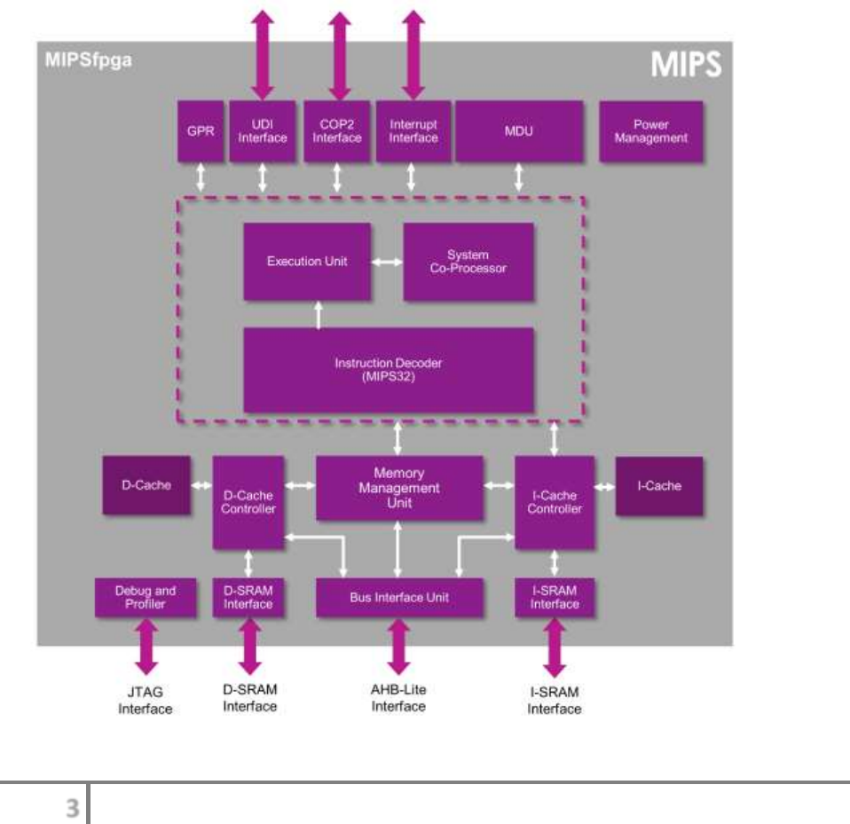
Figure 1 shows a diagram of the MIPSfpga processor. The central part of the processor is the
Execution Unit. It performs the operations commanded by the instructions, such as add or
subtract. The MDU (multiply/divide unit) is an extension of that unit that performs the multiply
and divide operations. The Instruction Decoder block receives the instructions from the
instruction cache and generates signals to make the execution unit perform the operation. The
System Co-Processor unit provides system interface signals, such as the system clock and reset.
The GPR unit holds the general purpose registers used as instruction operands.
Figure 1. The MIPSfpga Core

4
MIPSfpga Getting Started Guide © Imagination Technologies v1.1, July 22, 2015
The other interfaces at the top of Figure 1 (UDI, COP2, and Interrupt Interfaces) enable the
processor to run user-defined instructions (as described in the Datasheet found in
MIPSfpga\Documents\MicroAptiv UP Datasheet MD00929.pdf), to interface with a co-
processor 2 unit, and to receive external interrupts, respectively.
The instruction and data caches (I-Cache and D-Cache) are connected to their respective
controllers and a memory management unit (MMU). The MMU performs memory address
translations and fetches the data or instructions from memory when that data are not available in
the cache. The BIU (bus interface unit) enables the user to attach memories and memory-mapped
I/O to the processor via an AHB-Lite bus, which is described in Section 5.2.
The data and instruction scratchpad RAM interfaces (D-SRAM and I-SRAM Interfaces)
provide the processor with low-latency access to on-chip memories, as described in the
MicroAptiv UP Integrator's Guide (MIPSfpga\Documents\MocroAptiv UP Integrator's Guide
MD00941.pdf).
The Debug and Profiler unit provides the EJTAG
1
interface for debugging as well as
performance monitoring and downloading code to the processor. It is described further in Section
7.
The MIPSfpga core has a 5-stage pipeline. Table 1 lists each of the pipeline stages with a brief
description of each stage.
Table 1. The MIPSfpga pipeline
Number
Stage
Name
Description
1
I
Instruction
the processor fetches an instruction
2
E
Execution
the processor fetches operands from the register file and
performs an ALU operation (for example, addition,
subtraction, or memory address calculation)
3
M
Memory
if applicable, the processor accesses a memory operand
4
A
Align
if applicable, loaded data is aligned to its word boundary
5
W
Writeback
if applicable, the processor writes the result to the register file
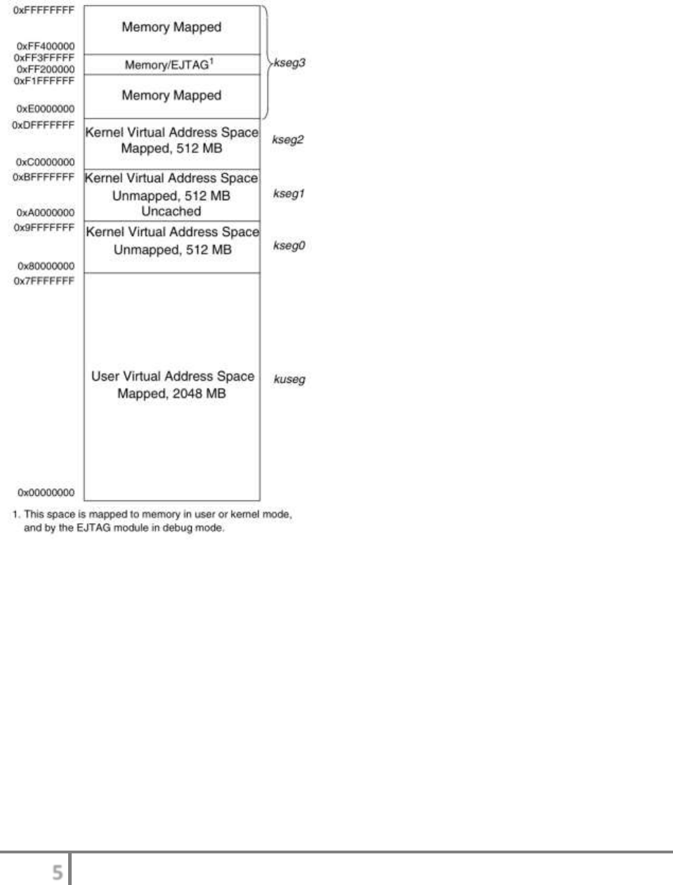
MIPSfpga has a 32-bit address space and three operating modes: kernel, user, and debug. On
reset, the processor begins in kernel mode and jumps to the reset vector at address 0xbfc00000.
Figure 2 shows a memory map for the processor. Address 0xbfc00000 is in kernel segment 1
(kseg1), which is uncached and unmapped. This means that all instructions will be fetched from
external memory rather than the caches and that the segment has a fixed mapping of virtual to
physical address rather than using the MMU, which is important because the caches and MMU
have not yet been initialized immediately after reset. The fixed mapping table maps kseg1 to
physical address 0x00000000 by subtracting 0xa0000000 from the virtual address. Hence, after
reset, the program begins executing code out of main memory starting at physical address
0x1fc00000. The Software User's Manual (MIPSfpga\Documents\MicroAptiv UP Software
1
EJTAG is an acronym for Enhanced JTAG. JTAG is the popular name for the IEEE 1149.1
standard for chip testing developed by the Joint Test Action Group.
5
MIPSfpga Getting Started Guide © Imagination Technologies v1.1, July 22, 2015
User's Manual 00942.pdf) provides additional information about the memory map. See Section
4.2 of that document, starting at page 77.
Figure 2. Memory map (from the MicroAptiv UP Datasheet)
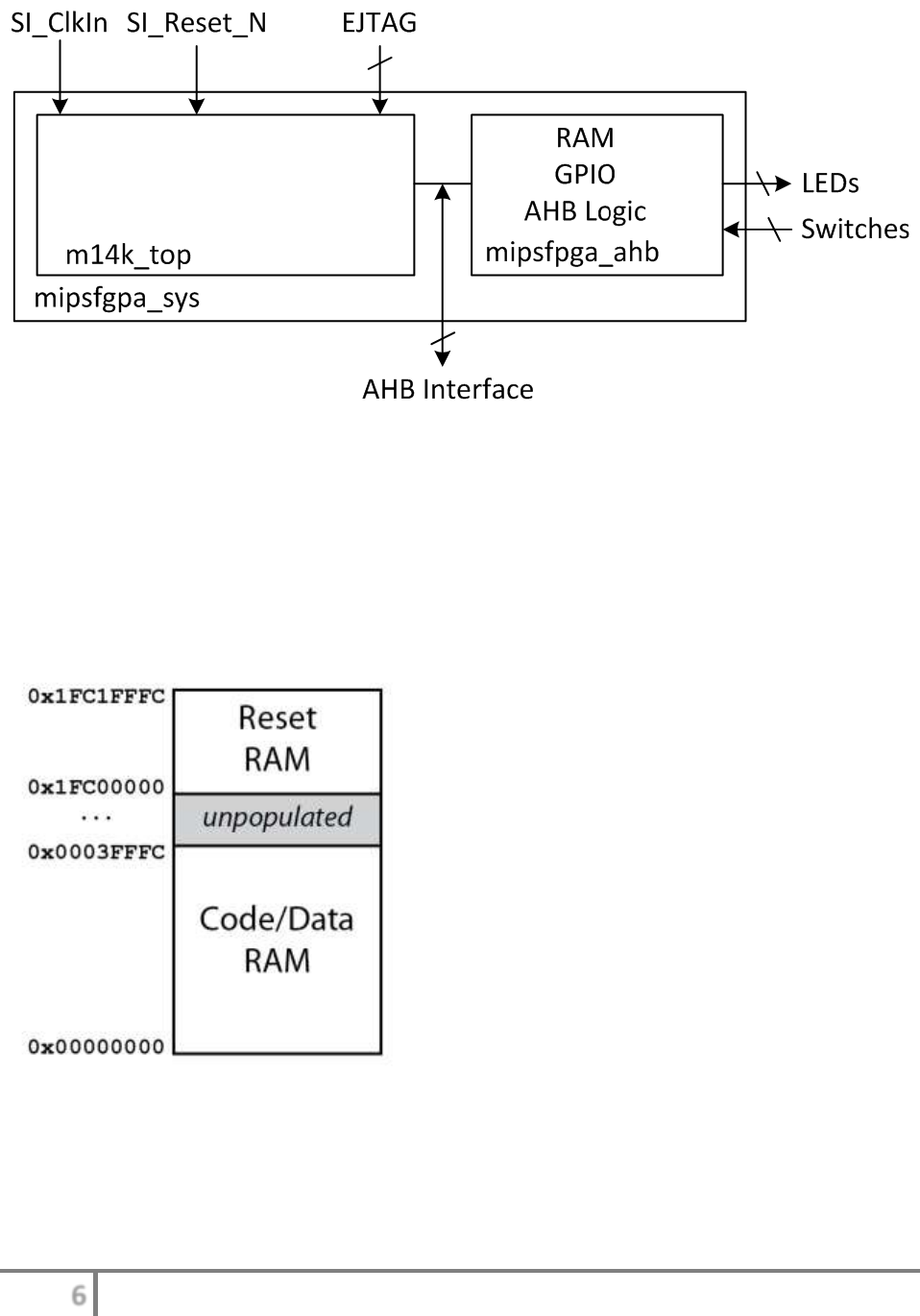
Figure 3 shows a block diagram of the key parts of MIPSfpga system. The system receives
clock, reset, and EJTAG programming signals from an FPGA board or simulation test bench. It
interfaces with external LEDs or switches, and drives the bus interface signals. Within the
mipsfpga_sys block is the m14k_top microAptiv core and the mipsfpga_ahb block containing
RAM, general-purpose input/output (GPIO), and the AHB-Lite Bus interface logic.
6
MIPSfpga Getting Started Guide © Imagination Technologies v1.1, July 22, 2015
Figure 3. MIPSfpga system
Figure 4 shows the physical memory map provided by the mipsfpga_ahb block. It contains a
128 KB RAM block at 0x1fc00000 initialized with the code to execute when the processor is
reset and another 256 KB RAM block at 0x00000000 for other code or data. It also contains four
GPIO registers controlling LEDs and switches, as described in Section 5.3. The machine
language code to execute upon reset is loaded from the ram_reset_init.txt file at startup or can be
downloaded over EJTAG as described in Section 7.
Figure 4. MIPSfpga physical memory map
7
MIPSfpga Getting Started Guide © Imagination Technologies v1.1, July 22, 2015
Section 4. How to use MIPSfpga
This section describes how to use the MIPSfpga system in simulation and hardware. Recall that
the files needed are provided in the MIPSfpga folder.
It is strongly recommended that you save a backup of the entire MIPSfpga
folder so that you can revert to the original files later as needed.
We use Mentor Graphics ModelSim for simulation, and we show how to run MIPSfpga on both
Digilient's Nexys4 DDR board (which contains Xilinx's Artix-7 FPGA), and Altera's DE2-115
board (which contains Altera's Cyclone IV FPGA). Table 2 lists the overall specifications for
each board.
If you would like to use a different FPGA board, see Appendix I for instructions on porting
MIPSfpga to other boards.
Table 2. FPGA board specifications
Board
Development Software
FPGA
Cost
Website
Nexys4 DDR
Vivado Design Suite
Artix-7
$320
$159 (academic)
www.digilentinc.com
DE2-115
Quartus II
Cyclone
IV
$595
$309 (academic)
de2-115.terasic.com
See Appendices A and B or C for instructions on installing ModelSim and either Vivado or
Quartus II.
Section 4.1. Simulation
Simulating a system is critical for both development and debug of hardware and software.
Simulation is fast, cheap, and makes it easy to probe internal signals of the system. We show
how to use ModelSim PE Student Edition 10.3d to simulate the MIPSfpga core running a simple
program we'll refer to as IncrementLEDs. If you do not already have ModelSim on your
computer, see Appendix A for instructions on how to install it. If you have ModelSim-Altera
Starter Edition, the instructions below will also work. The instructions have been verified for
ModelSim-Altera Starter Edition 10.3c and ModelSim PE Student Edition 10.3d. Later versions
will also likely work. If you prefer to use Vivado or Quartus II's built-in simulator instead of
ModelSim, feel free to do so. Appendix F describes how to run a simulation using Vivado's
built-in simulator, XSim.
This section describes how to use a script to simulate the processor in ModelSim PE Student
Edition 10.3d, from now on referred to simply as ModelSim. Follow these steps (described in
detail below):
Step 1. Open ModelSim project
Step 2. Run the provided script
Step 3. View the simulation output
8
MIPSfpga Getting Started Guide © Imagination Technologies v1.1, July 22, 2015
Step 1. Open ModelSim project
Browse to the MIPSfpga\ModelSim folder and make a copy of the Project1 folder. Rename the
copied folder Project2. Next, open ModelSim. If the Welcome window pops up (Figure 5), click
Close. You may also select the 'Don't show this dialog again' box at the bottom left of the
window before clicking Close.
Figure 5. ModelSim Welcome window
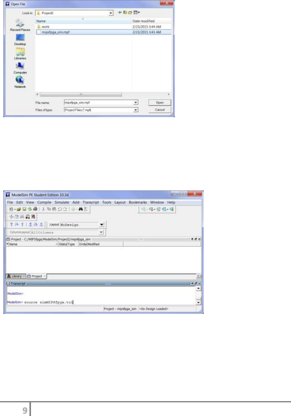
Now open a ModelSim project by selecting File → Open from the menu, as shown in Figure 6.
Figure 6. Open ModelSim project file
Browse to the MIPSfpga\ModelSim\Project2 directory. Select Project Files (*.mpf) under the
Files of type box, select mipsfpga_sim.mpf, and click Open, as shown in Figure 7.
9
MIPSfpga Getting Started Guide © Imagination Technologies v1.1, July 22, 2015
Figure 7. Open project file window
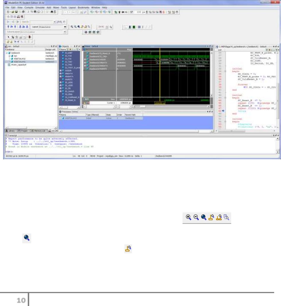
Step 2. Run the provided script
As shown in Figure 8, in the Transcript pane of the ModelSim window, type:
source simMIPSfpga.tcl
Figure 8. Running the simMIPSfpga.tcl script in ModelSim
The script (1) compiles the Verilog files located in MIPSfpga\rtl_up, (2) adds signals to the
output waveform, and (3) simulates the processor running the IncrementLEDs program using the
testbench.v top-level module (see Step 3 below). Running the script takes several minutes. Note:
you will see the following message:
10
MIPSfpga Getting Started Guide © Imagination Technologies v1.1, July 22, 2015
Warning: Design size of 12114 statements or 2473 leaf instances
exceeds ModelSim PE Student Edition recommended capacity. Expect
performance to be quite adversely affected.
The free version of ModelSim runs programs at a slower rate for designs with over 10,000 lines
of code. However, the speed is sufficiently fast for this purpose. For more extensive simulation,
the ModelSim PE Edition is recommended.
The simulation takes several minutes to complete. When it is done, you will again see the prompt
(VSIM 2>) in the Transcript window, as shown in Figure 9.
Figure 9. ModelSim window after the script has completed
As an alternate method, you can also use the instructions in Appendix E for manually creating a
ModelSim project and then running the simulation.
Step 3. View the simulation output
You should now see waveforms of the processor signals. If the wave panel is not selected, click
on it. Use the zoom buttons to zoom in and out of the waveform: , and use the
scroll button at the bottom of the pane to move left and right. For example, use the Zoom Full
button to view the entire waveform. Then move the cursor to where you would like to zoom
in and click on Zoom In on Active Cursor . The Wave pane must be selected to use these
options.

11
MIPSfpga Getting Started Guide © Imagination Technologies v1.1, July 22, 2015
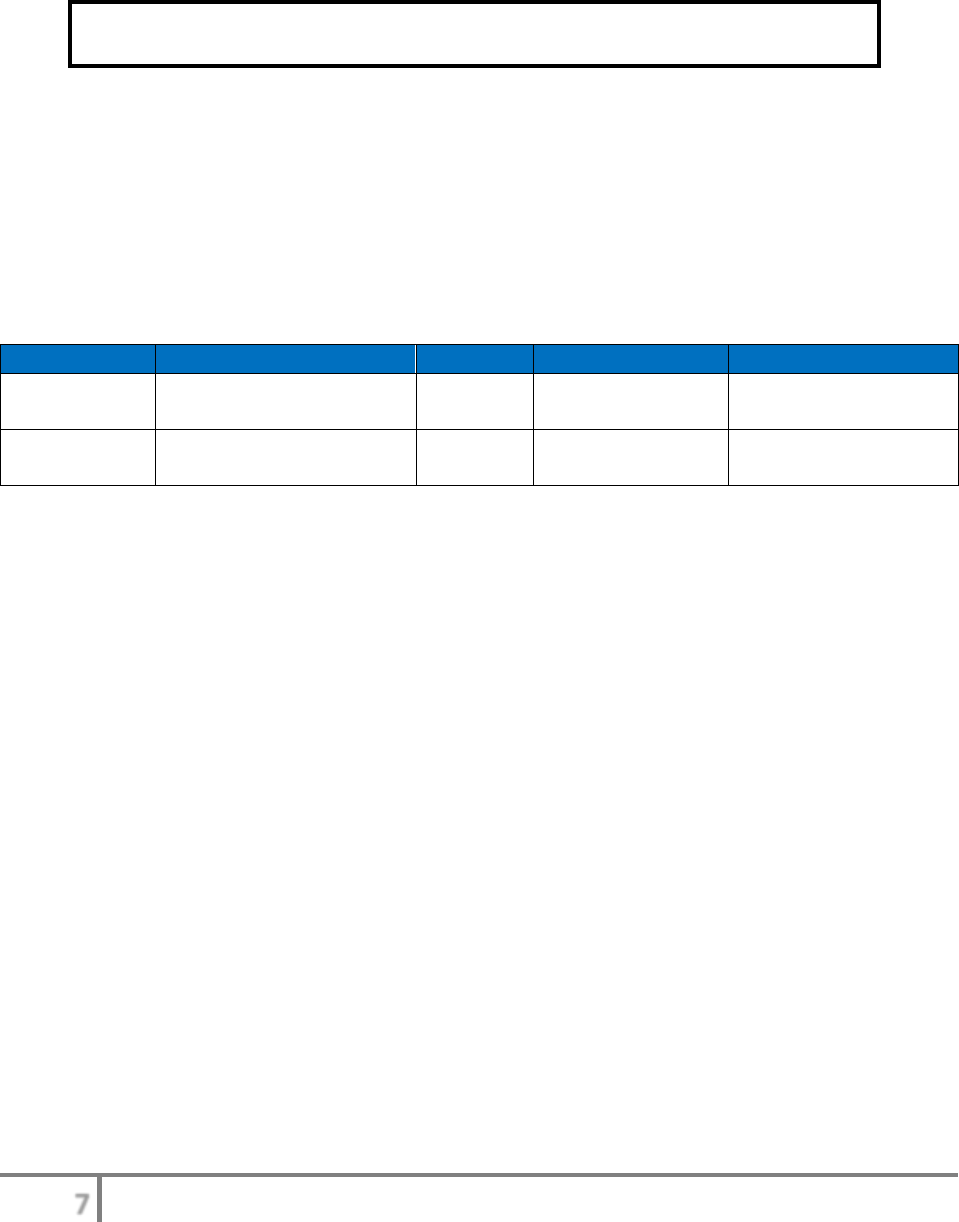
Table 3 gives a brief description of the high-level I/O signal names. The signals are the
processor's reset and clock and signals to read and write data using the AHB-Lite Bus (see
Section 5.2).
Table 3. MIPSfpga interface signals
Signal Name
Description
SI_Reset_N
Processor reset signal (active low)
SI_ClkIn
Processor clock
HADDR[31:0]
Address on the AHB-Lite bus
HRDATA[31:0]
Read data: data being read by the processor via the AHB-Lite bus
HWDATA[31:0]
Write data: data being written by the processor via the AHB-Lite bus
HWRITE
Write enable on the AHB-Lite bus
At the beginning of the simulation SI_Reset_N is low, so the proessor is being reset. Around 1
μs (1,000,000 ps), as shown in Figure 9 above, SI_Reset_N transitions from low to high, so the
processor is no longer held in reset, and it begins to execute the program, described next.
This simulation preloads the MIPSfpga core with the IncrementLEDs program, shown in Figure
10. The figure gives the C code and equivalent MIPS assembly instructions. The program
repeatedly writes an incremented value to memory address 0xbf800000.
For a refresher on MIPS assembly language, refer to any of the textbooks listed in the References
section (Section 8) or see the MIPS32 Quick Reference Card located in:
MIPSfpga\Documents\MIPS32_QuickReferenceCard.pdf
// C code
unsigned int val = 1;
volatile unsigned int* dest;
dest = 0xbf800000;
while (1) {
*dest = val;
val = val + 1;
}
# MIPS assembly code
# $9 = val, $8 = mem address 0xbf800000
addiu $9, $0, 1 # val = 1
lui $8, 0xbf80 # $8=0xbf800000
L1: sw $9, 0($8) # mem[0xbf800000] = val
addiu $9, $9, 1 # val = val+1
beqz $0, L1 # branch to L1
nop # branch delay slot
Figure 10. IncrementLEDs program
Figure 11 shows the equivalent machine code (given in hexadecimal) for the MIPS assembly
code of Figure 10. The IncrementLEDs program is loaded into memory starting at virtual address
0xbfc00000, as indicated by the instruction address column.
Machine Code Instruction Address Assembly Code
24090001 // bfc00000: addiu $9, $0, 1 # val = 1
3c08bf80 // bfc00004: lui $8, 0xbf80 # $8=0xbf800000
ad090000 // bfc00008: L1: sw $9, 0($8) # mem[0xbf800000] = val
25290001 // bfc0000c: addiu $9, $9, 1 # val = val+1
1000fffd // bfc00010: beqz $0, L1 # branch to L1
00000000 // bfc00014: nop # branch delay slot
Figure 11. MIPS machine code for the IncrementLEDs program

12
MIPSfpga Getting Started Guide © Imagination Technologies v1.1, July 22, 2015
Recall from Section 3 that virtual memory addresses starting at 0xa0000000 map to physical
address 0x00000000. The simulation shows the AHB-Lite bus interface signals, which see
physical addresses. So, in the simulation waveform, instruction address 0xbfc00000 will show up
as 0x1fc00000, 0xbf800000 as 0x1f800000, etc.
View the ModelSim waveform again, as shown in Figure 9. After the processor comes out of
reset (SI_Reset_N transitions from 0 to 1), the processor is designed to begin fetching
instructions starting at virtual address 0xbfc00000 (physical address 0x1fc00000).
View the waveform to see that just after reset (around 1,000,000 ps) HADDR becomes
0x1fc00000 and one cycle later the value read from memory (seen on HRDATA) is 0x24090001,
the program's first machine instruction (the 32-bit encoding of addiu $9, $0, 1). Section
5.2 describes the timing of the AHB-Lite bus. Four clock cycles later, the next instruction is
fetched from address 0x1fc00004 (HRADDR). The new instruction (0x3c08bf80 = lui $8,
0xbf80) again shows up on the read data signal (HRDATA). Note that a new instruction is
fetched about every 5 clock cycles instead of every clock cycle because, just after reset, the
caches are not yet initialized. Specifically, the 5 cycles required for an instruction fetch are as
follows:
1 cycle for the processor to recognize that the data/instruction is not in the cache
1 cycle to send the request to the Bus Interface Unit (BIU)
1 cycle for the BIU to place the read request on the AHB-Lite Bus
1 cycle for data to be returned from the external memory onto the AHB-Lite Bus
1 cycle for the processor to put the read data/instruction into a register
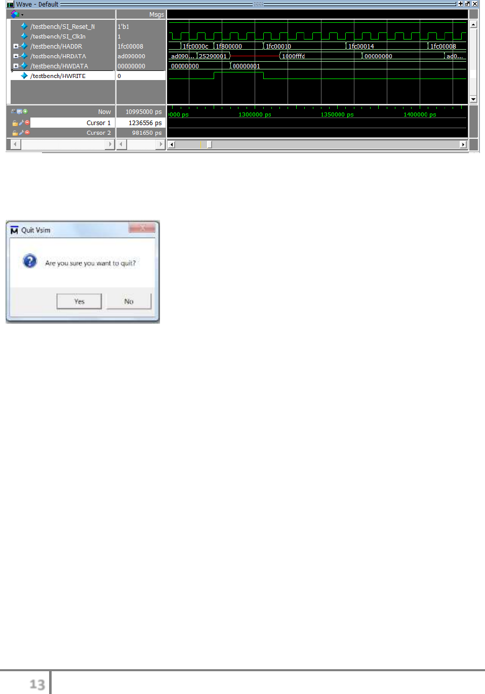
The processor continues fetching instructions. The store word instruction (sw $9, 0($8) =
0xad090000) is located at physical address 0x1fc00008. This instruction will write to address
0xbf800000 (physical address 0x1f800000). Notice that the next instruction (addiu $9, $9,
1 = 0x25290001) is fetched from address 0x1fc0000c before the store word's write to memory
occurs. Just after the addiu instruction (0x25290001) appears on HRDATA, the address
(HADDR) changes to 0x1f800000, the address being written by the earlier store word (sw)
instruction, and HWRITE asserts, as shown in Figure 12. The write to memory completes one
cycle later as HWDATA becomes the value to be written (1). Next, the processor fetches the
branch and nop instructions (0x1000fffd and 0x00000000, located at physical addresses
0x1fc00010 and 0x1fc00014) and then loops back to the sw instruction at address 0x1fc00008.
You can follow the waveform as it loops back, repeatedly fetching instructions from memory
addresses 0x1fc00008-0x1fc00014 and writing incremented values to memory address
0x1f800000.
13
MIPSfpga Getting Started Guide © Imagination Technologies v1.1, July 22, 2015
Figure 12. Memory write and branch shown in simulation waveforms
After you are finished viewing the waveform, close ModelSim. A pop-up window will ask if
you're sure you want to quit. Click Yes.
Figure 13. Quit ModelSim window
Section 4.2. Hardware: Running MIPSfpga on an FPGA
Now we will show you how to download and run the MIPSfpga processor on the Nexys4 DDR
board (Section 4.2.1) and the DE2-115 board (Section 4.2.2). Follow the instructions for the
FPGA board you are using.
Each board has a board-specific top-level wrapper module that instantiates the MIPSfpga system
(see MIPSfpga\rtl_up\mipsfpga_sys.v) and connects it to the physical switches, LEDs, and reset
button on the FPGA board. The wrapper also uses the FPGA’s on-board phase-locked loop
(PLL) to generate the system clock from the onboard clock. MIPSfpga comes with the
mipsfpga_nexys4_ddr.v and mipsfpga_de2_115.v wrapper modules for the Nexys4 DDR and
DE2-115 FPGA boards. You may use these as a starting point to write wrappers for different
FPGA boards (see Appendix I). Each board also requires a constraints file to specify timing
constraints and to assign top-level I/O signals to physical pins on the target FPGA.
The MIPSfpga system has been synthesized for each board with a pre-loaded program similar to
the IncrementLEDs program in Figure 11. The program, called IncrementLEDsDelay, counts up
on the LEDs and adds a delay loop (see Section 6.1) so the counting is slow enough to see.
Follow the instructions below for the FPGA board you are using (either the Nexys4 DDR board
or the DE2-115 board) to run the MIPSfpga system on an FPGA.

14
MIPSfpga Getting Started Guide © Imagination Technologies v1.1, July 22, 2015
Section 4.2.1. Nexys4 DDR FPGA Board
If you are using a Nexys4 DDR FPGA board, use the instructions in this section to download and
run the MIPSfpga system onto the Xilinx Artix-7 FPGA located on the Nexys4 DDR board using
Vivado software. The screen shots below are from Vivado 2014.4. Steps for using later versions
of Vivado are likely similar or exactly the same. If you do not already have Vivado installed on
your computer, see Appendix B for instructions on how to install it.
Follow these steps, described in detail below, to download and run the MIPSfpga system on the
Nexys4 DDR board.
Step 1. Connect and turn on the Nexys4 DDR board
Step 2. Open Vivado
Step 3. Program the Nexys4 DDR board with the MIPSfpga soft core
Step 4. Run the MIPSfpga core
Step 1. Connect and turn on the Nexys4 DDR board
Turn on the Nexys4 DDR FPGA board and plug it into your computer using a different USB
port than the one you used for the Bus Blaster probe. A detailed description of how to do this
is below, if needed.
Figure 14 highlights the Nexys4 DDR board's power switch and USB port. Plug the standard end
of the programming cable into your computer and the micro-USB end of the programming cable
into the board, at the location indicated as "USB Programmer Port" in Figure 14. Remember to
use a different USB port than the one you used for the Bus Blaster probe. Now turn the
board's power switch to the ON position. If the board is factory configured, it will run a pre-
loaded program that writes to the 7-segment displays with a snake-like pattern that repeats
indefinitely. Make sure that the board is in JTAG mode: i.e., the Mode pins should have the two
left-most pins connected by a jumper, as shown in Figure 14.

15
MIPSfpga Getting Started Guide © Imagination Technologies v1.1, July 22, 2015
Figure 14. Nexys4 DDR board
Step 2. Open Vivado
Now open Vivado. You will see the Vivado window shown in Figure 15.
Figure 15. Vivado window
Step 3. Program the Nexys4 DDR board with the MIPSfpga soft core
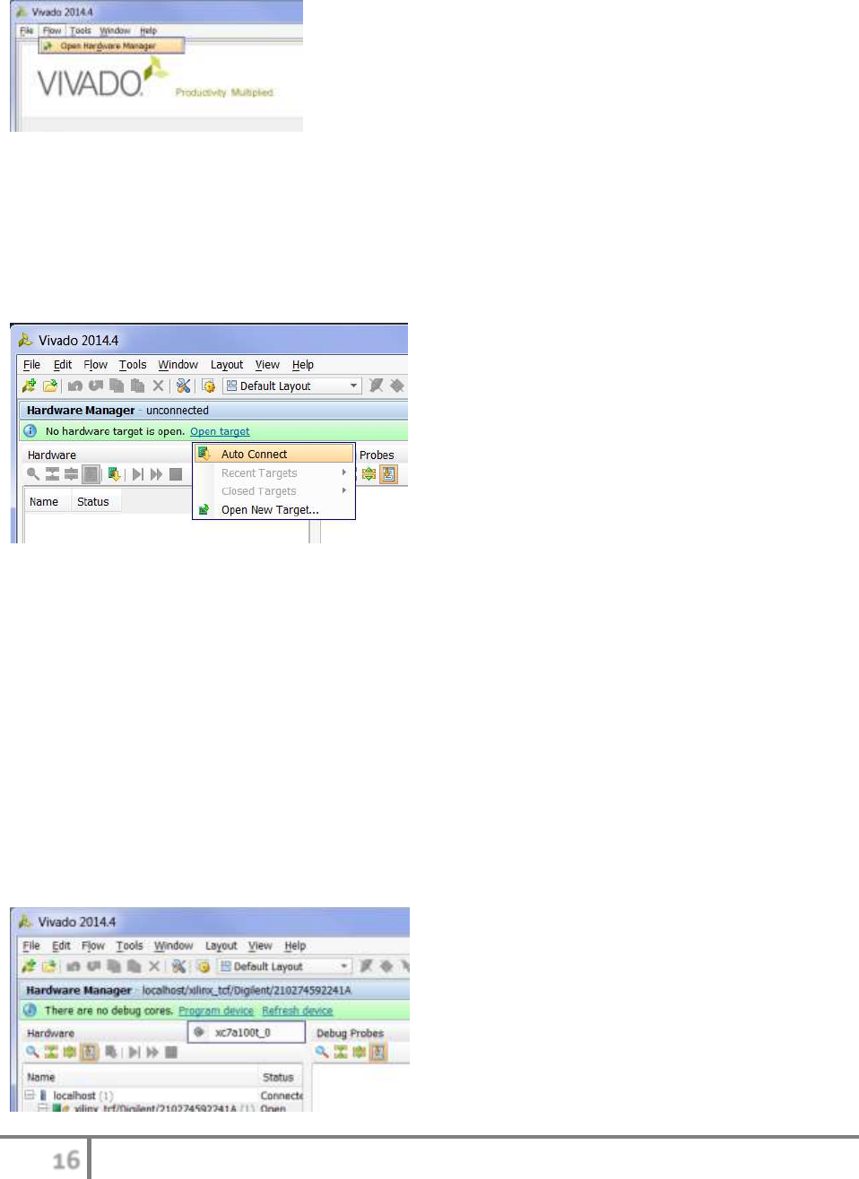
In the Vivado window, select Flow → Open Hardware Manager, as shown in Figure 16.
16
MIPSfpga Getting Started Guide © Imagination Technologies v1.1, July 22, 2015
Figure 16. Open Hardware Manager
The Hardware Manager window will now open. Click on Open Target and choose Auto
Connect, as shown in Figure 17. Warning: when you click on Auto Connect, Vivado might
appear to hang. It is connecting to the target – this will take a few seconds as Vivado detects the
FPGA on the Nexys4 DDR board.
Figure 17. Auto connect to target FPGA
You will see the following warning, that you can ignore:
WARNING: [Labtools 27-3123] The debug hub core was not detected
at User Scan Chain 1 or 3. …
Troubleshooting Hint: If you see the message "No hardware target is open," you might need to
reinstall the driver for the USB programmer cable. But first make sure that your Nexys4 DDR
board is connected to your computer and turned on.
Now click on Program device and select xc7a100t_0, as shown in Figure 18.
17
MIPSfpga Getting Started Guide © Imagination Technologies v1.1, July 22, 2015
Figure 18. Selecting Program device
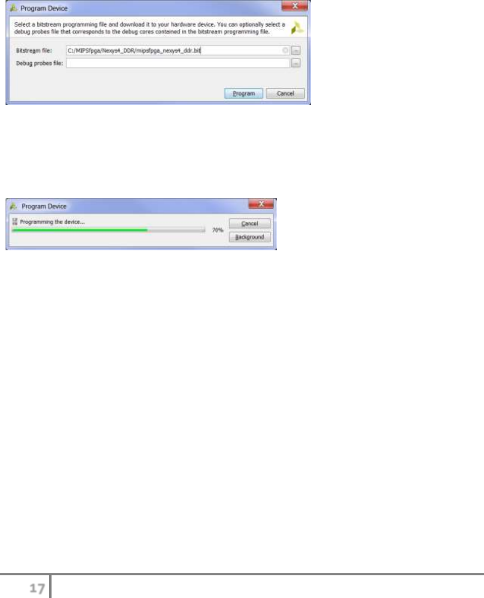
Now the Program Device window will open, as shown in Figure 19. In the Bitstream file box,
browse to: MIPSfpga/Nexys4_DDR/mipsfpga_nexys4_ddr.bit, as shown in the figure. Leave
the Debug Probes file box blank. Click Program. (Warning: be sure to choose the bitfile from
the Nexys4_DDR directory – not the Nexys4 directory.)
Figure 19. Program Device window
A window will pop up showing the programming progress, as shown in Figure 20. Programming
the Artix-7 FPGA on the Nexys4 DDR board will take several seconds. Once it is complete, the
progress window will close.
Figure 20. Program Device progress window
Warning: sometimes Vivado crashes just after it finishes programming the FPGA board.
Step 4. Run the MIPSfpga core
Now you are ready to run the MIPSfpga core on the Artix-7 FPGA on the Nexys4 DDR board.
Push the red Reset pushbutton (labeled CPU RESET) to reset the processor. After releasing the
Reset button, the processor will run the IncrementLEDsDelay program, which outputs increasing
binary numbers to the LEDs, starting with 1. The LEDs change values about every second.
Section 4.2.2. DE2-115 FPGA Board
If you are using the DE2-115 FPGA board, use instructions in this section to download and run
the MIPSfpga system on the Altera Cyclone IV FPGA located on that board using Quartus II
version 14.0 (64-bit) software. After configuring the FPGA following the steps below, the
MIPSfpga processor will drive the red LEDs on the DE2-115 board to display repeatedly
incremented binary numbers. If needed, see Appendix C for instructions on how to install
Quartus II. These steps are likely very similar or exactly the same for later versions of Quartus II.
Follow these steps, described in detail below.
Step 1. Connect and turn on the DE2-115 board
Step 2. Open Quartus II
Step 3. Program the DE2-115 board with the MIPSfpga system
18
MIPSfpga Getting Started Guide © Imagination Technologies v1.1, July 22, 2015
Step 4. Run the MIPSfpga core
Step 1. Connect and turn on the DE2-115 FPGA board
Connect the DE2-115 FPGA board to both power and your computer and turn on the board.
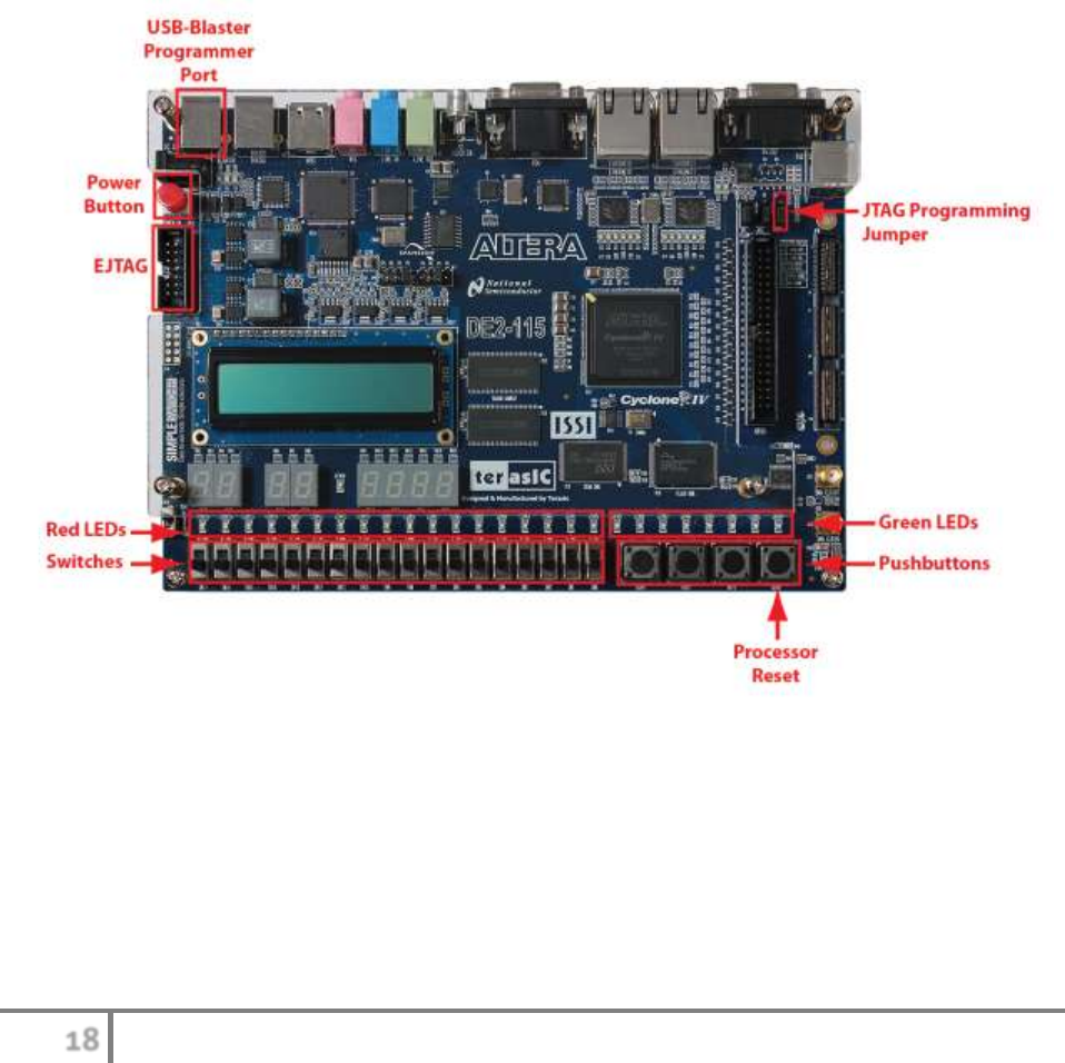
Figure 21 shows the power switch and the location to plug in the USB programming cable
(called the USB-Blaster) as well as other interfaces that will be described later. Plug in the power
cable into the port just above the red power switch. Plug the typical end of the USB
programming cable (USB standard-A) into your computer and the large end of the USB-Blaster
programming cable (USB standard-B) into the board, at the location indicated as "USB-Blaster
Programmer Port" in Figure 21. Now press the red power push-button to turn on the board. The
board will run a preloaded program that flashes the red and green LEDs in a pattern and
sequentially shows the hex digits 0 through F on the 7-segment displays. Make sure that the
jumper for the JTAG programmer is covering pins 2 and 3 (the lower 2 of the header pins labeled
J3), as shown in Figure 21. Also, make sure that the switch to the left of the red LEDs is up (i.e.,
in the RUN position).
Figure 21. The DE2-115 FPGA board (photograph © Terasic, 2014)
Step 2. Open Quartus II
Now open Quartus II (Figure 22).

19
MIPSfpga Getting Started Guide © Imagination Technologies v1.1, July 22, 2015
Figure 22. Quartus II window
Step 3. Program the DE2-115 board with the MIPSfpga system
You will now download the MIPSfpga processor's configuration file onto the FPGA. From the
top menu, choose Tools → Programmer, as shown in Figure 23.
Figure 23. Opening the Programmer interface
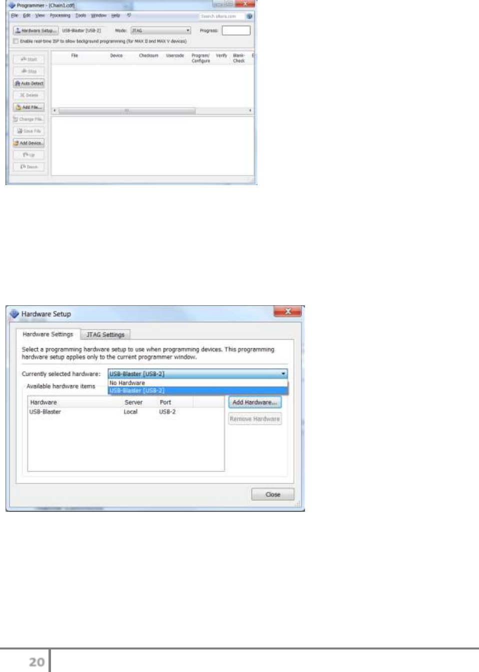
The Programmer window will now open, as shown in Figure 24. For Hardware Setup, use
USB-Blaster [USB-2] and JTAG for the Mode, as shown in the figure. The USB-Blaster is the
USB cable connecting the PC to the DE2-115 board. It is used to download the MIPSfpga
configuration to the FPGA. If the Hardware Setup text box is blank, click on the Hardware Setup
button.
20
MIPSfpga Getting Started Guide © Imagination Technologies v1.1, July 22, 2015
Figure 24. The Programmer window
A new window will open, as shown in Figure 25. Under Currently selected hardware, select
USB-Blaster[USB-2] as shown in the figure. The number after USB- (i.e., [USB-2]), could be
different. Then click Close. If the USB-Blaster [USB-2] option is not available, the USB-Blaster
driver has not been installed. Refer to the installation instructions in Appendix C to install the
driver.
Figure 25. Hardware Setup window
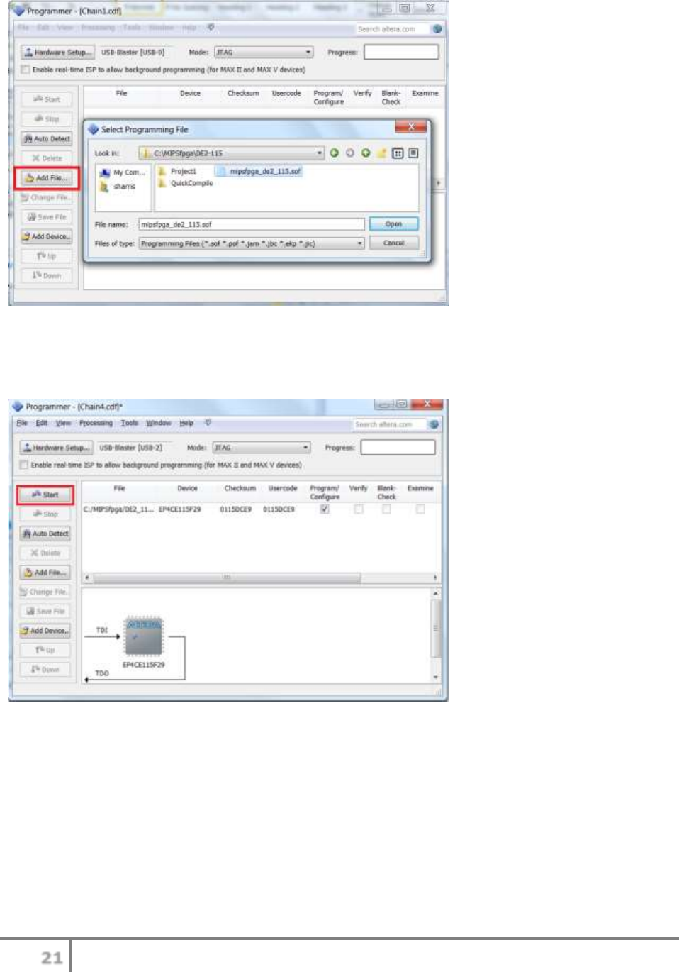
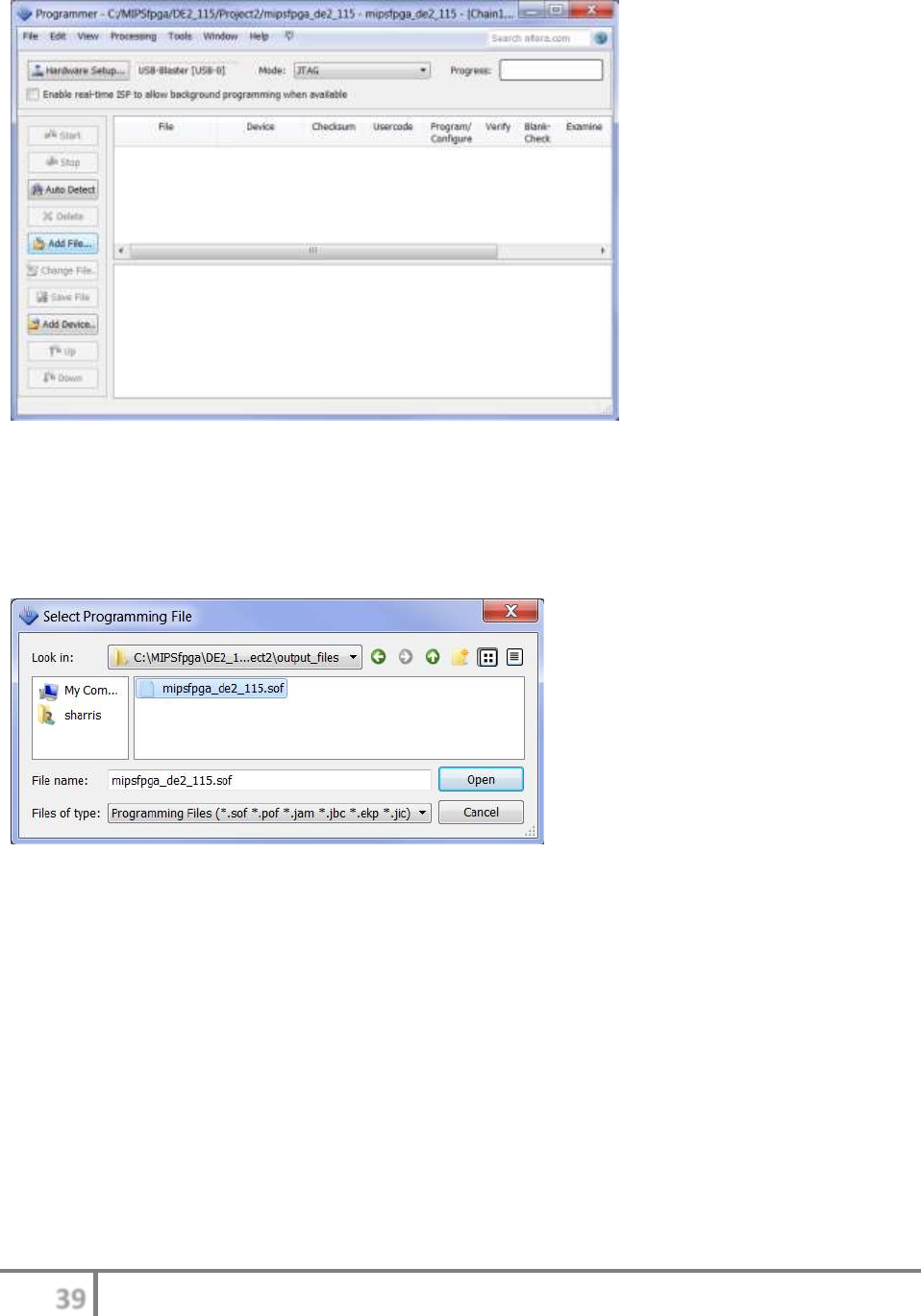
From the Programmer window, click on Add File, as highlighted in Figure 26. A Select
Programming File window will pop up. Browse to the MIPSfpga\DE2_115 folder and select
mipsfpga_de2_115.sof, as shown in Figure 26. This is the configuration file that will program
the MIPS soft core processor onto the FPGA. Click Open.
21
MIPSfpga Getting Started Guide © Imagination Technologies v1.1, July 22, 2015
Figure 26. Select Programming File window
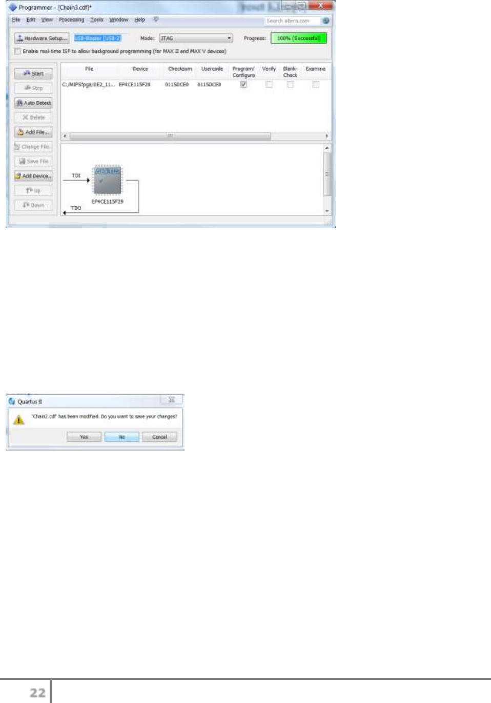
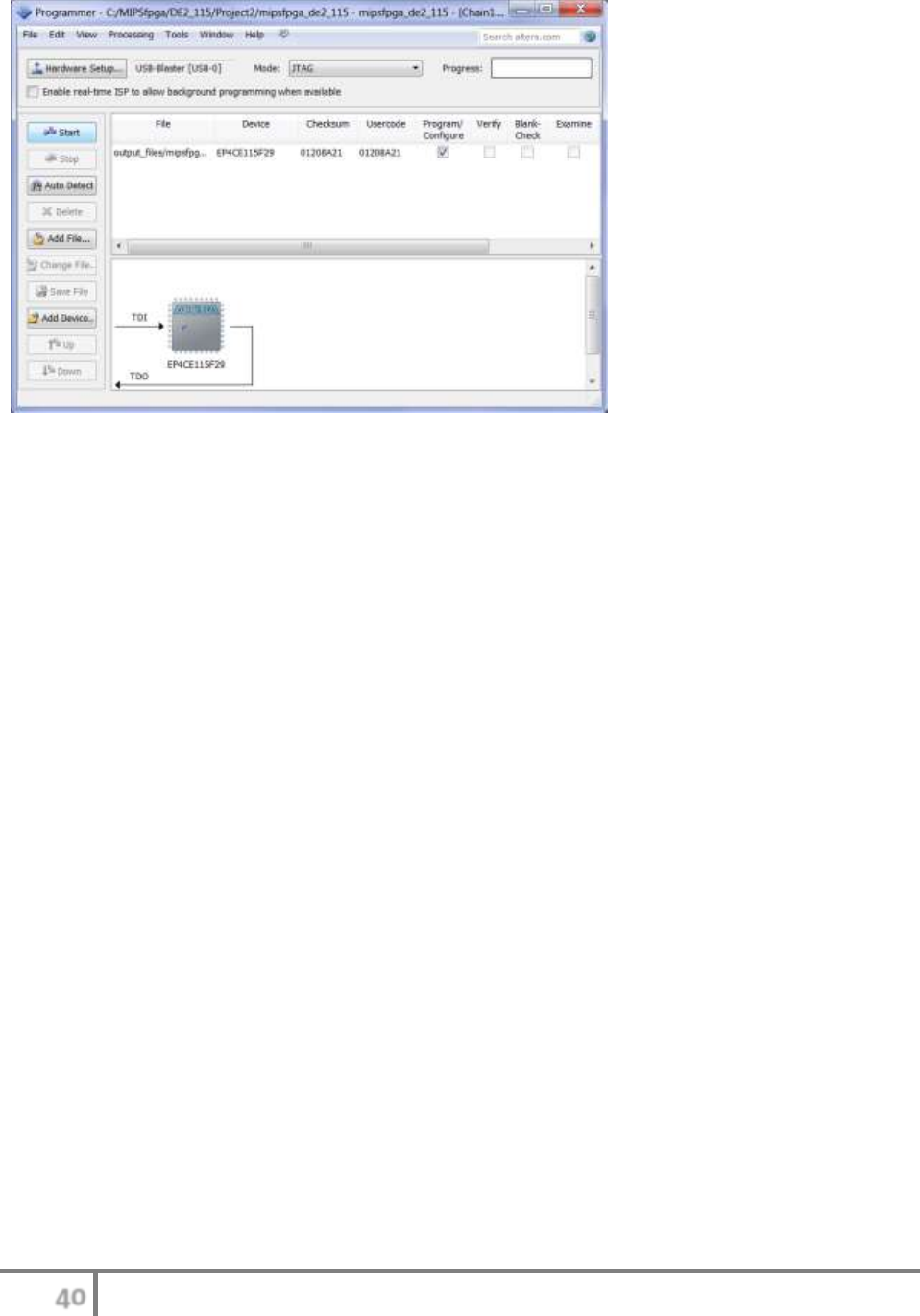
The Programmer window will now list the file and a figure of the Cyclone IV FPGA (Xilinx part
number EP4CE115F29), as shown in Figure 27.
Figure 27. Programmer with configuration file added
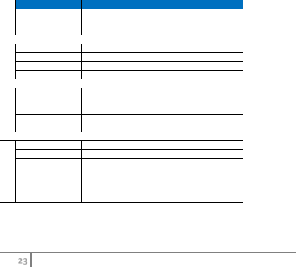
Click the Start button, shown highlighted in Figure 27. The configuration file will begin
downloading onto the FPGA, as shown in the Progress bar at the top right of the Programmer
window. Programming will take several seconds. After it has completed, 100% (Successful) will
be printed in the Progress bar, as shown in Figure 28.
22
MIPSfpga Getting Started Guide © Imagination Technologies v1.1, July 22, 2015
Figure 28. Programming the FPGA with successful completion
Step 4. Run the MIPSfpga core
Now you are ready to run the MIPSfpga core on the Cyclone IV FPGA on the DE2-115 board.
Refer to Figure 21 for the locations of the Reset button and the LEDs. Push the Reset button
(labeled KEY0) to reset the processor. After releasing the Reset button, the processor will run the
IncrementLEDsDelay program, which outputs increasing binary numbers to the red LEDs,
starting with 1. The LEDs change values about every second.
Close the Programmer window in Quartus II. It will prompt if you want to save the changes, as
shown in Figure 29. Click No.
Figure 29. Quartus II save changes prompt
Section 5. MIPSfpga Interfaces
The MIPSfpga system has three main interfaces: the AHB-Lite Bus, the FPGA board
input/output, and the EJTAG interface. The AHB-Lite bus connects the MIPSfpga core to
memory and peripheral devices. The FPGA board input/output (I/O) interface allows the
MIPSfpga core to access the switches and LEDs on the FPGA boards, and the EJTAG interface
is used for downloading programs onto the MIPSfpga core and real-time debugging. This section
begins with an overall description of the interface signals and then details each of the three
interfaces.
23
MIPSfpga Getting Started Guide © Imagination Technologies v1.1, July 22, 2015
Section 5.1. MIPSfpga Interface Signals
Table 4 lists MIPSfpga's interface signals. The signals use these prefixes:
SI: System Interface, general system interface signal
IO: Input/Output (I/O) signals for the FPGA board
H: AHB-Lite bus signals
EJ: EJTAG interface signals
The clock signal (SI_ClkIn) is the system clock for the processor. The MIPSfpga runs at 62 MHz
on the Nexys4 DDR board and at 47 MHz on the DE2-115 board using derivatives of the
onboard 100 MHz (Nexys4 DDR) and 50 MHz (DE2-115) clocks. The reset signal (SI_Reset_N)
is low asserted (indicated by the "_N" suffix). Pressing the reset button (either CPU_RESETN on
the Nexys4 DDR or KEY[0] in the DE2-115) forces that pin low and resets the processor. The
processor must be reset after power-up. The following sections describe the AHB-Lite Bus,
Board I/O, and EJTAG signals.
Table 4. MIPSfpga processor interface signals
General
MIPSfpga
Nexys4 DDR
DE2-115
SI_Reset_N
CPU_RESETN
KEY[0]
SI_ClkIn
clk_out
(62 MHz)
clk_out
(47 MHz)
AHB-Lite
HADDR[31:0]
N/A
N/A
HRDATA[31:0]
N/A
N/A
HWDATA[31:0]
N/A
N/A
HWRITE
N/A
N/A
Board I/O
IO_Switch[17:0]
SW[15:0]
SW[17:0]
IO_PB[4:0]
{BTNU, BTND, BTNL, BTNR,
BTNC}
KEY[3:0]
IO_LEDR[17:0]
LED[15:0]
LEDR[17:0]
IO_LEDG[8:0]
N/A
LEDG[17:0]
EJTAG
EJ_TRST_N_probe
JB[7]
EXT_IO[6]
EJ_TDI
JB[2]
EXT_IO[5]
EJ_TDO
JB[3]
EXT_IO[4]
EJ_TMS
JB[1]
EXT_IO[3]
EJ_TCK
JB[4]
EXT_IO[2]
SI_ColdReset_N
JB[8]
EXT_IO[1]
EJ_DINT
GND
EXT_IO[0]
Section 2.1 of the Integrator's Guide (MIPSfpga\Documents\MicroAptiv UP Integrator's Guide
MD009241.pdf) describes other signals that you could optionally tap out.
24
MIPSfpga Getting Started Guide © Imagination Technologies v1.1, July 22, 2015
Section 5.2. AHB-Lite Interface
The Advanced High-performance Bus (AHB) is an open-source interface used in many
microprocessors, particularly those in embedded systems. The AHB bus facilitates the
connection of multiple devices or peripherals. AHB-Lite is a simpler version of AHB with a
single bus master. This section covers the basic operation of the AHB-Lite bus; please refer to
the AHB-Lite Interface Guide (MIPSfpga\Documents\MicroAptiv UP AHB-Lite Interface
MD01082.pdf) for further information.
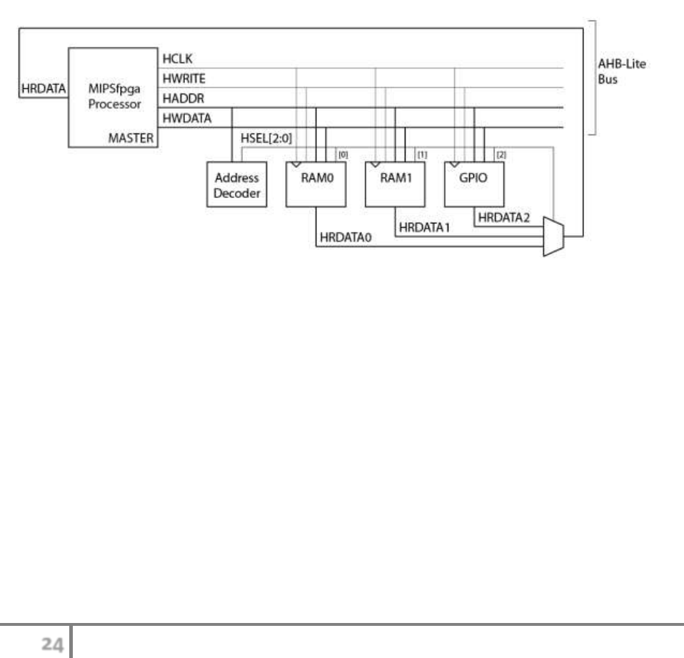
Figure 30 shows the AHB-Lite Bus on the MIPSfpga processor. This configuration has one
master, the MIPSfpga processor, and three slaves: RAM0, RAM1, and GPIO, which are two
RAM blocks and a module for accessing the I/O (switches and LEDs) on the FPGA boards. The
processor, the master, sends the clock, write enable, address, and write data signals: HCLK,
HWRITE, HADDR, and HWDATA. It receives the read data (HRDATA) from one of the
slaves, depending on the address. The Address Decoder asserts the HSEL signal to select the
slave device indicated by the address.
Figure 30. AHB-Lite bus
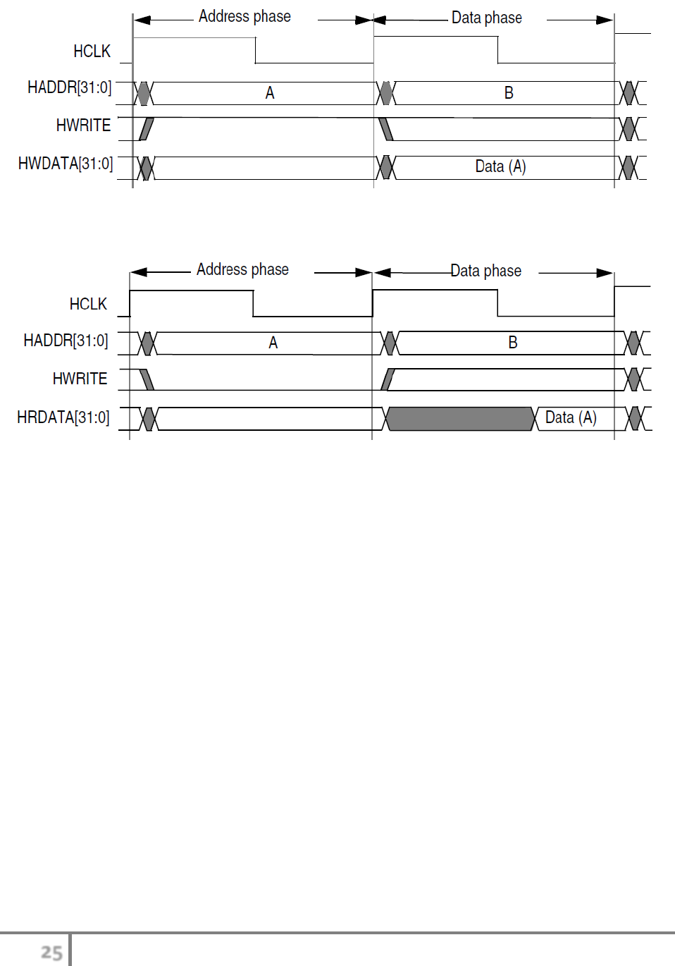
An AHB-Lite transaction consists of two cycles: an Address phase and a Data phase. During the
Address phase, the master sends the address on HADDR and asserts HWRITE for a write or
deasserts it for a read. During the Data phase the master sends HWDATA on a write or the slave
sends HRDATA on a read. Figure 31 and Figure 32 show the waveforms for a processor write
and read, respectively.
25
MIPSfpga Getting Started Guide © Imagination Technologies v1.1, July 22, 2015
Figure 31. AHB-Lite Write
Figure 32. AHB-Lite Read
For the MIPSfpga processor, the slave modules and address decoder are located in the
mipsfpga_ahb module (found in mipsfpga_ahb.v) and its submodules. Recall that all of the HDL
files are found in the MIPSfpga/rtl_up folder. RAM0 contains the instruction memory that is
read at start-up. At reset, the processor sets the PC to the instruction address of the reset
exception: physical address 0x1fc00000 (virtual address 0xbfc00000). RAM1 contains
programmer accessible memory starting at physical address 0. The GPIO slave module interacts
with the FPGA board I/O, which is discussed next.
Section 5.3. FPGA Board Interfaces
Both of the FPGA boards (Nexys4 DDR and DE2-115) provide LEDs and switches that are
connected to the pins of the FPGA via wire traces on the printed circuit board (PCB). Figure 14
and Figure 21 show each of the FPGA boards with labels highlighting those I/Os.
The general-purpose I/O (GPIO) module on the AHB-Lite bus writes to and reads from the
FPGA board I/O (LEDs, switches, etc.) using memory-mapped I/O. In memory-mapped I/O, the
processor accesses an I/O device, also called a peripheral, in the same way it accesses memory,
with each peripheral being mapped to a particular memory address. Table 5 lists the memory
addresses for the FPGA board I/O. The virtual address is used by the MIPS instructions and the
physical address is what appears on HADDR on the AHB-Lite bus.

26
MIPSfpga Getting Started Guide © Imagination Technologies v1.1, July 22, 2015
Table 5. Memory-mapped I/O addresses for FPGA boards
Virtual address
Physical address
Signal Name
Nexys4 DDR
DE2-115
0xbf80 0000
0x1f80 0000
IO_LEDR
LEDs
Red LEDs
0xbf80 0004
0x1f80 0004
IO_LEDG
N/A
Green LEDs
0xbf80 0008
0x1f80 0008
IO_SW
switches
switches
0xbf80 000c
0x1f80 000c
IO_PB
U, D, L, R, C pushbuttons
pushbuttons
So, for example, the following MIPS instructions write the value 0x543 to the LEDs (red LEDs
on the DE2-115):
addiu $7, $0, 0x543 # $7 = 0x543
lui $5, 0xbf80 # $5 = 0xbf800000 (LED address)
sw $7, 0($5) # LEDs = 0x543
Likewise, these MIPS instructions read the value of the switches into register 10:
lui $5, 0xbf80 # $5 = 0xbf800000
lw $10, 8($5) # $10 = value of switches
Notice that the switch signal (IO_Switch) is only 18 bits. Thus, the value of the switches
occupies the lower 18 bits of $10, with the upper 14 bits being 0.
See mipsfpga_ahb_gpio.v for further details about how memory-mapped I/O is implemented.
Section 5.4. EJTAG Interface
EJTAG is a protocol that enables (1) hardware-based debugging and (2) downloading programs
onto a MIPS core. The interface signals, collectively called the Test Access Port (TAP), are:
TCK, TDI, TDO, TMS, and TRST. EJTAG borrows the functionality of these signals as defined
in the JTAG protocol, as listed below:
EJ_TCK: Test Clock
EJ_TMS: Test Mode Select – select mode of operation
EJ_TDI: Test Data In – data shifted into the processor's test or programming logic
EJ_TDO: Test Data Out – data shifted out of the processor's test or programming logic
EJ_TRST_N_probe: Test Reset, low asserted – resets the EJTAG controller
EJTAG also adds a debug interrupt request signal, EJ_DINT. EJTAG is used by the
programming and debugging tools described in Section 7. A deep understanding of the EJTAG
interface is not needed for most MIPSfpga users. However, interested users can refer to the
"EJTAG Debug Support" chapter in the Software User's Manual (in the MIPSfpga\Documents
folder) to learn about the software debugging capabilities of EJTAG beyond those covered in
Section 7.

27
MIPSfpga Getting Started Guide © Imagination Technologies v1.1, July 22, 2015
Section 6. Example Programs
Now we show you how to run two sample programs on the MIPSfpga core. These are simple
programs that do not require any set up of the processor, beyond pressing the reset button. More
advanced programs require initializing the caches, MMU, etc. This setup is done with code
called boot code or start-up code. Section 7 describes how to run more advanced programs using
boot code provided with the Codescape MIPS SDK Essentials programming environment and
OpenOCD, a gasket program that couples gdb, an open-source debugger, with the Bus Blaster
probe, a USB-to-EJTAG converter.
Section 6.1. Example: Memory-Mapped Outputs (LEDs)
First, we show an example program that uses memory-mapped outputs. Recall the
IncrementLEDsDelay program that was run on the MIPSfpga core in Section 4. Figure 33 gives
the C and MIPS assembly code for this program. As shown in the C code, the variable val is set
to 1. During each while loop iteration, val is output to the LEDs (at memory address
0xbf800000) then incremented. Each loop iteration finishes with a delay of about 1/2 a second on
the Nexys4 DDR board and 1 second on the DE2-115. This delay allows the user to see the
change on the LEDs. The IncrementLEDsDelay program is identical to IncrementLEDs (given in
Figure 10) except with the addition of the code to cause a delay, highlighted in bold.
// C code
unsigned int val = 1;
volatile unsigned int*
ledr_ptr;
ledr_ptr = 0xbf800000;
while (1) {
*ledr_ptr = val;
val = val + 1;
// delay
}
# MIPS assembly code
# $9 = val, $8 = memory address 0xbf800000
addiu $9, $0, 1 # val = 1
lui $8, 0xbf80 # $8=0xbf800000
L1: sw $9, 0($8) # mem[0xbf800000] = val
addiu $9, $9, 1 # val = val+1
delay: # loop 2,500,000x
lui $5, 0x026 # $5 = 2,500,000
ori $5, $5, 0x25a0
add $6, $0, $0 # $6 = 0
L2: sub $7, $5, $6 # $7 = 2,500,000 - $6
addi $6, $6, 1 # increment $6
bgtz $7, L2 # finished?
nop # branch delay slot
beqz $0, L1 # branch to L1
nop # branch delay slot
Figure 33. IncrementLEDsDelay program
Recall that, upon reset, the processor caches are not yet initialized. As described in Section 4.1,
before caches are initialized, each instruction takes about 5 cycles.

28
MIPSfpga Getting Started Guide © Imagination Technologies v1.1, July 22, 2015
Thus, the 4 instructions in the delay loop (from label L2 to the first nop) take 5 cycles each to
execute. Thus, with the 62 MHz clock on the Nexys4 DDR FPGA board, 2,500,000 iterations of
the delay loop take about a second, as shown in the equation below:
2,500,000 iterations×(4 instructions/iteration)×(5 clock cycles/instruction)×(1 sec/62,000,000 cycles) ≈ 0.8 sec.
The delay is also around a second on the DE2-115 FPGA board, given its 47 MHz clock.
After the reset button is pushed, the MIPSfpga core sets the program counter (PC) to 0xbfc00000
and begins executing. As stated in Section 4.1, virtual address 0xbfc00000 maps to physical
address 0x1fc00000. The reset RAM, RAM0 from Figure 30, holds memory starting at that
address. The code from Figure 33 is pre-loaded into RAM0 (ahb_ram_reset.v). The
ahb_ram_reset module loads the instructions listed in the ram_reset_init.txt file (shown in Figure
34) into its memory. This file can be found in the MIPSfpga\rtl_up directory. The memory
values (instructions) are placed starting at the lowest memory address: 0xbfc00000. So, the first
instruction (0x24090001) is located at memory address 0xbfc00000, the second instruction at
0xbfc00004, etc.
24090001 // bfc00000: addiu $9, $0, 1
3c08bf80 // bfc00004: lui $8, 0xbf80
ad090000 // bfc00008: L1: sw $9, 0($8)
25290001 // bfc0000c: addiu $9, $9, 1
3c050026 // bfc00010: delay: lui $5, 0x026
34a525a0 // bfc00014: ori $5, $5, 0x25a0
00003020 // bfc00018: add $6, $0, $0
00a63822 // bfc0001c: L2: sub $7, $5, $6
20c60001 // bfc00020: addi $6, $6, 1
1ce0fffd // bfc00024: bgtz $7, L2
00000000 // bfc00028: nop
1000fff6 // bfc0002c: beq $0, $0, L1
00000000 // bfc00030: nop
Figure 34. ram_reset_init.txt memory initialization file for IncrementLEDsDelay
The master copy of this ram_reset_init.txt file is located in the
MIPSfpga\rtl_up\initfiles\2_IncrementLEDsDelay directory.
Section 6.2. Example: Memory-Mapped I/O (Switches and LEDs)
The MIPSfpga core both writes to and reads from memory-mapped I/O on the FPGA boards.
Figure 35 shows the C and MIPS assembly code for the Switches&LEDs program. This
program reads from the switches and pushbuttons on the FPGA board and outputs their values to
the red and green LEDs, respectively. (Note: the Nexys4 DDR board will not display the
pushbutton values when running this program because it lacks the green LEDs.)

29
MIPSfpga Getting Started Guide © Imagination Technologies v1.1, July 22, 2015
// C code
unsigned int sw, pb;
unsigned int* ledr_ptr;
unsigned int* ledg_ptr;
unsigned int* sw_ptr;
unsigned int* pb_ptr;
ledr_ptr = 0xbf800000;
ledg_ptr = 0xbf800004;
sw_ptr = 0xbf800008;
pb_ptr = 0xbf80000c;
while (1) {
sw = *sw_ptr;
pb = *pb_ptr;
*ledr_ptr = sw;
*ledg_ptr = pb;
}
# MIPS assembly code
# $10 = sw, $11 = pb
lui $8, 0xbf80
addiu $12, $8, 4 # $12 = LEDG addr
addiu $13, $8, 8 # $13 = SW addr
addiu $14, $8, 0xc # $14 = PB addr
readIO:
lw $10, 0($13) # sw = SW values
lw $11, 0($14) # pb = PB values
sw $10, 0($8) # store sw to LEDR
sw $11, 0($12) # store pb to LEDG
beq $0, $0, readIO # repeat
nop # branch delay slot
Figure 35. The Switches&LEDs program
In the first four MIPS assembly instructions, the code places the memory-mapped addresses for
the red and green LEDs and the switches and pushbuttons in registers 8, 12, 13, and 14. In the
next two lw (load word) instructions, the assembly program reads the values of the switches and
pushbuttons (into registers 10 and 1l). Finally, in the following two sw (store word) instructions,
the code writes those values to the red and green LEDs. The loop then repeats using the beq
(branch if equal) instruction. The branch is always taken because $0 is always equal to itself.
Figure 36 shows the ram_reset_init.txt file with the machine code for the Switches&LEDs
program. This file is located in MIPSfpga\rtl_up\initfiles\3_Switches&LEDs.
3c08bf80 //bfc00000 lui $8, 0xbf80 #$8=LEDR addr
250c0004 //bfc00004 addiu $12, $8, 4 #$12=LEDG addr
250d0008 //bfc00008 addiu $13, $8, 8 #$13=SW addr
250e000c //bfc0000c addiu $14, $8, 0xc #$14=PB addr
8daa0000 //bfc00010 readIO: lw $10, 0($13) #$10=SW
8dcb0000 //bfc00014 lw $11, 0($14) #$11=PB
ad0a0000 //bfc00018 sw $10, 0($8) #SW->LEDR
ad8b0000 //bfc0001c sw $11, 0($12) #PB->LEDG
1000fffb //bfc00020 beq $0, $0, readIO #repeat
00000000 //bfc00024 nop #branch delay slot
Figure 36. ram_reset_init.txt memory initialization file for the Switches&LEDs program
30
MIPSfpga Getting Started Guide © Imagination Technologies v1.1, July 22, 2015
The following section describes how to load and run the Switches&LEDs program on the
MIPSfpga core in simulation and in hardware (i.e., on the Nexys4 DDR and DE2-115 FPGA
boards).
Section 6.3. Simulation: Running an Example Program in Simulation
Perform the following steps to simulate the MIPSfpga core running the Switches&LEDs
program from Figure 35. Steps are described in detail below. Again, you may also use the built-
in Vivado and Quartus II simulators if preferred.
Step 1. Copy ram_reset_init.txt file to the ModelSim folder
Step 2. Open ModelSim
Step 3. Run the provided script
Step 4. View the simulation
Step 1. Copy ram_reset_init.txt to ModelSim folder
If you haven't already done so in an earlier step, browse to MIPSfpga\ModelSim and make a
copy of the Project1 folder. Rename the copied folder Project2. Copy ram_reset_init.txt from
MIPSfpga\rtl_up\initfiles\3_Switches&LEDs to MIPSfpga\ModelSim\Project2. (Notice that this
will overwrite the existing initialization file, i.e., the code that wrote incremented values to the
LEDs, with no delay. If needed, a copy of that initialization file is available in
MIPSfpga\rtl_up\1_IncrementLEDs.
Step 2. Open the mipsfpga_modelsim project
In the MIPSfpga\ModelSim\Project2 folder, double-click on mipsfpga_modelsim.mpf. (As an
alternate method, you can instead open ModelSim. Then in the top menu, click on File → Open.
Select Project Files (*.mpf) in the 'Files of type' box. Browse to MIPSfpga\ModelSim\Project2
and click on mipsfpga_sim.mpf. Then click Open.)
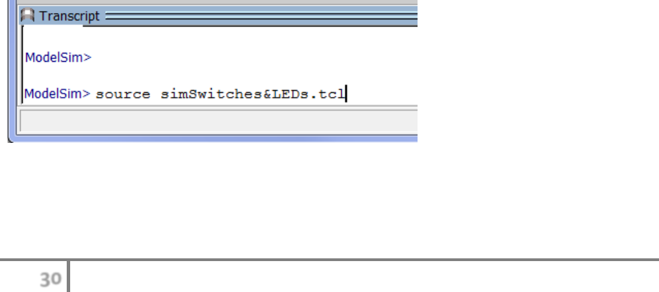
Step 3. Run the provided script
As shown in Figure 37, in the Transcript pane of the main ModelSim window, type:
source simSwitches&LEDs.tcl
Figure 37. Running the simSwitches&LEDs.tcl script in ModelSim
The script (1) compiles the Verilog files located in MIPSfpga\rtl_up, (2) adds signals to the
output waveform, and (3) simulates the processor running the Switches&LEDs program (see
31
MIPSfpga Getting Started Guide © Imagination Technologies v1.1, July 22, 2015
Figure 35) while varying the values of the inputs IO_Switch and IO_PB. Running the script takes
several minutes. When the script is complete you will again see the prompt (VSIM 2>) in the
Transcript window.
Step 4. View the simulation output
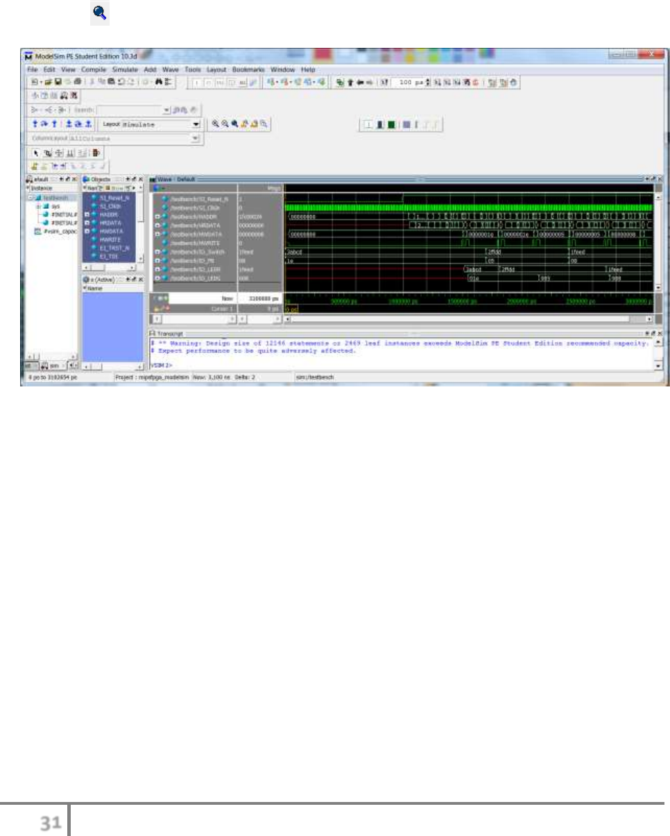
In the ModelSim window, click on the Wave tab as shown in Figure 38. Click on the Zoom
Full button to view the entire waveform and then zoom in as desired.
Figure 38. ModelSim waveform
First notice the input values IO_Switch and IO_PB change (simulating changing input values,
i.e., the values at the physical pins of the switches and pushbuttons on the FPGA boards). Several
cycles later, the LEDs (IO_LEDR and IO_LEDG) change as well. You can view the instruction
addresses on the HADDR signal, starting at address 0x1fc00000, and the instructions on the
HRDATA signal.
Appendix E describes how to create a project in ModelSim. To run a different program (i.e., a
new ram_reset_init.txt file) you need only restart and rerun the simulation (type 'restart –f' in the
Transcript pane, then 'run 2000000', or for however long you'd like to run the simulation). You
need not recompile the Verilog files.
Section 6.4. Hardware: Running an Example Program in Hardware
This section shows how to run the Switches&LEDs program on the Nexys4 DDR or DE2-115
FPGA board. The steps, described in detail below are:
Step 1. Copy new ram_reset_init.txt file to HDL folder
Step 2. Open FPGA programming environment

32
MIPSfpga Getting Started Guide © Imagination Technologies v1.1, July 22, 2015
Step 3. Compile HDL
Step 4. Program FPGA board
Step 5. Test
Warning: this process will take some time (around 10-25 minutes or more, depending on your
computer speed). Appendices F and G describe how to speed up the process when changing only
the program (code) to be run on the MIPSfpga core.
Step 1 is the same for both the Nexys4 DDR and DE2-115 FPGA boards.
Step 1. Copy new ram_reset_init.txt file to HDL folder
Copy ram_reset_init.txt from MIPSfpga\rtl_up\initfiles\3_Switches&LEDs to the
MIPSfpga\rtl_up directory. This will overwrite the existing initialization file, i.e., the code that
wrote incremented values to the LEDs, with delay. If needed, a copy of that initialization file is
available in MIPSfpga\rtl_up\2_IncrementLEDsDelay.
After completing this step, follow steps 2-5 for whichever FPGA board you are using.
Section 6.4.1. Nexys4 DDR FPGA Board
Step 2. Open FPGA programming environment
Browse to the MIPSfpga\Nexys4_DDR directory. Copy the Project1 folder and rename the new
folder Project2. Then browse to the Project2 folder and double-click on
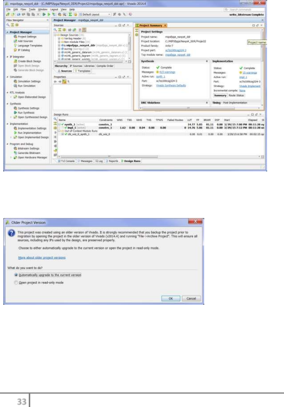
mipsfpga_nexys4_ddr.xpr. The mipsfpga_nexys4_ddr project will now open in Vivado, as
shown in Figure 39. This project is already set up to reference the Verilog files in the
MIPSfpga\rtl_up folder. (As an alternate method for opening the project, you can open Vivado
first and then open the project within Vivado by selecting File → Open Project from the top
menu.)
33
MIPSfpga Getting Started Guide © Imagination Technologies v1.1, July 22, 2015
Figure 39. Vivado Project window
Note that, when opening the project, if you are using a Vivado version newer than 2014.4, a
window will open telling you that the project was made using an older version of Vivado. Click
on Automatically upgrade to the current version and click OK, as shown in Figure 40.
Figure 40. Vivado upgrading project to newer version of Vivado
After the project is opened, a window will pop up indicating that Xilinx IP (the PLL) might have
been upgraded. Click on Report IP Status.
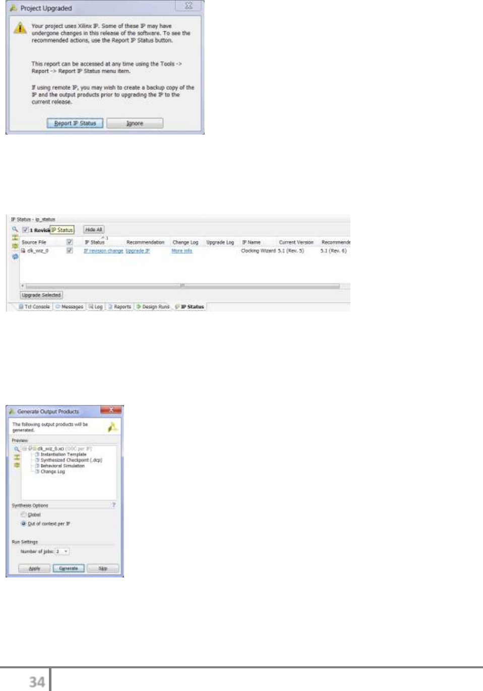
34
MIPSfpga Getting Started Guide © Imagination Technologies v1.1, July 22, 2015
Figure 41. Report IP Status window
Make sure the box next to clk_wiz_0 is selected, then click on Upgrade Selected in the IP Status
pane, as shown in Figure 42.
Figure 42. Upgrade IP
Once the upgrade has completed, a window will pop up saying the Upgrade Completed. Click
OK. Now you will be prompted to create the output files for the upgraded IP (the PLL that
generates the MIPSfpga system clock from the onboard clock). Click on Generate, as shown in
Figure 43. You will be prompted that an Out-of-context module run was launched. Click OK.
Figure 43. Generate output files for PLL (clk_wiz_0)
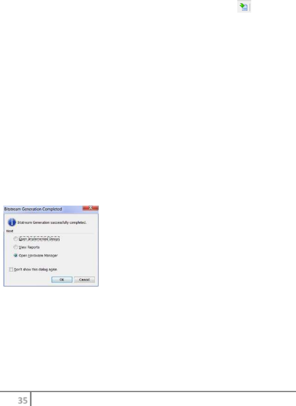
35
MIPSfpga Getting Started Guide © Imagination Technologies v1.1, July 22, 2015
Step 3. Compile HDL
In this step, you will compile the HDL that describes the MIPSfpga processor and make it ready
to download onto the Artix-7 FPGA. Click on the Generate Bitstream button at the top of
the window. The bitstream, also called a bitfile, configures the FPGA to be the MIPSfpga
system, as defined by the Verilog files.
A window may pop up saying:
There are no implementation results available. OK to launch
synthesis and implementation?...
Click Yes. Now wait for bitstream generation to complete. This typically takes around 10-20
minutes or more, depending on your computer speed.
Note that you will see over 400 warnings, all of which you can ignore. For example, you will see
"does not have a driver" warnings, undriven pins tied to 0 warnings, etc. I.e.:
[Synth 8-3848] Net BistIn in module/entity mipsfpga_sys does not have driver.
[Synth 8-3295] tying undriven pin watch:cpz[6] to constant 0
Step 4. Program FPGA board
After the bitstream is created in Step 3, the window in Figure 44 will pop up. You are now ready
to program the FPGA to be configured as a MIPSfpga processor loaded with the
Switches&LEDs program (Figure 35). Select the Open Hardware Manager radio button, as
shown in Figure 44, and click OK.
Figure 44. Open Hardware Manager
Make sure that the Nexys4 DDR FPGA board is turned on and connected to your computer. Now
click on Open Target → Auto Connect, as shown in Figure 45. This will take a few seconds for
Vivado to connect to the Artix-7 FPGA on the Nexys4 DDR board.
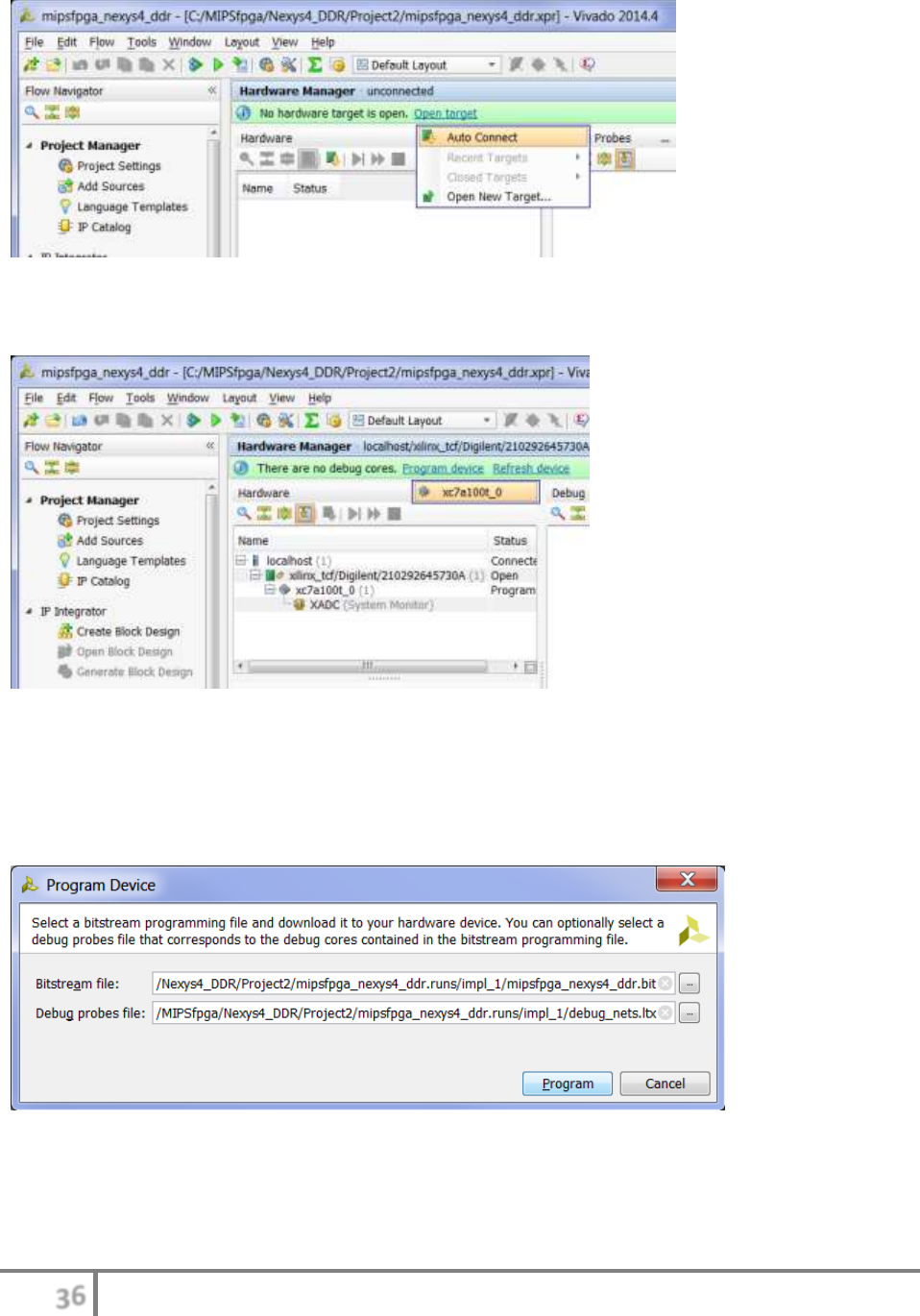
36
MIPSfpga Getting Started Guide © Imagination Technologies v1.1, July 22, 2015
Figure 45. Open Target
Now click on Program Device → xc7a100t_0 in the Flow Navigator, as shown in Figure 46.
Figure 46. Program Device
In the Program Device window, as shown in Figure 47, if a file is not shown, browse to
MIPSfpga/Nexys4_DDR/Project2/mipsfpga_nexys4_ddr.runs/impl_1/mipsfpga_nexys4_ddr.bit
and select it as the Bitstream file. You can leave the Debug probes file field as shown in the
figure (or you can leave it blank). Now press Program. Programming will take a few seconds.
Figure 47. Program Device window
37
MIPSfpga Getting Started Guide © Imagination Technologies v1.1, July 22, 2015
Step 5. Test
Now you are ready to test the Switches&LEDs program running on the MIPSfpga processor.
Press the red processor Reset pushbutton (labeled CPU RESET) on the Nexys4 DDR board (see
Figure 14). The program is now reading the switch values from the Nexys4 DDR board and
writing those values onto the LEDs. Toggle the switches at the bottom of the board (again, see
Figure 14) and watch as the corresponding LEDs change their values.
Section 6.4.2. DE2-115 FPGA Board
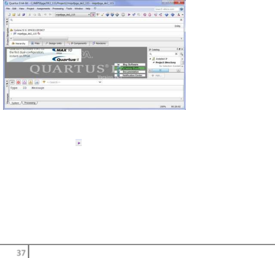
Step 2. Open FPGA programming environment
Follow these instructions for running the MIPSfpga system on Altera's DE2-115 board. Browse
to the MIPSfpga\DE2_115 folder. Make a copy of the Project1 folder and rename the copied
folder Project2. Then open the mipsfpga_de2_115.qpf file in the Project2 folder. The
mipsfpga_de2_115 project will now open in Quartus II, as shown in Figure 48. This project uses
the Verilog files in the MIPSfpga\rtl_up folder. (As an alternate method for opening the project,
you can open Quartus II first and then open the project within Quartus II by selecting File →
Open Project from the top menu.)
Figure 48. Quartus II opening the mipsfpga_de2_115 project
Step 3. Compile HDL
Click on the purple arrow to compile and synthesize the processor from the Verilog files. This
step will compile the HDL that describes the MIPSfpga processor and make it ready to download
onto the Cyclone IV FPGA. This will take about 10-20 minutes or more, depending on your
computer's speed and what else you have running. You will see the progress indicated at the
lower right of the window, as highlighted in Figure 49.
38
MIPSfpga Getting Started Guide © Imagination Technologies v1.1, July 22, 2015
Figure 49. Quartus II window showing synthesis progress
Step 4. Program FPGA board
Turn on your DE2-115 board and make sure the USB-Blaster (DE2-115 programming cable) is
connected to the board and your computer. Now choose Tools → Programmer from the top
menu, as shown in Figure 50.
Figure 50. Selecting the Programmer
The Programmer window in Figure 51 will pop up.
As in Section 4.2.2, choose USB-Blaster [USB-2] next to the Hardware Setup button. Click on
Add File.
39
MIPSfpga Getting Started Guide © Imagination Technologies v1.1, July 22, 2015
Figure 51. Programmer window
In the Select Programming File pop-up window, select the
MIPSfpga\DE2_115\Project2\output_files\mipsfpga_de2_115.sof file, as shown in Figure 52.
This contains the configuration information for the Cyclone IV FPGA on the DE2-115 board.
Click Open.
Figure 52. Select Programming File
Now click Start, as shown in Figure 53. The Progress bar at the top right of the Programmer
window indicates the FPGA programming progress. It will take several seconds to program the
FPGA.
40
MIPSfpga Getting Started Guide © Imagination Technologies v1.1, July 22, 2015
Figure 53. Programming the FPGA
Step 5. Test
Now you are ready to test the Switches&LEDs program running on the MIPSfpga processor.
Press and release the processor Reset pushbutton (pushbutton on the lower right labeled KEY0)
on the DE2-115 board (see Figure 21). The program is now reading the switch and pushbutton
values from the DE2-115 board and displaying those values onto the red and green LEDs,
respectively. Toggle the switches and press the pushbuttons at the bottom of the board (again,
see Figure 21) and watch as the corresponding red LEDs change their values. The red LEDs
reflect the values of the switches and the green LEDs reflect the values of the four pushbuttons.
The pushbuttons are low when pressed, so the green LEDs are on unless the pushbuttons are
pressed. (Remember that pushbutton 0 – KEY0 – is the processor reset button.)
Appendix G (for the DE2-115 board) and Appendix H (for the Nexys4 DDR board) describe
how to reduce compilation time when the only change to the hardware is loading a new program
onto the processor (i.e., writing a new ram_reset_init.txt file that will load into the RAM0
module). This section showed how to load simple programs (without bootcode initialization)
onto the MIPSfpga system. The next section shows how to compile programs and initialize the
processor with boot code.
Section 7. Programming using Codescape
Simple programs are useful for testing basic functionality of the MIPSfpga system. However, if
we want to exercise the more advanced features of the MIPSfpga system, such as caching, we
must have boot code that initializes the processor before it calls the user code. This section
describes how to compile and run both C and MIPS assembly language programs on the
MIPSfpga processor using Codescape MIPS SDK Essentials, referred to as simply Codescape.
Codescape is a free software development kit (SDK) for MIPSfpga provided by Imagination
Technologies.

41
MIPSfpga Getting Started Guide © Imagination Technologies v1.1, July 22, 2015
You will also use OpenOCD and the Bus Blaster probe to load programs onto the MIPSfpga
system. OpenOCD uses Codescape's gdb, a source-level console debugger, to download and
debug programs on the MIPSfpga core using an EJTAG probe. Essentially OpenOCD is a
software gasket between gdb and a probe. OpenOCD also has several core-specific commands
that can be accessed from gdb via the gdb ‘monitor’ command. See Appendix D for instructions
on how to install Codescape and OpenOCD.
Codescape is a group of open source gnu compilers and debuggers (gcc and gdb) targeted to
MIPS cores. This section will show you how to:
1. Use Codescape to compile C and MIPS assembly programs
2. Simulate a compiled program using ModelSim
3. Load the compiled program onto MIPSfpga (two methods available):
Method 1: Resynthesize the MIPSfpga with a compiled program
Method 2: Download a program onto MIPSfpga using the Bus Blaster probe
(recommended method)
4. Debug code running in real time on the MIPSfpga core
The section describes each of these capabilities in detail, beginning with a discussion of the
provided boot code that initializes the MIPSfpga core. Follow the instructions in Appendix D to
install the Codescape SDK and OpenOCD tools.
Section 7.1. MIPSfpga Boot Code
Up until now, we have been running programs on an uninitialized MIPSfpga core. While this is
acceptable for simple programs, for programs that use caching and other advanced features, the
core must be initialized using boot code. After it has finished initializing the processor, the boot
code jumps to the main function in the user code to execute the program.
The provided MIPSfpga boot code initializes the MIPSfpga core by setting up the registers and
initializing the caches and TLB. The boot code is located at virtual address 0xbfc00000, which is
the address of the reset exception. Upon reset, the MIPSfpga core begins fetching instructions at
this address (virtual address 0xbfc00000 = physical address 0x1fc00000.) Although a deep
understanding is not essential for running code on the MIPSfpga, the interested user can find the
boot code in the MIPSfpga\Codescape\ExamplePrograms\CExample folder. The boot code files
are boot.S, init_caches.S, init_cp0.S, init_gpr.S, and init_tlb.S. boot.S includes calls to the boot
code found in the other files. The boot code gets the MIPSfpga core ready to run user code by
initializing:
1. Coprocessor 0 (search for init_cp0 in boot.S)
2. The TLB (init_tlb)
3. The instruction cache (init_icache)
4. The data cache (init_dcache)

42
MIPSfpga Getting Started Guide © Imagination Technologies v1.1, July 22, 2015
After initializing the processor, the boot code calls the _start function, which performs some
more initialization and then calls the user's main function.
Section 7.2. Compiling C and Assembly Code using Codescape
This section describes how to compile both C and assembly programs using Codescape MIPS
SDK Essentials.
Section 7.2.1. Example C Program
Figure 54 is an example C program. The program has three modes corresponding to pushbutton
inputs as well as a default mode. When pushbutton 3 is pressed (KEY[3] on the DE2-115 and
btnD on the Nexys4 DDR), the program displays incremented values on the LEDs. When
pushbutton 2 is pressed (KEY[2] or btnL), the LEDs show decremented values on the LEDs.
When pushbutton 1 is pressed (KEY[1] or btnC), the LEDs flash. When no buttons are pressed,
the LEDs show a repeatedly left-shifted group of 4 lit LEDs.
In addition to typical C constructs, the code also demonstrates how to include inline assembly.
#define inline_assembly() asm("ori $0, $0, 0x1234")
void delay();
int main() {
volatile int *IO_LEDR = (int*)0xbf800000;
volatile int *IO_PUSHBUTTONS = (int*)0xbf80000c;
volatile unsigned int pushbutton, count = 0;
while (1) {
pushbutton = *IO_PUSHBUTTONS;
switch (pushbutton) {
case 0x8: count++; break;
case 0x4: count--; break;
case 0x2:
if (count==0) count = ~count;
else count = 0;
break;
default: if (count==0) count = 0xf;
else count = count << 1;
}
*IO_LEDR = count; // write to red LEDs
delay();
inline_assembly();
}
return 0;
}
Figure 54. main.c for example C program

43
MIPSfpga Getting Started Guide © Imagination Technologies v1.1, July 22, 2015
Notice that any variable associated with hardware, for example the variable pushbutton, must
be declared volatile so that it is not optimized away by the compiler. The iteration variable j in
the delay function is also declared volatile so that is not optimized away by the compiler.
To compile this C program, first open a shell (i.e., cmd.exe from the Start menu). Change to the
MIPSfpga\Codescape\ExamplePrograms\CExample folder. For example, if MIPSfpga is in
C:\MIPSfpga, in the shell type:
cd C:\MIPSfpga\Codescape\ExamplePrograms\CExample
Next type in the shell:
make
This will compile the C program using the Makefile (located in the CExample folder) and
Codescape's gcc (i.e., mips-mti-elf-gcc).
The Makefile generates the file FPGA_Ram.elf, which is an ELF (executable and linkable
format) executable. This file is used by Codescape's gdb to load the program onto MIPSfpga via
the EJTAG probe, as will be described in Section 7.5. You may also be interested in viewing
FPGA_Ram_dasm.txt which shows the disassembled executable interspersed with the assembly
or C source code. The top of this file lists the boot code, starting at virtual address 0x9fc00000.
LEAF(__reset_vector)
la a2,__cpu_init
9fc00000: 3c069fc0 lui a2,0x9fc0
9fc00004: 24c60014 addiu a2,a2,20
...
Virtual address 0x9fc00000 corresponds to the same physical address as 0xbfc00000, namely
0x1fc00000. So, the instruction at 0x9fc00000 will be fetched upon reset. The difference is that
0x9fc00000+ is in kseg0 and is cacheable, 0xbfc00000+ is in kseg1 and is non-cacheable.
Placing the code at 0x9fc00000+ allows the boot code to run faster after caching is enabled. The
bottom of the file (search for "main.c") shows the user code, beginning at virtual address
0x80000644.
int main() {
80000644: 27bdffd8 addiu sp,sp,-40
80000648: afbf0024 sw ra,36(sp)
8000064c: afbe0020 sw s8,32(sp)
80000650: 03a0f021 move s8,sp
...
The FPGA_Ram_modelsim.txt file, also located in the CExample folder, shows a human-
readable version of the executable (memory addresses with machine code and assembly code)
without the source C or assembly code interspersed.

44
MIPSfpga Getting Started Guide © Imagination Technologies v1.1, July 22, 2015
You can remove all of the files created during compilation by typing make clean at the
command shell prompt.
Section 7.2.2. Example MIPS Assembly Program
Figure 55 shows an example MIPS assembly program, which is located in the
MIPSfpga\Codescape\ExamplePrograms\AssemblyExample folder. This is the Switches&LEDs
program from Figure 35. However, this time the boot code will be compiled with the assembly
code, so that the processor is initialized before the user program runs. Recall that the program
reads the values of the switches and pushbuttons on the FPGA board and outputs the results to
the red and green LEDS, respectively.
# $10 = sw, $11 = pb
.globl main
main:
lui $8, 0xbf80
addiu $12, $8, 4 # $12 = LEDG address offset
addiu $13, $8, 8 # $13 = SW address offset
addiu $14, $8, 0xc # $14 = PB address offset
readIO:
lw $10, 0($13) # read switches: sw = SW values
lw $11, 0($14) # read pushbuttons: pb = PB values
sw $10, 0($8) # write switch values to red LEDs
sw $11, 0($12) # write pushbutton values to green LEDs
beq $0, $0, readIO # repeat
nop # branch delay slot
Figure 55. main.S for example MIPS assembly program
To compile this MIPS assembly program, first open a command shell (i.e., Start →cmd.exe).
Change to the MIPSfpga\Codescape\ExamplePrograms\AssemblyExample folder. For example,
if my files are in C:\MIPSfpga, type in the command shell:
cd C:\MIPSfpga\Codescape\ExamplePrograms\AssemblyExample
Then type the following in the shell:
make
This will compile the MIPS assembly program using Codescape's gcc (i.e., mips-mti-elf-gcc).
View the Makefile, located in the AssemblyExample folder, if interested.
As with the C program, you can view the human-readable versions of the executable
(FPGA_Ram.elf) in the FPGA_Ram_dasm.txt and FPGA_Ram_modelsim.txt files. You can
remove all of the files created during compilation by typing make clean at the command
prompt.

45
MIPSfpga Getting Started Guide © Imagination Technologies v1.1, July 22, 2015
Section 7.3. Simulation of a Compiled Program
This section describes how to simulate a compiled program using ModelSim. This process will
take 60-80 minutes or more, depending on the speed of your computer. The overall steps are:
Step 1. Create the text files for initializing MIPSfpga memories
Step 2. Copy the text files to the ModelSim project folder
Step 3. Add Verilog files to project and simulate
Step 1. Create the text files for initializing MIPSfpga memories
Before simulating a compiled program running on MIPSfpga using ModelSim, first create the
text files that initialize MIPSfpga memories (ram_reset_init.txt and ram_program_init.txt).
The reset memory holds the boot code that is executed upon reset, and the program memory
holds the user code.
To create the .txt files, first open a command shell (Start Menu → cmd.exe). In the shell,
change to the following directory: MIPSfpga\Codescape\ExamplePrograms\Scripts. For
example, if MIPSfpga is at C:\MIPSfpga, at the command shell prompt type:
cd C:\MIPSfpga\Codescape\ExamplePrograms\Scripts
Now, type the following at the command prompt:
createMemfiles.bat ..\CExample
This script creates text files containing the machine instructions based on the compiled code in
the CExample folder (MIPSfpga\Codescape\ExamplePrograms\CExample). This process takes
5-15 minutes or more to complete, depending on the speed of your computer.
The script creates a MemoryFiles folder within the CExample folder that contains the following
memory initialization files:
ram_program_init.txt
ram_reset_init.txt
ram_program_init.txt lists the program instructions for initializing the program RAM,
and ram_reset_init.txt lists the bootcode instructions for initializing the reset RAM. The
.mif versions of these files are also created and can be used for quick compilation in Quartus II
(see Appendix G). Recall that Xilinx also offers a quick compilation sequence (see Appendix H).
Note that the script also compiles the C program in the CExample folder before generating the
memory definition files.
The script can be used to create memory definition files from any program. The general format
of the script command is:
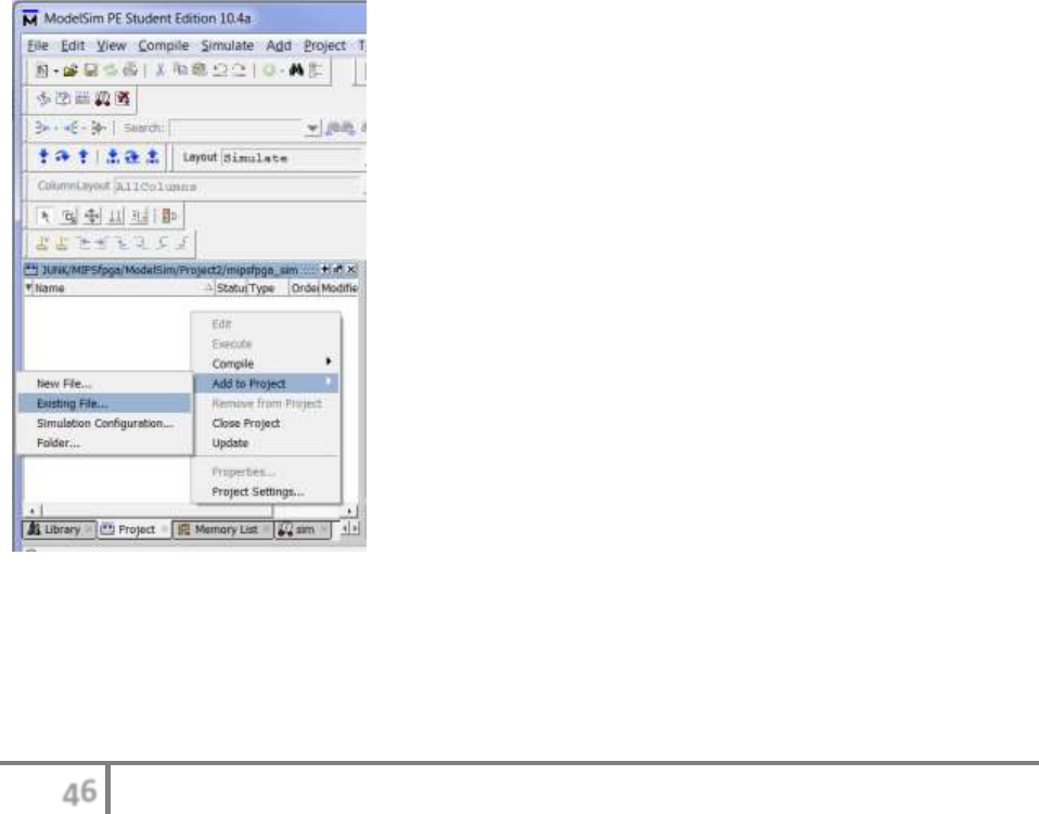
46
MIPSfpga Getting Started Guide © Imagination Technologies v1.1, July 22, 2015
createMemfiles.bat <program directory>
The script must be run from the MIPSfpga\Codescape\ExamplePrograms\Scripts directory. You
can specify any directory for the program code. For example, to create memory files for the
example MIPS assembly program, type:
createMemfiles.bat ..\AssemblyExample\
This will create memory definition files for the example assembly program and place them in the
MIPSfpga\Codescape\ExamplePrograms\AssemblyExample\MemoryFiles directory.
Step 2. Copy the text files to the ModelSim project folder
Copy ram_program_init.txt and ram_reset_init.txt from the
MIPSfpga\Codescape\ExamplePrograms\CExample\MemoryFiles folder to your ModelSim
project directory, i.e., MIPSfpga\ModelSim\Project2. This will overwrite the existing memory
definition files (but remember that those files are available in the MIPSfpga\rtl_up\initfiles
directory if you need them again).
Step 3. Add Verilog files to project and simulate
Now add all of the Verilog files from the MIPSfpga\rtl_up directory to the ModelSim project by
right-clicking in the Project pane and choosing Add to Project →Existing File…
Figure 56. Add files to ModelSim project
Browse to the MIPSfpga\rtl_up directory and select all of the Verilog files and click Open and
OK. Use shift, shift-click to select multiple files. (Be sure to add testbench_boot.v.)
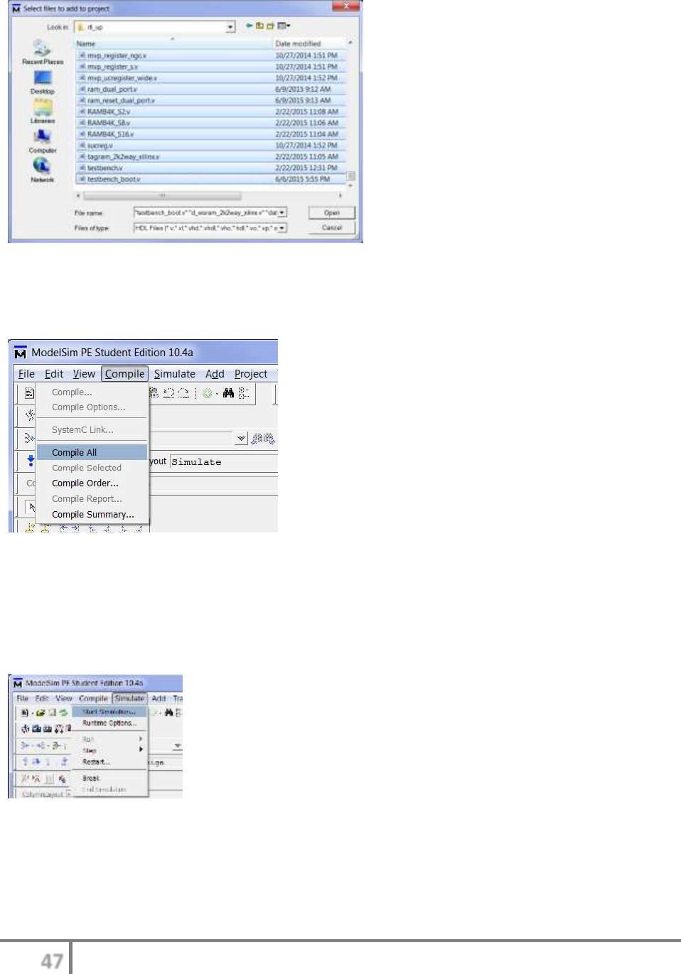
47
MIPSfpga Getting Started Guide © Imagination Technologies v1.1, July 22, 2015
Figure 57. Add Verilog files to ModelSim project
Now from the top menu select Compile → Compile All.
Figure 58. Compiling Verilog files
After the files have finished compiling, you are ready to simulate the MIPSfpga core running the
compiled C program. The MIPSfpga core will first execute the boot code followed by the user
(program) code. Click on Simulate →Start Simulation.
Figure 59. Start Simulation
Expand the work Library and select testbench_boot.
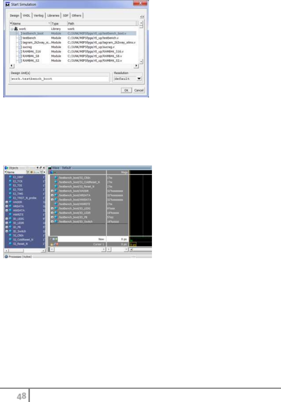
48
MIPSfpga Getting Started Guide © Imagination Technologies v1.1, July 22, 2015
Figure 60. Simulate testbench_boot module
After the Wave pane has opened, drag all of the top-level signals (except the EJTAG signals)
from the Objects pane over to the Wave pane, as shown in Figure 61. Use shift, shift-click to
select multiple signals. (Note: if you don't see the Wave pane, click on View → Wave from the
file menu.)
Figure 61. Adding signals to view in simulation
Now type the following in the Transcript pane, as shown in Figure 62:
run -all
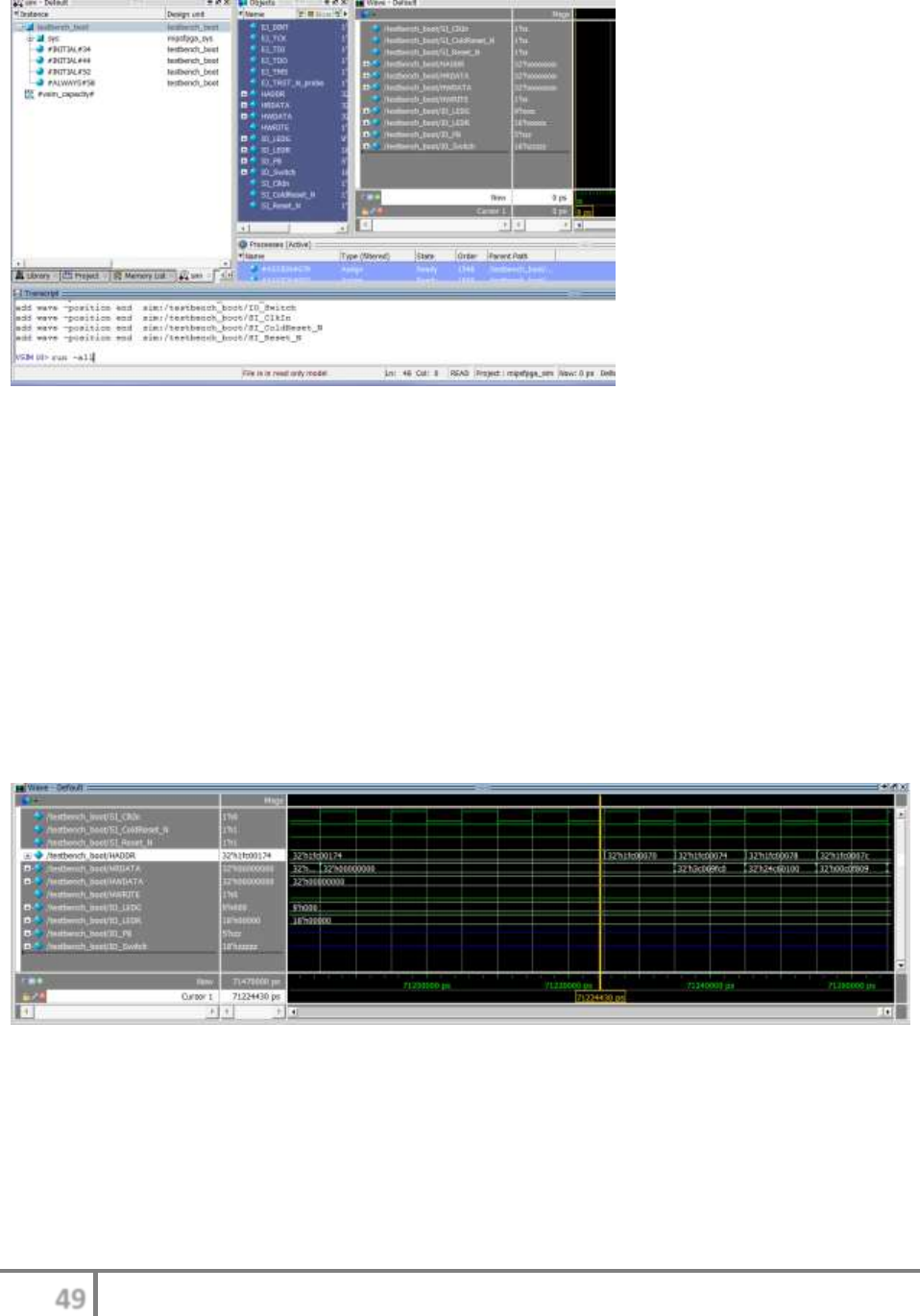
49
MIPSfpga Getting Started Guide © Imagination Technologies v1.1, July 22, 2015
Figure 62. Running the simulation
This will run the program through the first part of the boot code until just before caching is
enabled. The simulation will take about a minute, depending on the speed of your computer.
When the simulation stops, run the program for 800,000 more picoseconds to execute a few
more instructions (i.e., type run 800000 in the transcript window). Because the testbench
stops when it detects the instruction at address 0x1fc00058, you will have to type run -all
five times until it gets past that instruction.
Now observe the waveform around 71,225 ns (71,225,000 ps), as shown in Figure 63. Caching is
now enabled and a new instruction is fetched every cycle (except when there are dependencies),
as expected with a pipelined processor.
Figure 63. Instructions executing at 1 cycle per instruction after caching is enabled
When a dependency occurs, for example upon a branch instruction, instructions take longer than
one cycle. For example, notice that the instruction at 0x1fc0007c (the nop at 0x9fc0007c in
MIPSfpga\Codescape\ExamplePrograms\CExample\FPGA_Ram_dasm.txt) takes 5 cycles as the
jump just before it (jalr at 0x9fc00078) is taken.
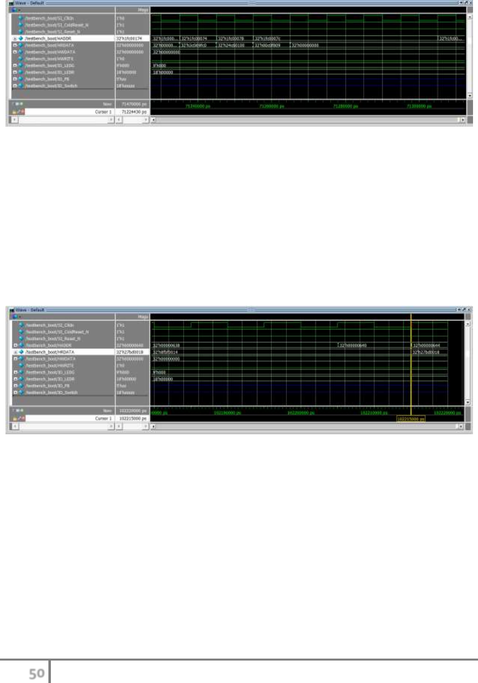
50
MIPSfpga Getting Started Guide © Imagination Technologies v1.1, July 22, 2015
Figure 64. Branch timing
Now continue running the simulation by typing run –all at the ModelSim command prompt
in the Transcript pane. After a few minutes, the simulation will stop again, this time at the
beginning of the program/user code, at physical address 0x00000644 (shown on HADDR), as
seen in Figure 65. Notice that the read data on the AHB-Lite bus (HRDATA) shows the
instruction from the previous address (instruction 0x27bd0018 – the addiu sp, sp, 24 at
address 0x80000640, see FPGA_Ram_dasm.txt). Again, this is because of the 1-cycle delay
between the address appearing on the AHB-Lite bus (on HADDR) and the read or write data
appearing on the AHB-Lite bus (HRDATA or HWDATA).
Figure 65. Beginning of user code
Now set the switch and pushbutton values that are inputs to the MIPSfpga system. First,
highlight testbench_boot in the sim tab of ModelSim, as shown in Figure 66, and then type the
following in the Transcript pane:
force IO_PB 5'h0
force IO_Switch 18'h3ABCD
This will simulate the pushbuttons being the value 0 (i.e., no pushbuttons pressed) and the
switches being the value 0x3abcd. Recall that the switch signal is an 18-bit value to
accommodate the 18 switches on the DE2-115 board. Only the 16 least significant values are
used for the 16 switches on the Nexys4 DDR board.
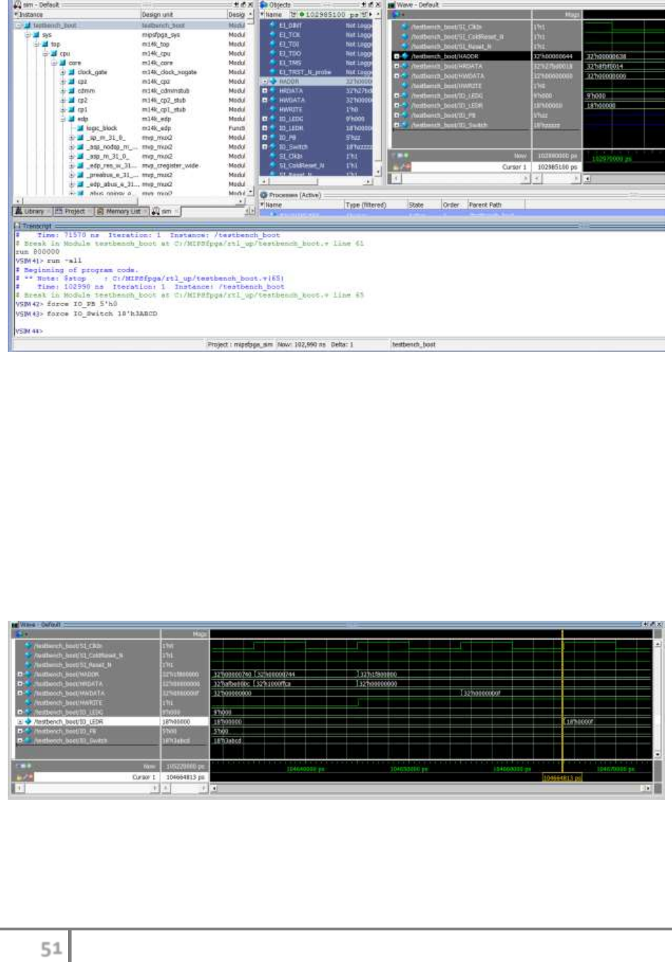
51
MIPSfpga Getting Started Guide © Imagination Technologies v1.1, July 22, 2015
Figure 66. Setting input values (IO_PB and IO_Switch) in ModelSim
Now that the pushbutton and switch inputs from the FPGA board to the MIPSfpga core
(IO_Switch and IO_PB) have values, Run the simulation for another 3,000,000 ps (run
3000000). Notice at around 104,665,000 ps, as shown in Figure 67, how the (red) LEDs
(IO_LEDR) are written with the value 0xf. This happened because, two cycles earlier (at
104,645,000 ps) HADDR became the address of the red LEDs (0x1f800000) and HWRITE
asserted. Then at 104,655,000 ps HWDATA became 0xf. Finally, one cycle later, at 104,665,000
ps that value was fed to the red LEDs (IO_LEDR).
The store word (sw) instruction that causes this write was fetched earlier from memory address
0x80000730 at 104,535,000 ps.
Figure 67. Program writing to the (red) LEDs
Continue to run the simulation of the user code and change the pushbutton values as desired.
After the user code runs for a while, you'll notice a long time when no instruction addresses are
seen on the HADDR lines. This is the delay loop, and the instructions are being fetched from the

52
MIPSfpga Getting Started Guide © Imagination Technologies v1.1, July 22, 2015
instruction cache instead of the memory. Continue exploring the execution of the boot code and
user code as desired.
Section 7.4. Hardware: Resynthesizing MIPSfpga with a Compiled Program
We now show two ways to run compiled code in hardware on the FPGA. With the first method,
you download the code onto MIPSfpga by resynthesizing the core with the new boot and
instruction code, as described here. With the second method, described in the next section, you
download the program and boot code onto the MIPSfpga core using the EJTAG interface. The
latter method is faster and is the recommended method.
To resynthesize the core with the compiled programs, first create the text files that describe the
instructions that will be stored in the boot RAM and the program RAM (ram_reset_init.txt and
ram_program_init.txt). To do so, follow step 1 from Section 7.3. Then copy
ram_program_init.txt and ram_reset_init.txt from the MemoryFiles folder (for example, from
MIPSfpga\Codescape\ExamplePrograms\CExample\MemoryFiles) to the rtl_up folder
(MIPSfpga\rtl_up). Finally resynthesize the core and reload it onto the FPGA board as described
earlier (see Section 6.4.2).
Section 7.5. Downloading a Compiled Program using EJTAG
In this section you will download a compiled program onto the MIPSfpga core using the EJTAG
interface and Bus Blaster probe. The Bus Blaster probe receives a high-speed USB 2.0 cable
input and converts commands into the EJTAG serial protocol that loads programs onto the
MIPSfpga core and controls debugging of programs running on MIPSfgpa.
The Bus Blaster probe is available from SEEED Studio for $45 at:
http://www.seeedstudio.com/depot/ Bus-Blaster-V3c-for-MIPS-Kit-p-2258.html
Follow these steps, described in detail below, to download a compiled program onto the
MIPSfpga core:
Step 1. Download the MIPSfpga core onto the FPGA board
Step 2. Connect the Bus Blaster probe
Step 3. Run the provided script to download and run the program on the MIPSfpga core
Step 1. Download the MIPSfpga core onto the FPGA board
Download MIPSfpga onto the FPGA board using Vivado or Quartus II, as described in Section
4.2.
Step 2. Connect the Bus Blaster probe
Plug the Bus Blaster probe into your computer and into the FPGA board. First, connect the
provided USB cable between the Bus Blaster probe and your computer. Now plug the ribbon
cable from the Bus Blaster probe into the FPGA board. For the DE2-115, plug the Bus Blaster
into the FPGA board's EJTAG port, as shown in Figure 68. For the Nexys4 DDR board, plug the
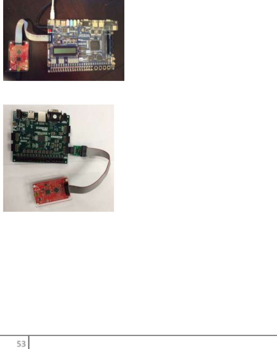
53
MIPSfpga Getting Started Guide © Imagination Technologies v1.1, July 22, 2015
Bus Blaster into the PMODB port of the FPGA board, as shown in Figure 69, using an adapter
board. The adapter board comes in the Bus Blaster package from SEEED Studio (see above
link). Additional details about the Bus Blaster and its connection to the DE2-115 and Nexys4
DDR FPGA boards are in Appendix J.
Figure 68 Bus Blaster connected to the DE2-115 FPGA board
Figure 69. Bus Blaster connected to the Nexys4 DDR FPGA board
Install Bus Blaster Drivers
Now you will install the drivers for the Bus Blaster probe using these steps. Make sure that you
have installed the Codescape SDK and OpenOCD programming tools. The yellow power light
(labeled PWR, as shown on the bottom left of Figure 70) should be lit, indicating that the Bus
Blaster probe is connected to your computer.
54
MIPSfpga Getting Started Guide © Imagination Technologies v1.1, July 22, 2015
Figure 70. Bus Blaster probe
Browse to: C:\Program Files\Imagination Technologies\OpenOCD. Double-click on
zadig_2.1.1.exe. You will be prompted if you want the Zadig program to make changes to your
computer: click Yes. In the Zadig window that opens, click on Options → List All Devices from
the File menu, as shown in Figure 71.
Figure 71. Zadig List All Devices
Highlight BUSBLASTERv3c (Interface 0) and click on Install Driver (or Reinstall Driver or
Replace Driver), as shown in Figure 72.
Figure 72. Install or reinstall Bus Blaster drivers
This process may take a few minutes. After the driver has finished installing, a window will pop
up stating that "The driver was installed successfully". Click Close. Also install the driver for
BUSBLASTERv3c (Interface 1). When that completes, close the Zadig window.
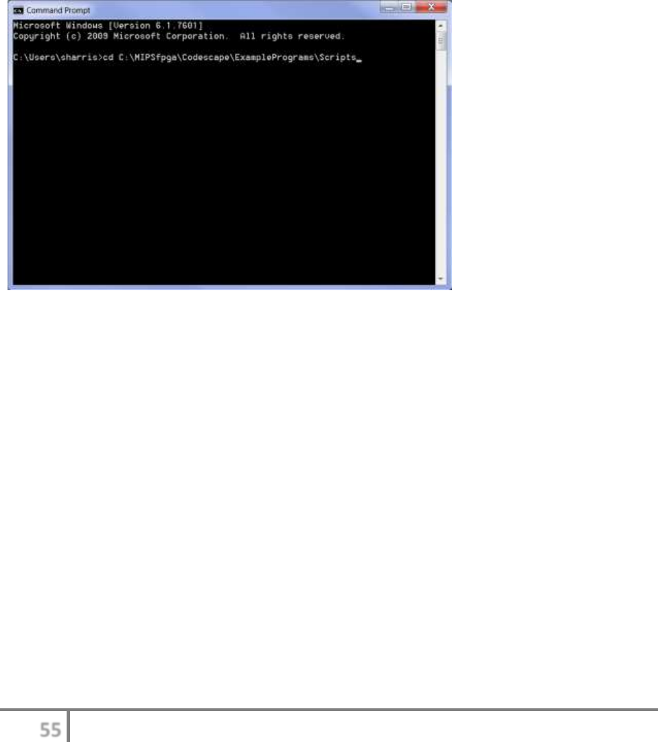
55
MIPSfpga Getting Started Guide © Imagination Technologies v1.1, July 22, 2015
Step 4. Run the provided script to download and run the program on the MIPSfpga core
Now open a command shell. (I.e., Start menu → cmd.exe.)
In the command shell, change to the MIPSfpga\Codescape\ExamplePrograms\Scripts directory.
For example, if MIPSfpga is at C:\MIPSfpga, type the following at the shell prompt, as shown in
Figure 73:
cd C:\MIPSfpga\Codescape\ExamplePrograms\Scripts
Figure 73. Changing directory in the command shell
Now change to either the Nexys4 DDR or DE2_115 directory, depending on the FPGA board
you're using. Do this by typing the following at the shell prompt:
cd Nexys4_DDR
or
cd DE2_115
Now run the script that loads the new program (from the CExample directory) onto the
MIPSfpga core. Type the following at the command shell prompt:
loadMIPSfpga.bat ..\..\CExample
The loadMIPSfpga.bat script:
1. Compiles the program in the directory specified (using make)
2. Runs Open OCD in a new shell

56
MIPSfpga Getting Started Guide © Imagination Technologies v1.1, July 22, 2015
3. Runs gdb (i.e., Codescape's mips-mti-elf-gdb) on the MIPSfpga core in a new shell
4. Loads the executable (.elf) file from the directory specified onto the MIPSfpga core using
OpenOCD and gdb
After running the script, you should see the program running on the MIPSfpga core. In the case
of the CExample program, you should see the LEDs scrolling to the left. Press the pushbuttons to
see the other modes. After your program has been loaded onto MIPSfpga (via the script), close
the two new command shells that the script opened for gdb and OpenOCD. You can continue to
interact with the program running on the MIPSfpga system.
The loadMIPSfpga.bat script can be used to load any program (in the form of a .elf file). The
general format of the script command is:
loadMIPSfpga.bat <program directory>
The script must be run from the MIPSfpga\Codescape\ExamplePrograms\Scripts directory. You
can specify any directory for the program code. For example, to load the example MIPS
assembly program onto the MIPSfpga core using the Bus Blaster EJTAG probe, type:
loadMIPSfpga.bat ..\..\AssemblyExample\
Once Steps 1 and 2 are completed (i.e., the MIPSfpga core is downloaded onto the FPGA board
and the Bus Blaster is connected to the FPGA board and the computer), you need only repeat
Step 3 to download and run other programs on the MIPSfpga core.
Section 7.6. Debugging Compiled Programs on MIPSfpga using Codescape's
gdb
This section shows how to use Codescape's gdb to debug a program running in real time on the
MIPSfpga core. Download the MIPSfpga core onto the FPGA board using Quartus II (DE2-115
FPGA board) or Vivado (Nexys4 DDR FPGA board), as described in Section 4.2.2, and load the
CExample program onto the FPGA board as described in Sections 7.5. Do not close the
OpenOCD and gdb shells created by the loadMIPSfpga.bat script.
Now click on the gdb shell (labeled mips-mti-elf-gdb) that was opened, as shown in Figure 74.

57
MIPSfpga Getting Started Guide © Imagination Technologies v1.1, July 22, 2015
Figure 74. command shell running gdb
gdb is connected to the MIPSfpga core using OpenOCD. You can also view the OpenOCD shell
if you're interested. At the end of the loadMIPSfpga.bat script, gdb loads the executable
(.elf) file and starts the program running on the MIPSfpga core. Below are some useful
commands for running and debugging a program that is running in real time on the MIPSfpga
core using gdb. Type each gdb command from Table 6 into the gdb command shell in sequence
to try them out for yourself.
Table 6. gdb commands
Command
Description
monitor reset halt
Reset and stop the processor. Notice the program stopped
running. Note: the gdb ‘monitor’ command passes the ‘reset halt’
text through to the OpenOCD command parser which executes
the reset command.
Shortcut: mo reset halt
b main
Set a breakpoint at the main function. (Short for: "break main".)
The main function starts at instruction address 0x80000654 (after
the stack operations located at addresses 0x80000644 -
0x80000650).
b *0x80000730
Set a breakpoint at instruction address 0x80000730. In the
example C program (main.c) this is the store word instruction
(sw) that writes to the (red) LEDs (see MIPSfpga\Codescape\
ExamplePrograms\CExample\FPGA_Ram_dasm.txt):
80000730: ac430000 sw v1,0(v0)
i b
List the breakpoints. (Short for: "info breakpoint".) At this point it
will list the breakpoint at instruction addresses 0x80000654

58
MIPSfpga Getting Started Guide © Imagination Technologies v1.1, July 22, 2015
(main) and 0x80000730.
c
Continue the processor execution. (Short for: "continue".) It will
stop at the first breakpoint, in this case, when it gets to main.
c
Continue to the next break point. (You can also simply press enter
to repeat the last command.)
p count
Print the value of the variable count. (Short for: "print count".)
For example, count is now 15.
p/x count
Prints the value of the count variable in hexadecimal (0xf).
p/x &count
Prints the address of count (0x8003ffb4).
i r
Print the value of all registers. (Short for: info registers.)
i r v1
Print the value of register v1 only. At this point, v1 holds the value
being stored to the LEDs (0xf) by the store word (sw) instruction
at 0x80000730.
i r v0
Print the value of register v0. When the PC is at 0x80000730, v0
holds the address of the (red) LEDs: 0xbf800000.
c
Continue program execution until the next break point. (Short for:
"continue".) Notice that the sw instruction completed and the
LEDs now show the value 0xf.
i r v1
Print the value of register v1. Now v1 has been shifted left and
holds the value 0x1e.
Repeat the above two commands (c and i r v1) to see the
count continue shifting left.
As you continue executing the program, notice that the LEDs on
the FPGA board also show the shifted value.
stepi
Executes a single instruction. For example, now you will see the
PC increment to 0x80000734.
Shortcut: si
d 1
Delete breakpoint 1 (type i b to list the breakpoints with their
numbers)
monitor reset run
Reset and run the processor. This will run the processor without
breakpoints, even if breakpoints have been set.
Shortcut: mo reset run
Table 7 lists other useful gdb commands. Also refer to the GDB User Manual available as a link
on this webpage:
http://www.gnu.org/software/gdb/documentation/
A quick reference card of common gdb commands is available here:
C:\Program Files\Imagination Technologies\Documentation\refcard.pdf
Table 7. Other gdb commands
Command
Example / Description
load <elf_file_name>
Example 1: load FPGA_Ram.elf

59
MIPSfpga Getting Started Guide © Imagination Technologies v1.1, July 22, 2015
Example 2:
load ..\\AssemblyExample\\FPGA_Ram.elf
Description: Load an executable file (in ELF format) onto
the MIPSfpga core.
Note: the processor must be halted (mo reset halt)
before loading a new ELF file. After loading the executable,
then run it by typing mo reset run.
disas
Disassemble instructions.
Examples:
disas 0xbfc00000,+100 (+100 is length in bytes)
disas /m main (disassemble mixed source/assembly
of the main function)
disas /r main (show raw bytes as well as
instructions)
Note: If the above commands don't work (for example
return nops), first halt the processor and then enter the
program: type mo reset halt, set a breakpoint at
main (b main), and continue to that point (c). Then use
the above commands.
x/i 0xbfc00000
Examine instruction – similar to disas
set disassemble-next-line
on|off
If on, gdb will display disassembly of next source line when
program is halted
monitor mdw addr <#
words>
monitor mdw 0xbfc000000 16
Description: Read 16 words of memory starting at memory
address 0xbfc00000. The default number of words is 1.
Must be executed when the processor is halted.
monitor mww addr word
monitor mww 0xbfc000000 0xaaaaaaaa
Description: Write value 0xaaaaaaaa to memory address
0xbfc00000.
Must be executed when the processor is halted.
<return>
Description: Pressing the return/enter key in gdb with no
command typed at the prompt will repeat the last
command.
Table 8 lists some OpenOCD commands to run in gdb. Refer to the OpenOCD online manual for
additional documentation:
http://openocd.sourceforge.net/doc/html/index.html
Table 8. OpenOCD commands to run in gdb
Command
Example / Description
monitor mips32 cp0
[[regname|regnum select]
monitor mips32 cp0
Description: Displays the values of all of the

60
MIPSfpga Getting Started Guide © Imagination Technologies v1.1, July 22, 2015
[value]]
coprocessor 0 registers.
Options:
regname: register name (i.e., config)
regnum: register number
select: register select value
value: value to write to the register
Example: monitor mips32 perfcnt0 0xff
writes the value 0xff to the perfcnt0 register.
monitor mips32 invalidate
[all | inst | data | allnowb
| datanowb]
monitor mips32 invalidate
Description: Invalidate the instruction and/or data
cache with/without writeback.
Options:
all: invalidates both caches with writeback
inst: invalidates the instruction cache only with
writeback
data: invalidates the data cache only with writeback
allnowb: invalidates both caches without writeback
datanowb: invalidates the data cache only without
writeback
monitor mips32 scan_delay
[value]
monitor mips32 scan_delay 3000
Description: Sets the delay between fastdata writes.
This is useful when writing to the MIPSfpga cores (for
example, when loading the .elf file). When value ≥
2000000, fastdata mode is turned off and the probe is
in legacy mode.
Options:
value: delay in nanoseconds between fastdata
writes
monitor version
Display version of OpenOCD server.
Section 8. Summary and a Look Ahead
Now that you have completed this MIPSfpga Getting Started Guide, you have a foundational
understanding of the MIPSfpga core and how to use it to simulate code and to download, run,
and debug code on the MIPSfpga system. To further your understanding of MIPSfpga, the
MIPSfpga Fundamentals materials are available for download from the following website (under
the Teaching Materials heading):
http://community.imgtec.com/university/MIPSfpga/resources
The MIPSfpga Fundamentals teaching materials include lecture slides, nine laboratory exercises,
and solutions. The materials show how to use MIPSfpga as the center of system-on-chip design.
System-on-chip (SoC) design integrates all parts of a system, including hardware support for
peripherals, on a single chip. In the MIPSfpga Fundamentals Laboratories you will expand the

61
MIPSfpga Getting Started Guide © Imagination Technologies v1.1, July 22, 2015
MIPSfpga system described in this Getting Started Guide to include peripherals such as 7-
segment displays, counters, and serial interfaces (SPI).
Section 9. References
This Getting Started Guide provides the foundation for using the MIPSfpga core. MIPSfpga also
comes with documentation to deepen understanding and use of the microAptiv UP family of
processors. These documents are available as PDFs in the MIPSfpga\Documents folder.
MicroAptiv UP Overview MD00928.pdf: Provides an overview of the MicroAptiv UP
cores, a family of MIPS processors that have been introduced to be highly-efficient,
compact cores aimed at use in embedded systems.
MicroAptiv UP Datasheet MD00939.pdf: Describes the pipeline, functional units, and
configuration and testing options for the MicroAptiv UP functional units.
MicroAptiv UP Integrator's Guide MD00941.pdf: Describes how to interface with the
MicroAptiv UP core for System on Chip (SoC) designs. The document includes
descriptions of the overall signal interfaces, the AHB-Lite interface, the interrupt
interface, and clocking, reset, and power.
MicroAptiv UP Software User's Manual MD00942.pdf: Describes hardware and
software initialization, the instruction set, exceptions and interrupts, and EJTAG debug
support.
MicroAptiv UP AHB-Lite Interface MD01082.pdf: Provides specifications for the
AHB-Lite interface.
MIPS32_QuickReferenceCard.pdf: Provides a brief summary of the MIPS32
Instruction Set Architecture (ISA).
Imagination also provides a set of basic training videos for MIPS cores available here:
http://community.imgtec.com/developers/mips/resources/training-
courses/mips-basic-training-course/
Note that this URL has changed from time to time on the Imagination website. So, if the link
doesn't work, search the Imagination website for keywords.
The following three textbooks provide an understanding of the MIPS architecture in general. The
textbooks can be used with MIPSfpga to gain a better understanding of how to use, program, and
modify the MIPSfpga core and how to use the MIPSfpga as the center of system-on-chip (SoC)
designs.
Digital Design and Computer Architecture
2nd Edition, © 2012, David Money Harris & Sarah L. Harris, Morgan Kaufmann
Describes how to build a MIPS processor from the ground up. The book starts with a
description of digital signals, number systems, gates, and combinational and sequential

62
MIPSfpga Getting Started Guide © Imagination Technologies v1.1, July 22, 2015
logic followed by an introduction to hardware description languages (both System
Verilog and VHDL). Supplementary online materials are also available for Verilog. The
second half of the book introduces the MIPS architecture, from MIPS assembly and
machine instructions to the detailed description of three MIPS processor designs and an
explanation of memory systems, including caching, virtual memory, and I/O.
Computer Organization and Design
5th Edition, © 2013, Morgan Kaufmann, David A. Patterson & John L. Hennessy
Describes the MIPS architecture and processor design, from performance and power
issues to multiprocessor systems. Begins with a description of power and performance
calculations and moves on to a description of the MIPS architecture, including assembly
and machine instructions, and processor design, including the description of three
processor designs.
See MIPS Run Linux
2nd Edition, © 2006, Morgan Kaufmann, Dominic Sweetman
Describes the MIPS architecture and programming environment as well as the Linux
operating system, including specific examples of low-level operating system code.

63
MIPSfpga Getting Started Guide © Imagination Technologies v1.1, July 22, 2015
Section 10. Acknowledgements
Many have contributed to the making of this MIPSfpga Getting Started Guide, including the
following people from Imagination Technologies, Xilinx, Digilent, Harvey Mudd College, the
University of Nevada, Las Vegas, the University College London, and the Complutense
University of Madrid.
Robert Owen
Sarah Harris
David Money Harris
Yuri Panchul
Bruce Ableidinger
Kent Brinkley
Chuck Swartley
Sean Raby
Rick Leatherman
Matthew Fortune
Munir Hasan
Sachin Sundar
Michael Alexander
Sam Bobrowicz
Larissa Swanland
Clint Cole
Students and faculty at UCL
Ian Oliver
Steve Kromer
Daniel Martinez
Parimal Patel
Jason Wong

64
MIPSfpga Getting Started Guide © Imagination Technologies v1.1, July 22, 2015
Getting Started
Guide
Appendices
65
MIPSfpga Getting Started Guide © Imagination Technologies v1.1, July 22, 2015
Appendix A. Installing ModelSim PE Student Edition
Follow these steps, detailed below, to install ModelSim PE Student Edition 10.3d, which is
freely available from Mentor Graphics. The installation file is about 250 MB, and the application
requires 420 MB.
Step 1. Download the installation file
Step 2. Open the installation file
Step 3. Complete online license request form
Step 4. Check email and install license
Note: Mentor Graphics is likely to update ModelSim after the writing of this MIPSfpga Getting
Started Guide. If you are installing a later version of ModelSim PE Student Edition the steps are
likely similar or even exactly the same as those described here.
Step 1. Download the installation file
Browse to the following website:
http://www.mentor.com/company/higher_ed/modelsim-student-edition
You will see the webpage in Figure 75. Click on Download Student Edition.
Figure 75. ModelSim PE Student Edition website
The window shown in Figure 76 will now open. Click on Save File. In the window that pops up,
browse to the location you'd like to save the installation file and click Save. The file is about 350
MB. So, depending on your internet connection speed, it may take several minutes to download
the file.
66
MIPSfpga Getting Started Guide © Imagination Technologies v1.1, July 22, 2015
Figure 76. Save installation file window
Step 2. Open the installation file
Now open the downloaded file, modelsim-pe_student_edition.exe. You may be prompted if you
want to allow the program from an unknown publisher to make changes to your computer. Click
Yes. After a few minutes, you will see the window in Figure 77. Click Next and then Yes to
accept the software license agreement.
Figure 77. ModelSim PE Student Edition installation window
You will now be asked where you want to install ModelSim, as shown in Figure 78. Click
Browse to choose a different destination folder or accept the default location, and click Next.
67
MIPSfpga Getting Started Guide © Imagination Technologies v1.1, July 22, 2015
Figure 78. ModelSim installation folder
Click Next again to accept the default program folder, as shown in Figure 79.
Figure 79. Select Program Folder window
Now the application will begin to install. You can view the progress in the progress bar, as
shown in Figure 80.
Figure 80. ModelSim installation progress bar
68
MIPSfpga Getting Started Guide © Imagination Technologies v1.1, July 22, 2015
After installation is complete, you will be asked if you want a shortcut to ModelSim on your
desktop, as shown in Figure 81. Click Yes or No, depending on your preference.
Figure 81. Desktop icon prompt
You will now be asked to add the ModelSim executable directory to your path, as shown in
Figure 82. Click Yes.
Figure 82. Add ModelSim executable directory to path
The installation will now finish, which will take about a minute. When it is complete, the
window in Figure 83 will pop up. Click Finish.
Figure 83. ModelSim Setup Complete window
Step 3. Complete online license request form
MentorGraphics will now open an online license request form, as shown in Figure 84.
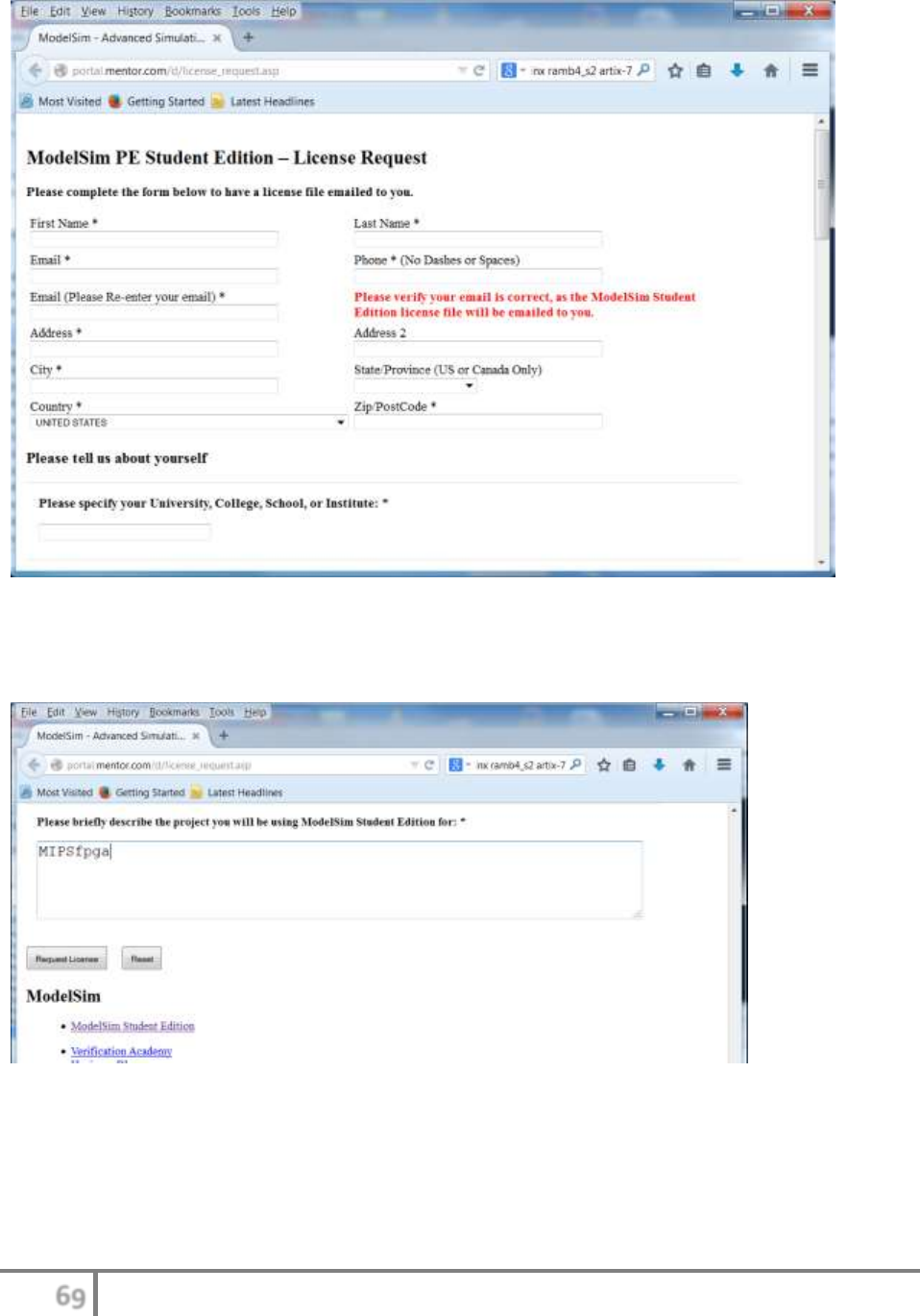
69
MIPSfpga Getting Started Guide © Imagination Technologies v1.1, July 22, 2015
Figure 84. ModelSim online license request form
After you have entered your information in the form, click on Request License, as shown in
Figure 85.
Figure 85. Request ModelSim PE Student Edition license
You will see a confirmation page indicating that licensing information has been sent to the
entered email address.
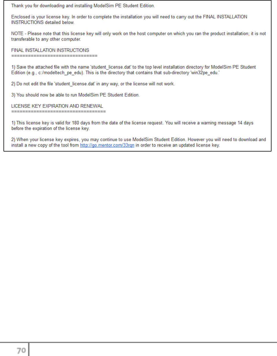
70
MIPSfpga Getting Started Guide © Imagination Technologies v1.1, July 22, 2015
Step 4. Check email and install license
The license will be emailed to you almost immediately. If you don't see the licensing email
within a few minutes, check your Spam folder. Follow the instructions in the email to install the
free license and activate ModelSim, as shown in Figure 86.
Figure 86. ModelSim licensing email
ModelSim is now ready for use. As indicated in the email, MentorGraphics requires you to re-
install ModelSim PE Student Edition every six months, but it is free every time.
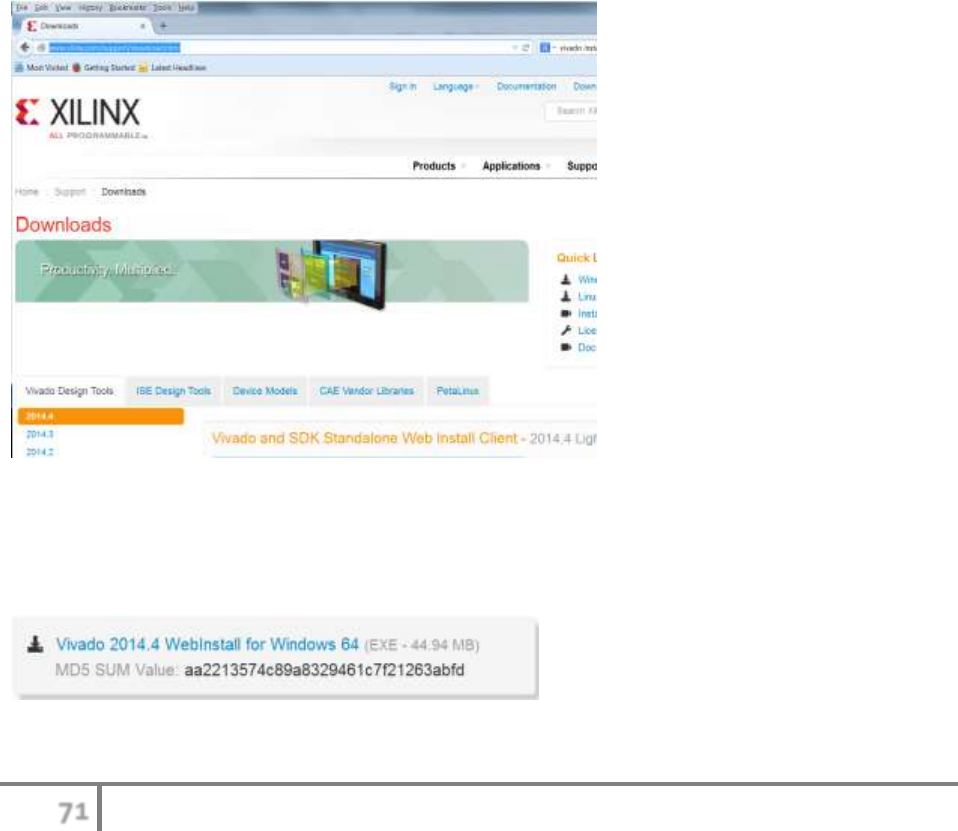
71
MIPSfpga Getting Started Guide © Imagination Technologies v1.1, July 22, 2015
Appendix B. Installing Vivado for the Nexys4 DDR FPGA Board
Follow these steps, detailed below, to install Vivado 2014.4, which is freely available from
Xilinx Inc. The installation file is about 46 MB, and the application requires 9.5 GB.
Step 1. Download the installation file
Step 2. Open the installation file
Step 3. Obtain a free Vivado license
Note: Xilinx is likely to update Vivado after the writing of this MIPSfpga Getting Started Guide.
If you are installing a later version, the steps are likely similar to those described here.
Step 1. Download the installation file
Browse to the Xilinx download website:
http://www.xilinx.com/support/download.html
You will see the webpage in Figure 87.
Figure 87. Xilinx download page
Make sure 2014 is highlighted under the Vivado Design Tools tab, as shown in Figure 87. Then
scroll down in the web browser and click on Vivado 2014.4 WebInstall for Windows 64, as
shown in Figure 88.
Figure 88. Download Vivado installation file download link

72
MIPSfpga Getting Started Guide © Imagination Technologies v1.1, July 22, 2015
You will now be brought to the Xilinx sign in page, as shown in Figure 89. If you don't already
have a Xilinx account, click on Create Account. Creating an account is free.
Figure 89. Xilinx sign in page
After you have signed in, the website will prompt you to enter your name, address, etc., as shown
in Figure 90. After entering your information, click on Next at the bottom of the web page.
Figure 90. Download center name/address entry form
You will now be asked if you want to save the installation executable. Save the file where ever is
convenient (a temporary location is fine).
Step 2. Open the installation file
After the installation executable has downloaded, browse to where you saved it, and double-click
on it to open it and start the installation. A warning window may pop up saying "The publisher
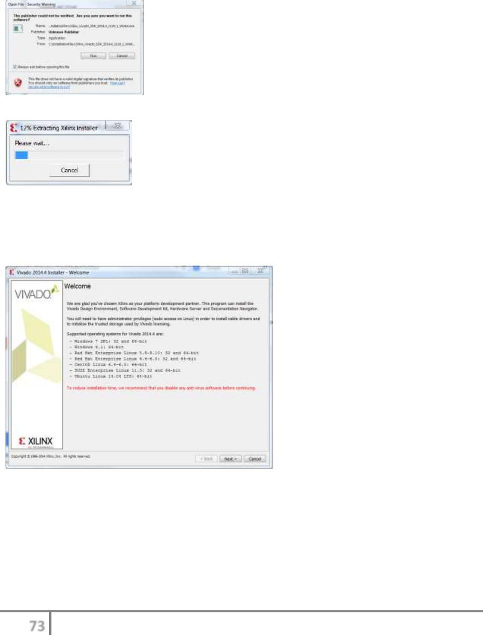
73
MIPSfpga Getting Started Guide © Imagination Technologies v1.1, July 22, 2015
could not be verified…", as shown in Figure 91. If so, click on Run. The Windows Firewall may
also issue a warning that you must override. Now the Xilinx Installer will be extracted, as shown
in Figure 92.
Figure 91. Security warning window
Figure 92. Xilinx installer extraction progress window
You may be asked if you want the Xilinx program to make changes to your computer. Click Yes.
The Vivado 2014.4 Installer window will now open, as shown in Figure 93. Click Next.
Figure 93. Xilinx Installer window
You will be prompted for your Xilinx user id and password (Figure 94) created in Step 1. Then
click Next.
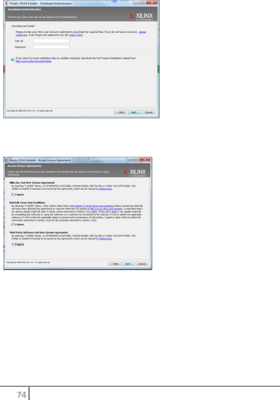
74
MIPSfpga Getting Started Guide © Imagination Technologies v1.1, July 22, 2015
Figure 94. Xilinx login page
Now you will see the Xilinx license agreement (Figure 95). Click on all of the I Agree boxes,
and click Next.
Figure 95. Xilinx License Agreement
Now select Vivado WebPACK Edition, as shown in Figure 96, and click Next.
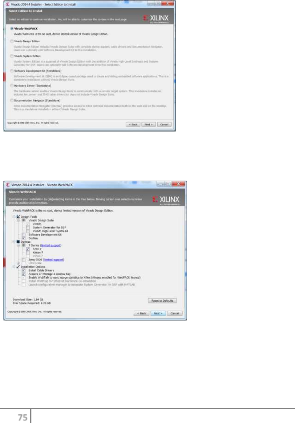
75
MIPSfpga Getting Started Guide © Imagination Technologies v1.1, July 22, 2015
Figure 96. Choose Vivado WebPACK Edition
Now choose which Design tools and Devices to support. Make the choices shown in Figure 97.
(Under Devices, you need only select the Artix-7 devices, because that is the FPGA on the
Nexys4 DDR board, but feel free to add additional devices as desired.) Click Next.
Figure 97. Design Tool and Devices
Now select a destination directory (or accept the default), as shown in Figure 98, and click Next.
You may be prompted to approve the creation of the installation directory (i.e., C:\Xilinx).
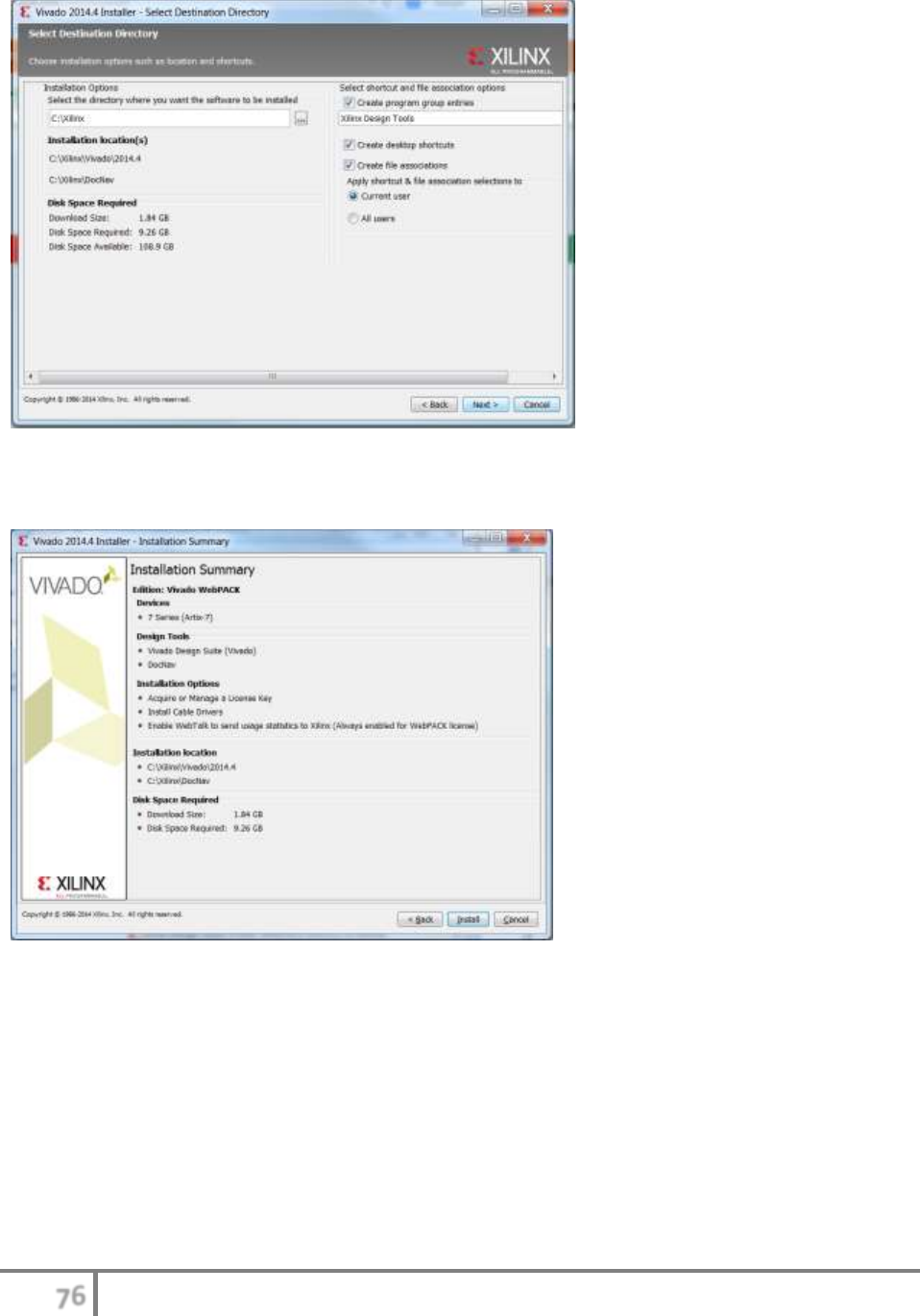
76
MIPSfpga Getting Started Guide © Imagination Technologies v1.1, July 22, 2015
Figure 98. Xilinx Vivado destination directory
Now the Installation Summary window will appear, as shown in Figure 99. Click on Install.
Figure 99. Installation Summary window
The installation Progress window will appear (Figure 100). Installation could take over an hour,
depending on your internet and computer speed.

77
MIPSfpga Getting Started Guide © Imagination Technologies v1.1, July 22, 2015
Figure 100. Installation Progress window
At the end of installation, the Vivado Installer will prompt you to unplug all Xilinx cables, as
shown in Figure 101. Click OK.
Figure 101. Cable Driver Installer window
If a window pops up asking if you want to install the device software, click Install.
After the cable drivers are installed, a window will pop up indicating that the installation was
successful, as shown in Figure 102. Click OK.
Figure 102. Installation successful window
Step 3. Obtain a free Vivado license
Now you will see the Vivado License Manager window, as shown in Figure 103. Select Get Free
Licenses, as shown, and click Connect Now.

78
MIPSfpga Getting Started Guide © Imagination Technologies v1.1, July 22, 2015
Figure 103. Vivado License Manager window
The installer will now open a Xilinx Sign in webpage, as shown in Figure 104. If you don't
already have a Xilinx account, click on Create Account to create a free account. Otherwise, enter
your User ID and Password and click Sign In.
Figure 104. Xilinx Sign in webpage
Enter your name and other information in the Product Licensing window (Figure 105) and click
Next at the bottom of that window.

79
MIPSfpga Getting Started Guide © Imagination Technologies v1.1, July 22, 2015
Figure 105. Product Licensing Window
In the next Product Licensing window, as shown in Figure 106, scroll down until you see
Activation Based Licenses, as shown in Figure 107. Select Vivado WebPACK License as shown
in the figure, and click Activate Node-Locked License.
Figure 106. Product Licensing window

80
MIPSfpga Getting Started Guide © Imagination Technologies v1.1, July 22, 2015
Figure 107. Select Vivado WebPACK License
A Generate Node License window will appear (Figure 108).
Figure 108. Generate Node License
Scroll down to the bottom of the window and click Next (Figure 109).
Figure 109. Bottom of Generate Node License window
It will now ask you to review your license request (Figure 110). Scroll to the bottom of that
window and click Next.
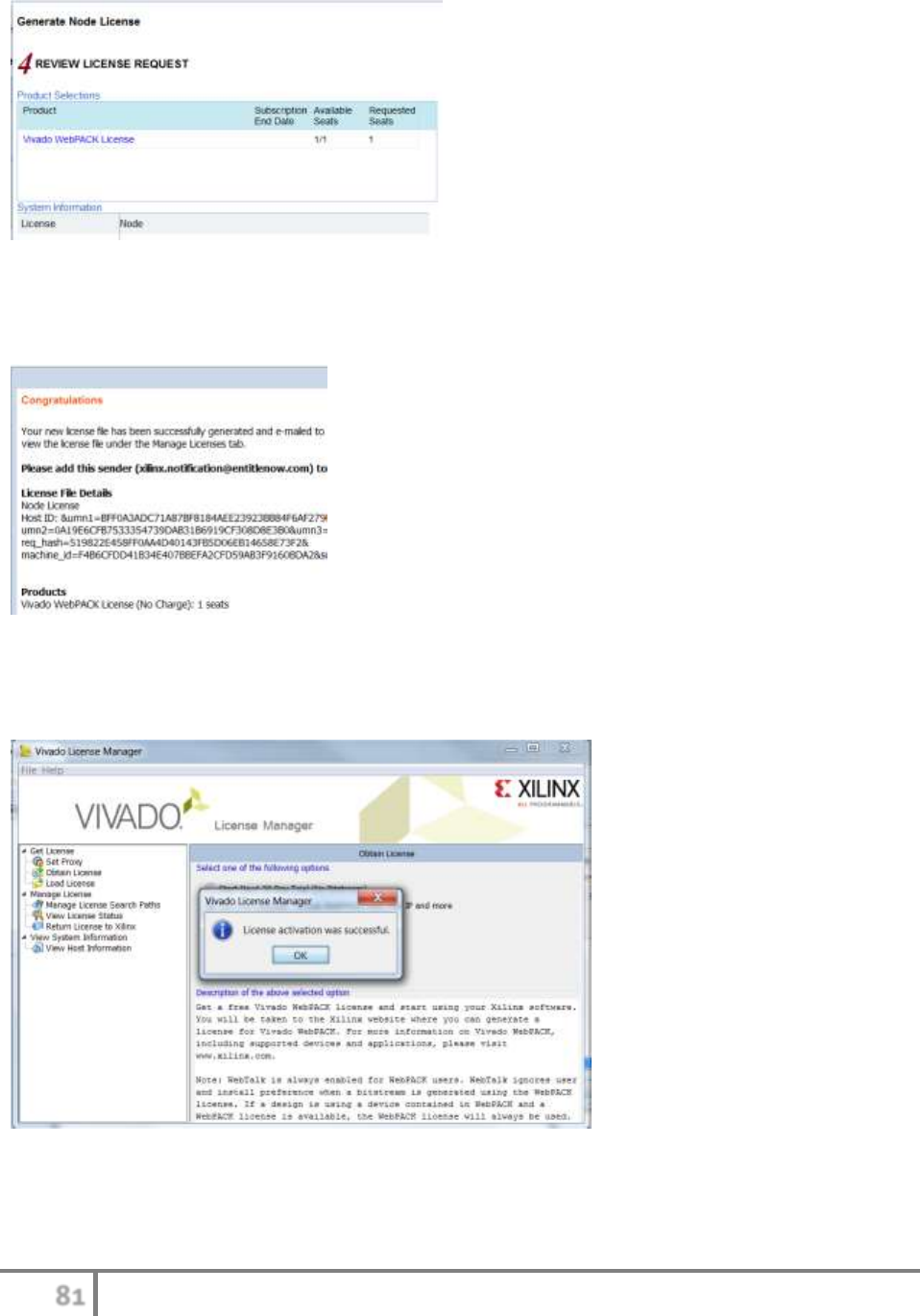
81
MIPSfpga Getting Started Guide © Imagination Technologies v1.1, July 22, 2015
Figure 110. Review license request
You will now see a window indicating that your license file has been successfully generated and
that it has been emailed to you (Figure 111). Close this Congratulations window.
Figure 111. License file successfully generated
In the Vivado License Manager Window, you will also see that License activation was
successful (Figure 112). Click OK. Do not close the Vivado License Manager window.
Figure 112. License activation successful
Now check your email at the address you entered in the Xilinx webpage (Figure 105). You will
receive an email, as shown in Figure 113, with the license attachment.

82
MIPSfpga Getting Started Guide © Imagination Technologies v1.1, July 22, 2015
Figure 113. License email
Save the license attachment to a folder (Figure 114).
Figure 114. Saving Xilinx license file
Now click on Load License in the Vivado License Manager window, as shown in Figure 115. (If
you closed the Vivado License Manager window, go to the start menu and type Manage Xilinx
Licenses to open it.)
Figure 115. Load License
Now click on Activate License (Figure 116).
83
MIPSfpga Getting Started Guide © Imagination Technologies v1.1, July 22, 2015
Figure 116. Activate License
Browse to where you saved the license file and click Open (Figure 117).
Figure 117. Select License File
If the license has already been processed, a pop-up window will indicate that it likely has already
been processed. Now you can close the license manager window and use Vivado.
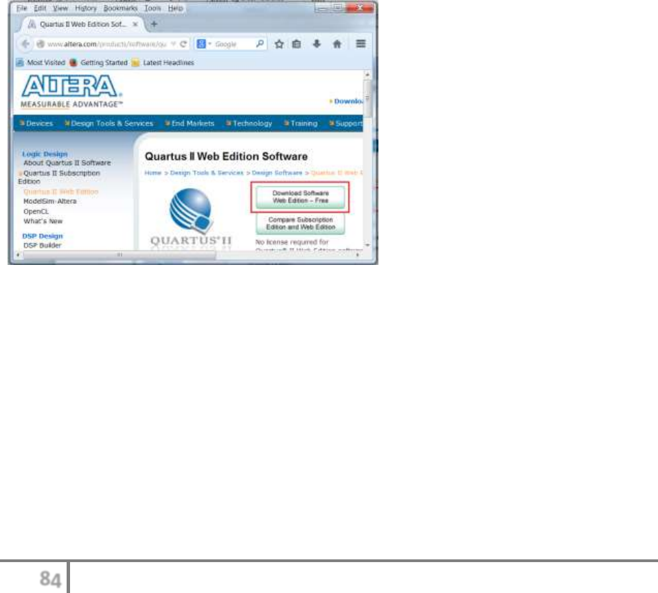
84
MIPSfpga Getting Started Guide © Imagination Technologies v1.1, July 22, 2015
Appendix C. Installing Quartus II for the DE2-115 FPGA Board
Follow these steps, detailed below, to install Quartus II Web Edition 14.0, which is freely
available from Altera. The installation file is about 2 GB and the Quartus II application requires
about 4.5 GB.
Step 1. Download the installation file
Step 2. Open the installation file
Note: Altera is likely to update Quartus II after the writing of this MIPSfpga Getting Started
Guide. If you are installing a later version, the steps are likely similar to those described here.
Step 1. Download the installation file
Browse to the following web page:
http://www.altera.com/products/software/quartus-ii/web-edition/qts-we-index.html
You will see the webpage shown in Figure 118. Click on the Download Software Web Edition –
Free button.
Figure 118. Quartus II download window
Now you will see the Quartus II Web Edition download webpage as shown in Figure 119.
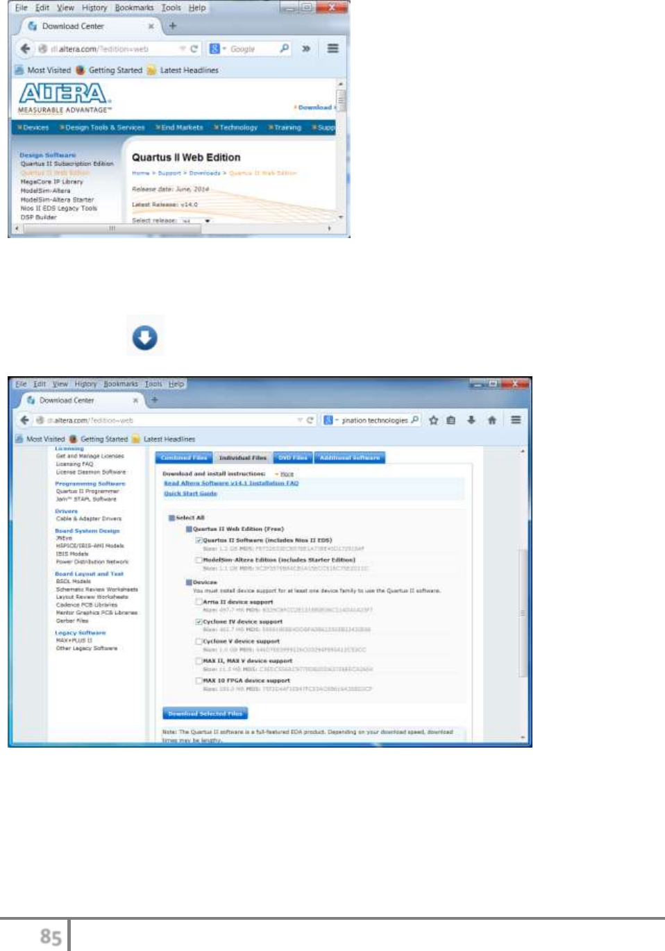
85
MIPSfpga Getting Started Guide © Imagination Technologies v1.1, July 22, 2015
Figure 119. Altera download center: Quartus II Web Edition
Scroll down in this web page and click on the Individual Files tab. Make the selections as shown
in Figure 120, then click on Download Selected Files. (Note: when using the Internet Explorer
browser, click on next to each item to download).
Figure 120. Download installation files
The installation file download will now begin, as shown in Figure 121. A pop-up window will
prompt you to save the file. Browse to whichever folder you'd like – a temporary folder is fine.
Then click Save.

86
MIPSfpga Getting Started Guide © Imagination Technologies v1.1, July 22, 2015
The installation file is about 2 GB, so downloading it may take some time, depending on your
internet speed. Progress is graphed in the installation progress window shown in Figure 121.
Figure 121. Download progress window
Step 2. Open the installation file
After the installation file (QuartusSetupWeb-14.0.200-windows.exe) has downloaded, open it.
You will then likely be asked if you want to allow changes from an unknown publisher. Click
Yes.
Figure 122. Open installation file window
The Quartus II installation window will open, as shown in Figure 123. Click Next.
Figure 123. Quartus II installation window

87
MIPSfpga Getting Started Guide © Imagination Technologies v1.1, July 22, 2015
You will now see the Licensing Agreement shown in Figure 124. Click I accept the agreement,
as shown in the figure. Then click Next.
Figure 124. Quartus II License Agreement
You will now be prompted for an installation directory, as shown in Figure 125. Leave it as the
default, or choose another, and click Next.
Figure 125. Quartus II installation directory
Now the Select Components window will open, as shown in Figure 126. Click Next.
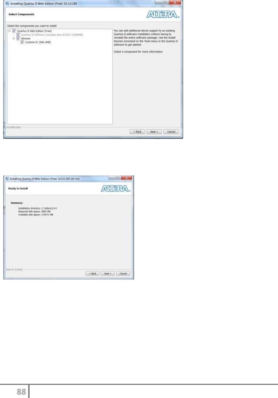
88
MIPSfpga Getting Started Guide © Imagination Technologies v1.1, July 22, 2015
Figure 126. Quartus II Select Components window
In the summary window (Figure 127). Click Next.
Figure 127. Quartus II installation summary window
You will now see a progress bar as the Quartus II installer unpacks files and installs the
application (Figure 128).

89
MIPSfpga Getting Started Guide © Imagination Technologies v1.1, July 22, 2015
Figure 128. Quartus II installation progress window
When installation is complete, the window shown in Figure 129 will pop up. Select the options
you'd like (at a minimum, select Launch USB Blaster II driver installation and Launch Quartus II
(64-bit)) and click Finish.
Figure 129. Installation Complete Window
The Device Driver and Installation Wizard window will now pop up (Figure 130). Click Next.

90
MIPSfpga Getting Started Guide © Imagination Technologies v1.1, July 22, 2015
Figure 130. Device Driver Installation Wizard
The drivers will now install. If you get a Windows Security message (Figure 131), click Install.
Figure 131. Windows security window
When the device drivers have finished installing (Figure 132), click Finish.
Figure 132. Device Driver Installation complete
You may now be prompted to enable Talkback, a feature that gives some feedback to Altera
when you use Quartus II. Choose to enable or disable it, whichever is your preference. You may
also be prompted to restart your computer.
Quartus II should now open – if it doesn't, you can open it manually from the Start menu. If you
are prompted for a license option, do not buy a license, simply run the software (with the free
license).
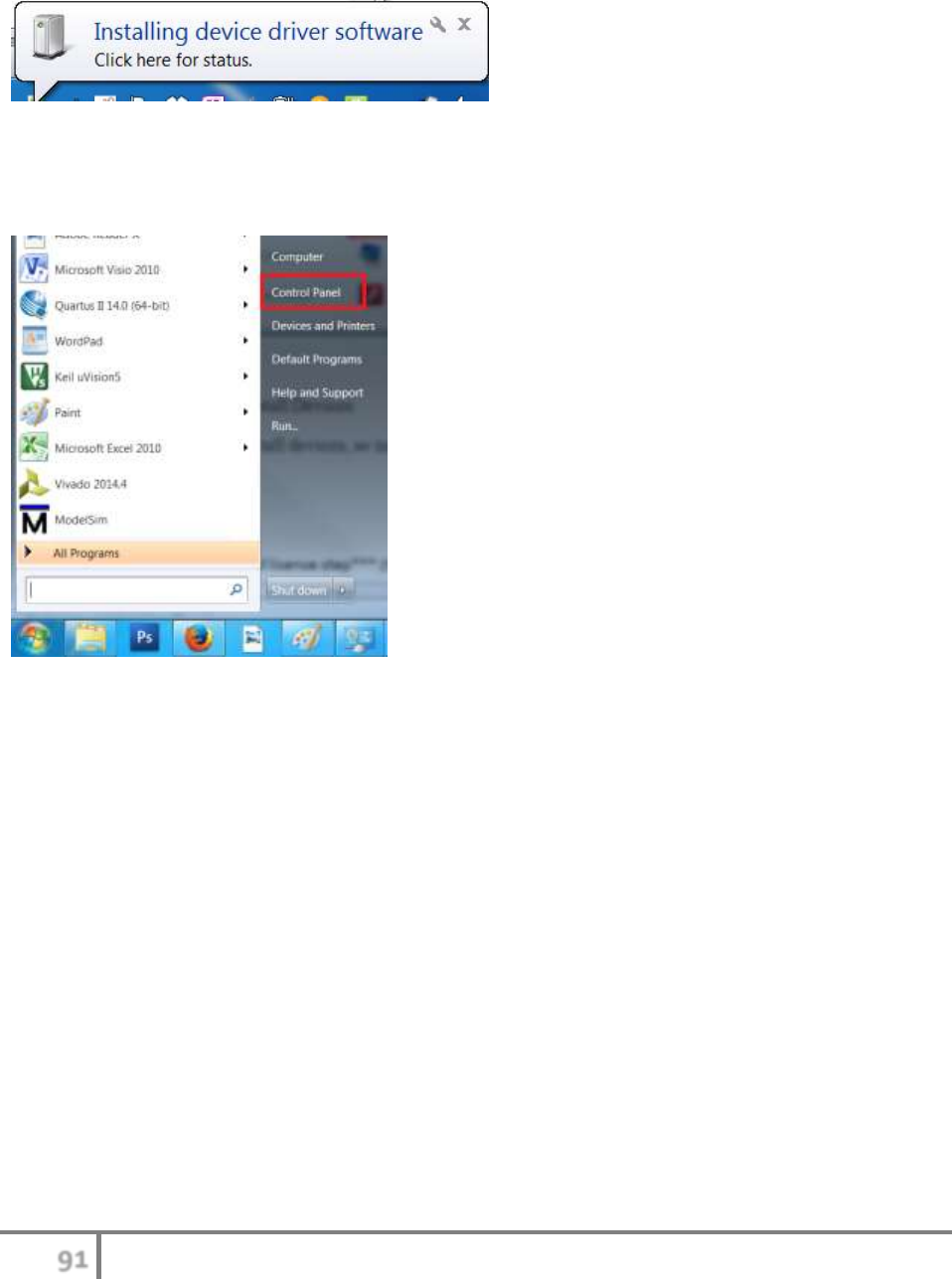
91
MIPSfpga Getting Started Guide © Imagination Technologies v1.1, July 22, 2015
Power on the DE2-115 board and plug in the USB-Blaster cable to the DE2-115 board and to
your computer. The device driver for the USB-Blaster cable will attempt to install (Figure 133).
Figure 133. USB-Blaster device driver installation
If the driver installation fails, you can install it manually by clicking on Start Menu → Control
Panel, as shown in Figure 134.
Figure 134. Opening the Control Panel
Then click on Device Manager, as shown in Figure 135. (Note: if you don't see the Device
Manager in the Control Panel window, make sure View by Large Icons is selected as shown in
the figure.)
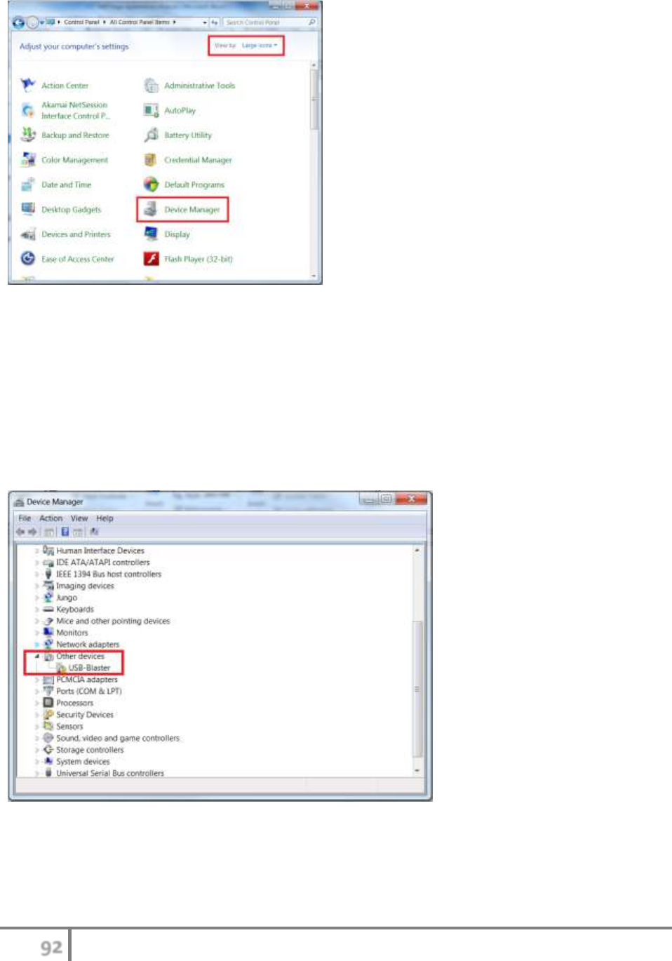
92
MIPSfpga Getting Started Guide © Imagination Technologies v1.1, July 22, 2015
Figure 135. Opening the Device Manager
In the Device Manager window, right-click on USB-Blaster under Other devices (Figure 136).
(Note that it may say Unknown device instead of USB-Blaster.) After right-clicking, choose
'Update Driver Software' from the pop-up menu. Then select 'Browse my computer for driver
software'. In the 'Search for driver software in this location' field, browse to the Altera
installation directory, for example: C:\altera\14.0\quartus\drivers\usb-blaster. Click Next and
Install. You can close the Update Driver Software window and the Device Manager window
after the driver has been successfully installed.
Figure 136. Installing USB-Blaster driver manually
Now, back in the Quartus II application, check that everything is set up correctly.
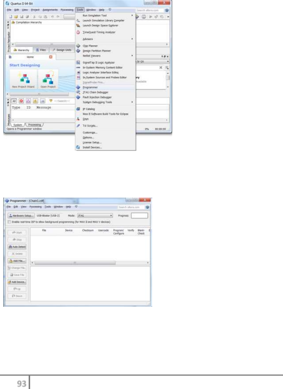
93
MIPSfpga Getting Started Guide © Imagination Technologies v1.1, July 22, 2015
From the file menu, choose Tools → Programmer, as shown in Figure 23.
Figure 137. Opening the Programmer window
The Programmer window will now open, as shown in Figure 24. For Hardware Setup, use USB-
Blaster [USB-2] and JTAG for the Mode, as shown in the figure. If the Hardware Setup text box
is blank, click on the Hardware Setup button.
Figure 138. The Programmer window
A new window will open, as shown in Figure 139. Under Currently selected hardware, select
USB-Blaster [USB-2] as shown in the figure. Then click Close.
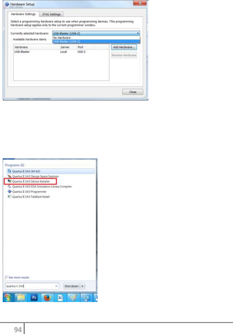
94
MIPSfpga Getting Started Guide © Imagination Technologies v1.1, July 22, 2015
Figure 139. Hardware Setup window
You are now ready to use Quartus II.
If you need to install additional target devices (i.e., in addition to Cyclone IV FPGAs or if the
Cyclone IV FPGA targets did not install correctly), you can use the Quartus II Device Installer,
which is available from the Start menu (Figure 140).
Figure 140. Quartus II Device Installer

95
MIPSfpga Getting Started Guide © Imagination Technologies v1.1, July 22, 2015
Appendix D. Installing Programming Tools
This appendix describes how to install the programming tools for writing, compiling and
downloading your C or assembly code onto MIPSfpga. You will install OpenOCD and
Codescape MIPS SDK Essentials using a single installer.
Browse to the MIPSfpga\Codescape folder and run (double-click on) OpenOCD-0.9.2-
Installer.exe. A pop-up window will ask if you want to allow an unknown publisher to make
changes to your computer. Click yes. A window will then open asking which programs to install,
as shown in Figure 141. Leave both boxes checked so that you install both OpenOCD and
Codescape MIPS SDK, and click Next.
Figure 141. Installation options window
You will now be asked where you would like to install the files, as shown in Figure 142. Leave it
as default (note that you must leave it as the default to ensure the rest of the scripting works),
and click Install.
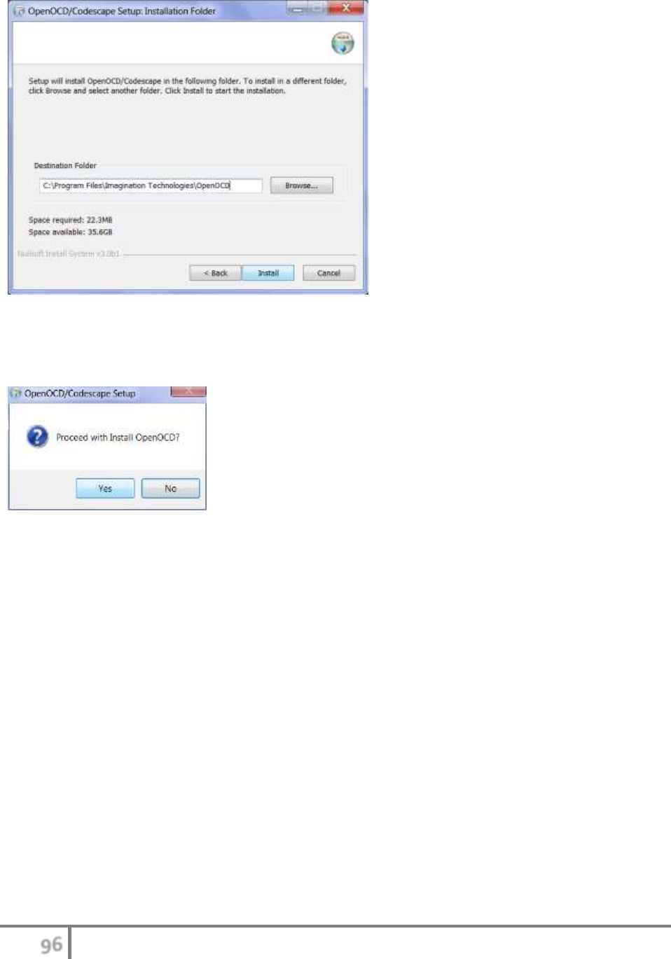
96
MIPSfpga Getting Started Guide © Imagination Technologies v1.1, July 22, 2015
Figure 142. Installation Folder
A window will pop asking for confirmation to proceed with the installation of OpenOCD as
shown in Figure 143. Click Yes.
Figure 143. Confirm OpenOCD installation window
Installation of OpenOCD should take several seconds. After it has finished, it will say that the
OpenOCD install is complete, click OK. The installer will then install Codescape MIPS SDK
Essentials, after a short delay. Click Next, Next, then "I accept the agreement" and Next. Select
Bare Metal Applications, as shown in Figure 144, and click Next.

98
MIPSfpga Getting Started Guide © Imagination Technologies v1.1, July 22, 2015
Now the Downloading Required Files window pops up. If you need to use an HTTP Proxy, click
the Use HTTP Proxy box and fill in the information. (If you don't know what this is, you
probably don't need to use a proxy.) Click Next.
Codescape will now install in the following directory: C:\Program Files\Imagination
Technologies.
After Codescape MIPS SDK installation is complete, a window will open with an option to
Display Codescape's getting started guide. Click Next. A webpage will open with Codescape's
getting started guide. You can view it if desired or simply close the window.
OpenOCD and Codescape MIPS SDK Essentials installations are now complete. Close the
OpenOCD/Codescape Installation window by clicking Close.
The OpenOCD online manual is available here for your reference:
http://openocd.sourceforge.net/doc/html/index.html
The OpenOCD User Guide is the file OpenOCD User’s Guide.pdf. This file was installed along
with OpenOCD in folder C:\Program Files\Imagination Technologies\OpenOCD\openocd-0.9.1.
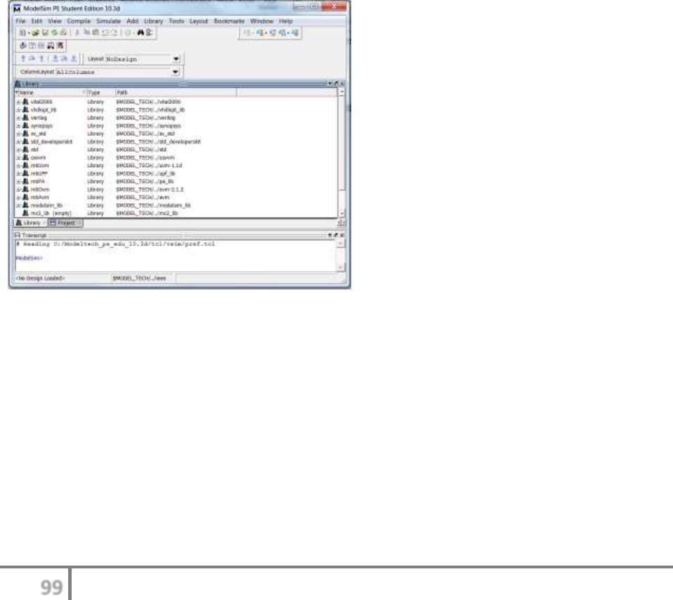
99
MIPSfpga Getting Started Guide © Imagination Technologies v1.1, July 22, 2015
Appendix E. Setting up a Project in ModelSim
This appendix describes how to create a project in ModelSim to simulate the MIPSfpga
processor. These instructions apply to both ModelSim PE Student Edition and ModelSim-Altera
Starter Edition. Each time a new program is simulated, only the reset RAM module
(ram_reset_dual_port) must be recompiled. Follow these steps, described in detail below.
Step 1. Open ModelSim
Step 2. Create a project
Step 3. Add Verilog files to the project
Step 4. Compile the Verilog modules
Step 5. Copy the ram initialization file (ram_reset_init.txt) to the project folder
Step 6. Simulate the testbench
Step 7. Repeat with modified program
Step 1. Open ModelSim
Open ModelSim (Figure 146).
Figure 146. ModelSim window
Step 2. Create a project
In the main ModelSim window, select File → New → Project, as shown in Figure 147. A
window may pop up indicating that the current project will be closed. If so, click Yes.
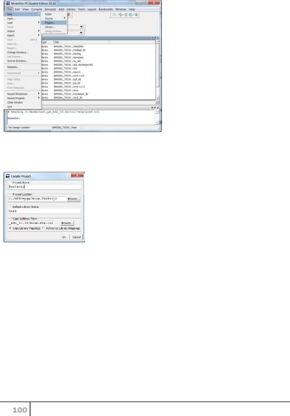
100
MIPSfpga Getting Started Guide © Imagination Technologies v1.1, July 22, 2015
Figure 147. Create a new ModelSim project
Browse to where you would like to create the project and name the project, then click OK.
Figure 148 shows an example project location and name.
Figure 148. Create Project window
Step 3. Add Verilog files to the project
Now an Add items to the project window will open (Figure 149). Click on Add Existing File.
You will now add the Verilog files that define MIPSfpga to your ModelSim project. You will
add these files by reference, so they refer to the files in MIPSfpga\rtl_up.
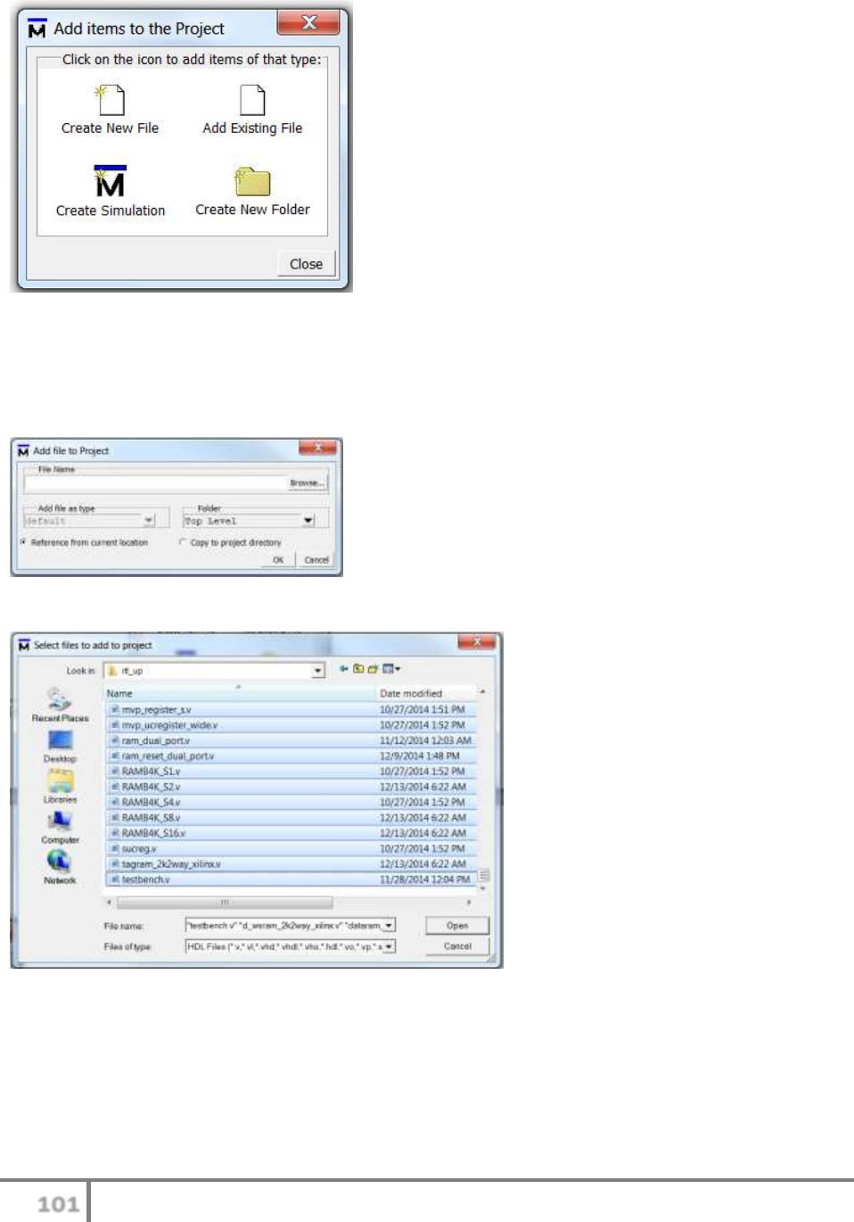
101
MIPSfpga Getting Started Guide © Imagination Technologies v1.1, July 22, 2015
Figure 149. Add items to the Project window
In the Add file to Project window (Figure 150), click on Browse. Now, in the Select files to add
to project window (Figure 151), browse to the MIPSfpga\rtl_up folder, select all of the Verilog
files (as shown in Figure 151) and click Open. (Note: do not select the initfiles folder.)
Figure 150. Add file to Project window
Figure 151. Select files to add to project window
Now the Add file to Project window (Figure 150) will appear again. The File Name window is
blank because you have added too many files to list. Click OK. You will now see the files added
to your project, as shown in Figure 152.
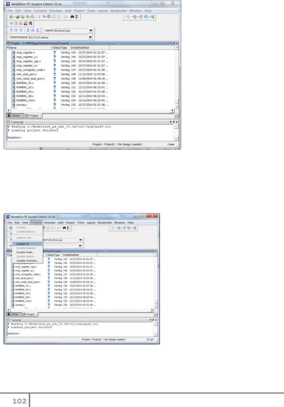
102
MIPSfpga Getting Started Guide © Imagination Technologies v1.1, July 22, 2015
Figure 152. Verilog files added to ModelSim project
In the Add items to the project window (Figure 149), click Close.
Step 4. Compile the Verilog modules
Now in the main ModelSim window, select Compile → Compile All from the file menu, as
shown in Figure 153.
Figure 153. Compile project files
The Transcript window will indicate that the modules are being compiled successfully. After
compilation has completed, all of the files will have a green checkmark in the Status column and
the Transcript window will indicate that there were no failures or errors, as shown in Figure 154.

103
MIPSfpga Getting Started Guide © Imagination Technologies v1.1, July 22, 2015
Figure 154. Compilation successful
Step 5. Copy the ram initialization file (ram_reset_init.txt) to the project folder
Now copy the RAM initialization file to your ModelSim project directory: Copy
MIPSfpga\rtl_up\initfiles\1_IncrementLEDs\ram_reset_init.txt to your project directory. For
example, if you chose the same project directory as the example in Step 2, the project directory
will look as shown in Figure 155.
Figure 155. Project directory after ram initialization file was copied
Step 6. Simulate the testbench
Now you are ready to simulate the testbench Verilog module. In the main ModelSim window,
select Simulate → Start Simulation from the file menu, as shown in Figure 156.
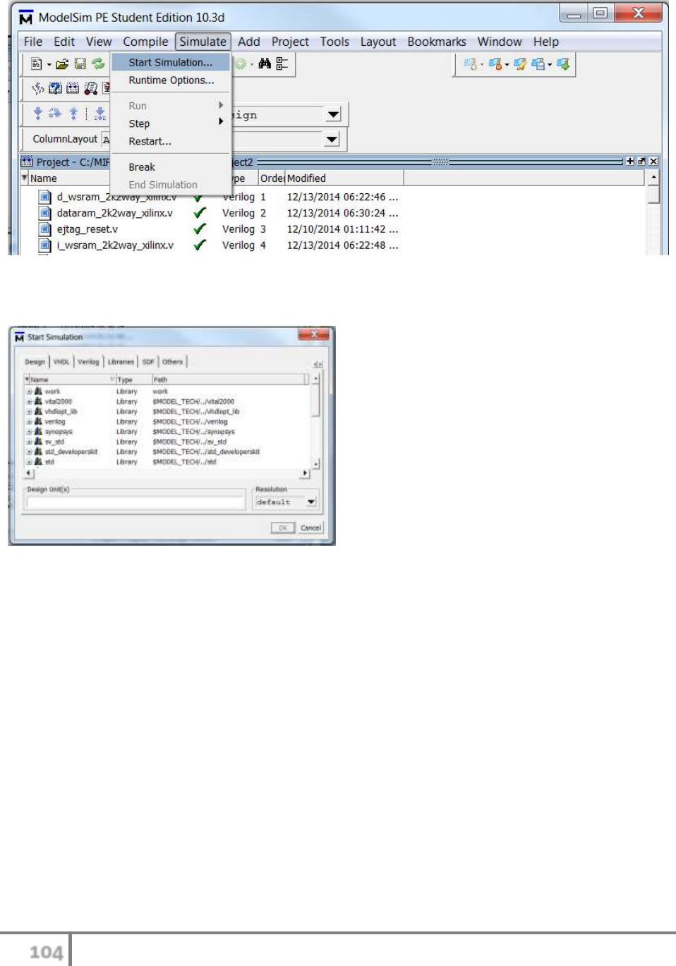
104
MIPSfpga Getting Started Guide © Imagination Technologies v1.1, July 22, 2015
Figure 156. Start Simulation
The Start Simulation window will open, as shown in Figure 157.
Figure 157. Select module to simulate
Expand the work library by clicking the + sign to the left of it. (Hint: click on the Name column
twice to sort in reverse alphabetical order.) Now highlight testbench, as shown in Figure 158, and
click OK.
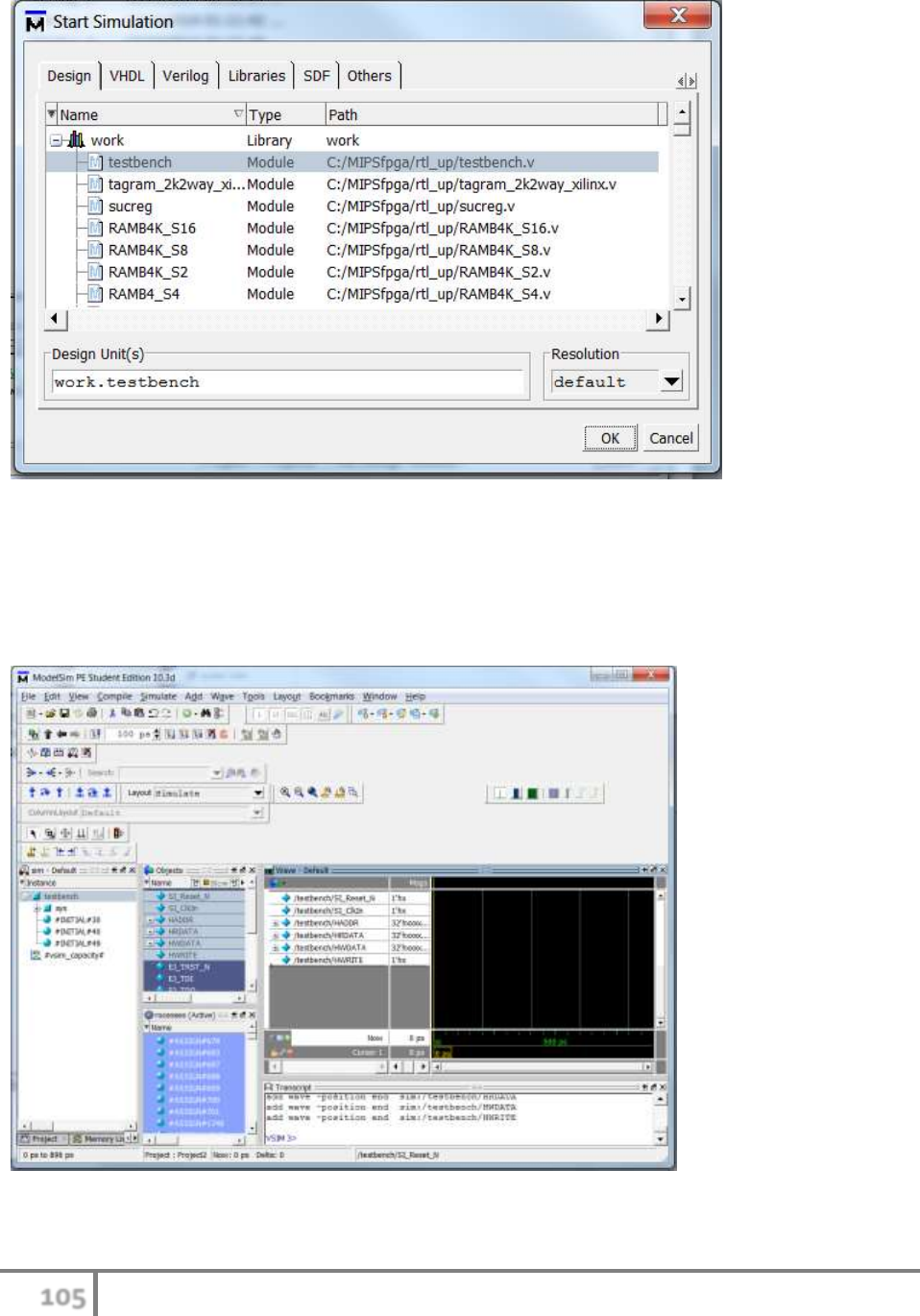
105
MIPSfpga Getting Started Guide © Imagination Technologies v1.1, July 22, 2015
Figure 158. Choose testbench as module to simulate
The testbench module and all of its submodules will be loaded into the simulator. Now add
signals to the timing waveform. Select some signals in the Objects pane and drag them over to
the Wave pane, as shown in Figure 159. These signals are the reset and clock signals for the
MIPSfpga processor as well as the AHB-Lite Bus interface signals.
Figure 159. Select signals to display
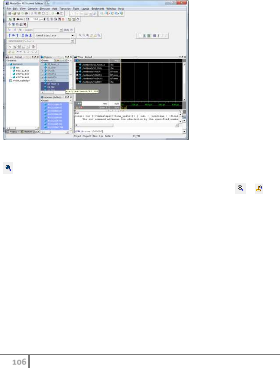
106
MIPSfpga Getting Started Guide © Imagination Technologies v1.1, July 22, 2015
Now run the simulation by typing run 1500000 in the Transcript pane, as shown in Figure 160.
This will run the simulation for 1,500,000 ps. Wait while the simulation completes (about 10
seconds).
Figure 160. Run the simulation
Now view the simulation results. Click on the Wave pane and then click on the Zoom full button:
. (Note: the Zoom full option is available only when the Wave pane is highlighted.) The
waveform will now look as shown in Figure 161. Run the simulation longer (run #, where #
indicates the number of ps to continue the simulation) or zoom into the simulation or , as
desired. As in Section 4.1, HWDATA increments, indicating the value being written to the
LEDs, and the instructions repeat (as indicated by HADDR and HRDATA).
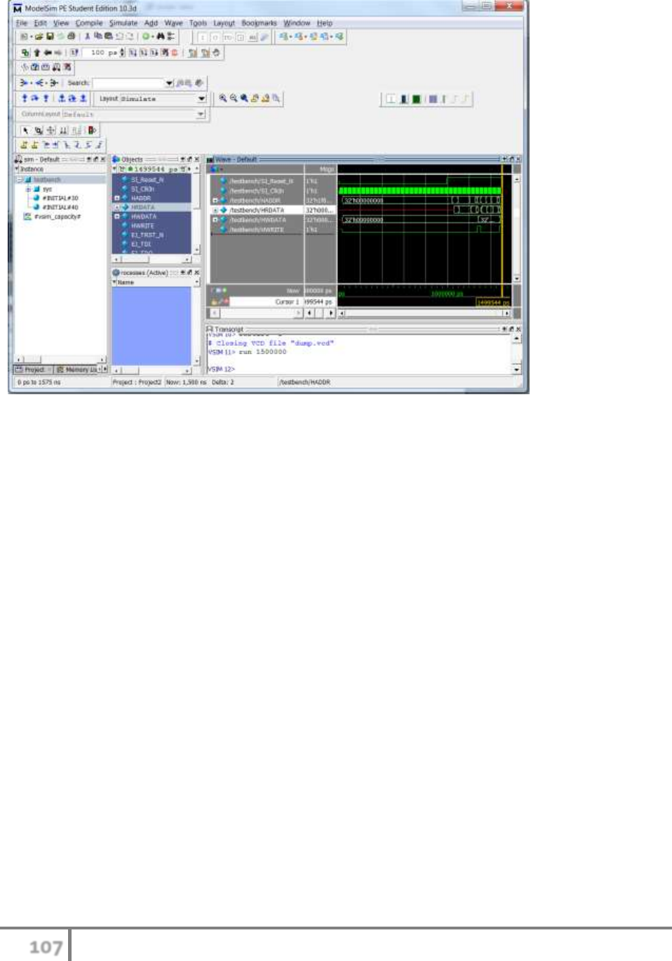
107
MIPSfpga Getting Started Guide © Imagination Technologies v1.1, July 22, 2015
Figure 161. Simulation waveform
Step 7. Repeat with modified program
You may now simulate a different program by simply copying the new ram_reset_init.txt file to
the ModelSim project folder. For example, let's simulate the simple I/O program
(Switches&LEDs) from Section 6.2. Copy
MIPSfpga\rtl_up\initfiles\3_Switches&LEDs\ram_reset_init.txt to your ModelSim project folder
(you will overwrite the memory initialization file already there).
Now, still in ModelSim, type 'restart –f' in the Transcript window, as shown in Figure 162. This
will restart the simulation, including reading the new memory initialization file into the memory
module.
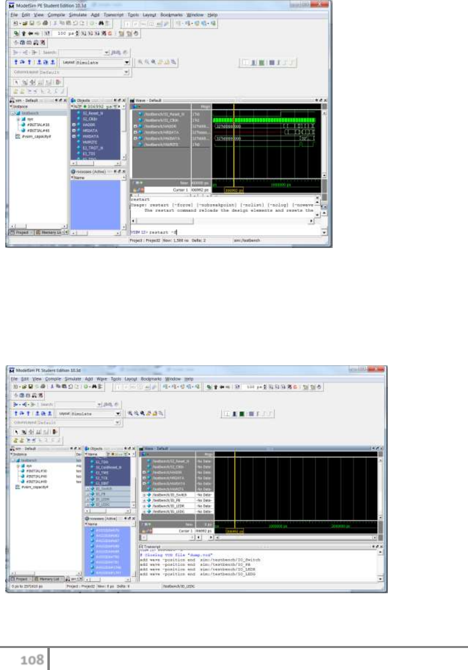
108
MIPSfpga Getting Started Guide © Imagination Technologies v1.1, July 22, 2015
Figure 162. Restarting the ModelSim simulation using 'restart –f'
You will now start the simulation with the new program loaded into the reset RAM. Recall that
the Switches&LEDs program reads the values of the switches and pushbuttons, and outputs those
values to the LEDs. So you will want to view the board inputs and outputs in simulation to see
that the program is operating correctly. In the Objects pane, scroll down until you see the I/O
signals: IO_Switch, IO_PB, IO_LEDR, and IO_LEDG. Select these signals, and drag them over
to the wave window, as shown in Figure 163.
Figure 163. Adding board IO signals: IO_Switch, IO_PB, IO_LEDR, and IO_LEDG
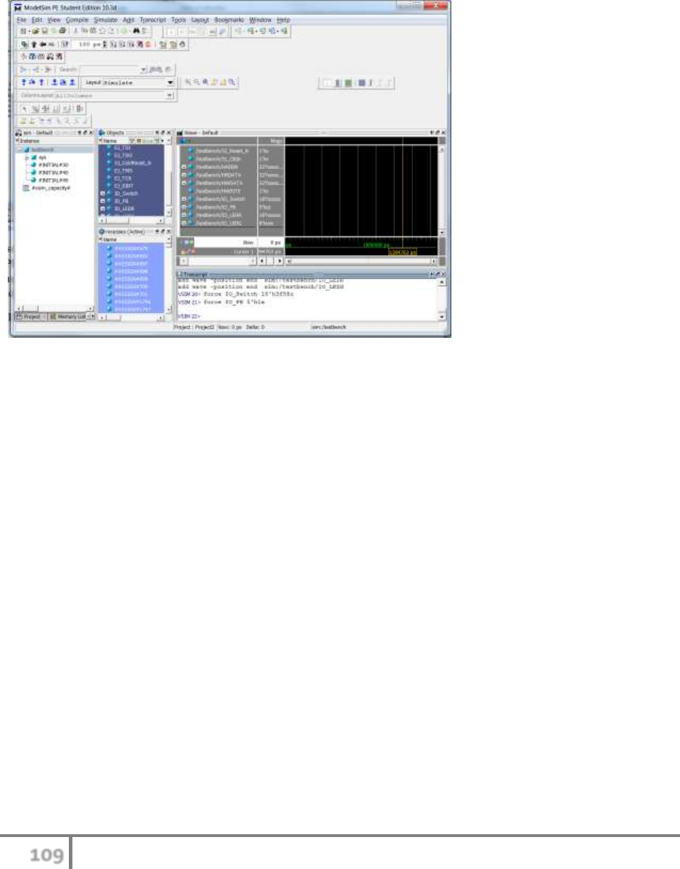
109
MIPSfpga Getting Started Guide © Imagination Technologies v1.1, July 22, 2015
Now set the input values: IO_Switch and IO_PB. Recall that IO_Switch is an 18-bit signal and
IO_PB is a 5-bit signal. In the Transcript pane, type 'force IO_Switch 18'h3f58c' and press
return. Then type 'force IO_PB 5'h1a' and press return (as shown in Figure 164). This sets the
values of the inputs (switches and the pushbuttons).
Figure 164. Applying input values in ModelSim
Now type: run 2000000 in the Transcript pane. This will run the simulation for 2,000,000 ps.
View the signals to see that the switch value (IO_Switch) is written to IO_LEDR and the
pushbutton values (IO_PB) are written to IO_LEDG, as shown in Figure 165. Specifically, after
the processor comes out of reset (i.e., SI_Reset_N goes high) and the program runs for several
instructions, IO_LEDR becomes 18'h3f58c and IO_LEDG becomes 5'h1a, the input values of the
switches and pushbuttons, respectively.
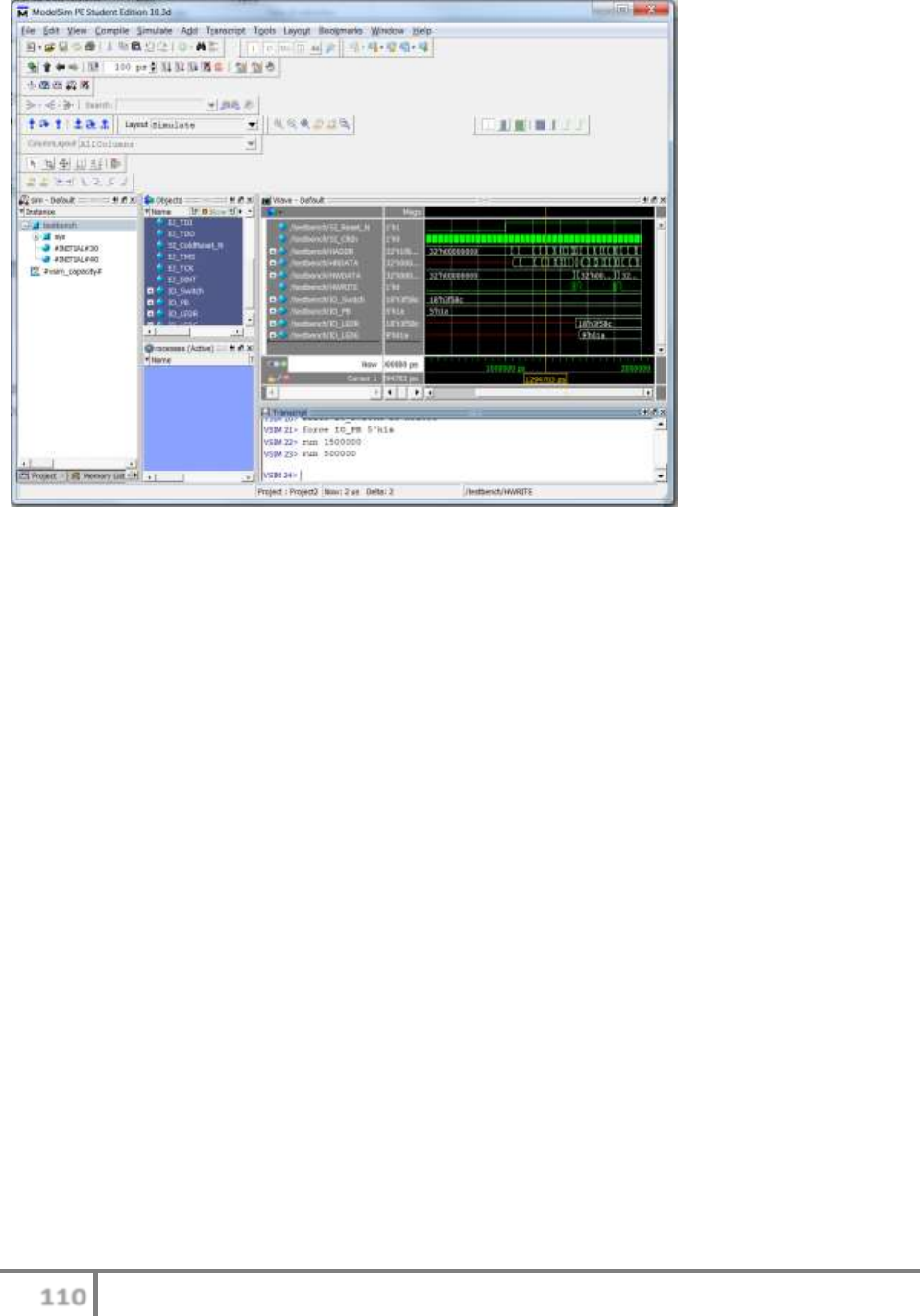
110
MIPSfpga Getting Started Guide © Imagination Technologies v1.1, July 22, 2015
Figure 165. Switches&LEDs program running in simulation on the MIPSfpga core
Change the values of the inputs (IO_Switch and IO_PB) using the force command and run the
processor again (run #) to see the LED values change.
Warning: ModelSim reads the RAM initialization file (ram_reset_init.txt) from the ModelSim
project directory; whereas, the FPGA design tools (Vivado and Quartus II) read the RAM
initialization file from MIPSfpga\rtl_up, the location of the memory module file
(ram_reset_dual_port.v).

111
MIPSfpga Getting Started Guide © Imagination Technologies v1.1, July 22, 2015
Appendix F. Using Vivado's Built-In Simulator (XSim)
This appendix shows how to use Xilinx's Vivado Simulator, XSim, to simulate the MIPSfpga
core running the IncrementLEDs program. Follow these steps (described in detail below):
Step 1. Open the mipsfpga_nexys4_ddr Vivado project
Step 2. Add the testbench and the program files
Step 3. Run the simulation and view the simulation output
Step 1. Open your mipsfpga_nexys4_ddr project
Start Vivado. Browse to MIPSfpga\Nexys4_DDR. If you haven't already, make a copy of the
Project1 folder. Name the new folder Project2. Open the Project2 folder and open the Vivado
project file, mipsfpga_nexys4_ddr.xpr.
Step 2. Add the testbench and the program file
Click on the Add Sources in the Flow Navigator window on the left, select Add or create
simulation sources option, and then click Next. Click on the Add Files… button, browse to the
testbench.v Verilog file in MIPSfpga\rtl_up\, select it, click OK, and then click Finish.
Again click on the Add Sources in the Flow Navigator window on the left, select Add or create
simulation sources option, and then click Next. Click on the Add Files… button, select All Files
as Files of type filter, browse to the ram_reset_init.txt file in MIPSfpga\rtl_up\initfiles\
1_IncrementLEDs, select it, and click OK. This time, check the Copy sources into project option
box, and then click Finish.
Expand the hierarchy under Simulation Sources and observe that ram_reset_init.txt is added in a
separate sub-folder called Text. Also notice that testbench.v is also listed, with mipsfpga_sys
listed as its lower-level module.
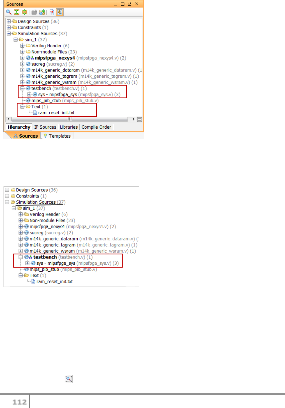
112
MIPSfpga Getting Started Guide © Imagination Technologies v1.1, July 22, 2015
Figure 166. Testbench and the program file added to the project in simulation group
Right-click on the testbench entry, and select Set As Top. Notice that the testbench entry is now
bold.
Figure 167. testbench as top-level module for simulation
Step 3. Run the simulation and view the simulation output
Click on the Simulation Settings in the Flow Navigator window on the left. The simulation
settings window will show up. Click on the Simulation tab and set the simulation run time to
2000 ns. Click OK.
Click on the Run Simulation > Run behavioral simulation in the Flow Navigator window. The
testbench and lower-level modules will compile, the simulation window will open, and the
simulation results will be displayed. You will see the top-level signals being displayed. Click on
the Zoom Fit button ( ).
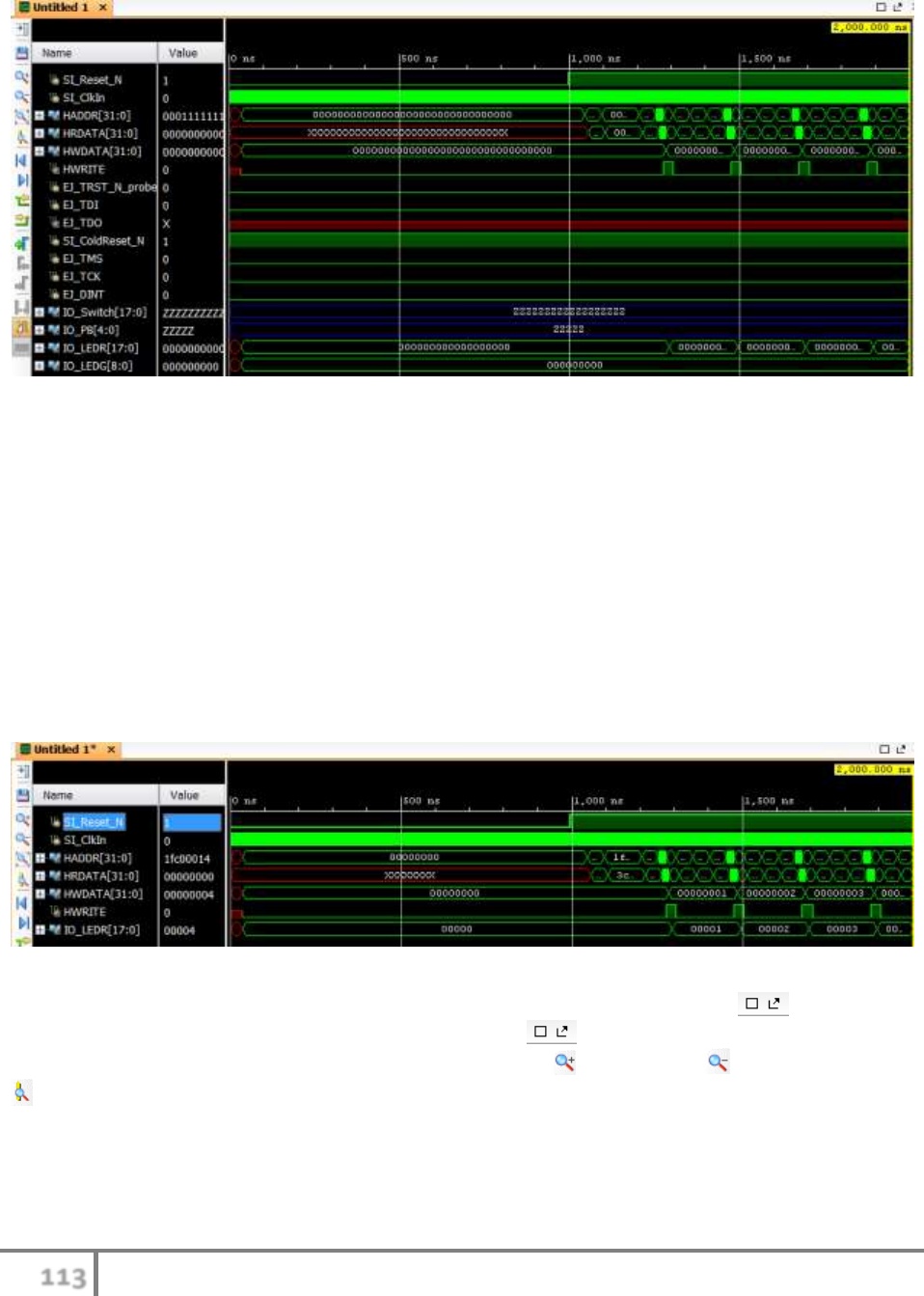
113
MIPSfpga Getting Started Guide © Imagination Technologies v1.1, July 22, 2015
Figure 168. Simulation results showing top-level signals
Right-click on HADDR, HRDATA, HWDATA, and IO_LEDR signals in the waveform window
and select Radix > Hexadecimal. You may also use shift-click and ctrl-click to select multiple
signals at a time.
Delete the EJ_TRST_N_probe, EJ_TDI, EJ_TDO, SI_ColdReset_N, EJ_TMS, EJ_TCK,
EDJ_DINT, IO_Switch, IO_PB, and IO_LEDG signals by right-clicking in the waveform
window and pressing Delete. Again, you can also select multiple signals using shift-click and
ctrl-click.
The waveform window will now look like as shown below.
Figure 169. Keeping only the desired top-level signals
You can float the waveform window by clicking on the float button (right one ) and then
maximize it by clicking on the full size button (left one ). Click on the Zoom Fit button to
see the waveform completely. You can also use Zoom In ( ), Zoom Out ( ), Zoom to Cursor (
) buttons to view desired section of the waveform.
You can view lower-level module signals by adding the corresponding signals to the waveform.
Expand the testbench hierarchy to testbench > sys > mipsfpga_ahb > mipsfpga_ahb_ram_reset
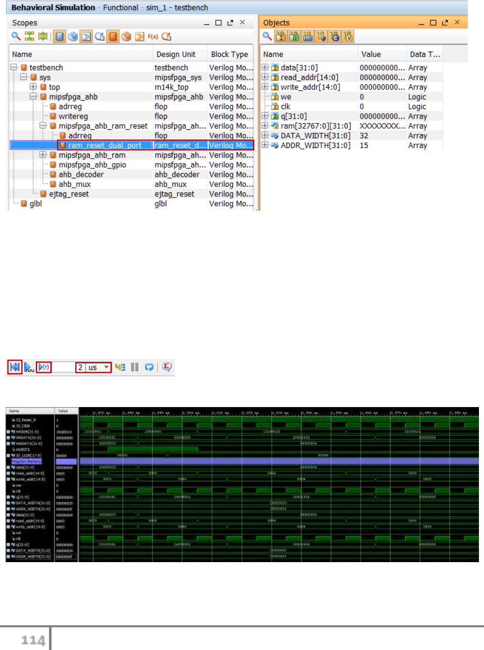
114
MIPSfpga Getting Started Guide © Imagination Technologies v1.1, July 22, 2015
to see ram_reset_dual_port entry in the Scopes window. Click on the ram_reset_dual_port entry
to see the corresponding signals in the Objects window.
Figure 170 Accessing the objects of the lower-level module
In the waveform window, right-click in the signals area below the last signal, and select New
Divider. The New Divider dialog box will appear. Type Program Memory in the field and click
OK.
Select all the objects in the Objects window, right-click and select Add to Wave Window and
observe that the signals are added to the Waveform window. You can change the radix of the
added signals to Hexadecimal as before. In the tool buttons bar, change the run time to 2 us, click
on the Reset button, and then click on the Run for <time> button (
) to reset and run the simulation for 2 us. You will see the
output as shown below.
Figure 171. Simulation result showing lower-level module signals

115
MIPSfpga Getting Started Guide © Imagination Technologies v1.1, July 22, 2015
After you are finished viewing the waveform, you can close the simulator by selecting File >
Close Simuation. A pop-up window will appear. Click OK. Another window will pop-up asking
if you want to save the waveform. You could select Yes and then save it. For now, click No.
Refer back to Section 4.1 for a description of the program running on the MIPSfpga core.
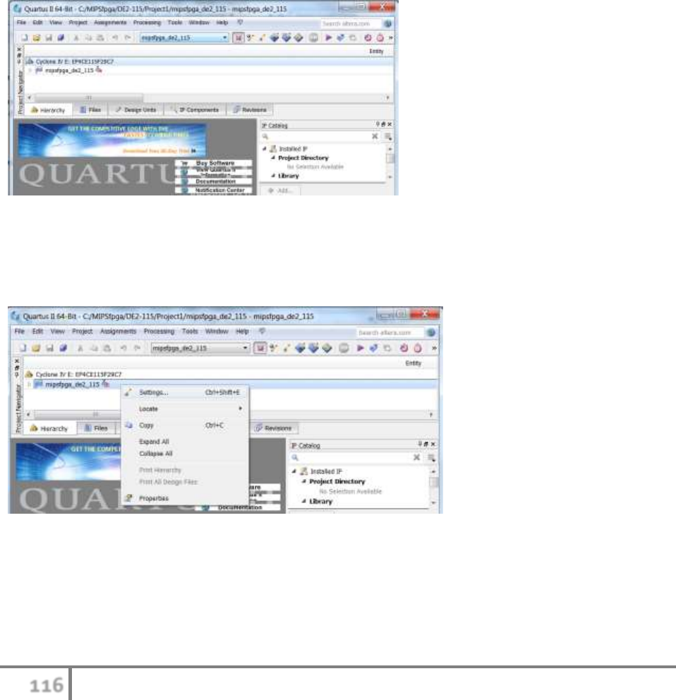
116
MIPSfpga Getting Started Guide © Imagination Technologies v1.1, July 22, 2015
Appendix G. Reducing Compile Time in Quartus II
This appendix describes how to minimize compile time of the MIPSfpga core when making code
changes only. Altera's Quartus II enables resynthesis of just the memory core by following these
steps, detailed below.
Step 1. Open the mipsfpga_de2_115 Quartus II project
Step 2. Enable smart compilation
Step 3. Use a .mif file for memory content initialization
Step 1. Open the mipsfpga_de2_115 Quartus II project
Browse to MIPSfpga\DE2-115\Project2 and open the Quartus II project file,
mipsfpga_de2_115.qpf. After opening the project, Quartus II will look as shown in Figure 172.
Figure 172. mipsfpga_de2_115 project
Step 2. Enable smart compilation
Now, in the Project Navigator window, right-click on the project and select Settings in the drop-
down menu, as shown in Figure 173.
Figure 173. Accessing Project Settings
In the Settings window, click on Compilation Process Settings and click on the Use smart
compilation box, as shown in Figure 174, and click OK.
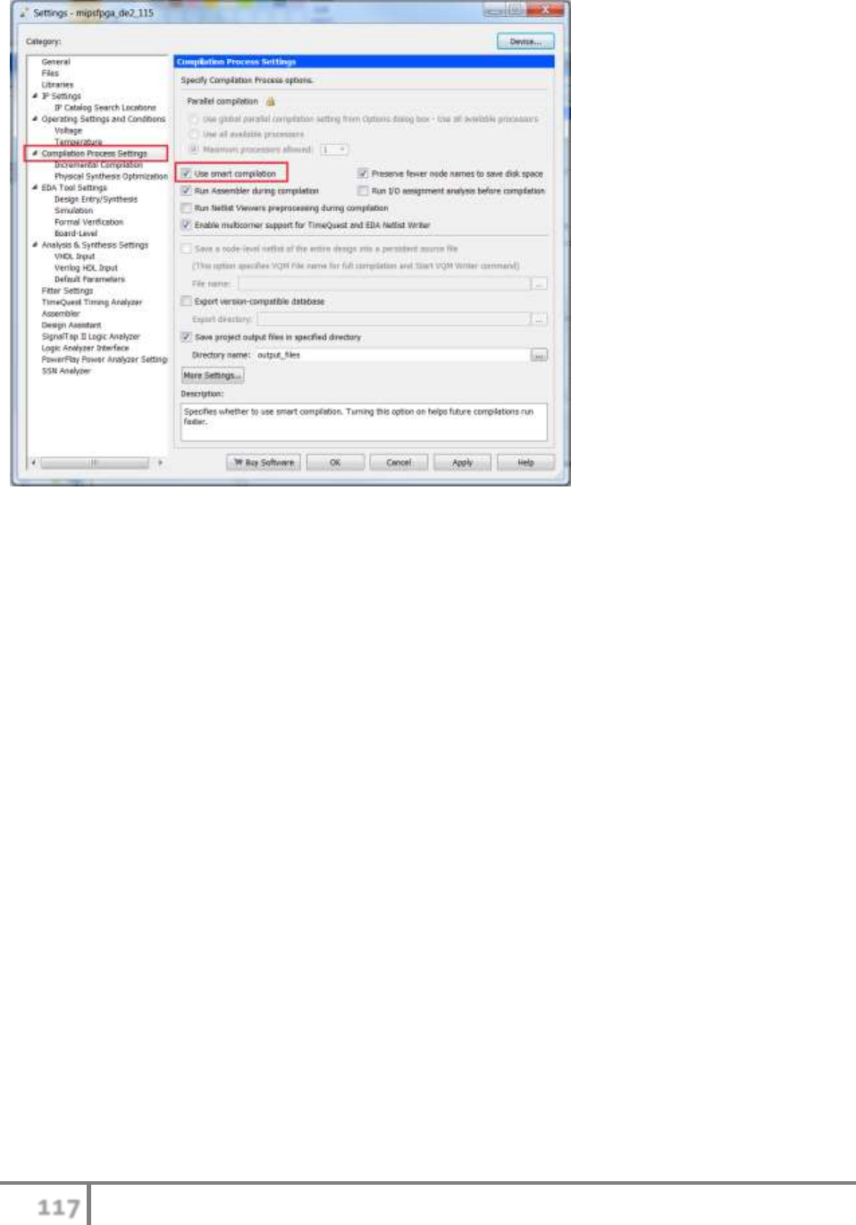
117
MIPSfpga Getting Started Guide © Imagination Technologies v1.1, July 22, 2015
Figure 174. Use smart compilation setting
Step 3. Use a .mif file for memory content initialization
Quartus II requires a .mif (memory initialization file) to recognize that only the memory must be
resynthesized. Figure 175 shows the memory initialization file equivalent to the
IncrementLEDsDelay program (see Figure 34).
WIDTH = 32;
DEPTH = 32768;
ADDRESS_RADIX = HEX;
DATA_RADIX = HEX;
CONTENT BEGIN
0 : 24090001;
1 : 3c08bf80;
2 : ad090000;
3 : 25290001;
4 : 3c050026;
5 : 34a525a0;
6 : 00003020;
7 : 00a63822;
8 : 20c60001;
9 : 1ce0fffd;
a : 00000000;
b : 1000fff6;
c : 00000000;
END;
Figure 175. Memory initialization file
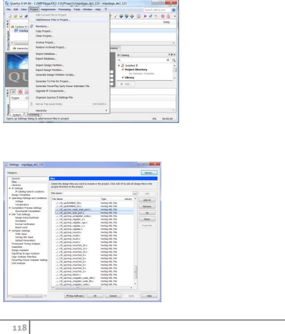
118
MIPSfpga Getting Started Guide © Imagination Technologies v1.1, July 22, 2015
Copy the program and reset ram .mif files from
MIPSfpga\DE2_115\QuickCompile\initfiles\2_IncrementLEDsDelay\ to the Quartus II project
directory (i.e., MIPSfpga\DE2_115\Project2).
In order to use the ram_reset_init.mif and ram_program_init.mif files (instead of
ram_reset_init.txt and ram_program_init.txt used in Section 6), we need to modify the Verilog
memory module. In the mipsfpga_de2_115 Quartus II project, select Project → Add/Remove
Files in Project, as shown in Figure 176.
Figure 176. Add/Remove Files in Project
Select ../../rtl_up/ram_reset_dual_port.v and ../../rtl_up/ram_reset_dual_port.v and click Remove,
as shown in Figure 177.
Figure 177. Removing existing reset RAM module from project
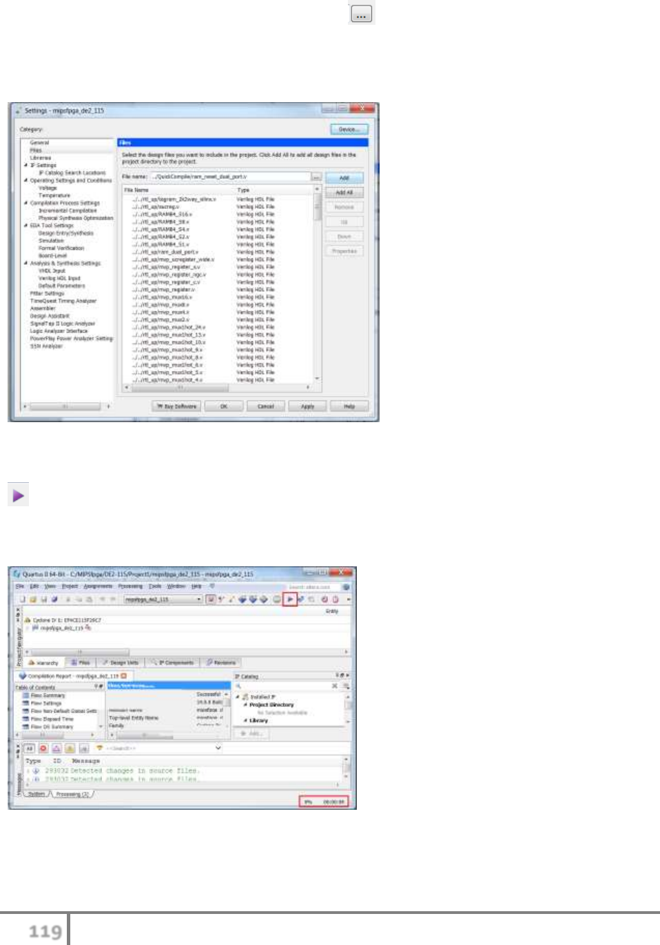
119
MIPSfpga Getting Started Guide © Imagination Technologies v1.1, July 22, 2015
Next click on the browse button next to File name ( ) to add a different memory module.
Browse to MIPSfpga\DE2-115\QuickCompile, then select ram_reset_dual_port.v and
ram_dual_port.v, and click Open.
Next click on OK in the Quartus II Settings window (Figure 178).
Figure 178. Add new ram_reset_dual_port module to Quartus II project
Now compile the project with these new RAM files by clicking on the Start Compilation button
in the main Quartus II window (Figure 179). You can view the compilation progress in the
bottom right of the Quartus II window. Depending on your computer's speed, compilation takes
about 5-25 minutes or more.
Figure 179. Compile Quartus II project

120
MIPSfpga Getting Started Guide © Imagination Technologies v1.1, July 22, 2015
At the end of compilation, you can program the DE2-115 board as described in Section 6.4.2,
and summarized here for your convenience:
1. Turn on your DE2-115 FPGA board and make sure the USB-Blaster (DE2-115
programming cable) is connected to the board and your computer.
2. In the main Quartus II window, select Tools → Programmer from the file menu
3. In the Programmer window that opens, click on Add File…
4. Browse to MIPSfpga\DE2-115\Project1\output_files, then double-click on
mipsfpga_de2_115.sof.
5. In the Programmer window, click Start.
6. To run the program, press the lower right pushbutton on the DE2-115 board (KEY0).
Upon future changes to the program memory only (ram_reset_init.mif), compilations will take
seconds instead of minutes because it will recompile the ram_reset_dual_port module only, not
the entire MIPSfpga processor.
View one of the new RAM modules if desired, for example, ram_reset_dual_port (located in
MIPSfpga\DE2-115\QuickCompile\ram_reset_dual_port.v). This memory module initializes its
memory contents by declaring the memory array using this code construct:
(* ram_init_file = "ram_reset_init.mif" *)reg [DATA_WIDTH-1:0]
ram[2**ADDR_WIDTH-1:0];
Important note: In contrast to the memory initialization method described in Section 6.4.2,
Quartus II will now look for the memory initialization file in the Quartus II project directory,
i.e., MIPSfpga\DE2-115\Project2 (instead of in the same directory as the Verilog memory
module file, ram_reset_dual_port.v).
As an example of how fast compilation is when only changing the program stored in the reset
RAM (the RAM located at virtual address 0xbfc00000), change the program in the
ram_reset_init.mif file (see Figure 175) located in
MIPSfpga\DE2_115\Project2\ram_reset_init.mif so that the first instruction is: 0 :
240900FF; (instead of 0 : 24090001;). The .mif file is a text file, so it can be edited using
any text editor.
This will change the IncrementLEDsDelay program so that the LEDs display 0xFF at processor
reset and increment from there. Specifically, it changes the program's first instruction from:
addiu $9, $0, 1 to: addiu $9, $0, 0xFF (see Figure 34).
Now click on the Start Compilation button. . This time, compilation takes about 10-60
seconds (vs 5-20 minutes for compiling the entire project). Program the DE2-115 board to see
that the program stored in memory was changed. The red LEDs should now display 0xFF at the
beginning of the program, just after reset, then increment from there.

121
MIPSfpga Getting Started Guide © Imagination Technologies v1.1, July 22, 2015
The MIPSfpga\DE2-115\QuickCompile\initfiles folder contains .mif versions of the
IncrementLEDsDelay and Switches&LEDs programs (see Sections 6.1 and 6.2) as examples.
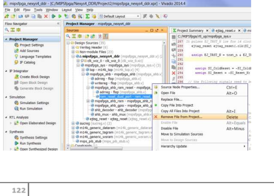
122
MIPSfpga Getting Started Guide © Imagination Technologies v1.1, July 22, 2015
Appendix H. Reducing Compile Time in Vivado
This appendix describes how to minimize Vivado compile time of a design when only code
changes are made. Vivado allows the creation of a design checkpoint (dcp). This design
checkpoint is then used to resynthesize the model out-of-context when a design change is made –
in this case, when the program the processor runs changes.
Follow these steps, described in detail below.
Step 1. Open the mipsfpga_nexys4_ddr Vivado project
Step 2. Set up for out-of-context synthesis and generate the design checkpoints
Step 3. Use the provided Tcl files to synthesize the ram_reset_dual_port.v model,
implement the entire design, and generate the bitstream
Step 1. Open the mipsfpga_nexys4_ddr project
Start Vivado. Click on the Open Project link. Browse to MIPSfpga\Nexys4_DDR\Project2 and
open the Vivado project file, mipsfpga_nexys4_ddr.xpr. (If you have not already copied
MIPSfpga\Nexys4_DDR\Project1 to MIPSfpga\Nexys4_DDR\Project2, do so now.)
Step 2. Set up for out-of-context synthesis and generate the design checkpoints
In the sources window, right-click on the ram_reset_dual_port.v and select Remove file from the
project… to remove the file from the project.
Figure 180. Removing the file that will be compiled separately

123
MIPSfpga Getting Started Guide © Imagination Technologies v1.1, July 22, 2015
Click OK to delete the file.
Click on Add Sources in the Flow Navigator window on the left, select Add or create design
sources option, and then click Next. Click on the Add Files… button, browse to the provided
ram_reset_dual_port_bb.v in MIPSfpga\Nexys4_DDR\QuickCompile, select it, click OK, and
then click Finish.
Click Run Synthesis to synthesize the modified project. When synthesis is complete (which will
take about 5-15 minutes), click Cancel when the dialog box below appears.
Figure 181. Synthesis process completed
Note that you do the above step only once. However, each time you change program memory,
you will need to perform the following steps.
Copy your desired program (ram_reset_init.txt file) to the MIPSfpga\Nexys4_DDR\Project2
directory. Example files are in the MIPSfpga\rtl_up\initfiles subdirectories. For example, you
could copy MIPSfpga\rtl_up\initfiles\2_IncrementLEDsDelay\ram_reset_init.txt to the
MIPSfpga\Nexys4_DDR\Project2 directory.
Step 3. Use the provided Tcl files to synthesize the ram_reset_dual_port.v module, and to
implement and generate the bitstream of the entire design using the design checkpoint
generated in Step 2
Click on the Tcl Console tab of Vivado and change to the Nexys4_DDR\Project2 directory by
using the cd command. For example:
cd C:/MIPSfpga/Nexys4_DDR/Project2
Execute the Tcl file by typing the following command:
source ../QuickCompile/synth_ram_reset_dual_port_module.tcl
This will take several minutes to complete. The Tcl file content is shown below.
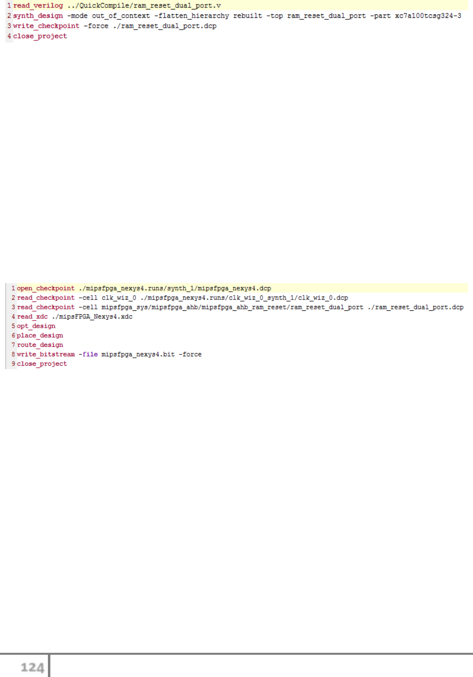
124
MIPSfpga Getting Started Guide © Imagination Technologies v1.1, July 22, 2015
Figure 182. Memory module synthesis Tcl file content
Line 1: Reads the provided ram_reset_dual_port.v file. It defines the correct data width (32) and
address width (15). It also adds block ram synthesis attribute to the ram definition
Line 2: Synthesizes the model for the given target part
Line 3: Writes the design checkpoint
Line 4: Closes the project
Now, again in the Tcl console, make sure that the directory is still
MIPSfpga\Nexys4_DDR\Project2 (otherwise change to it using the cd command). Now type the
following command in the Tcl console window:
source ../QuickCompile/generate_bitstream.tcl
This Tcl script implements the MIPSfpga core and generates the bitstream. The Tcl file content
is shown below.
Figure 183. Bitstream generation Tcl file
Line 1: Reads the design checkpoint of the entire design with the program memory treated as a
black box.
Lines 2-3: Read the design checkpoints of the clock and block ram (bram) modules
Line 4: Reads the design constraints (I/O locations, clocks etc)
Lines 5-7: Perform the implementation
Line 8: Generates the bitstream in the Nexys4_DDR/Project2 directory
Line 9: Closes the project
This will take a few minutes. When it is finished, the bitfile (mipsfpga_nexys4_ddr.bit) will be
generated in the MIPSfpga\Nexys4_DDR\Project2 directory. Use this bitfile to program the
FPGA.

125
MIPSfpga Getting Started Guide © Imagination Technologies v1.1, July 22, 2015
Appendix I. Porting MIPSfpga to Other FPGA Boards
To run MIPSfpga on other FPGA boards, the following steps need to be taken, described in
detail below:
Step 1. Write a Verilog wrapper file for the FPGA board
Step 2. Modify MIPSfpga memory sizes (if needed)
Step 3. Create a constraints file
Step 1. Write a Verilog wrapper file for the FPGA board
The Verilog wrapper file interfaces the MIPSfpga core to the FPGA board. For example,
mipsfpga_de2_115.v (in the MIPSfpga\rtl_up directory) is the wrapper file for the DE2-115
board, and mipsfpga_nexys4_ddr.v (also in MIPSfpga\rtl_up) is the wrapper file for the Nexys4
DDR board. These files interface the MIPSfpga core with the specific FPGA board by using
board-specific names for the I/O. For example, the mipsfpga_de2_115 module (see
MIPSfpga\rtl_up\mipsfpga_de2_115.v) has the following interface:
module mipsfpga_de2_115(input CLOCK_50,
input [17:0] SW,
input [ 3:0] KEY,
output [17:0] LEDR,
output [ 8:0] LEDG,
inout [ 6:0] EXT_IO);
The interface connects to the on-board 50 MHz clock (CLOCK_50), the switches (SW), the
pushbuttons (KEY), the red and green LEDs (LEDR and LEDG) and the EJTAG port (EXT_IO).
The wrapper file (mipsfpga_de2_115.v) then instantiates the MIPSfpga core (mipsfpga_sys) as
follows, connecting the FPGA board I/O to the appropriate I/O of the MIPSfpga system.
mipsfpga_sys mipsfpga_sys(
.SI_Reset_N(KEY[0]),
.SI_ClkIn(CLOCK_50),
.HADDR(),
.HRDATA(),
.HWDATA(),
.HWRITE(),
.EJ_TRST_N_probe(EXT_IO[6]),
.EJ_TDI(EXT_IO[5]),
.EJ_TDO(EXT_IO[4]),
.EJ_TMS(EXT_IO[3]),
.EJ_TCK(EXT_IO[2]),
.SI_ColdReset_N(EXT_IO[1]),
.EJ_DINT(EXT_IO[0]),
.IO_Switch(SW),
.IO_PB({1'b0, ~KEY}),
.IO_LEDR(LEDR),
.IO_LEDG(LEDG));

126
MIPSfpga Getting Started Guide © Imagination Technologies v1.1, July 22, 2015
In the mipsfpga_de2_115.v wrapper file, the input clock frequency is reduced, so the
mipsfpga_sys module receives the output of the PLL (clk_out) instead of the 50 MHz clock
(CLOCK_50).
We provide wrapper modules for Digilent's Basys3 and Nexys4 boards in the MIPSfpga\Basys3
and MIPSfpga\Nexys4 folders. See the mipsfpga_basys3.v and mipsfpga_nexys4.v files.
Step 2. Modify MIPSfpga memory sizes (if needed)
Some FPGA boards do not have enough memory (block RAM) to accommodate the 128 KB +
256 KB of memory currently declared. The following two lines in the mipsfpga_ahb_const.vh
file (located in MIPSfpga\rtl_up) need to be modified to change the memory sizes:
`define H_RAM_RESET_ADDR_WIDTH (15)
`define H_RAM_ADDR_WIDTH (16)
Currently the memory sizes are 215 words = 217 bytes = 128 KB of reset (boot) RAM and 216
words = 218 bytes = 256 KB of program RAM.
For example, the Basys3 board only has 225 KB of block RAM, so we would need to reduce the
sizes of the reset and program RAMs. mipsfpga_ahb_const.vh in the MIPSfpga\Basys3 folder
shows that
Step 3. Create a constraints file
According to the new FPGA board specifications, write (or modify) the constraints file to map
the wrapper module's signal names to FPGA pins and specify timing constraints.
For example, the constraints files for the DE2-115 board are in the MIPSfpga\DE2_115\Project1
folder:
DE2_115.qsf // mapping the wrapper's signal names to FPGA pins
mipsfpga_de2_115.sdc // timing constraints
The constraints file for the Nexys4 DDR board is in the MIPSfpga\Nexys4_DDR\Project1
folder:
mipsfpga_nexys4_ddr.xdc // mapping the signal names to the FPGA board
// includes timing constraints
In the Quartus II or Vivado project, you will then need to choose the correct FPGA as the target
device. For example, for the Nexys4 DDR or Nexys4 FPGA board, the target FPGA is the
xc7a100tcsg324c-3. The Basys3 FPGA is the xc7a35tcpg236c-3.
After completing these three steps above, download the MIPSfpga core onto the new FPGA
board by doing the following:
1. Build a project (in Vivado, Quartus II, etc.)
2. Add all of the Verilog files from MIPSfpga\rtl_up.
3. Instead of mipsfpga_de2_115.v or mipsfpga_nexys4_ddr.v, use the wrapper file
created in Step 1.

127
MIPSfpga Getting Started Guide © Imagination Technologies v1.1, July 22, 2015
4. Use the modified version of mipsfpga_ahb_const.vh (if needed)
5. Add the board-specific constraints file
6. Add a PLL (or create one within the project) as needed to produce the desired clock
frequency.
7. Target the FPGA that is on the target board.
8. Compile and synthesize the project and download it onto the FPGA board.
For detailed instructions on porting the MIPSfpga system to other FPGA boards, see the
MIPSfpga Fundamentals Materials (Lab 9), which is available as part of the MIPSfgpa
Fundamentals Laboratories package, available for download here (under the Teaching Materials
heading):
http://community.imgtec.com/university/resources/
EJTAG Interface
While most of the MIPSfpga I/O is relatively straight-forward to interface with the FPGA board
I/O (switches, pushbuttons and LEDs), the EJTAG interface is more tricky. For example, you
will need wires to connect the Bus Blaster to header pins on the new FPGA board. The
EJ_TRST_N_probe and SI_ColdReset_N signals need to have pull-up resistors. Some FPGA
pins have configurable internal pull-up or pull-down resistors (see
MIPSfpga\Nexys4_DDR\Project1\mipsfpga_nexys4_ddr.xdc for an example – search for JB[4]
or JB[5]). See Appendix J for details about how the Bus Blaster connects to the MIPSfpga core
via the EJTAG interface.
128
MIPSfpga Getting Started Guide © Imagination Technologies v1.1, July 22, 2015
Appendix J. Bus Blaster Interface
Below is some additional hardware information on the Bus Blaster probe and its interfaces with
the DE2-115 and Nexys4 DDR FPGA boards. Figure 184 shows the Quartus II EJTAG header
pins. On the board the pins are connected to pull-up/pull-down resistors, power and ground, as
shown. The diagram (courtesy of Altera) should say "EXT_IO" instead of "EX_IO".
Figure 184. DE2-115 EJTAG interface (JP4), © Altera, from the DE2-115 User's Manual
Figure 185 shows the PMOD connector for the Nexys4 DDR board. The EJTAG interface uses
PMODB, as shown in Figure 14. Pins 9 and 10 of PMODB are unused in the EJTAG interface.
The other pins are used as listed in Table 9.
Figure 185. Nexys4 DDR PMOD connector, © Digilent, from the Nexys4 DDR User's
Manual
Table 9 lists EJTAG signals and their corresponding connections on the MIPSfpga core and the
FPGA boards.

129
MIPSfpga Getting Started Guide © Imagination Technologies v1.1, July 22, 2015
Table 9. EJTAG signal names: Bus Blaster, MIPSfpga, DE2-115, and Nexys4
Bus Blaster
MIPSfpga
DE2-115
Nexys4 DDR
TRST*
EJ_TRST_N_probe
EXT_IO[6]
JB[7] (internal pull-up)
TDI
EJ_TDI
EXT_IO[5]
JB[2]
TDO
EJ_TDO
EXT_IO[4]
JB[3]
TMS
EJ_TMS
EXT_IO[3]
JB[1]
TCK
EJ_TCK
EXT_IO[2]
JB[4]
RST*
SI_ColdReset_N
EXT_IO[1]
JB[8] (internal pull-up)
DINT
EJ_DINT
EXT_IO[0]
GND
VIO
3.3V
pin 14
PMOD B pins 6 & 12
GND
GND
pins 2,4,6,8,10,12
PMOD B pins 5 & 11
Nexys4 DDR Bus Blaster Adapter Board
The Bus Blaster probe you buy from SEEED studios should come with a small adapter board to
enable connecting the Bus Blaster probe to the Nexys4 DDR FPGA board. (The Bus Blaster
probe can plug directly into the DE2-115 FPGA board.) If you need to manufacture your own
adapter boards, the Gerber files are available in: C:\Program Files\Imagination
Technologies\OpenOCD\Digilent Adapter Gerbers Files.

130
MIPSfpga Getting Started Guide © Imagination Technologies v1.1, July 22, 2015
About the Authors
David Money Harris is the Harvey S. Mudd Professor of Engineering Design at Harvey Mudd College. He
received his S.B. and M.Eng. degrees from MIT and his Ph.D. from Stanford University. He has designed
chips at Intel, Hewlett Packard, Sun Microsystems, and Broadcom. David is the author of several
textbooks including Digital Design and Computer Architecture, CMOS VLSI Design, Logical Effort, and
Skew-Tolerant Circuit Design. When he is not teaching or designing chips, he can often be found
exploring the mountains and deserts of Southern California with his three sons.
Sarah L. Harris is an Associate Professor at the University of Nevada, Las Vegas. She received her B.S. at
B.Y.U. and her M.S. and Ph.D. from Stanford University. She has worked at Hewlett Packard, NVidia, and
various other places. Sarah is a co-author of the textbook Digital Design and Computer Architecture.

131
MIPSfpga Getting Started Guide © Imagination Technologies v1.1, July 22, 2015
MIPSfpga Support
MIPSfpga Technical Support: For MIPSfpga technical support, go to the MIPSfpga subforum
of the MIPS Insider Forum at:
http://community.imgtec.com/forums/cat/mips-insider/mipsfpga
General MIPS Technical Support: For general MIPS technical support, you can also go to the
general MIPS Insider Forum at:
http://community.imgtec.com/forums/cat/mips-insider/
IUP Support: For support and discussions about the Imagination University Programme (IUP),
for example, curriculum discussions, questions about the IUP, etc. go to:
http://community.imgtec.com/forums/cat/university/
Teaching Materials: MIPSfpga (and other) teaching materials are available for download from
the Resources page of the Imagination University Programme website under the Teaching
Materials heading:
http://community.imgtec.com/university/resources/

132
MIPSfpga Getting Started Guide © Imagination Technologies v1.1, July 22, 2015
MIPSfpga License Agreement
Thanks for your interest in MIPSfpga™. If you’re reading this, it means that you already know what
MIPSfpga is and that you want it. The next steps are that you read and accept these terms of use, you
tell us a bit about your plans for using MIPSfpga, and then you request approval for the MIPSfpga
download. So next we need you to read and confirm your agreement to a few terms set out below -
we’ll try to keep it brief!
The reason for making MIPSfpga available to the academic world is to provide teachers and students
with a hands-on way of studying and understanding the MIPS® architecture. We want the engineers of
the future to become familiar with the MIPS instruction set architecture, so that they can experience
first-hand the benefits of working with a MIPS CPU.
We therefore encourage you to:
•
use MIPSfpga for teaching purposes, to study the MIPS architecture;
•
incorporate MIPSfpga into an FPGA chip in order to actually see the MIPS instruction set at
work;
•
explore the MIPSfpga architecture, design, and inner workings;
•
circulate copies of the MIPSfpga teaching materials to your students – provided you make
them aware of these Terms of Use;
•
host MIPSfpga core(s) on a secure location that is accessible only to students taking this
course;
•
be generous and visible! - write and publish papers, reports and articles based on your
experiments and experiences with MIPSfpga;
•
Share your expertise to make it easier for others to use MIPSfpga.
MIPSfpga is an academic teaching resource only – it’s not a commercially available processor, which is
why we’re not charging you anything to access it. To that end, we obviously can’t permit you to
distribute MIPSfpga or make chips for commercial purposes. Furthermore, MIPSfpga is a “soft core”
only. We are not giving permission to put it into silicon. However, if this is something that you would
like to explore, please get in touch with us to discuss your needs and we can see if there is an
alternative way in which we can help you achieve this.
As we’re sure you’ll appreciate, the opportunity to work with MIPSfpga is not something that is
given to everybody, so please ensure that the MIPSfpga materials are only circulated to students
that are registered on your course. If other individuals, universities or organisations contact you
because they’re interested in accessing MIPSfpga, please refer them directly to the Imagination
University Programme (IUP) website (see http://www.imgtec.com/university) so they can request the
materials in the same way that you have done.
While we do not require that you transfer ownership of any intellectual property arising from your use
of MIPSfpga, it is a condition that you promise not to take any action to assert or enforce those
intellectual property rights against us or our customers (or our customers’ customers, and so on!).

133
MIPSfpga Getting Started Guide © Imagination Technologies v1.1, July 22, 2015
MIPSfpga has been developed as an educational tool and hasn’t been designed with any particular
application in mind. We therefore can’t give any warranties or assurances that it will come without any
faults, will be fit for a particular purpose, that it won’t infringe any third party rights, or promises of any
other nature. Essentially, MIPSfpga will be delivered ‘as is’, but if you discover any issues that affect the
way that MIPSfpga performs, please do let us know. The nature of this project also means that we can’t
be liable to you or any user of MIPSfpga for any losses attributable to any use of the MIPSfpga;
however, this limitation obviously doesn’t apply to those losses that the law says cannot be excluded.
At the end of the course or project, you will need to provide us with a brief report (for our
unrestricted use), setting out what you’ve done with MIPSfpga, including if any, the modifications
that you made, and you can publish it on the IUP Forum
(http://forum.imgtec.com/categories/university ).
You will also need to let us know about any intellectual property you’ve developed and/or applied to
register as a result of your use of the MIPSfpga. If you or your students are going to publish papers or
articles, you’ll also need to send us a copy – we’re very interested to hear what you’ve got to say!
Any publications should make reference to the fact that the MIPSfpga is the proprietary technology of
Imagination Technologies Limited, that MIPSfpga™ is a trademark of Imagination Technologies
Limited and that these have been used by you under licence from Imagination. In case you’d also
like to incorporate some of our other brands, please contact us for our prior approval.
By choosing to download MIPSfpga, you are confirming your agreement to comply with the various
terms and conditions set out above. If you want to use MIPSfpga for anything not expressly
permitted in these terms of use, please contact us to discuss it further. To help us enable
participants to get the most out of the MIPSfpga project, we’re dependent on those participants
working with us and sticking to these terms of use. In the unlikely event that we discover that your
use of MIPSfpga does not comply with these terms, we reserve the right to withdraw our permission
for you to use MIPSfpga (in which case you will have to stop using and return all MIPSfpga materials
immediately), in addition to any other legal rights we may have. If there is a dispute arising out of
these terms or your use of MIPSfpga, then English law will apply and all disputes will need to be
resolved in the English courts.
So, there you have it! We promised we’d be brief and the good news is that these are the only terms–
this is the entire agreement. Hopefully it’s clear to you what you can and cannot do with MIPSfpga, and
we hope you and your students enjoy working with MIPSfpga. Obviously, if you do not agree to any of
the above, you may not use MIPSfpga and you’ll have to stop at this point. If you have any queries,
please get in touch via the Forum on the IUP website.
Version 1 / March 2015
