MSP430 DriverLib For MSP430F5xx_6xx Devices MSP430F5xx 6xx Driver Lib Users Guide 2 91 10 06
User Manual:
Open the PDF directly: View PDF ![]() .
.
Page Count: 631 [warning: Documents this large are best viewed by clicking the View PDF Link!]
- Copyright
- Revision Information
- 1 Introduction
- 2 Navigating to driverlib through CCS Resource Explorer
- 3 How to create a new CCS project that uses Driverlib
- 4 How to include driverlib into your existing CCS project
- 5 How to create a new IAR project that uses Driverlib
- 6 How to include driverlib into your existing IAR project
- 7 10-Bit Analog-to-Digital Converter (ADC10_A)
- 8 12-Bit Analog-to-Digital Converter (ADC12_A)
- 9 Advanced Encryption Standard (AES)
- 10 Battery Backup System
- 11 Comparator (COMP_B)
- 12 Cyclical Redundancy Check (CRC)
- 13 16-Bit Sigma Delta Converter (CTSD16)
- 14 12-bit Digital-to-Analog Converter (DAC12_A)
- 15 Direct Memory Access (DMA)
- 16 EUSCI Universal Asynchronous Receiver/Transmitter (EUSCI_A_UART)
- 17 EUSCI Synchronous Peripheral Interface (EUSCI_A_SPI)
- 18 EUSCI Synchronous Peripheral Interface (EUSCI_B_SPI)
- 19 EUSCI Inter-Integrated Circuit (EUSCI_B_I2C)
- 20 FlashCtl - Flash Memory Controller
- 21 GPIO
- 22 LCDB Controller
- 23 LDO-PWR
- 24 32-Bit Hardware Multiplier (MPY32)
- 25 Operational Amplifier (OA)
- 26 Port Mapping Controller
- 27 Power Management Module (PMM)
- 28 RAM Controller
- 29 Internal Reference (REF)
- 30 Real-Time Clock (RTC_A)
- 31 Real-Time Clock (RTC_B)
- 32 Real-Time Clock (RTC_C)
- 33 24-Bit Sigma Delta Converter (SD24_B)
- 34 SFR Module
- 35 System Control Module
- 36 Timer Event Control (TEC)
- 37 16-Bit Timer_A (TIMER_A)
- 38 16-Bit Timer_B (TIMER_B)
- 39 TIMER_D
- 40 Tag Length Value
- 41 Unified Clock System (UCS)
- 42 USCI Universal Asynchronous Receiver/Transmitter (USCI_A_UART)
- 43 USCI Synchronous Peripheral Interface (USCI_A_SPI)
- 44 USCI Synchronous Peripheral Interface (USCI_B_SPI)
- 45 USCI Inter-Integrated Circuit (USCI_B_I2C)
- 46 WatchDog Timer (WDT_A)
- 47 Data Structure Documentation
- 47.1 Data Structures
- 47.2 Timer_D_initCompareModeParam Struct Reference
- 47.3 Timer_B_initContinuousModeParam Struct Reference
- 47.4 Timer_D_outputPWMParam Struct Reference
- 47.5 SD24_B_initParam Struct Reference
- 47.6 USCI_B_SPI_changeMasterClockParam Struct Reference
- 47.7 Timer_A_initUpModeParam Struct Reference
- 47.8 USCI_B_I2C_initMasterParam Struct Reference
- 47.9 EUSCI_B_SPI_initSlaveParam Struct Reference
- 47.10 Timer_A_initCompareModeParam Struct Reference
- 47.11 EUSCI_B_SPI_changeMasterClockParam Struct Reference
- 47.12 Timer_B_initUpDownModeParam Struct Reference
- 47.13 Timer_D_initUpModeParam Struct Reference
- 47.14 Timer_A_initContinuousModeParam Struct Reference
- 47.15 EUSCI_B_I2C_initSlaveParam Struct Reference
- 47.16 Comp_B_configureReferenceVoltageParam Struct Reference
- 47.17 Timer_A_initCaptureModeParam Struct Reference
- 47.18 USCI_A_UART_initParam Struct Reference
- 47.19 RTC_C_configureCalendarAlarmParam Struct Reference
- 47.20 USCI_A_SPI_initMasterParam Struct Reference
- 47.21 USCI_B_SPI_initMasterParam Struct Reference
- 47.22 TEC_initExternalFaultInputParam Struct Reference
- 47.23 USCI_A_SPI_changeMasterClockParam Struct Reference
- 47.24 SD24_B_initConverterParam Struct Reference
- 47.25 EUSCI_A_UART_initParam Struct Reference
- 47.26 Timer_B_outputPWMParam Struct Reference
- 47.27 EUSCI_B_I2C_initMasterParam Struct Reference
- 47.28 EUSCI_A_SPI_changeMasterClockParam Struct Reference
- 47.29 Timer_B_initUpModeParam Struct Reference
- 47.30 Timer_B_initCompareModeParam Struct Reference
- 47.31 EUSCI_A_SPI_initMasterParam Struct Reference
- 47.32 DAC12_A_initParam Struct Reference
- 47.33 Timer_D_initCaptureModeParam Struct Reference
- 47.34 Timer_B_initCaptureModeParam Struct Reference
- 47.35 EUSCI_B_SPI_initMasterParam Struct Reference
- 47.36 SD24_B_initConverterAdvancedParam Struct Reference
- 47.37 Timer_D_combineTDCCRToOutputPWMParam Struct Reference
- 47.38 Timer_D_initContinuousModeParam Struct Reference
- 47.39 DMA_initParam Struct Reference
- 47.40 ADC12_A_configureMemoryParam Struct Reference
- 47.41 Timer_D_initHighResGeneratorInRegulatedModeParam Struct Reference
- 47.42 Calendar Struct Reference
- 47.43 Timer_A_initUpDownModeParam Struct Reference
- 47.44 Comp_B_initParam Struct Reference
- 47.45 RTC_A_configureCalendarAlarmParam Struct Reference
- 47.46 EUSCI_A_SPI_initSlaveParam Struct Reference
- 47.47 Timer_D_initUpDownModeParam Struct Reference
- 47.48 PMAP_initPortsParam Struct Reference
- 47.49 RTC_B_configureCalendarAlarmParam Struct Reference
- 47.50 Timer_A_outputPWMParam Struct Reference
- IMPORTANT NOTICE

Copyright © 2019 Texas Instruments Incorporated.DOCNUM-2.91.10.06
User’s Guide
MSP430 DriverLib for MSP430F5xx 6xx Devices
1
Copyright
Copyright © 2019 Texas Instruments Incorporated. All rights reserved. MSP430 and MSP430Ware are trademarks of Texas Instruments Instruments.
ARM and Thumb are registered trademarks and Cortex is a trademark of ARM Limited. Other names and brands may be claimed as the property of
others.
Please be aware that an important notice concerning availability, standard warranty, and use in critical applications of Texas Instruments semi-
conductor products and disclaimers thereto appears at the end of this document.
Texas Instruments
13532 N. Central Expressway MS3810
Dallas, TX 75243
www.ti.com/
Revision Information
This is version 2.91.10.06 of this document, last updated on Wed Jan 23 2019 17:54:26.

Table of Contents 2
Table of Contents
Copyright ..................................................... 1
Revision Information ............................................... 1
1 Introduction ................................................. 7
2 Navigating to driverlib through CCS Resource Explorer ....................... 9
2.1 Introduction .................................................. 9
3 How to create a new CCS project that uses Driverlib ......................... 21
3.1 Introduction .................................................. 21
4 How to include driverlib into your existing CCS project ....................... 23
4.1 Introduction .................................................. 23
5 How to create a new IAR project that uses Driverlib ......................... 25
5.1 Introduction .................................................. 25
6 How to include driverlib into your existing IAR project ........................ 28
6.1 Introduction .................................................. 28
7 10-Bit Analog-to-Digital Converter (ADC10 A) ............................. 31
7.1 Introduction .................................................. 31
7.2 API Functions ................................................ 31
7.3 Programming Example ........................................... 49
8 12-Bit Analog-to-Digital Converter (ADC12 A) ............................. 51
8.1 Introduction .................................................. 51
8.2 API Functions ................................................ 51
8.3 Programming Example ........................................... 70
9 Advanced Encryption Standard (AES) ................................. 72
9.1 Introduction .................................................. 72
9.2 API Functions ................................................ 72
9.3 Programming Example ........................................... 82
10 Battery Backup System .......................................... 83
10.1 Introduction .................................................. 83
10.2 API Functions ................................................ 83
11 Comparator (COMP B) ........................................... 84
11.1 Introduction .................................................. 84
11.2 API Functions ................................................ 84
11.3 Programming Example ........................................... 95
12 Cyclical Redundancy Check (CRC) ................................... 97
12.1 Introduction .................................................. 97
12.2 API Functions ................................................ 97
12.3 Programming Example ........................................... 101
13 16-Bit Sigma Delta Converter (CTSD16) ................................ 102
13.1 Introduction .................................................. 102
13.2 API Functions ................................................ 102
13.3 Programming Example ........................................... 103
14 12-bit Digital-to-Analog Converter (DAC12 A) ............................. 104
14.1 Introduction .................................................. 104
14.2 API Functions ................................................ 104
14.3 Programming Example ........................................... 116

Table of Contents 3
15 Direct Memory Access (DMA) ...................................... 117
15.1 Introduction .................................................. 117
15.2 API Functions ................................................ 117
15.3 Programming Example ........................................... 130
16 EUSCI Universal Asynchronous Receiver/Transmitter (EUSCI A UART) ............. 131
16.1 Introduction .................................................. 131
16.2 API Functions ................................................ 131
16.3 Programming Example ........................................... 142
17 EUSCI Synchronous Peripheral Interface (EUSCI A SPI) ...................... 143
17.1 Introduction .................................................. 143
17.2 Functions ................................................... 143
17.3 Programming Example ........................................... 152
18 EUSCI Synchronous Peripheral Interface (EUSCI B SPI) ...................... 153
18.1 Introduction .................................................. 153
18.2 Functions ................................................... 153
18.3 Programming Example ........................................... 162
19 EUSCI Inter-Integrated Circuit (EUSCI B I2C) ............................. 163
19.1 Introduction .................................................. 163
19.2 Master Operations .............................................. 163
19.3 Slave Operations .............................................. 164
19.4 API Functions ................................................ 165
19.5 Programming Example ........................................... 186
20 FlashCtl - Flash Memory Controller ................................... 187
20.1 Introduction .................................................. 187
20.2 API Functions ................................................ 187
20.3 Programming Example ........................................... 193
21 GPIO ..................................................... 194
21.1 Introduction .................................................. 194
21.2 API Functions ................................................ 195
21.3 Programming Example ........................................... 228
22 LCDBController ............................................... 230
22.1 Introduction .................................................. 230
22.2 API Functions ................................................ 230
22.3 Programming Example ........................................... 231
23 LDO-PWR .................................................. 232
23.1 Introduction .................................................. 232
23.2 API Functions ................................................ 232
23.3 Programming Example ........................................... 243
24 32-Bit Hardware Multiplier (MPY32) ................................... 245
24.1 Introduction .................................................. 245
24.2 API Functions ................................................ 245
24.3 Programming Example ........................................... 254
25 Operational Amplifier (OA) ........................................ 255
25.1 Introduction .................................................. 255
25.2 API Functions ................................................ 255
25.3 Programming Example ........................................... 256
26 Port Mapping Controller .......................................... 257
26.1 Introduction .................................................. 257
26.2 API Functions ................................................ 257

Table of Contents 4
26.3 Programming Example ........................................... 258
27 Power Management Module (PMM) ................................... 259
27.1 Introduction .................................................. 259
27.2 API Functions ................................................ 261
27.3 Programming Example ........................................... 273
28 RAM Controller ............................................... 275
28.1 Introduction .................................................. 275
28.2 API Functions ................................................ 275
28.3 Programming Example ........................................... 277
29 Internal Reference (REF) ......................................... 279
29.1 Introduction .................................................. 279
29.2 API Functions ................................................ 279
29.3 Programming Example ........................................... 285
30 Real-Time Clock (RTC A) ......................................... 287
30.1 Introduction .................................................. 287
30.2 API Functions ................................................ 287
30.3 Programming Example ........................................... 302
31 Real-Time Clock (RTC B) ......................................... 304
31.1 Introduction .................................................. 304
31.2 API Functions ................................................ 304
31.3 Programming Example ........................................... 316
32 Real-Time Clock (RTC C) ......................................... 317
32.1 Introduction .................................................. 317
32.2 API Functions ................................................ 317
32.3 Programming Example ........................................... 334
33 24-Bit Sigma Delta Converter (SD24 B) ................................. 336
33.1 Introduction .................................................. 336
33.2 API Functions ................................................ 336
33.3 Programming Example ........................................... 352
34 SFR Module ................................................. 353
34.1 Introduction .................................................. 353
34.2 API Functions ................................................ 353
34.3 Programming Example ........................................... 359
35 System Control Module .......................................... 360
35.1 Introduction .................................................. 360
35.2 API Functions ................................................ 360
35.3 Programming Example ........................................... 368
36 Timer Event Control (TEC) ........................................ 369
36.1 Introduction .................................................. 369
36.2 API Functions ................................................ 369
36.3 Programming Example ........................................... 379
37 16-Bit Timer A (TIMER A) ......................................... 380
37.1 Introduction .................................................. 380
37.2 API Functions ................................................ 381
37.3 Programming Example ........................................... 396
38 16-Bit Timer B (TIMER B) ......................................... 398
38.1 Introduction .................................................. 398
38.2 API Functions ................................................ 399

Table of Contents 5
38.3 Programming Example ........................................... 417
39 TIMER D ................................................... 418
39.1 Introduction .................................................. 418
39.2 API Functions ................................................ 419
39.3 Programming Example ........................................... 446
40 Tag Length Value .............................................. 448
40.1 Introduction .................................................. 448
40.2 API Functions ................................................ 448
40.3 Programming Example ........................................... 455
41 Unified Clock System (UCS) ....................................... 456
41.1 Introduction .................................................. 456
41.2 API Functions ................................................ 457
41.3 Programming Example ........................................... 473
42 USCI Universal Asynchronous Receiver/Transmitter (USCI A UART) ............... 474
42.1 Introduction .................................................. 474
42.2 API Functions ................................................ 474
42.3 Programming Example ........................................... 484
43 USCI Synchronous Peripheral Interface (USCI A SPI) ........................ 486
43.1 Introduction .................................................. 486
43.2 API Functions ................................................ 486
43.3 Programming Example ........................................... 495
44 USCI Synchronous Peripheral Interface (USCI B SPI) ........................ 497
44.1 Introduction .................................................. 497
44.2 API Functions ................................................ 497
44.3 Programming Example ........................................... 506
45 USCI Inter-Integrated Circuit (USCI B I2C) ............................... 508
45.1 Introduction .................................................. 508
45.2 Master Operations .............................................. 508
45.3 Slave Operations .............................................. 509
45.4 API Functions ................................................ 510
45.5 Programming Example ........................................... 529
46 WatchDog Timer (WDT A) ......................................... 531
46.1 Introduction .................................................. 531
46.2 API Functions ................................................ 531
46.3 Programming Example ........................................... 535
47 Data Structure Documentation ...................................... 536
47.1 Data Structures ............................................... 536
47.2 Timer D initCompareModeParam Struct Reference ........................... 538
47.3 Timer B initContinuousModeParam Struct Reference .......................... 539
47.4 Timer D outputPWMParam Struct Reference ............................... 541
47.5 SD24 B initParam Struct Reference .................................... 544
47.6 USCI B SPI changeMasterClockParam Struct Reference ........................ 546
47.7 Timer A initUpModeParam Struct Reference ............................... 547
47.8 USCI B I2C initMasterParam Struct Reference .............................. 549
47.9 EUSCI B SPI initSlaveParam Struct Reference .............................. 550
47.10Timer A initCompareModeParam Struct Reference ........................... 552
47.11EUSCI B SPI changeMasterClockParam Struct Reference ....................... 553
47.12Timer B initUpDownModeParam Struct Reference ............................ 554
47.13Timer D initUpModeParam Struct Reference ............................... 556

Table of Contents 6
47.14Timer A initContinuousModeParam Struct Reference .......................... 559
47.15EUSCI B I2C initSlaveParam Struct Reference .............................. 561
47.16Comp B configureReferenceVoltageParam Struct Reference ...................... 562
47.17Timer A initCaptureModeParam Struct Reference ............................ 563
47.18USCI A UART initParam Struct Reference ................................ 565
47.19RTC C configureCalendarAlarmParam Struct Reference ........................ 568
47.20USCI A SPI initMasterParam Struct Reference .............................. 569
47.21USCI B SPI initMasterParam Struct Reference .............................. 571
47.22TEC initExternalFaultInputParam Struct Reference ............................ 572
47.23USCI A SPI changeMasterClockParam Struct Reference ........................ 574
47.24SD24 B initConverterParam Struct Reference .............................. 574
47.25EUSCI A UART initParam Struct Reference ............................... 576
47.26Timer B outputPWMParam Struct Reference ............................... 579
47.27EUSCI B I2C initMasterParam Struct Reference ............................. 581
47.28EUSCI A SPI changeMasterClockParam Struct Reference ....................... 582
47.29Timer B initUpModeParam Struct Reference ............................... 583
47.30Timer B initCompareModeParam Struct Reference ........................... 585
47.31EUSCI A SPI initMasterParam Struct Reference ............................. 587
47.32DAC12 A initParam Struct Reference ................................... 589
47.33Timer D initCaptureModeParam Struct Reference ............................ 591
47.34Timer B initCaptureModeParam Struct Reference ............................ 594
47.35EUSCI B SPI initMasterParam Struct Reference ............................. 596
47.36SD24 B initConverterAdvancedParam Struct Reference ......................... 598
47.37Timer D combineTDCCRToOutputPWMParam Struct Reference .................... 601
47.38Timer D initContinuousModeParam Struct Reference .......................... 604
47.39DMA initParam Struct Reference ...................................... 606
47.40ADC12 A configureMemoryParam Struct Reference ........................... 609
47.41Timer D initHighResGeneratorInRegulatedModeParam Struct Reference ............... 612
47.42Calendar Struct Reference ......................................... 614
47.43Timer A initUpDownModeParam Struct Reference ............................ 615
47.44Comp B initParam Struct Reference .................................... 617
47.45RTC A configureCalendarAlarmParam Struct Reference ........................ 620
47.46EUSCI A SPI initSlaveParam Struct Reference .............................. 621
47.47Timer D initUpDownModeParam Struct Reference ............................ 622
47.48PMAP initPortsParam Struct Reference .................................. 625
47.49RTC B configureCalendarAlarmParam Struct Reference ........................ 626
47.50Timer A outputPWMParam Struct Reference ............................... 627
IMPORTANT NOTICE ............................................... 630

CHAPTER 1. INTRODUCTION 7
1 Introduction
The Texas Instruments® MSP430® Peripheral Driver Library is a set of drivers for accessing the
peripherals found on the MSP430 5xx/6xx family of microcontrollers. While they are not drivers in
the pure operating system sense (that is, they do not have a common interface and do not connect
into a global device driver infrastructure), they do provide a mechanism that makes it easy to use
the device's peripherals.
The capabilities and organization of the drivers are governed by the following design goals:
They are written entirely in C except where absolutely not possible.
They demonstrate how to use the peripheral in its common mode of operation.
They are easy to understand.
They are reasonably efficient in terms of memory and processor usage.
They are as self-contained as possible.
Where possible, computations that can be performed at compile time are done there instead
of at run time.
They can be built with more than one tool chain.
Some consequences of these design goals are:
The drivers are not necessarily as efficient as they could be (from a code size and/or
execution speed point of view). While the most efficient piece of code for operating a
peripheral would be written in assembly and custom tailored to the specific requirements of
the application, further size optimizations of the drivers would make them more difficult to
understand.
The drivers do not support the full capabilities of the hardware. Some of the peripherals
provide complex capabilities which cannot be utilized by the drivers in this library, though the
existing code can be used as a reference upon which to add support for the additional
capabilities.
The APIs have a means of removing all error checking code. Because the error checking is
usually only useful during initial program development, it can be removed to improve code
size and speed.
For many applications, the drivers can be used as is. But in some cases, the drivers will have to be
enhanced or rewritten in order to meet the functionality, memory, or processing requirements of the
application. If so, the existing driver can be used as a reference on how to operate the peripheral.
Each MSP430ware driverlib API takes in the base address of the corresponding peripheral as the
first parameter. This base address is obtained from the msp430 device specific header files (or
from the device datasheet). The example code for the various peripherals show how base address
is used. When using CCS, the eclipse shortcut ”Ctrl + Space” helps. Type MSP430 and ”Ctrl +
Space”, and the list of base addresses from the included device specific header files is listed.
The following tool chains are supported:
IAR Embedded Workbench®
Texas Instruments Code Composer Studio™
Using assert statements to debug

CHAPTER 1. INTRODUCTION 8
Assert statements are disabled by default. To enable the assert statement edit the hw regaccess.h
file in the inc folder. Comment out the statement #define NDEBUG ->//#define NDEBUG Asserts
in CCS work only if the project is optimized for size.
CHAPTER 2. NAVIGATING TO DRIVERLIB THROUGH CCS RESOURCE EXPLORER 9
2 Navigating to driverlib through CCS
Resource Explorer
2.1 Introduction
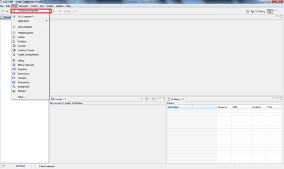
In CCS, click View->TI Resource Explorer
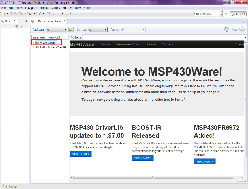
In Resource Explorer View, click on MSP430ware
CHAPTER 2. NAVIGATING TO DRIVERLIB THROUGH CCS RESOURCE EXPLORER 10
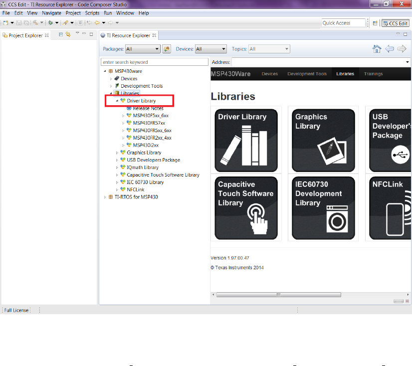
Clicking MSP430ware takes you to the introductory page. The version of the latest MSP430ware
installed is available in this page. In this screenshot the version is 1.30.00.15 The various
software, collateral, code examples, datasheets and user guides can be navigated by clicking the
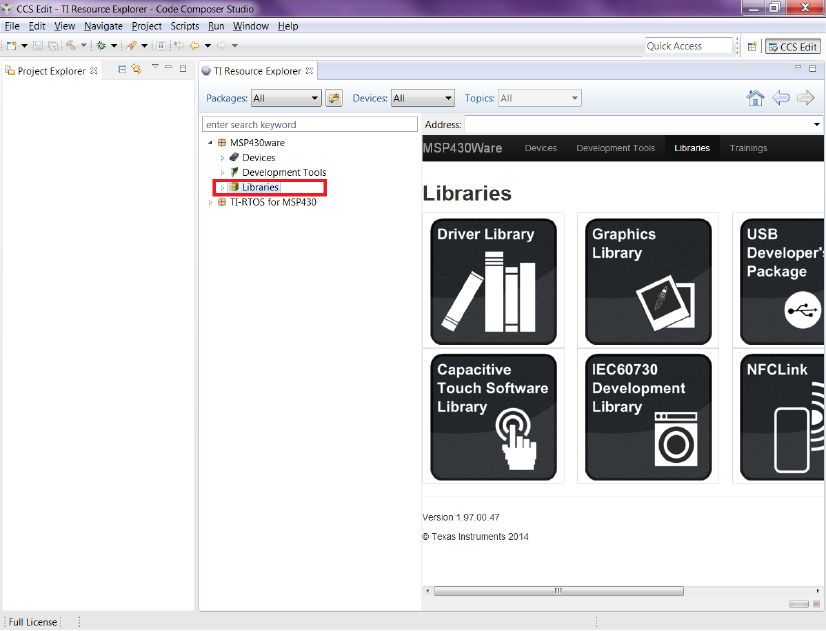
different topics under MSP430ware. To proceed to driverlib, click on Libraries->Driverlib as shown
in the next two screenshots.
CHAPTER 2. NAVIGATING TO DRIVERLIB THROUGH CCS RESOURCE EXPLORER 11
CHAPTER 2. NAVIGATING TO DRIVERLIB THROUGH CCS RESOURCE EXPLORER 12
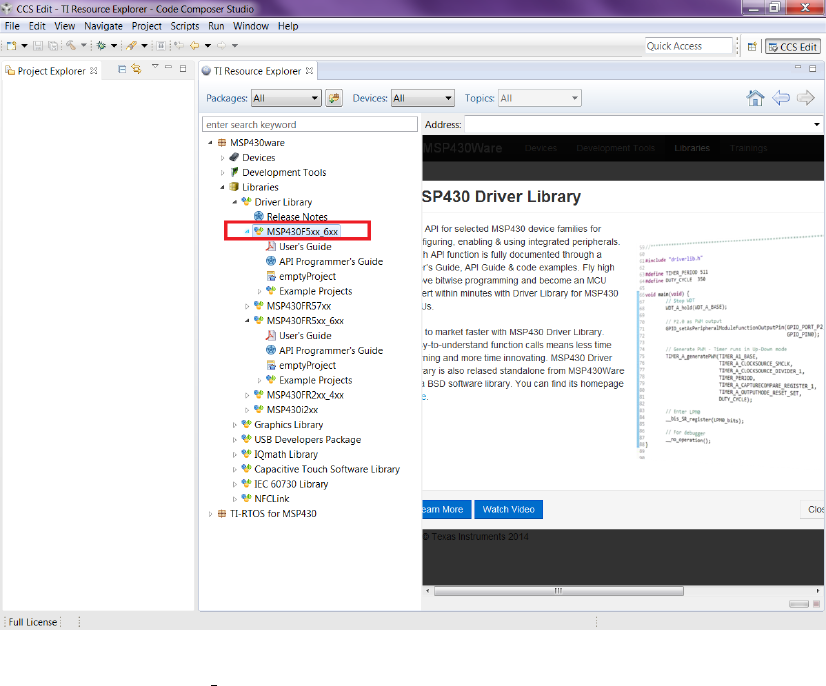
Driverlib is designed per Family. If a common device family user's guide exists for a group of
devices, these devices belong to the same 'family'. Currently driverlib is available for the following
family of devices. MSP430F5xx 6xx MSP430FR57xx MSP430FR2xx 4xx MSP430FR5xx 6xx
MSP430i2xx
CHAPTER 2. NAVIGATING TO DRIVERLIB THROUGH CCS RESOURCE EXPLORER 13
Click on the MSP430F5xx 6xx to navigate to the driverlib based example code for that family.
CHAPTER 2. NAVIGATING TO DRIVERLIB THROUGH CCS RESOURCE EXPLORER 14
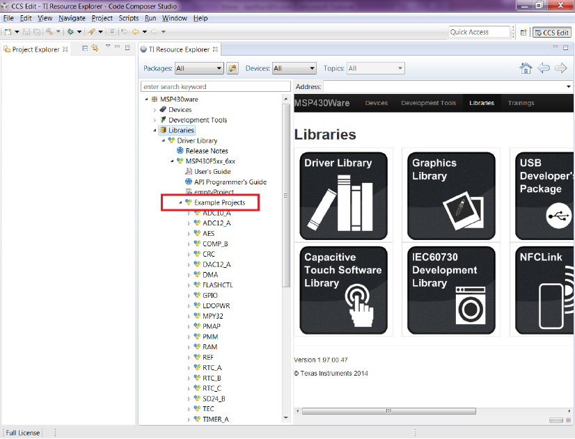
The various peripherals are listed in alphabetical order. The names of peripherals are as in device
family user's guide. Clicking on a peripheral name lists the driverlib example code for that
peripheral. The screenshot below shows an example when the user clicks on GPIO peripheral.
CHAPTER 2. NAVIGATING TO DRIVERLIB THROUGH CCS RESOURCE EXPLORER 15
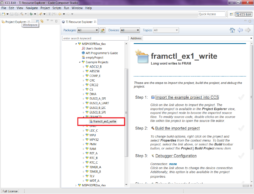
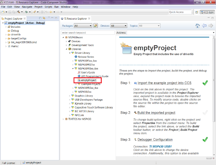
Now click on the specific example you are interested in. On the right side there are options to
Import/Build/Download and Debug. Import the project by clicking on the ”Import the example
project into CCS”
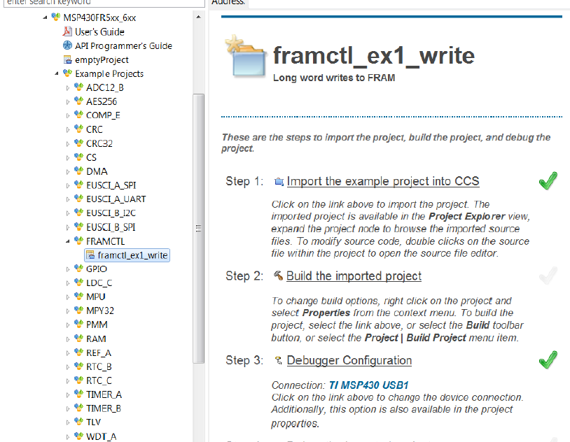
CHAPTER 2. NAVIGATING TO DRIVERLIB THROUGH CCS RESOURCE EXPLORER 16
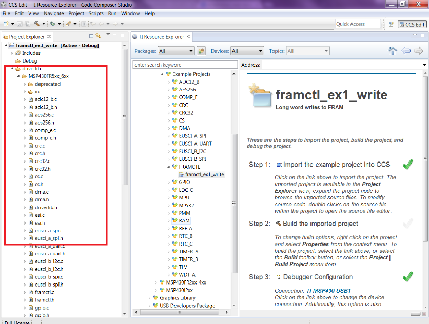
The imported project can be viewed on the left in the Project Explorer. All required driverlib source
and header files are included inside the driverlib folder. All driverlib source and header files are
linked to the example projects. So if the user modifies any of these source or header files, the
original copy of the installed MSP430ware driverlib source and header files get modified.
CHAPTER 2. NAVIGATING TO DRIVERLIB THROUGH CCS RESOURCE EXPLORER 17
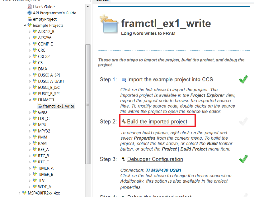
Now click on Build the imported project on the right to build the example project.
CHAPTER 2. NAVIGATING TO DRIVERLIB THROUGH CCS RESOURCE EXPLORER 18
Now click on Build the imported project on the right to build the example project.
CHAPTER 2. NAVIGATING TO DRIVERLIB THROUGH CCS RESOURCE EXPLORER 19
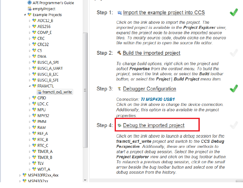
The COM port to download to can be changed using the Debugger Configuration option on the
right if required.
To get started on a new project we recommend getting started on an empty project we provide.
This project has all the driverlib source files, header files, project paths are set by default.
CHAPTER 2. NAVIGATING TO DRIVERLIB THROUGH CCS RESOURCE EXPLORER 20
The main.c included with the empty project can be modified to include user code.
CHAPTER 3. HOW TO CREATE A NEW CCS PROJECT THAT USES DRIVERLIB 21
3 How to create a new CCS project that uses
Driverlib
3.1 Introduction
To get started on a new project we recommend using the new project wizard. For driver library to
work with the new project wizard CCS must have discovered the driver library RTSC product. For
more information refer to the installation steps of the release notes. The new project wizard adds
the needed driver library source files and adds the driver library include path.
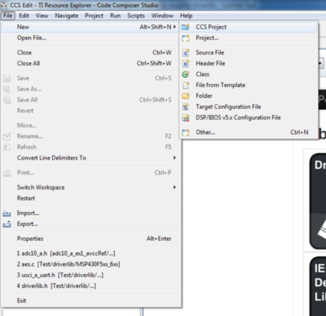
To open the new project wizard go to File ->New ->CCS Project as seen in the screenshot below.
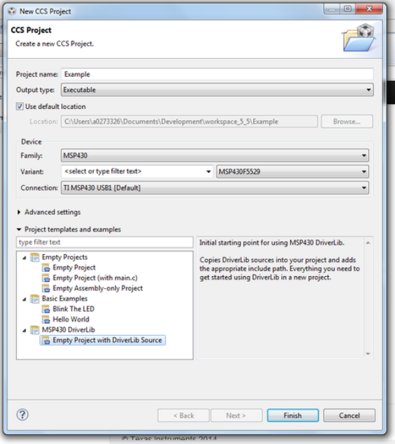
Once the new project wizard has been opened name your project and choose the device you
would like to create a Driver Library project for. The device must be supported by driver library.
Then under ”Project templates and examples” choose ”Empty Project with DriverLib Source” as
seen below.
CHAPTER 3. HOW TO CREATE A NEW CCS PROJECT THAT USES DRIVERLIB 22
Finally click ”Finish” and begin developing with your Driver Library enabled project.
We recommend -O4 compiler settings for more efficient optimizations for projects using driverlib
CHAPTER 4. HOW TO INCLUDE DRIVERLIB INTO YOUR EXISTING CCS PROJECT 23
4 How to include driverlib into your existing
CCS project
4.1 Introduction
To add driver library to an existing project we recommend using CCS project templates. For driver
library to work with project templates CCS must have discovered the driver library RTSC product.
For more information refer to the installation steps of the release notes. CCS project templates
adds the needed driver library source files and adds the driver library include path.
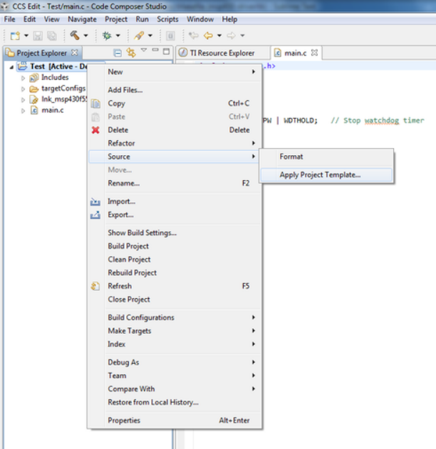
To apply a project template right click on an existing project then go to Source ->Apply Project
Template as seen in the screenshot below.
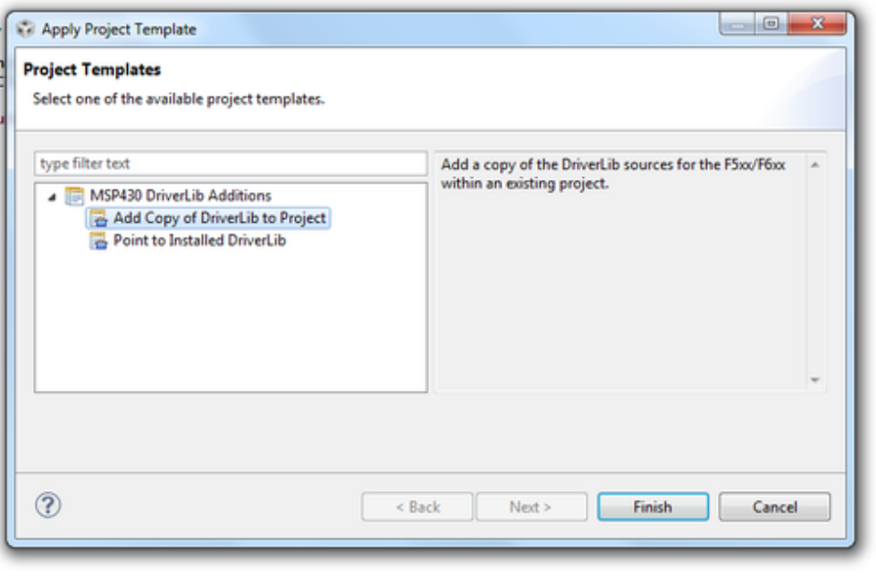
In the ”Apply Project Template” dialog box under ”MSP430 DriverLib Additions” choose either ”Add
Local Copy” or ”Point to Installed DriverLib” as seen in the screenshot below. Most users will want
to add a local copy which copies the DriverLib source into the project and sets the compiler
settings needed.
Pointing to an installed DriverLib is for advandced users who are including a static library in their
project and want to add the DriverLib header files to their include path.
CHAPTER 4. HOW TO INCLUDE DRIVERLIB INTO YOUR EXISTING CCS PROJECT 24
Click ”Finish” and start developing with driver library in your project.
CHAPTER 5. HOW TO CREATE A NEW IAR PROJECT THAT USES DRIVERLIB 25
5 How to create a new IAR project that uses
Driverlib
5.1 Introduction
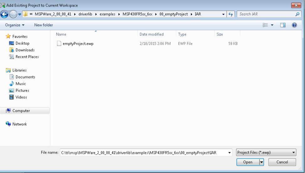
It is recommended to get started with an Empty Driverlib Project. Browse to the empty project in
your device's family. This is available in the driverlib instal folder\00 emptyProject
CHAPTER 5. HOW TO CREATE A NEW IAR PROJECT THAT USES DRIVERLIB 26

CHAPTER 5. HOW TO CREATE A NEW IAR PROJECT THAT USES DRIVERLIB 27
CHAPTER 6. HOW TO INCLUDE DRIVERLIB INTO YOUR EXISTING IAR PROJECT 28
6 How to include driverlib into your existing
IAR project
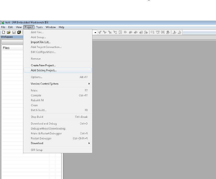
6.1 Introduction
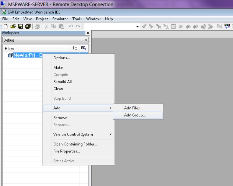
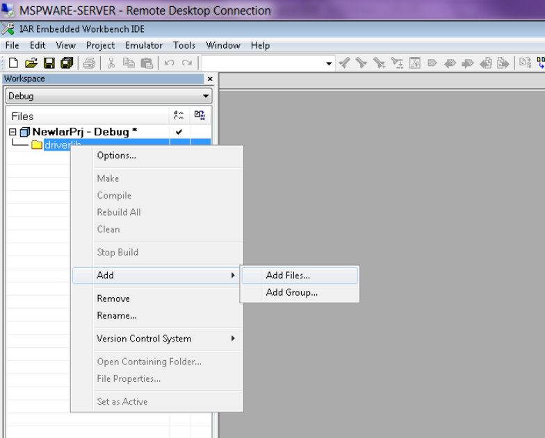
To add driver library to an existing project, right click project click on Add Group - ”driverlib”
Now click Add files and browse through driverlib folder and add all source files of the family the
device belongs to.
CHAPTER 6. HOW TO INCLUDE DRIVERLIB INTO YOUR EXISTING IAR PROJECT 29
Add another group via ”Add Group” and add inc folder. Add all files in the same driverlib family inc
folder
CHAPTER 6. HOW TO INCLUDE DRIVERLIB INTO YOUR EXISTING IAR PROJECT 30
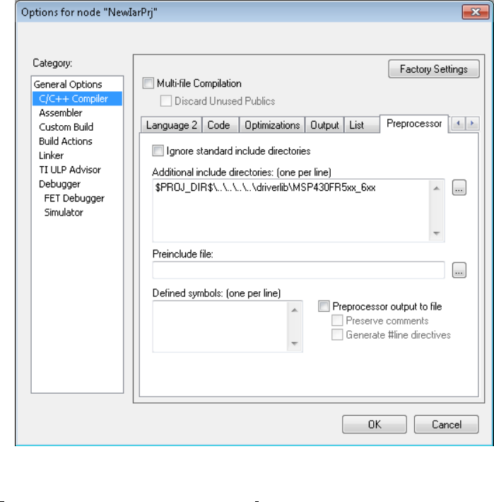
Right click on the project, select ”Options...”, add
”$PROJ DIR$\..\..\..\..\driverlib\MSP430FR5xx 6xx” under ”General Options->C/C++
Compiler->Additional include directories: (one per line)”. Click ”OK” and start developing with
driver library in your project.

CHAPTER 7. 10-BIT ANALOG-TO-DIGITAL CONVERTER (ADC10 A) 31
7 10-Bit Analog-to-Digital Converter
(ADC10 A)
Introduction ..............................................................................................31
API Functions ............................................................................................31
Programming Example ...................................................................................49
7.1 Introduction
The 10-Bit Analog-to-Digital (ADC10 A) API provides a set of functions for using the MSP430Ware
ADC10 A modules. Functions are provided to initialize the ADC10 A modules, setup signal
sources and reference voltages, and manage interrupts for the ADC10 A modules.
The ADC10 A module provides the ability to convert analog signals into a digital value in respect
to given reference voltages. The ADC10 A can generate digital values from 0 to Vcc with an 8- or
10-bit resolution. It operates in 2 different sampling modes, and 4 different conversion modes. The
sampling modes are extended sampling and pulse sampling, in extended sampling the
sample/hold signal must stay high for the duration of sampling, while in pulse mode a sampling
timer is setup to start on a rising edge of the sample/hold signal and sample for a specified
amount of clock cycles. The 4 conversion modes are single-channel single conversion, sequence
of channels single-conversion, repeated single channel conversions, and repeated sequence of
channels conversions.
The ADC10 A module can generate multiple interrupts. An interrupt can be asserted when a
conversion is complete, when a conversion is about to overwrite the converted data in the memory
buffer before it has been read out, and/or when a conversion is about to start before the last
conversion is complete. The ADC10 A also has a window comparator feature which asserts
interrupts when the input signal is above a high threshold, below a low threshold, or between the
two at any given moment.
7.2 API Functions
Functions
bool ADC10 A init (uint16 t baseAddress, uint16 t sampleHoldSignalSourceSelect, uint8 t
clockSourceSelect, uint16 t clockSourceDivider)
Initializes the ADC10 A Module.
void ADC10 A enable (uint16 t baseAddress)
Enables the ADC10 A block.
void ADC10 A disable (uint16 t baseAddress)
Disables the ADC10 A block.
void ADC10 A setupSamplingTimer (uint16 t baseAddress, uint16 t clockCycleHoldCount,
uint16 t multipleSamplesEnabled)
Sets up and enables the Sampling Timer Pulse Mode.
void ADC10 A disableSamplingTimer (uint16 t baseAddress)
Disables Sampling Timer Pulse Mode.

CHAPTER 7. 10-BIT ANALOG-TO-DIGITAL CONVERTER (ADC10 A) 32
void ADC10 A configureMemory (uint16 t baseAddress, uint8 t inputSourceSelect, uint8 t
positiveRefVoltageSourceSelect, uint8 t negativeRefVoltageSourceSelect)
Configures the controls of the selected memory buffer.
void ADC10 A enableInterrupt (uint16 t baseAddress, uint8 t interruptMask)
Enables selected ADC10 A interrupt sources.
void ADC10 A disableInterrupt (uint16 t baseAddress, uint8 t interruptMask)
Disables selected ADC10 A interrupt sources.
void ADC10 A clearInterrupt (uint16 t baseAddress, uint8 t interruptFlagMask)
Clears ADC10 A selected interrupt flags.
uint16 t ADC10 A getInterruptStatus (uint16 t baseAddress, uint8 t interruptFlagMask)
Returns the status of the selected memory interrupt flags.
void ADC10 A startConversion (uint16 t baseAddress, uint8 t
conversionSequenceModeSelect)
Enables/Starts an Analog-to-Digital Conversion.
void ADC10 A disableConversions (uint16 t baseAddress, bool preempt)
Disables the ADC from converting any more signals.
int16 t ADC10 A getResults (uint16 t baseAddress)
Returns the raw contents of the specified memory buffer.
void ADC10 A setResolution (uint16 t baseAddress, uint8 t resolutionSelect)
Use to change the resolution of the converted data.
void ADC10 A setSampleHoldSignalInversion (uint16 t baseAddress, uint16 t invertedSignal)
Use to invert or un-invert the sample/hold signal.
void ADC10 A setDataReadBackFormat (uint16 t baseAddress, uint16 t readBackFormat)
Use to set the read-back format of the converted data.
void ADC10 A enableReferenceBurst (uint16 t baseAddress)
Enables the reference buffer's burst ability.
void ADC10 A disableReferenceBurst (uint16 t baseAddress)
Disables the reference buffer's burst ability.
void ADC10 A setReferenceBufferSamplingRate (uint16 t baseAddress, uint16 t
samplingRateSelect)
Use to set the reference buffer's sampling rate.
void ADC10 A setWindowComp (uint16 t baseAddress, uint16 t highThreshold, uint16 t
lowThreshold)
Sets the high and low threshold for the window comparator feature.
uint32 t ADC10 A getMemoryAddressForDMA (uint16 t baseAddress)
Returns the address of the memory buffer for the DMA module.
uint16 t ADC10 A isBusy (uint16 t baseAddress)
Returns the busy status of the ADC10 A core.
7.2.1 Detailed Description
The ADC10 A API is broken into three groups of functions: those that deal with initialization and
conversions, those that handle interrupts, and those that handle auxiliary features of the ADC10 A.
The ADC10 A initialization and conversion functions are
ADC10 A init()
ADC10 A configureMemory()
ADC10 A setupSamplingTimer()
ADC10 A disableSamplingTimer()
ADC10 A setWindowComp()

CHAPTER 7. 10-BIT ANALOG-TO-DIGITAL CONVERTER (ADC10 A) 33
ADC10 A startConversion()
ADC10 A disableConversions()
ADC10 A getResults()
ADC10 A isBusy()
The ADC10 A interrupts are handled by
ADC10 A enableInterrupt()
ADC10 A disableInterrupt()
ADC10 A clearInterrupt()
ADC10 A getInterruptStatus()
Auxiliary features of the ADC10 A are handled by
ADC10 A setResolution()
ADC10 A setSampleHoldSignalInversion()
ADC10 A setDataReadBackFormat()
ADC10 A enableReferenceBurst()
ADC10 A disableReferenceBurst()
ADC10 A setReferenceBufferSamplingRate()
ADC10 A getMemoryAddressForDMA()
ADC10 A enable()
ADC10 A disable()
7.2.2 Function Documentation
ADC10 A clearInterrupt()
void ADC10 A clearInterrupt (
uint16 t baseAddress,
uint8 t interruptFlagMask )
Clears ADC10 A selected interrupt flags.
The selected ADC10 A interrupt flags are cleared, so that it no longer asserts. The memory buffer
interrupt flags are only cleared when the memory buffer is accessed.
Parameters
baseAddress is the base address of the ADC10 A module.
CHAPTER 7. 10-BIT ANALOG-TO-DIGITAL CONVERTER (ADC10 A) 34
Parameters
interruptFlagMask is a bit mask of the interrupt flags to be cleared. Mask value is the logical
OR of any of the following:
ADC10 A TIMEOVERFLOW INTFLAG - Interrupts flag when a new
conversion is starting before the previous one has finished
ADC10 A OVERFLOW INTFLAG - Interrupts flag when a new
conversion is about to overwrite the previous one
ADC10 A ABOVETHRESHOLD INTFLAG - Interrupts flag when the
input signal has gone above the high threshold of the window
comparator
ADC10 A BELOWTHRESHOLD INTFLAG - Interrupts flag when the
input signal has gone below the low threshold of the low window
comparator
ADC10 A INSIDEWINDOW INTFLAG - Interrupts flag when the
input signal is in between the high and low thresholds of the window
comparator
ADC10 A COMPLETED INTFLAG - Interrupt flag for new
conversion data in the memory buffer
Modified bits of ADC10IFG register.
Returns
None
ADC10 A configureMemory()
void ADC10 A configureMemory (
uint16 t baseAddress,
uint8 t inputSourceSelect,
uint8 t positiveRefVoltageSourceSelect,
uint8 t negativeRefVoltageSourceSelect )
Configures the controls of the selected memory buffer.
Maps an input signal conversion into the memory buffer, as well as the positive and negative
reference voltages for each conversion being stored into the memory buffer. If the internal
reference is used for the positive reference voltage, the internal REF module has to control the
voltage level. Note that if a conversion has been started with the startConversion() function, then a
call to disableConversions() is required before this function may be called. If conversion is not
disabled, this function does nothing.
Parameters
baseAddress is the base address of the ADC10 A module.
CHAPTER 7. 10-BIT ANALOG-TO-DIGITAL CONVERTER (ADC10 A) 35
Parameters
inputSourceSelect is the input that will store the converted data into the
specified memory buffer. Valid values are:
ADC10 A INPUT A0 [Default]
ADC10 A INPUT A1
ADC10 A INPUT A2
ADC10 A INPUT A3
ADC10 A INPUT A4
ADC10 A INPUT A5
ADC10 A INPUT A6
ADC10 A INPUT A7
ADC10 A INPUT A8
ADC10 A INPUT A9
ADC10 A INPUT TEMPSENSOR
ADC10 A INPUT BATTERYMONITOR
ADC10 A INPUT A12
ADC10 A INPUT A13
ADC10 A INPUT A14
ADC10 A INPUT A15
Modified bits are ADC10INCHx of ADC10MCTL0
register.
positiveRefVoltageSourceSelect is the reference voltage source to set as the upper limit for
the conversion that is to be stored in the specified memory
buffer. Valid values are:
ADC10 A VREFPOS AVCC [Default]
ADC10 A VREFPOS EXT
ADC10 A VREFPOS INT
Modified bits are ADC10SREF of ADC10MCTL0
register.
negativeRefVoltageSourceSelect is the reference voltage source to set as the lower limit for
the conversion that is to be stored in the specified memory
buffer. Valid values are:
ADC10 A VREFNEG AVSS
ADC10 A VREFNEG EXT
Modified bits are ADC10SREF of ADC10CTL0
register.
Returns
None

CHAPTER 7. 10-BIT ANALOG-TO-DIGITAL CONVERTER (ADC10 A) 36
ADC10 A disable()
void ADC10 A disable (
uint16 t baseAddress )
Disables the ADC10 A block.
This will disable operation of the ADC10 A block.
Parameters
baseAddress is the base address of the ADC10 A module.
Modified bits are ADC10ON of ADC10CTL0 register.
Returns
None
ADC10 A disableConversions()
void ADC10 A disableConversions (
uint16 t baseAddress,
bool preempt )
Disables the ADC from converting any more signals.
Disables the ADC from converting any more signals. If there is a conversion in progress, this
function can stop it immediately if the preempt parameter is set as
ADC10 A PREEMPTCONVERSION, by changing the conversion mode to single-channel,
single-conversion and disabling conversions. If the conversion mode is set as single-channel,
single-conversion and this function is called without preemption, then the ADC core conversion
status is polled until the conversion is complete before disabling conversions to prevent
unpredictable data. If the ADC10 A startConversion() has been called, then this function has to be
called to re-initialize the ADC, reconfigure a memory buffer control, enable/disable the sampling
pulse mode, or change the internal reference voltage.
Parameters
baseAddress is the base address of the ADC10 A module.
preempt specifies if the current conversion should be pre-empted before the end of the
conversion Valid values are:
ADC10 A COMPLETECONVERSION - Allows the ADC10 A to end the
current conversion before disabling conversions.
ADC10 A PREEMPTCONVERSION - Stops the ADC10 A immediately,
with unpredictable results of the current conversion. Cannot be used with
repeated conversion.
Modified bits of ADC10CTL1 register and bits of ADC10CTL0 register.
CHAPTER 7. 10-BIT ANALOG-TO-DIGITAL CONVERTER (ADC10 A) 37
Returns
None
ADC10 A disableInterrupt()
void ADC10 A disableInterrupt (
uint16 t baseAddress,
uint8 t interruptMask )
Disables selected ADC10 A interrupt sources.
Disables the indicated ADC10 A interrupt sources. Only the sources that are enabled can be
reflected to the processor interrupt; disabled sources have no effect on the processor.
Parameters
baseAddress is the base address of the ADC10 A module.
interruptMask is the bit mask of the memory buffer interrupt sources to be disabled. Mask
value is the logical OR of any of the following:
ADC10 A TIMEOVERFLOW INT - Interrupts when a new conversion is
starting before the previous one has finished
ADC10 A OVERFLOW INT - Interrupts when a new conversion is about
to overwrite the previous one
ADC10 A ABOVETHRESHOLD INT - Interrupts when the input signal
has gone above the high threshold of the window comparator
ADC10 A BELOWTHRESHOLD INT - Interrupts when the input signal
has gone below the low threshold of the low window comparator
ADC10 A INSIDEWINDOW INT - Interrupts when the input signal is in
between the high and low thresholds of the window comparator
ADC10 A COMPLETED INT - Interrupt for new conversion data in the
memory buffer
Modified bits of ADC10IE register.
Returns
None
ADC10 A disableReferenceBurst()
void ADC10 A disableReferenceBurst (
uint16 t baseAddress )
Disables the reference buffer's burst ability.
Disables the reference buffer's burst ability, forcing the reference buffer to remain on continuously.

CHAPTER 7. 10-BIT ANALOG-TO-DIGITAL CONVERTER (ADC10 A) 38
Parameters
baseAddress is the base address of the ADC10 A module.
Returns
None
ADC10 A disableSamplingTimer()
void ADC10 A disableSamplingTimer (
uint16 t baseAddress )
Disables Sampling Timer Pulse Mode.
Disables the Sampling Timer Pulse Mode. Note that if a conversion has been started with the
startConversion() function, then a call to disableConversions() is required before this function may
be called.
Parameters
baseAddress is the base address of the ADC10 A module.
Returns
None
ADC10 A enable()
void ADC10 A enable (
uint16 t baseAddress )
Enables the ADC10 A block.
This will enable operation of the ADC10 A block.
Parameters
baseAddress is the base address of the ADC10 A module.
Modified bits are ADC10ON of ADC10CTL0 register.
Returns
None
ADC10 A enableInterrupt()
void ADC10 A enableInterrupt (

CHAPTER 7. 10-BIT ANALOG-TO-DIGITAL CONVERTER (ADC10 A) 39
uint16 t baseAddress,
uint8 t interruptMask )
Enables selected ADC10 A interrupt sources.
Enables the indicated ADC10 A interrupt sources. Only the sources that are enabled can be
reflected to the processor interrupt; disabled sources have no effect on the processor. Does not
clear interrupt flags.
Parameters
baseAddress is the base address of the ADC10 A module.
interruptMask is the bit mask of the memory buffer interrupt sources to be enabled. Mask
value is the logical OR of any of the following:
ADC10 A TIMEOVERFLOW INT - Interrupts when a new conversion is
starting before the previous one has finished
ADC10 A OVERFLOW INT - Interrupts when a new conversion is about
to overwrite the previous one
ADC10 A ABOVETHRESHOLD INT - Interrupts when the input signal
has gone above the high threshold of the window comparator
ADC10 A BELOWTHRESHOLD INT - Interrupts when the input signal
has gone below the low threshold of the low window comparator
ADC10 A INSIDEWINDOW INT - Interrupts when the input signal is in
between the high and low thresholds of the window comparator
ADC10 A COMPLETED INT - Interrupt for new conversion data in the
memory buffer
Modified bits of ADC10IE register.
Returns
None
ADC10 A enableReferenceBurst()
void ADC10 A enableReferenceBurst (
uint16 t baseAddress )
Enables the reference buffer's burst ability.
Enables the reference buffer's burst ability, allowing the reference buffer to turn off while the ADC
is not converting, and automatically turning on when the ADC needs the generated reference
voltage for a conversion.
Parameters
baseAddress is the base address of the ADC10 A module.
CHAPTER 7. 10-BIT ANALOG-TO-DIGITAL CONVERTER (ADC10 A) 40
Returns
None
ADC10 A getInterruptStatus()
uint16 t ADC10 A getInterruptStatus (
uint16 t baseAddress,
uint8 t interruptFlagMask )
Returns the status of the selected memory interrupt flags.
Returns the status of the selected interrupt flags.
Parameters
baseAddress is the base address of the ADC10 A module.
interruptFlagMask is a bit mask of the interrupt flags status to be returned. Mask value is the
logical OR of any of the following:
ADC10 A TIMEOVERFLOW INTFLAG - Interrupts flag when a new
conversion is starting before the previous one has finished
ADC10 A OVERFLOW INTFLAG - Interrupts flag when a new
conversion is about to overwrite the previous one
ADC10 A ABOVETHRESHOLD INTFLAG - Interrupts flag when the
input signal has gone above the high threshold of the window
comparator
ADC10 A BELOWTHRESHOLD INTFLAG - Interrupts flag when the
input signal has gone below the low threshold of the low window
comparator
ADC10 A INSIDEWINDOW INTFLAG - Interrupts flag when the
input signal is in between the high and low thresholds of the window
comparator
ADC10 A COMPLETED INTFLAG - Interrupt flag for new
conversion data in the memory buffer
Returns
The current interrupt flag status for the corresponding mask.
ADC10 A getMemoryAddressForDMA()
uint32 t ADC10 A getMemoryAddressForDMA (
uint16 t baseAddress )
Returns the address of the memory buffer for the DMA module.
Returns the address of the memory buffer. This can be used in conjunction with the DMA to store
the converted data directly to memory.

CHAPTER 7. 10-BIT ANALOG-TO-DIGITAL CONVERTER (ADC10 A) 41
Parameters
baseAddress is the base address of the ADC10 A module.
Returns
The memory address of the memory buffer
ADC10 A getResults()
int16 t ADC10 A getResults (
uint16 t baseAddress )
Returns the raw contents of the specified memory buffer.
Returns the raw contents of the specified memory buffer. The format of the content depends on
the read-back format of the data: if the data is in signed 2's complement format then the contents
in the memory buffer will be left-justified with the least-significant bits as 0's, whereas if the data is
in unsigned format then the contents in the memory buffer will be right- justified with the
most-significant bits as 0's.
Parameters
baseAddress is the base address of the ADC10 A module.
Returns
A Signed Integer of the contents of the specified memory buffer.
ADC10 A init()
bool ADC10 A init (
uint16 t baseAddress,
uint16 t sampleHoldSignalSourceSelect,
uint8 t clockSourceSelect,
uint16 t clockSourceDivider )
Initializes the ADC10 A Module.
This function initializes the ADC module to allow for analog-to-digital conversions. Specifically this
function sets up the sample-and-hold signal and clock sources for the ADC core to use for
conversions. Upon successful completion of the initialization all of the ADC control registers will be
reset, excluding the memory controls and reference module bits, the given parameters will be set,
and the ADC core will be turned on (Note, that the ADC core only draws power during conversions
and remains off when not converting).Note that sample/hold signal sources are device dependent.
Note that if re-initializing the ADC after starting a conversion with the startConversion() function,
the disableConversion() must be called BEFORE this function can be called.
Parameters
baseAddress is the base address of the ADC10 A module.

CHAPTER 7. 10-BIT ANALOG-TO-DIGITAL CONVERTER (ADC10 A) 42
Parameters
sampleHoldSignalSourceSelect is the signal that will trigger a sample-and-hold for an input
signal to be converted. This parameter is device specific and
sources should be found in the device's datasheet Valid
values are:
ADC10 A SAMPLEHOLDSOURCE SC
ADC10 A SAMPLEHOLDSOURCE 1
ADC10 A SAMPLEHOLDSOURCE 2
ADC10 A SAMPLEHOLDSOURCE 3
Modified bits are ADC10SHSx of ADC10CTL1 register.
clockSourceSelect selects the clock that will be used by the ADC10 A core and
the sampling timer if a sampling pulse mode is enabled.
Valid values are:
ADC10 A CLOCKSOURCE ADC10OSC [Default] -
MODOSC 5 MHz oscillator from the UCS
ADC10 A CLOCKSOURCE ACLK - The Auxiliary
Clock
ADC10 A CLOCKSOURCE MCLK - The Master Clock
ADC10 A CLOCKSOURCE SMCLK - The Sub-Master
Clock
Modified bits are ADC10SSELx of ADC10CTL1
register.
CHAPTER 7. 10-BIT ANALOG-TO-DIGITAL CONVERTER (ADC10 A) 43
Parameters
clockSourceDivider selects the amount that the clock will be divided. Valid
values are:
ADC10 A CLOCKDIVIDER 1 [Default]
ADC10 A CLOCKDIVIDER 2
ADC10 A CLOCKDIVIDER 3
ADC10 A CLOCKDIVIDER 4
ADC10 A CLOCKDIVIDER 5
ADC10 A CLOCKDIVIDER 6
ADC10 A CLOCKDIVIDER 7
ADC10 A CLOCKDIVIDER 8
ADC10 A CLOCKDIVIDER 12
ADC10 A CLOCKDIVIDER 16
ADC10 A CLOCKDIVIDER 20
ADC10 A CLOCKDIVIDER 24
ADC10 A CLOCKDIVIDER 28
ADC10 A CLOCKDIVIDER 32
ADC10 A CLOCKDIVIDER 64
ADC10 A CLOCKDIVIDER 128
ADC10 A CLOCKDIVIDER 192
ADC10 A CLOCKDIVIDER 256
ADC10 A CLOCKDIVIDER 320
ADC10 A CLOCKDIVIDER 384
ADC10 A CLOCKDIVIDER 448
ADC10 A CLOCKDIVIDER 512
Modified bits are ADC10DIVx of ADC10CTL1 register;
bits ADC10PDIVx of ADC10CTL2 register.
Returns
STATUS SUCCESS or STATUS FAILURE of the initialization process.
ADC10 A isBusy()
uint16 t ADC10 A isBusy (
uint16 t baseAddress )
Returns the busy status of the ADC10 A core.
Returns the status of the ADC core if there is a conversion currently taking place.
CHAPTER 7. 10-BIT ANALOG-TO-DIGITAL CONVERTER (ADC10 A) 44
Parameters
baseAddress is the base address of the ADC10 A module.
Returns
One of the following:
ADC10 A BUSY
ADC10 A NOTBUSY
indicating if there is a conversion currently taking place
ADC10 A setDataReadBackFormat()
void ADC10 A setDataReadBackFormat (
uint16 t baseAddress,
uint16 t readBackFormat )
Use to set the read-back format of the converted data.
Sets the format of the converted data: how it will be stored into the memory buffer, and how it
should be read back. The format can be set as right-justified (default), which indicates that the
number will be unsigned, or left-justified, which indicates that the number will be signed in 2's
complement format. This change affects all memory buffers for subsequent conversions.
Parameters
baseAddress is the base address of the ADC10 A module.
readBackFormat is the specified format to store the conversions in the memory buffer. Valid
values are:
ADC10 A UNSIGNED BINARY [Default]
ADC10 A SIGNED 2SCOMPLEMENT
Modified bits are ADC10DF of ADC10CTL2 register.
Returns
None
ADC10 A setReferenceBufferSamplingRate()
void ADC10 A setReferenceBufferSamplingRate (
uint16 t baseAddress,
uint16 t samplingRateSelect )
Use to set the reference buffer's sampling rate.
Sets the reference buffer's sampling rate to the selected sampling rate. The default sampling rate
is maximum of 200-ksps, and can be reduced to a maximum of 50-ksps to conserve power.
CHAPTER 7. 10-BIT ANALOG-TO-DIGITAL CONVERTER (ADC10 A) 45
Parameters
baseAddress is the base address of the ADC10 A module.
samplingRateSelect is the specified maximum sampling rate. Valid values are:
ADC10 A MAXSAMPLINGRATE 200KSPS [Default]
ADC10 A MAXSAMPLINGRATE 50KSPS
Modified bits are ADC10SR of ADC10CTL2 register.
Returns
None
ADC10 A setResolution()
void ADC10 A setResolution (
uint16 t baseAddress,
uint8 t resolutionSelect )
Use to change the resolution of the converted data.
This function can be used to change the resolution of the converted data from the default of
12-bits.
Parameters
baseAddress is the base address of the ADC10 A module.
resolutionSelect determines the resolution of the converted data. Valid values
are:
ADC10 A RESOLUTION 8BIT
ADC10 A RESOLUTION 10BIT [Default]
Modified bits are ADC10RES of ADC10CTL2 register.
Returns
None
ADC10 A setSampleHoldSignalInversion()
void ADC10 A setSampleHoldSignalInversion (
uint16 t baseAddress,
uint16 t invertedSignal )
Use to invert or un-invert the sample/hold signal.
This function can be used to invert or un-invert the sample/hold signal. Note that if a conversion
has been started with the startConversion() function, then a call to disableConversions() is
required before this function may be called.
CHAPTER 7. 10-BIT ANALOG-TO-DIGITAL CONVERTER (ADC10 A) 46
Parameters
baseAddress is the base address of the ADC10 A module.
invertedSignal set if the sample/hold signal should be inverted Valid values are:
ADC10 A NONINVERTEDSIGNAL [Default] - a sample-and-hold of an
input signal for conversion will be started on a rising edge of the
sample/hold signal.
ADC10 A INVERTEDSIGNAL - a sample-and-hold of an input signal for
conversion will be started on a falling edge of the sample/hold signal.
Modified bits are ADC10ISSH of ADC10CTL1 register.
Returns
None
ADC10 A setupSamplingTimer()
void ADC10 A setupSamplingTimer (
uint16 t baseAddress,
uint16 t clockCycleHoldCount,
uint16 t multipleSamplesEnabled )
Sets up and enables the Sampling Timer Pulse Mode.
This function sets up the sampling timer pulse mode which allows the sample/hold signal to trigger
a sampling timer to sample-and-hold an input signal for a specified number of clock cycles without
having to hold the sample/hold signal for the entire period of sampling. Note that if a conversion
has been started with the startConversion() function, then a call to disableConversions() is
required before this function may be called.
Parameters
baseAddress is the base address of the ADC10 A module.

CHAPTER 7. 10-BIT ANALOG-TO-DIGITAL CONVERTER (ADC10 A) 47
Parameters
clockCycleHoldCount sets the amount of clock cycles to sample-and- hold for the memory
buffer. Valid values are:
ADC10 A CYCLEHOLD 4 CYCLES [Default]
ADC10 A CYCLEHOLD 8 CYCLES
ADC10 A CYCLEHOLD 16 CYCLES
ADC10 A CYCLEHOLD 32 CYCLES
ADC10 A CYCLEHOLD 64 CYCLES
ADC10 A CYCLEHOLD 96 CYCLES
ADC10 A CYCLEHOLD 128 CYCLES
ADC10 A CYCLEHOLD 192 CYCLES
ADC10 A CYCLEHOLD 256 CYCLES
ADC10 A CYCLEHOLD 384 CYCLES
ADC10 A CYCLEHOLD 512 CYCLES
ADC10 A CYCLEHOLD 768 CYCLES
ADC10 A CYCLEHOLD 1024 CYCLES
Modified bits are ADC10SHTx of ADC10CTL0 register.
multipleSamplesEnabled allows multiple conversions to start without a trigger signal from the
sample/hold signal Valid values are:
ADC10 A MULTIPLESAMPLESDISABLE - a timer trigger will
be needed to start every ADC conversion.
ADC10 A MULTIPLESAMPLESENABLE - during a
sequenced and/or repeated conversion mode, after the first
conversion, no sample/hold signal is necessary to start
subsequent samples.
Modified bits are ADC10MSC of ADC10CTL0 register.
Returns
None
ADC10 A setWindowComp()
void ADC10 A setWindowComp (
uint16 t baseAddress,
uint16 t highThreshold,
uint16 t lowThreshold )
Sets the high and low threshold for the window comparator feature.
Sets the high and low threshold for the window comparator feature. Use the ADC10HIIE,
ADC10INIE, ADC10LOIE interrupts to utilize this feature.
CHAPTER 7. 10-BIT ANALOG-TO-DIGITAL CONVERTER (ADC10 A) 48
Parameters
baseAddress is the base address of the ADC10 A module.
highThreshold is the upper bound that could trip an interrupt for the window comparator.
lowThreshold is the lower bound that could trip on interrupt for the window comparator.
Returns
None
ADC10 A startConversion()
void ADC10 A startConversion (
uint16 t baseAddress,
uint8 t conversionSequenceModeSelect )
Enables/Starts an Analog-to-Digital Conversion.
This function enables/starts the conversion process of the ADC. If the sample/hold signal source
chosen during initialization was ADC10OSC, then the conversion is started immediately, otherwise
the chosen sample/hold signal source starts the conversion by a rising edge of the signal. Keep in
mind when selecting conversion modes, that for sequenced and/or repeated modes, to keep the
sample/hold-and-convert process continuing without a trigger from the sample/hold signal source,
the multiple samples must be enabled using the ADC10 A setupSamplingTimer() function. Also
note that when a sequence conversion mode is selected, the first input channel is the one mapped
to the memory buffer, the next input channel selected for conversion is one less than the input
channel just converted (i.e. A1 comes after A2), until A0 is reached, and if in repeating mode, then
the next input channel will again be the one mapped to the memory buffer. Note that after this
function is called, the ADC10 A stopConversions() has to be called to re-initialize the ADC,
reconfigure a memory buffer control, enable/disable the sampling timer, or to change the internal
reference voltage.
Parameters
baseAddress is the base address of the ADC10 A module.

CHAPTER 7. 10-BIT ANALOG-TO-DIGITAL CONVERTER (ADC10 A) 49
Parameters
conversionSequenceModeSelect determines the ADC operating mode. Valid values are:
ADC10 A SINGLECHANNEL [Default] - one-time
conversion of a single channel into a single memory
buffer
ADC10 A SEQOFCHANNELS - one time conversion
of multiple channels into the specified starting memory
buffer and each subsequent memory buffer up until the
conversion is stored in a memory buffer dedicated as
the end-of-sequence by the memory's control register
ADC10 A REPEATED SINGLECHANNEL - repeated
conversions of one channel into a single memory
buffer
ADC10 A REPEATED SEQOFCHANNELS -
repeated conversions of multiple channels into the
specified starting memory buffer and each subsequent
memory buffer up until the conversion is stored in a
memory buffer dedicated as the end-of-sequence by
the memory's control register
Modified bits are ADC10CONSEQx of ADC10CTL1
register.
Returns
None
7.3 Programming Example
The following example shows how to initialize and use the ADC10 A API to start a single channel,
single conversion.
// Initialize ADC10 A with ADC10 A’s built-in oscillator
ADC10 A init (ADC10 A BASE,
ADC10 A SAMPLEHOLDSOURCE SC,
ADC10 A CLOCKSOURCE ADC10 AOSC,
ADC10 A CLOCKDIVIDEBY 1);
//Switch ON ADC10 A
ADC10 A enable(ADC10 A BASE);
// Setup sampling timer to sample-and-hold for 16 clock cycles
ADC10 A setupSamplingTimer (ADC10 A BASE,
ADC10 A CYCLEHOLD 16 CYCLES,
FALSE);
// Configure the Input to the Memory Buffer with the specified Reference Voltages
ADC10 A configureMemory (ADC10 A BASE,
ADC10 A INPUT A0,
ADC10 A VREF AVCC, // Vref+ = AVcc
ADC10 A VREF AVSS // Vref- = AVss
);
while (1)
{
// Start a single conversion, no repeating or sequences.

CHAPTER 7. 10-BIT ANALOG-TO-DIGITAL CONVERTER (ADC10 A) 50
ADC10 A startConversion (ADC10 A BASE,
ADC10 A SINGLECHANNEL);
// Wait for the Interrupt Flag to assert
while( !(ADC10 A getInterruptStatus(ADC10 A BASE,ADC10 AIFG0)) );
// Clear the Interrupt Flag and start another conversion
ADC10 A clearInterrupt(ADC10 A BASE,ADC10 AIFG0);
}

CHAPTER 8. 12-BIT ANALOG-TO-DIGITAL CONVERTER (ADC12 A) 51
8 12-Bit Analog-to-Digital Converter
(ADC12 A)
Introduction ..............................................................................................51
API Functions ............................................................................................51
Programming Example ...................................................................................70
8.1 Introduction
The 12-Bit Analog-to-Digital (ADC12 A) API provides a set of functions for using the MSP430Ware
ADC12 A modules. Functions are provided to initialize the ADC12 A modules, setup signal
sources and reference voltages for each memory buffer, and manage interrupts for the ADC12 A
modules.
The ADC12 A module provides the ability to convert analog signals into a digital value in respect
to given reference voltages. The ADC12 A can generate digital values from 0 to Vcc with an 8-,
10- or 12-bit resolution, with 16 different memory buffers to store conversion results. It operates in
2 different sampling modes, and 4 different conversion modes. The sampling modes are extended
sampling and pulse sampling, in extended sampling the sample/hold signal must stay high for the
duration of sampling, while in pulse mode a sampling timer is setup to start on a rising edge of the
sample/hold signal and sample for a specified amount of clock cycles. The 4 conversion modes
are single-channel single conversion, sequence of channels single-conversion, repeated single
channel conversions, and repeated sequence of channels conversions.
The ADC12 A module can generate multiple interrupts. An interrupt can be asserted for each
memory buffer when a conversion is complete, or when a conversion is about to overwrite the
converted data in any of the memory buffers before it has been read out, and/or when a
conversion is about to start before the last conversion is complete.
8.2 API Functions
Functions
bool ADC12 A init (uint16 t baseAddress, uint16 t sampleHoldSignalSourceSelect, uint8 t
clockSourceSelect, uint16 t clockSourceDivider)
Initializes the ADC12 A Module.
void ADC12 A enable (uint16 t baseAddress)
Enables the ADC12 A block.
void ADC12 A disable (uint16 t baseAddress)
Disables the ADC12 A block.
void ADC12 A setupSamplingTimer (uint16 t baseAddress, uint16 t
clockCycleHoldCountLowMem, uint16 t clockCycleHoldCountHighMem, uint16 t
multipleSamplesEnabled)
Sets up and enables the Sampling Timer Pulse Mode.
void ADC12 A disableSamplingTimer (uint16 t baseAddress)
Disables Sampling Timer Pulse Mode.

CHAPTER 8. 12-BIT ANALOG-TO-DIGITAL CONVERTER (ADC12 A) 52
void ADC12 A configureMemory (uint16 t baseAddress, ADC12 A configureMemoryParam
∗param)
Configures the controls of the selected memory buffer.
void ADC12 A enableInterrupt (uint16 t baseAddress, uint32 t interruptMask)
Enables selected ADC12 A interrupt sources.
void ADC12 A disableInterrupt (uint16 t baseAddress, uint32 t interruptMask)
Disables selected ADC12 A interrupt sources.
void ADC12 A clearInterrupt (uint16 t baseAddress, uint16 t memoryInterruptFlagMask)
Clears ADC12 A selected interrupt flags.
uint16 t ADC12 A getInterruptStatus (uint16 t baseAddress, uint16 t
memoryInterruptFlagMask)
Returns the status of the selected memory interrupt flags.
void ADC12 A startConversion (uint16 t baseAddress, uint16 t startingMemoryBufferIndex,
uint8 t conversionSequenceModeSelect)
Enables/Starts an Analog-to-Digital Conversion.
void ADC12 A disableConversions (uint16 t baseAddress, bool preempt)
Disables the ADC from converting any more signals.
uint16 t ADC12 A getResults (uint16 t baseAddress, uint8 t memoryBufferIndex)
A Signed Integer of the contents of the specified memory buffer.
void ADC12 A setResolution (uint16 t baseAddress, uint8 t resolutionSelect)
Use to change the resolution of the converted data.
void ADC12 A setSampleHoldSignalInversion (uint16 t baseAddress, uint16 t invertedSignal)
Use to invert or un-invert the sample/hold signal.
void ADC12 A setDataReadBackFormat (uint16 t baseAddress, uint8 t readBackFormat)
Use to set the read-back format of the converted data.
void ADC12 A enableReferenceBurst (uint16 t baseAddress)
Enables the reference buffer's burst ability.
void ADC12 A disableReferenceBurst (uint16 t baseAddress)
Disables the reference buffer's burst ability.
void ADC12 A setReferenceBufferSamplingRate (uint16 t baseAddress, uint8 t
samplingRateSelect)
Use to set the reference buffer's sampling rate.
uint32 t ADC12 A getMemoryAddressForDMA (uint16 t baseAddress, uint8 t memoryIndex)
Returns the address of the specified memory buffer for the DMA module.
uint16 t ADC12 A isBusy (uint16 t baseAddress)
Returns the busy status of the ADC12 A core.
8.2.1 Detailed Description
The ADC12 A API is broken into three groups of functions: those that deal with initialization and
conversions, those that handle interrupts, and those that handle auxiliary features of the ADC12 A.
The ADC12 A initialization and conversion functions are
ADC12 A init()
ADC12 A configureMemory()
ADC12 A setupSamplingTimer()
ADC12 A disableSamplingTimer()
ADC12 A startConversion()
ADC12 A disableConversions()

CHAPTER 8. 12-BIT ANALOG-TO-DIGITAL CONVERTER (ADC12 A) 53
ADC12 A readResults()
ADC12 A isBusy()
The ADC12 A interrupts are handled by
ADC12 A enableInterrupt()
ADC12 A disableInterrupt()
ADC12 A clearInterrupt()
ADC12 A getInterruptStatus()
Auxiliary features of the ADC12 A are handled by
ADC12 A setResolution()
ADC12 A setSampleHoldSignalInversion()
ADC12 A setDataReadBackFormat()
ADC12 A enableReferenceBurst()
ADC12 A disableReferenceBurst()
ADC12 A setReferenceBufferSamplingRate()
ADC12 A getMemoryAddressForDMA()
ADC12 A enable()
ADC12 A disable()
8.2.2 Function Documentation
ADC12 A clearInterrupt()
void ADC12 A clearInterrupt (
uint16 t baseAddress,
uint16 t memoryInterruptFlagMask )
Clears ADC12 A selected interrupt flags.
The selected ADC12 A interrupt flags are cleared, so that it no longer asserts. The memory buffer
interrupt flags are only cleared when the memory buffer is accessed. Note that the overflow
interrupts do not have an interrupt flag to clear; they must be accessed directly from the interrupt
vector.
Parameters
baseAddress is the base address of the ADC12 A module.

CHAPTER 8. 12-BIT ANALOG-TO-DIGITAL CONVERTER (ADC12 A) 54
Parameters
memoryInterruptFlagMask is a bit mask of the interrupt flags to be cleared. Mask value is the
logical OR of any of the following:
ADC12 A IFG0
ADC12 A IFG1
ADC12 A IFG2
ADC12 A IFG3
ADC12 A IFG4
ADC12 A IFG5
ADC12 A IFG6
ADC12 A IFG7
ADC12 A IFG8
ADC12 A IFG9
ADC12 A IFG10
ADC12 A IFG11
ADC12 A IFG12
ADC12 A IFG13
ADC12 A IFG14
ADC12 A IFG15
Modified bits of ADC12IFG register.
Returns
None
ADC12 A configureMemory()
void ADC12 A configureMemory (
uint16 t baseAddress,
ADC12 A configureMemoryParam ∗param )
Configures the controls of the selected memory buffer.
Maps an input signal conversion into the selected memory buffer, as well as the positive and
negative reference voltages for each conversion being stored into this memory buffer. If the
internal reference is used for the positive reference voltage, the internal REF module must be used
to control the voltage level. Note that if a conversion has been started with the startConversion()
function, then a call to disableConversions() is required before this function may be called. If
conversion is not disabled, this function does nothing.
Parameters
baseAddress is the base address of the ADC12 A module.
param is the pointer to struct for memory configuration.

CHAPTER 8. 12-BIT ANALOG-TO-DIGITAL CONVERTER (ADC12 A) 55
Returns
None
References ADC12 A configureMemoryParam::endOfSequence,
ADC12 A configureMemoryParam::inputSourceSelect,
ADC12 A configureMemoryParam::memoryBufferControlIndex,
ADC12 A configureMemoryParam::negativeRefVoltageSourceSelect, and
ADC12 A configureMemoryParam::positiveRefVoltageSourceSelect.
ADC12 A disable()
void ADC12 A disable (
uint16 t baseAddress )
Disables the ADC12 A block.
This will disable operation of the ADC12 A block.
Parameters
baseAddress is the base address of the ADC12 A module.
Modified bits are ADC12ON of ADC12CTL0 register.
Returns
None
ADC12 A disableConversions()
void ADC12 A disableConversions (
uint16 t baseAddress,
bool preempt )
Disables the ADC from converting any more signals.
Disables the ADC from converting any more signals. If there is a conversion in progress, this
function can stop it immediately if the preempt parameter is set as TRUE, by changing the
conversion mode to single-channel, single- conversion and disabling conversions. If the
conversion mode is set as single-channel, single-conversion and this function is called without
preemption, then the ADC core conversion status is polled until the conversion is complete before
disabling conversions to prevent unpredictable data. If the ADC12 A startConversion() has been
called, then this function has to be called to re-initialize the ADC, reconfigure a memory buffer
control, enable/disable the sampling pulse mode, or change the internal reference voltage.
Parameters
baseAddress is the base address of the ADC12 A module.

CHAPTER 8. 12-BIT ANALOG-TO-DIGITAL CONVERTER (ADC12 A) 56
Parameters
preempt specifies if the current conversion should be pre-empted before the end of the
conversion. Valid values are:
ADC12 A COMPLETECONVERSION - Allows the ADC12 A to end the
current conversion before disabling conversions.
ADC12 A PREEMPTCONVERSION - Stops the ADC12 A immediately,
with unpredictable results of the current conversion.
Modified bits of ADC12CTL1 register and bits of ADC12CTL0 register.
Returns
None
References ADC12 A isBusy().
ADC12 A disableInterrupt()
void ADC12 A disableInterrupt (
uint16 t baseAddress,
uint32 t interruptMask )
Disables selected ADC12 A interrupt sources.
Disables the indicated ADC12 A interrupt sources. Only the sources that are enabled can be
reflected to the processor interrupt, disabled sources have no effect on the processor.
Parameters
baseAddress is the base address of the ADC12 A module.
CHAPTER 8. 12-BIT ANALOG-TO-DIGITAL CONVERTER (ADC12 A) 57
Parameters
interruptMask Mask value is the logical OR of any of the following:
ADC12 A IE0
ADC12 A IE1
ADC12 A IE2
ADC12 A IE3
ADC12 A IE4
ADC12 A IE5
ADC12 A IE6
ADC12 A IE7
ADC12 A IE8
ADC12 A IE9
ADC12 A IE10
ADC12 A IE11
ADC12 A IE12
ADC12 A IE13
ADC12 A IE14
ADC12 A IE15
ADC12 A OVERFLOW IE
ADC12 A CONVERSION TIME OVERFLOW IE
Modified bits of ADC12IE register and bits of ADC12CTL0 register.
Returns
None
ADC12 A disableReferenceBurst()
void ADC12 A disableReferenceBurst (
uint16 t baseAddress )
Disables the reference buffer's burst ability.
Disables the reference buffer's burst ability, forcing the reference buffer to remain on continuously.
Parameters
baseAddress is the base address of the ADC12 A module.
Returns
None

CHAPTER 8. 12-BIT ANALOG-TO-DIGITAL CONVERTER (ADC12 A) 58
ADC12 A disableSamplingTimer()
void ADC12 A disableSamplingTimer (
uint16 t baseAddress )
Disables Sampling Timer Pulse Mode.
Disables the Sampling Timer Pulse Mode. Note that if a conversion has been started with the
startConversion() function, then a call to disableConversions() is required before this function may
be called.
Parameters
baseAddress is the base address of the ADC12 A module.
Modified bits are ADC12SHP of ADC12CTL0 register.
Returns
None
ADC12 A enable()
void ADC12 A enable (
uint16 t baseAddress )
Enables the ADC12 A block.
This will enable operation of the ADC12 A block.
Parameters
baseAddress is the base address of the ADC12 A module.
Modified bits are ADC12ON of ADC12CTL0 register.
Returns
None
ADC12 A enableInterrupt()
void ADC12 A enableInterrupt (
uint16 t baseAddress,
uint32 t interruptMask )
Enables selected ADC12 A interrupt sources.
Enables the indicated ADC12 A interrupt sources. Only the sources that are enabled can be
reflected to the processor interrupt, disabled sources have no effect on the processor. Does not
clear interrupt flags.

CHAPTER 8. 12-BIT ANALOG-TO-DIGITAL CONVERTER (ADC12 A) 59
Parameters
baseAddress is the base address of the ADC12 A module.
interruptMask Mask value is the logical OR of any of the following:
ADC12 A IE0
ADC12 A IE1
ADC12 A IE2
ADC12 A IE3
ADC12 A IE4
ADC12 A IE5
ADC12 A IE6
ADC12 A IE7
ADC12 A IE8
ADC12 A IE9
ADC12 A IE10
ADC12 A IE11
ADC12 A IE12
ADC12 A IE13
ADC12 A IE14
ADC12 A IE15
ADC12 A OVERFLOW IE
ADC12 A CONVERSION TIME OVERFLOW IE
Modified bits of ADC12IE register and bits of ADC12CTL0 register.
Returns
None
ADC12 A enableReferenceBurst()
void ADC12 A enableReferenceBurst (
uint16 t baseAddress )
Enables the reference buffer's burst ability.
Enables the reference buffer's burst ability, allowing the reference buffer to turn off while the ADC
is not converting, and automatically turning on when the ADC needs the generated reference
voltage for a conversion.
Parameters
baseAddress is the base address of the ADC12 A module.
CHAPTER 8. 12-BIT ANALOG-TO-DIGITAL CONVERTER (ADC12 A) 60
Returns
None
ADC12 A getInterruptStatus()
uint16 t ADC12 A getInterruptStatus (
uint16 t baseAddress,
uint16 t memoryInterruptFlagMask )
Returns the status of the selected memory interrupt flags.
Returns the status of the selected memory interrupt flags. Note that the overflow interrupts do not
have an interrupt flag to clear; they must be accessed directly from the interrupt vector.
Parameters
baseAddress is the base address of the ADC12 A module.
memoryInterruptFlagMask is a bit mask of the interrupt flags status to be returned. Mask
value is the logical OR of any of the following:
ADC12 A IFG0
ADC12 A IFG1
ADC12 A IFG2
ADC12 A IFG3
ADC12 A IFG4
ADC12 A IFG5
ADC12 A IFG6
ADC12 A IFG7
ADC12 A IFG8
ADC12 A IFG9
ADC12 A IFG10
ADC12 A IFG11
ADC12 A IFG12
ADC12 A IFG13
ADC12 A IFG14
ADC12 A IFG15
Returns
The current interrupt flag status for the corresponding mask.
ADC12 A getMemoryAddressForDMA()
uint32 t ADC12 A getMemoryAddressForDMA (
uint16 t baseAddress,
CHAPTER 8. 12-BIT ANALOG-TO-DIGITAL CONVERTER (ADC12 A) 61
uint8 t memoryIndex )
Returns the address of the specified memory buffer for the DMA module.
Returns the address of the specified memory buffer. This can be used in conjunction with the
DMA to store the converted data directly to memory.
Parameters
baseAddress is the base address of the ADC12 A module.
memoryIndex is the memory buffer to return the address of. Valid values are:
ADC12 A MEMORY 0 [Default]
ADC12 A MEMORY 1
ADC12 A MEMORY 2
ADC12 A MEMORY 3
ADC12 A MEMORY 4
ADC12 A MEMORY 5
ADC12 A MEMORY 6
ADC12 A MEMORY 7
ADC12 A MEMORY 8
ADC12 A MEMORY 9
ADC12 A MEMORY 10
ADC12 A MEMORY 11
ADC12 A MEMORY 12
ADC12 A MEMORY 13
ADC12 A MEMORY 14
ADC12 A MEMORY 15
Returns
address of the specified memory buffer
ADC12 A getResults()
uint16 t ADC12 A getResults (
uint16 t baseAddress,
uint8 t memoryBufferIndex )
A Signed Integer of the contents of the specified memory buffer.
Returns the raw contents of the specified memory buffer. The format of the content depends on
the read-back format of the data: if the data is in signed 2's complement format then the contents
in the memory buffer will be left-justified with the least-significant bits as 0's, whereas if the data is
in unsigned format then the contents in the memory buffer will be right- justified with the
most-significant bits as 0's.
CHAPTER 8. 12-BIT ANALOG-TO-DIGITAL CONVERTER (ADC12 A) 62
Parameters
baseAddress is the base address of the ADC12 A module.
memoryBufferIndex is the specified Memory Buffer to read. Valid values
are:
ADC12 A MEMORY 0 [Default]
ADC12 A MEMORY 1
ADC12 A MEMORY 2
ADC12 A MEMORY 3
ADC12 A MEMORY 4
ADC12 A MEMORY 5
ADC12 A MEMORY 6
ADC12 A MEMORY 7
ADC12 A MEMORY 8
ADC12 A MEMORY 9
ADC12 A MEMORY 10
ADC12 A MEMORY 11
ADC12 A MEMORY 12
ADC12 A MEMORY 13
ADC12 A MEMORY 14
ADC12 A MEMORY 15
Returns
A signed integer of the contents of the specified memory buffer
ADC12 A init()
bool ADC12 A init (
uint16 t baseAddress,
uint16 t sampleHoldSignalSourceSelect,
uint8 t clockSourceSelect,
uint16 t clockSourceDivider )
Initializes the ADC12 A Module.
This function initializes the ADC module to allow for analog-to-digital conversions. Specifically this
function sets up the sample-and-hold signal and clock sources for the ADC core to use for
conversions. Upon successful completion of the initialization all of the ADC control registers will be
reset, excluding the memory controls and reference module bits, the given parameters will be set,
and the ADC core will be turned on (Note, that the ADC core only draws power during conversions
and remains off when not converting).Note that sample/hold signal sources are device dependent.
Note that if re-initializing the ADC after starting a conversion with the startConversion() function,
the disableConversion() must be called BEFORE this function can be called.
CHAPTER 8. 12-BIT ANALOG-TO-DIGITAL CONVERTER (ADC12 A) 63
Parameters
baseAddress is the base address of the ADC12 A module.
sampleHoldSignalSourceSelect is the signal that will trigger a sample-and-hold for an input
signal to be converted. This parameter is device specific and
sources should be found in the device's datasheet. Valid
values are:
ADC12 A SAMPLEHOLDSOURCE SC [Default]
ADC12 A SAMPLEHOLDSOURCE 1
ADC12 A SAMPLEHOLDSOURCE 2
ADC12 A SAMPLEHOLDSOURCE 3 - This parameter
is device specific and sources should be found in the
device's datasheet.
Modified bits are ADC12SHSx of ADC12CTL1 register.
clockSourceSelect selects the clock that will be used by the ADC12 A core, and
the sampling timer if a sampling pulse mode is enabled.
Valid values are:
ADC12 A CLOCKSOURCE ADC12OSC [Default] -
MODOSC 5 MHz oscillator from the UCS
ADC12 A CLOCKSOURCE ACLK - The Auxiliary
Clock
ADC12 A CLOCKSOURCE MCLK - The Master Clock
ADC12 A CLOCKSOURCE SMCLK - The Sub-Master
Clock
Modified bits are ADC12SSELx of ADC12CTL1
register.
CHAPTER 8. 12-BIT ANALOG-TO-DIGITAL CONVERTER (ADC12 A) 64
Parameters
clockSourceDivider selects the amount that the clock will be divided. Valid
values are:
ADC12 A CLOCKDIVIDER 1 [Default]
ADC12 A CLOCKDIVIDER 2
ADC12 A CLOCKDIVIDER 3
ADC12 A CLOCKDIVIDER 4
ADC12 A CLOCKDIVIDER 5
ADC12 A CLOCKDIVIDER 6
ADC12 A CLOCKDIVIDER 7
ADC12 A CLOCKDIVIDER 8
ADC12 A CLOCKDIVIDER 12
ADC12 A CLOCKDIVIDER 16
ADC12 A CLOCKDIVIDER 20
ADC12 A CLOCKDIVIDER 24
ADC12 A CLOCKDIVIDER 28
ADC12 A CLOCKDIVIDER 32
Modified bits are ADC12PDIV of ADC12CTL2 register;
bits ADC12DIVx of ADC12CTL1 register.
Returns
STATUS SUCCESS or STATUS FAILURE of the initialization process.
ADC12 A isBusy()
uint16 t ADC12 A isBusy (
uint16 t baseAddress )
Returns the busy status of the ADC12 A core.
Returns the status of the ADC core if there is a conversion currently taking place.
Parameters
baseAddress is the base address of the ADC12 A module.
Returns
One of the following:
ADC12 A NOTBUSY
ADC12 A BUSY
indicating if a conversion is taking place
Referenced by ADC12 A disableConversions().
CHAPTER 8. 12-BIT ANALOG-TO-DIGITAL CONVERTER (ADC12 A) 65
ADC12 A setDataReadBackFormat()
void ADC12 A setDataReadBackFormat (
uint16 t baseAddress,
uint8 t readBackFormat )
Use to set the read-back format of the converted data.
Sets the format of the converted data: how it will be stored into the memory buffer, and how it
should be read back. The format can be set as right-justified (default), which indicates that the
number will be unsigned, or left-justified, which indicates that the number will be signed in 2's
complement format. This change affects all memory buffers for subsequent conversions.
Parameters
baseAddress is the base address of the ADC12 A module.
readBackFormat is the specified format to store the conversions in the memory buffer. Valid
values are:
ADC12 A UNSIGNED BINARY [Default]
ADC12 A SIGNED 2SCOMPLEMENT
Modified bits are ADC12DF of ADC12CTL2 register.
Returns
None
ADC12 A setReferenceBufferSamplingRate()
void ADC12 A setReferenceBufferSamplingRate (
uint16 t baseAddress,
uint8 t samplingRateSelect )
Use to set the reference buffer's sampling rate.
Sets the reference buffer's sampling rate to the selected sampling rate. The default sampling rate
is maximum of 200-ksps, and can be reduced to a maximum of 50-ksps to conserve power.
Parameters
baseAddress is the base address of the ADC12 A module.
samplingRateSelect is the specified maximum sampling rate. Valid values are:
ADC12 A MAXSAMPLINGRATE 200KSPS [Default]
ADC12 A MAXSAMPLINGRATE 50KSPS
Modified bits are ADC12SR of ADC12CTL2 register.
Returns
None
CHAPTER 8. 12-BIT ANALOG-TO-DIGITAL CONVERTER (ADC12 A) 66
ADC12 A setResolution()
void ADC12 A setResolution (
uint16 t baseAddress,
uint8 t resolutionSelect )
Use to change the resolution of the converted data.
This function can be used to change the resolution of the converted data from the default of
12-bits.
Parameters
baseAddress is the base address of the ADC12 A module.
resolutionSelect determines the resolution of the converted data. Valid values
are:
ADC12 A RESOLUTION 8BIT
ADC12 A RESOLUTION 10BIT
ADC12 A RESOLUTION 12BIT [Default]
Modified bits are ADC12RESx of ADC12CTL2 register.
Returns
None
ADC12 A setSampleHoldSignalInversion()
void ADC12 A setSampleHoldSignalInversion (
uint16 t baseAddress,
uint16 t invertedSignal )
Use to invert or un-invert the sample/hold signal.
This function can be used to invert or un-invert the sample/hold signal. Note that if a conversion
has been started with the startConversion() function, then a call to disableConversions() is
required before this function may be called.
Parameters
baseAddress is the base address of the ADC12 A module.
invertedSignal set if the sample/hold signal should be inverted Valid values are:
ADC12 A NONINVERTEDSIGNAL [Default] - a sample-and-hold of an
input signal for conversion will be started on a rising edge of the
sample/hold signal.
ADC12 A INVERTEDSIGNAL - a sample-and-hold of an input signal for
conversion will be started on a falling edge of the sample/hold signal.
Modified bits are ADC12ISSH of ADC12CTL1 register.
CHAPTER 8. 12-BIT ANALOG-TO-DIGITAL CONVERTER (ADC12 A) 67
Returns
None
ADC12 A setupSamplingTimer()
void ADC12 A setupSamplingTimer (
uint16 t baseAddress,
uint16 t clockCycleHoldCountLowMem,
uint16 tclockCycleHoldCountHighMem,
uint16 t multipleSamplesEnabled )
Sets up and enables the Sampling Timer Pulse Mode.
This function sets up the sampling timer pulse mode which allows the sample/hold signal to trigger
a sampling timer to sample-and-hold an input signal for a specified number of clock cycles without
having to hold the sample/hold signal for the entire period of sampling. Note that if a conversion
has been started with the startConversion() function, then a call to disableConversions() is
required before this function may be called.
Parameters
baseAddress is the base address of the ADC12 A module.
clockCycleHoldCountLowMem sets the amount of clock cycles to sample- and-hold for the
higher memory buffers 0-7. Valid values are:
ADC12 A CYCLEHOLD 4 CYCLES [Default]
ADC12 A CYCLEHOLD 8 CYCLES
ADC12 A CYCLEHOLD 16 CYCLES
ADC12 A CYCLEHOLD 32 CYCLES
ADC12 A CYCLEHOLD 64 CYCLES
ADC12 A CYCLEHOLD 96 CYCLES
ADC12 A CYCLEHOLD 128 CYCLES
ADC12 A CYCLEHOLD 192 CYCLES
ADC12 A CYCLEHOLD 256 CYCLES
ADC12 A CYCLEHOLD 384 CYCLES
ADC12 A CYCLEHOLD 512 CYCLES
ADC12 A CYCLEHOLD 768 CYCLES
ADC12 A CYCLEHOLD 1024 CYCLES
Modified bits are ADC12SHT0x of ADC12CTL0 register.
CHAPTER 8. 12-BIT ANALOG-TO-DIGITAL CONVERTER (ADC12 A) 68
Parameters
clockCycleHoldCountHighMem sets the amount of clock cycles to sample-and-hold for the
higher memory buffers 8-15. Valid values are:
ADC12 A CYCLEHOLD 4 CYCLES [Default]
ADC12 A CYCLEHOLD 8 CYCLES
ADC12 A CYCLEHOLD 16 CYCLES
ADC12 A CYCLEHOLD 32 CYCLES
ADC12 A CYCLEHOLD 64 CYCLES
ADC12 A CYCLEHOLD 96 CYCLES
ADC12 A CYCLEHOLD 128 CYCLES
ADC12 A CYCLEHOLD 192 CYCLES
ADC12 A CYCLEHOLD 256 CYCLES
ADC12 A CYCLEHOLD 384 CYCLES
ADC12 A CYCLEHOLD 512 CYCLES
ADC12 A CYCLEHOLD 768 CYCLES
ADC12 A CYCLEHOLD 1024 CYCLES
Modified bits are ADC12SHT1x of ADC12CTL0 register.
multipleSamplesEnabled allows multiple conversions to start without a trigger signal
from the sample/hold signal Valid values are:
ADC12 A MULTIPLESAMPLESDISABLE [Default] - a
timer trigger will be needed to start every ADC
conversion.
ADC12 A MULTIPLESAMPLESENABLE - during a
sequenced and/or repeated conversion mode, after the
first conversion, no sample/hold signal is necessary to
start subsequent sample/hold and convert processes.
Modified bits are ADC12MSC of ADC12CTL0 register.
Returns
None
ADC12 A startConversion()
void ADC12 A startConversion (
uint16 t baseAddress,
uint16 t startingMemoryBufferIndex,
uint8 t conversionSequenceModeSelect )
Enables/Starts an Analog-to-Digital Conversion.
This function enables/starts the conversion process of the ADC. If the sample/hold signal source
chosen during initialization was ADC12OSC, then the conversion is started immediately, otherwise
the chosen sample/hold signal source starts the conversion by a rising edge of the signal. Keep in
CHAPTER 8. 12-BIT ANALOG-TO-DIGITAL CONVERTER (ADC12 A) 69
mind when selecting conversion modes, that for sequenced and/or repeated modes, to keep the
sample/hold-and-convert process continuing without a trigger from the sample/hold signal source,
the multiple samples must be enabled using the ADC12 A setupSamplingTimer() function. Note
that after this function is called, the ADC12 A disableConversions() has to be called to re-initialize
the ADC, reconfigure a memory buffer control, enable/disable the sampling timer, or to change the
internal reference voltage.
Parameters
baseAddress is the base address of the ADC12 A module.
startingMemoryBufferIndex is the memory buffer that will hold the first or only
conversion. Valid values are:
ADC12 A MEMORY 0 [Default]
ADC12 A MEMORY 1
ADC12 A MEMORY 2
ADC12 A MEMORY 3
ADC12 A MEMORY 4
ADC12 A MEMORY 5
ADC12 A MEMORY 6
ADC12 A MEMORY 7
ADC12 A MEMORY 8
ADC12 A MEMORY 9
ADC12 A MEMORY 10
ADC12 A MEMORY 11
ADC12 A MEMORY 12
ADC12 A MEMORY 13
ADC12 A MEMORY 14
ADC12 A MEMORY 15
Modified bits are ADC12STARTADDx of ADC12CTL1
register.

CHAPTER 8. 12-BIT ANALOG-TO-DIGITAL CONVERTER (ADC12 A) 70
Parameters
conversionSequenceModeSelect determines the ADC operating mode. Valid values are:
ADC12 A SINGLECHANNEL [Default] - one-time
conversion of a single channel into a single memory
buffer.
ADC12 A SEQOFCHANNELS - one time conversion
of multiple channels into the specified starting memory
buffer and each subsequent memory buffer up until the
conversion is stored in a memory buffer dedicated as
the end-of-sequence by the memory's control register.
ADC12 A REPEATED SINGLECHANNEL - repeated
conversions of one channel into a single memory
buffer.
ADC12 A REPEATED SEQOFCHANNELS -
repeated conversions of multiple channels into the
specified starting memory buffer and each subsequent
memory buffer up until the conversion is stored in a
memory buffer dedicated as the end-of-sequence by
the memory's control register.
Modified bits are ADC12CONSEQx of ADC12CTL1
register.
Modified bits of ADC12CTL1 register and bits of ADC12CTL0 register.
Returns
None
8.3 Programming Example
The following example shows how to initialize and use the ADC12 API to start a single channel,
single conversion.
// Initialize ADC12 with ADC12’s built-in oscillator
ADC12 A init (ADC12 A BASE,
ADC12 A SAMPLEHOLDSOURCE SC,
ADC12 A CLOCKSOURCE ADC12OSC,
ADC12 A CLOCKDIVIDEBY 1);
//Switch ON ADC12
ADC12 A enable(ADC12 A BASE);
// Setup sampling timer to sample-and-hold for 16 clock cycles
ADC12 A setupSamplingTimer (ADC12 A BASE,
ADC12 A CYCLEHOLD 64 CYCLES,
ADC12 A CYCLEHOLD 4 CYCLES,
FALSE);
// Configure the Input to the Memory Buffer with the specified Reference Voltages
ADC12 A configureMemoryParam param = {0};
param.memoryBufferControlIndex = ADC12 A MEMORY 0;
param.inputSourceSelect = ADC12 A INPUT A0;
param.positiveRefVoltageSourceSelect = ADC12 A VREFPOS AVCC;
param.negativeRefVoltageSourceSelect = ADC12 A VREFNEG AVSS;

CHAPTER 8. 12-BIT ANALOG-TO-DIGITAL CONVERTER (ADC12 A) 71
param.endOfSequence = ADC12 A NOTENDOFSEQUENCE;
ADC12 A configureMemory(ADC12 A BASE ,¶m);
while (1)
{
// Start a single conversion, no repeating or sequences.
ADC12 A startConversion (ADC12 A BASE,
ADC12 A MEMORY 0,
ADC12 A SINGLECHANNEL);
// Wait for the Interrupt Flag to assert
while( !(ADC12 A getInterruptStatus(ADC12 A BASE,ADC12IFG0)) );
// Clear the Interrupt Flag and start another conversion
ADC12 A clearInterrupt(ADC12 A BASE,ADC12IFG0);
}

CHAPTER 9. ADVANCED ENCRYPTION STANDARD (AES) 72
9 Advanced Encryption Standard (AES)
Introduction ..............................................................................................72
API Functions ............................................................................................72
Programming Example ...................................................................................82
9.1 Introduction
The AES accelerator module performs encryption and decryption of 128-bit data with 128-bit keys
according to the advanced encryption standard (AES) (FIPS PUB 197) in hardware. The AES
accelerator features are:
Encryption and decryption according to AES FIPS PUB 197 with 128-bit key
On-the-fly key expansion for encryption and decryption
Off-line key generation for decryption
Byte and word access to key, input, and output data
AES ready interrupt flag The AES256 accelerator module performs encryption and
decryption of 128-bit data with 128-/192-/256-bit keys according to the advanced encryption
standard (AES) (FIPS PUB 197) in hardware. The AES accelerator features are: AES
encryption 128 bit - 168 cycles 192 bit - 204 cycles 256 bit - 234 cycles AES decryption
128 bit - 168 cycles 192 bit - 206 cycles 256 bit - 234 cycles
On-the-fly key expansion for encryption and decryption
Offline key generation for decryption
Shadow register storing the initial key for all key lengths
Byte and word access to key, input data, and output data
AES ready interrupt flag
9.2 API Functions
Functions
uint8 t AES setCipherKey (uint16 t baseAddress, const uint8 t ∗CipherKey)
Loads a 128 bit cipher key to AES module.
uint8 t AES encryptData (uint16 t baseAddress, const uint8 t ∗Data, uint8 t ∗encryptedData)
Encrypts a block of data using the AES module.
uint8 t AES decryptData (uint16 t baseAddress, const uint8 t ∗Data, uint8 t ∗decryptedData)
Decrypts a block of data using the AES module.
uint8 t AES setDecipherKey (uint16 t baseAddress, const uint8 t ∗CipherKey)
Sets the decipher key The API.
void AES clearInterrupt (uint16 t baseAddress)
Clears the AES ready interrupt flag.
uint32 t AES getInterruptStatus (uint16 t baseAddress)
Gets the AES ready interrupt flag status.
void AES enableInterrupt (uint16 t baseAddress)

CHAPTER 9. ADVANCED ENCRYPTION STANDARD (AES) 73
Enables AES ready interrupt.
void AES disableInterrupt (uint16 t baseAddress)
Disables AES ready interrupt.
void AES reset (uint16 t baseAddress)
Resets AES Module immediately.
uint8 t AES startEncryptData (uint16 t baseAddress, const uint8 t ∗Data, uint8 t
∗encryptedData)
Starts an encryption process on the AES module.
uint8 t AES startDecryptData (uint16 t baseAddress, const uint8 t ∗Data)
Decrypts a block of data using the AES module.
uint8 t AES startSetDecipherKey (uint16 t baseAddress, const uint8 t ∗CipherKey)
Loads the decipher key.
uint8 t AES getDataOut (uint16 t baseAddress, uint8 t ∗OutputData)
Reads back the output data from AES module.
uint8 t AES isBusy (uint16 t baseAddress)
Gets the AES module busy status.
void AES clearErrorFlag (uint16 t baseAddress)
Clears the AES error flag.
uint32 t AES getErrorFlagStatus (uint16 t baseAddress)
Gets the AES error flag status.
uint8 t AES startDecryptDataUsingEncryptionKey (uint16 t baseAddress, const uint8 t
∗Data)
DEPRECATED Starts an decryption process on the AES module.
uint8 t AES decryptDataUsingEncryptionKey (uint16 t baseAddress, const uint8 t ∗Data,
uint8 t ∗decryptedData)
DEPRECATED Decrypts a block of data using the AES module.
9.2.1 Detailed Description
The AES module APIs are
AES setCipherKey()
AES encryptData()
AES decryptDataUsingEncryptionKey()
AES setDecipherKey()
AES decryptData()
AES reset()
AES startEncryptData()
AES startDecryptDataUsingEncryptionKey()
AES startDecryptData()
AES startSetDecipherKey()
AES getDataOut()
The AES interrupt handler functions
AES enableInterrupt()
AES disableInterrupt()
AES clearInterrupt()
AES getInterruptStatus

CHAPTER 9. ADVANCED ENCRYPTION STANDARD (AES) 74
9.2.2 Function Documentation
AES clearErrorFlag()
void AES clearErrorFlag (
uint16 t baseAddress )
Clears the AES error flag.
Clears the AES error flag that results from a key or data being written while the AES module is
busy. Modified bit is AESERRFG of AESACTL0 register.
Parameters
baseAddress is the base address of the AES module.
Modified bits are AESERRFG of AESACTL0 register.
Returns
None
AES clearInterrupt()
void AES clearInterrupt (
uint16 t baseAddress )
Clears the AES ready interrupt flag.
This function clears the AES ready interrupt flag. This flag is automatically cleared when
AESADOUT is read, or when AESAKEY or AESADIN is written. This function should be used
when the flag needs to be reset and it has not been automatically cleared by one of the previous
actions.
Parameters
baseAddress is the base address of the AES module.
Modified bits are AESRDYIFG of AESACTL0 register.
Returns
None
AES decryptData()
uint8 t AES decryptData (
uint16 t baseAddress,
const uint8 t ∗Data,
uint8 t ∗decryptedData )
Decrypts a block of data using the AES module.

CHAPTER 9. ADVANCED ENCRYPTION STANDARD (AES) 75
This function requires a pre-generated decryption key. A key can be loaded and pre-generated by
using function AES startSetDecipherKey() or AES setDecipherKey(). The decryption takes 167
MCLK.
Parameters
baseAddress is the base address of the AES module.
Data is a pointer to an uint8 t array with a length of 16 bytes that contains
encrypted data to be decrypted.
decryptedData is a pointer to an uint8 t array with a length of 16 bytes in that the decrypted
data will be written.
Returns
STATUS SUCCESS
AES decryptDataUsingEncryptionKey()
uint8 t AES decryptDataUsingEncryptionKey (
uint16 t baseAddress,
const uint8 t ∗Data,
uint8 t ∗decryptedData )
DEPRECATED Decrypts a block of data using the AES module.
This function can be used to decrypt data by using the same key as used for a previous performed
encryption. The decryption takes 214 MCLK.
Parameters
baseAddress is the base address of the AES module.
Data is a pointer to an uint8 t array with a length of 16 bytes that contains
encrypted data to be decrypted.
decryptedData is a pointer to an uint8 t array with a length of 16 bytes in that the decrypted
data will be written.
Returns
STATUS SUCCESS
AES disableInterrupt()
void AES disableInterrupt (
uint16 t baseAddress )
Disables AES ready interrupt.
Disables AES ready interrupt. This interrupt is reset by a PUC, but not reset by AES reset.
CHAPTER 9. ADVANCED ENCRYPTION STANDARD (AES) 76
Parameters
baseAddress is the base address of the AES module.
Modified bits are AESRDYIE of AESACTL0 register.
Returns
None
AES enableInterrupt()
void AES enableInterrupt (
uint16 t baseAddress )
Enables AES ready interrupt.
Enables AES ready interrupt. This interrupt is reset by a PUC, but not reset by AES reset. Does
not clear interrupt flags.
Parameters
baseAddress is the base address of the AES module.
Modified bits are AESRDYIE of AESACTL0 register.
Returns
None
AES encryptData()
uint8 t AES encryptData (
uint16 t baseAddress,
const uint8 t ∗Data,
uint8 t ∗encryptedData )
Encrypts a block of data using the AES module.
The cipher key that is used for encryption should be loaded in advance by using function
AES setCipherKey()
Parameters
baseAddress is the base address of the AES module.
Data is a pointer to an uint8 t array with a length of 16 bytes that contains data to
be encrypted.
encryptedData is a pointer to an uint8 t array with a length of 16 bytes in that the encrypted
data will be written.
CHAPTER 9. ADVANCED ENCRYPTION STANDARD (AES) 77
Returns
STATUS SUCCESS
AES getDataOut()
uint8 t AES getDataOut (
uint16 t baseAddress,
uint8 t ∗OutputData )
Reads back the output data from AES module.
This function is meant to use after an encryption or decryption process that was started and
finished by initiating an interrupt by use of the AES startEncryptData() or
AES startDecryptData() functions.
Parameters
baseAddress is the base address of the AES module.
OutputData is a pointer to an uint8 t array with a length of 16 bytes in which the output data
of the AES module is available. If AES module is busy returns NULL.
Returns
STATUS SUCCESS if AES is not busy, STATUS FAIL if it is busy
AES getErrorFlagStatus()
uint32 t AES getErrorFlagStatus (
uint16 t baseAddress )
Gets the AES error flag status.
Checks the AES error flag that results from a key or data being written while the AES module is
busy. If the flag is set, it needs to be cleared using AES clearErrorFlag.
Parameters
baseAddress is the base address of the AES module.

CHAPTER 9. ADVANCED ENCRYPTION STANDARD (AES) 78
Returns
One of the following:
AES ERROR OCCURRED
AES NO ERROR
indicating if AESAKEY or AESADIN were written while an AES operation was in
progress
AES getInterruptStatus()
uint32 t AES getInterruptStatus (
uint16 t baseAddress )
Gets the AES ready interrupt flag status.
This function checks the AES ready interrupt flag. This flag is automatically cleared when
AESADOUT is read, or when AESAKEY or AESADIN is written. This function can be used to
confirm that this has been done.
Parameters
baseAddress is the base address of the AES module.
Returns
uint32 t - AES READY INTERRUPT or 0x00.
AES isBusy()
uint8 t AES isBusy (
uint16 t baseAddress )
Gets the AES module busy status.
Gets the AES module busy status. If a key or data are written while the AES module is busy, an
error flag will be thrown.
Parameters
baseAddress is the base address of the AES module.
CHAPTER 9. ADVANCED ENCRYPTION STANDARD (AES) 79
Returns
One of the following:
AES BUSY
AES NOT BUSY
indicating if encryption/decryption/key generation is taking place
AES reset()
void AES reset (
uint16 t baseAddress )
Resets AES Module immediately.
This function performs a software reset on the AES Module, note that this does not affect the AES
ready interrupt.
Parameters
baseAddress is the base address of the AES module.
Modified bits are AESSWRST of AESACTL0 register.
Returns
None
AES setCipherKey()
uint8 t AES setCipherKey (
uint16 t baseAddress,
const uint8 t ∗CipherKey )
Loads a 128 bit cipher key to AES module.
This function loads a 128 bit cipher key to AES module.
Parameters
baseAddress is the base address of the AES module.
CipherKey is a pointer to an uint8 t array with a length of 16 bytes that contains a 128 bit
cipher key.
Returns
STATUS SUCCESS
AES setDecipherKey()
uint8 t AES setDecipherKey (

CHAPTER 9. ADVANCED ENCRYPTION STANDARD (AES) 80
uint16 t baseAddress,
const uint8 t ∗CipherKey )
Sets the decipher key The API.
The API AES startSetDecipherKey() or AES setDecipherKey() must be invoked before invoking
AES setDecipherKey().
Parameters
baseAddress is the base address of the AES module.
CipherKey is a pointer to an uint8 t array with a length of 16 bytes that contains the initial
AES key.
Returns
STATUS SUCCESS
AES startDecryptData()
uint8 t AES startDecryptData (
uint16 t baseAddress,
const uint8 t ∗Data )
Decrypts a block of data using the AES module.
This is the non-blocking equivalent of AES decryptData(). This function requires a pre-generated
decryption key. A key can be loaded and pre- generated by using function AES setDecipherKey()
or AES startSetDecipherKey(). The decryption takes 167 MCLK. It is recommended to use
interrupt to check for procedure completion then using AES getDataOut() API to retrieve the
decrypted data.
Parameters
baseAddress is the base address of the AES module.
Data is a pointer to an uint8 t array with a length of 16 bytes that contains encrypted
data to be decrypted.
Returns
STATUS SUCCESS
AES startDecryptDataUsingEncryptionKey()
uint8 t AES startDecryptDataUsingEncryptionKey (
uint16 t baseAddress,
const uint8 t ∗Data )
DEPRECATED Starts an decryption process on the AES module.
This is the non-blocking equivalent of AES decryptDataUsingEncryptionKey(). This function can

CHAPTER 9. ADVANCED ENCRYPTION STANDARD (AES) 81
be used to decrypt data by using the same key as used for a previous performed encryption. The
decryption takes 214 MCLK.
Parameters
baseAddress is the base address of the AES module.
Data is a pointer to an uint8 t array with a length of 16 bytes that contains encrypted
data to be decrypted.
Returns
STATUS SUCCESS
AES startEncryptData()
uint8 t AES startEncryptData (
uint16 t baseAddress,
const uint8 t ∗Data,
uint8 t ∗encryptedData )
Starts an encryption process on the AES module.
This is the non-blocking equivalent of AES encryptData(). The cipher key that is used for
decryption should be loaded in advance by using function AES setCipherKey(). It is
recommended to use interrupt to check for procedure completion then using AES getDataOut()
API to retrieve the encrypted data.
Parameters
baseAddress is the base address of the AES module.
Data is a pointer to an uint8 t array with a length of 16 bytes that contains data to
be encrypted.
encryptedData is a pointer to an uint8 t array with a length of 16 bytes in that the encrypted
data will be written.
Returns
STATUS SUCCESS
AES startSetDecipherKey()
uint8 t AES startSetDecipherKey (
uint16 t baseAddress,
const uint8 t ∗CipherKey )
Loads the decipher key.
This is the non-blocking equivalent of AES setDecipherKey(). The API
AES startSetDecipherKey() or AES setDecipherKey() must be invoked before invoking
AES startSetDecipherKey().

CHAPTER 9. ADVANCED ENCRYPTION STANDARD (AES) 82
Parameters
baseAddress is the base address of the AES module.
CipherKey is a pointer to an uint8 t array with a length of 16 bytes that contains the initial
AES key.
Returns
STATUS SUCCESS
9.3 Programming Example
The following example shows some AES operations using the APIs
unsigned char Data[16] = {0x30, 0x31, 0x32, 0x33,
0x34, 0x35, 0x36, 0x37,
0x38, 0x39, 0x0A, 0x0B,
0x0C, 0x0D, 0x0E, 0x0F };
unsigned char CipherKey[16] = {0xAA, 0xBB, 0x02, 0x03,
0x04, 0x05, 0x06, 0x07,
0x08, 0x09, 0x0A, 0x0B,
0x0C, 0x0D, 0x0E, 0x0F };
unsigned char DataAES[16]; // Encrypted data
unsigned char DataunAES[16]; // Decrypted data
// Load a cipher key to module
AES setCipherKey(AES BASE, CipherKey);
// Encrypt data with preloaded cipher key
AES encryptData(AES BASE, Data, DataAES);
// Decrypt data with keys that were generated during encryption - takes 214 MCLK
// This function will generate all round keys needed for decryption first and then
// the encryption process starts
AES decryptDataUsingEncryptionKey(AES BASE, DataAES, DataunAES);

CHAPTER 10. BATTERY BACKUP SYSTEM 83
10 Battery Backup System
Introduction ..............................................................................................83
API Functions ............................................................................................83
10.1 Introduction
The Battery Backup System (BATBCK) API provides a set of functions for using the MSP430Ware
BATBCK modules. Functions are provided to handle the backup Battery sub-system, initialize and
enable the backup Battery charger, and control access to and from the backup RAM space.
The BATBCK module offers no interrupt, and is used only to control the Battery backup
sub-system, Battery charger, and backup RAM space.
10.2 API Functions
The BATBCK API is divided into three groups: one that handles the Battery backup sub-system,
one that controls the charger, and one that controls access to and from the backup RAM space.
The BATBCK sub-system controls are handled by
BattBak unlockBackupSubSystem()
BattBak enableBackupSupplyToADC()
BattBak disableBackupSupplyToADC()
BattBak switchToBackupSupplyManually()
BattBak disable()
The BATBCK charger is controlled by
BattBak initAndEnableCharger()
BattBak disableCharger()
The backup RAM space is accessed by
BattBak setBackupRAMData()
BattBak getBackupRAMData()

CHAPTER 11. COMPARATOR (COMP B) 84
11 Comparator (COMP B)
Introduction ..............................................................................................84
API Functions ............................................................................................84
Programming Example ...................................................................................95
11.1 Introduction
The Comparator B (COMP B) API provides a set of functions for using the MSP430Ware COMP B
modules. Functions are provided to initialize the COMP B modules, setup reference voltages for
input, and manage interrupts for the COMP B modules.
The COMP B module provides the ability to compare two analog signals and use the output in
software and on an output pin. The output represents whether the signal on the positive terminal is
higher than the signal on the negative terminal. The COMP B may be used to generate a
hysteresis. There are 16 different inputs that can be used, as well as the ability to short 2 input
together. The COMP B module also has control over the REF module to generate a reference
voltage as an input.
The COMP B module can generate multiple interrupts. An interrupt may be asserted for the
output, with separate interrupts on whether the output rises, or falls.
11.2 API Functions
Functions
bool Comp B init (uint16 t baseAddress, Comp B initParam ∗param)
Initializes the Comp B Module.
void Comp B configureReferenceVoltage (uint16 t baseAddress,
Comp B configureReferenceVoltageParam ∗param)
Generates a Reference Voltage to the terminal selected during initialization.
void Comp B enableInterrupt (uint16 t baseAddress, uint16 t interruptMask)
Enables selected Comp B interrupt sources.
void Comp B disableInterrupt (uint16 t baseAddress, uint16 t interruptMask)
Disables selected Comp B interrupt sources.
void Comp B clearInterrupt (uint16 t baseAddress, uint16 t interruptFlagMask)
Clears Comp B interrupt flags.
uint8 t Comp B getInterruptStatus (uint16 t baseAddress, uint16 t interruptFlagMask)
Gets the current Comp B interrupt status.
void Comp B setInterruptEdgeDirection (uint16 t baseAddress, uint16 t edgeDirection)
Explicitly sets the edge direction that would trigger an interrupt.
void Comp B toggleInterruptEdgeDirection (uint16 t baseAddress)
Toggles the edge direction that would trigger an interrupt.
void Comp B enable (uint16 t baseAddress)
Turns on the Comp B module.
void Comp B disable (uint16 t baseAddress)
Turns off the Comp B module.
void Comp B shortInputs (uint16 t baseAddress)

CHAPTER 11. COMPARATOR (COMP B) 85
Shorts the two input pins chosen during initialization.
void Comp B unshortInputs (uint16 t baseAddress)
Disables the short of the two input pins chosen during initialization.
void Comp B disableInputBuffer (uint16 t baseAddress, uint8 t inputPort)
Disables the input buffer of the selected input port to effectively allow for analog signals.
void Comp B enableInputBuffer (uint16 t baseAddress, uint8 t inputPort)
Enables the input buffer of the selected input port to allow for digital signals.
void Comp B swapIO (uint16 t baseAddress)
Toggles the bit that swaps which terminals the inputs go to, while also inverting the output of the
Comp B.
uint16 t Comp B outputValue (uint16 t baseAddress)
Returns the output value of the Comp B module.
void Comp B selectReferenceVoltage (uint16 t baseAddress, uint16 t selectType, uint16 t
selectVRef)
Modifies how comparator output selects between VREF0 or VREF1.
11.2.1 Detailed Description
The COMP B API is broken into three groups of functions: those that deal with initialization and
output, those that handle interrupts, and those that handle auxiliary features of the COMP B.
The COMP B initialization and output functions are
Comp B init()
Comp B configureReferenceVoltage()
Comp B selectReferenceVoltage()
Comp B enable()
Comp B disable()
Comp B outputValue()
The COMP B interrupts are handled by
Comp B enableInterrupt()
Comp B disableInterrupt()
Comp B clearInterrupt()
Comp B getInterruptStatus()
Comp B setInterruptEdgeDirection()
Comp B toggleInterruptEdgeDirection()
Auxiliary features of the COMP B are handled by
Comp B shortInputs()
Comp B unshortInputs()
Comp B disableInputBuffer()
Comp B enableInputBuffer()
Comp B swapIO()
CHAPTER 11. COMPARATOR (COMP B) 86
11.2.2 Function Documentation
Comp B clearInterrupt()
void Comp B clearInterrupt (
uint16 t baseAddress,
uint16 t interruptFlagMask )
Clears Comp B interrupt flags.
The Comp B interrupt source is cleared, so that it no longer asserts. The highest interrupt flag is
automatically cleared when an interrupt vector generator is used.
Parameters
baseAddress is the base address of the COMP B module.
interruptFlagMask is a bit mask of the interrupt sources to be cleared. Mask value is the
logical OR of any of the following:
COMP B OUTPUT FLAG - Output interrupt
COMP B OUTPUTINVERTED FLAG - Output interrupt inverted
polarity
Modified bits of CBINT register.
Returns
None
Comp B configureReferenceVoltage()
void Comp B configureReferenceVoltage (
uint16 t baseAddress,
Comp B configureReferenceVoltageParam ∗param )
Generates a Reference Voltage to the terminal selected during initialization.
Use this function to generate a voltage to serve as a reference to the terminal selected at
initialization. The voltage is determined by the equation: Vbase ∗(Numerator / 32). If the upper
and lower limit voltage numerators are equal, then a static reference is defined, whereas they are
different then a hysteresis effect is generated.
Parameters
baseAddress is the base address of the COMP B module.
param is the pointer to struct for reference voltage configuration.
CHAPTER 11. COMPARATOR (COMP B) 87
Returns
None
References Comp B configureReferenceVoltageParam::lowerLimitSupplyVoltageFractionOf32,
Comp B configureReferenceVoltageParam::referenceAccuracy,
Comp B configureReferenceVoltageParam::supplyVoltageReferenceBase, and
Comp B configureReferenceVoltageParam::upperLimitSupplyVoltageFractionOf32.
Comp B disable()
void Comp B disable (
uint16 t baseAddress )
Turns off the Comp B module.
This function clears the CBON bit disabling the operation of the Comp B module, saving from
excess power consumption.
Parameters
baseAddress is the base address of the COMP B module.
Returns
None
Comp B disableInputBuffer()
void Comp B disableInputBuffer (
uint16 t baseAddress,
uint8 t inputPort )
Disables the input buffer of the selected input port to effectively allow for analog signals.
This function sets the bit to disable the buffer for the specified input port to allow for analog signals
from any of the Comp B input pins. This bit is automatically set when the input is initialized to be
used with the Comp B module. This function should be used whenever an analog input is
connected to one of these pins to prevent parasitic voltage from causing unexpected results.
Parameters
baseAddress is the base address of the COMP B module.
CHAPTER 11. COMPARATOR (COMP B) 88
Parameters
inputPort is the port in which the input buffer will be disabled. Valid values are:
COMP B INPUT0 [Default]
COMP B INPUT1
COMP B INPUT2
COMP B INPUT3
COMP B INPUT4
COMP B INPUT5
COMP B INPUT6
COMP B INPUT7
COMP B INPUT8
COMP B INPUT9
COMP B INPUT10
COMP B INPUT11
COMP B INPUT12
COMP B INPUT13
COMP B INPUT14
COMP B INPUT15
COMP B VREF
Modified bits are CBPDx of CBCTL3 register.
Returns
None
Comp B disableInterrupt()
void Comp B disableInterrupt (
uint16 t baseAddress,
uint16 t interruptMask )
Disables selected Comp B interrupt sources.
Disables the indicated Comp B interrupt sources. Only the sources that are enabled can be
reflected to the processor interrupt; disabled sources have no effect on the processor.
Parameters
baseAddress is the base address of the COMP B module.
interruptMask is the bit mask of the interrupt sources to be disabled. Mask value is the logical
OR of any of the following:
COMP B OUTPUT INT - Output interrupt
COMP B OUTPUTINVERTED INT - Output interrupt inverted polarity
Modified bits of CBINT register.
CHAPTER 11. COMPARATOR (COMP B) 89
Returns
None
Comp B enable()
void Comp B enable (
uint16 t baseAddress )
Turns on the Comp B module.
This function sets the bit that enables the operation of the Comp B module.
Parameters
baseAddress is the base address of the COMP B module.
Returns
None
Comp B enableInputBuffer()
void Comp B enableInputBuffer (
uint16 t baseAddress,
uint8 t inputPort )
Enables the input buffer of the selected input port to allow for digital signals.
This function clears the bit to enable the buffer for the specified input port to allow for digital
signals from any of the Comp B input pins. This should not be reset if there is an analog signal
connected to the specified input pin to prevent from unexpected results.
Parameters
baseAddress is the base address of the COMP B module.
CHAPTER 11. COMPARATOR (COMP B) 90
Parameters
inputPort is the port in which the input buffer will be enabled. Valid values are:
COMP B INPUT0 [Default]
COMP B INPUT1
COMP B INPUT2
COMP B INPUT3
COMP B INPUT4
COMP B INPUT5
COMP B INPUT6
COMP B INPUT7
COMP B INPUT8
COMP B INPUT9
COMP B INPUT10
COMP B INPUT11
COMP B INPUT12
COMP B INPUT13
COMP B INPUT14
COMP B INPUT15
COMP B VREF
Modified bits are CBPDx of CBCTL3 register.
Returns
None
Comp B enableInterrupt()
void Comp B enableInterrupt (
uint16 t baseAddress,
uint16 t interruptMask )
Enables selected Comp B interrupt sources.
Enables the indicated Comp B interrupt sources. Only the sources that are enabled can be
reflected to the processor interrupt; disabled sources have no effect on the processor. Does not
clear interrupt flags.
Parameters
baseAddress is the base address of the COMP B module.
CHAPTER 11. COMPARATOR (COMP B) 91
Parameters
interruptMask is the bit mask of the interrupt sources to be enabled. Mask value is the logical
OR of any of the following:
COMP B OUTPUT INT - Output interrupt
COMP B OUTPUTINVERTED INT - Output interrupt inverted polarity
Modified bits of CBINT register.
Returns
None
Comp B getInterruptStatus()
uint8 t Comp B getInterruptStatus (
uint16 t baseAddress,
uint16 t interruptFlagMask )
Gets the current Comp B interrupt status.
This returns the interrupt status for the Comp B module based on which flag is passed.
Parameters
baseAddress is the base address of the COMP B module.
interruptFlagMask is the masked interrupt flag status to be returned. Mask value is the logical
OR of any of the following:
COMP B OUTPUT FLAG - Output interrupt
COMP B OUTPUTINVERTED FLAG - Output interrupt inverted
polarity
Returns
Logical OR of any of the following:
COMP B OUTPUT FLAG Output interrupt
COMP B OUTPUTINVERTED FLAG Output interrupt inverted polarity
indicating the status of the masked interrupts
Comp B init()
bool Comp B init (
uint16 t baseAddress,
Comp B initParam ∗param )
Initializes the Comp B Module.
Upon successful initialization of the Comp B module, this function will have reset all necessary
register bits and set the given options in the registers. To actually use the Comp B module, the
CHAPTER 11. COMPARATOR (COMP B) 92
Comp B enable() function must be explicitly called before use. If a Reference Voltage is set to a
terminal, the Voltage should be set using the Comp B setReferenceVoltage() function.
Parameters
baseAddress is the base address of the COMP B module.
param is the pointer to struct for initialization.
Returns
STATUS SUCCESS or STATUS FAILURE of the initialization process.
References Comp B initParam::invertedOutputPolarity, Comp B initParam::negativeTerminalInput,
Comp B initParam::outputFilterEnableAndDelayLevel, Comp B initParam::positiveTerminalInput,
and Comp B initParam::powerModeSelect.
Comp B outputValue()
uint16 t Comp B outputValue (
uint16 t baseAddress )
Returns the output value of the Comp B module.
Returns the output value of the Comp B module.
Parameters
baseAddress is the base address of the COMP B module.
Returns
One of the following:
COMP B LOW
COMP B HIGH
indicating the output value of the Comp B module
Comp B selectReferenceVoltage()
void Comp B selectReferenceVoltage (
uint16 t baseAddress,
uint16 t selectType,
uint16 t selectVRef )
Modifies how comparator output selects between VREF0 or VREF1.
Only applicable in certain Comp B reference sources. Consult
Comp B configureReferenceVoltage for details. If COMP B VREF AUTO SELECT, then
comparator output state chooses between VREF0 and VREF1. If
COMP B VREF MANUAL SELECT, then selectVRef param chooses.

CHAPTER 11. COMPARATOR (COMP B) 93
Parameters
baseAddress is the base address of the COMP B module.
selectType determines whether VREF instance is chosen automatically or manually Valid
values are:
COMP B VREF AUTO SELECT [Default] - VREF instance is chosen by
comparator output state.
COMP B VREF MANUAL SELECT - VREF instance is chosen by user
(CBCTL1. CBMRVL bit)
Modified bits are CBMRVS of CBCTL1 register.
selectVRef selects VREF0 or VREF1. Only applicable if VREF instance is set up to be
chosen manually Valid values are:
COMP B SELECT VREF0 [Default]
COMP B SELECT VREF1
Modified bits are CBMRVL of CBCTL1 register.
Comp B setInterruptEdgeDirection()
void Comp B setInterruptEdgeDirection (
uint16 t baseAddress,
uint16 t edgeDirection )
Explicitly sets the edge direction that would trigger an interrupt.
This function will set which direction the output will have to go, whether rising or falling, to generate
an interrupt based on a non-inverted interrupt.
Parameters
baseAddress is the base address of the COMP B module.
edgeDirection determines which direction the edge would have to go to generate an interrupt
based on the non-inverted interrupt flag. Valid values are:
COMP B RISINGEDGE [Default] - sets the bit to generate an interrupt
when the output of the Comp B falls from LOW to HIGH if the normal
interrupt bit is set(and HIGH to LOW if the inverted interrupt enable bit is
set).
COMP B FALLINGEDGE - sets the bit to generate an interrupt when the
output of the Comp B rises from HIGH to LOW if the normal interrupt bit
is set(and LOW to HIGH if the inverted interrupt enable bit is set).
Modified bits are CBIES of CBCTL1 register.

CHAPTER 11. COMPARATOR (COMP B) 94
Returns
None
Comp B shortInputs()
void Comp B shortInputs (
uint16 t baseAddress )
Shorts the two input pins chosen during initialization.
This function sets the bit that shorts the devices attached to the input pins chosen from the
initialization of the Comp B.
Parameters
baseAddress is the base address of the COMP B module.
Returns
None
Comp B swapIO()
void Comp B swapIO (
uint16 t baseAddress )
Toggles the bit that swaps which terminals the inputs go to, while also inverting the output of the
Comp B.
This function toggles the bit that controls which input goes to which terminal. After initialization,
this bit is set to 0, after toggling it once the inputs are routed to the opposite terminal and the
output is inverted.
Parameters
baseAddress is the base address of the COMP B module.
Returns
None
Comp B toggleInterruptEdgeDirection()
void Comp B toggleInterruptEdgeDirection (
uint16 t baseAddress )
Toggles the edge direction that would trigger an interrupt.
This function will toggle which direction the output will have to go, whether rising or falling, to
generate an interrupt based on a non-inverted interrupt. If the direction was rising, it is now falling,

CHAPTER 11. COMPARATOR (COMP B) 95
if it was falling, it is now rising.
Parameters
baseAddress is the base address of the COMP B module.
Returns
None
Comp B unshortInputs()
void Comp B unshortInputs (
uint16 t baseAddress )
Disables the short of the two input pins chosen during initialization.
This function clears the bit that shorts the devices attached to the input pins chosen from the
initialization of the Comp B.
Parameters
baseAddress is the base address of the COMP B module.
Returns
None
11.3 Programming Example
The following example shows how to initialize and use the COMP B API to turn on an LED when
the input to the positive terminal is higher than the input to the negative terminal.
// Initialize the Comparator B module
/*Base Address of Comparator B,
Pin CB0 to Positive(+) Terminal,
Reference Voltage to Negative(-) Terminal,
Normal Power Mode,
Output Filter On with minimal delay,
Non-Inverted Output Polarity
*/
Comp B initParam param = {0};
param.positiveTerminalInput = COMP B INPUT0;
param.negativeTerminalInput = COMP B VREF;
param.powerModeSelect = COMP B POWERMODE NORMALMODE;
param.outputFilterEnableAndDelayLevel = COMP B FILTEROUTPUT DLYLVL1;
param.invertedOutputPolarity = COMP B NORMALOUTPUTPOLARITY;
Comp B init(COMP B BASE, ¶m);
// Set the reference voltage that is being supplied to the (-) terminal
/*Base Address of Comparator B,
Reference Voltage of 2.0 V,
Upper Limit of 2.0*(32/32) = 2.0V,
Lower Limit of 2.0*(32/32) = 2.0V
*/
Comp B setReferenceVoltage(COMP B BASE,


CHAPTER 12. CYCLICAL REDUNDANCY CHECK (CRC) 97
12 Cyclical Redundancy Check (CRC)
Introduction ..............................................................................................97
API Functions ............................................................................................97
Programming Example ..................................................................................101
12.1 Introduction
The Cyclic Redundancy Check (CRC) API provides a set of functions for using the MSP430Ware
CRC module. Functions are provided to initialize the CRC and create a CRC signature to check
the validity of data. This is mostly useful in the communication of data, or as a startup procedure
to as a more complex and accurate check of data.
The CRC module offers no interrupts and is used only to generate CRC signatures to verify
against pre-made CRC signatures (Checksums).
12.2 API Functions
Functions
void CRC setSeed (uint16 t baseAddress, uint16 t seed)
Sets the seed for the CRC.
void CRC set16BitData (uint16 t baseAddress, uint16 t dataIn)
Sets the 16 bit data to add into the CRC module to generate a new signature.
void CRC set8BitData (uint16 t baseAddress, uint8 t dataIn)
Sets the 8 bit data to add into the CRC module to generate a new signature.
void CRC set16BitDataReversed (uint16 t baseAddress, uint16 t dataIn)
Translates the 16 bit data by reversing the bits in each byte and then sets this data to add into the
CRC module to generate a new signature.
void CRC set8BitDataReversed (uint16 t baseAddress, uint8 t dataIn)
Translates the 8 bit data by reversing the bits in each byte and then sets this data to add into the
CRC module to generate a new signature.
uint16 t CRC getData (uint16 t baseAddress)
Returns the value currently in the Data register.
uint16 t CRC getResult (uint16 t baseAddress)
Returns the value pf the Signature Result.
uint16 t CRC getResultBitsReversed (uint16 t baseAddress)
Returns the bit-wise reversed format of the Signature Result.
12.2.1 Detailed Description
The CRC API is one group that controls the CRC module. The APIs that are used to set the seed
and data are
CRC setSeed()
CRC set16BitData()

CHAPTER 12. CYCLICAL REDUNDANCY CHECK (CRC) 98
CRC set8BitData()
CRC set16BitDataReversed()
CRC set8BitDataReversed()
CRC setSeed()
The APIs that are used to get the data and results are
CRC getData()
CRC getResult()
CRC getResultBitsReversed()
12.2.2 Function Documentation
CRC getData()
uint16 t CRC getData (
uint16 t baseAddress )
Returns the value currently in the Data register.
This function returns the value currently in the data register. If set in byte bits reversed format,
then the translated data would be returned.
Parameters
baseAddress is the base address of the CRC module.
Returns
The value currently in the data register
CRC getResult()
uint16 t CRC getResult (
uint16 t baseAddress )
Returns the value pf the Signature Result.
This function returns the value of the signature result generated by the CRC.
Parameters
baseAddress is the base address of the CRC module.

CHAPTER 12. CYCLICAL REDUNDANCY CHECK (CRC) 99
Returns
The value currently in the data register
CRC getResultBitsReversed()
uint16 t CRC getResultBitsReversed (
uint16 t baseAddress )
Returns the bit-wise reversed format of the Signature Result.
This function returns the bit-wise reversed format of the Signature Result.
Parameters
baseAddress is the base address of the CRC module.
Returns
The bit-wise reversed format of the Signature Result
CRC set16BitData()
void CRC set16BitData (
uint16 t baseAddress,
uint16 t dataIn )
Sets the 16 bit data to add into the CRC module to generate a new signature.
This function sets the given data into the CRC module to generate the new signature from the
current signature and new data.
Parameters
baseAddress is the base address of the CRC module.
dataIn is the data to be added, through the CRC module, to the signature.
Modified bits are CRCDI of CRCDI register.
Returns
None
CRC set16BitDataReversed()
void CRC set16BitDataReversed (
uint16 t baseAddress,
uint16 t dataIn )
Translates the 16 bit data by reversing the bits in each byte and then sets this data to add into the
CRC module to generate a new signature.

CHAPTER 12. CYCLICAL REDUNDANCY CHECK (CRC) 100
This function first reverses the bits in each byte of the data and then generates the new signature
from the current signature and new translated data.
Parameters
baseAddress is the base address of the CRC module.
dataIn is the data to be added, through the CRC module, to the signature.
Modified bits are CRCDIRB of CRCDIRB register.
Returns
None
CRC set8BitData()
void CRC set8BitData (
uint16 t baseAddress,
uint8 t dataIn )
Sets the 8 bit data to add into the CRC module to generate a new signature.
This function sets the given data into the CRC module to generate the new signature from the
current signature and new data.
Parameters
baseAddress is the base address of the CRC module.
dataIn is the data to be added, through the CRC module, to the signature.
Modified bits are CRCDI of CRCDI register.
Returns
None
CRC set8BitDataReversed()
void CRC set8BitDataReversed (
uint16 t baseAddress,
uint8 t dataIn )
Translates the 8 bit data by reversing the bits in each byte and then sets this data to add into the
CRC module to generate a new signature.
This function first reverses the bits in each byte of the data and then generates the new signature
from the current signature and new translated data.
Parameters
baseAddress is the base address of the CRC module.
dataIn is the data to be added, through the CRC module, to the signature.
Modified bits are CRCDIRB of CRCDIRB register.

CHAPTER 12. CYCLICAL REDUNDANCY CHECK (CRC) 101
Returns
None
CRC setSeed()
void CRC setSeed (
uint16 t baseAddress,
uint16 t seed )
Sets the seed for the CRC.
This function sets the seed for the CRC to begin generating a signature with the given seed and all
passed data. Using this function resets the CRC signature.
Parameters
baseAddress is the base address of the CRC module.
seed is the seed for the CRC to start generating a signature from.
Modified bits are CRCINIRES of CRCINIRES register.
Returns
None
12.3 Programming Example
The following example shows how to initialize and use the CRC API to generate a CRC signature
on an array of data.
unsigned int crcSeed = 0xBEEF;
unsigned int data[] = {0x0123,
0x4567,
0x8910,
0x1112,
0x1314};
unsigned int crcResult;
int i;
// Stop WDT
WDT hold(WDT A BASE);
// Set P1.0 as an output
GPIO setAsOutputPin(GPIO PORT P1,
GPIO PIN0);
// Set the CRC seed
CRC setSeed(CRC BASE,
crcSeed);
for (i = 0; i < 5; i++)
{
//Add all of the values into the CRC signature
CRC set16BitData(CRC BASE,
data[i]);
}
// Save the current CRC signature checksum to be compared for later
crcResult = CRC getResult(CRC BASE);

CHAPTER 13. 16-BIT SIGMA DELTA CONVERTER (CTSD16) 102
13 16-Bit Sigma Delta Converter (CTSD16)
Introduction .............................................................................................102
API Functions ..........................................................................................102
Programming Example ..................................................................................103
13.1 Introduction
The CTSD16 module consists of up to seven independent sigma-delta analog-to-digital multi-input
and multi-converters. The converters are based on second-order oversampling sigma-delta
modulators and digital decimation filters. The decimation filters are comb type filters with
selectable oversampling ratios of up to 256. Additional filtering can be done in software.
A sigma-delta analog-to-digital converter basically consists of two parts: the analog part
called modulator - and the digital part - a decimation filter. The modulator of the CTSD16 with
fixed frequency 1.024Mhz, provides a bit stream of zeros and ones to the digital decimation
filter. The digital filter averages the bitstream from the modulator over a given number of bits
(specified by the oversampling rate) and provides samples at a reduced rate for further
processing to the CPU.
As commonly known averaging can be used to increase the signal-to-noise performance of a
conversion. With a conventional ADC each factor-of-4 oversampling can improve the SNR by
about 6 dB or 1 bit. To achieve a 16-bit resolution out of a simple 1-bit ADC would require an
impractical oversampling rate of 415 = 1.073.741.824. To overcome this limitation the sigma-delta
modulator implements a technique called noise-shaping - due to an implemented feedback-loop
and integrators the quantization noise is pushed to higher frequencies and thus much lower
oversampling rates are sufficient to achieve high resolutions.
13.2 API Functions
The CTSD16 API is broken into three groups of functions: those that deal with initialization and
conversions, those that handle interrupts, and those that handle auxiliary features of the CTSD16.
The CTSD16 initialization and conversion functions are
CTSD16 init()
CTSD16 initConverter()
CTSD16 initConverterAdvanced()
CTSD16 stopConverterConversion()
CTSD16 startConverterConversion()
CTSD16 getResults()
The CTSD16 interrupts are handled by
CTSD16 enableInterrupt()
CTSD16 disableInterrupt()

CHAPTER 13. 16-BIT SIGMA DELTA CONVERTER (CTSD16) 103
CTSD16 clearInterrupt()
CTSD16 getInterruptStatus()
Auxiliary features of the CTSD16 are handled by
CTSD16 setInputChannel()
CTSD16 setDataFormat()
CTSD16 setInterruptDelay()
CTSD16 setConversionDelay()
CTSD16 setOversampling()
CTSD16 setGain()
CTSD16 setRailToRailInput()
CTSD16 isRailToRailInputReady()
13.3 Programming Example
The following example shows how to initialize and use the CTSD16 API to start a single channel,
single conversion.
uint16 t result;
// Initialize CTSD16 using internal reference and internal resistor for clock
CTSD16 init(CTSD16 BASE,
CTSD16 RTR INPUT CHARGEPUMP BURST REQUEST DISABLE, CTSD16 REF INTERNAL);
// Initialize converter 0: AD0+ / AD0- as input, 2s complement, channel 9
CTSD16 initConverterParam convParam = {0};
convParam.converter = CTSD16 CONVERTER 0;
convParam.conversionMode = CTSD16 SINGLE MODE;
convParam.groupEnable = CTSD16 NOT GROUPED;
convParam.inputChannel = CTSD16 INPUT CH9;
convParam.dataFormat = CTSD16 DATA FORMAT 2COMPLEMENT;
convParam.railToRailInput = CTSD16 RTR INPUT DISABLE;
convParam.interruptDelay = CTSD16 FOURTH SAMPLE INTERRUPT;
convParam.oversampleRatio = CTSD16 OVERSAMPLE 256;
convParam.gain = CTSD16 GAIN 1;
CTSD16 initConverter(CTSD16 BASE, &convParam);
// Delay ˜120us for 1.2V ref to settle
delay cycles(2000);
while(1) {
// Set bit to start conversion
CTSD16 startConverterConversion(CTSD16 BASE, CTSD16 CONVERTER 0);
// Poll IFG until conversion completes
while(!CTSD16 getInterruptStatus(CTSD16 BASE, CTSD16 CONVERTER 0, CTSD16 CONVERTER INTERRUPT));
// Save CTSD16 conversion results
result = CTSD16 getResults(CTSD16 BASE, CTSD16 CONVERTER 0);
}

CHAPTER 14. 12-BIT DIGITAL-TO-ANALOG CONVERTER (DAC12 A) 104
14 12-bit Digital-to-Analog Converter
(DAC12 A)
Introduction .............................................................................................104
API Functions ..........................................................................................104
Programming Example ..................................................................................116
14.1 Introduction
The 12-Bit Digital-to-Analog (DAC12 A) API provides a set of functions for using the MSP430Ware
DAC12 A modules. Functions are provided to initialize setup the DAC12 A modules, calibrate the
output signal, and manage the interrupts for the DAC12 A modules.
The DAC12 A module provides the ability to convert digital values into an analog signal for output
to a pin. The DAC12 A can generate signals from 0 to Vcc from an 8- or 12-bit value. There can
be one or two DAC12 A modules in a device, and if there are two they can be grouped together to
create two analog signals in simultaneously. There are 3 ways to latch data in to the DAC module,
and those are by software with the startConversion API function call, as well as by the Timer A
output of CCR1 or Timer B output of CCR2.
The calibration API will unlock and start calibration, then wait for the calibration to end before
locking it back up, all in one API. There are also functions to read out the calibration data, as well
as be able to set it manually.
The DAC12 A module can generate one interrupt for each DAC module. It will generate the
interrupt when the data has been latched into the DAC module to be output into an analog signal.
14.2 API Functions
Functions
bool DAC12 A init (uint16 t baseAddress, DAC12 A initParam ∗param)
Initializes the DAC12 A module with the specified settings.
void DAC12 A setAmplifierSetting (uint16 t baseAddress, uint8 t submoduleSelect, uint8 t
amplifierSetting)
Sets the amplifier settings for the Vref+ and Vout buffers.
void DAC12 A disable (uint16 t baseAddress, uint8 t submoduleSelect)
Clears the amplifier settings to disable the DAC12 A module.
void DAC12 A enableGrouping (uint16 t baseAddress)
Enables grouping of two DAC12 A modules in a dual DAC12 A system.
void DAC12 A disableGrouping (uint16 t baseAddress)
Disables grouping of two DAC12 A modules in a dual DAC12 A system.
void DAC12 A enableInterrupt (uint16 t baseAddress, uint8 t submoduleSelect)
Enables the DAC12 A module interrupt source.
void DAC12 A disableInterrupt (uint16 t baseAddress, uint8 t submoduleSelect)
Disables the DAC12 A module interrupt source.
uint16 t DAC12 A getInterruptStatus (uint16 t baseAddress, uint8 t submoduleSelect)

CHAPTER 14. 12-BIT DIGITAL-TO-ANALOG CONVERTER (DAC12 A) 105
Returns the status of the DAC12 A module interrupt flag.
void DAC12 A clearInterrupt (uint16 t baseAddress, uint8 t submoduleSelect)
Clears the DAC12 A module interrupt flag.
void DAC12 A calibrateOutput (uint16 t baseAddress, uint8 t submoduleSelect)
Calibrates the output offset.
uint16 t DAC12 A getCalibrationData (uint16 t baseAddress, uint8 t submoduleSelect)
Returns the calibrated offset of the output buffer.
void DAC12 A setCalibrationOffset (uint16 t baseAddress, uint8 t submoduleSelect, uint16 t
calibrationOffsetValue)
Returns the calibrated offset of the output buffer.
void DAC12 A enableConversions (uint16 t baseAddress, uint8 t submoduleSelect)
Enables triggers to start conversions.
void DAC12 A setData (uint16 t baseAddress, uint8 t submoduleSelect, uint16 t data)
Sets the given data into the buffer to be converted.
void DAC12 A disableConversions (uint16 t baseAddress, uint8 t submoduleSelect)
Disables triggers to start conversions.
void DAC12 A setResolution (uint16 t baseAddress, uint8 t submoduleSelect, uint16 t
resolutionSelect)
Sets the resolution to be used by the DAC12 A module.
void DAC12 A setInputDataFormat (uint16 t baseAddress, uint8 t submoduleSelect, uint8 t
inputJustification, uint8 t inputSign)
Sets the input data format for the DAC12 A module.
uint32 t DAC12 A getDataBufferMemoryAddressForDMA (uint16 t baseAddress, uint8 t
submoduleSelect)
Returns the address of the specified DAC12 A data buffer for the DMA module.
14.2.1 Detailed Description
The DAC12 A API is broken into three groups of functions: those that deal with initialization and
conversions, those that deal with calibration of the output, and those that handle interrupts.
The DAC12 A initialization and conversion functions are
DAC12 A init()
DAC12 A setAmplifierSetting()
DAC12 A disable()
DAC12 A enableGrouping()
DAC12 A disableGrouping()
DAC12 A enableConversions()
DAC12 A setData()
DAC12 A disableConversions()
DAC12 A setResolution()
DAC12 A setInputDataFormat()
DAC12 A getDataBufferMemoryAddressForDMA()
Calibration features of the DAC12 A are handled by
DAC12 A calibrateOutput()
DAC12 A getCalibrationData()
CHAPTER 14. 12-BIT DIGITAL-TO-ANALOG CONVERTER (DAC12 A) 106
DAC12 A setCalibrationOffset()
The DAC12 A interrupts are handled by
DAC12 A enableInterrupt()
DAC12 A disableInterrupt()
DAC12 A getInterruptStatus()
DAC12 A clearInterrupt()
14.2.2 Function Documentation
DAC12 A calibrateOutput()
void DAC12 A calibrateOutput (
uint16 t baseAddress,
uint8 t submoduleSelect )
Calibrates the output offset.
This function disables the calibration lock, starts the calibration, whats for the calibration to
complete, and then re-locks the calibration lock. Please note, this function should be called after
initializing the dac12 module, and before using it.
Parameters
baseAddress is the base address of the DAC12 A module.
submoduleSelect decides which DAC12 A sub-module to configure. Valid values
are:
DAC12 A SUBMODULE 0
DAC12 A SUBMODULE 1
Modified bits are DAC12CALON of DAC12 xCTL0 register; bits DAC12PW of DAC12 xCALCTL
register.
Returns
None
DAC12 A clearInterrupt()
void DAC12 A clearInterrupt (
uint16 t baseAddress,
uint8 t submoduleSelect )
Clears the DAC12 A module interrupt flag.
The DAC12 A module interrupt flag is cleared, so that it no longer asserts. Note that an interrupt
is not thrown when DAC12 A TRIGGER ENCBYPASS has been set for the parameter
conversionTriggerSelect in initialization.
CHAPTER 14. 12-BIT DIGITAL-TO-ANALOG CONVERTER (DAC12 A) 107
Parameters
baseAddress is the base address of the DAC12 A module.
submoduleSelect decides which DAC12 A sub-module to configure. Valid values
are:
DAC12 A SUBMODULE 0
DAC12 A SUBMODULE 1
Modified bits are DAC12IFG of DAC12 xCTL0 register.
Returns
None
DAC12 A disable()
void DAC12 A disable (
uint16 t baseAddress,
uint8 t submoduleSelect )
Clears the amplifier settings to disable the DAC12 A module.
This function clears the amplifier settings for the selected DAC12 A module to disable the
DAC12 A module.
Parameters
baseAddress is the base address of the DAC12 A module.
submoduleSelect decides which DAC12 A sub-module to configure. Valid values
are:
DAC12 A SUBMODULE 0
DAC12 A SUBMODULE 1
Modified bits are DAC12AMP 7 of DAC12 xCTL0 register.
Returns
None
DAC12 A disableConversions()
void DAC12 A disableConversions (
uint16 t baseAddress,
uint8 t submoduleSelect )
Disables triggers to start conversions.
This function is used to disallow triggers to start a conversion. Note that this function does not
CHAPTER 14. 12-BIT DIGITAL-TO-ANALOG CONVERTER (DAC12 A) 108
have any affect if DAC12 A TRIGGER ENCBYPASS was set for the conversionTriggerSelect
parameter during initialization.
Parameters
baseAddress is the base address of the DAC12 A module.
submoduleSelect decides which DAC12 A sub-module to configure. Valid values
are:
DAC12 A SUBMODULE 0
DAC12 A SUBMODULE 1
Modified bits are DAC12ENC of DAC12 xCTL0 register.
Returns
None
DAC12 A disableGrouping()
void DAC12 A disableGrouping (
uint16 t baseAddress )
Disables grouping of two DAC12 A modules in a dual DAC12 A system.
This function disables grouping of two DAC12 A modules in a dual DAC12 A system.
Parameters
baseAddress is the base address of the DAC12 A module.
Returns
None
DAC12 A disableInterrupt()
void DAC12 A disableInterrupt (
uint16 t baseAddress,
uint8 t submoduleSelect )
Disables the DAC12 A module interrupt source.
Enables the DAC12 A module interrupt source. Only the sources that are enabled can be
reflected to the processor interrupt; disabled sources have no effect on the processor.
Parameters
baseAddress is the base address of the DAC12 A module.
CHAPTER 14. 12-BIT DIGITAL-TO-ANALOG CONVERTER (DAC12 A) 109
Parameters
submoduleSelect decides which DAC12 A sub-module to configure. Valid values
are:
DAC12 A SUBMODULE 0
DAC12 A SUBMODULE 1
Returns
None
DAC12 A enableConversions()
void DAC12 A enableConversions (
uint16 t baseAddress,
uint8 t submoduleSelect )
Enables triggers to start conversions.
This function is used to allow triggers to start a conversion. Note that this function does not need
to be used if DAC12 A TRIGGER ENCBYPASS was set for the conversionTriggerSelect
parameter during initialization. If DAC grouping is enabled, this has to be called for both DAC's.
Parameters
baseAddress is the base address of the DAC12 A module.
submoduleSelect decides which DAC12 A sub-module to configure. Valid values
are:
DAC12 A SUBMODULE 0
DAC12 A SUBMODULE 1
Modified bits are DAC12ENC of DAC12 xCTL0 register.
Returns
None
DAC12 A enableGrouping()
void DAC12 A enableGrouping (
uint16 t baseAddress )
Enables grouping of two DAC12 A modules in a dual DAC12 A system.
This function enables grouping two DAC12 A modules in a dual DAC12 A system. Both DAC12 A
modules will work in sync, converting data at the same time. To convert data, the same trigger
should be set for both DAC12 A modules during initialization (which should not be

CHAPTER 14. 12-BIT DIGITAL-TO-ANALOG CONVERTER (DAC12 A) 110
DAC12 A TRIGGER ENCBYPASS), the enableConversions() function needs to be called with
both DAC12 A modules, and data needs to be set for both DAC12 A modules separately.
Parameters
baseAddress is the base address of the DAC12 A module.
Modified bits are DAC12GRP of DAC12 xCTL0 register.
Returns
None
DAC12 A enableInterrupt()
void DAC12 A enableInterrupt (
uint16 tbaseAddress,
uint8 t submoduleSelect )
Enables the DAC12 A module interrupt source.
This function to enable the DAC12 A module interrupt, which throws an interrupt when the data
buffer is available for new data to be set. Only the sources that are enabled can be reflected to the
processor interrupt; disabled sources have no effect on the processor. Note that an interrupt is not
thrown when DAC12 A TRIGGER ENCBYPASS has been set for the parameter
conversionTriggerSelect in initialization. Does not clear interrupt flags.
Parameters
baseAddress is the base address of the DAC12 A module.
submoduleSelect decides which DAC12 A sub-module to configure. Valid values
are:
DAC12 A SUBMODULE 0
DAC12 A SUBMODULE 1
Returns
None
DAC12 A getCalibrationData()
uint16 t DAC12 A getCalibrationData (
uint16 t baseAddress,
uint8 t submoduleSelect )
Returns the calibrated offset of the output buffer.
This function returns the calibrated offset of the output buffer. The output buffer offset is used to
obtain accurate results from the output pin. This function should only be used while the calibration
CHAPTER 14. 12-BIT DIGITAL-TO-ANALOG CONVERTER (DAC12 A) 111
lock is enabled. Only the lower byte of the word of the register is returned, and the value is
between -128 and +127.
Parameters
baseAddress is the base address of the DAC12 A module.
submoduleSelect decides which DAC12 A sub-module to configure. Valid values
are:
DAC12 A SUBMODULE 0
DAC12 A SUBMODULE 1
Returns
The calibrated offset of the output buffer.
DAC12 A getDataBufferMemoryAddressForDMA()
uint32 t DAC12 A getDataBufferMemoryAddressForDMA (
uint16 t baseAddress,
uint8 t submoduleSelect )
Returns the address of the specified DAC12 A data buffer for the DMA module.
Returns the address of the specified memory buffer. This can be used in conjunction with the
DMA to obtain the data directly from memory.
Parameters
baseAddress is the base address of the DAC12 A module.
submoduleSelect decides which DAC12 A sub-module to configure. Valid values
are:
DAC12 A SUBMODULE 0
DAC12 A SUBMODULE 1
Returns
The address of the specified memory buffer
DAC12 A getInterruptStatus()
uint16 t DAC12 A getInterruptStatus (
uint16 t baseAddress,
uint8 t submoduleSelect )
Returns the status of the DAC12 A module interrupt flag.
This function returns the status of the DAC12 A module interrupt flag. Note that an interrupt is not
thrown when DAC12 A TRIGGER ENCBYPASS has been set for the conversionTriggerSelect

CHAPTER 14. 12-BIT DIGITAL-TO-ANALOG CONVERTER (DAC12 A) 112
parameter in initialization.
Parameters
baseAddress is the base address of the DAC12 A module.
submoduleSelect decides which DAC12 A sub-module to configure. Valid values
are:
DAC12 A SUBMODULE 0
DAC12 A SUBMODULE 1
Returns
One of the following:
DAC12 A INT ACTIVE
DAC12 A INT INACTIVE
indicating the status for the selected DAC12 A module
DAC12 A init()
bool DAC12 A init (
uint16 t baseAddress,
DAC12 A initParam ∗param )
Initializes the DAC12 A module with the specified settings.
This function initializes the DAC12 A module with the specified settings. Upon successful
completion of the initialization of this module the control registers and interrupts of this module are
all reset, and the specified variables will be set. Please note, that if conversions are enabled with
the enableConversions() function, then disableConversions() must be called before re-initializing
the DAC12 A module with this function.
Parameters
baseAddress is the base address of the DAC12 A module.
param is the pointer to struct for initialization.
Returns
STATUS SUCCESS or STATUS FAILURE of the initialization process.
References DAC12 A initParam::amplifierSetting, DAC12 A initParam::conversionTriggerSelect,
DAC12 A initParam::outputSelect, DAC12 A initParam::outputVoltageMultiplier,
DAC12 A initParam::positiveReferenceVoltage, and DAC12 A initParam::submoduleSelect.
DAC12 A setAmplifierSetting()
void DAC12 A setAmplifierSetting (
uint16 t baseAddress,
CHAPTER 14. 12-BIT DIGITAL-TO-ANALOG CONVERTER (DAC12 A) 113
uint8 t submoduleSelect,
uint8 t amplifierSetting )
Sets the amplifier settings for the Vref+ and Vout buffers.
This function sets the amplifier settings of the DAC12 A module for the Vref+ and Vout buffers
without re-initializing the DAC12 A module. This can be used to disable the control of the pin by
the DAC12 A module.
Parameters
baseAddress is the base address of the DAC12 A module.
submoduleSelect decides which DAC12 A sub-module to configure. Valid values are:
DAC12 A SUBMODULE 0
DAC12 A SUBMODULE 1
amplifierSetting is the setting of the settling speed and current of the Vref+ and the Vout
buffer. Valid values are:
DAC12 A AMP OFF PINOUTHIGHZ [Default] - Initialize the
DAC12 A Module with settings, but do not turn it on.
DAC12 A AMP OFF PINOUTLOW - Initialize the DAC12 A Module
with settings, and allow it to take control of the selected output pin to
pull it low (Note: this takes control away port mapping module).
DAC12 A AMP LOWIN LOWOUT - Select a slow settling speed and
current for Vref+ input buffer and for Vout output buffer.
DAC12 A AMP LOWIN MEDOUT - Select a slow settling speed and
current for Vref+ input buffer and a medium settling speed and current
for Vout output buffer.
DAC12 A AMP LOWIN HIGHOUT - Select a slow settling speed and
current for Vref+ input buffer and a high settling speed and current for
Vout output buffer.
DAC12 A AMP MEDIN MEDOUT - Select a medium settling speed
and current for Vref+ input buffer and for Vout output buffer.
DAC12 A AMP MEDIN HIGHOUT - Select a medium settling speed
and current for Vref+ input buffer and a high settling speed and
current for Vout output buffer.
DAC12 A AMP HIGHIN HIGHOUT - Select a high settling speed and
current for Vref+ input buffer and for Vout output buffer.
Returns
None
DAC12 A setCalibrationOffset()
void DAC12 A setCalibrationOffset (
uint16 t baseAddress,
uint8 t submoduleSelect,

CHAPTER 14. 12-BIT DIGITAL-TO-ANALOG CONVERTER (DAC12 A) 114
uint16 t calibrationOffsetValue )
Returns the calibrated offset of the output buffer.
This function is used to manually set the calibration offset value. The calibration is automatically
unlocked and re-locked to be able to allow for the offset value to be set.
Parameters
baseAddress is the base address of the DAC12 A module.
submoduleSelect decides which DAC12 A sub-module to configure. Valid values
are:
DAC12 A SUBMODULE 0
DAC12 A SUBMODULE 1
calibrationOffsetValue calibration offset value
Modified bits are DAC12LOCK of DAC12 xCALDAT register; bits DAC12PW of DAC12 xCTL0
register; bits DAC12PW of DAC12 xCALCTL register.
Returns
None
DAC12 A setData()
void DAC12 A setData (
uint16 t baseAddress,
uint8 t submoduleSelect,
uint16 t data )
Sets the given data into the buffer to be converted.
This function is used to set the given data into the data buffer of the DAC12 A module. The data
given should be in the format set (12-bit Unsigned, Right-justified by default). Note if
DAC12 A TRIGGER ENCBYPASS was set for the conversionTriggerSelect during initialization
then using this function will set the data and automatically trigger a conversion. If any other trigger
was set during initialization, then the DAC12 A enableConversions() function needs to be called
before a conversion can be started. If grouping DAC's and DAC12 A TRIGGER ENC was set
during initialization, then both data buffers must be set before a conversion will be started.
Parameters
baseAddress is the base address of the DAC12 A module.
submoduleSelect decides which DAC12 A sub-module to configure. Valid values
are:
DAC12 A SUBMODULE 0
DAC12 A SUBMODULE 1
data is the data to be set into the DAC12 A data buffer to be converted.
Modified bits are DAC12 DATA of DAC12 xDAT register.

CHAPTER 14. 12-BIT DIGITAL-TO-ANALOG CONVERTER (DAC12 A) 115
Modified bits of DAC12 xDAT register.
Returns
None
DAC12 A setInputDataFormat()
void DAC12 A setInputDataFormat (
uint16 t baseAddress,
uint8 t submoduleSelect,
uint8 t inputJustification,
uint8 t inputSign )
Sets the input data format for the DAC12 A module.
This function sets the input format for the binary data to be converted.
Parameters
baseAddress is the base address of the DAC12 A module.
submoduleSelect decides which DAC12 A sub-module to configure. Valid values
are:
DAC12 A SUBMODULE 0
DAC12 A SUBMODULE 1
inputJustification is the justification of the data to be converted. Valid values are:
DAC12 A JUSTIFICATION RIGHT [Default]
DAC12 A JUSTIFICATION LEFT
Modified bits are DAC12DFJ of DAC12 xCTL1 register.
inputSign is the sign of the data to be converted. Valid values are:
DAC12 A UNSIGNED BINARY [Default]
DAC12 A SIGNED 2SCOMPLEMENT
Modified bits are DAC12DF of DAC12 xCTL0 register.
Returns
None
DAC12 A setResolution()
void DAC12 A setResolution (
uint16 t baseAddress,
uint8 t submoduleSelect,
uint16 t resolutionSelect )
Sets the resolution to be used by the DAC12 A module.
This function sets the resolution of the data to be converted.
CHAPTER 14. 12-BIT DIGITAL-TO-ANALOG CONVERTER (DAC12 A) 116
Parameters
baseAddress is the base address of the DAC12 A module.
submoduleSelect decides which DAC12 A sub-module to configure. Valid values
are:
DAC12 A SUBMODULE 0
DAC12 A SUBMODULE 1
resolutionSelect is the resolution to use for conversions. Valid values are:
DAC12 A RESOLUTION 8BIT
DAC12 A RESOLUTION 12BIT [Default]
Modified bits are DAC12RES of DAC12 xCTL0 register.
Modified bits are DAC12ENC and DAC12RES of DAC12 xCTL0 register.
Returns
None
14.3 Programming Example
The following example shows how to initialize and use the DAC12 A API to output a 1.5V analog
signal.
DAC12 A initParam param = {0};
param.submoduleSelect = DAC12 A SUBMODULE 0;
param.outputSelect = DAC12 A OUTPUT 1;
param.positiveReferenceVoltage = DAC12 A VREF AVCC;
param.outputVoltageMultiplier = DAC12 A VREFx1;
param.amplifierSetting = DAC12 A AMP MEDIN MEDOUT;
param.conversionTriggerSelect = DAC12 A TRIGGER ENCBYPASS;
DAC12 A init(DAC12 A BASE, ¶m);
// Calibrate output buffer for DAC12 A 0
DAC12 A calibrateOutput(DAC12 A BASE,
DAC12 A SUBMODULE 0);
DAC12 A setData(DAC12 A BASE,
DAC12 A SUBMODULE 0, // Set 0x7FF (˜1.5V)
0x7FF // into data buffer for DAC12 A 0
);

CHAPTER 15. DIRECT MEMORY ACCESS (DMA) 117
15 Direct Memory Access (DMA)
Introduction .............................................................................................117
API Functions ..........................................................................................117
Programming Example ..................................................................................130
15.1 Introduction
The Direct Memory Access (DMA) API provides a set of functions for using the MSP430Ware
DMA modules. Functions are provided to initialize and setup each DMA channel with the source
and destination addresses, manage the interrupts for each channel, and set bits that affect all
DMA channels.
The DMA module provides the ability to move data from one address in the device to another, and
that includes other peripheral addresses to RAM or vice-versa, all without the actual use of the
CPU. Please be advised, that the DMA module does halt the CPU for 2 cycles while transferring,
but does not have to edit any registers or anything. The DMA can transfer by bytes or words at a
time, and will automatically increment or decrement the source or destination address if desired.
There are also 6 different modes to transfer by, including single-transfer, block-transfer, and
burst-block-transfer, as well as repeated versions of those three different kinds which allows
transfers to be repeated without having re-enable transfers.
The DMA settings that affect all DMA channels include prioritization, from a fixed priority to
dynamic round-robin priority. Another setting that can be changed is when transfers occur, the
CPU may be in a read-modify-write operation which can be disastrous to time sensitive material,
so this can be disabled. And Non-Maskable-Interrupts can indeed be maskable to the DMA
module if not enabled.
The DMA module can generate one interrupt per channel. The interrupt is only asserted when the
specified amount of transfers has been completed. With single-transfer, this occurs when that
many single transfers have occurred, while with block or burst-block transfers, once the block is
completely transferred the interrupt is asserted.
15.2 API Functions
Functions
void DMA init (DMA initParam ∗param)
Initializes the specified DMA channel.
void DMA setTransferSize (uint8 t channelSelect, uint16 t transferSize)
Sets the specified amount of transfers for the selected DMA channel.
uint16 t DMA getTransferSize (uint8 t channelSelect)
Gets the amount of transfers for the selected DMA channel.
void DMA setSrcAddress (uint8 t channelSelect, uint32 t srcAddress, uint16 t
directionSelect)
Sets source address and the direction that the source address will move after a transfer.
void DMA setDstAddress (uint8 t channelSelect, uint32 t dstAddress, uint16 t
directionSelect)

CHAPTER 15. DIRECT MEMORY ACCESS (DMA) 118
Sets the destination address and the direction that the destination address will move after a transfer.
void DMA enableTransfers (uint8 t channelSelect)
Enables transfers to be triggered.
void DMA disableTransfers (uint8 t channelSelect)
Disables transfers from being triggered.
void DMA startTransfer (uint8 t channelSelect)
Starts a transfer if using the default trigger source selected in initialization.
void DMA enableInterrupt (uint8 t channelSelect)
Enables the DMA interrupt for the selected channel.
void DMA disableInterrupt (uint8 t channelSelect)
Disables the DMA interrupt for the selected channel.
uint16 t DMA getInterruptStatus (uint8 t channelSelect)
Returns the status of the interrupt flag for the selected channel.
void DMA clearInterrupt (uint8 t channelSelect)
Clears the interrupt flag for the selected channel.
uint16 t DMA getNMIAbortStatus (uint8 t channelSelect)
Returns the status of the NMIAbort for the selected channel.
void DMA clearNMIAbort (uint8 t channelSelect)
Clears the status of the NMIAbort to proceed with transfers for the selected channel.
void DMA disableTransferDuringReadModifyWrite (void)
Disables the DMA from stopping the CPU during a Read-Modify-Write Operation to start a transfer.
void DMA enableTransferDuringReadModifyWrite (void)
Enables the DMA to stop the CPU during a Read-Modify-Write Operation to start a transfer.
void DMA enableRoundRobinPriority (void)
Enables Round Robin prioritization.
void DMA disableRoundRobinPriority (void)
Disables Round Robin prioritization.
void DMA enableNMIAbort (void)
Enables a NMI to interrupt a DMA transfer.
void DMA disableNMIAbort (void)
Disables any NMI from interrupting a DMA transfer.
15.2.1 Detailed Description
The DMA API is broken into three groups of functions: those that deal with initialization and
transfers, those that handle interrupts, and those that affect all DMA channels.
The DMA initialization and transfer functions are: DMA init() DMA setSrcAddress()
DMA setDstAddress() DMA enableTransfers() DMA disableTransfers() DMA startTransfer()
DMA setTransferSize() DMA getTransferSize()
The DMA interrupts are handled by: DMA enableInterrupt() DMA disableInterrupt()
DMA getInterruptStatus() DMA clearInterrupt() DMA getNMIAbortStatus() DMA clearNMIAbort()
Features of the DMA that affect all channels are handled by:
DMA disableTransferDuringReadModifyWrite() DMA enableTransferDuringReadModifyWrite()
DMA enableRoundRobinPriority() DMA disableRoundRobinPriority() DMA enableNMIAbort()
DMA disableNMIAbort()
CHAPTER 15. DIRECT MEMORY ACCESS (DMA) 119
15.2.2 Function Documentation
DMA clearInterrupt()
void DMA clearInterrupt (
uint8 t channelSelect )
Clears the interrupt flag for the selected channel.
This function clears the DMA interrupt flag is cleared, so that it no longer asserts.
Parameters
channelSelect is the specified channel to clear the interrupt flag for. Valid values are:
DMA CHANNEL 0
DMA CHANNEL 1
DMA CHANNEL 2
DMA CHANNEL 3
DMA CHANNEL 4
DMA CHANNEL 5
DMA CHANNEL 6
DMA CHANNEL 7
Returns
None
DMA clearNMIAbort()
void DMA clearNMIAbort (
uint8 t channelSelect )
Clears the status of the NMIAbort to proceed with transfers for the selected channel.
This function clears the status of the NMI Abort flag for the selected channel to allow for transfers
on the channel to continue.
CHAPTER 15. DIRECT MEMORY ACCESS (DMA) 120
Parameters
channelSelect is the specified channel to clear the NMI Abort flag for. Valid values are:
DMA CHANNEL 0
DMA CHANNEL 1
DMA CHANNEL 2
DMA CHANNEL 3
DMA CHANNEL 4
DMA CHANNEL 5
DMA CHANNEL 6
DMA CHANNEL 7
Returns
None
DMA disableInterrupt()
void DMA disableInterrupt (
uint8 t channelSelect )
Disables the DMA interrupt for the selected channel.
Disables the DMA interrupt source. Only the sources that are enabled can be reflected to the
processor interrupt; disabled sources have no effect on the processor.
Parameters
channelSelect is the specified channel to disable the interrupt for. Valid values are:
DMA CHANNEL 0
DMA CHANNEL 1
DMA CHANNEL 2
DMA CHANNEL 3
DMA CHANNEL 4
DMA CHANNEL 5
DMA CHANNEL 6
DMA CHANNEL 7

CHAPTER 15. DIRECT MEMORY ACCESS (DMA) 121
Returns
None
DMA disableNMIAbort()
void DMA disableNMIAbort (
void )
Disables any NMI from interrupting a DMA transfer.
This function disables NMI's from interrupting any DMA transfer currently in progress.
Returns
None
DMA disableRoundRobinPriority()
void DMA disableRoundRobinPriority (
void )
Disables Round Robin prioritization.
This function disables Round Robin Prioritization, enabling static prioritization of the DMA
channels. In static prioritization, the DMA channels are prioritized with the lowest DMA channel
index having the highest priority (i.e. DMA Channel 0 has the highest priority).
Returns
None
DMA disableTransferDuringReadModifyWrite()
void DMA disableTransferDuringReadModifyWrite (
void )
Disables the DMA from stopping the CPU during a Read-Modify-Write Operation to start a transfer.
This function allows the CPU to finish any read-modify-write operations it may be in the middle of
before transfers of and DMA channel stop the CPU.
Returns
None
DMA disableTransfers()
void DMA disableTransfers (
uint8 t channelSelect )
Disables transfers from being triggered.

CHAPTER 15. DIRECT MEMORY ACCESS (DMA) 122
This function disables transfer from being triggered for the selected channel. This function should
be called before any re-initialization of the selected DMA channel.
Parameters
channelSelect is the specified channel to disable transfers for. Valid values
are:
DMA CHANNEL 0
DMA CHANNEL 1
DMA CHANNEL 2
DMA CHANNEL 3
DMA CHANNEL 4
DMA CHANNEL 5
DMA CHANNEL 6
DMA CHANNEL 7
Returns
None
DMA enableInterrupt()
void DMA enableInterrupt (
uint8 t channelSelect )
Enables the DMA interrupt for the selected channel.
Enables the DMA interrupt source. Only the sources that are enabled can be reflected to the
processor interrupt; disabled sources have no effect on the processor. Does not clear interrupt
flags.
Parameters
channelSelect is the specified channel to enable the interrupt for. Valid values are:
DMA CHANNEL 0
DMA CHANNEL 1
DMA CHANNEL 2
DMA CHANNEL 3
DMA CHANNEL 4
DMA CHANNEL 5
DMA CHANNEL 6
DMA CHANNEL 7

CHAPTER 15. DIRECT MEMORY ACCESS (DMA) 123
Returns
None
DMA enableNMIAbort()
void DMA enableNMIAbort (
void )
Enables a NMI to interrupt a DMA transfer.
This function allow NMI's to interrupting any DMA transfer currently in progress and stops any
future transfers to begin before the NMI is done processing.
Returns
None
DMA enableRoundRobinPriority()
void DMA enableRoundRobinPriority (
void )
Enables Round Robin prioritization.
This function enables Round Robin Prioritization of DMA channels. In the case of Round Robin
Prioritization, the last DMA channel to have transferred data then has the last priority, which
comes into play when multiple DMA channels are ready to transfer at the same time.
Returns
None
DMA enableTransferDuringReadModifyWrite()
void DMA enableTransferDuringReadModifyWrite (
void )
Enables the DMA to stop the CPU during a Read-Modify-Write Operation to start a transfer.
This function allows the DMA to stop the CPU in the middle of a read- modify-write operation to
transfer data.
Returns
None
DMA enableTransfers()
void DMA enableTransfers (
uint8 t channelSelect )
Enables transfers to be triggered.
CHAPTER 15. DIRECT MEMORY ACCESS (DMA) 124
This function enables transfers upon appropriate trigger of the selected trigger source for the
selected channel.
Parameters
channelSelect is the specified channel to enable transfer for. Valid values
are:
DMA CHANNEL 0
DMA CHANNEL 1
DMA CHANNEL 2
DMA CHANNEL 3
DMA CHANNEL 4
DMA CHANNEL 5
DMA CHANNEL 6
DMA CHANNEL 7
Returns
None
DMA getInterruptStatus()
uint16 t DMA getInterruptStatus (
uint8 t channelSelect )
Returns the status of the interrupt flag for the selected channel.
Returns the status of the interrupt flag for the selected channel.
Parameters
channelSelect is the specified channel to return the interrupt flag status from. Valid values
are:
DMA CHANNEL 0
DMA CHANNEL 1
DMA CHANNEL 2
DMA CHANNEL 3
DMA CHANNEL 4
DMA CHANNEL 5
DMA CHANNEL 6
DMA CHANNEL 7
CHAPTER 15. DIRECT MEMORY ACCESS (DMA) 125
Returns
One of the following:
DMA INT INACTIVE
DMA INT ACTIVE
indicating the status of the current interrupt flag
DMA getNMIAbortStatus()
uint16 t DMA getNMIAbortStatus (
uint8 t channelSelect )
Returns the status of the NMIAbort for the selected channel.
This function returns the status of the NMI Abort flag for the selected channel. If this flag has been
set, it is because a transfer on this channel was aborted due to a interrupt from an NMI.
Parameters
channelSelect is the specified channel to return the status of the NMI Abort flag for. Valid
values are:
DMA CHANNEL 0
DMA CHANNEL 1
DMA CHANNEL 2
DMA CHANNEL 3
DMA CHANNEL 4
DMA CHANNEL 5
DMA CHANNEL 6
DMA CHANNEL 7
Returns
One of the following:
DMA NOTABORTED
DMA ABORTED
indicating the status of the NMIAbort for the selected channel
DMA getTransferSize()
uint16 t DMA getTransferSize (
uint8 t channelSelect )
Gets the amount of transfers for the selected DMA channel.
This function gets the amount of transfers for the selected DMA channel without having to
reinitialize the DMA channel.

CHAPTER 15. DIRECT MEMORY ACCESS (DMA) 126
Parameters
channelSelect is the specified channel to set source address direction for. Valid values are:
DMA CHANNEL 0
DMA CHANNEL 1
DMA CHANNEL 2
DMA CHANNEL 3
DMA CHANNEL 4
DMA CHANNEL 5
DMA CHANNEL 6
DMA CHANNEL 7
Returns
the amount of transfers
DMA init()
void DMA init (
DMA initParam ∗param )
Initializes the specified DMA channel.
This function initializes the specified DMA channel. Upon successful completion of initialization of
the selected channel the control registers will be cleared and the given variables will be set.
Please note, if transfers have been enabled with the enableTransfers() function, then a call to
disableTransfers() is necessary before re-initialization. Also note, that the trigger sources are
device dependent and can be found in the device family data sheet. The amount of DMA channels
available are also device specific.
Parameters
param is the pointer to struct for initialization.
Returns
STATUS SUCCESS or STATUS FAILURE of the initialization process.
References DMA initParam::channelSelect, DMA initParam::transferModeSelect,
DMA initParam::transferSize, DMA initParam::transferUnitSelect,
DMA initParam::triggerSourceSelect, and DMA initParam::triggerTypeSelect.
DMA setDstAddress()
void DMA setDstAddress (
uint8 t channelSelect,
uint32 t dstAddress,
CHAPTER 15. DIRECT MEMORY ACCESS (DMA) 127
uint16 t directionSelect )
Sets the destination address and the direction that the destination address will move after a
transfer.
This function sets the destination address and the direction that the destination address will move
after a transfer is complete. It may be incremented, decremented, or unchanged.
Parameters
channelSelect is the specified channel to set the destination address direction for. Valid
values are:
DMA CHANNEL 0
DMA CHANNEL 1
DMA CHANNEL 2
DMA CHANNEL 3
DMA CHANNEL 4
DMA CHANNEL 5
DMA CHANNEL 6
DMA CHANNEL 7
dstAddress is the address of where the data will be transferred to.
Modified bits are DMAxDA of DMAxDA register.
directionSelect is the specified direction of the destination address after a transfer. Valid
values are:
DMA DIRECTION UNCHANGED
DMA DIRECTION DECREMENT
DMA DIRECTION INCREMENT
Modified bits are DMADSTINCR of DMAxCTL register.
Returns
None
DMA setSrcAddress()
void DMA setSrcAddress (
uint8 t channelSelect,
uint32 t srcAddress,
uint16 t directionSelect )
Sets source address and the direction that the source address will move after a transfer.
This function sets the source address and the direction that the source address will move after a
transfer is complete. It may be incremented, decremented or unchanged.

CHAPTER 15. DIRECT MEMORY ACCESS (DMA) 128
Parameters
channelSelect is the specified channel to set source address direction for. Valid values are:
DMA CHANNEL 0
DMA CHANNEL 1
DMA CHANNEL 2
DMA CHANNEL 3
DMA CHANNEL 4
DMA CHANNEL 5
DMA CHANNEL 6
DMA CHANNEL 7
srcAddress is the address of where the data will be transferred from.
Modified bits are DMAxSA of DMAxSA register.
directionSelect is the specified direction of the source address after a transfer. Valid values
are:
DMA DIRECTION UNCHANGED
DMA DIRECTION DECREMENT
DMA DIRECTION INCREMENT
Modified bits are DMASRCINCR of DMAxCTL register.
Returns
None
DMA setTransferSize()
void DMA setTransferSize (
uint8 t channelSelect,
uint16 t transferSize )
Sets the specified amount of transfers for the selected DMA channel.
This function sets the specified amount of transfers for the selected DMA channel without having
to reinitialize the DMA channel.
CHAPTER 15. DIRECT MEMORY ACCESS (DMA) 129
Parameters
channelSelect is the specified channel to set source address direction for. Valid values are:
DMA CHANNEL 0
DMA CHANNEL 1
DMA CHANNEL 2
DMA CHANNEL 3
DMA CHANNEL 4
DMA CHANNEL 5
DMA CHANNEL 6
DMA CHANNEL 7
transferSize is the amount of transfers to complete in a block transfer mode, as well as how
many transfers to complete before the interrupt flag is set. Valid value is
between 1-65535, if 0, no transfers will occur.
Modified bits are DMAxSZ of DMAxSZ register.
Returns
None
DMA startTransfer()
void DMA startTransfer (
uint8 t channelSelect )
Starts a transfer if using the default trigger source selected in initialization.
This functions triggers a transfer of data from source to destination if the trigger source chosen
from initialization is the DMA TRIGGERSOURCE 0. Please note, this function needs to be called
for each (repeated-)single transfer, and when transferAmount of transfers have been complete in
(repeated-)block transfers.
Parameters
channelSelect is the specified channel to start transfers for. Valid values
are:
DMA CHANNEL 0
DMA CHANNEL 1
DMA CHANNEL 2
DMA CHANNEL 3
DMA CHANNEL 4
DMA CHANNEL 5
DMA CHANNEL 6
DMA CHANNEL 7

CHAPTER 15. DIRECT MEMORY ACCESS (DMA) 130
Returns
None
15.3 Programming Example
The following example shows how to initialize and use the DMA API to transfer words from one
spot in RAM to another.
// Initialize and Setup DMA Channel 0
/*
*Base Address of the DMA Module
*Configure DMA channel 0
*Configure channel for repeated block transfers
*DMA interrupt flag will be set after every 16 transfers
*Use DMA startTransfer() function to trigger transfers
*Transfer Word-to-Word
*Trigger upon Rising Edge of Trigger Source Signal
*/
DMA initParam param = {0};
param.channelSelect = DMA CHANNEL 0;
param.transferModeSelect = DMA TRANSFER REPEATED BLOCK;
param.transferSize = 16;
param.triggerSourceSelect = DMA TRIGGERSOURCE 0;
param.transferUnitSelect = DMA SIZE SRCWORD DSTWORD;
param.triggerTypeSelect = DMA TRIGGER RISINGEDGE;
DMA init(¶m);
/*
*Base Address of the DMA Module
*Configure DMA channel 0
*Use 0x1C00 as source
*Increment source address after every transfer
*/
DMA setSrcAddress(DMA CHANNEL 0,
0x1C00,
DMA DIRECTION INCREMENT);
/*
*Base Address of the DMA Module
*Configure DMA channel 0
*Use 0x1C20 as destination
*Increment destination address after every transfer
*/
DMA setDstAddress(DMA CHANNEL 0,
0x1C20,
DMA DIRECTION INCREMENT);
// Enable transfers on DMA channel 0
DMA enableTransfers(DMA CHANNEL 0);
while(1)
{
// Start block transfer on DMA channel 0
DMA startTransfer(DMA CHANNEL 0);
}

CHAPTER 16. EUSCI UNIVERSAL ASYNCHRONOUS RECEIVER/TRANSMITTER (EUSCI A UART) 131
16 EUSCI Universal Asynchronous
Receiver/Transmitter (EUSCI A UART)
Introduction .............................................................................................131
API Functions ..........................................................................................131
Programming Example ..................................................................................142
16.1 Introduction
The MSP430Ware library for UART mode features include:
Odd, even, or non-parity
Independent transmit and receive shift registers
Separate transmit and receive buffer registers
LSB-first or MSB-first data transmit and receive
Built-in idle-line and address-bit communication protocols for multiprocessor systems
Receiver start-edge detection for auto wake up from LPMx modes
Status flags for error detection and suppression
Status flags for address detection
Independent interrupt capability for receive and transmit
In UART mode, the USCI transmits and receives characters at a bit rate asynchronous to another
device. Timing for each character is based on the selected baud rate of the USCI. The transmit
and receive functions use the same baud-rate frequency.
16.2 API Functions
Functions
bool EUSCI A UART init (uint16 t baseAddress, EUSCI A UART initParam ∗param)
Advanced initialization routine for the UART block. The values to be written into the clockPrescalar,
firstModReg, secondModReg and overSampling parameters should be pre-computed and passed
into the initialization function.
void EUSCI A UART transmitData (uint16 t baseAddress, uint8 t transmitData)
Transmits a byte from the UART Module.Please note that if TX interrupt is disabled, this function
manually polls the TX IFG flag waiting for an indication that it is safe to write to the transmit buffer
and does not time-out.
uint8 t EUSCI A UART receiveData (uint16 t baseAddress)
Receives a byte that has been sent to the UART Module.
void EUSCI A UART enableInterrupt (uint16 t baseAddress, uint8 t mask)
Enables individual UART interrupt sources.
void EUSCI A UART disableInterrupt (uint16 t baseAddress, uint8 t mask)
Disables individual UART interrupt sources.
uint8 t EUSCI A UART getInterruptStatus (uint16 t baseAddress, uint8 t mask)

CHAPTER 16. EUSCI UNIVERSAL ASYNCHRONOUS RECEIVER/TRANSMITTER (EUSCI A UART) 132
Gets the current UART interrupt status.
void EUSCI A UART clearInterrupt (uint16 t baseAddress, uint16 t mask)
Clears UART interrupt sources.
void EUSCI A UART enable (uint16 t baseAddress)
Enables the UART block.
void EUSCI A UART disable (uint16 t baseAddress)
Disables the UART block.
uint8 t EUSCI A UART queryStatusFlags (uint16 t baseAddress, uint8 t mask)
Gets the current UART status flags.
void EUSCI A UART setDormant (uint16 t baseAddress)
Sets the UART module in dormant mode.
void EUSCI A UART resetDormant (uint16 t baseAddress)
Re-enables UART module from dormant mode.
void EUSCI A UART transmitAddress (uint16 t baseAddress, uint8 t transmitAddress)
Transmits the next byte to be transmitted marked as address depending on selected multiprocessor
mode.
void EUSCI A UART transmitBreak (uint16 t baseAddress)
Transmit break.
uint32 t EUSCI A UART getReceiveBufferAddress (uint16 t baseAddress)
Returns the address of the RX Buffer of the UART for the DMA module.
uint32 t EUSCI A UART getTransmitBufferAddress (uint16 t baseAddress)
Returns the address of the TX Buffer of the UART for the DMA module.
void EUSCI A UART selectDeglitchTime (uint16 t baseAddress, uint16 t deglitchTime)
Sets the deglitch time.
16.2.1 Detailed Description
The EUSI A UART API provides the set of functions required to implement an interrupt driven
EUSI A UART driver. The EUSI A UART initialization with the various modes and features is done
by the EUSCI A UART init(). At the end of this function EUSI A UART is initialized and stays
disabled. EUSCI A UART enable() enables the EUSI A UART and the module is now ready for
transmit and receive. It is recommended to initialize the EUSI A UART via EUSCI A UART init(),
enable the required interrupts and then enable EUSI A UART via EUSCI A UART enable().
The EUSI A UART API is broken into three groups of functions: those that deal with configuration
and control of the EUSI A UART modules, those used to send and receive data, and those that
deal with interrupt handling and those dealing with DMA.
Configuration and control of the EUSI UART are handled by the
EUSCI A UART init()
EUSCI A UART initAdvance()
EUSCI A UART enable()
EUSCI A UART disable()
EUSCI A UART setDormant()
EUSCI A UART resetDormant()
EUSCI A UART selectDeglitchTime()
Sending and receiving data via the EUSI UART is handled by the
EUSCI A UART transmitData()
CHAPTER 16. EUSCI UNIVERSAL ASYNCHRONOUS RECEIVER/TRANSMITTER (EUSCI A UART) 133
EUSCI A UART receiveData()
EUSCI A UART transmitAddress()
EUSCI A UART transmitBreak()
EUSCI A UART getTransmitBufferAddress()
EUSCI A UART getTransmitBufferAddress()
Managing the EUSI UART interrupts and status are handled by the
EUSCI A UART enableInterrupt()
EUSCI A UART disableInterrupt()
EUSCI A UART getInterruptStatus()
EUSCI A UART clearInterrupt()
EUSCI A UART queryStatusFlags()
16.2.2 Function Documentation
EUSCI A UART clearInterrupt()
void EUSCI A UART clearInterrupt (
uint16 t baseAddress,
uint16 t mask )
Clears UART interrupt sources.
The UART interrupt source is cleared, so that it no longer asserts. The highest interrupt flag is
automatically cleared when an interrupt vector generator is used.
Parameters
baseAddress is the base address of the EUSCI A UART module.
mask is a bit mask of the interrupt sources to be cleared. Mask value is the logical
OR of any of the following:
EUSCI A UART RECEIVE INTERRUPT FLAG
EUSCI A UART TRANSMIT INTERRUPT FLAG
EUSCI A UART STARTBIT INTERRUPT FLAG
EUSCI A UART TRANSMIT COMPLETE INTERRUPT FLAG
Modified bits of UCAxIFG register.
Returns
None
EUSCI A UART disable()
void EUSCI A UART disable (

CHAPTER 16. EUSCI UNIVERSAL ASYNCHRONOUS RECEIVER/TRANSMITTER (EUSCI A UART) 134
uint16 t baseAddress )
Disables the UART block.
This will disable operation of the UART block.
Parameters
baseAddress is the base address of the EUSCI A UART module.
Modified bits are UCSWRST of UCAxCTL1 register.
Returns
None
EUSCI A UART disableInterrupt()
void EUSCI A UART disableInterrupt (
uint16 t baseAddress,
uint8 t mask )
Disables individual UART interrupt sources.
Disables the indicated UART interrupt sources. Only the sources that are enabled can be reflected
to the processor interrupt; disabled sources have no effect on the processor.
Parameters
baseAddress is the base address of the EUSCI A UART module.
mask is the bit mask of the interrupt sources to be disabled. Mask value is the logical
OR of any of the following:
EUSCI A UART RECEIVE INTERRUPT - Receive interrupt
EUSCI A UART TRANSMIT INTERRUPT - Transmit interrupt
EUSCI A UART RECEIVE ERRONEOUSCHAR INTERRUPT - Receive
erroneous-character interrupt enable
EUSCI A UART BREAKCHAR INTERRUPT - Receive break character
interrupt enable
EUSCI A UART STARTBIT INTERRUPT - Start bit received interrupt
enable
EUSCI A UART TRANSMIT COMPLETE INTERRUPT - Transmit
complete interrupt enable
Modified bits of UCAxCTL1 register and bits of UCAxIE register.
CHAPTER 16. EUSCI UNIVERSAL ASYNCHRONOUS RECEIVER/TRANSMITTER (EUSCI A UART) 135
Returns
None
EUSCI A UART enable()
void EUSCI A UART enable (
uint16 t baseAddress )
Enables the UART block.
This will enable operation of the UART block.
Parameters
baseAddress is the base address of the EUSCI A UART module.
Modified bits are UCSWRST of UCAxCTL1 register.
Returns
None
EUSCI A UART enableInterrupt()
void EUSCI A UART enableInterrupt (
uint16 t baseAddress,
uint8 t mask )
Enables individual UART interrupt sources.
Enables the indicated UART interrupt sources. The interrupt flag is first and then the
corresponding interrupt is enabled. Only the sources that are enabled can be reflected to the
processor interrupt; disabled sources have no effect on the processor. Does not clear interrupt
flags.
Parameters
baseAddress is the base address of the EUSCI A UART module.
CHAPTER 16. EUSCI UNIVERSAL ASYNCHRONOUS RECEIVER/TRANSMITTER (EUSCI A UART) 136
Parameters
mask is the bit mask of the interrupt sources to be enabled. Mask value is the logical
OR of any of the following:
EUSCI A UART RECEIVE INTERRUPT - Receive interrupt
EUSCI A UART TRANSMIT INTERRUPT - Transmit interrupt
EUSCI A UART RECEIVE ERRONEOUSCHAR INTERRUPT - Receive
erroneous-character interrupt enable
EUSCI A UART BREAKCHAR INTERRUPT - Receive break character
interrupt enable
EUSCI A UART STARTBIT INTERRUPT - Start bit received interrupt
enable
EUSCI A UART TRANSMIT COMPLETE INTERRUPT - Transmit
complete interrupt enable
Modified bits of UCAxCTL1 register and bits of UCAxIE register.
Returns
None
EUSCI A UART getInterruptStatus()
uint8 t EUSCI A UART getInterruptStatus (
uint16 t baseAddress,
uint8 t mask )
Gets the current UART interrupt status.
This returns the interrupt status for the UART module based on which flag is passed.
Parameters
baseAddress is the base address of the EUSCI A UART module.
mask is the masked interrupt flag status to be returned. Mask value is the logical OR
of any of the following:
EUSCI A UART RECEIVE INTERRUPT FLAG
EUSCI A UART TRANSMIT INTERRUPT FLAG
EUSCI A UART STARTBIT INTERRUPT FLAG
EUSCI A UART TRANSMIT COMPLETE INTERRUPT FLAG
Modified bits of UCAxIFG register.
Returns
Logical OR of any of the following:
EUSCI A UART RECEIVE INTERRUPT FLAG

CHAPTER 16. EUSCI UNIVERSAL ASYNCHRONOUS RECEIVER/TRANSMITTER (EUSCI A UART) 137
EUSCI A UART TRANSMIT INTERRUPT FLAG
EUSCI A UART STARTBIT INTERRUPT FLAG
EUSCI A UART TRANSMIT COMPLETE INTERRUPT FLAG
indicating the status of the masked flags
EUSCI A UART getReceiveBufferAddress()
uint32 t EUSCI A UART getReceiveBufferAddress (
uint16 t baseAddress )
Returns the address of the RX Buffer of the UART for the DMA module.
Returns the address of the UART RX Buffer. This can be used in conjunction with the DMA to
store the received data directly to memory.
Parameters
baseAddress is the base address of the EUSCI A UART module.
Returns
Address of RX Buffer
EUSCI A UART getTransmitBufferAddress()
uint32 t EUSCI A UART getTransmitBufferAddress (
uint16 t baseAddress )
Returns the address of the TX Buffer of the UART for the DMA module.
Returns the address of the UART TX Buffer. This can be used in conjunction with the DMA to
obtain transmitted data directly from memory.
Parameters
baseAddress is the base address of the EUSCI A UART module.
Returns
Address of TX Buffer
EUSCI A UART init()
bool EUSCI A UART init (
uint16 t baseAddress,
EUSCI A UART initParam ∗param )
Advanced initialization routine for the UART block. The values to be written into the
clockPrescalar, firstModReg, secondModReg and overSampling parameters should be
pre-computed and passed into the initialization function.

CHAPTER 16. EUSCI UNIVERSAL ASYNCHRONOUS RECEIVER/TRANSMITTER (EUSCI A UART) 138
Upon successful initialization of the UART block, this function will have initialized the module, but
the UART block still remains disabled and must be enabled with EUSCI A UART enable(). To
calculate values for clockPrescalar, firstModReg, secondModReg and overSampling please use
the link below.
http://software-dl.ti.com/msp430/msp430 public sw/mcu/msp430/MSP430Baud←-
RateConverter/index.html
Parameters
baseAddress is the base address of the EUSCI A UART module.
param is the pointer to struct for initialization.
Modified bits are UCPEN,UCPAR,UCMSB,UC7BIT,UCSPB,UCMODEx and UCSYNC of
UCAxCTL0 register; bits UCSSELx and UCSWRST of UCAxCTL1 register.
Returns
STATUS SUCCESS or STATUS FAIL of the initialization process
References EUSCI A UART initParam::clockPrescalar, EUSCI A UART initParam::firstModReg,
EUSCI A UART initParam::msborLsbFirst, EUSCI A UART initParam::numberofStopBits,
EUSCI A UART initParam::overSampling, EUSCI A UART initParam::parity,
EUSCI A UART initParam::secondModReg, EUSCI A UART initParam::selectClockSource, and
EUSCI A UART initParam::uartMode.
EUSCI A UART queryStatusFlags()
uint8 t EUSCI A UART queryStatusFlags (
uint16 t baseAddress,
uint8 t mask )
Gets the current UART status flags.
This returns the status for the UART module based on which flag is passed.
Parameters
baseAddress is the base address of the EUSCI A UART module.
mask is the masked interrupt flag status to be returned. Mask value is the logical OR
of any of the following:
EUSCI A UART LISTEN ENABLE
EUSCI A UART FRAMING ERROR
EUSCI A UART OVERRUN ERROR
EUSCI A UART PARITY ERROR
EUSCI A UART BREAK DETECT
EUSCI A UART RECEIVE ERROR
EUSCI A UART ADDRESS RECEIVED
EUSCI A UART IDLELINE
EUSCI A UART BUSY
CHAPTER 16. EUSCI UNIVERSAL ASYNCHRONOUS RECEIVER/TRANSMITTER (EUSCI A UART) 139
Modified bits of UCAxSTAT register.
Returns
Logical OR of any of the following:
EUSCI A UART LISTEN ENABLE
EUSCI A UART FRAMING ERROR
EUSCI A UART OVERRUN ERROR
EUSCI A UART PARITY ERROR
EUSCI A UART BREAK DETECT
EUSCI A UART RECEIVE ERROR
EUSCI A UART ADDRESS RECEIVED
EUSCI A UART IDLELINE
EUSCI A UART BUSY
indicating the status of the masked interrupt flags
EUSCI A UART receiveData()
uint8 t EUSCI A UART receiveData (
uint16 t baseAddress )
Receives a byte that has been sent to the UART Module.
This function reads a byte of data from the UART receive data Register.
Parameters
baseAddress is the base address of the EUSCI A UART module.
Modified bits of UCAxRXBUF register.
Returns
Returns the byte received from by the UART module, cast as an uint8 t.
EUSCI A UART resetDormant()
void EUSCI A UART resetDormant (
uint16 t baseAddress )
Re-enables UART module from dormant mode.
Not dormant. All received characters set UCRXIFG.
Parameters
baseAddress is the base address of the EUSCI A UART module.
Modified bits are UCDORM of UCAxCTL1 register.
CHAPTER 16. EUSCI UNIVERSAL ASYNCHRONOUS RECEIVER/TRANSMITTER (EUSCI A UART) 140
Returns
None
EUSCI A UART selectDeglitchTime()
void EUSCI A UART selectDeglitchTime (
uint16 t baseAddress,
uint16 t deglitchTime )
Sets the deglitch time.
Parameters
baseAddress is the base address of the EUSCI A UART module.
deglitchTime is the selected deglitch time Valid values are:
EUSCI A UART DEGLITCH TIME 2ns
EUSCI A UART DEGLITCH TIME 50ns
EUSCI A UART DEGLITCH TIME 100ns
EUSCI A UART DEGLITCH TIME 200ns
Returns
None
EUSCI A UART setDormant()
void EUSCI A UART setDormant (
uint16 t baseAddress )
Sets the UART module in dormant mode.
Puts USCI in sleep mode Only characters that are preceded by an idle-line or with address bit set
UCRXIFG. In UART mode with automatic baud-rate detection, only the combination of a break
and sync field sets UCRXIFG.
Parameters
baseAddress is the base address of the EUSCI A UART module.
Modified bits of UCAxCTL1 register.

CHAPTER 16. EUSCI UNIVERSAL ASYNCHRONOUS RECEIVER/TRANSMITTER (EUSCI A UART) 141
Returns
None
EUSCI A UART transmitAddress()
void EUSCI A UART transmitAddress (
uint16 t baseAddress,
uint8 t transmitAddress )
Transmits the next byte to be transmitted marked as address depending on selected
multiprocessor mode.
Parameters
baseAddress is the base address of the EUSCI A UART module.
transmitAddress is the next byte to be transmitted
Modified bits of UCAxTXBUF register and bits of UCAxCTL1 register.
Returns
None
EUSCI A UART transmitBreak()
void EUSCI A UART transmitBreak (
uint16 t baseAddress )
Transmit break.
Transmits a break with the next write to the transmit buffer. In UART mode with automatic
baud-rate detection, EUSCI A UART AUTOMATICBAUDRATE SYNC(0x55) must be written into
UCAxTXBUF to generate the required break/sync fields. Otherwise, DEFAULT SYNC(0x00) must
be written into the transmit buffer. Also ensures module is ready for transmitting the next data.
Parameters
baseAddress is the base address of the EUSCI A UART module.
Modified bits of UCAxTXBUF register and bits of UCAxCTL1 register.
Returns
None
EUSCI A UART transmitData()
void EUSCI A UART transmitData (
uint16 t baseAddress,

CHAPTER 16. EUSCI UNIVERSAL ASYNCHRONOUS RECEIVER/TRANSMITTER (EUSCI A UART) 142
uint8 t transmitData )
Transmits a byte from the UART Module.Please note that if TX interrupt is disabled, this function
manually polls the TX IFG flag waiting for an indication that it is safe to write to the transmit buffer
and does not time-out.
This function will place the supplied data into UART transmit data register to start transmission
Parameters
baseAddress is the base address of the EUSCI A UART module.
transmitData data to be transmitted from the UART module
Modified bits of UCAxTXBUF register.
Returns
None
16.3 Programming Example
The following example shows how to use the EUSI UART API to initialize the EUSI UART,
transmit characters, and receive characters.
// Configure UART
EUSCI A UART initParam param = {0};
param.selectClockSource = EUSCI A UART CLOCKSOURCE ACLK;
param.clockPrescalar = 15;
param.firstModReg = 0;
param.secondModReg = 68;
param.parity = EUSCI A UART NO PARITY;
param.msborLsbFirst = EUSCI A UART LSB FIRST;
param.numberofStopBits = EUSCI A UART ONE STOP BIT;
param.uartMode = EUSCI A UART MODE;
param.overSampling = EUSCI A UART LOW FREQUENCY BAUDRATE GENERATION;
if (STATUS FAIL == EUSCI A UART init(EUSCI A0 BASE, ¶m)) {
return;
}
EUSCI A UART enable(EUSCI A0 BASE);
// Enable USCI A0 RX interrupt
EUSCI A UART enableInterrupt(EUSCI A0 BASE,
EUSCI A UART RECEIVE INTERRUPT);

CHAPTER 17. EUSCI SYNCHRONOUS PERIPHERAL INTERFACE (EUSCI A SPI) 143
17 EUSCI Synchronous Peripheral Interface
(EUSCI A SPI)
Introduction .............................................................................................143
API Functions ..........................................................................................143
Programming Example ..................................................................................152
17.1 Introduction
The Serial Peripheral Interface Bus or SPI bus is a synchronous serial data link standard named
by Motorola that operates in full duplex mode. Devices communicate in master/slave mode where
the master device initiates the data frame.
This library provides the API for handling a SPI communication using EUSCI.
The SPI module can be configured as either a master or a slave device.
The SPI module also includes a programmable bit rate clock divider and prescaler to generate the
output serial clock derived from the module's input clock.
17.2 Functions
Functions
void EUSCI A SPI initMaster (uint16 t baseAddress, EUSCI A SPI initMasterParam ∗param)
Initializes the SPI Master block.
void EUSCI A SPI select4PinFunctionality (uint16 t baseAddress, uint16 t
select4PinFunctionality)
Selects 4Pin Functionality.
void EUSCI A SPI changeMasterClock (uint16 t baseAddress,
EUSCI A SPI changeMasterClockParam ∗param)
Initializes the SPI Master clock. At the end of this function call, SPI module is left enabled.
void EUSCI A SPI initSlave (uint16 t baseAddress, EUSCI A SPI initSlaveParam ∗param)
Initializes the SPI Slave block.
void EUSCI A SPI changeClockPhasePolarity (uint16 t baseAddress, uint16 t clockPhase,
uint16 t clockPolarity)
Changes the SPI clock phase and polarity. At the end of this function call, SPI module is left
enabled.
void EUSCI A SPI transmitData (uint16 t baseAddress, uint8 t transmitData)
Transmits a byte from the SPI Module.
uint8 t EUSCI A SPI receiveData (uint16 t baseAddress)
Receives a byte that has been sent to the SPI Module.
void EUSCI A SPI enableInterrupt (uint16 t baseAddress, uint16 t mask)
Enables individual SPI interrupt sources.
void EUSCI A SPI disableInterrupt (uint16 t baseAddress, uint16 t mask)
Disables individual SPI interrupt sources.
uint8 t EUSCI A SPI getInterruptStatus (uint16 t baseAddress, uint8 t mask)

CHAPTER 17. EUSCI SYNCHRONOUS PERIPHERAL INTERFACE (EUSCI A SPI) 144
Gets the current SPI interrupt status.
void EUSCI A SPI clearInterrupt (uint16 t baseAddress, uint16 t mask)
Clears the selected SPI interrupt status flag.
void EUSCI A SPI enable (uint16 t baseAddress)
Enables the SPI block.
void EUSCI A SPI disable (uint16 t baseAddress)
Disables the SPI block.
uint32 t EUSCI A SPI getReceiveBufferAddress (uint16 t baseAddress)
Returns the address of the RX Buffer of the SPI for the DMA module.
uint32 t EUSCI A SPI getTransmitBufferAddress (uint16 t baseAddress)
Returns the address of the TX Buffer of the SPI for the DMA module.
uint16 t EUSCI A SPI isBusy (uint16 t baseAddress)
Indicates whether or not the SPI bus is busy.
17.2.1 Detailed Description
To use the module as a master, the user must call EUSCI A SPI initMaster() to configure the SPI
Master. This is followed by enabling the SPI module using EUSCI A SPI enable(). The interrupts
are then enabled (if needed). It is recommended to enable the SPI module before enabling the
interrupts. A data transmit is then initiated using EUSCI A SPI transmitData() and then when the
receive flag is set, the received data is read using EUSCI A SPI receiveData() and this indicates
that an RX/TX operation is complete.
To use the module as a slave, initialization is done using EUSCI A SPI initSlave() and this is
followed by enabling the module using EUSCI A SPI enable(). Following this, the interrupts may
be enabled as needed. When the receive flag is set, data is first transmitted using
EUSCI A SPI transmitData() and this is followed by a data reception by
EUSCI A SPI receiveData()
The SPI API is broken into 3 groups of functions: those that deal with status and initialization,
those that handle data, and those that manage interrupts.
The status and initialization of the SPI module are managed by
EUSCI A SPI initMaster()
EUSCI A SPI initSlave()
EUSCI A SPI disable()
EUSCI A SPI enable()
EUSCI A SPI masterChangeClock()
EUSCI A SPI isBusy()
EUSCI A SPI select4PinFunctionality()
EUSCI A SPI changeClockPhasePolarity()
Data handling is done by
EUSCI A SPI transmitData()
EUSCI A SPI receiveData()
Interrupts from the SPI module are managed using
EUSCI A SPI disableInterrupt()

CHAPTER 17. EUSCI SYNCHRONOUS PERIPHERAL INTERFACE (EUSCI A SPI) 145
EUSCI A SPI enableInterrupt()
EUSCI A SPI getInterruptStatus()
EUSCI A SPI clearInterrupt()
DMA related
EUSCI A SPI getReceiveBufferAddressForDMA()
EUSCI A SPI getTransmitBufferAddressForDMA()
17.2.2 Function Documentation
EUSCI A SPI changeClockPhasePolarity()
void EUSCI A SPI changeClockPhasePolarity (
uint16 t baseAddress,
uint16 t clockPhase,
uint16 t clockPolarity )
Changes the SPI clock phase and polarity. At the end of this function call, SPI module is left
enabled.
Parameters
baseAddress is the base address of the EUSCI A SPI module.
clockPhase is clock phase select. Valid values are:
EUSCI A SPI PHASE DATA CHANGED ONFIRST CAPTURED ON ←-
NEXT
[Default]
EUSCI A SPI PHASE DATA CAPTURED ONFIRST CHANGED ON ←-
NEXT
clockPolarity is clock polarity select Valid values are:
EUSCI A SPI CLOCKPOLARITY INACTIVITY HIGH
EUSCI A SPI CLOCKPOLARITY INACTIVITY LOW [Default]
Modified bits are UCCKPL,UCCKPH and UCSWRST of UCAxCTLW0 register.
Returns
None
EUSCI A SPI changeMasterClock()
void EUSCI A SPI changeMasterClock (
uint16 t baseAddress,
EUSCI A SPI changeMasterClockParam ∗param )
Initializes the SPI Master clock. At the end of this function call, SPI module is left enabled.

CHAPTER 17. EUSCI SYNCHRONOUS PERIPHERAL INTERFACE (EUSCI A SPI) 146
Parameters
baseAddress is the base address of the EUSCI A SPI module.
param is the pointer to struct for master clock setting.
Modified bits are UCSWRST of UCAxCTLW0 register.
Returns
None
References EUSCI A SPI changeMasterClockParam::clockSourceFrequency, and
EUSCI A SPI changeMasterClockParam::desiredSpiClock.
EUSCI A SPI clearInterrupt()
void EUSCI A SPI clearInterrupt (
uint16 t baseAddress,
uint16 t mask )
Clears the selected SPI interrupt status flag.
Parameters
baseAddress is the base address of the EUSCI A SPI module.
mask is the masked interrupt flag to be cleared. Mask value is the logical OR of any
of the following:
EUSCI A SPI TRANSMIT INTERRUPT
EUSCI A SPI RECEIVE INTERRUPT
Modified bits of UCAxIFG register.
Returns
None
EUSCI A SPI disable()
void EUSCI A SPI disable (
uint16 t baseAddress )
Disables the SPI block.
This will disable operation of the SPI block.
Parameters
baseAddress is the base address of the EUSCI A SPI module.
CHAPTER 17. EUSCI SYNCHRONOUS PERIPHERAL INTERFACE (EUSCI A SPI) 147
Modified bits are UCSWRST of UCAxCTLW0 register.
Returns
None
EUSCI A SPI disableInterrupt()
void EUSCI A SPI disableInterrupt (
uint16 t baseAddress,
uint16 t mask )
Disables individual SPI interrupt sources.
Disables the indicated SPI interrupt sources. Only the sources that are enabled can be reflected to
the processor interrupt; disabled sources have no effect on the processor.
Parameters
baseAddress is the base address of the EUSCI A SPI module.
mask is the bit mask of the interrupt sources to be disabled. Mask value is the logical
OR of any of the following:
EUSCI A SPI TRANSMIT INTERRUPT
EUSCI A SPI RECEIVE INTERRUPT
Modified bits of UCAxIE register.
Returns
None
EUSCI A SPI enable()
void EUSCI A SPI enable (
uint16 t baseAddress )
Enables the SPI block.
This will enable operation of the SPI block.
Parameters
baseAddress is the base address of the EUSCI A SPI module.
Modified bits are UCSWRST of UCAxCTLW0 register.
Returns
None
CHAPTER 17. EUSCI SYNCHRONOUS PERIPHERAL INTERFACE (EUSCI A SPI) 148
EUSCI A SPI enableInterrupt()
void EUSCI A SPI enableInterrupt (
uint16 t baseAddress,
uint16 t mask )
Enables individual SPI interrupt sources.
Enables the indicated SPI interrupt sources. Only the sources that are enabled can be reflected to
the processor interrupt; disabled sources have no effect on the processor. Does not clear interrupt
flags.
Parameters
baseAddress is the base address of the EUSCI A SPI module.
mask is the bit mask of the interrupt sources to be enabled. Mask value is the logical
OR of any of the following:
EUSCI A SPI TRANSMIT INTERRUPT
EUSCI A SPI RECEIVE INTERRUPT
Modified bits of UCAxIFG register and bits of UCAxIE register.
Returns
None
EUSCI A SPI getInterruptStatus()
uint8 t EUSCI A SPI getInterruptStatus (
uint16 t baseAddress,
uint8 t mask )
Gets the current SPI interrupt status.
This returns the interrupt status for the SPI module based on which flag is passed.
Parameters
baseAddress is the base address of the EUSCI A SPI module.
mask is the masked interrupt flag status to be returned. Mask value is the logical OR
of any of the following:
EUSCI A SPI TRANSMIT INTERRUPT
EUSCI A SPI RECEIVE INTERRUPT
Returns
Logical OR of any of the following:
EUSCI A SPI TRANSMIT INTERRUPT
EUSCI A SPI RECEIVE INTERRUPT
indicating the status of the masked interrupts

CHAPTER 17. EUSCI SYNCHRONOUS PERIPHERAL INTERFACE (EUSCI A SPI) 149
EUSCI A SPI getReceiveBufferAddress()
uint32 t EUSCI A SPI getReceiveBufferAddress (
uint16 t baseAddress )
Returns the address of the RX Buffer of the SPI for the DMA module.
Returns the address of the SPI RX Buffer. This can be used in conjunction with the DMA to store
the received data directly to memory.
Parameters
baseAddress is the base address of the EUSCI A SPI module.
Returns
the address of the RX Buffer
EUSCI A SPI getTransmitBufferAddress()
uint32 t EUSCI A SPI getTransmitBufferAddress (
uint16 t baseAddress )
Returns the address of the TX Buffer of the SPI for the DMA module.
Returns the address of the SPI TX Buffer. This can be used in conjunction with the DMA to obtain
transmitted data directly from memory.
Parameters
baseAddress is the base address of the EUSCI A SPI module.
Returns
the address of the TX Buffer
EUSCI A SPI initMaster()
void EUSCI A SPI initMaster (
uint16 t baseAddress,
EUSCI A SPI initMasterParam ∗param )
Initializes the SPI Master block.
Upon successful initialization of the SPI master block, this function will have set the bus speed for
the master, but the SPI Master block still remains disabled and must be enabled with
EUSCI A SPI enable()
Parameters
baseAddress is the base address of the EUSCI A SPI Master module.
param is the pointer to struct for master initialization.

CHAPTER 17. EUSCI SYNCHRONOUS PERIPHERAL INTERFACE (EUSCI A SPI) 150
Modified bits are UCCKPH,UCCKPL,UC7BIT,UCMSB,UCSSELx and UCSWRST of
UCAxCTLW0 register.
Returns
STATUS SUCCESS
References EUSCI A SPI initMasterParam::clockPhase,
EUSCI A SPI initMasterParam::clockPolarity,
EUSCI A SPI initMasterParam::clockSourceFrequency,
EUSCI A SPI initMasterParam::desiredSpiClock, EUSCI A SPI initMasterParam::msbFirst,
EUSCI A SPI initMasterParam::selectClockSource, and EUSCI A SPI initMasterParam::spiMode.
EUSCI A SPI initSlave()
void EUSCI A SPI initSlave (
uint16 t baseAddress,
EUSCI A SPI initSlaveParam ∗param )
Initializes the SPI Slave block.
Upon successful initialization of the SPI slave block, this function will have initialized the slave
block, but the SPI Slave block still remains disabled and must be enabled with
EUSCI A SPI enable()
Parameters
baseAddress is the base address of the EUSCI A SPI Slave module.
param is the pointer to struct for slave initialization.
Modified bits are UCMSB,UCMST,UC7BIT,UCCKPL,UCCKPH,UCMODE and UCSWRST of
UCAxCTLW0 register.
Returns
STATUS SUCCESS
References EUSCI A SPI initSlaveParam::clockPhase,
EUSCI A SPI initSlaveParam::clockPolarity, EUSCI A SPI initSlaveParam::msbFirst, and
EUSCI A SPI initSlaveParam::spiMode.
EUSCI A SPI isBusy()
uint16 t EUSCI A SPI isBusy (
uint16 t baseAddress )
Indicates whether or not the SPI bus is busy.
This function returns an indication of whether or not the SPI bus is busy.This function checks the
status of the bus via UCBBUSY bit
CHAPTER 17. EUSCI SYNCHRONOUS PERIPHERAL INTERFACE (EUSCI A SPI) 151
Parameters
baseAddress is the base address of the EUSCI A SPI module.
Returns
One of the following:
EUSCI A SPI BUSY
EUSCI A SPI NOT BUSY
indicating if the EUSCI A SPI is busy
EUSCI A SPI receiveData()
uint8 t EUSCI A SPI receiveData (
uint16 t baseAddress )
Receives a byte that has been sent to the SPI Module.
This function reads a byte of data from the SPI receive data Register.
Parameters
baseAddress is the base address of the EUSCI A SPI module.
Returns
Returns the byte received from by the SPI module, cast as an uint8 t.
EUSCI A SPI select4PinFunctionality()
void EUSCI A SPI select4PinFunctionality (
uint16 t baseAddress,
uint16 t select4PinFunctionality )
Selects 4Pin Functionality.
This function should be invoked only in 4-wire mode. Invoking this function has no effect in 3-wire
mode.
Parameters
baseAddress is the base address of the EUSCI A SPI module.
select4PinFunctionality selects 4 pin functionality Valid values are:
EUSCI A SPI PREVENT CONFLICTS WITH OTHER MAST←-
ERS
EUSCI A SPI ENABLE SIGNAL FOR 4WIRE SLAVE
Modified bits are UCSTEM of UCAxCTLW0 register.

CHAPTER 17. EUSCI SYNCHRONOUS PERIPHERAL INTERFACE (EUSCI A SPI) 152
Returns
None
EUSCI A SPI transmitData()
void EUSCI A SPI transmitData (
uint16 t baseAddress,
uint8 t transmitData )
Transmits a byte from the SPI Module.
This function will place the supplied data into SPI transmit data register to start transmission.
Parameters
baseAddress is the base address of the EUSCI A SPI module.
transmitData data to be transmitted from the SPI module
Returns
None
17.3 Programming Example
The following example shows how to use the SPI API to configure the SPI module as a master
device, and how to do a simple send of data.
//Initialize slave to MSB first, inactive high clock polarity and 3 wire SPI
EUSCI A SPI initSlaveParam param = {0};
param.msbFirst = EUSCI A SPI MSB FIRST;
param.clockPhase = EUSCI A SPI PHASE DATA CHANGED ONFIRST CAPTURED ON NEXT;
param.clockPolarity = EUSCI A SPI CLOCKPOLARITY INACTIVITY HIGH;
param.spiMode = EUSCI A SPI 3PIN;
EUSCI A SPI initSlave(EUSCI A0 BASE, ¶m);
//Enable SPI Module
EUSCI A SPI enable(EUSCI A0 BASE);
//Enable Receive interrupt
EUSCI A SPI enableInterrupt(EUSCI A0 BASE,
EUSCI A SPI RECEIVE INTERRUPT
);

CHAPTER 18. EUSCI SYNCHRONOUS PERIPHERAL INTERFACE (EUSCI B SPI) 153
18 EUSCI Synchronous Peripheral Interface
(EUSCI B SPI)
Introduction .............................................................................................153
API Functions ..........................................................................................153
Programming Example ..................................................................................162
18.1 Introduction
The Serial Peripheral Interface Bus or SPI bus is a synchronous serial data link standard named
by Motorola that operates in full duplex mode. Devices communicate in master/slave mode where
the master device initiates the data frame.
This library provides the API for handling a SPI communication using EUSCI.
The SPI module can be configured as either a master or a slave device.
The SPI module also includes a programmable bit rate clock divider and prescaler to generate the
output serial clock derived from the module's input clock.
18.2 Functions
Functions
void EUSCI B SPI initMaster (uint16 t baseAddress, EUSCI B SPI initMasterParam ∗param)
Initializes the SPI Master block.
void EUSCI B SPI select4PinFunctionality (uint16 t baseAddress, uint16 t
select4PinFunctionality)
Selects 4Pin Functionality.
void EUSCI B SPI changeMasterClock (uint16 t baseAddress,
EUSCI B SPI changeMasterClockParam ∗param)
Initializes the SPI Master clock. At the end of this function call, SPI module is left enabled.
void EUSCI B SPI initSlave (uint16 t baseAddress, EUSCI B SPI initSlaveParam ∗param)
Initializes the SPI Slave block.
void EUSCI B SPI changeClockPhasePolarity (uint16 t baseAddress, uint16 t clockPhase,
uint16 t clockPolarity)
Changes the SPI clock phase and polarity. At the end of this function call, SPI module is left
enabled.
void EUSCI B SPI transmitData (uint16 t baseAddress, uint8 t transmitData)
Transmits a byte from the SPI Module.
uint8 t EUSCI B SPI receiveData (uint16 t baseAddress)
Receives a byte that has been sent to the SPI Module.
void EUSCI B SPI enableInterrupt (uint16 t baseAddress, uint16 t mask)
Enables individual SPI interrupt sources.
void EUSCI B SPI disableInterrupt (uint16 t baseAddress, uint16 t mask)
Disables individual SPI interrupt sources.
uint8 t EUSCI B SPI getInterruptStatus (uint16 t baseAddress, uint8 t mask)

CHAPTER 18. EUSCI SYNCHRONOUS PERIPHERAL INTERFACE (EUSCI B SPI) 154
Gets the current SPI interrupt status.
void EUSCI B SPI clearInterrupt (uint16 t baseAddress, uint16 t mask)
Clears the selected SPI interrupt status flag.
void EUSCI B SPI enable (uint16 t baseAddress)
Enables the SPI block.
void EUSCI B SPI disable (uint16 t baseAddress)
Disables the SPI block.
uint32 t EUSCI B SPI getReceiveBufferAddress (uint16 t baseAddress)
Returns the address of the RX Buffer of the SPI for the DMA module.
uint32 t EUSCI B SPI getTransmitBufferAddress (uint16 t baseAddress)
Returns the address of the TX Buffer of the SPI for the DMA module.
uint16 t EUSCI B SPI isBusy (uint16 t baseAddress)
Indicates whether or not the SPI bus is busy.
18.2.1 Detailed Description
To use the module as a master, the user must call EUSCI B SPI masterInit() to configure the SPI
Master. This is followed by enabling the SPI module using EUSCI B SPI enable(). The interrupts
are then enabled (if needed). It is recommended to enable the SPI module before enabling the
interrupts. A data transmit is then initiated using EUSCI B SPI transmitData() and then when the
receive flag is set, the received data is read using EUSCI B SPI receiveData() and this indicates
that an RX/TX operation is complete.
To use the module as a slave, initialization is done using EUSCI B SPI slaveInit() and this is
followed by enabling the module using EUSCI B SPI enable(). Following this, the interrupts may
be enabled as needed. When the receive flag is set, data is first transmitted using
EUSCI B SPI transmitData() and this is followed by a data reception by
EUSCI B SPI receiveData()
The SPI API is broken into 3 groups of functions: those that deal with status and initialization,
those that handle data, and those that manage interrupts.
The status and initialization of the SPI module are managed by
EUSCI B SPI masterInit()
EUSCI B SPI slaveInit()
EUSCI B SPI disable()
EUSCI B SPI enable()
EUSCI B SPI masterChangeClock()
EUSCI B SPI isBusy()
EUSCI B SPI select4PinFunctionality()
EUSCI B SPI changeClockPhasePolarity()
Data handling is done by
EUSCI B SPI transmitData()
EUSCI B SPI receiveData()
Interrupts from the SPI module are managed using
EUSCI B SPI disableInterrupt()
CHAPTER 18. EUSCI SYNCHRONOUS PERIPHERAL INTERFACE (EUSCI B SPI) 155
EUSCI B SPI enableInterrupt()
EUSCI B SPI getInterruptStatus()
EUSCI B SPI clearInterrupt()
DMA related
EUSCI B SPI getReceiveBufferAddressForDMA()
EUSCI B SPI getTransmitBufferAddressForDMA()
18.2.2 Function Documentation
EUSCI B SPI changeClockPhasePolarity()
void EUSCI B SPI changeClockPhasePolarity (
uint16 t baseAddress,
uint16 t clockPhase,
uint16 t clockPolarity )
Changes the SPI clock phase and polarity. At the end of this function call, SPI module is left
enabled.
Parameters
baseAddress is the base address of the EUSCI B SPI module.
clockPhase is clock phase select. Valid values are:
EUSCI B SPI PHASE DATA CHANGED ONFIRST CAPTURED ON ←-
NEXT
[Default]
EUSCI B SPI PHASE DATA CAPTURED ONFIRST CHANGED ON ←-
NEXT
clockPolarity is clock polarity select Valid values are:
EUSCI B SPI CLOCKPOLARITY INACTIVITY HIGH
EUSCI B SPI CLOCKPOLARITY INACTIVITY LOW [Default]
Modified bits are UCCKPL,UCCKPH and UCSWRST of UCAxCTLW0 register.
Returns
None
EUSCI B SPI changeMasterClock()
void EUSCI B SPI changeMasterClock (
uint16 t baseAddress,
EUSCI B SPI changeMasterClockParam ∗param )
Initializes the SPI Master clock. At the end of this function call, SPI module is left enabled.
CHAPTER 18. EUSCI SYNCHRONOUS PERIPHERAL INTERFACE (EUSCI B SPI) 156
Parameters
baseAddress is the base address of the EUSCI B SPI module.
param is the pointer to struct for master clock setting.
Modified bits are UCSWRST of UCAxCTLW0 register.
Returns
None
References EUSCI B SPI changeMasterClockParam::clockSourceFrequency, and
EUSCI B SPI changeMasterClockParam::desiredSpiClock.
EUSCI B SPI clearInterrupt()
void EUSCI B SPI clearInterrupt (
uint16 t baseAddress,
uint16 t mask )
Clears the selected SPI interrupt status flag.
Parameters
baseAddress is the base address of the EUSCI B SPI module.
mask is the masked interrupt flag to be cleared. Mask value is the logical OR of any
of the following:
EUSCI B SPI TRANSMIT INTERRUPT
EUSCI B SPI RECEIVE INTERRUPT
Modified bits of UCAxIFG register.
Returns
None
EUSCI B SPI disable()
void EUSCI B SPI disable (
uint16 t baseAddress )
Disables the SPI block.
This will disable operation of the SPI block.
Parameters
baseAddress is the base address of the EUSCI B SPI module.

CHAPTER 18. EUSCI SYNCHRONOUS PERIPHERAL INTERFACE (EUSCI B SPI) 157
Modified bits are UCSWRST of UCAxCTLW0 register.
Returns
None
EUSCI B SPI disableInterrupt()
void EUSCI B SPI disableInterrupt (
uint16 t baseAddress,
uint16 t mask )
Disables individual SPI interrupt sources.
Disables the indicated SPI interrupt sources. Only the sources that are enabled can be reflected to
the processor interrupt; disabled sources have no effect on the processor.
Parameters
baseAddress is the base address of the EUSCI B SPI module.
mask is the bit mask of the interrupt sources to be disabled. Mask value is the logical
OR of any of the following:
EUSCI B SPI TRANSMIT INTERRUPT
EUSCI B SPI RECEIVE INTERRUPT
Modified bits of UCAxIE register.
Returns
None
EUSCI B SPI enable()
void EUSCI B SPI enable (
uint16 t baseAddress )
Enables the SPI block.
This will enable operation of the SPI block.
Parameters
baseAddress is the base address of the EUSCI B SPI module.
Modified bits are UCSWRST of UCAxCTLW0 register.
Returns
None

CHAPTER 18. EUSCI SYNCHRONOUS PERIPHERAL INTERFACE (EUSCI B SPI) 158
EUSCI B SPI enableInterrupt()
void EUSCI B SPI enableInterrupt (
uint16 t baseAddress,
uint16 t mask )
Enables individual SPI interrupt sources.
Enables the indicated SPI interrupt sources. Only the sources that are enabled can be reflected to
the processor interrupt; disabled sources have no effect on the processor. Does not clear interrupt
flags.
Parameters
baseAddress is the base address of the EUSCI B SPI module.
mask is the bit mask of the interrupt sources to be enabled. Mask value is the logical
OR of any of the following:
EUSCI B SPI TRANSMIT INTERRUPT
EUSCI B SPI RECEIVE INTERRUPT
Modified bits of UCAxIFG register and bits of UCAxIE register.
Returns
None
EUSCI B SPI getInterruptStatus()
uint8 t EUSCI B SPI getInterruptStatus (
uint16 t baseAddress,
uint8 t mask )
Gets the current SPI interrupt status.
This returns the interrupt status for the SPI module based on which flag is passed.
Parameters
baseAddress is the base address of the EUSCI B SPI module.
mask is the masked interrupt flag status to be returned. Mask value is the logical OR
of any of the following:
EUSCI B SPI TRANSMIT INTERRUPT
EUSCI B SPI RECEIVE INTERRUPT
Returns
Logical OR of any of the following:
EUSCI B SPI TRANSMIT INTERRUPT
EUSCI B SPI RECEIVE INTERRUPT
indicating the status of the masked interrupts
CHAPTER 18. EUSCI SYNCHRONOUS PERIPHERAL INTERFACE (EUSCI B SPI) 159
EUSCI B SPI getReceiveBufferAddress()
uint32 t EUSCI B SPI getReceiveBufferAddress (
uint16 t baseAddress )
Returns the address of the RX Buffer of the SPI for the DMA module.
Returns the address of the SPI RX Buffer. This can be used in conjunction with the DMA to store
the received data directly to memory.
Parameters
baseAddress is the base address of the EUSCI B SPI module.
Returns
the address of the RX Buffer
EUSCI B SPI getTransmitBufferAddress()
uint32 t EUSCI B SPI getTransmitBufferAddress (
uint16 t baseAddress )
Returns the address of the TX Buffer of the SPI for the DMA module.
Returns the address of the SPI TX Buffer. This can be used in conjunction with the DMA to obtain
transmitted data directly from memory.
Parameters
baseAddress is the base address of the EUSCI B SPI module.
Returns
the address of the TX Buffer
EUSCI B SPI initMaster()
void EUSCI B SPI initMaster (
uint16 t baseAddress,
EUSCI B SPI initMasterParam ∗param )
Initializes the SPI Master block.
Upon successful initialization of the SPI master block, this function will have set the bus speed for
the master, but the SPI Master block still remains disabled and must be enabled with
EUSCI B SPI enable()
Parameters
baseAddress is the base address of the EUSCI B SPI Master module.
param is the pointer to struct for master initialization.

CHAPTER 18. EUSCI SYNCHRONOUS PERIPHERAL INTERFACE (EUSCI B SPI) 160
Modified bits are UCCKPH,UCCKPL,UC7BIT,UCMSB,UCSSELx and UCSWRST of
UCAxCTLW0 register.
Returns
STATUS SUCCESS
References EUSCI B SPI initMasterParam::clockPhase,
EUSCI B SPI initMasterParam::clockPolarity,
EUSCI B SPI initMasterParam::clockSourceFrequency,
EUSCI B SPI initMasterParam::desiredSpiClock, EUSCI B SPI initMasterParam::msbFirst,
EUSCI B SPI initMasterParam::selectClockSource, and EUSCI B SPI initMasterParam::spiMode.
EUSCI B SPI initSlave()
void EUSCI B SPI initSlave (
uint16 t baseAddress,
EUSCI B SPI initSlaveParam ∗param )
Initializes the SPI Slave block.
Upon successful initialization of the SPI slave block, this function will have initialized the slave
block, but the SPI Slave block still remains disabled and must be enabled with
EUSCI B SPI enable()
Parameters
baseAddress is the base address of the EUSCI B SPI Slave module.
param is the pointer to struct for slave initialization.
Modified bits are UCMSB,UCMST,UC7BIT,UCCKPL,UCCKPH,UCMODE and UCSWRST of
UCAxCTLW0 register.
Returns
STATUS SUCCESS
References EUSCI B SPI initSlaveParam::clockPhase,
EUSCI B SPI initSlaveParam::clockPolarity, EUSCI B SPI initSlaveParam::msbFirst, and
EUSCI B SPI initSlaveParam::spiMode.
EUSCI B SPI isBusy()
uint16 t EUSCI B SPI isBusy (
uint16 t baseAddress )
Indicates whether or not the SPI bus is busy.
This function returns an indication of whether or not the SPI bus is busy.This function checks the
status of the bus via UCBBUSY bit

CHAPTER 18. EUSCI SYNCHRONOUS PERIPHERAL INTERFACE (EUSCI B SPI) 161
Parameters
baseAddress is the base address of the EUSCI B SPI module.
Returns
One of the following:
EUSCI B SPI BUSY
EUSCI B SPI NOT BUSY
indicating if the EUSCI B SPI is busy
EUSCI B SPI receiveData()
uint8 t EUSCI B SPI receiveData (
uint16 t baseAddress )
Receives a byte that has been sent to the SPI Module.
This function reads a byte of data from the SPI receive data Register.
Parameters
baseAddress is the base address of the EUSCI B SPI module.
Returns
Returns the byte received from by the SPI module, cast as an uint8 t.
EUSCI B SPI select4PinFunctionality()
void EUSCI B SPI select4PinFunctionality (
uint16 t baseAddress,
uint16 t select4PinFunctionality )
Selects 4Pin Functionality.
This function should be invoked only in 4-wire mode. Invoking this function has no effect in 3-wire
mode.
Parameters
baseAddress is the base address of the EUSCI B SPI module.
select4PinFunctionality selects 4 pin functionality Valid values are:
EUSCI B SPI PREVENT CONFLICTS WITH OTHER MAST←-
ERS
EUSCI B SPI ENABLE SIGNAL FOR 4WIRE SLAVE
Modified bits are UCSTEM of UCAxCTLW0 register.

CHAPTER 18. EUSCI SYNCHRONOUS PERIPHERAL INTERFACE (EUSCI B SPI) 162
Returns
None
EUSCI B SPI transmitData()
void EUSCI B SPI transmitData (
uint16 t baseAddress,
uint8 t transmitData )
Transmits a byte from the SPI Module.
This function will place the supplied data into SPI transmit data register to start transmission.
Parameters
baseAddress is the base address of the EUSCI B SPI module.
transmitData data to be transmitted from the SPI module
Returns
None
18.3 Programming Example
The following example shows how to use the SPI API to configure the SPI module as a master
device, and how to do a simple send of data.
//Initialize slave to MSB first, inactive high clock polarity and 3 wire SPI
EUSCI B SPI initSlaveParam param = {0};
param.msbFirst = EUSCI B SPI MSB FIRST;
param.clockPhase = EUSCI B SPI PHASE DATA CHANGED ONFIRST CAPTURED ON NEXT;
param.clockPolarity = EUSCI B SPI CLOCKPOLARITY INACTIVITY HIGH;
param.spiMode = EUSCI B SPI 3PIN;
EUSCI B SPI initSlave(EUSCI B0 BASE, ¶m);
//Enable SPI Module
EUSCI B SPI enable(EUSCI B0 BASE);
//Enable Receive interrupt
EUSCI B SPI enableInterrupt(EUSCI B0 BASE,
EUSCI B SPI RECEIVE INTERRUPT
);

CHAPTER 19. EUSCI INTER-INTEGRATED CIRCUIT (EUSCI B I2C) 163
19 EUSCI Inter-Integrated Circuit
(EUSCI B I2C)
Introduction .............................................................................................163
API Functions ..........................................................................................165
Programming Example ..................................................................................186
19.1 Introduction
In I2C mode, the eUSCI B module provides an interface between the device and I2C-compatible
devices connected by the two-wire I2C serial bus. External components attached to the I2C bus
serially transmit and/or receive serial data to/from the eUSCI B module through the 2-wire I2C
interface. The Inter-Integrated Circuit (I2C) API provides a set of functions for using the
MSP430Ware I2C modules. Functions are provided to initialize the I2C modules, to send and
receive data, obtain status, and to manage interrupts for the I2C modules.
The I2C module provide the ability to communicate to other IC devices over an I2C bus. The I2C
bus is specified to support devices that can both transmit and receive (write and read) data. Also,
devices on the I2C bus can be designated as either a master or a slave. The MSP430Ware I2C
modules support both sending and receiving data as either a master or a slave, and also support
the simultaneous operation as both a master and a slave.
I2C module can generate interrupts. The I2C module configured as a master will generate
interrupts when a transmit or receive operation is completed (or aborted due to an error). The I2C
module configured as a slave will generate interrupts when data has been sent or requested by a
master.
19.2 Master Operations
To drive the master module, the APIs need to be invoked in the following order
EUSCI B I2C initMaster
EUSCI B I2C setSlaveAddress
EUSCI B I2C setMode
EUSCI B I2C enable
EUSCI B I2C enableInterrupt ( if interrupts are being used ) This may be followed by the
APIs for transmit or receive as required
The user must first initialize the I2C module and configure it as a master with a call to
EUSCI B I2C initMaster(). That function will set the clock and data rates. This is followed by a call
to set the slave address with which the master intends to communicate with using
EUSCI B I2C setSlaveAddress. Then the mode of operation (transmit or receive) is chosen using
EUSCI B I2C setMode. The I2C module may now be enabled using EUSCI B I2C enable. It is
recommended to enable the EUSCI B I2C module before enabling the interrupts. Any
transmission or reception of data may be initiated at this point after interrupts are enabled (if any).

CHAPTER 19. EUSCI INTER-INTEGRATED CIRCUIT (EUSCI B I2C) 164
The transaction can then be initiated on the bus by calling the transmit or receive related APIs as
listed below.
Master Single Byte Transmission
EUSCI B I2C masterSendSingleByte()
Master Multiple Byte Transmission
EUSCI B I2C masterSendMultiByteStart()
EUSCI B I2C masterSendMultiByteNext()
EUSCI B I2C masterSendMultiByteStop()
Master Single Byte Reception
EUSCI B I2C masterReceiveSingleByte()
Master Multiple Byte Reception
EUSCI B I2C masterMultiByteReceiveStart()
EUSCI B I2C masterReceiveMultiByteNext()
EUSCI B I2C masterReceiveMultiByteFinish()
EUSCI B I2C masterReceiveMultiByteStop()
For the interrupt-driven transaction, the user must register an interrupt handler for the I2C devices
and enable the I2C interrupt.
19.3 Slave Operations
To drive the slave module, the APIs need to be invoked in the following order
EUSCI B I2C initSlave()
EUSCI B I2C setMode()
EUSCI B I2C enable()
EUSCI B I2C enableInterrupt() ( if interrupts are being used ) This may be followed by the
APIs for transmit or receive as required
The user must first call the EUSCI B I2C initSlave to initialize the slave module in I2C mode and
set the slave address. This is followed by a call to set the mode of operation ( transmit or receive
).The I2C module may now be enabled using EUSCI B I2C enable. It is recommended to enable
the I2C module before enabling the interrupts. Any transmission or reception of data may be
initiated at this point after interrupts are enabled (if any).
The transaction can then be initiated on the bus by calling the transmit or receive related APIs as
listed below.
Slave Transmission API
EUSCI B I2C slavePutData()
Slave Reception API

CHAPTER 19. EUSCI INTER-INTEGRATED CIRCUIT (EUSCI B I2C) 165
EUSCI B I2C slaveGetData()
For the interrupt-driven transaction, the user must register an interrupt handler for the I2C devices
and enable the I2C interrupt.
19.4 API Functions
Functions
void EUSCI B I2C initMaster (uint16 t baseAddress, EUSCI B I2C initMasterParam ∗param)
Initializes the I2C Master block.
void EUSCI B I2C initSlave (uint16 t baseAddress, EUSCI B I2C initSlaveParam ∗param)
Initializes the I2C Slave block.
void EUSCI B I2C enable (uint16 t baseAddress)
Enables the I2C block.
void EUSCI B I2C disable (uint16 t baseAddress)
Disables the I2C block.
void EUSCI B I2C setSlaveAddress (uint16 t baseAddress, uint8 t slaveAddress)
Sets the address that the I2C Master will place on the bus.
void EUSCI B I2C setMode (uint16 t baseAddress, uint16 t mode)
Sets the mode of the I2C device.
uint8 t EUSCI B I2C getMode (uint16 t baseAddress)
Gets the mode of the I2C device.
void EUSCI B I2C slavePutData (uint16 t baseAddress, uint8 t transmitData)
Transmits a byte from the I2C Module.
uint8 t EUSCI B I2C slaveGetData (uint16 t baseAddress)
Receives a byte that has been sent to the I2C Module.
uint16 t EUSCI B I2C isBusBusy (uint16 t baseAddress)
Indicates whether or not the I2C bus is busy.
uint16 t EUSCI B I2C masterIsStopSent (uint16 t baseAddress)
Indicates whether STOP got sent.
uint16 t EUSCI B I2C masterIsStartSent (uint16 t baseAddress)
Indicates whether Start got sent.
void EUSCI B I2C enableInterrupt (uint16 t baseAddress, uint16 t mask)
Enables individual I2C interrupt sources.
void EUSCI B I2C disableInterrupt (uint16 t baseAddress, uint16 t mask)
Disables individual I2C interrupt sources.
void EUSCI B I2C clearInterrupt (uint16 t baseAddress, uint16 t mask)
Clears I2C interrupt sources.
uint16 t EUSCI B I2C getInterruptStatus (uint16 t baseAddress, uint16 t mask)
Gets the current I2C interrupt status.
void EUSCI B I2C masterSendSingleByte (uint16 t baseAddress, uint8 t txData)
Does single byte transmission from Master to Slave.
uint8 t EUSCI B I2C masterReceiveSingleByte (uint16 t baseAddress)
Does single byte reception from Slave.
bool EUSCI B I2C masterSendSingleByteWithTimeout (uint16 t baseAddress, uint8 t txData,
uint32 t timeout)
Does single byte transmission from Master to Slave with timeout.
void EUSCI B I2C masterSendMultiByteStart (uint16 t baseAddress, uint8 t txData)
Starts multi-byte transmission from Master to Slave.

CHAPTER 19. EUSCI INTER-INTEGRATED CIRCUIT (EUSCI B I2C) 166
bool EUSCI B I2C masterSendMultiByteStartWithTimeout (uint16 t baseAddress, uint8 t
txData, uint32 t timeout)
Starts multi-byte transmission from Master to Slave with timeout.
void EUSCI B I2C masterSendMultiByteNext (uint16 t baseAddress, uint8 t txData)
Continues multi-byte transmission from Master to Slave.
bool EUSCI B I2C masterSendMultiByteNextWithTimeout (uint16 t baseAddress, uint8 t
txData, uint32 t timeout)
Continues multi-byte transmission from Master to Slave with timeout.
void EUSCI B I2C masterSendMultiByteFinish (uint16 t baseAddress, uint8 t txData)
Finishes multi-byte transmission from Master to Slave.
bool EUSCI B I2C masterSendMultiByteFinishWithTimeout (uint16 t baseAddress, uint8 t
txData, uint32 t timeout)
Finishes multi-byte transmission from Master to Slave with timeout.
void EUSCI B I2C masterSendStart (uint16 t baseAddress)
This function is used by the Master module to initiate START.
void EUSCI B I2C masterSendMultiByteStop (uint16 t baseAddress)
Send STOP byte at the end of a multi-byte transmission from Master to Slave.
bool EUSCI B I2C masterSendMultiByteStopWithTimeout (uint16 t baseAddress, uint32 t
timeout)
Send STOP byte at the end of a multi-byte transmission from Master to Slave with timeout.
void EUSCI B I2C masterReceiveStart (uint16 t baseAddress)
Starts reception at the Master end.
uint8 t EUSCI B I2C masterReceiveMultiByteNext (uint16 t baseAddress)
Starts multi-byte reception at the Master end one byte at a time.
uint8 t EUSCI B I2C masterReceiveMultiByteFinish (uint16 t baseAddress)
Finishes multi-byte reception at the Master end.
bool EUSCI B I2C masterReceiveMultiByteFinishWithTimeout (uint16 t baseAddress,
uint8 t∗txData, uint32 t timeout)
Finishes multi-byte reception at the Master end with timeout.
void EUSCI B I2C masterReceiveMultiByteStop (uint16 t baseAddress)
Sends the STOP at the end of a multi-byte reception at the Master end.
void EUSCI B I2C enableMultiMasterMode (uint16 t baseAddress)
Enables Multi Master Mode.
void EUSCI B I2C disableMultiMasterMode (uint16 t baseAddress)
Disables Multi Master Mode.
uint8 t EUSCI B I2C masterReceiveSingle (uint16 t baseAddress)
receives a byte that has been sent to the I2C Master Module.
uint32 t EUSCI B I2C getReceiveBufferAddress (uint16 t baseAddress)
Returns the address of the RX Buffer of the I2C for the DMA module.
uint32 t EUSCI B I2C getTransmitBufferAddress (uint16 t baseAddress)
Returns the address of the TX Buffer of the I2C for the DMA module.
void EUSCI B I2C setTimeout (uint16 t baseAddress, uint16 t timeout)
Enforces a timeout if the I2C clock is held low longer than a defined time.
19.4.1 Detailed Description
The eUSCI I2C API is broken into three groups of functions: those that deal with interrupts, those
that handle status and initialization, and those that deal with sending and receiving data.
The I2C master and slave interrupts are handled by
EUSCI B I2C enableInterrupt

CHAPTER 19. EUSCI INTER-INTEGRATED CIRCUIT (EUSCI B I2C) 167
EUSCI B I2C disableInterrupt
EUSCI B I2C clearInterrupt
EUSCI B I2C getInterruptStatus
Status and initialization functions for the I2C modules are
EUSCI B I2C initMaster
EUSCI B I2C enable
EUSCI B I2C disable
EUSCI B I2C isBusBusy
EUSCI B I2C isBusy
EUSCI B I2C initSlave
EUSCI B I2C interruptStatus
EUSCI B I2C setSlaveAddress
EUSCI B I2C setMode
EUSCI B I2C masterIsStopSent
EUSCI B I2C masterIsStartSent
EUSCI B I2C selectMasterEnvironmentSelect
Sending and receiving data from the I2C slave module is handled by
EUSCI B I2C slavePutData
EUSCI B I2C slaveGetData
Sending and receiving data from the I2C slave module is handled by
EUSCI B I2C masterSendSingleByte
EUSCI B I2C masterSendStart
EUSCI B I2C masterSendMultiByteStart
EUSCI B I2C masterSendMultiByteNext
EUSCI B I2C masterSendMultiByteFinish
EUSCI B I2C masterSendMultiByteStop
EUSCI B I2C masterReceiveMultiByteNext
EUSCI B I2C masterReceiveMultiByteFinish
EUSCI B I2C masterReceiveMultiByteStop
EUSCI B I2C masterReceiveStart
EUSCI B I2C masterReceiveSingle
19.4.2 Function Documentation
EUSCI B I2C clearInterrupt()
void EUSCI B I2C clearInterrupt (
uint16 t baseAddress,
uint16 t mask )
CHAPTER 19. EUSCI INTER-INTEGRATED CIRCUIT (EUSCI B I2C) 168
Clears I2C interrupt sources.
The I2C interrupt source is cleared, so that it no longer asserts. The highest interrupt flag is
automatically cleared when an interrupt vector generator is used.
Parameters
baseAddress is the base address of the I2C module.
mask is a bit mask of the interrupt sources to be cleared. Mask value is the logical
OR of any of the following:
EUSCI B I2C NAK INTERRUPT - Not-acknowledge interrupt
EUSCI B I2C ARBITRATIONLOST INTERRUPT - Arbitration lost
interrupt
EUSCI B I2C STOP INTERRUPT - STOP condition interrupt
EUSCI B I2C START INTERRUPT - START condition interrupt
EUSCI B I2C TRANSMIT INTERRUPT0 - Transmit interrupt0
EUSCI B I2C TRANSMIT INTERRUPT1 - Transmit interrupt1
EUSCI B I2C TRANSMIT INTERRUPT2 - Transmit interrupt2
EUSCI B I2C TRANSMIT INTERRUPT3 - Transmit interrupt3
EUSCI B I2C RECEIVE INTERRUPT0 - Receive interrupt0
EUSCI B I2C RECEIVE INTERRUPT1 - Receive interrupt1
EUSCI B I2C RECEIVE INTERRUPT2 - Receive interrupt2
EUSCI B I2C RECEIVE INTERRUPT3 - Receive interrupt3
EUSCI B I2C BIT9 POSITION INTERRUPT - Bit position 9 interrupt
EUSCI B I2C CLOCK LOW TIMEOUT INTERRUPT - Clock low timeout
interrupt enable
EUSCI B I2C BYTE COUNTER INTERRUPT - Byte counter interrupt
enable
Modified bits of UCBxIFG register.
Returns
None
EUSCI B I2C disable()
void EUSCI B I2C disable (
uint16 t baseAddress )
Disables the I2C block.
This will disable operation of the I2C block.
Parameters
baseAddress is the base address of the USCI I2C module.
CHAPTER 19. EUSCI INTER-INTEGRATED CIRCUIT (EUSCI B I2C) 169
Modified bits are UCSWRST of UCBxCTLW0 register.
Returns
None
EUSCI B I2C disableInterrupt()
void EUSCI B I2C disableInterrupt (
uint16 t baseAddress,
uint16 t mask )
Disables individual I2C interrupt sources.
Disables the indicated I2C interrupt sources. Only the sources that are enabled can be reflected to
the processor interrupt; disabled sources have no effect on the processor.
Parameters
baseAddress is the base address of the I2C module.
mask is the bit mask of the interrupt sources to be disabled. Mask value is the logical
OR of any of the following:
EUSCI B I2C NAK INTERRUPT - Not-acknowledge interrupt
EUSCI B I2C ARBITRATIONLOST INTERRUPT - Arbitration lost
interrupt
EUSCI B I2C STOP INTERRUPT - STOP condition interrupt
EUSCI B I2C START INTERRUPT - START condition interrupt
EUSCI B I2C TRANSMIT INTERRUPT0 - Transmit interrupt0
EUSCI B I2C TRANSMIT INTERRUPT1 - Transmit interrupt1
EUSCI B I2C TRANSMIT INTERRUPT2 - Transmit interrupt2
EUSCI B I2C TRANSMIT INTERRUPT3 - Transmit interrupt3
EUSCI B I2C RECEIVE INTERRUPT0 - Receive interrupt0
EUSCI B I2C RECEIVE INTERRUPT1 - Receive interrupt1
EUSCI B I2C RECEIVE INTERRUPT2 - Receive interrupt2
EUSCI B I2C RECEIVE INTERRUPT3 - Receive interrupt3
EUSCI B I2C BIT9 POSITION INTERRUPT - Bit position 9 interrupt
EUSCI B I2C CLOCK LOW TIMEOUT INTERRUPT - Clock low timeout
interrupt enable
EUSCI B I2C BYTE COUNTER INTERRUPT - Byte counter interrupt
enable
Modified bits of UCBxIE register.
Returns
None
CHAPTER 19. EUSCI INTER-INTEGRATED CIRCUIT (EUSCI B I2C) 170
EUSCI B I2C disableMultiMasterMode()
void EUSCI B I2C disableMultiMasterMode (
uint16 t baseAddress )
Disables Multi Master Mode.
At the end of this function, the I2C module is still disabled till EUSCI B I2C enable is invoked
Parameters
baseAddress is the base address of the I2C module.
Modified bits are UCSWRST and UCMM of UCBxCTLW0 register.
Returns
None
EUSCI B I2C enable()
void EUSCI B I2C enable (
uint16 t baseAddress )
Enables the I2C block.
This will enable operation of the I2C block.
Parameters
baseAddress is the base address of the USCI I2C module.
Modified bits are UCSWRST of UCBxCTLW0 register.
Returns
None
EUSCI B I2C enableInterrupt()
void EUSCI B I2C enableInterrupt (
uint16 t baseAddress,
uint16 t mask )
Enables individual I2C interrupt sources.
Enables the indicated I2C interrupt sources. Only the sources that are enabled can be reflected to
the processor interrupt; disabled sources have no effect on the processor.
Parameters
baseAddress is the base address of the I2C module.
CHAPTER 19. EUSCI INTER-INTEGRATED CIRCUIT (EUSCI B I2C) 171
Parameters
mask is the bit mask of the interrupt sources to be enabled. Mask value is the logical
OR of any of the following:
EUSCI B I2C NAK INTERRUPT - Not-acknowledge interrupt
EUSCI B I2C ARBITRATIONLOST INTERRUPT - Arbitration lost
interrupt
EUSCI B I2C STOP INTERRUPT - STOP condition interrupt
EUSCI B I2C START INTERRUPT - START condition interrupt
EUSCI B I2C TRANSMIT INTERRUPT0 - Transmit interrupt0
EUSCI B I2C TRANSMIT INTERRUPT1 - Transmit interrupt1
EUSCI B I2C TRANSMIT INTERRUPT2 - Transmit interrupt2
EUSCI B I2C TRANSMIT INTERRUPT3 - Transmit interrupt3
EUSCI B I2C RECEIVE INTERRUPT0 - Receive interrupt0
EUSCI B I2C RECEIVE INTERRUPT1 - Receive interrupt1
EUSCI B I2C RECEIVE INTERRUPT2 - Receive interrupt2
EUSCI B I2C RECEIVE INTERRUPT3 - Receive interrupt3
EUSCI B I2C BIT9 POSITION INTERRUPT - Bit position 9 interrupt
EUSCI B I2C CLOCK LOW TIMEOUT INTERRUPT - Clock low timeout
interrupt enable
EUSCI B I2C BYTE COUNTER INTERRUPT - Byte counter interrupt
enable
Modified bits of UCBxIE register.
Returns
None
EUSCI B I2C enableMultiMasterMode()
void EUSCI B I2C enableMultiMasterMode (
uint16 t baseAddress )
Enables Multi Master Mode.
At the end of this function, the I2C module is still disabled till EUSCI B I2C enable is invoked
Parameters
baseAddress is the base address of the I2C module.
Modified bits are UCSWRST and UCMM of UCBxCTLW0 register.
CHAPTER 19. EUSCI INTER-INTEGRATED CIRCUIT (EUSCI B I2C) 172
Returns
None
EUSCI B I2C getInterruptStatus()
uint16 t EUSCI B I2C getInterruptStatus (
uint16 t baseAddress,
uint16 t mask )
Gets the current I2C interrupt status.
This returns the interrupt status for the I2C module based on which flag is passed.
Parameters
baseAddress is the base address of the I2C module.
mask is the masked interrupt flag status to be returned. Mask value is the logical OR
of any of the following:
EUSCI B I2C NAK INTERRUPT - Not-acknowledge interrupt
EUSCI B I2C ARBITRATIONLOST INTERRUPT - Arbitration lost
interrupt
EUSCI B I2C STOP INTERRUPT - STOP condition interrupt
EUSCI B I2C START INTERRUPT - START condition interrupt
EUSCI B I2C TRANSMIT INTERRUPT0 - Transmit interrupt0
EUSCI B I2C TRANSMIT INTERRUPT1 - Transmit interrupt1
EUSCI B I2C TRANSMIT INTERRUPT2 - Transmit interrupt2
EUSCI B I2C TRANSMIT INTERRUPT3 - Transmit interrupt3
EUSCI B I2C RECEIVE INTERRUPT0 - Receive interrupt0
EUSCI B I2C RECEIVE INTERRUPT1 - Receive interrupt1
EUSCI B I2C RECEIVE INTERRUPT2 - Receive interrupt2
EUSCI B I2C RECEIVE INTERRUPT3 - Receive interrupt3
EUSCI B I2C BIT9 POSITION INTERRUPT - Bit position 9 interrupt
EUSCI B I2C CLOCK LOW TIMEOUT INTERRUPT - Clock low timeout
interrupt enable
EUSCI B I2C BYTE COUNTER INTERRUPT - Byte counter interrupt
enable
Returns
Logical OR of any of the following:
EUSCI B I2C NAK INTERRUPT Not-acknowledge interrupt
EUSCI B I2C ARBITRATIONLOST INTERRUPT Arbitration lost interrupt
EUSCI B I2C STOP INTERRUPT STOP condition interrupt
EUSCI B I2C START INTERRUPT START condition interrupt
EUSCI B I2C TRANSMIT INTERRUPT0 Transmit interrupt0

CHAPTER 19. EUSCI INTER-INTEGRATED CIRCUIT (EUSCI B I2C) 173
EUSCI B I2C TRANSMIT INTERRUPT1 Transmit interrupt1
EUSCI B I2C TRANSMIT INTERRUPT2 Transmit interrupt2
EUSCI B I2C TRANSMIT INTERRUPT3 Transmit interrupt3
EUSCI B I2C RECEIVE INTERRUPT0 Receive interrupt0
EUSCI B I2C RECEIVE INTERRUPT1 Receive interrupt1
EUSCI B I2C RECEIVE INTERRUPT2 Receive interrupt2
EUSCI B I2C RECEIVE INTERRUPT3 Receive interrupt3
EUSCI B I2C BIT9 POSITION INTERRUPT Bit position 9 interrupt
EUSCI B I2C CLOCK LOW TIMEOUT INTERRUPT Clock low timeout interrupt enable
EUSCI B I2C BYTE COUNTER INTERRUPT Byte counter interrupt enable
indicating the status of the masked interrupts
EUSCI B I2C getMode()
uint8 t EUSCI B I2C getMode (
uint16 t baseAddress )
Gets the mode of the I2C device.
Current I2C transmit/receive mode.
Parameters
baseAddress is the base address of the I2C module.
Modified bits are UCTR of UCBxCTLW0 register.
Returns
One of the following:
EUSCI B I2C TRANSMIT MODE
EUSCI B I2C RECEIVE MODE
indicating the current mode
EUSCI B I2C getReceiveBufferAddress()
uint32 t EUSCI B I2C getReceiveBufferAddress (
uint16 t baseAddress )
Returns the address of the RX Buffer of the I2C for the DMA module.
Returns the address of the I2C RX Buffer. This can be used in conjunction with the DMA to store
the received data directly to memory.
Parameters
baseAddress is the base address of the I2C module.

CHAPTER 19. EUSCI INTER-INTEGRATED CIRCUIT (EUSCI B I2C) 174
Returns
The address of the I2C RX Buffer
EUSCI B I2C getTransmitBufferAddress()
uint32 t EUSCI B I2C getTransmitBufferAddress (
uint16 t baseAddress )
Returns the address of the TX Buffer of the I2C for the DMA module.
Returns the address of the I2C TX Buffer. This can be used in conjunction with the DMA to obtain
transmitted data directly from memory.
Parameters
baseAddress is the base address of the I2C module.
Returns
The address of the I2C TX Buffer
EUSCI B I2C initMaster()
void EUSCI B I2C initMaster (
uint16 t baseAddress,
EUSCI B I2C initMasterParam ∗param )
Initializes the I2C Master block.
This function initializes operation of the I2C Master block. Upon successful initialization of the I2C
block, this function will have set the bus speed for the master; however I2C module is still disabled
till EUSCI B I2C enable is invoked.
Parameters
baseAddress is the base address of the I2C Master module.
param is the pointer to the struct for master initialization.
Returns
None
References EUSCI B I2C initMasterParam::autoSTOPGeneration,
EUSCI B I2C initMasterParam::byteCounterThreshold, EUSCI B I2C initMasterParam::dataRate,
EUSCI B I2C initMasterParam::i2cClk, and EUSCI B I2C initMasterParam::selectClockSource.
EUSCI B I2C initSlave()
void EUSCI B I2C initSlave (

CHAPTER 19. EUSCI INTER-INTEGRATED CIRCUIT (EUSCI B I2C) 175
uint16 t baseAddress,
EUSCI B I2C initSlaveParam ∗param )
Initializes the I2C Slave block.
This function initializes operation of the I2C as a Slave mode. Upon successful initialization of the
I2C blocks, this function will have set the slave address but the I2C module is still disabled till
EUSCI B I2C enable is invoked.
Parameters
baseAddress is the base address of the I2C Slave module.
param is the pointer to the struct for slave initialization.
Returns
None
References EUSCI B I2C initSlaveParam::slaveAddress,
EUSCI B I2C initSlaveParam::slaveAddressOffset, and
EUSCI B I2C initSlaveParam::slaveOwnAddressEnable.
EUSCI B I2C isBusBusy()
uint16 t EUSCI B I2C isBusBusy (
uint16 t baseAddress )
Indicates whether or not the I2C bus is busy.
This function returns an indication of whether or not the I2C bus is busy. This function checks the
status of the bus via UCBBUSY bit in UCBxSTAT register.
Parameters
baseAddress is the base address of the I2C module.
Returns
One of the following:
EUSCI B I2C BUS BUSY
EUSCI B I2C BUS NOT BUSY
indicating whether the bus is busy
EUSCI B I2C masterIsStartSent()
uint16 t EUSCI B I2C masterIsStartSent (
uint16 t baseAddress )
Indicates whether Start got sent.
This function returns an indication of whether or not Start got sent This function checks the status
of the bus via UCTXSTT bit in UCBxCTL1 register.

CHAPTER 19. EUSCI INTER-INTEGRATED CIRCUIT (EUSCI B I2C) 176
Parameters
baseAddress is the base address of the I2C Master module.
Returns
One of the following:
EUSCI B I2C START SEND COMPLETE
EUSCI B I2C SENDING START
indicating whether the start was sent
EUSCI B I2C masterIsStopSent()
uint16 t EUSCI B I2C masterIsStopSent (
uint16 t baseAddress )
Indicates whether STOP got sent.
This function returns an indication of whether or not STOP got sent This function checks the status
of the bus via UCTXSTP bit in UCBxCTL1 register.
Parameters
baseAddress is the base address of the I2C Master module.
Returns
One of the following:
EUSCI B I2C STOP SEND COMPLETE
EUSCI B I2C SENDING STOP
indicating whether the stop was sent
EUSCI B I2C masterReceiveMultiByteFinish()
uint8 t EUSCI B I2C masterReceiveMultiByteFinish (
uint16 t baseAddress )
Finishes multi-byte reception at the Master end.
This function is used by the Master module to initiate completion of a multi-byte reception. This
function receives the current byte and initiates the STOP from master to slave.
Parameters
baseAddress is the base address of the I2C Master module.
Modified bits are UCTXSTP of UCBxCTLW0 register.

CHAPTER 19. EUSCI INTER-INTEGRATED CIRCUIT (EUSCI B I2C) 177
Returns
Received byte at Master end.
EUSCI B I2C masterReceiveMultiByteFinishWithTimeout()
bool EUSCI B I2C masterReceiveMultiByteFinishWithTimeout (
uint16 t baseAddress,
uint8 t ∗txData,
uint32 t timeout )
Finishes multi-byte reception at the Master end with timeout.
This function is used by the Master module to initiate completion of a multi-byte reception. This
function receives the current byte and initiates the STOP from master to slave.
Parameters
baseAddress is the base address of the I2C Master module.
txData is a pointer to the location to store the received byte at master end
timeout is the amount of time to wait until giving up
Modified bits are UCTXSTP of UCBxCTLW0 register.
Returns
STATUS SUCCESS or STATUS FAILURE of the reception process
EUSCI B I2C masterReceiveMultiByteNext()
uint8 t EUSCI B I2C masterReceiveMultiByteNext (
uint16 t baseAddress )
Starts multi-byte reception at the Master end one byte at a time.
This function is used by the Master module to receive each byte of a multi- byte reception. This
function reads currently received byte.
Parameters
baseAddress is the base address of the I2C Master module.
Returns
Received byte at Master end.
EUSCI B I2C masterReceiveMultiByteStop()
void EUSCI B I2C masterReceiveMultiByteStop (
uint16 t baseAddress )

CHAPTER 19. EUSCI INTER-INTEGRATED CIRCUIT (EUSCI B I2C) 178
Sends the STOP at the end of a multi-byte reception at the Master end.
This function is used by the Master module to initiate STOP
Parameters
baseAddress is the base address of the I2C Master module.
Modified bits are UCTXSTP of UCBxCTLW0 register.
Returns
None
EUSCI B I2C masterReceiveSingle()
uint8 t EUSCI B I2C masterReceiveSingle (
uint16 t baseAddress )
receives a byte that has been sent to the I2C Master Module.
This function reads a byte of data from the I2C receive data Register.
Parameters
baseAddress is the base address of the I2C Master module.
Returns
Returns the byte received from by the I2C module, cast as an uint8 t.
EUSCI B I2C masterReceiveSingleByte()
uint8 t EUSCI B I2C masterReceiveSingleByte (
uint16 t baseAddress )
Does single byte reception from Slave.
This function is used by the Master module to receive a single byte. This function sends start and
stop, waits for data reception and then receives the data from the slave
Parameters
baseAddress is the base address of the I2C Master module.
Modified bits of UCBxTXBUF register, bits of UCBxCTLW0 register, bits of UCBxIE register and
bits of UCBxIFG register.

CHAPTER 19. EUSCI INTER-INTEGRATED CIRCUIT (EUSCI B I2C) 179
Returns
STATUS SUCCESS or STATUS FAILURE of the transmission process.
EUSCI B I2C masterReceiveStart()
void EUSCI B I2C masterReceiveStart (
uint16 t baseAddress )
Starts reception at the Master end.
This function is used by the Master module initiate reception of a single byte. This function sends
a start.
Parameters
baseAddress is the base address of the I2C Master module.
Modified bits are UCTXSTT of UCBxCTLW0 register.
Returns
None
EUSCI B I2C masterSendMultiByteFinish()
void EUSCI B I2C masterSendMultiByteFinish (
uint16 t baseAddress,
uint8 t txData )
Finishes multi-byte transmission from Master to Slave.
This function is used by the Master module to send the last byte and STOP. This function transmits
the last data byte of a multi-byte transmission to the slave and then sends a stop.
Parameters
baseAddress is the base address of the I2C Master module.
txData is the last data byte to be transmitted in a multi-byte transmission
Modified bits of UCBxTXBUF register and bits of UCBxCTLW0 register.
Returns
None
EUSCI B I2C masterSendMultiByteFinishWithTimeout()
bool EUSCI B I2C masterSendMultiByteFinishWithTimeout (
uint16 t baseAddress,
uint8 t txData,

CHAPTER 19. EUSCI INTER-INTEGRATED CIRCUIT (EUSCI B I2C) 180
uint32 t timeout )
Finishes multi-byte transmission from Master to Slave with timeout.
This function is used by the Master module to send the last byte and STOP. This function transmits
the last data byte of a multi-byte transmission to the slave and then sends a stop.
Parameters
baseAddress is the base address of the I2C Master module.
txData is the last data byte to be transmitted in a multi-byte transmission
timeout is the amount of time to wait until giving up
Modified bits of UCBxTXBUF register and bits of UCBxCTLW0 register.
Returns
STATUS SUCCESS or STATUS FAILURE of the transmission process.
EUSCI B I2C masterSendMultiByteNext()
void EUSCI B I2C masterSendMultiByteNext (
uint16 t baseAddress,
uint8 t txData )
Continues multi-byte transmission from Master to Slave.
This function is used by the Master module continue each byte of a multi- byte transmission. This
function transmits each data byte of a multi-byte transmission to the slave.
Parameters
baseAddress is the base address of the I2C Master module.
txData is the next data byte to be transmitted
Modified bits of UCBxTXBUF register.
Returns
None
EUSCI B I2C masterSendMultiByteNextWithTimeout()
bool EUSCI B I2C masterSendMultiByteNextWithTimeout (
uint16 t baseAddress,
uint8 t txData,
uint32 t timeout )
Continues multi-byte transmission from Master to Slave with timeout.
This function is used by the Master module continue each byte of a multi- byte transmission. This
function transmits each data byte of a multi-byte transmission to the slave.

CHAPTER 19. EUSCI INTER-INTEGRATED CIRCUIT (EUSCI B I2C) 181
Parameters
baseAddress is the base address of the I2C Master module.
txData is the next data byte to be transmitted
timeout is the amount of time to wait until giving up
Modified bits of UCBxTXBUF register.
Returns
STATUS SUCCESS or STATUS FAILURE of the transmission process.
EUSCI B I2C masterSendMultiByteStart()
void EUSCI B I2C masterSendMultiByteStart (
uint16 t baseAddress,
uint8 t txData )
Starts multi-byte transmission from Master to Slave.
This function is used by the master module to start a multi byte transaction.
Parameters
baseAddress is the base address of the I2C Master module.
txData is the first data byte to be transmitted
Modified bits of UCBxTXBUF register, bits of UCBxCTLW0 register, bits of UCBxIE register and
bits of UCBxIFG register.
Returns
None
EUSCI B I2C masterSendMultiByteStartWithTimeout()
bool EUSCI B I2C masterSendMultiByteStartWithTimeout (
uint16 t baseAddress,
uint8 t txData,
uint32 t timeout )
Starts multi-byte transmission from Master to Slave with timeout.
This function is used by the master module to start a multi byte transaction.
Parameters
baseAddress is the base address of the I2C Master module.
txData is the first data byte to be transmitted
timeout is the amount of time to wait until giving up

CHAPTER 19. EUSCI INTER-INTEGRATED CIRCUIT (EUSCI B I2C) 182
Modified bits of UCBxTXBUF register, bits of UCBxCTLW0 register, bits of UCBxIE register and
bits of UCBxIFG register.
Returns
STATUS SUCCESS or STATUS FAILURE of the transmission process.
EUSCI B I2C masterSendMultiByteStop()
void EUSCI B I2C masterSendMultiByteStop (
uint16 t baseAddress )
Send STOP byte at the end of a multi-byte transmission from Master to Slave.
This function is used by the Master module send STOP at the end of a multi- byte transmission.
This function sends a stop after current transmission is complete.
Parameters
baseAddress is the base address of the I2C Master module.
Modified bits are UCTXSTP of UCBxCTLW0 register.
Returns
None
EUSCI B I2C masterSendMultiByteStopWithTimeout()
bool EUSCI B I2C masterSendMultiByteStopWithTimeout (
uint16 t baseAddress,
uint32 t timeout )
Send STOP byte at the end of a multi-byte transmission from Master to Slave with timeout.
This function is used by the Master module send STOP at the end of a multi- byte transmission.
This function sends a stop after current transmission is complete.
Parameters
baseAddress is the base address of the I2C Master module.
timeout is the amount of time to wait until giving up
Modified bits are UCTXSTP of UCBxCTLW0 register.

CHAPTER 19. EUSCI INTER-INTEGRATED CIRCUIT (EUSCI B I2C) 183
Returns
STATUS SUCCESS or STATUS FAILURE of the transmission process.
EUSCI B I2C masterSendSingleByte()
void EUSCI B I2C masterSendSingleByte (
uint16 t baseAddress,
uint8 t txData )
Does single byte transmission from Master to Slave.
This function is used by the Master module to send a single byte. This function sends a start, then
transmits the byte to the slave and then sends a stop.
Parameters
baseAddress is the base address of the I2C Master module.
txData is the data byte to be transmitted
Modified bits of UCBxTXBUF register, bits of UCBxCTLW0 register, bits of UCBxIE register and
bits of UCBxIFG register.
Returns
None
EUSCI B I2C masterSendSingleByteWithTimeout()
bool EUSCI B I2C masterSendSingleByteWithTimeout (
uint16 t baseAddress,
uint8 t txData,
uint32 t timeout )
Does single byte transmission from Master to Slave with timeout.
This function is used by the Master module to send a single byte. This function sends a start, then
transmits the byte to the slave and then sends a stop.
Parameters
baseAddress is the base address of the I2C Master module.
txData is the data byte to be transmitted
timeout is the amount of time to wait until giving up
Modified bits of UCBxTXBUF register, bits of UCBxCTLW0 register, bits of UCBxIE register and
bits of UCBxIFG register.
Returns
STATUS SUCCESS or STATUS FAILURE of the transmission process.
CHAPTER 19. EUSCI INTER-INTEGRATED CIRCUIT (EUSCI B I2C) 184
EUSCI B I2C masterSendStart()
void EUSCI B I2C masterSendStart (
uint16 t baseAddress )
This function is used by the Master module to initiate START.
This function is used by the Master module to initiate START
Parameters
baseAddress is the base address of the I2C Master module.
Modified bits are UCTXSTT of UCBxCTLW0 register.
Returns
None
EUSCI B I2C setMode()
void EUSCI B I2C setMode (
uint16 t baseAddress,
uint16 t mode )
Sets the mode of the I2C device.
When the mode parameter is set to EUSCI B I2C TRANSMIT MODE, the address will indicate
that the I2C module is in send mode; otherwise, the I2C module is in receive mode.
Parameters
baseAddress is the base address of the USCI I2C module.
mode Mode for the EUSCI B I2C module Valid values
are:
EUSCI B I2C TRANSMIT MODE [Default]
EUSCI B I2C RECEIVE MODE
Modified bits are UCTR of UCBxCTLW0 register.
Returns
None
EUSCI B I2C setSlaveAddress()
void EUSCI B I2C setSlaveAddress (
uint16 t baseAddress,
uint8 t slaveAddress )
Sets the address that the I2C Master will place on the bus.
CHAPTER 19. EUSCI INTER-INTEGRATED CIRCUIT (EUSCI B I2C) 185
This function will set the address that the I2C Master will place on the bus when initiating a
transaction.
Parameters
baseAddress is the base address of the USCI I2C module.
slaveAddress 7-bit slave address
Modified bits of UCBxI2CSA register.
Returns
None
EUSCI B I2C setTimeout()
void EUSCI B I2C setTimeout (
uint16 t baseAddress,
uint16 t timeout )
Enforces a timeout if the I2C clock is held low longer than a defined time.
By using this function, the UCCLTOIFG interrupt will trigger if the clock is held low longer than this
defined time. It is possible to detect the situation, when a clock is stretched by a master or slave
for too long. The user can then handle this issue by, for example, resetting the eUSCI B module. It
is possible to select one of three predefined times for the clock low timeout.
Parameters
baseAddress is the base address of the I2C module.
timeout how long the clock can be low before a timeout triggers. Enables generation of
the UCCLTOIFG interrupt. Valid values are:
EUSCI B I2C TIMEOUT DISABLE [Default]
EUSCI B I2C TIMEOUT 28 MS
EUSCI B I2C TIMEOUT 31 MS
EUSCI B I2C TIMEOUT 34 MS
Modified bits are UCCLTO of UCBxCTLW1 register; bits UCSWRST of UCBxCTLW0 register.
Returns
None
EUSCI B I2C slaveGetData()
uint8 t EUSCI B I2C slaveGetData (
uint16 t baseAddress )
Receives a byte that has been sent to the I2C Module.

CHAPTER 19. EUSCI INTER-INTEGRATED CIRCUIT (EUSCI B I2C) 186
This function reads a byte of data from the I2C receive data Register.
Parameters
baseAddress is the base address of the I2C Slave module.
Returns
Returns the byte received from by the I2C module, cast as an uint8 t.
EUSCI B I2C slavePutData()
void EUSCI B I2C slavePutData (
uint16 t baseAddress,
uint8 t transmitData )
Transmits a byte from the I2C Module.
This function will place the supplied data into I2C transmit data register to start transmission.
Parameters
baseAddress is the base address of the I2C Slave module.
transmitData data to be transmitted from the I2C module
Modified bits of UCBxTXBUF register.
Returns
None
19.5 Programming Example
The following example shows how to use the I2C API to send data as a master.
//Initialize Slave
EUSCI B I2C initSlaveParam param = {0};
param.slaveAddress = 0x48;
param.slaveAddressOffset = EUSCI B I2C OWN ADDRESS OFFSET0;
param.slaveOwnAddressEnable = EUSCI B I2C OWN ADDRESS ENABLE;
EUSCI B I2C initSlave(EUSCI B0 BASE, ¶m);
EUSCI B I2C enable(EUSCI B0 BASE);
EUSCI B I2C enableInterrupt(EUSCI B0 BASE,
EUSCI B I2C TRANSMIT INTERRUPT0 +
EUSCI B I2C STOP INTERRUPT);

CHAPTER 20. FLASHCTL - FLASH MEMORY CONTROLLER 187
20 FlashCtl - Flash Memory Controller
Introduction .............................................................................................187
API Functions ..........................................................................................187
Programming Example ..................................................................................193
20.1 Introduction
The flash memory is byte, word, and long-word addressable and programmable. The flash
memory module has an integrated controller that controls programming and erase operations. The
flash main memory is partitioned into 512-byte segments. Single bits, bytes, or words can be
written to flash memory, but a segment is the smallest size of the flash memory that can be
erased. The flash memory is partitioned into main and information memory sections. There is no
difference in the operation of the main and information memory sections. Code and data can be
located in either section. The difference between the sections is the segment size. There are four
information memory segments, A through D. Each information memory segment contains 128
bytes and can be erased individually. The bootstrap loader (BSL) memory consists of four
segments, A through D. Each BSL memory segment contains 512 bytes and can be erased
individually. The main memory segment size is 512 byte. See the device-specific data sheet for
the start and end addresses of each bank, when available, and for the complete memory map of a
device. This library provides the API for flash segment erase, flash writes and flash operation
status check.
20.2 API Functions
Functions
void FlashCtl eraseSegment (uint8 t ∗flash ptr)
Erase a single segment of the flash memory.
void FlashCtl eraseBank (uint8 t ∗flash ptr)
Erase a single bank of the flash memory.
void FlashCtl performMassErase (uint8 t ∗flash ptr)
Erase all flash memory.
bool FlashCtl performEraseCheck (uint8 t ∗flash ptr, uint16 t numberOfBytes)
Erase check of the flash memory.
void FlashCtl write8 (uint8 t ∗data ptr, uint8 t ∗flash ptr, uint16 t count)
Write data into the flash memory in byte format, pass by reference.
void FlashCtl write16 (uint16 t ∗data ptr, uint16 t ∗flash ptr, uint16 t count)
Write data into the flash memory in 16-bit word format, pass by reference.
void FlashCtl write32 (uint32 t ∗data ptr, uint32 t ∗flash ptr, uint16 t count)
Write data into the flash memory in 32-bit word format, pass by reference.
void FlashCtl fillMemory32 (uint32 t value, uint32 t ∗flash ptr, uint16 t count)
Write data into the flash memory in 32-bit word format, pass by value.
uint8 t FlashCtl getStatus (uint8 t mask)
Check FlashCtl status to see if it is currently busy erasing or programming.
void FlashCtl lockInfoA (void)
Locks the information flash memory segment A.

CHAPTER 20. FLASHCTL - FLASH MEMORY CONTROLLER 188
void FlashCtl unlockInfoA (void)
Unlocks the information flash memory segment A.
20.2.1 Detailed Description
FlashCtl eraseSegment helps erase a single segment of the flash memory. A pointer to the flash
segment being erased is passed on to this function.
FlashCtl performEraseCheck helps check if a specific number of bytes in flash are currently
erased. A pointer to the starting location of the erase check and the number of bytes to be
checked is passed into this function.
Depending on the kind of writes being performed to the flash, this library provides APIs for flash
writes.
FlashCtl write8 facilitates writing into the flash memory in byte format. FlashCtl write16 facilitates
writing into the flash memory in word format. FlashCtl write32 facilitates writing into the flash
memory in long format, pass by reference. FlashCtl fillMemory32 facilitates writing into the flash
memory in long format, pass by value. FlashCtl getStatus checks if the flash is currently busy
erasing or programming. FlashCtl lockInfoA locks segment A of information memory.
FlashCtl unlockInfoA unlocks segment A of information memory.
The Flash API is broken into 4 groups of functions: those that deal with flash erase, those that
write into flash, those that give status of flash, and those that lock/unlock segment A of information
memory.
The flash erase operations are managed by
FlashCtl eraseSegment()
FlashCtl eraseBank()
Flash writes are managed by
FlashCtl write8()
FlashCtl write16()
FlashCtl write32()
FlashCtl fillMemory32()
The status is given by
FlashCtl getStatus()
FlashCtl performEraseCheck()
The segment A of information memory lock/unlock operations are managed by
FlashCtl lockInfoA()
FlashCtl unlockInfoA()
20.2.2 Function Documentation
FlashCtl eraseBank()
void FlashCtl eraseBank (
CHAPTER 20. FLASHCTL - FLASH MEMORY CONTROLLER 189
uint8 t ∗flash ptr )
Erase a single bank of the flash memory.
This function erases a single bank of the flash memory. This API will erase the entire flash if
device contains only one flash bank.
Parameters
flash ptr is a pointer into the bank to be erased
Returns
None
FlashCtl eraseSegment()
void FlashCtl eraseSegment (
uint8 t ∗flash ptr )
Erase a single segment of the flash memory.
For devices like MSP430i204x, if the specified segment is the information flash segment, the
FLASH unlockInfo API must be called prior to calling this API.
Parameters
flash ptr is the pointer into the flash segment to be erased
Returns
None
FlashCtl fillMemory32()
void FlashCtl fillMemory32 (
uint32 t value,
uint32 t ∗flash ptr,
uint16 t count )
Write data into the flash memory in 32-bit word format, pass by value.
This function writes a 32-bit data value into flash memory, count times. Assumes the flash memory
is already erased and unlocked. FlashCtl eraseSegment can be used to erase a segment.
Parameters
value value to fill memory with
flash ptr is the pointer into which to write the data
count number of times to write the value
CHAPTER 20. FLASHCTL - FLASH MEMORY CONTROLLER 190
Returns
None
FlashCtl getStatus()
uint8 t FlashCtl getStatus (
uint8 t mask )
Check FlashCtl status to see if it is currently busy erasing or programming.
This function checks the status register to determine if the flash memory is ready for writing.
Parameters
mask FLASHCTL status to read Mask value is the logical OR of any of the following:
FLASHCTL READY FOR NEXT WRITE
FLASHCTL ACCESS VIOLATION INTERRUPT FLAG
FLASHCTL PASSWORD WRITTEN INCORRECTLY
FLASHCTL BUSY
Returns
Logical OR of any of the following:
FLASHCTL READY FOR NEXT WRITE
FLASHCTL ACCESS VIOLATION INTERRUPT FLAG
FLASHCTL PASSWORD WRITTEN INCORRECTLY
FLASHCTL BUSY
indicating the status of the FlashCtl
FlashCtl lockInfoA()
void FlashCtl lockInfoA (
void )
Locks the information flash memory segment A.
This function is typically called after an erase or write operation on the information flash segment
is performed by any of the other API functions in order to re-lock the information flash segment.
Returns
None
FlashCtl performEraseCheck()
bool FlashCtl performEraseCheck (
uint8 t ∗flash ptr,

CHAPTER 20. FLASHCTL - FLASH MEMORY CONTROLLER 191
uint16 t numberOfBytes )
Erase check of the flash memory.
This function checks bytes in flash memory to make sure that they are in an erased state (are set
to 0xFF).
Parameters
flash ptr is the pointer to the starting location of the erase check
numberOfBytes is the number of bytes to be checked
Returns
STATUS SUCCESS or STATUS FAIL
FlashCtl performMassErase()
void FlashCtl performMassErase (
uint8 t ∗flash ptr )
Erase all flash memory.
This function erases all the flash memory banks. For devices like MSP430i204x, this API erases
main memory and information flash memory if the FLASH unlockInfo API was previously executed
(otherwise the information flash is not erased). Also note that erasing information flash memory in
the MSP430i204x impacts the TLV calibration constants located at the information memory.
Parameters
flash ptr is a pointer into the bank to be erased
Returns
None
FlashCtl unlockInfoA()
void FlashCtl unlockInfoA (
void )
Unlocks the information flash memory segment A.
This function must be called before an erase or write operation on the information flash segment is
performed by any of the other API functions.
Returns
None
CHAPTER 20. FLASHCTL - FLASH MEMORY CONTROLLER 192
FlashCtl write16()
void FlashCtl write16 (
uint16 t ∗data ptr,
uint16 t ∗flash ptr,
uint16 t count )
Write data into the flash memory in 16-bit word format, pass by reference.
This function writes a 16-bit word array of size count into flash memory. Assumes the flash
memory is already erased and unlocked. FlashCtl eraseSegment can be used to erase a
segment.
Parameters
data ptr is the pointer to the data to be written
flash ptr is the pointer into which to write the data
count number of times to write the value
Returns
None
FlashCtl write32()
void FlashCtl write32 (
uint32 t ∗data ptr,
uint32 t∗flash ptr,
uint16 t count )
Write data into the flash memory in 32-bit word format, pass by reference.
This function writes a 32-bit array of size count into flash memory. Assumes the flash memory is
already erased and unlocked. FlashCtl eraseSegment can be used to erase a segment.
Parameters
data ptr is the pointer to the data to be written
flash ptr is the pointer into which to write the data
count number of times to write the value
Returns
None
FlashCtl write8()
void FlashCtl write8 (
uint8 t ∗data ptr,
uint8 t ∗flash ptr,
uint16 t count )
CHAPTER 20. FLASHCTL - FLASH MEMORY CONTROLLER 193
Write data into the flash memory in byte format, pass by reference.
This function writes a byte array of size count into flash memory. Assumes the flash memory is
already erased and unlocked. FlashCtl eraseSegment can be used to erase a segment.
Parameters
data ptr is the pointer to the data to be written
flash ptr is the pointer into which to write the data
count number of times to write the value
Returns
None
20.3 Programming Example
The following example shows some flash operations using the APIs
do{
FlashCtl eraseSegment(FlashCtl BASE,
(unsigned char *)INFOD START
);
status = FlashCtl performEraseCheck(FlashCtl BASE,
(unsigned char *)INFOD START,
128
);
}while(status == STATUS FAIL);
//Flash write
FlashCtl write32(FlashCtl BASE,
calibration data,
(unsigned long *)(INFOD START),1);

CHAPTER 21. GPIO 194
21 GPIO
Introduction .............................................................................................194
API Functions ..........................................................................................195
Programming Example ..................................................................................228
21.1 Introduction
The Digital I/O (GPIO) API provides a set of functions for using the MSP430Ware GPIO modules.
Functions are provided to setup and enable use of input/output pins, setting them up with or
without interrupts and those that access the pin value. The digital I/O features include:
Independently programmable individual I/Os
Any combination of input or output
Individually configurable P1 and P2 interrupts. Some devices may include additional port
interrupts.
Independent input and output data registers
Individually configurable pullup or pulldown resistors
Devices within the family may have up to twelve digital I/O ports implemented (P1 to P11 and PJ).
Most ports contain eight I/O lines; however, some ports may contain less (see the device-specific
data sheet for ports available). Each I/O line is individually configurable for input or output
direction, and each can be individually read or written. Each I/O line is individually configurable for
pullup or pulldown resistors, as well as, configurable drive strength, full or reduced. PJ contains
only four I/O lines.
Ports P1 and P2 always have interrupt capability. Each interrupt for the P1 and P2 I/O lines can be
individually enabled and configured to provide an interrupt on a rising or falling edge of an input
signal. All P1 I/O lines source a single interrupt vector P1IV, and all P2 I/O lines source a different,
single interrupt vector P2IV. On some devices, additional ports with interrupt capability may be
available (see the device-specific data sheet for details) and contain their own respective interrupt
vectors. Individual ports can be accessed as byte-wide ports or can be combined into word-wide
ports and accessed via word formats. Port pairs P1/P2, P3/P4, P5/P6, P7/P8, etc., are associated
with the names PA, PB, PC, PD, etc., respectively. All port registers are handled in this manner
with this naming convention except for the interrupt vector registers, P1IV and P2IV; that is, PAIV
does not exist. When writing to port PA with word operations, all 16 bits are written to the port.
When writing to the lower byte of the PA port using byte operations, the upper byte remains
unchanged. Similarly, writing to the upper byte of the PA port using byte instructions leaves the
lower byte unchanged. When writing to a port that contains less than the maximum number of bits
possible, the unused bits are a ”don't care”. Ports PB, PC, PD, PE, and PF behave similarly.
Reading of the PA port using word operations causes all 16 bits to be transferred to the
destination. Reading the lower or upper byte of the PA port (P1 or P2) and storing to memory
using byte operations causes only the lower or upper byte to be transferred to the destination,
respectively. Reading of the PA port and storing to a general-purpose register using byte
operations causes the byte transferred to be written to the least significant byte of the register. The
upper significant byte of the destination register is cleared automatically. Ports PB, PC, PD, PE,
and PF behave similarly. When reading from ports that contain less than the maximum bits
possible, unused bits are read as zeros (similarly for port PJ).

CHAPTER 21. GPIO 195
The GPIO pin may be configured as an I/O pin with GPIO setAsOutputPin(),
GPIO setAsInputPin(),GPIO setAsInputPinWithPullDownResistor() or
GPIO setAsInputPinWithPullUpResistor(). The GPIO pin may instead be configured to operate in
the Peripheral Module assigned function by configuring the GPIO using
GPIO setAsPeripheralModuleFunctionOutputPin() or
GPIO setAsPeripheralModuleFunctionInputPin().
21.2 API Functions
Functions
void GPIO setAsOutputPin (uint8 t selectedPort, uint16 t selectedPins)
This function configures the selected Pin as output pin.
void GPIO setAsInputPin (uint8 t selectedPort, uint16 t selectedPins)
This function configures the selected Pin as input pin.
void GPIO setAsPeripheralModuleFunctionOutputPin (uint8 t selectedPort, uint16 t
selectedPins)
This function configures the peripheral module function in the output direction for the selected pin.
void GPIO setAsPeripheralModuleFunctionInputPin (uint8 t selectedPort, uint16 t
selectedPins)
This function configures the peripheral module function in the input direction for the selected pin.
void GPIO setOutputHighOnPin (uint8 t selectedPort, uint16 t selectedPins)
This function sets output HIGH on the selected Pin.
void GPIO setOutputLowOnPin (uint8 t selectedPort, uint16 t selectedPins)
This function sets output LOW on the selected Pin.
void GPIO toggleOutputOnPin (uint8 t selectedPort, uint16 t selectedPins)
This function toggles the output on the selected Pin.
void GPIO setAsInputPinWithPullDownResistor (uint8 t selectedPort, uint16 t selectedPins)
This function sets the selected Pin in input Mode with Pull Down resistor.
void GPIO setAsInputPinWithPullUpResistor (uint8 t selectedPort, uint16 t selectedPins)
This function sets the selected Pin in input Mode with Pull Up resistor.
uint8 t GPIO getInputPinValue (uint8 t selectedPort, uint16 t selectedPins)
This function gets the input value on the selected pin.
void GPIO enableInterrupt (uint8 t selectedPort, uint16 t selectedPins)
This function enables the port interrupt on the selected pin.
void GPIO disableInterrupt (uint8 t selectedPort, uint16 t selectedPins)
This function disables the port interrupt on the selected pin.
uint16 t GPIO getInterruptStatus (uint8 t selectedPort, uint16 t selectedPins)
This function gets the interrupt status of the selected pin.
void GPIO clearInterrupt (uint8 t selectedPort, uint16 t selectedPins)
This function clears the interrupt flag on the selected pin.
void GPIO selectInterruptEdge (uint8 t selectedPort, uint16 t selectedPins, uint8 t
edgeSelect)
This function selects on what edge the port interrupt flag should be set for a transition.
void GPIO setDriveStrength (uint8 t selectedPort, uint16 t selectedPins, uint8 t
driveStrength)
This function sets the drive strength for the selected port pin.

CHAPTER 21. GPIO 196
21.2.1 Detailed Description
The GPIO API is broken into three groups of functions: those that deal with configuring the GPIO
pins, those that deal with interrupts, and those that access the pin value.
The GPIO pins are configured with
GPIO setAsOutputPin()
GPIO setAsInputPin()
GPIO setAsInputPinWithPullDownResistor()
GPIO setAsInputPinWithPullUpResistor()
GPIO setDriveStrength()
GPIO setAsPeripheralModuleFunctionOutputPin()
GPIO setAsPeripheralModuleFunctionInputPin()
The GPIO interrupts are handled with
GPIO enableInterrupt()
GPIO disableInterrupt()
GPIO clearInterrupt()
GPIO getInterruptStatus()
GPIO selectInterruptEdge()
The GPIO pin state is accessed with
GPIO setOutputHighOnPin()
GPIO setOutputLowOnPin()
GPIO toggleOutputOnPin()
GPIO getInputPinValue()
21.2.2 Function Documentation
GPIO clearInterrupt()
void GPIO clearInterrupt (
uint8 t selectedPort,
uint16 t selectedPins )
This function clears the interrupt flag on the selected pin.
This function clears the interrupt flag on the selected pin. Please refer to family user's guide for
available ports with interrupt capability.

CHAPTER 21. GPIO 197
Parameters
selectedPort is the selected port. Valid values are:
GPIO PORT P1
GPIO PORT P2
GPIO PORT P3
GPIO PORT P4
GPIO PORT P5
GPIO PORT P6
GPIO PORT P7
GPIO PORT P8
GPIO PORT P9
GPIO PORT P10
GPIO PORT P11
GPIO PORT PA
GPIO PORT PB
GPIO PORT PC
GPIO PORT PD
GPIO PORT PE
GPIO PORT PF
GPIO PORT PJ

CHAPTER 21. GPIO 198
Parameters
selectedPins is the specified pin in the selected port. Mask value is the logical OR of any of
the following:
GPIO PIN0
GPIO PIN1
GPIO PIN2
GPIO PIN3
GPIO PIN4
GPIO PIN5
GPIO PIN6
GPIO PIN7
GPIO PIN8
GPIO PIN9
GPIO PIN10
GPIO PIN11
GPIO PIN12
GPIO PIN13
GPIO PIN14
GPIO PIN15
GPIO PIN ALL8
GPIO PIN ALL16
Modified bits of PxIFG register.
Returns
None
GPIO disableInterrupt()
void GPIO disableInterrupt (
uint8 t selectedPort,
uint16 t selectedPins )
This function disables the port interrupt on the selected pin.
This function disables the port interrupt on the selected pin. Please refer to family user's guide for
available ports with interrupt capability.

CHAPTER 21. GPIO 199
Parameters
selectedPort is the selected port. Valid values are:
GPIO PORT P1
GPIO PORT P2
GPIO PORT P3
GPIO PORT P4
GPIO PORT P5
GPIO PORT P6
GPIO PORT P7
GPIO PORT P8
GPIO PORT P9
GPIO PORT P10
GPIO PORT P11
GPIO PORT PA
GPIO PORT PB
GPIO PORT PC
GPIO PORT PD
GPIO PORT PE
GPIO PORT PF
GPIO PORT PJ

CHAPTER 21. GPIO 200
Parameters
selectedPins is the specified pin in the selected port. Mask value is the logical OR of any of
the following:
GPIO PIN0
GPIO PIN1
GPIO PIN2
GPIO PIN3
GPIO PIN4
GPIO PIN5
GPIO PIN6
GPIO PIN7
GPIO PIN8
GPIO PIN9
GPIO PIN10
GPIO PIN11
GPIO PIN12
GPIO PIN13
GPIO PIN14
GPIO PIN15
GPIO PIN ALL8
GPIO PIN ALL16
Modified bits of PxIE register.
Returns
None
GPIO enableInterrupt()
void GPIO enableInterrupt (
uint8 t selectedPort,
uint16 t selectedPins )
This function enables the port interrupt on the selected pin.
This function enables the port interrupt on the selected pin. Please refer to family user's guide for
available ports with interrupt capability.

CHAPTER 21. GPIO 201
Parameters
selectedPort is the selected port. Valid values are:
GPIO PORT P1
GPIO PORT P2
GPIO PORT P3
GPIO PORT P4
GPIO PORT P5
GPIO PORT P6
GPIO PORT P7
GPIO PORT P8
GPIO PORT P9
GPIO PORT P10
GPIO PORT P11
GPIO PORT PA
GPIO PORT PB
GPIO PORT PC
GPIO PORT PD
GPIO PORT PE
GPIO PORT PF
GPIO PORT PJ

CHAPTER 21. GPIO 202
Parameters
selectedPins is the specified pin in the selected port. Mask value is the logical OR of any of
the following:
GPIO PIN0
GPIO PIN1
GPIO PIN2
GPIO PIN3
GPIO PIN4
GPIO PIN5
GPIO PIN6
GPIO PIN7
GPIO PIN8
GPIO PIN9
GPIO PIN10
GPIO PIN11
GPIO PIN12
GPIO PIN13
GPIO PIN14
GPIO PIN15
GPIO PIN ALL8
GPIO PIN ALL16
Modified bits of PxIE register.
Returns
None
GPIO getInputPinValue()
uint8 t GPIO getInputPinValue (
uint8 t selectedPort,
uint16 t selectedPins )
This function gets the input value on the selected pin.
This function gets the input value on the selected pin.

CHAPTER 21. GPIO 203
Parameters
selectedPort is the selected port. Valid values are:
GPIO PORT P1
GPIO PORT P2
GPIO PORT P3
GPIO PORT P4
GPIO PORT P5
GPIO PORT P6
GPIO PORT P7
GPIO PORT P8
GPIO PORT P9
GPIO PORT P10
GPIO PORT P11
GPIO PORT PA
GPIO PORT PB
GPIO PORT PC
GPIO PORT PD
GPIO PORT PE
GPIO PORT PF
GPIO PORT PJ

CHAPTER 21. GPIO 204
Parameters
selectedPins is the specified pin in the selected port. Valid values
are:
GPIO PIN0
GPIO PIN1
GPIO PIN2
GPIO PIN3
GPIO PIN4
GPIO PIN5
GPIO PIN6
GPIO PIN7
GPIO PIN8
GPIO PIN9
GPIO PIN10
GPIO PIN11
GPIO PIN12
GPIO PIN13
GPIO PIN14
GPIO PIN15
GPIO PIN ALL8
GPIO PIN ALL16
Returns
One of the following:
GPIO INPUT PIN HIGH
GPIO INPUT PIN LOW
indicating the status of the pin
GPIO getInterruptStatus()
uint16 t GPIO getInterruptStatus (
uint8 t selectedPort,
uint16 t selectedPins )
This function gets the interrupt status of the selected pin.
This function gets the interrupt status of the selected pin. Please refer to family user's guide for
available ports with interrupt capability.

CHAPTER 21. GPIO 205
Parameters
selectedPort is the selected port. Valid values are:
GPIO PORT P1
GPIO PORT P2
GPIO PORT P3
GPIO PORT P4
GPIO PORT P5
GPIO PORT P6
GPIO PORT P7
GPIO PORT P8
GPIO PORT P9
GPIO PORT P10
GPIO PORT P11
GPIO PORT PA
GPIO PORT PB
GPIO PORT PC
GPIO PORT PD
GPIO PORT PE
GPIO PORT PF
GPIO PORT PJ
CHAPTER 21. GPIO 206
Parameters
selectedPins is the specified pin in the selected port. Mask value is the logical OR of any of
the following:
GPIO PIN0
GPIO PIN1
GPIO PIN2
GPIO PIN3
GPIO PIN4
GPIO PIN5
GPIO PIN6
GPIO PIN7
GPIO PIN8
GPIO PIN9
GPIO PIN10
GPIO PIN11
GPIO PIN12
GPIO PIN13
GPIO PIN14
GPIO PIN15
GPIO PIN ALL8
GPIO PIN ALL16
Returns
Logical OR of any of the following:
GPIO PIN0
GPIO PIN1
GPIO PIN2
GPIO PIN3
GPIO PIN4
GPIO PIN5
GPIO PIN6
GPIO PIN7
GPIO PIN8
GPIO PIN9
GPIO PIN10
GPIO PIN11
GPIO PIN12
GPIO PIN13
GPIO PIN14
GPIO PIN15
GPIO PIN ALL8
CHAPTER 21. GPIO 207
GPIO PIN ALL16
indicating the interrupt status of the selected pins [Default: 0]
GPIO selectInterruptEdge()
void GPIO selectInterruptEdge (
uint8 t selectedPort,
uint16 t selectedPins,
uint8 t edgeSelect )
This function selects on what edge the port interrupt flag should be set for a transition.
This function selects on what edge the port interrupt flag should be set for a transition. Values for
edgeSelect should be GPIO LOW TO HIGH TRANSITION or
GPIO HIGH TO LOW TRANSITION. Please refer to family user's guide for available ports with
interrupt capability.
Parameters
selectedPort is the selected port. Valid values are:
GPIO PORT P1
GPIO PORT P2
GPIO PORT P3
GPIO PORT P4
GPIO PORT P5
GPIO PORT P6
GPIO PORT P7
GPIO PORT P8
GPIO PORT P9
GPIO PORT P10
GPIO PORT P11
GPIO PORT PA
GPIO PORT PB
GPIO PORT PC
GPIO PORT PD
GPIO PORT PE
GPIO PORT PF
GPIO PORT PJ
CHAPTER 21. GPIO 208
Parameters
selectedPins is the specified pin in the selected port. Mask value is the logical OR of any of
the following:
GPIO PIN0
GPIO PIN1
GPIO PIN2
GPIO PIN3
GPIO PIN4
GPIO PIN5
GPIO PIN6
GPIO PIN7
GPIO PIN8
GPIO PIN9
GPIO PIN10
GPIO PIN11
GPIO PIN12
GPIO PIN13
GPIO PIN14
GPIO PIN15
GPIO PIN ALL8
GPIO PIN ALL16
edgeSelect specifies what transition sets the interrupt flag Valid values are:
GPIO HIGH TO LOW TRANSITION
GPIO LOW TO HIGH TRANSITION
Modified bits of PxIES register.
Returns
None
GPIO setAsInputPin()
void GPIO setAsInputPin (
uint8 t selectedPort,
uint16 t selectedPins )
This function configures the selected Pin as input pin.
This function selected pins on a selected port as input pins.

CHAPTER 21. GPIO 209
Parameters
selectedPort is the selected port. Valid values are:
GPIO PORT P1
GPIO PORT P2
GPIO PORT P3
GPIO PORT P4
GPIO PORT P5
GPIO PORT P6
GPIO PORT P7
GPIO PORT P8
GPIO PORT P9
GPIO PORT P10
GPIO PORT P11
GPIO PORT PA
GPIO PORT PB
GPIO PORT PC
GPIO PORT PD
GPIO PORT PE
GPIO PORT PF
GPIO PORT PJ

CHAPTER 21. GPIO 210
Parameters
selectedPins is the specified pin in the selected port. Mask value is the logical OR of any of
the following:
GPIO PIN0
GPIO PIN1
GPIO PIN2
GPIO PIN3
GPIO PIN4
GPIO PIN5
GPIO PIN6
GPIO PIN7
GPIO PIN8
GPIO PIN9
GPIO PIN10
GPIO PIN11
GPIO PIN12
GPIO PIN13
GPIO PIN14
GPIO PIN15
GPIO PIN ALL8
GPIO PIN ALL16
Modified bits of PxDIR register, bits of PxREN register and bits of PxSEL register.
Returns
None
GPIO setAsInputPinWithPullDownResistor()
void GPIO setAsInputPinWithPullDownResistor (
uint8 t selectedPort,
uint16 t selectedPins )
This function sets the selected Pin in input Mode with Pull Down resistor.
This function sets the selected Pin in input Mode with Pull Down resistor.

CHAPTER 21. GPIO 211
Parameters
selectedPort is the selected port. Valid values are:
GPIO PORT P1
GPIO PORT P2
GPIO PORT P3
GPIO PORT P4
GPIO PORT P5
GPIO PORT P6
GPIO PORT P7
GPIO PORT P8
GPIO PORT P9
GPIO PORT P10
GPIO PORT P11
GPIO PORT PA
GPIO PORT PB
GPIO PORT PC
GPIO PORT PD
GPIO PORT PE
GPIO PORT PF
GPIO PORT PJ

CHAPTER 21. GPIO 212
Parameters
selectedPins is the specified pin in the selected port. Mask value is the logical OR of any of
the following:
GPIO PIN0
GPIO PIN1
GPIO PIN2
GPIO PIN3
GPIO PIN4
GPIO PIN5
GPIO PIN6
GPIO PIN7
GPIO PIN8
GPIO PIN9
GPIO PIN10
GPIO PIN11
GPIO PIN12
GPIO PIN13
GPIO PIN14
GPIO PIN15
GPIO PIN ALL8
GPIO PIN ALL16
Modified bits of PxDIR register, bits of PxOUT register and bits of PxREN register.
Returns
None
GPIO setAsInputPinWithPullUpResistor()
void GPIO setAsInputPinWithPullUpResistor (
uint8 t selectedPort,
uint16 t selectedPins )
This function sets the selected Pin in input Mode with Pull Up resistor.
This function sets the selected Pin in input Mode with Pull Up resistor.

CHAPTER 21. GPIO 213
Parameters
selectedPort is the selected port. Valid values are:
GPIO PORT P1
GPIO PORT P2
GPIO PORT P3
GPIO PORT P4
GPIO PORT P5
GPIO PORT P6
GPIO PORT P7
GPIO PORT P8
GPIO PORT P9
GPIO PORT P10
GPIO PORT P11
GPIO PORT PA
GPIO PORT PB
GPIO PORT PC
GPIO PORT PD
GPIO PORT PE
GPIO PORT PF
GPIO PORT PJ

CHAPTER 21. GPIO 214
Parameters
selectedPins is the specified pin in the selected port. Mask value is the logical OR of any of
the following:
GPIO PIN0
GPIO PIN1
GPIO PIN2
GPIO PIN3
GPIO PIN4
GPIO PIN5
GPIO PIN6
GPIO PIN7
GPIO PIN8
GPIO PIN9
GPIO PIN10
GPIO PIN11
GPIO PIN12
GPIO PIN13
GPIO PIN14
GPIO PIN15
GPIO PIN ALL8
GPIO PIN ALL16
Modified bits of PxDIR register, bits of PxOUT register and bits of PxREN register.
Returns
None
GPIO setAsOutputPin()
void GPIO setAsOutputPin (
uint8 t selectedPort,
uint16 t selectedPins )
This function configures the selected Pin as output pin.
This function selected pins on a selected port as output pins.

CHAPTER 21. GPIO 215
Parameters
selectedPort is the selected port. Valid values are:
GPIO PORT P1
GPIO PORT P2
GPIO PORT P3
GPIO PORT P4
GPIO PORT P5
GPIO PORT P6
GPIO PORT P7
GPIO PORT P8
GPIO PORT P9
GPIO PORT P10
GPIO PORT P11
GPIO PORT PA
GPIO PORT PB
GPIO PORT PC
GPIO PORT PD
GPIO PORT PE
GPIO PORT PF
GPIO PORT PJ

CHAPTER 21. GPIO 216
Parameters
selectedPins is the specified pin in the selected port. Mask value is the logical OR of any of
the following:
GPIO PIN0
GPIO PIN1
GPIO PIN2
GPIO PIN3
GPIO PIN4
GPIO PIN5
GPIO PIN6
GPIO PIN7
GPIO PIN8
GPIO PIN9
GPIO PIN10
GPIO PIN11
GPIO PIN12
GPIO PIN13
GPIO PIN14
GPIO PIN15
GPIO PIN ALL8
GPIO PIN ALL16
Modified bits of PxDIR register and bits of PxSEL register.
Returns
None
GPIO setAsPeripheralModuleFunctionInputPin()
void GPIO setAsPeripheralModuleFunctionInputPin (
uint8 t selectedPort,
uint16 t selectedPins )
This function configures the peripheral module function in the input direction for the selected pin.
This function configures the peripheral module function in the input direction for the selected pin
for either primary, secondary or ternary module function modes. Note that MSP430F5xx/6xx
family doesn't support these function modes.

CHAPTER 21. GPIO 217
Parameters
selectedPort is the selected port. Valid values are:
GPIO PORT P1
GPIO PORT P2
GPIO PORT P3
GPIO PORT P4
GPIO PORT P5
GPIO PORT P6
GPIO PORT P7
GPIO PORT P8
GPIO PORT P9
GPIO PORT P10
GPIO PORT P11
GPIO PORT PA
GPIO PORT PB
GPIO PORT PC
GPIO PORT PD
GPIO PORT PE
GPIO PORT PF
GPIO PORT PJ

CHAPTER 21. GPIO 218
Parameters
selectedPins is the specified pin in the selected port. Mask value is the logical OR of any of
the following:
GPIO PIN0
GPIO PIN1
GPIO PIN2
GPIO PIN3
GPIO PIN4
GPIO PIN5
GPIO PIN6
GPIO PIN7
GPIO PIN8
GPIO PIN9
GPIO PIN10
GPIO PIN11
GPIO PIN12
GPIO PIN13
GPIO PIN14
GPIO PIN15
GPIO PIN ALL8
GPIO PIN ALL16
Modified bits of PxDIR register and bits of PxSEL register.
Returns
None
GPIO setAsPeripheralModuleFunctionOutputPin()
void GPIO setAsPeripheralModuleFunctionOutputPin (
uint8 t selectedPort,
uint16 t selectedPins )
This function configures the peripheral module function in the output direction for the selected pin.
This function configures the peripheral module function in the output direction for the selected pin
for either primary, secondary or ternary module function modes. Note that MSP430F5xx/6xx
family doesn't support these function modes.

CHAPTER 21. GPIO 219
Parameters
selectedPort is the selected port. Valid values are:
GPIO PORT P1
GPIO PORT P2
GPIO PORT P3
GPIO PORT P4
GPIO PORT P5
GPIO PORT P6
GPIO PORT P7
GPIO PORT P8
GPIO PORT P9
GPIO PORT P10
GPIO PORT P11
GPIO PORT PA
GPIO PORT PB
GPIO PORT PC
GPIO PORT PD
GPIO PORT PE
GPIO PORT PF
GPIO PORT PJ

CHAPTER 21. GPIO 220
Parameters
selectedPins is the specified pin in the selected port. Mask value is the logical OR of any of
the following:
GPIO PIN0
GPIO PIN1
GPIO PIN2
GPIO PIN3
GPIO PIN4
GPIO PIN5
GPIO PIN6
GPIO PIN7
GPIO PIN8
GPIO PIN9
GPIO PIN10
GPIO PIN11
GPIO PIN12
GPIO PIN13
GPIO PIN14
GPIO PIN15
GPIO PIN ALL8
GPIO PIN ALL16
Modified bits of PxDIR register and bits of PxSEL register.
Returns
None
GPIO setDriveStrength()
void GPIO setDriveStrength (
uint8 t selectedPort,
uint16 t selectedPins,
uint8 t driveStrength )
This function sets the drive strength for the selected port pin.
his function sets the drive strength for the selected port pin. Acceptable values for driveStrength
are GPIO REDUCED OUTPUT DRIVE STRENGTH and
GPIO FULL OUTPUT DRIVE STRENGTH.

CHAPTER 21. GPIO 221
Parameters
selectedPort is the selected port. Valid values are:
GPIO PORT P1
GPIO PORT P2
GPIO PORT P3
GPIO PORT P4
GPIO PORT P5
GPIO PORT P6
GPIO PORT P7
GPIO PORT P8
GPIO PORT P9
GPIO PORT P10
GPIO PORT P11
GPIO PORT PA
GPIO PORT PB
GPIO PORT PC
GPIO PORT PD
GPIO PORT PE
GPIO PORT PF
GPIO PORT PJ

CHAPTER 21. GPIO 222
Parameters
selectedPins is the specified pin in the selected port. Mask value is the logical OR of any of
the following:
GPIO PIN0
GPIO PIN1
GPIO PIN2
GPIO PIN3
GPIO PIN4
GPIO PIN5
GPIO PIN6
GPIO PIN7
GPIO PIN8
GPIO PIN9
GPIO PIN10
GPIO PIN11
GPIO PIN12
GPIO PIN13
GPIO PIN14
GPIO PIN15
GPIO PIN ALL8
GPIO PIN ALL16
driveStrength specifies the drive strength of the pin Valid values are:
GPIO REDUCED OUTPUT DRIVE STRENGTH
GPIO FULL OUTPUT DRIVE STRENGTH
Modified bits of PxDS register.
Returns
None
GPIO setOutputHighOnPin()
void GPIO setOutputHighOnPin (
uint8 t selectedPort,
uint16 t selectedPins )
This function sets output HIGH on the selected Pin.
This function sets output HIGH on the selected port's pin.

CHAPTER 21. GPIO 223
Parameters
selectedPort is the selected port. Valid values are:
GPIO PORT P1
GPIO PORT P2
GPIO PORT P3
GPIO PORT P4
GPIO PORT P5
GPIO PORT P6
GPIO PORT P7
GPIO PORT P8
GPIO PORT P9
GPIO PORT P10
GPIO PORT P11
GPIO PORT PA
GPIO PORT PB
GPIO PORT PC
GPIO PORT PD
GPIO PORT PE
GPIO PORT PF
GPIO PORT PJ

CHAPTER 21. GPIO 224
Parameters
selectedPins is the specified pin in the selected port. Mask value is the logical OR of any of
the following:
GPIO PIN0
GPIO PIN1
GPIO PIN2
GPIO PIN3
GPIO PIN4
GPIO PIN5
GPIO PIN6
GPIO PIN7
GPIO PIN8
GPIO PIN9
GPIO PIN10
GPIO PIN11
GPIO PIN12
GPIO PIN13
GPIO PIN14
GPIO PIN15
GPIO PIN ALL8
GPIO PIN ALL16
Modified bits of PxOUT register.
Returns
None
GPIO setOutputLowOnPin()
void GPIO setOutputLowOnPin (
uint8 t selectedPort,
uint16 t selectedPins )
This function sets output LOW on the selected Pin.
This function sets output LOW on the selected port's pin.

CHAPTER 21. GPIO 225
Parameters
selectedPort is the selected port. Valid values are:
GPIO PORT P1
GPIO PORT P2
GPIO PORT P3
GPIO PORT P4
GPIO PORT P5
GPIO PORT P6
GPIO PORT P7
GPIO PORT P8
GPIO PORT P9
GPIO PORT P10
GPIO PORT P11
GPIO PORT PA
GPIO PORT PB
GPIO PORT PC
GPIO PORT PD
GPIO PORT PE
GPIO PORT PF
GPIO PORT PJ

CHAPTER 21. GPIO 226
Parameters
selectedPins is the specified pin in the selected port. Mask value is the logical OR of any of
the following:
GPIO PIN0
GPIO PIN1
GPIO PIN2
GPIO PIN3
GPIO PIN4
GPIO PIN5
GPIO PIN6
GPIO PIN7
GPIO PIN8
GPIO PIN9
GPIO PIN10
GPIO PIN11
GPIO PIN12
GPIO PIN13
GPIO PIN14
GPIO PIN15
GPIO PIN ALL8
GPIO PIN ALL16
Modified bits of PxOUT register.
Returns
None
GPIO toggleOutputOnPin()
void GPIO toggleOutputOnPin (
uint8 t selectedPort,
uint16 t selectedPins )
This function toggles the output on the selected Pin.
This function toggles the output on the selected port's pin.

CHAPTER 21. GPIO 227
Parameters
selectedPort is the selected port. Valid values are:
GPIO PORT P1
GPIO PORT P2
GPIO PORT P3
GPIO PORT P4
GPIO PORT P5
GPIO PORT P6
GPIO PORT P7
GPIO PORT P8
GPIO PORT P9
GPIO PORT P10
GPIO PORT P11
GPIO PORT PA
GPIO PORT PB
GPIO PORT PC
GPIO PORT PD
GPIO PORT PE
GPIO PORT PF
GPIO PORT PJ

CHAPTER 21. GPIO 228
Parameters
selectedPins is the specified pin in the selected port. Mask value is the logical OR of any of
the following:
GPIO PIN0
GPIO PIN1
GPIO PIN2
GPIO PIN3
GPIO PIN4
GPIO PIN5
GPIO PIN6
GPIO PIN7
GPIO PIN8
GPIO PIN9
GPIO PIN10
GPIO PIN11
GPIO PIN12
GPIO PIN13
GPIO PIN14
GPIO PIN15
GPIO PIN ALL8
GPIO PIN ALL16
Modified bits of PxOUT register.
Returns
None
21.3 Programming Example
The following example shows how to use the GPIO API.
// Set P1.0 to output direction
GPIO setAsOutputPin(GPIO PORT P1,
GPIO PIN0
);
// Set P1.4 to input direction
GPIO setAsInputPin(GPIO PORT P1,
GPIO PIN4
);
while (1)
{
// Test P1.4
if(GPIO INPUT PIN HIGH == GPIO getInputPinValue(
GPIO PORT P1,


CHAPTER 22. LCDBCON T ROLLER 230
22 LCDBController
Introduction .............................................................................................230
API Functions ..........................................................................................230
Programming Example ..................................................................................231
22.1 Introduction
The LCD B Controller APIs provides a set of functions for using the LCD B module. Main
functions include initialization, LCD enable/disable, charge pump config, voltage settings and
memory/blinking memory writing.
LCD B only supports static/2-mux/3-mux/4-mux and no low-power waveform feature.
22.2 API Functions
The LCD B API is broken into four groups of functions: those that deal with the basic setup and
pin config, those that handle change pump, VLCD voltage and source, those that set memory and
blinking memory, and those auxiliary functions.
The LCD B setup and pin config functions are
LCD B init()
LCD B on()
LCD B off()
LCD B setPinAsLCDFunction()
LCD B setPinAsPortFunction()
LCD B setPinAsLCDFunctionEx()
The LCD B charge pump, VLCD voltage/source functions are
LCD B enableChargePump()
LCD B disableChargePump()
LCD B configureChargePump()
LCD B selectBias()
LCD B selectChargePumpReference()
LCD B setVLCDSource()
LCD B setVLCDVoltage()
The LCD B memory/blinking memory setting funtions are
LCD B clearAllMemory()
LCD B clearAllBlinkingMemory()
LCD B selectDisplayMemory()
LCD B setBlinkingControl()

CHAPTER 22. LCDBCON T ROLLER 231
LCD B setMemory()
LCD B updateMemory()
LCD B toggleMemory()
LCD B clearMemory()
LCD B setBlinkingMemory()
LCD B updateBlinkingMemory()
LCD B toggleBlinkingMemory()
LCD B clearBlinkingMemory()
The LCD B auxiliary functions are
LCD B clearInterrupt()
LCD B getInterruptStatus()
LCD B enableInterrupt()
LCD B disableInterrupt()
22.3 Programming Example
The following example shows how to initialize a 4-mux LCD and display ”09” on the LCD screen.
// Set pin to LCD function
LCD B setPinAsLCDFunctionEx(LCD B BASE, LCD B SEGMENT LINE 0, LCD B SEGMENT LINE 21);
LCD B setPinAsLCDFunctionEx(LCD B BASE, LCD B SEGMENT LINE 26, LCD B SEGMENT LINE 43);
LCD B InitParam initParams = {0};
initParams.clockSource = LCD B CLOCKSOURCE ACLK;
initParams.clockDivider = LCD B CLOLKDIVIDER 1;
initParams.clockPrescalar = LCD B CLOCKPRESCALAR 16;
initParams.muxRate = LCD B 4 MUX;
initParams.waveforms = LCD B LOW POWER WAVEFORMS;
initParams.segments = LCD B SEGMENTS ENABLED;
LCD B init(LCD B BASE, &initParams);
// LCD Operation - VLCD generated internally, V2-V4 generated internally, v5 to ground
LCD B setVLCDSource(LCD B BASE, LCD B VLCD GENERATED INTERNALLY,
LCD B V2V3V4 GENERATED INTERNALLY NOT SWITCHED TO PINS,
LCD B V5 VSS);
// Set VLCD voltage to 2.60v
LCD B setVLCDVoltage(LCD B BASE, LCD B CHARGEPUMP VOLTAGE 2 60V OR 2 17VREF);
// Enable charge pump and select internal reference for it
LCD B enableChargePump(LCD B BASE);
LCD B selectChargePumpReference(LCD B BASE, LCD B INTERNAL REFERNCE VOLTAGE);
LCD B configChargePump(LCD B BASE, LCD B SYNCHRONIZATION ENABLED, 0);
// Clear LCD memory
LCD B clearMemory(LCD B BASE);
// Display "09"
LCD B setMemory(LCD B BASE, LCD B SEGMENT LINE 8, 0xC);
LCD B setMemory(LCD B BASE, LCD B SEGMENT LINE 9, 0xF);
LCD B setMemory(LCD B BASE, LCD B SEGMENT LINE 12, 0x7);
LCD B setMemory(LCD B BASE, LCD B SEGMENT LINE 13, 0xF);
//Turn LCD on
LCD B on(LCD B BASE);

CHAPTER 23. LDO-PWR 232
23 LDO-PWR
Introduction .............................................................................................232
API Functions ..........................................................................................232
Programming Example ..................................................................................243
23.1 Introduction
The features of the LDO-PWR module include:
Integrated 3.3-V LDO regulator with sufficient output to power the entire MSP430
microcontroller and system circuitry from 5-V external supply
Current-limiting capability on 3.3-V LDO output with detection flag and interrupt generation
LDO input voltage detection flag and interrupt generation
The LDO-PWR power system incorporates an integrated 3.3-V LDO regulator that allows the
entire MSP430 microcontroller to be powered from nominal 5-V LDOI when it is made available
from the system. Alternatively, the power system can supply power only to other components
within the system, or it can be unused altogether.
23.2 API Functions
Functions
void LDOPWR unLockConfiguration (uint16 t baseAddress)
Unlocks the configuration registers and enables write access.
void LDOPWR lockConfiguration (uint16 t baseAddress)
Locks the configuration registers and disables write access.
void LDOPWR enablePort U inputs (uint16 t baseAddress)
Enables Port U inputs.
void LDOPWR disablePort U inputs (uint16 t baseAddress)
Disables Port U inputs.
void LDOPWR enablePort U outputs (uint16 t baseAddress)
Enables Port U outputs.
void LDOPWR disablePort U outputs (uint16 t baseAddress)
Disables Port U inputs.
uint8 t LDOPWR getPort U1 inputData (uint16 t baseAddress)
Returns PU.1 input data.
uint8 t LDOPWR getPort U0 inputData (uint16 t baseAddress)
Returns PU.0 input data.
uint8 t LDOPWR getPort U1 outputData (uint16 t baseAddress)
Returns PU.1 output data.
uint8 t LDOPWR getPort U0 outputData (uint16 t baseAddress)
Returns PU.0 output data.
void LDOPWR setPort U1 outputData (uint16 t baseAddress, uint8 t value)
Sets PU.1 output data.
void LDOPWR setPort U0 outputData (uint16 t baseAddress, uint8 t value)

CHAPTER 23. LDO-PWR 233
Sets PU.0 output data.
void LDOPWR togglePort U1 outputData (uint16 t baseAddress)
Toggles PU.1 output data.
void LDOPWR togglePort U0 outputData (uint16 t baseAddress)
Toggles PU.0 output data.
void LDOPWR enableInterrupt (uint16 t baseAddress, uint16 t mask)
Enables LDO-PWR module interrupts.
void LDOPWR disableInterrupt (uint16 t baseAddress, uint16 t mask)
Disables LDO-PWR module interrupts.
void LDOPWR enable (uint16 t baseAddress)
Enables LDO-PWR module.
void LDOPWR disable (uint16 t baseAddress)
Disables LDO-PWR module.
uint8 t LDOPWR getInterruptStatus (uint16 t baseAddress, uint16 t mask)
Returns the interrupt status of LDO-PWR module interrupts.
void LDOPWR clearInterrupt (uint16 t baseAddress, uint16 t mask)
Clears the interrupt status of LDO-PWR module interrupts.
uint8 t LDOPWR isLDOInputValid (uint16 t baseAddress)
Returns if the the LDOI is valid and within bounds.
void LDOPWR enableOverloadAutoOff (uint16 t baseAddress)
Enables the LDO overload auto-off.
void LDOPWR disableOverloadAutoOff (uint16 t baseAddress)
Disables the LDO overload auto-off.
uint8 t LDOPWR getOverloadAutoOffStatus (uint16 t baseAddress)
Returns if the LDOI overload auto-off is enabled or disabled.
23.2.1 Detailed Description
The LDOPWR configuration is handled by
LDOPWR unLockConfiguration()
LDOPWR lockConfiguration()
LDOPWR enablePort U inputs()
LDOPWR disablePort U inputs()
LDOPWR enablePort U outputs()
LDOPWR disablePort U outputs()
LDOPWR enable()
LDOPWR disable()
LDOPWR enableOverloadAutoOff()
LDOPWR disableOverloadAutoOff()
Handling the read/write of output data is handled by
LDOPWR getPort U1 inputData()
LDOPWR getPort U0 inputData()
LDOPWR getPort U1 outputData()
LDOPWR getPort U0 outputData()
LDOPWR getOverloadAutoOffStatus()

CHAPTER 23. LDO-PWR 234
LDOPWR setPort U0 outputData()
LDOPWR togglePort U1 outputData()
LDOPWR togglePort U0 outputData()
LDOPWR setPort U1 outputData()
The interrupt and status operations are handled by
LDOPWR enableInterrupt()
LDOPWR disableInterrupt()
LDOPWR getInterruptStatus()
LDOPWR clearInterrupt()
LDOPWR isLDOInputValid()
LDOPWR getOverloadAutoOffStatus()
23.2.2 Function Documentation
LDOPWR clearInterrupt()
void LDOPWR clearInterrupt (
uint16 t baseAddress,
uint16 t mask )
Clears the interrupt status of LDO-PWR module interrupts.
Parameters
baseAddress is the base address of the LDOPWR module.
mask mask of interrupts to clear the status of Mask value is the logical OR of any of
the following:
LDOPWR LDOI VOLTAGE GOING OFF INTERRUPT
LDOPWR LDOI VOLTAGE COMING ON INTERRUPT
LDOPWR LDO OVERLOAD INDICATION INTERRUPT
Modified bits of LDOPWRCTL register.
Returns
None
LDOPWR disable()
void LDOPWR disable (
uint16 t baseAddress )
Disables LDO-PWR module.
CHAPTER 23. LDO-PWR 235
Parameters
baseAddress is the base address of the LDOPWR module.
Modified bits of LDOPWRCTL register.
Returns
None
LDOPWR disableInterrupt()
void LDOPWR disableInterrupt (
uint16 t baseAddress,
uint16 t mask )
Disables LDO-PWR module interrupts.
Parameters
baseAddress is the base address of the LDOPWR module.
mask mask of interrupts to disable Mask value is the logical OR of any of the
following:
LDOPWR LDOI VOLTAGE GOING OFF INTERRUPT
LDOPWR LDOI VOLTAGE COMING ON INTERRUPT
LDOPWR LDO OVERLOAD INDICATION INTERRUPT
Modified bits of LDOPWRCTL register.
Returns
None
LDOPWR disableOverloadAutoOff()
void LDOPWR disableOverloadAutoOff (
uint16 t baseAddress )
Disables the LDO overload auto-off.
Parameters
baseAddress is the base address of the LDOPWR module.
Modified bits of LDOPWRCTL register.

CHAPTER 23. LDO-PWR 236
Returns
None
LDOPWR disablePort U inputs()
void LDOPWR disablePort U inputs (
uint16 t baseAddress )
Disables Port U inputs.
Parameters
baseAddress is the base address of the LDOPWR module.
Modified bits of PUCTL register.
Returns
None
LDOPWR disablePort U outputs()
void LDOPWR disablePort U outputs (
uint16 t baseAddress )
Disables Port U inputs.
Parameters
baseAddress is the base address of the LDOPWR module.
Modified bits of PUCTL register.
Returns
None
LDOPWR enable()
void LDOPWR enable (
uint16 t baseAddress )
Enables LDO-PWR module.
Parameters
baseAddress is the base address of the LDOPWR module.
CHAPTER 23. LDO-PWR 237
Modified bits of LDOPWRCTL register.
Returns
None
LDOPWR enableInterrupt()
void LDOPWR enableInterrupt (
uint16 t baseAddress,
uint16 t mask )
Enables LDO-PWR module interrupts.
Does not clear interrupt flags.
Parameters
baseAddress is the base address of the LDOPWR module.
mask mask of interrupts to enable Mask value is the logical OR of any of the
following:
LDOPWR LDOI VOLTAGE GOING OFF INTERRUPT
LDOPWR LDOI VOLTAGE COMING ON INTERRUPT
LDOPWR LDO OVERLOAD INDICATION INTERRUPT
Modified bits of LDOPWRCTL register.
Returns
None
LDOPWR enableOverloadAutoOff()
void LDOPWR enableOverloadAutoOff (
uint16 t baseAddress )
Enables the LDO overload auto-off.
Parameters
baseAddress is the base address of the LDOPWR module.
Modified bits of LDOPWRCTL register.

CHAPTER 23. LDO-PWR 238
Returns
None
LDOPWR enablePort U inputs()
void LDOPWR enablePort U inputs (
uint16 t baseAddress )
Enables Port U inputs.
Parameters
baseAddress is the base address of the LDOPWR module.
Modified bits of PUCTL register.
Returns
None
LDOPWR enablePort U outputs()
void LDOPWR enablePort U outputs (
uint16 t baseAddress )
Enables Port U outputs.
Parameters
baseAddress is the base address of the LDOPWR module.
Modified bits of PUCTL register.
Returns
None
LDOPWR getInterruptStatus()
uint8 t LDOPWR getInterruptStatus (
uint16 t baseAddress,
uint16 t mask )
Returns the interrupt status of LDO-PWR module interrupts.
Parameters
baseAddress is the base address of the LDOPWR module.
CHAPTER 23. LDO-PWR 239
Parameters
mask mask of interrupts to get the status of Mask value is the logical OR of any of the
following:
LDOPWR LDOI VOLTAGE GOING OFF INTERRUPT
LDOPWR LDOI VOLTAGE COMING ON INTERRUPT
LDOPWR LDO OVERLOAD INDICATION INTERRUPT
Returns
Logical OR of any of the following:
LDOPWR LDOI VOLTAGE GOING OFF INTERRUPT
LDOPWR LDOI VOLTAGE COMING ON INTERRUPT
LDOPWR LDO OVERLOAD INDICATION INTERRUPT
indicating the status of the masked interrupts
LDOPWR getOverloadAutoOffStatus()
uint8 t LDOPWR getOverloadAutoOffStatus (
uint16 t baseAddress )
Returns if the LDOI overload auto-off is enabled or disabled.
Parameters
baseAddress is the base address of the LDOPWR module.
Returns
One of the following:
LDOPWR AUTOOFF ENABLED
LDOPWR AUTOOFF DISABLED
LDOPWR getPort U0 inputData()
uint8 t LDOPWR getPort U0 inputData (
uint16 t baseAddress )
Returns PU.0 input data.
Parameters
baseAddress is the base address of the LDOPWR module.

CHAPTER 23. LDO-PWR 240
Returns
One of the following:
LDOPWR PORTU PIN HIGH
LDOPWR PORTU PIN LOW
LDOPWR getPort U0 outputData()
uint8 t LDOPWR getPort U0 outputData (
uint16 t baseAddress )
Returns PU.0 output data.
Parameters
baseAddress is the base address of the LDOPWR module.
Returns
One of the following:
LDOPWR PORTU PIN HIGH
LDOPWR PORTU PIN LOW
LDOPWR getPort U1 inputData()
uint8 t LDOPWR getPort U1 inputData (
uint16 t baseAddress )
Returns PU.1 input data.
Parameters
baseAddress is the base address of the LDOPWR module.
Returns
One of the following:
LDOPWR PORTU PIN HIGH
LDOPWR PORTU PIN LOW
LDOPWR getPort U1 outputData()
uint8 t LDOPWR getPort U1 outputData (
uint16 t baseAddress )
Returns PU.1 output data.

CHAPTER 23. LDO-PWR 241
Parameters
baseAddress is the base address of the LDOPWR module.
Returns
One of the following:
LDOPWR PORTU PIN HIGH
LDOPWR PORTU PIN LOW
LDOPWR isLDOInputValid()
uint8 t LDOPWR isLDOInputValid (
uint16 t baseAddress )
Returns if the the LDOI is valid and within bounds.
Parameters
baseAddress is the base address of the LDOPWR module.
Returns
One of the following:
LDOPWR LDO INPUT VALID
LDOPWR LDO INPUT INVALID
LDOPWR lockConfiguration()
void LDOPWR lockConfiguration (
uint16 t baseAddress )
Locks the configuration registers and disables write access.
Parameters
baseAddress is the base address of the LDOPWR module.
Modified bits of LDOKEYPID register.
Returns
None
LDOPWR setPort U0 outputData()
void LDOPWR setPort U0 outputData (
CHAPTER 23. LDO-PWR 242
uint16 t baseAddress,
uint8 t value )
Sets PU.0 output data.
Parameters
baseAddress is the base address of the LDOPWR module.
value Valid values are:
LDOPWR PORTU PIN HIGH
LDOPWR PORTU PIN LOW
Modified bits of PUCTL register.
Returns
None
LDOPWR setPort U1 outputData()
void LDOPWR setPort U1 outputData (
uint16 t baseAddress,
uint8 t value )
Sets PU.1 output data.
Parameters
baseAddress is the base address of the LDOPWR module.
value Valid values are:
LDOPWR PORTU PIN HIGH
LDOPWR PORTU PIN LOW
Modified bits of PUCTL register.
Returns
None
LDOPWR togglePort U0 outputData()
void LDOPWR togglePort U0 outputData (
uint16 t baseAddress )
Toggles PU.0 output data.

CHAPTER 23. LDO-PWR 243
Parameters
baseAddress is the base address of the LDOPWR module.
Modified bits of PUCTL register.
Returns
None
LDOPWR togglePort U1 outputData()
void LDOPWR togglePort U1 outputData (
uint16 t baseAddress )
Toggles PU.1 output data.
Parameters
baseAddress is the base address of the LDOPWR module.
Modified bits of PUCTL register.
Returns
None
LDOPWR unLockConfiguration()
void LDOPWR unLockConfiguration (
uint16 t baseAddress )
Unlocks the configuration registers and enables write access.
Parameters
baseAddress is the base address of the LDOPWR module.
Modified bits of LDOKEYPID register.
Returns
None
23.3 Programming Example
The following example shows how to use the LDO-PWR API.

CHAPTER 23. LDO-PWR 244
{
// Enable access to config registers
LDOPWR unLockConfiguration(LDOPWR BASE);
// Configure PU.0 as output pins
LDOPWR enablePort U outputs(LDOPWR BASE);
//Set PU.1 = high
LDOPWR setPort U1 outputData(LDOPWR BASE,
LDOPWR PORTU PIN HIGH
);
//Set PU.0 = low
LDOPWR setPort U0 outputData(LDOPWR BASE,
LDOPWR PORTU PIN LOW
);
// Enable LDO overload indication interrupt
LDOPWR enableInterrupt(LDOPWR BASE,
LDOPWR LDO OVERLOAD INDICATION INTERRUPT
);
// Disable access to config registers
LDOPWR lockConfiguration(LDOPWR BASE);
// continuous loop
while(1)
{
// Delay
for(i=50000;i>0;i--);
// Enable access to config registers
LDOPWR unLockConfiguration(LDOPWR BASE);
// XOR PU.0/1
LDOPWR togglePort U1 outputData(LDOPWR BASE);
LDOPWR togglePort U0 outputData(LDOPWR BASE);
// Disable access to config registers
LDOPWR lockConfiguration(LDOPWR BASE);
}
}
//******************************************************************************
//
// This is the LDO PWR VECTOR interrupt vector service routine.
//
//******************************************************************************
interrupt void LDOInterruptHandler(void)
{
if(LDOPWR getInterruptStatus(LDOPWR BASE,
LDOPWR LDO OVERLOAD INDICATION INTERRUPT
))
{
// Enable access to config registers
LDOPWR unLockConfiguration(LDOPWR BASE);
// Software clear IFG
LDOPWR clearInterrupt(LDOPWR BASE,
LDOPWR LDO OVERLOAD INDICATION INTERRUPT
);
// Disable access to config registers
LDOPWR lockConfiguration(LDOPWR BASE);
// Over load indication; take necessary steps in application firmware
while(1);
}
}

CHAPTER 24. 32-BIT HARDWARE MULTIPLIER (MPY32) 245
24 32-Bit Hardware Multiplier (MPY32)
Introduction .............................................................................................245
API Functions ..........................................................................................245
Programming Example ..................................................................................254
24.1 Introduction
The 32-Bit Hardware Multiplier (MPY32) API provides a set of functions for using the
MSP430Ware MPY32 modules. Functions are provided to setup the MPY32 modules, set the
operand registers, and obtain the results.
The MPY32 Modules does not generate any interrupts.
24.2 API Functions
Functions
void MPY32 setWriteDelay (uint16 t writeDelaySelect)
Sets the write delay setting for the MPY32 module.
void MPY32 enableSaturationMode (void)
Enables Saturation Mode.
void MPY32 disableSaturationMode (void)
Disables Saturation Mode.
uint8 t MPY32 getSaturationMode (void)
Gets the Saturation Mode.
void MPY32 enableFractionalMode (void)
Enables Fraction Mode.
void MPY32 disableFractionalMode (void)
Disables Fraction Mode.
uint8 t MPY32 getFractionalMode (void)
Gets the Fractional Mode.
void MPY32 setOperandOne8Bit (uint8 t multiplicationType, uint8 t operand)
Sets an 8-bit value into operand 1.
void MPY32 setOperandOne16Bit (uint8 t multiplicationType, uint16 t operand)
Sets an 16-bit value into operand 1.
void MPY32 setOperandOne24Bit (uint8 t multiplicationType, uint32 t operand)
Sets an 24-bit value into operand 1.
void MPY32 setOperandOne32Bit (uint8 t multiplicationType, uint32 t operand)
Sets an 32-bit value into operand 1.
void MPY32 setOperandTwo8Bit (uint8 t operand)
Sets an 8-bit value into operand 2, which starts the multiplication.
void MPY32 setOperandTwo16Bit (uint16 t operand)
Sets an 16-bit value into operand 2, which starts the multiplication.
void MPY32 setOperandTwo24Bit (uint32 t operand)
Sets an 24-bit value into operand 2, which starts the multiplication.
void MPY32 setOperandTwo32Bit (uint32 t operand)

CHAPTER 24. 32-BIT HARDWARE MULTIPLIER (MPY32) 246
Sets an 32-bit value into operand 2, which starts the multiplication.
uint64 t MPY32 getResult (void)
Returns an 64-bit result of the last multiplication operation.
uint16 t MPY32 getSumExtension (void)
Returns the Sum Extension of the last multiplication operation.
uint16 t MPY32 getCarryBitValue (void)
Returns the Carry Bit of the last multiplication operation.
void MPY32 clearCarryBitValue (void)
Clears the Carry Bit of the last multiplication operation.
void MPY32 preloadResult (uint64 t result)
Preloads the result register.
24.2.1 Detailed Description
The MPY32 API is broken into three groups of functions: those that control the settings, those that
set the operand registers, and those that return the results, sum extension, and carry bit value.
The settings are handled by
MPY32 setWriteDelay()
MPY32 enableSaturationMode()
MPY32 disableSaturationMode()
MPY32 enableFractionalMode()
MPY32 disableFractionalMode()
MPY32 preloadResult()
The operand registers are set by
MPY32 setOperandOne8Bit()
MPY32 setOperandOne16Bit()
MPY32 setOperandOne24Bit()
MPY32 setOperandOne32Bit()
MPY32 setOperandTwo8Bit()
MPY32 setOperandTwo16Bit()
MPY32 setOperandTwo24Bit()
MPY32 setOperandTwo32Bit()
The results can be returned by
MPY32 getResult()
MPY32 getSumExtension()
MPY32 getCarryBitValue()
MPY32 getSaturationMode()
MPY32 getFractionalMode()

CHAPTER 24. 32-BIT HARDWARE MULTIPLIER (MPY32) 247
24.2.2 Function Documentation
MPY32 clearCarryBitValue()
void MPY32 clearCarryBitValue (
void )
Clears the Carry Bit of the last multiplication operation.
This function clears the Carry Bit of the MPY module
Returns
The value of the MPY32 module Carry Bit 0x0 or 0x1.
MPY32 disableFractionalMode()
void MPY32 disableFractionalMode (
void )
Disables Fraction Mode.
This function disables fraction mode.
Returns
None
MPY32 disableSaturationMode()
void MPY32 disableSaturationMode (
void )
Disables Saturation Mode.
This function disables saturation mode, which allows the raw result of the MPY result registers to
be returned.
Returns
None
MPY32 enableFractionalMode()
void MPY32 enableFractionalMode (
void )
Enables Fraction Mode.
This function enables fraction mode.
Returns
None

CHAPTER 24. 32-BIT HARDWARE MULTIPLIER (MPY32) 248
MPY32 enableSaturationMode()
void MPY32 enableSaturationMode (
void )
Enables Saturation Mode.
This function enables saturation mode. When this is enabled, the result read out from the MPY
result registers is converted to the most-positive number in the case of an overflow, or the
most-negative number in the case of an underflow. Please note, that the raw value in the registers
does not reflect the result returned, and if the saturation mode is disabled, then the raw value of
the registers will be returned instead.
Returns
None
MPY32 getCarryBitValue()
uint16 t MPY32 getCarryBitValue (
void )
Returns the Carry Bit of the last multiplication operation.
This function returns the Carry Bit of the MPY module, which either gives the sign after a signed
operation or shows a carry after a multiply- and- accumulate operation.
Returns
The value of the MPY32 module Carry Bit 0x0 or 0x1.
MPY32 getFractionalMode()
uint8 t MPY32 getFractionalMode (
void )
Gets the Fractional Mode.
This function gets the current fractional mode.
Returns
Gets the fractional mode Return one of the following:
MPY32 FRACTIONAL MODE DISABLED
MPY32 FRACTIONAL MODE ENABLED
Gets the Fractional Mode
MPY32 getResult()
uint64 t MPY32 getResult (
void )
Returns an 64-bit result of the last multiplication operation.
This function returns all 64 bits of the result registers

CHAPTER 24. 32-BIT HARDWARE MULTIPLIER (MPY32) 249
Returns
The 64-bit result is returned as a uint64 t type
MPY32 getSaturationMode()
uint8 t MPY32 getSaturationMode (
void )
Gets the Saturation Mode.
This function gets the current saturation mode.
Returns
Gets the Saturation Mode Return one of the following:
MPY32 SATURATION MODE DISABLED
MPY32 SATURATION MODE ENABLED
Gets the Saturation Mode
MPY32 getSumExtension()
uint16 t MPY32 getSumExtension (
void )
Returns the Sum Extension of the last multiplication operation.
This function returns the Sum Extension of the MPY module, which either gives the sign after a
signed operation or shows a carry after a multiply- and-accumulate operation. The Sum Extension
acts as a check for overflows or underflows.
Returns
The value of the MPY32 module Sum Extension.
MPY32 preloadResult()
void MPY32 preloadResult (
uint64 t result )
Preloads the result register.
This function Preloads the result register
Parameters
result value to preload the result register to
Returns
None
CHAPTER 24. 32-BIT HARDWARE MULTIPLIER (MPY32) 250
MPY32 setOperandOne16Bit()
void MPY32 setOperandOne16Bit (
uint8 t multiplicationType,
uint16 t operand )
Sets an 16-bit value into operand 1.
This function sets the first operand for multiplication and determines what type of operation should
be performed. Once the second operand is set, then the operation will begin.
Parameters
multiplicationType is the type of multiplication to perform once the second operand is set.
Valid values are:
MPY32 MULTIPLY UNSIGNED
MPY32 MULTIPLY SIGNED
MPY32 MULTIPLYACCUMULATE UNSIGNED
MPY32 MULTIPLYACCUMULATE SIGNED
operand is the 16-bit value to load into the 1st operand.
Returns
None
MPY32 setOperandOne24Bit()
void MPY32 setOperandOne24Bit (
uint8 t multiplicationType,
uint32 t operand )
Sets an 24-bit value into operand 1.
This function sets the first operand for multiplication and determines what type of operation should
be performed. Once the second operand is set, then the operation will begin.
Parameters
multiplicationType is the type of multiplication to perform once the second operand is set.
Valid values are:
MPY32 MULTIPLY UNSIGNED
MPY32 MULTIPLY SIGNED
MPY32 MULTIPLYACCUMULATE UNSIGNED
MPY32 MULTIPLYACCUMULATE SIGNED
operand is the 24-bit value to load into the 1st operand.
CHAPTER 24. 32-BIT HARDWARE MULTIPLIER (MPY32) 251
Returns
None
MPY32 setOperandOne32Bit()
void MPY32 setOperandOne32Bit (
uint8 t multiplicationType,
uint32 t operand )
Sets an 32-bit value into operand 1.
This function sets the first operand for multiplication and determines what type of operation should
be performed. Once the second operand is set, then the operation will begin.
Parameters
multiplicationType is the type of multiplication to perform once the second operand is set.
Valid values are:
MPY32 MULTIPLY UNSIGNED
MPY32 MULTIPLY SIGNED
MPY32 MULTIPLYACCUMULATE UNSIGNED
MPY32 MULTIPLYACCUMULATE SIGNED
operand is the 32-bit value to load into the 1st operand.
Returns
None
MPY32 setOperandOne8Bit()
void MPY32 setOperandOne8Bit (
uint8 t multiplicationType,
uint8 t operand )
Sets an 8-bit value into operand 1.
This function sets the first operand for multiplication and determines what type of operation should
be performed. Once the second operand is set, then the operation will begin.
Parameters
multiplicationType is the type of multiplication to perform once the second operand is set.
Valid values are:
MPY32 MULTIPLY UNSIGNED
MPY32 MULTIPLY SIGNED
MPY32 MULTIPLYACCUMULATE UNSIGNED
MPY32 MULTIPLYACCUMULATE SIGNED

CHAPTER 24. 32-BIT HARDWARE MULTIPLIER (MPY32) 252
Parameters
operand is the 8-bit value to load into the 1st operand.
Returns
None
MPY32 setOperandTwo16Bit()
void MPY32 setOperandTwo16Bit (
uint16 t operand )
Sets an 16-bit value into operand 2, which starts the multiplication.
This function sets the second operand of the multiplication operation and starts the operation.
Parameters
operand is the 16-bit value to load into the 2nd operand.
Returns
None
MPY32 setOperandTwo24Bit()
void MPY32 setOperandTwo24Bit (
uint32 t operand )
Sets an 24-bit value into operand 2, which starts the multiplication.
This function sets the second operand of the multiplication operation and starts the operation.
Parameters
operand is the 24-bit value to load into the 2nd operand.
Returns
None
MPY32 setOperandTwo32Bit()
void MPY32 setOperandTwo32Bit (
uint32 t operand )
Sets an 32-bit value into operand 2, which starts the multiplication.

CHAPTER 24. 32-BIT HARDWARE MULTIPLIER (MPY32) 253
This function sets the second operand of the multiplication operation and starts the operation.
Parameters
operand is the 32-bit value to load into the 2nd operand.
Returns
None
MPY32 setOperandTwo8Bit()
void MPY32 setOperandTwo8Bit (
uint8 t operand )
Sets an 8-bit value into operand 2, which starts the multiplication.
This function sets the second operand of the multiplication operation and starts the operation.
Parameters
operand is the 8-bit value to load into the 2nd operand.
Returns
None
MPY32 setWriteDelay()
void MPY32 setWriteDelay (
uint16 t writeDelaySelect )
Sets the write delay setting for the MPY32 module.
This function sets up a write delay to the MPY module's registers, which holds any writes to the
registers until all calculations are complete. There are two different settings, one which waits for
32-bit results to be ready, and one which waits for 64-bit results to be ready. This prevents
unpredicatble results if registers are changed before the results are ready.

CHAPTER 24. 32-BIT HARDWARE MULTIPLIER (MPY32) 254
Parameters
writeDelaySelect delays the write to any MPY32 register until the selected bit size of result
has been written. Valid values are:
MPY32 WRITEDELAY OFF [Default] - writes are not delayed
MPY32 WRITEDELAY 32BIT - writes are delayed until a 32-bit result
is available in the result registers
MPY32 WRITEDELAY 64BIT - writes are delayed until a 64-bit result
is available in the result registers
Modified bits are MPYDLY32 and MPYDLYWRTEN of MPY32CTL0
register.
Returns
None
24.3 Programming Example
The following example shows how to initialize and use the MPY32 API to calculate a 16-bit by
16-bit unsigned multiplication operation.
WDT hold(WDT A BASE); // Stop WDT
// Set a 16-bit Operand into the specific Operand 1 register to specify
// unsigned multiplication
MPY32 setOperandOne16Bit(MPY32 MULTIPLY UNSIGNED,
0x1234);
// Set Operand 2 to begin the multiplication operation
MPY32 setOperandTwo16Bit(0x5678);
bis SR register(LPM4 bits); // Enter LPM4
no operation(); // BREAKPOINT HERE to verify the
// correct result in the registers

CHAPTER 25. OPERATIONAL AMPLIFIER (OA) 255
25 Operational Amplifier (OA)
Introduction .............................................................................................255
API Functions ..........................................................................................255
Programming Example ..................................................................................256
25.1 Introduction
The OA operational amplifiers can be used to support front-end analog signal conditioning prior to
analogto-digital conversion, as well as, other general purpose applications.
Features of the OA include
Single-supply, low-current operation
Software selectable rail-to-rail input
Rail-to-rail output
Input switches on positive and negative inputs individually software selectable
Internal voltage follower setting
Low impedance ground switches individually software selectable (not available on all devices)
25.2 API Functions
The OA API is broken into two groups of functions: those that deal with initialization and and those
that are used to obtain the status of the OA
The OA initialization functions are
OA openSwitch()
OA closeSwitch()
OA enableRailToRailInput()
OA disableRailToRailInput()
OA disableAmplifierMode()
OA enableAmplifierMode()
OA status can be obtained by
OA getSwitchStatus()
OA getRailToRailInputReadyStatus()
OA getRailToRailInputStatus()
OA getAmplifierModeStatus()

CHAPTER 25. OPERATIONAL AMPLIFIER (OA) 256
25.3 Programming Example
The following example shows how to initialize and use the OA API
// Select OA0IP0 as "+" input
// Select OA0IN0 as "-" input
OA closeSwitch(OA BASE,
OA POSITIVE INPUT TERMINAL SWITCH0,
OA NEGATIVE INPUT TERMINAL SWITCH0,
OA GROUND NONE
);
// Enable OA0 amplifier
OA enableAmplifierMode(OA BASE);

CHAPTER 26. PORT MAPPING CONTROLLER 257
26 Port Mapping Controller
Introduction .............................................................................................257
API Functions ..........................................................................................257
Programming Example ..................................................................................258
26.1 Introduction
The port mapping controller allows the flexible and re-configurable mapping of digital functions to
port pins. The port mapping controller features are:
Configuration protected by write access key.
Default mapping provided for each port pin (device-dependent, the device pinout in the
device-specific data sheet).
Mapping can be reconfigured during runtime.
Each output signal can be mapped to several output pins.
26.2 API Functions
Functions
void PMAP initPorts (uint16 t baseAddress, PMAP initPortsParam ∗param)
This function configures the MSP430 Port Mapper.
26.2.1 Detailed Description
The MSP430ware API that configures Port Mapping is PMAP initPorts()
It needs the following data to configure port mapping. portMapping - pointer to init Data PxMAPy -
pointer start of first Port Mapper to initialize numberOfPorts - number of Ports to initialize
portMapReconfigure - to enable/disable reconfiguration
26.2.2 Function Documentation
PMAP initPorts()
void PMAP initPorts (
uint16 t baseAddress,
PMAP initPortsParam ∗param )
This function configures the MSP430 Port Mapper.
This function port maps a set of pins to a new set.
Modified bits of PMAPKETID register and bits of PMAPCTL register.

CHAPTER 26. PORT MAPPING CONTROLLER 258
Returns
None
References PMAP initPortsParam::numberOfPorts, PMAP initPortsParam::portMapping,
PMAP initPortsParam::portMapReconfigure, and PMAP initPortsParam::PxMAPy.
26.3 Programming Example
The following example shows some Port Mapping Controller operations using the APIs
const unsigned char port mapping[] = {
//Port P4:
PM TB0CCR0A,
PM TB0CCR1A,
PM TB0CCR2A,
PM TB0CCR3A,
PM TB0CCR4A,
PM TB0CCR5A,
PM TB0CCR6A,
PM NONE
};
//CONFIGURE PORTS- pass the port mapping array, start @ P4MAP01, initialize
//a single port, do not allow run-time reconfiguration of port mapping
PMAP initPortsParam initPortsParams = {0};
initPortsParam.portMapping = port mapping;
initPortsParam.PxMAPy = (uint8 t *)&P4MAP01;
initPortsParam.numberOfPorts = 1;
initPortsParam.portMapReconfigure = PMAP DISABLE RECONFIGURATION;
PMAP initPorts(PMAP CTRL BASE, &initPortsParam);

CHAPTER 27. POWER MANAGEMENT MODULE (PMM) 259
27 Power Management Module (PMM)
Introduction .............................................................................................259
API Functions ..........................................................................................261
Programming Example ..................................................................................273
27.1 Introduction
The PMM manages the following internal circuitry:
An integrated low-dropout voltage regulator (LDO) that produces a secondary core voltage
(VCORE) from the primary voltage that is applied to the device (DVCC)
Supply voltage supervisors (SVS) and supply voltage monitors (SVM) for the primary voltage
(DVCC) and the secondary voltage (VCORE). The SVS and SVM include programmable
threshold levels and power-fail indicators. Therefore, the PMM plays a crucial role in defining
the maximum performance, valid voltage conditions, and current consumption for an
application running on an MSP430x5xx or MSP430x6xx device. The secondary voltage that
is generated by the integrated LDO, VCORE, is programmable to one of four core voltage
levels, shown as 0, 1, 2, and 3. Each increase in VCORE allows the CPU to operate at a
higher maximum frequency. The values of these frequencies are specified in the
device-specific data sheet. This feature allows the user the flexibility to trade power
consumption in active and low-power modes for different degrees of maximum performance
and minimum supply voltage.
NOTE: To align with the nomenclature in the MSP430x5xx/MSP430x6xx Family User's Guide, the
primary voltage domain (DVCC) is referred to as the high-side voltage (SvsH/SVMH) and the
secondary voltage domain (VCORE) is referred to as the low-side voltage (SvsL/SvmL).
Moving between the different VCORE voltages requires a specific sequence of events and can be
done only one level at a time; for example, to change from level 0 to level 3, the application code
must step through level 1 and level 2.
VCORE increase:
1. SvmL monitor level is incremented.
2. VCORE level is incremented.
3. The SvmL Level Reached Interrupt Flag (SVSMLVLRIFG) in the PMMIFG register is polled.
When asserted, SVSMLVLRIFG indicates that the VCORE voltage has reached its next level.
4. SvsL is increased. SvsL is changed last, because if SVSL were incremented prior to VCORE,
it would potentially cause a reset.
VCORE decrease:
1. Decrement SvmL and SVSL levels.
2. Decrement VCORE. The PMM setVCore() function appropriately handles an increase or
decrease of the core voltage. NOTE: The procedure recommended above provides a
workaround for the erratum FLASH37. See the device-specific erratasheet to determine if a
device is affected by FLASH37. The workaround is also highlighted in the source code for the
PMM library

CHAPTER 27. POWER MANAGEMENT MODULE (PMM) 260
Recommended SVS and SVM Settings The SVS and SVM on both the high side and the low side
are enabled in normal performance mode following a brown-out reset condition. The device is held
in reset until the SVS and SVM verify that the external and core voltages meet the minimum
requirements of the default core voltage, which is level zero. The SVS and SVM remain enabled
unless disabled by the firmware. The low-side SVS and SVM are useful for verifying the startup
conditions and for verifying any modification to the core voltage. However, in their default mode,
they prevent the CPU from executing code on wake-up from low-power modes 2, 3, and 4 for a full
150 s, not 5 s. This is because, in their default states, the SVSL and SvmL are powered down in
the low-power mode of the PMM and need time for their comparators to wake and stabilize before
they can verify the voltage condition and release the CPU for execution. Note that the high-side
SVS and SVM do not influence the wake time from low-power modes. If the wake-up from
low-power modes needs to be shortened to 5 s, the SVSL and SvmL should be disabled after the
initialization of the core voltage at the beginning of the application. Disabling SVSL and SvmL
prevents them from gating the CPU on wake-up from LPM2, LPM3, and LPM4. The application is
still protected on the high side with SvsH and SVMH. The PMM setVCore() function automatically
enables and disables the SVS and SVM as necessary if a non-zero core voltage level is required.
If the application does not require a change in the core voltage (that is, when the target MCLK is
less than 8 MHz), the PMM disableSVSLSvmL() and PMM enableSvsHReset() macros can be
used to disable the low-side SVS and SVM circuitry and enable only the high-side SVS POR
reset, respectively.
Setting SVS/SVM Threshold Levels The voltage thresholds for the SVS and SVM modules are
programmable. On the high side, there are two bit fields that control these threshold levels: the
SvsHRVL and SVSMHRRL. The SvsHRVL field defines the voltage threshold at which the SvsH
triggers a reset (also known as the SvsH ON voltage level). The SVSMHRRL field defines the
voltage threshold at which the SvsH releases the device from a reset (also known as SvsH OFF
voltage level). The MSP430x5xx/MSP430x6xx Family User's Guide (SLAU208) [1] recommends
the settings shown in Table 1 when setting these bits. The PMM setVCore() function follows these
recommendations and ensures that the SVS levels match the core voltage levels that are used.
Advanced SVS Controls and Trade-offs In addition to the default SVS settings that are provided
with the PMM setVCore() function, the SVS/SVM modules can be optimized for wake-up speed,
response time (propagation delay), and current consumption, as needed. The following controls
can be optimized for the SVS/SVM modules:
Protection in low power modes - LPM2, LPM3, and LPM4
Wake-up time from LPM2, LPM3, and LPM4
Response time to react to an SVS event Selecting the LPM option, wake-up time, and
response time that is best suited for the application is left to the user. A few typical examples
illustrate the trade-offs: Case A: The most robust protection that stays on in LPMs and has
the fastest response and wake-up time consumes the most power. Case B: With SVS high
side active only in AM, no protection in LPMs, slow wake-up, and slow response time has
SVS protection with the least current consumption. Case C: An optimized case is described -
turn off the low-side monitor and supervisor, thereby saving power while keeping response
time fast on the high side to help with timing critical applications. The user can call the
PMM setVCore() function, which configures SVS/SVM high side and low side with the
recommended or default configurations, or can call the APIs provided to control the
parameters as the application demands.
Any writes to the SVSMLCTL and SVSMHCTL registers require a delay time for these registers to
settle before the new settings take effect. This delay time is dependent on whether the SVS and
SVM modules are configured for normal or full performance. See device-specific data sheet for
exact delay times.

CHAPTER 27. POWER MANAGEMENT MODULE (PMM) 261
27.2 API Functions
Functions
void PMM enableSvsL (void)
Enables the low-side SVS circuitry.
void PMM disableSvsL (void)
Disables the low-side SVS circuitry.
void PMM enableSvmL (void)
Enables the low-side SVM circuitry.
void PMM disableSvmL (void)
Disables the low-side SVM circuitry.
void PMM enableSvsH (void)
Enables the high-side SVS circuitry.
void PMM disableSvsH (void)
Disables the high-side SVS circuitry.
void PMM enableSvmH (void)
Enables the high-side SVM circuitry.
void PMM disableSvmH (void)
Disables the high-side SVM circuitry.
void PMM enableSvsLSvmL (void)
Enables the low-side SVS and SVM circuitry.
void PMM disableSvsLSvmL (void)
Disables the low-side SVS and SVM circuitry.
void PMM enableSvsHSvmH (void)
Enables the high-side SVS and SVM circuitry.
void PMM disableSvsHSvmH (void)
Disables the high-side SVS and SVM circuitry.
void PMM enableSvsLReset (void)
Enables the POR signal generation when a low-voltage event is registered by the low-side SVS.
void PMM disableSvsLReset (void)
Disables the POR signal generation when a low-voltage event is registered by the low-side SVS.
void PMM enableSvmLInterrupt (void)
Enables the interrupt generation when a low-voltage event is registered by the low-side SVM.
void PMM disableSvmLInterrupt (void)
Disables the interrupt generation when a low-voltage event is registered by the low-side SVM.
void PMM enableSvsHReset (void)
Enables the POR signal generation when a low-voltage event is registered by the high-side SVS.
void PMM disableSvsHReset (void)
Disables the POR signal generation when a low-voltage event is registered by the high-side SVS.
void PMM enableSvmHInterrupt (void)
Enables the interrupt generation when a low-voltage event is registered by the high-side SVM.
void PMM disableSvmHInterrupt (void)
Disables the interrupt generation when a low-voltage event is registered by the high-side SVM.
void PMM clearPMMIFGS (void)
Clear all interrupt flags for the PMM.
void PMM enableSvsLInLPMFastWake (void)
Enables supervisor low side in LPM with twake-up-fast from LPM2, LPM3, and LPM4.
void PMM enableSvsLInLPMSlowWake (void)
Enables supervisor low side in LPM with twake-up-slow from LPM2, LPM3, and LPM4.
void PMM disableSvsLInLPMFastWake (void)
Disables supervisor low side in LPM with twake-up-fast from LPM2, LPM3, and LPM4.

CHAPTER 27. POWER MANAGEMENT MODULE (PMM) 262
void PMM disableSvsLInLPMSlowWake (void)
Disables supervisor low side in LPM with twake-up-slow from LPM2, LPM3, and LPM4.
void PMM enableSvsHInLPMNormPerf (void)
Enables supervisor high side in LPM with tpd = 20 s(1)
void PMM enableSvsHInLPMFullPerf (void)
Enables supervisor high side in LPM with tpd = 2.5 s(1)
void PMM disableSvsHInLPMNormPerf (void)
Disables supervisor high side in LPM with tpd = 20 s(1)
void PMM disableSvsHInLPMFullPerf (void)
Disables supervisor high side in LPM with tpd = 2.5 s(1)
void PMM optimizeSvsLInLPMFastWake (void)
Optimized to provide twake-up-fast from LPM2, LPM3, and LPM4 with least power.
void PMM optimizeSvsHInLPMFullPerf (void)
Optimized to provide tpd = 2.5 s(1) in LPM with least power.
uint16 t PMM setVCoreUp (uint8 t level)
Increase Vcore by one level.
uint16 t PMM setVCoreDown (uint8 t level)
Decrease Vcore by one level.
bool PMM setVCore (uint8 t level)
Set Vcore to expected level.
uint16 t PMM getInterruptStatus (uint16 t mask)
Returns interrupt status.
27.2.1 Detailed Description
PMM enableSvsL() /PMM disableSvsL() Enables or disables the low-side SVS circuitry
PMM enableSvmL() /PMM disableSvmL() Enables or disables the low-side SVM circuitry
PMM enableSvsH() /PMM disableSvsH() Enables or disables the high-side SVS circuitry
PMM enableSVMH() /PMM disableSVMH() Enables or disables the high-side SVM circuitry
PMM enableSvsLSvmL() /PMM disableSvsLSvmL() Enables or disables the low-side SVS and
SVM circuitry
PMM enableSvsHSvmH() /PMM disableSvsHSvmH() Enables or disables the high-side SVS
and SVM circuitry
PMM enableSvsLReset() /PMM disableSvsLReset() Enables or disables the POR signal
generation when a low-voltage event is registered by the low-side SVS
PMM enableSvmLInterrupt() /PMM disableSvmLInterrupt() Enables or disables the interrupt
generation when a low-voltage event is registered by the low-side SVM
PMM enableSvsHReset() /PMM disableSvsHReset() Enables or disables the POR signal
generation when a low-voltage event is registered by the high-side SVS
PMM enableSVMHInterrupt() /PMM disableSVMHInterrupt() Enables or disables the interrupt
generation when a low-voltage event is registered by the high-side SVM
PMM clearPMMIFGS() Clear all interrupt flags for the PMM
PMM enableSvsLInLPMFastWake() Enables supervisor low side in LPM with twake-up-fast from
LPM2, LPM3, and LPM4
PMM enableSvsLInLPMSlowWake() Enables supervisor low side in LPM with twake-up-slow
from LPM2, LPM3, and LPM4

CHAPTER 27. POWER MANAGEMENT MODULE (PMM) 263
PMM disableSvsLInLPMFastWake() Disables supervisor low side in LPM with twake-up-fast
from LPM2, LPM3, and LPM4
PMM disableSvsLInLPMSlowWake() Disables supervisor low side in LPM with twake-up-slow
from LPM2, LPM3, and LPM4
PMM enableSvsHInLPMNormPerf() Enables supervisor high side in LPM with tpd = 20 s(1)
PMM enableSvsHInLPMFullPerf() Enables supervisor high side in LPM with tpd = 2.5 s(1)
PMM disableSvsHInLPMNormPerf() Disables supervisor high side in LPM with tpd = 20 s(1)
PMM disableSvsHInLPMFullPerf() Disables supervisor high side in LPM with tpd = 2.5 s(1)
PMM optimizeSvsLInLPMFastWake() Optimized to provide twake-up-fast from LPM2, LPM3,
and LPM4 with least power
PMM optimizeSvsHInLPMFullPerf() Optimized to provide tpd = 2.5 s(1) in LPM with least power
PMM getInterruptStatus() Returns interrupt status of the PMM module
PMM setVCore() Sets the appropriate VCORE level. Calls the PMM setVCoreUp() or
PMM setVCoreDown() function the required number of times depending on the current VCORE
level, because the levels must be stepped through individually. A status indicator equal to
STATUS SUCCESS or STATUS FAIL that indicates a valid or invalid VCORE transition,
respectively. An invalid VCORE transition exists if DVCC is less than the minimum required
voltage for the target VCORE voltage.
27.2.2 Function Documentation
PMM clearPMMIFGS()
void PMM clearPMMIFGS (
void )
Clear all interrupt flags for the PMM.
Modified bits of PMMCTL0 register and bits of PMMIFG register.
Returns
None
PMM disableSvmH()
void PMM disableSvmH (
void )
Disables the high-side SVM circuitry.
Modified bits of PMMCTL0 register and bits of SVSMHCTL register.
Returns
None

CHAPTER 27. POWER MANAGEMENT MODULE (PMM) 264
PMM disableSvmHInterrupt()
void PMM disableSvmHInterrupt (
void )
Disables the interrupt generation when a low-voltage event is registered by the high-side SVM.
Modified bits of PMMCTL0 register and bits of PMMIE register.
Returns
None
PMM disableSvmL()
void PMM disableSvmL (
void )
Disables the low-side SVM circuitry.
Modified bits of PMMCTL0 register and bits of SVSMLCTL register.
Returns
None
PMM disableSvmLInterrupt()
void PMM disableSvmLInterrupt (
void )
Disables the interrupt generation when a low-voltage event is registered by the low-side SVM.
Modified bits of PMMCTL0 register and bits of PMMIE register.
Returns
None
PMM disableSvsH()
void PMM disableSvsH (
void )
Disables the high-side SVS circuitry.
Modified bits of PMMCTL0 register and bits of SVSMHCTL register.
Returns
None

CHAPTER 27. POWER MANAGEMENT MODULE (PMM) 265
PMM disableSvsHInLPMFullPerf()
void PMM disableSvsHInLPMFullPerf (
void )
Disables supervisor high side in LPM with tpd = 2.5 s(1)
Modified bits of PMMCTL0 register and bits of SVSMHCTL register.
Returns
None
PMM disableSvsHInLPMNormPerf()
void PMM disableSvsHInLPMNormPerf (
void )
Disables supervisor high side in LPM with tpd = 20 s(1)
Modified bits of PMMCTL0 register and bits of SVSMHCTL register.
Returns
None
PMM disableSvsHReset()
void PMM disableSvsHReset (
void )
Disables the POR signal generation when a low-voltage event is registered by the high-side SVS.
Modified bits of PMMCTL0 register and bits of PMMIE register.
Returns
None
PMM disableSvsHSvmH()
void PMM disableSvsHSvmH (
void )
Disables the high-side SVS and SVM circuitry.
Modified bits of PMMCTL0 register and bits of SVSMHCTL register.
Returns
None

CHAPTER 27. POWER MANAGEMENT MODULE (PMM) 266
PMM disableSvsL()
void PMM disableSvsL (
void )
Disables the low-side SVS circuitry.
Modified bits of PMMCTL0 register and bits of SVSMLCTL register.
Returns
None
PMM disableSvsLInLPMFastWake()
void PMM disableSvsLInLPMFastWake (
void )
Disables supervisor low side in LPM with twake-up-fast from LPM2, LPM3, and LPM4.
Modified bits of PMMCTL0 register and bits of SVSMLCTL register.
Returns
None
PMM disableSvsLInLPMSlowWake()
void PMM disableSvsLInLPMSlowWake (
void )
Disables supervisor low side in LPM with twake-up-slow from LPM2, LPM3, and LPM4.
Modified bits of PMMCTL0 register and bits of SVSMLCTL register.
Returns
None
PMM disableSvsLReset()
void PMM disableSvsLReset (
void )
Disables the POR signal generation when a low-voltage event is registered by the low-side SVS.
Modified bits of PMMCTL0 register and bits of PMMIE register.
Returns
None

CHAPTER 27. POWER MANAGEMENT MODULE (PMM) 267
PMM disableSvsLSvmL()
void PMM disableSvsLSvmL (
void )
Disables the low-side SVS and SVM circuitry.
Modified bits of PMMCTL0 register and bits of SVSMLCTL register.
Returns
None
PMM enableSvmH()
void PMM enableSvmH (
void )
Enables the high-side SVM circuitry.
Modified bits of PMMCTL0 register and bits of SVSMHCTL register.
Returns
None
PMM enableSvmHInterrupt()
void PMM enableSvmHInterrupt (
void )
Enables the interrupt generation when a low-voltage event is registered by the high-side SVM.
Modified bits of PMMCTL0 register and bits of PMMIE register.
Returns
None
PMM enableSvmL()
void PMM enableSvmL (
void )
Enables the low-side SVM circuitry.
Modified bits of PMMCTL0 register and bits of SVSMLCTL register.
Returns
None

CHAPTER 27. POWER MANAGEMENT MODULE (PMM) 268
PMM enableSvmLInterrupt()
void PMM enableSvmLInterrupt (
void )
Enables the interrupt generation when a low-voltage event is registered by the low-side SVM.
Modified bits of PMMCTL0 register and bits of PMMIE register.
Returns
None
PMM enableSvsH()
void PMM enableSvsH (
void )
Enables the high-side SVS circuitry.
Modified bits of PMMCTL0 register and bits of SVSMHCTL register.
Returns
None
PMM enableSvsHInLPMFullPerf()
void PMM enableSvsHInLPMFullPerf (
void )
Enables supervisor high side in LPM with tpd = 2.5 s(1)
Modified bits of PMMCTL0 register and bits of SVSMHCTL register.
Returns
None
PMM enableSvsHInLPMNormPerf()
void PMM enableSvsHInLPMNormPerf (
void )
Enables supervisor high side in LPM with tpd = 20 s(1)
Modified bits of PMMCTL0 register and bits of SVSMHCTL register.
Returns
None

CHAPTER 27. POWER MANAGEMENT MODULE (PMM) 269
PMM enableSvsHReset()
void PMM enableSvsHReset (
void )
Enables the POR signal generation when a low-voltage event is registered by the high-side SVS.
Modified bits of PMMCTL0 register and bits of PMMIE register.
Returns
None
PMM enableSvsHSvmH()
void PMM enableSvsHSvmH (
void )
Enables the high-side SVS and SVM circuitry.
Modified bits of PMMCTL0 register and bits of SVSMHCTL register.
Returns
None
PMM enableSvsL()
void PMM enableSvsL (
void )
Enables the low-side SVS circuitry.
Modified bits of PMMCTL0 register and bits of SVSMLCTL register.
Returns
None
PMM enableSvsLInLPMFastWake()
void PMM enableSvsLInLPMFastWake (
void )
Enables supervisor low side in LPM with twake-up-fast from LPM2, LPM3, and LPM4.
Modified bits of PMMCTL0 register and bits of SVSMLCTL register.
Returns
None

CHAPTER 27. POWER MANAGEMENT MODULE (PMM) 270
PMM enableSvsLInLPMSlowWake()
void PMM enableSvsLInLPMSlowWake (
void )
Enables supervisor low side in LPM with twake-up-slow from LPM2, LPM3, and LPM4.
Modified bits of PMMCTL0 register and bits of SVSMLCTL register.
Returns
None
PMM enableSvsLReset()
void PMM enableSvsLReset (
void )
Enables the POR signal generation when a low-voltage event is registered by the low-side SVS.
Modified bits of PMMCTL0 register and bits of PMMIE register.
Returns
None
PMM enableSvsLSvmL()
void PMM enableSvsLSvmL (
void )
Enables the low-side SVS and SVM circuitry.
Modified bits of PMMCTL0 register and bits of SVSMLCTL register.
Returns
None
PMM getInterruptStatus()
uint16 t PMM getInterruptStatus (
uint16 t mask )
Returns interrupt status.

CHAPTER 27. POWER MANAGEMENT MODULE (PMM) 271
Parameters
mask is the mask for specifying the required flag Mask value is the logical OR of any of the
following:
PMM SVSMLDLYIFG
PMM SVMLIFG
PMM SVMLVLRIFG
PMM SVSMHDLYIFG
PMM SVMHIFG
PMM SVMHVLRIFG
PMM PMMBORIFG
PMM PMMRSTIFG
PMM PMMPORIFG
PMM SVSHIFG
PMM SVSLIFG
PMM PMMLPM5IFG
Returns
Logical OR of any of the following:
PMM SVSMLDLYIFG
PMM SVMLIFG
PMM SVMLVLRIFG
PMM SVSMHDLYIFG
PMM SVMHIFG
PMM SVMHVLRIFG
PMM PMMBORIFG
PMM PMMRSTIFG
PMM PMMPORIFG
PMM SVSHIFG
PMM SVSLIFG
PMM PMMLPM5IFG
indicating the status of the masked interrupts
PMM optimizeSvsHInLPMFullPerf()
void PMM optimizeSvsHInLPMFullPerf (
void )
Optimized to provide tpd = 2.5 s(1) in LPM with least power.
Modified bits of PMMCTL0 register and bits of SVSMLCTL register.
Returns
None

CHAPTER 27. POWER MANAGEMENT MODULE (PMM) 272
PMM optimizeSvsLInLPMFastWake()
void PMM optimizeSvsLInLPMFastWake (
void )
Optimized to provide twake-up-fast from LPM2, LPM3, and LPM4 with least power.
Modified bits of PMMCTL0 register and bits of SVSMLCTL register.
Returns
None
PMM setVCore()
bool PMM setVCore (
uint8 t level )
Set Vcore to expected level.
Parameters
level level to which Vcore needs to be decreased/increased Valid values are:
PMM CORE LEVEL 0 [Default]
PMM CORE LEVEL 1
PMM CORE LEVEL 2
PMM CORE LEVEL 3
Modified bits of PMMCTL0 register, bits of PMMIFG register, bits of PMMRIE register, bits of
SVSMHCTL register and bits of SVSMLCTL register.
Returns
STATUS SUCCESS or STATUS FAIL
References PMM setVCoreDown(), and PMM setVCoreUp().
PMM setVCoreDown()
uint16 t PMM setVCoreDown (
uint8 t level )
Decrease Vcore by one level.
CHAPTER 27. POWER MANAGEMENT MODULE (PMM) 273
Parameters
level level to which Vcore needs to be decreased Valid values are:
PMM CORE LEVEL 0 [Default]
PMM CORE LEVEL 1
PMM CORE LEVEL 2
PMM CORE LEVEL 3
Modified bits of PMMCTL0 register, bits of PMMIFG register, bits of PMMRIE register, bits of
SVSMHCTL register and bits of SVSMLCTL register.
Returns
STATUS SUCCESS
Referenced by PMM setVCore().
PMM setVCoreUp()
uint16 t PMM setVCoreUp (
uint8 t level )
Increase Vcore by one level.
Parameters
level level to which Vcore needs to be increased Valid values are:
PMM CORE LEVEL 0 [Default]
PMM CORE LEVEL 1
PMM CORE LEVEL 2
PMM CORE LEVEL 3
Modified bits of PMMCTL0 register, bits of PMMIFG register, bits of PMMRIE register, bits of
SVSMHCTL register and bits of SVSMLCTL register.
Returns
STATUS SUCCESS or STATUS FAIL
Referenced by PMM setVCore().
27.3 Programming Example
The following example shows some pmm operations using the APIs
//Use the line below to bring the level back to 0


CHAPTER 28. RAM CONTROLLER 275
28 RAM Controller
Introduction .............................................................................................275
API Functions ..........................................................................................275
Programming Example ..................................................................................277
28.1 Introduction
The RAMCTL provides access to the different power modes of the RAM. The RAMCTL allows the
ability to reduce the leakage current while the CPU is off. The RAM can also be switched off. In
retention mode, the RAM content is saved while the RAM content is lost in off mode. The RAM is
partitioned in sectors, typically of 4KB (sector) size. See the device-specific data sheet for actual
block allocation and size. Each sector is controlled by the RAM controller RAM Sector Off control
bit (RCRSyOFF) of the RAMCTL Control 0 register (RCCTL0). The RCCTL0 register is protected
with a key. Only if the correct key is written during a word write, the RCCTL0 register content can
be modified. Byte write accesses or write accesses with a wrong key are ignored.
28.2 API Functions
Functions
void RAM setSectorOff (uint8 t sector)
Set specified RAM sector off.
uint8 t RAM getSectorState (uint8 t sector)
Get RAM sector ON/OFF status.
28.2.1 Detailed Description
The MSP430ware API that configure the RAM controller are:
RAM setSectorOff() - Set specified RAM sector off RAM getSectorState() - Get RAM sector
ON/OFF status
28.2.2 Function Documentation
RAM getSectorState()
uint8 t RAM getSectorState (
uint8 t sector )
Get RAM sector ON/OFF status.

CHAPTER 28. RAM CONTROLLER 276
Parameters
sector is specified sector Mask value is the logical OR of any of the following:
RAM SECTOR0
RAM SECTOR1
RAM SECTOR2
RAM SECTOR3
RAM SECTOR4
RAM SECTOR5
RAM SECTOR6
RAM SECTOR7
Modified bits of RCCTL0 register.
Returns
Logical OR of any of the following:
RAM SECTOR0
RAM SECTOR1
RAM SECTOR2
RAM SECTOR3
RAM SECTOR4
RAM SECTOR5
RAM SECTOR6
RAM SECTOR7
indicating the status of the masked sectors
RAM setSectorOff()
void RAM setSectorOff (
uint8 t sector )
Set specified RAM sector off.

CHAPTER 28. RAM CONTROLLER 277
Parameters
sector is specified sector to be set off. Mask value is the logical OR of any of the following:
RAM SECTOR0
RAM SECTOR1
RAM SECTOR2
RAM SECTOR3
RAM SECTOR4
RAM SECTOR5
RAM SECTOR6
RAM SECTOR7
Modified bits of RCCTL0 register.
Returns
None
28.3 Programming Example
The following example shows some RAM Controller operations using the APIs
//Start timer
Timer A clearTimerInterrupt(TIMER A0 BASE);
Timer A initUpModeParam param = {0};
param.clockSource = TIMER A CLOCKSOURCE ACLK;
param.clockSourceDivider = TIMER A CLOCKSOURCE DIVIDER 1;
param.timerPeriod = 25000;
param.timerInterruptEnable TAIE = TIMER A TAIE INTERRUPT DISABLE;
param.captureCompareInterruptEnable CCR0 CCIE =
TIMER A CAPTURECOMPARE INTERRUPT ENABLE;
param.timerClear = TIMER A DO CLEAR;
param.startTimer =true;
Timer A initUpMode(TIMER A0 BASE, ¶m);
//RAM controller sector off
RAM setSectorOff(RAM SECTOR2);
//Enter LPM0, enable interrupts
bis SR register(LPM3 bits + GIE);
//For debugger
no operation();
}
//******************************************************************************
//
//This is the Timer B0 interrupt vector service routine.
//
//******************************************************************************
#pragma vector=TIMERB0 VECTOR
interrupt void TIMERB0 ISR (void)
{
returnValue = RAM getSectorState(RAM BASE,
RAM SECTOR0 +
RAM SECTOR1 +
RAM SECTOR2 +
RAM SECTOR3);
CHAPTER 28. RAM CONTROLLER 278
}

CHAPTER 29. INTERNAL REFERENCE (REF) 279
29 Internal Reference (REF)
Introduction .............................................................................................279
API Functions ..........................................................................................279
Programming Example ..................................................................................285
29.1 Introduction
The Internal Reference (REF) API provides a set of functions for using the MSP430Ware REF
modules. Functions are provided to setup and enable use of the Reference voltage, enable or
disable the internal temperature sensor, and view the status of the inner workings of the REF
module.
The reference module (REF) is responsible for generation of all critical reference voltages that can
be used by various analog peripherals in a given device. These include, but are not necessarily
limited to, the ADC10 A, ADC12 A, DAC12 A, LCD B, and COMP B modules dependent upon the
particular device. The heart of the reference system is the bandgap from which all other
references are derived by unity or non-inverting gain stages. The REFGEN sub-system consists of
the bandgap, the bandgap bias, and the non-inverting buffer stage which generates the three
primary voltage reference available in the system, namely 1.5 V, 2.0 V, and 2.5 V. In addition, when
enabled, a buffered bandgap voltage is also available.
29.2 API Functions
Functions
void Ref setReferenceVoltage (uint16 t baseAddress, uint8 t referenceVoltageSelect)
Sets the reference voltage for the voltage generator.
void Ref disableTempSensor (uint16 t baseAddress)
Disables the internal temperature sensor to save power consumption.
void Ref enableTempSensor (uint16 t baseAddress)
Enables the internal temperature sensor.
void Ref enableReferenceVoltageOutput (uint16 t baseAddress)
Outputs the reference voltage to an output pin.
void Ref disableReferenceVoltageOutput (uint16 t baseAddress)
Disables the reference voltage as an output to a pin.
void Ref enableReferenceVoltage (uint16 t baseAddress)
Enables the reference voltage to be used by peripherals.
void Ref disableReferenceVoltage (uint16 t baseAddress)
Disables the reference voltage.
uint16 t Ref getBandgapMode (uint16 t baseAddress)
Returns the bandgap mode of the Ref module.
bool Ref isBandgapActive (uint16 t baseAddress)
Returns the active status of the bandgap in the Ref module.
uint16 t Ref isRefGenBusy (uint16 t baseAddress)
Returns the busy status of the reference generator in the Ref module.
bool Ref isRefGenActive (uint16 t baseAddress)
Returns the active status of the reference generator in the Ref module.

CHAPTER 29. INTERNAL REFERENCE (REF) 280
29.2.1 Detailed Description
The DMA API is broken into three groups of functions: those that deal with the reference voltage,
those that handle the internal temperature sensor, and those that return the status of the REF
module.
The reference voltage of the REF module is handled by
Ref setReferenceVoltage()
Ref enableReferenceVoltageOutput()
Ref disableReferenceVoltageOutput()
Ref enableReferenceVoltage()
Ref disableReferenceVoltage()
The internal temperature sensor is handled by
Ref disableTempSensor()
Ref enableTempSensor()
The status of the REF module is handled by
Ref getBandgapMode()
Ref isBandgapActive()
Ref isRefGenBusy()
Ref isRefGen()
29.2.2 Function Documentation
Ref disableReferenceVoltage()
void Ref disableReferenceVoltage (
uint16 t baseAddress )
Disables the reference voltage.
This function is used to disable the generated reference voltage. Please note, if the
Ref isRefGenBusy() returns Ref BUSY, this function will have no effect.
Parameters
baseAddress is the base address of the REF module.
Modified bits are REFON of REFCTL0 register.

CHAPTER 29. INTERNAL REFERENCE (REF) 281
Returns
None
Ref disableReferenceVoltageOutput()
void Ref disableReferenceVoltageOutput (
uint16 t baseAddress )
Disables the reference voltage as an output to a pin.
This function is used to disables the reference voltage being generated to be given to an output
pin. Please note, if the Ref isRefGenBusy() returns Ref BUSY, this function will have no effect.
Parameters
baseAddress is the base address of the REF module.
Modified bits are REFOUT of REFCTL0 register.
Returns
None
Ref disableTempSensor()
void Ref disableTempSensor (
uint16 t baseAddress )
Disables the internal temperature sensor to save power consumption.
This function is used to turn off the internal temperature sensor to save on power consumption.
The temperature sensor is enabled by default. Please note, that giving ADC12 module control
over the Ref module, the state of the temperature sensor is dependent on the controls of the
ADC12 module. Please note, if the Ref isRefGenBusy() returns Ref BUSY, this function will have
no effect.
Parameters
baseAddress is the base address of the REF module.
Modified bits are REFTCOFF of REFCTL0 register.
Returns
None
Ref enableReferenceVoltage()
void Ref enableReferenceVoltage (

CHAPTER 29. INTERNAL REFERENCE (REF) 282
uint16 t baseAddress )
Enables the reference voltage to be used by peripherals.
This function is used to enable the generated reference voltage to be used other peripherals or by
an output pin, if enabled. Please note, that giving ADC12 module control over the Ref module, the
state of the reference voltage is dependent on the controls of the ADC12 module. Please note,
ADC10 A does not support the reference request. If the Ref isRefGenBusy() returns Ref BUSY,
this function will have no effect.
Parameters
baseAddress is the base address of the REF module.
Modified bits are REFON of REFCTL0 register.
Returns
None
Ref enableReferenceVoltageOutput()
void Ref enableReferenceVoltageOutput (
uint16 t baseAddress )
Outputs the reference voltage to an output pin.
This function is used to output the reference voltage being generated to an output pin. Please
note, the output pin is device specific. Please note, that giving ADC12 module control over the Ref
module, the state of the reference voltage as an output to a pin is dependent on the controls of the
ADC12 module. If ADC12 A reference burst is disabled or DAC12 A is enabled, this output is
available continuously. If ADC12 A reference burst is enabled, this output is available only during
an ADC12 A conversion. For devices with CTSD16, Ref enableReferenceVoltage() needs to be
invoked to get VREFBG available continuously. Otherwise, VREFBG is only available externally
when a module requests it. Please note, if the Ref isRefGenBusy() returns Ref BUSY, this
function will have no effect.
Parameters
baseAddress is the base address of the REF module.
Modified bits are REFOUT of REFCTL0 register.
Returns
None
Ref enableTempSensor()
void Ref enableTempSensor (
uint16 t baseAddress )
CHAPTER 29. INTERNAL REFERENCE (REF) 283
Enables the internal temperature sensor.
This function is used to turn on the internal temperature sensor to use by other peripherals. The
temperature sensor is enabled by default. Please note, if the Ref isRefGenBusy() returns
Ref BUSY, this function will have no effect.
Parameters
baseAddress is the base address of the REF module.
Modified bits are REFTCOFF of REFCTL0 register.
Returns
None
Ref getBandgapMode()
uint16 t Ref getBandgapMode (
uint16 t baseAddress )
Returns the bandgap mode of the Ref module.
This function is used to return the bandgap mode of the Ref module, requested by the peripherals
using the bandgap. If a peripheral requests static mode, then the bandgap mode will be static for
all modules, whereas if all of the peripherals using the bandgap request sample mode, then that
will be the mode returned. Sample mode allows the bandgap to be active only when necessary to
save on power consumption, static mode requires the bandgap to be active until no peripherals
are using it anymore.
Parameters
baseAddress is the base address of the REF module.
Returns
One of the following:
REF STATICMODE if the bandgap is operating in static mode
REF SAMPLEMODE if the bandgap is operating in sample mode
indicating the bandgap mode of the module
Ref isBandgapActive()
bool Ref isBandgapActive (
uint16 t baseAddress )
Returns the active status of the bandgap in the Ref module.
This function is used to return the active status of the bandgap in the Ref module. If the bandgap
is in use by a peripheral, then the status will be seen as active.

CHAPTER 29. INTERNAL REFERENCE (REF) 284
Parameters
baseAddress is the base address of the REF module.
Returns
One of the following:
REF ACTIVE if active
REF INACTIVE if not active
indicating the bandgap active status of the module
Ref isRefGenActive()
bool Ref isRefGenActive (
uint16 t baseAddress )
Returns the active status of the reference generator in the Ref module.
This function is used to return the active status of the reference generator in the Ref module. If the
ref generator is on and ready to use, then the status will be seen as active.
Parameters
baseAddress is the base address of the REF module.
Returns
One of the following:
REF ACTIVE if active
REF INACTIVE if not active
indicating the reference generator active status of the module
Ref isRefGenBusy()
uint16 t Ref isRefGenBusy (
uint16 t baseAddress )
Returns the busy status of the reference generator in the Ref module.
This function is used to return the busy status of the reference generator in the Ref module. If the
ref generator is in use by a peripheral, then the status will be seen as busy.
Parameters
baseAddress is the base address of the REF module.
CHAPTER 29. INTERNAL REFERENCE (REF) 285
Returns
One of the following:
REF NOTBUSY if the reference generator is not being used
REF BUSY if the reference generator is being used, disallowing changes to be made to
the Ref module controls
indicating the reference generator busy status of the module
Ref setReferenceVoltage()
void Ref setReferenceVoltage (
uint16 t baseAddress,
uint8 t referenceVoltageSelect )
Sets the reference voltage for the voltage generator.
This function sets the reference voltage generated by the voltage generator to be used by other
peripherals. This reference voltage will only be valid while the Ref module is in control. Please
note, if the Ref isRefGenBusy() returns Ref BUSY, this function will have no effect.
Parameters
baseAddress is the base address of the REF module.
referenceVoltageSelect is the desired voltage to generate for a reference voltage. Valid
values are:
REF VREF1 5V [Default]
REF VREF2 0V
REF VREF2 5V
Modified bits are REFVSEL of REFCTL0 register.
Returns
None
29.3 Programming Example
The following example shows how to initialize and use the REF API with the ADC12 A module to
use as a positive reference to the analog signal input.
// By default, REFMSTR=1 => REFCTL is used to configure the internal reference
// If ref generator busy, WAIT
while(Ref refGenBusyStatus(REF BASE));
// Select internal ref = 2.5V
Ref setReferenceVoltage(REF BASE,
REF VREF2 5V);
// Internal Reference ON
Ref enableReferenceVoltage(REF BASE);
delay cycles(75); // Delay (˜75us) for Ref to settle
// Initialize the ADC12 A Module

CHAPTER 29. INTERNAL REFERENCE (REF) 286
/*
*Base address of ADC12 A Module
*Use internal ADC12 A bit as sample/hold signal to start conversion
*USE MODOSC 5MHZ Digital Oscillator as clock source
*Use default clock divider of 1
*/
ADC12 A init(ADC12 A BASE,
ADC12 A SAMPLEHOLDSOURCE SC,
ADC12 A CLOCKSOURCE ADC12OSC,
ADC12 A CLOCKDIVIDEBY 1);
/*
*Base address of ADC12 Module
*For memory buffers 0-7 sample/hold for 64 clock cycles
*For memory buffers 8-15 sample/hold for 4 clock cycles (default)
*Disable Multiple Sampling
*/
ADC12 A setupSamplingTimer(ADC12 A BASE,
ADC12 A CYCLEHOLD 64 CYCLES,
ADC12 A CYCLEHOLD 4 CYCLES,
ADC12 A MULTIPLESAMPLESENABLE);
// Configure Memory Buffer
/*
*Base address of the ADC12 Module
*Configure memory buffer 0
*Map input A0 to memory buffer 0
*Vref+ = Vref+ (INT)
*Vref- = AVss
*/
ADC12 A memoryConfigure(ADC12 A BASE,
ADC12 A MEMORY 0,
ADC12 A INPUT A0,
ADC12 A VREFPOS INT,
ADC12 A VREFNEG AVSS,
ADC12 A NOTENDOFSEQUENCE);
while (1)
{
// Enable/Start sampling and conversion
/*
*Base address of ADC12 Module
*Start the conversion into memory buffer 0
*Use the single-channel, single-conversion mode
*/
ADC12 A startConversion(ADC12 A BASE,
ADC12 A MEMORY 0,
ADC12 A SINGLECHANNEL);
// Poll for interrupt on memory buffer 0
while(!ADC12 A interruptStatus(ADC12 A BASE, ADC12IFG0));
no operation(); // SET BREAKPOINT HERE
}

CHAPTER 30. REAL-TIME CLOCK (RTC A) 287
30 Real-Time Clock (RTC A)
Introduction .............................................................................................287
API Functions ..........................................................................................287
Programming Example ..................................................................................302
30.1 Introduction
The Real Time Clock (RTC A) API provides a set of functions for using the MSP430Ware RTC A
modules. Functions are provided to calibrate the clock, initialize the RTC A modules in calendar
mode/counter mode and setup conditions for, and enable, interrupts for the RTC A modules. If an
RTC A module is used, then counter mode may also be initialized, as well as prescale counters.
The RTC A module provides the ability to keep track of the current time and date in calendar
mode, or can be setup as a 32-bit counter (RTC A Only).
The RTC A module generates multiple interrupts. There are 2 interrupts that can be defined in
calendar mode, and 1 interrupt in counter mode for counter overflow, as well as an interrupt for
each prescaler.
30.2 API Functions
Functions
void RTC A startClock (uint16 t baseAddress)
Starts the RTC.
void RTC A holdClock (uint16 t baseAddress)
Holds the RTC.
void RTC A setCalibrationFrequency (uint16 t baseAddress, uint16 t frequencySelect)
Allows and Sets the frequency output to RTCCLK pin for calibration measurement.
void RTC A setCalibrationData (uint16 t baseAddress, uint8 t offsetDirection, uint8 t
offsetValue)
Sets the specified calibration for the RTC.
void RTC A initCounter (uint16 t baseAddress, uint16 t clockSelect, uint16 t
counterSizeSelect)
Initializes the settings to operate the RTC in Counter mode.
void RTC A initCalendar (uint16 t baseAddress, Calendar ∗CalendarTime, uint16 t
formatSelect)
Initializes the settings to operate the RTC in calendar mode.
Calendar RTC A getCalendarTime (uint16 t baseAddress)
Returns the Calendar Time stored in the Calendar registers of the RTC.
void RTC A configureCalendarAlarm (uint16 t baseAddress,
RTC A configureCalendarAlarmParam ∗param)
Sets and Enables the desired Calendar Alarm settings.
void RTC A setCalendarEvent (uint16 t baseAddress, uint16 t eventSelect)
Sets a single specified Calendar interrupt condition.
uint32 t RTC A getCounterValue (uint16 t baseAddress)
Returns the value of the Counter register.

CHAPTER 30. REAL-TIME CLOCK (RTC A) 288
void RTC A setCounterValue (uint16 t baseAddress, uint32 t counterValue)
Sets the value of the Counter register.
void RTC A initCounterPrescale (uint16 t baseAddress, uint8 t prescaleSelect, uint16 t
prescaleClockSelect, uint16 t prescaleDivider)
Initializes the Prescaler for Counter mode.
void RTC A holdCounterPrescale (uint16 t baseAddress, uint8 t prescaleSelect)
Holds the selected Prescaler.
void RTC A startCounterPrescale (uint16 t baseAddress, uint8 t prescaleSelect)
Starts the selected Prescaler.
void RTC A definePrescaleEvent (uint16 t baseAddress, uint8 t prescaleSelect, uint8 t
prescaleEventDivider)
Sets up an interrupt condition for the selected Prescaler.
uint8 t RTC A getPrescaleValue (uint16 t baseAddress, uint8 t prescaleSelect)
Returns the selected prescaler value.
void RTC A setPrescaleValue (uint16 t baseAddress, uint8 t prescaleSelect, uint8 t
prescaleCounterValue)
Sets the selected prescaler value.
void RTC A enableInterrupt (uint16 t baseAddress, uint8 t interruptMask)
Enables selected RTC interrupt sources.
void RTC A disableInterrupt (uint16 t baseAddress, uint8 t interruptMask)
Disables selected RTC interrupt sources.
uint8 t RTC A getInterruptStatus (uint16 t baseAddress, uint8 t interruptFlagMask)
Returns the status of the selected interrupts flags.
void RTC A clearInterrupt (uint16 t baseAddress, uint8 t interruptFlagMask)
Clears selected RTC interrupt flags.
30.2.1 Detailed Description
The RTC A API is broken into 5 groups of functions: clock settings, calender mode, counter mode,
prescale counter, and interrupt condition setup/enable functions and data conversion.
The RTC A clock settings are handled by
RTC A startClock()
RTC A holdClock()
RTC A setCalibrationFrequency()
RTC A setCalibrationData()
The RTC A calender mode is initialized and setup by
RTC A initCalender()
RTC A getCalenderTime()
The RTC A counter mode is initialized and setup by
RTC A initCounter()
RTC A getCounterValue()
RTC A setCounterValue()
RTC A initCounterPrescale()
RTC A holdCounterPrescale()
CHAPTER 30. REAL-TIME CLOCK (RTC A) 289
RTC A startCounterPrescale()
The RTC A prescale counter is handled by
RTC A getPrescaleValue()
RTC A setPrescaleValue()
The RTC A interrupts are handled by
RTC A configureCalendarAlarm()
RTC A setCalenderEvent()
RTC A definePrescaleEvent()
RTC A enableInterrupt()
RTC A disableInterrupt()
RTC A getInterruptStatus()
RTC A clearInterrupt()
30.2.2 Function Documentation
RTC A clearInterrupt()
void RTC A clearInterrupt (
uint16 t baseAddress,
uint8 t interruptFlagMask )
Clears selected RTC interrupt flags.
This function clears the RTC interrupt flag is cleared, so that it no longer asserts.
Parameters
baseAddress is the base address of the RTC A module.
interruptFlagMask is a bit mask of the interrupt flags to be cleared. Mask value is the logical
OR of any of the following:
RTC A TIME EVENT INTERRUPT - asserts when counter overflows
in counter mode or when Calendar event condition defined by
defineCalendarEvent() is met.
RTC A CLOCK ALARM INTERRUPT - asserts when alarm
condition in Calendar mode is met.
RTC A CLOCK READ READY INTERRUPT - asserts when
Calendar registers are settled.
RTC A PRESCALE TIMER0 INTERRUPT - asserts when Prescaler
0 event condition is met.
RTC A PRESCALE TIMER1 INTERRUPT - asserts when Prescaler
1 event condition is met.
CHAPTER 30. REAL-TIME CLOCK (RTC A) 290
Returns
None
RTC A configureCalendarAlarm()
void RTC A configureCalendarAlarm (
uint16 t baseAddress,
RTC A configureCalendarAlarmParam ∗param )
Sets and Enables the desired Calendar Alarm settings.
This function sets a Calendar interrupt condition to assert the RTCAIFG interrupt flag. The
condition is a logical and of all of the parameters. For example if the minutes and hours alarm is
set, then the interrupt will only assert when the minutes AND the hours change to the specified
setting. Use the RTC A ALARM OFF for any alarm settings that should not be apart of the alarm
condition.
Parameters
baseAddress is the base address of the RTC A module.
param is the pointer to struct for calendar alarm configuration.
Returns
None
References RTC A configureCalendarAlarmParam::dayOfMonthAlarm,
RTC A configureCalendarAlarmParam::dayOfWeekAlarm,
RTC A configureCalendarAlarmParam::hoursAlarm, and
RTC A configureCalendarAlarmParam::minutesAlarm.
RTC A definePrescaleEvent()
void RTC A definePrescaleEvent (
uint16 t baseAddress,
uint8 t prescaleSelect,
uint8 t prescaleEventDivider )
Sets up an interrupt condition for the selected Prescaler.
This function sets the condition for an interrupt to assert based on the individual prescalers.
Parameters
baseAddress is the base address of the RTC A module.
prescaleSelect is the prescaler to define an interrupt for. Valid values are:
RTC A PRESCALE 0
RTC A PRESCALE 1

CHAPTER 30. REAL-TIME CLOCK (RTC A) 291
Parameters
prescaleEventDivider is a divider to specify when an interrupt can occur based on the clock
source of the selected prescaler. (Does not affect timer of the selected
prescaler). Valid values are:
RTC A PSEVENTDIVIDER 2 [Default]
RTC A PSEVENTDIVIDER 4
RTC A PSEVENTDIVIDER 8
RTC A PSEVENTDIVIDER 16
RTC A PSEVENTDIVIDER 32
RTC A PSEVENTDIVIDER 64
RTC A PSEVENTDIVIDER 128
RTC A PSEVENTDIVIDER 256
Modified bits are RTxIP of RTCPSxCTL register.
Returns
None
RTC A disableInterrupt()
void RTC A disableInterrupt (
uint16 t baseAddress,
uint8 t interruptMask )
Disables selected RTC interrupt sources.
This function disables the selected RTC interrupt source. Only the sources that are enabled can
be reflected to the processor interrupt; disabled sources have no effect on the processor.
Parameters
baseAddress is the base address of the RTC A module.
interruptMask is a bit mask of the interrupts to disable. Mask value is the logical OR of any of
the following:
RTC A TIME EVENT INTERRUPT - asserts when counter overflows in
counter mode or when Calendar event condition defined by
defineCalendarEvent() is met.
RTC A CLOCK ALARM INTERRUPT - asserts when alarm condition in
Calendar mode is met.
RTC A CLOCK READ READY INTERRUPT - asserts when Calendar
registers are settled.
RTC A PRESCALE TIMER0 INTERRUPT - asserts when Prescaler 0
event condition is met.
RTC A PRESCALE TIMER1 INTERRUPT - asserts when Prescaler 1
event condition is met.
CHAPTER 30. REAL-TIME CLOCK (RTC A) 292
Returns
None
RTC A enableInterrupt()
void RTC A enableInterrupt (
uint16 t baseAddress,
uint8 t interruptMask )
Enables selected RTC interrupt sources.
This function enables the selected RTC interrupt source. Only the sources that are enabled can
be reflected to the processor interrupt; disabled sources have no effect on the processor. Does not
clear interrupt flags.
Parameters
baseAddress is the base address of the RTC A module.
interruptMask is a bit mask of the interrupts to enable. Mask value is the logical OR of any of
the following:
RTC A TIME EVENT INTERRUPT - asserts when counter overflows in
counter mode or when Calendar event condition defined by
defineCalendarEvent() is met.
RTC A CLOCK ALARM INTERRUPT - asserts when alarm condition in
Calendar mode is met.
RTC A CLOCK READ READY INTERRUPT - asserts when Calendar
registers are settled.
RTC A PRESCALE TIMER0 INTERRUPT - asserts when Prescaler 0
event condition is met.
RTC A PRESCALE TIMER1 INTERRUPT - asserts when Prescaler 1
event condition is met.
Returns
None
RTC A getCalendarTime()
Calendar RTC A getCalendarTime (
uint16 t baseAddress )
Returns the Calendar Time stored in the Calendar registers of the RTC.
This function returns the current Calendar time in the form of a Calendar structure. The RTCRDY
polling is used in this function to prevent reading invalid time.
Parameters
baseAddress is the base address of the RTC A module.

CHAPTER 30. REAL-TIME CLOCK (RTC A) 293
Returns
ACalendar structure containing the current time.
References Calendar::DayOfMonth, Calendar::DayOfWeek, Calendar::Hours, Calendar::Minutes,
Calendar::Month, Calendar::Seconds, and Calendar::Year.
RTC A getCounterValue()
uint32 t RTC A getCounterValue (
uint16 t baseAddress )
Returns the value of the Counter register.
This function returns the value of the counter register for the RTC A module. It will return the
32-bit value no matter the size set during initialization. The RTC should be held before trying to
use this function.
Parameters
baseAddress is the base address of the RTC A module.
Returns
The raw value of the full 32-bit Counter Register.
RTC A getInterruptStatus()
uint8 t RTC A getInterruptStatus (
uint16 t baseAddress,
uint8 t interruptFlagMask )
Returns the status of the selected interrupts flags.
This function returns the status of the interrupt flag for the selected channel.
Parameters
baseAddress is the base address of the RTC A module.
CHAPTER 30. REAL-TIME CLOCK (RTC A) 294
Parameters
interruptFlagMask is a bit mask of the interrupt flags to return the status of. Mask value is the
logical OR of any of the following:
RTC A TIME EVENT INTERRUPT - asserts when counter overflows
in counter mode or when Calendar event condition defined by
defineCalendarEvent() is met.
RTC A CLOCK ALARM INTERRUPT - asserts when alarm
condition in Calendar mode is met.
RTC A CLOCK READ READY INTERRUPT - asserts when
Calendar registers are settled.
RTC A PRESCALE TIMER0 INTERRUPT - asserts when Prescaler
0 event condition is met.
RTC A PRESCALE TIMER1 INTERRUPT - asserts when Prescaler
1 event condition is met.
Returns
Logical OR of any of the following:
RTC A TIME EVENT INTERRUPT asserts when counter overflows in counter mode or
when Calendar event condition defined by defineCalendarEvent() is met.
RTC A CLOCK ALARM INTERRUPT asserts when alarm condition in Calendar mode
is met.
RTC A CLOCK READ READY INTERRUPT asserts when Calendar registers are
settled.
RTC A PRESCALE TIMER0 INTERRUPT asserts when Prescaler 0 event condition is
met.
RTC A PRESCALE TIMER1 INTERRUPT asserts when Prescaler 1 event condition is
met.
indicating the status of the masked interrupts
RTC A getPrescaleValue()
uint8 t RTC A getPrescaleValue (
uint16 t baseAddress,
uint8 t prescaleSelect )
Returns the selected prescaler value.
This function returns the value of the selected prescale counter register. Note that the counter
value should be held by calling RTC A holdClock() before calling this API.
Parameters
baseAddress is the base address of the RTC A module.
CHAPTER 30. REAL-TIME CLOCK (RTC A) 295
Parameters
prescaleSelect is the prescaler to obtain the value of. Valid values
are:
RTC A PRESCALE 0
RTC A PRESCALE 1
Returns
The value of the specified prescaler count register
RTC A holdClock()
void RTC A holdClock (
uint16 t baseAddress )
Holds the RTC.
This function sets the RTC main hold bit to disable RTC functionality.
Parameters
baseAddress is the base address of the RTC A module.
Returns
None
RTC A holdCounterPrescale()
void RTC A holdCounterPrescale (
uint16 t baseAddress,
uint8 t prescaleSelect )
Holds the selected Prescaler.
This function holds the prescale counter from continuing. This will only work in counter mode, in
Calendar mode, the RTC A holdClock() must be used. In counter mode, if using both prescalers
in conjunction with the main RTC counter, then stopping RT0PS will stop RT1PS, but stopping
RT1PS will not stop RT0PS.
Parameters
baseAddress is the base address of the RTC A module.
prescaleSelect is the prescaler to hold. Valid values are:
RTC A PRESCALE 0
RTC A PRESCALE 1

CHAPTER 30. REAL-TIME CLOCK (RTC A) 296
Returns
None
RTC A initCalendar()
void RTC A initCalendar (
uint16 t baseAddress,
Calendar ∗CalendarTime,
uint16 t formatSelect )
Initializes the settings to operate the RTC in calendar mode.
This function initializes the Calendar mode of the RTC module. To prevent potential erroneous
alarm conditions from occurring, the alarm should be disabled by clearing the RTCAIE, RTCAIFG
and AE bits with APIs: RTC A disableInterrupt(),RTC A clearInterrupt() and
RTC A configureCalendarAlarm() before calendar initialization.
Parameters
baseAddress is the base address of the RTC A module.
CalendarTime is the pointer to the structure containing the values for the Calendar to be
initialized to. Valid values should be of type pointer to Calendar and should
contain the following members and corresponding values:
Seconds between 0-59
Minutes between 0-59
Hours between 0-23
DayOfWeek between 0-6
DayOfMonth between 1-31
Month between 1-12
Year between 0-4095
NOTE: Values beyond the ones specified may result in erratic behavior.
formatSelect is the format for the Calendar registers to use. Valid values are:
RTC A FORMAT BINARY [Default]
RTC A FORMAT BCD
Modified bits are RTCBCD of RTCCTL1 register.
Returns
None
References Calendar::DayOfMonth, Calendar::DayOfWeek, Calendar::Hours, Calendar::Minutes,
Calendar::Month, Calendar::Seconds, and Calendar::Year.
RTC A initCounter()
void RTC A initCounter (
uint16 t baseAddress,
uint16 t clockSelect,
uint16 t counterSizeSelect )
CHAPTER 30. REAL-TIME CLOCK (RTC A) 297
Initializes the settings to operate the RTC in Counter mode.
This function initializes the Counter mode of the RTC A. Setting the clock source and counter size
will allow an interrupt from the RTCTEVIFG once an overflow to the counter register occurs.
Parameters
baseAddress is the base address of the RTC A module.
clockSelect is the selected clock for the counter mode to use. Valid values are:
RTC A CLOCKSELECT ACLK [Default]
RTC A CLOCKSELECT SMCLK
RTC A CLOCKSELECT RT1PS - use Prescaler 1 as source to RTC
Modified bits are RTCSSEL of RTCCTL1 register.
counterSizeSelect is the size of the counter. Valid values are:
RTC A COUNTERSIZE 8BIT [Default]
RTC A COUNTERSIZE 16BIT
RTC A COUNTERSIZE 24BIT
RTC A COUNTERSIZE 32BIT
Modified bits are RTCTEV of RTCCTL1 register.
Returns
None
RTC A initCounterPrescale()
void RTC A initCounterPrescale (
uint16 t baseAddress,
uint8 t prescaleSelect,
uint16 t prescaleClockSelect,
uint16 t prescaleDivider )
Initializes the Prescaler for Counter mode.
This function initializes the selected prescaler for the counter mode in the RTC A module. If the
RTC is initialized in Calendar mode, then these are automatically initialized. The Prescalers can
be used to divide a clock source additionally before it gets to the main RTC clock.
Parameters
baseAddress is the base address of the RTC A module.
prescaleSelect is the prescaler to initialize. Valid values are:
RTC A PRESCALE 0
RTC A PRESCALE 1
CHAPTER 30. REAL-TIME CLOCK (RTC A) 298
Parameters
prescaleClockSelect is the clock to drive the selected prescaler. Valid values are:
RTC A PSCLOCKSELECT ACLK
RTC A PSCLOCKSELECT SMCLK
RTC A PSCLOCKSELECT RT0PS - use Prescaler 0 as source to
Prescaler 1 (May only be used if prescaleSelect is
RTC A PRESCALE 1)
Modified bits are RTxSSEL of RTCPSxCTL register.
prescaleDivider is the divider for the selected clock source. Valid values are:
RTC A PSDIVIDER 2 [Default]
RTC A PSDIVIDER 4
RTC A PSDIVIDER 8
RTC A PSDIVIDER 16
RTC A PSDIVIDER 32
RTC A PSDIVIDER 64
RTC A PSDIVIDER 128
RTC A PSDIVIDER 256
Modified bits are RTxPSDIV of RTCPSxCTL register.
Returns
None
RTC A setCalendarEvent()
void RTC A setCalendarEvent (
uint16 t baseAddress,
uint16 t eventSelect )
Sets a single specified Calendar interrupt condition.
This function sets a specified event to assert the RTCTEVIFG interrupt. This interrupt is
independent from the Calendar alarm interrupt.
Parameters
baseAddress is the base address of the RTC A module.

CHAPTER 30. REAL-TIME CLOCK (RTC A) 299
Parameters
eventSelect is the condition selected. Valid values are:
RTC A CALENDAREVENT MINUTECHANGE - assert interrupt on every
minute
RTC A CALENDAREVENT HOURCHANGE - assert interrupt on every
hour
RTC A CALENDAREVENT NOON - assert interrupt when hour is 12
RTC A CALENDAREVENT MIDNIGHT - assert interrupt when hour is 0
Modified bits are RTCTEV of RTCCTL register.
Returns
None
RTC A setCalibrationData()
void RTC A setCalibrationData (
uint16 t baseAddress,
uint8 t offsetDirection,
uint8 t offsetValue )
Sets the specified calibration for the RTC.
This function sets the calibration offset to make the RTC as accurate as possible. The
offsetDirection can be either +4-ppm or -2-ppm, and the offsetValue should be from 1-63 and is
multiplied by the direction setting (i.e. +4-ppm ∗8 (offsetValue) = +32-ppm). Please note, when
measuring the frequency after setting the calibration, you will only see a change on the 1Hz
frequency.
Parameters
baseAddress is the base address of the RTC A module.
offsetDirection is the direction that the calibration offset will go. Valid values are:
RTC A CALIBRATION DOWN2PPM - calibrate at steps of -2
RTC A CALIBRATION UP4PPM - calibrate at steps of +4
Modified bits are RTCCALS of RTCCTL2 register.
offsetValue is the value that the offset will be a factor of; a valid value is any integer from
1-63.
Modified bits are RTCCAL of RTCCTL2 register.
CHAPTER 30. REAL-TIME CLOCK (RTC A) 300
Returns
None
RTC A setCalibrationFrequency()
void RTC A setCalibrationFrequency (
uint16 t baseAddress,
uint16 t frequencySelect )
Allows and Sets the frequency output to RTCCLK pin for calibration measurement.
This function sets a frequency to measure at the RTCCLK output pin. After testing the set
frequency, the calibration could be set accordingly.
Parameters
baseAddress is the base address of the RTC A module.
frequencySelect is the frequency output to RTCCLK. Valid values are:
RTC A CALIBRATIONFREQ OFF [Default] - turn off calibration output
RTC A CALIBRATIONFREQ 512HZ - output signal at 512Hz for
calibration
RTC A CALIBRATIONFREQ 256HZ - output signal at 256Hz for
calibration
RTC A CALIBRATIONFREQ 1HZ - output signal at 1Hz for calibration
Modified bits are RTCCALF of RTCCTL3 register.
Returns
None
RTC A setCounterValue()
void RTC A setCounterValue (
uint16 t baseAddress,
uint32 t counterValue )
Sets the value of the Counter register.
This function sets the counter register of the RTC A module.
Parameters
baseAddress is the base address of the RTC A module.
counterValue is the value to set the Counter register to; a valid value may be any 32-bit
integer.

CHAPTER 30. REAL-TIME CLOCK (RTC A) 301
Returns
None
RTC A setPrescaleValue()
void RTC A setPrescaleValue (
uint16 t baseAddress,
uint8 t prescaleSelect,
uint8 t prescaleCounterValue )
Sets the selected prescaler value.
This function sets the prescale counter value. Before setting the prescale counter, it should be
held by calling RTC A holdClock().
Parameters
baseAddress is the base address of the RTC A module.
prescaleSelect is the prescaler to set the value for. Valid values are:
RTC A PRESCALE 0
RTC A PRESCALE 1
prescaleCounterValue is the specified value to set the prescaler to. Valid values are any
integer between 0-255
Modified bits are RTxPS of RTxPS register.
Returns
None
RTC A startClock()
void RTC A startClock (
uint16 t baseAddress )
Starts the RTC.
This function clears the RTC main hold bit to allow the RTC to function.
Parameters
baseAddress is the base address of the RTC A module.

CHAPTER 30. REAL-TIME CLOCK (RTC A) 302
Returns
None
RTC A startCounterPrescale()
void RTC A startCounterPrescale (
uint16 t baseAddress,
uint8 t prescaleSelect )
Starts the selected Prescaler.
This function starts the selected prescale counter. This function will only work if the RTC is in
counter mode.
Parameters
baseAddress is the base address of the RTC A module.
prescaleSelect is the prescaler to start. Valid values are:
RTC A PRESCALE 0
RTC A PRESCALE 1
Returns
None
30.3 Programming Example
The following example shows how to initialize and use the RTC API to setup Calender Mode with
the current time and various interrupts.
//Initialize calendar struct
Calendar currentTime;
currentTime.Seconds = 0x00;
currentTime.Minutes = 0x26;
currentTime.Hours = 0x13;
currentTime.DayOfWeek = 0x03;
currentTime.DayOfMonth = 0x20;
currentTime.Month = 0x07;
currentTime.Year = 0x2011;
//Initialize alarm struct
RTC A configureCalendarAlarmParam alarmParam;
alarmParam.minutesAlarm = 0x00;
alarmParam.hoursAlarm = 0x17;
alarmParam.dayOfWeekAlarm = RTC A ALARMCONDITION OFF;
alarmParam.dayOfMonthAlarm = 0x05;
//Initialize Calendar Mode of RTC A
/*
*Base Address of the RTC A
*Pass in current time, initialized above
*Use BCD as Calendar Register Format
*/
RTC A initCalendar(RTC A BASE,
¤tTime,
RTC A FORMAT BCD);

CHAPTER 30. REAL-TIME CLOCK (RTC A) 303
//Setup Calendar Alarm for 5:00pm on the 5th day of the month.
//Note: Does not specify day of the week.
RTC C configureCalendarAlarm(RTC A BASE, &alarmParam);
//Specify an interrupt to assert every minute
RTC A setCalendarEvent(RTC A BASE,
RTC A CALENDAREVENT MINUTECHANGE);
//Enable interrupt for RTC A Ready Status, which asserts when the RTC A
//Calendar registers are ready to read.
//Also, enable interrupts for the Calendar alarm and Calendar event.
RTC A enableInterrupt(RTC A BASE,
RTC A CLOCK READ READY INTERRUPT +
RTC A TIME EVENT INTERRUPT +
RTC A CLOCK ALARM INTERRUPT);
//Start RTC A Clock
RTC A startClock(RTC A BASE);
//Enter LPM3 mode with interrupts enabled
bis SR register(LPM3 bits + GIE);
no operation();

CHAPTER 31. REAL-TIME CLOCK (RTC B) 304
31 Real-Time Clock (RTC B)
Introduction .............................................................................................304
API Functions ..........................................................................................304
Programming Example ..................................................................................316
31.1 Introduction
The Real Time Clock (RTC B) API provides a set of functions for using the MSP430Ware RTC B
modules. Functions are provided to calibrate the clock, initialize the RTC modules in calendar
mode, and setup conditions for, and enable, interrupts for the RTC modules. If an RTC B module
is used, then prescale counters are also initialized.
The RTC B module provides the ability to keep track of the current time and date in calendar
mode.
The RTC B module generates multiple interrupts. There are 2 interrupts that can be defined in
calendar mode, and 1 interrupt for user-configured event, as well as an interrupt for each
prescaler.
31.2 API Functions
Functions
void RTC B startClock (uint16 t baseAddress)
Starts the RTC.
void RTC B holdClock (uint16 t baseAddress)
Holds the RTC.
void RTC B setCalibrationFrequency (uint16 t baseAddress, uint16 t frequencySelect)
Allows and Sets the frequency output to RTCCLK pin for calibration measurement.
void RTC B setCalibrationData (uint16 t baseAddress, uint8 t offsetDirection, uint8 t
offsetValue)
Sets the specified calibration for the RTC.
void RTC B initCalendar (uint16 t baseAddress, Calendar ∗CalendarTime, uint16 t
formatSelect)
Initializes the settings to operate the RTC in calendar mode.
Calendar RTC B getCalendarTime (uint16 t baseAddress)
Returns the Calendar Time stored in the Calendar registers of the RTC.
void RTC B configureCalendarAlarm (uint16 t baseAddress,
RTC B configureCalendarAlarmParam ∗param)
Sets and Enables the desired Calendar Alarm settings.
void RTC B setCalendarEvent (uint16 t baseAddress, uint16 t eventSelect)
Sets a single specified Calendar interrupt condition.
void RTC B definePrescaleEvent (uint16 t baseAddress, uint8 t prescaleSelect, uint8 t
prescaleEventDivider)
Sets up an interrupt condition for the selected Prescaler.
uint8 t RTC B getPrescaleValue (uint16 t baseAddress, uint8 t prescaleSelect)
Returns the selected prescaler value.

CHAPTER 31. REAL-TIME CLOCK (RTC B) 305
void RTC B setPrescaleValue (uint16 t baseAddress, uint8 t prescaleSelect, uint8 t
prescaleCounterValue)
Sets the selected prescaler value.
void RTC B enableInterrupt (uint16 t baseAddress, uint8 t interruptMask)
Enables selected RTC interrupt sources.
void RTC B disableInterrupt (uint16 t baseAddress, uint8 t interruptMask)
Disables selected RTC interrupt sources.
uint8 t RTC B getInterruptStatus (uint16 t baseAddress, uint8 t interruptFlagMask)
Returns the status of the selected interrupts flags.
void RTC B clearInterrupt (uint16 t baseAddress, uint8 t interruptFlagMask)
Clears selected RTC interrupt flags.
uint16 t RTC B convertBCDToBinary (uint16 t baseAddress, uint16 t valueToConvert)
Convert the given BCD value to binary format.
uint16 t RTC B convertBinaryToBCD (uint16 t baseAddress, uint16 t valueToConvert)
Convert the given binary value to BCD format.
31.2.1 Detailed Description
The RTC B API is broken into 5 groups of functions: clock settings, calender mode, prescale
counter, interrupt condition setup/enable functions and data conversion.
The RTC B clock settings are handled by
RTC B startClock()
RTC B holdClock()
RTC B setCalibrationFrequency()
RTC B setCalibrationData()
The RTC B calender mode is initialized and handled by
RTC B initCalendar()
RTC B configureCalendarAlarm()
RTC B getCalendarTime()
The RTC B prescale counter is handled by
RTC B getPrescaleValue()
RTC B setPrescaleValue()
The RTC B interrupts are handled by
RTC B definePrescaleEvent()
RTC B setCalendarEvent()
RTC B enableInterrupt()
RTC B disableInterrupt()
RTC B getInterruptStatus()
RTC B clearInterrupt()
The RTC B conversions are handled by
RTC B convertBCDToBinary()
RTC B convertBinaryToBCD()
CHAPTER 31. REAL-TIME CLOCK (RTC B) 306
31.2.2 Function Documentation
RTC B clearInterrupt()
void RTC B clearInterrupt (
uint16 t baseAddress,
uint8 t interruptFlagMask )
Clears selected RTC interrupt flags.
This function clears the RTC interrupt flag is cleared, so that it no longer asserts.
Parameters
baseAddress is the base address of the RTC B module.
interruptFlagMask is a bit mask of the interrupt flags to be cleared. Mask value is the logical
OR of any of the following:
RTC B TIME EVENT INTERRUPT - asserts when counter overflows
in counter mode or when Calendar event condition defined by
defineCalendarEvent() is met.
RTC B CLOCK ALARM INTERRUPT - asserts when alarm
condition in Calendar mode is met.
RTC B CLOCK READ READY INTERRUPT - asserts when
Calendar registers are settled.
RTC B PRESCALE TIMER0 INTERRUPT - asserts when Prescaler
0 event condition is met.
RTC B PRESCALE TIMER1 INTERRUPT - asserts when Prescaler
1 event condition is met.
RTC B OSCILLATOR FAULT INTERRUPT - asserts if there is a
problem with the 32kHz oscillator, while the RTC is running.
Returns
None
RTC B configureCalendarAlarm()
void RTC B configureCalendarAlarm (
uint16 t baseAddress,
RTC B configureCalendarAlarmParam ∗param )
Sets and Enables the desired Calendar Alarm settings.
This function sets a Calendar interrupt condition to assert the RTCAIFG interrupt flag. The
condition is a logical and of all of the parameters. For example if the minutes and hours alarm is
set, then the interrupt will only assert when the minutes AND the hours change to the specified
setting. Use the RTC B ALARM OFF for any alarm settings that should not be apart of the alarm
condition.
CHAPTER 31. REAL-TIME CLOCK (RTC B) 307
Parameters
baseAddress is the base address of the RTC B module.
param is the pointer to struct for calendar alarm configuration.
Returns
None
References RTC B configureCalendarAlarmParam::dayOfMonthAlarm,
RTC B configureCalendarAlarmParam::dayOfWeekAlarm,
RTC B configureCalendarAlarmParam::hoursAlarm, and
RTC B configureCalendarAlarmParam::minutesAlarm.
RTC B convertBCDToBinary()
uint16 t RTC B convertBCDToBinary (
uint16 t baseAddress,
uint16 t valueToConvert )
Convert the given BCD value to binary format.
This function converts BCD values to binary format. This API uses the hardware registers to
perform the conversion rather than a software method.
Parameters
baseAddress is the base address of the RTC B module.
valueToConvert is the raw value in BCD format to convert to Binary.
Modified bits are BCD2BIN of BCD2BIN register.
Returns
The binary version of the input parameter
RTC B convertBinaryToBCD()
uint16 t RTC B convertBinaryToBCD (
uint16 t baseAddress,
uint16 t valueToConvert )
Convert the given binary value to BCD format.
This function converts binary values to BCD format. This API uses the hardware registers to
perform the conversion rather than a software method.
Parameters
baseAddress is the base address of the RTC B module.
valueToConvert is the raw value in Binary format to convert to BCD.
Modified bits are BIN2BCD of BIN2BCD register.
CHAPTER 31. REAL-TIME CLOCK (RTC B) 308
Returns
The BCD version of the valueToConvert parameter
RTC B definePrescaleEvent()
void RTC B definePrescaleEvent (
uint16 t baseAddress,
uint8 t prescaleSelect,
uint8 t prescaleEventDivider )
Sets up an interrupt condition for the selected Prescaler.
This function sets the condition for an interrupt to assert based on the individual prescalers.
Parameters
baseAddress is the base address of the RTC B module.
prescaleSelect is the prescaler to define an interrupt for. Valid values are:
RTC B PRESCALE 0
RTC B PRESCALE 1
prescaleEventDivider is a divider to specify when an interrupt can occur based on the clock
source of the selected prescaler. (Does not affect timer of the selected
prescaler). Valid values are:
RTC B PSEVENTDIVIDER 2 [Default]
RTC B PSEVENTDIVIDER 4
RTC B PSEVENTDIVIDER 8
RTC B PSEVENTDIVIDER 16
RTC B PSEVENTDIVIDER 32
RTC B PSEVENTDIVIDER 64
RTC B PSEVENTDIVIDER 128
RTC B PSEVENTDIVIDER 256
Modified bits are RTxIP of RTCPSxCTL register.
Returns
None
RTC B disableInterrupt()
void RTC B disableInterrupt (
uint16 t baseAddress,
uint8 t interruptMask )
Disables selected RTC interrupt sources.
This function disables the selected RTC interrupt source. Only the sources that are enabled can
be reflected to the processor interrupt; disabled sources have no effect on the processor.
CHAPTER 31. REAL-TIME CLOCK (RTC B) 309
Parameters
baseAddress is the base address of the RTC B module.
interruptMask is a bit mask of the interrupts to disable. Mask value is the logical OR of any of
the following:
RTC B TIME EVENT INTERRUPT - asserts when counter overflows in
counter mode or when Calendar event condition defined by
defineCalendarEvent() is met.
RTC B CLOCK ALARM INTERRUPT - asserts when alarm condition in
Calendar mode is met.
RTC B CLOCK READ READY INTERRUPT - asserts when Calendar
registers are settled.
RTC B PRESCALE TIMER0 INTERRUPT - asserts when Prescaler 0
event condition is met.
RTC B PRESCALE TIMER1 INTERRUPT - asserts when Prescaler 1
event condition is met.
RTC B OSCILLATOR FAULT INTERRUPT - asserts if there is a
problem with the 32kHz oscillator, while the RTC is running.
Returns
None
RTC B enableInterrupt()
void RTC B enableInterrupt (
uint16 t baseAddress,
uint8 t interruptMask )
Enables selected RTC interrupt sources.
This function enables the selected RTC interrupt source. Only the sources that are enabled can
be reflected to the processor interrupt; disabled sources have no effect on the processor. Does not
clear interrupt flags.
Parameters
baseAddress is the base address of the RTC B module.
CHAPTER 31. REAL-TIME CLOCK (RTC B) 310
Parameters
interruptMask is a bit mask of the interrupts to enable. Mask value is the logical OR of any of
the following:
RTC B TIME EVENT INTERRUPT - asserts when counter overflows in
counter mode or when Calendar event condition defined by
defineCalendarEvent() is met.
RTC B CLOCK ALARM INTERRUPT - asserts when alarm condition in
Calendar mode is met.
RTC B CLOCK READ READY INTERRUPT - asserts when Calendar
registers are settled.
RTC B PRESCALE TIMER0 INTERRUPT - asserts when Prescaler 0
event condition is met.
RTC B PRESCALE TIMER1 INTERRUPT - asserts when Prescaler 1
event condition is met.
RTC B OSCILLATOR FAULT INTERRUPT - asserts if there is a
problem with the 32kHz oscillator, while the RTC is running.
Returns
None
RTC B getCalendarTime()
Calendar RTC B getCalendarTime (
uint16 t baseAddress )
Returns the Calendar Time stored in the Calendar registers of the RTC.
This function returns the current Calendar time in the form of a Calendar structure. The RTCRDY
polling is used in this function to prevent reading invalid time.
Parameters
baseAddress is the base address of the RTC B module.
Returns
ACalendar structure containing the current time.
References Calendar::DayOfMonth, Calendar::DayOfWeek, Calendar::Hours, Calendar::Minutes,
Calendar::Month, Calendar::Seconds, and Calendar::Year.
RTC B getInterruptStatus()
uint8 t RTC B getInterruptStatus (
uint16 t baseAddress,
CHAPTER 31. REAL-TIME CLOCK (RTC B) 311
uint8 t interruptFlagMask )
Returns the status of the selected interrupts flags.
This function returns the status of the interrupt flag for the selected channel.
Parameters
baseAddress is the base address of the RTC B module.
interruptFlagMask is a bit mask of the interrupt flags to return the status of. Mask value is the
logical OR of any of the following:
RTC B TIME EVENT INTERRUPT - asserts when counter overflows
in counter mode or when Calendar event condition defined by
defineCalendarEvent() is met.
RTC B CLOCK ALARM INTERRUPT - asserts when alarm
condition in Calendar mode is met.
RTC B CLOCK READ READY INTERRUPT - asserts when
Calendar registers are settled.
RTC B PRESCALE TIMER0 INTERRUPT - asserts when Prescaler
0 event condition is met.
RTC B PRESCALE TIMER1 INTERRUPT - asserts when Prescaler
1 event condition is met.
RTC B OSCILLATOR FAULT INTERRUPT - asserts if there is a
problem with the 32kHz oscillator, while the RTC is running.
Returns
Logical OR of any of the following:
RTC B TIME EVENT INTERRUPT asserts when counter overflows in counter mode or
when Calendar event condition defined by defineCalendarEvent() is met.
RTC B CLOCK ALARM INTERRUPT asserts when alarm condition in Calendar mode
is met.
RTC B CLOCK READ READY INTERRUPT asserts when Calendar registers are
settled.
RTC B PRESCALE TIMER0 INTERRUPT asserts when Prescaler 0 event condition is
met.
RTC B PRESCALE TIMER1 INTERRUPT asserts when Prescaler 1 event condition is
met.
RTC B OSCILLATOR FAULT INTERRUPT asserts if there is a problem with the 32kHz
oscillator, while the RTC is running.
indicating the status of the masked interrupts
RTC B getPrescaleValue()
uint8 t RTC B getPrescaleValue (
uint16 t baseAddress,
uint8 t prescaleSelect )
Returns the selected prescaler value.

CHAPTER 31. REAL-TIME CLOCK (RTC B) 312
This function returns the value of the selected prescale counter register. Note that the counter
value should be held by calling RTC B holdClock() before calling this API.
Parameters
baseAddress is the base address of the RTC B module.
prescaleSelect is the prescaler to obtain the value of. Valid values
are:
RTC B PRESCALE 0
RTC B PRESCALE 1
Returns
The value of the specified prescaler count register
RTC B holdClock()
void RTC B holdClock (
uint16 t baseAddress )
Holds the RTC.
This function sets the RTC main hold bit to disable RTC functionality.
Parameters
baseAddress is the base address of the RTC B module.
Returns
None
RTC B initCalendar()
void RTC B initCalendar (
uint16 t baseAddress,
Calendar ∗CalendarTime,
uint16 t formatSelect )
Initializes the settings to operate the RTC in calendar mode.
This function initializes the Calendar mode of the RTC module. To prevent potential erroneous
alarm conditions from occurring, the alarm should be disabled by clearing the RTCAIE, RTCAIFG
and AE bits with APIs: RTC B disableInterrupt(),RTC B clearInterrupt() and
RTC B configureCalendarAlarm() before calendar initialization.
Parameters
baseAddress is the base address of the RTC B module.
CHAPTER 31. REAL-TIME CLOCK (RTC B) 313
Parameters
CalendarTime is the pointer to the structure containing the values for the Calendar to be
initialized to. Valid values should be of type pointer to Calendar and should
contain the following members and corresponding values:
Seconds between 0-59
Minutes between 0-59
Hours between 0-23
DayOfWeek between 0-6
DayOfMonth between 1-31
Month between 1-12
Year between 0-4095
NOTE: Values beyond the ones specified may result in erratic behavior.
formatSelect is the format for the Calendar registers to use. Valid values are:
RTC B FORMAT BINARY [Default]
RTC B FORMAT BCD
Modified bits are RTCBCD of RTCCTL1 register.
Returns
None
References Calendar::DayOfMonth, Calendar::DayOfWeek, Calendar::Hours, Calendar::Minutes,
Calendar::Month, Calendar::Seconds, and Calendar::Year.
RTC B setCalendarEvent()
void RTC B setCalendarEvent (
uint16 t baseAddress,
uint16 t eventSelect )
Sets a single specified Calendar interrupt condition.
This function sets a specified event to assert the RTCTEVIFG interrupt. This interrupt is
independent from the Calendar alarm interrupt.
Parameters
baseAddress is the base address of the RTC B module.
eventSelect is the condition selected. Valid values are:
RTC B CALENDAREVENT MINUTECHANGE - assert interrupt on every
minute
RTC B CALENDAREVENT HOURCHANGE - assert interrupt on every
hour
RTC B CALENDAREVENT NOON - assert interrupt when hour is 12
RTC B CALENDAREVENT MIDNIGHT - assert interrupt when hour is 0
Modified bits are RTCTEV of RTCCTL register.
CHAPTER 31. REAL-TIME CLOCK (RTC B) 314
Returns
None
RTC B setCalibrationData()
void RTC B setCalibrationData (
uint16 t baseAddress,
uint8 t offsetDirection,
uint8 t offsetValue )
Sets the specified calibration for the RTC.
This function sets the calibration offset to make the RTC as accurate as possible. The
offsetDirection can be either +4-ppm or -2-ppm, and the offsetValue should be from 1-63 and is
multiplied by the direction setting (i.e. +4-ppm ∗8 (offsetValue) = +32-ppm). Please note, when
measuring the frequency after setting the calibration, you will only see a change on the 1Hz
frequency.
Parameters
baseAddress is the base address of the RTC B module.
offsetDirection is the direction that the calibration offset will go. Valid values are:
RTC B CALIBRATION DOWN2PPM - calibrate at steps of -2
RTC B CALIBRATION UP4PPM - calibrate at steps of +4
Modified bits are RTCCALS of RTCCTL2 register.
offsetValue is the value that the offset will be a factor of; a valid value is any integer from
1-63.
Modified bits are RTCCAL of RTCCTL2 register.
Returns
None
RTC B setCalibrationFrequency()
void RTC B setCalibrationFrequency (
uint16 t baseAddress,
uint16 t frequencySelect )
Allows and Sets the frequency output to RTCCLK pin for calibration measurement.
This function sets a frequency to measure at the RTCCLK output pin. After testing the set
frequency, the calibration could be set accordingly.
Parameters
baseAddress is the base address of the RTC B module.
CHAPTER 31. REAL-TIME CLOCK (RTC B) 315
Parameters
frequencySelect is the frequency output to RTCCLK. Valid values are:
RTC B CALIBRATIONFREQ OFF [Default] - turn off calibration output
RTC B CALIBRATIONFREQ 512HZ - output signal at 512Hz for
calibration
RTC B CALIBRATIONFREQ 256HZ - output signal at 256Hz for
calibration
RTC B CALIBRATIONFREQ 1HZ - output signal at 1Hz for calibration
Modified bits are RTCCALF of RTCCTL3 register.
Returns
None
RTC B setPrescaleValue()
void RTC B setPrescaleValue (
uint16 t baseAddress,
uint8 t prescaleSelect,
uint8 t prescaleCounterValue )
Sets the selected prescaler value.
This function sets the prescale counter value. Before setting the prescale counter, it should be
held by calling RTC B holdClock().
Parameters
baseAddress is the base address of the RTC B module.
prescaleSelect is the prescaler to set the value for. Valid values are:
RTC B PRESCALE 0
RTC B PRESCALE 1
prescaleCounterValue is the specified value to set the prescaler to. Valid values are any
integer between 0-255
Modified bits are RTxPS of RTxPS register.
Returns
None
RTC B startClock()
void RTC B startClock (
uint16 t baseAddress )
Starts the RTC.

CHAPTER 31. REAL-TIME CLOCK (RTC B) 316
This function clears the RTC main hold bit to allow the RTC to function.
Parameters
baseAddress is the base address of the RTC B module.
Returns
None
31.3 Programming Example
The following example shows how to initialize and use the RTC API to setup Calender Mode with
the current time and various interrupts.
//Initialize calendar struct
Calendar currentTime;
currentTime.Seconds = 0x00;
currentTime.Minutes = 0x26;
currentTime.Hours = 0x13;
currentTime.DayOfWeek = 0x03;
currentTime.DayOfMonth = 0x20;
currentTime.Month = 0x07;
currentTime.Year = 0x2011;
//Initialize alarm struct
RTC B configureCalendarAlarmParam alarmParam;
alarmParam.minutesAlarm = 0x00;
alarmParam.hoursAlarm = 0x17;
alarmParam.dayOfWeekAlarm = RTC B ALARMCONDITION OFF;
alarmParam.dayOfMonthAlarm = 0x05;
//Initialize Calendar Mode of RTC B
/*
*Base Address of the RTC B
*Pass in current time, initialized above
*Use BCD as Calendar Register Format
*/
RTC B initCalendar(RTC B BASE,
¤tTime,
RTC B FORMAT BCD);
//Setup Calendar Alarm for 5:00pm on the 5th day of the month.
//Note: Does not specify day of the week.
RTC B setCalendarAlarm(RTC B BASE, &alarmParam);
//Specify an interrupt to assert every minute
RTC B setCalendarEvent(RTC B BASE,
RTC B CALENDAREVENT MINUTECHANGE);
//Enable interrupt for RTC B Ready Status, which asserts when the RTC B
//Calendar registers are ready to read.
//Also, enable interrupts for the Calendar alarm and Calendar event.
RTC B enableInterrupt(RTC B BASE,
RTC B CLOCK READ READY INTERRUPT +
RTC B TIME EVENT INTERRUPT +
RTC B CLOCK ALARM INTERRUPT);
//Start RTC B Clock
RTC B startClock(RTC B BASE);
//Enter LPM3 mode with interrupts enabled
bis SR register(LPM3 bits + GIE);
no operation();

CHAPTER 32. REAL-TIME CLOCK (RTC C) 317
32 Real-Time Clock (RTC C)
Introduction .............................................................................................317
API Functions ..........................................................................................317
Programming Example ..................................................................................334
32.1 Introduction
The Real Time Clock (RTC C) API provides a set of functions for using the MSP430Ware RTC C
modules. Functions are provided to calibrate the clock, initialize the RTC C modules in Calendar
mode, and setup conditions for, and enable, interrupts for the RTC C modules.
The RTC C module provides the ability to keep track of the current time and date in calendar
mode. The counter mode (device-dependent) provides a 32-bit counter.
The RTC C module generates multiple interrupts. There are 2 interrupts that can be defined in
calendar mode, and 1 interrupt in counter mode for counter overflow, as well as an interrupt for
each prescaler.
If the device header file defines the baseaddress as RTC C BASE, pass in RTC C BASE as the
baseaddress parameter.If the device header file defines the baseaddress as RTC CE BASE, pass
in RTC CE BASE as the baseaddress parameter.
32.2 API Functions
Functions
void RTC C startClock (uint16 t baseAddress)
Starts the RTC.
void RTC C holdClock (uint16 t baseAddress)
Holds the RTC.
void RTC C setCalibrationFrequency (uint16 t baseAddress, uint16 t frequencySelect)
Allows and Sets the frequency output to RTCCLK pin for calibration measurement.
void RTC C setCalibrationData (uint16 t baseAddress, uint8 t offsetDirection, uint8 t
offsetValue)
Sets the specified calibration for the RTC.
void RTC C initCounter (uint16 t baseAddress, uint16 t clockSelect, uint16 t
counterSizeSelect)
Initializes the settings to operate the RTC in Counter mode.
bool RTC C setTemperatureCompensation (uint16 t baseAddress, uint16 t offsetDirection,
uint8 t offsetValue)
Sets the specified temperature compensation for the RTC.
void RTC C initCalendar (uint16 t baseAddress, Calendar ∗CalendarTime, uint16 t
formatSelect)
Initializes the settings to operate the RTC in calendar mode.
Calendar RTC C getCalendarTime (uint16 t baseAddress)
Returns the Calendar Time stored in the Calendar registers of the RTC.
void RTC C configureCalendarAlarm (uint16 t baseAddress,
RTC C configureCalendarAlarmParam ∗param)

CHAPTER 32. REAL-TIME CLOCK (RTC C) 318
Sets and Enables the desired Calendar Alarm settings.
void RTC C setCalendarEvent (uint16 t baseAddress, uint16 t eventSelect)
Sets a single specified Calendar interrupt condition.
uint32 t RTC C getCounterValue (uint16 t baseAddress)
Returns the value of the Counter register.
void RTC C setCounterValue (uint16 t baseAddress, uint32 t counterValue)
Sets the value of the Counter register.
void RTC C initCounterPrescale (uint16 t baseAddress, uint8 t prescaleSelect, uint16 t
prescaleClockSelect, uint16 t prescaleDivider)
Initializes the Prescaler for Counter mode.
void RTC C holdCounterPrescale (uint16 t baseAddress, uint8 t prescaleSelect)
Holds the selected Prescaler.
void RTC C startCounterPrescale (uint16 t baseAddress, uint8 t prescaleSelect)
Starts the selected Prescaler.
void RTC C definePrescaleEvent (uint16 t baseAddress, uint8 t prescaleSelect, uint8 t
prescaleEventDivider)
Sets up an interrupt condition for the selected Prescaler.
uint8 t RTC C getPrescaleValue (uint16 t baseAddress, uint8 t prescaleSelect)
Returns the selected prescaler value.
void RTC C setPrescaleValue (uint16 t baseAddress, uint8 t prescaleSelect, uint8 t
prescaleCounterValue)
Sets the selected Prescaler value.
void RTC C enableInterrupt (uint16 t baseAddress, uint8 t interruptMask)
Enables selected RTC interrupt sources.
void RTC C disableInterrupt (uint16 t baseAddress, uint8 t interruptMask)
Disables selected RTC interrupt sources.
uint8 t RTC C getInterruptStatus (uint16 t baseAddress, uint8 t interruptFlagMask)
Returns the status of the selected interrupts flags.
void RTC C clearInterrupt (uint16 t baseAddress, uint8 t interruptFlagMask)
Clears selected RTC interrupt flags.
uint16 t RTC C convertBCDToBinary (uint16 t baseAddress, uint16 t valueToConvert)
Convert the given BCD value to binary format.
uint16 t RTC C convertBinaryToBCD (uint16 t baseAddress, uint16 t valueToConvert)
Convert the given binary value to BCD format.
32.2.1 Detailed Description
The RTC C API is broken into 6 groups of functions: clock settings, calender mode, counter mode,
prescale counter, interrupt condition setup/enable functions and data conversion.
The RTC C clock settings are handled by
RTC C startClock()
RTC C holdClock()
RTC C setCalibrationFrequency()
RTC C setCalibrationData()
RTC C setTemperatureCompensation()
The RTC C calender mode is initialized and setup by
RTC C initCalendar()

CHAPTER 32. REAL-TIME CLOCK (RTC C) 319
RTC C getCalenderTime()
The RTC C counter mode is initialized and handled by
RTC C initCounter()
RTC C setCounterValue()
RTC C getCounterValue()
RTC C initCounterPrescale()
RTC C holdCounterPrescale()
RTC C startCounterPrescale()
The RTC C prescale counter is handled by
RTC C getPrescaleValue()
RTC C setPrescaleValue()
The RTC C interrupts are handled by
RTC C configureCalendarAlarm()
RTC C setCalenderEvent()
RTC C definePrescaleEvent()
RTC C enableInterrupt()
RTC C disableInterrupt()
RTC C getInterruptStatus()
RTC C clearInterrupt()
The RTC C data conversion is handled by
RTC C convertBCDToBinary()
RTC C convertBinaryToBCD()
32.2.2 Function Documentation
RTC C clearInterrupt()
void RTC C clearInterrupt (
uint16 t baseAddress,
uint8 t interruptFlagMask )
Clears selected RTC interrupt flags.
This function clears the RTC interrupt flag is cleared, so that it no longer asserts.
Parameters
baseAddress is the base address of the RTC C module.
CHAPTER 32. REAL-TIME CLOCK (RTC C) 320
Parameters
interruptFlagMask is a bit mask of the interrupt flags to be cleared. Mask value is the logical
OR of any of the following:
RTC C TIME EVENT INTERRUPT - asserts when counter overflows
in counter mode or when Calendar event condition defined by
defineCalendarEvent() is met.
RTC C CLOCK ALARM INTERRUPT - asserts when alarm
condition in Calendar mode is met.
RTC C CLOCK READ READY INTERRUPT - asserts when
Calendar registers are settled.
RTC C PRESCALE TIMER0 INTERRUPT - asserts when Prescaler
0 event condition is met.
RTC C PRESCALE TIMER1 INTERRUPT - asserts when Prescaler
1 event condition is met.
RTC C OSCILLATOR FAULT INTERRUPT - asserts if there is a
problem with the 32kHz oscillator, while the RTC is running.
Returns
None
RTC C configureCalendarAlarm()
void RTC C configureCalendarAlarm (
uint16 t baseAddress,
RTC C configureCalendarAlarmParam ∗param )
Sets and Enables the desired Calendar Alarm settings.
This function sets a Calendar interrupt condition to assert the RTCAIFG interrupt flag. The
condition is a logical and of all of the parameters. For example if the minutes and hours alarm is
set, then the interrupt will only assert when the minutes AND the hours change to the specified
setting. Use the RTC C ALARM OFF for any alarm settings that should not be apart of the alarm
condition.
Parameters
baseAddress is the base address of the RTC C module.
param is the pointer to struct for calendar alarm configuration.
Returns
None
References RTC C configureCalendarAlarmParam::dayOfMonthAlarm,
RTC C configureCalendarAlarmParam::dayOfWeekAlarm,
RTC C configureCalendarAlarmParam::hoursAlarm, and
RTC C configureCalendarAlarmParam::minutesAlarm.

CHAPTER 32. REAL-TIME CLOCK (RTC C) 321
RTC C convertBCDToBinary()
uint16 t RTC C convertBCDToBinary (
uint16 t baseAddress,
uint16 t valueToConvert )
Convert the given BCD value to binary format.
This function converts BCD values to binary format. This API uses the hardware registers to
perform the conversion rather than a software method.
Parameters
baseAddress is the base address of the RTC C module.
valueToConvert is the raw value in BCD format to convert to Binary.
Modified bits are BCD2BIN of BCD2BIN register.
Returns
The binary version of the input parameter
RTC C convertBinaryToBCD()
uint16 t RTC C convertBinaryToBCD (
uint16 t baseAddress,
uint16 t valueToConvert )
Convert the given binary value to BCD format.
This function converts binary values to BCD format. This API uses the hardware registers to
perform the conversion rather than a software method.
Parameters
baseAddress is the base address of the RTC C module.
valueToConvert is the raw value in Binary format to convert to BCD.
Modified bits are BIN2BCD of BIN2BCD register.
Returns
The BCD version of the valueToConvert parameter
RTC C definePrescaleEvent()
void RTC C definePrescaleEvent (
uint16 t baseAddress,
uint8 t prescaleSelect,
uint8 t prescaleEventDivider )
Sets up an interrupt condition for the selected Prescaler.
This function sets the condition for an interrupt to assert based on the individual prescalers.

CHAPTER 32. REAL-TIME CLOCK (RTC C) 322
Parameters
baseAddress is the base address of the RTC C module.
prescaleSelect is the prescaler to define an interrupt for. Valid values are:
RTC C PRESCALE 0
RTC C PRESCALE 1
prescaleEventDivider is a divider to specify when an interrupt can occur based on the clock
source of the selected prescaler. (Does not affect timer of the selected
prescaler). Valid values are:
RTC C PSEVENTDIVIDER 2 [Default]
RTC C PSEVENTDIVIDER 4
RTC C PSEVENTDIVIDER 8
RTC C PSEVENTDIVIDER 16
RTC C PSEVENTDIVIDER 32
RTC C PSEVENTDIVIDER 64
RTC C PSEVENTDIVIDER 128
RTC C PSEVENTDIVIDER 256
Modified bits are RTxIP of RTCPSxCTL register.
Returns
None
RTC C disableInterrupt()
void RTC C disableInterrupt (
uint16 t baseAddress,
uint8 t interruptMask )
Disables selected RTC interrupt sources.
This function disables the selected RTC interrupt source. Only the sources that are enabled can
be reflected to the processor interrupt; disabled sources have no effect on the processor.
Parameters
baseAddress is the base address of the RTC C module.
CHAPTER 32. REAL-TIME CLOCK (RTC C) 323
Parameters
interruptMask is a bit mask of the interrupts to disable. Mask value is the logical OR of any of
the following:
RTC C TIME EVENT INTERRUPT - asserts when counter overflows in
counter mode or when Calendar event condition defined by
defineCalendarEvent() is met.
RTC C CLOCK ALARM INTERRUPT - asserts when alarm condition in
Calendar mode is met.
RTC C CLOCK READ READY INTERRUPT - asserts when Calendar
registers are settled.
RTC C PRESCALE TIMER0 INTERRUPT - asserts when Prescaler 0
event condition is met.
RTC C PRESCALE TIMER1 INTERRUPT - asserts when Prescaler 1
event condition is met.
RTC C OSCILLATOR FAULT INTERRUPT - asserts if there is a
problem with the 32kHz oscillator, while the RTC is running.
Returns
None
RTC C enableInterrupt()
void RTC C enableInterrupt (
uint16 t baseAddress,
uint8 t interruptMask )
Enables selected RTC interrupt sources.
This function enables the selected RTC interrupt source. Only the sources that are enabled can
be reflected to the processor interrupt; disabled sources have no effect on the processor. Does not
clear interrupt flags.
Parameters
baseAddress is the base address of the RTC C module.
CHAPTER 32. REAL-TIME CLOCK (RTC C) 324
Parameters
interruptMask is a bit mask of the interrupts to enable. Mask value is the logical OR of any of
the following:
RTC C TIME EVENT INTERRUPT - asserts when counter overflows in
counter mode or when Calendar event condition defined by
defineCalendarEvent() is met.
RTC C CLOCK ALARM INTERRUPT - asserts when alarm condition in
Calendar mode is met.
RTC C CLOCK READ READY INTERRUPT - asserts when Calendar
registers are settled.
RTC C PRESCALE TIMER0 INTERRUPT - asserts when Prescaler 0
event condition is met.
RTC C PRESCALE TIMER1 INTERRUPT - asserts when Prescaler 1
event condition is met.
RTC C OSCILLATOR FAULT INTERRUPT - asserts if there is a
problem with the 32kHz oscillator, while the RTC is running.
Returns
None
RTC C getCalendarTime()
Calendar RTC C getCalendarTime (
uint16 t baseAddress )
Returns the Calendar Time stored in the Calendar registers of the RTC.
This function returns the current Calendar time in the form of a Calendar structure. The RTCRDY
polling is used in this function to prevent reading invalid time.
Parameters
baseAddress is the base address of the RTC C module.
Returns
ACalendar structure containing the current time.
References Calendar::DayOfMonth, Calendar::DayOfWeek, Calendar::Hours, Calendar::Minutes,
Calendar::Month, Calendar::Seconds, and Calendar::Year.
RTC C getCounterValue()
uint32 t RTC C getCounterValue (
uint16 t baseAddress )

CHAPTER 32. REAL-TIME CLOCK (RTC C) 325
Returns the value of the Counter register.
This function returns the value of the counter register for the RTC C module. It will return the
32-bit value no matter the size set during initialization. The RTC should be held before trying to
use this function.
Parameters
baseAddress is the base address of the RTC C module.
Returns
The raw value of the full 32-bit Counter Register.
RTC C getInterruptStatus()
uint8 t RTC C getInterruptStatus (
uint16 t baseAddress,
uint8 t interruptFlagMask )
Returns the status of the selected interrupts flags.
This function returns the status of the interrupt flag for the selected channel.
Parameters
baseAddress is the base address of the RTC C module.
interruptFlagMask is a bit mask of the interrupt flags to return the status of. Mask value is the
logical OR of any of the following:
RTC C TIME EVENT INTERRUPT - asserts when counter overflows
in counter mode or when Calendar event condition defined by
defineCalendarEvent() is met.
RTC C CLOCK ALARM INTERRUPT - asserts when alarm
condition in Calendar mode is met.
RTC C CLOCK READ READY INTERRUPT - asserts when
Calendar registers are settled.
RTC C PRESCALE TIMER0 INTERRUPT - asserts when Prescaler
0 event condition is met.
RTC C PRESCALE TIMER1 INTERRUPT - asserts when Prescaler
1 event condition is met.
RTC C OSCILLATOR FAULT INTERRUPT - asserts if there is a
problem with the 32kHz oscillator, while the RTC is running.
Returns
Logical OR of any of the following:
RTC C TIME EVENT INTERRUPT asserts when counter overflows in counter mode or
when Calendar event condition defined by defineCalendarEvent() is met.
CHAPTER 32. REAL-TIME CLOCK (RTC C) 326
RTC C CLOCK ALARM INTERRUPT asserts when alarm condition in Calendar mode
is met.
RTC C CLOCK READ READY INTERRUPT asserts when Calendar registers are
settled.
RTC C PRESCALE TIMER0 INTERRUPT asserts when Prescaler 0 event condition is
met.
RTC C PRESCALE TIMER1 INTERRUPT asserts when Prescaler 1 event condition is
met.
RTC C OSCILLATOR FAULT INTERRUPT asserts if there is a problem with the 32kHz
oscillator, while the RTC is running.
indicating the status of the masked interrupts
RTC C getPrescaleValue()
uint8 t RTC C getPrescaleValue (
uint16 t baseAddress,
uint8 t prescaleSelect )
Returns the selected prescaler value.
This function returns the value of the selected prescale counter register. Note that the counter
value should be held by calling RTC C holdClock() before calling this API.
Parameters
baseAddress is the base address of the RTC C module.
prescaleSelect is the prescaler to obtain the value of. Valid values
are:
RTC C PRESCALE 0
RTC C PRESCALE 1
Returns
The value of the specified prescaler count register
RTC C holdClock()
void RTC C holdClock (
uint16 t baseAddress )
Holds the RTC.
This function sets the RTC main hold bit to disable RTC functionality.
Parameters
baseAddress is the base address of the RTC C module.
CHAPTER 32. REAL-TIME CLOCK (RTC C) 327
Returns
None
RTC C holdCounterPrescale()
void RTC C holdCounterPrescale (
uint16 t baseAddress,
uint8 t prescaleSelect )
Holds the selected Prescaler.
This function holds the prescale counter from continuing. This will only work in counter mode, in
Calendar mode, the RTC C holdClock() must be used. In counter mode, if using both prescalers
in conjunction with the main RTC counter, then stopping RT0PS will stop RT1PS, but stopping
RT1PS will not stop RT0PS.
Parameters
baseAddress is the base address of the RTC C module.
prescaleSelect is the prescaler to hold. Valid values are:
RTC C PRESCALE 0
RTC C PRESCALE 1
Returns
None
RTC C initCalendar()
void RTC C initCalendar (
uint16 t baseAddress,
Calendar ∗CalendarTime,
uint16 t formatSelect )
Initializes the settings to operate the RTC in calendar mode.
This function initializes the Calendar mode of the RTC module. To prevent potential erroneous
alarm conditions from occurring, the alarm should be disabled by clearing the RTCAIE, RTCAIFG
and AE bits with APIs: RTC C disableInterrupt(),RTC C clearInterrupt() and
RTC C configureCalendarAlarm() before calendar initialization.
Parameters
baseAddress is the base address of the RTC C module.
CHAPTER 32. REAL-TIME CLOCK (RTC C) 328
Parameters
CalendarTime is the pointer to the structure containing the values for the Calendar to be
initialized to. Valid values should be of type pointer to Calendar and should
contain the following members and corresponding values:
Seconds between 0-59
Minutes between 0-59
Hours between 0-23
DayOfWeek between 0-6
DayOfMonth between 1-31
Month between 1-12
Year between 0-4095
NOTE: Values beyond the ones specified may result in erratic behavior.
formatSelect is the format for the Calendar registers to use. Valid values are:
RTC C FORMAT BINARY [Default]
RTC C FORMAT BCD
Modified bits are RTCBCD of RTCCTL1 register.
Returns
None
References Calendar::DayOfMonth, Calendar::DayOfWeek, Calendar::Hours, Calendar::Minutes,
Calendar::Month, Calendar::Seconds, and Calendar::Year.
RTC C initCounter()
void RTC C initCounter (
uint16 t baseAddress,
uint16 t clockSelect,
uint16 t counterSizeSelect )
Initializes the settings to operate the RTC in Counter mode.
This function initializes the Counter mode of the RTC C. Setting the clock source and counter size
will allow an interrupt from the RTCTEVIFG once an overflow to the counter register occurs.
Parameters
baseAddress is the base address of the RTC C module.
clockSelect is the selected clock for the counter mode to use. Valid values are:
RTC C CLOCKSELECT 32KHZ OSC
RTC C CLOCKSELECT RT1PS
Modified bits are RTCSSEL of RTCCTL1 register.
CHAPTER 32. REAL-TIME CLOCK (RTC C) 329
Parameters
counterSizeSelect is the size of the counter. Valid values are:
RTC C COUNTERSIZE 8BIT [Default]
RTC C COUNTERSIZE 16BIT
RTC C COUNTERSIZE 24BIT
RTC C COUNTERSIZE 32BIT
Modified bits are RTCTEV of RTCCTL1 register.
Returns
None
RTC C initCounterPrescale()
void RTC C initCounterPrescale (
uint16 t baseAddress,
uint8 t prescaleSelect,
uint16 t prescaleClockSelect,
uint16 t prescaleDivider )
Initializes the Prescaler for Counter mode.
This function initializes the selected prescaler for the counter mode in the RTC C module. If the
RTC is initialized in Calendar mode, then these are automatically initialized. The Prescalers can
be used to divide a clock source additionally before it gets to the main RTC clock.
Parameters
baseAddress is the base address of the RTC C module.
prescaleSelect is the prescaler to initialize. Valid values are:
RTC C PRESCALE 0
RTC C PRESCALE 1
prescaleClockSelect is the clock to drive the selected prescaler. Valid values are:
RTC C PSCLOCKSELECT ACLK
RTC C PSCLOCKSELECT SMCLK
RTC C PSCLOCKSELECT RT0PS - use Prescaler 0 as source to
Prescaler 1 (May only be used if prescaleSelect is
RTC C PRESCALE 1)
Modified bits are RTxSSEL of RTCPSxCTL register.
CHAPTER 32. REAL-TIME CLOCK (RTC C) 330
Parameters
prescaleDivider is the divider for the selected clock source. Valid values are:
RTC C PSDIVIDER 2 [Default]
RTC C PSDIVIDER 4
RTC C PSDIVIDER 8
RTC C PSDIVIDER 16
RTC C PSDIVIDER 32
RTC C PSDIVIDER 64
RTC C PSDIVIDER 128
RTC C PSDIVIDER 256
Modified bits are RTxPSDIV of RTCPSxCTL register.
Returns
None
RTC C setCalendarEvent()
void RTC C setCalendarEvent (
uint16 t baseAddress,
uint16 t eventSelect )
Sets a single specified Calendar interrupt condition.
This function sets a specified event to assert the RTCTEVIFG interrupt. This interrupt is
independent from the Calendar alarm interrupt.
Parameters
baseAddress is the base address of the RTC C module.
eventSelect is the condition selected. Valid values are:
RTC C CALENDAREVENT MINUTECHANGE - assert interrupt on every
minute
RTC C CALENDAREVENT HOURCHANGE - assert interrupt on every
hour
RTC C CALENDAREVENT NOON - assert interrupt when hour is 12
RTC C CALENDAREVENT MIDNIGHT - assert interrupt when hour is 0
Modified bits are RTCTEV of RTCCTL register.
CHAPTER 32. REAL-TIME CLOCK (RTC C) 331
Returns
None
RTC C setCalibrationData()
void RTC C setCalibrationData (
uint16 t baseAddress,
uint8 t offsetDirection,
uint8 t offsetValue )
Sets the specified calibration for the RTC.
This function sets the calibration offset to make the RTC as accurate as possible. The
offsetDirection can be either +1-ppm or -1-ppm, and the offsetValue should be from 1-240 and is
multiplied by the direction setting (i.e. +1-ppm ∗8 (offsetValue) = +8-ppm).
Parameters
baseAddress is the base address of the RTC C module.
offsetDirection is the direction that the calibration offset will go. Valid values are:
RTC C CALIBRATION DOWN1PPM - calibrate at steps of -1
RTC C CALIBRATION UP1PPM - calibrate at steps of +1
Modified bits are RTC0CALS of RTC0CAL register.
offsetValue is the value that the offset will be a factor of; a valid value is any integer from
1-240.
Modified bits are RTC0CALx of RTC0CAL register.
Returns
None
RTC C setCalibrationFrequency()
void RTC C setCalibrationFrequency (
uint16 t baseAddress,
uint16 t frequencySelect )
Allows and Sets the frequency output to RTCCLK pin for calibration measurement.
This function sets a frequency to measure at the RTCCLK output pin. After testing the set
frequency, the calibration could be set accordingly.
Parameters
baseAddress is the base address of the RTC C module.

CHAPTER 32. REAL-TIME CLOCK (RTC C) 332
Parameters
frequencySelect is the frequency output to RTCCLK. Valid values are:
RTC C CALIBRATIONFREQ OFF [Default] - turn off calibration output
RTC C CALIBRATIONFREQ 512HZ - output signal at 512Hz for
calibration
RTC C CALIBRATIONFREQ 256HZ - output signal at 256Hz for
calibration
RTC C CALIBRATIONFREQ 1HZ - output signal at 1Hz for calibration
Modified bits are RTCCALF of RTCCTL3 register.
Returns
None
RTC C setCounterValue()
void RTC C setCounterValue (
uint16 t baseAddress,
uint32 t counterValue )
Sets the value of the Counter register.
This function sets the counter register of the RTC C module.
Parameters
baseAddress is the base address of the RTC C module.
counterValue is the value to set the Counter register to; a valid value may be any 32-bit
integer.
Returns
None
RTC C setPrescaleValue()
void RTC C setPrescaleValue (
uint16 t baseAddress,
uint8 t prescaleSelect,
uint8 t prescaleCounterValue )
Sets the selected Prescaler value.
This function sets the prescale counter value. Before setting the prescale counter, it should be
held by calling RTC C holdClock().
CHAPTER 32. REAL-TIME CLOCK (RTC C) 333
Parameters
baseAddress is the base address of the RTC C module.
prescaleSelect is the prescaler to set the value for. Valid values are:
RTC C PRESCALE 0
RTC C PRESCALE 1
prescaleCounterValue is the specified value to set the prescaler to. Valid values are any
integer between 0-255
Modified bits are RTxPS of RTxPS register.
Returns
None
RTC C setTemperatureCompensation()
bool RTC C setTemperatureCompensation (
uint16 t baseAddress,
uint16 t offsetDirection,
uint8 t offsetValue )
Sets the specified temperature compensation for the RTC.
This function sets the calibration offset to make the RTC as accurate as possible. The
offsetDirection can be either +1-ppm or -1-ppm, and the offsetValue should be from 1-240 and is
multiplied by the direction setting (i.e. +1-ppm ∗8 (offsetValue) = +8-ppm).
Parameters
baseAddress is the base address of the RTC C module.
offsetDirection is the direction that the calibration offset wil go Valid values are:
RTC C COMPENSATION DOWN1PPM
RTC C COMPENSATION UP1PPM
Modified bits are RTCTCMPS of RTCTCMP register.
offsetValue is the value that the offset will be a factor of; a valid value is any integer from
1-240.
Modified bits are RTCTCMPx of RTCTCMP register.
Returns
STATUS SUCCESS or STATUS FAILURE of setting the temperature compensation
RTC C startClock()
void RTC C startClock (
uint16 t baseAddress )
CHAPTER 32. REAL-TIME CLOCK (RTC C) 334
Starts the RTC.
This function clears the RTC main hold bit to allow the RTC to function.
Parameters
baseAddress is the base address of the RTC C module.
Returns
None
RTC C startCounterPrescale()
void RTC C startCounterPrescale (
uint16 t baseAddress,
uint8 t prescaleSelect )
Starts the selected Prescaler.
This function starts the selected prescale counter. This function will only work if the RTC is in
counter mode.
Parameters
baseAddress is the base address of the RTC C module.
prescaleSelect is the prescaler to start. Valid values are:
RTC C PRESCALE 0
RTC C PRESCALE 1
Returns
None
32.3 Programming Example
The following example shows how to initialize and use the RTC C API to setup Calender Mode
with the current time and various interrupts.
//Initialize calendar struct
Calendar currentTime;
currentTime.Seconds = 0x00;
currentTime.Minutes = 0x26;
currentTime.Hours = 0x13;
currentTime.DayOfWeek = 0x03;
currentTime.DayOfMonth = 0x20;
currentTime.Month = 0x07;
currentTime.Year = 0x2011;
//Initialize alarm struct
RTC C configureCalendarAlarmParam alarmParam;
alarmParam.minutesAlarm = 0x00;

CHAPTER 32. REAL-TIME CLOCK (RTC C) 335
alarmParam.hoursAlarm = 0x17;
alarmParam.dayOfWeekAlarm = RTC C ALARMCONDITION OFF;
alarmParam.dayOfMonthAlarm = 0x05;
//Initialize Calendar Mode of RTC C
/*
*Base Address of the RTC C A
*Pass in current time, initialized above
*Use BCD as Calendar Register Format
*/
RTC C initCalendar(RTC C BASE,
¤tTime,
RTC C FORMAT BCD);
//Setup Calendar Alarm for 5:00pm on the 5th day of the month.
//Note: Does not specify day of the week.
RTC C setCalendarAlarm(RTC C BASE, &alarmParam);
//Specify an interrupt to assert every minute
RTC C setCalendarEvent(RTC C BASE,
RTC C CALENDAREVENT MINUTECHANGE);
//Enable interrupt for RTC C Ready Status, which asserts when the RTC C
//Calendar registers are ready to read.
//Also, enable interrupts for the Calendar alarm and Calendar event.
RTC C enableInterrupt(RTC C BASE,
RTC C CLOCK READ READY INTERRUPT +
RTC C TIME EVENT INTERRUPT +
RTC C CLOCK ALARM INTERRUPT);
//Start RTC C Clock
RTC C startClock(RTC C BASE);
//Enter LPM3 mode with interrupts enabled
bis SR register(LPM3 bits + GIE);
no operation();

CHAPTER 33. 24-BIT SIGMA DELTA CONVERTER (SD24 B) 336
33 24-Bit Sigma Delta Converter (SD24 B)
Introduction .............................................................................................336
API Functions ..........................................................................................336
Programming Example ..................................................................................352
33.1 Introduction
The SD24 B module consists of up to eight independent sigma-delta analog-to-digital converters.
The converters are based on second-order oversampling sigma-delta modulators and digital
decimation filters. The decimation filters are comb type filters with selectable oversampling ratios
of up to 1024. Additional filtering can be done in software.
A sigma-delta analog-to-digital converter basically consists of two parts: the analog part
called modulator - and the digital part - a decimation filter. The modulator of the SD24 B
provides a bit stream of zeros and ones to the digital decimation filter. The digital filter
averages the bitstream from the modulator over a given number of bits (specified by the
oversampling rate) and provides samples at a reduced rate for further processing to the CPU.
As commonly known averaging can be used to increase the signal-to-noise performance of a
conversion. With a conventional ADC each factor-of-4 oversampling can improve the SNR by
about 6 dB or 1 bit. To achieve a 16-bit resolution out of a simple 1-bit ADC would require an
impractical oversampling rate of 415 = 1.073.741.824. To overcome this limitation the sigma-delta
modulator implements a technique called noise-shaping - due to an implemented feedback-loop
and integrators the quantization noise is pushed to higher frequencies and thus much lower
oversampling rates are sufficient to achieve high resolutions.
33.2 API Functions
Functions
void SD24 B init (uint16 t baseAddress, SD24 B initParam ∗param)
Initializes the SD24 B Module.
void SD24 B initConverter (uint16 t baseAddress, SD24 B initConverterParam ∗param)
Configure SD24 B converter.
void SD24 B initConverterAdvanced (uint16 t baseAddress,
SD24 B initConverterAdvancedParam ∗param)
Configure SD24 B converter - Advanced Configure.
void SD24 B setConverterDataFormat (uint16 t baseAddress, uint8 t converter, uint8 t
dataFormat)
Set SD24 B converter data format.
void SD24 B startGroupConversion (uint16 t baseAddress, uint8 t group)
Start Conversion Group.
void SD24 B stopGroupConversion (uint16 t baseAddress, uint8 t group)
Stop Conversion Group.
void SD24 B startConverterConversion (uint16 t baseAddress, uint8 t converter)
Start Conversion for Converter.

CHAPTER 33. 24-BIT SIGMA DELTA CONVERTER (SD24 B) 337
void SD24 B stopConverterConversion (uint16 t baseAddress, uint8 t converter)
Stop Conversion for Converter.
void SD24 B configureDMATrigger (uint16 t baseAddress, uint16 t interruptFlag)
Configures the converter that triggers a DMA transfer.
void SD24 B setInterruptDelay (uint16 t baseAddress, uint8 t converter, uint8 t sampleDelay)
Configures the delay for an interrupt to trigger.
void SD24 B setConversionDelay (uint16 t baseAddress, uint8 t converter, uint16 t
cycleDelay)
Configures the delay for the conversion start.
void SD24 B setOversampling (uint16 t baseAddress, uint8 t converter, uint16 t
oversampleRatio)
Configures the oversampling ratio for a converter.
void SD24 B setGain (uint16 t baseAddress, uint8 t converter, uint8 t gain)
Configures the gain for the converter.
uint32 t SD24 B getResults (uint16 t baseAddress, uint8 t converter)
Returns the results for a converter.
uint16 t SD24 B getHighWordResults (uint16 t baseAddress, uint8 t converter)
Returns the high word results for a converter.
void SD24 B enableInterrupt (uint16 t baseAddress, uint8 t converter, uint16 t mask)
Enables interrupts for the SD24 B Module.
void SD24 B disableInterrupt (uint16 t baseAddress, uint8 t converter, uint16 t mask)
Disables interrupts for the SD24 B Module.
void SD24 B clearInterrupt (uint16 t baseAddress, uint8 t converter, uint16 t mask)
Clears interrupts for the SD24 B Module.
uint16 t SD24 B getInterruptStatus (uint16 t baseAddress, uint8 t converter, uint16 t mask)
Returns the interrupt status for the SD24 B Module.
33.2.1 Detailed Description
The SD24 B API is broken into three groups of functions: those that deal with initialization and
conversions, those that handle interrupts, and those that handle auxiliary features of the SD24 B.
The SD24 B initialization and conversion functions are
SD24 B init()
SD24 B configureConverter()
SD24 B configureConverterAdvanced()
SD24 B startGroupConversion()
SD24 B stopGroupConversion()
SD24 B stopConverterConversion()
SD24 B startConverterConversion()
SD24 B configureDMATrigger()
SD24 B getResults()
SD24 B getHighWordResults()
The SD24 B interrupts are handled by
SD24 B enableInterrupt()
SD24 B disableInterrupt()

CHAPTER 33. 24-BIT SIGMA DELTA CONVERTER (SD24 B) 338
SD24 B clearInterrupt()
SD24 B getInterruptStatus()
Auxiliary features of the SD24 B are handled by
SD24 B setConverterDataFormat()
SD24 B setInterruptDelay()
SD24 B setOversampling()
SD24 B setGain()
33.2.2 Function Documentation
SD24 B clearInterrupt()
void SD24 B clearInterrupt (
uint16 tbaseAddress,
uint8 t converter,
uint16 t mask )
Clears interrupts for the SD24 B Module.
This function clears interrupt flags for the SD24 B module.
Parameters
baseAddress is the base address of the SD24 B module.
converter is the selected converter. Valid values are:
SD24 B CONVERTER 0
SD24 B CONVERTER 1
SD24 B CONVERTER 2
SD24 B CONVERTER 3
SD24 B CONVERTER 4
SD24 B CONVERTER 5
SD24 B CONVERTER 6
SD24 B CONVERTER 7
mask is the bit mask of the converter interrupt sources to clear. Mask value is the
logical OR of any of the following:
SD24 B CONVERTER INTERRUPT
SD24 B CONVERTER OVERFLOW INTERRUPT
Modified bits are SD24OVIFGx of SD24BIFG register.

CHAPTER 33. 24-BIT SIGMA DELTA CONVERTER (SD24 B) 339
Returns
None
SD24 B configureDMATrigger()
void SD24 B configureDMATrigger (
uint16 t baseAddress,
uint16 t interruptFlag )
Configures the converter that triggers a DMA transfer.
This function chooses which interrupt will trigger a DMA transfer.
Parameters
baseAddress is the base address of the SD24 B module.
interruptFlag selects the converter interrupt that triggers a DMA transfer. Valid values are:
SD24 B DMA TRIGGER IFG0
SD24 B DMA TRIGGER IFG1
SD24 B DMA TRIGGER IFG2
SD24 B DMA TRIGGER IFG3
SD24 B DMA TRIGGER IFG4
SD24 B DMA TRIGGER IFG5
SD24 B DMA TRIGGER IFG6
SD24 B DMA TRIGGER IFG7
SD24 B DMA TRIGGER TRGIFG
Modified bits are SD24DMAx of SD24BCTL1 register.
Returns
None
SD24 B disableInterrupt()
void SD24 B disableInterrupt (
uint16 t baseAddress,
uint8 t converter,
uint16 t mask )
Disables interrupts for the SD24 B Module.
This function disables interrupts for the SD24 B module.
Parameters
baseAddress is the base address of the SD24 B module.
CHAPTER 33. 24-BIT SIGMA DELTA CONVERTER (SD24 B) 340
Parameters
converter is the selected converter. Valid values are:
SD24 B CONVERTER 0
SD24 B CONVERTER 1
SD24 B CONVERTER 2
SD24 B CONVERTER 3
SD24 B CONVERTER 4
SD24 B CONVERTER 5
SD24 B CONVERTER 6
SD24 B CONVERTER 7
mask is the bit mask of the converter interrupt sources to be disabled. Mask value is
the logical OR of any of the following:
SD24 B CONVERTER INTERRUPT
SD24 B CONVERTER OVERFLOW INTERRUPT
Modified bits are SD24OVIEx of SD24BIE register.
Modified bits of SD24BIE register.
Returns
None
SD24 B enableInterrupt()
void SD24 B enableInterrupt (
uint16 t baseAddress,
uint8 t converter,
uint16 t mask )
Enables interrupts for the SD24 B Module.
This function enables interrupts for the SD24 B module. Does not clear interrupt flags.
Parameters
baseAddress is the base address of the SD24 B module.
CHAPTER 33. 24-BIT SIGMA DELTA CONVERTER (SD24 B) 341
Parameters
converter is the selected converter. Valid values are:
SD24 B CONVERTER 0
SD24 B CONVERTER 1
SD24 B CONVERTER 2
SD24 B CONVERTER 3
SD24 B CONVERTER 4
SD24 B CONVERTER 5
SD24 B CONVERTER 6
SD24 B CONVERTER 7
mask is the bit mask of the converter interrupt sources to be enabled. Mask value is
the logical OR of any of the following:
SD24 B CONVERTER INTERRUPT
SD24 B CONVERTER OVERFLOW INTERRUPT
Modified bits are SD24OVIEx of SD24BIE register.
Returns
None
SD24 B getHighWordResults()
uint16 t SD24 B getHighWordResults (
uint16 t baseAddress,
uint8 t converter )
Returns the high word results for a converter.
This function gets the results from the SD24MEMHx register and returns it.
Parameters
baseAddress is the base address of the SD24 B module.
converter selects the converter who's results will be returned Valid values are:
SD24 B CONVERTER 0
SD24 B CONVERTER 1
SD24 B CONVERTER 2
SD24 B CONVERTER 3
SD24 B CONVERTER 4
SD24 B CONVERTER 5
SD24 B CONVERTER 6
SD24 B CONVERTER 7

CHAPTER 33. 24-BIT SIGMA DELTA CONVERTER (SD24 B) 342
Returns
Result of conversion
SD24 B getInterruptStatus()
uint16 t SD24 B getInterruptStatus (
uint16 t baseAddress,
uint8 t converter,
uint16 t mask )
Returns the interrupt status for the SD24 B Module.
This function returns interrupt flag statuses for the SD24 B module.
Parameters
baseAddress is the base address of the SD24 B module.
converter is the selected converter. Valid values are:
SD24 B CONVERTER 0
SD24 B CONVERTER 1
SD24 B CONVERTER 2
SD24 B CONVERTER 3
SD24 B CONVERTER 4
SD24 B CONVERTER 5
SD24 B CONVERTER 6
SD24 B CONVERTER 7
mask is the bit mask of the converter interrupt sources to return. Mask value is the
logical OR of any of the following:
SD24 B CONVERTER INTERRUPT
SD24 B CONVERTER OVERFLOW INTERRUPT
Returns
Logical OR of any of the following:
SD24 B CONVERTER INTERRUPT
SD24 B CONVERTER OVERFLOW INTERRUPT
indicating the status of the masked interrupts
SD24 B getResults()
uint32 t SD24 B getResults (
uint16 t baseAddress,
uint8 t converter )
Returns the results for a converter.

CHAPTER 33. 24-BIT SIGMA DELTA CONVERTER (SD24 B) 343
This function gets the results from the SD24BMEMLx and SD24MEMHx registers and
concatenates them to form a long. The actual result is a maximum 24 bits.
Parameters
baseAddress is the base address of the SD24 B module.
converter selects the converter who's results will be returned Valid values are:
SD24 B CONVERTER 0
SD24 B CONVERTER 1
SD24 B CONVERTER 2
SD24 B CONVERTER 3
SD24 B CONVERTER 4
SD24 B CONVERTER 5
SD24 B CONVERTER 6
SD24 B CONVERTER 7
Returns
Result of conversion
SD24 B init()
void SD24 B init (
uint16 t baseAddress,
SD24 B initParam ∗param )
Initializes the SD24 B Module.
This function initializes the SD24 B module sigma-delta analog-to-digital conversions. Specifically
the function sets up the clock source for the SD24 B core to use for conversions. Upon completion
of the initialization the SD24 B interrupt registers will be reset and the given parameters will be
set. The converter configuration settings are independent of this function. The values you choose
for the clock divider and predivider are used to determine the effective clock frequency. The
formula used is: f sd24 = f clk /(divider ∗predivider)
Parameters
baseAddress is the base address of the SD24 B module.
param is the pointer to struct for initialization.
Returns
None
References SD24 B initParam::clockDivider, SD24 B initParam::clockPreDivider,
SD24 B initParam::clockSourceSelect, and SD24 B initParam::referenceSelect.

CHAPTER 33. 24-BIT SIGMA DELTA CONVERTER (SD24 B) 344
SD24 B initConverter()
void SD24 B initConverter (
uint16 t baseAddress,
SD24 B initConverterParam ∗param )
Configure SD24 B converter.
This function initializes a converter of the SD24 B module. Upon completion the converter will be
ready for a conversion and can be started with the SD24 B startGroupConversion() or
SD24 B startConverterConversion() depending on the startSelect parameter. Additional
configuration such as data format can be configured in SD24 B setConverterDataFormat().
Parameters
baseAddress is the base address of the SD24 B module.
param is the pointer to struct for converter configuration.
Returns
None
References SD24 B initConverterParam::alignment,
SD24 B initConverterParam::conversionMode, SD24 B initConverterParam::converter, and
SD24 B initConverterParam::startSelect.
SD24 B initConverterAdvanced()
void SD24 B initConverterAdvanced (
uint16 t baseAddress,
SD24 B initConverterAdvancedParam ∗param )
Configure SD24 B converter - Advanced Configure.
This function initializes a converter of the SD24 B module. Upon completion the converter will be
ready for a conversion and can be started with the SD24 B startGroupConversion() or
SD24 B startConverterConversion() depending on the startSelect parameter.
Parameters
baseAddress is the base address of the SD24 B module.
param is the pointer to struct for converter advanced configuration.
Returns
None
References SD24 B initConverterAdvancedParam::alignment,
SD24 B initConverterAdvancedParam::conversionMode,
SD24 B initConverterAdvancedParam::converter,
SD24 B initConverterAdvancedParam::dataFormat, SD24 B initConverterAdvancedParam::gain,
SD24 B initConverterAdvancedParam::oversampleRatio,
CHAPTER 33. 24-BIT SIGMA DELTA CONVERTER (SD24 B) 345
SD24 B initConverterAdvancedParam::sampleDelay, and
SD24 B initConverterAdvancedParam::startSelect.
SD24 B setConversionDelay()
void SD24 B setConversionDelay (
uint16 t baseAddress,
uint8 t converter,
uint16 t cycleDelay )
Configures the delay for the conversion start.
This function configures the delay for the specified converter start. Please note the delay should
be written before conversion or after corresponding conversion is completed. If no delay at start of
conversion is desired, a previously written non-zero value must be changed to zero before starting
the conversion.
Parameters
baseAddress is the base address of the SD24 B module.
converter selects the converter that will be delayed Valid values
are:
SD24 B CONVERTER 0
SD24 B CONVERTER 1
SD24 B CONVERTER 2
SD24 B CONVERTER 3
SD24 B CONVERTER 4
SD24 B CONVERTER 5
SD24 B CONVERTER 6
SD24 B CONVERTER 7
cycleDelay is the clock cycles to delay ranging from 0 to 1023.
Modified bits are SD24PREx of SD24BPREx register.
Returns
None
SD24 B setConverterDataFormat()
void SD24 B setConverterDataFormat (
uint16 t baseAddress,
uint8 t converter,
uint8 t dataFormat )
Set SD24 B converter data format.
This function sets the converter format so that the resulting data can be viewed in either binary or
2's complement.
CHAPTER 33. 24-BIT SIGMA DELTA CONVERTER (SD24 B) 346
Parameters
baseAddress is the base address of the SD24 B module.
converter selects the converter that will be configured. Check datasheet for available
converters on device. Valid values are:
SD24 B CONVERTER 0
SD24 B CONVERTER 1
SD24 B CONVERTER 2
SD24 B CONVERTER 3
SD24 B CONVERTER 4
SD24 B CONVERTER 5
SD24 B CONVERTER 6
SD24 B CONVERTER 7
dataFormat selects how the data format of the results Valid values are:
SD24 B DATA FORMAT BINARY [Default]
SD24 B DATA FORMAT 2COMPLEMENT
Modified bits are SD24DFx of SD24BCCTLx register.
Returns
None
SD24 B setGain()
void SD24 B setGain (
uint16 t baseAddress,
uint8 t converter,
uint8 t gain )
Configures the gain for the converter.
This function configures the gain for a single converter.
Parameters
baseAddress is the base address of the SD24 B module.
CHAPTER 33. 24-BIT SIGMA DELTA CONVERTER (SD24 B) 347
Parameters
converter selects the converter that will be configured Valid values are:
SD24 B CONVERTER 0
SD24 B CONVERTER 1
SD24 B CONVERTER 2
SD24 B CONVERTER 3
SD24 B CONVERTER 4
SD24 B CONVERTER 5
SD24 B CONVERTER 6
SD24 B CONVERTER 7
gain selects the gain for the converter Valid values are:
SD24 B GAIN 1 [Default]
SD24 B GAIN 2
SD24 B GAIN 4
SD24 B GAIN 8
SD24 B GAIN 16
SD24 B GAIN 32
SD24 B GAIN 64
SD24 B GAIN 128
Modified bits are SD24GAINx of SD24BINCTLx register.
Returns
None
SD24 B setInterruptDelay()
void SD24 B setInterruptDelay (
uint16 t baseAddress,
uint8 t converter,
uint8 t sampleDelay )
Configures the delay for an interrupt to trigger.
This function configures the delay for the first interrupt service request for the corresponding
converter. This feature delays the interrupt request for a completed conversion by up to four
conversion cycles allowing the digital filter to settle prior to generating an interrupt request.
Parameters
baseAddress is the base address of the SD24 B module.
CHAPTER 33. 24-BIT SIGMA DELTA CONVERTER (SD24 B) 348
Parameters
converter selects the converter that will be stopped Valid values are:
SD24 B CONVERTER 0
SD24 B CONVERTER 1
SD24 B CONVERTER 2
SD24 B CONVERTER 3
SD24 B CONVERTER 4
SD24 B CONVERTER 5
SD24 B CONVERTER 6
SD24 B CONVERTER 7
sampleDelay selects the delay for the interrupt Valid values are:
SD24 B FOURTH SAMPLE INTERRUPT [Default]
SD24 B THIRD SAMPLE INTERRUPT
SD24 B SECOND SAMPLE INTERRUPT
SD24 B FIRST SAMPLE INTERRUPT
Modified bits are SD24INTDLYx of SD24INCTLx register.
Returns
None
SD24 B setOversampling()
void SD24 B setOversampling (
uint16 t baseAddress,
uint8 t converter,
uint16 t oversampleRatio )
Configures the oversampling ratio for a converter.
This function configures the oversampling ratio for a given converter.
Parameters
baseAddress is the base address of the SD24 B module.
CHAPTER 33. 24-BIT SIGMA DELTA CONVERTER (SD24 B) 349
Parameters
converter selects the converter that will be configured Valid values
are:
SD24 B CONVERTER 0
SD24 B CONVERTER 1
SD24 B CONVERTER 2
SD24 B CONVERTER 3
SD24 B CONVERTER 4
SD24 B CONVERTER 5
SD24 B CONVERTER 6
SD24 B CONVERTER 7
oversampleRatio selects oversampling ratio for the converter Valid values are:
SD24 B OVERSAMPLE 32
SD24 B OVERSAMPLE 64
SD24 B OVERSAMPLE 128
SD24 B OVERSAMPLE 256
SD24 B OVERSAMPLE 512
SD24 B OVERSAMPLE 1024
Modified bits are SD24OSRx of SD24BOSRx register.
Returns
None
SD24 B startConverterConversion()
void SD24 B startConverterConversion (
uint16 t baseAddress,
uint8 t converter )
Start Conversion for Converter.
This function starts a single converter.
Parameters
baseAddress is the base address of the SD24 B module.
CHAPTER 33. 24-BIT SIGMA DELTA CONVERTER (SD24 B) 350
Parameters
converter selects the converter that will be started Valid values are:
SD24 B CONVERTER 0
SD24 B CONVERTER 1
SD24 B CONVERTER 2
SD24 B CONVERTER 3
SD24 B CONVERTER 4
SD24 B CONVERTER 5
SD24 B CONVERTER 6
SD24 B CONVERTER 7
Modified bits are SD24SC of SD24BCCTLx register.
Returns
None
SD24 B startGroupConversion()
void SD24 B startGroupConversion (
uint16 t baseAddress,
uint8 t group )
Start Conversion Group.
This function starts all the converters that are associated with a group. To set a converter to a
group use the SD24 B configureConverter() function.
Parameters
baseAddress is the base address of the SD24 B module.
group selects the group that will be started Valid values are:
SD24 B GROUP0
SD24 B GROUP1
SD24 B GROUP2
SD24 B GROUP3
Modified bits are SD24DGRPxSC of SD24BCTL1 register.
CHAPTER 33. 24-BIT SIGMA DELTA CONVERTER (SD24 B) 351
Returns
None
SD24 B stopConverterConversion()
void SD24 B stopConverterConversion (
uint16 t baseAddress,
uint8 t converter )
Stop Conversion for Converter.
This function stops a single converter.
Parameters
baseAddress is the base address of the SD24 B module.
converter selects the converter that will be stopped Valid values are:
SD24 B CONVERTER 0
SD24 B CONVERTER 1
SD24 B CONVERTER 2
SD24 B CONVERTER 3
SD24 B CONVERTER 4
SD24 B CONVERTER 5
SD24 B CONVERTER 6
SD24 B CONVERTER 7
Modified bits are SD24SC of SD24BCCTLx register.
Returns
None
SD24 B stopGroupConversion()
void SD24 B stopGroupConversion (
uint16 t baseAddress,
uint8 t group )
Stop Conversion Group.
This function stops all the converters that are associated with a group. To set a converter to a
group use the SD24 B configureConverter() function.
Parameters
baseAddress is the base address of the SD24 B module.

CHAPTER 33. 24-BIT SIGMA DELTA CONVERTER (SD24 B) 352
Parameters
group selects the group that will be stopped Valid values are:
SD24 B GROUP0
SD24 B GROUP1
SD24 B GROUP2
SD24 B GROUP3
Modified bits are SD24DGRPxSC of SD24BCTL1 register.
Returns
None
33.3 Programming Example
The following example shows how to initialize and use the SD24 B API to start a single channel,
single conversion.
unsigned long results;
SD24 B initParam initParam = {0};
initParam.clockSourceSelect = SD24 B CLOCKSOURCE SMCLK; // Select SMCLK as SD24 B clock
source
initParam.clockPreDivider = SD24 B PRECLOCKDIVIDER 1;
initParam.clockDivider = SD24 B CLOCKDIVIDER 1;
initParam.referenceSelect = SD24 B REF INTERNAL; // Select internal REF
SD24 B init(SD24 BASE, &initParam);
SD24 B configureConverter(SD24 BASE,
SD24 B CONVERTER 2,
SD24 B ALIGN RIGHT,
SD24 B CONVERSION SELECT SD24SC,
SD24 B SINGLE MODE);
delay cycles(0x3600); // Delay for 1.5V REF startup
while (1)
{
SD24 B startConverterConversion(SD24 BASE,
SD24 B CONVERTER 2); // Set bit to start conversion
// Poll interrupt flag for channel 2
while(SD24 B getInterruptStatus(SD24 BASE,
SD24 B CONVERTER 2
SD24 CONVERTER INTERRUPT) == 0 );
results = SD24 B getResults(SD24 BASE,
SD24 B CONVERTER 2); // Save CH2 results (clears IFG)
no operation(); // SET BREAKPOINT HERE
}

CHAPTER 34. SFR MODULE 353
34 SFR Module
Introduction .............................................................................................353
API Functions ..........................................................................................353
Programming Example ..................................................................................359
34.1 Introduction
The Special Function Registers API provides a set of functions for using the MSP430Ware SFR
module. Functions are provided to enable and disable interrupts and control the ∼RST/NMI pin
The SFR module can enable interrupts to be generated from other peripherals of the device.
34.2 API Functions
Functions
void SFR enableInterrupt (uint8 t interruptMask)
Enables selected SFR interrupt sources.
void SFR disableInterrupt (uint8 t interruptMask)
Disables selected SFR interrupt sources.
uint8 t SFR getInterruptStatus (uint8 t interruptFlagMask)
Returns the status of the selected SFR interrupt flags.
void SFR clearInterrupt (uint8 t interruptFlagMask)
Clears the selected SFR interrupt flags.
void SFR setResetPinPullResistor (uint16 t pullResistorSetup)
Sets the pull-up/down resistor on the ∼RST/NMI pin.
void SFR setNMIEdge (uint16 t edgeDirection)
Sets the edge direction that will assert an NMI from a signal on the ∼RST/NMI pin if NMI function is
active.
void SFR setResetNMIPinFunction (uint8 t resetPinFunction)
Sets the function of the ∼RST/NMI pin.
34.2.1 Detailed Description
The SFR API is broken into 2 groups: the SFR interrupts and the SFR ∼RST/NMI pin control
The SFR interrupts are handled by
SFR enableInterrupt()
SFR disableInterrupt()
SFR getInterruptStatus()
SFR clearInterrupt()
The SFR ∼RST/NMI pin is controlled by
CHAPTER 34. SFR MODULE 354
SFR setResetPinPullResistor()
SFR setNMIEdge()
SFR setResetNMIPinFunction()
34.2.2 Function Documentation
SFR clearInterrupt()
void SFR clearInterrupt (
uint8 t interruptFlagMask )
Clears the selected SFR interrupt flags.
This function clears the status of the selected SFR interrupt flags.
Parameters
interruptFlagMask is the bit mask of interrupt flags that should be cleared Mask value is the
logical OR of any of the following:
SFR JTAG OUTBOX INTERRUPT - JTAG outbox interrupt enable
SFR JTAG INBOX INTERRUPT - JTAG inbox interrupt enable
SFR NMI PIN INTERRUPT - NMI pin interrupt enable, if NMI
function is chosen
SFR VACANT MEMORY ACCESS INTERRUPT - Vacant memory
access interrupt enable
SFR OSCILLATOR FAULT INTERRUPT - Oscillator fault interrupt
enable
SFR WATCHDOG INTERVAL TIMER INTERRUPT - Watchdog
interval timer interrupt enable
SFR FLASH CONTROLLER ACCESS VIOLATION INTERRUPT -
Flash controller access violation interrupt enable
Returns
None
SFR disableInterrupt()
void SFR disableInterrupt (
uint8 t interruptMask )
Disables selected SFR interrupt sources.
This function disables the selected SFR interrupt sources. Only the sources that are enabled can
be reflected to the processor interrupt; disabled sources have no effect on the processor.

CHAPTER 34. SFR MODULE 355
Parameters
interruptMask is the bit mask of interrupts that will be disabled. Mask value is the logical OR
of any of the following:
SFR JTAG OUTBOX INTERRUPT - JTAG outbox interrupt enable
SFR JTAG INBOX INTERRUPT - JTAG inbox interrupt enable
SFR NMI PIN INTERRUPT - NMI pin interrupt enable, if NMI function is
chosen
SFR VACANT MEMORY ACCESS INTERRUPT - Vacant memory
access interrupt enable
SFR OSCILLATOR FAULT INTERRUPT - Oscillator fault interrupt
enable
SFR WATCHDOG INTERVAL TIMER INTERRUPT - Watchdog interval
timer interrupt enable
SFR FLASH CONTROLLER ACCESS VIOLATION INTERRUPT -
Flash controller access violation interrupt enable
Returns
None
SFR enableInterrupt()
void SFR enableInterrupt (
uint8 t interruptMask )
Enables selected SFR interrupt sources.
This function enables the selected SFR interrupt sources. Only the sources that are enabled can
be reflected to the processor interrupt; disabled sources have no effect on the processor.
CHAPTER 34. SFR MODULE 356
Parameters
interruptMask is the bit mask of interrupts that will be enabled. Mask value is the logical OR
of any of the following:
SFR JTAG OUTBOX INTERRUPT - JTAG outbox interrupt enable
SFR JTAG INBOX INTERRUPT - JTAG inbox interrupt enable
SFR NMI PIN INTERRUPT - NMI pin interrupt enable, if NMI function is
chosen
SFR VACANT MEMORY ACCESS INTERRUPT - Vacant memory
access interrupt enable
SFR OSCILLATOR FAULT INTERRUPT - Oscillator fault interrupt
enable
SFR WATCHDOG INTERVAL TIMER INTERRUPT - Watchdog interval
timer interrupt enable
SFR FLASH CONTROLLER ACCESS VIOLATION INTERRUPT -
Flash controller access violation interrupt enable
Returns
None
SFR getInterruptStatus()
uint8 t SFR getInterruptStatus (
uint8 t interruptFlagMask )
Returns the status of the selected SFR interrupt flags.
This function returns the status of the selected SFR interrupt flags in a bit mask format matching
that passed into the interruptFlagMask parameter.

CHAPTER 34. SFR MODULE 357
Parameters
interruptFlagMask is the bit mask of interrupt flags that the status of should be returned.
Mask value is the logical OR of any of the following:
SFR JTAG OUTBOX INTERRUPT - JTAG outbox interrupt enable
SFR JTAG INBOX INTERRUPT - JTAG inbox interrupt enable
SFR NMI PIN INTERRUPT - NMI pin interrupt enable, if NMI
function is chosen
SFR VACANT MEMORY ACCESS INTERRUPT - Vacant memory
access interrupt enable
SFR OSCILLATOR FAULT INTERRUPT - Oscillator fault interrupt
enable
SFR WATCHDOG INTERVAL TIMER INTERRUPT - Watchdog
interval timer interrupt enable
SFR FLASH CONTROLLER ACCESS VIOLATION INTERRUPT -
Flash controller access violation interrupt enable
Returns
Logical OR of any of the following:
SFR JTAG OUTBOX INTERRUPT JTAG outbox interrupt enable
SFR JTAG INBOX INTERRUPT JTAG inbox interrupt enable
SFR NMI PIN INTERRUPT NMI pin interrupt enable, if NMI function is chosen
SFR VACANT MEMORY ACCESS INTERRUPT Vacant memory access interrupt
enable
SFR OSCILLATOR FAULT INTERRUPT Oscillator fault interrupt enable
SFR WATCHDOG INTERVAL TIMER INTERRUPT Watchdog interval timer interrupt
enable
SFR FLASH CONTROLLER ACCESS VIOLATION INTERRUPT Flash controller
access violation interrupt enable
indicating the status of the masked interrupts
SFR setNMIEdge()
void SFR setNMIEdge (
uint16 t edgeDirection )
Sets the edge direction that will assert an NMI from a signal on the ∼RST/NMI pin if NMI function
is active.
This function sets the edge direction that will assert an NMI from a signal on the ∼RST/NMI pin if
the NMI function is active. To activate the NMI function of the ∼RST/NMI use the
SFR setResetNMIPinFunction() passing SFR RESETPINFUNC NMI into the resetPinFunction
parameter.
CHAPTER 34. SFR MODULE 358
Parameters
edgeDirection is the direction that the signal on the ∼RST/NMI pin should go to signal an
interrupt, if enabled. Valid values are:
SFR NMI RISINGEDGE [Default]
SFR NMI FALLINGEDGE
Modified bits are SYSNMIIES of SFRRPCR register.
Returns
None
SFR setResetNMIPinFunction()
void SFR setResetNMIPinFunction (
uint8 t resetPinFunction )
Sets the function of the ∼RST/NMI pin.
This function sets the functionality of the ∼RST/NMI pin, whether in reset mode which will assert a
reset if a low signal is observed on that pin, or an NMI which will assert an interrupt from an edge
of the signal dependent on the setting of the edgeDirection parameter in SFR setNMIEdge().
Parameters
resetPinFunction is the function that the ∼RST/NMI pin should take on. Valid values are:
SFR RESETPINFUNC RESET [Default]
SFR RESETPINFUNC NMI
Modified bits are SYSNMI of SFRRPCR register.
Returns
None
SFR setResetPinPullResistor()
void SFR setResetPinPullResistor (
uint16 t pullResistorSetup )
Sets the pull-up/down resistor on the ∼RST/NMI pin.
This function sets the pull-up/down resistors on the ∼RST/NMI pin to the settings from the
pullResistorSetup parameter.

CHAPTER 34. SFR MODULE 359
Parameters
pullResistorSetup is the selection of how the pull-up/down resistor on the ∼RST/NMI pin
should be setup or disabled. Valid values are:
SFR RESISTORDISABLE
SFR RESISTORENABLE PULLUP [Default]
SFR RESISTORENABLE PULLDOWN
Modified bits are SYSRSTUP of SFRRPCR register.
Returns
None
34.3 Programming Example
The following example shows how to initialize and use the SFR API
do
{
// Clear SFR Fault Flag
SFR clearInterrupt(SFR BASE,
OFIFG);
// Test oscillator fault flag
}while (SFR getInterruptStatus(SFR BASE,OFIFG));

CHAPTER 35. SYSTEM CONTROL MODULE 360
35 System Control Module
Introduction .............................................................................................360
API Functions ..........................................................................................360
Programming Example ..................................................................................368
35.1 Introduction
The System Control (SYS) API provides a set of functions for using the MSP430Ware SYS
module. Functions are provided to control various SYS controls, setup the BSL, and control the
JTAG Mailbox.
35.2 API Functions
Functions
void SysCtl enableDedicatedJTAGPins (void)
Sets the JTAG pins to be exclusively for JTAG until a BOR occurs.
uint8 t SysCtl getBSLEntryIndication (void)
Returns the indication of a BSL entry sequence from the Spy-Bi-Wire.
void SysCtl enablePMMAccessProtect (void)
Enables PMM Access Protection.
void SysCtl enableRAMBasedInterruptVectors (void)
Enables RAM-based Interrupt Vectors.
void SysCtl disableRAMBasedInterruptVectors (void)
Disables RAM-based Interrupt Vectors.
void SysCtl enableBSLProtect (void)
Enables BSL memory protection.
void SysCtl disableBSLProtect (void)
Disables BSL memory protection.
void SysCtl enableBSLMemory (void)
Enables BSL memory.
void SysCtl disableBSLMemory (void)
Disables BSL memory.
void SysCtl setRAMAssignedToBSL (uint8 t BSLRAMAssignment)
Sets RAM assignment to BSL area.
void SysCtl setBSLSize (uint8 t BSLSizeSelect)
Sets the size of the BSL in Flash.
void SysCtl initJTAGMailbox (uint8 t mailboxSizeSelect, uint8 t autoClearInboxFlagSelect)
Initializes JTAG Mailbox with selected properties.
uint8 t SysCtl getJTAGMailboxFlagStatus (uint8 t mailboxFlagMask)
Returns the status of the selected JTAG Mailbox flags.
void SysCtl clearJTAGMailboxFlagStatus (uint8 t mailboxFlagMask)
Clears the status of the selected JTAG Mailbox flags.
uint16 t SysCtl getJTAGInboxMessage16Bit (uint8 t inboxSelect)
Returns the contents of the selected JTAG Inbox in a 16 bit format.
uint32 t SysCtl getJTAGInboxMessage32Bit (void)

CHAPTER 35. SYSTEM CONTROL MODULE 361
Returns the contents of JTAG Inboxes in a 32 bit format.
void SysCtl setJTAGOutgoingMessage16Bit (uint8 t outboxSelect, uint16 t
outgoingMessage)
Sets a 16 bit outgoing message in to the selected JTAG Outbox.
void SysCtl setJTAGOutgoingMessage32Bit (uint32 t outgoingMessage)
Sets a 32 bit message in to both JTAG Outboxes.
35.2.1 Detailed Description
The SYS API is broken into 3 groups: the various SYS controls, the BSL controls, and the JTAG
mailbox controls.
The various SYS controls are handled by
SysCtl enableDedicatedJTAGPins()
SysCtl getBSLEntryIndication()
SysCtl enablePMMAccessProtect()
SysCtl enableRAMBasedInterruptVectors()
SysCtl disableRAMBasedInterruptVectors()
The BSL controls are handled by
SysCtl enableBSLProtect()
SysCtl disableBSLProtect()
SysCtl disableBSLMemory()
SysCtl enableBSLMemory()
SysCtl setRAMAssignedToBSL()
SysCtl setBSLSize()
The JTAG Mailbox controls are handled by
SysCtl initJTAGMailbox()
SysCtl getJTAGMailboxFlagStatus()
SysCtl getJTAGInboxMessage16Bit()
SysCtl getJTAGInboxMessage32Bit()
SysCtl setJTAGOutgoingMessage16Bit()
SysCtl setJTAGOutgoingMessage32Bit()
SysCtl clearJTAGMailboxFlagStatus()
35.2.2 Function Documentation
SysCtl clearJTAGMailboxFlagStatus()
void SysCtl clearJTAGMailboxFlagStatus (
uint8 t mailboxFlagMask )
Clears the status of the selected JTAG Mailbox flags.
This function clears the selected JTAG Mailbox flags.

CHAPTER 35. SYSTEM CONTROL MODULE 362
Parameters
mailboxFlagMask is the bit mask of JTAG mailbox flags that the status of should be cleared.
Mask value is the logical OR of any of the following:
SYSCTL JTAGOUTBOX FLAG0 - flag for JTAG outbox 0
SYSCTL JTAGOUTBOX FLAG1 - flag for JTAG outbox 1
SYSCTL JTAGINBOX FLAG0 - flag for JTAG inbox 0
SYSCTL JTAGINBOX FLAG1 - flag for JTAG inbox 1
Returns
None
SysCtl disableBSLMemory()
void SysCtl disableBSLMemory (
void )
Disables BSL memory.
This function disables BSL memory, which makes BSL memory act like vacant memory.
Returns
None
SysCtl disableBSLProtect()
void SysCtl disableBSLProtect (
void )
Disables BSL memory protection.
This function disables protection on the BSL memory.
Returns
None
SysCtl disableRAMBasedInterruptVectors()
void SysCtl disableRAMBasedInterruptVectors (
void )
Disables RAM-based Interrupt Vectors.
This function disables the interrupt vectors from being generated at the top of the RAM.
Returns
None

CHAPTER 35. SYSTEM CONTROL MODULE 363
SysCtl enableBSLMemory()
void SysCtl enableBSLMemory (
void )
Enables BSL memory.
This function enables BSL memory, which allows BSL memory to be addressed
Returns
None
SysCtl enableBSLProtect()
void SysCtl enableBSLProtect (
void )
Enables BSL memory protection.
This function enables protection on the BSL memory, which prevents any reading, programming,
or erasing of the BSL memory.
Returns
None
SysCtl enableDedicatedJTAGPins()
void SysCtl enableDedicatedJTAGPins (
void )
Sets the JTAG pins to be exclusively for JTAG until a BOR occurs.
This function sets the JTAG pins to be exclusively used for the JTAG, and not to be shared with
the GPIO pins. This setting can only be cleared when a BOR occurs.
Returns
None
SysCtl enablePMMAccessProtect()
void SysCtl enablePMMAccessProtect (
void )
Enables PMM Access Protection.
This function enables the PMM Access Protection, which will lock any changes on the PMM
control registers until a BOR occurs.
Returns
None

CHAPTER 35. SYSTEM CONTROL MODULE 364
SysCtl enableRAMBasedInterruptVectors()
void SysCtl enableRAMBasedInterruptVectors (
void )
Enables RAM-based Interrupt Vectors.
This function enables RAM-base Interrupt Vectors, which means that interrupt vectors are
generated with the end address at the top of RAM, instead of the top of the lower 64kB of flash.
Returns
None
SysCtl getBSLEntryIndication()
uint8 t SysCtl getBSLEntryIndication (
void )
Returns the indication of a BSL entry sequence from the Spy-Bi-Wire.
This function returns the indication of a BSL entry sequence from the Spy- Bi-Wire.
Returns
One of the following:
SYSCTL BSLENTRY INDICATED
SYSCTL BSLENTRY NOTINDICATED
indicating if a BSL entry sequence was detected
SysCtl getJTAGInboxMessage16Bit()
uint16 t SysCtl getJTAGInboxMessage16Bit (
uint8 t inboxSelect )
Returns the contents of the selected JTAG Inbox in a 16 bit format.
This function returns the message contents of the selected JTAG inbox. If the auto clear settings
for the Inbox flags were set, then using this function will automatically clear the corresponding
JTAG inbox flag.
Parameters
inboxSelect is the chosen JTAG inbox that the contents of should be returned Valid values
are:
SYSCTL JTAGINBOX 0 - return contents of JTAG inbox 0
SYSCTL JTAGINBOX 1 - return contents of JTAG inbox 1
Returns
The contents of the selected JTAG inbox in a 16 bit format.

CHAPTER 35. SYSTEM CONTROL MODULE 365
SysCtl getJTAGInboxMessage32Bit()
uint32 t SysCtl getJTAGInboxMessage32Bit (
void )
Returns the contents of JTAG Inboxes in a 32 bit format.
This function returns the message contents of both JTAG inboxes in a 32 bit format. This function
should be used if 32-bit messaging has been set in the SYS initJTAGMailbox() function. If the
auto clear settings for the Inbox flags were set, then using this function will automatically clear
both JTAG inbox flags.
Returns
The contents of both JTAG messages in a 32 bit format.
SysCtl getJTAGMailboxFlagStatus()
uint8 t SysCtl getJTAGMailboxFlagStatus (
uint8 t mailboxFlagMask )
Returns the status of the selected JTAG Mailbox flags.
This function will return the status of the selected JTAG Mailbox flags in bit mask format matching
that passed into the mailboxFlagMask parameter.
Parameters
mailboxFlagMask is the bit mask of JTAG mailbox flags that the status of should be returned.
Mask value is the logical OR of any of the following:
SYSCTL JTAGOUTBOX FLAG0 - flag for JTAG outbox 0
SYSCTL JTAGOUTBOX FLAG1 - flag for JTAG outbox 1
SYSCTL JTAGINBOX FLAG0 - flag for JTAG inbox 0
SYSCTL JTAGINBOX FLAG1 - flag for JTAG inbox 1
Returns
A bit mask of the status of the selected mailbox flags.
SysCtl initJTAGMailbox()
void SysCtl initJTAGMailbox (
uint8 t mailboxSizeSelect,
uint8 t autoClearInboxFlagSelect )
Initializes JTAG Mailbox with selected properties.
This function sets the specified settings for the JTAG Mailbox system. The settings that can be set
are the size of the JTAG messages, and the auto- clearing of the inbox flags. If the inbox flags are
set to auto-clear, then the inbox flags will be cleared upon reading of the inbox message buffer,

CHAPTER 35. SYSTEM CONTROL MODULE 366
otherwise they will have to be reset by software using the SYS clearJTAGMailboxFlagStatus()
function.
Parameters
mailboxSizeSelect is the size of the JTAG Mailboxes, whether 16- or 32-bits. Valid
values are:
SYSCTL JTAGMBSIZE 16BIT [Default] - the JTAG
messages will take up only one JTAG mailbox (i. e. an
outgoing message will take up only 1 outbox of the JTAG
mailboxes)
SYSCTL JTAGMBSIZE 32BIT - the JTAG messages will be
contained within both JTAG mailboxes (i. e. an outgoing
message will take up both Outboxes of the JTAG mailboxes)
Modified bits are JMBMODE of SYSJMBC register.
autoClearInboxFlagSelect decides how the JTAG inbox flags should be cleared, whether
automatically after the corresponding outbox has been written to,
or manually by software. Valid values are:
SYSCTL JTAGINBOX0AUTO JTAGINBOX1AUTO [Default]
- both JTAG inbox flags will be reset automatically when the
corresponding inbox is read from.
SYSCTL JTAGINBOX0AUTO JTAGINBOX1SW - only
JTAG inbox 0 flag is reset automatically, while JTAG inbox 1
is reset with the
SYSCTL JTAGINBOX0SW JTAGINBOX1AUTO - only
JTAG inbox 1 flag is reset automatically, while JTAG inbox 0
is reset with the
SYSCTL JTAGINBOX0SW JTAGINBOX1SW - both JTAG
inbox flags will need to be reset manually by the
Modified bits are JMBCLR0OFF and JMBCLR1OFF of
SYSJMBC register.
Returns
None
SysCtl setBSLSize()
void SysCtl setBSLSize (
uint8 t BSLSizeSelect )
Sets the size of the BSL in Flash.
This function sets the size of the BSL in Flash memory.
CHAPTER 35. SYSTEM CONTROL MODULE 367
Parameters
BSLSizeSelect is the amount of segments the BSL should take. Valid values are:
SYSCTL BSLSIZE SEG3
SYSCTL BSLSIZE SEGS23
SYSCTL BSLSIZE SEGS123
SYSCTL BSLSIZE SEGS1234 [Default]
Modified bits are SYSBSLSIZE of SYSBSLC register.
Returns
None
SysCtl setJTAGOutgoingMessage16Bit()
void SysCtl setJTAGOutgoingMessage16Bit (
uint8 t outboxSelect,
uint16 t outgoingMessage )
Sets a 16 bit outgoing message in to the selected JTAG Outbox.
This function sets the outgoing message in the selected JTAG outbox. The corresponding JTAG
outbox flag is cleared after this function, and set after the JTAG has read the message.
Parameters
outboxSelect is the chosen JTAG outbox that the message should be set it. Valid values
are:
SYSCTL JTAGOUTBOX 0 - set the contents of JTAG outbox 0
SYSCTL JTAGOUTBOX 1 - set the contents of JTAG outbox 1
outgoingMessage is the message to send to the JTAG.
Modified bits are MSGHI and MSGLO of SYSJMBOx register.
Returns
None
SysCtl setJTAGOutgoingMessage32Bit()
void SysCtl setJTAGOutgoingMessage32Bit (
uint32 t outgoingMessage )
Sets a 32 bit message in to both JTAG Outboxes.
This function sets the 32-bit outgoing message in both JTAG outboxes. The JTAG outbox flags
are cleared after this function, and set after the JTAG has read the message.
CHAPTER 35. SYSTEM CONTROL MODULE 368
Parameters
outgoingMessage is the message to send to the JTAG.
Modified bits are MSGHI and MSGLO of SYSJMBOx register.
Returns
None
SysCtl setRAMAssignedToBSL()
void SysCtl setRAMAssignedToBSL (
uint8 t BSLRAMAssignment )
Sets RAM assignment to BSL area.
This function allows RAM to be assigned to BSL, based on the selection of the
BSLRAMAssignment parameter.
Parameters
BSLRAMAssignment is the selection of if the BSL should be placed in RAM or not. Valid
values are:
SYSCTL BSLRAMASSIGN NORAM [Default]
SYSCTL BSLRAMASSIGN LOWEST16BYTES
Modified bits are SYSBSLR of SYSBSLC register.
Returns
None
35.3 Programming Example
The following example shows how to initialize and use the SYS API
SysCtl enableBSLProtect();

CHAPTER 36. TIMER EVENT CONTROL (TEC) 369
36 Timer Event Control (TEC)
Introduction .............................................................................................369
API Functions ..........................................................................................369
Programming Example ..................................................................................379
36.1 Introduction
Timer Event Control (TEC) module is the interface between Timer modules and the external
events. This chapter describes the TEC Module.
TEC is a module that connects different Timer modules to each other and routes the external
signals to the Timer modules. TEC contains the control registers to configure the routing between
the Timer modules, and it also has the enable register bits and the interrupt enable and interrupt
flags for external event inputs. TEC features include:
Enabling of internal and external clear signals
Routing of internal signals (between Timer D instances) and external clear signals
Support of external fault input signals
Interrupt vector generation of external fault and clear signals.
Generating feedback signals to the Timer capture/compare channels to affect the timer
outputs
36.2 API Functions
Functions
void TEC initExternalClearInput (uint16 t baseAddress, uint8 t signalType, uint8 t signalHold,
uint8 t polarityBit)
Configures the Timer Event Control External Clear Input.
void TEC initExternalFaultInput (uint16 t baseAddress, TEC initExternalFaultInputParam
∗param)
Configures the Timer Event Control External Fault Input.
void TEC enableExternalFaultInput (uint16 t baseAddress, uint8 t channelEventBlock)
Enable the Timer Event Control External fault input.
void TEC disableExternalFaultInput (uint16 t baseAddress, uint8 t channelEventBlock)
Disable the Timer Event Control External fault input.
void TEC enableExternalClearInput (uint16 t baseAddress)
Enable the Timer Event Control External Clear Input.
void TEC disableExternalClearInput (uint16 t baseAddress)
Disable the Timer Event Control External Clear Input.
void TEC enableAuxiliaryClearSignal (uint16 t baseAddress)
Enable the Timer Event Control Auxiliary Clear Signal.
void TEC disableAuxiliaryClearSignal (uint16 t baseAddress)
Disable the Timer Event Control Auxiliary Clear Signal.
void TEC clearInterrupt (uint16 t baseAddress, uint8 t mask)

CHAPTER 36. TIMER EVENT CONTROL (TEC) 370
Clears the Timer Event Control Interrupt flag.
uint8 t TEC getInterruptStatus (uint16 t baseAddress, uint8 t mask)
Gets the current Timer Event Control interrupt status.
void TEC enableInterrupt (uint16 t baseAddress, uint8 t mask)
Enables individual Timer Event Control interrupt sources.
void TEC disableInterrupt (uint16 t baseAddress, uint8 t mask)
Disables individual Timer Event Control interrupt sources.
uint8 t TEC getExternalFaultStatus (uint16 t baseAddress, uint8 t mask)
Gets the current Timer Event Control External Fault Status.
void TEC clearExternalFaultStatus (uint16 t baseAddress, uint8 t mask)
Clears the Timer Event Control External Fault Status.
uint8 t TEC getExternalClearStatus (uint16 t baseAddress)
Gets the current Timer Event Control External Clear Status.
void TEC clearExternalClearStatus (uint16 t baseAddress)
Clears the Timer Event Control External Clear Status.
36.2.1 Detailed Description
The tec configuration is handled by
TEC configureExternalClearInput()
TEC initExternalFaultInput()
TEC enableExternalFaultInput()
TEC disableExternalFaultInput()
TEC enableExternalClearInput()
TEC disableExternalClearInput()
TEC enableAuxiliaryClearSignal()
TEC disableAuxiliaryClearSignal()
The interrupt and status operations are handled by
TEC enableExternalFaultInput()
TEC disableExternalFaultInput()
TEC clearInterrupt()
TEC getInterruptStatus()
TEC enableInterrupt()
TEC disableInterrupt()
TEC getExternalFaultStatus()
TEC clearExternalFaultStatus()
TEC getExternalClearStatus()
TEC clearExternalClearStatus()
CHAPTER 36. TIMER EVENT CONTROL (TEC) 371
36.2.2 Function Documentation
TEC clearExternalClearStatus()
void TEC clearExternalClearStatus (
uint16 t baseAddress )
Clears the Timer Event Control External Clear Status.
Parameters
baseAddress is the base address of the TEC module.
Modified bits of TECxINT register.
Returns
None
TEC clearExternalFaultStatus()
void TEC clearExternalFaultStatus (
uint16 t baseAddress,
uint8 t mask )
Clears the Timer Event Control External Fault Status.
Parameters
baseAddress is the base address of the TEC module.
mask is the masked status flag be cleared Mask value is the logical OR of any of the
following:
TEC CE0
TEC CE1
TEC CE2
TEC CE3 - (available on TEC5 TEC7)
TEC CE4 - (available on TEC5 TEC7)
TEC CE5 - (only available on TEC7)
TEC CE6 - (only available on TEC7)
Modified bits of TECxINT register.
CHAPTER 36. TIMER EVENT CONTROL (TEC) 372
Returns
None
TEC clearInterrupt()
void TEC clearInterrupt (
uint16 t baseAddress,
uint8 t mask )
Clears the Timer Event Control Interrupt flag.
Parameters
baseAddress is the base address of the TEC module.
mask is the masked interrupt flag to be cleared. Mask value is the logical OR of any
of the following:
TEC EXTERNAL FAULT INTERRUPT - External fault interrupt flag
TEC EXTERNAL CLEAR INTERRUPT - External clear interrupt flag
TEC AUXILIARY CLEAR INTERRUPT - Auxiliary clear interrupt flag
Modified bits of TECxINT register.
Returns
None
TEC disableAuxiliaryClearSignal()
void TEC disableAuxiliaryClearSignal (
uint16 t baseAddress )
Disable the Timer Event Control Auxiliary Clear Signal.
Parameters
baseAddress is the base address of the TEC module.
Modified bits of TECxCTL2 register.
Returns
None
TEC disableExternalClearInput()
void TEC disableExternalClearInput (

CHAPTER 36. TIMER EVENT CONTROL (TEC) 373
uint16 t baseAddress )
Disable the Timer Event Control External Clear Input.
Parameters
baseAddress is the base address of the TEC module.
Modified bits of TECxCTL2 register.
Returns
None
TEC disableExternalFaultInput()
void TEC disableExternalFaultInput (
uint16 t baseAddress,
uint8 t channelEventBlock )
Disable the Timer Event Control External fault input.
Parameters
baseAddress is the base address of the TEC module.
channelEventBlock selects the channel event block Valid values
are:
TEC CE0
TEC CE1
TEC CE2
TEC CE3 - (available on TEC5 TEC7)
TEC CE4 - (available on TEC5 TEC7)
TEC CE5 - (only available on TEC7)
TEC CE6 - (only available on TEC7)
Modified bits of TECxCTL0 register.
Returns
None
TEC disableInterrupt()
void TEC disableInterrupt (
uint16 t baseAddress,
uint8 t mask )
Disables individual Timer Event Control interrupt sources.
CHAPTER 36. TIMER EVENT CONTROL (TEC) 374
Disables the indicated Timer Event Control interrupt sources. Only the sources that are enabled
can be reflected to the processor interrupt; disabled sources have no effect on the processor.
Parameters
baseAddress is the base address of the TEC module.
mask is the bit mask of the interrupt sources to be disabled. Mask value is the logical
OR of any of the following:
TEC EXTERNAL FAULT INTERRUPT - External fault interrupt flag
TEC EXTERNAL CLEAR INTERRUPT - External clear interrupt flag
TEC AUXILIARY CLEAR INTERRUPT - Auxiliary clear interrupt flag
Modified bits of TECxINT register.
Returns
None
TEC enableAuxiliaryClearSignal()
void TEC enableAuxiliaryClearSignal (
uint16 t baseAddress )
Enable the Timer Event Control Auxiliary Clear Signal.
Parameters
baseAddress is the base address of the TEC module.
Modified bits of TECxCTL2 register.
Returns
None
TEC enableExternalClearInput()
void TEC enableExternalClearInput (
uint16 t baseAddress )
Enable the Timer Event Control External Clear Input.
Parameters
baseAddress is the base address of the TEC module.
Modified bits of TECxCTL2 register.
CHAPTER 36. TIMER EVENT CONTROL (TEC) 375
Returns
None
TEC enableExternalFaultInput()
void TEC enableExternalFaultInput (
uint16 t baseAddress,
uint8 t channelEventBlock )
Enable the Timer Event Control External fault input.
Parameters
baseAddress is the base address of the TEC module.
channelEventBlock selects the channel event block Valid values
are:
TEC CE0
TEC CE1
TEC CE2
TEC CE3 - (available on TEC5 TEC7)
TEC CE4 - (available on TEC5 TEC7)
TEC CE5 - (only available on TEC7)
TEC CE6 - (only available on TEC7)
Modified bits of TECxCTL0 register.
Returns
None
TEC enableInterrupt()
void TEC enableInterrupt (
uint16 t baseAddress,
uint8 t mask )
Enables individual Timer Event Control interrupt sources.
Enables the indicated Timer Event Control interrupt sources. Only the sources that are enabled
can be reflected to the processor interrupt; disabled sources have no effect on the processor.
Does not clear interrupt flags.
Parameters
baseAddress is the base address of the TEC module.
CHAPTER 36. TIMER EVENT CONTROL (TEC) 376
Parameters
mask is the bit mask of the interrupt sources to be enabled. Mask value is the logical
OR of any of the following:
TEC EXTERNAL FAULT INTERRUPT - External fault interrupt flag
TEC EXTERNAL CLEAR INTERRUPT - External clear interrupt flag
TEC AUXILIARY CLEAR INTERRUPT - Auxiliary clear interrupt flag
Modified bits of TECxINT register.
Returns
None
TEC getExternalClearStatus()
uint8 t TEC getExternalClearStatus (
uint16 t baseAddress )
Gets the current Timer Event Control External Clear Status.
Parameters
baseAddress is the base address of the TEC module.
Returns
One of the following:
TEC EXTERNAL CLEAR DETECTED
TEC EXTERNAL CLEAR NOT DETECTED
indicating the status of the external clear
TEC getExternalFaultStatus()
uint8 t TEC getExternalFaultStatus (
uint16 t baseAddress,
uint8 t mask )
Gets the current Timer Event Control External Fault Status.
This returns the Timer Event Control fault status for the module.
Parameters
baseAddress is the base address of the TEC module.
CHAPTER 36. TIMER EVENT CONTROL (TEC) 377
Parameters
mask is the masked interrupt flag status to be returned. Mask value is the logical OR
of any of the following:
TEC CE0
TEC CE1
TEC CE2
TEC CE3 - (available on TEC5 TEC7)
TEC CE4 - (available on TEC5 TEC7)
TEC CE5 - (only available on TEC7)
TEC CE6 - (only available on TEC7)
Returns
Logical OR of any of the following:
TEC CE0
TEC CE1
TEC CE2
TEC CE3 (available on TEC5 TEC7)
TEC CE4 (available on TEC5 TEC7)
TEC CE5 (only available on TEC7)
TEC CE6 (only available on TEC7)
indicating the external fault status of the masked channel event blocks
TEC getInterruptStatus()
uint8 t TEC getInterruptStatus (
uint16 t baseAddress,
uint8 t mask )
Gets the current Timer Event Control interrupt status.
This returns the interrupt status for the module based on which flag is passed.
Parameters
baseAddress is the base address of the TEC module.
mask is the masked interrupt flag status to be returned. Mask value is the logical OR
of any of the following:
TEC EXTERNAL FAULT INTERRUPT - External fault interrupt flag
TEC EXTERNAL CLEAR INTERRUPT - External clear interrupt flag
TEC AUXILIARY CLEAR INTERRUPT - Auxiliary clear interrupt flag
CHAPTER 36. TIMER EVENT CONTROL (TEC) 378
Returns
Logical OR of any of the following:
TEC EXTERNAL FAULT INTERRUPT External fault interrupt flag
TEC EXTERNAL CLEAR INTERRUPT External clear interrupt flag
TEC AUXILIARY CLEAR INTERRUPT Auxiliary clear interrupt flag
indicating the status of the masked interrupts
TEC initExternalClearInput()
void TEC initExternalClearInput (
uint16 t baseAddress,
uint8 t signalType,
uint8 t signalHold,
uint8 t polarityBit )
Configures the Timer Event Control External Clear Input.
Parameters
baseAddress is the base address of the TEC module.
signalType is the selected signal type Valid values are:
TEC EXTERNAL CLEAR SIGNALTYPE EDGE SENSITIVE [Default]
TEC EXTERNAL CLEAR SIGNALTYPE LEVEL SENSITIVE
signalHold is the selected signal hold Valid values are:
TEC EXTERNAL CLEAR SIGNAL NOT HELD [Default]
TEC EXTERNAL CLEAR SIGNAL HELD
polarityBit is the selected signal type Valid values are:
TEC EXTERNAL CLEAR POLARITY FALLING EDGE OR LOW LEV←-
EL
[Default]
TEC EXTERNAL CLEAR POLARITY RISING EDGE OR HIGH LEVEL
Modified bits of TECxCTL2 register.
Returns
None
TEC initExternalFaultInput()
void TEC initExternalFaultInput (
uint16 t baseAddress,
TEC initExternalFaultInputParam ∗param )
Configures the Timer Event Control External Fault Input.
CHAPTER 36. TIMER EVENT CONTROL (TEC) 379
Parameters
baseAddress is the base address of the TEC module.
param is the pointer to struct for external fault input initialization.
Modified bits of TECxCTL2 register.
Returns
None
References TEC initExternalFaultInputParam::polarityBit,
TEC initExternalFaultInputParam::selectedExternalFault,
TEC initExternalFaultInputParam::signalHold, and TEC initExternalFaultInputParam::signalType.
36.3 Programming Example
The following example shows how to use the TEC API.
{
TIMER D startCounter(TIMER D1 BASE,
TIMERD UP MODE);
// Configure TD1 TEC External Clear
// Need to physically connect P2.0/TD0.2 to P2.7/TEC1CLR
GPIO setAsPeripheralModuleFunctionInputPin(
GPIO PORT P2,
GPIO PIN7
);
// High Level trigger, ext clear enable
TEC configureExternalClearInput(TEC1 BASE,
TEC EXTERNAL CLEAR SIGNALTYPE LEVEL SENSITIVE,
TEC EXTERNAL CLEAR SIGNAL NOT HELD,
TEC EXTERNAL CLEAR POLARITY RISING EDGE OR HIGH LEVEL
);
TEC enableExternalClearInput(TEC1 BASE);
}

CHAPTER 37. 16-BIT TIMER A (TIMER A) 380
37 16-Bit Timer A (TIMER A)
Introduction .............................................................................................380
API Functions ..........................................................................................381
Programming Example ..................................................................................396
37.1 Introduction
TIMER A is a 16-bit timer/counter with multiple capture/compare registers. TIMER A can support
multiple capture/compares, PWM outputs, and interval timing. TIMER A also has extensive
interrupt capabilities. Interrupts may be generated from the counter on overflow conditions and
from each of the capture/compare registers.
This peripheral API handles Timer A hardware peripheral.
TIMER A features include:
Asynchronous 16-bit timer/counter with four operating modes
Selectable and configurable clock source
Up to seven configurable capture/compare registers
Configurable outputs with pulse width modulation (PWM) capability
Asynchronous input and output latching
Interrupt vector register for fast decoding of all Timer interrupts
TIMER A can operate in 3 modes
Continuous Mode
Up Mode
Down Mode
TIMER A Interrupts may be generated on counter overflow conditions and during capture compare
events.
The TIMER A may also be used to generate PWM outputs. PWM outputs can be generated by
initializing the compare mode with TIMER A initCompare() and the necessary parameters. The
PWM may be customized by selecting a desired timer mode (continuous/up/upDown), duty cycle,
output mode, timer period etc. The library also provides a simpler way to generate PWM using
Timer A generatePWM() API. However the level of customization and the kinds of PWM
generated are limited in this API. Depending on how complex the PWM is and what level of
customization is required, the user can use Timer A generatePWM() or a combination of
Timer initCompare() and timer start APIs
The TIMER A API provides a set of functions for dealing with the TIMER A module. Functions are
provided to configure and control the timer, along with functions to modify timer/counter values,
and to manage interrupt handling for the timer.
Control is also provided over interrupt sources and events. Interrupts can be generated to indicate
that an event has been captured.

CHAPTER 37. 16-BIT TIMER A (TIMER A) 381
37.2 API Functions
Functions
void Timer A startCounter (uint16 t baseAddress, uint16 t timerMode)
Starts Timer A counter.
void Timer A initContinuousMode (uint16 t baseAddress, Timer A initContinuousModeParam
∗param)
Configures Timer A in continuous mode.
void Timer A initUpMode (uint16 t baseAddress, Timer A initUpModeParam ∗param)
Configures Timer A in up mode.
void Timer A initUpDownMode (uint16 t baseAddress, Timer A initUpDownModeParam
∗param)
Configures Timer A in up down mode.
void Timer A initCaptureMode (uint16 t baseAddress, Timer A initCaptureModeParam
∗param)
Initializes Capture Mode.
void Timer A initCompareMode (uint16 t baseAddress, Timer A initCompareModeParam
∗param)
Initializes Compare Mode.
void Timer A enableInterrupt (uint16 t baseAddress)
Enable timer interrupt.
void Timer A disableInterrupt (uint16 t baseAddress)
Disable timer interrupt.
uint32 t Timer A getInterruptStatus (uint16 t baseAddress)
Get timer interrupt status.
void Timer A enableCaptureCompareInterrupt (uint16 t baseAddress, uint16 t
captureCompareRegister)
Enable capture compare interrupt.
void Timer A disableCaptureCompareInterrupt (uint16 t baseAddress, uint16 t
captureCompareRegister)
Disable capture compare interrupt.
uint32 t Timer A getCaptureCompareInterruptStatus (uint16 t baseAddress, uint16 t
captureCompareRegister, uint16 t mask)
Return capture compare interrupt status.
void Timer A clear (uint16 t baseAddress)
Reset/Clear the timer clock divider, count direction, count.
uint8 t Timer A getSynchronizedCaptureCompareInput (uint16 t baseAddress, uint16 t
captureCompareRegister, uint16 t synchronized)
Get synchronized capturecompare input.
uint8 t Timer A getOutputForOutputModeOutBitValue (uint16 t baseAddress, uint16 t
captureCompareRegister)
Get output bit for output mode.
uint16 t Timer A getCaptureCompareCount (uint16 t baseAddress, uint16 t
captureCompareRegister)
Get current capturecompare count.
void Timer A setOutputForOutputModeOutBitValue (uint16 t baseAddress, uint16 t
captureCompareRegister, uint8 t outputModeOutBitValue)
Set output bit for output mode.
void Timer A outputPWM (uint16 t baseAddress, Timer A outputPWMParam ∗param)
Generate a PWM with timer running in up mode.
void Timer A stop (uint16 t baseAddress)

CHAPTER 37. 16-BIT TIMER A (TIMER A) 382
Stops the timer.
void Timer A setCompareValue (uint16 t baseAddress, uint16 t compareRegister, uint16 t
compareValue)
Sets the value of the capture-compare register.
void Timer A setOutputMode (uint16 t baseAddress, uint16 t compareRegister, uint16 t
compareOutputMode)
Sets the output mode.
void Timer A clearTimerInterrupt (uint16 t baseAddress)
Clears the Timer TAIFG interrupt flag.
void Timer A clearCaptureCompareInterrupt (uint16 t baseAddress, uint16 t
captureCompareRegister)
Clears the capture-compare interrupt flag.
uint16 t Timer A getCounterValue (uint16 t baseAddress)
Reads the current timer count value.
37.2.1 Detailed Description
The TIMER A API is broken into three groups of functions: those that deal with timer configuration
and control, those that deal with timer contents, and those that deal with interrupt handling.
TIMER A configuration and initialization is handled by
Timer A startCounter()
Timer A initUpMode()
Timer A initUpDownMode()
Timer A initContinuousMode()
Timer A initCaptureMode()
Timer A initCompareMode()
Timer A clear()
Timer A stop()
TIMER A outputs are handled by
Timer A getSynchronizedCaptureCompareInput()
Timer A getOutputForOutputModeOutBitValue()
Timer A setOutputForOutputModeOutBitValue()
Timer A outputPWM()
Timer A getCaptureCompareCount()
Timer A setCompareValue()
Timer A getCounterValue()
The interrupt handler for the TIMER A interrupt is managed with
Timer A enableInterrupt()
Timer A disableInterrupt()
Timer A getInterruptStatus()
Timer A enableCaptureCompareInterrupt()
CHAPTER 37. 16-BIT TIMER A (TIMER A) 383
Timer A disableCaptureCompareInterrupt()
Timer A getCaptureCompareInterruptStatus()
Timer A clearCaptureCompareInterrupt()
Timer A clearTimerInterrupt()
37.2.2 Function Documentation
Timer A clear()
void Timer A clear (
uint16 t baseAddress )
Reset/Clear the timer clock divider, count direction, count.
Parameters
baseAddress is the base address of the TIMER A module.
Modified bits of TAxCTL register.
Returns
None
References Timer A getSynchronizedCaptureCompareInput().
Timer A clearCaptureCompareInterrupt()
void Timer A clearCaptureCompareInterrupt (
uint16 t baseAddress,
uint16 t captureCompareRegister )
Clears the capture-compare interrupt flag.
Parameters
baseAddress is the base address of the TIMER A module.
captureCompareRegister selects the Capture-compare register being used. Valid values
are:
TIMER A CAPTURECOMPARE REGISTER 0
TIMER A CAPTURECOMPARE REGISTER 1
TIMER A CAPTURECOMPARE REGISTER 2
TIMER A CAPTURECOMPARE REGISTER 3
TIMER A CAPTURECOMPARE REGISTER 4
TIMER A CAPTURECOMPARE REGISTER 5
TIMER A CAPTURECOMPARE REGISTER 6
CHAPTER 37. 16-BIT TIMER A (TIMER A) 384
Modified bits are CCIFG of TAxCCTLn register.
Returns
None
Timer A clearTimerInterrupt()
void Timer A clearTimerInterrupt (
uint16 t baseAddress )
Clears the Timer TAIFG interrupt flag.
Parameters
baseAddress is the base address of the TIMER A module.
Modified bits are TAIFG of TAxCTL register.
Returns
None
Timer A disableCaptureCompareInterrupt()
void Timer A disableCaptureCompareInterrupt (
uint16 t baseAddress,
uint16 t captureCompareRegister )
Disable capture compare interrupt.
Parameters
baseAddress is the base address of the TIMER A module.
captureCompareRegister is the selected capture compare register Valid values
are:
TIMER A CAPTURECOMPARE REGISTER 0
TIMER A CAPTURECOMPARE REGISTER 1
TIMER A CAPTURECOMPARE REGISTER 2
TIMER A CAPTURECOMPARE REGISTER 3
TIMER A CAPTURECOMPARE REGISTER 4
TIMER A CAPTURECOMPARE REGISTER 5
TIMER A CAPTURECOMPARE REGISTER 6
Modified bits of TAxCCTLn register.

CHAPTER 37. 16-BIT TIMER A (TIMER A) 385
Returns
None
Timer A disableInterrupt()
void Timer A disableInterrupt (
uint16 t baseAddress )
Disable timer interrupt.
Parameters
baseAddress is the base address of the TIMER A module.
Modified bits of TAxCTL register.
Returns
None
Timer A enableCaptureCompareInterrupt()
void Timer A enableCaptureCompareInterrupt (
uint16 t baseAddress,
uint16 t captureCompareRegister )
Enable capture compare interrupt.
Does not clear interrupt flags
Parameters
baseAddress is the base address of the TIMER A module.
captureCompareRegister is the selected capture compare register Valid values
are:
TIMER A CAPTURECOMPARE REGISTER 0
TIMER A CAPTURECOMPARE REGISTER 1
TIMER A CAPTURECOMPARE REGISTER 2
TIMER A CAPTURECOMPARE REGISTER 3
TIMER A CAPTURECOMPARE REGISTER 4
TIMER A CAPTURECOMPARE REGISTER 5
TIMER A CAPTURECOMPARE REGISTER 6
Modified bits of TAxCCTLn register.

CHAPTER 37. 16-BIT TIMER A (TIMER A) 386
Returns
None
Timer A enableInterrupt()
void Timer A enableInterrupt (
uint16 t baseAddress )
Enable timer interrupt.
Does not clear interrupt flags
Parameters
baseAddress is the base address of the TIMER A module.
Modified bits of TAxCTL register.
Returns
None
Timer A getCaptureCompareCount()
uint16 t Timer A getCaptureCompareCount (
uint16 t baseAddress,
uint16 t captureCompareRegister )
Get current capturecompare count.
Parameters
baseAddress is the base address of the TIMER A module.
captureCompareRegister Valid values are:
TIMER A CAPTURECOMPARE REGISTER←-
0
TIMER A CAPTURECOMPARE REGISTER←-
1
TIMER A CAPTURECOMPARE REGISTER←-
2
TIMER A CAPTURECOMPARE REGISTER←-
3
TIMER A CAPTURECOMPARE REGISTER←-
4
TIMER A CAPTURECOMPARE REGISTER←-
5
TIMER A CAPTURECOMPARE REGISTER←-
6
CHAPTER 37. 16-BIT TIMER A (TIMER A) 387
Returns
Current count as an uint16 t
References Timer A setOutputForOutputModeOutBitValue().
Referenced by Timer A getOutputForOutputModeOutBitValue().
Timer A getCaptureCompareInterruptStatus()
uint32 t Timer A getCaptureCompareInterruptStatus (
uint16 t baseAddress,
uint16 t captureCompareRegister,
uint16 t mask )
Return capture compare interrupt status.
Parameters
baseAddress is the base address of the TIMER A module.
captureCompareRegister is the selected capture compare register Valid values are:
TIMER A CAPTURECOMPARE REGISTER 0
TIMER A CAPTURECOMPARE REGISTER 1
TIMER A CAPTURECOMPARE REGISTER 2
TIMER A CAPTURECOMPARE REGISTER 3
TIMER A CAPTURECOMPARE REGISTER 4
TIMER A CAPTURECOMPARE REGISTER 5
TIMER A CAPTURECOMPARE REGISTER 6
mask is the mask for the interrupt status Mask value is the logical OR of
any of the following:
TIMER A CAPTURE OVERFLOW
TIMER A CAPTURECOMPARE INTERRUPT FLAG
Returns
Logical OR of any of the following:
TIMER A CAPTURE OVERFLOW
TIMER A CAPTURECOMPARE INTERRUPT FLAG
indicating the status of the masked interrupts
Timer A getCounterValue()
uint16 t Timer A getCounterValue (
uint16 t baseAddress )
Reads the current timer count value.
CHAPTER 37. 16-BIT TIMER A (TIMER A) 388
Reads the current count value of the timer. There is a majority vote system in place to confirm an
accurate value is returned. The TIMER A THRESHOLD #define in the corresponding header file
can be modified so that the votes must be closer together for a consensus to occur.
Parameters
baseAddress is the base address of the TIMER A module.
Returns
Majority vote of timer count value
Timer A getInterruptStatus()
uint32 t Timer A getInterruptStatus (
uint16 t baseAddress )
Get timer interrupt status.
Parameters
baseAddress is the base address of the TIMER A module.
Returns
One of the following:
TIMER A INTERRUPT NOT PENDING
TIMER A INTERRUPT PENDING
indicating the Timer A interrupt status
Timer A getOutputForOutputModeOutBitValue()
uint8 t Timer A getOutputForOutputModeOutBitValue (
uint16 t baseAddress,
uint16 t captureCompareRegister )
Get output bit for output mode.
Parameters
baseAddress is the base address of the TIMER A module.
CHAPTER 37. 16-BIT TIMER A (TIMER A) 389
Parameters
captureCompareRegister Valid values are:
TIMER A CAPTURECOMPARE REGISTER←-
0
TIMER A CAPTURECOMPARE REGISTER←-
1
TIMER A CAPTURECOMPARE REGISTER←-
2
TIMER A CAPTURECOMPARE REGISTER←-
3
TIMER A CAPTURECOMPARE REGISTER←-
4
TIMER A CAPTURECOMPARE REGISTER←-
5
TIMER A CAPTURECOMPARE REGISTER←-
6
Returns
One of the following:
TIMER A OUTPUTMODE OUTBITVALUE HIGH
TIMER A OUTPUTMODE OUTBITVALUE LOW
References Timer A getCaptureCompareCount().
Referenced by Timer A getSynchronizedCaptureCompareInput().
Timer A getSynchronizedCaptureCompareInput()
uint8 t Timer A getSynchronizedCaptureCompareInput (
uint16 t baseAddress,
uint16 t captureCompareRegister,
uint16 t synchronized )
Get synchronized capturecompare input.
Parameters
baseAddress is the base address of the TIMER A module.
CHAPTER 37. 16-BIT TIMER A (TIMER A) 390
Parameters
captureCompareRegister Valid values are:
TIMER A CAPTURECOMPARE REGISTER 0
TIMER A CAPTURECOMPARE REGISTER 1
TIMER A CAPTURECOMPARE REGISTER 2
TIMER A CAPTURECOMPARE REGISTER 3
TIMER A CAPTURECOMPARE REGISTER 4
TIMER A CAPTURECOMPARE REGISTER 5
TIMER A CAPTURECOMPARE REGISTER 6
synchronized Valid values are:
TIMER A READ SYNCHRONIZED CAPTURECOMPAREI←-
NPUT
TIMER A READ CAPTURE COMPARE INPUT
Returns
One of the following:
TIMER A CAPTURECOMPARE INPUT HIGH
TIMER A CAPTURECOMPARE INPUT LOW
References Timer A getOutputForOutputModeOutBitValue().
Referenced by Timer A clear().
Timer A initCaptureMode()
void Timer A initCaptureMode (
uint16 t baseAddress,
Timer A initCaptureModeParam ∗param )
Initializes Capture Mode.
Parameters
baseAddress is the base address of the TIMER A module.
param is the pointer to struct for capture mode initialization.
Modified bits of TAxCCTLn register.
Returns
None
References Timer A initCaptureModeParam::captureInputSelect,
Timer A initCaptureModeParam::captureInterruptEnable,
Timer A initCaptureModeParam::captureMode,

CHAPTER 37. 16-BIT TIMER A (TIMER A) 391
Timer A initCaptureModeParam::captureOutputMode,
Timer A initCaptureModeParam::captureRegister, and
Timer A initCaptureModeParam::synchronizeCaptureSource.
Timer A initCompareMode()
void Timer A initCompareMode (
uint16 t baseAddress,
Timer A initCompareModeParam ∗param )
Initializes Compare Mode.
Parameters
baseAddress is the base address of the TIMER A module.
param is the pointer to struct for compare mode initialization.
Modified bits of TAxCCRn register and bits of TAxCCTLn register.
Returns
None
References Timer A initCompareModeParam::compareInterruptEnable,
Timer A initCompareModeParam::compareOutputMode,
Timer A initCompareModeParam::compareRegister, and
Timer A initCompareModeParam::compareValue.
Timer A initContinuousMode()
void Timer A initContinuousMode (
uint16 t baseAddress,
Timer A initContinuousModeParam ∗param )
Configures Timer A in continuous mode.
Parameters
baseAddress is the base address of the TIMER A module.
param is the pointer to struct for continuous mode initialization.
Modified bits of TAxCTL register.
Returns
None
References Timer A initContinuousModeParam::clockSource,
Timer A initContinuousModeParam::clockSourceDivider,
Timer A initContinuousModeParam::startTimer, Timer A initContinuousModeParam::timerClear,
and Timer A initContinuousModeParam::timerInterruptEnable TAIE.

CHAPTER 37. 16-BIT TIMER A (TIMER A) 392
Timer A initUpDownMode()
void Timer A initUpDownMode (
uint16 t baseAddress,
Timer A initUpDownModeParam ∗param )
Configures Timer A in up down mode.
Parameters
baseAddress is the base address of the TIMER A module.
param is the pointer to struct for up-down mode initialization.
Modified bits of TAxCTL register, bits of TAxCCTL0 register and bits of TAxCCR0 register.
Returns
None
References Timer A initUpDownModeParam::captureCompareInterruptEnable CCR0 CCIE,
Timer A initUpDownModeParam::clockSource,
Timer A initUpDownModeParam::clockSourceDivider,
Timer A initUpDownModeParam::startTimer, Timer A initUpDownModeParam::timerClear,
Timer A initUpDownModeParam::timerInterruptEnable TAIE, and
Timer A initUpDownModeParam::timerPeriod.
Timer A initUpMode()
void Timer A initUpMode (
uint16 t baseAddress,
Timer A initUpModeParam ∗param )
Configures Timer A in up mode.
Parameters
baseAddress is the base address of the TIMER A module.
param is the pointer to struct for up mode initialization.
Modified bits of TAxCTL register, bits of TAxCCTL0 register and bits of TAxCCR0 register.
Returns
None
References Timer A initUpModeParam::captureCompareInterruptEnable CCR0 CCIE,
Timer A initUpModeParam::clockSource, Timer A initUpModeParam::clockSourceDivider,
Timer A initUpModeParam::startTimer, Timer A initUpModeParam::timerClear,
Timer A initUpModeParam::timerInterruptEnable TAIE, and
Timer A initUpModeParam::timerPeriod.
CHAPTER 37. 16-BIT TIMER A (TIMER A) 393
Timer A outputPWM()
void Timer A outputPWM (
uint16 t baseAddress,
Timer A outputPWMParam ∗param )
Generate a PWM with timer running in up mode.
Parameters
baseAddress is the base address of the TIMER A module.
param is the pointer to struct for PWM configuration.
Modified bits of TAxCTL register, bits of TAxCCTL0 register, bits of TAxCCR0 register and bits of
TAxCCTLn register.
Returns
None
References Timer A outputPWMParam::clockSource,
Timer A outputPWMParam::clockSourceDivider,
Timer A outputPWMParam::compareOutputMode, Timer A outputPWMParam::compareRegister,
Timer A outputPWMParam::dutyCycle, and Timer A outputPWMParam::timerPeriod.
Timer A setCompareValue()
void Timer A setCompareValue (
uint16 t baseAddress,
uint16 t compareRegister,
uint16 t compareValue )
Sets the value of the capture-compare register.
Parameters
baseAddress is the base address of the TIMER A module.
compareRegister selects the Capture register being used. Refer to datasheet to ensure the
device has the capture compare register being used. Valid values are:
TIMER A CAPTURECOMPARE REGISTER 0
TIMER A CAPTURECOMPARE REGISTER 1
TIMER A CAPTURECOMPARE REGISTER 2
TIMER A CAPTURECOMPARE REGISTER 3
TIMER A CAPTURECOMPARE REGISTER 4
TIMER A CAPTURECOMPARE REGISTER 5
TIMER A CAPTURECOMPARE REGISTER 6
compareValue is the count to be compared with in compare mode
CHAPTER 37. 16-BIT TIMER A (TIMER A) 394
Modified bits of TAxCCRn register.
Returns
None
Timer A setOutputForOutputModeOutBitValue()
void Timer A setOutputForOutputModeOutBitValue (
uint16 t baseAddress,
uint16 t captureCompareRegister,
uint8 t outputModeOutBitValue )
Set output bit for output mode.
Parameters
baseAddress is the base address of the TIMER A module.
captureCompareRegister Valid values are:
TIMER A CAPTURECOMPARE REGISTER 0
TIMER A CAPTURECOMPARE REGISTER 1
TIMER A CAPTURECOMPARE REGISTER 2
TIMER A CAPTURECOMPARE REGISTER 3
TIMER A CAPTURECOMPARE REGISTER 4
TIMER A CAPTURECOMPARE REGISTER 5
TIMER A CAPTURECOMPARE REGISTER 6
outputModeOutBitValue is the value to be set for out bit Valid values are:
TIMER A OUTPUTMODE OUTBITVALUE HIGH
TIMER A OUTPUTMODE OUTBITVALUE LOW
Modified bits of TAxCCTLn register.
Returns
None
Referenced by Timer A getCaptureCompareCount().
Timer A setOutputMode()
void Timer A setOutputMode (
uint16 t baseAddress,
uint16 t compareRegister,
uint16 t compareOutputMode )
Sets the output mode.
Sets the output mode for the timer even the timer is already running.
CHAPTER 37. 16-BIT TIMER A (TIMER A) 395
Parameters
baseAddress is the base address of the TIMER A module.
compareRegister selects the compare register being used. Valid values
are:
TIMER A CAPTURECOMPARE REGISTER 0
TIMER A CAPTURECOMPARE REGISTER 1
TIMER A CAPTURECOMPARE REGISTER 2
TIMER A CAPTURECOMPARE REGISTER 3
TIMER A CAPTURECOMPARE REGISTER 4
TIMER A CAPTURECOMPARE REGISTER 5
TIMER A CAPTURECOMPARE REGISTER 6
compareOutputMode specifies the output mode. Valid values are:
TIMER A OUTPUTMODE OUTBITVALUE [Default]
TIMER A OUTPUTMODE SET
TIMER A OUTPUTMODE TOGGLE RESET
TIMER A OUTPUTMODE SET RESET
TIMER A OUTPUTMODE TOGGLE
TIMER A OUTPUTMODE RESET
TIMER A OUTPUTMODE TOGGLE SET
TIMER A OUTPUTMODE RESET SET
Modified bits are OUTMOD of TAxCCTLn register.
Returns
None
Timer A startCounter()
void Timer A startCounter (
uint16 t baseAddress,
uint16 t timerMode )
Starts Timer A counter.
This function assumes that the timer has been previously configured using
Timer A initContinuousMode, Timer A initUpMode or Timer A initUpDownMode.
Parameters
baseAddress is the base address of the TIMER A module.
CHAPTER 37. 16-BIT TIMER A (TIMER A) 396
Parameters
timerMode mode to put the timer in Valid values are:
TIMER A STOP MODE
TIMER A UP MODE
TIMER A CONTINUOUS MODE [Default]
TIMER A UPDOWN MODE
Modified bits of TAxCTL register.
Returns
None
Timer A stop()
void Timer A stop (
uint16 t baseAddress )
Stops the timer.
Parameters
baseAddress is the base address of the TIMER A module.
Modified bits of TAxCTL register.
Returns
None
37.3 Programming Example
The following example shows some TIMER A operations using the APIs
{//Start TIMER A
Timer A initContinuousModeParam initContParam = {0};
initContParam.clockSource = TIMER A CLOCKSOURCE SMCLK;
initContParam.clockSourceDivider = TIMER A CLOCKSOURCE DIVIDER 1;
initContParam.timerInterruptEnable TAIE = TIMER A TAIE INTERRUPT DISABLE;
initContParam.timerClear = TIMER A DO CLEAR;
initContParam.startTimer =false;
Timer A initContinuousMode(TIMER A1 BASE, &initContParam);
//Initiaze compare mode
Timer A clearCaptureCompareInterrupt(TIMER A1 BASE,
TIMER A CAPTURECOMPARE REGISTER 0
);
Timer A initCompareModeParam initCompParam = {0};
initCompParam.compareRegister = TIMER A CAPTURECOMPARE REGISTER 0;
initCompParam.compareInterruptEnable = TIMER A CAPTURECOMPARE INTERRUPT ENABLE;

CHAPTER 37. 16-BIT TIMER A (TIMER A) 397
initCompParam.compareOutputMode = TIMER A OUTPUTMODE OUTBITVALUE;
initCompParam.compareValue = COMPARE VALUE;
Timer A initCompareMode(TIMER A1 BASE, &initCompParam);
Timer A startCounter( TIMER A1 BASE,
TIMER A CONTINUOUS MODE
);
//Enter LPM0
bis SR register(LPM0 bits);
//For debugger
no operation();
}

CHAPTER 38. 16-BIT TIMER B (TIMER B) 398
38 16-Bit Timer B (TIMER B)
Introduction .............................................................................................398
API Functions ..........................................................................................399
Programming Example ..................................................................................417
38.1 Introduction
TIMER B is a 16-bit timer/counter with multiple capture/compare registers. TIMER B can support
multiple capture/compares, PWM outputs, and interval timing. TIMER B also has extensive
interrupt capabilities. Interrupts may be generated from the counter on overflow conditions and
from each of the capture/compare registers.
This peripheral API handles Timer B hardware peripheral.
TIMER B features include:
Asynchronous 16-bit timer/counter with four operating modes
Selectable and configurable clock source
Up to seven configurable capture/compare registers
Configurable outputs with pulse width modulation (PWM) capability
Asynchronous input and output latching
Interrupt vector register for fast decoding of all Timer B interrupts
Differences From Timer A Timer B is identical to Timer A with the following exceptions:
The length of Timer B is programmable to be 8, 10, 12, or 16 bits
Timer B TBxCCRn registers are double-buffered and can be grouped
All Timer B outputs can be put into a high-impedance state
The SCCI bit function is not implemented in Timer B
TIMER B can operate in 3 modes
Continuous Mode
Up Mode
Down Mode
TIMER B Interrupts may be generated on counter overflow conditions and during capture compare
events.
The TIMER B may also be used to generate PWM outputs. PWM outputs can be generated by
initializing the compare mode with TIMER B initCompare() and the necessary parameters. The
PWM may be customized by selecting a desired timer mode (continuous/up/upDown), duty cycle,
output mode, timer period etc. The library also provides a simpler way to generate PWM using
TIMER B generatePWM() API. However the level of customization and the kinds of PWM
generated are limited in this API. Depending on how complex the PWM is and what level of
customization is required, the user can use TIMER B generatePWM() or a combination of
Timer initCompare() and timer start APIs

CHAPTER 38. 16-BIT TIMER B (TIMER B) 399
The TIMER B API provides a set of functions for dealing with the TIMER B module. Functions are
provided to configure and control the timer, along with functions to modify timer/counter values,
and to manage interrupt handling for the timer.
Control is also provided over interrupt sources and events. Interrupts can be generated to indicate
that an event has been captured.
38.2 API Functions
Functions
void Timer B startCounter (uint16 t baseAddress, uint16 t timerMode)
Starts Timer B counter.
void Timer B initContinuousMode (uint16 t baseAddress, Timer B initContinuousModeParam
∗param)
Configures Timer B in continuous mode.
void Timer B initUpMode (uint16 t baseAddress, Timer B initUpModeParam ∗param)
Configures Timer B in up mode.
void Timer B initUpDownMode (uint16 t baseAddress, Timer B initUpDownModeParam
∗param)
Configures Timer B in up down mode.
void Timer B initCaptureMode (uint16 t baseAddress, Timer B initCaptureModeParam
∗param)
Initializes Capture Mode.
void Timer B initCompareMode (uint16 t baseAddress, Timer B initCompareModeParam
∗param)
Initializes Compare Mode.
void Timer B enableInterrupt (uint16 t baseAddress)
Enable Timer B interrupt.
void Timer B disableInterrupt (uint16 t baseAddress)
Disable Timer B interrupt.
uint32 t Timer B getInterruptStatus (uint16 t baseAddress)
Get Timer B interrupt status.
void Timer B enableCaptureCompareInterrupt (uint16 t baseAddress, uint16 t
captureCompareRegister)
Enable capture compare interrupt.
void Timer B disableCaptureCompareInterrupt (uint16 t baseAddress, uint16 t
captureCompareRegister)
Disable capture compare interrupt.
uint32 t Timer B getCaptureCompareInterruptStatus (uint16 t baseAddress, uint16 t
captureCompareRegister, uint16 t mask)
Return capture compare interrupt status.
void Timer B clear (uint16 t baseAddress)
Reset/Clear the Timer B clock divider, count direction, count.
uint8 t Timer B getSynchronizedCaptureCompareInput (uint16 t baseAddress, uint16 t
captureCompareRegister, uint16 t synchronized)
Get synchronized capturecompare input.
uint8 t Timer B getOutputForOutputModeOutBitValue (uint16 t baseAddress, uint16 t
captureCompareRegister)
Get output bit for output mode.

CHAPTER 38. 16-BIT TIMER B (TIMER B) 400
uint16 t Timer B getCaptureCompareCount (uint16 t baseAddress, uint16 t
captureCompareRegister)
Get current capturecompare count.
void Timer B setOutputForOutputModeOutBitValue (uint16 t baseAddress, uint16 t
captureCompareRegister, uint16 t outputModeOutBitValue)
Set output bit for output mode.
void Timer B outputPWM (uint16 t baseAddress, Timer B outputPWMParam ∗param)
Generate a PWM with Timer B running in up mode.
void Timer B stop (uint16 t baseAddress)
Stops the Timer B.
void Timer B setCompareValue (uint16 t baseAddress, uint16 t compareRegister, uint16 t
compareValue)
Sets the value of the capture-compare register.
void Timer B clearTimerInterrupt (uint16 t baseAddress)
Clears the Timer B TBIFG interrupt flag.
void Timer B clearCaptureCompareInterrupt (uint16 t baseAddress, uint16 t
captureCompareRegister)
Clears the capture-compare interrupt flag.
void Timer B selectCounterLength (uint16 t baseAddress, uint16 t counterLength)
Selects Timer B counter length.
void Timer B selectLatchingGroup (uint16 t baseAddress, uint16 t groupLatch)
Selects Timer B Latching Group.
void Timer B initCompareLatchLoadEvent (uint16 t baseAddress, uint16 t compareRegister,
uint16 t compareLatchLoadEvent)
Selects Compare Latch Load Event.
uint16 t Timer B getCounterValue (uint16 t baseAddress)
Reads the current timer count value.
void Timer B setOutputMode (uint16 t baseAddress, uint16 t compareRegister, uint16 t
compareOutputMode)
Sets the output mode.
38.2.1 Detailed Description
The TIMER B API is broken into three groups of functions: those that deal with timer configuration
and control, those that deal with timer contents, and those that deal with interrupt handling.
TIMER B configuration and initialization is handled by
Timer B startCounter()
Timer B initUpMode()
Timer B initUpDownMode()
Timer B initContinuousMode()
Timer B initCapture()
Timer B initCompare()
Timer B clear()
Timer B stop()
Timer B initCompareLatchLoadEvent()
Timer B selectLatchingGroup()
Timer B selectCounterLength()

CHAPTER 38. 16-BIT TIMER B (TIMER B) 401
TIMER B outputs are handled by
Timer B getSynchronizedCaptureCompareInput()
Timer B getOutputForOutputModeOutBitValue()
Timer B setOutputForOutputModeOutBitValue()
Timer B generatePWM()
Timer B getCaptureCompareCount()
Timer B setCompareValue()
Timer B getCounterValue()
The interrupt handler for the TIMER B interrupt is managed with
Timer B enableInterrupt()
Timer B disableInterrupt()
Timer B getInterruptStatus()
Timer B enableCaptureCompareInterrupt()
Timer B disableCaptureCompareInterrupt()
Timer B getCaptureCompareInterruptStatus()
Timer B clearCaptureCompareInterrupt()
Timer B clearTimerInterrupt()
38.2.2 Function Documentation
Timer B clear()
void Timer B clear (
uint16 t baseAddress )
Reset/Clear the Timer B clock divider, count direction, count.
Parameters
baseAddress is the base address of the TIMER B module.
Modified bits of TBxCTL register.
Returns
None
References Timer B getSynchronizedCaptureCompareInput().
Timer B clearCaptureCompareInterrupt()
void Timer B clearCaptureCompareInterrupt (
uint16 t baseAddress,
uint16 t captureCompareRegister )

CHAPTER 38. 16-BIT TIMER B (TIMER B) 402
Clears the capture-compare interrupt flag.
Parameters
baseAddress is the base address of the TIMER B module.
captureCompareRegister selects the capture compare register being used. Refer to
datasheet to ensure the device has the capture compare register
being used. Valid values are:
TIMER B CAPTURECOMPARE REGISTER 0
TIMER B CAPTURECOMPARE REGISTER 1
TIMER B CAPTURECOMPARE REGISTER 2
TIMER B CAPTURECOMPARE REGISTER 3
TIMER B CAPTURECOMPARE REGISTER 4
TIMER B CAPTURECOMPARE REGISTER 5
TIMER B CAPTURECOMPARE REGISTER 6
Modified bits are CCIFG of TBxCCTLn register.
Returns
None
Timer B clearTimerInterrupt()
void Timer B clearTimerInterrupt (
uint16 t baseAddress )
Clears the Timer B TBIFG interrupt flag.
Parameters
baseAddress is the base address of the TIMER B module.
Modified bits are TBIFG of TBxCTL register.
Returns
None
Timer B disableCaptureCompareInterrupt()
void Timer B disableCaptureCompareInterrupt (
uint16 t baseAddress,
uint16 t captureCompareRegister )
Disable capture compare interrupt.

CHAPTER 38. 16-BIT TIMER B (TIMER B) 403
Parameters
baseAddress is the base address of the TIMER B module.
captureCompareRegister selects the capture compare register being used. Refer to
datasheet to ensure the device has the capture compare register
being used. Valid values are:
TIMER B CAPTURECOMPARE REGISTER 0
TIMER B CAPTURECOMPARE REGISTER 1
TIMER B CAPTURECOMPARE REGISTER 2
TIMER B CAPTURECOMPARE REGISTER 3
TIMER B CAPTURECOMPARE REGISTER 4
TIMER B CAPTURECOMPARE REGISTER 5
TIMER B CAPTURECOMPARE REGISTER 6
Modified bits of TBxCCTLn register.
Returns
None
Timer B disableInterrupt()
void Timer B disableInterrupt (
uint16 t baseAddress )
Disable Timer B interrupt.
Parameters
baseAddress is the base address of the TIMER B module.
Modified bits of TBxCTL register.
Returns
None
Timer B enableCaptureCompareInterrupt()
void Timer B enableCaptureCompareInterrupt (
uint16 t baseAddress,
uint16 t captureCompareRegister )
Enable capture compare interrupt.
Parameters
baseAddress is the base address of the TIMER B module.
CHAPTER 38. 16-BIT TIMER B (TIMER B) 404
Parameters
captureCompareRegister selects the capture compare register being used. Refer to
datasheet to ensure the device has the capture compare register
being used. Valid values are:
TIMER B CAPTURECOMPARE REGISTER 0
TIMER B CAPTURECOMPARE REGISTER 1
TIMER B CAPTURECOMPARE REGISTER 2
TIMER B CAPTURECOMPARE REGISTER 3
TIMER B CAPTURECOMPARE REGISTER 4
TIMER B CAPTURECOMPARE REGISTER 5
TIMER B CAPTURECOMPARE REGISTER 6
Modified bits of TBxCCTLn register.
Returns
None
Timer B enableInterrupt()
void Timer B enableInterrupt (
uint16 t baseAddress )
Enable Timer B interrupt.
Enables Timer B interrupt. Does not clear interrupt flags.
Parameters
baseAddress is the base address of the TIMER B module.
Modified bits of TBxCTL register.
Returns
None
Timer B getCaptureCompareCount()
uint16 t Timer B getCaptureCompareCount (
uint16 t baseAddress,
uint16 t captureCompareRegister )
Get current capturecompare count.
CHAPTER 38. 16-BIT TIMER B (TIMER B) 405
Parameters
baseAddress is the base address of the TIMER B module.
captureCompareRegister selects the capture compare register being used. Refer to
datasheet to ensure the device has the capture compare register
being used. Valid values are:
TIMER B CAPTURECOMPARE REGISTER 0
TIMER B CAPTURECOMPARE REGISTER 1
TIMER B CAPTURECOMPARE REGISTER 2
TIMER B CAPTURECOMPARE REGISTER 3
TIMER B CAPTURECOMPARE REGISTER 4
TIMER B CAPTURECOMPARE REGISTER 5
TIMER B CAPTURECOMPARE REGISTER 6
Returns
Current count as uint16 t
References Timer B setOutputForOutputModeOutBitValue().
Referenced by Timer B getOutputForOutputModeOutBitValue().
Timer B getCaptureCompareInterruptStatus()
uint32 t Timer B getCaptureCompareInterruptStatus (
uint16 t baseAddress,
uint16 t captureCompareRegister,
uint16 t mask )
Return capture compare interrupt status.
Parameters
baseAddress is the base address of the TIMER B module.
captureCompareRegister selects the capture compare register being used. Refer to
datasheet to ensure the device has the capture compare register
being used. Valid values are:
TIMER B CAPTURECOMPARE REGISTER 0
TIMER B CAPTURECOMPARE REGISTER 1
TIMER B CAPTURECOMPARE REGISTER 2
TIMER B CAPTURECOMPARE REGISTER 3
TIMER B CAPTURECOMPARE REGISTER 4
TIMER B CAPTURECOMPARE REGISTER 5
TIMER B CAPTURECOMPARE REGISTER 6
CHAPTER 38. 16-BIT TIMER B (TIMER B) 406
Parameters
mask is the mask for the interrupt status Mask value is the logical OR of
any of the following:
TIMER B CAPTURE OVERFLOW
TIMER B CAPTURECOMPARE INTERRUPT FLAG
Returns
Logical OR of any of the following:
TIMER B CAPTURE OVERFLOW
TIMER B CAPTURECOMPARE INTERRUPT FLAG
indicating the status of the masked interrupts
Timer B getCounterValue()
uint16 t Timer B getCounterValue (
uint16 t baseAddress )
Reads the current timer count value.
Reads the current count value of the timer. There is a majority vote system in place to confirm an
accurate value is returned. The Timer B THRESHOLD #define in the associated header file can
be modified so that the votes must be closer together for a consensus to occur.
Parameters
baseAddress is the base address of the Timer module.
Returns
Majority vote of timer count value
Timer B getInterruptStatus()
uint32 t Timer B getInterruptStatus (
uint16 t baseAddress )
Get Timer B interrupt status.
Parameters
baseAddress is the base address of the TIMER B module.
CHAPTER 38. 16-BIT TIMER B (TIMER B) 407
Returns
One of the following:
TIMER B INTERRUPT NOT PENDING
TIMER B INTERRUPT PENDING
indicating the status of the Timer B interrupt
Timer B getOutputForOutputModeOutBitValue()
uint8 t Timer B getOutputForOutputModeOutBitValue (
uint16 t baseAddress,
uint16 t captureCompareRegister )
Get output bit for output mode.
Parameters
baseAddress is the base address of the TIMER B module.
captureCompareRegister selects the capture compare register being used. Refer to
datasheet to ensure the device has the capture compare register
being used. Valid values are:
TIMER B CAPTURECOMPARE REGISTER 0
TIMER B CAPTURECOMPARE REGISTER 1
TIMER B CAPTURECOMPARE REGISTER 2
TIMER B CAPTURECOMPARE REGISTER 3
TIMER B CAPTURECOMPARE REGISTER 4
TIMER B CAPTURECOMPARE REGISTER 5
TIMER B CAPTURECOMPARE REGISTER 6
Returns
One of the following:
TIMER B OUTPUTMODE OUTBITVALUE HIGH
TIMER B OUTPUTMODE OUTBITVALUE LOW
References Timer B getCaptureCompareCount().
Referenced by Timer B getSynchronizedCaptureCompareInput().
Timer B getSynchronizedCaptureCompareInput()
uint8 t Timer B getSynchronizedCaptureCompareInput (
uint16 t baseAddress,
uint16 t captureCompareRegister,
uint16 t synchronized )
Get synchronized capturecompare input.
CHAPTER 38. 16-BIT TIMER B (TIMER B) 408
Parameters
baseAddress is the base address of the TIMER B module.
captureCompareRegister selects the capture compare register being used. Refer to
datasheet to ensure the device has the capture compare register
being used. Valid values are:
TIMER B CAPTURECOMPARE REGISTER 0
TIMER B CAPTURECOMPARE REGISTER 1
TIMER B CAPTURECOMPARE REGISTER 2
TIMER B CAPTURECOMPARE REGISTER 3
TIMER B CAPTURECOMPARE REGISTER 4
TIMER B CAPTURECOMPARE REGISTER 5
TIMER B CAPTURECOMPARE REGISTER 6
synchronized selects the type of capture compare input Valid values are:
TIMER B READ SYNCHRONIZED CAPTURECOMPAREI←-
NPUT
TIMER B READ CAPTURE COMPARE INPUT
Returns
One of the following:
TIMER B CAPTURECOMPARE INPUT HIGH
TIMER B CAPTURECOMPARE INPUT LOW
References Timer B getOutputForOutputModeOutBitValue().
Referenced by Timer B clear().
Timer B initCaptureMode()
void Timer B initCaptureMode (
uint16 t baseAddress,
Timer B initCaptureModeParam ∗param )
Initializes Capture Mode.
Parameters
baseAddress is the base address of the TIMER B module.
param is the pointer to struct for capture mode initialization.
Modified bits of TBxCCTLn register.
CHAPTER 38. 16-BIT TIMER B (TIMER B) 409
Returns
None
References Timer B initCaptureModeParam::captureInputSelect,
Timer B initCaptureModeParam::captureInterruptEnable,
Timer B initCaptureModeParam::captureMode,
Timer B initCaptureModeParam::captureOutputMode,
Timer B initCaptureModeParam::captureRegister, and
Timer B initCaptureModeParam::synchronizeCaptureSource.
Timer B initCompareLatchLoadEvent()
void Timer B initCompareLatchLoadEvent (
uint16 t baseAddress,
uint16 t compareRegister,
uint16 t compareLatchLoadEvent )
Selects Compare Latch Load Event.
Parameters
baseAddress is the base address of the TIMER B module.
compareRegister selects the compare register being used. Refer to datasheet to
ensure the device has the compare register being used. Valid
values are:
TIMER B CAPTURECOMPARE REGISTER 0
TIMER B CAPTURECOMPARE REGISTER 1
TIMER B CAPTURECOMPARE REGISTER 2
TIMER B CAPTURECOMPARE REGISTER 3
TIMER B CAPTURECOMPARE REGISTER 4
TIMER B CAPTURECOMPARE REGISTER 5
TIMER B CAPTURECOMPARE REGISTER 6
compareLatchLoadEvent selects the latch load event Valid values are:
TIMER B LATCH ON WRITE TO TBxCCRn COMPARE ←-
REGISTER
[Default]
TIMER B LATCH WHEN COUNTER COUNTS TO 0 IN U←-
P OR CONT MODE
TIMER B LATCH WHEN COUNTER COUNTS TO 0 IN U←-
PDOWN MODE
TIMER B LATCH WHEN COUNTER COUNTS TO CURR←-
ENT COMPARE LATCH VALUE
Modified bits are CLLD of TBxCCTLn register.

CHAPTER 38. 16-BIT TIMER B (TIMER B) 410
Returns
None
Timer B initCompareMode()
void Timer B initCompareMode (
uint16 t baseAddress,
Timer B initCompareModeParam ∗param )
Initializes Compare Mode.
Parameters
baseAddress is the base address of the TIMER B module.
param is the pointer to struct for compare mode initialization.
Modified bits of TBxCCTLn register and bits of TBxCCRn register.
Returns
None
References Timer B initCompareModeParam::compareInterruptEnable,
Timer B initCompareModeParam::compareOutputMode,
Timer B initCompareModeParam::compareRegister, and
Timer B initCompareModeParam::compareValue.
Timer B initContinuousMode()
void Timer B initContinuousMode (
uint16 t baseAddress,
Timer B initContinuousModeParam ∗param )
Configures Timer B in continuous mode.
This API does not start the timer. Timer needs to be started when required using the
Timer B startCounter API.
Parameters
baseAddress is the base address of the TIMER B module.
param is the pointer to struct for continuous mode initialization.
Modified bits of TBxCTL register.
Returns
None
References Timer B initContinuousModeParam::clockSource,
Timer B initContinuousModeParam::clockSourceDivider,

CHAPTER 38. 16-BIT TIMER B (TIMER B) 411
Timer B initContinuousModeParam::startTimer, Timer B initContinuousModeParam::timerClear,
and Timer B initContinuousModeParam::timerInterruptEnable TBIE.
Timer B initUpDownMode()
void Timer B initUpDownMode (
uint16 t baseAddress,
Timer B initUpDownModeParam ∗param )
Configures Timer B in up down mode.
This API does not start the timer. Timer needs to be started when required using the
Timer B startCounter API.
Parameters
baseAddress is the base address of the TIMER B module.
param is the pointer to struct for up-down mode initialization.
Modified bits of TBxCTL register, bits of TBxCCTL0 register and bits of TBxCCR0 register.
Returns
None
References Timer B initUpDownModeParam::captureCompareInterruptEnable CCR0 CCIE,
Timer B initUpDownModeParam::clockSource,
Timer B initUpDownModeParam::clockSourceDivider,
Timer B initUpDownModeParam::startTimer, Timer B initUpDownModeParam::timerClear,
Timer B initUpDownModeParam::timerInterruptEnable TBIE, and
Timer B initUpDownModeParam::timerPeriod.
Timer B initUpMode()
void Timer B initUpMode (
uint16 t baseAddress,
Timer B initUpModeParam ∗param )
Configures Timer B in up mode.
This API does not start the timer. Timer needs to be started when required using the
Timer B startCounter API.
Parameters
baseAddress is the base address of the TIMER B module.
param is the pointer to struct for up mode initialization.
Modified bits of TBxCTL register, bits of TBxCCTL0 register and bits of TBxCCR0 register.

CHAPTER 38. 16-BIT TIMER B (TIMER B) 412
Returns
None
References Timer B initUpModeParam::captureCompareInterruptEnable CCR0 CCIE,
Timer B initUpModeParam::clockSource, Timer B initUpModeParam::clockSourceDivider,
Timer B initUpModeParam::startTimer, Timer B initUpModeParam::timerClear,
Timer B initUpModeParam::timerInterruptEnable TBIE, and
Timer B initUpModeParam::timerPeriod.
Timer B outputPWM()
void Timer B outputPWM (
uint16 t baseAddress,
Timer B outputPWMParam ∗param )
Generate a PWM with Timer B running in up mode.
Parameters
baseAddress is the base address of the TIMER B module.
param is the pointer to struct for PWM configuration.
Modified bits of TBxCCTLn register, bits of TBxCTL register, bits of TBxCCTL0 register and bits
of TBxCCR0 register.
Returns
None
References Timer B outputPWMParam::clockSource,
Timer B outputPWMParam::clockSourceDivider,
Timer B outputPWMParam::compareOutputMode, Timer B outputPWMParam::compareRegister,
Timer B outputPWMParam::dutyCycle, and Timer B outputPWMParam::timerPeriod.
Timer B selectCounterLength()
void Timer B selectCounterLength (
uint16 t baseAddress,
uint16 t counterLength )
Selects Timer B counter length.
Parameters
baseAddress is the base address of the TIMER B module.
CHAPTER 38. 16-BIT TIMER B (TIMER B) 413
Parameters
counterLength selects the value of counter length. Valid values
are:
TIMER B COUNTER 16BIT [Default]
TIMER B COUNTER 12BIT
TIMER B COUNTER 10BIT
TIMER B COUNTER 8BIT
Modified bits are CNTL of TBxCTL register.
Returns
None
Timer B selectLatchingGroup()
void Timer B selectLatchingGroup (
uint16 t baseAddress,
uint16 t groupLatch )
Selects Timer B Latching Group.
Parameters
baseAddress is the base address of the TIMER B module.
groupLatch selects the latching group. Valid values are:
TIMER B GROUP NONE [Default]
TIMER B GROUP CL12 CL23 CL56
TIMER B GROUP CL123 CL456
TIMER B GROUP ALL
Modified bits are TBCLGRP of TBxCTL register.
Returns
None
Timer B setCompareValue()
void Timer B setCompareValue (
uint16 t baseAddress,
uint16 t compareRegister,
uint16 t compareValue )
Sets the value of the capture-compare register.
CHAPTER 38. 16-BIT TIMER B (TIMER B) 414
Parameters
baseAddress is the base address of the TIMER B module.
compareRegister selects the compare register being used. Refer to datasheet to ensure the
device has the compare register being used. Valid values are:
TIMER B CAPTURECOMPARE REGISTER 0
TIMER B CAPTURECOMPARE REGISTER 1
TIMER B CAPTURECOMPARE REGISTER 2
TIMER B CAPTURECOMPARE REGISTER 3
TIMER B CAPTURECOMPARE REGISTER 4
TIMER B CAPTURECOMPARE REGISTER 5
TIMER B CAPTURECOMPARE REGISTER 6
compareValue is the count to be compared with in compare mode
Modified bits of TBxCCRn register.
Returns
None
Timer B setOutputForOutputModeOutBitValue()
void Timer B setOutputForOutputModeOutBitValue (
uint16 t baseAddress,
uint16 t captureCompareRegister,
uint16 t outputModeOutBitValue )
Set output bit for output mode.
Parameters
baseAddress is the base address of the TIMER B module.
captureCompareRegister selects the capture compare register being used. Refer to
datasheet to ensure the device has the capture compare register
being used. Valid values are:
TIMER B CAPTURECOMPARE REGISTER 0
TIMER B CAPTURECOMPARE REGISTER 1
TIMER B CAPTURECOMPARE REGISTER 2
TIMER B CAPTURECOMPARE REGISTER 3
TIMER B CAPTURECOMPARE REGISTER 4
TIMER B CAPTURECOMPARE REGISTER 5
TIMER B CAPTURECOMPARE REGISTER 6
CHAPTER 38. 16-BIT TIMER B (TIMER B) 415
Parameters
outputModeOutBitValue the value to be set for out bit Valid values are:
TIMER B OUTPUTMODE OUTBITVALUE HIGH
TIMER B OUTPUTMODE OUTBITVALUE LOW
Modified bits of TBxCCTLn register.
Returns
None
Referenced by Timer B getCaptureCompareCount().
Timer B setOutputMode()
void Timer B setOutputMode (
uint16 t baseAddress,
uint16 t compareRegister,
uint16 t compareOutputMode )
Sets the output mode.
Sets the output mode for the timer even the timer is already running.
Parameters
baseAddress is the base address of the TIMER B module.
compareRegister selects the compare register being used. Valid values
are:
TIMER B CAPTURECOMPARE REGISTER 0
TIMER B CAPTURECOMPARE REGISTER 1
TIMER B CAPTURECOMPARE REGISTER 2
TIMER B CAPTURECOMPARE REGISTER 3
TIMER B CAPTURECOMPARE REGISTER 4
TIMER B CAPTURECOMPARE REGISTER 5
TIMER B CAPTURECOMPARE REGISTER 6
CHAPTER 38. 16-BIT TIMER B (TIMER B) 416
Parameters
compareOutputMode specifies the output mode. Valid values are:
TIMER B OUTPUTMODE OUTBITVALUE [Default]
TIMER B OUTPUTMODE SET
TIMER B OUTPUTMODE TOGGLE RESET
TIMER B OUTPUTMODE SET RESET
TIMER B OUTPUTMODE TOGGLE
TIMER B OUTPUTMODE RESET
TIMER B OUTPUTMODE TOGGLE SET
TIMER B OUTPUTMODE RESET SET
Modified bits are OUTMOD of TBxCCTLn register.
Returns
None
Timer B startCounter()
void Timer B startCounter (
uint16 t baseAddress,
uint16 t timerMode )
Starts Timer B counter.
This function assumes that the timer has been previously configured using
Timer B initContinuousMode, Timer B initUpMode or Timer B initUpDownMode.
Parameters
baseAddress is the base address of the TIMER B module.
timerMode selects the mode of the timer Valid values are:
TIMER B STOP MODE
TIMER B UP MODE
TIMER B CONTINUOUS MODE [Default]
TIMER B UPDOWN MODE
Modified bits of TBxCTL register.

CHAPTER 38. 16-BIT TIMER B (TIMER B) 417
Returns
None
Timer B stop()
void Timer B stop (
uint16 t baseAddress )
Stops the Timer B.
Parameters
baseAddress is the base address of the TIMER B module.
Modified bits of TBxCTL register.
Returns
None
38.3 Programming Example
The following example shows some TIMER B operations using the APIs
{//Start timer in continuous mode sourced by SMCLK
Timer B initContinuousModeParam initContParam = {0};
initContParam.clockSource = TIMER B CLOCKSOURCE SMCLK;
initContParam.clockSourceDivider = TIMER B CLOCKSOURCE DIVIDER 1;
initContParam.timerInterruptEnable TBIE = TIMER B TBIE INTERRUPT DISABLE;
initContParam.timerClear = TIMER B DO CLEAR;
initContParam.startTimer =false;
Timer B initContinuousMode(TIMER B0 BASE, &initContParam);
//Initiaze compare mode
Timer B clearCaptureCompareInterrupt(TIMER B0 BASE,
TIMER B CAPTURECOMPARE REGISTER 0);
Timer B initCompareModeParam initCompParam = {0};
initCompParam.compareRegister = TIMER B CAPTURECOMPARE REGISTER 0;
initCompParam.compareInterruptEnable = TIMER B CAPTURECOMPARE INTERRUPT ENABLE;
initCompParam.compareOutputMode = TIMER B OUTPUTMODE OUTBITVALUE;
initCompParam.compareValue = COMPARE VALUE;
Timer B initCompareMode(TIMER B0 BASE, &initCompParam);
Timer B startCounter( TIMER B0 BASE,
TIMER B CONTINUOUS MODE
);
}

CHAPTER 39. TIMER D 418
39 TIMER D
Introduction .............................................................................................418
API Functions ..........................................................................................419
Programming Example ..................................................................................446
39.1 Introduction
Timer D is a 16-bit timer/counter with multiple capture/compare registers. Timer D can support
multiple capture/compares, interval timing, and PWM outputs both in general and high resolution
modes. Timer D also has extensive interrupt capabilities. Interrupts may be generated from the
counter on overflow conditions, from each of the capture/compare registers.
This peripheral API handles Timer D hardware peripheral.
TIMER D features include:
Asynchronous 16-bit timer/counter with four operating modes and four selectable lengths
Selectable and configurable clock source
Configurable capture/compare registers
Controlling rising and falling PWM edges by combining two neighbor TDCCR registers in one
compare channel output
Configurable outputs with PWM capability
High-resolution mode with a fine clock frequency up to 16 times the timer input clock
frequency
Double-buffered compare registers with synchronized loading
Interrupt vector register for fast decoding of all Timer D interrupts
Differences From Timer B Timer D is identical to Timer B with the following exceptions:
Timer D supports high-resolution mode.
Timer D supports the combination of two adjacent TDCCRx registers in one
capture/compare channel.
Timer D supports the dual capture event mode.
Timer D supports external fault input, external clear input, and signal. See the TEC chapter
for detailed information.
Timer D can synchronize with a second timer instance when available. See the TEC chapter
for detailed information.
Timer D can operate in 3 modes
Continuous Mode
Up Mode
Down Mode
Timer D Interrupts may be generated on counter overflow conditions and during capture compare
events.

CHAPTER 39. TIMER D 419
The Timer D may also be used to generate PWM outputs. PWM outputs can be generated by
initializing the compare mode with Timer D initCompare() and the necessary parameters. The
PWM may be customized by selecting a desired timer mode (continuous/up/upDown), duty cycle,
output mode, timer period etc. The library also provides a simpler way to generate PWM using
Timer D generatePWM() API. However the level of customization and the kinds of PWM
generated are limited in this API. Depending on how complex the PWM is and what level of
customization is required, the user can use Timer D generatePWM() or a combination of
Timer D initCompare() and timer start APIs
The TimerD API provides a set of functions for dealing with the TimerD module. Functions are
provided to configure and control the timer, along with functions to modify timer/counter values,
and to manage interrupt handling for the timer.
Control is also provided over interrupt sources and events. Interrupts can be generated to indicate
that an event has been captured.
39.2 API Functions
Functions
void Timer D startCounter (uint16 t baseAddress, uint16 t timerMode)
Starts Timer D counter.
void Timer D initContinuousMode (uint16 t baseAddress,
Timer D initContinuousModeParam ∗param)
Configures timer in continuous mode.
void Timer D initUpMode (uint16 t baseAddress, Timer D initUpModeParam ∗param)
Configures timer in up mode.
void Timer D initUpDownMode (uint16 t baseAddress, Timer D initUpDownModeParam
∗param)
Configures timer in up down mode.
void Timer D initCaptureMode (uint16 t baseAddress, Timer D initCaptureModeParam
∗param)
Initializes Capture Mode.
void Timer D initCompareMode (uint16 t baseAddress, Timer D initCompareModeParam
∗param)
Initializes Compare Mode.
void Timer D enableTimerInterrupt (uint16 t baseAddress)
Enable timer interrupt.
void Timer D enableHighResInterrupt (uint16 t baseAddress, uint16 t mask)
Enable High Resolution interrupt.
void Timer D disableTimerInterrupt (uint16 t baseAddress)
Disable timer interrupt.
void Timer D disableHighResInterrupt (uint16 t baseAddress, uint16 t mask)
Disable High Resolution interrupt.
uint32 t Timer D getTimerInterruptStatus (uint16 t baseAddress)
Get timer interrupt status.
void Timer D enableCaptureCompareInterrupt (uint16 t baseAddress, uint16 t
captureCompareRegister)
Enable capture compare interrupt.
void Timer D disableCaptureCompareInterrupt (uint16 t baseAddress, uint16 t
captureCompareRegister)

CHAPTER 39. TIMER D 420
Disable capture compare interrupt.
uint32 t Timer D getCaptureCompareInterruptStatus (uint16 t baseAddress, uint16 t
captureCompareRegister, uint16 t mask)
Return capture compare interrupt status.
uint16 t Timer D getHighResInterruptStatus (uint16 t baseAddress, uint16 t mask)
Returns High Resolution interrupt status.
void Timer D clear (uint16 t baseAddress)
Reset/Clear the timer clock divider, count direction, count.
void Timer D clearHighResInterrupt (uint16 t baseAddress, uint16 t mask)
Clears High Resolution interrupt status.
uint8 t Timer D getSynchronizedCaptureCompareInput (uint16 t baseAddress, uint16 t
captureCompareRegister, uint16 t synchronized)
Get synchronized capturecompare input.
uint8 t Timer D getOutputForOutputModeOutBitValue (uint16 t baseAddress, uint16 t
captureCompareRegister)
Get output bit for output mode.
uint16 t Timer D getCaptureCompareCount (uint16 t baseAddress, uint16 t
captureCompareRegister)
Get current capturecompare count.
uint16 t Timer D getCaptureCompareLatchCount (uint16 t baseAddress, uint16 t
captureCompareRegister)
Get current capture compare latch register count.
uint8 t Timer D getCaptureCompareInputSignal (uint16 t baseAddress, uint16 t
captureCompareRegister)
Get current capturecompare input signal.
void Timer D setOutputForOutputModeOutBitValue (uint16 t baseAddress, uint16 t
captureCompareRegister, uint8 t outputModeOutBitValue)
Set output bit for output mode.
void Timer D outputPWM (uint16 t baseAddress, Timer D outputPWMParam ∗param)
Generate a PWM with timer running in up mode.
void Timer D stop (uint16 t baseAddress)
Stops the timer.
void Timer D setCompareValue (uint16 t baseAddress, uint16 t compareRegister, uint16 t
compareValue)
Sets the value of the capture-compare register.
void Timer D clearTimerInterrupt (uint16 t baseAddress)
Clears the Timer TDIFG interrupt flag.
void Timer D clearCaptureCompareInterrupt (uint16 t baseAddress, uint16 t
captureCompareRegister)
Clears the capture-compare interrupt flag.
uint8 t Timer D initHighResGeneratorInFreeRunningMode (uint16 t baseAddress, uint8 t
desiredHighResFrequency)
Configures Timer D in free running mode.
void Timer D initHighResGeneratorInRegulatedMode (uint16 t baseAddress,
Timer D initHighResGeneratorInRegulatedModeParam ∗param)
Configures Timer D in Regulated mode.
void Timer D combineTDCCRToOutputPWM (uint16 t baseAddress,
Timer D combineTDCCRToOutputPWMParam ∗param)
Combine TDCCR to get PWM.
void Timer D selectLatchingGroup (uint16 t baseAddress, uint16 t groupLatch)
Selects Timer D Latching Group.
void Timer D selectCounterLength (uint16 t baseAddress, uint16 t counterLength)
Selects Timer D counter length.

CHAPTER 39. TIMER D 421
void Timer D initCompareLatchLoadEvent (uint16 t baseAddress, uint16 t compareRegister,
uint16 t compareLatchLoadEvent)
Selects Compare Latch Load Event.
void Timer D disableHighResFastWakeup (uint16 t baseAddress)
Disable High Resolution fast wakeup.
void Timer D enableHighResFastWakeup (uint16 t baseAddress)
Enable High Resolution fast wakeup.
void Timer D disableHighResClockEnhancedAccuracy (uint16 t baseAddress)
Disable High Resolution Clock Enhanced Accuracy.
void Timer D enableHighResClockEnhancedAccuracy (uint16 t baseAddress)
Enable High Resolution Clock Enhanced Accuracy.
void Timer D disableHighResGeneratorForceON (uint16 t baseAddress)
Disable High Resolution Clock Enhanced Accuracy.
void Timer D enableHighResGeneratorForceON (uint16 t baseAddress)
Enable High Resolution Clock Enhanced Accuracy.
void Timer D selectHighResCoarseClockRange (uint16 t baseAddress, uint16 t
highResCoarseClockRange)
Select High Resolution Coarse Clock Range.
void Timer D selectHighResClockRange (uint16 t baseAddress, uint16 t
highResClockRange)
Select High Resolution Clock Range Selection.
uint16 t Timer D getCounterValue (uint16 t baseAddress)
Reads the current timer count value.
void Timer D setOutputMode (uint16 t baseAddress, uint16 t compareRegister, uint16 t
compareOutputMode)
Sets the output mode.
39.2.1 Detailed Description
The Timer D API is broken into three groups of functions: those that deal with timer configuration
and control, those that deal with timer contents, and those that deal with interrupt handling.
TimerD configuration and initialization is handled by
Timer D startCounter(),
Timer D initContinuousMode(),
Timer D initUpMode(),
Timer D initUpDownMode(),
Timer D initCaptureMode(),
Timer D initCompareMode(),
Timer D clear(),
Timer D stop(),
Timer D configureHighResGeneratorInFreeRunningMode(),
Timer D configureHighResGeneratorInRegulatedMode(),
Timer D combineTDCCRToGeneratePWM(),
Timer D selectLatchingGroup(),
Timer D selectCounterLength(),
Timer D initCompareLatchLoadEvent(),

CHAPTER 39. TIMER D 422
Timer D disableHighResFastWakeup(),
Timer D enableHighResFastWakeup(),
Timer D disableHighResClockEnhancedAccuracy(),
Timer D enableHighResClockEnhancedAccuracy(),
Timer D DisableHighResGeneratorForceON(),
Timer D EnableHighResGeneratorForceON(),
Timer D selectHighResCoarseClockRange(),
Timer D selectHighResClockRange()
TimerD outputs are handled by
Timer D getSynchronizedCaptureCompareInput(),
Timer D getOutputForOutputModeOutBitValue(),
Timer D setOutputForOutputModeOutBitValue(),
Timer D outputPWM(),
Timer D getCaptureCompareCount(),
Timer D setCompareValue(),
Timer D getCaptureCompareLatchCount(),
Timer D getCaptureCompareInputSignal(),
Timer D getCounterValue()
The interrupt handler for the TimerD interrupt is managed with
Timer D enableTimerInterrupt(),
Timer D disableTimerInterrupt(),
Timer D getTimerInterruptStatus(),
Timer D enableCaptureCompareInterrupt(),
Timer D disableCaptureCompareInterrupt(),
Timer D getCaptureCompareInterruptStatus(),
Timer D clearCaptureCompareInterrupt()
Timer D clearTimerInterrupt(),
Timer D enableHighResInterrupt(),
Timer D disableTimerInterrupt(),
Timer D getHighResInterruptStatus(),
Timer D clearHighResInterrupt()
Timer D High Resolution handling APIs
Timer D getHighResInterruptStatus(),
Timer D clearHighResInterrupt(),
Timer D disableHighResFastWakeup(),
Timer D enableHighResFastWakeup(),
Timer D disableHighResClockEnhancedAccuracy(),
Timer D enableHighResClockEnhancedAccuracy(),
CHAPTER 39. TIMER D 423
Timer D DisableHighResGeneratorForceON(),
Timer D EnableHighResGeneratorForceON(),
Timer D selectHighResCoarseClockRange(),
Timer D selectHighResClockRange(),
Timer D configureHighResGeneratorInFreeRunningMode(),
Timer D configureHighResGeneratorInRegulatedMode()
39.2.2 Function Documentation
Timer D clear()
void Timer D clear (
uint16 t baseAddress )
Reset/Clear the timer clock divider, count direction, count.
Parameters
baseAddress is the base address of the TIMER D module.
Modified bits of TDxCTL0 register.
Returns
None
Timer D clearCaptureCompareInterrupt()
void Timer D clearCaptureCompareInterrupt (
uint16 t baseAddress,
uint16 t captureCompareRegister )
Clears the capture-compare interrupt flag.
Parameters
baseAddress is the base address of the TIMER D module.
captureCompareRegister selects the Capture-compare register being used. Valid values
are:
TIMER D CAPTURECOMPARE REGISTER 0
TIMER D CAPTURECOMPARE REGISTER 1
TIMER D CAPTURECOMPARE REGISTER 2
TIMER D CAPTURECOMPARE REGISTER 3
TIMER D CAPTURECOMPARE REGISTER 4
TIMER D CAPTURECOMPARE REGISTER 5
TIMER D CAPTURECOMPARE REGISTER 6
CHAPTER 39. TIMER D 424
Modified bits are CCIFG of TDxCCTLn register.
Returns
None
References Timer D initHighResGeneratorInFreeRunningMode().
Timer D clearHighResInterrupt()
void Timer D clearHighResInterrupt (
uint16 t baseAddress,
uint16 t mask )
Clears High Resolution interrupt status.
Parameters
baseAddress is the base address of the TIMER D module.
mask is the mask for the interrupts to clear Mask value is the logical OR of any of the
following:
TIMER D HIGH RES FREQUENCY UNLOCK
TIMER D HIGH RES FREQUENCY LOCK
TIMER D HIGH RES FAIL HIGH
TIMER D HIGH RES FAIL LOW
Modified bits of TDxHINT register.
Returns
None
References Timer D getSynchronizedCaptureCompareInput().
Timer D clearTimerInterrupt()
void Timer D clearTimerInterrupt (
uint16 t baseAddress )
Clears the Timer TDIFG interrupt flag.
Parameters
baseAddress is the base address of the TIMER D module.
Modified bits are TDIFG of TDxCTL0 register.
CHAPTER 39. TIMER D 425
Returns
None
Timer D combineTDCCRToOutputPWM()
void Timer D combineTDCCRToOutputPWM (
uint16 t baseAddress,
Timer D combineTDCCRToOutputPWMParam ∗param )
Combine TDCCR to get PWM.
Parameters
baseAddress is the base address of the TIMER D module.
param is the pointer to struct for PWM generation using two CCRs.
Modified bits of TDxCCTLn register, bits of TDxCCR0 register, bits of TDxCCTL0 register, bits of
TDxCTL0 register and bits of TDxCTL1 register.
Returns
None
References Timer D combineTDCCRToOutputPWMParam::clockingMode,
Timer D combineTDCCRToOutputPWMParam::clockSource,
Timer D combineTDCCRToOutputPWMParam::clockSourceDivider,
Timer D combineTDCCRToOutputPWMParam::combineCCRRegistersCombination,
Timer D combineTDCCRToOutputPWMParam::compareOutputMode,
Timer D combineTDCCRToOutputPWMParam::dutyCycle1,
Timer D combineTDCCRToOutputPWMParam::dutyCycle2, and
Timer D combineTDCCRToOutputPWMParam::timerPeriod.
Timer D disableCaptureCompareInterrupt()
void Timer D disableCaptureCompareInterrupt (
uint16 t baseAddress,
uint16 t captureCompareRegister )
Disable capture compare interrupt.
Parameters
baseAddress is the base address of the TIMER D module.
CHAPTER 39. TIMER D 426
Parameters
captureCompareRegister is the selected capture compare register Valid values
are:
TIMER D CAPTURECOMPARE REGISTER 0
TIMER D CAPTURECOMPARE REGISTER 1
TIMER D CAPTURECOMPARE REGISTER 2
TIMER D CAPTURECOMPARE REGISTER 3
TIMER D CAPTURECOMPARE REGISTER 4
TIMER D CAPTURECOMPARE REGISTER 5
TIMER D CAPTURECOMPARE REGISTER 6
Modified bits of TDxCCTLn register.
Returns
None
Timer D disableHighResClockEnhancedAccuracy()
void Timer D disableHighResClockEnhancedAccuracy (
uint16 t baseAddress )
Disable High Resolution Clock Enhanced Accuracy.
Parameters
baseAddress is the base address of the TIMER D module.
Modified bits are TDHEAEN of TDxHCTL0 register.
Returns
None
Timer D disableHighResFastWakeup()
void Timer D disableHighResFastWakeup (
uint16 t baseAddress )
Disable High Resolution fast wakeup.
Parameters
baseAddress is the base address of the TIMER D module.

CHAPTER 39. TIMER D 427
Modified bits are TDHFW of TDxHCTL0 register.
Returns
None
Timer D disableHighResGeneratorForceON()
void Timer D disableHighResGeneratorForceON (
uint16 t baseAddress )
Disable High Resolution Clock Enhanced Accuracy.
High-resolution generator is on if the Timer D counter
Parameters
baseAddress is the base address of the TIMER D module.
Modified bits are TDHRON of TDxHCTL0 register.
Returns
None
Timer D disableHighResInterrupt()
void Timer D disableHighResInterrupt (
uint16 t baseAddress,
uint16 t mask )
Disable High Resolution interrupt.
Parameters
baseAddress is the base address of the TIMER D module.
mask is the mask of interrupts to disable Mask value is the logical OR of any of the
following:
TIMER D HIGH RES FREQUENCY UNLOCK
TIMER D HIGH RES FREQUENCY LOCK
TIMER D HIGH RES FAIL HIGH
TIMER D HIGH RES FAIL LOW
Modified bits of TDxHINT register.
Returns
None
CHAPTER 39. TIMER D 428
Timer D disableTimerInterrupt()
void Timer D disableTimerInterrupt (
uint16 t baseAddress )
Disable timer interrupt.
Parameters
baseAddress is the base address of the TIMER D module.
Modified bits of TDxCTL0 register.
Returns
None
Timer D enableCaptureCompareInterrupt()
void Timer D enableCaptureCompareInterrupt (
uint16 t baseAddress,
uint16 t captureCompareRegister )
Enable capture compare interrupt.
Parameters
baseAddress is the base address of the TIMER D module.
captureCompareRegister is the selected capture compare register Valid values
are:
TIMER D CAPTURECOMPARE REGISTER 0
TIMER D CAPTURECOMPARE REGISTER 1
TIMER D CAPTURECOMPARE REGISTER 2
TIMER D CAPTURECOMPARE REGISTER 3
TIMER D CAPTURECOMPARE REGISTER 4
TIMER D CAPTURECOMPARE REGISTER 5
TIMER D CAPTURECOMPARE REGISTER 6
Modified bits of TDxCCTLn register.
Returns
None
Timer D enableHighResClockEnhancedAccuracy()
void Timer D enableHighResClockEnhancedAccuracy (

CHAPTER 39. TIMER D 429
uint16 t baseAddress )
Enable High Resolution Clock Enhanced Accuracy.
Parameters
baseAddress is the base address of the TIMER D module.
Modified bits are TDHEAEN of TDxHCTL0 register.
Returns
None
Timer D enableHighResFastWakeup()
void Timer D enableHighResFastWakeup (
uint16 t baseAddress )
Enable High Resolution fast wakeup.
Parameters
baseAddress is the base address of the TIMER D module.
Modified bits are TDHFW of TDxHCTL0 register.
Returns
None
Timer D enableHighResGeneratorForceON()
void Timer D enableHighResGeneratorForceON (
uint16 t baseAddress )
Enable High Resolution Clock Enhanced Accuracy.
High-resolution generator is on in all Timer D MCx modes. The PMM remains in high-current
mode.
Parameters
baseAddress is the base address of the TIMER D module.
Modified bits are TDHRON of TDxHCTL0 register.
Returns
None

CHAPTER 39. TIMER D 430
Timer D enableHighResInterrupt()
void Timer D enableHighResInterrupt (
uint16 t baseAddress,
uint16 t mask )
Enable High Resolution interrupt.
Parameters
baseAddress is the base address of the TIMER D module.
mask is the mask of interrupts to enable Mask value is the logical OR of any of the
following:
TIMER D HIGH RES FREQUENCY UNLOCK
TIMER D HIGH RES FREQUENCY LOCK
TIMER D HIGH RES FAIL HIGH
TIMER D HIGH RES FAIL LOW
Modified bits of TDxHINT register.
Returns
None
Timer D enableTimerInterrupt()
void Timer D enableTimerInterrupt (
uint16 t baseAddress )
Enable timer interrupt.
Parameters
baseAddress is the base address of the TIMER D module.
Modified bits of TDxCTL0 register.
Returns
None
Timer D getCaptureCompareCount()
uint16 t Timer D getCaptureCompareCount (
uint16 t baseAddress,
uint16 t captureCompareRegister )
Get current capturecompare count.
CHAPTER 39. TIMER D 431
Parameters
baseAddress is the base address of the TIMER D module.
captureCompareRegister selects the Capture register being used. Valid values
are:
TIMER D CAPTURECOMPARE REGISTER 0
TIMER D CAPTURECOMPARE REGISTER 1
TIMER D CAPTURECOMPARE REGISTER 2
TIMER D CAPTURECOMPARE REGISTER 3
TIMER D CAPTURECOMPARE REGISTER 4
TIMER D CAPTURECOMPARE REGISTER 5
TIMER D CAPTURECOMPARE REGISTER 6
Returns
current count as uint16 t
References Timer D getCaptureCompareLatchCount().
Referenced by Timer D getOutputForOutputModeOutBitValue().
Timer D getCaptureCompareInputSignal()
uint8 t Timer D getCaptureCompareInputSignal (
uint16 t baseAddress,
uint16 t captureCompareRegister )
Get current capturecompare input signal.
Parameters
baseAddress is the base address of the TIMER D module.
captureCompareRegister selects the Capture register being used. Valid values
are:
TIMER D CAPTURECOMPARE REGISTER 0
TIMER D CAPTURECOMPARE REGISTER 1
TIMER D CAPTURECOMPARE REGISTER 2
TIMER D CAPTURECOMPARE REGISTER 3
TIMER D CAPTURECOMPARE REGISTER 4
TIMER D CAPTURECOMPARE REGISTER 5
TIMER D CAPTURECOMPARE REGISTER 6
CHAPTER 39. TIMER D 432
Returns
One of the following:
TIMER D CAPTURECOMPARE INPUT
0x00
indicating the current input signal
References Timer D setOutputForOutputModeOutBitValue().
Referenced by Timer D getCaptureCompareLatchCount().
Timer D getCaptureCompareInterruptStatus()
uint32 t Timer D getCaptureCompareInterruptStatus (
uint16 t baseAddress,
uint16 t captureCompareRegister,
uint16 t mask )
Return capture compare interrupt status.
Parameters
baseAddress is the base address of the TIMER D module.
captureCompareRegister is the selected capture compare register Valid values are:
TIMER D CAPTURECOMPARE REGISTER 0
TIMER D CAPTURECOMPARE REGISTER 1
TIMER D CAPTURECOMPARE REGISTER 2
TIMER D CAPTURECOMPARE REGISTER 3
TIMER D CAPTURECOMPARE REGISTER 4
TIMER D CAPTURECOMPARE REGISTER 5
TIMER D CAPTURECOMPARE REGISTER 6
mask is the mask for the interrupt status Mask value is the logical OR of
any of the following:
TIMER D CAPTURE OVERFLOW
TIMER D CAPTURECOMPARE INTERRUPT FLAG
Returns
Logical OR of any of the following:
TIMER D CAPTURE OVERFLOW
TIMER D CAPTURECOMPARE INTERRUPT FLAG
indicating the status of the masked flags
Timer D getCaptureCompareLatchCount()
uint16 t Timer D getCaptureCompareLatchCount (

CHAPTER 39. TIMER D 433
uint16 t baseAddress,
uint16 t captureCompareRegister )
Get current capture compare latch register count.
Parameters
baseAddress is the base address of the TIMER D module.
captureCompareRegister selects the Capture register being used. Valid values
are:
TIMER D CAPTURECOMPARE REGISTER 0
TIMER D CAPTURECOMPARE REGISTER 1
TIMER D CAPTURECOMPARE REGISTER 2
TIMER D CAPTURECOMPARE REGISTER 3
TIMER D CAPTURECOMPARE REGISTER 4
TIMER D CAPTURECOMPARE REGISTER 5
TIMER D CAPTURECOMPARE REGISTER 6
Returns
current count as uint16 t
References Timer D getCaptureCompareInputSignal().
Referenced by Timer D getCaptureCompareCount().
Timer D getCounterValue()
uint16 t Timer D getCounterValue (
uint16 t baseAddress )
Reads the current timer count value.
Reads the current count value of the timer. There is a majority vote system in place to confirm an
accurate value is returned. The Timer D THRESHOLD #define in the corresponding header file
can be modified so that the votes must be closer together for a consensus to occur.
Parameters
baseAddress is the base address of the TIMER D module.
Returns
Majority vote of timer count value
Timer D getHighResInterruptStatus()
uint16 t Timer D getHighResInterruptStatus (
CHAPTER 39. TIMER D 434
uint16 t baseAddress,
uint16 t mask )
Returns High Resolution interrupt status.
Parameters
baseAddress is the base address of the TIMER D module.
mask is the mask for the interrupt status Mask value is the logical OR of any of the
following:
TIMER D HIGH RES FREQUENCY UNLOCK
TIMER D HIGH RES FREQUENCY LOCK
TIMER D HIGH RES FAIL HIGH
TIMER D HIGH RES FAIL LOW
Modified bits of TDxHINT register.
Returns
Logical OR of any of the following:
TIMER D HIGH RES FREQUENCY UNLOCK
TIMER D HIGH RES FREQUENCY LOCK
TIMER D HIGH RES FAIL HIGH
TIMER D HIGH RES FAIL LOW
indicating the status of the masked interrupts
Timer D getOutputForOutputModeOutBitValue()
uint8 t Timer D getOutputForOutputModeOutBitValue (
uint16 t baseAddress,
uint16 t captureCompareRegister )
Get output bit for output mode.
Parameters
baseAddress is the base address of the TIMER D module.
captureCompareRegister selects the Capture register being used. Valid values
are:
TIMER D CAPTURECOMPARE REGISTER 0
TIMER D CAPTURECOMPARE REGISTER 1
TIMER D CAPTURECOMPARE REGISTER 2
TIMER D CAPTURECOMPARE REGISTER 3
TIMER D CAPTURECOMPARE REGISTER 4
TIMER D CAPTURECOMPARE REGISTER 5
TIMER D CAPTURECOMPARE REGISTER 6
CHAPTER 39. TIMER D 435
Returns
One of the following:
TIMER D OUTPUTMODE OUTBITVALUE HIGH
TIMER D OUTPUTMODE OUTBITVALUE LOW
References Timer D getCaptureCompareCount().
Referenced by Timer D getSynchronizedCaptureCompareInput().
Timer D getSynchronizedCaptureCompareInput()
uint8 t Timer D getSynchronizedCaptureCompareInput (
uint16 t baseAddress,
uint16 t captureCompareRegister,
uint16 t synchronized )
Get synchronized capturecompare input.
Parameters
baseAddress is the base address of the TIMER D module.
captureCompareRegister selects the Capture register being used. Valid values are:
TIMER D CAPTURECOMPARE REGISTER 0
TIMER D CAPTURECOMPARE REGISTER 1
TIMER D CAPTURECOMPARE REGISTER 2
TIMER D CAPTURECOMPARE REGISTER 3
TIMER D CAPTURECOMPARE REGISTER 4
TIMER D CAPTURECOMPARE REGISTER 5
TIMER D CAPTURECOMPARE REGISTER 6
synchronized is to select type of capture compare input. Valid values are:
TIMER D READ SYNCHRONIZED CAPTURECOMPAREI←-
NPUT
TIMER D READ CAPTURE COMPARE INPUT
Returns
One of the following:
TIMER D CAPTURECOMPARE INPUT HIGH
TIMER D CAPTURECOMPARE INPUT LOW
References Timer D getOutputForOutputModeOutBitValue().
Referenced by Timer D clearHighResInterrupt().
Timer D getTimerInterruptStatus()
uint32 t Timer D getTimerInterruptStatus (

CHAPTER 39. TIMER D 436
uint16 t baseAddress )
Get timer interrupt status.
Parameters
baseAddress is the base address of the TIMER D module.
Returns
One of the following:
TIMER D INTERRUPT NOT PENDING
TIMER D INTERRUPT PENDING
indicating the timer interrupt status
Timer D initCaptureMode()
void Timer D initCaptureMode (
uint16 t baseAddress,
Timer D initCaptureModeParam ∗param )
Initializes Capture Mode.
Parameters
baseAddress is the base address of the TIMER D module.
param is the pointer to struct for capture mode initialization.
Modified bits of TDxCCTLn register and bits of TDxCTL2 register.
Returns
None
References Timer D initCaptureModeParam::captureInputSelect,
Timer D initCaptureModeParam::captureInterruptEnable,
Timer D initCaptureModeParam::captureMode,
Timer D initCaptureModeParam::captureOutputMode,
Timer D initCaptureModeParam::captureRegister,
Timer D initCaptureModeParam::channelCaptureMode, and
Timer D initCaptureModeParam::synchronizeCaptureSource.
Timer D initCompareLatchLoadEvent()
void Timer D initCompareLatchLoadEvent (
uint16 t baseAddress,
uint16 t compareRegister,
uint16 t compareLatchLoadEvent )
Selects Compare Latch Load Event.
CHAPTER 39. TIMER D 437
Parameters
baseAddress is the base address of the TIMER D module.
compareRegister selects the compare register being used. Valid values are:
TIMER D CAPTURECOMPARE REGISTER 0
TIMER D CAPTURECOMPARE REGISTER 1
TIMER D CAPTURECOMPARE REGISTER 2
TIMER D CAPTURECOMPARE REGISTER 3
TIMER D CAPTURECOMPARE REGISTER 4
TIMER D CAPTURECOMPARE REGISTER 5
TIMER D CAPTURECOMPARE REGISTER 6
compareLatchLoadEvent selects the latch load event Valid values are:
TIMER D LATCH ON WRITE TO TDxCCRn COMPARE ←-
REGISTER
[Default]
TIMER D LATCH WHEN COUNTER COUNTS TO 0 IN U←-
P OR CONT MODE
TIMER D LATCH WHEN COUNTER COUNTS TO 0 IN U←-
PDOWN MODE
TIMER D LATCH WHEN COUNTER COUNTS TO CURR←-
ENT COMPARE LATCH VALUE
Modified bits are CLLD of TDxCCTLn register.
Returns
None
Timer D initCompareMode()
void Timer D initCompareMode (
uint16 t baseAddress,
Timer D initCompareModeParam ∗param )
Initializes Compare Mode.
Parameters
baseAddress is the base address of the TIMER D module.
param is the pointer to struct for compare mode initialization.
Modified bits of TDxCCTLn register and bits of TDxCCRn register.

CHAPTER 39. TIMER D 438
Returns
None
References Timer D initCompareModeParam::compareInterruptEnable,
Timer D initCompareModeParam::compareOutputMode,
Timer D initCompareModeParam::compareRegister, and
Timer D initCompareModeParam::compareValue.
Timer D initContinuousMode()
void Timer D initContinuousMode (
uint16 t baseAddress,
Timer D initContinuousModeParam ∗param )
Configures timer in continuous mode.
This API does not start the timer. Timer needs to be started when required using the
Timer D start API.
Parameters
baseAddress is the base address of the TIMER D module.
param is the pointer to struct for continuous mode initialization.
Modified bits of TDxCTL0 register and bits of TDxCTL1 register.
Returns
None
References Timer D initContinuousModeParam::clockingMode,
Timer D initContinuousModeParam::clockSource,
Timer D initContinuousModeParam::clockSourceDivider,
Timer D initContinuousModeParam::timerClear, and
Timer D initContinuousModeParam::timerInterruptEnable TDIE.
Timer D initHighResGeneratorInFreeRunningMode()
uint8 t Timer D initHighResGeneratorInFreeRunningMode (
uint16 t baseAddress,
uint8 t desiredHighResFrequency )
Configures Timer D in free running mode.
Parameters
baseAddress is the base address of the TIMER D module.
CHAPTER 39. TIMER D 439
Parameters
desiredHighResFrequency selects the desired High Resolution frequency used. Valid values
are:
TIMER D HIGHRES 64MHZ
TIMER D HIGHRES 128MHZ
TIMER D HIGHRES 200MHZ
TIMER D HIGHRES 256MHZ
Modified bits of TDxHCTL1 register, bits of TDxHCTL0 register and bits of TDxCTL1 register.
Returns
STATUS SUCCESS or STATUS FAIL
References TLV getInfo().
Referenced by Timer D clearCaptureCompareInterrupt().
Timer D initHighResGeneratorInRegulatedMode()
void Timer D initHighResGeneratorInRegulatedMode (
uint16 t baseAddress,
Timer D initHighResGeneratorInRegulatedModeParam ∗param )
Configures Timer D in Regulated mode.
Parameters
baseAddress is the base address of the TIMER D module.
param is the pointer to struct for high resolution generator in regulated mode.
Modified bits of TDxHCTL0 register, bits of TDxCTL0 register and bits of TDxCTL1 register.
Returns
None
References Timer D initHighResGeneratorInRegulatedModeParam::clockingMode,
Timer D initHighResGeneratorInRegulatedModeParam::clockSource,
Timer D initHighResGeneratorInRegulatedModeParam::clockSourceDivider,
Timer D initHighResGeneratorInRegulatedModeParam::highResClockDivider, and
Timer D initHighResGeneratorInRegulatedModeParam::highResClockMultiplyFactor.
Timer D initUpDownMode()
void Timer D initUpDownMode (
uint16 t baseAddress,
Timer D initUpDownModeParam ∗param )

CHAPTER 39. TIMER D 440
Configures timer in up down mode.
This API does not start the timer. Timer needs to be started when required using the
Timer D start API.
Parameters
baseAddress is the base address of the TIMER D module.
param is the pointer to struct for up-down mode initialization.
Modified bits of TDxCCR0 register, bits of TDxCCTL0 register, bits of TDxCTL0 register and bits
of TDxCTL1 register.
Returns
None
References Timer D initUpDownModeParam::captureCompareInterruptEnable CCR0 CCIE,
Timer D initUpDownModeParam::clockingMode, Timer D initUpDownModeParam::clockSource,
Timer D initUpDownModeParam::clockSourceDivider,
Timer D initUpDownModeParam::timerClear,
Timer D initUpDownModeParam::timerInterruptEnable TDIE, and
Timer D initUpDownModeParam::timerPeriod.
Timer D initUpMode()
void Timer D initUpMode (
uint16 t baseAddress,
Timer D initUpModeParam ∗param )
Configures timer in up mode.
This API does not start the timer. Timer needs to be started when required using the
Timer D start API.
Parameters
baseAddress is the base address of the TIMER D module.
param is the pointer to struct for up mode initialization.
Modified bits of TDxCCR0 register, bits of TDxCCTL0 register, bits of TDxCTL0 register and bits
of TDxCTL1 register.
Returns
None
References Timer D initUpModeParam::captureCompareInterruptEnable CCR0 CCIE,
Timer D initUpModeParam::clockingMode, Timer D initUpModeParam::clockSource,
Timer D initUpModeParam::clockSourceDivider, Timer D initUpModeParam::timerClear,
Timer D initUpModeParam::timerInterruptEnable TDIE, and
Timer D initUpModeParam::timerPeriod.

CHAPTER 39. TIMER D 441
Timer D outputPWM()
void Timer D outputPWM (
uint16 t baseAddress,
Timer D outputPWMParam ∗param )
Generate a PWM with timer running in up mode.
Parameters
baseAddress is the base address of the TIMER D module.
param is the pointer to struct for PWM configuration.
Modified bits of TDxCCTLn register, bits of TDxCCR0 register, bits of TDxCCTL0 register, bits of
TDxCTL0 register and bits of TDxCTL1 register.
Returns
None
References Timer D outputPWMParam::clockingMode, Timer D outputPWMParam::clockSource,
Timer D outputPWMParam::clockSourceDivider,
Timer D outputPWMParam::compareOutputMode, Timer D outputPWMParam::compareRegister,
Timer D outputPWMParam::dutyCycle, and Timer D outputPWMParam::timerPeriod.
Timer D selectCounterLength()
void Timer D selectCounterLength (
uint16 t baseAddress,
uint16 t counterLength )
Selects Timer D counter length.
Parameters
baseAddress is the base address of the TIMER D module.
counterLength selects the value of counter length. Valid values
are:
TIMER D COUNTER 16BIT [Default]
TIMER D COUNTER 12BIT
TIMER D COUNTER 10BIT
TIMER D COUNTER 8BIT
Modified bits are CNTL of TDxCTL0 register.

CHAPTER 39. TIMER D 442
Returns
None
Timer D selectHighResClockRange()
void Timer D selectHighResClockRange (
uint16 t baseAddress,
uint16 t highResClockRange )
Select High Resolution Clock Range Selection.
Parameters
baseAddress is the base address of the TIMER D module.
highResClockRange selects the High Resolution Clock Range. Refer to datasheet for
frequency details Valid values are:
TIMER D CLOCK RANGE0 [Default]
TIMER D CLOCK RANGE1
TIMER D CLOCK RANGE2
Returns
None
Timer D selectHighResCoarseClockRange()
void Timer D selectHighResCoarseClockRange (
uint16 t baseAddress,
uint16 t highResCoarseClockRange )
Select High Resolution Coarse Clock Range.
Parameters
baseAddress is the base address of the TIMER D module.
highResCoarseClockRange selects the High Resolution Coarse Clock Range Valid values
are:
TIMER D HIGHRES BELOW 15MHz [Default]
TIMER D HIGHRES ABOVE 15MHz
Modified bits are TDHCLKCR of TDxHCTL1 register.
Returns
None
CHAPTER 39. TIMER D 443
Timer D selectLatchingGroup()
void Timer D selectLatchingGroup (
uint16 t baseAddress,
uint16 t groupLatch )
Selects Timer D Latching Group.
Parameters
baseAddress is the base address of the TIMER D module.
groupLatch selects the group latch Valid values are:
TIMER D GROUP NONE [Default]
TIMER D GROUP CL12 CL23 CL56
TIMER D GROUP CL123 CL456
TIMER D GROUP ALL
Modified bits are TDCLGRP of TDxCTL0 register.
Returns
None
Timer D setCompareValue()
void Timer D setCompareValue (
uint16 t baseAddress,
uint16 t compareRegister,
uint16 t compareValue )
Sets the value of the capture-compare register.
Parameters
baseAddress is the base address of the TIMER D module.
compareRegister selects the Capture register being used. Valid values
are:
TIMER D CAPTURECOMPARE REGISTER 0
TIMER D CAPTURECOMPARE REGISTER 1
TIMER D CAPTURECOMPARE REGISTER 2
TIMER D CAPTURECOMPARE REGISTER 3
TIMER D CAPTURECOMPARE REGISTER 4
TIMER D CAPTURECOMPARE REGISTER 5
TIMER D CAPTURECOMPARE REGISTER 6
compareValue is the count to be compared with in compare mode
CHAPTER 39. TIMER D 444
Modified bits of TDxCCRn register.
Returns
None
Timer D setOutputForOutputModeOutBitValue()
void Timer D setOutputForOutputModeOutBitValue (
uint16 t baseAddress,
uint16 t captureCompareRegister,
uint8 t outputModeOutBitValue )
Set output bit for output mode.
Parameters
baseAddress is the base address of the TIMER D module.
captureCompareRegister selects the Capture register being used. Valid values
are:
TIMER D CAPTURECOMPARE REGISTER 0
TIMER D CAPTURECOMPARE REGISTER 1
TIMER D CAPTURECOMPARE REGISTER 2
TIMER D CAPTURECOMPARE REGISTER 3
TIMER D CAPTURECOMPARE REGISTER 4
TIMER D CAPTURECOMPARE REGISTER 5
TIMER D CAPTURECOMPARE REGISTER 6
outputModeOutBitValue the value to be set for out bit Valid values are:
TIMER D OUTPUTMODE OUTBITVALUE HIGH
TIMER D OUTPUTMODE OUTBITVALUE LOW
Modified bits of TDxCCTLn register.
Returns
None
Referenced by Timer D getCaptureCompareInputSignal().
Timer D setOutputMode()
void Timer D setOutputMode (
uint16 t baseAddress,
uint16 t compareRegister,
uint16 t compareOutputMode )
Sets the output mode.
CHAPTER 39. TIMER D 445
Sets the output mode for the timer even the timer is already running.
Parameters
baseAddress is the base address of the TIMER D module.
compareRegister selects the compare register being used. Valid values
are:
TIMER D CAPTURECOMPARE REGISTER 0
TIMER D CAPTURECOMPARE REGISTER 1
TIMER D CAPTURECOMPARE REGISTER 2
TIMER D CAPTURECOMPARE REGISTER 3
TIMER D CAPTURECOMPARE REGISTER 4
TIMER D CAPTURECOMPARE REGISTER 5
TIMER D CAPTURECOMPARE REGISTER 6
compareOutputMode specifies the output mode. Valid values are:
TIMER D OUTPUTMODE OUTBITVALUE [Default]
TIMER D OUTPUTMODE SET
TIMER D OUTPUTMODE TOGGLE RESET
TIMER D OUTPUTMODE SET RESET
TIMER D OUTPUTMODE TOGGLE
TIMER D OUTPUTMODE RESET
TIMER D OUTPUTMODE TOGGLE SET
TIMER D OUTPUTMODE RESET SET
Modified bits are OUTMOD of TDxCCTLn register.
Returns
None
Timer D startCounter()
void Timer D startCounter (
uint16 t baseAddress,
uint16 t timerMode )
Starts Timer D counter.
NOTE: This function assumes that the timer has been previously configured using
Timer D initContinuousMode, Timer D initUpMode or Timer D initUpDownMode.
Parameters
baseAddress is the base address of the TIMER DA module.
CHAPTER 39. TIMER D 446
Parameters
timerMode selects the mode of the timer Valid values are:
TIMER D STOP MODE
TIMER D UP MODE
TIMER D CONTINUOUS MODE [Default]
TIMER D UPDOWN MODE
Modified bits of TDxCTL0 register.
Returns
None
Timer D stop()
void Timer D stop (
uint16 t baseAddress )
Stops the timer.
Parameters
baseAddress is the base address of the TIMER D module.
Modified bits of TDxCTL0 register.
Returns
None
39.3 Programming Example
The following example shows some TimerD operations using the APIs
{//Start TimerD
//Start timer in continuous mode sourced by SMCLK
Timer D initContinuousModeParam initContparam = {0};
initContparam.clockSource = TIMER D CLOCKSOURCE SMCLK;
initContparam.clockSourceDivider = TIMER D CLOCKSOURCE DIVIDER 1;
initContparam.clockingMode = TIMER D CLOCKINGMODE EXTERNAL CLOCK;
initContparam.timerInterruptEnable TDIE = TIMER D TDIE INTERRUPT DISABLE;
initContparam.timerClear = TIMER D DO CLEAR;
Timer D initContinuousMode(TIMER D0 BASE, &initContparam);
Timer D startCounter(TIMER D0 BASE,
TIMER D CONTINUOUS MODE
);
//Initiaze compare mode
Timer D clearCaptureCompareInterrupt(TIMER D0 BASE,
TIMER D CAPTURECOMPARE REGISTER 0);

CHAPTER 39. TIMER D 447
Timer D initCompareModeParam initCompParam = {0};
initCompParam.compareRegister = TIMER D CAPTURECOMPARE REGISTER 0;
initCompParam.compareInterruptEnable = TIMER D CAPTURECOMPARE INTERRUPT ENABLE;
initCompParam.compareOutputMode = TIMER D OUTPUTMODE OUTBITVALUE;
initCompParam.compareValue = 50000;
Timer D initCompareMode(TIMER D0 BASE, &initCompParam);
//Enter LPM0
bis SR register(LPM0 bits);
//For debugger
no operation();
}

CHAPTER 40. TAG LENGTH VALUE 448
40 Tag Length Value
Introduction .............................................................................................448
API Functions ..........................................................................................448
Programming Example ..................................................................................455
40.1 Introduction
The TLV structure is a table stored in flash memory that contains device-specific information. This
table is read-only and is write-protected. It contains important information for using and calibrating
the device. A list of the contents of the TLV is available in the device-specific data sheet (in the
Device Descriptors section), and an explanation on its functionality is available in the
MSP430x5xx/MSP430x6xx Family User's Guide
40.2 API Functions
Functions
void TLV getInfo (uint8 t tag, uint8 t instance, uint8 t ∗length, uint16 t ∗∗data address)
Gets TLV Info.
uint16 t TLV getDeviceType ()
Retrieves the unique device ID from the TLV structure.
uint16 t TLV getMemory (uint8 t instance)
Gets memory information.
uint16 t TLV getPeripheral (uint8 t tag, uint8 t instance)
Gets peripheral information from the TLV.
uint8 t TLV getInterrupt (uint8 t tag)
Get interrupt information from the TLV.
40.2.1 Detailed Description
The APIs that help in querying the information in the TLV structure are listed
TLV getInfo() This function retrieves the value of a tag and the length of the tag.
TLV getDeviceType() This function retrieves the unique device ID from the TLV structure.
TLV getMemory() The returned value is zero if the end of the memory list is reached.
TLV getPeripheral() The returned value is zero if the specified tag value (peripheral) is not
available in the device.
TLV getInterrupt() The returned value is zero is the specified interrupt vector is not defined.

CHAPTER 40. TAG LENGTH VALUE 449
40.2.2 Function Documentation
TLV getDeviceType()
uint16 t TLV getDeviceType (
void )
Retrieves the unique device ID from the TLV structure.
Returns
The device ID is returned as type uint16 t.
TLV getInfo()
void TLV getInfo (
uint8 t tag,
uint8 t instance,
uint8 t ∗length,
uint16 t ∗∗ data address )
Gets TLV Info.
The TLV structure uses a tag or base address to identify segments of the table where information
is stored. Some examples of TLV tags are Peripheral Descriptor, Interrupts, Info Block and Die
Record. This function retrieves the value of a tag and the length of the tag.

CHAPTER 40. TAG LENGTH VALUE 450
Parameters
tag represents the tag for which the information needs to be retrieved. Valid values
are:
TLV TAG LDTAG
TLV TAG PDTAG
TLV TAG Reserved3
TLV TAG Reserved4
TLV TAG BLANK
TLV TAG Reserved6
TLV TAG Reserved7
TLV TAG TAGEND
TLV TAG TAGEXT
TLV TAG TIMER D CAL
TLV DEVICE ID 0
TLV DEVICE ID 1
TLV TAG DIERECORD
TLV TAG ADCCAL
TLV TAG ADC12CAL
TLV TAG ADC10CAL
TLV TAG REFCAL
TLV TAG CTSD16CAL
instance In some cases a specific tag may have more than one instance. For example
there may be multiple instances of timer calibration data present under a single
Timer Cal tag. This variable specifies the instance for which information is to be
retrieved (0, 1, etc.). When only one instance exists; 0 is passed.
length Acts as a return through indirect reference. The function retrieves the value of
the TLV tag length. This value is pointed to by ∗length and can be used by the
application level once the function is called. If the specified tag is not found
then the pointer is null 0.
data address acts as a return through indirect reference. Once the function is called
data address points to the pointer that holds the value retrieved from the
specified TLV tag. If the specified tag is not found then the pointer is null 0.
Returns
None
Referenced by Timer D initHighResGeneratorInFreeRunningMode(), TLV getInterrupt(),
TLV getMemory(), and TLV getPeripheral().
TLV getInterrupt()
uint8 t TLV getInterrupt (

CHAPTER 40. TAG LENGTH VALUE 451
uint8 t tag )
Get interrupt information from the TLV.
This function is used to retrieve information on available interrupt vectors. It allows the user to
check if a specific interrupt vector is defined in a given device.
Parameters
tag represents the tag for the interrupt vector. Interrupt vector tags number from 0 to N
depending on the number of available interrupts. Refer to the device datasheet for a list of
available interrupts.
Returns
The returned value is zero is the specified interrupt vector is not defined.
References TLV getInfo(), and TLV getMemory().
TLV getMemory()
uint16 t TLV getMemory (
uint8 t instance )
Gets memory information.
The Peripheral Descriptor tag is split into two portions a list of the available flash memory blocks
followed by a list of available peripherals. This function is used to parse through the first portion
and calculate the total flash memory available in a device. The typical usage is to call the
TLV getMemory which returns a non-zero value until the entire memory list has been parsed.
When a zero is returned, it indicates that all the memory blocks have been counted and the next
address holds the beginning of the device peripheral list.
Parameters
instance In some cases a specific tag may have more than one instance. This variable
specifies the instance for which information is to be retrieved (0, 1 etc). When only
one instance exists; 0 is passed.
Returns
The returned value is zero if the end of the memory list is reached.
References TLV getInfo().
Referenced by TLV getInterrupt(), and TLV getPeripheral().
TLV getPeripheral()
uint16 t TLV getPeripheral (
uint8 t tag,
uint8 t instance )

CHAPTER 40. TAG LENGTH VALUE 452
Gets peripheral information from the TLV.
he Peripheral Descriptor tag is split into two portions a list of the available flash memory blocks
followed by a list of available peripherals. This function is used to parse through the second
portion and can be used to check if a specific peripheral is present in a device. The function calls
TLV getPeripheral() recursively until the end of the memory list and consequently the beginning of
the peripheral list is reached. <
CHAPTER 40. TAG LENGTH VALUE 453

CHAPTER 40. TAG LENGTH VALUE 454
Parameters
Parameters
tag represents represents the tag for a specific peripheral for which the information
needs to be retrieved. In the header file tlv. h specific peripheral tags are
pre-defined, for example USCIA B and TA0 are defined as TLV PID USCI AB and
TLV PID TA2 respectively. Valid values are:
TLV PID NO MODULE - No Module
TLV PID PORTMAPPING - Port Mapping
TLV PID MSP430CPUXV2 - MSP430CPUXV2
TLV PID JTAG - JTAG
TLV PID SBW - SBW
TLV PID EEM XS - EEM X-Small
TLV PID EEM S - EEM Small
TLV PID EEM M - EEM Medium
TLV PID EEM L - EEM Large
TLV PID PMM - PMM
TLV PID PMM FR - PMM FRAM
TLV PID FCTL - Flash
TLV PID CRC16 - CRC16
TLV PID CRC16 RB - CRC16 Reverse
TLV PID WDT A - WDT A
TLV PID SFR - SFR
TLV PID SYS - SYS
TLV PID RAMCTL - RAMCTL
TLV PID DMA 1 - DMA 1
TLV PID DMA 3 - DMA 3
TLV PID UCS - UCS
TLV PID DMA 6 - DMA 6
TLV PID DMA 2 - DMA 2
TLV PID PORT1 2 -Port1+2/A
TLV PID PORT3 4 -Port3+4/B
TLV PID PORT5 6 -Port5+6/C
TLV PID PORT7 8 -Port7+8/D
TLV PID PORT9 10 -Port9+10/E
TLV PID PORT11 12 - Port 11 + 12 / F
TLV PID PORTU - Port U
TLV PID PORTJ - Port J
TLV PID TA2 - Timer A2
TLV PID TA3 - Timer A1
TLV PID TA5 - Timer A5
TLV PID TA7 - Timer A7
TLV PID TB3 - Timer B3
TLV PID TB5 - Timer B5
TLV PID TB7 - Timer B7
TLV PID RTC - RTC
TLV PID BT RTC - BT + RTC
TLV PID BBS - Battery Backup Switch
TLV PID RTC B - RTC B
TLV PID TD2 - Timer D2
TLV PID TD3 - Timer D1
TLV PID TD5 - Timer D5
TLV PID TD7 - Timer D7
TLV PID TEC - Timer Event Control
TLV PID RTC C - RTC C
TLV PID AES - AES
TLV PID MPY16 - MPY16
TLV PID MPY32 - MPY32
TLV PID MPU - MPU
TLV PID USCI AB - USCI AB
TLV PID USCI A - USCI A
TLV PID USCI B - USCI B
TLV PID EUSCI A - eUSCI A
TLV PID EUSCI B - eUSCI B
TLV PID REF - Shared Reference
TLV PID COMP B - COMP B
TLV PID COMP D - COMP D
TLV PID USB - USB
TLV PID LCD B - LCD B
TLV PID LCD C - LCD C
TLV PID DAC12 A - DAC12 A
TLV PID SD16 B 1 - SD16 B 1 Channel
TLV PID SD16 B 2 - SD16 B 2 Channel
TLV PID SD16 B 3 - SD16 B 3 Channel
TLV PID SD16 B 4 - SD16 B 4 Channel
TLV PID SD16 B 5 - SD16 B 5 Channel
TLV PID SD16 B 6 - SD16 B 6 Channel
TLV PID SD16 B 7 - SD16 B 7 Channel
TLV PID SD16 B 8 - SD16 B 8 Channel
TLV PID ADC12 A - ADC12 A
TLV PID ADC10 A - ADC10 A
TLV PID ADC10 B - ADC10 B
TLV PID SD16 A - SD16 A
TLV PID TI BSL - BSL

CHAPTER 40. TAG LENGTH VALUE 455
Parameters
instance In some cases a specific tag may have more than one instance. For example a
device may have more than a single USCI module, each of which is defined by an
instance number 0, 1, 2, etc. When only one instance exists; 0 is passed.
Returns
The returned value is zero if the specified tag value (peripheral) is not available in the device.
References TLV getInfo(), and TLV getMemory().
40.3 Programming Example
The following example shows some tlv operations using the APIs
struct s TLV Die Record *pDIEREC;
unsigned char bDieRecord bytes;
TLV getInfo(TLV TAG DIERECORD,
0,
&bDieRecord bytes,
(unsigned int **)&pDIEREC
);

CHAPTER 41. UNIFIED CLOCK SYSTEM (UCS) 456
41 Unified Clock System (UCS)
Introduction .............................................................................................456
API Functions ..........................................................................................457
Programming Example ..................................................................................473
41.1 Introduction
The UCS is based on five available clock sources (VLO, REFO, XT1, XT2, and DCO) providing
signals to three system clocks (MCLK, SMCLK, ACLK). Different low power modes are achieved
by turning off the MCLK, SMCLK, ACLK, and integrated LDO.
VLO - Internal very-low-power low-frequency oscillator. 10 kHz (0.5%/C, 4%/V)
REFO - Reference oscillator. 32 kHz (1%, 3% over full temp range)
XT1 (LFXT1, HFXT1) - Ultra-low-power oscillator, compatible with low-frequency 32768-Hz
watch crystals and with standard XT1 (LFXT1, HFXT1) crystals, resonators, or external clock
sources in the 4-MHz to 32-MHz range, including digital inputs. Most commonly used as
32-kHz watch crystal oscillator.
XT2 - Optional high-frequency oscillator that can be used with standard crystals, resonators,
or external clock sources in the 4-MHz to 32-MHz range, including digital inputs.
DCO - Internal digitally-controlled oscillator (DCO) that can be stabilized by a frequency lock
loop (FLL) that sets the DCO to a specified multiple of a reference frequency.
System Clocks and Functionality on the MSP430 MCLK Master Clock Services the CPU.
Commonly sourced by DCO. Is available in Active mode only SMCLK Subsystem Master Clock
Services 'fast' system peripherals. Commonly sourced by DCO. Is available in Active mode, LPM0
and LPM1 ACLK Auxiliary Clock Services 'slow' system peripherals. Commonly used for 32-kHz
signal.Is available in Active mode, LPM0 to LPM3
System clocks of the MSP430x5xx generation are automatically enabled, regardless of the LPM
mode of operation, if they are required for the proper operation of the peripheral module that they
source. This additional flexibility of the UCS, along with improved fail-safe logic, provides a robust
clocking scheme for all applications.
Fail-Safe logic The UCS fail-safe logic plays an important part in providing a robust clocking
scheme for MSP430x5xx and MSP430x6xx applications. This feature hinges on the ability to
detect an oscillator fault for the XT1 in both low- and high-frequency modes (XT1LFOFFG and
XT1HFOFFG respectively), the high-frequency XT2 (XT2OFFG), and the DCO (DCOFFG). These
flags are set and latched when the respective oscillator is enabled but not operating properly;
therefore, they must be explicitly cleared in software
The oscillator fault flags on previous MSP430 generations are not latched and are asserted only
as long as the failing condition exists. Therefore, an important difference between the families is
that the fail-safe behavior in a 5xx-based MSP430 remains active until both the OFIFG and the
respective fault flag are cleared in software.
This fail-safe behavior is implemented at the oscillator level, at the system clock level and,
consequently, at the module level. Some notable highlights of this behavior are described below.
For the full description of fail-safe behavior and conditions, see the MSP430x5xx/MSP430x6xx
Family User's Guide (SLAU208).

CHAPTER 41. UNIFIED CLOCK SYSTEM (UCS) 457
Low-frequency crystal oscillator 1 (LFXT1) The low-frequency (32768 Hz) crystal oscillator is
the default reference clock to the FLL. An asserted XT1LFOFFG switches the FLL reference
from the failing LFXT1 to the internal 32-kHz REFO. This can influence the DCO accuracy,
because the FLL crystal ppm specification is typically tighter than the REFO accuracy over
temperature and voltage of 3%.
System Clocks (ACLK, SMCLK, MCLK) A fault on the oscillator that is sourcing a system
clock switches the source from the failing oscillator to the DCO oscillator (DCOCLKDIV). This
is true for all clock sources except the LFXT1. As previously described, a fault on the LFXT1
switches the source to the REFO. Since ACLK is the active clock in LPM3 there is a notable
difference in the LPM3 current consumption when the REFO is the clock source (∼3 uA
active) versus the LFXT1 (∼300 nA active).
Modules (WDT A) In watchdog mode, when SMCLK or ACLK fails, the clock source defaults
to the VLOCLK.
41.2 API Functions
Macros
#define CC430 DEVICE
#define NOT CC430 DEVICE
Functions
void UCS setExternalClockSource (uint32 t XT1CLK frequency, uint32 t XT2CLK frequency)
Sets the external clock source.
void UCS initClockSignal (uint8 t selectedClockSignal, uint16 t clockSource, uint16 t
clockSourceDivider)
Initializes a clock signal.
void UCS turnOnLFXT1 (uint16 t xt1drive, uint8 t xcap)
Initializes the XT1 crystal oscillator in low frequency mode.
void UCS turnOnHFXT1 (uint16 t xt1drive)
Initializes the XT1 crystal oscillator in high frequency mode.
void UCS bypassXT1 (uint8 t highOrLowFrequency)
Bypass the XT1 crystal oscillator.
bool UCS turnOnLFXT1WithTimeout (uint16 t xt1drive, uint8 t xcap, uint16 t timeout)
Initializes the XT1 crystal oscillator in low frequency mode with timeout.
bool UCS turnOnHFXT1WithTimeout (uint16 t xt1drive, uint16 t timeout)
Initializes the XT1 crystal oscillator in high frequency mode with timeout.
bool UCS bypassXT1WithTimeout (uint8 t highOrLowFrequency, uint16 t timeout)
Bypasses the XT1 crystal oscillator with time out.
void UCS turnOffXT1 (void)
Stops the XT1 oscillator using the XT1OFF bit.
void UCS turnOnXT2 (uint16 t xt2drive)
Initializes the XT2 crystal oscillator.
void UCS bypassXT2 (void)
Bypasses the XT2 crystal oscillator.
bool UCS turnOnXT2WithTimeout (uint16 t xt2drive, uint16 t timeout)
Initializes the XT2 crystal oscillator with timeout.

CHAPTER 41. UNIFIED CLOCK SYSTEM (UCS) 458
bool UCS bypassXT2WithTimeout (uint16 t timeout)
Bypasses the XT2 crystal oscillator with timeout.
void UCS turnOffXT2 (void)
Stops the XT2 oscillator using the XT2OFF bit.
void UCS initFLLSettle (uint16 t fsystem, uint16 t ratio)
Initializes the DCO to operate a frequency that is a multiple of the reference frequency into the FLL.
void UCS initFLL (uint16 t fsystem, uint16 t ratio)
Initializes the DCO to operate a frequency that is a multiple of the reference frequency into the FLL.
void UCS enableClockRequest (uint8 t selectClock)
Enables conditional module requests.
void UCS disableClockRequest (uint8 t selectClock)
Disables conditional module requests.
uint8 t UCS getFaultFlagStatus (uint8 t mask)
Gets the current UCS fault flag status.
void UCS clearFaultFlag (uint8 t mask)
Clears the current UCS fault flag status for the masked bit.
void UCS turnOffSMCLK (void)
Turns off SMCLK using the SMCLKOFF bit.
void UCS turnOnSMCLK (void)
Turns ON SMCLK using the SMCLKOFF bit.
uint32 t UCS getACLK (void)
Get the current ACLK frequency.
uint32 t UCS getSMCLK (void)
Get the current SMCLK frequency.
uint32 t UCS getMCLK (void)
Get the current MCLK frequency.
uint16 t UCS clearAllOscFlagsWithTimeout (uint16 t timeout)
Clears all the Oscillator Flags.
41.2.1 Detailed Description
The UCS API is broken into three groups of functions: those that deal with clock configuration and
control
General UCS configuration and initialization is handled by
UCS initClockSignal(),
UCS initFLLSettle(),
UCS enableClockRequest(),
UCS disableClockRequest(),
UCS turnOffSMCLK(),
UCS turnOnSMCLK()
External crystal specific configuration and initialization is handled by
UCS setExternalClockSource(),
UCS turnOnLFXT1(),
UCS turnOnHFXT1(),
UCS bypassXT1(),

CHAPTER 41. UNIFIED CLOCK SYSTEM (UCS) 459
UCS turnOnLFXT1WithTimeout(),
UCS turnOnHFXT1WithTimeout(),
UCS bypassXT1WithTimeout(),
UCS turnOffXT1(),
UCS turnOnXT2(),
UCS turnOffXT2(),
UCS bypassXT2(),
UCS turnOnXT2WithTimeout(),
UCS bypassXT2WithTimeout()
UCS clearAllOscFlagsWithTimeout()
UCS setExternalClockSource must be called if an external crystal XT1 or XT2 is used and the
user intends to call UCS getMCLK, UCS getSMCLK or UCS getACLK APIs. If not, it is not
necessary to invoke this API.
Failure to invoke UCS initClockSignal() sets the clock signals to the default modes ACLK default
mode - UCS XT1CLK SELECT SMCLK default mode - UCS DCOCLKDIV SELECT MCLK default
mode - UCS DCOCLKDIV SELECT
Also fail-safe mode behavior takes effect when a selected mode fails.
The status and configuration query are done by
UCS getFaultFlagStatus(),
UCS clearFaultFlag(),
UCS getACLK(),
UCS getSMCLK(),
UCS getMCLK()
41.2.2 Macro Definition Documentation
CC430 DEVICE
#define CC430 DEVICE
Value:
(defined ( CC430F5133 ) || defined( CC430F5135 ) || defined( CC430F5137 ) || \
defined( CC430F6125 ) || defined( CC430F6126 ) || defined( CC430F6127 ) || \
defined( CC430F6135 ) || defined( CC430F6137 ) || defined( CC430F5123 ) || \
defined( CC430F5125 ) || defined( CC430F5143 ) || defined( CC430F5145 ) || \
defined( CC430F5147 ) || defined( CC430F6143 ) || defined( CC430F6145 ) || \
defined( CC430F6147 ))
NOT CC430 DEVICE
#define NOT CC430 DEVICE
Value:

CHAPTER 41. UNIFIED CLOCK SYSTEM (UCS) 460
(!defined ( CC430F5133 ) && !defined( CC430F5135 ) && !defined( CC430F5137 ) && \
!defined( CC430F6125 ) && !defined( CC430F6126 ) && !defined( CC430F6127 ) && \
!defined( CC430F6135 ) && !defined( CC430F6137 ) && !defined( CC430F5123 ) && \
!defined( CC430F5125 ) && !defined( CC430F5143 ) && !defined( CC430F5145 ) && \
!defined( CC430F5147 ) && !defined( CC430F6143 ) && !defined( CC430F6145 ) && \
!defined( CC430F6147 ))
41.2.3 Function Documentation
UCS bypassXT1()
void UCS bypassXT1 (
uint8 t highOrLowFrequency )
Bypass the XT1 crystal oscillator.
Bypasses the XT1 crystal oscillator. Loops until all oscillator fault flags are cleared, with no
timeout.
Parameters
highOrLowFrequency selects high frequency or low frequency mode for XT1. Valid values
are:
UCS XT1 HIGH FREQUENCY
UCS XT1 LOW FREQUENCY [Default]
Modified bits of UCSCTL7 register, bits of UCSCTL6 register and bits of SFRIFG register.
Returns
None
UCS bypassXT1WithTimeout()
bool UCS bypassXT1WithTimeout (
uint8 t highOrLowFrequency,
uint16 t timeout )
Bypasses the XT1 crystal oscillator with time out.
Bypasses the XT1 crystal oscillator with time out. Loops until all oscillator fault flags are cleared or
until a timeout counter is decremented and equals to zero.
Parameters
highOrLowFrequency selects high frequency or low frequency mode for XT1. Valid values
are:
UCS XT1 HIGH FREQUENCY
UCS XT1 LOW FREQUENCY [Default]
timeout is the count value that gets decremented every time the loop that
clears oscillator fault flags gets executed.

CHAPTER 41. UNIFIED CLOCK SYSTEM (UCS) 461
Modified bits of UCSCTL7 register, bits of UCSCTL6 register and bits of SFRIFG register.
Returns
STATUS SUCCESS or STATUS FAIL
UCS bypassXT2()
void UCS bypassXT2 (
void )
Bypasses the XT2 crystal oscillator.
Bypasses the XT2 crystal oscillator, which supports crystal frequencies between 4 MHz and 32
MHz. Loops until all oscillator fault flags are cleared, with no timeout.
Modified bits of UCSCTL7 register, bits of UCSCTL6 register and bits of SFRIFG register.
Returns
None
UCS bypassXT2WithTimeout()
bool UCS bypassXT2WithTimeout (
uint16 t timeout )
Bypasses the XT2 crystal oscillator with timeout.
Bypasses the XT2 crystal oscillator, which supports crystal frequencies between 4 MHz and 32
MHz. Loops until all oscillator fault flags are cleared or until a timeout counter is decremented and
equals to zero.
Parameters
timeout is the count value that gets decremented every time the loop that clears oscillator
fault flags gets executed.
Modified bits of UCSCTL7 register, bits of UCSCTL6 register and bits of SFRIFG register.
Returns
STATUS SUCCESS or STATUS FAIL
UCS clearAllOscFlagsWithTimeout()
uint16 t UCS clearAllOscFlagsWithTimeout (
uint16 t timeout )
Clears all the Oscillator Flags.

CHAPTER 41. UNIFIED CLOCK SYSTEM (UCS) 462
Parameters
timeout is the count value that gets decremented every time the loop that clears oscillator
fault flags gets executed.
Returns
Logical OR of any of the following:
UCS XT2OFFG XT2 oscillator fault flag
UCS XT1HFOFFG XT1 oscillator fault flag (HF mode)
UCS XT1LFOFFG XT1 oscillator fault flag (LF mode)
UCS DCOFFG DCO fault flag
indicating the status of the oscillator fault flags
UCS clearFaultFlag()
void UCS clearFaultFlag (
uint8 t mask )
Clears the current UCS fault flag status for the masked bit.
Parameters
mask is the masked interrupt flag status to be returned. mask parameter can be any one of
the following Valid values are:
UCS XT2OFFG - XT2 oscillator fault flag
UCS XT1HFOFFG - XT1 oscillator fault flag (HF mode)
UCS XT1LFOFFG - XT1 oscillator fault flag (LF mode)
UCS DCOFFG - DCO fault flag
Modified bits of UCSCTL7 register.
Returns
None
UCS disableClockRequest()
void UCS disableClockRequest (
uint8 t selectClock )
Disables conditional module requests.
CHAPTER 41. UNIFIED CLOCK SYSTEM (UCS) 463
Parameters
selectClock selects specific request disable Valid values
are:
UCS ACLK
UCS SMCLK
UCS MCLK
UCS MODOSC
Modified bits of UCSCTL8 register.
Returns
None
UCS enableClockRequest()
void UCS enableClockRequest (
uint8 t selectClock )
Enables conditional module requests.
Parameters
selectClock selects specific request enables Valid values
are:
UCS ACLK
UCS SMCLK
UCS MCLK
UCS MODOSC
Modified bits of UCSCTL8 register.
Returns
None
UCS getACLK()
uint32 t UCS getACLK (
void )
Get the current ACLK frequency.
Get the current ACLK frequency. The user of this API must ensure that
UCS setExternalClockSource API was invoked before in case XT1 or XT2 is being used.
CHAPTER 41. UNIFIED CLOCK SYSTEM (UCS) 464
Returns
Current ACLK frequency in Hz
UCS getFaultFlagStatus()
uint8 t UCS getFaultFlagStatus (
uint8 t mask )
Gets the current UCS fault flag status.
Parameters
mask is the masked interrupt flag status to be returned. Mask parameter can be either any of
the following selection. Valid values are:
UCS XT2OFFG - XT2 oscillator fault flag
UCS XT1HFOFFG - XT1 oscillator fault flag (HF mode)
UCS XT1LFOFFG - XT1 oscillator fault flag (LF mode)
UCS DCOFFG - DCO fault flag
UCS getMCLK()
uint32 t UCS getMCLK (
void )
Get the current MCLK frequency.
Get the current MCLK frequency. The user of this API must ensure that
UCS setExternalClockSource API was invoked before in case XT1 or XT2 is being used.
Returns
Current MCLK frequency in Hz
UCS getSMCLK()
uint32 t UCS getSMCLK (
void )
Get the current SMCLK frequency.
Get the current SMCLK frequency. The user of this API must ensure that
UCS setExternalClockSource API was invoked before in case XT1 or XT2 is being used.
Returns
Current SMCLK frequency in Hz

CHAPTER 41. UNIFIED CLOCK SYSTEM (UCS) 465
UCS initClockSignal()
void UCS initClockSignal (
uint8 t selectedClockSignal,
uint16 t clockSource,
uint16 t clockSourceDivider )
Initializes a clock signal.
This function initializes each of the clock signals. The user must ensure that this function is called
for each clock signal. If not, the default state is assumed for the particular clock signal. Refer
MSP430Ware documentation for UCS module or Device Family User's Guide for details of default
clock signal states.
Parameters
selectedClockSignal selected clock signal Valid values are:
UCS ACLK
UCS MCLK
UCS SMCLK
UCS FLLREF
clockSource is clock source for the selectedClockSignal Valid values are:
UCS XT1CLK SELECT
UCS VLOCLK SELECT
UCS REFOCLK SELECT
UCS DCOCLK SELECT
UCS DCOCLKDIV SELECT
UCS XT2CLK SELECT
clockSourceDivider selected the clock divider to calculate clocksignal from clock source.
Valid values are:
UCS CLOCK DIVIDER 1 [Default]
UCS CLOCK DIVIDER 2
UCS CLOCK DIVIDER 4
UCS CLOCK DIVIDER 8
UCS CLOCK DIVIDER 12 - [Valid only for UCS FLLREF]
UCS CLOCK DIVIDER 16
UCS CLOCK DIVIDER 32 - [Not valid for UCS FLLREF]
Modified bits of UCSCTL5 register, bits of UCSCTL4 register and bits of UCSCTL3 register.

CHAPTER 41. UNIFIED CLOCK SYSTEM (UCS) 466
Returns
None
UCS initFLL()
void UCS initFLL (
uint16 t fsystem,
uint16 t ratio )
Initializes the DCO to operate a frequency that is a multiple of the reference frequency into the
FLL.
Initializes the DCO to operate a frequency that is a multiple of the reference frequency into the
FLL. Loops until all oscillator fault flags are cleared, with no timeout. If the frequency is greater
than 16 MHz, the function sets the MCLK and SMCLK source to the undivided DCO frequency.
Otherwise, the function sets the MCLK and SMCLK source to the DCOCLKDIV frequency. The
function PMM setVCore() is required to call first if the target frequency is beyond current Vcore
supported frequency range.
Parameters
fsystem is the target frequency for MCLK in kHz
ratio is the ratio x/y, where x = fsystem and y = FLL reference frequency.
Modified bits of UCSCTL0 register, bits of UCSCTL4 register, bits of UCSCTL7 register, bits of
UCSCTL1 register, bits of SFRIFG1 register and bits of UCSCTL2 register.
Returns
None
Referenced by UCS initFLLSettle().
UCS initFLLSettle()
void UCS initFLLSettle (
uint16 t fsystem,
uint16 t ratio )
Initializes the DCO to operate a frequency that is a multiple of the reference frequency into the
FLL.
Initializes the DCO to operate a frequency that is a multiple of the reference frequency into the
FLL. Loops until all oscillator fault flags are cleared, with a timeout. If the frequency is greater than
16 MHz, the function sets the MCLK and SMCLK source to the undivided DCO frequency.
Otherwise, the function sets the MCLK and SMCLK source to the DCOCLKDIV frequency. This
function executes a software delay that is proportional in length to the ratio of the target FLL
frequency and the FLL reference. The function PMM setVCore() is required to call first if the target
frequency is beyond current Vcore supported frequency range.

CHAPTER 41. UNIFIED CLOCK SYSTEM (UCS) 467
Parameters
fsystem is the target frequency for MCLK in kHz
ratio is the ratio x/y, where x = fsystem and y = FLL reference frequency.
Modified bits of UCSCTL0 register, bits of UCSCTL4 register, bits of UCSCTL7 register, bits of
UCSCTL1 register, bits of SFRIFG1 register and bits of UCSCTL2 register.
Returns
None
References UCS initFLL().
UCS setExternalClockSource()
void UCS setExternalClockSource (
uint32 t XT1CLK frequency,
uint32 t XT2CLK frequency )
Sets the external clock source.
This function sets the external clock sources XT1 and XT2 crystal oscillator frequency values. This
function must be called if an external crystal XT1 or XT2 is used and the user intends to call
UCS getMCLK, UCS getSMCLK or UCS getACLK APIs. If not, it is not necessary to invoke this
API.
Parameters
XT1CLK frequency is the XT1 crystal frequencies in Hz
XT2CLK frequency is the XT2 crystal frequencies in Hz
Returns
None
UCS turnOffSMCLK()
void UCS turnOffSMCLK (
void )
Turns off SMCLK using the SMCLKOFF bit.
Modified bits of UCSCTL6 register.

CHAPTER 41. UNIFIED CLOCK SYSTEM (UCS) 468
Returns
None
UCS turnOffXT1()
void UCS turnOffXT1 (
void )
Stops the XT1 oscillator using the XT1OFF bit.
Returns
None
UCS turnOffXT2()
void UCS turnOffXT2 (
void )
Stops the XT2 oscillator using the XT2OFF bit.
Modified bits of UCSCTL6 register.
Returns
None
UCS turnOnHFXT1()
void UCS turnOnHFXT1 (
uint16 t xt1drive )
Initializes the XT1 crystal oscillator in high frequency mode.
Initializes the XT1 crystal oscillator in high frequency mode. Loops until all oscillator fault flags are
cleared, with no timeout. See the device- specific data sheet for appropriate drive settings.
Parameters
xt1drive is the target drive strength for the XT1 crystal oscillator. Valid values are:
UCS XT1 DRIVE 0
UCS XT1 DRIVE 1
UCS XT1 DRIVE 2
UCS XT1 DRIVE 3 [Default]
Modified bits of UCSCTL7 register, bits of UCSCTL6 register and bits of SFRIFG register.
CHAPTER 41. UNIFIED CLOCK SYSTEM (UCS) 469
Returns
None
UCS turnOnHFXT1WithTimeout()
bool UCS turnOnHFXT1WithTimeout (
uint16 t xt1drive,
uint16 t timeout )
Initializes the XT1 crystal oscillator in high frequency mode with timeout.
Initializes the XT1 crystal oscillator in high frequency mode with timeout. Loops until all oscillator
fault flags are cleared or until a timeout counter is decremented and equals to zero. See the
device-specific data sheet for appropriate drive settings.
Parameters
xt1drive is the target drive strength for the XT1 crystal oscillator. Valid values are:
UCS XT1 DRIVE 0
UCS XT1 DRIVE 1
UCS XT1 DRIVE 2
UCS XT1 DRIVE 3 [Default]
timeout is the count value that gets decremented every time the loop that clears oscillator
fault flags gets executed.
Modified bits of UCSCTL7 register, bits of UCSCTL6 register and bits of SFRIFG register.
Returns
STATUS SUCCESS or STATUS FAIL
UCS turnOnLFXT1()
void UCS turnOnLFXT1 (
uint16 t xt1drive,
uint8 t xcap )
Initializes the XT1 crystal oscillator in low frequency mode.
Initializes the XT1 crystal oscillator in low frequency mode. Loops until all oscillator fault flags are
cleared, with no timeout. See the device- specific data sheet for appropriate drive settings.

CHAPTER 41. UNIFIED CLOCK SYSTEM (UCS) 470
Parameters
xt1drive is the target drive strength for the XT1 crystal oscillator. Valid values are:
UCS XT1 DRIVE 0
UCS XT1 DRIVE 1
UCS XT1 DRIVE 2
UCS XT1 DRIVE 3 [Default]
Modified bits are XT1DRIVE of UCSCTL6 register.
xcap is the selected capacitor value. This parameter selects the capacitors applied to the
LF crystal (XT1) or resonator in the LF mode. The effective capacitance (seen by the
crystal) is Ceff. (CXIN
2 pF)/2. It is assumed that CXIN = CXOUT and that a parasitic capacitance of 2
pF is added by the package and the printed circuit board. For details about the
typical internal and the effective capacitors, refer to the device-specific data
sheet. Valid values are:
UCS XCAP 0
UCS XCAP 1
UCS XCAP 2
UCS XCAP 3 [Default]
Modified bits are XCAP of UCSCTL6 register.
Returns
None
UCS turnOnLFXT1WithTimeout()
bool UCS turnOnLFXT1WithTimeout (
uint16 t xt1drive,
uint8 t xcap,
uint16 t timeout )
Initializes the XT1 crystal oscillator in low frequency mode with timeout.
Initializes the XT1 crystal oscillator in low frequency mode with timeout. Loops until all oscillator
fault flags are cleared or until a timeout counter is decremented and equals to zero. See the
device-specific datasheet for appropriate drive settings.
Parameters
xt1drive is the target drive strength for the XT1 crystal oscillator. Valid values are:
UCS XT1 DRIVE 0
UCS XT1 DRIVE 1
UCS XT1 DRIVE 2
UCS XT1 DRIVE 3 [Default]

CHAPTER 41. UNIFIED CLOCK SYSTEM (UCS) 471
Parameters
xcap is the selected capacitor value. This parameter selects the capacitors applied to the
LF crystal (XT1) or resonator in the LF mode. The effective capacitance (seen by the
crystal) is Ceff. (CXIN
2 pF)/2. It is assumed that CXIN = CXOUT and that a parasitic capacitance of 2
pF is added by the package and the printed circuit board. For details about the
typical internal and the effective capacitors, refer to the device-specific data
sheet. Valid values are:
UCS XCAP 0
UCS XCAP 1
UCS XCAP 2
UCS XCAP 3 [Default]
timeout is the count value that gets decremented every time the loop that clears oscillator
fault flags gets executed.
Modified bits of UCSCTL7 register, bits of UCSCTL6 register and bits of SFRIFG register.
Returns
STATUS SUCCESS or STATUS FAIL
UCS turnOnSMCLK()
void UCS turnOnSMCLK (
void )
Turns ON SMCLK using the SMCLKOFF bit.
Modified bits of UCSCTL6 register.
Returns
None
UCS turnOnXT2()
void UCS turnOnXT2 (
uint16 t xt2drive )
Initializes the XT2 crystal oscillator.
Initializes the XT2 crystal oscillator, which supports crystal frequencies between 4 MHz and 32
MHz, depending on the selected drive strength. Loops until all oscillator fault flags are cleared,
with no timeout. See the device-specific data sheet for appropriate drive settings.
CHAPTER 41. UNIFIED CLOCK SYSTEM (UCS) 472
Parameters
xt2drive is the target drive strength for the XT2 crystal oscillator. Valid values are:
UCS XT2 DRIVE 4MHZ 8MHZ
UCS XT2 DRIVE 8MHZ 16MHZ
UCS XT2 DRIVE 16MHZ 24MHZ
UCS XT2 DRIVE 24MHZ 32MHZ [Default]
Modified bits of UCSCTL7 register, bits of UCSCTL6 register and bits of SFRIFG register.
Returns
None
UCS turnOnXT2WithTimeout()
bool UCS turnOnXT2WithTimeout (
uint16 t xt2drive,
uint16 t timeout )
Initializes the XT2 crystal oscillator with timeout.
Initializes the XT2 crystal oscillator, which supports crystal frequencies between 4 MHz and 32
MHz, depending on the selected drive strength. Loops until all oscillator fault flags are cleared or
until a timeout counter is decremented and equals to zero. See the device-specific data sheet for
appropriate drive settings.
Parameters
xt2drive is the target drive strength for the XT2 crystal oscillator. Valid values are:
UCS XT2 DRIVE 4MHZ 8MHZ
UCS XT2 DRIVE 8MHZ 16MHZ
UCS XT2 DRIVE 16MHZ 24MHZ
UCS XT2 DRIVE 24MHZ 32MHZ [Default]
timeout is the count value that gets decremented every time the loop that clears oscillator
fault flags gets executed.
Modified bits of UCSCTL7 register, bits of UCSCTL6 register and bits of SFRIFG register.

CHAPTER 41. UNIFIED CLOCK SYSTEM (UCS) 473
Returns
STATUS SUCCESS or STATUS FAIL
41.3 Programming Example
The following example shows some UCS operations using the APIs
// Set DCO FLL reference = REFO
UCS initClockSignal(UCS BASE,
UCS FLLREF,
UCS REFOCLK SELECT,
UCS CLOCK DIVIDER 1
);
// Set ACLK = REFO
UCS initClockSignal(UCS BASE,
UCS ACLK,
UCS REFOCLK SELECT,
UCS CLOCK DIVIDER 1
);
// Set Ratio and Desired MCLK Frequency and initialize DCO
UCS initFLLSettle(UCS BASE,
UCS MCLK DESIRED FREQUENCY IN KHZ,
UCS MCLK FLLREF RATIO
);
//Verify if the Clock settings are as expected
clockValue = UCS getSMCLK();
while(1);

CHAPTER 42. USCI UNIVERSAL ASYNCHRONOUS RECEIVER/TRANSMITTER (USCI A UART) 474
42 USCI Universal Asynchronous
Receiver/Transmitter (USCI A UART)
Introduction .............................................................................................474
API Functions ..........................................................................................474
Programming Example ..................................................................................484
42.1 Introduction
The MSP430Ware library for USCI A UART mode features include:
Odd, even, or non-parity
Independent transmit and receive shift registers
Separate transmit and receive buffer registers
LSB-first or MSB-first data transmit and receive
Built-in idle-line and address-bit communication protocols for multiprocessor systems
Receiver start-edge detection for auto wake up from LPMx modes
Status flags for error detection and suppression
Status flags for address detection
Independent interrupt capability for receive and transmit
The modes of operations supported by the USCI A UART and the library include
USCI A UART mode
Idle-line multiprocessor mode
Address-bit multiprocessor mode
USCI A UART mode with automatic baud-rate detection
In USCI A UART mode, the USCI transmits and receives characters at a bit rate asynchronous to
another device. Timing for each character is based on the selected baud rate of the USCI. The
transmit and receive functions use the same baud-rate frequency.
42.2 API Functions
Functions
bool USCI A UART init (uint16 t baseAddress, USCI A UART initParam ∗param)
Advanced initialization routine for the UART block. The values to be written into the clockPrescalar,
firstModReg, secondModReg and overSampling parameters should be pre-computed and passed
into the initialization function.
void USCI A UART transmitData (uint16 t baseAddress, uint8 t transmitData)
Transmits a byte from the UART Module.
uint8 t USCI A UART receiveData (uint16 t baseAddress)

CHAPTER 42. USCI UNIVERSAL ASYNCHRONOUS RECEIVER/TRANSMITTER (USCI A UART) 475
Receives a byte that has been sent to the UART Module.
void USCI A UART enableInterrupt (uint16 t baseAddress, uint8 t mask)
Enables individual UART interrupt sources.
void USCI A UART disableInterrupt (uint16 t baseAddress, uint8 t mask)
Disables individual UART interrupt sources.
uint8 t USCI A UART getInterruptStatus (uint16 t baseAddress, uint8 t mask)
Gets the current UART interrupt status.
void USCI A UART clearInterrupt (uint16 t baseAddress, uint8 t mask)
Clears UART interrupt sources.
void USCI A UART enable (uint16 t baseAddress)
Enables the UART block.
void USCI A UART disable (uint16 t baseAddress)
Disables the UART block.
uint8 t USCI A UART queryStatusFlags (uint16 t baseAddress, uint8 t mask)
Gets the current UART status flags.
void USCI A UART setDormant (uint16 t baseAddress)
Sets the UART module in dormant mode.
void USCI A UART resetDormant (uint16 t baseAddress)
Re-enables UART module from dormant mode.
void USCI A UART transmitAddress (uint16 t baseAddress, uint8 t transmitAddress)
Transmits the next byte to be transmitted marked as address depending on selected multiprocessor
mode.
void USCI A UART transmitBreak (uint16 t baseAddress)
Transmit break.
uint32 t USCI A UART getReceiveBufferAddressForDMA (uint16 t baseAddress)
Returns the address of the RX Buffer of the UART for the DMA module.
uint32 t USCI A UART getTransmitBufferAddressForDMA (uint16 t baseAddress)
Returns the address of the TX Buffer of the UART for the DMA module.
42.2.1 Detailed Description
The USCI A UART API provides the set of functions required to implement an interrupt driven
USCI A UART driver. The USCI A UART initialization with the various modes and features is
done by the USCI A UART init(). At the end of this function USCI A UART is initialized and stays
disabled. USCI A UART enable() enables the USCI A UART and the module is now ready for
transmit and receive. It is recommended to initialize the USCI A UART via USCI A UART init(),
enable the required interrupts and then enable USCI A UART via USCI A UART enable().
The USCI A UART API is broken into three groups of functions: those that deal with configuration
and control of the USCI A UART modules, those used to send and receive data, and those that
deal with interrupt handling and those dealing with DMA.
Configuration and control of the USCI A UART are handled by the
USCI A UART init()
USCI A UART enable()
USCI A UART disable()
USCI A UART setDormant()
USCI A UART resetDormant()
Sending and receiving data via the USCI A UART is handled by the

CHAPTER 42. USCI UNIVERSAL ASYNCHRONOUS RECEIVER/TRANSMITTER (USCI A UART) 476
USCI A UART transmitData()
USCI A UART receiveData()
USCI A UART transmitAddress()
USCI A UART transmitBreak()
Managing the USCI A UART interrupts and status are handled by the
USCI A UART enableInterrupt()
USCI A UART disableInterrupt()
USCI A UART getInterruptStatus()
USCI A UART clearInterrupt()
USCI A UART queryStatusFlags()
DMA related
USCI A UART getReceiveBufferAddressForDMA()
USCI A UART getTransmitBufferAddressForDMA()
42.2.2 Function Documentation
USCI A UART clearInterrupt()
void USCI A UART clearInterrupt (
uint16 t baseAddress,
uint8 t mask )
Clears UART interrupt sources.
The UART interrupt source is cleared, so that it no longer asserts. The highest interrupt flag is
automatically cleared when an interrupt vector generator is used.
Parameters
baseAddress is the base address of the USCI A UART module.
mask is a bit mask of the interrupt sources to be cleared. Mask value is the logical
OR of any of the following:
USCI A UART RECEIVE INTERRUPT FLAG - Receive interrupt flag
USCI A UART TRANSMIT INTERRUPT FLAG - Transmit interrupt flag
Modified bits of UCAxIFG register.

CHAPTER 42. USCI UNIVERSAL ASYNCHRONOUS RECEIVER/TRANSMITTER (USCI A UART) 477
Returns
None
USCI A UART disable()
void USCI A UART disable (
uint16 t baseAddress )
Disables the UART block.
This will disable operation of the UART block.
Parameters
baseAddress is the base address of the USCI A UART module.
Modified bits are UCSWRST of UCAxCTL1 register.
Returns
None
USCI A UART disableInterrupt()
void USCI A UART disableInterrupt (
uint16 t baseAddress,
uint8 t mask )
Disables individual UART interrupt sources.
Disables the indicated UART interrupt sources. Only the sources that are enabled can be reflected
to the processor interrupt; disabled sources have no effect on the processor.
Parameters
baseAddress is the base address of the USCI A UART module.
mask is the bit mask of the interrupt sources to be disabled. Mask value is the logical
OR of any of the following:
USCI A UART RECEIVE INTERRUPT - Receive interrupt
USCI A UART TRANSMIT INTERRUPT - Transmit interrupt
USCI A UART RECEIVE ERRONEOUSCHAR INTERRUPT - Receive
erroneous-character interrupt enable
USCI A UART BREAKCHAR INTERRUPT - Receive break character
interrupt enable
Modified bits of UCAxCTL1 register and bits of UCAxIE register.
CHAPTER 42. USCI UNIVERSAL ASYNCHRONOUS RECEIVER/TRANSMITTER (USCI A UART) 478
Returns
None
USCI A UART enable()
void USCI A UART enable (
uint16 t baseAddress )
Enables the UART block.
This will enable operation of the UART block.
Parameters
baseAddress is the base address of the USCI A UART module.
Modified bits are UCSWRST of UCAxCTL1 register.
Returns
None
USCI A UART enableInterrupt()
void USCI A UART enableInterrupt (
uint16 t baseAddress,
uint8 t mask )
Enables individual UART interrupt sources.
Enables the indicated UART interrupt sources. The interrupt flag is first and then the
corresponding interrupt is enabled. Only the sources that are enabled can be reflected to the
processor interrupt; disabled sources have no effect on the processor. Does not clear interrupt
flags.
Parameters
baseAddress is the base address of the USCI A UART module.
mask is the bit mask of the interrupt sources to be enabled. Mask value is the logical
OR of any of the following:
USCI A UART RECEIVE INTERRUPT - Receive interrupt
USCI A UART TRANSMIT INTERRUPT - Transmit interrupt
USCI A UART RECEIVE ERRONEOUSCHAR INTERRUPT - Receive
erroneous-character interrupt enable
USCI A UART BREAKCHAR INTERRUPT - Receive break character
interrupt enable
Modified bits of UCAxCTL1 register and bits of UCAxIE register.
CHAPTER 42. USCI UNIVERSAL ASYNCHRONOUS RECEIVER/TRANSMITTER (USCI A UART) 479
Returns
None
USCI A UART getInterruptStatus()
uint8 t USCI A UART getInterruptStatus (
uint16 t baseAddress,
uint8 t mask )
Gets the current UART interrupt status.
This returns the interrupt status for the UART module based on which flag is passed.
Parameters
baseAddress is the base address of the USCI A UART module.
mask is the masked interrupt flag status to be returned. Mask value is the logical OR
of any of the following:
USCI A UART RECEIVE INTERRUPT FLAG - Receive interrupt flag
USCI A UART TRANSMIT INTERRUPT FLAG - Transmit interrupt flag
Modified bits of UCAxIFG register.
Returns
Logical OR of any of the following:
USCI A UART RECEIVE INTERRUPT FLAG Receive interrupt flag
USCI A UART TRANSMIT INTERRUPT FLAG Transmit interrupt flag
indicating the status of the masked flags
USCI A UART getReceiveBufferAddressForDMA()
uint32 t USCI A UART getReceiveBufferAddressForDMA (
uint16 t baseAddress )
Returns the address of the RX Buffer of the UART for the DMA module.
Returns the address of the UART RX Buffer. This can be used in conjunction with the DMA to
store the received data directly to memory.
Parameters
baseAddress is the base address of the USCI A UART module.

CHAPTER 42. USCI UNIVERSAL ASYNCHRONOUS RECEIVER/TRANSMITTER (USCI A UART) 480
Returns
Address of RX Buffer
USCI A UART getTransmitBufferAddressForDMA()
uint32 t USCI A UART getTransmitBufferAddressForDMA (
uint16 t baseAddress )
Returns the address of the TX Buffer of the UART for the DMA module.
Returns the address of the UART TX Buffer. This can be used in conjunction with the DMA to
obtain transmitted data directly from memory.
Parameters
baseAddress is the base address of the USCI A UART module.
Returns
Address of TX Buffer
USCI A UART init()
bool USCI A UART init (
uint16 t baseAddress,
USCI A UART initParam ∗param )
Advanced initialization routine for the UART block. The values to be written into the
clockPrescalar, firstModReg, secondModReg and overSampling parameters should be
pre-computed and passed into the initialization function.
Upon successful initialization of the UART block, this function will have initialized the module, but
the UART block still remains disabled and must be enabled with USCI A UART enable(). To
calculate values for clockPrescalar, firstModReg, secondModReg and overSampling please use
the link below.
http://software-dl.ti.com/msp430/msp430 public sw/mcu/msp430/MSP430Baud←-
RateConverter/index.html
Parameters
baseAddress is the base address of the USCI A UART module.
param is the pointer to struct for initialization.
Modified bits are UCPEN,UCPAR,UCMSB,UC7BIT,UCSPB,UCMODEx and UCSYNC of
UCAxCTL0 register; bits UCSSELx and UCSWRST of UCAxCTL1 register.
CHAPTER 42. USCI UNIVERSAL ASYNCHRONOUS RECEIVER/TRANSMITTER (USCI A UART) 481
Returns
STATUS SUCCESS or STATUS FAIL of the initialization process
References USCI A UART initParam::clockPrescalar, USCI A UART initParam::firstModReg,
USCI A UART initParam::msborLsbFirst, USCI A UART initParam::numberofStopBits,
USCI A UART initParam::overSampling, USCI A UART initParam::parity,
USCI A UART initParam::secondModReg, USCI A UART initParam::selectClockSource, and
USCI A UART initParam::uartMode.
USCI A UART queryStatusFlags()
uint8 t USCI A UART queryStatusFlags (
uint16 t baseAddress,
uint8 t mask )
Gets the current UART status flags.
This returns the status for the UART module based on which flag is passed.
Parameters
baseAddress is the base address of the USCI A UART module.
mask is the masked interrupt flag status to be returned. Mask value is the logical OR
of any of the following:
USCI A UART LISTEN ENABLE
USCI A UART FRAMING ERROR
USCI A UART OVERRUN ERROR
USCI A UART PARITY ERROR
USCI A UART BREAK DETECT
USCI A UART RECEIVE ERROR
USCI A UART ADDRESS RECEIVED
USCI A UART IDLELINE
USCI A UART BUSY
Modified bits of UCAxSTAT register.
Returns
Logical OR of any of the following:
USCI A UART LISTEN ENABLE
USCI A UART FRAMING ERROR
USCI A UART OVERRUN ERROR
USCI A UART PARITY ERROR
USCI A UART BREAK DETECT
USCI A UART RECEIVE ERROR
USCI A UART ADDRESS RECEIVED
USCI A UART IDLELINE
CHAPTER 42. USCI UNIVERSAL ASYNCHRONOUS RECEIVER/TRANSMITTER (USCI A UART) 482
USCI A UART BUSY
indicating the status of the masked interrupt flags
USCI A UART receiveData()
uint8 t USCI A UART receiveData (
uint16 t baseAddress )
Receives a byte that has been sent to the UART Module.
This function reads a byte of data from the UART receive data Register.
Parameters
baseAddress is the base address of the USCI A UART module.
Modified bits of UCAxRXBUF register.
Returns
Returns the byte received from by the UART module, cast as an uint8 t.
USCI A UART resetDormant()
void USCI A UART resetDormant (
uint16 t baseAddress )
Re-enables UART module from dormant mode.
Not dormant. All received characters set UCRXIFG.
Parameters
baseAddress is the base address of the USCI A UART module.
Modified bits are UCDORM of UCAxCTL1 register.
Returns
None
USCI A UART setDormant()
void USCI A UART setDormant (
uint16 t baseAddress )
Sets the UART module in dormant mode.
Puts USCI in sleep mode. Only characters that are preceded by an idle-line or with address bit set
UCRXIFG. In UART mode with automatic baud-rate detection, only the combination of a break
and sync field sets UCRXIFG.
CHAPTER 42. USCI UNIVERSAL ASYNCHRONOUS RECEIVER/TRANSMITTER (USCI A UART) 483
Parameters
baseAddress is the base address of the USCI A UART module.
Modified bits of UCAxCTL1 register.
Returns
None
USCI A UART transmitAddress()
void USCI A UART transmitAddress (
uint16 t baseAddress,
uint8 t transmitAddress )
Transmits the next byte to be transmitted marked as address depending on selected
multiprocessor mode.
Parameters
baseAddress is the base address of the USCI A UART module.
transmitAddress is the next byte to be transmitted
Modified bits of UCAxTXBUF register and bits of UCAxCTL1 register.
Returns
None
USCI A UART transmitBreak()
void USCI A UART transmitBreak (
uint16 t baseAddress )
Transmit break.
Transmits a break with the next write to the transmit buffer. In UART mode with automatic
baud-rate detection, USCI A UART AUTOMATICBAUDRATE SYNC(0x55) must be written into
UCAxTXBUF to generate the required break/sync fields. Otherwise, DEFAULT SYNC(0x00) must
be written into the transmit buffer. Also ensures module is ready for transmitting the next data.
Parameters
baseAddress is the base address of the USCI A UART module.
Modified bits of UCAxTXBUF register and bits of UCAxCTL1 register.

CHAPTER 42. USCI UNIVERSAL ASYNCHRONOUS RECEIVER/TRANSMITTER (USCI A UART) 484
Returns
None
USCI A UART transmitData()
void USCI A UART transmitData (
uint16 t baseAddress,
uint8 t transmitData )
Transmits a byte from the UART Module.
This function will place the supplied data into UART transmit data register to start transmission
Parameters
baseAddress is the base address of the USCI A UART module.
transmitData data to be transmitted from the UART module
Modified bits of UCAxTXBUF register.
Returns
None
42.3 Programming Example
The following example shows how to use the USCI A UART API to initialize the USCI A UART,
transmit characters, and receive characters.
if ( STATUS FAIL == USCI A UART init (USCI A0 BASE,
USCI A UART CLOCKSOURCE SMCLK,
UCS getSMCLK(UCS BASE),
BAUD RATE,
USCI A UART NO PARITY,
USCI A UART LSB FIRST,
USCI A UART ONE STOP BIT,
USCI A UART MODE,
USCI A UART OVERSAMPLING BAUDRATE GENERATION ))
{
return;
}
//Enable USCI A UART module for operation
USCI A UART enable (USCI A0 BASE);
//Enable Receive Interrupt
USCI A UART enableInterrupt (USCI A0 BASE,
UCRXIE);
//Transmit data
USCI A UART transmitData(USCI A0 BASE,
transmitData++
);
// Enter LPM3, interrupts enabled
bis SR register(LPM3 bits + GIE);
no operation();
}

CHAPTER 42. USCI UNIVERSAL ASYNCHRONOUS RECEIVER/TRANSMITTER (USCI A UART) 485
//******************************************************************************
//
// This is the USCI A0 interrupt vector service routine.
//
//******************************************************************************
#pragma vector=USCI A0 VECTOR
interrupt void USCI A0 ISR(void)
{
switch( even in range(UCA0IV,4))
{
// Vector 2 - RXIFG
case 2:
// Echo back RXed character, confirm TX buffer is ready first
// USCI A0 TX buffer ready?
while (!USCI A UART interruptStatus(USCI A0 BASE,
UCTXIFG)
);
//Receive echoed data
receivedData = USCI A UART receiveData(USCI A0 BASE);
//Transmit next data
USCI A UART transmitData(USCI A0 BASE,
transmitData++
);
break;
default:break;
}
}

CHAPTER 43. USCI SYNCHRONOUS PERIPHERAL INTERFACE (USCI A SPI) 486
43 USCI Synchronous Peripheral Interface
(USCI A SPI)
Introduction .............................................................................................486
API Functions ..........................................................................................486
Programming Example ..................................................................................495
43.1 Introduction
The Serial Peripheral Interface Bus or USCI A SPI bus is a synchronous serial data link standard
named by Motorola that operates in full duplex mode. Devices communicate in master/slave mode
where the master device initiates the data frame.
This library provides the API for handling a 3-wire USCI A SPI communication
The USCI A SPI module can be configured as either a master or a slave device.
The USCI A SPI module also includes a programmable bit rate clock divider and prescaler to
generate the output serial clock derived from the SSI module's input clock.
43.2 API Functions
Functions
bool USCI A SPI initMaster (uint16 t baseAddress, USCI A SPI initMasterParam ∗param)
Initializes the SPI Master block.
void USCI A SPI changeMasterClock (uint16 t baseAddress,
USCI A SPI changeMasterClockParam ∗param)
Initializes the SPI Master clock.At the end of this function call, SPI module is left enabled.
bool USCI A SPI initSlave (uint16 t baseAddress, uint8 t msbFirst, uint8 t clockPhase,
uint8 t clockPolarity)
Initializes the SPI Slave block.
void USCI A SPI changeClockPhasePolarity (uint16 t baseAddress, uint8 t clockPhase,
uint8 t clockPolarity)
Changes the SPI clock phase and polarity.At the end of this function call, SPI module is left enabled.
void USCI A SPI transmitData (uint16 t baseAddress, uint8 t transmitData)
Transmits a byte from the SPI Module.
uint8 t USCI A SPI receiveData (uint16 t baseAddress)
Receives a byte that has been sent to the SPI Module.
void USCI A SPI enableInterrupt (uint16 t baseAddress, uint8 t mask)
Enables individual SPI interrupt sources.
void USCI A SPI disableInterrupt (uint16 t baseAddress, uint8 t mask)
Disables individual SPI interrupt sources.
uint8 t USCI A SPI getInterruptStatus (uint16 t baseAddress, uint8 t mask)
Gets the current SPI interrupt status.
void USCI A SPI clearInterrupt (uint16 t baseAddress, uint8 t mask)
Clears the selected SPI interrupt status flag.

CHAPTER 43. USCI SYNCHRONOUS PERIPHERAL INTERFACE (USCI A SPI) 487
void USCI A SPI enable (uint16 t baseAddress)
Enables the SPI block.
void USCI A SPI disable (uint16 t baseAddress)
Disables the SPI block.
uint32 t USCI A SPI getReceiveBufferAddressForDMA (uint16 t baseAddress)
Returns the address of the RX Buffer of the SPI for the DMA module.
uint32 t USCI A SPI getTransmitBufferAddressForDMA (uint16 t baseAddress)
Returns the address of the TX Buffer of the SPI for the DMA module.
uint8 t USCI A SPI isBusy (uint16 t baseAddress)
Indicates whether or not the SPI bus is busy.
43.2.1 Detailed Description
To use the module as a master, the user must call USCI A SPI initMaster() to configure the
USCI A SPI Master. This is followed by enabling the USCI A SPI module using
USCI A SPI enable(). The interrupts are then enabled (if needed). It is recommended to enable
the USCI A SPI module before enabling the interrupts. A data transmit is then initiated using
USCI A SPI transmitData() and then when the receive flag is set, the received data is read using
USCI A SPI receiveData() and this indicates that an RX/TX operation is complete.
To use the module as a slave, initialization is done using USCI A SPI initSlave() and this is
followed by enabling the module using USCI A SPI enable(). Following this, the interrupts may be
enabled as needed. When the receive flag is set, data is first transmitted using
USCI A SPI transmitData() and this is followed by a data reception by USCI A SPI receiveData()
The USCI A SPI API is broken into 3 groups of functions: those that deal with status and
initialization, those that handle data, and those that manage interrupts.
The status and initialization of the USCI A SPI module are managed by
USCI A SPI initMaster()
USCI A SPI initSlave()
USCI A SPI disable()
USCI A SPI enable()
USCI A SPI masterChangeClock()
USCI A SPI isBusy()
Data handling is done by
USCI A SPI transmitData()
USCI A SPI receiveData()
Interrupts from the USCI A SPI module are managed using
USCI A SPI disableInterrupt()
USCI A SPI enableInterrupt()
USCI A SPI getInterruptStatus()
USCI A SPI clearInterrupt()
DMA related
USCI A SPI getReceiveBufferAddressForDMA()
USCI A SPI getTransmitBufferAddressForDMA()

CHAPTER 43. USCI SYNCHRONOUS PERIPHERAL INTERFACE (USCI A SPI) 488
43.2.2 Function Documentation
USCI A SPI changeClockPhasePolarity()
void USCI A SPI changeClockPhasePolarity (
uint16 t baseAddress,
uint8 t clockPhase,
uint8 t clockPolarity )
Changes the SPI clock phase and polarity.At the end of this function call, SPI module is left
enabled.
Parameters
baseAddress is the base address of the I2C Master module.
clockPhase is clock phase select. Valid values are:
USCI A SPI PHASE DATA CHANGED ONFIRST CAPTURED ON N←-
EXT
[Default]
USCI A SPI PHASE DATA CAPTURED ONFIRST CHANGED ON N←-
EXT
clockPolarity Valid values are:
USCI A SPI CLOCKPOLARITY INACTIVITY HIGH
USCI A SPI CLOCKPOLARITY INACTIVITY LOW [Default]
Modified bits are UCCKPL and UCCKPH of UCAxCTL0 register.
Returns
None
USCI A SPI changeMasterClock()
void USCI A SPI changeMasterClock (
uint16 t baseAddress,
USCI A SPI changeMasterClockParam ∗param )
Initializes the SPI Master clock.At the end of this function call, SPI module is left enabled.
Parameters
baseAddress is the base address of the I2C Master module.
param is the pointer to struct for master clock setting.
Modified bits of UCAxBRW register.
CHAPTER 43. USCI SYNCHRONOUS PERIPHERAL INTERFACE (USCI A SPI) 489
Returns
None
References USCI A SPI changeMasterClockParam::clockSourceFrequency, and
USCI A SPI changeMasterClockParam::desiredSpiClock.
USCI A SPI clearInterrupt()
void USCI A SPI clearInterrupt (
uint16 t baseAddress,
uint8 t mask )
Clears the selected SPI interrupt status flag.
Parameters
baseAddress is the base address of the SPI module.
mask is the masked interrupt flag to be cleared. Mask value is the logical OR of any
of the following:
USCI A SPI TRANSMIT INTERRUPT
USCI A SPI RECEIVE INTERRUPT
Modified bits of UCAxIFG register.
Returns
None
USCI A SPI disable()
void USCI A SPI disable (
uint16 t baseAddress )
Disables the SPI block.
This will disable operation of the SPI block.
Parameters
baseAddress is the base address of the USCI SPI module.
Modified bits are UCSWRST of UCAxCTL1 register.
CHAPTER 43. USCI SYNCHRONOUS PERIPHERAL INTERFACE (USCI A SPI) 490
Returns
None
USCI A SPI disableInterrupt()
void USCI A SPI disableInterrupt (
uint16 t baseAddress,
uint8 t mask )
Disables individual SPI interrupt sources.
Disables the indicated SPI interrupt sources. Only the sources that are enabled can be reflected to
the processor interrupt; disabled sources have no effect on the processor.
Parameters
baseAddress is the base address of the SPI module.
mask is the bit mask of the interrupt sources to be disabled. Mask value is the logical
OR of any of the following:
USCI A SPI TRANSMIT INTERRUPT
USCI A SPI RECEIVE INTERRUPT
Modified bits of UCAxIE register.
Returns
None
USCI A SPI enable()
void USCI A SPI enable (
uint16 t baseAddress )
Enables the SPI block.
This will enable operation of the SPI block.
Parameters
baseAddress is the base address of the USCI SPI module.
Modified bits are UCSWRST of UCAxCTL1 register.
CHAPTER 43. USCI SYNCHRONOUS PERIPHERAL INTERFACE (USCI A SPI) 491
Returns
None
USCI A SPI enableInterrupt()
void USCI A SPI enableInterrupt (
uint16 t baseAddress,
uint8 t mask )
Enables individual SPI interrupt sources.
Enables the indicated SPI interrupt sources. Only the sources that are enabled can be reflected to
the processor interrupt; disabled sources have no effect on the processor. Does not clear interrupt
flags.
Parameters
baseAddress is the base address of the SPI module.
mask is the bit mask of the interrupt sources to be enabled. Mask value is the logical
OR of any of the following:
USCI A SPI TRANSMIT INTERRUPT
USCI A SPI RECEIVE INTERRUPT
Modified bits of UCAxIE register.
Returns
None
USCI A SPI getInterruptStatus()
uint8 t USCI A SPI getInterruptStatus (
uint16 t baseAddress,
uint8 t mask )
Gets the current SPI interrupt status.
This returns the interrupt status for the SPI module based on which flag is passed.
Parameters
baseAddress is the base address of the SPI module.
mask is the masked interrupt flag status to be returned. Mask value is the logical OR
of any of the following:
USCI A SPI TRANSMIT INTERRUPT
USCI A SPI RECEIVE INTERRUPT

CHAPTER 43. USCI SYNCHRONOUS PERIPHERAL INTERFACE (USCI A SPI) 492
Returns
The current interrupt status as the mask of the set flags Return Logical OR of any of the
following:
USCI A SPI TRANSMIT INTERRUPT
USCI A SPI RECEIVE INTERRUPT
indicating the status of the masked interrupts
USCI A SPI getReceiveBufferAddressForDMA()
uint32 t USCI A SPI getReceiveBufferAddressForDMA (
uint16 t baseAddress )
Returns the address of the RX Buffer of the SPI for the DMA module.
Returns the address of the SPI RX Buffer. This can be used in conjunction with the DMA to store
the received data directly to memory.
Parameters
baseAddress is the base address of the SPI module.
Returns
the address of the RX Buffer
USCI A SPI getTransmitBufferAddressForDMA()
uint32 t USCI A SPI getTransmitBufferAddressForDMA (
uint16 t baseAddress )
Returns the address of the TX Buffer of the SPI for the DMA module.
Returns the address of the SPI TX Buffer. This can be used in conjunction with the DMA to obtain
transmitted data directly from memory.
Parameters
baseAddress is the base address of the SPI module.
Returns
the address of the TX Buffer
USCI A SPI initMaster()
bool USCI A SPI initMaster (
uint16 t baseAddress,
USCI A SPI initMasterParam ∗param )

CHAPTER 43. USCI SYNCHRONOUS PERIPHERAL INTERFACE (USCI A SPI) 493
Initializes the SPI Master block.
Upon successful initialization of the SPI master block, this function will have set the bus speed for
the master, but the SPI Master block still remains disabled and must be enabled with
USCI A SPI enable()
Parameters
baseAddress is the base address of the I2C Master module.
param is the pointer to struct for master initialization.
Modified bits are UCCKPH,UCCKPL,UC7BIT and UCMSB of UCAxCTL0 register; bits
UCSSELx and UCSWRST of UCAxCTL1 register.
Returns
STATUS SUCCESS
References USCI A SPI initMasterParam::clockPhase,
USCI A SPI initMasterParam::clockPolarity, USCI A SPI initMasterParam::clockSourceFrequency,
USCI A SPI initMasterParam::desiredSpiClock, USCI A SPI initMasterParam::msbFirst, and
USCI A SPI initMasterParam::selectClockSource.
USCI A SPI initSlave()
bool USCI A SPI initSlave (
uint16 t baseAddress,
uint8 t msbFirst,
uint8 t clockPhase,
uint8 t clockPolarity )
Initializes the SPI Slave block.
Upon successful initialization of the SPI slave block, this function will have initialized the slave
block, but the SPI Slave block still remains disabled and must be enabled with
USCI A SPI enable()
Parameters
baseAddress is the base address of the SPI Slave module.
msbFirst controls the direction of the receive and transmit shift register. Valid values are:
USCI A SPI MSB FIRST
USCI A SPI LSB FIRST [Default]
clockPhase is clock phase select. Valid values are:
USCI A SPI PHASE DATA CHANGED ONFIRST CAPTURED ON N←-
EXT
[Default]
USCI A SPI PHASE DATA CAPTURED ONFIRST CHANGED ON N←-
EXT

CHAPTER 43. USCI SYNCHRONOUS PERIPHERAL INTERFACE (USCI A SPI) 494
Parameters
clockPolarity Valid values are:
USCI A SPI CLOCKPOLARITY INACTIVITY HIGH
USCI A SPI CLOCKPOLARITY INACTIVITY LOW [Default]
Modified bits are UCMSB,UCMST,UC7BIT,UCCKPL,UCCKPH and UCMODE of UCAxCTL0
register; bits UCSWRST of UCAxCTL1 register.
Returns
STATUS SUCCESS
USCI A SPI isBusy()
uint8 t USCI A SPI isBusy (
uint16 t baseAddress )
Indicates whether or not the SPI bus is busy.
This function returns an indication of whether or not the SPI bus is busy.This function checks the
status of the bus via UCBBUSY bit
Parameters
baseAddress is the base address of the SPI module.
Returns
USCI A SPI BUSY if the SPI module transmitting or receiving is busy; otherwise, returns
USCI A SPI NOT BUSY. Return one of the following:
USCI A SPI BUSY
USCI A SPI NOT BUSY
indicating if the USCI A SPI is busy
USCI A SPI receiveData()
uint8 t USCI A SPI receiveData (
uint16 t baseAddress )
Receives a byte that has been sent to the SPI Module.
This function reads a byte of data from the SPI receive data Register.
Parameters
baseAddress is the base address of the SPI module.

CHAPTER 43. USCI SYNCHRONOUS PERIPHERAL INTERFACE (USCI A SPI) 495
Returns
Returns the byte received from by the SPI module, cast as an uint8 t.
USCI A SPI transmitData()
void USCI A SPI transmitData (
uint16 t baseAddress,
uint8 t transmitData )
Transmits a byte from the SPI Module.
This function will place the supplied data into SPI transmit data register to start transmission
Parameters
baseAddress is the base address of the SPI module.
transmitData data to be transmitted from the SPI module
Returns
None
43.3 Programming Example
The following example shows how to use the USCI A SPI API to configure the USCI A SPI
module as a master device, and how to do a simple send of data.
//Initialize Master
USCI B SPI initMasterParam param = {0};
param.selectClockSource = USCI B SPI CLOCKSOURCE SMCLK;
param.clockSourceFrequency =UCS getSMCLK();
param.desiredSpiClock = SPICLK;
param.msbFirst = USCI B SPI MSB FIRST;
param.clockPhase = USCI B SPI PHASE DATA CHANGED ONFIRST CAPTURED ON NEXT;
param.clockPolarity = USCI B SPI CLOCKPOLARITY INACTIVITY HIGH;
returnValue = USCI B SPI initMaster(USCI B0 BASE, ¶m);
if (STATUS FAIL == returnValue){
return;
}
//Enable USCI A SPI module
USCI A SPI enable(USCI A0 BASE);
//Enable Receive interrupt
USCI A SPI enableInterrupt(USCI A0 BASE, UCRXIE);
//Configure port pins to reset slave
// Wait for slave to initialize
delay cycles(100);
// Initialize data values
transmitData = 0x00;
// USCI A0 TX buffer ready?
while (!USCI A SPI interruptStatus(USCI A0 BASE, UCTXIFG));
//Transmit Data to slave
USCI A SPI transmitData(USCI A0 BASE, transmitData);

CHAPTER 43. USCI SYNCHRONOUS PERIPHERAL INTERFACE (USCI A SPI) 496
// CPU off, enable interrupts
bis SR register(LPM0 bits + GIE);
}
//******************************************************************************
//
// This is the USCI B0 interrupt vector service routine.
//
//******************************************************************************
#pragma vector=USCI A0 VECTOR
interrupt void USCI A0 ISR(void)
{
switch( even in range(UCA0IV,4))
{
// Vector 2 - RXIFG
case 2:
// USCI A0 TX buffer ready?
while (!USCI A SPI interruptStatus(USCI A0 BASE, UCTXIFG));
receiveData = USCI A SPI receiveData(USCI A0 BASE);
// Increment data
transmitData++;
// Send next value
USCI A SPI transmitData(USCI A0 BASE, transmitData);
//Delay between transmissions for slave to process information
delay cycles(40);
break;
default:break;
}
}

CHAPTER 44. USCI SYNCHRONOUS PERIPHERAL INTERFACE (USCI B SPI) 497
44 USCI Synchronous Peripheral Interface
(USCI B SPI)
Introduction .............................................................................................497
API Functions ..........................................................................................497
Programming Example ..................................................................................506
44.1 Introduction
The Serial Peripheral Interface Bus or USCI B SPI bus is a synchronous serial data link standard
named by Motorola that operates in full duplex mode. Devices communicate in master/slave mode
where the master device initiates the data frame.
This library provides the API for handling a 3-wire USCI B SPI communication
The USCI B SPI module can be configured as either a master or a slave device.
The USCI B SPI module also includes a programmable bit rate clock divider and prescaler to
generate the output serial clock derived from the SSI module's input clock.
44.2 API Functions
Functions
bool USCI B SPI initMaster (uint16 t baseAddress, USCI B SPI initMasterParam ∗param)
Initializes the SPI Master block.
void USCI B SPI changeMasterClock (uint16 t baseAddress,
USCI B SPI changeMasterClockParam ∗param)
Initializes the SPI Master clock.At the end of this function call, SPI module is left enabled.
bool USCI B SPI initSlave (uint16 t baseAddress, uint8 t msbFirst, uint8 t clockPhase,
uint8 t clockPolarity)
Initializes the SPI Slave block.
void USCI B SPI changeClockPhasePolarity (uint16 t baseAddress, uint8 t clockPhase,
uint8 t clockPolarity)
Changes the SPI clock phase and polarity.At the end of this function call, SPI module is left enabled.
void USCI B SPI transmitData (uint16 t baseAddress, uint8 t transmitData)
Transmits a byte from the SPI Module.
uint8 t USCI B SPI receiveData (uint16 t baseAddress)
Receives a byte that has been sent to the SPI Module.
void USCI B SPI enableInterrupt (uint16 t baseAddress, uint8 t mask)
Enables individual SPI interrupt sources.
void USCI B SPI disableInterrupt (uint16 t baseAddress, uint8 t mask)
Disables individual SPI interrupt sources.
uint8 t USCI B SPI getInterruptStatus (uint16 t baseAddress, uint8 t mask)
Gets the current SPI interrupt status.
void USCI B SPI clearInterrupt (uint16 t baseAddress, uint8 t mask)
Clears the selected SPI interrupt status flag.

CHAPTER 44. USCI SYNCHRONOUS PERIPHERAL INTERFACE (USCI B SPI) 498
void USCI B SPI enable (uint16 t baseAddress)
Enables the SPI block.
void USCI B SPI disable (uint16 t baseAddress)
Disables the SPI block.
uint32 t USCI B SPI getReceiveBufferAddressForDMA (uint16 t baseAddress)
Returns the address of the RX Buffer of the SPI for the DMA module.
uint32 t USCI B SPI getTransmitBufferAddressForDMA (uint16 t baseAddress)
Returns the address of the TX Buffer of the SPI for the DMA module.
uint8 t USCI B SPI isBusy (uint16 t baseAddress)
Indicates whether or not the SPI bus is busy.
44.2.1 Detailed Description
To use the module as a master, the user must call USCI B SPI initMaster() to configure the
USCI B SPI Master. This is followed by enabling the USCI B SPI module using
USCI B SPI enable(). The interrupts are then enabled (if needed). It is recommended to enable
the USCI B SPI module before enabling the interrupts. A data transmit is then initiated using
USCI B SPI transmitData() and then when the receive flag is set, the received data is read using
USCI B SPI receiveData() and this indicates that an RX/TX operation is complete.
To use the module as a slave, initialization is done using USCI B SPI initSlave() and this is
followed by enabling the module using USCI B SPI enable(). Following this, the interrupts may be
enabled as needed. When the receive flag is set, data is first transmitted using
USCI B SPI transmitData() and this is followed by a data reception by USCI B SPI receiveData()
The USCI B SPI API is broken into 3 groups of functions: those that deal with status and
initialization, those that handle data, and those that manage interrupts.
The status and initialization of the USCI B SPI module are managed by
USCI B SPI initMaster()
USCI B SPI initSlave()
USCI B SPI disable()
USCI B SPI enable()
USCI B SPI masterChangeClock()
USCI B SPI isBusy()
Data handling is done by
USCI B SPI transmitData()
USCI B SPI receiveData()
Interrupts from the USCI B SPI module are managed using
USCI B SPI disableInterrupt()
USCI B SPI enableInterrupt()
USCI B SPI getInterruptStatus()
USCI B SPI clearInterrupt()
DMA related
USCI B SPI getReceiveBufferAddressForDMA()
USCI B SPI getTransmitBufferAddressForDMA()
CHAPTER 44. USCI SYNCHRONOUS PERIPHERAL INTERFACE (USCI B SPI) 499
44.2.2 Function Documentation
USCI B SPI changeClockPhasePolarity()
void USCI B SPI changeClockPhasePolarity (
uint16 t baseAddress,
uint8 t clockPhase,
uint8 t clockPolarity )
Changes the SPI clock phase and polarity.At the end of this function call, SPI module is left
enabled.
Parameters
baseAddress is the base address of the I2C Master module.
clockPhase is clock phase select. Valid values are:
USCI B SPI PHASE DATA CHANGED ONFIRST CAPTURED ON N←-
EXT
[Default]
USCI B SPI PHASE DATA CAPTURED ONFIRST CHANGED ON N←-
EXT
clockPolarity Valid values are:
USCI B SPI CLOCKPOLARITY INACTIVITY HIGH
USCI B SPI CLOCKPOLARITY INACTIVITY LOW [Default]
Modified bits are UCCKPL and UCCKPH of UCAxCTL0 register.
Returns
None
USCI B SPI changeMasterClock()
void USCI B SPI changeMasterClock (
uint16 t baseAddress,
USCI B SPI changeMasterClockParam ∗param )
Initializes the SPI Master clock.At the end of this function call, SPI module is left enabled.
Parameters
baseAddress is the base address of the I2C Master module.
param is the pointer to struct for master clock setting.
Modified bits of UCAxBRW register.
CHAPTER 44. USCI SYNCHRONOUS PERIPHERAL INTERFACE (USCI B SPI) 500
Returns
None
References USCI B SPI changeMasterClockParam::clockSourceFrequency, and
USCI B SPI changeMasterClockParam::desiredSpiClock.
USCI B SPI clearInterrupt()
void USCI B SPI clearInterrupt (
uint16 t baseAddress,
uint8 t mask )
Clears the selected SPI interrupt status flag.
Parameters
baseAddress is the base address of the SPI module.
mask is the masked interrupt flag to be cleared. Valid values
are:
USCI B SPI TRANSMIT INTERRUPT
USCI B SPI RECEIVE INTERRUPT
Modified bits of UCBxIFG register.
Returns
None
USCI B SPI disable()
void USCI B SPI disable (
uint16 t baseAddress )
Disables the SPI block.
This will disable operation of the SPI block.
Parameters
baseAddress is the base address of the USCI SPI module.
Modified bits are UCSWRST of UCBxCTL1 register.
CHAPTER 44. USCI SYNCHRONOUS PERIPHERAL INTERFACE (USCI B SPI) 501
Returns
None
USCI B SPI disableInterrupt()
void USCI B SPI disableInterrupt (
uint16 t baseAddress,
uint8 t mask )
Disables individual SPI interrupt sources.
Disables the indicated SPI interrupt sources. Only the sources that are enabled can be reflected to
the processor interrupt; disabled sources have no effect on the processor.
Parameters
baseAddress is the base address of the SPI module.
mask is the bit mask of the interrupt sources to be disabled. Valid values are:
USCI B SPI TRANSMIT INTERRUPT
USCI B SPI RECEIVE INTERRUPT
Modified bits of UCBxIE register.
Returns
None
USCI B SPI enable()
void USCI B SPI enable (
uint16 t baseAddress )
Enables the SPI block.
This will enable operation of the SPI block.
Parameters
baseAddress is the base address of the USCI SPI module.
Modified bits are UCSWRST of UCBxCTL1 register.
CHAPTER 44. USCI SYNCHRONOUS PERIPHERAL INTERFACE (USCI B SPI) 502
Returns
None
USCI B SPI enableInterrupt()
void USCI B SPI enableInterrupt (
uint16 t baseAddress,
uint8 t mask )
Enables individual SPI interrupt sources.
Enables the indicated SPI interrupt sources. Only the sources that are enabled can be reflected to
the processor interrupt; disabled sources have no effect on the processor. Does not clear
interrupt flags.
Parameters
baseAddress is the base address of the SPI module.
mask is the bit mask of the interrupt sources to be enabled. Valid values are:
USCI B SPI TRANSMIT INTERRUPT
USCI B SPI RECEIVE INTERRUPT
Modified bits of UCBxIE register.
Returns
None
USCI B SPI getInterruptStatus()
uint8 t USCI B SPI getInterruptStatus (
uint16 t baseAddress,
uint8 t mask )
Gets the current SPI interrupt status.
This returns the interrupt status for the SPI module based on which flag is passed.
Parameters
baseAddress is the base address of the SPI module.
mask is the masked interrupt flag status to be returned. Valid values are:
USCI B SPI TRANSMIT INTERRUPT
USCI B SPI RECEIVE INTERRUPT

CHAPTER 44. USCI SYNCHRONOUS PERIPHERAL INTERFACE (USCI B SPI) 503
Returns
The current interrupt status as the mask of the set flags Return Logical OR of any of the
following:
USCI B SPI TRANSMIT INTERRUPT
USCI B SPI RECEIVE INTERRUPT
indicating the status of the masked interrupts
USCI B SPI getReceiveBufferAddressForDMA()
uint32 t USCI B SPI getReceiveBufferAddressForDMA (
uint16 t baseAddress )
Returns the address of the RX Buffer of the SPI for the DMA module.
Returns the address of the SPI RX Buffer. This can be used in conjunction with the DMA to store
the received data directly to memory.
Parameters
baseAddress is the base address of the SPI module.
Returns
The address of the SPI RX buffer
USCI B SPI getTransmitBufferAddressForDMA()
uint32 t USCI B SPI getTransmitBufferAddressForDMA (
uint16 t baseAddress )
Returns the address of the TX Buffer of the SPI for the DMA module.
Returns the address of the SPI TX Buffer. This can be used in conjunction with the DMA to obtain
transmitted data directly from memory.
Parameters
baseAddress is the base address of the SPI module.
Returns
The address of the SPI TX buffer
USCI B SPI initMaster()
bool USCI B SPI initMaster (
uint16 t baseAddress,
USCI B SPI initMasterParam ∗param )

CHAPTER 44. USCI SYNCHRONOUS PERIPHERAL INTERFACE (USCI B SPI) 504
Initializes the SPI Master block.
Upon successful initialization of the SPI master block, this function will have set the bus speed for
the master, but the SPI Master block still remains disabled and must be enabled with
USCI B SPI enable()
Parameters
baseAddress is the base address of the I2C Master module.
param is the pointer to struct for master initialization.
Modified bits are UCSSELx and UCSWRST of UCBxCTL1 register; bits UCCKPH,UCCKPL,
UC7BIT and UCMSB of UCBxCTL0 register.
Returns
STATUS SUCCESS
References USCI B SPI initMasterParam::clockPhase,
USCI B SPI initMasterParam::clockPolarity, USCI B SPI initMasterParam::clockSourceFrequency,
USCI B SPI initMasterParam::desiredSpiClock, USCI B SPI initMasterParam::msbFirst, and
USCI B SPI initMasterParam::selectClockSource.
USCI B SPI initSlave()
bool USCI B SPI initSlave (
uint16 t baseAddress,
uint8 t msbFirst,
uint8 t clockPhase,
uint8 t clockPolarity )
Initializes the SPI Slave block.
Upon successful initialization of the SPI slave block, this function will have initialized the slave
block, but the SPI Slave block still remains disabled and must be enabled with
USCI B SPI enable()
Parameters
baseAddress is the base address of the SPI Slave module.
msbFirst controls the direction of the receive and transmit shift register. Valid values are:
USCI B SPI MSB FIRST
USCI B SPI LSB FIRST [Default]
clockPhase is clock phase select. Valid values are:
USCI B SPI PHASE DATA CHANGED ONFIRST CAPTURED ON N←-
EXT
[Default]
USCI B SPI PHASE DATA CAPTURED ONFIRST CHANGED ON N←-
EXT
CHAPTER 44. USCI SYNCHRONOUS PERIPHERAL INTERFACE (USCI B SPI) 505
Parameters
clockPolarity Valid values are:
USCI B SPI CLOCKPOLARITY INACTIVITY HIGH
USCI B SPI CLOCKPOLARITY INACTIVITY LOW [Default]
Modified bits are UCSWRST of UCBxCTL1 register; bits UCMSB,UCMST,UC7BIT,UCCKPL,
UCCKPH and UCMODE of UCBxCTL0 register.
Returns
STATUS SUCCESS
USCI B SPI isBusy()
uint8 t USCI B SPI isBusy (
uint16 t baseAddress )
Indicates whether or not the SPI bus is busy.
This function returns an indication of whether or not the SPI bus is busy.This function checks the
status of the bus via UCBBUSY bit
Parameters
baseAddress is the base address of the SPI module.
Returns
USCI B SPI BUSY if the SPI module transmitting or receiving is busy; otherwise, returns
USCI B SPI NOT BUSY. Return one of the following:
USCI B SPI BUSY
USCI B SPI NOT BUSY
indicating if the USCI B SPI is busy
USCI B SPI receiveData()
uint8 t USCI B SPI receiveData (
uint16 t baseAddress )
Receives a byte that has been sent to the SPI Module.
This function reads a byte of data from the SPI receive data Register.
Parameters
baseAddress is the base address of the SPI module.

CHAPTER 44. USCI SYNCHRONOUS PERIPHERAL INTERFACE (USCI B SPI) 506
Returns
Returns the byte received from by the SPI module, cast as an uint8 t.
USCI B SPI transmitData()
void USCI B SPI transmitData (
uint16 t baseAddress,
uint8 t transmitData )
Transmits a byte from the SPI Module.
This function will place the supplied data into SPI transmit data register to start transmission
Parameters
baseAddress is the base address of the SPI module.
transmitData data to be transmitted from the SPI module
Returns
None
44.3 Programming Example
The following example shows how to use the USCI B SPI API to configure the USCI B SPI
module as a master device, and how to do a simple send of data.
//Initialize Master
USCI B SPI initMasterParam param = {0};
param.selectClockSource = USCI B SPI CLOCKSOURCE SMCLK;
param.clockSourceFrequency =UCS getSMCLK();
param.desiredSpiClock = SPICLK;
param.msbFirst = USCI B SPI MSB FIRST;
param.clockPhase = USCI B SPI PHASE DATA CHANGED ONFIRST CAPTURED ON NEXT;
param.clockPolarity = USCI B SPI CLOCKPOLARITY INACTIVITY HIGH;
returnValue = USCI B SPI initMaster(USCI B0 BASE, ¶m);
if (STATUS FAIL == returnValue){
return;
}
//Enable USCI B SPI module
USCI B SPI enable(USCI A0 BASE);
//Enable Receive interrupt
USCI B SPI enableInterrupt(USCI A0 BASE, UCRXIE);
//Configure port pins to reset slave
// Wait for slave to initialize
delay cycles(100);
// Initialize data values
transmitData = 0x00;
// USCI A0 TX buffer ready?
while (!USCI B SPI interruptStatus(USCI A0 BASE, UCTXIFG));
//Transmit Data to slave
USCI B SPI transmitData(USCI A0 BASE, transmitData);

CHAPTER 44. USCI SYNCHRONOUS PERIPHERAL INTERFACE (USCI B SPI) 507
// CPU off, enable interrupts
bis SR register(LPM0 bits + GIE);
}
//******************************************************************************
//
// This is the USCI B0 interrupt vector service routine.
//
//******************************************************************************
#pragma vector=USCI B0 VECTOR
interrupt void USCI B0 ISR(void)
{
switch( even in range(UCA0IV,4))
{
// Vector 2 - RXIFG
case 2:
// USCI A0 TX buffer ready?
while (!USCI B SPI interruptStatus(USCI A0 BASE, UCTXIFG));
receiveData = USCI B SPI receiveData(USCI A0 BASE);
// Increment data
transmitData++;
// Send next value
USCI B SPI transmitData(USCI A0 BASE, transmitData);
//Delay between transmissions for slave to process information
delay cycles(40);
break;
default:break;
}
}

CHAPTER 45. USCI INTER-INTEGRATED CIRCUIT (USCI B I2C) 508
45 USCI Inter-Integrated Circuit (USCI B I2C)
Introduction .............................................................................................508
API Functions ..........................................................................................510
Programming Example ..................................................................................529
45.1 Introduction
The Inter-Integrated Circuit (USCI B I2C) API provides a set of functions for using the
MSP430Ware USCI B I2C modules. Functions are provided to initialize the USCI B I2C modules,
to send and receive data, obtain status, and to manage interrupts for the USCI B I2C modules.
The USCI B I2C module provide the ability to communicate to other IC devices over an
USCI B I2C bus. The USCI B I2C bus is specified to support devices that can both transmit and
receive (write and read) data. Also, devices on the USCI B I2C bus can be designated as either a
master or a slave. The MSP430Ware USCI B I2C modules support both sending and receiving
data as either a master or a slave, and also support the simultaneous operation as both a master
and a slave. Finally, the MSP430Ware USCI B I2C modules can operate at two speeds: Standard
(100 kb/s) and Fast (400 kb/s).
USCI B I2C module can generate interrupts. The USCI B I2C module configured as a master will
generate interrupts when a transmit or receive operation is completed (or aborted due to an error).
The USCI B I2C module configured as a slave will generate interrupts when data has been sent
or requested by a master.
45.2 Master Operations
To drive the master module, the APIs need to be invoked in the following order
USCI B I2C initMaster()
USCI B I2C setSlaveAddress()
USCI B I2C setMode()
USCI B I2C enable()
USCI B I2C enableInterrupt() ( if interrupts are being used ) This may be followed by the
APIs for transmit or receive as required
The user must first initialize the USCI B I2C module and configure it as a master with a call to
USCI B I2C initMaster(). That function will set the clock and data rates. This is followed by a call
to set the slave address with which the master intends to communicate with using
USCI B I2C setSlaveAddress. Then the mode of operation (transmit or receive) is chosen using
USCI B I2C setMode. The USCI B I2C module may now be enabled using USCI B I2C enable. It
is recommended to enable the USCI B I2C module before enabling the interrupts. Any
transmission or reception of data may be initiated at this point after interrupts are enabled (if any).
The transaction can then be initiated on the bus by calling the transmit or receive related APIs as
listed below. APIs that include a time-out can be used to avoid being stuck in an infinite loop if the
device is stuck waiting for an IFG flag to be set.
Master Single Byte Transmission

CHAPTER 45. USCI INTER-INTEGRATED CIRCUIT (USCI B I2C) 509
USCI B I2C masterSendSingleByte()
Master Multiple Byte Transmission
USCI B I2C masterSendMultiByteStart()
USCI B I2C masterSendMultiByteNext()
USCI B I2C masterSendMultiByteFinish()
USCI B I2C masterSendMultiByteStop()
Master Single Byte Reception
USCI B I2C masterReceiveSingleStart()
USCI B I2C masterReceiveSingle()
Master Multiple Byte Reception
USCI B I2C masterReceiveMultiByteStart()
USCI B I2C masterReceiveMultiByteNext()
USCI B I2C masterReceiveMultiByteFinish()
USCI B I2C masterReceiveMultiByteStop()
Master Single Byte Transmission with Time-out
USCI B I2C masterSendSingleByteWithTimeout()
Master Multiple Byte Transmission with Time-out
USCI B I2C masterSendMultiByteStartWithTimeout()
USCI B I2C masterSendMultiByteNextWithTimeout()
USCI B I2C masterReceiveMultiByteFinishWithTimeout()
USCI B I2C masterSendMultiByteStopWithTimeout()
Master Single Byte Reception with Time-out USCI B I2C masterReceiveSingleStartWithTimeout()
For the interrupt-driven transaction, the user must register an interrupt handler for the USCI B I2C
devices and enable the USCI B I2C interrupt.
45.3 Slave Operations
To drive the slave module, the APIs need to be invoked in the following order
USCI B I2C initSlave()
USCI B I2C setMode()
USCI B I2C enable()
USCI B I2C enableInterrupt() ( if interrupts are being used ) This may be followed by the
APIs for transmit or receive as required

CHAPTER 45. USCI INTER-INTEGRATED CIRCUIT (USCI B I2C) 510
The user must first call the USCI B I2C initSlave to initialize the slave module in USCI B I2C
mode and set the slave address. This is followed by a call to set the mode of operation ( transmit
or receive ).The USCI B I2C module may now be enabled using USCI B I2C enable() It is
recommended to enable the USCI B I2C module before enabling the interrupts. Any transmission
or reception of data may be initiated at this point after interrupts are enabled (if any).
The transaction can then be initiated on the bus by calling the transmit or receive related APIs as
listed below.
Slave Transmission API
USCI B I2C slavePutData()
Slave Reception API
USCI B I2C slaveGetData()
For the interrupt-driven transaction, the user must register an interrupt handler for the USCI B I2C
devices and enable the USCI B I2C interrupt.
45.4 API Functions
Functions
void USCI B I2C initMaster (uint16 t baseAddress, USCI B I2C initMasterParam ∗param)
Initializes the I2C Master block.
void USCI B I2C initSlave (uint16 t baseAddress, uint8 t slaveAddress)
Initializes the I2C Slave block.
void USCI B I2C enable (uint16 t baseAddress)
Enables the I2C block.
void USCI B I2C disable (uint16 t baseAddress)
Disables the I2C block.
void USCI B I2C setSlaveAddress (uint16 t baseAddress, uint8 t slaveAddress)
Sets the address that the I2C Master will place on the bus.
void USCI B I2C setMode (uint16 t baseAddress, uint8 t mode)
Sets the mode of the I2C device.
void USCI B I2C slavePutData (uint16 t baseAddress, uint8 t transmitData)
Transmits a byte from the I2C Module.
uint8 t USCI B I2C slaveGetData (uint16 t baseAddress)
Receives a byte that has been sent to the I2C Module.
uint8 t USCI B I2C isBusBusy (uint16 t baseAddress)
Indicates whether or not the I2C bus is busy.
uint8 t USCI B I2C isBusy (uint16 t baseAddress)
DEPRECATED - Function may be removed in future release. Indicates whether or not the I2C
module is busy.
uint8 t USCI B I2C masterIsStopSent (uint16 t baseAddress)
Indicates whether STOP got sent.
uint8 t USCI B I2C masterIsStartSent (uint16 t baseAddress)
Indicates whether START got sent.
void USCI B I2C masterSendStart (uint16 t baseAddress)
This function is used by the Master module to initiate START.
void USCI B I2C enableInterrupt (uint16 t baseAddress, uint8 t mask)

CHAPTER 45. USCI INTER-INTEGRATED CIRCUIT (USCI B I2C) 511
Enables individual I2C interrupt sources.
void USCI B I2C disableInterrupt (uint16 t baseAddress, uint8 t mask)
Disables individual I2C interrupt sources.
void USCI B I2C clearInterrupt (uint16 t baseAddress, uint8 t mask)
Clears I2C interrupt sources.
uint8 t USCI B I2C getInterruptStatus (uint16 t baseAddress, uint8 t mask)
Gets the current I2C interrupt status.
void USCI B I2C masterSendSingleByte (uint16 t baseAddress, uint8 t txData)
Does single byte transmission from Master to Slave.
bool USCI B I2C masterSendSingleByteWithTimeout (uint16 t baseAddress, uint8 t txData,
uint32 t timeout)
Does single byte transmission from Master to Slave with timeout.
void USCI B I2C masterSendMultiByteStart (uint16 t baseAddress, uint8 t txData)
Starts multi-byte transmission from Master to Slave.
bool USCI B I2C masterSendMultiByteStartWithTimeout (uint16 t baseAddress, uint8 t
txData, uint32 t timeout)
Starts multi-byte transmission from Master to Slave with timeout.
void USCI B I2C masterSendMultiByteNext (uint16 t baseAddress, uint8 t txData)
Continues multi-byte transmission from Master to Slave.
bool USCI B I2C masterSendMultiByteNextWithTimeout (uint16 t baseAddress, uint8 t
txData, uint32 t timeout)
Continues multi-byte transmission from Master to Slave with timeout.
void USCI B I2C masterSendMultiByteFinish (uint16 t baseAddress, uint8 t txData)
Finishes multi-byte transmission from Master to Slave.
bool USCI B I2C masterSendMultiByteFinishWithTimeout (uint16 t baseAddress, uint8 t
txData, uint32 t timeout)
Finishes multi-byte transmission from Master to Slave with timeout.
void USCI B I2C masterSendMultiByteStop (uint16 t baseAddress)
Send STOP byte at the end of a multi-byte transmission from Master to Slave.
bool USCI B I2C masterSendMultiByteStopWithTimeout (uint16 t baseAddress, uint32 t
timeout)
Send STOP byte at the end of a multi-byte transmission from Master to Slave with timeout.
void USCI B I2C masterReceiveMultiByteStart (uint16 t baseAddress)
Starts multi-byte reception at the Master end.
uint8 t USCI B I2C masterReceiveMultiByteNext (uint16 t baseAddress)
Starts multi-byte reception at the Master end one byte at a time.
uint8 t USCI B I2C masterReceiveMultiByteFinish (uint16 t baseAddress)
Finishes multi-byte reception at the Master end.
bool USCI B I2C masterReceiveMultiByteFinishWithTimeout (uint16 t baseAddress, uint8 t
∗rxData, uint32 t timeout)
Finishes multi-byte reception at the Master end with timeout.
void USCI B I2C masterReceiveMultiByteStop (uint16 t baseAddress)
Sends the STOP at the end of a multi-byte reception at the Master end.
void USCI B I2C masterReceiveSingleStart (uint16 t baseAddress)
Initiates a single byte Reception at the Master End.
bool USCI B I2C masterReceiveSingleStartWithTimeout (uint16 t baseAddress, uint32 t
timeout)
Initiates a single byte Reception at the Master End with timeout.
uint8 t USCI B I2C masterReceiveSingle (uint16 t baseAddress)
Receives a byte that has been sent to the I2C Master Module.
uint32 t USCI B I2C getReceiveBufferAddressForDMA (uint16 t baseAddress)
Returns the address of the RX Buffer of the I2C for the DMA module.
uint32 t USCI B I2C getTransmitBufferAddressForDMA (uint16 t baseAddress)
Returns the address of the TX Buffer of the I2C for the DMA module.

CHAPTER 45. USCI INTER-INTEGRATED CIRCUIT (USCI B I2C) 512
45.4.1 Detailed Description
The USCI B I2C API is broken into three groups of functions: those that deal with interrupts, those
that handle status and initialization, and those that deal with sending and receiving data.
The USCI B I2C master and slave interrupts and status are handled by
USCI B I2C enableInterrupt()
USCI B I2C disableInterrupt()
USCI B I2C clearInterrupt()
USCI B I2C getInterruptStatus()
USCI B I2C masterIsStopSent()
USCI B I2C masterIsStartSent()
Status and initialization functions for the USCI B I2C modules are
USCI B I2C initMaster()
USCI B I2C enable()
USCI B I2C disable()
USCI B I2C isBusBusy()
USCI B I2C isBusy()
USCI B I2C initSlave()
USCI B I2C interruptStatus()
USCI B I2C setSlaveAddress()
USCI B I2C setMode()
Sending and receiving data from the USCI B I2C slave module is handled by
USCI B I2C slavePutData()
USCI B I2C slaveGetData()
Sending and receiving data from the USCI B I2C slave module is handled by
USCI B I2C masterSendSingleByte()
USCI B I2C masterSendMultiByteStart()
USCI B I2C masterSendMultiByteNext()
USCI B I2C masterSendMultiByteFinish()
USCI B I2C masterSendMultiByteStop()
USCI B I2C masterReceiveMultiByteStart()
USCI B I2C masterReceiveMultiByteNext()
USCI B I2C masterReceiveMultiByteFinish()
USCI B I2C masterReceiveMultiByteStop()
USCI B I2C masterReceiveSingleStart()
USCI B I2C masterReceiveSingle()
USCI B I2C getReceiveBufferAddressForDMA()
USCI B I2C getTransmitBufferAddressForDMA()
CHAPTER 45. USCI INTER-INTEGRATED CIRCUIT (USCI B I2C) 513
DMA related
USCI B I2C getReceiveBufferAddressForDMA()
USCI B I2C getTransmitBufferAddressForDMA()
45.4.2 Function Documentation
USCI B I2C clearInterrupt()
void USCI B I2C clearInterrupt (
uint16 t baseAddress,
uint8 t mask )
Clears I2C interrupt sources.
The I2C interrupt source is cleared, so that it no longer asserts. The highest interrupt flag is
automatically cleared when an interrupt vector generator is used.
Parameters
baseAddress is the base address of the I2C Slave module.
mask is a bit mask of the interrupt sources to be cleared. Mask value is the logical
OR of any of the following:
USCI B I2C STOP INTERRUPT - STOP condition interrupt
USCI B I2C START INTERRUPT - START condition interrupt
USCI B I2C RECEIVE INTERRUPT - Receive interrupt
USCI B I2C TRANSMIT INTERRUPT - Transmit interrupt
USCI B I2C NAK INTERRUPT - Not-acknowledge interrupt
USCI B I2C ARBITRATIONLOST INTERRUPT - Arbitration lost interrupt
Modified bits of UCBxIFG register.
Returns
None
USCI B I2C disable()
void USCI B I2C disable (
uint16 t baseAddress )
Disables the I2C block.
This will disable operation of the I2C block.
Parameters
baseAddress is the base address of the USCI I2C module.
CHAPTER 45. USCI INTER-INTEGRATED CIRCUIT (USCI B I2C) 514
Modified bits are UCSWRST of UCBxCTL1 register.
Returns
None
USCI B I2C disableInterrupt()
void USCI B I2C disableInterrupt (
uint16 t baseAddress,
uint8 t mask )
Disables individual I2C interrupt sources.
Disables the indicated I2C interrupt sources. Only the sources that are enabled can be reflected to
the processor interrupt; disabled sources have no effect on the processor.
Parameters
baseAddress is the base address of the I2C module.
mask is the bit mask of the interrupt sources to be disabled. Mask value is the logical
OR of any of the following:
USCI B I2C STOP INTERRUPT - STOP condition interrupt
USCI B I2C START INTERRUPT - START condition interrupt
USCI B I2C RECEIVE INTERRUPT - Receive interrupt
USCI B I2C TRANSMIT INTERRUPT - Transmit interrupt
USCI B I2C NAK INTERRUPT - Not-acknowledge interrupt
USCI B I2C ARBITRATIONLOST INTERRUPT - Arbitration lost interrupt
Modified bits of UCBxIE register.
Returns
None
USCI B I2C enable()
void USCI B I2C enable (
uint16 t baseAddress )
Enables the I2C block.
This will enable operation of the I2C block.
Parameters
baseAddress is the base address of the USCI I2C module.
CHAPTER 45. USCI INTER-INTEGRATED CIRCUIT (USCI B I2C) 515
Modified bits are UCSWRST of UCBxCTL1 register.
Returns
None
USCI B I2C enableInterrupt()
void USCI B I2C enableInterrupt (
uint16 t baseAddress,
uint8 t mask )
Enables individual I2C interrupt sources.
Enables the indicated I2C interrupt sources. Only the sources that are enabled can be reflected to
the processor interrupt; disabled sources have no effect on the processor. Does not clear interrupt
flags.
Parameters
baseAddress is the base address of the I2C module.
mask is the bit mask of the interrupt sources to be enabled. Mask value is the logical
OR of any of the following:
USCI B I2C STOP INTERRUPT - STOP condition interrupt
USCI B I2C START INTERRUPT - START condition interrupt
USCI B I2C RECEIVE INTERRUPT - Receive interrupt
USCI B I2C TRANSMIT INTERRUPT - Transmit interrupt
USCI B I2C NAK INTERRUPT - Not-acknowledge interrupt
USCI B I2C ARBITRATIONLOST INTERRUPT - Arbitration lost interrupt
Modified bits of UCBxIE register.
Returns
None
USCI B I2C getInterruptStatus()
uint8 t USCI B I2C getInterruptStatus (
uint16 t baseAddress,
uint8 t mask )
Gets the current I2C interrupt status.
This returns the interrupt status for the I2C module based on which flag is passed. mask
parameter can be logic OR of any of the following selection.
Parameters
baseAddress is the base address of the I2C module.
CHAPTER 45. USCI INTER-INTEGRATED CIRCUIT (USCI B I2C) 516
Parameters
mask is the masked interrupt flag status to be returned. Mask value is the logical OR
of any of the following:
USCI B I2C STOP INTERRUPT - STOP condition interrupt
USCI B I2C START INTERRUPT - START condition interrupt
USCI B I2C RECEIVE INTERRUPT - Receive interrupt
USCI B I2C TRANSMIT INTERRUPT - Transmit interrupt
USCI B I2C NAK INTERRUPT - Not-acknowledge interrupt
USCI B I2C ARBITRATIONLOST INTERRUPT - Arbitration lost interrupt
Returns
the masked status of the interrupt flag Return Logical OR of any of the following:
USCI B I2C STOP INTERRUPT STOP condition interrupt
USCI B I2C START INTERRUPT START condition interrupt
USCI B I2C RECEIVE INTERRUPT Receive interrupt
USCI B I2C TRANSMIT INTERRUPT Transmit interrupt
USCI B I2C NAK INTERRUPT Not-acknowledge interrupt
USCI B I2C ARBITRATIONLOST INTERRUPT Arbitration lost interrupt
indicating the status of the masked interrupts
USCI B I2C getReceiveBufferAddressForDMA()
uint32 t USCI B I2C getReceiveBufferAddressForDMA (
uint16 t baseAddress )
Returns the address of the RX Buffer of the I2C for the DMA module.
Returns the address of the I2C RX Buffer. This can be used in conjunction with the DMA to store
the received data directly to memory.
Parameters
baseAddress is the base address of the I2C module.
Returns
the address of the RX Buffer
USCI B I2C getTransmitBufferAddressForDMA()
uint32 t USCI B I2C getTransmitBufferAddressForDMA (
uint16 t baseAddress )
Returns the address of the TX Buffer of the I2C for the DMA module.

CHAPTER 45. USCI INTER-INTEGRATED CIRCUIT (USCI B I2C) 517
Returns the address of the I2C TX Buffer. This can be used in conjunction with the DMA to obtain
transmitted data directly from memory.
Parameters
baseAddress is the base address of the I2C module.
Returns
the address of the TX Buffer
USCI B I2C initMaster()
void USCI B I2C initMaster (
uint16 t baseAddress,
USCI B I2C initMasterParam ∗param )
Initializes the I2C Master block.
This function initializes operation of the I2C Master block. Upon successful initialization of the I2C
block, this function will have set the bus speed for the master; however I2C module is still disabled
till USCI B I2C enable is invoked. If the parameter dataRate is
USCI B I2C SET DATA RATE 400KBPS, then the master block will be set up to transfer data at
400 kbps; otherwise, it will be set up to transfer data at 100 kbps.
Parameters
baseAddress is the base address of the I2C Master module.
param is the pointe to struct for master initialization.
Modified bits are UCBxBR0 of UCBxBR1 register; bits UCSSELx and UCSWRST of UCBxCTL1
register; bits UCMST,UCMODE 3 and UCSYNC of UCBxCTL0 register.
Returns
None
References USCI B I2C initMasterParam::dataRate, USCI B I2C initMasterParam::i2cClk, and
USCI B I2C initMasterParam::selectClockSource.
USCI B I2C initSlave()
void USCI B I2C initSlave (
uint16 t baseAddress,
uint8 t slaveAddress )
Initializes the I2C Slave block.
This function initializes operation of the I2C as a Slave mode. Upon successful initialization of the
I2C blocks, this function will have set the slave address but the I2C module is still disabled till
USCI B I2C enable is invoked.
CHAPTER 45. USCI INTER-INTEGRATED CIRCUIT (USCI B I2C) 518
Parameters
baseAddress is the base address of the I2C Slave module.
slaveAddress 7-bit slave address
Modified bits of UCBxI2COA register; bits UCSWRST of UCBxCTL1 register; bits UCMODE 3
and UCSYNC of UCBxCTL0 register.
Returns
None
USCI B I2C isBusBusy()
uint8 t USCI B I2C isBusBusy (
uint16 t baseAddress )
Indicates whether or not the I2C bus is busy.
This function returns an indication of whether or not the I2C bus is busy.This function checks the
status of the bus via UCBBUSY bit in UCBxSTAT register.
Parameters
baseAddress is the base address of the I2C module.
Returns
Returns USCI B I2C BUS BUSY if the I2C Master is busy; otherwise, returns
USCI B I2C BUS NOT BUSY. Return one of the following:
USCI B I2C BUS BUSY
USCI B I2C BUS NOT BUSY
indicating if the USCI B I2C is busy
USCI B I2C isBusy()
uint8 t USCI B I2C isBusy (
uint16 t baseAddress )
DEPRECATED - Function may be removed in future release. Indicates whether or not the I2C
module is busy.
This function returns an indication of whether or not the I2C module is busy transmitting or
receiving data. This function checks if the Transmit or receive flag is set.
Parameters
baseAddress is the base address of the I2C module.

CHAPTER 45. USCI INTER-INTEGRATED CIRCUIT (USCI B I2C) 519
Returns
Returns USCI B I2C BUS BUSY if the I2C module is busy; otherwise, returns
USCI B I2C BUS NOT BUSY. Return one of the following:
USCI B I2C BUS BUSY
USCI B I2C BUS NOT BUSY
indicating if the USCI B I2C is busy
USCI B I2C masterIsStartSent()
uint8 t USCI B I2C masterIsStartSent (
uint16 t baseAddress )
Indicates whether START got sent.
This function returns an indication of whether or not START got sent This function checks the
status of the bus via UCTXSTT bit in UCBxCTL1 register.
Parameters
baseAddress is the base address of the I2C module.
Returns
Returns USCI B I2C START SEND COMPLETE if the I2C Master finished sending START;
otherwise, returns USCI B I2C SENDING START. Return one of the following:
USCI B I2C SENDING START
USCI B I2C START SEND COMPLETE
USCI B I2C masterIsStopSent()
uint8 t USCI B I2C masterIsStopSent (
uint16 t baseAddress )
Indicates whether STOP got sent.
This function returns an indication of whether or not STOP got sent This function checks the status
of the bus via UCTXSTP bit in UCBxCTL1 register.
Parameters
baseAddress is the base address of the I2C module.
Returns
Returns USCI B I2C STOP SEND COMPLETE if the I2C Master finished sending STOP;
otherwise, returns USCI B I2C SENDING STOP. Return one of the following:
USCI B I2C SENDING STOP
USCI B I2C STOP SEND COMPLETE

CHAPTER 45. USCI INTER-INTEGRATED CIRCUIT (USCI B I2C) 520
USCI B I2C masterReceiveMultiByteFinish()
uint8 t USCI B I2C masterReceiveMultiByteFinish (
uint16 t baseAddress )
Finishes multi-byte reception at the Master end.
This function is used by the Master module to initiate completion of a multi-byte reception. This
function does the following: - Receives the current byte and initiates the STOP from Master to
Slave
Parameters
baseAddress is the base address of the I2C Master module.
Modified bits are UCTXSTP of UCBxCTL1 register.
Returns
Received byte at Master end.
USCI B I2C masterReceiveMultiByteFinishWithTimeout()
bool USCI B I2C masterReceiveMultiByteFinishWithTimeout (
uint16 t baseAddress,
uint8 t ∗rxData,
uint32 t timeout )
Finishes multi-byte reception at the Master end with timeout.
This function is used by the Master module to initiate completion of a multi-byte reception. This
function does the following: - Receives the current byte and initiates the STOP from Master to
Slave
Parameters
baseAddress is the base address of the I2C Master module.
rxData is a pointer to the location to store the received byte at master end
timeout is the amount of time to wait until giving up
Modified bits are UCTXSTP of UCBxCTL1 register.
Returns
STATUS SUCCESS or STATUS FAILURE of the transmission process.
USCI B I2C masterReceiveMultiByteNext()
uint8 t USCI B I2C masterReceiveMultiByteNext (
uint16 t baseAddress )
Starts multi-byte reception at the Master end one byte at a time.

CHAPTER 45. USCI INTER-INTEGRATED CIRCUIT (USCI B I2C) 521
This function is used by the Master module to receive each byte of a multi- byte reception. This
function reads currently received byte
Parameters
baseAddress is the base address of the I2C Master module.
Returns
Received byte at Master end.
USCI B I2C masterReceiveMultiByteStart()
void USCI B I2C masterReceiveMultiByteStart (
uint16 t baseAddress )
Starts multi-byte reception at the Master end.
This function is used by the Master module initiate reception of a single byte. This function does
the following: - Sends START
Parameters
baseAddress is the base address of the I2C Master module.
Modified bits are UCTXSTT of UCBxCTL1 register.
Returns
None
USCI B I2C masterReceiveMultiByteStop()
void USCI B I2C masterReceiveMultiByteStop (
uint16 t baseAddress )
Sends the STOP at the end of a multi-byte reception at the Master end.
This function is used by the Master module to initiate STOP
Parameters
baseAddress is the base address of the I2C Master module.
Modified bits are UCTXSTP of UCBxCTL1 register.
Returns
None
CHAPTER 45. USCI INTER-INTEGRATED CIRCUIT (USCI B I2C) 522
USCI B I2C masterReceiveSingle()
uint8 t USCI B I2C masterReceiveSingle (
uint16 t baseAddress )
Receives a byte that has been sent to the I2C Master Module.
This function reads a byte of data from the I2C receive data Register.
Parameters
baseAddress is the base address of the I2C module.
Returns
Returns the byte received from by the I2C module, cast as an uint8 t.
USCI B I2C masterReceiveSingleStart()
void USCI B I2C masterReceiveSingleStart (
uint16 t baseAddress )
Initiates a single byte Reception at the Master End.
This function sends a START and STOP immediately to indicate Single byte reception
Parameters
baseAddress is the base address of the I2C Master module.
Modified bits are GIE of SR register; bits UCTXSTT and UCTXSTP of UCBxCTL1 register.
Returns
None
USCI B I2C masterReceiveSingleStartWithTimeout()
bool USCI B I2C masterReceiveSingleStartWithTimeout (
uint16 t baseAddress,
uint32 t timeout )
Initiates a single byte Reception at the Master End with timeout.
This function sends a START and STOP immediately to indicate Single byte reception
Parameters
baseAddress is the base address of the I2C Master module.
timeout is the amount of time to wait until giving up

CHAPTER 45. USCI INTER-INTEGRATED CIRCUIT (USCI B I2C) 523
Modified bits are GIE of SR register; bits UCTXSTT and UCTXSTP of UCBxCTL1 register.
Returns
STATUS SUCCESS or STATUS FAILURE of the transmission process.
USCI B I2C masterSendMultiByteFinish()
void USCI B I2C masterSendMultiByteFinish (
uint16 t baseAddress,
uint8 t txData )
Finishes multi-byte transmission from Master to Slave.
This function is used by the Master module to send the last byte and STOP. This function does the
following: - Transmits the last data byte of a multi-byte transmission to the Slave; - Sends STOP
Parameters
baseAddress is the base address of the I2C Master module.
txData is the last data byte to be transmitted in a multi-byte transmission
Modified bits of UCBxTXBUF register and bits of UCBxCTL1 register.
Returns
None
USCI B I2C masterSendMultiByteFinishWithTimeout()
bool USCI B I2C masterSendMultiByteFinishWithTimeout (
uint16 t baseAddress,
uint8 t txData,
uint32 t timeout )
Finishes multi-byte transmission from Master to Slave with timeout.
This function is used by the Master module to send the last byte and STOP. This function does the
following: - Transmits the last data byte of a multi-byte transmission to the Slave; - Sends STOP
Parameters
baseAddress is the base address of the I2C Master module.
txData is the last data byte to be transmitted in a multi-byte transmission
timeout is the amount of time to wait until giving up
Modified bits of UCBxTXBUF register and bits of UCBxCTL1 register.
Returns
STATUS SUCCESS or STATUS FAILURE of the transmission process.

CHAPTER 45. USCI INTER-INTEGRATED CIRCUIT (USCI B I2C) 524
USCI B I2C masterSendMultiByteNext()
void USCI B I2C masterSendMultiByteNext (
uint16 t baseAddress,
uint8 t txData )
Continues multi-byte transmission from Master to Slave.
This function is used by the Master module continue each byte of a multi- byte transmission. This
function does the following: -Transmits each data byte of a multi-byte transmission to the Slave
Parameters
baseAddress is the base address of the I2C Master module.
txData is the next data byte to be transmitted
Modified bits of UCBxTXBUF register.
Returns
None
USCI B I2C masterSendMultiByteNextWithTimeout()
bool USCI B I2C masterSendMultiByteNextWithTimeout (
uint16 t baseAddress,
uint8 t txData,
uint32 t timeout )
Continues multi-byte transmission from Master to Slave with timeout.
This function is used by the Master module continue each byte of a multi- byte transmission. This
function does the following: -Transmits each data byte of a multi-byte transmission to the Slave
Parameters
baseAddress is the base address of the I2C Master module.
txData is the next data byte to be transmitted
timeout is the amount of time to wait until giving up
Modified bits of UCBxTXBUF register.
Returns
STATUS SUCCESS or STATUS FAILURE of the transmission process.
USCI B I2C masterSendMultiByteStart()
void USCI B I2C masterSendMultiByteStart (
uint16 t baseAddress,
uint8 t txData )

CHAPTER 45. USCI INTER-INTEGRATED CIRCUIT (USCI B I2C) 525
Starts multi-byte transmission from Master to Slave.
This function is used by the Master module to send a single byte. This function does the following:
- Sends START; - Transmits the first data byte of a multi-byte transmission to the Slave
Parameters
baseAddress is the base address of the I2C Master module.
txData is the first data byte to be transmitted
Modified bits of UCBxTXBUF register, bits of UCBxIFG register, bits of UCBxCTL1 register and
bits of UCBxIE register.
Returns
None
USCI B I2C masterSendMultiByteStartWithTimeout()
bool USCI B I2C masterSendMultiByteStartWithTimeout (
uint16 t baseAddress,
uint8 t txData,
uint32 t timeout )
Starts multi-byte transmission from Master to Slave with timeout.
This function is used by the Master module to send a single byte. This function does the following:
- Sends START; - Transmits the first data byte of a multi-byte transmission to the Slave
Parameters
baseAddress is the base address of the I2C Master module.
txData is the first data byte to be transmitted
timeout is the amount of time to wait until giving up
Returns
STATUS SUCCESS or STATUS FAILURE of the transmission process.
USCI B I2C masterSendMultiByteStop()
void USCI B I2C masterSendMultiByteStop (
uint16 t baseAddress )
Send STOP byte at the end of a multi-byte transmission from Master to Slave.
This function is used by the Master module send STOP at the end of a multi- byte transmission.
This function does the following: - Sends a STOP after current transmission is complete

CHAPTER 45. USCI INTER-INTEGRATED CIRCUIT (USCI B I2C) 526
Parameters
baseAddress is the base address of the I2C Master module.
Modified bits are UCTXSTP of UCBxCTL1 register.
Returns
None
USCI B I2C masterSendMultiByteStopWithTimeout()
bool USCI B I2C masterSendMultiByteStopWithTimeout (
uint16 t baseAddress,
uint32 t timeout )
Send STOP byte at the end of a multi-byte transmission from Master to Slave with timeout.
This function is used by the Master module send STOP at the end of a multi- byte transmission.
This function does the following: - Sends a STOP after current transmission is complete
Parameters
baseAddress is the base address of the I2C Master module.
timeout is the amount of time to wait until giving up
Modified bits are UCTXSTP of UCBxCTL1 register.
Returns
STATUS SUCCESS or STATUS FAILURE of the transmission process.
USCI B I2C masterSendSingleByte()
void USCI B I2C masterSendSingleByte (
uint16 t baseAddress,
uint8 t txData )
Does single byte transmission from Master to Slave.
This function is used by the Master module to send a single byte.This function does the following: -
Sends START; - Transmits the byte to the Slave; - Sends STOP
Parameters
baseAddress is the base address of the I2C Master module.
txData is the data byte to be transmitted
Modified bits of UCBxTXBUF register, bits of UCBxIFG register, bits of UCBxCTL1 register and
bits of UCBxIE register.

CHAPTER 45. USCI INTER-INTEGRATED CIRCUIT (USCI B I2C) 527
Returns
None
USCI B I2C masterSendSingleByteWithTimeout()
bool USCI B I2C masterSendSingleByteWithTimeout (
uint16 t baseAddress,
uint8 t txData,
uint32 t timeout )
Does single byte transmission from Master to Slave with timeout.
This function is used by the Master module to send a single byte. This function does the following:
- Sends START; - Transmits the byte to the Slave; - Sends STOP
Parameters
baseAddress is the base address of the I2C Master module.
txData is the data byte to be transmitted
timeout is the amount of time to wait until giving up
Modified bits of UCBxTXBUF register, bits of UCBxIFG register, bits of UCBxCTL1 register and
bits of UCBxIE register.
Returns
STATUS SUCCESS or STATUS FAILURE of the transmission process.
USCI B I2C masterSendStart()
void USCI B I2C masterSendStart (
uint16 t baseAddress )
This function is used by the Master module to initiate START.
This function is used by the Master module to initiate STOP
Parameters
baseAddress is the base address of the I2C Master module.
Returns
None
USCI B I2C setMode()
void USCI B I2C setMode (
uint16 t baseAddress,
CHAPTER 45. USCI INTER-INTEGRATED CIRCUIT (USCI B I2C) 528
uint8 t mode )
Sets the mode of the I2C device.
When the receive parameter is set to USCI B I2C TRANSMIT MODE, the address will indicate
that the I2C module is in receive mode; otherwise, the I2C module is in send mode.
Parameters
baseAddress is the base address of the I2C Master module.
mode indicates whether module is in transmit/receive mode Valid values
are:
USCI B I2C TRANSMIT MODE
USCI B I2C RECEIVE MODE [Default]
Returns
None
USCI B I2C setSlaveAddress()
void USCI B I2C setSlaveAddress (
uint16 t baseAddress,
uint8 t slaveAddress )
Sets the address that the I2C Master will place on the bus.
This function will set the address that the I2C Master will place on the bus when initiating a
transaction.
Parameters
baseAddress is the base address of the I2C Master module.
slaveAddress 7-bit slave address
Modified bits of UCBxI2CSA register; bits UCSWRST of UCBxCTL1 register.
Returns
None
USCI B I2C slaveGetData()
uint8 t USCI B I2C slaveGetData (
uint16 t baseAddress )
Receives a byte that has been sent to the I2C Module.
This function reads a byte of data from the I2C receive data Register.
CHAPTER 45. USCI INTER-INTEGRATED CIRCUIT (USCI B I2C) 529
Parameters
baseAddress is the base address of the I2C module.
Returns
Returns the byte received from by the I2C module, cast as an uint8 t.
USCI B I2C slavePutData()
void USCI B I2C slavePutData (
uint16 t baseAddress,
uint8 t transmitData )
Transmits a byte from the I2C Module.
This function will place the supplied data into I2C transmit data register to start transmission
Modified bit is UCBxTXBUF register
Parameters
baseAddress is the base address of the I2C module.
transmitData data to be transmitted from the I2C module
Modified bits of UCBxTXBUF register.
Returns
None
45.5 Programming Example
The following example shows how to use the USCI B I2C API to send data as a master.
// Initialize Master
USCI B I2C initMasterParam param = {0};
param.selectClockSource = USCI B I2C CLOCKSOURCE SMCLK;
param.i2cClk =UCS getSMCLK();
param.dataRate = USCI B I2C SET DATA RATE 400KBPS;
USCI B I2C initMaster(USCI B0 BASE, ¶m);
// Specify slave address
USCI B I2C setSlaveAddress(USCI B0 BASE, SLAVE ADDRESS);
// Set in transmit mode
USCI B I2C setMode(USCI B0 BASE, USCI B I2C TRANSMIT MODE);
//Enable USCI B I2C Module to start operations
USCI B I2C enable(USCI B0 BASE);
while (1)
{
// Send single byte data.
USCI B I2C masterSendSingleByte(USCI B0 BASE, transmitData);

CHAPTER 45. USCI INTER-INTEGRATED CIRCUIT (USCI B I2C) 530
// Delay until transmission completes
while(USCI B I2C busBusy(USCI B0 BASE));
// Increment transmit data counter
transmitData++;
}

CHAPTER 46. WATCHDOG TIMER (WDT A) 531
46 WatchDog Timer (WDT A)
Introduction .............................................................................................531
API Functions ..........................................................................................531
Programming Example ..................................................................................535
46.1 Introduction
The Watchdog Timer (WDT A) API provides a set of functions for using the MSP430Ware WDT A
modules. Functions are provided to initialize the Watchdog in either timer interval mode, or
watchdog mode, with selectable clock sources and dividers to define the timer interval.
The WDT A module can generate only 1 kind of interrupt in timer interval mode. If in watchdog
mode, then the WDT A module will assert a reset once the timer has finished.
46.2 API Functions
Functions
void WDT A hold (uint16 t baseAddress)
Holds the Watchdog Timer.
void WDT A start (uint16 t baseAddress)
Starts the Watchdog Timer.
void WDT A resetTimer (uint16 t baseAddress)
Resets the timer counter of the Watchdog Timer.
void WDT A initWatchdogTimer (uint16 t baseAddress, uint8 t clockSelect, uint8 t
clockDivider)
Sets the clock source for the Watchdog Timer in watchdog mode.
void WDT A initIntervalTimer (uint16 t baseAddress, uint8 t clockSelect, uint8 t clockDivider)
Sets the clock source for the Watchdog Timer in timer interval mode.
46.2.1 Detailed Description
The WDT A API is one group that controls the WDT A module.
WDT A hold()
WDT A start()
WDT A clearCounter()
WDT A initWatchdogTimer()
WDT A initIntervalTimer()
CHAPTER 46. WATCHDOG TIMER (WDT A) 532
46.2.2 Function Documentation
WDT A hold()
void WDT A hold (
uint16 t baseAddress )
Holds the Watchdog Timer.
This function stops the watchdog timer from running, that way no interrupt or PUC is asserted.
Parameters
baseAddress is the base address of the WDT A module.
Returns
None
WDT A initIntervalTimer()
void WDT A initIntervalTimer (
uint16 t baseAddress,
uint8 t clockSelect,
uint8 t clockDivider )
Sets the clock source for the Watchdog Timer in timer interval mode.
This function sets the watchdog timer as timer interval mode, which will assert an interrupt without
causing a PUC.
Parameters
baseAddress is the base address of the WDT A module.
clockSelect is the clock source that the watchdog timer will use. Valid values are:
WDT A CLOCKSOURCE SMCLK [Default]
WDT A CLOCKSOURCE ACLK
WDT A CLOCKSOURCE VLOCLK
WDT A CLOCKSOURCE XCLK
Modified bits are WDTSSEL of WDTCTL register.
CHAPTER 46. WATCHDOG TIMER (WDT A) 533
Parameters
clockDivider is the divider of the clock source, in turn setting the watchdog timer interval.
Valid values are:
WDT A CLOCKDIVIDER 2G
WDT A CLOCKDIVIDER 128M
WDT A CLOCKDIVIDER 8192K
WDT A CLOCKDIVIDER 512K
WDT A CLOCKDIVIDER 32K [Default]
WDT A CLOCKDIVIDER 8192
WDT A CLOCKDIVIDER 512
WDT A CLOCKDIVIDER 64
Modified bits are WDTIS and WDTHOLD of WDTCTL register.
Returns
None
WDT A initWatchdogTimer()
void WDT A initWatchdogTimer (
uint16 t baseAddress,
uint8 t clockSelect,
uint8 t clockDivider )
Sets the clock source for the Watchdog Timer in watchdog mode.
This function sets the watchdog timer in watchdog mode, which will cause a PUC when the timer
overflows. When in the mode, a PUC can be avoided with a call to WDT A resetTimer() before the
timer runs out.
Parameters
baseAddress is the base address of the WDT A module.
clockSelect is the clock source that the watchdog timer will use. Valid values are:
WDT A CLOCKSOURCE SMCLK [Default]
WDT A CLOCKSOURCE ACLK
WDT A CLOCKSOURCE VLOCLK
WDT A CLOCKSOURCE XCLK
Modified bits are WDTSSEL of WDTCTL register.

CHAPTER 46. WATCHDOG TIMER (WDT A) 534
Parameters
clockDivider is the divider of the clock source, in turn setting the watchdog timer interval.
Valid values are:
WDT A CLOCKDIVIDER 2G
WDT A CLOCKDIVIDER 128M
WDT A CLOCKDIVIDER 8192K
WDT A CLOCKDIVIDER 512K
WDT A CLOCKDIVIDER 32K [Default]
WDT A CLOCKDIVIDER 8192
WDT A CLOCKDIVIDER 512
WDT A CLOCKDIVIDER 64
Modified bits are WDTIS and WDTHOLD of WDTCTL register.
Returns
None
WDT A resetTimer()
void WDT A resetTimer (
uint16 t baseAddress )
Resets the timer counter of the Watchdog Timer.
This function resets the watchdog timer to 0x0000h.
Parameters
baseAddress is the base address of the WDT A module.
Returns
None
WDT A start()
void WDT A start (
uint16 t baseAddress )
Starts the Watchdog Timer.
This function starts the watchdog timer functionality to start counting again.
Parameters
baseAddress is the base address of the WDT A module.

CHAPTER 46. WATCHDOG TIMER (WDT A) 535
Returns
None
46.3 Programming Example
The following example shows how to initialize and use the WDT A API to interrupt about every 32
ms, toggling the LED in the ISR.
//Initialize WDT A module in timer interval mode,
//with SMCLK as source at an interval of 32 ms.
WDT A initIntervalTimer(WDT A BASE,
WDT A CLOCKSOURCE SMCLK,
WDT A CLOCKDIVIDER 32K);
//Enable Watchdog Interrupt
SFR enableInterrupt(SFR WATCHDOG INTERVAL TIMER INTERRUPT);
//Set P1.0 to output direction
GPIO setAsOutputPin(
GPIO PORT P1,
GPIO PIN0
);
//Enter LPM0, enable interrupts
bis SR register(LPM0 bits + GIE);
//For debugger
no operation();

CHAPTER 47. DATA STRUCTURE DOCUMENTATION 536
47 Data Structure Documentation
47.1 Data Structures
Here are the data structures with brief descriptions:
ADC12 A configureMemoryParam
Used in the ADC12 A configureMemory() function as the param parameter . . . . 609
Calendar
Used in the RTC A initCalendar() function as the CalendarTime parameter . . . . . 614
Comp B configureReferenceVoltageParam
Used in the Comp B configureReferenceVoltage() function as the param parameter 562
Comp B initParam
Used in the Comp B init() function as the param parameter . . . . . . . . . . . . . 617
DAC12 A initParam
Used in the DAC12 A init() function as the param parameter . . . . . . . . . . . . . 589
DMA initParam
Used in the DMA init() function as the param parameter . . . . . . . . . . . . . . . 606
EUSCI A SPI changeMasterClockParam
Used in the EUSCI A SPI changeMasterClock() function as the param parameter . 582
EUSCI A SPI initMasterParam
Used in the EUSCI A SPI initMaster() function as the param parameter . . . . . . 587
EUSCI A SPI initSlaveParam
Used in the EUSCI A SPI initSlave() function as the param parameter . . . . . . . 621
EUSCI A UART initParam
Used in the EUSCI A UART init() function as the param parameter . . . . . . . . . 576
EUSCI B I2C initMasterParam
Used in the EUSCI B I2C initMaster() function as the param parameter . . . . . . . 581
EUSCI B I2C initSlaveParam
Used in the EUSCI B I2C initSlave() function as the param parameter . . . . . . . 561
EUSCI B SPI changeMasterClockParam
Used in the EUSCI B SPI changeMasterClock() function as the param parameter . 553
EUSCI B SPI initMasterParam
Used in the EUSCI B SPI initMaster() function as the param parameter . . . . . . 596
EUSCI B SPI initSlaveParam
Used in the EUSCI B SPI initSlave() function as the param parameter . . . . . . . 550
PMAP initPortsParam
Used in the PMAP initPorts() function as the param parameter . . . . . . . . . . . . 625
RTC A configureCalendarAlarmParam
Used in the RTC A configureCalendarAlarm() function as the param parameter . . 620
RTC B configureCalendarAlarmParam
Used in the RTC B configureCalendarAlarm() function as the param parameter . . 626
RTC C configureCalendarAlarmParam
Used in the RTC C configureCalendarAlarm() function as the param parameter . . 568
s Peripheral Memory Data ................................... ??
s TLV ADC Cal Data ...................................... ??
s TLV Die Record ........................................ ??
s TLV REF Cal Data ...................................... ??
s TLV Timer D Cal Data .................................... ??
SD24 B initConverterAdvancedParam
Used in the SD24 B initConverterAdvanced() function as the param parameter . . 598

CHAPTER 47. DATA STRUCTURE DOCUMENTATION 537
SD24 B initConverterParam
Used in the SD24 B initConverter() function as the param parameter . . . . . . . . 574
SD24 B initParam
Used in the SD24 B init() function as the param parameter . . . . . . . . . . . . . . 544
TEC initExternalFaultInputParam
Used in the TEC initExternalFaultInput() function as the param parameter . . . . . 572
Timer A initCaptureModeParam
Used in the Timer A initCaptureMode() function as the param parameter . . . . . . 563
Timer A initCompareModeParam
Used in the Timer A initCompareMode() function as the param parameter . . . . . 552
Timer A initContinuousModeParam
Used in the Timer A initContinuousMode() function as the param parameter . . . . 559
Timer A initUpDownModeParam
Used in the Timer A initUpDownMode() function as the param parameter . . . . . 615
Timer A initUpModeParam
Used in the Timer A initUpMode() function as the param parameter . . . . . . . . . 547
Timer A outputPWMParam
Used in the Timer A outputPWM() function as the param parameter . . . . . . . . . 627
Timer B initCaptureModeParam
Used in the Timer B initCaptureMode() function as the param parameter . . . . . . 594
Timer B initCompareModeParam
Used in the Timer B initCompareMode() function as the param parameter . . . . . 585
Timer B initContinuousModeParam
Used in the Timer B initContinuousMode() function as the param parameter . . . . 539
Timer B initUpDownModeParam
Used in the Timer B initUpDownMode() function as the param parameter . . . . . 554
Timer B initUpModeParam
Used in the Timer B initUpMode() function as the param parameter . . . . . . . . . 583
Timer B outputPWMParam
Used in the Timer B outputPWM() function as the param parameter . . . . . . . . . 579
Timer D combineTDCCRToOutputPWMParam
Used in the Timer D combineTDCCRToOutputPWM() function as the param param-
eter ................................................ 601
Timer D initCaptureModeParam
Used in the Timer D initCaptureMode() function as the param parameter . . . . . . 591
Timer D initCompareModeParam
Used in the Timer D initCompareMode() function as the param parameter . . . . . 538
Timer D initContinuousModeParam
Used in the Timer D initContinuousMode() function as the param parameter . . . . 604
Timer D initHighResGeneratorInRegulatedModeParam
Used in the Timer D initHighResGeneratorInRegulatedMode() function as the param
parameter ............................................ 612
Timer D initUpDownModeParam
Used in the Timer D initUpDownMode() function as the param parameter . . . . . 622
Timer D initUpModeParam
Used in the Timer D initUpMode() function as the param parameter . . . . . . . . . 556
Timer D outputPWMParam
Used in the Timer D outputPWM() function as the param parameter . . . . . . . . 541
USCI A SPI changeMasterClockParam
Used in the USCI A SPI changeMasterClock() function as the param parameter . . 574
USCI A SPI initMasterParam
Used in the USCI A SPI initMaster() function as the param parameter . . . . . . . 569

CHAPTER 47. DATA STRUCTURE DOCUMENTATION 538
USCI A UART initParam
Used in the USCI A UART init() function as the param parameter . . . . . . . . . . 565
USCI B I2C initMasterParam
Used in the USCI B I2C initMaster() function as the param parameter . . . . . . . 549
USCI B SPI changeMasterClockParam
Used in the USCI B SPI changeMasterClock() function as the param parameter . . 546
USCI B SPI initMasterParam
Used in the USCI B SPI initMaster() function as the param parameter . . . . . . . 571
47.2 Timer D initCompareModeParam Struct Reference
Used in the Timer D initCompareMode() function as the param parameter.
#include <timer d.h>
Data Fields
uint16 t compareRegister
uint16 t compareInterruptEnable
uint16 t compareOutputMode
uint16 t compareValue
Is the count to be compared with in compare mode.
47.2.1 Detailed Description
Used in the Timer D initCompareMode() function as the param parameter.
47.2.2 Field Documentation
compareInterruptEnable
uint16 t Timer D initCompareModeParam::compareInterruptEnable
Is to enable or disable timer captureComapre interrupt.
Valid values are:
TIMER D CAPTURECOMPARE INTERRUPT ENABLE
TIMER D CAPTURECOMPARE INTERRUPT DISABLE [Default]
Referenced by Timer D initCompareMode().
compareOutputMode
uint16 t Timer D initCompareModeParam::compareOutputMode
Specifies the output mode.
Valid values are:

CHAPTER 47. DATA STRUCTURE DOCUMENTATION 539
TIMER D OUTPUTMODE OUTBITVALUE [Default]
TIMER D OUTPUTMODE SET
TIMER D OUTPUTMODE TOGGLE RESET
TIMER D OUTPUTMODE SET RESET
TIMER D OUTPUTMODE TOGGLE
TIMER D OUTPUTMODE RESET
TIMER D OUTPUTMODE TOGGLE SET
TIMER D OUTPUTMODE RESET SET
Referenced by Timer D initCompareMode().
compareRegister
uint16 t Timer D initCompareModeParam::compareRegister
Selects the Capture register being used.
Valid values are:
TIMER D CAPTURECOMPARE REGISTER 0
TIMER D CAPTURECOMPARE REGISTER 1
TIMER D CAPTURECOMPARE REGISTER 2
TIMER D CAPTURECOMPARE REGISTER 3
TIMER D CAPTURECOMPARE REGISTER 4
TIMER D CAPTURECOMPARE REGISTER 5
TIMER D CAPTURECOMPARE REGISTER 6
Referenced by Timer D initCompareMode().
The documentation for this struct was generated from the following file:
timer d.h
47.3 Timer B initContinuousModeParam Struct Reference
Used in the Timer B initContinuousMode() function as the param parameter.
#include <timer b.h>
Data Fields
uint16 t clockSource
uint16 t clockSourceDivider
uint16 t timerInterruptEnable TBIE
uint16 t timerClear
bool startTimer
Whether to start the timer immediately.

CHAPTER 47. DATA STRUCTURE DOCUMENTATION 540
47.3.1 Detailed Description
Used in the Timer B initContinuousMode() function as the param parameter.
47.3.2 Field Documentation
clockSource
uint16 t Timer B initContinuousModeParam::clockSource
Selects the clock source
Valid values are:
TIMER B CLOCKSOURCE EXTERNAL TXCLK [Default]
TIMER B CLOCKSOURCE ACLK
TIMER B CLOCKSOURCE SMCLK
TIMER B CLOCKSOURCE INVERTED EXTERNAL TXCLK
Referenced by Timer B initContinuousMode().
clockSourceDivider
uint16 t Timer B initContinuousModeParam::clockSourceDivider
Is the divider for Clock source.
Valid values are:
TIMER B CLOCKSOURCE DIVIDER 1 [Default]
TIMER B CLOCKSOURCE DIVIDER 2
TIMER B CLOCKSOURCE DIVIDER 3
TIMER B CLOCKSOURCE DIVIDER 4
TIMER B CLOCKSOURCE DIVIDER 5
TIMER B CLOCKSOURCE DIVIDER 6
TIMER B CLOCKSOURCE DIVIDER 7
TIMER B CLOCKSOURCE DIVIDER 8
TIMER B CLOCKSOURCE DIVIDER 10
TIMER B CLOCKSOURCE DIVIDER 12
TIMER B CLOCKSOURCE DIVIDER 14
TIMER B CLOCKSOURCE DIVIDER 16
TIMER B CLOCKSOURCE DIVIDER 20
TIMER B CLOCKSOURCE DIVIDER 24
TIMER B CLOCKSOURCE DIVIDER 28
TIMER B CLOCKSOURCE DIVIDER 32
TIMER B CLOCKSOURCE DIVIDER 40
TIMER B CLOCKSOURCE DIVIDER 48

CHAPTER 47. DATA STRUCTURE DOCUMENTATION 541
TIMER B CLOCKSOURCE DIVIDER 56
TIMER B CLOCKSOURCE DIVIDER 64
Referenced by Timer B initContinuousMode().
timerClear
uint16 t Timer B initContinuousModeParam::timerClear
Decides if Timer B clock divider, count direction, count need to be reset.
Valid values are:
TIMER B DO CLEAR
TIMER B SKIP CLEAR [Default]
Referenced by Timer B initContinuousMode().
timerInterruptEnable TBIE
uint16 t Timer B initContinuousModeParam::timerInterruptEnable TBIE
Is to enable or disable Timer B interrupt
Valid values are:
TIMER B TBIE INTERRUPT ENABLE
TIMER B TBIE INTERRUPT DISABLE [Default]
Referenced by Timer B initContinuousMode().
The documentation for this struct was generated from the following file:
timer b.h
47.4 Timer D outputPWMParam Struct Reference
Used in the Timer D outputPWM() function as the param parameter.
#include <timer d.h>
Data Fields
uint16 t clockSource
uint16 t clockSourceDivider
uint16 t clockingMode
uint16 t timerPeriod
Is the specified timer period.
uint16 t compareRegister
uint16 t compareOutputMode
uint16 t dutyCycle
Specifies the dutycycle for the generated waveform.

CHAPTER 47. DATA STRUCTURE DOCUMENTATION 542
47.4.1 Detailed Description
Used in the Timer D outputPWM() function as the param parameter.
47.4.2 Field Documentation
clockingMode
uint16 t Timer D outputPWMParam::clockingMode
Is the selected clock mode register values.
Valid values are:
TIMER D CLOCKINGMODE EXTERNAL CLOCK [Default]
TIMER D CLOCKINGMODE HIRES LOCAL CLOCK
TIMER D CLOCKINGMODE AUXILIARY CLK
Referenced by Timer D outputPWM().
clockSource
uint16 t Timer D outputPWMParam::clockSource
Selects Clock source.
Valid values are:
TIMER D CLOCKSOURCE EXTERNAL TDCLK [Default]
TIMER D CLOCKSOURCE ACLK
TIMER D CLOCKSOURCE SMCLK
TIMER D CLOCKSOURCE INVERTED EXTERNAL TDCLK
Referenced by Timer D outputPWM().
clockSourceDivider
uint16 t Timer D outputPWMParam::clockSourceDivider
Is the divider for clock source.
Valid values are:
TIMER D CLOCKSOURCE DIVIDER 1 [Default]
TIMER D CLOCKSOURCE DIVIDER 2
TIMER D CLOCKSOURCE DIVIDER 3
TIMER D CLOCKSOURCE DIVIDER 4
TIMER D CLOCKSOURCE DIVIDER 5
TIMER D CLOCKSOURCE DIVIDER 6
TIMER D CLOCKSOURCE DIVIDER 7

CHAPTER 47. DATA STRUCTURE DOCUMENTATION 543
TIMER D CLOCKSOURCE DIVIDER 8
TIMER D CLOCKSOURCE DIVIDER 10
TIMER D CLOCKSOURCE DIVIDER 12
TIMER D CLOCKSOURCE DIVIDER 14
TIMER D CLOCKSOURCE DIVIDER 16
TIMER D CLOCKSOURCE DIVIDER 20
TIMER D CLOCKSOURCE DIVIDER 24
TIMER D CLOCKSOURCE DIVIDER 28
TIMER D CLOCKSOURCE DIVIDER 32
TIMER D CLOCKSOURCE DIVIDER 40
TIMER D CLOCKSOURCE DIVIDER 48
TIMER D CLOCKSOURCE DIVIDER 56
TIMER D CLOCKSOURCE DIVIDER 64
Referenced by Timer D outputPWM().
compareOutputMode
uint16 t Timer D outputPWMParam::compareOutputMode
Specifies the output mode.
Valid values are:
TIMER D OUTPUTMODE OUTBITVALUE [Default]
TIMER D OUTPUTMODE SET
TIMER D OUTPUTMODE TOGGLE RESET
TIMER D OUTPUTMODE SET RESET
TIMER D OUTPUTMODE TOGGLE
TIMER D OUTPUTMODE RESET
TIMER D OUTPUTMODE TOGGLE SET
TIMER D OUTPUTMODE RESET SET
Referenced by Timer D outputPWM().
compareRegister
uint16 t Timer D outputPWMParam::compareRegister
Selects the compare register being used.
Valid values are:
TIMER D CAPTURECOMPARE REGISTER 0
TIMER D CAPTURECOMPARE REGISTER 1
TIMER D CAPTURECOMPARE REGISTER 2
TIMER D CAPTURECOMPARE REGISTER 3

CHAPTER 47. DATA STRUCTURE DOCUMENTATION 544
TIMER D CAPTURECOMPARE REGISTER 4
TIMER D CAPTURECOMPARE REGISTER 5
TIMER D CAPTURECOMPARE REGISTER 6
Referenced by Timer D outputPWM().
The documentation for this struct was generated from the following file:
timer d.h
47.5 SD24 B initParam Struct Reference
Used in the SD24 B init() function as the param parameter.
#include <sd24 b.h>
Data Fields
uint16 t clockSourceSelect
uint16 t clockPreDivider
uint16 t clockDivider
uint16 t referenceSelect
47.5.1 Detailed Description
Used in the SD24 B init() function as the param parameter.
47.5.2 Field Documentation
clockDivider
uint16 t SD24 B initParam::clockDivider
Selects the amount that the clock will be divided.
Valid values are:
SD24 B CLOCKDIVIDER 1 [Default]
SD24 B CLOCKDIVIDER 2
SD24 B CLOCKDIVIDER 3
SD24 B CLOCKDIVIDER 4
SD24 B CLOCKDIVIDER 5
SD24 B CLOCKDIVIDER 6
SD24 B CLOCKDIVIDER 7
SD24 B CLOCKDIVIDER 8
SD24 B CLOCKDIVIDER 9

CHAPTER 47. DATA STRUCTURE DOCUMENTATION 545
SD24 B CLOCKDIVIDER 10
SD24 B CLOCKDIVIDER 11
SD24 B CLOCKDIVIDER 12
SD24 B CLOCKDIVIDER 13
SD24 B CLOCKDIVIDER 14
SD24 B CLOCKDIVIDER 15
SD24 B CLOCKDIVIDER 16
SD24 B CLOCKDIVIDER 17
SD24 B CLOCKDIVIDER 18
SD24 B CLOCKDIVIDER 19
SD24 B CLOCKDIVIDER 20
SD24 B CLOCKDIVIDER 21
SD24 B CLOCKDIVIDER 22
SD24 B CLOCKDIVIDER 23
SD24 B CLOCKDIVIDER 24
SD24 B CLOCKDIVIDER 25
SD24 B CLOCKDIVIDER 26
SD24 B CLOCKDIVIDER 27
SD24 B CLOCKDIVIDER 28
SD24 B CLOCKDIVIDER 29
SD24 B CLOCKDIVIDER 30
SD24 B CLOCKDIVIDER 31
SD24 B CLOCKDIVIDER 32
Referenced by SD24 B init().
clockPreDivider
uint16 t SD24 B initParam::clockPreDivider
Selects the amount that the clock will be predivided
Valid values are:
SD24 B PRECLOCKDIVIDER 1 [Default]
SD24 B PRECLOCKDIVIDER 2
SD24 B PRECLOCKDIVIDER 4
SD24 B PRECLOCKDIVIDER 8
SD24 B PRECLOCKDIVIDER 16
SD24 B PRECLOCKDIVIDER 32
SD24 B PRECLOCKDIVIDER 64
SD24 B PRECLOCKDIVIDER 128
Referenced by SD24 B init().

CHAPTER 47. DATA STRUCTURE DOCUMENTATION 546
clockSourceSelect
uint16 t SD24 B initParam::clockSourceSelect
Selects the clock that will be used as the SD24 B core
Valid values are:
SD24 B CLOCKSOURCE MCLK [Default]
SD24 B CLOCKSOURCE SMCLK
SD24 B CLOCKSOURCE ACLK
SD24 B CLOCKSOURCE SD24CLK
Referenced by SD24 B init().
referenceSelect
uint16 t SD24 B initParam::referenceSelect
Selects the reference source for the SD24 B core
Valid values are:
SD24 B REF EXTERNAL [Default]
SD24 B REF INTERNAL
Referenced by SD24 B init().
The documentation for this struct was generated from the following file:
sd24 b.h
47.6 USCI B SPI changeMasterClockParam Struct
Reference
Used in the USCI B SPI changeMasterClock() function as the param parameter.
#include <usci b spi.h>
Data Fields
uint32 t clockSourceFrequency
Is the frequency of the selected clock source.
uint32 t desiredSpiClock
Is the desired clock rate for SPI communication.
47.6.1 Detailed Description
Used in the USCI B SPI changeMasterClock() function as the param parameter.

CHAPTER 47. DATA STRUCTURE DOCUMENTATION 547
The documentation for this struct was generated from the following file:
usci b spi.h
47.7 Timer A initUpModeParam Struct Reference
Used in the Timer A initUpMode() function as the param parameter.
#include <timer a.h>
Data Fields
uint16 t clockSource
uint16 t clockSourceDivider
uint16 t timerPeriod
uint16 t timerInterruptEnable TAIE
uint16 t captureCompareInterruptEnable CCR0 CCIE
uint16 t timerClear
bool startTimer
Whether to start the timer immediately.
47.7.1 Detailed Description
Used in the Timer A initUpMode() function as the param parameter.
47.7.2 Field Documentation
captureCompareInterruptEnable CCR0 CCIE
uint16 t Timer A initUpModeParam::captureCompareInterruptEnable CCR0 CCIE
Is to enable or disable Timer A CCR0 captureComapre interrupt.
Valid values are:
TIMER A CCIE CCR0 INTERRUPT ENABLE
TIMER A CCIE CCR0 INTERRUPT DISABLE [Default]
Referenced by Timer A initUpMode().
clockSource
uint16 t Timer A initUpModeParam::clockSource
Selects Clock source.
Valid values are:
TIMER A CLOCKSOURCE EXTERNAL TXCLK [Default]

CHAPTER 47. DATA STRUCTURE DOCUMENTATION 548
TIMER A CLOCKSOURCE ACLK
TIMER A CLOCKSOURCE SMCLK
TIMER A CLOCKSOURCE INVERTED EXTERNAL TXCLK
Referenced by Timer A initUpMode().
clockSourceDivider
uint16 t Timer A initUpModeParam::clockSourceDivider
Is the desired divider for the clock source
Valid values are:
TIMER A CLOCKSOURCE DIVIDER 1 [Default]
TIMER A CLOCKSOURCE DIVIDER 2
TIMER A CLOCKSOURCE DIVIDER 3
TIMER A CLOCKSOURCE DIVIDER 4
TIMER A CLOCKSOURCE DIVIDER 5
TIMER A CLOCKSOURCE DIVIDER 6
TIMER A CLOCKSOURCE DIVIDER 7
TIMER A CLOCKSOURCE DIVIDER 8
TIMER A CLOCKSOURCE DIVIDER 10
TIMER A CLOCKSOURCE DIVIDER 12
TIMER A CLOCKSOURCE DIVIDER 14
TIMER A CLOCKSOURCE DIVIDER 16
TIMER A CLOCKSOURCE DIVIDER 20
TIMER A CLOCKSOURCE DIVIDER 24
TIMER A CLOCKSOURCE DIVIDER 28
TIMER A CLOCKSOURCE DIVIDER 32
TIMER A CLOCKSOURCE DIVIDER 40
TIMER A CLOCKSOURCE DIVIDER 48
TIMER A CLOCKSOURCE DIVIDER 56
TIMER A CLOCKSOURCE DIVIDER 64
Referenced by Timer A initUpMode().
timerClear
uint16 t Timer A initUpModeParam::timerClear
Decides if Timer A clock divider, count direction, count need to be reset.
Valid values are:
TIMER A DO CLEAR
TIMER A SKIP CLEAR [Default]
Referenced by Timer A initUpMode().

CHAPTER 47. DATA STRUCTURE DOCUMENTATION 549
timerInterruptEnable TAIE
uint16 t Timer A initUpModeParam::timerInterruptEnable TAIE
Is to enable or disable Timer A interrupt
Valid values are:
TIMER A TAIE INTERRUPT ENABLE
TIMER A TAIE INTERRUPT DISABLE [Default]
Referenced by Timer A initUpMode().
timerPeriod
uint16 t Timer A initUpModeParam::timerPeriod
Is the specified Timer A period. This is the value that gets written into the CCR0. Limited to 16
bits[uint16 t]
Referenced by Timer A initUpMode().
The documentation for this struct was generated from the following file:
timer a.h
47.8 USCI B I2C initMasterParam Struct Reference
Used in the USCI B I2C initMaster() function as the param parameter.
#include <usci b i2c.h>
Data Fields
uint8 t selectClockSource
uint32 t i2cClk
Is the rate of the clock supplied to the I2C module.
uint32 t dataRate
47.8.1 Detailed Description
Used in the USCI B I2C initMaster() function as the param parameter.
47.8.2 Field Documentation
dataRate
uint32 t USCI B I2C initMasterParam::dataRate

CHAPTER 47. DATA STRUCTURE DOCUMENTATION 550
Set up for selecting data transfer rate.
Valid values are:
USCI B I2C SET DATA RATE 400KBPS
USCI B I2C SET DATA RATE 100KBPS
Referenced by USCI B I2C initMaster().
selectClockSource
uint8 t USCI B I2C initMasterParam::selectClockSource
Is the clocksource.
Valid values are:
USCI B I2C CLOCKSOURCE ACLK
USCI B I2C CLOCKSOURCE SMCLK
Referenced by USCI B I2C initMaster().
The documentation for this struct was generated from the following file:
usci b i2c.h
47.9 EUSCI B SPI initSlaveParam Struct Reference
Used in the EUSCI B SPI initSlave() function as the param parameter.
#include <eusci b spi.h>
Data Fields
uint16 t msbFirst
uint16 t clockPhase
uint16 t clockPolarity
uint16 t spiMode
47.9.1 Detailed Description
Used in the EUSCI B SPI initSlave() function as the param parameter.
47.9.2 Field Documentation
clockPhase
uint16 t EUSCI B SPI initSlaveParam::clockPhase

CHAPTER 47. DATA STRUCTURE DOCUMENTATION 551
Is clock phase select.
Valid values are:
EUSCI B SPI PHASE DATA CHANGED ONFIRST CAPTURED ON NEXT [Default]
EUSCI B SPI PHASE DATA CAPTURED ONFIRST CHANGED ON NEXT
Referenced by EUSCI B SPI initSlave().
clockPolarity
uint16 t EUSCI B SPI initSlaveParam::clockPolarity
Is clock polarity select
Valid values are:
EUSCI B SPI CLOCKPOLARITY INACTIVITY HIGH
EUSCI B SPI CLOCKPOLARITY INACTIVITY LOW [Default]
Referenced by EUSCI B SPI initSlave().
msbFirst
uint16 t EUSCI B SPI initSlaveParam::msbFirst
Controls the direction of the receive and transmit shift register.
Valid values are:
EUSCI B SPI MSB FIRST
EUSCI B SPI LSB FIRST [Default]
Referenced by EUSCI B SPI initSlave().
spiMode
uint16 t EUSCI B SPI initSlaveParam::spiMode
Is SPI mode select
Valid values are:
EUSCI B SPI 3PIN
EUSCI B SPI 4PIN UCxSTE ACTIVE HIGH
EUSCI B SPI 4PIN UCxSTE ACTIVE LOW
Referenced by EUSCI B SPI initSlave().
The documentation for this struct was generated from the following file:
eusci b spi.h

CHAPTER 47. DATA STRUCTURE DOCUMENTATION 552
47.10 Timer A initCompareModeParam Struct Reference
Used in the Timer A initCompareMode() function as the param parameter.
#include <timer a.h>
Data Fields
uint16 t compareRegister
uint16 t compareInterruptEnable
uint16 t compareOutputMode
uint16 t compareValue
Is the count to be compared with in compare mode.
47.10.1 Detailed Description
Used in the Timer A initCompareMode() function as the param parameter.
47.10.2 Field Documentation
compareInterruptEnable
uint16 t Timer A initCompareModeParam::compareInterruptEnable
Is to enable or disable timer captureComapre interrupt.
Valid values are:
TIMER A CAPTURECOMPARE INTERRUPT DISABLE [Default]
TIMER A CAPTURECOMPARE INTERRUPT ENABLE
Referenced by Timer A initCompareMode().
compareOutputMode
uint16 t Timer A initCompareModeParam::compareOutputMode
Specifies the output mode.
Valid values are:
TIMER A OUTPUTMODE OUTBITVALUE [Default]
TIMER A OUTPUTMODE SET
TIMER A OUTPUTMODE TOGGLE RESET
TIMER A OUTPUTMODE SET RESET
TIMER A OUTPUTMODE TOGGLE
TIMER A OUTPUTMODE RESET
TIMER A OUTPUTMODE TOGGLE SET

CHAPTER 47. DATA STRUCTURE DOCUMENTATION 553
TIMER A OUTPUTMODE RESET SET
Referenced by Timer A initCompareMode().
compareRegister
uint16 t Timer A initCompareModeParam::compareRegister
Selects the Capture register being used. Refer to datasheet to ensure the device has the capture
compare register being used.
Valid values are:
TIMER A CAPTURECOMPARE REGISTER 0
TIMER A CAPTURECOMPARE REGISTER 1
TIMER A CAPTURECOMPARE REGISTER 2
TIMER A CAPTURECOMPARE REGISTER 3
TIMER A CAPTURECOMPARE REGISTER 4
TIMER A CAPTURECOMPARE REGISTER 5
TIMER A CAPTURECOMPARE REGISTER 6
Referenced by Timer A initCompareMode().
The documentation for this struct was generated from the following file:
timer a.h
47.11 EUSCI B SPI changeMasterClockParam Struct
Reference
Used in the EUSCI B SPI changeMasterClock() function as the param parameter.
#include <eusci b spi.h>
Data Fields
uint32 t clockSourceFrequency
Is the frequency of the selected clock source in Hz.
uint32 t desiredSpiClock
Is the desired clock rate in Hz for SPI communication.
47.11.1 Detailed Description
Used in the EUSCI B SPI changeMasterClock() function as the param parameter.
The documentation for this struct was generated from the following file:
eusci b spi.h

CHAPTER 47. DATA STRUCTURE DOCUMENTATION 554
47.12 Timer B initUpDownModeParam Struct Reference
Used in the Timer B initUpDownMode() function as the param parameter.
#include <timer b.h>
Data Fields
uint16 t clockSource
uint16 t clockSourceDivider
uint16 t timerPeriod
Is the specified Timer B period.
uint16 t timerInterruptEnable TBIE
uint16 t captureCompareInterruptEnable CCR0 CCIE
uint16 t timerClear
bool startTimer
Whether to start the timer immediately.
47.12.1 Detailed Description
Used in the Timer B initUpDownMode() function as the param parameter.
47.12.2 Field Documentation
captureCompareInterruptEnable CCR0 CCIE
uint16 t Timer B initUpDownModeParam::captureCompareInterruptEnable CCR0 CCIE
Is to enable or disable Timer B CCR0 capture compare interrupt.
Valid values are:
TIMER B CCIE CCR0 INTERRUPT ENABLE
TIMER B CCIE CCR0 INTERRUPT DISABLE [Default]
Referenced by Timer B initUpDownMode().
clockSource
uint16 t Timer B initUpDownModeParam::clockSource
Selects the clock source
Valid values are:
TIMER B CLOCKSOURCE EXTERNAL TXCLK [Default]
TIMER B CLOCKSOURCE ACLK
TIMER B CLOCKSOURCE SMCLK
TIMER B CLOCKSOURCE INVERTED EXTERNAL TXCLK
Referenced by Timer B initUpDownMode().

CHAPTER 47. DATA STRUCTURE DOCUMENTATION 555
clockSourceDivider
uint16 t Timer B initUpDownModeParam::clockSourceDivider
Is the divider for Clock source.
Valid values are:
TIMER B CLOCKSOURCE DIVIDER 1 [Default]
TIMER B CLOCKSOURCE DIVIDER 2
TIMER B CLOCKSOURCE DIVIDER 3
TIMER B CLOCKSOURCE DIVIDER 4
TIMER B CLOCKSOURCE DIVIDER 5
TIMER B CLOCKSOURCE DIVIDER 6
TIMER B CLOCKSOURCE DIVIDER 7
TIMER B CLOCKSOURCE DIVIDER 8
TIMER B CLOCKSOURCE DIVIDER 10
TIMER B CLOCKSOURCE DIVIDER 12
TIMER B CLOCKSOURCE DIVIDER 14
TIMER B CLOCKSOURCE DIVIDER 16
TIMER B CLOCKSOURCE DIVIDER 20
TIMER B CLOCKSOURCE DIVIDER 24
TIMER B CLOCKSOURCE DIVIDER 28
TIMER B CLOCKSOURCE DIVIDER 32
TIMER B CLOCKSOURCE DIVIDER 40
TIMER B CLOCKSOURCE DIVIDER 48
TIMER B CLOCKSOURCE DIVIDER 56
TIMER B CLOCKSOURCE DIVIDER 64
Referenced by Timer B initUpDownMode().
timerClear
uint16 t Timer B initUpDownModeParam::timerClear
Decides if Timer B clock divider, count direction, count need to be reset.
Valid values are:
TIMER B DO CLEAR
TIMER B SKIP CLEAR [Default]
Referenced by Timer B initUpDownMode().

CHAPTER 47. DATA STRUCTURE DOCUMENTATION 556
timerInterruptEnable TBIE
uint16 t Timer B initUpDownModeParam::timerInterruptEnable TBIE
Is to enable or disable Timer B interrupt
Valid values are:
TIMER B TBIE INTERRUPT ENABLE
TIMER B TBIE INTERRUPT DISABLE [Default]
Referenced by Timer B initUpDownMode().
The documentation for this struct was generated from the following file:
timer b.h
47.13 Timer D initUpModeParam Struct Reference
Used in the Timer D initUpMode() function as the param parameter.
#include <timer d.h>
Data Fields
uint16 t clockSource
uint16 t clockSourceDivider
uint16 t clockingMode
uint16 t timerPeriod
uint16 t timerInterruptEnable TDIE
uint16 t captureCompareInterruptEnable CCR0 CCIE
uint16 t timerClear
47.13.1 Detailed Description
Used in the Timer D initUpMode() function as the param parameter.
47.13.2 Field Documentation
captureCompareInterruptEnable CCR0 CCIE
uint16 t Timer D initUpModeParam::captureCompareInterruptEnable CCR0 CCIE
Is to enable or disable timer CCR0 captureComapre interrupt.
Valid values are:
TIMER D CCIE CCR0 INTERRUPT ENABLE
TIMER D CCIE CCR0 INTERRUPT DISABLE [Default]
Referenced by Timer D initUpMode().

CHAPTER 47. DATA STRUCTURE DOCUMENTATION 557
clockingMode
uint16 t Timer D initUpModeParam::clockingMode
Is the selected clock mode register values.
Valid values are:
TIMER D CLOCKINGMODE EXTERNAL CLOCK [Default]
TIMER D CLOCKINGMODE HIRES LOCAL CLOCK
TIMER D CLOCKINGMODE AUXILIARY CLK
Referenced by Timer D initUpMode().
clockSource
uint16 t Timer D initUpModeParam::clockSource
Selects Clock source.
Valid values are:
TIMER D CLOCKSOURCE EXTERNAL TDCLK [Default]
TIMER D CLOCKSOURCE ACLK
TIMER D CLOCKSOURCE SMCLK
TIMER D CLOCKSOURCE INVERTED EXTERNAL TDCLK
Referenced by Timer D initUpMode().
clockSourceDivider
uint16 t Timer D initUpModeParam::clockSourceDivider
Is the divider for clock source.
Valid values are:
TIMER D CLOCKSOURCE DIVIDER 1 [Default]
TIMER D CLOCKSOURCE DIVIDER 2
TIMER D CLOCKSOURCE DIVIDER 3
TIMER D CLOCKSOURCE DIVIDER 4
TIMER D CLOCKSOURCE DIVIDER 5
TIMER D CLOCKSOURCE DIVIDER 6
TIMER D CLOCKSOURCE DIVIDER 7
TIMER D CLOCKSOURCE DIVIDER 8
TIMER D CLOCKSOURCE DIVIDER 10
TIMER D CLOCKSOURCE DIVIDER 12
TIMER D CLOCKSOURCE DIVIDER 14
TIMER D CLOCKSOURCE DIVIDER 16
TIMER D CLOCKSOURCE DIVIDER 20

CHAPTER 47. DATA STRUCTURE DOCUMENTATION 558
TIMER D CLOCKSOURCE DIVIDER 24
TIMER D CLOCKSOURCE DIVIDER 28
TIMER D CLOCKSOURCE DIVIDER 32
TIMER D CLOCKSOURCE DIVIDER 40
TIMER D CLOCKSOURCE DIVIDER 48
TIMER D CLOCKSOURCE DIVIDER 56
TIMER D CLOCKSOURCE DIVIDER 64
Referenced by Timer D initUpMode().
timerClear
uint16 t Timer D initUpModeParam::timerClear
Decides if timer clock divider, count direction, count need to be reset.
Valid values are:
TIMER D DO CLEAR
TIMER D SKIP CLEAR [Default]
Referenced by Timer D initUpMode().
timerInterruptEnable TDIE
uint16 t Timer D initUpModeParam::timerInterruptEnable TDIE
Is to enable or disable timer interrupt
Valid values are:
TIMER D TDIE INTERRUPT ENABLE
TIMER D TDIE INTERRUPT DISABLE [Default]
Referenced by Timer D initUpMode().
timerPeriod
uint16 t Timer D initUpModeParam::timerPeriod
Is the specified timer period. This is the value that gets written into the CCR0. Limited to 16 bits
[uint16 t]
Referenced by Timer D initUpMode().
The documentation for this struct was generated from the following file:
timer d.h

CHAPTER 47. DATA STRUCTURE DOCUMENTATION 559
47.14 Timer A initContinuousModeParam Struct Reference
Used in the Timer A initContinuousMode() function as the param parameter.
#include <timer a.h>
Data Fields
uint16 t clockSource
uint16 t clockSourceDivider
uint16 t timerInterruptEnable TAIE
uint16 t timerClear
bool startTimer
Whether to start the timer immediately.
47.14.1 Detailed Description
Used in the Timer A initContinuousMode() function as the param parameter.
47.14.2 Field Documentation
clockSource
uint16 t Timer A initContinuousModeParam::clockSource
Selects Clock source.
Valid values are:
TIMER A CLOCKSOURCE EXTERNAL TXCLK [Default]
TIMER A CLOCKSOURCE ACLK
TIMER A CLOCKSOURCE SMCLK
TIMER A CLOCKSOURCE INVERTED EXTERNAL TXCLK
Referenced by Timer A initContinuousMode().
clockSourceDivider
uint16 t Timer A initContinuousModeParam::clockSourceDivider
Is the desired divider for the clock source
Valid values are:
TIMER A CLOCKSOURCE DIVIDER 1 [Default]
TIMER A CLOCKSOURCE DIVIDER 2
TIMER A CLOCKSOURCE DIVIDER 3
TIMER A CLOCKSOURCE DIVIDER 4

CHAPTER 47. DATA STRUCTURE DOCUMENTATION 560
TIMER A CLOCKSOURCE DIVIDER 5
TIMER A CLOCKSOURCE DIVIDER 6
TIMER A CLOCKSOURCE DIVIDER 7
TIMER A CLOCKSOURCE DIVIDER 8
TIMER A CLOCKSOURCE DIVIDER 10
TIMER A CLOCKSOURCE DIVIDER 12
TIMER A CLOCKSOURCE DIVIDER 14
TIMER A CLOCKSOURCE DIVIDER 16
TIMER A CLOCKSOURCE DIVIDER 20
TIMER A CLOCKSOURCE DIVIDER 24
TIMER A CLOCKSOURCE DIVIDER 28
TIMER A CLOCKSOURCE DIVIDER 32
TIMER A CLOCKSOURCE DIVIDER 40
TIMER A CLOCKSOURCE DIVIDER 48
TIMER A CLOCKSOURCE DIVIDER 56
TIMER A CLOCKSOURCE DIVIDER 64
Referenced by Timer A initContinuousMode().
timerClear
uint16 t Timer A initContinuousModeParam::timerClear
Decides if Timer A clock divider, count direction, count need to be reset.
Valid values are:
TIMER A DO CLEAR
TIMER A SKIP CLEAR [Default]
Referenced by Timer A initContinuousMode().
timerInterruptEnable TAIE
uint16 t Timer A initContinuousModeParam::timerInterruptEnable TAIE
Is to enable or disable Timer A interrupt
Valid values are:
TIMER A TAIE INTERRUPT ENABLE
TIMER A TAIE INTERRUPT DISABLE [Default]
Referenced by Timer A initContinuousMode().
The documentation for this struct was generated from the following file:
timer a.h

CHAPTER 47. DATA STRUCTURE DOCUMENTATION 561
47.15 EUSCI B I2C initSlaveParam Struct Reference
Used in the EUSCI B I2C initSlave() function as the param parameter.
#include <eusci b i2c.h>
Data Fields
uint8 t slaveAddress
7-bit slave address
uint8 t slaveAddressOffset
uint32 t slaveOwnAddressEnable
47.15.1 Detailed Description
Used in the EUSCI B I2C initSlave() function as the param parameter.
47.15.2 Field Documentation
slaveAddressOffset
uint8 t EUSCI B I2C initSlaveParam::slaveAddressOffset
Own address Offset referred to- 'x' value of UCBxI2COAx.
Valid values are:
EUSCI B I2C OWN ADDRESS OFFSET0
EUSCI B I2C OWN ADDRESS OFFSET1
EUSCI B I2C OWN ADDRESS OFFSET2
EUSCI B I2C OWN ADDRESS OFFSET3
Referenced by EUSCI B I2C initSlave().
slaveOwnAddressEnable
uint32 t EUSCI B I2C initSlaveParam::slaveOwnAddressEnable
Selects if the specified address is enabled or disabled.
Valid values are:
EUSCI B I2C OWN ADDRESS DISABLE
EUSCI B I2C OWN ADDRESS ENABLE
Referenced by EUSCI B I2C initSlave().
The documentation for this struct was generated from the following file:
eusci b i2c.h

CHAPTER 47. DATA STRUCTURE DOCUMENTATION 562
47.16 Comp B configureReferenceVoltageParam Struct
Reference
Used in the Comp B configureReferenceVoltage() function as the param parameter.
#include <comp b.h>
Data Fields
uint16 t supplyVoltageReferenceBase
uint16 t lowerLimitSupplyVoltageFractionOf32
uint16 t upperLimitSupplyVoltageFractionOf32
uint16 t referenceAccuracy
47.16.1 Detailed Description
Used in the Comp B configureReferenceVoltage() function as the param parameter.
47.16.2 Field Documentation
lowerLimitSupplyVoltageFractionOf32
uint16 t Comp B configureReferenceVoltageParam::lowerLimitSupplyVoltageFractionOf32
Is the numerator of the equation to generate the reference voltage for the lower limit reference
voltage.
Referenced by Comp B configureReferenceVoltage().
referenceAccuracy
uint16 t Comp B configureReferenceVoltageParam::referenceAccuracy
is the reference accuracy setting of the Comp B. Clocked is for low power/low accuracy.
Valid values are:
COMP B ACCURACY STATIC
COMP B ACCURACY CLOCKED
Referenced by Comp B configureReferenceVoltage().
supplyVoltageReferenceBase
uint16 t Comp B configureReferenceVoltageParam::supplyVoltageReferenceBase
Decides the source and max amount of Voltage that can be used as a reference.
Valid values are:

CHAPTER 47. DATA STRUCTURE DOCUMENTATION 563
COMP B VREFBASE VCC
COMP B VREFBASE1 5V
COMP B VREFBASE2 0V
COMP B VREFBASE2 5V
Referenced by Comp B configureReferenceVoltage().
upperLimitSupplyVoltageFractionOf32
uint16 t Comp B configureReferenceVoltageParam::upperLimitSupplyVoltageFractionOf32
Is the numerator of the equation to generate the reference voltage for the upper limit reference
voltage.
Referenced by Comp B configureReferenceVoltage().
The documentation for this struct was generated from the following file:
comp b.h
47.17 Timer A initCaptureModeParam Struct Reference
Used in the Timer A initCaptureMode() function as the param parameter.
#include <timer a.h>
Data Fields
uint16 t captureRegister
uint16 t captureMode
uint16 t captureInputSelect
uint16 t synchronizeCaptureSource
uint16 t captureInterruptEnable
uint16 t captureOutputMode
47.17.1 Detailed Description
Used in the Timer A initCaptureMode() function as the param parameter.
47.17.2 Field Documentation
captureInputSelect
uint16 t Timer A initCaptureModeParam::captureInputSelect
Decides the Input Select
Valid values are:

CHAPTER 47. DATA STRUCTURE DOCUMENTATION 564
TIMER A CAPTURE INPUTSELECT CCIxA
TIMER A CAPTURE INPUTSELECT CCIxB
TIMER A CAPTURE INPUTSELECT GND
TIMER A CAPTURE INPUTSELECT Vcc
Referenced by Timer A initCaptureMode().
captureInterruptEnable
uint16 t Timer A initCaptureModeParam::captureInterruptEnable
Is to enable or disable timer captureComapre interrupt.
Valid values are:
TIMER A CAPTURECOMPARE INTERRUPT DISABLE [Default]
TIMER A CAPTURECOMPARE INTERRUPT ENABLE
Referenced by Timer A initCaptureMode().
captureMode
uint16 t Timer A initCaptureModeParam::captureMode
Is the capture mode selected.
Valid values are:
TIMER A CAPTUREMODE NO CAPTURE [Default]
TIMER A CAPTUREMODE RISING EDGE
TIMER A CAPTUREMODE FALLING EDGE
TIMER A CAPTUREMODE RISING AND FALLING EDGE
Referenced by Timer A initCaptureMode().
captureOutputMode
uint16 t Timer A initCaptureModeParam::captureOutputMode
Specifies the output mode.
Valid values are:
TIMER A OUTPUTMODE OUTBITVALUE [Default]
TIMER A OUTPUTMODE SET
TIMER A OUTPUTMODE TOGGLE RESET
TIMER A OUTPUTMODE SET RESET
TIMER A OUTPUTMODE TOGGLE
TIMER A OUTPUTMODE RESET
TIMER A OUTPUTMODE TOGGLE SET
TIMER A OUTPUTMODE RESET SET
Referenced by Timer A initCaptureMode().

CHAPTER 47. DATA STRUCTURE DOCUMENTATION 565
captureRegister
uint16 t Timer A initCaptureModeParam::captureRegister
Selects the Capture register being used. Refer to datasheet to ensure the device has the capture
compare register being used.
Valid values are:
TIMER A CAPTURECOMPARE REGISTER 0
TIMER A CAPTURECOMPARE REGISTER 1
TIMER A CAPTURECOMPARE REGISTER 2
TIMER A CAPTURECOMPARE REGISTER 3
TIMER A CAPTURECOMPARE REGISTER 4
TIMER A CAPTURECOMPARE REGISTER 5
TIMER A CAPTURECOMPARE REGISTER 6
Referenced by Timer A initCaptureMode().
synchronizeCaptureSource
uint16 t Timer A initCaptureModeParam::synchronizeCaptureSource
Decides if capture source should be synchronized with timer clock
Valid values are:
TIMER A CAPTURE ASYNCHRONOUS [Default]
TIMER A CAPTURE SYNCHRONOUS
Referenced by Timer A initCaptureMode().
The documentation for this struct was generated from the following file:
timer a.h
47.18 USCI A UART initParam Struct Reference
Used in the USCI A UART init() function as the param parameter.
#include <usci a uart.h>
Data Fields
uint8 t selectClockSource
uint16 t clockPrescalar
Is the value to be written into UCBRx bits.
uint8 t firstModReg
uint8 t secondModReg
uint8 t parity
uint8 t msborLsbFirst

CHAPTER 47. DATA STRUCTURE DOCUMENTATION 566
uint8 t numberofStopBits
uint8 t uartMode
uint8 t overSampling
47.18.1 Detailed Description
Used in the USCI A UART init() function as the param parameter.
47.18.2 Field Documentation
firstModReg
uint8 t USCI A UART initParam::firstModReg
Is First modulation stage register setting. This value is a pre- calculated value which can be
obtained from the Device Users Guide. This value is written into UCBRFx bits of UCAxMCTLW.
Referenced by USCI A UART init().
msborLsbFirst
uint8 t USCI A UART initParam::msborLsbFirst
Controls direction of receive and transmit shift register.
Valid values are:
USCI A UART MSB FIRST
USCI A UART LSB FIRST [Default]
Referenced by USCI A UART init().
numberofStopBits
uint8 t USCI A UART initParam::numberofStopBits
Indicates one/two STOP bits
Valid values are:
USCI A UART ONE STOP BIT [Default]
USCI A UART TWO STOP BITS
Referenced by USCI A UART init().
overSampling
uint8 t USCI A UART initParam::overSampling
Indicates low frequency or oversampling baud generation
Valid values are:

CHAPTER 47. DATA STRUCTURE DOCUMENTATION 567
USCI A UART OVERSAMPLING BAUDRATE GENERATION
USCI A UART LOW FREQUENCY BAUDRATE GENERATION
Referenced by USCI A UART init().
parity
uint8 t USCI A UART initParam::parity
Is the desired parity.
Valid values are:
USCI A UART NO PARITY [Default]
USCI A UART ODD PARITY
USCI A UART EVEN PARITY
Referenced by USCI A UART init().
secondModReg
uint8 t USCI A UART initParam::secondModReg
Is Second modulation stage register setting. This value is a pre- calculated value which can be
obtained from the Device Users Guide. This value is written into UCBRSx bits of UCAxMCTLW.
Referenced by USCI A UART init().
selectClockSource
uint8 t USCI A UART initParam::selectClockSource
Selects Clock source.
Valid values are:
USCI A UART CLOCKSOURCE SMCLK
USCI A UART CLOCKSOURCE ACLK
Referenced by USCI A UART init().
uartMode
uint8 t USCI A UART initParam::uartMode
Selects the mode of operation
Valid values are:
USCI A UART MODE [Default]
USCI A UART IDLE LINE MULTI PROCESSOR MODE
USCI A UART ADDRESS BIT MULTI PROCESSOR MODE

CHAPTER 47. DATA STRUCTURE DOCUMENTATION 568
USCI A UART AUTOMATIC BAUDRATE DETECTION MODE
Referenced by USCI A UART init().
The documentation for this struct was generated from the following file:
usci a uart.h
47.19 RTC C configureCalendarAlarmParam Struct
Reference
Used in the RTC C configureCalendarAlarm() function as the param parameter.
#include <rtc c.h>
Data Fields
uint8 t minutesAlarm
uint8 t hoursAlarm
uint8 t dayOfWeekAlarm
uint8 t dayOfMonthAlarm
47.19.1 Detailed Description
Used in the RTC C configureCalendarAlarm() function as the param parameter.
47.19.2 Field Documentation
dayOfMonthAlarm
uint8 t RTC C configureCalendarAlarmParam::dayOfMonthAlarm
Is the alarm condition for the day of the month.
Valid values are:
RTC C ALARMCONDITION OFF [Default]
Referenced by RTC C configureCalendarAlarm().
dayOfWeekAlarm
uint8 t RTC C configureCalendarAlarmParam::dayOfWeekAlarm
Is the alarm condition for the day of week.
Valid values are:
RTC C ALARMCONDITION OFF [Default]

CHAPTER 47. DATA STRUCTURE DOCUMENTATION 569
Referenced by RTC C configureCalendarAlarm().
hoursAlarm
uint8 t RTC C configureCalendarAlarmParam::hoursAlarm
Is the alarm condition for the hours.
Valid values are:
RTC C ALARMCONDITION OFF [Default]
Referenced by RTC C configureCalendarAlarm().
minutesAlarm
uint8 t RTC C configureCalendarAlarmParam::minutesAlarm
Is the alarm condition for the minutes.
Valid values are:
RTC C ALARMCONDITION OFF [Default]
Referenced by RTC C configureCalendarAlarm().
The documentation for this struct was generated from the following file:
rtc c.h
47.20 USCI A SPI initMasterParam Struct Reference
Used in the USCI A SPI initMaster() function as the param parameter.
#include <usci a spi.h>
Data Fields
uint8 t selectClockSource
uint32 t clockSourceFrequency
Is the frequency of the selected clock source.
uint32 t desiredSpiClock
Is the desired clock rate for SPI communication.
uint8 t msbFirst
uint8 t clockPhase
uint8 t clockPolarity
47.20.1 Detailed Description
Used in the USCI A SPI initMaster() function as the param parameter.

CHAPTER 47. DATA STRUCTURE DOCUMENTATION 570
47.20.2 Field Documentation
clockPhase
uint8 t USCI A SPI initMasterParam::clockPhase
Is clock phase select.
Valid values are:
USCI A SPI PHASE DATA CHANGED ONFIRST CAPTURED ON NEXT [Default]
USCI A SPI PHASE DATA CAPTURED ONFIRST CHANGED ON NEXT
Referenced by USCI A SPI initMaster().
clockPolarity
uint8 t USCI A SPI initMasterParam::clockPolarity
Valid values are:
USCI A SPI CLOCKPOLARITY INACTIVITY HIGH
USCI A SPI CLOCKPOLARITY INACTIVITY LOW [Default]
Referenced by USCI A SPI initMaster().
msbFirst
uint8 t USCI A SPI initMasterParam::msbFirst
Controls the direction of the receive and transmit shift register.
Valid values are:
USCI A SPI MSB FIRST
USCI A SPI LSB FIRST [Default]
Referenced by USCI A SPI initMaster().
selectClockSource
uint8 t USCI A SPI initMasterParam::selectClockSource
Selects Clock source.
Valid values are:
USCI A SPI CLOCKSOURCE ACLK
USCI A SPI CLOCKSOURCE SMCLK
Referenced by USCI A SPI initMaster().
The documentation for this struct was generated from the following file:

CHAPTER 47. DATA STRUCTURE DOCUMENTATION 571
usci a spi.h
47.21 USCI B SPI initMasterParam Struct Reference
Used in the USCI B SPI initMaster() function as the param parameter.
#include <usci b spi.h>
Data Fields
uint8 t selectClockSource
uint32 t clockSourceFrequency
Is the frequency of the selected clock source.
uint32 t desiredSpiClock
Is the desired clock rate for SPI communication.
uint8 t msbFirst
uint8 t clockPhase
uint8 t clockPolarity
47.21.1 Detailed Description
Used in the USCI B SPI initMaster() function as the param parameter.
47.21.2 Field Documentation
clockPhase
uint8 t USCI B SPI initMasterParam::clockPhase
Is clock phase select.
Valid values are:
USCI B SPI PHASE DATA CHANGED ONFIRST CAPTURED ON NEXT [Default]
USCI B SPI PHASE DATA CAPTURED ONFIRST CHANGED ON NEXT
Referenced by USCI B SPI initMaster().
clockPolarity
uint8 t USCI B SPI initMasterParam::clockPolarity
Valid values are:
USCI B SPI CLOCKPOLARITY INACTIVITY HIGH
USCI B SPI CLOCKPOLARITY INACTIVITY LOW [Default]
Referenced by USCI B SPI initMaster().

CHAPTER 47. DATA STRUCTURE DOCUMENTATION 572
msbFirst
uint8 t USCI B SPI initMasterParam::msbFirst
Controls the direction of the receive and transmit shift register.
Valid values are:
USCI B SPI MSB FIRST
USCI B SPI LSB FIRST [Default]
Referenced by USCI B SPI initMaster().
selectClockSource
uint8 t USCI B SPI initMasterParam::selectClockSource
Selects Clock source.
Valid values are:
USCI B SPI CLOCKSOURCE ACLK
USCI B SPI CLOCKSOURCE SMCLK
Referenced by USCI B SPI initMaster().
The documentation for this struct was generated from the following file:
usci b spi.h
47.22 TEC initExternalFaultInputParam Struct Reference
Used in the TEC initExternalFaultInput() function as the param parameter.
#include <tec.h>
Data Fields
uint8 t selectedExternalFault
uint16 t signalType
uint8 t signalHold
uint8 t polarityBit
47.22.1 Detailed Description
Used in the TEC initExternalFaultInput() function as the param parameter.
CHAPTER 47. DATA STRUCTURE DOCUMENTATION 573
47.22.2 Field Documentation
polarityBit
uint8 t TEC initExternalFaultInputParam::polarityBit
Is the selected signal type
Valid values are:
TEC EXTERNAL FAULT POLARITY FALLING EDGE OR LOW LEVEL [Default]
TEC EXTERNAL FAULT POLARITY RISING EDGE OR HIGH LEVEL
Referenced by TEC initExternalFaultInput().
selectedExternalFault
uint8 t TEC initExternalFaultInputParam::selectedExternalFault
Is the selected external fault
Valid values are:
TEC EXTERNAL FAULT 0
TEC EXTERNAL FAULT 1
TEC EXTERNAL FAULT 2
TEC EXTERNAL FAULT 3
TEC EXTERNAL FAULT 4
TEC EXTERNAL FAULT 5
TEC EXTERNAL FAULT 6
Referenced by TEC initExternalFaultInput().
signalHold
uint8 t TEC initExternalFaultInputParam::signalHold
Is the selected signal hold
Valid values are:
TEC EXTERNAL FAULT SIGNAL NOT HELD [Default]
TEC EXTERNAL FAULT SIGNAL HELD
Referenced by TEC initExternalFaultInput().
signalType
uint16 t TEC initExternalFaultInputParam::signalType
Is the selected signal type
Valid values are:

CHAPTER 47. DATA STRUCTURE DOCUMENTATION 574
TEC EXTERNAL FAULT SIGNALTYPE EDGE SENSITIVE [Default]
TEC EXTERNAL FAULT SIGNALTYPE LEVEL SENSITIVE
Referenced by TEC initExternalFaultInput().
The documentation for this struct was generated from the following file:
tec.h
47.23 USCI A SPI changeMasterClockParam Struct
Reference
Used in the USCI A SPI changeMasterClock() function as the param parameter.
#include <usci a spi.h>
Data Fields
uint32 t clockSourceFrequency
Is the frequency of the selected clock source.
uint32 t desiredSpiClock
Is the desired clock rate for SPI communication.
47.23.1 Detailed Description
Used in the USCI A SPI changeMasterClock() function as the param parameter.
The documentation for this struct was generated from the following file:
usci a spi.h
47.24 SD24 B initConverterParam Struct Reference
Used in the SD24 B initConverter() function as the param parameter.
#include <sd24 b.h>
Data Fields
uint8 t converter
uint8 t alignment
uint8 t startSelect
uint8 t conversionMode

CHAPTER 47. DATA STRUCTURE DOCUMENTATION 575
47.24.1 Detailed Description
Used in the SD24 B initConverter() function as the param parameter.
47.24.2 Field Documentation
alignment
uint8 t SD24 B initConverterParam::alignment
Selects how the data will be aligned in result
Valid values are:
SD24 B ALIGN RIGHT [Default]
SD24 B ALIGN LEFT
Referenced by SD24 B initConverter().
conversionMode
uint8 t SD24 B initConverterParam::conversionMode
Determines whether the converter will do continuous samples or a single sample
Valid values are:
SD24 B CONTINUOUS MODE [Default]
SD24 B SINGLE MODE
Referenced by SD24 B initConverter().
converter
uint8 t SD24 B initConverterParam::converter
Selects the converter that will be configured. Check datasheet for available converters on device.
Valid values are:
SD24 B CONVERTER 0
SD24 B CONVERTER 1
SD24 B CONVERTER 2
SD24 B CONVERTER 3
SD24 B CONVERTER 4
SD24 B CONVERTER 5
SD24 B CONVERTER 6
SD24 B CONVERTER 7
Referenced by SD24 B initConverter().

CHAPTER 47. DATA STRUCTURE DOCUMENTATION 576
startSelect
uint8 t SD24 B initConverterParam::startSelect
Selects what will trigger the start of the converter
Valid values are:
SD24 B CONVERSION SELECT SD24SC [Default]
SD24 B CONVERSION SELECT EXT1
SD24 B CONVERSION SELECT EXT2
SD24 B CONVERSION SELECT EXT3
SD24 B CONVERSION SELECT GROUP0
SD24 B CONVERSION SELECT GROUP1
SD24 B CONVERSION SELECT GROUP2
SD24 B CONVERSION SELECT GROUP3
Referenced by SD24 B initConverter().
The documentation for this struct was generated from the following file:
sd24 b.h
47.25 EUSCI A UART initParam Struct Reference
Used in the EUSCI A UART init() function as the param parameter.
#include <eusci a uart.h>
Data Fields
uint8 t selectClockSource
uint16 t clockPrescalar
Is the value to be written into UCBRx bits.
uint8 t firstModReg
uint8 t secondModReg
uint8 t parity
uint16 t msborLsbFirst
uint16 t numberofStopBits
uint16 t uartMode
uint8 t overSampling
47.25.1 Detailed Description
Used in the EUSCI A UART init() function as the param parameter.

CHAPTER 47. DATA STRUCTURE DOCUMENTATION 577
47.25.2 Field Documentation
firstModReg
uint8 t EUSCI A UART initParam::firstModReg
Is First modulation stage register setting. This value is a pre- calculated value which can be
obtained from the Device Users Guide. This value is written into UCBRFx bits of UCAxMCTLW.
Referenced by EUSCI A UART init().
msborLsbFirst
uint16 t EUSCI A UART initParam::msborLsbFirst
Controls direction of receive and transmit shift register.
Valid values are:
EUSCI A UART MSB FIRST
EUSCI A UART LSB FIRST [Default]
Referenced by EUSCI A UART init().
numberofStopBits
uint16 t EUSCI A UART initParam::numberofStopBits
Indicates one/two STOP bits
Valid values are:
EUSCI A UART ONE STOP BIT [Default]
EUSCI A UART TWO STOP BITS
Referenced by EUSCI A UART init().
overSampling
uint8 t EUSCI A UART initParam::overSampling
Indicates low frequency or oversampling baud generation
Valid values are:
EUSCI A UART OVERSAMPLING BAUDRATE GENERATION
EUSCI A UART LOW FREQUENCY BAUDRATE GENERATION
Referenced by EUSCI A UART init().
parity
uint8 t EUSCI A UART initParam::parity

CHAPTER 47. DATA STRUCTURE DOCUMENTATION 578
Is the desired parity.
Valid values are:
EUSCI A UART NO PARITY [Default]
EUSCI A UART ODD PARITY
EUSCI A UART EVEN PARITY
Referenced by EUSCI A UART init().
secondModReg
uint8 t EUSCI A UART initParam::secondModReg
Is Second modulation stage register setting. This value is a pre- calculated value which can be
obtained from the Device Users Guide. This value is written into UCBRSx bits of UCAxMCTLW.
Referenced by EUSCI A UART init().
selectClockSource
uint8 t EUSCI A UART initParam::selectClockSource
Selects Clock source. Refer to device specific datasheet for available options.
Valid values are:
EUSCI A UART CLOCKSOURCE SMCLK
EUSCI A UART CLOCKSOURCE ACLK
Referenced by EUSCI A UART init().
uartMode
uint16 t EUSCI A UART initParam::uartMode
Selects the mode of operation
Valid values are:
EUSCI A UART MODE [Default]
EUSCI A UART IDLE LINE MULTI PROCESSOR MODE
EUSCI A UART ADDRESS BIT MULTI PROCESSOR MODE
EUSCI A UART AUTOMATIC BAUDRATE DETECTION MODE
Referenced by EUSCI A UART init().
The documentation for this struct was generated from the following file:
eusci a uart.h

CHAPTER 47. DATA STRUCTURE DOCUMENTATION 579
47.26 Timer B outputPWMParam Struct Reference
Used in the Timer B outputPWM() function as the param parameter.
#include <timer b.h>
Data Fields
uint16 t clockSource
uint16 t clockSourceDivider
uint16 t timerPeriod
Selects the desired Timer B period.
uint16 t compareRegister
uint16 t compareOutputMode
uint16 t dutyCycle
Specifies the dutycycle for the generated waveform.
47.26.1 Detailed Description
Used in the Timer B outputPWM() function as the param parameter.
47.26.2 Field Documentation
clockSource
uint16 t Timer B outputPWMParam::clockSource
Selects the clock source
Valid values are:
TIMER B CLOCKSOURCE EXTERNAL TXCLK [Default]
TIMER B CLOCKSOURCE ACLK
TIMER B CLOCKSOURCE SMCLK
TIMER B CLOCKSOURCE INVERTED EXTERNAL TXCLK
Referenced by Timer B outputPWM().
clockSourceDivider
uint16 t Timer B outputPWMParam::clockSourceDivider
Is the divider for Clock source.
Valid values are:
TIMER B CLOCKSOURCE DIVIDER 1 [Default]
TIMER B CLOCKSOURCE DIVIDER 2
TIMER B CLOCKSOURCE DIVIDER 3

CHAPTER 47. DATA STRUCTURE DOCUMENTATION 580
TIMER B CLOCKSOURCE DIVIDER 4
TIMER B CLOCKSOURCE DIVIDER 5
TIMER B CLOCKSOURCE DIVIDER 6
TIMER B CLOCKSOURCE DIVIDER 7
TIMER B CLOCKSOURCE DIVIDER 8
TIMER B CLOCKSOURCE DIVIDER 10
TIMER B CLOCKSOURCE DIVIDER 12
TIMER B CLOCKSOURCE DIVIDER 14
TIMER B CLOCKSOURCE DIVIDER 16
TIMER B CLOCKSOURCE DIVIDER 20
TIMER B CLOCKSOURCE DIVIDER 24
TIMER B CLOCKSOURCE DIVIDER 28
TIMER B CLOCKSOURCE DIVIDER 32
TIMER B CLOCKSOURCE DIVIDER 40
TIMER B CLOCKSOURCE DIVIDER 48
TIMER B CLOCKSOURCE DIVIDER 56
TIMER B CLOCKSOURCE DIVIDER 64
Referenced by Timer B outputPWM().
compareOutputMode
uint16 t Timer B outputPWMParam::compareOutputMode
Specifies the output mode.
Valid values are:
TIMER B OUTPUTMODE OUTBITVALUE [Default]
TIMER B OUTPUTMODE SET
TIMER B OUTPUTMODE TOGGLE RESET
TIMER B OUTPUTMODE SET RESET
TIMER B OUTPUTMODE TOGGLE
TIMER B OUTPUTMODE RESET
TIMER B OUTPUTMODE TOGGLE SET
TIMER B OUTPUTMODE RESET SET
Referenced by Timer B outputPWM().
compareRegister
uint16 t Timer B outputPWMParam::compareRegister
Selects the compare register being used. Refer to datasheet to ensure the device has the
compare register being used.
Valid values are:

CHAPTER 47. DATA STRUCTURE DOCUMENTATION 581
TIMER B CAPTURECOMPARE REGISTER 0
TIMER B CAPTURECOMPARE REGISTER 1
TIMER B CAPTURECOMPARE REGISTER 2
TIMER B CAPTURECOMPARE REGISTER 3
TIMER B CAPTURECOMPARE REGISTER 4
TIMER B CAPTURECOMPARE REGISTER 5
TIMER B CAPTURECOMPARE REGISTER 6
Referenced by Timer B outputPWM().
The documentation for this struct was generated from the following file:
timer b.h
47.27 EUSCI B I2C initMasterParam Struct Reference
Used in the EUSCI B I2C initMaster() function as the param parameter.
#include <eusci b i2c.h>
Data Fields
uint8 t selectClockSource
uint32 t i2cClk
uint32 t dataRate
uint8 t byteCounterThreshold
Sets threshold for automatic STOP or UCSTPIFG.
uint8 t autoSTOPGeneration
47.27.1 Detailed Description
Used in the EUSCI B I2C initMaster() function as the param parameter.
47.27.2 Field Documentation
autoSTOPGeneration
uint8 t EUSCI B I2C initMasterParam::autoSTOPGeneration
Sets up the STOP condition generation.
Valid values are:
EUSCI B I2C NO AUTO STOP
EUSCI B I2C SET BYTECOUNT THRESHOLD FLAG
EUSCI B I2C SEND STOP AUTOMATICALLY ON BYTECOUNT THRESHOLD
Referenced by EUSCI B I2C initMaster().

CHAPTER 47. DATA STRUCTURE DOCUMENTATION 582
dataRate
uint32 t EUSCI B I2C initMasterParam::dataRate
Setup for selecting data transfer rate.
Valid values are:
EUSCI B I2C SET DATA RATE 400KBPS
EUSCI B I2C SET DATA RATE 100KBPS
Referenced by EUSCI B I2C initMaster().
i2cClk
uint32 t EUSCI B I2C initMasterParam::i2cClk
Is the rate of the clock supplied to the I2C module (the frequency in Hz of the clock source
specified in selectClockSource).
Referenced by EUSCI B I2C initMaster().
selectClockSource
uint8 t EUSCI B I2C initMasterParam::selectClockSource
Selects the clocksource. Refer to device specific datasheet for available options.
Valid values are:
EUSCI B I2C CLOCKSOURCE ACLK
EUSCI B I2C CLOCKSOURCE SMCLK
Referenced by EUSCI B I2C initMaster().
The documentation for this struct was generated from the following file:
eusci b i2c.h
47.28 EUSCI A SPI changeMasterClockParam Struct
Reference
Used in the EUSCI A SPI changeMasterClock() function as the param parameter.
#include <eusci a spi.h>
Data Fields
uint32 t clockSourceFrequency
Is the frequency of the selected clock source in Hz.
uint32 t desiredSpiClock
Is the desired clock rate in Hz for SPI communication.

CHAPTER 47. DATA STRUCTURE DOCUMENTATION 583
47.28.1 Detailed Description
Used in the EUSCI A SPI changeMasterClock() function as the param parameter.
The documentation for this struct was generated from the following file:
eusci a spi.h
47.29 Timer B initUpModeParam Struct Reference
Used in the Timer B initUpMode() function as the param parameter.
#include <timer b.h>
Data Fields
uint16 t clockSource
uint16 t clockSourceDivider
uint16 t timerPeriod
uint16 t timerInterruptEnable TBIE
uint16 t captureCompareInterruptEnable CCR0 CCIE
uint16 t timerClear
bool startTimer
Whether to start the timer immediately.
47.29.1 Detailed Description
Used in the Timer B initUpMode() function as the param parameter.
47.29.2 Field Documentation
captureCompareInterruptEnable CCR0 CCIE
uint16 t Timer B initUpModeParam::captureCompareInterruptEnable CCR0 CCIE
Is to enable or disable Timer B CCR0 capture compare interrupt.
Valid values are:
TIMER B CCIE CCR0 INTERRUPT ENABLE
TIMER B CCIE CCR0 INTERRUPT DISABLE [Default]
Referenced by Timer B initUpMode().
clockSource
uint16 t Timer B initUpModeParam::clockSource

CHAPTER 47. DATA STRUCTURE DOCUMENTATION 584
Selects the clock source
Valid values are:
TIMER B CLOCKSOURCE EXTERNAL TXCLK [Default]
TIMER B CLOCKSOURCE ACLK
TIMER B CLOCKSOURCE SMCLK
TIMER B CLOCKSOURCE INVERTED EXTERNAL TXCLK
Referenced by Timer B initUpMode().
clockSourceDivider
uint16 t Timer B initUpModeParam::clockSourceDivider
Is the divider for Clock source.
Valid values are:
TIMER B CLOCKSOURCE DIVIDER 1 [Default]
TIMER B CLOCKSOURCE DIVIDER 2
TIMER B CLOCKSOURCE DIVIDER 3
TIMER B CLOCKSOURCE DIVIDER 4
TIMER B CLOCKSOURCE DIVIDER 5
TIMER B CLOCKSOURCE DIVIDER 6
TIMER B CLOCKSOURCE DIVIDER 7
TIMER B CLOCKSOURCE DIVIDER 8
TIMER B CLOCKSOURCE DIVIDER 10
TIMER B CLOCKSOURCE DIVIDER 12
TIMER B CLOCKSOURCE DIVIDER 14
TIMER B CLOCKSOURCE DIVIDER 16
TIMER B CLOCKSOURCE DIVIDER 20
TIMER B CLOCKSOURCE DIVIDER 24
TIMER B CLOCKSOURCE DIVIDER 28
TIMER B CLOCKSOURCE DIVIDER 32
TIMER B CLOCKSOURCE DIVIDER 40
TIMER B CLOCKSOURCE DIVIDER 48
TIMER B CLOCKSOURCE DIVIDER 56
TIMER B CLOCKSOURCE DIVIDER 64
Referenced by Timer B initUpMode().

CHAPTER 47. DATA STRUCTURE DOCUMENTATION 585
timerClear
uint16 t Timer B initUpModeParam::timerClear
Decides if Timer B clock divider, count direction, count need to be reset.
Valid values are:
TIMER B DO CLEAR
TIMER B SKIP CLEAR [Default]
Referenced by Timer B initUpMode().
timerInterruptEnable TBIE
uint16 t Timer B initUpModeParam::timerInterruptEnable TBIE
Is to enable or disable Timer B interrupt
Valid values are:
TIMER B TBIE INTERRUPT ENABLE
TIMER B TBIE INTERRUPT DISABLE [Default]
Referenced by Timer B initUpMode().
timerPeriod
uint16 t Timer B initUpModeParam::timerPeriod
Is the specified Timer B period. This is the value that gets written into the CCR0. Limited to 16
bits[uint16 t]
Referenced by Timer B initUpMode().
The documentation for this struct was generated from the following file:
timer b.h
47.30 Timer B initCompareModeParam Struct Reference
Used in the Timer B initCompareMode() function as the param parameter.
#include <timer b.h>
Data Fields
uint16 t compareRegister
uint16 t compareInterruptEnable
uint16 t compareOutputMode
uint16 t compareValue
Is the count to be compared with in compare mode.

CHAPTER 47. DATA STRUCTURE DOCUMENTATION 586
47.30.1 Detailed Description
Used in the Timer B initCompareMode() function as the param parameter.
47.30.2 Field Documentation
compareInterruptEnable
uint16 t Timer B initCompareModeParam::compareInterruptEnable
Is to enable or disable Timer B capture compare interrupt.
Valid values are:
TIMER B CAPTURECOMPARE INTERRUPT DISABLE [Default]
TIMER B CAPTURECOMPARE INTERRUPT ENABLE
Referenced by Timer B initCompareMode().
compareOutputMode
uint16 t Timer B initCompareModeParam::compareOutputMode
Specifies the output mode.
Valid values are:
TIMER B OUTPUTMODE OUTBITVALUE [Default]
TIMER B OUTPUTMODE SET
TIMER B OUTPUTMODE TOGGLE RESET
TIMER B OUTPUTMODE SET RESET
TIMER B OUTPUTMODE TOGGLE
TIMER B OUTPUTMODE RESET
TIMER B OUTPUTMODE TOGGLE SET
TIMER B OUTPUTMODE RESET SET
Referenced by Timer B initCompareMode().
compareRegister
uint16 t Timer B initCompareModeParam::compareRegister
Selects the compare register being used. Refer to datasheet to ensure the device has the
compare register being used.
Valid values are:
TIMER B CAPTURECOMPARE REGISTER 0
TIMER B CAPTURECOMPARE REGISTER 1
TIMER B CAPTURECOMPARE REGISTER 2

CHAPTER 47. DATA STRUCTURE DOCUMENTATION 587
TIMER B CAPTURECOMPARE REGISTER 3
TIMER B CAPTURECOMPARE REGISTER 4
TIMER B CAPTURECOMPARE REGISTER 5
TIMER B CAPTURECOMPARE REGISTER 6
Referenced by Timer B initCompareMode().
The documentation for this struct was generated from the following file:
timer b.h
47.31 EUSCI A SPI initMasterParam Struct Reference
Used in the EUSCI A SPI initMaster() function as the param parameter.
#include <eusci a spi.h>
Data Fields
uint8 t selectClockSource
uint32 t clockSourceFrequency
Is the frequency of the selected clock source in Hz.
uint32 t desiredSpiClock
Is the desired clock rate in Hz for SPI communication.
uint16 t msbFirst
uint16 t clockPhase
uint16 t clockPolarity
uint16 t spiMode
47.31.1 Detailed Description
Used in the EUSCI A SPI initMaster() function as the param parameter.
47.31.2 Field Documentation
clockPhase
uint16 t EUSCI A SPI initMasterParam::clockPhase
Is clock phase select.
Valid values are:
EUSCI A SPI PHASE DATA CHANGED ONFIRST CAPTURED ON NEXT [Default]
EUSCI A SPI PHASE DATA CAPTURED ONFIRST CHANGED ON NEXT
Referenced by EUSCI A SPI initMaster().

CHAPTER 47. DATA STRUCTURE DOCUMENTATION 588
clockPolarity
uint16 t EUSCI A SPI initMasterParam::clockPolarity
Is clock polarity select
Valid values are:
EUSCI A SPI CLOCKPOLARITY INACTIVITY HIGH
EUSCI A SPI CLOCKPOLARITY INACTIVITY LOW [Default]
Referenced by EUSCI A SPI initMaster().
msbFirst
uint16 t EUSCI A SPI initMasterParam::msbFirst
Controls the direction of the receive and transmit shift register.
Valid values are:
EUSCI A SPI MSB FIRST
EUSCI A SPI LSB FIRST [Default]
Referenced by EUSCI A SPI initMaster().
selectClockSource
uint8 t EUSCI A SPI initMasterParam::selectClockSource
Selects Clock source. Refer to device specific datasheet for available options.
Valid values are:
EUSCI A SPI CLOCKSOURCE ACLK
EUSCI A SPI CLOCKSOURCE SMCLK
Referenced by EUSCI A SPI initMaster().
spiMode
uint16 t EUSCI A SPI initMasterParam::spiMode
Is SPI mode select
Valid values are:
EUSCI A SPI 3PIN
EUSCI A SPI 4PIN UCxSTE ACTIVE HIGH
EUSCI A SPI 4PIN UCxSTE ACTIVE LOW
Referenced by EUSCI A SPI initMaster().
The documentation for this struct was generated from the following file:
eusci a spi.h

CHAPTER 47. DATA STRUCTURE DOCUMENTATION 589
47.32 DAC12 A initParam Struct Reference
Used in the DAC12 A init() function as the param parameter.
#include <dac12 a.h>
Data Fields
uint8 t submoduleSelect
uint16 t outputSelect
uint16 t positiveReferenceVoltage
uint16 t outputVoltageMultiplier
uint8 t amplifierSetting
uint16 t conversionTriggerSelect
47.32.1 Detailed Description
Used in the DAC12 A init() function as the param parameter.
47.32.2 Field Documentation
amplifierSetting
uint8 t DAC12 A initParam::amplifierSetting
Is the setting of the settling speed and current of the Vref+ and the Vout buffer.
Valid values are:
DAC12 A AMP OFF PINOUTHIGHZ [Default] - Initialize the DAC12 A Module with settings,
but do not turn it on.
DAC12 A AMP OFF PINOUTLOW - Initialize the DAC12 A Module with settings, and allow it
to take control of the selected output pin to pull it low (Note: this takes control away port
mapping module).
DAC12 A AMP LOWIN LOWOUT - Select a slow settling speed and current for Vref+ input
buffer and for Vout output buffer.
DAC12 A AMP LOWIN MEDOUT - Select a slow settling speed and current for Vref+ input
buffer and a medium settling speed and current for Vout output buffer.
DAC12 A AMP LOWIN HIGHOUT - Select a slow settling speed and current for Vref+ input
buffer and a high settling speed and current for Vout output buffer.
DAC12 A AMP MEDIN MEDOUT - Select a medium settling speed and current for Vref+
input buffer and for Vout output buffer.
DAC12 A AMP MEDIN HIGHOUT - Select a medium settling speed and current for Vref+
input buffer and a high settling speed and current for Vout output buffer.
DAC12 A AMP HIGHIN HIGHOUT - Select a high settling speed and current for Vref+ input
buffer and for Vout output buffer.
Referenced by DAC12 A init().
CHAPTER 47. DATA STRUCTURE DOCUMENTATION 590
conversionTriggerSelect
uint16 t DAC12 A initParam::conversionTriggerSelect
Selects the trigger that will start a conversion.
Valid values are:
DAC12 A TRIGGER ENCBYPASS [Default] - Automatically converts data as soon as it is
written into the data buffer. (Note: Do not use this selection if grouping DAC's).
DAC12 A TRIGGER ENC - Requires a call to enableConversions() to allow a conversion, but
starts a conversion as soon as data is written to the data buffer (Note: with DAC12 A
module's grouped, data has to be set in BOTH DAC12 A data buffers to start a conversion).
DAC12 A TRIGGER TA - Requires a call to enableConversions() to allow a conversion, and
a rising edge of Timer A's Out1 (TA1) to start a conversion.
DAC12 A TRIGGER TB - Requires a call to enableConversions() to allow a conversion, and
a rising edge of Timer B's Out2 (TB2) to start a conversion.
Referenced by DAC12 A init().
outputSelect
uint16 t DAC12 A initParam::outputSelect
Selects the output pin that the selected DAC12 A module will output to.
Valid values are:
DAC12 A OUTPUT 1 [Default]
DAC12 A OUTPUT 2
Referenced by DAC12 A init().
outputVoltageMultiplier
uint16 t DAC12 A initParam::outputVoltageMultiplier
Is the multiplier of the Vout voltage.
Valid values are:
DAC12 A VREFx1 [Default]
DAC12 A VREFx2
DAC12 A VREFx3
Referenced by DAC12 A init().
positiveReferenceVoltage
uint16 t DAC12 A initParam::positiveReferenceVoltage
Is the upper limit voltage that the data can be converted in to.
Valid values are:

CHAPTER 47. DATA STRUCTURE DOCUMENTATION 591
DAC12 A VREF INT [Default]
DAC12 A VREF AVCC
DAC12 A VREF EXT - For devices with CTSD16, use Ref module
Ref enableReferenceVoltageOutput/Ref disableReferenceVoltageOutput to select
VeREF(external reference signal) or VREFBG(internally generated reference signal)
Referenced by DAC12 A init().
submoduleSelect
uint8 t DAC12 A initParam::submoduleSelect
Decides which DAC12 A sub-module to configure.
Valid values are:
DAC12 A SUBMODULE 0
DAC12 A SUBMODULE 1
Referenced by DAC12 A init().
The documentation for this struct was generated from the following file:
dac12 a.h
47.33 Timer D initCaptureModeParam Struct Reference
Used in the Timer D initCaptureMode() function as the param parameter.
#include <timer d.h>
Data Fields
uint16 t captureRegister
uint16 t captureMode
uint16 t captureInputSelect
uint16 t synchronizeCaptureSource
uint16 t captureInterruptEnable
uint16 t captureOutputMode
uint8 t channelCaptureMode
47.33.1 Detailed Description
Used in the Timer D initCaptureMode() function as the param parameter.

CHAPTER 47. DATA STRUCTURE DOCUMENTATION 592
47.33.2 Field Documentation
captureInputSelect
uint16 t Timer D initCaptureModeParam::captureInputSelect
Decides the Input Select
Valid values are:
TIMER D CAPTURE INPUTSELECT CCIxA [Default]
TIMER D CAPTURE INPUTSELECT CCIxB
TIMER D CAPTURE INPUTSELECT GND
TIMER D CAPTURE INPUTSELECT Vcc
Referenced by Timer D initCaptureMode().
captureInterruptEnable
uint16 t Timer D initCaptureModeParam::captureInterruptEnable
Is to enable or disabel capture interrupt
Valid values are:
TIMER D CAPTURE INTERRUPT ENABLE
TIMER D CAPTURE INTERRUPT DISABLE [Default]
Referenced by Timer D initCaptureMode().
captureMode
uint16 t Timer D initCaptureModeParam::captureMode
Is the capture mode selected.
Valid values are:
TIMER D CAPTUREMODE NO CAPTURE [Default]
TIMER D CAPTUREMODE RISING EDGE
TIMER D CAPTUREMODE FALLING EDGE
TIMER D CAPTUREMODE RISING AND FALLING EDGE
Referenced by Timer D initCaptureMode().
captureOutputMode
uint16 t Timer D initCaptureModeParam::captureOutputMode
Specifies the output mode.
Valid values are:
TIMER D OUTPUTMODE OUTBITVALUE [Default]

CHAPTER 47. DATA STRUCTURE DOCUMENTATION 593
TIMER D OUTPUTMODE SET
TIMER D OUTPUTMODE TOGGLE RESET
TIMER D OUTPUTMODE SET RESET
TIMER D OUTPUTMODE TOGGLE
TIMER D OUTPUTMODE RESET
TIMER D OUTPUTMODE TOGGLE SET
TIMER D OUTPUTMODE RESET SET
Referenced by Timer D initCaptureMode().
captureRegister
uint16 t Timer D initCaptureModeParam::captureRegister
Selects the Capture register being used. Refer to datasheet to ensure the device has the capture
compare register being used
Valid values are:
TIMER D CAPTURECOMPARE REGISTER 0
TIMER D CAPTURECOMPARE REGISTER 1
TIMER D CAPTURECOMPARE REGISTER 2
TIMER D CAPTURECOMPARE REGISTER 3
TIMER D CAPTURECOMPARE REGISTER 4
TIMER D CAPTURECOMPARE REGISTER 5
TIMER D CAPTURECOMPARE REGISTER 6
Referenced by Timer D initCaptureMode().
channelCaptureMode
uint8 t Timer D initCaptureModeParam::channelCaptureMode
Specifies single/dual capture mode.
Valid values are:
TIMER D SINGLE CAPTURE MODE - value],
TIMER D DUAL CAPTURE MODE
Referenced by Timer D initCaptureMode().
synchronizeCaptureSource
uint16 t Timer D initCaptureModeParam::synchronizeCaptureSource
Decides if capture source should be synchronized with timer clock
Valid values are:
TIMER D CAPTURE ASYNCHRONOUS [Default]

CHAPTER 47. DATA STRUCTURE DOCUMENTATION 594
TIMER D CAPTURE SYNCHRONOUS
Referenced by Timer D initCaptureMode().
The documentation for this struct was generated from the following file:
timer d.h
47.34 Timer B initCaptureModeParam Struct Reference
Used in the Timer B initCaptureMode() function as the param parameter.
#include <timer b.h>
Data Fields
uint16 t captureRegister
uint16 t captureMode
uint16 t captureInputSelect
uint16 t synchronizeCaptureSource
uint16 t captureInterruptEnable
uint16 t captureOutputMode
47.34.1 Detailed Description
Used in the Timer B initCaptureMode() function as the param parameter.
47.34.2 Field Documentation
captureInputSelect
uint16 t Timer B initCaptureModeParam::captureInputSelect
Decides the Input Select
Valid values are:
TIMER B CAPTURE INPUTSELECT CCIxA [Default]
TIMER B CAPTURE INPUTSELECT CCIxB
TIMER B CAPTURE INPUTSELECT GND
TIMER B CAPTURE INPUTSELECT Vcc
Referenced by Timer B initCaptureMode().

CHAPTER 47. DATA STRUCTURE DOCUMENTATION 595
captureInterruptEnable
uint16 t Timer B initCaptureModeParam::captureInterruptEnable
Is to enable or disable Timer B capture compare interrupt.
Valid values are:
TIMER B CAPTURECOMPARE INTERRUPT DISABLE [Default]
TIMER B CAPTURECOMPARE INTERRUPT ENABLE
Referenced by Timer B initCaptureMode().
captureMode
uint16 t Timer B initCaptureModeParam::captureMode
Is the capture mode selected.
Valid values are:
TIMER B CAPTUREMODE NO CAPTURE [Default]
TIMER B CAPTUREMODE RISING EDGE
TIMER B CAPTUREMODE FALLING EDGE
TIMER B CAPTUREMODE RISING AND FALLING EDGE
Referenced by Timer B initCaptureMode().
captureOutputMode
uint16 t Timer B initCaptureModeParam::captureOutputMode
Specifies the output mode.
Valid values are:
TIMER B OUTPUTMODE OUTBITVALUE [Default]
TIMER B OUTPUTMODE SET
TIMER B OUTPUTMODE TOGGLE RESET
TIMER B OUTPUTMODE SET RESET
TIMER B OUTPUTMODE TOGGLE
TIMER B OUTPUTMODE RESET
TIMER B OUTPUTMODE TOGGLE SET
TIMER B OUTPUTMODE RESET SET
Referenced by Timer B initCaptureMode().
captureRegister
uint16 t Timer B initCaptureModeParam::captureRegister

CHAPTER 47. DATA STRUCTURE DOCUMENTATION 596
Selects the capture register being used. Refer to datasheet to ensure the device has the capture
register being used.
Valid values are:
TIMER B CAPTURECOMPARE REGISTER 0
TIMER B CAPTURECOMPARE REGISTER 1
TIMER B CAPTURECOMPARE REGISTER 2
TIMER B CAPTURECOMPARE REGISTER 3
TIMER B CAPTURECOMPARE REGISTER 4
TIMER B CAPTURECOMPARE REGISTER 5
TIMER B CAPTURECOMPARE REGISTER 6
Referenced by Timer B initCaptureMode().
synchronizeCaptureSource
uint16 t Timer B initCaptureModeParam::synchronizeCaptureSource
Decides if capture source should be synchronized with Timer B clock
Valid values are:
TIMER B CAPTURE ASYNCHRONOUS [Default]
TIMER B CAPTURE SYNCHRONOUS
Referenced by Timer B initCaptureMode().
The documentation for this struct was generated from the following file:
timer b.h
47.35 EUSCI B SPI initMasterParam Struct Reference
Used in the EUSCI B SPI initMaster() function as the param parameter.
#include <eusci b spi.h>
Data Fields
uint8 t selectClockSource
uint32 t clockSourceFrequency
Is the frequency of the selected clock source in Hz.
uint32 t desiredSpiClock
Is the desired clock rate in Hz for SPI communication.
uint16 t msbFirst
uint16 t clockPhase
uint16 t clockPolarity
uint16 t spiMode

CHAPTER 47. DATA STRUCTURE DOCUMENTATION 597
47.35.1 Detailed Description
Used in the EUSCI B SPI initMaster() function as the param parameter.
47.35.2 Field Documentation
clockPhase
uint16 t EUSCI B SPI initMasterParam::clockPhase
Is clock phase select.
Valid values are:
EUSCI B SPI PHASE DATA CHANGED ONFIRST CAPTURED ON NEXT [Default]
EUSCI B SPI PHASE DATA CAPTURED ONFIRST CHANGED ON NEXT
Referenced by EUSCI B SPI initMaster().
clockPolarity
uint16 t EUSCI B SPI initMasterParam::clockPolarity
Is clock polarity select
Valid values are:
EUSCI B SPI CLOCKPOLARITY INACTIVITY HIGH
EUSCI B SPI CLOCKPOLARITY INACTIVITY LOW [Default]
Referenced by EUSCI B SPI initMaster().
msbFirst
uint16 t EUSCI B SPI initMasterParam::msbFirst
Controls the direction of the receive and transmit shift register.
Valid values are:
EUSCI B SPI MSB FIRST
EUSCI B SPI LSB FIRST [Default]
Referenced by EUSCI B SPI initMaster().
selectClockSource
uint8 t EUSCI B SPI initMasterParam::selectClockSource
Selects Clock source. Refer to device specific datasheet for available options.
Valid values are:

CHAPTER 47. DATA STRUCTURE DOCUMENTATION 598
EUSCI B SPI CLOCKSOURCE ACLK
EUSCI B SPI CLOCKSOURCE SMCLK
Referenced by EUSCI B SPI initMaster().
spiMode
uint16 t EUSCI B SPI initMasterParam::spiMode
Is SPI mode select
Valid values are:
EUSCI B SPI 3PIN
EUSCI B SPI 4PIN UCxSTE ACTIVE HIGH
EUSCI B SPI 4PIN UCxSTE ACTIVE LOW
Referenced by EUSCI B SPI initMaster().
The documentation for this struct was generated from the following file:
eusci b spi.h
47.36 SD24 B initConverterAdvancedParam Struct
Reference
Used in the SD24 B initConverterAdvanced() function as the param parameter.
#include <sd24 b.h>
Data Fields
uint8 t converter
uint8 t alignment
uint8 t startSelect
uint8 t conversionMode
uint8 t dataFormat
uint8 t sampleDelay
uint16 t oversampleRatio
uint8 t gain
47.36.1 Detailed Description
Used in the SD24 B initConverterAdvanced() function as the param parameter.

CHAPTER 47. DATA STRUCTURE DOCUMENTATION 599
47.36.2 Field Documentation
alignment
uint8 t SD24 B initConverterAdvancedParam::alignment
Selects how the data will be aligned in result
Valid values are:
SD24 B ALIGN RIGHT [Default]
SD24 B ALIGN LEFT
Referenced by SD24 B initConverterAdvanced().
conversionMode
uint8 t SD24 B initConverterAdvancedParam::conversionMode
Determines whether the converter will do continuous samples or a single sample
Valid values are:
SD24 B CONTINUOUS MODE [Default]
SD24 B SINGLE MODE
Referenced by SD24 B initConverterAdvanced().
converter
uint8 t SD24 B initConverterAdvancedParam::converter
Selects the converter that will be configured. Check datasheet for available converters on device.
Valid values are:
SD24 B CONVERTER 0
SD24 B CONVERTER 1
SD24 B CONVERTER 2
SD24 B CONVERTER 3
SD24 B CONVERTER 4
SD24 B CONVERTER 5
SD24 B CONVERTER 6
SD24 B CONVERTER 7
Referenced by SD24 B initConverterAdvanced().
dataFormat
uint8 t SD24 B initConverterAdvancedParam::dataFormat
Selects how the data format of the results
Valid values are:

CHAPTER 47. DATA STRUCTURE DOCUMENTATION 600
SD24 B DATA FORMAT BINARY [Default]
SD24 B DATA FORMAT 2COMPLEMENT
Referenced by SD24 B initConverterAdvanced().
gain
uint8 t SD24 B initConverterAdvancedParam::gain
Selects the gain for the converter
Valid values are:
SD24 B GAIN 1 [Default]
SD24 B GAIN 2
SD24 B GAIN 4
SD24 B GAIN 8
SD24 B GAIN 16
SD24 B GAIN 32
SD24 B GAIN 64
SD24 B GAIN 128
Referenced by SD24 B initConverterAdvanced().
oversampleRatio
uint16 t SD24 B initConverterAdvancedParam::oversampleRatio
Selects oversampling ratio for the converter
Valid values are:
SD24 B OVERSAMPLE 32
SD24 B OVERSAMPLE 64
SD24 B OVERSAMPLE 128
SD24 B OVERSAMPLE 256
SD24 B OVERSAMPLE 512
SD24 B OVERSAMPLE 1024
Referenced by SD24 B initConverterAdvanced().
sampleDelay
uint8 t SD24 B initConverterAdvancedParam::sampleDelay
Selects the delay for the interrupt
Valid values are:
SD24 B FOURTH SAMPLE INTERRUPT [Default]

CHAPTER 47. DATA STRUCTURE DOCUMENTATION 601
SD24 B THIRD SAMPLE INTERRUPT
SD24 B SECOND SAMPLE INTERRUPT
SD24 B FIRST SAMPLE INTERRUPT
Referenced by SD24 B initConverterAdvanced().
startSelect
uint8 t SD24 B initConverterAdvancedParam::startSelect
Selects what will trigger the start of the converter
Valid values are:
SD24 B CONVERSION SELECT SD24SC [Default]
SD24 B CONVERSION SELECT EXT1
SD24 B CONVERSION SELECT EXT2
SD24 B CONVERSION SELECT EXT3
SD24 B CONVERSION SELECT GROUP0
SD24 B CONVERSION SELECT GROUP1
SD24 B CONVERSION SELECT GROUP2
SD24 B CONVERSION SELECT GROUP3
Referenced by SD24 B initConverterAdvanced().
The documentation for this struct was generated from the following file:
sd24 b.h
47.37 Timer D combineTDCCRToOutputPWMParam Struct
Reference
Used in the Timer D combineTDCCRToOutputPWM() function as the param parameter.
#include <timer d.h>
Data Fields
uint16 t clockSource
uint16 t clockSourceDivider
uint16 t clockingMode
uint16 t timerPeriod
Is the specified timer period.
uint16 t combineCCRRegistersCombination
uint16 t compareOutputMode
uint16 t dutyCycle1
Specifies the dutycycle for the generated waveform.
uint16 t dutyCycle2
Specifies the dutycycle for the generated waveform.

CHAPTER 47. DATA STRUCTURE DOCUMENTATION 602
47.37.1 Detailed Description
Used in the Timer D combineTDCCRToOutputPWM() function as the param parameter.
47.37.2 Field Documentation
clockingMode
uint16 t Timer D combineTDCCRToOutputPWMParam::clockingMode
Is the selected clock mode register values.
Valid values are:
TIMER D CLOCKINGMODE EXTERNAL CLOCK [Default]
TIMER D CLOCKINGMODE HIRES LOCAL CLOCK
TIMER D CLOCKINGMODE AUXILIARY CLK
Referenced by Timer D combineTDCCRToOutputPWM().
clockSource
uint16 t Timer D combineTDCCRToOutputPWMParam::clockSource
Selects Clock source.
Valid values are:
TIMER D CLOCKSOURCE EXTERNAL TDCLK [Default]
TIMER D CLOCKSOURCE ACLK
TIMER D CLOCKSOURCE SMCLK
TIMER D CLOCKSOURCE INVERTED EXTERNAL TDCLK
Referenced by Timer D combineTDCCRToOutputPWM().
clockSourceDivider
uint16 t Timer D combineTDCCRToOutputPWMParam::clockSourceDivider
Is the divider for clock source.
Valid values are:
TIMER D CLOCKSOURCE DIVIDER 1 [Default]
TIMER D CLOCKSOURCE DIVIDER 2
TIMER D CLOCKSOURCE DIVIDER 3
TIMER D CLOCKSOURCE DIVIDER 4
TIMER D CLOCKSOURCE DIVIDER 5
TIMER D CLOCKSOURCE DIVIDER 6
TIMER D CLOCKSOURCE DIVIDER 7

CHAPTER 47. DATA STRUCTURE DOCUMENTATION 603
TIMER D CLOCKSOURCE DIVIDER 8
TIMER D CLOCKSOURCE DIVIDER 10
TIMER D CLOCKSOURCE DIVIDER 12
TIMER D CLOCKSOURCE DIVIDER 14
TIMER D CLOCKSOURCE DIVIDER 16
TIMER D CLOCKSOURCE DIVIDER 20
TIMER D CLOCKSOURCE DIVIDER 24
TIMER D CLOCKSOURCE DIVIDER 28
TIMER D CLOCKSOURCE DIVIDER 32
TIMER D CLOCKSOURCE DIVIDER 40
TIMER D CLOCKSOURCE DIVIDER 48
TIMER D CLOCKSOURCE DIVIDER 56
TIMER D CLOCKSOURCE DIVIDER 64
Referenced by Timer D combineTDCCRToOutputPWM().
combineCCRRegistersCombination
uint16 t Timer D combineTDCCRToOutputPWMParam::combineCCRRegistersCombination
Selects desired CCR registers to combine
Valid values are:
TIMER D COMBINE CCR1 CCR2
TIMER D COMBINE CCR3 CCR4 - (available on Timer D5, Timer D7)
TIMER D COMBINE CCR5 CCR6 - (available only on Timer D7)
Referenced by Timer D combineTDCCRToOutputPWM().
compareOutputMode
uint16 t Timer D combineTDCCRToOutputPWMParam::compareOutputMode
Specifies the output mode.
Valid values are:
TIMER D OUTPUTMODE OUTBITVALUE [Default]
TIMER D OUTPUTMODE SET
TIMER D OUTPUTMODE TOGGLE RESET
TIMER D OUTPUTMODE SET RESET
TIMER D OUTPUTMODE TOGGLE
TIMER D OUTPUTMODE RESET
TIMER D OUTPUTMODE TOGGLE SET
TIMER D OUTPUTMODE RESET SET
Referenced by Timer D combineTDCCRToOutputPWM().
The documentation for this struct was generated from the following file:
timer d.h

CHAPTER 47. DATA STRUCTURE DOCUMENTATION 604
47.38 Timer D initContinuousModeParam Struct Reference
Used in the Timer D initContinuousMode() function as the param parameter.
#include <timer d.h>
Data Fields
uint16 t clockSource
uint16 t clockSourceDivider
uint16 t clockingMode
uint16 t timerInterruptEnable TDIE
uint16 t timerClear
47.38.1 Detailed Description
Used in the Timer D initContinuousMode() function as the param parameter.
47.38.2 Field Documentation
clockingMode
uint16 t Timer D initContinuousModeParam::clockingMode
Is the selected clock mode register values.
Valid values are:
TIMER D CLOCKINGMODE EXTERNAL CLOCK [Default]
TIMER D CLOCKINGMODE HIRES LOCAL CLOCK
TIMER D CLOCKINGMODE AUXILIARY CLK
Referenced by Timer D initContinuousMode().
clockSource
uint16 t Timer D initContinuousModeParam::clockSource
Selects Clock source.
Valid values are:
TIMER D CLOCKSOURCE EXTERNAL TDCLK [Default]
TIMER D CLOCKSOURCE ACLK
TIMER D CLOCKSOURCE SMCLK
TIMER D CLOCKSOURCE INVERTED EXTERNAL TDCLK
Referenced by Timer D initContinuousMode().

CHAPTER 47. DATA STRUCTURE DOCUMENTATION 605
clockSourceDivider
uint16 t Timer D initContinuousModeParam::clockSourceDivider
Is the divider for clock source.
Valid values are:
TIMER D CLOCKSOURCE DIVIDER 1 [Default]
TIMER D CLOCKSOURCE DIVIDER 2
TIMER D CLOCKSOURCE DIVIDER 3
TIMER D CLOCKSOURCE DIVIDER 4
TIMER D CLOCKSOURCE DIVIDER 5
TIMER D CLOCKSOURCE DIVIDER 6
TIMER D CLOCKSOURCE DIVIDER 7
TIMER D CLOCKSOURCE DIVIDER 8
TIMER D CLOCKSOURCE DIVIDER 10
TIMER D CLOCKSOURCE DIVIDER 12
TIMER D CLOCKSOURCE DIVIDER 14
TIMER D CLOCKSOURCE DIVIDER 16
TIMER D CLOCKSOURCE DIVIDER 20
TIMER D CLOCKSOURCE DIVIDER 24
TIMER D CLOCKSOURCE DIVIDER 28
TIMER D CLOCKSOURCE DIVIDER 32
TIMER D CLOCKSOURCE DIVIDER 40
TIMER D CLOCKSOURCE DIVIDER 48
TIMER D CLOCKSOURCE DIVIDER 56
TIMER D CLOCKSOURCE DIVIDER 64
Referenced by Timer D initContinuousMode().
timerClear
uint16 t Timer D initContinuousModeParam::timerClear
Decides if timer clock divider, count direction, count need to be reset.
Valid values are:
TIMER D DO CLEAR
TIMER D SKIP CLEAR [Default]
Referenced by Timer D initContinuousMode().

CHAPTER 47. DATA STRUCTURE DOCUMENTATION 606
timerInterruptEnable TDIE
uint16 t Timer D initContinuousModeParam::timerInterruptEnable TDIE
Is to enable or disable timer interrupt
Valid values are:
TIMER D TDIE INTERRUPT ENABLE
TIMER D TDIE INTERRUPT DISABLE [Default]
Referenced by Timer D initContinuousMode().
The documentation for this struct was generated from the following file:
timer d.h
47.39 DMA initParam Struct Reference
Used in the DMA init() function as the param parameter.
#include <dma.h>
Data Fields
uint8 t channelSelect
uint16 t transferModeSelect
uint16 t transferSize
uint8 t triggerSourceSelect
uint8 t transferUnitSelect
uint8 t triggerTypeSelect
47.39.1 Detailed Description
Used in the DMA init() function as the param parameter.
47.39.2 Field Documentation
channelSelect
uint8 t DMA initParam::channelSelect
Is the specified channel to initialize.
Valid values are:
DMA CHANNEL 0
DMA CHANNEL 1
DMA CHANNEL 2

CHAPTER 47. DATA STRUCTURE DOCUMENTATION 607
DMA CHANNEL 3
DMA CHANNEL 4
DMA CHANNEL 5
DMA CHANNEL 6
DMA CHANNEL 7
Referenced by DMA init().
transferModeSelect
uint16 t DMA initParam::transferModeSelect
Is the transfer mode of the selected channel.
Valid values are:
DMA TRANSFER SINGLE [Default] - Single transfer, transfers disabled after transferAmount
of transfers.
DMA TRANSFER BLOCK - Multiple transfers of transferAmount, transfers disabled once
finished.
DMA TRANSFER BURSTBLOCK - Multiple transfers of transferAmount interleaved with
CPU activity, transfers disabled once finished.
DMA TRANSFER REPEATED SINGLE - Repeated single transfer by trigger.
DMA TRANSFER REPEATED BLOCK - Multiple transfers of transferAmount by trigger.
DMA TRANSFER REPEATED BURSTBLOCK - Multiple transfers of transferAmount by
trigger interleaved with CPU activity.
Referenced by DMA init().
transferSize
uint16 t DMA initParam::transferSize
Is the amount of transfers to complete in a block transfer mode, as well as how many transfers to
complete before the interrupt flag is set. Valid value is between 1-65535, if 0, no transfers will
occur.
Referenced by DMA init().
transferUnitSelect
uint8 t DMA initParam::transferUnitSelect
Is the specified size of transfers.
Valid values are:
DMA SIZE SRCWORD DSTWORD [Default]
DMA SIZE SRCBYTE DSTWORD
DMA SIZE SRCWORD DSTBYTE

CHAPTER 47. DATA STRUCTURE DOCUMENTATION 608
DMA SIZE SRCBYTE DSTBYTE
Referenced by DMA init().
triggerSourceSelect
uint8 t DMA initParam::triggerSourceSelect
Is the source that will trigger the start of each transfer, note that the sources are device specific.
Valid values are:
DMA TRIGGERSOURCE 0 [Default]
DMA TRIGGERSOURCE 1
DMA TRIGGERSOURCE 2
DMA TRIGGERSOURCE 3
DMA TRIGGERSOURCE 4
DMA TRIGGERSOURCE 5
DMA TRIGGERSOURCE 6
DMA TRIGGERSOURCE 7
DMA TRIGGERSOURCE 8
DMA TRIGGERSOURCE 9
DMA TRIGGERSOURCE 10
DMA TRIGGERSOURCE 11
DMA TRIGGERSOURCE 12
DMA TRIGGERSOURCE 13
DMA TRIGGERSOURCE 14
DMA TRIGGERSOURCE 15
DMA TRIGGERSOURCE 16
DMA TRIGGERSOURCE 17
DMA TRIGGERSOURCE 18
DMA TRIGGERSOURCE 19
DMA TRIGGERSOURCE 20
DMA TRIGGERSOURCE 21
DMA TRIGGERSOURCE 22
DMA TRIGGERSOURCE 23
DMA TRIGGERSOURCE 24
DMA TRIGGERSOURCE 25
DMA TRIGGERSOURCE 26
DMA TRIGGERSOURCE 27
DMA TRIGGERSOURCE 28
DMA TRIGGERSOURCE 29
DMA TRIGGERSOURCE 30
DMA TRIGGERSOURCE 31
Referenced by DMA init().

CHAPTER 47. DATA STRUCTURE DOCUMENTATION 609
triggerTypeSelect
uint8 t DMA initParam::triggerTypeSelect
Is the type of trigger that the trigger signal needs to be to start a transfer.
Valid values are:
DMA TRIGGER RISINGEDGE [Default]
DMA TRIGGER HIGH - A trigger would be a high signal from the trigger source, to be held
high through the length of the transfer(s).
Referenced by DMA init().
The documentation for this struct was generated from the following file:
dma.h
47.40 ADC12 A configureMemoryParam Struct Reference
Used in the ADC12 A configureMemory() function as the param parameter.
#include <adc12 a.h>
Data Fields
uint8 t memoryBufferControlIndex
uint8 t inputSourceSelect
uint8 t positiveRefVoltageSourceSelect
uint8 t negativeRefVoltageSourceSelect
uint8 t endOfSequence
47.40.1 Detailed Description
Used in the ADC12 A configureMemory() function as the param parameter.
47.40.2 Field Documentation
endOfSequence
uint8 t ADC12 A configureMemoryParam::endOfSequence
Indicates that the specified memory buffer will be the end of the sequence if a sequenced
conversion mode is selected
Valid values are:
ADC12 A NOTENDOFSEQUENCE [Default] - The specified memory buffer will NOT be the
end of the sequence OR a sequenced conversion mode is not selected.

CHAPTER 47. DATA STRUCTURE DOCUMENTATION 610
ADC12 A ENDOFSEQUENCE - The specified memory buffer will be the end of the
sequence.
Referenced by ADC12 A configureMemory().
inputSourceSelect
uint8 t ADC12 A configureMemoryParam::inputSourceSelect
Is the input that will store the converted data into the specified memory buffer.
Valid values are:
ADC12 A INPUT A0 [Default]
ADC12 A INPUT A1
ADC12 A INPUT A2
ADC12 A INPUT A3
ADC12 A INPUT A4
ADC12 A INPUT A5
ADC12 A INPUT A6
ADC12 A INPUT A7
ADC12 A INPUT A8
ADC12 A INPUT A9
ADC12 A INPUT TEMPSENSOR
ADC12 A INPUT BATTERYMONITOR
ADC12 A INPUT A12
ADC12 A INPUT A13
ADC12 A INPUT A14
ADC12 A INPUT A15
Referenced by ADC12 A configureMemory().
memoryBufferControlIndex
uint8 t ADC12 A configureMemoryParam::memoryBufferControlIndex
Is the selected memory buffer to set the configuration for.
Valid values are:
ADC12 A MEMORY 0 [Default]
ADC12 A MEMORY 1
ADC12 A MEMORY 2
ADC12 A MEMORY 3
ADC12 A MEMORY 4
ADC12 A MEMORY 5
ADC12 A MEMORY 6

CHAPTER 47. DATA STRUCTURE DOCUMENTATION 611
ADC12 A MEMORY 7
ADC12 A MEMORY 8
ADC12 A MEMORY 9
ADC12 A MEMORY 10
ADC12 A MEMORY 11
ADC12 A MEMORY 12
ADC12 A MEMORY 13
ADC12 A MEMORY 14
ADC12 A MEMORY 15
Referenced by ADC12 A configureMemory().
negativeRefVoltageSourceSelect
uint8 t ADC12 A configureMemoryParam::negativeRefVoltageSourceSelect
Is the reference voltage source to set as the lower limit for the conversion stored in the specified
memory.
Valid values are:
ADC12 A VREFNEG AVSS [Default]
ADC12 A VREFNEG EXT
Referenced by ADC12 A configureMemory().
positiveRefVoltageSourceSelect
uint8 t ADC12 A configureMemoryParam::positiveRefVoltageSourceSelect
Is the reference voltage source to set as the upper limit for the conversion stored in the specified
memory.
Valid values are:
ADC12 A VREFPOS AVCC [Default]
ADC12 A VREFPOS EXT
ADC12 A VREFPOS INT
Referenced by ADC12 A configureMemory().
The documentation for this struct was generated from the following file:
adc12 a.h

CHAPTER 47. DATA STRUCTURE DOCUMENTATION 612
47.41 Timer D initHighResGeneratorInRegulatedMode←-
Param Struct
Reference
Used in the Timer D initHighResGeneratorInRegulatedMode() function as the param parameter.
#include <timer d.h>
Data Fields
uint16 t clockSource
uint16 t clockSourceDivider
uint16 t clockingMode
uint8 t highResClockMultiplyFactor
uint8 t highResClockDivider
47.41.1 Detailed Description
Used in the Timer D initHighResGeneratorInRegulatedMode() function as the param parameter.
47.41.2 Field Documentation
clockingMode
uint16 t Timer D initHighResGeneratorInRegulatedModeParam::clockingMode
Is the selected clock mode register values.
Valid values are:
TIMER D CLOCKINGMODE EXTERNAL CLOCK [Default]
TIMER D CLOCKINGMODE HIRES LOCAL CLOCK
TIMER D CLOCKINGMODE AUXILIARY CLK
Referenced by Timer D initHighResGeneratorInRegulatedMode().
clockSource
uint16 t Timer D initHighResGeneratorInRegulatedModeParam::clockSource
Selects Clock source.
Valid values are:
TIMER D CLOCKSOURCE EXTERNAL TDCLK [Default]
TIMER D CLOCKSOURCE ACLK
TIMER D CLOCKSOURCE SMCLK

CHAPTER 47. DATA STRUCTURE DOCUMENTATION 613
TIMER D CLOCKSOURCE INVERTED EXTERNAL TDCLK
Referenced by Timer D initHighResGeneratorInRegulatedMode().
clockSourceDivider
uint16 t Timer D initHighResGeneratorInRegulatedModeParam::clockSourceDivider
Is the divider for clock source.
Valid values are:
TIMER D CLOCKSOURCE DIVIDER 1 [Default]
TIMER D CLOCKSOURCE DIVIDER 2
TIMER D CLOCKSOURCE DIVIDER 3
TIMER D CLOCKSOURCE DIVIDER 4
TIMER D CLOCKSOURCE DIVIDER 5
TIMER D CLOCKSOURCE DIVIDER 6
TIMER D CLOCKSOURCE DIVIDER 7
TIMER D CLOCKSOURCE DIVIDER 8
TIMER D CLOCKSOURCE DIVIDER 10
TIMER D CLOCKSOURCE DIVIDER 12
TIMER D CLOCKSOURCE DIVIDER 14
TIMER D CLOCKSOURCE DIVIDER 16
TIMER D CLOCKSOURCE DIVIDER 20
TIMER D CLOCKSOURCE DIVIDER 24
TIMER D CLOCKSOURCE DIVIDER 28
TIMER D CLOCKSOURCE DIVIDER 32
TIMER D CLOCKSOURCE DIVIDER 40
TIMER D CLOCKSOURCE DIVIDER 48
TIMER D CLOCKSOURCE DIVIDER 56
TIMER D CLOCKSOURCE DIVIDER 64
Referenced by Timer D initHighResGeneratorInRegulatedMode().
highResClockDivider
uint8 t Timer D initHighResGeneratorInRegulatedModeParam::highResClockDivider
Selects the high resolution divider.
Valid values are:
TIMER D HIGHRES CLK DIVIDER 1
TIMER D HIGHRES CLK DIVIDER 2
TIMER D HIGHRES CLK DIVIDER 4
TIMER D HIGHRES CLK DIVIDER 8
Referenced by Timer D initHighResGeneratorInRegulatedMode().

CHAPTER 47. DATA STRUCTURE DOCUMENTATION 614
highResClockMultiplyFactor
uint8 t Timer D initHighResGeneratorInRegulatedModeParam::highResClockMultiplyFactor
Selects the high resolution multiply factor.
Valid values are:
TIMER D HIGHRES CLK MULTIPLY FACTOR 8x
TIMER D HIGHRES CLK MULTIPLY FACTOR 16x
Referenced by Timer D initHighResGeneratorInRegulatedMode().
The documentation for this struct was generated from the following file:
timer d.h
47.42 Calendar Struct Reference
Used in the RTC A initCalendar() function as the CalendarTime parameter.
#include <rtc a.h>
Data Fields
uint8 t Seconds
Seconds of minute between 0-59.
uint8 t Minutes
Minutes of hour between 0-59.
uint8 t Hours
Hour of day between 0-23.
uint8 t DayOfWeek
Day of week between 0-6.
uint8 t DayOfMonth
Day of month between 1-31.
uint8 t Month
Month between 1-12.
uint16 t Year
Year between 0-4095.
47.42.1 Detailed Description
Used in the RTC A initCalendar() function as the CalendarTime parameter.
Used in the RTC C initCalendar() function as the CalendarTime parameter.
Used in the RTC B initCalendar() function as the CalendarTime parameter.
The documentation for this struct was generated from the following files:
rtc a.h
rtc b.h
rtc c.h

CHAPTER 47. DATA STRUCTURE DOCUMENTATION 615
47.43 Timer A initUpDownModeParam Struct Reference
Used in the Timer A initUpDownMode() function as the param parameter.
#include <timer a.h>
Data Fields
uint16 t clockSource
uint16 t clockSourceDivider
uint16 t timerPeriod
Is the specified Timer A period.
uint16 t timerInterruptEnable TAIE
uint16 t captureCompareInterruptEnable CCR0 CCIE
uint16 t timerClear
bool startTimer
Whether to start the timer immediately.
47.43.1 Detailed Description
Used in the Timer A initUpDownMode() function as the param parameter.
47.43.2 Field Documentation
captureCompareInterruptEnable CCR0 CCIE
uint16 t Timer A initUpDownModeParam::captureCompareInterruptEnable CCR0 CCIE
Is to enable or disable Timer A CCR0 captureComapre interrupt.
Valid values are:
TIMER A CCIE CCR0 INTERRUPT ENABLE
TIMER A CCIE CCR0 INTERRUPT DISABLE [Default]
Referenced by Timer A initUpDownMode().
clockSource
uint16 t Timer A initUpDownModeParam::clockSource
Selects Clock source.
Valid values are:
TIMER A CLOCKSOURCE EXTERNAL TXCLK [Default]
TIMER A CLOCKSOURCE ACLK
TIMER A CLOCKSOURCE SMCLK
TIMER A CLOCKSOURCE INVERTED EXTERNAL TXCLK
Referenced by Timer A initUpDownMode().

CHAPTER 47. DATA STRUCTURE DOCUMENTATION 616
clockSourceDivider
uint16 t Timer A initUpDownModeParam::clockSourceDivider
Is the desired divider for the clock source
Valid values are:
TIMER A CLOCKSOURCE DIVIDER 1 [Default]
TIMER A CLOCKSOURCE DIVIDER 2
TIMER A CLOCKSOURCE DIVIDER 3
TIMER A CLOCKSOURCE DIVIDER 4
TIMER A CLOCKSOURCE DIVIDER 5
TIMER A CLOCKSOURCE DIVIDER 6
TIMER A CLOCKSOURCE DIVIDER 7
TIMER A CLOCKSOURCE DIVIDER 8
TIMER A CLOCKSOURCE DIVIDER 10
TIMER A CLOCKSOURCE DIVIDER 12
TIMER A CLOCKSOURCE DIVIDER 14
TIMER A CLOCKSOURCE DIVIDER 16
TIMER A CLOCKSOURCE DIVIDER 20
TIMER A CLOCKSOURCE DIVIDER 24
TIMER A CLOCKSOURCE DIVIDER 28
TIMER A CLOCKSOURCE DIVIDER 32
TIMER A CLOCKSOURCE DIVIDER 40
TIMER A CLOCKSOURCE DIVIDER 48
TIMER A CLOCKSOURCE DIVIDER 56
TIMER A CLOCKSOURCE DIVIDER 64
Referenced by Timer A initUpDownMode().
timerClear
uint16 t Timer A initUpDownModeParam::timerClear
Decides if Timer A clock divider, count direction, count need to be reset.
Valid values are:
TIMER A DO CLEAR
TIMER A SKIP CLEAR [Default]
Referenced by Timer A initUpDownMode().

CHAPTER 47. DATA STRUCTURE DOCUMENTATION 617
timerInterruptEnable TAIE
uint16 t Timer A initUpDownModeParam::timerInterruptEnable TAIE
Is to enable or disable Timer A interrupt
Valid values are:
TIMER A TAIE INTERRUPT ENABLE
TIMER A TAIE INTERRUPT DISABLE [Default]
Referenced by Timer A initUpDownMode().
The documentation for this struct was generated from the following file:
timer a.h
47.44 Comp B initParam Struct Reference
Used in the Comp B init() function as the param parameter.
#include <comp b.h>
Data Fields
uint8 t positiveTerminalInput
uint8 t negativeTerminalInput
uint16 t powerModeSelect
uint8 t outputFilterEnableAndDelayLevel
uint16 t invertedOutputPolarity
47.44.1 Detailed Description
Used in the Comp B init() function as the param parameter.
47.44.2 Field Documentation
invertedOutputPolarity
uint16 t Comp B initParam::invertedOutputPolarity
Controls if the output will be inverted or not
Valid values are:
COMP B NORMALOUTPUTPOLARITY [Default]
COMP B INVERTEDOUTPUTPOLARITY
Referenced by Comp B init().

CHAPTER 47. DATA STRUCTURE DOCUMENTATION 618
negativeTerminalInput
uint8 t Comp B initParam::negativeTerminalInput
Selects the input to the negative terminal.
Valid values are:
COMP B INPUT0 [Default]
COMP B INPUT1
COMP B INPUT2
COMP B INPUT3
COMP B INPUT4
COMP B INPUT5
COMP B INPUT6
COMP B INPUT7
COMP B INPUT8
COMP B INPUT9
COMP B INPUT10
COMP B INPUT11
COMP B INPUT12
COMP B INPUT13
COMP B INPUT14
COMP B INPUT15
COMP B VREF
Referenced by Comp B init().
outputFilterEnableAndDelayLevel
uint8 t Comp B initParam::outputFilterEnableAndDelayLevel
Controls the output filter delay state, which is either off or enabled with a specified delay level. This
parameter is device specific and delay levels should be found in the device's datasheet.
Valid values are:
COMP B FILTEROUTPUT OFF [Default]
COMP B FILTEROUTPUT DLYLVL1
COMP B FILTEROUTPUT DLYLVL2
COMP B FILTEROUTPUT DLYLVL3
COMP B FILTEROUTPUT DLYLVL4
Referenced by Comp B init().

CHAPTER 47. DATA STRUCTURE DOCUMENTATION 619
positiveTerminalInput
uint8 t Comp B initParam::positiveTerminalInput
Selects the input to the positive terminal.
Valid values are:
COMP B INPUT0 [Default]
COMP B INPUT1
COMP B INPUT2
COMP B INPUT3
COMP B INPUT4
COMP B INPUT5
COMP B INPUT6
COMP B INPUT7
COMP B INPUT8
COMP B INPUT9
COMP B INPUT10
COMP B INPUT11
COMP B INPUT12
COMP B INPUT13
COMP B INPUT14
COMP B INPUT15
COMP B VREF
Referenced by Comp B init().
powerModeSelect
uint16 t Comp B initParam::powerModeSelect
Selects the power mode at which the Comp B module will operate at.
Valid values are:
COMP B POWERMODE HIGHSPEED [Default]
COMP B POWERMODE NORMALMODE
COMP B POWERMODE ULTRALOWPOWER
Referenced by Comp B init().
The documentation for this struct was generated from the following file:
comp b.h

CHAPTER 47. DATA STRUCTURE DOCUMENTATION 620
47.45 RTC A configureCalendarAlarmParam Struct
Reference
Used in the RTC A configureCalendarAlarm() function as the param parameter.
#include <rtc a.h>
Data Fields
uint8 t minutesAlarm
uint8 t hoursAlarm
uint8 t dayOfWeekAlarm
uint8 t dayOfMonthAlarm
47.45.1 Detailed Description
Used in the RTC A configureCalendarAlarm() function as the param parameter.
47.45.2 Field Documentation
dayOfMonthAlarm
uint8 t RTC A configureCalendarAlarmParam::dayOfMonthAlarm
Is the alarm condition for the day of the month.
Valid values are:
RTC A ALARMCONDITION OFF [Default]
Referenced by RTC A configureCalendarAlarm().
dayOfWeekAlarm
uint8 t RTC A configureCalendarAlarmParam::dayOfWeekAlarm
Is the alarm condition for the day of week.
Valid values are:
RTC A ALARMCONDITION OFF [Default]
Referenced by RTC A configureCalendarAlarm().
hoursAlarm
uint8 t RTC A configureCalendarAlarmParam::hoursAlarm

CHAPTER 47. DATA STRUCTURE DOCUMENTATION 621
Is the alarm condition for the hours.
Valid values are:
RTC A ALARMCONDITION OFF [Default]
Referenced by RTC A configureCalendarAlarm().
minutesAlarm
uint8 t RTC A configureCalendarAlarmParam::minutesAlarm
Is the alarm condition for the minutes.
Valid values are:
RTC A ALARMCONDITION OFF [Default]
Referenced by RTC A configureCalendarAlarm().
The documentation for this struct was generated from the following file:
rtc a.h
47.46 EUSCI A SPI initSlaveParam Struct Reference
Used in the EUSCI A SPI initSlave() function as the param parameter.
#include <eusci a spi.h>
Data Fields
uint16 t msbFirst
uint16 t clockPhase
uint16 t clockPolarity
uint16 t spiMode
47.46.1 Detailed Description
Used in the EUSCI A SPI initSlave() function as the param parameter.
47.46.2 Field Documentation
clockPhase
uint16 t EUSCI A SPI initSlaveParam::clockPhase
Is clock phase select.
Valid values are:

CHAPTER 47. DATA STRUCTURE DOCUMENTATION 622
EUSCI A SPI PHASE DATA CHANGED ONFIRST CAPTURED ON NEXT [Default]
EUSCI A SPI PHASE DATA CAPTURED ONFIRST CHANGED ON NEXT
Referenced by EUSCI A SPI initSlave().
clockPolarity
uint16 t EUSCI A SPI initSlaveParam::clockPolarity
Is clock polarity select
Valid values are:
EUSCI A SPI CLOCKPOLARITY INACTIVITY HIGH
EUSCI A SPI CLOCKPOLARITY INACTIVITY LOW [Default]
Referenced by EUSCI A SPI initSlave().
msbFirst
uint16 t EUSCI A SPI initSlaveParam::msbFirst
Controls the direction of the receive and transmit shift register.
Valid values are:
EUSCI A SPI MSB FIRST
EUSCI A SPI LSB FIRST [Default]
Referenced by EUSCI A SPI initSlave().
spiMode
uint16 t EUSCI A SPI initSlaveParam::spiMode
Is SPI mode select
Valid values are:
EUSCI A SPI 3PIN
EUSCI A SPI 4PIN UCxSTE ACTIVE HIGH
EUSCI A SPI 4PIN UCxSTE ACTIVE LOW
Referenced by EUSCI A SPI initSlave().
The documentation for this struct was generated from the following file:
eusci a spi.h
47.47 Timer D initUpDownModeParam Struct Reference
Used in the Timer D initUpDownMode() function as the param parameter.

CHAPTER 47. DATA STRUCTURE DOCUMENTATION 623
#include <timer d.h>
Data Fields
uint16 t clockSource
uint16 t clockSourceDivider
uint16 t clockingMode
uint16 t timerPeriod
Is the specified timer period.
uint16 t timerInterruptEnable TDIE
uint16 t captureCompareInterruptEnable CCR0 CCIE
uint16 t timerClear
47.47.1 Detailed Description
Used in the Timer D initUpDownMode() function as the param parameter.
47.47.2 Field Documentation
captureCompareInterruptEnable CCR0 CCIE
uint16 t Timer D initUpDownModeParam::captureCompareInterruptEnable CCR0 CCIE
Is to enable or disable timer CCR0 captureComapre interrupt.
Valid values are:
TIMER D CCIE CCR0 INTERRUPT ENABLE
TIMER D CCIE CCR0 INTERRUPT DISABLE [Default]
Referenced by Timer D initUpDownMode().
clockingMode
uint16 t Timer D initUpDownModeParam::clockingMode
Is the selected clock mode register values.
Valid values are:
TIMER D CLOCKINGMODE EXTERNAL CLOCK [Default]
TIMER D CLOCKINGMODE HIRES LOCAL CLOCK
TIMER D CLOCKINGMODE AUXILIARY CLK
Referenced by Timer D initUpDownMode().

CHAPTER 47. DATA STRUCTURE DOCUMENTATION 624
clockSource
uint16 t Timer D initUpDownModeParam::clockSource
Selects Clock source.
Valid values are:
TIMER D CLOCKSOURCE EXTERNAL TDCLK [Default]
TIMER D CLOCKSOURCE ACLK
TIMER D CLOCKSOURCE SMCLK
TIMER D CLOCKSOURCE INVERTED EXTERNAL TDCLK
Referenced by Timer D initUpDownMode().
clockSourceDivider
uint16 t Timer D initUpDownModeParam::clockSourceDivider
Is the divider for clock source.
Valid values are:
TIMER D CLOCKSOURCE DIVIDER 1 [Default]
TIMER D CLOCKSOURCE DIVIDER 2
TIMER D CLOCKSOURCE DIVIDER 3
TIMER D CLOCKSOURCE DIVIDER 4
TIMER D CLOCKSOURCE DIVIDER 5
TIMER D CLOCKSOURCE DIVIDER 6
TIMER D CLOCKSOURCE DIVIDER 7
TIMER D CLOCKSOURCE DIVIDER 8
TIMER D CLOCKSOURCE DIVIDER 10
TIMER D CLOCKSOURCE DIVIDER 12
TIMER D CLOCKSOURCE DIVIDER 14
TIMER D CLOCKSOURCE DIVIDER 16
TIMER D CLOCKSOURCE DIVIDER 20
TIMER D CLOCKSOURCE DIVIDER 24
TIMER D CLOCKSOURCE DIVIDER 28
TIMER D CLOCKSOURCE DIVIDER 32
TIMER D CLOCKSOURCE DIVIDER 40
TIMER D CLOCKSOURCE DIVIDER 48
TIMER D CLOCKSOURCE DIVIDER 56
TIMER D CLOCKSOURCE DIVIDER 64
Referenced by Timer D initUpDownMode().

CHAPTER 47. DATA STRUCTURE DOCUMENTATION 625
timerClear
uint16 t Timer D initUpDownModeParam::timerClear
Decides if timer clock divider, count direction, count need to be reset.
Valid values are:
TIMER D DO CLEAR
TIMER D SKIP CLEAR [Default]
Referenced by Timer D initUpDownMode().
timerInterruptEnable TDIE
uint16 t Timer D initUpDownModeParam::timerInterruptEnable TDIE
Is to enable or disable timer interrupt
Valid values are:
TIMER D TDIE INTERRUPT ENABLE
TIMER D TDIE INTERRUPT DISABLE [Default]
Referenced by Timer D initUpDownMode().
The documentation for this struct was generated from the following file:
timer d.h
47.48 PMAP initPortsParam Struct Reference
Used in the PMAP initPorts() function as the param parameter.
#include <pmap.h>
Data Fields
const uint8 t ∗portMapping
Is the pointer to init Data.
uint8 t ∗PxMAPy
Is the pointer start of first PMAP to initialize.
uint8 t numberOfPorts
Is the number of Ports to initialize.
uint8 t portMapReconfigure
47.48.1 Detailed Description
Used in the PMAP initPorts() function as the param parameter.

CHAPTER 47. DATA STRUCTURE DOCUMENTATION 626
47.48.2 Field Documentation
portMapReconfigure
uint8 t PMAP initPortsParam::portMapReconfigure
Is used to enable/disable reconfiguration
Valid values are:
PMAP ENABLE RECONFIGURATION
PMAP DISABLE RECONFIGURATION [Default]
Referenced by PMAP initPorts().
The documentation for this struct was generated from the following file:
pmap.h
47.49 RTC B configureCalendarAlarmParam Struct
Reference
Used in the RTC B configureCalendarAlarm() function as the param parameter.
#include <rtc b.h>
Data Fields
uint8 t minutesAlarm
uint8 t hoursAlarm
uint8 t dayOfWeekAlarm
uint8 t dayOfMonthAlarm
47.49.1 Detailed Description
Used in the RTC B configureCalendarAlarm() function as the param parameter.
47.49.2 Field Documentation
dayOfMonthAlarm
uint8 t RTC B configureCalendarAlarmParam::dayOfMonthAlarm
Is the alarm condition for the day of the month.
Valid values are:
RTC B ALARMCONDITION OFF [Default]
Referenced by RTC B configureCalendarAlarm().

CHAPTER 47. DATA STRUCTURE DOCUMENTATION 627
dayOfWeekAlarm
uint8 t RTC B configureCalendarAlarmParam::dayOfWeekAlarm
Is the alarm condition for the day of week.
Valid values are:
RTC B ALARMCONDITION OFF [Default]
Referenced by RTC B configureCalendarAlarm().
hoursAlarm
uint8 t RTC B configureCalendarAlarmParam::hoursAlarm
Is the alarm condition for the hours.
Valid values are:
RTC B ALARMCONDITION OFF [Default]
Referenced by RTC B configureCalendarAlarm().
minutesAlarm
uint8 t RTC B configureCalendarAlarmParam::minutesAlarm
Is the alarm condition for the minutes.
Valid values are:
RTC B ALARMCONDITION OFF [Default]
Referenced by RTC B configureCalendarAlarm().
The documentation for this struct was generated from the following file:
rtc b.h
47.50 Timer A outputPWMParam Struct Reference
Used in the Timer A outputPWM() function as the param parameter.
#include <timer a.h>
Data Fields
uint16 t clockSource
uint16 t clockSourceDivider
uint16 t timerPeriod
Selects the desired timer period.
uint16 t compareRegister

CHAPTER 47. DATA STRUCTURE DOCUMENTATION 628
uint16 t compareOutputMode
uint16 t dutyCycle
Specifies the dutycycle for the generated waveform.
47.50.1 Detailed Description
Used in the Timer A outputPWM() function as the param parameter.
47.50.2 Field Documentation
clockSource
uint16 t Timer A outputPWMParam::clockSource
Selects Clock source.
Valid values are:
TIMER A CLOCKSOURCE EXTERNAL TXCLK [Default]
TIMER A CLOCKSOURCE ACLK
TIMER A CLOCKSOURCE SMCLK
TIMER A CLOCKSOURCE INVERTED EXTERNAL TXCLK
Referenced by Timer A outputPWM().
clockSourceDivider
uint16 t Timer A outputPWMParam::clockSourceDivider
Is the desired divider for the clock source
Valid values are:
TIMER A CLOCKSOURCE DIVIDER 1 [Default]
TIMER A CLOCKSOURCE DIVIDER 2
TIMER A CLOCKSOURCE DIVIDER 3
TIMER A CLOCKSOURCE DIVIDER 4
TIMER A CLOCKSOURCE DIVIDER 5
TIMER A CLOCKSOURCE DIVIDER 6
TIMER A CLOCKSOURCE DIVIDER 7
TIMER A CLOCKSOURCE DIVIDER 8
TIMER A CLOCKSOURCE DIVIDER 10
TIMER A CLOCKSOURCE DIVIDER 12
TIMER A CLOCKSOURCE DIVIDER 14
TIMER A CLOCKSOURCE DIVIDER 16
TIMER A CLOCKSOURCE DIVIDER 20

CHAPTER 47. DATA STRUCTURE DOCUMENTATION 629
TIMER A CLOCKSOURCE DIVIDER 24
TIMER A CLOCKSOURCE DIVIDER 28
TIMER A CLOCKSOURCE DIVIDER 32
TIMER A CLOCKSOURCE DIVIDER 40
TIMER A CLOCKSOURCE DIVIDER 48
TIMER A CLOCKSOURCE DIVIDER 56
TIMER A CLOCKSOURCE DIVIDER 64
Referenced by Timer A outputPWM().
compareOutputMode
uint16 t Timer A outputPWMParam::compareOutputMode
Specifies the output mode.
Valid values are:
TIMER A OUTPUTMODE OUTBITVALUE [Default]
TIMER A OUTPUTMODE SET
TIMER A OUTPUTMODE TOGGLE RESET
TIMER A OUTPUTMODE SET RESET
TIMER A OUTPUTMODE TOGGLE
TIMER A OUTPUTMODE RESET
TIMER A OUTPUTMODE TOGGLE SET
TIMER A OUTPUTMODE RESET SET
Referenced by Timer A outputPWM().
compareRegister
uint16 t Timer A outputPWMParam::compareRegister
Selects the compare register being used. Refer to datasheet to ensure the device has the capture
compare register being used.
Valid values are:
TIMER A CAPTURECOMPARE REGISTER 0
TIMER A CAPTURECOMPARE REGISTER 1
TIMER A CAPTURECOMPARE REGISTER 2
TIMER A CAPTURECOMPARE REGISTER 3
TIMER A CAPTURECOMPARE REGISTER 4
TIMER A CAPTURECOMPARE REGISTER 5
TIMER A CAPTURECOMPARE REGISTER 6
Referenced by Timer A outputPWM().
The documentation for this struct was generated from the following file:
timer a.h

630
IMPORTANT NOTICE
Texas Instruments Incorporated and its subsidiaries (TI) reserve the right to make corrections, modifications, enhancements, improvements,
and other changes to its products and services at any time and to discontinue any product or service without notice. Customers should
obtain the latest relevant information before placing orders and should verify that such information is current and complete. All products are
sold subject to TI’s terms and conditions of sale supplied at the time of order acknowledgment.
TI warrants performance of its hardware products to the specifications applicable at the time of sale in accordance with TI’s standard
warranty. Testing and other quality control techniques are used to the extent TI deems necessary to support this warranty. Except where
mandated by government requirements, testing of all parameters of each product is not necessarily performed.
TI assumes no liability for applications assistance or customer product design. Customers are responsible for their products and
applications using TI components. To minimize the risks associated with customer products and applications, customers should provide
adequate design and operating safeguards.
TI does not warrant or represent that any license, either express or implied, is granted under any TI patent right, copyright, mask work
right, or other TI intellectual property right relating to any combination, machine, or process in which TI products or services are used.
Information published by TI regarding third-party products or services does not constitute a license from TI to use such products or services
or a warranty or endorsement thereof. Use of such information may require a license from a third party under the patents or other intellectual
property of the third party, or a license from TI under the patents or other intellectual property of TI.
Reproduction of TI information in TI data books or data sheets is permissible only if reproduction is without alteration and is accom-
panied by all associated warranties, conditions, limitations, and notices. Reproduction of this information with alteration is an unfair and
deceptive business practice. TI is not responsible or liable for such altered documentation. Information of third parties may be subject to
additional restrictions.
Resale of TI products or services with statements different from or beyond the parameters stated by TI for that product or service voids
all express and any implied warranties for the associated TI product or service and is an unfair and deceptive business practice. TI is not
responsible or liable for any such statements.
TI products are not authorized for use in safety-critical applications (such as life support) where a failure of the TI product would
reasonably be expected to cause severe personal injury or death, unless officers of the parties have executed an agreement specifically
governing such use. Buyers represent that they have all necessary expertise in the safety and regulatory ramifications of their applications,
and acknowledge and agree that they are solely responsible for all legal, regulatory and safety-related requirements concerning their
products and any use of TI products in such safety-critical applications, notwithstanding any applications-related information or support that
may be provided by TI. Further, Buyers must fully indemnify TI and its representatives against any damages arising out of the use of TI
products in such safety-critical applications.
TI products are neither designed nor intended for use in military/aerospace applications or environments unless the TI products are
specifically designated by TI as military-grade or “enhanced plastic.” Only products designated by TI as military-grade meet military spec-
ifications. Buyers acknowledge and agree that any such use of TI products which TI has not designated as military-grade is solely at the
Buyer’s risk, and that they are solely responsible for compliance with all legal and regulatory requirements in connection with such use.
TI products are neither designed nor intended for use in automotive applications or environments unless the specific TI products are
designated by TI as compliant with ISO/TS 16949 requirements. Buyers acknowledge and agree that, if they use any non-designated
products in automotive applications, TI will not be responsible for any failure to meet such requirements.
Following are URLs where you can obtain information on other Texas Instruments products and application solutions:
Products
Amplifiers
Data Converters
DLP® Products
DSP
Clocks and Timers
Interface
Logic
Power Mgmt
Microcontrollers
RFID
RF/IF and ZigBee® Solutions
amplifier.ti.com
dataconverter.ti.com
www.dlp.com
dsp.ti.com
www.ti.com/clocks
interface.ti.com
logic.ti.com
power.ti.com
microcontroller.ti.com
www.ti-rfid.com
www.ti.com/lprf
Applications
Audio
Automotive
Broadband
Digital Control
Medical
Military
Optical Networking
Security
Telephony
Video & Imaging
Wireless
www.ti.com/audio
www.ti.com/automotive
www.ti.com/broadband
www.ti.com/digitalcontrol
www.ti.com/medical
www.ti.com/military
www.ti.com/opticalnetwork
www.ti.com/security
www.ti.com/telephony
www.ti.com/video
www.ti.com/wireless
Mailing Address: Texas Instruments, Post Office Box 655303, Dallas, Texas 75265
Copyright © 2019, Texas Instruments Incorporated
