MSP430 DriverLib For MSP430FR5xx_6xx Devices MSP430FR5xx User Guide
User Manual:
Open the PDF directly: View PDF ![]() .
.
Page Count: 463 [warning: Documents this large are best viewed by clicking the View PDF Link!]
- Copyright
- Revision Information
- 1 Introduction
- 2 Navigating to driverlib through CCS Resource Explorer
- 3 How to create a new CCS project that uses Driverlib
- 4 How to include driverlib into your existing CCS project
- 5 How to create a new IAR project that uses Driverlib
- 6 How to include driverlib into your existing IAR project
- 7 12-Bit Analog-to-Digital Converter (ADC12_B)
- 8 Advanced Encryption Standard (AES256)
- 9 Comparator (COMP_E)
- 10 Cyclical Redundancy Check (CRC)
- 11 Cyclical Redundancy Check (CRC32)
- 12 Clock System (CS)
- 13 Direct Memory Access (DMA)
- 14 EUSCI Universal Asynchronous Receiver/Transmitter (EUSCI_A_UART)
- 15 EUSCI Synchronous Peripheral Interface (EUSCI_A_SPI)
- 16 EUSCI Synchronous Peripheral Interface (EUSCI_B_SPI)
- 17 EUSCI Inter-Integrated Circuit (EUSCI_B_I2C)
- 18 FRAMCtl - FRAM Controller
- 19 FRAMCtl_A - FRAM Controller A
- 20 GPIO
- 21 LCD_C Controller
- 22 Memory Protection Unit (MPU)
- 23 32-Bit Hardware Multiplier (MPY32)
- 24 Power Management Module (PMM)
- 25 RAM Controller
- 26 Internal Reference (REF_A)
- 27 Real-Time Clock (RTC_B)
- 28 Real-Time Clock (RTC_C)
- 29 SFR Module
- 30 System Control Module
- 31 16-Bit Timer_A (TIMER_A)
- 32 16-Bit Timer_B (TIMER_B)
- 33 Tag Length Value
- 34 WatchDog Timer (WDT_A)
- 35 Data Structure Documentation
- 35.1 Data Structures
- 35.2 Comp_E_initParam Struct Reference
- 35.3 Timer_B_initContinuousModeParam Struct Reference
- 35.4 HSPLL_xtalInitParam Struct Reference
- 35.5 SAPH_configPHYBiasParam Struct Reference
- 35.6 SDHS_initParam Struct Reference
- 35.7 Timer_A_initUpModeParam Struct Reference
- 35.8 EUSCI_B_SPI_initSlaveParam Struct Reference
- 35.9 Timer_A_initCompareModeParam Struct Reference
- 35.10 EUSCI_B_SPI_changeMasterClockParam Struct Reference
- 35.11 Timer_B_initUpDownModeParam Struct Reference
- 35.12 Timer_A_initContinuousModeParam Struct Reference
- 35.13 EUSCI_B_I2C_initSlaveParam Struct Reference
- 35.14 Timer_A_initCaptureModeParam Struct Reference
- 35.15 RTC_C_configureCalendarAlarmParam Struct Reference
- 35.16 HSPLL_initParam Struct Reference
- 35.17 ESI_AFE1_InitParams Struct Reference
- 35.18 MPU_initThreeSegmentsParam Struct Reference
- 35.19 EUSCI_A_UART_initParam Struct Reference
- 35.20 Timer_B_outputPWMParam Struct Reference
- 35.21 EUSCI_B_I2C_initMasterParam Struct Reference
- 35.22 EUSCI_A_SPI_changeMasterClockParam Struct Reference
- 35.23 Timer_B_initUpModeParam Struct Reference
- 35.24 Timer_B_initCompareModeParam Struct Reference
- 35.25 LCD_C_initParam Struct Reference
- 35.26 EUSCI_A_SPI_initMasterParam Struct Reference
- 35.27 SAPH_configASQParam Struct Reference
- 35.28 SAPH_configPPGParam Struct Reference
- 35.29 SAPH_configPHYParam Struct Reference
- 35.30 SAPH_configASQPingParam Struct Reference
- 35.31 Timer_B_initCaptureModeParam Struct Reference
- 35.32 ESI_TSM_InitParams Struct Reference
- 35.33 EUSCI_B_SPI_initMasterParam Struct Reference
- 35.34 ESI_TSM_StateParams Struct Reference
- 35.35 SAPH_configModeParam Struct Reference
- 35.36 DMA_initParam Struct Reference
- 35.37 ESI_PSM_InitParams Struct Reference
- 35.38 ADC12_B_configureMemoryParam Struct Reference
- 35.39 Calendar Struct Reference
- 35.40 Timer_A_initUpDownModeParam Struct Reference
- 35.41 ADC12_B_initParam Struct Reference
- 35.42 SAPH_configPPGCountParam Struct Reference
- 35.43 EUSCI_A_SPI_initSlaveParam Struct Reference
- 35.44 ESI_AFE2_InitParams Struct Reference
- 35.45 RTC_B_configureCalendarAlarmParam Struct Reference
- 35.46 Timer_A_outputPWMParam Struct Reference
- IMPORTANT NOTICE

Copyright © 2018 Texas Instruments Incorporated.DOCNUM-2.91.08.00
User’s Guide
MSP430 DriverLib for MSP430FR5xx 6xx Devices

1
Copyright
Copyright © 2018 Texas Instruments Incorporated. All rights reserved. MSP430 and MSP430Ware are trademarks of Texas Instruments Instruments.
ARM and Thumb are registered trademarks and Cortex is a trademark of ARM Limited. Other names and brands may be claimed as the property of
others.
Please be aware that an important notice concerning availability, standard warranty, and use in critical applications of Texas Instruments semi-
conductor products and disclaimers thereto appears at the end of this document.
Texas Instruments
13532 N. Central Expressway MS3810
Dallas, TX 75243
www.ti.com/
Revision Information
This is version 2.91.08.00 of this document, last updated on Thu Sep 27 2018 15:45:33.

Table of Contents 2
Table of Contents
Copyright ..................................................... 1
Revision Information ............................................... 1
1 Introduction ................................................. 6
2 Navigating to driverlib through CCS Resource Explorer ....................... 8
2.1 Introduction .................................................. 8
3 How to create a new CCS project that uses Driverlib ......................... 20
3.1 Introduction .................................................. 20
4 How to include driverlib into your existing CCS project ....................... 22
4.1 Introduction .................................................. 22
5 How to create a new IAR project that uses Driverlib ......................... 24
5.1 Introduction .................................................. 24
6 How to include driverlib into your existing IAR project ........................ 27
6.1 Introduction .................................................. 27
7 12-Bit Analog-to-Digital Converter (ADC12 B) ............................. 30
7.1 Introduction .................................................. 30
7.2 API Functions ................................................ 31
7.3 Programming Example ........................................... 56
8 Advanced Encryption Standard (AES256) ............................... 58
8.1 Introduction .................................................. 58
8.2 API Functions ................................................ 58
8.3 Programming Example ........................................... 67
9 Comparator (COMP E) ........................................... 68
9.1 Introduction .................................................. 68
9.2 API Functions ................................................ 68
9.3 Programming Example ........................................... 79
10 Cyclical Redundancy Check (CRC) ................................... 81
10.1 Introduction .................................................. 81
10.2 API Functions ................................................ 81
10.3 Programming Example ........................................... 85
11 Cyclical Redundancy Check (CRC32) .................................. 86
11.1 Introduction .................................................. 86
11.2 API Functions ................................................ 86
11.3 Programming Example ........................................... 91
12 Clock System (CS) ............................................. 92
12.1 Introduction .................................................. 92
12.2 API Functions ................................................ 93
12.3 Programming Example ........................................... 106
13 Direct Memory Access (DMA) ...................................... 107
13.1 Introduction .................................................. 107
13.2 API Functions ................................................ 107
13.3 Programming Example ........................................... 120
14 EUSCI Universal Asynchronous Receiver/Transmitter (EUSCI A UART) ............. 121
14.1 Introduction .................................................. 121
14.2 API Functions ................................................ 121
14.3 Programming Example ........................................... 132

Table of Contents 3
15 EUSCI Synchronous Peripheral Interface (EUSCI A SPI) ...................... 133
15.1 Introduction .................................................. 133
15.2 Functions ................................................... 133
15.3 Programming Example ........................................... 142
16 EUSCI Synchronous Peripheral Interface (EUSCI B SPI) ...................... 143
16.1 Introduction .................................................. 143
16.2 Functions ................................................... 143
16.3 Programming Example ........................................... 152
17 EUSCI Inter-Integrated Circuit (EUSCI B I2C) ............................. 153
17.1 Introduction .................................................. 153
17.2 Master Operations .............................................. 153
17.3 Slave Operations .............................................. 154
17.4 API Functions ................................................ 155
17.5 Programming Example ........................................... 176
18 FRAMCtl - FRAM Controller ........................................ 177
18.1 Introduction .................................................. 177
18.2 API Functions ................................................ 177
18.3 Programming Example ........................................... 183
19 FRAMCtl A - FRAM Controller A ..................................... 184
19.1 Introduction .................................................. 184
19.2 API Functions ................................................ 184
19.3 Programming Example ........................................... 192
20 GPIO ..................................................... 193
20.1 Introduction .................................................. 193
20.2 API Functions ................................................ 194
20.3 Programming Example ........................................... 225
21 LCD C Controller .............................................. 227
21.1 Introduction .................................................. 227
21.2 API Functions ................................................ 227
21.3 Programming Example ........................................... 251
22 Memory Protection Unit (MPU) ...................................... 252
22.1 Introduction .................................................. 252
22.2 API Functions ................................................ 252
22.3 Programming Example ........................................... 260
23 32-Bit Hardware Multiplier (MPY32) ................................... 261
23.1 Introduction .................................................. 261
23.2 API Functions ................................................ 261
23.3 Programming Example ........................................... 270
24 Power Management Module (PMM) ................................... 271
24.1 Introduction .................................................. 271
24.2 API Functions ................................................ 271
24.3 Programming Example ........................................... 275
25 RAM Controller ............................................... 276
25.1 Introduction .................................................. 276
25.2 API Functions ................................................ 276
25.3 Programming Example ........................................... 278
26 Internal Reference (REF A) ........................................ 279
26.1 Introduction .................................................. 279

Table of Contents 4
26.2 API Functions ................................................ 279
26.3 Programming Example ........................................... 287
27 Real-Time Clock (RTC B) ......................................... 288
27.1 Introduction .................................................. 288
27.2 API Functions ................................................ 288
27.3 Programming Example ........................................... 300
28 Real-Time Clock (RTC C) ......................................... 301
28.1 Introduction .................................................. 301
28.2 API Functions ................................................ 301
28.3 Programming Example ........................................... 318
29 SFR Module ................................................. 320
29.1 Introduction .................................................. 320
29.2 API Functions ................................................ 320
29.3 Programming Example ........................................... 325
30 System Control Module .......................................... 326
30.1 Introduction .................................................. 326
30.2 API Functions ................................................ 326
30.3 Programming Example ........................................... 332
31 16-Bit Timer A (TIMER A) ......................................... 333
31.1 Introduction .................................................. 333
31.2 API Functions ................................................ 334
31.3 Programming Example ........................................... 349
32 16-Bit Timer B (TIMER B) ......................................... 351
32.1 Introduction .................................................. 351
32.2 API Functions ................................................ 352
32.3 Programming Example ........................................... 370
33 Tag Length Value .............................................. 371
33.1 Introduction .................................................. 371
33.2 API Functions ................................................ 371
33.3 Programming Example ........................................... 378
34 WatchDog Timer (WDT A) ......................................... 379
34.1 Introduction .................................................. 379
34.2 API Functions ................................................ 379
34.3 Programming Example ........................................... 383
35 Data Structure Documentation ...................................... 384
35.1 Data Structures ............................................... 384
35.2 Comp E initParam Struct Reference .................................... 385
35.3 Timer B initContinuousModeParam Struct Reference .......................... 388
35.4 HSPLL xtalInitParam Struct Reference .................................. 390
35.5 SAPH configPHYBiasParam Struct Reference .............................. 391
35.6 SDHS initParam Struct Reference ..................................... 393
35.7 Timer A initUpModeParam Struct Reference ............................... 397
35.8 EUSCI B SPI initSlaveParam Struct Reference .............................. 399
35.9 Timer A initCompareModeParam Struct Reference ........................... 401
35.10EUSCI B SPI changeMasterClockParam Struct Reference ....................... 402
35.11Timer B initUpDownModeParam Struct Reference ............................ 403
35.12Timer A initContinuousModeParam Struct Reference .......................... 405
35.13EUSCI B I2C initSlaveParam Struct Reference .............................. 407
35.14Timer A initCaptureModeParam Struct Reference ............................ 408

Table of Contents 5
35.15RTC C configureCalendarAlarmParam Struct Reference ........................ 410
35.16HSPLL initParam Struct Reference .................................... 412
35.17ESI AFE1 InitParams Struct Reference .................................. 413
35.18MPU initThreeSegmentsParam Struct Reference ............................ 413
35.19EUSCI A UART initParam Struct Reference ............................... 415
35.20Timer B outputPWMParam Struct Reference ............................... 417
35.21EUSCI B I2C initMasterParam Struct Reference ............................. 419
35.22EUSCI A SPI changeMasterClockParam Struct Reference ....................... 421
35.23Timer B initUpModeParam Struct Reference ............................... 421
35.24Timer B initCompareModeParam Struct Reference ........................... 424
35.25LCD C initParam Struct Reference ..................................... 425
35.26EUSCI A SPI initMasterParam Struct Reference ............................. 428
35.27SAPH configASQParam Struct Reference ................................ 430
35.28SAPH configPPGParam Struct Reference ................................ 433
35.29SAPH configPHYParam Struct Reference ................................. 434
35.30SAPH configASQPingParam Struct Reference .............................. 436
35.31Timer B initCaptureModeParam Struct Reference ............................ 436
35.32ESI TSM InitParams Struct Reference ................................... 439
35.33EUSCI B SPI initMasterParam Struct Reference ............................. 439
35.34ESI TSM StateParams Struct Reference ................................. 441
35.35SAPH configModeParam Struct Reference ................................ 441
35.36DMA initParam Struct Reference ...................................... 442
35.37ESI PSM InitParams Struct Reference .................................. 445
35.38ADC12 B configureMemoryParam Struct Reference ........................... 446
35.39Calendar Struct Reference ......................................... 449
35.40Timer A initUpDownModeParam Struct Reference ............................ 450
35.41ADC12 B initParam Struct Reference ................................... 452
35.42SAPH configPPGCountParam Struct Reference ............................. 455
35.43EUSCI A SPI initSlaveParam Struct Reference .............................. 456
35.44ESI AFE2 InitParams Struct Reference .................................. 457
35.45RTC B configureCalendarAlarmParam Struct Reference ........................ 458
35.46Timer A outputPWMParam Struct Reference ............................... 459
IMPORTANT NOTICE ............................................... 462

CHAPTER 1. INTRODUCTION 6
1 Introduction
The Texas Instruments® MSP430® Peripheral Driver Library is a set of drivers for accessing the
peripherals found on the MSP430 FR5xx/FR6xx family of microcontrollers. While they are not
drivers in the pure operating system sense (that is, they do not have a common interface and do
not connect into a global device driver infrastructure), they do provide a mechanism that makes it
easy to use the device's peripherals.
The capabilities and organization of the drivers are governed by the following design goals:
They are written entirely in C except where absolutely not possible.
They demonstrate how to use the peripheral in its common mode of operation.
They are easy to understand.
They are reasonably efficient in terms of memory and processor usage.
They are as self-contained as possible.
Where possible, computations that can be performed at compile time are done there instead
of at run time.
They can be built with more than one tool chain.
Some consequences of these design goals are:
The drivers are not necessarily as efficient as they could be (from a code size and/or
execution speed point of view). While the most efficient piece of code for operating a
peripheral would be written in assembly and custom tailored to the specific requirements of
the application, further size optimizations of the drivers would make them more difficult to
understand.
The drivers do not support the full capabilities of the hardware. Some of the peripherals
provide complex capabilities which cannot be utilized by the drivers in this library, though the
existing code can be used as a reference upon which to add support for the additional
capabilities.
The APIs have a means of removing all error checking code. Because the error checking is
usually only useful during initial program development, it can be removed to improve code
size and speed.
For many applications, the drivers can be used as is. But in some cases, the drivers will have to be
enhanced or rewritten in order to meet the functionality, memory, or processing requirements of the
application. If so, the existing driver can be used as a reference on how to operate the peripheral.
Each MSP430ware driverlib API takes in the base address of the corresponding peripheral as the
first parameter. This base address is obtained from the msp430 device specific header files (or
from the device datasheet). The example code for the various peripherals show how base address
is used. When using CCS, the eclipse shortcut ”Ctrl + Space” helps. Type MSP430 and ”Ctrl +
Space”, and the list of base addresses from the included device specific header files is listed.
The following tool chains are supported:
IAR Embedded Workbench®
Texas Instruments Code Composer Studio™
Using assert statements to debug

CHAPTER 1. INTRODUCTION 7
Assert statements are disabled by default. To enable the assert statement edit the hw regaccess.h
file in the inc folder. Comment out the statement #define NDEBUG ->//#define NDEBUG Asserts
in CCS work only if the project is optimized for size.
CHAPTER 2. NAVIGATING TO DRIVERLIB THROUGH CCS RESOURCE EXPLORER 8
2 Navigating to driverlib through CCS
Resource Explorer
2.1 Introduction
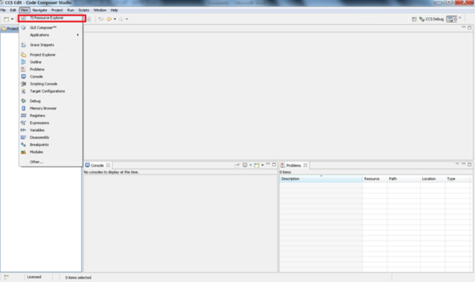
In CCS, click View->TI Resource Explorer
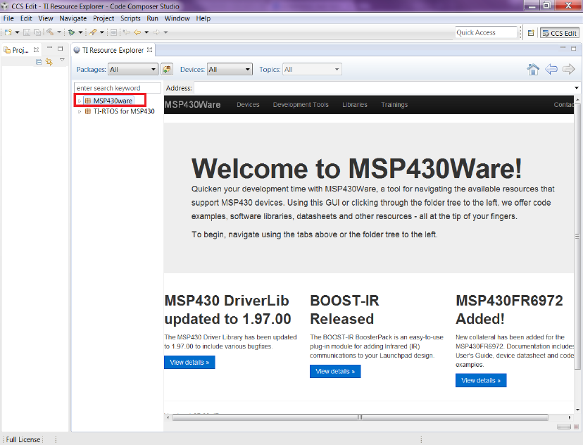
In Resource Explorer View, click on MSP430ware
CHAPTER 2. NAVIGATING TO DRIVERLIB THROUGH CCS RESOURCE EXPLORER 9
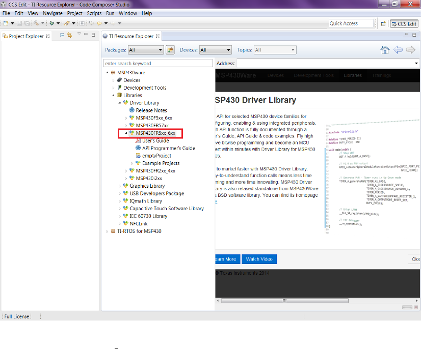
Clicking MSP430ware takes you to the introductory page. The version of the latest MSP430ware
installed is available in this page. In this screenshot the version is 1.30.00.15 The various
software, collateral, code examples, datasheets and user guides can be navigated by clicking the
different topics under MSP430ware. To proceed to driverlib, click on Libraries->Driverlib as shown
in the next two screenshots.
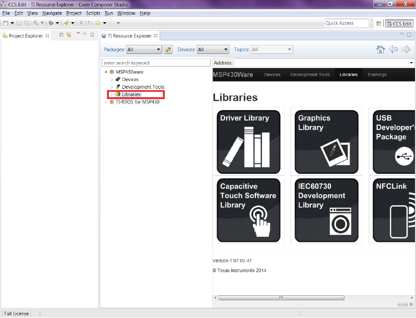
CHAPTER 2. NAVIGATING TO DRIVERLIB THROUGH CCS RESOURCE EXPLORER 10
CHAPTER 2. NAVIGATING TO DRIVERLIB THROUGH CCS RESOURCE EXPLORER 11
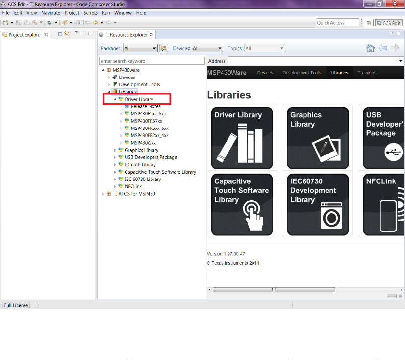
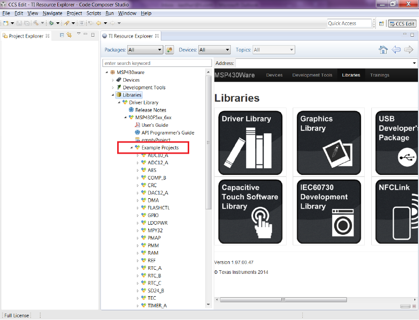
Driverlib is designed per Family. If a common device family user's guide exists for a group of
devices, these devices belong to the same 'family'. Currently driverlib is available for the following
family of devices. MSP430F5xx 6xx MSP430FR57xx MSP430FR2xx 4xx MSP430FR5xx 6xx
MSP430i2xx
CHAPTER 2. NAVIGATING TO DRIVERLIB THROUGH CCS RESOURCE EXPLORER 12
Click on the MSP430FR5xx 6xx to navigate to the driverlib based example code for that family.
CHAPTER 2. NAVIGATING TO DRIVERLIB THROUGH CCS RESOURCE EXPLORER 13
The various peripherals are listed in alphabetical order. The names of peripherals are as in device
family user's guide. Clicking on a peripheral name lists the driverlib example code for that
peripheral. The screenshot below shows an example when the user clicks on GPIO peripheral.
CHAPTER 2. NAVIGATING TO DRIVERLIB THROUGH CCS RESOURCE EXPLORER 14
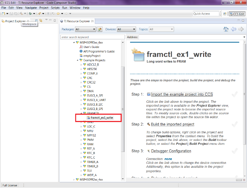
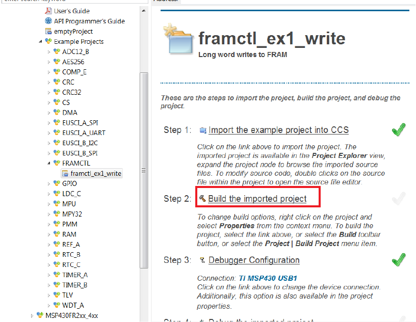
Now click on the specific example you are interested in. On the right side there are options to
Import/Build/Download and Debug. Import the project by clicking on the ”Import the example
project into CCS”

CHAPTER 2. NAVIGATING TO DRIVERLIB THROUGH CCS RESOURCE EXPLORER 15
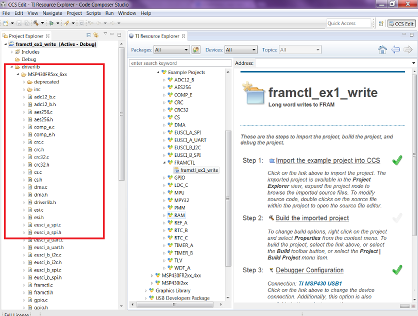
The imported project can be viewed on the left in the Project Explorer. All required driverlib source
and header files are included inside the driverlib folder. All driverlib source and header files are
linked to the example projects. So if the user modifies any of these source or header files, the
original copy of the installed MSP430ware driverlib source and header files get modified.
CHAPTER 2. NAVIGATING TO DRIVERLIB THROUGH CCS RESOURCE EXPLORER 16
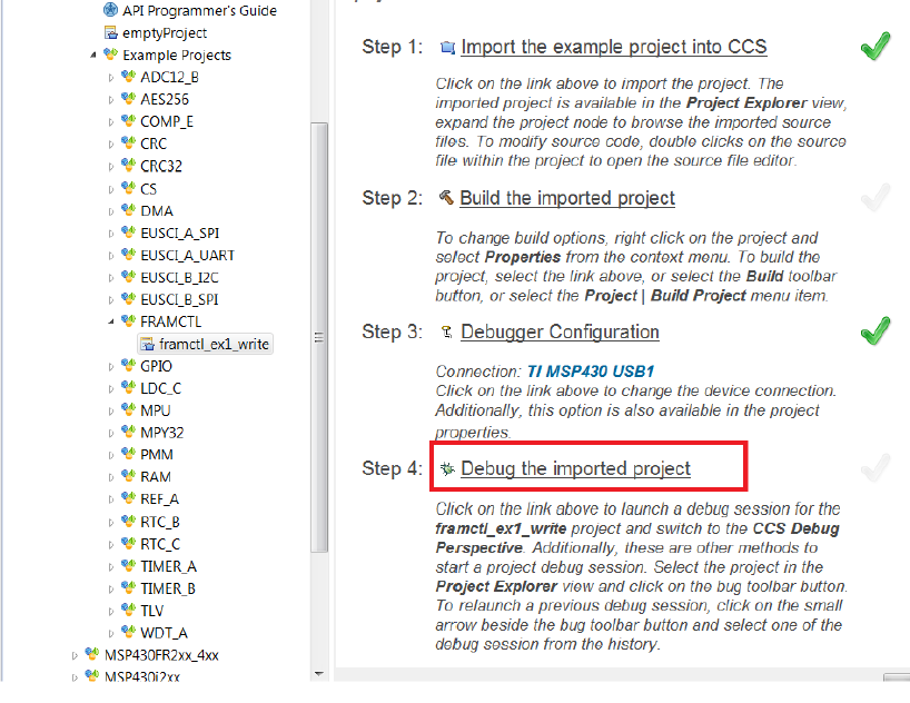
Now click on Build the imported project on the right to build the example project.
CHAPTER 2. NAVIGATING TO DRIVERLIB THROUGH CCS RESOURCE EXPLORER 17
Now click on Build the imported project on the right to build the example project.
CHAPTER 2. NAVIGATING TO DRIVERLIB THROUGH CCS RESOURCE EXPLORER 18
The COM port to download to can be changed using the Debugger Configuration option on the
right if required.
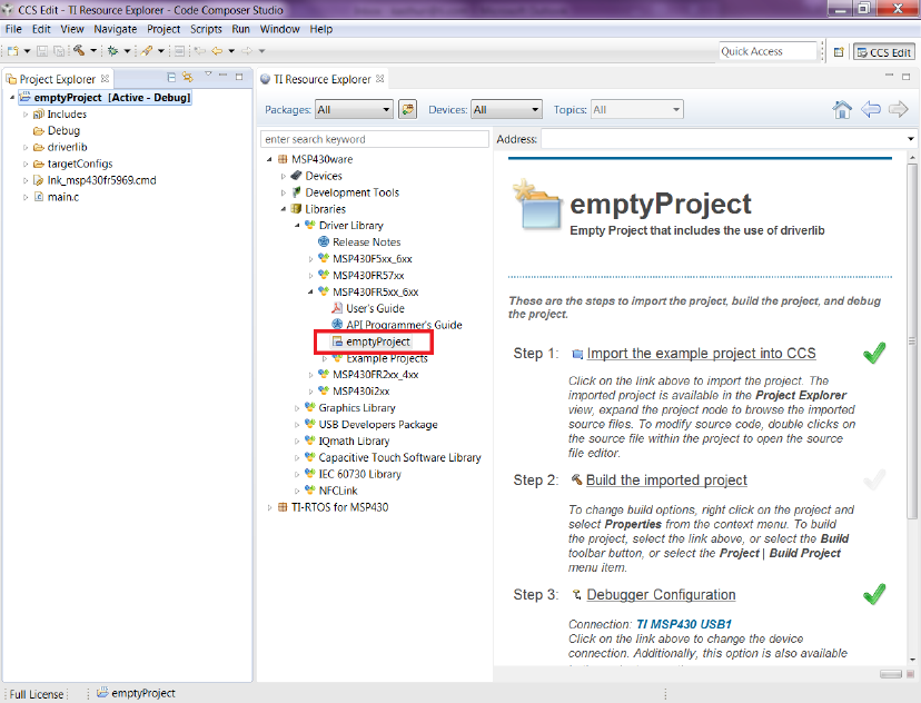
To get started on a new project we recommend getting started on an empty project we provide.
This project has all the driverlib source files, header files, project paths are set by default.
CHAPTER 2. NAVIGATING TO DRIVERLIB THROUGH CCS RESOURCE EXPLORER 19
The main.c included with the empty project can be modified to include user code.
CHAPTER 3. HOW TO CREATE A NEW CCS PROJECT THAT USES DRIVERLIB 20
3 How to create a new CCS project that uses
Driverlib
3.1 Introduction
To get started on a new project we recommend using the new project wizard. For driver library to
work with the new project wizard CCS must have discovered the driver library RTSC product. For
more information refer to the installation steps of the release notes. The new project wizard adds
the needed driver library source files and adds the driver library include path.
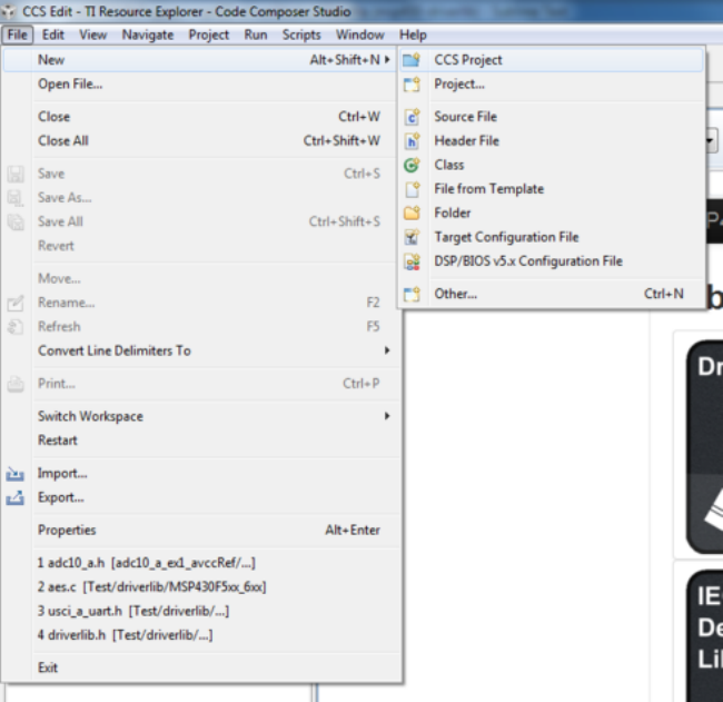
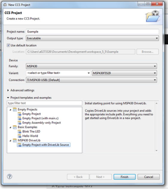
To open the new project wizard go to File ->New ->CCS Project as seen in the screenshot below.
Once the new project wizard has been opened name your project and choose the device you
would like to create a Driver Library project for. The device must be supported by driver library.
Then under ”Project templates and examples” choose ”Empty Project with DriverLib Source” as
seen below.
CHAPTER 3. HOW TO CREATE A NEW CCS PROJECT THAT USES DRIVERLIB 21
Finally click ”Finish” and begin developing with your Driver Library enabled project.
We recommend -O4 compiler settings for more efficient optimizations for projects using driverlib
CHAPTER 4. HOW TO INCLUDE DRIVERLIB INTO YOUR EXISTING CCS PROJECT 22
4 How to include driverlib into your existing
CCS project
4.1 Introduction
To add driver library to an existing project we recommend using CCS project templates. For driver
library to work with project templates CCS must have discovered the driver library RTSC product.
For more information refer to the installation steps of the release notes. CCS project templates
adds the needed driver library source files and adds the driver library include path.
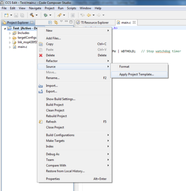
To apply a project template right click on an existing project then go to Source ->Apply Project
Template as seen in the screenshot below.
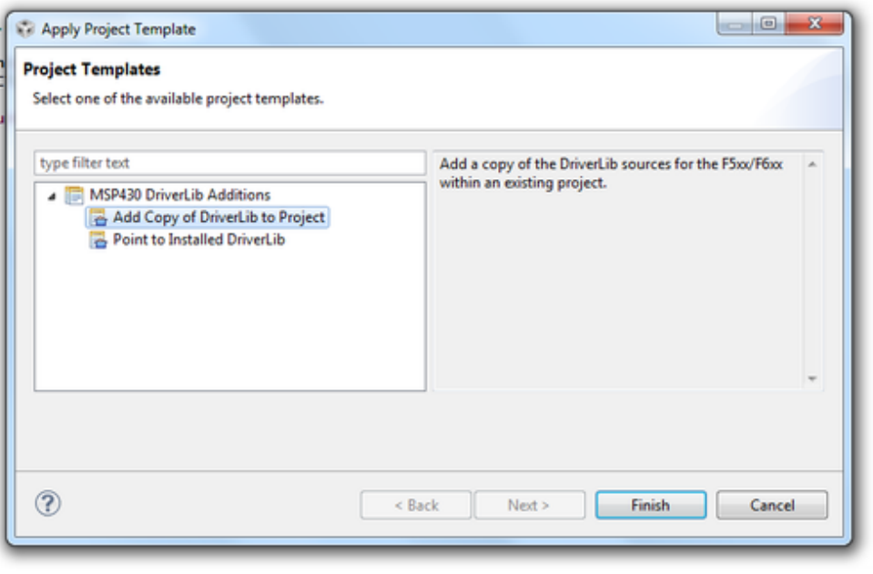
In the ”Apply Project Template” dialog box under ”MSP430 DriverLib Additions” choose either ”Add
Local Copy” or ”Point to Installed DriverLib” as seen in the screenshot below. Most users will want
to add a local copy which copies the DriverLib source into the project and sets the compiler
settings needed.
Pointing to an installed DriverLib is for advandced users who are including a static library in their
project and want to add the DriverLib header files to their include path.
CHAPTER 4. HOW TO INCLUDE DRIVERLIB INTO YOUR EXISTING CCS PROJECT 23
Click ”Finish” and start developing with driver library in your project.
CHAPTER 5. HOW TO CREATE A NEW IAR PROJECT THAT USES DRIVERLIB 24
5 How to create a new IAR project that uses
Driverlib
5.1 Introduction
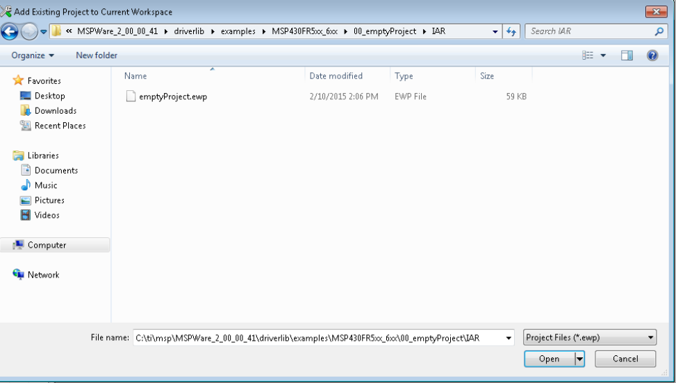
It is recommended to get started with an Empty Driverlib Project. Browse to the empty project in
your device's family. This is available in the driverlib instal folder\00 emptyProject
CHAPTER 5. HOW TO CREATE A NEW IAR PROJECT THAT USES DRIVERLIB 25

CHAPTER 5. HOW TO CREATE A NEW IAR PROJECT THAT USES DRIVERLIB 26
CHAPTER 6. HOW TO INCLUDE DRIVERLIB INTO YOUR EXISTING IAR PROJECT 27
6 How to include driverlib into your existing
IAR project
6.1 Introduction
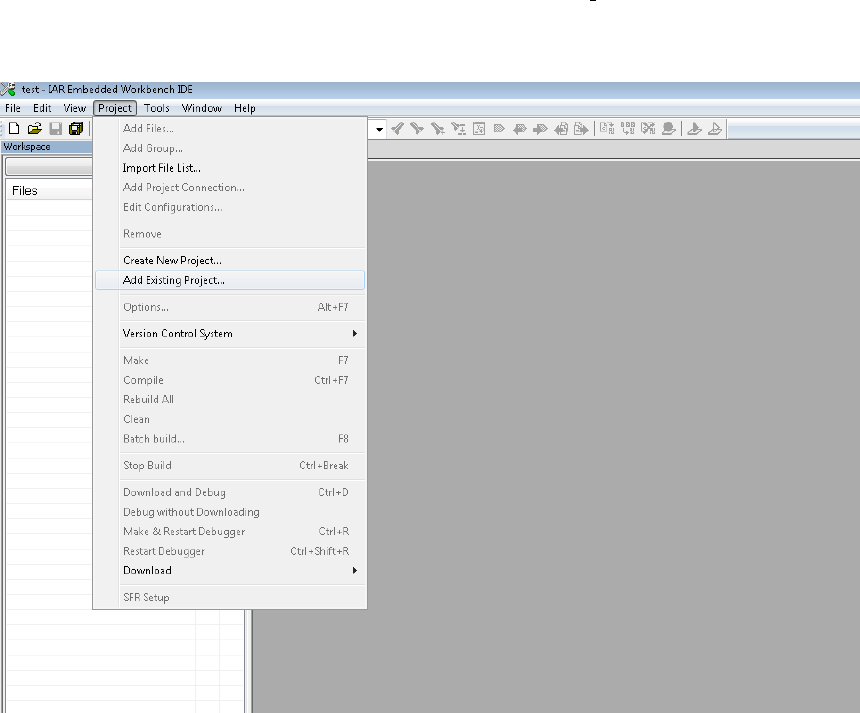
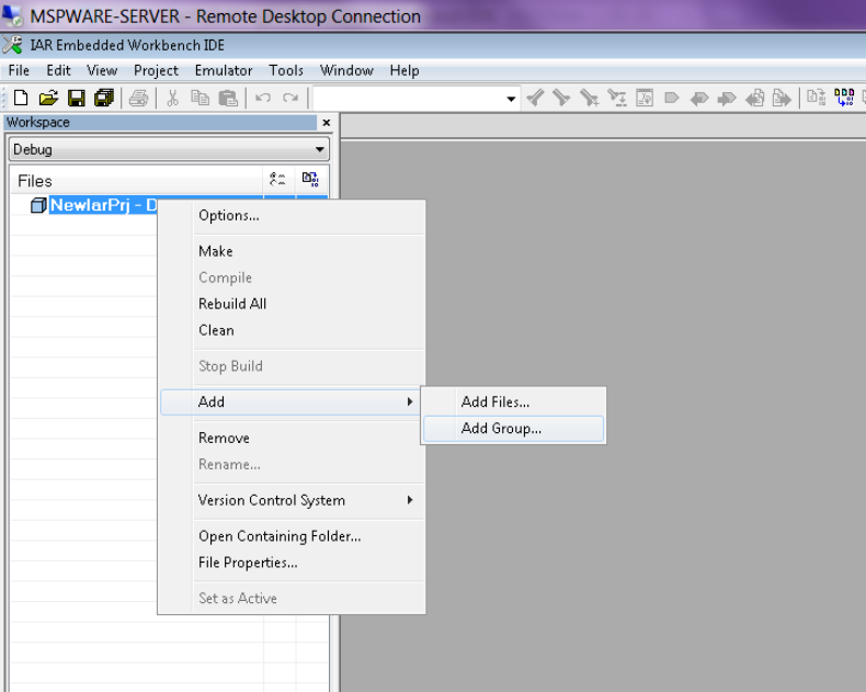
To add driver library to an existing project, right click project click on Add Group - ”driverlib”
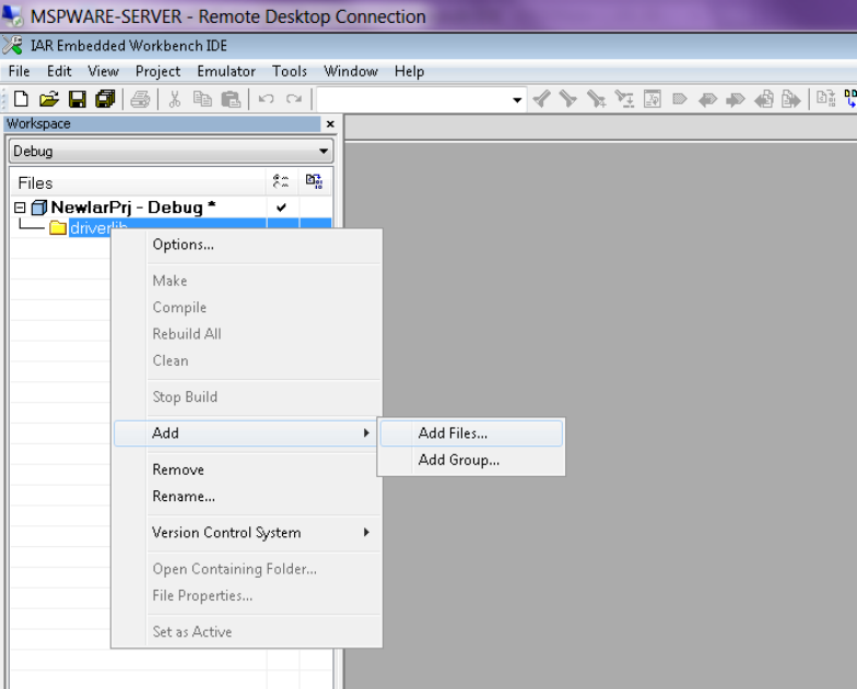
Now click Add files and browse through driverlib folder and add all source files of the family the
device belongs to.
CHAPTER 6. HOW TO INCLUDE DRIVERLIB INTO YOUR EXISTING IAR PROJECT 28
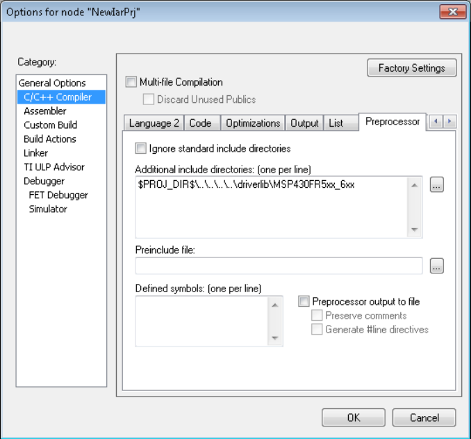
Add another group via ”Add Group” and add inc folder. Add all files in the same driverlib family inc
folder
CHAPTER 6. HOW TO INCLUDE DRIVERLIB INTO YOUR EXISTING IAR PROJECT 29
Click ”Finish” and start developing with driver library in your project.

CHAPTER 7. 12-BIT ANALOG-TO-DIGITAL CONVERTER (ADC12 B) 30
7 12-Bit Analog-to-Digital Converter
(ADC12 B)
Introduction ..............................................................................................30
API Functions ............................................................................................31
Programming Example ...................................................................................56
7.1 Introduction
The 12-Bit Analog-to-Digital (ADC12 B) API provides a set of functions for using the MSP430Ware
ADC12 B modules. Functions are provided to initialize the ADC12 B modules, setup signal
sources and reference voltages for each memory buffer, and manage interrupts for the ADC12 B
modules.
The ADC12 B module provides the ability to convert analog signals into a digital value in respect
to given reference voltages. The module implements a 12-bit SAR core, sample select control,
and up to 32 independent conversion-and-control buffers. The conversion-and-control buffer
allows up to 32 independent analog-to-digital converter (ADC) samples to be converted and stored
without any CPU intervention. The ADC12 B can also generate digital values from 0 to Vcc with
an 8-, 10- or 12-bit resolution and it can operate in 2 different sampling modes, and 4 different
conversion modes. The sampling modes are extended sampling and pulse sampling, in extended
sampling the sample/hold signal must stay high for the duration of sampling, while in pulse mode a
sampling timer is setup to start on a rising edge of the sample/hold signal and sample for a
specified amount of clock cycles. The 4 conversion modes are single-channel single conversion,
sequence of channels single-conversion, repeated single channel conversions, and repeated
sequence of channels conversions.
The ADC12 B module can generate multiple interrupts. An interrupt can be asserted for each
memory buffer when a conversion is complete, or when a conversion is about to overwrite the
converted data in any of the memory buffers before it has been read out, and/or when a
conversion is about to start before the last conversion is complete.
ADC12 B features include:
200 ksps maximum conversion rate at maximum resolution of 12-bits
Monotonic 12-bit converter with no missing codes
Sample-and-hold with programmable sampling periods controlled by software or timers.
Conversion initiation by software or timers.
Software-selectable on-chip reference voltage generation (1.2 V, 2.0 V, or 2.5 V) with option
to make available externally
Software-selectable internal or external reference
Up to 32 individually configurable external input channels, single-ended or differential input
selection available
Internal conversion channels for internal temperature sensor and 2/3 ?AVCC and four more
internal channels available on select devices see device data sheet for availability as well as
function
Independent channel-selectable reference sources for both positive and negative references

CHAPTER 7. 12-BIT ANALOG-TO-DIGITAL CONVERTER (ADC12 B) 31
Selectable conversion clock source
Single-channel, repeat-single-channel, sequence (autoscan), and repeat-sequence
(repeated autoscan) conversion modes
Interrupt vector register for fast decoding of 38 ADC interrupts
32 conversion-result storage registers
Window comparator for low power monitoring of input signals of conversion-result registers
7.2 API Functions
Functions
bool ADC12 B init (uint16 t baseAddress, ADC12 B initParam ∗param)
Initializes the ADC12B Module.
void ADC12 B enable (uint16 t baseAddress)
Enables the ADC12B block.
void ADC12 B disable (uint16 t baseAddress)
Disables the ADC12B block.
void ADC12 B setupSamplingTimer (uint16 t baseAddress, uint16 t
clockCycleHoldCountLowMem, uint16 t clockCycleHoldCountHighMem, uint16 t
multipleSamplesEnabled)
Sets up and enables the Sampling Timer Pulse Mode.
void ADC12 B disableSamplingTimer (uint16 t baseAddress)
Disables Sampling Timer Pulse Mode.
void ADC12 B configureMemory (uint16 t baseAddress, ADC12 B configureMemoryParam
∗param)
Configures the controls of the selected memory buffer.
void ADC12 B setWindowCompAdvanced (uint16 t baseAddress, uint16 t highThreshold,
uint16 t lowThreshold)
Sets the high and low threshold for the window comparator feature.
void ADC12 B enableInterrupt (uint16 t baseAddress, uint16 t interruptMask0, uint16 t
interruptMask1, uint16 t interruptMask2)
Enables selected ADC12B interrupt sources.
void ADC12 B disableInterrupt (uint16 t baseAddress, uint16 t interruptMask0, uint16 t
interruptMask1, uint16 t interruptMask2)
Disables selected ADC12B interrupt sources.
void ADC12 B clearInterrupt (uint16 t baseAddress, uint8 t interruptRegisterChoice, uint16 t
memoryInterruptFlagMask)
Clears ADC12B selected interrupt flags.
uint16 t ADC12 B getInterruptStatus (uint16 t baseAddress, uint8 t interruptRegisterChoice,
uint16 t memoryInterruptFlagMask)
Returns the status of the selected memory interrupt flags.
void ADC12 B startConversion (uint16 t baseAddress, uint16 t startingMemoryBufferIndex,
uint8 t conversionSequenceModeSelect)
Enables/Starts an Analog-to-Digital Conversion.
void ADC12 B disableConversions (uint16 t baseAddress, bool preempt)
Disables the ADC from converting any more signals.
uint16 t ADC12 B getResults (uint16 t baseAddress, uint8 t memoryBufferIndex)
Returns the raw contents of the specified memory buffer.
void ADC12 B setResolution (uint16 t baseAddress, uint8 t resolutionSelect)

CHAPTER 7. 12-BIT ANALOG-TO-DIGITAL CONVERTER (ADC12 B) 32
Use to change the resolution of the converted data.
void ADC12 B setSampleHoldSignalInversion (uint16 t baseAddress, uint16 t invertedSignal)
Use to invert or un-invert the sample/hold signal.
void ADC12 B setDataReadBackFormat (uint16 t baseAddress, uint8 t readBackFormat)
Use to set the read-back format of the converted data.
void ADC12 B setAdcPowerMode (uint16 t baseAddress, uint8 t powerMode)
Use to set the ADC's power conservation mode if the sampling rate is at 50-ksps or less.
uint32 t ADC12 B getMemoryAddressForDMA (uint16 t baseAddress, uint8 t memoryIndex)
Returns the address of the specified memory buffer for the DMA module.
uint8 t ADC12 B isBusy (uint16 t baseAddress)
Returns the busy status of the ADC12B core.
7.2.1 Detailed Description
The ADC12 B API is broken into three groups of functions: those that deal with initialization and
conversions, those that handle interrupts, and those that handle auxiliary features of the ADC12 B.
The ADC12 B initialization and conversion functions are
ADC12 B init
ADC12 B configureMemory
ADC12 B setWindowCompAdvanced
ADC12 B setupSamplingTimer
ADC12 B disableSamplingTimer
ADC12 B startConversion
ADC12 B disableConversions
ADC12 B getResults
ADC12 B isBusy
The ADC12 B interrupts are handled by
ADC12 B enableInterrupt
ADC12 B disableInterrupt
ADC12 B clearInterrupt
ADC12 B getInterruptStatus
Auxiliary features of the ADC12 B are handled by
ADC12 B setResolution
ADC12 B setSampleHoldSignalInversion
ADC12 B setDataReadBackFormat
ADC12 B enableReferenceBurst
ADC12 B disableReferenceBurst
ADC12 B setAdcPowerMode
ADC12 B getMemoryAddressForDMA
ADC12 B enable
ADC12 B disable

CHAPTER 7. 12-BIT ANALOG-TO-DIGITAL CONVERTER (ADC12 B) 33
7.2.2 Function Documentation
ADC12 B clearInterrupt()
void ADC12 B clearInterrupt (
uint16 t baseAddress,
uint8 t interruptRegisterChoice,
uint16 t memoryInterruptFlagMask )
Clears ADC12B selected interrupt flags.
Modified registers are ADC12IFG .
Parameters
baseAddress is the base address of the ADC12B module.
interruptRegisterChoice is either 0, 1, or 2, to choose the correct interrupt register to
update

CHAPTER 7. 12-BIT ANALOG-TO-DIGITAL CONVERTER (ADC12 B) 34
Parameters
memoryInterruptFlagMask is the bit mask of the memory buffer and overflow interrupt flags to
be cleared. Valid values are:
ADC12 B IFG0 - interruptRegisterChoice = 0
ADC12 B IFG1
ADC12 B IFG2
ADC12 B IFG3
ADC12 B IFG4
ADC12 B IFG5
ADC12 B IFG6
ADC12 B IFG7
ADC12 B IFG8
ADC12 B IFG9
ADC12 B IFG10
ADC12 B IFG11
ADC12 B IFG12
ADC12 B IFG13
ADC12 B IFG14
ADC12 B IFG15
ADC12 B IFG16 - interruptRegisterChoice = 1
ADC12 B IFG17
ADC12 B IFG18
ADC12 B IFG19
ADC12 B IFG20
ADC12 B IFG21
ADC12 B IFG22
ADC12 B IFG23
ADC12 B IFG24
ADC12 B IFG25
ADC12 B IFG26
ADC12 B IFG27
ADC12 B IFG28
ADC12 B IFG29
ADC12 B IFG30
ADC12 B IFG31
ADC12 B INIFG - interruptRegisterChoice = 2
ADC12 B LOIFG
ADC12 B HIIFG
ADC12 B OVIFG
ADC12 B TOVIFG
ADC12 B RDYIFG - The selected ADC12B interrupt flags
are cleared, so that it no longer asserts. The memory buffer
interrupt flags are only cleared when the memory buffer is
accessed. Note that the overflow interrupts do not have an
interrupt flag to clear; they must be accessed directly from
the interrupt vector.

CHAPTER 7. 12-BIT ANALOG-TO-DIGITAL CONVERTER (ADC12 B) 35
Parameters
Returns
None
ADC12 B configureMemory()
void ADC12 B configureMemory (
uint16 t baseAddress,
ADC12 B configureMemoryParam ∗param )
Configures the controls of the selected memory buffer.
Maps an input signal conversion into the selected memory buffer, as well as the positive and
negative reference voltages for each conversion being stored into this memory buffer. If the
internal reference is used for the positive reference voltage, the internal REF module must be used
to control the voltage level. Note that if a conversion has been started with the startConversion()
function, then a call to disableConversions() is required before this function may be called. If
conversion is not disabled, this function does nothing.
Parameters
baseAddress is the base address of the ADC12B module.
param is the pointer to struct for ADC12B memory configuration.
Returns
None
References ADC12 B configureMemoryParam::differentialModeSelect,
ADC12 B configureMemoryParam::endOfSequence,
ADC12 B configureMemoryParam::inputSourceSelect,
ADC12 B configureMemoryParam::memoryBufferControlIndex,
ADC12 B configureMemoryParam::refVoltageSourceSelect, and
ADC12 B configureMemoryParam::windowComparatorSelect.
ADC12 B disable()
void ADC12 B disable (
uint16 t baseAddress )
Disables the ADC12B block.
This will disable operation of the ADC12B block.
Parameters
baseAddress is the base address of the ADC12B module.

CHAPTER 7. 12-BIT ANALOG-TO-DIGITAL CONVERTER (ADC12 B) 36
Modified bits are ADC12ON of ADC12CTL0 register.
Returns
None
References ADC12 B isBusy().
ADC12 B disableConversions()
void ADC12 B disableConversions (
uint16 t baseAddress,
bool preempt )
Disables the ADC from converting any more signals.
Disables the ADC from converting any more signals. If there is a conversion in progress, this
function can stop it immediately if the preempt parameter is set as
ADC12 B PREEMPTCONVERSION, by changing the conversion mode to single-channel,
single-conversion and disabling conversions. If the conversion mode is set as single-channel,
single-conversion and this function is called without preemption, then the ADC core conversion
status is polled until the conversion is complete before disabling conversions to prevent
unpredictable data. If the ADC12 B startConversion() has been called, then this function has to be
called to re-initialize the ADC, reconfigure a memory buffer control, enable/disable the sampling
pulse mode, or change the internal reference voltage.
Parameters
baseAddress is the base address of the ADC12B module.
preempt specifies if the current conversion should be preemptively stopped before the
end of the conversion. Valid values are:
ADC12 B COMPLETECONVERSION - Allows the ADC12B to end the
current conversion before disabling conversions.
ADC12 B PREEMPTCONVERSION - Stops the ADC12B immediately,
with unpredictable results of the current conversion.
Modified bits of ADC12CTL1 register and bits of ADC12CTL0 register.
Returns
None
References ADC12 B isBusy().
ADC12 B disableInterrupt()
void ADC12 B disableInterrupt (
uint16 t baseAddress,
uint16 t interruptMask0,
uint16 t interruptMask1,
uint16 t interruptMask2 )

CHAPTER 7. 12-BIT ANALOG-TO-DIGITAL CONVERTER (ADC12 B) 37
Disables selected ADC12B interrupt sources.
Disables the indicated ADC12B interrupt sources. Only the sources that are enabled can be
reflected to the processor interrupt; disabled sources have no effect on the processor.
Parameters
baseAddress is the base address of the ADC12B module.
interruptMask0 is the bit mask of the memory buffer and overflow interrupt sources to be
disabled. If the desired interrupt is not available in the selection for
interruptMask0, then simply pass in a '0' for this value. Valid values are:
ADC12 B IE0
ADC12 B IE1
ADC12 B IE2
ADC12 B IE3
ADC12 B IE4
ADC12 B IE5
ADC12 B IE6
ADC12 B IE7
ADC12 B IE8
ADC12 B IE9
ADC12 B IE10
ADC12 B IE11
ADC12 B IE12
ADC12 B IE13
ADC12 B IE14
ADC12 B IE15

CHAPTER 7. 12-BIT ANALOG-TO-DIGITAL CONVERTER (ADC12 B) 38
Parameters
interruptMask1 is the bit mask of the memory buffer and overflow interrupt sources to be
disabled. If the desired interrupt is not available in the selection for
interruptMask1, then simply pass in a '0' for this value. Valid values are:
ADC12 B IE16
ADC12 B IE17
ADC12 B IE18
ADC12 B IE19
ADC12 B IE20
ADC12 B IE21
ADC12 B IE22
ADC12 B IE23
ADC12 B IE24
ADC12 B IE25
ADC12 B IE26
ADC12 B IE27
ADC12 B IE28
ADC12 B IE29
ADC12 B IE30
ADC12 B IE31
interruptMask2 is the bit mask of the memory buffer and overflow interrupt sources to be
disabled. If the desired interrupt is not available in the selection for
interruptMask2, then simply pass in a '0' for this value. Valid values are:
ADC12 B INIE - Interrupt enable for a conversion in the result register is
either greater than the ADC12LO or lower than the ADC12HI threshold.
GIE bit must be set to enable the interrupt.
ADC12 B LOIE - Interrupt enable for the falling short of the lower limit
interrupt of the window comparator for the result register. GIE bit must
be set to enable the interrupt.
ADC12 B HIIE - Interrupt enable for the exceeding the upper limit of the
window comparator for the result register. GIE bit must be set to enable
the interrupt.
ADC12 B OVIE - Interrupt enable for a conversion that is about to save
to a memory buffer that has not been read out yet. GIE bit must be set to
enable the interrupt.
ADC12 B TOVIE - enable for a conversion that is about to start before
the previous conversion has been completed. GIE bit must be set to
enable the interrupt.
ADC12 B RDYIE - enable for the local buffered reference ready signal.
GIE bit must be set to enable the interrupt.
Modified bits of ADC12IERx register.

CHAPTER 7. 12-BIT ANALOG-TO-DIGITAL CONVERTER (ADC12 B) 39
Returns
None
ADC12 B disableSamplingTimer()
void ADC12 B disableSamplingTimer (
uint16 t baseAddress )
Disables Sampling Timer Pulse Mode.
Disables the Sampling Timer Pulse Mode. Note that if a conversion has been started with the
startConversion() function, then a call to disableConversions() is required before this function may
be called.
Parameters
baseAddress is the base address of the ADC12B module.
Returns
None
ADC12 B enable()
void ADC12 B enable (
uint16 t baseAddress )
Enables the ADC12B block.
This will enable operation of the ADC12B block.
Parameters
baseAddress is the base address of the ADC12B module.
Modified bits are ADC12ON of ADC12CTL0 register.
Returns
None
ADC12 B enableInterrupt()
void ADC12 B enableInterrupt (
uint16 t baseAddress,
uint16 t interruptMask0,
uint16 t interruptMask1,
uint16 t interruptMask2 )
Enables selected ADC12B interrupt sources.

CHAPTER 7. 12-BIT ANALOG-TO-DIGITAL CONVERTER (ADC12 B) 40
Enables the indicated ADC12B interrupt sources. Only the sources that are enabled can be
reflected to the processor interrupt; disabled sources have no effect on the processor. Does not
clear interrupt flags.
Parameters
baseAddress is the base address of the ADC12B module.
interruptMask0 is the bit mask of the memory buffer and overflow interrupt sources to
be enabled. If the desired interrupt is not available in the selection for
interruptMask0, then simply pass in a '0' for this value. Valid values
are:
ADC12 B IE0
ADC12 B IE1
ADC12 B IE2
ADC12 B IE3
ADC12 B IE4
ADC12 B IE5
ADC12 B IE6
ADC12 B IE7
ADC12 B IE8
ADC12 B IE9
ADC12 B IE10
ADC12 B IE11
ADC12 B IE12
ADC12 B IE13
ADC12 B IE14
ADC12 B IE15

CHAPTER 7. 12-BIT ANALOG-TO-DIGITAL CONVERTER (ADC12 B) 41
Parameters
interruptMask1 is the bit mask of the memory buffer and overflow interrupt sources to
be enabled. If the desired interrupt is not available in the selection for
interruptMask1, then simply pass in a '0' for this value. Valid values
are:
ADC12 B IE16
ADC12 B IE17
ADC12 B IE18
ADC12 B IE19
ADC12 B IE20
ADC12 B IE21
ADC12 B IE22
ADC12 B IE23
ADC12 B IE24
ADC12 B IE25
ADC12 B IE26
ADC12 B IE27
ADC12 B IE28
ADC12 B IE29
ADC12 B IE30
ADC12 B IE31
interruptMask2 is the bit mask of the memory buffer and overflow interrupt sources to
be enabled. If the desired interrupt is not available in the selection for
interruptMask2, then simply pass in a '0' for this value. Valid values
are:
ADC12 B INIE - Interrupt enable for a conversion in the result
register is either greater than the ADC12LO or lower than the
ADC12HI threshold. GIE bit must be set to enable the interrupt.
ADC12 B LOIE - Interrupt enable for the falling short of the lower
limit interrupt of the window comparator for the result register.
GIE bit must be set to enable the interrupt.
ADC12 B HIIE - Interrupt enable for the exceeding the upper limit
of the window comparator for the result register. GIE bit must be
set to enable the interrupt.
ADC12 B OVIE - Interrupt enable for a conversion that is about to
save to a memory buffer that has not been read out yet. GIE bit
must be set to enable the interrupt.
ADC12 B TOVIE - enable for a conversion that is about to start
before the previous conversion has been completed. GIE bit must
be set to enable the interrupt.
ADC12 B RDYIE - enable for the local buffered reference ready
signal. GIE bit must be set to enable the interrupt.

CHAPTER 7. 12-BIT ANALOG-TO-DIGITAL CONVERTER (ADC12 B) 42
Modified bits of ADC12IERx register.
Returns
None
ADC12 B getInterruptStatus()
uint16 t ADC12 B getInterruptStatus (
uint16 t baseAddress,
uint8 t interruptRegisterChoice,
uint16 t memoryInterruptFlagMask )
Returns the status of the selected memory interrupt flags.
Returns the status of the selected memory interrupt flags. Note that the overflow interrupts do not
have an interrupt flag to clear; they must be accessed directly from the interrupt vector.
Parameters
baseAddress is the base address of the ADC12B module.
interruptRegisterChoice is either 0, 1, or 2, to choose the correct interrupt register to
update
CHAPTER 7. 12-BIT ANALOG-TO-DIGITAL CONVERTER (ADC12 B) 43
Parameters
memoryInterruptFlagMask is the bit mask of the memory buffer and overflow interrupt flags to
be cleared. Valid values are:
ADC12 B IFG0 - interruptRegisterChoice = 0
ADC12 B IFG1
ADC12 B IFG2
ADC12 B IFG3
ADC12 B IFG4
ADC12 B IFG5
ADC12 B IFG6
ADC12 B IFG7
ADC12 B IFG8
ADC12 B IFG9
ADC12 B IFG10
ADC12 B IFG11
ADC12 B IFG12
ADC12 B IFG13
ADC12 B IFG14
ADC12 B IFG15
ADC12 B IFG16 - interruptRegisterChoice = 1
ADC12 B IFG17
ADC12 B IFG18
ADC12 B IFG19
ADC12 B IFG20
ADC12 B IFG21
ADC12 B IFG22
ADC12 B IFG23
ADC12 B IFG24
ADC12 B IFG25
ADC12 B IFG26
ADC12 B IFG27
ADC12 B IFG28
ADC12 B IFG29
ADC12 B IFG30
ADC12 B IFG31
ADC12 B INIFG - interruptRegisterChoice = 2
ADC12 B LOIFG
ADC12 B HIIFG
ADC12 B OVIFG
ADC12 B TOVIFG
ADC12 B RDYIFG - The selected ADC12B interrupt flags
are cleared, so that it no longer asserts. The memory buffer
interrupt flags are only cleared when the memory buffer is
accessed. Note that the overflow interrupts do not have an
interrupt flag to clear; they must be accessed directly from
the interrupt vector.

CHAPTER 7. 12-BIT ANALOG-TO-DIGITAL CONVERTER (ADC12 B) 44
Parameters
Returns
The current interrupt flag status for the corresponding mask.
ADC12 B getMemoryAddressForDMA()
uint32 t ADC12 B getMemoryAddressForDMA (
uint16 t baseAddress,
uint8 t memoryIndex )
Returns the address of the specified memory buffer for the DMA module.
Returns the address of the specified memory buffer. This can be used in conjunction with the
DMA to store the converted data directly to memory.
Parameters
baseAddress is the base address of the ADC12B module.

CHAPTER 7. 12-BIT ANALOG-TO-DIGITAL CONVERTER (ADC12 B) 45
Parameters
memoryIndex is the memory buffer to return the address of. Valid values are:
ADC12 B MEMORY 0
ADC12 B MEMORY 1
ADC12 B MEMORY 2
ADC12 B MEMORY 3
ADC12 B MEMORY 4
ADC12 B MEMORY 5
ADC12 B MEMORY 6
ADC12 B MEMORY 7
ADC12 B MEMORY 8
ADC12 B MEMORY 9
ADC12 B MEMORY 10
ADC12 B MEMORY 11
ADC12 B MEMORY 12
ADC12 B MEMORY 13
ADC12 B MEMORY 14
ADC12 B MEMORY 15
ADC12 B MEMORY 16
ADC12 B MEMORY 17
ADC12 B MEMORY 18
ADC12 B MEMORY 19
ADC12 B MEMORY 20
ADC12 B MEMORY 21
ADC12 B MEMORY 22
ADC12 B MEMORY 23
ADC12 B MEMORY 24
ADC12 B MEMORY 25
ADC12 B MEMORY 26
ADC12 B MEMORY 27
ADC12 B MEMORY 28
ADC12 B MEMORY 29
ADC12 B MEMORY 30
ADC12 B MEMORY 31
Returns
address of the specified memory buffer

CHAPTER 7. 12-BIT ANALOG-TO-DIGITAL CONVERTER (ADC12 B) 46
ADC12 B getResults()
uint16 t ADC12 B getResults (
uint16 t baseAddress,
uint8 t memoryBufferIndex )
Returns the raw contents of the specified memory buffer.
Returns the raw contents of the specified memory buffer. The format of the content depends on
the read-back format of the data: if the data is in signed 2's complement format then the contents
in the memory buffer will be left-justified with the least-significant bits as 0's, whereas if the data is
in unsigned format then the contents in the memory buffer will be right- justified with the
most-significant bits as 0's.
Parameters
baseAddress is the base address of the ADC12B module.
CHAPTER 7. 12-BIT ANALOG-TO-DIGITAL CONVERTER (ADC12 B) 47
Parameters
memoryBufferIndex is the specified memory buffer to read. Valid values
are:
ADC12 B MEMORY 0
ADC12 B MEMORY 1
ADC12 B MEMORY 2
ADC12 B MEMORY 3
ADC12 B MEMORY 4
ADC12 B MEMORY 5
ADC12 B MEMORY 6
ADC12 B MEMORY 7
ADC12 B MEMORY 8
ADC12 B MEMORY 9
ADC12 B MEMORY 10
ADC12 B MEMORY 11
ADC12 B MEMORY 12
ADC12 B MEMORY 13
ADC12 B MEMORY 14
ADC12 B MEMORY 15
ADC12 B MEMORY 16
ADC12 B MEMORY 17
ADC12 B MEMORY 18
ADC12 B MEMORY 19
ADC12 B MEMORY 20
ADC12 B MEMORY 21
ADC12 B MEMORY 22
ADC12 B MEMORY 23
ADC12 B MEMORY 24
ADC12 B MEMORY 25
ADC12 B MEMORY 26
ADC12 B MEMORY 27
ADC12 B MEMORY 28
ADC12 B MEMORY 29
ADC12 B MEMORY 30
ADC12 B MEMORY 31
Returns
A signed integer of the contents of the specified memory buffer.
CHAPTER 7. 12-BIT ANALOG-TO-DIGITAL CONVERTER (ADC12 B) 48
ADC12 B init()
bool ADC12 B init (
uint16 t baseAddress,
ADC12 B initParam ∗param )
Initializes the ADC12B Module.
This function initializes the ADC module to allow for analog-to-digital conversions. Specifically this
function sets up the sample-and-hold signal and clock sources for the ADC core to use for
conversions. Upon successful completion of the initialization all of the ADC control registers will be
reset, excluding the memory controls and reference module bits, the given parameters will be set,
and the ADC core will be turned on (Note, that the ADC core only draws power during conversions
and remains off when not converting).Note that sample/hold signal sources are device dependent.
Note that if re-initializing the ADC after starting a conversion with the startConversion() function,
the disableConversion() must be called BEFORE this function can be called.
Parameters
baseAddress is the base address of the ADC12B module.
param is the pointer to struct for initialization.
Returns
STATUS SUCCESS or STATUS FAILURE of the initialization process.
References ADC12 B initParam::clockSourceDivider, ADC12 B initParam::clockSourcePredivider,
ADC12 B initParam::clockSourceSelect, ADC12 B initParam::internalChannelMap, and
ADC12 B initParam::sampleHoldSignalSourceSelect.
ADC12 B isBusy()
uint8 t ADC12 B isBusy (
uint16 t baseAddress )
Returns the busy status of the ADC12B core.
Returns the status of the ADC core if there is a conversion currently taking place.
Parameters
baseAddress is the base address of the ADC12B module.
Returns
ADC12 B BUSY or ADC12 B NOTBUSY dependent if there is a conversion currently taking
place. Return one of the following:
ADC12 B NOTBUSY
ADC12 B BUSY
indicating if a conversion is taking place
Referenced by ADC12 B disable(), and ADC12 B disableConversions().

CHAPTER 7. 12-BIT ANALOG-TO-DIGITAL CONVERTER (ADC12 B) 49
ADC12 B setAdcPowerMode()
void ADC12 B setAdcPowerMode (
uint16 t baseAddress,
uint8 t powerMode )
Use to set the ADC's power conservation mode if the sampling rate is at 50-ksps or less.
Sets ADC's power mode. If the user has a sampling rate greater than 50-ksps, then he/she can
only enable ADC12 B REGULARPOWERMODE. If the sampling rate is 50-ksps or less, the user
can enable ADC12 B LOWPOWERMODE granting additional power savings.
Parameters
baseAddress is the base address of the ADC12B module.
powerMode is the specified maximum sampling rate. Valid values are:
ADC12 B REGULARPOWERMODE [Default] - If sampling rate is greater
than 50-ksps, there is no power saving feature available.
ADC12 B LOWPOWERMODE - If sampling rate is less than or equal to
50-ksps, select this value to save power
Modified bits are ADC12SR of ADC12CTL2 register.
Returns
None
ADC12 B setDataReadBackFormat()
void ADC12 B setDataReadBackFormat (
uint16 t baseAddress,
uint8 t readBackFormat )
Use to set the read-back format of the converted data.
Sets the format of the converted data: how it will be stored into the memory buffer, and how it
should be read back. The format can be set as right-justified (default), which indicates that the
number will be unsigned, or left-justified, which indicates that the number will be signed in 2's
complement format. This change affects all memory buffers for subsequent conversions.
Parameters
baseAddress is the base address of the ADC12B module.
readBackFormat is the specified format to store the conversions in the memory buffer. Valid
values are:
ADC12 B UNSIGNED BINARY [Default]
ADC12 B SIGNED 2SCOMPLEMENT
Modified bits are ADC12DF of ADC12CTL2 register.
CHAPTER 7. 12-BIT ANALOG-TO-DIGITAL CONVERTER (ADC12 B) 50
Returns
None
ADC12 B setResolution()
void ADC12 B setResolution (
uint16 t baseAddress,
uint8 t resolutionSelect )
Use to change the resolution of the converted data.
This function can be used to change the resolution of the converted data from the default of
12-bits.
Parameters
baseAddress is the base address of the ADC12B module.
resolutionSelect determines the resolution of the converted data. Valid values
are:
ADC12 B RESOLUTION 8BIT
ADC12 B RESOLUTION 10BIT
ADC12 B RESOLUTION 12BIT [Default]
Modified bits are ADC12RESx of ADC12CTL2 register.
Returns
None
ADC12 B setSampleHoldSignalInversion()
void ADC12 B setSampleHoldSignalInversion (
uint16 t baseAddress,
uint16 t invertedSignal )
Use to invert or un-invert the sample/hold signal.
This function can be used to invert or un-invert the sample/hold signal. Note that if a conversion
has been started with the startConversion() function, then a call to disableConversions() is
required before this function may be called.
Parameters
baseAddress is the base address of the ADC12B module.

CHAPTER 7. 12-BIT ANALOG-TO-DIGITAL CONVERTER (ADC12 B) 51
Parameters
invertedSignal set if the sample/hold signal should be inverted Valid values are:
ADC12 B NONINVERTEDSIGNAL [Default] - a sample-and-hold of an
input signal for conversion will be started on a rising edge of the
sample/hold signal.
ADC12 B INVERTEDSIGNAL - a sample-and-hold of an input signal for
conversion will be started on a falling edge of the sample/hold signal.
Modified bits are ADC12ISSH of ADC12CTL1 register.
Returns
None
ADC12 B setupSamplingTimer()
void ADC12 B setupSamplingTimer (
uint16 t baseAddress,
uint16 t clockCycleHoldCountLowMem,
uint16 t clockCycleHoldCountHighMem,
uint16 t multipleSamplesEnabled )
Sets up and enables the Sampling Timer Pulse Mode.
This function sets up the sampling timer pulse mode which allows the sample/hold signal to trigger
a sampling timer to sample-and-hold an input signal for a specified number of clock cycles without
having to hold the sample/hold signal for the entire period of sampling. Note that if a conversion
has been started with the startConversion() function, then a call to disableConversions() is
required before this function may be called.
Parameters
baseAddress is the base address of the ADC12B module.

CHAPTER 7. 12-BIT ANALOG-TO-DIGITAL CONVERTER (ADC12 B) 52
Parameters
clockCycleHoldCountLowMem sets the amount of clock cycles to sample- and-hold for the
higher memory buffers 0-7. Valid values are:
ADC12 B CYCLEHOLD 4 CYCLES [Default]
ADC12 B CYCLEHOLD 8 CYCLES
ADC12 B CYCLEHOLD 16 CYCLES
ADC12 B CYCLEHOLD 32 CYCLES
ADC12 B CYCLEHOLD 64 CYCLES
ADC12 B CYCLEHOLD 96 CYCLES
ADC12 B CYCLEHOLD 128 CYCLES
ADC12 B CYCLEHOLD 192 CYCLES
ADC12 B CYCLEHOLD 256 CYCLES
ADC12 B CYCLEHOLD 384 CYCLES
ADC12 B CYCLEHOLD 512 CYCLES
ADC12 B CYCLEHOLD 768 CYCLES
ADC12 B CYCLEHOLD 1024 CYCLES
Modified bits are ADC12SHT0x of ADC12CTL0 register.
clockCycleHoldCountHighMem sets the amount of clock cycles to sample-and-hold for the
higher memory buffers 8-15. Valid values are:
ADC12 B CYCLEHOLD 4 CYCLES [Default]
ADC12 B CYCLEHOLD 8 CYCLES
ADC12 B CYCLEHOLD 16 CYCLES
ADC12 B CYCLEHOLD 32 CYCLES
ADC12 B CYCLEHOLD 64 CYCLES
ADC12 B CYCLEHOLD 96 CYCLES
ADC12 B CYCLEHOLD 128 CYCLES
ADC12 B CYCLEHOLD 192 CYCLES
ADC12 B CYCLEHOLD 256 CYCLES
ADC12 B CYCLEHOLD 384 CYCLES
ADC12 B CYCLEHOLD 512 CYCLES
ADC12 B CYCLEHOLD 768 CYCLES
ADC12 B CYCLEHOLD 1024 CYCLES
Modified bits are ADC12SHT1x of ADC12CTL0 register.
CHAPTER 7. 12-BIT ANALOG-TO-DIGITAL CONVERTER (ADC12 B) 53
Parameters
multipleSamplesEnabled allows multiple conversions to start without a trigger signal
from the sample/hold signal Valid values are:
ADC12 B MULTIPLESAMPLESDISABLE [Default] - a
timer trigger will be needed to start every ADC
conversion.
ADC12 B MULTIPLESAMPLESENABLE - during a
sequenced and/or repeated conversion mode, after the
first conversion, no sample/hold signal is necessary to
start subsequent sample/hold and convert processes.
Modified bits are ADC12MSC of ADC12CTL0 register.
Returns
None
ADC12 B setWindowCompAdvanced()
void ADC12 B setWindowCompAdvanced (
uint16 t baseAddress,
uint16 t highThreshold,
uint16 t lowThreshold )
Sets the high and low threshold for the window comparator feature.
Sets the high and low threshold for the window comparator feature. Use the ADC12HIIE,
ADC12INIE, ADC12LOIE interrupts to utilize this feature.
Parameters
baseAddress is the base address of the ADC12B module.
highThreshold is the upper bound that could trip an interrupt for the window comparator.
lowThreshold is the lower bound that could trip on interrupt for the window comparator.
Returns
None
ADC12 B startConversion()
void ADC12 B startConversion (
uint16 t baseAddress,
uint16 t startingMemoryBufferIndex,
uint8 t conversionSequenceModeSelect )
Enables/Starts an Analog-to-Digital Conversion.
Enables/starts the conversion process of the ADC. If the sample/hold signal source chosen during
initialization was ADC12OSC, then the conversion is started immediately, otherwise the chosen

CHAPTER 7. 12-BIT ANALOG-TO-DIGITAL CONVERTER (ADC12 B) 54
sample/hold signal source starts the conversion by a rising edge of the signal. Keep in mind when
selecting conversion modes, that for sequenced and/or repeated modes, to keep the
sample/hold-and-convert process continuing without a trigger from the sample/hold signal source,
the multiple samples must be enabled using the ADC12 B setupSamplingTimer() function. Note
that after this function is called, the ADC12 B stopConversions() has to be called to re-initialize the
ADC, reconfigure a memory buffer control, enable/disable the sampling timer, or to change the
internal reference voltage.
Parameters
baseAddress is the base address of the ADC12B module.
CHAPTER 7. 12-BIT ANALOG-TO-DIGITAL CONVERTER (ADC12 B) 55
Parameters
startingMemoryBufferIndex is the memory buffer that will hold the first or only
conversion. Valid values are:
ADC12 B START AT ADC12MEM0 [Default]
ADC12 B START AT ADC12MEM1
ADC12 B START AT ADC12MEM2
ADC12 B START AT ADC12MEM3
ADC12 B START AT ADC12MEM4
ADC12 B START AT ADC12MEM5
ADC12 B START AT ADC12MEM6
ADC12 B START AT ADC12MEM7
ADC12 B START AT ADC12MEM8
ADC12 B START AT ADC12MEM9
ADC12 B START AT ADC12MEM10
ADC12 B START AT ADC12MEM11
ADC12 B START AT ADC12MEM12
ADC12 B START AT ADC12MEM13
ADC12 B START AT ADC12MEM14
ADC12 B START AT ADC12MEM15
ADC12 B START AT ADC12MEM16
ADC12 B START AT ADC12MEM17
ADC12 B START AT ADC12MEM18
ADC12 B START AT ADC12MEM19
ADC12 B START AT ADC12MEM20
ADC12 B START AT ADC12MEM21
ADC12 B START AT ADC12MEM22
ADC12 B START AT ADC12MEM23
ADC12 B START AT ADC12MEM24
ADC12 B START AT ADC12MEM25
ADC12 B START AT ADC12MEM26
ADC12 B START AT ADC12MEM27
ADC12 B START AT ADC12MEM28
ADC12 B START AT ADC12MEM29
ADC12 B START AT ADC12MEM30
ADC12 B START AT ADC12MEM31
Modified bits are ADC12CSTARTADDx of
ADC12CTL1 register.

CHAPTER 7. 12-BIT ANALOG-TO-DIGITAL CONVERTER (ADC12 B) 56
Parameters
conversionSequenceModeSelect determines the ADC operating mode. Valid values are:
ADC12 B SINGLECHANNEL [Default] - one-time
conversion of a single channel into a single memory
buffer.
ADC12 B SEQOFCHANNELS - one time conversion
of multiple channels into the specified starting memory
buffer and each subsequent memory buffer up until the
conversion is stored in a memory buffer dedicated as
the end-of-sequence by the memory's control register.
ADC12 B REPEATED SINGLECHANNEL - repeated
conversions of one channel into a single memory
buffer.
ADC12 B REPEATED SEQOFCHANNELS -
repeated conversions of multiple channels into the
specified starting memory buffer and each subsequent
memory buffer up until the conversion is stored in a
memory buffer dedicated as the end-of-sequence by
the memory's control register.
Modified bits are ADC12CONSEQx of ADC12CTL1
register.
Modified bits of ADC12CTL1 register and bits of ADC12CTL0 register.
Returns
None
7.3 Programming Example
The following example shows how to initialize and use the ADC12 B API to start a single channel
with single conversion using an external positive reference for the ADC12 B.
//Initialize the ADC12 Module
/*
*Base address of ADC12 Module
*Use internal ADC12 bit as sample/hold signal to start conversion
*USE MODOSC 5MHZ Digital Oscillator as clock source
*Use default clock divider/pre-divider of 1
*Map to internal channel 0
*/
ADC12 B initParam initParam = {0};
initParam.sampleHoldSignalSourceSelect = ADC12 B SAMPLEHOLDSOURCE SC;
initParam.clockSourceSelect = ADC12 B CLOCKSOURCE ADC12OSC;
initParam.clockSourceDivider = ADC12 B CLOCKDIVIDER 1;
initParam.clockSourcePredivider = ADC12 B CLOCKPREDIVIDER 1;
initParam.internalChannelMap = ADC12 B MAPINTCH0;
ADC12 B init(ADC12 B BASE, &initParam);
//Enable the ADC12 B module
ADC12 B enable(ADC12 B BASE);
/*
*Base address of ADC12 Module

CHAPTER 7. 12-BIT ANALOG-TO-DIGITAL CONVERTER (ADC12 B) 57
*For memory buffers 0-7 sample/hold for 16 clock cycles
*For memory buffers 8-15 sample/hold for 4 clock cycles (default)
*Disable Multiple Sampling
*/
ADC12 B setupSamplingTimer(ADC12 B BASE,
ADC12 B CYCLEHOLD 16 CYCLES,
ADC12 B CYCLEHOLD 4 CYCLES,
ADC12 B MULTIPLESAMPLESDISABLE);
//Configure Memory Buffer
/*
*Base address of the ADC12 Module
*Configure memory buffer 0
*Map input A0 to memory buffer 0
*Vref+ = AVcc
*Vref- = EXT Positive
*Memory buffer 0 is not the end of a sequence
*/
ADC12 B configureMemoryParam configureMemoryParam = {0};
configureMemoryParam.memoryBufferControlIndex = ADC12 B MEMORY 0;
configureMemoryParam.inputSourceSelect = ADC12 B INPUT A0;
configureMemoryParam.refVoltageSourceSelect = ADC12 B VREFPOS EXTPOS VREFNEG VSS;
configureMemoryParam.endOfSequence = ADC12 B NOTENDOFSEQUENCE;
configureMemoryParam.windowComparatorSelect = ADC12 B WINDOW COMPARATOR DISABLE;
configureMemoryParam.differentialModeSelect = ADC12 B DIFFERENTIAL MODE DISABLE;
ADC12 B configureMemory(ADC12 B BASE, &configureMemoryParam);
while (1)
{
//Enable/Start first sampling and conversion cycle
/*
*Base address of ADC12 Module
*Start the conversion into memory buffer 0
*Use the single-channel, single-conversion mode
*/
ADC12 B startConversion(ADC12 B BASE,
ADC12 B MEMORY 0,
ADC12 B SINGLECHANNEL);
//Poll for interrupt on memory buffer 0
while (!ADC12 B getInterruptStatus(ADC12 B BASE,
0,
ADC12 B IFG0));
no operation(); // SET BREAKPOINT HERE
}

CHAPTER 8. ADVANCED ENCRYPTION STANDARD (AES256) 58
8 Advanced Encryption Standard (AES256)
Introduction ..............................................................................................58
API Functions ............................................................................................58
Programming Example ...................................................................................67
8.1 Introduction
The AES256 accelerator module performs encryption and decryption of 128-bit data with 128-bit
keys according to the advanced encryption standard (AES256) (FIPS PUB 197) in hardware. The
AES256 accelerator features are:
Encryption and decryption according to AES256 FIPS PUB 197 with 128-bit key
On-the-fly key expansion for encryption and decryption
Off-line key generation for decryption
Byte and word access to key, input, and output data
AES256 ready interrupt flag The AES256256 accelerator module performs encryption and
decryption of 128-bit data with 128-/192-/256-bit keys according to the advanced encryption
standard (AES256) (FIPS PUB 197) in hardware. The AES256 accelerator features are:
AES256 encryption ? 128 bit - 168 cycles ? 192 bit - 204 cycles ? 256 bit - 234 cycles
AES256 decryption ? 128 bit - 168 cycles ? 192 bit - 206 cycles ? 256 bit - 234 cycles
On-the-fly key expansion for encryption and decryption
Offline key generation for decryption
Shadow register storing the initial key for all key lengths
Byte and word access to key, input data, and output data
AES256 ready interrupt flag
8.2 API Functions
Functions
uint8 t AES256 setCipherKey (uint16 t baseAddress, const uint8 t ∗cipherKey, uint16 t
keyLength)
Loads a 128, 192 or 256 bit cipher key to AES256 module.
void AES256 encryptData (uint16 t baseAddress, const uint8 t ∗data, uint8 t
∗encryptedData)
Encrypts a block of data using the AES256 module.
void AES256 decryptData (uint16 t baseAddress, const uint8 t ∗data, uint8 t
∗decryptedData)
Decrypts a block of data using the AES256 module.
uint8 t AES256 setDecipherKey (uint16 t baseAddress, const uint8 t ∗cipherKey, uint16 t
keyLength)
Sets the decipher key.
void AES256 clearInterrupt (uint16 t baseAddress)

CHAPTER 8. ADVANCED ENCRYPTION STANDARD (AES256) 59
Clears the AES256 ready interrupt flag.
uint32 t AES256 getInterruptStatus (uint16 t baseAddress)
Gets the AES256 ready interrupt flag status.
void AES256 enableInterrupt (uint16 t baseAddress)
Enables AES256 ready interrupt.
void AES256 disableInterrupt (uint16 t baseAddress)
Disables AES256 ready interrupt.
void AES256 reset (uint16 t baseAddress)
Resets AES256 Module immediately.
void AES256 startEncryptData (uint16 t baseAddress, const uint8 t ∗data)
Starts an encryption process on the AES256 module.
void AES256 startDecryptData (uint16 t baseAddress, const uint8 t ∗data)
Decrypts a block of data using the AES256 module.
uint8 t AES256 startSetDecipherKey (uint16 t baseAddress, const uint8 t ∗cipherKey,
uint16 t keyLength)
Sets the decipher key.
uint8 t AES256 getDataOut (uint16 t baseAddress, uint8 t ∗outputData)
Reads back the output data from AES256 module.
uint16 t AES256 isBusy (uint16 t baseAddress)
Gets the AES256 module busy status.
void AES256 clearErrorFlag (uint16 t baseAddress)
Clears the AES256 error flag.
uint32 t AES256 getErrorFlagStatus (uint16 t baseAddress)
Gets the AES256 error flag status.
8.2.1 Detailed Description
The AES256 module APIs are
AES256 setCipherKey(),
AES256256 setCipherKey(),
AES256 encryptData(),
AES256 decryptDataUsingEncryptionKey(),
AES256 generateFirstRoundKey(),
AES256 decryptData(),
AES256 reset(),
AES256 startEncryptData(),
AES256 startDecryptDataUsingEncryptionKey(),
AES256 startDecryptData(),
AES256 startGenerateFirstRoundKey(),
AES256 getDataOut()
The AES256 interrupt handler functions
AES256 enableInterrupt(),
AES256 disableInterrupt(),
AES256 clearInterruptFlag(),

CHAPTER 8. ADVANCED ENCRYPTION STANDARD (AES256) 60
8.2.2 Function Documentation
AES256 clearErrorFlag()
void AES256 clearErrorFlag (
uint16 t baseAddress )
Clears the AES256 error flag.
Clears the AES256 error flag that results from a key or data being written while the AES256
module is busy.
Parameters
baseAddress is the base address of the AES256 module.
Modified bits are AESERRFG of AESACTL0 register.
Returns
None
AES256 clearInterrupt()
void AES256 clearInterrupt (
uint16 t baseAddress )
Clears the AES256 ready interrupt flag.
This function clears the AES256 ready interrupt flag. This flag is automatically cleared when
AES256ADOUT is read, or when AES256AKEY or AES256ADIN is written. This function should
be used when the flag needs to be reset and it has not been automatically cleared by one of the
previous actions.
Parameters
baseAddress is the base address of the AES256 module.
Modified bits are AESRDYIFG of AESACTL0 register.
Returns
None
AES256 decryptData()
void AES256 decryptData (
uint16 t baseAddress,
const uint8 t ∗data,
uint8 t ∗decryptedData )
Decrypts a block of data using the AES256 module.
CHAPTER 8. ADVANCED ENCRYPTION STANDARD (AES256) 61
This function requires a pregenerated decryption key. A key can be loaded and pregenerated by
using function AES256 setDecipherKey() or AES256 startSetDecipherKey(). The decryption takes
167 MCLK.
Parameters
baseAddress is the base address of the AES256 module.
data is a pointer to an uint8 t array with a length of 16 bytes that contains
encrypted data to be decrypted.
decryptedData is a pointer to an uint8 t array with a length of 16 bytes in that the decrypted
data will be written.
Returns
None
AES256 disableInterrupt()
void AES256 disableInterrupt (
uint16 t baseAddress )
Disables AES256 ready interrupt.
Disables AES256 ready interrupt. This interrupt is reset by a PUC, but not reset by AES256 reset.
Parameters
baseAddress is the base address of the AES256 module.
Modified bits are AESRDYIE of AESACTL0 register.
Returns
None
AES256 enableInterrupt()
void AES256 enableInterrupt (
uint16 t baseAddress )
Enables AES256 ready interrupt.
Enables AES256 ready interrupt. This interrupt is reset by a PUC, but not reset by AES256 reset.
Parameters
baseAddress is the base address of the AES256 module.
Modified bits are AESRDYIE of AESACTL0 register.

CHAPTER 8. ADVANCED ENCRYPTION STANDARD (AES256) 62
Returns
None
AES256 encryptData()
void AES256 encryptData (
uint16 t baseAddress,
const uint8 t ∗data,
uint8 t ∗encryptedData )
Encrypts a block of data using the AES256 module.
The cipher key that is used for encryption should be loaded in advance by using function
AES256 setCipherKey()
Parameters
baseAddress is the base address of the AES256 module.
data is a pointer to an uint8 t array with a length of 16 bytes that contains data to
be encrypted.
encryptedData is a pointer to an uint8 t array with a length of 16 bytes in that the encrypted
data will be written.
Returns
None
AES256 getDataOut()
uint8 t AES256 getDataOut (
uint16 t baseAddress,
uint8 t ∗outputData )
Reads back the output data from AES256 module.
This function is meant to use after an encryption or decryption process that was started and
finished by initiating an interrupt by use of AES256 startEncryptData or AES256 startDecryptData
functions.
Parameters
baseAddress is the base address of the AES256 module.
outputData is a pointer to an uint8 t array with a length of 16 bytes in that the data will be
written.

CHAPTER 8. ADVANCED ENCRYPTION STANDARD (AES256) 63
Returns
STATUS SUCCESS if data is valid, otherwise STATUS FAIL
AES256 getErrorFlagStatus()
uint32 t AES256 getErrorFlagStatus (
uint16 t baseAddress )
Gets the AES256 error flag status.
Checks the AES256 error flag that results from a key or data being written while the AES256
module is busy. If the flag is set, it needs to be cleared using AES256 clearErrorFlag.
Parameters
baseAddress is the base address of the AES256 module.
Returns
One of the following:
AES256 ERROR OCCURRED
AES256 NO ERROR
indicating the error flag status
AES256 getInterruptStatus()
uint32 t AES256 getInterruptStatus (
uint16 t baseAddress )
Gets the AES256 ready interrupt flag status.
This function checks the AES256 ready interrupt flag. This flag is automatically cleared when
AES256ADOUT is read, or when AES256AKEY or AES256ADIN is written. This function can be
used to confirm that this has been done.
Parameters
baseAddress is the base address of the AES256 module.
Returns
One of the following:
AES256 READY INTERRUPT
AES256 NOTREADY INTERRUPT
indicating the status of the AES256 ready status
AES256 isBusy()
uint16 t AES256 isBusy (
CHAPTER 8. ADVANCED ENCRYPTION STANDARD (AES256) 64
uint16 t baseAddress )
Gets the AES256 module busy status.
Gets the AES256 module busy status. If a key or data are written while the AES256 module is
busy, an error flag will be thrown.
Parameters
baseAddress is the base address of the AES256 module.
Returns
One of the following:
AES256 BUSY
AES256 NOT BUSY
indicating if the AES256 module is busy
AES256 reset()
void AES256 reset (
uint16 t baseAddress )
Resets AES256 Module immediately.
This function performs a software reset on the AES256 Module, note that this does not affect the
AES256 ready interrupt.
Parameters
baseAddress is the base address of the AES256 module.
Modified bits are AESSWRST of AESACTL0 register.
Returns
None
AES256 setCipherKey()
uint8 t AES256 setCipherKey (
uint16 t baseAddress,
const uint8 t ∗cipherKey,
uint16 t keyLength )
Loads a 128, 192 or 256 bit cipher key to AES256 module.
This function loads a 128, 192 or 256 bit cipher key to AES256 module. Requires both a key as
well as the length of the key provided. Acceptable key lengths are AES256 KEYLENGTH 128BIT,
AES256 KEYLENGTH 192BIT, or AES256 KEYLENGTH 256BIT
CHAPTER 8. ADVANCED ENCRYPTION STANDARD (AES256) 65
Parameters
baseAddress is the base address of the AES256 module.
cipherKey is a pointer to an uint8 t array with a length of 16 bytes that contains a 128 bit
cipher key.
keyLength is the length of the key. Valid values are:
AES256 KEYLENGTH 128BIT
AES256 KEYLENGTH 192BIT
AES256 KEYLENGTH 256BIT
Returns
STATUS SUCCESS or STATUS FAIL of key loading
AES256 setDecipherKey()
uint8 t AES256 setDecipherKey (
uint16 t baseAddress,
const uint8 t ∗cipherKey,
uint16 t keyLength )
Sets the decipher key.
The API AES256 startSetDecipherKey or AES256 setDecipherKey must be invoked before
invoking AES256 startDecryptData.
Parameters
baseAddress is the base address of the AES256 module.
cipherKey is a pointer to an uint8 t array with a length of 16 bytes that contains a 128 bit
cipher key.
keyLength is the length of the key. Valid values are:
AES256 KEYLENGTH 128BIT
AES256 KEYLENGTH 192BIT
AES256 KEYLENGTH 256BIT
Returns
STATUS SUCCESS or STATUS FAIL of key loading
AES256 startDecryptData()
void AES256 startDecryptData (
uint16 t baseAddress,
const uint8 t ∗data )

CHAPTER 8. ADVANCED ENCRYPTION STANDARD (AES256) 66
Decrypts a block of data using the AES256 module.
This is the non-blocking equivalent of AES256 decryptData(). This function requires a
pregenerated decryption key. A key can be loaded and pregenerated by using function
AES256 setDecipherKey() or AES256 startSetDecipherKey(). The decryption takes 167 MCLK. It
is recommended to use interrupt to check for procedure completion then use the
AES256 getDataOut() API to retrieve the decrypted data.
Parameters
baseAddress is the base address of the AES256 module.
data is a pointer to an uint8 t array with a length of 16 bytes that contains encrypted
data to be decrypted.
Returns
None
AES256 startEncryptData()
void AES256 startEncryptData (
uint16 t baseAddress,
const uint8 t ∗data )
Starts an encryption process on the AES256 module.
The cipher key that is used for decryption should be loaded in advance by using function
AES256 setCipherKey(). This is a non-blocking equivalent of AES256 encryptData(). It is
recommended to use the interrupt functionality to check for procedure completion then use the
AES256 getDataOut() API to retrieve the encrypted data.
Parameters
baseAddress is the base address of the AES256 module.
data is a pointer to an uint8 t array with a length of 16 bytes that contains data to be
encrypted.
Returns
None
AES256 startSetDecipherKey()
uint8 t AES256 startSetDecipherKey (
uint16 t baseAddress,
const uint8 t ∗cipherKey,
uint16 t keyLength )
Sets the decipher key.
CHAPTER 8. ADVANCED ENCRYPTION STANDARD (AES256) 67
The API AES256 startSetDecipherKey() or AES256 setDecipherKey() must be invoked before
invoking AES256 startDecryptData.
Parameters
baseAddress is the base address of the AES256 module.
cipherKey is a pointer to an uint8 t array with a length of 16 bytes that contains a 128 bit
cipher key.
keyLength is the length of the key. Valid values are:
AES256 KEYLENGTH 128BIT
AES256 KEYLENGTH 192BIT
AES256 KEYLENGTH 256BIT
Returns
STATUS SUCCESS or STATUS FAIL of key loading
8.3 Programming Example
The following example shows some AES256 operations using the APIs
unsigned char Data[16] = {
0x30, 0x30, 0x30, 0x30,
0x30, 0x30, 0x30, 0x30,
0x30, 0x30, 0x30, 0x30,
0x30, 0x30, 0x30, 0x30
};
unsigned char CipherKey[32] = {
0xAA, 0xBB, 0x02, 0x03,
0x04, 0x05, 0x06, 0x07,
0x08, 0x09, 0x0A, 0x0B,
0x0C, 0x0D, 0x0E, 0x0F,
0x30, 0x31, 0x32, 0x33,
0x34, 0x35, 0x36, 0x37,
0x30, 0x31, 0x32, 0x33,
0x34, 0x35, 0x36, 0x37
};
unsigned char DataAESencrypted[16]; // Encrypted data
unsigned char DataAESdecrypted[16]; // Decrypted data
// Load a cipher key to module
AES256 setCipherKey(AES256 BASE, CipherKey, Key 256BIT);
// Encrypt data with preloaded cipher key
AES256 encryptData(AES256 BASE, Data, DataAESencrypted);
// Decrypt data with keys that were generated during encryption - takes 214 MCLK
// This function will generate all round keys needed for decryption first and then
// the encryption process starts
AES256 decryptDataUsingEncryptionKey(AES256 BASE, DataAESencrypted, DataAESdecrypted);

CHAPTER 9. COMPARATOR (COMP E) 68
9 Comparator (COMP E)
Introduction ..............................................................................................68
API Functions ............................................................................................68
Programming Example ...................................................................................79
9.1 Introduction
The Comparator E (COMP E) API provides a set of functions for using the MSP430Ware COMP E
modules. Functions are provided to initialize the COMP E modules, setup reference voltages for
input, and manage interrupts for the COMP E modules.
The Comp E module provides the ability to compare two analog signals and use the output in
software and on an output pin. The output represents whether the signal on the positive terminal is
higher than the signal on the negative terminal. The Comp E may be used to generate a
hysteresis. There are 16 different inputs that can be used, as well as the ability to short 2 input
together. The Comp E module also has control over the REF module to generate a reference
voltage as an input.
The Comp E module can generate multiple interrupts. An interrupt may be asserted for the output,
with separate interrupts on whether the output rises, or falls.
9.2 API Functions
Functions
bool Comp E init (uint16 t baseAddress, Comp E initParam ∗param)
Initializes the Comp E Module.
void Comp E setReferenceVoltage (uint16 t baseAddress, uint16 t
supplyVoltageReferenceBase, uint16 t lowerLimitSupplyVoltageFractionOf32, uint16 t
upperLimitSupplyVoltageFractionOf32)
Generates a Reference Voltage to the terminal selected during initialization.
void Comp E setReferenceAccuracy (uint16 t baseAddress, uint16 t referenceAccuracy)
Sets the reference accuracy.
void Comp E setPowerMode (uint16 t baseAddress, uint16 t powerMode)
Sets the power mode.
void Comp E enableInterrupt (uint16 t baseAddress, uint16 t interruptMask)
Enables selected Comp E interrupt sources.
void Comp E disableInterrupt (uint16 t baseAddress, uint16 t interruptMask)
Disables selected Comp E interrupt sources.
void Comp E clearInterrupt (uint16 t baseAddress, uint16 t interruptFlagMask)
Clears Comp E interrupt flags.
uint8 t Comp E getInterruptStatus (uint16 t baseAddress, uint16 t interruptFlagMask)
Gets the current Comp E interrupt status.
void Comp E setInterruptEdgeDirection (uint16 t baseAddress, uint16 t edgeDirection)
Explicitly sets the edge direction that would trigger an interrupt.
void Comp E toggleInterruptEdgeDirection (uint16 t baseAddress)
Toggles the edge direction that would trigger an interrupt.

CHAPTER 9. COMPARATOR (COMP E) 69
void Comp E enable (uint16 t baseAddress)
Turns on the Comp E module.
void Comp E disable (uint16 t baseAddress)
Turns off the Comp E module.
void Comp E shortInputs (uint16 t baseAddress)
Shorts the two input pins chosen during initialization.
void Comp E unshortInputs (uint16 t baseAddress)
Disables the short of the two input pins chosen during initialization.
void Comp E disableInputBuffer (uint16 t baseAddress, uint16 t inputPort)
Disables the input buffer of the selected input port to effectively allow for analog signals.
void Comp E enableInputBuffer (uint16 t baseAddress, uint16 t inputPort)
Enables the input buffer of the selected input port to allow for digital signals.
void Comp E swapIO (uint16 t baseAddress)
Toggles the bit that swaps which terminals the inputs go to, while also inverting the output of the
Comp E.
uint16 t Comp E outputValue (uint16 t baseAddress)
Returns the output value of the Comp E module.
9.2.1 Detailed Description
The Comp E API is broken into three groups of functions: those that deal with initialization and
output, those that handle interrupts, and those that handle auxiliary features of the Comp E.
The Comp E initialization and output functions are
Comp E init()
Comp E setReferenceVoltage()
Comp E enable()
Comp E disable()
Comp E outputValue()
Comp E setPowerMode()
The Comp E interrupts are handled by
Comp E enableInterrupt()
Comp E disableInterrupt()
Comp E clearInterrupt()
Comp E getInterruptStatus()
Comp E setInterruptEdgeDirection()
Comp E toggleInterruptEdgeDirection()
Auxiliary features of the Comp E are handled by
Comp E enableShortOfInputs()
Comp E disableShortOfInputs()
Comp E disableInputBuffer()
Comp E enableInputBuffer()
Comp E swapIO()
Comp E setReferenceAccuracy()
Comp E setPowerMode()
CHAPTER 9. COMPARATOR (COMP E) 70
9.2.2 Function Documentation
Comp E clearInterrupt()
void Comp E clearInterrupt (
uint16 t baseAddress,
uint16 t interruptFlagMask )
Clears Comp E interrupt flags.
The Comp E interrupt source is cleared, so that it no longer asserts. The highest interrupt flag is
automatically cleared when an interrupt vector generator is used.
Parameters
baseAddress is the base address of the COMP E module.
interruptFlagMask Mask value is the logical OR of any of the following:
COMP E OUTPUT INTERRUPT FLAG - Output interrupt flag
COMP E INTERRUPT FLAG INVERTED POLARITY - Output
interrupt flag inverted polarity
COMP E INTERRUPT FLAG READY - Ready interrupt flag
Returns
None
Comp E disable()
void Comp E disable (
uint16 t baseAddress )
Turns off the Comp E module.
This function clears the CEON bit disabling the operation of the Comp E module, saving from
excess power consumption.
Parameters
baseAddress is the base address of the COMP E module.
Modified bits are CEON of CECTL1 register.
Returns
None
Comp E disableInputBuffer()
void Comp E disableInputBuffer (

CHAPTER 9. COMPARATOR (COMP E) 71
uint16 t baseAddress,
uint16 t inputPort )
Disables the input buffer of the selected input port to effectively allow for analog signals.
This function sets the bit to disable the buffer for the specified input port to allow for analog signals
from any of the Comp E input pins. This bit is automatically set when the input is initialized to be
used with the Comp E module. This function should be used whenever an analog input is
connected to one of these pins to prevent parasitic voltage from causing unexpected results.
Parameters
baseAddress is the base address of the COMP E module.
inputPort is the port in which the input buffer will be disabled. Mask value is the logical
OR of any of the following:
COMP E INPUT0 [Default]
COMP E INPUT1
COMP E INPUT2
COMP E INPUT3
COMP E INPUT4
COMP E INPUT5
COMP E INPUT6
COMP E INPUT7
COMP E INPUT8
COMP E INPUT9
COMP E INPUT10
COMP E INPUT11
COMP E INPUT12
COMP E INPUT13
COMP E INPUT14
COMP E INPUT15
COMP E VREF
Modified bits are CEPDx of CECTL3 register.
Returns
None
Comp E disableInterrupt()
void Comp E disableInterrupt (
uint16 t baseAddress,
uint16 t interruptMask )
Disables selected Comp E interrupt sources.
CHAPTER 9. COMPARATOR (COMP E) 72
Disables the indicated Comp E interrupt sources. Only the sources that are enabled can be
reflected to the processor interrupt; disabled sources have no effect on the processor.
Parameters
baseAddress is the base address of the COMP E module.
interruptMask Mask value is the logical OR of any of the following:
COMP E OUTPUT INTERRUPT - Output interrupt
COMP E INVERTED POLARITY INTERRUPT - Output interrupt
inverted polarity
COMP E READY INTERRUPT - Ready interrupt
Returns
None
Comp E enable()
void Comp E enable (
uint16 t baseAddress )
Turns on the Comp E module.
This function sets the bit that enables the operation of the Comp E module.
Parameters
baseAddress is the base address of the COMP E module.
Returns
None
Comp E enableInputBuffer()
void Comp E enableInputBuffer (
uint16 t baseAddress,
uint16 t inputPort )
Enables the input buffer of the selected input port to allow for digital signals.
This function clears the bit to enable the buffer for the specified input port to allow for digital
signals from any of the Comp E input pins. This should not be reset if there is an analog signal
connected to the specified input pin to prevent from unexpected results.
Parameters
baseAddress is the base address of the COMP E module.
CHAPTER 9. COMPARATOR (COMP E) 73
Parameters
inputPort is the port in which the input buffer will be enabled. Mask value is the logical
OR of any of the following:
COMP E INPUT0 [Default]
COMP E INPUT1
COMP E INPUT2
COMP E INPUT3
COMP E INPUT4
COMP E INPUT5
COMP E INPUT6
COMP E INPUT7
COMP E INPUT8
COMP E INPUT9
COMP E INPUT10
COMP E INPUT11
COMP E INPUT12
COMP E INPUT13
COMP E INPUT14
COMP E INPUT15
COMP E VREF
Modified bits are CEPDx of CECTL3 register.
Returns
None
Comp E enableInterrupt()
void Comp E enableInterrupt (
uint16 t baseAddress,
uint16 t interruptMask )
Enables selected Comp E interrupt sources.
Enables the indicated Comp E interrupt sources. Only the sources that are enabled can be
reflected to the processor interrupt; disabled sources have no effect on the processor. Does not
clear interrupt flags.
Parameters
baseAddress is the base address of the COMP E module.
CHAPTER 9. COMPARATOR (COMP E) 74
Parameters
interruptMask Mask value is the logical OR of any of the following:
COMP E OUTPUT INTERRUPT - Output interrupt
COMP E INVERTED POLARITY INTERRUPT - Output interrupt
inverted polarity
COMP E READY INTERRUPT - Ready interrupt
Returns
None
Comp E getInterruptStatus()
uint8 t Comp E getInterruptStatus (
uint16 t baseAddress,
uint16 t interruptFlagMask )
Gets the current Comp E interrupt status.
This returns the interrupt status for the Comp E module based on which flag is passed.
Parameters
baseAddress is the base address of the COMP E module.
interruptFlagMask Mask value is the logical OR of any of the following:
COMP E OUTPUT INTERRUPT FLAG - Output interrupt flag
COMP E INTERRUPT FLAG INVERTED POLARITY - Output
interrupt flag inverted polarity
COMP E INTERRUPT FLAG READY - Ready interrupt flag
Returns
Logical OR of any of the following:
COMP E OUTPUT INTERRUPT FLAG Output interrupt flag
COMP E INTERRUPT FLAG INVERTED POLARITY Output interrupt flag inverted
polarity
COMP E INTERRUPT FLAG READY Ready interrupt flag
indicating the status of the masked flags
Comp E init()
bool Comp E init (
uint16 t baseAddress,
Comp E initParam ∗param )
CHAPTER 9. COMPARATOR (COMP E) 75
Initializes the Comp E Module.
Upon successful initialization of the Comp E module, this function will have reset all necessary
register bits and set the given options in the registers. To actually use the Comp E module, the
Comp E enable() function must be explicitly called before use. If a Reference Voltage is set to a
terminal, the Voltage should be set using the setReferenceVoltage() function.
Parameters
baseAddress is the base address of the COMP E module.
param is the pointer to struct for initialization.
Returns
STATUS SUCCESS or STATUS FAILURE of the initialization process
Comp E outputValue()
uint16 t Comp E outputValue (
uint16 t baseAddress )
Returns the output value of the Comp E module.
Returns the output value of the Comp E module.
Parameters
baseAddress is the base address of the COMP E module.
Returns
One of the following:
COMP E LOW
COMP E HIGH
indicating the output value of the Comp E module
Comp E setInterruptEdgeDirection()
void Comp E setInterruptEdgeDirection (
uint16 t baseAddress,
uint16 t edgeDirection )
Explicitly sets the edge direction that would trigger an interrupt.
This function will set which direction the output will have to go, whether rising or falling, to generate
an interrupt based on a non-inverted interrupt.
Parameters
baseAddress is the base address of the COMP E module.
CHAPTER 9. COMPARATOR (COMP E) 76
Parameters
edgeDirection determines which direction the edge would have to go to generate an interrupt
based on the non-inverted interrupt flag. Valid values are:
COMP E RISINGEDGE [Default] - sets the bit to generate an interrupt
when the output of the Comp E rises from LOW to HIGH if the normal
interrupt bit is set(and HIGH to LOW if the inverted interrupt enable bit is
set).
COMP E FALLINGEDGE - sets the bit to generate an interrupt when the
output of the Comp E falls from HIGH to LOW if the normal interrupt bit is
set(and LOW to HIGH if the inverted interrupt enable bit is set).
Modified bits are CEIES of CECTL1 register.
Returns
None
Comp E setPowerMode()
void Comp E setPowerMode (
uint16 t baseAddress,
uint16 t powerMode )
Sets the power mode.
Parameters
baseAddress is the base address of the COMP E module.
powerMode decides the power mode Valid values are:
COMP E HIGH SPEED MODE
COMP E NORMAL MODE
COMP E ULTRA LOW POWER MODE
Modified bits are CEPWRMD of CECTL1 register.
Returns
None
Comp E setReferenceAccuracy()
void Comp E setReferenceAccuracy (
uint16 t baseAddress,
uint16 t referenceAccuracy )
Sets the reference accuracy.

CHAPTER 9. COMPARATOR (COMP E) 77
The reference accuracy is set to the desired setting. Clocked is better for low power operations but
has a lower accuracy.
Parameters
baseAddress is the base address of the COMP E module.
referenceAccuracy is the reference accuracy setting of the COMP E. Valid values are:
COMP E ACCURACY STATIC
COMP E ACCURACY CLOCKED - for low power / low accuracy
Modified bits are CEREFACC of CECTL2 register.
Returns
None
Comp E setReferenceVoltage()
void Comp E setReferenceVoltage (
uint16 t baseAddress,
uint16 t supplyVoltageReferenceBase,
uint16 t lowerLimitSupplyVoltageFractionOf32,
uint16 t upperLimitSupplyVoltageFractionOf32 )
Generates a Reference Voltage to the terminal selected during initialization.
Use this function to generate a voltage to serve as a reference to the terminal selected at
initialization. The voltage is determined by the equation: Vbase ∗(Numerator / 32). If the upper
and lower limit voltage numerators are equal, then a static reference is defined, whereas they are
different then a hysteresis effect is generated.
Parameters
baseAddress is the base address of the COMP E module.
supplyVoltageReferenceBase decides the source and max amount of Voltage that
can be used as a reference. Valid values are:
COMP E REFERENCE AMPLIFIER DISABLED
COMP E VREFBASE1 2V
COMP E VREFBASE2 0V
COMP E VREFBASE2 5V
Modified bits are CEREFL of CECTL2 register.
lowerLimitSupplyVoltageFractionOf32 is the numerator of the equation to generate the
reference voltage for the lower limit reference voltage.
Modified bits are CEREF0 of CECTL2 register.
upperLimitSupplyVoltageFractionOf32 is the numerator of the equation to generate the
reference voltage for the upper limit reference voltage.
Modified bits are CEREF1 of CECTL2 register.

CHAPTER 9. COMPARATOR (COMP E) 78
Returns
None
Comp E shortInputs()
void Comp E shortInputs (
uint16 t baseAddress )
Shorts the two input pins chosen during initialization.
This function sets the bit that shorts the devices attached to the input pins chosen from the
initialization of the Comp E.
Parameters
baseAddress is the base address of the COMP E module.
Modified bits are CESHORT of CECTL1 register.
Returns
None
Comp E swapIO()
void Comp E swapIO (
uint16 t baseAddress )
Toggles the bit that swaps which terminals the inputs go to, while also inverting the output of the
Comp E.
This function toggles the bit that controls which input goes to which terminal. After initialization,
this bit is set to 0, after toggling it once the inputs are routed to the opposite terminal and the
output is inverted.
Parameters
baseAddress is the base address of the COMP E module.
Returns
None
Comp E toggleInterruptEdgeDirection()
void Comp E toggleInterruptEdgeDirection (
uint16 t baseAddress )
Toggles the edge direction that would trigger an interrupt.

CHAPTER 9. COMPARATOR (COMP E) 79
This function will toggle which direction the output will have to go, whether rising or falling, to
generate an interrupt based on a non-inverted interrupt. If the direction was rising, it is now falling,
if it was falling, it is now rising.
Parameters
baseAddress is the base address of the COMP E module.
Modified bits are CEIES of CECTL1 register.
Returns
None
Comp E unshortInputs()
void Comp E unshortInputs (
uint16 t baseAddress )
Disables the short of the two input pins chosen during initialization.
This function clears the bit that shorts the devices attached to the input pins chosen from the
initialization of the Comp E.
Parameters
baseAddress is the base address of the COMP E module.
Modified bits are CESHORT of CECTL1 register.
Returns
None
9.3 Programming Example
The following example shows how to initialize and use the Comp E API to turn on an LED when
the input to the positive terminal is higher than the input to the negative terminal.
// Initialize the Comparator E module
/*Base Address of Comparator E,
Pin CD2 to Positive(+) Terminal,
Reference Voltage to Negative(-) Terminal,
Normal Power Mode,
Output Filter On with minimal delay,
Non-Inverted Output Polarity
*/
Comp E initParam param = {0};
param.posTerminalInput = COMP E INPUT2;
param.negTerminalInput = COMP E VREF;
param.outputFilterEnableAndDelayLevel = COMP E FILTEROUTPUT OFF;
param.invertedOutputPolarity = COMP E NORMALOUTPUTPOLARITY;
Comp E init(COMP E BASE, ¶m);

CHAPTER 9. COMPARATOR (COMP E) 80
//Set the reference voltage that is being supplied to the (-) terminal
/*Base Address of Comparator E,
*Reference Voltage of 2.0 V,
*Lower Limit of 2.0*(32/32) = 2.0V,
*Upper Limit of 2.0*(32/32) = 2.0V
*/
Comp E setReferenceVoltage(COMP E BASE,
COMP E VREFBASE2 0V,
32,
32
);
//Disable Input Buffer on P1.2/CD2
/*Base Address of Comparator E,
*Input Buffer port
*Selecting the CEx input pin to the comparator
*multiplexer with the CEx bits automatically
*disables output driver and input buffer for
*that pin, regardless of the state of the
*associated CEPD.x bit
*/
Comp E disableInputBuffer(COMP E BASE,
COMP E INPUT2);
// Allow power to Comparator module
Comp E enable(COMP E BASE);
delay cycles(400); // delay for the reference to settle

CHAPTER 10. CYCLICAL REDUNDANCY CHECK (CRC) 81
10 Cyclical Redundancy Check (CRC)
Introduction ..............................................................................................81
API Functions ............................................................................................81
Programming Example ...................................................................................85
10.1 Introduction
The Cyclic Redundancy Check (CRC) API provides a set of functions for using the MSP430Ware
CRC module. Functions are provided to initialize the CRC and create a CRC signature to check
the validity of data. This is mostly useful in the communication of data, or as a startup procedure
to as a more complex and accurate check of data.
The CRC module offers no interrupts and is used only to generate CRC signatures to verify
against pre-made CRC signatures (Checksums).
10.2 API Functions
Functions
void CRC setSeed (uint16 t baseAddress, uint16 t seed)
Sets the seed for the CRC.
void CRC set16BitData (uint16 t baseAddress, uint16 t dataIn)
Sets the 16 bit data to add into the CRC module to generate a new signature.
void CRC set8BitData (uint16 t baseAddress, uint8 t dataIn)
Sets the 8 bit data to add into the CRC module to generate a new signature.
void CRC set16BitDataReversed (uint16 t baseAddress, uint16 t dataIn)
Translates the 16 bit data by reversing the bits in each byte and then sets this data to add into the
CRC module to generate a new signature.
void CRC set8BitDataReversed (uint16 t baseAddress, uint8 t dataIn)
Translates the 8 bit data by reversing the bits in each byte and then sets this data to add into the
CRC module to generate a new signature.
uint16 t CRC getData (uint16 t baseAddress)
Returns the value currently in the Data register.
uint16 t CRC getResult (uint16 t baseAddress)
Returns the value pf the Signature Result.
uint16 t CRC getResultBitsReversed (uint16 t baseAddress)
Returns the bit-wise reversed format of the Signature Result.
10.2.1 Detailed Description
The CRC API is one group that controls the CRC module. The APIs that are used to set the seed
and data are
CRC setSeed()
CRC set16BitData()

CHAPTER 10. CYCLICAL REDUNDANCY CHECK (CRC) 82
CRC set8BitData()
CRC set16BitDataReversed()
CRC set8BitDataReversed()
CRC setSeed()
The APIs that are used to get the data and results are
CRC getData()
CRC getResult()
CRC getResultBitsReversed()
10.2.2 Function Documentation
CRC getData()
uint16 t CRC getData (
uint16 t baseAddress )
Returns the value currently in the Data register.
This function returns the value currently in the data register. If set in byte bits reversed format,
then the translated data would be returned.
Parameters
baseAddress is the base address of the CRC module.
Returns
The value currently in the data register
CRC getResult()
uint16 t CRC getResult (
uint16 t baseAddress )
Returns the value pf the Signature Result.
This function returns the value of the signature result generated by the CRC.
Parameters
baseAddress is the base address of the CRC module.

CHAPTER 10. CYCLICAL REDUNDANCY CHECK (CRC) 83
Returns
The value currently in the data register
CRC getResultBitsReversed()
uint16 t CRC getResultBitsReversed (
uint16 t baseAddress )
Returns the bit-wise reversed format of the Signature Result.
This function returns the bit-wise reversed format of the Signature Result.
Parameters
baseAddress is the base address of the CRC module.
Returns
The bit-wise reversed format of the Signature Result
CRC set16BitData()
void CRC set16BitData (
uint16 t baseAddress,
uint16 t dataIn )
Sets the 16 bit data to add into the CRC module to generate a new signature.
This function sets the given data into the CRC module to generate the new signature from the
current signature and new data.
Parameters
baseAddress is the base address of the CRC module.
dataIn is the data to be added, through the CRC module, to the signature.
Modified bits are CRCDI of CRCDI register.
Returns
None
CRC set16BitDataReversed()
void CRC set16BitDataReversed (
uint16 t baseAddress,
uint16 t dataIn )
Translates the 16 bit data by reversing the bits in each byte and then sets this data to add into the
CRC module to generate a new signature.

CHAPTER 10. CYCLICAL REDUNDANCY CHECK (CRC) 84
This function first reverses the bits in each byte of the data and then generates the new signature
from the current signature and new translated data.
Parameters
baseAddress is the base address of the CRC module.
dataIn is the data to be added, through the CRC module, to the signature.
Modified bits are CRCDIRB of CRCDIRB register.
Returns
None
CRC set8BitData()
void CRC set8BitData (
uint16 t baseAddress,
uint8 t dataIn )
Sets the 8 bit data to add into the CRC module to generate a new signature.
This function sets the given data into the CRC module to generate the new signature from the
current signature and new data.
Parameters
baseAddress is the base address of the CRC module.
dataIn is the data to be added, through the CRC module, to the signature.
Modified bits are CRCDI of CRCDI register.
Returns
None
CRC set8BitDataReversed()
void CRC set8BitDataReversed (
uint16 t baseAddress,
uint8 t dataIn )
Translates the 8 bit data by reversing the bits in each byte and then sets this data to add into the
CRC module to generate a new signature.
This function first reverses the bits in each byte of the data and then generates the new signature
from the current signature and new translated data.
Parameters
baseAddress is the base address of the CRC module.
dataIn is the data to be added, through the CRC module, to the signature.
Modified bits are CRCDIRB of CRCDIRB register.

CHAPTER 10. CYCLICAL REDUNDANCY CHECK (CRC) 85
Returns
None
CRC setSeed()
void CRC setSeed (
uint16 t baseAddress,
uint16 t seed )
Sets the seed for the CRC.
This function sets the seed for the CRC to begin generating a signature with the given seed and all
passed data. Using this function resets the CRC signature.
Parameters
baseAddress is the base address of the CRC module.
seed is the seed for the CRC to start generating a signature from.
Modified bits are CRCINIRES of CRCINIRES register.
Returns
None
10.3 Programming Example
The following example shows how to initialize and use the CRC API to generate a CRC signature
on an array of data.
unsigned int crcSeed = 0xBEEF;
unsigned int data[] = {0x0123,
0x4567,
0x8910,
0x1112,
0x1314};
unsigned int crcResult;
int i;
// Stop WDT
WDT hold(WDT A BASE);
// Set P1.0 as an output
GPIO setAsOutputPin(GPIO PORT P1,
GPIO PIN0);
// Set the CRC seed
CRC setSeed(CRC BASE,
crcSeed);
for (i = 0; i < 5; i++)
{
//Add all of the values into the CRC signature
CRC set16BitData(CRC BASE,
data[i]);
}
// Save the current CRC signature checksum to be compared for later
crcResult = CRC getResult(CRC BASE);

CHAPTER 11. CYCLICAL REDUNDANCY CHECK (CRC32) 86
11 Cyclical Redundancy Check (CRC32)
Introduction ..............................................................................................86
API Functions ............................................................................................86
Programming Example ...................................................................................91
11.1 Introduction
The Cyclic Redundancy Check (CRC) API provides a set of functions for using the MSP430Ware
CRC module. Functions are provided to initialize the CRC and create a CRC signature to check
the validity of data. This is mostly useful in the communication of data, or as a startup procedure
to as a more complex and accurate check of data.
The CRC module offers no interrupts and is used only to generate CRC signatures to verify
against pre-made CRC signatures (Checksums).
11.2 API Functions
Functions
void CRC32 setSeed (uint32 t seed, uint8 t crcMode)
Sets the seed for the CRC32.
void CRC32 set8BitData (uint8 t dataIn, uint8 t crcMode)
Sets the 8 bit data to add into the CRC32 module to generate a new signature.
void CRC32 set16BitData (uint16 t dataIn, uint8 t crcMode)
Sets the 16 bit data to add into the CRC32 module to generate a new signature.
void CRC32 set32BitData (uint32 t dataIn)
Sets the 32 bit data to add into the CRC32 module to generate a new signature.
void CRC32 set8BitDataReversed (uint8 t dataIn, uint8 t crcMode)
Translates the data by reversing the bits in each 8 bit data and then sets this data to add into the
CRC32 module to generate a new signature.
void CRC32 set16BitDataReversed (uint16 t dataIn, uint8 t crcMode)
Translates the data by reversing the bits in each 16 bit data and then sets this data to add into the
CRC32 module to generate a new signature.
void CRC32 set32BitDataReversed (uint32 t dataIn)
Translates the data by reversing the bits in each 32 bit data and then sets this data to add into the
CRC32 module to generate a new signature.
uint32 t CRC32 getResult (uint8 t crcMode)
Returns the value of the signature result.
uint32 t CRC32 getResultReversed (uint8 t crcMode)
Returns the bit-wise reversed format of the 32 bit signature result.
11.2.1 Detailed Description
The CRC32 API is one group that controls the CRC32 module.

CHAPTER 11. CYCLICAL REDUNDANCY CHECK (CRC32) 87
CRC32 setSeed
CRC32 set8BitData
CRC32 set16BitData
CRC32 set32BitData
CRC32 set8BitDataReversed
CRC32 set16BitDataReversed
CRC32 set32BitDataReversed
CRC32 getResult
CRC32 getResultReversed
11.2.2 Function Documentation
CRC32 getResult()
uint32 t CRC32 getResult (
uint8 t crcMode )
Returns the value of the signature result.
This function returns the value of the signature result generated by the CRC32. Bit 0 is treated as
LSB.
Parameters
crcMode selects the mode of operation for the CRC32 Valid values are:
CRC32 MODE - 32 Bit Mode
CRC16 MODE - 16 Bit Mode
Returns
The signature result
CRC32 getResultReversed()
uint32 t CRC32 getResultReversed (
uint8 t crcMode )
Returns the bit-wise reversed format of the 32 bit signature result.
This function returns the bit-wise reversed format of the signature result. Bit 0 is treated as MSB.
Parameters
crcMode selects the mode of operation for the CRC32 Valid values are:
CRC32 MODE - 32 Bit Mode
CRC16 MODE - 16 Bit Mode
CHAPTER 11. CYCLICAL REDUNDANCY CHECK (CRC32) 88
Returns
The bit-wise reversed format of the signature result
CRC32 set16BitData()
void CRC32 set16BitData (
uint16 t dataIn,
uint8 t crcMode )
Sets the 16 bit data to add into the CRC32 module to generate a new signature.
This function sets the given data into the CRC32 module to generate the new signature from the
current signature and new data. Bit 0 is treated as the LSB.
Parameters
dataIn is the data to be added, through the CRC32 module, to the signature.
crcMode selects the mode of operation for the CRC32 Valid values are:
CRC32 MODE - 32 Bit Mode
CRC16 MODE - 16 Bit Mode
Returns
None
CRC32 set16BitDataReversed()
void CRC32 set16BitDataReversed (
uint16 t dataIn,
uint8 t crcMode )
Translates the data by reversing the bits in each 16 bit data and then sets this data to add into the
CRC32 module to generate a new signature.
This function first reverses the bits in each byte of the data and then generates the new signature
from the current signature and new translated data. Bit 0 is treated as the MSB.
Parameters
dataIn is the data to be added, through the CRC32 module, to the signature.
crcMode selects the mode of operation for the CRC32 Valid values are:
CRC32 MODE - 32 Bit Mode
CRC16 MODE - 16 Bit Mode

CHAPTER 11. CYCLICAL REDUNDANCY CHECK (CRC32) 89
Returns
None
CRC32 set32BitData()
void CRC32 set32BitData (
uint32 t dataIn )
Sets the 32 bit data to add into the CRC32 module to generate a new signature.
This function sets the given data into the CRC32 module to generate the new signature from the
current signature and new data. Bit 0 is treated as the LSB.
Parameters
data←-
In
is the data to be added, through the CRC32 module, to the signature.
Returns
None
CRC32 set32BitDataReversed()
void CRC32 set32BitDataReversed (
uint32 t dataIn )
Translates the data by reversing the bits in each 32 bit data and then sets this data to add into the
CRC32 module to generate a new signature.
This function first reverses the bits in each byte of the data and then generates the new signature
from the current signature and new translated data. Bit 0 is treated as the MSB.
Parameters
data←-
In
is the data to be added, through the CRC32 module, to the signature.
Returns
None
CRC32 set8BitData()
void CRC32 set8BitData (
uint8 t dataIn,
uint8 t crcMode )
Sets the 8 bit data to add into the CRC32 module to generate a new signature.

CHAPTER 11. CYCLICAL REDUNDANCY CHECK (CRC32) 90
This function sets the given data into the CRC32 module to generate the new signature from the
current signature and new data. Bit 0 is treated as the LSB.
Parameters
dataIn is the data to be added, through the CRC32 module, to the signature.
crcMode selects the mode of operation for the CRC32 Valid values are:
CRC32 MODE - 32 Bit Mode
CRC16 MODE - 16 Bit Mode
Returns
None
CRC32 set8BitDataReversed()
void CRC32 set8BitDataReversed (
uint8 t dataIn,
uint8 t crcMode )
Translates the data by reversing the bits in each 8 bit data and then sets this data to add into the
CRC32 module to generate a new signature.
This function first reverses the bits in each byte of the data and then generates the new signature
from the current signature and new translated data. Bit 0 is treated as the MSB.
Parameters
dataIn is the data to be added, through the CRC32 module, to the signature.
crcMode selects the mode of operation for the CRC32 Valid values are:
CRC32 MODE - 32 Bit Mode
CRC16 MODE - 16 Bit Mode
Returns
None
CRC32 setSeed()
void CRC32 setSeed (
uint32 t seed,
uint8 t crcMode )
Sets the seed for the CRC32.
This function sets the seed for the CRC32 to begin generating a signature with the given seed and
all passed data. Using this function resets the CRC32 signature.
CHAPTER 11. CYCLICAL REDUNDANCY CHECK (CRC32) 91
Parameters
seed is the seed for the CRC32 to start generating a signature from.
Modified bits are CRC32INIRESL0 of CRC32INIRESL0 register.
crcMode selects the mode of operation for the CRC32 Valid values are:
CRC32 MODE - 32 Bit Mode
CRC16 MODE - 16 Bit Mode
Returns
None
11.3 Programming Example
The following example shows how to initialize and use the CRC API to generate a CRC signature
on an array of data
CRC32 setSeed(CRC16 INIT, CRC16 MODE);
for(ii=0;ii<9;ii++)
CRC32 set8BitDataReversed(myData[ii], CRC16 MODE);
/*Getting the result from the hardware module */
hwCalculatedCRC = CRC32 getResult(CRC16 MODE);

CHAPTER 12. CLOCK SYSTEM (CS) 92
12 Clock System (CS)
Introduction ..............................................................................................92
API Functions ............................................................................................93
Programming Example ..................................................................................106
12.1 Introduction
The clock system module supports low system cost and low power consumption. Using three
internal clock signals, the user can select the best balance of performance and low power
consumption. The clock module can be configured to operate without any external components,
with one or two external crystals,or with resonators, under full software control.
The clock system module includes the following clock sources:
LFXTCLK - Low-frequency oscillator that can be used either with low-frequency 32768-Hz
watch crystals, standard crystals, resonators, or external clock sources in the 50 kHz or below
range. When in bypass mode, LFXTCLK can be driven with an external square wave signal.
VLOCLK - Internal very-low-power low-frequency oscillator with 10-kHz typical frequency
DCOCLK - Internal digitally controlled oscillator (DCO) with selectable frequencies
MODCLK - Internal low-power oscillator with 5-MHz typical frequency. LFMODCLK is
MODCLK divided by 128.
HFXTCLK - High-frequency oscillator that can be used with standard crystals or resonators in
the 4-MHz to 24-MHz range. When in bypass mode, HFXTCLK can be driven with an
external square wave signal.
Four system clock signals are available from the clock module:
ACLK - Auxiliary clock. The ACLK is software selectable as LFXTCLK, VLOCLK, or
LFMODCLK. ACLK can be divided by 1, 2, 4, 8, 16, or 32. ACLK is software selectable by
individual peripheral modules.
MCLK - Master clock. MCLK is software selectable as LFXTCLK, VLOCLK, LFMODCLK,
DCOCLK, MODCLK, or HFXTCLK. MCLK can be divided by 1, 2, 4, 8, 16, or 32. MCLK is
used by the CPU and system.
SMCLK - Sub-system master clock. SMCLK is software selectable as LFXTCLK, VLOCLK,
LFMODCLK, DCOCLK, MODCLK, or HFXTCLK. SMCLK is software selectable by individual
peripheral modules.
MODCLK - Module clock. MODCLK may also be used by various peripheral modules and is
sourced by MODOSC.
VLOCLK - VLO clock. VLOCLK may also be used directly by various peripheral modules and
is sourced by VLO.
Fail-Safe logic The crystal oscillator faults are set if the corresponding crystal oscillator is turned
on and not operating properly. Once set, the fault bits remain set until reset in software, regardless
if the fault condition no longer exists. If the user clears the fault bits and the fault condition still
exists, the fault bits are automatically set, otherwise they remain cleared.
The OFIFG oscillator-fault interrupt flag is set and latched at POR or when any oscillator fault is
detected. When OFIFG is set and OFIE is set, the OFIFG requests a user NMI. When the interrupt

CHAPTER 12. CLOCK SYSTEM (CS) 93
is granted, the OFIE is not reset automatically as it is in previous MSP430 families. It is no longer
required to reset the OFIE. NMI entry/exit circuitry removes this requirement. The OFIFG flag
must be cleared by software. The source of the fault can be identified by checking the individual
fault bits.
If LFXT is sourcing any system clock (ACLK, MCLK, or SMCLK) and a fault is detected, the
system clock is automatically switched to LFMODCLK for its clock source. The LFXT fault logic
works in all power modes, including LPM3.5.
If HFXT is sourcing MCLK or SMCLK, and a fault is detected, the system clock is automatically
switched to MODCLK for its clock source. By default, the HFXT fault logic works in all power
modes, except LPM3.5 or LPM4.5, because high-frequency operation in these modes is not
supported.
The fail-safe logic does not change the respective SELA, SELM, and SELS bit settings. The
fail-safe mechanism behaves the same in normal and bypass modes.
12.2 API Functions
Macros
#define CS DCO FREQ 1 1000000
#define CS DCO FREQ 2 2670000
#define CS DCO FREQ 3 3330000
#define CS DCO FREQ 4 4000000
#define CS DCO FREQ 5 5330000
#define CS DCO FREQ 6 6670000
#define CS DCO FREQ 7 8000000
#define CS DCO FREQ 8 16000000
#define CS DCO FREQ 9 20000000
#define CS DCO FREQ 10 24000000
#define CS VLOCLK FREQUENCY 10000
#define CS MODCLK FREQUENCY 5000000
#define CS LFMODCLK FREQUENCY 39062
#define LFXT FREQUENCY THRESHOLD 50000
Functions
void CS setExternalClockSource (uint32 t LFXTCLK frequency, uint32 t
HFXTCLK frequency)
Sets the external clock source.
void CS initClockSignal (uint8 t selectedClockSignal, uint16 t clockSource, uint16 t
clockSourceDivider)
Initializes clock signal.
void CS turnOnLFXT (uint16 t lfxtdrive)
Initializes the LFXT crystal in low frequency mode.
void CS turnOffSMCLK (void)
Turns off SMCLK using the SMCLKOFF bit.
void CS turnOnSMCLK (void)
Turns on SMCLK using the SMCLKOFF bit.
void CS bypassLFXT (void)

CHAPTER 12. CLOCK SYSTEM (CS) 94
Bypasses the LFXT crystal oscillator.
bool CS turnOnLFXTWithTimeout (uint16 t lfxtdrive, uint32 t timeout)
Initializes the LFXT crystal oscillator in low frequency mode with timeout.
bool CS bypassLFXTWithTimeout (uint32 t timeout)
Bypass the LFXT crystal oscillator with timeout.
void CS turnOffLFXT (void)
Stops the LFXT oscillator using the LFXTOFF bit.
void CS turnOnHFXT (uint16 t hfxtdrive)
Starts the HFXFT crystal.
void CS bypassHFXT (void)
Bypasses the HFXT crystal oscillator.
bool CS turnOnHFXTWithTimeout (uint16 t hfxtdrive, uint32 t timeout)
Initializes the HFXT crystal oscillator with timeout.
bool CS bypassHFXTWithTimeout (uint32 t timeout)
Bypasses the HFXT crystal oscillator with timeout.
void CS turnOffHFXT (void)
Stops the HFXT oscillator using the HFXTOFF bit.
void CS enableClockRequest (uint8 t selectClock)
Enables conditional module requests.
void CS disableClockRequest (uint8 t selectClock)
Disables conditional module requests.
uint8 t CS getFaultFlagStatus (uint8 t mask)
Gets the current CS fault flag status.
void CS clearFaultFlag (uint8 t mask)
Clears the current CS fault flag status for the masked bit.
uint32 t CS getACLK (void)
Get the current ACLK frequency.
uint32 t CS getSMCLK (void)
Get the current SMCLK frequency.
uint32 t CS getMCLK (void)
Get the current MCLK frequency.
void CS turnOffVLO (void)
Turns off VLO.
uint16 t CS clearAllOscFlagsWithTimeout (uint32 t timeout)
Clears all the Oscillator Flags.
void CS setDCOFreq (uint16 t dcorsel, uint16 t dcofsel)
Set DCO frequency.
12.2.1 Detailed Description
The CS API is broken into four groups of functions: an API that initializes the clock module, those
that deal with clock configuration and control, and external crystal and bypass specific
configuration and initialization, and those that handle interrupts.
General CS configuration and initialization are handled by the following API
CS initClockSignal()
CS enableClockRequest()
CS disableClockRequest()
CS getACLK()
CS getSMCLK()

CHAPTER 12. CLOCK SYSTEM (CS) 95
CS getMCLK()
CS setDCOFreq()
The following external crystal and bypass specific configuration and initialization functions are
available
CS LFXTStart()
CS bypassLFXT()
CS bypassLFXTWithTimeout()
CS LFXTStartWithTimeout()
CS LFXTOff()
CS turnOnHFXT()
CS bypassHFXT()
CS turnOnHFXTWithTimeout()
CS bypassHFXTWithTimeout()
CS turnOffHFXT()
CS turnOffVLO()
CS turnOnSMCLK()
CS turnOffSMCLK()
The CS interrupts are handled by
CS enableClockRequest()
CS disableClockRequest()
CS getFaultFlagStatus()
CS clearFaultFlag()
CS clearAllOscFlagsWithTimeout()
CS setExternalClockSource must be called if an external crystal LFXT or HFXT is used and the
user intends to call CS getMCLK, CS getSMCLK or CS getACLK APIs and turnOnHFXT,
HFXTByPass, turnOnHFXTWithTimeout, HFXTByPassWithTimeout. If not any of the previous API
are going to be called, it is not necessary to invoke this API.
12.2.2 Function Documentation
CS bypassHFXT()
void CS bypassHFXT (
void )
Bypasses the HFXT crystal oscillator.
Bypasses the HFXT crystal oscillator, which supports crystal frequencies between 0 MHz and 24
MHz. Loops until all oscillator fault flags are cleared, with no timeout.NOTE: User must call
CS setExternalClockSource to set frequency of external clocks before calling this function.
Modified bits of CSCTL5 register, bits of CSCTL4 register and bits of SFRIFG register.

CHAPTER 12. CLOCK SYSTEM (CS) 96
Returns
None
CS bypassHFXTWithTimeout()
bool CS bypassHFXTWithTimeout (
uint32 t timeout )
Bypasses the HFXT crystal oscillator with timeout.
Bypasses the HFXT crystal oscillator, which supports crystal frequencies between 0 MHz and 24
MHz. Loops until all oscillator fault flags are cleared or until a timeout counter is decremented and
equals to zero. NOTE: User must call CS setExternalClockSource to set frequency of external
clocks before calling this function.
Parameters
timeout is the count value that gets decremented every time the loop that clears oscillator
fault flags gets executed.
Modified bits of CSCTL5 register, bits of CSCTL4 register and bits of SFRIFG1 register.
Returns
STATUS SUCCESS or STATUS FAIL
CS bypassLFXT()
void CS bypassLFXT (
void )
Bypasses the LFXT crystal oscillator.
Bypasses the LFXT crystal oscillator. Loops until all oscillator fault flags are cleared, with no
timeout. IMPORTANT: User must call CS setExternalClockSource function to set frequency of
external clocks before calling this function.
Modified bits of CSCTL0 register, bits of CSCTL5 register, bits of CSCTL4 register and bits of
SFRIFG register.
Returns
None
CS bypassLFXTWithTimeout()
bool CS bypassLFXTWithTimeout (
uint32 t timeout )
Bypass the LFXT crystal oscillator with timeout.

CHAPTER 12. CLOCK SYSTEM (CS) 97
Bypasses the LFXT crystal oscillator with timeout. Loops until all oscillator fault flags are cleared
or until a timeout counter is decremented and equals to zero. NOTE: User must call
CS setExternalClockSource to set frequency of external clocks before calling this function.
Parameters
timeout is the count value that gets decremented every time the loop that clears oscillator
fault flags gets executed.
Modified bits of CSCTL0 register, bits of CSCTL5 register, bits of CSCTL4 register and bits of
SFRIFG register.
Returns
STATUS SUCCESS or STATUS FAIL
CS clearAllOscFlagsWithTimeout()
uint16 t CS clearAllOscFlagsWithTimeout (
uint32 t timeout )
Clears all the Oscillator Flags.
Parameters
timeout is the count value that gets decremented every time the loop that clears oscillator
fault flags gets executed.
Modified bits of CSCTL5 register and bits of SFRIFG1 register.
Returns
the mask of the oscillator flag status
CS clearFaultFlag()
void CS clearFaultFlag (
uint8 t mask )
Clears the current CS fault flag status for the masked bit.
Parameters
mask is the masked interrupt flag status to be returned. mask parameter can be any one of
the following Mask value is the logical OR of any of the following:
CS LFXTOFFG - LFXT oscillator fault flag
CS HFXTOFFG - HFXT oscillator fault flag

CHAPTER 12. CLOCK SYSTEM (CS) 98
Modified bits of CSCTL5 register.
Returns
None
CS disableClockRequest()
void CS disableClockRequest (
uint8 t selectClock )
Disables conditional module requests.
Parameters
selectClock selects specific request enables. Valid values
are:
CS ACLK
CS MCLK
CS SMCLK
CS MODOSC
Modified bits of CSCTL6 register.
Returns
None
CS enableClockRequest()
void CS enableClockRequest (
uint8 t selectClock )
Enables conditional module requests.
Parameters
selectClock selects specific request enables. Valid values
are:
CS ACLK
CS MCLK
CS SMCLK
CS MODOSC
Modified bits of CSCTL6 register.
CHAPTER 12. CLOCK SYSTEM (CS) 99
Returns
None
CS getACLK()
uint32 t CS getACLK (
void )
Get the current ACLK frequency.
If a oscillator fault is set, the frequency returned will be based on the fail safe mechanism of CS
module. The user of this API must ensure that CS externalClockSourceInit API was invoked
before in case LFXT or HFXT is being used.
Returns
Current ACLK frequency in Hz
CS getFaultFlagStatus()
uint8 t CS getFaultFlagStatus (
uint8 t mask )
Gets the current CS fault flag status.
Parameters
mask is the masked interrupt flag status to be returned. Mask parameter can be either any of
the following selection. Mask value is the logical OR of any of the following:
CS LFXTOFFG - LFXT oscillator fault flag
CS HFXTOFFG - HFXT oscillator fault flag
Returns
Logical OR of any of the following:
CS LFXTOFFG LFXT oscillator fault flag
CS HFXTOFFG HFXT oscillator fault flag
indicating the status of the masked interrupts
CS getMCLK()
uint32 t CS getMCLK (
void )
Get the current MCLK frequency.
If a oscillator fault is set, the frequency returned will be based on the fail safe mechanism of CS
module. The user of this API must ensure that CS externalClockSourceInit API was invoked
before in case LFXT or HFXT is being used.

CHAPTER 12. CLOCK SYSTEM (CS) 100
Returns
Current MCLK frequency in Hz
CS getSMCLK()
uint32 t CS getSMCLK (
void )
Get the current SMCLK frequency.
If a oscillator fault is set, the frequency returned will be based on the fail safe mechanism of CS
module. The user of this API must ensure that CS externalClockSourceInit API was invoked
before in case LFXT or HFXT is being used.
Returns
Current SMCLK frequency in Hz
CS initClockSignal()
void CS initClockSignal (
uint8 t selectedClockSignal,
uint16 t clockSource,
uint16 t clockSourceDivider )
Initializes clock signal.
This function initializes each of the clock signals. The user must ensure that this function is called
for each clock signal. If not, the default state is assumed for the particular clock signal. Refer to
MSP430ware documentation for CS module or Device Family User's Guide for details of default
clock signal states.
Parameters
selectedClockSignal Selected clock signal Valid values are:
CS ACLK
CS MCLK
CS SMCLK
CS MODOSC
clockSource is the selected clock signal Valid values are:
CS VLOCLK SELECT
CS DCOCLK SELECT - [Not available for ACLK]
CS LFXTCLK SELECT
CS HFXTCLK SELECT - [Not available for ACLK]
CS LFMODOSC SELECT
CS MODOSC SELECT - [Not available for ACLK]

CHAPTER 12. CLOCK SYSTEM (CS) 101
Parameters
clockSourceDivider is the selected clock divider to calculate clock signal from clock source.
Valid values are:
CS CLOCK DIVIDER 1 - [Default for ACLK]
CS CLOCK DIVIDER 2
CS CLOCK DIVIDER 4
CS CLOCK DIVIDER 8 - [Default for SMCLK and MCLK]
CS CLOCK DIVIDER 16
CS CLOCK DIVIDER 32
Modified bits of CSCTL0 register, bits of CSCTL3 register and bits of CSCTL2 register.
Returns
None
CS setDCOFreq()
void CS setDCOFreq (
uint16 t dcorsel,
uint16 t dcofsel )
Set DCO frequency.
Parameters
dcorsel selects frequency range option. Valid values are:
CS DCORSEL 0 [Default] - Low Frequency Option
CS DCORSEL 1 - High Frequency Option
dcofsel selects valid frequency options based on dco frequency range selection (dcorsel)
Valid values are:
CS DCOFSEL 0 - Low frequency option 1MHz. High frequency option 1MHz.
CS DCOFSEL 1 - Low frequency option 2.67MHz. High frequency option
5.33MHz.
CS DCOFSEL 2 - Low frequency option 3.33MHz. High frequency option
6.67MHz.
CS DCOFSEL 3 - Low frequency option 4MHz. High frequency option 8MHz.
CS DCOFSEL 4 - Low frequency option 5.33MHz. High frequency option
16MHz.
CS DCOFSEL 5 - Low frequency option 6.67MHz. High frequency option
20MHz.
CS DCOFSEL 6 - Low frequency option 8MHz. High frequency option 24MHz.
CHAPTER 12. CLOCK SYSTEM (CS) 102
Returns
None
CS setExternalClockSource()
void CS setExternalClockSource (
uint32 t LFXTCLK frequency,
uint32 t HFXTCLK frequency )
Sets the external clock source.
This function sets the external clock sources LFXT and HFXT crystal oscillator frequency values.
This function must be called if an external crystal LFXT or HFXT is used and the user intends to
call CS getMCLK, CS getSMCLK, CS getACLK and CS turnOnLFXT, CS LFXTByPass,
CS turnOnLFXTWithTimeout, CS LFXTByPassWithTimeout, CS turnOnHFXT, CS HFXTByPass,
CS turnOnHFXTWithTimeout, CS HFXTByPassWithTimeout.
Parameters
LFXTCLK frequency is the LFXT crystal frequencies in Hz
HFXTCLK frequency is the HFXT crystal frequencies in Hz
Returns
None
CS turnOffHFXT()
void CS turnOffHFXT (
void )
Stops the HFXT oscillator using the HFXTOFF bit.
Modified bits of CSCTL4 register.
Returns
None
CS turnOffLFXT()
void CS turnOffLFXT (
void )
Stops the LFXT oscillator using the LFXTOFF bit.
Modified bits of CSCTL4 register.
Returns
None

CHAPTER 12. CLOCK SYSTEM (CS) 103
CS turnOffSMCLK()
void CS turnOffSMCLK (
void )
Turns off SMCLK using the SMCLKOFF bit.
Modified bits of CSCTL4 register.
Returns
None
CS turnOffVLO()
void CS turnOffVLO (
void )
Turns off VLO.
Modified bits of CSCTL4 register.
Returns
None
CS turnOnHFXT()
void CS turnOnHFXT (
uint16 t hfxtdrive )
Starts the HFXFT crystal.
Initializes the HFXT crystal oscillator, which supports crystal frequencies between 0 MHz and 24
MHz, depending on the selected drive strength. Loops until all oscillator fault flags are cleared,
with no timeout. See the device-specific data sheet for appropriate drive settings. NOTE: User
must call CS setExternalClockSource to set frequency of external clocks before calling this
function.
Parameters
hfxtdrive is the target drive strength for the HFXT crystal oscillator. Valid values are:
CS HFXT DRIVE 4MHZ 8MHZ
CS HFXT DRIVE 8MHZ 16MHZ
CS HFXT DRIVE 16MHZ 24MHZ
CS HFXT DRIVE 24MHZ 32MHZ [Default]
Modified bits of CSCTL5 register, bits of CSCTL4 register and bits of SFRIFG1 register.
CHAPTER 12. CLOCK SYSTEM (CS) 104
Returns
None
CS turnOnHFXTWithTimeout()
bool CS turnOnHFXTWithTimeout (
uint16 t hfxtdrive,
uint32 t timeout )
Initializes the HFXT crystal oscillator with timeout.
Initializes the HFXT crystal oscillator, which supports crystal frequencies between 0 MHz and 24
MHz, depending on the selected drive strength. Loops until all oscillator fault flags are cleared or
until a timeout counter is decremented and equals to zero. See the device-specific data sheet for
appropriate drive settings. NOTE: User must call CS setExternalClockSource to set frequency of
external clocks before calling this function.
Parameters
hfxtdrive is the target drive strength for the HFXT crystal oscillator. Valid values are:
CS HFXT DRIVE 4MHZ 8MHZ
CS HFXT DRIVE 8MHZ 16MHZ
CS HFXT DRIVE 16MHZ 24MHZ
CS HFXT DRIVE 24MHZ 32MHZ [Default]
timeout is the count value that gets decremented every time the loop that clears oscillator
fault flags gets executed.
Modified bits of CSCTL5 register, bits of CSCTL4 register and bits of SFRIFG1 register.
Returns
STATUS SUCCESS or STATUS FAIL
CS turnOnLFXT()
void CS turnOnLFXT (
uint16 t lfxtdrive )
Initializes the LFXT crystal in low frequency mode.
Initializes the LFXT crystal oscillator in low frequency mode. Loops until all oscillator fault flags are
cleared, with no timeout. See the device- specific data sheet for appropriate drive settings.
IMPORTANT: User must call CS setExternalClockSource function to set frequency of external
clocks before calling this function.
CHAPTER 12. CLOCK SYSTEM (CS) 105
Parameters
lfxtdrive is the target drive strength for the LFXT crystal oscillator. Valid values are:
CS LFXT DRIVE 0
CS LFXT DRIVE 1
CS LFXT DRIVE 2
CS LFXT DRIVE 3 [Default]
Modified bits of CSCTL0 register, bits of CSCTL5 register, bits of CSCTL4 register and bits of
SFRIFG1 register.
Returns
None
CS turnOnLFXTWithTimeout()
bool CS turnOnLFXTWithTimeout (
uint16 t lfxtdrive,
uint32 t timeout )
Initializes the LFXT crystal oscillator in low frequency mode with timeout.
Initializes the LFXT crystal oscillator in low frequency mode with timeout. Loops until all oscillator
fault flags are cleared or until a timeout counter is decremented and equals to zero. See the
device-specific datasheet for appropriate drive settings. IMPORTANT: User must call
CS setExternalClockSource to set frequency of external clocks before calling this function.
Parameters
lfxtdrive is the target drive strength for the LFXT crystal oscillator. Valid values are:
CS LFXT DRIVE 0
CS LFXT DRIVE 1
CS LFXT DRIVE 2
CS LFXT DRIVE 3 [Default]
timeout is the count value that gets decremented every time the loop that clears oscillator
fault flags gets executed.
Modified bits of CSCTL0 register, bits of CSCTL5 register, bits of CSCTL4 register and bits of
SFRIFG1 register.

CHAPTER 12. CLOCK SYSTEM (CS) 106
Returns
STATUS SUCCESS or STATUS FAIL indicating if the LFXT crystal oscillator was initialized
successfully
CS turnOnSMCLK()
void CS turnOnSMCLK (
void )
Turns on SMCLK using the SMCLKOFF bit.
Modified bits of CSCTL4 register.
Returns
None
12.3 Programming Example
The following example shows the configuration of the CS module that sets SMCLK = MCLK =
8MHz
//Set DCO Frequency to 8MHz
CS setDCOFreq(CS BASE,CS DCORSEL 0,CS DCOFSEL 6);
//configure MCLK, SMCLK to be source by DCOCLK
CS initClockSignal(CS BASE,CS SMCLK,CS DCOCLK SELECT,CS CLOCK DIVIDER 1);
CS initClockSignal(CS BASE,CS MCLK,CS DCOCLK SELECT,CS CLOCK DIVIDER 1);

CHAPTER 13. DIRECT MEMORY ACCESS (DMA) 107
13 Direct Memory Access (DMA)
Introduction .............................................................................................107
API Functions .......................................................................................... 107
Programming Example ..................................................................................120
13.1 Introduction
The Direct Memory Access (DMA) API provides a set of functions for using the MSP430Ware
DMA modules. Functions are provided to initialize and setup each DMA channel with the source
and destination addresses, manage the interrupts for each channel, and set bits that affect all
DMA channels.
The DMA module provides the ability to move data from one address in the device to another, and
that includes other peripheral addresses to RAM or vice-versa, all without the actual use of the
CPU. Please be advised, that the DMA module does halt the CPU for 2 cycles while transferring,
but does not have to edit any registers or anything. The DMA can transfer by bytes or words at a
time, and will automatically increment or decrement the source or destination address if desired.
There are also 6 different modes to transfer by, including single-transfer, block-transfer, and
burst-block-transfer, as well as repeated versions of those three different kinds which allows
transfers to be repeated without having re-enable transfers.
The DMA settings that affect all DMA channels include prioritization, from a fixed priority to
dynamic round-robin priority. Another setting that can be changed is when transfers occur, the
CPU may be in a read-modify-write operation which can be disastrous to time sensitive material,
so this can be disabled. And Non-Maskable-Interrupts can indeed be maskable to the DMA
module if not enabled.
The DMA module can generate one interrupt per channel. The interrupt is only asserted when the
specified amount of transfers has been completed. With single-transfer, this occurs when that
many single transfers have occurred, while with block or burst-block transfers, once the block is
completely transferred the interrupt is asserted.
13.2 API Functions
Functions
void DMA init (DMA initParam ∗param)
Initializes the specified DMA channel.
void DMA setTransferSize (uint8 t channelSelect, uint16 t transferSize)
Sets the specified amount of transfers for the selected DMA channel.
uint16 t DMA getTransferSize (uint8 t channelSelect)
Gets the amount of transfers for the selected DMA channel.
void DMA setSrcAddress (uint8 t channelSelect, uint32 t srcAddress, uint16 t
directionSelect)
Sets source address and the direction that the source address will move after a transfer.
void DMA setDstAddress (uint8 t channelSelect, uint32 t dstAddress, uint16 t
directionSelect)

CHAPTER 13. DIRECT MEMORY ACCESS (DMA) 108
Sets the destination address and the direction that the destination address will move after a transfer.
void DMA enableTransfers (uint8 t channelSelect)
Enables transfers to be triggered.
void DMA disableTransfers (uint8 t channelSelect)
Disables transfers from being triggered.
void DMA startTransfer (uint8 t channelSelect)
Starts a transfer if using the default trigger source selected in initialization.
void DMA enableInterrupt (uint8 t channelSelect)
Enables the DMA interrupt for the selected channel.
void DMA disableInterrupt (uint8 t channelSelect)
Disables the DMA interrupt for the selected channel.
uint16 t DMA getInterruptStatus (uint8 t channelSelect)
Returns the status of the interrupt flag for the selected channel.
void DMA clearInterrupt (uint8 t channelSelect)
Clears the interrupt flag for the selected channel.
uint16 t DMA getNMIAbortStatus (uint8 t channelSelect)
Returns the status of the NMIAbort for the selected channel.
void DMA clearNMIAbort (uint8 t channelSelect)
Clears the status of the NMIAbort to proceed with transfers for the selected channel.
void DMA disableTransferDuringReadModifyWrite (void)
Disables the DMA from stopping the CPU during a Read-Modify-Write Operation to start a transfer.
void DMA enableTransferDuringReadModifyWrite (void)
Enables the DMA to stop the CPU during a Read-Modify-Write Operation to start a transfer.
void DMA enableRoundRobinPriority (void)
Enables Round Robin prioritization.
void DMA disableRoundRobinPriority (void)
Disables Round Robin prioritization.
void DMA enableNMIAbort (void)
Enables a NMI to interrupt a DMA transfer.
void DMA disableNMIAbort (void)
Disables any NMI from interrupting a DMA transfer.
13.2.1 Detailed Description
The DMA API is broken into three groups of functions: those that deal with initialization and
transfers, those that handle interrupts, and those that affect all DMA channels.
The DMA initialization and transfer functions are: DMA init() DMA setSrcAddress()
DMA setDstAddress() DMA enableTransfers() DMA disableTransfers() DMA startTransfer()
DMA setTransferSize() DMA getTransferSize()
The DMA interrupts are handled by: DMA enableInterrupt() DMA disableInterrupt()
DMA getInterruptStatus() DMA clearInterrupt() DMA getNMIAbortStatus() DMA clearNMIAbort()
Features of the DMA that affect all channels are handled by:
DMA disableTransferDuringReadModifyWrite() DMA enableTransferDuringReadModifyWrite()
DMA enableRoundRobinPriority() DMA disableRoundRobinPriority() DMA enableNMIAbort()
DMA disableNMIAbort()
CHAPTER 13. DIRECT MEMORY ACCESS (DMA) 109
13.2.2 Function Documentation
DMA clearInterrupt()
void DMA clearInterrupt (
uint8 t channelSelect )
Clears the interrupt flag for the selected channel.
This function clears the DMA interrupt flag is cleared, so that it no longer asserts.
Parameters
channelSelect is the specified channel to clear the interrupt flag for. Valid values are:
DMA CHANNEL 0
DMA CHANNEL 1
DMA CHANNEL 2
DMA CHANNEL 3
DMA CHANNEL 4
DMA CHANNEL 5
DMA CHANNEL 6
DMA CHANNEL 7
Returns
None
DMA clearNMIAbort()
void DMA clearNMIAbort (
uint8 t channelSelect )
Clears the status of the NMIAbort to proceed with transfers for the selected channel.
This function clears the status of the NMI Abort flag for the selected channel to allow for transfers
on the channel to continue.
CHAPTER 13. DIRECT MEMORY ACCESS (DMA) 110
Parameters
channelSelect is the specified channel to clear the NMI Abort flag for. Valid values are:
DMA CHANNEL 0
DMA CHANNEL 1
DMA CHANNEL 2
DMA CHANNEL 3
DMA CHANNEL 4
DMA CHANNEL 5
DMA CHANNEL 6
DMA CHANNEL 7
Returns
None
DMA disableInterrupt()
void DMA disableInterrupt (
uint8 t channelSelect )
Disables the DMA interrupt for the selected channel.
Disables the DMA interrupt source. Only the sources that are enabled can be reflected to the
processor interrupt; disabled sources have no effect on the processor.
Parameters
channelSelect is the specified channel to disable the interrupt for. Valid values are:
DMA CHANNEL 0
DMA CHANNEL 1
DMA CHANNEL 2
DMA CHANNEL 3
DMA CHANNEL 4
DMA CHANNEL 5
DMA CHANNEL 6
DMA CHANNEL 7

CHAPTER 13. DIRECT MEMORY ACCESS (DMA) 111
Returns
None
DMA disableNMIAbort()
void DMA disableNMIAbort (
void )
Disables any NMI from interrupting a DMA transfer.
This function disables NMI's from interrupting any DMA transfer currently in progress.
Returns
None
DMA disableRoundRobinPriority()
void DMA disableRoundRobinPriority (
void )
Disables Round Robin prioritization.
This function disables Round Robin Prioritization, enabling static prioritization of the DMA
channels. In static prioritization, the DMA channels are prioritized with the lowest DMA channel
index having the highest priority (i.e. DMA Channel 0 has the highest priority).
Returns
None
DMA disableTransferDuringReadModifyWrite()
void DMA disableTransferDuringReadModifyWrite (
void )
Disables the DMA from stopping the CPU during a Read-Modify-Write Operation to start a transfer.
This function allows the CPU to finish any read-modify-write operations it may be in the middle of
before transfers of and DMA channel stop the CPU.
Returns
None
DMA disableTransfers()
void DMA disableTransfers (
uint8 t channelSelect )
Disables transfers from being triggered.
CHAPTER 13. DIRECT MEMORY ACCESS (DMA) 112
This function disables transfer from being triggered for the selected channel. This function should
be called before any re-initialization of the selected DMA channel.
Parameters
channelSelect is the specified channel to disable transfers for. Valid values
are:
DMA CHANNEL 0
DMA CHANNEL 1
DMA CHANNEL 2
DMA CHANNEL 3
DMA CHANNEL 4
DMA CHANNEL 5
DMA CHANNEL 6
DMA CHANNEL 7
Returns
None
DMA enableInterrupt()
void DMA enableInterrupt (
uint8 t channelSelect )
Enables the DMA interrupt for the selected channel.
Enables the DMA interrupt source. Only the sources that are enabled can be reflected to the
processor interrupt; disabled sources have no effect on the processor. Does not clear interrupt
flags.
Parameters
channelSelect is the specified channel to enable the interrupt for. Valid values are:
DMA CHANNEL 0
DMA CHANNEL 1
DMA CHANNEL 2
DMA CHANNEL 3
DMA CHANNEL 4
DMA CHANNEL 5
DMA CHANNEL 6
DMA CHANNEL 7

CHAPTER 13. DIRECT MEMORY ACCESS (DMA) 113
Returns
None
DMA enableNMIAbort()
void DMA enableNMIAbort (
void )
Enables a NMI to interrupt a DMA transfer.
This function allow NMI's to interrupting any DMA transfer currently in progress and stops any
future transfers to begin before the NMI is done processing.
Returns
None
DMA enableRoundRobinPriority()
void DMA enableRoundRobinPriority (
void )
Enables Round Robin prioritization.
This function enables Round Robin Prioritization of DMA channels. In the case of Round Robin
Prioritization, the last DMA channel to have transferred data then has the last priority, which
comes into play when multiple DMA channels are ready to transfer at the same time.
Returns
None
DMA enableTransferDuringReadModifyWrite()
void DMA enableTransferDuringReadModifyWrite (
void )
Enables the DMA to stop the CPU during a Read-Modify-Write Operation to start a transfer.
This function allows the DMA to stop the CPU in the middle of a read- modify-write operation to
transfer data.
Returns
None
DMA enableTransfers()
void DMA enableTransfers (
uint8 t channelSelect )
Enables transfers to be triggered.
CHAPTER 13. DIRECT MEMORY ACCESS (DMA) 114
This function enables transfers upon appropriate trigger of the selected trigger source for the
selected channel.
Parameters
channelSelect is the specified channel to enable transfer for. Valid values
are:
DMA CHANNEL 0
DMA CHANNEL 1
DMA CHANNEL 2
DMA CHANNEL 3
DMA CHANNEL 4
DMA CHANNEL 5
DMA CHANNEL 6
DMA CHANNEL 7
Returns
None
DMA getInterruptStatus()
uint16 t DMA getInterruptStatus (
uint8 t channelSelect )
Returns the status of the interrupt flag for the selected channel.
Returns the status of the interrupt flag for the selected channel.
Parameters
channelSelect is the specified channel to return the interrupt flag status from. Valid values
are:
DMA CHANNEL 0
DMA CHANNEL 1
DMA CHANNEL 2
DMA CHANNEL 3
DMA CHANNEL 4
DMA CHANNEL 5
DMA CHANNEL 6
DMA CHANNEL 7
CHAPTER 13. DIRECT MEMORY ACCESS (DMA) 115
Returns
One of the following:
DMA INT INACTIVE
DMA INT ACTIVE
indicating the status of the current interrupt flag
DMA getNMIAbortStatus()
uint16 t DMA getNMIAbortStatus (
uint8 t channelSelect )
Returns the status of the NMIAbort for the selected channel.
This function returns the status of the NMI Abort flag for the selected channel. If this flag has been
set, it is because a transfer on this channel was aborted due to a interrupt from an NMI.
Parameters
channelSelect is the specified channel to return the status of the NMI Abort flag for. Valid
values are:
DMA CHANNEL 0
DMA CHANNEL 1
DMA CHANNEL 2
DMA CHANNEL 3
DMA CHANNEL 4
DMA CHANNEL 5
DMA CHANNEL 6
DMA CHANNEL 7
Returns
One of the following:
DMA NOTABORTED
DMA ABORTED
indicating the status of the NMIAbort for the selected channel
DMA getTransferSize()
uint16 t DMA getTransferSize (
uint8 t channelSelect )
Gets the amount of transfers for the selected DMA channel.
This function gets the amount of transfers for the selected DMA channel without having to
reinitialize the DMA channel.

CHAPTER 13. DIRECT MEMORY ACCESS (DMA) 116
Parameters
channelSelect is the specified channel to set source address direction for. Valid values are:
DMA CHANNEL 0
DMA CHANNEL 1
DMA CHANNEL 2
DMA CHANNEL 3
DMA CHANNEL 4
DMA CHANNEL 5
DMA CHANNEL 6
DMA CHANNEL 7
Returns
the amount of transfers
DMA init()
void DMA init (
DMA initParam ∗param )
Initializes the specified DMA channel.
This function initializes the specified DMA channel. Upon successful completion of initialization of
the selected channel the control registers will be cleared and the given variables will be set.
Please note, if transfers have been enabled with the enableTransfers() function, then a call to
disableTransfers() is necessary before re-initialization. Also note, that the trigger sources are
device dependent and can be found in the device family data sheet. The amount of DMA channels
available are also device specific.
Parameters
param is the pointer to struct for initialization.
Returns
STATUS SUCCESS or STATUS FAILURE of the initialization process.
References DMA initParam::channelSelect, DMA initParam::transferModeSelect,
DMA initParam::transferSize, DMA initParam::transferUnitSelect,
DMA initParam::triggerSourceSelect, and DMA initParam::triggerTypeSelect.
DMA setDstAddress()
void DMA setDstAddress (
uint8 t channelSelect,
uint32 t dstAddress,

CHAPTER 13. DIRECT MEMORY ACCESS (DMA) 117
uint16 t directionSelect )
Sets the destination address and the direction that the destination address will move after a
transfer.
This function sets the destination address and the direction that the destination address will move
after a transfer is complete. It may be incremented, decremented, or unchanged.
Parameters
channelSelect is the specified channel to set the destination address direction for. Valid
values are:
DMA CHANNEL 0
DMA CHANNEL 1
DMA CHANNEL 2
DMA CHANNEL 3
DMA CHANNEL 4
DMA CHANNEL 5
DMA CHANNEL 6
DMA CHANNEL 7
dstAddress is the address of where the data will be transferred to.
Modified bits are DMAxDA of DMAxDA register.
directionSelect is the specified direction of the destination address after a transfer. Valid
values are:
DMA DIRECTION UNCHANGED
DMA DIRECTION DECREMENT
DMA DIRECTION INCREMENT
Modified bits are DMADSTINCR of DMAxCTL register.
Returns
None
DMA setSrcAddress()
void DMA setSrcAddress (
uint8 t channelSelect,
uint32 t srcAddress,
uint16 t directionSelect )
Sets source address and the direction that the source address will move after a transfer.
This function sets the source address and the direction that the source address will move after a
transfer is complete. It may be incremented, decremented or unchanged.

CHAPTER 13. DIRECT MEMORY ACCESS (DMA) 118
Parameters
channelSelect is the specified channel to set source address direction for. Valid values are:
DMA CHANNEL 0
DMA CHANNEL 1
DMA CHANNEL 2
DMA CHANNEL 3
DMA CHANNEL 4
DMA CHANNEL 5
DMA CHANNEL 6
DMA CHANNEL 7
srcAddress is the address of where the data will be transferred from.
Modified bits are DMAxSA of DMAxSA register.
directionSelect is the specified direction of the source address after a transfer. Valid values
are:
DMA DIRECTION UNCHANGED
DMA DIRECTION DECREMENT
DMA DIRECTION INCREMENT
Modified bits are DMASRCINCR of DMAxCTL register.
Returns
None
DMA setTransferSize()
void DMA setTransferSize (
uint8 t channelSelect,
uint16 t transferSize )
Sets the specified amount of transfers for the selected DMA channel.
This function sets the specified amount of transfers for the selected DMA channel without having
to reinitialize the DMA channel.
CHAPTER 13. DIRECT MEMORY ACCESS (DMA) 119
Parameters
channelSelect is the specified channel to set source address direction for. Valid values are:
DMA CHANNEL 0
DMA CHANNEL 1
DMA CHANNEL 2
DMA CHANNEL 3
DMA CHANNEL 4
DMA CHANNEL 5
DMA CHANNEL 6
DMA CHANNEL 7
transferSize is the amount of transfers to complete in a block transfer mode, as well as how
many transfers to complete before the interrupt flag is set. Valid value is
between 1-65535, if 0, no transfers will occur.
Modified bits are DMAxSZ of DMAxSZ register.
Returns
None
DMA startTransfer()
void DMA startTransfer (
uint8 t channelSelect )
Starts a transfer if using the default trigger source selected in initialization.
This functions triggers a transfer of data from source to destination if the trigger source chosen
from initialization is the DMA TRIGGERSOURCE 0. Please note, this function needs to be called
for each (repeated-)single transfer, and when transferAmount of transfers have been complete in
(repeated-)block transfers.
Parameters
channelSelect is the specified channel to start transfers for. Valid values
are:
DMA CHANNEL 0
DMA CHANNEL 1
DMA CHANNEL 2
DMA CHANNEL 3
DMA CHANNEL 4
DMA CHANNEL 5
DMA CHANNEL 6
DMA CHANNEL 7

CHAPTER 13. DIRECT MEMORY ACCESS (DMA) 120
Returns
None
13.3 Programming Example
The following example shows how to initialize and use the DMA API to transfer words from one
spot in RAM to another.
// Initialize and Setup DMA Channel 0
/*
*Base Address of the DMA Module
*Configure DMA channel 0
*Configure channel for repeated block transfers
*DMA interrupt flag will be set after every 16 transfers
*Use DMA startTransfer() function to trigger transfers
*Transfer Word-to-Word
*Trigger upon Rising Edge of Trigger Source Signal
*/
DMA initParam param = {0};
param.channelSelect = DMA CHANNEL 0;
param.transferModeSelect = DMA TRANSFER REPEATED BLOCK;
param.transferSize = 16;
param.triggerSourceSelect = DMA TRIGGERSOURCE 0;
param.transferUnitSelect = DMA SIZE SRCWORD DSTWORD;
param.triggerTypeSelect = DMA TRIGGER RISINGEDGE;
DMA init(¶m);
/*
*Base Address of the DMA Module
*Configure DMA channel 0
*Use 0x1C00 as source
*Increment source address after every transfer
*/
DMA setSrcAddress(DMA CHANNEL 0,
0x1C00,
DMA DIRECTION INCREMENT);
/*
*Base Address of the DMA Module
*Configure DMA channel 0
*Use 0x1C20 as destination
*Increment destination address after every transfer
*/
DMA setDstAddress(DMA CHANNEL 0,
0x1C20,
DMA DIRECTION INCREMENT);
// Enable transfers on DMA channel 0
DMA enableTransfers(DMA CHANNEL 0);
while(1)
{
// Start block transfer on DMA channel 0
DMA startTransfer(DMA CHANNEL 0);
}

CHAPTER 14. EUSCI UNIVERSAL ASYNCHRONOUS RECEIVER/TRANSMITTER (EUSCI A UART) 121
14 EUSCI Universal Asynchronous
Receiver/Transmitter (EUSCI A UART)
Introduction .............................................................................................121
API Functions .......................................................................................... 121
Programming Example ..................................................................................132
14.1 Introduction
The MSP430Ware library for UART mode features include:
Odd, even, or non-parity
Independent transmit and receive shift registers
Separate transmit and receive buffer registers
LSB-first or MSB-first data transmit and receive
Built-in idle-line and address-bit communication protocols for multiprocessor systems
Receiver start-edge detection for auto wake up from LPMx modes
Status flags for error detection and suppression
Status flags for address detection
Independent interrupt capability for receive and transmit
In UART mode, the USCI transmits and receives characters at a bit rate asynchronous to another
device. Timing for each character is based on the selected baud rate of the USCI. The transmit
and receive functions use the same baud-rate frequency.
14.2 API Functions
Functions
bool EUSCI A UART init (uint16 t baseAddress, EUSCI A UART initParam ∗param)
Advanced initialization routine for the UART block. The values to be written into the clockPrescalar,
firstModReg, secondModReg and overSampling parameters should be pre-computed and passed
into the initialization function.
void EUSCI A UART transmitData (uint16 t baseAddress, uint8 t transmitData)
Transmits a byte from the UART Module.Please note that if TX interrupt is disabled, this function
manually polls the TX IFG flag waiting for an indication that it is safe to write to the transmit buffer
and does not time-out.
uint8 t EUSCI A UART receiveData (uint16 t baseAddress)
Receives a byte that has been sent to the UART Module.
void EUSCI A UART enableInterrupt (uint16 t baseAddress, uint8 t mask)
Enables individual UART interrupt sources.
void EUSCI A UART disableInterrupt (uint16 t baseAddress, uint8 t mask)
Disables individual UART interrupt sources.
uint8 t EUSCI A UART getInterruptStatus (uint16 t baseAddress, uint8 t mask)

CHAPTER 14. EUSCI UNIVERSAL ASYNCHRONOUS RECEIVER/TRANSMITTER (EUSCI A UART) 122
Gets the current UART interrupt status.
void EUSCI A UART clearInterrupt (uint16 t baseAddress, uint8 t mask)
Clears UART interrupt sources.
void EUSCI A UART enable (uint16 t baseAddress)
Enables the UART block.
void EUSCI A UART disable (uint16 t baseAddress)
Disables the UART block.
uint8 t EUSCI A UART queryStatusFlags (uint16 t baseAddress, uint8 t mask)
Gets the current UART status flags.
void EUSCI A UART setDormant (uint16 t baseAddress)
Sets the UART module in dormant mode.
void EUSCI A UART resetDormant (uint16 t baseAddress)
Re-enables UART module from dormant mode.
void EUSCI A UART transmitAddress (uint16 t baseAddress, uint8 t transmitAddress)
Transmits the next byte to be transmitted marked as address depending on selected multiprocessor
mode.
void EUSCI A UART transmitBreak (uint16 t baseAddress)
Transmit break.
uint32 t EUSCI A UART getReceiveBufferAddress (uint16 t baseAddress)
Returns the address of the RX Buffer of the UART for the DMA module.
uint32 t EUSCI A UART getTransmitBufferAddress (uint16 t baseAddress)
Returns the address of the TX Buffer of the UART for the DMA module.
void EUSCI A UART selectDeglitchTime (uint16 t baseAddress, uint16 t deglitchTime)
Sets the deglitch time.
14.2.1 Detailed Description
The EUSI A UART API provides the set of functions required to implement an interrupt driven
EUSI A UART driver. The EUSI A UART initialization with the various modes and features is done
by the EUSCI A UART init(). At the end of this function EUSI A UART is initialized and stays
disabled. EUSCI A UART enable() enables the EUSI A UART and the module is now ready for
transmit and receive. It is recommended to initialize the EUSI A UART via EUSCI A UART init(),
enable the required interrupts and then enable EUSI A UART via EUSCI A UART enable().
The EUSI A UART API is broken into three groups of functions: those that deal with configuration
and control of the EUSI A UART modules, those used to send and receive data, and those that
deal with interrupt handling and those dealing with DMA.
Configuration and control of the EUSI UART are handled by the
EUSCI A UART init()
EUSCI A UART initAdvance()
EUSCI A UART enable()
EUSCI A UART disable()
EUSCI A UART setDormant()
EUSCI A UART resetDormant()
EUSCI A UART selectDeglitchTime()
Sending and receiving data via the EUSI UART is handled by the
EUSCI A UART transmitData()

CHAPTER 14. EUSCI UNIVERSAL ASYNCHRONOUS RECEIVER/TRANSMITTER (EUSCI A UART) 123
EUSCI A UART receiveData()
EUSCI A UART transmitAddress()
EUSCI A UART transmitBreak()
EUSCI A UART getTransmitBufferAddress()
EUSCI A UART getTransmitBufferAddress()
Managing the EUSI UART interrupts and status are handled by the
EUSCI A UART enableInterrupt()
EUSCI A UART disableInterrupt()
EUSCI A UART getInterruptStatus()
EUSCI A UART clearInterrupt()
EUSCI A UART queryStatusFlags()
14.2.2 Function Documentation
EUSCI A UART clearInterrupt()
void EUSCI A UART clearInterrupt (
uint16 t baseAddress,
uint8 t mask )
Clears UART interrupt sources.
The UART interrupt source is cleared, so that it no longer asserts. The highest interrupt flag is
automatically cleared when an interrupt vector generator is used.
Parameters
baseAddress is the base address of the EUSCI A UART module.
mask is a bit mask of the interrupt sources to be cleared. Mask value is the logical
OR of any of the following:
EUSCI A UART RECEIVE INTERRUPT FLAG
EUSCI A UART TRANSMIT INTERRUPT FLAG
EUSCI A UART STARTBIT INTERRUPT FLAG
EUSCI A UART TRANSMIT COMPLETE INTERRUPT FLAG
Modified bits of UCAxIFG register.
Returns
None
EUSCI A UART disable()
void EUSCI A UART disable (

CHAPTER 14. EUSCI UNIVERSAL ASYNCHRONOUS RECEIVER/TRANSMITTER (EUSCI A UART) 124
uint16 t baseAddress )
Disables the UART block.
This will disable operation of the UART block.
Parameters
baseAddress is the base address of the EUSCI A UART module.
Modified bits are UCSWRST of UCAxCTL1 register.
Returns
None
EUSCI A UART disableInterrupt()
void EUSCI A UART disableInterrupt (
uint16 t baseAddress,
uint8 t mask )
Disables individual UART interrupt sources.
Disables the indicated UART interrupt sources. Only the sources that are enabled can be reflected
to the processor interrupt; disabled sources have no effect on the processor.
Parameters
baseAddress is the base address of the EUSCI A UART module.
mask is the bit mask of the interrupt sources to be disabled. Mask value is the logical
OR of any of the following:
EUSCI A UART RECEIVE INTERRUPT - Receive interrupt
EUSCI A UART TRANSMIT INTERRUPT - Transmit interrupt
EUSCI A UART RECEIVE ERRONEOUSCHAR INTERRUPT - Receive
erroneous-character interrupt enable
EUSCI A UART BREAKCHAR INTERRUPT - Receive break character
interrupt enable
EUSCI A UART STARTBIT INTERRUPT - Start bit received interrupt
enable
EUSCI A UART TRANSMIT COMPLETE INTERRUPT - Transmit
complete interrupt enable
Modified bits of UCAxCTL1 register and bits of UCAxIE register.
CHAPTER 14. EUSCI UNIVERSAL ASYNCHRONOUS RECEIVER/TRANSMITTER (EUSCI A UART) 125
Returns
None
EUSCI A UART enable()
void EUSCI A UART enable (
uint16 t baseAddress )
Enables the UART block.
This will enable operation of the UART block.
Parameters
baseAddress is the base address of the EUSCI A UART module.
Modified bits are UCSWRST of UCAxCTL1 register.
Returns
None
EUSCI A UART enableInterrupt()
void EUSCI A UART enableInterrupt (
uint16 t baseAddress,
uint8 t mask )
Enables individual UART interrupt sources.
Enables the indicated UART interrupt sources. The interrupt flag is first and then the
corresponding interrupt is enabled. Only the sources that are enabled can be reflected to the
processor interrupt; disabled sources have no effect on the processor. Does not clear interrupt
flags.
Parameters
baseAddress is the base address of the EUSCI A UART module.
CHAPTER 14. EUSCI UNIVERSAL ASYNCHRONOUS RECEIVER/TRANSMITTER (EUSCI A UART) 126
Parameters
mask is the bit mask of the interrupt sources to be enabled. Mask value is the logical
OR of any of the following:
EUSCI A UART RECEIVE INTERRUPT - Receive interrupt
EUSCI A UART TRANSMIT INTERRUPT - Transmit interrupt
EUSCI A UART RECEIVE ERRONEOUSCHAR INTERRUPT - Receive
erroneous-character interrupt enable
EUSCI A UART BREAKCHAR INTERRUPT - Receive break character
interrupt enable
EUSCI A UART STARTBIT INTERRUPT - Start bit received interrupt
enable
EUSCI A UART TRANSMIT COMPLETE INTERRUPT - Transmit
complete interrupt enable
Modified bits of UCAxCTL1 register and bits of UCAxIE register.
Returns
None
EUSCI A UART getInterruptStatus()
uint8 t EUSCI A UART getInterruptStatus (
uint16 t baseAddress,
uint8 t mask )
Gets the current UART interrupt status.
This returns the interrupt status for the UART module based on which flag is passed.
Parameters
baseAddress is the base address of the EUSCI A UART module.
mask is the masked interrupt flag status to be returned. Mask value is the logical OR
of any of the following:
EUSCI A UART RECEIVE INTERRUPT FLAG
EUSCI A UART TRANSMIT INTERRUPT FLAG
EUSCI A UART STARTBIT INTERRUPT FLAG
EUSCI A UART TRANSMIT COMPLETE INTERRUPT FLAG
Modified bits of UCAxIFG register.
Returns
Logical OR of any of the following:
EUSCI A UART RECEIVE INTERRUPT FLAG

CHAPTER 14. EUSCI UNIVERSAL ASYNCHRONOUS RECEIVER/TRANSMITTER (EUSCI A UART) 127
EUSCI A UART TRANSMIT INTERRUPT FLAG
EUSCI A UART STARTBIT INTERRUPT FLAG
EUSCI A UART TRANSMIT COMPLETE INTERRUPT FLAG
indicating the status of the masked flags
EUSCI A UART getReceiveBufferAddress()
uint32 t EUSCI A UART getReceiveBufferAddress (
uint16 t baseAddress )
Returns the address of the RX Buffer of the UART for the DMA module.
Returns the address of the UART RX Buffer. This can be used in conjunction with the DMA to
store the received data directly to memory.
Parameters
baseAddress is the base address of the EUSCI A UART module.
Returns
Address of RX Buffer
EUSCI A UART getTransmitBufferAddress()
uint32 t EUSCI A UART getTransmitBufferAddress (
uint16 t baseAddress )
Returns the address of the TX Buffer of the UART for the DMA module.
Returns the address of the UART TX Buffer. This can be used in conjunction with the DMA to
obtain transmitted data directly from memory.
Parameters
baseAddress is the base address of the EUSCI A UART module.
Returns
Address of TX Buffer
EUSCI A UART init()
bool EUSCI A UART init (
uint16 t baseAddress,
EUSCI A UART initParam ∗param )
Advanced initialization routine for the UART block. The values to be written into the
clockPrescalar, firstModReg, secondModReg and overSampling parameters should be
pre-computed and passed into the initialization function.

CHAPTER 14. EUSCI UNIVERSAL ASYNCHRONOUS RECEIVER/TRANSMITTER (EUSCI A UART) 128
Upon successful initialization of the UART block, this function will have initialized the module, but
the UART block still remains disabled and must be enabled with EUSCI A UART enable(). To
calculate values for clockPrescalar, firstModReg, secondModReg and overSampling please use
the link below.
http://software-dl.ti.com/msp430/msp430 public sw/mcu/msp430/MSP430Baud←-
RateConverter/index.html
Parameters
baseAddress is the base address of the EUSCI A UART module.
param is the pointer to struct for initialization.
Modified bits are UCPEN,UCPAR,UCMSB,UC7BIT,UCSPB,UCMODEx and UCSYNC of
UCAxCTL0 register; bits UCSSELx and UCSWRST of UCAxCTL1 register.
Returns
STATUS SUCCESS or STATUS FAIL of the initialization process
References EUSCI A UART initParam::clockPrescalar, EUSCI A UART initParam::firstModReg,
EUSCI A UART initParam::msborLsbFirst, EUSCI A UART initParam::numberofStopBits,
EUSCI A UART initParam::overSampling, EUSCI A UART initParam::parity,
EUSCI A UART initParam::secondModReg, EUSCI A UART initParam::selectClockSource, and
EUSCI A UART initParam::uartMode.
EUSCI A UART queryStatusFlags()
uint8 t EUSCI A UART queryStatusFlags (
uint16 t baseAddress,
uint8 t mask )
Gets the current UART status flags.
This returns the status for the UART module based on which flag is passed.
Parameters
baseAddress is the base address of the EUSCI A UART module.
mask is the masked interrupt flag status to be returned. Mask value is the logical OR
of any of the following:
EUSCI A UART LISTEN ENABLE
EUSCI A UART FRAMING ERROR
EUSCI A UART OVERRUN ERROR
EUSCI A UART PARITY ERROR
EUSCI A UART BREAK DETECT
EUSCI A UART RECEIVE ERROR
EUSCI A UART ADDRESS RECEIVED
EUSCI A UART IDLELINE
EUSCI A UART BUSY
CHAPTER 14. EUSCI UNIVERSAL ASYNCHRONOUS RECEIVER/TRANSMITTER (EUSCI A UART) 129
Modified bits of UCAxSTAT register.
Returns
Logical OR of any of the following:
EUSCI A UART LISTEN ENABLE
EUSCI A UART FRAMING ERROR
EUSCI A UART OVERRUN ERROR
EUSCI A UART PARITY ERROR
EUSCI A UART BREAK DETECT
EUSCI A UART RECEIVE ERROR
EUSCI A UART ADDRESS RECEIVED
EUSCI A UART IDLELINE
EUSCI A UART BUSY
indicating the status of the masked interrupt flags
EUSCI A UART receiveData()
uint8 t EUSCI A UART receiveData (
uint16 t baseAddress )
Receives a byte that has been sent to the UART Module.
This function reads a byte of data from the UART receive data Register.
Parameters
baseAddress is the base address of the EUSCI A UART module.
Modified bits of UCAxRXBUF register.
Returns
Returns the byte received from by the UART module, cast as an uint8 t.
EUSCI A UART resetDormant()
void EUSCI A UART resetDormant (
uint16 t baseAddress )
Re-enables UART module from dormant mode.
Not dormant. All received characters set UCRXIFG.
Parameters
baseAddress is the base address of the EUSCI A UART module.
Modified bits are UCDORM of UCAxCTL1 register.
CHAPTER 14. EUSCI UNIVERSAL ASYNCHRONOUS RECEIVER/TRANSMITTER (EUSCI A UART) 130
Returns
None
EUSCI A UART selectDeglitchTime()
void EUSCI A UART selectDeglitchTime (
uint16 t baseAddress,
uint16 t deglitchTime )
Sets the deglitch time.
Parameters
baseAddress is the base address of the EUSCI A UART module.
deglitchTime is the selected deglitch time Valid values are:
EUSCI A UART DEGLITCH TIME 2ns
EUSCI A UART DEGLITCH TIME 50ns
EUSCI A UART DEGLITCH TIME 100ns
EUSCI A UART DEGLITCH TIME 200ns
Returns
None
EUSCI A UART setDormant()
void EUSCI A UART setDormant (
uint16 t baseAddress )
Sets the UART module in dormant mode.
Puts USCI in sleep mode Only characters that are preceded by an idle-line or with address bit set
UCRXIFG. In UART mode with automatic baud-rate detection, only the combination of a break
and sync field sets UCRXIFG.
Parameters
baseAddress is the base address of the EUSCI A UART module.
Modified bits of UCAxCTL1 register.

CHAPTER 14. EUSCI UNIVERSAL ASYNCHRONOUS RECEIVER/TRANSMITTER (EUSCI A UART) 131
Returns
None
EUSCI A UART transmitAddress()
void EUSCI A UART transmitAddress (
uint16 t baseAddress,
uint8 t transmitAddress )
Transmits the next byte to be transmitted marked as address depending on selected
multiprocessor mode.
Parameters
baseAddress is the base address of the EUSCI A UART module.
transmitAddress is the next byte to be transmitted
Modified bits of UCAxTXBUF register and bits of UCAxCTL1 register.
Returns
None
EUSCI A UART transmitBreak()
void EUSCI A UART transmitBreak (
uint16 t baseAddress )
Transmit break.
Transmits a break with the next write to the transmit buffer. In UART mode with automatic
baud-rate detection, EUSCI A UART AUTOMATICBAUDRATE SYNC(0x55) must be written into
UCAxTXBUF to generate the required break/sync fields. Otherwise, DEFAULT SYNC(0x00) must
be written into the transmit buffer. Also ensures module is ready for transmitting the next data.
Parameters
baseAddress is the base address of the EUSCI A UART module.
Modified bits of UCAxTXBUF register and bits of UCAxCTL1 register.
Returns
None
EUSCI A UART transmitData()
void EUSCI A UART transmitData (
uint16 t baseAddress,

CHAPTER 14. EUSCI UNIVERSAL ASYNCHRONOUS RECEIVER/TRANSMITTER (EUSCI A UART) 132
uint8 t transmitData )
Transmits a byte from the UART Module.Please note that if TX interrupt is disabled, this function
manually polls the TX IFG flag waiting for an indication that it is safe to write to the transmit buffer
and does not time-out.
This function will place the supplied data into UART transmit data register to start transmission
Parameters
baseAddress is the base address of the EUSCI A UART module.
transmitData data to be transmitted from the UART module
Modified bits of UCAxTXBUF register.
Returns
None
14.3 Programming Example
The following example shows how to use the EUSI UART API to initialize the EUSI UART,
transmit characters, and receive characters.
// Configure UART
EUSCI A UART initParam param = {0};
param.selectClockSource = EUSCI A UART CLOCKSOURCE ACLK;
param.clockPrescalar = 15;
param.firstModReg = 0;
param.secondModReg = 68;
param.parity = EUSCI A UART NO PARITY;
param.msborLsbFirst = EUSCI A UART LSB FIRST;
param.numberofStopBits = EUSCI A UART ONE STOP BIT;
param.uartMode = EUSCI A UART MODE;
param.overSampling = EUSCI A UART LOW FREQUENCY BAUDRATE GENERATION;
if (STATUS FAIL == EUSCI A UART init(EUSCI A0 BASE, ¶m)) {
return;
}
EUSCI A UART enable(EUSCI A0 BASE);
// Enable USCI A0 RX interrupt
EUSCI A UART enableInterrupt(EUSCI A0 BASE,
EUSCI A UART RECEIVE INTERRUPT);

CHAPTER 15. EUSCI SYNCHRONOUS PERIPHERAL INTERFACE (EUSCI A SPI) 133
15 EUSCI Synchronous Peripheral Interface
(EUSCI A SPI)
Introduction .............................................................................................133
API Functions .......................................................................................... 133
Programming Example ..................................................................................142
15.1 Introduction
The Serial Peripheral Interface Bus or SPI bus is a synchronous serial data link standard named
by Motorola that operates in full duplex mode. Devices communicate in master/slave mode where
the master device initiates the data frame.
This library provides the API for handling a SPI communication using EUSCI.
The SPI module can be configured as either a master or a slave device.
The SPI module also includes a programmable bit rate clock divider and prescaler to generate the
output serial clock derived from the module's input clock.
15.2 Functions
Functions
void EUSCI A SPI initMaster (uint16 t baseAddress, EUSCI A SPI initMasterParam ∗param)
Initializes the SPI Master block.
void EUSCI A SPI select4PinFunctionality (uint16 t baseAddress, uint8 t
select4PinFunctionality)
Selects 4Pin Functionality.
void EUSCI A SPI changeMasterClock (uint16 t baseAddress,
EUSCI A SPI changeMasterClockParam ∗param)
Initializes the SPI Master clock. At the end of this function call, SPI module is left enabled.
void EUSCI A SPI initSlave (uint16 t baseAddress, EUSCI A SPI initSlaveParam ∗param)
Initializes the SPI Slave block.
void EUSCI A SPI changeClockPhasePolarity (uint16 t baseAddress, uint16 t clockPhase,
uint16 t clockPolarity)
Changes the SPI clock phase and polarity. At the end of this function call, SPI module is left
enabled.
void EUSCI A SPI transmitData (uint16 t baseAddress, uint8 t transmitData)
Transmits a byte from the SPI Module.
uint8 t EUSCI A SPI receiveData (uint16 t baseAddress)
Receives a byte that has been sent to the SPI Module.
void EUSCI A SPI enableInterrupt (uint16 t baseAddress, uint8 t mask)
Enables individual SPI interrupt sources.
void EUSCI A SPI disableInterrupt (uint16 t baseAddress, uint8 t mask)
Disables individual SPI interrupt sources.
uint8 t EUSCI A SPI getInterruptStatus (uint16 t baseAddress, uint8 t mask)

CHAPTER 15. EUSCI SYNCHRONOUS PERIPHERAL INTERFACE (EUSCI A SPI) 134
Gets the current SPI interrupt status.
void EUSCI A SPI clearInterrupt (uint16 t baseAddress, uint8 t mask)
Clears the selected SPI interrupt status flag.
void EUSCI A SPI enable (uint16 t baseAddress)
Enables the SPI block.
void EUSCI A SPI disable (uint16 t baseAddress)
Disables the SPI block.
uint32 t EUSCI A SPI getReceiveBufferAddress (uint16 t baseAddress)
Returns the address of the RX Buffer of the SPI for the DMA module.
uint32 t EUSCI A SPI getTransmitBufferAddress (uint16 t baseAddress)
Returns the address of the TX Buffer of the SPI for the DMA module.
uint16 t EUSCI A SPI isBusy (uint16 t baseAddress)
Indicates whether or not the SPI bus is busy.
15.2.1 Detailed Description
To use the module as a master, the user must call EUSCI A SPI initMaster() to configure the SPI
Master. This is followed by enabling the SPI module using EUSCI A SPI enable(). The interrupts
are then enabled (if needed). It is recommended to enable the SPI module before enabling the
interrupts. A data transmit is then initiated using EUSCI A SPI transmitData() and then when the
receive flag is set, the received data is read using EUSCI A SPI receiveData() and this indicates
that an RX/TX operation is complete.
To use the module as a slave, initialization is done using EUSCI A SPI initSlave() and this is
followed by enabling the module using EUSCI A SPI enable(). Following this, the interrupts may
be enabled as needed. When the receive flag is set, data is first transmitted using
EUSCI A SPI transmitData() and this is followed by a data reception by
EUSCI A SPI receiveData()
The SPI API is broken into 3 groups of functions: those that deal with status and initialization,
those that handle data, and those that manage interrupts.
The status and initialization of the SPI module are managed by
EUSCI A SPI initMaster()
EUSCI A SPI initSlave()
EUSCI A SPI disable()
EUSCI A SPI enable()
EUSCI A SPI masterChangeClock()
EUSCI A SPI isBusy()
EUSCI A SPI select4PinFunctionality()
EUSCI A SPI changeClockPhasePolarity()
Data handling is done by
EUSCI A SPI transmitData()
EUSCI A SPI receiveData()
Interrupts from the SPI module are managed using
EUSCI A SPI disableInterrupt()

CHAPTER 15. EUSCI SYNCHRONOUS PERIPHERAL INTERFACE (EUSCI A SPI) 135
EUSCI A SPI enableInterrupt()
EUSCI A SPI getInterruptStatus()
EUSCI A SPI clearInterrupt()
DMA related
EUSCI A SPI getReceiveBufferAddressForDMA()
EUSCI A SPI getTransmitBufferAddressForDMA()
15.2.2 Function Documentation
EUSCI A SPI changeClockPhasePolarity()
void EUSCI A SPI changeClockPhasePolarity (
uint16 t baseAddress,
uint16 t clockPhase,
uint16 t clockPolarity )
Changes the SPI clock phase and polarity. At the end of this function call, SPI module is left
enabled.
Parameters
baseAddress is the base address of the EUSCI A SPI module.
clockPhase is clock phase select. Valid values are:
EUSCI A SPI PHASE DATA CHANGED ONFIRST CAPTURED ON ←-
NEXT
[Default]
EUSCI A SPI PHASE DATA CAPTURED ONFIRST CHANGED ON ←-
NEXT
clockPolarity is clock polarity select Valid values are:
EUSCI A SPI CLOCKPOLARITY INACTIVITY HIGH
EUSCI A SPI CLOCKPOLARITY INACTIVITY LOW [Default]
Modified bits are UCCKPL,UCCKPH and UCSWRST of UCAxCTLW0 register.
Returns
None
EUSCI A SPI changeMasterClock()
void EUSCI A SPI changeMasterClock (
uint16 t baseAddress,
EUSCI A SPI changeMasterClockParam ∗param )
Initializes the SPI Master clock. At the end of this function call, SPI module is left enabled.
CHAPTER 15. EUSCI SYNCHRONOUS PERIPHERAL INTERFACE (EUSCI A SPI) 136
Parameters
baseAddress is the base address of the EUSCI A SPI module.
param is the pointer to struct for master clock setting.
Modified bits are UCSWRST of UCAxCTLW0 register.
Returns
None
References EUSCI A SPI changeMasterClockParam::clockSourceFrequency, and
EUSCI A SPI changeMasterClockParam::desiredSpiClock.
EUSCI A SPI clearInterrupt()
void EUSCI A SPI clearInterrupt (
uint16 t baseAddress,
uint8 t mask )
Clears the selected SPI interrupt status flag.
Parameters
baseAddress is the base address of the EUSCI A SPI module.
mask is the masked interrupt flag to be cleared. Mask value is the logical OR of any
of the following:
EUSCI A SPI TRANSMIT INTERRUPT
EUSCI A SPI RECEIVE INTERRUPT
Modified bits of UCAxIFG register.
Returns
None
EUSCI A SPI disable()
void EUSCI A SPI disable (
uint16 t baseAddress )
Disables the SPI block.
This will disable operation of the SPI block.
Parameters
baseAddress is the base address of the EUSCI A SPI module.
CHAPTER 15. EUSCI SYNCHRONOUS PERIPHERAL INTERFACE (EUSCI A SPI) 137
Modified bits are UCSWRST of UCAxCTLW0 register.
Returns
None
EUSCI A SPI disableInterrupt()
void EUSCI A SPI disableInterrupt (
uint16 t baseAddress,
uint8 t mask )
Disables individual SPI interrupt sources.
Disables the indicated SPI interrupt sources. Only the sources that are enabled can be reflected to
the processor interrupt; disabled sources have no effect on the processor.
Parameters
baseAddress is the base address of the EUSCI A SPI module.
mask is the bit mask of the interrupt sources to be disabled. Mask value is the logical
OR of any of the following:
EUSCI A SPI TRANSMIT INTERRUPT
EUSCI A SPI RECEIVE INTERRUPT
Modified bits of UCAxIE register.
Returns
None
EUSCI A SPI enable()
void EUSCI A SPI enable (
uint16 t baseAddress )
Enables the SPI block.
This will enable operation of the SPI block.
Parameters
baseAddress is the base address of the EUSCI A SPI module.
Modified bits are UCSWRST of UCAxCTLW0 register.
Returns
None

CHAPTER 15. EUSCI SYNCHRONOUS PERIPHERAL INTERFACE (EUSCI A SPI) 138
EUSCI A SPI enableInterrupt()
void EUSCI A SPI enableInterrupt (
uint16 t baseAddress,
uint8 t mask )
Enables individual SPI interrupt sources.
Enables the indicated SPI interrupt sources. Only the sources that are enabled can be reflected to
the processor interrupt; disabled sources have no effect on the processor. Does not clear interrupt
flags.
Parameters
baseAddress is the base address of the EUSCI A SPI module.
mask is the bit mask of the interrupt sources to be enabled. Mask value is the logical
OR of any of the following:
EUSCI A SPI TRANSMIT INTERRUPT
EUSCI A SPI RECEIVE INTERRUPT
Modified bits of UCAxIFG register and bits of UCAxIE register.
Returns
None
EUSCI A SPI getInterruptStatus()
uint8 t EUSCI A SPI getInterruptStatus (
uint16 t baseAddress,
uint8 t mask )
Gets the current SPI interrupt status.
This returns the interrupt status for the SPI module based on which flag is passed.
Parameters
baseAddress is the base address of the EUSCI A SPI module.
mask is the masked interrupt flag status to be returned. Mask value is the logical OR
of any of the following:
EUSCI A SPI TRANSMIT INTERRUPT
EUSCI A SPI RECEIVE INTERRUPT
Returns
Logical OR of any of the following:
EUSCI A SPI TRANSMIT INTERRUPT
EUSCI A SPI RECEIVE INTERRUPT
indicating the status of the masked interrupts
CHAPTER 15. EUSCI SYNCHRONOUS PERIPHERAL INTERFACE (EUSCI A SPI) 139
EUSCI A SPI getReceiveBufferAddress()
uint32 t EUSCI A SPI getReceiveBufferAddress (
uint16 t baseAddress )
Returns the address of the RX Buffer of the SPI for the DMA module.
Returns the address of the SPI RX Buffer. This can be used in conjunction with the DMA to store
the received data directly to memory.
Parameters
baseAddress is the base address of the EUSCI A SPI module.
Returns
the address of the RX Buffer
EUSCI A SPI getTransmitBufferAddress()
uint32 t EUSCI A SPI getTransmitBufferAddress (
uint16 t baseAddress )
Returns the address of the TX Buffer of the SPI for the DMA module.
Returns the address of the SPI TX Buffer. This can be used in conjunction with the DMA to obtain
transmitted data directly from memory.
Parameters
baseAddress is the base address of the EUSCI A SPI module.
Returns
the address of the TX Buffer
EUSCI A SPI initMaster()
void EUSCI A SPI initMaster (
uint16 t baseAddress,
EUSCI A SPI initMasterParam ∗param )
Initializes the SPI Master block.
Upon successful initialization of the SPI master block, this function will have set the bus speed for
the master, but the SPI Master block still remains disabled and must be enabled with
EUSCI A SPI enable()
Parameters
baseAddress is the base address of the EUSCI A SPI Master module.
param is the pointer to struct for master initialization.

CHAPTER 15. EUSCI SYNCHRONOUS PERIPHERAL INTERFACE (EUSCI A SPI) 140
Modified bits are UCCKPH,UCCKPL,UC7BIT,UCMSB,UCSSELx and UCSWRST of
UCAxCTLW0 register.
Returns
STATUS SUCCESS
References EUSCI A SPI initMasterParam::clockPhase,
EUSCI A SPI initMasterParam::clockPolarity,
EUSCI A SPI initMasterParam::clockSourceFrequency,
EUSCI A SPI initMasterParam::desiredSpiClock, EUSCI A SPI initMasterParam::msbFirst,
EUSCI A SPI initMasterParam::selectClockSource, and EUSCI A SPI initMasterParam::spiMode.
EUSCI A SPI initSlave()
void EUSCI A SPI initSlave (
uint16 t baseAddress,
EUSCI A SPI initSlaveParam ∗param )
Initializes the SPI Slave block.
Upon successful initialization of the SPI slave block, this function will have initialized the slave
block, but the SPI Slave block still remains disabled and must be enabled with
EUSCI A SPI enable()
Parameters
baseAddress is the base address of the EUSCI A SPI Slave module.
param is the pointer to struct for slave initialization.
Modified bits are UCMSB,UCMST,UC7BIT,UCCKPL,UCCKPH,UCMODE and UCSWRST of
UCAxCTLW0 register.
Returns
STATUS SUCCESS
References EUSCI A SPI initSlaveParam::clockPhase,
EUSCI A SPI initSlaveParam::clockPolarity, EUSCI A SPI initSlaveParam::msbFirst, and
EUSCI A SPI initSlaveParam::spiMode.
EUSCI A SPI isBusy()
uint16 t EUSCI A SPI isBusy (
uint16 t baseAddress )
Indicates whether or not the SPI bus is busy.
This function returns an indication of whether or not the SPI bus is busy.This function checks the
status of the bus via UCBBUSY bit
CHAPTER 15. EUSCI SYNCHRONOUS PERIPHERAL INTERFACE (EUSCI A SPI) 141
Parameters
baseAddress is the base address of the EUSCI A SPI module.
Returns
One of the following:
EUSCI A SPI BUSY
EUSCI A SPI NOT BUSY
indicating if the EUSCI A SPI is busy
EUSCI A SPI receiveData()
uint8 t EUSCI A SPI receiveData (
uint16 t baseAddress )
Receives a byte that has been sent to the SPI Module.
This function reads a byte of data from the SPI receive data Register.
Parameters
baseAddress is the base address of the EUSCI A SPI module.
Returns
Returns the byte received from by the SPI module, cast as an uint8 t.
EUSCI A SPI select4PinFunctionality()
void EUSCI A SPI select4PinFunctionality (
uint16 t baseAddress,
uint8 t select4PinFunctionality )
Selects 4Pin Functionality.
This function should be invoked only in 4-wire mode. Invoking this function has no effect in 3-wire
mode.
Parameters
baseAddress is the base address of the EUSCI A SPI module.
select4PinFunctionality selects 4 pin functionality Valid values are:
EUSCI A SPI PREVENT CONFLICTS WITH OTHER MAST←-
ERS
EUSCI A SPI ENABLE SIGNAL FOR 4WIRE SLAVE
Modified bits are UCSTEM of UCAxCTLW0 register.

CHAPTER 15. EUSCI SYNCHRONOUS PERIPHERAL INTERFACE (EUSCI A SPI) 142
Returns
None
EUSCI A SPI transmitData()
void EUSCI A SPI transmitData (
uint16 t baseAddress,
uint8 t transmitData )
Transmits a byte from the SPI Module.
This function will place the supplied data into SPI transmit data register to start transmission.
Parameters
baseAddress is the base address of the EUSCI A SPI module.
transmitData data to be transmitted from the SPI module
Returns
None
15.3 Programming Example
The following example shows how to use the SPI API to configure the SPI module as a master
device, and how to do a simple send of data.
//Initialize slave to MSB first, inactive high clock polarity and 3 wire SPI
EUSCI A SPI initSlaveParam param = {0};
param.msbFirst = EUSCI A SPI MSB FIRST;
param.clockPhase = EUSCI A SPI PHASE DATA CHANGED ONFIRST CAPTURED ON NEXT;
param.clockPolarity = EUSCI A SPI CLOCKPOLARITY INACTIVITY HIGH;
param.spiMode = EUSCI A SPI 3PIN;
EUSCI A SPI initSlave(EUSCI A0 BASE, ¶m);
//Enable SPI Module
EUSCI A SPI enable(EUSCI A0 BASE);
//Enable Receive interrupt
EUSCI A SPI enableInterrupt(EUSCI A0 BASE,
EUSCI A SPI RECEIVE INTERRUPT
);

CHAPTER 16. EUSCI SYNCHRONOUS PERIPHERAL INTERFACE (EUSCI B SPI) 143
16 EUSCI Synchronous Peripheral Interface
(EUSCI B SPI)
Introduction .............................................................................................143
API Functions .......................................................................................... 143
Programming Example ..................................................................................152
16.1 Introduction
The Serial Peripheral Interface Bus or SPI bus is a synchronous serial data link standard named
by Motorola that operates in full duplex mode. Devices communicate in master/slave mode where
the master device initiates the data frame.
This library provides the API for handling a SPI communication using EUSCI.
The SPI module can be configured as either a master or a slave device.
The SPI module also includes a programmable bit rate clock divider and prescaler to generate the
output serial clock derived from the module's input clock.
16.2 Functions
Functions
void EUSCI B SPI initMaster (uint16 t baseAddress, EUSCI B SPI initMasterParam ∗param)
Initializes the SPI Master block.
void EUSCI B SPI select4PinFunctionality (uint16 t baseAddress, uint8 t
select4PinFunctionality)
Selects 4Pin Functionality.
void EUSCI B SPI changeMasterClock (uint16 t baseAddress,
EUSCI B SPI changeMasterClockParam ∗param)
Initializes the SPI Master clock. At the end of this function call, SPI module is left enabled.
void EUSCI B SPI initSlave (uint16 t baseAddress, EUSCI B SPI initSlaveParam ∗param)
Initializes the SPI Slave block.
void EUSCI B SPI changeClockPhasePolarity (uint16 t baseAddress, uint16 t clockPhase,
uint16 t clockPolarity)
Changes the SPI clock phase and polarity. At the end of this function call, SPI module is left
enabled.
void EUSCI B SPI transmitData (uint16 t baseAddress, uint8 t transmitData)
Transmits a byte from the SPI Module.
uint8 t EUSCI B SPI receiveData (uint16 t baseAddress)
Receives a byte that has been sent to the SPI Module.
void EUSCI B SPI enableInterrupt (uint16 t baseAddress, uint8 t mask)
Enables individual SPI interrupt sources.
void EUSCI B SPI disableInterrupt (uint16 t baseAddress, uint8 t mask)
Disables individual SPI interrupt sources.
uint8 t EUSCI B SPI getInterruptStatus (uint16 t baseAddress, uint8 t mask)

CHAPTER 16. EUSCI SYNCHRONOUS PERIPHERAL INTERFACE (EUSCI B SPI) 144
Gets the current SPI interrupt status.
void EUSCI B SPI clearInterrupt (uint16 t baseAddress, uint8 t mask)
Clears the selected SPI interrupt status flag.
void EUSCI B SPI enable (uint16 t baseAddress)
Enables the SPI block.
void EUSCI B SPI disable (uint16 t baseAddress)
Disables the SPI block.
uint32 t EUSCI B SPI getReceiveBufferAddress (uint16 t baseAddress)
Returns the address of the RX Buffer of the SPI for the DMA module.
uint32 t EUSCI B SPI getTransmitBufferAddress (uint16 t baseAddress)
Returns the address of the TX Buffer of the SPI for the DMA module.
uint16 t EUSCI B SPI isBusy (uint16 t baseAddress)
Indicates whether or not the SPI bus is busy.
16.2.1 Detailed Description
To use the module as a master, the user must call EUSCI B SPI masterInit() to configure the SPI
Master. This is followed by enabling the SPI module using EUSCI B SPI enable(). The interrupts
are then enabled (if needed). It is recommended to enable the SPI module before enabling the
interrupts. A data transmit is then initiated using EUSCI B SPI transmitData() and then when the
receive flag is set, the received data is read using EUSCI B SPI receiveData() and this indicates
that an RX/TX operation is complete.
To use the module as a slave, initialization is done using EUSCI B SPI slaveInit() and this is
followed by enabling the module using EUSCI B SPI enable(). Following this, the interrupts may
be enabled as needed. When the receive flag is set, data is first transmitted using
EUSCI B SPI transmitData() and this is followed by a data reception by
EUSCI B SPI receiveData()
The SPI API is broken into 3 groups of functions: those that deal with status and initialization,
those that handle data, and those that manage interrupts.
The status and initialization of the SPI module are managed by
EUSCI B SPI masterInit()
EUSCI B SPI slaveInit()
EUSCI B SPI disable()
EUSCI B SPI enable()
EUSCI B SPI masterChangeClock()
EUSCI B SPI isBusy()
EUSCI B SPI select4PinFunctionality()
EUSCI B SPI changeClockPhasePolarity()
Data handling is done by
EUSCI B SPI transmitData()
EUSCI B SPI receiveData()
Interrupts from the SPI module are managed using
EUSCI B SPI disableInterrupt()
CHAPTER 16. EUSCI SYNCHRONOUS PERIPHERAL INTERFACE (EUSCI B SPI) 145
EUSCI B SPI enableInterrupt()
EUSCI B SPI getInterruptStatus()
EUSCI B SPI clearInterrupt()
DMA related
EUSCI B SPI getReceiveBufferAddressForDMA()
EUSCI B SPI getTransmitBufferAddressForDMA()
16.2.2 Function Documentation
EUSCI B SPI changeClockPhasePolarity()
void EUSCI B SPI changeClockPhasePolarity (
uint16 t baseAddress,
uint16 t clockPhase,
uint16 t clockPolarity )
Changes the SPI clock phase and polarity. At the end of this function call, SPI module is left
enabled.
Parameters
baseAddress is the base address of the EUSCI B SPI module.
clockPhase is clock phase select. Valid values are:
EUSCI B SPI PHASE DATA CHANGED ONFIRST CAPTURED ON ←-
NEXT
[Default]
EUSCI B SPI PHASE DATA CAPTURED ONFIRST CHANGED ON ←-
NEXT
clockPolarity is clock polarity select Valid values are:
EUSCI B SPI CLOCKPOLARITY INACTIVITY HIGH
EUSCI B SPI CLOCKPOLARITY INACTIVITY LOW [Default]
Modified bits are UCCKPL,UCCKPH and UCSWRST of UCAxCTLW0 register.
Returns
None
EUSCI B SPI changeMasterClock()
void EUSCI B SPI changeMasterClock (
uint16 t baseAddress,
EUSCI B SPI changeMasterClockParam ∗param )
Initializes the SPI Master clock. At the end of this function call, SPI module is left enabled.

CHAPTER 16. EUSCI SYNCHRONOUS PERIPHERAL INTERFACE (EUSCI B SPI) 146
Parameters
baseAddress is the base address of the EUSCI B SPI module.
param is the pointer to struct for master clock setting.
Modified bits are UCSWRST of UCAxCTLW0 register.
Returns
None
References EUSCI B SPI changeMasterClockParam::clockSourceFrequency, and
EUSCI B SPI changeMasterClockParam::desiredSpiClock.
EUSCI B SPI clearInterrupt()
void EUSCI B SPI clearInterrupt (
uint16 t baseAddress,
uint8 t mask )
Clears the selected SPI interrupt status flag.
Parameters
baseAddress is the base address of the EUSCI B SPI module.
mask is the masked interrupt flag to be cleared. Mask value is the logical OR of any
of the following:
EUSCI B SPI TRANSMIT INTERRUPT
EUSCI B SPI RECEIVE INTERRUPT
Modified bits of UCAxIFG register.
Returns
None
EUSCI B SPI disable()
void EUSCI B SPI disable (
uint16 t baseAddress )
Disables the SPI block.
This will disable operation of the SPI block.
Parameters
baseAddress is the base address of the EUSCI B SPI module.

CHAPTER 16. EUSCI SYNCHRONOUS PERIPHERAL INTERFACE (EUSCI B SPI) 147
Modified bits are UCSWRST of UCAxCTLW0 register.
Returns
None
EUSCI B SPI disableInterrupt()
void EUSCI B SPI disableInterrupt (
uint16 t baseAddress,
uint8 t mask )
Disables individual SPI interrupt sources.
Disables the indicated SPI interrupt sources. Only the sources that are enabled can be reflected to
the processor interrupt; disabled sources have no effect on the processor.
Parameters
baseAddress is the base address of the EUSCI B SPI module.
mask is the bit mask of the interrupt sources to be disabled. Mask value is the logical
OR of any of the following:
EUSCI B SPI TRANSMIT INTERRUPT
EUSCI B SPI RECEIVE INTERRUPT
Modified bits of UCAxIE register.
Returns
None
EUSCI B SPI enable()
void EUSCI B SPI enable (
uint16 t baseAddress )
Enables the SPI block.
This will enable operation of the SPI block.
Parameters
baseAddress is the base address of the EUSCI B SPI module.
Modified bits are UCSWRST of UCAxCTLW0 register.
Returns
None
CHAPTER 16. EUSCI SYNCHRONOUS PERIPHERAL INTERFACE (EUSCI B SPI) 148
EUSCI B SPI enableInterrupt()
void EUSCI B SPI enableInterrupt (
uint16 t baseAddress,
uint8 t mask )
Enables individual SPI interrupt sources.
Enables the indicated SPI interrupt sources. Only the sources that are enabled can be reflected to
the processor interrupt; disabled sources have no effect on the processor. Does not clear interrupt
flags.
Parameters
baseAddress is the base address of the EUSCI B SPI module.
mask is the bit mask of the interrupt sources to be enabled. Mask value is the logical
OR of any of the following:
EUSCI B SPI TRANSMIT INTERRUPT
EUSCI B SPI RECEIVE INTERRUPT
Modified bits of UCAxIFG register and bits of UCAxIE register.
Returns
None
EUSCI B SPI getInterruptStatus()
uint8 t EUSCI B SPI getInterruptStatus (
uint16 t baseAddress,
uint8 t mask )
Gets the current SPI interrupt status.
This returns the interrupt status for the SPI module based on which flag is passed.
Parameters
baseAddress is the base address of the EUSCI B SPI module.
mask is the masked interrupt flag status to be returned. Mask value is the logical OR
of any of the following:
EUSCI B SPI TRANSMIT INTERRUPT
EUSCI B SPI RECEIVE INTERRUPT
Returns
Logical OR of any of the following:
EUSCI B SPI TRANSMIT INTERRUPT
EUSCI B SPI RECEIVE INTERRUPT
indicating the status of the masked interrupts

CHAPTER 16. EUSCI SYNCHRONOUS PERIPHERAL INTERFACE (EUSCI B SPI) 149
EUSCI B SPI getReceiveBufferAddress()
uint32 t EUSCI B SPI getReceiveBufferAddress (
uint16 t baseAddress )
Returns the address of the RX Buffer of the SPI for the DMA module.
Returns the address of the SPI RX Buffer. This can be used in conjunction with the DMA to store
the received data directly to memory.
Parameters
baseAddress is the base address of the EUSCI B SPI module.
Returns
the address of the RX Buffer
EUSCI B SPI getTransmitBufferAddress()
uint32 t EUSCI B SPI getTransmitBufferAddress (
uint16 t baseAddress )
Returns the address of the TX Buffer of the SPI for the DMA module.
Returns the address of the SPI TX Buffer. This can be used in conjunction with the DMA to obtain
transmitted data directly from memory.
Parameters
baseAddress is the base address of the EUSCI B SPI module.
Returns
the address of the TX Buffer
EUSCI B SPI initMaster()
void EUSCI B SPI initMaster (
uint16 t baseAddress,
EUSCI B SPI initMasterParam ∗param )
Initializes the SPI Master block.
Upon successful initialization of the SPI master block, this function will have set the bus speed for
the master, but the SPI Master block still remains disabled and must be enabled with
EUSCI B SPI enable()
Parameters
baseAddress is the base address of the EUSCI B SPI Master module.
param is the pointer to struct for master initialization.

CHAPTER 16. EUSCI SYNCHRONOUS PERIPHERAL INTERFACE (EUSCI B SPI) 150
Modified bits are UCCKPH,UCCKPL,UC7BIT,UCMSB,UCSSELx and UCSWRST of
UCAxCTLW0 register.
Returns
STATUS SUCCESS
References EUSCI B SPI initMasterParam::clockPhase,
EUSCI B SPI initMasterParam::clockPolarity,
EUSCI B SPI initMasterParam::clockSourceFrequency,
EUSCI B SPI initMasterParam::desiredSpiClock, EUSCI B SPI initMasterParam::msbFirst,
EUSCI B SPI initMasterParam::selectClockSource, and EUSCI B SPI initMasterParam::spiMode.
EUSCI B SPI initSlave()
void EUSCI B SPI initSlave (
uint16 t baseAddress,
EUSCI B SPI initSlaveParam ∗param )
Initializes the SPI Slave block.
Upon successful initialization of the SPI slave block, this function will have initialized the slave
block, but the SPI Slave block still remains disabled and must be enabled with
EUSCI B SPI enable()
Parameters
baseAddress is the base address of the EUSCI B SPI Slave module.
param is the pointer to struct for slave initialization.
Modified bits are UCMSB,UCMST,UC7BIT,UCCKPL,UCCKPH,UCMODE and UCSWRST of
UCAxCTLW0 register.
Returns
STATUS SUCCESS
References EUSCI B SPI initSlaveParam::clockPhase,
EUSCI B SPI initSlaveParam::clockPolarity, EUSCI B SPI initSlaveParam::msbFirst, and
EUSCI B SPI initSlaveParam::spiMode.
EUSCI B SPI isBusy()
uint16 t EUSCI B SPI isBusy (
uint16 t baseAddress )
Indicates whether or not the SPI bus is busy.
This function returns an indication of whether or not the SPI bus is busy.This function checks the
status of the bus via UCBBUSY bit

CHAPTER 16. EUSCI SYNCHRONOUS PERIPHERAL INTERFACE (EUSCI B SPI) 151
Parameters
baseAddress is the base address of the EUSCI B SPI module.
Returns
One of the following:
EUSCI B SPI BUSY
EUSCI B SPI NOT BUSY
indicating if the EUSCI B SPI is busy
EUSCI B SPI receiveData()
uint8 t EUSCI B SPI receiveData (
uint16 t baseAddress )
Receives a byte that has been sent to the SPI Module.
This function reads a byte of data from the SPI receive data Register.
Parameters
baseAddress is the base address of the EUSCI B SPI module.
Returns
Returns the byte received from by the SPI module, cast as an uint8 t.
EUSCI B SPI select4PinFunctionality()
void EUSCI B SPI select4PinFunctionality (
uint16 t baseAddress,
uint8 t select4PinFunctionality )
Selects 4Pin Functionality.
This function should be invoked only in 4-wire mode. Invoking this function has no effect in 3-wire
mode.
Parameters
baseAddress is the base address of the EUSCI B SPI module.
select4PinFunctionality selects 4 pin functionality Valid values are:
EUSCI B SPI PREVENT CONFLICTS WITH OTHER MAST←-
ERS
EUSCI B SPI ENABLE SIGNAL FOR 4WIRE SLAVE
Modified bits are UCSTEM of UCAxCTLW0 register.
CHAPTER 16. EUSCI SYNCHRONOUS PERIPHERAL INTERFACE (EUSCI B SPI) 152
Returns
None
EUSCI B SPI transmitData()
void EUSCI B SPI transmitData (
uint16 t baseAddress,
uint8 t transmitData )
Transmits a byte from the SPI Module.
This function will place the supplied data into SPI transmit data register to start transmission.
Parameters
baseAddress is the base address of the EUSCI B SPI module.
transmitData data to be transmitted from the SPI module
Returns
None
16.3 Programming Example
The following example shows how to use the SPI API to configure the SPI module as a master
device, and how to do a simple send of data.
//Initialize slave to MSB first, inactive high clock polarity and 3 wire SPI
EUSCI B SPI initSlaveParam param = {0};
param.msbFirst = EUSCI B SPI MSB FIRST;
param.clockPhase = EUSCI B SPI PHASE DATA CHANGED ONFIRST CAPTURED ON NEXT;
param.clockPolarity = EUSCI B SPI CLOCKPOLARITY INACTIVITY HIGH;
param.spiMode = EUSCI B SPI 3PIN;
EUSCI B SPI initSlave(EUSCI B0 BASE, ¶m);
//Enable SPI Module
EUSCI B SPI enable(EUSCI B0 BASE);
//Enable Receive interrupt
EUSCI B SPI enableInterrupt(EUSCI B0 BASE,
EUSCI B SPI RECEIVE INTERRUPT
);

CHAPTER 17. EUSCI INTER-INTEGRATED CIRCUIT (EUSCI B I2C) 153
17 EUSCI Inter-Integrated Circuit
(EUSCI B I2C)
Introduction .............................................................................................153
API Functions .......................................................................................... 155
Programming Example ..................................................................................176
17.1 Introduction
In I2C mode, the eUSCI B module provides an interface between the device and I2C-compatible
devices connected by the two-wire I2C serial bus. External components attached to the I2C bus
serially transmit and/or receive serial data to/from the eUSCI B module through the 2-wire I2C
interface. The Inter-Integrated Circuit (I2C) API provides a set of functions for using the
MSP430Ware I2C modules. Functions are provided to initialize the I2C modules, to send and
receive data, obtain status, and to manage interrupts for the I2C modules.
The I2C module provide the ability to communicate to other IC devices over an I2C bus. The I2C
bus is specified to support devices that can both transmit and receive (write and read) data. Also,
devices on the I2C bus can be designated as either a master or a slave. The MSP430Ware I2C
modules support both sending and receiving data as either a master or a slave, and also support
the simultaneous operation as both a master and a slave.
I2C module can generate interrupts. The I2C module configured as a master will generate
interrupts when a transmit or receive operation is completed (or aborted due to an error). The I2C
module configured as a slave will generate interrupts when data has been sent or requested by a
master.
17.2 Master Operations
To drive the master module, the APIs need to be invoked in the following order
EUSCI B I2C initMaster
EUSCI B I2C setSlaveAddress
EUSCI B I2C setMode
EUSCI B I2C enable
EUSCI B I2C enableInterrupt ( if interrupts are being used ) This may be followed by the
APIs for transmit or receive as required
The user must first initialize the I2C module and configure it as a master with a call to
EUSCI B I2C initMaster(). That function will set the clock and data rates. This is followed by a call
to set the slave address with which the master intends to communicate with using
EUSCI B I2C setSlaveAddress. Then the mode of operation (transmit or receive) is chosen using
EUSCI B I2C setMode. The I2C module may now be enabled using EUSCI B I2C enable. It is
recommended to enable the EUSCI B I2C module before enabling the interrupts. Any
transmission or reception of data may be initiated at this point after interrupts are enabled (if any).

CHAPTER 17. EUSCI INTER-INTEGRATED CIRCUIT (EUSCI B I2C) 154
The transaction can then be initiated on the bus by calling the transmit or receive related APIs as
listed below.
Master Single Byte Transmission
EUSCI B I2C masterSendSingleByte()
Master Multiple Byte Transmission
EUSCI B I2C masterSendMultiByteStart()
EUSCI B I2C masterSendMultiByteNext()
EUSCI B I2C masterSendMultiByteStop()
Master Single Byte Reception
EUSCI B I2C masterReceiveSingleByte()
Master Multiple Byte Reception
EUSCI B I2C masterMultiByteReceiveStart()
EUSCI B I2C masterReceiveMultiByteNext()
EUSCI B I2C masterReceiveMultiByteFinish()
EUSCI B I2C masterReceiveMultiByteStop()
For the interrupt-driven transaction, the user must register an interrupt handler for the I2C devices
and enable the I2C interrupt.
17.3 Slave Operations
To drive the slave module, the APIs need to be invoked in the following order
EUSCI B I2C initSlave()
EUSCI B I2C setMode()
EUSCI B I2C enable()
EUSCI B I2C enableInterrupt() ( if interrupts are being used ) This may be followed by the
APIs for transmit or receive as required
The user must first call the EUSCI B I2C initSlave to initialize the slave module in I2C mode and
set the slave address. This is followed by a call to set the mode of operation ( transmit or receive
).The I2C module may now be enabled using EUSCI B I2C enable. It is recommended to enable
the I2C module before enabling the interrupts. Any transmission or reception of data may be
initiated at this point after interrupts are enabled (if any).
The transaction can then be initiated on the bus by calling the transmit or receive related APIs as
listed below.
Slave Transmission API
EUSCI B I2C slavePutData()
Slave Reception API

CHAPTER 17. EUSCI INTER-INTEGRATED CIRCUIT (EUSCI B I2C) 155
EUSCI B I2C slaveGetData()
For the interrupt-driven transaction, the user must register an interrupt handler for the I2C devices
and enable the I2C interrupt.
17.4 API Functions
Functions
void EUSCI B I2C initMaster (uint16 t baseAddress, EUSCI B I2C initMasterParam ∗param)
Initializes the I2C Master block.
void EUSCI B I2C initSlave (uint16 t baseAddress, EUSCI B I2C initSlaveParam ∗param)
Initializes the I2C Slave block.
void EUSCI B I2C enable (uint16 t baseAddress)
Enables the I2C block.
void EUSCI B I2C disable (uint16 t baseAddress)
Disables the I2C block.
void EUSCI B I2C setSlaveAddress (uint16 t baseAddress, uint8 t slaveAddress)
Sets the address that the I2C Master will place on the bus.
void EUSCI B I2C setMode (uint16 t baseAddress, uint8 t mode)
Sets the mode of the I2C device.
uint8 t EUSCI B I2C getMode (uint16 t baseAddress)
Gets the mode of the I2C device.
void EUSCI B I2C slavePutData (uint16 t baseAddress, uint8 t transmitData)
Transmits a byte from the I2C Module.
uint8 t EUSCI B I2C slaveGetData (uint16 t baseAddress)
Receives a byte that has been sent to the I2C Module.
uint16 t EUSCI B I2C isBusBusy (uint16 t baseAddress)
Indicates whether or not the I2C bus is busy.
uint16 t EUSCI B I2C masterIsStopSent (uint16 t baseAddress)
Indicates whether STOP got sent.
uint16 t EUSCI B I2C masterIsStartSent (uint16 t baseAddress)
Indicates whether Start got sent.
void EUSCI B I2C enableInterrupt (uint16 t baseAddress, uint16 t mask)
Enables individual I2C interrupt sources.
void EUSCI B I2C disableInterrupt (uint16 t baseAddress, uint16 t mask)
Disables individual I2C interrupt sources.
void EUSCI B I2C clearInterrupt (uint16 t baseAddress, uint16 t mask)
Clears I2C interrupt sources.
uint16 t EUSCI B I2C getInterruptStatus (uint16 t baseAddress, uint16 t mask)
Gets the current I2C interrupt status.
void EUSCI B I2C masterSendSingleByte (uint16 t baseAddress, uint8 t txData)
Does single byte transmission from Master to Slave.
uint8 t EUSCI B I2C masterReceiveSingleByte (uint16 t baseAddress)
Does single byte reception from Slave.
bool EUSCI B I2C masterSendSingleByteWithTimeout (uint16 t baseAddress, uint8 t txData,
uint32 t timeout)
Does single byte transmission from Master to Slave with timeout.
void EUSCI B I2C masterSendMultiByteStart (uint16 t baseAddress, uint8 t txData)
Starts multi-byte transmission from Master to Slave.

CHAPTER 17. EUSCI INTER-INTEGRATED CIRCUIT (EUSCI B I2C) 156
bool EUSCI B I2C masterSendMultiByteStartWithTimeout (uint16 t baseAddress, uint8 t
txData, uint32 t timeout)
Starts multi-byte transmission from Master to Slave with timeout.
void EUSCI B I2C masterSendMultiByteNext (uint16 t baseAddress, uint8 t txData)
Continues multi-byte transmission from Master to Slave.
bool EUSCI B I2C masterSendMultiByteNextWithTimeout (uint16 t baseAddress, uint8 t
txData, uint32 t timeout)
Continues multi-byte transmission from Master to Slave with timeout.
void EUSCI B I2C masterSendMultiByteFinish (uint16 t baseAddress, uint8 t txData)
Finishes multi-byte transmission from Master to Slave.
bool EUSCI B I2C masterSendMultiByteFinishWithTimeout (uint16 t baseAddress, uint8 t
txData, uint32 t timeout)
Finishes multi-byte transmission from Master to Slave with timeout.
void EUSCI B I2C masterSendStart (uint16 t baseAddress)
This function is used by the Master module to initiate START.
void EUSCI B I2C masterSendMultiByteStop (uint16 t baseAddress)
Send STOP byte at the end of a multi-byte transmission from Master to Slave.
bool EUSCI B I2C masterSendMultiByteStopWithTimeout (uint16 t baseAddress, uint32 t
timeout)
Send STOP byte at the end of a multi-byte transmission from Master to Slave with timeout.
void EUSCI B I2C masterReceiveStart (uint16 t baseAddress)
Starts reception at the Master end.
uint8 t EUSCI B I2C masterReceiveMultiByteNext (uint16 t baseAddress)
Starts multi-byte reception at the Master end one byte at a time.
uint8 t EUSCI B I2C masterReceiveMultiByteFinish (uint16 t baseAddress)
Finishes multi-byte reception at the Master end.
bool EUSCI B I2C masterReceiveMultiByteFinishWithTimeout (uint16 t baseAddress,
uint8 t∗txData, uint32 t timeout)
Finishes multi-byte reception at the Master end with timeout.
void EUSCI B I2C masterReceiveMultiByteStop (uint16 t baseAddress)
Sends the STOP at the end of a multi-byte reception at the Master end.
void EUSCI B I2C enableMultiMasterMode (uint16 t baseAddress)
Enables Multi Master Mode.
void EUSCI B I2C disableMultiMasterMode (uint16 t baseAddress)
Disables Multi Master Mode.
uint8 t EUSCI B I2C masterReceiveSingle (uint16 t baseAddress)
receives a byte that has been sent to the I2C Master Module.
uint32 t EUSCI B I2C getReceiveBufferAddress (uint16 t baseAddress)
Returns the address of the RX Buffer of the I2C for the DMA module.
uint32 t EUSCI B I2C getTransmitBufferAddress (uint16 t baseAddress)
Returns the address of the TX Buffer of the I2C for the DMA module.
void EUSCI B I2C setTimeout (uint16 t baseAddress, uint16 t timeout)
Enforces a timeout if the I2C clock is held low longer than a defined time.
17.4.1 Detailed Description
The eUSCI I2C API is broken into three groups of functions: those that deal with interrupts, those
that handle status and initialization, and those that deal with sending and receiving data.
The I2C master and slave interrupts are handled by
EUSCI B I2C enableInterrupt

CHAPTER 17. EUSCI INTER-INTEGRATED CIRCUIT (EUSCI B I2C) 157
EUSCI B I2C disableInterrupt
EUSCI B I2C clearInterrupt
EUSCI B I2C getInterruptStatus
Status and initialization functions for the I2C modules are
EUSCI B I2C initMaster
EUSCI B I2C enable
EUSCI B I2C disable
EUSCI B I2C isBusBusy
EUSCI B I2C isBusy
EUSCI B I2C initSlave
EUSCI B I2C interruptStatus
EUSCI B I2C setSlaveAddress
EUSCI B I2C setMode
EUSCI B I2C masterIsStopSent
EUSCI B I2C masterIsStartSent
EUSCI B I2C selectMasterEnvironmentSelect
Sending and receiving data from the I2C slave module is handled by
EUSCI B I2C slavePutData
EUSCI B I2C slaveGetData
Sending and receiving data from the I2C slave module is handled by
EUSCI B I2C masterSendSingleByte
EUSCI B I2C masterSendStart
EUSCI B I2C masterSendMultiByteStart
EUSCI B I2C masterSendMultiByteNext
EUSCI B I2C masterSendMultiByteFinish
EUSCI B I2C masterSendMultiByteStop
EUSCI B I2C masterReceiveMultiByteNext
EUSCI B I2C masterReceiveMultiByteFinish
EUSCI B I2C masterReceiveMultiByteStop
EUSCI B I2C masterReceiveStart
EUSCI B I2C masterReceiveSingle
17.4.2 Function Documentation
EUSCI B I2C clearInterrupt()
void EUSCI B I2C clearInterrupt (
uint16 t baseAddress,
uint16 t mask )

CHAPTER 17. EUSCI INTER-INTEGRATED CIRCUIT (EUSCI B I2C) 158
Clears I2C interrupt sources.
The I2C interrupt source is cleared, so that it no longer asserts. The highest interrupt flag is
automatically cleared when an interrupt vector generator is used.
Parameters
baseAddress is the base address of the I2C module.
mask is a bit mask of the interrupt sources to be cleared. Mask value is the logical
OR of any of the following:
EUSCI B I2C NAK INTERRUPT - Not-acknowledge interrupt
EUSCI B I2C ARBITRATIONLOST INTERRUPT - Arbitration lost
interrupt
EUSCI B I2C STOP INTERRUPT - STOP condition interrupt
EUSCI B I2C START INTERRUPT - START condition interrupt
EUSCI B I2C TRANSMIT INTERRUPT0 - Transmit interrupt0
EUSCI B I2C TRANSMIT INTERRUPT1 - Transmit interrupt1
EUSCI B I2C TRANSMIT INTERRUPT2 - Transmit interrupt2
EUSCI B I2C TRANSMIT INTERRUPT3 - Transmit interrupt3
EUSCI B I2C RECEIVE INTERRUPT0 - Receive interrupt0
EUSCI B I2C RECEIVE INTERRUPT1 - Receive interrupt1
EUSCI B I2C RECEIVE INTERRUPT2 - Receive interrupt2
EUSCI B I2C RECEIVE INTERRUPT3 - Receive interrupt3
EUSCI B I2C BIT9 POSITION INTERRUPT - Bit position 9 interrupt
EUSCI B I2C CLOCK LOW TIMEOUT INTERRUPT - Clock low timeout
interrupt enable
EUSCI B I2C BYTE COUNTER INTERRUPT - Byte counter interrupt
enable
Modified bits of UCBxIFG register.
Returns
None
EUSCI B I2C disable()
void EUSCI B I2C disable (
uint16 t baseAddress )
Disables the I2C block.
This will disable operation of the I2C block.
Parameters
baseAddress is the base address of the USCI I2C module.
CHAPTER 17. EUSCI INTER-INTEGRATED CIRCUIT (EUSCI B I2C) 159
Modified bits are UCSWRST of UCBxCTLW0 register.
Returns
None
EUSCI B I2C disableInterrupt()
void EUSCI B I2C disableInterrupt (
uint16 t baseAddress,
uint16 t mask )
Disables individual I2C interrupt sources.
Disables the indicated I2C interrupt sources. Only the sources that are enabled can be reflected to
the processor interrupt; disabled sources have no effect on the processor.
Parameters
baseAddress is the base address of the I2C module.
mask is the bit mask of the interrupt sources to be disabled. Mask value is the logical
OR of any of the following:
EUSCI B I2C NAK INTERRUPT - Not-acknowledge interrupt
EUSCI B I2C ARBITRATIONLOST INTERRUPT - Arbitration lost
interrupt
EUSCI B I2C STOP INTERRUPT - STOP condition interrupt
EUSCI B I2C START INTERRUPT - START condition interrupt
EUSCI B I2C TRANSMIT INTERRUPT0 - Transmit interrupt0
EUSCI B I2C TRANSMIT INTERRUPT1 - Transmit interrupt1
EUSCI B I2C TRANSMIT INTERRUPT2 - Transmit interrupt2
EUSCI B I2C TRANSMIT INTERRUPT3 - Transmit interrupt3
EUSCI B I2C RECEIVE INTERRUPT0 - Receive interrupt0
EUSCI B I2C RECEIVE INTERRUPT1 - Receive interrupt1
EUSCI B I2C RECEIVE INTERRUPT2 - Receive interrupt2
EUSCI B I2C RECEIVE INTERRUPT3 - Receive interrupt3
EUSCI B I2C BIT9 POSITION INTERRUPT - Bit position 9 interrupt
EUSCI B I2C CLOCK LOW TIMEOUT INTERRUPT - Clock low timeout
interrupt enable
EUSCI B I2C BYTE COUNTER INTERRUPT - Byte counter interrupt
enable
Modified bits of UCBxIE register.
Returns
None
CHAPTER 17. EUSCI INTER-INTEGRATED CIRCUIT (EUSCI B I2C) 160
EUSCI B I2C disableMultiMasterMode()
void EUSCI B I2C disableMultiMasterMode (
uint16 t baseAddress )
Disables Multi Master Mode.
At the end of this function, the I2C module is still disabled till EUSCI B I2C enable is invoked
Parameters
baseAddress is the base address of the I2C module.
Modified bits are UCSWRST and UCMM of UCBxCTLW0 register.
Returns
None
EUSCI B I2C enable()
void EUSCI B I2C enable (
uint16 t baseAddress )
Enables the I2C block.
This will enable operation of the I2C block.
Parameters
baseAddress is the base address of the USCI I2C module.
Modified bits are UCSWRST of UCBxCTLW0 register.
Returns
None
EUSCI B I2C enableInterrupt()
void EUSCI B I2C enableInterrupt (
uint16 t baseAddress,
uint16 t mask )
Enables individual I2C interrupt sources.
Enables the indicated I2C interrupt sources. Only the sources that are enabled can be reflected to
the processor interrupt; disabled sources have no effect on the processor.
Parameters
baseAddress is the base address of the I2C module.
CHAPTER 17. EUSCI INTER-INTEGRATED CIRCUIT (EUSCI B I2C) 161
Parameters
mask is the bit mask of the interrupt sources to be enabled. Mask value is the logical
OR of any of the following:
EUSCI B I2C NAK INTERRUPT - Not-acknowledge interrupt
EUSCI B I2C ARBITRATIONLOST INTERRUPT - Arbitration lost
interrupt
EUSCI B I2C STOP INTERRUPT - STOP condition interrupt
EUSCI B I2C START INTERRUPT - START condition interrupt
EUSCI B I2C TRANSMIT INTERRUPT0 - Transmit interrupt0
EUSCI B I2C TRANSMIT INTERRUPT1 - Transmit interrupt1
EUSCI B I2C TRANSMIT INTERRUPT2 - Transmit interrupt2
EUSCI B I2C TRANSMIT INTERRUPT3 - Transmit interrupt3
EUSCI B I2C RECEIVE INTERRUPT0 - Receive interrupt0
EUSCI B I2C RECEIVE INTERRUPT1 - Receive interrupt1
EUSCI B I2C RECEIVE INTERRUPT2 - Receive interrupt2
EUSCI B I2C RECEIVE INTERRUPT3 - Receive interrupt3
EUSCI B I2C BIT9 POSITION INTERRUPT - Bit position 9 interrupt
EUSCI B I2C CLOCK LOW TIMEOUT INTERRUPT - Clock low timeout
interrupt enable
EUSCI B I2C BYTE COUNTER INTERRUPT - Byte counter interrupt
enable
Modified bits of UCBxIE register.
Returns
None
EUSCI B I2C enableMultiMasterMode()
void EUSCI B I2C enableMultiMasterMode (
uint16 t baseAddress )
Enables Multi Master Mode.
At the end of this function, the I2C module is still disabled till EUSCI B I2C enable is invoked
Parameters
baseAddress is the base address of the I2C module.
Modified bits are UCSWRST and UCMM of UCBxCTLW0 register.
CHAPTER 17. EUSCI INTER-INTEGRATED CIRCUIT (EUSCI B I2C) 162
Returns
None
EUSCI B I2C getInterruptStatus()
uint16 t EUSCI B I2C getInterruptStatus (
uint16 t baseAddress,
uint16 t mask )
Gets the current I2C interrupt status.
This returns the interrupt status for the I2C module based on which flag is passed.
Parameters
baseAddress is the base address of the I2C module.
mask is the masked interrupt flag status to be returned. Mask value is the logical OR
of any of the following:
EUSCI B I2C NAK INTERRUPT - Not-acknowledge interrupt
EUSCI B I2C ARBITRATIONLOST INTERRUPT - Arbitration lost
interrupt
EUSCI B I2C STOP INTERRUPT - STOP condition interrupt
EUSCI B I2C START INTERRUPT - START condition interrupt
EUSCI B I2C TRANSMIT INTERRUPT0 - Transmit interrupt0
EUSCI B I2C TRANSMIT INTERRUPT1 - Transmit interrupt1
EUSCI B I2C TRANSMIT INTERRUPT2 - Transmit interrupt2
EUSCI B I2C TRANSMIT INTERRUPT3 - Transmit interrupt3
EUSCI B I2C RECEIVE INTERRUPT0 - Receive interrupt0
EUSCI B I2C RECEIVE INTERRUPT1 - Receive interrupt1
EUSCI B I2C RECEIVE INTERRUPT2 - Receive interrupt2
EUSCI B I2C RECEIVE INTERRUPT3 - Receive interrupt3
EUSCI B I2C BIT9 POSITION INTERRUPT - Bit position 9 interrupt
EUSCI B I2C CLOCK LOW TIMEOUT INTERRUPT - Clock low timeout
interrupt enable
EUSCI B I2C BYTE COUNTER INTERRUPT - Byte counter interrupt
enable
Returns
Logical OR of any of the following:
EUSCI B I2C NAK INTERRUPT Not-acknowledge interrupt
EUSCI B I2C ARBITRATIONLOST INTERRUPT Arbitration lost interrupt
EUSCI B I2C STOP INTERRUPT STOP condition interrupt
EUSCI B I2C START INTERRUPT START condition interrupt
EUSCI B I2C TRANSMIT INTERRUPT0 Transmit interrupt0

CHAPTER 17. EUSCI INTER-INTEGRATED CIRCUIT (EUSCI B I2C) 163
EUSCI B I2C TRANSMIT INTERRUPT1 Transmit interrupt1
EUSCI B I2C TRANSMIT INTERRUPT2 Transmit interrupt2
EUSCI B I2C TRANSMIT INTERRUPT3 Transmit interrupt3
EUSCI B I2C RECEIVE INTERRUPT0 Receive interrupt0
EUSCI B I2C RECEIVE INTERRUPT1 Receive interrupt1
EUSCI B I2C RECEIVE INTERRUPT2 Receive interrupt2
EUSCI B I2C RECEIVE INTERRUPT3 Receive interrupt3
EUSCI B I2C BIT9 POSITION INTERRUPT Bit position 9 interrupt
EUSCI B I2C CLOCK LOW TIMEOUT INTERRUPT Clock low timeout interrupt enable
EUSCI B I2C BYTE COUNTER INTERRUPT Byte counter interrupt enable
indicating the status of the masked interrupts
EUSCI B I2C getMode()
uint8 t EUSCI B I2C getMode (
uint16 t baseAddress )
Gets the mode of the I2C device.
Current I2C transmit/receive mode.
Parameters
baseAddress is the base address of the I2C module.
Modified bits are UCTR of UCBxCTLW0 register.
Returns
One of the following:
EUSCI B I2C TRANSMIT MODE
EUSCI B I2C RECEIVE MODE
indicating the current mode
EUSCI B I2C getReceiveBufferAddress()
uint32 t EUSCI B I2C getReceiveBufferAddress (
uint16 t baseAddress )
Returns the address of the RX Buffer of the I2C for the DMA module.
Returns the address of the I2C RX Buffer. This can be used in conjunction with the DMA to store
the received data directly to memory.
Parameters
baseAddress is the base address of the I2C module.

CHAPTER 17. EUSCI INTER-INTEGRATED CIRCUIT (EUSCI B I2C) 164
Returns
The address of the I2C RX Buffer
EUSCI B I2C getTransmitBufferAddress()
uint32 t EUSCI B I2C getTransmitBufferAddress (
uint16 t baseAddress )
Returns the address of the TX Buffer of the I2C for the DMA module.
Returns the address of the I2C TX Buffer. This can be used in conjunction with the DMA to obtain
transmitted data directly from memory.
Parameters
baseAddress is the base address of the I2C module.
Returns
The address of the I2C TX Buffer
EUSCI B I2C initMaster()
void EUSCI B I2C initMaster (
uint16 t baseAddress,
EUSCI B I2C initMasterParam ∗param )
Initializes the I2C Master block.
This function initializes operation of the I2C Master block. Upon successful initialization of the I2C
block, this function will have set the bus speed for the master; however I2C module is still disabled
till EUSCI B I2C enable is invoked.
Parameters
baseAddress is the base address of the I2C Master module.
param is the pointer to the struct for master initialization.
Returns
None
References EUSCI B I2C initMasterParam::autoSTOPGeneration,
EUSCI B I2C initMasterParam::byteCounterThreshold, EUSCI B I2C initMasterParam::dataRate,
EUSCI B I2C initMasterParam::i2cClk, and EUSCI B I2C initMasterParam::selectClockSource.
EUSCI B I2C initSlave()
void EUSCI B I2C initSlave (

CHAPTER 17. EUSCI INTER-INTEGRATED CIRCUIT (EUSCI B I2C) 165
uint16 t baseAddress,
EUSCI B I2C initSlaveParam ∗param )
Initializes the I2C Slave block.
This function initializes operation of the I2C as a Slave mode. Upon successful initialization of the
I2C blocks, this function will have set the slave address but the I2C module is still disabled till
EUSCI B I2C enable is invoked.
Parameters
baseAddress is the base address of the I2C Slave module.
param is the pointer to the struct for slave initialization.
Returns
None
References EUSCI B I2C initSlaveParam::slaveAddress,
EUSCI B I2C initSlaveParam::slaveAddressOffset, and
EUSCI B I2C initSlaveParam::slaveOwnAddressEnable.
EUSCI B I2C isBusBusy()
uint16 t EUSCI B I2C isBusBusy (
uint16 t baseAddress )
Indicates whether or not the I2C bus is busy.
This function returns an indication of whether or not the I2C bus is busy. This function checks the
status of the bus via UCBBUSY bit in UCBxSTAT register.
Parameters
baseAddress is the base address of the I2C module.
Returns
One of the following:
EUSCI B I2C BUS BUSY
EUSCI B I2C BUS NOT BUSY
indicating whether the bus is busy
EUSCI B I2C masterIsStartSent()
uint16 t EUSCI B I2C masterIsStartSent (
uint16 t baseAddress )
Indicates whether Start got sent.
This function returns an indication of whether or not Start got sent This function checks the status
of the bus via UCTXSTT bit in UCBxCTL1 register.

CHAPTER 17. EUSCI INTER-INTEGRATED CIRCUIT (EUSCI B I2C) 166
Parameters
baseAddress is the base address of the I2C Master module.
Returns
One of the following:
EUSCI B I2C START SEND COMPLETE
EUSCI B I2C SENDING START
indicating whether the start was sent
EUSCI B I2C masterIsStopSent()
uint16 t EUSCI B I2C masterIsStopSent (
uint16 t baseAddress )
Indicates whether STOP got sent.
This function returns an indication of whether or not STOP got sent This function checks the status
of the bus via UCTXSTP bit in UCBxCTL1 register.
Parameters
baseAddress is the base address of the I2C Master module.
Returns
One of the following:
EUSCI B I2C STOP SEND COMPLETE
EUSCI B I2C SENDING STOP
indicating whether the stop was sent
EUSCI B I2C masterReceiveMultiByteFinish()
uint8 t EUSCI B I2C masterReceiveMultiByteFinish (
uint16 t baseAddress )
Finishes multi-byte reception at the Master end.
This function is used by the Master module to initiate completion of a multi-byte reception. This
function receives the current byte and initiates the STOP from master to slave.
Parameters
baseAddress is the base address of the I2C Master module.
Modified bits are UCTXSTP of UCBxCTLW0 register.

CHAPTER 17. EUSCI INTER-INTEGRATED CIRCUIT (EUSCI B I2C) 167
Returns
Received byte at Master end.
EUSCI B I2C masterReceiveMultiByteFinishWithTimeout()
bool EUSCI B I2C masterReceiveMultiByteFinishWithTimeout (
uint16 t baseAddress,
uint8 t ∗txData,
uint32 t timeout )
Finishes multi-byte reception at the Master end with timeout.
This function is used by the Master module to initiate completion of a multi-byte reception. This
function receives the current byte and initiates the STOP from master to slave.
Parameters
baseAddress is the base address of the I2C Master module.
txData is a pointer to the location to store the received byte at master end
timeout is the amount of time to wait until giving up
Modified bits are UCTXSTP of UCBxCTLW0 register.
Returns
STATUS SUCCESS or STATUS FAILURE of the reception process
EUSCI B I2C masterReceiveMultiByteNext()
uint8 t EUSCI B I2C masterReceiveMultiByteNext (
uint16 t baseAddress )
Starts multi-byte reception at the Master end one byte at a time.
This function is used by the Master module to receive each byte of a multi- byte reception. This
function reads currently received byte.
Parameters
baseAddress is the base address of the I2C Master module.
Returns
Received byte at Master end.
EUSCI B I2C masterReceiveMultiByteStop()
void EUSCI B I2C masterReceiveMultiByteStop (
uint16 t baseAddress )
CHAPTER 17. EUSCI INTER-INTEGRATED CIRCUIT (EUSCI B I2C) 168
Sends the STOP at the end of a multi-byte reception at the Master end.
This function is used by the Master module to initiate STOP
Parameters
baseAddress is the base address of the I2C Master module.
Modified bits are UCTXSTP of UCBxCTLW0 register.
Returns
None
EUSCI B I2C masterReceiveSingle()
uint8 t EUSCI B I2C masterReceiveSingle (
uint16 t baseAddress )
receives a byte that has been sent to the I2C Master Module.
This function reads a byte of data from the I2C receive data Register.
Parameters
baseAddress is the base address of the I2C Master module.
Returns
Returns the byte received from by the I2C module, cast as an uint8 t.
EUSCI B I2C masterReceiveSingleByte()
uint8 t EUSCI B I2C masterReceiveSingleByte (
uint16 t baseAddress )
Does single byte reception from Slave.
This function is used by the Master module to receive a single byte. This function sends start and
stop, waits for data reception and then receives the data from the slave
Parameters
baseAddress is the base address of the I2C Master module.
Modified bits of UCBxTXBUF register, bits of UCBxCTLW0 register, bits of UCBxIE register and
bits of UCBxIFG register.

CHAPTER 17. EUSCI INTER-INTEGRATED CIRCUIT (EUSCI B I2C) 169
Returns
STATUS SUCCESS or STATUS FAILURE of the transmission process.
EUSCI B I2C masterReceiveStart()
void EUSCI B I2C masterReceiveStart (
uint16 t baseAddress )
Starts reception at the Master end.
This function is used by the Master module initiate reception of a single byte. This function sends
a start.
Parameters
baseAddress is the base address of the I2C Master module.
Modified bits are UCTXSTT of UCBxCTLW0 register.
Returns
None
EUSCI B I2C masterSendMultiByteFinish()
void EUSCI B I2C masterSendMultiByteFinish (
uint16 t baseAddress,
uint8 t txData )
Finishes multi-byte transmission from Master to Slave.
This function is used by the Master module to send the last byte and STOP. This function transmits
the last data byte of a multi-byte transmission to the slave and then sends a stop.
Parameters
baseAddress is the base address of the I2C Master module.
txData is the last data byte to be transmitted in a multi-byte transmission
Modified bits of UCBxTXBUF register and bits of UCBxCTLW0 register.
Returns
None
EUSCI B I2C masterSendMultiByteFinishWithTimeout()
bool EUSCI B I2C masterSendMultiByteFinishWithTimeout (
uint16 t baseAddress,
uint8 t txData,

CHAPTER 17. EUSCI INTER-INTEGRATED CIRCUIT (EUSCI B I2C) 170
uint32 t timeout )
Finishes multi-byte transmission from Master to Slave with timeout.
This function is used by the Master module to send the last byte and STOP. This function transmits
the last data byte of a multi-byte transmission to the slave and then sends a stop.
Parameters
baseAddress is the base address of the I2C Master module.
txData is the last data byte to be transmitted in a multi-byte transmission
timeout is the amount of time to wait until giving up
Modified bits of UCBxTXBUF register and bits of UCBxCTLW0 register.
Returns
STATUS SUCCESS or STATUS FAILURE of the transmission process.
EUSCI B I2C masterSendMultiByteNext()
void EUSCI B I2C masterSendMultiByteNext (
uint16 t baseAddress,
uint8 t txData )
Continues multi-byte transmission from Master to Slave.
This function is used by the Master module continue each byte of a multi- byte transmission. This
function transmits each data byte of a multi-byte transmission to the slave.
Parameters
baseAddress is the base address of the I2C Master module.
txData is the next data byte to be transmitted
Modified bits of UCBxTXBUF register.
Returns
None
EUSCI B I2C masterSendMultiByteNextWithTimeout()
bool EUSCI B I2C masterSendMultiByteNextWithTimeout (
uint16 t baseAddress,
uint8 t txData,
uint32 t timeout )
Continues multi-byte transmission from Master to Slave with timeout.
This function is used by the Master module continue each byte of a multi- byte transmission. This
function transmits each data byte of a multi-byte transmission to the slave.

CHAPTER 17. EUSCI INTER-INTEGRATED CIRCUIT (EUSCI B I2C) 171
Parameters
baseAddress is the base address of the I2C Master module.
txData is the next data byte to be transmitted
timeout is the amount of time to wait until giving up
Modified bits of UCBxTXBUF register.
Returns
STATUS SUCCESS or STATUS FAILURE of the transmission process.
EUSCI B I2C masterSendMultiByteStart()
void EUSCI B I2C masterSendMultiByteStart (
uint16 t baseAddress,
uint8 t txData )
Starts multi-byte transmission from Master to Slave.
This function is used by the master module to start a multi byte transaction.
Parameters
baseAddress is the base address of the I2C Master module.
txData is the first data byte to be transmitted
Modified bits of UCBxTXBUF register, bits of UCBxCTLW0 register, bits of UCBxIE register and
bits of UCBxIFG register.
Returns
None
EUSCI B I2C masterSendMultiByteStartWithTimeout()
bool EUSCI B I2C masterSendMultiByteStartWithTimeout (
uint16 t baseAddress,
uint8 t txData,
uint32 t timeout )
Starts multi-byte transmission from Master to Slave with timeout.
This function is used by the master module to start a multi byte transaction.
Parameters
baseAddress is the base address of the I2C Master module.
txData is the first data byte to be transmitted
timeout is the amount of time to wait until giving up

CHAPTER 17. EUSCI INTER-INTEGRATED CIRCUIT (EUSCI B I2C) 172
Modified bits of UCBxTXBUF register, bits of UCBxCTLW0 register, bits of UCBxIE register and
bits of UCBxIFG register.
Returns
STATUS SUCCESS or STATUS FAILURE of the transmission process.
EUSCI B I2C masterSendMultiByteStop()
void EUSCI B I2C masterSendMultiByteStop (
uint16 t baseAddress )
Send STOP byte at the end of a multi-byte transmission from Master to Slave.
This function is used by the Master module send STOP at the end of a multi- byte transmission.
This function sends a stop after current transmission is complete.
Parameters
baseAddress is the base address of the I2C Master module.
Modified bits are UCTXSTP of UCBxCTLW0 register.
Returns
None
EUSCI B I2C masterSendMultiByteStopWithTimeout()
bool EUSCI B I2C masterSendMultiByteStopWithTimeout (
uint16 t baseAddress,
uint32 t timeout )
Send STOP byte at the end of a multi-byte transmission from Master to Slave with timeout.
This function is used by the Master module send STOP at the end of a multi- byte transmission.
This function sends a stop after current transmission is complete.
Parameters
baseAddress is the base address of the I2C Master module.
timeout is the amount of time to wait until giving up
Modified bits are UCTXSTP of UCBxCTLW0 register.

CHAPTER 17. EUSCI INTER-INTEGRATED CIRCUIT (EUSCI B I2C) 173
Returns
STATUS SUCCESS or STATUS FAILURE of the transmission process.
EUSCI B I2C masterSendSingleByte()
void EUSCI B I2C masterSendSingleByte (
uint16 t baseAddress,
uint8 t txData )
Does single byte transmission from Master to Slave.
This function is used by the Master module to send a single byte. This function sends a start, then
transmits the byte to the slave and then sends a stop.
Parameters
baseAddress is the base address of the I2C Master module.
txData is the data byte to be transmitted
Modified bits of UCBxTXBUF register, bits of UCBxCTLW0 register, bits of UCBxIE register and
bits of UCBxIFG register.
Returns
None
EUSCI B I2C masterSendSingleByteWithTimeout()
bool EUSCI B I2C masterSendSingleByteWithTimeout (
uint16 t baseAddress,
uint8 t txData,
uint32 t timeout )
Does single byte transmission from Master to Slave with timeout.
This function is used by the Master module to send a single byte. This function sends a start, then
transmits the byte to the slave and then sends a stop.
Parameters
baseAddress is the base address of the I2C Master module.
txData is the data byte to be transmitted
timeout is the amount of time to wait until giving up
Modified bits of UCBxTXBUF register, bits of UCBxCTLW0 register, bits of UCBxIE register and
bits of UCBxIFG register.
Returns
STATUS SUCCESS or STATUS FAILURE of the transmission process.

CHAPTER 17. EUSCI INTER-INTEGRATED CIRCUIT (EUSCI B I2C) 174
EUSCI B I2C masterSendStart()
void EUSCI B I2C masterSendStart (
uint16 t baseAddress )
This function is used by the Master module to initiate START.
This function is used by the Master module to initiate START
Parameters
baseAddress is the base address of the I2C Master module.
Modified bits are UCTXSTT of UCBxCTLW0 register.
Returns
None
EUSCI B I2C setMode()
void EUSCI B I2C setMode (
uint16 t baseAddress,
uint8 t mode )
Sets the mode of the I2C device.
When the mode parameter is set to EUSCI B I2C TRANSMIT MODE, the address will indicate
that the I2C module is in send mode; otherwise, the I2C module is in receive mode.
Parameters
baseAddress is the base address of the USCI I2C module.
mode Mode for the EUSCI B I2C module Valid values
are:
EUSCI B I2C TRANSMIT MODE [Default]
EUSCI B I2C RECEIVE MODE
Modified bits are UCTR of UCBxCTLW0 register.
Returns
None
EUSCI B I2C setSlaveAddress()
void EUSCI B I2C setSlaveAddress (
uint16 t baseAddress,
uint8 t slaveAddress )
Sets the address that the I2C Master will place on the bus.
CHAPTER 17. EUSCI INTER-INTEGRATED CIRCUIT (EUSCI B I2C) 175
This function will set the address that the I2C Master will place on the bus when initiating a
transaction.
Parameters
baseAddress is the base address of the USCI I2C module.
slaveAddress 7-bit slave address
Modified bits of UCBxI2CSA register.
Returns
None
EUSCI B I2C setTimeout()
void EUSCI B I2C setTimeout (
uint16 t baseAddress,
uint16 t timeout )
Enforces a timeout if the I2C clock is held low longer than a defined time.
By using this function, the UCCLTOIFG interrupt will trigger if the clock is held low longer than this
defined time. It is possible to detect the situation, when a clock is stretched by a master or slave
for too long. The user can then handle this issue by, for example, resetting the eUSCI B module. It
is possible to select one of three predefined times for the clock low timeout.
Parameters
baseAddress is the base address of the I2C module.
timeout how long the clock can be low before a timeout triggers. Enables generation of
the UCCLTOIFG interrupt. Valid values are:
EUSCI B I2C TIMEOUT DISABLE [Default]
EUSCI B I2C TIMEOUT 28 MS
EUSCI B I2C TIMEOUT 31 MS
EUSCI B I2C TIMEOUT 34 MS
Modified bits are UCCLTO of UCBxCTLW1 register; bits UCSWRST of UCBxCTLW0 register.
Returns
None
EUSCI B I2C slaveGetData()
uint8 t EUSCI B I2C slaveGetData (
uint16 t baseAddress )
Receives a byte that has been sent to the I2C Module.

CHAPTER 17. EUSCI INTER-INTEGRATED CIRCUIT (EUSCI B I2C) 176
This function reads a byte of data from the I2C receive data Register.
Parameters
baseAddress is the base address of the I2C Slave module.
Returns
Returns the byte received from by the I2C module, cast as an uint8 t.
EUSCI B I2C slavePutData()
void EUSCI B I2C slavePutData (
uint16 t baseAddress,
uint8 t transmitData )
Transmits a byte from the I2C Module.
This function will place the supplied data into I2C transmit data register to start transmission.
Parameters
baseAddress is the base address of the I2C Slave module.
transmitData data to be transmitted from the I2C module
Modified bits of UCBxTXBUF register.
Returns
None
17.5 Programming Example
The following example shows how to use the I2C API to send data as a master.
//Initialize Slave
EUSCI B I2C initSlaveParam param = {0};
param.slaveAddress = 0x48;
param.slaveAddressOffset = EUSCI B I2C OWN ADDRESS OFFSET0;
param.slaveOwnAddressEnable = EUSCI B I2C OWN ADDRESS ENABLE;
EUSCI B I2C initSlave(EUSCI B0 BASE, ¶m);
EUSCI B I2C enable(EUSCI B0 BASE);
EUSCI B I2C enableInterrupt(EUSCI B0 BASE,
EUSCI B I2C TRANSMIT INTERRUPT0 +
EUSCI B I2C STOP INTERRUPT);

CHAPTER 18. FRAMCTL - FRAM CONTROLLER 177
18 FRAMCtl - FRAM Controller
Introduction .............................................................................................177
API Functions .......................................................................................... 177
Programming Example ..................................................................................183
18.1 Introduction
FRAM memory is a non-volatile memory that reads and writes like standard SRAM. The MSP430
FRAM memory features include:
Byte or word write access
Automatic and programmable wait state control with independent wait state settings for
access and cycle times
Error Correction Code with bit error correction, extended bit error detection and flag indicators
Cache for fast read
Power control for disabling FRAM on non-usage
18.2 API Functions
Functions
void FRAMCtl write8 (uint8 t ∗dataPtr, uint8 t ∗framPtr, uint16 t numberOfBytes)
Write data into the fram memory in byte format.
void FRAMCtl write16 (uint16 t ∗dataPtr, uint16 t ∗framPtr, uint16 t numberOfWords)
Write data into the fram memory in word format.
void FRAMCtl write32 (uint32 t ∗dataPtr, uint32 t ∗framPtr, uint16 t count)
Write data into the fram memory in long format, pass by reference.
void FRAMCtl fillMemory32 (uint32 t value, uint32 t ∗framPtr, uint16 t count)
Write data into the fram memory in long format, pass by value.
void FRAMCtl enableInterrupt (uint8 t interruptMask)
Enables selected FRAMCtl interrupt sources.
uint8 t FRAMCtl getInterruptStatus (uint16 t interruptFlagMask)
Returns the status of the selected FRAMCtl interrupt flags.
void FRAMCtl disableInterrupt (uint16 t interruptMask)
Disables selected FRAMCtl interrupt sources.
void FRAMCtl configureWaitStateControl (uint8 t waitState)
Configures the access time of the FRAMCtl module.
void FRAMCtl delayPowerUpFromLPM (uint8 t delayStatus)
Configures when the FRAMCtl module will power up after LPM exit.
18.2.1 Detailed Description
FRAMCtl enableInterrupt enables selected FRAM interrupt sources.

CHAPTER 18. FRAMCTL - FRAM CONTROLLER 178
FRAMCtl getInterruptStatus returns the status of the selected FRAM interrupt flags.
FRAMCtl disableInterrupt disables selected FRAM interrupt sources.
Depending on the kind of writes being performed to the FRAM, this library provides APIs for
FRAM writes.
FRAMCtl write8 facilitates writing into the FRAM memory in byte format. FRAMCtl write16
facilitates writing into the FRAM memory in word format. FRAMCtl write32 facilitates writing into
the FRAM memory in long format, pass by reference. FRAMCtl fillMemory32 facilitates writing into
the FRAM memory in long format, pass by value.
Please note the FRAM writing behavior is different in the family MSP430FR2xx 4xx since it needs
to clear FRAM write protection bits before writing. The Driverlib FRAM functions already take care
of this protection for users. It is the user's responsiblity to clear protection bits if they don't use
Driverlib functions.
The FRAM API is broken into 3 groups of functions: those that write into FRAM, those that handle
interrupts, and those that configure the wait state and power-up delay after LPM.
FRAM writes are managed by
FRAMCtl write8()
FRAMCtl write16()
FRAMCtl write32()
FRAMCtl fillMemory32()
The FRAM interrupts are handled by
FRAMCtl enableInterrupt()
FRAMCtl getInterruptStatus()
FRAMCtl disableInterrupt()
The FRAM wait state and power-up delay after LPM are handled by
FRAMCtl configureWaitStateControl()
FRAMCtl delayPowerUpFromLPM()
18.2.2 Function Documentation
FRAMCtl configureWaitStateControl()
void FRAMCtl configureWaitStateControl (
uint8 t waitState )
Configures the access time of the FRAMCtl module.
Configures the access time of the FRAMCtl module.
CHAPTER 18. FRAMCTL - FRAM CONTROLLER 179
Parameters
waitState defines the number of CPU cycles required for access time defined in the
datasheet Valid values are:
FRAMCTL ACCESS TIME CYCLES 0
FRAMCTL ACCESS TIME CYCLES 1
FRAMCTL ACCESS TIME CYCLES 2
FRAMCTL ACCESS TIME CYCLES 3
FRAMCTL ACCESS TIME CYCLES 4
FRAMCTL ACCESS TIME CYCLES 5
FRAMCTL ACCESS TIME CYCLES 6
FRAMCTL ACCESS TIME CYCLES 7
Modified bits are NWAITS of GCCTL0 register.
Returns
None
FRAMCtl delayPowerUpFromLPM()
void FRAMCtl delayPowerUpFromLPM (
uint8 t delayStatus )
Configures when the FRAMCtl module will power up after LPM exit.
Configures when the FRAMCtl module will power up after LPM exit. The module can either wait
until the first FRAMCtl access to power up or power up immediately after leaving LPM. If FRAMCtl
power is disabled, a memory access will automatically insert wait states to ensure sufficient timing
for the FRAMCtl power-up and access.
Parameters
delayStatus chooses if FRAMCTL should power up instantly with LPM exit or to wait until first
FRAMCTL access after LPM exit Valid values are:
FRAMCTL DELAY FROM LPM ENABLE
FRAMCTL DELAY FROM LPM DISABLE
Returns
None
FRAMCtl disableInterrupt()
void FRAMCtl disableInterrupt (
CHAPTER 18. FRAMCTL - FRAM CONTROLLER 180
uint16 t interruptMask )
Disables selected FRAMCtl interrupt sources.
Disables the indicated FRAMCtl interrupt sources. Only the sources that are enabled can be
reflected to the processor interrupt; disabled sources have no effect on the processor.
Parameters
interruptMask is the bit mask of the memory buffer interrupt sources to be disabled. Mask
value is the logical OR of any of the following:
FRAMCTL PUC ON UNCORRECTABLE BIT - Enable PUC reset if
FRAMCtl uncorrectable bit error detected.
FRAMCTL UNCORRECTABLE BIT INTERRUPT - Interrupts when an
uncorrectable bit error is detected.
FRAMCTL CORRECTABLE BIT INTERRUPT - Interrupts when a
correctable bit error is detected.
Returns
None
FRAMCtl enableInterrupt()
void FRAMCtl enableInterrupt (
uint8 t interruptMask )
Enables selected FRAMCtl interrupt sources.
Enables the indicated FRAMCtl interrupt sources. Only the sources that are enabled can be
reflected to the processor interrupt; disabled sources have no effect on the processor. Does not
clear interrupt flags.
Parameters
interruptMask is the bit mask of the memory buffer interrupt sources to be disabled. Mask
value is the logical OR of any of the following:
FRAMCTL PUC ON UNCORRECTABLE BIT - Enable PUC reset if
FRAMCtl uncorrectable bit error detected.
FRAMCTL UNCORRECTABLE BIT INTERRUPT - Interrupts when an
uncorrectable bit error is detected.
FRAMCTL CORRECTABLE BIT INTERRUPT - Interrupts when a
correctable bit error is detected.
Modified bits of GCCTL0 register and bits of FRCTL0 register.
CHAPTER 18. FRAMCTL - FRAM CONTROLLER 181
Returns
None
FRAMCtl fillMemory32()
void FRAMCtl fillMemory32 (
uint32 t value,
uint32 t ∗framPtr,
uint16 t count )
Write data into the fram memory in long format, pass by value.
Parameters
value is the value to written to FRAMCTL memory
framPtr is the pointer into which to write the data
count is the number of 32 bit addresses to fill
Returns
None
FRAMCtl getInterruptStatus()
uint8 t FRAMCtl getInterruptStatus (
uint16 t interruptFlagMask )
Returns the status of the selected FRAMCtl interrupt flags.
Parameters
interruptFlagMask is a bit mask of the interrupt flags status to be returned. Mask value is the
logical OR of any of the following:
FRAMCTL ACCESS TIME ERROR FLAG - Interrupt flag is set if a
wrong setting for NPRECHG and NACCESS is set and FRAMCtl
access time is not hold.
FRAMCTL UNCORRECTABLE BIT FLAG - Interrupt flag is set if an
uncorrectable bit error has been detected in the FRAMCtl memory
error detection logic.
FRAMCTL CORRECTABLE BIT FLAG - Interrupt flag is set if a
correctable bit error has been detected and corrected in the FRAMCtl
memory error detection logic.
CHAPTER 18. FRAMCTL - FRAM CONTROLLER 182
Returns
Logical OR of any of the following:
FRAMCTL ACCESS TIME ERROR FLAG Interrupt flag is set if a wrong setting for
NPRECHG and NACCESS is set and FRAMCtl access time is not hold.
FRAMCTL UNCORRECTABLE BIT FLAG Interrupt flag is set if an uncorrectable bit
error has been detected in the FRAMCtl memory error detection logic.
FRAMCTL CORRECTABLE BIT FLAG Interrupt flag is set if a correctable bit error has
been detected and corrected in the FRAMCtl memory error detection logic.
indicating the status of the masked flags
FRAMCtl write16()
void FRAMCtl write16 (
uint16 t ∗dataPtr,
uint16 t ∗framPtr,
uint16 t numberOfWords )
Write data into the fram memory in word format.
Parameters
dataPtr is the pointer to the data to be written
framPtr is the pointer into which to write the data
numberOfWords is the number of words to be written
Returns
None
FRAMCtl write32()
void FRAMCtl write32 (
uint32 t ∗dataPtr,
uint32 t ∗framPtr,
uint16 t count )
Write data into the fram memory in long format, pass by reference.
Parameters
dataPtr is the pointer to the data to be written
framPtr is the pointer into which to write the data
count is the number of 32 bit words to be written
Returns
None

CHAPTER 18. FRAMCTL - FRAM CONTROLLER 183
FRAMCtl write8()
void FRAMCtl write8 (
uint8 t ∗dataPtr,
uint8 t ∗framPtr,
uint16 t numberOfBytes )
Write data into the fram memory in byte format.
Parameters
dataPtr is the pointer to the data to be written
framPtr is the pointer into which to write the data
numberOfBytes is the number of bytes to be written
Returns
None
18.3 Programming Example
The following example shows some FRAM operations using the APIs
//Writes the value of "data", 128 times to FRAM
FRAMCtl fillMemory32(FRAM BASE,data,
(unsigned long *)FRAMCTL TEST START,128);

CHAPTER 19. FRAMCTL A - FRAM CONTROLLER A 184
19 FRAMCtl A - FRAM Controller A
Introduction .............................................................................................184
API Functions .......................................................................................... 184
Programming Example ..................................................................................192
19.1 Introduction
FRAM memory is a non-volatile memory that reads and writes like standard SRAM. The MSP430
FRAM memory features include:
Byte or word write access
Automatic and programmable wait state control with independent wait state settings for
access and cycle times
Error Correction Code with bit error correction, extended bit error detection and flag indicators
Cache for fast read
Power control for disabling FRAM on non-usage The FRAM Controller A (FRAMCTL A) is
almost identical to the FRAM Controller. Besides the FRAM functionality, FRAMCTL A has
the capability to protect FRAM from write access.
19.2 API Functions
Functions
void FRAMCtl A write8 (uint8 t ∗dataPtr, uint8 t ∗framPtr, uint16 t numberOfBytes)
Write data into the fram memory in byte format.
void FRAMCtl A write16 (uint16 t ∗dataPtr, uint16 t ∗framPtr, uint16 t numberOfWords)
Write data into the fram memory in word format.
void FRAMCtl A write32 (uint32 t ∗dataPtr, uint32 t ∗framPtr, uint16 t count)
Write data into the fram memory in long format, pass by reference.
void FRAMCtl A fillMemory32 (uint32 t value, uint32 t ∗framPtr, uint16 t count)
Write data into the fram memory in long format, pass by value.
void FRAMCtl A enableInterrupt (uint8 t interruptMask)
Enables selected FRAMCtl A interrupt sources.
uint8 t FRAMCtl A getInterruptStatus (uint16 t interruptFlagMask)
Returns the status of the selected FRAMCtl A interrupt flags.
void FRAMCtl A disableInterrupt (uint16 t interruptMask)
Disables selected FRAMCtl A interrupt sources.
void FRAMCtl A clearInterrupt (uint16 t interruptFlagMask)
Clears selected FRAMCtl A interrupt status flag.
void FRAMCtl A configureWaitStateControl (uint8 t waitState)
Configures the access time of the FRAMCtl A module.
void FRAMCtl A delayPowerUpFromLPM (uint8 t delayStatus)
Configures when the FRAMCtl A module will power up after LPM exit.
void FRAMCtl A enableWriteProtection (void)
Enables FRAM write protection.
void FRAMCtl A disableWriteProtection (void)
Disables FRAM write protection.

CHAPTER 19. FRAMCTL A - FRAM CONTROLLER A 185
19.2.1 Detailed Description
FRAMCtl A enableInterrupt enables selected FRAM interrupt sources.
FRAMCtl A getInterruptStatus returns the status of the selected FRAM interrupt flags.
FRAMCtl A disableInterrupt disables selected FRAM interrupt sources.
FRAMCtl A clearInterrupt clears selected FRAM interrupt sources.
Depending on the kind of writes being performed to the FRAM, this library provides APIs for
FRAM writes.
FRAMCtl A write8 facilitates writing into the FRAM memory in byte format. FRAMCtl A write16
facilitates writing into the FRAM memory in word format. FRAMCtl A write32 facilitates writing into
the FRAM memory in long format, pass by reference. FRAMCtl A fillMemory32 facilitates writing
into the FRAM memory in long format, pass by value.
Please note the FRAM writing behavior is different in the family MSP430FR2xx 4xx since it needs
to clear FRAM write protection bits before writing. The Driverlib FRAM functions already take care
of this protection for users. It is the user's responsiblity to clear protection bits if they don't use
Driverlib functions.
The FRAM API is broken into 3 groups of functions: those that write into FRAM, those that handle
interrupts, and those that configure the wait state and power-up delay after LPM.
FRAM writes are managed by
FRAMCtl A write8()
FRAMCtl A write16()
FRAMCtl A write32()
FRAMCtl A fillMemory32()
The FRAM interrupts are handled by
FRAMCtl A enableInterrupt()
FRAMCtl A getInterruptStatus()
FRAMCtl A disableInterrupt()
FRAMCtl A clearInterrupt()
The FRAM wait state and power-up delay after LPM are handled by
FRAMCtl configureWaitStateControl()
FRAMCtl delayPowerUpFromLPM()
The FRAM automatic wait state and write protection are handled by
FRAMCtl A enableWriteProtection()
FRAMCtl A disableWriteProtection()
19.2.2 Function Documentation
FRAMCtl A clearInterrupt()
void FRAMCtl A clearInterrupt (
CHAPTER 19. FRAMCTL A - FRAM CONTROLLER A 186
uint16 t interruptFlagMask )
Clears selected FRAMCtl A interrupt status flag.
Clears the indicated FRAMCtl A interrupt status flag. These interrupt status flag can also be
cleared through reading the system reset vector word SYSRSTIV.
Parameters
interruptFlagMask is a bit mask of the interrupt flags status to be cleared. Mask value is the
logical OR of any of the following:
FRAMCTL A ACCESS TIME ERROR FLAG - Interrupt flag is set if
a wrong setting for NPRECHG and NACCESS is set and FRAMCtl A
access time is not hold.
FRAMCTL A UNCORRECTABLE BIT FLAG - Interrupt flag is set if
an uncorrectable bit error has been detected in the FRAMCtl A
memory error detection logic.
FRAMCTL A CORRECTABLE BIT FLAG - Interrupt flag is set if a
correctable bit error has been detected and corrected in the
FRAMCtl A memory error detection logic.
FRAMCTL A WRITE PROTECTION FLAG - Interrupt flag is set if a
write access to FRAM memory
Returns
None
FRAMCtl A configureWaitStateControl()
void FRAMCtl A configureWaitStateControl (
uint8 t waitState )
Configures the access time of the FRAMCtl A module.
Configures the access time of the FRAMCtl A module.
CHAPTER 19. FRAMCTL A - FRAM CONTROLLER A 187
Parameters
waitState defines the number of CPU cycles required for access time defined in the
datasheet Valid values are:
FRAMCTL A ACCESS TIME CYCLES 0
FRAMCTL A ACCESS TIME CYCLES 1
FRAMCTL A ACCESS TIME CYCLES 2
FRAMCTL A ACCESS TIME CYCLES 3
FRAMCTL A ACCESS TIME CYCLES 4
FRAMCTL A ACCESS TIME CYCLES 5
FRAMCTL A ACCESS TIME CYCLES 6
FRAMCTL A ACCESS TIME CYCLES 7
FRAMCTL A ACCESS TIME CYCLES 8
FRAMCTL A ACCESS TIME CYCLES 9
FRAMCTL A ACCESS TIME CYCLES 10
FRAMCTL A ACCESS TIME CYCLES 11
FRAMCTL A ACCESS TIME CYCLES 12
FRAMCTL A ACCESS TIME CYCLES 13
FRAMCTL A ACCESS TIME CYCLES 14
FRAMCTL A ACCESS TIME CYCLES 15
Modified bits are NWAITS of GCCTL0 register.
Returns
None
FRAMCtl A delayPowerUpFromLPM()
void FRAMCtl A delayPowerUpFromLPM (
uint8 t delayStatus )
Configures when the FRAMCtl A module will power up after LPM exit.
Configures when the FRAMCtl A module will power up after LPM exit. The module can either wait
until the first FRAM access to power up or power up immediately after leaving LPM. If FRAM
power is disabled, the FRAM memory remains in inactive mode until the FRAM memory is actually
accessed. If FRAM power is enabled, the FRAM wil be immediately powered up (active mode).
Parameters
delayStatus chooses if FRAMCTL A should power up instantly with LPM exit or to wait until
first FRAMCTL A access after LPM exit Valid values are:
FRAMCTL A DELAY FROM LPM ENABLE
FRAMCTL A DELAY FROM LPM DISABLE

CHAPTER 19. FRAMCTL A - FRAM CONTROLLER A 188
Returns
None
FRAMCtl A disableInterrupt()
void FRAMCtl A disableInterrupt (
uint16 t interruptMask )
Disables selected FRAMCtl A interrupt sources.
Disables the indicated FRAMCtl A interrupt sources. Only the sources that are enabled can be
reflected to the processor interrupt; disabled sources have no effect on the processor.
Parameters
interruptMask is the bit mask of the memory buffer interrupt sources to be disabled. Mask
value is the logical OR of any of the following:
FRAMCTL A PUC ON UNCORRECTABLE BIT - Enable PUC reset if
FRAMCtl A uncorrectable bit error detected.
FRAMCTL A UNCORRECTABLE BIT INTERRUPT - Interrupts when
an uncorrectable bit error is detected.
FRAMCTL A CORRECTABLE BIT INTERRUPT - Interrupts when a
correctable bit error is detected.
FRAMCTL A ACCESS TIME ERROR INTERRUPT - Interrupts when an
access time error occurs.
FRAMCTL A WRITE PROTECTION INTERRUPT - Interrupts when
detecting a write access to FRAM.
Returns
None
FRAMCtl A disableWriteProtection()
void FRAMCtl A disableWriteProtection (
void )
Disables FRAM write protection.
Disables the FRAM write protection. Writing to FRAM memory is allowed.
Modified bits are WPROT of FRCTL0 register.

CHAPTER 19. FRAMCTL A - FRAM CONTROLLER A 189
Returns
None
FRAMCtl A enableInterrupt()
void FRAMCtl A enableInterrupt (
uint8 t interruptMask )
Enables selected FRAMCtl A interrupt sources.
Enables the indicated FRAMCtl A interrupt sources. Only the sources that are enabled can be
reflected to the processor interrupt; disabled sources have no effect on the processor. Does not
clear interrupt flags.
Parameters
interruptMask is the bit mask of the memory buffer interrupt sources to be disabled. Mask
value is the logical OR of any of the following:
FRAMCTL A PUC ON UNCORRECTABLE BIT - Enable PUC reset if
FRAMCtl A uncorrectable bit error detected.
FRAMCTL A UNCORRECTABLE BIT INTERRUPT - Interrupts when
an uncorrectable bit error is detected.
FRAMCTL A CORRECTABLE BIT INTERRUPT - Interrupts when a
correctable bit error is detected.
FRAMCTL A ACCESS TIME ERROR INTERRUPT - Interrupts when an
access time error occurs.
FRAMCTL A WRITE PROTECTION INTERRUPT - Interrupts when
detecting a write access to FRAM.
Modified bits of GCCTL0 register and bits of FRCTL0 register.
Returns
None
FRAMCtl A enableWriteProtection()
void FRAMCtl A enableWriteProtection (
void )
Enables FRAM write protection.
This function enables FRAM write protection and protect entire FRAM memory from unintended
write. It should be used as temporary protection. The permanent FRAM memory protection
should be done via MPU segments related APIs.
Modified bits are WPROT of FRCTL0 register.
CHAPTER 19. FRAMCTL A - FRAM CONTROLLER A 190
Returns
None
FRAMCtl A fillMemory32()
void FRAMCtl A fillMemory32 (
uint32 t value,
uint32 t ∗framPtr,
uint16 t count )
Write data into the fram memory in long format, pass by value.
Parameters
value is the value to written to FRAMCTL A memory
framPtr is the pointer into which to write the data
count is the number of 32 bit addresses to fill
Returns
None
FRAMCtl A getInterruptStatus()
uint8 t FRAMCtl A getInterruptStatus (
uint16 t interruptFlagMask )
Returns the status of the selected FRAMCtl A interrupt flags.
Parameters
interruptFlagMask is a bit mask of the interrupt flags status to be returned. Mask value is the
logical OR of any of the following:
FRAMCTL A ACCESS TIME ERROR FLAG - Interrupt flag is set if
a wrong setting for NPRECHG and NACCESS is set and FRAMCtl A
access time is not hold.
FRAMCTL A UNCORRECTABLE BIT FLAG - Interrupt flag is set if
an uncorrectable bit error has been detected in the FRAMCtl A
memory error detection logic.
FRAMCTL A CORRECTABLE BIT FLAG - Interrupt flag is set if a
correctable bit error has been detected and corrected in the
FRAMCtl A memory error detection logic.
FRAMCTL A WRITE PROTECTION FLAG - Interrupt flag is set if a
write access to FRAM memory
CHAPTER 19. FRAMCTL A - FRAM CONTROLLER A 191
Returns
Logical OR of any of the following:
FRAMCTL A ACCESS TIME ERROR FLAG Interrupt flag is set if a wrong setting for
NPRECHG and NACCESS is set and FRAMCtl A access time is not hold.
FRAMCTL A UNCORRECTABLE BIT FLAG Interrupt flag is set if an uncorrectable bit
error has been detected in the FRAMCtl A memory error detection logic.
FRAMCTL A CORRECTABLE BIT FLAG Interrupt flag is set if a correctable bit error
has been detected and corrected in the FRAMCtl A memory error detection logic.
FRAMCTL A WRITE PROTECTION FLAG Interrupt flag is set if a write access to
FRAM memory
indicating the status of the masked flags
FRAMCtl A write16()
void FRAMCtl A write16 (
uint16 t ∗dataPtr,
uint16 t ∗framPtr,
uint16 t numberOfWords )
Write data into the fram memory in word format.
Parameters
dataPtr is the pointer to the data to be written
framPtr is the pointer into which to write the data
numberOfWords is the number of words to be written
Returns
None
FRAMCtl A write32()
void FRAMCtl A write32 (
uint32 t ∗dataPtr,
uint32 t ∗framPtr,
uint16 t count )
Write data into the fram memory in long format, pass by reference.
Parameters
dataPtr is the pointer to the data to be written
framPtr is the pointer into which to write the data
count is the number of 32 bit words to be written

CHAPTER 19. FRAMCTL A - FRAM CONTROLLER A 192
Returns
None
FRAMCtl A write8()
void FRAMCtl A write8 (
uint8 t ∗dataPtr,
uint8 t ∗framPtr,
uint16 t numberOfBytes )
Write data into the fram memory in byte format.
Parameters
dataPtr is the pointer to the data to be written
framPtr is the pointer into which to write the data
numberOfBytes is the number of bytes to be written
Returns
None
19.3 Programming Example
The following example shows some FRAM operations using the APIs
//Writes the value of "data", 128 times to FRAM
FRAMCtl A fillMemory32(FRAM BASE,data,
(unsigned long *)FRAMCTL TEST START,128);

CHAPTER 20. GPIO 193
20 GPIO
Introduction .............................................................................................193
API Functions .......................................................................................... 194
Programming Example ..................................................................................225
20.1 Introduction
The Digital I/O (GPIO) API provides a set of functions for using the MSP430Ware GPIO modules.
Functions are provided to setup and enable use of input/output pins, setting them up with or
without interrupts and those that access the pin value.
The digital I/O features include:
Independently programmable individual I/Os
Any combination of input or output
Individually configurable P1 and P2 interrupts. Some devices may include additional port
interrupts.
Independent input and output data registers
Individually configurable pullup or pulldown resistors
Devices within the family may have up to twelve digital I/O ports implemented (P1 to P11 and PJ).
Most ports contain eight I/O lines; however, some ports may contain less (see the device-specific
data sheet for ports available). Each I/O line is individually configurable for input or output
direction, and each can be individually read or written. Each I/O line is individually configurable for
pullup or pulldown resistors. PJ contains only four I/O lines.
Ports P1 and P2 always have interrupt capability. Each interrupt for the P1 and P2 I/O lines can be
individually enabled and configured to provide an interrupt on a rising or falling edge of an input
signal. All P1 I/O lines source a single interrupt vector P1IV, and all P2 I/O lines source a different,
single interrupt vector P2IV. On some devices, additional ports with interrupt capability may be
available (see the device-specific data sheet for details) and contain their own respective interrupt
vectors. Individual ports can be accessed as byte-wide ports or can be combined into word-wide
ports and accessed via word formats. Port pairs P1/P2, P3/P4, P5/P6, P7/P8, etc., are associated
with the names PA, PB, PC, PD, etc., respectively. All port registers are handled in this manner
with this naming convention except for the interrupt vector registers, P1IV and P2IV; that is, PAIV
does not exist. When writing to port PA with word operations, all 16 bits are written to the port.
When writing to the lower byte of the PA port using byte operations, the upper byte remains
unchanged. Similarly, writing to the upper byte of the PA port using byte instructions leaves the
lower byte unchanged. When writing to a port that contains less than the maximum number of bits
possible, the unused bits are a ”don't care”. Ports PB, PC, PD, PE, and PF behave similarly.
Reading of the PA port using word operations causes all 16 bits to be transferred to the
destination. Reading the lower or upper byte of the PA port (P1 or P2) and storing to memory
using byte operations causes only the lower or upper byte to be transferred to the destination,
respectively. Reading of the PA port and storing to a general-purpose register using byte
operations causes the byte transferred to be written to the least significant byte of the register. The
upper significant byte of the destination register is cleared automatically. Ports PB, PC, PD, PE,
and PF behave similarly. When reading from ports that contain less than the maximum bits
possible, unused bits are read as zeros (similarly for port PJ).

CHAPTER 20. GPIO 194
The GPIO pin may be configured as an I/O pin with GPIO setAsOutputPin(),
GPIO setAsInputPin(), GPIO setAsInputPinWithPullDownresistor() or
GPIO setAsInputPinWithPullUpresistor(). The GPIO pin may instead be configured to operate in
the Peripheral Module assigned function by configuring the GPIO using
GPIO setAsPeripheralModuleFunctionOutputPin() or
GPIO setAsPeripheralModuleFunctionInputPin().
20.2 API Functions
Functions
void GPIO setAsOutputPin (uint8 t selectedPort, uint16 t selectedPins)
This function configures the selected Pin as output pin.
void GPIO setAsInputPin (uint8 t selectedPort, uint16 t selectedPins)
This function configures the selected Pin as input pin.
void GPIO setAsPeripheralModuleFunctionOutputPin (uint8 t selectedPort, uint16 t
selectedPins, uint8 t mode)
This function configures the peripheral module function in the output direction for the selected pin.
void GPIO setAsPeripheralModuleFunctionInputPin (uint8 t selectedPort, uint16 t
selectedPins, uint8 t mode)
This function configures the peripheral module function in the input direction for the selected pin.
void GPIO setOutputHighOnPin (uint8 t selectedPort, uint16 t selectedPins)
This function sets output HIGH on the selected Pin.
void GPIO setOutputLowOnPin (uint8 t selectedPort, uint16 t selectedPins)
This function sets output LOW on the selected Pin.
void GPIO toggleOutputOnPin (uint8 t selectedPort, uint16 t selectedPins)
This function toggles the output on the selected Pin.
void GPIO setAsInputPinWithPullDownResistor (uint8 t selectedPort, uint16 t selectedPins)
This function sets the selected Pin in input Mode with Pull Down resistor.
void GPIO setAsInputPinWithPullUpResistor (uint8 t selectedPort, uint16 t selectedPins)
This function sets the selected Pin in input Mode with Pull Up resistor.
uint8 t GPIO getInputPinValue (uint8 t selectedPort, uint16 t selectedPins)
This function gets the input value on the selected pin.
void GPIO enableInterrupt (uint8 t selectedPort, uint16 t selectedPins)
This function enables the port interrupt on the selected pin.
void GPIO disableInterrupt (uint8 t selectedPort, uint16 t selectedPins)
This function disables the port interrupt on the selected pin.
uint16 t GPIO getInterruptStatus (uint8 t selectedPort, uint16 t selectedPins)
This function gets the interrupt status of the selected pin.
void GPIO clearInterrupt (uint8 t selectedPort, uint16 t selectedPins)
This function clears the interrupt flag on the selected pin.
void GPIO selectInterruptEdge (uint8 t selectedPort, uint16 t selectedPins, uint8 t
edgeSelect)
This function selects on what edge the port interrupt flag should be set for a transition.
20.2.1 Detailed Description
The GPIO API is broken into three groups of functions: those that deal with configuring the GPIO
pins, those that deal with interrupts, and those that access the pin value.
The GPIO pins are configured with

CHAPTER 20. GPIO 195
GPIO setAsOutputPin()
GPIO setAsInputPin()
GPIO setAsInputPinWithPullDownResistor()
GPIO setAsInputPinWithPullUpResistor()
GPIO setAsPeripheralModuleFunctionOutputPin()
GPIO setAsPeripheralModuleFunctionInputPin()
The GPIO interrupts are handled with
GPIO enableInterrupt()
GPIO disbleInterrupt()
GPIO clearInterrupt()
GPIO getInterruptStatus()
GPIO selectInterruptEdge()
The GPIO pin state is accessed with
GPIO setOutputHighOnPin()
GPIO setOutputLowOnPin()
GPIO toggleOutputOnPin()
GPIO getInputPinValue()
20.2.2 Function Documentation
GPIO clearInterrupt()
void GPIO clearInterrupt (
uint8 t selectedPort,
uint16 t selectedPins )
This function clears the interrupt flag on the selected pin.
This function clears the interrupt flag on the selected pin. Please refer to family user's guide for
available ports with interrupt capability.

CHAPTER 20. GPIO 196
Parameters
selectedPort is the selected port. Valid values are:
GPIO PORT P1
GPIO PORT P2
GPIO PORT P3
GPIO PORT P4
GPIO PORT P5
GPIO PORT P6
GPIO PORT P7
GPIO PORT P8
GPIO PORT P9
GPIO PORT P10
GPIO PORT P11
GPIO PORT PA
GPIO PORT PB
GPIO PORT PC
GPIO PORT PD
GPIO PORT PE
GPIO PORT PF
GPIO PORT PJ

CHAPTER 20. GPIO 197
Parameters
selectedPins is the specified pin in the selected port. Mask value is the logical OR of any of
the following:
GPIO PIN0
GPIO PIN1
GPIO PIN2
GPIO PIN3
GPIO PIN4
GPIO PIN5
GPIO PIN6
GPIO PIN7
GPIO PIN8
GPIO PIN9
GPIO PIN10
GPIO PIN11
GPIO PIN12
GPIO PIN13
GPIO PIN14
GPIO PIN15
GPIO PIN ALL8
GPIO PIN ALL16
Modified bits of PxIFG register.
Returns
None
GPIO disableInterrupt()
void GPIO disableInterrupt (
uint8 t selectedPort,
uint16 t selectedPins )
This function disables the port interrupt on the selected pin.
This function disables the port interrupt on the selected pin. Please refer to family user's guide for
available ports with interrupt capability.

CHAPTER 20. GPIO 198
Parameters
selectedPort is the selected port. Valid values are:
GPIO PORT P1
GPIO PORT P2
GPIO PORT P3
GPIO PORT P4
GPIO PORT P5
GPIO PORT P6
GPIO PORT P7
GPIO PORT P8
GPIO PORT P9
GPIO PORT P10
GPIO PORT P11
GPIO PORT PA
GPIO PORT PB
GPIO PORT PC
GPIO PORT PD
GPIO PORT PE
GPIO PORT PF
GPIO PORT PJ

CHAPTER 20. GPIO 199
Parameters
selectedPins is the specified pin in the selected port. Mask value is the logical OR of any of
the following:
GPIO PIN0
GPIO PIN1
GPIO PIN2
GPIO PIN3
GPIO PIN4
GPIO PIN5
GPIO PIN6
GPIO PIN7
GPIO PIN8
GPIO PIN9
GPIO PIN10
GPIO PIN11
GPIO PIN12
GPIO PIN13
GPIO PIN14
GPIO PIN15
GPIO PIN ALL8
GPIO PIN ALL16
Modified bits of PxIE register.
Returns
None
GPIO enableInterrupt()
void GPIO enableInterrupt (
uint8 t selectedPort,
uint16 t selectedPins )
This function enables the port interrupt on the selected pin.
This function enables the port interrupt on the selected pin. Please refer to family user's guide for
available ports with interrupt capability.

CHAPTER 20. GPIO 200
Parameters
selectedPort is the selected port. Valid values are:
GPIO PORT P1
GPIO PORT P2
GPIO PORT P3
GPIO PORT P4
GPIO PORT P5
GPIO PORT P6
GPIO PORT P7
GPIO PORT P8
GPIO PORT P9
GPIO PORT P10
GPIO PORT P11
GPIO PORT PA
GPIO PORT PB
GPIO PORT PC
GPIO PORT PD
GPIO PORT PE
GPIO PORT PF
GPIO PORT PJ

CHAPTER 20. GPIO 201
Parameters
selectedPins is the specified pin in the selected port. Mask value is the logical OR of any of
the following:
GPIO PIN0
GPIO PIN1
GPIO PIN2
GPIO PIN3
GPIO PIN4
GPIO PIN5
GPIO PIN6
GPIO PIN7
GPIO PIN8
GPIO PIN9
GPIO PIN10
GPIO PIN11
GPIO PIN12
GPIO PIN13
GPIO PIN14
GPIO PIN15
GPIO PIN ALL8
GPIO PIN ALL16
Modified bits of PxIE register.
Returns
None
GPIO getInputPinValue()
uint8 t GPIO getInputPinValue (
uint8 t selectedPort,
uint16 t selectedPins )
This function gets the input value on the selected pin.
This function gets the input value on the selected pin.

CHAPTER 20. GPIO 202
Parameters
selectedPort is the selected port. Valid values are:
GPIO PORT P1
GPIO PORT P2
GPIO PORT P3
GPIO PORT P4
GPIO PORT P5
GPIO PORT P6
GPIO PORT P7
GPIO PORT P8
GPIO PORT P9
GPIO PORT P10
GPIO PORT P11
GPIO PORT PA
GPIO PORT PB
GPIO PORT PC
GPIO PORT PD
GPIO PORT PE
GPIO PORT PF
GPIO PORT PJ

CHAPTER 20. GPIO 203
Parameters
selectedPins is the specified pin in the selected port. Valid values
are:
GPIO PIN0
GPIO PIN1
GPIO PIN2
GPIO PIN3
GPIO PIN4
GPIO PIN5
GPIO PIN6
GPIO PIN7
GPIO PIN8
GPIO PIN9
GPIO PIN10
GPIO PIN11
GPIO PIN12
GPIO PIN13
GPIO PIN14
GPIO PIN15
GPIO PIN ALL8
GPIO PIN ALL16
Returns
One of the following:
GPIO INPUT PIN HIGH
GPIO INPUT PIN LOW
indicating the status of the pin
GPIO getInterruptStatus()
uint16 t GPIO getInterruptStatus (
uint8 t selectedPort,
uint16 t selectedPins )
This function gets the interrupt status of the selected pin.
This function gets the interrupt status of the selected pin. Please refer to family user's guide for
available ports with interrupt capability.

CHAPTER 20. GPIO 204
Parameters
selectedPort is the selected port. Valid values are:
GPIO PORT P1
GPIO PORT P2
GPIO PORT P3
GPIO PORT P4
GPIO PORT P5
GPIO PORT P6
GPIO PORT P7
GPIO PORT P8
GPIO PORT P9
GPIO PORT P10
GPIO PORT P11
GPIO PORT PA
GPIO PORT PB
GPIO PORT PC
GPIO PORT PD
GPIO PORT PE
GPIO PORT PF
GPIO PORT PJ

CHAPTER 20. GPIO 205
Parameters
selectedPins is the specified pin in the selected port. Mask value is the logical OR of any of
the following:
GPIO PIN0
GPIO PIN1
GPIO PIN2
GPIO PIN3
GPIO PIN4
GPIO PIN5
GPIO PIN6
GPIO PIN7
GPIO PIN8
GPIO PIN9
GPIO PIN10
GPIO PIN11
GPIO PIN12
GPIO PIN13
GPIO PIN14
GPIO PIN15
GPIO PIN ALL8
GPIO PIN ALL16
Returns
Logical OR of any of the following:
GPIO PIN0
GPIO PIN1
GPIO PIN2
GPIO PIN3
GPIO PIN4
GPIO PIN5
GPIO PIN6
GPIO PIN7
GPIO PIN8
GPIO PIN9
GPIO PIN10
GPIO PIN11
GPIO PIN12
GPIO PIN13
GPIO PIN14
GPIO PIN15
GPIO PIN ALL8

CHAPTER 20. GPIO 206
GPIO PIN ALL16
indicating the interrupt status of the selected pins [Default: 0]
GPIO selectInterruptEdge()
void GPIO selectInterruptEdge (
uint8 t selectedPort,
uint16 t selectedPins,
uint8 t edgeSelect )
This function selects on what edge the port interrupt flag should be set for a transition.
This function selects on what edge the port interrupt flag should be set for a transition. Values for
edgeSelect should be GPIO LOW TO HIGH TRANSITION or
GPIO HIGH TO LOW TRANSITION. Please refer to family user's guide for available ports with
interrupt capability.
Parameters
selectedPort is the selected port. Valid values are:
GPIO PORT P1
GPIO PORT P2
GPIO PORT P3
GPIO PORT P4
GPIO PORT P5
GPIO PORT P6
GPIO PORT P7
GPIO PORT P8
GPIO PORT P9
GPIO PORT P10
GPIO PORT P11
GPIO PORT PA
GPIO PORT PB
GPIO PORT PC
GPIO PORT PD
GPIO PORT PE
GPIO PORT PF
GPIO PORT PJ

CHAPTER 20. GPIO 207
Parameters
selectedPins is the specified pin in the selected port. Mask value is the logical OR of any of
the following:
GPIO PIN0
GPIO PIN1
GPIO PIN2
GPIO PIN3
GPIO PIN4
GPIO PIN5
GPIO PIN6
GPIO PIN7
GPIO PIN8
GPIO PIN9
GPIO PIN10
GPIO PIN11
GPIO PIN12
GPIO PIN13
GPIO PIN14
GPIO PIN15
GPIO PIN ALL8
GPIO PIN ALL16
edgeSelect specifies what transition sets the interrupt flag Valid values are:
GPIO HIGH TO LOW TRANSITION
GPIO LOW TO HIGH TRANSITION
Modified bits of PxIES register.
Returns
None
GPIO setAsInputPin()
void GPIO setAsInputPin (
uint8 t selectedPort,
uint16 t selectedPins )
This function configures the selected Pin as input pin.
This function selected pins on a selected port as input pins.

CHAPTER 20. GPIO 208
Parameters
selectedPort is the selected port. Valid values are:
GPIO PORT P1
GPIO PORT P2
GPIO PORT P3
GPIO PORT P4
GPIO PORT P5
GPIO PORT P6
GPIO PORT P7
GPIO PORT P8
GPIO PORT P9
GPIO PORT P10
GPIO PORT P11
GPIO PORT PA
GPIO PORT PB
GPIO PORT PC
GPIO PORT PD
GPIO PORT PE
GPIO PORT PF
GPIO PORT PJ

CHAPTER 20. GPIO 209
Parameters
selectedPins is the specified pin in the selected port. Mask value is the logical OR of any of
the following:
GPIO PIN0
GPIO PIN1
GPIO PIN2
GPIO PIN3
GPIO PIN4
GPIO PIN5
GPIO PIN6
GPIO PIN7
GPIO PIN8
GPIO PIN9
GPIO PIN10
GPIO PIN11
GPIO PIN12
GPIO PIN13
GPIO PIN14
GPIO PIN15
GPIO PIN ALL8
GPIO PIN ALL16
Modified bits of PxDIR register, bits of PxREN register and bits of PxSEL register.
Returns
None
GPIO setAsInputPinWithPullDownResistor()
void GPIO setAsInputPinWithPullDownResistor (
uint8 t selectedPort,
uint16 t selectedPins )
This function sets the selected Pin in input Mode with Pull Down resistor.
This function sets the selected Pin in input Mode with Pull Down resistor.

CHAPTER 20. GPIO 210
Parameters
selectedPort is the selected port. Valid values are:
GPIO PORT P1
GPIO PORT P2
GPIO PORT P3
GPIO PORT P4
GPIO PORT P5
GPIO PORT P6
GPIO PORT P7
GPIO PORT P8
GPIO PORT P9
GPIO PORT P10
GPIO PORT P11
GPIO PORT PA
GPIO PORT PB
GPIO PORT PC
GPIO PORT PD
GPIO PORT PE
GPIO PORT PF
GPIO PORT PJ

CHAPTER 20. GPIO 211
Parameters
selectedPins is the specified pin in the selected port. Mask value is the logical OR of any of
the following:
GPIO PIN0
GPIO PIN1
GPIO PIN2
GPIO PIN3
GPIO PIN4
GPIO PIN5
GPIO PIN6
GPIO PIN7
GPIO PIN8
GPIO PIN9
GPIO PIN10
GPIO PIN11
GPIO PIN12
GPIO PIN13
GPIO PIN14
GPIO PIN15
GPIO PIN ALL8
GPIO PIN ALL16
Modified bits of PxDIR register, bits of PxOUT register and bits of PxREN register.
Returns
None
GPIO setAsInputPinWithPullUpResistor()
void GPIO setAsInputPinWithPullUpResistor (
uint8 t selectedPort,
uint16 t selectedPins )
This function sets the selected Pin in input Mode with Pull Up resistor.
This function sets the selected Pin in input Mode with Pull Up resistor.

CHAPTER 20. GPIO 212
Parameters
selectedPort is the selected port. Valid values are:
GPIO PORT P1
GPIO PORT P2
GPIO PORT P3
GPIO PORT P4
GPIO PORT P5
GPIO PORT P6
GPIO PORT P7
GPIO PORT P8
GPIO PORT P9
GPIO PORT P10
GPIO PORT P11
GPIO PORT PA
GPIO PORT PB
GPIO PORT PC
GPIO PORT PD
GPIO PORT PE
GPIO PORT PF
GPIO PORT PJ

CHAPTER 20. GPIO 213
Parameters
selectedPins is the specified pin in the selected port. Mask value is the logical OR of any of
the following:
GPIO PIN0
GPIO PIN1
GPIO PIN2
GPIO PIN3
GPIO PIN4
GPIO PIN5
GPIO PIN6
GPIO PIN7
GPIO PIN8
GPIO PIN9
GPIO PIN10
GPIO PIN11
GPIO PIN12
GPIO PIN13
GPIO PIN14
GPIO PIN15
GPIO PIN ALL8
GPIO PIN ALL16
Modified bits of PxDIR register, bits of PxOUT register and bits of PxREN register.
Returns
None
GPIO setAsOutputPin()
void GPIO setAsOutputPin (
uint8 t selectedPort,
uint16 t selectedPins )
This function configures the selected Pin as output pin.
This function selected pins on a selected port as output pins.

CHAPTER 20. GPIO 214
Parameters
selectedPort is the selected port. Valid values are:
GPIO PORT P1
GPIO PORT P2
GPIO PORT P3
GPIO PORT P4
GPIO PORT P5
GPIO PORT P6
GPIO PORT P7
GPIO PORT P8
GPIO PORT P9
GPIO PORT P10
GPIO PORT P11
GPIO PORT PA
GPIO PORT PB
GPIO PORT PC
GPIO PORT PD
GPIO PORT PE
GPIO PORT PF
GPIO PORT PJ

CHAPTER 20. GPIO 215
Parameters
selectedPins is the specified pin in the selected port. Mask value is the logical OR of any of
the following:
GPIO PIN0
GPIO PIN1
GPIO PIN2
GPIO PIN3
GPIO PIN4
GPIO PIN5
GPIO PIN6
GPIO PIN7
GPIO PIN8
GPIO PIN9
GPIO PIN10
GPIO PIN11
GPIO PIN12
GPIO PIN13
GPIO PIN14
GPIO PIN15
GPIO PIN ALL8
GPIO PIN ALL16
Modified bits of PxDIR register and bits of PxSEL register.
Returns
None
GPIO setAsPeripheralModuleFunctionInputPin()
void GPIO setAsPeripheralModuleFunctionInputPin (
uint8 t selectedPort,
uint16 t selectedPins,
uint8 t mode )
This function configures the peripheral module function in the input direction for the selected pin.
This function configures the peripheral module function in the input direction for the selected pin
for either primary, secondary or ternary module function modes. Note that MSP430F5xx/6xx
family doesn't support these function modes.

CHAPTER 20. GPIO 216
Parameters
selectedPort is the selected port. Valid values are:
GPIO PORT P1
GPIO PORT P2
GPIO PORT P3
GPIO PORT P4
GPIO PORT P5
GPIO PORT P6
GPIO PORT P7
GPIO PORT P8
GPIO PORT P9
GPIO PORT P10
GPIO PORT P11
GPIO PORT PA
GPIO PORT PB
GPIO PORT PC
GPIO PORT PD
GPIO PORT PE
GPIO PORT PF
GPIO PORT PJ

CHAPTER 20. GPIO 217
Parameters
selectedPins is the specified pin in the selected port. Mask value is the logical OR of any of
the following:
GPIO PIN0
GPIO PIN1
GPIO PIN2
GPIO PIN3
GPIO PIN4
GPIO PIN5
GPIO PIN6
GPIO PIN7
GPIO PIN8
GPIO PIN9
GPIO PIN10
GPIO PIN11
GPIO PIN12
GPIO PIN13
GPIO PIN14
GPIO PIN15
GPIO PIN ALL8
GPIO PIN ALL16
mode is the specified mode that the pin should be configured for the module function.
Valid values are:
GPIO PRIMARY MODULE FUNCTION
GPIO SECONDARY MODULE FUNCTION
GPIO TERNARY MODULE FUNCTION
Modified bits of PxDIR register and bits of PxSEL register.
Returns
None
GPIO setAsPeripheralModuleFunctionOutputPin()
void GPIO setAsPeripheralModuleFunctionOutputPin (
uint8 t selectedPort,
uint16 t selectedPins,
uint8 t mode )
This function configures the peripheral module function in the output direction for the selected pin.

CHAPTER 20. GPIO 218
This function configures the peripheral module function in the output direction for the selected pin
for either primary, secondary or ternary module function modes. Note that MSP430F5xx/6xx
family doesn't support these function modes.
Parameters
selectedPort is the selected port. Valid values are:
GPIO PORT P1
GPIO PORT P2
GPIO PORT P3
GPIO PORT P4
GPIO PORT P5
GPIO PORT P6
GPIO PORT P7
GPIO PORT P8
GPIO PORT P9
GPIO PORT P10
GPIO PORT P11
GPIO PORT PA
GPIO PORT PB
GPIO PORT PC
GPIO PORT PD
GPIO PORT PE
GPIO PORT PF
GPIO PORT PJ

CHAPTER 20. GPIO 219
Parameters
selectedPins is the specified pin in the selected port. Mask value is the logical OR of any of
the following:
GPIO PIN0
GPIO PIN1
GPIO PIN2
GPIO PIN3
GPIO PIN4
GPIO PIN5
GPIO PIN6
GPIO PIN7
GPIO PIN8
GPIO PIN9
GPIO PIN10
GPIO PIN11
GPIO PIN12
GPIO PIN13
GPIO PIN14
GPIO PIN15
GPIO PIN ALL8
GPIO PIN ALL16
mode is the specified mode that the pin should be configured for the module function.
Valid values are:
GPIO PRIMARY MODULE FUNCTION
GPIO SECONDARY MODULE FUNCTION
GPIO TERNARY MODULE FUNCTION
Modified bits of PxDIR register and bits of PxSEL register.
Returns
None
GPIO setOutputHighOnPin()
void GPIO setOutputHighOnPin (
uint8 t selectedPort,
uint16 t selectedPins )
This function sets output HIGH on the selected Pin.
This function sets output HIGH on the selected port's pin.

CHAPTER 20. GPIO 220
Parameters
selectedPort is the selected port. Valid values are:
GPIO PORT P1
GPIO PORT P2
GPIO PORT P3
GPIO PORT P4
GPIO PORT P5
GPIO PORT P6
GPIO PORT P7
GPIO PORT P8
GPIO PORT P9
GPIO PORT P10
GPIO PORT P11
GPIO PORT PA
GPIO PORT PB
GPIO PORT PC
GPIO PORT PD
GPIO PORT PE
GPIO PORT PF
GPIO PORT PJ

CHAPTER 20. GPIO 221
Parameters
selectedPins is the specified pin in the selected port. Mask value is the logical OR of any of
the following:
GPIO PIN0
GPIO PIN1
GPIO PIN2
GPIO PIN3
GPIO PIN4
GPIO PIN5
GPIO PIN6
GPIO PIN7
GPIO PIN8
GPIO PIN9
GPIO PIN10
GPIO PIN11
GPIO PIN12
GPIO PIN13
GPIO PIN14
GPIO PIN15
GPIO PIN ALL8
GPIO PIN ALL16
Modified bits of PxOUT register.
Returns
None
GPIO setOutputLowOnPin()
void GPIO setOutputLowOnPin (
uint8 t selectedPort,
uint16 t selectedPins )
This function sets output LOW on the selected Pin.
This function sets output LOW on the selected port's pin.

CHAPTER 20. GPIO 222
Parameters
selectedPort is the selected port. Valid values are:
GPIO PORT P1
GPIO PORT P2
GPIO PORT P3
GPIO PORT P4
GPIO PORT P5
GPIO PORT P6
GPIO PORT P7
GPIO PORT P8
GPIO PORT P9
GPIO PORT P10
GPIO PORT P11
GPIO PORT PA
GPIO PORT PB
GPIO PORT PC
GPIO PORT PD
GPIO PORT PE
GPIO PORT PF
GPIO PORT PJ

CHAPTER 20. GPIO 223
Parameters
selectedPins is the specified pin in the selected port. Mask value is the logical OR of any of
the following:
GPIO PIN0
GPIO PIN1
GPIO PIN2
GPIO PIN3
GPIO PIN4
GPIO PIN5
GPIO PIN6
GPIO PIN7
GPIO PIN8
GPIO PIN9
GPIO PIN10
GPIO PIN11
GPIO PIN12
GPIO PIN13
GPIO PIN14
GPIO PIN15
GPIO PIN ALL8
GPIO PIN ALL16
Modified bits of PxOUT register.
Returns
None
GPIO toggleOutputOnPin()
void GPIO toggleOutputOnPin (
uint8 t selectedPort,
uint16 t selectedPins )
This function toggles the output on the selected Pin.
This function toggles the output on the selected port's pin.

CHAPTER 20. GPIO 224
Parameters
selectedPort is the selected port. Valid values are:
GPIO PORT P1
GPIO PORT P2
GPIO PORT P3
GPIO PORT P4
GPIO PORT P5
GPIO PORT P6
GPIO PORT P7
GPIO PORT P8
GPIO PORT P9
GPIO PORT P10
GPIO PORT P11
GPIO PORT PA
GPIO PORT PB
GPIO PORT PC
GPIO PORT PD
GPIO PORT PE
GPIO PORT PF
GPIO PORT PJ

CHAPTER 20. GPIO 225
Parameters
selectedPins is the specified pin in the selected port. Mask value is the logical OR of any of
the following:
GPIO PIN0
GPIO PIN1
GPIO PIN2
GPIO PIN3
GPIO PIN4
GPIO PIN5
GPIO PIN6
GPIO PIN7
GPIO PIN8
GPIO PIN9
GPIO PIN10
GPIO PIN11
GPIO PIN12
GPIO PIN13
GPIO PIN14
GPIO PIN15
GPIO PIN ALL8
GPIO PIN ALL16
Modified bits of PxOUT register.
Returns
None
20.3 Programming Example
The following example shows how to use the GPIO API. A trigger is generated on a hi ”TO” low
transition on P1.4 (pulled-up input pin), which will generate P1 ISR. In the ISR, we toggle P1.0
(output pin).
//Set P1.0 to output direction
GPIO setAsOutputPin(
GPIO PORT P1,
GPIO PIN0
);
//Enable P1.4 internal resistance as pull-Up resistance
GPIO setAsInputPinWithPullUpresistor(
GPIO PORT P1,
GPIO PIN4

CHAPTER 20. GPIO 226
);
//P1.4 interrupt enabled
GPIO enableInterrupt(
GPIO PORT P1,
GPIO PIN4
);
//P1.4 Hi/Lo edge
GPIO selectInterruptEdge(
GPIO PORT P1,
GPIO PIN4,
GPIO HIGH TO LOW TRANSITION
);
//P1.4 IFG cleared
GPIO clearInterrupt(
GPIO PORT P1,
GPIO PIN4
);
//Enter LPM4 w/interrupt
bis SR register(LPM4 bits + GIE);
//For debugger
no operation();
}
//******************************************************************************
//
//This is the PORT1 VECTOR interrupt vector service routine
//
//******************************************************************************
#pragma vector=PORT1 VECTOR
interrupt void Port 1 (void)
{
//P1.0 = toggle
GPIO toggleOutputOnPin(
GPIO PORT P1,
GPIO PIN0
);
//P1.4 IFG cleared
GPIO clearInterrupt(
GPIO PORT P1,
GPIO PIN4
);
}

CHAPTER 21. LCD C CONTROLLER 227
21 LCD C Controller
Introduction .............................................................................................227
API Functions .......................................................................................... 227
Programming Example ..................................................................................251
21.1 Introduction
The LCD C Controller APIs provides a set of functions for using the LCD C module. Main
functions include initialization, LCD enable/disable, charge pump config, voltage settings and
memory/blink memory writing.
The difference between LCD B and LCD C is that LCD C supports 5-mux ∼8-mux and low power
waveform.
21.2 API Functions
Functions
void LCD C init (uint16 t baseAddress, LCD C initParam ∗initParams)
Initializes the LCD Module.
void LCD C on (uint16 t baseAddress)
Turns on the LCD module.
void LCD C off (uint16 t baseAddress)
Turns off the LCD module.
void LCD C clearInterrupt (uint16 t baseAddress, uint16 t mask)
Clears the LCD interrupt flags.
uint16 t LCD C getInterruptStatus (uint16 t baseAddress, uint16 t mask)
Gets the LCD interrupt status.
void LCD C enableInterrupt (uint16 t baseAddress, uint16 t mask)
Enables LCD interrupt sources.
void LCD C disableInterrupt (uint16 t baseAddress, uint16 t mask)
Disables LCD interrupt sources.
void LCD C clearMemory (uint16 t baseAddress)
Clears all LCD memory registers.
void LCD C clearBlinkingMemory (uint16 t baseAddress)
Clears all LCD blinking memory registers.
void LCD C selectDisplayMemory (uint16 t baseAddress, uint16 t displayMemory)
Selects display memory.
void LCD C setBlinkingControl (uint16 t baseAddress, uint8 t clockDivider, uint8 t
clockPrescalar, uint8 t mode)
Sets the blink settings.
void LCD C enableChargePump (uint16 t baseAddress)
Enables the charge pump.
void LCD C disableChargePump (uint16 t baseAddress)
Disables the charge pump.
void LCD C selectBias (uint16 t baseAddress, uint16 t bias)

CHAPTER 21. LCD C CONTROLLER 228
Selects the bias level.
void LCD C selectChargePumpReference (uint16 t baseAddress, uint16 t reference)
Selects the charge pump reference.
void LCD C setVLCDSource (uint16 t baseAddress, uint16 t vlcdSource, uint16 t
v2v3v4Source, uint16 t v5Source)
Sets the voltage source for V2/V3/V4 and V5.
void LCD C setVLCDVoltage (uint16 t baseAddress, uint16 t voltage)
Selects the charge pump reference.
void LCD C setPinAsLCDFunction (uint16 t baseAddress, uint8 t pin)
Sets the LCD Pin as LCD functions.
void LCD C setPinAsPortFunction (uint16 t baseAddress, uint8 t pin)
Sets the LCD Pin as Port functions.
void LCD C setPinAsLCDFunctionEx (uint16 t baseAddress, uint8 t startPin, uint8 t endPin)
Sets the LCD pins as LCD function pin.
void LCD C setMemory (uint16 t baseAddress, uint8 t pin, uint8 t value)
Sets the LCD memory register.
uint8 t LCD C getMemory (uint16 t baseAddress, uint8 t pin)
Gets the LCD memory register.
void LCD C setMemoryWithoutOverwrite (uint16 t baseAddress, uint8 t pin, uint8 t value)
Sets the LCD memory register without erasing what is already there. Uses LCD getMemory()
function.
void LCD C setBlinkingMemory (uint16 t baseAddress, uint8 t pin, uint8 t value)
Sets the LCD blink memory register.
uint8 t LCD C getBlinkingMemory (uint16 t baseAddress, uint8 t pin)
Gets the LCD blink memory register.
void LCD C setBlinkingMemoryWithoutOverwrite (uint16 t baseAddress, uint8 t pin, uint8 t
value)
Sets the LCD blink memory register without erasing what is already there. Uses LCD
getBlinkingMemory() function.
void LCD C configChargePump (uint16 t baseAddress, uint16 t syncToClock, uint16 t
functionControl)
Configs the charge pump for synchronization and disabled capability.
Variables
const LCD C initParam LCD C INIT PARAM
21.2.1 Detailed Description
The LCD C API is broken into four groups of functions: those that deal with the basic setup and
pin config, those that handle change pump, VLCD voltage and source, those that set memory and
blink memory, and those auxiliary functions.
The LCD C setup and pin config functions are
LCD C init()
LCD C on()
LCD C off()
LCD C setPinAsLCDFunction()
LCD C setPinAsPortFunction()

CHAPTER 21. LCD C CONTROLLER 229
LCD C setPinAsLCDFunctionEx()
The LCD C charge pump, VLCD voltage/source functions are
LCD C enableChargePump
LCD C disableChargePump()
LCD C configChargePump()
LCD C selectBias()
LCD C selectChargePumpReference()
LCD C setVLCDSource()
LCD C setVLCDVoltage()
The LCD C memory/blinking memory setting funtions are
LCD C clearMemory()
LCD C clearBlinkingMemory()
LCD C selectDisplayMemory()
LCD C setBlinkingControl()
LCD C setMemory()
LCD C setBlinkingMemory()
LCD C setMemoryCharacter()
The LCD C auxiliary functions are
LCD C clearInterrupt()
LCD C getInterruptStatus()
LCD C enableInterrupt()
LCD C disableInterrupt()
21.2.2 Function Documentation
LCD C clearBlinkingMemory()
void LCD C clearBlinkingMemory (
uint16 t baseAddress )
Clears all LCD blinking memory registers.
Parameters
baseAddress is the base address of the LCD C module.
Modified bits are LCDCLRBM of LCDMEMCTL register.
CHAPTER 21. LCD C CONTROLLER 230
Returns
None
LCD C clearInterrupt()
void LCD C clearInterrupt (
uint16 t baseAddress,
uint16 t mask )
Clears the LCD interrupt flags.
Parameters
baseAddress is the base address of the LCD C module.
mask is the masked interrupt flag to be cleared. Valid values are:
LCD C NO CAPACITANCE CONNECTED INTERRUPT
LCD C BLINKING SEGMENTS ON INTERRUPT
LCD C BLINKING SEGMENTS OFF INTERRUPT
LCD C FRAME INTERRUPT
Modified bits are LCDCAPIFG,LCDBLKONIFG,LCDBLKOFFIFG and
LCDFRMIFG of LCDCTL1 register.
Returns
None
LCD C clearMemory()
void LCD C clearMemory (
uint16 t baseAddress )
Clears all LCD memory registers.
Parameters
baseAddress is the base address of the LCD C module.
Modified bits are LCDCLRM of LCDMEMCTL register.
Returns
None
LCD C configChargePump()
void LCD C configChargePump (
CHAPTER 21. LCD C CONTROLLER 231
uint16 t baseAddress,
uint16 t syncToClock,
uint16 t functionControl )
Configs the charge pump for synchronization and disabled capability.
This function is device-specific. The charge pump clock can be synchronized to a device-specific
clock, and also can be disabled by connected function.
Parameters
baseAddress is the base address of the LCD C module.
syncToClock is the synchronization select. Valid values are:
LCD C SYNCHRONIZATION DISABLED [Default]
LCD C SYNCHRONIZATION ENABLED
functionControl is the connected function control select. Setting 0 to make connected
function not disable charge pump.
Modified bits are MBITx of LCDBMx register.
Returns
None
LCD C disableChargePump()
void LCD C disableChargePump (
uint16 t baseAddress )
Disables the charge pump.
Parameters
baseAddress is the base address of the LCD C module.
Modified bits are LCDCPEN of LCDVCTL register; bits LCDON of LCDCTL0 register.
Returns
None
LCD C disableInterrupt()
void LCD C disableInterrupt (
uint16 t baseAddress,
uint16 t mask )
Disables LCD interrupt sources.
CHAPTER 21. LCD C CONTROLLER 232
Parameters
baseAddress is the base address of the LCD C module.
mask is the interrupts to be disabled. Valid values are:
LCD C NO CAPACITANCE CONNECTED INTERRUPT
LCD C BLINKING SEGMENTS ON INTERRUPT
LCD C BLINKING SEGMENTS OFF INTERRUPT
LCD C FRAME INTERRUPT
Modified bits are LCDCAPIE,LCDBLKONIE,LCDBLKOFFIE and
LCDFRMIE of LCDCTL1 register.
Returns
None
LCD C enableChargePump()
void LCD C enableChargePump (
uint16 t baseAddress )
Enables the charge pump.
Parameters
baseAddress is the base address of the LCD C module.
Modified bits are LCDCPEN of LCDVCTL register; bits LCDON of LCDCTL0 register.
Returns
None
LCD C enableInterrupt()
void LCD C enableInterrupt (
uint16 t baseAddress,
uint16 t mask )
Enables LCD interrupt sources.
Parameters
baseAddress is the base address of the LCD C module.
CHAPTER 21. LCD C CONTROLLER 233
Parameters
mask is the interrupts to be enabled. Valid values are:
LCD C NO CAPACITANCE CONNECTED INTERRUPT
LCD C BLINKING SEGMENTS ON INTERRUPT
LCD C BLINKING SEGMENTS OFF INTERRUPT
LCD C FRAME INTERRUPT
Modified bits are LCDCAPIE,LCDBLKONIE,LCDBLKOFFIE and
LCDFRMIE of LCDCTL1 register.
Returns
None
LCD C getBlinkingMemory()
uint8 t LCD C getBlinkingMemory (
uint16 t baseAddress,
uint8 t pin )
Gets the LCD blink memory register.
Returns
The uint8 t value of the LCD blink memory register.
Referenced by LCD C setBlinkingMemoryWithoutOverwrite().
LCD C getInterruptStatus()
uint16 t LCD C getInterruptStatus (
uint16 t baseAddress,
uint16 t mask )
Gets the LCD interrupt status.
Parameters
baseAddress is the base address of the LCD C module.
mask is the masked interrupt flags. Valid values are:
LCD C NO CAPACITANCE CONNECTED INTERRUPT
LCD C BLINKING SEGMENTS ON INTERRUPT
LCD C BLINKING SEGMENTS OFF INTERRUPT
LCD C FRAME INTERRUPT

CHAPTER 21. LCD C CONTROLLER 234
Returns
None Return Logical OR of any of the following:
LCD C NO CAPACITANCE CONNECTED INTERRUPT
LCD C BLINKING SEGMENTS ON INTERRUPT
LCD C BLINKING SEGMENTS OFF INTERRUPT
LCD C FRAME INTERRUPT
indicating the status of the masked interrupts
LCD C getMemory()
uint8 t LCD C getMemory (
uint16 t baseAddress,
uint8 t pin )
Gets the LCD memory register.
Returns
The uint8 t value of the LCD memory register.
Referenced by LCD C setMemoryWithoutOverwrite().
LCD C init()
void LCD C init (
uint16 t baseAddress,
LCD C initParam ∗initParams )
Initializes the LCD Module.
This function initializes the LCD but without turning on. It bascially setup the clock source, clock
divider, clock prescalar, mux rate, low-power waveform and segments on/off. After calling this
function, user can config charge pump, internal reference voltage and voltage sources.
Parameters
baseAddress is the base address of the LCD C module.
initParams is the pointer to LCD InitParam structure. See the following parameters for
each field.

CHAPTER 21. LCD C CONTROLLER 235
Returns
None
References LCD C initParam::clockDivider, LCD C initParam::clockPrescalar,
LCD C initParam::clockSource, LCD C initParam::muxRate, LCD C initParam::segments, and
LCD C initParam::waveforms.
LCD C off()
void LCD C off (
uint16 t baseAddress )
Turns off the LCD module.
Parameters
baseAddress is the base address of the LCD C module.
Modified bits are LCDON of LCDCTL0 register.
Returns
None
LCD C on()
void LCD C on (
uint16 t baseAddress )
Turns on the LCD module.
Parameters
baseAddress is the base address of the LCD C module.
Modified bits are LCDON of LCDCTL0 register.
Returns
None
LCD C selectBias()
void LCD C selectBias (
uint16 t baseAddress,
uint16 t bias )
Selects the bias level.
CHAPTER 21. LCD C CONTROLLER 236
Parameters
baseAddress is the base address of the LCD C module.
bias is the select for bias level. Valid values
are:
LCD C BIAS 1 3 [Default] - 1/3 bias
LCD C BIAS 1 2 - 1/2 bias
Modified bits are LCD2B of LCDVCTL register; bits LCDON of LCDCTL0 register.
Returns
None
LCD C selectChargePumpReference()
void LCD C selectChargePumpReference (
uint16 t baseAddress,
uint16 t reference )
Selects the charge pump reference.
The charge pump reference does not support LCD C EXTERNAL REFERENCE VOLTAGE,
LCD C INTERNAL REFERENCE VOLTAGE SWITCHED TO EXTERNAL PIN when
LCD C V2V3V4 SOURCED EXTERNALLY or
LCD C V2V3V4 GENERATED INTERNALLY SWITCHED TO PINS is selected.
Parameters
baseAddress is the base address of the LCD C module.
reference is the select for charge pump reference. Valid values are:
LCD C INTERNAL REFERENCE VOLTAGE [Default]
LCD C EXTERNAL REFERENCE VOLTAGE
LCD C INTERNAL REFERENCE VOLTAGE SWITCHED TO EXTER←-
NAL PIN
Modified bits are VLCDREFx of LCDVCTL register; bits LCDON of LCDCTL0 register.
Returns
None
LCD C selectDisplayMemory()
void LCD C selectDisplayMemory (
uint16 t baseAddress,
uint16 t displayMemory )
CHAPTER 21. LCD C CONTROLLER 237
Selects display memory.
This function selects display memory either from memory or blinking memory. Please note if the
blinking mode is selected as LCD BLINKMODE INDIVIDUALSEGMENTS or
LCD BLINKMODE ALLSEGMENTS or mux rate >=5, display memory can not be changed. If
LCD BLINKMODE SWITCHDISPLAYCONTENTS is selected, display memory bit reflects current
displayed memory.
Parameters
baseAddress is the base address of the LCD C module.
displayMemory is the desired displayed memory. Valid values are:
LCD C DISPLAYSOURCE MEMORY [Default]
LCD C DISPLAYSOURCE BLINKINGMEMORY
Modified bits are LCDDISP of LCDMEMCTL register.
Returns
None
LCD C setBlinkingControl()
void LCD C setBlinkingControl (
uint16 t baseAddress,
uint8 t clockDivider,
uint8 t clockPrescalar,
uint8 t mode )
Sets the blink settings.
Parameters
baseAddress is the base address of the LCD C module.
clockDivider is the clock divider for blinking frequency. Valid values are:
LCD C BLINK FREQ CLOCK DIVIDER 1 [Default]
LCD C BLINK FREQ CLOCK DIVIDER 2
LCD C BLINK FREQ CLOCK DIVIDER 3
LCD C BLINK FREQ CLOCK DIVIDER 4
LCD C BLINK FREQ CLOCK DIVIDER 5
LCD C BLINK FREQ CLOCK DIVIDER 6
LCD C BLINK FREQ CLOCK DIVIDER 7
LCD C BLINK FREQ CLOCK DIVIDER 8
Modified bits are LCDBLKDIVx of LCDBLKCTL register.
CHAPTER 21. LCD C CONTROLLER 238
Parameters
clockPrescalar is the clock pre-scalar for blinking frequency. Valid values are:
LCD C BLINK FREQ CLOCK PRESCALAR 512 [Default]
LCD C BLINK FREQ CLOCK PRESCALAR 1024
LCD C BLINK FREQ CLOCK PRESCALAR 2048
LCD C BLINK FREQ CLOCK PRESCALAR 4096
LCD C BLINK FREQ CLOCK PRESCALAR 8162
LCD C BLINK FREQ CLOCK PRESCALAR 16384
LCD C BLINK FREQ CLOCK PRESCALAR 32768
LCD C BLINK FREQ CLOCK PRESCALAR 65536
Modified bits are LCDBLKPREx of LCDBLKCTL register.
Returns
None
LCD C setBlinkingMemory()
void LCD C setBlinkingMemory (
uint16 t baseAddress,
uint8 t pin,
uint8 t value )
Sets the LCD blink memory register.
Parameters
baseAddress is the base address of the LCD C module.
CHAPTER 21. LCD C CONTROLLER 239
Parameters
pin is the select pin for setting value. Valid values are:
LCD C SEGMENT LINE 0
LCD C SEGMENT LINE 1
LCD C SEGMENT LINE 2
LCD C SEGMENT LINE 3
LCD C SEGMENT LINE 4
LCD C SEGMENT LINE 5
LCD C SEGMENT LINE 6
LCD C SEGMENT LINE 7
LCD C SEGMENT LINE 8
LCD C SEGMENT LINE 9
LCD C SEGMENT LINE 10
LCD C SEGMENT LINE 11
LCD C SEGMENT LINE 12
LCD C SEGMENT LINE 13
LCD C SEGMENT LINE 14
LCD C SEGMENT LINE 15
LCD C SEGMENT LINE 16
LCD C SEGMENT LINE 17
LCD C SEGMENT LINE 18
LCD C SEGMENT LINE 19
LCD C SEGMENT LINE 20
LCD C SEGMENT LINE 21
LCD C SEGMENT LINE 22
LCD C SEGMENT LINE 23
LCD C SEGMENT LINE 24
LCD C SEGMENT LINE 25
LCD C SEGMENT LINE 26
LCD C SEGMENT LINE 27
LCD C SEGMENT LINE 28
LCD C SEGMENT LINE 29
LCD C SEGMENT LINE 30
LCD C SEGMENT LINE 31
LCD C SEGMENT LINE 32
LCD C SEGMENT LINE 33
LCD C SEGMENT LINE 34
LCD C SEGMENT LINE 35
LCD C SEGMENT LINE 36
LCD C SEGMENT LINE 37
LCD C SEGMENT LINE 38
LCD C SEGMENT LINE 39
LCD C SEGMENT LINE 40
LCD C SEGMENT LINE 41
LCD C SEGMENT LINE 42
LCD C SEGMENT LINE 43
LCD C SEGMENT LINE 44
LCD C SEGMENT LINE 45
LCD C SEGMENT LINE 46
LCD C SEGMENT LINE 47
LCD C SEGMENT LINE 48
LCD C SEGMENT LINE 49
LCD C SEGMENT LINE 50
LCD C SEGMENT LINE 51
LCD C SEGMENT LINE 52
LCD C SEGMENT LINE 53
LCD C SEGMENT LINE 54
LCD C SEGMENT LINE 55
LCD C SEGMENT LINE 56
LCD C SEGMENT LINE 57
LCD C SEGMENT LINE 58
LCD C SEGMENT LINE 59
LCD C SEGMENT LINE 60
LCD C SEGMENT LINE 61
LCD C SEGMENT LINE 62
LCD C SEGMENT LINE 63

CHAPTER 21. LCD C CONTROLLER 240
Parameters
value is the designated value for corresponding blink pin.
Modified bits are MBITx of LCDBMx register.
Returns
None
LCD C setBlinkingMemoryWithoutOverwrite()
void LCD C setBlinkingMemoryWithoutOverwrite (
uint16 tbaseAddress,
uint8 t pin,
uint8 t value )
Sets the LCD blink memory register without erasing what is already there. Uses LCD
getBlinkingMemory() function.
Modified bits are MBITx of LCDBMx register.
Returns
None
References LCD C getBlinkingMemory().
LCD C setMemory()
void LCD C setMemory (
uint16 t baseAddress,
uint8 t pin,
uint8 t value )
Sets the LCD memory register.
Parameters
baseAddress is the base address of the LCD C module.
CHAPTER 21. LCD C CONTROLLER 241
Parameters
pin is the select pin for setting value. Valid values
are:
LCD C SEGMENT LINE 0
LCD C SEGMENT LINE 1
LCD C SEGMENT LINE 2
LCD C SEGMENT LINE 3
LCD C SEGMENT LINE 4
LCD C SEGMENT LINE 5
LCD C SEGMENT LINE 6
LCD C SEGMENT LINE 7
LCD C SEGMENT LINE 8
LCD C SEGMENT LINE 9
LCD C SEGMENT LINE 10
LCD C SEGMENT LINE 11
LCD C SEGMENT LINE 12
LCD C SEGMENT LINE 13
LCD C SEGMENT LINE 14
LCD C SEGMENT LINE 15
LCD C SEGMENT LINE 16
LCD C SEGMENT LINE 17
LCD C SEGMENT LINE 18
LCD C SEGMENT LINE 19
LCD C SEGMENT LINE 20
LCD C SEGMENT LINE 21
LCD C SEGMENT LINE 22
LCD C SEGMENT LINE 23
LCD C SEGMENT LINE 24
LCD C SEGMENT LINE 25
LCD C SEGMENT LINE 26
LCD C SEGMENT LINE 27
LCD C SEGMENT LINE 28
LCD C SEGMENT LINE 29
LCD C SEGMENT LINE 30
LCD C SEGMENT LINE 31
LCD C SEGMENT LINE 32
LCD C SEGMENT LINE 33
LCD C SEGMENT LINE 34
LCD C SEGMENT LINE 35
LCD C SEGMENT LINE 36
LCD C SEGMENT LINE 37
LCD C SEGMENT LINE 38
LCD C SEGMENT LINE 39
LCD C SEGMENT LINE 40
LCD C SEGMENT LINE 41
LCD C SEGMENT LINE 42
LCD C SEGMENT LINE 43
LCD C SEGMENT LINE 44
LCD C SEGMENT LINE 45
LCD C SEGMENT LINE 46
LCD C SEGMENT LINE 47
LCD C SEGMENT LINE 48
LCD C SEGMENT LINE 49
LCD C SEGMENT LINE 50
LCD C SEGMENT LINE 51
LCD C SEGMENT LINE 52
LCD C SEGMENT LINE 53
LCD C SEGMENT LINE 54
LCD C SEGMENT LINE 55
LCD C SEGMENT LINE 56
LCD C SEGMENT LINE 57
LCD C SEGMENT LINE 58
LCD C SEGMENT LINE 59
LCD C SEGMENT LINE 60
LCD C SEGMENT LINE 61
LCD C SEGMENT LINE 62
LCD C SEGMENT LINE 63

CHAPTER 21. LCD C CONTROLLER 242
Parameters
value is the designated value for corresponding pin.
Modified bits are MBITx of LCDMx register.
Returns
None
LCD C setMemoryWithoutOverwrite()
void LCD C setMemoryWithoutOverwrite (
uint16 tbaseAddress,
uint8 t pin,
uint8 t value )
Sets the LCD memory register without erasing what is already there. Uses LCD getMemory()
function.
Modified bits are MBITx of LCDMx register.
Returns
None
References LCD C getMemory().
LCD C setPinAsLCDFunction()
void LCD C setPinAsLCDFunction (
uint16 t baseAddress,
uint8 t pin )
Sets the LCD Pin as LCD functions.
Parameters
baseAddress is the base address of the LCD C module.
CHAPTER 21. LCD C CONTROLLER 243
Parameters
pin is the select pin set as LCD function. Valid values
are:
LCD C SEGMENT LINE 0
LCD C SEGMENT LINE 1
LCD C SEGMENT LINE 2
LCD C SEGMENT LINE 3
LCD C SEGMENT LINE 4
LCD C SEGMENT LINE 5
LCD C SEGMENT LINE 6
LCD C SEGMENT LINE 7
LCD C SEGMENT LINE 8
LCD C SEGMENT LINE 9
LCD C SEGMENT LINE 10
LCD C SEGMENT LINE 11
LCD C SEGMENT LINE 12
LCD C SEGMENT LINE 13
LCD C SEGMENT LINE 14
LCD C SEGMENT LINE 15
LCD C SEGMENT LINE 16
LCD C SEGMENT LINE 17
LCD C SEGMENT LINE 18
LCD C SEGMENT LINE 19
LCD C SEGMENT LINE 20
LCD C SEGMENT LINE 21
LCD C SEGMENT LINE 22
LCD C SEGMENT LINE 23
LCD C SEGMENT LINE 24
LCD C SEGMENT LINE 25
LCD C SEGMENT LINE 26
LCD C SEGMENT LINE 27
LCD C SEGMENT LINE 28
LCD C SEGMENT LINE 29
LCD C SEGMENT LINE 30
LCD C SEGMENT LINE 31
LCD C SEGMENT LINE 32
LCD C SEGMENT LINE 33
LCD C SEGMENT LINE 34
LCD C SEGMENT LINE 35
LCD C SEGMENT LINE 36
LCD C SEGMENT LINE 37
LCD C SEGMENT LINE 38
LCD C SEGMENT LINE 39
LCD C SEGMENT LINE 40
LCD C SEGMENT LINE 41
LCD C SEGMENT LINE 42
LCD C SEGMENT LINE 43
LCD C SEGMENT LINE 44
LCD C SEGMENT LINE 45
LCD C SEGMENT LINE 46
LCD C SEGMENT LINE 47
LCD C SEGMENT LINE 48
LCD C SEGMENT LINE 49
LCD C SEGMENT LINE 50
LCD C SEGMENT LINE 51
LCD C SEGMENT LINE 52
LCD C SEGMENT LINE 53
LCD C SEGMENT LINE 54
LCD C SEGMENT LINE 55
LCD C SEGMENT LINE 56
LCD C SEGMENT LINE 57
LCD C SEGMENT LINE 58
LCD C SEGMENT LINE 59
LCD C SEGMENT LINE 60
LCD C SEGMENT LINE 61
LCD C SEGMENT LINE 62
LCD C SEGMENT LINE 63

CHAPTER 21. LCD C CONTROLLER 244
Parameters
Modified bits are LCDSx of LCDPCTLx register; bits LCDON of LCDCTL0 register.
Returns
None
LCD C setPinAsLCDFunctionEx()
void LCD C setPinAsLCDFunctionEx (
uint16 t baseAddress,
uint8 t startPin,
uint8 t endPin )
Sets the LCD pins as LCD function pin.
This function sets the LCD pins as LCD function pin. Instead of passing the all the possible pins, it
just requires the start pin and the end pin.
Parameters
baseAddress is the base address of the LCD C module.

CHAPTER 21. LCD C CONTROLLER 245
Parameters
startPin is the starting pin to be configed as LCD function pin. Valid values are:
LCD C SEGMENT LINE 0
LCD C SEGMENT LINE 1
LCD C SEGMENT LINE 2
LCD C SEGMENT LINE 3
LCD C SEGMENT LINE 4
LCD C SEGMENT LINE 5
LCD C SEGMENT LINE 6
LCD C SEGMENT LINE 7
LCD C SEGMENT LINE 8
LCD C SEGMENT LINE 9
LCD C SEGMENT LINE 10
LCD C SEGMENT LINE 11
LCD C SEGMENT LINE 12
LCD C SEGMENT LINE 13
LCD C SEGMENT LINE 14
LCD C SEGMENT LINE 15
LCD C SEGMENT LINE 16
LCD C SEGMENT LINE 17
LCD C SEGMENT LINE 18
LCD C SEGMENT LINE 19
LCD C SEGMENT LINE 20
LCD C SEGMENT LINE 21
LCD C SEGMENT LINE 22
LCD C SEGMENT LINE 23
LCD C SEGMENT LINE 24
LCD C SEGMENT LINE 25
LCD C SEGMENT LINE 26
LCD C SEGMENT LINE 27
LCD C SEGMENT LINE 28
LCD C SEGMENT LINE 29
LCD C SEGMENT LINE 30
LCD C SEGMENT LINE 31
LCD C SEGMENT LINE 32
LCD C SEGMENT LINE 33
LCD C SEGMENT LINE 34
LCD C SEGMENT LINE 35
LCD C SEGMENT LINE 36
LCD C SEGMENT LINE 37
LCD C SEGMENT LINE 38
LCD C SEGMENT LINE 39
LCD C SEGMENT LINE 40
LCD C SEGMENT LINE 41
LCD C SEGMENT LINE 42
LCD C SEGMENT LINE 43
LCD C SEGMENT LINE 44
LCD C SEGMENT LINE 45
LCD C SEGMENT LINE 46
LCD C SEGMENT LINE 47
LCD C SEGMENT LINE 48
LCD C SEGMENT LINE 49
LCD C SEGMENT LINE 50
LCD C SEGMENT LINE 51
LCD C SEGMENT LINE 52
LCD C SEGMENT LINE 53
LCD C SEGMENT LINE 54
LCD C SEGMENT LINE 55
LCD C SEGMENT LINE 56
LCD C SEGMENT LINE 57
LCD C SEGMENT LINE 58
LCD C SEGMENT LINE 59
LCD C SEGMENT LINE 60
LCD C SEGMENT LINE 61
LCD C SEGMENT LINE 62
LCD C SEGMENT LINE 63

CHAPTER 21. LCD C CONTROLLER 246
Parameters
endPin is the ending pin to be configed as LCD function pin. Valid values are:
LCD C SEGMENT LINE 0
LCD C SEGMENT LINE 1
LCD C SEGMENT LINE 2
LCD C SEGMENT LINE 3
LCD C SEGMENT LINE 4
LCD C SEGMENT LINE 5
LCD C SEGMENT LINE 6
LCD C SEGMENT LINE 7
LCD C SEGMENT LINE 8
LCD C SEGMENT LINE 9
LCD C SEGMENT LINE 10
LCD C SEGMENT LINE 11
LCD C SEGMENT LINE 12
LCD C SEGMENT LINE 13
LCD C SEGMENT LINE 14
LCD C SEGMENT LINE 15
LCD C SEGMENT LINE 16
LCD C SEGMENT LINE 17
LCD C SEGMENT LINE 18
LCD C SEGMENT LINE 19
LCD C SEGMENT LINE 20
LCD C SEGMENT LINE 21
LCD C SEGMENT LINE 22
LCD C SEGMENT LINE 23
LCD C SEGMENT LINE 24
LCD C SEGMENT LINE 25
LCD C SEGMENT LINE 26
LCD C SEGMENT LINE 27
LCD C SEGMENT LINE 28
LCD C SEGMENT LINE 29
LCD C SEGMENT LINE 30
LCD C SEGMENT LINE 31
LCD C SEGMENT LINE 32
LCD C SEGMENT LINE 33
LCD C SEGMENT LINE 34
LCD C SEGMENT LINE 35
LCD C SEGMENT LINE 36
LCD C SEGMENT LINE 37
LCD C SEGMENT LINE 38
LCD C SEGMENT LINE 39
LCD C SEGMENT LINE 40
LCD C SEGMENT LINE 41
LCD C SEGMENT LINE 42
LCD C SEGMENT LINE 43
LCD C SEGMENT LINE 44
LCD C SEGMENT LINE 45
LCD C SEGMENT LINE 46
LCD C SEGMENT LINE 47
LCD C SEGMENT LINE 48
LCD C SEGMENT LINE 49
LCD C SEGMENT LINE 50
LCD C SEGMENT LINE 51
LCD C SEGMENT LINE 52
LCD C SEGMENT LINE 53
LCD C SEGMENT LINE 54
LCD C SEGMENT LINE 55
LCD C SEGMENT LINE 56
LCD C SEGMENT LINE 57
LCD C SEGMENT LINE 58
LCD C SEGMENT LINE 59
LCD C SEGMENT LINE 60
LCD C SEGMENT LINE 61
LCD C SEGMENT LINE 62
LCD C SEGMENT LINE 63

CHAPTER 21. LCD C CONTROLLER 247
Parameters
Modified bits are LCDSx of LCDPCTLx register; bits LCDON of LCDCTL0 register.
Returns
None
LCD C setPinAsPortFunction()
void LCD C setPinAsPortFunction (
uint16 t baseAddress,
uint8 t pin )
Sets the LCD Pin as Port functions.
Parameters
baseAddress is the base address of the LCD C module.
CHAPTER 21. LCD C CONTROLLER 248
Parameters
pin is the select pin set as Port function. Valid values
are:
LCD C SEGMENT LINE 0
LCD C SEGMENT LINE 1
LCD C SEGMENT LINE 2
LCD C SEGMENT LINE 3
LCD C SEGMENT LINE 4
LCD C SEGMENT LINE 5
LCD C SEGMENT LINE 6
LCD C SEGMENT LINE 7
LCD C SEGMENT LINE 8
LCD C SEGMENT LINE 9
LCD C SEGMENT LINE 10
LCD C SEGMENT LINE 11
LCD C SEGMENT LINE 12
LCD C SEGMENT LINE 13
LCD C SEGMENT LINE 14
LCD C SEGMENT LINE 15
LCD C SEGMENT LINE 16
LCD C SEGMENT LINE 17
LCD C SEGMENT LINE 18
LCD C SEGMENT LINE 19
LCD C SEGMENT LINE 20
LCD C SEGMENT LINE 21
LCD C SEGMENT LINE 22
LCD C SEGMENT LINE 23
LCD C SEGMENT LINE 24
LCD C SEGMENT LINE 25
LCD C SEGMENT LINE 26
LCD C SEGMENT LINE 27
LCD C SEGMENT LINE 28
LCD C SEGMENT LINE 29
LCD C SEGMENT LINE 30
LCD C SEGMENT LINE 31
LCD C SEGMENT LINE 32
LCD C SEGMENT LINE 33
LCD C SEGMENT LINE 34
LCD C SEGMENT LINE 35
LCD C SEGMENT LINE 36
LCD C SEGMENT LINE 37
LCD C SEGMENT LINE 38
LCD C SEGMENT LINE 39
LCD C SEGMENT LINE 40
LCD C SEGMENT LINE 41
LCD C SEGMENT LINE 42
LCD C SEGMENT LINE 43
LCD C SEGMENT LINE 44
LCD C SEGMENT LINE 45
LCD C SEGMENT LINE 46
LCD C SEGMENT LINE 47
LCD C SEGMENT LINE 48
LCD C SEGMENT LINE 49
LCD C SEGMENT LINE 50
LCD C SEGMENT LINE 51
LCD C SEGMENT LINE 52
LCD C SEGMENT LINE 53
LCD C SEGMENT LINE 54
LCD C SEGMENT LINE 55
LCD C SEGMENT LINE 56
LCD C SEGMENT LINE 57
LCD C SEGMENT LINE 58
LCD C SEGMENT LINE 59
LCD C SEGMENT LINE 60
LCD C SEGMENT LINE 61
LCD C SEGMENT LINE 62
LCD C SEGMENT LINE 63

CHAPTER 21. LCD C CONTROLLER 249
Parameters
Modified bits are LCDSx of LCDPCTLx register; bits LCDON of LCDCTL0 register.
Returns
None
LCD C setVLCDSource()
void LCD C setVLCDSource (
uint16 t baseAddress,
uint16 t vlcdSource,
uint16 t v2v3v4Source,
uint16 t v5Source )
Sets the voltage source for V2/V3/V4 and V5.
The charge pump reference does not support LCD C EXTERNAL REFERENCE VOLTAGE,
LCD C INTERNAL REFERENCE VOLTAGE SWITCHED TO EXTERNAL PIN when
LCD C V2V3V4 SOURCED EXTERNALLY or
LCD C V2V3V4 GENERATED INTERNALLY SWITCHED TO PINS is selected.
Parameters
baseAddress is the base address of the LCD C module.
vlcdSource is the V(LCD) source select. Valid values are:
LCD C VLCD GENERATED INTERNALLY [Default]
LCD C VLCD SOURCED EXTERNALLY
v2v3v4Source is the V2/V3/V4 source select. Valid values are:
LCD C V2V3V4 GENERATED INTERNALLY NOT SWITCHED TO ←-
PINS
[Default]
LCD C V2V3V4 GENERATED INTERNALLY SWITCHED TO PINS
LCD C V2V3V4 SOURCED EXTERNALLY
v5Source is the V5 source select. Valid values are:
LCD C V5 VSS [Default]
LCD C V5 SOURCED FROM R03
Modified bits are VLCDEXT,LCDREXT,LCDEXTBIAS and R03EXT of LCDVCTL register; bits
LCDON of LCDCTL0 register.
Returns
None
CHAPTER 21. LCD C CONTROLLER 250
LCD C setVLCDVoltage()
void LCD C setVLCDVoltage (
uint16 t baseAddress,
uint16 t voltage )
Selects the charge pump reference.
Sets LCD charge pump voltage.
Parameters
baseAddress is the base address of the LCD C module.
voltage is the charge pump select. Valid values are:
LCD C CHARGEPUMP DISABLED [Default]
LCD C CHARGEPUMP VOLTAGE 2 60V OR 2 17VREF
LCD C CHARGEPUMP VOLTAGE 2 66V OR 2 22VREF
LCD C CHARGEPUMP VOLTAGE 2 72V OR 2 27VREF
LCD C CHARGEPUMP VOLTAGE 2 78V OR 2 32VREF
LCD C CHARGEPUMP VOLTAGE 2 84V OR 2 37VREF
LCD C CHARGEPUMP VOLTAGE 2 90V OR 2 42VREF
LCD C CHARGEPUMP VOLTAGE 2 96V OR 2 47VREF
LCD C CHARGEPUMP VOLTAGE 3 02V OR 2 52VREF
LCD C CHARGEPUMP VOLTAGE 3 08V OR 2 57VREF
LCD C CHARGEPUMP VOLTAGE 3 14V OR 2 62VREF
LCD C CHARGEPUMP VOLTAGE 3 20V OR 2 67VREF
LCD C CHARGEPUMP VOLTAGE 3 26V OR 2 72VREF
LCD C CHARGEPUMP VOLTAGE 3 32V OR 2 77VREF
LCD C CHARGEPUMP VOLTAGE 3 38V OR 2 82VREF
LCD C CHARGEPUMP VOLTAGE 3 44V OR 2 87VREF
Modified bits are VLCDx of LCDVCTL register; bits LCDON of LCDCTL0 register.
Returns
None
21.2.3 Variable Documentation
LCD C INIT PARAM
const LCD C initParam LCD C INIT PARAM
Initial value:
={

CHAPTER 21. LCD C CONTROLLER 251
LCD C CLOCKSOURCE ACLK,
LCD C CLOCKDIVIDER 1,
LCD C CLOCKPRESCALAR 1,
LCD C STATIC,
LCD C STANDARD WAVEFORMS,
LCD C SEGMENTS DISABLED
}
21.3 Programming Example
The following example shows how to initialize a 4-mux LCD and display ”09” on the LCD screen.
// Set pin to LCD function
LCD C setPinAsLCDFunctionEx(LCD C BASE, LCD C SEGMENT LINE 0,
LCD C SEGMENT LINE 21);
LCD C setPinAsLCDFunctionEx(LCD C BASE, LCD C SEGMENT LINE 26,
LCD C SEGMENT LINE 43);
LCD C InitParam initParams = {0};
initParams.clockSource = LCD C CLOCKSOURCE ACLK;
initParams.clockDivider = LCD C CLOLKDIVIDER 1;
initParams.clockPrescalar = LCD C CLOCKPRESCALAR 16;
initParams.muxRate = LCD C 4 MUX;
initParams.waveforms = LCD C LOW POWER WAVEFORMS;
initParams.segments = LCD C SEGMENTS ENABLED;
LCD C init(LCD C BASE, &initParams);
// LCD Operation - VLCD generated internally, V2-V4 generated internally, v5 to ground
LCD C setVLCDSource(LCD C BASE, LCD C VLCD GENERATED INTERNALLY,
LCD C V2V3V4 GENERATED INTERNALLY NOT SWITCHED TO PINS,
LCD C V5 VSS);
// Set VLCD voltage to 2.60v
LCD C setVLCDVoltage(LCD C BASE, LCD C CHARGEPUMP VOLTAGE 2 60V OR 2 17VREF);
// Enable charge pump and select internal reference for it
LCD C enableChargePump(LCD C BASE);
LCD C selectChargePumpReference(LCD C BASE, LCD C INTERNAL REFERNCE VOLTAGE)
;
LCD C configChargePump(LCD C BASE, LCD C SYNCHRONIZATION ENABLED, 0);
// Clear LCD memory
LCD C clearMemory(LCD C BASE);
// Display "09"
LCD C setMemory(LCD C BASE, LCD C SEGMENT LINE 8, 0xC);
LCD C setMemory(LCD C BASE, LCD C SEGMENT LINE 9, 0xF);
LCD C setMemory(LCD C BASE, LCD C SEGMENT LINE 12, 0x7);
LCD C setMemory(LCD C BASE, LCD C SEGMENT LINE 13, 0xF);
//Turn LCD on
LCD C on(LCD C BASE);

CHAPTER 22. MEMORY PROTECTION UNIT (MPU) 252
22 Memory Protection Unit (MPU)
Introduction .............................................................................................252
API Functions .......................................................................................... 252
Programming Example ..................................................................................260
22.1 Introduction
The MPU protects against accidental writes to designated read-only memory segments or
execution of code from a constant memory segment memory. Clearing the MPUENA bit disables
the MPU, making the complete memory accessible for read, write, and execute operations. After a
BOR, the complete memory is accessible without restrictions for read, write, and execute
operations.
MPU features include:
Main memory can be configured up to three segments of variable size
Access rights for each segment can be set independently
Information memory can have its access rights set independently
All MPU registers are protected from access by password
22.2 API Functions
Macros
#define MPU MAX SEG VALUE 0x13C1
Functions
void MPU initTwoSegments (uint16 t baseAddress, uint16 t seg1boundary, uint8 t
seg1accmask, uint8 t seg2accmask)
Initializes MPU with two memory segments.
void MPU initThreeSegments (uint16 t baseAddress, MPU initThreeSegmentsParam
∗param)
Initializes MPU with three memory segments.
void MPU initInfoSegment (uint16 t baseAddress, uint8 t accmask)
Initializes user information memory segment.
void MPU enableNMIevent (uint16 t baseAddress)
The following function enables the NMI Event if a Segment violation has occurred.
void MPU start (uint16 t baseAddress)
The following function enables the MPU module in the device.
void MPU enablePUCOnViolation (uint16 t baseAddress, uint16 t segment)
The following function enables PUC generation when an access violation has occurred on the
memory segment selected by the user.
void MPU disablePUCOnViolation (uint16 t baseAddress, uint16 t segment)

CHAPTER 22. MEMORY PROTECTION UNIT (MPU) 253
The following function disables PUC generation when an access violation has occurred on the
memory segment selected by the user.
uint16 t MPU getInterruptStatus (uint16 t baseAddress, uint16 t memAccFlag)
Returns the memory segment violation flag status requested by the user.
uint16 t MPU clearInterrupt (uint16 t baseAddress, uint16 t memAccFlag)
Clears the masked interrupt flags.
uint16 t MPU clearAllInterrupts (uint16 t baseAddress)
Clears all Memory Segment Access Violation Interrupt Flags.
void MPU lockMPU (uint16 t baseAddress)
Lock MPU to protect from write access.
22.2.1 Detailed Description
The MPU API is broken into three groups of functions: those that handle initialization, those that
deal with memory segmentation and access rights definition, and those that handle interrupts.
Please note that write access to all MPU registers is disabled after calling any MPU API.
The MPU initialization function is
MPU start()
The MPU memory segmentation and access right definition functions are
MPU initTwoSegments()
MPU initThreeSegments()
MPU initInfoSegment()
The MPU interrupt handler functions
MPU enablePUCOnViolation()
MPU disablePUCOnViolation()
MPU getInterruptStatus()
MPU clearInterrupt()
MPU clearAllInterrupts()
MPU enableNMIevent()
The MPU lock function is
MPU lockMPU()
22.2.2 Function Documentation
MPU clearAllInterrupts()
uint16 t MPU clearAllInterrupts (
uint16 t baseAddress )
Clears all Memory Segment Access Violation Interrupt Flags.
CHAPTER 22. MEMORY PROTECTION UNIT (MPU) 254
Parameters
baseAddress is the base address of the MPU module.
Modified bits of MPUCTL1 register.
Returns
Logical OR of any of the following:
MPU SEG 1 ACCESS VIOLATION is set if an access violation in Main Memory
Segment 1 is detected
MPU SEG 2 ACCESS VIOLATION is set if an access violation in Main Memory
Segment 2 is detected
MPU SEG 3 ACCESS VIOLATION is set if an access violation in Main Memory
Segment 3 is detected
MPU SEG INFO ACCESS VIOLATION is set if an access violation in User Information
Memory Segment is detected
indicating the status of the interrupt flags.
MPU clearInterrupt()
uint16 t MPU clearInterrupt (
uint16 t baseAddress,
uint16 t memAccFlag )
Clears the masked interrupt flags.
Returns the memory segment violation flag status requested by the user or if user is providing a
bit mask value, the function will return a value indicating if all flags were cleared.
Parameters
baseAddress is the base address of the MPU module.
memAccFlag is the is the memory access violation flag. Mask value is the logical OR of any
of the following:
MPU SEG 1 ACCESS VIOLATION - is set if an access violation in Main
Memory Segment 1 is detected
MPU SEG 2 ACCESS VIOLATION - is set if an access violation in Main
Memory Segment 2 is detected
MPU SEG 3 ACCESS VIOLATION - is set if an access violation in Main
Memory Segment 3 is detected
MPU SEG INFO ACCESS VIOLATION - is set if an access violation in
User Information Memory Segment is detected
Returns
Logical OR of any of the following:
MPU SEG 1 ACCESS VIOLATION is set if an access violation in Main Memory
Segment 1 is detected
CHAPTER 22. MEMORY PROTECTION UNIT (MPU) 255
MPU SEG 2 ACCESS VIOLATION is set if an access violation in Main Memory
Segment 2 is detected
MPU SEG 3 ACCESS VIOLATION is set if an access violation in Main Memory
Segment 3 is detected
MPU SEG INFO ACCESS VIOLATION is set if an access violation in User Information
Memory Segment is detected
indicating the status of the masked flags.
MPU disablePUCOnViolation()
void MPU disablePUCOnViolation (
uint16 t baseAddress,
uint16 t segment )
The following function disables PUC generation when an access violation has occurred on the
memory segment selected by the user.
Note that only specified segments for PUC generation are disabled. Other segments for PUC
generation are left untouched. Users may call MPU enablePUCOnViolation() and
MPU disablePUCOnViolation() to assure that all the bits will be set and/or cleared.
Parameters
baseAddress is the base address of the MPU module.
segment is the bit mask of memory segment that will NOT generate a PUC when an
access violation occurs. Mask value is the logical OR of any of the following:
MPU FIRST SEG - PUC generation on first memory segment
MPU SECOND SEG - PUC generation on second memory segment
MPU THIRD SEG - PUC generation on third memory segment
MPU INFO SEG - PUC generation on user information memory segment
Modified bits of MPUSAM register and bits of MPUCTL0 register.
Returns
None
MPU enableNMIevent()
void MPU enableNMIevent (
uint16 t baseAddress )
The following function enables the NMI Event if a Segment violation has occurred.
Parameters
baseAddress is the base address of the MPU module.
CHAPTER 22. MEMORY PROTECTION UNIT (MPU) 256
Modified bits of MPUCTL0 register.
Returns
None
MPU enablePUCOnViolation()
void MPU enablePUCOnViolation (
uint16 t baseAddress,
uint16 t segment )
The following function enables PUC generation when an access violation has occurred on the
memory segment selected by the user.
Note that only specified segments for PUC generation are enabled. Other segments for PUC
generation are left untouched. Users may call MPU enablePUCOnViolation() and
MPU disablePUCOnViolation() to assure that all the bits will be set and/or cleared.
Parameters
baseAddress is the base address of the MPU module.
segment is the bit mask of memory segment that will generate a PUC when an access
violation occurs. Mask value is the logical OR of any of the following:
MPU FIRST SEG - PUC generation on first memory segment
MPU SECOND SEG - PUC generation on second memory segment
MPU THIRD SEG - PUC generation on third memory segment
MPU INFO SEG - PUC generation on user information memory segment
Modified bits of MPUSAM register and bits of MPUCTL0 register.
Returns
None
MPU getInterruptStatus()
uint16 t MPU getInterruptStatus (
uint16 t baseAddress,
uint16 t memAccFlag )
Returns the memory segment violation flag status requested by the user.
Parameters
baseAddress is the base address of the MPU module.

CHAPTER 22. MEMORY PROTECTION UNIT (MPU) 257
Parameters
memAccFlag is the is the memory access violation flag. Mask value is the logical OR of any
of the following:
MPU SEG 1 ACCESS VIOLATION - is set if an access violation in Main
Memory Segment 1 is detected
MPU SEG 2 ACCESS VIOLATION - is set if an access violation in Main
Memory Segment 2 is detected
MPU SEG 3 ACCESS VIOLATION - is set if an access violation in Main
Memory Segment 3 is detected
MPU SEG INFO ACCESS VIOLATION - is set if an access violation in
User Information Memory Segment is detected
Returns
Logical OR of any of the following:
MPU SEG 1 ACCESS VIOLATION is set if an access violation in Main Memory
Segment 1 is detected
MPU SEG 2 ACCESS VIOLATION is set if an access violation in Main Memory
Segment 2 is detected
MPU SEG 3 ACCESS VIOLATION is set if an access violation in Main Memory
Segment 3 is detected
MPU SEG INFO ACCESS VIOLATION is set if an access violation in User Information
Memory Segment is detected
indicating the status of the masked flags.
MPU initInfoSegment()
void MPU initInfoSegment (
uint16 t baseAddress,
uint8 t accmask )
Initializes user information memory segment.
This function initializes user information memory segment with specified access rights.
Parameters
baseAddress is the base address of the MPU module.
accmask is the bit mask of access right for user information memory segment. Mask
value is the logical OR of any of the following:
MPU READ - Read rights
MPU WRITE - Write rights
MPU EXEC - Execute rights
MPU NO READ WRITE EXEC - no read/write/execute rights

CHAPTER 22. MEMORY PROTECTION UNIT (MPU) 258
Modified bits of MPUSAM register and bits of MPUCTL0 register.
Returns
None
MPU initThreeSegments()
void MPU initThreeSegments (
uint16 t baseAddress,
MPU initThreeSegmentsParam ∗param )
Initializes MPU with three memory segments.
This function creates three memory segments in FRAM allowing the user to set access right to
each segment. To set the correct value for seg1boundary, the user must consult the Device Family
User's Guide and provide the MPUSBx value corresponding to the memory address where the
user wants to create the partition. Consult the ”Segment Border Setting” section in the User's
Guide to find the options available for MPUSBx.
Parameters
baseAddress is the base address of the MPU module.
param is the pointer to struct for initializing three segments.
Modified bits of MPUSAM register, bits of MPUSEG register and bits of MPUCTL0 register.
Returns
None
References MPU initThreeSegmentsParam::seg1accmask,
MPU initThreeSegmentsParam::seg1boundary, MPU initThreeSegmentsParam::seg2accmask,
MPU initThreeSegmentsParam::seg2boundary, and
MPU initThreeSegmentsParam::seg3accmask.
MPU initTwoSegments()
void MPU initTwoSegments (
uint16 t baseAddress,
uint16 t seg1boundary,
uint8 t seg1accmask,
uint8 t seg2accmask )
Initializes MPU with two memory segments.
This function creates two memory segments in FRAM allowing the user to set access right to each
segment. To set the correct value for seg1boundary, the user must consult the Device Family
User's Guide and provide the MPUSBx value corresponding to the memory address where the
user wants to create the partition. Consult the ”Segment Border Setting” section in the User's
Guide to find the options available for MPUSBx.
CHAPTER 22. MEMORY PROTECTION UNIT (MPU) 259
Parameters
baseAddress is the base address of the MPU module.
seg1boundary Valid values can be found in the Family User's Guide
seg1accmask is the bit mask of access right for memory segment 1. Mask value is the
logical OR of any of the following:
MPU READ - Read rights
MPU WRITE - Write rights
MPU EXEC - Execute rights
MPU NO READ WRITE EXEC - no read/write/execute rights
seg2accmask is the bit mask of access right for memory segment 2 Mask value is the logical
OR of any of the following:
MPU READ - Read rights
MPU WRITE - Write rights
MPU EXEC - Execute rights
MPU NO READ WRITE EXEC - no read/write/execute rights
Modified bits of MPUSAM register, bits of MPUSEG register and bits of MPUCTL0 register.
Returns
None
MPU lockMPU()
void MPU lockMPU (
uint16 t baseAddress )
Lock MPU to protect from write access.
Sets MPULOCK to protect MPU from write access on all MPU registers except MPUCTL1,
MPUIPC0 and MPUIPSEGBx until a BOR occurs. MPULOCK bit cannot be cleared manually.
MPU clearInterrupt() and MPU clearAllInterrupts() still can be used after this API is called.
Parameters
baseAddress is the base address of the MPU module.
Modified bits are MPULOCK of MPUCTL1 register.

CHAPTER 22. MEMORY PROTECTION UNIT (MPU) 260
Returns
None
MPU start()
void MPU start (
uint16 t baseAddress )
The following function enables the MPU module in the device.
This function needs to be called once all memory segmentation has been done. If this function is
not called the MPU module will not be activated.
Parameters
baseAddress is the base address of the MPU module.
Modified bits of MPUCTL0 register.
Returns
None
22.3 Programming Example
The following example shows some MPU operations using the APIs
//Initialize struct for three segments configuration
MPU initThreeSegmentsParam threeSegParam;
threeSegParam.seg1boundary = 0x0600;
threeSegParam.seg1boundary = 0x0800;
threeSegParam.seg1accmask = MPU READ|MPU WRITE|MPU EXEC;
threeSegParam.seg2accmask = MPU READ;
threeSegParam.seg3accmask = MPU READ|MPU WRITE|MPU EXEC;
//Define memory segment boundaries and set access right for each memory segment
MPU initThreeSegments(MPU BASE,&threeSegParam);
// Configures MPU to generate a PUC on access violation on the second segment
MPU enablePUCOnViolation(MPU BASE,MPU SECOND SEG);
//Enables the MPU module
MPU start(MPU BASE);

CHAPTER 23. 32-BIT HARDWARE MULTIPLIER (MPY32) 261
23 32-Bit Hardware Multiplier (MPY32)
Introduction .............................................................................................261
API Functions .......................................................................................... 261
Programming Example ..................................................................................270
23.1 Introduction
The 32-Bit Hardware Multiplier (MPY32) API provides a set of functions for using the
MSP430Ware MPY32 modules. Functions are provided to setup the MPY32 modules, set the
operand registers, and obtain the results.
The MPY32 Modules does not generate any interrupts.
23.2 API Functions
Functions
void MPY32 setWriteDelay (uint16 t writeDelaySelect)
Sets the write delay setting for the MPY32 module.
void MPY32 enableSaturationMode (void)
Enables Saturation Mode.
void MPY32 disableSaturationMode (void)
Disables Saturation Mode.
uint8 t MPY32 getSaturationMode (void)
Gets the Saturation Mode.
void MPY32 enableFractionalMode (void)
Enables Fraction Mode.
void MPY32 disableFractionalMode (void)
Disables Fraction Mode.
uint8 t MPY32 getFractionalMode (void)
Gets the Fractional Mode.
void MPY32 setOperandOne8Bit (uint8 t multiplicationType, uint8 t operand)
Sets an 8-bit value into operand 1.
void MPY32 setOperandOne16Bit (uint8 t multiplicationType, uint16 t operand)
Sets an 16-bit value into operand 1.
void MPY32 setOperandOne24Bit (uint8 t multiplicationType, uint32 t operand)
Sets an 24-bit value into operand 1.
void MPY32 setOperandOne32Bit (uint8 t multiplicationType, uint32 t operand)
Sets an 32-bit value into operand 1.
void MPY32 setOperandTwo8Bit (uint8 t operand)
Sets an 8-bit value into operand 2, which starts the multiplication.
void MPY32 setOperandTwo16Bit (uint16 t operand)
Sets an 16-bit value into operand 2, which starts the multiplication.
void MPY32 setOperandTwo24Bit (uint32 t operand)
Sets an 24-bit value into operand 2, which starts the multiplication.
void MPY32 setOperandTwo32Bit (uint32 t operand)

CHAPTER 23. 32-BIT HARDWARE MULTIPLIER (MPY32) 262
Sets an 32-bit value into operand 2, which starts the multiplication.
uint64 t MPY32 getResult (void)
Returns an 64-bit result of the last multiplication operation.
uint16 t MPY32 getSumExtension (void)
Returns the Sum Extension of the last multiplication operation.
uint16 t MPY32 getCarryBitValue (void)
Returns the Carry Bit of the last multiplication operation.
void MPY32 clearCarryBitValue (void)
Clears the Carry Bit of the last multiplication operation.
void MPY32 preloadResult (uint64 t result)
Preloads the result register.
23.2.1 Detailed Description
The MPY32 API is broken into three groups of functions: those that control the settings, those that
set the operand registers, and those that return the results, sum extension, and carry bit value.
The settings are handled by
MPY32 setWriteDelay()
MPY32 enableSaturationMode()
MPY32 disableSaturationMode()
MPY32 enableFractionalMode()
MPY32 disableFractionalMode()
MPY32 preloadResult()
The operand registers are set by
MPY32 setOperandOne8Bit()
MPY32 setOperandOne16Bit()
MPY32 setOperandOne24Bit()
MPY32 setOperandOne32Bit()
MPY32 setOperandTwo8Bit()
MPY32 setOperandTwo16Bit()
MPY32 setOperandTwo24Bit()
MPY32 setOperandTwo32Bit()
The results can be returned by
MPY32 getResult()
MPY32 getSumExtension()
MPY32 getCarryBitValue()
MPY32 getSaturationMode()
MPY32 getFractionalMode()

CHAPTER 23. 32-BIT HARDWARE MULTIPLIER (MPY32) 263
23.2.2 Function Documentation
MPY32 clearCarryBitValue()
void MPY32 clearCarryBitValue (
void )
Clears the Carry Bit of the last multiplication operation.
This function clears the Carry Bit of the MPY module
Returns
The value of the MPY32 module Carry Bit 0x0 or 0x1.
MPY32 disableFractionalMode()
void MPY32 disableFractionalMode (
void )
Disables Fraction Mode.
This function disables fraction mode.
Returns
None
MPY32 disableSaturationMode()
void MPY32 disableSaturationMode (
void )
Disables Saturation Mode.
This function disables saturation mode, which allows the raw result of the MPY result registers to
be returned.
Returns
None
MPY32 enableFractionalMode()
void MPY32 enableFractionalMode (
void )
Enables Fraction Mode.
This function enables fraction mode.
Returns
None

CHAPTER 23. 32-BIT HARDWARE MULTIPLIER (MPY32) 264
MPY32 enableSaturationMode()
void MPY32 enableSaturationMode (
void )
Enables Saturation Mode.
This function enables saturation mode. When this is enabled, the result read out from the MPY
result registers is converted to the most-positive number in the case of an overflow, or the
most-negative number in the case of an underflow. Please note, that the raw value in the registers
does not reflect the result returned, and if the saturation mode is disabled, then the raw value of
the registers will be returned instead.
Returns
None
MPY32 getCarryBitValue()
uint16 t MPY32 getCarryBitValue (
void )
Returns the Carry Bit of the last multiplication operation.
This function returns the Carry Bit of the MPY module, which either gives the sign after a signed
operation or shows a carry after a multiply- and- accumulate operation.
Returns
The value of the MPY32 module Carry Bit 0x0 or 0x1.
MPY32 getFractionalMode()
uint8 t MPY32 getFractionalMode (
void )
Gets the Fractional Mode.
This function gets the current fractional mode.
Returns
Gets the fractional mode Return one of the following:
MPY32 FRACTIONAL MODE DISABLED
MPY32 FRACTIONAL MODE ENABLED
Gets the Fractional Mode
MPY32 getResult()
uint64 t MPY32 getResult (
void )
Returns an 64-bit result of the last multiplication operation.
This function returns all 64 bits of the result registers

CHAPTER 23. 32-BIT HARDWARE MULTIPLIER (MPY32) 265
Returns
The 64-bit result is returned as a uint64 t type
MPY32 getSaturationMode()
uint8 t MPY32 getSaturationMode (
void )
Gets the Saturation Mode.
This function gets the current saturation mode.
Returns
Gets the Saturation Mode Return one of the following:
MPY32 SATURATION MODE DISABLED
MPY32 SATURATION MODE ENABLED
Gets the Saturation Mode
MPY32 getSumExtension()
uint16 t MPY32 getSumExtension (
void )
Returns the Sum Extension of the last multiplication operation.
This function returns the Sum Extension of the MPY module, which either gives the sign after a
signed operation or shows a carry after a multiply- and-accumulate operation. The Sum Extension
acts as a check for overflows or underflows.
Returns
The value of the MPY32 module Sum Extension.
MPY32 preloadResult()
void MPY32 preloadResult (
uint64 t result )
Preloads the result register.
This function Preloads the result register
Parameters
result value to preload the result register to
Returns
None
CHAPTER 23. 32-BIT HARDWARE MULTIPLIER (MPY32) 266
MPY32 setOperandOne16Bit()
void MPY32 setOperandOne16Bit (
uint8 t multiplicationType,
uint16 t operand )
Sets an 16-bit value into operand 1.
This function sets the first operand for multiplication and determines what type of operation should
be performed. Once the second operand is set, then the operation will begin.
Parameters
multiplicationType is the type of multiplication to perform once the second operand is set.
Valid values are:
MPY32 MULTIPLY UNSIGNED
MPY32 MULTIPLY SIGNED
MPY32 MULTIPLYACCUMULATE UNSIGNED
MPY32 MULTIPLYACCUMULATE SIGNED
operand is the 16-bit value to load into the 1st operand.
Returns
None
MPY32 setOperandOne24Bit()
void MPY32 setOperandOne24Bit (
uint8 t multiplicationType,
uint32 t operand )
Sets an 24-bit value into operand 1.
This function sets the first operand for multiplication and determines what type of operation should
be performed. Once the second operand is set, then the operation will begin.
Parameters
multiplicationType is the type of multiplication to perform once the second operand is set.
Valid values are:
MPY32 MULTIPLY UNSIGNED
MPY32 MULTIPLY SIGNED
MPY32 MULTIPLYACCUMULATE UNSIGNED
MPY32 MULTIPLYACCUMULATE SIGNED
operand is the 24-bit value to load into the 1st operand.
CHAPTER 23. 32-BIT HARDWARE MULTIPLIER (MPY32) 267
Returns
None
MPY32 setOperandOne32Bit()
void MPY32 setOperandOne32Bit (
uint8 t multiplicationType,
uint32 t operand )
Sets an 32-bit value into operand 1.
This function sets the first operand for multiplication and determines what type of operation should
be performed. Once the second operand is set, then the operation will begin.
Parameters
multiplicationType is the type of multiplication to perform once the second operand is set.
Valid values are:
MPY32 MULTIPLY UNSIGNED
MPY32 MULTIPLY SIGNED
MPY32 MULTIPLYACCUMULATE UNSIGNED
MPY32 MULTIPLYACCUMULATE SIGNED
operand is the 32-bit value to load into the 1st operand.
Returns
None
MPY32 setOperandOne8Bit()
void MPY32 setOperandOne8Bit (
uint8 t multiplicationType,
uint8 t operand )
Sets an 8-bit value into operand 1.
This function sets the first operand for multiplication and determines what type of operation should
be performed. Once the second operand is set, then the operation will begin.
Parameters
multiplicationType is the type of multiplication to perform once the second operand is set.
Valid values are:
MPY32 MULTIPLY UNSIGNED
MPY32 MULTIPLY SIGNED
MPY32 MULTIPLYACCUMULATE UNSIGNED
MPY32 MULTIPLYACCUMULATE SIGNED

CHAPTER 23. 32-BIT HARDWARE MULTIPLIER (MPY32) 268
Parameters
operand is the 8-bit value to load into the 1st operand.
Returns
None
MPY32 setOperandTwo16Bit()
void MPY32 setOperandTwo16Bit (
uint16 t operand )
Sets an 16-bit value into operand 2, which starts the multiplication.
This function sets the second operand of the multiplication operation and starts the operation.
Parameters
operand is the 16-bit value to load into the 2nd operand.
Returns
None
MPY32 setOperandTwo24Bit()
void MPY32 setOperandTwo24Bit (
uint32 t operand )
Sets an 24-bit value into operand 2, which starts the multiplication.
This function sets the second operand of the multiplication operation and starts the operation.
Parameters
operand is the 24-bit value to load into the 2nd operand.
Returns
None
MPY32 setOperandTwo32Bit()
void MPY32 setOperandTwo32Bit (
uint32 t operand )
Sets an 32-bit value into operand 2, which starts the multiplication.

CHAPTER 23. 32-BIT HARDWARE MULTIPLIER (MPY32) 269
This function sets the second operand of the multiplication operation and starts the operation.
Parameters
operand is the 32-bit value to load into the 2nd operand.
Returns
None
MPY32 setOperandTwo8Bit()
void MPY32 setOperandTwo8Bit (
uint8 t operand )
Sets an 8-bit value into operand 2, which starts the multiplication.
This function sets the second operand of the multiplication operation and starts the operation.
Parameters
operand is the 8-bit value to load into the 2nd operand.
Returns
None
MPY32 setWriteDelay()
void MPY32 setWriteDelay (
uint16 t writeDelaySelect )
Sets the write delay setting for the MPY32 module.
This function sets up a write delay to the MPY module's registers, which holds any writes to the
registers until all calculations are complete. There are two different settings, one which waits for
32-bit results to be ready, and one which waits for 64-bit results to be ready. This prevents
unpredicatble results if registers are changed before the results are ready.

CHAPTER 23. 32-BIT HARDWARE MULTIPLIER (MPY32) 270
Parameters
writeDelaySelect delays the write to any MPY32 register until the selected bit size of result
has been written. Valid values are:
MPY32 WRITEDELAY OFF [Default] - writes are not delayed
MPY32 WRITEDELAY 32BIT - writes are delayed until a 32-bit result
is available in the result registers
MPY32 WRITEDELAY 64BIT - writes are delayed until a 64-bit result
is available in the result registers
Modified bits are MPYDLY32 and MPYDLYWRTEN of MPY32CTL0
register.
Returns
None
23.3 Programming Example
The following example shows how to initialize and use the MPY32 API to calculate a 16-bit by
16-bit unsigned multiplication operation.
WDT hold(WDT A BASE); // Stop WDT
// Set a 16-bit Operand into the specific Operand 1 register to specify
// unsigned multiplication
MPY32 setOperandOne16Bit(MPY32 MULTIPLY UNSIGNED,
0x1234);
// Set Operand 2 to begin the multiplication operation
MPY32 setOperandTwo16Bit(0x5678);
bis SR register(LPM4 bits); // Enter LPM4
no operation(); // BREAKPOINT HERE to verify the
// correct result in the registers

CHAPTER 24. POWER MANAGEMENT MODULE (PMM) 271
24 Power Management Module (PMM)
Introduction .............................................................................................271
API Functions .......................................................................................... 271
Programming Example ..................................................................................275
24.1 Introduction
The PMM manages all functions related to the power supply and its supervision for the device. Its
primary functions are first to generate a supply voltage for the core logic, and second, provide
several mechanisms for the supervision of the voltage applied to the device (DVCC).
The PMM uses an integrated low-dropout voltage regulator (LDO) to produce a secondary core
voltage (VCORE) from the primary one applied to the device (DVCC). In general, VCORE supplies
the CPU, memories, and the digital modules, while DVCC supplies the I/Os and analog modules.
The VCORE output is maintained using a dedicated voltage reference. The input or primary side
of the regulator is referred to as its high side. The output or secondary side is referred to as its low
side.
24.2 API Functions
Functions
void PMM enableSVSH (void)
Enables the high-side SVS circuitry.
void PMM disableSVSH (void)
Disables the high-side SVS circuitry.
void PMM turnOnRegulator (void)
Makes the low-dropout voltage regulator (LDO) remain ON when going into LPM 3/4.
void PMM turnOffRegulator (void)
Turns OFF the low-dropout voltage regulator (LDO) when going into LPM3/4, thus the system will
enter LPM3.5 or LPM4.5 respectively.
void PMM trigPOR (void)
Calling this function will trigger a software Power On Reset (POR).
void PMM trigBOR (void)
Calling this function will trigger a software Brown Out Rest (BOR).
void PMM clearInterrupt (uint16 t mask)
Clears interrupt flags for the PMM.
uint16 t PMM getInterruptStatus (uint16 t mask)
Returns interrupt status.
void PMM unlockLPM5 (void)
Unlock LPM5.
24.2.1 Detailed Description
PMM enableLowPowerReset() /PMM disableLowPowerReset() If enabled, SVSH does not
reset device but triggers a system NMI. If disabled, SVSH resets device.

CHAPTER 24. POWER MANAGEMENT MODULE (PMM) 272
PMM enableSVSH() /PMM disableSVSH() If disabled on FR58xx/FR59xx, High-side SVS
(SVSH) is disabled in LPM2, LPM3, LPM4, LPM3.5 and LPM4.5. SVSH is always enabled in
active mode, LPM0, and LPM1. If enabled, SVSH is always enabled. Note: this API has different
functionality depending on the part.
PMM turnOffRegulator() /PMM turnOnRegulator() If off, Regulator is turned off when going to
LPM3/4. System enters LPM3.5 or LPM4.5, respectively. If on, Regulator remains on when going
into LPM3/4
PMM clearInterrupt() Clear selected or all interrupt flags for the PMM
PMM getInterruptStatus() Returns interrupt status of the selected flag in the PMM module
PMM lockLPM5() /PMM unlockLPM5() If unlocked, LPMx.5 configuration is not locked and
defaults to its reset condition. if locked, LPMx.5 configuration remains locked. Pin state is held
during LPMx.5 entry and exit.
24.2.2 Function Documentation
PMM clearInterrupt()
void PMM clearInterrupt (
uint16 t mask )
Clears interrupt flags for the PMM.
Parameters
mask is the mask for specifying the required flag Mask value is the logical OR of any of the
following:
PMM BOR INTERRUPT - Software BOR interrupt
PMM RST INTERRUPT - RESET pin interrupt
PMM POR INTERRUPT - Software POR interrupt
PMM SVSH INTERRUPT - SVS high side interrupt
PMM LPM5 INTERRUPT - LPM5 indication
PMM ALL - All interrupts
Modified bits of PMMCTL0 register and bits of PMMIFG register.
Returns
None
PMM disableSVSH()
void PMM disableSVSH (
void )
Disables the high-side SVS circuitry.
CHAPTER 24. POWER MANAGEMENT MODULE (PMM) 273
Modified bits of PMMCTL0 register.
Returns
None
PMM enableSVSH()
void PMM enableSVSH (
void )
Enables the high-side SVS circuitry.
Modified bits of PMMCTL0 register.
Returns
None
PMM getInterruptStatus()
uint16 t PMM getInterruptStatus (
uint16 t mask )
Returns interrupt status.
Parameters
mask is the mask for specifying the required flag Mask value is the logical OR of any of the
following:
PMM BOR INTERRUPT - Software BOR interrupt
PMM RST INTERRUPT - RESET pin interrupt
PMM POR INTERRUPT - Software POR interrupt
PMM SVSH INTERRUPT - SVS high side interrupt
PMM LPM5 INTERRUPT - LPM5 indication
PMM ALL - All interrupts
Returns
Logical OR of any of the following:
PMM BOR INTERRUPT Software BOR interrupt
PMM RST INTERRUPT RESET pin interrupt
PMM POR INTERRUPT Software POR interrupt
PMM SVSH INTERRUPT SVS high side interrupt
PMM LPM5 INTERRUPT LPM5 indication
PMM ALL All interrupts
indicating the status of the selected interrupt flags

CHAPTER 24. POWER MANAGEMENT MODULE (PMM) 274
PMM trigBOR()
void PMM trigBOR (
void )
Calling this function will trigger a software Brown Out Rest (BOR).
Modified bits of PMMCTL0 register.
Returns
None
PMM trigPOR()
void PMM trigPOR (
void )
Calling this function will trigger a software Power On Reset (POR).
Modified bits of PMMCTL0 register.
Returns
None
PMM turnOffRegulator()
void PMM turnOffRegulator (
void )
Turns OFF the low-dropout voltage regulator (LDO) when going into LPM3/4, thus the system will
enter LPM3.5 or LPM4.5 respectively.
Modified bits of PMMCTL0 register.
Returns
None
PMM turnOnRegulator()
void PMM turnOnRegulator (
void )
Makes the low-dropout voltage regulator (LDO) remain ON when going into LPM 3/4.
Modified bits of PMMCTL0 register.
Returns
None

CHAPTER 24. POWER MANAGEMENT MODULE (PMM) 275
PMM unlockLPM5()
void PMM unlockLPM5 (
void )
Unlock LPM5.
LPMx.5 configuration is not locked and defaults to its reset condition. Disable the GPIO power-on
default high-impedance mode to activate previously configured port settings.
Returns
None
24.3 Programming Example
/*
*Base Address of PMM,
*By default, the pins are unlocked unless waking
*up from an LPMx.5 state in which case all GPIO
*are previously locked.
*/
PMM unlockLPM5();
if (PMM getInterruptStatus(PMM RST INTERRUPT)) // Was this reset triggered by the
Reset flag?
{
PMM clearInterrupt(PMM RST INTERRUPT); // Clear reset flag
//Trigger a software Brown Out Reset (BOR)
/*
*Base Address of PMM,
*Forces the devices to perform a BOR.
*/
PMM trigBOR(); // Software trigger a BOR.
}
if (PMM getInterruptStatus(PMM BOR INTERRUPT)) // Was this reset triggered by the
BOR flag?
{
PMM clearInterrupt(PMM BOR INTERRUPT); // Clear BOR flag
//Disable Regulator
/*
*Base Address of PMM,
*Regulator is turned off when going to LPM3/4.
*System enters LPM3.5 or LPM4.5, respectively.
*/
PMM turnOffRegulator();
bis SR register(LPM4 bits); // Enter LPM4.5, This automatically locks
// (if not locked already) all GPIO pins.
// and will set the LPM5 flag and set the LOCKLPM5 bit
// in the PM5CTL0 register upon wake up.
}
while (1)
{
no operation(); // Don’t sleep
}

CHAPTER 25. RAM CONTROLLER 276
25 RAM Controller
Introduction .............................................................................................276
API Functions .......................................................................................... 276
Programming Example ..................................................................................278
25.1 Introduction
The RAMCTL provides access to the different power modes of the RAM. The RAMCTL allows the
ability to reduce the leakage current while the CPU is off. The RAM can also be switched off. In
retention mode, the RAM content is saved while the RAM content is lost in off mode. The RAM is
partitioned in sectors, typically of 4KB (sector) size. See the device-specific data sheet for actual
block allocation and size. Each sector is controlled by the RAM controller RAM Sector Off control
bit (RCRSyOFF) of the RAMCTL Control 0 register (RCCTL0). The RCCTL0 register is protected
with a key. Only if the correct key is written during a word write, the RCCTL0 register content can
be modified. Byte write accesses or write accesses with a wrong key are ignored.
25.2 API Functions
Functions
void RAM setSectorOff (uint8 t sector, uint8 t mode)
Set specified RAM sector off.
uint8 t RAM getSectorState (uint8 t sector)
Get RAM sector ON/OFF status.
25.2.1 Detailed Description
The MSP430ware API that configure the RAM controller are:
RAM setSectorOff() - Set specified RAM sector off RAM getSectorState() - Get RAM sector
ON/OFF status
25.2.2 Function Documentation
RAM getSectorState()
uint8 t RAM getSectorState (
uint8 t sector )
Get RAM sector ON/OFF status.
CHAPTER 25. RAM CONTROLLER 277
Parameters
sector is specified sector Valid values
are:
RAM SECTOR0
RAM SECTOR1
RAM SECTOR2
RAM SECTOR3
Returns
One of the following:
RAM RETENTION MODE
RAM OFF WAKEUP MODE
RAM OFF NON WAKEUP MODE
indicating the status of the masked sectors
RAM setSectorOff()
void RAM setSectorOff (
uint8 t sector,
uint8 t mode )
Set specified RAM sector off.
Parameters
sector is specified sector to be set off. Valid values
are:
RAM SECTOR0
RAM SECTOR1
RAM SECTOR2
RAM SECTOR3
mode is sector off mode Valid values are:
RAM RETENTION MODE
RAM OFF WAKEUP MODE
RAM OFF NON WAKEUP MODE
Modified bits of RCCTL0 register.

CHAPTER 25. RAM CONTROLLER 278
Returns
None
25.3 Programming Example
The following example shows some RAM Controller operations using the APIs
//Start timer
Timer startUpMode( TIMER B0 BASE,
TIMER CLOCKSOURCE ACLK,
TIMER CLOCKSOURCE DIVIDER 1,
25000,
TIMER TAIE INTERRUPT DISABLE,
TIMER CAPTURECOMPARE INTERRUPT ENABLE,
TIMER DO CLEAR
);
//set RAM controller sector0 retention mode
RAM setSectorOff(RAM SECTOR0, RAM RETENTION MODE);
//Enter LPM0, enable interrupts
bis SR register(LPM3 bits + GIE);
//For debugger
no operation();
}
//******************************************************************************
//
//This is the Timer B0 interrupt vector service routine.
//
//******************************************************************************
#pragma vector=TIMERB0 VECTOR
interrupt void TIMERB0 ISR (void)
{
returnValue = RAM getSectorState(RAM SECTOR0);
}

CHAPTER 26. INTERNAL REFERENCE (REF A) 279
26 Internal Reference (REF A)
Introduction .............................................................................................279
API Functions .......................................................................................... 279
Programming Example ..................................................................................287
26.1 Introduction
The Internal Reference (REF A) API provides a set of functions for using the MSP430Ware REF A
modules. Functions are provided to setup and enable use of the Reference voltage, enable or
disable the internal temperature sensor, and view the status of the inner workings of the REF A
module.
The reference module (REF) is responsible for generation of all critical reference voltages that can
be used by various analog peripherals in a given device. The heart of the reference system is the
bandgap from which all other references are derived by unity or non-inverting gain stages. The
REFGEN sub-system consists of the bandgap, the bandgap bias, and the non-inverting buffer
stage which generates the three primary voltage reference available in the system, namely 1.2 V,
2.0 V, and 2.5 V. In addition, when enabled, a buffered bandgap voltage is available.
26.2 API Functions
Functions
void Ref A setReferenceVoltage (uint16 t baseAddress, uint8 t referenceVoltageSelect)
Sets the reference voltage for the voltage generator.
void Ref A disableTempSensor (uint16 t baseAddress)
Disables the internal temperature sensor to save power consumption.
void Ref A enableTempSensor (uint16 t baseAddress)
Enables the internal temperature sensor.
void Ref A enableReferenceVoltageOutput (uint16 t baseAddress)
Outputs the reference voltage to an output pin.
void Ref A disableReferenceVoltageOutput (uint16 t baseAddress)
Disables the reference voltage as an output to a pin.
void Ref A enableReferenceVoltage (uint16 t baseAddress)
Enables the reference voltage to be used by peripherals.
void Ref A disableReferenceVoltage (uint16 t baseAddress)
Disables the reference voltage.
uint16 t Ref A getBandgapMode (uint16 t baseAddress)
Returns the bandgap mode of the Ref A module.
bool Ref A isBandgapActive (uint16 t baseAddress)
Returns the active status of the bandgap in the Ref A module.
uint16 t Ref A isRefGenBusy (uint16 t baseAddress)
Returns the busy status of the reference generator in the Ref A module.
bool Ref A isRefGenActive (uint16 t baseAddress)
Returns the active status of the reference generator in the Ref A module.
bool Ref A isBufferedBandgapVoltageReady (uint16 t baseAddress)
Returns the busy status of the reference generator in the Ref A module.

CHAPTER 26. INTERNAL REFERENCE (REF A) 280
bool Ref A isVariableReferenceVoltageOutputReady (uint16 t baseAddress)
Returns the busy status of the variable reference voltage in the Ref A module.
void Ref A setReferenceVoltageOneTimeTrigger (uint16 t baseAddress)
Enables the one-time trigger of the reference voltage.
void Ref A setBufferedBandgapVoltageOneTimeTrigger (uint16 t baseAddress)
Enables the one-time trigger of the buffered bandgap voltage.
26.2.1 Detailed Description
The REF A API is broken into three groups of functions: those that deal with the reference voltage,
those that handle the internal temperature sensor, and those that return the status of the REF A
module.
The reference voltage of the REF A module is handled by
Ref A setReferenceVoltage()
Ref A enableReferenceVoltageOutput()
Ref A disableReferenceVoltageOutput()
Ref A enableReferenceVoltage()
Ref A disableReferenceVoltage()
The internal temperature sensor is handled by
Ref A disableTempSensor()
Ref A enableTempSensor()
The status of the Ref A module is handled by
Ref A getBandgapMode()
Ref A isBandgapActive()
Ref A isRefGenBusy()
Ref A isRefGenActive()
Ref A getBufferedBandgapVoltageStatus()
Ref A getVariableReferenceVoltageStatus()
Ref A setReferenceVoltageOneTimeTrigger()
Ref A setBufBandgapVoltageOneTimeTrigger()
26.2.2 Function Documentation
Ref A disableReferenceVoltage()
void Ref A disableReferenceVoltage (
uint16 t baseAddress )
Disables the reference voltage.
This function is used to disable the generated reference voltage. Please note, if the
Ref A isRefGenBusy() returns Ref A BUSY, this function will have no effect.

CHAPTER 26. INTERNAL REFERENCE (REF A) 281
Parameters
baseAddress is the base address of the REF A module.
Modified bits are REFON of REFCTL0 register.
Returns
None
Ref A disableReferenceVoltageOutput()
void Ref A disableReferenceVoltageOutput (
uint16 t baseAddress )
Disables the reference voltage as an output to a pin.
This function is used to disables the reference voltage being generated to be given to an output
pin. Please note, if the Ref A isRefGenBusy() returns Ref A BUSY, this function will have no
effect.
Parameters
baseAddress is the base address of the REF A module.
Modified bits are REFOUT of REFCTL0 register.
Returns
None
Ref A disableTempSensor()
void Ref A disableTempSensor (
uint16 t baseAddress )
Disables the internal temperature sensor to save power consumption.
This function is used to turn off the internal temperature sensor to save on power consumption.
The temperature sensor is enabled by default. Please note, that giving ADC12 module control
over the Ref A module, the state of the temperature sensor is dependent on the controls of the
ADC12 module. Please note, if the Ref A isRefGenBusy() returns Ref A BUSY, this function will
have no effect.
Parameters
baseAddress is the base address of the REF A module.
Modified bits are REFTCOFF of REFCTL0 register.

CHAPTER 26. INTERNAL REFERENCE (REF A) 282
Returns
None
Ref A enableReferenceVoltage()
void Ref A enableReferenceVoltage (
uint16 t baseAddress )
Enables the reference voltage to be used by peripherals.
This function is used to enable the generated reference voltage to be used other peripherals or by
an output pin, if enabled. Please note, that giving ADC12 module control over the Ref A module,
the state of the reference voltage is dependent on the controls of the ADC12 module. Please note,
ADC10 A does not support the reference request. If the Ref A isRefGenBusy() returns
Ref A BUSY, this function will have no effect.
Parameters
baseAddress is the base address of the REF A module.
Modified bits are REFON of REFCTL0 register.
Returns
None
Ref A enableReferenceVoltageOutput()
void Ref A enableReferenceVoltageOutput (
uint16 t baseAddress )
Outputs the reference voltage to an output pin.
This function is used to output the reference voltage being generated to an output pin. Please
note, the output pin is device specific. Please note, that giving ADC12 module control over the
Ref A module, the state of the reference voltage as an output to a pin is dependent on the controls
of the ADC12 module. If ADC12 A reference burst is disabled or DAC12 A is enabled, this output
is available continuously. If ADC12 A reference burst is enabled, this output is available only
during an ADC12 A conversion. For devices with CTSD16, Ref enableReferenceVoltage() needs
to be invoked to get VREFBG available continuously. Otherwise, VREFBG is only available
externally when a module requests it. Please note, if the Ref A isRefGenBusy() returns
Ref A BUSY, this function will have no effect.
Parameters
baseAddress is the base address of the REF A module.
Modified bits are REFOUT of REFCTL0 register.

CHAPTER 26. INTERNAL REFERENCE (REF A) 283
Returns
None
Ref A enableTempSensor()
void Ref A enableTempSensor (
uint16 t baseAddress )
Enables the internal temperature sensor.
This function is used to turn on the internal temperature sensor to use by other peripherals. The
temperature sensor is enabled by default. Please note, if the Ref A isRefGenBusy() returns
Ref A BUSY, this function will have no effect.
Parameters
baseAddress is the base address of the REF A module.
Modified bits are REFTCOFF of REFCTL0 register.
Returns
None
Ref A getBandgapMode()
uint16 t Ref A getBandgapMode (
uint16 t baseAddress )
Returns the bandgap mode of the Ref A module.
This function is used to return the bandgap mode of the Ref A module, requested by the
peripherals using the bandgap. If a peripheral requests static mode, then the bandgap mode will
be static for all modules, whereas if all of the peripherals using the bandgap request sample mode,
then that will be the mode returned. Sample mode allows the bandgap to be active only when
necessary to save on power consumption, static mode requires the bandgap to be active until no
peripherals are using it anymore.
Parameters
baseAddress is the base address of the REF A module.
Returns
One of the following:
REF A STATICMODE if the bandgap is operating in static mode
REF A SAMPLEMODE if the bandgap is operating in sample mode
indicating the bandgap mode of the module
CHAPTER 26. INTERNAL REFERENCE (REF A) 284
Ref A isBandgapActive()
bool Ref A isBandgapActive (
uint16 t baseAddress )
Returns the active status of the bandgap in the Ref A module.
This function is used to return the active status of the bandgap in the Ref A module. If the
bandgap is in use by a peripheral, then the status will be seen as active.
Parameters
baseAddress is the base address of the REF A module.
Returns
One of the following:
REF A ACTIVE if active
REF A INACTIVE if not active
indicating the bandgap active status of the module
Ref A isBufferedBandgapVoltageReady()
bool Ref A isBufferedBandgapVoltageReady (
uint16 t baseAddress )
Returns the busy status of the reference generator in the Ref A module.
This function is used to return the buys status of the buffered bandgap voltage in the Ref A
module. If the ref generator is on and ready to use, then the status will be seen as active.
Parameters
baseAddress is the base address of the REF A module.
Returns
One of the following:
REF A NOTREADY if NOT ready to be used
REF A READY if ready to be used
indicating the the busy status of the reference generator in the module
Ref A isRefGenActive()
bool Ref A isRefGenActive (
uint16 t baseAddress )
Returns the active status of the reference generator in the Ref A module.
This function is used to return the active status of the reference generator in the Ref A module. If
the ref generator is on and ready to use, then the status will be seen as active.
CHAPTER 26. INTERNAL REFERENCE (REF A) 285
Parameters
baseAddress is the base address of the REF A module.
Returns
One of the following:
REF A ACTIVE if active
REF A INACTIVE if not active
indicating the reference generator active status of the module
Ref A isRefGenBusy()
uint16 t Ref A isRefGenBusy (
uint16 t baseAddress )
Returns the busy status of the reference generator in the Ref A module.
This function is used to return the busy status of the reference generator in the Ref A module. If
the ref generator is in use by a peripheral, then the status will be seen as busy.
Parameters
baseAddress is the base address of the REF A module.
Returns
One of the following:
REF A NOTBUSY if the reference generator is not being used
REF A BUSY if the reference generator is being used, disallowing changes to be made
to the Ref A module controls
indicating the reference generator busy status of the module
Ref A isVariableReferenceVoltageOutputReady()
bool Ref A isVariableReferenceVoltageOutputReady (
uint16 t baseAddress )
Returns the busy status of the variable reference voltage in the Ref A module.
This function is used to return the busy status of the variable reference voltage in the Ref A
module. If the ref generator is on and ready to use, then the status will be seen as active.
Parameters
baseAddress is the base address of the REF A module.

CHAPTER 26. INTERNAL REFERENCE (REF A) 286
Returns
One of the following:
REF A NOTREADY if NOT ready to be used
REF A READY if ready to be used
indicating the the busy status of the variable reference voltage in the module
Ref A setBufferedBandgapVoltageOneTimeTrigger()
void Ref A setBufferedBandgapVoltageOneTimeTrigger (
uint16 t baseAddress )
Enables the one-time trigger of the buffered bandgap voltage.
Triggers the one-time generation of the buffered bandgap voltage. Once the buffered bandgap
voltage request is set, this bit is cleared by hardware
Parameters
baseAddress is the base address of the REF A module.
Modified bits are REFBGOT of REFCTL0 register.
Returns
None
Ref A setReferenceVoltage()
void Ref A setReferenceVoltage (
uint16 t baseAddress,
uint8 t referenceVoltageSelect )
Sets the reference voltage for the voltage generator.
This function sets the reference voltage generated by the voltage generator to be used by other
peripherals. This reference voltage will only be valid while the Ref A module is in control. Please
note, if the Ref A isRefGenBusy() returns Ref A BUSY, this function will have no effect.
Parameters
baseAddress is the base address of the REF A module.
referenceVoltageSelect is the desired voltage to generate for a reference voltage. Valid
values are:
REF A VREF1 2V [Default]
REF A VREF2 0V
REF A VREF2 5V
Modified bits are REFVSEL of REFCTL0 register.

CHAPTER 26. INTERNAL REFERENCE (REF A) 287
Returns
None
Ref A setReferenceVoltageOneTimeTrigger()
void Ref A setReferenceVoltageOneTimeTrigger (
uint16 t baseAddress )
Enables the one-time trigger of the reference voltage.
Triggers the one-time generation of the variable reference voltage. Once the reference voltage
request is set, this bit is cleared by hardware
Parameters
baseAddress is the base address of the REF A module.
Modified bits are REFGENOT of REFCTL0 register.
Returns
None
26.3 Programming Example
The following example shows how to initialize and use the Ref A API with the ADC12 module to
use the internal 2.5V reference and perform a single conversion on channel A0. The conversion
results are stored in ADC12BMEM0. Test by applying a voltage to channel A0, then setting and
running to a break point at the ” no operation()” instruction. To view the conversion results, open
an ADC12B register window in debugger and view the contents of ADC12BMEM0.
//If ref generator busy, WAIT
while (Ref A isRefGenBusy(REF A BASE)) ;
//Select internal ref = 2.5V
Ref A setReferenceVoltage(REF A BASE,
REF A VREF2 5V);
//Internal Reference ON
Ref A enableReferenceVoltage(REF A BASE);
//Delay (˜75us) for Ref to settle
delay cycles(75);
//Initialize the ADC12 Module
/*
*Base address of ADC12 Module
*Use internal ADC12 bit as sample/hold signal to start conversion
*USE MODOSC 5MHZ Digital Oscillator as clock source
*Use default clock divider/pre-divider of 1
*Map to internal channel 0
*/
ADC12 B initializeParam initializeParam = {0};
initializeParam.sampleHoldSignalSourceSelect = ADC12 B SAMPLEHOLDSOURCE SC;
initializeParam.clockSourceSelect = ADC12 B CLOCKSOURCE ADC12OSC;
initializeParam.clockSourceDivider = ADC12 B CLOCKDIVIDER 1;
initializeParam.clockSourcePredivider = ADC12 B CLOCKPREDIVIDER 1;
initializeParam.internalChannelMap = ADC12 B NOINTCH;
ADC12 B initialize(ADC12 B BASE, &initializeParam);

CHAPTER 27. REAL-TIME CLOCK (RTC B) 288
27 Real-Time Clock (RTC B)
Introduction .............................................................................................288
API Functions .......................................................................................... 288
Programming Example ..................................................................................300
27.1 Introduction
The Real Time Clock (RTC B) API provides a set of functions for using the MSP430Ware RTC B
modules. Functions are provided to calibrate the clock, initialize the RTC modules in calendar
mode, and setup conditions for, and enable, interrupts for the RTC modules. If an RTC B module
is used, then prescale counters are also initialized.
The RTC B module provides the ability to keep track of the current time and date in calendar
mode.
The RTC B module generates multiple interrupts. There are 2 interrupts that can be defined in
calendar mode, and 1 interrupt for user-configured event, as well as an interrupt for each
prescaler.
27.2 API Functions
Functions
void RTC B startClock (uint16 t baseAddress)
Starts the RTC.
void RTC B holdClock (uint16 t baseAddress)
Holds the RTC.
void RTC B setCalibrationFrequency (uint16 t baseAddress, uint16 t frequencySelect)
Allows and Sets the frequency output to RTCCLK pin for calibration measurement.
void RTC B setCalibrationData (uint16 t baseAddress, uint8 t offsetDirection, uint8 t
offsetValue)
Sets the specified calibration for the RTC.
void RTC B initCalendar (uint16 t baseAddress, Calendar ∗CalendarTime, uint16 t
formatSelect)
Initializes the settings to operate the RTC in calendar mode.
Calendar RTC B getCalendarTime (uint16 t baseAddress)
Returns the Calendar Time stored in the Calendar registers of the RTC.
void RTC B configureCalendarAlarm (uint16 t baseAddress,
RTC B configureCalendarAlarmParam ∗param)
Sets and Enables the desired Calendar Alarm settings.
void RTC B setCalendarEvent (uint16 t baseAddress, uint16 t eventSelect)
Sets a single specified Calendar interrupt condition.
void RTC B definePrescaleEvent (uint16 t baseAddress, uint8 t prescaleSelect, uint8 t
prescaleEventDivider)
Sets up an interrupt condition for the selected Prescaler.
uint8 t RTC B getPrescaleValue (uint16 t baseAddress, uint8 t prescaleSelect)
Returns the selected prescaler value.

CHAPTER 27. REAL-TIME CLOCK (RTC B) 289
void RTC B setPrescaleValue (uint16 t baseAddress, uint8 t prescaleSelect, uint8 t
prescaleCounterValue)
Sets the selected prescaler value.
void RTC B enableInterrupt (uint16 t baseAddress, uint8 t interruptMask)
Enables selected RTC interrupt sources.
void RTC B disableInterrupt (uint16 t baseAddress, uint8 t interruptMask)
Disables selected RTC interrupt sources.
uint8 t RTC B getInterruptStatus (uint16 t baseAddress, uint8 t interruptFlagMask)
Returns the status of the selected interrupts flags.
void RTC B clearInterrupt (uint16 t baseAddress, uint8 t interruptFlagMask)
Clears selected RTC interrupt flags.
uint16 t RTC B convertBCDToBinary (uint16 t baseAddress, uint16 t valueToConvert)
Convert the given BCD value to binary format.
uint16 t RTC B convertBinaryToBCD (uint16 t baseAddress, uint16 t valueToConvert)
Convert the given binary value to BCD format.
27.2.1 Detailed Description
The RTC B API is broken into 5 groups of functions: clock settings, calender mode, prescale
counter, interrupt condition setup/enable functions and data conversion.
The RTC B clock settings are handled by
RTC B startClock()
RTC B holdClock()
RTC B setCalibrationFrequency()
RTC B setCalibrationData()
The RTC B calender mode is initialized and handled by
RTC B initCalendar()
RTC B configureCalendarAlarm()
RTC B getCalendarTime()
The RTC B prescale counter is handled by
RTC B getPrescaleValue()
RTC B setPrescaleValue()
The RTC B interrupts are handled by
RTC B definePrescaleEvent()
RTC B setCalendarEvent()
RTC B enableInterrupt()
RTC B disableInterrupt()
RTC B getInterruptStatus()
RTC B clearInterrupt()
The RTC B conversions are handled by
RTC B convertBCDToBinary()
RTC B convertBinaryToBCD()
CHAPTER 27. REAL-TIME CLOCK (RTC B) 290
27.2.2 Function Documentation
RTC B clearInterrupt()
void RTC B clearInterrupt (
uint16 t baseAddress,
uint8 t interruptFlagMask )
Clears selected RTC interrupt flags.
This function clears the RTC interrupt flag is cleared, so that it no longer asserts.
Parameters
baseAddress is the base address of the RTC B module.
interruptFlagMask is a bit mask of the interrupt flags to be cleared. Mask value is the logical
OR of any of the following:
RTC B TIME EVENT INTERRUPT - asserts when counter overflows
in counter mode or when Calendar event condition defined by
defineCalendarEvent() is met.
RTC B CLOCK ALARM INTERRUPT - asserts when alarm
condition in Calendar mode is met.
RTC B CLOCK READ READY INTERRUPT - asserts when
Calendar registers are settled.
RTC B PRESCALE TIMER0 INTERRUPT - asserts when Prescaler
0 event condition is met.
RTC B PRESCALE TIMER1 INTERRUPT - asserts when Prescaler
1 event condition is met.
RTC B OSCILLATOR FAULT INTERRUPT - asserts if there is a
problem with the 32kHz oscillator, while the RTC is running.
Returns
None
RTC B configureCalendarAlarm()
void RTC B configureCalendarAlarm (
uint16 t baseAddress,
RTC B configureCalendarAlarmParam ∗param )
Sets and Enables the desired Calendar Alarm settings.
This function sets a Calendar interrupt condition to assert the RTCAIFG interrupt flag. The
condition is a logical and of all of the parameters. For example if the minutes and hours alarm is
set, then the interrupt will only assert when the minutes AND the hours change to the specified
setting. Use the RTC B ALARM OFF for any alarm settings that should not be apart of the alarm
condition.

CHAPTER 27. REAL-TIME CLOCK (RTC B) 291
Parameters
baseAddress is the base address of the RTC B module.
param is the pointer to struct for calendar alarm configuration.
Returns
None
References RTC B configureCalendarAlarmParam::dayOfMonthAlarm,
RTC B configureCalendarAlarmParam::dayOfWeekAlarm,
RTC B configureCalendarAlarmParam::hoursAlarm, and
RTC B configureCalendarAlarmParam::minutesAlarm.
RTC B convertBCDToBinary()
uint16 t RTC B convertBCDToBinary (
uint16 t baseAddress,
uint16 t valueToConvert )
Convert the given BCD value to binary format.
This function converts BCD values to binary format. This API uses the hardware registers to
perform the conversion rather than a software method.
Parameters
baseAddress is the base address of the RTC B module.
valueToConvert is the raw value in BCD format to convert to Binary.
Modified bits are BCD2BIN of BCD2BIN register.
Returns
The binary version of the input parameter
RTC B convertBinaryToBCD()
uint16 t RTC B convertBinaryToBCD (
uint16 t baseAddress,
uint16 t valueToConvert )
Convert the given binary value to BCD format.
This function converts binary values to BCD format. This API uses the hardware registers to
perform the conversion rather than a software method.
Parameters
baseAddress is the base address of the RTC B module.
valueToConvert is the raw value in Binary format to convert to BCD.
Modified bits are BIN2BCD of BIN2BCD register.
CHAPTER 27. REAL-TIME CLOCK (RTC B) 292
Returns
The BCD version of the valueToConvert parameter
RTC B definePrescaleEvent()
void RTC B definePrescaleEvent (
uint16 t baseAddress,
uint8 t prescaleSelect,
uint8 t prescaleEventDivider )
Sets up an interrupt condition for the selected Prescaler.
This function sets the condition for an interrupt to assert based on the individual prescalers.
Parameters
baseAddress is the base address of the RTC B module.
prescaleSelect is the prescaler to define an interrupt for. Valid values are:
RTC B PRESCALE 0
RTC B PRESCALE 1
prescaleEventDivider is a divider to specify when an interrupt can occur based on the clock
source of the selected prescaler. (Does not affect timer of the selected
prescaler). Valid values are:
RTC B PSEVENTDIVIDER 2 [Default]
RTC B PSEVENTDIVIDER 4
RTC B PSEVENTDIVIDER 8
RTC B PSEVENTDIVIDER 16
RTC B PSEVENTDIVIDER 32
RTC B PSEVENTDIVIDER 64
RTC B PSEVENTDIVIDER 128
RTC B PSEVENTDIVIDER 256
Modified bits are RTxIP of RTCPSxCTL register.
Returns
None
RTC B disableInterrupt()
void RTC B disableInterrupt (
uint16 t baseAddress,
uint8 t interruptMask )
Disables selected RTC interrupt sources.
This function disables the selected RTC interrupt source. Only the sources that are enabled can
be reflected to the processor interrupt; disabled sources have no effect on the processor.
CHAPTER 27. REAL-TIME CLOCK (RTC B) 293
Parameters
baseAddress is the base address of the RTC B module.
interruptMask is a bit mask of the interrupts to disable. Mask value is the logical OR of any of
the following:
RTC B TIME EVENT INTERRUPT - asserts when counter overflows in
counter mode or when Calendar event condition defined by
defineCalendarEvent() is met.
RTC B CLOCK ALARM INTERRUPT - asserts when alarm condition in
Calendar mode is met.
RTC B CLOCK READ READY INTERRUPT - asserts when Calendar
registers are settled.
RTC B PRESCALE TIMER0 INTERRUPT - asserts when Prescaler 0
event condition is met.
RTC B PRESCALE TIMER1 INTERRUPT - asserts when Prescaler 1
event condition is met.
RTC B OSCILLATOR FAULT INTERRUPT - asserts if there is a
problem with the 32kHz oscillator, while the RTC is running.
Returns
None
RTC B enableInterrupt()
void RTC B enableInterrupt (
uint16 t baseAddress,
uint8 t interruptMask )
Enables selected RTC interrupt sources.
This function enables the selected RTC interrupt source. Only the sources that are enabled can
be reflected to the processor interrupt; disabled sources have no effect on the processor. Does not
clear interrupt flags.
Parameters
baseAddress is the base address of the RTC B module.
CHAPTER 27. REAL-TIME CLOCK (RTC B) 294
Parameters
interruptMask is a bit mask of the interrupts to enable. Mask value is the logical OR of any of
the following:
RTC B TIME EVENT INTERRUPT - asserts when counter overflows in
counter mode or when Calendar event condition defined by
defineCalendarEvent() is met.
RTC B CLOCK ALARM INTERRUPT - asserts when alarm condition in
Calendar mode is met.
RTC B CLOCK READ READY INTERRUPT - asserts when Calendar
registers are settled.
RTC B PRESCALE TIMER0 INTERRUPT - asserts when Prescaler 0
event condition is met.
RTC B PRESCALE TIMER1 INTERRUPT - asserts when Prescaler 1
event condition is met.
RTC B OSCILLATOR FAULT INTERRUPT - asserts if there is a
problem with the 32kHz oscillator, while the RTC is running.
Returns
None
RTC B getCalendarTime()
Calendar RTC B getCalendarTime (
uint16 t baseAddress )
Returns the Calendar Time stored in the Calendar registers of the RTC.
This function returns the current Calendar time in the form of a Calendar structure. The RTCRDY
polling is used in this function to prevent reading invalid time.
Parameters
baseAddress is the base address of the RTC B module.
Returns
ACalendar structure containing the current time.
References Calendar::DayOfMonth, Calendar::DayOfWeek, Calendar::Hours, Calendar::Minutes,
Calendar::Month, Calendar::Seconds, and Calendar::Year.
RTC B getInterruptStatus()
uint8 t RTC B getInterruptStatus (
uint16 t baseAddress,
CHAPTER 27. REAL-TIME CLOCK (RTC B) 295
uint8 t interruptFlagMask )
Returns the status of the selected interrupts flags.
This function returns the status of the interrupt flag for the selected channel.
Parameters
baseAddress is the base address of the RTC B module.
interruptFlagMask is a bit mask of the interrupt flags to return the status of. Mask value is the
logical OR of any of the following:
RTC B TIME EVENT INTERRUPT - asserts when counter overflows
in counter mode or when Calendar event condition defined by
defineCalendarEvent() is met.
RTC B CLOCK ALARM INTERRUPT - asserts when alarm
condition in Calendar mode is met.
RTC B CLOCK READ READY INTERRUPT - asserts when
Calendar registers are settled.
RTC B PRESCALE TIMER0 INTERRUPT - asserts when Prescaler
0 event condition is met.
RTC B PRESCALE TIMER1 INTERRUPT - asserts when Prescaler
1 event condition is met.
RTC B OSCILLATOR FAULT INTERRUPT - asserts if there is a
problem with the 32kHz oscillator, while the RTC is running.
Returns
Logical OR of any of the following:
RTC B TIME EVENT INTERRUPT asserts when counter overflows in counter mode or
when Calendar event condition defined by defineCalendarEvent() is met.
RTC B CLOCK ALARM INTERRUPT asserts when alarm condition in Calendar mode
is met.
RTC B CLOCK READ READY INTERRUPT asserts when Calendar registers are
settled.
RTC B PRESCALE TIMER0 INTERRUPT asserts when Prescaler 0 event condition is
met.
RTC B PRESCALE TIMER1 INTERRUPT asserts when Prescaler 1 event condition is
met.
RTC B OSCILLATOR FAULT INTERRUPT asserts if there is a problem with the 32kHz
oscillator, while the RTC is running.
indicating the status of the masked interrupts
RTC B getPrescaleValue()
uint8 t RTC B getPrescaleValue (
uint16 t baseAddress,
uint8 t prescaleSelect )
Returns the selected prescaler value.
CHAPTER 27. REAL-TIME CLOCK (RTC B) 296
This function returns the value of the selected prescale counter register. Note that the counter
value should be held by calling RTC B holdClock() before calling this API.
Parameters
baseAddress is the base address of the RTC B module.
prescaleSelect is the prescaler to obtain the value of. Valid values
are:
RTC B PRESCALE 0
RTC B PRESCALE 1
Returns
The value of the specified prescaler count register
RTC B holdClock()
void RTC B holdClock (
uint16 t baseAddress )
Holds the RTC.
This function sets the RTC main hold bit to disable RTC functionality.
Parameters
baseAddress is the base address of the RTC B module.
Returns
None
RTC B initCalendar()
void RTC B initCalendar (
uint16 t baseAddress,
Calendar ∗CalendarTime,
uint16 t formatSelect )
Initializes the settings to operate the RTC in calendar mode.
This function initializes the Calendar mode of the RTC module. To prevent potential erroneous
alarm conditions from occurring, the alarm should be disabled by clearing the RTCAIE, RTCAIFG
and AE bits with APIs: RTC B disableInterrupt(),RTC B clearInterrupt() and
RTC B configureCalendarAlarm() before calendar initialization.
Parameters
baseAddress is the base address of the RTC B module.
CHAPTER 27. REAL-TIME CLOCK (RTC B) 297
Parameters
CalendarTime is the pointer to the structure containing the values for the Calendar to be
initialized to. Valid values should be of type pointer to Calendar and should
contain the following members and corresponding values:
Seconds between 0-59
Minutes between 0-59
Hours between 0-23
DayOfWeek between 0-6
DayOfMonth between 1-31
Month between 1-12
Year between 0-4095
NOTE: Values beyond the ones specified may result in erratic behavior.
formatSelect is the format for the Calendar registers to use. Valid values are:
RTC B FORMAT BINARY [Default]
RTC B FORMAT BCD
Modified bits are RTCBCD of RTCCTL1 register.
Returns
None
References Calendar::DayOfMonth, Calendar::DayOfWeek, Calendar::Hours, Calendar::Minutes,
Calendar::Month, Calendar::Seconds, and Calendar::Year.
RTC B setCalendarEvent()
void RTC B setCalendarEvent (
uint16 t baseAddress,
uint16 t eventSelect )
Sets a single specified Calendar interrupt condition.
This function sets a specified event to assert the RTCTEVIFG interrupt. This interrupt is
independent from the Calendar alarm interrupt.
Parameters
baseAddress is the base address of the RTC B module.
eventSelect is the condition selected. Valid values are:
RTC B CALENDAREVENT MINUTECHANGE - assert interrupt on every
minute
RTC B CALENDAREVENT HOURCHANGE - assert interrupt on every
hour
RTC B CALENDAREVENT NOON - assert interrupt when hour is 12
RTC B CALENDAREVENT MIDNIGHT - assert interrupt when hour is 0
Modified bits are RTCTEV of RTCCTL register.
CHAPTER 27. REAL-TIME CLOCK (RTC B) 298
Returns
None
RTC B setCalibrationData()
void RTC B setCalibrationData (
uint16 t baseAddress,
uint8 t offsetDirection,
uint8 t offsetValue )
Sets the specified calibration for the RTC.
This function sets the calibration offset to make the RTC as accurate as possible. The
offsetDirection can be either +4-ppm or -2-ppm, and the offsetValue should be from 1-63 and is
multiplied by the direction setting (i.e. +4-ppm ∗8 (offsetValue) = +32-ppm). Please note, when
measuring the frequency after setting the calibration, you will only see a change on the 1Hz
frequency.
Parameters
baseAddress is the base address of the RTC B module.
offsetDirection is the direction that the calibration offset will go. Valid values are:
RTC B CALIBRATION DOWN2PPM - calibrate at steps of -2
RTC B CALIBRATION UP4PPM - calibrate at steps of +4
Modified bits are RTCCALS of RTCCTL2 register.
offsetValue is the value that the offset will be a factor of; a valid value is any integer from
1-63.
Modified bits are RTCCAL of RTCCTL2 register.
Returns
None
RTC B setCalibrationFrequency()
void RTC B setCalibrationFrequency (
uint16 t baseAddress,
uint16 t frequencySelect )
Allows and Sets the frequency output to RTCCLK pin for calibration measurement.
This function sets a frequency to measure at the RTCCLK output pin. After testing the set
frequency, the calibration could be set accordingly.
Parameters
baseAddress is the base address of the RTC B module.
CHAPTER 27. REAL-TIME CLOCK (RTC B) 299
Parameters
frequencySelect is the frequency output to RTCCLK. Valid values are:
RTC B CALIBRATIONFREQ OFF [Default] - turn off calibration output
RTC B CALIBRATIONFREQ 512HZ - output signal at 512Hz for
calibration
RTC B CALIBRATIONFREQ 256HZ - output signal at 256Hz for
calibration
RTC B CALIBRATIONFREQ 1HZ - output signal at 1Hz for calibration
Modified bits are RTCCALF of RTCCTL3 register.
Returns
None
RTC B setPrescaleValue()
void RTC B setPrescaleValue (
uint16 t baseAddress,
uint8 t prescaleSelect,
uint8 t prescaleCounterValue )
Sets the selected prescaler value.
This function sets the prescale counter value. Before setting the prescale counter, it should be
held by calling RTC B holdClock().
Parameters
baseAddress is the base address of the RTC B module.
prescaleSelect is the prescaler to set the value for. Valid values are:
RTC B PRESCALE 0
RTC B PRESCALE 1
prescaleCounterValue is the specified value to set the prescaler to. Valid values are any
integer between 0-255
Modified bits are RTxPS of RTxPS register.
Returns
None
RTC B startClock()
void RTC B startClock (
uint16 t baseAddress )
Starts the RTC.

CHAPTER 27. REAL-TIME CLOCK (RTC B) 300
This function clears the RTC main hold bit to allow the RTC to function.
Parameters
baseAddress is the base address of the RTC B module.
Returns
None
27.3 Programming Example
The following example shows how to initialize and use the RTC API to setup Calender Mode with
the current time and various interrupts.
//Initialize calendar struct
Calendar currentTime;
currentTime.Seconds = 0x00;
currentTime.Minutes = 0x26;
currentTime.Hours = 0x13;
currentTime.DayOfWeek = 0x03;
currentTime.DayOfMonth = 0x20;
currentTime.Month = 0x07;
currentTime.Year = 0x2011;
//Initialize alarm struct
RTC B configureCalendarAlarmParam alarmParam;
alarmParam.minutesAlarm = 0x00;
alarmParam.hoursAlarm = 0x17;
alarmParam.dayOfWeekAlarm = RTC B ALARMCONDITION OFF;
alarmParam.dayOfMonthAlarm = 0x05;
//Initialize Calendar Mode of RTC B
/*
*Base Address of the RTC B
*Pass in current time, initialized above
*Use BCD as Calendar Register Format
*/
RTC B initCalendar(RTC B BASE,
¤tTime,
RTC B FORMAT BCD);
//Setup Calendar Alarm for 5:00pm on the 5th day of the month.
//Note: Does not specify day of the week.
RTC B setCalendarAlarm(RTC B BASE, &alarmParam);
//Specify an interrupt to assert every minute
RTC B setCalendarEvent(RTC B BASE,
RTC B CALENDAREVENT MINUTECHANGE);
//Enable interrupt for RTC B Ready Status, which asserts when the RTC B
//Calendar registers are ready to read.
//Also, enable interrupts for the Calendar alarm and Calendar event.
RTC B enableInterrupt(RTC B BASE,
RTC B CLOCK READ READY INTERRUPT +
RTC B TIME EVENT INTERRUPT +
RTC B CLOCK ALARM INTERRUPT);
//Start RTC B Clock
RTC B startClock(RTC B BASE);
//Enter LPM3 mode with interrupts enabled
bis SR register(LPM3 bits + GIE);
no operation();

CHAPTER 28. REAL-TIME CLOCK (RTC C) 301
28 Real-Time Clock (RTC C)
Introduction .............................................................................................301
API Functions .......................................................................................... 301
Programming Example ..................................................................................318
28.1 Introduction
The Real Time Clock (RTC C) API provides a set of functions for using the MSP430Ware RTC C
modules. Functions are provided to calibrate the clock, initialize the RTC C modules in Calendar
mode, and setup conditions for, and enable, interrupts for the RTC C modules.
The RTC C module provides the ability to keep track of the current time and date in calendar
mode. The counter mode (device-dependent) provides a 32-bit counter.
The RTC C module generates multiple interrupts. There are 2 interrupts that can be defined in
calendar mode, and 1 interrupt in counter mode for counter overflow, as well as an interrupt for
each prescaler.
If the device header file defines the baseaddress as RTC C BASE, pass in RTC C BASE as the
baseaddress parameter.If the device header file defines the baseaddress as RTC CE BASE, pass
in RTC CE BASE as the baseaddress parameter.
28.2 API Functions
Functions
void RTC C startClock (uint16 t baseAddress)
Starts the RTC.
void RTC C holdClock (uint16 t baseAddress)
Holds the RTC.
void RTC C setCalibrationFrequency (uint16 t baseAddress, uint16 t frequencySelect)
Allows and Sets the frequency output to RTCCLK pin for calibration measurement.
void RTC C setCalibrationData (uint16 t baseAddress, uint8 t offsetDirection, uint8 t
offsetValue)
Sets the specified calibration for the RTC.
void RTC C initCounter (uint16 t baseAddress, uint16 t clockSelect, uint16 t
counterSizeSelect)
Initializes the settings to operate the RTC in Counter mode.
bool RTC C setTemperatureCompensation (uint16 t baseAddress, uint16 t offsetDirection,
uint8 t offsetValue)
Sets the specified temperature compensation for the RTC.
void RTC C initCalendar (uint16 t baseAddress, Calendar ∗CalendarTime, uint16 t
formatSelect)
Initializes the settings to operate the RTC in calendar mode.
Calendar RTC C getCalendarTime (uint16 t baseAddress)
Returns the Calendar Time stored in the Calendar registers of the RTC.
void RTC C configureCalendarAlarm (uint16 t baseAddress,
RTC C configureCalendarAlarmParam ∗param)

CHAPTER 28. REAL-TIME CLOCK (RTC C) 302
Sets and Enables the desired Calendar Alarm settings.
void RTC C setCalendarEvent (uint16 t baseAddress, uint16 t eventSelect)
Sets a single specified Calendar interrupt condition.
uint32 t RTC C getCounterValue (uint16 t baseAddress)
Returns the value of the Counter register.
void RTC C setCounterValue (uint16 t baseAddress, uint32 t counterValue)
Sets the value of the Counter register.
void RTC C initCounterPrescale (uint16 t baseAddress, uint8 t prescaleSelect, uint16 t
prescaleClockSelect, uint16 t prescaleDivider)
Initializes the Prescaler for Counter mode.
void RTC C holdCounterPrescale (uint16 t baseAddress, uint8 t prescaleSelect)
Holds the selected Prescaler.
void RTC C startCounterPrescale (uint16 t baseAddress, uint8 t prescaleSelect)
Starts the selected Prescaler.
void RTC C definePrescaleEvent (uint16 t baseAddress, uint8 t prescaleSelect, uint8 t
prescaleEventDivider)
Sets up an interrupt condition for the selected Prescaler.
uint8 t RTC C getPrescaleValue (uint16 t baseAddress, uint8 t prescaleSelect)
Returns the selected prescaler value.
void RTC C setPrescaleValue (uint16 t baseAddress, uint8 t prescaleSelect, uint8 t
prescaleCounterValue)
Sets the selected Prescaler value.
void RTC C enableInterrupt (uint16 t baseAddress, uint8 t interruptMask)
Enables selected RTC interrupt sources.
void RTC C disableInterrupt (uint16 t baseAddress, uint8 t interruptMask)
Disables selected RTC interrupt sources.
uint8 t RTC C getInterruptStatus (uint16 t baseAddress, uint8 t interruptFlagMask)
Returns the status of the selected interrupts flags.
void RTC C clearInterrupt (uint16 t baseAddress, uint8 t interruptFlagMask)
Clears selected RTC interrupt flags.
uint16 t RTC C convertBCDToBinary (uint16 t baseAddress, uint16 t valueToConvert)
Convert the given BCD value to binary format.
uint16 t RTC C convertBinaryToBCD (uint16 t baseAddress, uint16 t valueToConvert)
Convert the given binary value to BCD format.
28.2.1 Detailed Description
The RTC C API is broken into 6 groups of functions: clock settings, calender mode, counter mode,
prescale counter, interrupt condition setup/enable functions and data conversion.
The RTC C clock settings are handled by
RTC C startClock()
RTC C holdClock()
RTC C setCalibrationFrequency()
RTC C setCalibrationData()
RTC C setTemperatureCompensation()
The RTC C calender mode is initialized and setup by
RTC C initCalendar()

CHAPTER 28. REAL-TIME CLOCK (RTC C) 303
RTC C getCalenderTime()
The RTC C counter mode is initialized and handled by
RTC C initCounter()
RTC C setCounterValue()
RTC C getCounterValue()
RTC C initCounterPrescale()
RTC C holdCounterPrescale()
RTC C startCounterPrescale()
The RTC C prescale counter is handled by
RTC C getPrescaleValue()
RTC C setPrescaleValue()
The RTC C interrupts are handled by
RTC C configureCalendarAlarm()
RTC C setCalenderEvent()
RTC C definePrescaleEvent()
RTC C enableInterrupt()
RTC C disableInterrupt()
RTC C getInterruptStatus()
RTC C clearInterrupt()
The RTC C data conversion is handled by
RTC C convertBCDToBinary()
RTC C convertBinaryToBCD()
28.2.2 Function Documentation
RTC C clearInterrupt()
void RTC C clearInterrupt (
uint16 t baseAddress,
uint8 t interruptFlagMask )
Clears selected RTC interrupt flags.
This function clears the RTC interrupt flag is cleared, so that it no longer asserts.
Parameters
baseAddress is the base address of the RTC C module.
CHAPTER 28. REAL-TIME CLOCK (RTC C) 304
Parameters
interruptFlagMask is a bit mask of the interrupt flags to be cleared. Mask value is the logical
OR of any of the following:
RTC C TIME EVENT INTERRUPT - asserts when counter overflows
in counter mode or when Calendar event condition defined by
defineCalendarEvent() is met.
RTC C CLOCK ALARM INTERRUPT - asserts when alarm
condition in Calendar mode is met.
RTC C CLOCK READ READY INTERRUPT - asserts when
Calendar registers are settled.
RTC C PRESCALE TIMER0 INTERRUPT - asserts when Prescaler
0 event condition is met.
RTC C PRESCALE TIMER1 INTERRUPT - asserts when Prescaler
1 event condition is met.
RTC C OSCILLATOR FAULT INTERRUPT - asserts if there is a
problem with the 32kHz oscillator, while the RTC is running.
Returns
None
RTC C configureCalendarAlarm()
void RTC C configureCalendarAlarm (
uint16 t baseAddress,
RTC C configureCalendarAlarmParam ∗param )
Sets and Enables the desired Calendar Alarm settings.
This function sets a Calendar interrupt condition to assert the RTCAIFG interrupt flag. The
condition is a logical and of all of the parameters. For example if the minutes and hours alarm is
set, then the interrupt will only assert when the minutes AND the hours change to the specified
setting. Use the RTC C ALARM OFF for any alarm settings that should not be apart of the alarm
condition.
Parameters
baseAddress is the base address of the RTC C module.
param is the pointer to struct for calendar alarm configuration.
Returns
None
References RTC C configureCalendarAlarmParam::dayOfMonthAlarm,
RTC C configureCalendarAlarmParam::dayOfWeekAlarm,
RTC C configureCalendarAlarmParam::hoursAlarm, and
RTC C configureCalendarAlarmParam::minutesAlarm.

CHAPTER 28. REAL-TIME CLOCK (RTC C) 305
RTC C convertBCDToBinary()
uint16 t RTC C convertBCDToBinary (
uint16 t baseAddress,
uint16 t valueToConvert )
Convert the given BCD value to binary format.
This function converts BCD values to binary format. This API uses the hardware registers to
perform the conversion rather than a software method.
Parameters
baseAddress is the base address of the RTC C module.
valueToConvert is the raw value in BCD format to convert to Binary.
Modified bits are BCD2BIN of BCD2BIN register.
Returns
The binary version of the input parameter
RTC C convertBinaryToBCD()
uint16 t RTC C convertBinaryToBCD (
uint16 t baseAddress,
uint16 t valueToConvert )
Convert the given binary value to BCD format.
This function converts binary values to BCD format. This API uses the hardware registers to
perform the conversion rather than a software method.
Parameters
baseAddress is the base address of the RTC C module.
valueToConvert is the raw value in Binary format to convert to BCD.
Modified bits are BIN2BCD of BIN2BCD register.
Returns
The BCD version of the valueToConvert parameter
RTC C definePrescaleEvent()
void RTC C definePrescaleEvent (
uint16 t baseAddress,
uint8 t prescaleSelect,
uint8 t prescaleEventDivider )
Sets up an interrupt condition for the selected Prescaler.
This function sets the condition for an interrupt to assert based on the individual prescalers.
CHAPTER 28. REAL-TIME CLOCK (RTC C) 306
Parameters
baseAddress is the base address of the RTC C module.
prescaleSelect is the prescaler to define an interrupt for. Valid values are:
RTC C PRESCALE 0
RTC C PRESCALE 1
prescaleEventDivider is a divider to specify when an interrupt can occur based on the clock
source of the selected prescaler. (Does not affect timer of the selected
prescaler). Valid values are:
RTC C PSEVENTDIVIDER 2 [Default]
RTC C PSEVENTDIVIDER 4
RTC C PSEVENTDIVIDER 8
RTC C PSEVENTDIVIDER 16
RTC C PSEVENTDIVIDER 32
RTC C PSEVENTDIVIDER 64
RTC C PSEVENTDIVIDER 128
RTC C PSEVENTDIVIDER 256
Modified bits are RTxIP of RTCPSxCTL register.
Returns
None
RTC C disableInterrupt()
void RTC C disableInterrupt (
uint16 t baseAddress,
uint8 t interruptMask )
Disables selected RTC interrupt sources.
This function disables the selected RTC interrupt source. Only the sources that are enabled can
be reflected to the processor interrupt; disabled sources have no effect on the processor.
Parameters
baseAddress is the base address of the RTC C module.
CHAPTER 28. REAL-TIME CLOCK (RTC C) 307
Parameters
interruptMask is a bit mask of the interrupts to disable. Mask value is the logical OR of any of
the following:
RTC C TIME EVENT INTERRUPT - asserts when counter overflows in
counter mode or when Calendar event condition defined by
defineCalendarEvent() is met.
RTC C CLOCK ALARM INTERRUPT - asserts when alarm condition in
Calendar mode is met.
RTC C CLOCK READ READY INTERRUPT - asserts when Calendar
registers are settled.
RTC C PRESCALE TIMER0 INTERRUPT - asserts when Prescaler 0
event condition is met.
RTC C PRESCALE TIMER1 INTERRUPT - asserts when Prescaler 1
event condition is met.
RTC C OSCILLATOR FAULT INTERRUPT - asserts if there is a
problem with the 32kHz oscillator, while the RTC is running.
Returns
None
RTC C enableInterrupt()
void RTC C enableInterrupt (
uint16 t baseAddress,
uint8 t interruptMask )
Enables selected RTC interrupt sources.
This function enables the selected RTC interrupt source. Only the sources that are enabled can
be reflected to the processor interrupt; disabled sources have no effect on the processor. Does not
clear interrupt flags.
Parameters
baseAddress is the base address of the RTC C module.
CHAPTER 28. REAL-TIME CLOCK (RTC C) 308
Parameters
interruptMask is a bit mask of the interrupts to enable. Mask value is the logical OR of any of
the following:
RTC C TIME EVENT INTERRUPT - asserts when counter overflows in
counter mode or when Calendar event condition defined by
defineCalendarEvent() is met.
RTC C CLOCK ALARM INTERRUPT - asserts when alarm condition in
Calendar mode is met.
RTC C CLOCK READ READY INTERRUPT - asserts when Calendar
registers are settled.
RTC C PRESCALE TIMER0 INTERRUPT - asserts when Prescaler 0
event condition is met.
RTC C PRESCALE TIMER1 INTERRUPT - asserts when Prescaler 1
event condition is met.
RTC C OSCILLATOR FAULT INTERRUPT - asserts if there is a
problem with the 32kHz oscillator, while the RTC is running.
Returns
None
RTC C getCalendarTime()
Calendar RTC C getCalendarTime (
uint16 t baseAddress )
Returns the Calendar Time stored in the Calendar registers of the RTC.
This function returns the current Calendar time in the form of a Calendar structure. The RTCRDY
polling is used in this function to prevent reading invalid time.
Parameters
baseAddress is the base address of the RTC C module.
Returns
ACalendar structure containing the current time.
References Calendar::DayOfMonth, Calendar::DayOfWeek, Calendar::Hours, Calendar::Minutes,
Calendar::Month, Calendar::Seconds, and Calendar::Year.
RTC C getCounterValue()
uint32 t RTC C getCounterValue (
uint16 t baseAddress )
CHAPTER 28. REAL-TIME CLOCK (RTC C) 309
Returns the value of the Counter register.
This function returns the value of the counter register for the RTC C module. It will return the
32-bit value no matter the size set during initialization. The RTC should be held before trying to
use this function.
Parameters
baseAddress is the base address of the RTC C module.
Returns
The raw value of the full 32-bit Counter Register.
RTC C getInterruptStatus()
uint8 t RTC C getInterruptStatus (
uint16 t baseAddress,
uint8 t interruptFlagMask )
Returns the status of the selected interrupts flags.
This function returns the status of the interrupt flag for the selected channel.
Parameters
baseAddress is the base address of the RTC C module.
interruptFlagMask is a bit mask of the interrupt flags to return the status of. Mask value is the
logical OR of any of the following:
RTC C TIME EVENT INTERRUPT - asserts when counter overflows
in counter mode or when Calendar event condition defined by
defineCalendarEvent() is met.
RTC C CLOCK ALARM INTERRUPT - asserts when alarm
condition in Calendar mode is met.
RTC C CLOCK READ READY INTERRUPT - asserts when
Calendar registers are settled.
RTC C PRESCALE TIMER0 INTERRUPT - asserts when Prescaler
0 event condition is met.
RTC C PRESCALE TIMER1 INTERRUPT - asserts when Prescaler
1 event condition is met.
RTC C OSCILLATOR FAULT INTERRUPT - asserts if there is a
problem with the 32kHz oscillator, while the RTC is running.
Returns
Logical OR of any of the following:
RTC C TIME EVENT INTERRUPT asserts when counter overflows in counter mode or
when Calendar event condition defined by defineCalendarEvent() is met.
CHAPTER 28. REAL-TIME CLOCK (RTC C) 310
RTC C CLOCK ALARM INTERRUPT asserts when alarm condition in Calendar mode
is met.
RTC C CLOCK READ READY INTERRUPT asserts when Calendar registers are
settled.
RTC C PRESCALE TIMER0 INTERRUPT asserts when Prescaler 0 event condition is
met.
RTC C PRESCALE TIMER1 INTERRUPT asserts when Prescaler 1 event condition is
met.
RTC C OSCILLATOR FAULT INTERRUPT asserts if there is a problem with the 32kHz
oscillator, while the RTC is running.
indicating the status of the masked interrupts
RTC C getPrescaleValue()
uint8 t RTC C getPrescaleValue (
uint16 t baseAddress,
uint8 t prescaleSelect )
Returns the selected prescaler value.
This function returns the value of the selected prescale counter register. Note that the counter
value should be held by calling RTC C holdClock() before calling this API.
Parameters
baseAddress is the base address of the RTC C module.
prescaleSelect is the prescaler to obtain the value of. Valid values
are:
RTC C PRESCALE 0
RTC C PRESCALE 1
Returns
The value of the specified prescaler count register
RTC C holdClock()
void RTC C holdClock (
uint16 t baseAddress )
Holds the RTC.
This function sets the RTC main hold bit to disable RTC functionality.
Parameters
baseAddress is the base address of the RTC C module.
CHAPTER 28. REAL-TIME CLOCK (RTC C) 311
Returns
None
RTC C holdCounterPrescale()
void RTC C holdCounterPrescale (
uint16 t baseAddress,
uint8 t prescaleSelect )
Holds the selected Prescaler.
This function holds the prescale counter from continuing. This will only work in counter mode, in
Calendar mode, the RTC C holdClock() must be used. In counter mode, if using both prescalers
in conjunction with the main RTC counter, then stopping RT0PS will stop RT1PS, but stopping
RT1PS will not stop RT0PS.
Parameters
baseAddress is the base address of the RTC C module.
prescaleSelect is the prescaler to hold. Valid values are:
RTC C PRESCALE 0
RTC C PRESCALE 1
Returns
None
RTC C initCalendar()
void RTC C initCalendar (
uint16 t baseAddress,
Calendar ∗CalendarTime,
uint16 t formatSelect )
Initializes the settings to operate the RTC in calendar mode.
This function initializes the Calendar mode of the RTC module. To prevent potential erroneous
alarm conditions from occurring, the alarm should be disabled by clearing the RTCAIE, RTCAIFG
and AE bits with APIs: RTC C disableInterrupt(),RTC C clearInterrupt() and
RTC C configureCalendarAlarm() before calendar initialization.
Parameters
baseAddress is the base address of the RTC C module.
CHAPTER 28. REAL-TIME CLOCK (RTC C) 312
Parameters
CalendarTime is the pointer to the structure containing the values for the Calendar to be
initialized to. Valid values should be of type pointer to Calendar and should
contain the following members and corresponding values:
Seconds between 0-59
Minutes between 0-59
Hours between 0-23
DayOfWeek between 0-6
DayOfMonth between 1-31
Month between 1-12
Year between 0-4095
NOTE: Values beyond the ones specified may result in erratic behavior.
formatSelect is the format for the Calendar registers to use. Valid values are:
RTC C FORMAT BINARY [Default]
RTC C FORMAT BCD
Modified bits are RTCBCD of RTCCTL1 register.
Returns
None
References Calendar::DayOfMonth, Calendar::DayOfWeek, Calendar::Hours, Calendar::Minutes,
Calendar::Month, Calendar::Seconds, and Calendar::Year.
RTC C initCounter()
void RTC C initCounter (
uint16 t baseAddress,
uint16 t clockSelect,
uint16 t counterSizeSelect )
Initializes the settings to operate the RTC in Counter mode.
This function initializes the Counter mode of the RTC C. Setting the clock source and counter size
will allow an interrupt from the RTCTEVIFG once an overflow to the counter register occurs.
Parameters
baseAddress is the base address of the RTC C module.
clockSelect is the selected clock for the counter mode to use. Valid values are:
RTC C CLOCKSELECT 32KHZ OSC
RTC C CLOCKSELECT RT1PS
Modified bits are RTCSSEL of RTCCTL1 register.
CHAPTER 28. REAL-TIME CLOCK (RTC C) 313
Parameters
counterSizeSelect is the size of the counter. Valid values are:
RTC C COUNTERSIZE 8BIT [Default]
RTC C COUNTERSIZE 16BIT
RTC C COUNTERSIZE 24BIT
RTC C COUNTERSIZE 32BIT
Modified bits are RTCTEV of RTCCTL1 register.
Returns
None
RTC C initCounterPrescale()
void RTC C initCounterPrescale (
uint16 t baseAddress,
uint8 t prescaleSelect,
uint16 t prescaleClockSelect,
uint16 t prescaleDivider )
Initializes the Prescaler for Counter mode.
This function initializes the selected prescaler for the counter mode in the RTC C module. If the
RTC is initialized in Calendar mode, then these are automatically initialized. The Prescalers can
be used to divide a clock source additionally before it gets to the main RTC clock.
Parameters
baseAddress is the base address of the RTC C module.
prescaleSelect is the prescaler to initialize. Valid values are:
RTC C PRESCALE 0
RTC C PRESCALE 1
prescaleClockSelect is the clock to drive the selected prescaler. Valid values are:
RTC C PSCLOCKSELECT ACLK
RTC C PSCLOCKSELECT SMCLK
RTC C PSCLOCKSELECT RT0PS - use Prescaler 0 as source to
Prescaler 1 (May only be used if prescaleSelect is
RTC C PRESCALE 1)
Modified bits are RTxSSEL of RTCPSxCTL register.
CHAPTER 28. REAL-TIME CLOCK (RTC C) 314
Parameters
prescaleDivider is the divider for the selected clock source. Valid values are:
RTC C PSDIVIDER 2 [Default]
RTC C PSDIVIDER 4
RTC C PSDIVIDER 8
RTC C PSDIVIDER 16
RTC C PSDIVIDER 32
RTC C PSDIVIDER 64
RTC C PSDIVIDER 128
RTC C PSDIVIDER 256
Modified bits are RTxPSDIV of RTCPSxCTL register.
Returns
None
RTC C setCalendarEvent()
void RTC C setCalendarEvent (
uint16 t baseAddress,
uint16 t eventSelect )
Sets a single specified Calendar interrupt condition.
This function sets a specified event to assert the RTCTEVIFG interrupt. This interrupt is
independent from the Calendar alarm interrupt.
Parameters
baseAddress is the base address of the RTC C module.
eventSelect is the condition selected. Valid values are:
RTC C CALENDAREVENT MINUTECHANGE - assert interrupt on every
minute
RTC C CALENDAREVENT HOURCHANGE - assert interrupt on every
hour
RTC C CALENDAREVENT NOON - assert interrupt when hour is 12
RTC C CALENDAREVENT MIDNIGHT - assert interrupt when hour is 0
Modified bits are RTCTEV of RTCCTL register.
CHAPTER 28. REAL-TIME CLOCK (RTC C) 315
Returns
None
RTC C setCalibrationData()
void RTC C setCalibrationData (
uint16 t baseAddress,
uint8 t offsetDirection,
uint8 t offsetValue )
Sets the specified calibration for the RTC.
This function sets the calibration offset to make the RTC as accurate as possible. The
offsetDirection can be either +1-ppm or -1-ppm, and the offsetValue should be from 1-240 and is
multiplied by the direction setting (i.e. +1-ppm ∗8 (offsetValue) = +8-ppm).
Parameters
baseAddress is the base address of the RTC C module.
offsetDirection is the direction that the calibration offset will go. Valid values are:
RTC C CALIBRATION DOWN1PPM - calibrate at steps of -1
RTC C CALIBRATION UP1PPM - calibrate at steps of +1
Modified bits are RTC0CALS of RTC0CAL register.
offsetValue is the value that the offset will be a factor of; a valid value is any integer from
1-240.
Modified bits are RTC0CALx of RTC0CAL register.
Returns
None
RTC C setCalibrationFrequency()
void RTC C setCalibrationFrequency (
uint16 t baseAddress,
uint16 t frequencySelect )
Allows and Sets the frequency output to RTCCLK pin for calibration measurement.
This function sets a frequency to measure at the RTCCLK output pin. After testing the set
frequency, the calibration could be set accordingly.
Parameters
baseAddress is the base address of the RTC C module.
CHAPTER 28. REAL-TIME CLOCK (RTC C) 316
Parameters
frequencySelect is the frequency output to RTCCLK. Valid values are:
RTC C CALIBRATIONFREQ OFF [Default] - turn off calibration output
RTC C CALIBRATIONFREQ 512HZ - output signal at 512Hz for
calibration
RTC C CALIBRATIONFREQ 256HZ - output signal at 256Hz for
calibration
RTC C CALIBRATIONFREQ 1HZ - output signal at 1Hz for calibration
Modified bits are RTCCALF of RTCCTL3 register.
Returns
None
RTC C setCounterValue()
void RTC C setCounterValue (
uint16 t baseAddress,
uint32 t counterValue )
Sets the value of the Counter register.
This function sets the counter register of the RTC C module.
Parameters
baseAddress is the base address of the RTC C module.
counterValue is the value to set the Counter register to; a valid value may be any 32-bit
integer.
Returns
None
RTC C setPrescaleValue()
void RTC C setPrescaleValue (
uint16 t baseAddress,
uint8 t prescaleSelect,
uint8 t prescaleCounterValue )
Sets the selected Prescaler value.
This function sets the prescale counter value. Before setting the prescale counter, it should be
held by calling RTC C holdClock().
CHAPTER 28. REAL-TIME CLOCK (RTC C) 317
Parameters
baseAddress is the base address of the RTC C module.
prescaleSelect is the prescaler to set the value for. Valid values are:
RTC C PRESCALE 0
RTC C PRESCALE 1
prescaleCounterValue is the specified value to set the prescaler to. Valid values are any
integer between 0-255
Modified bits are RTxPS of RTxPS register.
Returns
None
RTC C setTemperatureCompensation()
bool RTC C setTemperatureCompensation (
uint16 t baseAddress,
uint16 t offsetDirection,
uint8 t offsetValue )
Sets the specified temperature compensation for the RTC.
This function sets the calibration offset to make the RTC as accurate as possible. The
offsetDirection can be either +1-ppm or -1-ppm, and the offsetValue should be from 1-240 and is
multiplied by the direction setting (i.e. +1-ppm ∗8 (offsetValue) = +8-ppm).
Parameters
baseAddress is the base address of the RTC C module.
offsetDirection is the direction that the calibration offset wil go Valid values are:
RTC C COMPENSATION DOWN1PPM
RTC C COMPENSATION UP1PPM
Modified bits are RTCTCMPS of RTCTCMP register.
offsetValue is the value that the offset will be a factor of; a valid value is any integer from
1-240.
Modified bits are RTCTCMPx of RTCTCMP register.
Returns
STATUS SUCCESS or STATUS FAILURE of setting the temperature compensation
RTC C startClock()
void RTC C startClock (
uint16 t baseAddress )
CHAPTER 28. REAL-TIME CLOCK (RTC C) 318
Starts the RTC.
This function clears the RTC main hold bit to allow the RTC to function.
Parameters
baseAddress is the base address of the RTC C module.
Returns
None
RTC C startCounterPrescale()
void RTC C startCounterPrescale (
uint16 t baseAddress,
uint8 t prescaleSelect )
Starts the selected Prescaler.
This function starts the selected prescale counter. This function will only work if the RTC is in
counter mode.
Parameters
baseAddress is the base address of the RTC C module.
prescaleSelect is the prescaler to start. Valid values are:
RTC C PRESCALE 0
RTC C PRESCALE 1
Returns
None
28.3 Programming Example
The following example shows how to initialize and use the RTC C API to setup Calender Mode
with the current time and various interrupts.
//Initialize calendar struct
Calendar currentTime;
currentTime.Seconds = 0x00;
currentTime.Minutes = 0x26;
currentTime.Hours = 0x13;
currentTime.DayOfWeek = 0x03;
currentTime.DayOfMonth = 0x20;
currentTime.Month = 0x07;
currentTime.Year = 0x2011;
//Initialize alarm struct
RTC C configureCalendarAlarmParam alarmParam;
alarmParam.minutesAlarm = 0x00;

CHAPTER 28. REAL-TIME CLOCK (RTC C) 319
alarmParam.hoursAlarm = 0x17;
alarmParam.dayOfWeekAlarm = RTC C ALARMCONDITION OFF;
alarmParam.dayOfMonthAlarm = 0x05;
//Initialize Calendar Mode of RTC C
/*
*Base Address of the RTC C A
*Pass in current time, initialized above
*Use BCD as Calendar Register Format
*/
RTC C initCalendar(RTC C BASE,
¤tTime,
RTC C FORMAT BCD);
//Setup Calendar Alarm for 5:00pm on the 5th day of the month.
//Note: Does not specify day of the week.
RTC C setCalendarAlarm(RTC C BASE, &alarmParam);
//Specify an interrupt to assert every minute
RTC C setCalendarEvent(RTC C BASE,
RTC C CALENDAREVENT MINUTECHANGE);
//Enable interrupt for RTC C Ready Status, which asserts when the RTC C
//Calendar registers are ready to read.
//Also, enable interrupts for the Calendar alarm and Calendar event.
RTC C enableInterrupt(RTC C BASE,
RTC C CLOCK READ READY INTERRUPT +
RTC C TIME EVENT INTERRUPT +
RTC C CLOCK ALARM INTERRUPT);
//Start RTC C Clock
RTC C startClock(RTC C BASE);
//Enter LPM3 mode with interrupts enabled
bis SR register(LPM3 bits + GIE);
no operation();

CHAPTER 29. SFR MODULE 320
29 SFR Module
Introduction .............................................................................................320
API Functions .......................................................................................... 320
Programming Example ..................................................................................325
29.1 Introduction
The Special Function Registers API provides a set of functions for using the MSP430Ware SFR
module. Functions are provided to enable and disable interrupts and control the ∼RST/NMI pin
The SFR module can enable interrupts to be generated from other peripherals of the device.
29.2 API Functions
Functions
void SFR enableInterrupt (uint8 t interruptMask)
Enables selected SFR interrupt sources.
void SFR disableInterrupt (uint8 t interruptMask)
Disables selected SFR interrupt sources.
uint8 t SFR getInterruptStatus (uint8 t interruptFlagMask)
Returns the status of the selected SFR interrupt flags.
void SFR clearInterrupt (uint8 t interruptFlagMask)
Clears the selected SFR interrupt flags.
void SFR setResetPinPullResistor (uint16 t pullResistorSetup)
Sets the pull-up/down resistor on the ∼RST/NMI pin.
void SFR setNMIEdge (uint16 t edgeDirection)
Sets the edge direction that will assert an NMI from a signal on the ∼RST/NMI pin if NMI function is
active.
void SFR setResetNMIPinFunction (uint8 t resetPinFunction)
Sets the function of the ∼RST/NMI pin.
29.2.1 Detailed Description
The SFR API is broken into 2 groups: the SFR interrupts and the SFR ∼RST/NMI pin control
The SFR interrupts are handled by
SFR enableInterrupt()
SFR disableInterrupt()
SFR getInterruptStatus()
SFR clearInterrupt()
The SFR ∼RST/NMI pin is controlled by
CHAPTER 29. SFR MODULE 321
SFR setResetPinPullResistor()
SFR setNMIEdge()
SFR setResetNMIPinFunction()
29.2.2 Function Documentation
SFR clearInterrupt()
void SFR clearInterrupt (
uint8 t interruptFlagMask )
Clears the selected SFR interrupt flags.
This function clears the status of the selected SFR interrupt flags.
Parameters
interruptFlagMask is the bit mask of interrupt flags that will be cleared. Mask value is the
logical OR of any of the following:
SFR JTAG OUTBOX INTERRUPT - JTAG outbox interrupt
SFR JTAG INBOX INTERRUPT - JTAG inbox interrupt
SFR NMI PIN INTERRUPT - NMI pin interrupt, if NMI function is
chosen
SFR VACANT MEMORY ACCESS INTERRUPT - Vacant memory
access interrupt
SFR OSCILLATOR FAULT INTERRUPT - Oscillator fault interrupt
SFR WATCHDOG INTERVAL TIMER INTERRUPT - Watchdog
interval timer interrupt
Returns
None
SFR disableInterrupt()
void SFR disableInterrupt (
uint8 t interruptMask )
Disables selected SFR interrupt sources.
This function disables the selected SFR interrupt sources. Only the sources that are enabled can
be reflected to the processor interrupt; disabled sources have no effect on the processor.

CHAPTER 29. SFR MODULE 322
Parameters
interruptMask is the bit mask of interrupts that will be disabled. Mask value is the logical OR
of any of the following:
SFR JTAG OUTBOX INTERRUPT - JTAG outbox interrupt
SFR JTAG INBOX INTERRUPT - JTAG inbox interrupt
SFR NMI PIN INTERRUPT - NMI pin interrupt, if NMI function is chosen
SFR VACANT MEMORY ACCESS INTERRUPT - Vacant memory
access interrupt
SFR OSCILLATOR FAULT INTERRUPT - Oscillator fault interrupt
SFR WATCHDOG INTERVAL TIMER INTERRUPT - Watchdog interval
timer interrupt
Returns
None
SFR enableInterrupt()
void SFR enableInterrupt (
uint8 t interruptMask )
Enables selected SFR interrupt sources.
This function enables the selected SFR interrupt sources. Only the sources that are enabled can
be reflected to the processor interrupt; disabled sources have no effect on the processor. Does not
clear interrupt flags.
Parameters
interruptMask is the bit mask of interrupts that will be enabled. Mask value is the logical OR
of any of the following:
SFR JTAG OUTBOX INTERRUPT - JTAG outbox interrupt
SFR JTAG INBOX INTERRUPT - JTAG inbox interrupt
SFR NMI PIN INTERRUPT - NMI pin interrupt, if NMI function is chosen
SFR VACANT MEMORY ACCESS INTERRUPT - Vacant memory
access interrupt
SFR OSCILLATOR FAULT INTERRUPT - Oscillator fault interrupt
SFR WATCHDOG INTERVAL TIMER INTERRUPT - Watchdog interval
timer interrupt
Returns
None
CHAPTER 29. SFR MODULE 323
SFR getInterruptStatus()
uint8 t SFR getInterruptStatus (
uint8 t interruptFlagMask )
Returns the status of the selected SFR interrupt flags.
This function returns the status of the selected SFR interrupt flags in a bit mask format matching
that passed into the interruptFlagMask parameter.
Parameters
interruptFlagMask is the bit mask of interrupt flags that the status of should be returned.
Mask value is the logical OR of any of the following:
SFR JTAG OUTBOX INTERRUPT - JTAG outbox interrupt
SFR JTAG INBOX INTERRUPT - JTAG inbox interrupt
SFR NMI PIN INTERRUPT - NMI pin interrupt, if NMI function is
chosen
SFR VACANT MEMORY ACCESS INTERRUPT - Vacant memory
access interrupt
SFR OSCILLATOR FAULT INTERRUPT - Oscillator fault interrupt
SFR WATCHDOG INTERVAL TIMER INTERRUPT - Watchdog
interval timer interrupt
Returns
A bit mask of the status of the selected interrupt flags. Return Logical OR of any of the
following:
SFR JTAG OUTBOX INTERRUPT JTAG outbox interrupt
SFR JTAG INBOX INTERRUPT JTAG inbox interrupt
SFR NMI PIN INTERRUPT NMI pin interrupt, if NMI function is chosen
SFR VACANT MEMORY ACCESS INTERRUPT Vacant memory access interrupt
SFR OSCILLATOR FAULT INTERRUPT Oscillator fault interrupt
SFR WATCHDOG INTERVAL TIMER INTERRUPT Watchdog interval timer interrupt
indicating the status of the masked interrupts
SFR setNMIEdge()
void SFR setNMIEdge (
uint16 t edgeDirection )
Sets the edge direction that will assert an NMI from a signal on the ∼RST/NMI pin if NMI function
is active.
This function sets the edge direction that will assert an NMI from a signal on the ∼RST/NMI pin if
the NMI function is active. To activate the NMI function of the ∼RST/NMI use the
SFR setResetNMIPinFunction() passing SFR RESETPINFUNC NMI into the resetPinFunction
parameter.
CHAPTER 29. SFR MODULE 324
Parameters
edgeDirection is the direction that the signal on the ∼RST/NMI pin should go to signal an
interrupt, if enabled. Valid values are:
SFR NMI RISINGEDGE [Default]
SFR NMI FALLINGEDGE
Modified bits are SYSNMIIES of SFRRPCR register.
Returns
None
SFR setResetNMIPinFunction()
void SFR setResetNMIPinFunction (
uint8 t resetPinFunction )
Sets the function of the ∼RST/NMI pin.
This function sets the functionality of the ∼RST/NMI pin, whether in reset mode which will assert a
reset if a low signal is observed on that pin, or an NMI which will assert an interrupt from an edge
of the signal dependent on the setting of the edgeDirection parameter in SFR setNMIEdge().
Parameters
resetPinFunction is the function that the ∼RST/NMI pin should take on. Valid values are:
SFR RESETPINFUNC RESET [Default]
SFR RESETPINFUNC NMI
Modified bits are SYSNMI of SFRRPCR register.
Returns
None
SFR setResetPinPullResistor()
void SFR setResetPinPullResistor (
uint16 t pullResistorSetup )
Sets the pull-up/down resistor on the ∼RST/NMI pin.
This function sets the pull-up/down resistors on the ∼RST/NMI pin to the settings from the
pullResistorSetup parameter.

CHAPTER 29. SFR MODULE 325
Parameters
pullResistorSetup is the selection of how the pull-up/down resistor on the ∼RST/NMI pin
should be setup or disabled. Valid values are:
SFR RESISTORDISABLE
SFR RESISTORENABLE PULLUP [Default]
SFR RESISTORENABLE PULLDOWN
Modified bits are SYSRSTUP and SYSRSTRE of SFRRPCR register.
Returns
None
29.3 Programming Example
The following example shows how to initialize and use the SFR API
do
{
// Clear SFR Fault Flag
SFR clearInterrupt(SFR BASE,
OFIFG);
// Test oscillator fault flag
}while (SFR getInterruptStatus(SFR BASE,OFIFG));

CHAPTER 30. SYSTEM CONTROL MODULE 326
30 System Control Module
Introduction .............................................................................................326
API Functions .......................................................................................... 326
Programming Example ..................................................................................332
30.1 Introduction
The System Control (SYS) API provides a set of functions for using the MSP430Ware SYS
module. Functions are provided to control various SYS controls, setup the BSL, and control the
JTAG Mailbox.
30.2 API Functions
Functions
void SysCtl enableDedicatedJTAGPins (void)
Sets the JTAG pins to be exclusively for JTAG until a BOR occurs.
uint8 t SysCtl getBSLEntryIndication (void)
Returns the indication of a BSL entry sequence from the Spy-Bi-Wire.
void SysCtl enablePMMAccessProtect (void)
Enables PMM Access Protection.
void SysCtl enableRAMBasedInterruptVectors (void)
Enables RAM-based Interrupt Vectors.
void SysCtl disableRAMBasedInterruptVectors (void)
Disables RAM-based Interrupt Vectors.
void SysCtl initJTAGMailbox (uint8 t mailboxSizeSelect, uint8 t autoClearInboxFlagSelect)
Initializes JTAG Mailbox with selected properties.
uint8 t SysCtl getJTAGMailboxFlagStatus (uint8 t mailboxFlagMask)
Returns the status of the selected JTAG Mailbox flags.
void SysCtl clearJTAGMailboxFlagStatus (uint8 t mailboxFlagMask)
Clears the status of the selected JTAG Mailbox flags.
uint16 t SysCtl getJTAGInboxMessage16Bit (uint8 t inboxSelect)
Returns the contents of the selected JTAG Inbox in a 16 bit format.
uint32 t SysCtl getJTAGInboxMessage32Bit (void)
Returns the contents of JTAG Inboxes in a 32 bit format.
void SysCtl setJTAGOutgoingMessage16Bit (uint8 t outboxSelect, uint16 t
outgoingMessage)
Sets a 16 bit outgoing message in to the selected JTAG Outbox.
void SysCtl setJTAGOutgoingMessage32Bit (uint32 t outgoingMessage)
Sets a 32 bit message in to both JTAG Outboxes.
30.2.1 Detailed Description
The SYS API is broken into 2 groups: the various SYS controls and the JTAG mailbox controls.
The various SYS controls are handled by
CHAPTER 30. SYSTEM CONTROL MODULE 327
SysCtl enableDedicatedJTAGPins()
SysCtl getBSLEntryIndication()
SysCtl enablePMMAccessProtect()
SysCtl enableRAMBasedInterruptVectors()
SysCtl disableRAMBasedInterruptVectors()
The JTAG Mailbox controls are handled by
SysCtl initJTAGMailbox()
SysCtl getJTAGMailboxFlagStatus()
SysCtl getJTAGInboxMessage16Bit()
SysCtl getJTAGInboxMessage32Bit()
SysCtl setJTAGOutgoingMessage16Bit()
SysCtl setJTAGOutgoingMessage32Bit()
SysCtl clearJTAGMailboxFlagStatus()
30.2.2 Function Documentation
SysCtl clearJTAGMailboxFlagStatus()
void SysCtl clearJTAGMailboxFlagStatus (
uint8 t mailboxFlagMask )
Clears the status of the selected JTAG Mailbox flags.
This function clears the selected JTAG Mailbox flags.
Parameters
mailboxFlagMask is the bit mask of JTAG mailbox flags that the status of should be cleared.
Mask value is the logical OR of any of the following:
SYSCTL JTAGOUTBOX FLAG0 - flag for JTAG outbox 0
SYSCTL JTAGOUTBOX FLAG1 - flag for JTAG outbox 1
SYSCTL JTAGINBOX FLAG0 - flag for JTAG inbox 0
SYSCTL JTAGINBOX FLAG1 - flag for JTAG inbox 1
Returns
None
SysCtl disableRAMBasedInterruptVectors()
void SysCtl disableRAMBasedInterruptVectors (
void )

CHAPTER 30. SYSTEM CONTROL MODULE 328
Disables RAM-based Interrupt Vectors.
This function disables the interrupt vectors from being generated at the top of the RAM.
Returns
None
SysCtl enableDedicatedJTAGPins()
void SysCtl enableDedicatedJTAGPins (
void )
Sets the JTAG pins to be exclusively for JTAG until a BOR occurs.
This function sets the JTAG pins to be exclusively used for the JTAG, and not to be shared with
the GPIO pins. This setting can only be cleared when a BOR occurs.
Returns
None
SysCtl enablePMMAccessProtect()
void SysCtl enablePMMAccessProtect (
void )
Enables PMM Access Protection.
This function enables the PMM Access Protection, which will lock any changes on the PMM
control registers until a BOR occurs.
Returns
None
SysCtl enableRAMBasedInterruptVectors()
void SysCtl enableRAMBasedInterruptVectors (
void )
Enables RAM-based Interrupt Vectors.
This function enables RAM-base Interrupt Vectors, which means that interrupt vectors are
generated with the end address at the top of RAM, instead of the top of the lower 64kB of flash.
Returns
None
CHAPTER 30. SYSTEM CONTROL MODULE 329
SysCtl getBSLEntryIndication()
uint8 t SysCtl getBSLEntryIndication (
void )
Returns the indication of a BSL entry sequence from the Spy-Bi-Wire.
This function returns the indication of a BSL entry sequence from the Spy- Bi-Wire.
Returns
One of the following:
SYSCTL BSLENTRY INDICATED
SYSCTL BSLENTRY NOTINDICATED
indicating if a BSL entry sequence was detected
SysCtl getJTAGInboxMessage16Bit()
uint16 t SysCtl getJTAGInboxMessage16Bit (
uint8 t inboxSelect )
Returns the contents of the selected JTAG Inbox in a 16 bit format.
This function returns the message contents of the selected JTAG inbox. If the auto clear settings
for the Inbox flags were set, then using this function will automatically clear the corresponding
JTAG inbox flag.
Parameters
inboxSelect is the chosen JTAG inbox that the contents of should be returned Valid values
are:
SYSCTL JTAGINBOX 0 - return contents of JTAG inbox 0
SYSCTL JTAGINBOX 1 - return contents of JTAG inbox 1
Returns
The contents of the selected JTAG inbox in a 16 bit format.
SysCtl getJTAGInboxMessage32Bit()
uint32 t SysCtl getJTAGInboxMessage32Bit (
void )
Returns the contents of JTAG Inboxes in a 32 bit format.
This function returns the message contents of both JTAG inboxes in a 32 bit format. This function
should be used if 32-bit messaging has been set in the SYS initJTAGMailbox() function. If the
auto clear settings for the Inbox flags were set, then using this function will automatically clear
both JTAG inbox flags.
CHAPTER 30. SYSTEM CONTROL MODULE 330
Returns
The contents of both JTAG messages in a 32 bit format.
SysCtl getJTAGMailboxFlagStatus()
uint8 t SysCtl getJTAGMailboxFlagStatus (
uint8 t mailboxFlagMask )
Returns the status of the selected JTAG Mailbox flags.
This function will return the status of the selected JTAG Mailbox flags in bit mask format matching
that passed into the mailboxFlagMask parameter.
Parameters
mailboxFlagMask is the bit mask of JTAG mailbox flags that the status of should be returned.
Mask value is the logical OR of any of the following:
SYSCTL JTAGOUTBOX FLAG0 - flag for JTAG outbox 0
SYSCTL JTAGOUTBOX FLAG1 - flag for JTAG outbox 1
SYSCTL JTAGINBOX FLAG0 - flag for JTAG inbox 0
SYSCTL JTAGINBOX FLAG1 - flag for JTAG inbox 1
Returns
A bit mask of the status of the selected mailbox flags.
SysCtl initJTAGMailbox()
void SysCtl initJTAGMailbox (
uint8 t mailboxSizeSelect,
uint8 t autoClearInboxFlagSelect )
Initializes JTAG Mailbox with selected properties.
This function sets the specified settings for the JTAG Mailbox system. The settings that can be set
are the size of the JTAG messages, and the auto- clearing of the inbox flags. If the inbox flags are
set to auto-clear, then the inbox flags will be cleared upon reading of the inbox message buffer,
otherwise they will have to be reset by software using the SYS clearJTAGMailboxFlagStatus()
function.

CHAPTER 30. SYSTEM CONTROL MODULE 331
Parameters
mailboxSizeSelect is the size of the JTAG Mailboxes, whether 16- or 32-bits. Valid
values are:
SYSCTL JTAGMBSIZE 16BIT [Default] - the JTAG
messages will take up only one JTAG mailbox (i. e. an
outgoing message will take up only 1 outbox of the JTAG
mailboxes)
SYSCTL JTAGMBSIZE 32BIT - the JTAG messages will be
contained within both JTAG mailboxes (i. e. an outgoing
message will take up both Outboxes of the JTAG mailboxes)
Modified bits are JMBMODE of SYSJMBC register.
autoClearInboxFlagSelect decides how the JTAG inbox flags should be cleared, whether
automatically after the corresponding outbox has been written to,
or manually by software. Valid values are:
SYSCTL JTAGINBOX0AUTO JTAGINBOX1AUTO [Default]
- both JTAG inbox flags will be reset automatically when the
corresponding inbox is read from.
SYSCTL JTAGINBOX0AUTO JTAGINBOX1SW - only
JTAG inbox 0 flag is reset automatically, while JTAG inbox 1
is reset with the
SYSCTL JTAGINBOX0SW JTAGINBOX1AUTO - only
JTAG inbox 1 flag is reset automatically, while JTAG inbox 0
is reset with the
SYSCTL JTAGINBOX0SW JTAGINBOX1SW - both JTAG
inbox flags will need to be reset manually by the
Modified bits are JMBCLR0OFF and JMBCLR1OFF of
SYSJMBC register.
Returns
None
SysCtl setJTAGOutgoingMessage16Bit()
void SysCtl setJTAGOutgoingMessage16Bit (
uint8 t outboxSelect,
uint16 t outgoingMessage )
Sets a 16 bit outgoing message in to the selected JTAG Outbox.
This function sets the outgoing message in the selected JTAG outbox. The corresponding JTAG
outbox flag is cleared after this function, and set after the JTAG has read the message.
CHAPTER 30. SYSTEM CONTROL MODULE 332
Parameters
outboxSelect is the chosen JTAG outbox that the message should be set it. Valid values
are:
SYSCTL JTAGOUTBOX 0 - set the contents of JTAG outbox 0
SYSCTL JTAGOUTBOX 1 - set the contents of JTAG outbox 1
outgoingMessage is the message to send to the JTAG.
Modified bits are MSGHI and MSGLO of SYSJMBOx register.
Returns
None
SysCtl setJTAGOutgoingMessage32Bit()
void SysCtl setJTAGOutgoingMessage32Bit (
uint32 t outgoingMessage )
Sets a 32 bit message in to both JTAG Outboxes.
This function sets the 32-bit outgoing message in both JTAG outboxes. The JTAG outbox flags
are cleared after this function, and set after the JTAG has read the message.
Parameters
outgoingMessage is the message to send to the JTAG.
Modified bits are MSGHI and MSGLO of SYSJMBOx register.
Returns
None
30.3 Programming Example
The following example shows how to initialize and use the SYS API
SysCtl enableRAMBasedInterruptVectors();

CHAPTER 31. 16-BIT TIMER A (TIMER A) 333
31 16-Bit Timer A (TIMER A)
Introduction .............................................................................................333
API Functions .......................................................................................... 334
Programming Example ..................................................................................349
31.1 Introduction
TIMER A is a 16-bit timer/counter with multiple capture/compare registers. TIMER A can support
multiple capture/compares, PWM outputs, and interval timing. TIMER A also has extensive
interrupt capabilities. Interrupts may be generated from the counter on overflow conditions and
from each of the capture/compare registers.
This peripheral API handles Timer A hardware peripheral.
TIMER A features include:
Asynchronous 16-bit timer/counter with four operating modes
Selectable and configurable clock source
Up to seven configurable capture/compare registers
Configurable outputs with pulse width modulation (PWM) capability
Asynchronous input and output latching
Interrupt vector register for fast decoding of all Timer interrupts
TIMER A can operate in 3 modes
Continuous Mode
Up Mode
Down Mode
TIMER A Interrupts may be generated on counter overflow conditions and during capture compare
events.
The TIMER A may also be used to generate PWM outputs. PWM outputs can be generated by
initializing the compare mode with TIMER A initCompare() and the necessary parameters. The
PWM may be customized by selecting a desired timer mode (continuous/up/upDown), duty cycle,
output mode, timer period etc. The library also provides a simpler way to generate PWM using
Timer A generatePWM() API. However the level of customization and the kinds of PWM
generated are limited in this API. Depending on how complex the PWM is and what level of
customization is required, the user can use Timer A generatePWM() or a combination of
Timer initCompare() and timer start APIs
The TIMER A API provides a set of functions for dealing with the TIMER A module. Functions are
provided to configure and control the timer, along with functions to modify timer/counter values,
and to manage interrupt handling for the timer.
Control is also provided over interrupt sources and events. Interrupts can be generated to indicate
that an event has been captured.

CHAPTER 31. 16-BIT TIMER A (TIMER A) 334
31.2 API Functions
Functions
void Timer A startCounter (uint16 t baseAddress, uint16 t timerMode)
Starts Timer A counter.
void Timer A initContinuousMode (uint16 t baseAddress, Timer A initContinuousModeParam
∗param)
Configures Timer A in continuous mode.
void Timer A initUpMode (uint16 t baseAddress, Timer A initUpModeParam ∗param)
Configures Timer A in up mode.
void Timer A initUpDownMode (uint16 t baseAddress, Timer A initUpDownModeParam
∗param)
Configures Timer A in up down mode.
void Timer A initCaptureMode (uint16 t baseAddress, Timer A initCaptureModeParam
∗param)
Initializes Capture Mode.
void Timer A initCompareMode (uint16 t baseAddress, Timer A initCompareModeParam
∗param)
Initializes Compare Mode.
void Timer A enableInterrupt (uint16 t baseAddress)
Enable timer interrupt.
void Timer A disableInterrupt (uint16 t baseAddress)
Disable timer interrupt.
uint32 t Timer A getInterruptStatus (uint16 t baseAddress)
Get timer interrupt status.
void Timer A enableCaptureCompareInterrupt (uint16 t baseAddress, uint16 t
captureCompareRegister)
Enable capture compare interrupt.
void Timer A disableCaptureCompareInterrupt (uint16 t baseAddress, uint16 t
captureCompareRegister)
Disable capture compare interrupt.
uint32 t Timer A getCaptureCompareInterruptStatus (uint16 t baseAddress, uint16 t
captureCompareRegister, uint16 t mask)
Return capture compare interrupt status.
void Timer A clear (uint16 t baseAddress)
Reset/Clear the timer clock divider, count direction, count.
uint8 t Timer A getSynchronizedCaptureCompareInput (uint16 t baseAddress, uint16 t
captureCompareRegister, uint16 t synchronized)
Get synchronized capturecompare input.
uint8 t Timer A getOutputForOutputModeOutBitValue (uint16 t baseAddress, uint16 t
captureCompareRegister)
Get output bit for output mode.
uint16 t Timer A getCaptureCompareCount (uint16 t baseAddress, uint16 t
captureCompareRegister)
Get current capturecompare count.
void Timer A setOutputForOutputModeOutBitValue (uint16 t baseAddress, uint16 t
captureCompareRegister, uint8 t outputModeOutBitValue)
Set output bit for output mode.
void Timer A outputPWM (uint16 t baseAddress, Timer A outputPWMParam ∗param)
Generate a PWM with timer running in up mode.
void Timer A stop (uint16 t baseAddress)

CHAPTER 31. 16-BIT TIMER A (TIMER A) 335
Stops the timer.
void Timer A setCompareValue (uint16 t baseAddress, uint16 t compareRegister, uint16 t
compareValue)
Sets the value of the capture-compare register.
void Timer A setOutputMode (uint16 t baseAddress, uint16 t compareRegister, uint16 t
compareOutputMode)
Sets the output mode.
void Timer A clearTimerInterrupt (uint16 t baseAddress)
Clears the Timer TAIFG interrupt flag.
void Timer A clearCaptureCompareInterrupt (uint16 t baseAddress, uint16 t
captureCompareRegister)
Clears the capture-compare interrupt flag.
uint16 t Timer A getCounterValue (uint16 t baseAddress)
Reads the current timer count value.
31.2.1 Detailed Description
The TIMER A API is broken into three groups of functions: those that deal with timer configuration
and control, those that deal with timer contents, and those that deal with interrupt handling.
TIMER A configuration and initialization is handled by
Timer A startCounter()
Timer A initUpMode()
Timer A initUpDownMode()
Timer A initContinuousMode()
Timer A initCaptureMode()
Timer A initCompareMode()
Timer A clear()
Timer A stop()
TIMER A outputs are handled by
Timer A getSynchronizedCaptureCompareInput()
Timer A getOutputForOutputModeOutBitValue()
Timer A setOutputForOutputModeOutBitValue()
Timer A outputPWM()
Timer A getCaptureCompareCount()
Timer A setCompareValue()
Timer A getCounterValue()
The interrupt handler for the TIMER A interrupt is managed with
Timer A enableInterrupt()
Timer A disableInterrupt()
Timer A getInterruptStatus()
Timer A enableCaptureCompareInterrupt()
CHAPTER 31. 16-BIT TIMER A (TIMER A) 336
Timer A disableCaptureCompareInterrupt()
Timer A getCaptureCompareInterruptStatus()
Timer A clearCaptureCompareInterrupt()
Timer A clearTimerInterrupt()
31.2.2 Function Documentation
Timer A clear()
void Timer A clear (
uint16 t baseAddress )
Reset/Clear the timer clock divider, count direction, count.
Parameters
baseAddress is the base address of the TIMER A module.
Modified bits of TAxCTL register.
Returns
None
References Timer A getSynchronizedCaptureCompareInput().
Timer A clearCaptureCompareInterrupt()
void Timer A clearCaptureCompareInterrupt (
uint16 t baseAddress,
uint16 t captureCompareRegister )
Clears the capture-compare interrupt flag.
Parameters
baseAddress is the base address of the TIMER A module.
captureCompareRegister selects the Capture-compare register being used. Valid values
are:
TIMER A CAPTURECOMPARE REGISTER 0
TIMER A CAPTURECOMPARE REGISTER 1
TIMER A CAPTURECOMPARE REGISTER 2
TIMER A CAPTURECOMPARE REGISTER 3
TIMER A CAPTURECOMPARE REGISTER 4
TIMER A CAPTURECOMPARE REGISTER 5
TIMER A CAPTURECOMPARE REGISTER 6

CHAPTER 31. 16-BIT TIMER A (TIMER A) 337
Modified bits are CCIFG of TAxCCTLn register.
Returns
None
Timer A clearTimerInterrupt()
void Timer A clearTimerInterrupt (
uint16 t baseAddress )
Clears the Timer TAIFG interrupt flag.
Parameters
baseAddress is the base address of the TIMER A module.
Modified bits are TAIFG of TAxCTL register.
Returns
None
Timer A disableCaptureCompareInterrupt()
void Timer A disableCaptureCompareInterrupt (
uint16 t baseAddress,
uint16 t captureCompareRegister )
Disable capture compare interrupt.
Parameters
baseAddress is the base address of the TIMER A module.
captureCompareRegister is the selected capture compare register Valid values
are:
TIMER A CAPTURECOMPARE REGISTER 0
TIMER A CAPTURECOMPARE REGISTER 1
TIMER A CAPTURECOMPARE REGISTER 2
TIMER A CAPTURECOMPARE REGISTER 3
TIMER A CAPTURECOMPARE REGISTER 4
TIMER A CAPTURECOMPARE REGISTER 5
TIMER A CAPTURECOMPARE REGISTER 6
Modified bits of TAxCCTLn register.

CHAPTER 31. 16-BIT TIMER A (TIMER A) 338
Returns
None
Timer A disableInterrupt()
void Timer A disableInterrupt (
uint16 t baseAddress )
Disable timer interrupt.
Parameters
baseAddress is the base address of the TIMER A module.
Modified bits of TAxCTL register.
Returns
None
Timer A enableCaptureCompareInterrupt()
void Timer A enableCaptureCompareInterrupt (
uint16 t baseAddress,
uint16 t captureCompareRegister )
Enable capture compare interrupt.
Does not clear interrupt flags
Parameters
baseAddress is the base address of the TIMER A module.
captureCompareRegister is the selected capture compare register Valid values
are:
TIMER A CAPTURECOMPARE REGISTER 0
TIMER A CAPTURECOMPARE REGISTER 1
TIMER A CAPTURECOMPARE REGISTER 2
TIMER A CAPTURECOMPARE REGISTER 3
TIMER A CAPTURECOMPARE REGISTER 4
TIMER A CAPTURECOMPARE REGISTER 5
TIMER A CAPTURECOMPARE REGISTER 6
Modified bits of TAxCCTLn register.

CHAPTER 31. 16-BIT TIMER A (TIMER A) 339
Returns
None
Timer A enableInterrupt()
void Timer A enableInterrupt (
uint16 t baseAddress )
Enable timer interrupt.
Does not clear interrupt flags
Parameters
baseAddress is the base address of the TIMER A module.
Modified bits of TAxCTL register.
Returns
None
Timer A getCaptureCompareCount()
uint16 t Timer A getCaptureCompareCount (
uint16 t baseAddress,
uint16 t captureCompareRegister )
Get current capturecompare count.
Parameters
baseAddress is the base address of the TIMER A module.
captureCompareRegister Valid values are:
TIMER A CAPTURECOMPARE REGISTER←-
0
TIMER A CAPTURECOMPARE REGISTER←-
1
TIMER A CAPTURECOMPARE REGISTER←-
2
TIMER A CAPTURECOMPARE REGISTER←-
3
TIMER A CAPTURECOMPARE REGISTER←-
4
TIMER A CAPTURECOMPARE REGISTER←-
5
TIMER A CAPTURECOMPARE REGISTER←-
6
CHAPTER 31. 16-BIT TIMER A (TIMER A) 340
Returns
Current count as an uint16 t
References Timer A setOutputForOutputModeOutBitValue().
Referenced by Timer A getOutputForOutputModeOutBitValue().
Timer A getCaptureCompareInterruptStatus()
uint32 t Timer A getCaptureCompareInterruptStatus (
uint16 t baseAddress,
uint16 t captureCompareRegister,
uint16 t mask )
Return capture compare interrupt status.
Parameters
baseAddress is the base address of the TIMER A module.
captureCompareRegister is the selected capture compare register Valid values are:
TIMER A CAPTURECOMPARE REGISTER 0
TIMER A CAPTURECOMPARE REGISTER 1
TIMER A CAPTURECOMPARE REGISTER 2
TIMER A CAPTURECOMPARE REGISTER 3
TIMER A CAPTURECOMPARE REGISTER 4
TIMER A CAPTURECOMPARE REGISTER 5
TIMER A CAPTURECOMPARE REGISTER 6
mask is the mask for the interrupt status Mask value is the logical OR of
any of the following:
TIMER A CAPTURE OVERFLOW
TIMER A CAPTURECOMPARE INTERRUPT FLAG
Returns
Logical OR of any of the following:
TIMER A CAPTURE OVERFLOW
TIMER A CAPTURECOMPARE INTERRUPT FLAG
indicating the status of the masked interrupts
Timer A getCounterValue()
uint16 t Timer A getCounterValue (
uint16 t baseAddress )
Reads the current timer count value.
CHAPTER 31. 16-BIT TIMER A (TIMER A) 341
Reads the current count value of the timer. There is a majority vote system in place to confirm an
accurate value is returned. The TIMER A THRESHOLD #define in the corresponding header file
can be modified so that the votes must be closer together for a consensus to occur.
Parameters
baseAddress is the base address of the TIMER A module.
Returns
Majority vote of timer count value
Timer A getInterruptStatus()
uint32 t Timer A getInterruptStatus (
uint16 t baseAddress )
Get timer interrupt status.
Parameters
baseAddress is the base address of the TIMER A module.
Returns
One of the following:
TIMER A INTERRUPT NOT PENDING
TIMER A INTERRUPT PENDING
indicating the Timer A interrupt status
Timer A getOutputForOutputModeOutBitValue()
uint8 t Timer A getOutputForOutputModeOutBitValue (
uint16 t baseAddress,
uint16 t captureCompareRegister )
Get output bit for output mode.
Parameters
baseAddress is the base address of the TIMER A module.
CHAPTER 31. 16-BIT TIMER A (TIMER A) 342
Parameters
captureCompareRegister Valid values are:
TIMER A CAPTURECOMPARE REGISTER←-
0
TIMER A CAPTURECOMPARE REGISTER←-
1
TIMER A CAPTURECOMPARE REGISTER←-
2
TIMER A CAPTURECOMPARE REGISTER←-
3
TIMER A CAPTURECOMPARE REGISTER←-
4
TIMER A CAPTURECOMPARE REGISTER←-
5
TIMER A CAPTURECOMPARE REGISTER←-
6
Returns
One of the following:
TIMER A OUTPUTMODE OUTBITVALUE HIGH
TIMER A OUTPUTMODE OUTBITVALUE LOW
References Timer A getCaptureCompareCount().
Referenced by Timer A getSynchronizedCaptureCompareInput().
Timer A getSynchronizedCaptureCompareInput()
uint8 t Timer A getSynchronizedCaptureCompareInput (
uint16 t baseAddress,
uint16 t captureCompareRegister,
uint16 t synchronized )
Get synchronized capturecompare input.
Parameters
baseAddress is the base address of the TIMER A module.
CHAPTER 31. 16-BIT TIMER A (TIMER A) 343
Parameters
captureCompareRegister Valid values are:
TIMER A CAPTURECOMPARE REGISTER 0
TIMER A CAPTURECOMPARE REGISTER 1
TIMER A CAPTURECOMPARE REGISTER 2
TIMER A CAPTURECOMPARE REGISTER 3
TIMER A CAPTURECOMPARE REGISTER 4
TIMER A CAPTURECOMPARE REGISTER 5
TIMER A CAPTURECOMPARE REGISTER 6
synchronized Valid values are:
TIMER A READ SYNCHRONIZED CAPTURECOMPAREI←-
NPUT
TIMER A READ CAPTURE COMPARE INPUT
Returns
One of the following:
TIMER A CAPTURECOMPARE INPUT HIGH
TIMER A CAPTURECOMPARE INPUT LOW
References Timer A getOutputForOutputModeOutBitValue().
Referenced by Timer A clear().
Timer A initCaptureMode()
void Timer A initCaptureMode (
uint16 t baseAddress,
Timer A initCaptureModeParam ∗param )
Initializes Capture Mode.
Parameters
baseAddress is the base address of the TIMER A module.
param is the pointer to struct for capture mode initialization.
Modified bits of TAxCCTLn register.
Returns
None
References Timer A initCaptureModeParam::captureInputSelect,
Timer A initCaptureModeParam::captureInterruptEnable,
Timer A initCaptureModeParam::captureMode,

CHAPTER 31. 16-BIT TIMER A (TIMER A) 344
Timer A initCaptureModeParam::captureOutputMode,
Timer A initCaptureModeParam::captureRegister, and
Timer A initCaptureModeParam::synchronizeCaptureSource.
Timer A initCompareMode()
void Timer A initCompareMode (
uint16 t baseAddress,
Timer A initCompareModeParam ∗param )
Initializes Compare Mode.
Parameters
baseAddress is the base address of the TIMER A module.
param is the pointer to struct for compare mode initialization.
Modified bits of TAxCCRn register and bits of TAxCCTLn register.
Returns
None
References Timer A initCompareModeParam::compareInterruptEnable,
Timer A initCompareModeParam::compareOutputMode,
Timer A initCompareModeParam::compareRegister, and
Timer A initCompareModeParam::compareValue.
Timer A initContinuousMode()
void Timer A initContinuousMode (
uint16 t baseAddress,
Timer A initContinuousModeParam ∗param )
Configures Timer A in continuous mode.
Parameters
baseAddress is the base address of the TIMER A module.
param is the pointer to struct for continuous mode initialization.
Modified bits of TAxCTL register.
Returns
None
References Timer A initContinuousModeParam::clockSource,
Timer A initContinuousModeParam::clockSourceDivider,
Timer A initContinuousModeParam::startTimer, Timer A initContinuousModeParam::timerClear,
and Timer A initContinuousModeParam::timerInterruptEnable TAIE.

CHAPTER 31. 16-BIT TIMER A (TIMER A) 345
Timer A initUpDownMode()
void Timer A initUpDownMode (
uint16 t baseAddress,
Timer A initUpDownModeParam ∗param )
Configures Timer A in up down mode.
Parameters
baseAddress is the base address of the TIMER A module.
param is the pointer to struct for up-down mode initialization.
Modified bits of TAxCTL register, bits of TAxCCTL0 register and bits of TAxCCR0 register.
Returns
None
References Timer A initUpDownModeParam::captureCompareInterruptEnable CCR0 CCIE,
Timer A initUpDownModeParam::clockSource,
Timer A initUpDownModeParam::clockSourceDivider,
Timer A initUpDownModeParam::startTimer, Timer A initUpDownModeParam::timerClear,
Timer A initUpDownModeParam::timerInterruptEnable TAIE, and
Timer A initUpDownModeParam::timerPeriod.
Timer A initUpMode()
void Timer A initUpMode (
uint16 t baseAddress,
Timer A initUpModeParam ∗param )
Configures Timer A in up mode.
Parameters
baseAddress is the base address of the TIMER A module.
param is the pointer to struct for up mode initialization.
Modified bits of TAxCTL register, bits of TAxCCTL0 register and bits of TAxCCR0 register.
Returns
None
References Timer A initUpModeParam::captureCompareInterruptEnable CCR0 CCIE,
Timer A initUpModeParam::clockSource, Timer A initUpModeParam::clockSourceDivider,
Timer A initUpModeParam::startTimer, Timer A initUpModeParam::timerClear,
Timer A initUpModeParam::timerInterruptEnable TAIE, and
Timer A initUpModeParam::timerPeriod.

CHAPTER 31. 16-BIT TIMER A (TIMER A) 346
Timer A outputPWM()
void Timer A outputPWM (
uint16 t baseAddress,
Timer A outputPWMParam ∗param )
Generate a PWM with timer running in up mode.
Parameters
baseAddress is the base address of the TIMER A module.
param is the pointer to struct for PWM configuration.
Modified bits of TAxCTL register, bits of TAxCCTL0 register, bits of TAxCCR0 register and bits of
TAxCCTLn register.
Returns
None
References Timer A outputPWMParam::clockSource,
Timer A outputPWMParam::clockSourceDivider,
Timer A outputPWMParam::compareOutputMode, Timer A outputPWMParam::compareRegister,
Timer A outputPWMParam::dutyCycle, and Timer A outputPWMParam::timerPeriod.
Timer A setCompareValue()
void Timer A setCompareValue (
uint16 t baseAddress,
uint16 t compareRegister,
uint16 t compareValue )
Sets the value of the capture-compare register.
Parameters
baseAddress is the base address of the TIMER A module.
compareRegister selects the Capture register being used. Refer to datasheet to ensure the
device has the capture compare register being used. Valid values are:
TIMER A CAPTURECOMPARE REGISTER 0
TIMER A CAPTURECOMPARE REGISTER 1
TIMER A CAPTURECOMPARE REGISTER 2
TIMER A CAPTURECOMPARE REGISTER 3
TIMER A CAPTURECOMPARE REGISTER 4
TIMER A CAPTURECOMPARE REGISTER 5
TIMER A CAPTURECOMPARE REGISTER 6
compareValue is the count to be compared with in compare mode
CHAPTER 31. 16-BIT TIMER A (TIMER A) 347
Modified bits of TAxCCRn register.
Returns
None
Timer A setOutputForOutputModeOutBitValue()
void Timer A setOutputForOutputModeOutBitValue (
uint16 t baseAddress,
uint16 t captureCompareRegister,
uint8 t outputModeOutBitValue )
Set output bit for output mode.
Parameters
baseAddress is the base address of the TIMER A module.
captureCompareRegister Valid values are:
TIMER A CAPTURECOMPARE REGISTER 0
TIMER A CAPTURECOMPARE REGISTER 1
TIMER A CAPTURECOMPARE REGISTER 2
TIMER A CAPTURECOMPARE REGISTER 3
TIMER A CAPTURECOMPARE REGISTER 4
TIMER A CAPTURECOMPARE REGISTER 5
TIMER A CAPTURECOMPARE REGISTER 6
outputModeOutBitValue is the value to be set for out bit Valid values are:
TIMER A OUTPUTMODE OUTBITVALUE HIGH
TIMER A OUTPUTMODE OUTBITVALUE LOW
Modified bits of TAxCCTLn register.
Returns
None
Referenced by Timer A getCaptureCompareCount().
Timer A setOutputMode()
void Timer A setOutputMode (
uint16 t baseAddress,
uint16 t compareRegister,
uint16 t compareOutputMode )
Sets the output mode.
Sets the output mode for the timer even the timer is already running.
CHAPTER 31. 16-BIT TIMER A (TIMER A) 348
Parameters
baseAddress is the base address of the TIMER A module.
compareRegister selects the compare register being used. Valid values
are:
TIMER A CAPTURECOMPARE REGISTER 0
TIMER A CAPTURECOMPARE REGISTER 1
TIMER A CAPTURECOMPARE REGISTER 2
TIMER A CAPTURECOMPARE REGISTER 3
TIMER A CAPTURECOMPARE REGISTER 4
TIMER A CAPTURECOMPARE REGISTER 5
TIMER A CAPTURECOMPARE REGISTER 6
compareOutputMode specifies the output mode. Valid values are:
TIMER A OUTPUTMODE OUTBITVALUE [Default]
TIMER A OUTPUTMODE SET
TIMER A OUTPUTMODE TOGGLE RESET
TIMER A OUTPUTMODE SET RESET
TIMER A OUTPUTMODE TOGGLE
TIMER A OUTPUTMODE RESET
TIMER A OUTPUTMODE TOGGLE SET
TIMER A OUTPUTMODE RESET SET
Modified bits are OUTMOD of TAxCCTLn register.
Returns
None
Timer A startCounter()
void Timer A startCounter (
uint16 t baseAddress,
uint16 t timerMode )
Starts Timer A counter.
This function assumes that the timer has been previously configured using
Timer A initContinuousMode, Timer A initUpMode or Timer A initUpDownMode.
Parameters
baseAddress is the base address of the TIMER A module.
CHAPTER 31. 16-BIT TIMER A (TIMER A) 349
Parameters
timerMode mode to put the timer in Valid values are:
TIMER A STOP MODE
TIMER A UP MODE
TIMER A CONTINUOUS MODE [Default]
TIMER A UPDOWN MODE
Modified bits of TAxCTL register.
Returns
None
Timer A stop()
void Timer A stop (
uint16 t baseAddress )
Stops the timer.
Parameters
baseAddress is the base address of the TIMER A module.
Modified bits of TAxCTL register.
Returns
None
31.3 Programming Example
The following example shows some TIMER A operations using the APIs
{//Start TIMER A
Timer A initContinuousModeParam initContParam = {0};
initContParam.clockSource = TIMER A CLOCKSOURCE SMCLK;
initContParam.clockSourceDivider = TIMER A CLOCKSOURCE DIVIDER 1;
initContParam.timerInterruptEnable TAIE = TIMER A TAIE INTERRUPT DISABLE;
initContParam.timerClear = TIMER A DO CLEAR;
initContParam.startTimer =false;
Timer A initContinuousMode(TIMER A1 BASE, &initContParam);
//Initiaze compare mode
Timer A clearCaptureCompareInterrupt(TIMER A1 BASE,
TIMER A CAPTURECOMPARE REGISTER 0
);
Timer A initCompareModeParam initCompParam = {0};
initCompParam.compareRegister = TIMER A CAPTURECOMPARE REGISTER 0;
initCompParam.compareInterruptEnable = TIMER A CAPTURECOMPARE INTERRUPT ENABLE;

CHAPTER 31. 16-BIT TIMER A (TIMER A) 350
initCompParam.compareOutputMode = TIMER A OUTPUTMODE OUTBITVALUE;
initCompParam.compareValue = COMPARE VALUE;
Timer A initCompareMode(TIMER A1 BASE, &initCompParam);
Timer A startCounter( TIMER A1 BASE,
TIMER A CONTINUOUS MODE
);
//Enter LPM0
bis SR register(LPM0 bits);
//For debugger
no operation();
}

CHAPTER 32. 16-BIT TIMER B (TIMER B) 351
32 16-Bit Timer B (TIMER B)
Introduction .............................................................................................351
API Functions .......................................................................................... 352
Programming Example ..................................................................................370
32.1 Introduction
TIMER B is a 16-bit timer/counter with multiple capture/compare registers. TIMER B can support
multiple capture/compares, PWM outputs, and interval timing. TIMER B also has extensive
interrupt capabilities. Interrupts may be generated from the counter on overflow conditions and
from each of the capture/compare registers.
This peripheral API handles Timer B hardware peripheral.
TIMER B features include:
Asynchronous 16-bit timer/counter with four operating modes
Selectable and configurable clock source
Up to seven configurable capture/compare registers
Configurable outputs with pulse width modulation (PWM) capability
Asynchronous input and output latching
Interrupt vector register for fast decoding of all Timer B interrupts
Differences From Timer A Timer B is identical to Timer A with the following exceptions:
The length of Timer B is programmable to be 8, 10, 12, or 16 bits
Timer B TBxCCRn registers are double-buffered and can be grouped
All Timer B outputs can be put into a high-impedance state
The SCCI bit function is not implemented in Timer B
TIMER B can operate in 3 modes
Continuous Mode
Up Mode
Down Mode
TIMER B Interrupts may be generated on counter overflow conditions and during capture compare
events.
The TIMER B may also be used to generate PWM outputs. PWM outputs can be generated by
initializing the compare mode with TIMER B initCompare() and the necessary parameters. The
PWM may be customized by selecting a desired timer mode (continuous/up/upDown), duty cycle,
output mode, timer period etc. The library also provides a simpler way to generate PWM using
TIMER B generatePWM() API. However the level of customization and the kinds of PWM
generated are limited in this API. Depending on how complex the PWM is and what level of
customization is required, the user can use TIMER B generatePWM() or a combination of
Timer initCompare() and timer start APIs

CHAPTER 32. 16-BIT TIMER B (TIMER B) 352
The TIMER B API provides a set of functions for dealing with the TIMER B module. Functions are
provided to configure and control the timer, along with functions to modify timer/counter values,
and to manage interrupt handling for the timer.
Control is also provided over interrupt sources and events. Interrupts can be generated to indicate
that an event has been captured.
32.2 API Functions
Functions
void Timer B startCounter (uint16 t baseAddress, uint16 t timerMode)
Starts Timer B counter.
void Timer B initContinuousMode (uint16 t baseAddress, Timer B initContinuousModeParam
∗param)
Configures Timer B in continuous mode.
void Timer B initUpMode (uint16 t baseAddress, Timer B initUpModeParam ∗param)
Configures Timer B in up mode.
void Timer B initUpDownMode (uint16 t baseAddress, Timer B initUpDownModeParam
∗param)
Configures Timer B in up down mode.
void Timer B initCaptureMode (uint16 t baseAddress, Timer B initCaptureModeParam
∗param)
Initializes Capture Mode.
void Timer B initCompareMode (uint16 t baseAddress, Timer B initCompareModeParam
∗param)
Initializes Compare Mode.
void Timer B enableInterrupt (uint16 t baseAddress)
Enable Timer B interrupt.
void Timer B disableInterrupt (uint16 t baseAddress)
Disable Timer B interrupt.
uint32 t Timer B getInterruptStatus (uint16 t baseAddress)
Get Timer B interrupt status.
void Timer B enableCaptureCompareInterrupt (uint16 t baseAddress, uint16 t
captureCompareRegister)
Enable capture compare interrupt.
void Timer B disableCaptureCompareInterrupt (uint16 t baseAddress, uint16 t
captureCompareRegister)
Disable capture compare interrupt.
uint32 t Timer B getCaptureCompareInterruptStatus (uint16 t baseAddress, uint16 t
captureCompareRegister, uint16 t mask)
Return capture compare interrupt status.
void Timer B clear (uint16 t baseAddress)
Reset/Clear the Timer B clock divider, count direction, count.
uint8 t Timer B getSynchronizedCaptureCompareInput (uint16 t baseAddress, uint16 t
captureCompareRegister, uint16 t synchronized)
Get synchronized capturecompare input.
uint8 t Timer B getOutputForOutputModeOutBitValue (uint16 t baseAddress, uint16 t
captureCompareRegister)
Get output bit for output mode.

CHAPTER 32. 16-BIT TIMER B (TIMER B) 353
uint16 t Timer B getCaptureCompareCount (uint16 t baseAddress, uint16 t
captureCompareRegister)
Get current capturecompare count.
void Timer B setOutputForOutputModeOutBitValue (uint16 t baseAddress, uint16 t
captureCompareRegister, uint8 t outputModeOutBitValue)
Set output bit for output mode.
void Timer B outputPWM (uint16 t baseAddress, Timer B outputPWMParam ∗param)
Generate a PWM with Timer B running in up mode.
void Timer B stop (uint16 t baseAddress)
Stops the Timer B.
void Timer B setCompareValue (uint16 t baseAddress, uint16 t compareRegister, uint16 t
compareValue)
Sets the value of the capture-compare register.
void Timer B clearTimerInterrupt (uint16 t baseAddress)
Clears the Timer B TBIFG interrupt flag.
void Timer B clearCaptureCompareInterrupt (uint16 t baseAddress, uint16 t
captureCompareRegister)
Clears the capture-compare interrupt flag.
void Timer B selectCounterLength (uint16 t baseAddress, uint16 t counterLength)
Selects Timer B counter length.
void Timer B selectLatchingGroup (uint16 t baseAddress, uint16 t groupLatch)
Selects Timer B Latching Group.
void Timer B initCompareLatchLoadEvent (uint16 t baseAddress, uint16 t compareRegister,
uint16 t compareLatchLoadEvent)
Selects Compare Latch Load Event.
uint16 t Timer B getCounterValue (uint16 t baseAddress)
Reads the current timer count value.
void Timer B setOutputMode (uint16 t baseAddress, uint16 t compareRegister, uint16 t
compareOutputMode)
Sets the output mode.
32.2.1 Detailed Description
The TIMER B API is broken into three groups of functions: those that deal with timer configuration
and control, those that deal with timer contents, and those that deal with interrupt handling.
TIMER B configuration and initialization is handled by
Timer B startCounter()
Timer B initUpMode()
Timer B initUpDownMode()
Timer B initContinuousMode()
Timer B initCapture()
Timer B initCompare()
Timer B clear()
Timer B stop()
Timer B initCompareLatchLoadEvent()
Timer B selectLatchingGroup()
Timer B selectCounterLength()

CHAPTER 32. 16-BIT TIMER B (TIMER B) 354
TIMER B outputs are handled by
Timer B getSynchronizedCaptureCompareInput()
Timer B getOutputForOutputModeOutBitValue()
Timer B setOutputForOutputModeOutBitValue()
Timer B generatePWM()
Timer B getCaptureCompareCount()
Timer B setCompareValue()
Timer B getCounterValue()
The interrupt handler for the TIMER B interrupt is managed with
Timer B enableInterrupt()
Timer B disableInterrupt()
Timer B getInterruptStatus()
Timer B enableCaptureCompareInterrupt()
Timer B disableCaptureCompareInterrupt()
Timer B getCaptureCompareInterruptStatus()
Timer B clearCaptureCompareInterrupt()
Timer B clearTimerInterrupt()
32.2.2 Function Documentation
Timer B clear()
void Timer B clear (
uint16 t baseAddress )
Reset/Clear the Timer B clock divider, count direction, count.
Parameters
baseAddress is the base address of the TIMER B module.
Modified bits of TBxCTL register.
Returns
None
References Timer B getSynchronizedCaptureCompareInput().
Timer B clearCaptureCompareInterrupt()
void Timer B clearCaptureCompareInterrupt (
uint16 t baseAddress,
uint16 t captureCompareRegister )
CHAPTER 32. 16-BIT TIMER B (TIMER B) 355
Clears the capture-compare interrupt flag.
Parameters
baseAddress is the base address of the TIMER B module.
captureCompareRegister selects the capture compare register being used. Refer to
datasheet to ensure the device has the capture compare register
being used. Valid values are:
TIMER B CAPTURECOMPARE REGISTER 0
TIMER B CAPTURECOMPARE REGISTER 1
TIMER B CAPTURECOMPARE REGISTER 2
TIMER B CAPTURECOMPARE REGISTER 3
TIMER B CAPTURECOMPARE REGISTER 4
TIMER B CAPTURECOMPARE REGISTER 5
TIMER B CAPTURECOMPARE REGISTER 6
Modified bits are CCIFG of TBxCCTLn register.
Returns
None
Timer B clearTimerInterrupt()
void Timer B clearTimerInterrupt (
uint16 t baseAddress )
Clears the Timer B TBIFG interrupt flag.
Parameters
baseAddress is the base address of the TIMER B module.
Modified bits are TBIFG of TBxCTL register.
Returns
None
Timer B disableCaptureCompareInterrupt()
void Timer B disableCaptureCompareInterrupt (
uint16 t baseAddress,
uint16 t captureCompareRegister )
Disable capture compare interrupt.
CHAPTER 32. 16-BIT TIMER B (TIMER B) 356
Parameters
baseAddress is the base address of the TIMER B module.
captureCompareRegister selects the capture compare register being used. Refer to
datasheet to ensure the device has the capture compare register
being used. Valid values are:
TIMER B CAPTURECOMPARE REGISTER 0
TIMER B CAPTURECOMPARE REGISTER 1
TIMER B CAPTURECOMPARE REGISTER 2
TIMER B CAPTURECOMPARE REGISTER 3
TIMER B CAPTURECOMPARE REGISTER 4
TIMER B CAPTURECOMPARE REGISTER 5
TIMER B CAPTURECOMPARE REGISTER 6
Modified bits of TBxCCTLn register.
Returns
None
Timer B disableInterrupt()
void Timer B disableInterrupt (
uint16 t baseAddress )
Disable Timer B interrupt.
Parameters
baseAddress is the base address of the TIMER B module.
Modified bits of TBxCTL register.
Returns
None
Timer B enableCaptureCompareInterrupt()
void Timer B enableCaptureCompareInterrupt (
uint16 t baseAddress,
uint16 t captureCompareRegister )
Enable capture compare interrupt.
Parameters
baseAddress is the base address of the TIMER B module.
CHAPTER 32. 16-BIT TIMER B (TIMER B) 357
Parameters
captureCompareRegister selects the capture compare register being used. Refer to
datasheet to ensure the device has the capture compare register
being used. Valid values are:
TIMER B CAPTURECOMPARE REGISTER 0
TIMER B CAPTURECOMPARE REGISTER 1
TIMER B CAPTURECOMPARE REGISTER 2
TIMER B CAPTURECOMPARE REGISTER 3
TIMER B CAPTURECOMPARE REGISTER 4
TIMER B CAPTURECOMPARE REGISTER 5
TIMER B CAPTURECOMPARE REGISTER 6
Modified bits of TBxCCTLn register.
Returns
None
Timer B enableInterrupt()
void Timer B enableInterrupt (
uint16 t baseAddress )
Enable Timer B interrupt.
Enables Timer B interrupt. Does not clear interrupt flags.
Parameters
baseAddress is the base address of the TIMER B module.
Modified bits of TBxCTL register.
Returns
None
Timer B getCaptureCompareCount()
uint16 t Timer B getCaptureCompareCount (
uint16 t baseAddress,
uint16 t captureCompareRegister )
Get current capturecompare count.
CHAPTER 32. 16-BIT TIMER B (TIMER B) 358
Parameters
baseAddress is the base address of the TIMER B module.
captureCompareRegister selects the capture compare register being used. Refer to
datasheet to ensure the device has the capture compare register
being used. Valid values are:
TIMER B CAPTURECOMPARE REGISTER 0
TIMER B CAPTURECOMPARE REGISTER 1
TIMER B CAPTURECOMPARE REGISTER 2
TIMER B CAPTURECOMPARE REGISTER 3
TIMER B CAPTURECOMPARE REGISTER 4
TIMER B CAPTURECOMPARE REGISTER 5
TIMER B CAPTURECOMPARE REGISTER 6
Returns
Current count as uint16 t
References Timer B setOutputForOutputModeOutBitValue().
Referenced by Timer B getOutputForOutputModeOutBitValue().
Timer B getCaptureCompareInterruptStatus()
uint32 t Timer B getCaptureCompareInterruptStatus (
uint16 t baseAddress,
uint16 t captureCompareRegister,
uint16 t mask )
Return capture compare interrupt status.
Parameters
baseAddress is the base address of the TIMER B module.
captureCompareRegister selects the capture compare register being used. Refer to
datasheet to ensure the device has the capture compare register
being used. Valid values are:
TIMER B CAPTURECOMPARE REGISTER 0
TIMER B CAPTURECOMPARE REGISTER 1
TIMER B CAPTURECOMPARE REGISTER 2
TIMER B CAPTURECOMPARE REGISTER 3
TIMER B CAPTURECOMPARE REGISTER 4
TIMER B CAPTURECOMPARE REGISTER 5
TIMER B CAPTURECOMPARE REGISTER 6
CHAPTER 32. 16-BIT TIMER B (TIMER B) 359
Parameters
mask is the mask for the interrupt status Mask value is the logical OR of
any of the following:
TIMER B CAPTURE OVERFLOW
TIMER B CAPTURECOMPARE INTERRUPT FLAG
Returns
Logical OR of any of the following:
TIMER B CAPTURE OVERFLOW
TIMER B CAPTURECOMPARE INTERRUPT FLAG
indicating the status of the masked interrupts
Timer B getCounterValue()
uint16 t Timer B getCounterValue (
uint16 t baseAddress )
Reads the current timer count value.
Reads the current count value of the timer. There is a majority vote system in place to confirm an
accurate value is returned. The Timer B THRESHOLD #define in the associated header file can
be modified so that the votes must be closer together for a consensus to occur.
Parameters
baseAddress is the base address of the Timer module.
Returns
Majority vote of timer count value
Timer B getInterruptStatus()
uint32 t Timer B getInterruptStatus (
uint16 t baseAddress )
Get Timer B interrupt status.
Parameters
baseAddress is the base address of the TIMER B module.
CHAPTER 32. 16-BIT TIMER B (TIMER B) 360
Returns
One of the following:
TIMER B INTERRUPT NOT PENDING
TIMER B INTERRUPT PENDING
indicating the status of the Timer B interrupt
Timer B getOutputForOutputModeOutBitValue()
uint8 t Timer B getOutputForOutputModeOutBitValue (
uint16 t baseAddress,
uint16 t captureCompareRegister )
Get output bit for output mode.
Parameters
baseAddress is the base address of the TIMER B module.
captureCompareRegister selects the capture compare register being used. Refer to
datasheet to ensure the device has the capture compare register
being used. Valid values are:
TIMER B CAPTURECOMPARE REGISTER 0
TIMER B CAPTURECOMPARE REGISTER 1
TIMER B CAPTURECOMPARE REGISTER 2
TIMER B CAPTURECOMPARE REGISTER 3
TIMER B CAPTURECOMPARE REGISTER 4
TIMER B CAPTURECOMPARE REGISTER 5
TIMER B CAPTURECOMPARE REGISTER 6
Returns
One of the following:
TIMER B OUTPUTMODE OUTBITVALUE HIGH
TIMER B OUTPUTMODE OUTBITVALUE LOW
References Timer B getCaptureCompareCount().
Referenced by Timer B getSynchronizedCaptureCompareInput().
Timer B getSynchronizedCaptureCompareInput()
uint8 t Timer B getSynchronizedCaptureCompareInput (
uint16 t baseAddress,
uint16 t captureCompareRegister,
uint16 t synchronized )
Get synchronized capturecompare input.
CHAPTER 32. 16-BIT TIMER B (TIMER B) 361
Parameters
baseAddress is the base address of the TIMER B module.
captureCompareRegister selects the capture compare register being used. Refer to
datasheet to ensure the device has the capture compare register
being used. Valid values are:
TIMER B CAPTURECOMPARE REGISTER 0
TIMER B CAPTURECOMPARE REGISTER 1
TIMER B CAPTURECOMPARE REGISTER 2
TIMER B CAPTURECOMPARE REGISTER 3
TIMER B CAPTURECOMPARE REGISTER 4
TIMER B CAPTURECOMPARE REGISTER 5
TIMER B CAPTURECOMPARE REGISTER 6
synchronized selects the type of capture compare input Valid values are:
TIMER B READ SYNCHRONIZED CAPTURECOMPAREI←-
NPUT
TIMER B READ CAPTURE COMPARE INPUT
Returns
One of the following:
TIMER B CAPTURECOMPARE INPUT HIGH
TIMER B CAPTURECOMPARE INPUT LOW
References Timer B getOutputForOutputModeOutBitValue().
Referenced by Timer B clear().
Timer B initCaptureMode()
void Timer B initCaptureMode (
uint16 t baseAddress,
Timer B initCaptureModeParam ∗param )
Initializes Capture Mode.
Parameters
baseAddress is the base address of the TIMER B module.
param is the pointer to struct for capture mode initialization.
Modified bits of TBxCCTLn register.

CHAPTER 32. 16-BIT TIMER B (TIMER B) 362
Returns
None
References Timer B initCaptureModeParam::captureInputSelect,
Timer B initCaptureModeParam::captureInterruptEnable,
Timer B initCaptureModeParam::captureMode,
Timer B initCaptureModeParam::captureOutputMode,
Timer B initCaptureModeParam::captureRegister, and
Timer B initCaptureModeParam::synchronizeCaptureSource.
Timer B initCompareLatchLoadEvent()
void Timer B initCompareLatchLoadEvent (
uint16 t baseAddress,
uint16 t compareRegister,
uint16 t compareLatchLoadEvent )
Selects Compare Latch Load Event.
Parameters
baseAddress is the base address of the TIMER B module.
compareRegister selects the compare register being used. Refer to datasheet to
ensure the device has the compare register being used. Valid
values are:
TIMER B CAPTURECOMPARE REGISTER 0
TIMER B CAPTURECOMPARE REGISTER 1
TIMER B CAPTURECOMPARE REGISTER 2
TIMER B CAPTURECOMPARE REGISTER 3
TIMER B CAPTURECOMPARE REGISTER 4
TIMER B CAPTURECOMPARE REGISTER 5
TIMER B CAPTURECOMPARE REGISTER 6
compareLatchLoadEvent selects the latch load event Valid values are:
TIMER B LATCH ON WRITE TO TBxCCRn COMPARE ←-
REGISTER
[Default]
TIMER B LATCH WHEN COUNTER COUNTS TO 0 IN U←-
P OR CONT MODE
TIMER B LATCH WHEN COUNTER COUNTS TO 0 IN U←-
PDOWN MODE
TIMER B LATCH WHEN COUNTER COUNTS TO CURR←-
ENT COMPARE LATCH VALUE
Modified bits are CLLD of TBxCCTLn register.

CHAPTER 32. 16-BIT TIMER B (TIMER B) 363
Returns
None
Timer B initCompareMode()
void Timer B initCompareMode (
uint16 t baseAddress,
Timer B initCompareModeParam ∗param )
Initializes Compare Mode.
Parameters
baseAddress is the base address of the TIMER B module.
param is the pointer to struct for compare mode initialization.
Modified bits of TBxCCTLn register and bits of TBxCCRn register.
Returns
None
References Timer B initCompareModeParam::compareInterruptEnable,
Timer B initCompareModeParam::compareOutputMode,
Timer B initCompareModeParam::compareRegister, and
Timer B initCompareModeParam::compareValue.
Timer B initContinuousMode()
void Timer B initContinuousMode (
uint16 t baseAddress,
Timer B initContinuousModeParam ∗param )
Configures Timer B in continuous mode.
This API does not start the timer. Timer needs to be started when required using the
Timer B startCounter API.
Parameters
baseAddress is the base address of the TIMER B module.
param is the pointer to struct for continuous mode initialization.
Modified bits of TBxCTL register.
Returns
None
References Timer B initContinuousModeParam::clockSource,
Timer B initContinuousModeParam::clockSourceDivider,

CHAPTER 32. 16-BIT TIMER B (TIMER B) 364
Timer B initContinuousModeParam::startTimer, Timer B initContinuousModeParam::timerClear,
and Timer B initContinuousModeParam::timerInterruptEnable TBIE.
Timer B initUpDownMode()
void Timer B initUpDownMode (
uint16 t baseAddress,
Timer B initUpDownModeParam ∗param )
Configures Timer B in up down mode.
This API does not start the timer. Timer needs to be started when required using the
Timer B startCounter API.
Parameters
baseAddress is the base address of the TIMER B module.
param is the pointer to struct for up-down mode initialization.
Modified bits of TBxCTL register, bits of TBxCCTL0 register and bits of TBxCCR0 register.
Returns
None
References Timer B initUpDownModeParam::captureCompareInterruptEnable CCR0 CCIE,
Timer B initUpDownModeParam::clockSource,
Timer B initUpDownModeParam::clockSourceDivider,
Timer B initUpDownModeParam::startTimer, Timer B initUpDownModeParam::timerClear,
Timer B initUpDownModeParam::timerInterruptEnable TBIE, and
Timer B initUpDownModeParam::timerPeriod.
Timer B initUpMode()
void Timer B initUpMode (
uint16 t baseAddress,
Timer B initUpModeParam ∗param )
Configures Timer B in up mode.
This API does not start the timer. Timer needs to be started when required using the
Timer B startCounter API.
Parameters
baseAddress is the base address of the TIMER B module.
param is the pointer to struct for up mode initialization.
Modified bits of TBxCTL register, bits of TBxCCTL0 register and bits of TBxCCR0 register.

CHAPTER 32. 16-BIT TIMER B (TIMER B) 365
Returns
None
References Timer B initUpModeParam::captureCompareInterruptEnable CCR0 CCIE,
Timer B initUpModeParam::clockSource, Timer B initUpModeParam::clockSourceDivider,
Timer B initUpModeParam::startTimer, Timer B initUpModeParam::timerClear,
Timer B initUpModeParam::timerInterruptEnable TBIE, and
Timer B initUpModeParam::timerPeriod.
Timer B outputPWM()
void Timer B outputPWM (
uint16 t baseAddress,
Timer B outputPWMParam ∗param )
Generate a PWM with Timer B running in up mode.
Parameters
baseAddress is the base address of the TIMER B module.
param is the pointer to struct for PWM configuration.
Modified bits of TBxCCTLn register, bits of TBxCTL register, bits of TBxCCTL0 register and bits
of TBxCCR0 register.
Returns
None
References Timer B outputPWMParam::clockSource,
Timer B outputPWMParam::clockSourceDivider,
Timer B outputPWMParam::compareOutputMode, Timer B outputPWMParam::compareRegister,
Timer B outputPWMParam::dutyCycle, and Timer B outputPWMParam::timerPeriod.
Timer B selectCounterLength()
void Timer B selectCounterLength (
uint16 t baseAddress,
uint16 t counterLength )
Selects Timer B counter length.
Parameters
baseAddress is the base address of the TIMER B module.
CHAPTER 32. 16-BIT TIMER B (TIMER B) 366
Parameters
counterLength selects the value of counter length. Valid values
are:
TIMER B COUNTER 16BIT [Default]
TIMER B COUNTER 12BIT
TIMER B COUNTER 10BIT
TIMER B COUNTER 8BIT
Modified bits are CNTL of TBxCTL register.
Returns
None
Timer B selectLatchingGroup()
void Timer B selectLatchingGroup (
uint16 t baseAddress,
uint16 t groupLatch )
Selects Timer B Latching Group.
Parameters
baseAddress is the base address of the TIMER B module.
groupLatch selects the latching group. Valid values are:
TIMER B GROUP NONE [Default]
TIMER B GROUP CL12 CL23 CL56
TIMER B GROUP CL123 CL456
TIMER B GROUP ALL
Modified bits are TBCLGRP of TBxCTL register.
Returns
None
Timer B setCompareValue()
void Timer B setCompareValue (
uint16 t baseAddress,
uint16 t compareRegister,
uint16 t compareValue )
Sets the value of the capture-compare register.
CHAPTER 32. 16-BIT TIMER B (TIMER B) 367
Parameters
baseAddress is the base address of the TIMER B module.
compareRegister selects the compare register being used. Refer to datasheet to ensure the
device has the compare register being used. Valid values are:
TIMER B CAPTURECOMPARE REGISTER 0
TIMER B CAPTURECOMPARE REGISTER 1
TIMER B CAPTURECOMPARE REGISTER 2
TIMER B CAPTURECOMPARE REGISTER 3
TIMER B CAPTURECOMPARE REGISTER 4
TIMER B CAPTURECOMPARE REGISTER 5
TIMER B CAPTURECOMPARE REGISTER 6
compareValue is the count to be compared with in compare mode
Modified bits of TBxCCRn register.
Returns
None
Timer B setOutputForOutputModeOutBitValue()
void Timer B setOutputForOutputModeOutBitValue (
uint16 t baseAddress,
uint16 t captureCompareRegister,
uint8 t outputModeOutBitValue )
Set output bit for output mode.
Parameters
baseAddress is the base address of the TIMER B module.
captureCompareRegister selects the capture compare register being used. Refer to
datasheet to ensure the device has the capture compare register
being used. Valid values are:
TIMER B CAPTURECOMPARE REGISTER 0
TIMER B CAPTURECOMPARE REGISTER 1
TIMER B CAPTURECOMPARE REGISTER 2
TIMER B CAPTURECOMPARE REGISTER 3
TIMER B CAPTURECOMPARE REGISTER 4
TIMER B CAPTURECOMPARE REGISTER 5
TIMER B CAPTURECOMPARE REGISTER 6
CHAPTER 32. 16-BIT TIMER B (TIMER B) 368
Parameters
outputModeOutBitValue the value to be set for out bit Valid values are:
TIMER B OUTPUTMODE OUTBITVALUE HIGH
TIMER B OUTPUTMODE OUTBITVALUE LOW
Modified bits of TBxCCTLn register.
Returns
None
Referenced by Timer B getCaptureCompareCount().
Timer B setOutputMode()
void Timer B setOutputMode (
uint16 t baseAddress,
uint16 t compareRegister,
uint16 t compareOutputMode )
Sets the output mode.
Sets the output mode for the timer even the timer is already running.
Parameters
baseAddress is the base address of the TIMER B module.
compareRegister selects the compare register being used. Valid values
are:
TIMER B CAPTURECOMPARE REGISTER 0
TIMER B CAPTURECOMPARE REGISTER 1
TIMER B CAPTURECOMPARE REGISTER 2
TIMER B CAPTURECOMPARE REGISTER 3
TIMER B CAPTURECOMPARE REGISTER 4
TIMER B CAPTURECOMPARE REGISTER 5
TIMER B CAPTURECOMPARE REGISTER 6
CHAPTER 32. 16-BIT TIMER B (TIMER B) 369
Parameters
compareOutputMode specifies the output mode. Valid values are:
TIMER B OUTPUTMODE OUTBITVALUE [Default]
TIMER B OUTPUTMODE SET
TIMER B OUTPUTMODE TOGGLE RESET
TIMER B OUTPUTMODE SET RESET
TIMER B OUTPUTMODE TOGGLE
TIMER B OUTPUTMODE RESET
TIMER B OUTPUTMODE TOGGLE SET
TIMER B OUTPUTMODE RESET SET
Modified bits are OUTMOD of TBxCCTLn register.
Returns
None
Timer B startCounter()
void Timer B startCounter (
uint16 t baseAddress,
uint16 t timerMode )
Starts Timer B counter.
This function assumes that the timer has been previously configured using
Timer B initContinuousMode, Timer B initUpMode or Timer B initUpDownMode.
Parameters
baseAddress is the base address of the TIMER B module.
timerMode selects the mode of the timer Valid values are:
TIMER B STOP MODE
TIMER B UP MODE
TIMER B CONTINUOUS MODE [Default]
TIMER B UPDOWN MODE
Modified bits of TBxCTL register.

CHAPTER 32. 16-BIT TIMER B (TIMER B) 370
Returns
None
Timer B stop()
void Timer B stop (
uint16 t baseAddress )
Stops the Timer B.
Parameters
baseAddress is the base address of the TIMER B module.
Modified bits of TBxCTL register.
Returns
None
32.3 Programming Example
The following example shows some TIMER B operations using the APIs
{//Start timer in continuous mode sourced by SMCLK
Timer B initContinuousModeParam initContParam = {0};
initContParam.clockSource = TIMER B CLOCKSOURCE SMCLK;
initContParam.clockSourceDivider = TIMER B CLOCKSOURCE DIVIDER 1;
initContParam.timerInterruptEnable TBIE = TIMER B TBIE INTERRUPT DISABLE;
initContParam.timerClear = TIMER B DO CLEAR;
initContParam.startTimer =false;
Timer B initContinuousMode(TIMER B0 BASE, &initContParam);
//Initiaze compare mode
Timer B clearCaptureCompareInterrupt(TIMER B0 BASE,
TIMER B CAPTURECOMPARE REGISTER 0);
Timer B initCompareModeParam initCompParam = {0};
initCompParam.compareRegister = TIMER B CAPTURECOMPARE REGISTER 0;
initCompParam.compareInterruptEnable = TIMER B CAPTURECOMPARE INTERRUPT ENABLE;
initCompParam.compareOutputMode = TIMER B OUTPUTMODE OUTBITVALUE;
initCompParam.compareValue = COMPARE VALUE;
Timer B initCompareMode(TIMER B0 BASE, &initCompParam);
Timer B startCounter( TIMER B0 BASE,
TIMER B CONTINUOUS MODE
);
}

CHAPTER 33. TAG LENGTH VALUE 371
33 Tag Length Value
Introduction .............................................................................................371
API Functions .......................................................................................... 371
Programming Example ..................................................................................378
33.1 Introduction
The TLV structure is a table stored in flash memory that contains device-specific information. This
table is read-only and is write-protected. It contains important information for using and calibrating
the device. A list of the contents of the TLV is available in the device-specific data sheet (in the
Device Descriptors section), and an explanation on its functionality is available in the
MSP430x5xx/MSP430x6xx Family User's Guide
33.2 API Functions
Functions
void TLV getInfo (uint8 t tag, uint8 t instance, uint8 t ∗length, uint16 t ∗∗data address)
Gets TLV Info.
uint16 t TLV getDeviceType ()
Retrieves the unique device ID from the TLV structure.
uint16 t TLV getMemory (uint8 t instance)
Gets memory information.
uint16 t TLV getPeripheral (uint8 t tag, uint8 t instance)
Gets peripheral information from the TLV.
uint8 t TLV getInterrupt (uint8 t tag)
Get interrupt information from the TLV.
33.2.1 Detailed Description
The APIs that help in querying the information in the TLV structure are listed
TLV getInfo() This function retrieves the value of a tag and the length of the tag.
TLV getDeviceType() This function retrieves the unique device ID from the TLV structure.
TLV getMemory() The returned value is zero if the end of the memory list is reached.
TLV getPeripheral() The returned value is zero if the specified tag value (peripheral) is not
available in the device.
TLV getInterrupt() The returned value is zero is the specified interrupt vector is not defined.

CHAPTER 33. TAG LENGTH VALUE 372
33.2.2 Function Documentation
TLV getDeviceType()
uint16 t TLV getDeviceType (
void )
Retrieves the unique device ID from the TLV structure.
Returns
The device ID is returned as type uint16 t.
TLV getInfo()
void TLV getInfo (
uint8 t tag,
uint8 t instance,
uint8 t ∗length,
uint16 t ∗∗ data address )
Gets TLV Info.
The TLV structure uses a tag or base address to identify segments of the table where information
is stored. Some examples of TLV tags are Peripheral Descriptor, Interrupts, Info Block and Die
Record. This function retrieves the value of a tag and the length of the tag.

CHAPTER 33. TAG LENGTH VALUE 373
Parameters
tag represents the tag for which the information needs to be retrieved. Valid values
are:
TLV TAG LDTAG
TLV TAG PDTAG
TLV TAG Reserved3
TLV TAG Reserved4
TLV TAG BLANK
TLV TAG Reserved6
TLV TAG Reserved7
TLV TAG TAGEND
TLV TAG TAGEXT
TLV TAG TIMER D CAL
TLV DEVICE ID 0
TLV DEVICE ID 1
TLV TAG DIERECORD
TLV TAG ADCCAL
TLV TAG ADC12CAL
TLV TAG ADC10CAL
TLV TAG REFCAL
TLV TAG CTSD16CAL
instance In some cases a specific tag may have more than one instance. For example
there may be multiple instances of timer calibration data present under a single
Timer Cal tag. This variable specifies the instance for which information is to be
retrieved (0, 1, etc.). When only one instance exists; 0 is passed.
length Acts as a return through indirect reference. The function retrieves the value of
the TLV tag length. This value is pointed to by ∗length and can be used by the
application level once the function is called. If the specified tag is not found
then the pointer is null 0.
data address acts as a return through indirect reference. Once the function is called
data address points to the pointer that holds the value retrieved from the
specified TLV tag. If the specified tag is not found then the pointer is null 0.
Returns
None
Referenced by TLV getInterrupt(), TLV getMemory(), and TLV getPeripheral().
TLV getInterrupt()
uint8 t TLV getInterrupt (

CHAPTER 33. TAG LENGTH VALUE 374
uint8 t tag )
Get interrupt information from the TLV.
This function is used to retrieve information on available interrupt vectors. It allows the user to
check if a specific interrupt vector is defined in a given device.
Parameters
tag represents the tag for the interrupt vector. Interrupt vector tags number from 0 to N
depending on the number of available interrupts. Refer to the device datasheet for a list of
available interrupts.
Returns
The returned value is zero is the specified interrupt vector is not defined.
References TLV getInfo(), and TLV getMemory().
TLV getMemory()
uint16 t TLV getMemory (
uint8 t instance )
Gets memory information.
The Peripheral Descriptor tag is split into two portions a list of the available flash memory blocks
followed by a list of available peripherals. This function is used to parse through the first portion
and calculate the total flash memory available in a device. The typical usage is to call the
TLV getMemory which returns a non-zero value until the entire memory list has been parsed.
When a zero is returned, it indicates that all the memory blocks have been counted and the next
address holds the beginning of the device peripheral list.
Parameters
instance In some cases a specific tag may have more than one instance. This variable
specifies the instance for which information is to be retrieved (0, 1 etc). When only
one instance exists; 0 is passed.
Returns
The returned value is zero if the end of the memory list is reached.
References TLV getInfo().
Referenced by TLV getInterrupt(), and TLV getPeripheral().
TLV getPeripheral()
uint16 t TLV getPeripheral (
uint8 t tag,
uint8 t instance )

CHAPTER 33. TAG LENGTH VALUE 375
Gets peripheral information from the TLV.
he Peripheral Descriptor tag is split into two portions a list of the available flash memory blocks
followed by a list of available peripherals. This function is used to parse through the second
portion and can be used to check if a specific peripheral is present in a device. The function calls
TLV getPeripheral() recursively until the end of the memory list and consequently the beginning of
the peripheral list is reached. <
CHAPTER 33. TAG LENGTH VALUE 376

CHAPTER 33. TAG LENGTH VALUE 377
Parameters
Parameters
tag represents represents the tag for a specific peripheral for which the information
needs to be retrieved. In the header file tlv. h specific peripheral tags are
pre-defined, for example USCIA B and TA0 are defined as TLV PID USCI AB and
TLV PID TA2 respectively. Valid values are:
TLV PID NO MODULE - No Module
TLV PID PORTMAPPING - Port Mapping
TLV PID MSP430CPUXV2 - MSP430CPUXV2
TLV PID JTAG - JTAG
TLV PID SBW - SBW
TLV PID EEM XS - EEM X-Small
TLV PID EEM S - EEM Small
TLV PID EEM M - EEM Medium
TLV PID EEM L - EEM Large
TLV PID PMM - PMM
TLV PID PMM FR - PMM FRAM
TLV PID FCTL - Flash
TLV PID CRC16 - CRC16
TLV PID CRC16 RB - CRC16 Reverse
TLV PID WDT A - WDT A
TLV PID SFR - SFR
TLV PID SYS - SYS
TLV PID RAMCTL - RAMCTL
TLV PID DMA 1 - DMA 1
TLV PID DMA 3 - DMA 3
TLV PID UCS - UCS
TLV PID DMA 6 - DMA 6
TLV PID DMA 2 - DMA 2
TLV PID PORT1 2 -Port1+2/A
TLV PID PORT3 4 -Port3+4/B
TLV PID PORT5 6 -Port5+6/C
TLV PID PORT7 8 -Port7+8/D
TLV PID PORT9 10 -Port9+10/E
TLV PID PORT11 12 - Port 11 + 12 / F
TLV PID PORTU - Port U
TLV PID PORTJ - Port J
TLV PID TA2 - Timer A2
TLV PID TA3 - Timer A1
TLV PID TA5 - Timer A5
TLV PID TA7 - Timer A7
TLV PID TB3 - Timer B3
TLV PID TB5 - Timer B5
TLV PID TB7 - Timer B7
TLV PID RTC - RTC
TLV PID BT RTC - BT + RTC
TLV PID BBS - Battery Backup Switch
TLV PID RTC B - RTC B
TLV PID TD2 - Timer D2
TLV PID TD3 - Timer D1
TLV PID TD5 - Timer D5
TLV PID TD7 - Timer D7
TLV PID TEC - Timer Event Control
TLV PID RTC C - RTC C
TLV PID AES - AES
TLV PID MPY16 - MPY16
TLV PID MPY32 - MPY32
TLV PID MPU - MPU
TLV PID USCI AB - USCI AB
TLV PID USCI A - USCI A
TLV PID USCI B - USCI B
TLV PID EUSCI A - eUSCI A
TLV PID EUSCI B - eUSCI B
TLV PID REF - Shared Reference
TLV PID COMP B - COMP B
TLV PID COMP D - COMP D
TLV PID USB - USB
TLV PID LCD B - LCD B
TLV PID LCD C - LCD C
TLV PID DAC12 A - DAC12 A
TLV PID SD16 B 1 - SD16 B 1 Channel
TLV PID SD16 B 2 - SD16 B 2 Channel
TLV PID SD16 B 3 - SD16 B 3 Channel
TLV PID SD16 B 4 - SD16 B 4 Channel
TLV PID SD16 B 5 - SD16 B 5 Channel
TLV PID SD16 B 6 - SD16 B 6 Channel
TLV PID SD16 B 7 - SD16 B 7 Channel
TLV PID SD16 B 8 - SD16 B 8 Channel
TLV PID ADC12 A - ADC12 A
TLV PID ADC10 A - ADC10 A
TLV PID ADC10 B - ADC10 B
TLV PID SD16 A - SD16 A
TLV PID TI BSL - BSL

CHAPTER 33. TAG LENGTH VALUE 378
Parameters
instance In some cases a specific tag may have more than one instance. For example a
device may have more than a single USCI module, each of which is defined by an
instance number 0, 1, 2, etc. When only one instance exists; 0 is passed.
Returns
The returned value is zero if the specified tag value (peripheral) is not available in the device.
References TLV getInfo(), and TLV getMemory().
33.3 Programming Example
The following example shows some tlv operations using the APIs
struct s TLV Die Record *pDIEREC;
unsigned char bDieRecord bytes;
TLV getInfo(TLV TAG DIERECORD,
0,
&bDieRecord bytes,
(unsigned int **)&pDIEREC
);

CHAPTER 34. WATCHDOG TIMER (WDT A) 379
34 WatchDog Timer (WDT A)
Introduction .............................................................................................379
API Functions .......................................................................................... 379
Programming Example ..................................................................................383
34.1 Introduction
The Watchdog Timer (WDT A) API provides a set of functions for using the MSP430Ware WDT A
modules. Functions are provided to initialize the Watchdog in either timer interval mode, or
watchdog mode, with selectable clock sources and dividers to define the timer interval.
The WDT A module can generate only 1 kind of interrupt in timer interval mode. If in watchdog
mode, then the WDT A module will assert a reset once the timer has finished.
34.2 API Functions
Functions
void WDT A hold (uint16 t baseAddress)
Holds the Watchdog Timer.
void WDT A start (uint16 t baseAddress)
Starts the Watchdog Timer.
void WDT A resetTimer (uint16 t baseAddress)
Resets the timer counter of the Watchdog Timer.
void WDT A initWatchdogTimer (uint16 t baseAddress, uint8 t clockSelect, uint8 t
clockDivider)
Sets the clock source for the Watchdog Timer in watchdog mode.
void WDT A initIntervalTimer (uint16 t baseAddress, uint8 t clockSelect, uint8 t clockDivider)
Sets the clock source for the Watchdog Timer in timer interval mode.
34.2.1 Detailed Description
The WDT A API is one group that controls the WDT A module.
WDT A hold()
WDT A start()
WDT A clearCounter()
WDT A initWatchdogTimer()
WDT A initIntervalTimer()
CHAPTER 34. WATCHDOG TIMER (WDT A) 380
34.2.2 Function Documentation
WDT A hold()
void WDT A hold (
uint16 t baseAddress )
Holds the Watchdog Timer.
This function stops the watchdog timer from running, that way no interrupt or PUC is asserted.
Parameters
baseAddress is the base address of the WDT A module.
Returns
None
WDT A initIntervalTimer()
void WDT A initIntervalTimer (
uint16 t baseAddress,
uint8 t clockSelect,
uint8 t clockDivider )
Sets the clock source for the Watchdog Timer in timer interval mode.
This function sets the watchdog timer as timer interval mode, which will assert an interrupt without
causing a PUC.
Parameters
baseAddress is the base address of the WDT A module.
clockSelect is the clock source that the watchdog timer will use. Valid values are:
WDT A CLOCKSOURCE SMCLK [Default]
WDT A CLOCKSOURCE ACLK
WDT A CLOCKSOURCE VLOCLK
WDT A CLOCKSOURCE XCLK
Modified bits are WDTSSEL of WDTCTL register.
CHAPTER 34. WATCHDOG TIMER (WDT A) 381
Parameters
clockDivider is the divider of the clock source, in turn setting the watchdog timer interval.
Valid values are:
WDT A CLOCKDIVIDER 2G
WDT A CLOCKDIVIDER 128M
WDT A CLOCKDIVIDER 8192K
WDT A CLOCKDIVIDER 512K
WDT A CLOCKDIVIDER 32K [Default]
WDT A CLOCKDIVIDER 8192
WDT A CLOCKDIVIDER 512
WDT A CLOCKDIVIDER 64
Modified bits are WDTIS and WDTHOLD of WDTCTL register.
Returns
None
WDT A initWatchdogTimer()
void WDT A initWatchdogTimer (
uint16 t baseAddress,
uint8 t clockSelect,
uint8 t clockDivider )
Sets the clock source for the Watchdog Timer in watchdog mode.
This function sets the watchdog timer in watchdog mode, which will cause a PUC when the timer
overflows. When in the mode, a PUC can be avoided with a call to WDT A resetTimer() before the
timer runs out.
Parameters
baseAddress is the base address of the WDT A module.
clockSelect is the clock source that the watchdog timer will use. Valid values are:
WDT A CLOCKSOURCE SMCLK [Default]
WDT A CLOCKSOURCE ACLK
WDT A CLOCKSOURCE VLOCLK
WDT A CLOCKSOURCE XCLK
Modified bits are WDTSSEL of WDTCTL register.
CHAPTER 34. WATCHDOG TIMER (WDT A) 382
Parameters
clockDivider is the divider of the clock source, in turn setting the watchdog timer interval.
Valid values are:
WDT A CLOCKDIVIDER 2G
WDT A CLOCKDIVIDER 128M
WDT A CLOCKDIVIDER 8192K
WDT A CLOCKDIVIDER 512K
WDT A CLOCKDIVIDER 32K [Default]
WDT A CLOCKDIVIDER 8192
WDT A CLOCKDIVIDER 512
WDT A CLOCKDIVIDER 64
Modified bits are WDTIS and WDTHOLD of WDTCTL register.
Returns
None
WDT A resetTimer()
void WDT A resetTimer (
uint16 t baseAddress )
Resets the timer counter of the Watchdog Timer.
This function resets the watchdog timer to 0x0000h.
Parameters
baseAddress is the base address of the WDT A module.
Returns
None
WDT A start()
void WDT A start (
uint16 t baseAddress )
Starts the Watchdog Timer.
This function starts the watchdog timer functionality to start counting again.
Parameters
baseAddress is the base address of the WDT A module.

CHAPTER 34. WATCHDOG TIMER (WDT A) 383
Returns
None
34.3 Programming Example
The following example shows how to initialize and use the WDT A API to interrupt about every 32
ms, toggling the LED in the ISR.
//Initialize WDT A module in timer interval mode,
//with SMCLK as source at an interval of 32 ms.
WDT A initIntervalTimer(WDT A BASE,
WDT A CLOCKSOURCE SMCLK,
WDT A CLOCKDIVIDER 32K);
//Enable Watchdog Interrupt
SFR enableInterrupt(SFR WATCHDOG INTERVAL TIMER INTERRUPT);
//Set P1.0 to output direction
GPIO setAsOutputPin(
GPIO PORT P1,
GPIO PIN0
);
//Enter LPM0, enable interrupts
bis SR register(LPM0 bits + GIE);
//For debugger
no operation();

CHAPTER 35. DATA STRUCTURE DOCUMENTATION 384
35 Data Structure Documentation
35.1 Data Structures
Here are the data structures with brief descriptions:
ADC12 B configureMemoryParam
Used in the ADC12 B configureMemory() function as the param parameter . . . . 446
ADC12 B initParam
Used in the ADC12 B init() function as the param parameter . . . . . . . . . . . . . 452
Calendar
Used in the RTC B initCalendar() function as the CalendarTime parameter . . . . . 449
Comp E initParam
Used in the Comp E init() function as the param parameter . . . . . . . . . . . . . 385
DMA initParam
Used in the DMA init() function as the param parameter . . . . . . . . . . . . . . . 442
ESI AFE1 InitParams ...................................... 413
ESI AFE2 InitParams ...................................... 457
ESI PSM InitParams ...................................... 445
ESI TSM InitParams ...................................... 439
ESI TSM StateParams ..................................... 441
EUSCI A SPI changeMasterClockParam
Used in the EUSCI A SPI changeMasterClock() function as the param parameter . 421
EUSCI A SPI initMasterParam
Used in the EUSCI A SPI initMaster() function as the param parameter . . . . . . 428
EUSCI A SPI initSlaveParam
Used in the EUSCI A SPI initSlave() function as the param parameter . . . . . . . 456
EUSCI A UART initParam
Used in the EUSCI A UART init() function as the param parameter . . . . . . . . . 415
EUSCI B I2C initMasterParam
Used in the EUSCI B I2C initMaster() function as the param parameter . . . . . . . 419
EUSCI B I2C initSlaveParam
Used in the EUSCI B I2C initSlave() function as the param parameter . . . . . . . 407
EUSCI B SPI changeMasterClockParam
Used in the EUSCI B SPI changeMasterClock() function as the param parameter . 402
EUSCI B SPI initMasterParam
Used in the EUSCI B SPI initMaster() function as the param parameter . . . . . . 439
EUSCI B SPI initSlaveParam
Used in the EUSCI B SPI initSlave() function as the param parameter . . . . . . . 399
HSPLL initParam
Used in the HSPLL init() function as the param parameter . . . . . . . . . . . . . . 412
HSPLL xtalInitParam
Used in the HSPLL xtalInit() function as the param parameter . . . . . . . . . . . . 390
LCD C initParam
Used in the LCD C init() function as the initParams parameter . . . . . . . . . . . . 425
MPU initThreeSegmentsParam
Used in the MPU initThreeSegments() function as the param parameter . . . . . . 413
RTC B configureCalendarAlarmParam
Used in the RTC B configureCalendarAlarm() function as the param parameter . . 458
RTC C configureCalendarAlarmParam
Used in the RTC C configureCalendarAlarm() function as the param parameter . . 410

CHAPTER 35. DATA STRUCTURE DOCUMENTATION 385
s Peripheral Memory Data ................................... ??
s TLV ADC Cal Data ...................................... ??
s TLV Die Record ........................................ ??
s TLV REF Cal Data ...................................... ??
s TLV Timer D Cal Data .................................... ??
SAPH configASQParam .................................... 430
SAPH configASQPingParam .................................. 436
SAPH configModeParam .................................... 441
SAPH configPHYBiasParam .................................. 391
SAPH configPHYParam .................................... 434
SAPH configPPGCountParam ................................. 455
SAPH configPPGParam .................................... 433
SDHS initParam
Used in the SDHS init() function as the param parameter . . . . . . . . . . . . . . . 393
Timer A initCaptureModeParam
Used in the Timer A initCaptureMode() function as the param parameter . . . . . . 408
Timer A initCompareModeParam
Used in the Timer A initCompareMode() function as the param parameter . . . . . 401
Timer A initContinuousModeParam
Used in the Timer A initContinuousMode() function as the param parameter . . . . 405
Timer A initUpDownModeParam
Used in the Timer A initUpDownMode() function as the param parameter . . . . . 450
Timer A initUpModeParam
Used in the Timer A initUpMode() function as the param parameter . . . . . . . . . 397
Timer A outputPWMParam
Used in the Timer A outputPWM() function as the param parameter . . . . . . . . . 459
Timer B initCaptureModeParam
Used in the Timer B initCaptureMode() function as the param parameter . . . . . . 436
Timer B initCompareModeParam
Used in the Timer B initCompareMode() function as the param parameter . . . . . 424
Timer B initContinuousModeParam
Used in the Timer B initContinuousMode() function as the param parameter . . . . 388
Timer B initUpDownModeParam
Used in the Timer B initUpDownMode() function as the param parameter . . . . . 403
Timer B initUpModeParam
Used in the Timer B initUpMode() function as the param parameter . . . . . . . . . 421
Timer B outputPWMParam
Used in the Timer B outputPWM() function as the param parameter . . . . . . . . . 417
35.2 Comp E initParam Struct Reference
Used in the Comp E init() function as the param parameter.
#include <comp e.h>
Data Fields
uint16 t posTerminalInput
uint16 t negTerminalInput
uint8 t outputFilterEnableAndDelayLevel

CHAPTER 35. DATA STRUCTURE DOCUMENTATION 386
uint16 t invertedOutputPolarity
35.2.1 Detailed Description
Used in the Comp E init() function as the param parameter.
35.2.2 Field Documentation
invertedOutputPolarity
uint16 t Comp E initParam::invertedOutputPolarity
Controls if the output will be inverted or not
Valid values are:
COMP E NORMALOUTPUTPOLARITY - indicates the output should be normal
COMP E INVERTEDOUTPUTPOLARITY - the output should be inverted
negTerminalInput
uint16 t Comp E initParam::negTerminalInput
Selects the input to the negative terminal.
Valid values are:
COMP E INPUT0 [Default]
COMP E INPUT1
COMP E INPUT2
COMP E INPUT3
COMP E INPUT4
COMP E INPUT5
COMP E INPUT6
COMP E INPUT7
COMP E INPUT8
COMP E INPUT9
COMP E INPUT10
COMP E INPUT11
COMP E INPUT12
COMP E INPUT13
COMP E INPUT14
COMP E INPUT15
COMP E VREF

CHAPTER 35. DATA STRUCTURE DOCUMENTATION 387
outputFilterEnableAndDelayLevel
uint8 t Comp E initParam::outputFilterEnableAndDelayLevel
Controls the output filter delay state, which is either off or enabled with a specified delay level. This
parameter is device specific and delay levels should be found in the device's datasheet.
Valid values are:
COMP E FILTEROUTPUT OFF [Default]
COMP E FILTEROUTPUT DLYLVL1
COMP E FILTEROUTPUT DLYLVL2
COMP E FILTEROUTPUT DLYLVL3
COMP E FILTEROUTPUT DLYLVL4
posTerminalInput
uint16 t Comp E initParam::posTerminalInput
Selects the input to the positive terminal.
Valid values are:
COMP E INPUT0 [Default]
COMP E INPUT1
COMP E INPUT2
COMP E INPUT3
COMP E INPUT4
COMP E INPUT5
COMP E INPUT6
COMP E INPUT7
COMP E INPUT8
COMP E INPUT9
COMP E INPUT10
COMP E INPUT11
COMP E INPUT12
COMP E INPUT13
COMP E INPUT14
COMP E INPUT15
COMP E VREF
The documentation for this struct was generated from the following file:
comp e.h

CHAPTER 35. DATA STRUCTURE DOCUMENTATION 388
35.3 Timer B initContinuousModeParam Struct Reference
Used in the Timer B initContinuousMode() function as the param parameter.
#include <timer b.h>
Data Fields
uint16 t clockSource
uint16 t clockSourceDivider
uint16 t timerInterruptEnable TBIE
uint16 t timerClear
bool startTimer
Whether to start the timer immediately.
35.3.1 Detailed Description
Used in the Timer B initContinuousMode() function as the param parameter.
35.3.2 Field Documentation
clockSource
uint16 t Timer B initContinuousModeParam::clockSource
Selects the clock source
Valid values are:
TIMER B CLOCKSOURCE EXTERNAL TXCLK [Default]
TIMER B CLOCKSOURCE ACLK
TIMER B CLOCKSOURCE SMCLK
TIMER B CLOCKSOURCE INVERTED EXTERNAL TXCLK
Referenced by Timer B initContinuousMode().
clockSourceDivider
uint16 t Timer B initContinuousModeParam::clockSourceDivider
Is the divider for Clock source.
Valid values are:
TIMER B CLOCKSOURCE DIVIDER 1 [Default]
TIMER B CLOCKSOURCE DIVIDER 2
TIMER B CLOCKSOURCE DIVIDER 3
TIMER B CLOCKSOURCE DIVIDER 4

CHAPTER 35. DATA STRUCTURE DOCUMENTATION 389
TIMER B CLOCKSOURCE DIVIDER 5
TIMER B CLOCKSOURCE DIVIDER 6
TIMER B CLOCKSOURCE DIVIDER 7
TIMER B CLOCKSOURCE DIVIDER 8
TIMER B CLOCKSOURCE DIVIDER 10
TIMER B CLOCKSOURCE DIVIDER 12
TIMER B CLOCKSOURCE DIVIDER 14
TIMER B CLOCKSOURCE DIVIDER 16
TIMER B CLOCKSOURCE DIVIDER 20
TIMER B CLOCKSOURCE DIVIDER 24
TIMER B CLOCKSOURCE DIVIDER 28
TIMER B CLOCKSOURCE DIVIDER 32
TIMER B CLOCKSOURCE DIVIDER 40
TIMER B CLOCKSOURCE DIVIDER 48
TIMER B CLOCKSOURCE DIVIDER 56
TIMER B CLOCKSOURCE DIVIDER 64
Referenced by Timer B initContinuousMode().
timerClear
uint16 t Timer B initContinuousModeParam::timerClear
Decides if Timer B clock divider, count direction, count need to be reset.
Valid values are:
TIMER B DO CLEAR
TIMER B SKIP CLEAR [Default]
Referenced by Timer B initContinuousMode().
timerInterruptEnable TBIE
uint16 t Timer B initContinuousModeParam::timerInterruptEnable TBIE
Is to enable or disable Timer B interrupt
Valid values are:
TIMER B TBIE INTERRUPT ENABLE
TIMER B TBIE INTERRUPT DISABLE [Default]
Referenced by Timer B initContinuousMode().
The documentation for this struct was generated from the following file:
timer b.h

CHAPTER 35. DATA STRUCTURE DOCUMENTATION 390
35.4 HSPLL xtalInitParam Struct Reference
Used in the HSPLL xtalInit() function as the param parameter.
#include <hspll.h>
Data Fields
uint16 t oscillatorType
uint16 t xtlOutput
uint16 t oscillatorEnable
35.4.1 Detailed Description
Used in the HSPLL xtalInit() function as the param parameter.
35.4.2 Field Documentation
oscillatorEnable
uint16 t HSPLL xtalInitParam::oscillatorEnable
Selects the Auto Sample Start
Valid values are:
HSPLL XTAL DISABLE [Default]
HSPLL XTAL ENABLE
Referenced by HSPLL xtalInit().
oscillatorType
uint16 t HSPLL xtalInitParam::oscillatorType
Selects the oscillator type
Valid values are:
HSPLL XTAL GATING COUNTER LENGTH 4096 [Default]
HSPLL XTAL GATING COUNTER LENGTH 512
HSPLL XTAL OSCTYPE XTAL [Default]
HSPLL XTAL OSCTYPE CERAMIC
Referenced by HSPLL xtalInit().

CHAPTER 35. DATA STRUCTURE DOCUMENTATION 391
xtlOutput
uint16 t HSPLL xtalInitParam::xtlOutput
Disables/Enables the oscillator output
Valid values are:
HSPLL XTAL OUTPUT DISABLE [Default]
HSPLL XTAL OUTPUT ENABLE
Referenced by HSPLL xtalInit().
The documentation for this struct was generated from the following file:
hspll.h
35.5 SAPH configPHYBiasParam Struct Reference
Data Fields
uint16 t biasSwitch [SAPH PHY CHANNEL COUNT]
uint16 t biasPGA
uint16 t biasExcitation
uint16 t enableChargePump
uint16 t enableLeakageCompensation
uint16 t biasSwitchPGA
uint16 t biasSwitchASQ
35.5.1 Field Documentation
biasExcitation
uint16 t SAPH configPHYBiasParam::biasExcitation
Selects excitation bias.
Valid values are:
SAPH PHY EXCITATION BIAS GROUNDED
SAPH PHY EXCITATION BIAS LOW VALUE
SAPH PHY EXCITATION BIAS NOMINAL VALUE
SAPH PHY EXCITATION BIAS HIGH VALUE
Referenced by SAPH configurePHYBias().
biasPGA
uint16 t SAPH configPHYBiasParam::biasPGA
Selects PGA bias.
Valid values are:

CHAPTER 35. DATA STRUCTURE DOCUMENTATION 392
SAPH PHY PGA BIAS GROUNDED
SAPH PHY PGA BIAS LOW VALUE
SAPH PHY PGA BIAS NOMINAL VALUE
SAPH PHY PGA BIAS HIGH VALUE
Referenced by SAPH configurePHYBias().
biasSwitch
uint16 t SAPH configPHYBiasParam::biasSwitch[SAPH PHY CHANNEL COUNT]
Selects the channel for excitation bias switch.
Valid values are:
SAPH PHY BIAS SWITCH OPEN [Default]
SAPH PHY BIAS SWITCH CLOSED
Referenced by SAPH configurePHYBias().
biasSwitchASQ
uint16 t SAPH configPHYBiasParam::biasSwitchASQ
Select ASQ bias switch control.
Valid values are:
SAPH PHY BIAS SWITCH CONTROLLED BY REGISTER
SAPH PHY BIAS SWITCH CONTROLLED BY ASQ
Referenced by SAPH configurePHYBias().
biasSwitchPGA
uint16 t SAPH configPHYBiasParam::biasSwitchPGA
Selects PGA bias switch open or closed.
Valid values are:
SAPH PHY PGA BIAS SWITCH OPEN
SAPH PHY PGA BIAS SWITCH CLOSED
Referenced by SAPH configurePHYBias().
enableChargePump
uint16 t SAPH configPHYBiasParam::enableChargePump
Enables charge pump during acquisition.
Valid values are:

CHAPTER 35. DATA STRUCTURE DOCUMENTATION 393
SAPH PHY MULTIPLEXER CHARGEPUMP ENABLE
SAPH PHY MULTIPLEXER CHARGEPUMP DISABLE
Referenced by SAPH configurePHYBias().
enableLeakageCompensation
uint16 t SAPH configPHYBiasParam::enableLeakageCompensation
Enables line input leakage compensation.
Valid values are:
SAPH PHY LEAKAGE COMPENSATION ENABLE
SAPH PHY LEAKAGE COMPENSATION DISABLE
Referenced by SAPH configurePHYBias().
The documentation for this struct was generated from the following file:
saph.h
35.6 SDHS initParam Struct Reference
Used in the SDHS init() function as the param parameter.
#include <sdhs.h>
Data Fields
uint16 t triggerSourceSelect
uint8 t msbShift
uint16 t outputBitResolution
uint16 t dataFormat
uint16 t dataAlignment
uint16 t interruptDelayGeneration
uint16 t autoSampleStart
uint16 t oversamplingRate
uint16 t dataTransferController
uint16 t windowComparator
uint16 t sampleSizeCounting
35.6.1 Detailed Description
Used in the SDHS init() function as the param parameter.

CHAPTER 35. DATA STRUCTURE DOCUMENTATION 394
35.6.2 Field Documentation
autoSampleStart
uint16 t SDHS initParam::autoSampleStart
Selects the Auto Sample Start
Valid values are:
SDHS AUTO SAMPLE START DISABLED [Default]
SDHS AUTO SAMPLE START ENABLED
Referenced by SDHS init().
dataAlignment
uint16 t SDHS initParam::dataAlignment
Selects the data format
Valid values are:
SDHS DATA ALIGNED RIGHT [Default]
SDHS DATA ALIGNED LEFT
Referenced by SDHS init().
dataFormat
uint16 t SDHS initParam::dataFormat
Selects the data format
Valid values are:
SDHS DATA FORMAT TWOS COMPLEMENT [Default]
SDHS DATA FORMAT OFFSET BINARY
Referenced by SDHS init().
dataTransferController
uint16 t SDHS initParam::dataTransferController
Selects the Data Transfer Controller State
Valid values are:
SDHS DATA TRANSFER CONTROLLER ON [Default]
SDHS DATA TRANSFER CONTROLLER OFF
Referenced by SDHS init().

CHAPTER 35. DATA STRUCTURE DOCUMENTATION 395
interruptDelayGeneration
uint16 t SDHS initParam::interruptDelayGeneration
Selects the data format
Valid values are:
SDHS DELAY SAMPLES 0
SDHS DELAY SAMPLES 1 [Default]
SDHS DELAY SAMPLES 2
SDHS DELAY SAMPLES 3
SDHS DELAY SAMPLES 4
SDHS DELAY SAMPLES 5
SDHS DELAY SAMPLES 6
SDHS DELAY SAMPLES 7
Referenced by SDHS init().
msbShift
uint8 t SDHS initParam::msbShift
Selects MSB shift from filter out
SDHS NO SHIFT [Default]
SDHS SHIFT LEFT 1
SDHS SHIFT LEFT 2
Referenced by SDHS init().
outputBitResolution
uint16 t SDHS initParam::outputBitResolution
Selects the output bit resolution
Valid values are:
SDHS OUTPUT RESOLUTION 12 BIT [Default]
SDHS OUTPUT RESOLUTION 13 BIT
SDHS OUTPUT RESOLUTION 14 BIT
Referenced by SDHS init().
oversamplingRate
uint16 t SDHS initParam::oversamplingRate
Selects the Oversampling Rate
Valid values are:

CHAPTER 35. DATA STRUCTURE DOCUMENTATION 396
SDHS OVERSAMPLING RATE 10 [Default]
SDHS OVERSAMPLING RATE 20
SDHS OVERSAMPLING RATE 40
SDHS OVERSAMPLING RATE 80
SDHS OVERSAMPLING RATE 160
Referenced by SDHS init().
sampleSizeCounting
uint16 t SDHS initParam::sampleSizeCounting
Selects the Sample Size Counting
Valid values are:
SDHS SMPSZ USED [Default]
SDHS SMPSZ IGNORED
Referenced by SDHS init().
triggerSourceSelect
uint16 t SDHS initParam::triggerSourceSelect
Trigger source select
Valid values are:
SDHS REGISTER CONTROL MODE [Default]
SDHS ASQ CONTROL MODE
Referenced by SDHS init().
windowComparator
uint16 t SDHS initParam::windowComparator
Selects the Window Comparator State
Valid values are:
SDHS WINDOW COMPARATOR DISABLE [Default]
SDHS WINDOW COMPARATOR ENABLE
Referenced by SDHS init().
The documentation for this struct was generated from the following file:
sdhs.h

CHAPTER 35. DATA STRUCTURE DOCUMENTATION 397
35.7 Timer A initUpModeParam Struct Reference
Used in the Timer A initUpMode() function as the param parameter.
#include <timer a.h>
Data Fields
uint16 t clockSource
uint16 t clockSourceDivider
uint16 t timerPeriod
uint16 t timerInterruptEnable TAIE
uint16 t captureCompareInterruptEnable CCR0 CCIE
uint16 t timerClear
bool startTimer
Whether to start the timer immediately.
35.7.1 Detailed Description
Used in the Timer A initUpMode() function as the param parameter.
35.7.2 Field Documentation
captureCompareInterruptEnable CCR0 CCIE
uint16 t Timer A initUpModeParam::captureCompareInterruptEnable CCR0 CCIE
Is to enable or disable Timer A CCR0 captureComapre interrupt.
Valid values are:
TIMER A CCIE CCR0 INTERRUPT ENABLE
TIMER A CCIE CCR0 INTERRUPT DISABLE [Default]
Referenced by Timer A initUpMode().
clockSource
uint16 t Timer A initUpModeParam::clockSource
Selects Clock source.
Valid values are:
TIMER A CLOCKSOURCE EXTERNAL TXCLK [Default]
TIMER A CLOCKSOURCE ACLK
TIMER A CLOCKSOURCE SMCLK
TIMER A CLOCKSOURCE INVERTED EXTERNAL TXCLK
Referenced by Timer A initUpMode().

CHAPTER 35. DATA STRUCTURE DOCUMENTATION 398
clockSourceDivider
uint16 t Timer A initUpModeParam::clockSourceDivider
Is the desired divider for the clock source
Valid values are:
TIMER A CLOCKSOURCE DIVIDER 1 [Default]
TIMER A CLOCKSOURCE DIVIDER 2
TIMER A CLOCKSOURCE DIVIDER 3
TIMER A CLOCKSOURCE DIVIDER 4
TIMER A CLOCKSOURCE DIVIDER 5
TIMER A CLOCKSOURCE DIVIDER 6
TIMER A CLOCKSOURCE DIVIDER 7
TIMER A CLOCKSOURCE DIVIDER 8
TIMER A CLOCKSOURCE DIVIDER 10
TIMER A CLOCKSOURCE DIVIDER 12
TIMER A CLOCKSOURCE DIVIDER 14
TIMER A CLOCKSOURCE DIVIDER 16
TIMER A CLOCKSOURCE DIVIDER 20
TIMER A CLOCKSOURCE DIVIDER 24
TIMER A CLOCKSOURCE DIVIDER 28
TIMER A CLOCKSOURCE DIVIDER 32
TIMER A CLOCKSOURCE DIVIDER 40
TIMER A CLOCKSOURCE DIVIDER 48
TIMER A CLOCKSOURCE DIVIDER 56
TIMER A CLOCKSOURCE DIVIDER 64
Referenced by Timer A initUpMode().
timerClear
uint16 t Timer A initUpModeParam::timerClear
Decides if Timer A clock divider, count direction, count need to be reset.
Valid values are:
TIMER A DO CLEAR
TIMER A SKIP CLEAR [Default]
Referenced by Timer A initUpMode().

CHAPTER 35. DATA STRUCTURE DOCUMENTATION 399
timerInterruptEnable TAIE
uint16 t Timer A initUpModeParam::timerInterruptEnable TAIE
Is to enable or disable Timer A interrupt
Valid values are:
TIMER A TAIE INTERRUPT ENABLE
TIMER A TAIE INTERRUPT DISABLE [Default]
Referenced by Timer A initUpMode().
timerPeriod
uint16 t Timer A initUpModeParam::timerPeriod
Is the specified Timer A period. This is the value that gets written into the CCR0. Limited to 16
bits[uint16 t]
Referenced by Timer A initUpMode().
The documentation for this struct was generated from the following file:
timer a.h
35.8 EUSCI B SPI initSlaveParam Struct Reference
Used in the EUSCI B SPI initSlave() function as the param parameter.
#include <eusci b spi.h>
Data Fields
uint16 t msbFirst
uint16 t clockPhase
uint16 t clockPolarity
uint16 t spiMode
35.8.1 Detailed Description
Used in the EUSCI B SPI initSlave() function as the param parameter.
35.8.2 Field Documentation
clockPhase
uint16 t EUSCI B SPI initSlaveParam::clockPhase

CHAPTER 35. DATA STRUCTURE DOCUMENTATION 400
Is clock phase select.
Valid values are:
EUSCI B SPI PHASE DATA CHANGED ONFIRST CAPTURED ON NEXT [Default]
EUSCI B SPI PHASE DATA CAPTURED ONFIRST CHANGED ON NEXT
Referenced by EUSCI B SPI initSlave().
clockPolarity
uint16 t EUSCI B SPI initSlaveParam::clockPolarity
Is clock polarity select
Valid values are:
EUSCI B SPI CLOCKPOLARITY INACTIVITY HIGH
EUSCI B SPI CLOCKPOLARITY INACTIVITY LOW [Default]
Referenced by EUSCI B SPI initSlave().
msbFirst
uint16 t EUSCI B SPI initSlaveParam::msbFirst
Controls the direction of the receive and transmit shift register.
Valid values are:
EUSCI B SPI MSB FIRST
EUSCI B SPI LSB FIRST [Default]
Referenced by EUSCI B SPI initSlave().
spiMode
uint16 t EUSCI B SPI initSlaveParam::spiMode
Is SPI mode select
Valid values are:
EUSCI B SPI 3PIN
EUSCI B SPI 4PIN UCxSTE ACTIVE HIGH
EUSCI B SPI 4PIN UCxSTE ACTIVE LOW
Referenced by EUSCI B SPI initSlave().
The documentation for this struct was generated from the following file:
eusci b spi.h

CHAPTER 35. DATA STRUCTURE DOCUMENTATION 401
35.9 Timer A initCompareModeParam Struct Reference
Used in the Timer A initCompareMode() function as the param parameter.
#include <timer a.h>
Data Fields
uint16 t compareRegister
uint16 t compareInterruptEnable
uint16 t compareOutputMode
uint16 t compareValue
Is the count to be compared with in compare mode.
35.9.1 Detailed Description
Used in the Timer A initCompareMode() function as the param parameter.
35.9.2 Field Documentation
compareInterruptEnable
uint16 t Timer A initCompareModeParam::compareInterruptEnable
Is to enable or disable timer captureComapre interrupt.
Valid values are:
TIMER A CAPTURECOMPARE INTERRUPT DISABLE [Default]
TIMER A CAPTURECOMPARE INTERRUPT ENABLE
Referenced by Timer A initCompareMode().
compareOutputMode
uint16 t Timer A initCompareModeParam::compareOutputMode
Specifies the output mode.
Valid values are:
TIMER A OUTPUTMODE OUTBITVALUE [Default]
TIMER A OUTPUTMODE SET
TIMER A OUTPUTMODE TOGGLE RESET
TIMER A OUTPUTMODE SET RESET
TIMER A OUTPUTMODE TOGGLE
TIMER A OUTPUTMODE RESET
TIMER A OUTPUTMODE TOGGLE SET

CHAPTER 35. DATA STRUCTURE DOCUMENTATION 402
TIMER A OUTPUTMODE RESET SET
Referenced by Timer A initCompareMode().
compareRegister
uint16 t Timer A initCompareModeParam::compareRegister
Selects the Capture register being used. Refer to datasheet to ensure the device has the capture
compare register being used.
Valid values are:
TIMER A CAPTURECOMPARE REGISTER 0
TIMER A CAPTURECOMPARE REGISTER 1
TIMER A CAPTURECOMPARE REGISTER 2
TIMER A CAPTURECOMPARE REGISTER 3
TIMER A CAPTURECOMPARE REGISTER 4
TIMER A CAPTURECOMPARE REGISTER 5
TIMER A CAPTURECOMPARE REGISTER 6
Referenced by Timer A initCompareMode().
The documentation for this struct was generated from the following file:
timer a.h
35.10 EUSCI B SPI changeMasterClockParam Struct
Reference
Used in the EUSCI B SPI changeMasterClock() function as the param parameter.
#include <eusci b spi.h>
Data Fields
uint32 t clockSourceFrequency
Is the frequency of the selected clock source.
uint32 t desiredSpiClock
Is the desired clock rate for SPI communication.
35.10.1 Detailed Description
Used in the EUSCI B SPI changeMasterClock() function as the param parameter.
The documentation for this struct was generated from the following file:
eusci b spi.h

CHAPTER 35. DATA STRUCTURE DOCUMENTATION 403
35.11 Timer B initUpDownModeParam Struct Reference
Used in the Timer B initUpDownMode() function as the param parameter.
#include <timer b.h>
Data Fields
uint16 t clockSource
uint16 t clockSourceDivider
uint16 t timerPeriod
Is the specified Timer B period.
uint16 t timerInterruptEnable TBIE
uint16 t captureCompareInterruptEnable CCR0 CCIE
uint16 t timerClear
bool startTimer
Whether to start the timer immediately.
35.11.1 Detailed Description
Used in the Timer B initUpDownMode() function as the param parameter.
35.11.2 Field Documentation
captureCompareInterruptEnable CCR0 CCIE
uint16 t Timer B initUpDownModeParam::captureCompareInterruptEnable CCR0 CCIE
Is to enable or disable Timer B CCR0 capture compare interrupt.
Valid values are:
TIMER B CCIE CCR0 INTERRUPT ENABLE
TIMER B CCIE CCR0 INTERRUPT DISABLE [Default]
Referenced by Timer B initUpDownMode().
clockSource
uint16 t Timer B initUpDownModeParam::clockSource
Selects the clock source
Valid values are:
TIMER B CLOCKSOURCE EXTERNAL TXCLK [Default]
TIMER B CLOCKSOURCE ACLK
TIMER B CLOCKSOURCE SMCLK
TIMER B CLOCKSOURCE INVERTED EXTERNAL TXCLK
Referenced by Timer B initUpDownMode().

CHAPTER 35. DATA STRUCTURE DOCUMENTATION 404
clockSourceDivider
uint16 t Timer B initUpDownModeParam::clockSourceDivider
Is the divider for Clock source.
Valid values are:
TIMER B CLOCKSOURCE DIVIDER 1 [Default]
TIMER B CLOCKSOURCE DIVIDER 2
TIMER B CLOCKSOURCE DIVIDER 3
TIMER B CLOCKSOURCE DIVIDER 4
TIMER B CLOCKSOURCE DIVIDER 5
TIMER B CLOCKSOURCE DIVIDER 6
TIMER B CLOCKSOURCE DIVIDER 7
TIMER B CLOCKSOURCE DIVIDER 8
TIMER B CLOCKSOURCE DIVIDER 10
TIMER B CLOCKSOURCE DIVIDER 12
TIMER B CLOCKSOURCE DIVIDER 14
TIMER B CLOCKSOURCE DIVIDER 16
TIMER B CLOCKSOURCE DIVIDER 20
TIMER B CLOCKSOURCE DIVIDER 24
TIMER B CLOCKSOURCE DIVIDER 28
TIMER B CLOCKSOURCE DIVIDER 32
TIMER B CLOCKSOURCE DIVIDER 40
TIMER B CLOCKSOURCE DIVIDER 48
TIMER B CLOCKSOURCE DIVIDER 56
TIMER B CLOCKSOURCE DIVIDER 64
Referenced by Timer B initUpDownMode().
timerClear
uint16 t Timer B initUpDownModeParam::timerClear
Decides if Timer B clock divider, count direction, count need to be reset.
Valid values are:
TIMER B DO CLEAR
TIMER B SKIP CLEAR [Default]
Referenced by Timer B initUpDownMode().

CHAPTER 35. DATA STRUCTURE DOCUMENTATION 405
timerInterruptEnable TBIE
uint16 t Timer B initUpDownModeParam::timerInterruptEnable TBIE
Is to enable or disable Timer B interrupt
Valid values are:
TIMER B TBIE INTERRUPT ENABLE
TIMER B TBIE INTERRUPT DISABLE [Default]
Referenced by Timer B initUpDownMode().
The documentation for this struct was generated from the following file:
timer b.h
35.12 Timer A initContinuousModeParam Struct Reference
Used in the Timer A initContinuousMode() function as the param parameter.
#include <timer a.h>
Data Fields
uint16 t clockSource
uint16 t clockSourceDivider
uint16 t timerInterruptEnable TAIE
uint16 t timerClear
bool startTimer
Whether to start the timer immediately.
35.12.1 Detailed Description
Used in the Timer A initContinuousMode() function as the param parameter.
35.12.2 Field Documentation
clockSource
uint16 t Timer A initContinuousModeParam::clockSource
Selects Clock source.
Valid values are:
TIMER A CLOCKSOURCE EXTERNAL TXCLK [Default]
TIMER A CLOCKSOURCE ACLK
TIMER A CLOCKSOURCE SMCLK

CHAPTER 35. DATA STRUCTURE DOCUMENTATION 406
TIMER A CLOCKSOURCE INVERTED EXTERNAL TXCLK
Referenced by Timer A initContinuousMode().
clockSourceDivider
uint16 t Timer A initContinuousModeParam::clockSourceDivider
Is the desired divider for the clock source
Valid values are:
TIMER A CLOCKSOURCE DIVIDER 1 [Default]
TIMER A CLOCKSOURCE DIVIDER 2
TIMER A CLOCKSOURCE DIVIDER 3
TIMER A CLOCKSOURCE DIVIDER 4
TIMER A CLOCKSOURCE DIVIDER 5
TIMER A CLOCKSOURCE DIVIDER 6
TIMER A CLOCKSOURCE DIVIDER 7
TIMER A CLOCKSOURCE DIVIDER 8
TIMER A CLOCKSOURCE DIVIDER 10
TIMER A CLOCKSOURCE DIVIDER 12
TIMER A CLOCKSOURCE DIVIDER 14
TIMER A CLOCKSOURCE DIVIDER 16
TIMER A CLOCKSOURCE DIVIDER 20
TIMER A CLOCKSOURCE DIVIDER 24
TIMER A CLOCKSOURCE DIVIDER 28
TIMER A CLOCKSOURCE DIVIDER 32
TIMER A CLOCKSOURCE DIVIDER 40
TIMER A CLOCKSOURCE DIVIDER 48
TIMER A CLOCKSOURCE DIVIDER 56
TIMER A CLOCKSOURCE DIVIDER 64
Referenced by Timer A initContinuousMode().
timerClear
uint16 t Timer A initContinuousModeParam::timerClear
Decides if Timer A clock divider, count direction, count need to be reset.
Valid values are:
TIMER A DO CLEAR
TIMER A SKIP CLEAR [Default]
Referenced by Timer A initContinuousMode().

CHAPTER 35. DATA STRUCTURE DOCUMENTATION 407
timerInterruptEnable TAIE
uint16 t Timer A initContinuousModeParam::timerInterruptEnable TAIE
Is to enable or disable Timer A interrupt
Valid values are:
TIMER A TAIE INTERRUPT ENABLE
TIMER A TAIE INTERRUPT DISABLE [Default]
Referenced by Timer A initContinuousMode().
The documentation for this struct was generated from the following file:
timer a.h
35.13 EUSCI B I2C initSlaveParam Struct Reference
Used in the EUSCI B I2C initSlave() function as the param parameter.
#include <eusci b i2c.h>
Data Fields
uint8 t slaveAddress
7-bit slave address
uint8 t slaveAddressOffset
uint32 t slaveOwnAddressEnable
35.13.1 Detailed Description
Used in the EUSCI B I2C initSlave() function as the param parameter.
35.13.2 Field Documentation
slaveAddressOffset
uint8 t EUSCI B I2C initSlaveParam::slaveAddressOffset
Own address Offset referred to- 'x' value of UCBxI2COAx.
Valid values are:
EUSCI B I2C OWN ADDRESS OFFSET0
EUSCI B I2C OWN ADDRESS OFFSET1
EUSCI B I2C OWN ADDRESS OFFSET2
EUSCI B I2C OWN ADDRESS OFFSET3
Referenced by EUSCI B I2C initSlave().

CHAPTER 35. DATA STRUCTURE DOCUMENTATION 408
slaveOwnAddressEnable
uint32 t EUSCI B I2C initSlaveParam::slaveOwnAddressEnable
Selects if the specified address is enabled or disabled.
Valid values are:
EUSCI B I2C OWN ADDRESS DISABLE
EUSCI B I2C OWN ADDRESS ENABLE
Referenced by EUSCI B I2C initSlave().
The documentation for this struct was generated from the following file:
eusci b i2c.h
35.14 Timer A initCaptureModeParam Struct Reference
Used in the Timer A initCaptureMode() function as the param parameter.
#include <timer a.h>
Data Fields
uint16 t captureRegister
uint16 t captureMode
uint16 t captureInputSelect
uint16 t synchronizeCaptureSource
uint16 t captureInterruptEnable
uint16 t captureOutputMode
35.14.1 Detailed Description
Used in the Timer A initCaptureMode() function as the param parameter.
35.14.2 Field Documentation
captureInputSelect
uint16 t Timer A initCaptureModeParam::captureInputSelect
Decides the Input Select
Valid values are:
TIMER A CAPTURE INPUTSELECT CCIxA
TIMER A CAPTURE INPUTSELECT CCIxB
TIMER A CAPTURE INPUTSELECT GND

CHAPTER 35. DATA STRUCTURE DOCUMENTATION 409
TIMER A CAPTURE INPUTSELECT Vcc
Referenced by Timer A initCaptureMode().
captureInterruptEnable
uint16 t Timer A initCaptureModeParam::captureInterruptEnable
Is to enable or disable timer captureComapre interrupt.
Valid values are:
TIMER A CAPTURECOMPARE INTERRUPT DISABLE [Default]
TIMER A CAPTURECOMPARE INTERRUPT ENABLE
Referenced by Timer A initCaptureMode().
captureMode
uint16 t Timer A initCaptureModeParam::captureMode
Is the capture mode selected.
Valid values are:
TIMER A CAPTUREMODE NO CAPTURE [Default]
TIMER A CAPTUREMODE RISING EDGE
TIMER A CAPTUREMODE FALLING EDGE
TIMER A CAPTUREMODE RISING AND FALLING EDGE
Referenced by Timer A initCaptureMode().
captureOutputMode
uint16 t Timer A initCaptureModeParam::captureOutputMode
Specifies the output mode.
Valid values are:
TIMER A OUTPUTMODE OUTBITVALUE [Default]
TIMER A OUTPUTMODE SET
TIMER A OUTPUTMODE TOGGLE RESET
TIMER A OUTPUTMODE SET RESET
TIMER A OUTPUTMODE TOGGLE
TIMER A OUTPUTMODE RESET
TIMER A OUTPUTMODE TOGGLE SET
TIMER A OUTPUTMODE RESET SET
Referenced by Timer A initCaptureMode().

CHAPTER 35. DATA STRUCTURE DOCUMENTATION 410
captureRegister
uint16 t Timer A initCaptureModeParam::captureRegister
Selects the Capture register being used. Refer to datasheet to ensure the device has the capture
compare register being used.
Valid values are:
TIMER A CAPTURECOMPARE REGISTER 0
TIMER A CAPTURECOMPARE REGISTER 1
TIMER A CAPTURECOMPARE REGISTER 2
TIMER A CAPTURECOMPARE REGISTER 3
TIMER A CAPTURECOMPARE REGISTER 4
TIMER A CAPTURECOMPARE REGISTER 5
TIMER A CAPTURECOMPARE REGISTER 6
Referenced by Timer A initCaptureMode().
synchronizeCaptureSource
uint16 t Timer A initCaptureModeParam::synchronizeCaptureSource
Decides if capture source should be synchronized with timer clock
Valid values are:
TIMER A CAPTURE ASYNCHRONOUS [Default]
TIMER A CAPTURE SYNCHRONOUS
Referenced by Timer A initCaptureMode().
The documentation for this struct was generated from the following file:
timer a.h
35.15 RTC C configureCalendarAlarmParam Struct
Reference
Used in the RTC C configureCalendarAlarm() function as the param parameter.
#include <rtc c.h>
Data Fields
uint8 t minutesAlarm
uint8 t hoursAlarm
uint8 t dayOfWeekAlarm
uint8 t dayOfMonthAlarm

CHAPTER 35. DATA STRUCTURE DOCUMENTATION 411
35.15.1 Detailed Description
Used in the RTC C configureCalendarAlarm() function as the param parameter.
35.15.2 Field Documentation
dayOfMonthAlarm
uint8 t RTC C configureCalendarAlarmParam::dayOfMonthAlarm
Is the alarm condition for the day of the month.
Valid values are:
RTC C ALARMCONDITION OFF [Default]
Referenced by RTC C configureCalendarAlarm().
dayOfWeekAlarm
uint8 t RTC C configureCalendarAlarmParam::dayOfWeekAlarm
Is the alarm condition for the day of week.
Valid values are:
RTC C ALARMCONDITION OFF [Default]
Referenced by RTC C configureCalendarAlarm().
hoursAlarm
uint8 t RTC C configureCalendarAlarmParam::hoursAlarm
Is the alarm condition for the hours.
Valid values are:
RTC C ALARMCONDITION OFF [Default]
Referenced by RTC C configureCalendarAlarm().
minutesAlarm
uint8 t RTC C configureCalendarAlarmParam::minutesAlarm
Is the alarm condition for the minutes.
Valid values are:
RTC C ALARMCONDITION OFF [Default]
Referenced by RTC C configureCalendarAlarm().
The documentation for this struct was generated from the following file:

CHAPTER 35. DATA STRUCTURE DOCUMENTATION 412
rtc c.h
35.16 HSPLL initParam Struct Reference
Used in the HSPLL init() function as the param parameter.
#include <hspll.h>
Data Fields
uint16 t multiplier
uint16 t frequency
uint16 t lockStatus
35.16.1 Detailed Description
Used in the HSPLL init() function as the param parameter.
35.16.2 Field Documentation
frequency
uint16 t HSPLL initParam::frequency
Selects MSB shift from filter out
HSPLL LESSER OR EQUAL TO 6MHZ [Default]
HSPLL GREATER THAN 6MHZ
Referenced by HSPLL init().
lockStatus
uint16 t HSPLL initParam::lockStatus
Selects the output bit resolution
Valid values are:
HSPLL UNLOCKED [Default]
HSPLL LOCKED
Referenced by HSPLL init().

CHAPTER 35. DATA STRUCTURE DOCUMENTATION 413
multiplier
uint16 t HSPLL initParam::multiplier
PLL Multiplier
Valid values are 16 thru 39. Default value is 16
Alternative valid values are any OR of PLLM x H bits
Referenced by HSPLL init().
The documentation for this struct was generated from the following file:
hspll.h
35.17 ESI AFE1 InitParams Struct Reference
Data Fields
uint16 t excitationCircuitSelect
uint16 t sampleAndHoldSelect
uint16 t midVoltageGeneratorSelect
uint16 t sampleAndHoldVSSConnect
uint16 t inputSelectAFE1
uint16 t inverterSelectOutputAFE1
The documentation for this struct was generated from the following file:
esi.h
35.18 MPU initThreeSegmentsParam Struct Reference
Used in the MPU initThreeSegments() function as the param parameter.
#include <mpu.h>
Data Fields
uint16 t seg1boundary
Valid values can be found in the Family User's Guide.
uint16 t seg2boundary
Valid values can be found in the Family User's Guide.
uint8 t seg1accmask
uint8 t seg2accmask
uint8 t seg3accmask
35.18.1 Detailed Description
Used in the MPU initThreeSegments() function as the param parameter.

CHAPTER 35. DATA STRUCTURE DOCUMENTATION 414
35.18.2 Field Documentation
seg1accmask
uint8 t MPU initThreeSegmentsParam::seg1accmask
Is the bit mask of access right for memory segment 1.
Logical OR of any of the following:
MPU READ - Read rights
MPU WRITE - Write rights
MPU EXEC - Execute rights
MPU NO READ WRITE EXEC - no read/write/execute rights
Referenced by MPU initThreeSegments().
seg2accmask
uint8 t MPU initThreeSegmentsParam::seg2accmask
Is the bit mask of access right for memory segment 2.
Logical OR of any of the following:
MPU READ - Read rights
MPU WRITE - Write rights
MPU EXEC - Execute rights
MPU NO READ WRITE EXEC - no read/write/execute rights
Referenced by MPU initThreeSegments().
seg3accmask
uint8 t MPU initThreeSegmentsParam::seg3accmask
Is the bit mask of access right for memory segment 3.
Logical OR of any of the following:
MPU READ - Read rights
MPU WRITE - Write rights
MPU EXEC - Execute rights
MPU NO READ WRITE EXEC - no read/write/execute rights
Referenced by MPU initThreeSegments().
The documentation for this struct was generated from the following file:
mpu.h

CHAPTER 35. DATA STRUCTURE DOCUMENTATION 415
35.19 EUSCI A UART initParam Struct Reference
Used in the EUSCI A UART init() function as the param parameter.
#include <eusci a uart.h>
Data Fields
uint8 t selectClockSource
uint16 t clockPrescalar
Is the value to be written into UCBRx bits.
uint8 t firstModReg
uint8 t secondModReg
uint8 t parity
uint16 t msborLsbFirst
uint16 t numberofStopBits
uint16 t uartMode
uint8 t overSampling
35.19.1 Detailed Description
Used in the EUSCI A UART init() function as the param parameter.
35.19.2 Field Documentation
firstModReg
uint8 t EUSCI A UART initParam::firstModReg
Is First modulation stage register setting. This value is a pre- calculated value which can be
obtained from the Device Users Guide. This value is written into UCBRFx bits of UCAxMCTLW.
Referenced by EUSCI A UART init().
msborLsbFirst
uint16 t EUSCI A UART initParam::msborLsbFirst
Controls direction of receive and transmit shift register.
Valid values are:
EUSCI A UART MSB FIRST
EUSCI A UART LSB FIRST [Default]
Referenced by EUSCI A UART init().

CHAPTER 35. DATA STRUCTURE DOCUMENTATION 416
numberofStopBits
uint16 t EUSCI A UART initParam::numberofStopBits
Indicates one/two STOP bits
Valid values are:
EUSCI A UART ONE STOP BIT [Default]
EUSCI A UART TWO STOP BITS
Referenced by EUSCI A UART init().
overSampling
uint8 t EUSCI A UART initParam::overSampling
Indicates low frequency or oversampling baud generation
Valid values are:
EUSCI A UART OVERSAMPLING BAUDRATE GENERATION
EUSCI A UART LOW FREQUENCY BAUDRATE GENERATION
Referenced by EUSCI A UART init().
parity
uint8 t EUSCI A UART initParam::parity
Is the desired parity.
Valid values are:
EUSCI A UART NO PARITY [Default]
EUSCI A UART ODD PARITY
EUSCI A UART EVEN PARITY
Referenced by EUSCI A UART init().
secondModReg
uint8 t EUSCI A UART initParam::secondModReg
Is Second modulation stage register setting. This value is a pre- calculated value which can be
obtained from the Device Users Guide. This value is written into UCBRSx bits of UCAxMCTLW.
Referenced by EUSCI A UART init().
selectClockSource
uint8 t EUSCI A UART initParam::selectClockSource

CHAPTER 35. DATA STRUCTURE DOCUMENTATION 417
Selects Clock source. Refer to device specific datasheet for available options.
Valid values are:
EUSCI A UART CLOCKSOURCE SMCLK
EUSCI A UART CLOCKSOURCE ACLK
Referenced by EUSCI A UART init().
uartMode
uint16 t EUSCI A UART initParam::uartMode
Selects the mode of operation
Valid values are:
EUSCI A UART MODE [Default]
EUSCI A UART IDLE LINE MULTI PROCESSOR MODE
EUSCI A UART ADDRESS BIT MULTI PROCESSOR MODE
EUSCI A UART AUTOMATIC BAUDRATE DETECTION MODE
Referenced by EUSCI A UART init().
The documentation for this struct was generated from the following file:
eusci a uart.h
35.20 Timer B outputPWMParam Struct Reference
Used in the Timer B outputPWM() function as the param parameter.
#include <timer b.h>
Data Fields
uint16 t clockSource
uint16 t clockSourceDivider
uint16 t timerPeriod
Selects the desired Timer B period.
uint16 t compareRegister
uint16 t compareOutputMode
uint16 t dutyCycle
Specifies the dutycycle for the generated waveform.
35.20.1 Detailed Description
Used in the Timer B outputPWM() function as the param parameter.

CHAPTER 35. DATA STRUCTURE DOCUMENTATION 418
35.20.2 Field Documentation
clockSource
uint16 t Timer B outputPWMParam::clockSource
Selects the clock source
Valid values are:
TIMER B CLOCKSOURCE EXTERNAL TXCLK [Default]
TIMER B CLOCKSOURCE ACLK
TIMER B CLOCKSOURCE SMCLK
TIMER B CLOCKSOURCE INVERTED EXTERNAL TXCLK
Referenced by Timer B outputPWM().
clockSourceDivider
uint16 t Timer B outputPWMParam::clockSourceDivider
Is the divider for Clock source.
Valid values are:
TIMER B CLOCKSOURCE DIVIDER 1 [Default]
TIMER B CLOCKSOURCE DIVIDER 2
TIMER B CLOCKSOURCE DIVIDER 3
TIMER B CLOCKSOURCE DIVIDER 4
TIMER B CLOCKSOURCE DIVIDER 5
TIMER B CLOCKSOURCE DIVIDER 6
TIMER B CLOCKSOURCE DIVIDER 7
TIMER B CLOCKSOURCE DIVIDER 8
TIMER B CLOCKSOURCE DIVIDER 10
TIMER B CLOCKSOURCE DIVIDER 12
TIMER B CLOCKSOURCE DIVIDER 14
TIMER B CLOCKSOURCE DIVIDER 16
TIMER B CLOCKSOURCE DIVIDER 20
TIMER B CLOCKSOURCE DIVIDER 24
TIMER B CLOCKSOURCE DIVIDER 28
TIMER B CLOCKSOURCE DIVIDER 32
TIMER B CLOCKSOURCE DIVIDER 40
TIMER B CLOCKSOURCE DIVIDER 48
TIMER B CLOCKSOURCE DIVIDER 56
TIMER B CLOCKSOURCE DIVIDER 64
Referenced by Timer B outputPWM().

CHAPTER 35. DATA STRUCTURE DOCUMENTATION 419
compareOutputMode
uint16 t Timer B outputPWMParam::compareOutputMode
Specifies the output mode.
Valid values are:
TIMER B OUTPUTMODE OUTBITVALUE [Default]
TIMER B OUTPUTMODE SET
TIMER B OUTPUTMODE TOGGLE RESET
TIMER B OUTPUTMODE SET RESET
TIMER B OUTPUTMODE TOGGLE
TIMER B OUTPUTMODE RESET
TIMER B OUTPUTMODE TOGGLE SET
TIMER B OUTPUTMODE RESET SET
Referenced by Timer B outputPWM().
compareRegister
uint16 t Timer B outputPWMParam::compareRegister
Selects the compare register being used. Refer to datasheet to ensure the device has the
compare register being used.
Valid values are:
TIMER B CAPTURECOMPARE REGISTER 0
TIMER B CAPTURECOMPARE REGISTER 1
TIMER B CAPTURECOMPARE REGISTER 2
TIMER B CAPTURECOMPARE REGISTER 3
TIMER B CAPTURECOMPARE REGISTER 4
TIMER B CAPTURECOMPARE REGISTER 5
TIMER B CAPTURECOMPARE REGISTER 6
Referenced by Timer B outputPWM().
The documentation for this struct was generated from the following file:
timer b.h
35.21 EUSCI B I2C initMasterParam Struct Reference
Used in the EUSCI B I2C initMaster() function as the param parameter.
#include <eusci b i2c.h>

CHAPTER 35. DATA STRUCTURE DOCUMENTATION 420
Data Fields
uint8 t selectClockSource
uint32 t i2cClk
uint32 t dataRate
uint8 t byteCounterThreshold
Sets threshold for automatic STOP or UCSTPIFG.
uint8 t autoSTOPGeneration
35.21.1 Detailed Description
Used in the EUSCI B I2C initMaster() function as the param parameter.
35.21.2 Field Documentation
autoSTOPGeneration
uint8 t EUSCI B I2C initMasterParam::autoSTOPGeneration
Sets up the STOP condition generation.
Valid values are:
EUSCI B I2C NO AUTO STOP
EUSCI B I2C SET BYTECOUNT THRESHOLD FLAG
EUSCI B I2C SEND STOP AUTOMATICALLY ON BYTECOUNT THRESHOLD
Referenced by EUSCI B I2C initMaster().
dataRate
uint32 t EUSCI B I2C initMasterParam::dataRate
Setup for selecting data transfer rate.
Valid values are:
EUSCI B I2C SET DATA RATE 400KBPS
EUSCI B I2C SET DATA RATE 100KBPS
Referenced by EUSCI B I2C initMaster().
i2cClk
uint32 t EUSCI B I2C initMasterParam::i2cClk
Is the rate of the clock supplied to the I2C module (the frequency in Hz of the clock source
specified in selectClockSource).
Referenced by EUSCI B I2C initMaster().

CHAPTER 35. DATA STRUCTURE DOCUMENTATION 421
selectClockSource
uint8 t EUSCI B I2C initMasterParam::selectClockSource
Selects the clocksource. Refer to device specific datasheet for available options.
Valid values are:
EUSCI B I2C CLOCKSOURCE ACLK
EUSCI B I2C CLOCKSOURCE SMCLK
Referenced by EUSCI B I2C initMaster().
The documentation for this struct was generated from the following file:
eusci b i2c.h
35.22 EUSCI A SPI changeMasterClockParam Struct
Reference
Used in the EUSCI A SPI changeMasterClock() function as the param parameter.
#include <eusci a spi.h>
Data Fields
uint32 t clockSourceFrequency
Is the frequency of the selected clock source in Hz.
uint32 t desiredSpiClock
Is the desired clock rate in Hz for SPI communication.
35.22.1 Detailed Description
Used in the EUSCI A SPI changeMasterClock() function as the param parameter.
The documentation for this struct was generated from the following file:
eusci a spi.h
35.23 Timer B initUpModeParam Struct Reference
Used in the Timer B initUpMode() function as the param parameter.
#include <timer b.h>

CHAPTER 35. DATA STRUCTURE DOCUMENTATION 422
Data Fields
uint16 t clockSource
uint16 t clockSourceDivider
uint16 t timerPeriod
uint16 t timerInterruptEnable TBIE
uint16 t captureCompareInterruptEnable CCR0 CCIE
uint16 t timerClear
bool startTimer
Whether to start the timer immediately.
35.23.1 Detailed Description
Used in the Timer B initUpMode() function as the param parameter.
35.23.2 Field Documentation
captureCompareInterruptEnable CCR0 CCIE
uint16 t Timer B initUpModeParam::captureCompareInterruptEnable CCR0 CCIE
Is to enable or disable Timer B CCR0 capture compare interrupt.
Valid values are:
TIMER B CCIE CCR0 INTERRUPT ENABLE
TIMER B CCIE CCR0 INTERRUPT DISABLE [Default]
Referenced by Timer B initUpMode().
clockSource
uint16 t Timer B initUpModeParam::clockSource
Selects the clock source
Valid values are:
TIMER B CLOCKSOURCE EXTERNAL TXCLK [Default]
TIMER B CLOCKSOURCE ACLK
TIMER B CLOCKSOURCE SMCLK
TIMER B CLOCKSOURCE INVERTED EXTERNAL TXCLK
Referenced by Timer B initUpMode().
clockSourceDivider
uint16 t Timer B initUpModeParam::clockSourceDivider
Is the divider for Clock source.
Valid values are:

CHAPTER 35. DATA STRUCTURE DOCUMENTATION 423
TIMER B CLOCKSOURCE DIVIDER 1 [Default]
TIMER B CLOCKSOURCE DIVIDER 2
TIMER B CLOCKSOURCE DIVIDER 3
TIMER B CLOCKSOURCE DIVIDER 4
TIMER B CLOCKSOURCE DIVIDER 5
TIMER B CLOCKSOURCE DIVIDER 6
TIMER B CLOCKSOURCE DIVIDER 7
TIMER B CLOCKSOURCE DIVIDER 8
TIMER B CLOCKSOURCE DIVIDER 10
TIMER B CLOCKSOURCE DIVIDER 12
TIMER B CLOCKSOURCE DIVIDER 14
TIMER B CLOCKSOURCE DIVIDER 16
TIMER B CLOCKSOURCE DIVIDER 20
TIMER B CLOCKSOURCE DIVIDER 24
TIMER B CLOCKSOURCE DIVIDER 28
TIMER B CLOCKSOURCE DIVIDER 32
TIMER B CLOCKSOURCE DIVIDER 40
TIMER B CLOCKSOURCE DIVIDER 48
TIMER B CLOCKSOURCE DIVIDER 56
TIMER B CLOCKSOURCE DIVIDER 64
Referenced by Timer B initUpMode().
timerClear
uint16 t Timer B initUpModeParam::timerClear
Decides if Timer B clock divider, count direction, count need to be reset.
Valid values are:
TIMER B DO CLEAR
TIMER B SKIP CLEAR [Default]
Referenced by Timer B initUpMode().
timerInterruptEnable TBIE
uint16 t Timer B initUpModeParam::timerInterruptEnable TBIE
Is to enable or disable Timer B interrupt
Valid values are:
TIMER B TBIE INTERRUPT ENABLE
TIMER B TBIE INTERRUPT DISABLE [Default]
Referenced by Timer B initUpMode().

CHAPTER 35. DATA STRUCTURE DOCUMENTATION 424
timerPeriod
uint16 t Timer B initUpModeParam::timerPeriod
Is the specified Timer B period. This is the value that gets written into the CCR0. Limited to 16
bits[uint16 t]
Referenced by Timer B initUpMode().
The documentation for this struct was generated from the following file:
timer b.h
35.24 Timer B initCompareModeParam Struct Reference
Used in the Timer B initCompareMode() function as the param parameter.
#include <timer b.h>
Data Fields
uint16 t compareRegister
uint16 t compareInterruptEnable
uint16 t compareOutputMode
uint16 t compareValue
Is the count to be compared with in compare mode.
35.24.1 Detailed Description
Used in the Timer B initCompareMode() function as the param parameter.
35.24.2 Field Documentation
compareInterruptEnable
uint16 t Timer B initCompareModeParam::compareInterruptEnable
Is to enable or disable Timer B capture compare interrupt.
Valid values are:
TIMER B CAPTURECOMPARE INTERRUPT DISABLE [Default]
TIMER B CAPTURECOMPARE INTERRUPT ENABLE
Referenced by Timer B initCompareMode().

CHAPTER 35. DATA STRUCTURE DOCUMENTATION 425
compareOutputMode
uint16 t Timer B initCompareModeParam::compareOutputMode
Specifies the output mode.
Valid values are:
TIMER B OUTPUTMODE OUTBITVALUE [Default]
TIMER B OUTPUTMODE SET
TIMER B OUTPUTMODE TOGGLE RESET
TIMER B OUTPUTMODE SET RESET
TIMER B OUTPUTMODE TOGGLE
TIMER B OUTPUTMODE RESET
TIMER B OUTPUTMODE TOGGLE SET
TIMER B OUTPUTMODE RESET SET
Referenced by Timer B initCompareMode().
compareRegister
uint16 t Timer B initCompareModeParam::compareRegister
Selects the compare register being used. Refer to datasheet to ensure the device has the
compare register being used.
Valid values are:
TIMER B CAPTURECOMPARE REGISTER 0
TIMER B CAPTURECOMPARE REGISTER 1
TIMER B CAPTURECOMPARE REGISTER 2
TIMER B CAPTURECOMPARE REGISTER 3
TIMER B CAPTURECOMPARE REGISTER 4
TIMER B CAPTURECOMPARE REGISTER 5
TIMER B CAPTURECOMPARE REGISTER 6
Referenced by Timer B initCompareMode().
The documentation for this struct was generated from the following file:
timer b.h
35.25 LCD C initParam Struct Reference
Used in the LCD C init() function as the initParams parameter.
#include <lcd c.h>

CHAPTER 35. DATA STRUCTURE DOCUMENTATION 426
Data Fields
uint16 t clockSource
uint16 t clockDivider
uint16 t clockPrescalar
uint16 t muxRate
uint16 t waveforms
uint16 t segments
35.25.1 Detailed Description
Used in the LCD C init() function as the initParams parameter.
35.25.2 Field Documentation
clockDivider
uint16 t LCD C initParam::clockDivider
Selects the divider for LCD frequency.
Valid values are:
LCD C CLOCKDIVIDER 1 [Default]
LCD C CLOCKDIVIDER 2
LCD C CLOCKDIVIDER 3
LCD C CLOCKDIVIDER 4
LCD C CLOCKDIVIDER 5
LCD C CLOCKDIVIDER 6
LCD C CLOCKDIVIDER 7
LCD C CLOCKDIVIDER 8
LCD C CLOCKDIVIDER 9
LCD C CLOCKDIVIDER 10
LCD C CLOCKDIVIDER 11
LCD C CLOCKDIVIDER 12
LCD C CLOCKDIVIDER 13
LCD C CLOCKDIVIDER 14
LCD C CLOCKDIVIDER 15
LCD C CLOCKDIVIDER 16
LCD C CLOCKDIVIDER 17
LCD C CLOCKDIVIDER 18
LCD C CLOCKDIVIDER 19
LCD C CLOCKDIVIDER 20
LCD C CLOCKDIVIDER 21
LCD C CLOCKDIVIDER 22

CHAPTER 35. DATA STRUCTURE DOCUMENTATION 427
LCD C CLOCKDIVIDER 23
LCD C CLOCKDIVIDER 24
LCD C CLOCKDIVIDER 25
LCD C CLOCKDIVIDER 26
LCD C CLOCKDIVIDER 27
LCD C CLOCKDIVIDER 28
LCD C CLOCKDIVIDER 29
LCD C CLOCKDIVIDER 30
LCD C CLOCKDIVIDER 31
LCD C CLOCKDIVIDER 32
Referenced by LCD C init().
clockPrescalar
uint16 t LCD C initParam::clockPrescalar
Selects the prescalar for frequency.
Valid values are:
LCD C CLOCKPRESCALAR 1 [Default]
LCD C CLOCKPRESCALAR 2
LCD C CLOCKPRESCALAR 4
LCD C CLOCKPRESCALAR 8
LCD C CLOCKPRESCALAR 16
LCD C CLOCKPRESCALAR 32
Referenced by LCD C init().
clockSource
uint16 t LCD C initParam::clockSource
Selects the clock that will be used by the LCD.
Valid values are:
LCD C CLOCKSOURCE ACLK [Default]
LCD C CLOCKSOURCE VLOCLK
Referenced by LCD C init().
muxRate
uint16 t LCD C initParam::muxRate
Selects LCD mux rate.
Valid values are:

CHAPTER 35. DATA STRUCTURE DOCUMENTATION 428
LCD C STATIC [Default]
LCD C 2 MUX
LCD C 3 MUX
LCD C 4 MUX
LCD C 5 MUX
LCD C 6 MUX
LCD C 7 MUX
LCD C 8 MUX
Referenced by LCD C init().
segments
uint16 t LCD C initParam::segments
Sets LCD segment on/off.
Valid values are:
LCD C SEGMENTS DISABLED [Default]
LCD C SEGMENTS ENABLED
Referenced by LCD C init().
waveforms
uint16 t LCD C initParam::waveforms
Selects LCD waveform mode.
Valid values are:
LCD C STANDARD WAVEFORMS [Default]
LCD C LOW POWER WAVEFORMS
Referenced by LCD C init().
The documentation for this struct was generated from the following file:
lcd c.h
35.26 EUSCI A SPI initMasterParam Struct Reference
Used in the EUSCI A SPI initMaster() function as the param parameter.
#include <eusci a spi.h>

CHAPTER 35. DATA STRUCTURE DOCUMENTATION 429
Data Fields
uint8 t selectClockSource
uint32 t clockSourceFrequency
Is the frequency of the selected clock source in Hz.
uint32 t desiredSpiClock
Is the desired clock rate in Hz for SPI communication.
uint16 t msbFirst
uint16 t clockPhase
uint16 t clockPolarity
uint16 t spiMode
35.26.1 Detailed Description
Used in the EUSCI A SPI initMaster() function as the param parameter.
35.26.2 Field Documentation
clockPhase
uint16 t EUSCI A SPI initMasterParam::clockPhase
Is clock phase select.
Valid values are:
EUSCI A SPI PHASE DATA CHANGED ONFIRST CAPTURED ON NEXT [Default]
EUSCI A SPI PHASE DATA CAPTURED ONFIRST CHANGED ON NEXT
Referenced by EUSCI A SPI initMaster().
clockPolarity
uint16 t EUSCI A SPI initMasterParam::clockPolarity
Is clock polarity select
Valid values are:
EUSCI A SPI CLOCKPOLARITY INACTIVITY HIGH
EUSCI A SPI CLOCKPOLARITY INACTIVITY LOW [Default]
Referenced by EUSCI A SPI initMaster().
msbFirst
uint16 t EUSCI A SPI initMasterParam::msbFirst
Controls the direction of the receive and transmit shift register.
Valid values are:

CHAPTER 35. DATA STRUCTURE DOCUMENTATION 430
EUSCI A SPI MSB FIRST
EUSCI A SPI LSB FIRST [Default]
Referenced by EUSCI A SPI initMaster().
selectClockSource
uint8 t EUSCI A SPI initMasterParam::selectClockSource
Selects Clock source. Refer to device specific datasheet for available options.
Valid values are:
EUSCI A SPI CLOCKSOURCE ACLK
EUSCI A SPI CLOCKSOURCE SMCLK
Referenced by EUSCI A SPI initMaster().
spiMode
uint16 t EUSCI A SPI initMasterParam::spiMode
Is SPI mode select
Valid values are:
EUSCI A SPI 3PIN
EUSCI A SPI 4PIN UCxSTE ACTIVE HIGH
EUSCI A SPI 4PIN UCxSTE ACTIVE LOW
Referenced by EUSCI A SPI initMaster().
The documentation for this struct was generated from the following file:
eusci a spi.h
35.27 SAPH configASQParam Struct Reference
Data Fields
uint16 t abortOnError
uint16 t triggerSource
uint16 t channelSelect
uint16 t sideOfChannel
uint16 t standByIndication
uint16 t endOfSequence
uint16 t earlyReceiveBias
uint16 t enableChannelToggle

CHAPTER 35. DATA STRUCTURE DOCUMENTATION 431
35.27.1 Field Documentation
abortOnError
uint16 t SAPH configASQParam::abortOnError
Enables ASQ abort on errors if the conversion result is outside of expected value or an
overflow/underflow condition occured.
Valid values are:
SAPH ASQ ABORT ON ERROR ENABLE
SAPH ASQ ABORT ON ERROR DISABLE
Referenced by SAPH configureASQ().
channelSelect
uint16 t SAPH configASQParam::channelSelect
Selects ASQ channel.
Valid values are:
SAPH ASQ CHANNEL 0
SAPH ASQ CHANNEL 1
Referenced by SAPH configureASQ().
earlyReceiveBias
uint16 t SAPH configASQParam::earlyReceiveBias
Selects early receive bias generating source.
Valid values are:
SAPH ASQ EARLY RECEIVE BIAS BY TIMEMARK C
SAPH ASQ EARLY RECEIVE BIAS BY TIMEMARK A
Referenced by SAPH configureASQ().
enableChannelToggle
uint16 t SAPH configASQParam::enableChannelToggle
Enables channel toggle.
Valid values are:
SAPH ASQ TOGGLE CHANNEL ENABLE
SAPH ASQ TOGGLE CHANNEL DISABLE
Referenced by SAPH configureASQ().

CHAPTER 35. DATA STRUCTURE DOCUMENTATION 432
endOfSequence
uint16 t SAPH configASQParam::endOfSequence
Requests OFF in the end of sequence.
Valid values are:
SAPH ASQ END OF SEQUENCE OFF DISABLE
SAPH ASQ END OF SEQUENCE OFF ENABLE
Referenced by SAPH configureASQ().
sideOfChannel
uint16 t SAPH configASQParam::sideOfChannel
Selects pwn channel or opposite side channel to receive.
Valid values are:
SAPH ASQ IDENTICAL CHANNEL
SAPH ASQ DIFFERENT CHANNEL
Referenced by SAPH configureASQ().
standByIndication
uint16 t SAPH configASQParam::standByIndication
Selects standby indication.
Valid values are:
SAPH ASQ STANDBY INDICATION POWEROFF
SAPH ASQ STANDBY INDICATION STANDBY
Referenced by SAPH configureASQ().
triggerSource
uint16 t SAPH configASQParam::triggerSource
Selects ASQ trigger source.
Valid values are:
SAPH ASQ TRIGGER SOURCE SOFTWARE
SAPH ASQ TRIGGER SOURCE P SEQUENCER
SAPH ASQ TRIGGER SOURCE TIMER
Referenced by SAPH configureASQ().
The documentation for this struct was generated from the following file:
saph.h

CHAPTER 35. DATA STRUCTURE DOCUMENTATION 433
35.28 SAPH configPPGParam Struct Reference
Data Fields
uint16 t enablePrescaler
uint16 t triggerSource
uint16 t channelSelect
uint16 t portSelect
35.28.1 Field Documentation
channelSelect
uint16 t SAPH configPPGParam::channelSelect
Selects PPG channel.
Valid values are:
SAPH PPG CHANNEL 0
SAPH PPG CHANNEL 1
Referenced by SAPH configurePPG().
enablePrescaler
uint16 t SAPH configPPGParam::enablePrescaler
Enables PPG prescaler.
Valid values are:
SAPH PPG PRESCALER ENABLE
SAPH PPG PRESCALER DISABLE
Referenced by SAPH configurePPG().
portSelect
uint16 t SAPH configPPGParam::portSelect
Selects PPG or ASEQ in charge of PHY port.
Valid values are:
SAPH PPG PORT CHARGED BY PPG
SAPH PPG PORT CHARGED BY ASEQ
Referenced by SAPH configurePPG().

CHAPTER 35. DATA STRUCTURE DOCUMENTATION 434
triggerSource
uint16 t SAPH configPPGParam::triggerSource
Selects PPG trigger source.
Valid values are:
SAPH PPG TRIGGER SOURCE SOFTWARE
SAPH PPG TRIGGER SOURCE ASQ
SAPH PPG TRIGGER SOURCE TIMER
Referenced by SAPH configurePPG().
The documentation for this struct was generated from the following file:
saph.h
35.29 SAPH configPHYParam Struct Reference
Data Fields
uint16 t channel
uint16 t outputValue
uint16 t enableOutput
uint16 t enableFullPull
uint16 t enableTermination
uint16 t outputFunction
uint16 t pullUpTrim
Is the channel pull up trim pattern.
uint16 t pullDownTrim
Is the channel pull down trim pattern.
uint16 t terminationTrim
Is the channel termination trim pattern.
35.29.1 Field Documentation
channel
uint16 t SAPH configPHYParam::channel
Is the physical output channel to configure.
Valid values are:
SAPH PHY CHANNEL 1
SAPH PHY CHANNEL 2
Referenced by SAPH configurePHY().

CHAPTER 35. DATA STRUCTURE DOCUMENTATION 435
enableFullPull
uint16 t SAPH configPHYParam::enableFullPull
Is the channel output full pull enable.
Valid values are:
SAPH PHY FULLPULL ENABLE
SAPH PHY FULLPULL DISABLE [Default]
Referenced by SAPH configurePHY().
enableOutput
uint16 t SAPH configPHYParam::enableOutput
Is the channel output enable.
Valid values are:
SAPH PHY OUTPUT ENABLE
SAPH PHY OUTPUT DISABLE [Default]
Referenced by SAPH configurePHY().
enableTermination
uint16 t SAPH configPHYParam::enableTermination
Is the channel output termination enable.
Valid values are:
SAPH PHY TERMINATION ENABLE
SAPH PHY TERMINATION DISABLE [Default]
Referenced by SAPH configurePHY().
outputFunction
uint16 t SAPH configPHYParam::outputFunction
Is the channel output functional select.
Valid values are:
SAPH PHY OUTPUT GENERAL PURPOSE [Default]
SAPH PHY OUTPUT PULSEGENERATOR SINGLE DRIVE
SAPH PHY OUTPUT PULSEGENERATOR DIFFERENTIAL DRIVE
Referenced by SAPH configurePHY().

CHAPTER 35. DATA STRUCTURE DOCUMENTATION 436
outputValue
uint16 t SAPH configPHYParam::outputValue
Is the channel output value.
Valid values are:
SAPH PHY OUTPUT HIGH
SAPH PHY OUTPUT LOW [Default]
Referenced by SAPH configurePHY().
The documentation for this struct was generated from the following file:
saph.h
35.30 SAPH configASQPingParam Struct Reference
Data Fields
uint16 t polarity
Sets ASQ ping counter for polarity.
uint16 t pauseLevel
Sets ASQ ping counter for pause level.
uint16 t pauseHighImpedance
Sets ASQ ping counter for high impedance.
The documentation for this struct was generated from the following file:
saph.h
35.31 Timer B initCaptureModeParam Struct Reference
Used in the Timer B initCaptureMode() function as the param parameter.
#include <timer b.h>
Data Fields
uint16 t captureRegister
uint16 t captureMode
uint16 t captureInputSelect
uint16 t synchronizeCaptureSource
uint16 t captureInterruptEnable
uint16 t captureOutputMode

CHAPTER 35. DATA STRUCTURE DOCUMENTATION 437
35.31.1 Detailed Description
Used in the Timer B initCaptureMode() function as the param parameter.
35.31.2 Field Documentation
captureInputSelect
uint16 t Timer B initCaptureModeParam::captureInputSelect
Decides the Input Select
Valid values are:
TIMER B CAPTURE INPUTSELECT CCIxA [Default]
TIMER B CAPTURE INPUTSELECT CCIxB
TIMER B CAPTURE INPUTSELECT GND
TIMER B CAPTURE INPUTSELECT Vcc
Referenced by Timer B initCaptureMode().
captureInterruptEnable
uint16 t Timer B initCaptureModeParam::captureInterruptEnable
Is to enable or disable Timer B capture compare interrupt.
Valid values are:
TIMER B CAPTURECOMPARE INTERRUPT DISABLE [Default]
TIMER B CAPTURECOMPARE INTERRUPT ENABLE
Referenced by Timer B initCaptureMode().
captureMode
uint16 t Timer B initCaptureModeParam::captureMode
Is the capture mode selected.
Valid values are:
TIMER B CAPTUREMODE NO CAPTURE [Default]
TIMER B CAPTUREMODE RISING EDGE
TIMER B CAPTUREMODE FALLING EDGE
TIMER B CAPTUREMODE RISING AND FALLING EDGE
Referenced by Timer B initCaptureMode().

CHAPTER 35. DATA STRUCTURE DOCUMENTATION 438
captureOutputMode
uint16 t Timer B initCaptureModeParam::captureOutputMode
Specifies the output mode.
Valid values are:
TIMER B OUTPUTMODE OUTBITVALUE [Default]
TIMER B OUTPUTMODE SET
TIMER B OUTPUTMODE TOGGLE RESET
TIMER B OUTPUTMODE SET RESET
TIMER B OUTPUTMODE TOGGLE
TIMER B OUTPUTMODE RESET
TIMER B OUTPUTMODE TOGGLE SET
TIMER B OUTPUTMODE RESET SET
Referenced by Timer B initCaptureMode().
captureRegister
uint16 t Timer B initCaptureModeParam::captureRegister
Selects the capture register being used. Refer to datasheet to ensure the device has the capture
register being used.
Valid values are:
TIMER B CAPTURECOMPARE REGISTER 0
TIMER B CAPTURECOMPARE REGISTER 1
TIMER B CAPTURECOMPARE REGISTER 2
TIMER B CAPTURECOMPARE REGISTER 3
TIMER B CAPTURECOMPARE REGISTER 4
TIMER B CAPTURECOMPARE REGISTER 5
TIMER B CAPTURECOMPARE REGISTER 6
Referenced by Timer B initCaptureMode().
synchronizeCaptureSource
uint16 t Timer B initCaptureModeParam::synchronizeCaptureSource
Decides if capture source should be synchronized with Timer B clock
Valid values are:
TIMER B CAPTURE ASYNCHRONOUS [Default]
TIMER B CAPTURE SYNCHRONOUS
Referenced by Timer B initCaptureMode().
The documentation for this struct was generated from the following file:
timer b.h

CHAPTER 35. DATA STRUCTURE DOCUMENTATION 439
35.32 ESI TSM InitParams Struct Reference
Data Fields
uint16 t smclkDivider
uint16 t aclkDivider
uint16 t startTriggerAclkDivider
uint16 t repeatMode
uint16 t startTriggerSelection
uint16 t tsmFunctionSelection
The documentation for this struct was generated from the following file:
esi.h
35.33 EUSCI B SPI initMasterParam Struct Reference
Used in the EUSCI B SPI initMaster() function as the param parameter.
#include <eusci b spi.h>
Data Fields
uint8 t selectClockSource
uint32 t clockSourceFrequency
Is the frequency of the selected clock source.
uint32 t desiredSpiClock
Is the desired clock rate for SPI communication.
uint16 t msbFirst
uint16 t clockPhase
uint16 t clockPolarity
uint16 t spiMode
35.33.1 Detailed Description
Used in the EUSCI B SPI initMaster() function as the param parameter.
35.33.2 Field Documentation
clockPhase
uint16 t EUSCI B SPI initMasterParam::clockPhase
Is clock phase select.
Valid values are:
EUSCI B SPI PHASE DATA CHANGED ONFIRST CAPTURED ON NEXT [Default]

CHAPTER 35. DATA STRUCTURE DOCUMENTATION 440
EUSCI B SPI PHASE DATA CAPTURED ONFIRST CHANGED ON NEXT
Referenced by EUSCI B SPI initMaster().
clockPolarity
uint16 t EUSCI B SPI initMasterParam::clockPolarity
Is clock polarity select
Valid values are:
EUSCI B SPI CLOCKPOLARITY INACTIVITY HIGH
EUSCI B SPI CLOCKPOLARITY INACTIVITY LOW [Default]
Referenced by EUSCI B SPI initMaster().
msbFirst
uint16 t EUSCI B SPI initMasterParam::msbFirst
Controls the direction of the receive and transmit shift register.
Valid values are:
EUSCI B SPI MSB FIRST
EUSCI B SPI LSB FIRST [Default]
Referenced by EUSCI B SPI initMaster().
selectClockSource
uint8 t EUSCI B SPI initMasterParam::selectClockSource
Selects Clock source. Refer to device specific datasheet for available options.
Valid values are:
EUSCI B SPI CLOCKSOURCE ACLK
EUSCI B SPI CLOCKSOURCE SMCLK
Referenced by EUSCI B SPI initMaster().
spiMode
uint16 t EUSCI B SPI initMasterParam::spiMode
Is SPI mode select
Valid values are:
EUSCI B SPI 3PIN
EUSCI B SPI 4PIN UCxSTE ACTIVE HIGH
EUSCI B SPI 4PIN UCxSTE ACTIVE LOW

CHAPTER 35. DATA STRUCTURE DOCUMENTATION 441
Referenced by EUSCI B SPI initMaster().
The documentation for this struct was generated from the following file:
eusci b spi.h
35.34 ESI TSM StateParams Struct Reference
Data Fields
uint16 t inputChannelSelect
uint16 t LCDampingSelect
uint16 t excitationSelect
uint16 t comparatorSelect
uint16 t highFreqClkOn or compAutoZeroCycle
uint16 t outputLatchSelect
uint16 t testCycleSelect
uint16 t dacSelect
uint16 t tsmStop
uint16 t tsmClkSrc
uint16 t duration
The documentation for this struct was generated from the following file:
esi.h
35.35 SAPH configModeParam Struct Reference
Data Fields
uint16 t lowPowerBiasMode
uint16 t chargePump
uint16 t biasImpedance
35.35.1 Field Documentation
biasImpedance
uint16 t SAPH configModeParam::biasImpedance
Sets bias impedance for RxBias and TxBias.
Valid values are:
SAPH MCNF 500 OHMS RXBIAS 450 OHMS TXBIAS
SAPH MCNF 900 OHMS RXBIAS 850 OHMS TXBIAS
SAPH MCNF 1500 OHMS RXBIAS 1450 OHMS TXBIAS [Default]
SAPH MCNF 2950 OHMS RXBIAS 2900 OHMS TXBIAS
Referenced by SAPH configureMode().

CHAPTER 35. DATA STRUCTURE DOCUMENTATION 442
chargePump
uint16 t SAPH configModeParam::chargePump
Enables/disables charge pump of the input multiplexer.
Valid values are:
SAPH CHARGE PUMP ON SDHS ASQ REQUESTS ONLY [Default]
SAPH CHARGE PUMP ON ALWAYS
Referenced by SAPH configureMode().
lowPowerBiasMode
uint16 t SAPH configModeParam::lowPowerBiasMode
Enables/disables low power bias operation mode.
Valid values are:
SAPH LOW POWER BIAS MODE DISABLE [Default]
SAPH LOW POWER BIAS MODE ENABLE
Referenced by SAPH configureMode().
The documentation for this struct was generated from the following file:
saph.h
35.36 DMA initParam Struct Reference
Used in the DMA init() function as the param parameter.
#include <dma.h>
Data Fields
uint8 t channelSelect
uint16 t transferModeSelect
uint16 t transferSize
uint8 t triggerSourceSelect
uint8 t transferUnitSelect
uint8 t triggerTypeSelect
35.36.1 Detailed Description
Used in the DMA init() function as the param parameter.

CHAPTER 35. DATA STRUCTURE DOCUMENTATION 443
35.36.2 Field Documentation
channelSelect
uint8 t DMA initParam::channelSelect
Is the specified channel to initialize.
Valid values are:
DMA CHANNEL 0
DMA CHANNEL 1
DMA CHANNEL 2
DMA CHANNEL 3
DMA CHANNEL 4
DMA CHANNEL 5
DMA CHANNEL 6
DMA CHANNEL 7
Referenced by DMA init().
transferModeSelect
uint16 t DMA initParam::transferModeSelect
Is the transfer mode of the selected channel.
Valid values are:
DMA TRANSFER SINGLE [Default] - Single transfer, transfers disabled after transferAmount
of transfers.
DMA TRANSFER BLOCK - Multiple transfers of transferAmount, transfers disabled once
finished.
DMA TRANSFER BURSTBLOCK - Multiple transfers of transferAmount interleaved with
CPU activity, transfers disabled once finished.
DMA TRANSFER REPEATED SINGLE - Repeated single transfer by trigger.
DMA TRANSFER REPEATED BLOCK - Multiple transfers of transferAmount by trigger.
DMA TRANSFER REPEATED BURSTBLOCK - Multiple transfers of transferAmount by
trigger interleaved with CPU activity.
Referenced by DMA init().
transferSize
uint16 t DMA initParam::transferSize
Is the amount of transfers to complete in a block transfer mode, as well as how many transfers to
complete before the interrupt flag is set. Valid value is between 1-65535, if 0, no transfers will
occur.
Referenced by DMA init().

CHAPTER 35. DATA STRUCTURE DOCUMENTATION 444
transferUnitSelect
uint8 t DMA initParam::transferUnitSelect
Is the specified size of transfers.
Valid values are:
DMA SIZE SRCWORD DSTWORD [Default]
DMA SIZE SRCBYTE DSTWORD
DMA SIZE SRCWORD DSTBYTE
DMA SIZE SRCBYTE DSTBYTE
Referenced by DMA init().
triggerSourceSelect
uint8 t DMA initParam::triggerSourceSelect
Is the source that will trigger the start of each transfer, note that the sources are device specific.
Valid values are:
DMA TRIGGERSOURCE 0 [Default]
DMA TRIGGERSOURCE 1
DMA TRIGGERSOURCE 2
DMA TRIGGERSOURCE 3
DMA TRIGGERSOURCE 4
DMA TRIGGERSOURCE 5
DMA TRIGGERSOURCE 6
DMA TRIGGERSOURCE 7
DMA TRIGGERSOURCE 8
DMA TRIGGERSOURCE 9
DMA TRIGGERSOURCE 10
DMA TRIGGERSOURCE 11
DMA TRIGGERSOURCE 12
DMA TRIGGERSOURCE 13
DMA TRIGGERSOURCE 14
DMA TRIGGERSOURCE 15
DMA TRIGGERSOURCE 16
DMA TRIGGERSOURCE 17
DMA TRIGGERSOURCE 18
DMA TRIGGERSOURCE 19
DMA TRIGGERSOURCE 20
DMA TRIGGERSOURCE 21
DMA TRIGGERSOURCE 22
DMA TRIGGERSOURCE 23

CHAPTER 35. DATA STRUCTURE DOCUMENTATION 445
DMA TRIGGERSOURCE 24
DMA TRIGGERSOURCE 25
DMA TRIGGERSOURCE 26
DMA TRIGGERSOURCE 27
DMA TRIGGERSOURCE 28
DMA TRIGGERSOURCE 29
DMA TRIGGERSOURCE 30
DMA TRIGGERSOURCE 31
Referenced by DMA init().
triggerTypeSelect
uint8 t DMA initParam::triggerTypeSelect
Is the type of trigger that the trigger signal needs to be to start a transfer.
Valid values are:
DMA TRIGGER RISINGEDGE [Default]
DMA TRIGGER HIGH - A trigger would be a high signal from the trigger source, to be held
high through the length of the transfer(s).
Referenced by DMA init().
The documentation for this struct was generated from the following file:
dma.h
35.37 ESI PSM InitParams Struct Reference
Data Fields
uint16 t Q6Select
uint16 t Q7TriggerSelect
uint16 t count0Select
uint16 t count0Reset
uint16 t count1Select
uint16 t count1Reset
uint16 t count2Select
uint16 t count2Reset
uint16 t V2Select
uint16 t TEST4Select
The documentation for this struct was generated from the following file:
esi.h

CHAPTER 35. DATA STRUCTURE DOCUMENTATION 446
35.38 ADC12 B configureMemoryParam Struct Reference
Used in the ADC12 B configureMemory() function as the param parameter.
#include <adc12 b.h>
Data Fields
uint8 t memoryBufferControlIndex
uint8 t inputSourceSelect
uint16 t refVoltageSourceSelect
uint16 t endOfSequence
uint16 t windowComparatorSelect
uint16 t differentialModeSelect
35.38.1 Detailed Description
Used in the ADC12 B configureMemory() function as the param parameter.
35.38.2 Field Documentation
differentialModeSelect
uint16 t ADC12 B configureMemoryParam::differentialModeSelect
Sets the differential mode
Valid values are:
ADC12 B DIFFERENTIAL MODE DISABLE [Default]
ADC12 B DIFFERENTIAL MODE ENABLE
Referenced by ADC12 B configureMemory().
endOfSequence
uint16 t ADC12 B configureMemoryParam::endOfSequence
Indicates that the specified memory buffer will be the end of the sequence if a sequenced
conversion mode is selected
Valid values are:
ADC12 B NOTENDOFSEQUENCE [Default] - The specified memory buffer will NOT be the
end of the sequence OR a sequenced conversion mode is not selected.
ADC12 B ENDOFSEQUENCE - The specified memory buffer will be the end of the
sequence.
Referenced by ADC12 B configureMemory().

CHAPTER 35. DATA STRUCTURE DOCUMENTATION 447
inputSourceSelect
uint8 t ADC12 B configureMemoryParam::inputSourceSelect
Is the input that will store the converted data into the specified memory buffer.
Valid values are:
ADC12 B INPUT A0 [Default]
ADC12 B INPUT A1
ADC12 B INPUT A2
ADC12 B INPUT A3
ADC12 B INPUT A4
ADC12 B INPUT A5
ADC12 B INPUT A6
ADC12 B INPUT A7
ADC12 B INPUT A8
ADC12 B INPUT A9
ADC12 B INPUT A10
ADC12 B INPUT A11
ADC12 B INPUT A12
ADC12 B INPUT A13
ADC12 B INPUT A14
ADC12 B INPUT A15
ADC12 B INPUT A16
ADC12 B INPUT A17
ADC12 B INPUT A18
ADC12 B INPUT A19
ADC12 B INPUT A20
ADC12 B INPUT A21
ADC12 B INPUT A22
ADC12 B INPUT A23
ADC12 B INPUT A24
ADC12 B INPUT A25
ADC12 B INPUT A26
ADC12 B INPUT A27
ADC12 B INPUT A28
ADC12 B INPUT A29
ADC12 B INPUT TCMAP
ADC12 B INPUT BATMAP
Referenced by ADC12 B configureMemory().

CHAPTER 35. DATA STRUCTURE DOCUMENTATION 448
memoryBufferControlIndex
uint8 t ADC12 B configureMemoryParam::memoryBufferControlIndex
Is the selected memory buffer to set the configuration for.
Valid values are:
ADC12 B MEMORY 0
ADC12 B MEMORY 1
ADC12 B MEMORY 2
ADC12 B MEMORY 3
ADC12 B MEMORY 4
ADC12 B MEMORY 5
ADC12 B MEMORY 6
ADC12 B MEMORY 7
ADC12 B MEMORY 8
ADC12 B MEMORY 9
ADC12 B MEMORY 10
ADC12 B MEMORY 11
ADC12 B MEMORY 12
ADC12 B MEMORY 13
ADC12 B MEMORY 14
ADC12 B MEMORY 15
ADC12 B MEMORY 16
ADC12 B MEMORY 17
ADC12 B MEMORY 18
ADC12 B MEMORY 19
ADC12 B MEMORY 20
ADC12 B MEMORY 21
ADC12 B MEMORY 22
ADC12 B MEMORY 23
ADC12 B MEMORY 24
ADC12 B MEMORY 25
ADC12 B MEMORY 26
ADC12 B MEMORY 27
ADC12 B MEMORY 28
ADC12 B MEMORY 29
ADC12 B MEMORY 30
ADC12 B MEMORY 31
Referenced by ADC12 B configureMemory().

CHAPTER 35. DATA STRUCTURE DOCUMENTATION 449
refVoltageSourceSelect
uint16 t ADC12 B configureMemoryParam::refVoltageSourceSelect
Is the reference voltage source to set as the upper/lower limits for the conversion stored in the
specified memory.
Valid values are:
ADC12 B VREFPOS AVCC VREFNEG VSS [Default]
ADC12 B VREFPOS INTBUF VREFNEG VSS
ADC12 B VREFPOS EXTNEG VREFNEG VSS
ADC12 B VREFPOS EXTBUF VREFNEG VSS
ADC12 B VREFPOS EXTPOS VREFNEG VSS
ADC12 B VREFPOS AVCC VREFNEG EXTBUF
ADC12 B VREFPOS AVCC VREFNEG EXTPOS
ADC12 B VREFPOS INTBUF VREFNEG EXTPOS
ADC12 B VREFPOS AVCC VREFNEG INTBUF
ADC12 B VREFPOS EXTPOS VREFNEG INTBUF
ADC12 B VREFPOS AVCC VREFNEG EXTNEG
ADC12 B VREFPOS INTBUF VREFNEG EXTNEG
ADC12 B VREFPOS EXTPOS VREFNEG EXTNEG
ADC12 B VREFPOS EXTBUF VREFNEG EXTNEG
Referenced by ADC12 B configureMemory().
windowComparatorSelect
uint16 t ADC12 B configureMemoryParam::windowComparatorSelect
Sets the window comparator mode
Valid values are:
ADC12 B WINDOW COMPARATOR DISABLE [Default]
ADC12 B WINDOW COMPARATOR ENABLE
Referenced by ADC12 B configureMemory().
The documentation for this struct was generated from the following file:
adc12 b.h
35.39 Calendar Struct Reference
Used in the RTC B initCalendar() function as the CalendarTime parameter.
#include <rtc b.h>

CHAPTER 35. DATA STRUCTURE DOCUMENTATION 450
Data Fields
uint8 t Seconds
Seconds of minute between 0-59.
uint8 t Minutes
Minutes of hour between 0-59.
uint8 t Hours
Hour of day between 0-23.
uint8 t DayOfWeek
Day of week between 0-6.
uint8 t DayOfMonth
Day of month between 1-31.
uint8 t Month
Month between 1-12.
uint16 t Year
Year between 0-4095.
35.39.1 Detailed Description
Used in the RTC B initCalendar() function as the CalendarTime parameter.
Used in the RTC C initCalendar() function as the CalendarTime parameter.
The documentation for this struct was generated from the following files:
rtc b.h
rtc c.h
35.40 Timer A initUpDownModeParam Struct Reference
Used in the Timer A initUpDownMode() function as the param parameter.
#include <timer a.h>
Data Fields
uint16 t clockSource
uint16 t clockSourceDivider
uint16 t timerPeriod
Is the specified Timer A period.
uint16 t timerInterruptEnable TAIE
uint16 t captureCompareInterruptEnable CCR0 CCIE
uint16 t timerClear
bool startTimer
Whether to start the timer immediately.
35.40.1 Detailed Description
Used in the Timer A initUpDownMode() function as the param parameter.

CHAPTER 35. DATA STRUCTURE DOCUMENTATION 451
35.40.2 Field Documentation
captureCompareInterruptEnable CCR0 CCIE
uint16 t Timer A initUpDownModeParam::captureCompareInterruptEnable CCR0 CCIE
Is to enable or disable Timer A CCR0 captureComapre interrupt.
Valid values are:
TIMER A CCIE CCR0 INTERRUPT ENABLE
TIMER A CCIE CCR0 INTERRUPT DISABLE [Default]
Referenced by Timer A initUpDownMode().
clockSource
uint16 t Timer A initUpDownModeParam::clockSource
Selects Clock source.
Valid values are:
TIMER A CLOCKSOURCE EXTERNAL TXCLK [Default]
TIMER A CLOCKSOURCE ACLK
TIMER A CLOCKSOURCE SMCLK
TIMER A CLOCKSOURCE INVERTED EXTERNAL TXCLK
Referenced by Timer A initUpDownMode().
clockSourceDivider
uint16 t Timer A initUpDownModeParam::clockSourceDivider
Is the desired divider for the clock source
Valid values are:
TIMER A CLOCKSOURCE DIVIDER 1 [Default]
TIMER A CLOCKSOURCE DIVIDER 2
TIMER A CLOCKSOURCE DIVIDER 3
TIMER A CLOCKSOURCE DIVIDER 4
TIMER A CLOCKSOURCE DIVIDER 5
TIMER A CLOCKSOURCE DIVIDER 6
TIMER A CLOCKSOURCE DIVIDER 7
TIMER A CLOCKSOURCE DIVIDER 8
TIMER A CLOCKSOURCE DIVIDER 10
TIMER A CLOCKSOURCE DIVIDER 12
TIMER A CLOCKSOURCE DIVIDER 14
TIMER A CLOCKSOURCE DIVIDER 16

CHAPTER 35. DATA STRUCTURE DOCUMENTATION 452
TIMER A CLOCKSOURCE DIVIDER 20
TIMER A CLOCKSOURCE DIVIDER 24
TIMER A CLOCKSOURCE DIVIDER 28
TIMER A CLOCKSOURCE DIVIDER 32
TIMER A CLOCKSOURCE DIVIDER 40
TIMER A CLOCKSOURCE DIVIDER 48
TIMER A CLOCKSOURCE DIVIDER 56
TIMER A CLOCKSOURCE DIVIDER 64
Referenced by Timer A initUpDownMode().
timerClear
uint16 t Timer A initUpDownModeParam::timerClear
Decides if Timer A clock divider, count direction, count need to be reset.
Valid values are:
TIMER A DO CLEAR
TIMER A SKIP CLEAR [Default]
Referenced by Timer A initUpDownMode().
timerInterruptEnable TAIE
uint16 t Timer A initUpDownModeParam::timerInterruptEnable TAIE
Is to enable or disable Timer A interrupt
Valid values are:
TIMER A TAIE INTERRUPT ENABLE
TIMER A TAIE INTERRUPT DISABLE [Default]
Referenced by Timer A initUpDownMode().
The documentation for this struct was generated from the following file:
timer a.h
35.41 ADC12 B initParam Struct Reference
Used in the ADC12 B init() function as the param parameter.
#include <adc12 b.h>

CHAPTER 35. DATA STRUCTURE DOCUMENTATION 453
Data Fields
uint16 t sampleHoldSignalSourceSelect
uint8 t clockSourceSelect
uint16 t clockSourceDivider
uint16 t clockSourcePredivider
uint16 t internalChannelMap
35.41.1 Detailed Description
Used in the ADC12 B init() function as the param parameter.
35.41.2 Field Documentation
clockSourceDivider
uint16 t ADC12 B initParam::clockSourceDivider
Selects the amount that the clock will be divided.
Valid values are:
ADC12 B CLOCKDIVIDER 1 [Default]
ADC12 B CLOCKDIVIDER 2
ADC12 B CLOCKDIVIDER 3
ADC12 B CLOCKDIVIDER 4
ADC12 B CLOCKDIVIDER 5
ADC12 B CLOCKDIVIDER 6
ADC12 B CLOCKDIVIDER 7
ADC12 B CLOCKDIVIDER 8
Referenced by ADC12 B init().
clockSourcePredivider
uint16 t ADC12 B initParam::clockSourcePredivider
Selects the amount that the clock will be predivided.
Valid values are:
ADC12 B CLOCKPREDIVIDER 1 [Default]
ADC12 B CLOCKPREDIVIDER 4
ADC12 B CLOCKPREDIVIDER 32
ADC12 B CLOCKPREDIVIDER 64
Referenced by ADC12 B init().

CHAPTER 35. DATA STRUCTURE DOCUMENTATION 454
clockSourceSelect
uint8 t ADC12 B initParam::clockSourceSelect
Selects the clock that will be used by the ADC12B core, and the sampling timer if a sampling pulse
mode is enabled.
Valid values are:
ADC12 B CLOCKSOURCE ADC12OSC [Default] - MODOSC 5 MHz oscillator from the
UCS
ADC12 B CLOCKSOURCE ACLK - The Auxiliary Clock
ADC12 B CLOCKSOURCE MCLK - The Master Clock
ADC12 B CLOCKSOURCE SMCLK - The Sub-Master Clock
Referenced by ADC12 B init().
internalChannelMap
uint16 t ADC12 B initParam::internalChannelMap
Selects what internal channel to map for ADC input channels
Valid values are:
ADC12 B MAPINTCH3
ADC12 B MAPINTCH2
ADC12 B MAPINTCH1
ADC12 B MAPINTCH0
ADC12 B TEMPSENSEMAP
ADC12 B BATTMAP
ADC12 B NOINTCH
Referenced by ADC12 B init().
sampleHoldSignalSourceSelect
uint16 t ADC12 B initParam::sampleHoldSignalSourceSelect
Is the signal that will trigger a sample-and-hold for an input signal to be converted.
Valid values are:
ADC12 B SAMPLEHOLDSOURCE SC [Default]
ADC12 B SAMPLEHOLDSOURCE 1
ADC12 B SAMPLEHOLDSOURCE 2
ADC12 B SAMPLEHOLDSOURCE 3
ADC12 B SAMPLEHOLDSOURCE 4
ADC12 B SAMPLEHOLDSOURCE 5
ADC12 B SAMPLEHOLDSOURCE 6

CHAPTER 35. DATA STRUCTURE DOCUMENTATION 455
ADC12 B SAMPLEHOLDSOURCE 7 - This parameter is device specific and sources should
be found in the device's datasheet.
Referenced by ADC12 B init().
The documentation for this struct was generated from the following file:
adc12 b.h
35.42 SAPH configPPGCountParam Struct Reference
Data Fields
uint16 t highImpedance
uint16 t pauseLevel
uint16 t pausePolarity
uint16 t stopPauseCount
Sets the stop pulse count.
uint16 t excitationPulseCount
Sets the excitation pulse count.
35.42.1 Field Documentation
highImpedance
uint16 t SAPH configPPGCountParam::highImpedance
Selects high impedance input.
Valid values are:
SAPH PPG HIGH IMPEDANCE ON PAUSE OUTPUTDRIVE
SAPH PPG HIGH IMPEDANCE ON PAUSE PLEV
Referenced by SAPH configurePPGCount().
pauseLevel
uint16 t SAPH configPPGCountParam::pauseLevel
Sets the pause level high or low.
Valid values are:
SAPH PPG PAUSE LEVEL LOW
SAPH PPG PAUSE LEVEL HIGH
Referenced by SAPH configurePPGCount().

CHAPTER 35. DATA STRUCTURE DOCUMENTATION 456
pausePolarity
uint16 t SAPH configPPGCountParam::pausePolarity
Sets the pause polarity high or low.
Valid values are:
SAPH PPG PAUSE POLARITY HIGH
SAPH PPG PAUSE POLARITY LOW
Referenced by SAPH configurePPGCount().
The documentation for this struct was generated from the following file:
saph.h
35.43 EUSCI A SPI initSlaveParam Struct Reference
Used in the EUSCI A SPI initSlave() function as the param parameter.
#include <eusci a spi.h>
Data Fields
uint16 t msbFirst
uint16 t clockPhase
uint16 t clockPolarity
uint16 t spiMode
35.43.1 Detailed Description
Used in the EUSCI A SPI initSlave() function as the param parameter.
35.43.2 Field Documentation
clockPhase
uint16 t EUSCI A SPI initSlaveParam::clockPhase
Is clock phase select.
Valid values are:
EUSCI A SPI PHASE DATA CHANGED ONFIRST CAPTURED ON NEXT [Default]
EUSCI A SPI PHASE DATA CAPTURED ONFIRST CHANGED ON NEXT
Referenced by EUSCI A SPI initSlave().

CHAPTER 35. DATA STRUCTURE DOCUMENTATION 457
clockPolarity
uint16 t EUSCI A SPI initSlaveParam::clockPolarity
Is clock polarity select
Valid values are:
EUSCI A SPI CLOCKPOLARITY INACTIVITY HIGH
EUSCI A SPI CLOCKPOLARITY INACTIVITY LOW [Default]
Referenced by EUSCI A SPI initSlave().
msbFirst
uint16 t EUSCI A SPI initSlaveParam::msbFirst
Controls the direction of the receive and transmit shift register.
Valid values are:
EUSCI A SPI MSB FIRST
EUSCI A SPI LSB FIRST [Default]
Referenced by EUSCI A SPI initSlave().
spiMode
uint16 t EUSCI A SPI initSlaveParam::spiMode
Is SPI mode select
Valid values are:
EUSCI A SPI 3PIN
EUSCI A SPI 4PIN UCxSTE ACTIVE HIGH
EUSCI A SPI 4PIN UCxSTE ACTIVE LOW
Referenced by EUSCI A SPI initSlave().
The documentation for this struct was generated from the following file:
eusci a spi.h
35.44 ESI AFE2 InitParams Struct Reference
Data Fields
uint16 t inputSelectAFE2
uint16 t inverterSelectOutputAFE2
uint16 t tsmControlComparatorAFE2
uint16 t tsmControlDacAFE2

CHAPTER 35. DATA STRUCTURE DOCUMENTATION 458
The documentation for this struct was generated from the following file:
esi.h
35.45 RTC B configureCalendarAlarmParam Struct
Reference
Used in the RTC B configureCalendarAlarm() function as the param parameter.
#include <rtc b.h>
Data Fields
uint8 t minutesAlarm
uint8 t hoursAlarm
uint8 t dayOfWeekAlarm
uint8 t dayOfMonthAlarm
35.45.1 Detailed Description
Used in the RTC B configureCalendarAlarm() function as the param parameter.
35.45.2 Field Documentation
dayOfMonthAlarm
uint8 t RTC B configureCalendarAlarmParam::dayOfMonthAlarm
Is the alarm condition for the day of the month.
Valid values are:
RTC B ALARMCONDITION OFF [Default]
Referenced by RTC B configureCalendarAlarm().
dayOfWeekAlarm
uint8 t RTC B configureCalendarAlarmParam::dayOfWeekAlarm
Is the alarm condition for the day of week.
Valid values are:
RTC B ALARMCONDITION OFF [Default]
Referenced by RTC B configureCalendarAlarm().

CHAPTER 35. DATA STRUCTURE DOCUMENTATION 459
hoursAlarm
uint8 t RTC B configureCalendarAlarmParam::hoursAlarm
Is the alarm condition for the hours.
Valid values are:
RTC B ALARMCONDITION OFF [Default]
Referenced by RTC B configureCalendarAlarm().
minutesAlarm
uint8 t RTC B configureCalendarAlarmParam::minutesAlarm
Is the alarm condition for the minutes.
Valid values are:
RTC B ALARMCONDITION OFF [Default]
Referenced by RTC B configureCalendarAlarm().
The documentation for this struct was generated from the following file:
rtc b.h
35.46 Timer A outputPWMParam Struct Reference
Used in the Timer A outputPWM() function as the param parameter.
#include <timer a.h>
Data Fields
uint16 t clockSource
uint16 t clockSourceDivider
uint16 t timerPeriod
Selects the desired timer period.
uint16 t compareRegister
uint16 t compareOutputMode
uint16 t dutyCycle
Specifies the dutycycle for the generated waveform.
35.46.1 Detailed Description
Used in the Timer A outputPWM() function as the param parameter.

CHAPTER 35. DATA STRUCTURE DOCUMENTATION 460
35.46.2 Field Documentation
clockSource
uint16 t Timer A outputPWMParam::clockSource
Selects Clock source.
Valid values are:
TIMER A CLOCKSOURCE EXTERNAL TXCLK [Default]
TIMER A CLOCKSOURCE ACLK
TIMER A CLOCKSOURCE SMCLK
TIMER A CLOCKSOURCE INVERTED EXTERNAL TXCLK
Referenced by Timer A outputPWM().
clockSourceDivider
uint16 t Timer A outputPWMParam::clockSourceDivider
Is the desired divider for the clock source
Valid values are:
TIMER A CLOCKSOURCE DIVIDER 1 [Default]
TIMER A CLOCKSOURCE DIVIDER 2
TIMER A CLOCKSOURCE DIVIDER 3
TIMER A CLOCKSOURCE DIVIDER 4
TIMER A CLOCKSOURCE DIVIDER 5
TIMER A CLOCKSOURCE DIVIDER 6
TIMER A CLOCKSOURCE DIVIDER 7
TIMER A CLOCKSOURCE DIVIDER 8
TIMER A CLOCKSOURCE DIVIDER 10
TIMER A CLOCKSOURCE DIVIDER 12
TIMER A CLOCKSOURCE DIVIDER 14
TIMER A CLOCKSOURCE DIVIDER 16
TIMER A CLOCKSOURCE DIVIDER 20
TIMER A CLOCKSOURCE DIVIDER 24
TIMER A CLOCKSOURCE DIVIDER 28
TIMER A CLOCKSOURCE DIVIDER 32
TIMER A CLOCKSOURCE DIVIDER 40
TIMER A CLOCKSOURCE DIVIDER 48
TIMER A CLOCKSOURCE DIVIDER 56
TIMER A CLOCKSOURCE DIVIDER 64
Referenced by Timer A outputPWM().

CHAPTER 35. DATA STRUCTURE DOCUMENTATION 461
compareOutputMode
uint16 t Timer A outputPWMParam::compareOutputMode
Specifies the output mode.
Valid values are:
TIMER A OUTPUTMODE OUTBITVALUE [Default]
TIMER A OUTPUTMODE SET
TIMER A OUTPUTMODE TOGGLE RESET
TIMER A OUTPUTMODE SET RESET
TIMER A OUTPUTMODE TOGGLE
TIMER A OUTPUTMODE RESET
TIMER A OUTPUTMODE TOGGLE SET
TIMER A OUTPUTMODE RESET SET
Referenced by Timer A outputPWM().
compareRegister
uint16 t Timer A outputPWMParam::compareRegister
Selects the compare register being used. Refer to datasheet to ensure the device has the capture
compare register being used.
Valid values are:
TIMER A CAPTURECOMPARE REGISTER 0
TIMER A CAPTURECOMPARE REGISTER 1
TIMER A CAPTURECOMPARE REGISTER 2
TIMER A CAPTURECOMPARE REGISTER 3
TIMER A CAPTURECOMPARE REGISTER 4
TIMER A CAPTURECOMPARE REGISTER 5
TIMER A CAPTURECOMPARE REGISTER 6
Referenced by Timer A outputPWM().
The documentation for this struct was generated from the following file:
timer a.h

462
IMPORTANT NOTICE
Texas Instruments Incorporated and its subsidiaries (TI) reserve the right to make corrections, modifications, enhancements, improvements,
and other changes to its products and services at any time and to discontinue any product or service without notice. Customers should
obtain the latest relevant information before placing orders and should verify that such information is current and complete. All products are
sold subject to TI’s terms and conditions of sale supplied at the time of order acknowledgment.
TI warrants performance of its hardware products to the specifications applicable at the time of sale in accordance with TI’s standard
warranty. Testing and other quality control techniques are used to the extent TI deems necessary to support this warranty. Except where
mandated by government requirements, testing of all parameters of each product is not necessarily performed.
TI assumes no liability for applications assistance or customer product design. Customers are responsible for their products and
applications using TI components. To minimize the risks associated with customer products and applications, customers should provide
adequate design and operating safeguards.
TI does not warrant or represent that any license, either express or implied, is granted under any TI patent right, copyright, mask work
right, or other TI intellectual property right relating to any combination, machine, or process in which TI products or services are used.
Information published by TI regarding third-party products or services does not constitute a license from TI to use such products or services
or a warranty or endorsement thereof. Use of such information may require a license from a third party under the patents or other intellectual
property of the third party, or a license from TI under the patents or other intellectual property of TI.
Reproduction of TI information in TI data books or data sheets is permissible only if reproduction is without alteration and is accom-
panied by all associated warranties, conditions, limitations, and notices. Reproduction of this information with alteration is an unfair and
deceptive business practice. TI is not responsible or liable for such altered documentation. Information of third parties may be subject to
additional restrictions.
Resale of TI products or services with statements different from or beyond the parameters stated by TI for that product or service voids
all express and any implied warranties for the associated TI product or service and is an unfair and deceptive business practice. TI is not
responsible or liable for any such statements.
TI products are not authorized for use in safety-critical applications (such as life support) where a failure of the TI product would
reasonably be expected to cause severe personal injury or death, unless officers of the parties have executed an agreement specifically
governing such use. Buyers represent that they have all necessary expertise in the safety and regulatory ramifications of their applications,
and acknowledge and agree that they are solely responsible for all legal, regulatory and safety-related requirements concerning their
products and any use of TI products in such safety-critical applications, notwithstanding any applications-related information or support that
may be provided by TI. Further, Buyers must fully indemnify TI and its representatives against any damages arising out of the use of TI
products in such safety-critical applications.
TI products are neither designed nor intended for use in military/aerospace applications or environments unless the TI products are
specifically designated by TI as military-grade or “enhanced plastic.” Only products designated by TI as military-grade meet military spec-
ifications. Buyers acknowledge and agree that any such use of TI products which TI has not designated as military-grade is solely at the
Buyer’s risk, and that they are solely responsible for compliance with all legal and regulatory requirements in connection with such use.
TI products are neither designed nor intended for use in automotive applications or environments unless the specific TI products are
designated by TI as compliant with ISO/TS 16949 requirements. Buyers acknowledge and agree that, if they use any non-designated
products in automotive applications, TI will not be responsible for any failure to meet such requirements.
Following are URLs where you can obtain information on other Texas Instruments products and application solutions:
Products
Amplifiers
Data Converters
DLP® Products
DSP
Clocks and Timers
Interface
Logic
Power Mgmt
Microcontrollers
RFID
RF/IF and ZigBee® Solutions
amplifier.ti.com
dataconverter.ti.com
www.dlp.com
dsp.ti.com
www.ti.com/clocks
interface.ti.com
logic.ti.com
power.ti.com
microcontroller.ti.com
www.ti-rfid.com
www.ti.com/lprf
Applications
Audio
Automotive
Broadband
Digital Control
Medical
Military
Optical Networking
Security
Telephony
Video & Imaging
Wireless
www.ti.com/audio
www.ti.com/automotive
www.ti.com/broadband
www.ti.com/digitalcontrol
www.ti.com/medical
www.ti.com/military
www.ti.com/opticalnetwork
www.ti.com/security
www.ti.com/telephony
www.ti.com/video
www.ti.com/wireless
Mailing Address: Texas Instruments, Post Office Box 655303, Dallas, Texas 75265
Copyright © 2018, Texas Instruments Incorporated
