MT2523 Series Reference Manual Public
User Manual:
Open the PDF directly: View PDF ![]() .
.
Page Count: 700 [warning: Documents this large are best viewed by clicking the View PDF Link!]
- 1. Documentation General Conventions
- 2. Bus Architecture and Memory Map
- 3. External Interrupt Controller
- 4. Direct Memory Access
- 5. Real Time Clock
- 6. Universal Asynchronous Receiver Transmitter
- 7. Serial Peripheral Interface Master Controller
- 8. Serial Peripheral Interface Slave Controller
- 9. Inter-Integrated Circuit Controller
- 10. SD Memory Card Controller
- 11. USB2.0 High-Speed Device Controller
- 12. General Purpose Timer
- 13. Pulse Width Modulation
- 14. Keypad Scanner
- 15. General Purpose Counter
- 16. Auxiliary ADC Unit
- 17. General Purpose DAC
- 18. Accessory Detector
- 19. True Random Number Generator
- 20. Audio Front End
- 21. 2D Acceleration
- 22. Multimedia Subsystem Configuration
- 23. LCD display
- 24. Display Serial Interface (DSI)
- 25. Image Resizer
- 26. Image Rotator DMA
- 27. General Purpose Inputs/Outputs
- 28. MT2523 Top Clock Setting
- 28.
- 28.1. MT2523 Clock Scheme
- 28.2. Clock Setting Programming Guide
- 28.2.1. General Slow Clock Setting
- 28.2.2. CM4 MCU Clock Setting
- 28.2.3. Peripheral BUS Clock Setting
- 28.2.4. BSI BUS Clock Setting
- 28.2.5. Serial Flash Clock Setting
- 28.2.6. DSP Clock Setting
- 28.2.7. DISP PWM Clock Setting
- 28.2.8. CAM Clock Setting
- 28.2.9. SLCD Clock Setting
- 28.2.10. MSDC0 Clock Setting
- 28.2.11. MSDC1 Clock Setting
- 29. Power Management Unit

MT2523 Series Reference Manual
Version: 1.1
Release date: 14 December 2016
© 2015 - 2018 Airoha Technology Corp.
This document contains information that is proprietary to Airoha Technology Corp. (“Airoha”) and/or its licensor(s). Airoha cannot grant you
permission for any material that is owned by third parties. You may only use or reproduce this document if you have agreed to and been
bound by the applicable license agreement with Airoha (“License Agreement”) and been granted explicit permission within the License
Agreement (“Permitted User”). If you are not a Permitted User, please cease any access or use of this document immediately. Any
unauthorized use, reproduction or disclosure of this document in whole or in part is strictly prohibited. THIS DOCUMENT IS PROVIDED ON AN
“AS-IS” BASIS ONLY. AIROHA EXPRESSLY DISCLAIMS ANY AND ALL WARRANTIES OF ANY KIND AND SHALL IN NO EVENT BE LIABLE FOR ANY
CLAIMS RELATING TO OR ARISING OUT OF THIS DOCUMENT OR ANY USE OR INABILITY TO USE THEREOF. Specifications contained herein are
subject to change without notice.

MT2523 Series Reference Manual
© 2015 - 2018 Airoha Technology Corp.
Page i of vii
This document contains information that is proprietary to Airoha Technology Corp. (“Airoha”) and/or its licensor(s).
Any unauthorized use, reproduction or disclosure of this document in whole or in part is strictly prohibited.
Document Revision History
Revision Date Description
0.1 11 December 2015 Initial draft.
0.2 22 February 2016 Review completed.
0.3 23 June 2016 Update G2D, AFE, MMSYS.
1.0 31 Auguest 2016 Update MMSYS.
1.1 14 December 2016 Add PMU.

MT2523 Series Reference Manual
© 2015 - 2018 Airoha Technology Corp.
Page ii of vii
This document contains information that is proprietary to Airoha Technology Corp. (“Airoha”) and/or its licensor(s).
Any unauthorized use, reproduction or disclosure of this document in whole or in part is strictly prohibited.
Table of contents
1. Documentation General Conventions .................................................................................................... 1
1.1. Abbreviations for Control Modules .................................................................................................... 1
1.2. Abbreviations for Registers ................................................................................................................ 2
2. Bus Architecture and Memory Map ....................................................................................................... 3
3. External Interrupt Controller ................................................................................................................. 8
3.1. General Description ............................................................................................................................ 8
3.2. Register Definition ............................................................................................................................ 10
4. Direct Memory Access .......................................................................................................................... 20
4.1. General Description .......................................................................................................................... 20
4.2. Register Definition ............................................................................................................................ 24
5. Real Time Clock..................................................................................................................................... 44
5.1. General Description .......................................................................................................................... 44
5.2. Register Definitions .......................................................................................................................... 44
6. Universal Asynchronous Receiver Transmitter ...................................................................................... 56
6.1. General Description .......................................................................................................................... 56
6.2. Register Definition ............................................................................................................................ 60
7. Serial Peripheral Interface Master Controller ....................................................................................... 75
7.1. General Description .......................................................................................................................... 75
7.2. Register Definition ............................................................................................................................ 78
8. Serial Peripheral Interface Slave Controller .......................................................................................... 85
8.1. General Description .......................................................................................................................... 85
8.2. Register Definition ............................................................................................................................ 89
9. Inter-Integrated Circuit Controller ........................................................................................................ 97
9.1. General Description .......................................................................................................................... 97
9.2. Register Definition .......................................................................................................................... 100
10. SD Memory Card Controller ................................................................................................................ 110
10.1. General Description ........................................................................................................................ 110
10.2. Register Definition .......................................................................................................................... 112
11. USB2.0 High-Speed Device Controller ................................................................................................. 142
11.1. General Description ........................................................................................................................ 142
11.2. Register Definition .......................................................................................................................... 145
12. General Purpose Timer ....................................................................................................................... 210
12.1. Introduction .................................................................................................................................... 210
12.2. Register Definition .......................................................................................................................... 212
13. Pulse Width Modulation ..................................................................................................................... 233
13.1. General Description ........................................................................................................................ 233
13.2. Register Definition .......................................................................................................................... 234
14. Keypad Scanner .................................................................................................................................. 236
14.1. General Description ........................................................................................................................ 236
14.2. Register Definition .......................................................................................................................... 242
15. General Purpose Counter .................................................................................................................... 246
15.1. General Description ........................................................................................................................ 246
15.2. Register Definition .......................................................................................................................... 247

MT2523 Series Reference Manual
© 2015 - 2018 Airoha Technology Corp.
Page iii of vii
This document contains information that is proprietary to Airoha Technology Corp. (“Airoha”) and/or its licensor(s).
Any unauthorized use, reproduction or disclosure of this document in whole or in part is strictly prohibited.
16. Auxiliary ADC Unit .............................................................................................................................. 251
16.1. General Description ........................................................................................................................ 251
16.2. Register Definition .......................................................................................................................... 252
16.3. Programming Guide ........................................................................................................................ 256
17. General Purpose DAC .......................................................................................................................... 257
17.1. General Description ........................................................................................................................ 257
17.2. Register Definition .......................................................................................................................... 257
17.3. Programming Guide ........................................................................................................................ 259
17.4. Limitations and Important Notes ................................................................................................... 260
18. Accessory Detector ............................................................................................................................. 261
18.1. General Description ........................................................................................................................ 261
18.2. Register Definition .......................................................................................................................... 263
19. True Random Number Generator ....................................................................................................... 273
19.1. General Description ........................................................................................................................ 273
19.2. Register Definition .......................................................................................................................... 275
19.3. Programming Guide ........................................................................................................................ 278
20. Audio Front End .................................................................................................................................. 279
20.1. General Description ........................................................................................................................ 279
20.2. Register Definition .......................................................................................................................... 281
21. 2D Acceleration .................................................................................................................................. 303
21.1. General Description ........................................................................................................................ 303
21.2. Features .......................................................................................................................................... 304
21.3. Application Notes ........................................................................................................................... 309
21.4. Register Definitions ........................................................................................................................ 311
22. Multimedia Subsystem Configuration ................................................................................................. 324
22.1. Introduction .................................................................................................................................... 324
22.2. Block diagram ................................................................................................................................. 324
22.3. Register definition .......................................................................................................................... 325
23. LCD display ......................................................................................................................................... 330
23.1. General Description ........................................................................................................................ 330
23.2. LCD registers definition .................................................................................................................. 336
24. Display Serial Interface (DSI) ............................................................................................................... 381
24.1. General Description ........................................................................................................................ 381
24.2. Features .......................................................................................................................................... 381
24.3. Register Definition .......................................................................................................................... 382
25. Image Resizer ..................................................................................................................................... 397
25.1. General Description ........................................................................................................................ 397
25.2. Application Notes ........................................................................................................................... 397
25.3. Register Definition .......................................................................................................................... 400
26. Image Rotator DMA ............................................................................................................................ 413
26.1. General Description ........................................................................................................................ 413
26.2. Register Definition .......................................................................................................................... 415
27. General Purpose Inputs/Outputs ........................................................................................................ 423
27.1. General Description ........................................................................................................................ 423
27.2. IO Pull Up/Down Control Truth Table ............................................................................................. 423
27.3. Register Definition .......................................................................................................................... 426
28. MT2523 Top Clock Setting .................................................................................................................. 567
28.1. MT2523 Clock Scheme ................................................................................................................... 567

MT2523 Series Reference Manual
© 2015 - 2018 Airoha Technology Corp.
Page iv of vii
This document contains information that is proprietary to Airoha Technology Corp. (“Airoha”) and/or its licensor(s).
Any unauthorized use, reproduction or disclosure of this document in whole or in part is strictly prohibited.
28.2. Clock Setting Programming Guide .................................................................................................. 568
29. Power Management Unit.................................................................................................................... 585
29.1. Power supply schemes ................................................................................................................... 586
29.2. Voltage regulator ............................................................................................................................ 587
29.3. Low power mode ............................................................................................................................ 589
29.4. Pulse Charger (PCHR) ...................................................................................................................... 589
29.5. Power On/Off sequence ................................................................................................................. 592
29.6. LED current sink (ISINK) .................................................................................................................. 594
29.7. Vibrator driver ................................................................................................................................ 595
29.8. PMU AUXADC ................................................................................................................................. 595

MT2523 Series Reference Manual
© 2015 - 2018 Airoha Technology Corp.
Page v of vii
This document contains information that is proprietary to Airoha Technology Corp. (“Airoha”) and/or its licensor(s).
Any unauthorized use, reproduction or disclosure of this document in whole or in part is strictly prohibited.
Lists of tables and figures
Table 2-1. MT2523 bus connection ......................................................................................................................... 3
Table 2-2. Top view memory map .......................................................................................................................... 3
Table 2-3. Always-on domain peripherals............................................................................................................... 4
Table 2-4. Power-down domain peripherals........................................................................................................... 5
Table 3-1. External interrupt sources ...................................................................................................................... 9
Table 4-1. Virtual FIFO access ports ...................................................................................................................... 23
Table 7-1. SPI master controller interface ............................................................................................................ 76
Table 8-1. SPI slave controller interface................................................................................................................ 86
Table 8-2. SPI slave command description............................................................................................................ 87
Table 8-3. SPI slave status description (use RS command to poll SPI slave status) .............................................. 87
Table 10-1. Sharing of pins for SD memory card controller ................................................................................ 111
Table 12-1. Operation mode of GPT ................................................................................................................... 210
Table 12-2. Timer feature ................................................................................................................................... 210
Table 14-1. 3*3 single key’s order number in COL/ROW matrix ........................................................................ 236
Table 14-2. 3*3 double key’s order number in COL/ROW matrix ...................................................................... 236
Table 16-1. AUXADC channel description ........................................................................................................... 252
Table 21-1. The 2D engine register mapping ...................................................................................................... 311
Table 23-1. LCD controller internal state ............................................................................................................ 332
Table 23-2. LCD TE Ports ..................................................................................................................................... 348
Table 23-3. WROICON.FORMAT List ................................................................................................................... 352
Table 23-4. Layer address alignment constraint ................................................................................................. 365
Table 26-1. ImageRotator DMA Output Format ................................................................................................. 413
Table 26-2. Base Address and Buffer Size Restrictions ....................................................................................... 414
Table 27-1. GPIO v.s. IO type mapping ............................................................................................................... 423
Table 29-1. LDO input power plan ...................................................................................................................... 586
Table 29-2. LDO types and brief specifications ................................................................................................... 588
Table 29-3. Application and input range of ADC channels .................................................................................. 595
Figure 3-1. Block diagram of external interrupt controller ..................................................................................... 8
Figure 4-1. Variety data paths of DMA transfers .................................................................................................. 20
Figure 4-2. DMA block diagram............................................................................................................................. 20
Figure 4-3. Ring buffer and double buffer memory data movement ................................................................... 21
Figure 4-4. Unaligned word accesses .................................................................................................................... 22
Figure 4-5. Virtual FIFO DMA ................................................................................................................................ 22
Figure 6-1. Block Diagram of UART ....................................................................................................................... 57
Figure 7-1. Pin connection between SPI master and SPI slave ............................................................................. 75
Figure 7-2. SPI transmission formats .................................................................................................................... 75
Figure 7-3. Operation flow with or without PAUSE mode .................................................................................... 77
Figure 7-4. CS_N de-assert mode .......................................................................................................................... 77
Figure 7-5. Block diagram of SPI master controller ............................................................................................... 77

MT2523 Series Reference Manual
© 2015 - 2018 Airoha Technology Corp.
Page vi of vii
This document contains information that is proprietary to Airoha Technology Corp. (“Airoha”) and/or its licensor(s).
Any unauthorized use, reproduction or disclosure of this document in whole or in part is strictly prohibited.
Figure 8-1. Pin connection between SPI master and SPI slave ............................................................................. 85
Figure 8-2. SPI transmission formats .................................................................................................................... 85
Figure 8-3. SPI slave controller commands waveform .......................................................................................... 86
Figure 8-4. SPI slave control flow diagram ............................................................................................................ 86
Figure 8-5. Config read/write (CR/CW) command format .................................................................................... 88
Figure 8-6. Block diagram of SPI slave controller .................................................................................................. 89
Figure 10-1. Card detection for SD memory card ............................................................................................... 111
Figure 10-2. IO Pinmux setting for MSDC............................................................................................................ 112
Figure 11-1. Multiple packet RX flow (known size) ............................................................................................. 143
Figure 11-2. Multiple packet RX flow (unknown size) ......................................................................................... 144
Figure 11-3. Block diagram ................................................................................................................................. 145
Figure 12-1. Block diagram of GPT ...................................................................................................................... 211
Figure 13-1. PWM waveform .............................................................................................................................. 233
Figure 13-2. PWM waveform with register values.............................................................................................. 233
Figure 14-1. 3x3 keypad matrix (9 keys) ............................................................................................................. 237
Figure 14-2. 3x3 keypad matrix (18 keys) ........................................................................................................... 237
Figure 14-3. One key pressed with de-bounce mechanism denoted ................................................................. 238
Figure 14-4. (a) Two keys pressed, case 1; (b) Two keys pressed, case 2 ........................................................... 238
Figure 14-5. Single keypad detection method .................................................................................................... 239
Figure 14-6. Brief schematic diagram of double keypad .................................................................................... 240
Figure 14-7. Single key case ................................................................................................................................ 240
Figure 14-8. Row scan ......................................................................................................................................... 241
Figure 14-9. Column scan .................................................................................................................................... 241
Figure 16-1. AUXADC architecture ...................................................................................................................... 251
Figure 18-1. Suggested accessory detection circuit ............................................................................................ 261
Figure 18-2. State machine between microphone and hook-switch plug-in/out change .................................. 262
Figure 18-3. PWM waveform .............................................................................................................................. 262
Figure 18-4. PWM waveform with register value present .................................................................................. 265
Figure 18-5. PWM waveform with DEBOUNCE register value present ............................................................... 267
Figure 19-1. TRNG architecture........................................................................................................................... 273
Figure 19-2. H-FIRO architecture ........................................................................................................................ 274
Figure 19-3. H-RO and H-GARO architecture ...................................................................................................... 274
Figure 19-4. TRNG operation flow ...................................................................................................................... 275
Figure 20-1. Block diagram of digital circuits of the audio front-end ................................................................. 279
Figure 20-2. Timing diagram of Bluetooth application ....................................................................................... 280
Figure 20-3. Timing diagram of different clock rate Bluetooth application ........................................................ 280
Figure 20-4. EDI Format 1: EIAJ (FMT = 0) ........................................................................................................... 281
Figure 20-5. EDI Format 1: I2S (FMT = 1) ............................................................................................................ 281
Figure 21-1. 2D Engine Block Diagram ................................................................................................................ 303
Figure 21-2. 2D Engine Coordinates .................................................................................................................... 304
Figure 21-3. 2D Engine Clipping Operation ......................................................................................................... 305
Figure 21-4. Font Drawing Setting ...................................................................................................................... 306
Figure 21-5. Anti-aliasing Font Diagram .............................................................................................................. 307
Figure 21-6. Anti-aliasing Font Example.............................................................................................................. 308

MT2523 Series Reference Manual
© 2015 - 2018 Airoha Technology Corp.
Page vii of vii
This document contains information that is proprietary to Airoha Technology Corp. (“Airoha”) and/or its licensor(s).
Any unauthorized use, reproduction or disclosure of this document in whole or in part is strictly prohibited.
Figure 21-7. Rectangle Fill with Alpha-Blending Example ................................................................................... 308
Figure 21-8. The block diagram of graphic 2D driver interface........................................................................... 309
Figure 21-9. DIS_BG example .............................................................................................................................. 315
Figure 21-10. Color Replacement Stage .............................................................................................................. 318
Figure 21-11. ROI Memory Offset ....................................................................................................................... 319
Figure 21-12. Image of Different Rotation Angles .............................................................................................. 321
Figure 22-1. Multimedia Subsystem Block Diagram ........................................................................................... 324
Figure 23-1. LCD Block Diagram .......................................................................................................................... 331
Figure 23-2. Two kinds of usages of overlay& PQ can be configured by different settings. ............................... 331
Figure 23-3. LCD State Transitions ...................................................................................................................... 332
Figure 23-4. LCD serial interface read timing diagram ........................................................................................ 343
Figure 23-5. LCD serial interface read waveform example ................................................................................. 344
Figure 23-6. LCD serial interface write timing diagram....................................................................................... 344
Figure 23-7. LCD serial interface write waveform example ................................................................................ 345
Figure 23-8. SYNC_MODE = 0 .............................................................................................................................. 346
Figure 23-9. LCM Scan Line Timing ..................................................................................................................... 346
Figure 23-10. TE Scan Line Example .................................................................................................................... 347
Figure 23-11. Layers and ROI setting .................................................................................................................. 357
Figure 23-12. ROI write to memory setting ........................................................................................................ 358
Figure 23-13. Layer source RGB format .............................................................................................................. 360
Figure 23-14. YUYV422 byte order in memory ................................................................................................... 360
Figure 24-1. Pixel Format of RGB888 .................................................................................................................. 381
Figure 24-2. Pixel Format of Loosely RGB666 ..................................................................................................... 382
Figure 24-3. Pixel Format of RGB565 .................................................................................................................. 382
Figure 25-1. Image Resizer Overview .................................................................................................................. 397
Figure 25-2. Resizer double buffered registers updating and taking effect timing chart ................................... 398
Figure 25-3. Resizer interrupt and busy asserting timing chart .......................................................................... 398
Figure 25-4. Memory clipping chart .................................................................................................................... 410
Figure 26-1. Image Rotator DMA Input Interface ............................................................................................... 413
Figure 26-2. Image Rotator DMA Architecture ................................................................................................... 413
Figure 26-3. Image Rotator DMA Descriptor Format .......................................................................................... 414
Figure 27-1. GPIO block diagram ........................................................................................................................ 423
Figure 28-1. MT2523 clock scheme .................................................................................................................... 568
Figure 29-1. MT2523 series PMU architecture ................................................................................................... 585
Figure 29-2. MT2523 series power domain ....................................................................................................... 587
Figure 29-3. General LDO block diagram ........................................................................................................... 588
Figure 29-4. PCHR schematics ............................................................................................................................ 590
Figure 29-5. Charging control modes ................................................................................................................. 591
Figure 29-6. Power-on/off control sequence by pressing PWRKEY ................................................................... 593
Figure 29-7. Power-on/off control sequence by charger plug in ....................................................................... 593
Figure 29-8. ISINK block diagram ....................................................................................................................... 595
MT2523 Series Reference Manual
© 2015 - 2018 Airoha Technology Corp.
Page 1 of 692
This document contains information that is proprietary to Airoha Technology Corp. (“Airoha”) and/or its licensor(s).
Any unauthorized use, reproduction or disclosure of this document in whole or in part is strictly prohibited.
1. Documentation General Conventions
1.1. Abbreviations for Control Modules
Abbreviation Full name
EINT External interrupt controller
DMA Direct memory access
UART Universal asynchronous receiver transmitter
SPI master Serial peripheral interface master controller
SPI slave Serial peripheral interface slave controller
I2C Inter-integrated circuit interface
MSDC SD memory card controller
USB USB 2.0 high-speed device controller
GPT General purpose timer
PWM Pulse width modulation
KP Scanner Keypad scanner
GPCount General purpose counter
AUXADC Auxiliary ADC
GPDAC General purpose DAC
Accdet Accessory detector
TRNG True random Number Generator
GPIO General purpose inputs-outputs
PMU Power management unit
MT2523 Series Reference Manual
© 2015 - 2018 Airoha Technology Corp.
Page 2 of 692
This document contains information that is proprietary to Airoha Technology Corp. (“Airoha”) and/or its licensor(s).
Any unauthorized use, reproduction or disclosure of this document in whole or in part is strictly prohibited.
1.2. Abbreviations for Registers
Abbreviation Full name
RW Read and write
RO Read only
WO Write only
RC Read 1 to clear
WC Write 1 to clear
RWC Read or write 1 to clear
FM Frequency measurement
FRC Free running counter
MT2523 Series Reference Manual
© 2015 - 2018 Airoha Technology Corp.
Page 3 of 692
This document contains information that is proprietary to Airoha Technology Corp. (“Airoha”) and/or its licensor(s).
Any unauthorized use, reproduction or disclosure of this document in whole or in part is strictly prohibited.
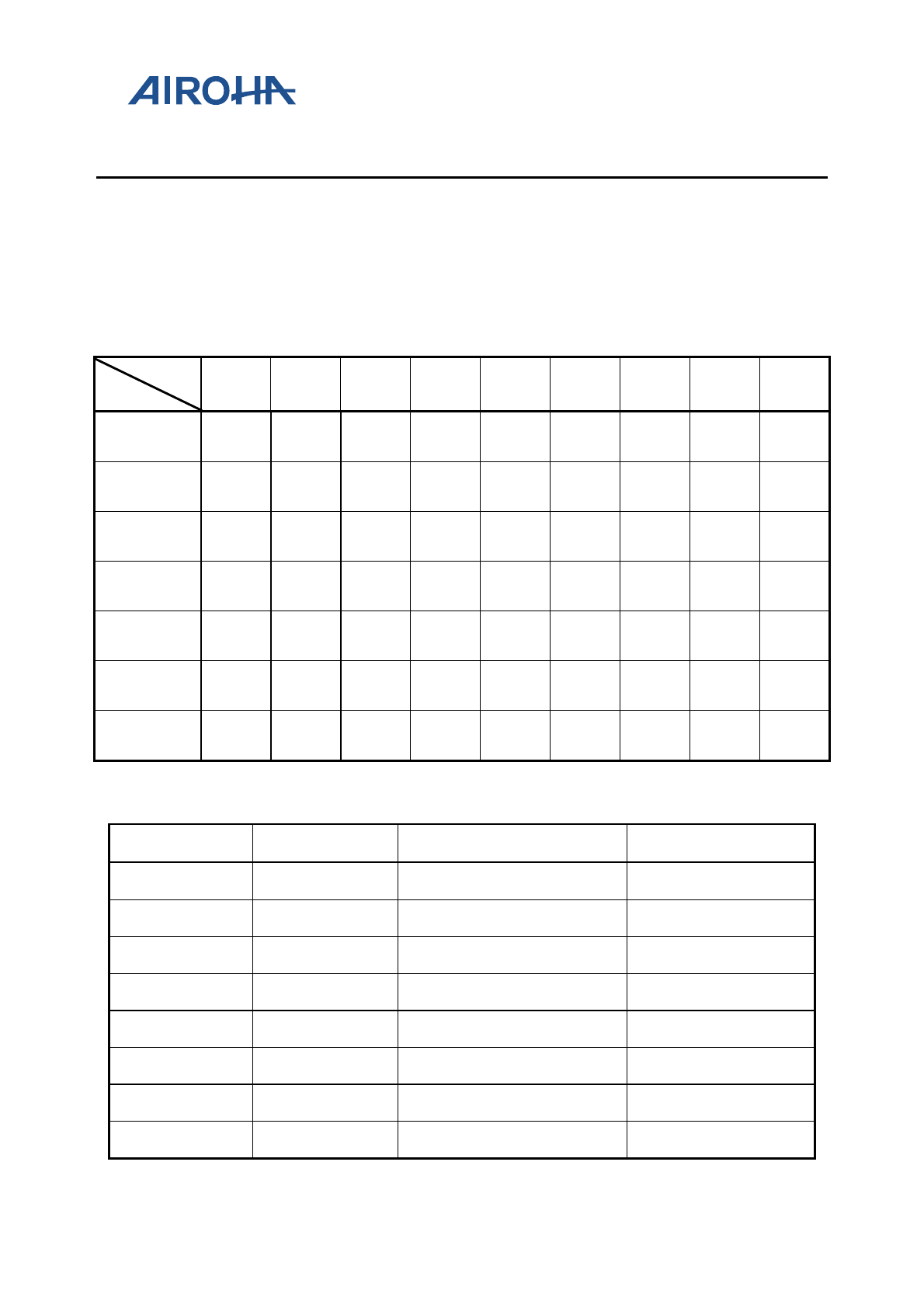
2. Bus Architecture and Memory Map
To better support various IOT applications, MT2523 adopts 32-bit multi-AHB matrix to provide low-power, fast and
flexible data operation. Table 2-1 shows the interconnections between bus masters (CM4, four SPI masters, SPI
slave, debug system, Multimedia (MM) system, USB, and three DMAs) and slaves (AO APB peripherals, PD APB
peripherals, TCM, SFC, EMI, MDSYS, BTSYS).
Table 2-1. MT2523 bus connection
Master
Slave
ARM
CM4
AO
DMA
PD
DMA
Sensor
DMA USB MM
SYS
Debug
SYS
SPI
Master
SPI
Slave
AO APB
Peripherals ● ●
PD APB
Peripherals ● ● ● ● ●
TCM ● ● ● ● ● ● ●
EMI ● ● ● ● ● ● ● ● ●
SFC ● ● ● ● ● ●
Audio DSP ● ● ● ● ●
BTSYS ● ● ● ● ●
Table 2-2. Top view memory map
Start Address End Address Corresponding Module Comment
0x0000_0000 0x03FF_FFFF EMI
0x0400_0000 0x0400_7FFF CM4 TCM/cache
0x0400_8000 0x0402_7FFF CM4 TCM
0x0410_0000 0x041F_FFFF Boot ROM
0x0800_0000 0x0BFF_FFFF SFC
0x8000_0000 0x8000_FFFF Version code
0x8200_0000 0x83FF_FFFF MDSYS
0xA000_0000 0xA03F_FFFF PD APB peripherals
MT2523 Series Reference Manual
© 2015 - 2018 Airoha Technology Corp.
Page 4 of 692
This document contains information that is proprietary to Airoha Technology Corp. (“Airoha”) and/or its licensor(s).
Any unauthorized use, reproduction or disclosure of this document in whole or in part is strictly prohibited.
Start Address End Address Corresponding Module Comment
0xA040_0000 0xA04F_FFFF MMSYS
0xA080_0000 0xA08F_FFFF CM4 peripheral
0xA090_0000 0xA09F_FFFF PD AHB peripherals
0xA200_0000 0xA21F_FFFF AO APB peripherals
0xA290_0000 0xA29F_FFFF AO AHB peripherals
0xA300_0000 0xA3FF_FFFF BTSYS
0xE000_0000 0xE003_FFFF CM4 private peripheral bus -
internal
0xE004_0000 0xE00F_FFFF CM4 private peripheral bus -
external
Table 2-3. Always-on domain peripherals
Start Address Module Description Bus Interface Comments
A200_0000 VERSION_CTRL APB Mapped to 0x8000_0000
A201_0000 Configuration registers APB Clock, power down, version and
reset
A202_0000 General purpose inputs/outputs APB
A203_0000 Interrupt controller (eint+cirq) APB
A204_0000 Analog chip interface controller APB PLL, CLKSQ, FH, CLKSW and
SIMLS
A205_0000 Reset generation unit APB
A206_0000 EFUSE APB
A207_0000 AO DMA controller APB
A208_0000 INFRA BUS configuration APB
A209_0000 MIPI_TX_CONFIG APB
A20A_0000 Configuration Registers APB Clock, 104M
A20B_0000 SEJ APB
A20C_0000 PSI_MST APB
A20D_0000 Keypad Scanner APB
A20E_0000 BTIF APB
MT2523 Series Reference Manual
© 2015 - 2018 Airoha Technology Corp.
Page 5 of 692
This document contains information that is proprietary to Airoha Technology Corp. (“Airoha”) and/or its licensor(s).
Any unauthorized use, reproduction or disclosure of this document in whole or in part is strictly prohibited.
Start Address Module Description Bus Interface Comments
A20F_0000 MCU_TOPSM APB
A210_0000 CM4_TOPSM APB
A211_0000 CM4_CFG_PRIVATE APB
A213_0000 GP Counter APB
A214_0000 GP Timer APB
A215_0000 I2C_D2D APB
A216_0000 Pulse width modulation outputs 0 APB
A217_0000 Pulse width modulation outputs 1 APB
A218_0000 Display pulse width modulation APB
A219_0000 Reserved APB
A21A_0000 PMU mixedsys APB
A21B_0000 General purpose DAC APB
A21C_0000 Analog baseband (ABB) controller APB
A21D_0000 A-Die configuration registers APB Clock, reset, etc.
A21E_0000 Real-time clock APB
A21F_0000 ACCDET APB
A292_0000 AO DMA controller AHB AHB slave port of AO DMA
Table 2-4. Power-down domain peripherals
Start Address Module Description Bus Interface Comments
A000_0000 DMA controller APB
A001_0000 TRNG APB
A002_0000 MS/SD controller 0 APB
A003_0000 MS/SD controller 1 APB
A004_0000 Serial flash APB
A005_0000 External memory interface APB

MT2523 Series Reference Manual
© 2015 - 2018 Airoha Technology Corp.
Page 6 of 692
This document contains information that is proprietary to Airoha Technology Corp. (“Airoha”) and/or its licensor(s).
Any unauthorized use, reproduction or disclosure of this document in whole or in part is strictly prohibited.
Start Address Module Description Bus Interface Comments
A006_0000 DebugSYS APB 0 APB
A007_0000 DebugSYS APB 1 APB
A008_0000 DebugSYS APB 2 APB
A009_0000 DebugSYS APB 3 APB
A00A_0000 DebugSYS APB 4 APB
A00B_0000 DebugSYS APB 5 APB
A00C_0000 DebugSYS APB 6 APB
A00D_0000 UART 0 APB
A00E_0000 UART 1 APB
A00F_0000 UART 2 APB
A010_0000 UART 3 APB
A011_0000 SPI_MASTER 0 APB
A012_0000 SPI_MASTER 1 APB
A013_0000 SPI_MASTER 2 APB
A014_0000 SPI_MASTER 3 APB
A015_0000 SPI_SLAVE APB
A016_0000 Pulse width modulation outputs 2 APB
A017_0000 Pulse width modulation outputs 3 APB
A018_0000 Pulse width modulation outputs 4 APB
A019_0000 Pulse width modulation outputs 5 APB
A01A_0000 Reserved APB
A01B_0000 I2C_2 APB
A01C_0000 INFRA MBIST configuration APB
A01D_0000 Reserved APB
A01E_0000 Reserved APB
A01F_0000 Sensor memory APB
A020_0000 Reserved APB
MT2523 Series Reference Manual
© 2015 - 2018 Airoha Technology Corp.
Page 7 of 692
This document contains information that is proprietary to Airoha Technology Corp. (“Airoha”) and/or its licensor(s).
Any unauthorized use, reproduction or disclosure of this document in whole or in part is strictly prohibited.
Start Address Module Description Bus Interface Comments
A021_0000 I2C_0 APB
A022_0000 I2C_1_18V APB
A023_0000 Sensor DMA controller APB
A024_0000 Auxiliary ADC Unit APB
A090_0000 USB AHB
A091_0000 USB SIFSLV AHB
A090_0001 PD DMA AHB
MT2523 Series Reference Manual
© 2015 - 2018 Airoha Technology Corp.
Page 8 of 692
This document contains information that is proprietary to Airoha Technology Corp. (“Airoha”) and/or its licensor(s).
Any unauthorized use, reproduction or disclosure of this document in whole or in part is strictly prohibited.
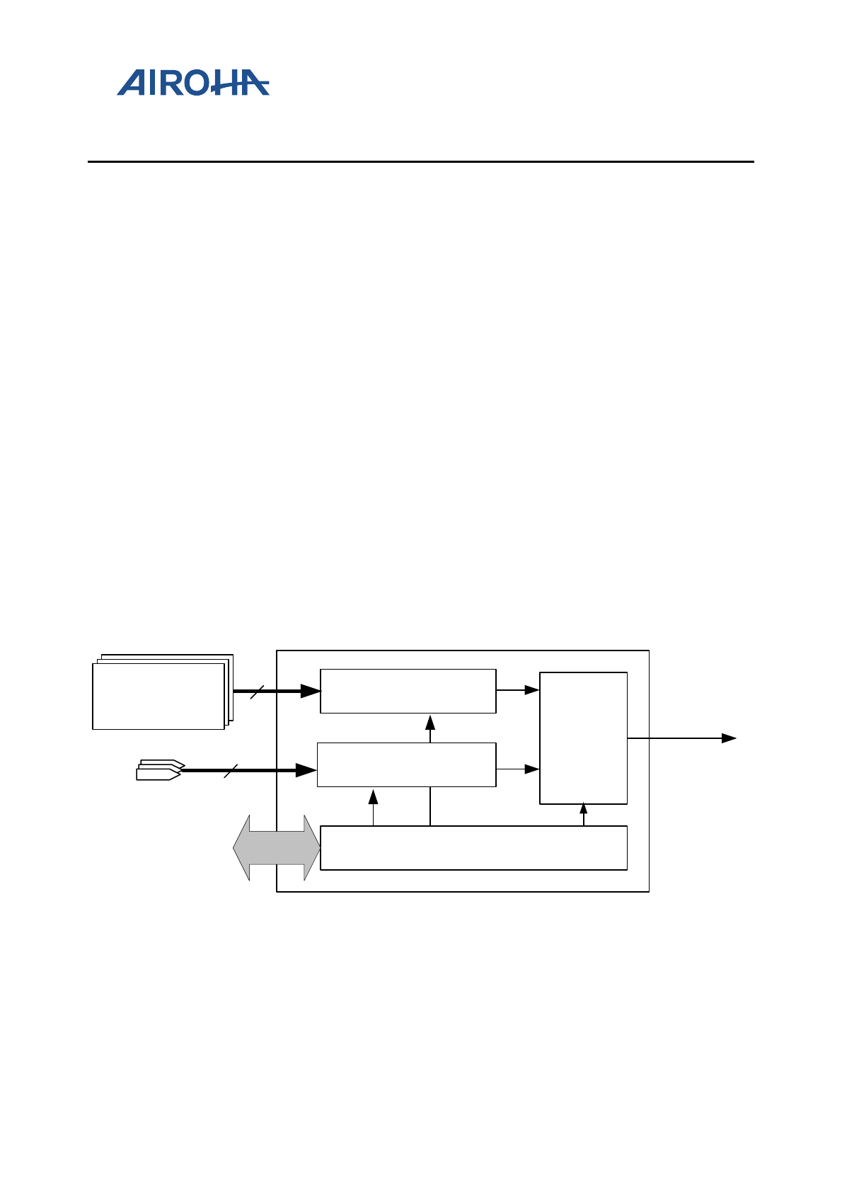
3. External Interrupt Controller
3.1. General Description
External interrupt controller supports some interrupt requests coming from external sources and peripherals. All
external interrupts, including external and peripherals sources, have the ability to inform the system to resume the
system clock.
The external interrupts can be used for different types of applications, mainly for event detections: detection of
hand free connection, hood opening and battery charger connection.
Since the external event may be unstable in a certain period, a de-bounce mechanism is introduced to ensure the
functionality. The circuitry is mainly used to verify that the input signal remains stable for a programmable number
of periods of the clock. When this condition is satisfied, for the appearance or the disappearance of the input, the
output of the de-bounce logic will change to the desired state. Note that because it uses the 32,768Hz slow clock to
perform the de-bounce process, the parameter of the de-bounce period and de-bounce enable takes effect no
sooner than one 32,768Hz clock cycle (~30.52us) after the software program sets them up. When the sources of
external interrupt controller are used to resume the system clock in sleep mode, the de-bounce mechanism must
be enabled. However, the polarities of EINTs are clocked with the system clock, and therefore any change to them
takes effect immediately. Figure 3-1 is the block diagram of external interrupt controller. Table 3-1 illustrates the
external interrupt sources and related configuration of GPIO mode.
Note that the corresponding GPIO as external interrupt source should be in the input mode and is affected by GPIO
data input inversion registers (GPIO_DINV). Refer to the GPIO section for more details.
Interrupt
Control
EINT_IRQ
Debounce Logic
Debounce Logic
Register
APB BUS
peripherals
peripherals
peripherals
Figure 3-1. Block diagram of external interrupt controller

MT2523 Series Reference Manual
© 2015 - 2018 Airoha Technology Corp.
Page 9 of 692
This document contains information that is proprietary to Airoha Technology Corp. (“Airoha”) and/or its licensor(s).
Any unauthorized use, reproduction or disclosure of this document in whole or in part is strictly prohibited.
Table 3-1. External interrupt sources
EINT Source pin EINT Source pin
EINT0 AUXIN0 if (GPIO0_MODE==1) EINT16 URXD0 if (GPIO16_MODE==3)
EINT1 AUXIN1 if (GPIO1_MODE==1) EINT17 UTXD0 if (GPIO17_MODE==3)
EINT2 AUXIN2 if (GPIO2_MODE==1) EINT18 GPIO_B1 if (GPIO19_MODE==2)
EINT3 GPIO_A04 if (GPIO4_MODE==1), otherwise
MCDA3 if (GPIO35_MODE==2) EINT19 GPIO_B5 if (GPIO23_MODE==2)
EINT4 GPIO_A1 if (GPIO5_MODE==1), otherwise
LSCE_B if (GPIO39_MODE==2) EINT20 keypad (KCOL0~4)
EINT5 GPIO_A2 if (GPIO6_MODE==1), otherwise
LSDA if (GPIO41_MODE==2) EINT21 uart0_rxd
EINT6 GPIO_A3 if (GPIO7_MODE==1), otherwise
LPTE if (GPIO43_MODE==2) EINT22 uart1_rxd
EINT7 GPIO_A4 if (GPIO8_MODE==1) EINT23 uart2_rxd
EINT8 GPIO_A5 if (GPIO9_MODE==1) EINT24 uart3_rxd
EINT9 GPIO_C0 if (GPIO11_MODE==1), otherwise
CMRST if (GPIO24_MODE==4) EINT25 bt_eint_b
EINT10 GPIO_C1 if (GPIO12_MODE==1), otherwise
CMCSK if (GPIO29_MODE==5) EINT26 btif_sleep_wakeup_in_b
EINT11 GPIO_C2 if (GPIO13_MODE==1), otherwise
MCCK if (GPIO30_MODE==2) EINT27 pdn_usb11
EINT12 GPIO_C3 if (GPIO14_MODE==1), otherwise
MCCM0 if (GPIO31_MODE==2) EINT28 accdet_irq_b
EINT13 GPIO_C4 if (GPIO15_MODE==1), otherwise
MCDA0 if (GPIO32_MODE==2) EINT29 rtc_event_b
EINT14 AUXIN3 if (GPIO3_MODE==1), otherwise
MCDA1 if (GPIO33_MODE==2) EINT30 pmic_irq_b
EINT15 AUXIN4 if (GPIO10_MODE==1), otherwise
MCDA2 if (GPIO34_MODE==2) EINT31 gpcounter_irq_b
MT2523 Series Reference Manual
© 2015 - 2018 Airoha Technology Corp.
Page 10 of 692
This document contains information that is proprietary to Airoha Technology Corp. (“Airoha”) and/or its licensor(s).
Any unauthorized use, reproduction or disclosure of this document in whole or in part is strictly prohibited.
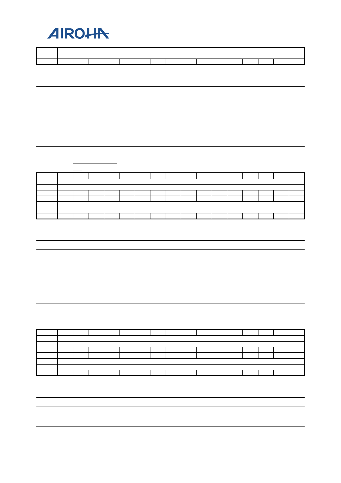
3.2. Register Definition
Module name: EINT Base address: (+A2030000h)
Address
Name
Width
Register Function
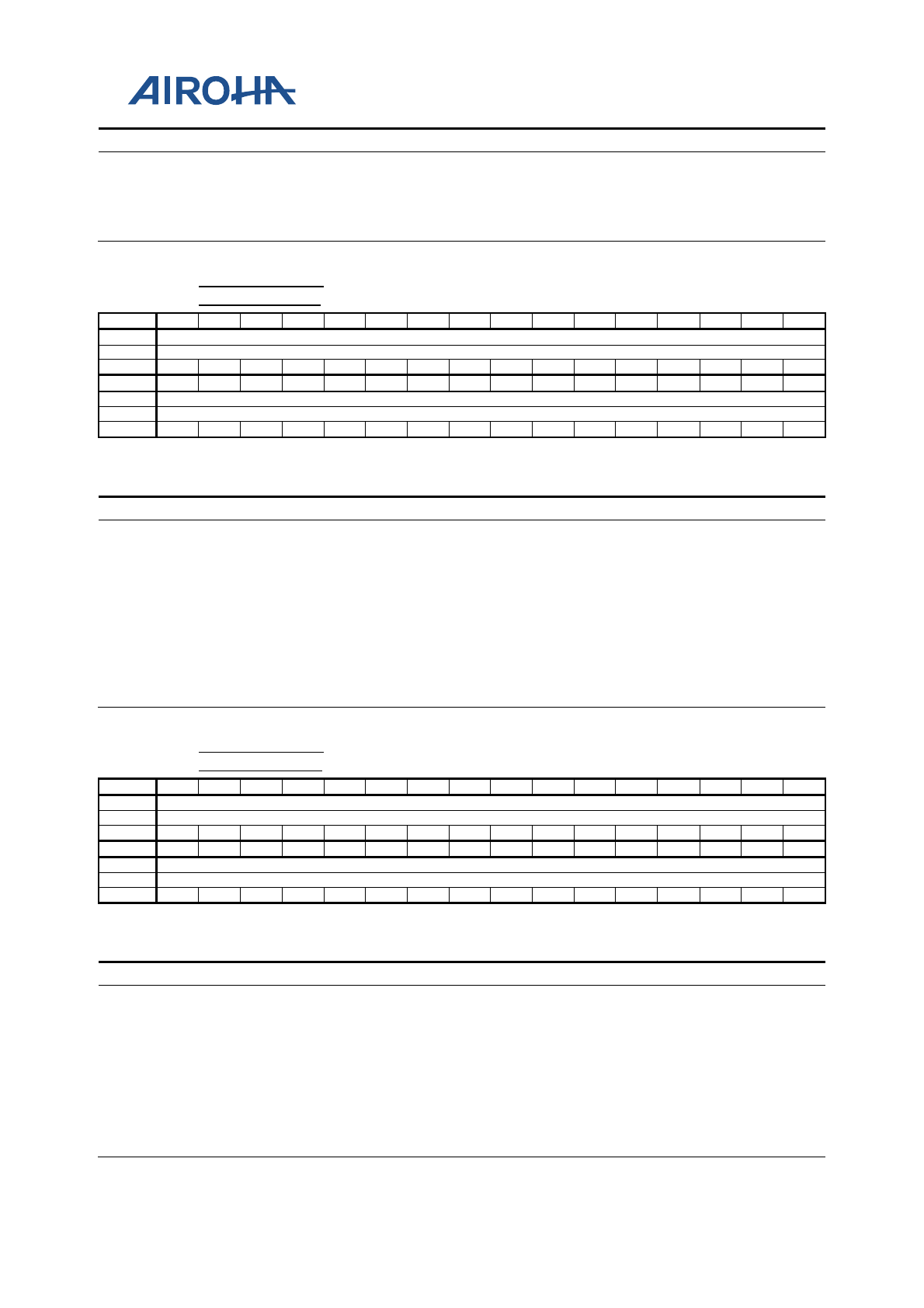
A2030300 EINT_STA 32 EINT interrupt status register
A2030308
EINT_INTACK
32
EINT interrupt acknowledge register
A2030310 EINT_EEVT 32 EINT wakeup event_b status register
A2030320
EINT_MASK
32
EINT interrupt mask register
A2030328 EINT_MASK_SE
T 32 EINT interrupt mask set register
A2030330
EINT_MASK_C
LR 32 EINT interrupt mask clear register
A2030340 EINT_WAKEUP
_MASK 32 EINT wakeup event mask register
A2030348
EINT_WAKEUP
_MASK_SET 32 EINT wakeup event mask set register
A2030350 EINT_WAKEUP
_MASK_CLR 32 EINT wakeup event mask clear register
A2030360
EINT_SENS
32
EINT sensitivity register
A2030368 EINT_SENS_SE
T 32 EINT sensitivity set register
A2030370
EINT_SENS_CL
R 32 EINT sensitivity clear register
A2030380 EINT_DUALED
GE_SENS 32 EINT dual edge sensitivity register
A2030388
EINT_DUALED
GE_SENS_SET 32 EINT dual edge sensitivity set register
A2030390 EINT_DUALED
GE_SENS_CLR 32 EINT dual edge sensitivity clear register
A20303a0
EINT_SOFT
32
EINT software interrupt register
A20303a8 EINT_SOFT_SE
T 32 EINT software interrupt soft register
A20303b0
EINT_SOFT_CL
R 32 EINT software interrupt clear register
A20303c0 EINT_D0EN 32 EINT domain 0 enable register
A2030400 ~
A203047C
EINTi_CON
(i=0~31) 32 EINTi config register
A2030
300
EINT_STA
EINT interrupt status register
00000000
Bit
31
30
29
28
27
26
25
24
23
22
21
20
19
18
17
16
Name
EINT_STA[31:16]
Type
RO
Reset
0
0
0
0
0
0
0
0
0
0
0
0
0
0
0
0
Bit
15
14
13
12
11
10
9
8
7
6
5
4
3
2
1
0
Name
EINT_STA[15:0]
Type
RO
Reset
0
0
0
0
0
0
0
0
0
0
0
0
0
0
0
0
MT2523 Series Reference Manual
© 2015 - 2018 Airoha Technology Corp.
Page 11 of 692
This document contains information that is proprietary to Airoha Technology Corp. (“Airoha”) and/or its licensor(s).
Any unauthorized use, reproduction or disclosure of this document in whole or in part is strictly prohibited.
Overview
Bit(s)
Mnemonic
Name
Description
31:0
EINT_STA
External interrupt status
This register keeps up with the current status of which EINT source
generates the interrupt request. If the EINT sources are set to edge
sensitivity, EINT_IRQ will be de-asserted when the corresponding
EINT_INTACK is programmed by 1.
EINT_STA[i] for EINTi.
0: No external interrupt request is generated.
1: External Interrupt request is pending.
A2030
308
EINT_
INTACK
EINT interrupt
acknowledge register
00000000
Bit
31
30
29
28
27
26
25
24
23
22
21
20
19
18
17
16
Name
EINT_INTACK[31:16]
Type
WO
Reset
0
0
0
0
0
0
0
0
0
0
0
0
0
0
0
0
Bit
15
14
13
12
11
10
9
8
7
6
5
4
3
2
1
0
Name
EINT_INTACK[15:0]
Type
WO
Reset
0
0
0
0
0
0
0
0
0
0
0
0
0
0
0
0
Overview
Bit(s)
Mnemonic
Name
Description
31:0
EINT_
INTACK Interrupt acknowledgement
Writing “1” to the specific bit position to acknowledge the interrupt
request corresponding to the external interrupt line source.
EINT_INTACK[i] for EINTi.
0: No effect
1: Interrupt request is acknowledged.
A2030
310
EINT_EEVT
EINT wakeup event_b status register
00000000
Bit
31
30
29
28
27
26
25
24
23
22
21
20
19
18
17
16
Name
Type
Reset
Bit
15
14
13
12
11
10
9
8
7
6
5
4
3
2
1
0
Name
EEB
Type
RO
Reset
0
Overview
Bit(s)
Mnemonic
Name
Description
0
EEB
EINT wake up event_b
This register is a debugging port to monitor internal signals. It is async
signal.
0: EINT wakes up sleep mode.
1: EINT does not wake up sleep mode.
MT2523 Series Reference Manual
© 2015 - 2018 Airoha Technology Corp.
Page 12 of 692
This document contains information that is proprietary to Airoha Technology Corp. (“Airoha”) and/or its licensor(s).
Any unauthorized use, reproduction or disclosure of this document in whole or in part is strictly prohibited.
A2030
320
EINT_
MASK
EINT interrupt
mask register
FFFFFFFF
Bit
31
30
29
28
27
26
25
24
23
22
21
20
19
18
17
16
Name
EINT_MASK[31:16]
Type
RO
Reset
1
1
1
1
1
1
1
1
1
1
1
1
1
1
1
1
Bit
15
14
13
12
11
10
9
8
7
6
5
4
3
2
1
0
Name
EINT_MASK[15:0]
Type
RO
Reset
1
1
1
1
1
1
1
1
1
1
1
1
1
1
1
1
Overview
Bit(s) Mnemonic Name Description
31:0
EINT
_MASK
Interrupt mas
k
This register controls whether or not the EINT source is allowed to
generate an interrupt request. Setting a specific bit position to “1”
will
prevent the external interrupt line from becoming active.
EINT_MASK[i] for EINTi.
0: Interrupt request is enabled.
1: Interrupt request is disabled.
A2030
328
EINT_
MASK_S
ET
EINT interrupt
mask set register
00000000
Bit
31
30
29
28
27
26
25
24
23
22
21
20
19
18
17
16
Name
EINT_MASK[31:16]
Type
WO
Reset
0
0
0
0
0
0
0
0
0
0
0
0
0
0
0
0
Bit
15
14
13
12
11
10
9
8
7
6
5
4
3
2
1
0
Name
EINT_MASK[15:0]
Type
WO
Reset
0
0
0
0
0
0
0
0
0
0
0
0
0
0
0
0
Overview
Bit(s) Mnemonic Name Description
31:0
EINT
_MASK Enables mask for the associated external interrupt source
This register is used to set up individual mask bits. Only the bits set to 1
are effective; also set EINT_MASK bits to 1. Otherwise, EINT_MASK
bits will retain the original value.
EINT_MASK[i] for EINTi.
0: No effect
1: Enable the corresponding MASK bit
A2030
330
EINT_MASK_C
LR
EINT interrupt
mask clear register
00000000
Bit
31
30
29
28
27
26
25
24
23
22
21
20
19
18
17
16
Name
EINT_MASK[31:16]
Type
WO
Reset
0
0
0
0
0
0
0
0
0
0
0
0
0
0
0
0
Bit
15
14
13
12
11
10
9
8
7
6
5
4
3
2
1
0
Name
EINT_MASK[15:0]
Type
WO
Reset
0
0
0
0
0
0
0
0
0
0
0
0
0
0
0
0
MT2523 Series Reference Manual
© 2015 - 2018 Airoha Technology Corp.
Page 13 of 692
This document contains information that is proprietary to Airoha Technology Corp. (“Airoha”) and/or its licensor(s).
Any unauthorized use, reproduction or disclosure of this document in whole or in part is strictly prohibited.
Overview
Bit(s) Mnemonic Name Description
31:0
EINT
_MASK
Disables mask for the associated external interrupt source
This
register is used to clear individual mask bits. Only the bits set to 1
are effective, and EINT_MASK bits are also cleared (to 0). Otherwise,
EINT_MASK bits will retain the original value.
EINT_MASK[i] for EINTi.
0: No effect
1: Disable the corresponding M
ASK bit
A2030
340
EINT_
WAKEU
P_MASK
EINT
wakeup event mask register
FFFFFFFF
Bit
31
30
29
28
27
26
25
24
23
22
21
20
19
18
17
16
Name
EINT_WAKEUP_MASK[31:16]
Type
RO
Reset
1
1
1
1
1
1
1
1
1
1
1
1
1
1
1
1
Bit
15
14
13
12
11
10
9
8
7
6
5
4
3
2
1
0
Name
EINT_WAKEUP_MASK[15:0]
Type
RO
Reset
1
1
1
1
1
1
1
1
1
1
1
1
1
1
1
1
Overview
Bit(s) Mnemonic Name Description
31:0
EINT
_WAKEUP_M
ASK
Wakeup event
mask
This register controls whether or not the EINT source is allowed to
generate a
wakeup event
request. Setting a specific bit position to “1” will
prevent the external interrupt line from becoming active.
EINT_WAKEUP_MASK[i] for EINTi.
0:
Wakeup event request is enabled.
1:
Wakeup event request is disabled.
A2030
348
EINT_
WAKEU
P_MASK_SET
EINT
wakeup event mask set register
00000000
Bit
31
30
29
28
27
26
25
24
23
22
21
20
19
18
17
16
Name
EINT_WAKEUP_MASK[31:16]
Type
WO
Reset
0
0
0
0
0
0
0
0
0
0
0
0
0
0
0
0
Bit
15
14
13
12
11
10
9
8
7
6
5
4
3
2
1
0
Name
EINT_WAKEUP_MASK[15:0]
Type
WO
Reset
0
0
0
0
0
0
0
0
0
0
0
0
0
0
0
0
Overview
Bit(s) Mnemonic Name Description
31:0
EINT
_WAKEUP_M
ASK
Enables mask for the associated external interrupt source
This register is used to set up individual mask bits. Only the bits set to 1
are effective; also set EINT_WAKEUP_MASK bits to 1. Otherwise,
EINT_WAKEUP_MASK bits will retain the original value.
EINT_WAKEUP_MASK[i] for EINTi.
MT2523 Series Reference Manual
© 2015 - 2018 Airoha Technology Corp.
Page 14 of 692
This document contains information that is proprietary to Airoha Technology Corp. (“Airoha”) and/or its licensor(s).
Any unauthorized use, reproduction or disclosure of this document in whole or in part is strictly prohibited.
Bit(s) Mnemonic Name Description
0: No effect
1: Enable the corresponding MASK bit
A2030
350
EINT_
WAKEU
P_MASK_CLR
EINT
wakeup event mask clear register
00000000
Bit
31
30
29
28
27
26
25
24
23
22
21
20
19
18
17
16
Name
EINT_WAKEUP_MASK[31:16]
Type
WO
Reset
0
0
0
0
0
0
0
0
0
0
0
0
0
0
0
0
Bit
15
14
13
12
11
10
9
8
7
6
5
4
3
2
1
0
Name
EINT_WAKEUP_MASK[15:0]
Type
WO
Reset
0
0
0
0
0
0
0
0
0
0
0
0
0
0
0
0
Overview
Bit(s) Mnemonic Name Description
31:0
EINT
_WAKEUP_M
ASK
Disables mask for the associated external interrupt source
This register is used to clear individual mask bits. Only the bits set to 1
are effective, and EINT_WAKEUP_MASK
bits are also cleared (to 0).
Otherwise, EINT_WAKEUP_MASK bits will retain the original value.
EINT_WAKEUP_MASK[i] for EINTi.
0: No effect
1: Disable the corresponding MASK bit
A2030
360
EINT_
SENS
EINT
sensitivity register
00000000
Bit
31
30
29
28
27
26
25
24
23
22
21
20
19
18
17
16
Name
EINT_SENS[31:16]
Type
RO
Reset
0
0
0
0
0
0
0
0
0
0
0
0
0
0
0
0
Bit
15
14
13
12
11
10
9
8
7
6
5
4
3
2
1
0
Name
EINT_SENS[15:0]
Type
RO
Reset
0
0
0
0
0
0
0
0
0
0
0
0
0
0
0
0
Overview
Bit(s) Mnemonic Name Description
31:0
EINT
_SENS Sensitivity type of the associated external interrupt source
Sensitivity type of external interrupt source.
EINT_SENS[i] for EINTi.
0: Edge sensitivity
1: Level sensitivity
A2030
368
EINT_
SENS_S
ET
EINT
sensitivity set register
00000000
Bit
31
30
29
28
27
26
25
24
23
22
21
20
19
18
17
16
Name
EINT_SENS[31:16]
Type
WO
Reset
0
0
0
0
0
0
0
0
0
0
0
0
0
0
0
0
Bit
15
14
13
12
11
10
9
8
7
6
5
4
3
2
1
0
MT2523 Series Reference Manual
© 2015 - 2018 Airoha Technology Corp.
Page 15 of 692
This document contains information that is proprietary to Airoha Technology Corp. (“Airoha”) and/or its licensor(s).
Any unauthorized use, reproduction or disclosure of this document in whole or in part is strictly prohibited.
Name
EINT_SENS[15:0]
Type
WO
Reset
0
0
0
0
0
0
0
0
0
0
0
0
0
0
0
0
Overview
Bit(s) Mnemonic Name Description
31:0
EINT
_SENS
Enables sensitive for the associated external interrupt source.
This register is used to set up individual sensitive bits. Only the bits set
to 1 are effective
; also set EINT_SENS bits to 1. Otherwise, EINT_SENS
bits will retain the original value.
EINT_SENS[i] for EINTi.
0: No effect
1: Enable the corresponding SENS bit
A2030
370
EINT_
SENS_C
LR
EINT
sensitivity clear register
00000000
Bit
31
30
29
28
27
26
25
24
23
22
21
20
19
18
17
16
Name
EINT_SENS[31:16]
Type
WO
Reset
0
0
0
0
0
0
0
0
0
0
0
0
0
0
0
0
Bit
15
14
13
12
11
10
9
8
7
6
5
4
3
2
1
0
Name
EINT_SENS[15:0]
Type
WO
Reset
0
0
0
0
0
0
0
0
0
0
0
0
0
0
0
0
Overview
Bit(s) Mnemonic Name Description
31:0
EINT
_SENS
Disables sensitive for the associated external interrupt source.
This register is used to clear individual sensitive bits. Only the bits set to
1 are effective, and EINT_SENS bits are also cleared (set to 0).
Otherwise, EINT_SENS bits will retain
the original value.
EINT_SENS[i] for EINTi.
0: No effect
1: Disable the corresponding SENS bit
A2030
380
EINT_DUALED
GE_SENS
EINT
dual edge sensitivity register
00000000
Bit
31
30
29
28
27
26
25
24
23
22
21
20
19
18
17
16
Name
EINT_DUALEDGE_SENS[31:16]
Type
RO
Reset
0
0
0
0
0
0
0
0
0
0
0
0
0
0
0
0
Bit
15
14
13
12
11
10
9
8
7
6
5
4
3
2
1
0
Name
EINT_DUALEDGE_SENS[15:0]
Type
RO
Reset
0
0
0
0
0
0
0
0
0
0
0
0
0
0
0
0
Overview
Bit(s) Mnemonic Name Description
31:0
EINT
_DUALEDGE_
SENS
Dual edge sensitivity enable of the associated external
interrupt source
Dual edge sensitivity enable of external interrupt source. (EINT_SENS
MT2523 Series Reference Manual
© 2015 - 2018 Airoha Technology Corp.
Page 16 of 692
This document contains information that is proprietary to Airoha Technology Corp. (“Airoha”) and/or its licensor(s).
Any unauthorized use, reproduction or disclosure of this document in whole or in part is strictly prohibited.
Bit(s) Mnemonic Name Description
should be 0.)
EINT_DUALEDGE_SENS[i] for EINTi.
0: Disable
1: Enable
A2030
388
EINT_DUALED
GE_SENS_SET
EINT
dual edge sensitivity set register
00000000
Bit
31
30
29
28
27
26
25
24
23
22
21
20
19
18
17
16
Name
EINT_DUALEDGE_SENS[31:16]
Type
WO
Reset
0
0
0
0
0
0
0
0
0
0
0
0
0
0
0
0
Bit
15
14
13
12
11
10
9
8
7
6
5
4
3
2
1
0
Name
EINT_DUALEDGE_SENS[15:0]
Type
WO
Reset
0
0
0
0
0
0
0
0
0
0
0
0
0
0
0
0
Overview
Bit(s) Mnemonic Name Description
31:0
EINT
_DUALEDGE_
SENS
Enables dual edge sensitivity for the associated external
interrupt source
This register is used to set up individual dual edge sensitive bits.
(EINT_SENS should be 0)
Only the bits set to 1 are effective; also set EINT_DUALEDGE_SENS
bits to 1. Otherwise, EINT_DUALEDGE_SENS bits will retain the
original value.
EINT_DUALEDGE_SENS[i] for EINTi.
0: No effect
1: Enable the corresponding DUALEDGE bit
A2030
390
EINT_DUALED
GE_SENS_CLR
EINT
dual edge sensitivity clear register
00000000
Bit
31
30
29
28
27
26
25
24
23
22
21
20
19
18
17
16
Name
EINT_DUALEDGE_SENS[31:16]
Type
WO
Reset
0
0
0
0
0
0
0
0
0
0
0
0
0
0
0
0
Bit
15
14
13
12
11
10
9
8
7
6
5
4
3
2
1
0
Name
EINT_DUALEDGE_SENS[15:0]
Type
WO
Reset
0
0
0
0
0
0
0
0
0
0
0
0
0
0
0
0
Overview
Bit(s) Mnemonic Name Description
31:0
EINT
_DUALEDGE_
SENS
Disables dual edge sensitive for the associated external
interrupt source.
This register is used to clear individual sensitive bits. Only the bits set
to 1 are effective, and EINT_DUALEDGE_SENS bits are also cleared
(to 0). Otherwise, EINT_DUALEDGE_SENS bits will retain the
original value.
EINT_DUALEDGE_SENS[i] for EINTi.
0: No effect
1: Disable the corresponding DUALEDGE bit
MT2523 Series Reference Manual
© 2015 - 2018 Airoha Technology Corp.
Page 17 of 692
This document contains information that is proprietary to Airoha Technology Corp. (“Airoha”) and/or its licensor(s).
Any unauthorized use, reproduction or disclosure of this document in whole or in part is strictly prohibited.
A2030
3a0
EINT_
SOFT
EINT
software interrupt register
00000000
Bit
31
30
29
28
27
26
25
24
23
22
21
20
19
18
17
16
Name
EINT_SOFT[31:16]
Type
RO
Reset
0
0
0
0
0
0
0
0
0
0
0
0
0
0
0
0
Bit
15
14
13
12
11
10
9
8
7
6
5
4
3
2
1
0
Name
EINT_SOFT[15:0]
Type
RO
Reset
0
0
0
0
0
0
0
0
0
0
0
0
0
0
0
0
Overview
Bit(s) Mnemonic Name Description
31:0
EINT
_SOFT
Software
interrupt
This register is used for debug
ging purpose.
EINT_SOFT[i] for EINTi.
0: No effect
1: Trigger a
n EINT
A2030
3a8
EINT_
SOFT_S
ET
EINT
software interrupt set register
00000000
Bit
31
30
29
28
27
26
25
24
23
22
21
20
19
18
17
16
Name
EINT_SOFT[31:16]
Type
WO
Reset
0
0
0
0
0
0
0
0
0
0
0
0
0
0
0
0
Bit
15
14
13
12
11
10
9
8
7
6
5
4
3
2
1
0
Name
EINT_SOFT[15:0]
Type
WO
Reset
0
0
0
0
0
0
0
0
0
0
0
0
0
0
0
0
Overview
Bit(s) Mnemonic Name Description
31:0
EINT
_SOFT
Enables software for the associated external interrupt source
This register is used to set up individual software bits. Only the bits set to
1 are effective, and EINT_SOFT bits are also set to 1. Otherwise,
EINT_SOFT bits will retain the original value.
EINT_SOFT[i] for EINTi.
0: No effect
1: Enable the corresponding SOFT bit
A2030
3b0
EINT_
SOFT_C
LR
EINT
software interrupt clear register
00000000
Bit
31
30
29
28
27
26
25
24
23
22
21
20
19
18
17
16
Name
EINT_SOFT[31:16]
Type
WO
Reset
0
0
0
0
0
0
0
0
0
0
0
0
0
0
0
0
Bit
15
14
13
12
11
10
9
8
7
6
5
4
3
2
1
0
Name
EINT_SOFT[15:0]
Type
WO
Reset
0
0
0
0
0
0
0
0
0
0
0
0
0
0
0
0
Overview
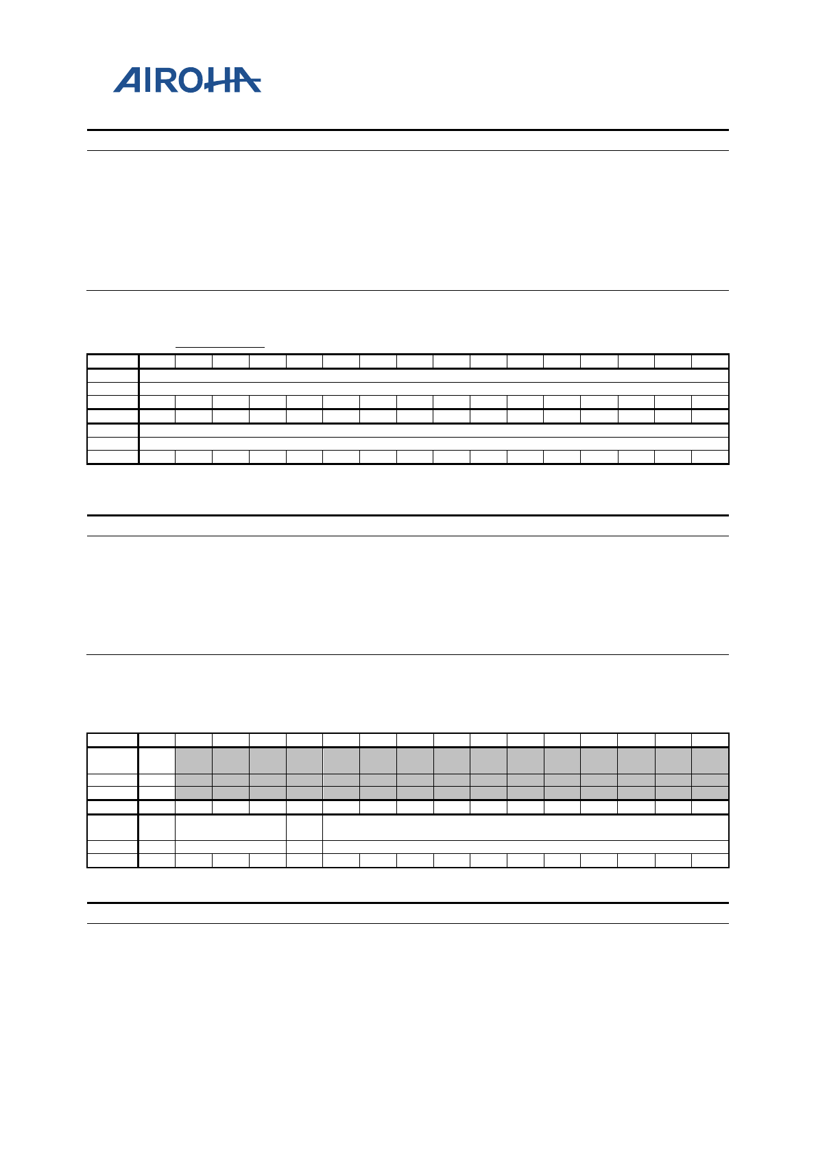
MT2523 Series Reference Manual
© 2015 - 2018 Airoha Technology Corp.
Page 18 of 692
This document contains information that is proprietary to Airoha Technology Corp. (“Airoha”) and/or its licensor(s).
Any unauthorized use, reproduction or disclosure of this document in whole or in part is strictly prohibited.
Bit(s) Mnemonic Name Description
31:0
EINT
_SOFT Disables software for the associated external interrupt
source
This register is used to clear individual software bits. Only the bits set
to 1 are effective, and EINT_SOFT bits are also cleared (to 0).
Otherwise, EINT_SOFT bits will retain the original value.
EINT_SOFT[i] for EINTi.
0: No effect
1: Disable the corresponding SOFT bit
A2030
3c0
EINT_D0EN
EINT domain
0 enable register
00000000
Bit
31
30
29
28
27
26
25
24
23
22
21
20
19
18
17
16
Name
EINT_D0EN[31:16]
Type
RW
Reset
0
0
0
0
0
0
0
0
0
0
0
0
0
0
0
0
Bit
15
14
13
12
11
10
9
8
7
6
5
4
3
2
1
0
Name
EINT_D0EN[15:0]
Type
RW
Reset
0
0
0
0
0
0
0
0
0
0
0
0
0
0
0
0
Overview
Bit(s)
Mnemonic
Name
Description
31:0
EINT_D0EN
EINT enable config for domain 0
Each bit indicates whether the corresponding EINT is enabled for
domain 0. If enabled, it will assert interrupt or wakeup_event
depending on the corresponding mask bit value.
EINT_D0EN[i] for EINTi.
0: Disable
1: Enable
A2030
400~
A2030
47c
(step 0x
4)
EINTi_CON
(
i=0~31)
EINTi config register
0000000
0
Bit
31
30
29
28
27
26
25
24
23
22
21
20
19
18
17
16
Name
RSTD
BC
Type
WO
Reset
0
Bit
15
14
13
12
11
10
9
8
7
6
5
4
3
2
1
0
Name
DBC_
EN
PRESCALER POL DBC_CNT
Type
RW
RW
RW
RW
Reset
0
0
0
0
0
0
0
0
0
0
0
0
0
0
0
0
Bit(s) Mnemonic
Name Description
31
RSTDBC
EINTi debounce count reset
Write once to reset the de-bounce counter so that EINT can be updated
immediately without de-bounce latency. This option needs 100usec
latency to take effect.
0: No effect
1: Reset

MT2523 Series Reference Manual
© 2015 - 2018 Airoha Technology Corp.
Page 19 of 692
This document contains information that is proprietary to Airoha Technology Corp. (“Airoha”) and/or its licensor(s).
Any unauthorized use, reproduction or disclosure of this document in whole or in part is strictly prohibited.
Bit(s) Mnemonic
Name Description
15
DBC_
EN Enables EINTi debounce circuit
0: Disable
1: Enable
14:12
PRESCALER
EINTi debounce clock cycle period prescaler.
000: 32,768Hz, max. 0.0625sec
001: 16,384Hz
010: 8,192Hz
011: 4,096Hz
100: 2,048Hz, max. 1sec
101: 1,024Hz
110: 512Hz
111: 256Hz, max. 8secs
11
POL
Configures polarity
Activation type of the EINT source
0: Active low
1: Active high
10:0
DBC_
CNT Configures EINTi debounce duration
(The clock period is determined in PRESCALER.)
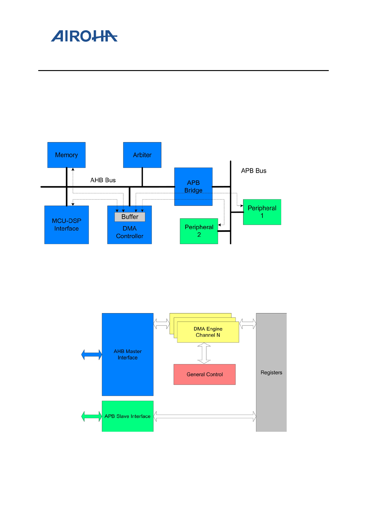
MT2523 Series Reference Manual
© 2015 - 2018 Airoha Technology Corp.
Page 20 of 692
This document contains information that is proprietary to Airoha Technology Corp. (“Airoha”) and/or its licensor(s).
Any unauthorized use, reproduction or disclosure of this document in whole or in part is strictly prohibited.
4. Direct Memory Access
4.1. General Description
A DMA controller is placed on AHB bus to support fast data transfers and off-load the processor. With this
controller, specific devices on AHB or APB buses can benefit greatly from quick completion of data movement from
or to memory modules. Such generic DMA controller can also be used to connect two devices other than memory
modules as long as they can be addressed in memory space. Figure 4-1 illustrates the system connections.
Figure 4-1. Variety data paths of DMA transfers
Up to 17 channels of simultaneous data transfers are supported. Each channel has a similar set of registers to be
configured to different schemes as desired. Both interrupt and polling based schemes in handling the completion
event are supported. The block diagram of such generic DMA controller is illustrated in Figure 4-2.
Figure 4-2. DMA block diagram
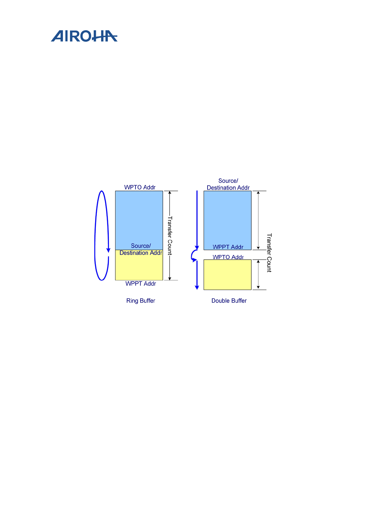
MT2523 Series Reference Manual
© 2015 - 2018 Airoha Technology Corp.
Page 21 of 692
This document contains information that is proprietary to Airoha Technology Corp. (“Airoha”) and/or its licensor(s).
Any unauthorized use, reproduction or disclosure of this document in whole or in part is strictly prohibited.
4.1.1. Full-size and Half-size DMA Channels
There are three types of DMA channels in the DMA controller: full-size DMA channel, half-size DMA channel and
virtual FIFO DMA. Channel 1 is a full-size DMA channel, channels 2 to 7 are half-size channels, and channels 9 to 18
are virtual FIFO DMA channels. The difference between the first two types of DMA channels is that both source
and destination address are programmable in full-size DMA channels, but only the address of one side can be
programmed in the half-size DMA channel. In half-size channels, only either the source or destination address can
be programmed while the addresses of the other side are fixed.
4.1.2. Ring Buffer and Double Buffer Memory Data Movement
DMA channels 1 to 7 support ring-buffer and double-buffer memory data movement. This can be achieved by
programming DMA_WPPT and DMA_WPTO, as well as setting up WPEN in the DMA_CON register to enable. Figure
4-3 illustrates how this function works. Once the transfer counter reaches WPPT, the next address will jump to
WPTO address after the WPPT data transfer is completed. Note that only one side can be configured as ring-buffer
or double-buffer memory, and this is controlled by WPSD in the DMA_CON register.
Figure 4-3. Ring buffer and double buffer memory data movement
4.1.3. Unaligned Word Access
The address of word access on AHB bus must be aligned to word boundary, or the 2 LSB is truncated to 00b. If the
programmer does not notice this, an incorrect data fetch may be caused. In the case where the data are to be
moved from unaligned addresses to aligned addresses, the word is usually first split into four bytes then moved
byte by byte. Thus the four read and four write transfers will appear on the bus.
To improve bus efficiency, the unaligned-word access is provided in DMA2~7. When this function is enabled, the
DMAs will move data from the unaligned address to aligned address by executing four continuous byte-read
accesses and one word-write access, reducing the number of transfers on the bus by three.
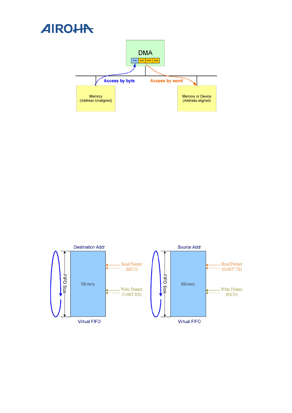
MT2523 Series Reference Manual
© 2015 - 2018 Airoha Technology Corp.
Page 22 of 692
This document contains information that is proprietary to Airoha Technology Corp. (“Airoha”) and/or its licensor(s).
Any unauthorized use, reproduction or disclosure of this document in whole or in part is strictly prohibited.
Figure 4-4. Unaligned word accesses
4.1.4. Virtual FIFO DMA
Virtual FIFO DMA is used to ease UART control. The difference between the virtual FIFO DMA and the ordinary
DMA is that the virtual FIFO DMA contains additional FIFO controllers. The read and write pointers are kept in the
virtual FIFO DMA. In a read from the FIFO, the read pointer points to the address of the next data. In a write to the
FIFO, the write pointer moves to the next address. If the FIFO is empty, a FIFO read will not be allowed. Similarly,
the data will not be written to the FIFO if the FIFO is full. Due to UART flow control requirements, an alert length is
programmed. Once the FIFO space is smaller than this value, an alert signal will be issued to enable the UART flow
control. The type of flow control performed depends on the setting in the UART.
Each virtual FIFO DMA can be programmed as RX or TX FIFO. This depends on the setting of DIR in the DMA_CON
register. If DIR is “0” (READ), it means TX FIFO. On the other hand, if DIR is “1” (WRITE), the virtual FIFO DMA will
be specified as an RX FIFO.
The virtual FIFO DMA provides an interrupt to MCU. This interrupt informs the MCU that there are data in the
FIFO, and the amount of data is above or under the value defined in the DMA_COUNT register. Based on this, the
MCU does not need to poll the DMA to know when the data must be removed from or put into the FIFO.
Figure 4-5. Virtual FIFO DMA
MT2523 Series Reference Manual
© 2015 - 2018 Airoha Technology Corp.
Page 23 of 692
This document contains information that is proprietary to Airoha Technology Corp. (“Airoha”) and/or its licensor(s).
Any unauthorized use, reproduction or disclosure of this document in whole or in part is strictly prohibited.
Table 4-1. Virtual FIFO access ports
DMA number Address of virtual FIFO access port Reference UART
DMA9(PD) A092_0000h UART1 TX
DMA10(PD) A092_0100h UART1 RX
DMA11(PD) A092_0200h UART2 TX
DMA12(PD) A092_0300h UART2 RX
DMA13(PD) A092_0400h UART3 TX
DMA14(PD) A092_0500h UART3 RX
DMA15(PD) A092_0600h UART0 TX
DMA16(PD) A092_0700h UART0 RX
DMA17(AO) A292_0000h BTIF TX
DMA18(AO) A292_0100h BTIF RX
Table 4-2. Function list of DMA channels
DMA number Type Ring buffer
Double
buffer
Burst
mode
Unaligned
word access Peripheral
DMA1 (PD) Full size
●
●
●
DMA2 (PD) Half size
●
●
●
●
MSDC1
DMA3 (PD) Half size
●
●
●
●
MSDC2
DMA4 (Sensor) Half size
●
●
●
●
I2C0 TX
DMA5 (Sensor) Half size
●
●
●
●
I2C0 RX
DMA6 (Sensor) Half size
●
●
●
●
I2C1 TX
DMA7 (Sensor) Half size
●
●
●
●
I2C1 RX
DMA9 (PD) Virtual FIFO
●
UART1_TX
DMA10 (PD) Virtual FIFO
●
UART1_RX
DMA11 (PD) Virtual FIFO
●
UART2_TX
DMA12 (PD) Virtual FIFO
●
UART2_RX
DMA13 (PD) Virtual FIFO
●
UART3_TX
DMA14 (PD) Virtual FIFO
●
UART3_RX
DMA15 (PD) Virtual FIFO
●
UART0_TX
DMA16 (PD) Virtual FIFO
●
UART0_RX
DMA17 (AO) Virtual FIFO
●
BTIF_TX
DMA18 (AO) Virtual FIFO
●
BTIF_RX

MT2523 Series Reference Manual
© 2015 - 2018 Airoha Technology Corp.
Page 24 of 692
This document contains information that is proprietary to Airoha Technology Corp. (“Airoha”) and/or its licensor(s).
Any unauthorized use, reproduction or disclosure of this document in whole or in part is strictly prohibited.
4.2. Register Definition
4.2.1. Register Summary
Module name: PD_DMA Base address: (+A0000000h)
Address
Name
Width
Register Function
A0000000 PD_DMA_GLBSTA 32 DMA global status register
A0000020 PD_DMA_GLB_SWRST 32 DMA global software reset
A0000100 GDMA1_SRC 32 DMA channel 1 source address register
A0000104 GDMA1_DST 32 DMA channel 1 destination address register
A0000108 GDMA1_WPPT 32 DMA channel 1 wrap point address register
A000010C GDMA1_WPTO 32 DMA channel 1 wrap to address register
A0000110 GDMA1_COUNT 32 DMA channel 1 transfer count register
A0000114 GDMA1_CON 32 DMA channel 1 control register
A0000118 GDMA1_START 32 DMA channel 1 start register
A000011C GDMA1_INTSTA 32 DMA channel 1 interrupt status register
A0000120 GDMA1_ACKINT 32 DMA channel 1 interrupt acknowledge register
A0000124 GDMA1_RLCT 32 DMA channel 1 remaining length of current transfer
A0000208 PDMA2_WPPT 32 DMA channel 2 wrap point address register
A000020C PDMA2_WPTO 32 DMA channel 2 wrap to address register
A0000210 PDMA2_COUNT 32 DMA channel 2 transfer count register
A0000214 PDMA2_CON 32 DMA channel 2 control register
A0000218 PDMA2_START 32 DMA channel 2 start register
A000021C PDMA2_INTSTA 32 DMA channel 2 interrupt status register
A0000220 PDMA2_ACKINT 32 DMA channel 2 interrupt acknowledge register
A0000224 PDMA2_RLCT 32 DMA channel 2 remaining length of current transfer
A000022C PDMA2_PGMADDR 32 DMA channel 2 programmable address register
A0000308 PDMA3_WPPT 32 DMA channel 3 wrap point address register
A000030C PDMA3_WPTO 32 DMA channel 3 wrap to address register
A0000310 PDMA3_COUNT 32 DMA channel 3 transfer count register
A0000314 PDMA3_CON 32 DMA channel 3 control register
A0000318 PDMA3_START 32 DMA channel 3 start register
A000031C PDMA3_INTSTA 32 DMA channel 3 interrupt status register
A0000320 PDMA3_ACKINT 32 DMA channel 3 interrupt acknowledge register
A0000324 PDMA3_RLCT 32 DMA channel 3 remaining length of current transfer
A000032C PDMA3_PGMADDR 32 DMA channel 3 programmable address register
A0000910 VDMA9_COUNT 32 DMA channel 9 transfer count register
A0000914 VDMA9_CON 32 DMA channel 9 control register
A0000918 VDMA9_START 32 DMA channel 9 start register
A000091C VDMA9_INTSTA 32 DMA channel 9 interrupt status register
A0000920 VDMA9_ACKINT 32 DMA channel 9 interrupt acknowledge register
A000092C VDMA9_PGMADDR 32 DMA channel 9 programmable address register
A0000930 VDMA9_WRPTR 32 DMA channel 9 write pointer
A0000934 VDMA9_RDPTR 32 DMA channel 9 read pointer
A0000938 VDMA9_FFCNT 32 DMA channel 9 FIFO count
A000093C VDMA9_FFSTA 32 DMA channel 9 FIFO status
A0000940 VDMA9_ALTLEN 32 DMA channel 9 alert length

MT2523 Series Reference Manual
© 2015 - 2018 Airoha Technology Corp.
Page 25 of 692
This document contains information that is proprietary to Airoha Technology Corp. (“Airoha”) and/or its licensor(s).
Any unauthorized use, reproduction or disclosure of this document in whole or in part is strictly prohibited.
A0000944 VDMA9_FFSIZE 32 DMA channel 9 FIFO size
A0000A10 VDMA10_COUNT 32 DMA channel 10 transfer count register
A0000A14 VDMA10_CON 32 DMA channel 10 control register
A0000A18 VDMA10_START 32 DMA channel 10 start register
A0000A1C VDMA10_INTSTA 32 DMA channel 10 interrupt status register
A0000A20 VDMA10_ACKINT 32 DMA channel 10 interrupt acknowledge register
A0000A2C VDMA10_PGMADDR 32 DMA channel 10 programmable address register
A0000A30 VDMA10_WRPTR 32 DMA channel 10 write pointer
A0000A34 VDMA10_RDPTR 32 DMA channel 10 read pointer
A0000A38 VDMA10_FFCNT 32 DMA channel 10 FIFO count
A0000A3C VDMA10_FFSTA 32 DMA channel 10 FIFO status
A0000A40 VDMA10_ALTLEN 32 DMA channel 10 alert length
A0000A44 VDMA10_FFSIZE 32 DMA channel 10 FIFO size
A0000B10 VDMA11_COUNT 32 DMA channel 11 transfer count register
A0000B14 VDMA11_CON 32 DMA channel 11 control register
A0000B18 VDMA11_START 32 DMA channel 11 start register
A0000B1C VDMA11_INTSTA 32 DMA channel 11 interrupt status register
A0000B20 VDMA11_ACKINT 32 DMA channel 11 interrupt acknowledge register
A0000B2C VDMA11_PGMADDR 32 DMA channel 11 programmable address register
A0000B30 VDMA11_WRPTR 32 DMA channel 11 write pointer
A0000B34 VDMA11_RDPTR 32 DMA channel 11 read pointer
A0000B38 VDMA11_FFCNT 32 DMA channel 11 FIFO count
A0000B3C VDMA11_FFSTA 32 DMA channel 11 FIFO status
A0000B40 VDMA11_ALTLEN 32 DMA channel 11 alert length
A0000B44 VDMA11_FFSIZE 32 DMA channel 11 FIFO size
A0000C10 VDMA12_COUNT 32 DMA channel 12 transfer count register
A0000C14 VDMA12_CON 32 DMA channel 12 control register
A0000C18 VDMA12_START 32 DMA channel 12 start register
A0000C1C VDMA12_INTSTA 32 DMA channel 12 interrupt status register
A0000C20 VDMA12_ACKINT 32 DMA channel 12 interrupt acknowledge register
A0000C2C VDMA12_PGMADDR 32 DMA channel 12 programmable address register
A0000C30 VDMA12_WRPTR 32 DMA channel 12 write pointer
A0000C34 VDMA12_RDPTR 32 DMA channel 12 read pointer
A0000C38 VDMA12_FFCNT 32 DMA channel 12 FIFO count
A0000C3C VDMA12_FFSTA 32 DMA channel 12 FIFO status
A0000C40 VDMA12_ALTLEN 32 DMA channel 12 alert length
A0000C44 VDMA12_FFSIZE 32 DMA channel 12 FIFO size
A0000D10 VDMA13_COUNT 32 DMA channel 13 transfer count register
A0000D14 VDMA13_CON 32 DMA channel 13 control register
A0000D18 VDMA13_START 32 DMA channel 13 start register
A0000D1C VDMA13_INTSTA 32 DMA channel 13 interrupt status register
A0000D20 VDMA13_ACKINT 32 DMA channel 13 interrupt acknowledge register
A0000D2C VDMA13_PGMADDR 32 DMA channel 13 programmable address register
A0000D30 VDMA13_WRPTR 32 DMA channel 13 write pointer
A0000D34 VDMA13_RDPTR 32 DMA channel 13 read pointer
A0000D38 VDMA13_FFCNT 32 DMA channel 13 FIFO count
A0000D3C VDMA13_FFSTA 32 DMA channel 13 FIFO status
A0000D40 VDMA13_ALTLEN 32 DMA channel 13 alert length
A0000D44 VDMA13_FFSIZE 32 DMA channel 13 FIFO size
MT2523 Series Reference Manual
© 2015 - 2018 Airoha Technology Corp.
Page 26 of 692
This document contains information that is proprietary to Airoha Technology Corp. (“Airoha”) and/or its licensor(s).
Any unauthorized use, reproduction or disclosure of this document in whole or in part is strictly prohibited.
A0000E10 VDMA14_COUNT 32 DMA channel 14 transfer count register
A0000E14 VDMA14_CON 32 DMA channel 14 control register
A0000E18 VDMA14_START 32 DMA channel 14 start register
A0000E1C VDMA14_INTSTA 32 DMA channel 14 interrupt status register
A0000E20 VDMA14_ACKINT 32 DMA channel 14 interrupt acknowledge register
A0000E2C VDMA14_PGMADDR 32 DMA channel 14 programmable address register
A0000E30 VDMA14_WRPTR 32 DMA channel 14 write pointer
A0000E34 VDMA14_RDPTR 32 DMA channel 14 read pointer
A0000E38 VDMA14_FFCNT 32 DMA channel 14 FIFO count
A0000E3C VDMA14_FFSTA 32 DMA channel 14 FIFO status
A0000E40 VDMA14_ALTLEN 32 DMA channel 14 alert length
A0000E44 VDMA14_FFSIZE 32 DMA channel 14 FIFO size
A0000F10 VDMA15_COUNT 32 DMA channel 15 transfer count register
A0000F14 VDMA15_CON 32 DMA channel 15 control register
A0000F18 VDMA15_START 32 DMA channel 15 start register
A0000F1C VDMA15_INTSTA 32 DMA channel 15 interrupt status register
A0000F20 VDMA15_ACKINT 32 DMA channel 15 interrupt acknowledge register
A0000F2C VDMA15_PGMADDR 32 DMA channel 15 programmable address register
A0000F30 VDMA15_WRPTR 32 DMA channel 15 write pointer
A0000F34 VDMA15_RDPTR 32 DMA channel 15 read pointer
A0000F38 VDMA15_FFCNT 32 DMA channel 15 FIFO count
A0000F3C VDMA15_FFSTA 32 DMA channel 15 FIFO status
A0000F40 VDMA15_ALTLEN 32 DMA channel 15 alert length
A0000F44 VDMA15_FFSIZE 32 DMA channel 15 FIFO size
A0001010 VDMA16_COUNT 32 DMA channel 16 transfer count register
A0001014 VDMA16_CON 32 DMA channel 16 control register
A0001018 VDMA16_START 32 DMA channel 16 start register
A000101C VDMA16_INTSTA 32 DMA channel 16 interrupt status register
A0001020 VDMA16_ACKINT 32 DMA channel 16 interrupt acknowledge register
A000102C VDMA16_PGMADDR 32 DMA channel 16 programmable address register
A0001030 VDMA16_WRPTR 32 DMA channel 16 write pointer
A0001034 VDMA16_RDPTR 32 DMA channel 16 read pointer
A0001038 VDMA16_FFCNT 32 DMA channel 16 FIFO count
A000103C VDMA16_FFSTA 32 DMA channel 16 FIFO status
A0001040 VDMA16_ALTLEN 32 DMA channel 16 alert length
A0001044 VDMA16_FFSIZE 32 DMA channel 16 FIFO size
Module name: AO_DMA Base address: (+A2070000h)
Address
Name
Width
Register Function
A2070000 AO_DMA_GLBSTA 32 DMA global status register
A2070020 AO_DMA_GLB_SWRST 32 DMA global software reset
A2070910 VDMA17_COUNT 32 DMA channel 17 transfer count register
A2070914 VDMA17_CON 32 DMA channel 17 control register
A2070918 VDMA17_START 32 DMA channel 17 start register
A207091C VDMA17_INTSTA 32 DMA channel 17 interrupt status register
A2070920 VDMA17_ACKINT 32 DMA channel 17 interrupt acknowledge register
A207092C VDMA17_PGMADDR 32 DMA channel 17 programmable address register
MT2523 Series Reference Manual
© 2015 - 2018 Airoha Technology Corp.
Page 27 of 692
This document contains information that is proprietary to Airoha Technology Corp. (“Airoha”) and/or its licensor(s).
Any unauthorized use, reproduction or disclosure of this document in whole or in part is strictly prohibited.
A2070930 VDMA17_WRPTR 32 DMA channel 17 write pointer
A2070934 VDMA17_RDPTR 32 DMA channel 17 read pointer
A2070938 VDMA17_FFCNT 32 DMA channel 17 FIFO count
A207093C VDMA17_FFSTA 32 DMA channel 17 FIFO status
A2070940 VDMA17_ALTLEN 32 DMA channel 17 alert length
A2070944 VDMA17_FFSIZE 32 DMA channel 17 FIFO size
A2070A10 VDMA18_COUNT 32 DMA channel 18 transfer count register
A2070A14 VDMA18_CON 32 DMA channel 18 control register
A2070A18 VDMA18_START 32 DMA channel 18 start register
A2070A1C VDMA18_INTSTA 32 DMA channel 18 interrupt status register
A2070A20 VDMA18_ACKINT 32 DMA channel 18 interrupt acknowledge register
A2070A2C VDMA18_PGMADDR 32 DMA channel 18 programmable address register
A2070A30 VDMA18_WRPTR 32 DMA channel 18 write pointer
A2070A34 VDMA18_RDPTR 32 DMA channel 18 read pointer
A2070A38 VDMA18_FFCNT 32 DMA channel 18 FIFO count
A2070A3C VDMA18_FFSTA 32 DMA channel 18 FIFO status
A2070A40 VDMA18_ALTLEN 32 DMA channel 18 alert length
A2070A44 VDMA18_FFSIZE 32 DMA channel 18 FIFO size
Module name: SENSOR_DMA Base address: (+A0230000h)
Address
Name
Width
Register Function
A0230000 SENSOR_DMA_GLBSTA 32 DMA global status register
A0230020 SENSOR_DMA_GLB_SWRS
T 32 DMA global software reset
A0230208 PDMA4_WPPT 32 DMA channel 4 wrap point address register
A023020C PDMA4_WPTO 32 DMA channel 4 wrap to address register
A0230210 PDMA4_COUNT 32 DMA channel 4 transfer count register
A0230214 PDMA4_CON 32 DMA channel 4 control register
A0230218 PDMA4_START 32 DMA channel 4 start register
A023021C PDMA4_INTSTA 32 DMA channel 4 interrupt status register
A0230220 PDMA4_ACKINT 32 DMA channel 4 interrupt acknowledge register
A0230224 PDMA4_RLCT 32 DMA channel 4 remaining length of current transfer
A023022C PDMA4_PGMADDR 32 DMA channel 4 programmable address register
A0230308 PDMA5_WPPT 32 DMA channel 5 wrap point address register
A023030C PDMA5_WPTO 32 DMA channel 5 wrap to address register
A0230310 PDMA5_COUNT 32 DMA channel 5 transfer count register
A0230314 PDMA5_CON 32 DMA channel 5 control register
A0230318 PDMA5_START 32 DMA channel 5 start register
A023031C PDMA5_INTSTA 32 DMA channel 5 interrupt status register
A0230320 PDMA5_ACKINT 32 DMA channel 5 interrupt acknowledge register
A0230324 PDMA5_RLCT 32 DMA channel 5 remaining length of current transfer
A023032C PDMA5_PGMADDR 32 DMA channel 5 programmable address register
A0230408 PDMA6_WPPT 32 DMA channel 6 wrap point address register
A023040C PDMA6_WPTO 32 DMA channel 6 wrap to address register
A0230410 PDMA6_COUNT 32 DMA channel 6 transfer count register
A0230414 PDMA6_CON 32 DMA channel 6 control register
A0230418 PDMA6_START 32 DMA channel 6 start register
A023041C PDMA6_INTSTA 32 DMA channel 6 interrupt status register
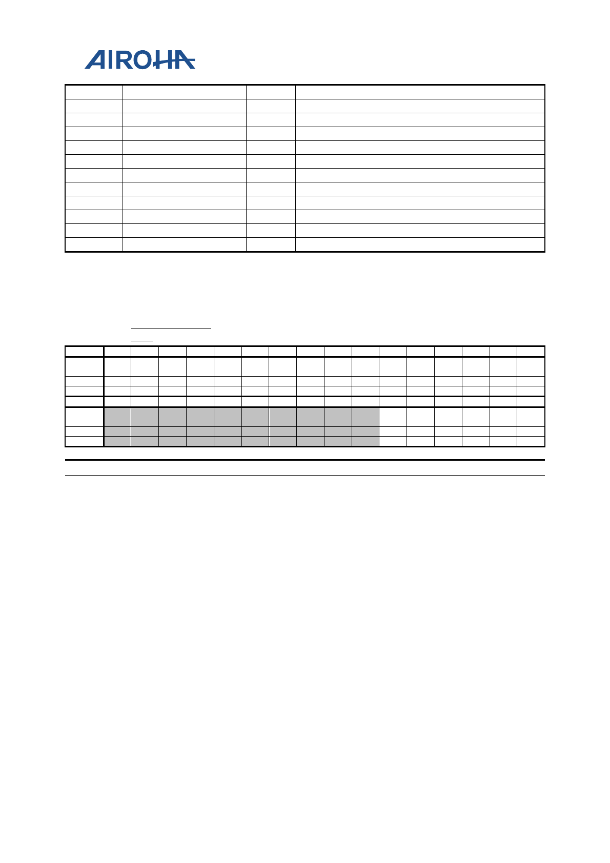
MT2523 Series Reference Manual
© 2015 - 2018 Airoha Technology Corp.
Page 28 of 692
This document contains information that is proprietary to Airoha Technology Corp. (“Airoha”) and/or its licensor(s).
Any unauthorized use, reproduction or disclosure of this document in whole or in part is strictly prohibited.
A0230420 PDMA6_ACKINT 32 DMA channel 6 interrupt acknowledge register
A0230424 PDMA6_RLCT 32 DMA channel 6 remaining length of current transfer
A023042C PDMA6_PGMADDR 32 DMA channel 6 programmable address register
A0230508 PDMA7_WPPT 32 DMA channel 7 wrap point address register
A023050C PDMA7_WPTO 32 DMA channel 7 wrap to address register
A0230510 PDMA7_COUNT 32 DMA channel 7 transfer count register
A0230514 PDMA7_CON 32 DMA channel 7 control register
A0230518 PDMA7_START 32 DMA channel 7 start register
A023051C PDMA7_INTSTA 32 DMA channel 7 interrupt status register
A0230520 PDMA7_ACKINT 32 DMA channel 7 interrupt acknowledge register
A0230524 PDMA7_RLCT 32 DMA channel 7 remaining length of current transfer
A023052C PDMA7_PGMADDR 32 DMA channel 7 programmable address register
4.2.2. Global Registers
A0000000
PD_
DMA_GLB
STA
DMA global
status register
00000000
Bit
31
30
29
28
27
26
25
24
23
22
21
20
19
18
17
16
Name
IT
16
RUN
16
IT
15
RUN
15
IT
14
RUN
14
IT
13
RUN
13
IT
12
RUN
12
IT
11
RUN
11
IT
10
RUN
10
IT
9
RUN
9
Type
RO
RO
RO
RO
RO
RO
RO
RO
RO
RO
RO
RO
RO
RO
RO
RO
Reset
0
0
0
0
0
0
0
0
0
0
0
0
0
0
0
0
Bit
15
14
13
12
11
10
9
8
7
6
5
4
3
2
1
0
Name
IT
3
RUN
3
IT
2
RUN
2
IT
1
RUN
1
Type
RO
RO
RO
RO
RO
RO
Reset
0
0
0
0
0
0
Bit(s)
Name
Description
31
IT16
Channel 16 interrupt status
30
RUN16
Channel 16 running status
29
IT15
Channel 15 interrupt status
28
RUN15
Channel 15 running status
27
IT14
Channel 14 interrupt status
26
RUN14
Channel 14 running status
25
IT13
Channel 13 interrupt status
24
RUN13
Channel 13 running status
23
IT12
Channel 12 interrupt status
22
RUN12
Channel 12 running status
21
IT11
Channel 11 interrupt status
20
RUN11
Channel 11 running status
19
IT10
Channel 10 interrupt status
18
RUN10
Channel 10 running status
17
IT9
Channel 9 interrupt status
16
RUN9
Channel 9 running status
5
IT3
Channel 3 interrupt status
4
RUN3
Channel 3 running status
3
IT2
Channel 2 interrupt status
2
RUN2
Channel 2 running status
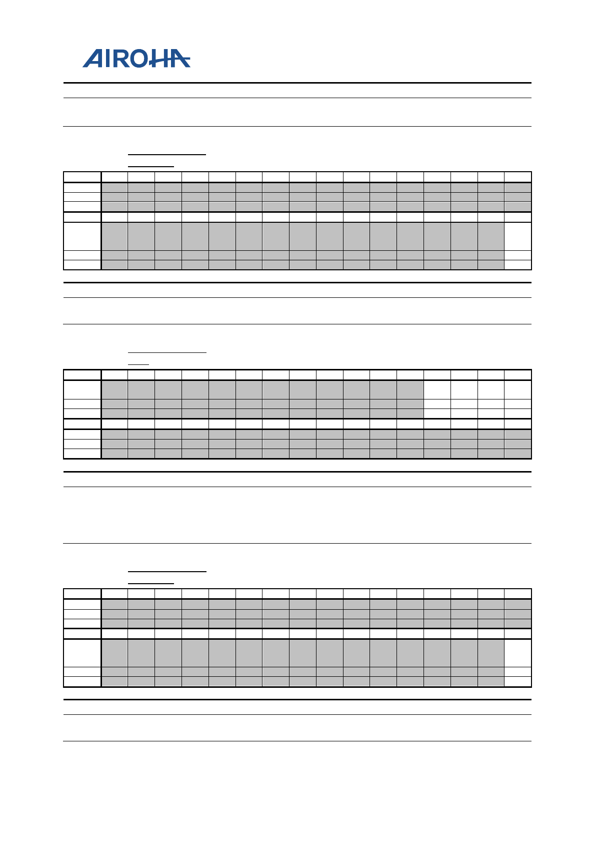
MT2523 Series Reference Manual
© 2015 - 2018 Airoha Technology Corp.
Page 29 of 692
This document contains information that is proprietary to Airoha Technology Corp. (“Airoha”) and/or its licensor(s).
Any unauthorized use, reproduction or disclosure of this document in whole or in part is strictly prohibited.
Bit(s)
Name
Description
1
IT1
Channel 1 interrupt status
0
RUN1
Channel 1 running status
A0000020
PD_
DMA_GLB
_SWRST
DMA global software reset
00000000
Bit
31
30
29
28
27
26
25
24
23
22
21
20
19
18
17
16
Name
Type
Reset
Bit
15
14
13
12
11
10
9
8
7
6
5
4
3
2
1
0
Name
SW_
RESE
T
Type
RW
Reset
0
Bit(s)
Name
Description
0
SW_RESET
Software reset
Write 1 to reset.
A2070000
AO_
DMA_GLB
STA
DMA global status register
00000000
Bit
31
30
29
28
27
26
25
24
23
22
21
20
19
18
17
16
Name
IT
18
RUN
18
IT
17
RUN
17
Type
RO
RO
RO
RO
Reset
0
0
0
0
Bit
15
14
13
12
11
10
9
8
7
6
5
4
3
2
1
0
Name
Type
Reset
Bit(s)
Name
Description
19
IT18
Channel 18 interrupt status
18
RUN18
Channel 18 running status
17
IT17
Channel 17 interrupt status
16
RUN17
Channel 17 running status
A2070020
AO_
DMA_GLB
_SWRST
DMA
global software reset
00000000
Bit
31
30
29
28
27
26
25
24
23
22
21
20
19
18
17
16
Name
Type
Reset
Bit
15
14
13
12
11
10
9
8
7
6
5
4
3
2
1
0
Name
SW_
RESE
T
Type
RW
Reset
0
Bit(s)
Name
Description
0
SW_RESET
Software reset
Write 1 to reset.
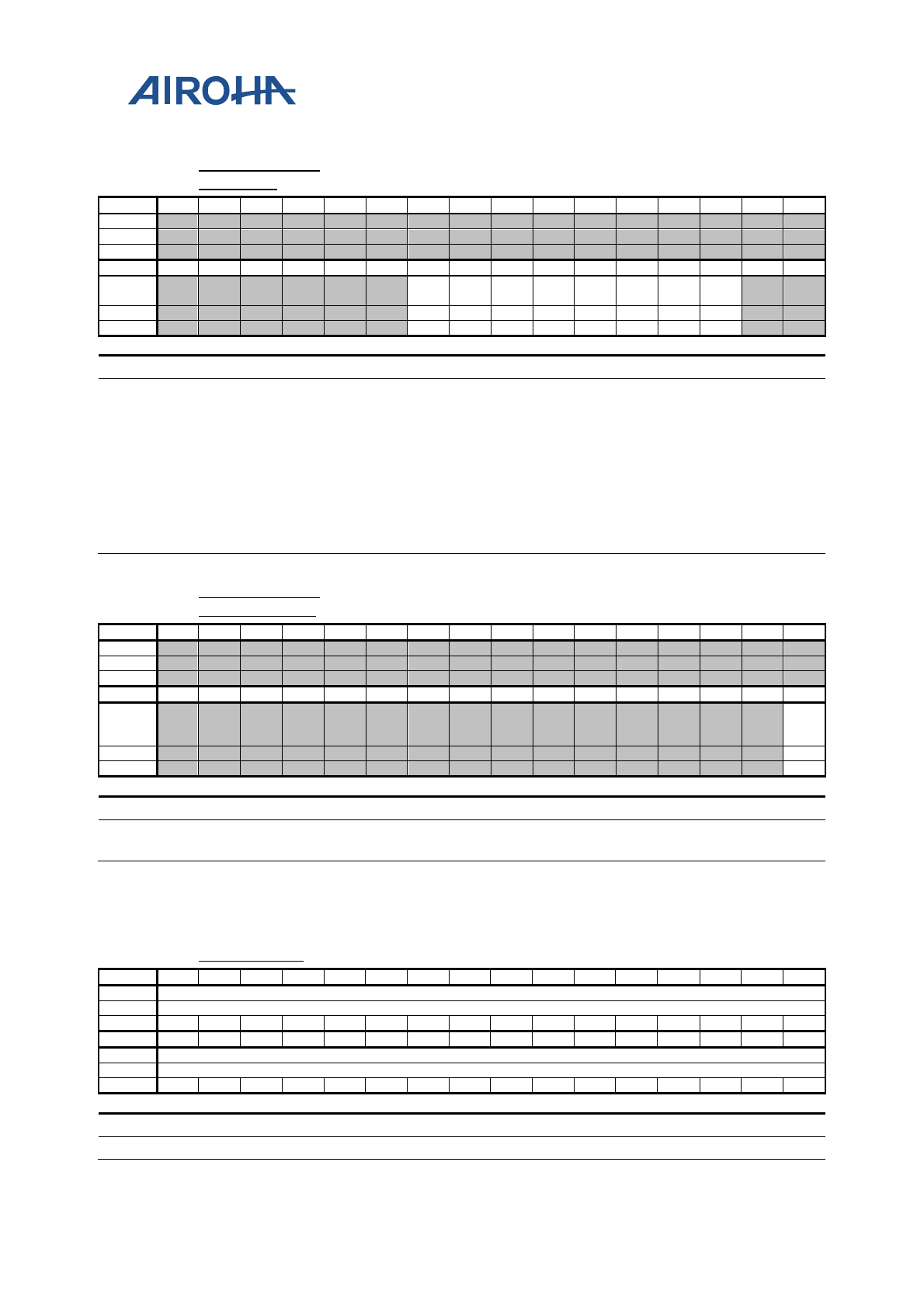
MT2523 Series Reference Manual
© 2015 - 2018 Airoha Technology Corp.
Page 30 of 692
This document contains information that is proprietary to Airoha Technology Corp. (“Airoha”) and/or its licensor(s).
Any unauthorized use, reproduction or disclosure of this document in whole or in part is strictly prohibited.
A0230000
SENSOR_
DMA
_GLBSTA
DMA global status register
00000000
Bit
31
30
29
28
27
26
25
24
23
22
21
20
19
18
17
16
Name
Type
Reset
Bit
15
14
13
12
11
10
9
8
7
6
5
4
3
2
1
0
Name
IT
7
RUN
7
IT
6
RUN
6
IT
5
RUN
5
IT
4
RUN
4
Type
RO
RO
RO
RO
RO
RO
RO
RO
Reset
0
0
0
0
0
0
0
0
Bit(s)
Name
Description
9
IT7
Channel 10 interrupt status
8
RUN7
Channel 10 running status
7
IT6
Channel 4 interrupt status
6
RUN6
Channel 4 running status
5
IT5
Channel 3 interrupt status
4
RUN5
Channel 3 running status
3
IT4
Channel 2 interrupt status
2
RUN4
Channel 2 running status
A0230020
SENSOR_
DMA
_GLB_SWRST
DMA global software reset
00000000
Bit
31
30
29
28
27
26
25
24
23
22
21
20
19
18
17
16
Name
Type
Reset
Bit
15
14
13
12
11
10
9
8
7
6
5
4
3
2
1
0
Name
SW_
RESE
T
Type
RW
Reset
0
Bit(s)
Name
Description
0
SW_RESET
Software reset
Write 1 to reset.
4.2.3. GDMA (Full-size DMA) Registers
A0000100
GDMA1_SRC
DMA channel 1 source address register
00000000
Bit
31
30
29
28
27
26
25
24
23
22
21
20
19
18
17
16
Name
SRC[31:16]
Type
RW
Reset
0
0
0
0
0
0
0
0
0
0
0
0
0
0
0
0
Bit
15
14
13
12
11
10
9
8
7
6
5
4
3
2
1
0
Name
SRC[15:0]
Type
RW
Reset
0
0
0
0
0
0
0
0
0
0
0
0
0
0
0
0
Bit(s)
Name
Description
31:0
SRC
GDMA source address
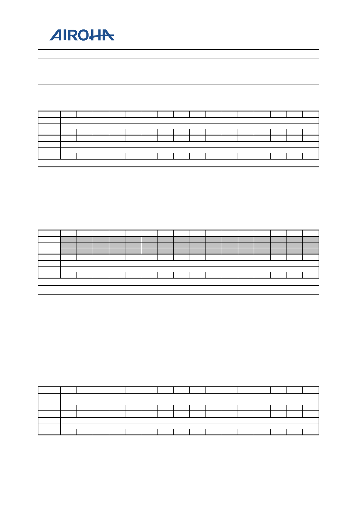
MT2523 Series Reference Manual
© 2015 - 2018 Airoha Technology Corp.
Page 31 of 692
This document contains information that is proprietary to Airoha Technology Corp. (“Airoha”) and/or its licensor(s).
Any unauthorized use, reproduction or disclosure of this document in whole or in part is strictly prohibited.
Bit(s)
Name
Description
The register contains the base or current source address that the DMA channel is
currently operating in. Writing to this register specifies the base address of the
transfer source for a DMA channel. Reading this register will return the address
value from which the DMA is reading.
A0000104
GDMA1_DST
DMA channel 1 destination address register
00000000
Bit
31
30
29
28
27
26
25
24
23
22
21
20
19
18
17
16
Name
DST[31:16]
Type
RW
Reset
0
0
0
0
0
0
0
0
0
0
0
0
0
0
0
0
Bit
15
14
13
12
11
10
9
8
7
6
5
4
3
2
1
0
Name
DST[15:0]
Type
RW
Reset
0
0
0
0
0
0
0
0
0
0
0
0
0
0
0
0
Bit(s)
Name
Description
31:0
DST
GDMA destination address
The register contains the base or current destination address that the DMA
channel is currently operating in. Writing to this register specifies the base
address of the transfer destination for a DMA channel. Reading this register will
return the address value to which the DMA is writing.
A0000108
GDMA1_WPPT
DMA channel 1 wrap point address register
00000000
Bit
31
30
29
28
27
26
25
24
23
22
21
20
19
18
17
16
Name
Type
Reset
Bit
15
14
13
12
11
10
9
8
7
6
5
4
3
2
1
0
Name
WPPT
Type
RW
Reset
0
0
0
0
0
0
0
0
0
0
0
0
0
0
0
0
Bit(s)
Name
Description
15:0
WPPT
Transfer counts before jump
The register specifies the transfer count required to perform before the jump
point. This can be used to support the ring buffer or double buffer style memory
accesses. To enable this function, two control bits, WPEN and WPSD, in the DMA
control register must be programmed. If the transfer counter in the DMA engine
matches this value, an address jump will occur, and the next address will be the
address specified in GDMAn_WPTO. To enable this function, set up WPEN in
GDMAn_CON.
Note: The total size of data specified in the wrap point count in a DMA channel is
determined by LEN together with SIZE in GDMAn_CON, i.e. WPPT x SIZE.
A000010C
GDMA1_WPTO
DMA channel 1 wrap to address register
00000000
Bit
31
30
29
28
27
26
25
24
23
22
21
20
19
18
17
16
Name
WPTO[31:16]
Type
RW
Reset
0
0
0
0
0
0
0
0
0
0
0
0
0
0
0
0
Bit
15
14
13
12
11
10
9
8
7
6
5
4
3
2
1
0
Name
WPTO[15:0]
Type
RW
Reset
0
0
0
0
0
0
0
0
0
0
0
0
0
0
0
0
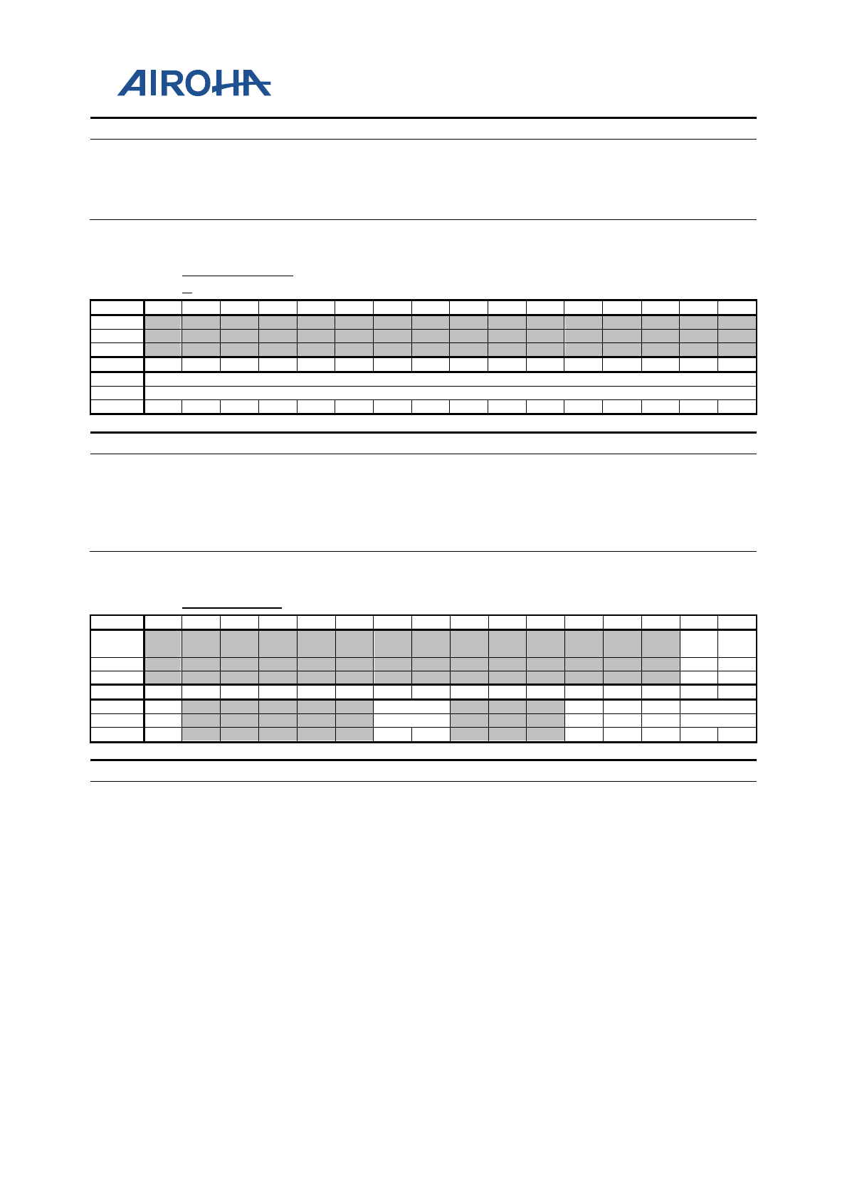
MT2523 Series Reference Manual
© 2015 - 2018 Airoha Technology Corp.
Page 32 of 692
This document contains information that is proprietary to Airoha Technology Corp. (“Airoha”) and/or its licensor(s).
Any unauthorized use, reproduction or disclosure of this document in whole or in part is strictly prohibited.
Bit(s)
Name
Description
31:0
WPTO
Jump address
The register specifies the address of the jump destination of a given DMA transfer
to support the ring buffer or double buffer style memory accesses. To enable this
function, set up two control bits, WPEN and WPSD, in the DMA control register.
To enable this function, WPEN in GDMAn_CON should be set.
A0000110
GDMA1_COUN
T
DMA channel 1 transfer count register
00000000
Bit
31
30
29
28
27
26
25
24
23
22
21
20
19
18
17
16
Name
Type
Reset
Bit
15
14
13
12
11
10
9
8
7
6
5
4
3
2
1
0
Name
COUNT
Type
RW
Reset
0
0
0
0
0
0
0
0
0
0
0
0
0
0
0
0
Bit(s)
Name
Description
15:0
COUNT
Amount of total transfer counts
This register specifies the amount of total transfer counts the DMA channel is
required to perform. Upon completion, the DMA channel will generate an
interrupt request to the processor when ITEN in GDMAn_CON is set to 1.
Note: The total size of data transferred by a DMA channel is determined by LEN
together with SIZE in GDMAn_CON, i.e. LEN x SIZE.
A0000114
GDMA1_CON
DMA channel 1 control register
00000000
Bit
31
30
29
28
27
26
25
24
23
22
21
20
19
18
17
16
Name
WPE
N
WPS
D
Type
RW
RW
Reset
0
0
Bit
15
14
13
12
11
10
9
8
7
6
5
4
3
2
1
0
Name
ITEN
BURST
DREQ
DINC
SINC
SIZE
Type
RW
RW
RW
RW
RW
RW
Reset
0
0
0
0
0
0
0
0
Bit(s)
Name
Description
17
WPEN
Enables wrap
Address-wrapping for ring buffer and double buffer. The next address of DMA
will jump to WRAP TO address when the current address matches WRAP POINT
count.
0: Disable
1: Enable
16
WPSD
Selects wrap
The side using address-wrapping function. Only one side of a DMA channel can
activate the address-wrapping function at a time.
0: Address-wrapping on source
1: Address-wrapping on destination
15
ITEN
Enables DMA transfer completion interrupt
0: Disable
1: Enable
9:8
BURST
Transfer type
The burst-type transfers have better bus efficiency. Mass data movement is
recommended to use this type of transfer.
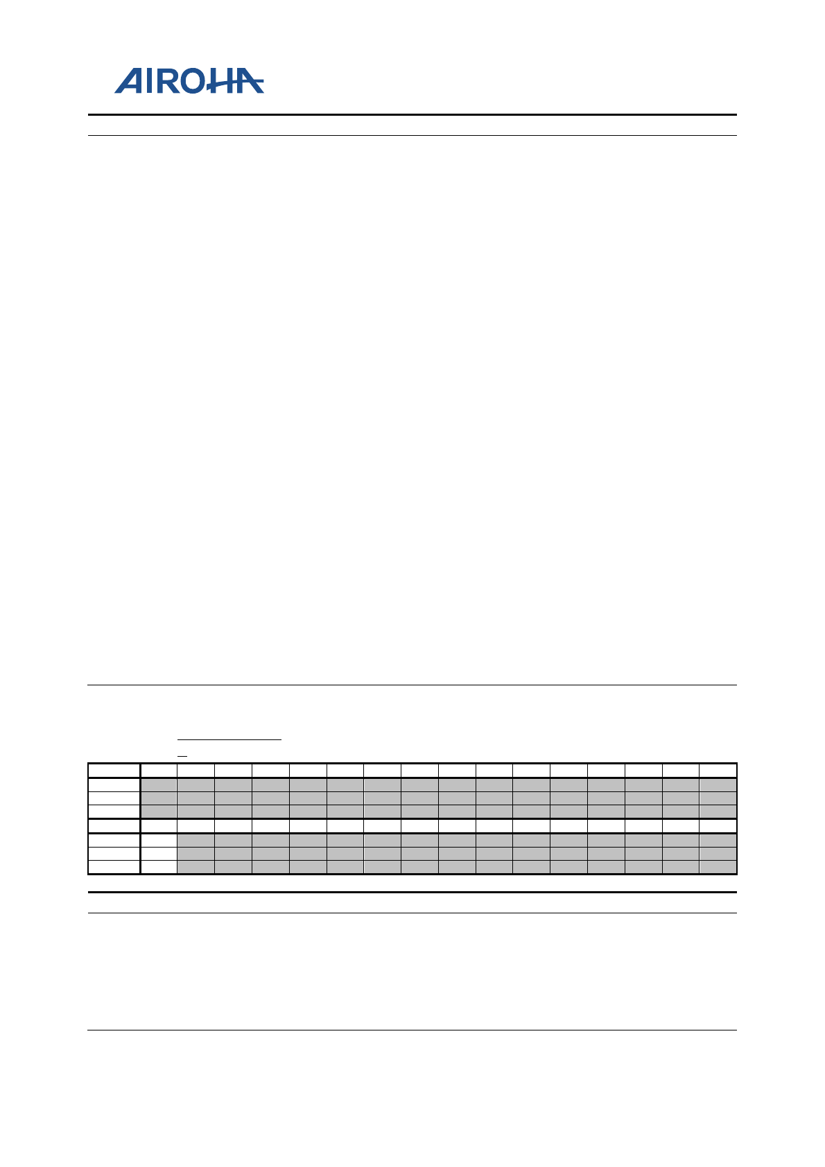
MT2523 Series Reference Manual
© 2015 - 2018 Airoha Technology Corp.
Page 33 of 692
This document contains information that is proprietary to Airoha Technology Corp. (“Airoha”) and/or its licensor(s).
Any unauthorized use, reproduction or disclosure of this document in whole or in part is strictly prohibited.
Bit(s)
Name
Description
Note: The burst-type transfer will not stop until all the beats in a burst are
completed or the transfer length is reached. Which transfer type can be used is
restricted by the SIZE. If SIZE is 00b, i.e. byte transfer, all of the four transfer
types can be used. If SIZE is 01b, i.e. half-word transfer, 16-beat incrementing
burst cannot be used. If SIZE is 10b, i.e. word transfer, only single and 4-beat
incrementing burst can be used.
00: Single
01: Reserved
10: 4-beat incrementing burst
11: Reserved
4
DREQ
Throttle and handshake control for DMA transfer
The DMA master is able to throttle down the transfer rate by request-grant
handshake.
0: No throttle control during DMA transfer or transfers occurr only between
memories
1: Hardware handshake management
3
DINC
Incremental destination address
The destination addresses increase every transfer. If the setting of SIZE is byte,
the destination addresses will increase by 1 every single transfer. If half-word, it
will increase by 2; and if word, increase by 4.
0: Disable
1: Enable
2
SINC
Incremental source address
The source addresses increase every transfer. If the setting of SIZE is byte, the
source addresses will increase by 1 every single transfer. If half-word, it will
increase by 2; and if word, increase by 4.
0: Disable
1: Enable
1:0
SIZE
Data size within the confine of a bus cycle per transfer
These bits conf
ine the data transfer size between the source and destination to the
specified value for individual bus cycle. The size is in terms of byte, and the
maximum value is 4 bytes. It is mainly decided by the data width of a DMA
master.
00: Byte transfer/1 byte
01: Half-word transfer/2 bytes
10: Word transfer/4 bytes
11: Reserved
A0000118
GDMA1_STAR
T
DMA channel 1 start register
00000000
Bit
31
30
29
28
27
26
25
24
23
22
21
20
19
18
17
16
Name
Type
Reset
Bit
15
14
13
12
11
10
9
8
7
6
5
4
3
2
1
0
Name
STR
Type
RW
Reset
0
Bit(s)
Name
Description
15
STR
Start control for a DMA channel
This register controls the activity of a DMA channel. Note that prior to setting
STR to 1, all the configurations should be done by giving proper value to the
registers. Once STR is set to 1, the hardware will not clear it automatically no
matter the DMA channel accomplishes the DMA transfer or not. In other words,
the value of STR stays at 1 regardless of the completion of the DMA transfer.
Therefore, the software program should clear STR to 0 before restarting another
DMA transfer. If this bit is cleared to 0 when DMA transfer is active, the software
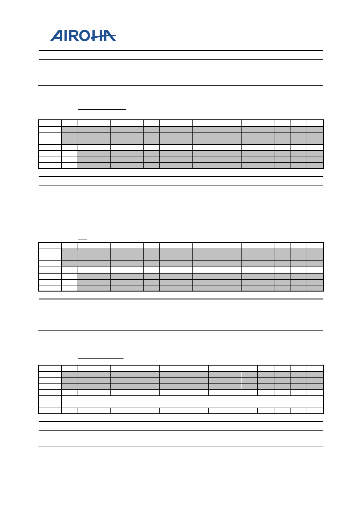
MT2523 Series Reference Manual
© 2015 - 2018 Airoha Technology Corp.
Page 34 of 692
This document contains information that is proprietary to Airoha Technology Corp. (“Airoha”) and/or its licensor(s).
Any unauthorized use, reproduction or disclosure of this document in whole or in part is strictly prohibited.
Bit(s)
Name
Description
should poll RUNn in DMA_GLBSTA after this bit is cleared to ensure the current
DMA transfer is terminated by the DMA engine.
0: The DMA channel is stopped.
1: The DMA channel is started and running.
A000011C
GDMA1_INTST
A
DMA channel 1 interrupt status register
00000000
Bit
31
30
29
28
27
26
25
24
23
22
21
20
19
18
17
16
Name
Type
Reset
Bit
15
14
13
12
11
10
9
8
7
6
5
4
3
2
1
0
Name
INT
Type
RW
Reset
0
Bit(s)
Name
Description
15
INT
Interrupt status for DMA channel
0: No interrupt request is generated.
1: One interrupt request is pending and waiting for service.
A0000120
GDMA1_ACKI
NT
DMA channel 1 interrupt acknowledge register
00000000
Bit
31
30
29
28
27
26
25
24
23
22
21
20
19
18
17
16
Name
Type
Reset
Bit
15
14
13
12
11
10
9
8
7
6
5
4
3
2
1
0
Name
ACK
Type
WO
Reset
0
Bit(s)
Name
Description
15
ACK
Interrupt acknowledge for the DMA channel
0: No effect
1: Interrupt request is acknowledged and should be relinquished.
A0000124
GDMA1_RLCT
DMA channel 1 remaining length of current
transfer
00000000
Bit
31
30
29
28
27
26
25
24
23
22
21
20
19
18
17
16
Name
Type
Reset
Bit
15
14
13
12
11
10
9
8
7
6
5
4
3
2
1
0
Name
RLCT
Type
RO
Reset
0
0
0
0
0
0
0
0
0
0
0
0
0
0
0
0
Bit(s)
Name
Description
15:0
RLCT
Reflects left count of transfer
Note: This value is transfer count, not the transfer data size.
MT2523 Series Reference Manual
© 2015 - 2018 Airoha Technology Corp.
Page 35 of 692
This document contains information that is proprietary to Airoha Technology Corp. (“Airoha”) and/or its licensor(s).
Any unauthorized use, reproduction or disclosure of this document in whole or in part is strictly prohibited.
4.2.3.1. PDMA (Half-size DMA) Registers
Only PDMA2 register is listed below. The register contents of other PDMA channels are the same as those of
PDMA2, only that the addresses are different. For register addresses, refer to the register summary section.
A0000208
PDMA
2_WPPT
DMA channel 2 wrap point address register
00000000
Bit
31
30
29
28
27
26
25
24
23
22
21
20
19
18
17
16
Name
Type
Reset
Bit
15
14
13
12
11
10
9
8
7
6
5
4
3
2
1
0
Name
WPPT
Type
RW
Reset
0
0
0
0
0
0
0
0
0
0
0
0
0
0
0
0
Bit(s)
Name
Description
15:0
WPPT
Transfer counts before jump
The register specifies the transfer count required to perform before the jump
point. This can be used to support the ring buffer or double buffer style memory
accesses. To enable this function, two control bits, WPEN and WPSD, in the DMA
control register must be programmed. If the transfer counter in the DMA engine
matches this value, an address jump will occur, and the next address will be the
address specified in PDMAn_WPTO. To enable this function, set up WPEN in
PDMAn_CON.
Note: The total size of data specified in the wrap point count in a DMA channel is
determined by LEN together with SIZE in PDMAn_CON, i.e. WPPT x SIZE.
A000020C
PDMA2_WPTO
DMA channel 2 wrap to address register
00000000
Bit
31
30
29
28
27
26
25
24
23
22
21
20
19
18
17
16
Name
WPTO[31:16]
Type
RW
Reset
0
0
0
0
0
0
0
0
0
0
0
0
0
0
0
0
Bit
15
14
13
12
11
10
9
8
7
6
5
4
3
2
1
0
Name
WPTO[15:0]
Type
RW
Reset
0
0
0
0
0
0
0
0
0
0
0
0
0
0
0
0
Bit(s)
Name
Description
31:0
WPTO
Jump address
The register specifies the address of the jump destination of a given DMA transfer
to support the ring buffer or double buffer style memory accesses. To enable this
function, set up two control bits, WPEN and WPSD, in the DMA control register.
To enable this function, WPEN in PDMAn_CON should be set.
A0000210
PDMA2_COUN
T
DMA channel 2 transfer count register
00000000
Bit
31
30
29
28
27
26
25
24
23
22
21
20
19
18
17
16
Name
Type
Reset
Bit
15
14
13
12
11
10
9
8
7
6
5
4
3
2
1
0
Name
COUNT
Type
RW
Reset
0
0
0
0
0
0
0
0
0
0
0
0
0
0
0
0
MT2523 Series Reference Manual
© 2015 - 2018 Airoha Technology Corp.
Page 36 of 692
This document contains information that is proprietary to Airoha Technology Corp. (“Airoha”) and/or its licensor(s).
Any unauthorized use, reproduction or disclosure of this document in whole or in part is strictly prohibited.
Bit(s)
Name
Description
15:0
COUNT
Amount of total transfer counts
This register specifies the amount of total transfer counts the DMA channel is
required to perform. Upon completion, the DMA channel will generate an
interrupt request to the processor when ITEN in PDMAn_CON is set to 1.
Note: The total size of data transferred by a DMA channel is determined by LEN
together with SIZE in PDMAn_CON, i.e. LEN x SIZE.
A0000214
PDMA2_CON
DMA channel 2 control register
00000000
Bit
31
30
29
28
27
26
25
24
23
22
21
20
19
18
17
16
Name
DIR
WPE
N
WPS
D
Type
RW
RW
RW
Reset
0
0
0
Bit
15
14
13
12
11
10
9
8
7
6
5
4
3
2
1
0
Name
ITEN
BURST
B2W
DREQ
DINC
SINC
SIZE
Type
RW
RW
RW
RW
RW
RW
RW
Reset
0
0
0
0
0
0
0
0
0
Bit(s)
Name
Description
18
DIR
Directions of PDMA transfer
The direction is from the perspective of the DMA masters. WRITE means reading
from master then writing to the address specified in PDMAn_PGMADDR, and
vice versa. No effect on channel 1.
0: Peripheral TX
1: Peripheral RX
17
WPEN
Enables wrap
Address-wrapping for ring buffer and double buffer. The next address of DMA
will jump to WRAP TO address when the current address matches WRAP POINT
count.
0: Disable
1: Enable
16
WPSD
Selects wrap
The side using address-wrapping function. Only one side of a DMA channel can
activate the address-wrapping function at a time.
0: Address-wrapping on source
1: Address-wrapping on destination
15
ITEN
Enables DMA transfer completion interrupt
0: Disable
1: Enable
9:8
BURST
Transfer type
The burst-type transfers have better bus efficiency. Mass data movement is
recommended to use this type of transfer.
Note: The burst-type transfer will not stop until all of the beats in a burst are
completed or the transfer length is reached. Which transfer type can be used is
restricted by the SIZE. If SIZE is 00b, i.e. byte transfer, all of the four transfer
types can be used. If SIZE is 01b, i.e. half-word transfer, 16-beat incrementing
burst cannot be used. If SIZE is 10b, i.e. word transfer, only single and 4-beat
incrementing burst can be used.
00: Single
01: Reserved
10: 4-beat incrementing burst
11: Reserved
5
B2W
Byte to word
Word to byte or byte to word transfer for the applications of transferring non-
word-aligned-address data to word-aligned-address data.
Note: BURST is set to 4-beat burst this function is enabled, and the SIZE is set to
MT2523 Series Reference Manual
© 2015 - 2018 Airoha Technology Corp.
Page 37 of 692
This document contains information that is proprietary to Airoha Technology Corp. (“Airoha”) and/or its licensor(s).
Any unauthorized use, reproduction or disclosure of this document in whole or in part is strictly prohibited.
Bit(s)
Name
Description
byte.
0: Disable
1: Enable
4
DREQ
Throttle and handshake control for DMA transfer
The DMA master is able to throttle down the transfer rate by request-grant
handshake.
0: No throttle control during DMA transfer or transfers occurred only between
memories
1: Hardware handshake management
3
DINC
Incremental destination address
The destination addresses increase every transfer. If the setting of SIZE is byte,
the destination addresses will increase by 1 every single transfer. If half-word, it
will increase by 2; and if word, increase by 4.
0: Disable
1: Enable
2
SINC
Incremental source address
The source addresses increase every transfer. If the setting of SIZE is byte, the
source addresses will increase by 1 every single transfer. If half-word, it will
increase by 2; and if word, increase by 4.
0: Disable
1: Enable
1:0
SIZE
Data size within the confine of a bus cycle per transfer
These
bits confine the data transfer size between the source and destination to the
specified value for individual bus cycle. The size is in terms of byte, and the
maximum value is 4 bytes. It is mainly decided by the data width of a DMA
master.
00: Byte transfer/1 byte
01: Half-word transfer/2 bytes
10: Word transfer/4 bytes
11: Reserved
A0000218
PDMA2_STAR
T
DMA channel 2 start register
00000000
Bit
31
30
29
28
27
26
25
24
23
22
21
20
19
18
17
16
Name
Type
Reset
Bit
15
14
13
12
11
10
9
8
7
6
5
4
3
2
1
0
Name
STR
Type
RW
Reset
0
Bit(s)
Name
Description
15
STR
Start control for a DMA channel
This register controls the activity of a DMA channel. Note that prior to setting
STR to 1, all the configurations should be done by giving proper value to the
registers. Once STR is set to 1, the hardware will not clear it automatically no
matter the DMA channel accomplishes the DMA transfer or not. In other words,
the value of STR stays at 1 regardless of the completion of the DMA transfer.
Therefore, the software program should clear STR to 0 before restarting another
DMA transfer. If this bit is cleared to 0 when DMA transfer is active, the software
should poll RUNn in DMA_GLBSTA after this bit is cleared to ensure the current
DMA transfer is terminated by the DMA engine.
0: The DMA channel is stopped.
1: The DMA channel is started and running.
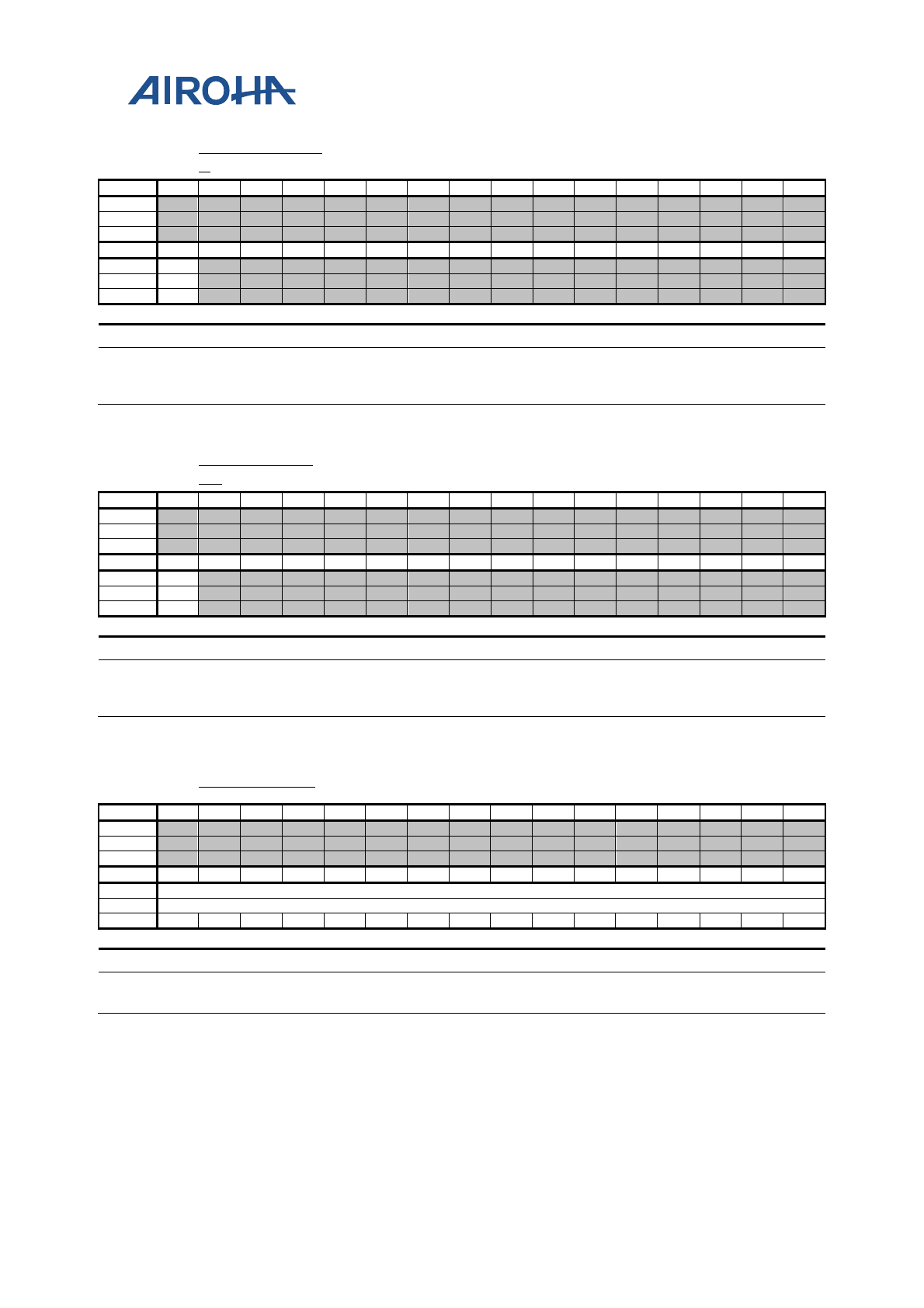
MT2523 Series Reference Manual
© 2015 - 2018 Airoha Technology Corp.
Page 38 of 692
This document contains information that is proprietary to Airoha Technology Corp. (“Airoha”) and/or its licensor(s).
Any unauthorized use, reproduction or disclosure of this document in whole or in part is strictly prohibited.
A000021C
PDMA2_INTST
A
DMA channel 2 interrupt status register
00000000
Bit
31
30
29
28
27
26
25
24
23
22
21
20
19
18
17
16
Name
Type
Reset
Bit
15
14
13
12
11
10
9
8
7
6
5
4
3
2
1
0
Name
INT
Type
RO
Reset
0
Bit(s)
Name
Description
15
INT
Interrupt status for DMA channel
0: No interrupt request is generated.
1: One interrupt request is pending and waiting for service.
A0000220
PDMA2_ACKI
NT
DMA channel 2 interrupt acknowledge register
00000000
Bit
31
30
29
28
27
26
25
24
23
22
21
20
19
18
17
16
Name
Type
Reset
Bit
15
14
13
12
11
10
9
8
7
6
5
4
3
2
1
0
Name
ACK
Type
WO
Reset
0
Bit(s)
Name
Description
15
ACK
Interrupt acknowledge for the DMA channel
0: No effect
1: Interrupt request is acknowledged and should be relinquished.
A0000224
PDMA2_RLCT
DMA channel 2 remaining length of current
transfer
00000000
Bit
31
30
29
28
27
26
25
24
23
22
21
20
19
18
17
16
Name
Type
Reset
Bit
15
14
13
12
11
10
9
8
7
6
5
4
3
2
1
0
Name
RLCT
Type
RO
Reset
0
0
0
0
0
0
0
0
0
0
0
0
0
0
0
0
Bit(s)
Name
Description
15:0
RLCT
Reflects left count of transfer
Note: This value is transfer count, not the transfer data size.
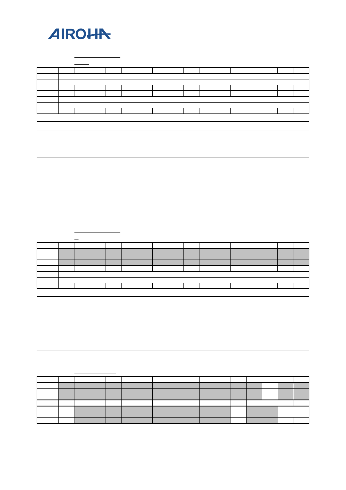
MT2523 Series Reference Manual
© 2015 - 2018 Airoha Technology Corp.
Page 39 of 692
This document contains information that is proprietary to Airoha Technology Corp. (“Airoha”) and/or its licensor(s).
Any unauthorized use, reproduction or disclosure of this document in whole or in part is strictly prohibited.
A000022C
PDMA2_PGMA
DDR
DMA channel 2 programmable address
register
00000000
Bit
31
30
29
28
27
26
25
24
23
22
21
20
19
18
17
16
Name
PGMADDR[31:16]
Type
RW
Reset
0
0
0
0
0
0
0
0
0
0
0
0
0
0
0
0
Bit
15
14
13
12
11
10
9
8
7
6
5
4
3
2
1
0
Name
PGMADDR[15:0]
Type
RW
Reset
0
0
0
0
0
0
0
0
0
0
0
0
0
0
0
0
Bit(s)
Name
Description
31:0
PGMADDR
PDMA programmable address
The above registers specify the address for a half-size DMA channel. This address
represents the source address if DIR in DMA_CON is set to 0 and represents the
destination address if DIR in PDMAn_CON is set to 1.
4.2.3.2. VDMA (Virtual FIFO DMA) Registers
Only VDMA9 register is listed below. The register contents of other VDMA channels are the same as those of
VDMA9, only that the addresses are different. For register addresses, refer to the register summary section.
A0000910
VDMA9_COUN
T
DMA channel 9 t
ransfer count register
00000000
Bit
31
30
29
28
27
26
25
24
23
22
21
20
19
18
17
16
Name
Type
Reset
Bit
15
14
13
12
11
10
9
8
7
6
5
4
3
2
1
0
Name
COUNT
Type
RW
Reset
0
0
0
0
0
0
0
0
0
0
0
0
0
0
0
0
Bit(s)
Name
Description
15:0
COUNT
FIFO threshold
For virtual FIFO DMA, this register is used to configure the RX threshold and TX
threshold. The interrupt will be
triggered when FIFO count is larger than or equal
to RX threshold in RX path or FIFO count is less than or equal to TX threshold in
TX path.
Note: The ITEN bit in the VDMAn_CON register should be set, or no interrupt
will be issued. n is from 1 to 16.
A0000914
VDMA9_CON
DMA channel 9
control register
00000000
Bit
31
30
29
28
27
26
25
24
23
22
21
20
19
18
17
16
Name
DIR
Type
RW
Reset
0
Bit
15
14
13
12
11
10
9
8
7
6
5
4
3
2
1
0
Name
ITEN
DREQ
SIZE
Type
RW
RW
RW
Reset
0
0
0
0
MT2523 Series Reference Manual
© 2015 - 2018 Airoha Technology Corp.
Page 40 of 692
This document contains information that is proprietary to Airoha Technology Corp. (“Airoha”) and/or its licensor(s).
Any unauthorized use, reproduction or disclosure of this document in whole or in part is strictly prohibited.
Bit(s)
Name
Description
18
DIR
Directions of PDMA transfer
The direction is from the perspective of the DMA masters. WRITE means reading
from master and then writing to the address specified in VDMAn_PGMADDR,
and vice versa. No effect on channel 1.
0: Peripheral TX
1: Peripheral RX
15
ITEN
Enables DMA transfer completion interrupt
0: Disable
1: Enable
4
DREQ
Throttle and handshake control for DMA transfer
The DMA master is able to throttle down the transfer rate by request-grant
handshake.
0: No throttle control during DMA transfer or transfers occurred only between
memories
1: Hardware handshake management
1:0
SIZE
Data size within the confine of a bus cycle per transfer
These bits confine the data transfer size
between the source and destination to the
specified value for individual bus cycle. The size is in terms of byte, and the
maximum value is 4 bytes. It is mainly decided by the data width of a DMA
master.
00: Byte transfer/1 byte
01: Half-word transfer/2 bytes
10: Word transfer/4 bytes
11: Reserved
A0000918
VDMA9_STAR
T
DMA channel 9 start register
00000000
Bit
31
30
29
28
27
26
25
24
23
22
21
20
19
18
17
16
Name
Type
Reset
Bit
15
14
13
12
11
10
9
8
7
6
5
4
3
2
1
0
Name
STR
Type
RW
Reset
0
Bit(s)
Name
Description
15
STR
Start control for a DMA channel
This register controls the activity of a DMA channel. Note that prior to setting
STR to 1, all the configurations should be done by giving proper value to the
registers. Once STR is set to 1, the hardware will not clear it automatically no
matter the DMA channel accomplishes the DMA transfer or not. In other words,
the value of STR stays at 1 regardless of the completion of the DMA transfer.
Therefore, the software program should clear STR to 0 before restarting another
DMA transfer. If this bit is cleared to 0 when DMA transfer is active, the software
should poll RUNn in DMA_GLBSTA after this bit is cleared to ensure the current
DMA transfer is terminated by the DMA engine.
0: The DMA channel is stopped.
1: The DMA channel is started and running.
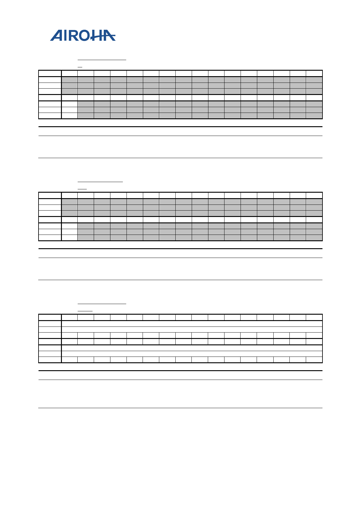
MT2523 Series Reference Manual
© 2015 - 2018 Airoha Technology Corp.
Page 41 of 692
This document contains information that is proprietary to Airoha Technology Corp. (“Airoha”) and/or its licensor(s).
Any unauthorized use, reproduction or disclosure of this document in whole or in part is strictly prohibited.
A000091C
VDMA9_INTST
A
DMA channel 9 interrupt status register
00000000
Bit
31
30
29
28
27
26
25
24
23
22
21
20
19
18
17
16
Name
Type
Reset
Bit
15
14
13
12
11
10
9
8
7
6
5
4
3
2
1
0
Name
INT
Type
RW
Reset
0
Bit(s)
Name
Description
15
INT
Interrupt status for DMA channel
0: No interrupt request is generated.
1: One interrupt request is pending and waiting for service.
A0000920
VDMA9_ACKI
NT
DMA channel 9 interrupt acknowledge register
00000000
Bit
31
30
29
28
27
26
25
24
23
22
21
20
19
18
17
16
Name
Type
Reset
Bit
15
14
13
12
11
10
9
8
7
6
5
4
3
2
1
0
Name
ACK
Type
WO
Reset
0
Bit(s)
Name
Description
15
ACK
Interrupt acknowledge for the DMA channel
0: No effect
1: Interrupt request is acknowledged and should be relinquished.
A000092C
VDMA9_PGMA
DDR
DMA channel 9 programmable address
register
00000000
Bit
31
30
29
28
27
26
25
24
23
22
21
20
19
18
17
16
Name
PGMADDR[31:16]
Type
RW
Reset
0
0
0
0
0
0
0
0
0
0
0
0
0
0
0
0
Bit
15
14
13
12
11
10
9
8
7
6
5
4
3
2
1
0
Name
PGMADDR[15:0]
Type
RW
Reset
0
0
0
0
0
0
0
0
0
0
0
0
0
0
0
0
Bit(s)
Name
Description
31:0
PGMADDR
VDMA programmable address
The above registers specify the address for a half-size DMA channel. This address
represents the source address if DIR in DMA_CON is set to 0 and represents the
destination address if DIR in VDMAn_CON is set to 1.
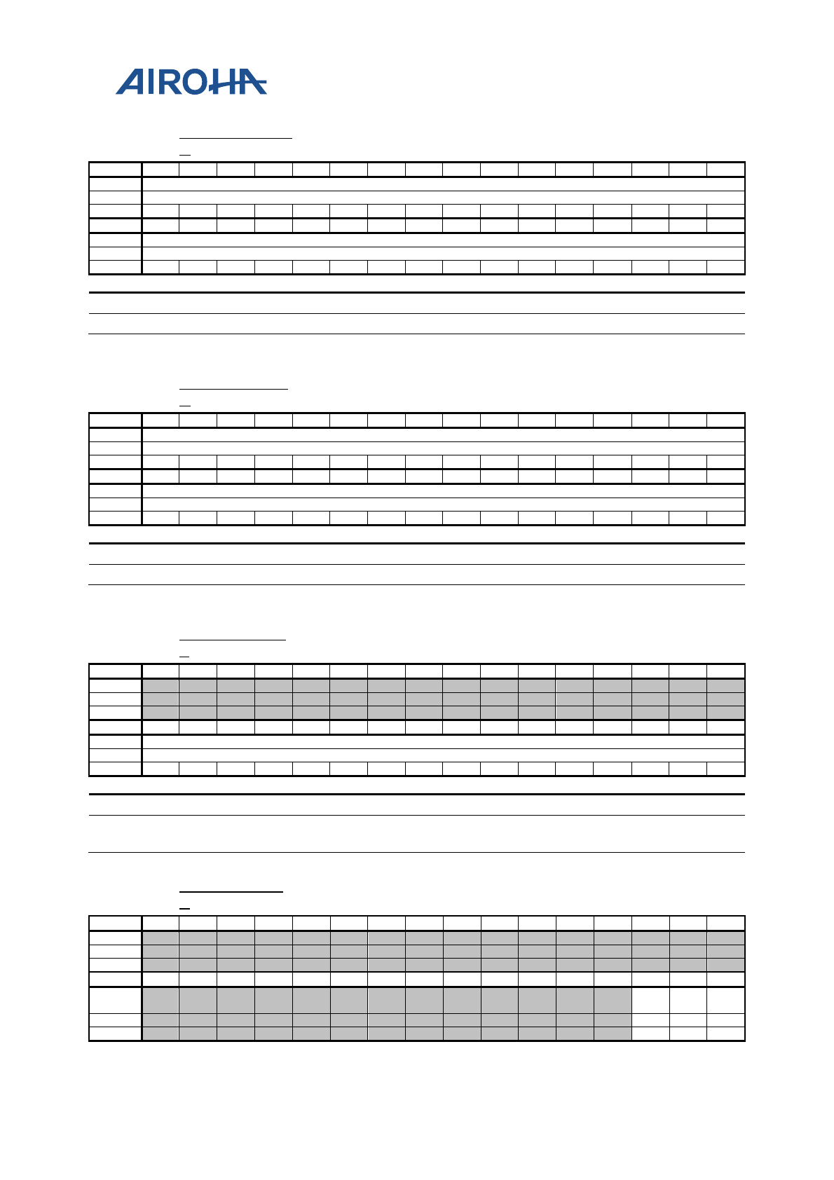
MT2523 Series Reference Manual
© 2015 - 2018 Airoha Technology Corp.
Page 42 of 692
This document contains information that is proprietary to Airoha Technology Corp. (“Airoha”) and/or its licensor(s).
Any unauthorized use, reproduction or disclosure of this document in whole or in part is strictly prohibited.
A0000930
VDMA9_WRPT
R
DMA channel 9 write pointer
00000000
Bit
31
30
29
28
27
26
25
24
23
22
21
20
19
18
17
16
Name
WRPTR[31:16]
Type
RO
Reset
0
0
0
0
0
0
0
0
0
0
0
0
0
0
0
0
Bit
15
14
13
12
11
10
9
8
7
6
5
4
3
2
1
0
Name
WRPTR[15:0]
Type
RO
Reset
0
0
0
0
0
0
0
0
0
0
0
0
0
0
0
0
Bit(s)
Name
Description
31:0
WRPTR
Virtual FIFO write pointer
A0000934
VDMA9_RDPT
R
DMA channel 9 read pointer
00000000
Bit
31
30
29
28
27
26
25
24
23
22
21
20
19
18
17
16
Name
RDPTR[31:16]
Type
RO
Reset
0
0
0
0
0
0
0
0
0
0
0
0
0
0
0
0
Bit
15
14
13
12
11
10
9
8
7
6
5
4
3
2
1
0
Name
RDPTR[15:0]
Type
RO
Reset
0
0
0
0
0
0
0
0
0
0
0
0
0
0
0
0
Bit(s)
Name
Description
31:0
RDPTR
Virtual FIFO read pointer
A0000938
VDMA9_FFCN
T
DMA channel 9 FIFO count
00000000
Bit
31
30
29
28
27
26
25
24
23
22
21
20
19
18
17
16
Name
Type
Reset
Bit
15
14
13
12
11
10
9
8
7
6
5
4
3
2
1
0
Name
FFCNT
Type
RO
Reset
0
0
0
0
0
0
0
0
0
0
0
0
0
0
0
0
Bit(s)
Name
Description
15:0
FFCNT
Displays the number of data stored in FIFO
0 means FIFO is empty; FIFO will be full if FFCNT is equal to FFSIZE.
A000093C
VDMA9_FFST
A
DMA channel 9 FIFO status
00000000
Bit
31
30
29
28
27
26
25
24
23
22
21
20
19
18
17
16
Name
Type
Reset
Bit
15
14
13
12
11
10
9
8
7
6
5
4
3
2
1
0
Name
ALT
EMPT
Y
FULL
Type
RO
RO
RO
Reset
0
0
0
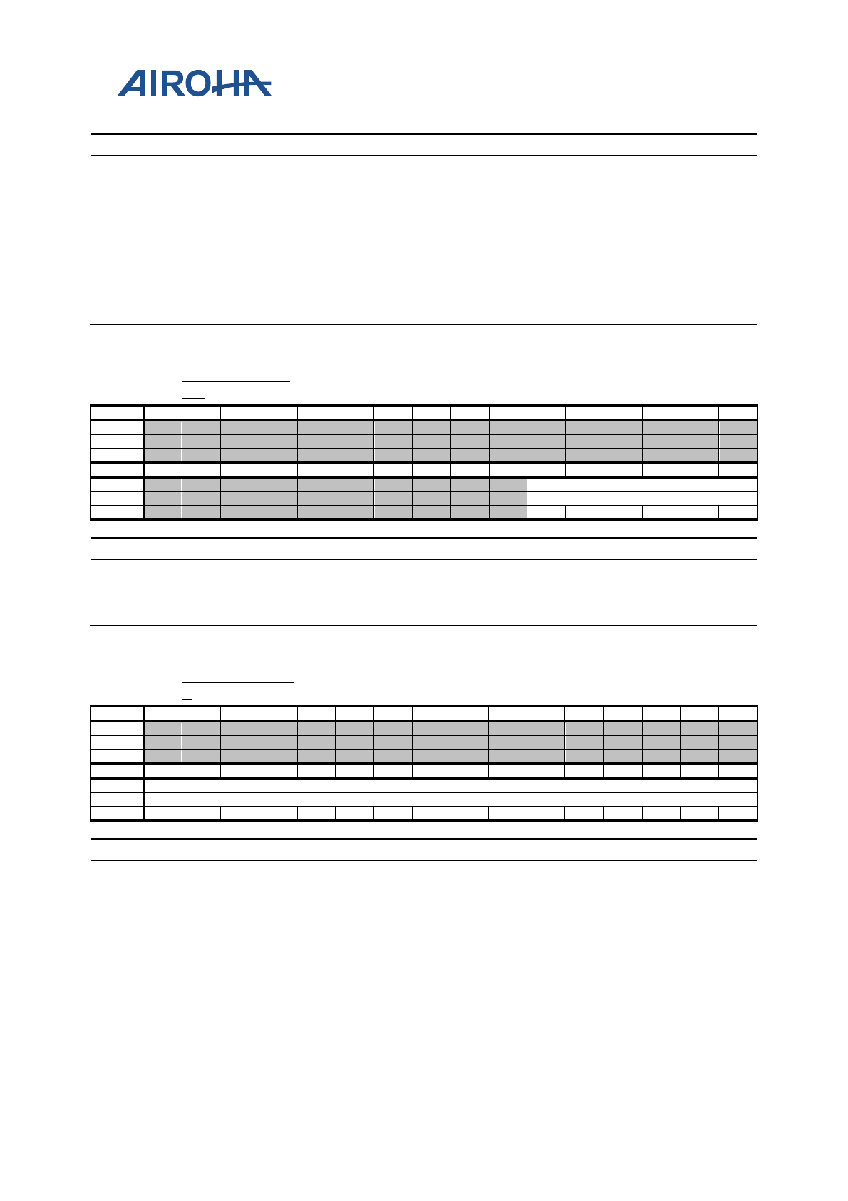
MT2523 Series Reference Manual
© 2015 - 2018 Airoha Technology Corp.
Page 43 of 692
This document contains information that is proprietary to Airoha Technology Corp. (“Airoha”) and/or its licensor(s).
Any unauthorized use, reproduction or disclosure of this document in whole or in part is strictly prohibited.
Bit(s)
Name
Description
2
ALT
Indicates FIFO count is larger than ALTLEN
DMA issues an alert signal to UART/BRIF to enable UART/BRIF flow control.
0: Not reach alert region
1: Reach alert region
1
EMPTY
Indicates FIFO is empty
0: Not empty
1: Empty
0
FULL
Indicates FIFO is full
0: Not full
1: Full
A0000940
VDMA9_ALTL
EN
DMA channel 9 alert length
00000000
Bit
31
30
29
28
27
26
25
24
23
22
21
20
19
18
17
16
Name
Type
Reset
Bit
15
14
13
12
11
10
9
8
7
6
5
4
3
2
1
0
Name
ALTLEN
Type
RW
Reset
0
0
0
0
0
0
Bit(s)
Name
Description
5:0
ALTLEN
Specifies alert length of virtual FIFO DMA
Once the remaining FIFO space is less than ALTLEN, an alert signal will be
issued to UART/BRIF to enable the flow control. Normally, ALTLEN should be
bigger than 16 for UART/BRIF applications.
A0000944
VDMA9_FFSIZ
E
DMA channel 9 FIFO size
00000000
Bit
31
30
29
28
27
26
25
24
23
22
21
20
19
18
17
16
Name
Type
Reset
Bit
15
14
13
12
11
10
9
8
7
6
5
4
3
2
1
0
Name
FFSIZE
Type
RW
Reset
0
0
0
0
0
0
0
0
0
0
0
0
0
0
0
0
Bit(s)
Name
Description
15:0
FFSIZE
Specifies FIFO size of virtual FIFO DMA
MT2523 Series Reference Manual
© 2015 - 2018 Airoha Technology Corp.
Page 44 of 692
This document contains information that is proprietary to Airoha Technology Corp. (“Airoha”) and/or its licensor(s).
Any unauthorized use, reproduction or disclosure of this document in whole or in part is strictly prohibited.
5. Real Time Clock
5.1. General Description
The Real-Time Clock (RTC) module provides time and data information, as well as 32,768 kHz clock. The provided
32k clock is selected between three clock sources: one from the external (XOSC32), and two from the internal
(DCXO, EOSC32). An additional pin, XOSC32_ENB, is added for the 32k crystal existence information. The clock
source is from the external oscillator or from the embedded clock sources, determined by the XOSC32_ENB pin
setting. The RTC block has an independent power supply. When the mobile handset is powered off, a dedicated
regulator supplies the RTC block. In addition to providing timing data, an alarm interrupt is generated and can be
used to power up the baseband core. Regulator interrupts corresponding to seconds, minutes, hours and days can
be generated whenever the time counter value reaches a maximum value (e.g., 59 for seconds and minutes, 23 for
hours, etc.). The year span is supported up to 2127. The maximum day-of-month values, which depend on the leap
year condition, are stored in the RTC block.
5.2. Register Definitions
Module name: RTC Base address: (+A21E0000h)
Address Name
Widt
h Register Function
A21E0000 RTC_BBPU 16 Baseband power up
A21E0004 RTC_IRQ_STA 16 RTC IRQ status
This register is fixed atin 0 when RTC_POWERKEY1 &
RTC_POWERKEY2 unmatch the correct values.
A21E0008 RTC_IRQ_EN 16
RTC IRQ enable
This register is fixed atin 0 when RTC_POWERKEY1 &
RTC_POWERKEY2 unmatch the correct values.
A21E000C RTC_CII_EN 16
Counter increment IRQ enable
This register activates or de-activates the IRQ generation when the
TC counter reaches its maximum value.
A21E0010 RTC_AL_MAS
K 16
RTC alarm mask
The alarm condition for alarm IRQ generation depends on whether
or not the corresponding bit in this register is masked. Warning: If
you set all bits to 1 in RTC_AL_MASK (i.e. RTC_AL_MASK=0x7f)
and PWREN=1 in RTC_BBPU, it means alarm will comes every
secondEVERY SECOND, not disabled.
A21E0014 RTC_TC_SEC 16 RTC seconds time counter register
A21E0018 RTC_TC_MIN 16 RTC minutes time counter register
A21E001C
RTC_TC_HOU 16 RTC hours time counter register
A21E0020
RTC_TC_DOM 16 RTC day-of-month time counter register
A21E0024
RTC_TC_DOW 16 RTC day-of-week time counter register
A21E0028 RTC_TC_MTH 16 RTC month time counter register
A21E002C RTC_TC_YEA 16 RTC year time counter register
A21E0030 RTC_AL_SEC 16 RTC second alarm setting register
MT2523 Series Reference Manual
© 2015 - 2018 Airoha Technology Corp.
Page 45 of 692
This document contains information that is proprietary to Airoha Technology Corp. (“Airoha”) and/or its licensor(s).
Any unauthorized use, reproduction or disclosure of this document in whole or in part is strictly prohibited.
Module name: RTC Base address: (+A21E0000h)
A21E0034
RTC_AL_MIN 16 RTC minute alarm setting register
A21E0038
RTC_AL_HOU 16 RTC hour alarm setting register
A21E003C RTC_AL_DOM 16 RTC day-of-month alarm setting register
A21E0040 RTC_AL_DOW 16 RTC day-of-week alarm setting register
A21E0044 RTC_AL_MTH 16 RTC month alarm setting register
A21E0048 RTC_AL_YEA 16 RTC year alarm setting register
A21E0050
RTC_POWER
KEY1 16 RTC_POWERKEY1 register
A21E0054
RTC_POWER
KEY2 16 RTC_POWERKEY2 register
A21E0058 RTC_PDN1 16 PDN1
A21E005C RTC_PDN2 16 PDN2
A21E0060 RTC_SPAR0 16 Spare register for specific purpose
A21E0064
RTC_SPAR1 16 Spare register for specific purpose
A21E0068
RTC_PROT 16 Lock/unlock scheme to prevent RTC miswriting
A21E006C RTC_DIFF 16
One-time calibration offset
This register is fixed atin 0 when RTC_POWERKEY1 &
RTC_POWERKEY2 unmatch the correct values.
A21E0070 RTC_CALI 16
Repeat calibration offset
This register is fixed atin 0 when RTC_POWERKEY1 &
RTC_POWERKEY2 unmatch the correct values.
A21E0074 RTC_WRTGR 16 Enable the transfers from core to RTC in the queue
A21E0000 RTC_BBPU Baseband power up 0000
Bit
15
14
13
12
11
10
9
8
7
6
5
4
3
2
1
0
Name KEY_BBPU CB
US
Y
RE
LO
AD
AL
AR
M_
PU
PW
RE
N
Type
WO
RO
WO
RW
RW
Reset
0
0
0
0
0
0
0
0
0
0
0
0
Overview
Bit(s) Name Description
15:8 KEY_BBPU A bus write is acceptable only when KEY_BBPU is correct.
6 CBUSY
The read/write channels between RTC / Core is busy. This bit
indicates high after software program sequence to anyone of RTC
data registers and enables the transfer by RTC_WRTGR=1. By thise
way, it will beis high after the reset from low to high because RTC
reloads the process.
5 RELOAD Reloads the values from RTC domain to Ccore domain. Generally
speaking, RTC will reload to synchronize the data from RTC to core
when reset from 0 to 1. This bit can be treated as a debug bit.
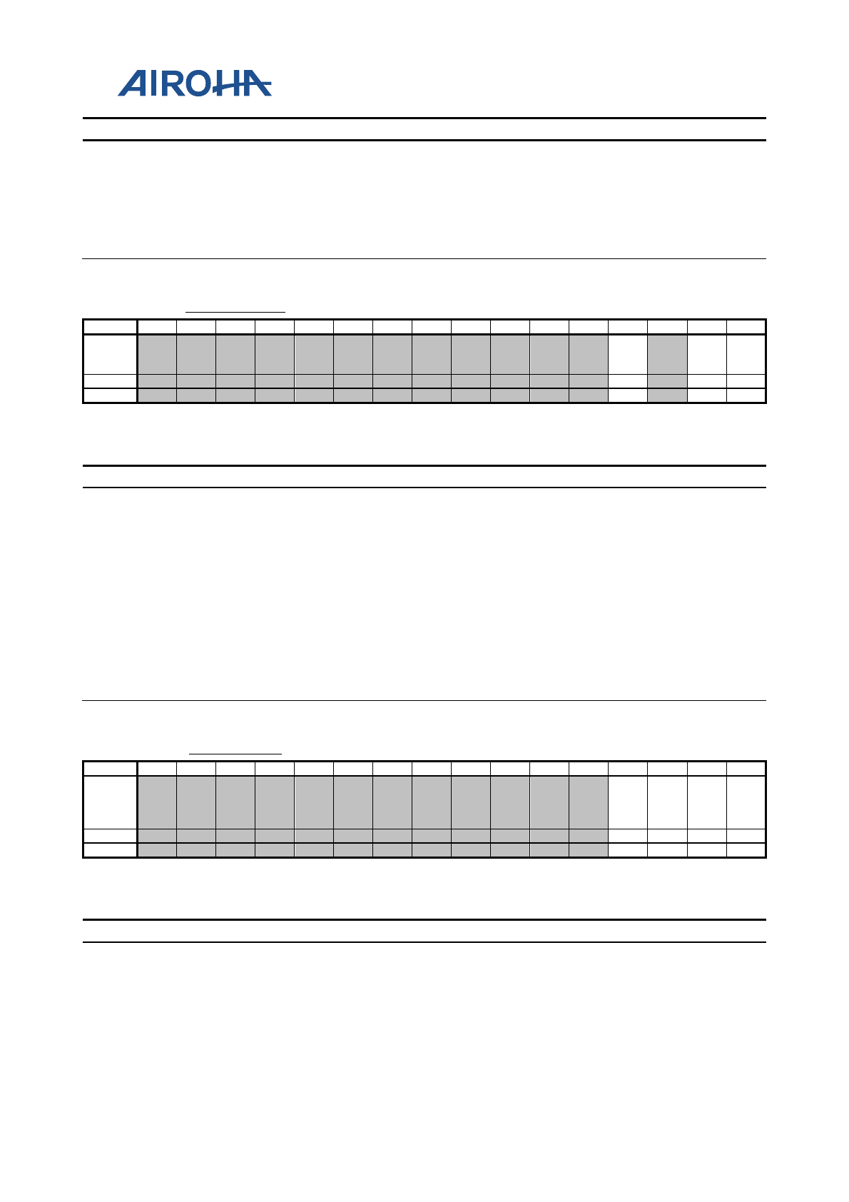
MT2523 Series Reference Manual
© 2015 - 2018 Airoha Technology Corp.
Page 46 of 692
This document contains information that is proprietary to Airoha Technology Corp. (“Airoha”) and/or its licensor(s).
Any unauthorized use, reproduction or disclosure of this document in whole or in part is strictly prohibited.
Bit(s) Name Description
2 ALARM_PU
Indicates whether or not PMU is powered on by alarm.
0: No alarm occurred; the alarm condition has not been met.
1: Alarm occurred.
Write 1 to clear this bit.
0 PWREN 0: RTC alarm has no action on power switch.
1: When an RTC alarm occurs, ALARM_PU will beis set to 1 and the system will
be powereds on by RTC alarm wakeup.
A21E0004 RTC_IRQ_STA RTC IRQ status 0000
Bit
15
14
13
12
11
10
9
8
7
6
5
4
3
2
1
0
Name
LP
ST
A
TC
ST
A
AL
ST
A
Type
RO
RC
RC
Reset
0
0
0
Overview
This register is fixed in 0 when RTC_POWERKEY1 & RTC_POWERKEY2 unmatch the
correct values.
Bit(s) Name Description
3 LPSTA
This register iIndicates the IRQ status and whether or not the LPD is
asserteds.
0: No IRQ occurred; the 32K clock is good.
1: IRQ occurred; the 32K clock stopped or stops. This can be masked by LP_EN
or cleared by initializinge LPD.
1 TCSTA
This register iIndicates the IRQ status and whether or not the tick
condition has been met.
0: No IRQ occurred; the tick condition has not been met.
1: IRQ occurred; the tick condition has been met.
0 ALSTA
This register iIndicates the IRQ status and whether or not the alarm
condition has been met.
0: No IRQ occurred; the alarm condition has not been met.
1: IRQ occurred; the alarm condition has been met.
A21E0008 RTC_IRQ_EN RTC IRQ enable 0000
Bit
15
14
13
12
11
10
9
8
7
6
5
4
3
2
1
0
Name LP
_E
N
ON
ES
HO
T
TC
_E
N
AL
_E
N
Type
RW
RW
RW
RW
Reset
0
0
0
0
Overview
This register is fixed atin 0 when RTC_POWERKEY1 & RTC_POWERKEY2 unmatch
the correct values.
Bit(s) Name Description
3 LP_EN
This register eEnables the control bit for IRQ generation if the Llow
power is detected (32k clock off).
0: Disable IRQ generations.
1: Enable the LPD.
2 ONESHOT Controls automatic reset of AL_EN and TC_EN.
1 TC_EN This register eEnables the control bit for IRQ generation if the tick
condition has been met.
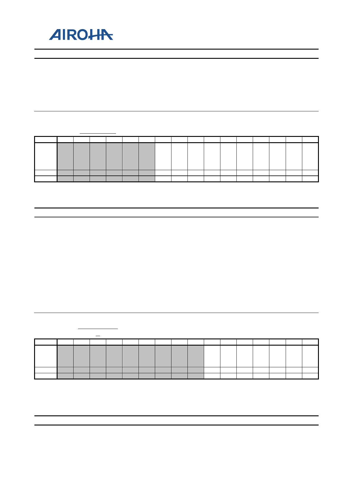
MT2523 Series Reference Manual
© 2015 - 2018 Airoha Technology Corp.
Page 47 of 692
This document contains information that is proprietary to Airoha Technology Corp. (“Airoha”) and/or its licensor(s).
Any unauthorized use, reproduction or disclosure of this document in whole or in part is strictly prohibited.
Bit(s) Name Description
0: Disable IRQ generations.
1: Enable the tick time match interrupt. Clear the interrupt when ONESHOT is
high upon generation of the corresponding IRQ.
0 AL_EN
This register eEnables the control bit for IRQ generation if the alarm
condition has been met.
0: Disable IRQ generations.
1: Enable the alarm time match interrupt. Clear the interrupt when ONESHOT is
high upon generation of the corresponding IRQ.
A21E000C RTC_CII_EN Counter increment IRQ enable 0000
Bit
15
14
13
12
11
10
9
8
7
6
5
4
3
2
1
0
Name
SE
CC
II_
1_
8
SE
CC
II_
1_4
SE
CC
II_
1_2
YE
AC
II
MT
HC
II
DO
WC
II
DO
MC
II
HO
UC
II
MI
NC
II
SE
CC
II
Type
RW
RW
RW
RW
RW
RW
RW
RW
RW
RW
Reset
0
0
0
0
0
0
0
0
0
0
Overview
This register activates or de-activates the IRQ generation when the TC counter reaches
its maximum value.
Bit(s) Name Description
9 SECCII_1_8 Set the bit to 1 to activate the IRQ at each one-eighth of a second
update.
8 SECCII_1_4 Set the bit to 1 to activate the IRQ at each one-fourth of a second
update.
7 SECCII_1_2 Set the bit to 1 to activate the IRQ at each one-half of a second update.
6 YEACII Set the bit to 1 to activate the IRQ at each year update.
5 MTHCII Set the bit to 1 to activate the IRQ at each month update.
4 DOWCII Set the bit to 1 to activate the IRQ at each day-of-week update.
3 DOMCII Set the bit to 1 to activate the IRQ at each day-of-month update.
2 HOUCII Set the bit to 1 to activate the IRQ at each hour update.
1 MINCII Set the bit to 1 to activate the IRQ at each minute update.
0 SECCII Set this bit to 1 to activate the IRQ at each second update.
A21E0010 RTC_AL_MAS
K RTC alarm mask 0000
Bit
15
14
13
12
11
10
9
8
7
6
5
4
3
2
1
0
Name
YE
A_
MS
K
MT
H_
MS
K
DO
W_
MS
K
DO
M_
MS
K
HO
U_
MS
K
MI
N_
MS
K
SE
C_
MS
K
Type
RW
RW
RW
RW
RW
RW
RW
Reset
0
0
0
0
0
0
0
Overview
The alarm condition for alarm IRQ generation depends on whether or not the
corresponding bit in this register is masked. Warning: If you set all bits to 1 in
RTC_AL_MASK (i.e. RTC_AL_MASK=0x7f) and PWREN=1 in RTC_BBPU, it means
alarm will comes every second EVERY SECOND, not disabled.
Bit(s) Name Description
6 YEA_MSK 0: Condition (RTC_TC_YEA = RTC_AL_YEA) is checked to generate the alarm
signal.
1: Condition (RTC_TC_YEA = RTC_AL_YEA) is masked, i.e. the value of
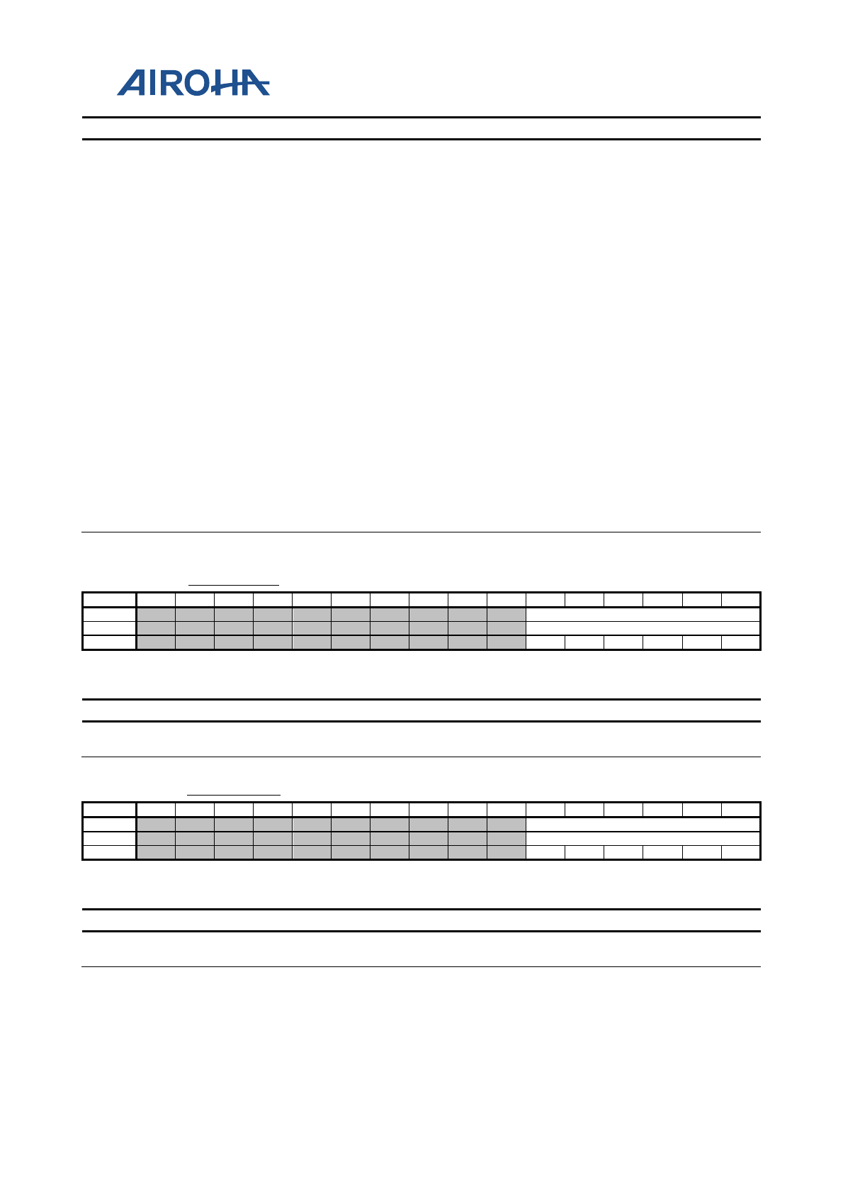
MT2523 Series Reference Manual
© 2015 - 2018 Airoha Technology Corp.
Page 48 of 692
This document contains information that is proprietary to Airoha Technology Corp. (“Airoha”) and/or its licensor(s).
Any unauthorized use, reproduction or disclosure of this document in whole or in part is strictly prohibited.
Bit(s) Name Description
RTC_TC_YEA does not affect the alarm IRQ generation.
5 MTH_MSK
0: Condition (RTC_TC_MTH = RTC_AL_MTH) is checked to generate the
alarm signal.
1: Condition (RTC_TC_MTH = RTC_AL_MTH) is masked, i.e. the value of
RTC_TC_MTH does not affect the alarm IRQ generation.
4 DOW_MSK
0: Condition (RTC_TC_DOW = RTC_AL_DOW) is checked to generate the
alarm signal.
1: Condition (RTC_TC_DOW = RTC_AL_DOW) is masked, i.e. the value of
RTC_TC_DOW does not affect the alarm IRQ generation.
3 DOM_MSK
0: Condition (RTC_TC_DOM = RTC_AL_DOM) is checked to generate the
alarm signal.
1: Condition (RTC_TC_DOM = RTC_AL_DOM) is masked, i.e. the value of
RTC_TC_DOM does not affect the alarm IRQ generation.
2 HOU_MSK
0: Condition (RTC_TC_HOU = RTC_AL_HOU) is checked to generate the
alarm signal.
1: Condition (RTC_TC_HOU = RTC_AL_HOU) is masked, i.e. the value of
RTC_TC_HOU does not affect the alarm IRQ generation.
1 MIN_MSK
0: Condition (RTC_TC_MIN = RTC_AL_MIN) is checked to generate the alarm
signal.
1: Condition (RTC_TC_MIN = RTC_AL_MIN) is masked, i.e. the value of
RTC_TC_MIN does not affect the alarm IRQ generation.
0 SEC_MSK
0: Condition (RTC_TC_SEC = RTC_AL_SEC) is checked to generate the alarm
signal.
1: Condition (RTC_TC_SEC = RTC_AL_SEC) is masked, i.e. the value of
RTC_TC_SEC does not affect the alarm IRQ generation.
A21E0014 RTC_TC_SEC RTC seconds time counter register 0000
Bit
15
14
13
12
11
10
9
8
7
6
5
4
3
2
1
0
Name
TC_SECOND
Type
RW
Reset
0
0
0
0
0
0
Overview
Bit(s) Name Description
5:0 TC_SECOND The second initial value for the time counter. The rRange: of its value
is: 0-~59.
A21E0018 RTC_TC_MIN RTC minutes time counter register 0000
Bit
15
14
13
12
11
10
9
8
7
6
5
4
3
2
1
0
Name
TC_MINUTE
Type
RW
Reset
0
0
0
0
0
0
Overview
Bit(s) Name Description
5:0 TC_MINUTE The minute initial value for the time counter. The rRange: of its value
is: 0~-59.
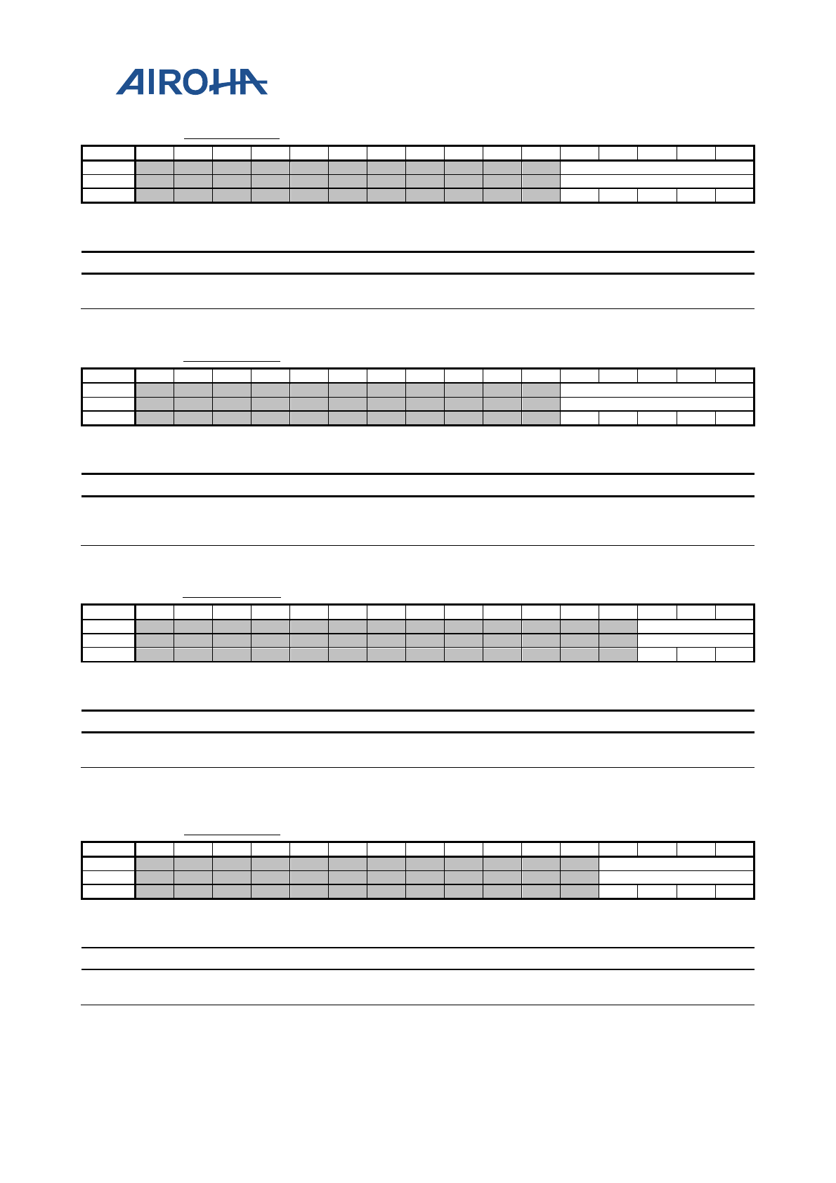
MT2523 Series Reference Manual
© 2015 - 2018 Airoha Technology Corp.
Page 49 of 692
This document contains information that is proprietary to Airoha Technology Corp. (“Airoha”) and/or its licensor(s).
Any unauthorized use, reproduction or disclosure of this document in whole or in part is strictly prohibited.
A21E001C RTC_TC_HOU RTC hours time counter register 0000
Bit
15
14
13
12
11
10
9
8
7
6
5
4
3
2
1
0
Name
TC_HOUR
Type
RW
Reset
0
0
0
0
0
Overview
Bit(s) Name Description
4:0 TC_HOUR The hour initial value for the time counter. The rRange: of its value
is: 0-~23.
A21E0020 RTC_TC_DOM RTC day-of-month time counter register 0000
Bit
15
14
13
12
11
10
9
8
7
6
5
4
3
2
1
0
Name
TC_DOM
Type
RW
Reset
0
0
0
0
0
Overview
Bit(s) Name Description
4:0 TC_DOM The day-of-month initial value for the time counter. The day-of-
month maximum value depends on the leap year condition, i.e. 2 LSB
of year time counter are 0zeros.
A21E0024 RTC_TC_DOW RTC day-of-week time counter register 0000
Bit
15
14
13
12
11
10
9
8
7
6
5
4
3
2
1
0
Name
TC_DOW
Type
RW
Reset
0
0
0
Overview
Bit(s) Name Description
2:0 TC_DOW The day-of-week initial value for the time counter. The rRange: of its
value is: 1-~7.
A21E0028 RTC_TC_MTH RTC month time counter register 0000
Bit
15
14
13
12
11
10
9
8
7
6
5
4
3
2
1
0
Name
TC_MONTH
Type
RW
Reset
0
0
0
0
Overview
Bit(s) Name Description
3:0 TC_MONTH The month initial value for the time counter. The rRange: of its value
is: 1-~12.
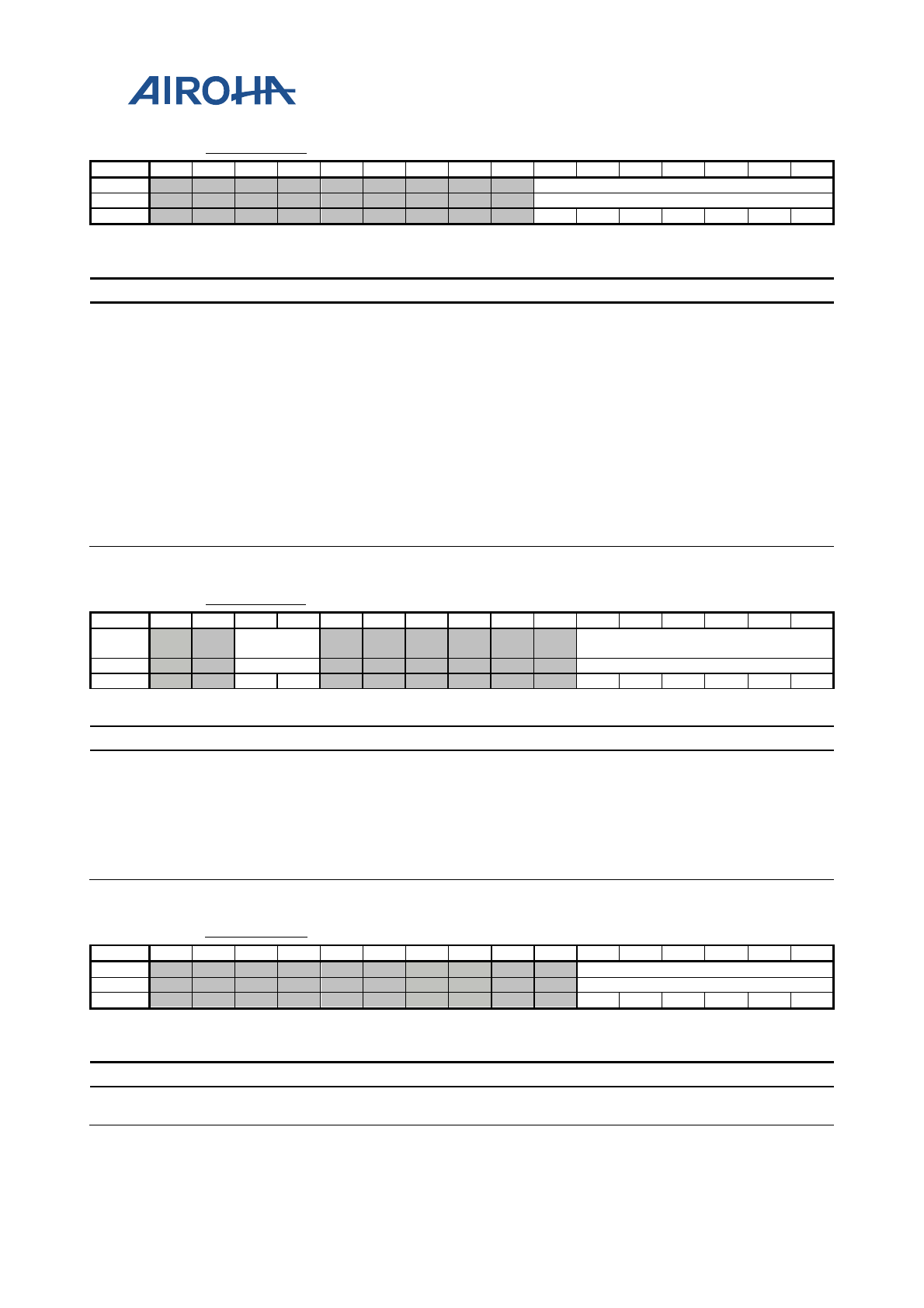
MT2523 Series Reference Manual
© 2015 - 2018 Airoha Technology Corp.
Page 50 of 692
This document contains information that is proprietary to Airoha Technology Corp. (“Airoha”) and/or its licensor(s).
Any unauthorized use, reproduction or disclosure of this document in whole or in part is strictly prohibited.
A21E002C RTC_TC_YEA RTC year time counter register 0000
Bit
15
14
13
12
11
10
9
8
7
6
5
4
3
2
1
0
Name
TC_YEAR
Type
RW
Reset
0
0
0
0
0
0
0
Overview
Bit(s) Name Description
6:0 TC_YEAR
The year initial value for the time counter. The rRange: of its value is:
0-127. (2000-2127).
Software can bias the year as multiples of 4 for the internal leap-year formula.
Here are 3 examples: 2000-2127, 1972~2099, 1904~2031.To simplify, RTC
hardware treats all 4-multiple as leap years. If the range you defined includes
non-leap 4-multiple year (e.g.say: 2100), you have to adjust it to the correct date
by yourselves. (e.g.x: change Feb. 29th, 2100 to Mar. 1st, 2100).
It's suggested to bias the range large than 1900 and less thean 2100 to evade the
manual adjustment, i.e.ing. I.e.: the bias values are suggested to be in the range
of [-28,-96], that are (1972~ 2099) ~ (1904~ 2031).
The formal leap formula:
if year modulo 400 is 0 then leap
else if year modulo 100 is 0 then no_leap
else if year modulo 4 is 0 then leap
else no_leap
A21E0030 RTC_AL_SEC RTC second alarm setting register 0000
Bit
15
14
13
12
11
10
9
8
7
6
5
4
3
2
1
0
Name
RTC_LP
D_OPT
AL_SECOND
Type
RW
RW
Reset
0
0
0
0
0
0
0
0
Overview
Bit(s) Name Description
13:12 RTC_LPD_OPT
LPD option
00: XOSC LPD | EOSC LPD (triggers when clock stops or VRTC low-V)
01: EOSC LPD (triggers when VRTC low-V)
10: XOSC LPD (triggers when clock stops)
11: nNo LPD
5:0 AL_SECOND The second value of the alarm counter setting. The rRange: of its
value is: 0-59.
A21E0034 RTC_AL_MIN RTC minute alarm setting register 0000
Bit
15
14
13
12
11
10
9
8
7
6
5
4
3
2
1
0
Name
AL_MINUTE
Type
RW
Reset
0
0
0
0
0
0
Overview
Bit(s) Name Description
5:0 AL_MINUTE The minute value of the alarm counter setting. The rRange: of its
value is: 0-59.
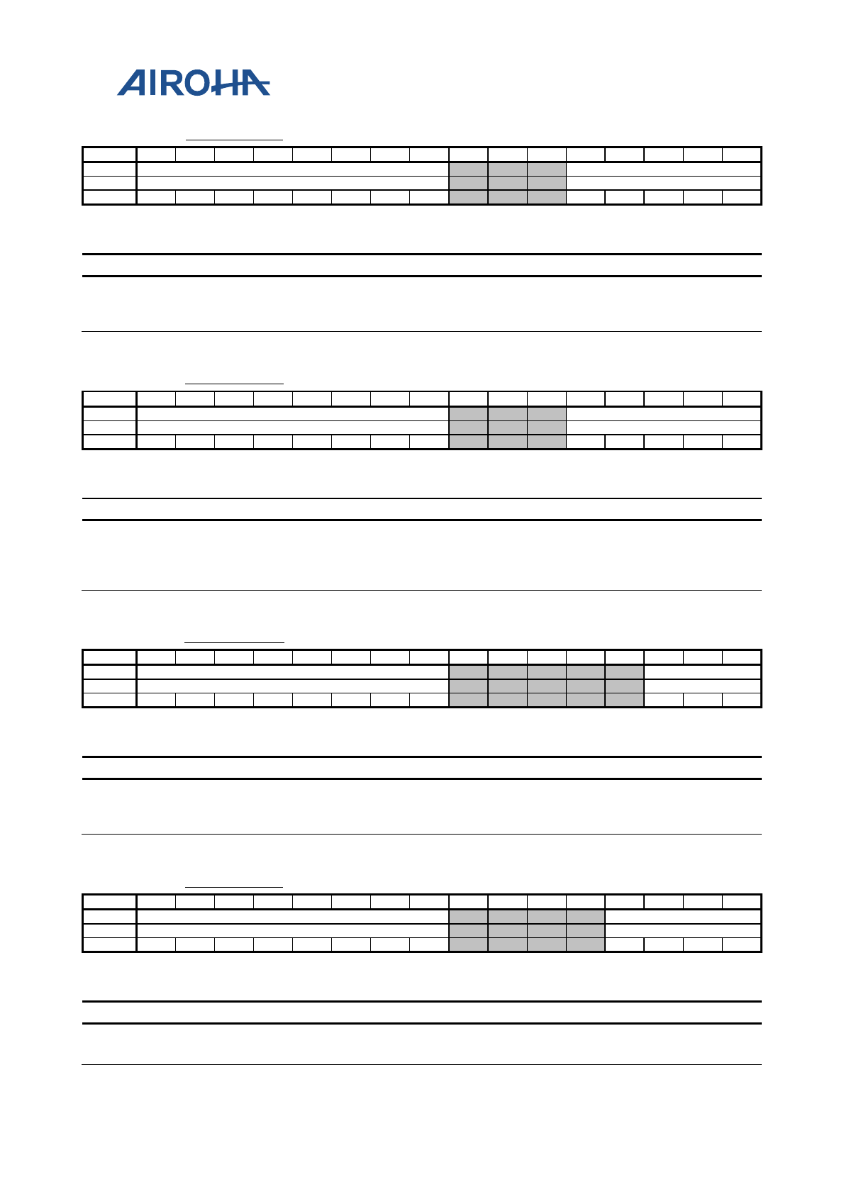
MT2523 Series Reference Manual
© 2015 - 2018 Airoha Technology Corp.
Page 51 of 692
This document contains information that is proprietary to Airoha Technology Corp. (“Airoha”) and/or its licensor(s).
Any unauthorized use, reproduction or disclosure of this document in whole or in part is strictly prohibited.
A21E0038 RTC_AL_HOU RTC hour alarm setting register 0000
Bit
15
14
13
12
11
10
9
8
7
6
5
4
3
2
1
0
Name
NEW_SPARE0
AL_HOUR
Type
RW
RW
Reset
0
0
0
0
0
0
0
0
0
0
0
0
0
Overview
Bit(s) Name Description
15:8 NEW_SPARE0 The registers are rReserved for specific purposes.
4:0 AL_HOUR The hour value of the alarm counter setting. The rRange: of its value
is: 0-~23.
A21E003C RTC_AL_DOM RTC day-of-month alarm setting register 0000
Bit
15
14
13
12
11
10
9
8
7
6
5
4
3
2
1
0
Name
NEW_SPARE1
AL_DOM
Type
RW
RW
Reset
0
0
0
0
0
0
0
0
0
0
0
0
0
Overview
Bit(s) Name Description
15:8 NEW_SPARE1 The registers are rReserved for specific purposes.
4:0 AL_DOM The day-of-month value of the alarm counter setting. The day-of-
month maximum value depends on the leap year condition, i.e. 2 LSB
of year time counter are zeros 0.
A21E0040 RTC_AL_DOW RTC day-of-week alarm setting register 0000
Bit
15
14
13
12
11
10
9
8
7
6
5
4
3
2
1
0
Name
NEW_SPARE2
AL_DOW
Type
RW
RW
Reset
0
0
0
0
0
0
0
0
0
0
0
Overview
Bit(s) Name Description
15:8 NEW_SPARE2 The registers are rReserved for specific purposes.
2:0 AL_DOW The day-of-week value of the alarm counter setting. The rRange: of its
value is: 1-~7.
A21E0044 RTC_AL_MTH RTC month alarm setting register 0000
Bit
15
14
13
12
11
10
9
8
7
6
5
4
3
2
1
0
Name
NEW_SPARE3
AL_MONTH
Type
RW
RW
Reset
0
0
0
0
0
0
0
0
0
0
0
0
Overview
Bit(s) Name Description
15:8 NEW_SPARE3 The registers are rReserved for specific purposes.
3:0 AL_MONTH
The month value of the alarm counter setting. The rRange: of its
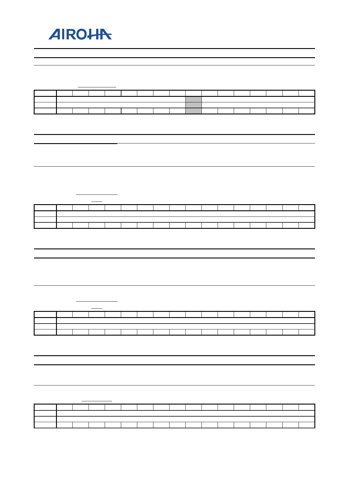
MT2523 Series Reference Manual
© 2015 - 2018 Airoha Technology Corp.
Page 52 of 692
This document contains information that is proprietary to Airoha Technology Corp. (“Airoha”) and/or its licensor(s).
Any unauthorized use, reproduction or disclosure of this document in whole or in part is strictly prohibited.
Bit(s) Name Description
value is: 1-~12.
A21E0048 RTC_AL_YEA RTC year alarm setting register 0000
Bit
15
14
13
12
11
10
9
8
7
6
5
4
3
2
1
0
Name
NEW_SPARE4
AL_YEAR
Type
RW
RW
Reset
0
0
0
0
0
0
0
0
0
0
0
0
0
0
0
Overview
Bit(s) Name Description
15:8 NEW_SPARE4 The registers are rReserved for specific purposes.
6:0 AL_YEAR The year value of the alarm counter setting. The rRange: of its value
is: 0-~127. (2000-2127)
A21E0050 RTC_POWERK
EY1 RTC_POWERKEY1 register 0000
Bit
15
14
13
12
11
10
9
8
7
6
5
4
3
2
1
0
Name
RTC_POWERKEY1
Type
RW
Reset
0
0
0
0
0
0
0
0
0
0
0
0
0
0
0
0
Overview
Bit(s) Name Description
15:0 RTC_POWERKEY1
The RTC content is protected by RTC_POWERKEY1 and
RTC_POWRKEY2. When RTC_POWERKEY1 & RTC_POWERKEY2
are not equal to the correct values, the RTC content is not credibleis.
A21E0054 RTC_POWERK
EY2 RTC_POWERKEY2 register 0000
Bit
15
14
13
12
11
10
9
8
7
6
5
4
3
2
1
0
Name
RTC_POWERKEY2
Type
RW
Reset
0
0
0
0
0
0
0
0
0
0
0
0
0
0
0
0
Overview
Bit(s) Name Description
15:0 RTC_POWERKEY2 The RTC content is protected by RTC_POWERKEY1 and
RTC_POWRKEY2. When RTC_POWERKEY1 & RTC_POWERKEY2
are not equal to the correct values, the RTC content is not credibleis.
A21E0058 RTC_PDN1 PDN1 0000
Bit
15
14
13
12
11
10
9
8
7
6
5
4
3
2
1
0
Name
RTC_PDN1
Type
RW
Reset
0
0
0
0
0
0
0
0
0
0
0
0
0
0
0
0
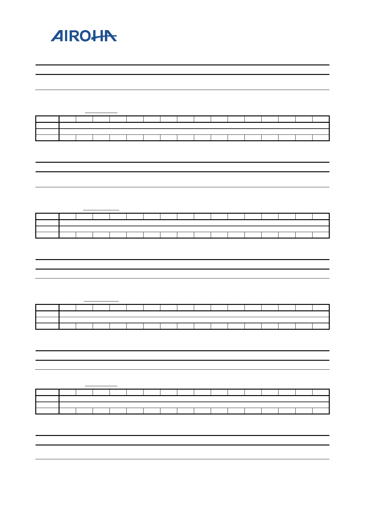
MT2523 Series Reference Manual
© 2015 - 2018 Airoha Technology Corp.
Page 53 of 692
This document contains information that is proprietary to Airoha Technology Corp. (“Airoha”) and/or its licensor(s).
Any unauthorized use, reproduction or disclosure of this document in whole or in part is strictly prohibited.
Overview
Bit(s) Name Description
15:0 RTC_PDN1 The sSpare registers for software to keep the power -on and power -
off state information.
A21E005C RTC_PDN2 PDN2 0000
Bit
15
14
13
12
11
10
9
8
7
6
5
4
3
2
1
0
Name
RTC_PDN2
Type
RW
Reset
0
0
0
0
0
0
0
0
0
0
0
0
0
0
0
0
Overview
Bit(s) Name Description
15:0 RTC_PDN2 The sSpare registers for software to keep the power power-on and
power power-off state information.
A21E0060 RTC_SPAR0 Spare register for specific purpose 0000
Bit
15
14
13
12
11
10
9
8
7
6
5
4
3
2
1
0
Name
RTC_SPAR0
Type
RW
Reset
0
0
0
0
0
0
0
0
0
0
0
0
0
0
0
0
Overview
Bit(s) Name Description
15:0 RTC_SPAR0 The registers are rReserved for specific purposes.
A21E0064 RTC_SPAR1 Spare register for specific purpose 0000
Bit
15
14
13
12
11
10
9
8
7
6
5
4
3
2
1
0
Name
RTC_SPAR1
Type
RW
Reset
0
0
0
0
0
0
0
0
0
0
0
0
0
0
0
0
Overview
Bit(s) Name Description
15:0 RTC_SPAR1 The registers are rReserved for specific purposes.
A21E0068 RTC_PROT Lock/unlock scheme to prevent RTC miswriting 0000
Bit
15
14
13
12
11
10
9
8
7
6
5
4
3
2
1
0
Name
RTC_PROT
Type
RW
Reset
0
0
0
0
0
0
0
0
0
0
0
0
0
0
0
0
Overview
Bit(s) Name Description
15:0 RTC_PROT The RTC write interface is protected by RTC_PROT. Whether the RTC
writing interface is enabled or not is decided by RTC_PROT contents.
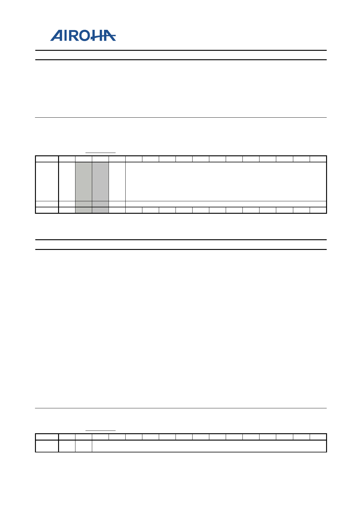
MT2523 Series Reference Manual
© 2015 - 2018 Airoha Technology Corp.
Page 54 of 692
This document contains information that is proprietary to Airoha Technology Corp. (“Airoha”) and/or its licensor(s).
Any unauthorized use, reproduction or disclosure of this document in whole or in part is strictly prohibited.
Bit(s) Name Description
When RTC_POWERKEY1 & RTC_POWERKEY2 are not equal to the
correct values, the RTC writing interface willis always be enabled.
But when they match, users have to perform Uunlock flow to enable
the writing interface.
Notice: Please aAlways keep RTC in the unlock state in power -on mode. Once
the normal RTC content writing is completed, do notDO NOT modify the
RTC_PROT content to lock the RTC. The RTC_PROT contents will be cleared
automatically when powered off immediately.
A21E006C RTC_DIFF One-time calibration offset 0000
Bit
15
14
13
12
11
10
9
8
7
6
5
4
3
2
1
0
Name
CA
LI_
RD
_S
EL
PO
WE
R_
DE
TE
CT
ED
RTC_DIFF
Type
RW
RO
RW
Reset
0
-
0
0
0
0
0
0
0
0
0
0
0
0
Overview
This register is fixed atin 0 when RTC_POWERKEY1 & RTC_POWERKEY2 unmatch
the correct values.
Bit(s) Name Description
15 CALI_RD_SEL
Selects which RTC_CALI is to be read when reading RTC_CALI
register
0: nNormal RTC_CALI
1: K_EOSC32_RTC_CALI
12 POWER_DETECTED
POWER_DETECTED status
0: powerkey not match
1: RTC_POWERKEY1, RTC_POWERKEY2, RTC_POWERKEY1_NEW, and
RTC_POWERKEY2_NEW match the correct value.
11:0 RTC_DIFF
These registers are used to aAdjusts the internal counter of RTC. It
eaffects once and returns to 0zero when in done.
In some cases, you observe the RTC is faster or slower than the standard. To
cChanginge RTC_TC_SEC is coarse and may cause alarm problems. RTC_DIFF
provides a finer time unit. An internal 15-bit counter accumulates in each 32768-
HZz clock. Entering a non-zero value into the RTC_DIFF will causes the internal
RTC counter to increases or decreases RTC_DIFF when RTC_DIFF changes to
0zero again. RTC_DIFF is in represents as 2's completement form.
For example, if you fill in 0xfff into RTC_DIFF, the internal counter will
decreases 1 when RTC_DIFF returns to 0zero. In other words, you can only use
RTC_DIFF continuously if RTC_DIFF is equal to 0zero now.
Note: RTC_DIFF ranges from 0x800 (-2048) to 0x7fd (2045). Using 0x7ff and &
0x7fe is not allowed.are forbid to use.
A21E0070 RTC_CALI Repeat calibration offset 0000
Bit
15
14
13
12
11
10
9
8
7
6
5
4
3
2
1
0
Name
K_
EO
CA
LI_
RTC_CALI
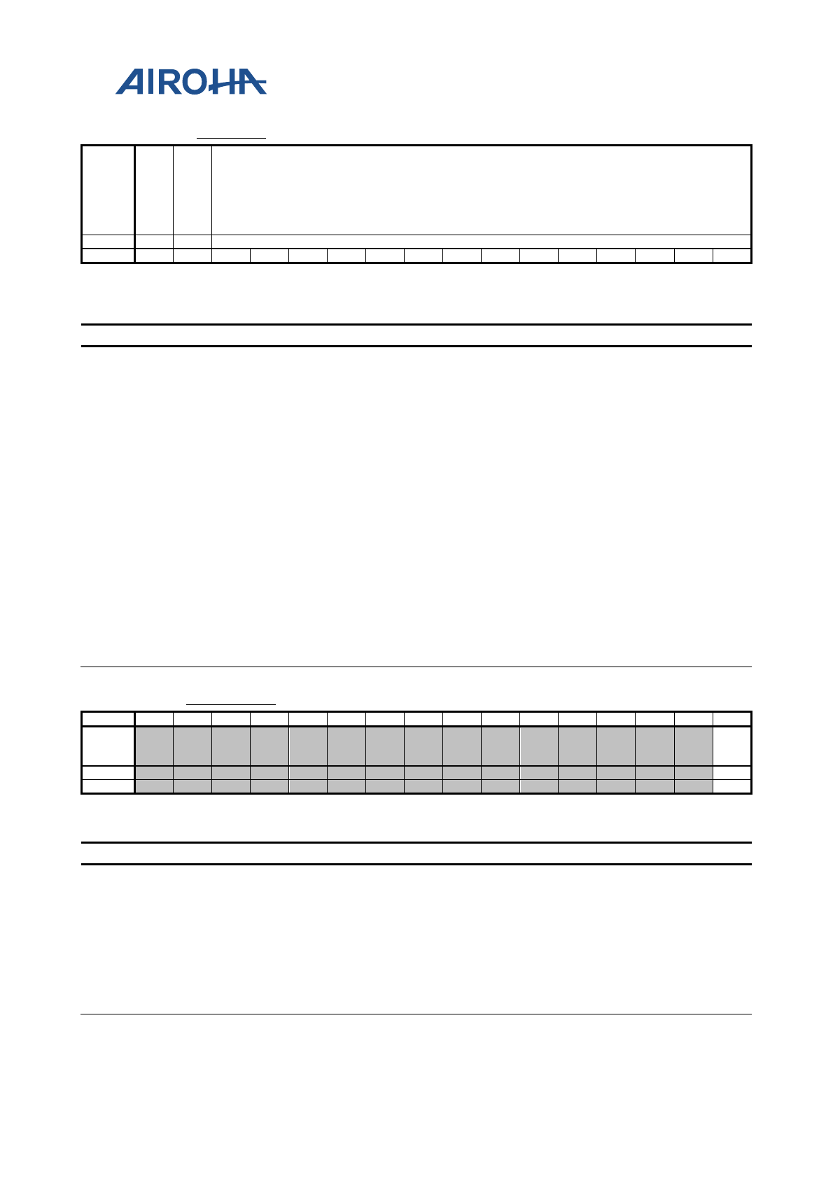
MT2523 Series Reference Manual
© 2015 - 2018 Airoha Technology Corp.
Page 55 of 692
This document contains information that is proprietary to Airoha Technology Corp. (“Airoha”) and/or its licensor(s).
Any unauthorized use, reproduction or disclosure of this document in whole or in part is strictly prohibited.
A21E0070 RTC_CALI Repeat calibration offset 0000
SC
32
_O
VE
RF
LO
W
W
R_
SE
L
Type
RW
RW
RW
Reset
0
0
0
0
0
0
0
0
0
0
0
0
0
0
0
0
Overview
This register is fixed atin 0 when RTC_POWERKEY1 & RTC_POWERKEY2 unmatch
the correct values.
Bit(s) Name Description
15 K_EOSC32_OVERFL
OW
EOSC32 calibration overflow (EOSC32 RTC_CALI update result from
PMU rtc_eosc_cali module overflow)
0: nNot overflow
1: oOverflow
14 CALI_WR_SEL
Enables EOSC32 Cali value write enable.
Only takes effect oin RTC_CALI write operation.
0: nNormal RTC_CALI
1: K_EOSC32_RTC_CALI
13:0 RTC_CALI
These registers provide a repeat calibration scheme. RTC_CALI
provides two types2 kinds of calibration.
1. 14-bit calibration capability in 8-second duration; in other words, 12-bit
calibration capability in each second. RTC_CALI is in represents in 2's
complement form, such that you can adjust RTC increasing or decreasing.
Due to that RTC_CALI is revealed in 8 seconds, the resolution is less than a
1/32768 clock.
Avg. resolution: 1/32768/8=3.81us
Avg. adjust range: -31.25~31.246ms/sec in 2's complement: -0x2000~0x1fff
(-8192~8191)
2. 14-bit calibration capability in 1-second duration when use EOSC32 as 32K
source (K_EOSC32_RTC_CALI); This typekind of usage is with resolution
1/32768=30.52us
A21E0074 RTC_WRTGR Enable the transfers from core to RTC in the queue 0000
Bit
15
14
13
12
11
10
9
8
7
6
5
4
3
2
1
0
Name
W
RT
GR
Type
WO
Reset
0
Overview
Bit(s) Name Description
0 WRTGR
This register eEnables the transfers from core to RTC. After you
modify all the RTC registers you are'd like to change, you must write
RTC_WRTGR to 1 to trigger the transfer. The prior writing
operations are queued at core power domain. The pending data will
not be transferred to RTC domain until WRTGR=1.
After WRTGR=1, the pending data will beis transferred to RTC domain
sequentially in order of register address, from low to high. For example:
RTC_BBPU -> RTC_IRQ_EN -> RTC_CII_EN -> RTC_AL_MASK ->
RTC_TC_SEC -> etc. The CBUSY in RTC_BBPU is equal to 1 in writing process.
You can observe CBUSY to determine when the transmission is completeds.

MT2523 Series Reference Manual
© 2015 - 2018 Airoha Technology Corp.
Page 56 of 692
This document contains information that is proprietary to Airoha Technology Corp. (“Airoha”) and/or its licensor(s).
Any unauthorized use, reproduction or disclosure of this document in whole or in part is strictly prohibited.
6. Universal Asynchronous Receiver Transmitter
6.1. General Description
The baseband chipset houses four UARTs. UARTs provide full duplex serial communication channels between the
baseband chipset and external devices.
UART has both M16C450 and M16550A modes of operation, which are compatible with a range of standard
software drivers. The extensions are designed to be broadly software compatible with 16550A variants, but certain
areas offer no consensus.
In common with M16550A, the UART supports word lengths from 5 to 8 bits, an optional parity bit and one or two
stop bits and is fully programmable by an 8-bit CPU interface. A 16-bit programmable baud rate generator and an
8-bit scratch register are included, together with separate transmit and receive FIFOs. Two modem control lines
and a diagnostic loop-back mode are provided. UART also includes two DMA handshake lines, indicating when the
FIFOs are ready to transfer data to the CPU.
Note that UART is designed so that all internal operation is synchronized by the CLK signal. This synchronization
results in minor timing differences between the UART and industry standard 16550A device, which means that the
core is not clock for clock identical to the original device.
After hardware reset, UART will be in M16C450 mode; its FIFOs can then be enabled and UART can enter M16550A
mode. UART has further additional functions beyond the M16550A mode. Each of the extended functions can be
selected individually under software control.
UART provides more powerful enhancements than the industry-standard 16550:
Hardware flow control
This feature is very useful when the ISR latency is hard to predict and control in embedded applications. The MCU
is relieved of having to fetch the received data within a fixed amount of time.
Note that in order to enable the enhancements (hardware flow control), the enhanced mode bit, EFR[4], must be
set. If EFR[4] is not set, IER[7:4], FCR[5:4], cannot be written and MCR[7] cannot be read. The enhanced mode bit
ensures that UART is backward compatible with the software that has been written for 16C450 and 16550A
devices.
6.1.1. Features
• Provides four channels
• DMA, polling or interrupt operation
• Supports word lengths from five to eignt bits, with an optional parity bit and one or two stop bits
• Two UART ports for hardware automatic flow control (UART0, UART1)
• Supports baud rates from 110bps up to 3Mbps
• Baud rate auto detection from 110bps up to 115,200bps

MT2523 Series Reference Manual
© 2015 - 2018 Airoha Technology Corp.
Page 57 of 692
This document contains information that is proprietary to Airoha Technology Corp. (“Airoha”) and/or its licensor(s).
Any unauthorized use, reproduction or disclosure of this document in whole or in part is strictly prohibited.
6.1.2. Block Diagram
Figure 6-1. Block Diagram of UART
6.1.3. Programming Guide
6.1.3.1. UART Band Rate Setting
UART baud rate = UART clock frequency/HIGHSPEED/{DLM, DLL}
UART clock frequency = 26MHz
HIGHSPEED = 16/8/4/(sampe_count+1)
DLM = User setting
DLL = User setting
Example 1:
Setting UART baud rate = 921600
RATEFIX_AD = 0x00 > UART clock frequency is set to “26MHz”
HIGHSPEED = 0x02 > HIGHSPEED is set to “4”
DLM = 0x0 > DLM is set to “0”
DLL = 0x7 > DLM is set to “7”
UART baud rate 26MHz/4/7 ≒ 921600Hz
APB
BUS
I/F
Baud Rate
Generator
TX FIFO
TX Machine
RX FIFO
Modem
Control
RX Machine
Modem Outputs
Modem Inputs
APB Bus
Clock
Divisor
Uart_tx
_data
Uart_rx
_data
Baud
MT2523 Series Reference Manual
© 2015 - 2018 Airoha Technology Corp.
Page 58 of 692
This document contains information that is proprietary to Airoha Technology Corp. (“Airoha”) and/or its licensor(s).
Any unauthorized use, reproduction or disclosure of this document in whole or in part is strictly prohibited.
Example 2:
Setting UART baud rate = 115200
RATEFIX_AD = 0x05 > UART clock frequency is set to “13MHz”
HIGHSPEED = 0x03 > HIGHSPEED is set to “Sample Count”
SAMPLE_COUNT = 0xD > Sample count is set to “13”
DLM = 0x0 > DLM is set to “0”
DLL = 0x7 > DLM is set to “8”
UART baud rate 13MHz/(13+1)/8 ≒ 115200Hz
Note: You can increase (+1) the sample count of each bit of data by register FRACDIV_M and FRACDIV_L.
For example, to set bit 0, 4 and 8 of data to having a bigger sample count:
SAMPLE_COUNT = 0xD
FRACDIV_M = 0x1
FRACDIV_L = 0x11
Data
Bit 8
Bit 7
Bit 6
Bit 5
Bit 4
Bit 3
Bit 2
Bit 1
Bit 0
sample count
14
13
13
13
14
13
13
13
14
The feature can make UART receive/transmit data more accurately.
6.1.3.2. Automatic Baud Rate Detection Setting
This feature can auto detect RX data baud rate without setting up UART baud rate.
1. AUTOBAUD_EN = |0x1: Enable auto-baud feature with standard baud rate
(standard baud rate: 115200, 57600, 38400, 19200, 9600, 4800, 1200, 300, 110 bits/sec)
AUTOBAUD_EN = |0x3: Enable auto-baud feature without standard baud rate (range from 115200 to 110 bits/sec)
2. AUTOBAUD_RATE_FIX: autobaud feature sample clock 26/13MHz
3. AUTOBAUDSAMPLE = 0d13: For autobaud feature sample clock = 26MHz
AUTOBAUDSAMPLE = 0d6: For autobaud feature sample clock = 13MHz
6.1.3.3. HW Flow Control Setting
This feature controls UART start/stop transmission by RTS/CTS signal.
1. EFR = |0xC0: Enable RTS/CTS for hardware transmission/reception flow control
2. MCR = |0x2: RTS output can be controlled by flow control condition.
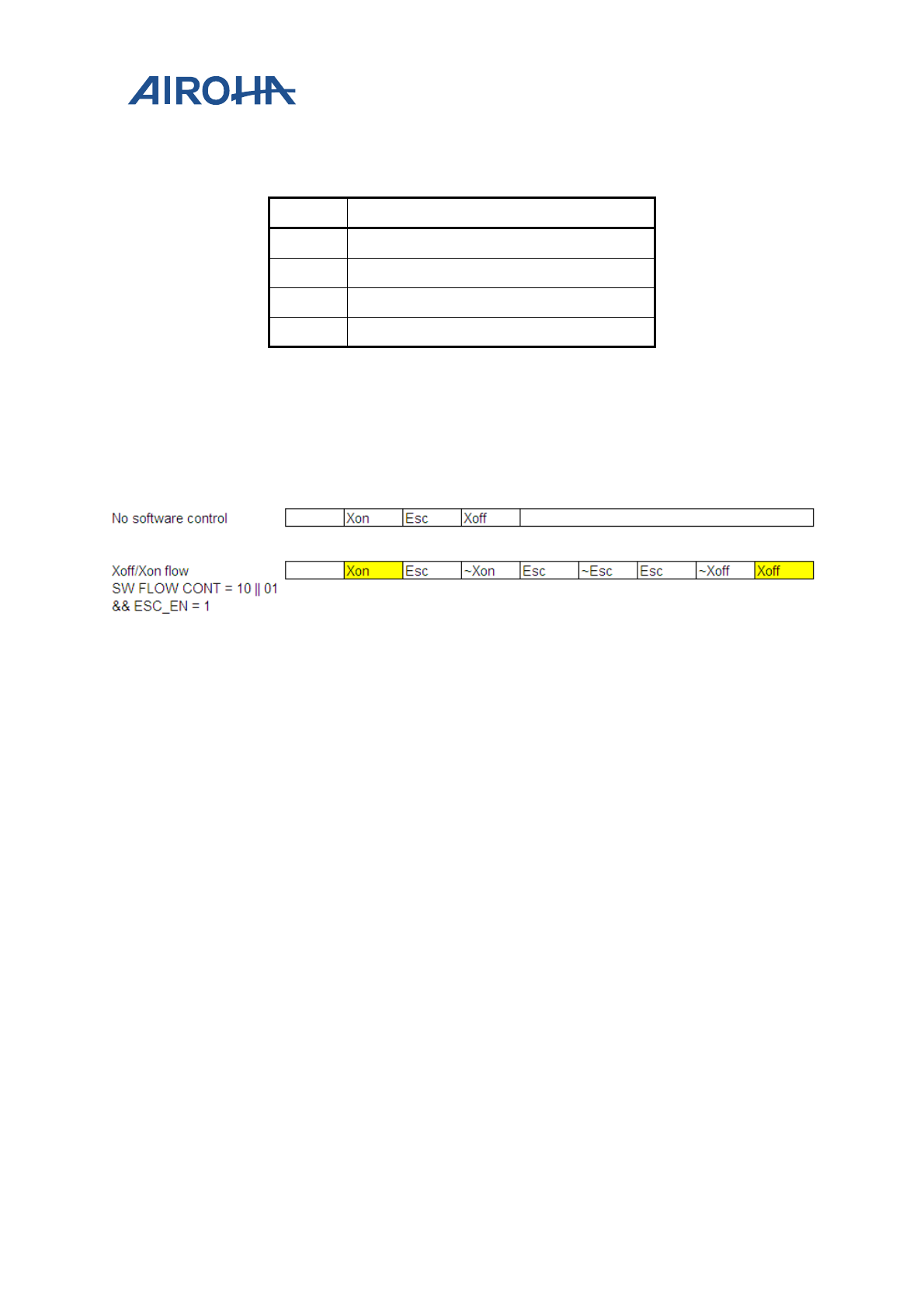
MT2523 Series Reference Manual
© 2015 - 2018 Airoha Technology Corp.
Page 59 of 692
This document contains information that is proprietary to Airoha Technology Corp. (“Airoha”) and/or its licensor(s).
Any unauthorized use, reproduction or disclosure of this document in whole or in part is strictly prohibited.
6.1.3.4. SW Flow Control Setting
This feature controls UART start/stop transmission by transmitting/receiving specific data.
1.
2. XON1: User setting
3. XOFF1: User setting
4. ESCAPE_en: 0x01
5. ESCAPE_DAT: User setting
When SW flow control is enabled, and you are to transmit special character (ESC, XON, XOFF), set ESCAPE_en = 1.
When UART device receives two data (ESC & ~ special character), it can recognize the ESC command and store the
special character as a data.
Example:
UART TX transmit > ESC(command), ~XON ̶ UART RX receive > XON(data)
UART TX transmit > ESC(command), ~XOFF ̶ UART RX receive > XOFF(data)
UART TX transmit > ESC(command), ~ESC ̶ UART RX receive > ESC(data)
6.1.3.5. Enable Sleep Mode
This feature gives feedback sleep_ack signal for system having sleep requirement.
1. SLEEP_ACK_SEL = 0: Support sleep_ack when autobaud_en is opened.
SLEEP_ACK_SEL = 1: Does not support sleep_ack when autobaud_en is opened.
2. SLEEP_EN = 1
EFR[3:0] Function
00xx No TX flow control
xx00 No RX flow control
10xx Transmit XON1/XOFF1 as flow control bytes
xx10 Receive XON1/XOFF1 as flow control bytes
MT2523 Series Reference Manual
© 2015 - 2018 Airoha Technology Corp.
Page 60 of 692
This document contains information that is proprietary to Airoha Technology Corp. (“Airoha”) and/or its licensor(s).
Any unauthorized use, reproduction or disclosure of this document in whole or in part is strictly prohibited.
6.2. Register Definition
There are four UARTs in this SOC. The usage of the registers below is the same except that the base address should
be changed to respective one.
Module name: UART Base address: (+A00D0000h)
Address Name Width Register Function
A00D0000 RBR 8
RX Buffer Register
Note: RBR is modified when LCR[7] = 0
A00D0000 THR 8 TX Holding Register
Note: THR is modified when LCR[7] = 0
A00D0000 DLL 8 Divisor Latch (LS)
Divides the UART internal clk frequency
Note: DLL is modified when LCR[7] != 0
A00D0004 IER 8
Interrupt Enable Register
By storing 1 to a specific bit position, the interrupt associated
with that bit is enabled. Otherwise, the interrupt will be
disabled.
Note: IER[3:0] are modified when LCR[7] = 0. IER[7:4] are
modified when LCR[7] = 0 & EFR[4] = 1.
A00D0004 DLM 8 Divisor Latch (MS)
Divides the UART internal clk frequency.
Note: DLM is modified when LCR[7] != 0.
A00D0008 IIR 8
Interrupt Identification Register
Priority is from high to low as the following.
IIR[5:0]= 6'h1: No interrupt pending.
IIR[5:0]= 6'h6: Line status interrupt (under IER[2]=1).
IIR[5:0]= 6'hc: RX data time-out interrupt (under
IER[0]=1).
IIR[5:0]= 6'h4: RX data are placed in the RX buffer register
or the RX FIFO trigger level is reached (under IER[0]=1).
IIR[5:0]= 6'h2: TX holding register is empty or the contents
of the TX FIFO have been reduced to its trigger level (under
IER[1]=1).
IIR[5:0]= 6'h10: XOFF character received (under IER[5]=1,
EFR[4] = 1).
IIR[5:0]= 6'h20: CTS or RTS rising edge (under IER[7]=1 or
EFR[6] = 1).
Note: DLM is modified when LCR != 8'hBF.
A00D0008 FCR 8
FIFO Control Register
FCR is used to control the trigger levels of the FIFOs or flush
the FIFOs.
Note: FCR[7:6] is modified when LCR != 8'hBF
FCR[5:4] is modified when LCR != 8'hBF & EFR[4] = 1
FCR[4:0] is modified when LCR != 8'hBF.
A00D0008 EFR 8 Enhanced Feature Register
UART number Base address Feature
UART0 0xA00D0000 Supports DMA, HW flow control
UART1 0xA00E0000 Supports DMA, HW flow control
UART2 0xA00F0000 Supports DMA
UART3 0xA0100000 Supports DMA
MT2523 Series Reference Manual
© 2015 - 2018 Airoha Technology Corp.
Page 61 of 692
This document contains information that is proprietary to Airoha Technology Corp. (“Airoha”) and/or its licensor(s).
Any unauthorized use, reproduction or disclosure of this document in whole or in part is strictly prohibited.
Address
Name
Width
Register Function
EFR is used to enable HW/SW flow control.
Note: EFR is modified when LCR = 8'hBF.
A00D000C LCR 8
Line Control Register
Determines characteristics of serial communication signals.
A00D0010 MCR 8
Modem Control Register
Controls interface signals of the UART.
Note: MCR[5:0] is modified when LCR != 8'hBF, MCR[7]
can be read when LCR != 8'hBF & EFR[4] = 1.
A00D0010 XON1 8 XON1 Char Register
Note: XON1 is modified when LCR = 8'hBF.
A00D0014 LSR 8
Line Status Register
Note: LSR is modified when LCR != 8'hBF.
A00D0018 XOFF1 8
XOFF1 Char Register
Note: XOFF1 is modified when LCR = 8'hBF.
A00D001C SCR 8
Scratch Register
General purpose read/write register. After reset, its value
will be un-defined.
Note: SCR is modified when LCR != 8'hBF.
A00D0020 AUTOBAUD_EN 8
Auto Baud Detect Enable Register
Enables UART auto baud detect feature.
A00D0024 HIGHSPEED 8
High Speed Mode Register
HIGHSPEED is used to control UART baud rate.
A00D0028 SAMPLE_COUNT 8
Sample Counter Register
When HIGHSPEED=3, sample_count will be the threshold
value for UART sample counter (sample_num).
Count from 0 to sample_count.
A00D002C SAMPLE_POINT 8
Sample Point Register
When HIGHSPEED=3, UART gets the input data when
sample_count=sample_num, e.g. system clock = 13MHz,
921600 = 13000000/14. Therefore, sample_count = 13, and
sample point = 6 (sampling the central point to decrease the
inaccuracy) SAMPLE_POINT is usually (SAMPLE_COUNT-
1)/2 without decimal.
A00D0030 AUTOBAUD_REG 8
Auto Baud Monitor Register
Autobaud detection state. Will not be changed until
autobaud_en is enabled again.
A00D0034 RATEFIX_AD 8
Clock Rate Fix Register
Configures system and autobaud feature clock.
A00D0038 AUTOBAUDSAMPLE 8
Auto Baud Sample Register
Since the system clock may change, autobaud sample
duration should change as the system clock changes.
When system clock = 13MHz, autobaudsample = 6; when
system clock = 26MHz, autobaudsample = 13.
A00D003C GUARD 8
Guard Time Added Register
Adds guard interval after stop bit.
A00D0040 ESCAPE_DAT 8
Escape Character Register
Escape character of software flow control.
A00D0044 ESCAPE_EN 8 Escape Enable Register
Uses escape character for software flow control.
A00D0048 SLEEP_EN 8 Sleep Enable Register
Allows UART to enter sleep mode.
A00D004C DMA_EN 8
DMA Enable Register
Allows UART to transmit/receive data using DMA.
A00D0050 RXTRI_AD 8
Rx Trigger Address
UART RX FIFO threshold.
MT2523 Series Reference Manual
© 2015 - 2018 Airoha Technology Corp.
Page 62 of 692
This document contains information that is proprietary to Airoha Technology Corp. (“Airoha”) and/or its licensor(s).
Any unauthorized use, reproduction or disclosure of this document in whole or in part is strictly prohibited.
Address
Name
Width
Register Function
A00D0054 FRACDIV_L 8 Fractional Divider LSB Address
Increases (+1) the sample count of bit 0 ~ 7 of data.
A00D0058 FRACDIV_M 8
Fractional Divider MSB Address
Increases (+1) the sample count of bit 8 ~ 9 of data.
A00D005C FCR_RD 8
FIFO Control Register
Sets up FIFO trigger threshold.
A00D0000
RBR
RX Buffer Register
00
Bit
15
14
13
12
11
10
9
8
7
6
5
4
3
2
1
0
Name
RBR
Type
RU
Reset
0
0
0
0
0
0
0
0
Bit(s)
Name
Description
7:0
RBR
RX buffer register
Read-update register. The received data can be read by accessing this register.
Only when LCR[7] = 0.
A00D0000
THR
TX Holding Register
00
Bit
15
14
13
12
11
10
9
8
7
6
5
4
3
2
1
0
Name
THR
Type
WO
Reset
0
0
0
0
0
0
0
0
Bit(s)
Name
Description
7:0
THR
TX holding Register
Write-only register. The transmitted data can be written by setting this register.
Only when LCR[7] = 0.
A00D0000
DLL
Divisor
Latch (LS)
01
Bit
15
14
13
12
11
10
9
8
7
6
5
4
3
2
1
0
Name
DLL
Type
RW
Reset
0
0
0
0
0
0
0
1
Bit(s)
Name
Description
7:0
DLL
Divisor latch low 8-bit data
Note: Modified when LCR[7] != 0.
A00D0004
IER
Interrupt Enable Register
00
Bit
15
14
13
12
11
10
9
8
7
6
5
4
3
2
1
0
Name
CTSI
RTSI
XOF
FI
ELSI
ETBE
I
ERB
FI
Type
RW
RW
RW
RW
RW
RW
Reset
0
0
0
0
0
0
MT2523 Series Reference Manual
© 2015 - 2018 Airoha Technology Corp.
Page 63 of 692
This document contains information that is proprietary to Airoha Technology Corp. (“Airoha”) and/or its licensor(s).
Any unauthorized use, reproduction or disclosure of this document in whole or in part is strictly prohibited.
Bit(s)
Name
Description
7
CTSI
Masks an
interrupt that is generated when a rising edge is detected on
the CTS modem control line.
Note: This interrupt is only enabled when hardware flow control is enabled.
0: Mask an interrupt generated when a rising edge is detected on the
CTS modem
control line.
1: Unmask an interrupt generated when a rising edge is detected on the CTS
modem control line.
6
RTSI
Interrupt is inhibited when a rising edge is detected on the RTS
modem control line.
Note: This interrupt is only enabled when hardware flow control is enabled.
0: Interrupt is inhibited when a rising edge is detected on the
RTS modem control
line.
1: Interrupt is generated when a rising edge is detected on the RTS modem
control line.
5
XOFFI
Masks an interrupt that is generated when an XOFF character is
received.
Note: This interrupt is only enabled when software flow control is enabled.
0: Mask an interrupt generated when an XOFF character is received.
1: Unmask an interrupt generated when an XOFF character is received.
2
ELSI
When set to1, an interrupt will be generated if BI, FE, PE or OE
(LSR[4:1]) becomes set.
0: No interrupt will be generated if BI, FE, PE or OE (LSR[4:1]) becomes set.
1: An interrupt will be generated if BI, FE, PE or OE (LSR[4:1]) becomes set.
1
ETBEI
When set to 1, an interrupt will be generated if the TX holding r
egister
is empty or the contents of the TX FIFO have been reduced to its
trigger level.
0: No interrupt will be generated if the TX holding register is empty or the
contents of the TX FIFO have been reduced to its trigger level.
1: An interrupt will be generated if the TX folding register is empty or the
contents of the TX FIFO have been reduced to its trigger level.
0
ERBFI
When set to 1, an interrupt will be generated if RX data are placed in
RX buffer register or the RX trigger level is reached.
0: No interrupt will be generated if RX data are placed in the RX buffer r
egister or
the RX trigger level is reached.
1: An interrupt will be generated if RX Data are placed in the RX buffer r
egister or
the RX trigger level is reached.
A00D0004
DLM
Divisor Latch (MS)
00
Bit
15
14
13
12
11
10
9
8
7
6
5
4
3
2
1
0
Name
DLM
Type
RW
Reset
0
0
0
0
0
0
0
0
Bit(s)
Name
Description
7:0
DLM
Divisor latch high 8-bit data
Note: Modified when LCR[7]!=0. DLL & DLM can only be updated when
DLAB(LCR[7]) is set to 1. Division by 1 will generate a BAUD signal that is
constantly high. DLL & DLM setting formula is {DLM,DLL}=(system clock
frequency/baud_pulse/baud_rate).
When RATE_FIX(RATEFIX_AD[0])=0, system clock frequency = 26MHz.
When RATE_FIX(RATEFIX_AD[0])=1, system clock frequency = 13MHz.
For baud_pulse value, refer to HIGH_SPEED(offset=24H) register.
For example, when at 26MHz, default speed mode and 115200 baud rate,
{DLM,DLL}=26MHz/16/115200=14.

MT2523 Series Reference Manual
© 2015 - 2018 Airoha Technology Corp.
Page 64 of 692
This document contains information that is proprietary to Airoha Technology Corp. (“Airoha”) and/or its licensor(s).
Any unauthorized use, reproduction or disclosure of this document in whole or in part is strictly prohibited.
A00D0008
IIR
Interrupt Identification Register
01
Bit
15
14
13
12
11
10
9
8
7
6
5
4
3
2
1
0
Name
FIFOE
ID
Type
RO
RU
Reset
0
0
0
0
0
0
0
1
Bit(s)
Name
Description
7:6
FIFOE
5:0
ID
IIR[5:0] -Priority level- interrupt source
000001 - No interrupt pending
000110 1 Line status interrupt:
BI, FE, PE or OE set in LSR (under IER[2]=1)
001100 2 RX data time-out:
Time-out on character in RX FIFO (under IER[0]=1)
000100 3 RX data received:
RX data received or RX trigger level reached (under IER[0]=1)
000010 4 TX holding register empty:
TX holding register empty or TX FIFO trigger level reached (under IER[1]=1)
010000 5 Software flow control:
XOFF character received (under IER[5]=1)
100000 6 Hardware flow control:
CTS or RTS rising edge (under IER[7]=1 or IER[6]=1)
Line status interrupt: A RX line status interrupt (IIR[5:0] = 000110) will be
generated if ELSI (IER[2]) is set and any of BI, FE, PE or OE (LSR[4:1]) becomes
set. The interrupt is cleared by reading the line status register.
RX data time-out interrupt: When the virtual FIFO mode is disabled, RX
data time-out interrupt will be generated if all of the following conditions are
applied:
1. FIFO contains at least one character.
2. The most recent character is received longer than four character periods ago
(including all start, parity and stop bits);
3. The most recent CPU read of the FIFO is longer than four character periods
ago.
The timeout timer is restarted upon receipt of a new byte from the RX shift
register or upon a CPU read from the RX FIFO. The RX data time-out i
nterrupt is
enabled by setting EFRBI (IER[0]) to 1 and is cleared by reading RX FIFO.
When the virtual FIFO mode is enabled, RX data time-out interrupt will be
generated if all of the following conditions are applied:
1. FIFO is empty.
2. The most recent character is received longer than four character periods ago
(including all start, parity and stop bits).
3. The most recent CPU read of the FIFO is longer than four character periods
ago.
The timeout timer is restarted upon receipt of a new byte from the RX shift
register or reading DMA_EN register. The RX Data Timeout Interrupt is enabled
by setting EFRBI (IER[0]) to 1 and is cleared by reading DMA_EN register.
RX data received interrupt: A RX received interrupt (IER[5:0] = 000100b)
will be generated if EFRBI (IER[0]) is set and either RX data are
placed in the RX
buffer register or the RX trigger level is reached. The interrupt is cleared by
reading the RX buffer register or the RX FIFO (if enabled).
TX holding register empty interrupt: A TX holding register empty interrupt
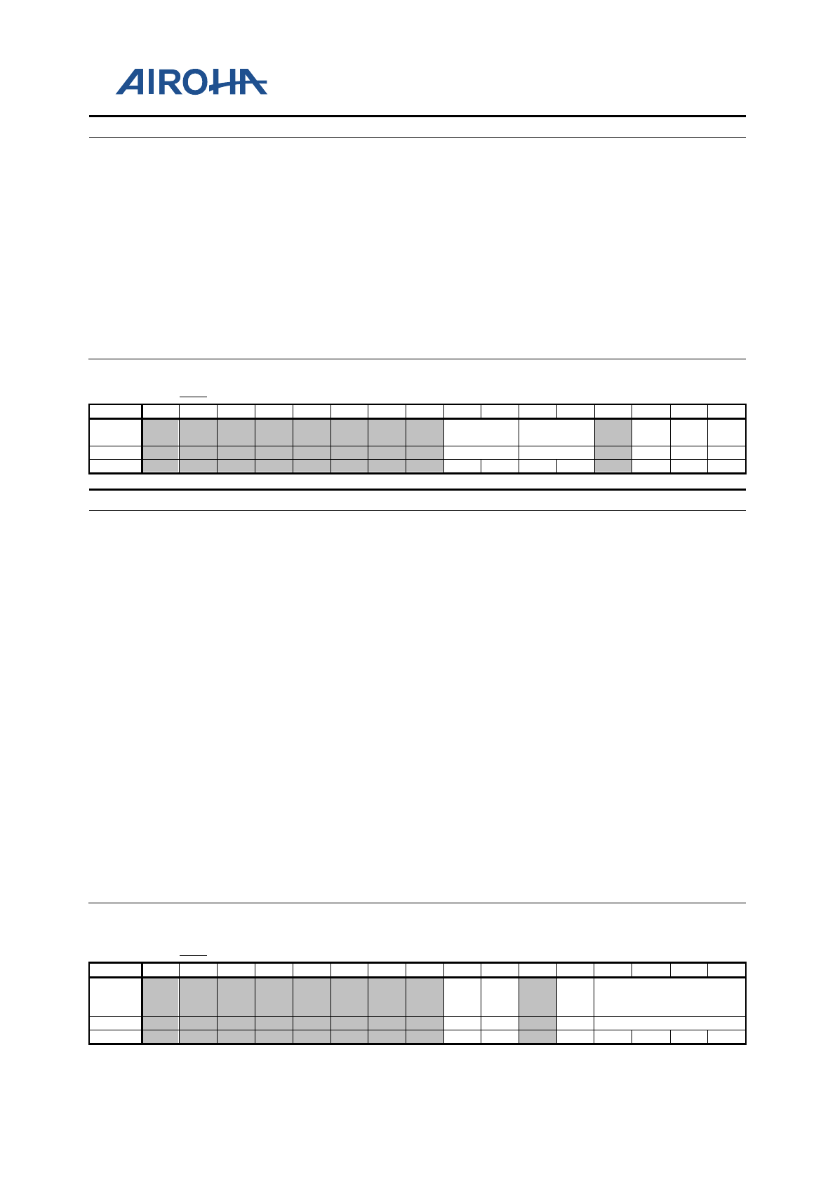
MT2523 Series Reference Manual
© 2015 - 2018 Airoha Technology Corp.
Page 65 of 692
This document contains information that is proprietary to Airoha Technology Corp. (“Airoha”) and/or its licensor(s).
Any unauthorized use, reproduction or disclosure of this document in whole or in part is strictly prohibited.
Bit(s)
Name
Description
(IIR[5:0] = 000010) will be generated if ETRBI (IER[1]) is set and either the TX
holding register is empty or the contents of the TX FIFO are reduced to its tr
igger
level. The interrupt is cleared by writing to the TX holding register or TX FIFO if
FIFO is enabled.
Software flow control interrupt: A software flow control interrupt (IIR[5:0]
= 010000) will be generated if the software flow control is enabled and XOFFI
(IER[5]) becomes set, indicating that an XOFF character has been received. The
interrupt is cleared by reading the interrupt identification register.
Hardware flow control interrupt: A hardware flow control interrupt
(IER[5:0] = 100000) will be generated if the hardware flow control is enabled
and either RTSI (IER[6]) or CTSI (IER[7]) becomes set indicating that a rising
edge has been detected on either the RTS/CTS modem control line. The interrupt
is cleared by reading the interrupt identification register.
A00D0008
FCR
FIFO Control Register
00
Bit
15
14
13
12
11
10
9
8
7
6
5
4
3
2
1
0
Name
RFTL1_RF
TL0
TFTL1_TF
TL0
CLRT
CLR
R
FIFO
E
Type
WO
WO
WO
WO
WO
Reset
0
0
0
0
0
0
0
Bit(s)
Name
Description
7:6
RFTL1_RFTL0
RX FIFO trigger threshold
RX FIFO contains total 32 bytes.
0: 1
1: 6
2: 12
3: Use RX TRIG register data
5:4
TFTL1_TFTL0
TX FIFO trigger threshold
TX FIFO contains total 16 bytes.
0: 1
1: 4
2: 8
3: 14
2
CLRT
Control bit to clear TX FIFO
0: No effect
1: Clear TX FIFO
1
CLRR
Control bit to clear RX FIFO
0: No effect
1: Clear RX FIFO
0
FIFOE
Enables FIFO
This bit can affect other registers setting.
0: Disable both RX and TX FIFOs.
1: Enable both RX and TX FIFOs.
A00D0008
EFR
Enhanced Feature Register
00
Bit
15
14
13
12
11
10
9
8
7
6
5
4
3
2
1
0
Name
AUT
O_CT
S
AUT
O_R
TS
ENA
BLE_
E
SW_FLOW_CONT
Type
RW
RW
RW
RW
Reset
0
0
0
0
0
0
0
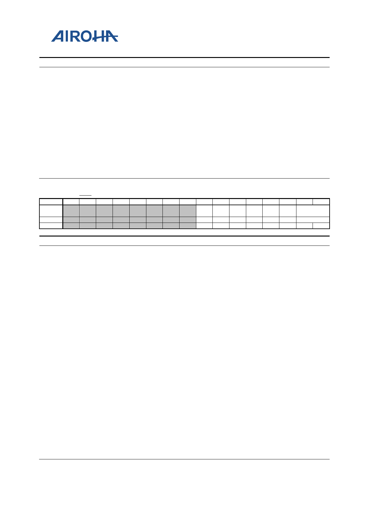
MT2523 Series Reference Manual
© 2015 - 2018 Airoha Technology Corp.
Page 66 of 692
This document contains information that is proprietary to Airoha Technology Corp. (“Airoha”) and/or its licensor(s).
Any unauthorized use, reproduction or disclosure of this document in whole or in part is strictly prohibited.
Bit(s)
Name
Description
7
AUTO_CTS
Enables hardware transmission flow control
0: Disable
1: Enable
6
AUTO_RTS
Enables hardware reception flow control
0: Disable
1: Enable
4
ENABLE_E
Enables enhancement feature
0: Disable
1: Enable
3:0
SW_FLOW_CONT
Software flow control bits
00xx: No TX flow control
10xx: Transmit XON1/XOFF1 as flow control bytes
xx00: No RX flow control
xx10: Receive XON1/XOFF1 as flow control bytes
A00D000C
LCR
Line Control Register
00
Bit
15
14
13
12
11
10
9
8
7
6
5
4
3
2
1
0
Name
DLA
B
SB SP EPS PEN STB
WLS1_WL
S0
Type
RW
RW
RW
RW
RW
RW
RW
Reset
0
0
0
0
0
0
0
0
Bit(s)
Name
Description
7
DLAB
Divisor latch access bit
0: RX and TX registers are read/written at Address 0 and the IER register is
read/written at Address 4.
1: Divisor Latch LS is read/written at Address 0 and the Divisor Latch MS is
read/written at Address 4.
6
SB
Sets up break
0: No effect
1: TX signal is forced to the 0 state.
5
SP
Stick parity
0: No effect.
1: The parity bit is forced to a defined state, depending on the states of EPS and
PEN: If EPS=1 & PEN=1, the even parity bit will be set and checked. If EPS=0 &
PEN=1, the odd parity bit will be set and checked.
4
EPS
Selects even parity
0: When EPS=0, an odd number of ones is sent and checked.
1: When EPS=1, an even number of ones is sent and checked.
3
PEN
Enables parity
0: The parity is neither transmitted nor checked.
1: The parity is transmitted and checked.
2
STB
Number of STOP bits
0: One STOP bit is always added.
1: Two STOP bits are added after each character is sent; unless the character
length is 5 when 1 STOP bit is added.
1:0
WLS1_WLS0
Selects word length
0: 5 bits
1: 6 bits
2: 7 bits
3: 8 bits
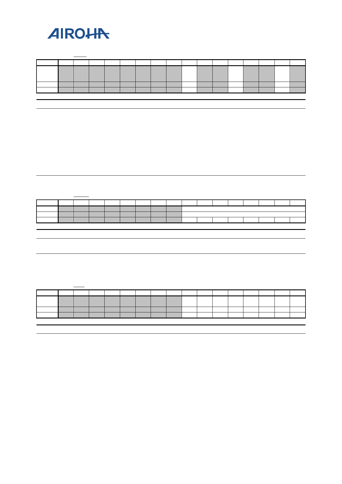
MT2523 Series Reference Manual
© 2015 - 2018 Airoha Technology Corp.
Page 67 of 692
This document contains information that is proprietary to Airoha Technology Corp. (“Airoha”) and/or its licensor(s).
Any unauthorized use, reproduction or disclosure of this document in whole or in part is strictly prohibited.
A00D0010
MCR
Modem Control Register
00
Bit
15
14
13
12
11
10
9
8
7
6
5
4
3
2
1
0
Name
XOF
F_ST
ATUS
Loop
RTS
Type
RU
RW
RW
Reset
0
0
0
Bit(s)
Name
Description
7
XOFF_STATUS
Read-only bit
0: When an XON character is received.
1: When an XOFF character is received.
4
Loop
Loop-back control bit
0: No loop-back is enabled.
1: Loop-back mode is enabled.
1
RTS
Controls the state of the output NRTS, even in loop mode.
0: RTS will always output 1.
1: RTS's output will be controlled by flow control condition.
A00D0010
XON1
XON1 Char Register
00
Bit
15
14
13
12
11
10
9
8
7
6
5
4
3
2
1
0
Name
XON1
Type
RW
Reset
0
0
0
0
0
0
0
0
Bit(s)
Name
Description
7:0
XON1
XON1 character for software flow control
Modified only when LCR = 8'hBF.
A00D0014
LSR
Line Status Register
60
Bit
15
14
13
12
11
10
9
8
7
6
5
4
3
2
1
0
Name
FIFO
ERR
TEM
T
THR
E
BI FE PE OE DR
Type
RU
RU
RU
RU
RU
RU
RU
RU
Reset
0
1
1
0
0
0
0
0
Bit(s)
Name
Description
7
FIFOERR
RX FIFO error indicator
0: No PE, FE, BI set in the RX FIFO.
1: Set to 1 when there is at least one PE, FE or BI in the RX FIFO.
6
TEMT
TX holding register (or TX FIFO) and the TX shift register are empty.
0: Empty conditions below are not met.
1: If FIFOs are enabled, the bit will be set whenever the TX FIFO and the TX shift
register are empty. If FIFOs are disabled, the bit will be set whenever TX holding
register and TX shift register are empty.
5
THRE
Indicates if there is room for TX holding register or TX FIFO is
reduced to its trigger level
0: Reset whenever the contents of the TX FIFO are more than its trigger level
(FIFOs are enabled), or whenever TX holding register is not empty (FIFOs are
disabled).
1: Set whenever the contents of the TX FIFO are reduced to its trigger level
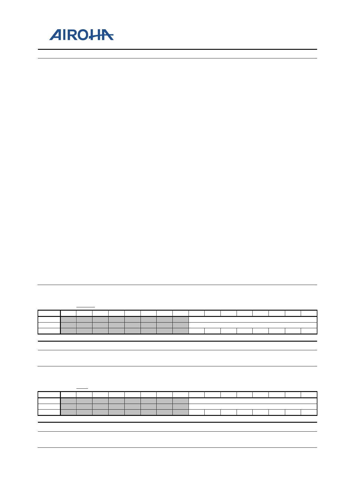
MT2523 Series Reference Manual
© 2015 - 2018 Airoha Technology Corp.
Page 68 of 692
This document contains information that is proprietary to Airoha Technology Corp. (“Airoha”) and/or its licensor(s).
Any unauthorized use, reproduction or disclosure of this document in whole or in part is strictly prohibited.
Bit(s)
Name
Description
(FIFOs are enabled), or whenever TX holding register is empty and ready to
accept new data (FIFOs are disabled).
4
BI
Break interrupt
0: Reset by the CPU reading this register
1: If the FIFOs are disabled, this bit will be set whenever the SIN is held in the 0
state for more than one transmission time (START bit + DATA bits + PARITY +
STOP bits).
If the FIFOs are enabled, this error will be associated with a corresponding
character in the FIFO and is flagged when this byte is at the top of the FIFO.
When a break occurs, only one zero character is loaded into the FIFO: The next
character transfer is enabled when RX signal goes into the marking state and
receives the next valid start bit.
3
FE
Framing error
0: Reset by the CPU reading this register
1: If the FIFOs are disabled, this bit will be set if the received data do not have a
valid STOP bit. If the FIFOs are enabled, the state of this bit will be
revealed when
the byte it refers to is the next to be read.
2
PE
Parity error
0: Reset by the CPU reading this register
1: If the FIFOs are disabled, this bit will be set if the received data do not have a
valid parity bit. If the FIFOs are enabled, the state of this bit will be revealed
when the referred byte is the next to be read.
1
OE
Overrun error
0: Reset by the CPU reading this register.
1: If the FIFOs are disabled, this bit will be set if the RX buffer is not read by the
CPU before the new data from the RX shift register overwrites the previous
contents. If the FIFOs are enabled, an overrun error will
occur when the RX FIFO
is full and the RX shift register becomes full. OE will be set as soon as this
happens. The character in the shift register is then overwritten, but not
transferred to the FIFO.
0
DR
Data ready
0: Cleared by the CPU reading the RX buffer or by reading all the FIFO bytes.
1: Set by the RX buffer register has data or FIFO becoming no empty.
A00D0018
XOFF1
XOFF1 Char Register
00
Bit
15
14
13
12
11
10
9
8
7
6
5
4
3
2
1
0
Name
XOFF1
Type
RW
Reset
0
0
0
0
0
0
0
0
Bit(s)
Name
Description
7:0
XOFF1
XOFF1 character for software flow control
Modified only when LCR = 0xBF.
A00D001C
SCR
Scratch Register
00
Bit
15
14
13
12
11
10
9
8
7
6
5
4
3
2
1
0
Name
SCR
Type
RW
Reset
0
0
0
0
0
0
0
0
Bit(s)
Name
Description
7:0
SCR
General purpose read/write register
The register will not be reset. Modified when LCR != 8'hBF.
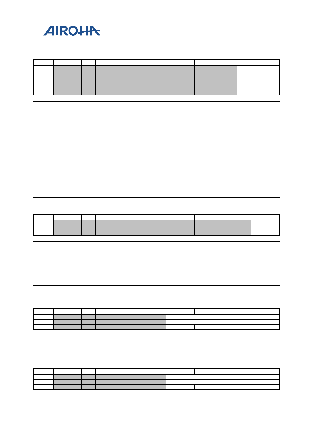
MT2523 Series Reference Manual
© 2015 - 2018 Airoha Technology Corp.
Page 69 of 692
This document contains information that is proprietary to Airoha Technology Corp. (“Airoha”) and/or its licensor(s).
Any unauthorized use, reproduction or disclosure of this document in whole or in part is strictly prohibited.
A00D0020
AUTOBAUD_EN
Auto Baud Detect Enable Register
00
Bit
15
14
13
12
11
10
9
8
7
6
5
4
3
2
1
0
Name
SLEE
P_AC
K_SE
L
AUT
OBA
UD_
SEL
AUT
OBA
UD_
EN
Type
RO
RW
RW
Reset
0
0
0
Bit(s)
Name
Description
2
SLEEP_ACK_SEL
Selects sleep ack when autobaud_en
0: Support sleep_ack when autobaud_en is opened .
1: Does not support sleep_ack when autobaud_en is opened .
1
AUTOBAUD_SEL
Selects auto-baud
0: Support standard baud rate detection
1: Support non_standard baud rate detection (support baud from 110 to 115200;
recommended to use 26MHz to auto fix) .
0
AUTOBAUD_EN
Auto-baud enabling signal
0: Disable auto-baud function
1: Enable auto-baud function (UARTn+0024h SPEED should be set to 0.)
Note: When AUTOBAUD_EN is active, there should not be
A*/a* char before the
auto baud char AT/at. If A*/a* is Inevitable, autobaud will fail and please
disable AUTOBAUD_EN to reset the autobaud feature and autobaud_en again.
The AUTOBAUD_EN will automatic clear when baud rate detect success.
A00D0024
HIGHSPEED
High Speed Mode Register
00
Bit
15
14
13
12
11
10
9
8
7
6
5
4
3
2
1
0
Name
SPEED
Type
RW
Reset
0
0
Bit(s)
Name
Description
1:0
SPEED
UART sample counter base
0: Based on 16*baud_pulse, baud_rate = system clock frequency/16/{DLM
, DLL}
1: Based on 8*baud_pulse, baud_rate = system clock frequency/8/{DLM, DLL}
2: Based on 4*baud_pulse, baud_rate = system clock frequency/4/{DLM, DLL}
3: Based on sampe_count * baud_pulse, baud_rate = system clock frequency /
(sampe_count+1)/{DLM, DLL}
A00D0028
SAMPLE_COUN
T
Sample Counter Register
00
Bit
15
14
13
12
11
10
9
8
7
6
5
4
3
2
1
0
Name
SAMPLECOUNT
Type
RW
Reset
0
0
0
0
0
0
0
0
Bit(s)
Name
Description
7:0
SAMPLECOUNT
Only useful when HIGHSPEED mode = 3.
A00D002C
SAMPLE_POINT
Sample Point Register
FF
Bit
15
14
13
12
11
10
9
8
7
6
5
4
3
2
1
0
Name
SAMPLEPOINT
Type
RW
Reset
1
1
1
1
1
1
1
1
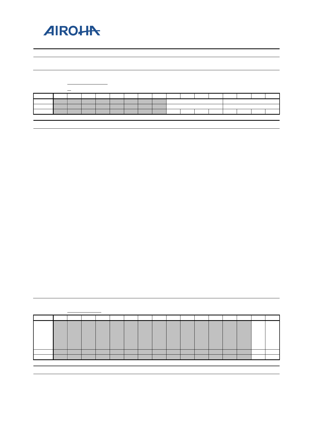
MT2523 Series Reference Manual
© 2015 - 2018 Airoha Technology Corp.
Page 70 of 692
This document contains information that is proprietary to Airoha Technology Corp. (“Airoha”) and/or its licensor(s).
Any unauthorized use, reproduction or disclosure of this document in whole or in part is strictly prohibited.
Bit(s)
Name
Description
7:0
SAMPLEPOINT
SAMPLE_POINT is usually (SAMPLE_COUNT-1)/2 without decimal. Effective
only when HIGHSPEED=3.
A00D0030
AUTOBAUD_RE
G
Auto Baud Monitor Register
00
Bit
15
14
13
12
11
10
9
8
7
6
5
4
3
2
1
0
Name
BAUD_STAT
BAUD_RATE
Type
RU
RU
Reset
0
0
0
0
0
0
0
0
Bit(s)
Name
Description
7:4
BAUD_STAT
Autobaud state (only true value in standard autobaud detection)
0: Autobaud is detecting.
1: AT_7N1
2: AT_7O1
3: AT_7E1
4: AT_8N1
5: AT_8O1
6: AT_8E1
7: at_7N1
8: at_7E1
9: at_7O1
10: at_8N1
11: at_8E1
12: at_8O1
13: Autobaud detection fails
3:0
BAUD_RATE
Autobaud baud rate (only true value in standard autobaud detection)
0: 115,200
1: 57,600
2: 38,400
3: 19,200
4: 9,600
5: 4,800
6: 2,400
7: 1,200
8: 300
9: 110
A00D0034
RATEFIX_AD
Clock Rate Fix Register
00
Bit
15
14
13
12
11
10
9
8
7
6
5
4
3
2
1
0
Name
AUT
OBA
UD_
RAT
E_FI
X
RAT
E_FI
X
Type
RW
RW
Reset
0
0
Bit(s)
Name
Description
1
AUTOBAUD_RATE_FI
X
0: Use 26MHz as system clock for UART auto baud detection
1: Use 13MHz as system clock for UART auto baud detection
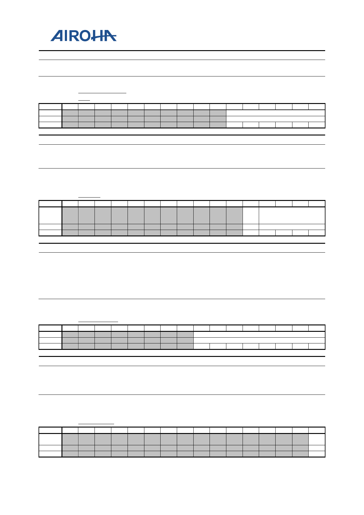
MT2523 Series Reference Manual
© 2015 - 2018 Airoha Technology Corp.
Page 71 of 692
This document contains information that is proprietary to Airoha Technology Corp. (“Airoha”) and/or its licensor(s).
Any unauthorized use, reproduction or disclosure of this document in whole or in part is strictly prohibited.
Bit(s)
Name
Description
0
RATE_FIX
0: Use 26MHz as system clock for UART TX/RX
1: Use 13MHz as system clock for UART TX/RX
A00D0038
AUTOBAUDSAM
PLE
Auto Baud Sample Register
0D
Bit
15
14
13
12
11
10
9
8
7
6
5
4
3
2
1
0
Name
AUTOBAUDSAMPLE
Type
RW
Reset
0
0
1
1
0
1
Bit(s)
Name
Description
5:0
AUTOBAUDSAMPLE
clk diveision for autobaud rate detection
System clk 26m: 'd13
System clk 13m: 'd6
A00D003C
GUARD
Guard
Time Added Register
0F
Bit
15
14
13
12
11
10
9
8
7
6
5
4
3
2
1
0
Name
GUA
RD_
EN
GUARD_CNT
Type
RW
RW
Reset
0
1
1
1
1
Bit(s)
Name
Description
4
GUARD_EN
Guard interval add enabling signal
0: No guard interval added
1: Add guard interval after stop bit.
3:0
GUARD_CNT
Guard interval count value
Guard interval = [1/( UART clock frequency / HIGHSPEED / {DLM, DLL})]
*GUARD_CNT.
A00D0040
ESCAPE_DAT
Escape
Character Register
FF
Bit
15
14
13
12
11
10
9
8
7
6
5
4
3
2
1
0
Name
ESCAPE_DAT
Type
RW
Reset
1
1
1
1
1
1
1
1
Bit(s)
Name
Description
7:0
ESCAPE_DAT
Escape character added before software flow control data and escape
character
If TX data are xon (31h), with esc_en =1, UART will transmit data as esc + CEh
(~xon).
A00D0044
ESCAPE_EN
Escape
Enable Register
00
Bit
15
14
13
12
11
10
9
8
7
6
5
4
3
2
1
0
Name
ESC_
EN
Type
RW
Reset
0
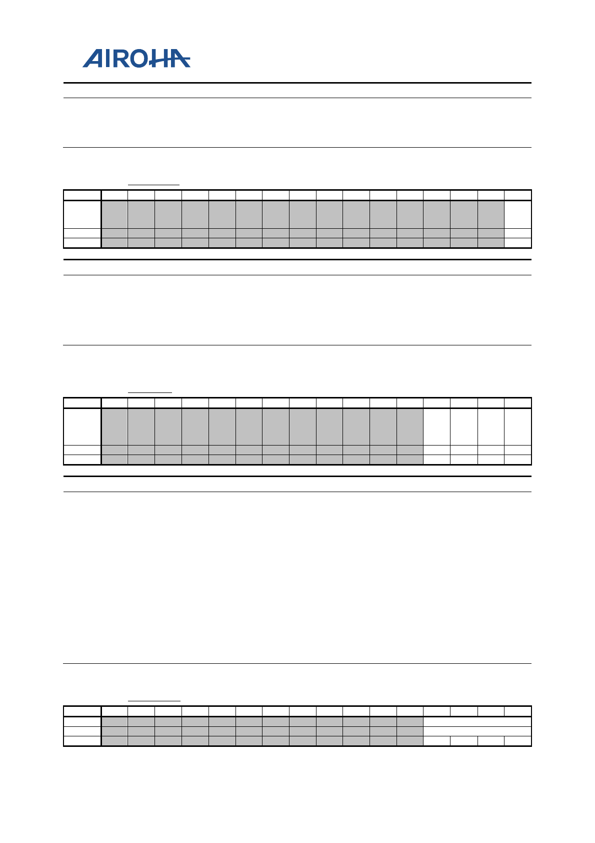
MT2523 Series Reference Manual
© 2015 - 2018 Airoha Technology Corp.
Page 72 of 692
This document contains information that is proprietary to Airoha Technology Corp. (“Airoha”) and/or its licensor(s).
Any unauthorized use, reproduction or disclosure of this document in whole or in part is strictly prohibited.
Bit(s)
Name
Description
0
ESC_EN
Adds escape character in transmitter and removes
escape character in
receiver by UART
0: Does not deal with the escape character
1: Add escape character in transmitter and remove escape character in receiver
A00D0048
SLEEP_EN
Sleep
Enable Register
00
Bit
15
14
13
12
11
10
9
8
7
6
5
4
3
2
1
0
Name
SLEE
P_E
N
Type
RW
Reset
0
Bit(s)
Name
Description
0
SLEEP_EN
For sleep mode issue
0: Does not deal with sleep mode indicate signal
1: Activate hardware flow control or software control according to software initial
setting when the chip enters sleep mode. Release hardware flow when the chip
wakes up. However, for software control, UART sends xon when awaken and
when FIFO does not reach threshold level.
A00D004C
DMA_EN
DMA
Enable Register
00
Bit
15
14
13
12
11
10
9
8
7
6
5
4
3
2
1
0
Name FIFO
_lsr_
sel
TO_C
NT_
AUT
ORST
TX_
DMA
_EN
RX_
DMA
_EN
Type
RW
RW
RW
RW
Reset
0
0
0
0
Bit(s)
Name
Description
3
FIFO_lsr_sel
Selects FIFO LSR mode
0: LSR will hold the first line status error state until you read the LSR register.
1: LSR will update automatically.
2
TO_CNT_AUTORST
Time-out counter auto reset register
0: After RX time-out happens, SW shall reset the interrupt by reading DMA_EN.
1: The RX time-out counter will be auto reset.
1
TX_DMA_EN
TX_DMA mechanism enabling signal
0: Does not use DMA in TX
1: Use DMA in TX. When this register is enabled, the flow control will be
based on
the DMA threshold and generate a time-out interrupt for DMA.
0
RX_DMA_EN
RX_DMA mechanism enabling signal
0: Does not use DMA in RX
1: Use DMA in RX. When this register is enabled, the flow control will be based
on the DMA threshold and generate a time-out interrupt
A00D0050
RXTRI_AD
Rx Trigger Address
00
Bit
15
14
13
12
11
10
9
8
7
6
5
4
3
2
1
0
Name
RXTRIG
Type
RW
Reset
0
0
0
0
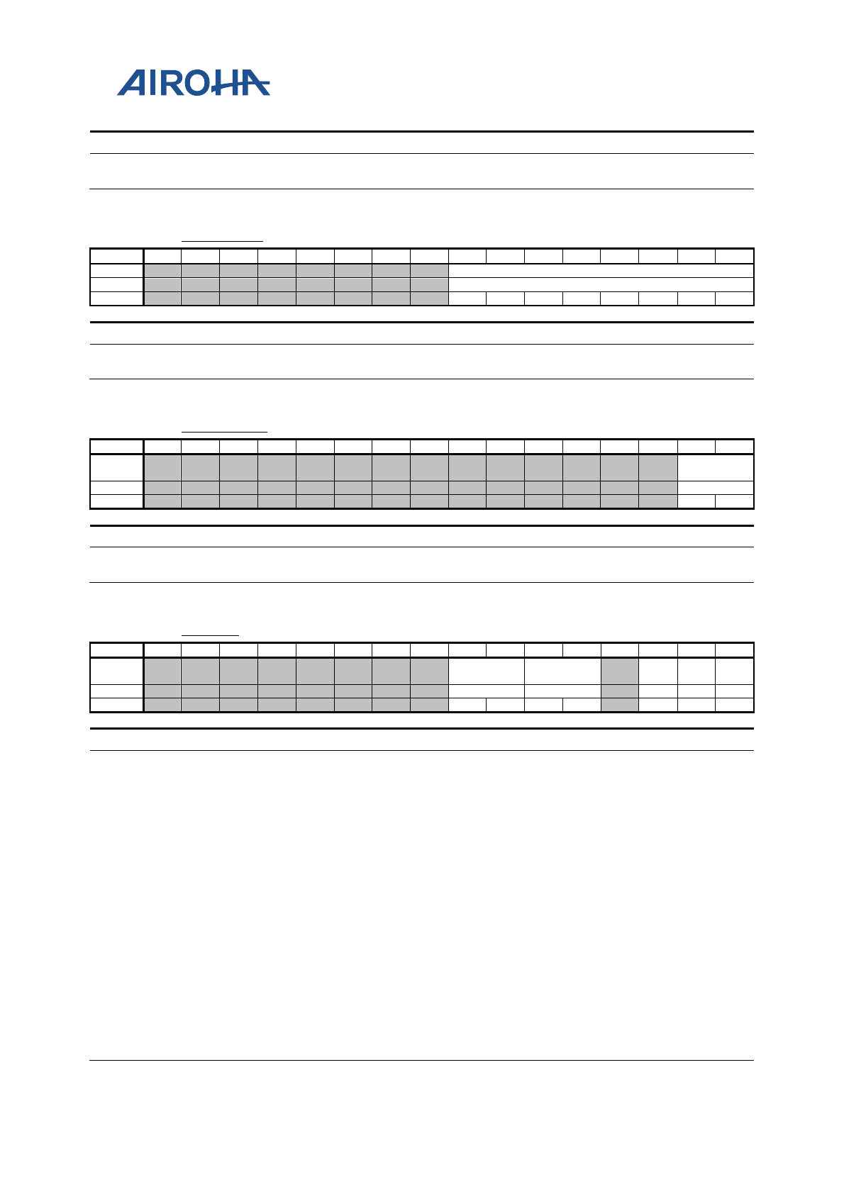
MT2523 Series Reference Manual
© 2015 - 2018 Airoha Technology Corp.
Page 73 of 692
This document contains information that is proprietary to Airoha Technology Corp. (“Airoha”) and/or its licensor(s).
Any unauthorized use, reproduction or disclosure of this document in whole or in part is strictly prohibited.
Bit(s)
Name
Description
3:0
RXTRIG
When { RFTL1_RFTL0}=2'b11, the RX FIFO threshold will be Rxtrig.
The value is
suggested to be smaller than half of RX FIFO size, which is 32 bytes.
A00D0054
FRACDIV_L
Fractional Divider LSB Address
00
Bit
15
14
13
12
11
10
9
8
7
6
5
4
3
2
1
0
Name
FRACDIV_L
Type
RW
Reset
0
0
0
0
0
0
0
0
Bit(s)
Name
Description
7:0
FRACDIV_L
Adds sampling count (+1) from state data7 to data0 to contribute fractional
divisor.only when high_speed=3.
A00D0058
FRACDIV_M
Fractional Divider MSB Address
00
Bit
15
14
13
12
11
10
9
8
7
6
5
4
3
2
1
0
Name
FRACDIV_
M
Type
RW
Reset
0
0
Bit(s)
Name
Description
1:0
FRACDIV_M
Adds sampling count when in state stop to parity to contribute fractional
divisor.only when high_speed=3.
A00D005C
FCR_RD
FIFO Control Register
00
Bit
15
14
13
12
11
10
9
8
7
6
5
4
3
2
1
0
Name
RFTL1_RF
TL0
TFTL1_TF
TL0
CLRT
CLR
R
FIFO
E
Type
RO
RO
RO
RO
RO
Reset
0
0
0
0
0
0
0
Bit(s)
Name
Description
7:6
RFTL1_RFTL0
RX FIFO trigger threshold
RX FIFO contains total 32 bytes.
0: 1
1: 6
2: 12
3: Use RX TRIG register data
5:4
TFTL1_TFTL0
TX FIFO trigger threshold
TX FIFO contains total 32 bytes.
0: 1
1: 4
2: 8
3: 14
2
CLRT
0: TX FIFO is not cleared.
1: TX FIFO is cleared.
1
CLRR
0: RX FIFO is not cleared.
1: RX FIFO is cleared.
0
FIFOE
Enables FIFO

MT2523 Series Reference Manual
© 2015 - 2018 Airoha Technology Corp.
Page 74 of 692
This document contains information that is proprietary to Airoha Technology Corp. (“Airoha”) and/or its licensor(s).
Any unauthorized use, reproduction or disclosure of this document in whole or in part is strictly prohibited.
Bit(s)
Name
Description
This bit must be set to 1 for any of other bits in the registers to have any effect.
0: RX and TX FIFOs are not enabled.
1: RX and TX FIFOs are enabled.
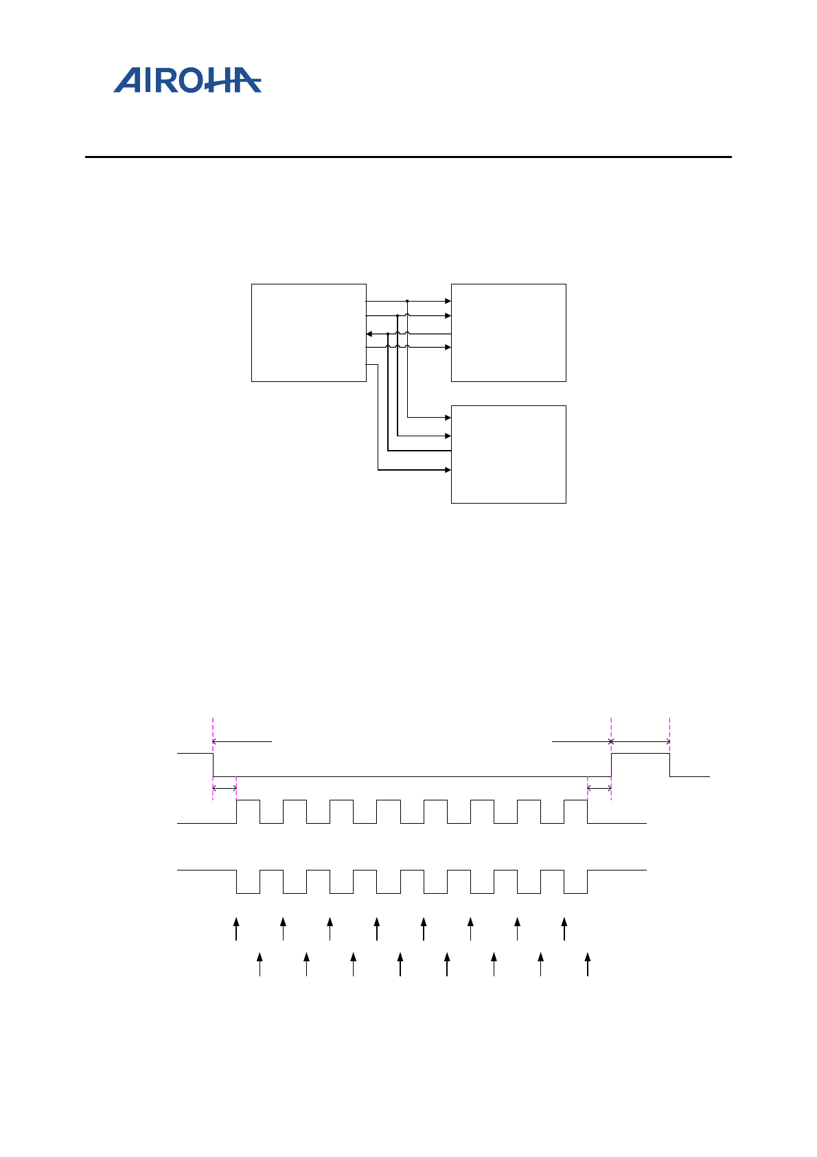
MT2523 Series Reference Manual
© 2015 - 2018 Airoha Technology Corp.
Page 75 of 692
This document contains information that is proprietary to Airoha Technology Corp. (“Airoha”) and/or its licensor(s).
Any unauthorized use, reproduction or disclosure of this document in whole or in part is strictly prohibited.
7. Serial Peripheral Interface Master Controller
7.1. General Description
The SPI (Serial Peripheral Interface) is a bit-serial, four-pin transmission protocol. Figure 7-1 is an example of the
connection between the SPI master and SPI slave. The SPI controller is a master responsible of data transmission
with slave.
SCK
MOSI
MISO
CS0
CS1
SCK
MOSI
MISO
CS
SPI
Master SPI
Slave0
SCK
MOSI
MISO
CS
SPI
Slave1
Figure 7-1. Pin connection between SPI master and SPI slave
Figure 7-2 shows the waveform during SPI transmission. The low active CS_N determines the start point and end
point of one transaction. The CS_N setup time, hold time and idle time are also depicted.
CPOL defines the clock polarity in the transmission. Two types of polarity can be adopted, i.e. polarity 0 and
polarity 1. Figure 7-2 shows both of the clock polarity (CPOL) as examples.
CPHA defines the legal timing to sample MOSI and MISO. Two different methods can be adopted.
CS_N
SCK
(CPOL=0)
SCK Edge
Number
SCK
(CPOL=1)
12345678910 11 12 13 14 15 16
SAMPLE MOSI/MISO
(CPHA=0)
SAMPLE MOSI/MISO
(CPHA=1)
Data Transmission
CS_N
idle time
CS_N setup time CS_N hold time
Figure 7-2. SPI transmission formats

MT2523 Series Reference Manual
© 2015 - 2018 Airoha Technology Corp.
Page 76 of 692
This document contains information that is proprietary to Airoha Technology Corp. (“Airoha”) and/or its licensor(s).
Any unauthorized use, reproduction or disclosure of this document in whole or in part is strictly prohibited.
Table 7-1. SPI master controller interface
Signal name Type Description
CS0 O Low active chip selection signal
CS1 O Low active chip selection signal
SCK O The (bit) serial clock
MOSI O Data signal from master output to slave input
MISO I Data signal from slave output to master input
7.1.1. Features
The features of the SPI master controller are:
• Configurable CS_N setup time, hold time and idle time
• Programmable SCK high time and low time
• Configurable transmitting and receiving bit order
• Two configurable modes for the source of the data to be transmitted: 1) In TX DMA mode, the SPI
controller automatically fetches the transmitted data (to be put on the MOSI line) from memory; 2) In TX
FIFO mode, the data to be transmitted on the MOSI line are written to FIFO before the start of the
transaction.
• Two configurable modes for destination of the data to be received: 1) In RX DMA mode, the SPI controller
automatically stores the received data (from MISO line) to memory; 2) In RX FIFO mode, the received data
keep being in RX FIFO of the SPI controller. The processor must read back the data by itself.
• Adjustable endian order from/to memory system
• Programmable byte length for transmission
• Unlimited length for transmission, achieved by the operation of PAUSE mode. In PAUSE mode, the CS_N
signal will keep being active (low) after the transmission. At this time, the SPI controller is in PAUSE_IDLE
state, ready to receive the resume command. Figure 7-3 is the state transition.
• Configurable option to control CS_N de-assertion between byte transfers. The controller supports a
special transmission format called CS_N de-assert mode. Figure 7-4 illustrates the waveform in this
transmission format.
• SPI master supports connecting two SPI slaves.
MT2523 Series Reference Manual
© 2015 - 2018 Airoha Technology Corp.
Page 77 of 692
This document contains information that is proprietary to Airoha Technology Corp. (“Airoha”) and/or its licensor(s).
Any unauthorized use, reproduction or disclosure of this document in whole or in part is strictly prohibited.
IDLE
PAUSE IDLE
BUSY
activate
resume
! (pause)
pause
Figure 7-3. Operation flow with or without PAUSE mode
Figure 7-4. CS_N de-assert mode
7.1.2. Block Diagram
tx0
(16byte)
rx0
(16byte)
tx1
(16byte)
rx1
(16byte)
AHB
Interface
MOSI
MISO
TX
RX
32 bits
Control Register
AHB BUS
APB BUS
Figure 7-5. Block diagram of SPI master controller
CS_N
BYTE
SCLK BYTE BYTE
... BYTE BYTE
MT2523 Series Reference Manual
© 2015 - 2018 Airoha Technology Corp.
Page 78 of 692
This document contains information that is proprietary to Airoha Technology Corp. (“Airoha”) and/or its licensor(s).
Any unauthorized use, reproduction or disclosure of this document in whole or in part is strictly prohibited.
7.2. Register Definition
There are four SPI master controllers in this SOC. The usage of the registers below is the same except that the base
address should be changed to respective one.
Module name: SPI0 Base address: (+A0110000h)
Address Name Width Register Function
A0110000
SPI_CFG0
32
SPI Configuration 0 Register
A0110004
SPI_CFG1
32 SPI Configuration 1 Register
A0110008 SPI_TX_SRC 32 SPI TX Source Address Register
A011000C
SPI_RX_DST
32
SPI RX Destination Address Register
A0110010 SPI_TX_DATA
32 SPI TX DATA FIFO
A0110014
SPI_RX_DATA
32
SPI RX DATA FIFO
A0110018
SPI_CMD
32
SPI Command Register
A011001C SPI_STATUS0
32 SPI Status 0 Register
A0110020
SPI_STATUS1
32
SPI Status 1 Register
A0110024
SPI_PAD_MACR
O_SEL
32 SPI pad_macro selection Register
A0110028
SPI_CFG2
32
SPI Configuration 2 Register
A0110000
SPI_CFG0
SPI Configuration 0 Register
00000000
Bit
31
30
29
28
27
26
25
24
23
22
21
20
19
18
17
16
Name
CS_SETUP_COUNT
Type
RW
Reset
0
0
0
0
0
0
0
0
0
0
0
0
0
0
0
0
Bit
15
14
13
12
11
10
9
8
7
6
5
4
3
2
1
0
Name
CS_HOLD_COUNT
Type
RW
Reset
0
0
0
0
0
0
0
0
0
0
0
0
0
0
0
0
Bit(s)
Mnemonic
Name
Description
31:16
CS_SETUP_COUNT
CS_SETUP_COUNT
C
hip select setup time
S
etup time = (CS_SETUP_COUNT+1)*CLK_PERIOD,
where CLK_PERIOD
(38.46ns) is the cycle time of the
clock the SPI engine adopts.
15:0
CS_HOLD_COUNT
CS_HOLD_COUNT
Chip select hold time
H
old time = (CS_HOLD_COUNT+1)*CLK_PERIOD,
where CLK_PERIOD
(38.46ns) is the cycle time of the
clock the SPI engine adopts.
SPI number Base address
SPI0 0xA0110000
SPI1 0xA0120000
SPI2 0xA0130000
SPI3 0xA0140000
MT2523 Series Reference Manual
© 2015 - 2018 Airoha Technology Corp.
Page 79 of 692
This document contains information that is proprietary to Airoha Technology Corp. (“Airoha”) and/or its licensor(s).
Any unauthorized use, reproduction or disclosure of this document in whole or in part is strictly prohibited.
A0110004
SPI_CFG1
SPI Configuration 1 Register
00000000
Bit
31
30
29
28
27
26
25
24
23
22
21
20
19
18
17
16
Name GET_ TICK
_DLY
DE
VIC
E_
SE
L
PACKET_LENGTH
Type
RW
RW
RW
Reset
0
0
0
0
0
0
0
0
0
0
0
0
0
0
Bit
15
14
13
12
11
10
9
8
7
6
5
4
3
2
1
0
Name
PACKET_LOOP_CNT
CS_IDLE_COUNT
Type
RW
RW
Reset
0
0
0
0
0
0
0
0
0
0
0
0
0
0
0
0
Bit(s)
Mnemonic
Name
Description
31:29
GET_TICK_DLY
GET_TICK_DLY
If the speed of SPI is not fast enough, the three bits can
help tolera
te get_tick timing. The timing range between
get_tick is one cycle depending on CLK_PERIOD
(38.46ns)
.
26
DEVICE_SEL
DEVICE_SEL
SPI master rec
eives device 0 or device 1 MISO data.
25:16
PACKET_LENGTH
PACKET_LENGTH
15:8
PACKET_LOOP_CN
T
PACKET_LOOP_CN T
The transmission on SPI bus consists of units
bytes.
Hence, PACKET_LENGTH[9:0] define number of
bytes in one packet
;
PACKET_LOOP_CNT[7:0] define the
number of packets within one transaction. The number of
bytes in one packet = PACKET_LENGTH + 1. The number
of packets in one transaction = PACKET_LOOP_CNT + 1.
Total bytes of one transaction = (PACKET_LENGTH + 1)
*(PACKET_
LOOP_CNT + 1).
7:0
CS_IDLE_COUNT
CS_IDLE_COUNT
Chip select idle time
T
ime between consecutive transaction =
(CS_HOLD_COUNT+1)*CLK_PERIOD.
A0110008
SPI_TX_SRC
SPI TX Source Address Register
00000000
Bit
31
30
29
28
27
26
25
24
23
22
21
20
19
18
17
16
Name
SPI_TX_SRC
Type
RW
Reset
0
0
0
0
0
0
0
0
0
0
0
0
0
0
0
0
Bit
15
14
13
12
11
10
9
8
7
6
5
4
3
2
1
0
Name
SPI_TX_SRC
Type
RW
Reset
0
0
0
0
0
0
0
0
0
0
0
0
0
0
0
0
Bit(s)
Mnemonic
Name
Description
31:0
SPI_TX_SRC
SPI_TX_SRC
If TX_DMA_EN is set, the data to be put on the
MOSI line
will be kept in memory in advance, and
the SPI controller will automatically read the data
from memory. SPI_TX_SRC define
s the memory
address from which SPI controller starts to read
data.
The address must be aligned to word
boundary
.
MT2523 Series Reference Manual
© 2015 - 2018 Airoha Technology Corp.
Page 80 of 692
This document contains information that is proprietary to Airoha Technology Corp. (“Airoha”) and/or its licensor(s).
Any unauthorized use, reproduction or disclosure of this document in whole or in part is strictly prohibited.
A011000C
SPI_RX_DST
SPI RX Destination Address
Register
00000000
Bit
31
30
29
28
27
26
25
24
23
22
21
20
19
18
17
16
Name
SPI_RX_DST
Type
RW
Reset
0
0
0
0
0
0
0
0
0
0
0
0
0
0
0
0
Bit
15
14
13
12
11
10
9
8
7
6
5
4
3
2
1
0
Name
SPI_RX_DST
Type
RW
Reset
0
0
0
0
0
0
0
0
0
0
0
0
0
0
0
0
Bit(s)
Mnemonic
Name
Description
31:0
SPI_RX_DST
SPI_RX_DST
If RX_DMA_EN is set, the received data from the
MISO line will be move
d to memory automatically
by the SPI controller. SPI_RX_DST define
s the
memory address to which the SPI controller starts
to store the data. The address must be aligned to
word boundary
.
A0110010
SPI_TX_DATA
SPI TX DATA FIFO
00000000
Bit
31
30
29
28
27
26
25
24
23
22
21
20
19
18
17
16
Name
SPI_TX_DATA
Type
WO
Reset
0
0
0
0
0
0
0
0
0
0
0
0
0
0
0
0
Bit
15
14
13
12
11
10
9
8
7
6
5
4
3
2
1
0
Name
SPI_TX_DATA
Type
WO
Reset
0
0
0
0
0
0
0
0
0
0
0
0
0
0
0
0
Bit(s)
Mnemonic
Name
Description
31:0
SPI_TX_DATA
SPI_TX_DATA
The depth of the TX FIFO is 32 bytes. Write to
this register
to
write 4 bytes to TX FIFO. The TX
FIFO pointer will automatically move toward
the next four bytes. Read from this register
to
read 4 bytes from the FIFO, and the TX FIFO
pointer
will
automatically move toward the next
four bytes.
A0110014
SPI_RX_DATA
SPI RX DATA FIFO
00000000
Bit
31
30
29
28
27
26
25
24
23
22
21
20
19
18
17
16
Name
SPI_RX_DATA
Type
RO
Reset
0
0
0
0
0
0
0
0
0
0
0
0
0
0
0
0
Bit
15
14
13
12
11
10
9
8
7
6
5
4
3
2
1
0
Name
SPI_RX_DATA
Type
RO
Reset
0
0
0
0
0
0
0
0
0
0
0
0
0
0
0
0
Bit(s)
Mnemonic
Name
Description
31:0
SPI_RX_DATA
SPI_RX_DATA
The depth of the RX FIFO is 32 bytes. Read from
this register
to
read 4 bytes from RX FIFO. The RX
FIFO pointer will automatically move toward the
MT2523 Series Reference Manual
© 2015 - 2018 Airoha Technology Corp.
Page 81 of 692
This document contains information that is proprietary to Airoha Technology Corp. (“Airoha”) and/or its licensor(s).
Any unauthorized use, reproduction or disclosure of this document in whole or in part is strictly prohibited.
Bit(s)
Mnemonic
Name
Description
next four bytes. Write to this register to write 4
bytes to FIFO, and the RX FIFO pointer
will
automatically move toward the next four bytes
.
A0110018
SPI_CMD
SPI Command Register
00000000
Bit
31
30
29
28
27
26
25
24
23
22
21
20
19
18
17
16
Name
PAUS
E_IE
FINI
SH_I
E
Type
RW
RW
Reset
0
0
Bit
15
14
13
12
11
10
9
8
7
6
5
4
3
2
1
0
Name
TX_E
NDIA
N
RX_E
NDIA
N
RXM
SBF TXM
SBF
TX_D
MA_
E N
RX_
D
MA_
E N
CPOL
CPHA
CS_P
OL
SAM
P
LE_S
EL
CS_D
EASS
ERT_
EN
PAUS
E_EN
RST
RESU
ME
CMD_
ACT
Type
RW
RW
RW
RW
RW
RW
RW
RW
RW
RW
RW
RW
RW
WO
WO
Reset
0
0
0
0
0
0
0
0
0
0
0
0
0
0
0
Bit(s)
Mnemonic
Name
Description
17
PAUSE_IE
PAUSE_IE
Interrupt enable bit of pause flag in SPI status
register
16
FINISH_IE
FINISH_IE
Interrupt enable bit of finish flag in SPI status
register
15
TX_ENDIAN
TX_ENDIAN
Defines whether to reverse the endian order of
the data
DMA from memory. Default (0) is not to
reverse. Only supports DMA mode.
14
RX_ENDIAN
RX_ENDIAN
Defines whether to reverse the endian order of
the data DMA to memory. Default (0) is not to
reverse.
13
RXMSBF
RXMSBF
Indicates the data received from MISO line is
MSB first or not. Set RXMSBF to 1 for MSB first,
otherwise set it to 0.
12
TXMSBF
TXMSBF
Indicates the data sent on MOSI line is MSB first
or not. Set TXMSBF to 1 for MSB first, otherwise
set it to 0.
11
TX_DMA_EN
TX_DMA_EN
DMA mode enable bit of the data to be
transmitted. Default (0) is not to enable.
10
RX_DMA_EN
RX_DMA_EN
DMA mode enable bit of the data being received.
Default (0) is not to enable.
9
CPOL
CPOL
Control bit of the SCK polarity.
0: CPOL = 0
1: CPOL = 1
8
CPHA
CPHA
Defines the SPI clock format 0 or SPI clock
format 1 during transmission
MT2523 Series Reference Manual
© 2015 - 2018 Airoha Technology Corp.
Page 82 of 692
This document contains information that is proprietary to Airoha Technology Corp. (“Airoha”) and/or its licensor(s).
Any unauthorized use, reproduction or disclosure of this document in whole or in part is strictly prohibited.
Bit(s)
Mnemonic
Name
Description
0: CPHA = 0
1: CPHA = 1
7
CS_POL
CS_POL
Control bit of chip select polarity
0: Active low
1: Active high
6
SAMPLE_SEL
SAMPLE_SEL
Control bit of sample edge of miso
0: Positive edge
1: Negative
edge
5
CS_DEASSERT_EN
CS_DEASSERT_EN
Enable bit of the chip select de-assertion mode.
Set it to1 to enable this mode.
4
PAUSE_EN
PAUSE_EN
Enable bit of the pause mode. Set it to 1 to enable
this mode.
2
RST
RST
Software reset bit; resets the state machine and
data FIFO of SPI controller.
When this bit is 1,
software reset is active high. The default value is
0.
1
RESUME
RESUME
This bit is used when controller is in PAUSE IDLE
state. Write 1 to this bit to trigger the SPI
controller resum
e transfer from PAUSE IDLE
state.
0
CMD_ACT
CMD_ACT
Command activate bit. Write 1 to this bit to trigger
the SPI controller to start the transaction.
A011001C
SPI_STATUS0
SPI Status 0 Register
00000000
Bit
31
30
29
28
27
26
25
24
23
22
21
20
19
18
17
16
Name
AAAA
Type
Reset
Bit
15
14
13
12
11
10
9
8
7
6
5
4
3
2
1
0
Name
PAUS
E
FINI
SH
Type
RC
RC
Reset
0
0
Bit(s)
Mnemonic
Name
Description
1
PAUSE
PAUSE
Interrupt status bit in pause mode. It will be set by
the SPI controller when it completes the
transaction, entering the PAUSE IDLE state.
0
FINISH
FINISH
Interrupt status bit in non-pause mode. It will be
set by the SPI
controller when it completes the
transaction, entering the IDLE state.
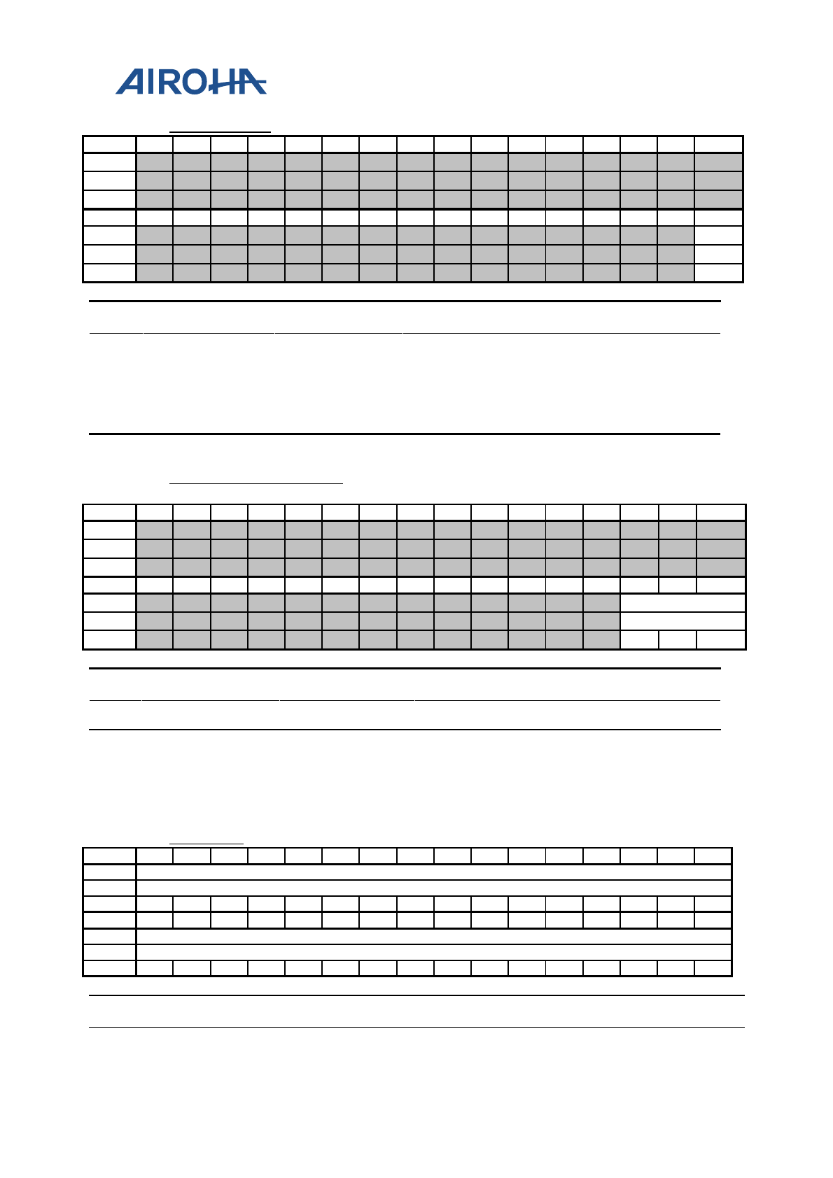
MT2523 Series Reference Manual
© 2015 - 2018 Airoha Technology Corp.
Page 83 of 692
This document contains information that is proprietary to Airoha Technology Corp. (“Airoha”) and/or its licensor(s).
Any unauthorized use, reproduction or disclosure of this document in whole or in part is strictly prohibited.
A0110020
SPI_STATUS1
SPI Status 1 Register
00000001
Bit
31
30
29
28
27
26
25
24
23
22
21
20
19
18
17
16
Name
AAAA
Type
Reset
Bit
15
14
13
12
11
10
9
8
7
6
5
4
3
2
1
0
Name
BUSY
Type
RO
Reset
1
Bit(s)
Mnemonic
Name
Description
0
BUSY
BUSY
This status flag reflects the SPI controller is busy
or not.
This bit is low active, i.e. 0 represents the
SPI controller is busy now.
1'b1: Idle
1'b0: Busy
A0110024
SPI_PAD_MACRO_SEL
SPI pad_macro selection
Register
00000000
Bit
31
30
29
28
27
26
25
24
23
22
21
20
19
18
17
16
Name
AAAA
Type
Reset
Bit
15
14
13
12
11
10
9
8
7
6
5
4
3
2
1
0
Name
PAD_MACRO_SEL
Type
RW
Reset
0
0
0
Bit(s)
Mnemonic
Name
Description
2:0
PAD_MACRO_SEL
PAD_MACRO_SEL
Selects which PAD group SPI will use
Note:
SPI0 pad macro A = 0, SPI0 pad macro B = 1;
SPI1 pad macro A = 0, SPI1 pad macro B = 2;
SPI2 pad macro A = 0, SPI2 pad macro B = 2;
SPI3 pad macro A = 0, SPI3 pad macro B = 1;
A0110028
SPI_CFG2
SPI Configuration 2 Register
00000000
Bit
31
30
29
28
27
26
25
24
23
22
21
20
19
18
17
16
Name
SCK_LOW_COUNT
Type
RW
Reset
0
0
0
0
0
0
0
0
0
0
0
0
0
0
0
0
Bit
15
14
13
12
11
10
9
8
7
6
5
4
3
2
1
0
Name
SCK_HIGH_COUNT
Type
RW
Reset
0
0
0
0
0
0
0
0
0
0
0
0
0
0
0
0
Bit(s)
Mnemonic
Name
Description

MT2523 Series Reference Manual
© 2015 - 2018 Airoha Technology Corp.
Page 84 of 692
This document contains information that is proprietary to Airoha Technology Corp. (“Airoha”) and/or its licensor(s).
Any unauthorized use, reproduction or disclosure of this document in whole or in part is strictly prohibited.
Bit(s)
Mnemonic
Name
Description
31:16
SCK_LOW_COUNT
SCK_LOW_COUNT
SCK clock low time =
(SCK_LOW_COUNT+1)*CLK_PERIOD
15:0
SCK_HIGH_COUNT
SCK_HIGH_COUNT
SCK clock high time =
(SCK_HIGH_COUNT+1)*CLK_PERIOD.
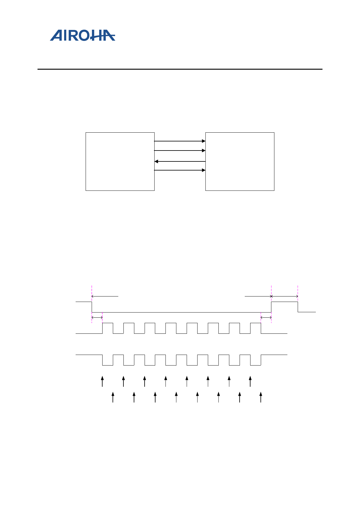
MT2523 Series Reference Manual
© 2015 - 2018 Airoha Technology Corp.
Page 85 of 692
This document contains information that is proprietary to Airoha Technology Corp. (“Airoha”) and/or its licensor(s).
Any unauthorized use, reproduction or disclosure of this document in whole or in part is strictly prohibited.
8. Serial Peripheral Interface Slave Controller
8.1. General Description
The SPI (Serial Peripheral Interface) is a bit-serial, four-pin transmission protocol. Figure 8-1 is an example of the
connection between the SPI master and SPI slave. The SPI slave controller can be configured by SPI master
transmit data, it is a slave responsible of data transmission with the master.
SCK
MOSI
MISO
CS
SCK
MOSI
MISO
CS
SPI
Master SPI
Slave
Figure 8-1. Pin connection between SPI master and SPI slave
Figure 7-2 shows the waveform during the SPI transmission. The low active CS_N determines the start point and
end point of one transaction. The CS_N setup time, hold time and idle time are also depicted.
CPOL defines the clock polarity in the transmission. Two types of polarity can be adopted, i.e. polarity 0 and
polarity 1. Figure 7-2 shows both of the clock polarity (CPOL) as examples.
CPHA defines the legal timing to sample MOSI and MISO. Two different methods can be adopted.
CS_N
SCK
(CPOL=0)
SCK Edge
Number
SCK
(CPOL=1)
1 2 34 5 6 7 8 910 11 12 13 14 15 16
SAMPLE MOSI/MISO
(CPHA=0)
SAMPLE MOSI/MISO
(CPHA=1)
Data Transmission
CS_N
idle time
CS_N setup time CS_N hold time
Figure 8-2. SPI transmission formats
MT2523 Series Reference Manual
© 2015 - 2018 Airoha Technology Corp.
Page 86 of 692
This document contains information that is proprietary to Airoha Technology Corp. (“Airoha”) and/or its licensor(s).
Any unauthorized use, reproduction or disclosure of this document in whole or in part is strictly prohibited.
Table 8-1. SPI slave controller interface
Signal name Type Description
CS I Low active chip selection signal
SCK I The (bit) serial clock (Max SCK clock rate is 13MHz.)
MOSI I Data signal from master output to slave input
MISO O Data signal from slave output to master input
8.1.1. Features
The SPI slave controller has eight commands that can be configured by SPI master transmit data. The commands
include “power-off”, “power-on”, “configure-write”, “configure-read”, “write-data”, “read-data”, “write-status”
and “read-status”. The command waveform is shown in Figure 8-3.
Figure 8-3. SPI slave controller commands waveform
SPI slave control flow
The SPI slave control flow is shown in Figure 8-4 .
Read Status
CMD
Config Read/Write
CMD
Read Status
CMD
Read/Write Data
CMD
SPI Transmission
Read Status
CMD
SLV_ON = 1
Power On
CMD
CFG_SUCESS = 1 &
TXRX_FIFO_RDY = 1
RDWR_FINISH = 1 &
RD_ERR/WR_ERR = 0
Power Off
CMD
Y
N
Y
Y
N
Write Status CMD
(clear RD_ERR/WR_ERR)
N
Figure 8-4. SPI slave control flow diagram
MT2523 Series Reference Manual
© 2015 - 2018 Airoha Technology Corp.
Page 87 of 692
This document contains information that is proprietary to Airoha Technology Corp. (“Airoha”) and/or its licensor(s).
Any unauthorized use, reproduction or disclosure of this document in whole or in part is strictly prohibited.
First, SPI master transmits “power-on” command to turn on SPI slave controller then transmits “config-read/write”
command to configure the transfer data length and read/write address of the memory. After SPI slave is
configured, it can send/receive data package with SPI master by “read/write-data” command. Finally, use “power-
off” command to turn off SPI slave controller. In each state, SPI master transmits “read-status” command to poll
SPI slave situation. If SPI master detects error flag bit of state, it should send “write-status” command to clear the
bit and poll this bit until it turns low. Detailed descriptions of SPI slave command are shown in Table 8-2 and the
SPI slave status in
Table 8-3 .
Table 8-2. SPI slave command description
Table 8-3. SPI slave status description (use RS command to poll SPI slave status)
Function Bit Usage Interrupt
source
SLV_ON
0
Master polls this bit until slave is on after sending POWERON CMD.
N
SR_CFG_SUCCESS
1
Master checks this bit to know if CW/CR command is successful.
N
SR_TXRX_FIFO_RDY 2 If master configures read/write, when slave is ready to send/receive
data, the master can send RD/WD command. Clean: After SPI slave
receives CR/CW command.
N
SR_RD_ERR 3 After a RD command, master can read this bit to know if there is error
in the read transfer. If there is error, master should send WS command
to clear this bit and poll this bit until this bit turns 0. Y
SR_WR_ERR 4 After a WD command, master can read this bit to know if there is error
in the write transfer. If there is error, master should send WS command
to clear this bit and poll this bit until this bit turns 0.
Y
SR_RDWR_FINISH
5
After RD/WD transaction, master can poll this bit to know if the Y
Cmd field [7:0] CMD default
code Data field Usage
Read Data (RD) 8’b81 N bytes. Burst data payload Master read data
Write Data (WD) 8’h06 N bytes. Burst data payload Master write data
Read Status (RS) 8’h0A 1 byte Master reads slave status register
Write Status (WS) 8’h08 1 byte Master writes slave status register to clear error
bit (i.e. write 1 to clear).
Config Read (CR) 8‘h02 4 bytes addr,
4 bytes data length Master configure slave to start read data.
Config Write (CW) 8’h04 4 bytes addr,
4 bytes data length Master configures slave to start write data.
Power On (PWRO) 8’h0E 0 byte Master uses this configure CMD to wake up
system and tell MCU to turn on SLAVE.
Power Off (PWRF) 8’h0C 0 byte Master uses this configure CMD to wake up
system and tell MCU to turn off SLAVE.
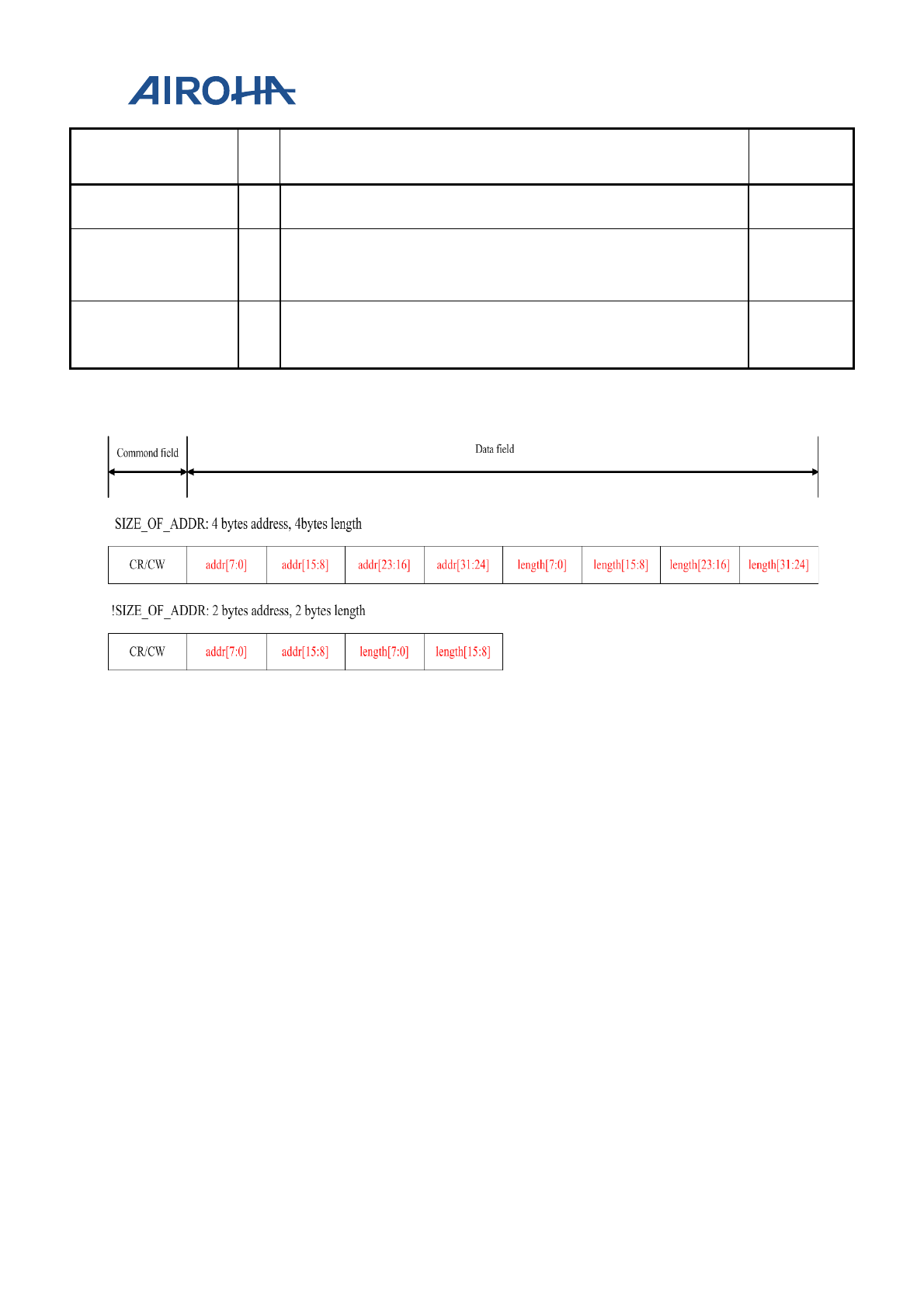
MT2523 Series Reference Manual
© 2015 - 2018 Airoha Technology Corp.
Page 88 of 692
This document contains information that is proprietary to Airoha Technology Corp. (“Airoha”) and/or its licensor(s).
Any unauthorized use, reproduction or disclosure of this document in whole or in part is strictly prohibited.
Function Bit Usage Interrupt
source
read/write transfer is finished. Clean: After SPI slave receives CR/CW
command.
SR_TIMOUT_ERR 6 Indicates SPI slave does not receive or send data for some time.
If there is error, master should send WS command to clear this bit and
poll this bit until this bit turns 0.
Y
SR_CMD_ERR 7 If master sends an error CMD at the first byte, master can know the
error status through the received data. Clean: After SPI slave receives
correct command.
N
Figure 8-5. Config read/write (CR/CW) command format
The features of the SPI slave controller are:
• Configurable transmitting and receiving bit order
• The SPI slave controller automatically fetches the transmitted data (to be put on the MISO line) from
memory.
• The SPI slave controller automatically stores the received data (from MOSI line) to memory.
• Programmable byte length for transmission
• Adjustable time out interrupt threshold, if the time that SPI slave does not receive or send data is
exceeded.
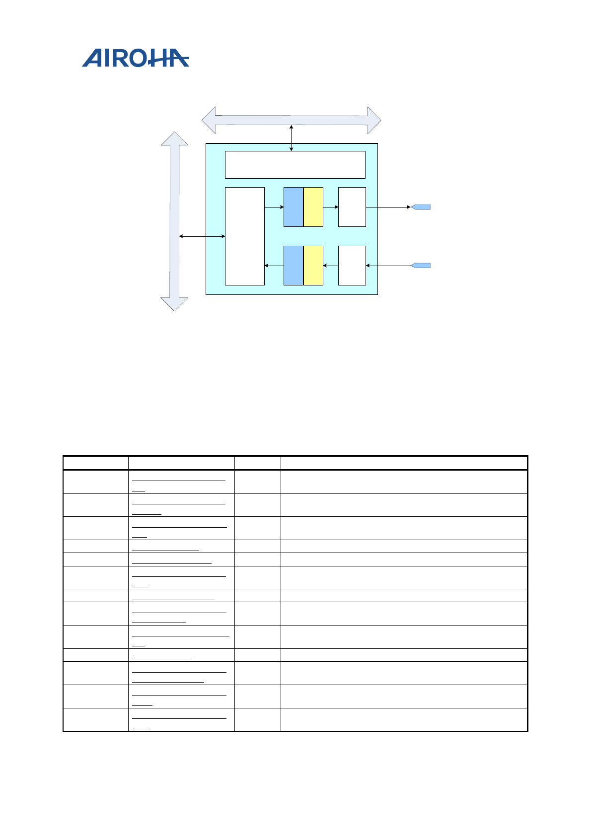
MT2523 Series Reference Manual
© 2015 - 2018 Airoha Technology Corp.
Page 89 of 692
This document contains information that is proprietary to Airoha Technology Corp. (“Airoha”) and/or its licensor(s).
Any unauthorized use, reproduction or disclosure of this document in whole or in part is strictly prohibited.
8.1.2. Block Diagram
tx0
(16byte)
rx0
(16byte)
tx1
(16byte)
rx1
(16byte)
AHB
Interface
MISO
MOSI
TX
RX
Control Register
AHB BUS
APB BUS
Figure 8-6. Block diagram of SPI slave controller
8.2. Register Definition
There is one SPI slave controller in this SOC. The usage of the registers below is the same except that the base
address should be changed to respective one.
Module name: SPISLV Base address: (+A0150000h)
Address Name Width Register Function
A0150000 SPISLV_TRANS_TY
PE
32 SPISLV Transfer Information Register
A0150004
SPISLV_TRANS_LE
NGTH 32 SPISLV Transfer Length Register
A0150008 SPISLV_TRANS_AD
DR 32 SPISLV Transfer Address Register
A015000C
SPISLV_CTRL
32
SPISLV Control Register
A0150010
SPISLV_STATUS
32
SPISLV Status Register
A0150014
SPISLV_TIMOUT_T
HR 32 SPISLV Timeout Threshold Register
A0150018 SPISLV_SW_RST 32 SPISLV SW Reset Register
A015001C SPISLV_BUFFER_B
ASE_ADDR
32 SPISLV Buffer Base Address Register
A0150020
SPISLV_BUFFER_SI
ZE
32 SPISLV Buffer Size Register
A0150024
SPISLV_IRQ
32 SPISLV IRQ Register
A0150028 SPISLV_MISO_EAR
LY_HALF_SCK 32 SPISLV MISO EARLY HALF SCK Register
A015002C SPISLV_CMD_DEFI
NE0
32 SPISLV Command0 Define
A0150030
SPISLV_CMD_DEFI
NE1 32 SPISLV Command1 Define
MT2523 Series Reference Manual
© 2015 - 2018 Airoha Technology Corp.
Page 90 of 692
This document contains information that is proprietary to Airoha Technology Corp. (“Airoha”) and/or its licensor(s).
Any unauthorized use, reproduction or disclosure of this document in whole or in part is strictly prohibited.
A0150
000
SPISLV_TRAN
S_TYPE
SPISLV Transfer
Information Register
0000200
0
Bit
31
30
29
28
27
26
25
24
23
22
21
20
19
18
17
16
Name
Type
Reset
Bit
15
14
13
12
11
10
9
8
7
6
5
4
3
2
1
0
Name
DBG_AHB_
STATUS
DIR CMD_RECEIVED
Type
RO
RO
RO
Reset
1
0
0
0
0
0
0
0
0
0
0
Bit(s)
Mnemonic
Name
Description
10:9
DBG_AHB_
STATUS
DBG_AHB_STATUS
10: IDLE
00: BUST transfer
01: SINGLE WORD transfer
11: SINGLE BYTE transfer
8
DIR
DIR
DIR=1: DMA write memory
DIR=0: DMA read memory
7:0
CMD_RECE
IVED
CMD_RECEIVED
Command spislv receives
A0150
004
SPISLV_TRAN
S_LENGTH
SPISLV Transfer Length Register
0000000
1
Bit
31
30
29
28
27
26
25
24
23
22
21
20
19
18
17
16
Name
TRANS_LENGTH[31:16]
Type
RO
Reset
0
0
0
0
0
0
0
0
0
0
0
0
0
0
0
0
Bit
15
14
13
12
11
10
9
8
7
6
5
4
3
2
1
0
Name
TRANS_LENGTH[15:0]
Type
RO
Reset
0
0
0
0
0
0
0
0
0
0
0
0
0
0
0
1
Bit(s)
Mnemonic
Name
Description
31:0
TRANS_LE
NGTH
TRANS_LENGTH
Transfer length which SPI master has configured
1: 1 byte transfer
n: n byte transfer
A0150
008
SPISLV_TRAN
S_ADDR
SPISLV Transfer Address Register
0000000
0
Bit
31
30
29
28
27
26
25
24
23
22
21
20
19
18
17
16
Name
TRANS_ADDR[31:16]
Type
RO
Reset
0
0
0
0
0
0
0
0
0
0
0
0
0
0
0
0
Bit
15
14
13
12
11
10
9
8
7
6
5
4
3
2
1
0
Name
TRANS_ADDR[15:0]
Type
RO
Reset
0
0
0
0
0
0
0
0
0
0
0
0
0
0
0
0
Bit(s)
Mnemonic
Name
Description
31:0
TRANS_AD
DR
TRANS_ADDR
Transfer address which SPI master has configured
MT2523 Series Reference Manual
© 2015 - 2018 Airoha Technology Corp.
Page 91 of 692
This document contains information that is proprietary to Airoha Technology Corp. (“Airoha”) and/or its licensor(s).
Any unauthorized use, reproduction or disclosure of this document in whole or in part is strictly prohibited.
A0150
00C
SPISLV_CTRL
SPISLV Control Register
0001000
0
Bit
31
30
29
28
27
26
25
24
23
22
21
20
19
18
17
16
Name
POW
ER_O
N_IN
T_EN
Type
RW
Reset
1
Bit
15
14
13
12
11
10
9
8
7
6
5
4
3
2
1
0
Name
SW_
DECO
DE_A
DDRE
SS_E
N
TX_D
MA_S
W_R
EADY
RX_D
MA_S
W_R
EADY
TXMS
BF
RXMS
BF
POW
ER_O
FF_I
NT_E
N
WR_
CFG_
FINIS
H_IN
T_EN
RD_C
FG_F
INISH
_INT
_EN
RD_T
RANS
_FINI
SH_I
NT_E
N
TMO
UT_E
RR_I
NT_E
N
WR_
TRAN
S_FI
NISH
_INT
_EN
WR_
DATA
_ERR
_INT
_EN
RD_D
ATA_
ERR_
INT_
EN
CPOL
CPHA
SIZE_
OF_A
DDR
Type
RW
RW
RW
RW
RW
RW
RW
RW
RW
RW
RW
RW
RW
RW
RW
RW
Reset
0
0
0
0
0
0
0
0
0
0
0
0
0
0
0
0
Bit(s)
Mnemonic
Name
Description
16
POWER_O
N_INT_EN
POWER_ON_INT_
EN
Defines POWER ON command IRQ enable.
15
SW_DECO
DE_ADDRE
SS_EN
SW_DECODE_ADD
RESS_EN
Indicates whether software decode address is sent by SPI
master
0: SW will not decode address. HW should judge whether master is
configured successfully.
1: SW will decode address. HW does not need to judge whether master
is configured successfully.
14
TX_DMA_S
W_READY
TX_DMA_SW_REA
DY
Indicates SW has received IRQ after SPI master sends CR/RD
CMD and configures data, prepares TX DATA and configures
DMA address; HW can start TX DMA transfer
13
RX_DMA_
SW_READ
Y
RX_DMA_SW_REA
DY
Indicates SW has received IRQ after SPI master sends
CW/WR CMD and configures data, configures DMA address;
HW can start RX DMA transfer
12
TXMSBF
TXMSBF
Indicates the data sent on MISO line is MSB first or not
Set RXMSBF to 1 for MSB first; otherwise set it to 0.
11
RXMSBF
RXMSBF
Indicates
the data received from MOSI line is MSB first or not
Set TXMSBF to 1 for MSB first; otherwise set it to 0.
10
POWER_O
FF_INT_E
N
POWER_OFF_INT_
EN
Defines POWER OFF command IRQ enable
9
WR_CFG_F
INISH_INT
_EN
CW_FINISH_INT_
EN
Defines CW configure finishing IRQ enable
8
RD_CFG_F
INISH_INT
_EN
CR_FINISH_INT_E
N
Defines CR configure finishing IRQ enable
7
RD_TRANS
_FINISH_I
NT_EN
RD_TRANS_FINIS
H_INT_EN
Defines RD data finishing IRQ enable
6
TMOUT_E
RR_INT_E
N
TMOUT_ERR_INT
_EN
Defines TIMEOUT IRQ enable
5
WR_TRAN
S_FINISH_
INT_EN
WR_TRANS_FINIS
H_INT_EN
Defines WR data finishing IRQ enable
4
WR_DATA
_ERR_INT
WR_DATA_ERR_I
NT_EN
Defines WR data error IRQ enable
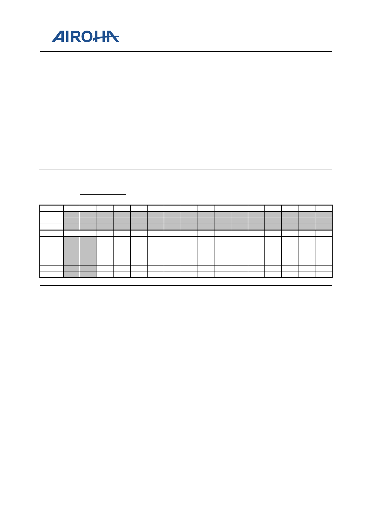
MT2523 Series Reference Manual
© 2015 - 2018 Airoha Technology Corp.
Page 92 of 692
This document contains information that is proprietary to Airoha Technology Corp. (“Airoha”) and/or its licensor(s).
Any unauthorized use, reproduction or disclosure of this document in whole or in part is strictly prohibited.
Bit(s)
Mnemonic
Name
Description
_EN
3
RD_DATA_
ERR_INT_
EN
RD_DATA_ERR_IN
T_EN
Defines RD data error IRQ enable
2
CPOL
CPOL
Control bit of the SCK polarity
0: CPOL = 0
1: CPOL = 1
1
CPHA
CPHA
Defines SPI Clock Format 0 or SPI Clock Format 1 during
transmission
0: CPHA = 0
1: CPHA = 1
0
SIZE_OF_AD
DR
SIZE_OF_ADDR
Defines CW/CR command format
0: Data filed includes 2 byte transfer address and 2 byte transfer length.
1: Data filed includes 4 byte transfer address & and byte transfer length.
A0150
010
SPISLV_STAT
US
SPISLV Status Register
0000000
0
Bit
31
30
29
28
27
26
25
24
23
22
21
20
19
18
17
16
Name
Type
Reset
Bit
15
14
13
12
11
10
9
8
7
6
5
4
3
2
1
0
Name SR_P
OWE
R_ON
SR_P
OWE
R_OF
F
SR_W
R_FI
NISH
SR_R
D_FI
NISH
SR_C
FG_
WRIT
E_FI
NISH
SR_C
FG_R
EAD_
FINIS
H
SR_C
MD_E
RROR
SR_TI
MOU
T_ER
R
SR_R
DWR
_FINI
SH
SR_W
R_ER
R
SR_R
D_ER
R
SR_T
XRX_
FIFO_
RDY
SR_C
FG_S
UCES
S
SLV_
ON
Type
RO
RO
RO
RO
RO
RO
RO
RO
RO
RO
RO
RO
RO
RW
Reset
0
0
0
0
0
0
0
0
0
0
0
0
0
0
Bit(s)
Mnemonic
Name
Description
13
SR_POWE
R_ON
SR_POWER_ON
Indicates whether SPI SLAVE receives power-on command
Cleared after SLV_ON = 0.
12
SR_POWE
R_OFF
SR_POWER_OFF
Indicates whether SPI SLAVE receives power-off command
Cleared after SLV_ON = 1.
11
SR_WR_FI
NISH
SR_WR_FINISH
Indicates whether SPI SLAVE write data is finished
Cleared after the next CFG read/write.
10
SR_RD_FI
NISH
SR_RD_FINISH
Indicates whether SPI SLAVE read data is finished
Cleared after the next CFG read/write.
9
SR_CFG_W
RITE_FINI
SH
SR_CFG_WRITE_F
INISH
Indicates whether SPI receive CFG READ CMD is finished
Cleared after sw_rx_dma_ready.
8
SR_CFG_R
EAD_FINIS
H
SR_CFG_READ_FI
NISH
Indicates whether SPI receive CFG READ CMD is finished
Cleared after sw_tx_dma_ready.
7
SR_CMD_E
RROR
SR_CMD_ERROR
Indicates whether SPI master sends an error command
Used for SPI master to debug; cleared after SPI master sends a correct
command.
6
SR_TIMOU
T_ERR
SR_TIMOUT_ERR
Indicates time-out and SPI slave does not receive or send
data for some time
If there is error, master must send WS command to clear this bit and
poll this bit until this bit turns to 0.
5
SR_RDWR
SR_RDWR_FINISH
Indicates whether SPI master RD/WR is finished
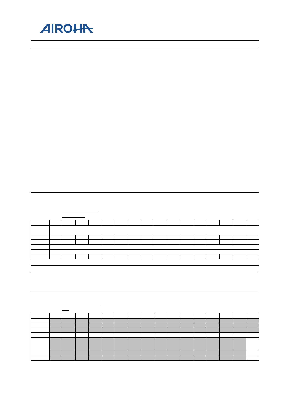
MT2523 Series Reference Manual
© 2015 - 2018 Airoha Technology Corp.
Page 93 of 692
This document contains information that is proprietary to Airoha Technology Corp. (“Airoha”) and/or its licensor(s).
Any unauthorized use, reproduction or disclosure of this document in whole or in part is strictly prohibited.
Bit(s)
Mnemonic
Name
Description
_FINISH
After the master receives/sends all data, it can poll this bit to know if
the read/write transfer is finished.
Cleared after SPI slave receives CR/CW command.
4
SR_WR_E
RR
SR_WR_ERR
Indicates SPI master WR error
After a RD command, master can read this bit to know if there is error
in the write transfer through RS.
If there is error, master must send WS command to clear this bit and
poll this bit until this bit turns to 0
3
SR_RD_ER
R
SR_RD_ERR
Indicates SPI master RD error
After a RD command, master can read this bit to know if there is error
in the read transfer through RS.
If there is error, master must send WS command to clear this bit and
poll this bit until this bit turns to 0.
2
SR_TXRX_
FIFO_RDY
SR_TXRX_FIFO_R
DY
Indicates TX/RX FIFO ready
When CR, this bit used to indicate whether TX FIFO is ready. Master
polls this bit to know if the slave is ready to send data, then master can
send RD command.
When CW, this bit used to indicate whether RX FIFO is ready. Master
polls this bit to know if the slave is ready to send data, then master can
send WD command.
This bit will be cleared after SPI slave receives CR/CW command.
1
SR_CFG_S
UCESS
SR_CFG_SUCESS
Indicates whether SPI master is configured successfully.
Master checks this bit to know if CW/CR command is successful.
0
SLV_ON
SLV_ON
Defines SPI slave on
Master polls this bit until the slave is on.
A0150
014
SPISLV_TIMO
UT_THR
SPISLV Timeout Threshold Register
000000F
F
Bit
31
30
29
28
27
26
25
24
23
22
21
20
19
18
17
16
Name
SPI_TIMOUT_THR[31:16]
Type
RW
Reset
0
0
0
0
0
0
0
0
0
0
0
0
0
0
0
0
Bit
15
14
13
12
11
10
9
8
7
6
5
4
3
2
1
0
Name
SPI_TIMOUT_THR[15:0]
Type
RW
Reset
0
0
0
0
0
0
0
0
1
1
1
1
1
1
1
1
Bit(s)
Mnemonic
Name
Description
31:0
SPI_TIMO
UT_THR
TIMOUT_THR
Timeout threshold time
If the time that SPI slave does not receive or send data is exceeded,
there will be a timeout IRQ.
A0150
018
SPISLV_SW_R
ST
SPISLV SW Reset Register
0000000
0
Bit
31
30
29
28
27
26
25
24
23
22
21
20
19
18
17
16
Name
Type
Reset
Bit
15
14
13
12
11
10
9
8
7
6
5
4
3
2
1
0
Name
SPI_S
W_R
ST
Type
RW
Reset
0
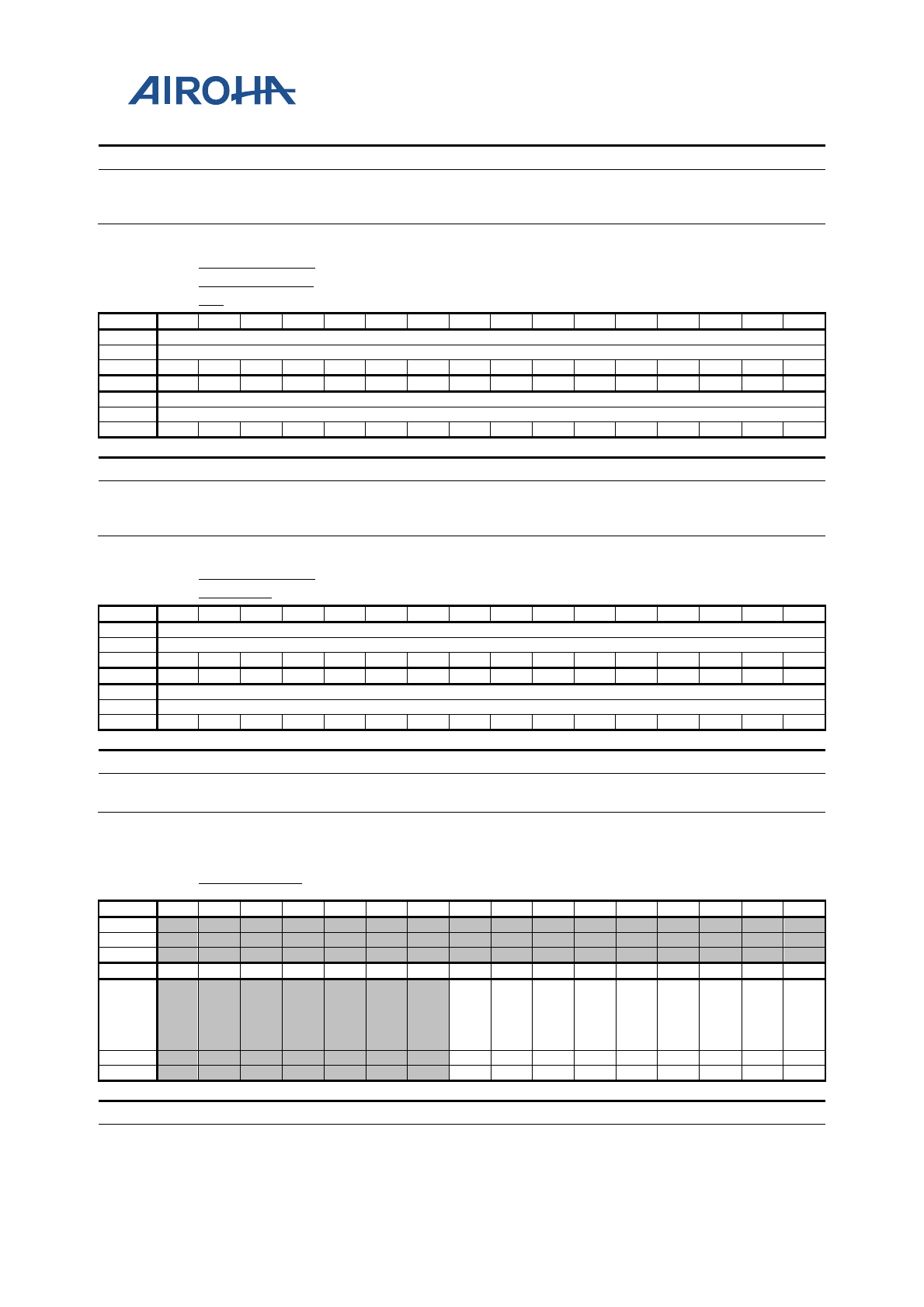
MT2523 Series Reference Manual
© 2015 - 2018 Airoha Technology Corp.
Page 94 of 692
This document contains information that is proprietary to Airoha Technology Corp. (“Airoha”) and/or its licensor(s).
Any unauthorized use, reproduction or disclosure of this document in whole or in part is strictly prohibited.
Bit(s)
Mnemonic
Name
Description
0
SPI_SW_R
ST
SW_RST
Software reset bit; resets the state machine and data FIFO of
SPI controller. When this bit is 1, software reset is active
high. The default value is 0.
A0150
01C
SPISLV_BUFF
ER_BASE_AD
DR
SPISLV Buffer Base Address Register
0000000
0
Bit
31
30
29
28
27
26
25
24
23
22
21
20
19
18
17
16
Name
SPI_BUFFER_BASE_ADDR[31:16]
Type
RW
Reset
0
0
0
0
0
0
0
0
0
0
0
0
0
0
0
0
Bit
15
14
13
12
11
10
9
8
7
6
5
4
3
2
1
0
Name
SPI_BUFFER_BASE_ADDR[15:0]
Type
RW
Reset
0
0
0
0
0
0
0
0
0
0
0
0
0
0
0
0
Bit(s)
Mnemonic
Name
Description
31:0
SPI_BUFFE
R_BASE_A
DDR
BUFFER_BASE_AD
DR
Configurable DMA address to access memory
A0150
020
SPISLV_BUFF
ER_SIZE
SPISLV Buffer Size Register
0000000
0
Bit
31
30
29
28
27
26
25
24
23
22
21
20
19
18
17
16
Name
SPI_BUFFER_SIZE[31:16]
Type
RW
Reset
0
0
0
0
0
0
0
0
0
0
0
0
0
0
0
0
Bit
15
14
13
12
11
10
9
8
7
6
5
4
3
2
1
0
Name
SPI_BUFFER_SIZE[15:0]
Type
RW
Reset
0
0
0
0
0
0
0
0
0
0
0
0
0
0
0
0
Bit(s)
Mnemonic
Name
Description
31:0
SPI_BUFFE
R_SIZE
BUFFER_SIZE
Configurable BUFFER size indicating whether SPI master is configured
successfully
A0150
024
SPISLV_IRQ
SPISLV IRQ Register
0000000
0
Bit
31
30
29
28
27
26
25
24
23
22
21
20
19
18
17
16
Name
Type
Reset
Bit
15
14
13
12
11
10
9
8
7
6
5
4
3
2
1
0
Name
SR_TI
MOU
T_ER
R_IR
Q
SR_W
R_ER
R_IR
Q
SR_R
D_ER
R_IR
Q
SR_P
WRO
N_IR
Q
SR_P
WRO
FF_IR
Q
SR_W
R_FI
NISH
_IRQ
SR_R
D_FI
NISH
_IRQ
SR_C
WR_
FINIS
H_IR
Q
SR_C
RD_F
INIS
H_IR
Q
Type
RC
RC
RC
RO
RC
RC
RC
RC
RC
Reset
0
0
0
0
0
0
0
0
0
Bit(s)
Mnemonic
Name Description
8
SR_TIMOU
T_ERR_IR
SR_TIMOUT_ER
R_IRQ Indicates timeout IRQ
Read clear
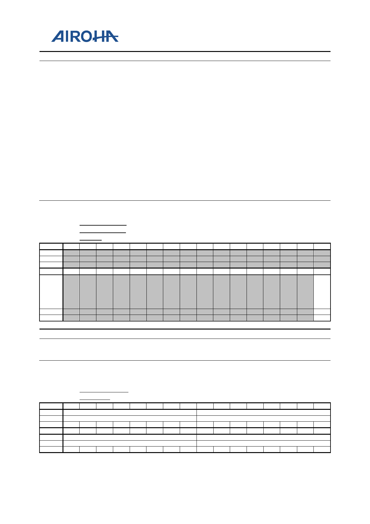
MT2523 Series Reference Manual
© 2015 - 2018 Airoha Technology Corp.
Page 95 of 692
This document contains information that is proprietary to Airoha Technology Corp. (“Airoha”) and/or its licensor(s).
Any unauthorized use, reproduction or disclosure of this document in whole or in part is strictly prohibited.
Bit(s)
Mnemonic
Name Description
Q
7
SR_WR_E
RR_IRQ
SR_WR_ERR_IR
Q Indicates SPI master WR error IRQ
Read clear
6
SR_RD_ER
R_IRQ
SR_RD_ERR_IR
Q Indicates SPI master RD error IRQ
Read clear
5
SR_PWRO
N_IRQ
SR_PWRON_IRQ Indicates slave receiving power-on IRQ
Cleared by SLV_ON = 1
4
SR_PWRO
FF_IRQ
SR_PWROFF_IR
Q Indicates receiving power-off CMD IRQ
Read clear
3
SR_WR_FI
NISH_IRQ
SR_WR_FINISH
_IRQ Indicates SPI master WR is finished
Read clear
2
SR_RD_FI
NISH_IRQ
SR_RD_FINISH_
IRQ Indicates SPI master RD finished IRQ
Read clear
1
SR_CWR_F
INISH_IRQ
SR_CWR_FINIS
H_IRQ Indicates SPI master configure write transfer finished IRQ
Read clear
0
SR_CRD_F
INISH_IRQ
SR_CRD_FINISH
_IRQ Indicates SPI master configure read transfer finished IRQ
Read clear
A0150
028
SPISLV_MISO
_EARLY_HAL
F_SCK
SPISLV MISO EARLY HALF SCK Register
0000000
0
Bit
31
30
29
28
27
26
25
24
23
22
21
20
19
18
17
16
Name
Type
Reset
Bit
15
14
13
12
11
10
9
8
7
6
5
4
3
2
1
0
Name
SPI_
MISO
_EAR
LY_H
ALF_
SCK
Type
RW
Reset
0
Bit(s)
Mnemonic
Name Description
0
SPI_MISO_
EARLY_HA
LF_SCK
MISO_EARLY_HA
LF_SCK Defines whether to send miso early harf sck cycle
Used for improving SPI timing
A0150
02C
SPISLV_CMD_
DEFINE0
SPISLV Command0 Define
080A0681
Bit
31
30
29
28
27
26
25
24
23
22
21
20
19
18
17
16
Name
CMD_WS
CMD_RS
Type
RW
RW
Reset
0
0
0
0
1
0
0
0
0
0
0
0
1
0
1
0
Bit
15
14
13
12
11
10
9
8
7
6
5
4
3
2
1
0
Name
CMD_WR
CMD_RD
Type
RW
RW
Reset
0
0
0
0
0
1
1
0
1
0
0
0
0
0
0
1
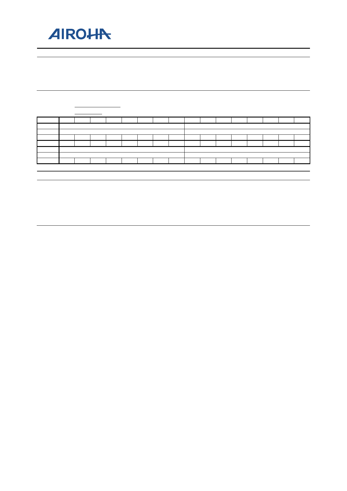
MT2523 Series Reference Manual
© 2015 - 2018 Airoha Technology Corp.
Page 96 of 692
This document contains information that is proprietary to Airoha Technology Corp. (“Airoha”) and/or its licensor(s).
Any unauthorized use, reproduction or disclosure of this document in whole or in part is strictly prohibited.
Bit(s)
Mnemonic
Name
Description
31:24
CMD_WS
CMD_WS
Defines Write Status (WR) command value
23:16
CMD_RS
CMD_RS
Defines Read Status (RS) command value
15:8
CMD_WR
CMD_WR
Defines Write Data (WR) command value
7:0
CMD_RD
CMD_RD
Defines Read Data (RD) command value
A0150
030
SPISLV_CMD_
DEFINE1
SPISLV Command1 Define
0C0E040
2
Bit
31
30
29
28
27
26
25
24
23
22
21
20
19
18
17
16
Name
CMD_POWEROFF
CMD_POWERON
Type
RW
RW
Reset
0
0
0
0
1
1
0
0
0
0
0
0
1
1
1
0
Bit
15
14
13
12
11
10
9
8
7
6
5
4
3
2
1
0
Name
CMD_CW
CMD_CR
Type
RW
RW
Reset
0
0
0
0
0
1
0
0
0
0
0
0
0
0
1
0
Bit(s)
Mnemonic
Name
Description
31:24
CMD_POW
EROFF
CMD_POWEROFF
Defines power-off command value
23:16
CMD_POW
ERON
CMD_POWERON
Defines power-on command value
15:8
CMD_CW
CMD_CW
Defines Configure Write (CW) command value
7:0
CMD_CR
CMD_CR
Defines Configure Read (CR) command value

MT2523 Series Reference Manual
© 2015 - 2018 Airoha Technology Corp.
Page 97 of 692
This document contains information that is proprietary to Airoha Technology Corp. (“Airoha”) and/or its licensor(s).
Any unauthorized use, reproduction or disclosure of this document in whole or in part is strictly prohibited.
9. Inter-Integrated Circuit Controller
9.1. General Description
Inter-Integrated Circuit (I2C) is a two-wire serial interface. The two signals are SCL and SDA. SCL is a clock signal
driven by the master. SDA is a bi-directional data signal that can be driven by either the master or the slave. This
generic controller supports the master role and conforms to the I2C specification.
9.1.1. Feature
• I2C compliant master mode operation
• Adjustable clock speed for LS/FS mode operation
• Supports 7-bit/10-bit addressing
• Supports high-speed mode
• Supports slave clock extension
• Supports DMA mode
• START/STOP/REPEATED START condition
• Manual/DMA transfer mode
• Multi-write per transfer (up to 15 data bytes)
• Multi-read per transfer (up to 15 data bytes)
• Multi-transfer per transaction
• Combined format transfer with length change capability
• Active drive/wired-and I/O configuration
9.1.2. Manual/DMA Transfer Mode
The controller offers two types of transfer mode, manual and DMA.
When manual mode is selected, in addition to the slave address register, the controller has a built-in 8-byte deep
FIFO which allows MCU to prepare up to eight bytes of data for a write transfer, or read up to eight bytes of data
for a read transfer.
When DMA mode is enabled, the data to and from the FIFO is controlled via DMA transfer and therefore supports
up to 15 bytes of consecutive read or write, with the data read from or write to another memory space. When
DMA mode is enabled, the flow control mechanism is also implemented to hold the bus clk when FIFO underflow
or overflow condition is encountered.
MT2523 Series Reference Manual
© 2015 - 2018 Airoha Technology Corp.
Page 98 of 692
This document contains information that is proprietary to Airoha Technology Corp. (“Airoha”) and/or its licensor(s).
Any unauthorized use, reproduction or disclosure of this document in whole or in part is strictly prohibited.
9.1.3. Transfer Format Support
This controller is designed to be as generic as possible to support a wide range of devices that may utilize different
combinations of transfer formats. Here are the transfer format types that can be supported through different
software configurations.
Wording convention note
• Transfer = Anything encapsulated within a Start and Stop or Repeated Start.
• Transfer length = Number of bytes within the transfer
• Transaction = This is the top unit. Everything combined equals one transaction.
• Transaction length = Number of transfers to be conducted.
Master to slave dir
Slave to master dir
Single-byte access
Slave Address AS DATA A P
Slave Address AS DATA nA P
Single Byte Write
Single Byte Read
Multi-byte access
Slave Address A
SDATA AP
N bytes + ack
Slave Address A
SDATA A/
nA P
N bytes + ack/nak
Multi Byte Write
Multi Byte Read
MT2523 Series Reference Manual
© 2015 - 2018 Airoha Technology Corp.
Page 99 of 692
This document contains information that is proprietary to Airoha Technology Corp. (“Airoha”) and/or its licensor(s).
Any unauthorized use, reproduction or disclosure of this document in whole or in part is strictly prohibited.
Multi-byte transfer + multi-transfer (same direction)
Slave
Address ADATA A
SP
Slave
Address ADATA A/
nA
SP
N bytes + ack/nak
N bytes + ack/nak
Multi Byte Write + Multi Transfer
Multi Byte Read + Multi Transfer
X transfers
+ wait time +
X transfers
+ wait time +
Multi-byte transfer + multi-transfer w RS (same direction)
Slave
Address ADATA AS R
Slave
Address ADATA A/
nA
S R
N bytes + ack/nak
N bytes + ack/nak
Multi Byte Write + Multi Transfer + Repeated Start
Multi Byte Read + Multi Transfer + Repeated Start
X transfers
X transfers
++
P
P
+
Combined write/read with Repeated Start (direction change)
Note:
1. Only supports write and then read sequence. Read and then write is not supported.
2. In this format, transaction is 2
Slave
Address AS DATA A R
N bytes + ack/nak
Slave
Address ADATA A P
M bytes + ack/nak
Combined Multi Byte Write + Multi Byte Read
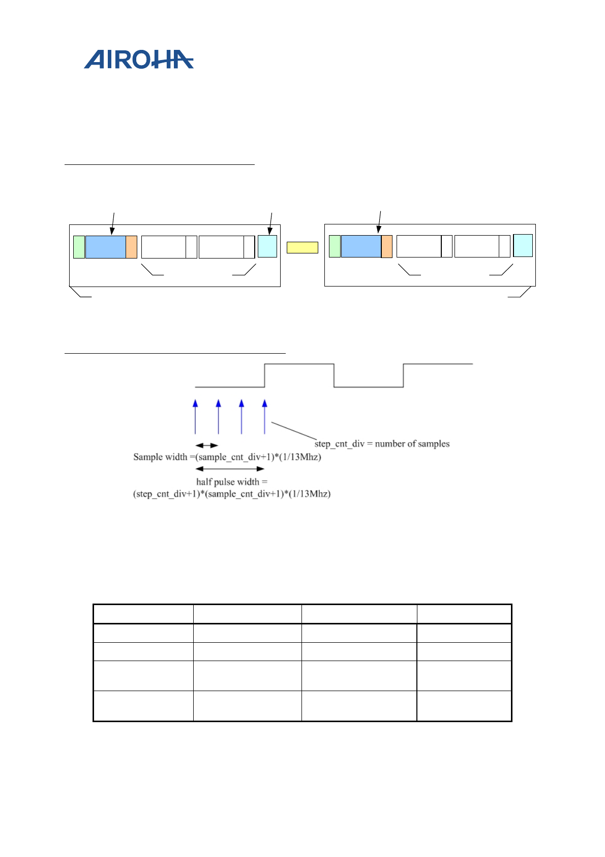
MT2523 Series Reference Manual
© 2015 - 2018 Airoha Technology Corp.
Page 100 of 692
This document contains information that is proprietary to Airoha Technology Corp. (“Airoha”) and/or its licensor(s).
Any unauthorized use, reproduction or disclosure of this document in whole or in part is strictly prohibited.
9.1.4. Programming Guide
Common transfer programmable parameters
Slave
Address ADATA A
SP/
RS
transfer_len
Programmable Parameters
transac_len
DATA A
rs_stop
slave_addr
Slave
Address ADATA A
SP/
RS
DATA A
delay_len
transfer_len / aux transfer_len
slave_addr + dir change
Output waveform timing programmable parameters
9.2. Register Definition
There are four I2C channels in this SOC.
I2C number Base address Feature Source clock
I2C0 0xA0210000 Supports DMA mode Fix 26M
I2C1 0xA0220000 Supports DMA mode Fix 26M
I2C2 0xA01B0000 Does not support DMA
mode Bus clock
I2C_d2d 0xA2150000 Does not support DMA
mode Bus clock
MT2523 Series Reference Manual
© 2015 - 2018 Airoha Technology Corp.
Page 101 of 692
This document contains information that is proprietary to Airoha Technology Corp. (“Airoha”) and/or its licensor(s).
Any unauthorized use, reproduction or disclosure of this document in whole or in part is strictly prohibited.
Module name: I2C_SCCB_Controller base address: (+A0210000)
Address
Name
Width
Register function
A0210000
DATA_PORT
16
Data port register
A0210004
SLAVE_ADDR
16 Slave address register
A0210008 INTR_MASK 16
Interrupt mask register
This register provides masks for the corresponding
interrupt sources as indicated in the intr_stat
register.
1 = Allow interrupt
0 = Disable interrupt
Note: When disabled, the corresponding interrupt
will not be asserted; however intr_stat will still be
updated with the status, i.e. mask does not affect
intr_stat register values.
A021000C INTR_STAT 16
Interrupt status register
When an interrupt is issued by the I2C controller, this
register will need to be read by MCU to determine the
cause for the interrupt. After this status is read and
appropriate actions are taken, the corresponding
interrupt source will need to be written 1 to clear.
A0210010
CONTROL
16 Control register
A0210014 TRANSFER_LEN 16
Transfer length register (number of bytes per
transfer)
A0210018 TRANSAC_LEN 16 Transaction length register (number of transfers per
transaction)
A021001C
DELAY_LEN
16
Inter delay length register
A0210020 TIMING 16
Timing control register
LS/FS only. This register is used to control the output
waveform timing. Each half pulse width, i.e. each high
or low pulse, is equal to
(step_cnt_div+1)*(sample_cnt_div + 1)/13MHz
A0210024 START 16 Start register
A021002C
CLOCK_DIV
16
Clock divergence of I2C source clock
A0210030 FIFO_STAT 16 FIFO status register
A0210038
FIFO_ADDR_CLR
16 FIFO address clear register
A0210040 IO_CONFIG 16
IO config register
This register is used to configure the I/O for the SDA
and SCL lines to select between normal I/O mode, or
open-drain mode to support wired-and bus.
A0210048 HS 16
High speed mode register
This register contains options for supporting high
speed operation features.
Each HS half pulse width, i.e. each high or low pulse,
is equal to (step_cnt_div+1)*(sample_cnt_div +
1)/13MHz
A0210050
SOFTRESET
16
Soft reset register
A0210060
SPARE
16 SPARE
A0210064
DEBUGSTAT
16
Debug status register
A0210068
DEBUGCTRL
16 Debug control register
A021006C
TRANSFER_LEN_
16
Transfer length register (number of bytes per
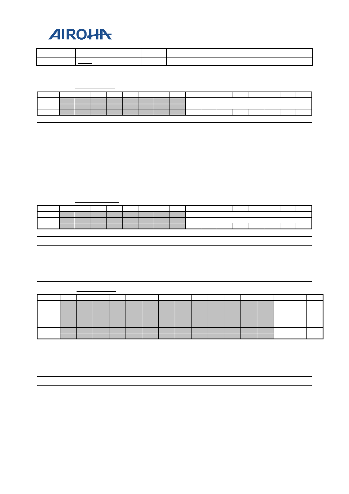
MT2523 Series Reference Manual
© 2015 - 2018 Airoha Technology Corp.
Page 102 of 692
This document contains information that is proprietary to Airoha Technology Corp. (“Airoha”) and/or its licensor(s).
Any unauthorized use, reproduction or disclosure of this document in whole or in part is strictly prohibited.
Address
Name
Width
Register function
AUX
transfer)
A0
210000
DATA_PORT
Data Port Register
0000
Bit
15
14
13
12
11
10
9
8
7
6
5
4
3
2
1
0
Name
DATA_PORT
Type
RW
Reset
0
0
0
0
0
0
0
0
Bit(s)
Mnemonic
Name
Description
7:0
DATA_POR
T
DATA_PORT
FIFO access port
During master write sequences (slave_addr[0] = 0), this port can be
written by APB, and during master read sequences (slave_addr[0] = 1),
this port can be read by APB.
Note: Slave_addr must be set correctly before accessing FIFO.
For debugging only: If the fifo_apb_debug bit is set, FIFO can be read
and written by the APB.
A0
210004
SLAVE_ADDR
Slave Address Register
00BF
Bit
15
14
13
12
11
10
9
8
7
6
5
4
3
2
1
0
Name
SLAVE_ADDR
Type
RW
Reset
1
0
1
1
1
1
1
1
Bit(s)
Mnemonic
Name
Description
7:0
SLAVE_AD
DR
SLAVE_ADDR
Specifies the slave address of the device to be accessed
Bit 0 is defined by the I2C protocol as a bit that indicates the direction
of transfer.
0: Master write
1: Master read
A0210008
INTR_MASK
Interrupt Mask Register
0007
Bit
15
14
13
12
11
10
9
8
7
6
5
4
3
2
1
0
Name
MASK
_HS_
NACK
ER
MASK
_ACK
ERR
MASK
_TRA
NSAC
_COM
P
Type
RW
RW
RW
Reset
1
1
1
Overview
This register provides masks for the corresponding interrupt sources as indicated in intr_stat
register. (1 = allow interrupt 0 = disable interrupt) Note that when disabled, the corresponding
interrupt will not be asserted; however the intr_stat will still be updated with the status, i.e. mask
does not affect intr_stat register values.
Bit(s)
Mnemonic
Name
Description
2
MASK_HS_
NACKER
MASK_HS_NACKE
R
Setting this value to 0 will mask HS_NACKERR interrupt
signal.
1
MASK_AC
KERR
MASK_ACKERR
Setting this value to 0 will mask ACK_ERR interrupt signal.
0
MASK_TRA
NSAC_COM
P
MASK_TRANSAC_
COMP
Setting this value to 0 will mask TRANSAC_COMP interrupt
signal.
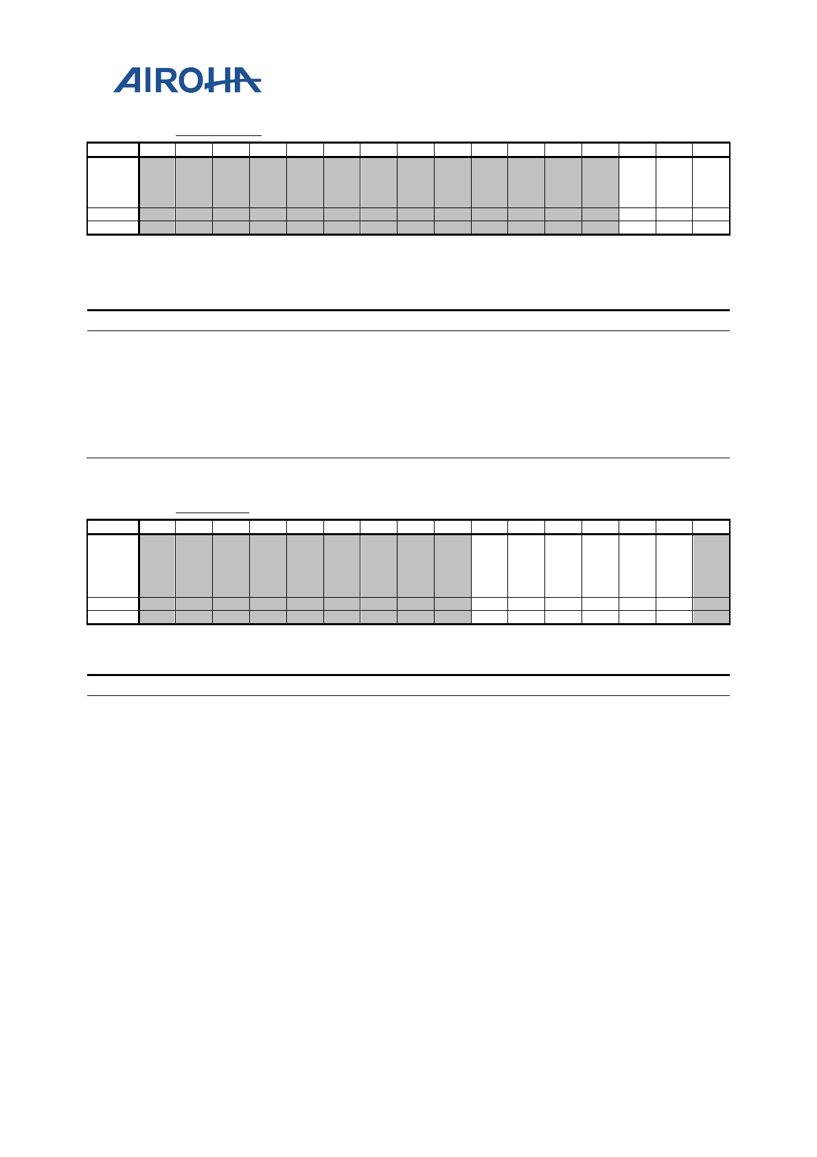
MT2523 Series Reference Manual
© 2015 - 2018 Airoha Technology Corp.
Page 103 of 692
This document contains information that is proprietary to Airoha Technology Corp. (“Airoha”) and/or its licensor(s).
Any unauthorized use, reproduction or disclosure of this document in whole or in part is strictly prohibited.
A021000C
INTR_STAT
Interrupt Status Register
0000
Bit
15
14
13
12
11
10
9
8
7
6
5
4
3
2
1
0
Name
HS_N
ACKE
RR
ACKE
RR
TRAN
SAC_
COM
P
Type
W1C
W1C
W1C
Reset
0
0
0
Overview
When an interrupt is issued by i2c controller, this register will need to be read by mcu to determine
the cause for the interrupt. After this status has been read and appropriate actions are taken, the
corresponding interrupt source will need to be write 1 cleared.
Bit(s)
Mnemonic
Name
Description
2
HS_NACKE
RR
HS_NACKERR
This status will be asserted if HS master code nack error
detection is enabled. If enabled, HS
master code nack err will
cause transaction to end and stop will be issued.
1
ACKERR
ACKERR
This status will be asserted if ACK error detection is enabled.
If enabled, ackerr will cause transaction to end and stop will
be issued.
0
TRANSAC_
COMP
TRANSAC_COMP
This status will be
asserted when a transaction has completed
successfully.
A0
210010
CONTROL
Control Register
0000
Bit
15
14
13
12
11
10
9
8
7
6
5
4
3
2
1
0
Name
TRAN
SFER
_LEN
_CHA
NGE
ACKE
RR_D
ET_E
N
DIR_
CHAN
GE
CLK_
EXT_
EN
DMA
_EN RS_S
TOP
Type
RW
RW
RW
RW
RW
RW
Reset
0
0
0
0
0
0
Overview
Bit(s)
Mnemonic
Name
Description
6
TRANSFER
_LEN_CHA
NGE
TRANSFER_LEN_C
HANGE
This options specifies whether or not to change the transfer
length after the fist transfer completes. If enabled, the
transfers after the first transfer will
use the transfer_len_aux
parameter.
5
ACKERR_D
ET_EN
ACKERR_DET_EN
This option enables slave ack error detection. When enabled,
if slave ack error is detected, the master will terminate the
transaction by issuing a STOP condition then assert ackerr
interrupt. MCU should handle this case appropriately then
reset the FIFO address before reissuing transaction. If this
option is disabled, the controller will ignore slave ack error
and keep on scheduled transaction.
0: Disable
1: Enable
4
DIR_CHAN
GE
DIR_CHANGE
This option is used for combined transfer format, where the
direction of transfer is to be changed from write to read after
the FIRST RS condition.
Note: When set to 1, the transfers after the direction change
will be based on the transfer_len_aux parameter.
0: Disable
1: Enable
3
CLK_EXT_
EN
CLK_EXT_EN
I2C spec allows slaves to hold the SCL line low if it is not yet
ready for further processing. Therefore, if this bit is set to 1,
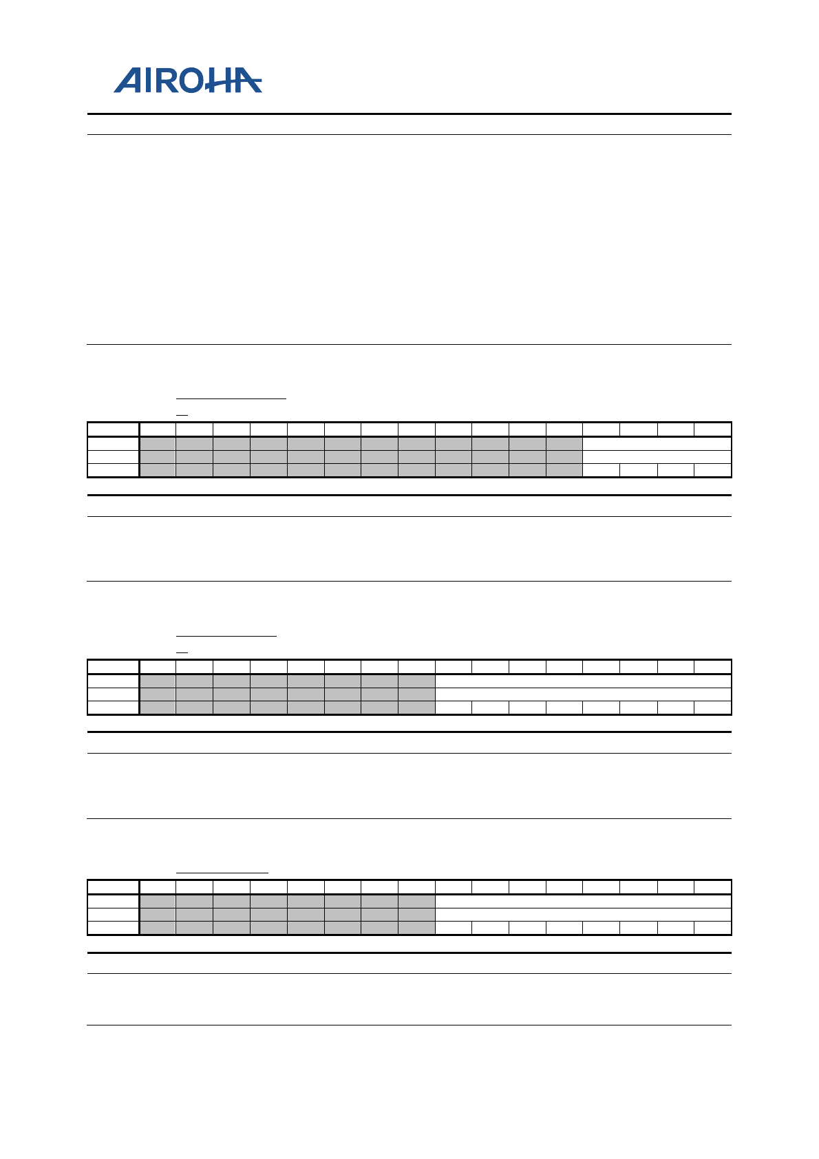
MT2523 Series Reference Manual
© 2015 - 2018 Airoha Technology Corp.
Page 104 of 692
This document contains information that is proprietary to Airoha Technology Corp. (“Airoha”) and/or its licensor(s).
Any unauthorized use, reproduction or disclosure of this document in whole or in part is strictly prohibited.
Bit(s)
Mnemonic
Name
Description
master controller will enter a high wait state until the slave
releases the SCL line.
2
DMA_EN
DMA_EN
By default, this is disabled, and FIFO data should
be manually
prepared by MCU. This default setting should be used for
transfer sizes of less than 8 data bytes and no multiple
transfer is configured. When enabled, DMA requests will be
turned on, and the FIFO data should be prepared in memory.
1
RS_STOP
RS_STOP
In LS/FS mode, this bit affects multi-transfer transaction
only. It controls whether or not REPEATED-
START condition
is used between transfers. The last ending transfer always
ends with a STOP.
In HS mode, this bit must be set to 1.
0: Use STOP
1: Use REPEATED-START
A0
210014
TRANSFER_LE
N
Transfer Length Register (Number of Bytes
per
Transfer)
0001
Bit
15
14
13
12
11
10
9
8
7
6
5
4
3
2
1
0
Name
TRANSFER_LEN
Type
RW
Reset
0
0
0
1
Bit(s)
Mnemonic
Name
Description
3:0
TRANSFER
_LEN
TRANSFER_LEN
Indicates the number of data bytes to be transferred in 1
transfer unit (excluding slave address byte)
Note: The value must be set to be bigger than 1; otherwise no transfer
will take place.
A0
210018
TRANSAC_LE
N
Transaction Length Register (Number of Transfers
per
Transaction)
0001
Bit
15
14
13
12
11
10
9
8
7
6
5
4
3
2
1
0
Name
TRANSAC_LEN
Type
RW
Reset
0
0
0
0
0
0
0
1
Bit(s)
Mnemonic
Name
Description
7:0
TRANSAC_
LEN
TRANSAC_LEN
Indicates the number of transfers to be transferred in 1
transaction
Note: The value must be set to be bigger than 1; otherwise no transfer
will take place.
A0
21001C
DELAY_LEN
Inter Delay Length
Register
0002
Bit
15
14
13
12
11
10
9
8
7
6
5
4
3
2
1
0
Name
DELAY_LEN
Type
RW
Reset
0
0
0
0
0
0
1
0
Bit(s)
Mnemonic
Name
Description
7:0
DELAY_LE
N
DELAY_LEN
Sets up wait delay between consecutive transfers when
RS_STOP bit is set to 0
Unit: Half the pulse width
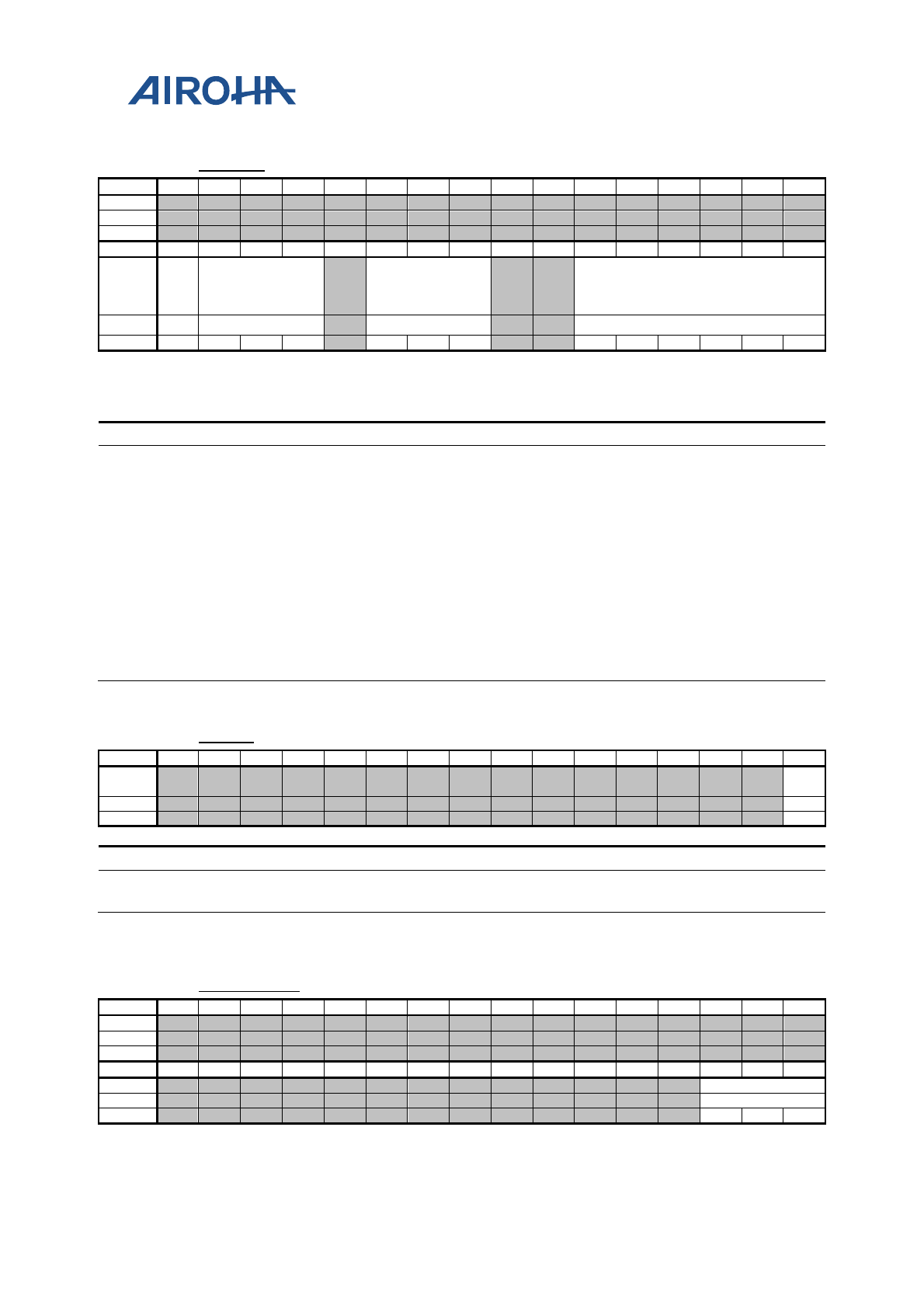
MT2523 Series Reference Manual
© 2015 - 2018 Airoha Technology Corp.
Page 105 of 692
This document contains information that is proprietary to Airoha Technology Corp. (“Airoha”) and/or its licensor(s).
Any unauthorized use, reproduction or disclosure of this document in whole or in part is strictly prohibited.
A0210020
TIMING
Timing Control Register
00001303
Bit
31
30
29
28
27
26
25
24
23
22
21
20
19
18
17
16
Name
Type
Reset
Bit
15
14
13
12
11
10
9
8
7
6
5
4
3
2
1
0
Name
DATA
_REA
D_AD
J
DATA_READ_TIM
E
SAMPLE_CNT_DI
V
STEP_CNT_DIV
Type
RW RW
RW
RW
Reset
0
0
0
1
0
1
1
0
0
0
0
1
1
Overview
LS/FS only. This register is used to control the output waveform timing. Each half pulse width (ie.
each high or low pulse) is equal to = step_cnt_div * (sample_cnt_div * f_clock_div Mhz)
Bit(s)
Mnemonic
Name
Description
15
DATA_REA
D_ADJ
DATA_READ_ADJ
When set to 1, data latch in sampling time during master
reads are adjusted according to DATA_READ_TIME value.
Otherwise, by default, data is latched in at half of the high
pulse width point. This value must be set to less than
or equal
to half the high pulse width.
14:12
DATA_REA
D_TIME
DATA_READ_TIME
This value is valid only when DATA_READ_ADJ is set to 1.
This can be used to adjust so that data is latched in at earlier
sampling points (assuming data is settled by then)
10:8
SAMPLE_C
NT_DIV
SAMPLE_CNT_DIV
Used for LS/FS only. This adjusts the width of each sample.
(sample width = sample_cnt_div*f_clock_div Mhz)
5:0
STEP_CNT
_DIV
STEP_CNT_DIV
Specifies the number of samples per half pulse width (i.e.
each high or low pulse)
Cannot be 0 .
A0
210024
START
Start Register
0000
Bit
15
14
13
12
11
10
9
8
7
6
5
4
3
2
1
0
Name
STAR
T
Type
RW
Reset
0
Bit(s)
Mnemonic
Name
Description
0
START
START
Starts the transaction on the bus
It is auto de-asserted at the end of the transaction.
A021002C
CLOCK_DIV
Clock divergence of I2C source clock
0004
Bit
31
30
29
28
27
26
25
24
23
22
21
20
19
18
17
16
Name
Type
Reset
Bit
15
14
13
12
11
10
9
8
7
6
5
4
3
2
1
0
Name
CLOCK_DIV
Type
RW
Reset
1
0
0
Overview
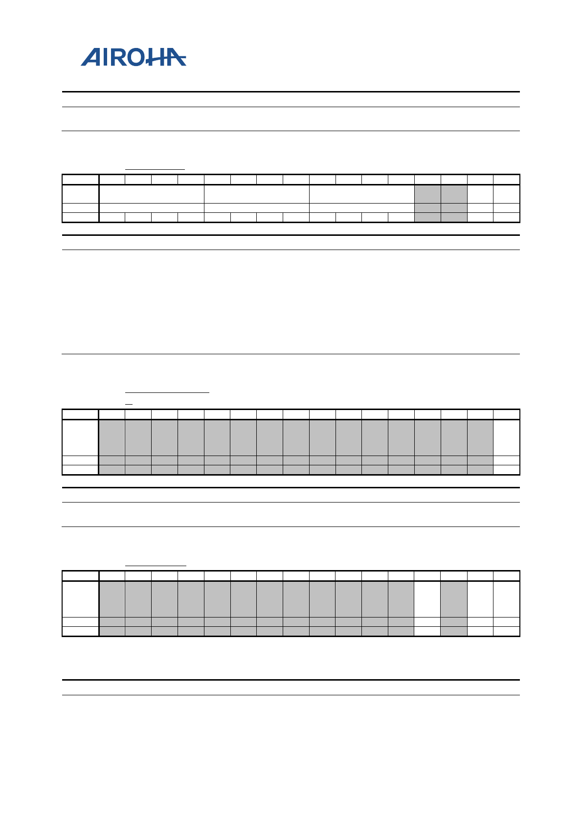
MT2523 Series Reference Manual
© 2015 - 2018 Airoha Technology Corp.
Page 106 of 692
This document contains information that is proprietary to Airoha Technology Corp. (“Airoha”) and/or its licensor(s).
Any unauthorized use, reproduction or disclosure of this document in whole or in part is strictly prohibited.
Bit(s)
Mnemonic
Name
Description
2:0
CLOCK_DI
V
CLOCK_DIV
f_clock_div = source clock/(CLOCK_DIV + 1)
A0
210030
FIFO_STAT
FIFO Status Register
0001
Bit
15
14
13
12
11
10
9
8
7
6
5
4
3
2
1
0
Name RD_ADDR WR_ADDR FIFO_OFFSET
WR_
FULL
RD_E
MPTY
Type
RO
RU
RU
RO
RO
Reset
0
0
0
0
0
0
0
0
0
0
0
0
0
1
Bit(s)
Mnemonic
Name
Description
15:12
RD_ADDR
RD_ADDR
Current RD address pointer
Only bit [2:0] have physical meanings.
11:8
WR_ADDR
WR_ADDR
Current WR address pointer
Only bit [2:0] have physical meanings.
7:4
FIFO_OFFS
ET
FIFO_OFFSET
wr_addr[3:0] - rd_addr[3:0]
1
WR_FULL
WR_FULL
Indicates FIFO is full
0
RD_EMPTY
RD_EMPTY
Indicates FIFO is empty
A0
210038
FIFO_ADDR_CL
R
FIFO Address Clear Register
0000
Bit
15
14
13
12
11
10
9
8
7
6
5
4
3
2
1
0
Name
FIFO
_ADD
R_CL
R
Type
WO
Reset
0
Bit(s)
Mnemonic
Name
Description
0
FIFO_ADD
R_CLR
FIFO_ADDR_CLR
When written 1'b1, a one pulse fifo_addr_clr will be generated to clear
the FIFO address to 0.
A0
210040
IO_CONFIG
IO Config Register
0000
Bit
15
14
13
12
11
10
9
8
7
6
5
4
3
2
1
0
Name IDLE
_OE_
EN
SDA_
IO_C
ONFI
G
SCL_I
O_CO
NFIG
Type
RW
RW
RW
Reset
0
0
0
Overview: This register is used to configure the I/O for the SDA and SCL lines to select between normal I/O mode or
open-drain mode to support wired-and bus.
Bit(s)
Mnemonic
Name
Description
3
IDLE_OE_
EN
IDLE_OE_EN
0: Does not drive bus in idle state
1: Drive bus in idle state
1
SDA_IO_C
SDA_IO_CONFIG
0: Normal tristate I/O mode
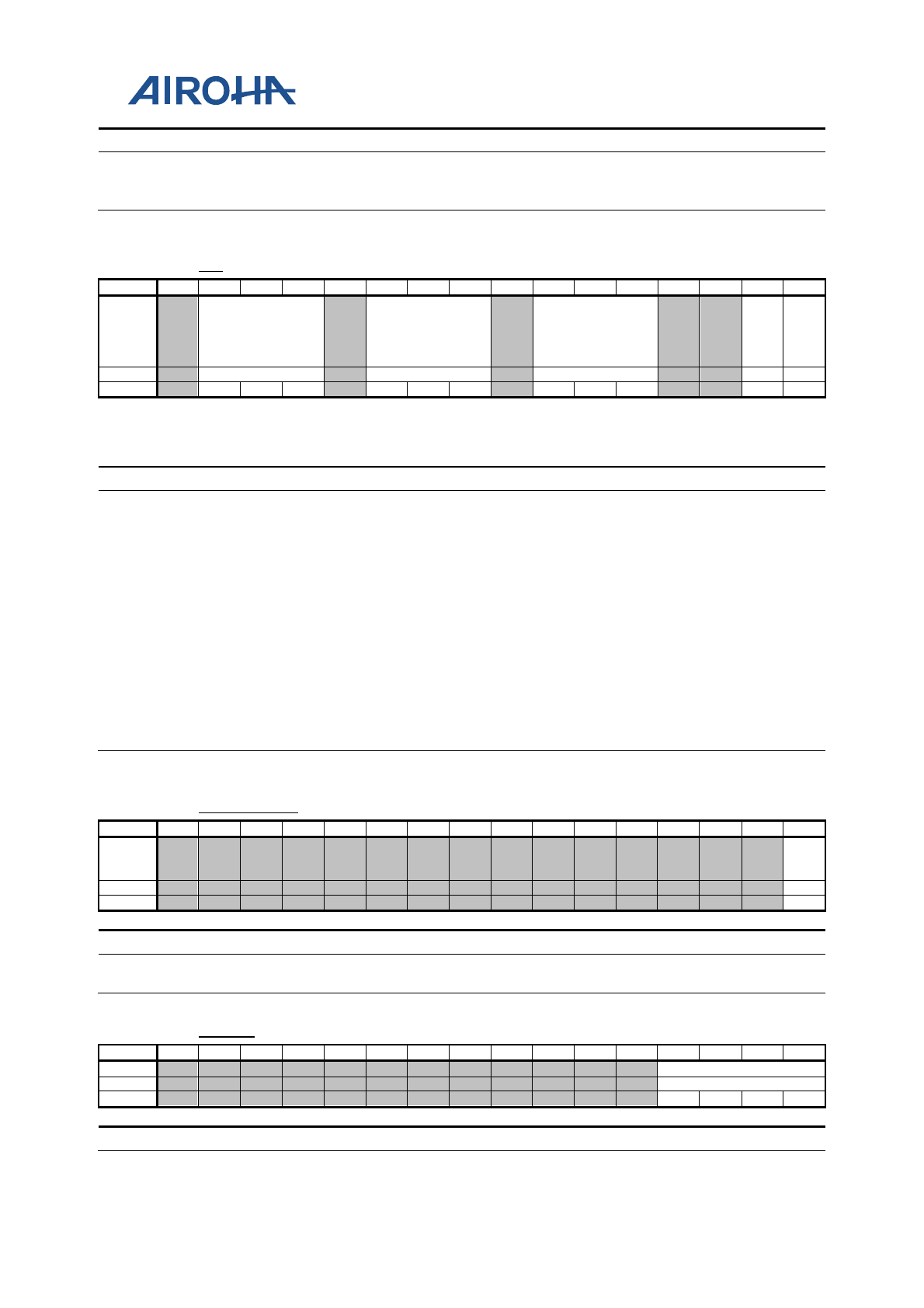
MT2523 Series Reference Manual
© 2015 - 2018 Airoha Technology Corp.
Page 107 of 692
This document contains information that is proprietary to Airoha Technology Corp. (“Airoha”) and/or its licensor(s).
Any unauthorized use, reproduction or disclosure of this document in whole or in part is strictly prohibited.
Bit(s)
Mnemonic
Name
Description
ONFIG
1: Open-drain mode
0
SCL_IO_C
ONFIG
SCL_IO_CONFIG
0: Normal tristate I/O mode
1: Open-drain mode
A0
210048
HS
High Speed Mode Register
0102
Bit
15
14
13
12
11
10
9
8
7
6
5
4
3
2
1
0
Name HS_SAMPLE_CNT
_DIV
HS_STEP_CNT_DI
V MASTER_CODE
HS_N
ACKE
RR_D
ET_E
N
HS_E
N
Type
RW
RW
RW
RW
RW
Reset
0
0
0
0
0
1
0
0
0
1
0
Overview: This register contains options for supporting high speed operation features Each HS half pulse width, i.e.
each high or low pulse, is equal to (step_cnt_div+1)*(sample_cnt_div + 1)/13MHz.
Bit(s)
Mnemonic
Name
Description
14:12
HS_SAMPL
E_CNT_DI
V
HS_SAMPLE_CNT_
DIV
When the high-speed mode is entered after the master code transfer is
completed, the sample width will become dependent on this parameter.
10:8
HS_STEP_
CNT_DIV
HS_STEP_CNT_DI
V
When the high-speed mode is entered after the master code transfer is
completed, the number of samples per half pulse width will become
dependent on this value.
6:4
MASTER_C
ODE
MASTER_CODE
This is the 3 bit programmable value for the master code to be
transmitted.
1
HS_NACKE
RR_DET_E
N
HS_NACKERR_DE
T_EN
Enables NACKERR detection during the master code
transmission
When enabled, if NACK is not received after the master code is
transmitted, the transaction will be terminated with a STOP condition.
0
HS_EN
HS_EN
Enables high-speed transaction
Note: rs_stop must be set to 1.
A0
210050
SOFTRESET
Soft Reset Register
0000
Bit
15
14
13
12
11
10
9
8
7
6
5
4
3
2
1
0
Name
SOFT
_RES
ET
Type
WO
Reset
0
Bit(s)
Mnemonic
Name
Description
0
SOFT_RES
ET
SOFT_RESET
When written 1'b1, a one pulse soft reset will be used as synchronous
reset to reset the I2C internal hardware circuits.
A0
210060
SPARE
SPARE
0000
Bit
15
14
13
12
11
10
9
8
7
6
5
4
3
2
1
0
Name
SPARE
Type
RW
Reset
0
0
0
0
Bit(s)
Mnemonic
Name
Description

MT2523 Series Reference Manual
© 2015 - 2018 Airoha Technology Corp.
Page 108 of 692
This document contains information that is proprietary to Airoha Technology Corp. (“Airoha”) and/or its licensor(s).
Any unauthorized use, reproduction or disclosure of this document in whole or in part is strictly prohibited.
Bit(s)
Mnemonic
Name
Description
3:0
SPARE
SPARE
Reserved for future use
A0
210064
DEBUGSTAT
Debug Status Register
0020
Bit
15
14
13
12
11
10
9
8
7
6
5
4
3
2
1
0
Name BUS_
BUSY
MAST
ER_
WRIT
E
MAST
ER_R
EAD MASTER_STATE
Type
RO
RO
RO
RO
Reset
0
0
1
0
0
0
0
0
Bit(s)
Mnemonic
Name
Description
7
BUS_BUSY
SPARE
Reserved
6
MASTER_
WRITE
MASTER_WRITE
For debugging only
1: Current transfer is in the master write dir.
5
MASTER_R
EAD
MASTER_READ
For debugging only
1: Current transfer is in the master read dir.
4:0
MASTER_S
TATE
MASTER_STATE
(For debugging only) Reads back the current master_state.
0: Idle state
1: I2c master is preparing to send out the start bit, SCL=1, SDA=1.
2: I2C master is sending out the start bit, SCL=1, SDA=0.
3: I2C master/slave is preparing to
transmit data bit, SCL=0, SDA=data
bit. (Data bit can be changed when SCL=0.)
4: I2C master/slave is transmitting data bit, SCL=1, SDA=data bit.
(Data bit is stable when SCL=1.)
5: I2C master/slave is preparing to transmit the ACK bit, SCL=0,
SDA=ack. (The ACK bit can be changed when SCL=0.)
6: I2C master/slave is transmitting the ACK bit, SCL=1, SDA=0. (The
ACK bit is stable when SCL=1.)
7: I2C master is preparing to send out stop bit or repeated-start bit,
SCL=0, SDA=0/1. (0: Stop bit; 1: Repeated-start bit)
8: I2C master is sending out stop bit or repeated-start bit, SCL=1,
SDA=1/0. (0: Repeated-start bit; 1: Stop bit)
9: I2C master is in delay start between two transfers, SCL=1, SDA=1.
10: I2C master is in FIFO wait state; For writing transaction, it means
FIFO is empty and I2C master is waiting for DMA controller to
write data into FIFo. For reading transaction, it means FIFO is full
and I2C master is waiting for DMA controller to read data from
FIFOo, SCL=0, SDA=don't care.
12: I2C master is preparing to send out data bit of master code. This
state is used only in high-speed transaction, SCL=0, SDA=data bit
of master code. (Data bit of master code can be changed when
SCL=0.)
13: I2C master is sending out data bit of master code. This state is used
only in high-speed transaction, SCL=1, SDA=data bit of master
code. (Data bit of master code is stable when SCL=1.)
14: I2C master/slave is preparing to transmit the NACK bit, SCL=0,
SDA=nack bit. (The NACK bit can be changed when SCL=0.) This
state is used only in high-speed transaction.
15: I2C master/slave is transmitting the NACK bit, SCL=1, SDA=1. This
state is used only in high-speed transaction.
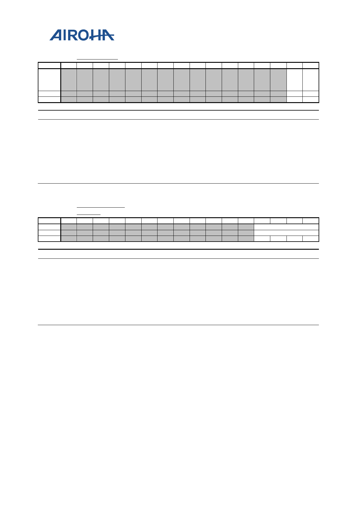
MT2523 Series Reference Manual
© 2015 - 2018 Airoha Technology Corp.
Page 109 of 692
This document contains information that is proprietary to Airoha Technology Corp. (“Airoha”) and/or its licensor(s).
Any unauthorized use, reproduction or disclosure of this document in whole or in part is strictly prohibited.
A0
210068
DEBUGCTRL
Debug Control Register
0000
Bit
15
14
13
12
11
10
9
8
7
6
5
4
3
2
1
0
Name APB_
DEBU
G_RD
FIFO
_APB
_DEB
UG
Type
WO
RW
Reset
0
0
Bit(s)
Mnemonic
Name
Description
1
APB_DEBU
G_RD
APB_DEBUG_RD
Only valid when fifo_apb_debug is set to 1
Writing to this register will generate a 1 pulsed FIFO APB RD signal for
reading the FIFO data.
0
FIFO_APB_
DEBUG
FIFO_APB_DEBUG
Used for trace 32 debugging
When using trace 32, and the memory map is shown, turning this bit on
will block the normal APB read access. The APB read access to the
FIFO
will then be enabled by writing to apb_debug_rd.
0: Disable
1: Enable
A0
21006C
TRANSFER_LE
N_AUX
Transfer Length Register (Number of Bytes per
Transfer)
0001
Bit
15
14
13
12
11
10
9
8
7
6
5
4
3
2
1
0
Name
TRANSFER_LEN_AUX
Type
RW
Reset
0
0
0
1
Bit(s)
Mnemonic
Name
Description
3:0
TRANSFER
_LEN_AUX
TRANSFER_LEN_A
UX
Only valid when dir_change or transfer_len_change is set to
1. Indicates the number of data bytes to be transferred in 1
transfer unit (excluding slave address byte) for the transfers
following the direction change or transfer_len_change
If dir_change =1, the first write transfer length will depend on
transfer_len, while the second read transfer length will depend on
transfer_len_aux. Dir change is always after the first transfer.
Similarly, transfer length change is always after the first transfer.
Note: The value must be set to be bigger than 1; otherwise no transfer
will take place.

MT2523 Series Reference Manual
© 2015 - 2018 Airoha Technology Corp.
Page 110 of 692
This document contains information that is proprietary to Airoha Technology Corp. (“Airoha”) and/or its licensor(s).
Any unauthorized use, reproduction or disclosure of this document in whole or in part is strictly prohibited.
10. SD Memory Card Controller
10.1. General Description
The controller fully supports the SD memory card bus protocol as defined in SD Memory Card Specification Part 1
Physical Layer Specification version 2.0 and eMMC 4.41 protocol.
Furthermore, the controller also partially supports the SDIO card specification version 2.0. However, the controller
can only be configured as the host of the SD memory card. Hereafter, the controller is also abbreviated as the SD
controller. The following are the main features of the controller.
• Interface with MCU by APB bus
• 16/32-bit access on APB bus
• 16/32-bit access for control registers
• 32-bit access for FIFO
• Built-in 32 bytes FIFO buffers for transmit and receive, FIFO is shared for transmit and receive
• Built-in CRC circuit
• CRC generation can be disabled
• DMA supported
• Interrupt capabilities
• Data rate up to 48Mbps in serial mode, 48x4 Mbps in parallel model, the module is targeted at 48MHz
operating clock
• Serial clock rate on SD/MMC bus is programmable
• Card detection capabilities during sleep mode
• Controllability of power for memory card
• Does not support SPI mode for SD/MMC memory card
• Does not support multiple SD/MMC memory cards
10.1.1. Pin Assignment
The following lists pins required for the SD memory card. Table 10-1 shows how the pins are shared. Note that all
I/O pads have embedded both pull-up and pull-down resistors because they are shared by the SD memory card.
The pull-down resistors for these pins can be used for power saving. If optimal pull-up or pull-down resistors are
required on the system board, all embedded pull-up and pull-down resistors can be disabled by programming the
corresponding control registers. The VDDPD pin is used for power saving. Power for the SD memory card can be
shut down by programming the corresponding control register. The WP (Write Protection) pin is used to detect the
status of the Write Protection Switch on the SD memory card.
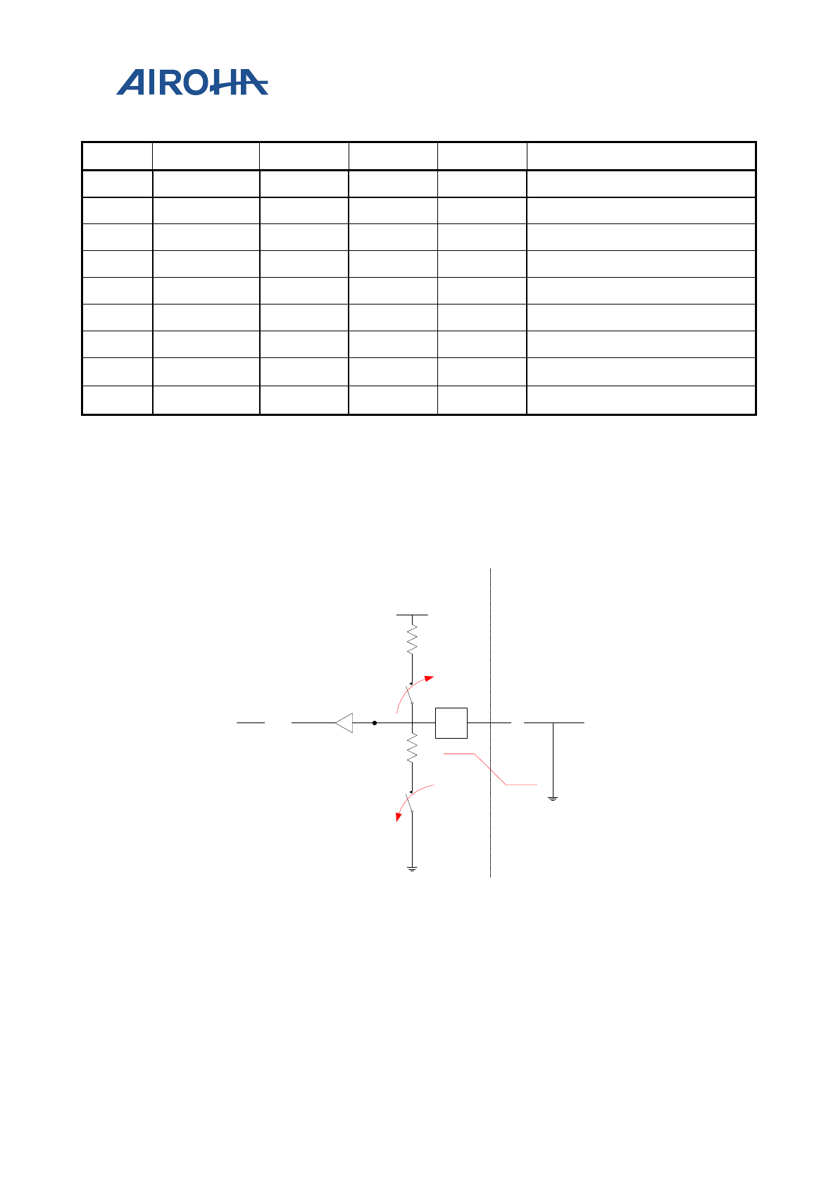
MT2523 Series Reference Manual
© 2015 - 2018 Airoha Technology Corp.
Page 111 of 692
This document contains information that is proprietary to Airoha Technology Corp. (“Airoha”) and/or its licensor(s).
Any unauthorized use, reproduction or disclosure of this document in whole or in part is strictly prohibited.
Table 10-1. Sharing of pins for SD memory card controller
No. Name Type MMC SD Description
1 SD_CLK O CLK CLK Clock
2 SD_DAT3 I/O/PP CD/DAT3 CD/DAT3 Data Line [Bit 3]
3 SD_DAT0 I/O/PP DAT0 DAT0 Data Line [Bit 0]
4 SD_DAT1 I/O/PP DAT1 DAT1 Data Line [Bit 1]
5 SD_DAT2 I/O/PP DAT2 DAT2 Data Line [Bit 2]
6 SD_CMD I/O/PP CMD CMD Command or bus state
7 SD_PWRON O - - VDD ON/OFF
8 SD_WP I - - Write protection switch in SD
9 SD_INS I VSS2 VSS2 Card detection
10.1.2. Card Detection
For SD memory card, detection of card insertion/removal by hardware is supported, and a dedicated pin “INS” is
used to perform card insertion and removal for SD. The pin “INS” will be connected to the pin “VSS2” of a SD
connector (see Figure 10-1 ).
INS
R
PU
PAD
SW1
R
PD
SW2
INS_IN
HOST CARD
Figure 10-1. Card detection for SD memory card
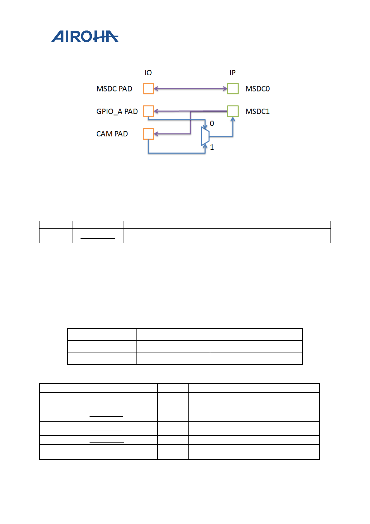
MT2523 Series Reference Manual
© 2015 - 2018 Airoha Technology Corp.
Page 112 of 692
This document contains information that is proprietary to Airoha Technology Corp. (“Airoha”) and/or its licensor(s).
Any unauthorized use, reproduction or disclosure of this document in whole or in part is strictly prohibited.
10.1.3. IO Pad Setting
Figure 10-2. IO Pinmux setting for MSDC
There are one set of dedicated pads for MSDC0 and two sets of pads for MSDC1. To switch between those two sets,
the GPIO and an extra input mux setting are needed. For GPIO settings, refer to GPIO specification. For input mux
setting, refer to the table below.
Address
Register Name
Field Name
MSB
LSB
Description
A2010234 HW_MISC3 MSDC1_PAD_SEL 0 0
0: GPIO_A PAD for MSDC1
1: CAMERA PAD for MSDC1
10.2. Register Definition
There are two MSDCs in this SOC. The usage of the registers below is the same except that the base address should
be changed to respective one.
Module name: MSDC0 Base address: (+a0020000h)
Address
Name
Width
Register Function
A0020000
MSDC_CFG
32
SD Memory Card Controller Configuration
Register
A0020004
MSDC_STA
32
SD Memory Card Controller Status
Register
A0020008
MSDC_INT
32
SD Memory Card Controller Interrupt
Register
A0020010
MSDC_DAT
32
SD Memory Card
Controller Data Register
A0020014
MSDC_IOCON
32
SD Memory Card Controller IO Control
Register
MSDC number Base address Feature
MSDC0 0xA0020000 Supports DMA, 4-bit data line
MSDC1 0xA0030000 Supports DMA, 4-bit data line
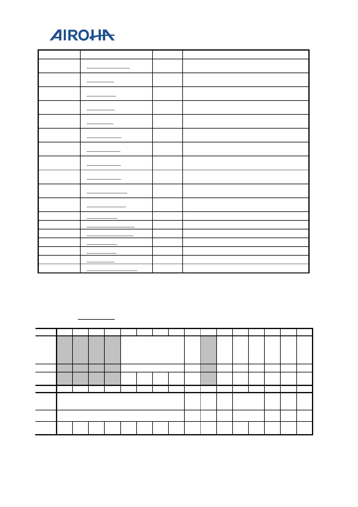
MT2523 Series Reference Manual
© 2015 - 2018 Airoha Technology Corp.
Page 113 of 692
This document contains information that is proprietary to Airoha Technology Corp. (“Airoha”) and/or its licensor(s).
Any unauthorized use, reproduction or disclosure of this document in whole or in part is strictly prohibited.
Address
Name
Width
Register Function
A0020018
MSDC_IOCON1
32
SD Memory Card Controller IO Control
Register 1
A0020020
SDC_CFG
32
SD Memory Card Controller Configuration
Register
A0020024
SDC_CMD
32
SD Memory Card Controller Command
Register
A0020028
SDC_ARG
32
SD Memory Card Controller Argument
Register
A002002C
SDC_STA
32
SD Memory Card Controller Status
Register
A0020030
SDC_RESP0
32
SD Memory Card Controller Response
Register 0
A0020034
SDC_RESP1
32
SD Memory Card Controller Response
Register 1
A0020038
SDC_RESP2
32
SD Memory Card Controller Response
Register 2
A002003C
SDC_RESP3
32
SD Memory Card Controller Response
Register 3
A0020040
SDC_CMDSTA
32
SD Memory Card Controller Command
Status Register
A0020044
SDC_DATSTA
32
SD Memory Card Controller Data Status
Register
A0020048
SDC_CSTA
32
SD Memory Card Status Register
A002004C
SDC_IRQMASK0
32
SD Memory Card IRQ Mask Register 0
A0020050
SDC_IRQMASK1
32
SD Memory Card
IRQ Mask Register 1
A0020054
SDIO_CFG
32
SDIO Configuration Register
A0020058
SDIO_STA
32
SDIO Status Register
A0020080
CLK_RED
32
CLK Latch
Configuration Register
A0020098
DAT_CHECKSUM
32
MSDC Rx Data Check Sum Register
A0020000
MSDC_CFG
SD Memory Card Controller
Configuration Register
04000020
Bit
31
30
29
28
27
26
25
24
23
22
21
20
19
18
17
16
Nam
e FIFOTHD
CL
KS
RC
_P
AT
VD
DP
D
RC
DE
N
DI
RQ
EN
PI
NE
N
DM
AE
N
INT
EN
Type
RW
RW
RW
RW
RW
RW
RW
RW
Rese
t
0 1 0 0 0 0 0 0 0 0 0
Bit
15
14
13
12
11
10
9
8
7
6
5
4
3
2
1
0
Nam
e SCLKF
SC
LK
ON
CR
ED
ST
DB
Y
CLKSRC
NO
CR
C
RS
T MS
DC
Type RW RW RW RW RW RW
W1
C
RW
Rese
t
0 0 0 0 0 0 0 0 0 0 1 0 0 0 0 0

MT2523 Series Reference Manual
© 2015 - 2018 Airoha Technology Corp.
Page 114 of 692
This document contains information that is proprietary to Airoha Technology Corp. (“Airoha”) and/or its licensor(s).
Any unauthorized use, reproduction or disclosure of this document in whole or in part is strictly prohibited.
Bit(s)
Mnemonic
Name
Description
27:24
FIFOTHD
FIFOTHD
FIFO threshold. The register field determines
when to issue a DMA request. For write
transactions, DMA requests will be asserted
if
the number of free entries in FIFO are larger
than or equal to the value in the register field.
For read transactions, DMA requests will be
asserted if the number of valid entries in FIFO
are larger than or equal to the value in the
register field. The
register field must be set
according to the setting of data transfer count
in DMA burst mode. If single mode for DMA
transfer is used, the register field should be set
to 0b0001.
0000: Invalid.
0001: Threshold value is 1.
0010: Threshold value is 2.
0011~01111: ...
1000: Threshold value is 8.
others: Invalid
23
CLKSRC_PAT
CLKSRC_PAT
CLKSRC patch, when {CLKSRC_PAT,CLKSRC}
equal to
0: CLKSQ_F26M_CK
1: LFOSC_F26M_CK
2: MPLL_DIV3P5_CK (89.1MHz)
3: MPLL_DIV4_CK (78MHz)
4: MPLL_DIV5_CK
(62.4MHz)
5: HFOSC_DIV3P5_CK (89.1MHz)
6: HFOSC_DIV4_CK (78MHz)
7: HFOSC_DIV5_CK (62.4MHz)
21
VDDPD
VDDPD
Controls the output pin VDDPD used for power
saving. The output pin VDDPD will control
power for memory card.
0: The output pin VDDPD will output logic low. The
power for memory card will be turned off.
1: The output pin VDDPD will output logic high. The
power for memory card will be turned on.
20
RCDEN
RCDEN
Controls the output pin RCDEN used for card
identification process when the
controller is
for SD memory card. Its output will control the
pull down resistor on the system board to
connect or disconnect with the signal

MT2523 Series Reference Manual
© 2015 - 2018 Airoha Technology Corp.
Page 115 of 692
This document contains information that is proprietary to Airoha Technology Corp. (“Airoha”) and/or its licensor(s).
Any unauthorized use, reproduction or disclosure of this document in whole or in part is strictly prohibited.
Bit(s)
Mnemonic
Name
Description
CD/DAT3.
0: The output pin RCDEN will output logic low.
1: The output pin RCDEN will output logic high.
19
DIRQEN
DIRQEN
Enables data request interrupt. The register bit
is used to control if data request is used as an
interrupt source.
0: Data request is not used as an interrupt source.
1: Data request is used as an interrupt source.
18
PINEN
PINEN
Enables pin interrupt. The register bit is used
to control if the pin for card detection is used
as an interrupt source.
0: The pin for card detection is not used as an
interrupt source.
1: The pin for card detection is used as an interrupt
source.
17
DMAEN
DMAEN
Enables DMA. Note that if DMA capability is
disabled then application software must poll
the status of the register MSDC_STA for
checking any data transfer request. If DMA is
desired, the register bit must be set before
command register is
written.
0: DMA request induced by various conditions is
disabled, no matter the controller is configured as the
host of either SD memory card or memory stick.
1: DMA request induced by various conditions is
enabled, no matter the controller is
configured as the
host of either SD memory card or memory stick.
16
INTEN
INTEN
Enables interrupt. Note that if interrupt
capability is disabled, application software
must poll the status of the register MSDC_STA
to check for any interrupt request.
0: Interrupt induced by various conditions is disabled,
no matter the controller is configured as the host of
either SD memory card or memory stick.
1: Interrupt induced by various conditions is enabled,
no matter the controller is configured as the
host of
either SD memory card or memory stick.
15:8
SCLKF
SCLKF
Controls clock frequency of serial clock on SD
bus. Denote clock frequency of SD bus serial
clock as fslave and clock frequency of the SD
controller as fhost which is 89.1MHz. Then the
value
of the register field is as the following.
Note: The allowed maximum frequency of

MT2523 Series Reference Manual
© 2015 - 2018 Airoha Technology Corp.
Page 116 of 692
This document contains information that is proprietary to Airoha Technology Corp. (“Airoha”) and/or its licensor(s).
Any unauthorized use, reproduction or disclosure of this document in whole or in part is strictly prohibited.
Bit(s)
Mnemonic
Name
Description
fslave is 44.55MHz. While changing clock rate,
it needs "1T clock period before changing + 1T
clock period after change" for HW signal to re
-
synchronize.
00000000b: fslave =(1/2)*fhost
00000001b: fslave = (1/(4*1))*fhost
00000010b: fslave = (1/(4*2))*fhost
00000011b: fslave = (1/(4*3))*fhost
00000100b~111111110b: ...
11111111b: fslave = (1/(4*255))*fhost
7
SCLKON
SCLKON
Serial clock always on. For debugging.
0: Serial clock not always on.
1: Serial clock always on.
6
CRED
CRED
Rising edge data. The register bit is used to
determine that serial data input is latched at
the falling edge or the rising edge of serial
clock. The default setting
is at the rising edge.
If serial data have worse timing, set the
register bit to'1'. When the memory card has
worse timing on return read data, set the
register bit to '1'.
0: Serial data input is latched at the rising edge of
serial clock.
1: Serial data input is latched at the falling edge of
serial clock.
5
STDBY
STDBY
Standby mode. If the module is powered down,
operating clock to the module will be stopped.
At the same time, clock to card detection
circuitry will also be stopped. If detection
of
memory card insertion and removal is desired,
write '1' to the register bit. If interrupt for
detection of memory card insertion and
removal is enabled, interrupt will take place
whenever memory is inserted or removed.
0: Standby mode is disabled.
1: Standby mode is enabled.
4:3
CLKSRC
CLKSRC
Specifies which clock is used as source clock of
memory card. Use MPLL (312MHz) or HFOSC
(312MHz) as source clock of memory card
when clock hopping is not enabled. If clock
hopping is enabled, MPLL clock's
hopping rate
will be 0~
-8% and HFOSC 312MHz (0~-8%).
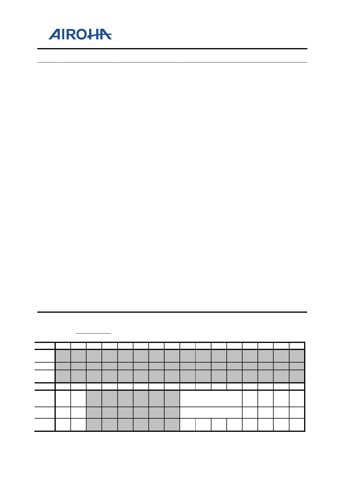
MT2523 Series Reference Manual
© 2015 - 2018 Airoha Technology Corp.
Page 117 of 692
This document contains information that is proprietary to Airoha Technology Corp. (“Airoha”) and/or its licensor(s).
Any unauthorized use, reproduction or disclosure of this document in whole or in part is strictly prohibited.
Bit(s)
Mnemonic
Name
Description
00: CLKSQ_F26M_CK; MPLL_DIV5_CK (62.4MHz)
01: LFOSC_F26M_CK; HFOSC_DIV3P5_CK
(89.1MHz)
10: MPLL_DIV3P5_CK (89.1MHz);
HFOSC_DIV4_CK (78MHz)
11: MPLL_DIV4_CK (78MHz); HFOSC_DIV5_CK
(62.4MHz)
2
NOCRC
NOCRC
Disables CRC. 1 indicates that data transfer
without CRC is desired. For write data block,
data will be transmitted without CRC. For read
data block, CRC will not be checked. It is for
tests.
0: Data transfer with CRC is desired.
1: Data transfer without CRC is desired.
1
RST
RST
Software reset. Writing 1 to the register bit will
cause internal synchronous reset of SD
controller but will not reset register settings.
RST should only be set when RST is equal to 0.
0: Read 0 stands for the reset process is finished.
1: Write 1 to reset SD controller.
0
MSDC
MSDC
Configures the controller as SD memory card
mode. CLK/CMD/DAT line will be pulled low
when SD memory card mode is disabled.
0: Disable SD memory card
1: Enable SD memory card
A0020004
MSDC_STA
SD Memory Card Controller Status
Register
00000002
Bit
31
30
29
28
27
26
25
24
23
22
21
20
19
18
17
16
Nam
e
Type
Rese
t
Bit
15
14
13
12
11
10
9
8
7
6
5
4
3
2
1
0
Nam
e BU
SY
FIF
OC
LR
FIFOCNT INT DR
Q BE BF
Type RO
W1
C
RO RO RO RO RO
Rese
t
0 0 0 0 0 0 0 0 1 0

MT2523 Series Reference Manual
© 2015 - 2018 Airoha Technology Corp.
Page 118 of 692
This document contains information that is proprietary to Airoha Technology Corp. (“Airoha”) and/or its licensor(s).
Any unauthorized use, reproduction or disclosure of this document in whole or in part is strictly prohibited.
Bit(s)
Mnemonic
Name
Description
15
BUSY
BUSY
Status of the controller. If the controller is in
busy state, the register bit will be '1'. Otherwise
'0'.
0: The controller is in busy state.
1: The controller is in idle state.
14
FIFOCLR
FIFOCLR
Clears FIFO. Writing '1' to the register bit will
cause the content of FIFO clear and reset the
status of FIFO controller.
0: Read 0 stands for the FIFO clear process is finished.
1: Write 1 to clear the content of FIFO clear and reset
the status of FIFO controller.
7:4
FIFOCNT
FIFOCNT
FIFO count. The register field shows how many
valid
entries are in FIFO.
0000: There is 0 valid entry in FIFO.
0001: There is 1 valid entry in FIFO.
0010: There are 2 valid entries in FIFO.
0011~0111: ...
1000: There are 8 valid entries in FIFO.
3
INT
INT
Indicates if any interrupt exists. While any
interrupt exists, the register bit still will be
active even if the register bit INTEN in the
register MSDC_CFG is disabled. SD controller
can interrupt MCU by issuing interrupt request
to interrupt controller, or software/application
pol
ls the register endlessly to check if any
interrupt request exists in SD controller. When
the register bit INTEN in the register
MSDC_CFG is disabled, the second method will
be used. For read commands, it is possible that
timeout error takes place. Softwar
e can read
the status register to check if timeout error
takes place without OS time tick support or
data request is asserted.
Note: The register bit will be cleared when
reading the register MSDC_INT.
0: No interrupt request exists.
1: Interrupt request exists.
2
DRQ
DRQ
Indicates if any data transfer is required. When
any data transfer is required, the register bit
still will be active even if the register bit
DIRQEN in the register MSDC_CFG is disabled.
Data transfer can be achieved by DMA chan
nel
alleviating MCU loading, or by polling the
register bit to check if any data transfer is
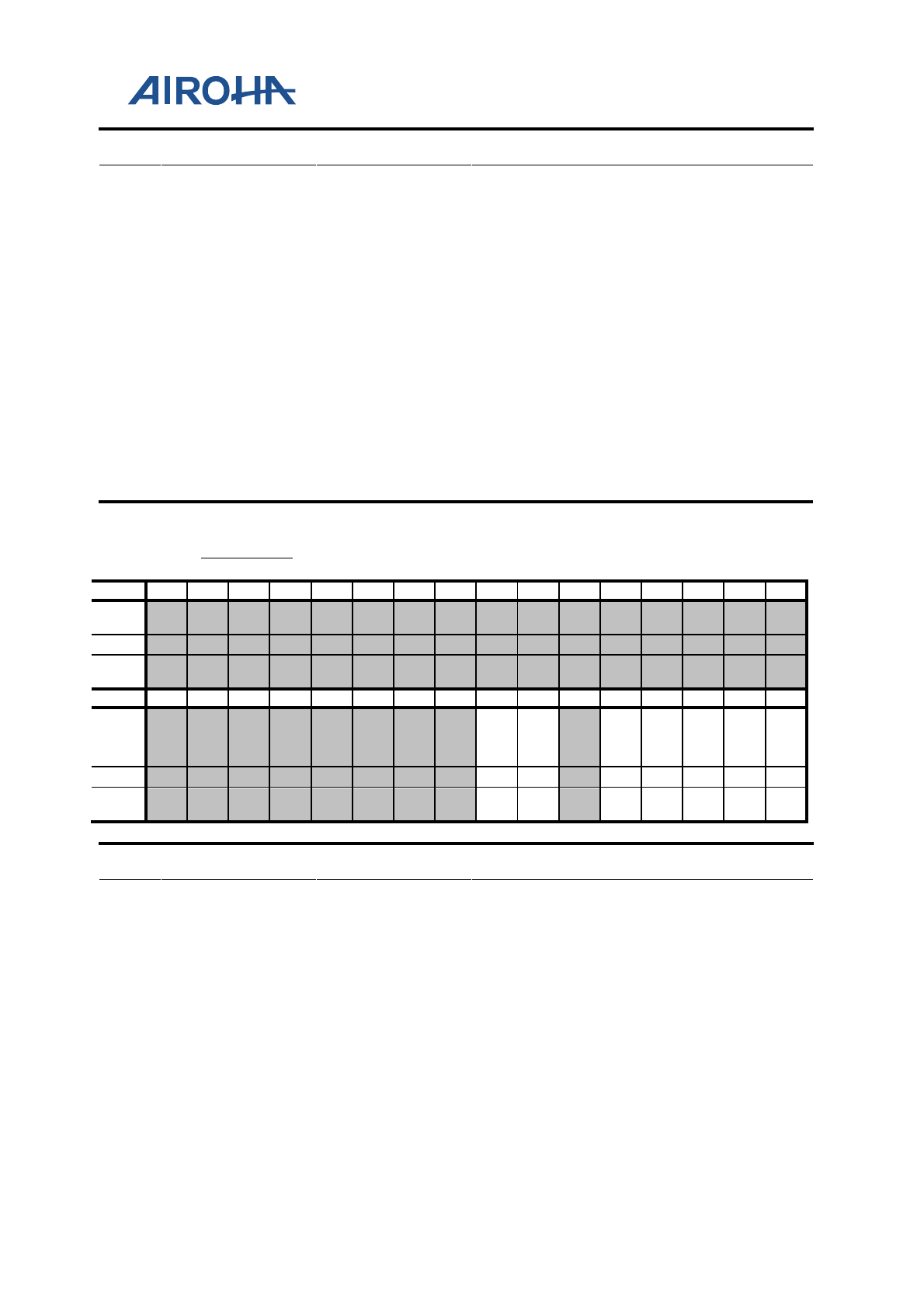
MT2523 Series Reference Manual
© 2015 - 2018 Airoha Technology Corp.
Page 119 of 692
This document contains information that is proprietary to Airoha Technology Corp. (“Airoha”) and/or its licensor(s).
Any unauthorized use, reproduction or disclosure of this document in whole or in part is strictly prohibited.
Bit(s)
Mnemonic
Name
Description
requested. When the register bit DIRQEN in
the register MSDC_CFG is disabled, the second
method will be used.
0: No DMA request exists.
1: DMA request exists.
1
BE
BE
Indicates if FIFO in SD controller is empty
0: FIFO in SD controller is not empty.
1: FIFO in SD controller is empty.
0
BF
BF
Indicates if FIFO in SD controller is full
0: FIFO in SD controller is not full.
1: FIFO in SD controller is full.
A0020008
MSDC_INT
SD Memory Card Controller Interrupt
Register
00000000
Bit
31
30
29
28
27
26
25
24
23
22
21
20
19
18
17
16
Nam
e
Type
Rese
t
Bit
15
14
13
12
11
10
9
8
7
6
5
4
3
2
1
0
Nam
e SDI
OI
RQ
SD
R1
BI
RQ
SD
MC
IR
Q
SD
DA
TIR
Q
SD
CM
DI
RQ
PI
NI
RQ
DI
RQ
Type
RC
RC
RC
RC
RC
RC
RC
Rese
t
0 0 0 0 0 0 0
Bit(s)
Mnemonic
Name
Description
7
SDIOIRQ
SDIOIRQ
SDIO interrupt. The register bit indicates if any
interrupt for SDIO exists. Whenever interrupt
for SDIO exists, the register bit will be set to '1'
if interrupt is enabled. It will be reset when the
register is read.
0: No SDIO interrupt
1: Interrupt for SDIO exists.
6
SDR1BIRQ
SDR1BIRQ
SD R1b response interrupt. The register bit will
be active when a SD command with R1b
response finished and the DAT0 line has
transited from busy to idle state. Single block
write commands with R1b response will cause
interrupt when the command is
completed no
matter successfully or with CRC error.

MT2523 Series Reference Manual
© 2015 - 2018 Airoha Technology Corp.
Page 120 of 692
This document contains information that is proprietary to Airoha Technology Corp. (“Airoha”) and/or its licensor(s).
Any unauthorized use, reproduction or disclosure of this document in whole or in part is strictly prohibited.
Bit(s)
Mnemonic
Name
Description
However, multi-block write commands with
R1b response will not cause the interrupt
because multi
-block write commands are
always stopped by STOP_TRANS commands.
STOP_TRANS commands (with R1b response)
be
hind multi-block write commands will cause
the interrupt. Single block read command with
R1b response will cause the interrupt when the
command is completed but multi
-block read
commands do not.
Note: STOP_TRANS commands (with R1b
response) behind multi
-block read commands
will cause interrupt.
0: No interrupt for SD R1b response.
1: Interrupt for SD R1b response exists.
4
SDMCIRQ
SDMCIRQ
SD memory card interrupt. The register bit
indicates if any interrupt for SD memory card
exists. Whenever
interrupt for SD memory
card exists, i.e. any bit in the register
SDC_CSTA is active, the register bit will be set
to '1' if interrupt is enabled. It will be reset
when the register is read.
Note: This bit will not trigger MSDC hardware
interrupt.
0: No SD memory card interrupt
1: SD memory card interrupt exists.
3
SDDATIRQ
SDDATIRQ
SD bus DAT interrupt. The register bit
indicates if any interrupt for SD DAT line
exists. Whenever interrupt for SD DAT line
exists, i.e. any bit in the register SDC_
DATSTA
is active, the register bit will be set to '1' if
interrupt is enabled. It will be reset when the
register is read.
0: No SD DAT line interrupt
1: SD DAT line interrupt exists.
2
SDCMDIRQ
SDCMDIRQ
SD bus CMD interrupt. The register bit
indicates if any interrupt for SD CMD line
exists. Whenever interrupt for SD CMD line
exists, i.e. any bit in the register SDC_CMDSTA
is active, the register bit will be set to '1' if
interrupt is enabled. It will be reset when the
register is read.
0: No SD CMD line interrupt
1: SD CMD line interrupt exists.
1
PINIRQ
PINIRQ
Pin change interrupt. The register bit indicates
if any interrupt for memory card
insertion/removal exists. Whenever memory
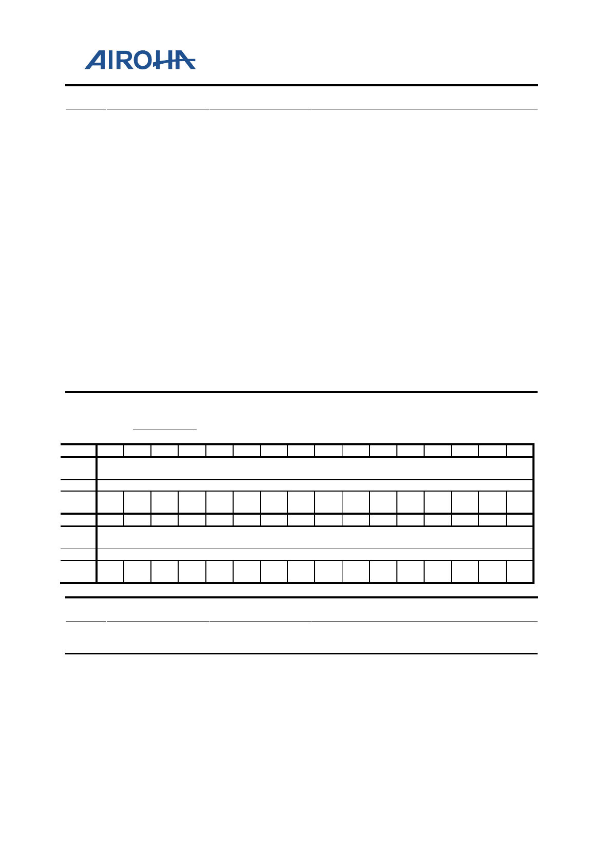
MT2523 Series Reference Manual
© 2015 - 2018 Airoha Technology Corp.
Page 121 of 692
This document contains information that is proprietary to Airoha Technology Corp. (“Airoha”) and/or its licensor(s).
Any unauthorized use, reproduction or disclosure of this document in whole or in part is strictly prohibited.
Bit(s)
Mnemonic
Name
Description
card is inserted or removed and card detection
interrupt is enabled, i.e. the register bit PINEN
in the register MSDC_CFG is set to '1', the
register bit will be set to '1'. It will be reset
when the register is read.
0: Otherwise
1: Card is inserted or removed.
0
DIRQ
DIRQ
Data request interrupt. The register bit
indicates if any interrupt for data request
exists. Whenever data request exists and data
request as an interrupt source is enabled, i.e.
the register bit DIRQEN in the register
MSDC_CFG is set to '1', the register bit will be
a
ctive. It will be reset when reading it. For
software, data requests can be recognized by
polling the register bit DRQ or by data request
interrupt. Data request interrupts will be
generated every FIFOTHD data transfer.
0: No data request interrupt
1: Data request interrupt occurs.
A0020010
MSDC_DAT
SD Memory Card Controller Data
Register
00000000
Bit
31
30
29
28
27
26
25
24
23
22
21
20
19
18
17
16
Nam
e
DATA
Type
RW
Rese
t
0 0 0 0 0 0 0 0 0 0 0 0 0 0 0 0
Bit
15
14
13
12
11
10
9
8
7
6
5
4
3
2
1
0
Nam
e
DATA
Type
RW
Rese
t
0 0 0 0 0 0 0 0 0 0 0 0 0 0 0 0
Bit(s)
Mnemonic
Name
Description
31:0
DATA
DATA
Reads/writes data from/to FIFO inside SD
controller. Data access is in unit of 32 bits.
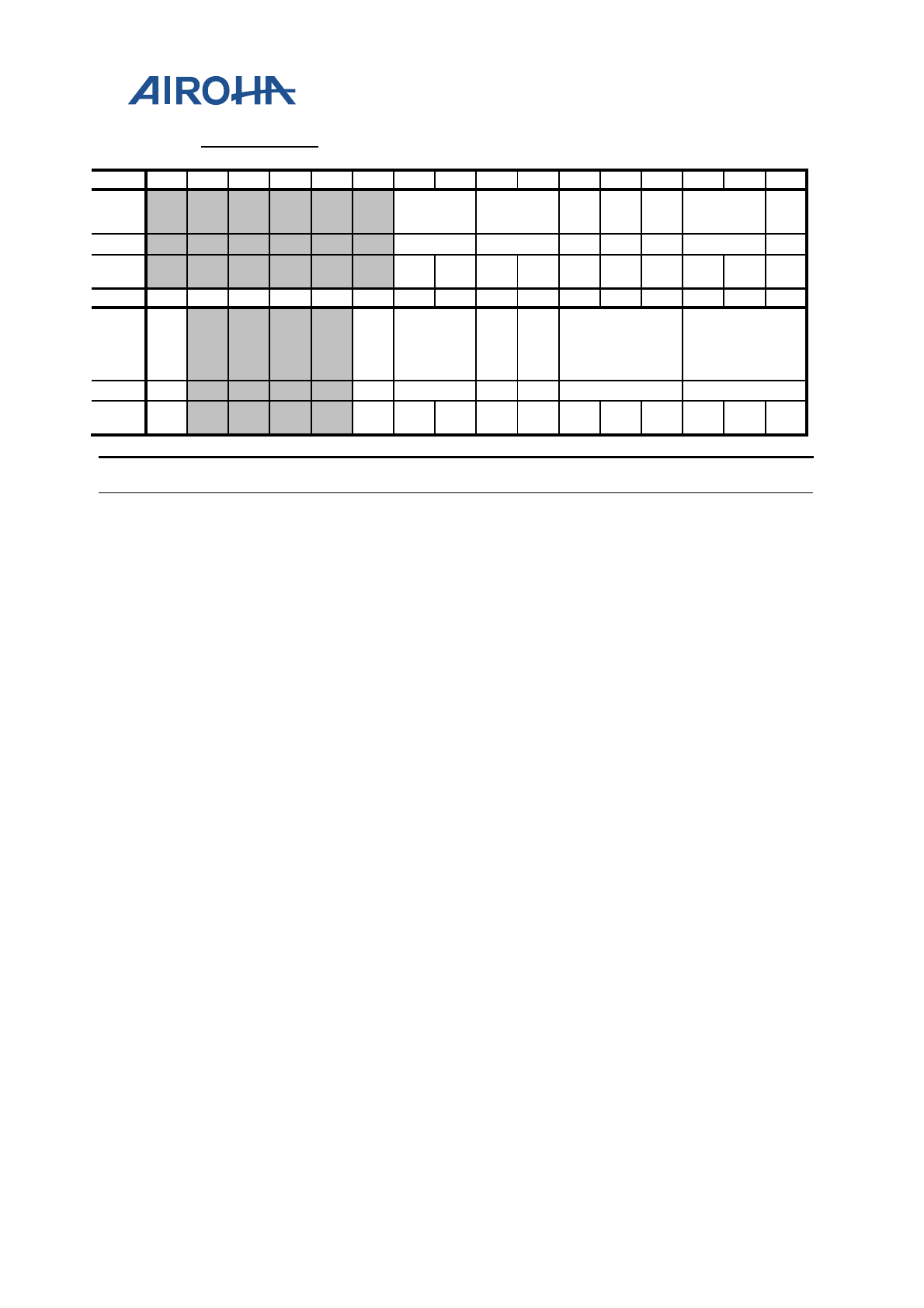
MT2523 Series Reference Manual
© 2015 - 2018 Airoha Technology Corp.
Page 122 of 692
This document contains information that is proprietary to Airoha Technology Corp. (“Airoha”) and/or its licensor(s).
Any unauthorized use, reproduction or disclosure of this document in whole or in part is strictly prohibited.
A0020014
MSDC_IOCON
SD Memory Card Controller IO Control
Register
010000C3
Bit
31
30
29
28
27
26
25
24
23
22
21
20
19
18
17
16
Nam
e SAMPLE
DLY FIXDLY
SA
MP
ON
CR
CD
IS
CM
DS
EL
INTLH DS
W
Type
RW
RW
RW
RW
RW
RW
RW
Rese
t
0 1 0 0 0 0 0 0 0 0
Bit
15
14
13
12
11
10
9
8
7
6
5
4
3
2
1
0
Nam
e
CM
DR
E
HI
GH
_S
PE
ED
DMABUR
ST
SR
CF
G1
SR
CF
G0 ODCCFG1 ODCCFG0
Type
RW
RW
RW
RW
RW
RW
RW
Rese
t
0 0 0 0 1 1 0 0 0 0 1 1
Bit(s)
Mnemonic
Name
Description
25:24
SAMPLEDLY
SAMPLEDLY
The register is used for SW to select the turn
around delay cycle between write data end bit
and CRC status for SD card.
00: 0-T delay
01: 1-T delay
10: 2-T delay
11: 3-T delay
23:22
FIXDLY
FIXDLY
The register is used for SW to select the delay
cycle after clock fix high for the host controller
to SD card.
00: 0-T delay
01: 1-T delay
10: 2-T delay
11: 3-T delay
21
SAMPON
SAMPON
Data sample enable always on. The bit’s
suggested setting is 1 when feedback clock is
used and 0
when multiple phase clock is used.
0: Data sample enable not always on
1: Data sample enable always on.
20
CRCDIS
CRCDIS
Switches off data CRC check for SD read data
0: CRC check is on.
1: CRC check is off.
19
CMDSEL
CMDSEL
Determines whether the host should delay 1-T

MT2523 Series Reference Manual
© 2015 - 2018 Airoha Technology Corp.
Page 123 of 692
This document contains information that is proprietary to Airoha Technology Corp. (“Airoha”) and/or its licensor(s).
Any unauthorized use, reproduction or disclosure of this document in whole or in part is strictly prohibited.
Bit(s)
Mnemonic
Name
Description
to latch response from card
0: Host latches response without 1-T delay.
1: Host latches response with 1-T delay.
18:17
INTLH
INTLH
Selects latch timing for SDIO multi-block read
interrupt
00: Host latches INT at the second backend clock after
the end bit of current data block from card is received.
(default)
01: Host latches INT at the first backend clock after the
end bit of current data block from card is received.
10: Host latches INT at the second backend clock after
the end bit of current data block from card is received.
11: Host latches INT at the third backend clock after
the end bit of current data block from card is received.
16
DSW
DSW
Determines whether the host should latch data
with
1-T delay or not. For SD card, this bit is
suggested to be 0. For MSPRO cards, it is
suggested to be 1.
0: Host latches the data with 1-T delay.
1: Host latches the data without 1-T delay.
15
CMDRE
CMDRE
Determines whether the host should latch
response token (sent from card on CMD line )
at rising edge or falling edge of serial clock.
(T.B.D this bit is un
-useful)
0: Host latches response at rising edge of serial clock
1: Host latches response at falling edge of serial clock
10
HIGH_SPEED
HIGH_SPEED
For high-speed mode when internal sample
clock is used. High
-speed mode means that the
SD/MMC serial bus clock rate is bigger than
25MHz. The default speed mode means that the
SD/MMC serial bus clock rate is bigger than
25MHz.
0: Default speed
1: High speed
9:8
DMABURST
DMABURST
The register is used for SW to select burst type
when data transfer by DMA.
Note: Only single mode can support non
-4N
bytes data transfer in read operation.
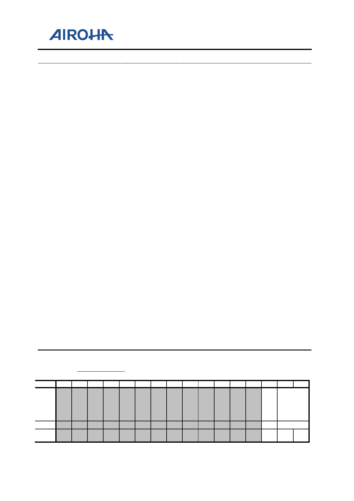
MT2523 Series Reference Manual
© 2015 - 2018 Airoha Technology Corp.
Page 124 of 692
This document contains information that is proprietary to Airoha Technology Corp. (“Airoha”) and/or its licensor(s).
Any unauthorized use, reproduction or disclosure of this document in whole or in part is strictly prohibited.
Bit(s)
Mnemonic
Name
Description
00: Single mode
01: 4-beat incrementing burst
10: 8-beat incrementing burst
11: Reserved.
7
SRCFG1
SRCFG1
Output driving capability the pins DAT0, DAT1,
DAT2 and DAT3
0: Fast slew rate
1: Slow slew rate
6
SRCFG0
SRCFG0
Output driving capability the pins CMD/BS and
SCLK
0: Fast slew rate
1: Slow slew rate
5:3
ODCCFG1
ODCCFG1
Output driving capability the pins DAT0, DAT1,
DAT2 and DAT3
000: 4mA
001: 8mA
010: 12mA
011: 16mA
2:0
ODCCFG0
ODCCFG0
Output driving capability the pins CMD/BS and
SCLK
000: 4mA
001: 8mA
010: 12mA
011: 16mA
A0020018
MSDC_IOCON1
SD Memory Card Controller IO Control
Register 1
00022022
Bit
31
30
29
28
27
26
25
24
23
22
21
20
19
18
17
16
Nam
e
PR
CF
G_
RS
T_
WP
PRVAL_R
ST_WP
Type
RW
RW
Rese
t
0 1 0

MT2523 Series Reference Manual
© 2015 - 2018 Airoha Technology Corp.
Page 125 of 692
This document contains information that is proprietary to Airoha Technology Corp. (“Airoha”) and/or its licensor(s).
Any unauthorized use, reproduction or disclosure of this document in whole or in part is strictly prohibited.
Bit
15
14
13
12
11
10
9
8
7
6
5
4
3
2
1
0
Nam
e
PR
CF
G_
CK
PRVAL_C
K
PR
CF
G_
CM
PRVAL_C
M
PR
CF
G_
DA
PRVAL_D
A
PR
CF
G_I
NS
PRVAL_I
NS
Type
RW
RW
RW
RW
RW
RW
RW
RW
Rese
t
0 1 0 0 0 0 0 1 0 0 1 0
Bit(s)
Mnemonic
Name
Description
18
PRCFG_RST/WP
PRCFG_RST_WP
Pull up/down register configuration for pin
RST/WP. The default value is 0.
0: Pull up resistor in the I/O pad of the pin WP is
enabled.
1: Pull down resistor in the I/O pad of the pin WP is
enabled.
17:16
PRVAL_RST/WP
PRVAL_RST_WP
Pull up/down register value for pin RST/WP.
The default value is 10.
00: Pull up resistor and pull down resistor in the I/O
pad of the pin WP are all disabled.
01: Pull up/down resistor in the I/O pad of the pin WP
value is 47k.
10: Pull up/down resistor in the I/O pad of the pin WP
value is 47k.
11: Pull up/down resistor in the I/O pad of the pin WP
value is 23.5k.
14
PRCFG_CK
PRCFG_CK
Configures pull up/down register for pin CK.
The
default value is 0.
0: Pull up resistor in the I/O pad of the pin CK is
enabled.
1: Pull down resistor in the I/O pad of the pin CK is
enabled.
13:12
PRVAL_CK
PRVAL_CK
Pull up/down register value for pin CLK. The
default value is 10.
00: Pull up resistor and pull down resistor in the I/O
pad of the pin CLK are all disabled.
01: Pull up/down resistor in the I/O pad of the pin CLK
value is 47k.
10: Pull up/down resistor in the I/O pad of the pin CLK
value is 47k.
11: Pull up/down resistor in the I/O pad of the pin CLK
value is 23.5k.
10
PRCFG_CM
PRCFG_CM
Configures pull up/down register for the pin
CM. The default value is 0.
0: Pull up resistor in the I/O pad of the pin CM is

MT2523 Series Reference Manual
© 2015 - 2018 Airoha Technology Corp.
Page 126 of 692
This document contains information that is proprietary to Airoha Technology Corp. (“Airoha”) and/or its licensor(s).
Any unauthorized use, reproduction or disclosure of this document in whole or in part is strictly prohibited.
Bit(s)
Mnemonic
Name
Description
enabled.
1: Pull down resistor in the I/O pad of the pin CM is
enabled.
9:8
PRVAL_CM
PRVAL_CM
Pull up/down register value for pin CMD/BS.
The default value is 00.
00: Pull up resistor and pull down resistor in the I/O
pad of the pin CMD/BS are all disabled.
01: Pull up/down resistor in the I/O pad of the pin
CMD/BS value is 47k.
10: Pull up/down resistor in the I/O pad of the pin
CMD/BS value is 47k.
11: Pull up/down resistor in the I/O pad of the pin
CMD/BS value is 23.5k.
6
PRCFG_DA
PRCFG_DA
Configures pull up/down register for pin DAT0,
DAT1, DAT2, DAT3. The default value is 0.
0: Pull up resistor in the I/O pad of the pin DAT is
enabled.
1: Pull down resistor in the I/O pad of the pin DAT is
enabled.
5:4
PRVAL_DA
PRVAL_DA
Pull up/down register value for pin DAT0,
DAT1,
DAT2, DAT3. The default value is 10.
00: Pull up resistor and pull down resistor in the I/O
pad of the pin DAT are all disabled.
01: Pull up/down resistor in the I/O pad of the pin
DAT value is 47k.
10: Pull up/down resistor in the I/O pad of the pin
DAT value is 47k.
11: Pull up/down resistor in the I/O pad of the pin DAT
value is 23.5k.
2
PRCFG_INS
PRCFG_INS
Configures pull up/down register for pin INS.
The default value is 0
0: Pull up resistor in the I/O pad of the pin WP is
enabled.
1: Pull down resistor in the I/O pad of the pin WP is
enabled.
1:0
PRVAL_INS
PRVAL_INS
Pull up/down register value for pin INS. The
default value is 10.
00: Pull up resistor and pull down resistor in the I/O
pad of the pin INS are all
disabled.
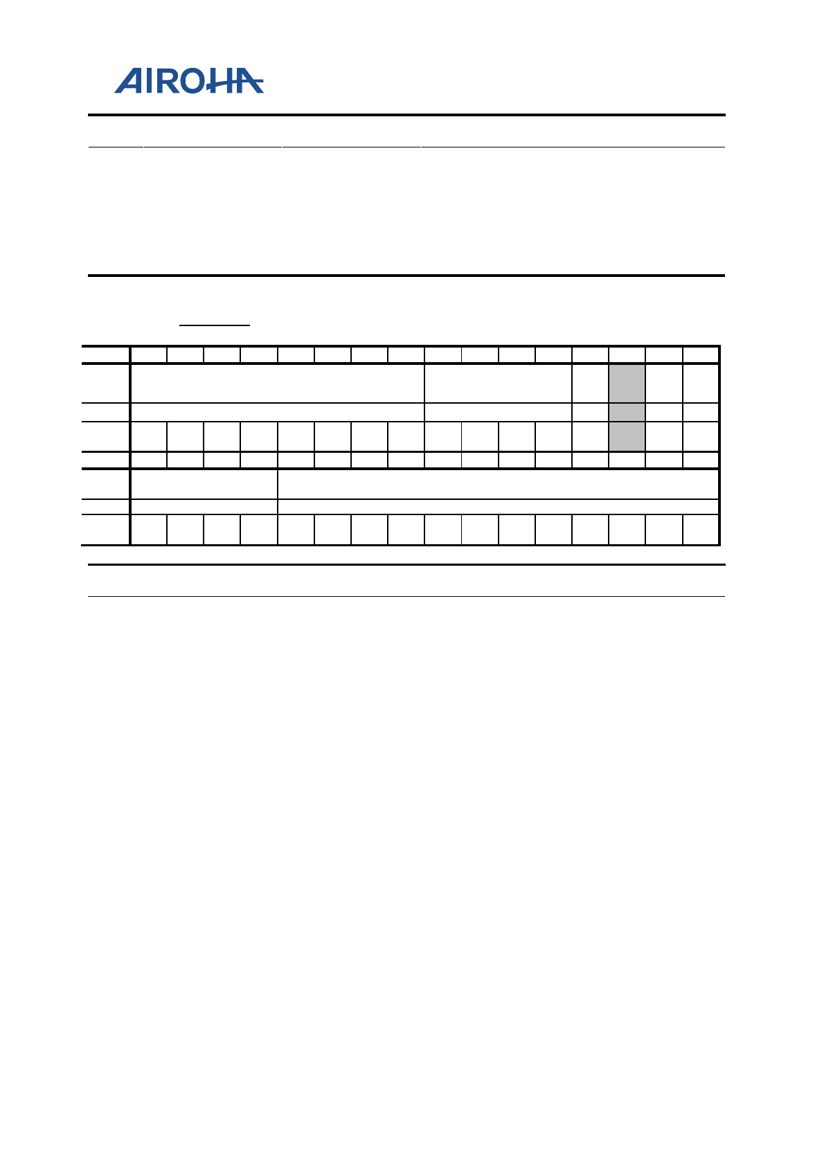
MT2523 Series Reference Manual
© 2015 - 2018 Airoha Technology Corp.
Page 127 of 692
This document contains information that is proprietary to Airoha Technology Corp. (“Airoha”) and/or its licensor(s).
Any unauthorized use, reproduction or disclosure of this document in whole or in part is strictly prohibited.
Bit(s)
Mnemonic
Name
Description
01: Pull up/down resistor in the I/O pad of the pin INS
value is 47k.
10: Pull up/down resistor in the I/O pad of the pin INS
value is 47k.
11: Pull up/down resistor in the I/O pad of the pin INS
value is 23.5k.
A0020020
SDC_CFG
SD Memory Card Controller
Configuration Register
00008000
Bit
31
30
29
28
27
26
25
24
23
22
21
20
19
18
17
16
Nam
e DTOC WDOD SDI
O
MD
LE
N
SIE
N
Type
RW
RW
RW
RW
RW
Rese
t
0 0 0 0 0 0 0 0 0 0 0 0 0 0 0
Bit
15
14
13
12
11
10
9
8
7
6
5
4
3
2
1
0
Nam
e
BSYDLY BLKLEN
Type
RW
RW
Rese
t
1 0 0 0 0 0 0 0 0 0 0 0 0 0 0 0
Bit(s)
Mnemonic
Name
Description
31:24
DTOC
DTOC
Data timeout counter. The period from finish
of the initial host read command or the last
read data block
in a multiple block read
operation to the start bit of the next read data
block requires at least two serial clock cycles.
The counter is used to extend the period (Read
Data Access Time) in unit of 65,536 serial
clocks. See the register field description
of the
register bit RDINT for reference.
00000000: Extend 65,536 more serial clock cycle.
00000001: Extend 65,536x2 more serial clock cycles.
00000010: Extend 65,536x3 more serial clock cycles.
00000011~11111110: ...
11111111: Extend 65,536x 256 more serial clock cycles.
23:20
WDOD
WDOD
Write data output delay. The period from finish
of the response for the initial host write
command or the last write data block in a
multiple block write operation to the start bit
of the next write
data block requires at least
two serial clock cycles. The register field is
used to extend the period (Write Data Output
Delay) in unit of one serial clock.

MT2523 Series Reference Manual
© 2015 - 2018 Airoha Technology Corp.
Page 128 of 692
This document contains information that is proprietary to Airoha Technology Corp. (“Airoha”) and/or its licensor(s).
Any unauthorized use, reproduction or disclosure of this document in whole or in part is strictly prohibited.
Bit(s)
Mnemonic
Name
Description
0000: No extension
0001: Extend one more serial clock cycle.
0010: Extend two more serial clock cycles.
0011~1110: ...
1111: Extend fifteen more serial clock cycles.
19
SDIO
SDIO
Enables SDIO
0: SDIO mode is disabled.
1: SDIO mode is enabled.
17
MDLEN
MDLEN
Enables multiple data line. The register can be
enabled only
when SD memory card is applied
and detected by software application. It is the
responsibility of the application to program the
bit correctly when a MultiMediaCard is
applied. If a MultiMediaCard is applied and 4
-
bit data line is enabled, the 4 bits will b
e
outputted every serial clock. Therefore, data
integrity will fail.
0: 4-bit data line is disabled.
1: 4-bit data line is enabled.
16
SIEN
SIEN
Enables serial interface. It should be enabled
as soon as possible before any command.
0: Serial interface for SD is disabled.
1: Serial interface for SD is enabled.
15:12
BSYDLY
BSYDLY
The register field is only valid for the
commands with R1b response. If the command
has a response of R1b type, SD controller must
monitor the data line 0 for car
d busy status
from the bit time that is two serial clock cycles
after the command end bit to check if
operations in SD memory card have finished.
The register field is used to expand the time
between the command end bit and end of
detection period to detec
t card busy status. If
time is up and there is no card busy status on
data line 0, the controller will abandon the
detection.
0000: No extension
0001: Extend one more serial clock cycle.
0010: Extend two more serial clock cycles.
0011~1110: ...
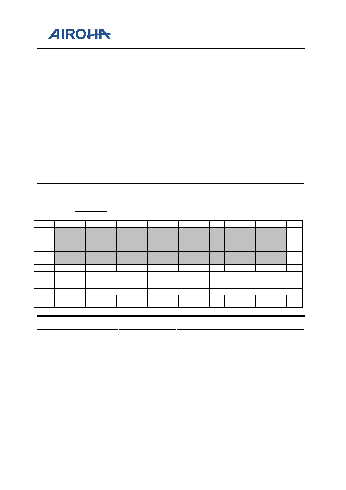
MT2523 Series Reference Manual
© 2015 - 2018 Airoha Technology Corp.
Page 129 of 692
This document contains information that is proprietary to Airoha Technology Corp. (“Airoha”) and/or its licensor(s).
Any unauthorized use, reproduction or disclosure of this document in whole or in part is strictly prohibited.
Bit(s)
Mnemonic
Name
Description
1111: Extend fifteen more serial clock cycles.
11:0
BLKLEN
BLKLEN
It refers to Block Length. The register field
defines the length of one block in unit of byte in
a data transaction. The maximum value of
block length is 2048 bytes.
000000000000: Reserved.
000000000001: Block length is 1 byte.
000000000010: Block length is 2 bytes.
000000000011~011111111110: ...
011111111111: Block length is 2047 bytes.
100000000000: Block length is 2048 bytes.
A0020024
SDC_CMD
SD Memory Card Controller Command
Register
00000000
Bit
31
30
29
28
27
26
25
24
23
22
21
20
19
18
17
16
Nam
e
CM
DF
AIL
Type
RW
Rese
t
0
Bit
15
14
13
12
11
10
9
8
7
6
5
4
3
2
1
0
Nam
e INT
C ST
OP RW DTYPE ID
RT RSPTYP
BR
EA
K
CMD
Type
RW
RW
RW
RW
RW
RW
RW
RW
Rese
t
0 0 0 0 0 0 0 0 0 0 0 0 0 0 0 0
Bit(s)
Mnemonic
Name
Description
16
CMDFAIL
CMDFAIL
If 4-bit SDIO mode is enabled, when CMD/DAT
error occurs, set up this bit to select whether to
"wait stop command" or "wait data state
machine idle".
0: Wait stop command
1: Wait data state machine idle
15
INTC
INTC
Indicates if the command is GO_IRQ_STATE.
If the command is GO_IRQ_STATE, the period
between command token
and response token
will not be limited.
0: The command is not GO_IRQ_STATE.

MT2523 Series Reference Manual
© 2015 - 2018 Airoha Technology Corp.
Page 130 of 692
This document contains information that is proprietary to Airoha Technology Corp. (“Airoha”) and/or its licensor(s).
Any unauthorized use, reproduction or disclosure of this document in whole or in part is strictly prohibited.
Bit(s)
Mnemonic
Name
Description
1: The command is GO_IRQ_STATE.
14
STOP
STOP
Indicates if the command is a stop
transmission command.
0: The command is not a stop transmission command.
1: The command is a stop transmission command.
13
RW
RW
Defines the command is a read command or
write command. The register bit is valid only
when the command will cause a transaction
with data token.
0: The command is a read command.
1: The command is a write command.
12:11
DTYPE
DTYPE
Defines data token type for the command
00: No data token for the command
01: Single block transaction
10: Multiple block transaction. That is, the command is
a multiple block read or write command.
11: Stream operation. It should only be used when a
MultiMediaCard is applied.
10
IDRT
IDRT
Identification response time. The register bit
indicates if the command has a response with
NID (i.e. 5 serial clock cycles as defined in SD
Memory Card Specification
Part 1 Physical
Layer Specification version 1.0) response time.
The register bit is valid only when the
command has a response token. Thus the
register bit must be set to '1' for CMD2
(ALL_SEND_CID) and ACMD41
(SD_APP_OP_CMD).
0: Otherwise.
1: The command has a response with NID response
time.
9:7
RSPTYP
RSPTYP
Defines response type for the command. For
commands with R1 and R1b response, the
register SDC_CSTA (not SDC_STA) will be
updated after response token is received. This
register SDC_CSTA
contains the status of the
SD and will be used as response interrupt
sources.
Note: If CMD7 is used with all 0's RCA, RSPTYP
must be "000". Command "GO_TO_IDLE" also
has RSPTYP='000'.

MT2523 Series Reference Manual
© 2015 - 2018 Airoha Technology Corp.
Page 131 of 692
This document contains information that is proprietary to Airoha Technology Corp. (“Airoha”) and/or its licensor(s).
Any unauthorized use, reproduction or disclosure of this document in whole or in part is strictly prohibited.
Bit(s)
Mnemonic
Name
Description
000: There is no response for the command. For
instance, broadcast
command without response and
GO_INACTIVE_STATE command.
001: The command has R1 response. R1 response token
is 48
-bit.
010: The command has R2 response. R2 response
token is 136
-bit.
011: The command has R3 response. Even though R3 is
48
-bit response, it does not contain CRC checksum.
100: The command has R4 response. R4 response
token is 48
-bit. (only for MMC)
101: The command has R5 response. R5 response
token is 48
-bit. (only for MMC)
110: The command has R6 response. R6 response
token is 48
-bit.
111: The command has R1b response. If the command
has a response of R1b type, SD controller must monitor
the data line 0 for card busy status from the bit time
that is two or four serial clock cycles after the
command end bit to
check if operations in SD memory
card have finished. There are two cases for detection of
card busy status. The first case is that the host stops
the data transmission during an active write data
transfer. The card will assert busy signal after the stop
tr
ansmission command end bit followed by four serial
clock cycles. The second case is that the card is in idle
state or under a scenario of receiving a stop
transmission command between data blocks when
multiple block write command is in progress. The
regist
er bit is valid only when the command has a
response token.
6
BREAK
BREAK
Aborts pending MMC GO_IRQ_MODE
command. It is only valid for a pending
GO_IRQ_MODE command waiting for MMC
interrupt response.
0: Other fields are valid.
1: Break a pending MMC GO_IRQ_MODE command
in the controller. Other fields are invalid.
5:0
CMD
CMD
SD memory card command. Total 6 bits.
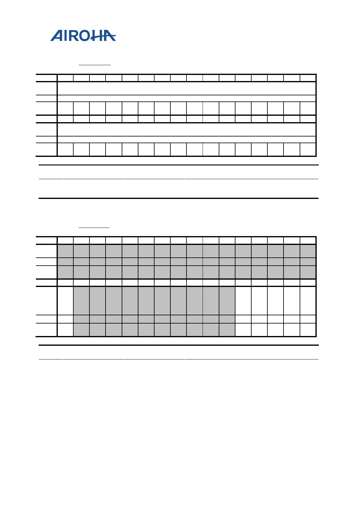
MT2523 Series Reference Manual
© 2015 - 2018 Airoha Technology Corp.
Page 132 of 692
This document contains information that is proprietary to Airoha Technology Corp. (“Airoha”) and/or its licensor(s).
Any unauthorized use, reproduction or disclosure of this document in whole or in part is strictly prohibited.
A0020028
SDC_ARG
SD Memory Card Controller Argument
Register
00000000
Bit
31
30
29
28
27
26
25
24
23
22
21
20
19
18
17
16
Nam
e
ARG
Type
RW
Rese
t
0 0 0 0 0 0 0 0 0 0 0 0 0 0 0 0
Bit
15
14
13
12
11
10
9
8
7
6
5
4
3
2
1
0
Nam
e
ARG
Type
RW
Rese
t
0 0 0 0 0 0 0 0 0 0 0 0 0 0 0 0
Bit(s)
Mnemonic
Name
Description
31:0
ARG
ARG
Contains argument of SD memory card
command
A002002C
SDC_STA
SD Memory Card Controller Status
Register
00000000
Bit
31
30
29
28
27
26
25
24
23
22
21
20
19
18
17
16
Nam
e
Type
Rese
t
Bit
15
14
13
12
11
10
9
8
7
6
5
4
3
2
1
0
Nam
e WP
FE
DA
TB
US
Y
FE
CM
DB
US
Y
BE
DA
TB
US
Y
BE
CM
DB
US
Y
BE
SD
CB
US
Y
Type
RO
RO
RO
RO
RO
RO
Rese
t
0 0 0 0 0 0
Bit(s)
Mnemonic
Name
Description
15
WP
WP
Detects the status of Write Protection switch on
SD memory card. The register bit shows the
status of Write Protection switch on SD
memory card. There is no default reset value.
The pin WP (Write Protection) is also only
useful while the controller is configured for SD
memory card.
1: Write Protection switch on. It means that memory
card is desired to be write
-protected.
0: Write Protection switch off. It means that memory
card is writable.

MT2523 Series Reference Manual
© 2015 - 2018 Airoha Technology Corp.
Page 133 of 692
This document contains information that is proprietary to Airoha Technology Corp. (“Airoha”) and/or its licensor(s).
Any unauthorized use, reproduction or disclosure of this document in whole or in part is strictly prohibited.
Bit(s)
Mnemonic
Name
Description
4
FEDATBUSY
FEDATBUSY
Indicates if any transmission is going on DAT
line on SD bus. This bit indic
ates directly the
CMD line at card clock domain. For those
commands without data but still involving DAT
line, the register bit is useless. For example, if
an Erase command is issued, checking if the
register bit is '0' before issuing the next
command with
data will not guarantee that the
controller is idle. In this situation, use the
register bit BESDCBUSY.
0: No transmission is going on DAT line on SD bus.
1: There exists transmission going on DAT line on SD
bus.
3
FECMDBUSY
FECMDBUSY
Indicates if any transmission is going on CMD
line on SD bus. This bit indicates directly the
CMD line at card clock domain.
0: No transmission is going on CMD line on SD bus.
1: There exists transmission going on CMD line on SD
bus.
2
BEDATBUSY
BEDATBUSY
Indicates if any transmission is going on DAT
line on SD bus.
0: Backend SDC controller gets the info that no
transmission is going on DAT line on SD bus.
1: Backend SDC controller gets the info that there
exists transmission going on DAT line on
SD bus.
1
BECMDBUSY
BECMDBUSY
Indicates if any transmission is going on CMD
line on SD bus. This bit shows backend
controller's CMD busy state. The busy state is
sync from card clock domain to bus clock
domain.
0: Backend SDC controller gets the info that no
transmission is going on CMD line on SD bus.
1: Backend SDC controller gets the info that there
exists transmission going on CMD line on SD bus.
0
BESDCBUSY
BESDCBUSY
Indicates if SD controller is busy, i.e. any
transmission is going on CMD or
DAT line on
SD bus. This bit shows backend controller's
SDC busy state. The busy state is sync from
card clock domain to bus clock domain.
0: Backend SD controller is idle.
1: Backend SD controller is busy.
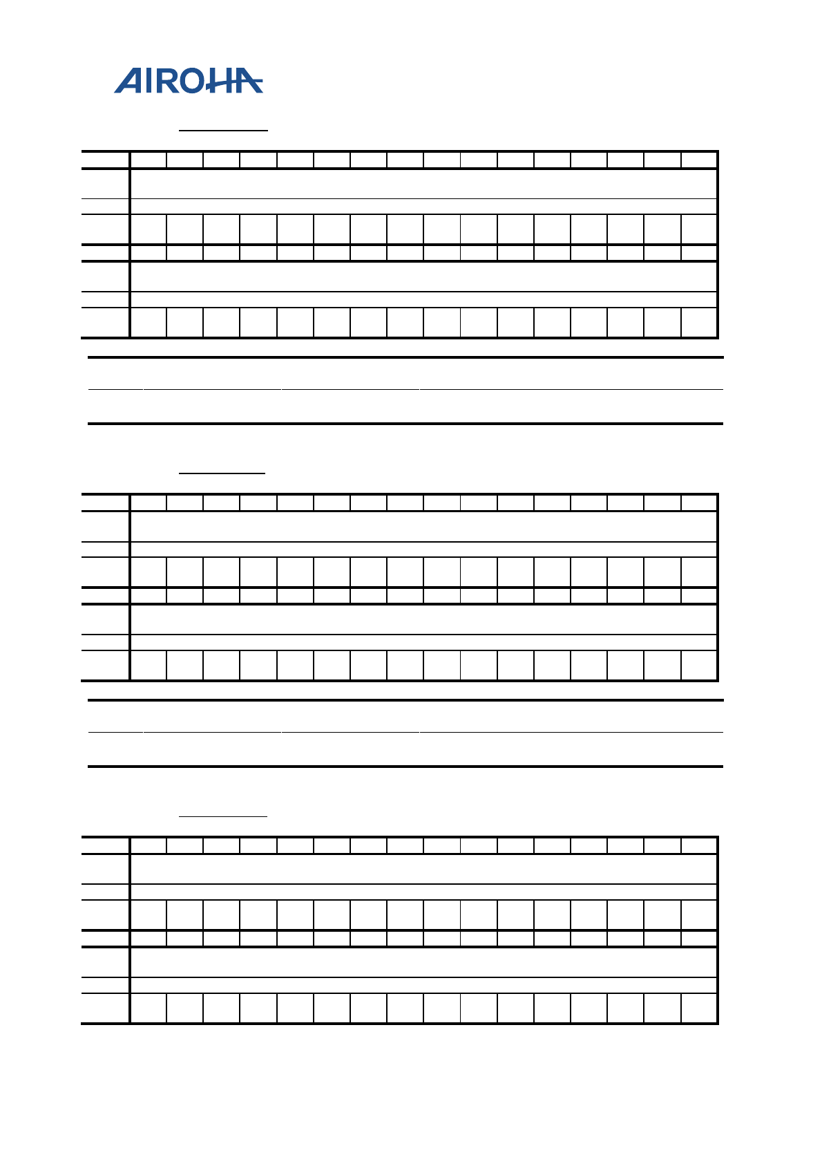
MT2523 Series Reference Manual
© 2015 - 2018 Airoha Technology Corp.
Page 134 of 692
This document contains information that is proprietary to Airoha Technology Corp. (“Airoha”) and/or its licensor(s).
Any unauthorized use, reproduction or disclosure of this document in whole or in part is strictly prohibited.
A0020030
SDC_RESP0
SD Memory Card Controller Response
Register 0
00000000
Bit
31
30
29
28
27
26
25
24
23
22
21
20
19
18
17
16
Nam
e
RESP_31_0
Type
RO
Rese
t
0 0 0 0 0 0 0 0 0 0 0 0 0 0 0 0
Bit
15
14
13
12
11
10
9
8
7
6
5
4
3
2
1
0
Nam
e
RESP_31_0
Type
RO
Rese
t
0 0 0 0 0 0 0 0 0 0 0 0 0 0 0 0
Bit(s)
Mnemonic
Name
Description
31:0
RESP[31:0]
RESP_31_0
A0020034
SDC_RESP1
SD Memory Card Controller Response
Register 1
00000000
Bit
31
30
29
28
27
26
25
24
23
22
21
20
19
18
17
16
Nam
e
RESP_63_32
Type
RO
Rese
t
0 0 0 0 0 0 0 0 0 0 0 0 0 0 0 0
Bit
15
14
13
12
11
10
9
8
7
6
5
4
3
2
1
0
Nam
e
RESP_63_32
Type
RO
Rese
t
0 0 0 0 0 0 0 0 0 0 0 0 0 0 0 0
Bit(s)
Mnemonic
Name
Description
31:0
RESP[63:32]
RESP_63_32
A0020038
SDC_RESP2
SD Memory Card Controller Response
Register 2
00000000
Bit
31
30
29
28
27
26
25
24
23
22
21
20
19
18
17
16
Nam
e
RESP_95_64
Type
RO
Rese
t
0 0 0 0 0 0 0 0 0 0 0 0 0 0 0 0
Bit
15
14
13
12
11
10
9
8
7
6
5
4
3
2
1
0
Nam
e
RESP_95_64
Type
RO
Rese
t
0 0 0 0 0 0 0 0 0 0 0 0 0 0 0 0
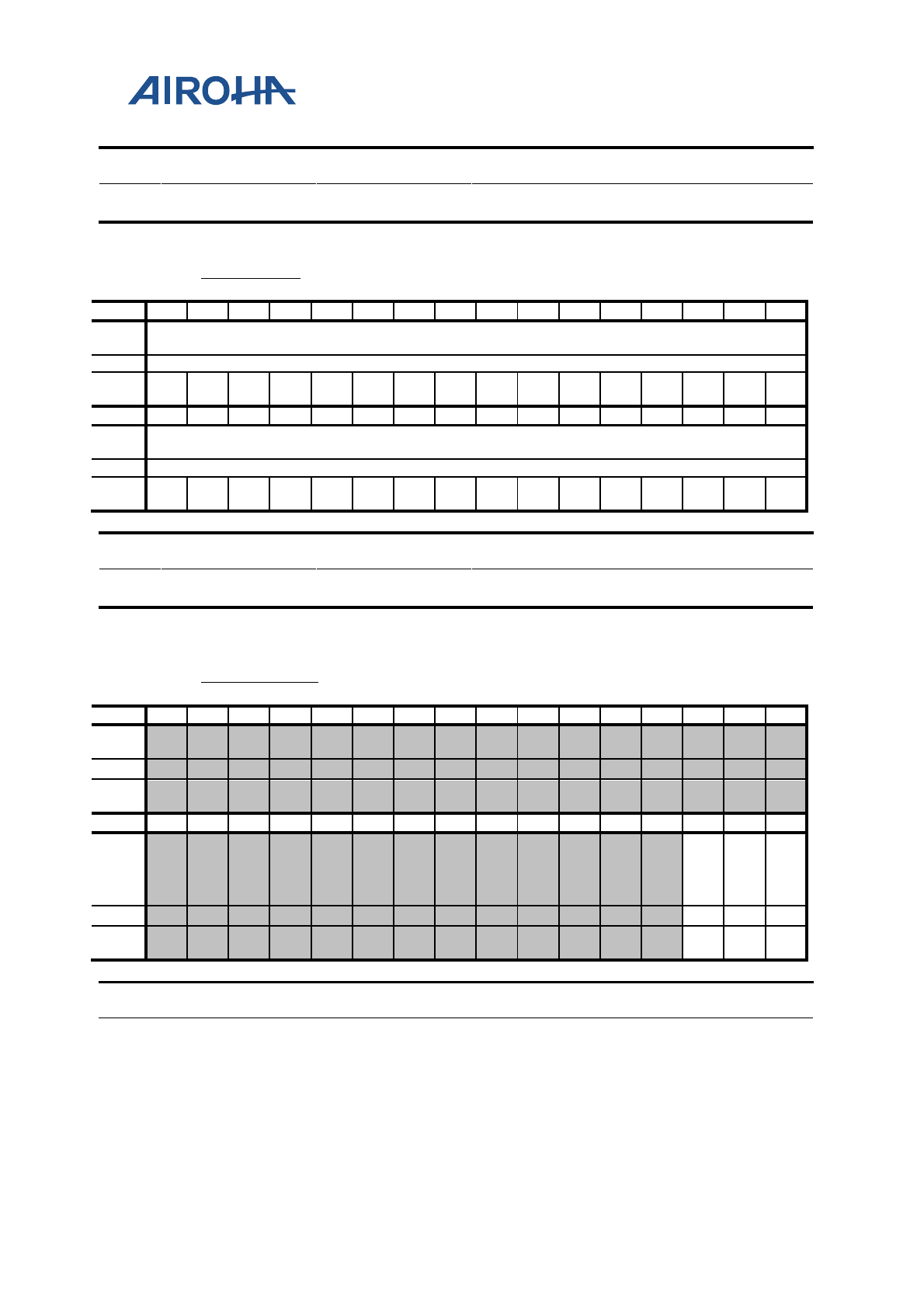
MT2523 Series Reference Manual
© 2015 - 2018 Airoha Technology Corp.
Page 135 of 692
This document contains information that is proprietary to Airoha Technology Corp. (“Airoha”) and/or its licensor(s).
Any unauthorized use, reproduction or disclosure of this document in whole or in part is strictly prohibited.
Bit(s)
Mnemonic
Name
Description
31:0
RESP[95:64]
RESP_95_64
A002003C
SDC_RESP3
SD Memory Card Controller Response
Register 3
00000000
Bit
31
30
29
28
27
26
25
24
23
22
21
20
19
18
17
16
Nam
e
RESP_127_96
Type
RO
Rese
t
0 0 0 0 0 0 0 0 0 0 0 0 0 0 0 0
Bit
15
14
13
12
11
10
9
8
7
6
5
4
3
2
1
0
Nam
e
RESP_127_96
Type
RO
Rese
t
0 0 0 0 0 0 0 0 0 0 0 0 0 0 0 0
Bit(s)
Mnemonic
Name
Description
31:0
RESP[127:96]
RESP_127_96
A0020040
SDC_CMDSTA
SD Memory Card Controller Command
Status Register
00000000
Bit
31
30
29
28
27
26
25
24
23
22
21
20
19
18
17
16
Nam
e
Type
Rese
t
Bit
15
14
13
12
11
10
9
8
7
6
5
4
3
2
1
0
Nam
e
RS
PC
RC
ER
R
CM
DT
O
CM
DR
DY
Type
RC
RC
RC
Rese
t
0 0 0
Bit(s)
Mnemonic
Name
Description
2
RSPCRCERR
RSPCRCERR
CRC error on CMD detected. 1 indicates that SD
controller detects a CRC error after reading a
response from the CMD line.
0: Otherwise
1: SD controller detects a CRC error after reading a
response from the CMD line.
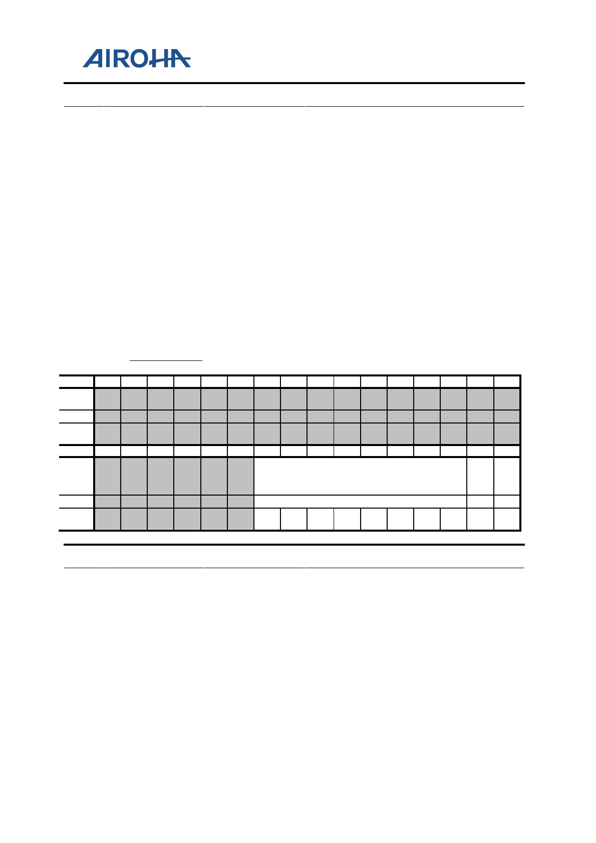
MT2523 Series Reference Manual
© 2015 - 2018 Airoha Technology Corp.
Page 136 of 692
This document contains information that is proprietary to Airoha Technology Corp. (“Airoha”) and/or its licensor(s).
Any unauthorized use, reproduction or disclosure of this document in whole or in part is strictly prohibited.
Bit(s)
Mnemonic
Name
Description
1
CMDTO
CMDTO
Timeout on CMD detected. 1 indicates that SD
controller detects a timeout condition while
waiting for a response on the CMD line.
0: Otherwise
1: SD controller detects a timeout condition while
waiting for a response on the CMD line.
0
CMDRDY
CMDRDY
For command without response, the register
bit will be '1' once the command is completed
on SD bus. For command with response, the
register bit will be '1' whenever the command is
issued onto SD bus and its corresponding
response is received without CRC error.
0: Otherwise
1: Command with/without response finish successfully
without CRC error.
A0020044
SDC_DATSTA
SD Memory Card Controller Data
Status Register
00000000
Bit
31
30
29
28
27
26
25
24
23
22
21
20
19
18
17
16
Nam
e
Type
Rese
t
Bit
15
14
13
12
11
10
9
8
7
6
5
4
3
2
1
0
Nam
e DATCRCERR DA
TT
O
BL
KD
ON
E
Type
RC
RC
RC
Rese
t
0 0 0 0 0 0 0 0 0 0
Bit(s)
Mnemonic
Name
Description
9:2
DATCRCERR
DATCRCERR
CRC error on DAT detected. 1 indicates that SD
controller detected a CRC error for bit n after
reading a block of data from the DAT line or SD
signaled a CRC error after writing a block of
data to the DAT line.
0: Otherwise
1: SD controller detects a CRC error after reading a
block of data from the DAT line or SD signaled a CRC
error after writing a block of data to the DAT line.
Note that: n is 7~0 for 8-bits mode, each bit read and
clear individually.
1
DATTO
DATTO
Timeout on DAT detected. 1 indicates that SD
controller detected a timeout condition while
MT2523 Series Reference Manual
© 2015 - 2018 Airoha Technology Corp.
Page 137 of 692
This document contains information that is proprietary to Airoha Technology Corp. (“Airoha”) and/or its licensor(s).
Any unauthorized use, reproduction or disclosure of this document in whole or in part is strictly prohibited.
Bit(s)
Mnemonic
Name
Description
waiting for data token on the DAT line.
0: Otherwise
1: SD controller detects a timeout condition while
waiting for data token on the DAT line.
0
BLKDONE
BLKDONE
Indicates the status of data block transfer
0: Otherwise
1: A data block is successfully transferred.
A0020048
SDC_CSTA
SD Memory Card Status Register
00000000
Bit
31
30
29
28
27
26
25
24
23
22
21
20
19
18
17
16
Nam
e
CSTA_31_0
Type
RC
Rese
t
0 0 0 0 0 0 0 0 0 0 0 0 0 0 0 0
Bit
15
14
13
12
11
10
9
8
7
6
5
4
3
2
1
0
Nam
e
CSTA_31_0
Type
RC
Rese
t
0 0 0 0 0 0 0 0 0 0 0 0 0 0 0 0
Bit(s)
Mnemonic
Name
Description
31:0
CSTA [31:0]
CSTA_31_0
A002004C
SDC_IRQMASK0
SD Memory Card IRQ Mask Register 0
00000000
Bit
31
30
29
28
27
26
25
24
23
22
21
20
19
18
17
16
Nam
e
IRQMASK_31_0
Type
RW
Rese
t
0 0 0 0 0 0 0 0 0 0 0 0 0 0 0 0
Bit
15
14
13
12
11
10
9
8
7
6
5
4
3
2
1
0
Nam
e
IRQMASK_31_0
Type
RW
Rese
t
0 0 0 0 0 0 0 0 0 0 0 0 0 0 0 0
Bit(s)
Mnemonic
Name
Description
MT2523 Series Reference Manual
© 2015 - 2018 Airoha Technology Corp.
Page 138 of 692
This document contains information that is proprietary to Airoha Technology Corp. (“Airoha”) and/or its licensor(s).
Any unauthorized use, reproduction or disclosure of this document in whole or in part is strictly prohibited.
Bit(s)
Mnemonic
Name
Description
31:0
IRQMASK [31:0]
IRQMASK_31_0
A0020050
SDC_IRQMASK1
SD Memory Card IRQ Mask Register 1
00000000
Bit
31
30
29
28
27
26
25
24
23
22
21
20
19
18
17
16
Nam
e
IRQMASK_63_32
Type
RW
Rese
t
0 0 0 0 0 0 0 0 0 0 0 0 0 0 0 0
Bit
15
14
13
12
11
10
9
8
7
6
5
4
3
2
1
0
Nam
e
IRQMASK_63_32
Type
RW
Rese
t
0 0 0 0 0 0 0 0 0 0 0 0 0 0 0 0
Bit(s)
Mnemonic
Name
Description
31:0
IRQMASK [63:32]
IRQMASK_63_32
A0020054
SDIO_CFG
SDIO Configuration Register
00000000
Bit
31
30
29
28
27
26
25
24
23
22
21
20
19
18
17
16
Nam
e
Type
Rese
t
Bit
15
14
13
12
11
10
9
8
7
6
5
4
3
2
1
0
Nam
e
DIS
SE
L
INT
CS
EL
DS
BS
EL
INT
EN
Type
RW
RW
RW
RW
Rese
t
0 0 0 0
Bit(s)
Mnemonic
Name
Description
5
DISSEL
DISSEL
Selects data block interrupt source
0: The host will detect SDIO interrupt during interrupt
period between two
data blocks of multiple block data
access.
1: The host will ignore SDIO interrupt during interrupt
period between two data blocks of multiple block data
access.
3
INTCSEL
INTCSEL
Selects interrupt control
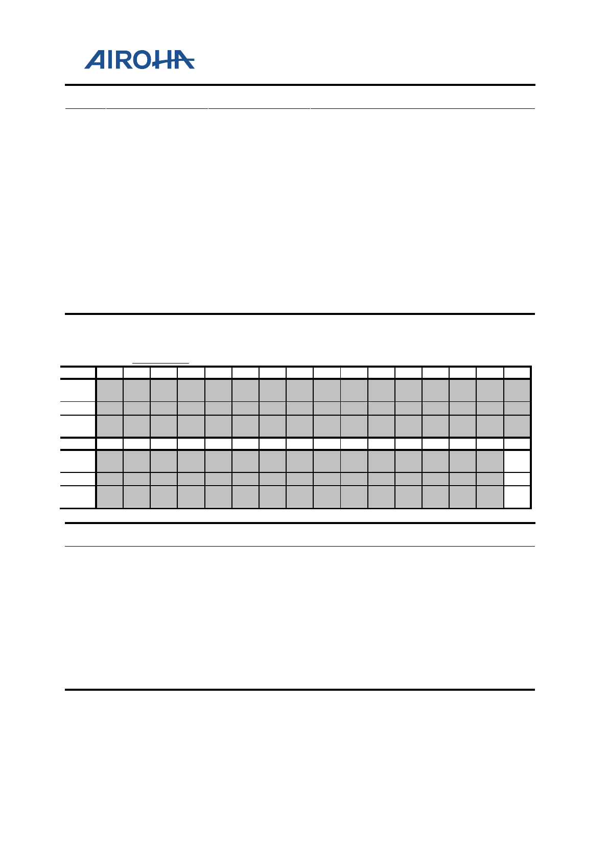
MT2523 Series Reference Manual
© 2015 - 2018 Airoha Technology Corp.
Page 139 of 692
This document contains information that is proprietary to Airoha Technology Corp. (“Airoha”) and/or its licensor(s).
Any unauthorized use, reproduction or disclosure of this document in whole or in part is strictly prohibited.
Bit(s)
Mnemonic
Name
Description
0: The host detects DAT1 low as SDIO interrupt.
1: The host detects DAT3/DAT2/DAT1/DAT0 4'b1101
as SDIO interrupt.
2
DSBSEL
DSBSEL
Selects data block start bit
0: Use data line 0 as start bit of data block and other
data lines are ignored.
1: Start bit of a data block is received only when data
line 0
-3 all become low.
0
INTEN
INTEN
Enables interrupt for SDIO
0: Disable
1: Enable
A0020058
SDIO_STA
SDIO Status Register
00000000
Bit
31
30
29
28
27
26
25
24
23
22
21
20
19
18
17
16
Nam
e
Type
Rese
t
Bit
15
14
13
12
11
10
9
8
7
6
5
4
3
2
1
0
Nam
e
IR
Q
Type
RO
Rese
t
0
Bit(s)
Mnemonic
Name
Description
0
IRQ
IRQ
SDIO interrupt exists on the data line. F, for
example, during the interrupt period, in the 1
-
bit data line mode, and DAT1/5 goes low from
high, this bit will become 1 from 0. I, if DAT1/5
goes high from low, this bit will become 0 from
1.
0: There is no SDIO interrupt existing on the data line.
1: There is SDIO interrupt existing on the data line.
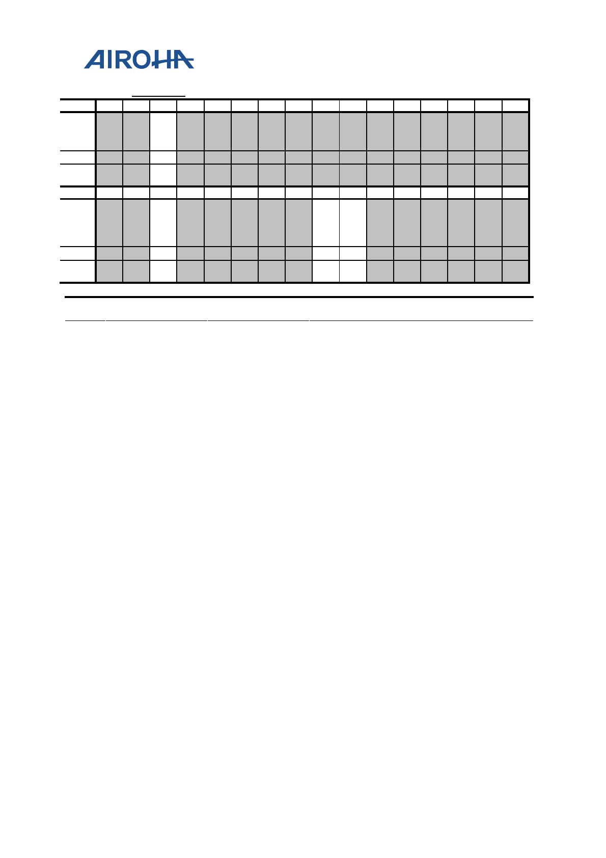
MT2523 Series Reference Manual
© 2015 - 2018 Airoha Technology Corp.
Page 140 of 692
This document contains information that is proprietary to Airoha Technology Corp. (“Airoha”) and/or its licensor(s).
Any unauthorized use, reproduction or disclosure of this document in whole or in part is strictly prohibited.
A0020080
CLK_RED
CLK Latch Configuration Register
00000000
Bit
31
30
29
28
27
26
25
24
23
22
21
20
19
18
17
16
Nam
e
CM
D_
RE
D
Type
RW
Rese
t
0
Bit
15
14
13
12
11
10
9
8
7
6
5
4
3
2
1
0
Nam
e
DA
T_
RE
D
CL
KP
AD
_R
ED
CL
K_
LA
TC
H
Type
RW
RW
RW
Rese
t
0 0 0
Bit(s)
Mnemonic
Name
Description
29
CMD_RED
CMD_RED
Determines command response from card
output is latched at falling edge or rising edge
of internal clock (only effective when
CLK_LATCH = 1)
0: Internal clock rising edge to latch response
1: Internal clock falling edge to latch response
13
DAT_RED
DAT_RED
Determines input data from card output is
latched at falling edge or rising edge of internal
sample clock (only effective when CLK_LATCH
= 1)
0: Internal clock rising edge to latch data
1: Internal clock falling edge to latch data
7
CLKPAD_RED
CLKPAD_RED
Determines input data from card is latched at
falling edge or rising edge of the feedback clock
from pad. The suggested setting is 0 for
SD/eMMC serial clock is less than 25MHz and 1
for SD serial clock is higher than 25MHz. (only
e
ffective when CLK_LATCH = 0)
0: Internal feedback clock rising edge to latch
data/response
1: Internal feedback clock falling edge to latch
data/response
6
CLK_LATCH
CLK_LATCH
Determines which clock to latch data from
card. The suggested setting
is 0.
0: Internal feedback clock is used to latch
data/response from card.
1: Internal clock is used to latch data/response from
card.
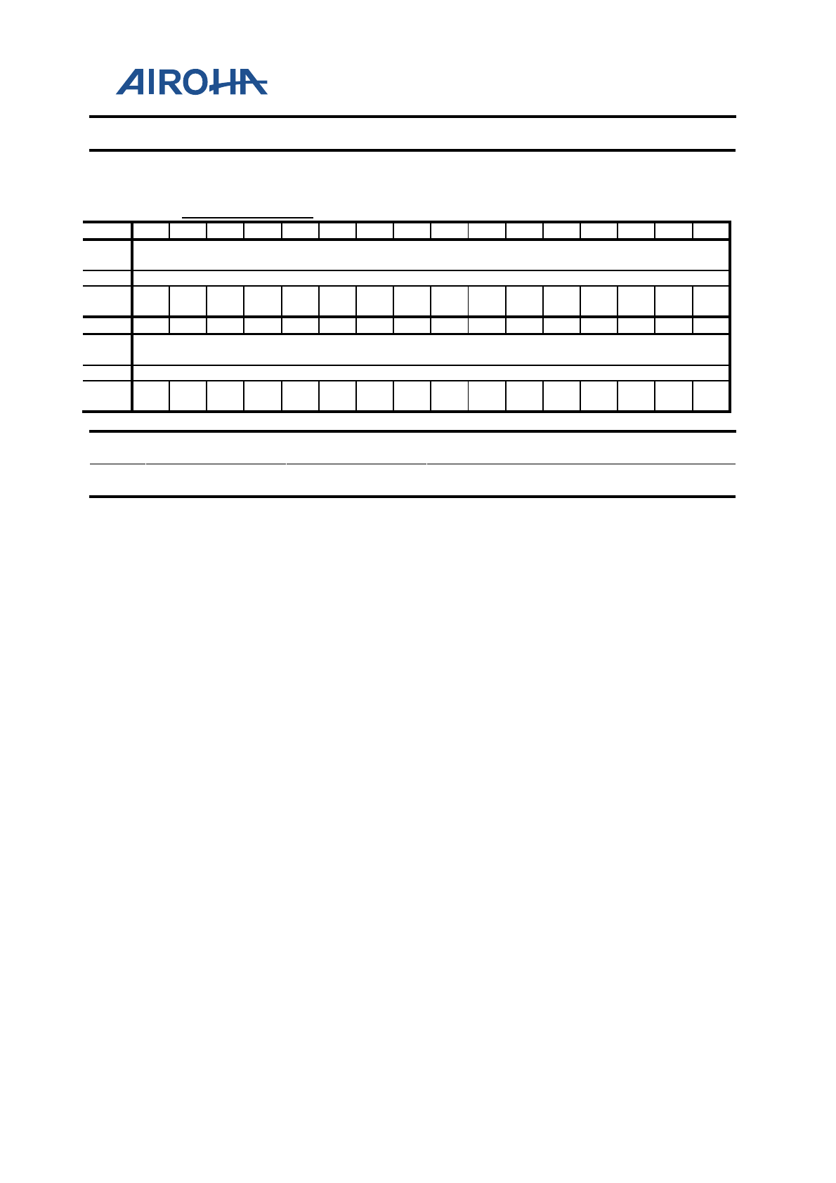
MT2523 Series Reference Manual
© 2015 - 2018 Airoha Technology Corp.
Page 141 of 692
This document contains information that is proprietary to Airoha Technology Corp. (“Airoha”) and/or its licensor(s).
Any unauthorized use, reproduction or disclosure of this document in whole or in part is strictly prohibited.
Bit(s)
Mnemonic
Name
Description
A0020098
DAT_CHECKSUM
MSDC Rx Data Check Sum Register
00000000
Bit
31
30
29
28
27
26
25
24
23
22
21
20
19
18
17
16
Nam
e
DAT_CHECKSUM
Type
RW
Rese
t
0 0 0 0 0 0 0 0 0 0 0 0 0 0 0 0
Bit
15
14
13
12
11
10
9
8
7
6
5
4
3
2
1
0
Nam
e
DAT_CHECKSUM
Type
RW
Rese
t
0 0 0 0 0 0 0 0 0 0 0 0 0 0 0 0
Bit(s)
Mnemonic
Name
Description
31:0
DAT_CHECKSUM
The checksum algorithm is 32 bit's XOR.
MT2523 Series Reference Manual
© 2015 - 2018 Airoha Technology Corp.
Page 142 of 692
This document contains information that is proprietary to Airoha Technology Corp. (“Airoha”) and/or its licensor(s).
Any unauthorized use, reproduction or disclosure of this document in whole or in part is strictly prohibited.
11. USB2.0 High-Speed Device Controller
11.1. General Description
USB20 controller supports HS (480M)/FS (12M)/LS (1.5M). The USB controller is configured for supporting 2
endpoints to receive packets and four endpoints to send packets except for endpoint 0. These endpoints can be
individually configured in the software to handle either Bulk transfers, Interrupt transfers or Isochronous
transfers. There are four DMA channels, and the embedded RAM size is configurable up to 3264 bytes. The
embedded RAM can be dynamically configured to each endpoint.
11.1.1. Features
Feature Description
Speed HS (480M)/FS (12M)/LS (1.5M)
Enhanced feature Generic device
Endpoint 4 TX, 2 RX
DMA channel 4
Embedded RAM 3264
11.1.2. Programming Guide
DMA: USB20 includes a multi-channel DMA controller, configurable for up to 4 channels. This DMA controller
supports two DMA modes, referred to as DMA Modes 0 and 1. When operating in DMA Mode 0, the DMA
controller can only be programmed to load/unload one packet, so processor intervention is required for each
packet transferred over the USB. This mode can be used with any endpoint, whether it uses Control, Bulk,
Isochronous, or Interrupt transactions. When operating in DMA Mode 1, the DMA controller can be programmed
to load/unload a complete bulk transfer (which can be many packets). Once set up, the DMA controller will
load/unload all packets of the transfer, interrupting the processor only when the transfer has completed. DMA
Mode 1 can only be used with endpoints that use Bulk transactions. Each channel can be independently
programmed for the selected operating mode. (For detailed register information, refer to USB20 MAC register
map.)
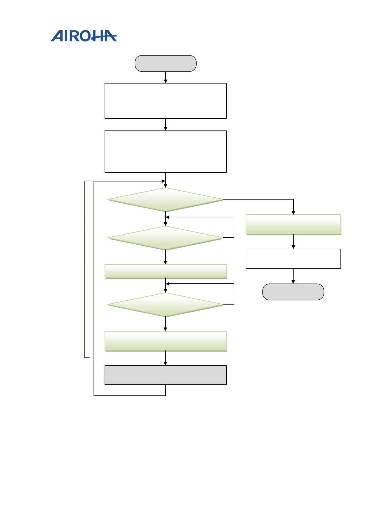
MT2523 Series Reference Manual
© 2015 - 2018 Airoha Technology Corp.
Page 143 of 692
This document contains information that is proprietary to Airoha Technology Corp. (“Airoha”) and/or its licensor(s).
Any unauthorized use, reproduction or disclosure of this document in whole or in part is strictly prohibited.
Figure 11-1. Multiple packet RX flow (known size)
IDLE State
Set IntrRxE.Dn=0
Set RxCSR.D15 (AutoClear) = 1
Set RxCSR.D13 (DMAReqEnab) = 1
Set RxCSR.D11 (DMAReqMode) = 0
(If Host: Also set RxCSR.D14(AutoReq) = 1)
Set DMA registers as follows:
Set ADDR = Address to store data
Set COUNT = Amount of data
Set CNTL.D0, CNTL.D2, CNTL.D3 = 1
Set CNTL.D1 = 0
Set CNTL[D10,9] as required
Is COUNT = 0?
Is DMAReq[m] high?
DMA controller request bus
Is AHB_HGRANT high?
DMA Controller reads from FIFO.
Write to ADDR and decrements COUNT.
RxPktRdy cleared
(Unless packet is less than RxMaxP)
No
Yes
Yes
No
No
DMA controller asserts DMA_NINT.
If necessary, clear RxPktRdy.
IDLE State
Yes
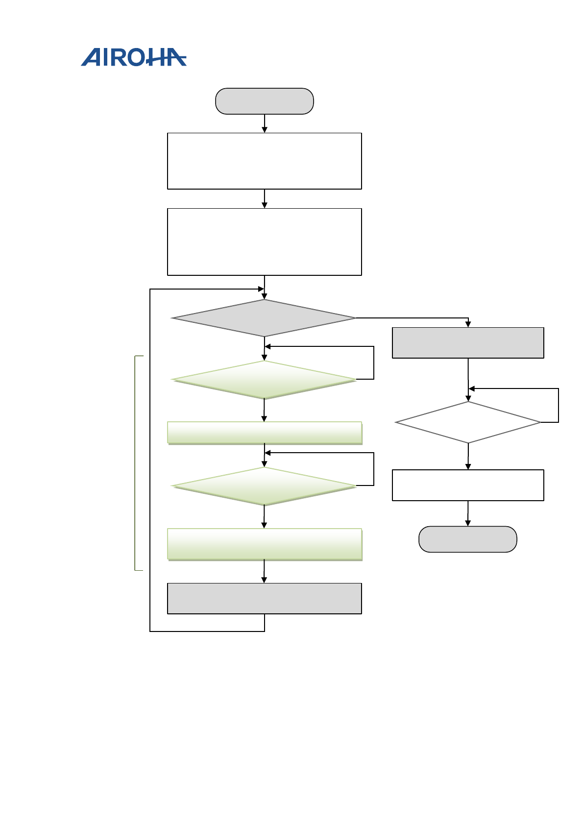
MT2523 Series Reference Manual
© 2015 - 2018 Airoha Technology Corp.
Page 144 of 692
This document contains information that is proprietary to Airoha Technology Corp. (“Airoha”) and/or its licensor(s).
Any unauthorized use, reproduction or disclosure of this document in whole or in part is strictly prohibited.
Figure 11-2. Multiple packet RX flow (unknown size)
IDLE State
Set IntrRxE.Dn=0
Set RxCSR.D15 (AutoClear) = 1
Set RxCSR.D13 (DMAReqEnab) = 1
Set RxCSR.D11 (DMAReqMode) = 1
(If Host: Also set RxCSR.D14(AutoReq) = 1)
Set DMA registers as follows:
Set ADDR = Address to store data
Set COUNT = Size of buffer
Set CNTL.D0, CNTL.D2, CNTL.D3 = 1
Set CNTL.D1 = 0
Set CNTL[D10,9] as required
Is Packet Size = RxMaxP?
Is DMAReq[m] high?
DMA controller request bus
Is AHB_HGRANT high?
DMA controller reads from FIFO.
Write to ADDR and decrements COUNT.
RxPktRdy cleared
Yes
Yes
Yes
No
No
Read packet from FIFO.
Clear RxPktRdy.
IDLE State
No
On MC_NINT = 1,
Is IntrRx[n] = 1?
No
Yes
Assert Rx Endpoint interrupt.
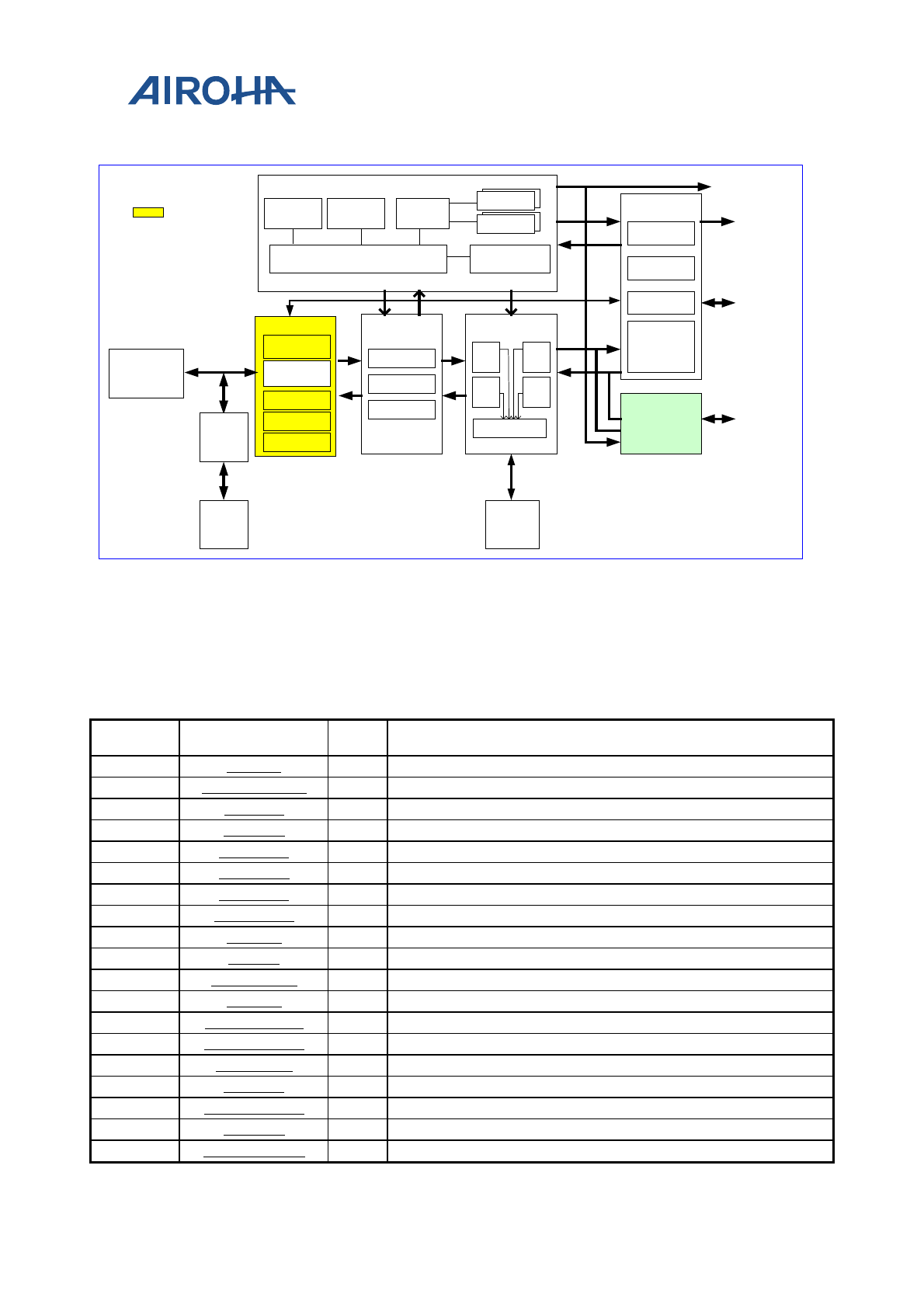
MT2523 Series Reference Manual
© 2015 - 2018 Airoha Technology Corp.
Page 145 of 692
This document contains information that is proprietary to Airoha Technology Corp. (“Airoha”) and/or its licensor(s).
Any unauthorized use, reproduction or disclosure of this document in whole or in part is strictly prohibited.
11.1.3. Block Diagram
EP0 Control
(Host)
Endpoint Control
EP0 Control
(Peripheral)
EP1- 15
Control
Combine Wndpoints
Transmit
Host Transaction
Scheduler
Receive
UTM
Data Sync
(HCLK to XCLK)
HS Negotiation
HNP/SRP
Timers
Packet
Encoder/Decoder
Packet Encode
Packet Decode
CRC gen/check
RAM Controller
Rx
Buff
Rx
Buff
Tx
Buff
Tx
Buff
Cycle Control
CPU
INTERFACE
Interrupt
Control
Common
Regs
Cycle Control
FIFO
decoder
DMA Controller
(Optional)
USB1.1
PHY
UTMI+Level2
PHY
ULPI
Wrapper
RAM
DMA
Requests
Interrupts
AHB Slave
AHB Master
XCLK
Data Sync
(XCLK to HCLK)
Figure 11-3. Block diagram
11.2. Register Definition
Module name: Unified_USB Base address: (+A0900000h)
Address Name
Widt
h Register Function
A0900000 FADDR 8 Function Address Register (Device mode only)
A0900001
POWER_PERI
8
Power Management Register
A0900002
INTRTX
16
Tx Interrupt Status Register
A0900004
INTRRX
16
Rx Interrupt Status Register
A0900006 INTRTXE 16 Tx Interrupt Enable Register
A0900008
INTRRXE
16
Rx Interrupt Enable Register
A090000A
INTRUSB
8
Common USB Interrupt Register
A090000B
INTRUSBE
8
Common USB Interrupt Enable Register
A090000C FRAME 16 Frame Number Register
A090000E
INDEX
8
Endpoint Selection Index Register
A090000F
TESTMODE
8
Test Mode Enable Register
A0900010
TXMAP
16
TXMAP Register
A0900012 TXCSR_PERI 16 Tx CSR Register
A0900016
RXCSR_PERI
16
RX CSR Register
A0900018
RXCOUNT
16
Rx Count Register
A090001A
TXTYPE
8
TxType Register
A090001B TXINTERVAL 8 TxInterval Register
A090001C
RXTYPE
8
RxType Register
A090001D
RXINTERVAL
8
RxInterval Register
MT2523 Series Reference Manual
© 2015 - 2018 Airoha Technology Corp.
Page 146 of 692
This document contains information that is proprietary to Airoha Technology Corp. (“Airoha”) and/or its licensor(s).
Any unauthorized use, reproduction or disclosure of this document in whole or in part is strictly prohibited.
Module name: Unified_USB Base address: (+A0900000h)
A090001F
FIFOSIZE
8
Configured FIFO Size Register
A0900020
FIFO0
32
USB Endpoint 0 FIFO Register
A0900024 FIFO1 32 USB Endpoint 1 FIFO Register
A0900028
FIFO2
32
USB Endpoint 2 FIFO Register
A0900060
DEVCTL
8
Device Control Register
A0900061
PWRUPCNT
8
Power Up Counter Register
A0900062 TXFIFOSZ 8 Tx FIFO Size Register
A0900063
RXFIFOSZ
8
Rx FIFO Size Register
A0900064
TXFIFOADD
16
Tx FIFO Address Register
A0900066
RXFIFOADD
16
Rx FIFO Address Register
A090006C HWCAPS 16 Hardware Capability Register
A090006E
HWSVERS
16
Version Register
A0900070
BUSPERF1
16
USB Bus Performance Register 1
A0900072
BUSPERF2
16
USB Bus Performance Register 2
A0900074 BUSPERF3 16 USB Bus Performance Register 3
A0900078
EPINFO
8
Number of Tx and Rx Register
A0900079
RAMINFO
8
Width of RAM and Number of DMA Channel Register
A090007A
LINKINFO
8
Delay to be Applied Register
A090007B VPLEN 8 Vbus Pulsing Charge Register
A090007C
HS_EOF1
8
Time Buffer Available on HS Transaction Register
A090007D
FS_EOF1
8
Time Buffer Available on FS Transaction Register
A090007E
LS_EOF1
8
Time Buffer Available on LS Transaction Register
A090007F RST_INFO 8 Reset Information Register
A0900080
RXTOG
16
Rx Data Toggle Set/Status Register
A0900082
RXTOGEN
16
Rx Data Toggle Enable Register
A0900084
TXTOG
16
Tx Data Toggle Set/Status Register
A0900086 TXTOGEN 16 Tx Data Toggle Enable Register
A09000A0
USB_L1INTS
32
USB Level 1 Interrupt Status Register
A09000A4
USB_L1INTM
32
USB Level 1 Interrupt Mask Register
A09000A8
USB_L1INTP
32
USB Level 1 Interrupt Polarity Register
A09000AC USB_L1INTC 32 USB Level 1 Interrupt Control Register
A0900102
CSR0_PERI
16
EP0 Control Status Register
A0900108
COUNT0
16
EP0 Received Bytes Register
A090010A
Type0
8
EP0 Type Register
A090010B NAKLIMT0 8 NAK Limit Register
A090010C
SRAMCONFIG
SIZE 16 SRAM Size Register
A090010E
HBCONFIGDA
TA 8 High Bind-width Configuration Register
A090010F
CONFIGDATA
8
Core Configuration Register
A0900110 TX1MAP 16 TX1MAP Register
A0900112
TX1CSR_PERI
16
Tx1 CSR Register
A0900114
RX1MAP
16
RX1MAP Register
A0900116
RX1CSR_PERI
16
RX1 CSR Register
A0900118 RX1COUNT 16 Rx1 Count Register
A090011A
TX1TYPE
8
Tx1Type Register
A090011B
TX1INTERVAL
8
Tx1Interval Register
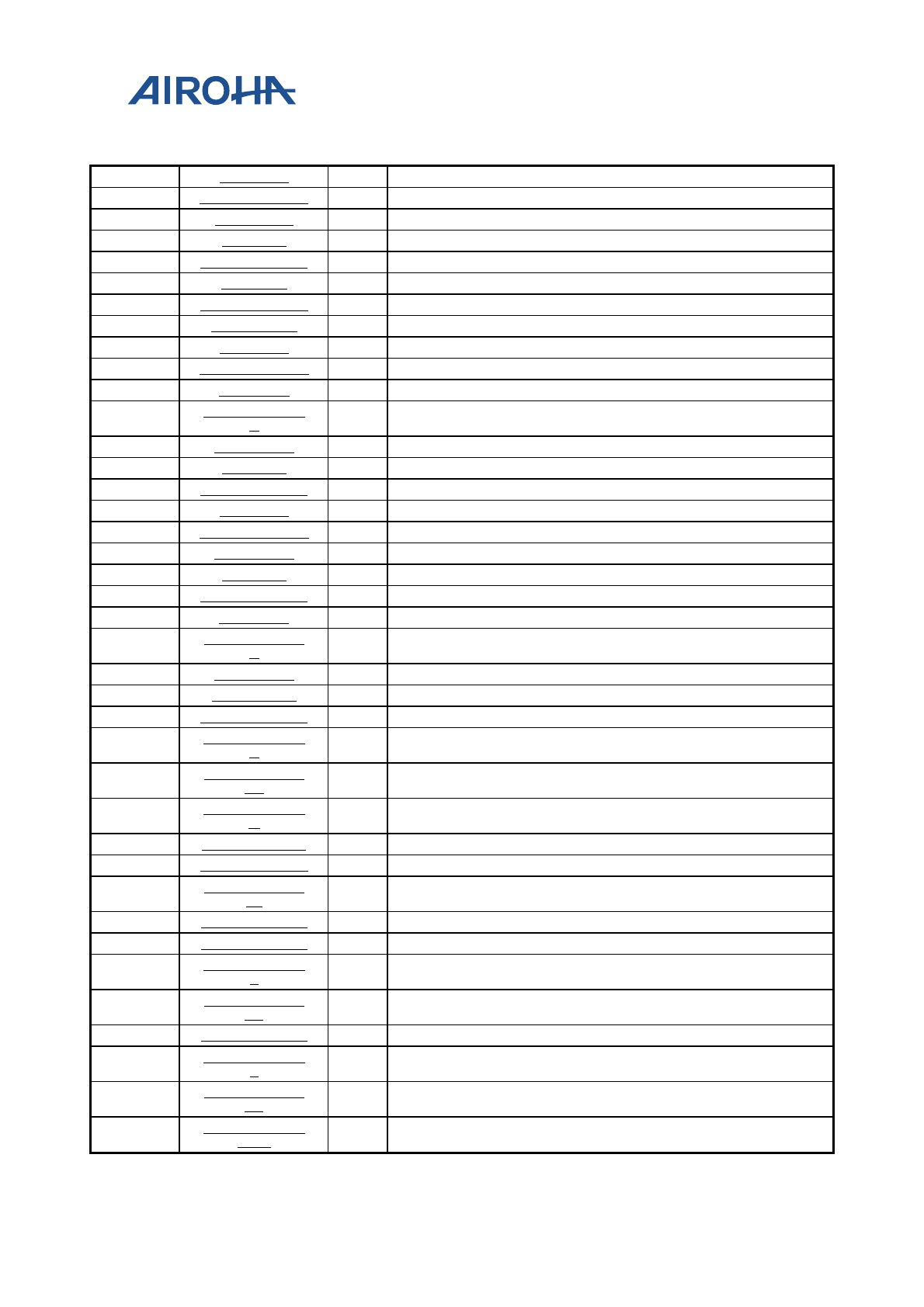
MT2523 Series Reference Manual
© 2015 - 2018 Airoha Technology Corp.
Page 147 of 692
This document contains information that is proprietary to Airoha Technology Corp. (“Airoha”) and/or its licensor(s).
Any unauthorized use, reproduction or disclosure of this document in whole or in part is strictly prohibited.
Module name: Unified_USB Base address: (+A0900000h)
A090011C
RX1TYPE
8
Rx1Type Register
A090011D
RX1INTERVAL
8
Rx1Interval Register
A090011F FIFOSIZE1 8 EP1 Configured FIFO Size Register
A0900120
TX2MAP
16
TX2MAP Register
A0900122
TX2CSR_PERI
16
Tx2 CSR Register
A0900124
RX2MAP
16
RX2MAP Register
A0900126 RX2CSR_PERI 16 RX2 CSR Register
A0900128
RX2COUNT
16
Rx2 Count Register
A090012A
TX2TYPE
8
Tx2Type Register
A090012B
TX2INTERVAL
8
Tx2Interval Register
A090012C RX2TYPE 8 Rx2Type Register
A090012D
RX2INTERVA
L 8 Rx2Interval Register
A090012F
FIFOSIZE2
8
EP2 Configured FIFO Size Register
A0900130
TX3MAP
16
TX3MAP Register
A0900132 TX3CSR_PERI 16 Tx3 CSR Register
A090013A
TX3TYPE
8
Tx3Type Register
A090013B
TX3INTERVAL
8
Tx3Interval Register
A090013F
FIFOSIZE3
8
EP3 Configured FIFO Size Register
A0900140 TX4MAP 16 TX4MAP Register
A0900142
TX4CSR_PERI
16
Tx4 CSR Register
A090014A
TX4TYPE
8
Tx4Type Register
A090014B
TX4INTERVA
L 8 Tx4Interval Register
A090014F FIFOSIZE4 8 EP4 Configured FIFO Size Register
A0900200
DMA_INTR
32
DMA Interrupt Status Register
A0900204
DMA_CNTL_0
16
DMA Channel 0 Control Register
A0900208
DMA_ADDR_
0 32 DMA Channel 0 Address Register
A090020C DMA_COUNT
_0 32 DMA Channel 0 Byte Count Register
A0900210
DMA_LIMITE
R 32 DMA Limiter Register
A0900214
DMA_CNTL_1
16
DMA Channel 1 Control Register
A0900218
DMA_ADDR_1
32
DMA Channel 1 Address Register
A090021C DMA_COUNT
_1 32 DMA Channel 1 Byte Count Register
A0900220
DMA_CONFIG
32
DMA Configuration Register
A0900224
DMA_CNTL_2
16
DMA Channel 2 Control Register
A0900228
DMA_ADDR_
2 32 DMA Channel 2 Address Register
A090022C DMA_COUNT
_2 32 DMA Channel 2 Byte Count Register
A0900234
DMA_CNTL_3
16
DMA Channel 3 Control Register
A0900238
DMA_ADDR_
3 32 DMA Channel 3 Address Register
A090023C
DMA_COUNT
_3 32 DMA Channel 3 Byte Count Register
A0900304 EP1RXPKTCO
UNT 16 EP1 RxPktCount Register
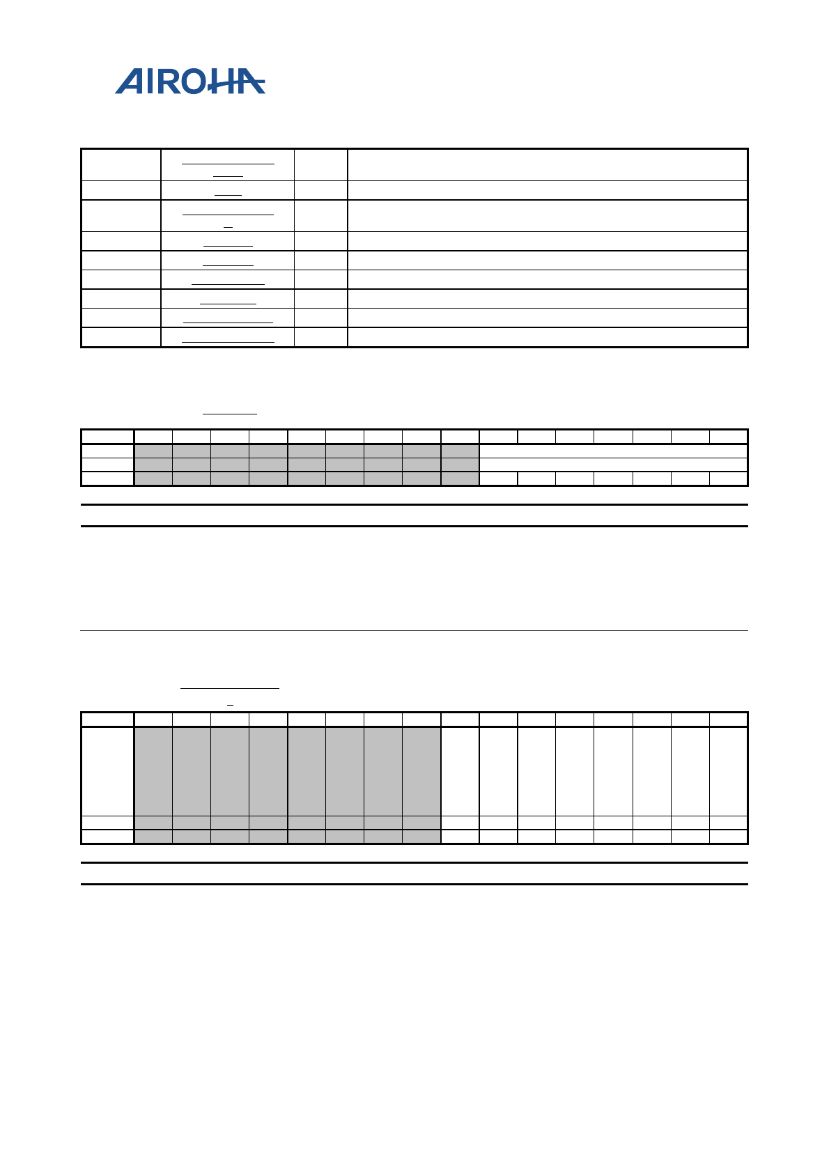
MT2523 Series Reference Manual
© 2015 - 2018 Airoha Technology Corp.
Page 148 of 692
This document contains information that is proprietary to Airoha Technology Corp. (“Airoha”) and/or its licensor(s).
Any unauthorized use, reproduction or disclosure of this document in whole or in part is strictly prohibited.
Module name: Unified_USB Base address: (+A0900000h)
A0900308
EP2RXPKTCO
UNT 16 EP2 RxPktCount Register
A0900604
TM1
16
Test Mode 1 Register
A0900608 HWVER_DAT
E 32 HW Version Control Register
A0900684
SRAMA
32
SRAM Address Register
A0900688
SRAMD
32
SRAM Data Register
A0900690
RISC_SIZE
32
RISC Size Register
A0900700 RESREG 32 Reserved Register
A0900730
OTG20_CSRL
8
OTG20 Related Control Register L
A0900731
OTG20_CSRH
8
OTG20 Related Control Register H
A090000
0 FADDR Function Address Register (Device mode
only) 00
Bit
15
14
13
12
11
10
9
8
7
6
5
4
3
2
1
0
Name
FUNCTION_ADDRESS
Type
RW
Reset
0
0
0
0
0
0
0
Bit(s) Name Description
6:0 FUNCTION_ADDRE
SS
FAddr is an 8-bit register that should be written with the 7-bit address of the
peripheral part of the transaction. When the USB2.0 controller is used in
Peripheral mode (DevCtl.bit2=0), this register should be written with the
address received through a SET_ADDRESS command, which will then be used
for decoding the function address in subsequent token packets. When the
USB2.0 controller is used in host mode (DevCtl.bit2=1), function address will be
configured by TXFUNCADDR and RXFUNCADDR.
A0900001 POWER_PER
I Power Management Register 20
Bit
15
14
13
12
11
10
9
8
7
6
5
4
3
2
1
0
Name
ISO
UP
DA
TE
SO
FTC
ON
N
HS
EN
AB
HS
MO
DE
RE
SET
RE
SU
ME
SU
SPE
ND
MO
DE
EN
AB
LES
US
PE
ND
M
Type
RW
RW
RW
RU
RU
RW
RU
RW
Reset
0
0
1
0
0
0
0
0
Bit(s) Name Description
7 ISOUPDATE
When set by the CPU, the USB2.0 controller will wait for an SOF
token from the time TxPktRdy is set before sending the packet. If an
IN token is received before an SOF token, a 0 length data packet will
be sent.
Note: Only valid in peripheral mode. This bit only affects endpoints performing
Isochronous transfers.
6 SOFTCONN
If Soft Connect/Disconnect feature is enabled, the USB D+/D- lines
will be enabled when this bit is set by the CPU and tri-stated when
this bit is cleared by the CPU.
In Peripheral FS mode, clearing Softcon bit may need execution of latency until
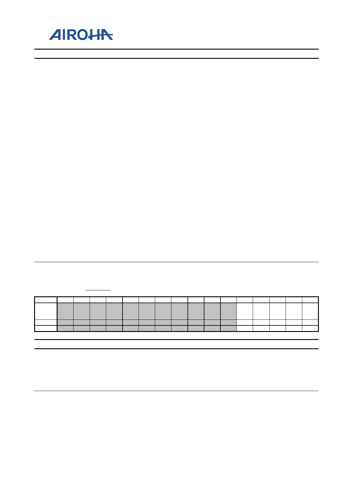
MT2523 Series Reference Manual
© 2015 - 2018 Airoha Technology Corp.
Page 149 of 692
This document contains information that is proprietary to Airoha Technology Corp. (“Airoha”) and/or its licensor(s).
Any unauthorized use, reproduction or disclosure of this document in whole or in part is strictly prohibited.
Bit(s) Name Description
USB BUS SE0 is detected by HW.
Execution Latency ~= 1ms, such as SOF Packet EOP or RESET
In Peripheral HS mode, clearing Softcon bit still needs execution of latency until
USB BUS SE0 is detected by HW.
Execution Latency ~= 1us, such as HS idle
Note: This bit should only be set in peripheral mode. For host mode, this bit will
be set if DEVCTL[0] session bit is set. This bit should also be cleared if session
bit is cleared by CPU.
5 HSENAB When set by the CPU, the USB2.0 controller will negotiate for high-
speed mode when the device is reset by the hub. If not set, the device
will only operate in full-speed mode.
4 HSMODE
When set, this read-only bit indicates high-speed mode successfully
negotiated during USB reset.
In peripheral mode, becomes valid when USB reset is completed (as indicated by
USB reset interrupt).
In host mode, becomes valid when Reset bit is cleared. Remains valid for the
duration of the session.
Note: Allowance is made for Tiny-J signaling in determining the transfer speed
to select.
3 RESET
This bit is set when Reset signaling is present on the bus.
Note: This bit is read/written from the CPU in host mode but read-only in
peripheral mode.
2 RESUME
Set by the CPU to generate Resume signaling when the function is in
suspend mode. The CPU should clear this bit after 10ms (max. 15ms)
to end Resume signaling. In host mode, this bit is also automatically
set when Resume signaling from the target is detected when the
USB2.0 controller is suspended.
1 SUSPENDMODE
In host mode, this bit is set by the CPU to enter suspend mode.
In peripheral mode, this bit is set on entryo into suspend mode. Cleared when
the CPU reads the interrupt register or sets up the Resume bit above.
0 ENABLESUSPENDM Set by the CPU to enable the SUSPENDM output
A090000
2 INTRTX Tx Interrupt Status Register 0000
Bit
15
14
13
12
11
10
9
8
7
6
5
4
3
2
1
0
Name
EP4
_T
X
EP3
_T
X
EP2
_T
X
EP1
_T
X
EP
0
Type
W1C
W1C
W1C
W1C
W1C
Reset
0
0
0
0
0
Bit(s) Name Description
4 EP4_TX T4 Endpoint N interrupt event
3 EP3_TX T3 Endpoint N interrupt event
2 EP2_TX T2 Endpoint N interrupt event
1 EP1_TX T1 Endpoint N interrupt event.
0 EP0 Endpoint 0 interrupt event
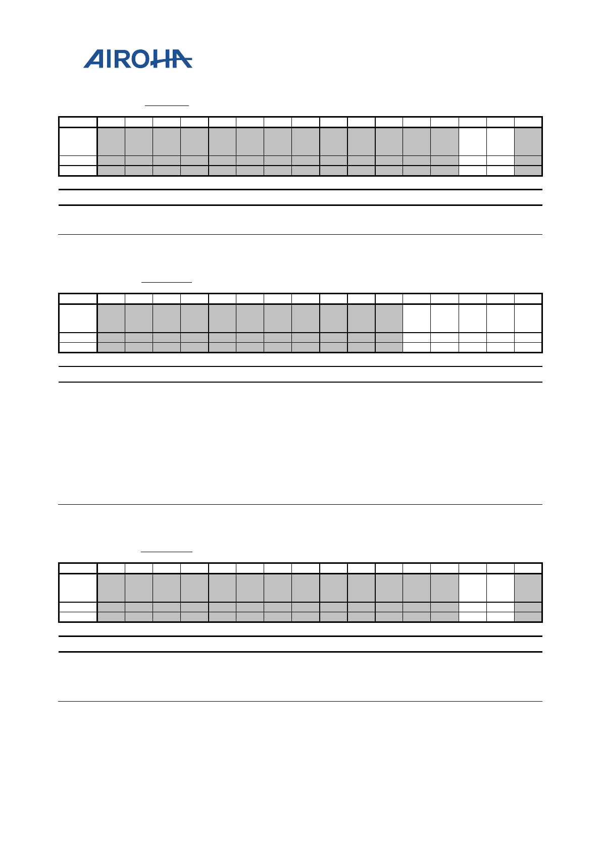
MT2523 Series Reference Manual
© 2015 - 2018 Airoha Technology Corp.
Page 150 of 692
This document contains information that is proprietary to Airoha Technology Corp. (“Airoha”) and/or its licensor(s).
Any unauthorized use, reproduction or disclosure of this document in whole or in part is strictly prohibited.
A090000
4 INTRRX Rx Interrupt Status Register 0000
Bit
15
14
13
12
11
10
9
8
7
6
5
4
3
2
1
0
Name
EP2
_R
X
EP1
_R
X
Type
W1C
W1C
Reset
0
0
Bit(s) Name Description
2 EP2_RX R2 Endpoint N interrupt event
1 EP1_RX R1 Endpoint N interrupt event
A090000
6 INTRTXE Tx Interrupt Enable Register FFFF
Bit
15
14
13
12
11
10
9
8
7
6
5
4
3
2
1
0
Name
EP4
_T
XE
EP3
_T
XE
EP2
_T
XE
EP1
_T
XE
EP
0_
E
Type
RW
RW
RW
RW
RW
Reset
1
1
1
1
1
Bit(s) Name Description
4 EP4_TXE 1'b0: Disable Tx Endpoint N interrupt event
1'b1: Enable Tx Endpoint N interrupt event
3 EP3_TXE 1'b0: Disable Tx Endpoint N interrupt event
1'b1: Enable Tx Endpoint N interrupt event
2 EP2_TXE 1'b0: Disable Tx Endpoint N interrupt event
1'b1: Enable Tx Endpoint N interrupt event
1 EP1_TXE 1'b0: Disable Tx Endpoint N interrupt event
1'b1: Enable Tx Endpoint N interrupt event
0 EP0_E 1'b0: Disable Tx Endpoint N interrupt event
1'b1: Enable Tx Endpoint N interrupt event
A090000
8 INTRRXE Rx Interrupt Enable Register FFFE
Bit
15
14
13
12
11
10
9
8
7
6
5
4
3
2
1
0
Name
EP2
_R
XE
EP1
_R
XE
Type
RW
RW
Reset
1
1
Bit(s) Name Description
2 EP2_RXE 1'b0: Disable Rx Endpoint N interrupt event
1'b1: Enable Rx Endpoint N interrupt event
1 EP1_RXE 1'b0: Disable Rx Endpoint N interrupt event
1'b1: Enable Rx Endpoint N interrupt event
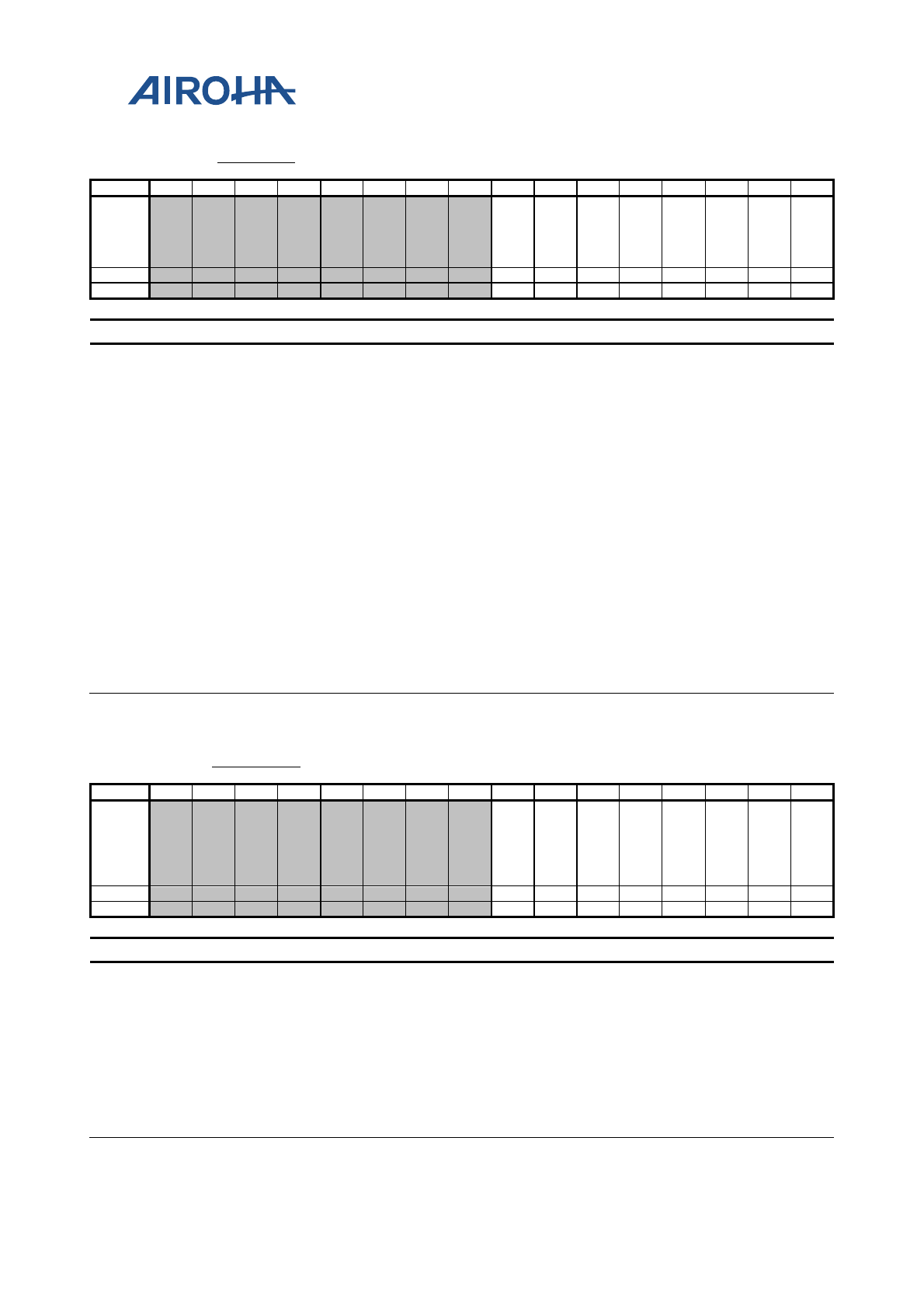
MT2523 Series Reference Manual
© 2015 - 2018 Airoha Technology Corp.
Page 151 of 692
This document contains information that is proprietary to Airoha Technology Corp. (“Airoha”) and/or its licensor(s).
Any unauthorized use, reproduction or disclosure of this document in whole or in part is strictly prohibited.
A090000
A INTRUSB Common USB Interrupt Register 00
Bit
15
14
13
12
11
10
9
8
7
6
5
4
3
2
1
0
Name
VB
US
ER
RO
R
SES
SR
EQ
DIS
CO
N
CO
NN
SO
F
RE
SET
_B
AB
LE
RE
SU
ME
SU
SPE
ND
Type
W1C
W1C
W1C
W1C
W1C
W1C
W1C
W1C
Reset
0
0
0
0
0
0
0
0
Bit(s) Name Description
7 VBUSERROR
Set when VBus drops below the VBus Valid threshold during a
session
Only valid when USB2.0 controller is 'A' device.
6 SESSREQ Set when Session Request signaling has been detected
Only valid when USB2.0 controller is 'A' device.
5 DISCON
Set in host mode when a device disconnect is detected. Set in
peripheral mode when a session ends.
Valid at all transaction speeds.
4 CONN Set when a device connection is detected
Only valid in host mode. Valid at all transaction speeds.
3 SOF Set when a new frame starts.
2 RESET_BABLE
Set in peripheral mode when Reset signaling is detected on the bus.
Set in host mode when babble is detected.
Note: Only active after the first SOF has been sent.
1 RESUME Set when Resume signaling is detected on the bus when the USB2.0
controller is in suspend mode.
0 SUSPEND Set when Suspend signaling is detected on the bus
Only valid in peripheral mode.
A090000
B INTRUSBE Common USB Interrupt Enable Register 06
Bit
15
14
13
12
11
10
9
8
7
6
5
4
3
2
1
0
Name
VB
US
ER
RO
R_
E
SES
SR
EQ
_E
DIS
CO
N_
E
CO
NN
_E
SO
F_E
RE
SET
_B
AB
LE
_E
RE
SE
UM
_E
SU
SPE
ND
_E
Type
RW
RW
RW
RW
RW
RW
RW
RW
Reset
0
0
0
0
0
1
1
0
Bit(s) Name Description
7 VBUSERROR_E Enables VBusError interrupt
6 SESSREQ_E Enables SessReq interrupt
5 DISCON_E Enables Discon interrupt
4 CONN_E Enables Conn interrupt
3 SOF_E Enables SOF interrupt
2 RESET_BABLE_E Enables Reset/Babble interrupt
1 RESEUM_E Enables Resume interrupt
0 SUSPEND_E Enables Suspend interrupt
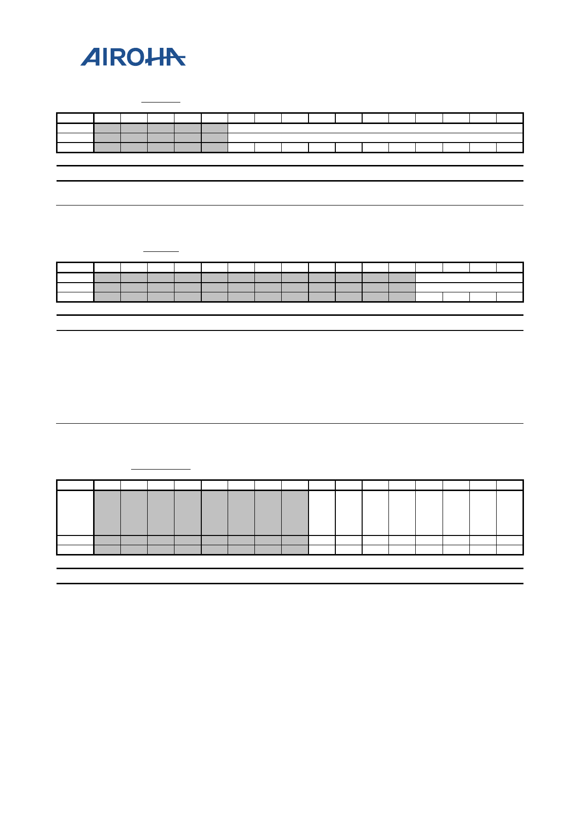
MT2523 Series Reference Manual
© 2015 - 2018 Airoha Technology Corp.
Page 152 of 692
This document contains information that is proprietary to Airoha Technology Corp. (“Airoha”) and/or its licensor(s).
Any unauthorized use, reproduction or disclosure of this document in whole or in part is strictly prohibited.
A090000
C FRAME Frame Number Register 0000
Bit
15
14
13
12
11
10
9
8
7
6
5
4
3
2
1
0
Name
FRAME_NUMBER
Type
RU
Reset
0
0
0
0
0
0
0
0
0
0
0
Bit(s) Name Description
10:0 FRAME_NUMBER Frame is a 11-bit read-only register that holds the last received frame
number.
A090000
E INDEX Endpoint Selection Index Register 00
Bit
15
14
13
12
11
10
9
8
7
6
5
4
3
2
1
0
Name
SELECTED_ENDPOINT
Type
RW
Reset
0
0
0
0
Bit(s) Name Description
3:0 SELECTED_ENDPO
INT
Each TX endpoint and RX endpoint has its own set of control/status
registers located between USB+100h - USB+1FFh. In addition, one
set of TX control/status and one set of RX control/status registers
appear at USB+010h - USB+01Fh. Index is a 4-bit register that
determines which endpoint control/status registers are accessed.
Before accessing an endpoint's control/status registers at USB+010h
- USB+01Fh, the endpoint number should be written to the Index
register to ensure that the correct control/status registers appear in
the memory map.
A090000
F TESTMODE Test Mode Enable Register 00
Bit
15
14
13
12
11
10
9
8
7
6
5
4
3
2
1
0
Name
FO
RC
E_
HO
ST
FIF
O_
AC
CES
S
FO
RC
E_
FS
FO
RC
E_
HS
TES
T_P
AC
KE
T
TES
T_
K
TES
T_J
TES
T_S
E0
_N
AK
Type
RW
A0
RW
RW
RW
RW
RW
RW
Reset
0
0
0
0
0
0
0
0
Bit(s) Name Description
7 FORCE_HOST
The CPU sets up this bit to instruct the core to enter host mode when
the Session bit is set, regardless of whether it is connected to any
peripheral. The state of the CID input, HostDisconnect and LineState
signals are ignored. The core will then remain in host mode until the
Session bit is cleared, even if a device is disconnected, and if the
Force_Host bit remains set, will re-enter host mode the next time the
Session bit is set. When in this mode, the status of the HOSTDISCON
signal from the PHY may be read from bit7 of the ACTLR0.DevCtl
register. The operating speed is determined by the Force_HS and
Force_FS bits as the following. USB2.0 IP only
Force_HS Force_FS Operating Speed
0 0 Low Speed
0 1 Full Speed
1 0 High Speed
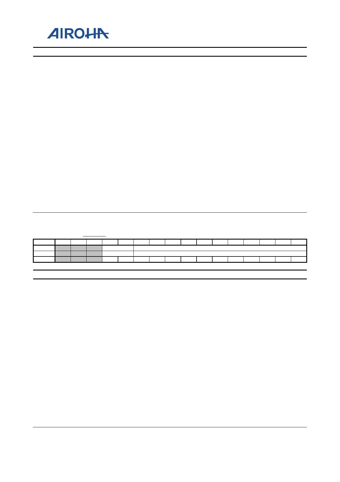
MT2523 Series Reference Manual
© 2015 - 2018 Airoha Technology Corp.
Page 153 of 692
This document contains information that is proprietary to Airoha Technology Corp. (“Airoha”) and/or its licensor(s).
Any unauthorized use, reproduction or disclosure of this document in whole or in part is strictly prohibited.
Bit(s) Name Description
1 1 Undefined
6 FIFO_ACCESS The CPU sets up this bit to transfer the packet in Endpoint 0 TX FIFO
to Endpoint 0 RX FIFO. It is cleared automatically. USB2.0 IP only.
5 FORCE_FS
The CPU sets up this bit either in conjunction with bit7 above or to
force the USB2.0 controller into full-speed mode when it receives a
USB reset.
4 FORCE_HS The CPU sets up this bit either in conjunction with bit7 above or to
force the USB2.0 controller into high-speed mode when it receives a
USB reset. USB2.0 IP only.
3 TEST_PACKET
(HS_MODE) The CPU sets up this bit to enter Test_Packet test mode.
In this mode, the USB2.0 controller repetitively transmits on the bus
a 53-byte test packet, the form of which is defined in the Universal
Serial Bus Specification Revision 2.0, Section 7.1.20.
Note: The test packet has a fixed format and must be loaded into
Endpoint 0 FIFO before the test mode is entered. USB2.0 IP only.
2 TEST_K (HS_MODE) The CPU sets up this bit to enter Test_K test mode. In
this mode, the USB2.0 controller transmits a continuous K on the
bus. USB2.0 IP only.
1 TEST_J
(HS_MODE) The CPU sets up this bit to enter Test_J test mode. In
this mode, the USB2.0 controller transmits a continuous J on the
bus. USB2.0 IP only.
0 TEST_SE0_NAK (HS_MODE) The CPU sets up this bit to enter Test_SE0_NAK test
mode. In this mode, the USB2.0 controller remains in high-speed
mode but responds to any valid IN token with a NAK. USB2.0 IP only.
A0900010 TXMAP TXMAP Register 0000
Bit
15
14
13
12
11
10
9
8
7
6
5
4
3
2
1
0
Name
M_1
MAXIMUM_PAYLOAD_TRANSACTION
Type
RW
RW
Reset
0
0
0
0
0
0
0
0
0
0
0
0
0
Bit(s) Name Description
12:11 M_1 Maximum payload size for indexed TX endpoint, M-1 Packet
multiplier m maximum payload transaction register
10:0 MAXIMUM_PAYLO
AD_TRANSACTION
The TxMaxP register defines the maximum amount of data that can
be transferred through the selected TX endpoint in a single
operation. There is a TxMaxP register for each TX endpoint (except
for Endpoint 0). Bit10~0 define (in bytes) the maximum payload
transmitted in a single transaction. The value set can be up to 1024
bytes but is subject to the constraints placed by the USB Specification
on packet sizes for Bulk, Interrupt and Isochronous transfers in full-
speed and high-speed operations. Where the option of high-
bandwidth Isochronous endpoints or of packet splitting on Bulk
endpoints has been taken when the core is configured, the register
includes either 2 or 5 further bits that define a multiplier m which is
equal to one more than the value recorded. In the case of Bulk
endpoints with the packet splitting option enabled, the multiplier m
can be up to 32 and defines the maximum number of 'USB' packets
(i.e. packets for transmission over the USB) of the specified payload
into which a single data packet placed in the FIFO should be split,
prior to transfer. (If the packet splitting option is not enabled, bit15-
13 will not be implemented and bit12-11 (if included) will be ignored.)
Note: The data packet is required to be an exact multiple of the payload specified
by bit10~0, which is itself required to be one of 8, 16, 32, 64 or (in the case of
high speed transfers) 512 bytes. For Isochronous endpoints operating in high-
speed mode and with the high-bandwidth option enabled, m may only be either
2 or 3 (corresponding to bit 11 set or bit 12 set, respectively) and it specifies the
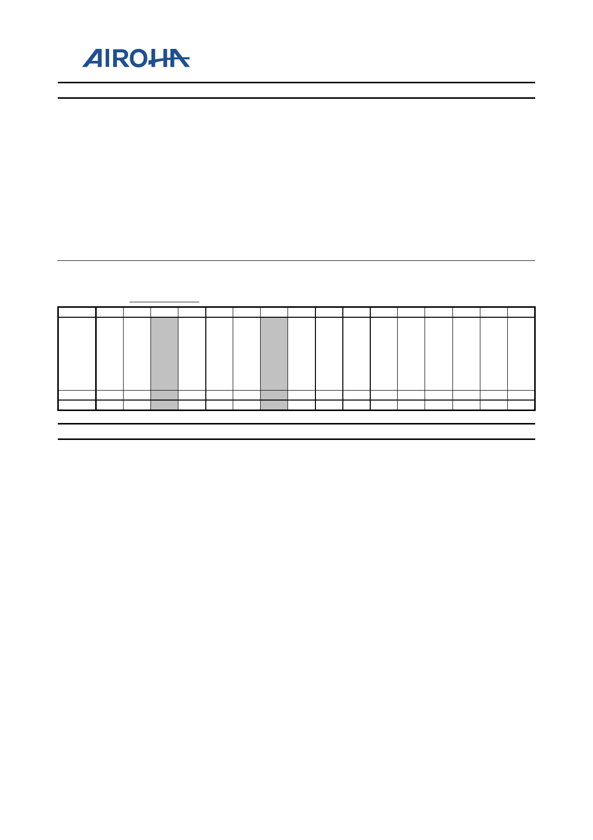
MT2523 Series Reference Manual
© 2015 - 2018 Airoha Technology Corp.
Page 154 of 692
This document contains information that is proprietary to Airoha Technology Corp. (“Airoha”) and/or its licensor(s).
Any unauthorized use, reproduction or disclosure of this document in whole or in part is strictly prohibited.
Bit(s) Name Description
maximum number of such transactions that can take place in a single
microframe. If either bit11 or bit12 is non-0, the USB2.0 controller will
automatically split any data packet written to the FIFO into up to 2 or 3 'USB'
packets, each containing the specified payload (or less). The maximum payload
for each transaction is 1024 bytes, so this allows up to 3072 bytes to be
transmitted in each microframe. (For Isochronous/Interrupt transfers in full-
speed mod, bits11 and 12 are ignored.) The value written to bit10~0 (multiplied
by m in the case of high-bandwidth Isochronous transfers) should match the
value given in the wMaxPacketSize field of the Standard Endpoint Descriptor for
the associated endpoint (see USB Specification Revision 2.0, Chapter 9). A
mismatch will cause unexpected results. The total amount of data represented by
the value written to this register (specified payload * m) should not exceed the
FIFO size for the TX endpoint and should not exceed half the FIFO size if
double-buffering is required. If this register is changed after packets have been
sent from the endpoint, the TX endpoint FIFO should be completely flushed
(using the FlushFIFO bit in TxCSR) after writing the new value to this register.
A0900012 TXCSR_PERI Tx CSR Register 0000
Bit
15
14
13
12
11
10
9
8
7
6
5
4
3
2
1
0
Name AU
TO
SET
ISO
DM
AR
EQ
EN
FR
CD
AT
AT
OG
DM
AR
EQ
MO
DE
SET
TX
PK
TR
DY
_T
WI
CE
INC
OM
PT
X
CL
RD
AT
AT
OG
SE
NT
ST
AL
L
SE
ND
ST
AL
L
FL
US
HFI
FO
UN
DE
RR
UN
FIF
ON
OT
EM
PT
Y
TX
PK
TR
DY
Type
RW
RW
RW
RW
RW
A1
A1
A0
A1
RW
A0
A1
RU
A0
Reset
0
0
0
0
0
0
0
0
0
0
0
0
0
0
Bit(s) Name Description
15 AUTOSET
If The CPU sets up this bit, TxPktRdy will be automatically set when
data of the maximum packet size (value in TxMaxP) is loaded into the
TxFIFO. If a packet of less than the maximum packet size is loaded,
TxPktRdy will have to be set manually.
14 ISO
The CPU sets up this bit to enable the TX endpoint for Isochronous
transfers and clears it to enable the TX endpoint for Bulk or
Interrupt transfers.
Note: This bit only takes effect in peripheral mode. In host mode, it
always returns 0.
12 DMAREQEN The CPU sets up this bit to enable the DMA request for TX endpoint.
11 FRCDATATOG
The CPU sets up this bit to force the endpoint data toggle to switch
and the data packet to be cleared from the FIFO, regardless of
whether an ACK is received. This can be used by Interrupt TX
endpoints used to communicate rate feedback for Isochronous
endpoints.
10 DMAREQMODE
The CPU sets up this bit to select DMA request mode 1 and clears it to
select DMA request mode 0.
Note: This bit should not be cleared either before or in the same cycle as the
DMAReqEn bit is cleared.
8 SETTXPKTRDY_TW
ICE
Indicates TxPktRdy had been set while it is 1'b1 already. Write 0 to
clear it.
7 INCOMPTX
When the endpoint is used for high-bandwidth
Isochronous/Interrupt transfers, this bit will be set to indicate where
a large packet has been split into 2 or 3 packets for transmission but
insufficient IN tokens have been received to send all the parts.
Note: In anything other than a high-bandwidth transfer, this bit will
always return 0.
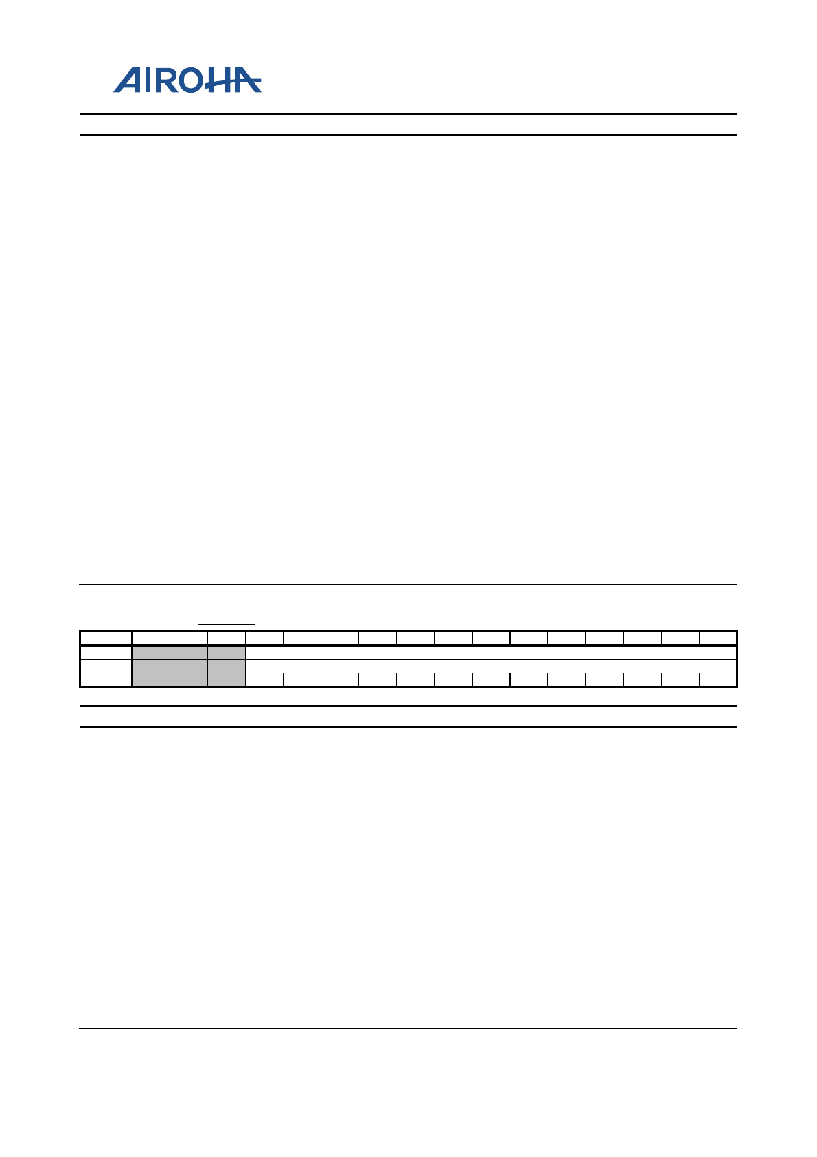
MT2523 Series Reference Manual
© 2015 - 2018 Airoha Technology Corp.
Page 155 of 692
This document contains information that is proprietary to Airoha Technology Corp. (“Airoha”) and/or its licensor(s).
Any unauthorized use, reproduction or disclosure of this document in whole or in part is strictly prohibited.
Bit(s) Name Description
Write 0 to clear it.
6 CLRDATATOG The CPU writes 1 to this bit to reset the endpoint data toggle to 0.
5 SENTSTALL
This bit is set when a STALL handshake is transmitted. The FIFO will
be flushed and TX interrupt generated if enabled and the TxPktRdy
bit is cleared. The CPU should clear this bit.
Write 0 to clear it.
4 SENDSTALL
The CPU writes 1 to this bit to issue a STALL handshake to an IN
token. The CPU clears this bit to terminate the stall condition.
Note: This bit has no effect where the endpoint is used for
Isochronous transfer. Otherwise, CPU should wait for SENTSTALL
interrupt to be generated before clearing the SENDSTALL bit.
3 FLUSHFIFO
The CPU writes 1 to this bit to flush the latest packet from the
endpoint TxFIFO. The FIFO pointer is reset, the TxPktRdy bit is
cleared, and an interrupt is generated. May be set simultaneously
with TxPktRdy to abort the packet that is currently loaded into the
FIFO.
Note: FlushFIFO should only be used when TxPktRdy is set. In other cases, it
may cause data corruption. If the FIFO is double-buffered, FlushFIFO may need
to be set twice to completely clear the FIFO.
2 UNDERRUN The USB sets up this bit if an IN token is received when the TxPktRdy
bit not set. The CPU should clear this bit. Write 0 to clear it.
1 FIFONOTEMPTY The USB sets up this bit when there is at least 1 packet in the TxFIFO.
This bit will be asserted automatically when TXPKTRDY is set by CPU
and de-asserted when CPU flushes FIFO or sends a STALL packet.
0 TXPKTRDY
The CPU sets up this bit after loading a data packet into the FIFO. It is
cleared automatically when a data packet has been transmitted. An
interrupt is also generated at this point (if enabled). TxPktRdy is also
automatically cleared (interrupt is generated) prior to loading a
second packet into a double-buffered FIFO.
A0900014 RXMAP RXMAP Register 0000
Bit
15
14
13
12
11
10
9
8
7
6
5
4
3
2
1
0
Name
M_1
MAXIMUM_PAYLOAD_TRANSACTION
Type
RW
RW
Reset
0
0
0
0
0
0
0
0
0
0
0
0
0
Bit(s) Name Description
12:11 M_1 Maximum payload size for indexed RX endpoint , M-1 Packet
multiplier m
10:0 MAXIMUM_PAYLO
AD_TRANSACTION
The RxMaxP register defines the maximum amount of data that can
be transferred through the selected RX endpoint in a single
operation. There is a RxMaxP register for each RX endpoint (except
for Endpoint 0). Bit10~0 define (in bytes) the maximum payload
transmitted in a single transaction. The value set can be up to 1024
bytes but is subject to the constraints placed by the USB Specification
on packet sizes for Bulk, Interrupt and Isochronous transfers in full-
speed and high-speed operations.
Where the option of high-bandwidth Isochronous endpoints or of combining
Bulk packets has been taken when the core is configured, the register includes
either 2 or 5 further bits that define a multiplier m which is equal to one more
than the value recorded.
For Bulk endpoints with the packet combining option enabled, the multiplier m
can be up to 32 and defines the number of USB packets of the specified payload
which are to be combined into a single data packet within the FIFO. (If the
packet splitting option is not enabled, bit15-bit13 will not be implemented and
bit12-bit11 (if included) will be ignored.) For Isochronous endpoints operating in
high-speed mode and with the high-bandwidth option enabled, m may only be
either 2 or 3 (corresponding to bit 11 set or bit 12 set, respectively) and it
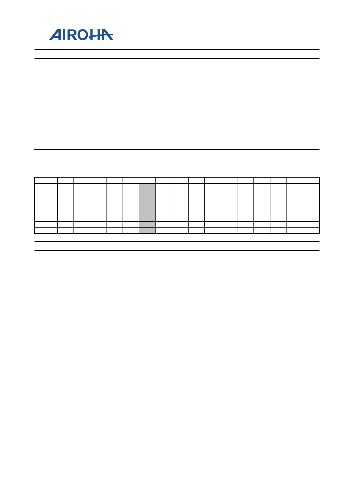
MT2523 Series Reference Manual
© 2015 - 2018 Airoha Technology Corp.
Page 156 of 692
This document contains information that is proprietary to Airoha Technology Corp. (“Airoha”) and/or its licensor(s).
Any unauthorized use, reproduction or disclosure of this document in whole or in part is strictly prohibited.
Bit(s) Name Description
specifies the maximum number of such transactions that can take place in a
single microframe. If either bit 11 or bit 12 is non-0, the USB2.0 controller will
automatically combine the separate USB packets received in any microframe
into a single packet within the Rx FIFO. The maximum payload for each
transaction is 1024 bytes, so this allows up to 3072 bytes to be received in each
microframe.
(For Isochronous/Interrupt transfers in full-speed mode or if high-bandwidth is
not enabled, bits 11 and 12 are ignored.) The value written to bit10~0 (multiplied
by m in the case of high-bandwidth Isochronous transfers) must match the value
given in the wMaxPacketSize field of the Standard Endpoint Descriptor for the
associated endpoint (see USB Specification Revision 2.0, Chapter 9). A
mismatch will cause unexpected results.
The total amount of data represented by the value written to this register
(specified payload * m) should not exceed the FIFO size for the OUT endpoint,
and should not exceed half the FIFO size if double-buffering is required.
A0900016 RXCSR_PERI RX CSR Register 0000
Bit
15
14
13
12
11
10
9
8
7
6
5
4
3
2
1
0
Name
AU
TO
CL
EA
R
ISO
DM
AR
EQ
EN
DIS
NY
ET
_PI
DE
RR
DM
AR
EQ
MO
DE
KE
EP
ER
RS
TA
TU
S
INC
OM
PR
X
CL
RD
TA
TO
G
SE
NT
ST
AL
L
SE
ND
ST
AL
L
FL
US
HFI
FO
DA
TA
ER
R
OV
ER
RU
N
FIF
OF
UL
L
RX
PK
TR
DY
Type
RW
RW
RW
RW
RW
RW
A1
A0
A1
RW
A0
RU
A1
RU
A1
Reset
0
0
0
0
0
0
0
0
0
0
0
0
0
0
0
Bit(s) Name Description
15 AUTOCLEAR
If the CPU sets up this bit, the RxPktRdy bit will be automatically
cleared when a packet of RxMaxP bytes has been unloaded from the
RxFIFO. When packets of less than the maximum packet size are
unloaded, RxPktRdy will have to be cleared manually.
Note: Maximum packet size-3,-2,-1 is handled like maximum packet size which
is auto cleared by hardware.
14 ISO The CPU sets up this bit to enable the Rx endpoint for Isochronous
transfers and clears it to enable the Rx endpoint for Bulk/Interrupt
transfers.
13 DMAREQEN The CPU sets up this bit to enable the DMA request for the Rx
endpoint.
12 DISNYET_PIDERR
The CPU sets up this bit to disable the sending of NYET handshakes.
When set, all successfully received Rx packets will be ACK'd
including at the point at which the RxFIFO becomes full.
Note: This bit only takes effect in high-speed mode, in which it should
be set for all interrupt endpoints.
This bit is set when there is a PID error in the received packet. It is cleared when
RxPktRdy is cleared or write 0 to clear i
t
.
11 DMAREQMODE
The CPU sets up this bit to select DMA Request Mode 1 and clears it to
select DMA Request Mode 0.
DMA Request Mode 1: Rx endpoint interrupt is generated only when DMA
Request Mode 1 receives a short packet. RxDMAReq is generated when receiving
a Max-Packet-size packet.
DMA Request Mode 0: No Rx endpoint interrupt. RxDMAReq is generated when
RxPktRdy is set.
9 KEEPERRSTATUS
This bit is used when endpoint works with USBQ and in
ISOCHRONOUS mode. When this bit is set, the isochronous error,
PIDERROR, INCOMPRX and DATAERROR will be kept and only
cleared by SW.
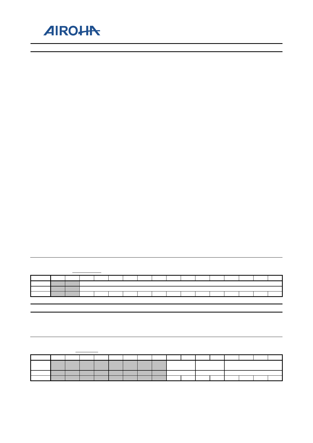
MT2523 Series Reference Manual
© 2015 - 2018 Airoha Technology Corp.
Page 157 of 692
This document contains information that is proprietary to Airoha Technology Corp. (“Airoha”) and/or its licensor(s).
Any unauthorized use, reproduction or disclosure of this document in whole or in part is strictly prohibited.
Bit(s) Name Description
8 INCOMPRX
This bit is set in an isochronous transfer if the packet in RxFIFO is
incomplete because parts of the data are not received. When
KeepErrorStatus = 0, it will be cleared when RxPktRdy is cleared or
write 0 to clear it.
Note: In anything other than an isochronous transfer, this bit will always return
0. Write 0 to clear it.
7 CLRDTATOG The CPU writes 1 to this bit to reset the endpoint data toggle to 0.
6 SENTSTALL
This bit is set when a STALL handshake is transmitted. The CPU
should clear this bit. An interrupt will be generated when the bit is
set.
Write 0 to clear it.
5 SENDSTALL
The CPU writes 1 to this bit to issue a STALL handshake. The CPU
clears this bit to terminate the stall condition.
Note: This bit has no effect where the endpoint is used for ISO transfers.
4 FLUSHFIFO
The CPU writes 1 to this bit to flush the next packet to be read from
the endpoint RxFIFO. The RxFIFO pointer is reset and the RxPktRdy
bit is cleared.
Note: FlushFIFO should only be used when RxPktRdy is set. In other cases, it
may cause data corruption. If RxFIFO is double buffered, FlushFIFO may need
to be set twice to completely clear RxFIFO.
3 DATAERR
This bit is set when RxPktRdy is set if the data packet has a CRC or
bit-stuff error in it. It is cleared when RxPktRdy is cleared.
Note: This bit is only valid when the endpoint operates in ISO mode.
In Bulk mode, it always returns to 0.
2 OVERRUN
This bit will be set if an OUT packet cannot be loaded into RxFIFO.
The CPU should clear this bit (write 0 to clear it).
Note: This bit is only valid when the endpoint operates in ISO mode. In Bulk
mode, it always returns to 0. The new incoming packet will not be written to
RxFIFO. Write 0 to clear it.
1 FIFOFULL This bit is set when no more packets can be loaded into RxFIFO.
0 RXPKTRDY
This bit is set when a data packet has been received (to RxFIFO). The
CPU should clear this bit when the packet has been unloaded from
RxFIFO. An interrupt will be generated when the bit is set.
Write 0 to clear it.
A0900018 RXCOUNT Rx Count Register 0000
Bit
15
14
13
12
11
10
9
8
7
6
5
4
3
2
1
0
Name
RXCOUNT
Type
RU
Reset
0
0
0
0
0
0
0
0
0
0
0
0
0
0
Bit(s) Name Description
13:0 RXCOUNT
It is a 14-bit read-only register that holds the number of received data
bytes in the packet in RxFIFO.
Note: The value returns changes as FIFO is unloaded and is only valid when
RxPktRdy (RxCSR.D0) is set.
A090001A TXTYPE TxType Register 00
Bit
15
14
13
12
11
10
9
8
7
6
5
4
3
2
1
0
Name
TX_SPEE
D
TX_PROT
OCOL
TX_TARGET_EP_NUM
BER
Type
RW
RW
RW
Reset
0
0
0
0
0
0
0
0
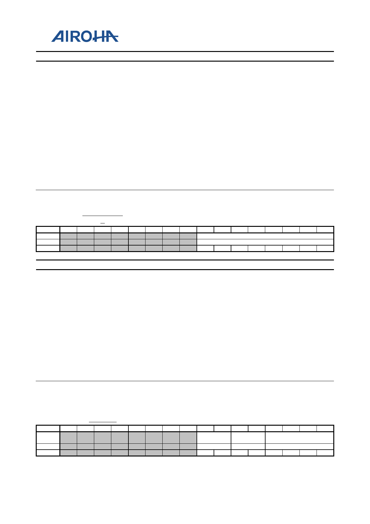
MT2523 Series Reference Manual
© 2015 - 2018 Airoha Technology Corp.
Page 158 of 692
This document contains information that is proprietary to Airoha Technology Corp. (“Airoha”) and/or its licensor(s).
Any unauthorized use, reproduction or disclosure of this document in whole or in part is strictly prohibited.
Bit(s) Name Description
7:6 TX_SPEED
Operating speed of the target device when the core is configured with
the multipoint option. When the core is not configured with the
multipoint option, these bits should not be accessed
2'b00: Unused
2'b01: High
2'b10: Full
2'b11: Low
5:4 TX_PROTOCOL
The CPU should set up this bit to select the required protocol for Tx
endpoint:
2'b00: Illegal
2'b01: Isochronous
2'b10: Bulk
2'b11: Interrupt
3:0 TX_TARGET_EP_N
UMBER
The CPU should set this value to the endpoint number containing in
the Tx endpoint descriptor returned to the USB2.0 controller during
device enumeration.
A090001B TXINTERVA
L TxInterval Register 00
Bit
15
14
13
12
11
10
9
8
7
6
5
4
3
2
1
0
Name
TX_POLLING_INTERVAL_NAK_LIMIT_M
Type
RW
Reset
0
0
0
0
0
0
0
0
Bit(s) Name Description
7:0
TX_POLLING_INTE
RVAL_NAK_LIMIT_
M
(Host mode only) TxInterval Register TxInterval is an 8-bit register
that, for Interrupt and Isochronous transfers, defines the polling
interval for the currently selected Tx endpoint. For Bulk endpoints,
this register sets up the number of frames/microframes after which
the endpoint should time out on receiving a stream of NAK
responses. There is a TxInterval register for each configured Tx
endpoint (except for Endpoint 0).
In each case the value that is set defines a number of frames/microframes (high
speed transfers), as the following:
Transfer Type | Speed | Valid values (m) | Interpretation
Interrupt | Low Speed or Full Speed | 1-255 | Polling interval is m frames.
Interrupt | High Speed | 1-16 | Polling interval is 2^(m-1) microframes
Isochronous | Full Speed or High Speed | 1-16 | Polling interval is 2^(m-1)
frames/microframes
Bulk | Full Speed or High Speed | 2-16 | NAK Limit is 2^(m-1)
frames/microframes.
Note: Value 0 or 1 disables the NAK timeout function.
A090001C RXTYPE RxType Register 00
Bit
15
14
13
12
11
10
9
8
7
6
5
4
3
2
1
0
Name RXSPEED
RX_PROT
OCOL
RX_TARGET_EP_NUM
BER
Type
RW
RW
RW
Reset
0
0
0
0
0
0
0
0
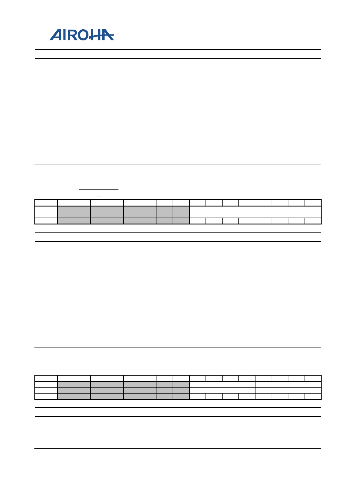
MT2523 Series Reference Manual
© 2015 - 2018 Airoha Technology Corp.
Page 159 of 692
This document contains information that is proprietary to Airoha Technology Corp. (“Airoha”) and/or its licensor(s).
Any unauthorized use, reproduction or disclosure of this document in whole or in part is strictly prohibited.
Bit(s) Name Description
7:6 RXSPEED
Operating speed of the target device when the core is configured with
the multipoint option. When the core is not configured with the
multipoint option, these bits should not be accessed
2'b00: Unused
2'b01: High
2'b10: Full
2'b11: Low
5:4 RX_PROTOCOL
The CPU should set this to select the required protocol for the Tx
endpoint:
2'b00: Illegal
2'b01: Isochronous
2'b10: Bulk
2'b11: Interrupt
3:0 RX_TARGET_EP_N
UMBER
The CPU should set this value to the endpoint number containing in
the Tx endpoint descriptor returned to the USB2.0 controller during
device enumeration.
A090001
D
RXINTERVA
L RxInterval Register 00
Bit
15
14
13
12
11
10
9
8
7
6
5
4
3
2
1
0
Name
RX_POLLING_INTERVAL_NAK_LIMIT_M
Type
RW
Reset
0
0
0
0
0
0
0
0
Bit(s) Name Description
7:0
RX_POLLING_INTE
RVAL_NAK_LIMIT_
M
RxInterval Register RxInterval is an 8-bit register that, for Interrupt
and Isochronous transfers, defines the polling interval for the
currently selected Rx endpoint. For Bulk endpoints, this register sets
the number of frames/microframes after which the endpoint should
time out on receiving a stream of NAK responses. There is a
RxInterval register for each configured Rx endpoint (except for
Endpoint 0).
RX POLLING INTERVAL/NAK LIMIT (M), (host mode only)
In each case the value that is set defines a number of frames/microframes (high
speed transfers), as the following:
Transfer type speed valid values (m) interpretation
Interrupt low speed or full speed 1 - 255 polling interval is m frames.
High speed 1 - 16 polling interval is 2(m-1) microframes
Isochronous full speed or high speed 1 - 16 polling interval is 2(m-1)
frames/microframes
Bulk full speed or high speed 2 - 16 NAK limit is 2(m-1) frames/microframes.
Note: Value 0 or 1 disables the NAK timeout function.
A090001F FIFOSIZE Configured FIFO Size Register 00
Bit
15
14
13
12
11
10
9
8
7
6
5
4
3
2
1
0
Name
RXFIFOSIZE
TXFIFOSIZE
Type
DC
DC
Reset
0
0
0
0
0
0
0
0
Bit(s) Name Description
7:4 RXFIFOSIZE Indicates RxFIFO size of 2^n bytes
Example: Value 10 means 2^10 = 1024 bytes.
3:0 TXFIFOSIZE Indicates TxFIFO size of 2^n bytes
Example: Value 10 means 2^10 = 1024 bytes.
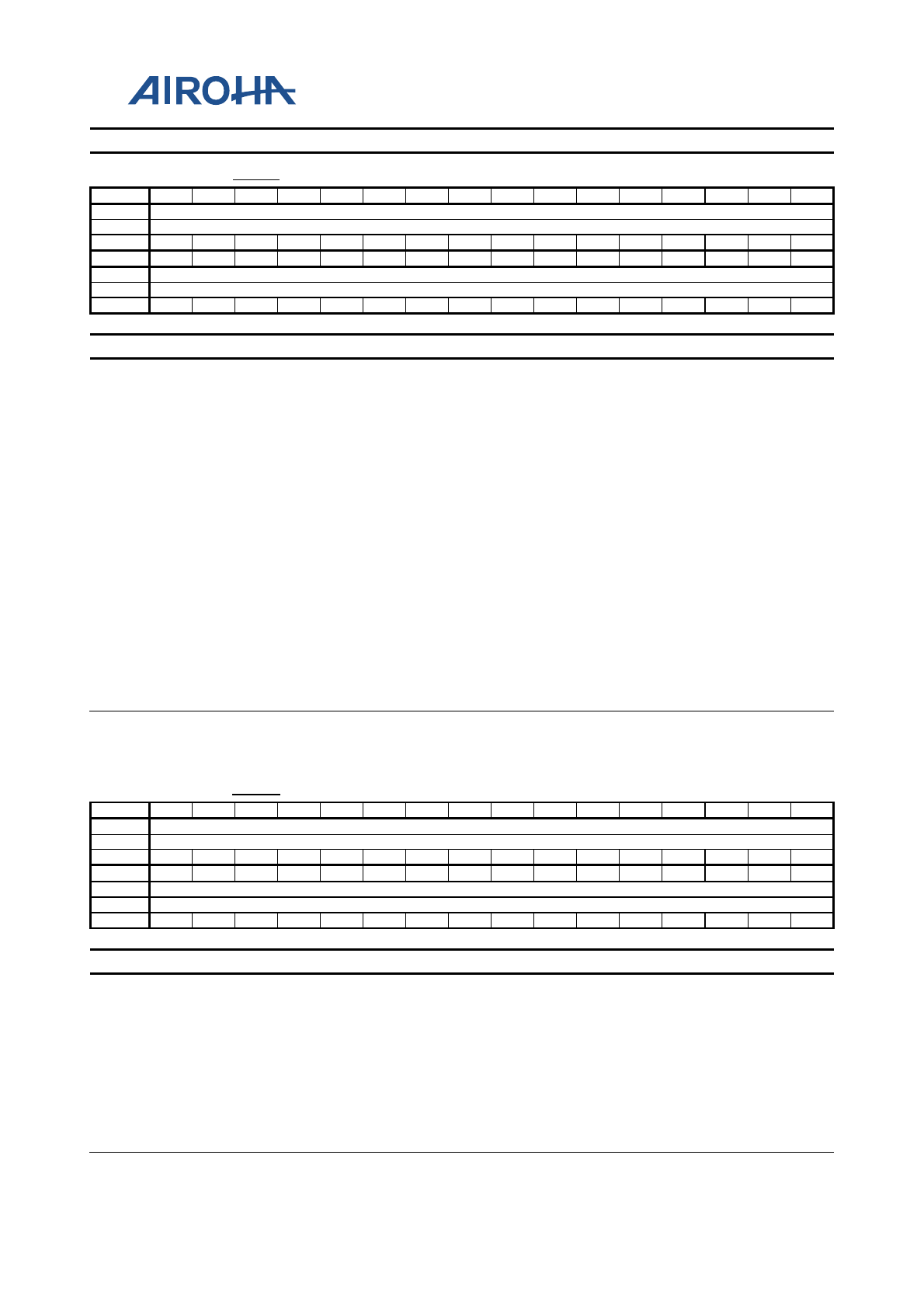
MT2523 Series Reference Manual
© 2015 - 2018 Airoha Technology Corp.
Page 160 of 692
This document contains information that is proprietary to Airoha Technology Corp. (“Airoha”) and/or its licensor(s).
Any unauthorized use, reproduction or disclosure of this document in whole or in part is strictly prohibited.
Bit(s) Name Description
A0900020 FIFO0 USB Endpoint 0 FIFO Register 00000000
Bit
31
30
29
28
27
26
25
24
23
22
21
20
19
18
17
16
Name
FIFO_DATA[31:16]
Type
Other
Reset
0
0
0
0
0
0
0
0
0
0
0
0
0
0
0
0
Bit
15
14
13
12
11
10
9
8
7
6
5
4
3
2
1
0
Name
FIFO_DATA[15:0]
Type
Other
Reset
0
0
0
0
0
0
0
0
0
0
0
0
0
0
0
0
Bit(s) Name Description
31:0 FIFO_DATA
The Endpoint FIFO registers provides 16 addresses for CPU to access
FIFOs for each endpoint. Writing to these addresses loads data into
TxFIFO for the corresponding endpoint. Reading from these
addresses unloads data from RxFIFO for the corresponding
endpoint.
Note:
1. Transfers to and from FIFOs may be 8-bit, 16-bit or 32-bit as required, and
any combination of access is allowed provided the data accessed are contiguous.
However, all the transfers associated with one packet must be of the ame width
so that the data are consistently byte-, word- or double-word-aligned. The last
transfer may however contain fewer bytes than the previous transfers in order to
complete an odd-byte or odd-word transfer. For DC/DTV project, also refer to
the RISC_SIZE register to complete FIFO access.
2. Depending on the size of the FIFO and the expected maximum packet size, the
FIFOs support either single-packet or double-packet buffering. However, burst
writing of multiple packets is not supported as flags need to be set after each
packet is written.
3. Following a STALL response or a Tx Strike Out error on Endpoint, the
associated FIFO is completely flushed.
4. For programmers, do not use debug tools to monitor or read the FIFO region.
The FIFO pointer will increase and cause unexpected error in MAC state
machine.
A0900024 FIFO1 USB Endpoint 1 FIFO Register 00000000
Bit
31
30
29
28
27
26
25
24
23
22
21
20
19
18
17
16
Name
FIFO_DATA[31:16]
Type
Other
Reset
0
0
0
0
0
0
0
0
0
0
0
0
0
0
0
0
Bit
15
14
13
12
11
10
9
8
7
6
5
4
3
2
1
0
Name
FIFO_DATA[15:0]
Type
Other
Reset
0
0
0
0
0
0
0
0
0
0
0
0
0
0
0
0
Bit(s) Name Description
31:0 FIFO_DATA
The Endpoint FIFO registers provides 16 addresses for CPU access to
FIFOs for each endpoint. Writing to these addresses loads data into
the TxFIFO for the corresponding endpoint. Reading from these
addresses unloads data from RxFIFO for the corresponding
endpoint.
Note:
1. Transfers to and from FIFOs may be 8-bit, 16-bit or 32-bit as required, and
any combination of access is allowed provided the data accessed are contiguous.
However, all the transfers associated with one packet must be of the ame width
so that the data are consistently byte-, word- or double-word-aligned. The last
transfer may however contain fewer bytes than the previous transfers in order to
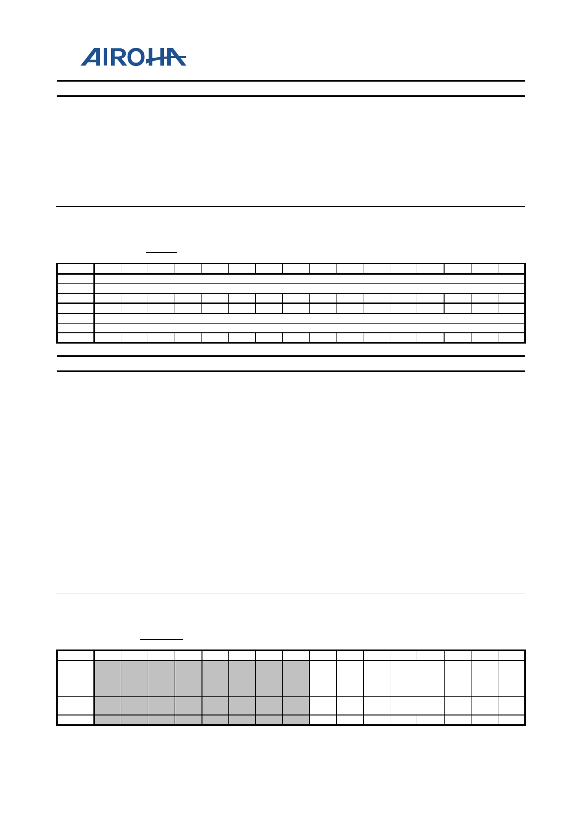
MT2523 Series Reference Manual
© 2015 - 2018 Airoha Technology Corp.
Page 161 of 692
This document contains information that is proprietary to Airoha Technology Corp. (“Airoha”) and/or its licensor(s).
Any unauthorized use, reproduction or disclosure of this document in whole or in part is strictly prohibited.
Bit(s) Name Description
complete an odd-byte or odd-word transfer. For DC/DTV project, also refer to
the RISC_SIZE register to complete FIFO access.
2. Depending on the size of the FIFO and the expected maximum packet size,
the FIFOs support either single-packet or double-packet buffering. However,
burst writing of multiple packets is not supported as flags need to be set after
each packet is written.
3. Following a STALL response or a Tx Strike Out error on Endpoint, the
associated FIFO is completely flushed.
4. For programmers, do not use debug tools to monitor or read the FIFO region.
The FIFO pointer will increase and cause unexpected error in MAC state
machine.
A090002
8 FIFO2 USB Endpoint 2 FIFO Register 00000000
Bit
31
30
29
28
27
26
25
24
23
22
21
20
19
18
17
16
Name
FIFO_DATA[31:16]
Type
Other
Reset
0
0
0
0
0
0
0
0
0
0
0
0
0
0
0
0
Bit
15
14
13
12
11
10
9
8
7
6
5
4
3
2
1
0
Name
FIFO_DATA[15:0]
Type
Other
Reset
0
0
0
0
0
0
0
0
0
0
0
0
0
0
0
0
Bit(s) Name Description
31:0 FIFO_DATA
The Endpoint FIFO registers provides 16 addresses for CPU access to
the FIFOs for each endpoint. Writing to these addresses loads data
into TxFIFO for the corresponding endpoint. Reading from these
addresses unloads data from RxFIFO for the corresponding
endpoint.
Note:
1. Transfers to and from FIFOs may be 8-bit, 16-bit or 32-bit as required, and
any combination of access is allowed provided the data accessed are contiguous.
However, all the transfers associated with one packet must be of the ame width
so that the data are consistently byte-, word- or double-word-aligned. The last
transfer may however contain fewer bytes than the previous transfers in order to
complete an odd-byte or odd-word transfer. For DC/DTV project, also refer to
RISC_SIZE register to complete FIFO access.
2. Depending on the size of the FIFO and the expected maximum packet size,
the FIFOs support either single-packet or double-packet buffering. However,
burst writing of multiple packets is not supported as flags need to be set after
each packet is written.
3. Following a STALL response or a Tx Strike Out error on Endpoint, the
associated FIFO is completely flushed.
4. For programmers, do not use debug tools to monitor or read the FIFO region.
The FIFO pointer will increase and cause unexpected error in MAC state
machine.
A090006
0 DEVCTL Device Control Register 80
Bit
15
14
13
12
11
10
9
8
7
6
5
4
3
2
1
0
Name
B_
DE
VIC
E
FS
DE
V
LS
DE
V
VBUS
HO
ST
MO
DE
HO
ST
RE
Q
SES
SIO
N
Type RU RU RU RU RU
Oth
er
Oth
er
Reset
1
0
0
0
0
0
0
0
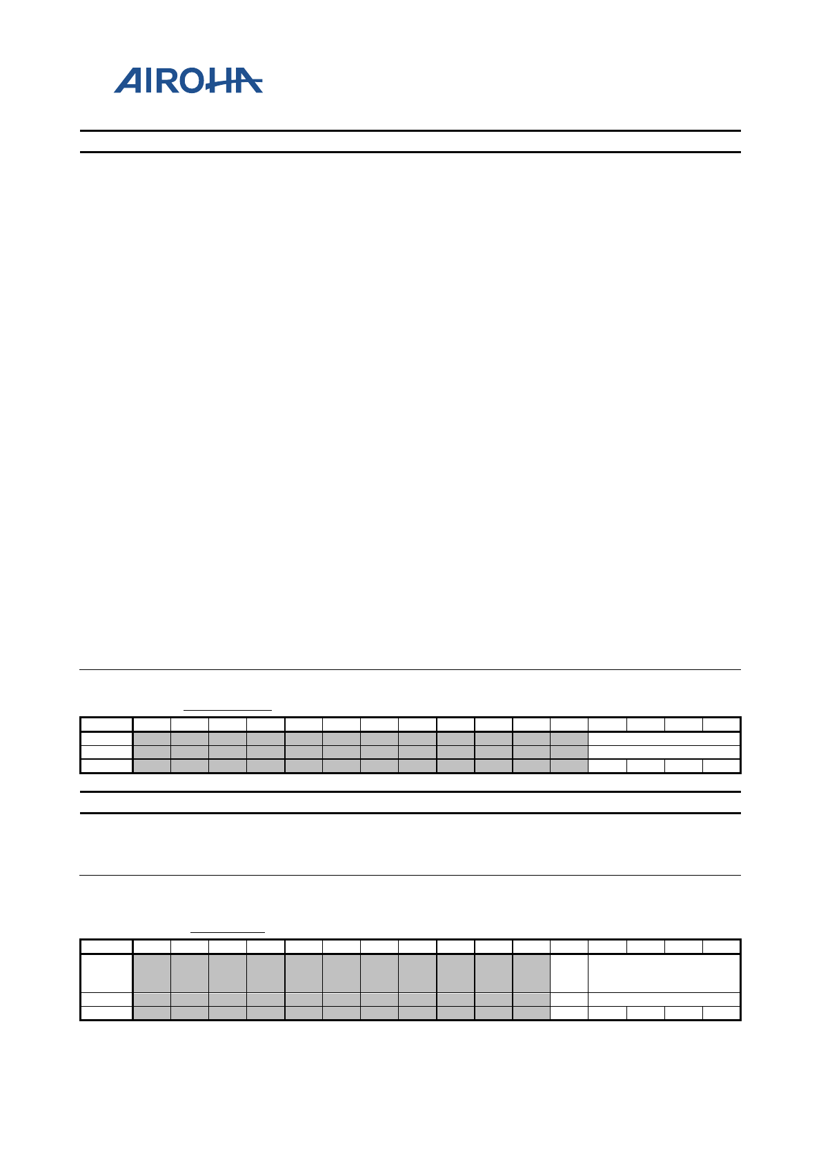
MT2523 Series Reference Manual
© 2015 - 2018 Airoha Technology Corp.
Page 162 of 692
This document contains information that is proprietary to Airoha Technology Corp. (“Airoha”) and/or its licensor(s).
Any unauthorized use, reproduction or disclosure of this document in whole or in part is strictly prohibited.
Bit(s) Name Description
7 B_DEVICE
This read-only bit indicates whether the USB2.0 controller operates
as the 'A' device or the 'B' device. Only valid when a session is in
progress.
Note: If the core is in Force_Host mode, this bit will indicate the state of the
HOSTDISCON input signal from the PHY.
1'b0: 'A' device
1'b1: 'B' device
6 FSDEV
This read-only bit is set when a full-speed or high-speed device has
been detected being connected to the port. (High-speed devices are
distinguished from full-speed by checking for high-speed chirps
when the device is reset.) Only valid in host mode.
5 LSDEV This read-only bit is set when a low-speed device has been detected
being connected to the port. Only valid in host mode.
4:3 VBUS
These read-only bits encode the current VBUS level as the following:
(only available with OTG function equipped; else the register value
will be undefined.)
2'b00: Below SessionEnd
2'b01: Above SessionEnd, below AValid
2'b10: Above AValid, below VBusValid
2'b11: About VBusValid
2 HOSTMODE This read-only bit is set when the USB2.0 controller is acting as a
host.
1 HOSTREQ When set, the USB2.0 controller will initiate Host Negotiation when
Suspend mode is entered. Cleared when Host Negotiation is
completed ('B' device only).
0 SESSION
When operating as 'A' device, this bit is set or cleared by the CPU to
start or end a session. When operating as 'B' device, this bit is
set/cleared by the USB2.0 controller when a session starts/ends. It is
also set by the CPU to initiate the Session Request Protocol. When the
USB2.0 controller is in Suspend mode, the bit may be cleared by the
CPU to perform software disconnect.
Note: Clearing this bit when the core is not suspended will result in undefined
behavior.
A0900061 PWRUPCNT Power Up Counter Register 0F
Bit
15
14
13
12
11
10
9
8
7
6
5
4
3
2
1
0
Name
PWRUPCNT
Type
RW
Reset
1
1
1
1
Bit(s) Name Description
3:0 PWRUPCNT
Power up counter limit. The power up counter counts the K state
duration during suspend; when it times out, the resume interrupt
will be issued. The register should be configured according to AHB
clock speed.
A0900062 TXFIFOSZ Tx FIFO Size Register 00
Bit
15
14
13
12
11
10
9
8
7
6
5
4
3
2
1
0
Name
TX
DP
B
TXSZ
Type
RW
RW
Reset
0
0
0
0
0
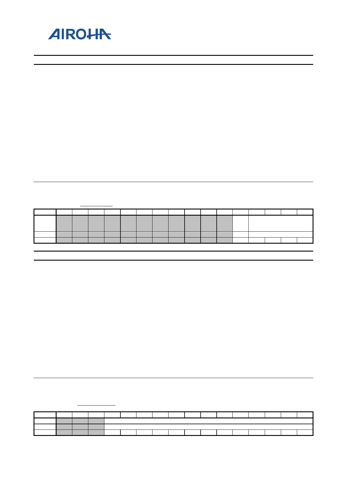
MT2523 Series Reference Manual
© 2015 - 2018 Airoha Technology Corp.
Page 163 of 692
This document contains information that is proprietary to Airoha Technology Corp. (“Airoha”) and/or its licensor(s).
Any unauthorized use, reproduction or disclosure of this document in whole or in part is strictly prohibited.
Bit(s) Name Description
4 TXDPB Defines whether double-packet buffering supported for TxFIFO.
When '1', double-packet buffering is supported. When '0', only single-
packet buffering is supported.
3:0 TXSZ
Maximum packet size to be allowed for (before any splitting within
the FIFO of Bulk/High-Bandwidth packets prior to transmission). If
TxDPB = 0, FIFO will also be this size; if TxDPB = 1, FIFO will be
twice this size.
TxSZ[3:0] Packet size (bytes)
4'b0000: 8
4'b0001: 16
4'b0010: 32
4'b0011: 64
4'b0100: 128
4'b0101: 256
4'b0110: 512
4'b0111: 1024
4'b1000: 2048 (single-packet buffering only)
4'b1001: 4096 (single-packet buffering only)
Others: Not supported
A0900063 RXFIFOSZ Rx FIFO Size Register 00
Bit
15
14
13
12
11
10
9
8
7
6
5
4
3
2
1
0
Name
RX
DP
B
RXSZ
Type
RW
RW
Reset
0
0
0
0
0
Bit(s) Name Description
4 RXDPB Defines whether double-packet buffering supported for TxFIFO.
When 1, double-packet buffering is supported. When 0, only single-
packet buffering is supported.
3:0 RXSZ
Maximum packet size to be allowed for (before any splitting within
the FIFO of Bulk/High-Bandwidth packets prior to transmission). If
TxDPB = 0, FIFO will also be this size; if TxDPB = 1, FIFO will be
twice this size
RxSZ[3:0] Packet size (bytes)
4'b0000: 8
4'b0001: 16
4'b0010: 32
4'b0011: 64
4'b0100: 128
4'b0101: 256
4'b0110: 512
4'b0111: 1024
4'b1000: 2048 (single-packet buffering only)
4'b1001: 4096 (single-packet buffering only)
Others: Not supported
A090006
4 TXFIFOADD Tx FIFO Address Register 0000
Bit
15
14
13
12
11
10
9
8
7
6
5
4
3
2
1
0
Name
TXFIFOADD
Type
RW
Reset
0
0
0
0
0
0
0
0
0
0
0
0
0
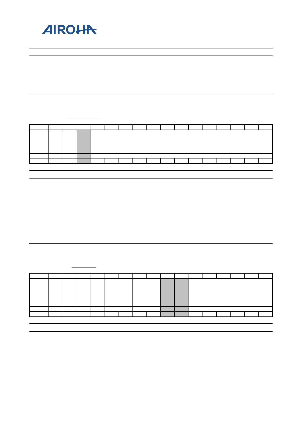
MT2523 Series Reference Manual
© 2015 - 2018 Airoha Technology Corp.
Page 164 of 692
This document contains information that is proprietary to Airoha Technology Corp. (“Airoha”) and/or its licensor(s).
Any unauthorized use, reproduction or disclosure of this document in whole or in part is strictly prohibited.
Bit(s) Name Description
12:0 TXFIFOADD
TxFIFOadd is a 13-bit register which controls the start address of the
selected Tx endpoint FIFO.
TxFIFOadd[12:0] Start address
13'h0000: 0000
13'h0001: 0008
13'h0002: 0010
13'h1FFF: FFF8
A090006
6 RXFIFOADD Rx FIFO Address Register 0000
Bit
15
14
13
12
11
10
9
8
7
6
5
4
3
2
1
0
Name
Dat
aEr
rInt
rEn
Ove
rR
UN
Intr
En
RXFIFOADD
Type
RW
RW
RW
Reset
0
0
0
0
0
0
0
0
0
0
0
0
0
0
0
Bit(s) Name Description
15 DataErrIntrEn Enables data error interrupt
Note: This bit is only valid when the endpoint is operating in ISO mode.
14 OverRUNIntrEn Enables over run interrupt
Note: this bit is only valid when the endpoint is operating in ISO mode.
12:0 RXFIFOADD
RxFIFOadd is a 13-bit register which controls the start address of the
selected Rx endpoint FIFO.
RxFIFOadd[12:0] Start address
13'h0000: 0000
13'h0001: 0008
13'h0002: 0010
13'h1FFF: FFF8
A090006
C HWCAPS Hardware Capability Register 2003
Bit
15
14
13
12
11
10
9
8
7
6
5
4
3
2
1
0
Name
QM
U_
SU
PP
OR
T
HU
B_
SU
PP
OR
T
US
B20
_S
UP
PO
RT
US
B11
_S
UP
PO
RT
MSTR_W
RAP_INT
FX
SLAVE_W
RAP_INT
FX
USB_VERSION_CODE
Type
RO
RO
RO
RO
DC
DC
RO
Reset
0
0
1
0
0
0
0
0
0
0
0
0
1
1
Bit(s) Name Description
15 QMU_SUPPORT QMU feature support
14 HUB_SUPPORT HUB feature support
13 USB20_SUPPORT USB2.0 feature support
12 USB11_SUPPORT USB1.1 feature support
11:10 MSTR_WRAP_INTF
X
Configures AHB master interface
2'b00: Mentor AHB master interface
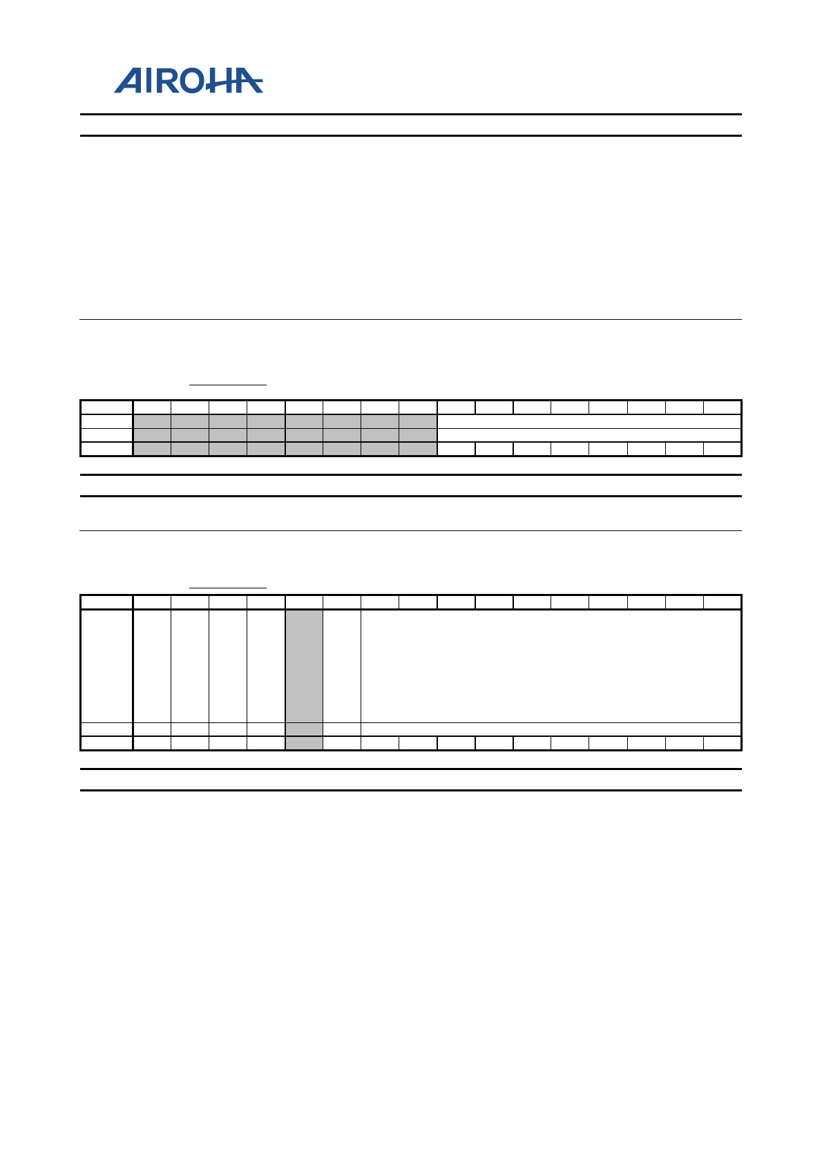
MT2523 Series Reference Manual
© 2015 - 2018 Airoha Technology Corp.
Page 165 of 692
This document contains information that is proprietary to Airoha Technology Corp. (“Airoha”) and/or its licensor(s).
Any unauthorized use, reproduction or disclosure of this document in whole or in part is strictly prohibited.
Bit(s) Name Description
2'b01: Asynchronous AHB master interface
2'b10: Asynchronous AXI master interface
2'b11: Asynchronous DX DRAM master interface
9:8 SLAVE_WRAP_INT
FX
Configures AHB slave interface
2'b00: Mentor AHB slave interface
2'b01: Asynchronous AHB master interface
2'b10: Asynchronous AXI master interface
2'b11: Asynchronous DX CPU slave interface
5:0 USB_VERSION_CO
DE USB hardware version code
A090006
E HWSVERS Version Register 0000
Bit
15
14
13
12
11
10
9
8
7
6
5
4
3
2
1
0
Name
USB_SUB_VERSION_CODE
Type
RO
Reset
0
0
0
0
0
0
0
0
Bit(s) Name Description
7:0 USB_SUB_VERSIO
N_CODE USB software version code
A0900070 BUSPERF1 USB Bus Performance Register 1 0000
Bit
15
14
13
12
11
10
9
8
7
6
5
4
3
2
1
0
Name
CL
RD
MA
RE
QE
AR
LY
_E
N
SO
FT_
DE
BO
UN
CE
ISO
_E
RR
_C
NT
_E
N
ISO
_R
TY
_DI
S
PR
EA
MB
LE
_D
EL
AY
_E
N
HOST_WAIT_EP0
Type
RW
RW
RW
RW
RW
RW
Reset
0
0
0
0
0
0
0
0
0
0
0
0
0
0
0
Bit(s) Name Description
15 CLRDMAREQEARLY
_EN
CLRDMAREQEARLY_EN = 1 means DMAReq is cleared when 8 bytes
of data remain in FIFO for RX, or TXMAXP-8 bytes are loaded in
FIFO for TX.
CLRDMAREQEARLY_EN = 0 means DMAReq is only cleared when RX FIFO is
read empty, or TXMAXP is loaded to TX FIFO.
14 SOFT_DEBOUNCE
If soft_debounce=0, debounce will be implemented by hardware,
that is 120ms, the same as before.
If soft_debounce=1, after DP/DM is stable for 1ms, connection interrupt will be
generated, and software will determine how long the delay is for debounce.
This bit only affects the debounce behavior when the cable starts connection. It
does not affect HNP when the cable is connected.
13 ISO_ERR_CNT_EN Musbhdrc has different behavior from the USB spec. in HUB ISO
mode. When this bit is set, the Strike out mechanism of re-try failed
will be engaged and complete the transaction.
12 ISO_RTY_DIS Musbhdrc has different behavior from the USB spec. in HUB ISO
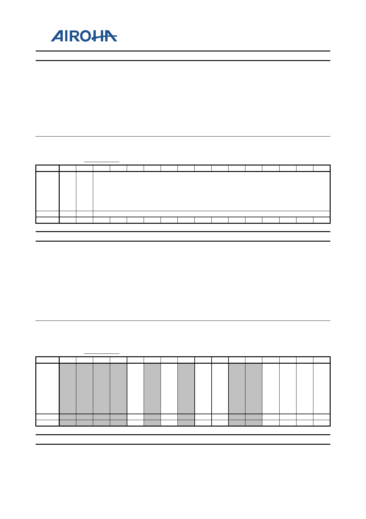
MT2523 Series Reference Manual
© 2015 - 2018 Airoha Technology Corp.
Page 166 of 692
This document contains information that is proprietary to Airoha Technology Corp. (“Airoha”) and/or its licensor(s).
Any unauthorized use, reproduction or disclosure of this document in whole or in part is strictly prohibited.
Bit(s) Name Description
mode. This bit is disable the retry of CSplit @ SOF
10 PREAMBLE_DELAY
_EN
Host mode only and downstream port connect to hub. This bit
enables the function of host delay to issue a preamble +ack packet
after receiving data from LS device about 3 LS bit time.
9:0 HOST_WAIT_EP0
Host waiting time of Endpoint 0
The written value defines the minimum cycles for controller to issue the next
IN/OUT/PING token during idle state.
0: No wait
>0: During idle state, the controller must wait for at least the exact cycles written
before it issues the next IN/OUT/PING token. The cycle unit is as USB system
clock cycle.
A0900072 BUSPERF2 USB Bus Performance Register 2 C000
Bit
15
14
13
12
11
10
9
8
7
6
5
4
3
2
1
0
Name
HS
R_I
SOI
CH
K_
DIS
HS
T_I
SO
OC
HK
_DI
S
HOST_WAIT_EPX
Type
RW
RW
RW
Reset
1
1
0
0
0
0
0
0
0
0
0
0
0
0
0
0
Bit(s) Name Description
15 HSR_ISOICHK_DIS ISO Rx 0-packet Disable in host mode
Optional disable selection for ISO Rx 0 packet
14 HST_ISOOCHK_DIS ISO Tx 0-packet Disable in host mode
Optional disable selection for ISO Rx 0 packet
13:0 HOST_WAIT_EPX
Host waiting time of all endpoints except for Endpoint 0
The written value defines the minimum cycles for controller to issue the next
IN/OUT/PING token during idle state.
0: No wait
>0: During idle state, the controller must wait for at least the exact cycles written
before it issues the next IN/OUT/PING token. The cycle unit is as USB system
clock cycle.
A0900074 BUSPERF3 USB Bus Performance Register 3 0A48
Bit
15
14
13
12
11
10
9
8
7
6
5
4
3
2
1
0
Name
VB
US
ER
R_
MO
DE
FL
US
H_
FIF
O_
EN
NO
ISE
_ST
ILL
_S
OF
BA
B_
CL
R_
EN
UN
DO
_S
RP
FIX
OT
G_
DE
GLI
TC
H_
DIS
AB
LE
EP
_S
WR
ST
DIS
US
BR
ESE
T
Type
RW
RW
RW
RW
RW
RW
A0
RW
Reset
1
1
0
1
1
0
0
0
Bit(s) Name Description
11 VBUSERR_MODE Controls whether VBUS error will reset USB controller or only set up
the VBUS error bit
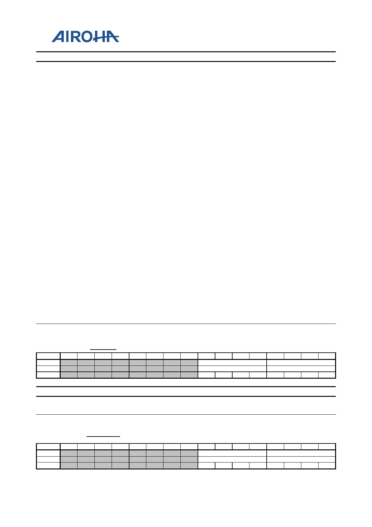
MT2523 Series Reference Manual
© 2015 - 2018 Airoha Technology Corp.
Page 167 of 692
This document contains information that is proprietary to Airoha Technology Corp. (“Airoha”) and/or its licensor(s).
Any unauthorized use, reproduction or disclosure of this document in whole or in part is strictly prohibited.
Bit(s) Name Description
1'b0: Set up INTRUSB.bit[7] VBUS error only
1'b1: Reset USB controller and set up INTRUSB.bit[7] VBUS error tooDataErr
interrupt enable. The DataErr status bit is in RxCSR[3] and should be written 0
to clear.TBD
9 FLUSH_FIFO_EN
Enables Flush FIFO
1'b1: Clear USBPtr0, USBPtr1 of EPx Tx by flush FIFO command.
1'b0: USBPtr0, USBPtr1 of EPx Tx cannot be cleared by flush FIFO command.
7 NOISE_STILL_SOF Forces transmitting SOF as babble interrupt
6 BAB_CLR_EN
Controls babble session
1'b0: Babble interrupt will not close session automatically.
1'b1: Babble interrupt will close session automatically.
3 UNDO_SRPFIX The CPU sets up this bit to recover to the original circuit of USB2.0 IP
about SRP.
2 OTG_DEGLITCH_D
ISABLE
Set to 1 to disable deglitch circuit of OTG signal group VBUSVALID,
AVALID and SESSEND.
1 EP_SWRST
SW can reset the USB MAC setting by setting this bit to 1. EP_SWRST
will be cleared by HW automatically.
The MAC settings include function address, endpoint interrupt enable/status,
endpoint state and EP TX/RX CSR.
0 DISUSBRESET
If DISUSBRESET is 0, USB MAC setting will be reset to inconfigured
condition when USB bus reset is detected. SW can set this bit to 1 to
disable USB MAC setting. Reset by HW when USB bus reset is
detected.
The HW reset MAC settings include:
1. Clear function address register
2. Clear index register
3. Flush all endpoint FIFOs
4. Clear control/status register
a. EPN TX/RXMAXP
b. EPN TX/RXCSR
c. EPN TX/RXTYPE
d. EPN TX/RXInterval
e. EPN RXCOUNT
f. EP0 CSR0
g. EP0 COUNT0
5. Enable TX/RX endpoint interrupt and clear TX/RX interrupt status
Note: EPN TX/RX FIFOSZ/AD are not cleared.
A0900078 EPINFO Number of Tx and Rx Register 24
Bit
15
14
13
12
11
10
9
8
7
6
5
4
3
2
1
0
Name
RXENDPOINTS
TXENDPOINTS
Type
RO
RO
Reset
0
0
1
0
0
1
0
0
Bit(s) Name Description
7:4 RXENDPOINTS Number of Rx endpoints implemented in the design.
3:0 TXENDPOINTS Number of Tx endpoints implemented in the design.
A0900079 RAMINFO Width of RAM and Number of DMA Channel
Register 4A
Bit
15
14
13
12
11
10
9
8
7
6
5
4
3
2
1
0
Name
DMACHANS
RAMBITS
Type
RO
DC
Reset
0
1
0
0
1
0
1
0
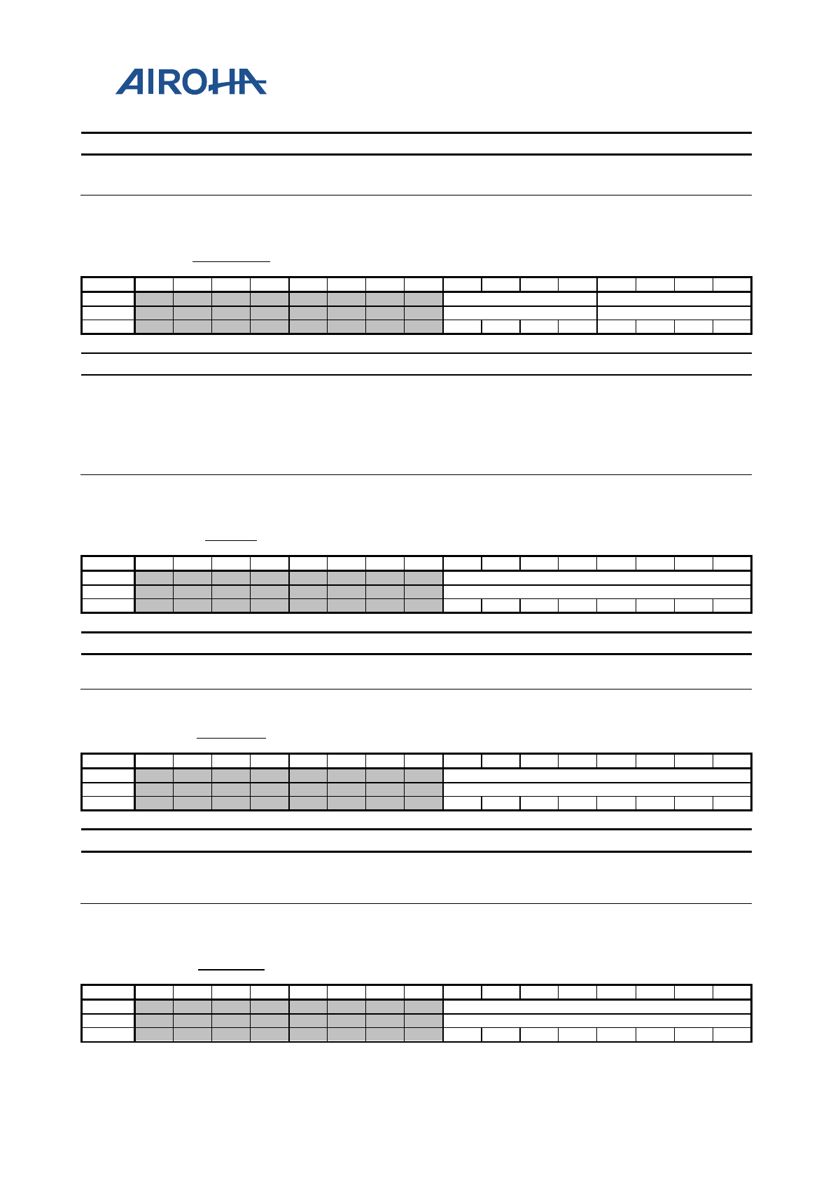
MT2523 Series Reference Manual
© 2015 - 2018 Airoha Technology Corp.
Page 168 of 692
This document contains information that is proprietary to Airoha Technology Corp. (“Airoha”) and/or its licensor(s).
Any unauthorized use, reproduction or disclosure of this document in whole or in part is strictly prohibited.
Bit(s) Name Description
7:4 DMACHANS Number of DMA channels implemented in the design.
3:0 RAMBITS Width of the RAM address bus-1
A090007
A LINKINFO Delay to be Applied Register 5C
Bit
15
14
13
12
11
10
9
8
7
6
5
4
3
2
1
0
Name
WTCON
WTID
Type
RW
RW
Reset
0
1
0
1
1
1
0
0
Bit(s) Name Description
7:4 WTCON
Sets the wait to be applied to allow for the user's connect/disconnect
filter in units of 533.3ns. (The default setting corresponds to
2.667us.) The default value will change to be 4'h8 to meet 2.667us.
3:0 WTID
Sets up delay to be applied from IDPULLUP being asserted to IDDIG
being considered valid in units of 4.369ms.
The default setting corresponds to 52.43ms.)
A090007
B VPLEN Vbus Pulsing Charge Register 3C
Bit
15
14
13
12
11
10
9
8
7
6
5
4
3
2
1
0
Name
VPLEN
Type
RW
Reset
0
0
1
1
1
1
0
0
Bit(s) Name Description
7:0 VPLEN Sets up duration of the VBus pulsing charge in units of 136.5 us. (The
default setting corresponds to 8.19ms
A090007C HS_EOF1 Time Buffer Available on HS Transaction
Register 80
Bit
15
14
13
12
11
10
9
8
7
6
5
4
3
2
1
0
Name
HS_EOF1
Type
RW
Reset
1
0
0
0
0
0
0
0
Bit(s) Name Description
7:0 HS_EOF1
Sets up high-speed transactions the time before EOF to stop
beginning new transactions, in units of 133.3ns.
The default setting corresponds to 17.07us. USB2.0 IP only.
A090007
D FS_EOF1 Time Buffer Available on FS Transaction
Register 77
Bit
15
14
13
12
11
10
9
8
7
6
5
4
3
2
1
0
Name
FS_EOF1
Type
RW
Reset
0
1
1
1
0
1
1
1
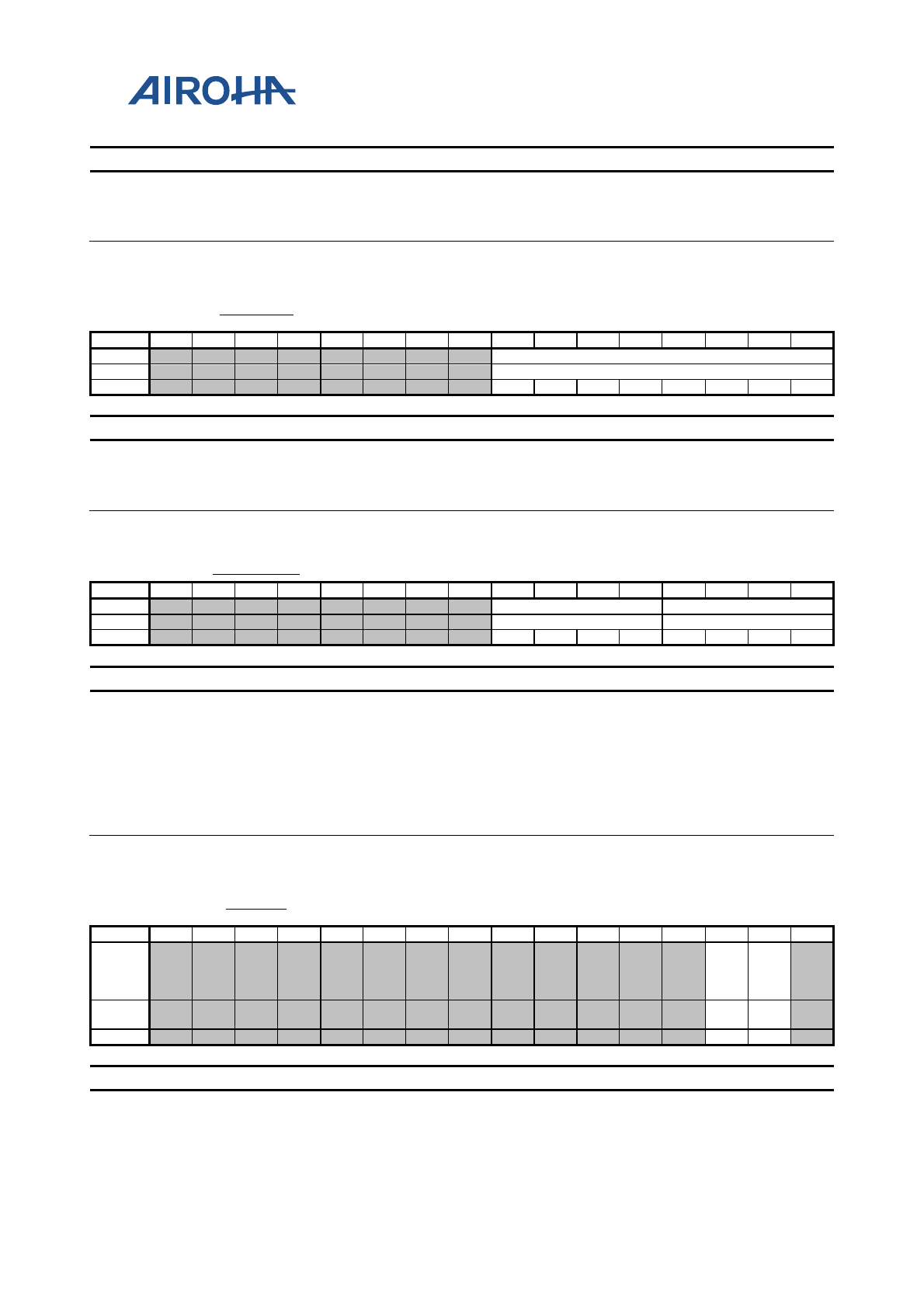
MT2523 Series Reference Manual
© 2015 - 2018 Airoha Technology Corp.
Page 169 of 692
This document contains information that is proprietary to Airoha Technology Corp. (“Airoha”) and/or its licensor(s).
Any unauthorized use, reproduction or disclosure of this document in whole or in part is strictly prohibited.
Bit(s) Name Description
7:0 FS_EOF1
Sets up full-speed transactions the time before EOF to stop beginning
new transactions, in units of 533.3ns. (The default setting
corresponds to 63.46us.) The default value will change to be 8'hBE to
meet 63.46us.
A090007E LS_EOF1 Time Buffer Available on LS Transaction
Register 72
Bit
15
14
13
12
11
10
9
8
7
6
5
4
3
2
1
0
Name
LS_EOF1
Type
RW
Reset
0
1
1
1
0
0
1
0
Bit(s) Name Description
7:0 LS_EOF1
Sets up Q252low-speed transactions the time before EOF to stop
beginning new transactions, in units of 1.067us. (The default setting
corresponds to 121.6us.). USB2.0 IP only. The default value will
change to be 8'hB6 to meet 121.6us.
A090007F RST_INFO Reset Information Register 00
Bit
15
14
13
12
11
10
9
8
7
6
5
4
3
2
1
0
Name
WTFSSE0
WTCHRP
Type
RW
RW
Reset
0
0
0
0
0
0
0
0
Bit(s) Name Description
7:4 WTFSSE0
Signifies the SE0 signal duration before issuing the reset signal (for
device only).
Duration = 272.8 x WTFSSE0 + 2.5 usec.
This register will only be reset when hardware is reset.
3:0 WTCHRP
Sets up delay to be applied from detecting Reset to sending chirp K
(for device only).
The duration = 272.8 x WTCHRP + 0.1 usec.
This register will only be reset when hardware is reset.
A090008
0 RXTOG Rx Data Toggle Set/Status Register 0000
Bit
15
14
13
12
11
10
9
8
7
6
5
4
3
2
1
0
Name
EP2
RX
TO
G
EP1
RX
TO
G
Type
Oth
er
Oth
er
Reset
0
0
Bit(s) Name Description
2 EP2RXTOG
Receive Logical Endpoint n Data Toggle Bit Set/Status
When read, these bits indicate the current state of the Endpoint n data toggle. If
enable bit is high, the bit may be written with the required setting of the data
toggle. If enable is low, any value written will be ignored
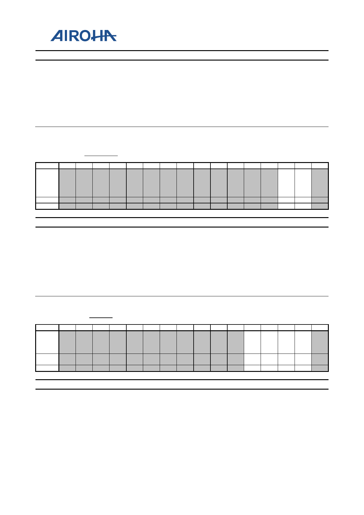
MT2523 Series Reference Manual
© 2015 - 2018 Airoha Technology Corp.
Page 170 of 692
This document contains information that is proprietary to Airoha Technology Corp. (“Airoha”) and/or its licensor(s).
Any unauthorized use, reproduction or disclosure of this document in whole or in part is strictly prohibited.
Bit(s) Name Description
Note: This register is word access.
1'b0: Logical Endpoint n RX data toggle bit = 0
1'b1: Logical Endpoint n RX data toggle bit = 1
1 EP1RXTOG
Receive Logical Endpoint n Data Toggle Bit Set/Status.
When read, these bits indicate the current state of the Endpoint n data toggle. If
enable bit is high, the bit may be written with the required setting of the data
toggle. If enable is low, any value written will be ignored
Note: This register is word access.
1'b0: Logical Endpoint n RX data toggle bit = 0
1'b1: Logical Endpoint n RX data toggle bit = 1
A090008
2 RXTOGEN Rx Data Toggle Enable Register 0000
Bit
15
14
13
12
11
10
9
8
7
6
5
4
3
2
1
0
Name
EP2
RX
TO
GE
N
EP1
RX
TO
GE
N
Type
RW
RW
Reset
0
0
Bit(s) Name Description
2 EP2RXTOGEN
Enables Receive Logical Endpoint n Data Toggle Bit
If enable bit is set, the endpoint n data toggle can be set.
Note: This register is word access.
1'b0: Forbid RISC writing EP n data toggle status with EP1RXTOG
1'b1: Allow RISC writing EP n data toggle status with EP1RXTOG
1 EP1RXTOGEN
Enables Receive Logical Endpoint n Data Toggle Bit
If enable bit is set, the endpoint n data toggle can be set.
Note: This register is word access.
1'b0: Forbid RISC writing EP n data toggle status with EP1RXTOG
1'b1: Allow RISC writing EP n data toggle status with EP1RXTOG
A090008
4 TXTOG Tx Data Toggle Set/Status Register 0000
Bit
15
14
13
12
11
10
9
8
7
6
5
4
3
2
1
0
Name
EP4
TX
TO
G
EP3
TX
TO
G
EP2
TX
TO
G
EP1
TX
TO
G
Type
Oth
er
Oth
er
Oth
er
Oth
er
Reset
0
0
0
0
Bit(s) Name Description
4 EP4TXTOG
Transmit Logical Endpoint n Data Toggle Bit Set/Status
When read, these bits indicate the current state of the Endpoint n data toggle. If
enable bit is high, the bit may be written with the required setting of the data
toggle. If enable is low, any value written will be ignored
Note: This register is word access.
1'b0: Logical Endpoint n TX data toggle bit = 0
1'b1: Logical Endpoint n TX data toggle bit = 1
3 EP3TXTOG
Transmit Logical Endpoint n Data Toggle Bit Set/Status
When read, these bits indicate the current state of the Endpoint n data toggle. If
enable bit is high, the bit may be written with the required setting of the data
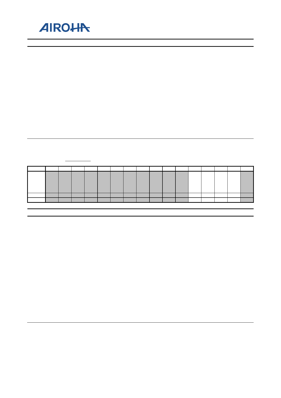
MT2523 Series Reference Manual
© 2015 - 2018 Airoha Technology Corp.
Page 171 of 692
This document contains information that is proprietary to Airoha Technology Corp. (“Airoha”) and/or its licensor(s).
Any unauthorized use, reproduction or disclosure of this document in whole or in part is strictly prohibited.
Bit(s) Name Description
toggle. If enable is low, any value written will be ignored
Note: This register is word access.
1'b0: Logical Endpoint n TX data toggle bit = 0
1'b1: Logical Endpoint n TX data toggle bit = 1
2 EP2TXTOG
Transmit Logical Endpoint n Data Toggle Bit Set/Status
When read, these bits indicate the current state of the Endpoint n data toggle. If
enable bit is high, the bit may be written with the required setting of the data
toggle. If enable is low, any value written will be ignored
Note: This register is word access.
1'b0: Logical Endpoint n TX data toggle bit = 0
1'b1: Logical Endpoint n TX data toggle bit = 1
1 EP1TXTOG
Transmit Logical Endpoint n Data Toggle Bit Set/Status
When read, these bits indicate the current state of the Endpoint n data toggle. If
enable bit is high, the bit may be written with the required setting of the data
toggle. If enable is low, any value written will be ignored
Note: This register is word access.
1'b0: Logical Endpoint n TX data toggle bit = 0
1'b1: Logical Endpoint n TX data toggle bit = 1
A090008
6 TXTOGEN Tx Data Toggle Enable Register 0000
Bit
15
14
13
12
11
10
9
8
7
6
5
4
3
2
1
0
Name
EP4
TX
TO
GE
N
EP3
TX
TO
GE
N
EP2
TX
TO
GE
N
EP1
TX
TO
GE
N
Type
RW
RW
RW
RW
Reset
0
0
0
0
Bit(s) Name Description
4 EP4TXTOGEN
Enables Receive Logical Endpoint 1 Data Toggle Bit
If enable bit is set, the endpoint n data toggle can be set.
Note: This register is word access.
1'b0: Forbid RISC writing EP n data toggle status with EP1RXTOG
1'b1: Allow RISC writing EP n data toggle status with EP1RXTOG
3 EP3TXTOGEN
Enables Receive Logical Endpoint 1 Data Toggle Bit
If enable bit is set, the endpoint n data toggle can be set.
Note: This register is word access.
1'b0: Forbid RISC writing EP n data toggle status with EP1RXTOG
1'b1: Allow RISC writing EP n data toggle status with EP1RXTOG
2 EP2TXTOGEN
Enables Receive Logical Endpoint 1 Data Toggle Bit
If enable bit is set, the endpoint n data toggle can be set.
Note: This register is word access.
1'b0: Forbid RISC writing EP n data toggle status with EP1RXTOG
1'b1: Allow RISC writing EP n data toggle status with EP1RXTOG
1 EP1TXTOGEN
Enables Receive Logical Endpoint 1 Data Toggle Bit
If enable bit is set, the endpoint n data toggle can be set.
Note: This register is word access.
1'b0: Forbid RISC writing EP n data toggle status with EP1RXTOG
1'b1: Allow RISC writing EP n data toggle status with EP1RXTOG
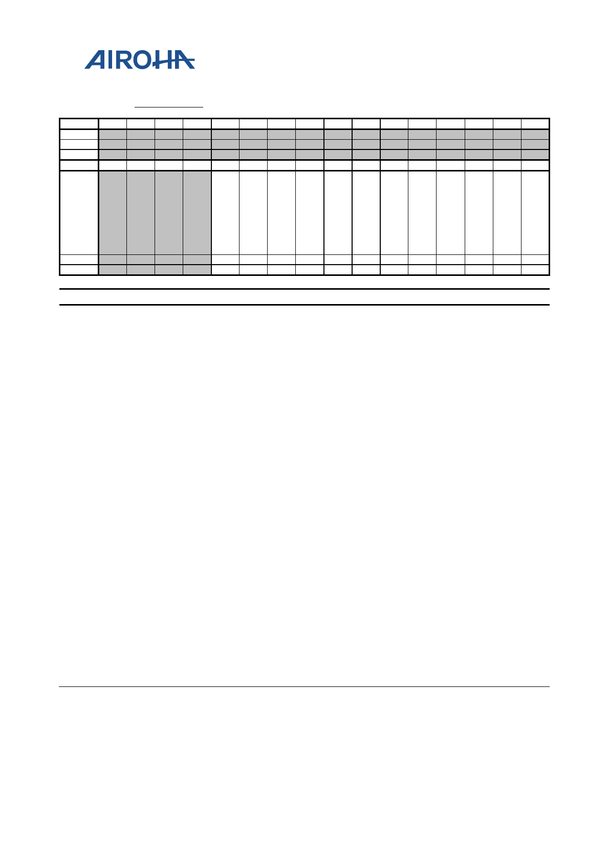
MT2523 Series Reference Manual
© 2015 - 2018 Airoha Technology Corp.
Page 172 of 692
This document contains information that is proprietary to Airoha Technology Corp. (“Airoha”) and/or its licensor(s).
Any unauthorized use, reproduction or disclosure of this document in whole or in part is strictly prohibited.
A09000A
0 USB_L1INTS USB Level 1 Interrupt Status Register 00000000
Bit
31
30
29
28
27
26
25
24
23
22
21
20
19
18
17
16
Name
Type
Reset
Bit
15
14
13
12
11
10
9
8
7
6
5
4
3
2
1
0
Name
PO
WE
RD
WN
_IN
T_S
TA
TU
S
DR
VV
BU
S_I
NT
_ST
AT
US
ID
DIG
_IN
T_S
TA
TU
S
VB
US
VA
LID
_IN
T_S
TA
TU
S
DP
DM
_IN
T_S
TA
TU
S
QH
IF_
INT
_ST
AT
US
QI
NT
_ST
AT
US
PS
R_I
NT
_ST
AT
US
DM
A_I
NT
_ST
AT
US
US
BC
OM
_IN
T_S
TA
TU
S
RX
_IN
T_S
TA
TU
S
TX
_IN
T_S
TA
TU
S
Type
RU
RU
RU
RU
RU
RU
RU
RU
RU
RU
RU
RU
Reset
0
0
0
0
0
0
0
0
0
0
0
0
Bit(s) Name Description
11 POWERDWN_INT_
STATUS
Power-down interrupt status
When controller is in host suspend mode, VBus is valid, and DP is asserted, this
bit will set. When controller is in peripheral mode, Avalid is setting, and DP is
asserted, this bit will set. When controller is in idle state, avalid is de-asserted ,
and linestate is in SE0, this bit will also set.
10 DRVVBUS_INT_STA
TUS
DRVVBUS interrupt status
This bit shows the interrupt trigger status of DRVVBUS. The trigger polarity is
determined by DRVVBUS_INT_POL.
This interrupt is used in USB OTG charge pump control.
9 IDDIG_INT_STATU
S
IDDIG interrupt status
This bit shows the interrupt trigger status of IDDIG. The trigger polarity is
determined by IDDIG_INT_POL.
This interrupt is used in USB OTG attachment.
8 VBUSVALID_INT_S
TATUS
VBUSVALID interrupt status
This bit shows the interrupt trigger status of VBUSVALID. The trigger polarity is
determined by VBUSVALID_INT_POL.
This interrupt is used in USB attachment to host.
7 DPDM_INT_STATU
S
DPDM interrupt status
This bit shows the interrupt trigger status of DPDM. The trigger condition is
whether DP or DM goes high.
This interrupt is used in USB HOST mode to detect device attachment.
6 QHIF_INT_STATUS USBQ HIF command interrupt status
Only valid when WiMAX Q is available.
5 QINT_STATUS USBQ interrupt status
Only valid when USBQ is available.
4 PSR_INT_STATUS Packet sequence recorder interrupt status
3 DMA_INT_STATUS DMA interrupt status
2 USBCOM_INT_STA
TUS USB common interrupt status
1 RX_INT_STATUS Endpoint Rx interrupt status
0 TX_INT_STATUS Endpoint Tx interrupt status

MT2523 Series Reference Manual
© 2015 - 2018 Airoha Technology Corp.
Page 173 of 692
This document contains information that is proprietary to Airoha Technology Corp. (“Airoha”) and/or its licensor(s).
Any unauthorized use, reproduction or disclosure of this document in whole or in part is strictly prohibited.
A09000A
4 USB_L1INTM USB Level 1 Interrupt Mask Register 00000000
Bit
31
30
29
28
27
26
25
24
23
22
21
20
19
18
17
16
Name
Type
Reset
Bit
15
14
13
12
11
10
9
8
7
6
5
4
3
2
1
0
Name
PO
WE
RD
WN
_IN
T_
UN
MA
SK
DR
VV
BU
S_I
NT
_U
NM
AS
K
ID
DIG
_IN
T_
UN
MA
SK
VB
US
VA
LID
_IN
T_
UN
MA
SK
DP
DM
_IN
T_
UN
MA
SK
QH
IF_
INT
_U
NM
AS
K
QI
NT
_U
NM
AS
K
PS
R_I
NT
_U
NM
AS
K
DM
A_I
NT
_U
NM
AS
K
US
BC
OM
_IN
T_
UN
MA
SK
RX
_IN
T_
UN
MA
SK
TX
_IN
T_
UN
MA
SK
Type
RW
RW
RW
RW
RW
RW
RW
RW
RW
RW
RW
RW
Reset
0
0
0
0
0
0
0
0
0
0
0
0
Bit(s) Name Description
11 POWERDWN_INT_
UNMASK
Unmasks POWERDWN interrupt
1'b0: Mask interrupt
1'b1: Unmask interrupt
10 DRVVBUS_INT_UN
MASK
Unmasks DRVVBUS interrupt
1'b0: Mask interrupt
1'b1: Unmask interrupt
9 IDDIG_INT_UNMA
SK
Unmasks IDDIG Interrupt
1'b0: Mask interrupt
1'b1: Unmask interrupt
8 VBUSVALID_INT_U
NMASK
Unmasks VBUSVALID Interrupt
1'b0: Mask interrupt
1'b1: Unmask interrupt
7 DPDM_INT_UNMA
SK
Unmasks DPDM Interrupt
1'b0: Mask interrupt
1'b1: Unmask interrupt
6 QHIF_INT_UNMAS
K
Unmasks USBQ HIF command interrupt
Only valid when WiMAX Q is available.
1'b0: Mask interrupt
1'b1: Unmask interrupt
5 QINT_UNMASK
Unmasks USBQ Interrupt
Only valid when USBQ is available.
.
1'b0: Mask interrupt
1'b1: Unmask interrupt
4 PSR_INT_UNMASK
Unmasks packet sequence recorder interrupt
1'b0: Mask interrupt
1'b1: Unmask interrupt
3 DMA_INT_UNMAS
K
Unmasks DMA interrupt
1'b0: Mask interrupt
1'b1: Unmask interrupt
2 USBCOM_INT_UN
MASK
Unmasks USB common interrupt
1'b0: Mask interrupt
1'b1: Unmask interrupt
1 RX_INT_UNMASK
Unmasks endpoint Rx interrupt
1'b0: Mask interrupt
1'b1: Unmask interrupt
0 TX_INT_UNMASK Unmasks endpoint Tx Interrupt
1'b0: Mask interrupt
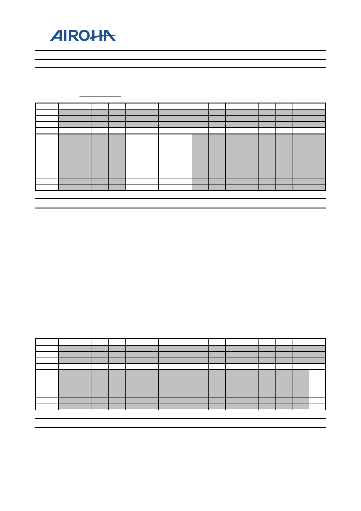
MT2523 Series Reference Manual
© 2015 - 2018 Airoha Technology Corp.
Page 174 of 692
This document contains information that is proprietary to Airoha Technology Corp. (“Airoha”) and/or its licensor(s).
Any unauthorized use, reproduction or disclosure of this document in whole or in part is strictly prohibited.
Bit(s) Name Description
1'b1: Unmask interrupt
A09000A
8 USB_L1INTP USB Level 1 Interrupt Polarity Register 00000200
Bit
31
30
29
28
27
26
25
24
23
22
21
20
19
18
17
16
Name
Type
Reset
Bit
15
14
13
12
11
10
9
8
7
6
5
4
3
2
1
0
Name
PO
WE
RD
WN
_IN
T_
PO
L
DR
VV
BU
S_I
NT
_P
OL
ID
DIG
_IN
T_
PO
L
VB
US
VA
LID
_IN
T_
PO
L
Type
RW
RW
RW
RW
Reset
0
0
1
0
Bit(s) Name Description
11 POWERDWN_INT_
POL
POWERDWN interrupt polarity
1'b0: Interrupt trigger when POWERDWN is 1.
1'b1: Interrupt trigger when POWERDWN is 0.
10 DRVVBUS_INT_PO
L
DRVVBUS interrupt polarity
1'b0: Interrupt trigger when DRVVBUS is 1.
1'b1: Interrupt trigger when DRVVBUS is 0.
9 IDDIG_INT_POL
IDDIG interrupt polarity
1'b0: Interrupt trigger when IDDIG is 1.
1'b1: Interrupt trigger when IDDIG is 0.
8 VBUSVALID_INT_P
OL
VBUSVALID interrupt polarity
1'b0: Interrupt trigger when VBUSVALID is 1.
1'b1: Interrupt trigger when VBUSVALID is 0.
A09000A
C USB_L1INTC USB Level 1 Interrupt Control Register 00000000
Bit
31
30
29
28
27
26
25
24
23
22
21
20
19
18
17
16
Name
Type
Reset
Bit
15
14
13
12
11
10
9
8
7
6
5
4
3
2
1
0
Name
US
B_I
NT
_SY
NC
Type
RW
Reset
0
Bit(s) Name Description
0 USB_INT_SYNC
USB interrupt synchronization
1'b0: USB output interrupt is output directly.
1'b1: USB output interrupt is synchronized by MCU BUS clock registers.
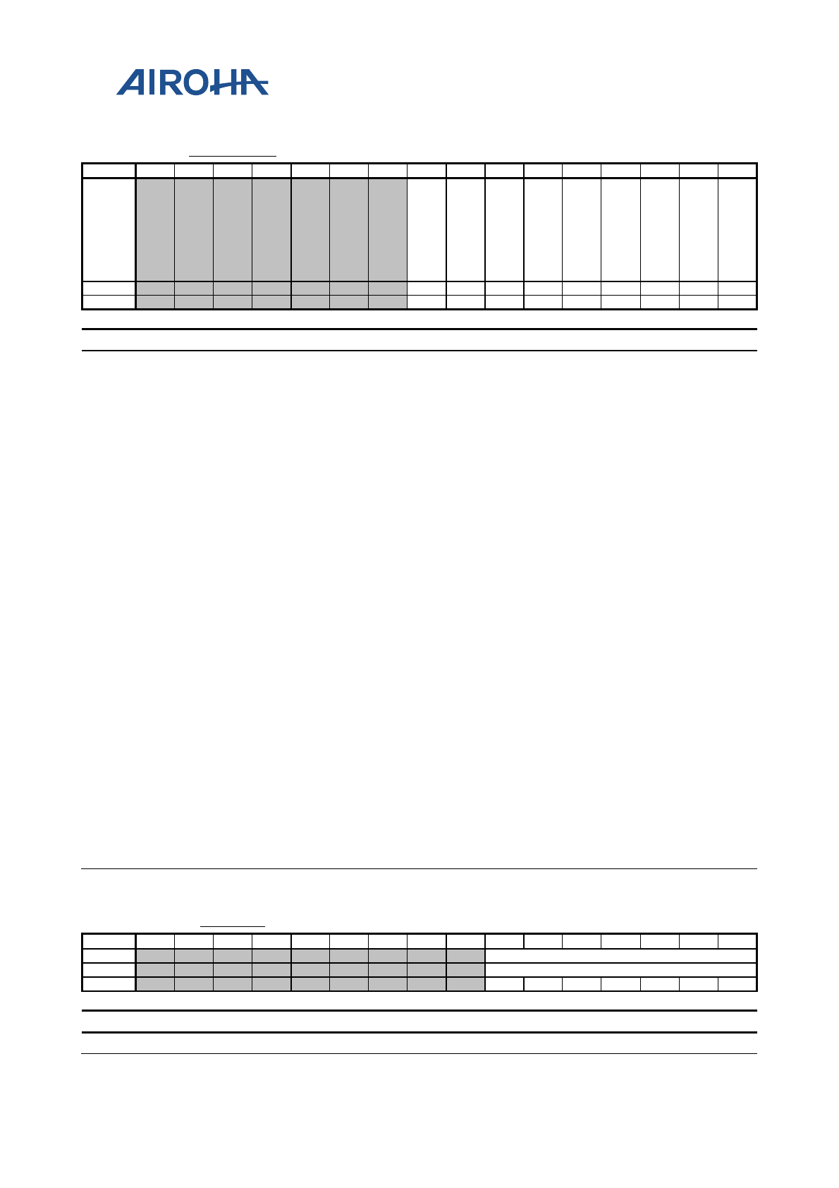
MT2523 Series Reference Manual
© 2015 - 2018 Airoha Technology Corp.
Page 175 of 692
This document contains information that is proprietary to Airoha Technology Corp. (“Airoha”) and/or its licensor(s).
Any unauthorized use, reproduction or disclosure of this document in whole or in part is strictly prohibited.
A0900102 CSR0_PERI EP0 Control Status Register 0000
Bit
15
14
13
12
11
10
9
8
7
6
5
4
3
2
1
0
Name
FL
US
HFI
FO
SE
RVI
CES
ET
UP
ED
N
SE
RVI
CE
DR
XP
KT
RD
Y
SE
ND
ST
AL
L
SET
UP
EN
D
DA
TA
EN
D
SE
NT
ST
AL
L
TX
PK
TR
DY
RX
PK
TR
DY
Type
A0
A0
A0
A0
RU
A0
RW
A0
RU
Reset
0
0
0
0
0
0
0
0
0
Bit(s) Name Description
8 FLUSHFIFO
The CPU writes 1 to this bit to flush the next packet to be
transmitted/read from the Endpoint 0 FIFO. It is cleared
automatically. The FIFO pointer is reset and the TxPktRdy/RxPktRdy
bit (below) is cleared. May be set simultaneously with TxPktRdy to
abort the packet that is currently loaded into FIFO.
Note: FlushFIFO should only be used when TxPktRdy/RxPktRdy is set. In other
cases, it may cause data corruption.
7 SERVICESETUPEDN The CPU writes 1 to this bit to clear the SetupEnd bit.
It is cleared automatically.
6 SERVICEDRXPKTR
DY
The CPU writes 1 to this bit to clear the RxPktRdy bit.
It is cleared automatically.
5 SENDSTALL
The CPU writes 1 to this bit to terminate the current transaction. The
STALL handshake will be transmitted, and this bit will be cleared
automatically.
Note: The FIFO should be flushed before SendStall is set.
4 SETUPEND
This bit will be set when a control transaction ends before the
DataEnd bit is set. An interrupt will be generated and the FIFO
flushed at this time. The bit is cleared by the CPU writing 1 to the
ServicedSetupEnd bit.
3 DATAEND
The CPU sets up this bit when setting TxPktRdy for the last data
packet, when clearing RxPktRdy after unloading the last data packet,
and when setting up TxPktRdy for a 0 length data packet. It is cleared
automatically.
2 SENTSTALL
This bit is set when a STALL handshake is transmitted. The CPU
should clear this bit.
Write 0 to clear it.
1 TXPKTRDY The CPU sets up this bit after loading a data packet into the FIFO. It is
cleared automatically when a data packet has been transmitted. An
interrupt is also generated at this point (if enabled)
0 RXPKTRDY
This bit is set when a data packet has been received. An interrupt is
generated when this bit is set. The CPU clears this bit by setting up
the ServicedRxPktRdy bit.
A0900108 COUNT0 EP0 Received Bytes Register 0000
Bit
15
14
13
12
11
10
9
8
7
6
5
4
3
2
1
0
Name
EP0_RX_COUNT
Type
RU
Reset
0
0
0
0
0
0
0
Bit(s) Name Description
6:0 EP0_RX_COUNT
Count0 is a 7-bit read-only register that indicates the number of
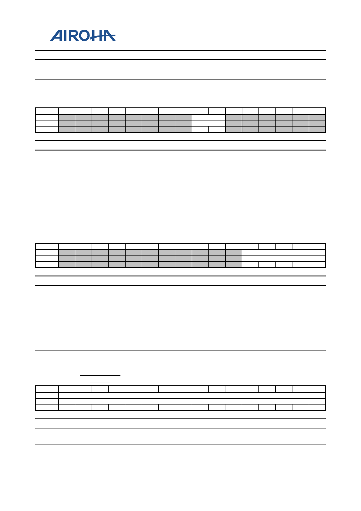
MT2523 Series Reference Manual
© 2015 - 2018 Airoha Technology Corp.
Page 176 of 692
This document contains information that is proprietary to Airoha Technology Corp. (“Airoha”) and/or its licensor(s).
Any unauthorized use, reproduction or disclosure of this document in whole or in part is strictly prohibited.
Bit(s) Name Description
received data bytes in the Endpoint 0 FIFO. The value returned
changes as the contents of the FIFO change and is only valid when
RxPktRdy (IDXEPR0.CSR0.bit0) is set.
A090010A Type0 EP0 Type Register 00
Bit
15
14
13
12
11
10
9
8
7
6
5
4
3
2
1
0
Name
EP0_Type
Type
RW
Reset
0
0
Bit(s) Name Description
7:6 EP0_Type
Operating speed of the target device when the core is configured with
the multipoint option. When the core is not configured with the
multipoint option, these bits should not be accessed
2'b00: Unused
2'b01: High
2'b10: Full
2'b11: Low
A090010B NAKLIMT0 NAK Limit Register 00
Bit
15
14
13
12
11
10
9
8
7
6
5
4
3
2
1
0
Name
NAKLIMIT0
Type
RW
Reset
0
0
0
0
0
Bit(s) Name Description
4:0 NAKLIMIT0
(Host mode only) NAKLimit0 is a 5-bit register that sets up the
number of frames/microframes (high-speed transfers) after which
Endpoint 0 should time out on receiving a stream of NAK responses.
(Equivalent settings for other endpoints can be made through their
TxInterval and RxInterval registers.). The number of
frames/microframes selected is 2(m-1) (where m is the value set in
the register, valid values 2 - 16). If the host receives NAK responses
from the target for more frames than the number represented by the
limit set in this register, the endpoint will be halted.
Note: Value 0 or 1 disables the NAK timeout function.
A090010C SRAMCONFI
GSIZE SRAM Size Register 0800
Bit
15
14
13
12
11
10
9
8
7
6
5
4
3
2
1
0
Name
SRAM_SIZE
Type
RO
Reset
0
0
0
0
1
0
0
0
0
0
0
0
0
0
0
0
Bit(s) Name Description
15:0 SRAM_SIZE Depth of SRAM with data bus width 32 bits.
For example, if SRAM is configured to 8KB, SRAM_SIZE will be 16'h800.
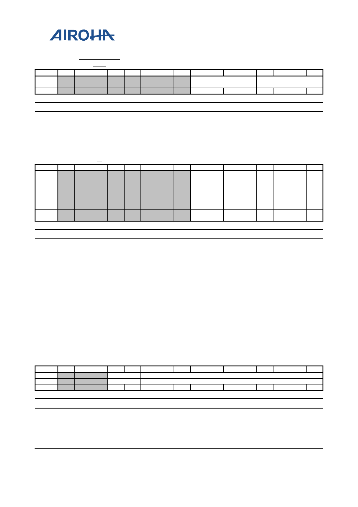
MT2523 Series Reference Manual
© 2015 - 2018 Airoha Technology Corp.
Page 177 of 692
This document contains information that is proprietary to Airoha Technology Corp. (“Airoha”) and/or its licensor(s).
Any unauthorized use, reproduction or disclosure of this document in whole or in part is strictly prohibited.
A090010E HBCONFIGD
ATA High Bind-width Configuration Register 00
Bit
15
14
13
12
11
10
9
8
7
6
5
4
3
2
1
0
Name
NUM_HB_EPR
NUM_HB_EPT
Type
RO
RO
Reset
0
0
0
0
0
0
0
0
Bit(s) Name Description
7:4 NUM_HB_EPR Number of high bind-width RX endpoints
3:0 NUM_HB_EPT Number of high bind-width TX endpoints
A090010F CONFIGDAT
A Core Configuration Register 1F
Bit
15
14
13
12
11
10
9
8
7
6
5
4
3
2
1
0
Name
MP
RX
E
MP
TX
E
BIG
EN
DIA
N
HB
RX
E
HB
TX
E
DY
NFI
FO
SIZ
IN
G
SO
FTC
ON
E
UT
MI
DA
TA
WI
DT
H
Type
RO
RO
RO
RO
RO
RO
RO
RO
Reset
0
0
0
1
1
1
1
1
Bit(s) Name Description
7 MPRXE When set to 1, automatic amalgamation of bulk packets will be
selected.
6 MPTXE When set to 1, automatic splitting of bulk packets will be selected.
5 BIGENDIAN Set to 1 indicates big-endian ordering is selected.
4 HBRXE Set to 1 indicates high-bandwidth Rx ISO Endpoint Support is
selected.
3 HBTXE Set to 1 indicates high-bandwidth Tx ISO Endpoint Support is
selected.
2 DYNFIFOSIZING Set to 1 indicates Dynamic FIFO Sizing option is selected.
1 SOFTCONE Set to 1 indicates Soft Connect/Disconnect option is selected.
0 UTMIDATAWIDTH
Indicates selected UTMI+ data width
1'b0: 8 bits
1'b1: 16 bits
A0900110 TX1MAP TX1MAP Register 0000
Bit
15
14
13
12
11
10
9
8
7
6
5
4
3
2
1
0
Name
M1
MAXIMUM_PAYLOAD_TRANSACTION
Type
RW
RW
Reset
0
0
0
0
0
0
0
0
0
0
0
0
0
Bit(s) Name Description
12:11 M1 Maximum payload size for indexed TX endpoint, M1 packet
multiplier m maximum payload transaction register
10:0 MAXIMUM_PAYLO
AD_TRANSACTION
The TxMaxP register defines the maximum amount of data that can
be transferred through the selected Tx endpoint in a single operation.
There is a TxMaxP register for each Tx endpoint (except for Endpoint
0). Bits 10~0 define (in bytes) the maximum payload transmitted in a
MT2523 Series Reference Manual
© 2015 - 2018 Airoha Technology Corp.
Page 178 of 692
This document contains information that is proprietary to Airoha Technology Corp. (“Airoha”) and/or its licensor(s).
Any unauthorized use, reproduction or disclosure of this document in whole or in part is strictly prohibited.
Bit(s) Name Description
single transaction. The value set can be up to 1024 bytes but is subject
to the constraints placed by the USB Specification on packet sizes for
Bulk, Interrupt and Isochronous transfers in full-speed and high-
speed operations. Where the option of high-bandwidth isochronous
endpoints or of packet splitting on bulk endpoints has been taken
when the core is configured, the register will include either 2 or 5
further bits that define a multiplier m which is equal to one more
than the value recorded. In the case of bulk endpoints with the packet
splitting option enabled, the multiplier m can be up to 32 and defines
the maximum number of 'USB' packets (i.e. packets for transmission
over the USB) of the specified payload into which a single data packet
placed in the FIFO should be split, prior to the transfer. (If the packet
splitting option is not enabled, bit15-13 will not be implemented and
bit12-11 (if included) will be ignored.)
Note: The data packet should be an exact multiple of the payload specified by
bit10~0, which is itself required to be one of 8, 16, 32, 64 or (in the case of high
speed transfers) 512 bytes. For isochronous endpoints operating in high-speed
mode and with the High-bandwidth option enabled, m may only be either 2 or 3
(corresponding to bit11 set or bit12 set respectively) and it specifies the
maximum number of such transactions that can take place in a single
microframe. If either bit11 or bit12 is not 0, the USB2.0 controller will
automatically split any data packet written to FIFO into up to 2 or 3 'USB'
packets, each containing the specified payload (or less). The maximum payload
for each transaction is 1024 bytes, so this allows up to 3072 bytes to be
transmitted in each microframe. (For Isochronous/Interrupt transfers in full-
speed mode, bit11 and 12 are ignored.) The value written to bit10~0 (multiplied
by m in the case of high-bandwidth Isochronous transfers) should match the
value given in the wMaxPacketSize field of the Standard Endpoint Descriptor for
the associated endpoint (see USB Specification Revision 2.0, Chapter 9). A
mismatch can cause unexpected results. The total amount of data represented by
the value written to this register (specified payload * m) must not exceed the
FIFO size for the Tx endpoint and should not exceed half the FIFO size if double-
buffering is required. If this register is changed after packets have been sent
from the endpoint, the Tx endpoint FIFO should be completely flushed (using
the FlushFIFO bit in TxCSR) after writing the new value to this register.
A0900112 TX1CSR_PER
I Tx1 CSR Register 0000
Bit
15
14
13
12
11
10
9
8
7
6
5
4
3
2
1
0
Name AU
TO
SET
ISO
DM
AR
EQ
EN
FR
CD
AT
AT
OG
DM
AR
EQ
MO
DE
SET
TX
PK
TR
DY
_T
WI
CE
INC
OM
PT
X
CL
RD
AT
AT
OG
SE
NT
ST
AL
L
SE
ND
ST
AL
L
FL
US
HFI
FO
UN
DE
RR
UN
FIF
ON
OT
EM
PT
Y
TX
PK
TR
DY
Type
RW
RW
RW
RW
RW
A1
A1
A0
A1
RW
A0
A1
RU
A0
Reset
0
0
0
0
0
0
0
0
0
0
0
0
0
0
Bit(s) Name Description
15 AUTOSET
If The CPU sets up this bit, TxPktRdy will be automatically set when
data of the maximum packet size (value in TxMaxP) is loaded into the
TxFIFO. If a packet of less than the maximum packet size is loaded,
TxPktRdy will have to be set manually.
14 ISO
The CPU sets up this bit to enable the Tx endpoint for Isochronous
transfers and clears it to enable the Tx endpoint for Bulk or Interrupt
transfers.
Note: This bit only takes effect in peripheral mode. In host mode, it
always returns to 0.
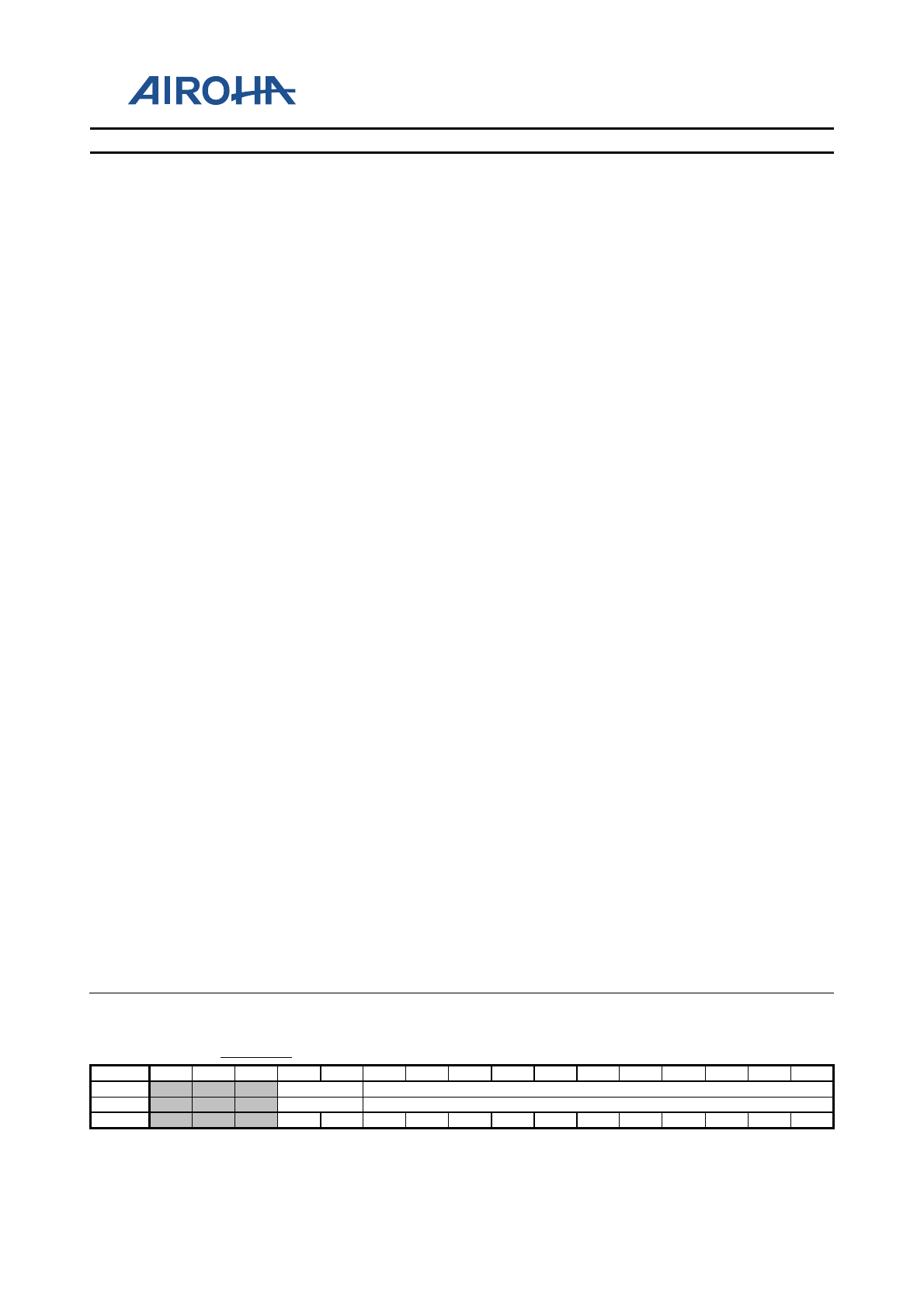
MT2523 Series Reference Manual
© 2015 - 2018 Airoha Technology Corp.
Page 179 of 692
This document contains information that is proprietary to Airoha Technology Corp. (“Airoha”) and/or its licensor(s).
Any unauthorized use, reproduction or disclosure of this document in whole or in part is strictly prohibited.
Bit(s) Name Description
12 DMAREQEN The CPU sets up this bit to enable the DMA request for the Tx
endpoint.
11 FRCDATATOG
The CPU sets up this bit to force the endpoint data toggle to switch
and the data packet to be cleared from the FIFO, regardless of
whether an ACK was received. This can be used by Interrupt Tx
endpoints that are used to communicate rate feedback for
Isochronous endpoints.
10 DMAREQMODE
The CPU sets up this bit to select DMA Request Mode 1 and clears it to
select DMA Request Mode 0.
Note: This bit should not be cleared either before or in the same cycle
as the DMAReqEn bit is cleared.
8 SETTXPKTRDY_TW
ICE
Indicates TxPktRdy had been set when it is 1'b1 already. Write 0 to
clear it.
7 INCOMPTX
When the endpoint is used for high-bandwidth
Isochronous/Interrupt transfers, this bit is set to indicate where a
large packet has been split into 2 or 3 packets for transmission but
insufficient IN tokens have been received to send all the parts.
Note: In anything other than a high-bandwidth transfer, this bit will
always return to 0.
Write 0 to clear it.
6 CLRDATATOG The CPU writes 1 to this bit to reset the endpoint data toggle to 0.
5 SENTSTALL
This bit is set when a STALL handshake is transmitted. The FIFO will
be flushed and Tx interrupt generated if enabled and the TxPktRdy
bit is cleared. The CPU should clear this bit.
Write 0 to clear it.
4 SENDSTALL
The CPU writes 1 to this bit to issue a STALL handshake to an IN
token. The CPU clears this bit to terminate the stall condition.
Note: This bit has no effect where the endpoint is used for
Isochronous transfer. Otherwise, CPU should wait for SENTSTALL
interrupt to be generated before clearing the SENDSTALL bit.
3 FLUSHFIFO
The CPU writes 1 to this bit to flush the latest packet from the
endpoint TxFIFO. The FIFO pointer is reset, the TxPktRdy bit is
cleared and an interrupt is generated. May be set simultaneously
with TxPktRdy to abort the packet currently loaded into FIFO.
Note: FlushFIFO should only be used when TxPktRdy is set. In other cases, it
may cause data corruption. If the FIFO is double-buffered, FlushFIFO may need
to be set twice to completely clear the FIFO.
2 UNDERRUN The USB will set up this bit if an IN token is received when the
TxPktRdy bit is not set. The CPU should clear this bit (write 0 to clear
it).
1 FIFONOTEMPTY The USB sets up this bit when there is at least 1 packet in TxFIFO.
This bit will be asserted automatically when TXPKTRDY is set by CPU
and de-asserted when CPU flushes FIFO or sends a STALL packet.
0 TXPKTRDY
The CPU sets up this bit after loading a data packet into FIFO. It is
cleared automatically when a data packet has been transmitted. An
interrupt is also generated at this point (if enabled). TxPktRdy is also
automatically cleared (interrupt is generated) prior to loading a
second packet into a double-buffered FIFO.
A0900114 RX1MAP RX1MAP Register 0000
Bit
15
14
13
12
11
10
9
8
7
6
5
4
3
2
1
0
Name
M1
MAXIMUM_PAYLOAD_TRANSACTION
Type
RW
RW
Reset
0
0
0
0
0
0
0
0
0
0
0
0
0
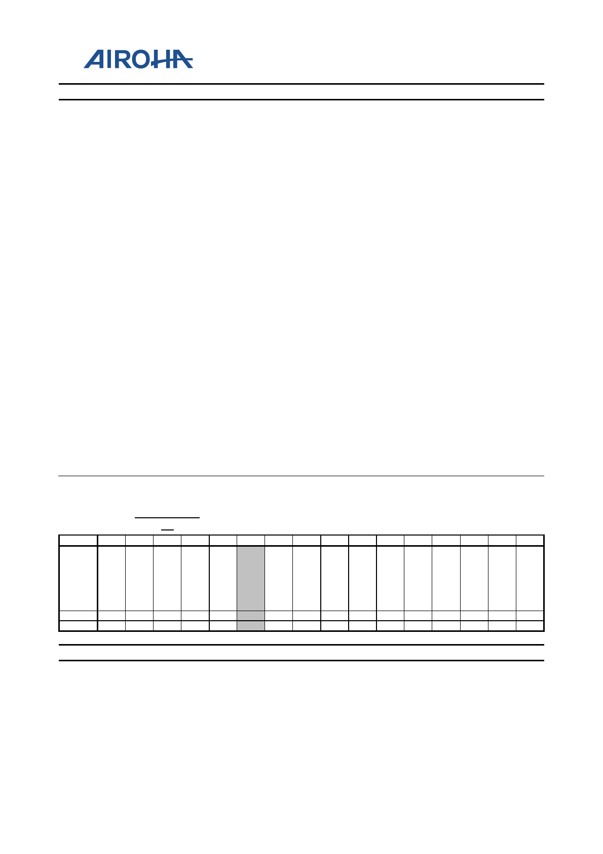
MT2523 Series Reference Manual
© 2015 - 2018 Airoha Technology Corp.
Page 180 of 692
This document contains information that is proprietary to Airoha Technology Corp. (“Airoha”) and/or its licensor(s).
Any unauthorized use, reproduction or disclosure of this document in whole or in part is strictly prohibited.
Bit(s) Name Description
12:11 M1 Maximum payload size for indexed RX endpoint, M1 packet
multiplier m
10:0 MAXIMUM_PAYLO
AD_TRANSACTION
The RxMaxP register defines the maximum amount of data that can
be transferred through the selected Rx endpoint in a single
operation. There is a RxMaxP register for each Rx endpoint (except
for Endpoint 0). Bit10~0 define (in bytes) the maximum payload
transmitted in a single transaction. The value set can be up to 1024
bytes but is subject to the constraints placed by the USB Specification
on packet sizes for Bulk, Interrupt and Isochronous transfers in full-
speed and high-speed operations.
Where the option of high-bandwidth isochronous endpoints or of combining
bulk packets has been taken when the core is configured, the register includes
either 2 or 5 further bits that define a multiplier m which is equal to one more
than the value recorded.
For Bulk endpoints with the packet combining option enabled, the multiplier m
can be up to 32 and defines the number of USB packets of the specified payload
which are to be combined into a single data packet within the FIFO. (If the
packet splitting option is not enabled, bit15~13 will not be implemented and
bit12~11 (if included) will be ignored.) For isochronous endpoints operating in
high-speed mode and with the high-bandwidth option enabled, m may only be
either 2 or 3 (corresponding to bit11 set or bit12 set respectively) and it specifies
the maximum number of such transactions that can take place in a single
microframe. If either bit11 or bit12 is not 0, the USB2.0 controller will
automatically combine the separate USB packets received in any microframe
into a single packet within the Rx FIFO. The maximum payload for each
transaction is 1024 bytes, so this allows up to 3072 bytes to be received in each
microframe.
(For Isochronous/Interrupt transfers in full-speed mode or if high-bandwidth is
not enabled, bit11 and 12 will be ignored.) The value written to bit10~0
(multiplied by m in the case of high-bandwidth Isochronous transfers) should
match the value given in the wMaxPacketSize field of the Standard Endpoint
Descriptor for the associated endpoint (see USB Specification Revision 2.0,
Chapter 9). A mismatch can cause unexpected results.
The total amount of data represented by the value written to this register
(specified payload * m) should not exceed the FIFO size for the OUT endpoint
and half the FIFO size if double-buffering is required.
A0900116 RX1CSR_PE
RI RX1 CSR Register 0000
Bit
15
14
13
12
11
10
9
8
7
6
5
4
3
2
1
0
Name
AU
TO
CL
EA
R
ISO
DM
AR
EQ
EN
DIS
NY
ET
_PI
DE
RR
DM
AR
EQ
MO
DE
KE
EP
ER
RS
TA
TU
S
INC
OM
PR
X
CL
RD
TA
TO
G
SE
NT
ST
AL
L
SE
ND
ST
AL
L
FL
US
HFI
FO
DA
TA
ER
R
OV
ER
RU
N
FIF
OF
UL
L
RX
PK
TR
DY
Type
RW
RW
RW
RW
RW
RW
A1
A0
A1
RW
A0
RU
A1
RU
A1
Reset
0
0
0
0
0
0
0
0
0
0
0
0
0
0
0
Bit(s) Name Description
15 AUTOCLEAR
If the CPU sets up this bit, the RxPktRdy bit will be automatically
cleared when a packet of RxMaxP bytes has been unloaded from the
RxFIFO. When packets of less than the maximum packet size are
unloaded, RxPktRdy will have to be cleared manually.
Note: Maximum packet size-3,-2,-1 is handled like maximum packet size which
is auto cleared by hardware.
14 ISO The CPU sets up this bit to enable the Rx endpoint for Isochronous
transfers and clears it to enable the Rx endpoint for Bulk/Interrupt

MT2523 Series Reference Manual
© 2015 - 2018 Airoha Technology Corp.
Page 181 of 692
This document contains information that is proprietary to Airoha Technology Corp. (“Airoha”) and/or its licensor(s).
Any unauthorized use, reproduction or disclosure of this document in whole or in part is strictly prohibited.
Bit(s) Name Description
transfers.
13 DMAREQEN The CPU sets up this bit to enable the DMA request for the Rx
endpoint.
12 DISNYET_PIDERR
The CPU sets up this bit to disable the sending of NYET handshakes.
When set, all successfully received Rx packets will be ACK'd
including at the point at which the RxFIFO becomes full.
Note: This bit only takes effect in high-speed mode, in which it should
be set for all interrupt endpoint.
This bit is set when there is a PID error in the received packet. It is cleared when
RxPktRdy is cleared or write 0 to clear it.
11 DMAREQMODE
The CPU sets up this bit to select DMA Request Mode 1 and clears it to
select DMA Request Mode 0. DMA Request Mode 1: Rx endpoint
interrupt is generated only when DMA Request Mode 1 and received a
short packet. RxDMAReq is generated when receiving a Max-Packet-
size packet. DMA Request Mode 0: No Rx endpoint interrupt.
RxDMAReq will be generated when RxPktRdy is set.
9 KEEPERRSTATUS
This bit is used when endpoint works with USBQ and in
ISOCHRONOUS mode. When this bit is set, the isochronous error,
PIDERROR, INCOMPRX and DATAERROR will be kept and only
cleared by SW.
8 INCOMPRX
This bit will be set in an Isochronous transfer if the packet in the
RxFIFO is incomplete because parts of the data are not received.
When KeepErrorStatus = 0, it will be cleared when RxPktRdy is
cleared or write 0 to clear it.
Note: In anything other than a Isochronous transfer, this bit will always return 0.
Write 0 to clear it.
7 CLRDTATOG The CPU writes 1 to this bit to reset the endpoint data toggle to 0.
6 SENTSTALL
This bit is set when a STALL handshake is transmitted. The CPU
should clear this bit. An interrupt will be generated when the bit is
set.
Write 0 to clear it.
5 SENDSTALL
The CPU writes 1 to this bit to issue a STALL handshake. The CPU
clears this bit to terminate the stall condition.
Note: This bit has no effect where the endpoint is being used for ISO transfers.
4 FLUSHFIFO
The CPU writes 1 to this bit to flush the next packet to be read from
the endpoint RxFIFO. The RxFIFO pointer is reset and the RxPktRdy
bit is cleared.
Note: FlushFIFO should only be used when RxPktRdy is set. In other cases, it
may cause data corruption. If the RxFIFO is double buffered, FlushFIFO may
need to be set twice to completely clear the RxFIFO.
3 DATAERR
This bit will be set when RxPktRdy is set if the data packet has a CRC
or bit-stuff error in it. Cleared when RxPktRdy is cleared.
Note: This bit is only valid when the endpoint is operating in ISO mode. In Bulk
mode, it always returns to 0.
2 OVERRUN
This bit will be set if an OUT packet cannot be loaded into RxFIFO.
The CPU should clear this bit (write 0 to clear it).
Note: This bit is only valid when the endpoint is operating in ISO mode. In Bulk
mode, it always returns to 0. The new incoming packet will not be written to
RxFIFO.
1 FIFOFULL This bit will be set when no more packets can be loaded into RxFIFO.
0 RXPKTRDY
This bit will be set when a data packet has been received (to RxFIFO).
The CPU should clear this bit when the packet has been unloaded
from RxFIFO. An interrupt will be generated when the bit is set.
Write 0 to clear it.
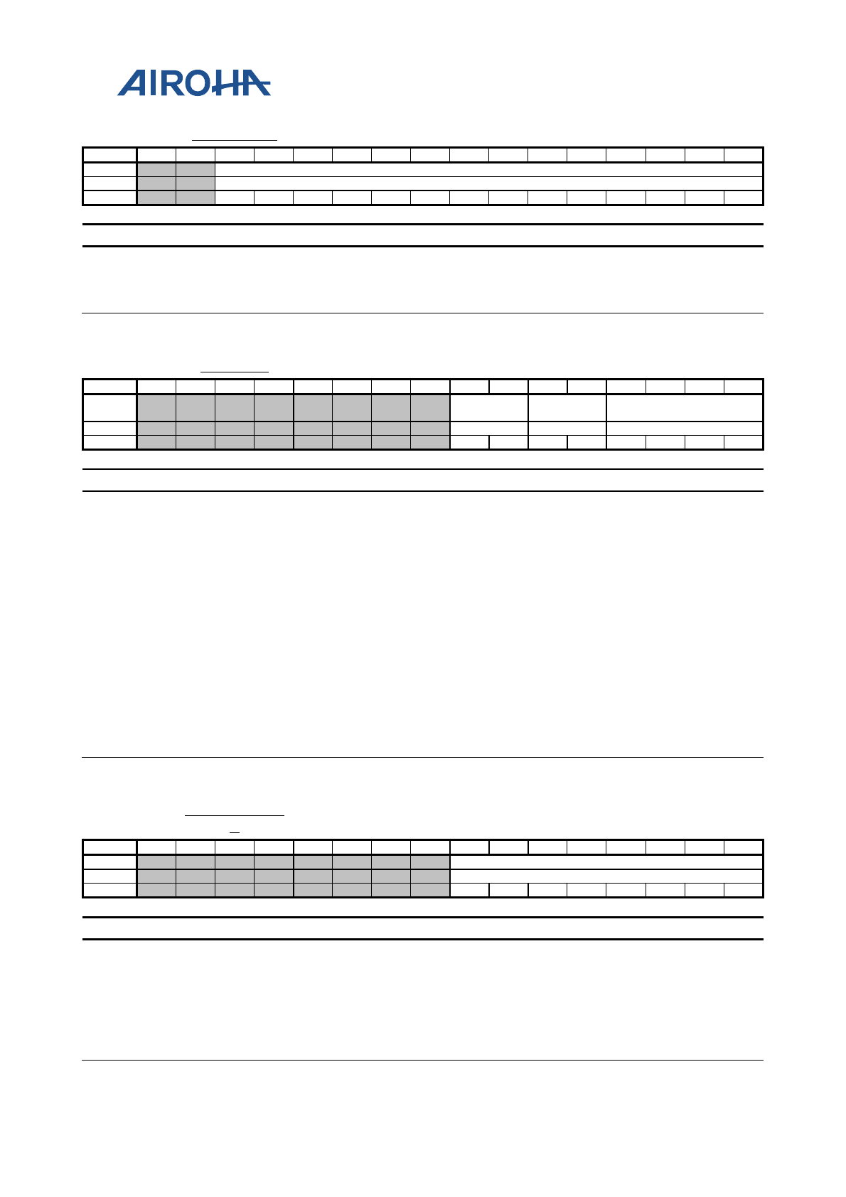
MT2523 Series Reference Manual
© 2015 - 2018 Airoha Technology Corp.
Page 182 of 692
This document contains information that is proprietary to Airoha Technology Corp. (“Airoha”) and/or its licensor(s).
Any unauthorized use, reproduction or disclosure of this document in whole or in part is strictly prohibited.
A0900118 RX1COUNT Rx1 Count Register 0000
Bit
15
14
13
12
11
10
9
8
7
6
5
4
3
2
1
0
Name
RXCOUNT
Type
RU
Reset
0
0
0
0
0
0
0
0
0
0
0
0
0
0
Bit(s) Name Description
13:0 RXCOUNT
It is a 14-bit read-only register that holds the number of received data
bytes in the packet in RxFIFO.
Note: The value returned changes as the FIFO is unloaded and is only valid when
RxPktRdy(RxCSR.D0) is set.
A090011A TX1TYPE Tx1Type Register 00
Bit
15
14
13
12
11
10
9
8
7
6
5
4
3
2
1
0
Name
TX_SPEE
D
TX_PROT
OCOL
TX_TARGET_EP_NUM
BER
Type
RW
RW
RW
Reset
0
0
0
0
0
0
0
0
Bit(s) Name Description
7:6 TX_SPEED
Operating speed of the target device when the core is configured with
the multipoint option
When the core is not configured with the multipoint option, these bits should not
be accessed.
2'b00: Unused
2'b01: High
2'b10: Full
2'b11: Low
5:4 TX_PROTOCOL
The CPU should set up this to select the required protocol for the Tx
endpoint.
2'b00: Illegal
2'b01: Isochronous
2'b10: Bulk
2'b11: Interrupt
3:0 TX_TARGET_EP_N
UMBER
The CPU should set this value to the endpoint number containing in
the Tx endpoint descriptor returned to the USB2.0 controller during
device enumeration.
A090011B TX1INTERVA
L Tx1Interval Register 00
Bit
15
14
13
12
11
10
9
8
7
6
5
4
3
2
1
0
Name
TX_POLLING_INTERVAL_NAK_LIMIT_M
Type
RW
Reset
0
0
0
0
0
0
0
0
Bit(s) Name Description
7:0
TX_POLLING_INTE
RVAL_NAK_LIMIT_
M
(Host mode only) TxInterval Register TxInterval is an 8-bit register
that, for Interrupt and Isochronous transfers, defines the polling
interval for the currently-selected Tx endpoint. For Bulk endpoints,
this register sets up the number of frames/microframes after which
the endpoint should time out on receiving a stream of NAK
responses. There is a TxInterval register for each configured Tx
endpoint (except for Endpoint 0).
In each case the value that is set defines a number of frames/microframes (high
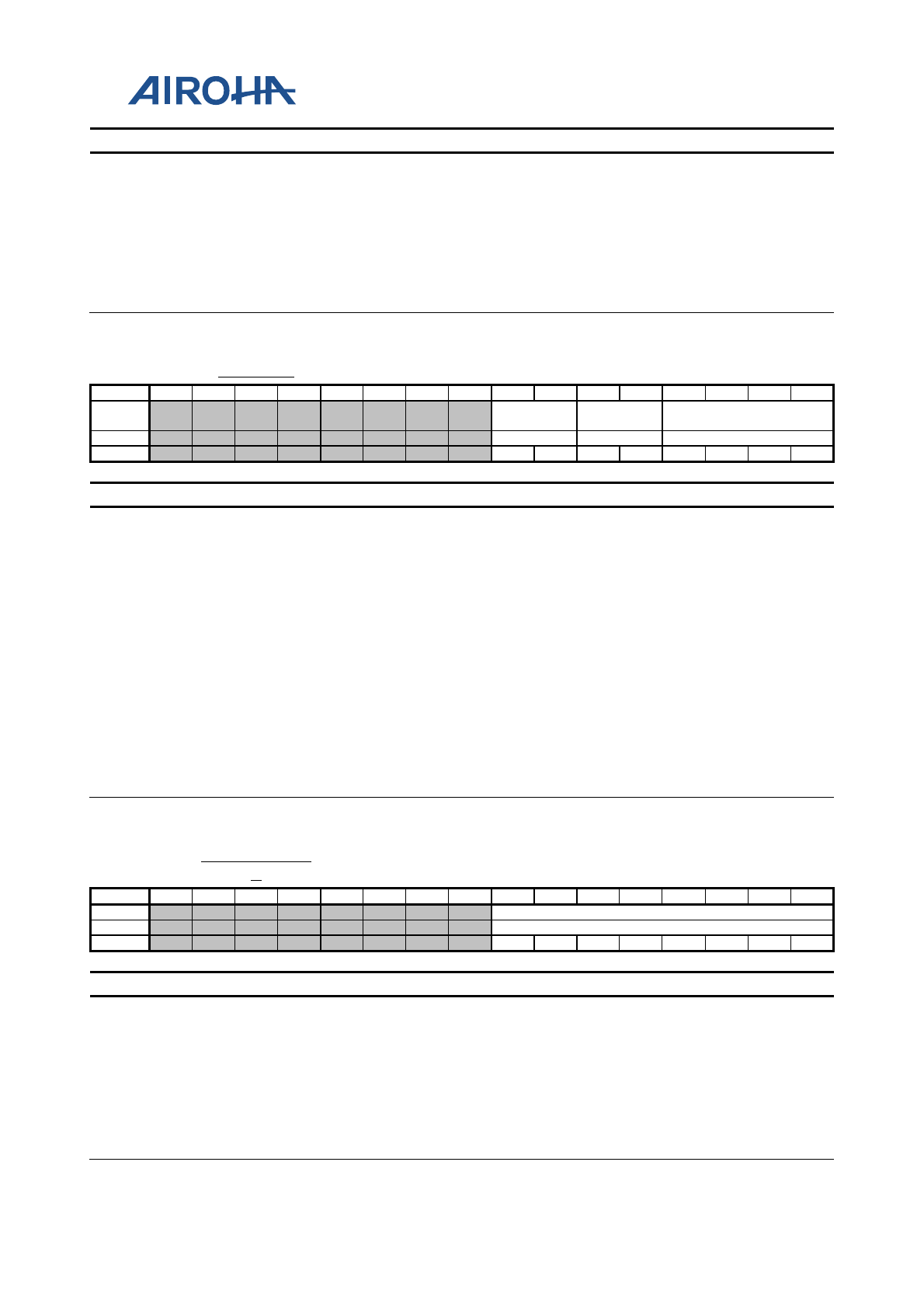
MT2523 Series Reference Manual
© 2015 - 2018 Airoha Technology Corp.
Page 183 of 692
This document contains information that is proprietary to Airoha Technology Corp. (“Airoha”) and/or its licensor(s).
Any unauthorized use, reproduction or disclosure of this document in whole or in part is strictly prohibited.
Bit(s) Name Description
speed transfers), as the following:
Transfer Type | Speed | Valid values (m) | Interpretation
Interrupt | Low Speed or Full Speed | 1-255 | Polling interval is m frames.
Interrupt | High Speed | 1-16 | Polling interval is 2^(m-1) microframes
Isochronous | Full Speed or High Speed | 1-16 | Polling interval is 2^(m-1)
frames/microframes
Bulk | Full Speed or High Speed | 2-16 | NAK Limit is 2^(m-1)
frames/microframes.
Note: Value 0 or 1 disables the NAK timeout function. The register should be set
before TxType for Bulk endpoint.
A090011C RX1TYPE Rx1Type Register 00
Bit
15
14
13
12
11
10
9
8
7
6
5
4
3
2
1
0
Name RXSPEED
RX_PROT
OCOL
RX_TARGET_EP_NUM
BER
Type
RW
RW
RW
Reset
0
0
0
0
0
0
0
0
Bit(s) Name Description
7:6 RXSPEED
Operating speed of the target device when the core is configured with
the multipoint option
When the core is not configured with the multipoint option, these bits should not
be accessed.
2'b00: Unused
2'b01: High
2'b10: Full
2'b11: Low
5:4 RX_PROTOCOL
The CPU should set up this to select the required protocol for the Tx
endpoint.
2'b00: Illegal
2'b01: Isochronous
2'b10: Bulk
2'b11: Interrupt
3:0 RX_TARGET_EP_N
UMBER
The CPU should set this value to the endpoint number containing in
the Tx endpoint descriptor returned to the USB2.0 controller during
device enumeration.
A090011D RX1INTERVA
L Rx1Interval Register 00
Bit
15
14
13
12
11
10
9
8
7
6
5
4
3
2
1
0
Name
RX_POLLING_INTERVAL_NAK_LIMIT_M
Type
RW
Reset
0
0
0
0
0
0
0
0
Bit(s) Name Description
7:0
RX_POLLING_INTE
RVAL_NAK_LIMIT_
M
RxInterval Register RxInterval is an 8-bit register that, for Interrupt
and Isochronous transfers, defines the polling interval for the
currently selected Rx endpoint. For Bulk endpoints, this register sets
up the number of frames/microframes after which the endpoint
should time out on receiving a stream of NAK responses. There is a
RxInterval register for each configured Rx endpoint (except for
Endpoint 0).
RX POLLING INTERVAL / NAK LIMIT (M), (Host mode only)
In each case the value that is set defines a number of frames/microframes (high
speed transfers), as the following:
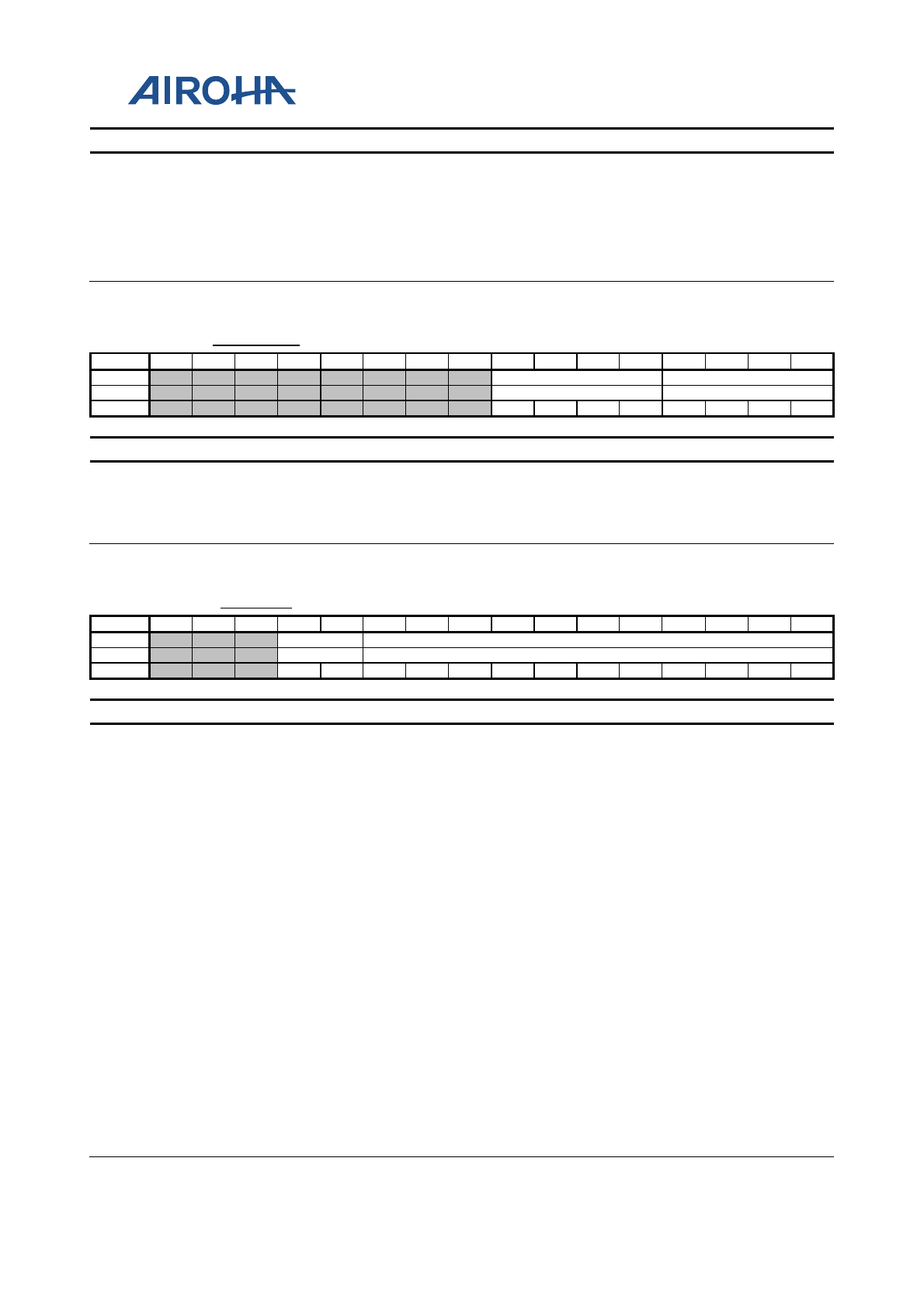
MT2523 Series Reference Manual
© 2015 - 2018 Airoha Technology Corp.
Page 184 of 692
This document contains information that is proprietary to Airoha Technology Corp. (“Airoha”) and/or its licensor(s).
Any unauthorized use, reproduction or disclosure of this document in whole or in part is strictly prohibited.
Bit(s) Name Description
Transfer Type Speed Valid values (m) Interpretation
Interrupt Low Speed or Full Speed 1 - 255 Polling interval is m frames.
High Speed 1 - 16 Polling interval is 2(m-1) microframes
Isochronous Full Speed or High Speed 1 - 16 Polling interval is 2(m-1)
frames/microframes
Bulk Full Speed or High Speed 2 - 16 NAK Limit is 2(m-1) frames/microframes.
Note: Value 0 or 1 disables the NAK timeout function. The register should be set
before RxType for Bulk endpoint.
A090011F FIFOSIZE1 EP1 Configured FIFO Size Register AA
Bit
15
14
13
12
11
10
9
8
7
6
5
4
3
2
1
0
Name
RXFIFOSIZE
TXFIFOSIZE
Type
DC
DC
Reset
1
0
1
0
1
0
1
0
Bit(s) Name Description
7:4 RXFIFOSIZE Indicates the RxFIFO size of 2^n bytes
Example: Value 10 means 2^10 = 1024 bytes.
3:0 TXFIFOSIZE Indicates the TxFIFO size of 2^n bytes
Example: Value 10 means 2^10 = 1024 bytes.
A0900120 TX2MAP TX2MAP Register 0000
Bit
15
14
13
12
11
10
9
8
7
6
5
4
3
2
1
0
Name
M1
MAXIMUM_PAYLOAD_TRANSACTION
Type
RW
RW
Reset
0
0
0
0
0
0
0
0
0
0
0
0
0
Bit(s) Name Description
12:11 M1 Maximum payload size for indexed TX endpoint, M1 packet
multiplier m maximum payload transaction register
10:0 MAXIMUM_PAYLO
AD_TRANSACTION
The TxMaxP register defines the maximum amount of data that can
be transferred through the selected Tx endpoint in a single operation.
There is a TxMaxP register for each Tx endpoint (except for Endpoint
0). Bit10~0 define (in bytes) the maximum payload transmitted in a
single transaction. The value set can be up to 1024 bytes but is subject
to the constraints placed by the USB Specification on packet sizes for
Bulk, Interrupt and Isochronous transfers in full-speed and high-
speed operations. Where the option of high-bandwidth Isochronous
endpoints or of packet splitting on Bulk endpoints has been taken
when the core is configured, the register includes either 2 or 5
further bits that define a multiplier m which is equal to one more
than the value recorded. In the case of Bulk endpoints with the
packet splitting option enabled, the multiplier m can be up to 32 and
defines the maximum number of 'USB' packets (i.e. packets for
transmission over the USB) of the specified payload into which a
single data packet placed in the FIFO should be split, prior to
transfer. (If the packet splitting option is not enabled, bit15-13 will
not be implemented and bit12-11 (if included) will be ignored.)
Note: The data packet should be an exact multiple of the payload specified by
bit10~0, which is itself required to be one of 8, 16, 32, 64 or (in the case of high-
speed transfers) 512 bytes. For Isochronous endpoints operating in high-speed
mode and with the high-bandwidth option enabled, m may only be either 2 or 3
(corresponding to bit11 set or bit12 set respectively) and it specifies the
maximum number of such transactions that can take place in a single
microframe. If either bit11 or bit12 is not 0, the USB2.0 controller will

MT2523 Series Reference Manual
© 2015 - 2018 Airoha Technology Corp.
Page 185 of 692
This document contains information that is proprietary to Airoha Technology Corp. (“Airoha”) and/or its licensor(s).
Any unauthorized use, reproduction or disclosure of this document in whole or in part is strictly prohibited.
Bit(s) Name Description
automatically split any data packet written to the FIFO into up to 2 or 3 'USB'
packets, each containing the specified payload (or less). The maximum payload
for each transaction is 1024 bytes, so this allows up to 3072 bytes to be
transmitted in each microframe. (For Isochronous/Interrupt transfers in full-
speed mod, bit11 and 12 are ignored.) The value written to bit10~0 (multiplied
by m in the case of high-bandwidth Isochronous transfers) should match the
value given in the wMaxPacketSize field of the Standard Endpoint Descriptor for
the associated endpoint (see USB Specification Revision 2.0, Chapter 9). A
mismatch can cause unexpected results. The total amount of data represented by
the value written to this register (specified payload * m) should not exceed the
FIFO size for the Tx endpoint and half the FIFO size if double-buffering is
required. If this register is changed after packets have been sent from the
endpoint, the Tx endpoint FIFO should be completely flushed (using the
FlushFIFO bit in TxCSR) after writing the new value to this register.
A0900122 TX2CSR_PE
RI Tx2 CSR Register 0000
Bit
15
14
13
12
11
10
9
8
7
6
5
4
3
2
1
0
Name AU
TO
SET
ISO
DM
AR
EQ
EN
FR
CD
AT
AT
OG
DM
AR
EQ
MO
DE
SET
TX
PK
TR
DY
_T
WI
CE
INC
OM
PT
X
CL
RD
AT
AT
OG
SE
NT
ST
AL
L
SE
ND
ST
AL
L
FL
US
HFI
FO
UN
DE
RR
UN
FIF
ON
OT
EM
PT
Y
TX
PK
TR
DY
Type
RW
RW
RW
RW
RW
A1
A1
A0
A1
RW
A0
A1
RU
A0
Reset
0
0
0
0
0
0
0
0
0
0
0
0
0
0
Bit(s) Name Description
15 AUTOSET
If The CPU sets up this bit, TxPktRdy will be automatically set when
data of the maximum packet size (value in TxMaxP) is loaded into the
TxFIFO. If a packet of less than the maximum packet size is loaded,
TxPktRdy will have to be set manually.
14 ISO
The CPU sets up this bit to enable the Tx endpoint for Isochronous
transfers and clears it to enable the Tx endpoint for Bulk or Interrupt
transfers.
Note: This bit only takes effect in peripheral mode. In host mode, it always
returns to 0.
12 DMAREQEN The CPU sets up this bit to enable the DMA request for the Tx
endpoint.
11 FRCDATATOG
The CPU sets up this bit to force the endpoint data toggle to switch
and the data packet to be cleared from FIFO, regardless of whether
an ACK is received. This can be used by Interrupt Tx endpoints that
are used to communicate rate feedback for isochronous endpoints.
10 DMAREQMODE
The CPU sets up this bit to select DMA Request Mode 1 and clears it to
select DMA Request Mode 0.
Note: This bit should not be cleared either before or in the same cycle as the
DMAReqEn bit is cleared.
8 SETTXPKTRDY_TW
ICE
Indicates TxPktRdy had been set when it is 1'b1 already. Write 0 to
clear it.
7 INCOMPTX
When the endpoint is used for high-bandwidth
Isochronous/Interrupt transfers, this bit is set to indicate where a
large packet has been split into 2 or 3 packets for transmission but
insufficient IN tokens have been received to send all the parts.
Note: In anything other than a high-bandwidth transfer, this bit will always
return to 0. Write 0 to clear it.
6 CLRDATATOG The CPU writes 1 to this bit to reset the endpoint data toggle to 0.
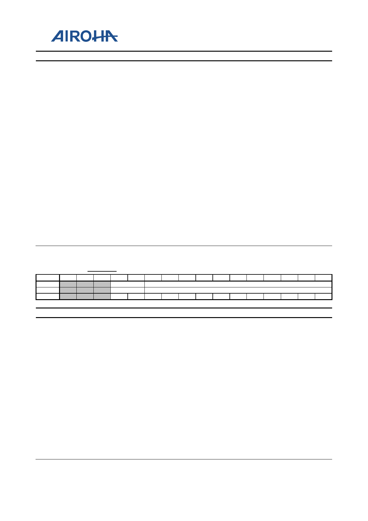
MT2523 Series Reference Manual
© 2015 - 2018 Airoha Technology Corp.
Page 186 of 692
This document contains information that is proprietary to Airoha Technology Corp. (“Airoha”) and/or its licensor(s).
Any unauthorized use, reproduction or disclosure of this document in whole or in part is strictly prohibited.
Bit(s) Name Description
5 SENTSTALL
This bit will be set when a STALL handshake is transmitted. The FIFO
will be flushed and Tx interrupt generated if enabled and the
TxPktRdy bit is cleared. The CPU should clear this bit.
Write 0 to clear it.
4 SENDSTALL
The CPU writes 1 to this bit to issue a STALL handshake to an IN
token. The CPU clears this bit to terminate the stall condition. Note:
This bit has no effect where the endpoint is being used for
Isochronous transfer. Otherwise, CPU should wait SENTSTALL
interrupt generated before clearning SENDSTALL bit.
3 FLUSHFIFO
The CPU writes 1 to this bit to flush the latest packet from the
endpoint TxFIFO. The FIFO pointer is reset, the TxPktRdy bit is
cleared and an interrupt is generated. May be set simultaneously
with TxPktRdy to abort the packet currently loaded into FIFO.
Note: FlushFIFO should only be used when TxPktRdy is set. In other cases, it
may cause data corruption. If the FIFO is double-buffered, FlushFIFO may need
to be set twice to completely clear the FIFO.
2 UNDERRUN The USB will set up this bit if an IN token is received when the
TxPktRdy bit is not set. The CPU should clear this bit (write 0 to clear
it).
1 FIFONOTEMPTY
The USB sets up this bit when there is at least 1 packet in TxFIFO.
This bit will be asserted automatically when TXPKTRDY is set by CPU
and de-asserted when CPU flushes FIFO or sends a STALL packet.
0 TXPKTRDY
The CPU sets up this bit after loading a data packet into FIFO. It is
cleared automatically when a data packet has been transmitted. An
interrupt is also generated at this point (if enabled). TxPktRdy is also
automatically cleared (interrupt is generated) prior to loading a
second packet into a double-buffered FIFO.
A0900124 RX2MAP RX2MAP Register 0000
Bit
15
14
13
12
11
10
9
8
7
6
5
4
3
2
1
0
Name
M1
MAXIMUM_PAYLOAD_TRANSACTION
Type
RW
RW
Reset
0
0
0
0
0
0
0
0
0
0
0
0
0
Bit(s) Name Description
12:11 M1 Maximum payload size for indexed RX endpoint, M1 packet
multiplier m
10:0 MAXIMUM_PAYLO
AD_TRANSACTION
The RxMaxP register defines the maximum amount of data that can
be transferred through the selected Rx endpoint in a single
operation. There is a RxMaxP register for each Rx endpoint (except
for Endpoint 0). Bit10~0 define (in bytes) the maximum payload
transmitted in a single transaction. The value set can be up to 1024
bytes but is subject to the constraints placed by the USB Specification
on packet sizes for Bulk, Interrupt and Isochronous transfers in full-
speed and high-speed operations.
Where the option of high-bandwidth isochronous endpoints or of combining
bulk packets has been taken when the core is configured, the register includes
either 2 or 5 further bits that define a multiplier m which is equal to one more
than the value recorded.
For bulk endpoints with the packet combining option enabled, the multiplier m
can be up to 32 and defines the number of USB packets of the specified payload
which are to be combined into a single data packet within the FIFO. (If the
packet splitting option is not enabled, bit15-bit13 will not be implemented and
bit12-11 (if included) will be ignored.) For isochronous endpoints operating in
high-speed mode and with the high-bandwidth option enabled, m may only be
either 2 or 3 (corresponding to bit11 set or bit12 set respectively) and it specifies
the maximum number of such transactions that can take place in a single
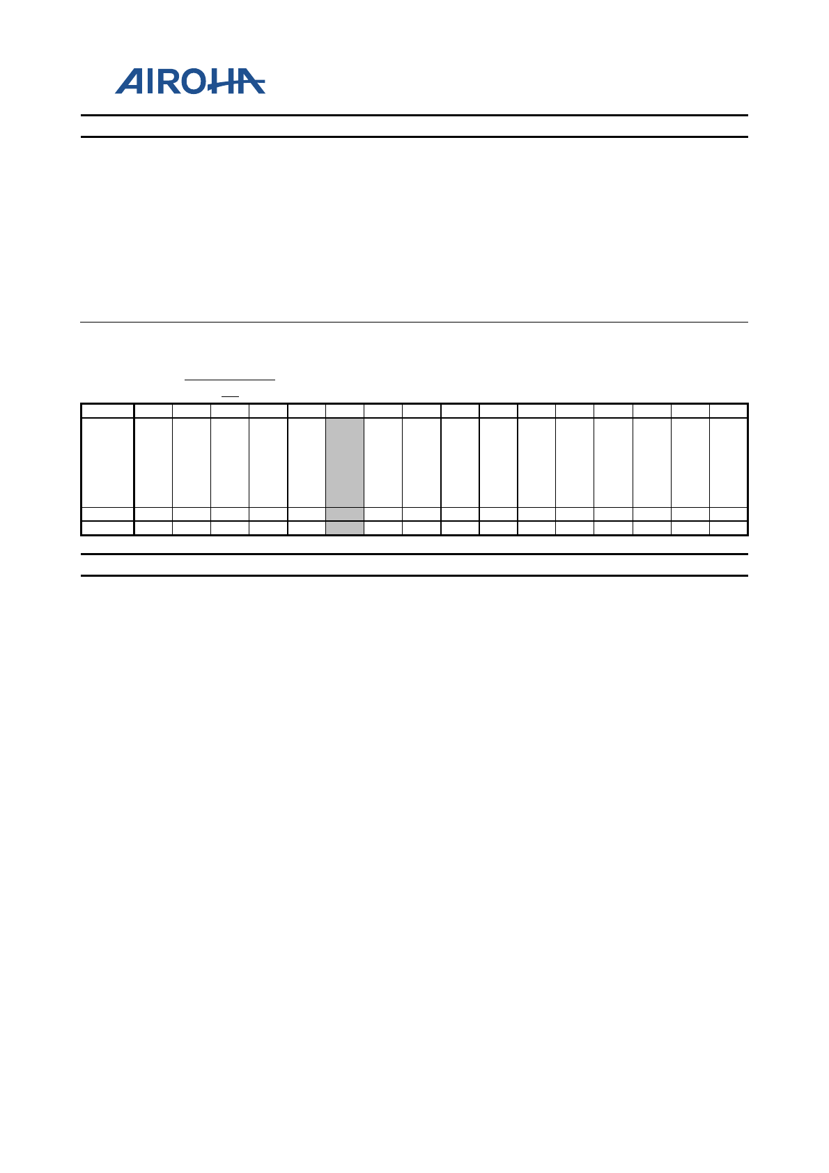
MT2523 Series Reference Manual
© 2015 - 2018 Airoha Technology Corp.
Page 187 of 692
This document contains information that is proprietary to Airoha Technology Corp. (“Airoha”) and/or its licensor(s).
Any unauthorized use, reproduction or disclosure of this document in whole or in part is strictly prohibited.
Bit(s) Name Description
microframe. If either bit11 or bit12 is not 0, the USB2.0 controller will
automatically combine the separate USB packets received in any microframe
into a single packet within Rx FIFO. The maximum payload for each transaction
is 1024 bytes, so this allows up to 3072 bytes to be received in each microframe.
(For Isochronous/Interrupt transfers in full-speed mode or if high-bandwidth is
not enabled, bit11 and 12 will be ignored.) The value written to bit10~0
(multiplied by m in the case of high-bandwidth Isochronous transfers) should
match the value given in the wMaxPacketSize field of the Standard Endpoint
Descriptor for the associated endpoint (see USB Specification Revision 2.0,
Chapter 9). A mismatch can cause unexpected results.
The total amount of data represented by the value written to this register
(specified payload * m) should not exceed the FIFO size for the OUT endpoint
and half the FIFO size if double-buffering is required.
A0900126 RX2CSR_PE
RI RX2 CSR Register 0000
Bit
15
14
13
12
11
10
9
8
7
6
5
4
3
2
1
0
Name
AU
TO
CL
EA
R
ISO
DM
AR
EQ
EN
DIS
NY
ET
_PI
DE
RR
DM
AR
EQ
MO
DE
KE
EP
ER
RS
TA
TU
S
INC
OM
PR
X
CL
RD
TA
TO
G
SE
NT
ST
AL
L
SE
ND
ST
AL
L
FL
US
HFI
FO
DA
TA
ER
R
OV
ER
RU
N
FIF
OF
UL
L
RX
PK
TR
DY
Type
RW
RW
RW
RW
RW
RW
A1
A0
A1
RW
A0
RU
A1
RU
A1
Reset
0
0
0
0
0
0
0
0
0
0
0
0
0
0
0
Bit(s) Name Description
15 AUTOCLEAR
If the CPU sets up this bit, the RxPktRdy bit will be automatically
cleared when a packet of RxMaxP bytes has been unloaded from
RxFIFO. When packets of less than the maximum packet size are
unloaded, RxPktRdy will have to be cleared manually.
Note: Maximum packet size-3,-2,-1 is handled like maximum packet size which
is auto cleared by hardware.
14 ISO
The CPU sets up this bit to enable the Rx endpoint for Isochronous
transfers and clears it to enable the Rx endpoint for bulk/interrupt
transfers.
13 DMAREQEN The CPU sets up this bit to enable the DMA request for the Rx
endpoint.
12 DISNYET_PIDERR
The CPU sets up this bit to disable the sending of NYET handshakes.
When set, all successfully received Rx packets will be ACK'd
including at the point at which the RxFIFO becomes full.
Note: This bit only takes effect in high-speed mode, in which it should
be set for all interrupt endpoints.
This bit will be set when there is a PID error in the received packet. Cleared
when RxPktRdy is cleared or write 0 to clear it.
11 DMAREQMODE
The CPU sets up this bit to select DMA Request Mode 1 and clears it to
select DMA Request Mode 0.
DMA Request Mode 1: Rx endpoint interrupt is generated only when DMA
Request Mode 1 and received a short packet. RxDMAReq is generated when
receiving a Max-Packet-size packet.
DMA Request Mode 0: No Rx endpoint interrupt. RxDMAReq will be generated
when RxPktRdy is set.
9 KEEPERRSTATUS
This bit is used when endpoint works with USBQ and in
ISOCHRONOUS mode. When this bit is set, the isochronous error,
PIDERROR, INCOMPRX and DATAERROR will be kept and only
cleared by SW.
8 INCOMPRX
This bit will be set in an Isochronous transfer if the packet in the
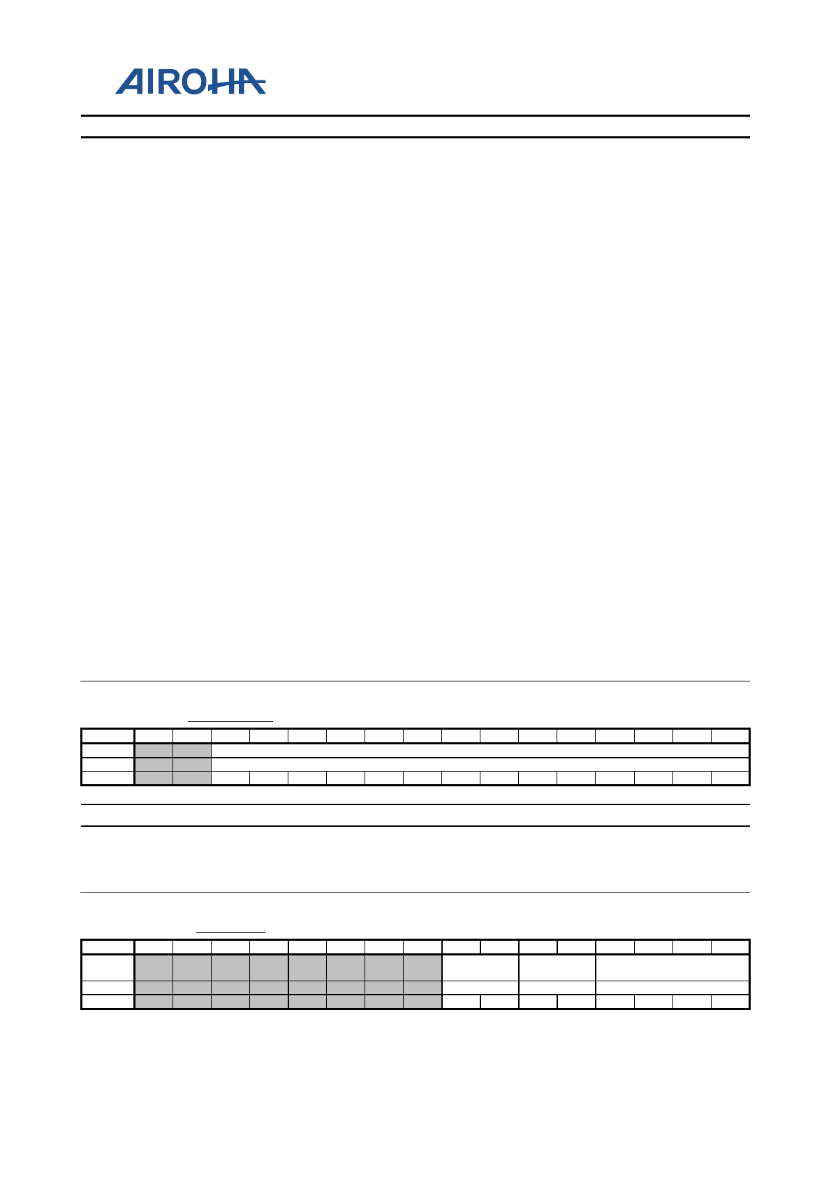
MT2523 Series Reference Manual
© 2015 - 2018 Airoha Technology Corp.
Page 188 of 692
This document contains information that is proprietary to Airoha Technology Corp. (“Airoha”) and/or its licensor(s).
Any unauthorized use, reproduction or disclosure of this document in whole or in part is strictly prohibited.
Bit(s) Name Description
RxFIFO is incomplete because parts of the data are not received.
When KeepErrorStatus = 0, it will be cleared when RxPktRdy is
cleared or write 0 to clear it.
Note: In anything other than a Isochronous transfer, this bit will always return 0.
Write 0 to clear it.
7 CLRDTATOG The CPU writes 1 to this bit to reset the endpoint data toggle to 0.
6 SENTSTALL
This bit will be set when a STALL handshake is transmitted. The CPU
should clear this bit. An interrupt will be generated when the bit is
set.
Write 0 to clear it.
5 SENDSTALL
The CPU writes 1 to this bit to issue a STALL handshake. The CPU
clears this bit to terminate the stall condition.
Note: This bit has no effect where the endpoint is used for ISO
transfers.
4 FLUSHFIFO
The CPU writes 1 to this bit to flush the next packet to be read from
the endpoint RxFIFO. The RxFIFO pointer is reset and the RxPktRdy
bit is cleared.
Note: FlushFIFO should only be used when RxPktRdy is set. In other cases, it
may cause data corruption. If the RxFIFO is double buffered, FlushFIFO may
need to be set twice to completely clear RxFIFO.
3 DATAERR
This bit is set when RxPktRdy is set if the data packet has a CRC or
bit-stuff error in it. Cleared when RxPktRdy is cleared.
Note: This bit is only valid when the endpoint is operating in ISO mode. In bulk
mode, it always returns to 0.
2 OVERRUN
This bit will be set if an OUT packet cannot be loaded into RxFIFO.
The CPU should clear this bit (write 0 to clear it).
Note: This bit is only valid when the endpoint is operating in ISO mode. In bulk
mode, it always returns to 0. The new incoming packet will not be written to
RxFIFO.
1 FIFOFULL This bit will be set when no more packets can be loaded into RxFIFO.
0 RXPKTRDY
This bit will be set when a data packet has been received (to RxFIFO).
The CPU should clear this bit when the packet has been unloaded
from RxFIFO. An interrupt will be generated when the bit is set.
Write 0 to clear it.
A0900128 RX2COUNT Rx2 Count Register 0000
Bit
15
14
13
12
11
10
9
8
7
6
5
4
3
2
1
0
Name
RXCOUNT
Type
RU
Reset
0
0
0
0
0
0
0
0
0
0
0
0
0
0
Bit(s) Name Description
13:0 RXCOUNT
It is a 14-bit read-only register that holds the number of received data
bytes in the packet in RxFIFO.
Note: The value returned changes as the FIFO is unloaded and is only valid when
RxPktRdy(RxCSR.D0) is set.
A090012A TX2TYPE Tx2Type Register 00
Bit
15
14
13
12
11
10
9
8
7
6
5
4
3
2
1
0
Name
TX_SPEE
D
TX_PROT
OCOL
TX_TARGET_EP_NUM
BER
Type
RW
RW
RW
Reset
0
0
0
0
0
0
0
0
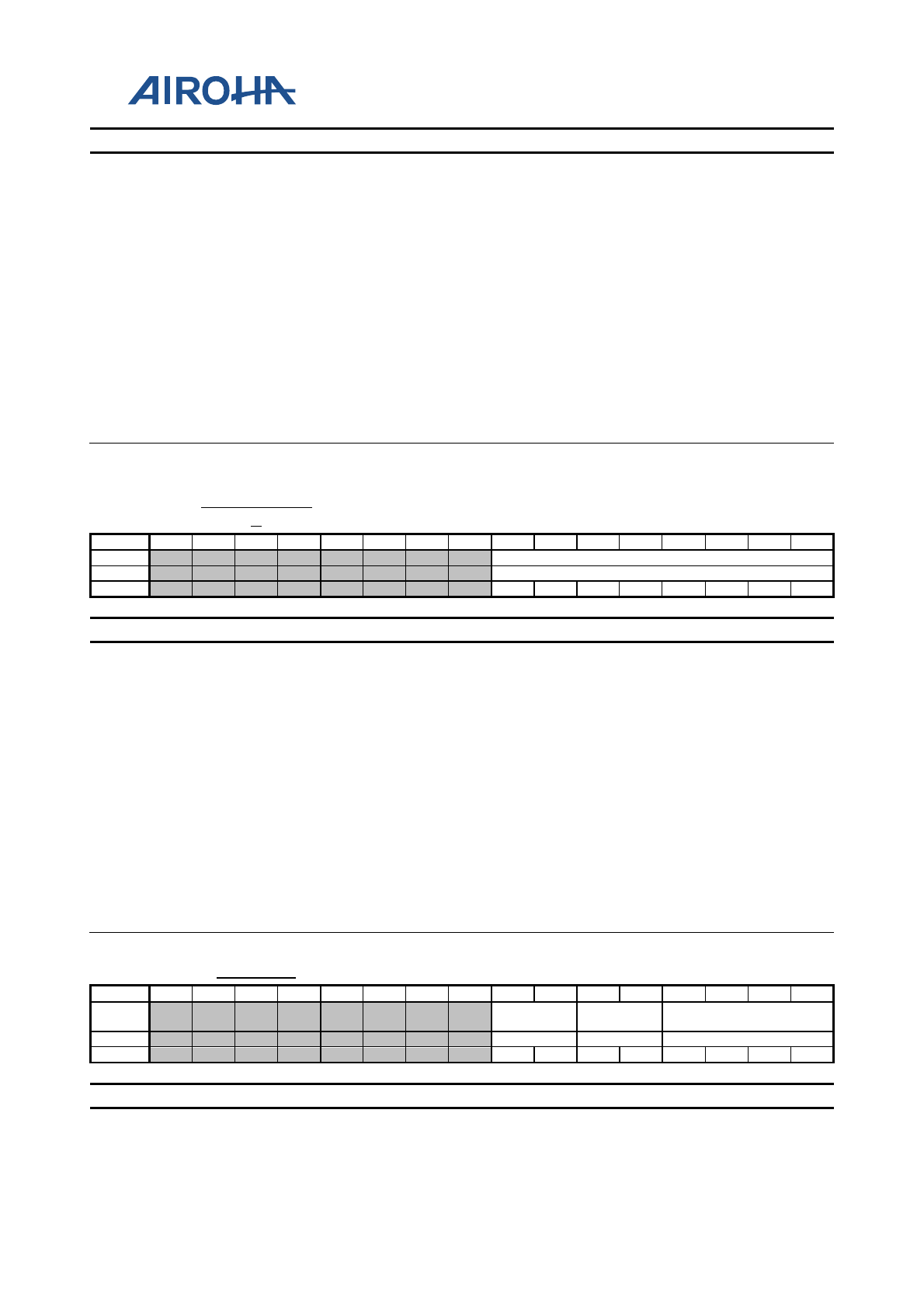
MT2523 Series Reference Manual
© 2015 - 2018 Airoha Technology Corp.
Page 189 of 692
This document contains information that is proprietary to Airoha Technology Corp. (“Airoha”) and/or its licensor(s).
Any unauthorized use, reproduction or disclosure of this document in whole or in part is strictly prohibited.
Bit(s) Name Description
7:6 TX_SPEED
Operating speed of the target device when the core is configured with
the multipoint option
When the core is not configured with the multipoint option, these bits should not
be accessed.
2'b00: Unused
2'b01: High
2'b10: Full
2'b11: Low
5:4 TX_PROTOCOL
The CPU should set up this to select the required protocol for the Tx
endpoint.
2'b00: Illegal
2'b01: Isochronous
2'b10: Bulk
2'b11: Interrupt
3:0 TX_TARGET_EP_N
UMBER
The CPU should set this value to the endpoint number containing in
the Tx endpoint descriptor returned to the USB2.0 controller during
device enumeration.
A090012B TX2INTERVA
L Tx2Interval Register 00
Bit
15
14
13
12
11
10
9
8
7
6
5
4
3
2
1
0
Name
TX_POLLING_INTERVAL_NAK_LIMIT_M
Type
RW
Reset
0
0
0
0
0
0
0
0
Bit(s) Name Description
7:0
TX_POLLING_INTE
RVAL_NAK_LIMIT_
M
(Host mode only) TxInterval Register TxInterval is an 8-bit register
that, for Interrupt and Isochronous transfers, defines the polling
interval for the currently selected Tx endpoint. For bulk endpoints,
this register sets up the number of frames/microframes after which
the endpoint should time out on receiving a stream of NAK
responses. There is a TxInterval register for each configured Tx
endpoint (except for Endpoint 0).
In each case the value that is set defines a number of frames/microframes (high
speed transfers), as the following:
Transfer Type | Speed | Valid values (m) | Interpretation
Interrupt | Low Speed or Full Speed | 1-255 | Polling interval is m frames.
Interrupt | High Speed | 1-16 | Polling interval is 2^(m-1) microframes
Isochronous | Full Speed or High Speed | 1-16 | Polling interval is 2^(m-1)
frames/microframes
Bulk | Full Speed or High Speed | 2-16 | NAK Limit is 2^(m-1)
frames/microframes.
Note: Value 0 or 1 disables the NAK timeout function. The register should be set
before TxType for Bulk endpoint.
A090012C RX2TYPE Rx2Type Register 00
Bit
15
14
13
12
11
10
9
8
7
6
5
4
3
2
1
0
Name RXSPEED
RX_PROT
OCOL
RX_TARGET_EP_NUM
BER
Type
RW
RW
RW
Reset
0
0
0
0
0
0
0
0
Bit(s) Name Description
7:6 RXSPEED Operating speed of the target device when the core is configured with
the multipoint option
When the core is not configured with the multipoint option, these bits should not
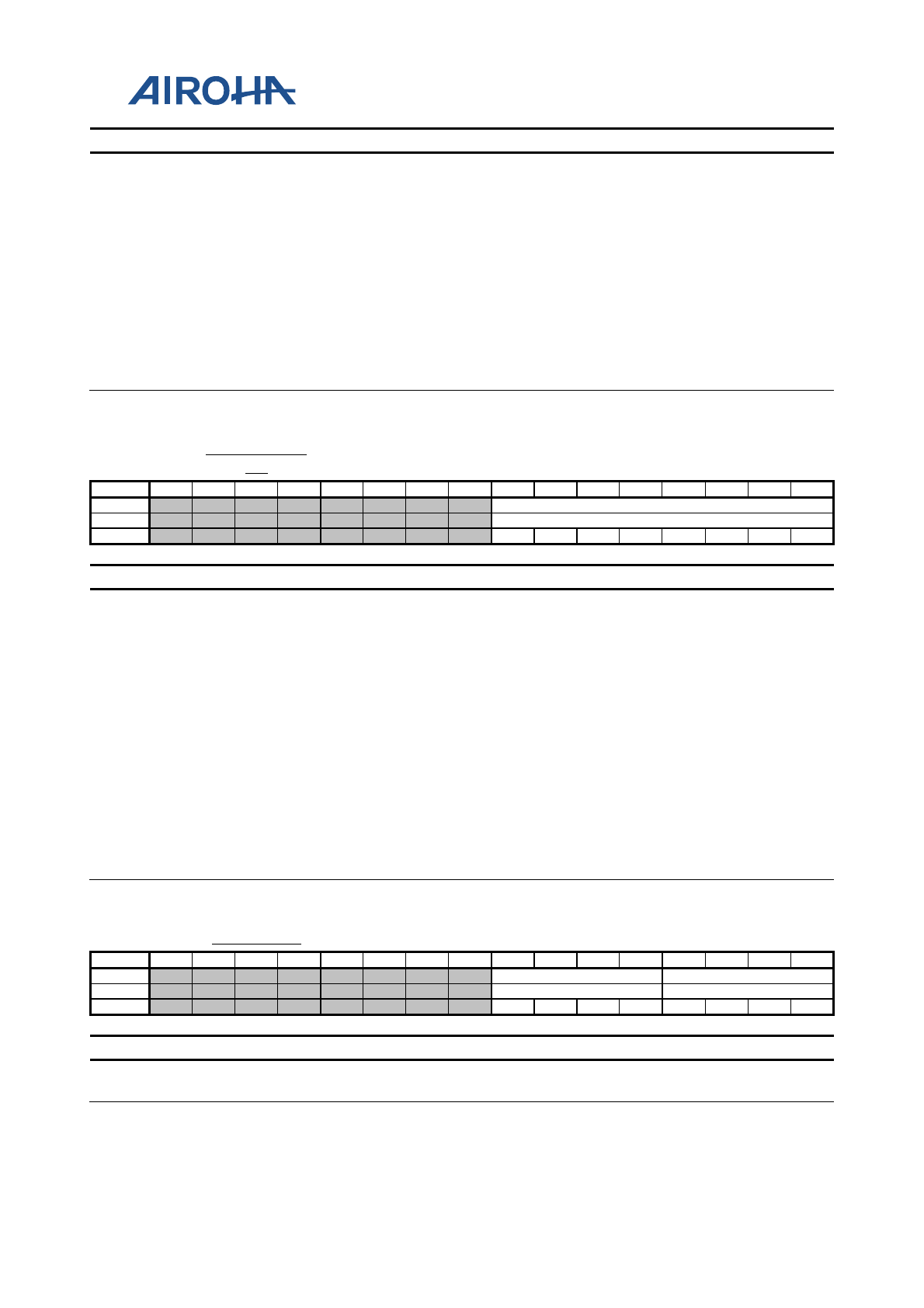
MT2523 Series Reference Manual
© 2015 - 2018 Airoha Technology Corp.
Page 190 of 692
This document contains information that is proprietary to Airoha Technology Corp. (“Airoha”) and/or its licensor(s).
Any unauthorized use, reproduction or disclosure of this document in whole or in part is strictly prohibited.
Bit(s) Name Description
be accessed.
2'b00: Unused
2'b01: High
2'b10: Full
2'b11: Low
5:4 RX_PROTOCOL
The CPU should set up this to select the required protocol for the Tx
endpoint.
2'b00: Illegal
2'b01: Isochronous
2'b10: Bulk
2'b11: Interrupt
3:0 RX_TARGET_EP_N
UMBER
The CPU should set this value to the endpoint number containing in
the Tx endpoint descriptor returned to the USB2.0 controller during
device enumeration.
A090012D RX2INTERV
AL Rx2Interval Register 00
Bit
15
14
13
12
11
10
9
8
7
6
5
4
3
2
1
0
Name
RX_POLLING_INTERVAL_NAK_LIMIT_M
Type
RW
Reset
0
0
0
0
0
0
0
0
Bit(s) Name Description
7:0
RX_POLLING_INTE
RVAL_NAK_LIMIT_
M
RxInterval Register RxInterval is an 8-bit register that, for Interrupt
and Isochronous transfers, defines the polling interval for the
currently selected Rx endpoint. For bulk endpoints, this register sets
up the number of frames/microframes after which the endpoint
should time out on receiving a stream of NAK responses. There is a
RxInterval register for each configured Rx endpoint (except for
Endpoint 0).
RX POLLING INTERVAL / NAK LIMIT (M), (Host mode only)
In each case the value that is set defines a number of frames/microframes (high
speed transfers), as the following:
Transfer Type Speed Valid values (m) Interpretation
Interrupt Low Speed or Full Speed 1 - 255 Polling interval is m frames.
High Speed 1 - 16 Polling interval is 2(m-1) microframes
Isochronous Full Speed or High Speed 1 - 16 Polling interval is 2(m-1)
frames/microframes
Bulk Full Speed or High Speed 2 - 16 NAK Limit is 2(m-1) frames/microframes.
Note: Value 0 or 1 disables the NAK timeout function. The register should be set
before RxType for bulk endpoint.
A090012F FIFOSIZE2 EP2 Configured FIFO Size Register AA
Bit
15
14
13
12
11
10
9
8
7
6
5
4
3
2
1
0
Name
RXFIFOSIZE
TXFIFOSIZE
Type
DC
DC
Reset
1
0
1
0
1
0
1
0
Bit(s) Name Description
7:4 RXFIFOSIZE Indicates the RxFIFO size of 2^n bytes
Example: Value 10 means 2^10 = 1024 bytes.
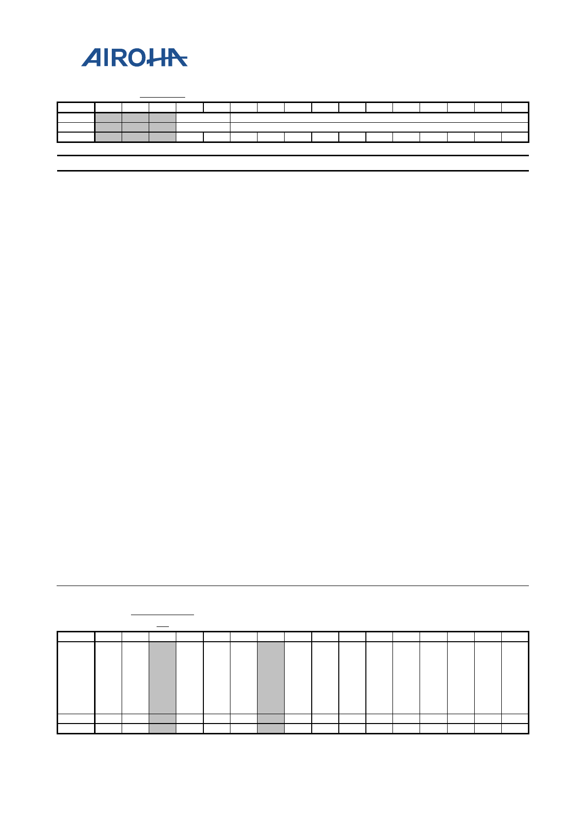
MT2523 Series Reference Manual
© 2015 - 2018 Airoha Technology Corp.
Page 191 of 692
This document contains information that is proprietary to Airoha Technology Corp. (“Airoha”) and/or its licensor(s).
Any unauthorized use, reproduction or disclosure of this document in whole or in part is strictly prohibited.
A0900130 TX3MAP TX3MAP Register 0000
Bit
15
14
13
12
11
10
9
8
7
6
5
4
3
2
1
0
Name
M1
MAXIMUM_PAYLOAD_TRANSACTION
Type
RW
RW
Reset
0
0
0
0
0
0
0
0
0
0
0
0
0
Bit(s) Name Description
12:11 M1 Maximum payload size for indexed TX endpoint, M1 packet
multiplier m maximum payload transaction register
10:0 MAXIMUM_PAYLO
AD_TRANSACTION
The TxMaxP register defines the maximum amount of data that can
be transferred through the selected Tx endpoint in a single operation.
There is a TxMaxP register for each Tx endpoint (except for Endpoint
0). Bit10~0 define (in bytes) the maximum payload transmitted in a
single transaction. The value set can be up to 1024 bytes but is subject
to the constraints placed by the USB Specification on packet sizes for
Bulk, Interrupt and Isochronous transfers in full-speed and high-
speed operations. Where the option of high-bandwidth isochronous
endpoints or of packet splitting on bulk endpoints has been taken
when the core is configured, the register includes either 2 or 5
further bits that define a multiplier m which is equal to one more
than the value recorded. In the case of bulk endpoints with the packet
splitting option enabled, the multiplier m can be up to 32 and defines
the maximum number of 'USB' packets (i.e. packets for transmission
over the USB) of the specified payload into which a single data packet
placed in the FIFO should be split, prior to transfer. (If the packet
splitting option is not enabled, bit15-13 will not be implemented and
bit12-11 (if included) will be ignored.)
Note: The data packet should be an exact multiple of the payload specified by
bit10~0, which is itself required to be one of 8, 16, 32, 64 or (in the case of high
speed transfers) 512 bytes. For isochronous endpoints operating in high-speed
mode and with the high-bandwidth option enabled, m may only be either 2 or 3
(corresponding to bit11 set or bit12 set respectively) and it specifies the
maximum number of such transactions that can take place in a single
microframe. If either bit11 or bit 12 is not 0, the USB2.0 controller will
automatically split any data packet written to FIFO into up to 2 or 3 'USB'
packets, each containing the specified payload (or less). The maximum payload
for each transaction is 1024 bytes, so this allows up to 3072 bytes to be
transmitted in each microframe. (For Isochronous/Interrupt transfers in full-
speed mode, bit11 and 12 are ignored.) The value written to bit10~0 (multiplied
by m in the case of high-bandwidth Isochronous transfers) should match the
value given in the wMaxPacketSize field of the Standard Endpoint Descriptor for
the associated endpoint (see USB Specification Revision 2.0, Chapter 9). A
mismatch can cause unexpected results. The total amount of data represented by
the value written to this register (specified payload * m) should not exceed the
FIFO size for the Tx endpoint and half the FIFO size if double-buffering is
required. If this register is changed after packets have been sent from the
endpoint, the Tx endpoint FIFO should be completely flushed (using the
FlushFIFO bit in TxCSR) after writing the new value to this register.
A0900132 TX3CSR_PE
RI Tx3 CSR Register 0000
Bit
15
14
13
12
11
10
9
8
7
6
5
4
3
2
1
0
Name AU
TO
SET
ISO
DM
AR
EQ
EN
FR
CD
AT
AT
OG
DM
AR
EQ
MO
DE
SET
TX
PK
TR
DY
_T
WI
CE
INC
OM
PT
X
CL
RD
AT
AT
OG
SE
NT
ST
AL
L
SE
ND
ST
AL
L
FL
US
HFI
FO
UN
DE
RR
UN
FIF
ON
OT
EM
PT
Y
TX
PK
TR
DY
Type
RW
RW
RW
RW
RW
A1
A1
A0
A1
RW
A0
A1
RU
A0
Reset
0
0
0
0
0
0
0
0
0
0
0
0
0
0

MT2523 Series Reference Manual
© 2015 - 2018 Airoha Technology Corp.
Page 192 of 692
This document contains information that is proprietary to Airoha Technology Corp. (“Airoha”) and/or its licensor(s).
Any unauthorized use, reproduction or disclosure of this document in whole or in part is strictly prohibited.
Bit(s) Name Description
15 AUTOSET
If the CPU sets up this bit, TxPktRdy will be automatically set when data
of the maximum packet size (value in TxMaxP) is loaded into TxFIFO. If a
packet of less than the maximum packet size is loaded, TxPktRdy will
have to be set manually.
14 ISO
The CPU sets up this bit to enable the Tx endpoint for Isochronous
transfers and clears it to enable the Tx endpoint for Bulk or Interrupt
transfers.
Note: This bit only takes effect in peripheral mode. In host mode, it always returns to
0.
12 DMAREQEN The CPU sets up this bit to enable the DMA request for the Tx endpoint.
11 FRCDATATOG
The CPU sets up this bit to force the endpoint data toggle to switch and
the data packet to be cleared from FIFO, regardless of whether an ACK is
received. This can be used by interrupt Tx endpoints that are used to
communicate rate feedback for isochronous endpoints.
10 DMAREQMODE
The CPU sets up this bit to select DMA Request Mode 1 and clears it to
select DMA Request Mode 0.
Note: This bit should not be cleared either before or in the same cycle as the
DMAReqEn bit is cleared.
8 SETTXPKTRDY_
TWICE
Indicates TxPktRdy had been set when it is 1'b1 already. Write 0 to clear
it.
7 INCOMPTX
When the endpoint is used for high-bandwidth Isochronous/Interrupt
transfers, this bit is set to indicate where a large packet has been split
into 2 or 3 packets for transmission but insufficient IN tokens have been
received to send all the parts.
Note: In anything other than a high-bandwidth transfer, this bit will always return to
0.
Write 0 to clear it.
6 CLRDATATOG The CPU writes 1 to this bit to reset the endpoint data toggle to 0.
5 SENTSTALL
This bit will be set when a STALL handshake is transmitted. The FIFO
will be flushed and Tx interrupt generated if enabled and the TxPktRdy
bit is cleared. The CPU should clear this bit.
Write 0 to clear it.
4 SENDSTALL
The CPU writes 1 to this bit to issue a STALL handshake to an IN token.
The CPU clears this bit to terminate the stall condition.
Note: This bit has no effect where the endpoint is used for Isochronous
transfer. Otherwise, CPU should wait for SENTSTALL interrupt to be
generated before clearing the SENDSTALL bit.
3 FLUSHFIFO
The CPU writes 1 to this bit to flush the latest packet from the endpoint
TxFIFO. The FIFO pointer is reset, the TxPktRdy bit is cleared and an
interrupt is generated. May be set simultaneously with TxPktRdy to abort
the packet currently loaded into FIFO.
Note: FlushFIFO should only be used when TxPktRdy is set. In other cases, it may
cause data corruption. If FIFO is double-buffered, FlushFIFO may need to be set
twice to completely clear FIFO.
2 UNDERRUN The USB will set up this bit if an IN token is received when the TxPktRdy
bit not set. The CPU should clear this bit (write 0 to clear it).
1 FIFONOTEMPTY
The USB will set up this bit when there is at least 1 packet in TxFIFO. This
bit will be asserted automatically when TXPKTRDY is set by CPU and de-
asserted when CPU flush FIFO or send a STALL packet.
0 TXPKTRDY
The CPU will set up this bit after loading a data packet into FIFO. It is
cleared automatically when a data packet has been transmitted. An
interrupt is also generated at this point (if enabled). TxPktRdy is also
automatically cleared (interrupt is generated) prior to loading a second
packet into a double-buffered FIFO.
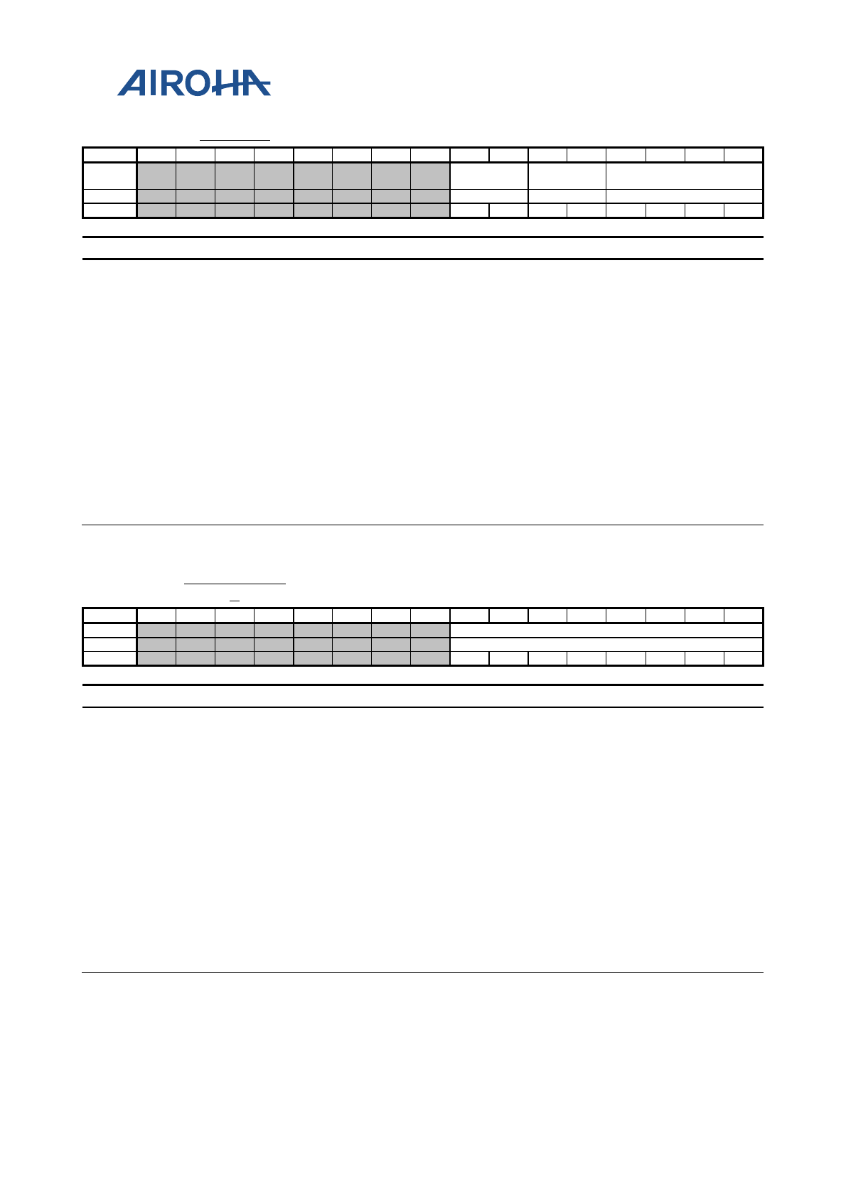
MT2523 Series Reference Manual
© 2015 - 2018 Airoha Technology Corp.
Page 193 of 692
This document contains information that is proprietary to Airoha Technology Corp. (“Airoha”) and/or its licensor(s).
Any unauthorized use, reproduction or disclosure of this document in whole or in part is strictly prohibited.
A090013A TX3TYPE Tx3Type Register 00
Bit
15
14
13
12
11
10
9
8
7
6
5
4
3
2
1
0
Name
TX_SPEE
D
TX_PROT
OCOL
TX_TARGET_EP_NUM
BER
Type
RW
RW
RW
Reset
0
0
0
0
0
0
0
0
Bit(s) Name Description
7:6 TX_SPEED
Operating speed of the target device when the core is configured with
the multipoint option
When the core is not configured with the multipoint option, these bits should not
be accessed.
2'b00: Unused
2'b01: High
2'b10: Full
2'b11: Low
5:4 TX_PROTOCOL
The CPU should set up this to select the required protocol for the Tx
endpoint.
2'b00: Illegal
2'b01: Isochronous
2'b10: Bulk
2'b11: Interrupt
3:0 TX_TARGET_EP_N
UMBER
The CPU should set this value to the endpoint number containing in
the Tx endpoint descriptor returned to the USB2.0 controller during
device enumeration.
A090013B TX3INTERVA
L Tx3Interval Register 00
Bit
15
14
13
12
11
10
9
8
7
6
5
4
3
2
1
0
Name
TX_POLLING_INTERVAL_NAK_LIMIT_M
Type
RW
Reset
0
0
0
0
0
0
0
0
Bit(s) Name Description
7:0
TX_POLLING_INTE
RVAL_NAK_LIMIT_
M
(Host mode only) TxInterval Register TxInterval is an 8-bit register
that, for Interrupt and Isochronous transfers, defines the polling
interval for the currently selected Tx endpoint. For bulk endpoints,
this register sets up the number of frames/microframes after which
the endpoint should time out on receiving a stream of NAK
responses. There is a TxInterval register for each configured Tx
endpoint (except for Endpoint 0).
In each case the value that is set defines a number of frames/microframes (high
speed transfers), as the following:
Transfer Type | Speed | Valid values (m) | Interpretation
Interrupt | Low Speed or Full Speed | 1-255 | Polling interval is m frames.
Interrupt | High Speed | 1-16 | Polling interval is 2^(m-1) microframes
Isochronous | Full Speed or High Speed | 1-16 | Polling interval is 2^(m-1)
frames/microframes
Bulk | Full Speed or High Speed | 2-16 | NAK Limit is 2^(m-1)
frames/microframes.
Note: Value 0 or 1 disables the NAK timeout function. The register should be set
before TxType for Bulk endpoint.
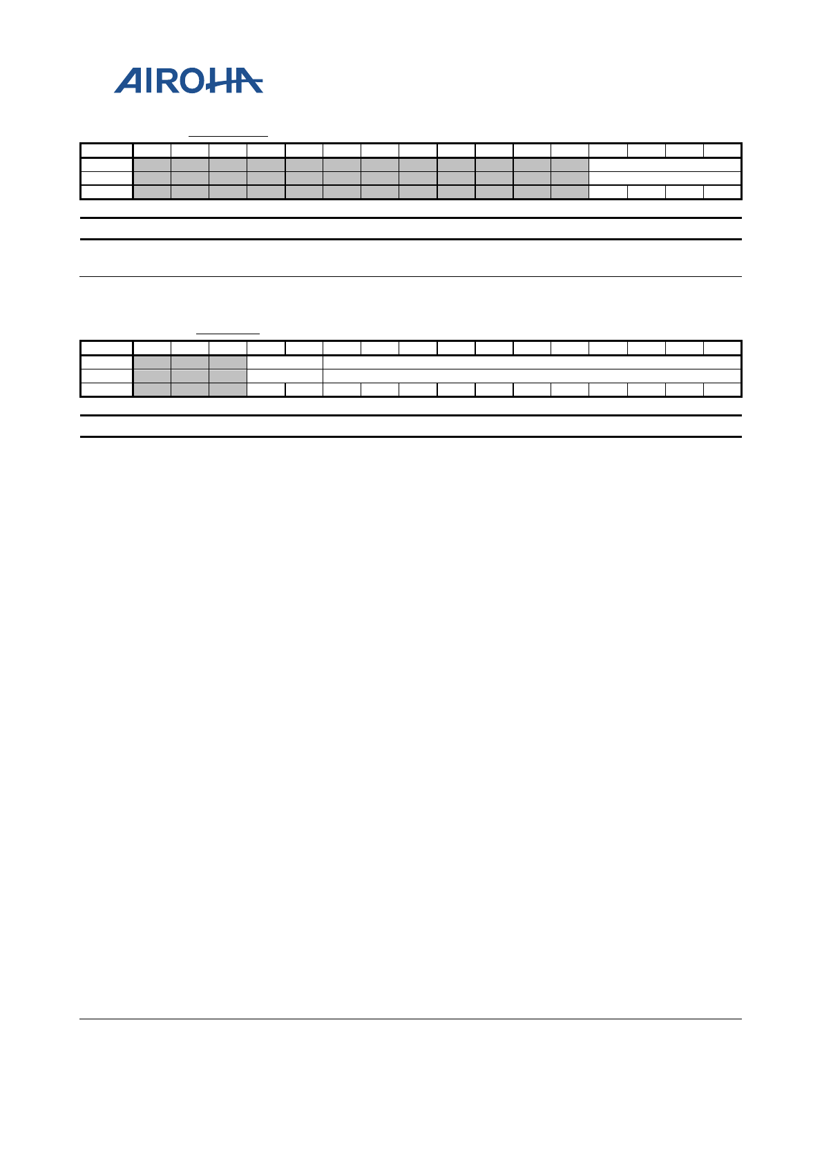
MT2523 Series Reference Manual
© 2015 - 2018 Airoha Technology Corp.
Page 194 of 692
This document contains information that is proprietary to Airoha Technology Corp. (“Airoha”) and/or its licensor(s).
Any unauthorized use, reproduction or disclosure of this document in whole or in part is strictly prohibited.
A090013F FIFOSIZE3 EP3 Configured FIFO Size Register 2A
Bit
15
14
13
12
11
10
9
8
7
6
5
4
3
2
1
0
Name
TXFIFOSIZE
Type
DC
Reset
1
0
1
0
Bit(s) Name Description
3:0 TXFIFOSIZE Indicates the TxFIFO size of 2^n bytes
Example: Value 10 means 2^10 = 1024 bytes.
A0900140 TX4MAP TX4MAP Register 0000
Bit
15
14
13
12
11
10
9
8
7
6
5
4
3
2
1
0
Name
M1
MAXIMUM_PAYLOAD_TRANSACTION
Type
RW
RW
Reset
0
0
0
0
0
0
0
0
0
0
0
0
0
Bit(s) Name Description
12:11 M1 Maximum payload size for indexed TX endpoint, M1 packet
multiplier m maximum payload transaction register
10:0 MAXIMUM_PAYLO
AD_TRANSACTION
The TxMaxP register defines the maximum amount of data that can
be transferred through the selected Tx endpoint in asingle operation.
There is a TxMaxP register for each Tx endpoint (except for Endpoint
0). Bit10~0 define (in bytes) the maximum payload transmitted in a
single transaction. The value set can be up to 1024 bytes but is subject
to the constraints placed by the USB Specification on packet sizes for
Bulk, Interrupt and Isochronous transfers in full-speed and high-
speed operations. Where the option of high-bandwidth isochronous
endpoints or of packet splitting on bulk endpoints has been taken
when the core is configured, the register includes either 2 or 5
further bits that define a multiplier m which is equal to one more
than the value recorded. In the case of bulk endpoints with the packet
splitting option enabled, the multiplier m can be up to 32 and defines
the maximum number of 'USB' packets (i.e. packets for transmission
over the USB) of the specified payload into which a single data packet
placed in the FIFO should be split, prior to transfer. (If the packet
splitting option is not enabled, bit15-13 will not be implemented and
bit12-11 (if included) will be ignored.)
Note: The data packet should be an exact multiple of the payload specified by
bit10~0, which is itself required to be one of 8, 16, 32, 64 or (in the case of high
speed transfers) 512 bytes. For isochronous endpoints operating in high-speed
mode and with the high-bandwidth option enabled, m may only be either 2 or 3
(corresponding to bit11 set or bit12 set respectively) and it specifies the
maximum number of such transactions that can take place in a single
microframe. If either bit11 or bit12 is not 0, the USB2.0 controller will
automatically split any data packet written to the FIFO into up to 2 or 3 'USB'
packets, each containing the specified payload (or less). The maximum payload
for each transaction is 1024 bytes, so this allows up to 3072 bytes to be
transmitted in each microframe. (For Isochronous/Interrupt transfers in full-
speed mode, bit 11 and 12 are ignored.) The value written to bit10~0 (multiplied
by m in the case of high-bandwidth Isochronous transfers) should match the
value given in the wMaxPacketSize field of the Standard Endpoint Descriptor for
the associated endpoint (see USB Specification Revision 2.0, Chapter 9). A
mismatch can cause unexpected results. The total amount of data represented by
the value written to this register (specified payload * m) should not exceed the
FIFO size for the Tx endpoint and half the FIFO size if double-buffering is
required. If this register is changed after packets have been sent from the
endpoint, the Tx endpoint FIFO should be completely flushed (using the
FlushFIFO bit in TxCSR) after writing the new value to this register.

MT2523 Series Reference Manual
© 2015 - 2018 Airoha Technology Corp.
Page 195 of 692
This document contains information that is proprietary to Airoha Technology Corp. (“Airoha”) and/or its licensor(s).
Any unauthorized use, reproduction or disclosure of this document in whole or in part is strictly prohibited.
A0900142 TX4CSR_PE
RI Tx4 CSR Register 0000
Bit
15
14
13
12
11
10
9
8
7
6
5
4
3
2
1
0
Name AU
TO
SET
ISO
DM
AR
EQ
EN
FR
CD
AT
AT
OG
DM
AR
EQ
MO
DE
SET
TX
PK
TR
DY
_T
WI
CE
INC
OM
PT
X
CL
RD
AT
AT
OG
SE
NT
ST
AL
L
SE
ND
ST
AL
L
FL
US
HFI
FO
UN
DE
RR
UN
FIF
ON
OT
EM
PT
Y
TX
PK
TR
DY
Type
RW
RW
RW
RW
RW
A1
A1
A0
A1
RW
A0
A1
RU
A0
Reset
0
0
0
0
0
0
0
0
0
0
0
0
0
0
Bit(s) Name Description
15 AUTOSET
If the CPU sets up this bit, TxPktRdy will be automatically set when
data of the maximum packet size (value in TxMaxP) is loaded into
TxFIFO. If a packet of less than the maximum packet size is loaded,
TxPktRdy will have to be set manually.
14 ISO
The CPU sets up this bit to enable the Tx endpoint for Isochronous
transfers and clears it to enable the Tx endpoint for Bulk or Interrupt
transfers.
Note: This bit only takes effect in peripheral mode. In host mode, it always
returns to 0.
12 DMAREQEN The CPU sets up this bit to enable the DMA request for the Tx
endpoint.
11 FRCDATATOG
The CPU sets up this bit to force the endpoint data toggle to switch
and the data packet to be cleared from the FIFO, regardless of
whether an ACK is received. This can be used by Interrupt Tx
endpoints that are used to communicate rate feedback for
isochronous endpoints.
10 DMAREQMODE
The CPU sets up this bit to select DMA Request Mode 1 and clears it to
select DMA Request Mode 0.
Note: This bit should not be cleared either before or in the same cycle as the
DMAReqEn bit is cleared.
8 SETTXPKTRDY_TW
ICE
Indicates TxPktRdy had been set when it is 1'b1 already. Write 0 to
clear it.
7 INCOMPTX
When the endpoint is used for high-bandwidth
Isochronous/Interrupt transfers, this bit will be set to indicate where
a large packet has been split into 2 or 3 packets for transmission but
insufficient IN tokens have been received to send all the parts.
Note: In anything other than a high-bandwidth transfer, this bit will always
return to 0.
Write 0 to clear it.
6 CLRDATATOG The CPU writes 1 to this bit to reset the endpoint data toggle to 0.
5 SENTSTALL
This bit will be set when a STALL handshake is transmitted. The FIFO
will be flushed and Tx interrupt generated if enabled and the
TxPktRdy bit is cleared. The CPU should clear this bit.
Write 0 to clear it.
4 SENDSTALL
The CPU writes 1 to this bit to issue a STALL handshake to an IN
token. The CPU clears this bit to terminate the stall condition.
Note: This bit has no effect where the endpoint is used for
Isochronous transfer. Otherwise, CPU should wait for SENTSTALL
interrupt to be generated before clearing the SENDSTALL bit.
3 FLUSHFIFO
The CPU writes 1 to this bit to flush the latest packet from the
endpoint TxFIFO. The FIFO pointer is reset, the TxPktRdy bit is
cleared and an interrupt is generated. May be set simultaneously
with TxPktRdy to abort the packet currently loaded into FIFO.
Note: FlushFIFO should only be used when TxPktRdy is set. In other cases, it
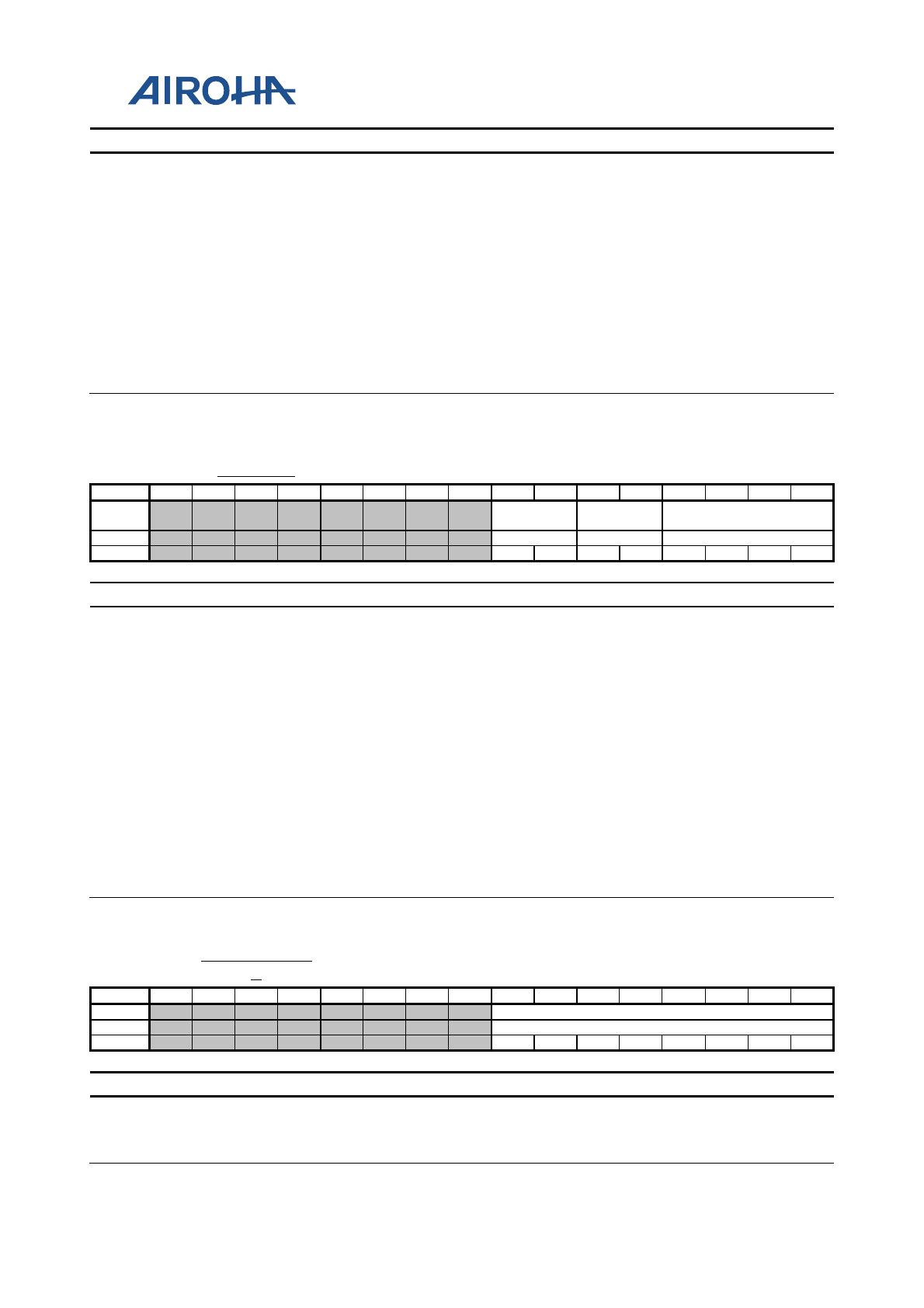
MT2523 Series Reference Manual
© 2015 - 2018 Airoha Technology Corp.
Page 196 of 692
This document contains information that is proprietary to Airoha Technology Corp. (“Airoha”) and/or its licensor(s).
Any unauthorized use, reproduction or disclosure of this document in whole or in part is strictly prohibited.
Bit(s) Name Description
may cause data corruption. If the FIFO is double-buffered, FlushFIFO may need
to be set twice to completely clear the FIFO.
2 UNDERRUN The USB will set up this bit if an IN token is received when the
TxPktRdy bit not set. The CPU should clear this bit (write 0 to clear
it).
1 FIFONOTEMPTY
The USB will set up this bit when there is at least 1 packet in the
TxFIFO. This bit will be asserted automatically when TXPKTRDY is
set by CPU and de-asserted when CPU flushes FIFO or sends a STALL
packet.
0 TXPKTRDY
The CPU will set up this bit after loading a data packet into FIFO. It is
cleared automatically when a data packet has been transmitted. An
interrupt is also generated at this point (if enabled). TxPktRdy is also
automatically cleared (interrupt is generated) prior to loading a
second packet into a double-buffered FIFO.
A090014A TX4TYPE Tx4Type Register 00
Bit
15
14
13
12
11
10
9
8
7
6
5
4
3
2
1
0
Name
TX_SPEE
D
TX_PROT
OCOL
TX_TARGET_EP_NUM
BER
Type
RW
RW
RW
Reset
0
0
0
0
0
0
0
0
Bit(s) Name Description
7:6 TX_SPEED
Operating speed of the target device when the core is configured with
the multipoint option
When the core is not configured with the multipoint option, these bits should not
be accessed.
2'b00: Unused
2'b01: High
2'b10: Full
2'b11: Low
5:4 TX_PROTOCOL
The CPU should set up this to select the required protocol for the Tx
endpoint.
2'b00: Illegal
2'b01: Isochronous
2'b10: Bulk
2'b11: Interrupt
3:0 TX_TARGET_EP_N
UMBER
The CPU should set this value to the endpoint number containing in
the Tx endpoint descriptor returned to the USB2.0 controller during
device enumeration.
A090014B TX4INTERVA
L Tx4Interval Register 00
Bit
15
14
13
12
11
10
9
8
7
6
5
4
3
2
1
0
Name
TX_POLLING_INTERVAL_NAK_LIMIT_M
Type
RW
Reset
0
0
0
0
0
0
0
0
Bit(s) Name Description
7:0
TX_POLLING_INTE
RVAL_NAK_LIMIT_
M
(Host mode only) TxInterval Register TxInterval is an 8-bit register
that, for Interrupt and Isochronous transfers, defines the polling
interval for the currently selected Tx endpoint. For bulk endpoints,
this register sets up the number of frames/microframes after which
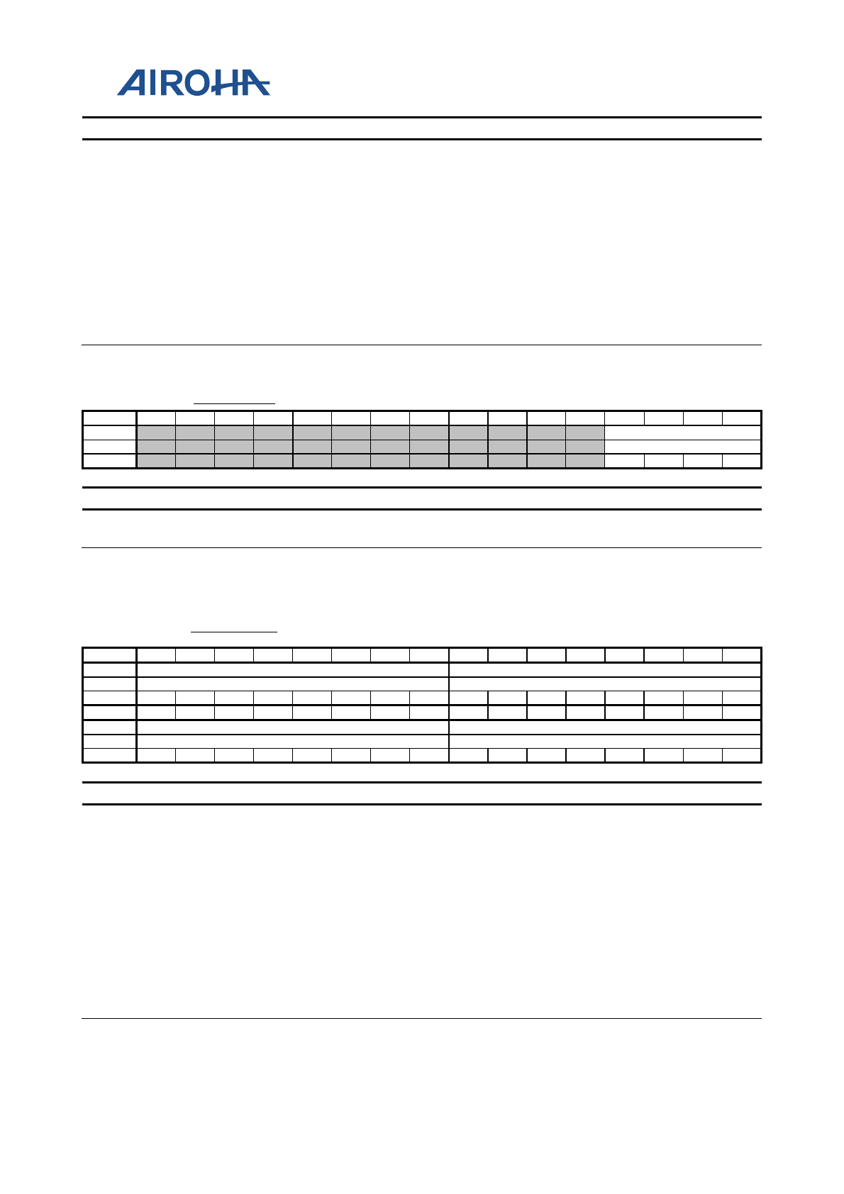
MT2523 Series Reference Manual
© 2015 - 2018 Airoha Technology Corp.
Page 197 of 692
This document contains information that is proprietary to Airoha Technology Corp. (“Airoha”) and/or its licensor(s).
Any unauthorized use, reproduction or disclosure of this document in whole or in part is strictly prohibited.
Bit(s) Name Description
the endpoint should time out on receiving a stream of NAK
responses. There is a TxInterval register for each configured Tx
endpoint (except for Endpoint 0).
In each case the value that is set defines a number of frames/microframes (high
speed transfers), as the following:
Transfer Type | Speed | Valid values (m) | Interpretation
Interrupt | Low Speed or Full Speed | 1-255 | Polling interval is m frames.
Interrupt | High Speed | 1-16 | Polling interval is 2^(m-1) microframes
Isochronous | Full Speed or High Speed | 1-16 | Polling interval is 2^(m-1)
frames/microframes
Bulk | Full Speed or High Speed | 2-16 | NAK Limit is 2^(m-1)
frames/microframes.
Note: Value 0 or 1 disables the NAK timeout function. The register should be set
before TxType for Bulk endpoint.
A090014F FIFOSIZE4 EP4 Configured FIFO Size Register 2A
Bit
15
14
13
12
11
10
9
8
7
6
5
4
3
2
1
0
Name
TXFIFOSIZE
Type
DC
Reset
1
0
1
0
Bit(s) Name Description
3:0 TXFIFOSIZE Indicates the TxFIFO size of 2^n bytes
Example: Value 10 means 2^10 = 1024 bytes.
A090020
0 DMA_INTR DMA Interrupt Status Register 00000000
Bit
31
30
29
28
27
26
25
24
23
22
21
20
19
18
17
16
Name
DMA_INTR_UNMASK_SET
DMA_INTR_UNMASK_CLEAR
Type
A0
A0
Reset
0
0
0
0
0
0
0
0
0
0
0
0
0
0
0
0
Bit
15
14
13
12
11
10
9
8
7
6
5
4
3
2
1
0
Name
DMA_INTR_UNMASK
DMA_INTR_STATUS
Type
RU
W1C
Reset
0
0
0
0
0
0
0
0
0
0
0
0
0
0
0
0
Bit(s) Name Description
31:24 DMA_INTR_UNMA
SK_SET Sets DMA_INTR_UNMASK to 1
23:16 DMA_INTR_UNMA
SK_CLEAR Clears DMA_INTR_UNMASK to 0
15:8 DMA_INTR_UNMA
SK
Unmasks DMA interrupts
The DMA interrupt will be generated when DMA_INTR_UNMASK and
DMA_INTR_STATUS are both 1.
7:0 DMA_INTR_STATU
S
Indicates DMA complete interrupt status, one bit per DMA channel
implemented
Bit 0 is used for DMA channel 1; bit 1 is used for DMA channel 2, etc. Write 1 to
clear it.
Note: DMA interrupt will be asserted after disabling the DMA enable when
receiving a null packet even thought DMA_COUNT_M still does not reach 0.
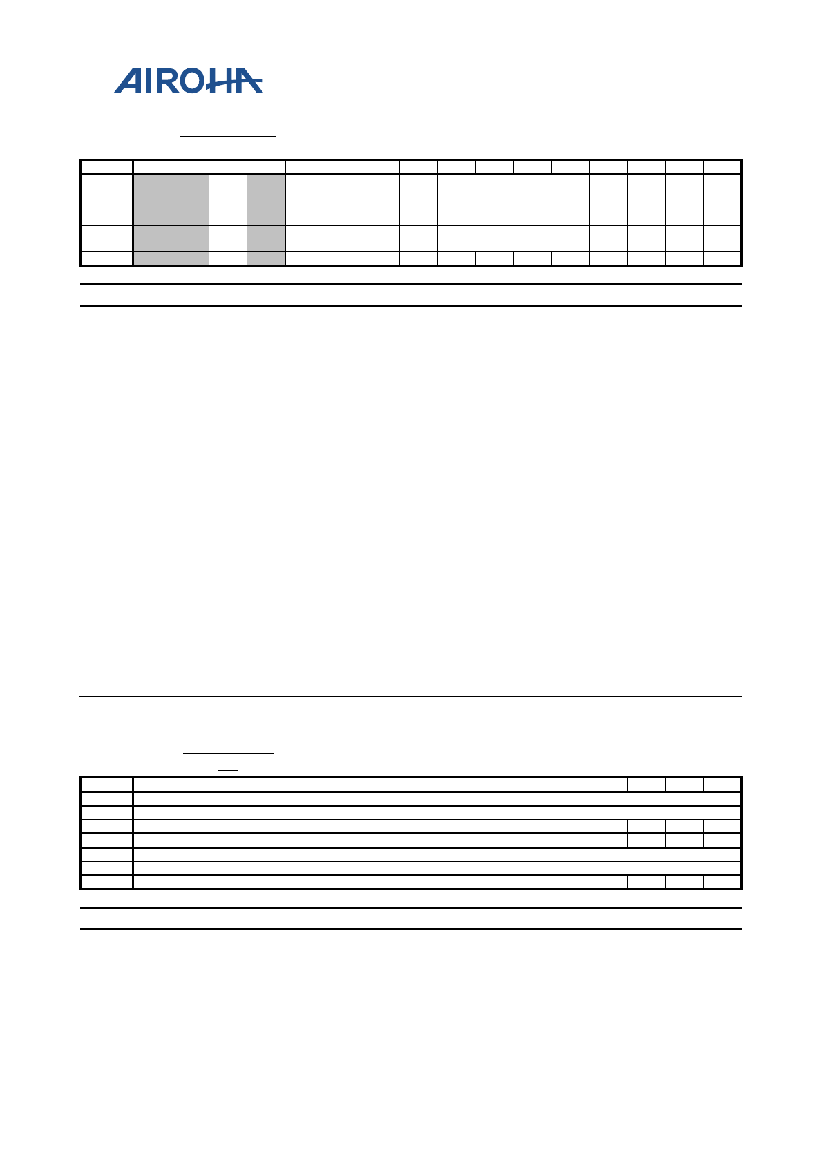
MT2523 Series Reference Manual
© 2015 - 2018 Airoha Technology Corp.
Page 198 of 692
This document contains information that is proprietary to Airoha Technology Corp. (“Airoha”) and/or its licensor(s).
Any unauthorized use, reproduction or disclosure of this document in whole or in part is strictly prohibited.
A0900204 DMA_CNTL_
0 DMA Channel 0 Control Register 0000
Bit
15
14
13
12
11
10
9
8
7
6
5
4
3
2
1
0
Name
DM
AA
BO
RT
DM
AC
HE
N
BURST_M
ODE
BU
SE
RR
ENDPNT INT
EN
DM
AM
OD
E
DM
ADI
R
DM
AE
N
Type A0 RU RW RU RW RW RW RW
Oth
er
Reset
0
0
0
0
0
0
0
0
0
0
0
0
0
Bit(s) Name Description
13 DMAABORT If SW needs to abort the current DMA transfer, set DMAABORT=1
and DMAEN=0. After the transfer is aborted completely, DMA
interrupt will occur.
11 DMACHEN DMA channel enable monitor bit
10:9 BURST_MODE
2'b00: Burst Mode 0: Bursts of unspecified length
2'b01: Burst Mode 1: INCR4 or unspecified length
2'b10: Burst Mode 2: INCR8, INCR4 or unspecified length
2'b11: Burst Mode 3: INCR16, INCR8, INCR4 or unspecified length
8 BUSERR Bus error
7:4 ENDPNT Endpoint which DMA will transfer with
3 INTEN Enables interrupt
2 DMAMODE
DMA mode
DMA mode 0: Single packet operation
DMA mode 1: Multi packets operation, with the configuration of DMAReqMode
in RXCSR bit 11 DMA mode 1 can support both known and unknown size
transaction.
1 DMADIR
Direction
0: DMA write (Rx endpoint)
1: DMA read (Tx endpoint)
0 DMAEN
Enables DMA
The bit will be cleared when the DMA transfer is completed. Programmers
should not disable DMA_en before the transfer is completed. If programmers
disable dma_en during the transfer, DMA will not stop immediately until the
last bus transfer is completed.
A090020
8
DMA_ADDR
_0 DMA Channel 0 Address Register 00000000
Bit
31
30
29
28
27
26
25
24
23
22
21
20
19
18
17
16
Name
DMA_ADDR_0[31:16]
Type
RW
Reset
0
0
0
0
0
0
0
0
0
0
0
0
0
0
0
0
Bit
15
14
13
12
11
10
9
8
7
6
5
4
3
2
1
0
Name
DMA_ADDR_0[15:0]
Type
RW
Reset
0
0
0
0
0
0
0
0
0
0
0
0
0
0
0
0
Bit(s) Name Description
31:0 DMA_ADDR_0
32-bit DMA start address
Updated (increased) by USB2.0 controller automatically when multiple packet
DMA (DMA Mode = 1) is used
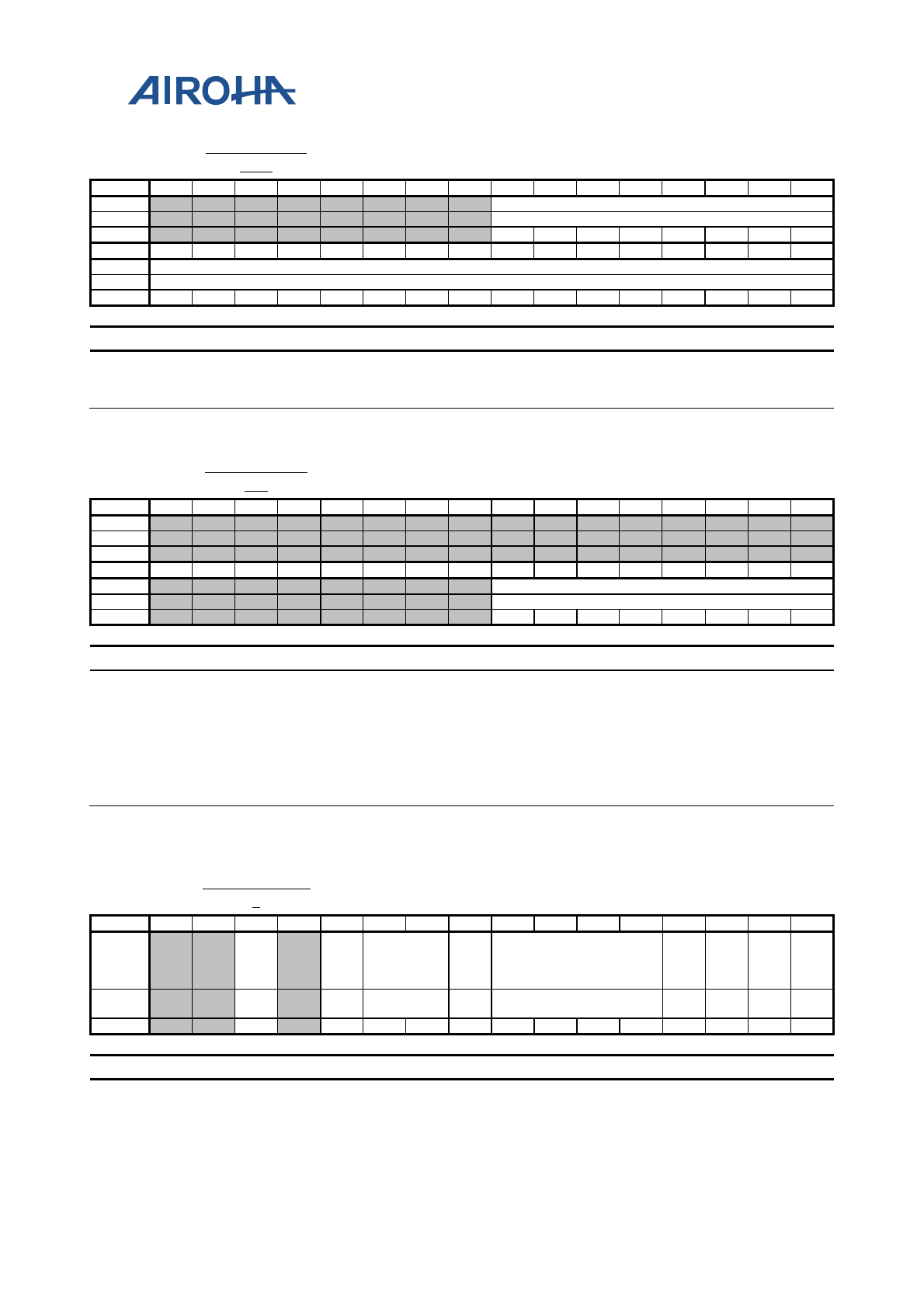
MT2523 Series Reference Manual
© 2015 - 2018 Airoha Technology Corp.
Page 199 of 692
This document contains information that is proprietary to Airoha Technology Corp. (“Airoha”) and/or its licensor(s).
Any unauthorized use, reproduction or disclosure of this document in whole or in part is strictly prohibited.
A090020
C
DMA_COUN
T_0 DMA Channel 0 Byte Count Register 00000000
Bit
31
30
29
28
27
26
25
24
23
22
21
20
19
18
17
16
Name
DMA_COUNT_0[23:16]
Type
RW
Reset
0
0
0
0
0
0
0
0
Bit
15
14
13
12
11
10
9
8
7
6
5
4
3
2
1
0
Name
DMA_COUNT_0[15:0]
Type
RW
Reset
0
0
0
0
0
0
0
0
0
0
0
0
0
0
0
0
Bit(s) Name Description
23:0 DMA_COUNT_0
24-bit DMA transfer count with byte unit
Updated (decreased) by USB2.0 controller automatically when each packet is
transferred.
A0900210 DMA_LIMIT
ER DMA Limiter Register 00000000
Bit
31
30
29
28
27
26
25
24
23
22
21
20
19
18
17
16
Name
Type
Reset
Bit
15
14
13
12
11
10
9
8
7
6
5
4
3
2
1
0
Name
DMA_LIMITER
Type
RW
Reset
0
0
0
0
0
0
0
0
Bit(s) Name Description
7:0 DMA_LIMITER
This register suppresses bus utilization of the DMA channel. The
value is from 0 to 255. 0 means no limitation, and 255 means totally
banned. The value between 0 and 255 means certain DMA can have
permission to use AHB every (4 x n) AHB clock cycles.
Note: It is not recommended to limit the bus utilization of the DMA channels
because this increases the latency of response to the masters, and the transfer
rate will decrease. Before using it, programmers should make sure that the bus
masters have some protective mechanism to avoid entering wrong states.
A0900214 DMA_CNTL_
1 DMA Channel 1 Control Register 0000
Bit
15
14
13
12
11
10
9
8
7
6
5
4
3
2
1
0
Name
DM
AA
BO
RT
DM
AC
HE
N
BURST_M
ODE
BU
SE
RR
ENDPNT INT
EN
DM
AM
OD
E
DM
ADI
R
DM
AE
N
Type A0 RU RW RU RW RW RW RW
Oth
er
Reset
0
0
0
0
0
0
0
0
0
0
0
0
0
Bit(s) Name Description
13 DMAABORT
If SW needs to abort the current DMA transfer, set DMAABORT=1
and DMAEN=0. After the transfer is aborted completely, DMA
interrupt will occur.
11 DMACHEN DMA channel enable monitor bit.
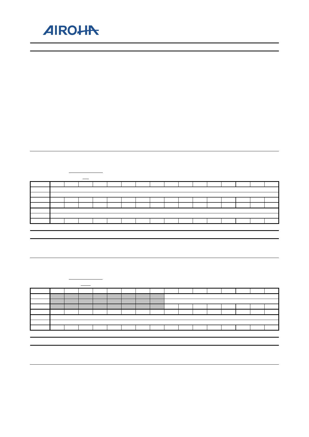
MT2523 Series Reference Manual
© 2015 - 2018 Airoha Technology Corp.
Page 200 of 692
This document contains information that is proprietary to Airoha Technology Corp. (“Airoha”) and/or its licensor(s).
Any unauthorized use, reproduction or disclosure of this document in whole or in part is strictly prohibited.
Bit(s) Name Description
10:9 BURST_MODE
2'b00: Burst Mode 0: Bursts of unspecified length
2'b01: Burst Mode 1: INCR4 or unspecified length
2'b10: Burst Mode 2: INCR8, INCR4 or unspecified length
2'b11: Burst Mode 3: INCR16, INCR8, INCR4 or unspecified length
8 BUSERR Bus error
7:4 ENDPNT Endpoint which DMA will transfer with.
3 INTEN Enables interrupt
2 DMAMODE DMA mode
1 DMADIR
Direction
0: DMA write (Rx endpoint)
1: DMA read (Tx endpoint)
0 DMAEN
Enables DMA
The bit will be cleared when the DMA transfer is completed. Programmers
should not disable DMA_en before the transfer is completed. If programmers
disable dma_en during the transfer, DMA will not stop immediately until the
last bus transfer is completed.
A0900218 DMA_ADDR
_1 DMA Channel 1 Address Register 00000000
Bit
31
30
29
28
27
26
25
24
23
22
21
20
19
18
17
16
Name
DMA_ADDR_1[31:16]
Type
RW
Reset
0
0
0
0
0
0
0
0
0
0
0
0
0
0
0
0
Bit
15
14
13
12
11
10
9
8
7
6
5
4
3
2
1
0
Name
DMA_ADDR_1[15:0]
Type
RW
Reset
0
0
0
0
0
0
0
0
0
0
0
0
0
0
0
0
Bit(s) Name Description
31:0 DMA_ADDR_1
32-bit DMA start address
Updated (increased) by USB2.0 controller automatically when multiple packet
DMA (DMA Mode = 1) is used
A090021C DMA_COUN
T_1 DMA Channel 1 Byte Count Register 00000000
Bit
31
30
29
28
27
26
25
24
23
22
21
20
19
18
17
16
Name
DMA_COUNT_1[23:16]
Type
RW
Reset
0
0
0
0
0
0
0
0
Bit
15
14
13
12
11
10
9
8
7
6
5
4
3
2
1
0
Name
DMA_COUNT_1[15:0]
Type
RW
Reset
0
0
0
0
0
0
0
0
0
0
0
0
0
0
0
0
Bit(s) Name Description
23:0 DMA_COUNT_1
24-bit DMA transfer count with byte unit
Updated (decreased) by USB2.0 controller automatically when each packet is
transferred.
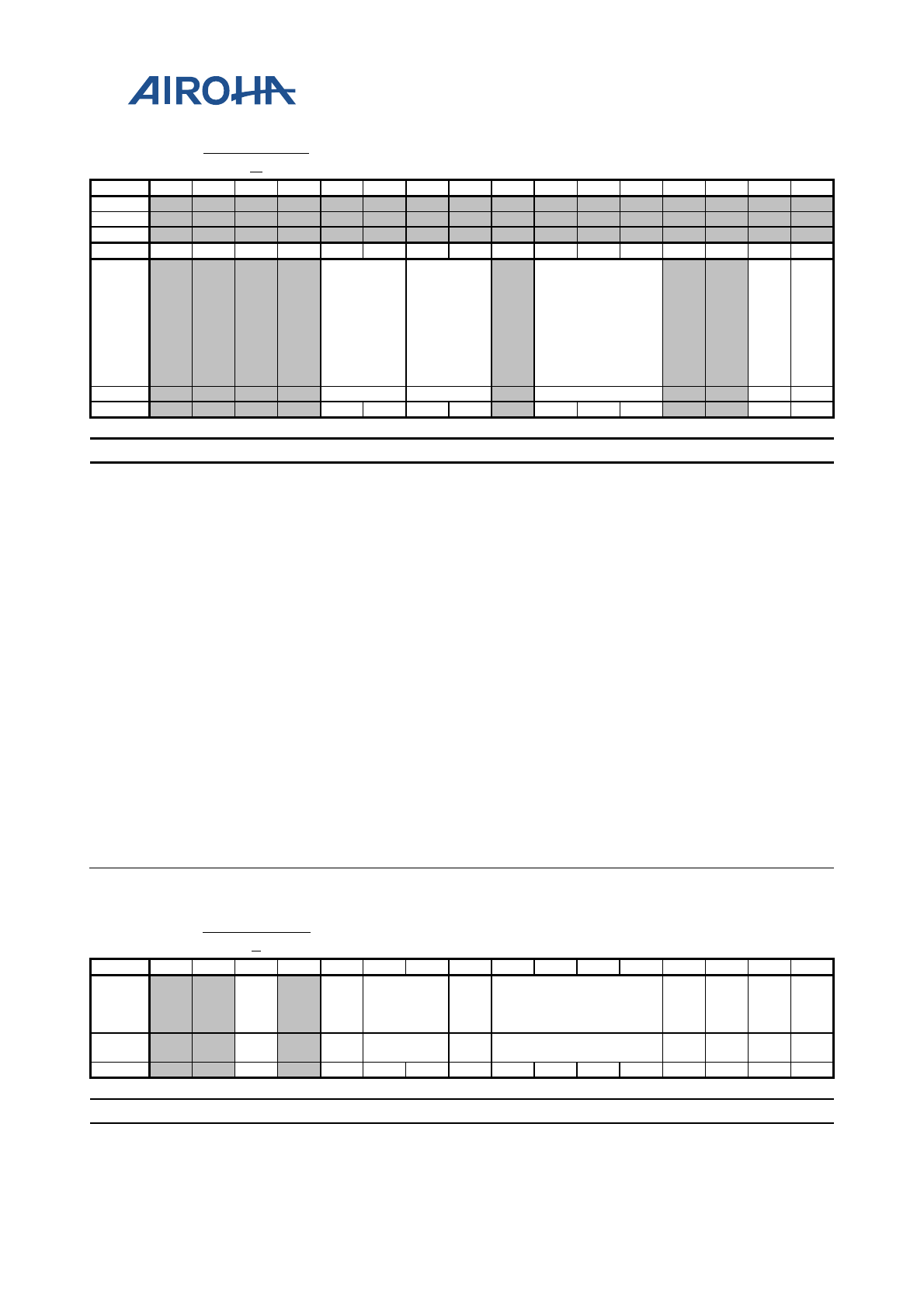
MT2523 Series Reference Manual
© 2015 - 2018 Airoha Technology Corp.
Page 201 of 692
This document contains information that is proprietary to Airoha Technology Corp. (“Airoha”) and/or its licensor(s).
Any unauthorized use, reproduction or disclosure of this document in whole or in part is strictly prohibited.
A0900220 DMA_CONFI
G DMA Configuration Register 00000004
Bit
31
30
29
28
27
26
25
24
23
22
21
20
19
18
17
16
Name
Type
Reset
Bit
15
14
13
12
11
10
9
8
7
6
5
4
3
2
1
0
Name DMA_ACT
IVE_EN
AHB_HP
ROT_2_E
N
DMAQ_CHAN_S
EL
AH
BW
AIT
_SE
L
BO
UN
DA
RY
_1K
_C
RO
SS_
EN
Type
RW
RW
RW
RW
RW
Reset
0
0
0
0
0
0
0
0
0
Bit(s) Name Description
11:10 DMA_ACTIVE_EN
The two bits control usb_active.
2'b00: usb_active depends on all DMAEN of DMA channel control register.
2'b01: usb_active ties to 1.
2'b10: usb_active ties to 0.
2'b11: usb_active depends on ep_active, dma_active and all DMAEN of DMA
channel control register (OR logic).
9:8 AHB_HPROT_2_EN
The two bits control the AHB master interface HPROT2 function
operating in non-bufferable/bufferable/last transfer non-bufferable
mode.
2'b00: All write transfers of a burst will be accessed by bufferable mode except
for the last transfer of a burst.
2'b01: AHB master HPROT2 is always accessed by non-bufferable mode.
2'b10: AHB master HPROT2 is always accessed by bufferable mode.
2'b11: Reserved
6:4 DMAQ_CHAN_SEL Selects DMA channel used by USB_DMAQ if it is available
It will not affect if USB_DMAQ is not available.
1 AHBWAIT_SEL
Selects AHBWAIT behavior
Set to 1 to return to old DMA master AHB wait condition.
This bit is used to test DMA FIFO overflow bug.
0 BOUNDARY_1K_CR
OSS_EN
Enables 1k boundary page crossing
Set to 1 to force burst transfer regardless of 1k boundary crossing.
Note: This will violate AHB 1k boundary specification but gain some bus
performance.
A0900224 DMA_CNTL_
2 DMA Channel 2 Control Register 0000
Bit
15
14
13
12
11
10
9
8
7
6
5
4
3
2
1
0
Name
DM
AA
BO
RT
DM
AC
HE
N
BURST_M
ODE
BU
SE
RR
ENDPNT INT
EN
DM
AM
OD
E
DM
ADI
R
DM
AE
N
Type A0 RU RW RU RW RW RW RW
Oth
er
Reset
0
0
0
0
0
0
0
0
0
0
0
0
0
Bit(s) Name Description
13 DMAABORT If SW needs to abort the current DMA transfer, set DMAABORT=1
and DMAEN=0. After the transfer is aborted completely, DMA
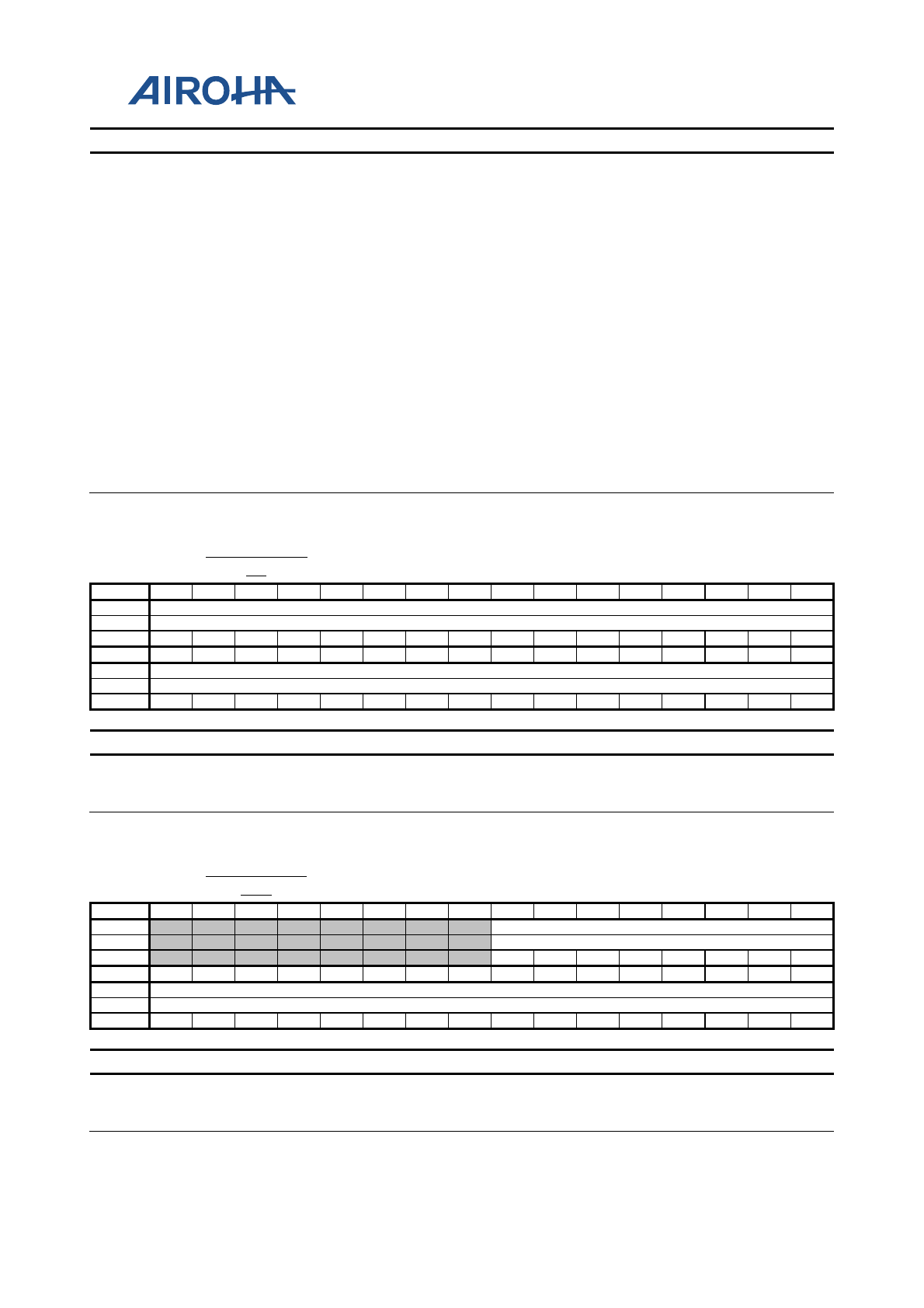
MT2523 Series Reference Manual
© 2015 - 2018 Airoha Technology Corp.
Page 202 of 692
This document contains information that is proprietary to Airoha Technology Corp. (“Airoha”) and/or its licensor(s).
Any unauthorized use, reproduction or disclosure of this document in whole or in part is strictly prohibited.
Bit(s) Name Description
interrupt will occur.
11 DMACHEN DMA channel enable monitor bit
10:9 BURST_MODE
2'b00: Burst Mode 0: Bursts of unspecified length
2'b01: Burst Mode 1: INCR4 or unspecified length
2'b10: Burst Mode 2: INCR8, INCR4 or unspecified length
2'b11: Burst Mode 3: INCR16, INCR8, INCR4 or unspecified length
8 BUSERR Bus error
7:4 ENDPNT Endpoint which DMA will transfer with
3 INTEN Enables interrupt
2 DMAMODE DMA mode
1 DMADIR
Direction
0: DMA write (Rx endpoint)
1: DMA read (Tx endpoint)
0 DMAEN
Enables DMA
The bit will be cleared when the DMA transfer is completed. Programmers
should not disable DMA_en before the transfer is completed. If programmers
disable dma_en during the transfer, DMA will not stop immediately until the
last bus transfer is completed.
A0900228 DMA_ADDR
_2 DMA Channel 2 Address Register 00000000
Bit
31
30
29
28
27
26
25
24
23
22
21
20
19
18
17
16
Name
DMA_ADDR_2[31:16]
Type
RW
Reset
0
0
0
0
0
0
0
0
0
0
0
0
0
0
0
0
Bit
15
14
13
12
11
10
9
8
7
6
5
4
3
2
1
0
Name
DMA_ADDR_2[15:0]
Type
RW
Reset
0
0
0
0
0
0
0
0
0
0
0
0
0
0
0
0
Bit(s) Name Description
31:0 DMA_ADDR_2
32-bit DMA start address
Updated (increased) by USB2.0 controller automatically when multiple packet
DMA (DMA Mode = 1) is used
A090022C DMA_COUN
T_2 DMA Channel 2 Byte Count Register 00000000
Bit
31
30
29
28
27
26
25
24
23
22
21
20
19
18
17
16
Name
DMA_COUNT_2[23:16]
Type
RW
Reset
0
0
0
0
0
0
0
0
Bit
15
14
13
12
11
10
9
8
7
6
5
4
3
2
1
0
Name
DMA_COUNT_2[15:0]
Type
RW
Reset
0
0
0
0
0
0
0
0
0
0
0
0
0
0
0
0
Bit(s) Name Description
23:0 DMA_COUNT_2
24-bit DMA transfer count with byte unit
Updated (decreased) by USB2.0 controller automatically when each packet is
transferred.
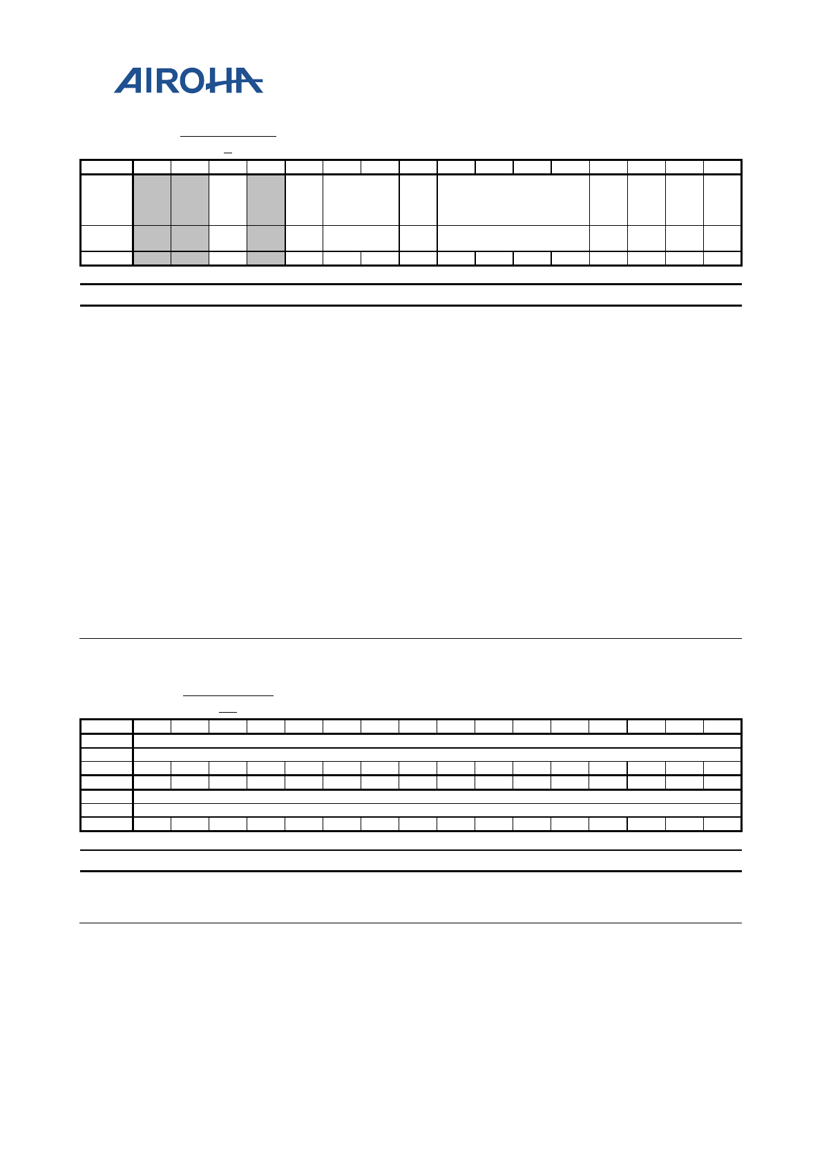
MT2523 Series Reference Manual
© 2015 - 2018 Airoha Technology Corp.
Page 203 of 692
This document contains information that is proprietary to Airoha Technology Corp. (“Airoha”) and/or its licensor(s).
Any unauthorized use, reproduction or disclosure of this document in whole or in part is strictly prohibited.
A0900234 DMA_CNTL_
3 DMA Channel 3 Control Register 0000
Bit
15
14
13
12
11
10
9
8
7
6
5
4
3
2
1
0
Name
DM
AA
BO
RT
DM
AC
HE
N
BURST_M
ODE
BU
SE
RR
ENDPNT INT
EN
DM
AM
OD
E
DM
ADI
R
DM
AE
N
Type A0 RU RW RU RW RW RW RW
Oth
er
Reset
0
0
0
0
0
0
0
0
0
0
0
0
0
Bit(s) Name Description
13 DMAABORT If SW needs to abort the current DMA transfer, set DMAABORT=1
and DMAEN=0. After the transfer is aborted completely, DMA
interrupt will occur.
11 DMACHEN DMA channel enable monitor bit
10:9 BURST_MODE
2'b00: Burst Mode 0: Bursts of unspecified length
2'b01: Burst Mode 1: INCR4 or unspecified length
2'b10: Burst Mode 2: INCR8, INCR4 or unspecified length
2'b11: Burst Mode 3: INCR16, INCR8, INCR4 or unspecified length
8 BUSERR Bus error
7:4 ENDPNT Endpoint which DMA will transfer with
3 INTEN Enables interrupt
2 DMAMODE DMA mode
1 DMADIR
Direction
0: DMA write (Rx endpoint)
1: DMA read (Tx endpoint)
0 DMAEN
Enables DMA
The bit will be cleared when the DMA transfer is completed. Programmers
should not disable DMA_en before the trnsfer is completed. If programmers
disable dma_en during the transfer, DMA will not stop immediately until the
last bus transfer is completed.
A0900238 DMA_ADDR
_3 DMA Channel 3 Address Register 00000000
Bit
31
30
29
28
27
26
25
24
23
22
21
20
19
18
17
16
Name
DMA_ADDR_3[31:16]
Type
RW
Reset
0
0
0
0
0
0
0
0
0
0
0
0
0
0
0
0
Bit
15
14
13
12
11
10
9
8
7
6
5
4
3
2
1
0
Name
DMA_ADDR_3[15:0]
Type
RW
Reset
0
0
0
0
0
0
0
0
0
0
0
0
0
0
0
0
Bit(s) Name Description
31:0 DMA_ADDR_3
32-bit DMA start address
Updated (increased) by USB2.0 controller automatically when multiple packet
DMA (DMA Mode = 1) is used
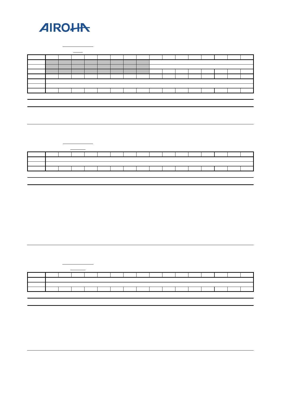
MT2523 Series Reference Manual
© 2015 - 2018 Airoha Technology Corp.
Page 204 of 692
This document contains information that is proprietary to Airoha Technology Corp. (“Airoha”) and/or its licensor(s).
Any unauthorized use, reproduction or disclosure of this document in whole or in part is strictly prohibited.
A090023C DMA_COUN
T_3 DMA Channel 3 Byte Count Register 00000000
Bit
31
30
29
28
27
26
25
24
23
22
21
20
19
18
17
16
Name
DMA_COUNT_3[23:16]
Type
RW
Reset
0
0
0
0
0
0
0
0
Bit
15
14
13
12
11
10
9
8
7
6
5
4
3
2
1
0
Name
DMA_COUNT_3[15:0]
Type
RW
Reset
0
0
0
0
0
0
0
0
0
0
0
0
0
0
0
0
Bit(s) Name Description
23:0 DMA_COUNT_3
24-bit DMA transfer count with byte unit
Updated (decreased) by USB2.0 controller automatically when each packet is
transferred.
A0900304 EP1RXPKTC
OUNT EP1 RxPktCount Register 0000
Bit
15
14
13
12
11
10
9
8
7
6
5
4
3
2
1
0
Name
EP1RXPKTCOUNT
Type
RW
Reset
0
0
0
0
0
0
0
0
0
0
0
0
0
0
0
0
Bit(s) Name Description
15:0 EP1RXPKTCOUNT
Sets up the number of packets of Rx Endpoint n size MaxP that are to
be transferred in a block transfer
Only used in host mode when AutoReq is set. It has no effect in peripheral mode
or when AutoReq is not set.
RqPktCount (host mode only) For each Rx Endpoint 1 - 15, the USB2.0
controller provides a 16-bit RqPktCount register. This read/write register is used
in host mode to specify the number of packets that are to be transferred in a
block transfer of one or more bulk packets of length MaxP to Rx Endpoint n. The
core uses the value recorded in this register to determine the number of requests
to issue where the AutoReq option (included in the RxCSR register) has been set.
Note: Multiple packets combined into a single bulk packet within the FIFO count
as one packet.
A090030
8
EP2RXPKTC
OUNT EP2 RxPktCount Register 0000
Bit
15
14
13
12
11
10
9
8
7
6
5
4
3
2
1
0
Name
EP2RXPKTCOUNT
Type
RW
Reset
0
0
0
0
0
0
0
0
0
0
0
0
0
0
0
0
Bit(s) Name Description
15:0 EP2RXPKTCOUNT
Sets up the number of packets of Rx Endpoint n size MaxP that are to
be transferred in a block transfer
Only used in host mode when AutoReq is set. It has no effect in peripheral mode
or when AutoReq is not set.
RqPktCount (host mode only) For each Rx Endpoint 1 - 15, the USB2.0
controller provides a 16-bit RqPktCount register. This read/write register is used
in host mode to specify the number of packets that are to be transferred in a
block transfer of one or more bulk packets of length MaxP to Rx Endpoint n. The
core uses the value recorded in this register to determine the number of requests
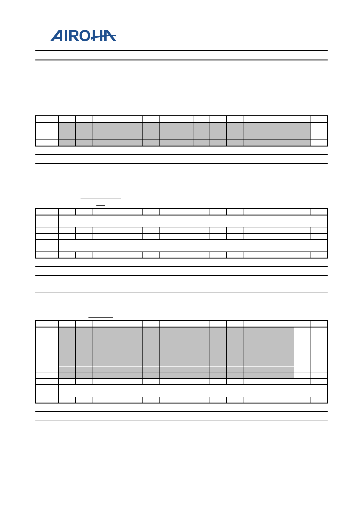
MT2523 Series Reference Manual
© 2015 - 2018 Airoha Technology Corp.
Page 205 of 692
This document contains information that is proprietary to Airoha Technology Corp. (“Airoha”) and/or its licensor(s).
Any unauthorized use, reproduction or disclosure of this document in whole or in part is strictly prohibited.
Bit(s) Name Description
to issue where the AutoReq option (included in the RxCSR register) has been set.
Note: Multiple packets combined into a single bulk packet within the FIFO count
as one packet.
A090060
4 TM1 Test Mode 1 Register 0000
Bit
15
14
13
12
11
10
9
8
7
6
5
4
3
2
1
0
Name
TM
1
Type
RW
Reset
0
Bit(s) Name Description
0 TM1 USB IP internal TM1.
A090060
8
HWVER_DA
TE HW Version Control Register 20121214
Bit
31
30
29
28
27
26
25
24
23
22
21
20
19
18
17
16
Name
HWVER_DATE[31:16]
Type
DC
Reset
0
0
1
0
0
0
0
0
0
0
0
1
0
0
1
0
Bit
15
14
13
12
11
10
9
8
7
6
5
4
3
2
1
0
Name
HWVER_DATE[15:0]
Type
DC
Reset
0
0
0
1
0
0
1
0
0
0
0
1
0
1
0
0
Bit(s) Name Description
31:0 HWVER_DATE Hardware version control register date format
32'hYYYYMMDD
A0900684 SRAMA SRAM Address Register 00000000
Bit
31
30
29
28
27
26
25
24
23
22
21
20
19
18
17
16
Name
EP
0_S
tart
Ad
_T
M6
_en
SR
AM
DB
G
Type
RW
RW
Reset
0
0
Bit
15
14
13
12
11
10
9
8
7
6
5
4
3
2
1
0
Name
SRAMA
Type
RW
Reset
0
0
0
0
0
0
0
0
0
0
0
0
0
0
0
0
Bit(s) Name Description
17 EP0_StartAd_TM6_
en
Software can enable this bit to change the EP0 FIFO start address for test mode
6 FIFO loopback test by DMA/PIO.
16 SRAMDBG
SRAM_DEBUG_MODE
Software can read the data in SRAM of USB core when this bit is enabled. The
related registers are SRAMA, SRAMD. After setting this bit to 1, software can set
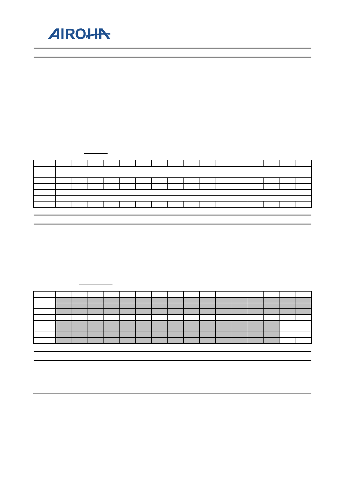
MT2523 Series Reference Manual
© 2015 - 2018 Airoha Technology Corp.
Page 206 of 692
This document contains information that is proprietary to Airoha Technology Corp. (“Airoha”) and/or its licensor(s).
Any unauthorized use, reproduction or disclosure of this document in whole or in part is strictly prohibited.
Bit(s) Name Description
up SRAMA (SRAM address) then read the data in register SRAMD (SRAM data).
This is for debugging mode only and should be disabled in normal operation.
1'b0: Software set this bit 0 to disable SRAM_DEBUG_MODE.
1'b1: Software set this bit 1 to enable SRAM_DEBUG_MODE.
15:0 SRAMA
SRAM_ADDRESS
The register is used for RISC to read data from USB SRAM. The unit is 4 bytes.
For example, to check 0x400 byte address, set this register to 0x100. This
register is only available when the register bit SRAM_DEBUG_MODE of register
SRAMDBG is set to 1. When SRAM ADDRESS is set, SRAM DATA will display
the data in the address SRAM ADDRESS in SRAM. It is for debugging mode
only.
A090068
8 SRAMD SRAM Data Register 00000000
Bit
31
30
29
28
27
26
25
24
23
22
21
20
19
18
17
16
Name
SRAMDATA[31:16]
Type
RU
Reset
0
0
0
0
0
0
0
0
0
0
0
0
0
0
0
0
Bit
15
14
13
12
11
10
9
8
7
6
5
4
3
2
1
0
Name
SRAMDATA[15:0]
Type
RU
Reset
0
0
0
0
0
0
0
0
0
0
0
0
0
0
0
0
Bit(s) Name Description
31:0 SRAMDATA
SRAM_DATA
The register is used for RISC to read data from USB SRAM. This register is only
available when the register bit SRAM_DEBUG_MODE of register SRAMDBG is
set to 1. When SRAM ADDRESS is set, SRAM DATA will display the data in the
address SRAM ADDRESS in SRAM. It is for debugging mode only.
A090069
0 RISC_SIZE RISC Size Register 00000002
Bit
31
30
29
28
27
26
25
24
23
22
21
20
19
18
17
16
Name
Type
Reset
Bit
15
14
13
12
11
10
9
8
7
6
5
4
3
2
1
0
Name
RISC_SIZ
E
Type
RW
Reset
1
0
Bit(s) Name Description
1:0 RISC_SIZE
Configures RISC wrapper access size
2'b00: 8-bit byte access
2'b01: 16-bit half word access
2'b10: 32-bit word access
2'b11: Reserved
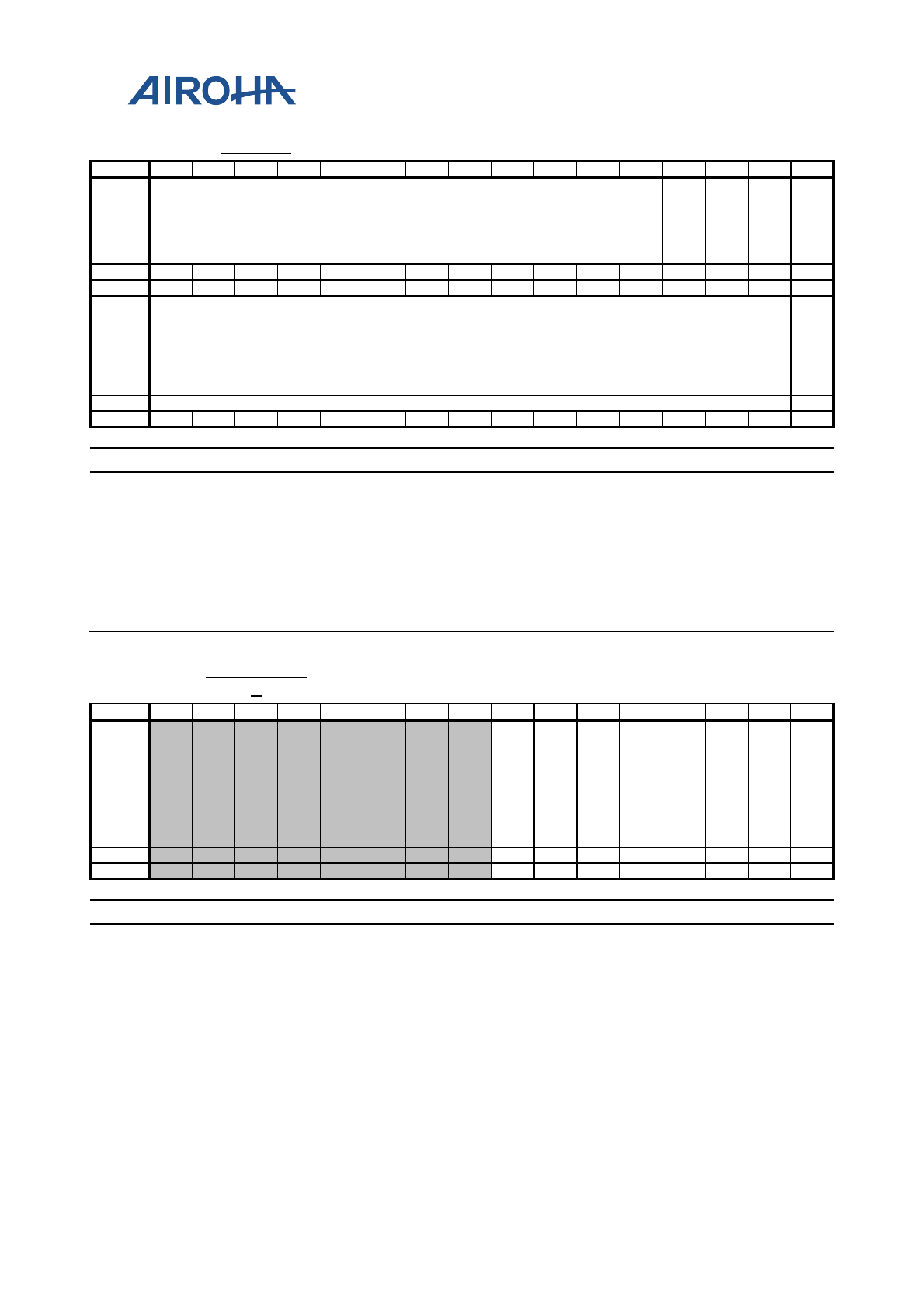
MT2523 Series Reference Manual
© 2015 - 2018 Airoha Technology Corp.
Page 207 of 692
This document contains information that is proprietary to Airoha Technology Corp. (“Airoha”) and/or its licensor(s).
Any unauthorized use, reproduction or disclosure of this document in whole or in part is strictly prohibited.
A0900700 RESREG Reserved Register FFFF0000
Bit
31
30
29
28
27
26
25
24
23
22
21
20
19
18
17
16
Name RESERVEDH
MA
C_
CG
_DI
S
US
B_
CG
_DI
S
DM
A_
CG
_DI
S
MC
U_
CG
_DI
S
Type
RW
RW
RW
RW
RW
Reset
1
1
1
1
1
1
1
1
1
1
1
1
1
1
1
1
Bit
15
14
13
12
11
10
9
8
7
6
5
4
3
2
1
0
Name RESERVEDL
HS
TP
WR
DW
N_
OP
T
Type
RW
RW
Reset
0
0
0
0
0
0
0
0
0
0
0
0
0
0
0
0
Bit(s) Name Description
19 MAC_CG_DIS Disables USB MAC clock gate to enhance dynamic power
18 USB_CG_DIS Disables USB clock gate
17 DMA_CG_DIS Disables DMA clock gate
16 MCU_CG_DIS Disables MCU clock gate
0 HSTPWRDWN_OPT
Host mode device connection detection option
0: Disable
1: Enable the detection of device connection when MAC clock is off and drive
powerdwn wakeup signal to wake up the system
A0900730 OTG20_CSR
L OTG20 Related Control Register L 00
Bit
15
14
13
12
11
10
9
8
7
6
5
4
3
2
1
0
Name
DIS
_H
SU
S
EN
_A
_H
FS_
WH
NP
DIS
_B
_W
TDI
S
EN
_H
HS
_S
US
P_
DIS
DIS
_C
HA
RG
E_
VB
US
EN
_H
SU
S_
RE
SU
ME
_IN
T
EN
_H
SU
S_
RE
SU
ME
OT
G2
0_
EN
Type
RW
RW
RW
RW
RW
RW
RW
RW
Reset
0
0
0
0
0
0
0
0
Bit(s) Name Description
7 DIS_HSUS
Disables host mode entering C_OPM_HSUS state before entering
suspend
Suggested: 1'b1
0: Host mode enters C_OPM_HSUS state before entering suspend.
1: Disable host mode entering C_OPM_HSUS state before entering suspend.
6 EN_A_HFS_WHNP
If this bit is enabled, FS idle of A device will transfer to HFS_HSUS
state first.
Suggested: 1'b1 in all modes (device/host/OTG)
0: FS idle of A device will not transfer to HFS_HSUS state first.
1: FS idle of A device will transfer to HFS_HSUS state first.
5 DIS_B_WTDIS
Disables B device entering C_OPM_B_WTDIS states before switching
to host mode
Suggested: 1'b1
MT2523 Series Reference Manual
© 2015 - 2018 Airoha Technology Corp.
Page 208 of 692
This document contains information that is proprietary to Airoha Technology Corp. (“Airoha”) and/or its licensor(s).
Any unauthorized use, reproduction or disclosure of this document in whole or in part is strictly prohibited.
Bit(s) Name Description
0: B device enters C_OPM_B_WTDIS states before switching to host mode.
1: B device does not enter C_OPM_B_WTDIS states before switching to host
mode.
4 EN_HHS_SUSP_DI
S
Enables host-hs-suspend entering OPM_FS_WTCON state first while
receiving disconnect signal
Suggested: 1'b1 in all modes (device/host/OTG)
0: The host mode enters fs_normal mode directly when the device receives the
disconnect signal as suspend state in all states.
1: The host mode enters OPM_FS_WTCON mode first when the device receives
the disconnect signal as suspend state in all states.
3 DIS_CHARGE_VBU
S
Disables B device charging VBUS function for OTG2.0 feature
0: B device charges VBUS when B device initiates the SRP protocol. This mode
makes compatible the OTG1.3 related SRP flow.
1: B device does not charge VBUS when B device initiates the SRP protocol. This
mode is for satisfying the OTG2.0 protocol.
2 EN_HSUS_RESUME
_INT
Enables hsus mode of host initializing resuming interrupt while
receiving resume K as waiting for HNP
Suggested: 1'b1 for OTG2.0 mode
0: Suspend mode of host does not initialize resuming interrupt as receiving
resume K while host is waiting for HNP protocol in OTG20 mode.
1: Suspend mode of host initializes resuming interrupt as receiving resume K
while host is waiting for HNP protocol in OTG20 mode.
1 EN_HSUS_RESUME
Enables hnpsus-mode of host entering host-normal mode as
receiving resume K while waiting for HNP
Suggested: 1'b0 when USB works in OTG20 mode
0: hnpsus-mode of host stays in hnpsus-mode as receiving resume K while
waiting for HNP.
1: hnpsus-mode of host enters host-normal mode as receiving resume K while
waiting for HNP.
0 OTG20_EN
Enables OTG 2.0 feature
0: Disable OTG2.0 feature; default OTG1.3 mode.
1: Enable USB OTG20 feature
A0900731 OTG20_CSR
H OTG20 Related Control Register H 00
Bit
15
14
13
12
11
10
9
8
7
6
5
4
3
2
1
0
Name
DIS
_A
UT
OR
ST
EN
_C
ON
_D
EB
_S
HO
RT
Type
RW
RW
Reset
0
0
Bit(s) Name Description
1 DIS_AUTORST
Informs whether HW sends bus reset automatically when B-device
changes to host with HNP
0: HW sends bus reset automatically when B-device changes to host with HNP.
1: HW does not send bus reset when B-device changes to host mode. SW should
set up the reset bit for sending bus reset. The bit is added for OTG20 compliance
test.
0 EN_CON_DEB_SHO
RT
Enable this bit to decrease A device connection denounce waiting
timing.
Suggested: 1'b1

MT2523 Series Reference Manual
© 2015 - 2018 Airoha Technology Corp.
Page 209 of 692
This document contains information that is proprietary to Airoha Technology Corp. (“Airoha”) and/or its licensor(s).
Any unauthorized use, reproduction or disclosure of this document in whole or in part is strictly prohibited.
Bit(s) Name Description
0: A device connection without denounce waiting timing
1: Decrease A device connection denounce waiting timing
MT2523 Series Reference Manual
© 2015 - 2018 Airoha Technology Corp.
Page 210 of 692
This document contains information that is proprietary to Airoha Technology Corp. (“Airoha”) and/or its licensor(s).
Any unauthorized use, reproduction or disclosure of this document in whole or in part is strictly prohibited.
12. General Purpose Timer
12.1. Introduction
The GPT includes five 32-bit timers and one 64-bit timer. Each timer has four operation modes, which are ONE-
SHOT, REPEAT, freerun with interrupt (FREERUN_I) and FREERUN, and can operate on one of the two clock
sources, RTC clock (32.768kHz) and system clock (13MHz).
GPT is an always on IP. When the system is in sleep or deep sleep mode, it still keeps the previous configuration
and keeps working. However, there is no 13MHz clock source in deep sleep mode; users need to switch clock
source to 32kHz, which sets GPT*_CLK[4] to 1’b1.
12.1.1. Features
The four operation modes for GPT are ONE-SHOT, REPEAT, FREERUN_I, and FREERUN. See Table 12-1 for the
functions of each mode.
Table 12-1. Operation mode of GPT
Mode Auto
Stop Interrupt Increases when
EN=1 and …
When COUNTn =
COMPAREn
Example: Compare is set to 2
*Bold means interrupt
ONE-SHOT Yes Yes
Stops when
COUNTn =
COMPAREn
EN is reset to 0. 0,1,2,2,2,2,2,2,2,2,2,2,…
REPEAT No Yes Count is reset to 0. 0,1,2,0,1,2,0,1,2,0,1,2…
FREERUN_I No Yes Reset to 0 when
overflow 0,1,2,3,4,5,6,7,8,9,10,…
FREERUN No No Reset to 0 when
overflow 0,1,2,3,4,5,6,7,8,9,10,…
Each timer can be programmed to select the clock source, RTC clock (32.76kHz) or system clock (13MHz). After the
clock source is determined, the division ratio of the selected clock can be programmed. The division ratio can be
fine-granulated as 1, 2, 3, 4 to 13 and coarse-granulated as 16, 32 and 64.
Table 12-2. Timer feature
Timer Resolution Interrupt Prescalor Mode Clock
GPT1– GPT5 32-bit Yes 1-13, 16, 32, 64 ONE-SHOT/ REPEAT /
FREERUN_I/FREERUN 32KHz/ 13MHz
GPT6 64-bit Yes 1-13, 16, 32, 64 ONE-SHOT/ REPEAT /
FREERUN_I/FREERUN 32KHz/ 13MHz
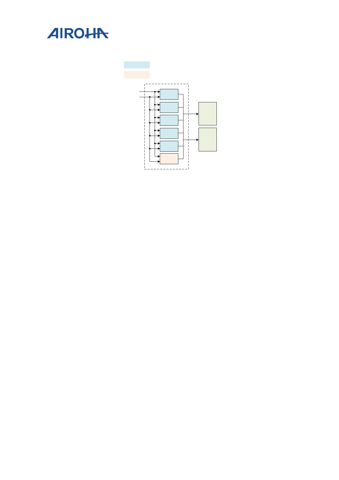
MT2523 Series Reference Manual
© 2015 - 2018 Airoha Technology Corp.
Page 211 of 692
This document contains information that is proprietary to Airoha Technology Corp. (“Airoha”) and/or its licensor(s).
Any unauthorized use, reproduction or disclosure of this document in whole or in part is strictly prohibited.
12.1.2. Block Diagram
GPT1
GPT2
GPT3
GPT4
GPT5
GPT6
32kHz
13MHz
32bit
64 bit
Sleep
Control
MCU
IRQ
APXGPT
Figure 12-1. Block diagram of GPT
12.1.3. Programming Guide
To program and use GPT, note that:
• The counter value can be read any time even when the clock source is RTC clock.
• The compare value can be programmed any time.
Sequence flow:
• Turn off GPT clock.
• Set up GPT clock source and frequency divider.
• Turn on GPT clock.
• Enable/disable IRQ and IRQ mask.
• Set up compare value.
• Set up GPT mode.
• Enable GPT.
For the GPT6 64-bit timer, the read operation of the 64-bit timer value will be separated into two APB reads since
an APB read is of 32-bit width. To perform the read of 64-bit timer value, the lower word should be read first then
the higher word. The read operation of lower word freezes the “read value” of the higher word but does not freeze
the timer counting. This ensures that the separated read operation acquires the correct timer value. If both two
tasks, e.g. task A and task B, perform the read of 64-bit timer value, task A first reads the lower word of the value,
and task B reads the lower word of the value. Either of the tasks reads the higher word of timer value, and the
obtained value will be the time when task B reads the lower word of timer value. To guarantee task A reads the
correct 64-bit timer value, some software procedures are required, e.g. the semaphore.
MT2523 Series Reference Manual
© 2015 - 2018 Airoha Technology Corp.
Page 212 of 692
This document contains information that is proprietary to Airoha Technology Corp. (“Airoha”) and/or its licensor(s).
Any unauthorized use, reproduction or disclosure of this document in whole or in part is strictly prohibited.
12.2. Register Definition
Module name: GPT Base address: (+A2140000h)
Address
Name
Width
Register Function
A2140000 GPT_IRQSTA 32 GPT IRQ Status
Shows the interrupt status of each GPT
A2140004 GPT_IRQMASK
0 32
ARM IRQMASK Register
Masks specific GPT's interrupt to ARM
A2140008 GPT_IRQMASK1 32
CM4 IRQMASK Register
Masks specific GPT's interrupt to CM4
A2140010 GPT1_CON 32
GPT1 Control
The General control for GPT1
A2140014 GPT1_CLK 32 GPT1 Clock Setting
Controls the clock source and division ratio of GPT clock
A2140018 GPT1_IRQ_EN 32
GPT IRQ Enabling
Controls the enabling/disabling of GPT interrupt
A214001C GPT1_IRQ_STA 32 GPT IRQ Status
Shows the interrupt status of GPT1
A2140020 GPT1_IRQ_ACK 32
GPT IRQ Acknowledgement
Acknowledges the GPT interrupt
A2140024 GPT1_COUNT 32
GPT1 Counter
Timer count of GPT1
A2140028 GPT1_COMPAR
E 32
GPT1 Compare Value
Compare value for GPT1
A2140040 GPT2_CON 32 GPT2 Control
General control for GPT2
A2140044 GPT2_CLK 32
GPT2 Clock Setting
Controls the clock source and division ratio of GPT clock
A2140048 GPT2_IRQ_EN 32 GPT IRQ Enabling
Controls the enabling/disabling of GPT interrupt
A214004C GPT2_IRQ_STA 32
GPT IRQ Status
Shows the interrupt status of GPT1
A2140050 GPT2_IRQ_ACK 32
GPT IRQ Acknowledgement
Acknowledges the GPT interrupt
A2140054 GPT2_COUNT 32
GPT2 Counter
Timer count of GPT2
A2140058 GPT2_COMPAR
E 32 GPT2 Compare Value
Compare value for GPT2
A2140070 GPT3_CON 32
GPT3 Control
General control for GPT3
A2140074 GPT3_CLK 32 GPT3 Clock Setting
Controls the clock source and division ratio of GPT clock
A2140078 GPT3_IRQ_EN 32
GPT IRQ Enabling
Controls the enabling/disabling of GPT interrupt
A214007C GPT3_IRQ_STA 32
GPT IRQ Status
Shows the interrupt status of GPT1
A2140080 GPT3_IRQ_ACK 32
GPT IRQ Acknowledgement
Acknowledges the GPT interrupt
A2140084 GPT3_COUNT 32 GPT3 Counter
Timer count of GPT3
A2140088
GPT3_COMPAR
E 32 GPT3 Compare Value
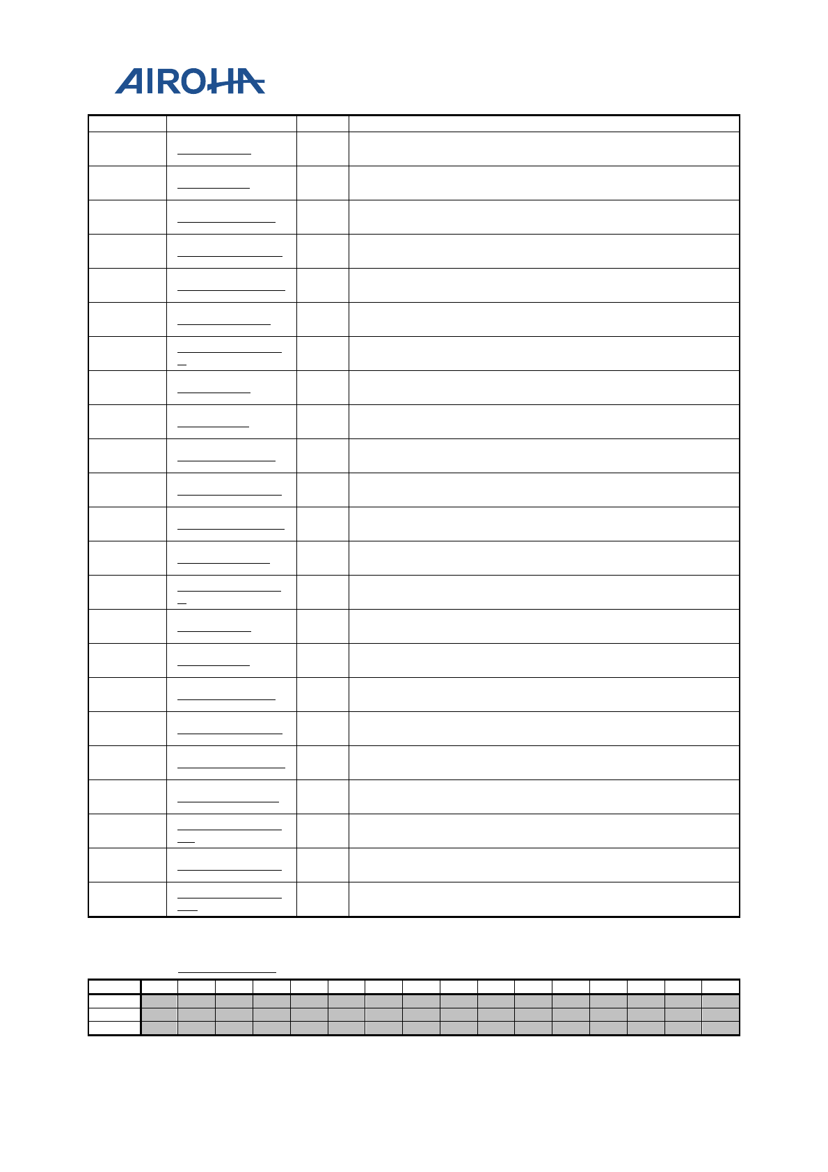
MT2523 Series Reference Manual
© 2015 - 2018 Airoha Technology Corp.
Page 213 of 692
This document contains information that is proprietary to Airoha Technology Corp. (“Airoha”) and/or its licensor(s).
Any unauthorized use, reproduction or disclosure of this document in whole or in part is strictly prohibited.
Compare value for GPT3
A21400A0 GPT4_CON 32 GPT4 Control
General control for GPT4
A21400A4 GPT4_CLK 32
GPT4 Clock Setting
Controls the clock source and division ratio of GPT clock
A21400A8 GPT4_IRQ_EN 32 GPT IRQ Enabling
Controls the enabling/disabling of GPT interrupt
A21400AC GPT4_IRQ_STA 32
GPT IRQ Status
Shows the interrupt status of GPT1
A21400B0 GPT4_IRQ_ACK 32 GPT IRQ Acknowledgement
Acknowledges the GPT interrupt
A21400B4 GPT4_COUNT 32
GPT4 Counter
Timer count of GPT4
A21400B8 GPT4_COMPAR
E 32 GPT4 Compare Value
Compare value for GPT4
A21400D0 GPT5_CON 32
GPT5 Control
General control for GPT5
A21400D4 GPT5_CLK 32 GPT5 Clock Setting
Controls the clock source and division ratio of GPT clock
A21400D8 GPT5_IRQ_EN 32
GPT IRQ Enabling
Controls the enabling/disabling of GPT interrupt
A21400DC GPT5_IRQ_STA 32 GPT IRQ Status
Shows the interrupt status of GPT1
A21400E0 GPT5_IRQ_ACK 32
GPT IRQ Acknowledgement
Acknowledges the GPT interrupt
A21400E4 GPT5_COUNT 32 GPT5 Counter
Timer count of GPT5
A21400E8 GPT5_COMPAR
E 32
GPT5 Compare Value
Compare value for GPT5
A2140100 GPT6_CON 32 GPT6 Control
General control for GPT6
A2140104 GPT6_CLK 32
GPT6 Clock Setting
Controls the clock source and division ratio of GPT clock
A2140108 GPT6_IRQ_EN 32 GPT IRQ Enabling
Controls the enabling/disabling of GPT interrupt
A214010C GPT6_IRQ_STA 32
GPT IRQ Status
Shows the interrupt status of GPT1
A2140110 GPT6_IRQ_ACK 32 GPT IRQ Acknowledgement
Acknowledges the GPT interrupt
A2140114 GPT6_COUNTL 32
GPT6 Counter L
Lower word timer count for GPT6
A2140118 GPT6_COMPAR
EL 32 GPT6 Compare Value L
Lower word compare value for GPT6
A214011C GPT6_COUNTH 32
GPT6 Counter L
Higher word timer count for GPT6
A2140120 GPT6_COMPAR
EH 32 GPT6 Compare Value H
Higher word compare value for GPT6
A2140000
GPT_IRQSTA
GPT IRQ Status
00000000
Bit
31
30
29
28
27
26
25
24
23
22
21
20
19
18
17
16
Name
Type
Reset
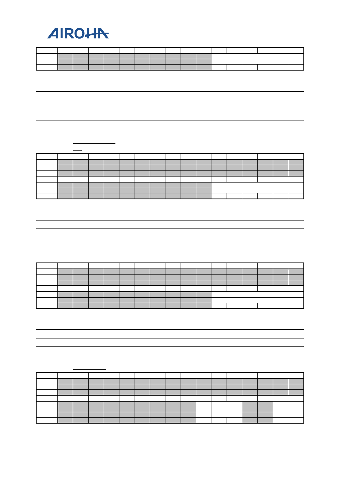
MT2523 Series Reference Manual
© 2015 - 2018 Airoha Technology Corp.
Page 214 of 692
This document contains information that is proprietary to Airoha Technology Corp. (“Airoha”) and/or its licensor(s).
Any unauthorized use, reproduction or disclosure of this document in whole or in part is strictly prohibited.
Bit
15
14
13
12
11
10
9
8
7
6
5
4
3
2
1
0
Name
IRQSTA
Type
RO
Reset
0
0
0
0
0
0
Overview
Shows the interrupt status of each GPT
Bit(s)
Name
Description
5:0
IRQSTA
Interrupt status of each GPT
0: No associated interrupt is generated
1: Associated interrupt is pending and waiting for service.
A2140004
GPT_IRQMAS
K0
ARM IRQMASK Register
0000003F
Bit
31
30
29
28
27
26
25
24
23
22
21
20
19
18
17
16
Name
Type
Reset
Bit
15
14
13
12
11
10
9
8
7
6
5
4
3
2
1
0
Name
IRQ_MSK0
Type
RW
Reset
1
1
1
1
1
1
Overview
Masks specific GPT's interrupt to ARM
Bit(s)
Name
Description
5:0
IRQ_MSK0
By default, ARM will not receive GPT3's interrupt.
A2140008
GPT_IRQMAS
K1
CM4 IRQMASK Register
0000003F
Bit
31
30
29
28
27
26
25
24
23
22
21
20
19
18
17
16
Name
Type
Reset
Bit
15
14
13
12
11
10
9
8
7
6
5
4
3
2
1
0
Name
IRQ_MSK1
Type
RW
Reset
1
1
1
1
1
1
Overview
Masks specific GPT's interrupt to CM4
Bit(s)
Name
Description
5:0
IRQ_MSK1
By default, CM4 will only receive GPT3's interrupt.
A2140010
GPT1_CON
GPT1 Control
00000000
Bit
31
30
29
28
27
26
25
24
23
22
21
20
19
18
17
16
Name
Type
Reset
Bit
15
14
13
12
11
10
9
8
7
6
5
4
3
2
1
0
Name
SW_C
G1
MODE1
CLR1 EN1
Type
RW
RW
WO
RW
Reset
0
0
0
0
0
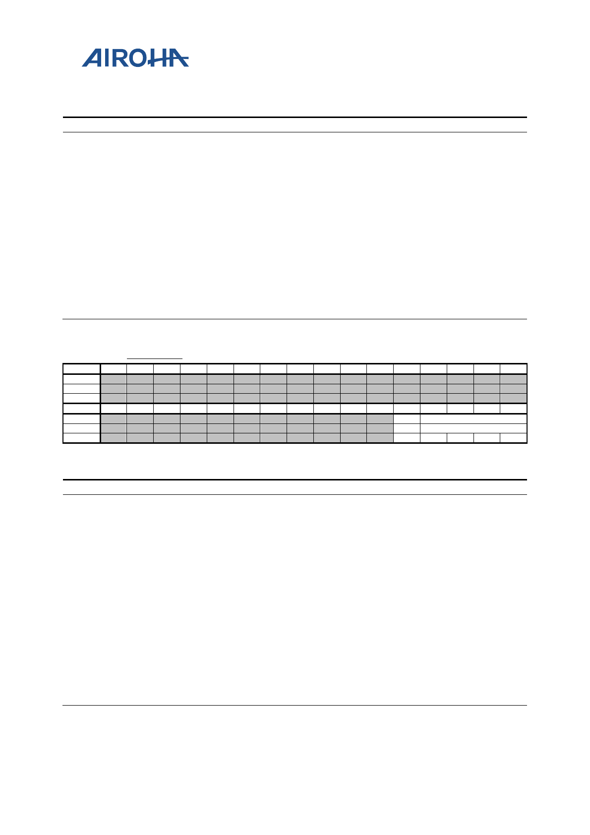
MT2523 Series Reference Manual
© 2015 - 2018 Airoha Technology Corp.
Page 215 of 692
This document contains information that is proprietary to Airoha Technology Corp. (“Airoha”) and/or its licensor(s).
Any unauthorized use, reproduction or disclosure of this document in whole or in part is strictly prohibited.
Overview
The General control for GPT1
Bit(s)
Name
Description
6
SW_CG1
Stop GPT1's clock if this bit is enabled.
0: Disable
1: Enable
5:4
MODE1
Operation mode of GPT1
00: ONE-SHOT mode
01: REPEAT mode
10: FREERUN_I mode
11: FREERUN mode
1
CLR1
Clears the counter of GPT1 to 0
0: No effect
1: Clear
It takes 2~3 T GPT1_CK for CLR1 to clear the counter of GPT1.
0
EN1
Enables GPT1
0: Disable
1: Enable
It takes 2~3 T GPT1_CK for EN1 to enable/disable GPT1.
A2140014
GPT1_CLK
GPT1 Clock Setting
00000000
Bit
31
30
29
28
27
26
25
24
23
22
21
20
19
18
17
16
Name
Type
Reset
Bit
15
14
13
12
11
10
9
8
7
6
5
4
3
2
1
0
Name
CLK1
CLKDIV1
Type
RW
RW
Reset
0
0
0
0
0
Overview
Controls the clock source and division ratio of GPT clock
Bit(s)
Name
Description
4
CLK1
Sets up clock source of GPT1
0: System clock (13MHz)
1: RTC clock (32kHz)
3:0
CLKDIV1
Setting of GPT1 input clock frequency divider
0000: Clock source divided by 1
0001: Clock source divided by 2
0010: Clock source divided by 3
0011: Clock source divided by 4
0100: Clock source divided by 5
0101: Clock source divided by 6
0110: Clock source divided by 7
0111: Clock source divided by 8
1000: Clock source divided by 9
1001: Clock source divided by 10
1010: Clock source divided by 11
1011: Clock source divided by 12
1100: Clock source divided by 13
1101: Clock source divided by 16
1110: Clock source divided by 32
1111: Clock source divided by 64
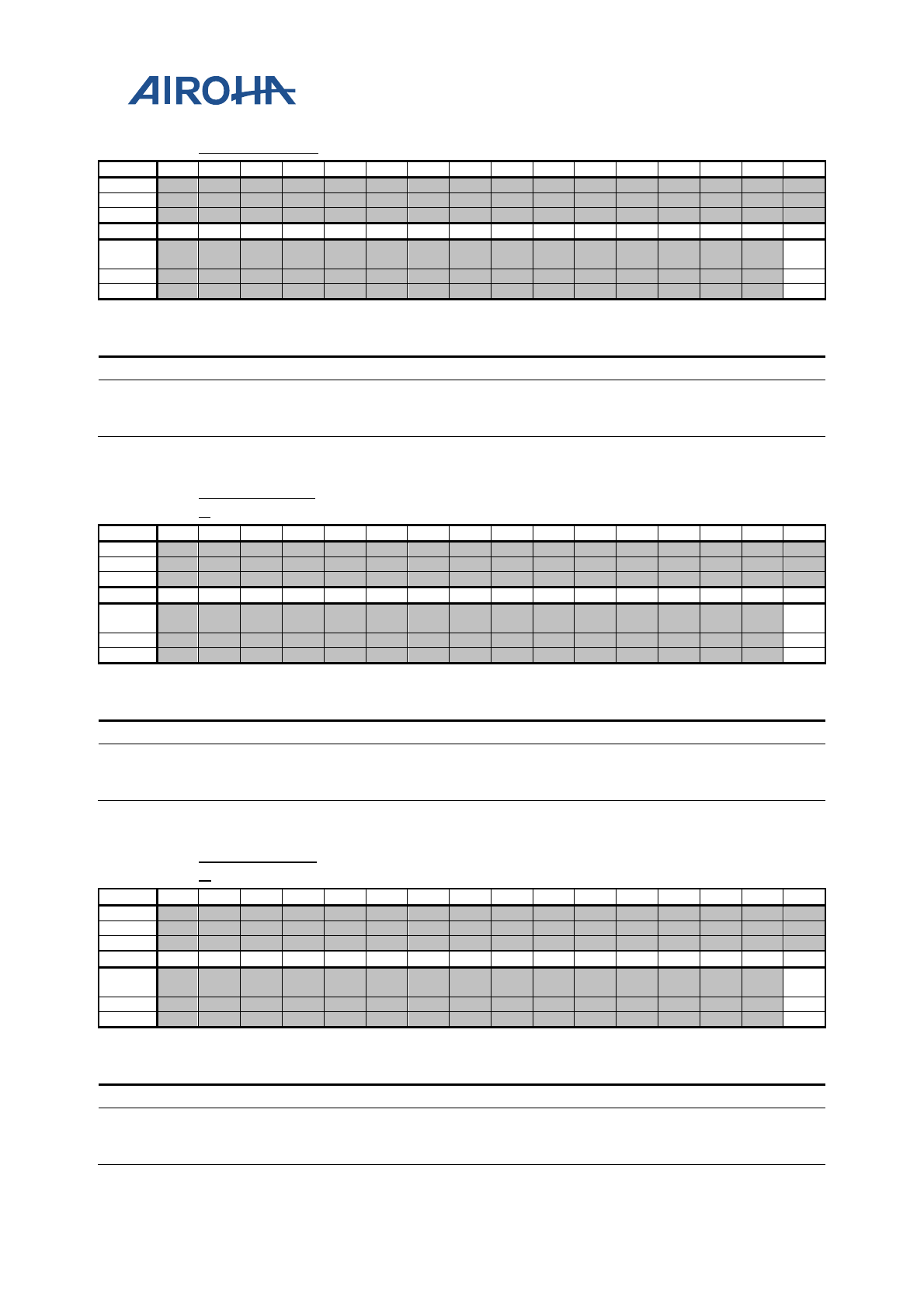
MT2523 Series Reference Manual
© 2015 - 2018 Airoha Technology Corp.
Page 216 of 692
This document contains information that is proprietary to Airoha Technology Corp. (“Airoha”) and/or its licensor(s).
Any unauthorized use, reproduction or disclosure of this document in whole or in part is strictly prohibited.
A2140018
GPT1_IRQ_EN
GPT IRQ
Enabling
00000000
Bit
31
30
29
28
27
26
25
24
23
22
21
20
19
18
17
16
Name
Type
Reset
Bit
15
14
13
12
11
10
9
8
7
6
5
4
3
2
1
0
Name
IRQE
N
Type
RW
Reset
0
Overview
Controls the enabling/disabling of GPT interrupt
Bit(s)
Name
Description
0
IRQEN
Enables interrupt of GPT1
0: Disable interrupt of GPT1
1: Enable interrupt of GPT1
A214001C
GPT1_IRQ_ST
A
GPT IRQ
Status
00000000
Bit
31
30
29
28
27
26
25
24
23
22
21
20
19
18
17
16
Name
Type
Reset
Bit
15
14
13
12
11
10
9
8
7
6
5
4
3
2
1
0
Name
IRQS
TA
Type
RO
Reset
0
Overview
Shows the interrupt status of GPT1
Bit(s)
Name
Description
0
IRQSTA
Interrupt status of GPT1
0: No interrupt is generated from GPT1
1: GPT1's interrupt is pending and waiting for service.
A2140020
GPT1_IRQ_AC
K
GPT IRQ Acknowledgement
00000000
Bit
31
30
29
28
27
26
25
24
23
22
21
20
19
18
17
16
Name
Type
Reset
Bit
15
14
13
12
11
10
9
8
7
6
5
4
3
2
1
0
Name
IRQA
CK
Type
WO
Reset
0
Overview
Acknowledges the GPT interrupt
Bit(s)
Name
Description
0
IRQACK
Interrupt acknowledgement for GPT1
0: No effect
1: Associated interrupt request is acknowledged and should be relinquished.
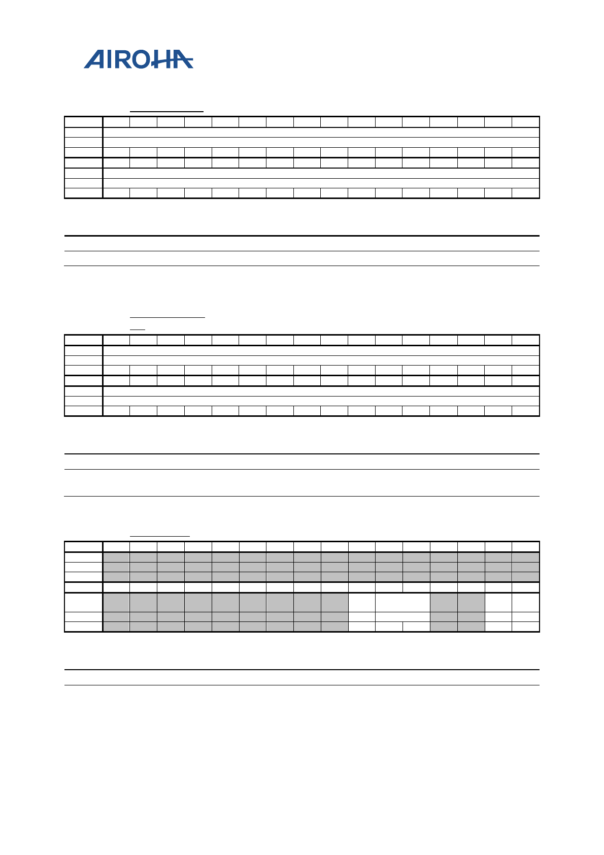
MT2523 Series Reference Manual
© 2015 - 2018 Airoha Technology Corp.
Page 217 of 692
This document contains information that is proprietary to Airoha Technology Corp. (“Airoha”) and/or its licensor(s).
Any unauthorized use, reproduction or disclosure of this document in whole or in part is strictly prohibited.
A2140024
GPT1_COUNT
GPT1 Counter
00000000
Bit
31
30
29
28
27
26
25
24
23
22
21
20
19
18
17
16
Name
COUNTER1[31:16]
Type
RO
Reset
0
0
0
0
0
0
0
0
0
0
0
0
0
0
0
0
Bit
15
14
13
12
11
10
9
8
7
6
5
4
3
2
1
0
Name
COUNTER1[15:0]
Type
RO
Reset
0
0
0
0
0
0
0
0
0
0
0
0
0
0
0
0
Overview
Timer count of GPT1
Bit(s)
Name
Description
31:0
COUNTER1
Timer counter of GPT1
A2140028
GPT1_COMPA
RE
GPT1 Compare Value
00000000
Bit
31
30
29
28
27
26
25
24
23
22
21
20
19
18
17
16
Name
COMPARE1[31:16]
Type
RW
Reset
0
0
0
0
0
0
0
0
0
0
0
0
0
0
0
0
Bit
15
14
13
12
11
10
9
8
7
6
5
4
3
2
1
0
Name
COMPARE1[15:0]
Type
RW
Reset
0
0
0
0
0
0
0
0
0
0
0
0
0
0
0
0
Overview
Compare value for GPT1
Bit(s)
Name
Description
31:0
COMPARE1
Compare value of GPT1
Write new compare value will also clear the counter of GPT1.
A2140040
GPT2_CON
GPT2 Control
00000000
Bit
31
30
29
28
27
26
25
24
23
22
21
20
19
18
17
16
Name
Type
Reset
Bit
15
14
13
12
11
10
9
8
7
6
5
4
3
2
1
0
Name
SW_C
G2
MODE2
CLR2
EN2
Type
RW
RW
WO
RW
Reset
0
0
0
0
0
Overview
General control for GPT2
Bit(s)
Name
Description
6
SW_CG2
Stop GPT2's clock if this bit is enabled.
0: Disable
1: Enable
5:4
MODE2
Operation mode of GPT2
00: ONE-SHOT mode
01: REPEAT mode
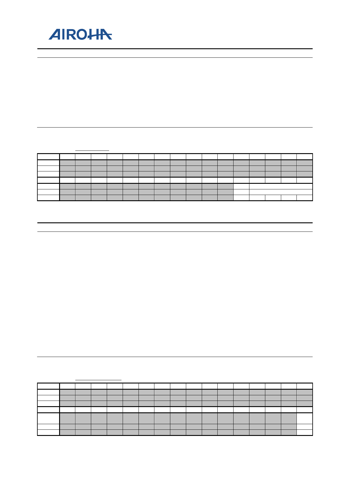
MT2523 Series Reference Manual
© 2015 - 2018 Airoha Technology Corp.
Page 218 of 692
This document contains information that is proprietary to Airoha Technology Corp. (“Airoha”) and/or its licensor(s).
Any unauthorized use, reproduction or disclosure of this document in whole or in part is strictly prohibited.
Bit(s)
Name
Description
10: FREERUN_I mode
11: FREERUN mode
1
CLR2
Clears the counter of GPT2 to 0
0: No effect
1: Clear
It takes 2~3 T GPT2_CK for CLR2 to clear the counter of GPT2.
0
EN2
Enables GPT2
0: Disable
1: Enable
It takes 2~3 T GPT2_CK for EN2 to enable/disable GPT2.
A2140044
GPT2_CLK
GPT2 Clock Setting
00000000
Bit
31
30
29
28
27
26
25
24
23
22
21
20
19
18
17
16
Name
Type
Reset
Bit
15
14
13
12
11
10
9
8
7
6
5
4
3
2
1
0
Name
CLK2
CLKDIV2
Type
RW
RW
Reset
0
0
0
0
0
Overview
Controls the clock source and division ratio of GPT clock
Bit(s)
Name
Description
4
CLK2
Sets up clock source of GPT2
0: System clock (13MHz)
1: RTC clock (32kHz)
3:0
CLKDIV2
Setting of GPT2 input clock frequency divider
0000: Clock source divided by 1
0001: Clock source divided by 2
0010: Clock source divided by 3
0011: Clock source divided by 4
0100: Clock source divided by 5
0101: Clock source divided by 6
0110: Clock source divided by 7
0111: Clock source divided by 8
1000: Clock source divided by 9
1001: Clock source divided by 10
1010: Clock source divided by 11
1011: Clock source divided by 12
1100: Clock source divided by 13
1101: Clock source divided by 16
1110: Clock source divided by 32
1111: Clock source divided by 64
A2140048
GPT2_IRQ_EN
GPT IRQ Enabling
00000000
Bit
31
30
29
28
27
26
25
24
23
22
21
20
19
18
17
16
Name
Type
Reset
Bit
15
14
13
12
11
10
9
8
7
6
5
4
3
2
1
0
Name
IRQE
N
Type
RW
Reset
0
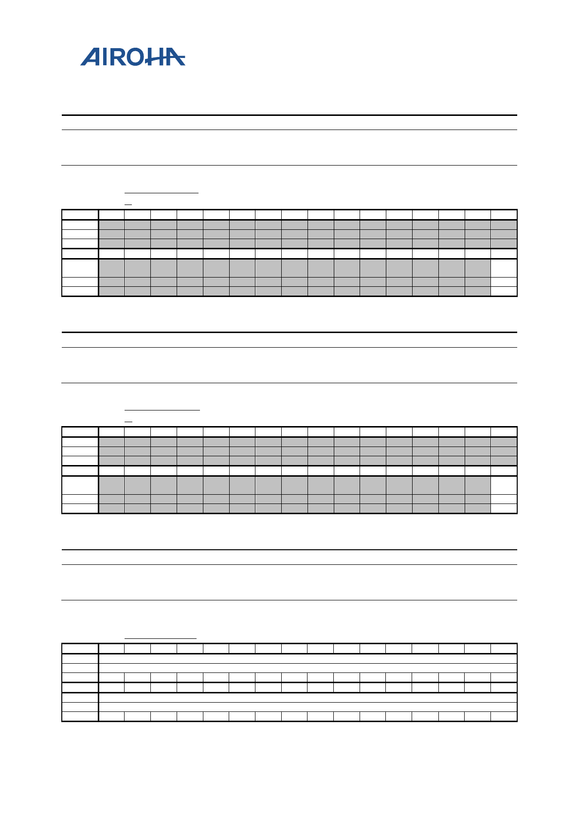
MT2523 Series Reference Manual
© 2015 - 2018 Airoha Technology Corp.
Page 219 of 692
This document contains information that is proprietary to Airoha Technology Corp. (“Airoha”) and/or its licensor(s).
Any unauthorized use, reproduction or disclosure of this document in whole or in part is strictly prohibited.
Overview
Controls the enabling/disabling of GPT interrupt
Bit(s)
Name
Description
0
IRQEN
Enables interrupt of GPT2
0: Disable interrupt of GPT2
1: Enable interrupt of GPT2
A214004C
GPT2_IRQ_ST
A
GPT IRQ Status
00000000
Bit
31
30
29
28
27
26
25
24
23
22
21
20
19
18
17
16
Name
Type
Reset
Bit
15
14
13
12
11
10
9
8
7
6
5
4
3
2
1
0
Name
IRQS
TA
Type
RO
Reset
0
Overview
Shows the interrupt status of GPT1
Bit(s)
Name
Description
0
IRQSTA
Interrupt status of GPT2
0: No interrupt is generated from GPT2
1: GPT2's interrupt is pending and waiting for service.
A2140050
GPT2_IRQ_AC
K
GPT IRQ Acknowledgement
00000000
Bit
31
30
29
28
27
26
25
24
23
22
21
20
19
18
17
16
Name
Type
Reset
Bit
15
14
13
12
11
10
9
8
7
6
5
4
3
2
1
0
Name
IRQA
CK
Type
WO
Reset
0
Overview
Acknowledges the GPT interrupt
Bit(s)
Name
Description
0
IRQACK
Interrupt acknowledgement for GPT2
0: No effect
1: Associated interrupt request is acknowledged and should be relinquished.
A2140054
GPT2_COUNT
GPT2 Counter
00000000
Bit
31
30
29
28
27
26
25
24
23
22
21
20
19
18
17
16
Name
COUNTER2[31:16]
Type
RO
Reset
0
0
0
0
0
0
0
0
0
0
0
0
0
0
0
0
Bit
15
14
13
12
11
10
9
8
7
6
5
4
3
2
1
0
Name
COUNTER2[15:0]
Type
RO
Reset
0
0
0
0
0
0
0
0
0
0
0
0
0
0
0
0
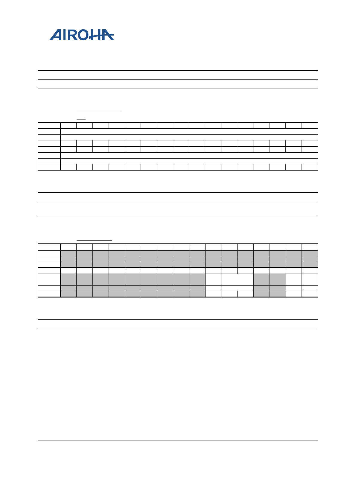
MT2523 Series Reference Manual
© 2015 - 2018 Airoha Technology Corp.
Page 220 of 692
This document contains information that is proprietary to Airoha Technology Corp. (“Airoha”) and/or its licensor(s).
Any unauthorized use, reproduction or disclosure of this document in whole or in part is strictly prohibited.
Overview
Timer count of GPT2
Bit(s)
Name
Description
31:0
COUNTER2
Timer counter of GPT2
A2140058
GPT2_COMPA
RE
GPT2 Compare Value
00000000
Bit
31
30
29
28
27
26
25
24
23
22
21
20
19
18
17
16
Name
COMPARE2[31:16]
Type
RW
Reset
0
0
0
0
0
0
0
0
0
0
0
0
0
0
0
0
Bit
15
14
13
12
11
10
9
8
7
6
5
4
3
2
1
0
Name
COMPARE2[15:0]
Type
RW
Reset
0
0
0
0
0
0
0
0
0
0
0
0
0
0
0
0
Overview
Compare value for GPT2
Bit(s)
Name
Description
31:0
COMPARE2
Compare value of GPT2
Write new compare value will also clear the counter of GPT2.
A2140070
GPT3_CON
GPT3 Control
00000000
Bit
31
30
29
28
27
26
25
24
23
22
21
20
19
18
17
16
Name
Type
Reset
Bit
15
14
13
12
11
10
9
8
7
6
5
4
3
2
1
0
Name
SW_C
G3
MODE3
CLR3
EN3
Type
RW
RW
WO
RW
Reset
0
0
0
0
0
Overview
General control for GPT3
Bit(s)
Name
Description
6
SW_CG3
Stop GPT3's clock if this bit is enabled.
0: Disable
1: Enable
5:4
MODE3
Operation mode of GPT3
00: ONE-SHOT mode
01: REPEAT mode
10: FREERUN_I mode
11: FREERUN mode
1
CLR3
Clears the counter of GPT3 to 0
0: No effect
1: Clear
It takes 2~3 T GPT3_CK for CLR3 to clear the counter of GPT3.
0
EN3
Enables GPT3
0: Disable
1: Enable
It takes 2~3 T GPT3_CK for EN3 to enable/disable GPT3.
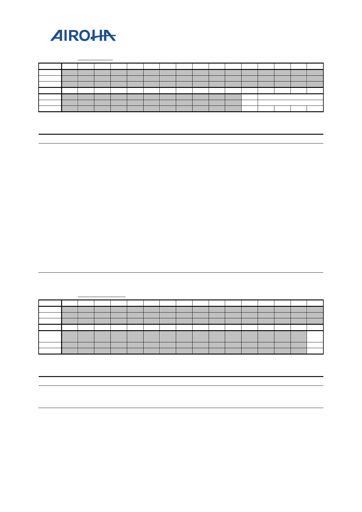
MT2523 Series Reference Manual
© 2015 - 2018 Airoha Technology Corp.
Page 221 of 692
This document contains information that is proprietary to Airoha Technology Corp. (“Airoha”) and/or its licensor(s).
Any unauthorized use, reproduction or disclosure of this document in whole or in part is strictly prohibited.
A2140074
GPT3_CLK
GPT3 Clock Setting
00000000
Bit
31
30
29
28
27
26
25
24
23
22
21
20
19
18
17
16
Name
Type
Reset
Bit
15
14
13
12
11
10
9
8
7
6
5
4
3
2
1
0
Name
CLK3
CLKDIV3
Type
RW
RW
Reset
0
0
0
0
0
Overview
Controls the clock source and division ratio of GPT clock
Bit(s)
Name
Description
4
CLK3
Sets up clock source of GPT3
0: System clock (13MHz)
1: RTC clock (32kHz)
3:0
CLKDIV3
Setting of GPT3 input clock frequency divider
0000: Clock source divided by 1
0001: Clock source divided by 2
0010: Clock source divided by 3
0011: Clock source divided by 4
0100: Clock source divided by 5
0101: Clock source divided by 6
0110: Clock source divided by 7
0111: Clock source divided by 8
1000: Clock source divided by 9
1001: Clock source divided by 10
1010: Clock source divided by 11
1011: Clock source divided by 12
1100: Clock source divided by 13
1101: Clock source divided by 16
1110: Clock source divided by 32
1111: Clock source divided by 64
A2140078
GPT3_IRQ_EN
GPT IRQ Enabling
00000000
Bit
31
30
29
28
27
26
25
24
23
22
21
20
19
18
17
16
Name
Type
Reset
Bit
15
14
13
12
11
10
9
8
7
6
5
4
3
2
1
0
Name
IRQE
N
Type
RW
Reset
0
Overview
Controls the enabling/disabling of GPT interrupt
Bit(s)
Name
Description
0
IRQEN
Enables interrupt of GPT3
0: Disable interrupt of GPT3
1: Enable interrupt of GPT3
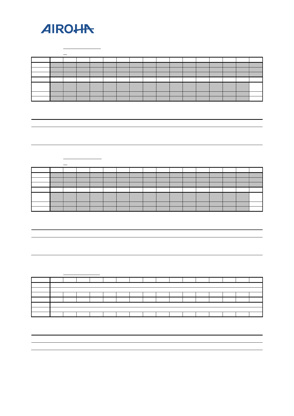
MT2523 Series Reference Manual
© 2015 - 2018 Airoha Technology Corp.
Page 222 of 692
This document contains information that is proprietary to Airoha Technology Corp. (“Airoha”) and/or its licensor(s).
Any unauthorized use, reproduction or disclosure of this document in whole or in part is strictly prohibited.
A214007C
GPT3_IRQ_ST
A
GPT IRQ Status
00000000
Bit
31
30
29
28
27
26
25
24
23
22
21
20
19
18
17
16
Name
Type
Reset
Bit
15
14
13
12
11
10
9
8
7
6
5
4
3
2
1
0
Name
IRQS
TA
Type
RO
Reset
0
Overview
Shows the interrupt status of GPT1
Bit(s)
Name
Description
0
IRQSTA
Interrupt status of GPT3
0: No interrupt is generated from GPT3
1: GPT3's interrupt is pending and waiting for service.
A2140080
GPT3_IRQ_AC
K
GPT IRQ Acknowledgement
00000000
Bit
31
30
29
28
27
26
25
24
23
22
21
20
19
18
17
16
Name
Type
Reset
Bit
15
14
13
12
11
10
9
8
7
6
5
4
3
2
1
0
Name
IRQA
CK
Type
WO
Reset
0
Overview
Acknowledges the GPT interrupt
Bit(s)
Name
Description
0
IRQACK
Interrupt acknowledgement for GPT3
0: No effect
1: Associated interrupt request is acknowledged and should be relinquished.
A2140084
GPT3_COUNT
GPT3 Counter
00000000
Bit
31
30
29
28
27
26
25
24
23
22
21
20
19
18
17
16
Name
COUNTER3[31:16]
Type
RO
Reset
0
0
0
0
0
0
0
0
0
0
0
0
0
0
0
0
Bit
15
14
13
12
11
10
9
8
7
6
5
4
3
2
1
0
Name
COUNTER3[15:0]
Type
RO
Reset
0
0
0
0
0
0
0
0
0
0
0
0
0
0
0
0
Overview
Timer count of GPT3
Bit(s)
Name
Description
31:0
COUNTER3
Timer counter of GPT3
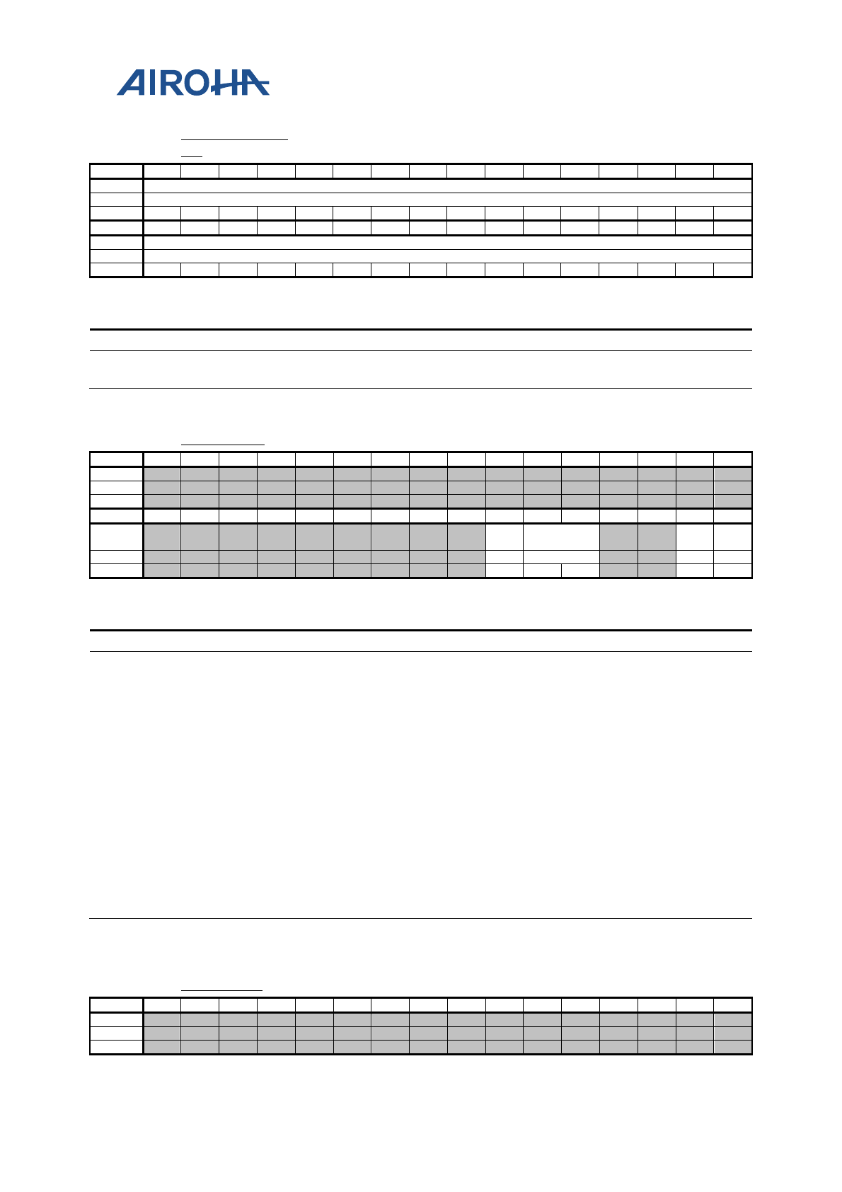
MT2523 Series Reference Manual
© 2015 - 2018 Airoha Technology Corp.
Page 223 of 692
This document contains information that is proprietary to Airoha Technology Corp. (“Airoha”) and/or its licensor(s).
Any unauthorized use, reproduction or disclosure of this document in whole or in part is strictly prohibited.
A2140088
GPT3_COMPA
RE
GPT3 Compare Value
00000000
Bit
31
30
29
28
27
26
25
24
23
22
21
20
19
18
17
16
Name
COMPARE3[31:16]
Type
RW
Reset
0
0
0
0
0
0
0
0
0
0
0
0
0
0
0
0
Bit
15
14
13
12
11
10
9
8
7
6
5
4
3
2
1
0
Name
COMPARE3[15:0]
Type
RW
Reset
0
0
0
0
0
0
0
0
0
0
0
0
0
0
0
0
Overview
Compare value for GPT3
Bit(s)
Name
Description
31:0
COMPARE3
Compare value of GPT3
Write new compare value will also clear the counter of GPT3.
A21400A0
GPT4_CON
GPT4 Control
00000000
Bit
31
30
29
28
27
26
25
24
23
22
21
20
19
18
17
16
Name
Type
Reset
Bit
15
14
13
12
11
10
9
8
7
6
5
4
3
2
1
0
Name
SW_C
G4
MODE4
CLR4
EN4
Type
RW
RW
WO
RW
Reset
0
0
0
0
0
Overview
General control for GPT4
Bit(s)
Name
Description
6
SW_CG4
Stop GPT4's clock if this bit is enabled.
0: Disable
1: Enable
5:4
MODE4
Operation mode of GPT4
00: ONE-SHOT mode
01: REPEAT mode
10: FREERUN_I mode
11: FREERUN mode
1
CLR4
Clears the counter of GPT4 to 0
0: No effect
1: Clear
It takes 2~3 T GPT4_CK for CLR4 to clear the counter of GPT4.
0
EN4
Enables GPT4
0: Disable
1: Enable
It takes 2~3 T GPT4_CK for EN4 to enable/disable GPT4.
A21400A4
GPT4_CLK
GPT4 Clock Setting
00000000
Bit
31
30
29
28
27
26
25
24
23
22
21
20
19
18
17
16
Name
Type
Reset
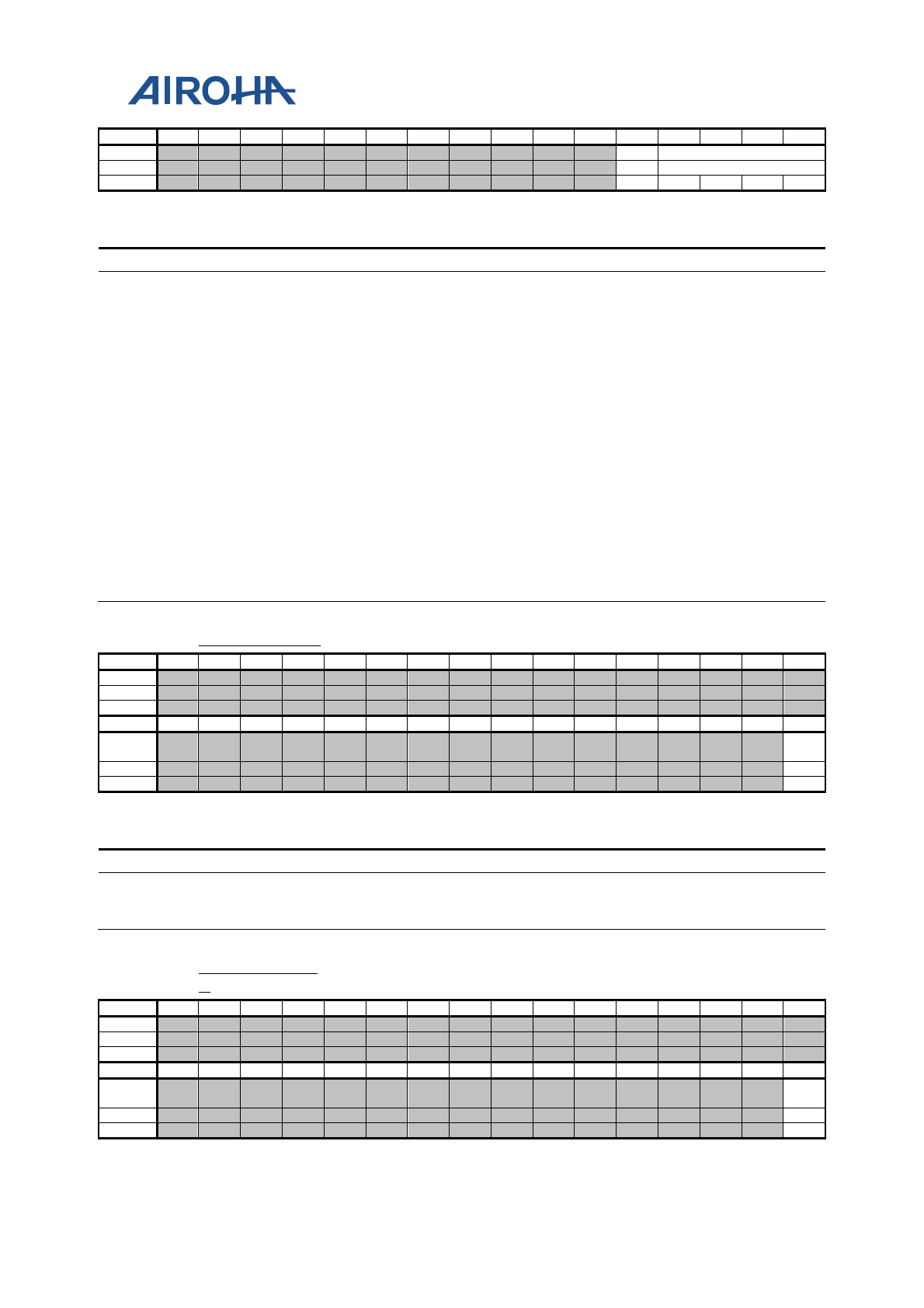
MT2523 Series Reference Manual
© 2015 - 2018 Airoha Technology Corp.
Page 224 of 692
This document contains information that is proprietary to Airoha Technology Corp. (“Airoha”) and/or its licensor(s).
Any unauthorized use, reproduction or disclosure of this document in whole or in part is strictly prohibited.
Bit
15
14
13
12
11
10
9
8
7
6
5
4
3
2
1
0
Name
CLK4
CLKDIV4
Type
RW
RW
Reset
0
0
0
0
0
Overview
Controls the clock source and division ratio of GPT clock
Bit(s)
Name
Description
4
CLK4
Sets up clock source of GPT4
0: System clock (13MHz)
1: RTC clock (32kHz)
3:0
CLKDIV4
Setting of GPT4 input clock frequency divider
0000: Clock source divided by 1
0001: Clock source divided by 2
0010: Clock source divided by 3
0011: Clock source divided by 4
0100: Clock source divided by 5
0101: Clock source divided by 6
0110: Clock source divided by 7
0111: Clock source divided by 8
1000: Clock source divided by 9
1001: Clock source divided by 10
1010: Clock source divided by 11
1011: Clock source divided by 12
1100: Clock source divided by 13
1101: Clock source divided by 16
1110: Clock source divided by 32
1111: Clock source divided by 64
A21400A8
GPT4_IRQ_EN
GPT IRQ Enabling
00000000
Bit
31
30
29
28
27
26
25
24
23
22
21
20
19
18
17
16
Name
Type
Reset
Bit
15
14
13
12
11
10
9
8
7
6
5
4
3
2
1
0
Name
IRQE
N
Type
RW
Reset
0
Overview
Controls the enabling/disabling of GPT interrupt
Bit(s)
Name
Description
0
IRQEN
Enables interrupt of GPT4
0: Disable interrupt of GPT4
1: Enable interrupt of GPT4
A21400AC
GPT4_IRQ_ST
A
GPT IRQ Status
00000000
Bit
31
30
29
28
27
26
25
24
23
22
21
20
19
18
17
16
Name
Type
Reset
Bit
15
14
13
12
11
10
9
8
7
6
5
4
3
2
1
0
Name
IRQS
TA
Type
RO
Reset
0
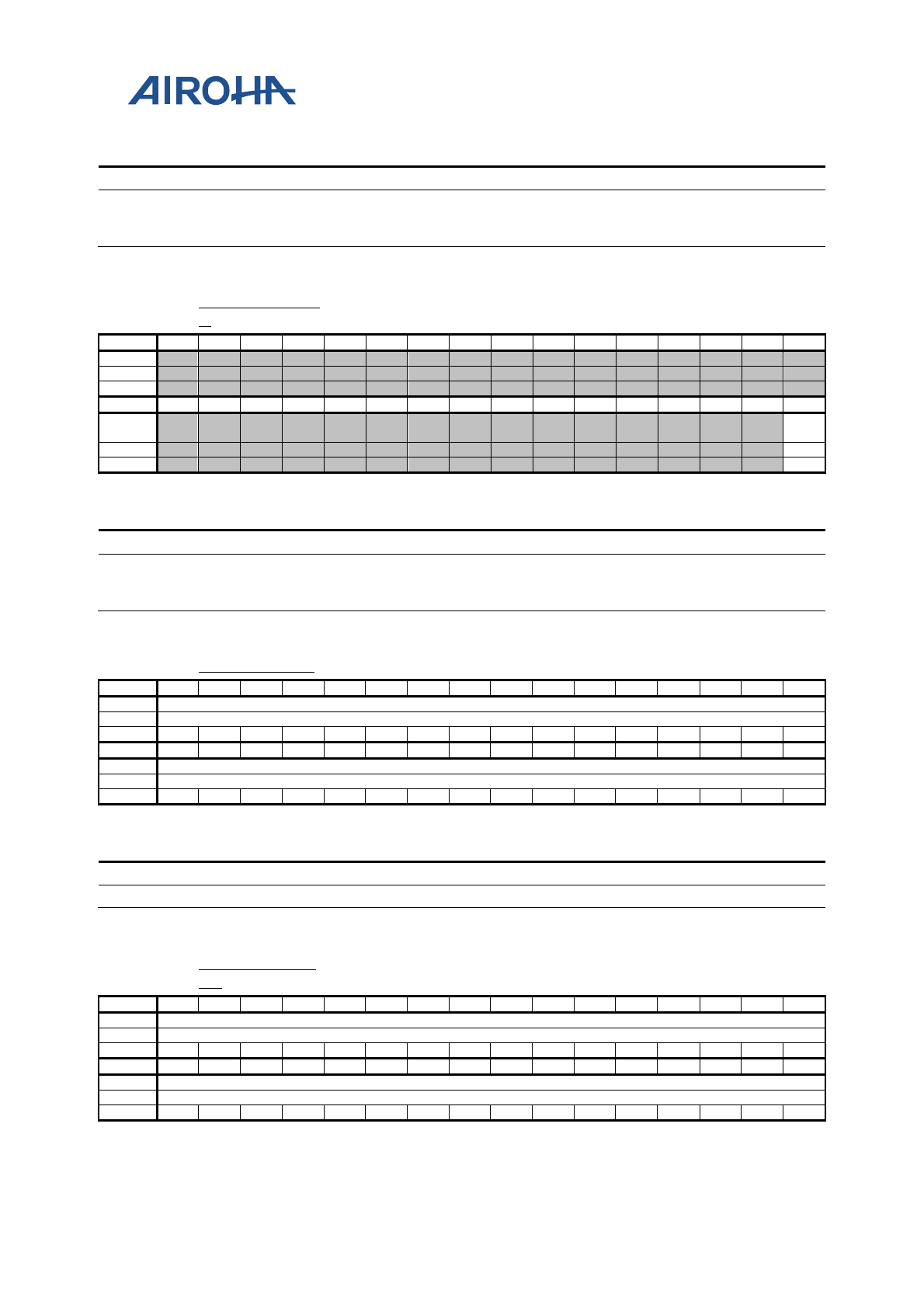
MT2523 Series Reference Manual
© 2015 - 2018 Airoha Technology Corp.
Page 225 of 692
This document contains information that is proprietary to Airoha Technology Corp. (“Airoha”) and/or its licensor(s).
Any unauthorized use, reproduction or disclosure of this document in whole or in part is strictly prohibited.
Overview
Shows the interrupt status of GPT1
Bit(s)
Name
Description
0
IRQSTA
Interrupt status of GPT4
0: No interrupt is generated from GPT4
1: GPT4's interrupt is pending and waiting for service.
A21400B0
GPT4_IRQ_AC
K
GPT IRQ Acknowledgement
00000000
Bit
31
30
29
28
27
26
25
24
23
22
21
20
19
18
17
16
Name
Type
Reset
Bit
15
14
13
12
11
10
9
8
7
6
5
4
3
2
1
0
Name
IRQA
CK
Type
WO
Reset
0
Overview
Acknowledges the GPT interrupt
Bit(s)
Name
Description
0
IRQACK
Interrupt acknowledgement for GPT4
0: No effect
1: Associated interrupt request is acknowledged and should be relinquished.
A21400B4
GPT4_COUNT
GPT4 Counter
00000000
Bit
31
30
29
28
27
26
25
24
23
22
21
20
19
18
17
16
Name
COUNTER4[31:16]
Type
RO
Reset
0
0
0
0
0
0
0
0
0
0
0
0
0
0
0
0
Bit
15
14
13
12
11
10
9
8
7
6
5
4
3
2
1
0
Name
COUNTER4[15:0]
Type
RO
Reset
0
0
0
0
0
0
0
0
0
0
0
0
0
0
0
0
Overview
Timer count of GPT4
Bit(s)
Name
Description
31:0
COUNTER4
Timer counter of GPT4
A21400B8
GPT4_COMPA
RE
GPT4 Compare Value
00000000
Bit
31
30
29
28
27
26
25
24
23
22
21
20
19
18
17
16
Name
COMPARE4[31:16]
Type
RW
Reset
0
0
0
0
0
0
0
0
0
0
0
0
0
0
0
0
Bit
15
14
13
12
11
10
9
8
7
6
5
4
3
2
1
0
Name
COMPARE4[15:0]
Type
RW
Reset
0
0
0
0
0
0
0
0
0
0
0
0
0
0
0
0
Overview
Compare value for GPT4
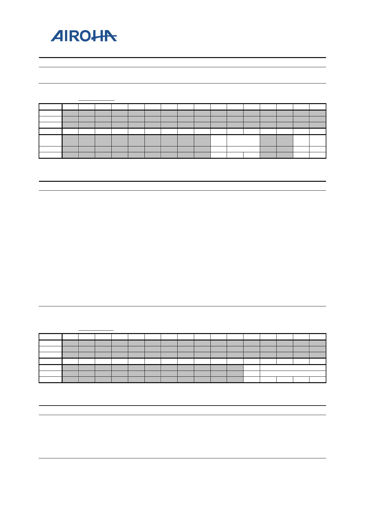
MT2523 Series Reference Manual
© 2015 - 2018 Airoha Technology Corp.
Page 226 of 692
This document contains information that is proprietary to Airoha Technology Corp. (“Airoha”) and/or its licensor(s).
Any unauthorized use, reproduction or disclosure of this document in whole or in part is strictly prohibited.
Bit(s)
Name
Description
31:0
COMPARE4
Compare value of GPT4
Write new compare value will also clear the counter of GPT4.
A21400D0
GPT5_CON
GPT5 Control
00000000
Bit
31
30
29
28
27
26
25
24
23
22
21
20
19
18
17
16
Name
Type
Reset
Bit
15
14
13
12
11
10
9
8
7
6
5
4
3
2
1
0
Name
SW_C
G5
MODE5
CLR5
EN5
Type
RW
RW
WO
RW
Reset
0
0
0
0
0
Overview
General control for GPT5
Bit(s)
Name
Description
6
SW_CG5
Stop GPT5's clock if this bit is enabled.
0: Disable
1: Enable
5:4
MODE5
Operation mode of GPT5
00: ONE-SHOT mode
01: REPEAT mode
10: FREERUN_I mode
11: FREERUN mode
1
CLR5
Clears the counter of GPT5 to 0
0: No effect
1: Clear
It takes 2~3 T GPT5_CK for CLR5 to clear the counter of GPT5.
0
EN5
Enables GPT5
0: Disable
1: Enable
It takes 2~3 T GPT5_CK for EN5 to enable/disable GPT5.
A21400D4
GPT5_CLK
GPT5 Clock Setting
00000000
Bit
31
30
29
28
27
26
25
24
23
22
21
20
19
18
17
16
Name
Type
Reset
Bit
15
14
13
12
11
10
9
8
7
6
5
4
3
2
1
0
Name
CLK5
CLKDIV5
Type
RW
RW
Reset
0
0
0
0
0
Overview
Controls the clock source and division ratio of GPT clock
Bit(s)
Name
Description
4
CLK5
Sets up clock source of GPT5
0: System clock (13MHz)
1: RTC clock (32kHz)
3:0
CLKDIV5
Setting of GPT5 input clock frequency divider
0000: Clock source divided by 1
0001: Clock source divided by 2
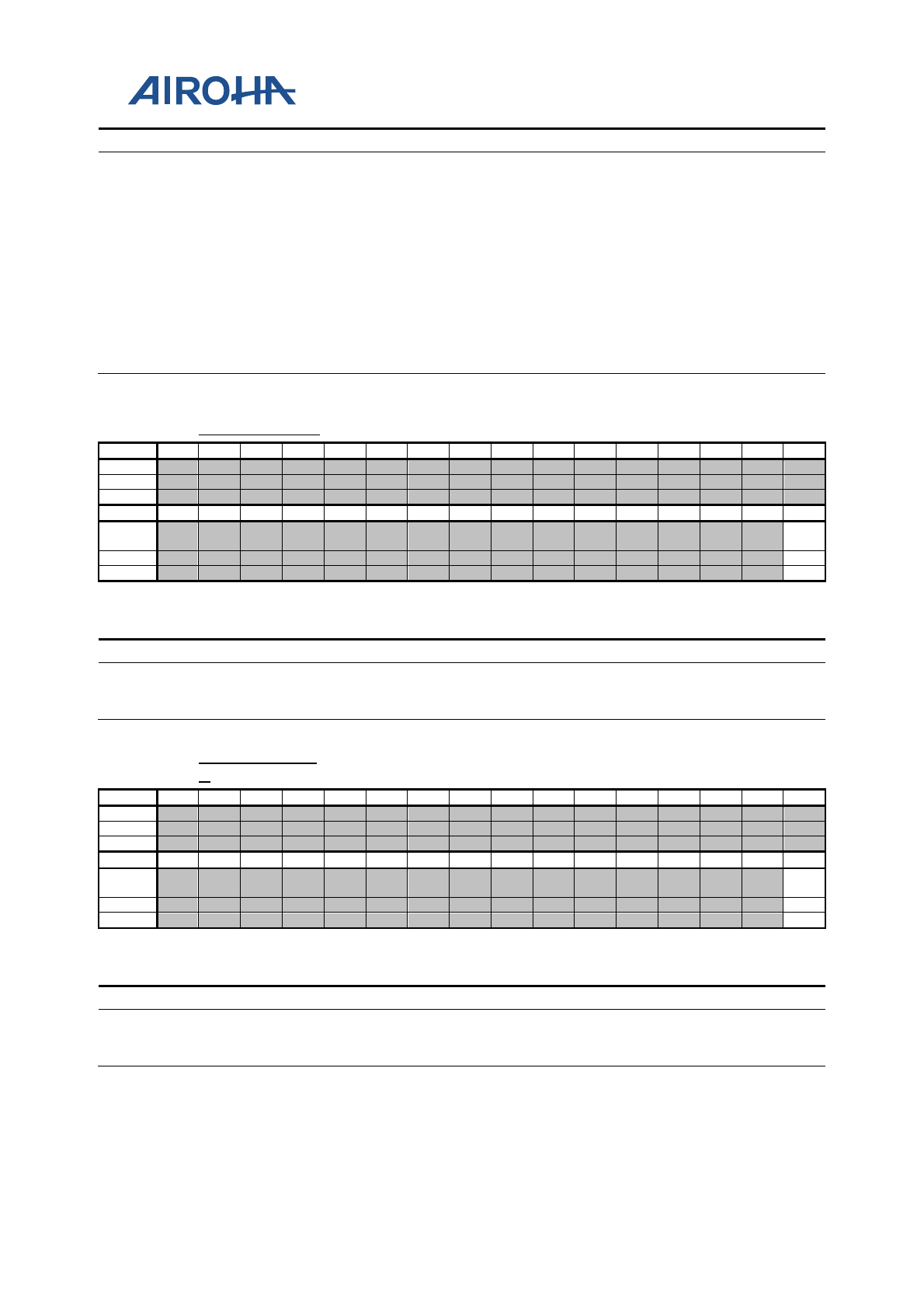
MT2523 Series Reference Manual
© 2015 - 2018 Airoha Technology Corp.
Page 227 of 692
This document contains information that is proprietary to Airoha Technology Corp. (“Airoha”) and/or its licensor(s).
Any unauthorized use, reproduction or disclosure of this document in whole or in part is strictly prohibited.
Bit(s)
Name
Description
0010: Clock source divided by 3
0011: Clock source divided by 4
0100: Clock source divided by 5
0101: Clock source divided by 6
0110: Clock source divided by 7
0111: Clock source divided by 8
1000: Clock source divided by 9
1001: Clock source divided by 10
1010: Clock source divided by 11
1011: Clock source divided by 12
1100: Clock source divided by 13
1101: Clock source divided by 16
1110: Clock source divided by 32
1111: Clock source divided by 64
A21400D8
GPT5_IRQ_EN
GPT IRQ Enabling
00000000
Bit
31
30
29
28
27
26
25
24
23
22
21
20
19
18
17
16
Name
Type
Reset
Bit
15
14
13
12
11
10
9
8
7
6
5
4
3
2
1
0
Name
IRQE
N
Type
RW
Reset
0
Overview
Controls the enabling/disabling of GPT interrupt
Bit(s)
Name
Description
0
IRQEN
Enables interrupt of GPT5
0: Disable interrupt of GPT5
1: Enable interrupt of GPT5
A21400DC
GPT5_IRQ_ST
A
GPT IRQ Status
00000000
Bit
31
30
29
28
27
26
25
24
23
22
21
20
19
18
17
16
Name
Type
Reset
Bit
15
14
13
12
11
10
9
8
7
6
5
4
3
2
1
0
Name
IRQS
TA
Type
RO
Reset
0
Overview
Shows the interrupt status of GPT1
Bit(s)
Name
Description
0
IRQSTA
Interrupt status of GPT5
0: No interrupt is generated from GPT5
1: GPT5's interrupt is pending and waiting for service.
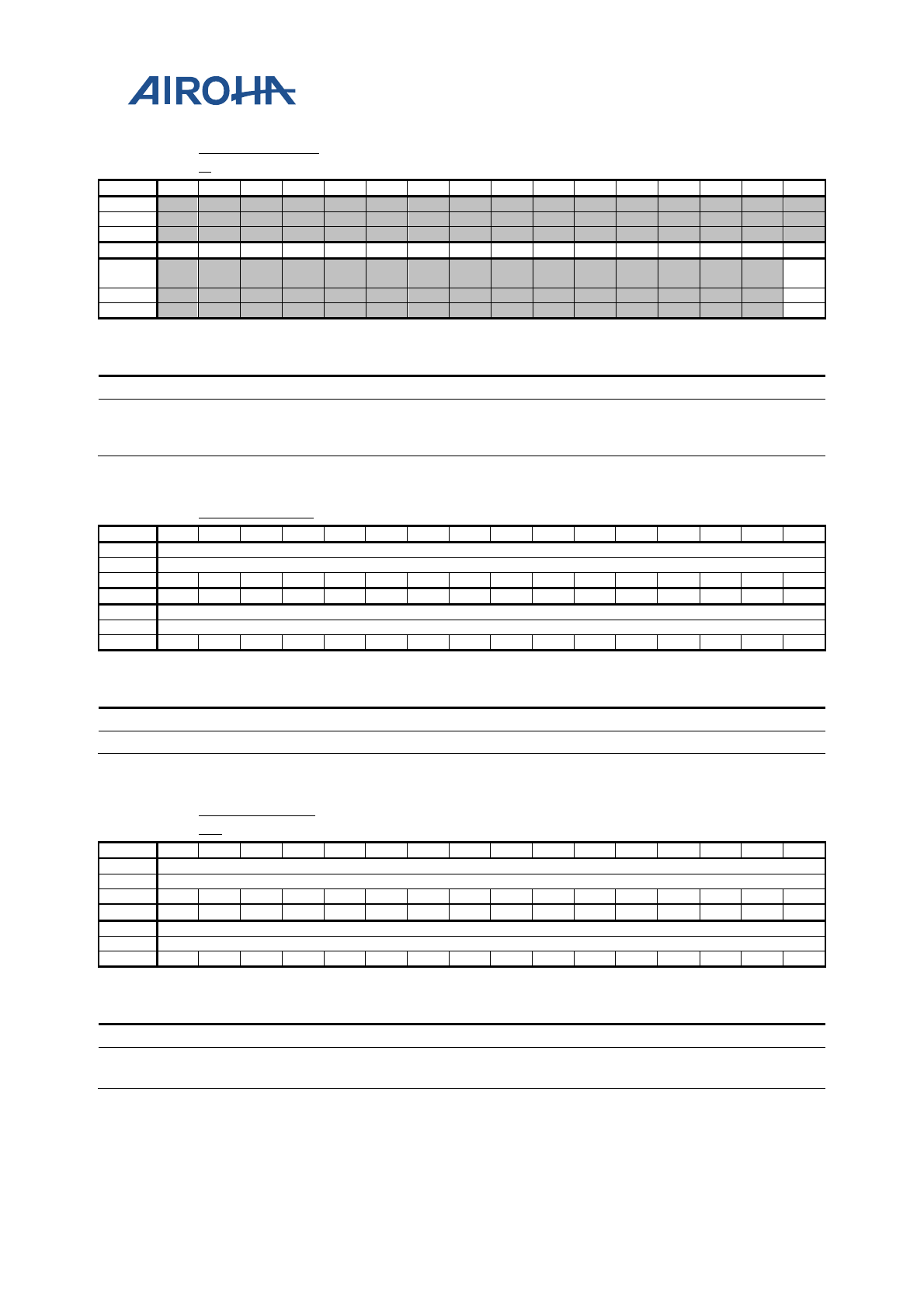
MT2523 Series Reference Manual
© 2015 - 2018 Airoha Technology Corp.
Page 228 of 692
This document contains information that is proprietary to Airoha Technology Corp. (“Airoha”) and/or its licensor(s).
Any unauthorized use, reproduction or disclosure of this document in whole or in part is strictly prohibited.
A21400E0
GPT5_IRQ_AC
K
GPT IRQ Acknowledgement
00000000
Bit
31
30
29
28
27
26
25
24
23
22
21
20
19
18
17
16
Name
Type
Reset
Bit
15
14
13
12
11
10
9
8
7
6
5
4
3
2
1
0
Name
IRQA
CK
Type
WO
Reset
0
Overview
Acknowledges the GPT interrupt
Bit(s)
Name
Description
0
IRQACK
Interrupt acknowledgement for GPT5
0: No effect
1: Associated interrupt request is acknowledged and should be relinquished.
A21400E4
GPT5_COUNT
GPT5 Counter
00000000
Bit
31
30
29
28
27
26
25
24
23
22
21
20
19
18
17
16
Name
COUNTER5[31:16]
Type
RO
Reset
0
0
0
0
0
0
0
0
0
0
0
0
0
0
0
0
Bit
15
14
13
12
11
10
9
8
7
6
5
4
3
2
1
0
Name
COUNTER5[15:0]
Type
RO
Reset
0
0
0
0
0
0
0
0
0
0
0
0
0
0
0
0
Overview
Timer count of GPT5
Bit(s)
Name
Description
31:0
COUNTER5
Timer counter of GPT5
A21400E8
GPT5_COMPA
RE
GPT5 Compare Value
00000000
Bit
31
30
29
28
27
26
25
24
23
22
21
20
19
18
17
16
Name
COMPARE5[31:16]
Type
RW
Reset
0
0
0
0
0
0
0
0
0
0
0
0
0
0
0
0
Bit
15
14
13
12
11
10
9
8
7
6
5
4
3
2
1
0
Name
COMPARE5[15:0]
Type
RW
Reset
0
0
0
0
0
0
0
0
0
0
0
0
0
0
0
0
Overview
Compare value for GPT5
Bit(s)
Name
Description
31:0
COMPARE5
Compare value of GPT5
Write new compare value will also clear the counter of GPT5.
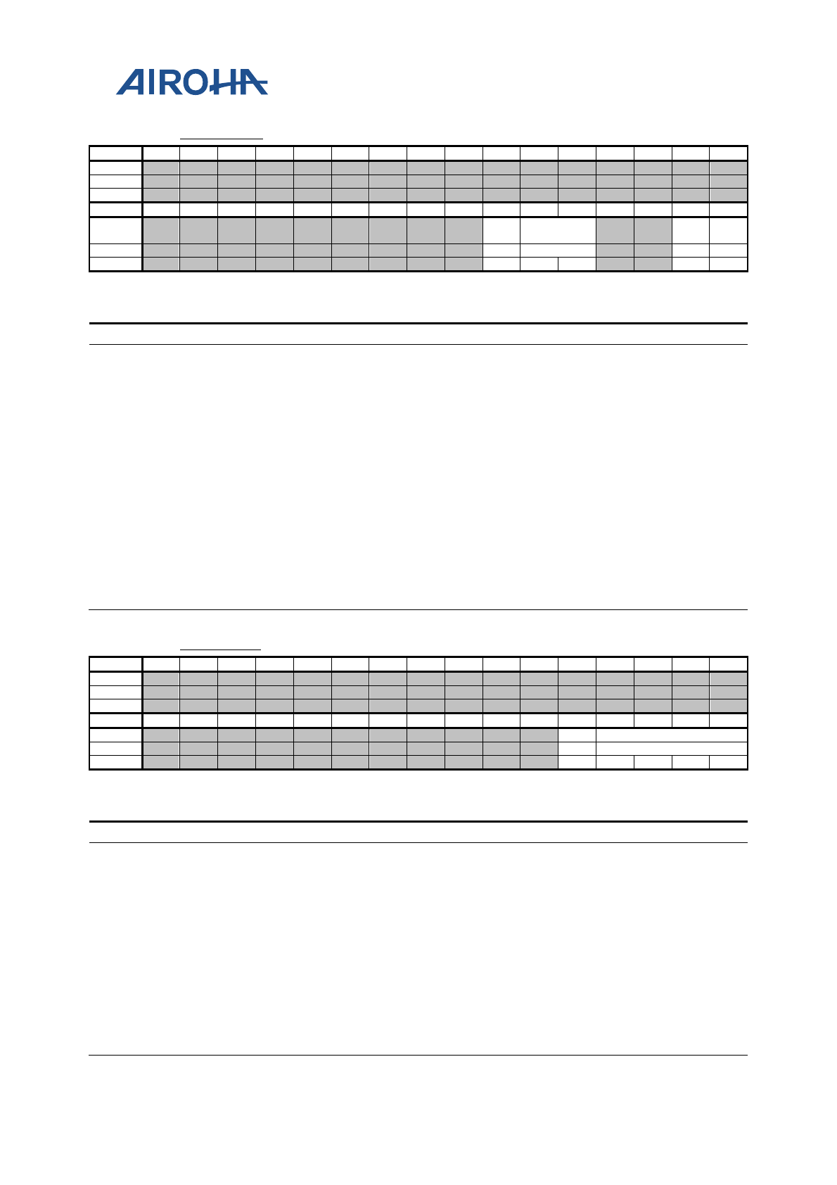
MT2523 Series Reference Manual
© 2015 - 2018 Airoha Technology Corp.
Page 229 of 692
This document contains information that is proprietary to Airoha Technology Corp. (“Airoha”) and/or its licensor(s).
Any unauthorized use, reproduction or disclosure of this document in whole or in part is strictly prohibited.
A2140100
GPT6_CON
GPT6 Control
00000000
Bit
31
30
29
28
27
26
25
24
23
22
21
20
19
18
17
16
Name
Type
Reset
Bit
15
14
13
12
11
10
9
8
7
6
5
4
3
2
1
0
Name
SW_C
G6
MODE6
CLR6
EN6
Type
RW
RW
WO
RW
Reset
0
0
0
0
0
Overview
General control for GPT6
Bit(s)
Name
Description
6
SW_CG6
Stop GPT6's clock if this bit is enabled.
0: Disable
1: Enable
5:4
MODE6
Operation mode of GPT6
00: ONE-SHOT mode
01: REPEAT mode
10: FREERUN_I mode
11: FREERUN mode
1
CLR6
Clears the counter of GPT6 to 0
0: No effect
1: Clear
It takes 2~3 T GPT6_CK for CLR6 to clear the counter of GPT6.
0
EN6
Enables GPT6
0: Disable
1: Enable
It takes 2~3 T GPT6_CK for EN6 to enable/disable GPT6.
A2140104
GPT6_CLK
GPT6 Clock Setting
00000000
Bit
31
30
29
28
27
26
25
24
23
22
21
20
19
18
17
16
Name
Type
Reset
Bit
15
14
13
12
11
10
9
8
7
6
5
4
3
2
1
0
Name
CLK6
CLKDIV6
Type
RW
RW
Reset
0
0
0
0
0
Overview
Controls the clock source and division ratio of GPT clock
Bit(s)
Name
Description
4
CLK6
Set clock source of GPT6
0: System clock (13MHz)
1: RTC clock (32kHz)
3:0
CLKDIV6
Setting of GPT6 input clock frequency divider
0000: Clock source divided by 1
0001: Clock source divided by 2
0010: Clock source divided by 3
0011: Clock source divided by 4
0100: Clock source divided by 5
0101: Clock source divided by 6
0110: Clock source divided by 7
0111: Clock source divided by 8
1000: Clock source divided by 9
1001: Clock source divided by 10
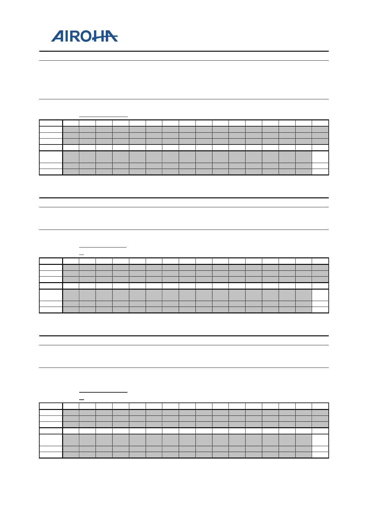
MT2523 Series Reference Manual
© 2015 - 2018 Airoha Technology Corp.
Page 230 of 692
This document contains information that is proprietary to Airoha Technology Corp. (“Airoha”) and/or its licensor(s).
Any unauthorized use, reproduction or disclosure of this document in whole or in part is strictly prohibited.
Bit(s)
Name
Description
1010: Clock source divided by 11
1011: Clock source divided by 12
1100: Clock source divided by 13
1101: Clock source divided by 16
1110: Clock source divided by 32
1111: Clock source divided by 64
A2140108
GPT6_IRQ_EN
GPT IRQ Enabling
00000000
Bit
31
30
29
28
27
26
25
24
23
22
21
20
19
18
17
16
Name
Type
Reset
Bit
15
14
13
12
11
10
9
8
7
6
5
4
3
2
1
0
Name
IRQE
N
Type
RW
Reset
0
Overview
Controls the enabling/disabling of GPT interrupt
Bit(s)
Name
Description
0
IRQEN
Enables interrupt of GPT6
0: Disable interrupt of GPT6
1: Enable interrupt of GPT6
A214010C
GPT6_IRQ_ST
A
GPT IRQ Status
00000000
Bit
31
30
29
28
27
26
25
24
23
22
21
20
19
18
17
16
Name
Type
Reset
Bit
15
14
13
12
11
10
9
8
7
6
5
4
3
2
1
0
Name
IRQS
TA
Type
RO
Reset
0
Overview
Shows the interrupt status of GPT1
Bit(s)
Name
Description
0
IRQSTA
Interrupt status of GPT6
0: No interrupt is generated from GPT6
1: GPT6's interrupt is pending and waiting for service.
A2140110
GPT6_IRQ_AC
K
GPT IRQ
Acknowledgement
00000000
Bit
31
30
29
28
27
26
25
24
23
22
21
20
19
18
17
16
Name
Type
Reset
Bit
15
14
13
12
11
10
9
8
7
6
5
4
3
2
1
0
Name
IRQA
CK
Type
WO
Reset
0
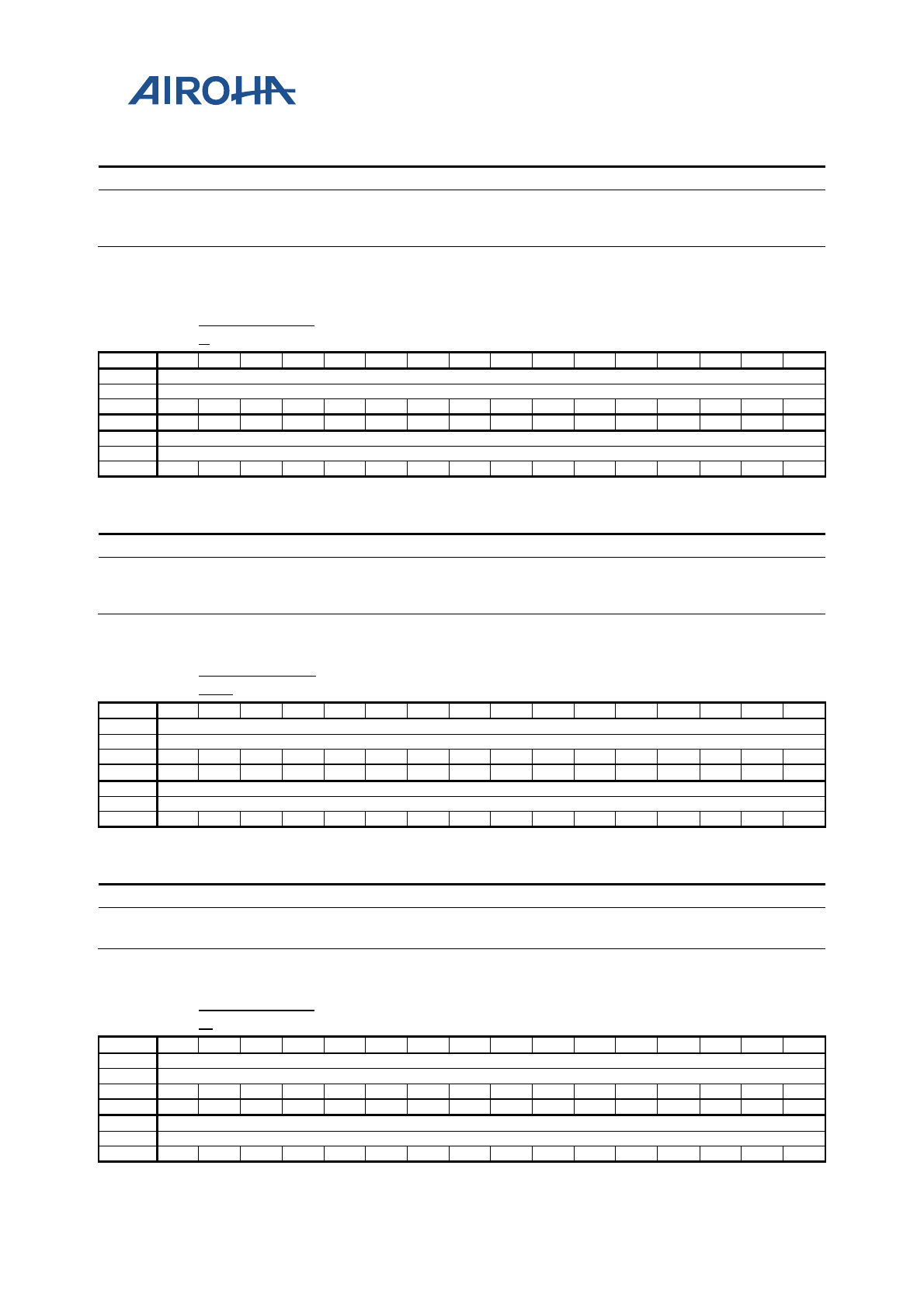
MT2523 Series Reference Manual
© 2015 - 2018 Airoha Technology Corp.
Page 231 of 692
This document contains information that is proprietary to Airoha Technology Corp. (“Airoha”) and/or its licensor(s).
Any unauthorized use, reproduction or disclosure of this document in whole or in part is strictly prohibited.
Overview
Acknowledges the GPT interrupt
Bit(s)
Name
Description
0
IRQACK
Interrupt acknowledgement for GPT6
0: No effect
1: Associated interrupt request is acknowledged and should be relinquished.
A2140114
GPT6_COUNT
L
GPT6 Counter L
00000000
Bit
31
30
29
28
27
26
25
24
23
22
21
20
19
18
17
16
Name
COUNTER6L[31:16]
Type
RO
Reset
0
0
0
0
0
0
0
0
0
0
0
0
0
0
0
0
Bit
15
14
13
12
11
10
9
8
7
6
5
4
3
2
1
0
Name
COUNTER6L[15:0]
Type
RO
Reset
0
0
0
0
0
0
0
0
0
0
0
0
0
0
0
0
Overview
Lower word timer count for GPT6
Bit(s)
Name
Description
31:0
COUNTER6L
Lower word of timer count of GPT6
The read operation of GPT6_COUNTL will make GPT6_COUNTH fixed until the
next read operation of GPT6_COUNTL.
A2140118
GPT6_COMPA
REL
GPT6 Compare Value L
00000000
Bit
31
30
29
28
27
26
25
24
23
22
21
20
19
18
17
16
Name
COMPARE6L[31:16]
Type
RW
Reset
0
0
0
0
0
0
0
0
0
0
0
0
0
0
0
0
Bit
15
14
13
12
11
10
9
8
7
6
5
4
3
2
1
0
Name
COMPARE6L[15:0]
Type
RW
Reset
0
0
0
0
0
0
0
0
0
0
0
0
0
0
0
0
Overview
Lower word compare value for GPT6
Bit(s)
Name
Description
31:0
COMPARE6L
Lower word of compare value of GPT6
Write new compare value will also clear the counter of GPT6.
A214011C
GPT6_COUNT
H
GPT6 Counter L
00000000
Bit
31
30
29
28
27
26
25
24
23
22
21
20
19
18
17
16
Name
COUNTER6H[31:16]
Type
RO
Reset
0
0
0
0
0
0
0
0
0
0
0
0
0
0
0
0
Bit
15
14
13
12
11
10
9
8
7
6
5
4
3
2
1
0
Name
COUNTER6H[15:0]
Type
RO
Reset
0
0
0
0
0
0
0
0
0
0
0
0
0
0
0
0
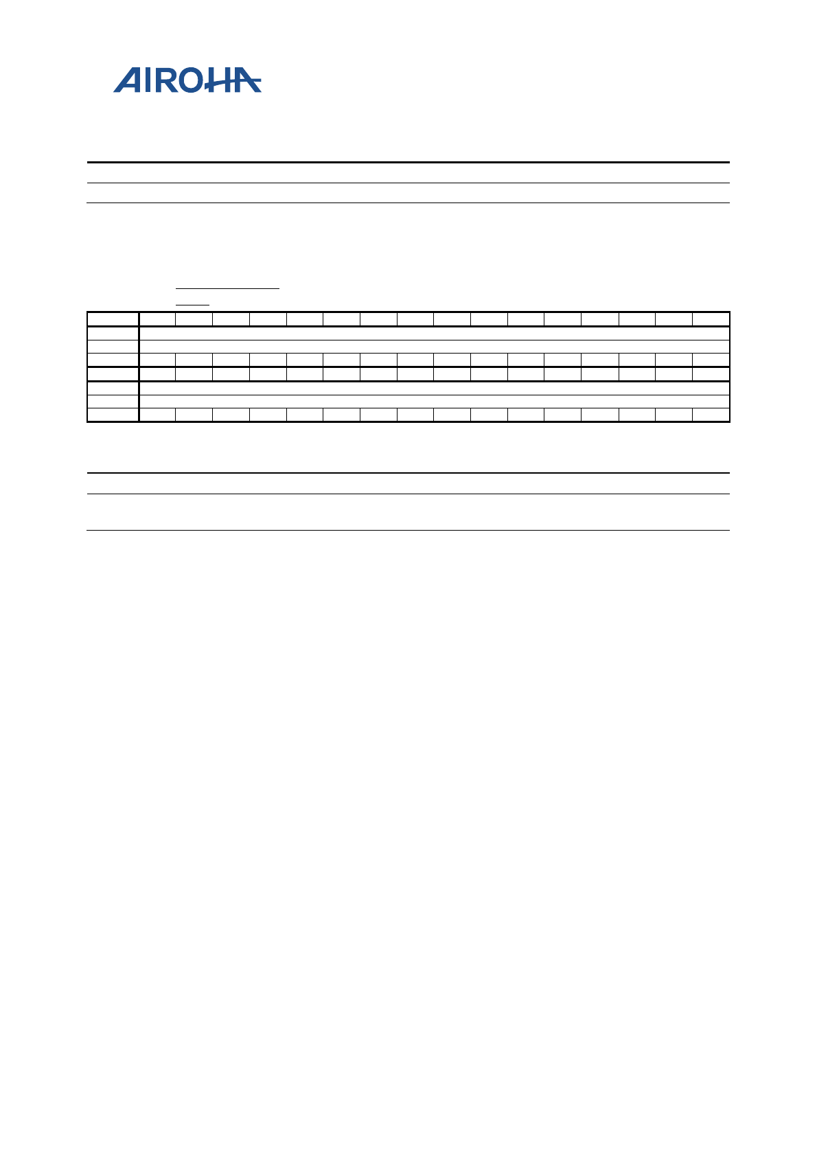
MT2523 Series Reference Manual
© 2015 - 2018 Airoha Technology Corp.
Page 232 of 692
This document contains information that is proprietary to Airoha Technology Corp. (“Airoha”) and/or its licensor(s).
Any unauthorized use, reproduction or disclosure of this document in whole or in part is strictly prohibited.
Overview
Higher word timer count for GPT6
Bit(s)
Name
Description
31:0
COUNTER6H
Higher word of timer count of GPT6
A2140120
GPT6_COMPA
REH
GPT6 Compare Value H
00000000
Bit
31
30
29
28
27
26
25
24
23
22
21
20
19
18
17
16
Name
COMPARE6H[31:16]
Type
RW
Reset
0
0
0
0
0
0
0
0
0
0
0
0
0
0
0
0
Bit
15
14
13
12
11
10
9
8
7
6
5
4
3
2
1
0
Name
COMPARE6H[15:0]
Type
RW
Reset
0
0
0
0
0
0
0
0
0
0
0
0
0
0
0
0
Overview
Higher word compare value for GPT6
Bit(s)
Name
Description
31:0
COMPARE6H
Higher word of compare of GPT6
Write new compare value will also clear the counter of GPT6.
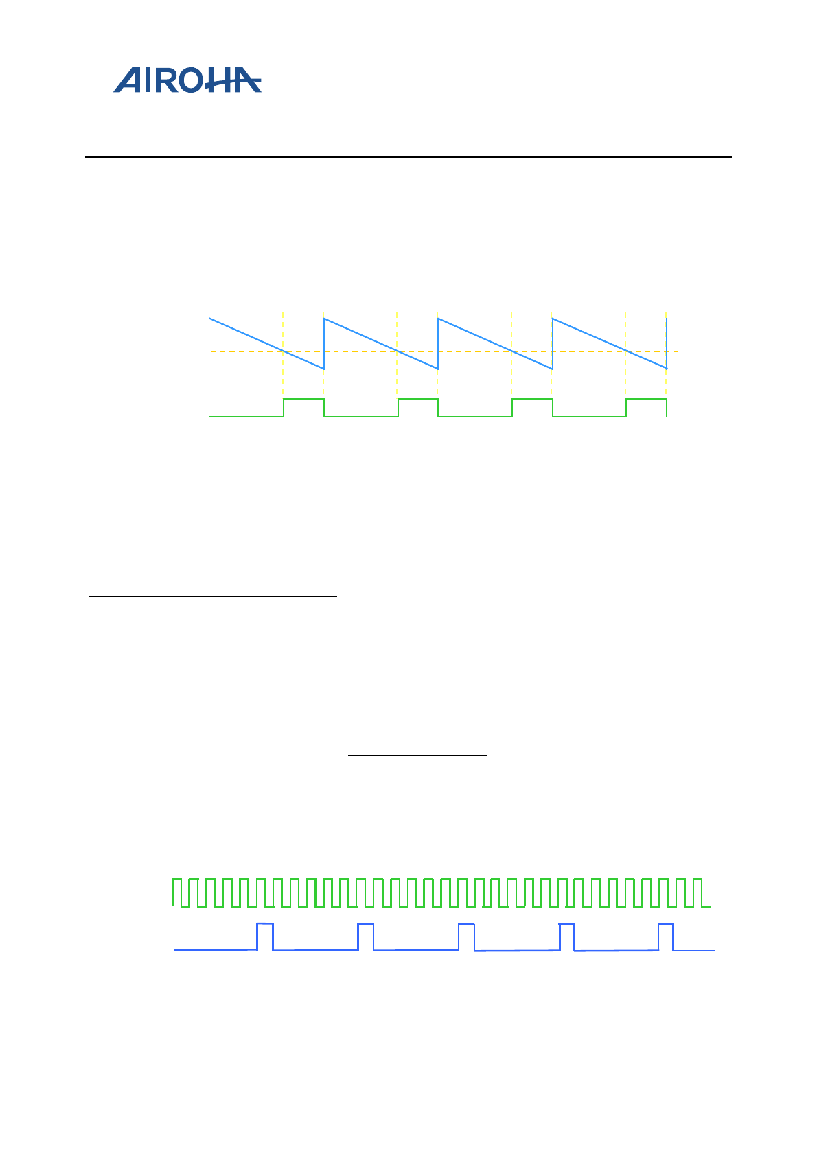
MT2523 Series Reference Manual
© 2015 - 2018 Airoha Technology Corp.
Page 233 of 692
This document contains information that is proprietary to Airoha Technology Corp. (“Airoha”) and/or its licensor(s).
Any unauthorized use, reproduction or disclosure of this document in whole or in part is strictly prohibited.
13. Pulse Width Modulation
13.1. General Description
The generic pulse width modulators (PWM) are implemented to generate pulse sequences with programmable
frequency and duty cycle for LCD backlight. The duration of the PWM output signal is LOW as long as the internal
counter value is bigger than or equal to the threshold value. The waveform is shown in Figure 13-1.
Figure 13-1. PWM waveform
The frequency and volume of PWM output signal are determined by registers PWM_1CH_CTRL,
PWM_1CH_THRES, and PWM_1CH_COUNT. The POWERDOWN (pwm_1ch_pdn) signal is applied to power down
the PWM_1CH module. When PWM_1CH is deactivated (pwm_1ch_pdn=1), the output will be in LOW state.
The output PWM frequency is determined by:
)1_1_(_ +× COUNTCHPWMDIVCLOCK
CLK
CLK = 13 MHz, when CLK_SLE=0
CLK = 32 KHz, when CLK_SLE=1
CLOCK_DIV = 1, when CLK_DIV = 00b
CLOCK_DIV = 2, when CLK_DIV = 01b
CLOCK_DIV = 4, when CLK_DIV = 10b
CLOCK_DIV = 8, when CLK_DIV = 11b
The output PWM duty cycle is determined by:
1_1_
_1_
+COUNTCHPWM
THRESCHPWM
Note that PWM_1CH_THRES should be less than PWM_1CH_COUNT. If this condition is not satisfied, the output
pulse of the PWM will always behigh. Figure 7-2 is the PWM waveform with indicated register values.
Figure 13-2. PWM waveform with register values
Internal counter
Threshold
PWM Signal
PWM_COUNT = 5
PWM_ THRES = 1
PWM_CON = 0b
13MHz
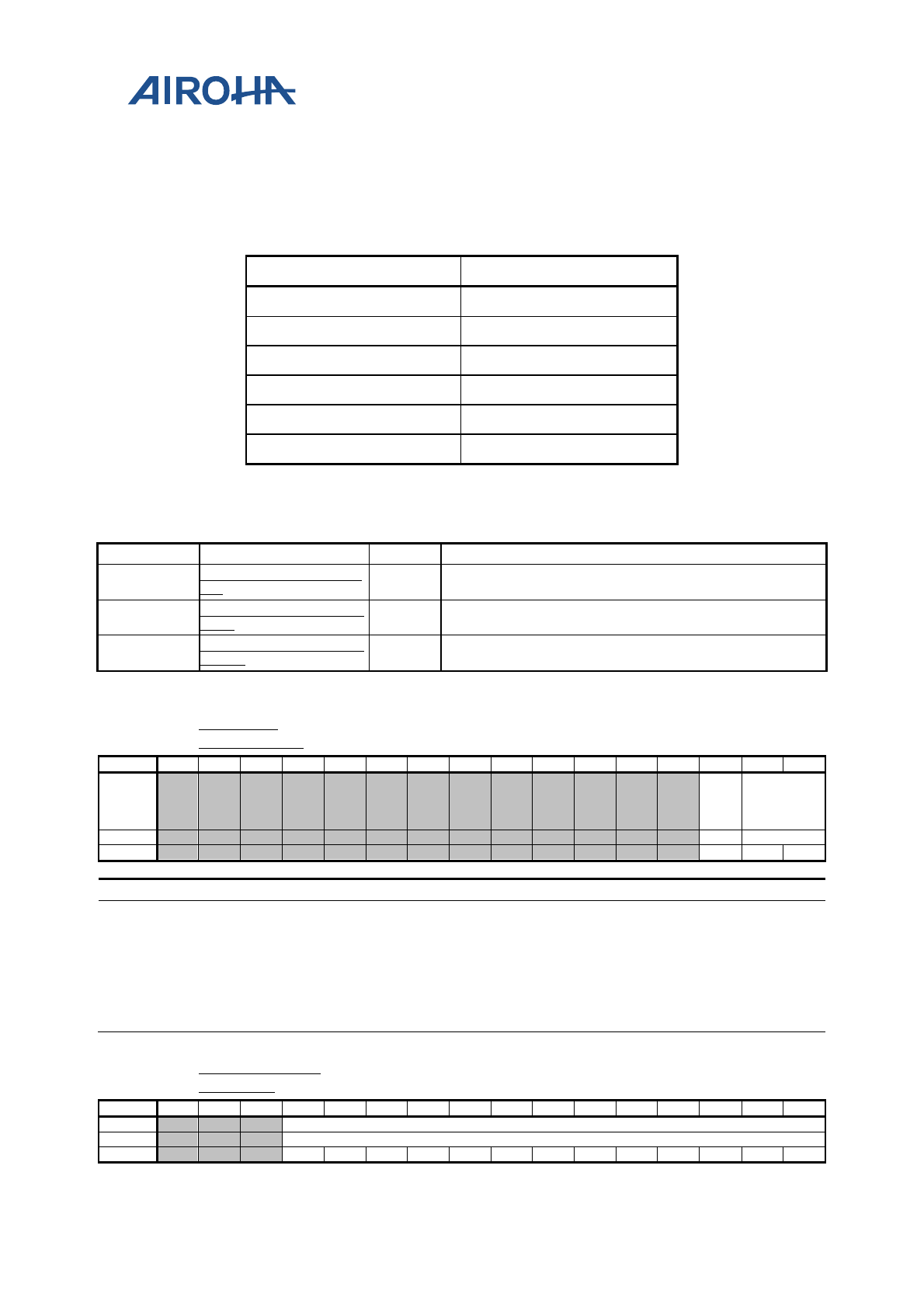
MT2523 Series Reference Manual
© 2015 - 2018 Airoha Technology Corp.
Page 234 of 692
This document contains information that is proprietary to Airoha Technology Corp. (“Airoha”) and/or its licensor(s).
Any unauthorized use, reproduction or disclosure of this document in whole or in part is strictly prohibited.
13.2. Register Definition
There are six PWM channels in this SOC. The usage of the registers below is the same except that the base address
should be changed to respective one.
PWM number Base address
PWM0 (Always on domain) 0xA2160000
PWM1 (Always on domain) 0xA2170000
PWM2 (Power down domain) 0xA0160000
PWM3 (Power down domain) 0xA0170000
PWM4 (Power down domain) 0xA0180000
PWM5 (Power down domain) 0xA0190000
Module name: PulseWidthModulation Base address: (+A2160000h)
Address
Name
Width
Register Function
A2160000
PWM_1CH_CTRL_AD
DR
16 PWM control register
A2160004
PWM_1CH_COUNT_A
DDR
16 PWM max counter value register
A2160008
PWM_1CH_THRESH_
ADDR
16
PWM threshold value register
A2
160000
PWM
_1CH
_CTRL_ADD
R
PWM
control register
0000
Bit
15
14
13
12
11
10
9
8
7
6
5
4
3
2
1
0
Name
PWM
_1CH
_CLK
_SEL
PWM
_1CH
_CLK_DIV
Type
RW
RW
Reset
0
0
0
Bit(s)
Mnemonic
Name
Description
2
PWM
_1CH
_CLK_SEL
CLK_SEL
Selects source clock frequency of PWM
0:CLK=13MHz (unable to work in sleep mode)
1: CLK=32kHz
1:0
PWM
_1CH
_CLK_DIV
CLK_DIV
Selects clock prescaler scale of PWM
2'b00: f=fclk
2'b01: f=fclk/2
2'b10: f=fclk/4
2'b11: f=fclk/8
A2
160004
PWM
_1CH_COU
NT_ADDR
PWM
max counter value register
0000
Bit
15
14
13
12
11
10
9
8
7
6
5
4
3
2
1
0
Name
PWM_1CH_COUNT
Type
RW
Reset
1
1
1
1
1
1
1
1
1
1
1
1
1
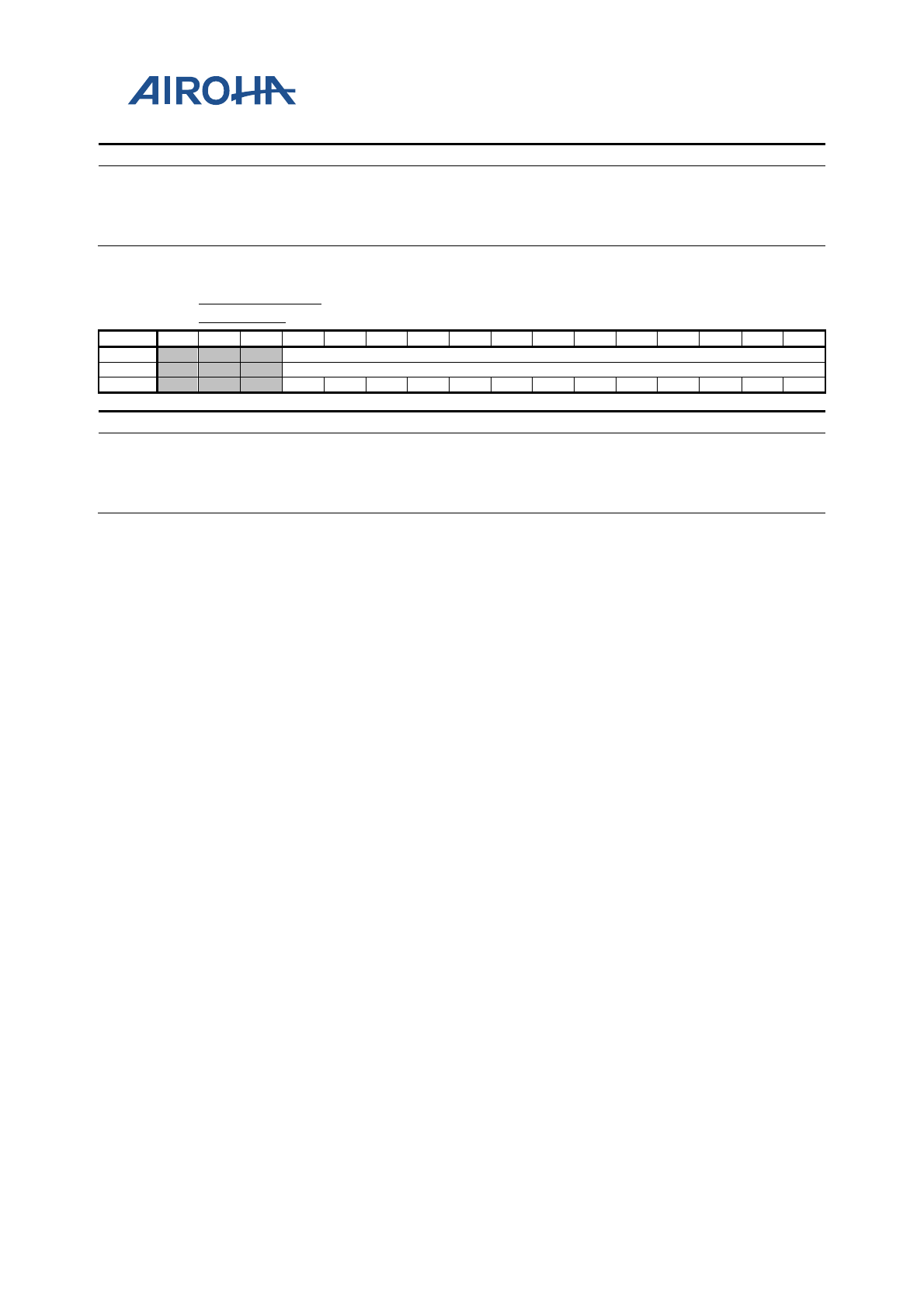
MT2523 Series Reference Manual
© 2015 - 2018 Airoha Technology Corp.
Page 235 of 692
This document contains information that is proprietary to Airoha Technology Corp. (“Airoha”) and/or its licensor(s).
Any unauthorized use, reproduction or disclosure of this document in whole or in part is strictly prohibited.
Bit(s)
Mnemonic
Name
Description
12:0
PWM_1CH
_COUNT
PWM_1CH_COUNT
PWM max. counter value
This value is the initial value for the internal counter. Regardless of the
operation mode, if PWM_1CH_COUNT is written when the internal
counter is counting backwards, the new initial value will not take effect
until the internal counter counts down to 0, i.e. a complete period.
A2
160008
PWM
_1CH_THR
ESH_ADDR
PWM
threshold value register
0000
Bit
15
14
13
12
11
10
9
8
7
6
5
4
3
2
1
0
Name
PWM_1CH_THRES
Type
RW
Reset
0
0
0
0
0
0
0
0
0
0
0
0
0
Bit(s)
Mnemonic
Name
Description
12:0
PWM
_1CH
_THRES
PWM
_1CH_THRES PWM threshold value
When the internal counter value is bigger than or equal to
PWM_1CH_THRES, the PWM output signal will be 0. When the
internal counter is less than PWM_1CH_THRES, the PWM output
signal will be 1.
MT2523 Series Reference Manual
© 2015 - 2018 Airoha Technology Corp.
Page 236 of 692
This document contains information that is proprietary to Airoha Technology Corp. (“Airoha”) and/or its licensor(s).
Any unauthorized use, reproduction or disclosure of this document in whole or in part is strictly prohibited.
14. Keypad Scanner
14.1. General Description
The keypad supports two types of keypads, 3*3 single keys and 3*3 configurable double keys, and it will not be
powered off to support the system wake-up event.
The 3*3 keypad can be divided into two parts: 1) The keypad interface including three columns and three rows
(see Figure 14-1 and Figure 14-2); 2) The key detection block provides key pressed, key released and de-bounce
mechanisms.
Each time the key is pressed or released, i.e. something different in the 3x3 matrix, the key detection block senses
the change and recognizes if a key has been pressed or released. Whenever the key status changes and is stable, a
KEYPAD IRQ will be issued. The MCU can then read the key(s) pressed directly in register KP_MEM1 and KP_MEM2.
To ensure the key pressed information is not missed, the status register in keypad will not be read-cleared by the
APB read command. The status register can only be changed by the key-pressed detection FSM.
This keypad detects one or two keys pressed simultaneously with any combination. Figure 14-3 shows the
condition when one key is pressed. Figure 14-4(a) and Figure 14-4(b) illustrate the cases of two keys pressed. Since
the key pressed detection depends on the HIGH or LOW level of the external keypad interface, if the keys are
pressed at the same time, and there exists a key that is on the same column and the same row with other keys, the
pressed key cannot be correctly decoded. For example, if there are three key pressed: key1 = (x1, y1), key2 = (x2,
y2), and key3 = (x1, y2), both key3 and key4 = (x2, y1) will be detected, and therefore they cannot be distinguished
correctly. Hence, the keypad detects only one or two keys pressed simultaneously in any combination. More than
two keys pressed simultaneously in a specific pattern will retrieve wrong information.
The 3*3 keypad supports a 3*3*2 = 18 keys matrix. The 18 keys are divided into 9 sub groups, and each group
consists of 2 keys and a 20ohm resistor. Besides the limitation of the 3*3 keypad, 3*3 keypad has another
limitation, which is it cannot detect two keys pressed simultaneously when the two keys are in one group, i.e. the
3*3 keypad cannot detect key 0 and key 1 or key 15 and key 16 pressed simultaneously.
Table 14-1. 3*3 single key’s order number in COL/ROW matrix
COL0 COL1 COL2
ROW2 18 19 20
ROW1 9 10 11
ROW0 0 1 2
Table 14-2. 3*3 double key’s order number in COL/ROW matrix
COL0 COL1 COL2
ROW2 26/27 28/29 30/31
ROW1 13/14 15/16 17/18
ROW0 0/1 2/3 4/5
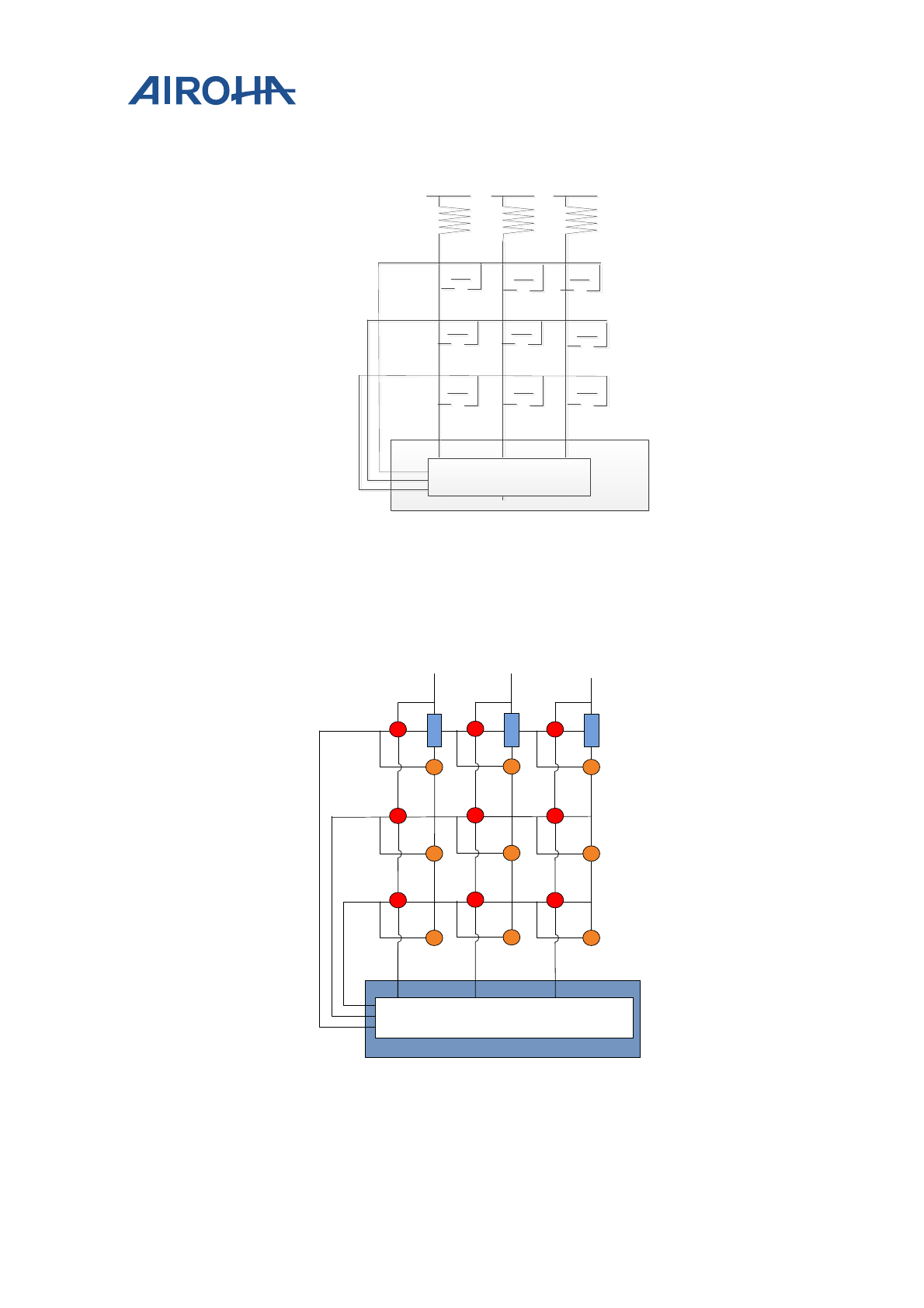
MT2523 Series Reference Manual
© 2015 - 2018 Airoha Technology Corp.
Page 237 of 692
This document contains information that is proprietary to Airoha Technology Corp. (“Airoha”) and/or its licensor(s).
Any unauthorized use, reproduction or disclosure of this document in whole or in part is strictly prohibited.
ROW0
ROW0
ROW1
ROW1
ROW2
ROW2
Baseband
Baseband
PMIC integrated BB chip
PMIC integrated BB chip
COL1
COL1 COL2
COL2
COL0
COL0
1
11
11
1
1
11
11
1
1
11
11
1
Figure 14-1. 3x3 keypad matrix (9 keys)
7
0
15
14
10
9
2
17
16
12
11
4
19
18
KROW0
KROW1
KROW2
KCOL0 KCOL1 KCOL2
Baseband
3
15
8
Figure 14-2. 3x3 keypad matrix (18 keys)
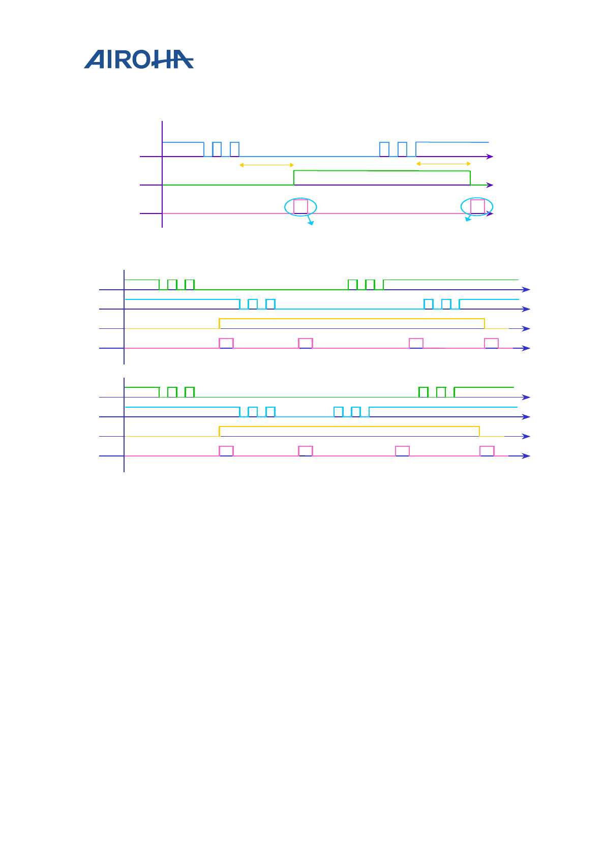
MT2523 Series Reference Manual
© 2015 - 2018 Airoha Technology Corp.
Page 238 of 692
This document contains information that is proprietary to Airoha Technology Corp. (“Airoha”) and/or its licensor(s).
Any unauthorized use, reproduction or disclosure of this document in whole or in part is strictly prohibited.
14.1.1. Waveform
Figure 14-3. One key pressed with de-bounce mechanism denoted
Figure 14-4. (a) Two keys pressed, case 1; (b) Two keys pressed, case 2
14.1.2. Keypad Detection Flow
14.1.2.1. Single Keypad Detection
In single keypad, the KROWx is always in output mode and KCOLx always in input mode. KCOLx has low detection
capability, which means that if there are no keys pressed, KCOLx will be pulled up and KROWx always pulled low.
In Figure 14-2, assume A1 (red key) is pressed, KCOLx can detect key pressed by the low pulse signal. According to
the order of low pulse time occurrence, t1, t2 and t3 decide which KROWx is pressed. In this example, KCOL0 can
detect a low pulse signal at t1 to know A1 key has been pressed.
Key-pressed Stat us
De-bounce time De-bounce time
Key Pressed
KP_ I RQ
KEY_PRESS_ I RQ KEY_RELEASE_ I RQ
Key1 pressed
Key2 pressed
Status
I RQ
Key1 pressed Key2 pressed Key1 released Key2 released
Key1 pressed
Key2 pressed
Status
I RQ
Key1 pressed Key2 pressed Key2 released Key1 released
(a)
(b)
Key1 pressed
Key2 pressed
Status
I RQ
Key1 pressed Key2 pressed Key1 released Key2 released
Key1 pressed
Key2 pressed
Status
I RQ
Key1 pressed Key2 pressed Key2 released Key1 released
(a)
(b)
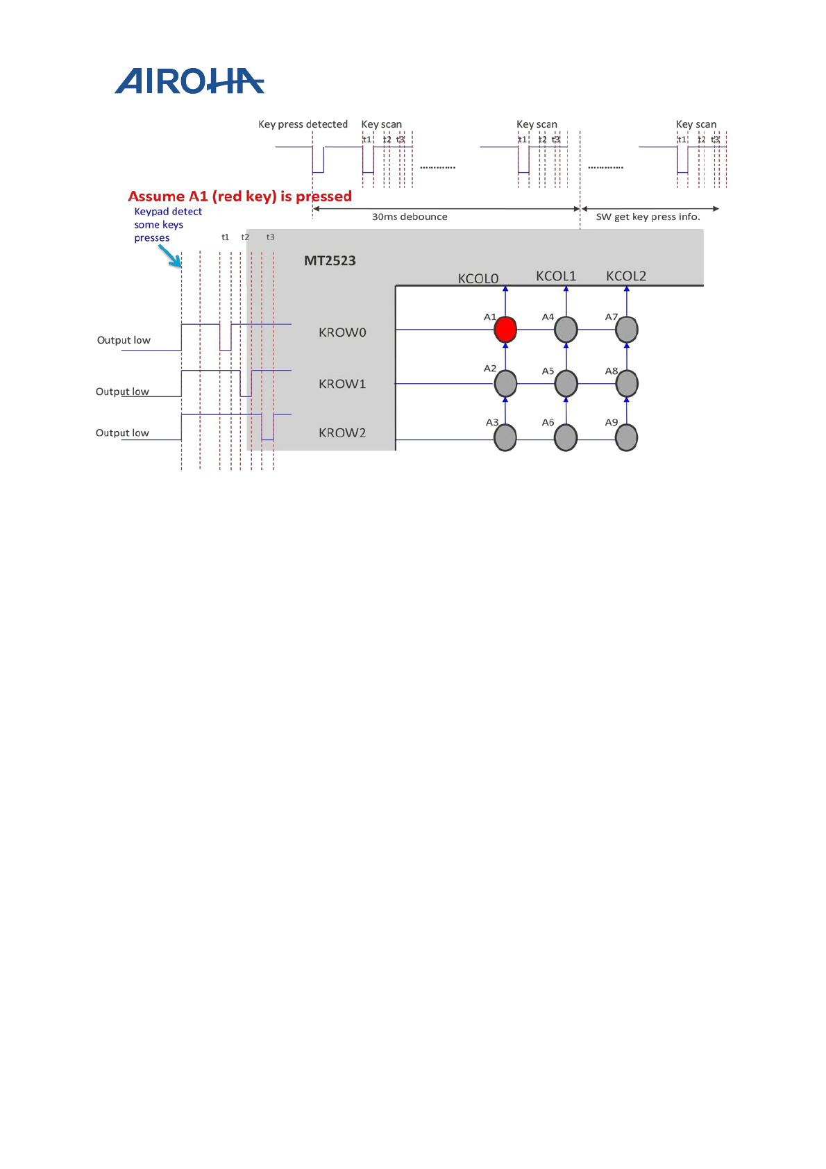
MT2523 Series Reference Manual
© 2015 - 2018 Airoha Technology Corp.
Page 239 of 692
This document contains information that is proprietary to Airoha Technology Corp. (“Airoha”) and/or its licensor(s).
Any unauthorized use, reproduction or disclosure of this document in whole or in part is strictly prohibited.
Figure 14-5. Single keypad detection method
14.1.2.2. Double Keypad Detection Flow
Figure 14-6 is the brief schematic diagram of double keypad internal circuit, including the following characteristics:
1. 20K ohm resistors on new added keys are required.
2. KCOL needs 200K ohm internal PD/PU resistors.
3. KROW needs 2K ohm internal PD resistors.
4. KROW/KCOL should be bi-directional.
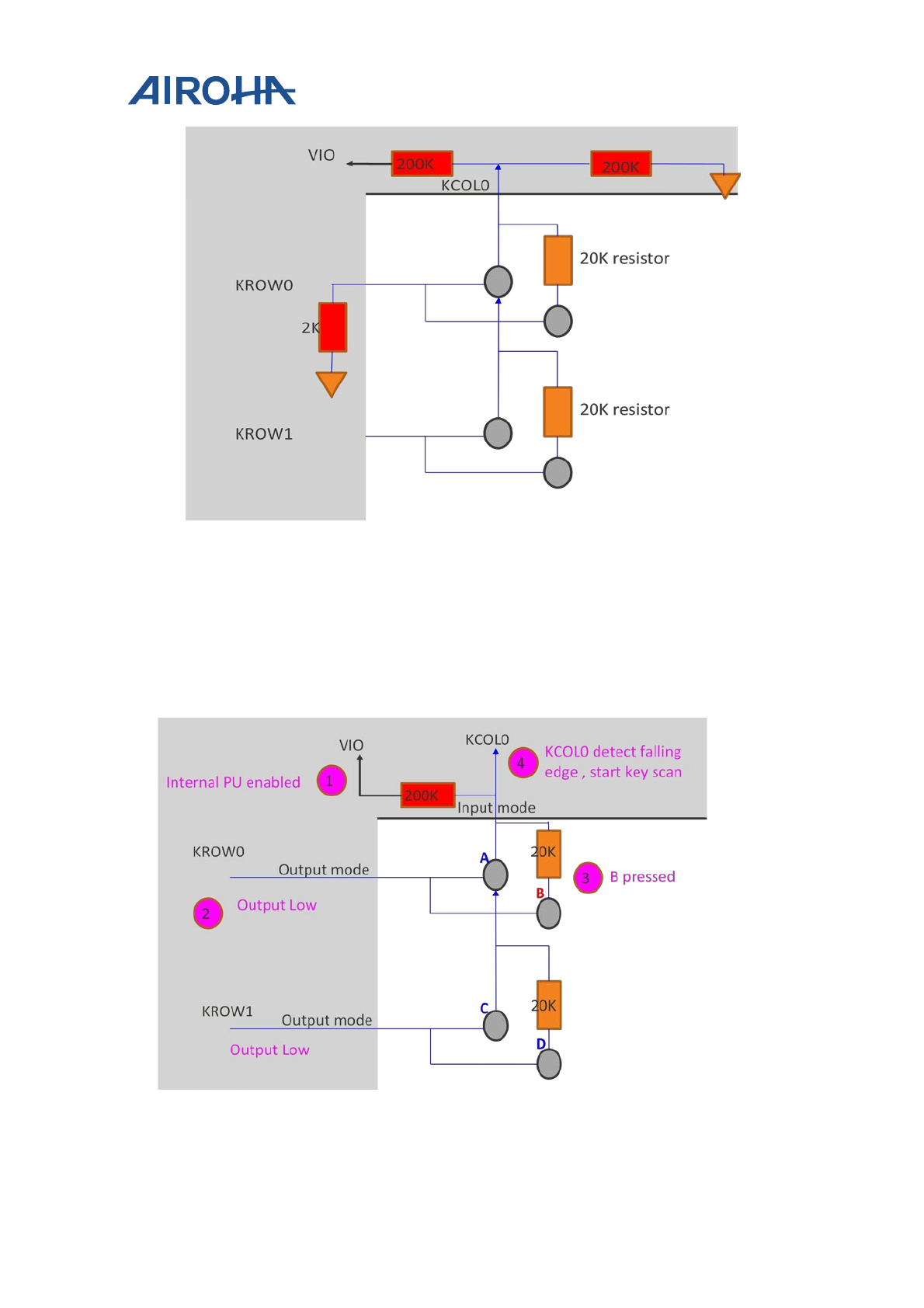
MT2523 Series Reference Manual
© 2015 - 2018 Airoha Technology Corp.
Page 240 of 692
This document contains information that is proprietary to Airoha Technology Corp. (“Airoha”) and/or its licensor(s).
Any unauthorized use, reproduction or disclosure of this document in whole or in part is strictly prohibited.
Figure 14-6. Brief schematic diagram of double keypad
The detection flow of single keypad case in double keypad hardware is described step by step in Figure 14-7, Figure
14-8 and Figure 14-9. In Figure 14-7, KCOLx is initialized as input mode and the KROWx as output mode. In step 1,
internal pull up resistor is enabled in KCOLx to let it stuck at high, and output low to all of KROWx in step 2. In step
4, the falling edge signal can be detected from KCOL0 to start key scanning.
Figure 14-7. Single key case
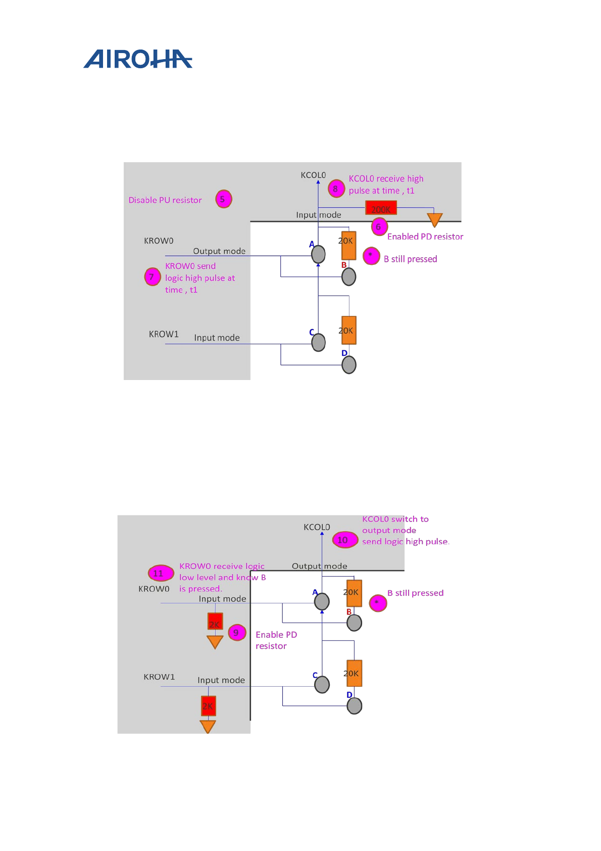
MT2523 Series Reference Manual
© 2015 - 2018 Airoha Technology Corp.
Page 241 of 692
This document contains information that is proprietary to Airoha Technology Corp. (“Airoha”) and/or its licensor(s).
Any unauthorized use, reproduction or disclosure of this document in whole or in part is strictly prohibited.
The keypad row scan is depicted in Figure 14-8. The pull-up resistor is disabled and the pull-down resistor is
enabled to let KCOL0 stuck at low in step 5 and 6. In step 7, KROW0 is sent logic high pulse at time t1, and KCOL0
can receive high pulse signal at time t1 due to key B is still pressed. Hence, the keypad in which rows can be
decided.
Figure 14-8. Row scan
The row position is decided after the row scan. In Figure 14-8, column scanning is conducted to locate the final
position of key. All KROWx are changed to input mode, and pull-down resistor is enabled in step 9. Switch KCOL0
to output mode and send logic high pulse in step 10 for KROW0 to receive logic low level and know key B is
pressed in the final step 11.
Figure 14-9. Column scan
MT2523 Series Reference Manual
© 2015 - 2018 Airoha Technology Corp.
Page 242 of 692
This document contains information that is proprietary to Airoha Technology Corp. (“Airoha”) and/or its licensor(s).
Any unauthorized use, reproduction or disclosure of this document in whole or in part is strictly prohibited.
14.1.3. Programming Guide
14.1.3.1. Single Keypad Command Sequence Example
Address
Register name
R/W
Value
Loop
Register function
A20D0024 KP_EN W 0x0001 Enable keypad
A20D0020 KP_SEL W 0x1c70 Select single keypad
Enable 3 rows and 3 columns
A20D0018
KP_DEBOUNCE
W
0x0018
Set up de-bounce time
A20D0018 KP_DEBOUNCE R 0x0018 Loop
14.1.3.2. Double Keypad Command Sequence Example
Address
Register name
R/W
Value
Loop
Register function
A20D0024 KP_EN W 0x0001 Enable keypad
A20D0020 KP_SEL W 0x1c71
Select double keypad;
Enable 3 rows and 3 columns
A20D0018 KP_DEBOUNCE W 0x0018 Set up de-bounce time
A20D001C
KP_SCAN_TIMING
W
0x0011
A20D0018 KP_DEBOUNCE R 0x0018 Loop
14.2. Register Definition
Module name: KP Base address: (+A20D0000h)
Address
Name
Width
Register Function
A20D0000
KP_STA
16
Keypad Status
A20D0004 KP_MEM1 16
Keypad Scanning Output Register
Shows the key-pressed status of key 0 (LSB) ~ key 15. Refer to Table
14-1 and Table 14-2.
A20D0008 KP_MEM2 16
Keypad Scanning Output Register
Shows the key-pressed status of key 16 (LSB) ~ key 31. Refer to
Table 14-1 and Table 14-2.
A20D0018 KP_DEBOUNCE 16
De-bounce Period Setting
Defines the waiting period before key pressing or release events are
considered stable. If the de-bounce setting is too small, the keypad
will be too sensitive and detect too many unexpected key presses.
The suitable de-bounce time setting must be adjusted according to
the user's habit.
A20D001C KP_SCAN_TIMI
NG 16
Keypad Scan Timing Adjustment Register
Sets up the 3*3 keypad scan timing. Note: ROW_SCAN_DIV >
ROW_ HIGH_PULSE and COL_SCAN_DIV > COL_
HIGH_PULSE. ROW_ HIGH_PULSE /COL_ HIGH_PULSE are
used to lower the power consumption for it decreases the actual scan
number during the de-bounce time.
A20D0020 KP_SEL 16
Keypad Selection Register
For selecting:
1: To use single keypad or double keypad
2: Which cols and rows are used when double keypad is used
A20D0024 KP_EN 16
Keypad Enable Register
Enables/Disables keypad.
MT2523 Series Reference Manual
© 2015 - 2018 Airoha Technology Corp.
Page 243 of 692
This document contains information that is proprietary to Airoha Technology Corp. (“Airoha”) and/or its licensor(s).
Any unauthorized use, reproduction or disclosure of this document in whole or in part is strictly prohibited.
A20D0000
KP_STA
Keypad Status
0000
Bit
15
14
13
12
11
10
9
8
7
6
5
4
3
2
1
0
Name
STA
Type
RO
Reset
0
Overview
Bit(s)
Mnemonic
Name
Description
0
STA
STA
Indicates keypad status
This register will not be cleared by the read operation.
0: No key pressed
1: Key pressed
A20D0004
KP_MEM1
Keypad Scanning Output Register
EE3F
Bit
15
14
13
12
11
10
9
8
7
6
5
4
3
2
1
0
Name
KEY1
5
KEY1
4
KEY1
3
KEY11
KEY1
0
KEY9
KEY5
KEY4
KEY3
KEY2
KEY1
KEY0
Type
RO
RO
RO
RO
RO
RO
RO
RO
RO
RO
RO
RO
Reset
1
1
1
1
1
1
1
1
1
1
1
1
Overview
Shows the key-pressed status of key 0 (LSB) ~ key 15. Refer to Table 14-1 and Table 14-2.
Bit(s)
Mnemonic
Name
Description
15
KEY15
KEY15
14
KEY14
KEY14
13
KEY13
KEY13
11
KEY11
KEY11
10
KEY10
KEY10
9
KEY9
KEY9
5
KEY5
KEY5
4
KEY4
KEY4
3
KEY3
KEY3
2
KEY2
KEY2
1
KEY1
KEY1
0
KEY0
KEY0
A20D0008
KP_MEM2
Keypad Scanning Output Register
FC1F
Bit
15
14
13
12
11
10
9
8
7
6
5
4
3
2
1
0
Name
KEY3
1
KEY3
0
KEY2
9
KEY2
8
KEY2
7
KEY2
6
KEY2
0
KEY1
9
KEY1
8
KEY1
7
KEY1
6
Type
RO
RO
RO
RO
RO
RO
RO
RO
RO
RO
RO
Reset
1
1
1
1
1
1
1
1
1
1
1
Overview
Shows the key-pressed status of key 16 (LSB) ~ key 31. Refer to Table 14-1 and Table 14-2.
Bit(s)
Mnemonic
Name
Description
15
KEY31
KEY31
14
KEY30
KEY30
13
KEY29
KEY29
MT2523 Series Reference Manual
© 2015 - 2018 Airoha Technology Corp.
Page 244 of 692
This document contains information that is proprietary to Airoha Technology Corp. (“Airoha”) and/or its licensor(s).
Any unauthorized use, reproduction or disclosure of this document in whole or in part is strictly prohibited.
Bit(s)
Mnemonic
Name
Description
12
KEY28
KEY28
11
KEY27
KEY27
10
KEY26
KEY26
4
KEY20
KEY20
3
KEY19
KEY19
2
KEY18
KEY18
1
KEY17
KEY17
0
KEY16
KEY16
A20D0018
KP_DEBOUNC
E
De
-bounce Period Setting
0400
Bit
15
14
13
12
11
10
9
8
7
6
5
4
3
2
1
0
Name
DEBOUNCE
Type
RW
Reset
0
0
0
1
0
0
0
0
0
0
0
0
0
0
Overview
Defines the waiting period before key pressing or release events are considered stable. If the de-
bounce setting is too small, the keypad will be too sensitive and detect too many unexpected key
presses. The suitable de-bounce time setting must be adjusted according to the user's habit.
Bit(s)
Mnemonic
Name
Description
13:0
DEBOUNC
E
DEBOUNCE
De-bounce time = KP_DEBOUNCE/32ms
A20D001C
KP_SCAN_TIM
ING
Keypad Scan Timing Adjustment Register
0011
Bit
15
14
13
12
11
10
9
8
7
6
5
4
3
2
1
0
Name
COL_ HIGH_PULSE
ROW_ HIGH_PULSE
COL_SCAN_DIV
ROW_SCAN_DIV
Type
RW
RW
RW
RW
Reset
0
0
0
0
0
0
0
0
0
0
0
1
0
0
0
1
Overview
Sets up the 3*3 keypad scan timing for double keypad.
Note: ROW_SCAN_DIV > ROW_ HIGH_PULSE and COL_SCAN_DIV > COL_ HIGH_PULSE.
ROW_ HIGH_PULSE /COL_ HIGH_PULSE are used to lower the power consumption for it
decreases the actual scan number during the de-bounce time.
Bit(s)
Mnemonic
Name
Description
15:12
COL_
HIGH_PUL
SE
COL_HIGH_PULSE
Sets up the COL SCAN high pulse, i.e. cycles of the scan high
pulse
Default 0 means the high scan pulse needs 1 cycle.
11:8
ROW_
HIGH_PUL
SE
ROW_HIGH_PULS
E
Sets up the ROW SCAN high pulse, i.e. cycles of the scan high
pulse
Default 0 means the high scan pulse needs 1 cycle.
7:4
COL_SCAN
_DIV
COL_SCAN_DIV
Sets up the COL SCAN cycle which includes
COL_INTERVAL_DIV and the high pulse period
Default 1 means there are 2 cycles for each scan, including 1 cycle high
pulse and 1 cycle interval.
3:0
ROW_SCA
N_DIV
ROW_SCAN_DIV
Sets up the ROW SCAN cycle which includes
ROW_INTERVAL_DIV and the high pulse period
Default 1 means there are 2 cycles for each scan, including 1 cycle high
pulse and 1 cycle interval.
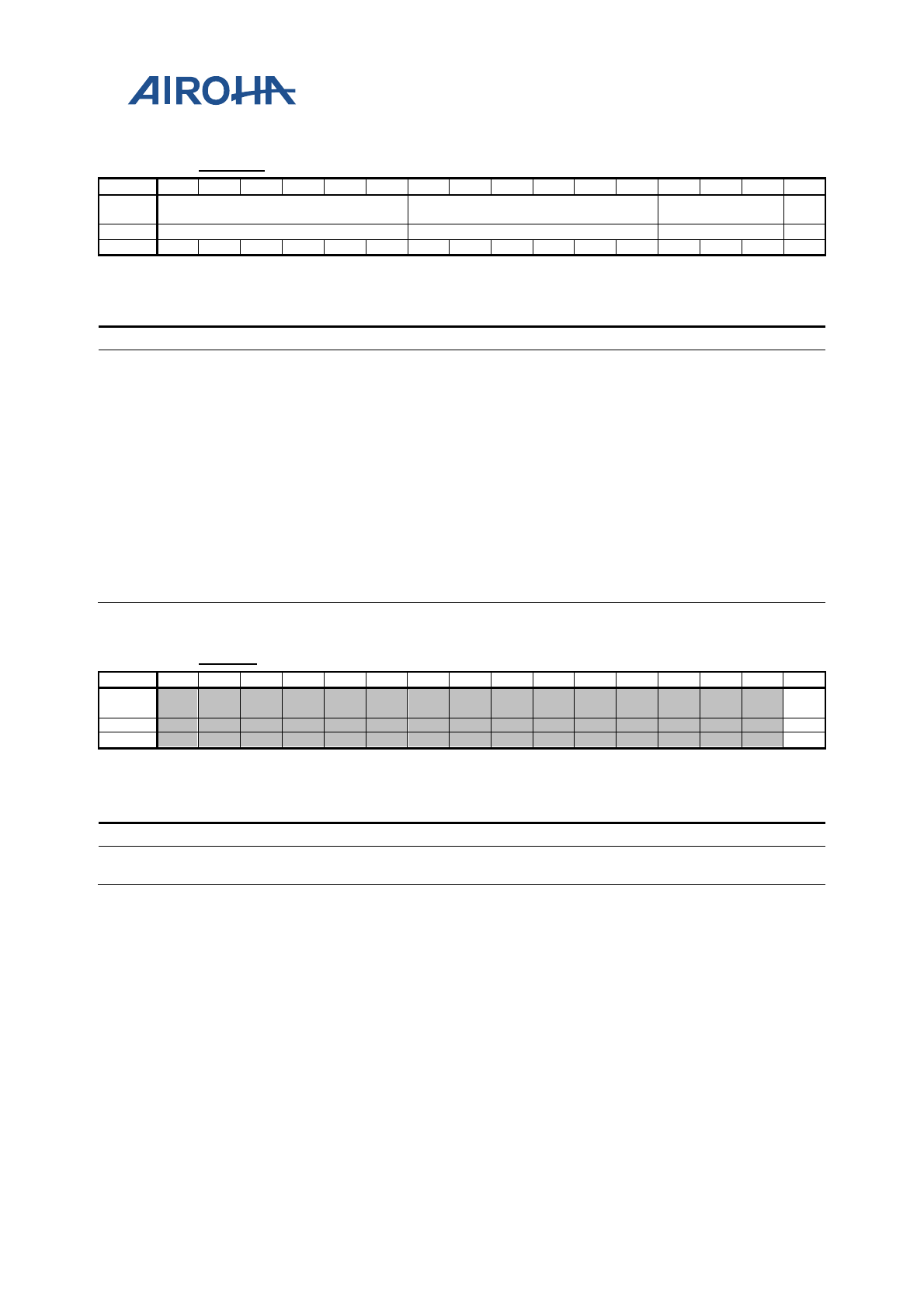
MT2523 Series Reference Manual
© 2015 - 2018 Airoha Technology Corp.
Page 245 of 692
This document contains information that is proprietary to Airoha Technology Corp. (“Airoha”) and/or its licensor(s).
Any unauthorized use, reproduction or disclosure of this document in whole or in part is strictly prohibited.
A20D0020
KP_SEL
Keypad Selection Register
1C70
Bit
15
14
13
12
11
10
9
8
7
6
5
4
3
2
1
0
Name KP1_COL_SEL KP1_ROW_SEL DUMMY2
KP_S
EL
Type
RW
RW
RW
DC
Reset
0
0
0
1
1
1
0
0
0
1
1
1
0
0
0
0
Overview
For selecting: 1) To use single keypad or double keypad; 2) Which cols and rows are used when
double keypad is used
Bit(s)
Mnemonic
Name
Description
15:10
KP1_COL_
SEL
KP1_COL_SEL
Selects which cols are used when double keypad is used
MT2523 supports maximum 3*3 double. col2, col1 and col0 can be
used.
0: Disable corresponding column
1: Enable corresponding column
9:4
KP1_ROW_
SEL
KP1_ROW_SEL
Selects which rows are used when double keypad is used
MT2523 supports maximum 3*3 double. row2, row1 and row0 can be
used.
0: Disable corresponding row
1: Enable corresponding row
3:1
DUMMY2
DUMMY2
0
KP_SEL
KP_SEL
Selects to use single keypad or double keypad
0: Use single keypad
1: Use double keypad
A20D0024
KP_EN
Keypad Enable Register
0001
Bit
15
14
13
12
11
10
9
8
7
6
5
4
3
2
1
0
Name
KP_E
N
Type
RW
Reset
0
Overview
Enables/Disables keypad.
Note: When KP_EN is set to 0, both single and double keypad registers cannot be read and written.
Bit(s)
Mnemonic
Name
Description
0
KP_EN
KP_EN
0: Disable keypad (Both single and double keypad will not work.)
1: Enable keypad (Either single or double keypad will work.)

MT2523 Series Reference Manual
© 2015 - 2018 Airoha Technology Corp.
Page 246 of 692
This document contains information that is proprietary to Airoha Technology Corp. (“Airoha”) and/or its licensor(s).
Any unauthorized use, reproduction or disclosure of this document in whole or in part is strictly prohibited.
15. General Purpose Counter
15.1. General Description
General purpose counter (GP-counter) is a counter to count a pad toggle times and furthermore calculates the
moving speed. It counts once the channel is enabled and provides an interrupt which will be triggered when the
counter exceeds the threshold.
Depending on the pulse width from pad, you can choose suitable clock source for the GP-counter: 32kHz or 26MHz.
You only have to set up GPCOUNTER_MISC[8]: GPC_BCLK_SEL to choose. The GP-counter will add 1 when the
pluse width from pad is longer than debouce time, which is set on GPCOUNTER_DEBOUNCE.
GP-counter is an always on IP. When the system is in sleep mode, it still works. However, there is no 26MHz clock
source in sleep mode, so users have to switch the clock source to 32kHz, which sets GPCOUNTER_MISC[8]:
GPC_BCLK_SEL to 1’b1.
GP-counter can trigger interrupt and wake-up events (level). You can set up EINT to capture wake-up events from
GP-counter before the system enters sleep mode. Refer to EINT datasheet for more details.
15.1.1. Programming Guide
GP-counter is an always on IP. To save the most power, the software has to power down the block clock to the
module. You may set up the GP-counter register before powering on the block clock. Next, set up
GPCOUNTER_CON_SET to start counting and set GPCOUNTER_CON_CLR to end counting. Read GPCOUNTER_CON
to see if GP-counter is enabled or not.
The counted data are stored in GPCOUNTER_DATA. Once GPCOUNTER_DATA is read, you may get the number
and clear the counter at the same time.
Programming sequence:
1. Set up GP-Counter register: Set up clock source, interrupt enable, debounce time, and threshold.
a. Select 32K clock source before the system enters sleep mode.
b. Power down GP-counter block clock first then switch block clock source.
2. Power on GP-counter block clock.
3. Set up GPCOUNTER_CON_SET to start counting.
4. Set up GPCOUNTER_CON_CLR to end counting.
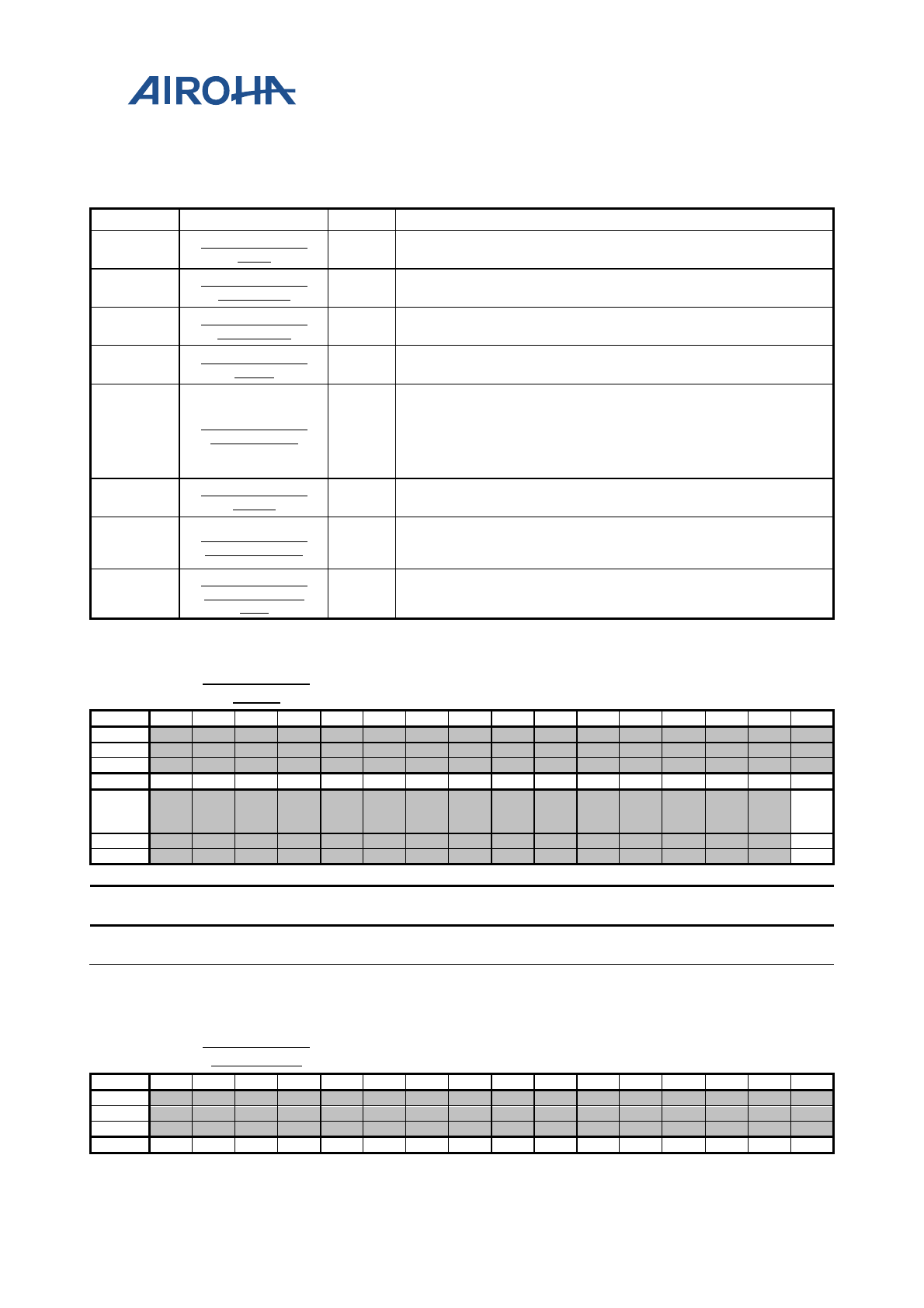
MT2523 Series Reference Manual
© 2015 - 2018 Airoha Technology Corp.
Page 247 of 692
This document contains information that is proprietary to Airoha Technology Corp. (“Airoha”) and/or its licensor(s).
Any unauthorized use, reproduction or disclosure of this document in whole or in part is strictly prohibited.
15.2. Register Definition
Module name: GPCOUNTER Base address: (+A21E0000h)
Address
Name
Width
Register Function
A21E0000 GPCOUNTER_
CON 32
GPCOUNTER Control Register
Shows the GP counter status (counter enabled or not).
A21E0004 GPCOUNTER_
CON_SET 32
GPCOUNTER Control Set Register
Sets up the GP counter status (counter enabled).
A21E0008 GPCOUNTER_
CON_CLR 32 GPCOUNTER Control Clear Register
Clears the GP counter enable status (counter not enabled).
A21E000C GPCOUNTER_
MISC 32 GPCOUNTER MISC Setting
Defines clock and interrupt, etc.
A21E0010 GPCOUNTER_
DEBOUNCE 32
GPCOUNTER De-bounce Period Setting
Defines the waiting period before PAD pressing events are
considered stable. If the de-bounce setting is too small, the
counter will be too sensitive and detect too many unexpected PAD
presses. The suitable de-bounce time setting should be adjusted
according to the user's habit.
A21E0014 GPCOUNTER_
DATA 32
GPCOUNTER Counter for Clear (Read and Clear)
Data counted by GPCOUNTER will be cleared once they are read
A21E0018 GPCOUNTER_
THRESHOLD 32
GPCOUNTER Threshold
When the counter value is bigger than or equal to GPCOUNTER
Threshold, the GP counter interrupt will be triggered.
A21E001C GPCOUNTER_
INTERRUPT_
STA 32 GPCOUNTER Interrupt Status
Interrupt status
A21E0000 GPCOUNTER
_CON GPCOUNTER Control Register 00000000
Bit
31
30
29
28
27
26
25
24
23
22
21
20
19
18
17
16
Name
Type
Reset
Bit
15
14
13
12
11
10
9
8
7
6
5
4
3
2
1
0
Name
GP
C_
EN
Type
RO
Reset
0
Bit(s) Mnemoni
c Name Description
0 GPC_EN GPC_CH_EN 0: Not enable mode.
1: Enable mode.
A21E0004 GPCOUNTER
_CON_SET GPCOUNTER Control Set Register 00000000
Bit
31
30
29
28
27
26
25
24
23
22
21
20
19
18
17
16
Name
Type
Reset
Bit
15
14
13
12
11
10
9
8
7
6
5
4
3
2
1
0
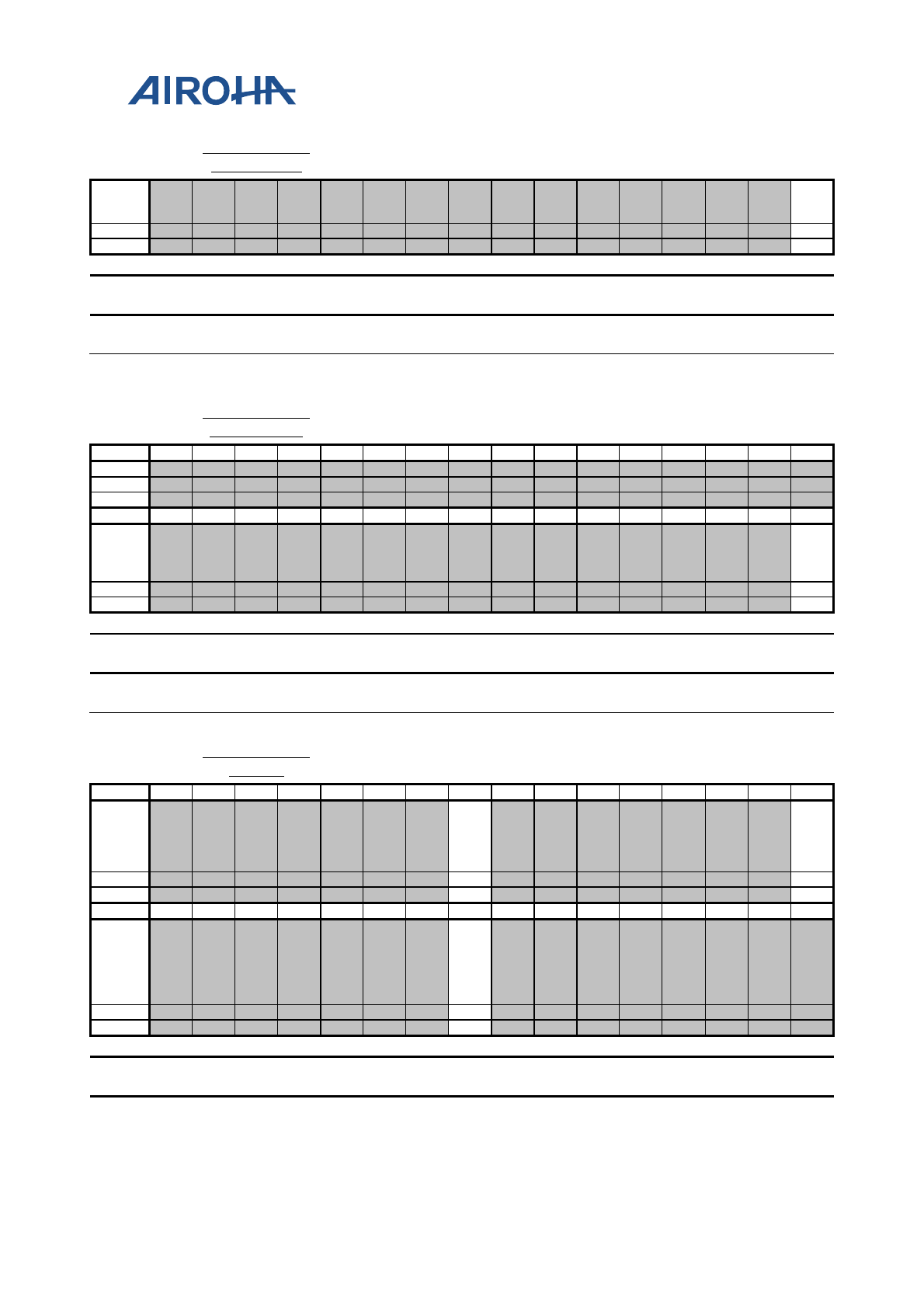
MT2523 Series Reference Manual
© 2015 - 2018 Airoha Technology Corp.
Page 248 of 692
This document contains information that is proprietary to Airoha Technology Corp. (“Airoha”) and/or its licensor(s).
Any unauthorized use, reproduction or disclosure of this document in whole or in part is strictly prohibited.
A21E0004 GPCOUNTER
_CON_SET GPCOUNTER Control Set Register 00000000
Name
GP
C_S
ET
Type
WO
Reset
0
Bit(s) Mnemoni
c Name Description
0 GPC_SET GPC_SET 0: Not enable counter
1: Enable counter
A21E0008 GPCOUNTER
_CON_CLR GPCOUNTER Control Clear Register 00000000
Bit
31
30
29
28
27
26
25
24
23
22
21
20
19
18
17
16
Name
Type
Reset
Bit
15
14
13
12
11
10
9
8
7
6
5
4
3
2
1
0
Name
GP
C_
CL
R
Type
WO
Reset
0
Bit(s) Mnemoni
c Name Description
0 GPC_CLR GPC_CLR 0: Enable counter
1: Clear counter enabled
A21E000C GPCOUNTER
_MISC GPCOUNTER MISC Setting 00010001
Bit
31
30
29
28
27
26
25
24
23
22
21
20
19
18
17
16
Name
GP
C_I
NV
_E
N
GP
C_I
NT
_E
N
Type
RW
RW
Reset
0
1
Bit
15
14
13
12
11
10
9
8
7
6
5
4
3
2
1
0
Name
GP
C_
BC
LK
_SE
L
Type
RW
Reset
0
Bit(s) Mnemoni
c Name Description
24 GPC_INV
_EN GPC_INV_EN
GP-counter will detect rising edge from Pad_in toggle
0: Detect rising edge of a toggle
1: Detect falling edge of a toggle
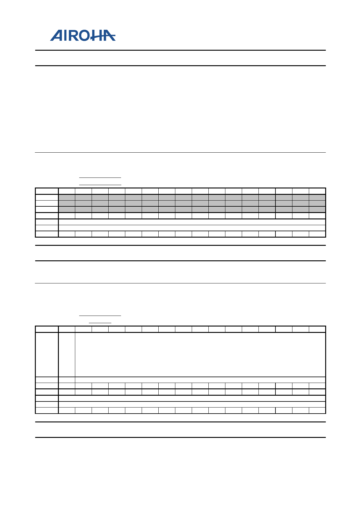
MT2523 Series Reference Manual
© 2015 - 2018 Airoha Technology Corp.
Page 249 of 692
This document contains information that is proprietary to Airoha Technology Corp. (“Airoha”) and/or its licensor(s).
Any unauthorized use, reproduction or disclosure of this document in whole or in part is strictly prohibited.
Bit(s) Mnemoni
c Name Description
Note: Set GPC_INV_EN as the default level of signal from pad (HIGH
or LOW). Once the GP-counter is disabled (GPC_CH_EN=1'b0), it will
keep pad-in signal LEVEL as GPC_INV_EN, no matter the level of
signal from the pad is HIGH or LOW. Issues will happen when the
default level of signal from pad is different from GPC_INV_EN. For
example, when GPC_INV_EN=1'b0, but the default level of signal
from pad is HIGH, the GP-counter will automatically add 1 when
GPC_CH_EN goes from 0 to 1.
16 GPC_INT
_EN GPC_INT_EN 0: For disable
1: For enable
8 GPC_BCL
K_SEL GPC_CLK_SEL 0: Clock from 26MHz
1: Clock from 32kHz
A21E0010 GPCOUNTER
_DEBOUNCE GPCOUNTER De-bounce Period Setting 00000001
Bit
31
30
29
28
27
26
25
24
23
22
21
20
19
18
17
16
Name
Type
Reset
Bit
15
14
13
12
11
10
9
8
7
6
5
4
3
2
1
0
Name
GPC_PAD_DEB
Type
RW
Reset
0
0
0
0
0
0
0
0
0
0
0
0
0
0
0
1
Bit(s) Mnemoni
c Name Description
15:0 GPC_PA
D_DEB GPC_DEBOUNCE
De-bounce time = DEB_TIME*clock period
GPC_COUNTER counts according to the GP counter clock, which can
be selected by register GPC_BCLK_SEL.
A21E0014 GPCOUNTER
_DATA
GPCOUNTER Counter for Clear (Read and
Clear) 00000000
Bit
31
30
29
28
27
26
25
24
23
22
21
20
19
18
17
16
Name
GP
C_
CO
UN
TE
R1_
DA
TA
GPC_COUNTER1_OVERFLOW[30:16]
Type
RO
RO
Reset
0
0
0
0
0
0
0
0
0
0
0
0
0
0
0
0
Bit
15
14
13
12
11
10
9
8
7
6
5
4
3
2
1
0
Name
GPC_COUNTER1_OVERFLOW[15:0]
Type
RO
Reset
0
0
0
0
0
0
0
0
0
0
0
0
0
0
0
0
Bit(s) Mnemoni
c Name Description
31 GPC_CO
UNTER1_
GPC_OVERFLOW 0: Not overflow
1: Overflow
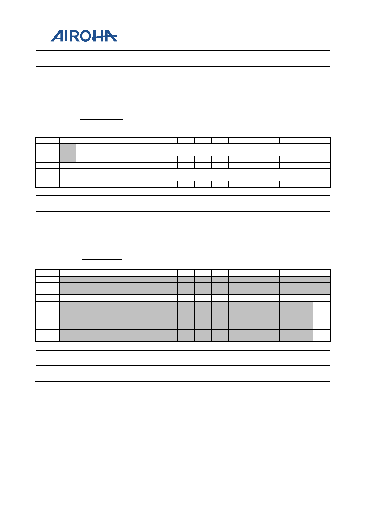
MT2523 Series Reference Manual
© 2015 - 2018 Airoha Technology Corp.
Page 250 of 692
This document contains information that is proprietary to Airoha Technology Corp. (“Airoha”) and/or its licensor(s).
Any unauthorized use, reproduction or disclosure of this document in whole or in part is strictly prohibited.
Bit(s) Mnemoni
c Name Description
DATA
30:0
GPC_CO
UNTER1_
OVERFL
OW
GPC_COUNTER Data counted by GPCOUNTER (read and clear)
A21E0018
GPCOUNTER
_THRESHOL
D
GPCOUNTER Threshold 60000000
Bit
31
30
29
28
27
26
25
24
23
22
21
20
19
18
17
16
Name
GPC_THRESHOLD[30:16]
Type
RW
Reset
1
1
0
0
0
0
0
0
0
0
0
0
0
0
0
Bit
15
14
13
12
11
10
9
8
7
6
5
4
3
2
1
0
Name
GPC_THRESHOLD[15:0]
Type
RW
Reset
0
0
0
0
0
0
0
0
0
0
0
0
0
0
0
0
Bit(s) Mnemoni
c Name Description
30:0 GPC_TH
RESHOL
D
GPC_THRESHOL
D
If GPC_COUNTER > GPC_THRESHOLD, IRQ request.
GPC_COUNTER counts according to the GP counter clock, which can
be selected by register GPC_BCLK_SEL.
A21E001C
GPCOUNTER
_INTERRUP
T_STA
GPCOUNTER Interrupt Status 00000000
Bit
31
30
29
28
27
26
25
24
23
22
21
20
19
18
17
16
Name
Type
Reset
Bit
15
14
13
12
11
10
9
8
7
6
5
4
3
2
1
0
Name
GP
C_I
NT
_ST
A
Type
RO
Reset
0
Bit(s) Mnemoni
c Name Description
0 GPC_INT
_STA GPC_INT_STA 0: Interrupt
1: No interrupt
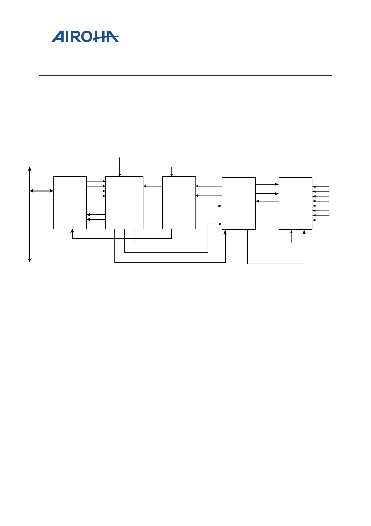
MT2523 Series Reference Manual
© 2015 - 2018 Airoha Technology Corp.
Page 251 of 692
This document contains information that is proprietary to Airoha Technology Corp. (“Airoha”) and/or its licensor(s).
Any unauthorized use, reproduction or disclosure of this document in whole or in part is strictly prohibited.
16. Auxiliary ADC Unit
16.1. General Description
MT2523 features one auxiliary ADC function. The auxiliary ADC unit is for identifying the plugged peripheral. The
ADC function contains 8 channels for measuring external channel or internal use and a 12-bit SAR (Successive
Approximation Register) ADC.
AUXADC_REG
APB
BUS AUXADC_CORE AUXADC_SIF
F13M_EN
ADC_SDAT
A
ADC_SFS
ADC_SCKO
ADC_RDY
ADC_LATCH
IMMEDIATE_STR
ADC_STATE
AUTOSET_STR
SEL_LATCH [7:0]
PUWAIT_EN
PDN_AUXADC
ADC_PDN
ADC_SEL_IN
ADC_S
T
SADC_SIF ADC
DAC
COMP
Vin
Latch_Dat
a
SPLD
ADC_SEL_OUT
Figure 16-1. AUXADC architecture
Each channel operates in immediate mode. In immediate mode, the A/D converter samples the value once only
when the flag of channel in the AUXADC_CON1 register is set. For example, if flag IMM0 in AUXADC_CON1 is set,
the A/D converter will sample the data for channel 0. The IMM flags should be cleared and set again to initialize
another sampling.
The value sampled for channel 0 is stored in register AUXADC_DAT0, and the value for channel 1 is stored in
register AUXADC_DAT1, and so on.
If the AUTOSET flag in register AUXADC_CON3 is set, the auto-sample function will be enabled. So far, it is used in
test mode only. The A/D converter samples the data for the channel in which the corresponding data register is
read. For example, the AUTOSET flag is set. When the data register AUXADC_DAT0 is read, the A/D converter will
sample the next value for channel 0 immediately.
If multiple channels are selected at the same time, the task will be performed sequentially on every selected
channel. For example, if AUXADC_CON1 is set to 0x3f, i.e. 6 channels are selected, the state machine in the unit
will start sampling from channel 5 to channel 0 and save the values of each input channel in respective registers.
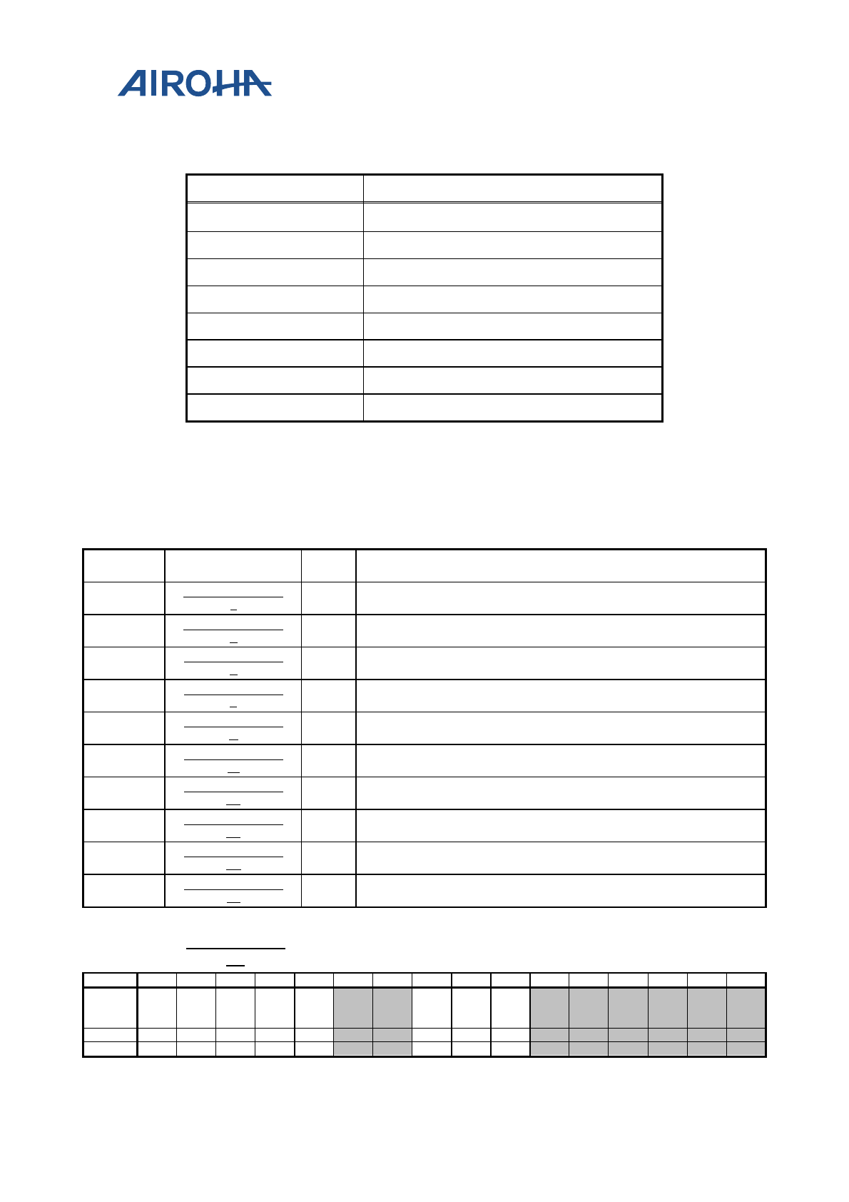
MT2523 Series Reference Manual
© 2015 - 2018 Airoha Technology Corp.
Page 252 of 692
This document contains information that is proprietary to Airoha Technology Corp. (“Airoha”) and/or its licensor(s).
Any unauthorized use, reproduction or disclosure of this document in whole or in part is strictly prohibited.
Table 16-1. AUXADC channel description
AUXADC Channel ID Description
Channel 6 GPDAC (test only)
Channel 7 Audio DL_HPL (internal use)
Channel 8 Audio DL_HPR (internal use)
Channel 11 External
Channel 12 External
Channel 13 External
Channel 14 External
Channel 15 External
16.2. Register Definition
Module name: AUXADC Base address: (+A0240000h)
Address Name
Widt
h Register Function
A0240004
AUXADC_CON
1 16 Auxiliary ADC Control Register 1
A024000C AUXADC_CON
3 16 Auxiliary ADC Control Register 3
A0240028
AUXADC_DAT
6 16 Auxiliary ADC Channel 6 Register (GPDAC)
A024002C
AUXADC_DAT
7 16 Auxiliary ADC Channel 7 Register (Audio DL_HPL)
A0240030
AUXADC_DAT
8 16 Auxiliary ADC Channel 8 Register (Audio DL_HPR)
A024003C AUXADC_DAT
11 16 Auxiliary ADC Channel 11 Register (External)
A0240040
AUXADC_DAT
12 16 Auxiliary ADC Channel 12 Register (External)
A0240044
AUXADC_DAT
13 16 Auxiliary ADC Channel 13 Register (External)
A0240048
AUXADC_DAT
14 16 Auxiliary ADC Channel 14 Register (External)
A024004C AUXADC_DAT
15 16 Auxiliary ADC Channel 15 Register (External)
A0240004 AUXADC_CO
N1 Auxiliary ADC Control Register 1 0000
Bit
15
14
13
12
11
10
9
8
7
6
5
4
3
2
1
0
Name
IM
M1
5
IM
M1
4
IM
M1
3
IM
M1
2
IM
M11 IM
M8 IM
M7 IM
M6
Type
RW
RW
RW
RW
RW
RW
RW
RW
Reset
0
0
0
0
0
0
0
0
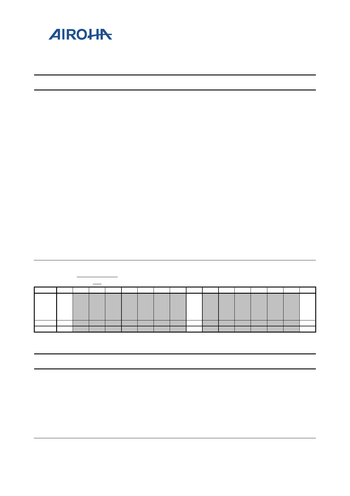
MT2523 Series Reference Manual
© 2015 - 2018 Airoha Technology Corp.
Page 253 of 692
This document contains information that is proprietary to Airoha Technology Corp. (“Airoha”) and/or its licensor(s).
Any unauthorized use, reproduction or disclosure of this document in whole or in part is strictly prohibited.
Overview
These bits are set individually to sample the data for the corresponding channel. It
supports multiple flags.
Bit(s) Mnemoni
c Name Description
15 IMM15 IMM15 Channel 15 immediate mode
0: The channel is not selected.
1: The channel is selected.
14 IMM14 IMM14 Channel 14 immediate mode
0: The channel is not selected.
1: The channel is selected.
13 IMM13 IMM13 Channel 13 immediate mode
0: The channel is not selected.
1: The channel is selected.
12 IMM12 IMM12 Channel 12 immediate mode
0: The channel is not selected.
1: The channel is selected.
11 IMM11 IMM11 Channel 11 immediate mode
0: The channel is not selected.
1: The channel is selected.
8 IMM8 IMM8 Channel 8 immediate mode
0: The channel is not selected.
1: The channel is selected.
7 IMM7 IMM7 Channel 7 immediate mode
0: The channel is not selected.
1: The channel is selected.
6 IMM6 IMM6 Channel 6 immediate mode
0: The channel is not selected.
1: The channel is selected.
A024000
C AUXADC_CO
N3 Auxiliary ADC Control Register 3 0010
Bit
15
14
13
12
11
10
9
8
7
6
5
4
3
2
1
0
Name AU
TO
SET
SO
FT_
RS
T
AU
XA
DC
_ST
A
Type
RW
RW
RO
Reset
0
0
0
Overview
Bit(s) Mnemoni
c Name Description
15 AUTOSET AUTOSET
(Test mode only) Defines the auto-sample mode of the
module. In auto-sample mode, each channel with its sample
register read can start sampling immediately without
configuring the control register AUXADC_CON1 again.
7 SOFT_RS
T SOFT_RST Software reset AUXADC state machine
0: Normal function
1: Reset AUXADC state machine
0 AUXADC
_STA AUXADC_STA Defines the state of the module
0: This module is idle.
1: This module is busy.
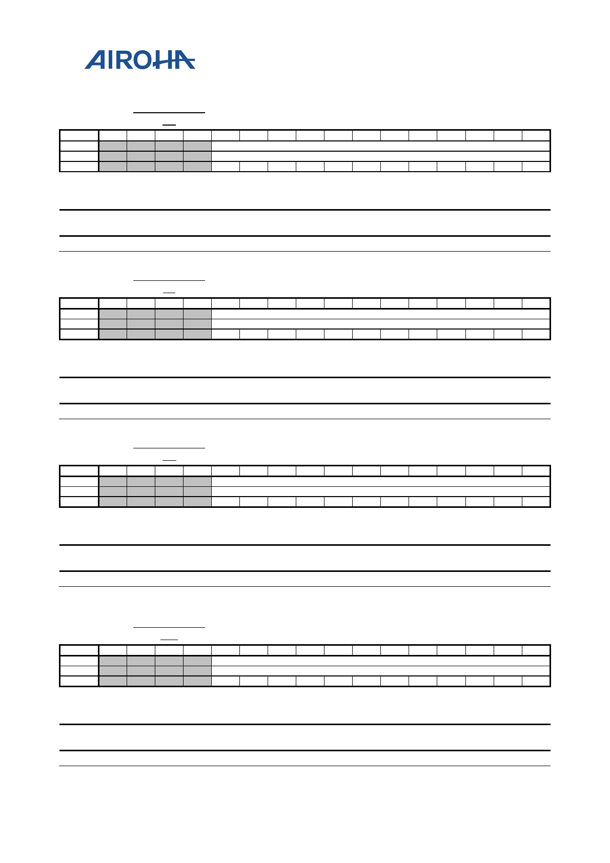
MT2523 Series Reference Manual
© 2015 - 2018 Airoha Technology Corp.
Page 254 of 692
This document contains information that is proprietary to Airoha Technology Corp. (“Airoha”) and/or its licensor(s).
Any unauthorized use, reproduction or disclosure of this document in whole or in part is strictly prohibited.
A0240028 AUXADC_DA
T6 Auxiliary ADC Channel 6 Register (GPDAC) 0000
Bit
15
14
13
12
11
10
9
8
7
6
5
4
3
2
1
0
Name
DAT6
Type
RO
Reset
0
0
0
0
0
0
0
0
0
0
0
0
Overview
Bit(s) Mnemoni
c Name Description
11:0 DAT6 DAT6 Sampled data for channel 6
A024002C AUXADC_DA
T7 Auxiliary ADC Channel 7 Register (Audio
DL_HPL) 0000
Bit
15
14
13
12
11
10
9
8
7
6
5
4
3
2
1
0
Name
DAT7
Type
RO
Reset
0
0
0
0
0
0
0
0
0
0
0
0
Overview
Bit(s) Mnemoni
c Name Description
11:0 DAT7 DAT7 Sampled data for channel7
A0240030 AUXADC_DA
T8 Auxiliary ADC Channel 8 Register (Audio
DL_HPR) 0000
Bit
15
14
13
12
11
10
9
8
7
6
5
4
3
2
1
0
Name
DAT8
Type
RO
Reset
0
0
0
0
0
0
0
0
0
0
0
0
Overview
Bit(s) Mnemoni
c Name Description
11:0 DAT8 DAT8 Sampled data for channel 8
A024003C AUXADC_DA
T11 Auxiliary ADC Channel 11 Register (External) 0000
Bit
15
14
13
12
11
10
9
8
7
6
5
4
3
2
1
0
Name
DAT11
Type
RO
Reset
0
0
0
0
0
0
0
0
0
0
0
0
Overview
Bit(s) Mnemoni
c Name Description
11:0 DAT11 DAT11 Sampled data for channel 11

MT2523 Series Reference Manual
© 2015 - 2018 Airoha Technology Corp.
Page 255 of 692
This document contains information that is proprietary to Airoha Technology Corp. (“Airoha”) and/or its licensor(s).
Any unauthorized use, reproduction or disclosure of this document in whole or in part is strictly prohibited.
A0240040 AUXADC_DA
T12 Auxiliary ADC Channel 12 Register (External) 0000
Bit
15
14
13
12
11
10
9
8
7
6
5
4
3
2
1
0
Name
DAT12
Type
RO
Reset
0
0
0
0
0
0
0
0
0
0
0
0
Overview
Bit(s) Mnemoni
c Name Description
11:0 DAT12 DAT12 Sampled data for channel 12
A0240044 AUXADC_DA
T13 Auxiliary ADC Channel 13 Register (External) 0000
Bit
15
14
13
12
11
10
9
8
7
6
5
4
3
2
1
0
Name
DAT13
Type
RO
Reset
0
0
0
0
0
0
0
0
0
0
0
0
Overview
Bit(s) Mnemoni
c Name Description
11:0 DAT13 DAT13 Sampled data for channel 13
A0240048 AUXADC_DA
T14 Auxiliary ADC Channel 14 Register (External) 0000
Bit
15
14
13
12
11
10
9
8
7
6
5
4
3
2
1
0
Name
DAT14
Type
RO
Reset
0
0
0
0
0
0
0
0
0
0
0
0
Overview
Bit(s) Mnemoni
c Name Description
11:0 DAT14 DAT14 Sampled data for channel 14
A024004
C AUXADC_DA
T15 Auxiliary ADC Channel 15 Register (External) 0000
Bit
15
14
13
12
11
10
9
8
7
6
5
4
3
2
1
0
Name
DAT15
Type
RO
Reset
0
0
0
0
0
0
0
0
0
0
0
0
Overview
Bit(s) Mnemoni
c Name Description
11:0 DAT15 DAT15 Sampled data for channel 15
MT2523 Series Reference Manual
© 2015 - 2018 Airoha Technology Corp.
Page 256 of 692
This document contains information that is proprietary to Airoha Technology Corp. (“Airoha”) and/or its licensor(s).
Any unauthorized use, reproduction or disclosure of this document in whole or in part is strictly prohibited.
16.3. Programming Guide
Turn on auxadc
clock
Sel channel
(IMM mode)
Sample data
Wait for adc_state==idle
1. Immediate mode sampling is accomplished by programming AUXADC_CON1 with the channels to be
sampled.
2. Sample data after selecting channel. Wait for AUXADC_CON3[0]:AUXADC_STAT changing from busy to idle. It
is necessary to program AUXADC_CON1 back to 0 before sampling again
3. To do the next immediate mode, wait for 17us for per channel enable in the previous AUXADC_CON1 setting.
If there are flag IMM6 and IMM7 in AUXADC_CON1, wait for 34us.
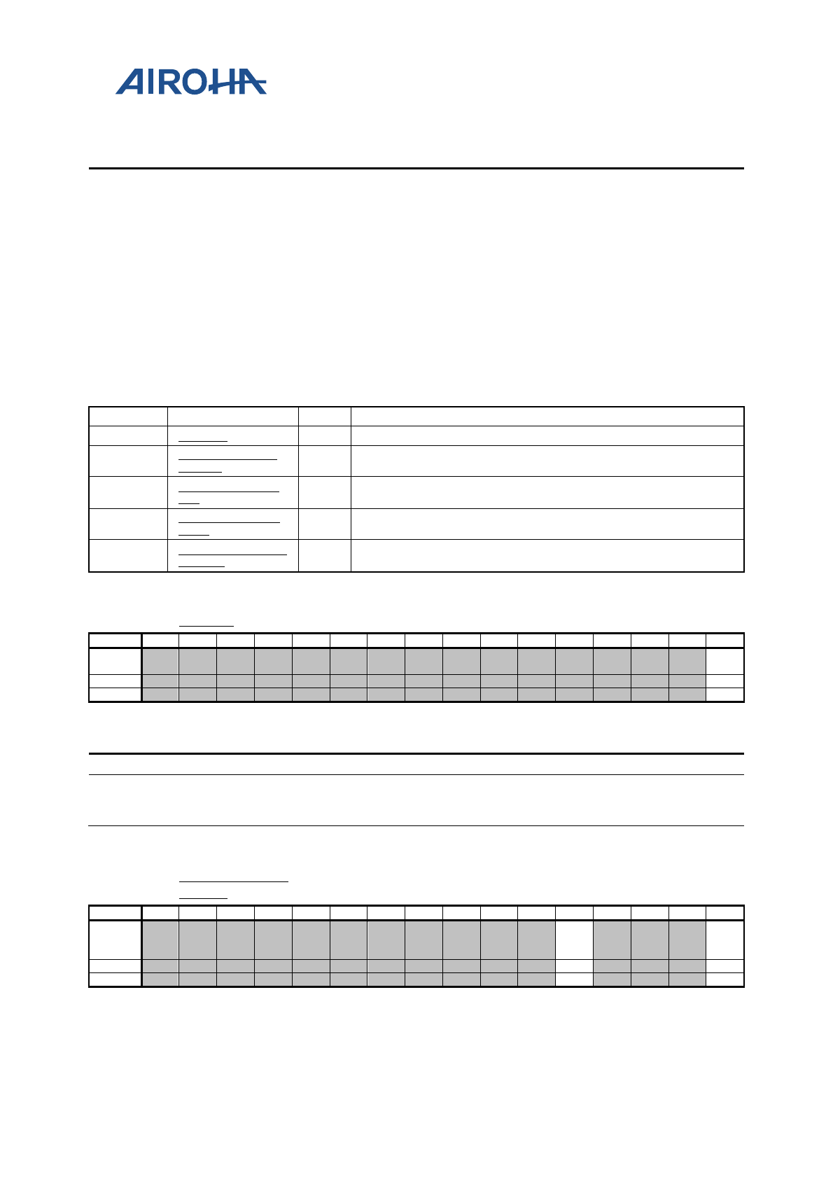
MT2523 Series Reference Manual
© 2015 - 2018 Airoha Technology Corp.
Page 257 of 692
This document contains information that is proprietary to Airoha Technology Corp. (“Airoha”) and/or its licensor(s).
Any unauthorized use, reproduction or disclosure of this document in whole or in part is strictly prohibited.
17.
General Purpose DAC
17.1.
General Description
The general purpose
DAC is a fat monitor containing 128x10 SRAM in design. It outputs data from SRAM to
DAC
continuously
at 1.083MHz and the output region from register settings.
17.2.
Register Definition
Module name: GPDAC Base address: (+A21B0000h)
Address
Name
Width
Register Function
A21B0018
SWRST
16
Soft reset
A21B001C
OUTPUT_COM
MAND 16 Output command
A21B0020
OUTPUT_REGI
ON 16 Output address region
A21B0024
WRITE_COMM
AND 32 Write command
A21B0050
GPDAC_SRAM
_PWR 16 SRAM power control register
A21B0018
SWRST
Soft
reset
0000
Bit
15
14
13
12
11
10
9
8
7
6
5
4
3
2
1
0
Name
SWRS
T
Type
RW
Reset
0
Overview
Bit(s)
Name
Description
0
SWRST
Resets all register
0: Idle, in normal mode
1: Reset
A21B001C
OUTPUT_COM
MAND
O
utput command
0010
Bit
15
14
13
12
11
10
9
8
7
6
5
4
3
2
1
0
Name
REPE
AT_E
N
OUTP
UT_E
N
Type
RW
RW
Reset
1
0
Overview
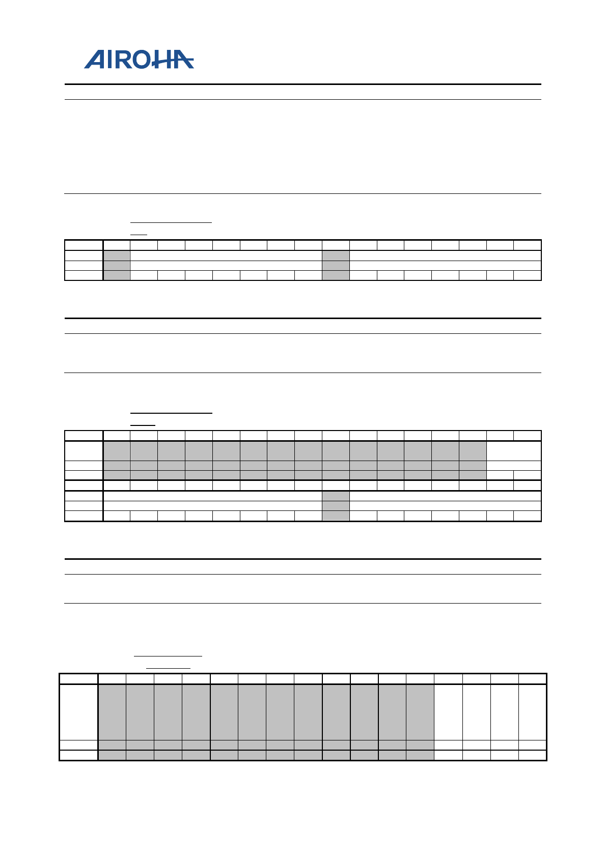
MT2523 Series Reference Manual
© 2015 - 2018 Airoha Technology Corp.
Page 258 of 692
This document contains information that is proprietary to Airoha Technology Corp. (“Airoha”) and/or its licensor(s).
Any unauthorized use, reproduction or disclosure of this document in whole or in part is strictly prohibited.
Bit(s)
Name
Description
4
REPEAT_EN
GPDAC is always in repeat mode; it repeats
by the configuration of the
OUTPUT REGION register.
0: Stop repeat
1: GPDAC is in repeat mode (default)
0
OUTPUT_EN
GPDAC starts to output data. If STOP is required, set output_en and
repeat_en
to 0.
0: Stop output
1: Output data
A21B0020
OUTPUT_REGI
ON
Define the range of output
0000
Bit
15
14
13
12
11
10
9
8
7
6
5
4
3
2
1
0
Name
OUTPUT_END_ADDR
OUTPUT_START_ADDR
Type
RW
RW
Reset
0
0
0
0
0
0
0
0
0
0
0
0
0
0
Overview
Bit(s)
Name
Description
14:8
OUTPUT_END_ADDR
Defines the range of output (end of address)
6:0
OUTPUT_START_AD
DR
Defines the range of output (start of address)
A21B0024
WRITE_COMM
AND
W
rite command
00000000
Bit
31
30
29
28
27
26
25
24
23
22
21
20
19
18
17
16
Name
SRAM_DAT
A[9:8]
Type
RW
Reset
0
0
Bit
15
14
13
12
11
10
9
8
7
6
5
4
3
2
1
0
Name
SRAM_DATA[7:0]
SRAM_ADDR
Type
RW
RW
Reset
0
0
0
0
0
0
0
0
0
0
0
0
0
0
0
Overview
Bit(s)
Name
Description
17:8
SRAM_DATA
Write in SRAM. SRAM_data
6:0
SRAM_ADDR
Write in SRAM. SRAM address
A2370050 GPDAC_SRA
M_PWR SRAM power control register 000A
Bit
15
14
13
12
11
10
9
8
7
6
5
4
3
2
1
0
Name
GP
DA
C_S
LEE
PB
GP
DA
C_
PD
GP
DA
C_I
SOI
NT
B
GP
DA
C_
RE
T
Type
RW
RW
RW
RW
Reset
1
0
1
0
MT2523 Series Reference Manual
© 2015 - 2018 Airoha Technology Corp.
Page 259 of 692
This document contains information that is proprietary to Airoha Technology Corp. (“Airoha”) and/or its licensor(s).
Any unauthorized use, reproduction or disclosure of this document in whole or in part is strictly prohibited.
Bit(s) Name Description
3 GPDAC_SLEEPB SRAM sleep control
2 GPDAC_PD SRAM power down control
1 GPDAC_ISOINTB SRAM ISO control
0 GPDAC_RET SRAM retention control
17.3. Programming Guide
Turn on gpdac
clock
Write in sram
Set ACFG_CLK_CG_CLR=0x0040
Set GPDAC_WRITE_COMMAND
Config Output Set GPDAC_OUTPUT_REGION
Set GPDAC_OUTPUT_COMMAND
START output
Definition of each step shown in the figure above:
1. Turn on GPDAC.
2. Write in SRAM: Write data into SRAM by register GPDAC_WRITE_COMMAND, including SRAM_ADDR and
SRAM_DATA.
3. Configure output: Set up output data region by GPDAC_OUTPUT_REGION and set repeat_en (default 1)
and output_en = 1 by GPDAC_OUTPUT_COMMAND.
4. Start output to DAC.
5. Stop output DAC: Set GPDAC_OUTPUT_COMMAND = 0x00. Configure output_en and repeat_en as 0.

MT2523 Series Reference Manual
© 2015 - 2018 Airoha Technology Corp.
Page 260 of 692
This document contains information that is proprietary to Airoha Technology Corp. (“Airoha”) and/or its licensor(s).
Any unauthorized use, reproduction or disclosure of this document in whole or in part is strictly prohibited.
17.4. Limitations and Important Notes
This section describes the limitations and some important notes on GPDAC.
17.4.1. Soft Reset
GPDAC_SWRST resets all registers expect for itself and the data in SRAM.
Set GPDAC_SWRST to 1 then set GPDAC_SWRST to 0 to complete soft reset.
17.4.2. Definition of repeat_mode and no_repeat Mode
By default repeat_en is 1. output_en = 1 will start output data as expected, and DA_GPDAC_BUS will output the
data by the settings of start address and end address in GPDAC_OUTPUT_REGION continuously.
However, if repeat_en turns to 0, DA_GPDAC_BUS will still output until the setting of the end address in
GPDAC_OUTPUT_REGION and output_en will become 0 automatically in the end of output.
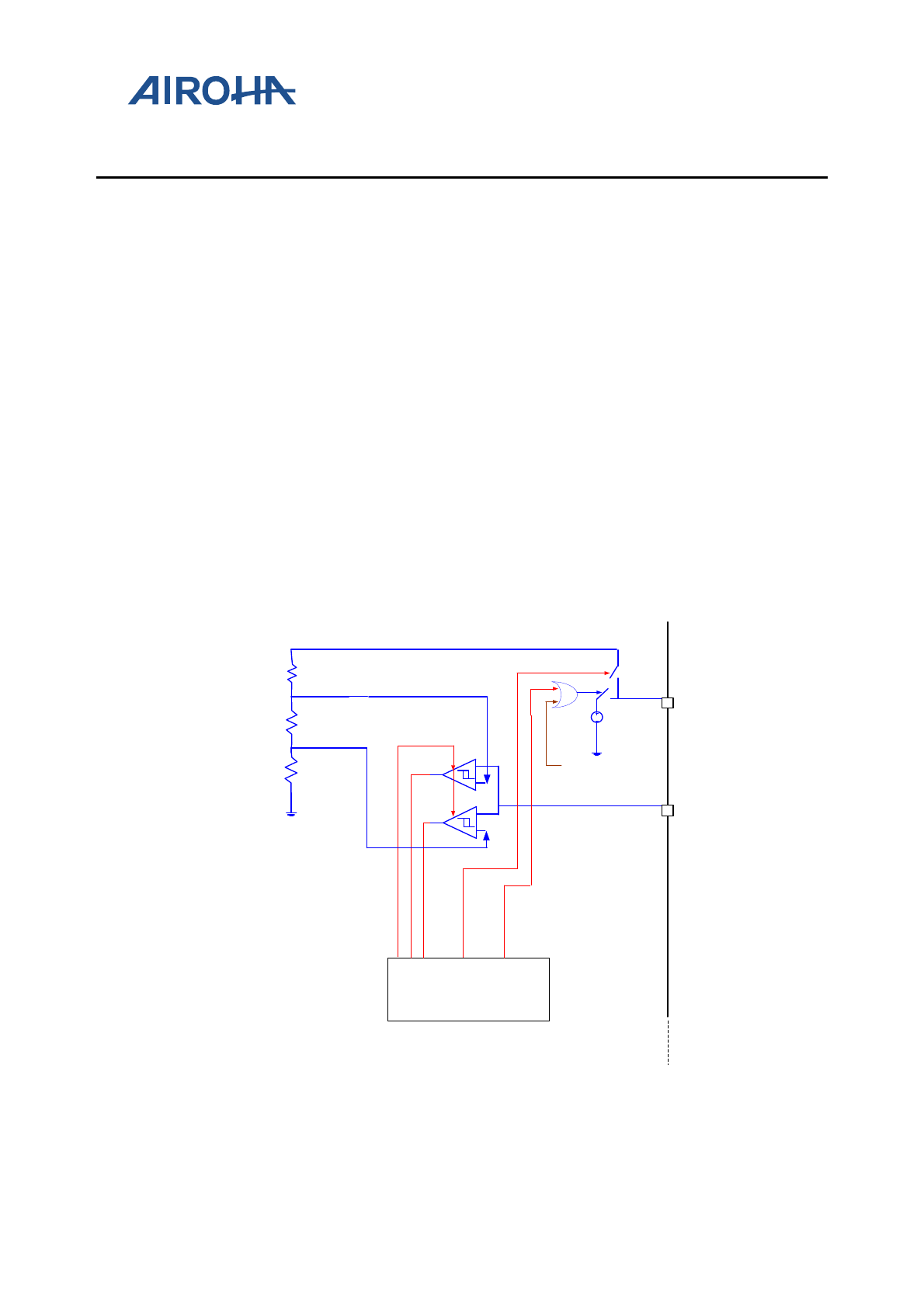
MT2523 Series Reference Manual
© 2015 - 2018 Airoha Technology Corp.
Page 261 of 692
This document contains information that is proprietary to Airoha Technology Corp. (“Airoha”) and/or its licensor(s).
Any unauthorized use, reproduction or disclosure of this document in whole or in part is strictly prohibited.
18. Accessory Detector
18.1. General Description
The hardware accessory detector (ACCDET) detects plug-in/out of multiple types of external components. Based
on the suggested circuit (see Figure 18-1), this design supports two types of external components, which are
microphone and hook-switch. This design uses the internal 2-bit comparator to separate external components. The
de-bounce scheme is also supported to resist uncertain input noises. When the plug-in/out state is stable, the
PWM unit of ACCDET will enable the comparator, MBIAS and threshold voltage of the comparator periodically for
the plugging detection. With suitable PWM settings, very low-power consumption can be achieved when the
detection feature is enabled. To compensate the delay between the detection login and comparator, the delay
enabling scheme is adopted. Given the suitable delay number compared to the rising edge of PWM high pulse, the
stable plugging state can be prorogated to digital detection logic, and the correct plugging state can then be
detected and reported.
Figure 18-2 shows the state machine. The state machine is executed by the software to control the ACCDET design.
The ACCDET design will send one interrupt to acknowledge the software after the ACCDET input state is changed
and the duration of the state is longer than de-bounce time. The software needs to read out the memorized
ACCDET input state and follow the recommended state machine to program the register in it.
MICBIASP
AccDetect
0.4V
1.77V
+
-
+
-
A
B
AccDetection Logic
1.9V
Vth_clk
CMP_clk
Pploy
w=0.5u
MBias_clk
Brown: Register
Red: Digital Signal
350k
1220k
110k
RG_VPWDB_MBIAS
Figure 18-1. Suggested accessory detection circuit
(Note.RG_VPWDB_MBIAS = A21C0060[1])
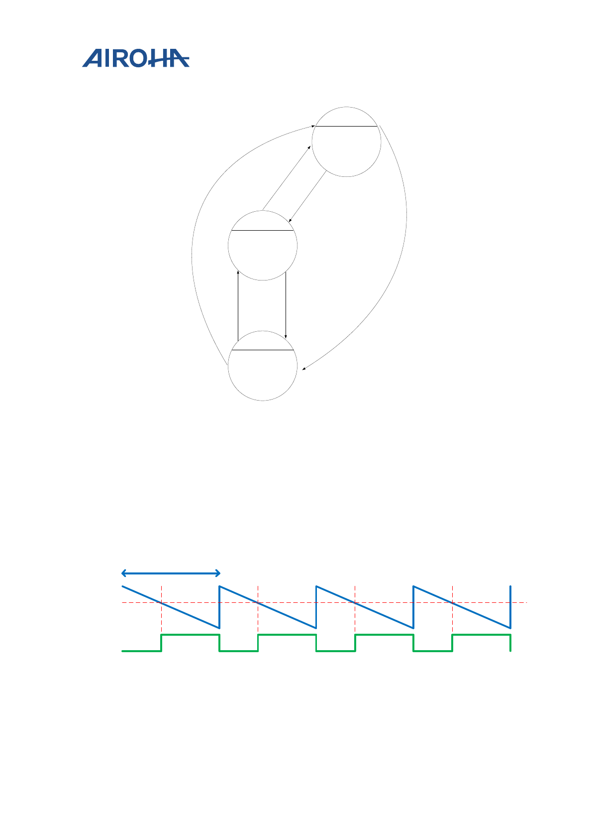
MT2523 Series Reference Manual
© 2015 - 2018 Airoha Technology Corp.
Page 262 of 692
This document contains information that is proprietary to Airoha Technology Corp. (“Airoha”) and/or its licensor(s).
Any unauthorized use, reproduction or disclosure of this document in whole or in part is strictly prohibited.
A=0
B=1
A=1
B=1
A=0
B=1 A=0
B=0
A=1
B=1
A=0,B=0
MIC
Hook Switched
RG_VPWDB_MBAIS=
0 or 1
MicBias_clk=on/off
Vth_clk=on/off
CMP_clk=on/off
RG_VPWDB_MBAIS=
0 or 1
MicBias_clk=on/off
Vth_clk=on/off
CMP_clk=on/off
Standby
RG_VPWDB_MBAIS=
0 or 1
MicBias_clk=on/off
Vth_clk=on/off
CMP_clk=on/off
(not plugged)
Always:
MicBias_clk=on/off
Vth_MB_clk=on/off
CMP_clk=on/off
RG_VPWDB_MBIAS=0
means Microphone
activated;
RG_VPWDB_MBIAS=1
means not activated
Figure 18-2. State machine between microphone and hook-switch plug-in/out change
18.1.1. Pulse Width Modulation
The ACCDET design also provides one Pulse-Width-Modulation (PWM) to enable the comparator, microphone’s
bias current and the threshold voltage of the comparator periodically. With suitable PWM and settings for delayed
enabling, the ACCDET can achieve very low power consumption and accurate plug-in/out detection. Figure 18-3 is
a timing diagram example of such PWM design. The output from PWM keeps being at 0 until the value of the
counter is smaller than the programmed threshold.
PWM_WIDTH
Internal Counter
Threshold
PWM Signal
Figure 18-3. PWM waveform
MT2523 Series Reference Manual
© 2015 - 2018 Airoha Technology Corp.
Page 263 of 692
This document contains information that is proprietary to Airoha Technology Corp. (“Airoha”) and/or its licensor(s).
Any unauthorized use, reproduction or disclosure of this document in whole or in part is strictly prohibited.
18.2. Register Definition
Module name: ACCDET Base address: (+A21F0000h)
Address
Name
Width
Register function
A21F0000
ACCDET_RSTB
32 ACCDET software reset register
A21F0004
ACCDET_CTRL
32
ACCDET control register
A21F0008
ACCDET_STATE_SWCTRL
32 ACCDET state switch control register
A21F000C
ACCDET_PWM_WIDTH
32
ACCDET PWM width register
A21F0010
ACCDET_PWM_THRESH
32 ACCDET PWM threshold register
A21F0024
ACCDET_EN_DELAY_NU
M
32
ACCDET enable delay number register
A21F0028 ACCDET_PWM_IDLE_VA
LUE
32 ACCDET PWM IDLE value register
A21F002C
ACCDET_DEBOUNCE0
32
ACCDET debounce0 register
A21F0030
ACCDET_DEBOUNCE1
32 ACCDET debounce1 register
A21F0038
ACCDET_DEBOUNCE3
32
ACCDET debounce3 register
A21F003C
ACCDET_IRQ_STS
32 ACCDET interrupt status register
A21F0040
ACCDET_CURR_IN
32
ACCDET current input status register
A21F0044 ACCDET_SAMPLE_IN 32 ACCDET sampled input status register
A21F0048
ACCDET_MEMOIZED_IN
32
ACCDET memorized input status register
A21F004C ACCDET_LAST_MEMOIZE
D_IN
32 ACCDET last memorized input status
register
A21F0050
ACCDET_FSM_STATE
32 ACCDET FSM status register
A21F0054
ACCDET_CURR_DEBOUN
CE
32
ACCDET current de-bounce status register
A21F0058
ACCDET_VERSION
32
ACCDET version code
A21F005C
ACCDET_IN_DEFAULT
32 Default value of accdet_in
A21F
0000
ACCDET_RSTB
ACCDET software reset register
0000000
1
Bit
31
30
29
28
27
26
25
24
23
22
21
20
19
18
17
16
Mne
Type
Reset
Bit 15 14 13 12 11 10 9 8 7 6 5 4 3 2 1 0
Mne RST
B
Type
RW
Reset
1
Overview
After applying the setting to register, software reset will be necessary for state initialization.
Without this process, ACCDET may detect incorrect plug state.
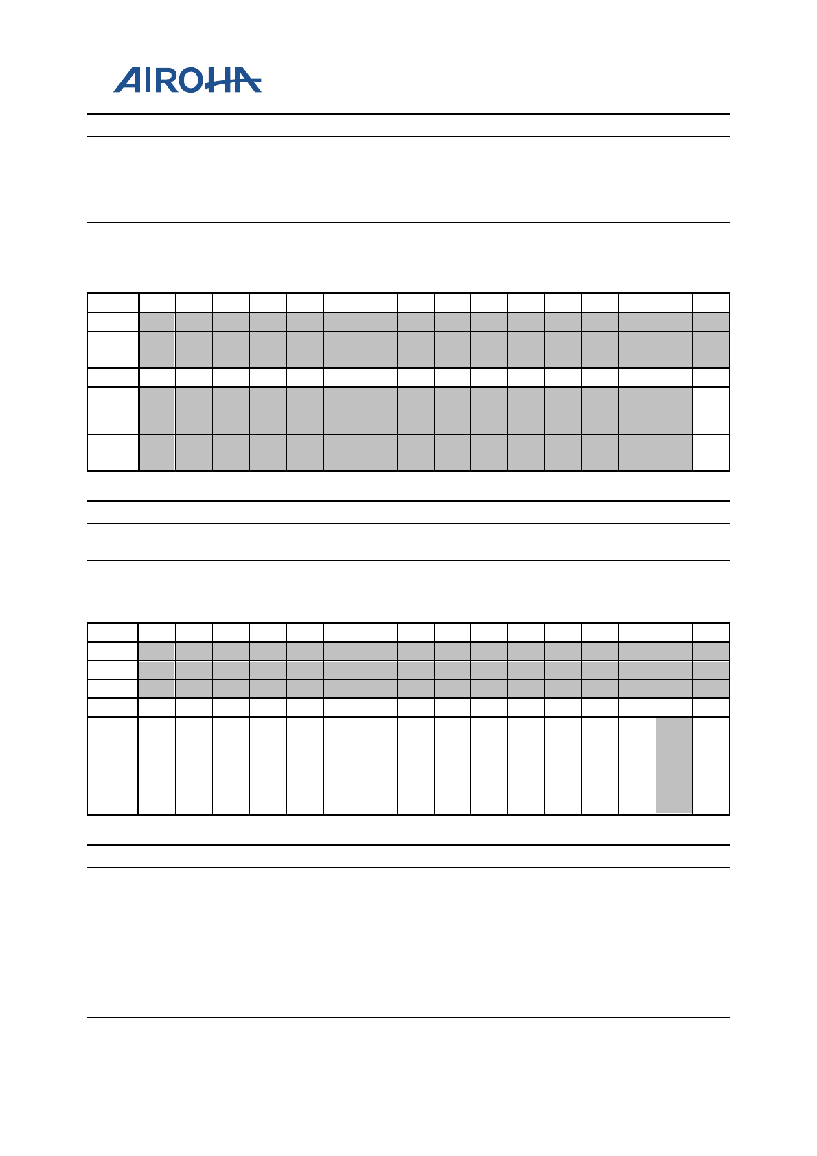
MT2523 Series Reference Manual
© 2015 - 2018 Airoha Technology Corp.
Page 264 of 692
This document contains information that is proprietary to Airoha Technology Corp. (“Airoha”) and/or its licensor(s).
Any unauthorized use, reproduction or disclosure of this document in whole or in part is strictly prohibited.
Bit(s)
Mnemonic
Name
Description
0
RSTB
RSTB
Set to 0 to reset the ACCDET unit
; set to 1 after the reset
process is finished.
This software reset will clear ACCDET's enable signal but keep all
ACCDET's settings. After the reset process, ACCDET will return
to the IDLE state.
A21F
0004
ACCDET_CTRL
ACCDET control register
0000000
1
Bit
31
30
29
28
27
26
25
24
23
22
21
20
19
18
17
16
Mne
Type
Reset
Bit 15 14 13 12 11 10 9 8 7 6 5 4 3 2 1 0
Mne ACC
DET
_EN
Type
RW
Reset 0
Bit(s)
Mnemonic
Name
Description
0
ACCDET_
EN
EN
Set to 1 to enable the ACCDET unit.
A21F
0008
ACCDET_STAT
E_SWCTRL
ACCDET state switch control register
0000000
1
Bit 31 30 29 28 27 26 25 24 23 22 21 20 19 18 17 16
Mne
Type
Reset
Bit
15
14
13
12
11
10
9
8
7
6
5
4
3
2
1
0
Mne
MBI
AS_P
WM_
EN
VTH
_PW
M_E
N
CMP
_PW
M_E
N
RES
ERV
ED
Type RW RW RW RW
Reset
0
0
0
1
Bit(s)
Mnemonic
Name
Description
4
MBIAS_P
WM_EN
MBIAS_PWM_EN
Enables PWM of ACCDET MBIAS unit
3
VTH_PW
M_EN
VTH_PWM_EN
Enables PWM of ACCDET voltage threshold unit
2
0
CMP_PW
M_EN
RESERVE
D
CMP_PWM_EN
Reserved
Enables PWM of ACCDET comparator
Reserved as 1
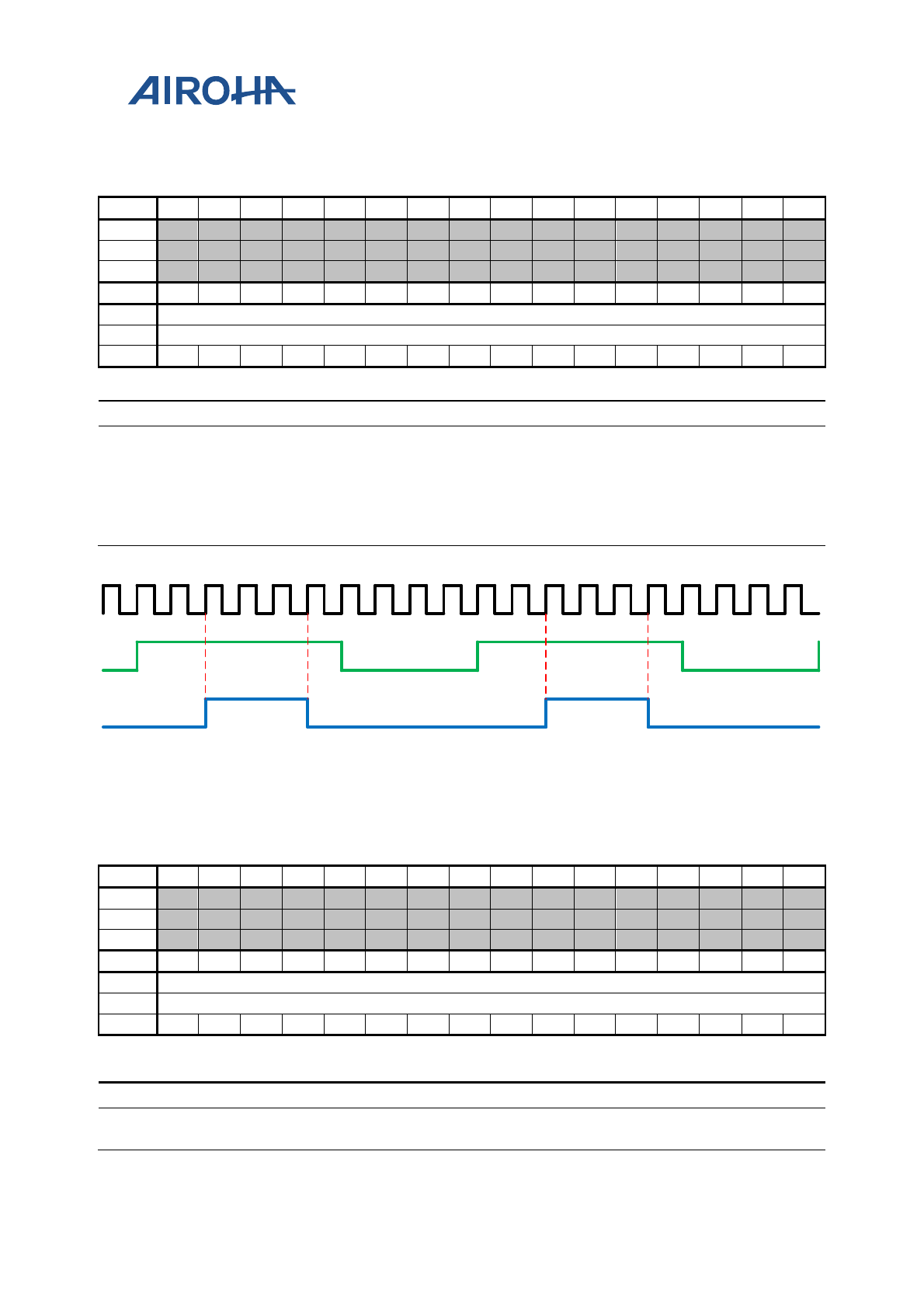
MT2523 Series Reference Manual
© 2015 - 2018 Airoha Technology Corp.
Page 265 of 692
This document contains information that is proprietary to Airoha Technology Corp. (“Airoha”) and/or its licensor(s).
Any unauthorized use, reproduction or disclosure of this document in whole or in part is strictly prohibited.
A
21F000C
ACCDET_PWM
_WIDTH
ACCDET PWM width register
0000000
0
Bit 31 30 29 28 27 26 25 24 23 22 21 20 19 18 17 16
Mne
Type
Reset
Bit
15
14
13
12
11
10
9
8
7
6
5
4
3
2
1
0
Mne
PWM_WIDTH
Type RW
Reset 0 0 0 0 0 0 0 0 0 0 0 0 0 0 0 0
Bit(s)
Mnemonic
Name
Description
15:0
PWM_WI
DTH
PWM_WIDTH
ACCDET PWM width
It is PWM max. counter value. It will be the initial value for the
internal counter. The PWM internal counter always counts down
to
0 to finish one complete period, and the value of the internal
counter will return to the value of PWM_WIDTH.
PWM output fre
quency = (32k/PWM_WIDTH) Hz
PWM WIDTH = 10
PWM THRESH = 6
RISE_DELAY_NUM = 2
FALL_DELAY_NUM = 1
Stable
Detection Sate Stable
Detection Sate
Figure 18-4. PWM waveform with register value present
A21F
0010
ACCDET_PWM
_THRESH
ACCDET PWM threshold register
0000000
0
Bit
31
30
29
28
27
26
25
24
23
22
21
20
19
18
17
16
Mne
Type
Reset
Bit 15 14 13 12 11 10 9 8 7 6 5 4 3 2 1 0
Mne PWM_THRESH
Type RW
Reset 0 0 0 0 0 0 0 0 0 0 0 0 0 0 0 0
Bit(s)
Mnemonic
Name
Description
15:0
PWM_TH
RESH
PWM_THRESH
ACCDET PWM threshold
When the internal counter value is bigger than or equal to
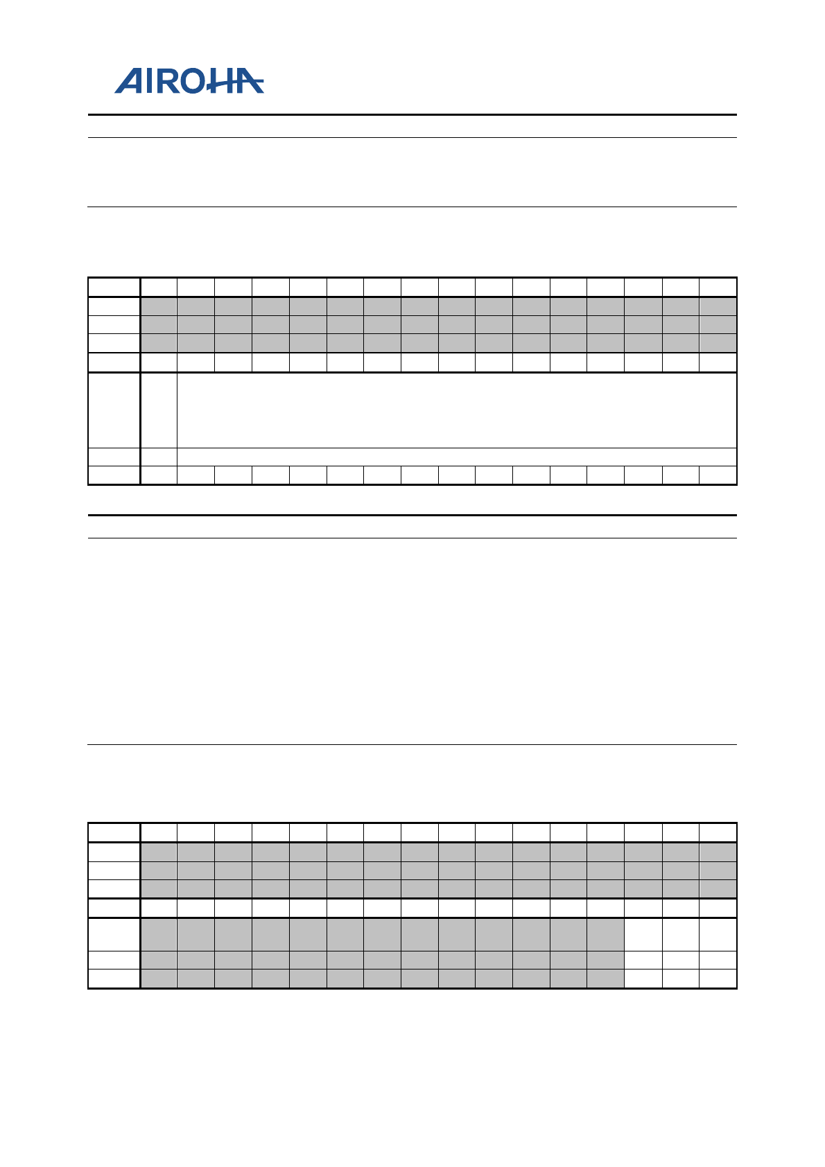
MT2523 Series Reference Manual
© 2015 - 2018 Airoha Technology Corp.
Page 266 of 692
This document contains information that is proprietary to Airoha Technology Corp. (“Airoha”) and/or its licensor(s).
Any unauthorized use, reproduction or disclosure of this document in whole or in part is strictly prohibited.
Bit(s)
Mnemonic
Name
Description
PWM_THRESH, the PWM output signal will be 0. When the
internal counter is smaller than PWM_THRESH, the PWM
output signal will be 1.
PWM output duty cycle = (PWM_THRE
SH)x(1/32) ms
A21F
0024
ACCDET_EN_
DELAY_NUM
ACCDET enable delay number register
00000101
Bit 31 30 29 28 27 26 25 24 23 22 21 20 19 18 17 16
Mne
Type
Reset
Bit
15
14
13
12
11
10
9
8
7
6
5
4
3
2
1
0
Mne
FALL
_DE
LAY
_NU
M
RISE_DELAY_NUM
Type RW RW
Reset 0 0 0 0 0 0 0 1 0 0 0 0 0 0 0 1
Bit(s)
Mnemonic
Name
Description
15
FALL_DE
LAY_NUM
FALL_DELAY_N
UM Falling delay cycle compared to CMP PWM waveform
Suitable delay cycle is necessary for making sure the plug state
is stable after ACCDET is disabled. This number indicates the
clock cycle number between the point when the digital part of
ACCDET stops receiving accdet_in and the point when the
analog part of ACCDET stops working.
14:0
RISE_DEL
AY_N
UM RISE_DELAY_N
UM Rising delay cycle compared to PWM waveform
Suitable delay cycle is necessary for making sure the plug state
is stable before ACCDET is activated
. This number indicates the
clock cycle number between the point when the analog part of
ACCDET starts working and the point when the digital part of
ACCDET starts receiving stable accdet_in.
A21F
0028
ACCDET_PWM
_IDLE_VALUE
ACCDET PWM IDLE value register
0000000
1
Bit 31 30 29 28 27 26 25 24 23 22 21 20 19 18 17 16
Mne
Type
Reset
Bit
15
14
13
12
11
10
9
8
7
6
5
4
3
2
1
0
Mne
MBI
AS VTH
CMP
Type RW RW RW
Reset 0 0 0
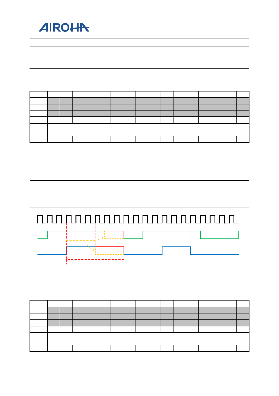
MT2523 Series Reference Manual
© 2015 - 2018 Airoha Technology Corp.
Page 267 of 692
This document contains information that is proprietary to Airoha Technology Corp. (“Airoha”) and/or its licensor(s).
Any unauthorized use, reproduction or disclosure of this document in whole or in part is strictly prohibited.
Bit(s)
Mnemonic
Name
Description
2
MBIAS
MBIAS
IDLE value of MBIAS PWM
(MBias_clk in Figure 1-1)
1
VTH
VTH
IDLE value of VTH PWM
(Vth_clk in Figure 1-1)
0
CMP
CMP
IDLE value of CMP PWM
(CMP_clk in Figure 1-1)
A21F
002C
ACCDET_DEB
OUNCE0
ACCDET debounce0 register
0000001
0
Bit 31 30 29 28 27 26 25 24 23 22 21 20 19 18 17 16
Mne
Type
Reset
Bit
15
14
13
12
11
10
9
8
7
6
5
4
3
2
1
0
Mne
DEBOUNCE0
Type
RW
Reset
0
0
0
0
0
0
0
0
0
0
0
1
0
0
0
0
Overview
This register defines the waiting period before hook key press event is considered stable. If
the de-bounce setting is too small, the hook key press will be too sensitive and detect too
many unexpected plug-ins/outs or hook press/release events. The suitable de-bounce time
setting must be adjusted according to the user's demand.
Bit(s)
Mnemonic
Name
Description
15:0
DEBOUNC
E0
DEBOUNCE0
De
-bounce time for hook key press event (control of the
next state =
Hook Switch State in Figure 1-2)
De
-bounce time = DEBOUNCE/32 ms
PWM WIDTH = 10
PWM THRESH = 6
RISE_DELAY_NUM = 2
FALL_DELAY_NUM = 1
De-bounce Region
DEBOUNCE = 6
DEBOUNCE = 3
De-bounce
Region
Figure 18-5. PWM waveform with DEBOUNCE register value present
A21F
0030
ACCDET_DEB
OUNCE1
ACCDET debounce1 register
0000001
0
Bit
31
30
29
28
27
26
25
24
23
22
21
20
19
18
17
16
Mne
Type
Reset
Bit 15 14 13 12 11 10 9 8 7 6 5 4 3 2 1 0
Mne
DEBOUNCE1
Type
RW
Reset
0
0
0
0
0
0
0
0
0
0
0
1
0
0
0
0
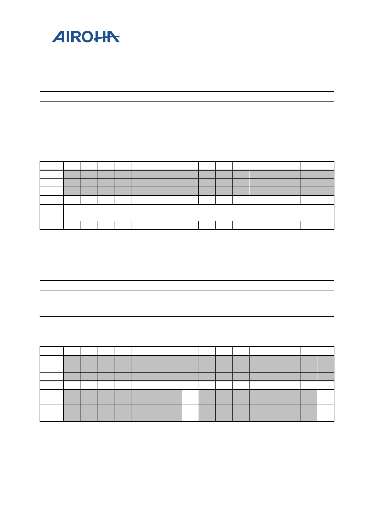
MT2523 Series Reference Manual
© 2015 - 2018 Airoha Technology Corp.
Page 268 of 692
This document contains information that is proprietary to Airoha Technology Corp. (“Airoha”) and/or its licensor(s).
Any unauthorized use, reproduction or disclosure of this document in whole or in part is strictly prohibited.
Overview
This register defines the waiting period before plug-in is considered stable. If the de-
bounce setting is too small, the plug-in will be too sensitive and detect too many
unexpected plug-ins/outs or hook key press/release events. The suitable de-bounce time
setting must be adjusted according to the user's demand.
Bit(s)
Mnemonic
Name
Description
15:0
DEBOUNC
E1
DEBOUNCE1
De
-bounce time for plug-in event (control of the next
state =
MIC State in Figure 1-2)
De
-bounce time = DEBOUNCE/32 ms
A21F
0038
ACCDET_DEB
OUNCE3
ACCDET debounce3 register
0000001
0
Bit
31
30
29
28
27
26
25
24
23
22
21
20
19
18
17
16
Mne
Type
Reset
Bit 15 14 13 12 11 10 9 8 7 6 5 4 3 2 1 0
Mne DEBOUNCE3
Type
RW
Reset
0
0
0
0
0
0
0
0
0
0
0
1
0
0
0
0
Overview
This register defines the waiting period before plug-out is considered stable. If the de-
bounce setting is too small, the plug-out will be too sensitive and detect too many
unexpected plug-ins/outs or hook key press/release events. The suitable de-bounce time
setting must be adjusted according to the user's demand.
Bit(s)
Mnemonic
Name
Description
15:0
DEBOUNC
E3
DEBOUNCE3
De
-bounce time for plug-out event (control of the next
state =
Standby State in Figure 1-2)
De
-bounce time = DEBOUNCE/32 ms
A21F
003C
ACCDET_IRQ_
STS
ACCDET interrupt status register
0000000
0
Bit 31 30 29 28 27 26 25 24 23 22 21 20 19 18 17 16
Mne
Type
Reset
Bit
15
14
13
12
11
10
9
8
7
6
5
4
3
2
1
0
Mne
IRQ_
CLR
IRQ
Type RW RO
Reset 0 0
Overview
When the interrupt of ACCDET is asserted, IRQ_CLR should be set to 1 to clear the
interrupt status. This bit will pause all activities in the ACCDET design until both interrupt
status and IRQ_CLR are cleared. The software should write 1 to IRQ_CLR first to clear the
interrupt (IRQ). After that, the software should read ACCDET_IRQ_STS again to make
IRQ_CLR self-reset to 0.
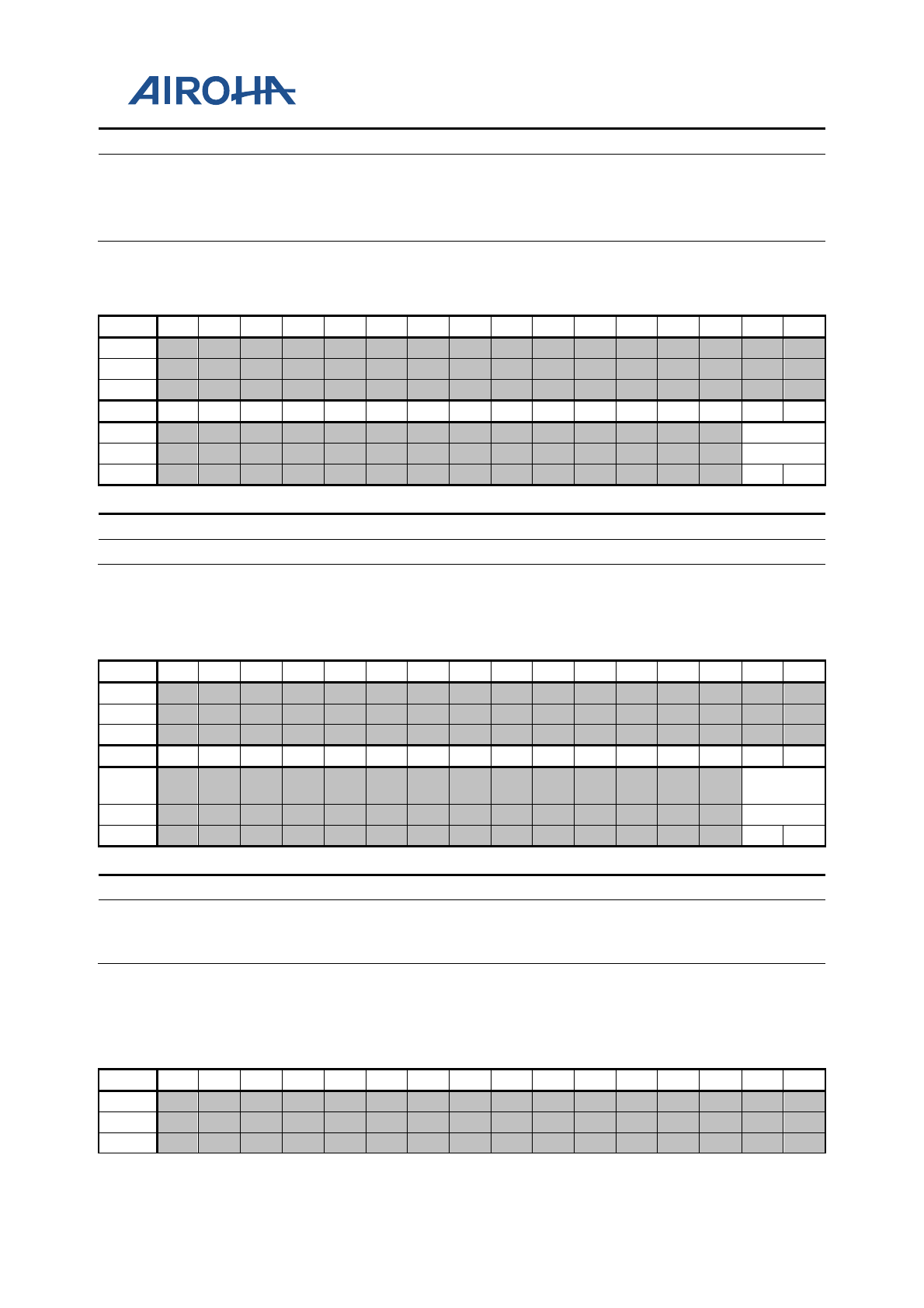
MT2523 Series Reference Manual
© 2015 - 2018 Airoha Technology Corp.
Page 269 of 692
This document contains information that is proprietary to Airoha Technology Corp. (“Airoha”) and/or its licensor(s).
Any unauthorized use, reproduction or disclosure of this document in whole or in part is strictly prohibited.
Bit(s)
Mnemonic
Name
Description
8
IRQ_CLR
IRQ_CLR
Clears interrupt status of ACCDET unit
0
IRQ
IRQ
Interrupt status of ACCDET unit
Because this register will be cleared by hardware, the interrupt
edge
-sensitive scheme should be adopted for this design.
A21F
0040
ACCDET_CUR
R_IN
ACCDET current input status register
0000000
3
Bit 31 30 29 28 27 26 25 24 23 22 21 20 19 18 17 16
Mne
Type
Reset
Bit 15 14 13 12 11 10 9 8 7 6 5 4 3 2 1 0
Mne
CURR_IN
Type RO
Reset 1 1
Bit(s)
Mnemonic
Name
Description
1:0
CURR_IN
CURR_IN
Current input status of
ACCDET unit
A21F
0044
ACCDET_SAM
PLE_IN
ACCDET sampled input status register
0000000
3
Bit
31
30
29
28
27
26
25
24
23
22
21
20
19
18
17
16
Mne
Type
Reset
Bit 15 14 13 12 11 10 9 8 7 6 5 4 3 2 1 0
Mne
SAMPLE_I
N
Type
RO
Reset
1
1
Bit(s)
Mnemonic
Name
Description
1:0
SAMPLE_
IN
SAMPLE_IN
Samples input status of ACCDET unit
When the plug
-in/out/hook-key state is changed, the ACCDET
unit will do sampling.
A21F
0048
ACCDET_MEM
OIZED_IN
ACCDET memorized input status register
0000000
3
Bit 31 30 29 28 27 26 25 24 23 22 21 20 19 18 17 16
Mne
Type
Reset
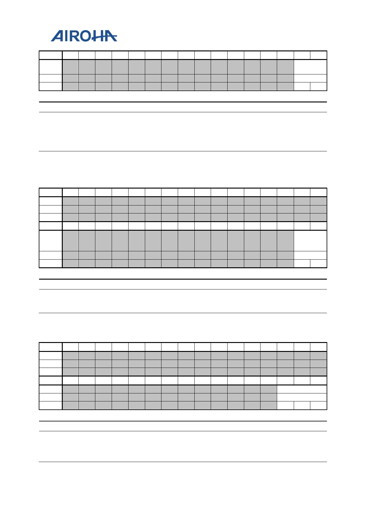
MT2523 Series Reference Manual
© 2015 - 2018 Airoha Technology Corp.
Page 270 of 692
This document contains information that is proprietary to Airoha Technology Corp. (“Airoha”) and/or its licensor(s).
Any unauthorized use, reproduction or disclosure of this document in whole or in part is strictly prohibited.
Bit
15
14
13
12
11
10
9
8
7
6
5
4
3
2
1
0
Mne
MEMORIZ
ED_IN
Type RO
Reset
1
1
Bit(s)
Mnemonic
Name
Description
1:0
MEMORIZ
ED_IN
MEMORIZED_IN
Memorized input status of ACCDET unit
When the plug
-in/out/hook-key states is changed and held
longer than the de
-bounce time, the ACCDET unit will save the
sampled input state to the memorized state. The interrupt will
also be asserted to acknowledge the software.
A21F
004C
ACCDET_LAST
_MEMOIZED_
IN
ACCDET Last memorized
input status register
0000000
3
Bit 31 30 29 28 27 26 25 24 23 22 21 20 19 18 17 16
Mne
Type
Reset
Bit
15
14
13
12
11
10
9
8
7
6
5
4
3
2
1
0
Mne
LAST_ME
MORIZED
_IN
Type RO
Reset 1 1
Bit(s)
Mnemonic
Name Description
1:0
LAST_ME
MORIZED
_IN
LAST_MEMORI
ZED_IN Last memorized input status of ACCDET unit
A21F
0050
ACCDET_FSM
_STATE
ACCDET FSM status register
0000000
0
Bit 31 30 29 28 27 26 25 24 23 22 21 20 19 18 17 16
Mne
Type
Reset
Bit
15
14
13
12
11
10
9
8
7
6
5
4
3
2
1
0
Mne
FSM_STATE
Type RO
Reset 0 0 0
Bit(s)
Mnemonic
Name
Description
2:0
FSM_STA
TE
FSM_SATE
State of
ACCDET unit finite-state-machine
0: ACCDET_IDLE
1: ACCDET_SAMPLE
2: ACCDET_DEBOUNCE
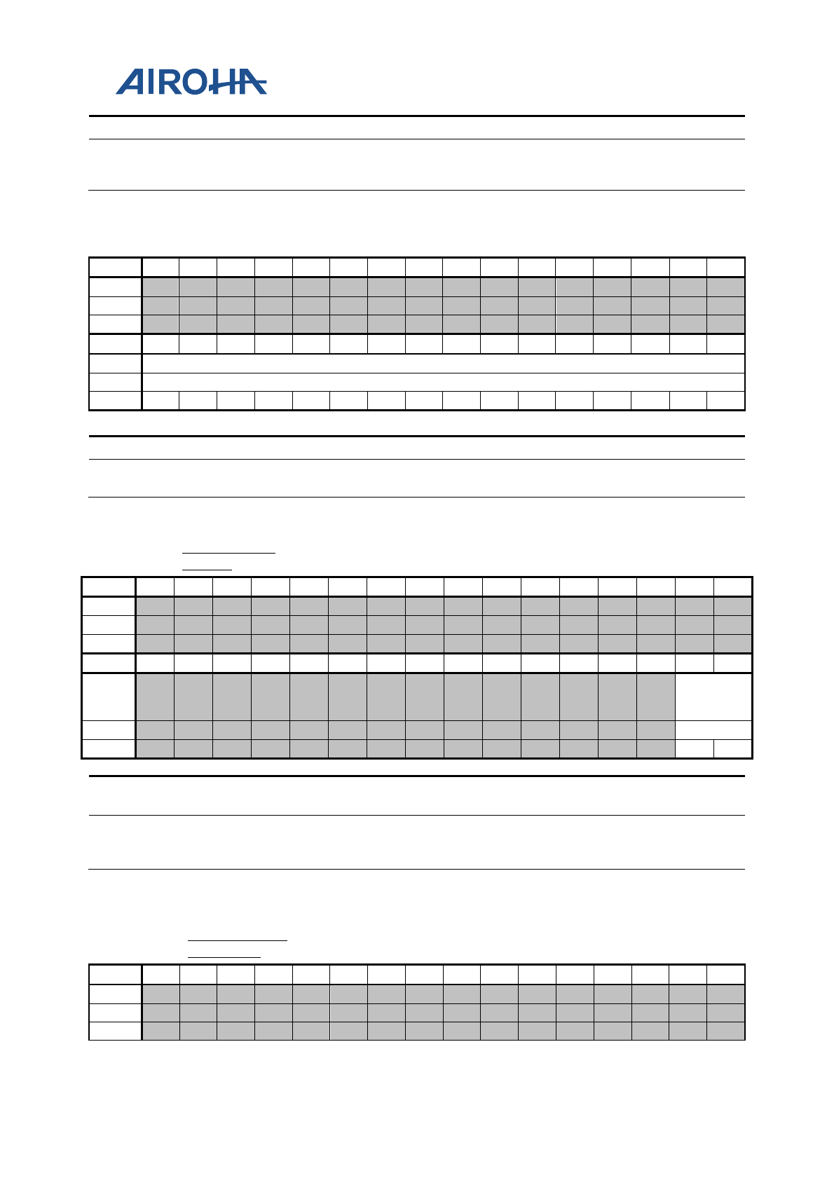
MT2523 Series Reference Manual
© 2015 - 2018 Airoha Technology Corp.
Page 271 of 692
This document contains information that is proprietary to Airoha Technology Corp. (“Airoha”) and/or its licensor(s).
Any unauthorized use, reproduction or disclosure of this document in whole or in part is strictly prohibited.
Bit(s)
Mnemonic
Name
Description
3: ACCDET_CHECK
4: ACCDET_MEMORIZED
5: ACCDET_IRQ
A21F
0054
ACCDET_CUR
R_DEBOUNCE
ACCDET current de
-bounce status register
0000000
4
Bit 31 30 29 28 27 26 25 24 23 22 21 20 19 18 17 16
Mne
Type
Reset
Bit
15
14
13
12
11
10
9
8
7
6
5
4
3
2
1
0
Mne
CURR_DEBOUNCE
Type
RO
Reset 0 0 0 0 0 0 0 0 0 0 0 1 0 0 0 0
Bit(s)
Mnemonic
Name
Description
15:0
CURR_DE
BOUNCE
CURR_DEBOUNC
E
Currently used de-bounce time setting
A21F0058 ACCDET_VE
RSION
ACCDET version code 000000
03
Bit 31 30 29 28 27 26 25 24 23 22 21 20 19 18 17 16
Name
Type
Reset
Bit 15 14 13 12 11 10 9 8 7 6 5 4 3 2 1 0
Name
ACCDET
_VERSIO
N
Type RO
Reset 1 1
Bit(s) Mnemon
ic Name Description
1:0 ACCDET
_VERSI
ON
ACCDET_VERS
ION Version code for ACCDET
A21F005C ACCDET_IN_
DEFAULT
Default value of accdet_in 0000000
0
Bit
31
30
29
28
27
26
25
24
23
22
21
20
19
18
17
16
Name
Type
Reset

MT2523 Series Reference Manual
© 2015 - 2018 Airoha Technology Corp.
Page 272 of 692
This document contains information that is proprietary to Airoha Technology Corp. (“Airoha”) and/or its licensor(s).
Any unauthorized use, reproduction or disclosure of this document in whole or in part is strictly prohibited.
Bit
15
14
13
12
11
10
9
8
7
6
5
4
3
2
1
0
Name
ACC
DET
_IN
_DE
FAU
LT_
REF
RES
H_E
N
ACCDET_
IN_DEFA
ULT
Type RW RW
Reset 0 1 1
Overview
The default value of sample_accdet_in and memorised_accdet_in can be set by software
instead of using the default value set by hardware(i.e. 3).
ACCDET_DEFAULT_REFRESH_EN is the enable bit controlling whether to use this
additional function. The value of sample_accdet_in and memorized_accdet_in will change
when accdet_en rises from low to high. Note that if software reset is applied when
accdet_en is high, the default value of sample_accdet_in and memorized_accdet_in will
also be loaded when the software reset is de-asserted.
Bit(s) Mnemon
ic Name Description
4 ACCDET
_IN_DE
FAULT_
REFRES
H_EN
ACCDET_IN_D
EFAULT_REFR
ESH_EN
Enable signal for whether to load accdet_in_default
0: accdet_in_default will not be loaded.
1: accdet_in_default will be loaded.
1:0 ACCDET
_IN_DE
FAULT
ACCDET_IN_D
EFAULT Default value of accdet_in set by software
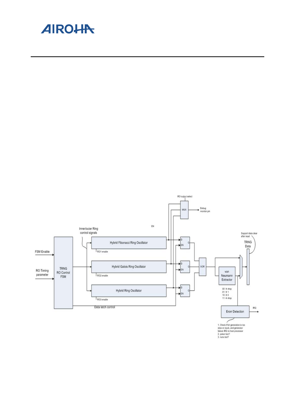
MT2523 Series Reference Manual
© 2015 - 2018 Airoha Technology Corp.
Page 273 of 692
This document contains information that is proprietary to Airoha Technology Corp. (“Airoha”) and/or its licensor(s).
Any unauthorized use, reproduction or disclosure of this document in whole or in part is strictly prohibited.
19. True Random Number Generator
19.1. General Description
The True Random Number Generator (TRNG) is a device in power-down domain that generates random numbers
from a physical process. Figure 19-1 is the basic architecture. TRNG RO control FSM controls the flow of random
number generation. The randomness comes from the inter-operation between various ring oscillators of which the
output transition frequency is affected by PVT (process, voltage, temperature) variation. The utilized ring oscillator
includes Hybrid Fibonacci Ring Oscillator (H-FIRO), Hybrid Ring Oscillator (H-RO), and Hybrid Galois Ring
Oscillator (H-GARO). Von Neumann Extractor is used to balance the 0/1 occurrence of the random number. It
monitors two consecutively generated random bits to determine one valid output bit; the basic rules are
00drop, 011, 100, 11drop. Error detection block detects if the execution time exceeds the timeout limit
while enabling the Von Neumann extractor. IRQ will be issued when random number is successfully generated or
timeout error occurs. Note that the generated random number is for one-time use only. Once the generated
random data are acquired by CPU, TRNG data will be reset to 0. Furthermore, TRNG also supports freerun mode
which turns on the ring oscillator constantly to interfere the supply voltage for security purpose.
19.1.1. Block Diagram
Figure 19-1. TRNG architecture
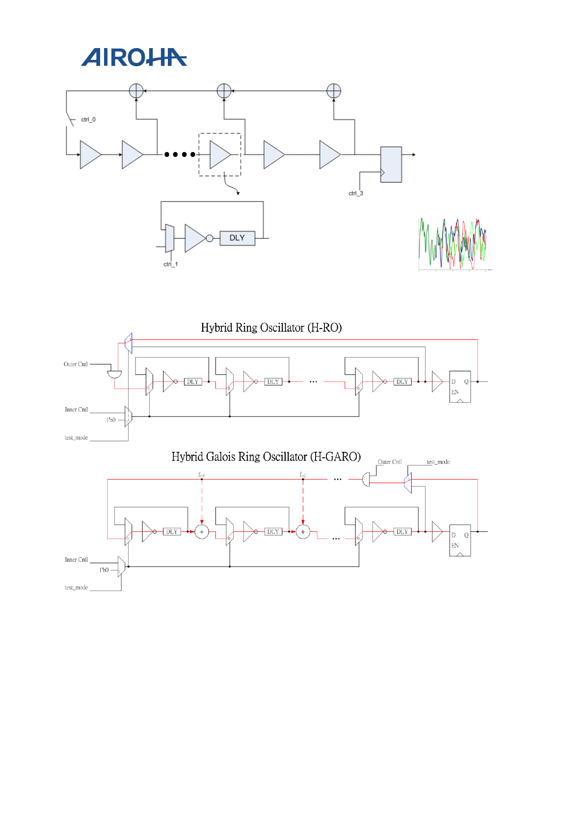
MT2523 Series Reference Manual
© 2015 - 2018 Airoha Technology Corp.
Page 274 of 692
This document contains information that is proprietary to Airoha Technology Corp. (“Airoha”) and/or its licensor(s).
Any unauthorized use, reproduction or disclosure of this document in whole or in part is strictly prohibited.
Figure 19-2. H-FIRO architecture
Figure 19-3. H-RO and H-GARO architecture
The polynomial used by TRNG is x15 + x14 + x7 + x6 + x5 + x4 + x2 +1. The RO operation is as the following:
1. Inner RO is closed and starts oscillating.
2. Inner RO is opened and in an unpredictable state. Outer RO is closed and starts oscillating.
3. Sample the RO data as TRNG data.
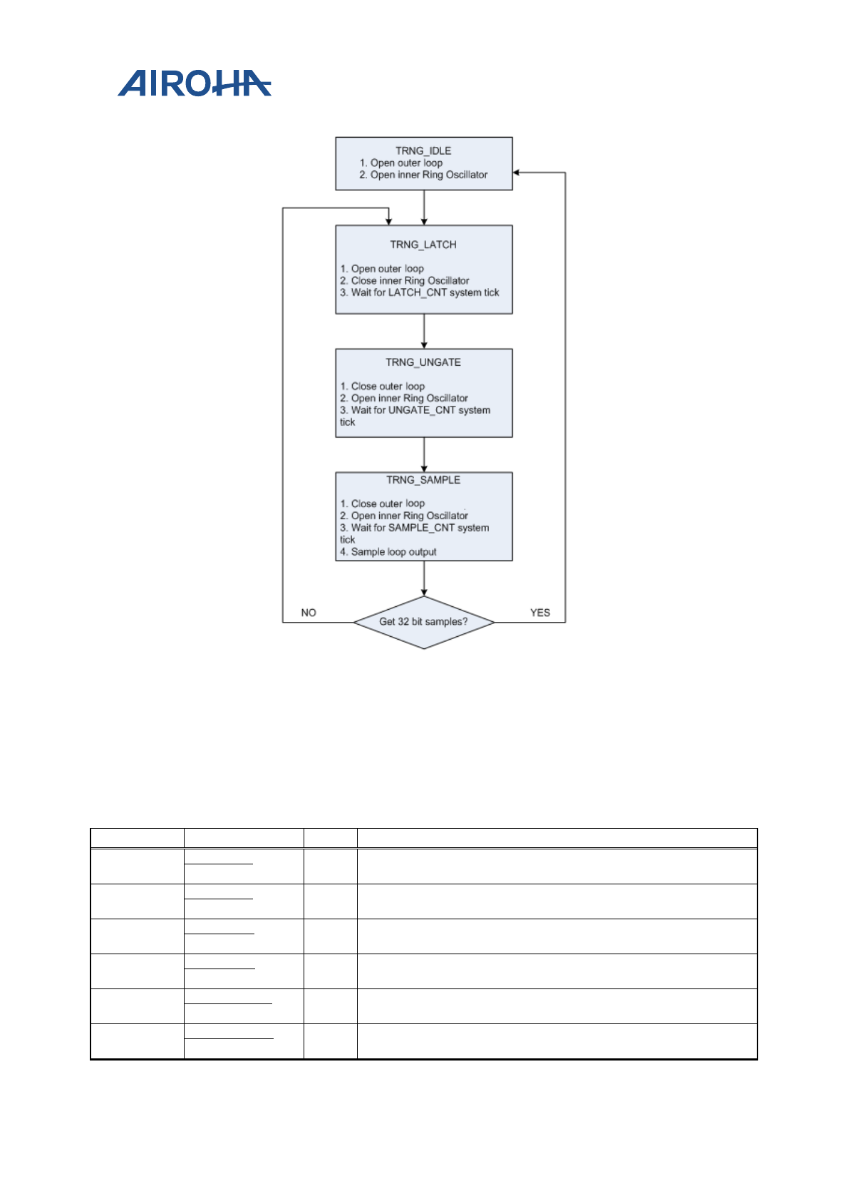
MT2523 Series Reference Manual
© 2015 - 2018 Airoha Technology Corp.
Page 275 of 692
This document contains information that is proprietary to Airoha Technology Corp. (“Airoha”) and/or its licensor(s).
Any unauthorized use, reproduction or disclosure of this document in whole or in part is strictly prohibited.
Figure 19-4. TRNG operation flow
19.2. Register Definition
TRNG control/status registers are available over APB interface. The corresponding address map is as the following.
Module name: TRNG Base address: (+A0010000h)
Address
Name
Width
Register Function
A0010
000
TRNG_CTRL
32
TRNG Control Register
This register
controls the TRNG FSM.
A0010
004
TRNG_TIME
32
TRNG Time Register
This register controls the timing of internal FSM
.
A0010
008
TRNG_DATA
32
TRNG Data Register
This register stores the random data
.
A0010
00C
TRNG_CONF
32
TRNG Configure Register
This register configures ROs, extractor setting
.
A0010
010
TRNG_INT_SET
32
Interrupt Setting Register
This register stores the
IRQ status.
A0010
014
TRNG_INT_CLR
32
Interrupt
Clean Register
This register clea
rs the IRQ status.
MT2523 Series Reference Manual
© 2015 - 2018 Airoha Technology Corp.
Page 276 of 692
This document contains information that is proprietary to Airoha Technology Corp. (“Airoha”) and/or its licensor(s).
Any unauthorized use, reproduction or disclosure of this document in whole or in part is strictly prohibited.
A0010000
TRNG_CTRL
TRNG Control Register
00000000
Bit
31
30
29
28
27
26
25
24
23
22
21
20
19
18
17
16
Name
TRNG
_RDY
Type
RO
Reset
0
Bit
15
14
13
12
11
10
9
8
7
6
5
4
3
2
1
0
Name
TRNG
_
FREE
RUN
TRNG
_STAR
T
Type
RW
RW
Reset
0
0
Bit(s)
Name
Description
31
TRNG_RDY
Indicates whether the TRNG data are ready or not (software polling)
0: Random data are not ready.
1: Random data are ready.
1
0
TRNF_FREERUN
TRNG_START
Turns on freerun (interference) mode
0: Disable freerun
1: Enable freerun
Starts/terminates random number generation
0: Stop generation
1: Start generation
A0010004
TRNG_TIME
TRNG Time Register
00000000
Bit
31
30
29
28
27
26
25
24
23
22
21
20
19
18
17
16
Name
SAMPLE_CNT
UNGATE_CNT
Type
RW
RW
Reset
0
0
0
0
0
0
1
1
0
0
0
0
1
1
1
1
Bit
15
14
13
12
11
10
9
8
7
6
5
4
3
2
1
0
Name
LATCH_CNT
SYSCLK_CNT
Type
RW
RW
Reset
0
0
0
0
1
0
0
0
0
0
0
0
0
0
0
1
Bit(s)
Name
Description
31:24
SAMPLE_CNT
Controls sampling time of TRNG data. Counted by TRNG SYSCLK.
23:16
UNGATE_CNT
Controls interval of TRNG inverter ungating time. Counted by TRNG SYSCLK.
15:8
LATCH_CNT
Controls interval of TRNG inverter latching time. Counted by TRNG SYSCLK.
7:0
SYSCLK_CNT
Controls frequency of TRNG SYSCLK. Counted by system bus clock (TRNG_SYSCLK =
SYSTEM_BUS_CLOCK/ SYSCLK_CNT)
A0010008
TRNG_DATA
TRNG Data Register
00000000
Bit
31
30
29
28
27
26
25
24
23
22
21
20
19
18
17
16
Name
DATA[31:16]
Type
RO
Reset
0
0
0
0
0
0
0
0
0
0
0
0
0
0
0
0
Bit
15
14
13
12
11
10
9
8
7
6
5
4
3
2
1
0
Name
DATA[15:0]
Type
RO
Reset
0
0
0
0
0
0
0
0
0
0
0
0
0
0
0
0
Bit(s)
Name
Description
31:0
DATA
Generated random data
A001000C
TRNG_CONF
TRNG Configure Register
0001001C
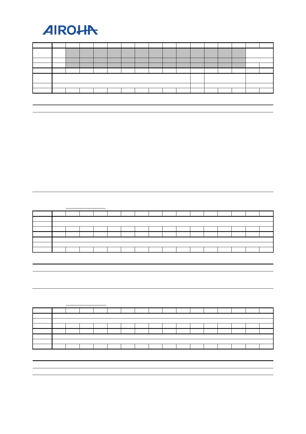
MT2523 Series Reference Manual
© 2015 - 2018 Airoha Technology Corp.
Page 277 of 692
This document contains information that is proprietary to Airoha Technology Corp. (“Airoha”) and/or its licensor(s).
Any unauthorized use, reproduction or disclosure of this document in whole or in part is strictly prohibited.
Bit
31
30
29
28
27
26
25
24
23
22
21
20
19
18
17
16
Name
FR_IR
Q_EN
TIMEOUT_LI
MIT[11:10]
Type
RW
RW
Reset
0
0
1
Bit
15
14
13
12
11
10
9
8
7
6
5
4
3
2
1
0
Name
TIMEOUT_LIMIT[9:0]
VON_
EN
RO_EN
RO_OUT_SE
L
Type
RW
RW
RW
RW
Reset
0
0
0
0
0
0
0
0
0
0
0
1
1
1
0
0
Bit(s)
Name
Description
31
17:6
FR_IRQ_EN
TIMEOUT_LIMIT
1: Enable IRQ during freerun mode
0: Disable IRQ during freerun mode
Configures sampling times limit when extractor is enabled
If the limit is exceeded, it will issue timeout error interrupt and turn off TRNG.
5
VON_EN
1: Turn on Von-Neumann extractor
0: Turn off Von-Neumann extractor
4:2
RO_EN
Enables ring oscillator
Bit[0] = 1: Enable H-FIRO
Bit[1] = 1: Enable H-RO
Bit[2] = 1: Enable H-GARO
1:0
RO_OUT_SEL
Selects which RO to connect to debug out
2'b00: H-FIRO
2'b01: H-RO
2'b10: H-GARO
A0010010
TRNG_INT_SET
Interrupt Setting Register
00000000
Bit
31
30
29
28
27
26
25
24
23
22
21
20
19
18
17
16
Name
INT[31:16]
Type
RO
Reset
0
0
0
0
0
0
0
0
0
0
0
0
0
0
0
0
Bit
15
14
13
12
11
10
9
8
7
6
5
4
3
2
1
0
Name
INT[15:0]
Type
RO
Reset
0
0
0
0
0
0
0
0
0
0
0
0
0
0
0
0
Bit(s)
Name
Description
31:0
INT
IRQ status
Bit [0] = 1: Successful random number generation
Bit [1] = 1: Timeout error
A0010014
TRNG_INT_CLR
Interrupt Clean Register
00000000
Bit
31
30
29
28
27
26
25
24
23
22
21
20
19
18
17
16
Name
CLR[31:16]
Type
RW
Reset
0
0
0
0
0
0
0
0
0
0
0
0
0
0
0
0
Bit
15
14
13
12
11
10
9
8
7
6
5
4
3
2
1
0
Name
CLR[15:0]
Type
RW
Reset
0
0
0
0
0
0
0
0
0
0
0
0
0
0
0
0
Bit(s)
Name
Description
31:0
CLR
Clears IRQ status by setting register to 0x0

MT2523 Series Reference Manual
© 2015 - 2018 Airoha Technology Corp.
Page 278 of 692
This document contains information that is proprietary to Airoha Technology Corp. (“Airoha”) and/or its licensor(s).
Any unauthorized use, reproduction or disclosure of this document in whole or in part is strictly prohibited.
19.3. Programming Guide
1. Enable TRNG_CG_CLOCK.
2. Set TRNG_TIME to a proper latch/sampling period with respect to system bus clock (e.g. 0x08030F01).
3. Set TRNG_CONF TIMEOUT_LIMIT (e.g. 0xFFF).
4. Set TRNG_CONF RO_EN value (e.g. 0x7).
5. Set TRNG_CTRL[0] to 1 to start TRNG
6. Wait for IRQ or poll TRNG_CTRL[31] (TRNG_RDY).
7. Read TRNG_INT_SET to check IRQ status (bit[0] = 1: successful; bit[1] = 1: timeout ).
8. Set TRNG_INT_CLR to 0x0 to clear IRQ status.
9. Set TRNG_CTRL[0] to 0 to stop TRNG.
10. If timeout, go to step 5 to regenerate random numbers.
11. If the generation is successful, read TRNG_DATA to get 32-bit random data.
12. Disable TRNG_CG_CLOCK.
Note that TRNG_TIME and TRNG_CONF (except for RO_OUT_SEL) can only be configured when TRNG is idle
(TRNG_CTRL [0] = 0). Furthermore, if timeout occurs, TRNG will terminate the generation process until the user
restarts TRNG.
G2D+0094h
G2D Layer 0 Source Key
G2D_L0_SRC
KEY
Bit
31
30
29
28
27
26
25
24
23
22
21
20
19
18
17
16
Name
SRCKEY[31:16]
Type
R/W
Reset
0
Bit
15
14
13
12
11
10
9
8
7
6
5
4
3
2
1
0
Name
SRCKEY[15:0]
Type
R/W
Reset
0
SRCKEY If SKEY_EN is enabled, this field represents source key color. If FONT_EN is enabled, this
filed represents foreground color. If RECT_EN is enabled, this field represents the constant color for
rectangle fill. The color format is the same as CLRFMT in G2D_L0_CON.
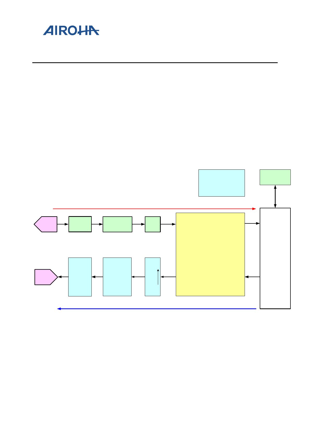
MT2523 Series Reference Manual
© 2015 - 2018 Airoha Technology Corp.
Page 279 of 692
This document contains information that is proprietary to Airoha Technology Corp. (“Airoha”) and/or its licensor(s).
Any unauthorized use, reproduction or disclosure of this document in whole or in part is strictly prohibited.
20. Audio Front End
20.1. General Description
The audio front end (AFE) essentially consists of voice and audio data paths. All voice band data paths comply with
the GSM 03.50 specification. Mono hands-free audio or external FM radio playback paths are also provided. The
audio stereo path facilitates CD-quality playback, external FM radio, and voice playback through a headset.
Figure 1-1 is the digital circuits block diagram of the audio front-end. The APB register block is an APB peripheral
that stores settings from the MCU. The DSP audio port (DAP) block interfaces with the DSP for control and data
communications. The digital filter block performs filter operations for voice band and audio band signal processing.
The Digital Audio Interface (DAI) block communicates with the system simulator for FTA or external Bluetooth
modules.
ADC DF
DSP
6.5M
DSP processor
Voice UL : down 4X/8X
Voice DL: up8X
Audio DL: up 8X
SDM 1st order
SRC
8X
6.5MHz6.5MHz 8~48K
APB
Registers
DAI/BT
2X
16X
64k
A/V
DAC
Uplink
Downlink
IF DF
8/16K
Figure 20-1. Block diagram of digital circuits of the audio front-end
To communicate with the external Bluetooth module, the master-mode PCM interface and master-mode I2S/EIAJ
interface are supported. The clock of PCM interface is 256kHz while the frame sync is 8kHz. Both long sync and
short sync interfaces are supported. The PCM interface can transmit 16-bit stereo or 32-bit mono 8kHz sampling
rate voice signal. Figure 20-2 is the timing diagram of the PCM interface. Note that the serial data changes when
the clock is rising and is latched when the clock is falling. Figure 20-3 shows the timing diagram of different clock
rate PCM interface; the clock rate can be configured to 1x/2x/4x/8x of the original clock rate.
MT2523 Series Reference Manual
© 2015 - 2018 Airoha Technology Corp.
Page 280 of 692
This document contains information that is proprietary to Airoha Technology Corp. (“Airoha”) and/or its licensor(s).
Any unauthorized use, reproduction or disclosure of this document in whole or in part is strictly prohibited.
Figure 20-2. Timing diagram of Bluetooth application
Figure 20-3. Timing diagram of different clock rate Bluetooth application
I2S/EIAJ interface is designed to transmit high quality audio data. Figure 20-4 and Figure 20-5 illustrate the timing
diagram of the two types of interfaces. I2S/EIAJ can support 32 kHz, 44.1 kHz, and 48 kHz sampling rate audio
signals. The clock frequency of I2S/EIAJ can be 32×(sampling frequency), or 64×(sampling frequency). For
example, to transmit a 44.1 kHz CD-quality music, the clock frequency should be 32 × 44.1 kHz = 1.4112 MHz or 64
× 44.1 kHz = 2.8224 MHz.
I2S/EIAJ interface is not only used for Bluetooth module, but also for external DAC components. Audio data can
easily be sent to the external DAC through the I2S/EIAJ interface.
In this document, the I2S/EIAJ interface is referred to as EDI (External DAC Interface).
dai_clk
dai_tx
dai_rx
bt_sync(s)
bt_sync(l)
2131030 28 2427 2526 222329
2 1 31030 28 2427 2526 222329
3
3
MT2523 Series Reference Manual
© 2015 - 2018 Airoha Technology Corp.
Page 281 of 692
This document contains information that is proprietary to Airoha Technology Corp. (“Airoha”) and/or its licensor(s).
Any unauthorized use, reproduction or disclosure of this document in whole or in part is strictly prohibited.
EDI_CLK
EDI_WS Left Channel Right Channel
EDI_DAT
654321015 14 13 12 11 10 987654321015 14 13 12 11 10 987654321015 14 13
Figure 20-4. EDI Format 1: EIAJ (FMT = 0)
EDI_CLK
EDI_WS Left Channel Right Channel
EDI_DAT
6543 2 1 0 15 14 13 12 11 10 9 8 7 6 5 4 3 2 1 0 15 14 13 12 11 10 987654321015 14 13
Figure 20-5. EDI Format 1: I2S (FMT = 1)
20.2. Register Definition
Registers in audio front-end are listed as the following.
Module name: AFE_A63260 Base address: (+82CD0000h)
Address
Name
Width
Register Function
82CD0000
AFE_VMCU_CON0
16 AFE Voice MCU Control Register
A synchronous reset signal is issued before periodical interrupts of 8-
kHz frequency are issued. Clearing this register will stop the interrupt
generation.
82CD000C
AFE_VMCU_CON1
16
AFE Voice MCU Control Register 1
82CD0010
AFE_VMCU_CON2
16 AFE Voice MCU Control Register 2
Set up this register for consistency of analog circuit setting.
Suggested value: 0x003c
82CD0014
AFE_VDB_CON
16
AFE Voice DAI Bluetooth Control Register
Set up this register for DAI test mode and Bluetooth application.
82CD0018
AFE_VLB_CON
16 AFE Voice Loopback Mode Control Register
Set up this register for AFE voice digital circuit configuration control.
Several loop back modes are implemented for test purposes. Default
values correspond to the normal function mode.
82CD001C
AFE_VMCU_CON3
16
AFE Voice MCU Control Register 3
Set up this register for voice settings.
82CD0020
AFE_AMCU_CON0
16 AFE Audio MCU Control Register 0
A synchronous reset signal is issued before periodical interrupts of
1/6 sampling frequency are issued. Clearing this register will stop the
interrupt generation.
82CD0024
AFE_AMCU_CON1
16
AFE Audio MCU Control Register 1
MCU sets up this register to inform hardware of the sampling
frequency of audio being played back.
82CD0028
AFE_EDI_CON
16 AFE EDI Control Register
This register is used to control the EDI.
82CD002C
AFE_AMCU_CON2
16
AFE Audio Control Register 2
Set up this register for consistency of analog circuit setting.
Suggested value: 0x3c
MT2523 Series Reference Manual
© 2015 - 2018 Airoha Technology Corp.
Page 282 of 692
This document contains information that is proprietary to Airoha Technology Corp. (“Airoha”) and/or its licensor(s).
Any unauthorized use, reproduction or disclosure of this document in whole or in part is strictly prohibited.
82CD0030
AFE_DAC_TEST
16
Audio/Voice DAC SineWave Generator
This register is only for analog design verification on audio/voice
DACs.
82CD0034
AFE_VAM_SET
16 Audio/Voice Interactive Mode Setting
82CD0038
AFE_AMCU_CON3
16 AFE Audio Control Register 3
Set up this register for A2 parameter of pre-distortion.
82CD003C
AFE_AMCU_CON4
16 AFE Audio Control Register 4
Set up this register for A3 parameter of pre-distortion.
82CD0040
AFE_DC_DBG_1
16
AFE DC Compensation Debug Register 1
82CD0044
AFE_DC_DBG_2
16 AFE DC Compensation Debug Register 2
82CD0048
AFE_DC_DBG_3
16
AFE DC Compensation Debug Register 3
82CD0140
AFE_ACHECK_SUM
_R
16 AFE Checksum Register 0
82CD0144
AFE_ACHECK_SUM
_L
16
AFE Checksum Register 1
82CD0148
AFE_MUTE_STA
16 AFE Mute Status Register
This register indicates the current mute status.
82CD0180
AFE_AMCU_CON5
16 AFE Audio MCU Control Register 5
This register sets up audio SDM selection in normal mode.
82CD0184
AFE_AMCU_CON6
16 AFE Audio MCU Control Register 6
Set up this register for audio right channel dc offset value
cancellation.
82CD0188
AFE_AMCU_CON7
16
AFE Audio MCU Control Register 7
Set up this register for audio left channel dc offset value cancellation.
82CD0190
AFE_DBG_RD_PRE
16 AFE MCU Debug Mode Reading SRAM Out
This register reads memory content from AFE SRAM in debug mode.
It can only work when debug mode register pulls high.
82CD0194
AFE_DBG_MD_CON
0
16
AFE Debug Mode Control Register 0
Set up this register to start debug mode; the debug done signal will
return in the same register.
82CD0198
AFE_DBG_MD_CON
1
16 AFE Debug Mode Control Register 1
This register reads memory content from AFE SRAM in debug mode.
It can only work when debug mode register pulls high.
82CD019C
AFE_DBG_APB_STA
TUS
16 AFE MCU Status Register
This register reads the status when writing/reading SRAM data or
debugging.
82CD01A0
AFE_VMCU_CON4
16 AFE Voice MCU Control Register 4
Set up this register for DC offset value cancellation.
82CD01CC
AFE_CMPR_CNTR
16
AFE Compare Counter Control Register
Compares counter control
82CD01E0
AFE_DBG_RD_DAT
24 AFE Debug Mode - Reading SRAM Data
When user reads memory data from memory in debug mode, the data
will be here. Before read, make sure the read status is ok for read.
82CD01E4
AFE_APBMEM_RD_
DAT
24
AFE MCU Reading SRAM Data
This register reads memory content from AFE SRAM. If the read
address is AFE_BASE + 1518~153C, this register will output IIR
coefficient.
Before read, make sure the read status is ok for read.
82CD01E8
AFE_APBMEM_RD
16 AFE MCU Read SRAM Request
Reads AFE SRAM data from MCU
82CD01EC
AFE_PC_1X_IDX
16 AFE Program 1X IDX
82CD01F0
AFE_DBG_SIG
16 AFE 8X/Buffer/Mux Debug
Debug mode signals in AFE hardware
Bit [5:4] is aafe_on/vafe_on align 1x_enable signal; used for debug
mode
Bit [3:0] is debug signal of AFE 8X buffer.
82CD01F4
AFE_PC_OUT_DBG
16
AFE Program PC Address
MT2523 Series Reference Manual
© 2015 - 2018 Airoha Technology Corp.
Page 283 of 692
This document contains information that is proprietary to Airoha Technology Corp. (“Airoha”) and/or its licensor(s).
Any unauthorized use, reproduction or disclosure of this document in whole or in part is strictly prohibited.
82CD01F8
AFE_DBG_1XDAT
16
DBG_1XDAT
82CD0200
AFE_COSIM_RG
16 AFE COSIM RG Test
82CD0210
AFE_MCU_CON0
16
AFE MCU CON0
AFE top control register; turns on/off enable generation
82CD0214
AFE_MCU_CON1
16 AFE MCU CON1
AFE data path control register; turns on/off udsp and a_interface
82CD000
0 AFE_VMCU_
CON0
AFE Voice MCU Control Register 0000
Bit
15
14
13
12
11
10
9
8
7
6
5
4
3
2
1
0
Name
VIR
QO
N
Type
RW
Reset
0
Bit(s)
Mnemoni
c
Name
Description
0 VIRQON Turns on 8k interrupt
0: Turn off
1: Turn on
82CD000
C AFE_VMCU_
CON1
AFE Voice MCU Control Register 1 0200
Bit
15
14
13
12
11
10
9
8
7
6
5
4
3
2
1
0
Nam
e
DU
AL
_M
IC
VM
OD
E32
K
VM
OD
E4
K
VR
SD
ON
Type
RW
RW
RW
RW
Reset
0
0
1
0
Bit(s)
Mnemoni
c
Name
Description
12 DUAL_MIC Dual mic control
0: Signal mic
1: Dual mic
10 VMODE32K Configures uplink 32K recording
0: See vmode4K RG
1: 32K sample rate
9 VMODE4K Selects DSP data mode
0: 8K inband
1: 4K inband
7 VRSDON SDM level for VBITX (uplink)
0: 2 levels
1: 3 levels
82CD0010 AFE_VMCU_
CON2
AFE Voice MCU Control Register 2 003C
Bit
15
14
13
12
11
10
9
8
7
6
5
4
3
2
1
0
Name
VD
C_
CO
MP
_E
VT
X_
CK
_P
HA
VSDM_GAIN
MT2523 Series Reference Manual
© 2015 - 2018 Airoha Technology Corp.
Page 284 of 692
This document contains information that is proprietary to Airoha Technology Corp. (“Airoha”) and/or its licensor(s).
Any unauthorized use, reproduction or disclosure of this document in whole or in part is strictly prohibited.
N
SE
Type
RW
RW
RW
Reset
0
0
1
1
1
1
0
0
Bit(s) Mnemoni
c Name Description
15 VDC_COMP_EN Enables DC offset compensation
0: Disable
1: Enable
11 VTX_CK_PHASE Selects phase selection for clock to analog
0: Clock changes at data falling edge.
1: Clock changes at data rising edge.
5:0 VSDM_GAIN Gain settings at voice SDM input. Suggested value: 0x3c (60/64).
Other SDM gain settings may cause performance degradation.
000000: 0/64
000001: 1/64
111111: 63/64
82CD001C AFE_VMCU_
CON3
AFE Voice MCU Control Register 3 0000
Bit
15
14
13
12
11
10
9
8
7
6
5
4
3
2
1
0
Nam
e
SD
ML
P_
UL
TO
DL
VS
DM
_D
AT
A_
MO
NO
SD
ML
P_
DL
TO
UL
SD
M_
CK
_P
HA
SE
Type
RW
RW
RW
RW
Reset
0
0
0
0
Bit(s) Mnemoni
c Name Description
8 SDMLP_ULTODL UL sigma delta data loopback to DL sigma delta data
0: Disable
1: Enable
5 VSDM_DATA_MON
O Rch output data = Lch outut data
0: Disable
1: Enable
4 SDMLP_DLTOUL DL sigma delta data loopback to UL sigma delta data
0: Disable
1: Enable
0 SDM_CK_PHASE Selects phase of SDM clock
0: Clock changes at data falling edge.
1: Clock changes at data rising edge.
82CD01A
0 AFE_VMCU_
CON4
AFE Voice MCU Control Register 4 0000
Bit
15
14
13
12
11
10
9
8
7
6
5
4
3
2
1
0
Name
DC_OFFSET_VALUE
Type
RW
Reset
0
0
0
0
0
0
0
0
0
0
0
0
0
0
0
0
Bit(s) Mnemoni
c Name Description
15:0 DC_OFFSET_VALU
E Set up this register for DC offset value cancellation.
MT2523 Series Reference Manual
© 2015 - 2018 Airoha Technology Corp.
Page 285 of 692
This document contains information that is proprietary to Airoha Technology Corp. (“Airoha”) and/or its licensor(s).
Any unauthorized use, reproduction or disclosure of this document in whole or in part is strictly prohibited.
82CD01A
C AFE_VMCU_
CON5
AFE Voice MCU Control Register 5 0000
Bit
15
14
13
12
11
10
9
8
7
6
5
4
3
2
1
0
Nam
e
LCH_PHASE
RCH_PHASE
CK
_P
HA
SE
DIG
MI
C_
EN
3P2
5M
_SE
L
Type
RW
RW
RW
RW
RW
Reset
011
111
0
0
0
Bit(s) Mnemoni
c Name Description
15:13 LCH_PHASE Selects digital mic LCH data phase from phase 0~phase 7
12:10 RCH_PHASE Selects digital mic RCH data phase from phase 0~phase 7
9 CK_PHASE Selects digital mic clock latch phase (option since the L/R phase can
select)
4 DIG_MIC_EN Enables digital mic
0: Enable analog mic
1: Enable digital mic
0 D3P25M_SEL Selects digital mic sample rate
0: 1.625M
1: 3.25M
82CD0014 AFE_VDB_C
ON
AFE Voice DAI Bluetooth Control Register 0000
Bit
15
14
13
12
11
10
9
8
7
6
5
4
3
2
1
0
Nam
e PCM_CK_
MODE
VB
T_L
OO
P_
BA
CK
VB
T_L
OO
P
VD
AIO
N
VB
TO
N
VB
TSY
NC VBTSLEN
Type
RW
RW
RW
RW
RW
RW
RW
Reset
0
0
0
0
0
0
0
0
0
0
Bit(s)
Mnemoni
c
Name
Description
15:14 PCM_CK_MODE Pcm clock (dai_clk) rate mode
00: 1x, dai_clk rate = dai_tx bit rate (8k*32-bit = 256kHz)
01: 2x, dai_clk rate = 2*dai_tx bit rate (512kHz)
10: 4x, dai_clk rate = 4*dai_tx bit rate (1024kHz)
11: 8x, dai_clk rate = 8*dai_tx bit rate (2048kHz)
12 VBT_LOOP_BACK Loop back test for DAI/BT interface. DAI_TX = DAI_RX
0: No loopback
1: Loopback
10 VBT_LOOP Loop back test for DAI/BT interface
If true, dai_rx_tmp = dai_tx
0: No loopback
1: Loopback
5 VDAION Turns on DAI function
4 VBTON Turns on Bluetooth PCM function
3 VBTSYNC Bluetooth PCM frame sync type
0: Short sync
1: Long sync
2:0 VBTSLEN Bluetooth PCM long frame sync length = VBTSLEN+1
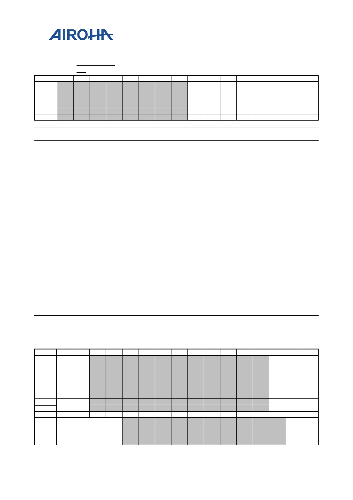
MT2523 Series Reference Manual
© 2015 - 2018 Airoha Technology Corp.
Page 286 of 692
This document contains information that is proprietary to Airoha Technology Corp. (“Airoha”) and/or its licensor(s).
Any unauthorized use, reproduction or disclosure of this document in whole or in part is strictly prohibited.
82CD0018 AFE_VLB_C
ON
AFE Voice Loopback Mode Control Register 0000
Bit
15
14
13
12
11
10
9
8
7
6
5
4
3
2
1
0
Nam
e
EN
GE
N_
OP
T
VIN
TIN
SEL
VD
SP
BY
PA
SS
VD
SPC
SM
OD
E
VD
API
N_
CH
1
VD
API
N_
CH
0
VIN
TIN
MO
DE
VD
ECI
NM
OD
E
Type
RW
RW
RW
RW
RW
RW
RW
RW
Reset
0
0
0
0
0
0
0
0
Bit(s)
Mnemoni
c
Name
Description
7 ENGEN_OPT engen generator option
0: Origin engen
1: New engen option
6 VINTINSEL Selects DL data when VINTINMODE = 1
0: 1st voice uplink input
1: 2nd voice uplink input
5 VDSPBYPASS Loopback data will not be gated by VDSPRDY.
0: Normal mode
1: Bypass DSP loopback mode
4 VDSPCSMODE DSP COSIM only, to align DATA
0: Normal mode
1: Cosim mode
3 VDAPIN_CH1 MODEMSIM voice loopback control
Uplink1 data = downlink data loopback
0: Normal mode
1: Loopback mode
2 VDAPIN_CH0 MODEMSIM voice loopback control
Uplink0 data = downlink data loopback
0: Normal mode
1: Loopback mode
1 VINTINMODE Downlink data = uplink data
0: Normal mode
1: Loopback mode
0 VDECINMODE Decimator input mode control
Downlink output data are looped back to uplink through internal SDM.
0: Normal mode
1: Loopback mode
82CD030
0 AFE_SLV_I2
S_CON
AFE Slave I2S Control Register 000000
00
Bit
31
30
29
28
27
26
25
24
23
22
21
20
19
18
17
16
Nam
e
SL
V_I
2S_
EN
AF
E_
FO
C_
EN
SLV
_I2
S_B
IT_
SW
AP
SL
V_I
2S_
BY
PA
SS_
SR
C
SLV
_I2
S_2
CH
_SE
L
Type
RW
RW
RW
RW
RW
Reset
0
0
0
0
0
Bit
15
14
13
12
11
10
9
8
7
6
5
4
3
2
1
0
Nam
e
SLV_I2S_MODE
SL
V_I
2S_
FM
T
SLV
_I2
S_P
CM
_SE
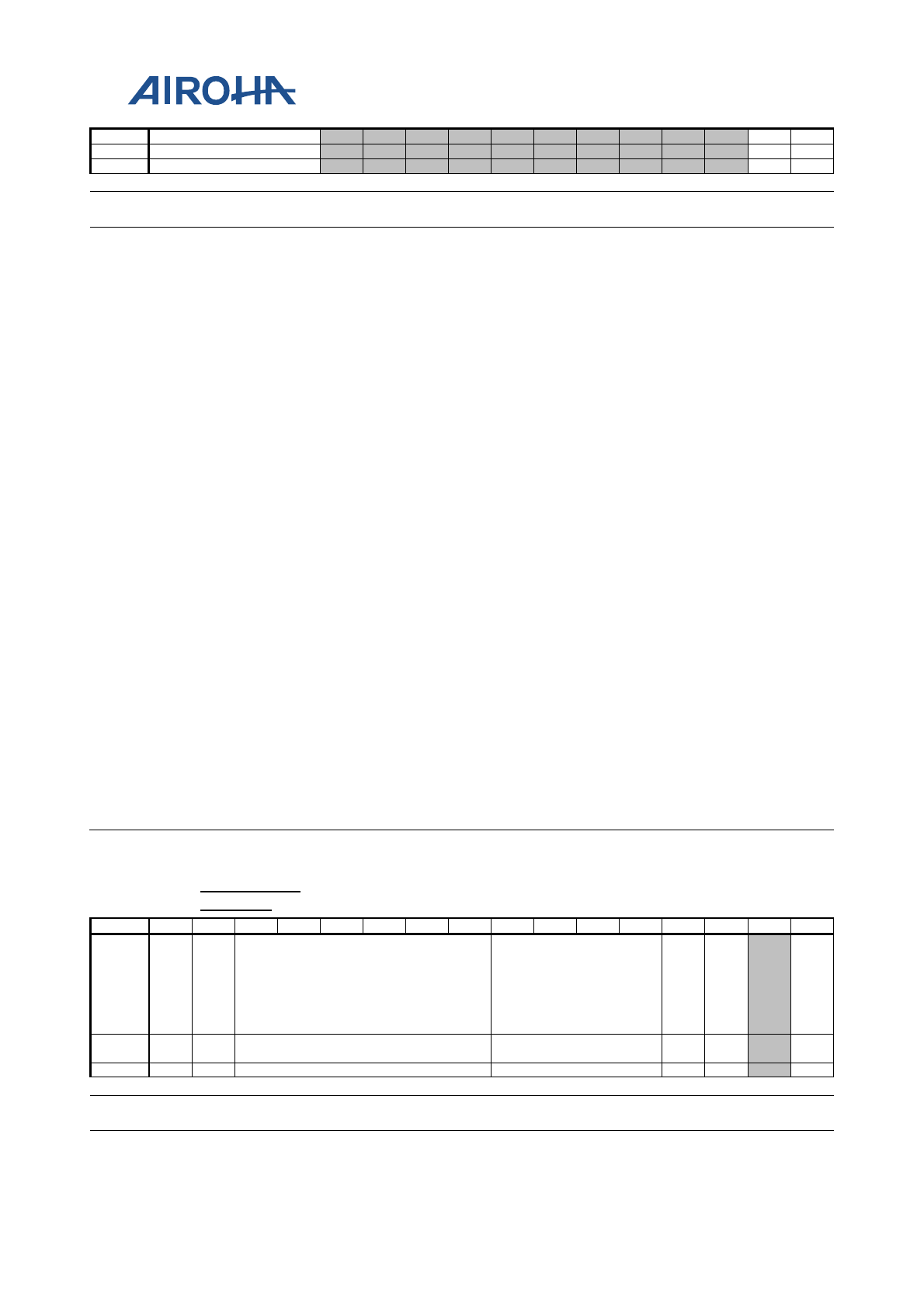
MT2523 Series Reference Manual
© 2015 - 2018 Airoha Technology Corp.
Page 287 of 692
This document contains information that is proprietary to Airoha Technology Corp. (“Airoha”) and/or its licensor(s).
Any unauthorized use, reproduction or disclosure of this document in whole or in part is strictly prohibited.
L
Type
R/W
RW
RW
Reset
0
0
0
Bit(s) Mnemoni
c Name Description
31 SLV_I2S_EN Enables slave I2S
0: Disable
1: Enable
30 AFE_FOC_EN Enables SRC function in slave I2S
0: Disable
1: Enable
18 SLV_I2S_BIT_SWA
P Swaps MSB 16 bits and LSB 16 bits. For backup control, keep 0 in
default.
0: No swap
1: Swap
17 SLV_I2S_BYPASS_
SRC Bypasses SRC function in slave I2S. For backup control, keep 0 in
default.
0: No bypass
1: Bypass SRC
16 SLV_I2S_2CH_SEL Slave I2S nomo or stereo mode. For backup control, keep 0 in
default.
0: Speech mode, RCH = LCH data
1: Stereo mode
15:12 SLV_I2S_MODE Sampling frequency setting; only 8kHz and 16kHz are useful.
Others reserved
0000: 8kHz
0001: 11.025kHz
0010: 12kHz
0100: 16kHz
0101: 22.05kHz
0110: 24kHz
1000: 32kHz
1001: 44.1kHz
1010: 48kHz
1 SLV_I2S_FMT EDI format
0: EIAJ
1: I2S
0 SLV_I2S_PCM_SEL Selects PCM or slave I2S
UL: PCM FIFO data from PCM or slave I2S
DL: DSP output data to PCM or slave I2S
0: PCM
1: Slave I2S
82CD0310 AFE_FOC_T
X_CON0
AFE Slave I2S TX FOC Control Register 0 5a00
Bit
15
14
13
12
11
10
9
8
7
6
5
4
3
2
1
0
Nam
e
FR
EQ
_ES
T_
MO
DE
N_
STE
P_
MO
DE
STEP_EST_UPDATE_LV
MON
STE
P_
LI
M_
MO
DE
PT
R_
TA
RA
CK
_E
M
RT
_E
N
Type
R/
W
R/
W
R/W
RW RW RW
RW
Reset
0
1
011010
0000
0
0
0
Bit(s)
Mnemoni
c
Name
Description
15 FREQ_EST_MODE Frequency offset estimation mode
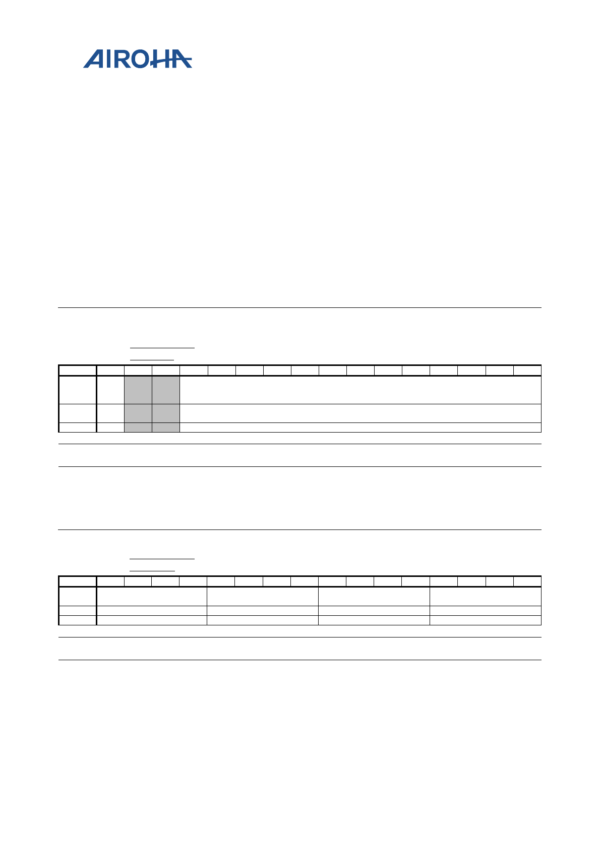
MT2523 Series Reference Manual
© 2015 - 2018 Airoha Technology Corp.
Page 288 of 692
This document contains information that is proprietary to Airoha Technology Corp. (“Airoha”) and/or its licensor(s).
Any unauthorized use, reproduction or disclosure of this document in whole or in part is strictly prohibited.
0: In 512 cycles
1: In 1024 cycles
14 N_STEP_MODE Controls the reference for step_change
0: Refer to step
1: Refer to step_target
13:8 STEP_EST_UPDAT
E_LV Controls step update threshold for frequency tracking
0~63
7:4 MON Selects data monitor
Only used in debug mode. Keep at 0000 in normal mode.
3 STEP_LIM_MODE Controls maximum tracking frequency offset
0: 270 ppm
1: 540 ppm
2 PTR_TRACK_EN Controls the enable signal to tracking frequency when pointer
difference changes
0: Disable
1: Enable
0 FT_EN Controls the enable signals for frequency tracking
Note: Remember to open SRC and I2S before starting frequency tracking.
0: No frequency tracking
1: Frequency tracking on
82CD0314 AFE_FOC_T
X_CON1
AFE Slave I2S TX FOC Control Register 1 0000
Bit
15
14
13
12
11
10
9
8
7
6
5
4
3
2
1
0
Nam
e
MA
NU
AL
STEP_MANUAL
Type
R/
W
RW
Reset
0
0_0000_0000_0000
Bit(s)
Mnemoni
c
Name
Description
15 MANUAL Controls frequency tracking mode
0: Auto-tracking
1: Manual mode
12:0 STEP_MANUAL
step_manual = frequency offset (ppm)/step_ini.
82CD0318 AFE_FOC_T
X_CON2
AFE Slave I2S TX FOC Control Register 2 1589
Bit
15
14
13
12
11
10
9
8
7
6
5
4
3
2
1
0
Nam
e
N_STEP_JUMP_CON3
N_STEP_JUMP_CON2
N_STEP_JUMP_CON1
N_STEP_JUMP_CON0
Type
R/W
R/W
R/W
R/W
Reset
0001
0101
1000
1001
Bit(s)
Mnemoni
c
Name
Description
15:12 N_STEP_JUMP_CO
N3 Controls input samples to change step when step change is larger
than power (2, step_change_con3)
11:8 N_STEP_JUMP_CO
N2 Controls input samples to change step when step change is smaller
than power (2, step_change_con2)
7:4 N_STEP_JUMP_CO
N1 Controls input samples to change step when step change is smaller
than power (2, step_change_con1)
3:0 N_STEP_JUMP_CO
N0 Controls input samples to change step when step change is smaller
than power (2, step_change_con0)
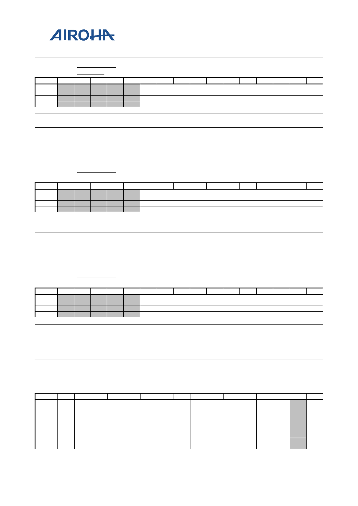
MT2523 Series Reference Manual
© 2015 - 2018 Airoha Technology Corp.
Page 289 of 692
This document contains information that is proprietary to Airoha Technology Corp. (“Airoha”) and/or its licensor(s).
Any unauthorized use, reproduction or disclosure of this document in whole or in part is strictly prohibited.
82CD031C AFE_FOC_T
X_CON3
AFE Slave I2S TX FOC Control Register 3 0034
Bit
15
14
13
12
11
10
9
8
7
6
5
4
3
2
1
0
Nam
e
STEP_CHANGE_CON0
Type
R/W
Reset
000_0011_0100
Bit(s) Mnemoni
c Name Description
10:0 STEP_CHANGE_CO
N0
Controls boundary between N_STEP_JUMP0 and N_STEP_JUMP1
82CD032
0 AFE_FOC_T
X_CON4
AFE Slave I2S TX FOC Control Register 4 0067
Bit
15
14
13
12
11
10
9
8
7
6
5
4
3
2
1
0
Nam
e
STEP_CHANGE_CON1
Type
R/W
Reset
000_0110_0111
Bit(s) Mnemoni
c Name Description
10:0 STEP_CHANGE_CO
N1
Controls boundary between N_STEP_JUMP1 and N_STEP_JUMP2
82CD032
4 AFE_FOC_T
X_CON5
AFE Slave I2S TX FOC Control Register 5 019a
Bit
15
14
13
12
11
10
9
8
7
6
5
4
3
2
1
0
Nam
e
STEP_CHANGE_CON2
Type
R/W
Reset
001_1001_1010
Bit(s) Mnemoni
c Name Description
10:0 STEP_CHANGE_CO
N2
Controls boundary between N_STEP_JUMP2 and N_STEP_JUMP3
82CD033
0 AFE_FOC_R
X_CON0
AFE Slave I2S RX FOC Control Register 0 5a00
Bit
15
14
13
12
11
10
9
8
7
6
5
4
3
2
1
0
Nam
e
FR
EQ
_ES
T_
MO
DE
N_
STE
P_
MO
DE
STEP_EST_UPDATE_LV
MON
STE
P_
LI
M_
MO
DE
PT
R_
TA
RA
CK
_E
M
RT
_E
N
Type
R/
W
R/
W
R/W
RW RW RW
RW
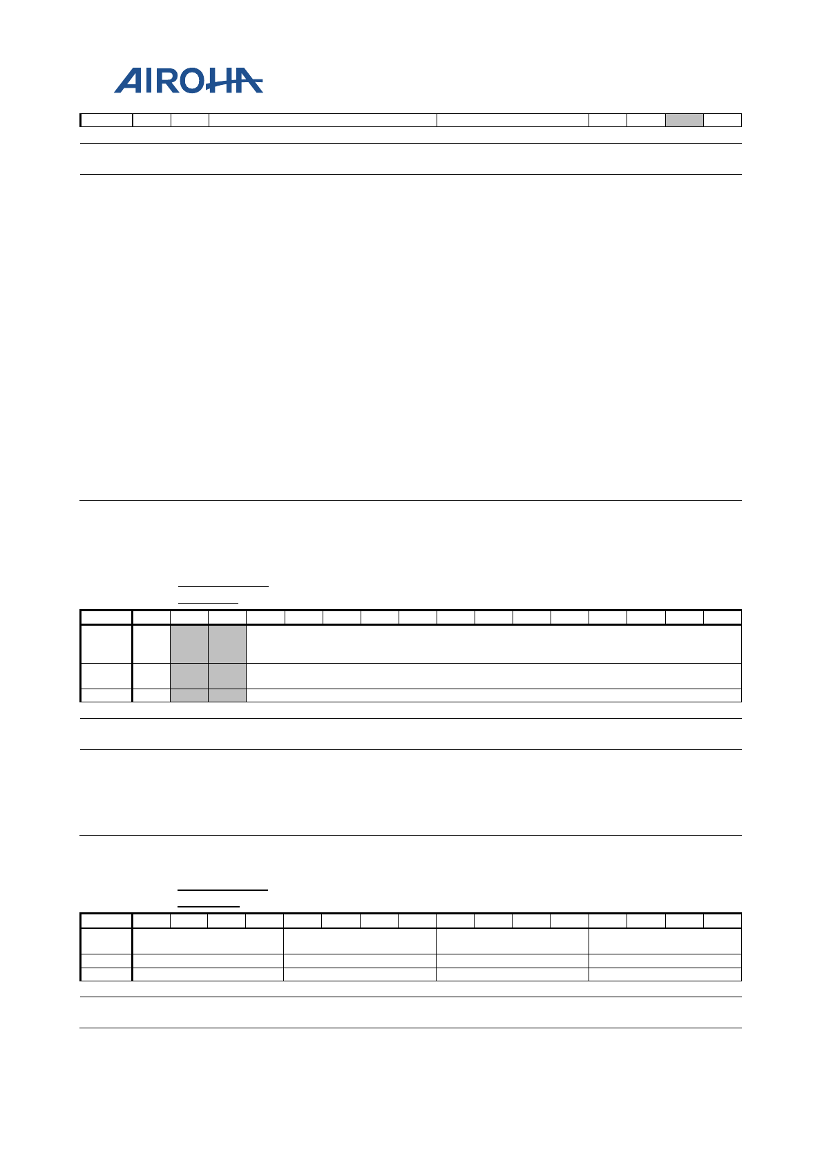
MT2523 Series Reference Manual
© 2015 - 2018 Airoha Technology Corp.
Page 290 of 692
This document contains information that is proprietary to Airoha Technology Corp. (“Airoha”) and/or its licensor(s).
Any unauthorized use, reproduction or disclosure of this document in whole or in part is strictly prohibited.
Reset
0
1
011010
0000
0
0
0
Bit(s)
Mnemoni
c
Name
Description
15 FREQ_EST_MODE Frequency offset estimation mode
0: In 512 cycles
1: In 1024 cycles
14 N_STEP_MODE Controls reference for step_change.
0: Refer to step
1: Refer to step_target
13:8 STEP_EST_UPDAT
E_LV Controls step update threshold for frequency tracking
0~63
7:4 MON Selects data monitor
Only used in debug mode. Keep 0000 in normal mode.
3 STEP_LIM_MODE This bit controls the maximum tracking frequency offset.
0: 270 ppm
1: 540 ppm
2 PTR_TRACK_EN Controls the enable signal to tracking frequency when pointer
difference changes
0: Disable
1: Enable
0 FT_EN Controls the enable signals for frequency tracking
Note: Remember to open SRC and I2S before starting frequency tracking.
0: No frequency tracking
1: Frequency tracking on
82CD033
4 AFE_FOC_R
X_CON1
AFE Slave I2S RX FOC Control Register 1 0000
Bit
15
14
13
12
11
10
9
8
7
6
5
4
3
2
1
0
Nam
e
MA
NU
AL
STEP_MANUAL
Type
R/
W
RW
Reset
0
0_0000_0000_0000
Bit(s)
Mnemoni
c
Name
Description
15 MANUAL Controls frequency tracking mode
0: Auto-tracking
1: Manual mode
12:0 STEP_MANUAL
step_manual = frequency offset (ppm)/step_ini.
82CD033
8 AFE_FOC_R
X_CON2
AFE Slave I2S RX FOC Control Register 2 1589
Bit
15
14
13
12
11
10
9
8
7
6
5
4
3
2
1
0
Nam
e
N_STEP_JUMP_CON3
N_STEP_JUMP_CON2
N_STEP_JUMP_CON1
N_STEP_JUMP_CON0
Type
R/W
R/W
R/W
R/W
Reset
0001
0101
1000
1001
Bit(s)
Mnemoni
c
Name
Description
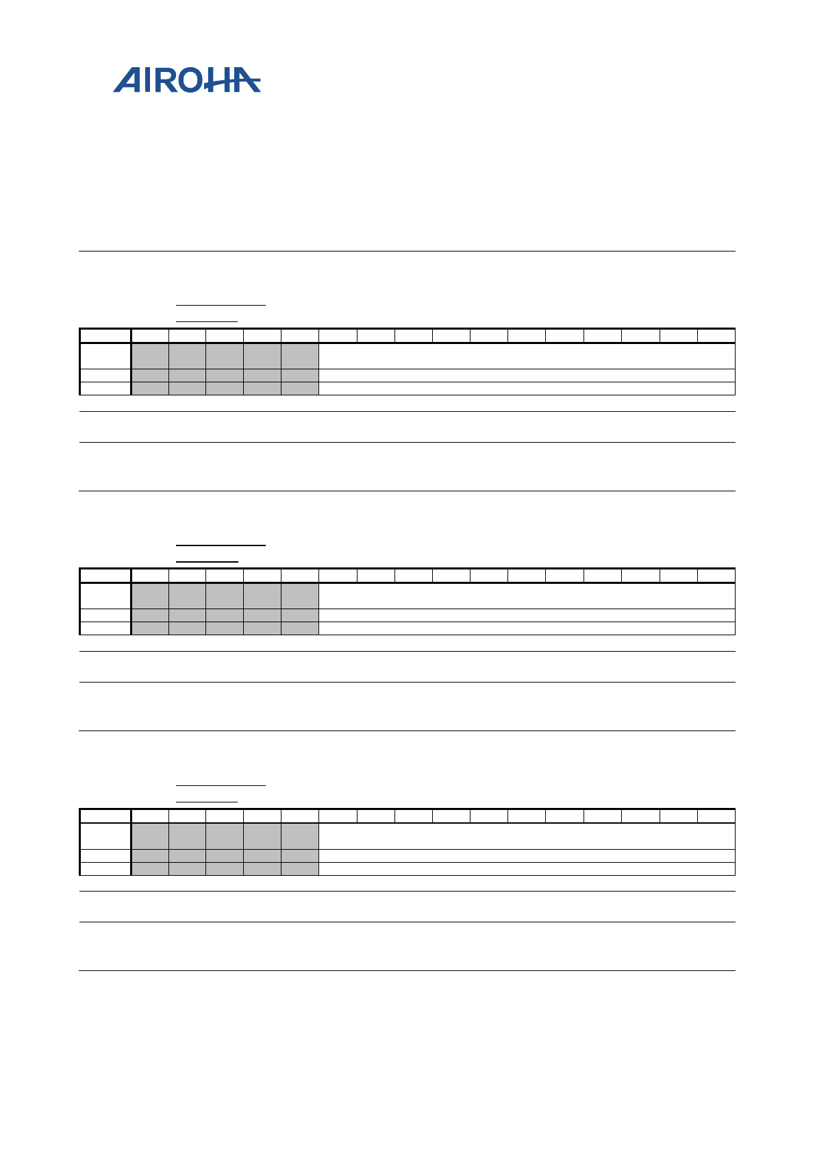
MT2523 Series Reference Manual
© 2015 - 2018 Airoha Technology Corp.
Page 291 of 692
This document contains information that is proprietary to Airoha Technology Corp. (“Airoha”) and/or its licensor(s).
Any unauthorized use, reproduction or disclosure of this document in whole or in part is strictly prohibited.
15:12 N_STEP_JUMP_CO
N3 Controls input samples to change step when step change is larger
than power (2, step_change_con3)
11:8 N_STEP_JUMP_CO
N2 Controls input samples to change step when step change is smaller
than power (2, step_change_con2)
7:4 N_STEP_JUMP_CO
N1 Controls input samples to change step when step change is smaller
than power (2, step_change_con1)
3:0 N_STEP_JUMP_CO
N0 Controls input samples to change step when step change is smaller
than power (2, step_change_con0)
82CD033
C AFE_FOC_R
X_CON3
AFE Slave I2S RX FOC Control Register 3 0034
Bit
15
14
13
12
11
10
9
8
7
6
5
4
3
2
1
0
Nam
e
STEP_CHANGE_CON0
Type
R/W
Reset
000_0011_0100
Bit(s)
Mnemoni
c
Name
Description
10:0 STEP_CHANGE_CO
N0
Controls boundary between N_STEP_JUMP0 and N_STEP_JUMP1
82CD034
0 AFE_FOC_R
X_CON4
AFE Slave I2S RX FOC Control Register 4 0067
Bit
15
14
13
12
11
10
9
8
7
6
5
4
3
2
1
0
Nam
e
STEP_CHANGE_CON1
Type
R/W
Reset
000_0110_0111
Bit(s)
Mnemoni
c
Name
Description
10:0 STEP_CHANGE_CO
N1
Controls boundary between N_STEP_JUMP1 and N_STEP_JUMP2
82CD034
4 AFE_FOC_R
X_CON5
AFE Slave I2S RX FOC Control Register 5 019a
Bit
15
14
13
12
11
10
9
8
7
6
5
4
3
2
1
0
Nam
e
STEP_CHANGE_CON2
Type
R/W
Reset
001_1001_1010
Bit(s)
Mnemoni
c
Name
Description
10:0 STEP_CHANGE_CO
N2
Controls boundary between N_STEP_JUMP2 and N_STEP_JUMP3
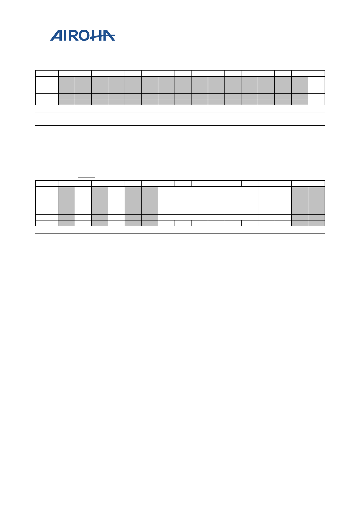
MT2523 Series Reference Manual
© 2015 - 2018 Airoha Technology Corp.
Page 292 of 692
This document contains information that is proprietary to Airoha Technology Corp. (“Airoha”) and/or its licensor(s).
Any unauthorized use, reproduction or disclosure of this document in whole or in part is strictly prohibited.
82CD002
0 AFE_AMCU_
CON0
AFE Audio MCU Control Register 0 0000
Bit
15
14
13
12
11
10
9
8
7
6
5
4
3
2
1
0
Name
AIR
QO
N
Type
RW
Reset
0
Bit(s)
Mnemoni
c
Name
Description
0 AIRQON Turns on audio interrupt operation
0: Turn off
1: Turn on
82CD002
4 AFE_AMCU_
CON1
AFE Audio MCU Control Register 1 0C00
Bit
15
14
13
12
11
10
9
8
7
6
5
4
3
2
1
0
Nam
e
MO
NO
_SE
L
i2s
_1x
out
_se
l
AFS ARAMPSP AM
UT
ER
AM
UT
EL
Type
RW
RW
RW
RW
RW
RW
Reset
0
0
0
0
0
0
0
0
0
0
Bit(s)
Mnemoni
c
Name
Description
14 MONO_SEL Selects mono mode
AFE HW will do “(left + right)/2” operation to the audio sample pair. Thus
both right and left channel DAC will have the same inputs.
0: Normal function
1: Enable mono mode
12 i2s_1xout_sel 1X data to I2S means data from DSP FIFO and do not pass ASP
0: Normal mode
1: Audio 1x data to I2S
9:6 AFS Sampling frequency setting
Others reserved
0000: 8kHz
0001: 11.025kHz
0010: 12kHz
0100: 16kHz
0101: 22.05kHz
0110: 24kHz
1000: 32kHz
1001: 44.1kHz
1010: 48kHz
5:4 ARAMPSP Selects ramp up/down speed
00: 8, 4096/AFS
01: 16, 2048/AFS
10: 24, 1024/AFS
11: 32, 512/AFS
3 AMUTER Mute the audio R-channel, with soft ramp up/down
0: No mute
1: Turn on mute function
2 AMUTEL Mutes audio L-channel, with soft ramp up/down
0: No mute
1: Turn on mute function
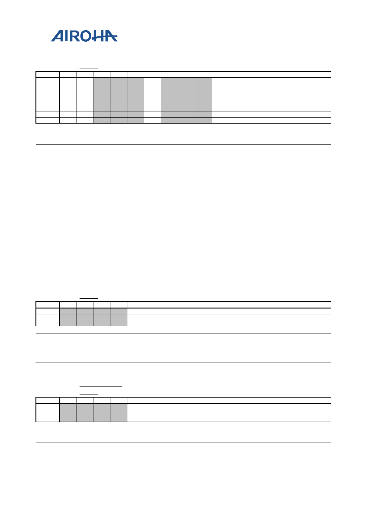
MT2523 Series Reference Manual
© 2015 - 2018 Airoha Technology Corp.
Page 293 of 692
This document contains information that is proprietary to Airoha Technology Corp. (“Airoha”) and/or its licensor(s).
Any unauthorized use, reproduction or disclosure of this document in whole or in part is strictly prohibited.
82CD002
C AFE_AMCU_
CON2
AFE Audio Control Register 2 003C
Bit
15
14
13
12
11
10
9
8
7
6
5
4
3
2
1
0
Name
AD
C_
CO
MP
_E
N
EDI
_W
S_
OP
TIO
N
PR
EDI
T_
EN
EDI
_SE
L ASDM_GAIN
Type
RW
RW
RW
RW
RW
Reset
0
0
0
0
1
1
1
1
0
0
Bit(s)
Mnemoni
c
Name
Description
15 ADC_COMP_EN Enables DC offset compensation
0: Disable
1: Enable
14 EDI_WS_OPTION Optional setting for I2S
Do not touch the bit.
10 PREDIT_EN Enables pre-distortion function
No use now
0: Disable
1: Enable
6 EDI_SEL Feeds EDI input data to audio filter directly
0: Audio data come from DSP.
1: Audio data come from EDI input.
5:0 ASDM_GAIN Gain settings at audio SDM input
Suggested value: 0x3c (60/64). Other SDM gain settings may cause
performance degradation.
000000: 0/64
000001: 1/64
111111: 63/64
82CD003
8 AFE_AMCU_
CON3
AFE Audio Control Register 3 0000
Bit
15
14
13
12
11
10
9
8
7
6
5
4
3
2
1
0
Name
PRE_A2
Type
RW
Reset
0
0
0
0
0
0
0
0
0
0
0
0
Bit(s)
Mnemoni
c
Name
Description
11:0 PRE_A2 A2 parameter for pre-distortion
82CD003
C AFE_AMCU_
CON4
AFE Audio Control Register 4 0000
Bit
15
14
13
12
11
10
9
8
7
6
5
4
3
2
1
0
Name
PRE_A3
Type
RW
Reset
0
0
0
0
0
0
0
0
0
0
0
0
Bit(s)
Mnemoni
c
Name
Description
11:0 PRE_A3 A3 parameter for pre-distortion
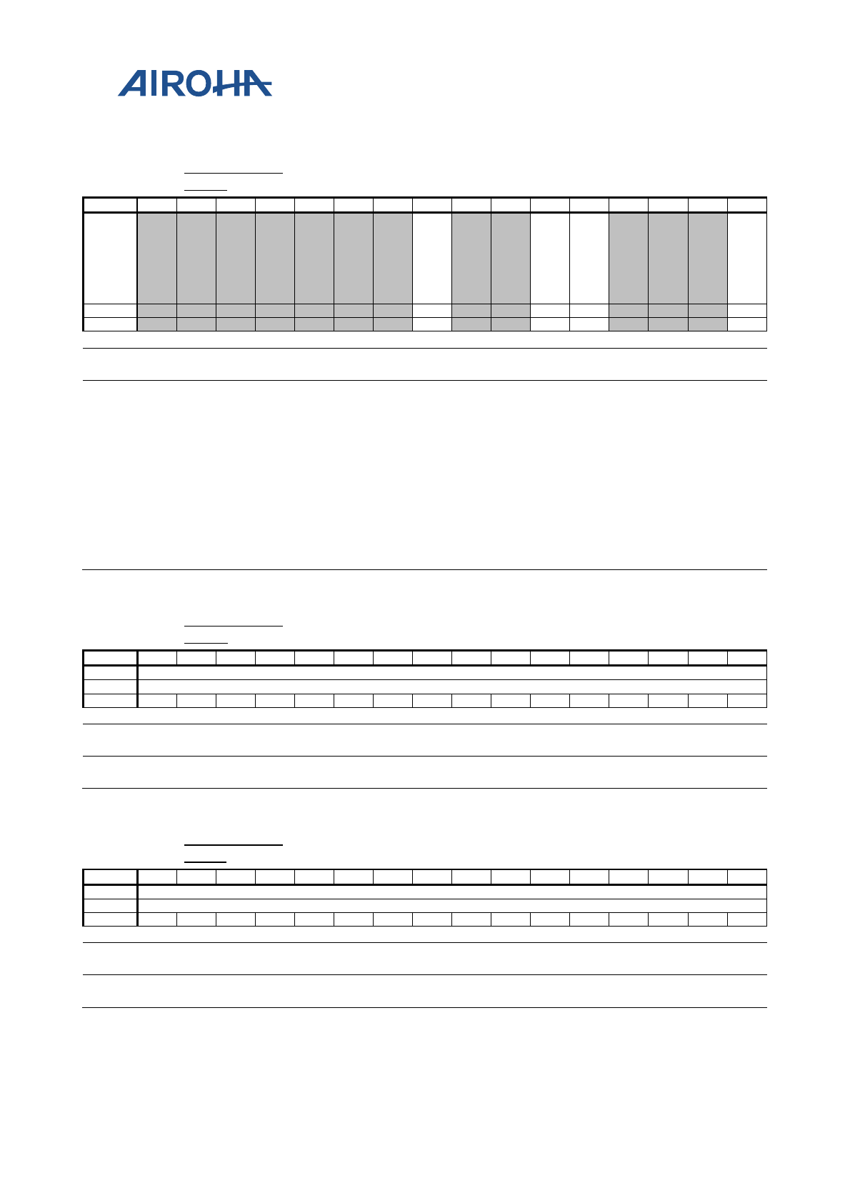
MT2523 Series Reference Manual
© 2015 - 2018 Airoha Technology Corp.
Page 294 of 692
This document contains information that is proprietary to Airoha Technology Corp. (“Airoha”) and/or its licensor(s).
Any unauthorized use, reproduction or disclosure of this document in whole or in part is strictly prohibited.
82CD0180 AFE_AMCU_
CON5
AFE Audio MCU Control Register 5 0000
Bit
15
14
13
12
11
10
9
8
7
6
5
4
3
2
1
0
Nam
e
SD
ML
P_
UL
TO
DL
AS
DM
_D
AT
A_
MO
NO
SD
ML
P_
DL
TO
UL
SD
M_
CK
_P
HA
SE
Type
RW
RW
RW
RW
Reset
0
0
0
0
Bit(s) Mnemoni
c Name Description
8 SDMLP_ULTODL UL sigma delta data loopback to DL sigma delta data
0: Disable
1: Enable
5 ASDM_DATA_MON
O Rch output data = Lch outut data
0: Disable
1: Enable
4 SDMLP_DLTOUL DL sigma delta data loopback to UL sigma delta data
0: Disable
1: Enable
0 SDM_CK_PHASE Selects phase of SDM clock
0: Clock changes at data falling edge.
1: Clock changes at data rising edge.
82CD0184 AFE_AMCU_
CON6
AFE Audio MCU Control Register 6 0000
Bit
15
14
13
12
11
10
9
8
7
6
5
4
3
2
1
0
Name
RCH_AUDIO_DC_OFFSET_VALUE
Type
RW
Reset
0
0
0
0
0
0
0
0
0
0
0
0
0
0
0
0
Bit(s)
Mnemoni
c
Name
Description
15:0 RCH_AUDIO_DC_
OFFSET_VALUE Set up this register for audio right channel DC offset value
cancellation.
82CD0188 AFE_AMCU_
CON7
AFE Audio MCU Control Register 7 0000
Bit
15
14
13
12
11
10
9
8
7
6
5
4
3
2
1
0
Name
LCH_AUDIO_DC_OFFSET_VALUE
Type
RW
Reset
0
0
0
0
0
0
0
0
0
0
0
0
0
0
0
0
Bit(s)
Mnemoni
c
Name
Description
15:0 LCH_AUDIO_DC_
OFFSET_VALUE Set up this register for audio left channel DC offset value
cancellation.
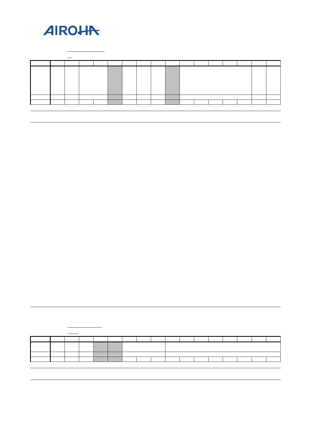
MT2523 Series Reference Manual
© 2015 - 2018 Airoha Technology Corp.
Page 295 of 692
This document contains information that is proprietary to Airoha Technology Corp. (“Airoha”) and/or its licensor(s).
Any unauthorized use, reproduction or disclosure of this document in whole or in part is strictly prohibited.
82CD002
8 AFE_EDI_CO
N
AFE EDI Control Register 003C
Bit
15
14
13
12
11
10
9
8
7
6
5
4
3
2
1
0
Name
EN
2
UL
_T
OI2
SD
SP
I2S_OUT_
MODE
UL
TO
EDI
EDI
_L
PB
K_
MO
DE
DIR WCYCLE FM
T EN
Type
RW
RW
RW
RW
RW
RW
RW
RW
RW
Reset
0
0
0
0
0
0
0
0
1
1
1
1
0
0
Bit(s)
Mnemoni
c
Name
Description
15 EN2 Enables EDI PAD output
Only for master output mode.
0: Disable EDI PAD output
1: Enable EDI PAD output
14 UL_TOI2SDSP For 32K recording; uplink data should go to dsp_i2s port
0: UL data do not go to dsp_i2s port.
1: UL data go to dsp_i2s port.
13:12 I2S_OUT_MODE I2S output mode
00: 1X output
01: 2X output
10: 4X output
10 ULTOEDI Uplink data to I2S
0: Disable
1: Enable
9 EDI_LPBK_MODE Control loopback mode: EDI_RX = EDI_TX
0: Normal mode
1: Loopback mode
8 DIR Serial data bit direction
0: Only output mode active. Audio data are fed out to the external device.
1: Both input mode and output mode are active.
6:2 WCYCLE Clock cycle count in a word
Cycle count = WCYCLE + 1; and WCYCLE can only be 15 or 31. Any other
values will result in unpredictable errors.
15: Cycle count is 16.
31: Cycle count is 32.
1 FMT EDI format
0: EIAJ
1: I2S
0 EN Enables EDI
When EDI is disabled, EDI_DAT and EDI_WS will hold low.
0: Disable EDI
1: Enable EDI
82CD003
0 AFE_DAC_T
EST
Audio/Voice DAC SineWave Generator 0701
Bit
15
14
13
12
11
10
9
8
7
6
5
4
3
2
1
0
Name
VO
N
AO
N
MU
TE
AMP_DIV FREQ_DIV
Type
RW
RW
RW
RW
RW
Reset
0
0
0
1
1
1
0
0
0
0
0
0
0
1
Bit(s)
Mnemoni
c
Name
Description
15 VON Makes voice DAC output the test sine wave
0: Voice DAC inputs are normal voice samples.
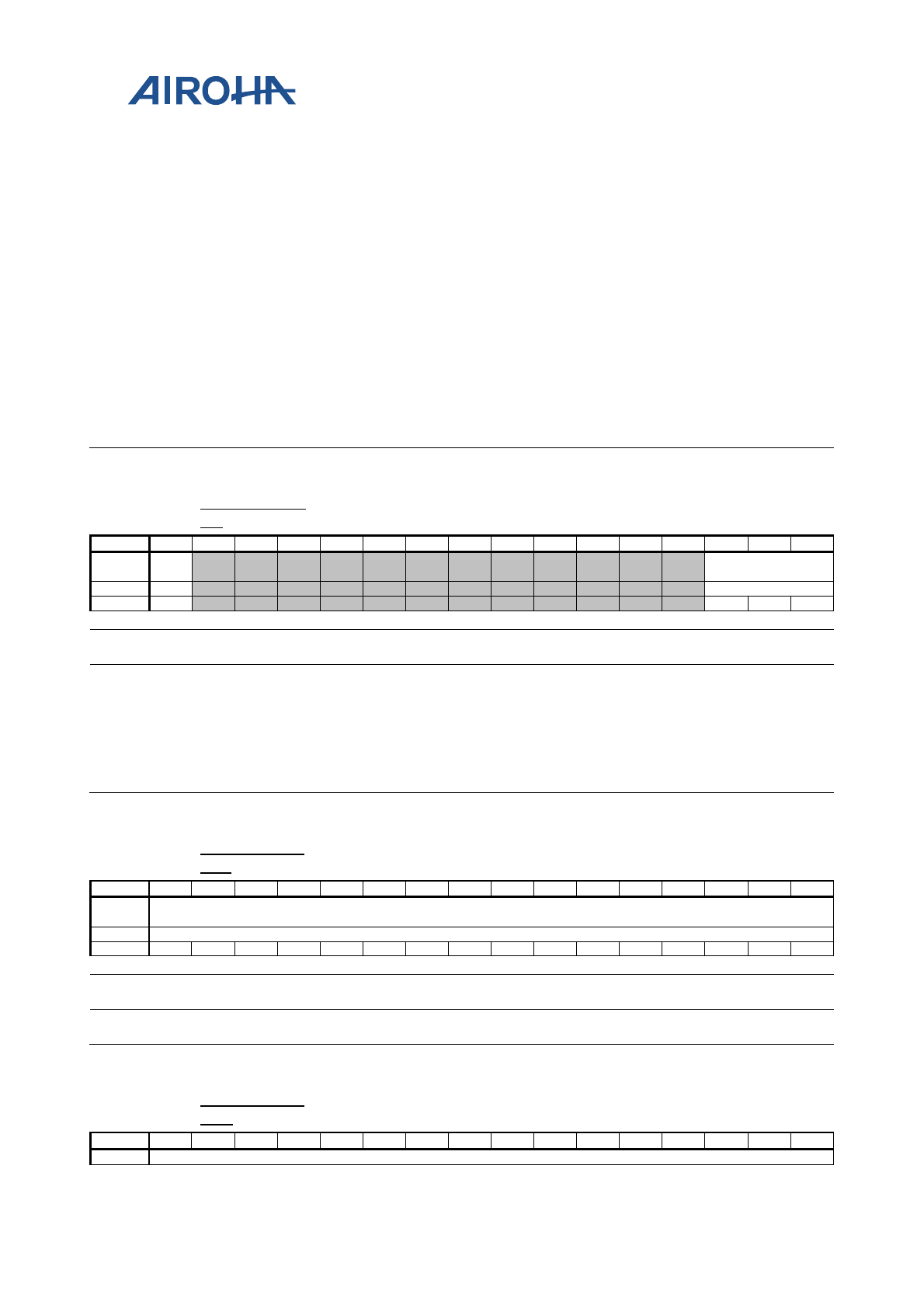
MT2523 Series Reference Manual
© 2015 - 2018 Airoha Technology Corp.
Page 296 of 692
This document contains information that is proprietary to Airoha Technology Corp. (“Airoha”) and/or its licensor(s).
Any unauthorized use, reproduction or disclosure of this document in whole or in part is strictly prohibited.
1: Voice DAC inputs are sine waves.
14 AON Makes audio DAC output the test sine wave
0: Audio DAC inputs are normal voice samples.
1: Audio DAC inputs are sine waves.
13 MUTE Mute switch
0: Turn on the sine wave output in this test mode
1: Mute the sine wave output
10:8 AMP_DIV Amplitude setting
111: Full scale
110: 1/2 full scale
101: 1/4 full scale
100: 1/8 full scale
011: 1/16 full scale
010: 1/32 full scale
001: 1/64 full scale
000: 1/128 full scale
7:0 FREQ_DIV Frequency setting, 1X ~ 15X (voice), 1X ~ 31X (audio)
Audio frequency = Sampling rate/64*FREQ_DIV
Voice frequency = Sampling rate/32*FREQ_DIV
Example: 16K voice mode, FREQ_DIV=3, frequency = 16K/32*3 = 1.5K
82CD003
4 AFE_VAM_S
ET
Audio/Voice Interactive Mode Setting 0005
Bit
15
14
13
12
11
10
9
8
7
6
5
4
3
2
1
0
Name
A2
V
PER_VAL
Type
RW
RW
Reset
0
1
0
1
Bit(s)
Mnemoni
c
Name
Description
15 A2V Redirects audio interrupt to voice interrupt, i.e. replaces voice
interrupt by audio interrupt
0: Voice interrupt/audio interrupt
1: Audio interrupt/no interrupt
2:0 PER_VAL Counter reset value for audio interrupt generation period setting.
For example, by default, the setting = 5 will lead to interrupt per 6
L/R samples. Changing this value will change the rate of audio
interrupt.
82CD004
0 AFE_DC_DB
G_1
AFE DC Debug Register 1 0000
Bit
15
14
13
12
11
10
9
8
7
6
5
4
3
2
1
0
Nam
e
AFE_DC_DBG_1
Type
RO
Reset
0
0
0
0
0
0
0
0
0
0
0
0
0
0
0
0
Bit(s)
Mnemoni
c
Name
Description
15:0 AFE_DC_DBG_1 AFE left channel 8X dc compensation/gain output value [15:0] for
debugging
82CD004
4 AFE_DC_DB
G_2
AFE DC Debug Register 2 0000
Bit
15
14
13
12
11
10
9
8
7
6
5
4
3
2
1
0
Nam
AFE_DC_DBG_2
MT2523 Series Reference Manual
© 2015 - 2018 Airoha Technology Corp.
Page 297 of 692
This document contains information that is proprietary to Airoha Technology Corp. (“Airoha”) and/or its licensor(s).
Any unauthorized use, reproduction or disclosure of this document in whole or in part is strictly prohibited.
e
Type
RO
Reset
0
0
0
0
0
0
0
0
0
0
0
0
0
0
0
0
Bit(s) Mnemoni
c Name Description
15:0 AFE_DC_DBG_2 AFE right channel 8X dc compensation/gain output value [15:0] for
debugging
82CD004
8 AFE_DC_DB
G_3
AFE DC Debug Register 3 0000
Bit
15
14
13
12
11
10
9
8
7
6
5
4
3
2
1
0
Nam
e
DB
G_
DC
_SE
L
AFE_DC_DBG_2_1 AFE_DC_DBG_1_1
Type
R/
W
RO RO
Reset
0
0
0
0
0
0
0
0
0
Bit(s) Mnemoni
c Name Description
15 DBG_DC_SEL DBG_DC_SEL
0: AFE_DC_DBG_0 to AFE_DC_DBG_3 is DC compensation
output.
1: AFE_DC_DBG_0 to AFE_DC_DBG_3 is gain stage output.
7:4 AFE_DC_DBG_2
_1 AFE right channel 8X dc compensation/gain output value
[19:16] for debugging
3:0 AFE_DC_DBG_1
_1 AFE left channel 8X dc compensation/gain output value
[19:16] for debugging
82CD0140 AFE_ACHEC
K_SUM_R
AFE Checksum Register 0 0000
Bit
15
14
13
12
11
10
9
8
7
6
5
4
3
2
1
0
Nam
e
AFE_ACHECK_SUM_R
Type
RO
Reset
0
0
0
0
0
0
0
0
0
0
0
0
0
0
0
0
Bit(s)
Mnemoni
c
Name
Description
15:0 AFE_ACHECK_SU
M_R AFE right channel 8X checksum value for cosim debugging
82CD0144 AFE_ACHEC
K_SUM_L
AFE Checksum Register 1 0000
Bit
15
14
13
12
11
10
9
8
7
6
5
4
3
2
1
0
Name
AFE_ACHECK_SUM_L
Type
RO
Reset
0
0
0
0
0
0
0
0
0
0
0
0
0
0
0
0
Bit(s)
Mnemoni
c
Name
Description
15:0 AFE_ACHECK_SU
M_L AFE left channel 8X checksum value for cosim debugging
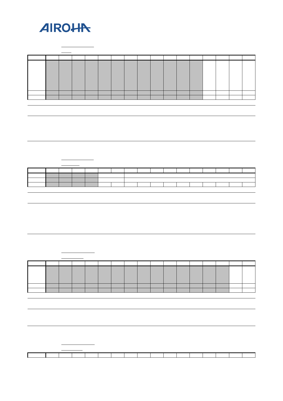
MT2523 Series Reference Manual
© 2015 - 2018 Airoha Technology Corp.
Page 298 of 692
This document contains information that is proprietary to Airoha Technology Corp. (“Airoha”) and/or its licensor(s).
Any unauthorized use, reproduction or disclosure of this document in whole or in part is strictly prohibited.
82CD0148 AFE_MUTE_
STA
AFE Mute Status Register 0000
Bit
15
14
13
12
11
10
9
8
7
6
5
4
3
2
1
0
Name
UN
MU
TE
_D
ON
E_
L
UN
MU
TE_
DO
NE
_R
MU
TE
_D
ON
E_
L
MU
TE
_D
ON
E_
R
Type
RO
RO
RO
RO
Reset
0
0
0
0
Bit(s)
Mnemoni
c
Name
Description
3 UNMUTE_DONE_L UNMUTE_DONE_L status
2 UNMUTE_DONE_R UNMUTE_DONE_R status
1 MUTE_DONE_L MUTE_DONE_L status
0 MUTE_DONE_R MUTE_DONE_R status
82CD0190 AFE_DBG_R
D_PRE
AFE MCU Debug Mode Reading SRAM Out 0000
Bit
15
14
13
12
11
10
9
8
7
6
5
4
3
2
1
0
Name
MEM
AFE_DBG_RD_PRE
Type
RW
RW
Reset
0
0
0
0
0
0
0
0
0
0
0
0
Bit(s)
Mnemoni
c
Name
Description
11:10 MEM Memory
00: NA
01: Data memory
10: Coefficient memory
11: DSP co-processor mapping registers
9:0 AFE_DBG_RD_PRE Read address
82CD0194 AFE_DBG_M
D_CON0
AFE Debug Mode Control Register 0 0000
Bit
15
14
13
12
11
10
9
8
7
6
5
4
3
2
1
0
Name
DB
G_
DO
NE
DB
G_
TRI
G
Type
RO
RW
Reset
0
0
Bit(s)
Mnemoni
c
Name
Description
1 DBG_DONE Debug done signal
0 DBG_TRIG Set up this bit to start running debug mode when debug mode
enable register is high.
82CD0198 AFE_DBG_M
D_CON1
AFE Debug Mode Control Register 1 0000
Bit
15
14
13
12
11
10
9
8
7
6
5
4
3
2
1
0
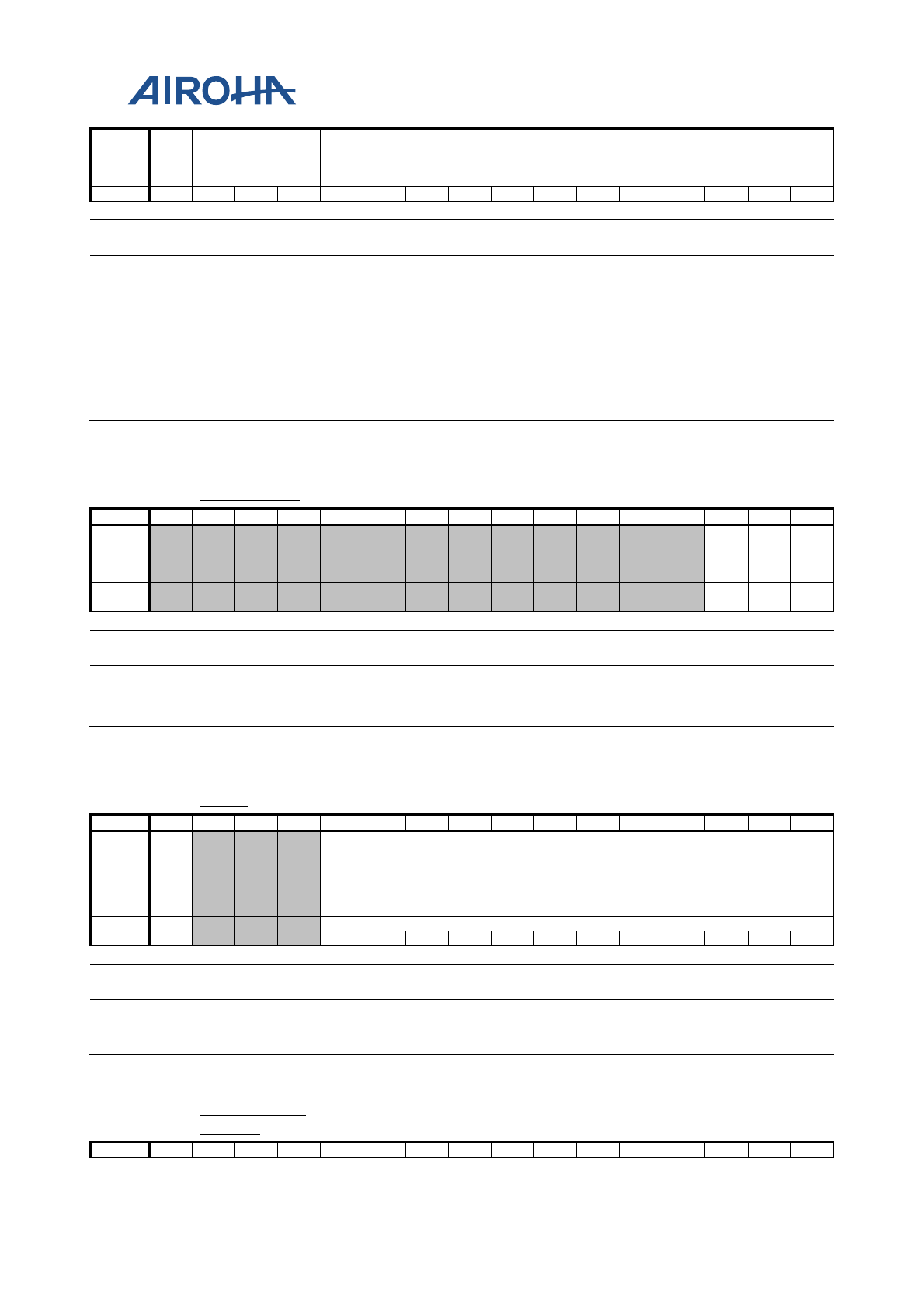
MT2523 Series Reference Manual
© 2015 - 2018 Airoha Technology Corp.
Page 299 of 692
This document contains information that is proprietary to Airoha Technology Corp. (“Airoha”) and/or its licensor(s).
Any unauthorized use, reproduction or disclosure of this document in whole or in part is strictly prohibited.
Name
DB
G_
MD
MODE_SEL DBG_MD_VAL
Type
RW
RW
RW
Reset
0
0
0
0
0
0
0
0
0
0
0
0
0
0
0
0
Bit(s) Mnemoni
c Name Description
15 DBG_MD Enables debug mode
0: Disable
1: Enable
14:12 MODE_SEL Selects debug mode
000: Step 1 mode
001: Nxt n cycle, n is DBG_MD_VAL
010: Run to break point. Break point is DBG_MD_VAL
011: Run 1X
101: Run to n 1X, n is DBG_MD_VAL
11:0 DBG_MD_VAL Corresponding value for different debug mode
82CD019C AFE_DBG_A
PB_STATUS
AFE MCU Status Register 0000
Bit
15
14
13
12
11
10
9
8
7
6
5
4
3
2
1
0
Name
DB
GR
_O
K
AP
BR
_O
K
AP
BW
_A
CK
Type
RO
RO
RO
Reset
0
0
0
Bit(s) Mnemoni
c Name Description
2 DBGR_OK Status for debug mode reading SRAM
1 APBR_OK Status for read SRAM data
0 APBW_ACK Status for writing data into SRAM
82CD01CC AFE_CMPR_
CNTR
AFE Compare Counter Control Register 021D
Bit
15
14
13
12
11
10
9
8
7
6
5
4
3
2
1
0
Name
avc
ntr
_er
r_s
ign
al
cmpr_cntr
Type
RO
RW
Reset
0
0
0
1
0
0
0
0
1
1
1
0
1
Bit(s) Mnemoni
c Name Description
15 avcntr_err_signal Compare counter for 1X enable error flag
11:0 cmpr_cntr If the clock count in 1x enable < cmpr_cntr, avcntr_err_signal will
be pulled high.
82CD01E0 AFE_DBG_R
D_DAT
AFE Debug Mode - Reading SRAM Data 000000
Bit
31
30
29
28
27
26
25
24
23
22
21
20
19
18
17
16
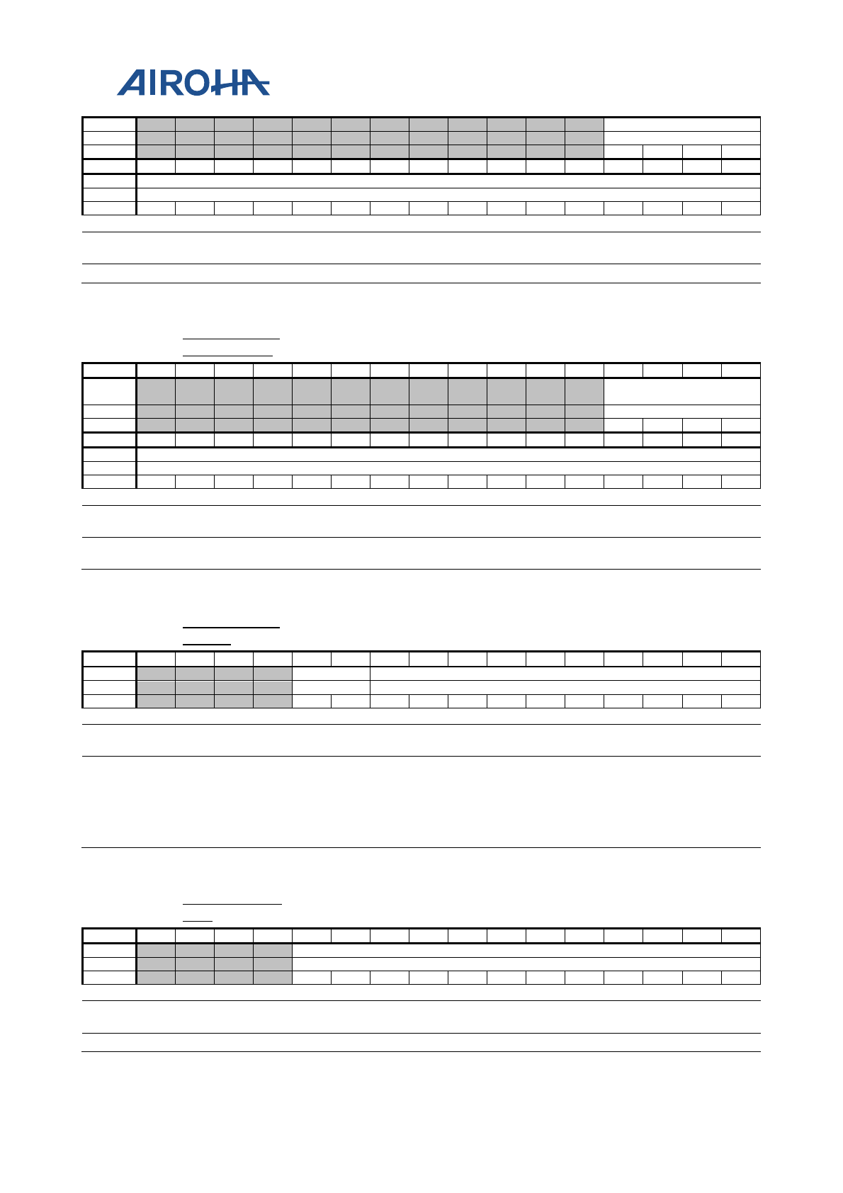
MT2523 Series Reference Manual
© 2015 - 2018 Airoha Technology Corp.
Page 300 of 692
This document contains information that is proprietary to Airoha Technology Corp. (“Airoha”) and/or its licensor(s).
Any unauthorized use, reproduction or disclosure of this document in whole or in part is strictly prohibited.
Name
DBG_RD_DAT[19:16]
Type
RO
Reset
0
0
0
0
Bit
15
14
13
12
11
10
9
8
7
6
5
4
3
2
1
0
Name
DBG_RD_DAT[15:0]
Type
RO
Reset
0
0
0
0
0
0
0
0
0
0
0
0
0
0
0
0
Bit(s)
Mnemoni
c
Name
Description
19:0 DBG_RD_DAT The register width is 20 bits.
82CD01E4 AFE_APBME
M_RD_DAT
AFE MCU Reading SRAM Data 000000
Bit
31
30
29
28
27
26
25
24
23
22
21
20
19
18
17
16
Name
AFE_APBMEM_RD_DA
T[19:16]
Type
RO
Reset
0
0
0
0
Bit
15
14
13
12
11
10
9
8
7
6
5
4
3
2
1
0
Name
AFE_APBMEM_RD_DAT[15:0]
Type
RO
Reset
0
0
0
0
0
0
0
0
0
0
0
0
0
0
0
0
Bit(s) Mnemoni
c Name Description
19:0 AFE_APBMEM_RD
_DAT The register width is 20 bits
82CD01E8 AFE_APBME
M_RD
AFE MCU Read SRAM Request 0000
Bit
15
14
13
12
11
10
9
8
7
6
5
4
3
2
1
0
Name
MEM
AFE_APBMEM_RD
Type
RW
RW
Reset
0
0
0
0
0
0
0
0
0
0
0
0
Bit(s)
Mnemoni
c
Name
Description
11:10 MEM Memory
00: NA
01: Data memory
10: Coefficient memory
11: DSP co-processor mapping registers
9:0 AFE_APBMEM_RD Read address
82CD01EC AFE_PC_1X_
IDX
AFE Program 1X IDX 0022
Bit
15
14
13
12
11
10
9
8
7
6
5
4
3
2
1
0
Name
AFE_PC_1X_IDX
Type
RW
Reset
0
0
0
0
0
0
1
0
0
0
1
0
Bit(s)
Mnemoni
c
Name
Description
11:0 AFE_PC_1X_IDX DSP co-processor idle address
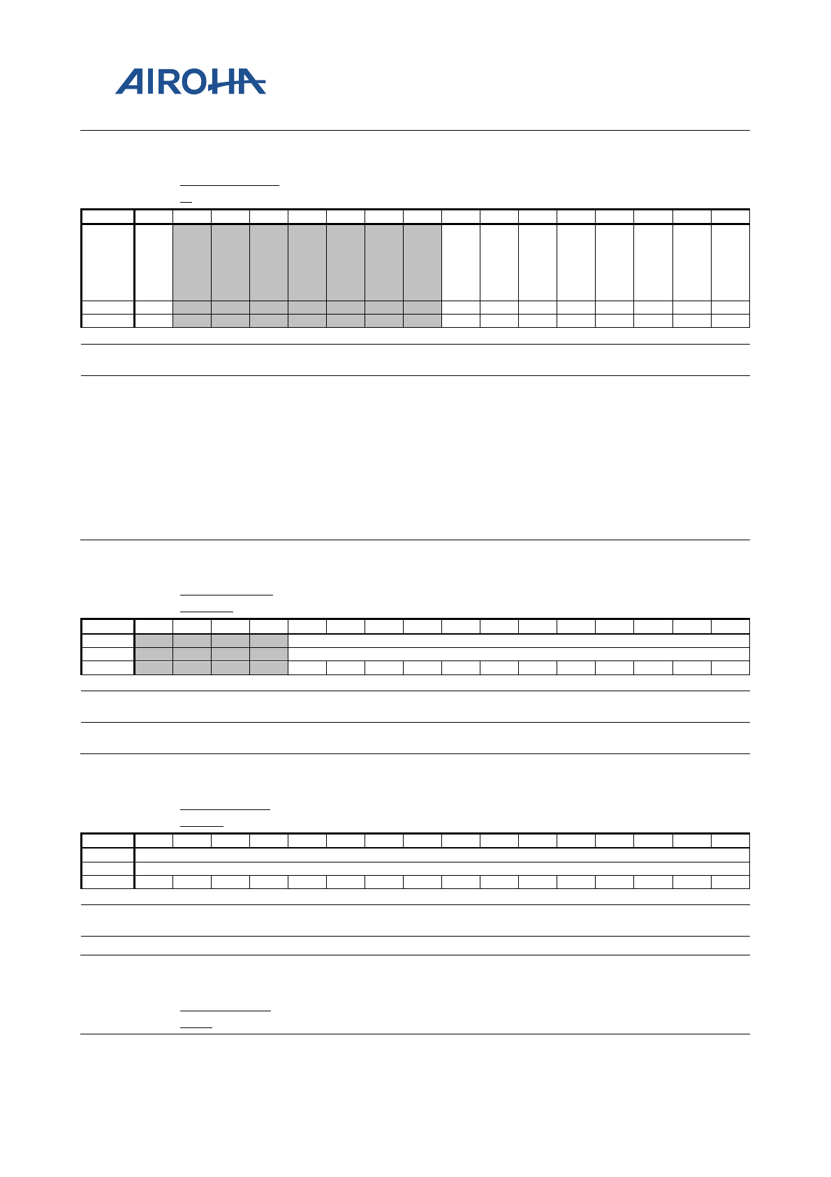
MT2523 Series Reference Manual
© 2015 - 2018 Airoha Technology Corp.
Page 301 of 692
This document contains information that is proprietary to Airoha Technology Corp. (“Airoha”) and/or its licensor(s).
Any unauthorized use, reproduction or disclosure of this document in whole or in part is strictly prohibited.
Do not change the value. AFE may hang if the value is changed.
82CD01F0 AFE_DBG_SI
G
AFE 8X/Buffer/Mux Debug 0000
Bit
15
14
13
12
11
10
9
8
7
6
5
4
3
2
1
0
Name
DB
G_1
XD
AT
_E
N
V8
X_
LP
BK
DM
IC_
SW
AP
AA
FE
_A
LN
VA
FE
_A
LN
VD
L VU
L AD
L I2S
Type
RW
RW
RW
RO
RO
RO
RO
RO
RO
Reset
0
0
0
0
0
0
0
0
0
Bit(s)
Mnemoni
c
Name
Description
15 DBG_1XDAT_EN Enables 1X sample data for debug input
7 V8X_LPBK Voice downlink 8x output loopback to uplink 8x
6 DMIC_SWAP Swaps digital mic input source
5 AAFE_ALN aafe_on align 1x_enable signal
4 VAFE_ALN vafe_on align 1x_enable signal
3 VDL VDL debug signal
2 VUL VLL debug signal
1 ADL ADL debug signal
0 I2S I2S debug signal
82CD01F4 AFE_PC_OU
T_DBG
AFE Program PC Address 0000
Bit
15
14
13
12
11
10
9
8
7
6
5
4
3
2
1
0
Name
PC_OUT
Type
RO
Reset
0
0
0
0
0
0
0
0
0
0
0
0
Bit(s)
Mnemoni
c
Name
Description
11:0 PC_OUT Current DSP co-processor programming counter output for
debugging
82CD01F8 AFE_DBG_1
XDAT
DBG_1XDAT 0000
Bit
15
14
13
12
11
10
9
8
7
6
5
4
3
2
1
0
Name
AFE_DBG_1XDAT
Type
RW
Reset
0
0
0
0
0
0
0
0
0
0
0
0
0
0
0
0
Bit(s)
Mnemoni
c
Name
Description
15:0 AFE_DBG_1XDAT Debug 1X input. Used in debug mode
82CD020
0 AFE_COSIM
_RG
AFE COSIM RG Test 0000
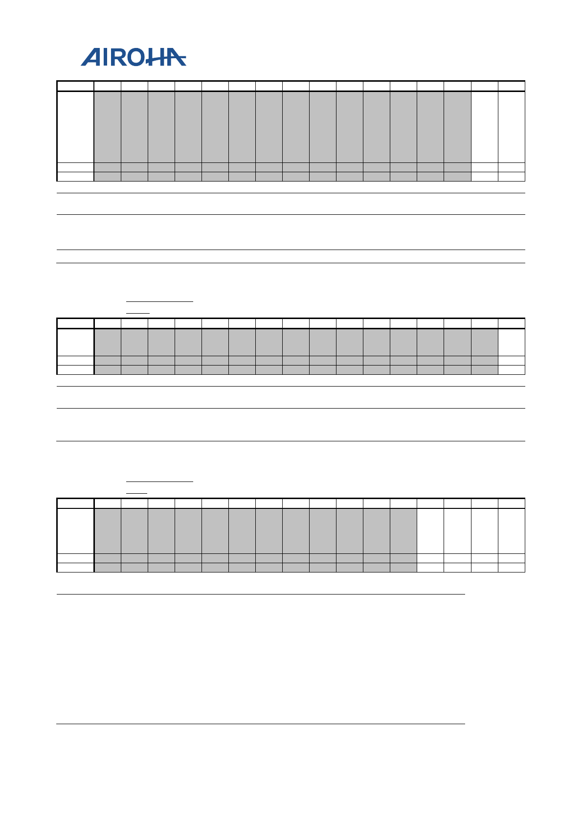
MT2523 Series Reference Manual
© 2015 - 2018 Airoha Technology Corp.
Page 302 of 692
This document contains information that is proprietary to Airoha Technology Corp. (“Airoha”) and/or its licensor(s).
Any unauthorized use, reproduction or disclosure of this document in whole or in part is strictly prohibited.
Bit
15
14
13
12
11
10
9
8
7
6
5
4
3
2
1
0
Nam
e
FP
GA
_D
L2
UL
_L
PB
K
UL
_SI
NE
_O
UT
Type
RW
RW
Reset
0
0
Bit(s)
Mnemoni
c
Name
Description
1 FPGA_DL2UL_LPB
K FPGA loopback mode
0: Normal mode
1: Uplink data are from DL FIFO.
0 UL_SINE_OUT Uplink data are sine table output.
82CD0210 AFE_MCU_C
ON0
AFE MCU Control Register 0 0000
Bit
15
14
13
12
11
10
9
8
7
6
5
4
3
2
1
0
Name
AF
E_
ON
Type
RW
Reset
0
Bit(s) Mnemoni
c Name Description
0 AFE_ON Turns on the audio front end
0: Turn off
1: Turn on
82CD0214 AFE_MCU_C
ON1
AFE MCU Control Register 1 0000
Bit
15
14
13
12
11
10
9
8
7
6
5
4
3
2
1
0
Name
UD
SP_
DL
_O
N
A_I
F_
DL
_O
N
UD
SP_
UL
_O
N
A_I
F_
UL
_O
N
Type
RW
RW
RW
RW
Reset
0
0
0
0
Bit(s
)
Mnemo
nic
Name
Description
3 UDSP_DL_ON Turns on UDSP DL function
0: Turn off
1: Turn on
2 A_IF_DL_ON Turns on a_interface DL function
0: Turn off
1: Turn on
1 UDSP_UL_ON Turns on UDSP UL function
0: Turn off
1: Turn on
0 A_IF_UL_ON Turns on a_interface UL function
0: Turn off
1: Turn on
MT2523 Series Reference Manual
© 2015 - 2018 Airoha Technology Corp.
Page 303 of 692
This document contains information that is proprietary to Airoha Technology Corp. (“Airoha”) and/or its licensor(s).
Any unauthorized use, reproduction or disclosure of this document in whole or in part is strictly prohibited.
21. 2D Acceleration
21.1. General Description
To enhance MMI display and gaming experiences, a 2D acceleration engine is implemented. It supports many
types of color formats. Main features are listed as follows:
• Four-layer overlay with individual color format, window size, source key, constant alpha and rotation.
• Supports up to 2048x2048 resolution for each layer and Region of Interest (ROI).
• Each layer supports RGB565, RGB888, BGR888, ARGB8888, PARGB8888, ARGB6666, ARGB8565,
PARGB6666, PARGB8565 and YUYV422 format
• Font caching: normal font and anti-aliasing font
• Rectangle fill with alpha-blending
• Specific output color replacement
MCU can program 2D engine registers via APB. However, MCU has to make sure that the 2D engine is not BUSY
before any write to 2D engine registers occurs. An interrupt scheme is also provided for more flexibility. Top view
of 2D engine is shown as .
Figure 21-1. 2D Engine Block Diagram
G2D Engine
s
CLK / RST / IRQ
Test mode
rw
APB
GMC
MT2523 Series Reference Manual
© 2015 - 2018 Airoha Technology Corp.
Page 304 of 692
This document contains information that is proprietary to Airoha Technology Corp. (“Airoha”) and/or its licensor(s).
Any unauthorized use, reproduction or disclosure of this document in whole or in part is strictly prohibited.
21.2. Features
21.2.1. 2D Coordinate
The ROI coordinates in 2D engine are represented as 12-bit signed integers which covered from -2048 to 2047. The
maximum resolution of ROI coordinates can achieve 4096x4096, however the maximum ROI size and layer window
size are 2048x2048. shows the coordinate system of 2D engine.
(0,0)
L0_ofs
L2_ofs
L3_ofs
ROI_ofs
ROI_width
ROI_height
x
y
max(2047)
min(-2048)
max(2047)
min(-2048)
Figure 21-2. 2D Engine Coordinates
21.2.2. Color Format
Each layer supports RGB565, RGB888, BGR888, ARGB8888, PARGB8888 and YUV422 (UY0VY1 from low address to
high address) color format. 2D engine supports RGB565, RGB888, BGR888, ARGB8888 and PARGB8888 color
format for write channel. However, 2D engine cannot convert PARGB to ARGB color format (Ex. Layer 0 and 1 are
PARGB color format but ROI is ARGB)
21.2.3. Clipping Window
The setting for clipping window is effective for all the 2D graphics. A pair of minimum and maximum boundary is
applied on ROI window. The portion outside the clipping window will not be drawn to the memory, but the pixels
on the boundary will be kept. The clipping operation is illustrated in .

MT2523 Series Reference Manual
© 2015 - 2018 Airoha Technology Corp.
Page 305 of 692
This document contains information that is proprietary to Airoha Technology Corp. (“Airoha”) and/or its licensor(s).
Any unauthorized use, reproduction or disclosure of this document in whole or in part is strictly prohibited.
(0,0) x
y
ROI
clp_min
clp_max
Figure 21-3. 2D Engine Clipping Operation
21.2.4. Alpha Blending Formula
The alpha blending formula is selected by source color format and the formula is listed below:
1. If the source color format is PARGB
if (SCA != 0xff) {
Dst.R = Dst.R * (0xff – Src.A * SCA/0xff) / 0xff + Src.R * SCA/0xff;
Dst.G = Dst.G * (0xff – Src.A * SCA/0xff) / 0xff + Src.G * SCA/0xff;
Dst.B = Dst.B * (0xff – Src.A * SCA/0xff) / 0xff + Src.B * SCA/0xff;
Dst.A = Dst.A * (0xff – Src.A * SCA/0xff) / 0xff + Src.A * SCA/0xff;
}
else {
Dst.R = Dst.R * (0xff – Src.A) / 0xff + Src.R;
Dst.G = Dst.G * (0xff – Src.A) / 0xff + Src.G;
Dst.B = Dst.B * (0xff – Src.A) / 0xff + Src.B;
Dst.A = Dst.A * (0xff – Src.A) / 0xff + Src.A;
}
2. If the source color format is ARGB
if (SCA != 0xff) {
Dst.R = Dst.R * (0xff – Src.A * SCA/0xff) / 0xff + Src.R * (Src.A/0xff) * (SCA/0xff);
Dst.G = Dst.G * (0xff – Src.A * SCA/0xff) / 0xff + Src.G * (Src.A/0xff) * (SCA/0xff);
Dst.B = Dst.B * (0xff – Src.A * SCA/0xff) / 0xff + Src.B * (Src.A/0xff) * (SCA/0xff);
Dst.A = Dst.A * (0xff – Src.A * SCA/0xff) / 0xff + Src.A * SCA/0xff;
}
else {
Dst.R = Dst.R * (0xff – Src.A) / 0xff + Src.R * Src.A/0xff;
Dst.G = Dst.G * (0xff – Src.A) / 0xff + Src.G * Src.A/0xff;
Dst.B = Dst.B * (0xff – Src.A) / 0xff + Src.B * Src.A/0xff;
Dst.A = Dst.A * (0xff – Src.A) / 0xff + Src.A;
}
3. If the source color format is RGB)
Dst.R = Dst.R * (0xff – SCA) / 0xff + Src.R * SCA/0xff;
Dst.G = Dst.G * (0xff – SCA) / 0xff + Src.G * SCA/0xff;
Dst.B = Dst.B * (0xff – SCA) / 0xff + Src.B * SCA/0xff;
Dst.A = Dst.A * (0xff – SCA) / 0xff + Src.A * SCA/0xff;
MT2523 Series Reference Manual
© 2015 - 2018 Airoha Technology Corp.
Page 306 of 692
This document contains information that is proprietary to Airoha Technology Corp. (“Airoha”) and/or its licensor(s).
Any unauthorized use, reproduction or disclosure of this document in whole or in part is strictly prohibited.
Where SCA is the source constant alpha specified by ALPHA in G2D_Lx_CON, Dst.ARGB is the destination color,
and Src.ARGB is the source color. If the source color format is RGB888 or RGB565, Src.A will be 0xff. The range of
the alpha channel is from 0x0 to 0xff. When performing PARGB or ARGB with SCA, it takes two cycles to complete
the alpha-blending formula. Thus we do not recommend using SCA when aa-font drawing and rectangle fill.
21.2.5. Font Drawing
21.2.5.1. Normal Font Drawing
The 2D engine helps to render fonts stored in one-bit-per-pixel format. If the index value is one, 2D engine writes
foreground color out to memory and no action will be taken if the value is zero. The start bit of font drawing can
be implemented by shifting the starting x coordinate of source, and it can be non-byte aligned to save memory
usage for font caching. In addition, the rotations can be performed at the same time when drawing fonts.
Figure 21-4. Font Drawing Setting
F
Fo
or
re
eg
gr
ro
ou
un
nd
d
C
Co
ol
lo
or
r
B
Ba
ac
ck
kg
gr
ro
ou
un
nd
d
C
Co
ol
lo
or
r
D
De
es
st
ti
in
na
at
ti
io
on
n
b
ba
as
se
e
a
ad
dd
dr
re
es
ss
s
D
De
es
st
ti
in
na
at
ti
io
on
n
h
he
ei
ig
gh
ht
t
D
De
es
st
ti
in
na
at
ti
io
on
n
w
wi
id
dt
th
h
D
De
es
st
ti
in
na
at
ti
io
on
n
p
pi
it
tc
ch
h
S
So
ou
ur
rc
ce
e
b
ba
as
se
e
a
ad
dd
dr
re
es
ss
s
S
So
ou
ur
rc
ce
e
h
he
ei
ig
gh
ht
t
(
(t
th
he
e
s
sa
am
me
e
w
wi
it
th
h
d
de
es
st
ti
in
na
at
ti
io
on
n
o
on
ne
e)
)
S
So
ou
ur
rc
ce
e
w
wi
id
dt
th
h
(
(t
th
he
e
s
sa
am
me
e
w
wi
it
th
h
d
de
es
st
ti
in
na
at
ti
io
on
n
o
on
ne
e)
)
S
So
ou
ur
rc
ce
e
p
pi
it
tc
ch
h
(
(t
th
he
e
s
sa
am
me
e
w
wi
it
th
h
d
de
es
st
ti
in
na
at
ti
io
on
n
w
wi
id
dt
th
h)
)
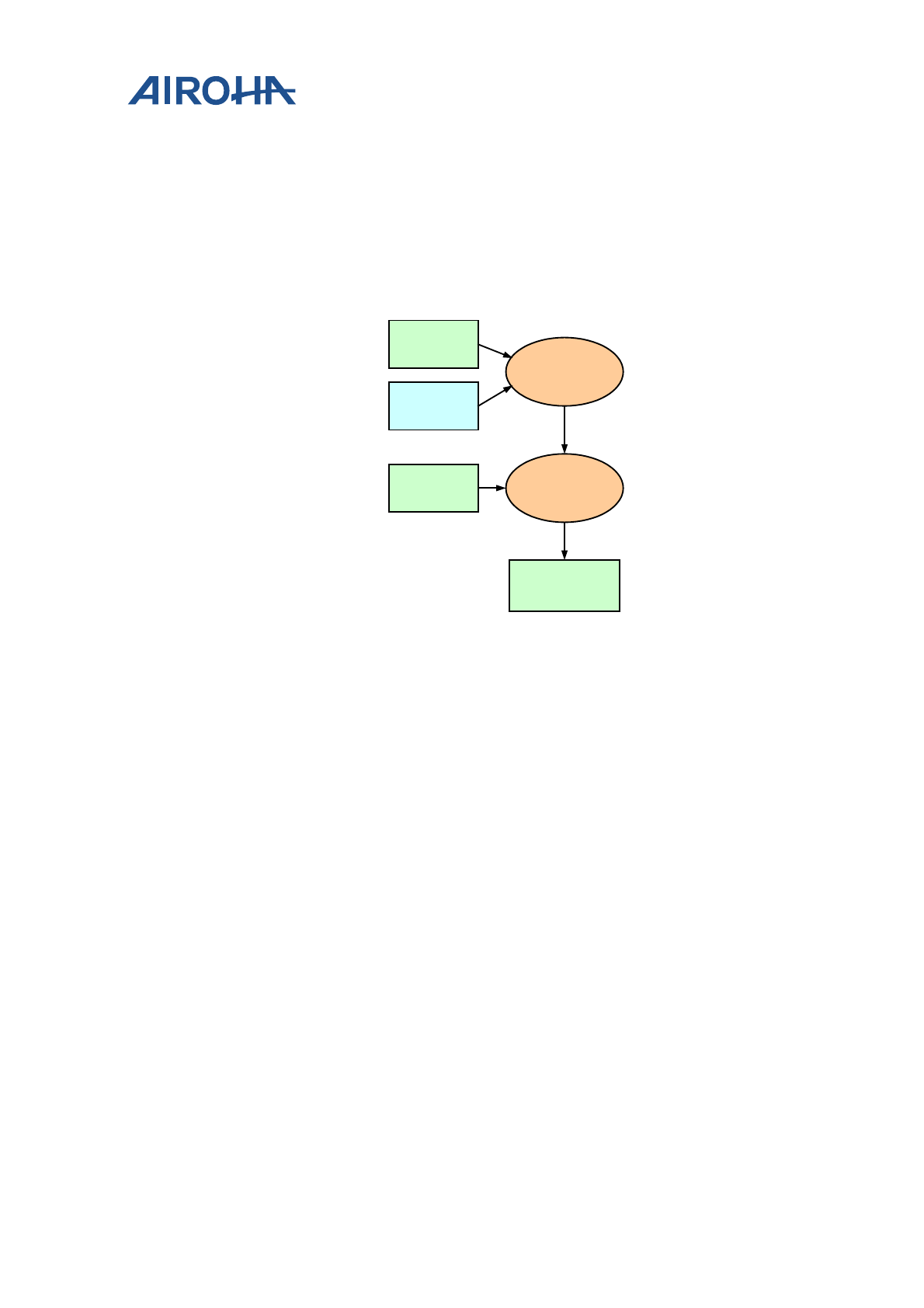
MT2523 Series Reference Manual
© 2015 - 2018 Airoha Technology Corp.
Page 307 of 692
This document contains information that is proprietary to Airoha Technology Corp. (“Airoha”) and/or its licensor(s).
Any unauthorized use, reproduction or disclosure of this document in whole or in part is strictly prohibited.
21.2.5.2. Anti-Aliasing Font Drawing
The 2D engine can accelerate the rendering of anti-aliasing fonts stored in multi-bit-per-pixel format (1/2/4/8). It is
realized by enabled FONT_EN and ALP_EN in G2D_Lx_CON. The index color gives the interpolation weight value for
foreground color.
In anti-aliasing font drawing, there are two passes alpha blending applying among the font alpha value, foreground
color, and destination color. The following figure describes the sequence.
index
bitstream
FGCLR
Alpha
Blending 1
Bitmap font
1/2/4/8 bit
ARGB or
PARGB
lower layer
buffer Alpha
Blending 2
ROI memory
buffer
Figure 21-5. Anti-aliasing Font Diagram
Alpha blending 1 performs alpha blending between alpha value from font alpha bitstream and foreground color.
The formula is listed below:
switch( bit_per_pixel){
case 1: weighting = (bit_stream == 1) ? 0xff : 0x00;
case 2: weighting = (bit_stream << 6) | (bit_stream << 4) | (bit_stream << 2) | (bit_stream << 0);
case 4: weighting = (bit_stream << 4) | (bit_stream << 0);
case 8: weighting = bit_stream;
}
if (layer color format == PARGB){
font.[argb] = (fgclr.[argb] * weighting + 0x80) / 0xff;
} else {
font.a = (fgclr.a * weighting + 0x80) / 0xff;
}
where the divide by 0xff is implemented as following formula:
value / 0xff = (value * 257) >> 16;
Alpha blending 2 is an alpha blending between the result of alpha blending 1 and destination color. The formula of
alpha blending 2 is as same as section 21.2.4.
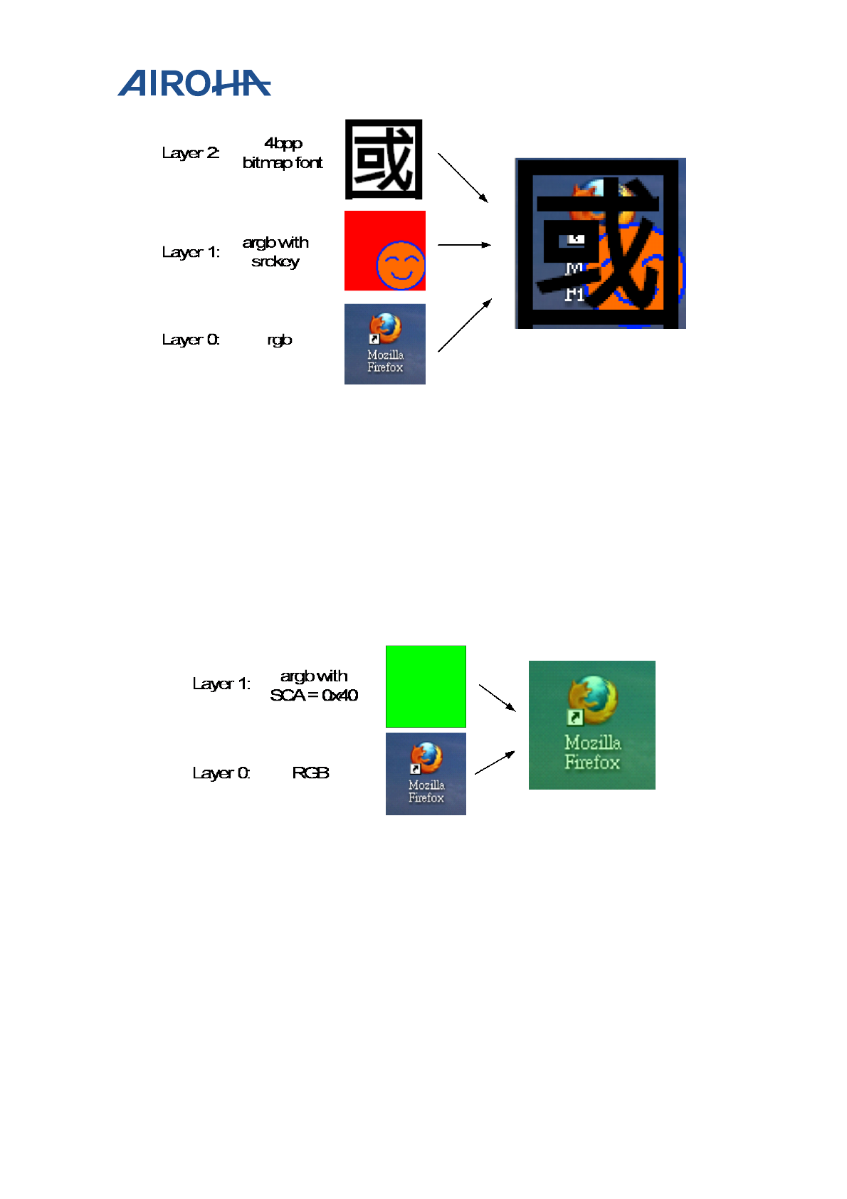
MT2523 Series Reference Manual
© 2015 - 2018 Airoha Technology Corp.
Page 308 of 692
This document contains information that is proprietary to Airoha Technology Corp. (“Airoha”) and/or its licensor(s).
Any unauthorized use, reproduction or disclosure of this document in whole or in part is strictly prohibited.
Figure 21-6. Anti-aliasing Font Example
shows an example of anti-aliasing font operation. Each layer can be configured as font bitmap (layer 2 in this
example). After blending all layers’ pixel, the color would be written to ROI memory buffer.
21.2.6. Rectangle Fill
Each layer could be configured as a constant color to perform rectangle fill. If alpha-blending is enabled at this
layer, the constant color will blending to lower layer as shown in .
Figure 21-7. Rectangle Fill with Alpha-Blending Example
MT2523 Series Reference Manual
© 2015 - 2018 Airoha Technology Corp.
Page 309 of 692
This document contains information that is proprietary to Airoha Technology Corp. (“Airoha”) and/or its licensor(s).
Any unauthorized use, reproduction or disclosure of this document in whole or in part is strictly prohibited.
21.3. Application Notes
The purpose of this document is to describe the functional interface of G2D to help supporting the usage of 2D
accelerations. It is noted that there are many 2D acceleration features provided by MediaTek’s 2D
Hardware/Software engine. However, in current driver design, we supported
1. Hardware Bitblt
2. Hardware Rectangle fill
3. Hardware Font drawing
4. Software Linear transform
5. Hardware Overlay
Generally, the G2D driver interfaces are provided and combined with GDI layers. It is strongly suggested that
application to use G2D interface through GDI. Nevertheless, you could use the 2D engine by calling the G2D driver
APIs directly. Below figure shows the block diagram of graphic 2D driver interface
• GDI: Graphics Device Interface,
• G2D: Graphic 2D engine
• BitBlt: Bit block transfers
Figure 21-8. The block diagram of graphic 2D driver interface
Unified G2D Interface
GDI Camera
HW Driver SW Codec
(Only support Linear Transform)

MT2523 Series Reference Manual
© 2015 - 2018 Airoha Technology Corp.
Page 310 of 692
This document contains information that is proprietary to Airoha Technology Corp. (“Airoha”) and/or its licensor(s).
Any unauthorized use, reproduction or disclosure of this document in whole or in part is strictly prohibited.
Here is an example for BitBlt using API:
src_buf = (kal_uint8 *)&rgb565_240X320[0];
dst_buf = (kal_uint8 *)&dst_hw_image_240X320[0];
src_color_format = G2D_COLOR_FORMAT_RGB565;
dst_color_format = G2D_COLOR_FORMAT_RGB565;
src_rect_w = 240;
src_rect_h = 320;
dst_rect_w = 320;
dst_rect_h = 240;
/// G2D_STATUS_BUSY means someone is using G2D
if(G2D_STATUS_OK != g2dGetHandle(&g2dHandle, G2D_CODEC_TYPE_HW,
G2D_GET_HANDLE_MODE_DIRECT_RETURN_HANDLE))
return;
g2dSetCallbackFunction(g2dHandle,NULL);
g2dSetDstRGBBufferInfo(g2dHandle, (kal_uint8 *)dst_buf, 240 * 320 * 4, dst_rect_w, dst_rect_h,
dst_color_format);
g2dSetColorReplacement(g2dHandle, KAL_FALSE, 0, 255, 0, 0, 0, 0, 0, 255);
g2dSetDstClipWindow(g2dHandle, KAL_FALSE, 0, 0, dst_rect_w, dst_rect_h);
g2dSetSrcKey(g2dHandle, KAL_FALSE, 0, 0, 0, 0);
g2dBitBltSetSrcRGBBufferInfo(g2dHandle, src_buf, 240 * 320 * 2, src_rect_w, src_rect_h, src_color_format);
g2dBitBltSetSrcWindow(g2dHandle, 0, 0, src_rect_w, src_rect_h);
g2dBitBltSetDstWindow(g2dHandle, 0, 0, dst_rect_w, dst_rect_h);
g2dBitBltSetRotation(g2dHandle, G2D_ROTATE_ANGLE_090);
g2dBitBltSetSrcAlpha(g2dHandle, KAL_FALSE, 0x0);
g2dBitBltSetDstAlpha(g2dHandle, KAL_FALSE, 0x0);
g2dBitBltStart(g2dHandle);
while(g2dGetStatus(g2dHandle)) {};
g2dReleaseHandle(g2dHandle);

MT2523 Series Reference Manual
© 2015 - 2018 Airoha Technology Corp.
Page 311 of 692
This document contains information that is proprietary to Airoha Technology Corp. (“Airoha”) and/or its licensor(s).
Any unauthorized use, reproduction or disclosure of this document in whole or in part is strictly prohibited.
21.4. Register Definitions
summarizes the 2D engine register mapping on APB. The base address of 2D engine is A0440000h .
Table 21-1. The 2D engine register mapping
APB Address Register Function Acronym
G2D+0000h G2D Start Register START
G2D+0004h G2D Mode Control Register MODE_CON
G2D+0008h G2D Reset Register RESET
G2D+000Ch G2D Status Register STATUS
G2D+0010 G2D Interrupt Regsiter IRQ
G2D+0014h G2D Slow Down Control Register SLOW_DOWN
G2D+0040h G2D ROI Control Register ROI_CON
G2D+0044h G2D Write to Memory Address Register W2M_ADDR
G2D+0048h G2D Write to Memory Pitch Register W2M_PITCH
G2D+004Ch G2D ROI Offset Register ROI_OFS
G2D+0050h G2D ROI Size Register ROI_SIZE
G2D+0054h G2D ROI Background Color Register ROI_BGCLR
G2D+0058h G2D Clipping Minimum Coordinate Register CLP_MIN
G2D+005Ch G2D Clipping Maximum Coordinate Register CLP_MAX
G2D+0060h G2D Avoid Write Color Register AVO_CLR
G2D+0064h G2D Replaced Color Register REP_CLR
G2D+0068h G2D Write to Memory Offset Register W2M_MOFS
G2D+0070h G2D MW Initial value MW_INIT
G2D+0074h G2D MZ Initial value MZ_INIT
G2D+0078h G2D Dithering Control Register DI_CON
G2D+0080h G2D Layer 0 Control Register L0_CON
G2D+0084h G2D Layer 0 Address Register L0_ADDR
G2D+0088h G2D Layer 0 Pitch Register L0_PITCH
G2D+008Ch G2D Layer 0 Offset Register L0_OFS
G2D+0090h G2D Layer 0 Size Register L0_SIZE
G2D+0094h G2D Layer 0 Source Key Register
G2D Initial Source Sample Z Register
L0_SRCKEY
SZ_INIT
G2D+00C0h G2D Layer 1 Control Register L1_CON
G2D+00C4h G2D Layer 1 Address Register L1_ADDR
MT2523 Series Reference Manual
© 2015 - 2018 Airoha Technology Corp.
Page 312 of 692
This document contains information that is proprietary to Airoha Technology Corp. (“Airoha”) and/or its licensor(s).
Any unauthorized use, reproduction or disclosure of this document in whole or in part is strictly prohibited.
G2D+00C8h G2D Layer 1 Pitch Register L1_PITCH
G2D+00CCh G2D Layer 1 Offset Register L1_OFS
G2D+00D0h G2D Layer 1 Size Register L1_SIZE
G2D+00D4h G2D Layer 1 Source Key Register L1_SRCKEY
G2D+0100h G2D Layer 2 Control Register L2_CON
G2D+0104h G2D Layer 2 Address Register L2_ADDR
G2D+0108h G2D Layer 2 Pitch Register L2_PITCH
G2D+010Ch G2D Layer 2 Offset Register L2_OFS
G2D+0110h G2D Layer 2 Size Register L2_SIZE
G2D+0114h G2D Layer 2 Source Key Register L2_SRCKEY
G2D+0140h G2D Layer 3 Control Register L3_CON
G2D+0144h G2D Layer 3 Address Register L3_ADDR
G2D+0148h G2D Layer 3 Pitch Register L3_PITCH
G2D+014Ch G2D Layer 3 Offset Register L3_OFS
G2D+0150h G2D Layer 3 Size Register L3_SIZE
G2D+0154h G2D Layer 3 Source Key Register L3_SRCKEY
Module name: 2D Accleration Base address: (+A0440000h)
G2D+0000h
G2D Start Register
G2D_START
Bit
15
14
13
12
11
10
9
8
7
6
5
4
3
2
1
0
Name
STAR
T
Type
R/W
Reset
0
START G2D start register. This register should be enabled after all of other registers are already filled.
Please follow the start sequence to trigger G2D:
*G2D_RESET = 2;
*G2D_RESET = 0;
*G2D_START = 1;
0 disable G2D engine
1 trigger G2D engine
G2D+0004h
G2D Mode Control Register
G2D_MODE_
CON
Bit
31
30
29
28
27
26
25
24
23
22
21
20
19
18
17
16
Name
RESERVED
Type
R/W
Reset
0
MT2523 Series Reference Manual
© 2015 - 2018 Airoha Technology Corp.
Page 313 of 692
This document contains information that is proprietary to Airoha Technology Corp. (“Airoha”) and/or its licensor(s).
Any unauthorized use, reproduction or disclosure of this document in whole or in part is strictly prohibited.
Bit
15
14
13
12
11
10
9
8
7
6
5
4
3
2
1
0
Name
ENG_MODE
Type
RO
Reset
1
ENG_MODE 2D engine function mode
001 Bitblt
others Reserved
G2D+0008h
G2D Reset Register
G2D_RESET
Bit
15
14
13
12
11
10
9
8
7
6
5
4
3
2
1
0
Name
HRST
WRS
T
Type
R/W
R/W
Reset
0
0
HRST G2D hard reset. All registers (except APB registers) will be reset to initial value immediately.
WRST G2D warm reset. Please follow correct reset sequence to avoid potential bus hang problem
(breaking bus protocol)
G2D_RESET = 0x1;
while (G2D_STATUS != 0){
read G2D_STATUS;
}
G2D_RESET = 0x2;
G2D_RESET = 0x0;
G2D+000Ch
G2D Status Register
G2D_STATUS
Bit
15
14
13
12
11
10
9
8
7
6
5
4
3
2
1
0
Name
TBUS
Y
BUSY
Type
RO
RO
Reset
0
0
Read this register to get 2D engine status. 2D engine may function abnormally if any 2D engine register is
modified when BUSY.
BUSY 2D engine is busy.
TBUSY Transaction busy. If any read/write memory access transaction is not completed, this register will
be asserted.
G2D+0010h
G2D Interrupt Register
G2D_IRQ
Bit
31
30
29
28
27
26
25
24
23
22
21
20
19
18
17
16
Name
FLAG
0
Type
R/W
Reset
0
Bit
15
14
13
12
11
10
9
8
7
6
5
4
3
2
1
0
Name
FLGA
0_IR
Q_EN
Type
R/W
Reset
0
MT2523 Series Reference Manual
© 2015 - 2018 Airoha Technology Corp.
Page 314 of 692
This document contains information that is proprietary to Airoha Technology Corp. (“Airoha”) and/or its licensor(s).
Any unauthorized use, reproduction or disclosure of this document in whole or in part is strictly prohibited.
FLAG0_IRQ_EN 2D engine interrupt enabled. The interrupt is negative level sensitive.
FLAG0 2D interrupt status. It is raised when engine finished the task and
FLAG0_IRQ_EN is asserted.
0 Write 0 to clear interrupt
1 Interrupt occurs. Software can also write this bit to trigger G2D interrupt.
G2D+0014h
G2D Slow Down Control Register
G2D_SLOW_
DOWN
Bit
31
30
29
28
27
26
25
24
23
22
21
20
19
18
17
16
Name
EN
RD_BTYP
WR_BTYP
Type
R/W
R/W
R/W
Reset
0
0
100
Bit
15
14
13
12
11
10
9
8
7
6
5
4
3
2
1
0
Name
SLOW_CNT
Type
R/W
Reset
0
EN Enable slow down mechanism to slower 2D engine read/write memory speed
RD_BTYP Read request maximum burst type
000 burst-8
001 burst-4
011 single
others reserved
WR_BTYP Write request maximum burst type
100 burst-16
011 burst-8
010 burst-4
000 single
SLOW_CNT Read/write request slow counter. The minimum cycle count between two read/write
request.
G2D+0040h
G2D ROI Control Register
G2D_ROI_CO
N
Bit
31
30
29
28
27
26
25
24
23
22
21
20
19
18
17
16
Name
EN0 EN1 EN2 EN3
CLR_
REP_
EN
DIS_
BG
TILE_
SIZE FORC
E_TS CLP_
EN
Type
R/W
R/W
R/W
R/W
R/W
R/W
R/W
R/W
R/W
Reset
0
0
0
0
0
0
0
0
0
Bit
15
14
13
12
11
10
9
8
7
6
5
4
3
2
1
0
Name
OUT_ALPHA
OUT_
ALP_
EN
CLRFMT
Type
R/W
R/W
R/W
Reset
0
0
0
ENn Enable the nth layer
CLR_REP_EN Color replacement enabled.
DIS_BG Disable background color. shows the effect of this register. In linear transform
mode, DIS_BG should always be 1’b1.
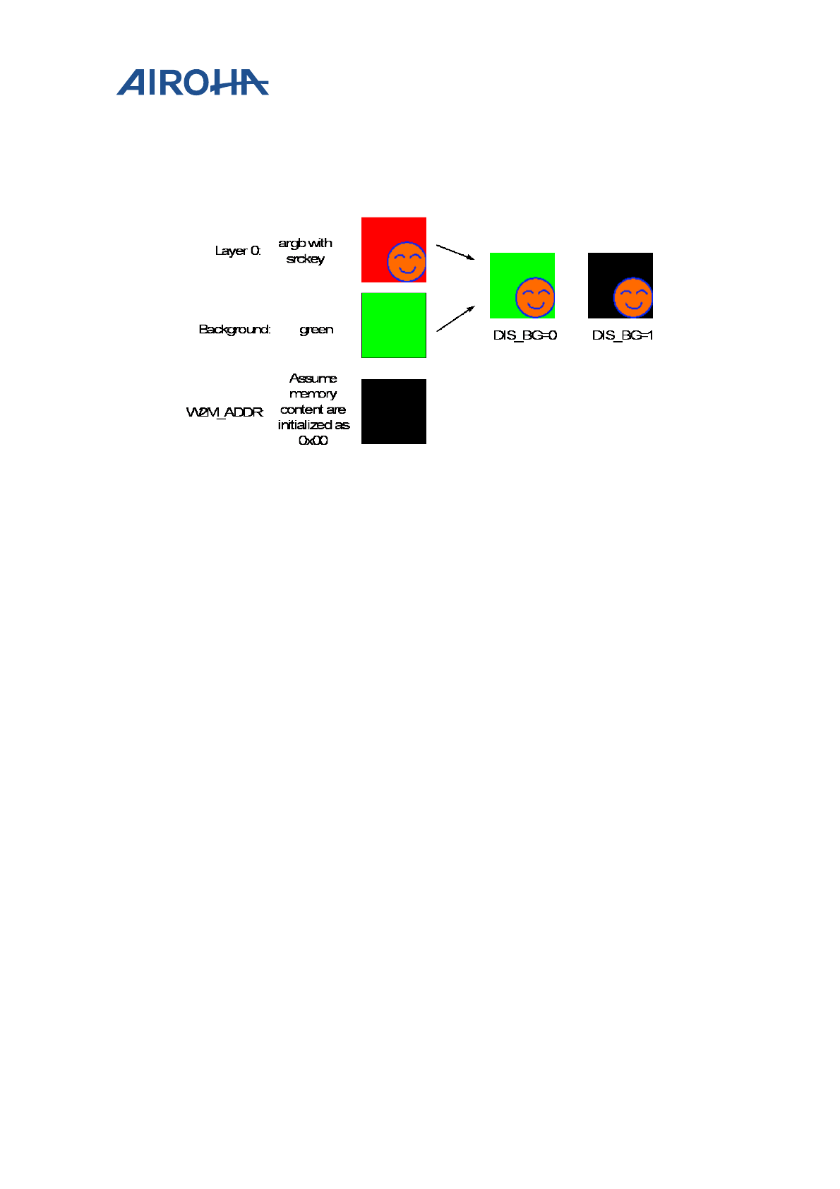
MT2523 Series Reference Manual
© 2015 - 2018 Airoha Technology Corp.
Page 315 of 692
This document contains information that is proprietary to Airoha Technology Corp. (“Airoha”) and/or its licensor(s).
Any unauthorized use, reproduction or disclosure of this document in whole or in part is strictly prohibited.
0 Enable background color
1 If any of following condition is true, this write request will be ignored
(1) No layer covered this ROI position
(2) Normal font and the bitstream value is zero
(3) Source key hit
Figure 21-9. DIS_BG example
TILE_SIZE ROI scan tile size, only take effect when FORCE_TS is on. Please set zero (8x8) when
performing linear transform.
0 4x4 for bitblt. 8x8 for linear transform
1 8x8 for bitblt. 16x8 for linear transform
FORCE_TS Force tile size. When this field is off, hardware selects the best tile size automatically. 8x8
for linear transform. 16x8 for only one layer is enabled.
0 Off. Hardware select automatically
1 On. Force tile size
CLP_EN Clipping window enabled. Pixels out of clipping window will not be written.
OUT_ALPHA Replace written alpha channel value with this field when OUT_ALP_EN is enabled.
OUT_ALP_EN Output alpha channel replacement enabled.
CLRFMT Write to memory color format. (Notice: After alpha-blending, the color format is always
PARGB, not ARGB)
00001 RGB565
00011 RGB888
01000 ARGB8888 (only for bitblt without alpha-blending)
01001 ARGB8565 (only for bitblt without alpha-blending)
01010 ARGB6666 (only for bitblt without alpha-blending)
01100 PARGB8888
01101 PARGB8565
01110 PARGB6666
10011 BGR888
MT2523 Series Reference Manual
© 2015 - 2018 Airoha Technology Corp.
Page 316 of 692
This document contains information that is proprietary to Airoha Technology Corp. (“Airoha”) and/or its licensor(s).
Any unauthorized use, reproduction or disclosure of this document in whole or in part is strictly prohibited.
G2D+0044h
G2D W2M Address Register
G2D_W2M_A
DDR
Bit
31
30
29
28
27
26
25
24
23
22
21
20
19
18
17
16
Name
W2M_ADDR[31:16]
Type
R/W
Reset
0
Bit
15
14
13
12
11
10
9
8
7
6
5
4
3
2
1
0
Name
W2M_ADDR[15:0]
Type
R/W
Reset
0
W2M_ADDR Write to memory base address. The address should be 2 byte aligned for RGB565 output
and 4 byte aligned for ARGB8888 or PARGB8888. RGB888 output can start at any address.
G2D+0048h
G2D W2M Pitch Register
G2D_W2M_P
ITCH
Bit
15
14
13
12
11
10
9
8
7
6
5
4
3
2
1
0
Name
PITCH
Type
R/W
Reset
0
PITCH Write to memory pitch in unit of byte. The pitch divided by the output color format byte-per-pixel
(bpp) must be equal or greater than the ROI width. If the output bpp is 4, the pitch must be
divisible by 4. If the bpp is 2, the pitch must be divisible by 2. If the bpp is 3 (RGB888), the pitch
can be any number greater than ROI width*3. The maximum pitch is 0x2000 which indicates the
maximum resolution is 2048x2048@ARGB8888.
G2D+004Ch
G2D ROI Offset Register
G2D_ROI_OF
S
Bit
31
30
29
28
27
26
25
24
23
22
21
20
19
18
17
16
Name
OFS_X
Type
R/W
Reset
0
Bit
15
14
13
12
11
10
9
8
7
6
5
4
3
2
1
0
Name
OFS_Y
Type
R/W
Reset
0
OFS_X ROI x offset in unit of pixel. 12-bit signed integer, range: [-2048~2047]
OFS_Y ROI y offset in unit of pixel. 12-bit signed integer, range: [-2048~2047]
G2D+0050h
G2D ROI Size Register
G2D_ROI_SI
ZE
Bit
31
30
29
28
27
26
25
24
23
22
21
20
19
18
17
16
Name
WIDTH
Type
R/W
Reset
0
Bit
15
14
13
12
11
10
9
8
7
6
5
4
3
2
1
0
Name
HEIGHT
Type
R/W
Reset
0
MT2523 Series Reference Manual
© 2015 - 2018 Airoha Technology Corp.
Page 317 of 692
This document contains information that is proprietary to Airoha Technology Corp. (“Airoha”) and/or its licensor(s).
Any unauthorized use, reproduction or disclosure of this document in whole or in part is strictly prohibited.
WIDTH Width of ROI window in unit of pixel. 12bit unsigned integer, range: [1, 2048]
HEIGHT Height of ROI window in unit of pixel. 12bit unsigned integer, range: [1, 2048]
G2D+0054h
G2D ROI
Background Color G2D_ROI_BG
CLR
Bit
31
30
29
28
27
26
25
24
23
22
21
20
19
18
17
16
Name
ALPHA
REG
Type
R/W
R/W
Reset
0
0
Bit
15
14
13
12
11
10
9
8
7
6
5
4
3
2
1
0
Name
GREEN
BLUE
Type
R/W
R/W
Reset
0
0
The color format of background color is PARGB8888.
ALPHA Alpha component of ROI background color
RED Red component of ROI background color
GREEN Green component of ROI background color
BLUE Blue component of ROI background color
G2D+0058h
G2D Clipping Minimum Register
G2D_CLP_MI
N
Bit
31
30
29
28
27
26
25
24
23
22
21
20
19
18
17
16
Name
CLP_MIN_X
Type
R/W
Reset
0
Bit
15
14
13
12
11
10
9
8
7
6
5
4
3
2
1
0
Name
CLP_MIN_Y
Type
R/W
Reset
0
The clipping window is shown in . Clipping window is not supported in SAD function mode.
CLP_MIN_X The minimum value of x coordinate in clipping window, signed 12-bit integer. Range:[-
2048~2047]
CLP_MIN_Y The minimum value of y coordinate in clipping window, signed 12-bit integer. Range:[-
2048~2047]
G2D+005Ch
G2D Clipping Maximum Register
G2D_CLP_M
AX
Bit
31
30
29
28
27
26
25
24
23
22
21
20
19
18
17
16
Name
CLP_MAX_X
Type
R/W
Reset
0
Bit
15
14
13
12
11
10
9
8
7
6
5
4
3
2
1
0
Name
CLP_MAX_Y
Type
R/W
Reset
0
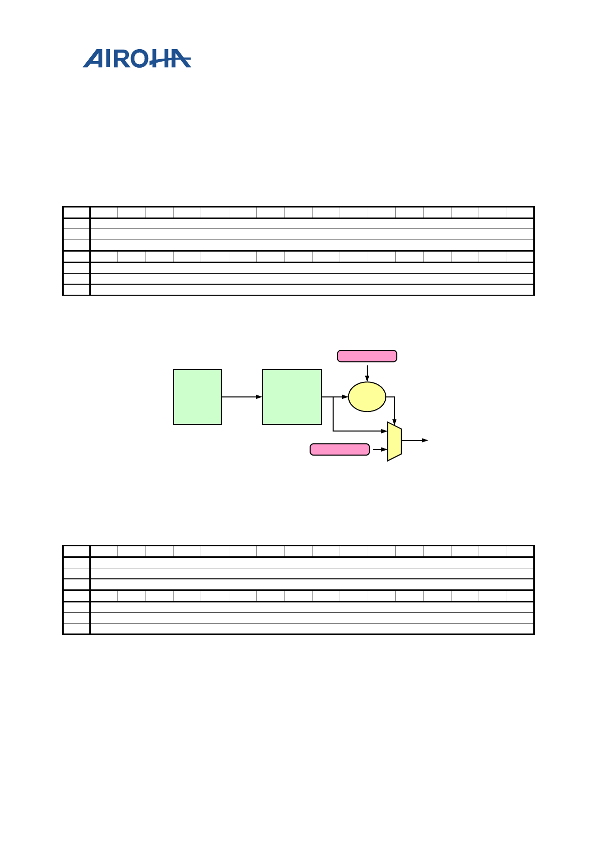
MT2523 Series Reference Manual
© 2015 - 2018 Airoha Technology Corp.
Page 318 of 692
This document contains information that is proprietary to Airoha Technology Corp. (“Airoha”) and/or its licensor(s).
Any unauthorized use, reproduction or disclosure of this document in whole or in part is strictly prohibited.
The clipping window is shown in .
CLP_MAX_X The maximum value of x coordinate in clipping window, signed 12-bit integer. Range:[-
2048~2047]
CLP_MAX_Y The maximum value of y coordinate in clipping window, signed 12-bit integer. Range:[-
2048~2047]
G2D+0060h
G2D Avoid Write Color
G2D_AVO_CL
R
Bit
31
30
29
28
27
26
25
24
23
22
21
20
19
18
17
16
Name
AVO_CLR[31:16]
Type
R/W
Reset
0
Bit
15
14
13
12
11
10
9
8
7
6
5
4
3
2
1
0
Name
AVO_CLR[15:0]
Type
R/W
Reset
0
AVO_CLR When CLR_REP_EN is enabled and write out color is equal to AVO_CLR, the color would be
replaced with REP_CLR. The color format of AVO_CLR is the same with ROI color format. The
compare operation is done at the last stage as shown in following figure.
Pixel
Engine
Color
Conversion
(w2m_fmt)
ARGB8888
CMP
AVO_CLR
REP_CLR
Write
color
Figure 21-10. Color Replacement Stage
G2D+0064h
G2D Replaced Color
G2D_REP_CL
R
Bit
31
30
29
28
27
26
25
24
23
22
21
20
19
18
17
16
Name
REP_CLR[31:16]
Type
R/W
Reset
0
Bit
15
14
13
12
11
10
9
8
7
6
5
4
3
2
1
0
Name
REP_CLR[15:0]
Type
R/W
Reset
0
REP_CLR When CLR_REP_EN is enabled and write out color is equal to AVO_CLR, the color would be
replaced with REP_CLR. The color format of REP_CLR is the same with ROI color format.
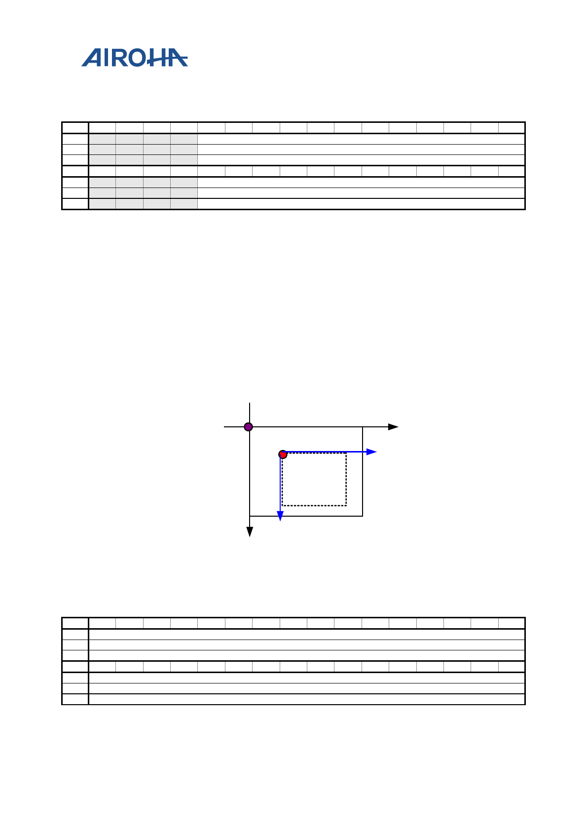
MT2523 Series Reference Manual
© 2015 - 2018 Airoha Technology Corp.
Page 319 of 692
This document contains information that is proprietary to Airoha Technology Corp. (“Airoha”) and/or its licensor(s).
Any unauthorized use, reproduction or disclosure of this document in whole or in part is strictly prohibited.
G2D+0068h
G2D Write to Memory Offset Register
G2D_W2M_M
OFS
Bit
31
30
29
28
27
26
25
24
23
22
21
20
19
18
17
16
Name
W2M_MOFS _X
Type
R/W
Reset
0
Bit
15
14
13
12
11
10
9
8
7
6
5
4
3
2
1
0
Name
W2M_MOFS_Y
Type
R/W
Reset
0
W2M_MOFS _X The ROI memory x-offset, signed 12-bit integer. Range:[-2048~2047]
W2M_MOFS_Y The ROI memory y-offset, signed 12-bit integer. Range:[-2048~2047]
for(y’=0; y’<roi_h; y’++){
for(x’=0; x’<roi_w; x’++){
wx = x’ + w2m_mofs_x;
wy = y’ + w2m_mofs_y;
if(wx<0 || wy <0){
skip this pixel;
}
waddr = W2M_ADDR + wy * PITCH + wx * BPP;
}
}
x
y
ROI
x’
y’
Figure 21-11. ROI Memory Offset
G2D+0070h
G2D MW Initial Value Register
G2D_MW_IN
IT
Bit
31
30
29
28
27
26
25
24
23
22
21
20
19
18
17
16
Name
MW_INIT[31:16]
Type
RW
Reset
0
Bit
15
14
13
12
11
10
9
8
7
6
5
4
3
2
1
0
Name
MW_INIT[15:0]
Type
RW
Reset
0
MW_INIT The initial value of MW for dithering circuit.
MT2523 Series Reference Manual
© 2015 - 2018 Airoha Technology Corp.
Page 320 of 692
This document contains information that is proprietary to Airoha Technology Corp. (“Airoha”) and/or its licensor(s).
Any unauthorized use, reproduction or disclosure of this document in whole or in part is strictly prohibited.
G2D+0074h
G2D MZ Initial Value Register
G2D_MZ_INI
T
Bit
31
30
29
28
27
26
25
24
23
22
21
20
19
18
17
16
Name
MZ_INIT[31:16]
Type
RW
Reset
0
Bit
15
14
13
12
11
10
9
8
7
6
5
4
3
2
1
0
Name
MZ_INIT[15:0]
Type
RW
Reset
0
MZ_INIT The initial value of MZ for dithering circuit.
G2D+0078h
G2D Dithering Control Register
G2D_DI_CON
Bit
15
14
13
12
11
10
9
8
7
6
5
4
3
2
1
0
Name
DI_R
DI_G
DI_B
DI_MODE
Type
R/W
R/W
R/W
R/W
Reset
0
0
0
0
DI_RGB Dithering bit for each channel
00 0bit dithering
01 1bit dithering
10 2bit dithering
11 3bit dithering
DI_MODE Dither mode
00 Disable dithering
01 Random number algorithm
10 Fixed-pattern
G2D+0080h
G2D Layer 0 Control Register
G2D_L0_CON
Bit
31
30
29
28
27
26
25
24
23
22
21
20
19
18
17
16
Name
FONT
_EN
IDX
SKEY
_EN
RECT
_EN
ROT
Type
R/W
R/W
R/W
R/W
R/W
Reset
0
0
0
0
0
Bit
15
14
13
12
11
10
9
8
7
6
5
4
3
2
1
0
Name
ALPHA
ALP_
EN
CLRFMT
Type
R/W
R/W
R/W
Reset
0
0
0
FONT_EN Enabled font drawing. If SKEY_EN or RECT_EN is enabled, this register cannot be enabled.
When this register is enabled, CLRFMT only supports ARGB8888 or PARGB8888.
IDX Bit-per-pixel for font drawing. If FONT_EN is enabled and ALP_EN is disabled, this register can
only be 00.
00 1 bit index color
01 2 bit index color
10 4 bit index color
11 8 bit index color
SKEY_EN Enable source color key. When FONT_EN or RECT_EN is enabled, this register cannot be
enabled. Source key cannot be enabled when CLRFMT is YUYV422.
MT2523 Series Reference Manual
© 2015 - 2018 Airoha Technology Corp.
Page 321 of 692
This document contains information that is proprietary to Airoha Technology Corp. (“Airoha”) and/or its licensor(s).
Any unauthorized use, reproduction or disclosure of this document in whole or in part is strictly prohibited.
RECT_EN Fill this layer as constant color which is defined in Ln_SRCKEY. If FONT_EN or SKEY_EN is
enabled, this register cannot be enabled. When this register is enabled, CLRFMT does not support
YUYV422 color format.
ROT Rotation configuration
000 No rotation
001 Horizontal flip then 90 degree rotation (counterclockwise)
010 Horizontal flip
011 90 degree rotation (counterclockwise)
100 Horizontal flip then 180 degree rotation (counterclockwise)
101 270 degree rotation (counterclockwise)
110 180 degree rotation (counterclockwise)
111 Horizontal flip then 270 degree rotation (counterclockwise)
000
ROT
IMG
001 010 011
100ROT
IMG
101 110 111
Figure 21-12. Image of Different Rotation Angles
If original ofs_x, ofs_y is at top-left corner, please move the coordinate by following algorithm:
width = layer_width – 1;
height = layer_height – 1;
switch(ROT){
case 2: ofs_x += width; break; //Hor_flip
case 3: ofs_y += width ; break; //90 rot (counterclockwise)
case 4: ofs_y += height; break; //Hor_flip then rot_180
case 5: ofs_x += height; break; //270 rot
case 6: ofs_x += width ; ofs_y += height; break; //180 rot
case 7: ofs_x += height; ofs_y += width; break; //Hor_flip then rot_270
}
ALPHA Constant alpha value for alpha-blending and AA-font.
ALP_EN Enable alpha-blending. AA-font is realized by enable both of FONT_EN and ALP_EN.
CLRFMT Layer color format
00001 RGB565
00010 UY0VY1 (from low to high byte address)
00011 RGB888
01000 ARGB8888
01001 ARGB8565
MT2523 Series Reference Manual
© 2015 - 2018 Airoha Technology Corp.
Page 322 of 692
This document contains information that is proprietary to Airoha Technology Corp. (“Airoha”) and/or its licensor(s).
Any unauthorized use, reproduction or disclosure of this document in whole or in part is strictly prohibited.
01010 ARGB6666
01100 PARGB8888
01101 PARGB8565
01110 PARGB6666
10011 BGR888
G2D+0084h
G2D Layer 0 Address Register
G2D_L0_ADD
R
Bit
31
30
29
28
27
26
25
24
23
22
21
20
19
18
17
16
Name
ADDR[31:16]
Type
R/W
Reset
0
Bit
15
14
13
12
11
10
9
8
7
6
5
4
3
2
1
0
Name
ADDR[15:0]
Type
R/W
Reset
0
ADDR Layer 0 base address. The address should be 2 byte aligned for RGB565 output and 4 byte aligned
for ARGB8888, PARGB8888 or YVU422. RGB888 color format can start at any address.
G2D+0088h
G2D Layer 0 Pitch Register
G2D_L0_PIT
CH
Bit
15
14
13
12
11
10
9
8
7
6
5
4
3
2
1
0
Name
PITCH
Type
R/W
Reset
0
PITCH Layer 0 pitch in unit of byte, but the unit is pixel number when FONT_EN is enabled. The pitch
divided by byte-per-pixel (bpp) of color format must be equal or greater than the width. If the bpp
is 4, the pitch must be divisible by 4. If the bpp is 2, the pitch must be divisible by 2. If the bpp is 3
(RGB888), the pitch can be any number greater than width*3. The maximum pitch is 0x2000
which indicates the maximum resolution is 2048x2048@ARGB8888.
G2D+008Ch
G2D Layer 0 Offset Register
G2D_L0_OFS
Bit
31
30
29
28
27
26
25
24
23
22
21
20
19
18
17
16
Name
OFS_X
Type
R/W
Reset
0
Bit
15
14
13
12
11
10
9
8
7
6
5
4
3
2
1
0
Name
OFS_Y
Type
R/W
Reset
0
OFS_X ROI x offset in unit of pixel. 12-bit signed integer, range: [-2048~2047]
OFS_Y ROI y offset in unit of pixel. 12-bit signed integer, range: [-2048~2047]
MT2523 Series Reference Manual
© 2015 - 2018 Airoha Technology Corp.
Page 323 of 692
This document contains information that is proprietary to Airoha Technology Corp. (“Airoha”) and/or its licensor(s).
Any unauthorized use, reproduction or disclosure of this document in whole or in part is strictly prohibited.
G2D+0090h
G2D Layer 0 Size Register
G2D_L0_SIZ
E
Bit
31
30
29
28
27
26
25
24
23
22
21
20
19
18
17
16
Name
WITDH
Type
R/W
Reset
0
Bit
15
14
13
12
11
10
9
8
7
6
5
4
3
2
1
0
Name
HEIGHT
Type
R/W
Reset
0
WIDTH Width of Layer 0 window in unit of pixel. 12bit unsigned integer, range: [1, 2048]
HEIGHT Height of Layer 0window in unit of pixel. 12bit unsigned integer, range: [1, 2048]
G2D+0094h
G2D Layer 0 Source Key
G2D_L0_SRC
KEY
Bit
31
30
29
28
27
26
25
24
23
22
21
20
19
18
17
16
Name
SRCKEY[31:16]
Type
R/W
Reset
0
Bit
15
14
13
12
11
10
9
8
7
6
5
4
3
2
1
0
Name
SRCKEY[15:0]
Type
R/W
Reset
0
SRCKEY If SKEY_EN is enabled, this field represents source key color. If FONT_EN is enabled, this
filed represents foreground color. If RECT_EN is enabled, this field represents the constant color for
rectangle fill. The color format is the same as CLRFMT in G2D_L0_CON.
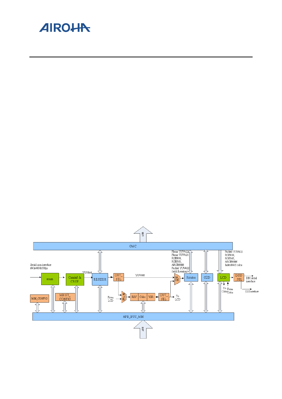
MT2523 Series Reference Manual
© 2015 - 2018 Airoha Technology Corp.
Page 324 of 692
This document contains information that is proprietary to Airoha Technology Corp. (“Airoha”) and/or its licensor(s).
Any unauthorized use, reproduction or disclosure of this document in whole or in part is strictly prohibited.
22. Multimedia Subsystem Configuration
22.1. Introduction
The multimedia subsystem contains the multimedia controller, multimedia data path(MDP ) and display (DISP).
The multimedia controller includes direct memory access and multimedia configuration. MDP is the time sharing
pipeline data flow controller to process resizing and rotation by memory access. The display pipeline outputs pixels
to display interface with overlay, color enhancement, adaptive ambient light processing.
22.1.1. Features
The multimedia subsystem has the following features:
• APB bus control.
• Multimedia Data Path. It has one read DMA, one resizer, and one write rotator.
• 2D accelerator engine to enhance MMI display and gaming experiences .
• Display pipe line with overlay, color engine, adaptive ambient light processing and display interface
controller.
Supports adaptive ambient light processing for backlight power saving and sunlight visibility improvement
22.2. Block diagram
Figure 22-1. Multimedia Subsystem Block Diagram
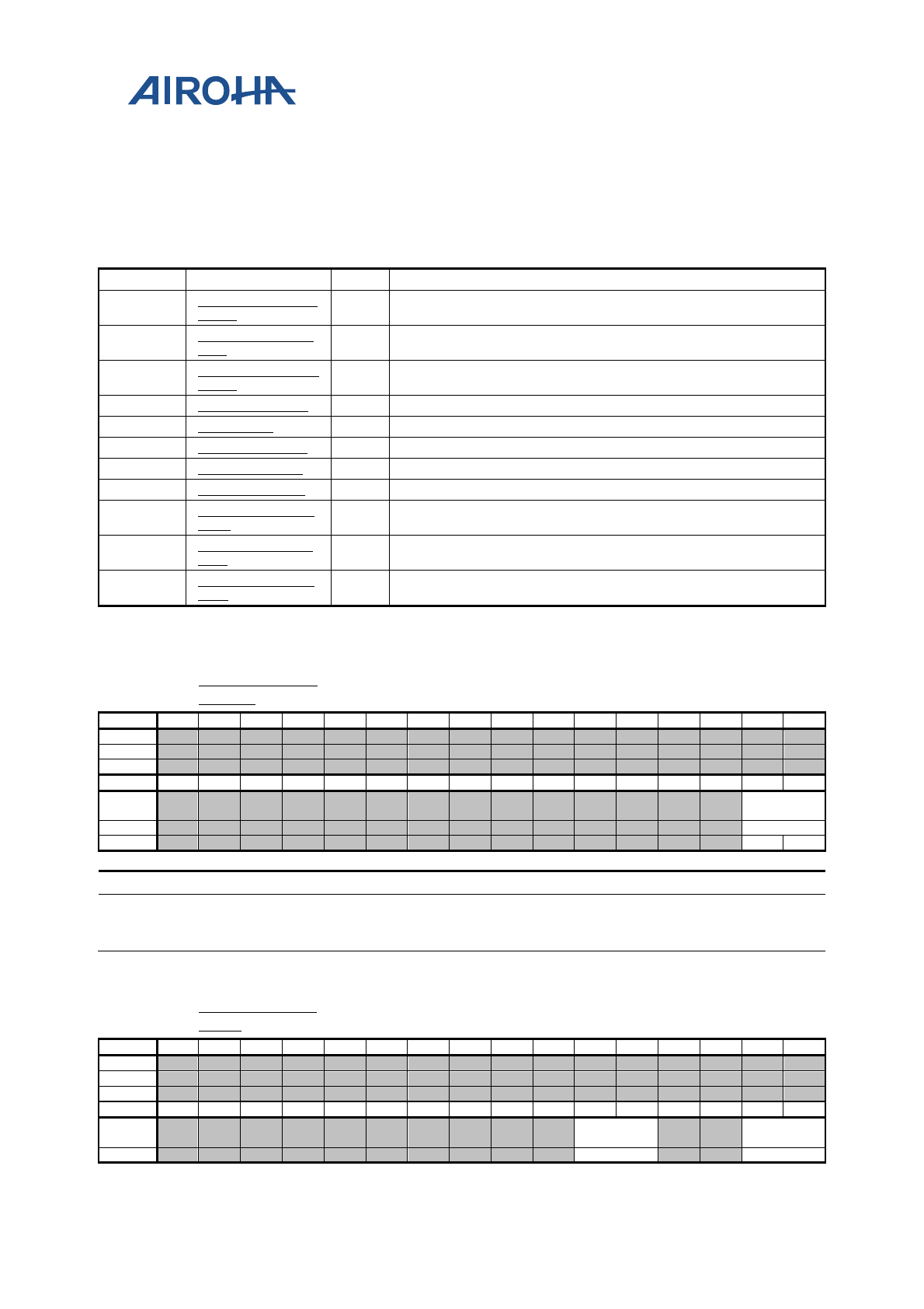
MT2523 Series Reference Manual
© 2015 - 2018 Airoha Technology Corp.
Page 325 of 692
This document contains information that is proprietary to Airoha Technology Corp. (“Airoha”) and/or its licensor(s).
Any unauthorized use, reproduction or disclosure of this document in whole or in part is strictly prohibited.
22.3. Register definition
Module name: MMSYS_CONFIG Base address: (+A0480000h)
Address
Name
Width
Register Function
A0480000
RESIZER_PATH
_SEL 32 MDP Resizer In/Out Selection
A0480004
COLOR_PATH_
SEL 32 MDP Color In/Out Selection
A0480008
ROTDMA_PATH
_SEL 32 MDP Rotator In/Out Selection
A048000C
APB_OPT_SEL
32
APB buffer enable Selection
A0480010
DSI0_SEL
32
DSI/ DBI interface selection
A0480014
CG_1ST_CON0
32
CG_1ST_CON0
A0480018
CG_1ST_SET0
32
CG_1ST_SET0
A048001C
CG_1ST_CLR0
32
CG_1ST_CLR0
A0480020
HW_CG_DIS_C
ON0 32 HW_CG_DIS_CON0
A0480024
HW_CG_DIS_S
ET0 32 HW_CG_DIS_SET0
A0480028
HW_CG_DIS_C
LR0 32 HW_CG_DIS_CLR0
A0480000
RESIZER_PAT
H_SEL
MDP Resizer In/Out Selection
00000000
Bit
31
30
29
28
27
26
25
24
23
22
21
20
19
18
17
16
Name
Type
Reset
Bit
15
14
13
12
11
10
9
8
7
6
5
4
3
2
1
0
Name
RESIZER_O
UT_SEL
Type
RW
Reset
0
0
Bit(s)
Name
Description
1:0
RESIZER_OUT_SEL
Resizer output selection
0: output to Rotator
1: output to Color
A0480004
COLOR_PATH
_SEL
MDP Color In/Out Selection
00000011
Bit
31
30
29
28
27
26
25
24
23
22
21
20
19
18
17
16
Name
Type
Reset
Bit
15
14
13
12
11
10
9
8
7
6
5
4
3
2
1
0
Name
COLOR_IN_
SEL
COLOR_OU
T_SEL
Type
RW
RW
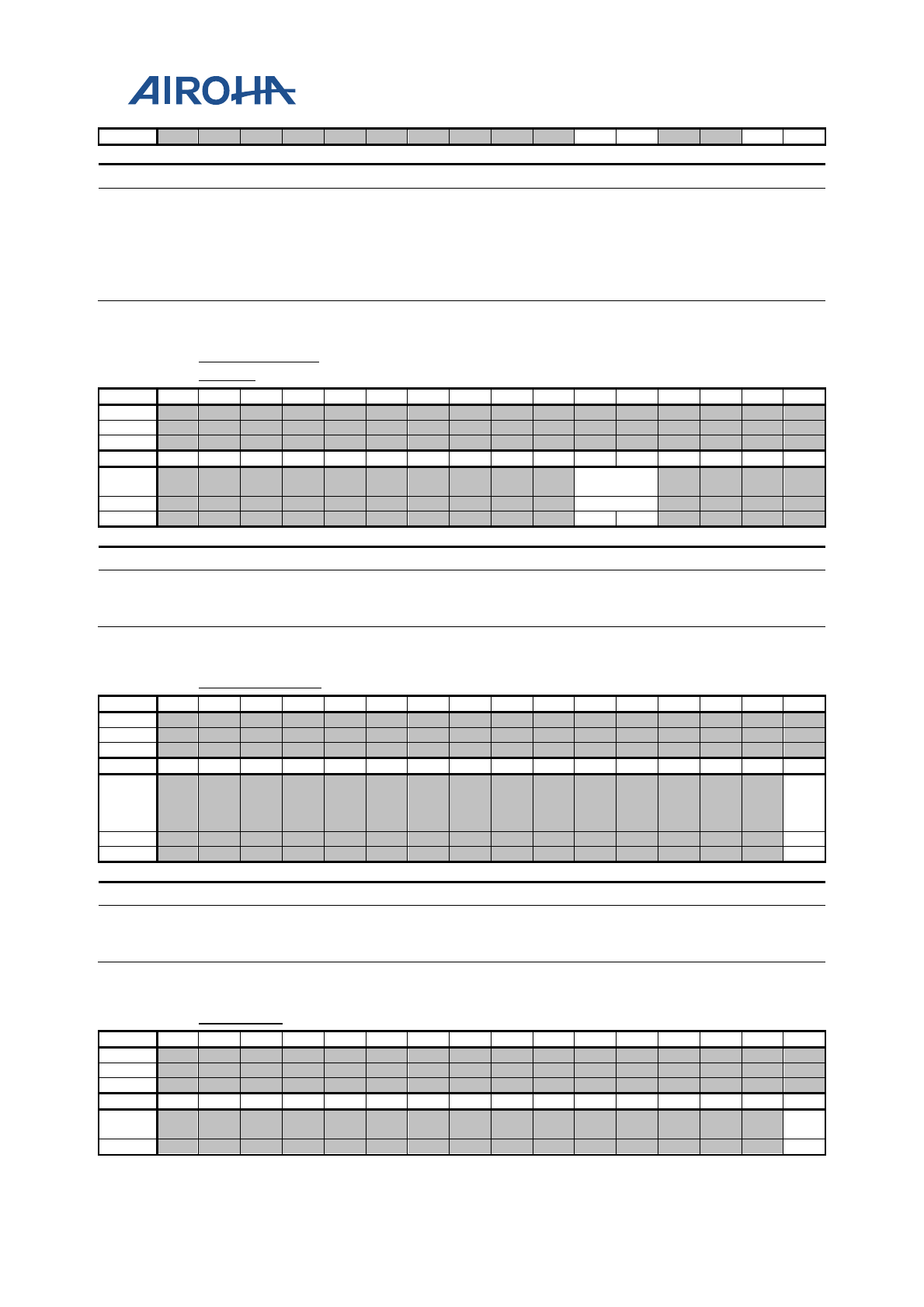
MT2523 Series Reference Manual
© 2015 - 2018 Airoha Technology Corp.
Page 326 of 692
This document contains information that is proprietary to Airoha Technology Corp. (“Airoha”) and/or its licensor(s).
Any unauthorized use, reproduction or disclosure of this document in whole or in part is strictly prohibited.
Reset
0
1
0
1
Bit(s)
Name
Description
5:4
COLOR_IN_SEL
Color input selection
0: input from Resizer
1: input from LCD
1:0
COLOR_OUT_SEL
Color output selection
0: output to Rotator
1: output to LCD
A0480008
ROTDMA_PAT
H_SEL
MDP Rotator In/Out Selection
00000000
Bit
31
30
29
28
27
26
25
24
23
22
21
20
19
18
17
16
Name
Type
Reset
Bit
15
14
13
12
11
10
9
8
7
6
5
4
3
2
1
0
Name
ROTATOR_I
N_SEL
Type
RW
Reset
0
0
Bit(s)
Name
Description
5:4
ROTATOR_IN_SEL
Rotator input selection
0: input from Resizer
1: input from Color
A048000C
APB_OPT_SEL
APB buffer enable Selection
00000000
Bit
31
30
29
28
27
26
25
24
23
22
21
20
19
18
17
16
Name
Type
Reset
Bit
15
14
13
12
11
10
9
8
7
6
5
4
3
2
1
0
Name
APB_
BUFF
ER_E
N
Type
RW
Reset
0
Bit(s)
Name
Description
0
APB_BUFFER_EN
APB buffer enable selection
0: apb buffer NOT enable
1: apb buffer enable
A0480010
DSI0_SEL
DSI/ DBI interface selection
00000000
Bit
31
30
29
28
27
26
25
24
23
22
21
20
19
18
17
16
Name
Type
Reset
Bit
15
14
13
12
11
10
9
8
7
6
5
4
3
2
1
0
Name
DSI0
_SEL
Type
RW
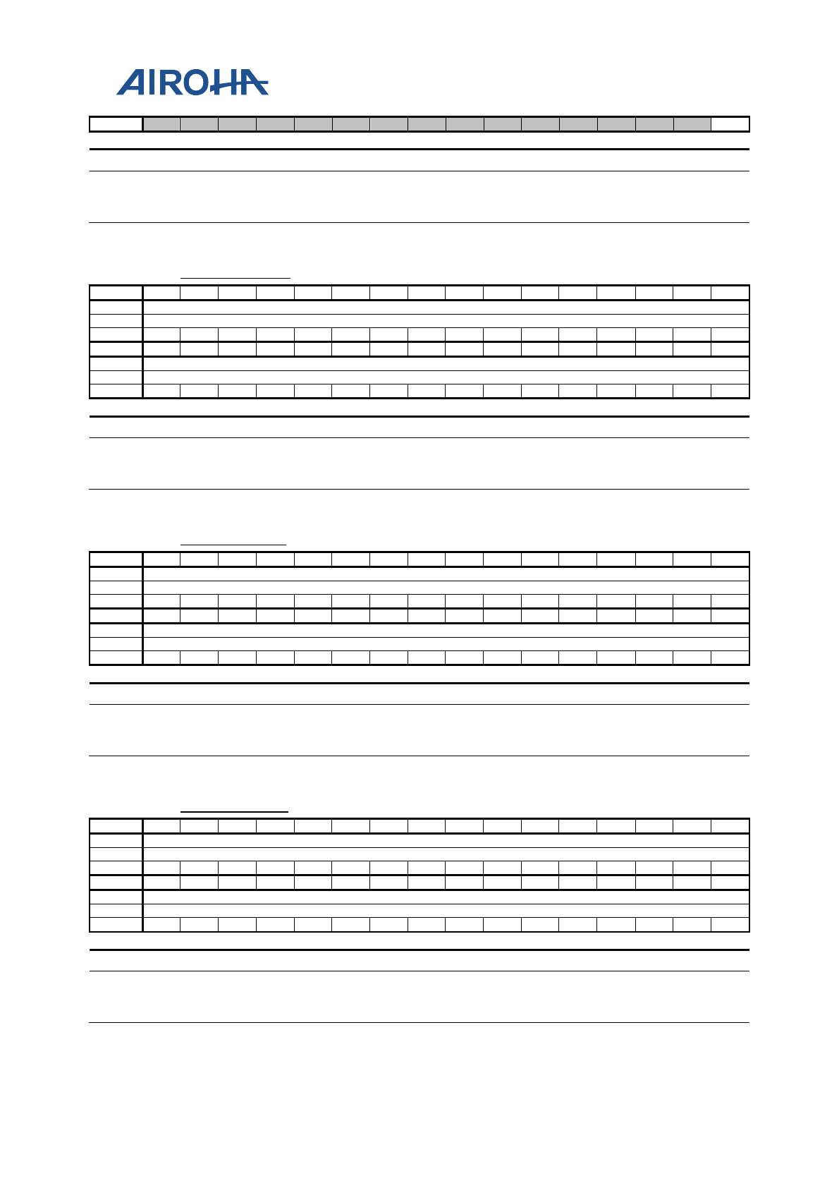
MT2523 Series Reference Manual
© 2015 - 2018 Airoha Technology Corp.
Page 327 of 692
This document contains information that is proprietary to Airoha Technology Corp. (“Airoha”) and/or its licensor(s).
Any unauthorized use, reproduction or disclosure of this document in whole or in part is strictly prohibited.
Reset
0
Bit(s)
Name
Description
0
DSI0_SEL
interface output selection
0: output to DBI
1: output to DSI
A0480014
CG_1ST_CON0
CG_1ST_CON0
00000000
Bit
31
30
29
28
27
26
25
24
23
22
21
20
19
18
17
16
Name
CG_1ST_CON0[31:16]
Type
RW
Reset
0
0
0
0
0
0
0
0
0
0
0
0
0
0
0
0
Bit
15
14
13
12
11
10
9
8
7
6
5
4
3
2
1
0
Name
CG_1ST_CON0[15:0]
Type
RW
Reset
0
0
0
0
0
0
0
0
0
0
0
0
0
0
0
0
Bit(s)
Name
Description
31:0
CG_1ST_CON0
hardware cg 1st configuration
0: set dsi free run clock on
1: set dsi free run clock gated
A0480018
CG_1ST_SET0
CG_1ST_SET0
00000000
Bit
31
30
29
28
27
26
25
24
23
22
21
20
19
18
17
16
Name
CG_1ST_SET0[31:16]
Type
RW
Reset
0
0
0
0
0
0
0
0
0
0
0
0
0
0
0
0
Bit
15
14
13
12
11
10
9
8
7
6
5
4
3
2
1
0
Name
CG_1ST_SET0[15:0]
Type
RW
Reset
0
0
0
0
0
0
0
0
0
0
0
0
0
0
0
0
Bit(s)
Name
Description
31:0
CG_1ST_SET0
hardware cg 1st set
0: no effect
1: set dsi free run clock gated
A048001C
CG_1ST_CLR0
CG_1ST_CLR0
00000000
Bit
31
30
29
28
27
26
25
24
23
22
21
20
19
18
17
16
Name
CG_1ST_CLR0[31:16]
Type
RW
Reset
0
0
0
0
0
0
0
0
0
0
0
0
0
0
0
0
Bit
15
14
13
12
11
10
9
8
7
6
5
4
3
2
1
0
Name
CG_1ST_CLR0[15:0]
Type
RW
Reset
0
0
0
0
0
0
0
0
0
0
0
0
0
0
0
0
Bit(s)
Name
Description
31:0
CG_1ST_CLR0
hardware cg 1st clear
0: no effect
1: enable DSI freen run clock
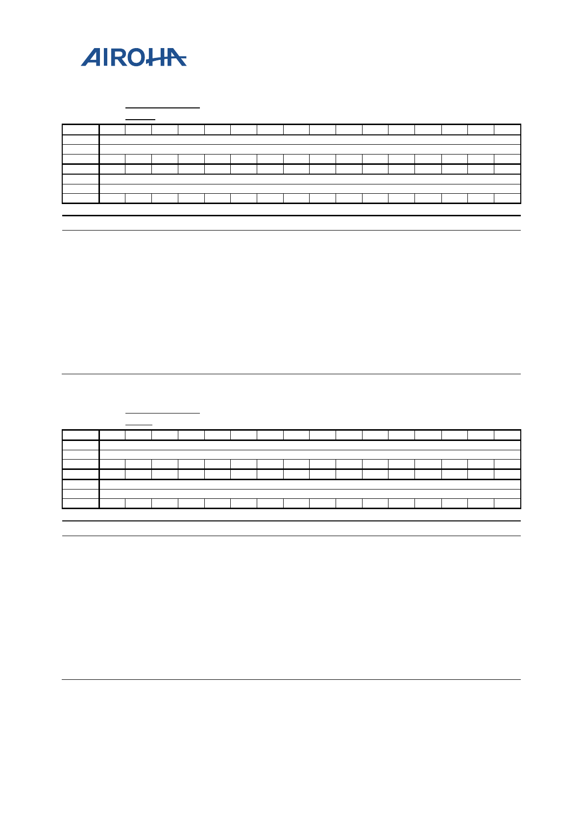
MT2523 Series Reference Manual
© 2015 - 2018 Airoha Technology Corp.
Page 328 of 692
This document contains information that is proprietary to Airoha Technology Corp. (“Airoha”) and/or its licensor(s).
Any unauthorized use, reproduction or disclosure of this document in whole or in part is strictly prohibited.
A0480020
HW_CG_DIS_
CON0
HW_CG_DIS_CON0
00000000
Bit
31
30
29
28
27
26
25
24
23
22
21
20
19
18
17
16
Name
HW_CG_DIS_CON0[31:16]
Type
RW
Reset
0
0
0
0
0
0
0
0
0
0
0
0
0
0
0
0
Bit
15
14
13
12
11
10
9
8
7
6
5
4
3
2
1
0
Name
HW_CG_DIS_CON0[15:0]
Type
RW
Reset
0
0
0
0
0
0
0
0
0
0
0
0
0
0
0
0
Bit(s)
Name
Description
31:0
HW_CG_DIS_CON0
hardware cg dis configuration
0: enable HW DCM
1: disable HW DCM
bit 0: lcd engine clock
bit 1: resizer
bit 2: rotdma
bit 3: caminf
bit 4: pad2cam
bit 5: g2d
bit 6: mm_color
bit 7: aal
bit 8: dsi engine clock
bit 9: gmc
bit 10: dsi interface clock
A0480024
HW_CG_DIS_
SET0
HW_CG_DIS_SET0
00000000
Bit
31
30
29
28
27
26
25
24
23
22
21
20
19
18
17
16
Name
HW_CG_DIS_SET0[31:16]
Type
RW
Reset
0
0
0
0
0
0
0
0
0
0
0
0
0
0
0
0
Bit
15
14
13
12
11
10
9
8
7
6
5
4
3
2
1
0
Name
HW_CG_DIS_SET0[15:0]
Type
RW
Reset
0
0
0
0
0
0
0
0
0
0
0
0
0
0
0
0
Bit(s)
Name
Description
31:0
HW_CG_DIS_SET0
hardware cg dis set
0: no effect
1: disable HW DCM
bit 0: lcd engine clock
bit 1: resizer
bit 2: rotdma
bit 3: caminf
bit 4: pad2cam
bit 5: g2d
bit 6: mm_color
bit 7: aal
bit 8: dsi engine clock
bit 9: gmc
bit 10: dsi interface clock

MT2523 Series Reference Manual
© 2015 - 2018 Airoha Technology Corp.
Page 329 of 692
This document contains information that is proprietary to Airoha Technology Corp. (“Airoha”) and/or its licensor(s).
Any unauthorized use, reproduction or disclosure of this document in whole or in part is strictly prohibited.
A0480028
HW_CG_DIS_
CLR0
HW_CG_DIS_CLR0
00000000
Bit
31
30
29
28
27
26
25
24
23
22
21
20
19
18
17
16
Name
HW_CG_DIS_CLR0[31:16]
Type
RW
Reset
0
0
0
0
0
0
0
0
0
0
0
0
0
0
0
0
Bit
15
14
13
12
11
10
9
8
7
6
5
4
3
2
1
0
Name
HW_CG_DIS_CLR0[15:0]
Type
RW
Reset
0
0
0
0
0
0
0
0
0
0
0
0
0
0
0
0
Bit(s)
Name
Description
31:0
HW_CG_DIS_CLR0
hardware cg dis clear
0: no effect
1: enable HW DCM
bit 0: lcd engine clock
bit 1: resizer
bit 2: rotdma
bit 3: caminf
bit 4: pad2cam
bit 5: g2d
bit 6: mm_color
bit 7: aal
bit 8: dsi engine clock
bit 9: gmc
bit 10: dsi interface clock

MT2523 Series Reference Manual
© 2015 - 2018 Airoha Technology Corp.
Page 330 of 692
This document contains information that is proprietary to Airoha Technology Corp. (“Airoha”) and/or its licensor(s).
Any unauthorized use, reproduction or disclosure of this document in whole or in part is strictly prohibited.
23. LCD display
23.1. General Description
MT2523 contains a versatile LCD controller which is optimized for multimedia applications. This controller supports
many types of LCD modules and contains a rich feature set to enhance the functionality. These features are:
• Up to 320 x 320 resolution with 30fps by DBI serial interface, 480x320 resolution with 30fps by DSI
interface
• Supports read frame buffer format: RGB565, RGB888, ARGB8888, PARGB8888, ARGB6666, PARGB6666,
YUYV422, index-4, index-2 and index-1 color.
• Supports output pixel format: 16-bpp (RGB565), 18-bpp (RGB666) and 24-bpp (RGB888) LCD modules.
• Supports 4 Layers overlay with individual color depth, window size, vertical and horizontal offset, source
key, dither and alpha value.
• Supports DBI serial interface:
data-pin interface: 4-wire mode, 3-wire mode, single a0 mode, start byte mode, CS stay low
mode
Dual edge 2-data-pin interface
• Supports DSI interface output. (for detail about DSI, please read DSI data sheet)
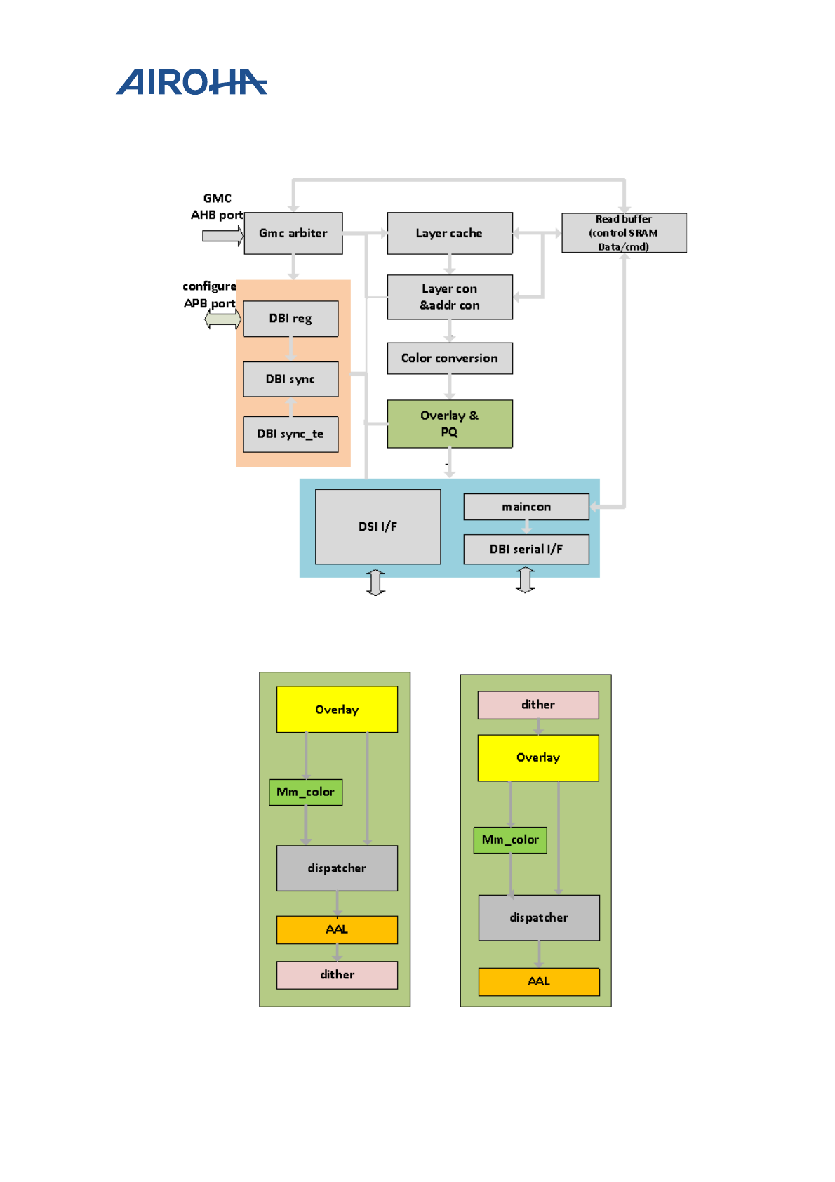
MT2523 Series Reference Manual
© 2015 - 2018 Airoha Technology Corp.
Page 331 of 692
This document contains information that is proprietary to Airoha Technology Corp. (“Airoha”) and/or its licensor(s).
Any unauthorized use, reproduction or disclosure of this document in whole or in part is strictly prohibited.
23.1.1. Block diagram
Figure 23-1. LCD Block Diagram
Figure 23-2. Two kinds of usages of overlay& PQ can be configured by different settings.
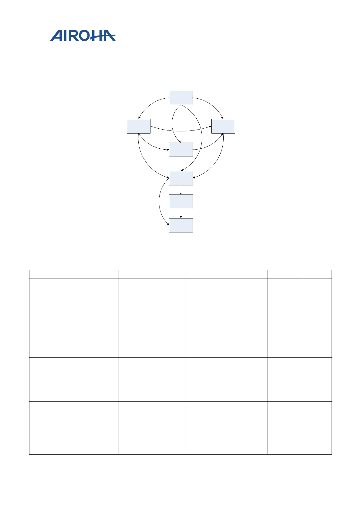
MT2523 Series Reference Manual
© 2015 - 2018 Airoha Technology Corp.
Page 332 of 692
This document contains information that is proprietary to Airoha Technology Corp. (“Airoha”) and/or its licensor(s).
Any unauthorized use, reproduction or disclosure of this document in whole or in part is strictly prohibited.
23.1.2. LCD Operating States
Below is a state diagram detailing the various states of the LCD controller. State transitions depend on
the current hardware trigger and tearing settings. Please consult for detailed explanations.
Figure 23-3. LCD State Transitions
Table 23-1. LCD controller internal state
State
Action
Exit State
Exit Condition
IRQ
LCD_STA
IDLE
LCD is idle
If hw_trig_en = 1,
then A;
If te_en = 1
and te_mode = 1,
then D;
If te_en = 1 and te_mode
= 0, then B;
Else C;
LCD_START.START has been
changed to 0 from 1.
No IRQ
0x00
WAIT
HWTRIG
LCD is waiting for
a hardware trigger
signal from another
engine.
If te_en = 0 and te_mode
= 0, then E;
If te_en = 1, and te_mode
= 1, then F;
Else G;
Received hardware trigger
signal.
HWTRIG
0x24
WAIT
VSYNC
LCD is waiting for
a vertical sync
signal from the
LCM
Always H
LCD has detected a vertical sync
signal with length specified in
the tearing register
VSYNC
0x28
WAIT
HSYNC
If te_mode = 0, then
LCD is waiting for
Always I
If te_mode = 0, then LCD must
receive a tearing edge and must
SYNC
0x30
IDLE
WAIT HWTRIG
WAIT VSYNC
WAIT HSYNC
REGISTER
COMMAND
DATA
A
I
H
GF
E
DC
B
J
K
L
MT2523 Series Reference Manual
© 2015 - 2018 Airoha Technology Corp.
Page 333 of 692
This document contains information that is proprietary to Airoha Technology Corp. (“Airoha”) and/or its licensor(s).
Any unauthorized use, reproduction or disclosure of this document in whole or in part is strictly prohibited.
a tearing edge;
I
f te_mode = 1, then
LCD horizontal
sync signals;
wait for a period of time;
If te_mode = 1, then LCD must
wait for a certain number of
horizontal sync signals.
REGISTER
LCD is transferring
register values to its
double registers for
use.
If command queue is
enabled then J;
Else K;
LCD will transition in 1T
REG_CPL
0x20
COMMAND
LCD is transferring
command queue
data to the LCM
Always L
After LCD has finished
transferring all command queue
data.
CMDQ_CPL
0x23
DATA
LCD is transferring
ROI data to the
LCM
If hw_trig_en = 1, then
WAIT_HWTRIG;
If te_repeat = 1, then
WAIT_VSYNC or
WAIT_HSYNC;
Else IDLE;
After LCD has finished
transferring all ROI data to the
LCM.
CPL
0x21
23.1.3. Serial Interface Modes
1-data-pin, 4 wire mode (CS, CK, DA, A0)
There is a dedicated pin for command/data indication.
CS
SLCK
LSDA D7 D6 D5 D4 D3 D2 D1 D0
LSA0
MT2523 Series Reference Manual
© 2015 - 2018 Airoha Technology Corp.
Page 334 of 692
This document contains information that is proprietary to Airoha Technology Corp. (“Airoha”) and/or its licensor(s).
Any unauthorized use, reproduction or disclosure of this document in whole or in part is strictly prohibited.
3-wire mode (CS,CK,DA)
When there is no dedicated pin for command/data indication, command/data indication must be transmitted by
the LSDA pin. It is called as 3-wire mode. A0 signal is transmitted first in every transaction under this mode.
CS
SLCK
LSDA A0 D7 D6 D5 D4 D3 D2 D1 D0
Single A0 mode
During the frame data transmission, the command/data indication is always data. Single A0 mode is to reduce the
unnecessary transmission of the repeated A0 (command/data indication). In single A0 mode, frame data
transactions only transmit A0 once, which is in the very first transaction.
CS
SLCK
LSDA A0 D7 D6 D5 D4 D3 D2 D1 D0 D7 D6 D5 D4 D3 D2 D1 D0
CS Stay Low mode
When transmitting pixel data in the CS Stay Low Mode, instead of asserting CS (chip select) signal after completing
every single transmission of every pixel, the CS is asserted only after the whole frame pixel data transmission
completes. This can reduce the time spent on the CS setup and hold time.
CS
SLCK
LSDA A0 D7 D6 D5 D4 D3 D2 D1 D0 A0 D7 D6 D5 D4 D3 D2 D1 D0
Start Byte mode
In start byte mode, every time CS goes low, serial interface transmit start byte first before sending command or
data.
CS
SLCK
LSDA Sta rt byte (8 bit) D7 D6 D5 D4 D3 D2 D1 D0
LSA0
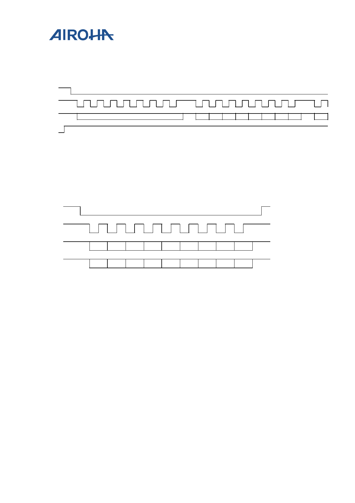
MT2523 Series Reference Manual
© 2015 - 2018 Airoha Technology Corp.
Page 335 of 692
This document contains information that is proprietary to Airoha Technology Corp. (“Airoha”) and/or its licensor(s).
Any unauthorized use, reproduction or disclosure of this document in whole or in part is strictly prohibited.
Start Byte mode with CS stay low mode
Start byte is always sent when CS goes low; therefore, when combined with CS stay low mode, during the whole
frame data transmission, start byte is sent only in the very first transaction.
CS
SLCK
LSDA Start byte (8 bit) D7 D6 D5 D4 D3 D2 D1 D0 D7
LSA0
2-Data-Pin mode
Pixel data is transmitted in 2-data-pin protocol instead of in the original 1-data-pin way. MT6250 only supports 2-
data-pin protocol with 3-Wire Mode (no dedicated cmd/data indication wire). It is because in the 2-data-pin
protocol in MT6250, the additional data pin is actually the original cmd/dat indication wire. As you can see from
the figure below, because there is no dedicated cmd/data indication wire anymore, the 2 data pins have to
transmit the cmd/dat information ahead of the pixel data bits in every transmission. This overhead can be greatly
reduced if the Single A0 Mode is turned on.
CS
SLCK
LSDA A0 D15 D14 D13 D12 D11 D10 D9 D8
LSA0 A0 D7 D6 D5 D4 D3 D2 D1 D0
MT2523 Series Reference Manual
© 2015 - 2018 Airoha Technology Corp.
Page 336 of 692
This document contains information that is proprietary to Airoha Technology Corp. (“Airoha”) and/or its licensor(s).
Any unauthorized use, reproduction or disclosure of this document in whole or in part is strictly prohibited.
23.2. LCD registers definition
Module name: LCD Base address: (+A0450000h)
Address Name Width Register Function
A0450000 LCD_STA 32 LCD interface status register
LCD interface status register
A0450004 LCD_INTEN 16
LCD Interface Interrupt Enable Register
This register controls which interrupts will be issued by the LCD
Interface. Each bit enable the corresponding interrupt listed in
LCD_INTSTA
A0450008 LCD_INTSTA 16
LCD Interface Interrupt Status Register
This register indicates which interrupt has been issued by the LCD
Interface. Writing 0 will clear a register bit. Writing 1 does nothing.
A045000C LCD_START 16 LCD Interface Frame Transfer Register
This register resets and starts the LCD Interface.
A0450010 LCD_RSTB 16 LCD Parallel/Serial Interface Reset Register
Ths register controls the reset pin of all connected external LCM.
A0450018 LCD_SIF_PIX_CON 32 LCD Serial Interface Pixel Data Configuration Register
This register controls the pixel transaction of serial interface
A045001C LCD_SIF_TIMING0 32 LCD Serial Interface 0 Timing Register
This register controls the waveform timing of the serial LCM interface 0
A0450020 LCD_SIF_TIMING1 32 LCD Serial Interface 1 Timing Register
This register controls the waveform timing of the serial LCM interface 1
A0450028 LCD_SCNF 32 LCD Serial Interface Configuration Register
This register has settings for connected LCD-C LCM.
A045002C LCD_SCNF_CS 32 LCD Serial Interface Chip Select Register
This register controls the chip selects for connected LCD-C LCM.
A0450048 LCD_SYNC_LCM_SIZE 32 LCD Sync LCM Size Register
Set the current LCM VTT and HTT timing parameters
A045004C LCD_SYNC_CNT 32 LCD Sync Counter Register
TE current scanline and stop line settings
A0450050 LCD_TECON 32
LCD Tearing Control Register
This register configures the LCD response to the frame sync (tearing)
signal sent from the LCM.
A0450080 LCD_ROICON 32 LCD Region of Interest Control Register
This register contains settings used for the Region of Interest.
A0450084 LCD_WROIOFS 32 LCD Region of Interest Window Offset Register
Specify the offset of the Region of Interest
A0450088 LCD_WROICADD 32
LCD Region of Interest Command Address Register
Specify which address to send commands. Each LCM has a defined
address offset.
A045008C LCD_WROIDADD 32 LCD Region of Interest Data Address Register
Specify which address to send data. Each LCM has a defined address
MT2523 Series Reference Manual
© 2015 - 2018 Airoha Technology Corp.
Page 337 of 692
This document contains information that is proprietary to Airoha Technology Corp. (“Airoha”) and/or its licensor(s).
Any unauthorized use, reproduction or disclosure of this document in whole or in part is strictly prohibited.
Address Name Width Register Function
offset.
A0450090 LCD_WROISIZE 32 LCD Region of Interest Size Register
Specify the size of the Region of Interest
A045009C LCD_WROI_BGCLR 32 LCD Region of Interest Background Color Register
Specify the background color
A04500B0 LCD_L0WINCON 32 LCD Layer 0 Window Control Register
L0 setttings
A04500B4 LCD_L0WINKEY 32 LCD Layer 0 Color Key Register
A04500B8 LCD_L0WINOFS 32 LCD Layer 0 Window Display Offset Register
A04500BC LCD_L0WINADD 32 LCD Layer 0 Window Display Start Address Register
A04500C0 LCD_L0WINSIZE 32 LCD Layer 0 Window Size
A04500C8 LCD_L0WINMOFS 32 LCD Layer 0 Memory Offset
A04500CC LCD_L0WINPITCH 16 LCD Layer 0 Memory Pitch
A04500E0 LCD_L1WINCON 32 LCD Layer 1 Window Control Register
L1 settings
A04500E4 LCD_L1WINKEY 32 LCD Layer 1 Color Key Register
A04500E8 LCD_L1WINOFS 32 LCD Layer 1 Window Display Offset Register
A04500EC LCD_L1WINADD 32 LCD Layer 1 Window Display Start Address Register
A04500F0 LCD_L1WINSIZE 32 LCD Layer 1 Window Size
A04500F8 LCD_L1WINMOFS 32 LCD Layer 1 Memory Offset
A04500FC LCD_L1WINPITCH 16 LCD Layer 1 Memory Pitch
A0450110 LCD_L2WINCON 32 LCD Layer 2 Window Control Register
L2 settings
A0450114 LCD_L2WINKEY 32 LCD Layer 2 Color Key Register
A0450118 LCD_L2WINOFS 32 LCD Layer 2 Window Display Offset Register
A045011C LCD_L2WINADD 32 LCD Layer 2 Window Display Start Address Register
A0450120 LCD_L2WINSIZE 32 LCD Layer 2 Window Size
A0450128 LCD_L2WINMOFS 32 LCD Layer 2 Memory Offset
A045012C LCD_L2WINPITCH 16 LCD Layer 2 Memory Pitch
A0450140 LCD_L3WINCON 32 LCD Layer 3 Window Control Register
L3 settings
A0450144 LCD_L3WINKEY 32 LCD Layer 3 Color Key Register
A0450148 LCD_L3WINOFS 32 LCD Layer 3 Window Display Offset Register
A045014C LCD_L3WINADD 32 LCD Layer 3 Window Display Start Address Register
A0450150 LCD_L3WINSIZE 32 LCD Layer 3 Window Size
A0450158 LCD_L3WINMOFS 32 LCD Layer 3 Memory Offset
A045015C LCD_L3WINPITCH 16 LCD Layer 3 Memory Pitch
MT2523 Series Reference Manual
© 2015 - 2018 Airoha Technology Corp.
Page 338 of 692
This document contains information that is proprietary to Airoha Technology Corp. (“Airoha”) and/or its licensor(s).
Any unauthorized use, reproduction or disclosure of this document in whole or in part is strictly prohibited.
Address Name Width Register Function
A0450270 LCD_SIF_STR_BYTE_CON 32 LCD SIF Start Byte Configuration Register
A0450278 LCD_SIF_WR_STR_BYTE 32 LCD SIF Write Start Byte Value
A045027C LCD_SIF_RD_STR_BYTE 32 LCD SIF Read Start Byte Value
A0450300 LCD_SIF_PAD_INPUT_SEL
ECT 32 LCD serial pad selection
A0450400 LCD_TABLE_INDEX_0_1 32 LCD INDEX Mode 0_1
A0450404 LCD_TABLE_INDEX_2_3 32 LCD INDEX Mode 2_3
A0450408 LCD_TABLE_INDEX_4_5 32 LCD INDEX Mode 4_5
A045040C LCD_TABLE_INDEX_6_7 32 LCD INDEX Mode 6_7
A0450410 LCD_TABLE_INDEX_8_9 32 LCD INDEX Mode 8_9
A0450414 LCD_TABLE_INDEX_a_b 32 LCD INDEX Mode a_b
A0450418 LCD_TABLE_INDEX_c_d 32 LCD INDEX Mode c_d
A045041C LCD_TABLE_INDEX_e_f 32 LCD INDEX Mode e_f
A0450F80 LCD_SCMD0 32 LCD Serial Interface Command Port0
This register allows software to directly write or read to Serial Interface.
A0450F90 LCD_SDAT0 32 LCD Serial Interface Data Port0
This register allows software to directly write or read to Serial Interface.
A0450FA0 LCD_SCMD1 32 LCD Serial Interface Command Port1
This register allows software to directly write or read to Serial Interface.
A0450FB0 LCD_SDAT1 32 LCD Serial Interface Data Port1
This register allows software to directly write or read to Serial Interface.
A0450000
LCD_STA
LCD interface status register
00000000
Bit
31
30
29
28
27
26
25
24
23
22
21
20
19
18
17
16
Name
Type
Reset
Bit
15
14
13
12
11
10
9
8
7
6
5
4
3
2
1
0
Name
main
_idle
GMC BUSY
WAIT
_SYN
C
RUN
Type
RU
RU
RU
RU
RU
Reset
1
0
0
0
0
Bit(s)
Mnemonic
Name
Description
8
main_idle
0: maincon is not idle
1: maincon is idle
6
GMC
LCD is currently sending a read/write GMC request
0: not sending GMC request
1: is sening GMC request
5
BUSY
LCD interface is busy.
0: LCD is not busy
1: LCD may be in the process of waiting for a hardware trigger signal,
waiting for tearing signal, sending commands to command queue, or
writing pixels to LCM
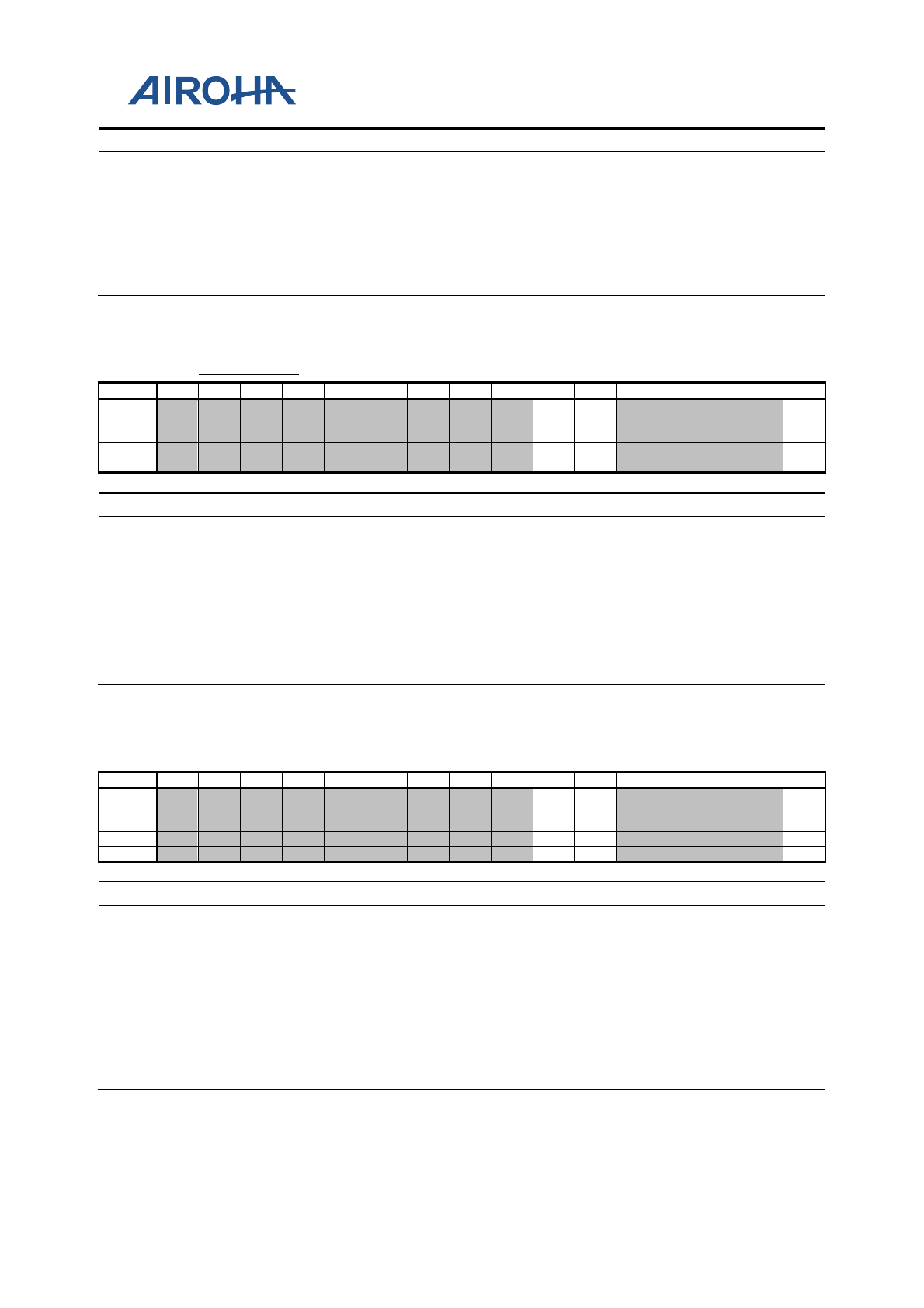
MT2523 Series Reference Manual
© 2015 - 2018 Airoha Technology Corp.
Page 339 of 692
This document contains information that is proprietary to Airoha Technology Corp. (“Airoha”) and/or its licensor(s).
Any unauthorized use, reproduction or disclosure of this document in whole or in part is strictly prohibited.
Bit(s)
Mnemonic
Name
Description
4
WAIT_SYNC
LCD is waiting for LCM tearing-free sync signal
0: not waiting TE signal
1: is waiting TE signal
0
RUN
LCD Interface Transfer Bit
0: LCD Interface is currently not transferring command/pixel data to
the external LCM
1: LCD Interface is currently transferring command/pixel data to the
external LCM.
A0450004
LCD_INTEN
LCD Interface Interrupt Enable
Register
0000
Bit
15
14
13
12
11
10
9
8
7
6
5
4
3
2
1
0
Name
APB_
TIME
OUT
SYNC
CPL
Type
RW
RW
RW
Reset
0
0
0
Bit(s)
Mnemonic
Name
Description
6
APB_TIMEOUT
CPU accessing LCD time out interrupt enable
0: Disable Interrupt
1: Enable Interrupt
5
SYNC
TE Sync Interrupt Enable
0: Disable Interrupt
1: Enable Interrupt
0
CPL
Frame Complete Interrupt Enable
0: Disable Interrupt
1: Enable Interrupt
A0450008
LCD_INTSTA
LCD Interface Interrupt Status Register
0000
Bit
15
14
13
12
11
10
9
8
7
6
5
4
3
2
1
0
Name
APB_
TIME
OUT
SYNC
CPL
Type
A1
A1
A1
Reset
0
0
0
Bit(s)
Mnemonic
Name
Description
6
APB_TIMEOUT
CPU accessing LCD time out interrupt
0: No Interrupt
1: Indicates the CPU access LCD time out
5
SYNC
TE Sync Interrupt
0: No Interrupt
1: Indicates the LCD Interface has received a TE sync signal from the
LCM
0
CPL
Frame Complete Interrupt
0: No Interrupt
1: Indicates a frame has been completely transferred to the LCM.
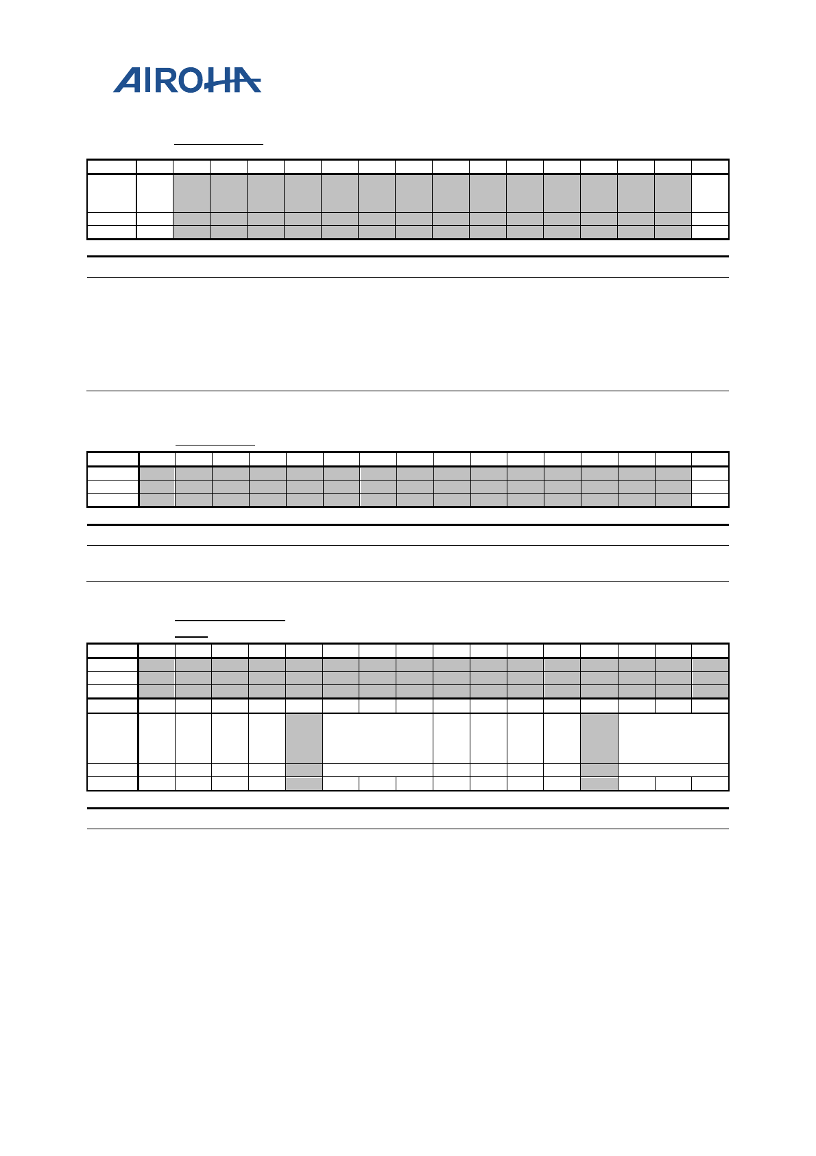
MT2523 Series Reference Manual
© 2015 - 2018 Airoha Technology Corp.
Page 340 of 692
This document contains information that is proprietary to Airoha Technology Corp. (“Airoha”) and/or its licensor(s).
Any unauthorized use, reproduction or disclosure of this document in whole or in part is strictly prohibited.
A045000C
LCD_START
LCD Interface Frame
Transfer Register
0000
Bit
15
14
13
12
11
10
9
8
7
6
5
4
3
2
1
0
Name STAR
T
INT_
RESE
T
Type
RW
RW
Reset
0
0
Bit(s)
Mnemonic
Name
Description
15
START
LCD Interface Start Bit
0: No action
1: Enable the LCD Interface.
0
INT_RESET
LCD Interface Software Reset Bit
0: No action
1: Reset the LCD Interface. This does not reset the LCD Interface
configuration registers or command queue.
A0450010
LCD_RSTB
LCD Parallel/Serial Interface Reset Register
0001
Bit
15
14
13
12
11
10
9
8
7
6
5
4
3
2
1
0
Name
RSTB
Type
RW
Reset
1
Bit(s)
Mnemonic
Name
Description
0
RSTB
LCD-B/LCD-C Reset Signal
Directly controls the LCM Reset Pin
A0450018
LCD_SIF_PIX_
CON
LCD Serial Interface Pixel
Data Configuration
Register
00000000
Bit
31
30
29
28
27
26
25
24
23
22
21
20
19
18
17
16
Name
Type
Reset
Bit
15
14
13
12
11
10
9
8
7
6
5
4
3
2
1
0
Name
SIF1_
CS_S
TAY_
LOW
SIF1_
SING
LE_A
0
SIF1_
PARA
_2PI
N
SIF1_
PIX_2
PIN
SIF1_2PIN_SIZE
SIF0_
CS_S
TAY_
LOW
SIF0_
SING
LE_A
0
SIF0_
PARA
_2PI
N
SIF0_
PIX_2
PIN
SIF0_2PIN_SIZE
Type
RW
RW
RW
RW
RW
RW
RW
RW
RW
RW
Reset
0
0
0
0
0
0
0
0
0
0
0
0
0
0
Bit(s)
Mnemonic
Name
Description
15
SIF1_CS_STAY_LO
W
Enable the CS_Stay_Low mode for frame pixel data
transmission in both 1-data-pin and 2-data-pin protocol
14
SIF1_SINGLE_A0
Enable the Single A0 mode for frame pixel data transmission
in 1-data-pin or 2-data-pin protocol. This bit only takes effect
when the 3-wire mode is enabled.
13
SIF1_PARA_2PIN
Enable 2-data-pin parameter protocol
not recommend to use
12
SIF1_PIX_2PIN
Enable 2-data-pin protocol
10:8
SIF1_2PIN_SIZE
Interface size of Serial interface 0 in 2-data-
pin protocol. This
size configuration takes effect only when data is actually
transmitted in 2-data-pin protocol. Each transaction would
be transmitted in bit specified as field description below.
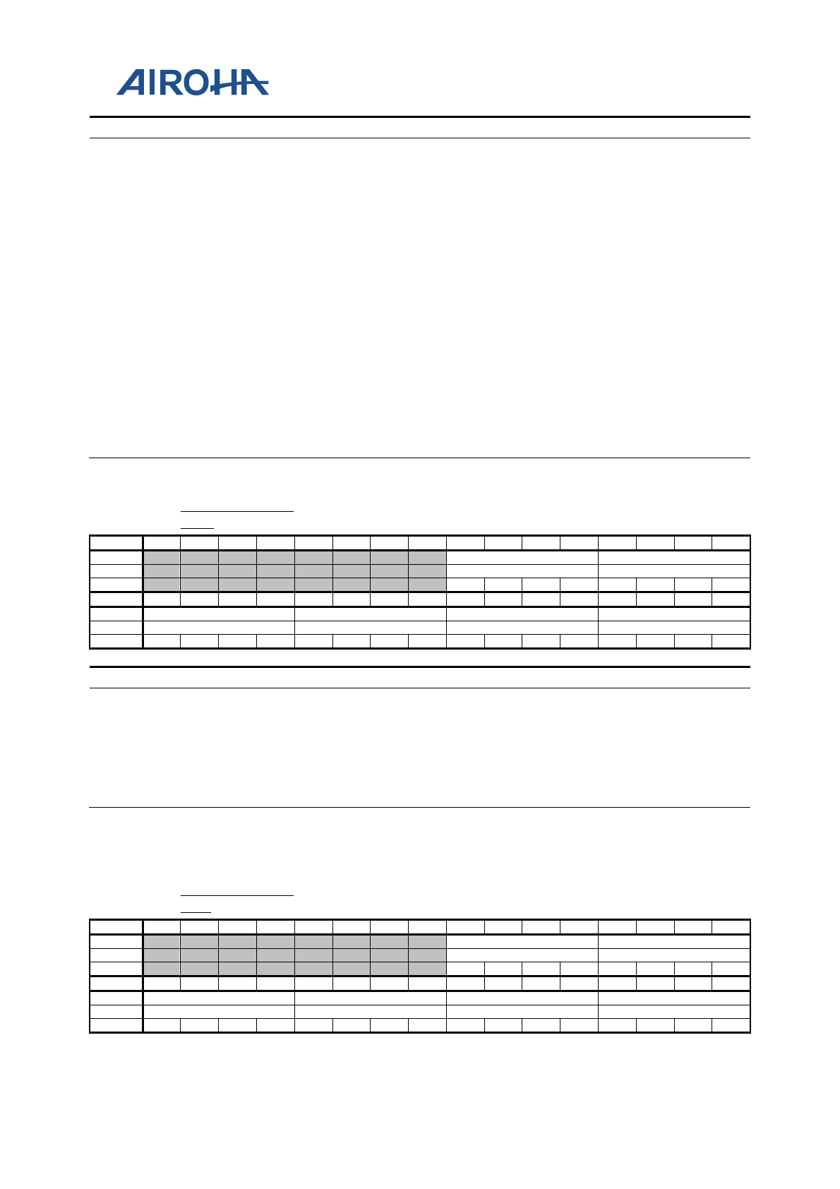
MT2523 Series Reference Manual
© 2015 - 2018 Airoha Technology Corp.
Page 341 of 692
This document contains information that is proprietary to Airoha Technology Corp. (“Airoha”) and/or its licensor(s).
Any unauthorized use, reproduction or disclosure of this document in whole or in part is strictly prohibited.
Bit(s)
Mnemonic
Name
Description
010: 16 bits
011: 18 bits
100: 24 bits
110: 12 bits
7
SIF0_CS_STAY_LO
W
Enable the CS_Stay_Low mode for frame pixel data
transmission in both 1-data-pin and 2-data-pin protocol
6
SIF0_SINGLE_A0
Enable the Single A0 mode for frame pixel data transmission
in 1-data-pin or 2-data-pin protocol. This bit only takes effect
when the 3-wire mode is enabled.
5
SIF0_PARA_2PIN
Enable 2-data-pin parameter protocol
not recommend to use
4
SIF0_PIX_2PIN
Enable 2-data-pin protocol
2:0
SIF0_2PIN_SIZE
Interface size of Serial interface 0 in 2-data-
pin protocol. This
size configuration takes effect only when data is actually
transmitted in 2-data-pin protocol. Each transaction would
be transmitted in bit specified as field description below.
010: 16 bits
011: 18 bits
100: 24 bits
110: 12 bits
A045001C
LCD_SIF_TIMI
NG0
LCD Serial Interface 0 Timing Register
00000000
Bit
31
30
29
28
27
26
25
24
23
22
21
20
19
18
17
16
Name
CSS
CSH
Type
RW
RW
Reset
0
0
0
0
0
0
0
0
Bit
15
14
13
12
11
10
9
8
7
6
5
4
3
2
1
0
Name
RD1ST
RD2ND
WR1ST
WR2ND
Type
RW
RW
RW
RW
Reset
0
0
0
0
0
0
0
0
0
0
0
0
0
0
0
0
Bit(s)
Mnemonic
Name
Description
23:20
CSS
chip select setup time
19:16
CSH
chip select hold time
15:12
RD1ST
The first phase timing of LSCK when read transfer
11:8
RD2ND
The second phase timing of LSCK when read transfer
7:4
WR1ST
The first phase timing of LSCK when write transfer
3:0
WR2ND
The second phase timing of LSCK when write transfer
A0450020
LCD_SIF_TIMI
NG1
LCD Serial Interface 1
Timing Register
00000000
Bit
31
30
29
28
27
26
25
24
23
22
21
20
19
18
17
16
Name
CSS
CSH
Type
RW
RW
Reset
0
0
0
0
0
0
0
0
Bit
15
14
13
12
11
10
9
8
7
6
5
4
3
2
1
0
Name
RD1ST
RD2ND
WR1ST
WR2ND
Type
RW
RW
RW
RW
Reset
0
0
0
0
0
0
0
0
0
0
0
0
0
0
0
0
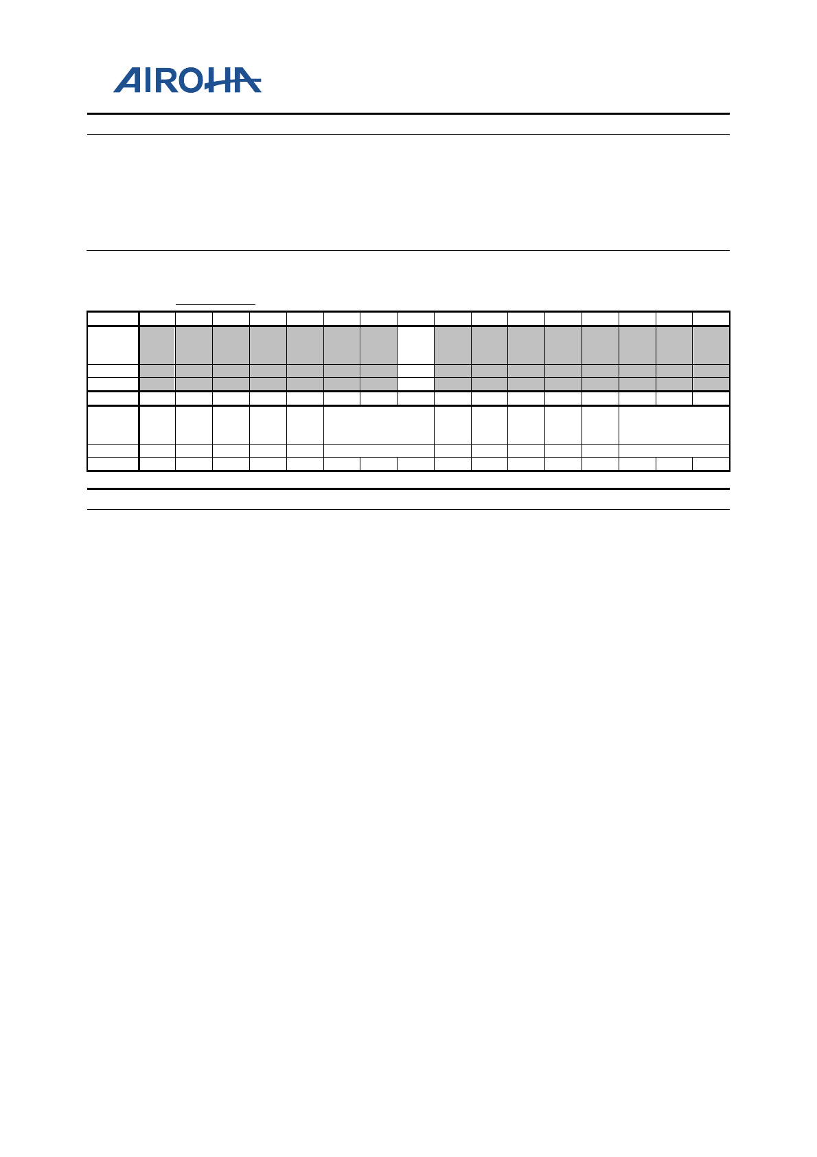
MT2523 Series Reference Manual
© 2015 - 2018 Airoha Technology Corp.
Page 342 of 692
This document contains information that is proprietary to Airoha Technology Corp. (“Airoha”) and/or its licensor(s).
Any unauthorized use, reproduction or disclosure of this document in whole or in part is strictly prohibited.
Bit(s)
Mnemonic
Name
Description
23:20
CSS
chip select setup time
19:16
CSH
chip select hold time
15:12
RD1ST
The first phase timing of LSCK when read transfer
11:8
RD2ND
The second phase timing of LSCK when read transfer
7:4
WR1ST
The first phase timing of LSCK when write transfer
3:0
WR2ND
The second phase timing of LSCK when write transfer
A0450028
LCD_SCNF
LCD Serial Interface Configuration Register
10000000
Bit
31
30
29
28
27
26
25
24
23
22
21
20
19
18
17
16
Name
SIF_
HW_
CS
Type
RW
Reset
0
Bit
15
14
13
12
11
10
9
8
7
6
5
4
3
2
1
0
Name SIF1_
DIV2
SIF1_
SCK_
DEF
SIF1_
1ST_P
OL
SIF1_
SDI
SIF1_
3WIR
E
SIF1_SIZE
SIF0_
DIV2
SIF0_
SCK_
DEF
SIF0_
1ST_P
OL
SIF0_
SDI
SIF0_
3WIR
E
SIF0_SIZE
Type
RW
RW
RW
RW
RW
RW
RW
RW
RW
RW
RW
RW
Reset
0
0
0
0
0
0
0
0
0
0
0
0
0
0
0
0
Bit(s)
Mnemonic
Name
Description
24
SIF_HW_CS
Hardware controls serial interface chip select.
0: the chip select of serial interface is controlled by software by
manipulating register LCD_SCNF_CS
1: the chip select of serial interface is controlled by hardware.
15
SIF1_DIV2
Slow down the serial interface 1 timing
0: Disable
1: Enable
14
SIF1_SCK_DEF
The default value of LSCK for serial interface 1 when not
transfer data
0: The default of LSCK is low
1: The default of LSCK is high
13
SIF1_1ST_POL
The first phase polarity of LSCK for serial interface 1
0: The first phase of LSCK is low
1: The first phase of LSCK is high
12
SIF1_SDI
Set to 1 to read data from LSDI pin, otherwise LCD will use
the bi-directional LSDA pin
11
SIF1_3WIRE
Enable 3 wire mode of serial interface 1. Serial interface will
transfer an A0 bit before transferring the MSB of each
transcation
10:8
SIF1_SIZE
Interface size of Serial interface 1. Each transaction will
transmit this many bits.
000: 8bits
001: 9bits
010: 16bits
011: 18bits
100: 24bits
101: 32bits
7
SIF0_DIV2
Slow down the serial interface 0 timing
0: Disable
1: Enable
6
SIF0_SCK_DEF
The default value of LSCK for serial interface 0 when not
transfer data
0: The default of LSCK is low
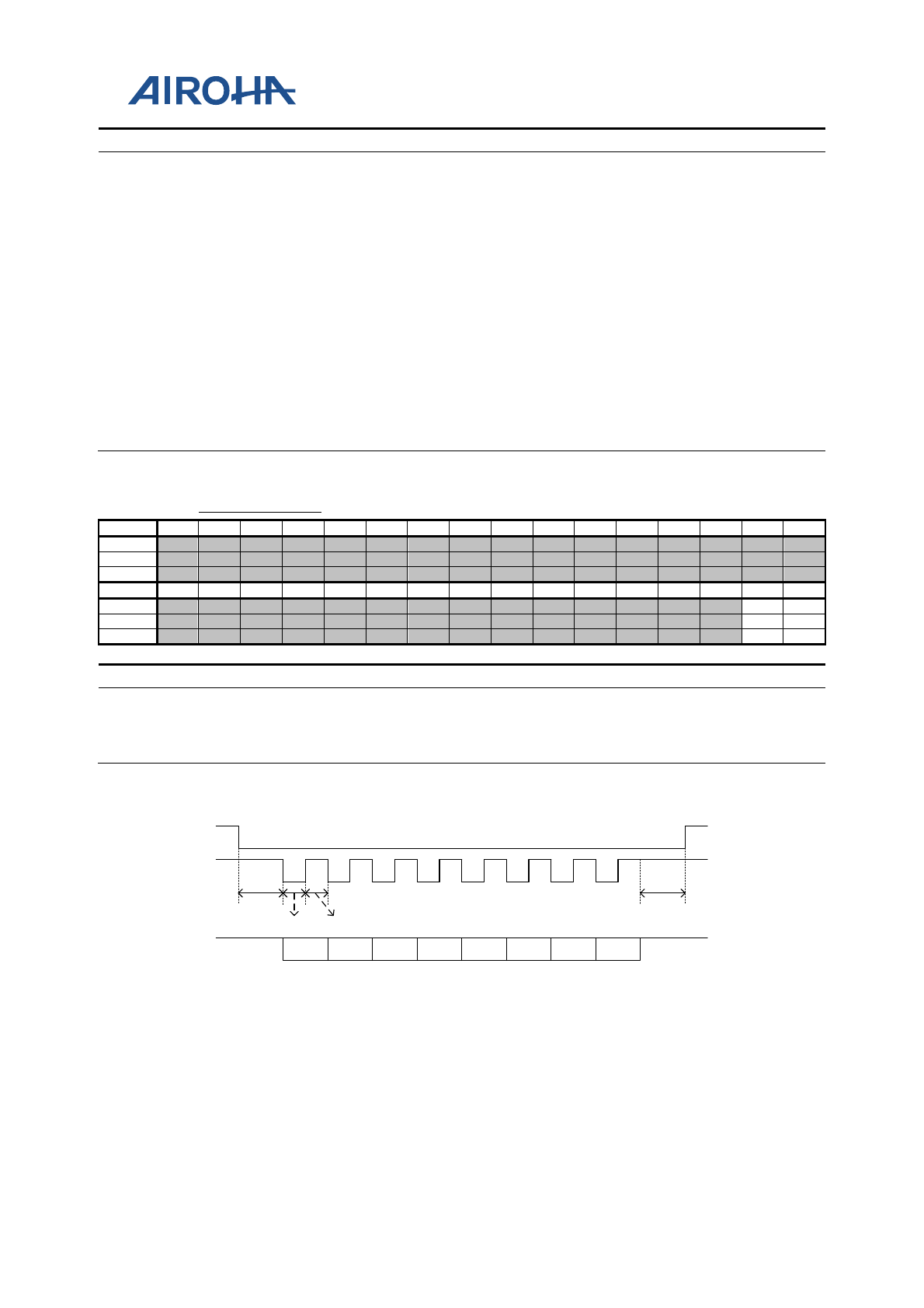
MT2523 Series Reference Manual
© 2015 - 2018 Airoha Technology Corp.
Page 343 of 692
This document contains information that is proprietary to Airoha Technology Corp. (“Airoha”) and/or its licensor(s).
Any unauthorized use, reproduction or disclosure of this document in whole or in part is strictly prohibited.
Bit(s)
Mnemonic
Name
Description
1: The default of LSCK is high
5
SIF0_1ST_POL
The first phase polarity of LSCK for serial interface 0
0: The first phase of LSCK is low
1: The first phase of LSCK is high
4
SIF0_SDI
Set to 1 to read data from LSDI pin, otherwise LCD will use
the bi-directional LSDA pin
3
SIF0_3WIRE
Enable 3 wire mode of serial interface 0. Serial interface will
transfer an A0 bit before transferring the MSB of each
transcation
2:0
SIF0_SIZE
Interface size of Serial interface 0. Each transaction will
transmit this many bits.
000: 8bits
001: 9bits
010: 16bits
011: 18bits
100: 24bits
101: 32bits
A045002C
LCD_SCNF_CS
LCD
Serial Interface Chip Select Register
00000003
Bit
31
30
29
28
27
26
25
24
23
22
21
20
19
18
17
16
Name
Type
Reset
Bit
15
14
13
12
11
10
9
8
7
6
5
4
3
2
1
0
Name
CS1
CS0
Type
RW
RW
Reset
1
1
Bit(s)
Mnemonic
Name
Description
1
CS1
Directly control the value of the Chip Select pin LSCE1. This
bit takes effect only when LCD_SIF_CON.SIF_HW_CS=0.
0
CS0
Directly control the value of the Chip Select pin LSCE0. This
bit takes effect only when LCD_SIF_CON.SIF_HW_CS=0.
D7 D6 D5 D4 D3 D2 D1 D0
(SIF0_SCK_DEF,SIF0_1ST_POL) = (1,0)
RD_1ST RD_2ND
CSS CSH
LSCE0B
LSCK
LSDA or
LSDI
CSS = (LCD_SIF0_TIMING.CSS*(LCD_SIF_CON.SIF0_DIV2+1) ) + 1;
CSH = (LCD_SIF0_TIMING.CSH*(LCD_SIF_CON.SIF0_DIV2+1) ) + 1;
RD_1ST = (LCD_SIF0_TIMING.RD_1ST*(LCD_SIF_CON.SIF0_DIV2+1) ) + 1;
RD_2ND = (LCD_SIF0_TIMING.RD_2ND*(LCD_SIF_CON.SIF0_DIV2+1) ) + 1;
All the above parameter are in unit of lcd working clock cycle time, 9.615384ns.
Figure 23-4. LCD serial interface read timing diagram
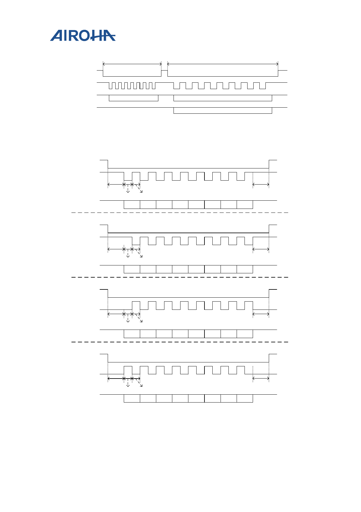
MT2523 Series Reference Manual
© 2015 - 2018 Airoha Technology Corp.
Page 344 of 692
This document contains information that is proprietary to Airoha Technology Corp. (“Airoha”) and/or its licensor(s).
Any unauthorized use, reproduction or disclosure of this document in whole or in part is strictly prohibited.
read command
LSCE0B
LSCK
LSDA
LSDI
read data from LCM
read data from LCM
Send read command
(write operation) Read data (read operation)
Figure 23-5. LCD serial interface read waveform example
D7 D6 D5 D4 D3 D2 D1 D0
(SIF0_SCK_DEF,SIF0_1ST_POL) = (1,0)
(SIF0_SCK_DEF,SIF0_1ST_POL) = (1,1)
(SIF0_SCK_DEF,SIF0_1ST_POL) = (0,0)
LSCE0B
LSCK
LSDA
LSCE0B
LSCK
LSDA
D7 D6 D5 D4 D3 D2 D1 D0
LSDA
D7 D6 D5 D4 D3 D2 D1 D0
(SIF0_SCK_DEF,SIF0_1ST_POL) = (0,1)
LSCE0B
LSCK
LSCE0B
LSCK
LSDA
D7 D6 D5 D4 D3 D2 D1 D0
CSH
WR_1ST WR_2ND
CSS
WR_1ST WR_2ND
CSS
WR_1ST WR_2ND
CSS
WR_1ST WR_2ND
CSS
CSH
CSH
CSH
CSS = (LCD_SIF0_TIMING.CSS*(LCD_SIF_CON.SIF0_DIV2+1) ) + 1;
CSH = (LCD_SIF0_TIMING.CSH*(LCD_SIF_CON.SIF0_DIV2+1) ) + 1;
WR_1ST = (LCD_SIF0_TIMING.WR_1ST*(LCD_SIF_CON.SIF0_DIV2+1) ) + 1;
WR_2ND = (LCD_SIF0_TIMING.WR_2ND*(LCD_SIF_CON.SIF0_DIV2+1) ) + 1;
All the above parameter are in unit of lcd working clock cycle time, 9.615384ns.
Figure 23-6. LCD serial interface write timing diagram
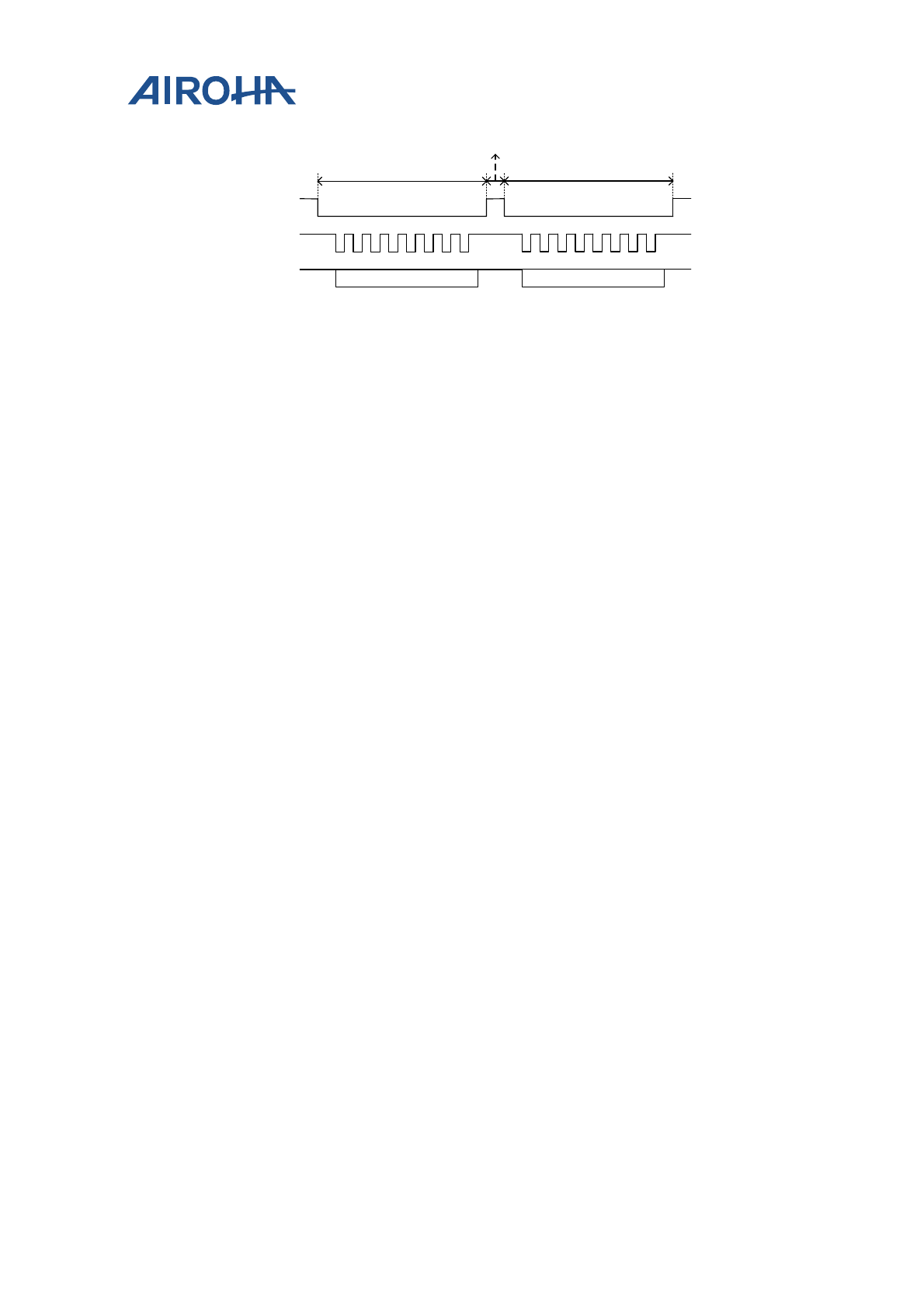
MT2523 Series Reference Manual
© 2015 - 2018 Airoha Technology Corp.
Page 345 of 692
This document contains information that is proprietary to Airoha Technology Corp. (“Airoha”) and/or its licensor(s).
Any unauthorized use, reproduction or disclosure of this document in whole or in part is strictly prohibited.
Data 0
LSCE0B
LSCK
LSDA
First transfer
Data 1
Second transfer
CSHW
CSHW = 2 cycles when transfer pixel data.
CSHW = 4 cycles when transfer commands.
One cycle = 9.615384ns.
Figure 23-7. LCD serial interface write waveform example
Tearing Control
When moving pictures are played, LCD controller must be synchronized to LCM scanning timing to prevent tearing
on screen. The LCD controller provides two methods to synchronize to LCM, and one time-out counter to get LCM
scanning speed.
The first synchronous method is “hardware TE” mode. In this mode, LCD controller can be programmed to wait
certain time interval after LCM TE signal is received, and then starts to update LCM.
The second synchronous method is “read scan line” mode, which doesn’t need to connect TE signal from LCM to
LCD controller. Instead, this mode uses reading LCM current scan line to synchronize to LCM scanning.
If we know the LCM scanning speed and LCM current scan line, we can use a counter to synchronize to LCM, and
wait a proper time to start transferring to prevent tearing. “Read scan line” mode provides the capability to read
LCM current scan line. And the time-out counter provides the capability to get the LCM scanning speed.
Sync Mode 0: “Hardware TE” mode
In sync mode = 0, LCD will start to transfer data to LCM after receiving TE signal plus counting a set number of
horizontal sync lines. The LCM scanning time of each horizontal sync line is set by LCD_SYNC_LCM_SIZE.HTT, which
indicates how long a LCM horizontal line is in units of 16*T, where T is the cycle time of LCD working clock. Cycle
time is 9.615384 ns (104MHz). After receiving a TE edge, LCD will count LCD_SYNC_CNT.WAITLINE number of lines
and then begin updating the new frame to the LCM. To use this mode, please follow these steps:
• Set LCD_TECON.SYNC_MODE = 0 and LCD_TECON.SYNC_EN = 1
• Set LCD_SYNC_LCM_SIZE.HTT to the correct value. See for more information on this. Also see below “HTT
Calibration” section for more information on this.
• Set LCD_SYNC_CNT.WAITLINE to the number of lines you wish to wait before updating the LCM.
• Set other registers (ROI, Layer, etc.) and start the LCD controller by setting LCD_START.START = 1 (from 0).
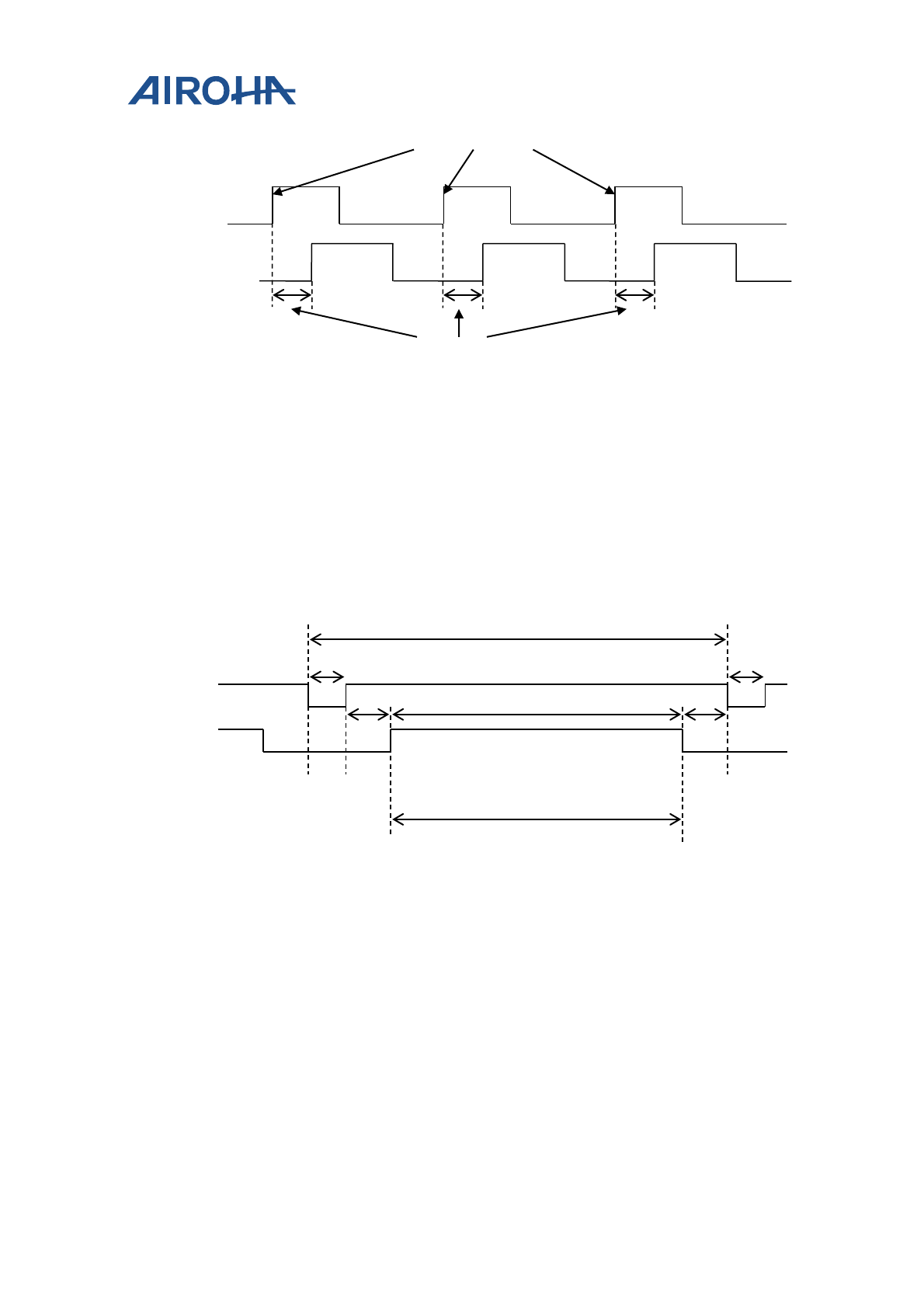
MT2523 Series Reference Manual
© 2015 - 2018 Airoha Technology Corp.
Page 346 of 692
This document contains information that is proprietary to Airoha Technology Corp. (“Airoha”) and/or its licensor(s).
Any unauthorized use, reproduction or disclosure of this document in whole or in part is strictly prohibited.
Figure 23-8. SYNC_MODE = 0
Sync Mode 1: “Read scan line” mode
In sync mode 1, LCD will not use the TE pin to detect the LCM scan line position. Instead, software must read the
LCM scan line from the LCM register. When software reads a specified port, LCD will interpret this and
automatically begin its internal TE counter at the read LCM scan line position. Scan line 0 indicates the beginning
(the first edge, either rising or falling edge) of VSYNC as shown in . The LCD ROI begins during the V active region
(vact).
Figure 23-9. LCM Scan Line Timing
LCM VSYNC
vsync
vact
vbp
vfp
LCM DE
vsync
LCD ROI
0
vtt = vsync + vbp + vact + vfp
vtt: vertical total lines
vsync: vertical sync width
vbp: vertical back porch
vfp: vertical front porch
vact: vertical active region
TE input
LCD updating
Vertical Synchro
16*T*HTT*WAITLINE, T=9.615384 ns
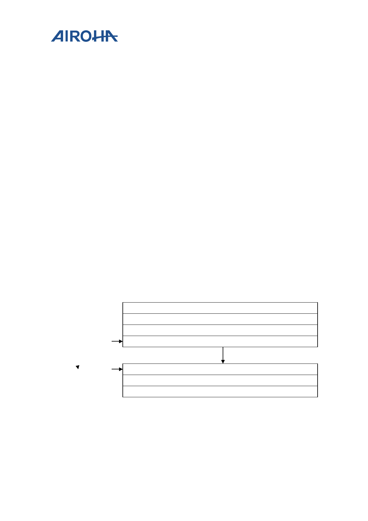
MT2523 Series Reference Manual
© 2015 - 2018 Airoha Technology Corp.
Page 347 of 692
This document contains information that is proprietary to Airoha Technology Corp. (“Airoha”) and/or its licensor(s).
Any unauthorized use, reproduction or disclosure of this document in whole or in part is strictly prohibited.
Typically, the scan line register is divided into 2 parameters (each parameter is 1 byte) and 1 dummy read. To read
the current LCM scan line, software uses the following steps: (assume the LCM is on Serial CS0)
1. Set LCD_TECON.SYNC_MODE = 1 and LCD_TECON.SYNC_EN = 1
2. Set LCD_SYNC_LCM.VTT size to the number of LCM vertical total lines including blanking.
3. Set LCD_SYNC_LCM.HTT to the correct timing parameter. See below “HTT Calibration” section for more
information on this.
4. Set LCD_SYNC_CNT.WAITLINE to the LCM scan line number where you wish to start updating the frame.
5. Start the LCD by setting LCD_START.START = 1 (from 0).
6. Write “read scan line command” to LCD_SCMD0.
7. If the LCM needs a dummy read, then read LCD_SDAT0. This step can be skipped if no dummy read is
required.
8. Read port LCD_SDAT0_SYNC0 to latch the first parameter of LCM current scan line into LCD internal
counter.
9. Read port LCD_SDAT0_SYNC1 to latch the second parameter into the LCM internal counter and begin the
TE counter. SW must use an 8 bit read for this parameter or else the top byte will be covered. If the
interface size is greater then 8/9 bits and there is only 1 parameter to read, the SW may skip step 7 and
only use step 8. In this case, SW may use a 16 or 32 bit read to this port.
In , the LCM has 240 total horizontal lines including blanking. Assume we want LCD to begin updating at Point A
because the partial update begins at this point. In this case, we should set VTT = 240 and WAITLINE = 3. When SW
takes steps 6 and 7 above, assume the returned value is Point B. This means the TE internal counter will count up
to Line 239 and loop back to 0. The counter will count until Point A is reached and then begin updating the LCM.
Note that Line 0 is typically not within the active LCM region.
Figure 23-10. TE Scan Line Example
Point A
Line 0
Line 1
Line 2
Line 3
Line 237
Line 238
Line 239
Point B

MT2523 Series Reference Manual
© 2015 - 2018 Airoha Technology Corp.
Page 348 of 692
This document contains information that is proprietary to Airoha Technology Corp. (“Airoha”) and/or its licensor(s).
Any unauthorized use, reproduction or disclosure of this document in whole or in part is strictly prohibited.
Table 23-2. LCD TE Ports
Name Function
LCD_SDAT*_SYNC0 Latches the first parameter of the LCM current scan line into the TE counter. The
first parameter must be the high byte of the LCM current scan line.
LCD_SDAT*_SYNC1 Latches the second parameter of the LCM current scan line into the TE counter
and begin the counter.
LCD_SDAT*_HTT Read once to begin HTT calculation. Read again to stop the calculation. This can
only be used when LCD is idle.
HTT Calibration
The HTT parameter can be calculated from the LCM datasheet. However, if SW wants a more automatic method to
calculate HTT, then SW can use the HTT timeout interrupt mechanism. The steps are as follows:
1. Make sure LCD is in the IDLE state (LCD_START.START = 0 and LCD_STA = 0).
2. Set HTT = 256.
3. Set LCD_CALC_HTT.TIMEOUT to 128.
4. Enable the HTT timeout interrupt in LCD_INTEN.HTT.
5. Read LCM current scan line and start HTT timeout counter.
5.1 Write “read scan line command” to LCD_SCMD0, or other interface command port depending on
which interface is used.
5.2 If the LCM needs a dummy read, then read LCD_SDAT0. This step can be skipped if no dummy
read is required.
5.3 If there are two parameters of LCM current scan line, read port LCD_SDAT0 to get the first
parameter of LCM current scan line. If there is only one parameter, this step should be skipped.
5.4 Read LCD_SDAT0_HTT to get the second parameter (or to get the only one parameter) of LCM
current scan line and also start HTT timeout counter. Software must use the data read in step 5.3
and 5.4 to construct LCM current scan line.
6. LCD will begin counting cycles. When LCD_CALC_HTT.COUNT reaches LCD_CALC_HTT.TIMEOUT, LCD will
issue the HTT timeout interrupt. Software should do step 5 again to get LCM current scan line and stop
HTT timeout counter..
7. Assume the first scan line read in step5 is SE0 and the second read in step6 is SE1. Then the scanning time
of one line is:
if (SE1>SE0)
Scanning time of one line (in unit of LCD working clock cycle)
= (LCD_CALC_HTT.COUNT*256) / (SE1 – SE0)
else
Scanning time of one line (in unit of LCD working clock cycle)
= (LCD_CALC_HTT.COUNT*256) / (SE1 – SE0 + vertical total lines including blanking)
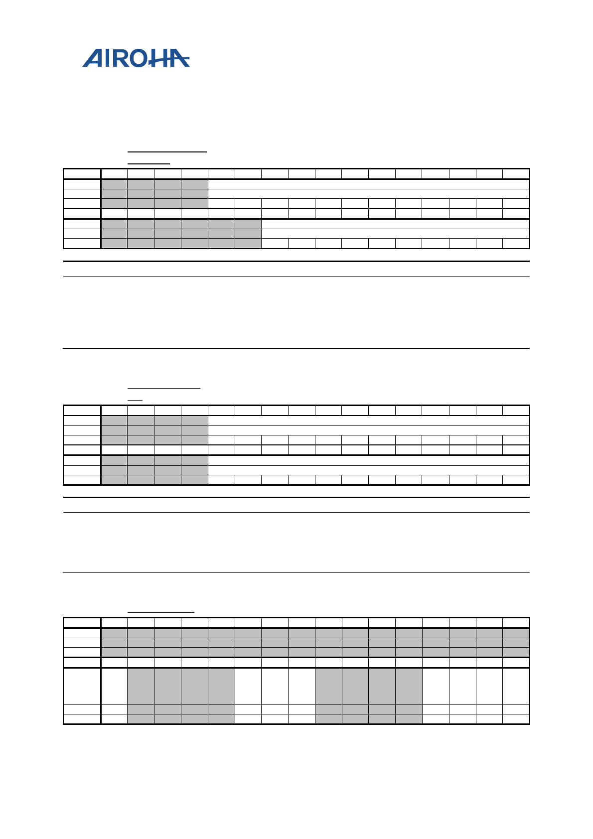
MT2523 Series Reference Manual
© 2015 - 2018 Airoha Technology Corp.
Page 349 of 692
This document contains information that is proprietary to Airoha Technology Corp. (“Airoha”) and/or its licensor(s).
Any unauthorized use, reproduction or disclosure of this document in whole or in part is strictly prohibited.
8. The scanning time of one line can be used in both sync mode 0 and mode 1 by setting
LCD_SYNC_LCM_SIZE.HTT = (Scanning time of one line)/16;
A0450048
LCD_SYNC_LC
M_SIZE
LCD Sync LCM Size Register
00010001
Bit
31
30
29
28
27
26
25
24
23
22
21
20
19
18
17
16
Name
VTT
Type
RW
Reset
0
0
0
0
0
0
0
0
0
0
0
1
Bit
15
14
13
12
11
10
9
8
7
6
5
4
3
2
1
0
Name
HTT
Type
RW
Reset
0
0
0
0
0
0
0
0
0
1
Bit(s)
Mnemonic
Name
Description
27:16
VTT
Vertical Timing
Set the number of horizontal LCM lines including blanking lines. VTT
must be greater than 0.
9:0
HTT
Horizontal Timing
Indicate how long a LCM horizontal line is in unites of 16*T which T is
the LCD cycle time.
A045004C
LCD_SYNC_C
NT
LCD Sync Counter Register
00000001
Bit
31
30
29
28
27
26
25
24
23
22
21
20
19
18
17
16
Name
SCANLINE
Type
RU
Reset
0
0
0
0
0
0
0
0
0
0
0
0
Bit
15
14
13
12
11
10
9
8
7
6
5
4
3
2
1
0
Name
WAITLINE
Type
RW
Reset
0
0
0
0
0
0
0
0
0
0
0
1
Bit(s)
Mnemonic
Name
Description
27:16
SCANLINE
Current TE counter value
11:0
WAITLINE
TE Delay
SCANLINE will count until it reaches this value and a TE interrupt will
be issued (if enabled). LCD will then begin updating a frame.
WAITLINE must be greater than 0.
A0450050
LCD_TECON
LCD Tearing Control Register
00000000
Bit
31
30
29
28
27
26
25
24
23
22
21
20
19
18
17
16
Name
Type
Reset
Bit
15
14
13
12
11
10
9
8
7
6
5
4
3
2
1
0
Name
SW_T
E
TE_C
OUNT
ER_E
N
DSI_
END_
CTL
DSI_S
TART
_CTL
TE_R
EPEA
T
SYNC
_MO
DE
TE_E
DGE_
SEL
SYNC
_EN
Type
RW
RW
RW
RW
RW
RW
RW
RW
Reset
0
0
0
0
0
0
0
0
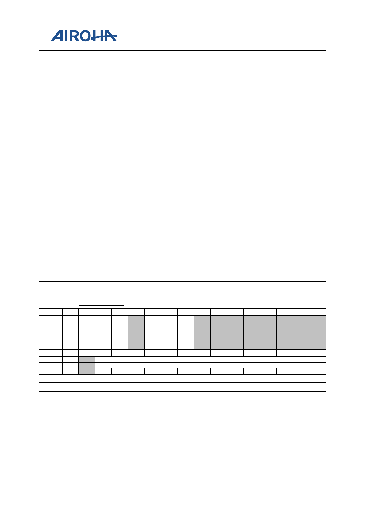
MT2523 Series Reference Manual
© 2015 - 2018 Airoha Technology Corp.
Page 350 of 692
This document contains information that is proprietary to Airoha Technology Corp. (“Airoha”) and/or its licensor(s).
Any unauthorized use, reproduction or disclosure of this document in whole or in part is strictly prohibited.
Bit(s)
Mnemonic
Name
Description
15
SW_TE
Software TE
Software emulated TE signal. Write this bit from 0 to 1 will let LCD act
like a TE signal has been received. This is only used for
SYNC_MODE =
0.
10
TE_COUNTER_EN
The way DSI leaves wait TE state
0: by DSI’s TE signal
1: by LCD’s TE counter
9
DSI_END_CTL
DSI produce eof
0: end indication is by DSI vde falling
1: end indication is by DSI frame done signal
8
DSI_START_CTL
DSI produces sof
0: start byDSI vsync falling
1: start by DSI TE event
3
TE_REPEAT
repeat mode
0: update LCM once every TE signal coming
1: repeat updaing LCM after TE signal coming
2
SYNC_MODE
TE Sync Mode:
Select the TE type to use
(0: LCd working cycle time *16 *HTT *LINES ns)
0: LCD updates when a TE edge is detected and a specified delay has
passed.
1: LCD updates when software read the current LCM scanline and LCD
has counted from the current scanline the specified update scanline.
1
TE_EDGE_SEL
TE Edge Select
Select which edge is used to detect a TE signal
0: Rising edge
1: Falling edge
0
SYNC_EN
Sync Enable
Enable or Disable LCD TE control
0: Disable
1: Enable
A0450080
LCD_ROICON
LCD Region of
Interest Control Register
00000000
Bit
31
30
29
28
27
26
25
24
23
22
21
20
19
18
17
16
Name EN0 EN1 EN2 EN3
COLO
R_EN
IF24
SEND
_RES
_MO
D
Type
RW
RW
RW
RW
RW
RW
RW
Reset
0
0
0
0
0
0
0
Bit
15
14
13
12
11
10
9
8
7
6
5
4
3
2
1
0
Name
ENC
COMMAND
FMT
Type
RW
RW
RW
Reset
0
0
0
0
0
0
0
0
0
0
0
0
0
0
0
Bit(s)
Mnemonic
Name
Description
31
EN0
Layer 0 window enable control
30
EN1
Layer 1 window enable control
29
EN2
Layer 2 window enable control
28
EN3
Layer 3 window enable control
26
COLOR_EN
Enable the data path through mm_color
0: Disable the data path through mm_color
1: Enable the data path through mm_color
25
IF24
24 Bit Data bus Enable:

MT2523 Series Reference Manual
© 2015 - 2018 Airoha Technology Corp.
Page 351 of 692
This document contains information that is proprietary to Airoha Technology Corp. (“Airoha”) and/or its licensor(s).
Any unauthorized use, reproduction or disclosure of this document in whole or in part is strictly prohibited.
Bit(s)
Mnemonic
Name
Description
0: ROI BUS width set to FMT specified width
1: ROI BUS width set to 24 bit width
24
SEND_RES_MOD
Send Residual Odd Pixel
When the LCD Interface is configured to send 2 pixels/cycle or 2
pixels/3 cycles and the ROI width is odd, the last pixel of each line will
not form a pixel pair. If the ROI height is odd as well, the last pixel of
the frame will also not be a pixel pair. In each case, the LCD Interface
will send extra data to fill in for the missing pixel. This setting allows
one to choose how the extra data will be sent.
0: Send the residual odd pixel per frame. In this mode, the last pixel of
a line is combined with an extra byte and sent to LCM. LCD driver
should not care this extra byte.
EX: ROI is 3x2, the output sequence is
R0G0 --- pixel0 of line 0
B0R1
G1B1
R2G2
B2R1 --- LCD driver should not care R1
R0G0 --- pixel 0 of line 1
B0R1
G1B1
R2G2
B2R1 --- LCD driver should not care R1
1: Send the residual odd pixel per frame. In this mode, the last pixel of a
line is combined with the first pixel of the next line as a two-pixel-pair,
and is sent to LCM
EX: ROI is 3x2, the output sequence is
R0G0 --- pixel0 of line 0
B0R1
G1B1
R2G2
B2R0 --- pixel 0 of line 1
G0B0
R1G1
B1R2
G2B2
R0G0 --- pixel 0 of line 2
B0R1
G1B1
R2G2
B2R1 --- LCD driver should not care R1.
15
ENC
Command Transfer Enable Control
0: Only send pixel data to LCM, not send commands in command
queue.
1: Send commands in command queue first, and then send pixel data to
LCM. The number of commands to be sent is specified by COMMAND.
13:8
COMMAND
Number of commands to be sent to LCD module. N means
N+1 commands will be sent. Maximum value is 63.
7:0
FMT
ROI Transfer Format
Specify the interface size and transfer color format of the ROI. The
interface size should match the Parallel/Serial Interface size setting.
FORMAT is divided into several fields:
Bit 0: Sequence (0:BGR, 1: RGB)
Bit 1: Significance
Bit 2: Padding
Bit 5-3: Color format (010: RGB565, 011: RGB666, 100: RGB888)
Bit 7-6: Interface size (00: 8 bit, 01: 16 bit, 10: 9 bit, 11: 18 bit)
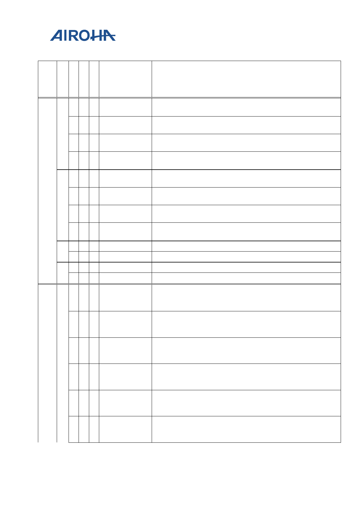
MT2523 Series Reference Manual
© 2015 - 2018 Airoha Technology Corp.
Page 352 of 692
This document contains information that is proprietary to Airoha Technology Corp. (“Airoha”) and/or its licensor(s).
Any unauthorized use, reproduction or disclosure of this document in whole or in part is strictly prohibited.
Table 23-3. WROICON.FORMAT List
format
I/F
width
padding
significance
sequence
throughput
(pixel/cycle)
output
sequence
RGB56
5
8
x
0
0
1pixel/2cycle R4R3R2R1R0G5G4G3
G2G1G0B4B3B2B1B0
x
0
1
1pixel/2cycle B4B3B2B1B0G5G4G3
G2G1G0R4R3R2R1R0
x
1
0
1pixel/2cycle G2G1G0B4B3B2B1B0
R4R3R2R1R0G5G4G3
x
1
1
1pixel/2cycle G2G1G0R4R3R2R1R0
B4B3B2B1B0G5G4G3
9
x
0
0
1pixel/2cycle G3R4R3R2R1R0G5G4G3
B0G2G1G0B4B3B2B1B0
x
0
1
1pixel/2cycle G3B4B3B2B1B0G5G4G3
R0G2G1G0R4R3R2R1R0
x
1
0
1pixel/2cycle B0G2G1G0B4B3B2B1B0
G3R4R3R2R1R0G5G4G3
x
1
1
1pixel/2cycle R0G2G1G0R4R3R2R1R0
G3B4B3B2B1B0G5G4G3
16
x
x
0
1pixel/1cycle R4R3R2R1R0G5G4G3G2G1G0B4B3B2B1B0
x
x
1
1pixel/1cycle B4B3B2B1B0G5G4G3G2G1G0R4R3R2R1R0
18
x
x
0
1pixel/1cycle xxR4R3R2R1R0G5G4G3G2G1G0B4B3B2B1B0
x
x
1
1pixel/1cycle xxB4B3B2B1B0G5G4G3G2G1G0R4R3R2R1R0
RGB66
6
8
0
0
0
1pixel/3cycle
R5R4R3R2R1R0xx
G5G4G3G2G1G0xx
B5B4B3B2B1B0xx
0
0
1
1pixel/3cycle
B5B4B3B2B1B0xx
G5G4G3G2G1G0xx
R5R4R3R2R1R0xx
0
1
0
1pixel/3cycle
B5B4B3B2B1B0xx
G5G4G3G2G1G0xx
R5R4R3R2R1R0xx
0
1
1
1pixel/3cycle
R5R4R3R2R1R0xx
G5G4G3G2G1G0xx
B5B4B3B2B1B0xx
1
0
0
1pixel/3cycle
xxR5R4R3R2R1R0
xxG5G4G3G2G1G0
xxB5B4B3B2B1B0
1
0
1
1pixel/3cycle
xxB5B4B3B2B1B0
xxG5G4G3G2G1G0
xxR5R4R3R2R1R0
MT2523 Series Reference Manual
© 2015 - 2018 Airoha Technology Corp.
Page 353 of 692
This document contains information that is proprietary to Airoha Technology Corp. (“Airoha”) and/or its licensor(s).
Any unauthorized use, reproduction or disclosure of this document in whole or in part is strictly prohibited.
format
I/F
width
padding
significance
sequence
throughput
(pixel/cycle)
output
sequence
1
1
0
1pixel/3cycle
xxB5B4B3B2B1B0
xxG5G4G3G2G1G0
xxR5R4R3R2R1R0
1
1
1
1pixel/3cycle
xxR5R4R3R2R1R0
xxG5G4G3G2G1G0
xxB5B4B3B2B1B0
9
x
0
0
1pixel/2cycle R5R4R3R2R1R0G5G4G3
G2G1G0B5B4B3B2B1B0
x
0
1
1pixel/2cycle B5B4B3B2B1B0G5G4G3
G2G1G0R5R4R3R2R1R0
x
1
0
1pixel/2cycle G2G1G0B5B4B3B2B1B0
R5R4R3R2R1R0G5G4G3
x
1
1
1pixel/2cycle G2G1G0R5R4R3R2R1R0
B5B4B3B2B1B0G5G4G3
RGB66
6
16
0
0
0
2pixel/3cycle
R5R4R3R2R1R0G5G4G3G2G1G0xxxx
B5B4B3B2B1B0R5R4R3R2R1R0xxxx
G5G4G3G2G1G0B5B4B3B2B1B0xxxx
0
0
1
2pixel/3cycle
B5B4B3B2B1B0G5G4G3G2G1G0xxxx
R5R4R3R2R1R0B5B4B3B2B1B0xxxx
G5G4G3G2G1G0R5R4R3R2R1R0xxxx
0
1
0
2pixel/3cycle
G5G4G3G2G1G0B5B4B3B2B1B0xxxx
B5B4B3B2B1B0R5R4R3R2R1R0xxxx
R5R4R3R2R1R0G5G4G3G2G1G0xxxx
0
1
1
2pixel/3cycle
G5G4G3G2G1G0R5R4R3R2R1R0xxxx
R5R4R3R2R1R0B5B4B3B2B1B0xxxx
B5B4B3B2B1B0G5G4G3G2G1G0xxxx
1
0
0
2pixel/3cycle
xxxxR5R4R3R2R1R0G5G4G3G2G1G0
xxxxB5B4B3B2B1B0R5R4R3R2R1R0
xxxxG5G4G3G2G1G0B5B4B3B2B1B0
1
0
1
2pixel/3cycle
xxxxB5B4B3B2B1B0G5G4G3G2G1G0
xxxxR5R4R3R2R1R0B5B4B3B2B1B0
xxxxG5G4G3G2G1G0R5R4R3R2R1R0
1
1
0
2pixel/3cycle
xxxxG5G4G3G2G1G0B5B4B3B2B1B0
xxxxB5B4B3B2B1B0R5R4R3R2R1R0
xxxxR5R4R3R2R1R0G5G4G3G2G1G0
1
1
1
2pixel/3cycle
xxxxG5G4G3G2G1G0R5R4R3R2R1R0
xxxxR5R4R3R2R1R0B5B4B3B2B1B0
xxxxB5B4B3B2B1B0G5G4G3G2G1G0
18
x
x
0
1pixel/1cycle R5R4R3R2R1R0G5G4G3G2G1G0B5B4B3B2B1B0
x
x
1
1pixel/1cycle B5B4B3B2B1B0G5G4G3G2G1G0R5R4R3R2R1R0
24
0
x
0
1pixel/1cycle R5R4R3R2R1R0xxG5G4G3G2G1G0xxB5B4B3B2B1B0xx
MT2523 Series Reference Manual
© 2015 - 2018 Airoha Technology Corp.
Page 354 of 692
This document contains information that is proprietary to Airoha Technology Corp. (“Airoha”) and/or its licensor(s).
Any unauthorized use, reproduction or disclosure of this document in whole or in part is strictly prohibited.
format
I/F
width
padding
significance
sequence
throughput
(pixel/cycle)
output
sequence
0
x
1
1pixel/1cycle B5B4B3B2B1B0xxG5G4G3G2G1G0xx R5R4R3R2R1R0xx
1
x
0
1pixel/1cycle xxR5R4R3R2R1R0xxG5G4G3G2G1G0xxB5B4B3B2B1B0
1
x
1
1pixel/1cycle xxB5B4B3B2B1B0xxG5G4G3G2G1G0xxR5R4R3R2R1R0
RGB88
8 8
x
0
0
1pixel/3cycle
R7R6R5R4R3R2R1R0
G7G6G5G4G3G2G1G0
B7B6B5B4B3B2B1B0
RGB88
8
8
x
0
1
1pixel/3cycle
B7B6B5B4B3B2B1B0
G7G6G5G4G3G2G1G0
R7R6R5R4R3R2R1R0
x
1
0
1pixel/3cycle
B7B6B5B4B3B2B1B0
G7G6G5G4G3G2G1G0
R7R6R5R4R3R2R1R0
x
1
1
1pixel/3cycle
R7R6R5R4R3R2R1R0
G7G6G5G4G3G2G1G0
B7B6B5B4B3B2B1B0
9
x
0
0
1pixel/3cycle
R0R7R6R5R4R3R2R1R0
G0G7G6G5G4G3G2G1G0
B0B7B6B5B4B3B2B1B0
x
0
1
1pixel/3cycle
B0B7B6B5B4B3B2B1B0
G0G7G6G5G4G3G2G1G0
R0R7R6R5R4R3R2R1R0
x
1
0
1pixel/3cycle
B0B7B6B5B4B3B2B1B0
G0G7G6G5G4G3G2G1G0
R0R7R6R5R4R3R2R1R0
x
1
1
1pixel/3cycle
R0R7R6R5R4R3R2R1R0
G0G7G6G5G4G3G2G1G0
B0B7B6B5B4B3B2B1B0
16
x
0
0
2pixel/3cycle
R7R6R5R4R3R2R1R0G7G6G5G4G3G2G1G0
B7B6B5B4B3B2B1B0R7R6R5R4R3R2R1R0
G7G6G5G4G3G2G1G0B7B6B5B4B3B2B1B0
x
0
1
2pixel/3cycle
B7B6B5B4B3B2B1B0G7G6G5G4G3G2G1G0
R7R6R5R4R3R2R1R0B7B6B5B4B3B2B1B0
G7G6G5G4G3G2G1G0R7R6R5R4R3R2R1R0
x
1
0
2pixel/3cycle
G7G6G5G4G3G2G1G0B7B6B5B4B3B2B1B0
B7B6B5B4B3B2B1B0R7R6R5R4R3R2R1R0
R7R6R5R4R3R2R1R0G7G6G5G4G3G2G1G0
RGB88
8
16
x
1
1
2pixel/3cycle
G7G6G5G4G3G2G1G0R7R6R5R4R3R2R1R0
R7R6R5R4R3R2R1R0B7B6B5B4B3B2B1B0
B7B6B5B4B3B2B1B0G7G5G5G4G3G2G1G0
MT2523 Series Reference Manual
© 2015 - 2018 Airoha Technology Corp.
Page 355 of 692
This document contains information that is proprietary to Airoha Technology Corp. (“Airoha”) and/or its licensor(s).
Any unauthorized use, reproduction or disclosure of this document in whole or in part is strictly prohibited.
format
I/F
width
padding
significance
sequence
throughput
(pixel/cycle)
output
sequence
18
x
0
0
2pixel/3cycle
xxR7R6R5R4R3R2R1R0G7G6G5G4G3G2G1G0
xxB7B6B5B4B3B2B1B0R7R6R5R4R3R2R1R0
xxG7G6G5G4G3G2G1G0B7B6B5B4B3B2B1B0
x
0
1
2pixel/3cycle
xxB7B6B5B4B3B2B1B0G7G6G5G4G3G2G1G0
xxR7R6R5R4R3R2R1R0B7B6B5B4B3B2B1B0
xxG7G6G5G4G3G2G1G0R7R6R5R4R3R2R1R0
x
1
0
2pixel/3cycle
xxG7G6G5G4G3G2G1G0B7B6B5B4B3B2B1B0
xxB7B6B5B4B3B2B1B0R7R6R5R4R3R2R1R0
xxR7R6R5R4R3R2R1R0G7G6G5G4G3G2G1G0
x
1
1
2pixel/3cycle
xxG7G6G5G4G3G2G1G0R7R6R5R4R3R2R1R0
xxR7R6R5R4R3R2R1R0B7B6B5B4B3B2B1B0
xxB7B6B5B4B3B2B1B0G7G5G5G4G3G2G1G0
24
x
x
0
1pixel/1cycle R7R6R5R4R3R2R1R0G7G5G5G4G3G2G1G0B7B6B5B4B3B2B1B0
x
x
1
1pixel/1cycle B7B6B5B4B3B2B1B0 G7G5G5G4G3G2G1G0R7R6R5R4R3R2R1R0
Mapping of data order in 2-data-pin protocol with WROICON.FORMAT
General Exp ression
Sequence settin g in LCD _WROICON/Data
written to SIF_SPE_SDAT port D23 D22 D21 D20 D19 D18 D17 D16 D15 D14 D13 D12 D11 D10 D9 D8 D7 D6 D5 D4 D3 D2 D1 D0
Output
sequence in 2-
data-pin
SIF_2PIN_SIZE (I/F
width)
24 LSDA0 A0 D23 D22 D21 D20 D19 D18 D17 D16 D15 D14 D13 D12
LSA0 A0 D11 D10 D9 D8 D7 D6 D5 D4 D3 D2 D1 D0
18 LSDA0 A0 D17 D16 D15 D14 D13 D12 D11 D10 D9
LSA0 A0 D8 D7 D6 D5 D4 D3 D2 D1 D0
16 LSDA0 A0 D15 D14 D13 D12 D11 D10 D9 D8
LSA0 A0 D7 D6 D5 D4 D3 D2 D1 D0
12 LSDA0 A0 D11 D10 D9 D8 D7 D6
LSA0 A0 D5 D4 D3 D2 D1 D0
A0450084
LCD_WROIOF
S
LCD Region of Interest Window Offset
Register
00000000
Bit
31
30
29
28
27
26
25
24
23
22
21
20
19
18
17
16
Name
Y_OFFSET
Type
RW
Reset
0
0
0
0
0
0
0
0
0
0
0
Bit
15
14
13
12
11
10
9
8
7
6
5
4
3
2
1
0
Name
X_OFFSET
Type
RW
Reset
0
0
0
0
0
0
0
0
0
0
0
Bit(s)
Mnemonic
Name
Description
26:16
Y_OFFSET
ROI Window Column Offset, please see figure 13.
10:0
X_OFFSET
ROI Window ROW Offset, please see figure 13.
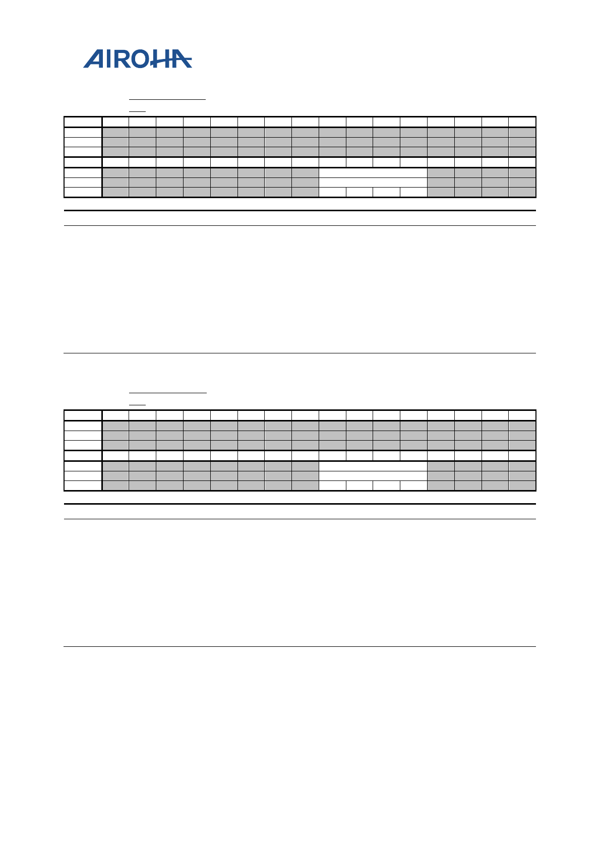
MT2523 Series Reference Manual
© 2015 - 2018 Airoha Technology Corp.
Page 356 of 692
This document contains information that is proprietary to Airoha Technology Corp. (“Airoha”) and/or its licensor(s).
Any unauthorized use, reproduction or disclosure of this document in whole or in part is strictly prohibited.
A0450088
LCD_WROICA
DD
LCD Region of Interest Command Address
Register
00000000
Bit
31
30
29
28
27
26
25
24
23
22
21
20
19
18
17
16
Name
Type
Reset
Bit
15
14
13
12
11
10
9
8
7
6
5
4
3
2
1
0
Name
ADDR
Type
RW
Reset
0
0
0
0
Bit(s)
Mnemonic
Name
Description
7:4
ADDR
LCM Address
There are only 5 possible values that may be set for ADDR:
0h: Commands are sent to LCD-
B LCM CS0 and the A0 bit will be set to
0.
2h: Commands are sent to LCD-
B LCM CS1 and the A0 bit will be set to
0.
4h: Commands are sent to LCD-
B LCM CS2 and the A0 bit will be set to
0.
8h: Commands are sent to LCD-C
LCM CS0 and the A0 bit will be set to
0.
Ah: Commands are sent to LCD-
C LCM CS1 and the A0 bit will be set to
0.
A045008C
LCD_WROIDA
DD
LCD Region of Interest Data Address Register
00000000
Bit
31
30
29
28
27
26
25
24
23
22
21
20
19
18
17
16
Name
Type
Reset
Bit
15
14
13
12
11
10
9
8
7
6
5
4
3
2
1
0
Name
ADDR
Type
RW
Reset
0
0
0
0
Bit(s)
Mnemonic
Name
Description
7:4
ADDR
LCM Address
There are only 5 possible values that may be set for ADDR:
1h: Commands are sent to LCD-
B LCM CS0 and the A0 bit will be set to
1.
3h: Commands are sent to LCD-
B LCM CS1 and the A0 bit will be set to
1.
5h: Commands are sent to LCD-B LCM
CS2 and the A0 bit will be set to
1.
9h: Commands are sent to LCD-
C LCM CS0 and the A0 bit will be set to
1.
Bh: Commands are sent to LCD-
C LCM CS1 and the A0 bit will be set to
1.
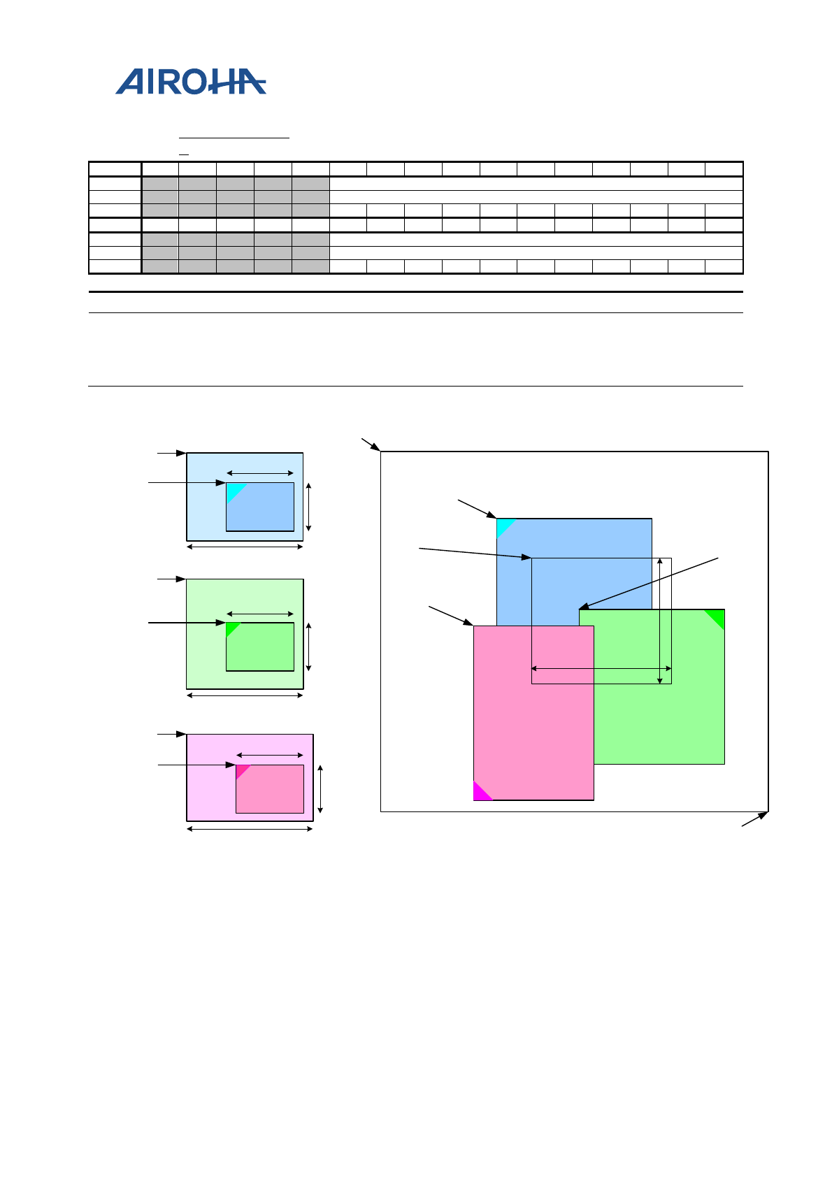
MT2523 Series Reference Manual
© 2015 - 2018 Airoha Technology Corp.
Page 357 of 692
This document contains information that is proprietary to Airoha Technology Corp. (“Airoha”) and/or its licensor(s).
Any unauthorized use, reproduction or disclosure of this document in whole or in part is strictly prohibited.
A0450090
LCD_WROISIZ
E
LCD Region of Interest Size Register
00000000
Bit
31
30
29
28
27
26
25
24
23
22
21
20
19
18
17
16
Name
ROW
Type
RW
Reset
0
0
0
0
0
0
0
0
0
0
0
Bit
15
14
13
12
11
10
9
8
7
6
5
4
3
2
1
0
Name
COL
Type
RW
Reset
0
0
0
0
0
0
0
0
0
0
0
Bit(s)
Mnemonic
Name
Description
26:16
ROW
ROI Window Row Size
Specify the number of rows in the ROI window.
10:0
COL
ROI Window Column Size
Specify the number of columns in the ROI window.
(L0WINOFS.X,
L0WINOFS.Y)
(L1WINOFS.X,
L1WINOFS.Y)
(L3WINOFS.X,
L3WINOFS.Y)
L1WINSIZE.ROW
L1WINSIZE.COL
L0WINSIZE.COL
L0WINSIZE.ROW
L3WINSIZE.ROW
L3WINSIZE.COL
(WROIOFS.X,
WROIOFS.Y)
WROISIZE.ROW
WROISIZE.COL
Layer 1
Layer 3
Layer 0
ROI
L0WINCON.ROTATE = 0
L1WINCON.ROTATE = 3
L3WINCON.ROTATE = 1
L0WINADD
L1WINADD
L3WINADD
Layers in memory Layers in ROI coordinate system
L0WINSIZE.ROW
L0WINSIZE.COL
L1WINSIZE.COL
L1WINSIZE.ROW
L3WINSIZE.ROW
L3WINSIZE.COL
L3WINPITCH
L3WINMOFS
L1WINMOFS
L1WINPITCH
L0WINMOFS
L0WINPITCH
(0,0)
(2047,2047)
Figure 23-11. Layers and ROI setting
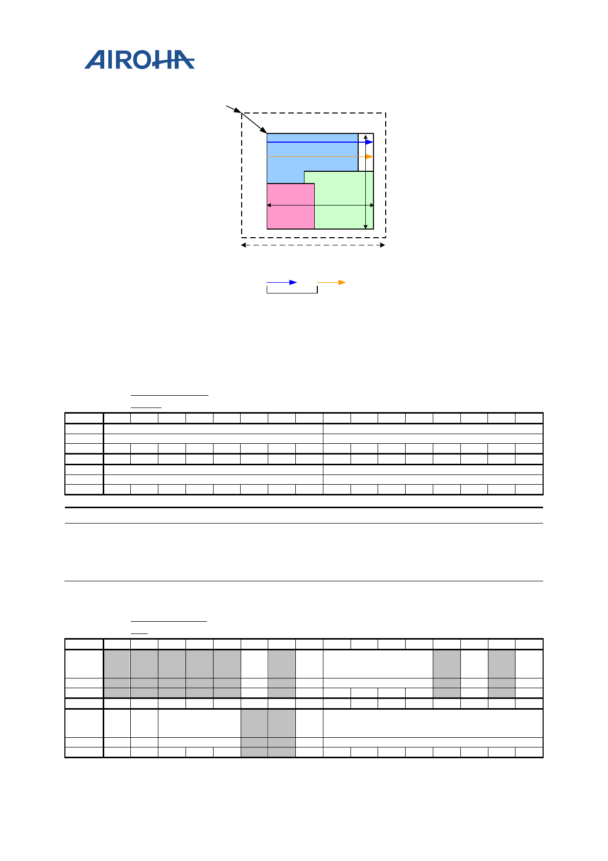
MT2523 Series Reference Manual
© 2015 - 2018 Airoha Technology Corp.
Page 358 of 692
This document contains information that is proprietary to Airoha Technology Corp. (“Airoha”) and/or its licensor(s).
Any unauthorized use, reproduction or disclosure of this document in whole or in part is strictly prohibited.
ROI
row 0
row 1
row 0 row 1
Each row is separated by a pitch when written to memory.
The pitch between each line is specified by WROI_W2M_PITCH
WROI_W2MADD
WROI_W2MOFS
ROI in memory
WROI_W2M_PITCH
WROISIZE.ROW
WROISIZE.COL
Figure 23-12. ROI write to memory setting
A045009C
LCD_WROI_B
GCLR
LCD Region of Interest Background Color
Register
00000000
Bit
31
30
29
28
27
26
25
24
23
22
21
20
19
18
17
16
Name
ALPHA
RED
Type
RW
RW
Reset
0
0
0
0
0
0
0
0
0
0
0
0
0
0
0
0
Bit
15
14
13
12
11
10
9
8
7
6
5
4
3
2
1
0
Name
GREEN
BLUE
Type
RW
RW
Reset
0
0
0
0
0
0
0
0
0
0
0
0
0
0
0
0
Bit(s)
Mnemonic
Name
Description
31:24
ALPHA
Alpha component of ROI window's background color
23:16
RED
Red component of ROI window's background color
15:8
GREEN
Green component of ROI window's background color
7:0
BLUE
Blue component of ROI window's background color
A04500B0
LCD_L0WINC
ON
LCD Layer 0 Window Control Register
00000000
Bit
31
30
29
28
27
26
25
24
23
22
21
20
19
18
17
16
Name
RGB_
SWAP
DST_
KEYE
N
CLRFMT
DITH
ER_E
N
BYTE
_SWA
P
Type
RW
RW
RW
RW
RW
Reset
0
0
0
0
0
0
0
0
Bit
15
14
13
12
11
10
9
8
7
6
5
4
3
2
1
0
Name SRC
SRC_
KEYE
N
ROTATE
ALPH
A_EN
ALPHA
Type
RW
RW
RW
RW
RW
Reset
0
0
0
0
0
0
0
0
0
0
0
0
0
0

MT2523 Series Reference Manual
© 2015 - 2018 Airoha Technology Corp.
Page 359 of 692
This document contains information that is proprietary to Airoha Technology Corp. (“Airoha”) and/or its licensor(s).
Any unauthorized use, reproduction or disclosure of this document in whole or in part is strictly prohibited.
Bit(s)
Mnemonic
Name
Description
26
RGB_SWAP
Swap RGB order of pixel data read from memory.
24
DST_KEYEN
Enable destination color key. If the color format is YUYV422,
this function is not supported.
23:20
CLRFMT
Color format
0000: 8bpp indexed color
0001: RGB565
0010: YUYV422
0011: RGB888
0100: ARGB8888
0101: PARGB8888
0110: XRGB
0111: ARGB6666
1000: PARGB6666
1001: 4bpp index color mode
1010: 2bpp index color mode
1011: 1bpp index color mode
1000: PARGB6666
Others: Reserved
18
DITHER_EN
Enable dithering. Please refer to LCD_DITHERCON
16
BYTE_SWAP
Swap high byte and low byte of pixel data read from memory.
15
SRC
Disable auot-increment of the source pixel address. It makes
the value of each pixel is the same as the first pixel of this
frame. It is just for debug.
14
SRC_KEYEN
Enable source color key. If the color format is YUYV422, this
function is not supported
13:11
ROTATE
Rotation configuration
000: no rotation
001: 90 degree rotation (counterclockwise, single request only)
010: 180 degree rotation (counterclockwise)
011: 270 degree rotation (counterclockwise, single request only)
100: Horizontal flip
101: Horizontal flip then 90 degree rotation (counterclockwise, single
request only)
110: Horizontal flip then 180 degree rotation (counterclockwise)
111: Horizontal flip then 270 degree rotation (counterclockwise, single
request only)
8
ALPHA_EN
Enable alpha blending
7:0
ALPHA
Constant alpha value
Note: SRC_KEYEN and DST_KEYEN are exclusive setting. They can’t be enabled at the same time.
RGB_SWP Swap RGB order of pixel data read from memory
MT2523 Series Reference Manual
© 2015 - 2018 Airoha Technology Corp.
Page 360 of 692
This document contains information that is proprietary to Airoha Technology Corp. (“Airoha”) and/or its licensor(s).
Any unauthorized use, reproduction or disclosure of this document in whole or in part is strictly prohibited.
Figure 23-13. Layer source RGB format
The byte order in memory of YUYV422 is described in . Y0 is the Y component of the first pixel, P0. Y1 is the Y
component of the second pixel, P1.
Figure 23-14. YUYV422 byte order in memory
Note: When use YUYV422 mode, the pitch of this layer (LCD_LxWINPITCH) must be even, and the base address
(LCD_LxWINADD) of this layer also must be 4-byte aligned. Source color key and destination color key are NOT
supported in YUYV422 mode.
RGB888
XRGB
PARGB
ARGB
RGB565
RGB_SWP=1
BYTE_SWP=1
RGB_SWP=0
BYTE_SWP=0
071523
X
31
RGB
PR PG PB
071523
A
31
RGB
071523
A
31
RG B
071523
GB
0
R
15 7
RGB_SWP=1
BYTE_SWP=0
G R
0
B
15 7
BGR
071523
R
G
B
071523
A
31
PR
PG
PB
071523
A
31
071523
B
31
GR
X
RGB_SWP=0
BYTE_SWP=1
BGR
071523
071523
B
31
GRX
PG PR A
071523
PB
31
07152331
GRA
B
R
0
B
15 7
07152331
RGBA
07152331
PR PG PB A
07152331
B
G
R X
071523
B
G
R
015 7
BR
G
5B
4
015 7
R
4G
4G
3G
2G
1G
0B
3B
2B
1B
0
R
3R
2R
1R
0G
5
B
4
015 7
R
4G
4G
3
G
2G
1G
0B
3B
2B
1B
0R
3R
2R
1R
0G
5
B
4
015 7
R
4
G
4G
3G
2G
1G
0
B
3B
2B
1B
0R
3R
2R
1R
0
015 7
R
4
G
2G
1G
0R
3R
2R
1R
0G
5
B
4G
4G
3
B
3B
2B
1B
0
U
V
Y
0
Y
1
0
1
2
3
P
0
P
1
image of this layer
byte order in memory

MT2523 Series Reference Manual
© 2015 - 2018 Airoha Technology Corp.
Page 361 of 692
This document contains information that is proprietary to Airoha Technology Corp. (“Airoha”) and/or its licensor(s).
Any unauthorized use, reproduction or disclosure of this document in whole or in part is strictly prohibited.
Note: If color depth is YUYV422, the YUYV422 source will be translated to RGB domain and then overlaid. The YUV
to RGB transformation is following the equations.
The alpha blending formula is selected by source color format automatically.
If source color format is RGB565, RGB888 or YUYV422 then the alpha blending formula is
SCA;
+ 0xff /
)SCA
-
(0xff
*
dst.a = dst.a
0xff;SCA / * src.b + 0xff / )SCA - (0xff * dst.b = dst.b
0xff;SCA / * src.g + 0xff / )SCA - (0xff * dst.g = dst.g
0xff;SCA / *src.r + 0xff / )SCA - (0xff *dst.r =dst.r
If source color format is PARGB then the alpha blending formula is
}
src.a +
0xff / ) src.a
- (0xff *
dst.a = dst.a
src.b;
+ 0xff / ) src.a
- (0xff
* dst.b
= dst.b
src.g; +
0xff / ) src.a
- (0xff
* dst.g
= dst.g
src.r;
+ 0xff /
) src.a -
(0xff *dst.r
=dst.r
0xff SCA //
{ else
}
0xff;SCA / * src.a + 0xff / 0xff)SCA /
* src.a
- (0xff * dst.a = dst.a
0xff;SCA / * src.b
+ 0xff
/ 0xff)SCA /
* src.a
- (0xff
*
dst.b =
dst.b
0xff;SCA / * src.g + 0xff / 0xff)SCA /
* src.a
- (0xff * dst.g = dst.g
0xff;SCA /
*src.r +
0xff /
0xff)SCA /
* src.a
- (0xff
*dst.r
=dst.r
{ 0xff) !SCA
( if
==
=
If source color format is ARGB then the alpha blending formula is
−
−
•
−−×=
128
128
05732
231132
45032
32
1
V
U
Y
B
G
R

MT2523 Series Reference Manual
© 2015 - 2018 Airoha Technology Corp.
Page 362 of 692
This document contains information that is proprietary to Airoha Technology Corp. (“Airoha”) and/or its licensor(s).
Any unauthorized use, reproduction or disclosure of this document in whole or in part is strictly prohibited.
}
src.a;
+
0xff
/
)
src.a
-
(0xff
*
dst.a
=
dst.a
0xff; / src.a * src.b + 0xff / )
src.a
-
(0xff
*
dst.b =dst.r
0xff; / src.a
*
src.g
+
0xff
/
)
src.a
-
(0xff
*
dst.g = dst.g
0xff;
/
src.a
*src.r
+
0xff /
)
src.a
-
(0xff
*
dst.r =dst.r
0xff
=SCA
if
0xff
SCA // { else }
0xff;SCA / * src.a + 0xff / 0xff)
SCA /
*
src.a
-
(0xff
*
dst.a = dst.a
0xff;SCA / * 0xff / src.a *
src.b
+
0xff
/
0xff)SCA /
*
src.a
-
(0xff
*
dst.b = dst.b
0xff;SCA /
*
0xff /
src.a
*
src.g
+
0xff /
0xff)SCA /
*
src.a
-
(0xff
*
dst.g = dst.g
0xff;
SCA /
*
0xff /
src.a
*
src.r
+
0xff
/ 0xff)
SCA /
*
src.a
-
(0xff
*
dst.r
=dst.r
{
)
0xff
!SCA ( if
==
=
src.r, src.g, src.b, and src.a are this layer’s pixel value.
dst.r, dst.r, dst.b, and dst.a are the result of alpha blending of all lower layers.
Note: SCA is the source constant alpha specified by LCD_L0WINCON.ALPHA.
Alpha blending hardware approximation:
If source color format is RGB565, RGB888 or YUYV422 then the hardware implements the following equation to
approximate the above equation of 8-bit index color, RGB565, RGB888 or YUYV422. Only list red channel, other
channels are the same.
tmp.asrc.adst'.a
88)tmp_d.a(tmp_d.atmp.a
128SCA)-(255dst.atmp_d.a
8;8)tmp.rtmp.r(dst'.r
128;
dst.r*552dst.r)-(src.rSCAtmp.r
+=
>>>>+
=
+×
=
>>>>+=
++×=
If source color format is PARGB then the hardware implements the following equation to approximate the above
equation of PARGB. Only list red channel, others are the same.

MT2523 Series Reference Manual
© 2015 - 2018 Airoha Technology Corp.
Page 363 of 692
This document contains information that is proprietary to Airoha Technology Corp. (“Airoha”) and/or its licensor(s).
Any unauthorized use, reproduction or disclosure of this document in whole or in part is strictly prohibited.
}
tmp.rsrc.rdst'.r
88)tmp_d.r(tmp_d.r tmp.r
128src.a)-(255dst.rr tmp_d.
0xff SCA // { else }
tmp.rsrc'.rdst'.r
88)tmp_d.r(tmp_d.r tmp.r
128src'.a)-(255dst.rr tmp_d.
88)tmp_s.r(tmp_s.rsrc'.r
128SCAsrc.rr tmp_s.
88)tmp_s.a(tmp_s.asrc'.a
128SCAsrc.aa tmp_s.
{ ) 0xff !SCA ( if
+=
>>>>+=
+×=
==
+=
>>>>+=
+×=
>>>>+=
+×=
>>>>+=
+×=
=
If source color format is ARGB then the hardware implements the following equation to approximate the above
equation of ARGB. Only list red and alpha channels, others are the same.
}
8;8)tmp.rtmp.r(dst'.r
128;dst.r*552dst.r)-(src.rsrc.a tmp.r
tmp.a;src.adst'.a
8;8)tmp_d.a(tmp_d.a tmp.a
128;src.a)-(255dst.aa tmp_d.
0xff SCA // { else }
8;8)tmp.rtmp.r(dst'.r
128;dst.r*552dst.r)-(src.rsrc'.a tmp.r
tmp.a;src'.adst'.a
8;8)tmp_d.a(tmp_d.a tmp.a
128;src'.a)-(255dst.aa tmp_d.
8;8)tmp_s.a(tmp_s.asrc'.a
128;SCAsrc.aa tmp_s.
{ ) 0xff !SCA ( if
>>>>+=
++×=
+=
>>>>+=
+×=
==
>>>>+=
++×=
+=
>>>>+=
+×=
>>>>+=
+×=
=
Effect Ordering: Each layer has many effects which can be turned on concurrently. The order the effects are
applied are as follows:
1. Memory Offset and Pitch are first used to determine which part of the layer in memory to display.
2. If turned on, a scroll effect is then applied.
3. Rotation is applied to the layer.
4. Finally, swap and dither are applied in this order
5. The layer is alpha blended with previous layers and/or the ROI background.
6. The ROI output is sent to the LCM and/or memory in the color format set by the corresponding register.

MT2523 Series Reference Manual
© 2015 - 2018 Airoha Technology Corp.
Page 364 of 692
This document contains information that is proprietary to Airoha Technology Corp. (“Airoha”) and/or its licensor(s).
Any unauthorized use, reproduction or disclosure of this document in whole or in part is strictly prohibited.
A04500B4
LCD_L0WINK
EY
LCD Layer 0 Color Key Register
00000000
Bit
31
30
29
28
27
26
25
24
23
22
21
20
19
18
17
16
Name
CLRKEY[31:16]
Type
RW
Reset
0
0
0
0
0
0
0
0
0
0
0
0
0
0
0
0
Bit
15
14
13
12
11
10
9
8
7
6
5
4
3
2
1
0
Name
CLRKEY[15:0]
Type
RW
Reset
0
0
0
0
0
0
0
0
0
0
0
0
0
0
0
0
Bit(s)
Mnemonic
Name
Description
31:0
CLRKEY
The source color key or destination key, which depends on
LCD_L0WINCON.SRC_KEYEN or
LCD_L0WINCON.DST_KEYEN
A04500B8
LCD_L0WINO
FS
LCD
Layer 0 Window Display Offset Register
00000000
Bit
31
30
29
28
27
26
25
24
23
22
21
20
19
18
17
16
Name
Y_OFFSET
Type
RW
Reset
0
0
0
0
0
0
0
0
0
0
0
Bit
15
14
13
12
11
10
9
8
7
6
5
4
3
2
1
0
Name
X_OFFSET
Type
RW
Reset
0
0
0
0
0
0
0
0
0
0
0
Bit(s)
Mnemonic
Name
Description
26:16
Y_OFFSET
Layer 0 Window Column Offset, please see figure 13.
10:0
X_OFFSET
Layer 0 Window ROW Offset, please see figure 13.
A04500BC
LCD_L0WINA
DD
LCD Layer 0 Window Display Start Address
Register
00000000
Bit
31
30
29
28
27
26
25
24
23
22
21
20
19
18
17
16
Name
ADDR[31:16]
Type
RW
Reset
0
0
0
0
0
0
0
0
0
0
0
0
0
0
0
0
Bit
15
14
13
12
11
10
9
8
7
6
5
4
3
2
1
0
Name
ADDR[15:0]
Type
RW
Reset
0
0
0
0
0
0
0
0
0
0
0
0
0
0
0
0
Bit(s)
Mnemonic
Name
Description
31:0
ADDR
Layer 0 source start address (byte address), please see Figure
13. The address must be aligned to layer color depth
boundary as Table 6. The LCD has a special function to use
the LCM as a layer's frame buffer.
MT2523 Series Reference Manual
© 2015 - 2018 Airoha Technology Corp.
Page 365 of 692
This document contains information that is proprietary to Airoha Technology Corp. (“Airoha”) and/or its licensor(s).
Any unauthorized use, reproduction or disclosure of this document in whole or in part is strictly prohibited.
Table 23-4. Layer address alignment constraint
LCD_L0WINCON.CLRFMT Color format ADDR alignment
0001 RGB565 2 bytes alignment
0100/0101, ARGB8888/ PRGB8888 4 bytes alignment
0011 RGB888 no alignment constraint
0010 YUYV422 4 bytes alignment
0000 8bpp index color mode 4 bytes alignment
1001 4bpp index color mode 4 bytes alignment
1010 2bpp index color mode 4 bytes alignment
1011 1bpp index color mode 4 bytes alignment
A04500C0
LCD_L0WINSI
ZE
LCD Layer 0 Window Size
00000000
Bit
31
30
29
28
27
26
25
24
23
22
21
20
19
18
17
16
Name
ROW
Type
RW
Reset
0
0
0
0
0
0
0
0
0
0
0
Bit
15
14
13
12
11
10
9
8
7
6
5
4
3
2
1
0
Name
COLUMN
Type
RW
Reset
0
0
0
0
0
0
0
0
0
0
0
Bit(s)
Mnemonic
Name
Description
26:16
ROW
Layer 0 Window Row Size in unit of pixel, please see Figure
13.
10:0
COLUMN
Layer 0 Window Column Size in unit of pixel, please see
Figure 13.
A04500C8
LCD_L0WINM
OFS
LCD Layer 0 Memory Offset
00000000
Bit
31
30
29
28
27
26
25
24
23
22
21
20
19
18
17
16
Name
Y_OFFSET
Type
RW
Reset
0
0
0
0
0
0
0
0
0
0
0
Bit
15
14
13
12
11
10
9
8
7
6
5
4
3
2
1
0
Name
X_OFFSET
Type
RW
Reset
0
0
0
0
0
0
0
0
0
0
0
Bit(s)
Mnemonic
Name
Description
26:16
Y_OFFSET
Layer 0 Window Column Offset, please see figure 13.
10:0
X_OFFSET
Layer 0 Window ROW Offset, please see figure 13.
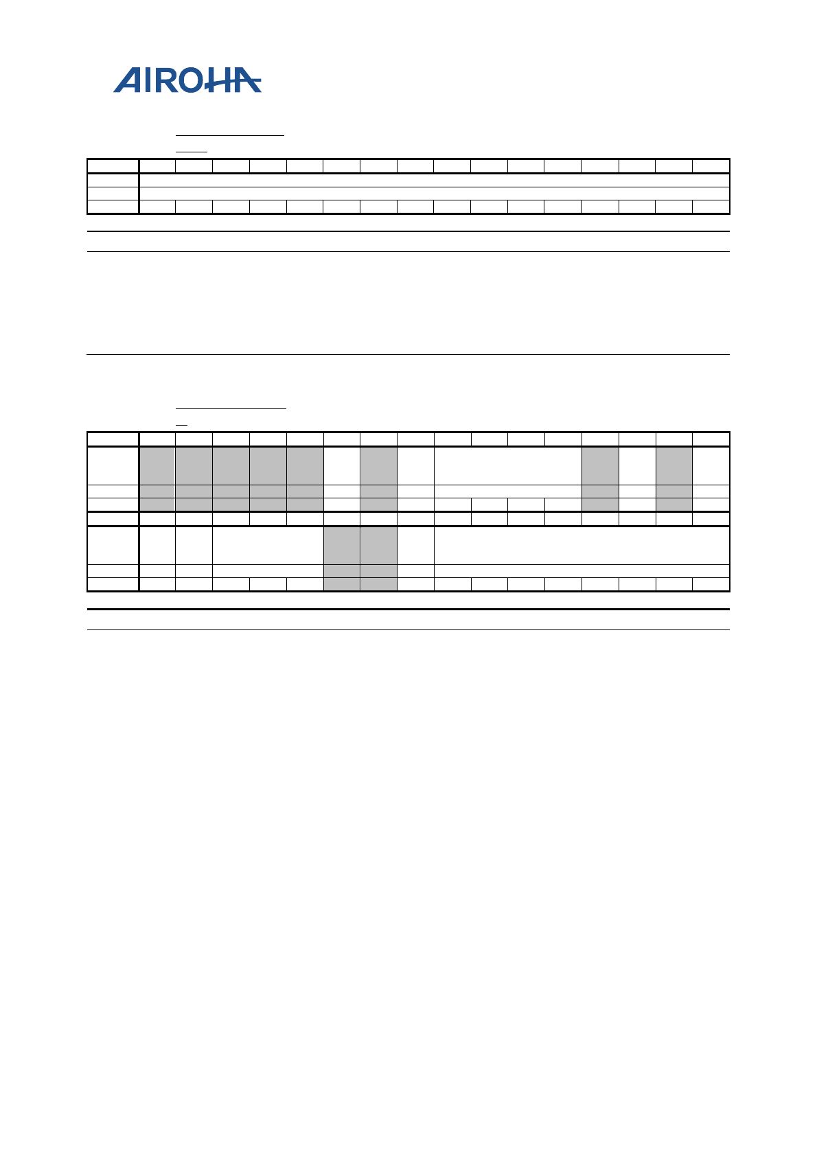
MT2523 Series Reference Manual
© 2015 - 2018 Airoha Technology Corp.
Page 366 of 692
This document contains information that is proprietary to Airoha Technology Corp. (“Airoha”) and/or its licensor(s).
Any unauthorized use, reproduction or disclosure of this document in whole or in part is strictly prohibited.
A04500CC
LCD_L0WINPI
TCH
LCD Layer 0 Memory Pitch
0000
Bit
15
14
13
12
11
10
9
8
7
6
5
4
3
2
1
0
Name
PITCH
Type
RW
Reset
0
0
0
0
0
0
0
0
0
0
0
0
0
0
0
0
Bit(s)
Mnemonic
Name
Description
15:0
PITCH
Layer 0 Memory Pitch in unit of byte, please see Figure 13.
This should be set to the total width of the image in memory
times the number of bytes per pixel. For 4 bpp color depth
settings, the pitch must be a multple of 4. For 2 bpp color
depth settings, the pitch must be a multiple of 2. For 3 bpp
(RGB888) color depth settings, the pitch may be a multiple of
any number
A04500E0
LCD_L1WINCO
N
LCD Layer 1 Window Control
Register
00000000
Bit
31
30
29
28
27
26
25
24
23
22
21
20
19
18
17
16
Name
RGB_
SWAP
DST_
KEYE
N
CLRFMT
DITH
ER_E
N
BYTE
_SWA
P
Type
RW
RW
RW
RW
RW
Reset
0
0
0
0
0
0
0
0
Bit
15
14
13
12
11
10
9
8
7
6
5
4
3
2
1
0
Name SRC
SRC_
KEYE
N
ROTATE
ALPH
A_EN
ALPHA
Type
RW
RW
RW
RW
RW
Reset
0
0
0
0
0
0
0
0
0
0
0
0
0
0
Bit(s)
Mnemonic
Name
Description
26
RGB_SWAP
24
DST_KEYEN
23:20
CLRFMT
Color format
0000: 8bpp indexed color
0001: RGB565
0010: YUYV422
0011: RGB888
0100: ARGB8888
0101: PARGB8888
0110: XRGB
0111: ARGB6666
1000: PARGB6666
1001: 4bpp index color mode
1010: 2bpp index color mode
1011: 1bpp index color mode
1000: PARGB6666
Others: Reserved
18
DITHER_EN
16
BYTE_SWAP
15
SRC
Disable auot-increment of the source pixel address. It makes
the value of each pixel is the same as the first pixel of this
frame. It is just for debug.
14
SRC_KEYEN
13:11
ROTATE
Rotation configuration
000: no rotation
MT2523 Series Reference Manual
© 2015 - 2018 Airoha Technology Corp.
Page 367 of 692
This document contains information that is proprietary to Airoha Technology Corp. (“Airoha”) and/or its licensor(s).
Any unauthorized use, reproduction or disclosure of this document in whole or in part is strictly prohibited.
Bit(s)
Mnemonic
Name
Description
001: 90 degree rotation (counterclockwise, single request only)
010: 180 degree rotation (counterclockwise)
011: 270 degree rotation (counterclockwise, single request only)
100: Horizontal flip
101: Horizontal flip then 90 degree rotation (counterclockwise, single
request only)
110: Horizontal flip then 180 degree rotation (counterclockwise)
111: Horizontal flip then 270 degree rotation (counterclockwise, single
request only)
8
ALPHA_EN
Enable alpha blending
7:0
ALPHA
Constant alpha value
A04500E4
LCD_L1WINKE
Y
LCD
Layer 1 Color Key Register
00000000
Bit
31
30
29
28
27
26
25
24
23
22
21
20
19
18
17
16
Name
CLRKEY[31:16]
Type
RW
Reset
0
0
0
0
0
0
0
0
0
0
0
0
0
0
0
0
Bit
15
14
13
12
11
10
9
8
7
6
5
4
3
2
1
0
Name
CLRKEY[15:0]
Type
RW
Reset
0
0
0
0
0
0
0
0
0
0
0
0
0
0
0
0
Bit(s)
Mnemonic
Name
Description
31:0
CLRKEY
The source color key or destination key, which depends on
LCD_L1WINCON.SRC_KEYEN or
LCD_L1WINCON.DST_KEYEN
A04500E8
LCD_L1WINOF
S
LCD Layer 1 Window
Display Offset Register
00000000
Bit
31
30
29
28
27
26
25
24
23
22
21
20
19
18
17
16
Name
Y_OFFSET
Type
RW
Reset
0
0
0
0
0
0
0
0
0
0
0
Bit
15
14
13
12
11
10
9
8
7
6
5
4
3
2
1
0
Name
X_OFFSET
Type
RW
Reset
0
0
0
0
0
0
0
0
0
0
0
Bit(s)
Mnemonic
Name
Description
26:16
Y_OFFSET
Layer 1 Window Column Offset, please see figure 13.
10:0
X_OFFSET
Layer 1 Window ROW Offset, please see figure 13.
A04500EC
LCD_L1WINA
DD
LCD Layer 1
Window Display Start Address
Register
00000000
Bit
31
30
29
28
27
26
25
24
23
22
21
20
19
18
17
16
Name
ADDR[31:16]
Type
RW
Reset
0
0
0
0
0
0
0
0
0
0
0
0
0
0
0
0
Bit
15
14
13
12
11
10
9
8
7
6
5
4
3
2
1
0
Name
ADDR[15:0]
Type
RW
Reset
0
0
0
0
0
0
0
0
0
0
0
0
0
0
0
0
MT2523 Series Reference Manual
© 2015 - 2018 Airoha Technology Corp.
Page 368 of 692
This document contains information that is proprietary to Airoha Technology Corp. (“Airoha”) and/or its licensor(s).
Any unauthorized use, reproduction or disclosure of this document in whole or in part is strictly prohibited.
Bit(s)
Mnemonic
Name
Description
31:0
ADDR
Layer 1 source start address (byte address), please see Figure
13. The address must be aligned to layer color depth
boundary as Table 6. The LCD has a special function to use
the LCM as a layer's frame buffer.
A04500F0
LCD_L1WINSI
ZE
LCD Layer 1 Window Size
00000000
Bit
31
30
29
28
27
26
25
24
23
22
21
20
19
18
17
16
Name
ROW
Type
RW
Reset
0
0
0
0
0
0
0
0
0
0
0
Bit
15
14
13
12
11
10
9
8
7
6
5
4
3
2
1
0
Name
COLUMN
Type
RW
Reset
0
0
0
0
0
0
0
0
0
0
0
Bit(s)
Mnemonic
Name
Description
26:16
ROW
Layer 1 Window Row Size in unit of pixel, please see Figure
13.
10:0
COLUMN
Layer 1 Window Column Size in unit of pixel, please see
Figure 13.
A04500F8
LCD_L1WINM
OFS
LCD Layer 1 Memory Offset
00000000
Bit
31
30
29
28
27
26
25
24
23
22
21
20
19
18
17
16
Name
Y_OFFSET
Type
RW
Reset
0
0
0
0
0
0
0
0
0
0
0
Bit
15
14
13
12
11
10
9
8
7
6
5
4
3
2
1
0
Name
X_OFFSET
Type
RW
Reset
0
0
0
0
0
0
0
0
0
0
0
Bit(s)
Mnemonic
Name
Description
26:16
Y_OFFSET
Layer 1 Window Column Offset, please see figure 13.
10:0
X_OFFSET
Layer 1 Window ROW Offset, please see figure 13.
A04500FC
LCD_L1WINPI
TCH
LCD Layer 1 Memory Pitch
0000
Bit
15
14
13
12
11
10
9
8
7
6
5
4
3
2
1
0
Name
PITCH
Type
RW
Reset
0
0
0
0
0
0
0
0
0
0
0
0
0
0
0
0
Bit(s)
Mnemonic
Name
Description
15:0
PITCH
Layer 1 Memory Pitch in unit of byte, please see Figure 13.
This should be set to the total width of the image in memory
times the number of bytes per pixel. For 4 bpp color depth
settings, the pitch must be a multple of 4. For 2 bpp color
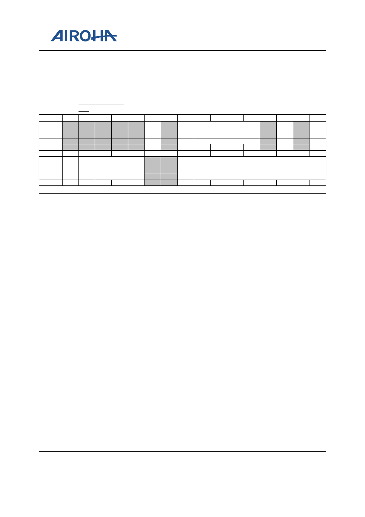
MT2523 Series Reference Manual
© 2015 - 2018 Airoha Technology Corp.
Page 369 of 692
This document contains information that is proprietary to Airoha Technology Corp. (“Airoha”) and/or its licensor(s).
Any unauthorized use, reproduction or disclosure of this document in whole or in part is strictly prohibited.
Bit(s)
Mnemonic
Name
Description
depth settings, the pitch must be a multiple of 2. For 3 bpp
(RGB888) color depth settins, the pitch may be a multiple of
any number
A0450110
LCD_L2WINC
ON
LCD Layer 2 Window Control Register
00000000
Bit
31
30
29
28
27
26
25
24
23
22
21
20
19
18
17
16
Name
RGB_
SWAP
DST_
KEYE
N
CLRFMT
DITH
ER_E
N
BYTE
_SWA
P
Type
RW
RW
RW
RW
RW
Reset
0
0
0
0
0
0
0
0
Bit
15
14
13
12
11
10
9
8
7
6
5
4
3
2
1
0
Name SRC
SRC_
KEYE
N
ROTATE
ALPH
A_EN
ALPHA
Type
RW
RW
RW
RW
RW
Reset
0
0
0
0
0
0
0
0
0
0
0
0
0
0
Bit(s)
Mnemonic
Name
Description
26
RGB_SWAP
24
DST_KEYEN
23:20
CLRFMT
Color format
0000: 8bpp indexed color
0001: RGB565
0010: YUYV422
0011: RGB888
0100: ARGB8888
0101: PARGB8888
0110: XRGB
0111: ARGB6666
1000: PARGB6666
1001: 4bpp index color mode
1010: 2bpp index color mode
1011: 1bpp index color mode
1000: PARGB6666
Others: Reserved
18
DITHER_EN
16
BYTE_SWAP
15
SRC
Disable auot-increment of the source pixel address. It makes
the value of each pixel is the same as the first pixel of this
frame. It is just for debug.
14
SRC_KEYEN
13:11
ROTATE
Rotation configuration
000: no rotation
001: 90 degree rotation (counterclockwise, single request only)
010: 180 degree rotation (counterclockwise)
011: 270 degree rotation (counterclockwise, single request only)
100: Horizontal flip
101: Horizontal flip then 90 degree rotation (counterclockwise, single
reqest only)
110: Horizontal flip then 180 degree rotation (counterclockwise)
111: Horizontal flip then 270 degree rotation (counterclockwise, single
request only)
8
ALPHA_EN
Enable alpha blending
7:0
ALPHA
Constant alpha value
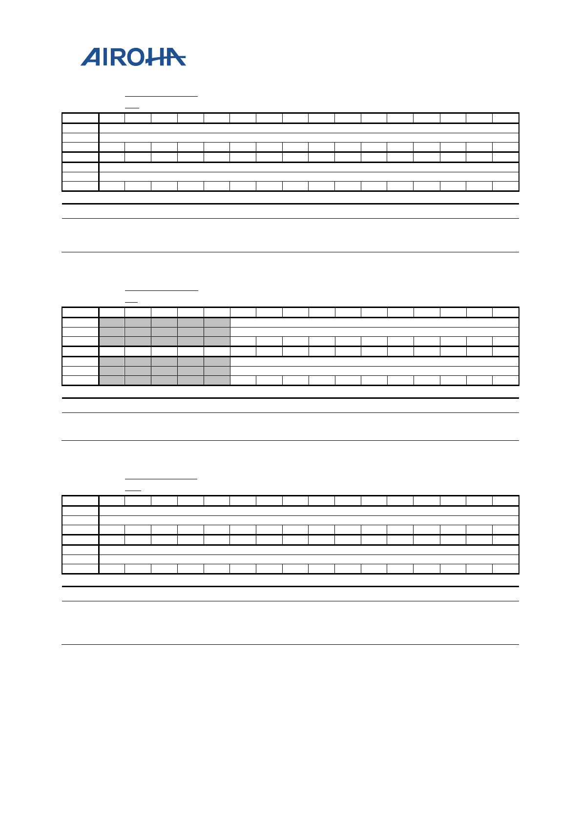
MT2523 Series Reference Manual
© 2015 - 2018 Airoha Technology Corp.
Page 370 of 692
This document contains information that is proprietary to Airoha Technology Corp. (“Airoha”) and/or its licensor(s).
Any unauthorized use, reproduction or disclosure of this document in whole or in part is strictly prohibited.
A0450114
LCD_L2WINK
EY
LCD Layer 2 Color
Key Register
00000000
Bit
31
30
29
28
27
26
25
24
23
22
21
20
19
18
17
16
Name
CLRKEY[31:16]
Type
RW
Reset
0
0
0
0
0
0
0
0
0
0
0
0
0
0
0
0
Bit
15
14
13
12
11
10
9
8
7
6
5
4
3
2
1
0
Name
CLRKEY[15:0]
Type
RW
Reset
0
0
0
0
0
0
0
0
0
0
0
0
0
0
0
0
Bit(s)
Mnemonic
Name
Description
31:0
CLRKEY
The source color key or destination key, which depends on
LCD_L2WINCON.SRC_KEYEN or
LCD_L2WINCON.DST_KEYEN
A0450118
LCD_L2WINO
FS
LCD Layer 2 Window Display Offset
Register
00000000
Bit
31
30
29
28
27
26
25
24
23
22
21
20
19
18
17
16
Name
Y_OFFSET
Type
RW
Reset
0
0
0
0
0
0
0
0
0
0
0
Bit
15
14
13
12
11
10
9
8
7
6
5
4
3
2
1
0
Name
X_OFFSET
Type
RW
Reset
0
0
0
0
0
0
0
0
0
0
0
Bit(s)
Mnemonic
Name
Description
26:16
Y_OFFSET
Layer 2 Window Column Offset, please see figure 13.
10:0
X_OFFSET
Layer 2 Window ROW Offset, please see figure 13.
A045011C
LCD_L2WINA
DD
LCD Layer 2 Window
Display Start Address
Register
00000000
Bit
31
30
29
28
27
26
25
24
23
22
21
20
19
18
17
16
Name
ADDR[31:16]
Type
RW
Reset
0
0
0
0
0
0
0
0
0
0
0
0
0
0
0
0
Bit
15
14
13
12
11
10
9
8
7
6
5
4
3
2
1
0
Name
ADDR[15:0]
Type
RW
Reset
0
0
0
0
0
0
0
0
0
0
0
0
0
0
0
0
Bit(s)
Mnemonic
Name
Description
31:0
ADDR
Layer 2 source start address (byte address), please see Figure
13. The address must be aligned to layer color depth
boundary as Table 6. The LCD has a special function to use
the LCM as a layer's frame buffer.
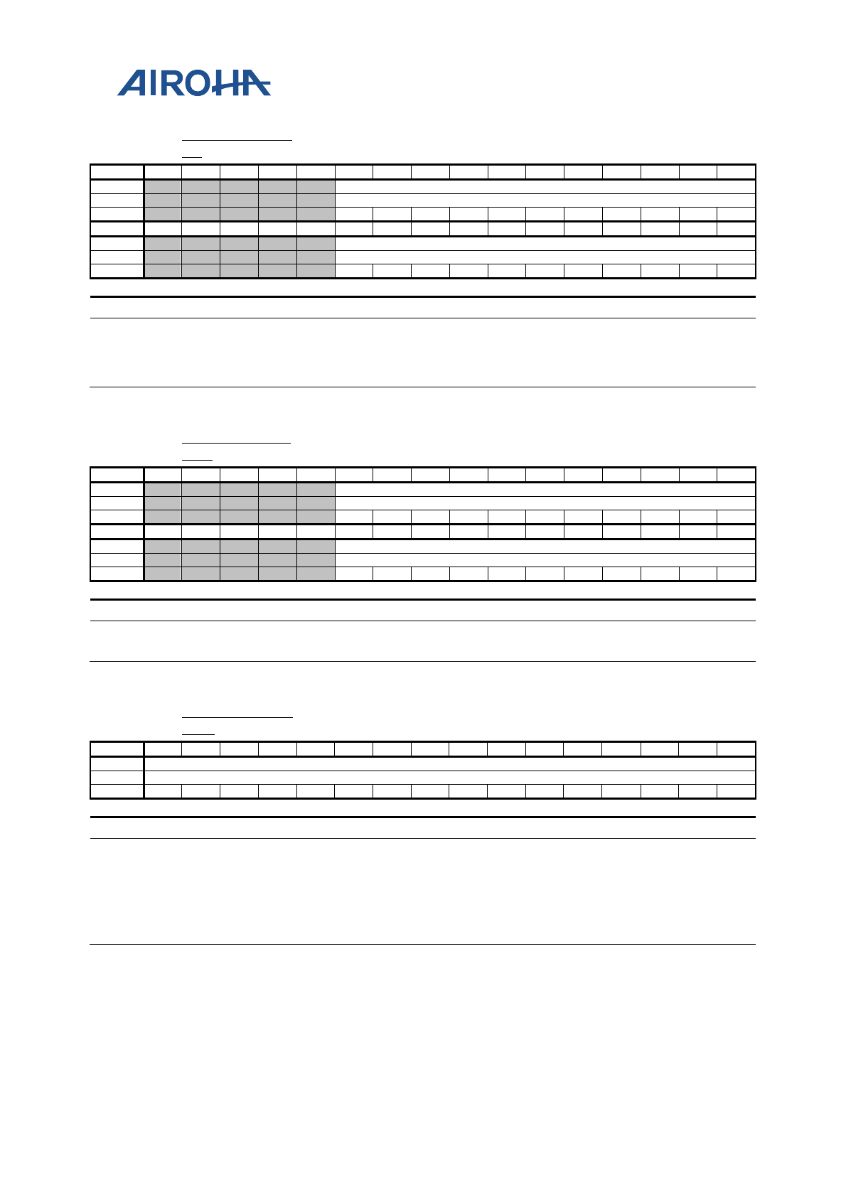
MT2523 Series Reference Manual
© 2015 - 2018 Airoha Technology Corp.
Page 371 of 692
This document contains information that is proprietary to Airoha Technology Corp. (“Airoha”) and/or its licensor(s).
Any unauthorized use, reproduction or disclosure of this document in whole or in part is strictly prohibited.
A0450120
LCD_L2WINSI
ZE
LCD Layer 2 Window Size
00000000
Bit
31
30
29
28
27
26
25
24
23
22
21
20
19
18
17
16
Name
ROW
Type
RW
Reset
0
0
0
0
0
0
0
0
0
0
0
Bit
15
14
13
12
11
10
9
8
7
6
5
4
3
2
1
0
Name
COLUMN
Type
RW
Reset
0
0
0
0
0
0
0
0
0
0
0
Bit(s)
Mnemonic
Name
Description
26:16
ROW
Layer 2 Window Row Size in unit of pixel, please see Figure
13.
10:0
COLUMN
Layer 2 Window Column Size in unit of pixel, please see
Figure 13.
A0450128
LCD_L2WINM
OFS
LCD Layer 2 Memory Offset
00000000
Bit
31
30
29
28
27
26
25
24
23
22
21
20
19
18
17
16
Name
Y_OFFSET
Type
RW
Reset
0
0
0
0
0
0
0
0
0
0
0
Bit
15
14
13
12
11
10
9
8
7
6
5
4
3
2
1
0
Name
X_OFFSET
Type
RW
Reset
0
0
0
0
0
0
0
0
0
0
0
Bit(s)
Mnemonic
Name
Description
26:16
Y_OFFSET
Layer 2 Window Column Offset, please see figure 13.
10:0
X_OFFSET
Layer 2 Window ROW Offset, please see figure 13.
A045012C
LCD_L2WINPI
TCH
LCD Layer 2 Memory Pitch
0000
Bit
15
14
13
12
11
10
9
8
7
6
5
4
3
2
1
0
Name
PITCH
Type
RW
Reset
0
0
0
0
0
0
0
0
0
0
0
0
0
0
0
0
Bit(s)
Mnemonic
Name
Description
15:0
PITCH
Layer 2 Memory Pitch in unit of byte, please see Figure 13.
This should be set to the total width of the image in memory
times the number of bytes per pixel. For 4 bpp color depth
settings, the pitch must be a multple of 4. For 2 bpp color
depth settings, the pitch must be a multiple of 2. For 3 bpp
(RGB888) color depth settins, the pitch may be a multiple of
any number
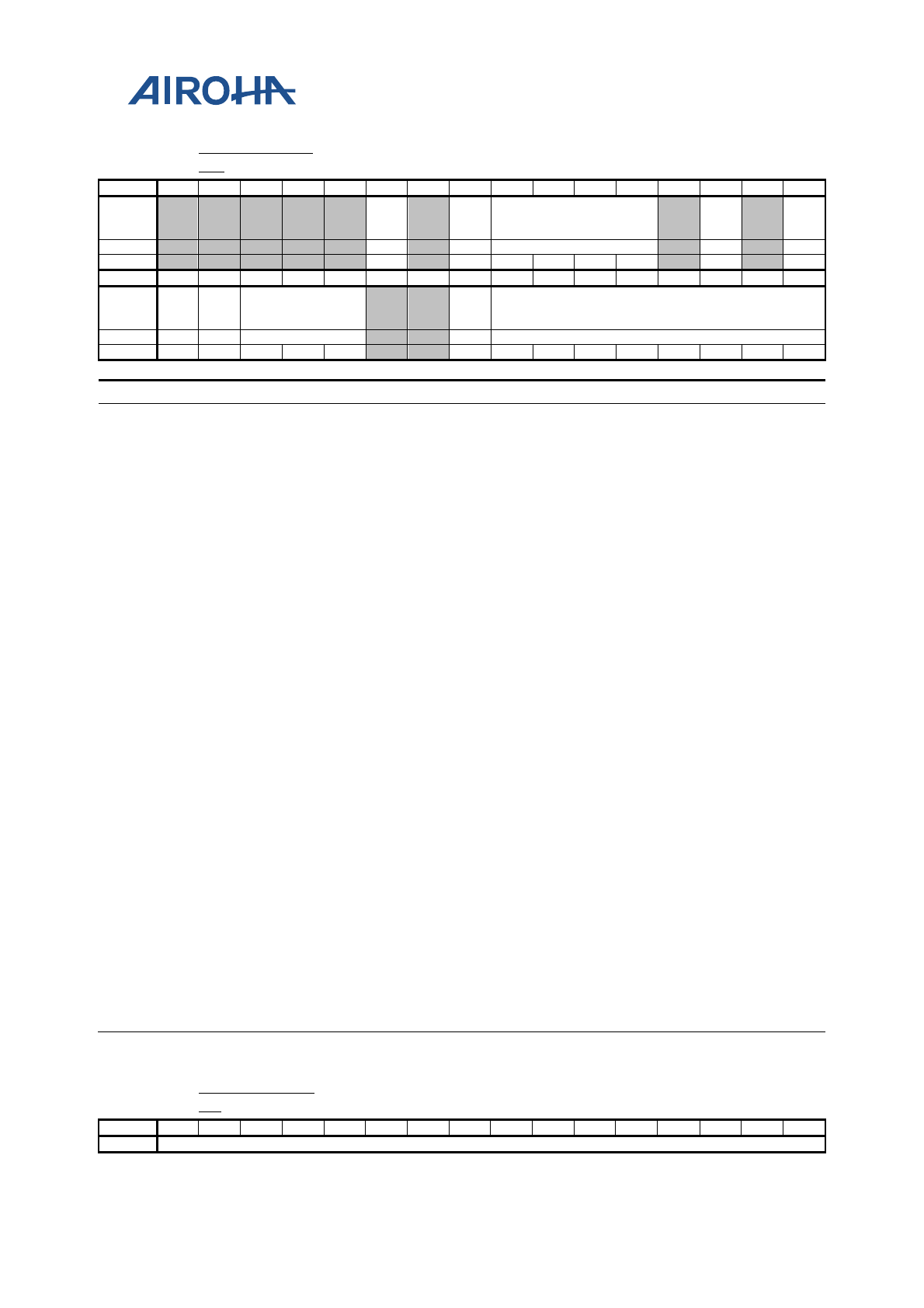
MT2523 Series Reference Manual
© 2015 - 2018 Airoha Technology Corp.
Page 372 of 692
This document contains information that is proprietary to Airoha Technology Corp. (“Airoha”) and/or its licensor(s).
Any unauthorized use, reproduction or disclosure of this document in whole or in part is strictly prohibited.
A0450140
LCD_L3WINC
ON
LCD Layer 3 Window Control Register
00000000
Bit
31
30
29
28
27
26
25
24
23
22
21
20
19
18
17
16
Name
RGB_
SWAP
DST_
KEYE
N
CLRFMT
DITH
ER_E
N
BYTE
_SWA
P
Type
RW
RW
RW
RW
RW
Reset
0
0
0
0
0
0
0
0
Bit
15
14
13
12
11
10
9
8
7
6
5
4
3
2
1
0
Name SRC
SRC_
KEYE
N
ROTATE
ALPH
A_EN
ALPHA
Type
RW
RW
RW
RW
RW
Reset
0
0
0
0
0
0
0
0
0
0
0
0
0
0
Bit(s)
Mnemonic
Name
Description
26
RGB_SWAP
24
DST_KEYEN
23:20
CLRFMT
Color format
0000: 8bpp indexed color
0001: RGB565
0010: YUYV422
0011: RGB888
0100: ARGB8888
0101: PARGB8888
0110: XRGB
0111: ARGB6666
1000: PARGB6666
1001: 4bpp index color mode
1010: 2bpp index color mode
1011: 1bpp index color mode
1000: PARGB6666
Others: Reserved
18
DITHER_EN
16
BYTE_SWAP
15
SRC
Disable auot-increment of the source pixel address. It makes
the value of each pixel is the same as the first pixel of this
frame. It is just for debug.
14
SRC_KEYEN
13:11
ROTATE
Rotation configuration
000: no rotation
001: 90 degree rotation (counterclockwise, single request only)
010: 180 degree rotation (counterclockwise)
011: 270 degree rotation (counterclockwise, single request only)
100: Horizontal flip
101: Horizontal flip then 90 degree rotation (counterclockwise, single
reqest only)
110: Horizontal flip then 180 degree rotation (counterclockwise)
111: Horizontal flip then 270 degree rotation (counterclockwise, single
request only)
8
ALPHA_EN
Enable alpha blending
7:0
ALPHA
Constant alpha value
A0450144
LCD_L3WINK
EY
LCD Layer 3 Color
Key Register
00000000
Bit
31
30
29
28
27
26
25
24
23
22
21
20
19
18
17
16
Name
CLRKEY[31:16]
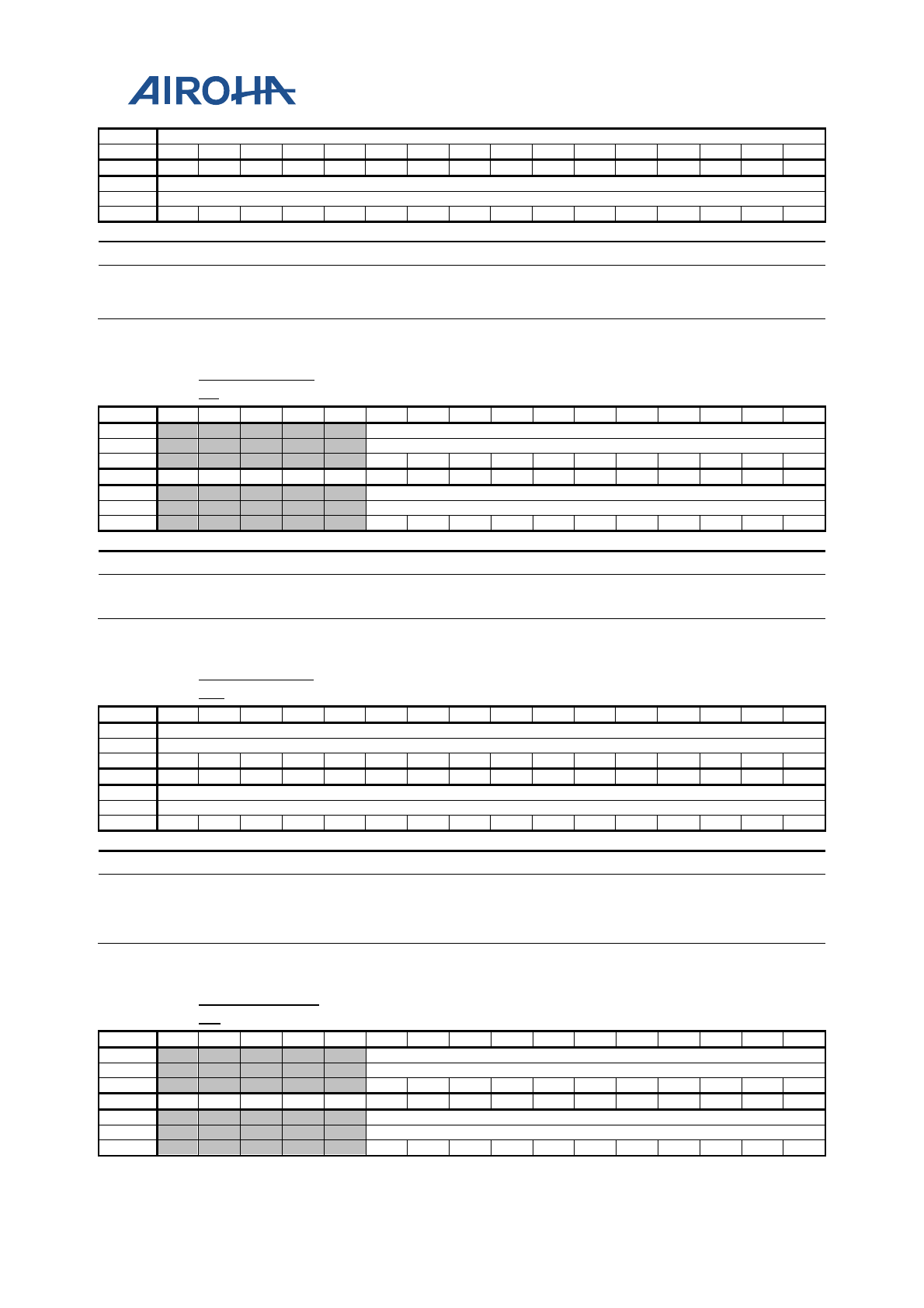
MT2523 Series Reference Manual
© 2015 - 2018 Airoha Technology Corp.
Page 373 of 692
This document contains information that is proprietary to Airoha Technology Corp. (“Airoha”) and/or its licensor(s).
Any unauthorized use, reproduction or disclosure of this document in whole or in part is strictly prohibited.
Type
RW
Reset
0
0
0
0
0
0
0
0
0
0
0
0
0
0
0
0
Bit
15
14
13
12
11
10
9
8
7
6
5
4
3
2
1
0
Name
CLRKEY[15:0]
Type
RW
Reset
0
0
0
0
0
0
0
0
0
0
0
0
0
0
0
0
Bit(s)
Mnemonic
Name
Description
31:0
CLRKEY
The source color key or destination key, which depends on
LCD_L3WINCON.SRC_KEYEN or
LCD_L3WINCON.DST_KEYEN
A0450148
LCD_L3WINO
FS
LCD Layer 3 Window Display Offset
Register
00000000
Bit
31
30
29
28
27
26
25
24
23
22
21
20
19
18
17
16
Name
Y_OFFSET
Type
RW
Reset
0
0
0
0
0
0
0
0
0
0
0
Bit
15
14
13
12
11
10
9
8
7
6
5
4
3
2
1
0
Name
X_OFFSET
Type
RW
Reset
0
0
0
0
0
0
0
0
0
0
0
Bit(s)
Mnemonic
Name
Description
26:16
Y_OFFSET
Layer 3 Window Column Offset, please see figure 13.
10:0
X_OFFSET
Layer 3 Window ROW Offset, please see figure 13.
A045014C
LCD_L3WINA
DD
LCD Layer 3 Window
Display Start Address
Register
00000000
Bit
31
30
29
28
27
26
25
24
23
22
21
20
19
18
17
16
Name
ADDR[31:16]
Type
RW
Reset
0
0
0
0
0
0
0
0
0
0
0
0
0
0
0
0
Bit
15
14
13
12
11
10
9
8
7
6
5
4
3
2
1
0
Name
ADDR[15:0]
Type
RW
Reset
0
0
0
0
0
0
0
0
0
0
0
0
0
0
0
0
Bit(s)
Mnemonic
Name
Description
31:0
ADDR
Layer 3 source start address (byte address), please see Figure
13. The address must be aligned to layer color depth
boundary as Table 6. The LCD has a special function to use
the LCM as a layer's frame buffer.
A0450150
LCD_L3WINSI
ZE
LCD Layer 3 Window Size
00000000
Bit
31
30
29
28
27
26
25
24
23
22
21
20
19
18
17
16
Name
ROW
Type
RW
Reset
0
0
0
0
0
0
0
0
0
0
0
Bit
15
14
13
12
11
10
9
8
7
6
5
4
3
2
1
0
Name
COLUMN
Type
RW
Reset
0
0
0
0
0
0
0
0
0
0
0
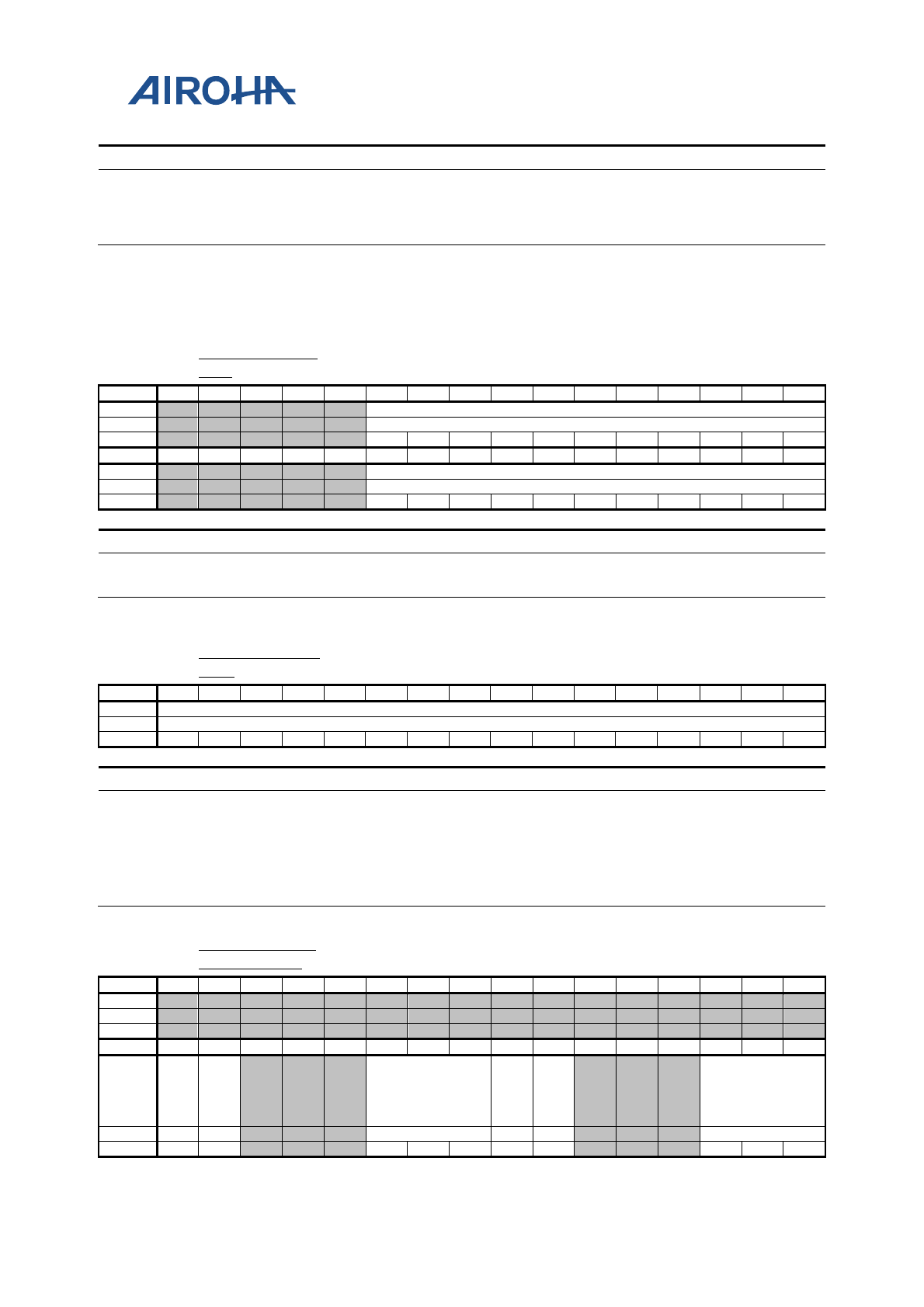
MT2523 Series Reference Manual
© 2015 - 2018 Airoha Technology Corp.
Page 374 of 692
This document contains information that is proprietary to Airoha Technology Corp. (“Airoha”) and/or its licensor(s).
Any unauthorized use, reproduction or disclosure of this document in whole or in part is strictly prohibited.
Bit(s)
Mnemonic
Name
Description
26:16
ROW
Layer 3 Window Row Size in unit of pixel, please see Figure
13.
10:0
COLUMN
Layer 3 Window Column Size in unit of pixel, please see
Figure 13.
A0450158
LCD_L3WINM
OFS
LCD Layer 3 Memory Offset
00000000
Bit
31
30
29
28
27
26
25
24
23
22
21
20
19
18
17
16
Name
Y_OFFSET
Type
RW
Reset
0
0
0
0
0
0
0
0
0
0
0
Bit
15
14
13
12
11
10
9
8
7
6
5
4
3
2
1
0
Name
X_OFFSET
Type
RW
Reset
0
0
0
0
0
0
0
0
0
0
0
Bit(s)
Mnemonic
Name
Description
26:16
Y_OFFSET
Layer 3 Window Column Offset, please see figure 13.
10:0
X_OFFSET
Layer 3 Window ROW Offset, please see figure 13.
A045015C
LCD_L3WINPI
TCH
LCD Layer 3 Memory Pitch
0000
Bit
15
14
13
12
11
10
9
8
7
6
5
4
3
2
1
0
Name
PITCH
Type
RW
Reset
0
0
0
0
0
0
0
0
0
0
0
0
0
0
0
0
Bit(s)
Mnemonic
Name
Description
15:0
PITCH
Layer 3 Memory Pitch in unit of byte, please see Figure 13.
This should be set to the total width of the image in memory
times the number of bytes per pixel. For 4 bpp color depth
settings, the pitch must be a multple of 4. For 2 bpp color
depth settings, the pitch must be a multiple of 2. For 3 bpp
(RGB888) color depth settins, the pitch may be a multiple of
any number
A0450270
LCD_SIF_STR
_BYTE_CON
LCD SIF Start Byte Configurat
ion Register
00000000
Bit
31
30
29
28
27
26
25
24
23
22
21
20
19
18
17
16
Name
Type
Reset
Bit
15
14
13
12
11
10
9
8
7
6
5
4
3
2
1
0
Name
SIF1_
STR_
BYTE
_MO
D
SIF1_
STR_
BYTE
_SWI
TCH
SIF1_STR_DATA_
SIZE
SIF0_
STR_
BYTE
_MO
D
SIF0_
STR_
BYTE
_SWI
TCH
SIF0_STR_DATA_
SIZE
Type
RW
RW
RW
RW
RW
RW
Reset
0
0
0
0
0
0
0
0
0
0
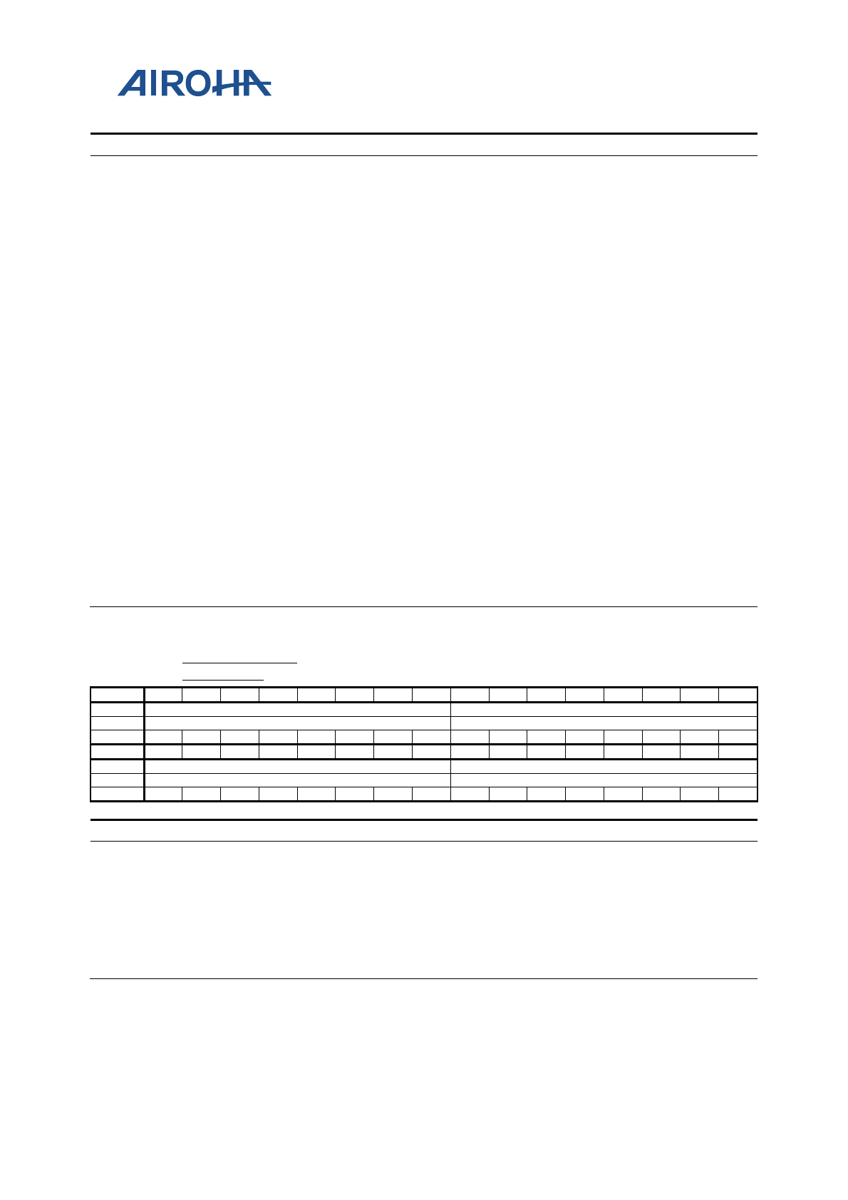
MT2523 Series Reference Manual
© 2015 - 2018 Airoha Technology Corp.
Page 375 of 692
This document contains information that is proprietary to Airoha Technology Corp. (“Airoha”) and/or its licensor(s).
Any unauthorized use, reproduction or disclosure of this document in whole or in part is strictly prohibited.
Bit(s)
Mnemonic
Name
Description
15
SIF1_STR_BYTE_M
OD
Start Byte mode of serial interface 1.
0: Start Byte mode off
1: Start Byte mode on
14
SIF1_STR_BYTE_S
WITCH
Start Byte mod2 switch of serial interface 1.
0: Start Byte mod2 switch off
1: Start Byte mod2 switch on
10:8
SIF1_STR_DATA_S
IZE
Interface size of the data part of serial interface 1 under Start
Byte mode.
000: 8 bits
001: 9 bits
010: 16 bits
011: 18 bits
100: 24 bits
101: 32 bits
7
SIF0_STR_BYTE_
MOD
Start Byte mode of serial interface 0.
0: Start Byte mode off
1: Start Byte mode on
6
SIF0_STR_BYTE_S
WITCH
Start Byte mod2 switch of serial interface 0.
0: Start Byte mod2 switch off
1: Start Byte mod2 switch on
2:0
SIF0_STR_DATA_S
IZE
Interface size of the data part of serial interface 0 under Start
Byte mode.
000: 8 bits
001: 9 bits
010: 16 bits
011: 18 bits
100: 24 bits
101: 32 bits
A0450278
LCD_SIF_WR_
STR_BYTE
LCD SIF Write Start Byte Value
00000000
Bit
31
30
29
28
27
26
25
24
23
22
21
20
19
18
17
16
Name
SIF1_WR_STR_BYTE2
SIF0_WR_STR_BYTE2
Type
RW
RW
Reset
0
0
0
0
0
0
0
0
0
0
0
0
0
0
0
0
Bit
15
14
13
12
11
10
9
8
7
6
5
4
3
2
1
0
Name
SIF1_WR_STR_BYTE
SIF0_WR_STR_BYTE
Type
RW
RW
Reset
0
0
0
0
0
0
0
0
0
0
0
0
0
0
0
0
Bit(s)
Mnemonic
Name
Description
31:24
SIF1_WR_STR_BYT
E2
Value of the write start byte2 of serial interface 1.
23:16
SIF0_WR_STR_BY
TE2
Value of the write start byte2 of serial interface 0.
15:8
SIF1_WR_STR_BYT
E
Value of the write start byte of serial interface 1.
7:0
SIF0_WR_STR_BY
TE
Value of the write start byte of serial interface 0.
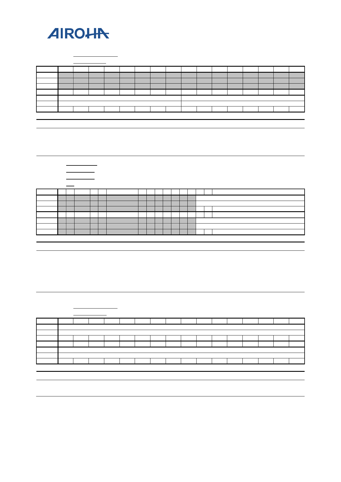
MT2523 Series Reference Manual
© 2015 - 2018 Airoha Technology Corp.
Page 376 of 692
This document contains information that is proprietary to Airoha Technology Corp. (“Airoha”) and/or its licensor(s).
Any unauthorized use, reproduction or disclosure of this document in whole or in part is strictly prohibited.
A045027C
LCD_SIF_RD_
STR_BYTE
LCD SIF Read Start Byte Value
00000000
Bit
31
30
29
28
27
26
25
24
23
22
21
20
19
18
17
16
Name
Type
Reset
Bit
15
14
13
12
11
10
9
8
7
6
5
4
3
2
1
0
Name
SIF1_RD_STR_BYTE
SIF0_RD_STR_BYTE
Type
RW
RW
Reset
0
0
0
0
0
0
0
0
0
0
0
0
0
0
0
0
Bit(s)
Mnemonic
Name
Description
15:8
SIF1_RD_STR_BYT
E
Value of the read start byte of serial interface 1.
7:0
SIF0_RD_STR_BYT
E
Value of the read start byte of serial interface 0.
A045030
0
LCD_SIF_
PAD_INP
UT_SELE
CT
LCD serial pad selection
00000000
Bit
31
30
29
28
27
26
25
24
23
22
21
20
19
18
17
16
Name
LSDA_SEL
Type
RW
Reset
0
0
0
Bit
15
14
13
12
11
10
9
8
7
6
5
4
3
2
1
0
Name
LSDI_SEL
Type
RW
Reset
0
0
0
Bit(s)
Mnemonic
Name
Description
18:16
LSDA_SEL
input selection of lsda from slcd_pad_macro
000: from pad_macro input 0
001: from pad_macro input 1
2:0
LSDI_SEL
Input selection of lsdi from slcd_pad_macro
000: from pad_macro input 0
001: from pad_macro input 1
A0450400
LCD_TABLE_I
NDEX_0_1
LCD
INDEX Mode 0_1
00000000
Bit
31
30
29
28
27
26
25
24
23
22
21
20
19
18
17
16
Name
INDEX1_RGB565
Type
RW
Reset
0
0
0
0
0
0
0
0
0
0
0
0
0
0
0
0
Bit
15
14
13
12
11
10
9
8
7
6
5
4
3
2
1
0
Name
INDEX0_RGB565
Type
RW
Reset
0
0
0
0
0
0
0
0
0
0
0
0
0
0
0
0
Bit(s)
Mnemonic
Name
Description
31:16
INDEX1_RGB565
index 1 RGB565
15:0
INDEX0_RGB565
index 0 RGB565
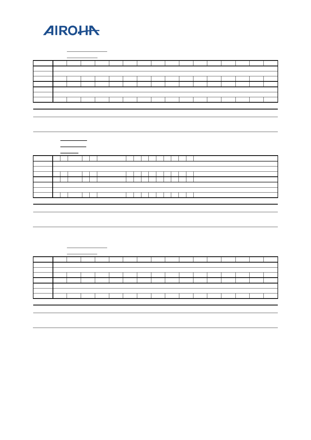
MT2523 Series Reference Manual
© 2015 - 2018 Airoha Technology Corp.
Page 377 of 692
This document contains information that is proprietary to Airoha Technology Corp. (“Airoha”) and/or its licensor(s).
Any unauthorized use, reproduction or disclosure of this document in whole or in part is strictly prohibited.
A0450404
LCD_TABLE_I
NDEX_2_3
LCD INDEX Mode 2_3
00000000
Bit
31
30
29
28
27
26
25
24
23
22
21
20
19
18
17
16
Name
INDEX3_RGB565
Type
RW
Reset
0
0
0
0
0
0
0
0
0
0
0
0
0
0
0
0
Bit
15
14
13
12
11
10
9
8
7
6
5
4
3
2
1
0
Name
INDEX2_RGB565
Type
RW
Reset
0
0
0
0
0
0
0
0
0
0
0
0
0
0
0
0
Bit(s)
Mnemonic
Name
Description
31:16
INDEX3_RGB565
index 3 RGB565
15:0
INDEX2_RGB565
index 2 RGB565
A045040
8
LCD_TAB
LE_INDE
X_4_5
LCD INDEX Mode 4_5
00000000
Bit
31
30
29
28
27
26
25
24
23
22
21
20
19
18
17
16
Name
INDEX5_RGB565
Type
RW
Reset
0
0
0
0
0
0
0
0
0
0
0
0
0
0
0
0
Bit
15
14
13
12
11
10
9
8
7
6
5
4
3
2
1
0
Name
INDEX4_RGB565
Type
RW
Reset
0
0
0
0
0
0
0
0
0
0
0
0
0
0
0
0
Bit(s)
Mnemonic
Name
Description
31:16
INDEX5_RGB565
index 5 RGB565
15:0
INDEX4_RGB565
index 4 RGB565
A045040C
LCD_TABLE_I
NDEX_6_7
LCD INDEX Mode 6_7
00000000
Bit
31
30
29
28
27
26
25
24
23
22
21
20
19
18
17
16
Name
INDEX7_RGB565
Type
RW
Reset
0
0
0
0
0
0
0
0
0
0
0
0
0
0
0
0
Bit
15
14
13
12
11
10
9
8
7
6
5
4
3
2
1
0
Name
INDEX6_RGB565
Type
RW
Reset
0
0
0
0
0
0
0
0
0
0
0
0
0
0
0
0
Bit(s)
Mnemonic
Name
Description
31:16
INDEX7_RGB565
index 7 RGB565
15:0
INDEX6_RGB565
index 6 RGB565
MT2523 Series Reference Manual
© 2015 - 2018 Airoha Technology Corp.
Page 378 of 692
This document contains information that is proprietary to Airoha Technology Corp. (“Airoha”) and/or its licensor(s).
Any unauthorized use, reproduction or disclosure of this document in whole or in part is strictly prohibited.
A0450410
LCD_TABLE_I
NDEX_8_9
LCD INDEX Mode 8_9
00000000
Bit
31
30
29
28
27
26
25
24
23
22
21
20
19
18
17
16
Name
INDEX9_RGB565
Type
RW
Reset
0
0
0
0
0
0
0
0
0
0
0
0
0
0
0
0
Bit
15
14
13
12
11
10
9
8
7
6
5
4
3
2
1
0
Name
INDEX8_RGB565
Type
RW
Reset
0
0
0
0
0
0
0
0
0
0
0
0
0
0
0
0
Bit(s)
Mnemonic
Name
Description
31:16
INDEX9_RGB565
index 9 RGB565
15:0
INDEX8_RGB565
index 8 RGB565
A0450414
LCD_TABLE_I
NDEX_a_b
LCD INDEX Mode a_b
00000000
Bit
31
30
29
28
27
26
25
24
23
22
21
20
19
18
17
16
Name
INDEXb_RGB565
Type
RW
Reset
0
0
0
0
0
0
0
0
0
0
0
0
0
0
0
0
Bit
15
14
13
12
11
10
9
8
7
6
5
4
3
2
1
0
Name
INDEXa_RGB565
Type
RW
Reset
0
0
0
0
0
0
0
0
0
0
0
0
0
0
0
0
Bit(s)
Mnemonic
Name
Description
31:16
INDEXb_RGB565
index 11 RGB565
15:0
INDEXa_RGB565
index 10 RGB565
A0450418
LCD_TABLE_I
NDEX_c_d
LCD INDEX Mode c_d
00000000
Bit
31
30
29
28
27
26
25
24
23
22
21
20
19
18
17
16
Name
INDEXd_RGB565
Type
RW
Reset
0
0
0
0
0
0
0
0
0
0
0
0
0
0
0
0
Bit
15
14
13
12
11
10
9
8
7
6
5
4
3
2
1
0
Name
INDEXc_RGB565
Type
RW
Reset
0
0
0
0
0
0
0
0
0
0
0
0
0
0
0
0
Bit(s)
Mnemonic
Name
Description
31:16
INDEXd_RGB565
index 13 RGB565
15:0
INDEXc_RGB565
index 12 RGB565
A045041C
LCD_TABLE_I
NDEX_e_f
LCD INDEX Mode e_f
00000000
Bit
31
30
29
28
27
26
25
24
23
22
21
20
19
18
17
16
Name
INDEXf_RGB565
Type
RW
Reset
0
0
0
0
0
0
0
0
0
0
0
0
0
0
0
0
MT2523 Series Reference Manual
© 2015 - 2018 Airoha Technology Corp.
Page 379 of 692
This document contains information that is proprietary to Airoha Technology Corp. (“Airoha”) and/or its licensor(s).
Any unauthorized use, reproduction or disclosure of this document in whole or in part is strictly prohibited.
Bit
15
14
13
12
11
10
9
8
7
6
5
4
3
2
1
0
Name
INDEXe_RGB565
Type
RW
Reset
0
0
0
0
0
0
0
0
0
0
0
0
0
0
0
0
Bit(s)
Mnemonic
Name
Description
31:16
INDEXf_RGB565
index 15 RGB565
15:0
INDEXe_RGB565
index 14 RGB565
A0450F80
LCD_SCMD0
LCD Serial Interface Command Port0
00000000
Bit
31
30
29
28
27
26
25
24
23
22
21
20
19
18
17
16
Name
DATA[31:16]
Type
Other
Reset
0
0
0
0
0
0
0
0
0
0
0
0
0
0
0
0
Bit
15
14
13
12
11
10
9
8
7
6
5
4
3
2
1
0
Name
DATA[15:0]
Type
Other
Reset
0
0
0
0
0
0
0
0
0
0
0
0
0
0
0
0
Bit(s)
Mnemonic
Name
Description
31:0
DATA
Command Port
Write or read this register to directly access the LCD-C LCM0. LSA0=0
in 4-wire mode or A0 bit=0 in 3-wire mode
A0450F90
LCD_SDAT0
LCD Serial Interface Data Port0
00000000
Bit
31
30
29
28
27
26
25
24
23
22
21
20
19
18
17
16
Name
DATA[31:16]
Type
Other
Reset
0
0
0
0
0
0
0
0
0
0
0
0
0
0
0
0
Bit
15
14
13
12
11
10
9
8
7
6
5
4
3
2
1
0
Name
DATA[15:0]
Type
Other
Reset
0
0
0
0
0
0
0
0
0
0
0
0
0
0
0
0
Bit(s)
Mnemonic
Name
Description
31:0
DATA
Data Port
Write or read this register to directly access the LCD-C LCM0. The A0
bit will be 1.
A0450FA0
LCD_SCMD1
LCD Serial Interface Command Port1
00000000
Bit
31
30
29
28
27
26
25
24
23
22
21
20
19
18
17
16
Name
DATA[31:16]
Type
Other
Reset
0
0
0
0
0
0
0
0
0
0
0
0
0
0
0
0
Bit
15
14
13
12
11
10
9
8
7
6
5
4
3
2
1
0
Name
DATA[15:0]
Type
Other
Reset
0
0
0
0
0
0
0
0
0
0
0
0
0
0
0
0
Bit(s)
Mnemonic
Name
Description
31:0
DATA
Command Port
Write or read this register to directly access the LCD-C LCM1. The A0
bit will be 0.

MT2523 Series Reference Manual
© 2015 - 2018 Airoha Technology Corp.
Page 380 of 692
This document contains information that is proprietary to Airoha Technology Corp. (“Airoha”) and/or its licensor(s).
Any unauthorized use, reproduction or disclosure of this document in whole or in part is strictly prohibited.
A0450FB0
LCD_SDAT1
LCD Serial Interface Data Port1
00000000
Bit
31
30
29
28
27
26
25
24
23
22
21
20
19
18
17
16
Name
DATA[31:16]
Type
Other
Reset
0
0
0
0
0
0
0
0
0
0
0
0
0
0
0
0
Bit
15
14
13
12
11
10
9
8
7
6
5
4
3
2
1
0
Name
DATA[15:0]
Type
Other
Reset
0
0
0
0
0
0
0
0
0
0
0
0
0
0
0
0
Bit(s)
Mnemonic
Name
Description
31:0
DATA
Data Port
Write or read this register to directly access the LCD-C LCM1. The A0
bit will be 1.
MT2523 Series Reference Manual
© 2015 - 2018 Airoha Technology Corp.
Page 381 of 692
This document contains information that is proprietary to Airoha Technology Corp. (“Airoha”) and/or its licensor(s).
Any unauthorized use, reproduction or disclosure of this document in whole or in part is strictly prohibited.
24. Display Serial Interface (DSI)
24.1. General Description
The display serial interface (DSI) is based on MIPI Alliance Specification, supporting high-speed serial data transfer
between host processor and peripheral devices such as display modules. DSI supports command mode data
transfer defined in MIPI spec, and it also provides bidirectional transmission with low-power mode to receive
messages from the peripheral.
24.2. Features
The DSI engine has the following features for display serial interface:
• One clock lane and one data lane
• Bidirectional data transmission in low-power mode in data lane 0
• Uni-directional data transmission in high-speed mode in data lane 0
• DCS command transmission
• Pixel format of RGB565/loosely RGB666/RGB888
• Supports non-continuous high-speed transmission in data lane
• Supports peripheral TE and external TE signal detection
• Supports ultra-low power mode control
24.2.1. Pixel Format
R1[7] G1[7] B1[7] R2[7] G2[7] B2[7] …
R1[6] G1[6] B1[6] R2[6] G2[6] B2[6] …
R1[5] G1[5] B1[5] R2[5] G2[5] B2[5] …
R1[4] G1[4] B1[4] R2[4] G2[4] B2[4] …
R1[3] G1[3] B1[3] R2[3] G2[3] B2[3] …
R1[2] G1[2] B1[2] R2[2] G2[2] B2[2] …
R1[1] G1[1] B1[1] R2[1] G2[1] B2[1] …
R1[0] G1[0] B1[0] R2[0] G2[0] B2[0] …
Time
Figure 24-1. Pixel Format of RGB888
MT2523 Series Reference Manual
© 2015 - 2018 Airoha Technology Corp.
Page 382 of 692
This document contains information that is proprietary to Airoha Technology Corp. (“Airoha”) and/or its licensor(s).
Any unauthorized use, reproduction or disclosure of this document in whole or in part is strictly prohibited.
1'b0 1'b0 1'b0 1'b0 1'b0 1'b0 …
1'b0 1'b0 1'b0 1'b0 1'b0 1'b0 …
Time
R1[5] G1[5] B1[5] R2[5] G2[5] B2[5] …
R1[4] G1[4] B1[4] R2[4] G2[4] B2[4] …
R1[3] G1[3] B1[3] R2[3] G2[3] B2[3] …
R1[2] G1[2] B1[2] R2[2] G2[2] B2[2] …
R1[1] G1[1] B1[1] R2[1] G2[1] B2[1] …
R1[0] G1[0] B1[0] R2[0] G2[0] B2[0] …
Figure 24-2. Pixel Format of Loosely RGB666
R1[4] G1[2] R2[4] G2[2] R3[4] G3[2] …
R1[3] G1[1] R2[3] G2[1] R3[3] G3[1] …
R1[2] G1[0] R2[2] G2[0] R3[2] G3[0] …
R1[1] B1[4] R2[1] B2[4] R3[1] B3[4] …
R1[0] B1[3] R2[0] B2[3] R3[0] B3[3] …
G1[5] B1[2] G2[5] B2[2] G3[5] B3[2] …
G1[4] B1[1] G2[4] B2[1] G3[4] B3[1] …
G1[3] B1[0] G2[3] B2[0] G3[3] B3[0] …
Time
Figure 24-3. Pixel Format of RGB565
24.3. Register Definition
Module name: DISP_DSI Base address: (+a04a0000h)
Address
Name
Width
Register Function
A04A0000
DSI_START
32
DSI Start Register
A04A0008
DSI_INTEN
32
DSI Interrupt Enable Register
A04A000C
DSI_INTSTA
32
DSI Interrupt Status Register
A04A0010
DSI_COM_CON
32
DSI Common Control Register
A04A0014
DSI_MODE_CON
32
DSI Mode Control Register
A04A0018
DSI_TXRX_CON
32
DSI TX RX Control Register
A04A001C
DSI_PSCON
32
DSI Pixel Stream Control Register
A04A002C
DSI_VACT_NL
32
DSI Vertical Active
Register
A04A0060
DSI_CMDQ_CON
32
DSI Command Queue Control Register
A04A0064
DSI_HSTX_CKLP_WC
32
DSI HSTX Clock Low-power Mode Word
Count Register
A04A0074
DSI_RX_DATA03
32
DSI Receive Packet Data Byte 0 ~ 3
Register
A04A0078
DSI_RX_DATA47
32
DSI Receive Packet Data Byte 4 ~ 7
Register
A04A007C
DSI_RX_DATA8B
32
DSI Receive Packet Data Byte 8 ~ 11
Register
A04A0080
DSI_RX_DATAC
32
DSI Receive Packet Data Byte 12 ~ 15
Register
A04A0084
DSI_RX_RACK
32
DSI Read Data Acknowledge Register
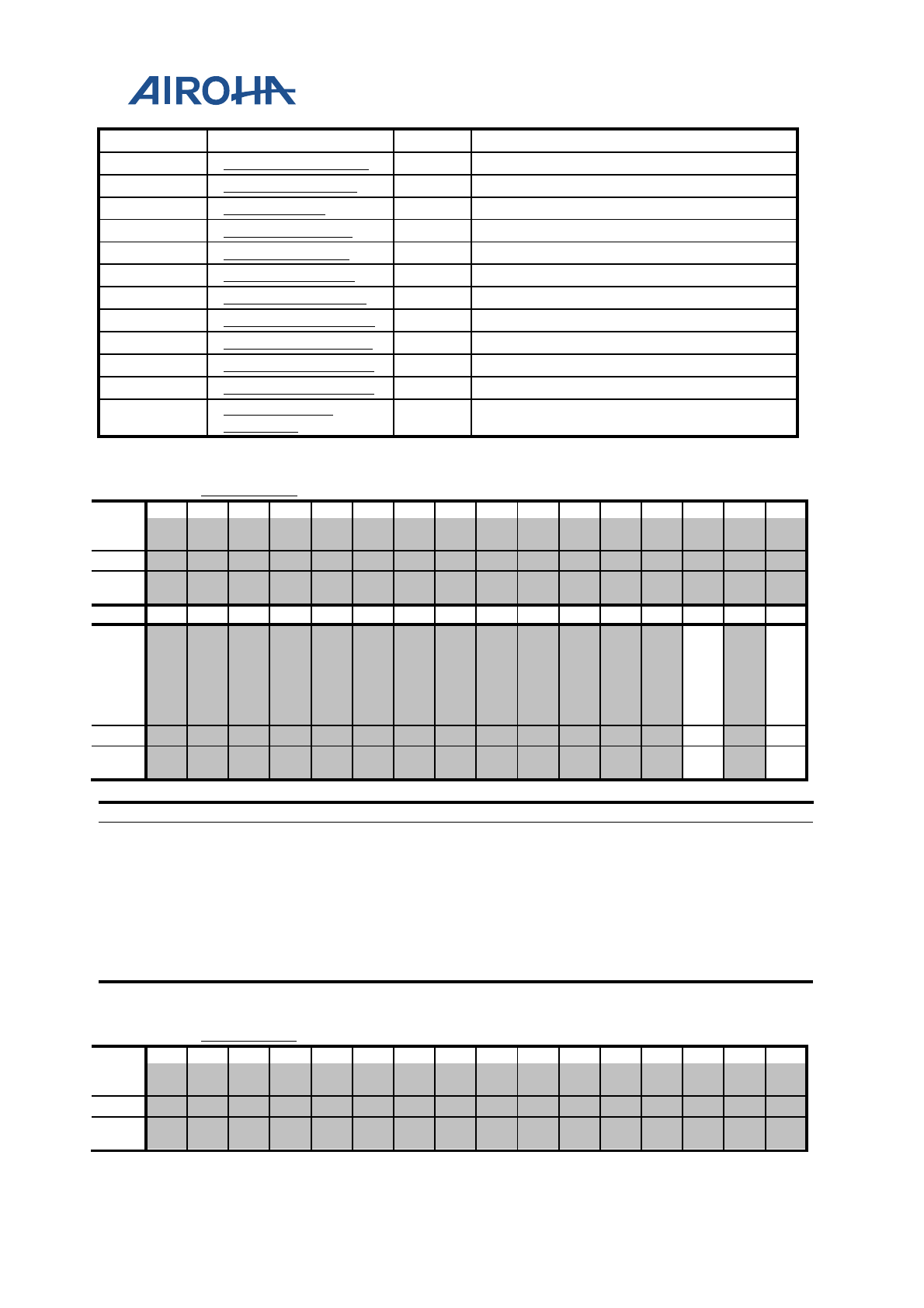
MT2523 Series Reference Manual
© 2015 - 2018 Airoha Technology Corp.
Page 383 of 692
This document contains information that is proprietary to Airoha Technology Corp. (“Airoha”) and/or its licensor(s).
Any unauthorized use, reproduction or disclosure of this document in whole or in part is strictly prohibited.
Address
Name
Width
Register Function
A04A0088
DSI_RX_TRIG_STA
32
DSI Receiver Status Register
A04A0090
DSI_MEM_CONTI
32
DSI Memory Continue Command Register
A04A0094
DSI_FRM_BC
32
DSI Frame Byte
Count Register
A04A00A0
DSI_TIME_CON0
32
DSI Timing Control 0 Register
A04A00A4
DSI_TIME_CON1
32
DSI Timing Control 1 Register
A04A0104
DSI_PHY_LCCON
32
DSI PHY Lane Clock Control Register
A04A0108
DSI_PHY_LD0CON
32
DSI PHY Lane 0 Control Register
A04A0110
DSI_PHY_TIMCON0
32
DSI PHY Timing Control 0 Register
A04A0114
DSI_PHY_TIMCON1
32
DSI PHY Timing Control 1 Register
A04A0118
DSI_PHY_TIMCON2
32
DSI PHY Timing Control 2 Register
A04A011C
DSI_PHY_TIMCON3
32
DSI PHY
Timing Control 3 Register
A04A0200~
a04a03fc
DSI_CMDQ [n]
(n=0~127)
32
DSI Command Queue
A04A0000
DSI_START
DSI Start Register
00000000
Bit
31
30
29
28
27
26
25
24
23
22
21
20
19
18
17
16
Nam
e
Type
Rese
t
Bit
15
14
13
12
11
10
9
8
7
6
5
4
3
2
1
0
Nam
e
SL
EE
PO
UT
_S
TA
RT
DSI
_S
TA
RT
Type
RW
RW
Rese
t
0 0
Bit(s)
Name
Description
2
SLEEPOUT_START
DSI sleep-out operation
Set up this bit to wake up DSI from ULPS mode. This bit is only
available when SLEEP_MODE = 1.
0: No effect
1: Start
0
DSI_START
Starts DSI controller operation
Set up this bit to start DSI control.
0: No effect
1: Start
A04A0008
DSI_INTEN
DSI Interrupt Enable Register
00000000
Bit
31
30
29
28
27
26
25
24
23
22
21
20
19
18
17
16
Nam
e
Type
Rese
t
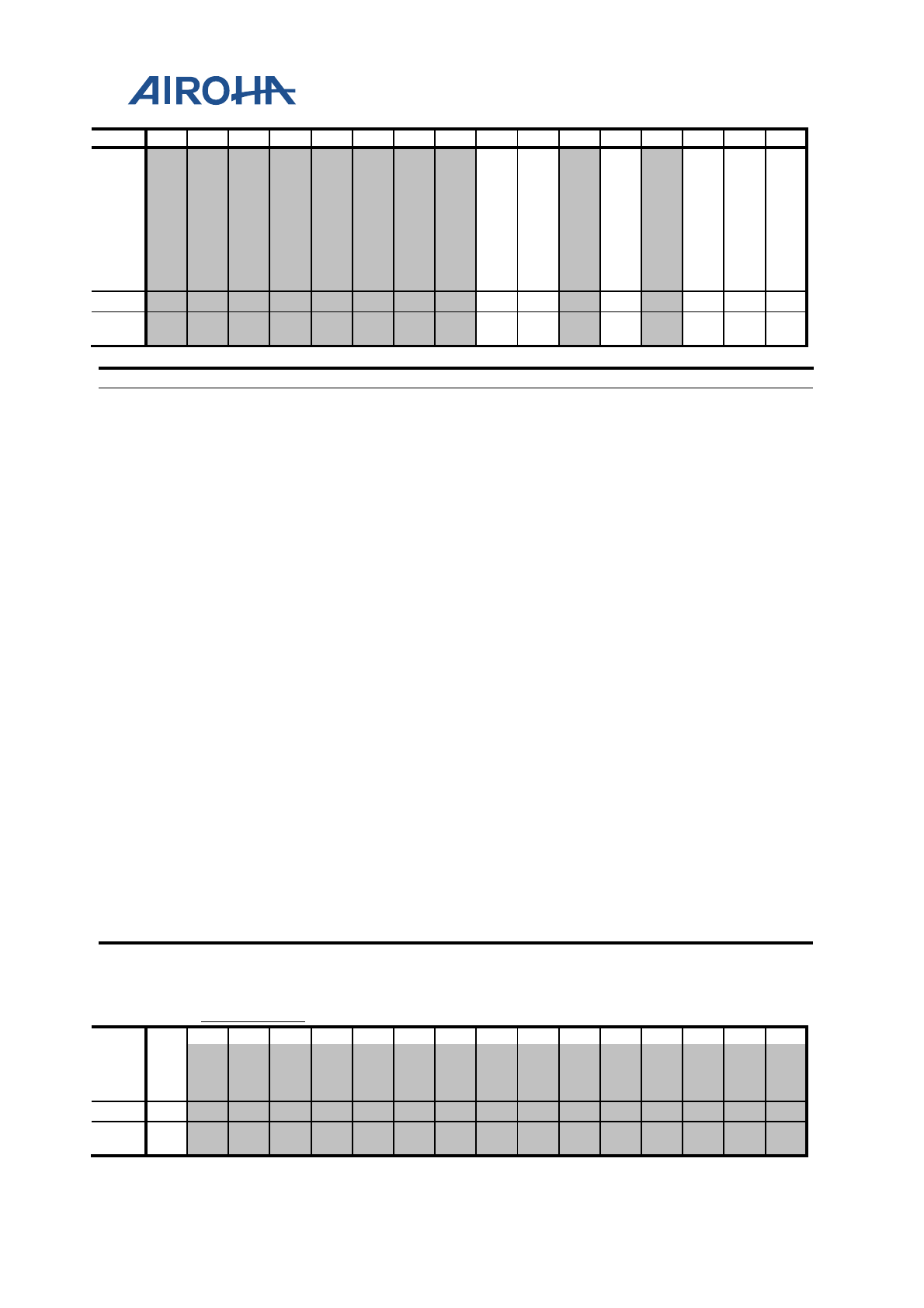
MT2523 Series Reference Manual
© 2015 - 2018 Airoha Technology Corp.
Page 384 of 692
This document contains information that is proprietary to Airoha Technology Corp. (“Airoha”) and/or its licensor(s).
Any unauthorized use, reproduction or disclosure of this document in whole or in part is strictly prohibited.
Bit
15
14
13
12
11
10
9
8
7
6
5
4
3
2
1
0
Nam
e
TE
_TI
ME
OU
T_I
NT
_E
N
SL
EE
PO
UT
_D
ON
E_I
NT
_E
N
FR
AM
E_
DO
NE
_I
NT
_E
N
TE
_R
DY
_I
NT
_E
N
CM
D_
DO
NE
_I
NT
_E
N
LP
RX
_R
D_
RD
Y_I
NT
_E
N
Type
RW
RW
RW
RW
RW
RW
Rese
t
0 0 0 0 0 0
Bit(s)
Name
Description
7
TE_TIMEOUT_INT_EN
TE timeout interrupt
This interrupt will be issued when the wait time of TE signal
exceeds SW-configured threshold
0: Disable
1: Enable
6
SLEEPOUT_DONE_INT_EN
Enables ULPS sleep-out interrupt
The interrupt will be issued when ULPS sleep out procedure
is
completed
0: Disable
1: Enable
4
FRAME_DONE_INT_EN
Frame done interrupt
This interrupt will be issued when the frame transmission is done
0: Disable
1: Enable
2
TE_RDY_INT_EN
DSI TE ready interrupt
This interrupt will be issued when either
BTA TE or external TE is
received
0: Disable
1: Enable
1
CMD_DONE_INT_EN
Enables DSI command mode finished interrupt
This interrupt will be issued when all commands set in command
queue are executed
0: Disable
1: Enable
0
LPRX_RD_RDY_INT_EN
Enables RX data-ready interrupt
This interrupt will be issued when RX data are received through
read commands. It is recommended to enable this interrupt to
receive data because the read response may be overwritten if
another read command exists. An RACK o
peration should be set
after reading data to allow HW continue execution
0: Disable
1: Enable
A04A000C
DSI_INTSTA
DSI Interrupt Status Register
00000000
Bit
31
30
29
28
27
26
25
24
23
22
21
20
19
18
17
16
Nam
e
DSI
_B
US
Y
Type
RU
Rese
t
0
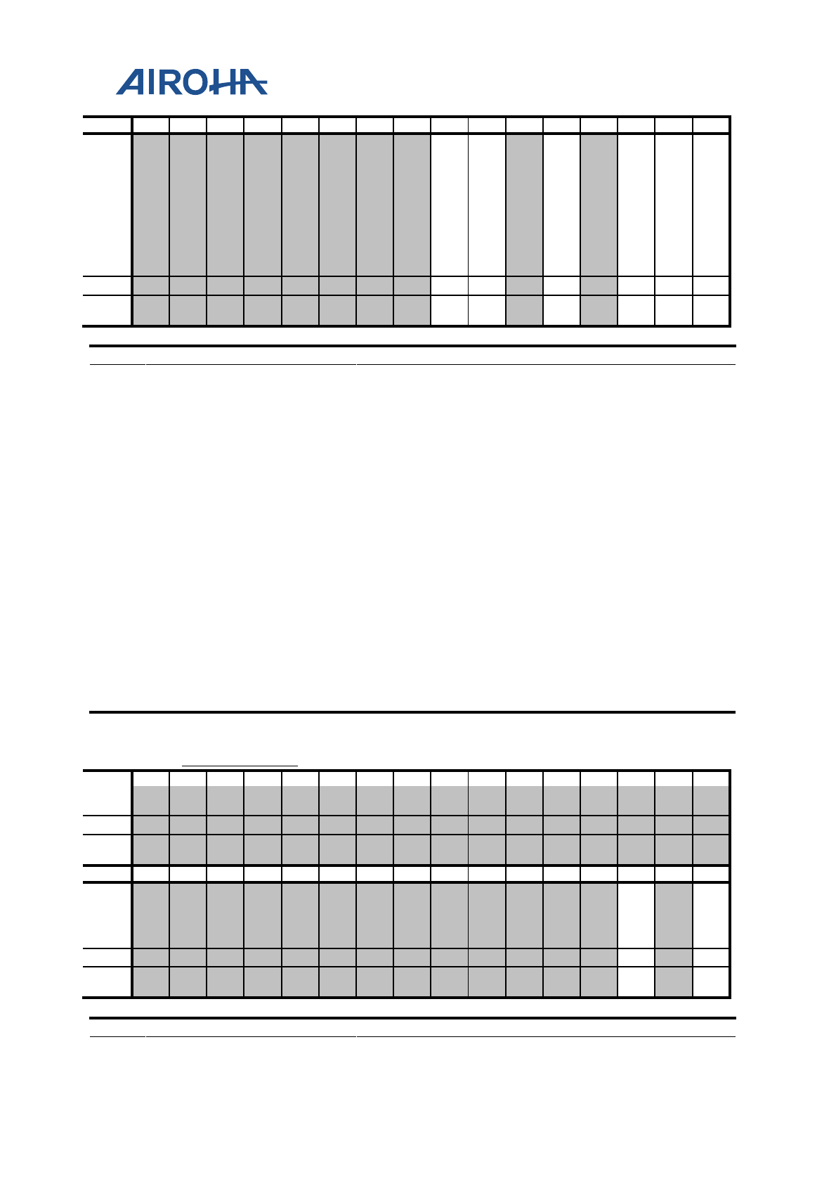
MT2523 Series Reference Manual
© 2015 - 2018 Airoha Technology Corp.
Page 385 of 692
This document contains information that is proprietary to Airoha Technology Corp. (“Airoha”) and/or its licensor(s).
Any unauthorized use, reproduction or disclosure of this document in whole or in part is strictly prohibited.
Bit
15
14
13
12
11
10
9
8
7
6
5
4
3
2
1
0
Nam
e
TE
_TI
ME
OU
T_I
NT
_F
LA
G
SL
EE
PO
UT
_D
ON
E_I
NT
_F
LA
G
FR
AM
E_
DO
NE
_I
NT
_F
LA
G
TE
_R
DY
_I
NT
_F
LA
G
CM
D_
DO
NE
_I
NT
_F
LA
G
LP
RX
_R
D_
RD
Y_I
NT
_F
LA
G
Type
A1
A1
A1
A1
A1
A1
Rese
t
0 0 0 0 0 0
Bit(s)
Name
Description
31
DSI_BUSY
DSI busy status
0: Idle
1: Busy
7
TE_TIMEOUT_INT_FLAG
TE time-out interrupt status
0: Clear interrupt
1: No effect
6
SLEEPOUT_DONE_INT_FLAG
ULPS sleep-out done interrupt status.
0: Clear interrupt
1: No effect
4
FRAME_DONE_INT_FLAG
Frame done interrupt status
0: Clear interrupt
1: No effect
2
TE_RDY_INT_FLAG
DSI TE ready interrupt status
0: Clear interrupt
1: No effect
1
CMD_DONE_INT_FLAG
DSI command mode finish interrupt status
0: Clear interrupt
1: No effect
0
LPRX_RD_RDY_INT_FLAG
RX data-ready interrupt status
0: Clear interrupt
1: No effect
A04A0010
DSI_COM_CON
DSI Common Control Register
00000000
Bit
31
30
29
28
27
26
25
24
23
22
21
20
19
18
17
16
Nam
e
Type
Rese
t
Bit
15
14
13
12
11
10
9
8
7
6
5
4
3
2
1
0
Nam
e
DP
HY
_R
ES
ET
DSI
_R
ES
ET
Type
RW
RW
Rese
t
0 0
Bit(s)
Name
Description
2
DPHY_RESET
DIG_MIPI_TX software reset
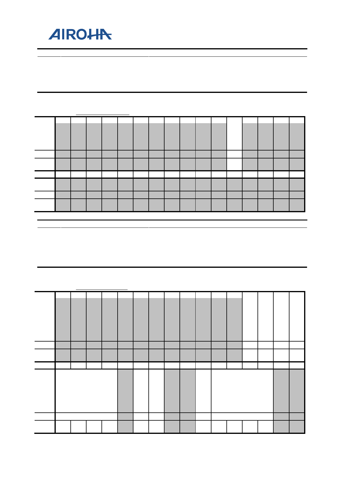
MT2523 Series Reference Manual
© 2015 - 2018 Airoha Technology Corp.
Page 386 of 692
This document contains information that is proprietary to Airoha Technology Corp. (“Airoha”) and/or its licensor(s).
Any unauthorized use, reproduction or disclosure of this document in whole or in part is strictly prohibited.
Bit(s)
Name
Description
0: De-assert software reset
1: Assert software reset
0
DSI_RESET
DSI module software reset
0: De-assert software reset
1: Assert software reset
A04A0014
DSI_MODE_CON
DSI Mode Control Register
00000000
Bit
31
30
29
28
27
26
25
24
23
22
21
20
19
18
17
16
Nam
e
SL
EE
P_
MO
DE
Type
RW
Rese
t
0
Bit
15
14
13
12
11
10
9
8
7
6
5
4
3
2
1
0
Nam
e
Type
Rese
t
Bit(s)
Name
Description
20
SLEEP_MODE
DSI sleep mode for ULPS wake-up operation
This mode is used during wake
-up stage to leave ULPS. Set this bit
to 1 before setting LANE_NUM to
enable output data lane to LP-
00; then set up SLEEPOUT_START to start the ULPS-exit process.
0: Disable
1: Enable
A04A0018
DSI_TXRX_CON
DSI TX RX Control Register
00000000
Bit
31
30
29
28
27
26
25
24
23
22
21
20
19
18
17
16
Nam
e
TE
_TI
ME
OU
T_
CH
K_
EN
TE
_W
IT
H_
CM
D_
EN
TY
PE1
_B
TA
_S
EL
HS
TX
_C
KL
P_
EN
Type
RW
RW
RW
RW
Rese
t
0 0 0 0
Bit
15
14
13
12
11
10
9
8
7
6
5
4
3
2
1
0
Nam
e MAX_RTN_SIZE
EX
T_
TE
_E
DG
E_
SE
L
EX
T_
TE
_E
N
HS
TX
_D
IS_
EO
T
LANE_NUM
Type
RW
RW
RW
RW
RW
Rese
t
0 0 0 0 0 0 0 0 0 0 0
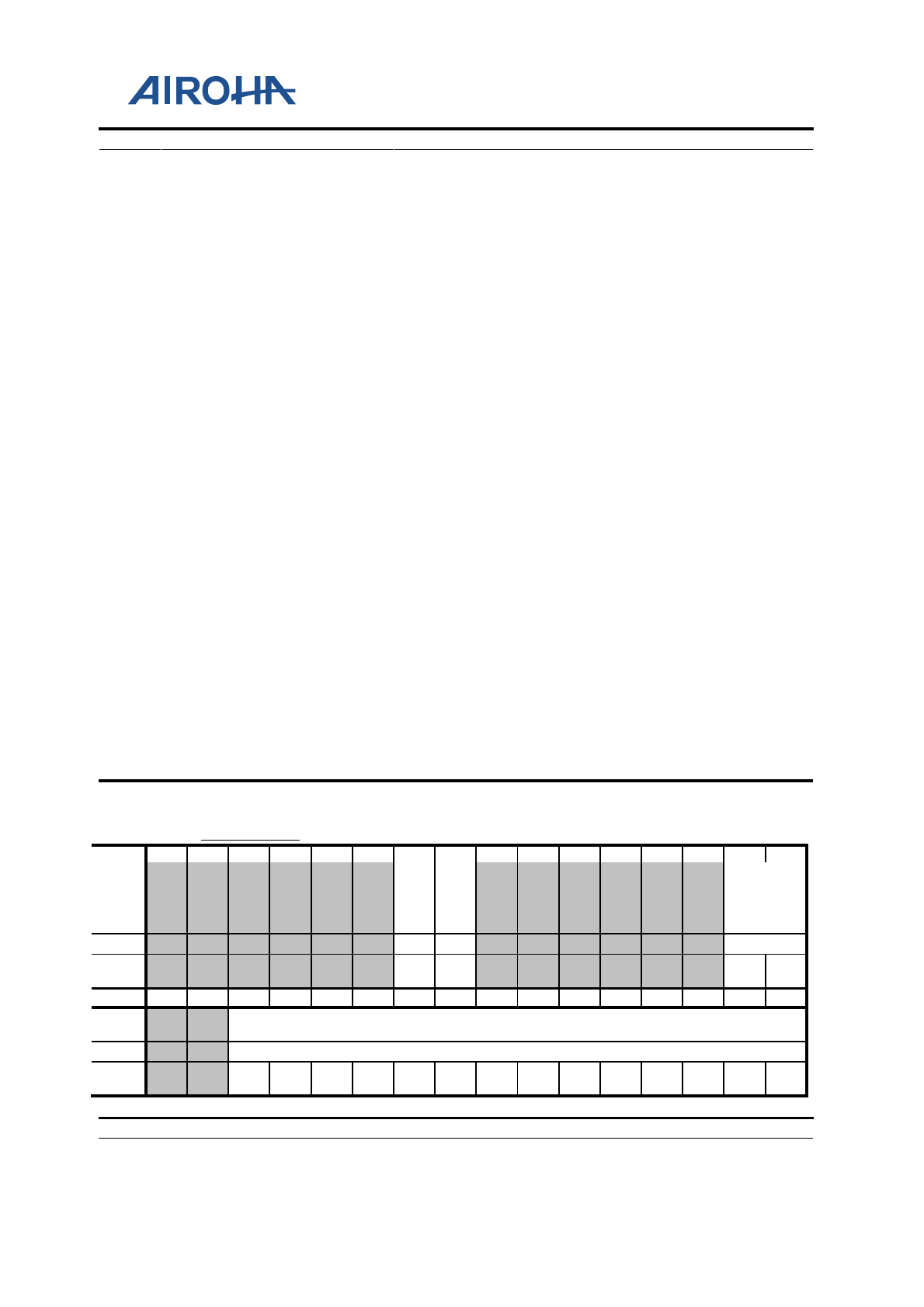
MT2523 Series Reference Manual
© 2015 - 2018 Airoha Technology Corp.
Page 387 of 692
This document contains information that is proprietary to Airoha Technology Corp. (“Airoha”) and/or its licensor(s).
Any unauthorized use, reproduction or disclosure of this document in whole or in part is strictly prohibited.
Bit(s)
Name
Description
19
TE_TIMEOUT_CHK_EN
Enables TE time-out check mechanism
Enable this bit to turn on DSI TE and external TE time
-out check
mechanism based on wait time of TE_TIMEOUT.
0: Disable
1: Enable
18
TE_WITH_CMD_EN
In the tradition design, TE command executes 'bus
turnaround' and ignores other settings in the same
command column. Combine the TE bit and other
commands if this bit is asserted.
0: Disable
1: Enable
17
TYPE1_BTA_SEL
Selects TYPE1 BTA mechanism
0: TYPE1 BTA by frame
1: TYPE1 BTA by packet
16
HSTX_CKLP_EN
Enables non-continuous clock lane
0: Disable
1: Enable
15:12
MAX_RTN_SIZE
Maximum return packet size
This register constrains maximum
return packet that the slave side
will send back to the host. It takes effect after the host sends 'Set
Maximum Return Packet Size' packet to slave.
10
EXT_TE_EDGE_SEL
Selects trigger edge type of external TE
0: Rising edge
1: Falling edge
9
EXT_TE_EN
Enables external TE signal
This bit should be set to receive external TE if LPTE pin is used as
external TE pin
0: Disable
1: Enable
6
HSTX_DIS_EOT
Disables end of transmission packet.
0: Enable EoTp
1: Disable EoTp
5:2
LANE_NUM
Lane number
Set up this bit to turn on lane circuit.
4'b0000: Disable all lanes
4'b0001: Enable 1 data lane + 1 clock lane
A04A001C
DSI_PSCON
DSI Pixel Stream Control Register
00000000
Bit
31
30
29
28
27
26
25
24
23
22
21
20
19
18
17
16
Nam
e
BY
TE
_S
WA
P
RG
B_
SW
AP
DSI_PS_
SEL
Type
RW
RW
RW
Rese
t
0 0 0 0
Bit
15
14
13
12
11
10
9
8
7
6
5
4
3
2
1
0
Nam
e
DSI_PS_WC
Type
RW
Rese
t
0 0 0 0 0 0 0 0 0 0 0 0 0 0
Bit(s)
Name
Description
25
BYTE_SWAP
Selects byte order
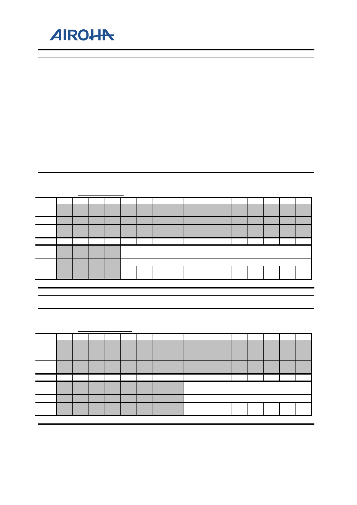
MT2523 Series Reference Manual
© 2015 - 2018 Airoha Technology Corp.
Page 388 of 692
This document contains information that is proprietary to Airoha Technology Corp. (“Airoha”) and/or its licensor(s).
Any unauthorized use, reproduction or disclosure of this document in whole or in part is strictly prohibited.
Bit(s)
Name
Description
For RGB565 type, it swaps bytes between MSB and LSB. For other
stream types, this bit is not used.
0: Normal case
1: Byte order change
24
RGB_SWAP
Selects order of RGB
For all color types, it changes the
color order in format of RGB or
BGR.
0: Normal case
1: R/B order change
17:16
DSI_PS_SEL
Selects pixel stream type
0: Packed pixel stream with 16-bit RGB 5-6-5 format
2: Loosely pixel stream with 24-bit RGB 6-6-6 format
3: Packed pixel stream with 24-bit RGB 8-8-8 format
13:0
DSI_PS_WC
Word count of long packet in valid pixel data duration
Unit: Byte
This value must be (H_SIZE*BPP). Take the QVGA display as an
example, the value of PS_WC is (240*3) = 720 in decimal.
A04A002C
DSI_VACT_NL
DSI Vertical Active Register
00000000
Bit
31
30
29
28
27
26
25
24
23
22
21
20
19
18
17
16
Nam
e
Type
Rese
t
Bit
15
14
13
12
11
10
9
8
7
6
5
4
3
2
1
0
Nam
e
VACT_NL
Type
RW
Rese
t
0 0 0 0 0 0 0 0 0 0 0 0
Bit(s)
Name
Description
11:0
VACT_NL
Vertical active duration
Configures frame height of pixels
A04A0060
DSI_CMDQ_CON
DSI Command Queue Control Register
00000000
Bit
31
30
29
28
27
26
25
24
23
22
21
20
19
18
17
16
Nam
e
Type
Rese
t
Bit
15
14
13
12
11
10
9
8
7
6
5
4
3
2
1
0
Nam
e
CMDQ_SIZE
Type
RW
Rese
t
0 0 0 0 0 0 0 0
Bit(s)
Name
Description
7:0
CMDQ_SIZE
Number of commands in command queue
Range: 1 ~ 127
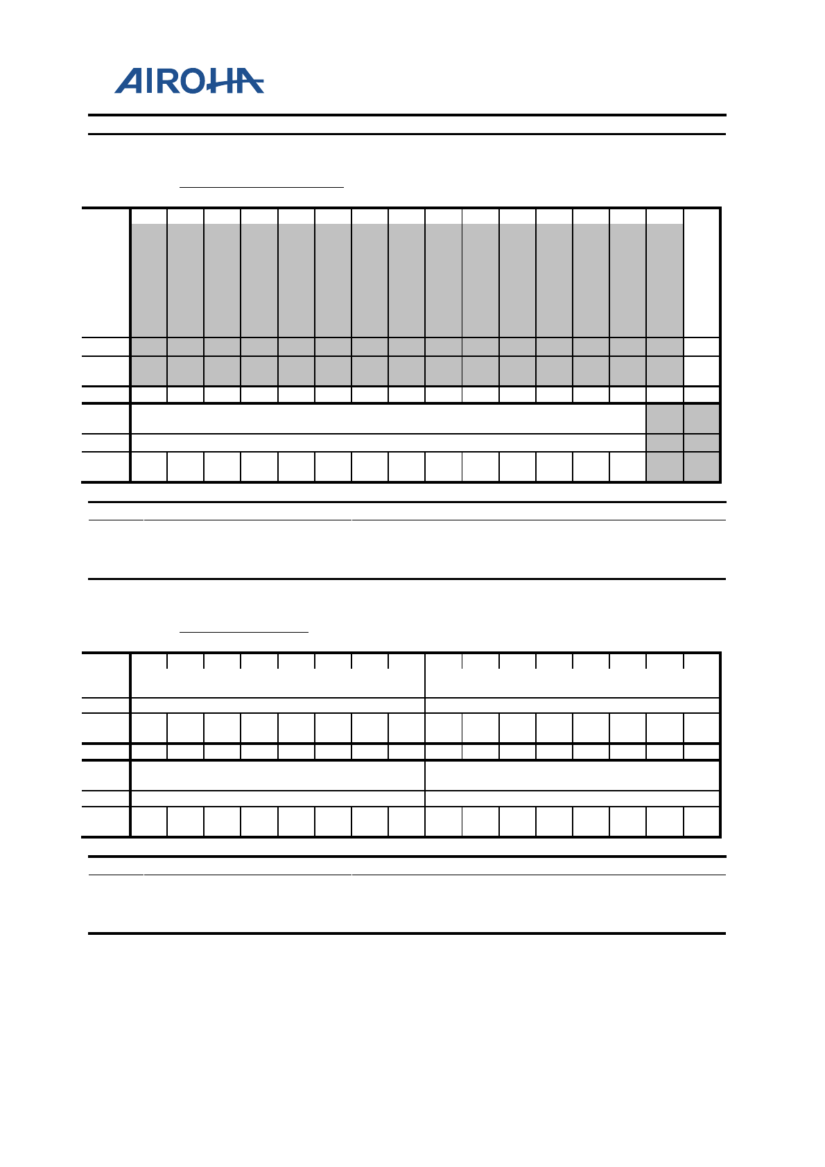
MT2523 Series Reference Manual
© 2015 - 2018 Airoha Technology Corp.
Page 389 of 692
This document contains information that is proprietary to Airoha Technology Corp. (“Airoha”) and/or its licensor(s).
Any unauthorized use, reproduction or disclosure of this document in whole or in part is strictly prohibited.
Bit(s)
Name
Description
A04A0064
DSI_HSTX_CKLP_WC
DSI HSTX Clock Low-power Mode
Word Count Register
00010000
Bit
31
30
29
28
27
26
25
24
23
22
21
20
19
18
17
16
Nam
e
HS
TX
_C
KL
P_
WC
_A
UT
O
Type
RW
Rese
t
1
Bit
15
14
13
12
11
10
9
8
7
6
5
4
3
2
1
0
Nam
e
HSTX_CKLP_WC
Type
RW
Rese
t
0 0 0 0 0 0 0 0 0 0 0 0 0 0
Bit(s)
Name
Description
16
HSTX_CKLP_WC_AUTO
Automatic calculation for HSTX_CKLP_WC
15:2
HSTX_CKLP_WC
Word count of non-continuous clock lane counter
Sets up HSTX clock low
-power period when HSTX_CKLP_EN = 1.
Refer to programming guide for details on the usage.
A04A0074
DSI_RX_DATA03
DSI Receive Packet Data Byte 0 ~ 3
Register
00000000
Bit
31
30
29
28
27
26
25
24
23
22
21
20
19
18
17
16
Nam
e
BYTE3 BYTE2
Type
RO
RO
Rese
t
0 0 0 0 0 0 0 0 0 0 0 0 0 0 0 0
Bit
15
14
13
12
11
10
9
8
7
6
5
4
3
2
1
0
Nam
e
BYTE1 BYTE0
Type
RO
RO
Rese
t
0 0 0 0 0 0 0 0 0 0 0 0 0 0 0 0
Bit(s)
Name
Description
31:24
BYTE3
RX read data buffer byte 3
23:16
BYTE2
RX read data buffer byte 2
15:8
BYTE1
RX read data buffer byte 1
7:0
BYTE0
RX read data buffer byte 0
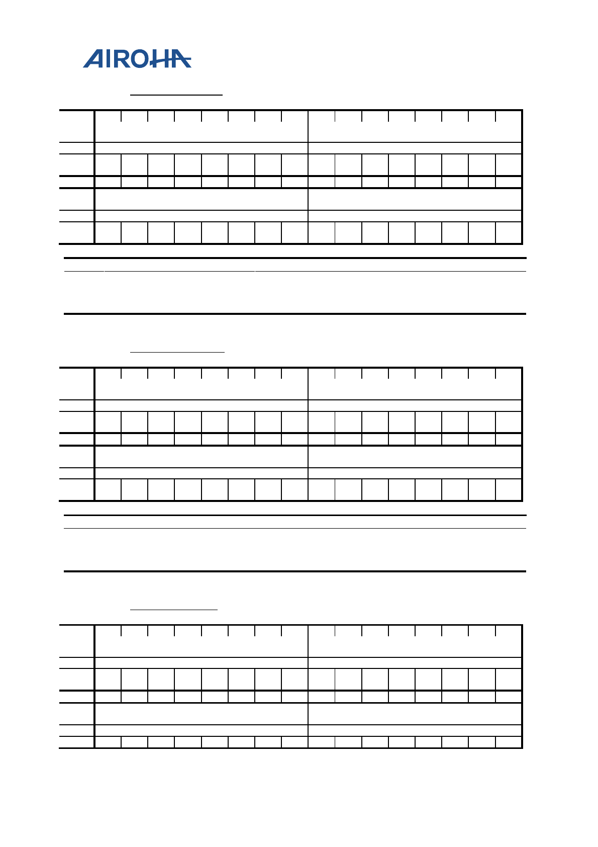
MT2523 Series Reference Manual
© 2015 - 2018 Airoha Technology Corp.
Page 390 of 692
This document contains information that is proprietary to Airoha Technology Corp. (“Airoha”) and/or its licensor(s).
Any unauthorized use, reproduction or disclosure of this document in whole or in part is strictly prohibited.
A04A0078
DSI_RX_DATA47
DSI Receive Packet Data Byte 4 ~ 7
Register
00000000
Bit
31
30
29
28
27
26
25
24
23
22
21
20
19
18
17
16
Nam
e
BYTE7 BYTE6
Type
RO
RO
Rese
t
0 0 0 0 0 0 0 0 0 0 0 0 0 0 0 0
Bit
15
14
13
12
11
10
9
8
7
6
5
4
3
2
1
0
Nam
e
BYTE5 BYTE4
Type
RO
RO
Rese
t
0 0 0 0 0 0 0 0 0 0 0 0 0 0 0 0
Bit(s)
Name
Description
31:24
BYTE7
RX read data buffer byte 7
23:16
BYTE6
RX read data buffer byte 6
15:8
BYTE5
RX read data buffer byte 5
7:0
BYTE4
RX read data buffer byte 4
A04A007C
DSI_RX_DATA8B
DSI Receive Packet Data Byte 8 ~ 11
Register
00000000
Bit
31
30
29
28
27
26
25
24
23
22
21
20
19
18
17
16
Nam
e
BYTEB BYTEA
Type
RO
RO
Rese
t
0 0 0 0 0 0 0 0 0 0 0 0 0 0 0 0
Bit
15
14
13
12
11
10
9
8
7
6
5
4
3
2
1
0
Nam
e
BYTE9 BYTE8
Type
RO
RO
Rese
t
0 0 0 0 0 0 0 0 0 0 0 0 0 0 0 0
Bit(s)
Name
Description
31:24
BYTEB
RX read data buffer byte 11
23:16
BYTEA
RX read data buffer byte 10
15:8
BYTE9
RX read data buffer byte 9
7:0
BYTE8
RX read data buffer byte 8
A04A0080
DSI_RX_DATAC
DSI Receive Packet Data Byte 12 ~ 15
Register
00000000
Bit
31
30
29
28
27
26
25
24
23
22
21
20
19
18
17
16
Nam
e
BYTEF BYTEE
Type
RO
RO
Rese
t
0 0 0 0 0 0 0 0 0 0 0 0 0 0 0 0
Bit
15
14
13
12
11
10
9
8
7
6
5
4
3
2
1
0
Nam
e
BYTED BYTEC
Type
RO
RO
Rese
0
0
0
0
0
0
0
0
0
0
0
0
0
0
0
0
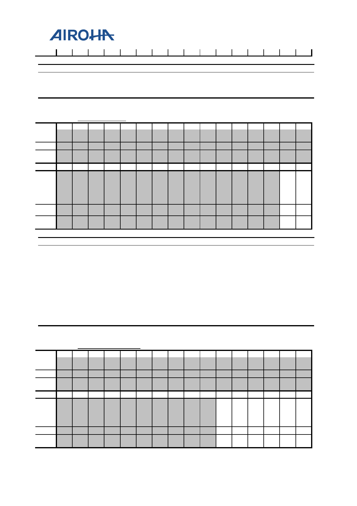
MT2523 Series Reference Manual
© 2015 - 2018 Airoha Technology Corp.
Page 391 of 692
This document contains information that is proprietary to Airoha Technology Corp. (“Airoha”) and/or its licensor(s).
Any unauthorized use, reproduction or disclosure of this document in whole or in part is strictly prohibited.
t
Bit(s)
Name
Description
31:24
BYTEF
RX read data buffer byte 15
23:16
BYTEE
RX read data buffer byte 14
15:8
BYTED
RX read data buffer byte 13
7:0
BYTEC
RX read data buffer byte 12
A04A0084
DSI_RX_RACK
DSI Read Data Acknowledge Register
00000000
Bit
31
30
29
28
27
26
25
24
23
22
21
20
19
18
17
16
Nam
e
Type
Rese
t
Bit
15
14
13
12
11
10
9
8
7
6
5
4
3
2
1
0
Nam
e
RA
CK
_B
YP
AS
S
RA
CK
Type RW
W1
C
Rese
t
0 0
Bit(s)
Name
Description
1
RACK_BYPASS
Enables RX read acknowledge bypass
Set this bit to enable to ignore RACK from SW and continue next
commands
1: Does not check RACK
0: Check RACK
0
RACK
Acknowledges RX read
When a read command is executed and read data are received
completely, the LPRX_RD_RDY interrupt will be issued. After read
from the RX_DATA buffer, set up this bit to
continue to the next
command.
1: Acknowledge
0: No effect
A04A0088
DSI_RX_TRIG_STA
DSI Receiver Status Register
00000000
Bit
31
30
29
28
27
26
25
24
23
22
21
20
19
18
17
16
Nam
e
Type
Rese
t
Bit
15
14
13
12
11
10
9
8
7
6
5
4
3
2
1
0
Nam
e
DI
RE
CTI
ON
RX
_U
LP
S
RX
_T
RI
G_
3
RX
_T
RI
G_
2
RX
_T
RI
G_
1
RX
_T
RI
G_
0
Type
RU
RU
RU
RU
RU
RU
Rese
t
0 0 0 0 0 0
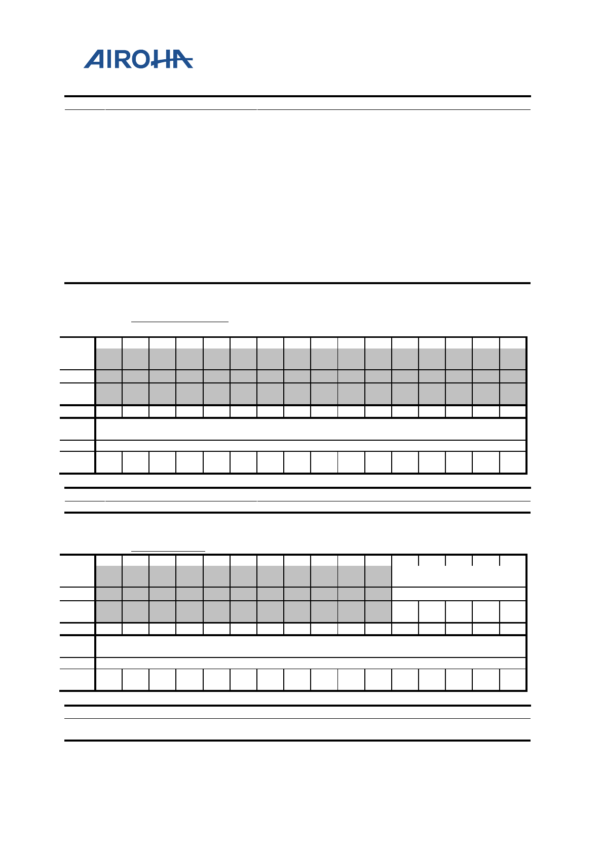
MT2523 Series Reference Manual
© 2015 - 2018 Airoha Technology Corp.
Page 392 of 692
This document contains information that is proprietary to Airoha Technology Corp. (“Airoha”) and/or its licensor(s).
Any unauthorized use, reproduction or disclosure of this document in whole or in part is strictly prohibited.
Bit(s)
Name
Description
5
DIRECTION
Escape turnaround direction
Current bus direction of Data Lane 0. If set to 1, there will be
reverse direction transmission on Data Lane0 in Low Power mode.
Otherwise, it will be a forward direction transmission.
1: Reverse direction
0: Forward direction
4
RX_ULPS
RX ULPS (Ultra-low power state)
Entry pattern is 00011110
3
RX_TRIG_3
Reserved by DSI specification.
Entry pattern is 10100000
2
RX_TRIG_2
Acknowledge.
Entry pattern is 00100001
1
RX_TRIG_1
TE.
Entry pattern is 01011101
0
RX_TRIG_0
Remote application reset.
Entry pattern is 01100010
A04A0090
DSI_MEM_CONTI
DSI Memory Continue Command
Register
00000000
Bit
31
30
29
28
27
26
25
24
23
22
21
20
19
18
17
16
Nam
e
Type
Rese
t
Bit
15
14
13
12
11
10
9
8
7
6
5
4
3
2
1
0
Nam
e
DSI_RWMEM_CONTI
Type
RW
Rese
t
0 0 0 0 0 0 0 0 0 0 0 0 0 0 0 0
Bit(s)
Name
Description
15:0
DSI_RWMEM_CONTI
Read/Write memory continue command.
A04A0094
DSI_FRM_BC
DSI Frame Byte Count Register
00000000
Bit
31
30
29
28
27
26
25
24
23
22
21
20
19
18
17
16
Nam
e
DSI_FRM_BC
Type
RW
Rese
t
0 0 0 0 0
Bit
15
14
13
12
11
10
9
8
7
6
5
4
3
2
1
0
Nam
e
DSI_FRM_BC
Type
RW
Rese
t
0 0 0 0 0 0 0 0 0 0 0 0 0 0 0 0
Bit(s)
Name
Description
20:0
DSI_FRM_BC
Frame buffer byte count
The total number of byte is expected to be read for type3 command.
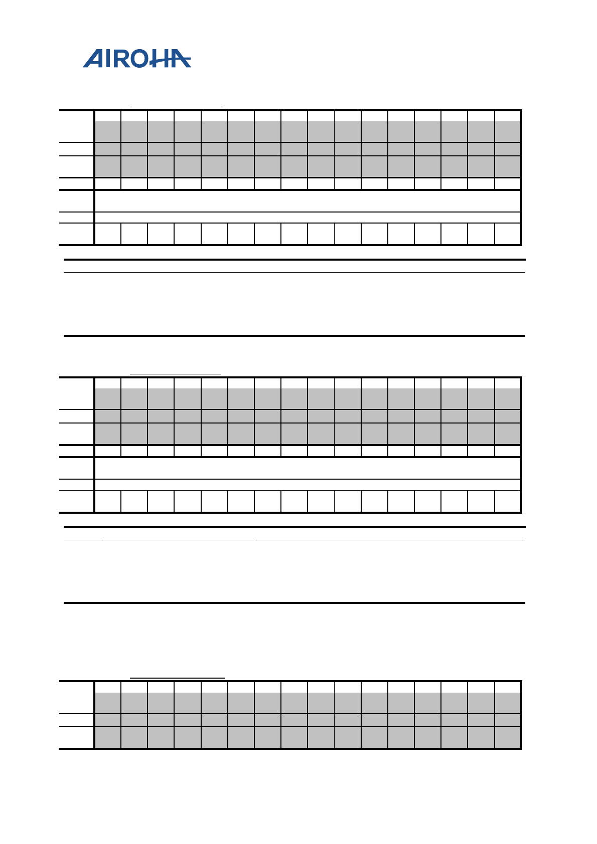
MT2523 Series Reference Manual
© 2015 - 2018 Airoha Technology Corp.
Page 393 of 692
This document contains information that is proprietary to Airoha Technology Corp. (“Airoha”) and/or its licensor(s).
Any unauthorized use, reproduction or disclosure of this document in whole or in part is strictly prohibited.
A04A00A0
DSI_TIME_CON0
DSI Timing Control 0 Register
00000080
Bit
31
30
29
28
27
26
25
24
23
22
21
20
19
18
17
16
Nam
e
Type
Rese
t
Bit
15
14
13
12
11
10
9
8
7
6
5
4
3
2
1
0
Nam
e
ULPS_WAKEUP_PRD
Type
RW
Rese
t
0 0 0 0 0 0 0 0 1 0 0 0 0 0 0 0
Bit(s)
Name
Description
15:0
ULPS_WAKEUP_PRD
ULPS wakeup period
Cycle count for ultra
-low power state (ULPS) wake-up during
ULPS
-exit sequence.
Total wait time = (ULPS_WAKEUP_PRD*1024*DSI clock cycle
time)
Default value: 5ms under 26MHz DSI byte clock
A04A00A4
DSI_TIME_CON1
DSI Timing Control 1 Register
00002000
Bit
31
30
29
28
27
26
25
24
23
22
21
20
19
18
17
16
Nam
e
Type
Rese
t
Bit
15
14
13
12
11
10
9
8
7
6
5
4
3
2
1
0
Nam
e
TE_TIMEOUT_PRD
Type
RW
Rese
t
0 0 1 0 0 0 0 0 0 0 0 0 0 0 0 0
Bit(s)
Name
Description
15:0
TE_TIMEOUT_PRD
TE time-out check period
Cycle count to check TE time
-out and issue time-
out interrupt when
waiting for TE signal.
Total wait time =
(TE_TIMEOUT_PRD*16384*DSI clock cycle
time)
Default value: 5sec under 26MHz DSI byte clock
A04A0104
DSI_PHY_LCCON
DSI PHY Lane Clock Control Register
00000000
Bit
31
30
29
28
27
26
25
24
23
22
21
20
19
18
17
16
Nam
e
Type
Rese
t
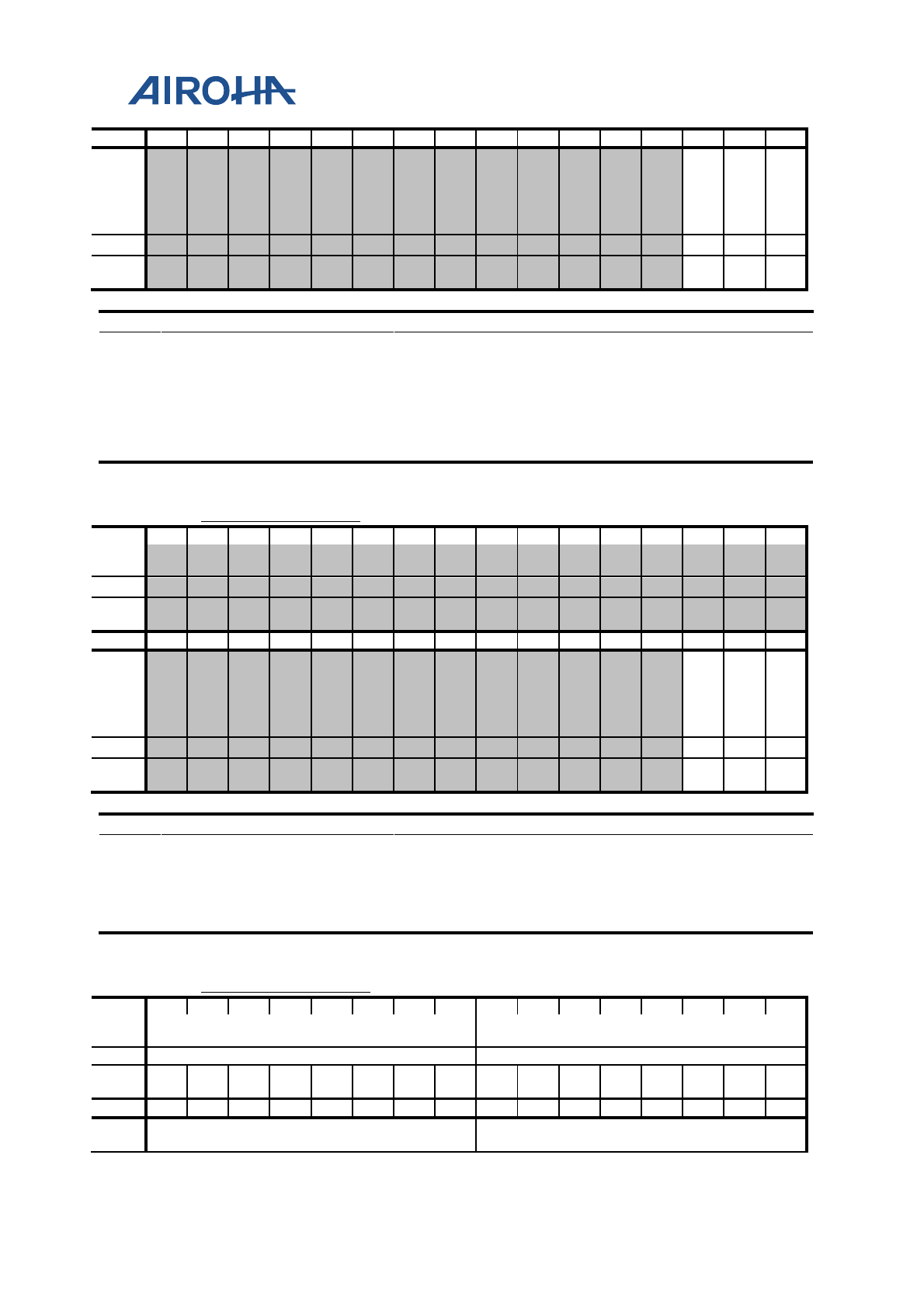
MT2523 Series Reference Manual
© 2015 - 2018 Airoha Technology Corp.
Page 394 of 692
This document contains information that is proprietary to Airoha Technology Corp. (“Airoha”) and/or its licensor(s).
Any unauthorized use, reproduction or disclosure of this document in whole or in part is strictly prohibited.
Bit
15
14
13
12
11
10
9
8
7
6
5
4
3
2
1
0
Nam
e
LC
_W
AK
EU
P_
EN
LC
_U
LP
M_
EN
LC
_H
ST
X_
EN
Type
RW
RW
RW
Rese
t
0 0 0
Bit(s)
Name
Description
2
LC_WAKEUP_EN
Enables clock lane wake-up
Make the clock lane wake
-up from ultra-low power mode. Make
sure DSI_EN = 1 when setting this register
1
LC_ULPM_EN
Enables clock lane ULPS
Make the clock lane go to ultra
-low power mode. Make sure
DSI_EN = 1 when setup this register
0
LC_HSTX_EN
Enables clock lane HS mode
Start clock lane high speed transmission.
A04A0108
DSI_PHY_LD0CON
DSI PHY Lane 0 Control Register
00000000
Bit
31
30
29
28
27
26
25
24
23
22
21
20
19
18
17
16
Nam
e
Type
Rese
t
Bit
15
14
13
12
11
10
9
8
7
6
5
4
3
2
1
0
Nam
e
L0
_W
AK
EU
P_
EN
L0
_U
LP
M_
EN
L0
_R
M_
TRI
G_
EN
Type
RW
RW
RW
Rese
t
0 0 0
Bit(s)
Name
Description
2
L0_WAKEUP_EN
Enables data lane 0 wake-up
Make the data lane 0 wake-up from ultra-low power mode.
1
L0_ULPM_EN
Enables data lane 0 ULPS
Make the data lane 0 go to ultra-low power mode.
0
L0_RM_TRIG_EN
Enables data lane 0 remote application trigger
Send application trigger to slave side.
A04A0110
DSI_PHY_TIMCON0
DSI PHY Timing Control 0 Register
14140A0A
Bit
31
30
29
28
27
26
25
24
23
22
21
20
19
18
17
16
Nam
e
DA_HS_TRAIL DA_HS_ZERO
Type
RW
RW
Rese
t
0 0 0 1 0 1 0 0 0 0 0 1 0 1 0 0
Bit
15
14
13
12
11
10
9
8
7
6
5
4
3
2
1
0
Nam
e
DA_HS_PREP LPX
MT2523 Series Reference Manual
© 2015 - 2018 Airoha Technology Corp.
Page 395 of 692
This document contains information that is proprietary to Airoha Technology Corp. (“Airoha”) and/or its licensor(s).
Any unauthorized use, reproduction or disclosure of this document in whole or in part is strictly prohibited.
Type
RW
RW
Rese
t
0 0 0 0 1 0 1 0 0 0 0 0 1 0 1 0
Bit(s)
Name
Description
31:24
DA_HS_TRAIL
Control for timing parameter: T_HS-Trail
23:16
DA_HS_ZERO
Control for timing parameter: T_HS-Zero
15:8
DA_HS_PREP
Control for timing parameter: T_HS-Prepare
7:0
LPX
Control for timing parameter: T_LPX
A04A0114
DSI_PHY_TIMCON1
DSI PHY Timing Control 1 Register
0E1A1632
Bit
31
30
29
28
27
26
25
24
23
22
21
20
19
18
17
16
Nam
e
CLK_HS_EXIT TA_GET
Type
RW
RW
Rese
t
0 0 0 0 1 1 1 0 0 0 0 1 1 0 1 0
Bit
15
14
13
12
11
10
9
8
7
6
5
4
3
2
1
0
Nam
e
TA_SURE TA_GO
Type
RW
RW
Rese
t
0 0 0 1 0 1 1 0 0 0 1 1 0 0 1 0
Bit(s)
Name
Description
31:24
CLK_HS_EXIT
Control for timing parameter: T_HS-Exit for clock lane
23:16
TA_GET
Control for timing parameter: T_TA-Get
15:8
TA_SURE
Control for timing parameter: T_TA-Sure
7:0
TA_GO
Control for timing parameter: T_TA-Go
A04A0118
DSI_PHY_TIMCON2
DSI PHY Timing Control 2 Register
14140000
Bit
31
30
29
28
27
26
25
24
23
22
21
20
19
18
17
16
Nam
e
CLK_HS_TRAIL CLK_HS_ZERO
Type
RW
RW
Rese
t
0 0 0 1 0 1 0 0 0 0 0 1 0 1 0 0
Bit
15
14
13
12
11
10
9
8
7
6
5
4
3
2
1
0
Nam
e
Type
Rese
t
Bit(s)
Name
Description
31:24
CLK_HS_TRAIL
Control for timing parameter: T_CLK-Trail
23:16
CLK_HS_ZERO
Control for timing parameter: T_CLK-Zero
A04A011C
DSI_PHY_TIMCON3
DSI PHY Timing Control 3 Register
000E0E0A
Bit
31
30
29
28
27
26
25
24
23
22
21
20
19
18
17
16
Nam
e
DA_HS_EXIT
Type
RW
Rese
t
0 0 0 0 0 0 1 1 1 0
MT2523 Series Reference Manual
© 2015 - 2018 Airoha Technology Corp.
Page 396 of 692
This document contains information that is proprietary to Airoha Technology Corp. (“Airoha”) and/or its licensor(s).
Any unauthorized use, reproduction or disclosure of this document in whole or in part is strictly prohibited.
Bit
15
14
13
12
11
10
9
8
7
6
5
4
3
2
1
0
Nam
e
CLK_HS_POST CLK_HS_PREP
Type
RW
RW
Rese
t
0 0 0 0 1 1 1 0 0 0 0 0 1 0 1 0
Bit(s)
Name
Description
25:16
DA_HS_EXIT
Control for timing parameter: T_HS-Exit for data lane
15:8
CLK_HS_POST
Control for timing parameter: T_CLK-Post
7:0
CLK_HS_PREP
Control for timing parameter: T_CLK-Prepare
A04A0200
~
A04A03FC
DSI_CMDQ
[n](n=0~127)
DSI Command Queue
00000000
Bit
31
30
29
28
27
26
25
24
23
22
21
20
19
18
17
16
Nam
e
DATA_1 DATA_0
Type
RW
RW
Rese
t
0 0 0 0 0 0 0 0 0 0 0 0 0 0 0 0
Bit
15
14
13
12
11
10
9
8
7
6
5
4
3
2
1
0
Nam
e
DATA_ID RESV TE CL HS
BT
A
TYPE
Type
RW
RW
RW
RW
RW
RW
RW
Rese
t
0 0 0 0 0 0 0 0 0 0 0 0 0 0 0 0
Bit(s)
Name
Description
31:24
DATA_1
Data byte 1 of command
23:16
DATA_0
Data byte 0 of command
15:8
DATA_ID
Data ID of command
7:6
RESV
Reserved
5
TE
Enables internal or external TE
0: Disable
1: Enable
4
CL
Selects DCS byte
0: 1-byte DCS
1: 2-byte DCS
3
HS
Enables high-speed transmission
0: LPTX transmission
1: HSTX transmission
2
BTA
Enables BTA
0: Disable
1: Enable
1:0
TYPE
Command types
0: Type-0 command
1: Type-1 command
2: Type-2 command
3: Type-3 command
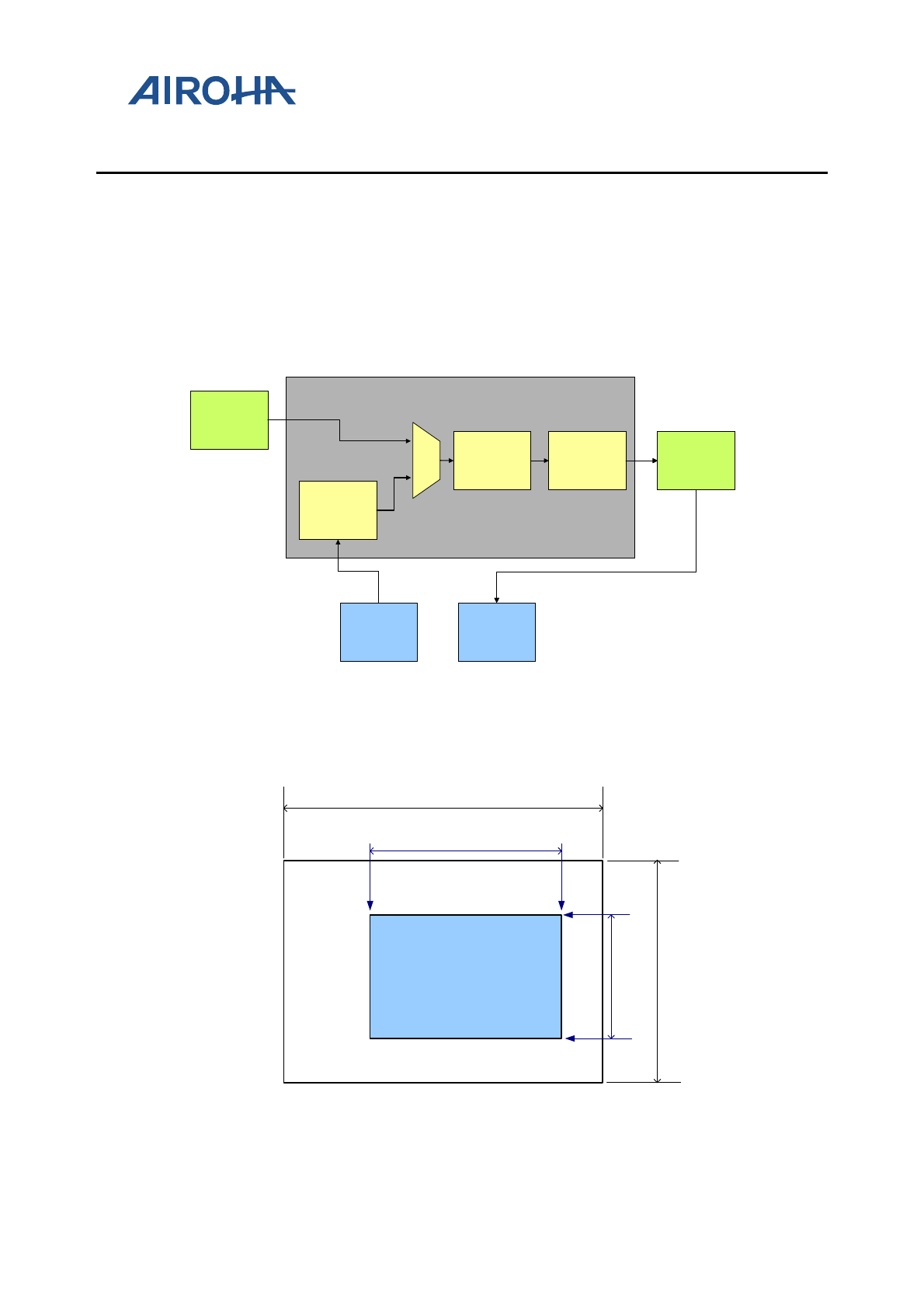
MT2523 Series Reference Manual
© 2015 - 2018 Airoha Technology Corp.
Page 397 of 692
This document contains information that is proprietary to Airoha Technology Corp. (“Airoha”) and/or its licensor(s).
Any unauthorized use, reproduction or disclosure of this document in whole or in part is strictly prohibited.
25. Image Resizer
25.1. General Description
This block provides the image resizing function for image and video capturing scenarios. It receives image data
from the Caminf module or from memory input, performs the image resizing function and outputs to the
ROTATOR. shows the block diagram. The resizer is composed of horizontal and vertical resizing blocks. It can scale
up or down the input image by any ratio. It also supports tile processing which can combines tiles into a full frame
in memory-input mode. The maximum size of input images is limited to 2047x2047 and maximum size of output
images is limited to 2047x2047.
Figure 25-1. Image Resizer Overview
25.2. Application Notes
INPUT IMAGE
CROPPED IMAGE
ORIGSZ.WS
SRCSZ.WS
CROP_L CROP_R
ORIGSZ.HS
SRCSZ.HS
CROP_T CROP_B
Caminf
Memory
CROP Resizing
Memory Input
(CLIP)
Rotator
Memory
UYVY
YUV420
YUV422
UYVY
YUV420
YUV422
YUV444
(UV duplicated)
YUV444
(UV duplicated)
Image Resizer
Caminf
Memory
CROP Resizing
Memory Input
(CLIP)
Rotator
Memory
UYVY
YUV420
YUV422
UYVY
YUV420
YUV422
YUV444
(UV duplicated)
YUV444
(UV duplicated)
Caminf
Memory
CROP Resizing
Memory Input
(CLIP)
Rotator
Memory
UYVY
YUV420
YUV422
UYVY
YUV420
YUV422
YUV444
(UV duplicated)
YUV444
(UV duplicated)
Image Resizer
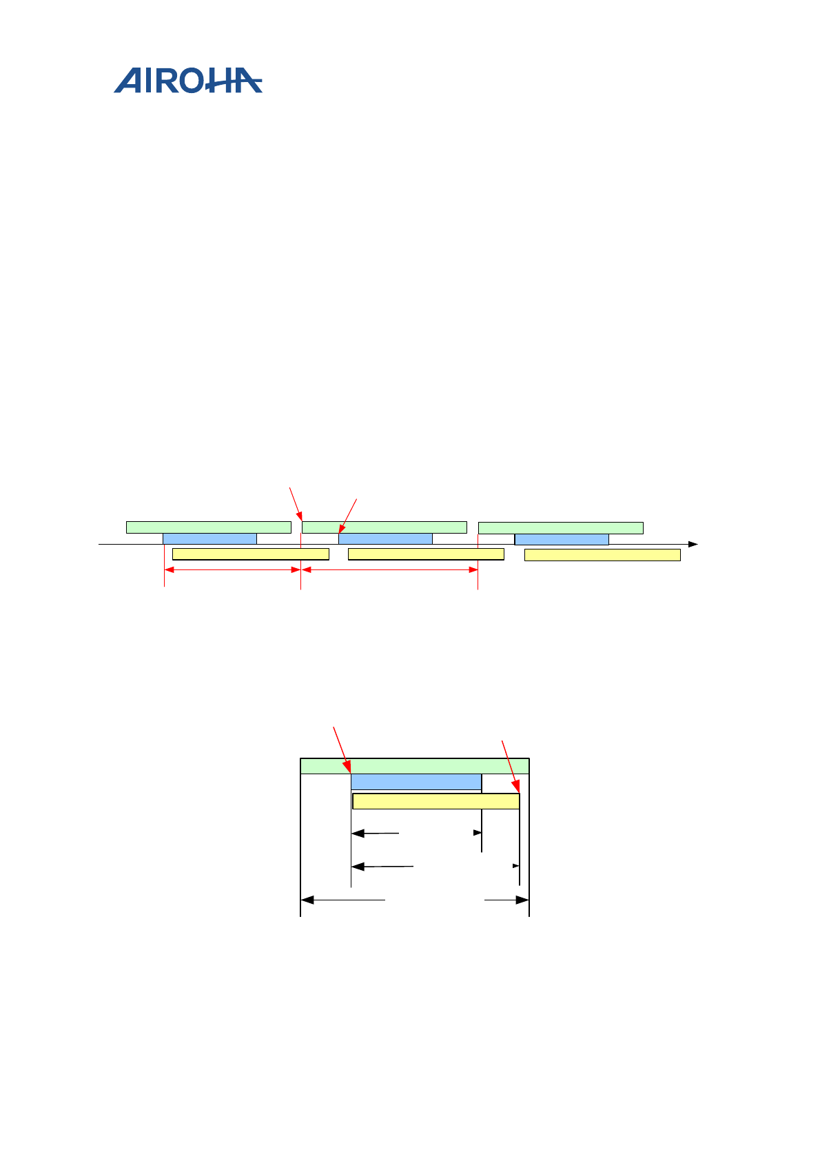
MT2523 Series Reference Manual
© 2015 - 2018 Airoha Technology Corp.
Page 398 of 692
This document contains information that is proprietary to Airoha Technology Corp. (“Airoha”) and/or its licensor(s).
Any unauthorized use, reproduction or disclosure of this document in whole or in part is strictly prohibited.
There is a cropping example. Assuming an uncropped image with size = (640, 480), if the size of the cropped frame
is (320, 240) and the cropped region is the center of input frame. Then the setting will be CROP_L = 160, CROP_R =
479, CROP_T = 120, CROP_B = 359, and SRCSZ_WS = 320, SRCSZ_HS = 240.
Note that there are two kinds of registers, registers related to cropping function and the rest registers, including
ratio, and size, etc. Two kinds of double buffered registers have two separated updating time as described in the .
In the normal case, registers related to cropping function will be updated at B if the following criterion is satisfied:
1. LOCK bit is not ‘1’ at B.
The rest registers will be updated at C if the following criteria are satisfied:
1. LOCK bit is not ‘1’ at B.
2. LOCK bit is not changed from B to C.
To make sure HW double buffered registers behave by this rule, we can guarantee that the cropping registers and
the rest registers take effect at the same frame. However, from input frame #0, if after interrupt is asserted at A
and FW cannot finish registers programming before B, then all the registers will take function at frame #2.
Cropped frame #2
Input frame #0
Cropped frame #0Input frame #1
Cropped frame #1
Upscaled output frame #1
time
update crop registers
if not lock update rest registers if:
1. B is not lock
2. LOCK bit is not changed from B to C
Settings take effect at frame #1
Upscaled output frame #0
A
B
C
Input frame #2
Upscaled output frame #2
Settings take effect at frame #2
Figure 25-2. Resizer double buffered registers updating and taking effect timing chart
As shown in , in cropping mode, the FSTINT is asserted at the beginning of cropped frame. The FEDINT is asserted
at the end of output frame. There are three independent busy status bits for three different frames, input frame,
cropping frame and output frame.
Input frame #0
Cropped frame #0
FSTINT
output frame #0
FEDINT
BUSYC
BUSYO
BUSYI
Figure 25-3. Resizer interrupt and busy asserting timing chart
INBUSY
OUTBUSY
CROPBUSY

MT2523 Series Reference Manual
© 2015 - 2018 Airoha Technology Corp.
Page 399 of 692
This document contains information that is proprietary to Airoha Technology Corp. (“Airoha”) and/or its licensor(s).
Any unauthorized use, reproduction or disclosure of this document in whole or in part is strictly prohibited.
- Configuration procedure when source is cam
RESZ_CFG = 0x10 (continuous), 0x0 (single run);
RESZ_SRCSZ1 = source image size;
RESZ_TARSZ1 = target image size;
RESZ_HRATIO1 = horizontal ratio;
RESZ_VRATIO1 = vertical ratio;
RESZ_HRES1 = horizontal residual;
RESZ_VRES1 = vertical residual;
RESZ_FRCFG = working memory size, interrupt enable;
RESZ_CON = 0x1;
- Configuration procedure when source is memory (frame mode)
RESZ_CFG = 0x1 or 0x2 or 0x3 (single run);
RESZ_SMBASE_Y = source memory for Y base address;
RESZ_SMBASE_U = source memory for U base address;
RESZ_SMBASE_V = source memory for V base address;
RESZ_SRCSZ1 = source image size;
RESZ_TARSZ1 = target image size;
RESZ_HRATIO1 = horizontal ratio;
RESZ_VRATIO1 = vertical ratio;
RESZ_HRES1 = horizontal residual;
RESZ_VRES1 = vertical residual;
RESZ_FRCFG = working memory size, interrupt enable;
RESZ_CON = 0x1;
- Configuration procedure when source is memory (tile mode)
RESZ_CFG = 0x10001 or 0x10002 or 0x10003 (single run);
RESZ_SMBASE_Y = source tile memory for Y base address;
RESZ_SMBASE_U = source tile memory for U base address;
RESZ_SMBASE_V = source tile memory for V base address;
RESZ_SRCSZ1 = source tile size;
RESZ_TARSZ1 = target tile size;
RESZ_HRATIO1 = horizontal ratio;
RESZ_VRATIO1 = vertical ratio;
RESZ_HRES1 = horizontal residual;
RESZ_VRES1 = vertical residual;
Setup tile parameters according tile formula
RESZ_FRCFG = working memory size, interrupt enable;
RESZ_CON = 0x1;
- Configuration procedure for disable clock.
RESZ_CON = 0x0;
RESZ_CON = 0X10000;
while ((RESZ_CON&0x10000) == 1) ;
RESZ_FRCFG = RESZ_FRCFG & 0xFFFF13FF;
SWInt = RESZ_INT & 0x0000003F;
Disable clock;
MT2523 Series Reference Manual
© 2015 - 2018 Airoha Technology Corp.
Page 400 of 692
This document contains information that is proprietary to Airoha Technology Corp. (“Airoha”) and/or its licensor(s).
Any unauthorized use, reproduction or disclosure of this document in whole or in part is strictly prohibited.
25.3. Register Definition
Address Name Width Register Function
A0410000 RESZ_CFG 32 Image Resizer Configuration Register
The register is for global configuration of Image Resizer.
A0410004 RESZ_CON 32
Image Resizer Control Register
The register is for global control of Image Resizer. Furthermore, software reset will
not reset all register setting. Remember trigger Image Resizer first before trigger
image sources to Image Resizer.
A0410008 RESZ_STA 32 Image Resizer Status Register
The register indicates global status of Image Resizer.
A041000C RESZ_INT 32 Image Resizer Interrupt Register
The register shows up the interrupt status of resizer.
A0410010 RESZ_SRCSZ1 32
Image Resizer Source Image Size Register 1
The register specifies the size of source image. The allowable maximum size is
2047x2047.
A0410014 RESZ_TARSZ1 32
Image Resizer Target Image Size Register 1
The register specifies the size of target image. The allowable maximum size is
960x2047 with resizing and 2047x2047 without resizing. However, it is suggested to
limit WT <= 480 when SRC is CAM and with resizing.
A0410018 RESZ_HRATIO1 32 Image Resizer Horizontal Ratio Register 1
The register specifies horizontal resizing ratio.
A041001C RESZ_VRATIO1 32 Image Resizer Vertical Ratio Register 1
The register specifies vertical resizing ratio.
A0410020 RESZ_HRES1 32
Image Resizer Horizontal Residual Register 1
The register specifies horizontal residual. It is obtained by RESZ_SRCSZ1.WS %
RESZ_TARSZ1.WT.
A0410024 RESZ_VRES1 32
Image Resizer Vertical Residual Register 1
The register specifies vertical residual. It is obtained by RESZ_SRCSZ1.HS %
RESZ_TARSZ1.HT.
A041002C RESZ_LOCK 32
Image Resizer LOCK Register
This register specifies the lock register. Once this bit is programmed to be '1', Resizer
stops updating double buffered registers at Vsync. The function of lock register is to
prevent Resizer updating only partial parameters when firmware programs registers
near input Vsync. Set to 1 before changing size related registers, and set to 0 after
all size related registers are programmed.
A0410030 RESZ_ORIGSZ1 32
Image Resizer Crop Original Size Register 1
These registers are only used when CROP_EN = '1'. This field specifies original size
before image cropping.
A0410034 RESZ_CROPLR1 32
Image Resizer Crop Left Right Register 1
These registers are only used when CROP_EN = '1'. This field specifies the horizontal
start and end position index for image cropping. Please note that these indexes are
defined as the following illustration. For an uncropped image, the index of start
point is 0 and the index of end point is (ORIGSZ_WS-1). The width cropped frame is
therefore defined as (CROP_R - CROP_L+1).
A0410038 RESZ_CROPTB1 32
Image Resizer Crop Top Bottom Register 1
These registers are only used when CROP_EN = '1'. This field specifies the vertical
start and end position index for image cropping. Please note that these indexes are
defined as the following illustration. For an uncropped image, the index of start
point is 0 and the index of end point is (ORIGSZ_HS-1). The height cropped frame is
therefore defined as (CROP_B - CROP_T+1).
MT2523 Series Reference Manual
© 2015 - 2018 Airoha Technology Corp.
Page 401 of 692
This document contains information that is proprietary to Airoha Technology Corp. (“Airoha”) and/or its licensor(s).
Any unauthorized use, reproduction or disclosure of this document in whole or in part is strictly prohibited.
Address Name Width Register Function
A0410040 RESZ_FRCFG 32
Image Resizer Fine Resizing Configuration Register
The register specifies various setting of control for fine resizing, including of
horizontal and vertical resizing. Note that all parameters must be set before
horizontal and vertical resizing proceeds.
A0410090 RESZ_DBGCFG 32 Image Resizer Debug Configuration Register
The register is used to help debug.
A04100B0 RESZ_INFO0 32 Image Resizer Information Register 0
A04100B4 RESZ_INFO1 32 Image Resizer Information Register 1
A04100DC RESZ_SMBASE_Y 32
Image Resizer Y-Component Source Memory Base Address Register
The register specifies the base address of memory input for Y-component or UYVY
format. It's only useful in Memory input mode. It should be 4 bytes aligned without
CLIP_EN. It should be format aligned with CLIP_EN. That is 4 bytes for UYVY format
and 2 bytes for YUV420 and YUV422 format. However, the base address before
clipping must be 4 bytes aligned.
A04100E0 RESZ_SMBASE_U 32
Image Resizer U-Component Source Memory Base Address Register
The register specifies the base address of memory input for U-component. It's only
useful in Memory input mode. It should be 4 bytes aligned without CLIP_EN. It
should be format aligned with CLIP_EN. That is 1 byte. However, the base address
before clipping must be 4 bytes aligned.
A04100E4 RESZ_SMBASE_V 32
Image Resizer V-Component Source Memory Base Address Register
The register specifies the base address of memory input for V-component. It's only
useful in Memory input mode. It should be 4 bytes aligned without CLIP_EN. It
should be format aligned with CLIP_EN. That is 1 byte. However, the base address
before clipping must be 4 bytes aligned.
A04100F0 RESZ_GMCCON 32 Image Resizer GMC Control Register
A04100FC RESZ_CLIP 32 Image Resizer CLIP Register
A0410100 RESZ_TILE_CFG 32 Image Resizer Tile Configuration Register
Configuration setting of tile-based resizer.
A0410104 RESZ_TILE_START_POS
_X1 32 Image Resizer Tile Start Position X Register 1
Start setting of tile-based resizer.
A041010C RESZ_TILE_START_POS
_Y1 32 Image Resizer Tile Start Position Y Register 1
Start setting of tile-based resizer.
A0410114 RESZ_BI_TRUNC_ERR_
COMP1 32 Image Resizer Bilinear Truncation Error Compensation Register 1
Bilinear setting of tile-based resizer.
A0410118 RESZ_BI_INIT_RESID1 32 Image Resizer Bilinear Initial Residual Register 1
Bilinear setting of tile-based resizer.
All undefined bit fields must be set as the default values.
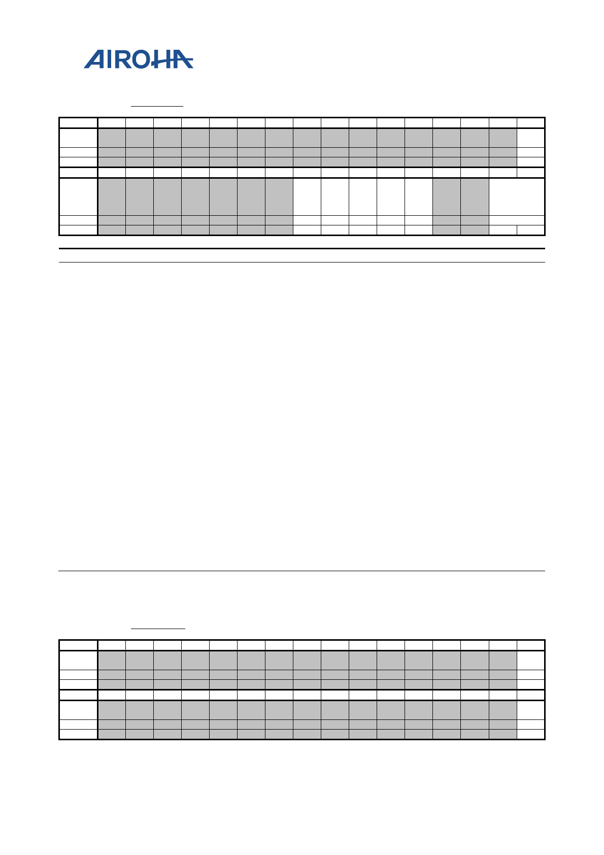
MT2523 Series Reference Manual
© 2015 - 2018 Airoha Technology Corp.
Page 402 of 692
This document contains information that is proprietary to Airoha Technology Corp. (“Airoha”) and/or its licensor(s).
Any unauthorized use, reproduction or disclosure of this document in whole or in part is strictly prohibited.
A0410000 RESZ_CFG Image Resizer Configuration Register 000000
00
Bit
31
30
29
28
27
26
25
24
23
22
21
20
19
18
17
16
Name
MO
DE1
Type
RW
Reset
0
0
0
0
0
0
0
0
0
0
0
0
0
0
0
0
Bit
15
14
13
12
11
10
9
8
7
6
5
4
3
2
1
0
Name
VS
RS
TE
N2
VS
RS
TE
N1
VS
RS
TE
N0
DC
M_
DIS
PC
ON SRC1
Type
RW
RW
RW
RW
RW
RW
Reset
0
0
0
0
0
0
0
0
0
0
0
0
0
0
0
0
Bit(s)
Name
Description
16 MODE1 Mode selection of 1st pass of resizer.
0: Frame mode.
1: Tile mode.
8 VSRSTEN2 Resizer auto reset when SRC1 is camera and pixel drop is detected.
0: Disable.
1: Enable.
7 VSRSTEN1
Resizer auto reset when SRC1 is camera and new frame comes and previous
input is complete but output not complete.
0: Disable. (skip current frame)
1: Enable. (Give up previous frame)
6 VSRSTEN0 Resizer auto reset when SRC1 is camera and new frame comes.
0: Disable.
1: Enable.
5 DCM_DIS DCM enabling/disabling setting.
0: Enable DCM.
1: Disable DCM.
4 PCON
The register bit specifies if resizing continues whenever an image finishes
processing. Once continuous run for pixel-based resizing is enabled and pixel-
based resizing is running, the only way to stop is to reset resizer. If to stop
immediately is desired, reset resizer directly. If the last image is desired, set
the register bit to '0' first. Then wait until image resizer is not busy again.
Finally reset image resizer.
0: Single run.
1: Continuous run.
1:0 SRC1
The register bit specified the input source of 1st pass of resizer.
0: Camera input.
1: Memory input. Packet UYVY format.
2: Memory input. Planar YUV420 format.
3: Memory input. Planar YUV422 format.
A0410004 RESZ_CON Image Resizer Control Register 000000
00
Bit
31
30
29
28
27
26
25
24
23
22
21
20
19
18
17
16
Name
RS
T
Type
RW
Reset
0
0
0
0
0
0
0
0
0
0
0
0
0
0
0
0
Bit
15
14
13
12
11
10
9
8
7
6
5
4
3
2
1
0
Name
EN
A
Type
RW
Reset
0
0
0
0
0
0
0
0
0
0
0
0
0
0
0
0
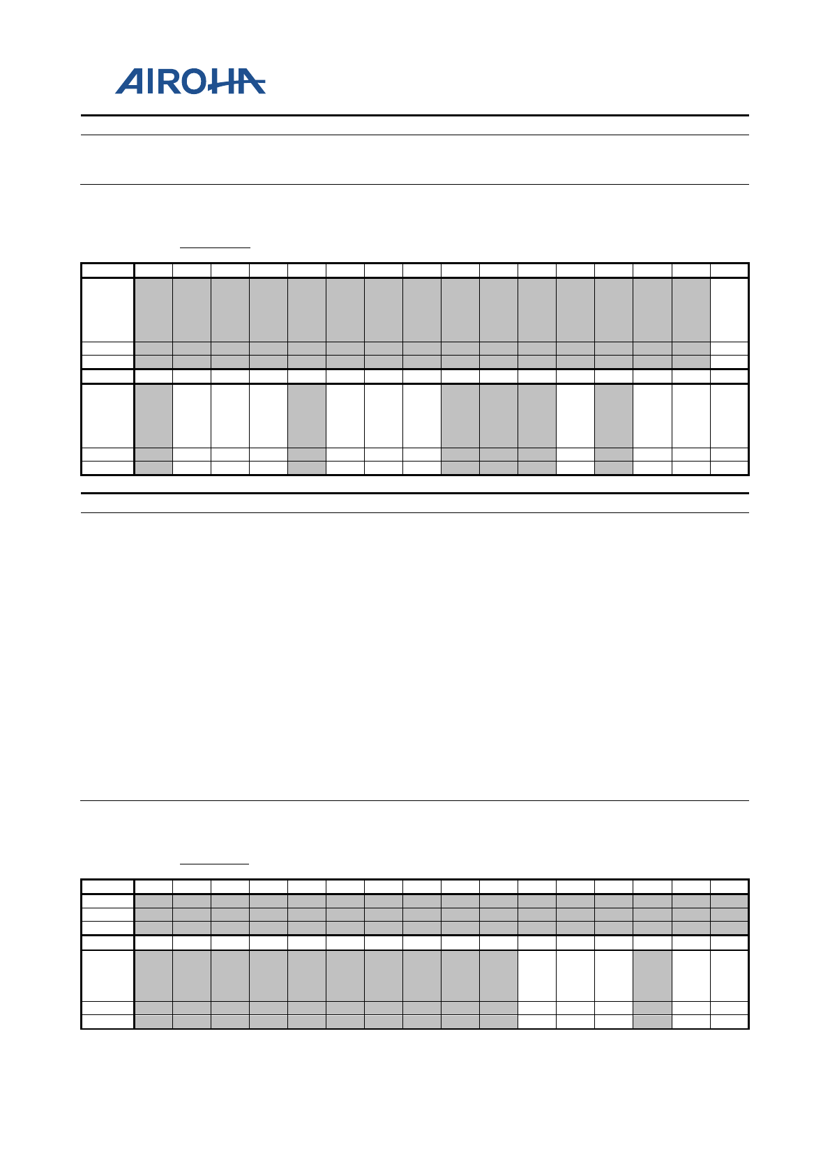
MT2523 Series Reference Manual
© 2015 - 2018 Airoha Technology Corp.
Page 403 of 692
This document contains information that is proprietary to Airoha Technology Corp. (“Airoha”) and/or its licensor(s).
Any unauthorized use, reproduction or disclosure of this document in whole or in part is strictly prohibited.
Bit(s)
Name
Description
16 RST Writing '1' to the register will cause resizing to stop. Resizer itself would clear this bit to 0
when it is ready to be enabled. When this bit is 1, do not enable resizer.
0 ENA Writing '1' to the register bit to enable resizer.
A0410008 RESZ_STA Image Resizer Status Register 000000
00
Bit
31
30
29
28
27
26
25
24
23
22
21
20
19
18
17
16
Name
DC
M_
STA
TU
S
Type
RO
Reset
0
0
0
0
0
0
0
0
0
0
0
0
0
0
0
0
Bit
15
14
13
12
11
10
9
8
7
6
5
4
3
2
1
0
Name ER
R5 ER
R4 ER
R3 ER
R2 ER
R1 ER
R0
CR
OP
BU
SY
INB
US
Y
ME
MI
NB
US
Y
OU
TB
US
Y
Type
W1C
W1C
W1C
W1C
W1C
W1C
RO
RO
RO
RO
Reset
0
0
0
0
0
0
0
0
0
0
0
0
0
0
0
0
Bit(s)
Name
Description
16 DCM_STATUS DCM status.
14 ERR5 Error status. Input pixel is not enough when crop is enabled. Write this bit to
1 or reset resizer to clear.
13 ERR4 Error status. Drop frame due to LOCK is changed between start point of
original image and start point of cropped image. Write this bit to 1 or reset
resizer to clear.
12 ERR3 Error status. Drop frame due to LOCK when vsync comes. Write this bit to 1 or
reset resizer to clear.
10 ERR2 Error status. Input complete but output not complete when new frame comes.
Write this bit to 1 or reset resizer to clear.
9 ERR1 Error status. Input pixel is not enough. Write this bit to 1 or reset resizer to
clear.
8 ERR0 Error status. Pixel over run (Camera request but resizer not ack). Write this
bit to 1 or reset resizer to clear.
4 CROPBUSY Cropping busy status.
2 INBUSY Input busy status.
1 MEMINBUSY Memory input busy status.
0 OUTBUSY Output busy status.
A041000C RESZ_INT Image Resizer Interrupt Register 000000
00
Bit
31
30
29
28
27
26
25
24
23
22
21
20
19
18
17
16
Name
Type
Reset
0
0
0
0
0
0
0
0
0
0
0
0
0
0
0
0
Bit
15
14
13
12
11
10
9
8
7
6
5
4
3
2
1
0
Name
LC
KD
RPI
NT
MI
NI
NT
PX
DI
NT
FST
AR
T1I
NT
FE
ND
INT
Type
RC
RC
RC
RC
RC
Reset
0
0
0
0
0
0
0
0
0
0
0
0
0
0
0
0
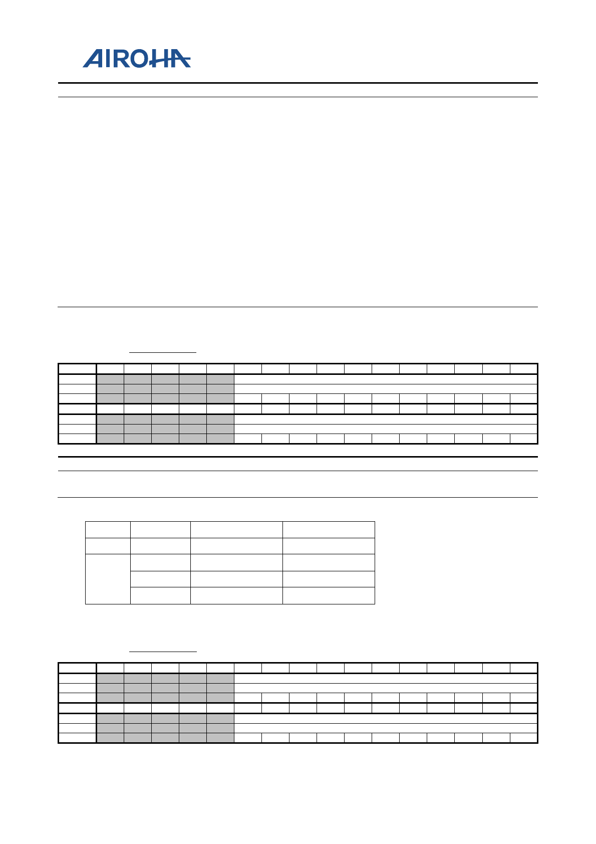
MT2523 Series Reference Manual
© 2015 - 2018 Airoha Technology Corp.
Page 404 of 692
This document contains information that is proprietary to Airoha Technology Corp. (“Airoha”) and/or its licensor(s).
Any unauthorized use, reproduction or disclosure of this document in whole or in part is strictly prohibited.
Bit(s)
Name
Description
5 LCKDRPINT
Interrupt for drop frame for lock occurs. No matter the register bit
RESZ_FRCFG.LCKDRPINTEN is enabled or not, the register bit will be active
whenever drop frame for lock occurs. It could be as software interrupt by
polling the register bit. Clear it by reading the register.
4 MININT
Interrupt for memory input. No matter the register bit
RESZ_FRCFG.MININTEN is enabled or not, the register bit will be active
whenever memory input is done. It could be as software interrupt by polling
the register bit. Clear it by reading the register.
3 PXDINT
Interrupt for pixel drop. No matter the register bit RESZ_FRCFG.PXDINTEN
is enabled or not, the register bit will be active whenever pixel drop occurs. It
could be as software interrupt by polling the register bit. Clear it by reading
the register. Useful for error detection.
1 FSTART1INT
Interrupt for frame start of 1st pass. No matter the register bit
RESZ_FRCFG.FSTART1INTEN is enabled or not, the register bit will be active
whenever a new frame of 1st pass arrives. It could be as software interrupt by
polling the register bit. Clear it by reading the register. Useful for digital
zooming.
0 FENDINT
Interrupt for frame end. No matter the register bit
RESZ_FRCFG.FENDINTEN is enabled or not, the register bit will be active
whenever whole image is done. It could be as software interrupt by polling the
register bit. Clear it by reading the register.
A0410010 RESZ_SRCSZ1 Image Resizer Source Image Size Register 1 000000
00
Bit
31
30
29
28
27
26
25
24
23
22
21
20
19
18
17
16
Name
HS
Type
RW
Reset
0
0
0
0
0
0
0
0
0
0
0
0
0
0
0
0
Bit
15
14
13
12
11
10
9
8
7
6
5
4
3
2
1
0
Name
WS
Type
RW
Reset
0
0
0
0
0
0
0
0
0
0
0
0
0
0
0
0
Bit(s)
Name
Description
26:16 HS The register field specifies the height of source image.
10:0 WS The register field specifies the width of source image.
Note: WS and HS must be format aligned (RESZ_CROPLR1.CROP_EN = 0).
src format HS WS
caminf YUV444 Multiples of 1 Multiples of 1
memory
YUV420 Multiples of 2 Multiples of 2
YUV422 Multiples of 1 Multiples of 2
UYVY Multiples of 1 Multiples of 2
A0410014 RESZ_TARSZ1 Image Resizer Target Image Size Register 1 000000
00
Bit
31
30
29
28
27
26
25
24
23
22
21
20
19
18
17
16
Name
HT
Type
RW
Reset
0
0
0
0
0
0
0
0
0
0
0
0
0
0
0
0
Bit
15
14
13
12
11
10
9
8
7
6
5
4
3
2
1
0
Name
WT
Type
RW
Reset
0
0
0
0
0
0
0
0
0
0
0
0
0
0
0
0
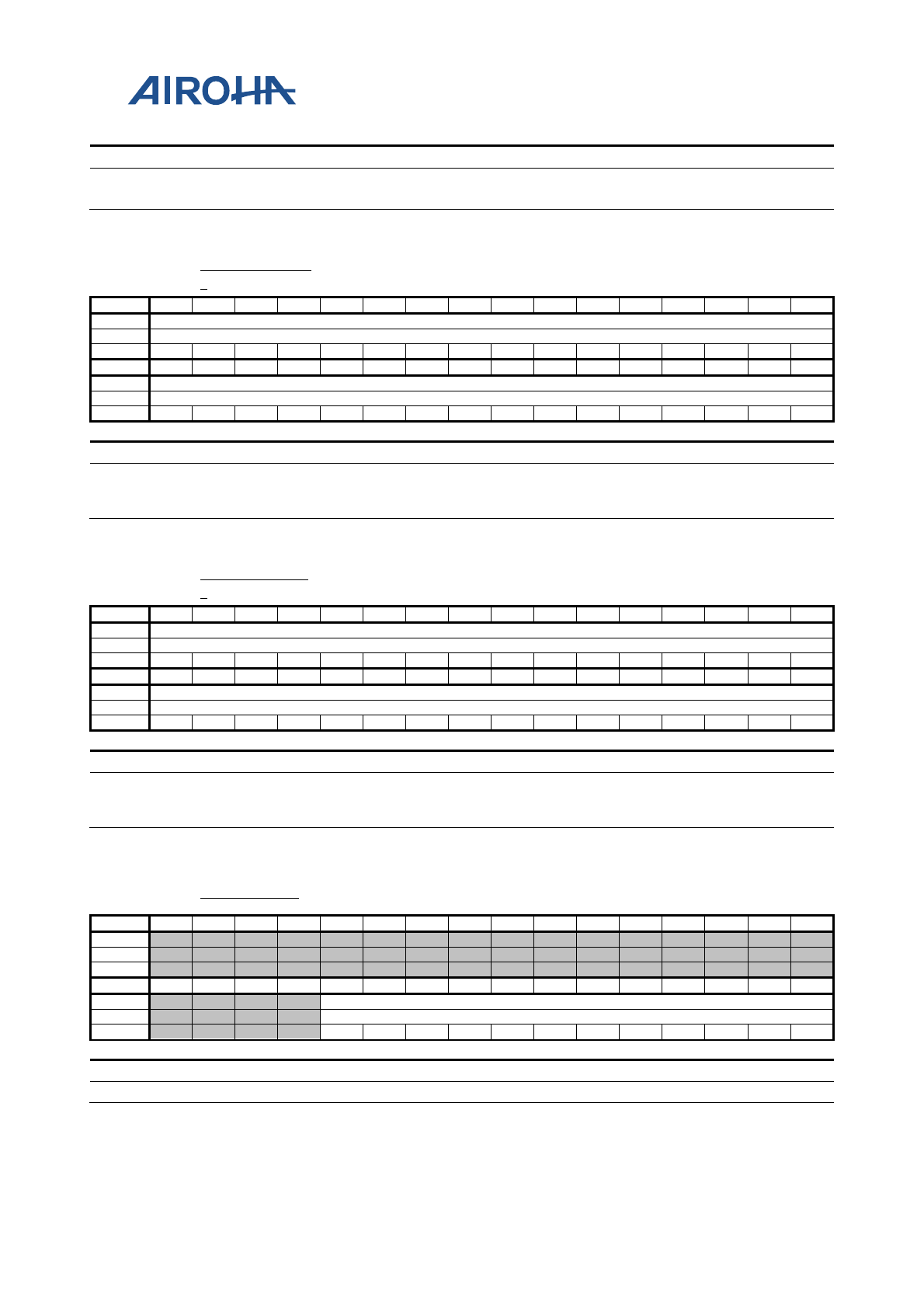
MT2523 Series Reference Manual
© 2015 - 2018 Airoha Technology Corp.
Page 405 of 692
This document contains information that is proprietary to Airoha Technology Corp. (“Airoha”) and/or its licensor(s).
Any unauthorized use, reproduction or disclosure of this document in whole or in part is strictly prohibited.
Bit(s)
Name
Description
26:16 HT The register field specifies the height of target image.
10:0 WT The register field specifies the width of target image.
A0410018 RESZ_HRATIO
1 Image Resizer Horizontal Ratio Register 1 000000
00
Bit
31
30
29
28
27
26
25
24
23
22
21
20
19
18
17
16
Name
RATIO[31:16]
Type
RW
Reset
0
0
0
0
0
0
0
0
0
0
0
0
0
0
0
0
Bit
15
14
13
12
11
10
9
8
7
6
5
4
3
2
1
0
Name
RATIO[15:0]
Type
RW
Reset
0
0
0
0
0
0
0
0
0
0
0
0
0
0
0
0
Bit(s) Name Description
31:0 RATIO Ratio = (RESZ_TARSZ.WT < RESZ_SRCSZ.WS ) ?
(RESZ_TARSZ.WT -1) * 220 / (RESZ_SRCSZ.WS -1) :
(RESZ_SRCSZ.WS) * 220 / RESZ_TARSZ.WT
A041001C RESZ_VRATIO
1 Image Resizer Vertical Ratio Register 1 000000
00
Bit
31
30
29
28
27
26
25
24
23
22
21
20
19
18
17
16
Name
RATIO[31:16]
Type
RW
Reset
0
0
0
0
0
0
0
0
0
0
0
0
0
0
0
0
Bit
15
14
13
12
11
10
9
8
7
6
5
4
3
2
1
0
Name
RATIO[15:0]
Type
RW
Reset
0
0
0
0
0
0
0
0
0
0
0
0
0
0
0
0
Bit(s) Name Description
31:0 RATIO Ratio = (RESZ_TARSZ.HT < RESZ_SRCSZ.HS ) ?
(RESZ_TARSZ.HT -1) * 220 / (RESZ_SRCSZ.HS -1) :
(RESZ_SRCSZ.HS) * 220 / RESZ_TARSZ.HT
A0410020 RESZ_HRES1 Image Resizer Horizontal Residual Register 1 000000
00
Bit
31
30
29
28
27
26
25
24
23
22
21
20
19
18
17
16
Name
Type
Reset
0
0
0
0
0
0
0
0
0
0
0
0
0
0
0
0
Bit
15
14
13
12
11
10
9
8
7
6
5
4
3
2
1
0
Name
RESIDUAL
Type
RW
Reset
0
0
0
0
0
0
0
0
0
0
0
0
0
0
0
0
Bit(s) Name Description
11:0 RESIDUAL Residual = RESZ_SRCSZ1.WS % RESZ_TARSZ1.WT
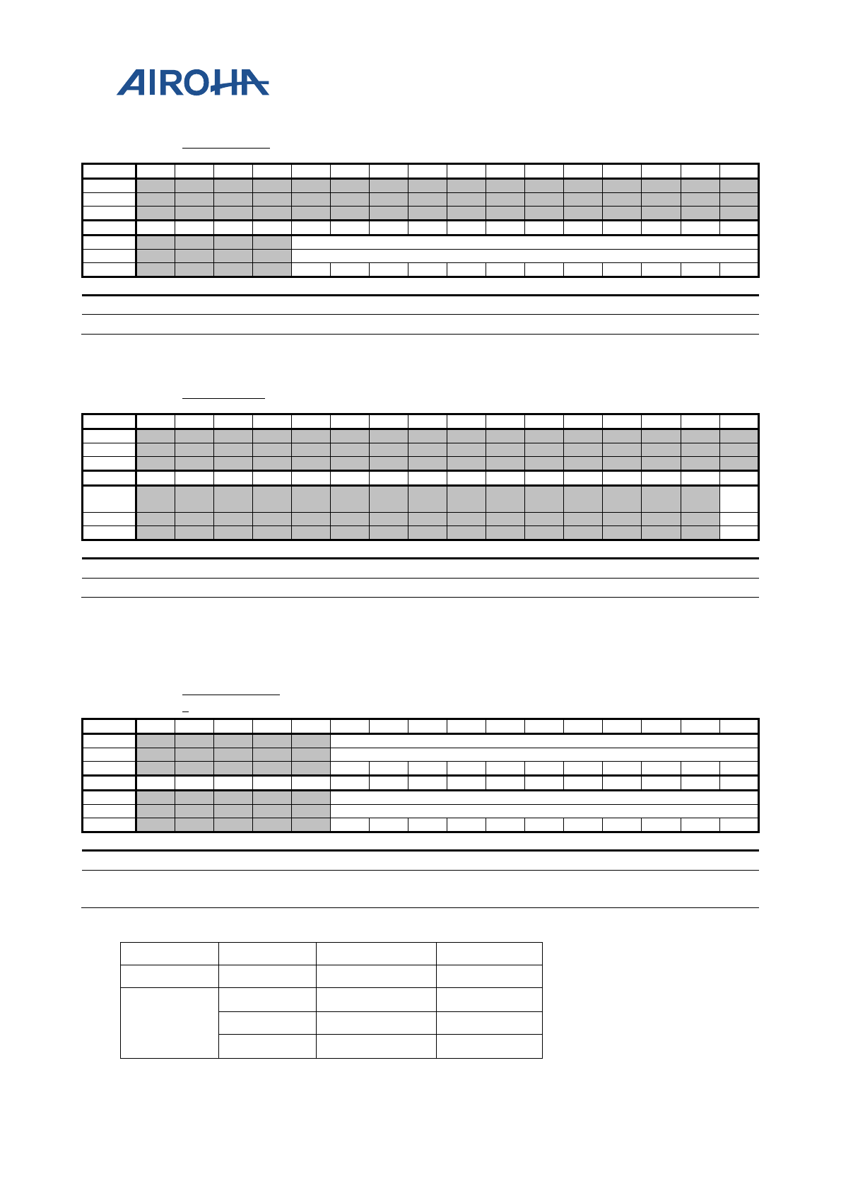
MT2523 Series Reference Manual
© 2015 - 2018 Airoha Technology Corp.
Page 406 of 692
This document contains information that is proprietary to Airoha Technology Corp. (“Airoha”) and/or its licensor(s).
Any unauthorized use, reproduction or disclosure of this document in whole or in part is strictly prohibited.
A0410024 RESZ_VRES1 Image Resizer Vertical Residual Register 1 000000
00
Bit
31
30
29
28
27
26
25
24
23
22
21
20
19
18
17
16
Name
Type
Reset
0
0
0
0
0
0
0
0
0
0
0
0
0
0
0
0
Bit
15
14
13
12
11
10
9
8
7
6
5
4
3
2
1
0
Name
RESIDUAL
Type
RW
Reset
0
0
0
0
0
0
0
0
0
0
0
0
0
0
0
0
Bit(s)
Name
Description
11:0 RESIDUAL Residual = RESZ_SRCSZ1.HS % RESZ_TARSZ1.HT
A041002C RESZ_LOCK Image Resizer LOCK Register 000000
00
Bit
31
30
29
28
27
26
25
24
23
22
21
20
19
18
17
16
Name
Type
Reset
0
0
0
0
0
0
0
0
0
0
0
0
0
0
0
0
Bit
15
14
13
12
11
10
9
8
7
6
5
4
3
2
1
0
Name
LO
CK
Type
RW
Reset
0
0
0
0
0
0
0
0
0
0
0
0
0
0
0
0
Bit(s)
Name
Description
0 LOCK Writing '1' to the register bit prevents updating double buffered registers.
Note: If lock is set to 1, and vsync comes, the frame will be dropped because the setting is not reliable. So please keep the locked
region as short as possible. LCKDRP interrupt can be used to detect this event.
A0410030 RESZ_ORIGSZ
1 Image Resizer Crop Original Size Register 1 000000
00
Bit
31
30
29
28
27
26
25
24
23
22
21
20
19
18
17
16
Name
ORIGSZ_HS
Type
RW
Reset
0
0
0
0
0
0
0
0
0
0
0
0
0
0
0
0
Bit
15
14
13
12
11
10
9
8
7
6
5
4
3
2
1
0
Name
ORIGSZ_WS
Type
RW
Reset
0
0
0
0
0
0
0
0
0
0
0
0
0
0
0
0
Bit(s) Name Description
26:16 ORIGSZ_HS Resizer input image height before cropping for pass 1.
10:0 ORIGSZ_WS Resizer input image width before cropping for pass 1.
Note: If CROP_EN = 1 and SRC is memory, ORIGSZ_WS and ORIGSZ_HS must be format aligned.
src format ORIGSZ_HS ORIGSZ_WS
caminf YUV444 Multiples of 1 Multiples of 1
memory
YUV420 Multiples of 2 Multiples of 2
YUV422 Multiples of 1 Multiples of 2
UYVY Multiples of 1 Multiples of 2
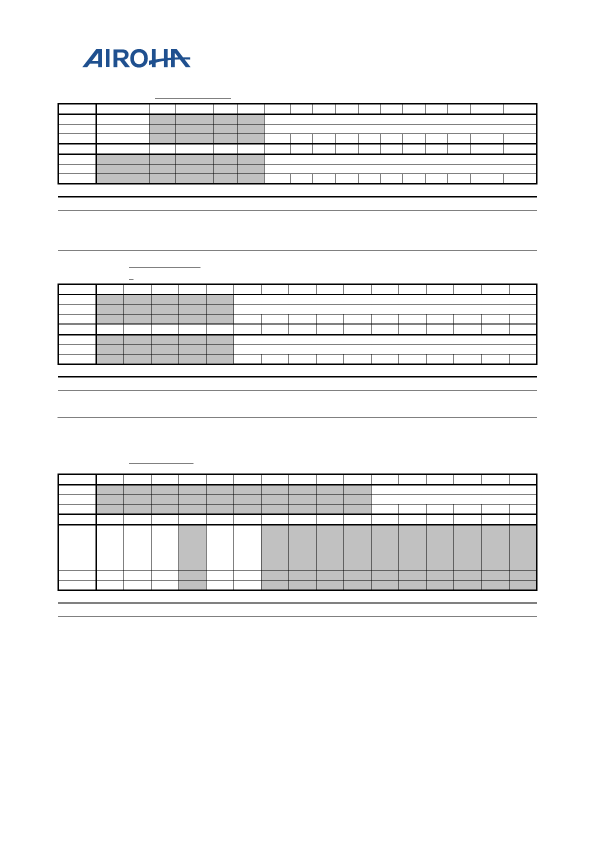
MT2523 Series Reference Manual
© 2015 - 2018 Airoha Technology Corp.
Page 407 of 692
This document contains information that is proprietary to Airoha Technology Corp. (“Airoha”) and/or its licensor(s).
Any unauthorized use, reproduction or disclosure of this document in whole or in part is strictly prohibited.
A0410034 RESZ_CROPLR1 Image Resizer Crop Left Right Register 1 00000000
Bit
31
30
29
28
27
26
25
24
23
22
21
20
19
18
17
16
Name
CROP_EN
CROP_L
Type
RW
RW
Reset
0
0
0
0
0
0
0
0
0
0
0
0
0
0
0
0
Bit
15
14
13
12
11
10
9
8
7
6
5
4
3
2
1
0
Name
CROP_R
Type
RW
Reset
0
0
0
0
0
0
0
0
0
0
0
0
0
0
0
0
Bit(s)
Name
Description
31 CROP_EN Crop enable for pass 1.
26:16 CROP_L Horizontal cropping start/left position index for pass 1.
10:0 CROP_R Horizontal cropping end/right position index for pass 1.
A0410038 RESZ_CROPTB
1 Image Resizer Crop Top Bottom Register 1 000000
00
Bit
31
30
29
28
27
26
25
24
23
22
21
20
19
18
17
16
Name
CROP_T
Type
RW
Reset
0
0
0
0
0
0
0
0
0
0
0
0
0
0
0
0
Bit
15
14
13
12
11
10
9
8
7
6
5
4
3
2
1
0
Name
CROP_B
Type
RW
Reset
0
0
0
0
0
0
0
0
0
0
0
0
0
0
0
0
Bit(s)
Name
Description
26:16 CROP_T Vertical cropping start/top position index for pass 1.
10:0 CROP_B Vertical cropping end/bottom position index for pass 1.
A0410040 RESZ_FRCFG Image Resizer Fine Resizing Configuration
Register 000000
02
Bit
31
30
29
28
27
26
25
24
23
22
21
20
19
18
17
16
Name
WMSZ1
Type
RW
Reset
0
0
0
0
0
0
0
0
0
0
0
0
0
0
0
0
Bit
15
14
13
12
11
10
9
8
7
6
5
4
3
2
1
0
Name
LC
KI
NT
EN
MI
NI
NT
EN
PX
DI
NT
EN
FST
AR
T1I
NT
EN
FE
ND
INT
EN
Type
RW
RW
RW
RW
RW
Reset
0
0
0
0
0
0
0
0
0
0
0
0
0
0
1
0
Bit(s)
Name
Description
21:16 WMSZ1
It stands for working memory size for single pass or 1st pass of two pass
resizing. The register specifies how many lines after horizontal resizing can
be filled into working memory. Its minimum value is 2 and maximum value is
31. And the formula is (1920 / ((WT+3)/4*4)).
15 LCKINTEN Drop frame due to lock interrupt enable.
14 MININTEN Memory input interrupt enable.
13 PXDINTEN Pixel drop interrupt enable.
11 FSTART1INTEN Frame start of 1st pass interrupt enable.
0: Interrupt for frame start of 1st pass is disabled.
1: Interrupt for frame start of 1st pass is enabled.
10 FENDINTEN Frame end interrupt enable.
0: Interrupt for frame end is disabled.
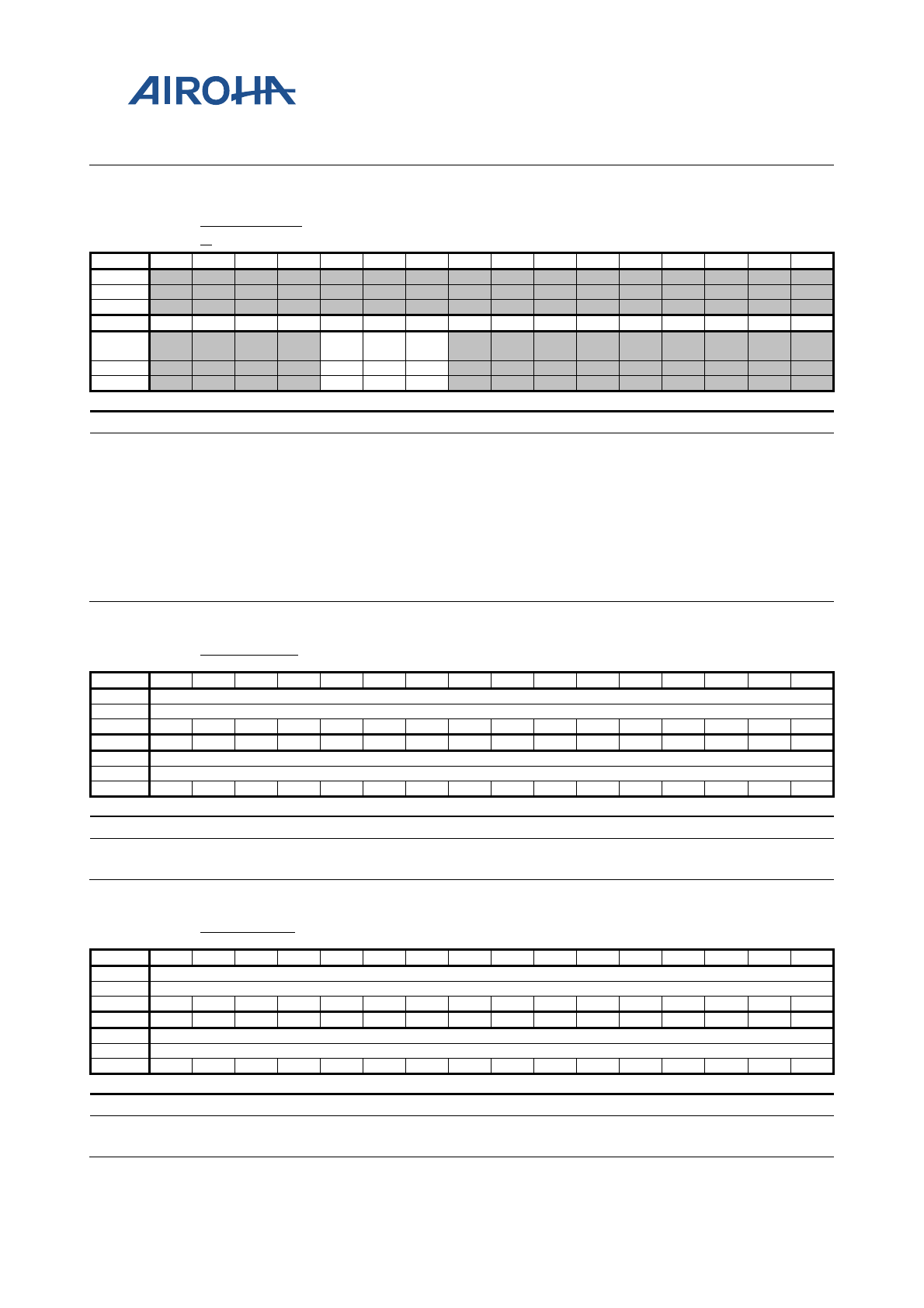
MT2523 Series Reference Manual
© 2015 - 2018 Airoha Technology Corp.
Page 408 of 692
This document contains information that is proprietary to Airoha Technology Corp. (“Airoha”) and/or its licensor(s).
Any unauthorized use, reproduction or disclosure of this document in whole or in part is strictly prohibited.
1: Interrupt for frame end is enabled.
A0410090 RESZ_DBGCF
G Image Resizer Debug Configuration Register 000002
00
Bit
31
30
29
28
27
26
25
24
23
22
21
20
19
18
17
16
Name
Type
Reset
0
0
0
0
0
0
0
0
0
0
0
0
0
0
0
0
Bit
15
14
13
12
11
10
9
8
7
6
5
4
3
2
1
0
Name
NO
DB
PH
R1
PV
R1
Type
RW
RW
RW
Reset
0
0
0
0
0
0
1
0
0
0
0
0
0
0
0
0
Bit(s)
Name
Description
11 NODB
Force register not double buffered.
0: Double buffered, registers are effective when camera vsync arrives or memory input
starts.
1: No double buffered.
10 PHR1 Force horizontal resizing to execute even though it's not necessary.
0: Normal operation.
1: Force horizontal resizing to execute even though it's not necessary.
9 PVR1 Force vertical resizing to execute even though it's not necessary.
0: Normal operation.
1: Force vertical resizing to execute even though it's not necessary.
A04100B0 RESZ_INFO0 Image Resizer Information Register 0 000000
00
Bit
31
30
29
28
27
26
25
24
23
22
21
20
19
18
17
16
Name
IN_VERT_CNT
Type
RO
Reset
0
0
0
0
0
0
0
0
0
0
0
0
0
0
0
0
Bit
15
14
13
12
11
10
9
8
7
6
5
4
3
2
1
0
Name
IN_HORZ_CNT
Type
RO
Reset
0
0
0
0
0
0
0
0
0
0
0
0
0
0
0
0
Bit(s)
Name
Description
31:16 IN_VERT_CNT Input vertical counter.
15:0 IN_HORZ_CNT Input horizontal counter.
A04100B4 RESZ_INFO1 Image Resizer Information Register 1 000000
00
Bit
31
30
29
28
27
26
25
24
23
22
21
20
19
18
17
16
Name
OUT_VERT_CNT
Type
RO
Reset
0
0
0
0
0
0
0
0
0
0
0
0
0
0
0
0
Bit
15
14
13
12
11
10
9
8
7
6
5
4
3
2
1
0
Name
OUT_HORZ_CNT
Type
RO
Reset
0
0
0
0
0
0
0
0
0
0
0
0
0
0
0
0
Bit(s) Name Description
31:16 OUT_VERT_CNT Output vertical counter.
15:0 OUT_HORZ_CNT Output horizontal counter.
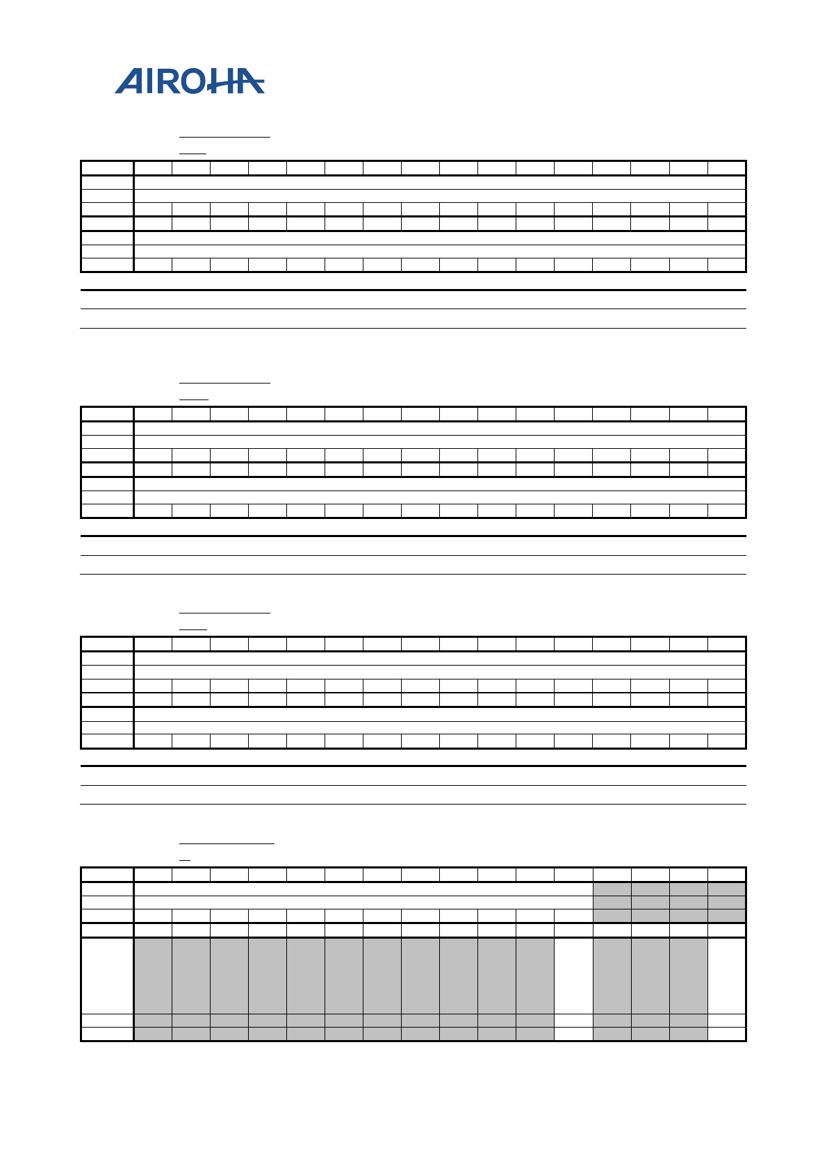
MT2523 Series Reference Manual
© 2015 - 2018 Airoha Technology Corp.
Page 409 of 692
This document contains information that is proprietary to Airoha Technology Corp. (“Airoha”) and/or its licensor(s).
Any unauthorized use, reproduction or disclosure of this document in whole or in part is strictly prohibited.
A04100D
C RESZ_SMBAS
E_Y Image Resizer Y-Component Source Memory Base
Address Register xxxxxxx
x
Bit
31
30
29
28
27
26
25
24
23
22
21
20
19
18
17
16
Name
SMBASE_Y[31:16]
Type
RW
Reset
Bit
15
14
13
12
11
10
9
8
7
6
5
4
3
2
1
0
Name
SMBASE_Y[15:0]
Type
RW
Reset
Bit(s)
Name
Description
31:0 SMBASE_Y
A04100E0 RESZ_SMBAS
E_U Image Resizer U-Component Source Memory Base
Address Register xxxxxxx
x
Bit
31
30
29
28
27
26
25
24
23
22
21
20
19
18
17
16
Name
SMBASE_U[31:16]
Type
RW
Reset
Bit
15
14
13
12
11
10
9
8
7
6
5
4
3
2
1
0
Name
SMBASE_U[15:0]
Type
RW
Reset
Bit(s)
Name
Description
31:0 SMBASE_U
A04100E4 RESZ_SMBAS
E_V Image Resizer V-Component Source Memory Base
Address Register xxxxxxx
x
Bit
31
30
29
28
27
26
25
24
23
22
21
20
19
18
17
16
Name
SMBASE_V[31:16]
Type
RW
Reset
Bit
15
14
13
12
11
10
9
8
7
6
5
4
3
2
1
0
Name
SMBASE_V[15:0]
Type
RW
Reset
Bit(s)
Name
Description
31:0 SMBASE_V
A04100F0 RESZ_GMCCO
N Image Resizer GMC Control Register 000000
00
Bit
31
30
29
28
27
26
25
24
23
22
21
20
19
18
17
16
Name
RD_MIN_REQ_INTERVAL
Type
RW
Reset
0
0
0
0
0
0
0
0
0
0
0
0
0
0
0
0
Bit
15
14
13
12
11
10
9
8
7
6
5
4
3
2
1
0
Name
RD
_M
AX
_B
L
RD
_M
IN_
RE
Q_
EN
Type
RW
RW
Reset
0
0
0
0
0
0
0
0
0
0
0
0
0
0
0
0
MT2523 Series Reference Manual
© 2015 - 2018 Airoha Technology Corp.
Page 410 of 692
This document contains information that is proprietary to Airoha Technology Corp. (“Airoha”) and/or its licensor(s).
Any unauthorized use, reproduction or disclosure of this document in whole or in part is strictly prohibited.
Bit(s)
Name
Description
31:20 RD_MIN_REQ_INTER
VAL It specifies how many AHB bus cycles between two GMC requests for read
port.
4 RD_MAX_BL Specify the maximum burst length of GMC request for read port.
0: Burst 4 beats access, and one beat is 4 bytes. Total data amount is 16 bytes per access.
1: Single 4 bytes access.
0 RD_MIN_REQ_EN Enable GMC port minimum request control for read port.
A04100FC RESZ_CLIP Image Resizer CLIP Register 000000
00
Bit
31
30
29
28
27
26
25
24
23
22
21
20
19
18
17
16
Name
CLI
P_
EN
Type
RW
Reset
0
0
0
0
0
0
0
0
0
0
0
0
0
0
0
0
Bit
15
14
13
12
11
10
9
8
7
6
5
4
3
2
1
0
Name
MEM_WD
Type
RW
Reset
0
0
0
0
0
0
0
0
0
0
0
0
0
0
0
0
Bit(s)
Name
Description
31 CLIP_EN Enable clip function of memory in mode.
0: Disable.
1: Enable.
11:0 MEM_WD Width of background image. The unit is pixels.
Figure 25-4. Memory clipping chart
Note: MEM_WD should be format aligned.
format MEM_WD
YUV420 Multiples of 2
YUV422 Multiples of 2
UYVY Multiples of 2
All of the following registers are for tile-based processing. These registers are inactive while RESZ_CFG.MODE1 is
frame mode.
mem_wd
ws
hs
smbase
4 bytes align
MT2523 Series Reference Manual
© 2015 - 2018 Airoha Technology Corp.
Page 411 of 692
This document contains information that is proprietary to Airoha Technology Corp. (“Airoha”) and/or its licensor(s).
Any unauthorized use, reproduction or disclosure of this document in whole or in part is strictly prohibited.
A0410100 RESZ_TILE_C
FG Image Resizer Tile Configuration Register 000000
00
Bit
31
30
29
28
27
26
25
24
23
22
21
20
19
18
17
16
Name
Type
Reset
0
0
0
0
0
0
0
0
0
0
0
0
0
0
0
0
Bit
15
14
13
12
11
10
9
8
7
6
5
4
3
2
1
0
Name
SA
_E
N_
Y1
SA
_E
N_
X1
Type
RW
RW
Reset
0
0
0
0
0
0
0
0
0
0
0
0
0
0
0
0
Bit(s)
Name
Description
1 SA_EN_Y1 Vertical source accumulation enable siganl of 1st pass of resizer.
0: Disable (frame_target_height ≥ frame_source_height).
1: Enable (frame_target_height < frame_source_height).
0 SA_EN_X1 Horizontal source accumulation enable siganl of 1st pass of resizer.
0: Disable (frame_target_width ≥ frame_source_width).
1: Enable (frame_target_width < frame_source_width).
A0410104 RESZ_TILE_S
TART_POS_X1 Image Resizer Tile Start Position X Register 1 000000
00
Bit
31
30
29
28
27
26
25
24
23
22
21
20
19
18
17
16
Name
TILE_START_POS_X[30:16]
Type
RW
Reset
0
0
0
0
0
0
0
0
0
0
0
0
0
0
0
0
Bit
15
14
13
12
11
10
9
8
7
6
5
4
3
2
1
0
Name
TILE_START_POS_X[15:0]
Type
RW
Reset
0
0
0
0
0
0
0
0
0
0
0
0
0
0
0
0
Bit(s)
Name
Description
30:0 TILE_START_POS_X Horizontal start position of bilinear interpolation. Format: Q0.11.20.
Horizontal start weight of source accumulation. Format: Q0.0.20.
A041010C RESZ_TILE_S
TART_POS_Y1 Image Resizer Tile Start Position Y Register 1 000000
00
Bit
31
30
29
28
27
26
25
24
23
22
21
20
19
18
17
16
Name
TILE_START_POS_Y[30:16]
Type
RW
Reset
0
0
0
0
0
0
0
0
0
0
0
0
0
0
0
0
Bit
15
14
13
12
11
10
9
8
7
6
5
4
3
2
1
0
Name
TILE_START_POS_Y[15:0]
Type
RW
Reset
0
0
0
0
0
0
0
0
0
0
0
0
0
0
0
0
Bit(s)
Name
Description
30:0 TILE_START_POS_Y Vertical start position of bilinear interpolation. Format: Q0.11.20. Vertical
start weight of source accumulation. Format: Q0.0.20.
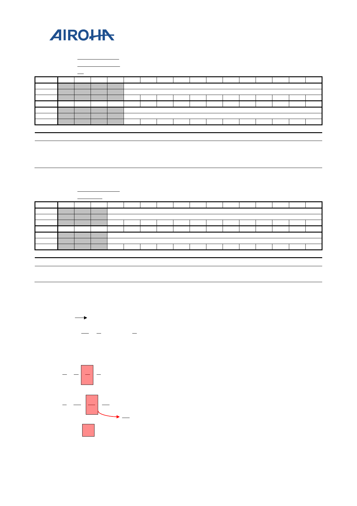
MT2523 Series Reference Manual
© 2015 - 2018 Airoha Technology Corp.
Page 412 of 692
This document contains information that is proprietary to Airoha Technology Corp. (“Airoha”) and/or its licensor(s).
Any unauthorized use, reproduction or disclosure of this document in whole or in part is strictly prohibited.
A0410114 RESZ_BI_TRU
NC_ERR_COM
P1
Image Resizer Bilinear Truncation Error
Compensation Register 1 000000
00
Bit
31
30
29
28
27
26
25
24
23
22
21
20
19
18
17
16
Name
BI_TRUNC_ERR_COMP_Y
Type
RW
Reset
0
0
0
0
0
0
0
0
0
0
0
0
0
0
0
0
Bit
15
14
13
12
11
10
9
8
7
6
5
4
3
2
1
0
Name
BI_TRUNC_ERR_COMP_X
Type
RW
Reset
0
0
0
0
0
0
0
0
0
0
0
0
0
0
0
0
Bit(s)
Name
Description
27:16 BI_TRUNC_ERR_COM
P_Y Vertical condition of truncation error compensation by accumulated residual.
11:0 BI_TRUNC_ERR_COM
P_X Horizontal condition of truncation error compensation by accumulated
residual.
A0410118 RESZ_BI_INIT
_RESID1 Image Resizer Bilinear Initial Residual Register 1 000000
00
Bit
31
30
29
28
27
26
25
24
23
22
21
20
19
18
17
16
Name
BI_INIT_RESID_Y
Type
RW
Reset
0
0
0
0
0
0
0
0
0
0
0
0
0
0
0
0
Bit
15
14
13
12
11
10
9
8
7
6
5
4
3
2
1
0
Name
BI_INIT_RESID_X
Type
RW
Reset
0
0
0
0
0
0
0
0
0
0
0
0
0
0
0
0
Bit(s)
Name
Description
28:16 BI_INIT_RESID_Y Vertical initial residual for truncation error compensation.
12:0 BI_INIT_RESID_X Horizontal initial residual for truncation error compensation.
Since the bilinear-interpolation step is represented by fixed-point representation, there are truncation errors in the
computational process. In order to reduce the truncation-error effect, resizer will compensate the errors at each
integer interpolation point. The following is the example.
10 pixels 15 pixels
10
155100
residual lincrementa 8
21
8
15
8
10
8
5
0
point fixedby position ion interpolat 3
8
3
6
3
4
3
2
0
positionion interpolat
1015 % 10residual
precision)binary bit
-(3
8
5
625.0
3
2
15
10
(ratio) step
⇒
==
=≈==
8
16
(truncation-error compensation)
MT2523 Series Reference Manual
© 2015 - 2018 Airoha Technology Corp.
Page 413 of 692
This document contains information that is proprietary to Airoha Technology Corp. (“Airoha”) and/or its licensor(s).
Any unauthorized use, reproduction or disclosure of this document in whole or in part is strictly prohibited.
26. Image Rotator DMA
26.1. General Description
Image Rotator DMA receives YUV444 pixel data from input interface as shown in Figure 26-1, and output to
memory. The architecture is shown in Figure 26-2. When writing to memory, it supports various formats.
Supported Ooutput packed formats include: UYVY (YUYV422). Supported oOutput planar formats include: scanline
planarYUV420 and YUV422. In this specification, generic YUV format refers to scanline planar YUV420/YUV422.
These output formats ares shown in Table 26-1.
clk
req
pixel[31:0]
ack
pixel #1 pixel #2
Figure 26-1. Image Rotator DMA Input Interface
ROT_DMA
input from previous engine
output to memory
Figure 26-2. Image Rotator DMA Architecture
Table 26-1. ImageRotator DMA Output Format
Output formats
UYVY
Planar YUV420
Planar YUV422
26.1.1. Feature List
• Descriptor based mode
• Hardware auto loop mode
• Color formats transformation
• Output Image pitching for UYVY
• Rotation for UYVY
• Hardware semaphore support
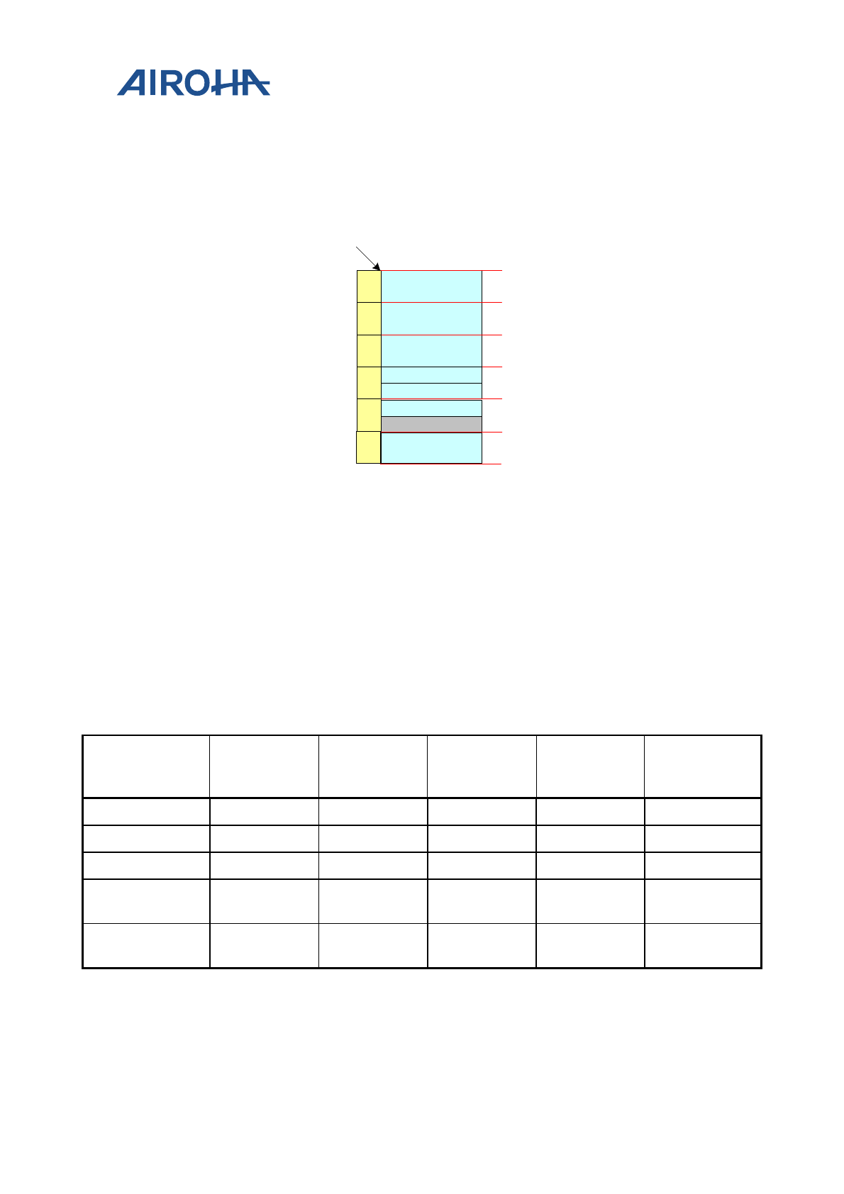
MT2523 Series Reference Manual
© 2015 - 2018 Airoha Technology Corp.
Page 414 of 692
This document contains information that is proprietary to Airoha Technology Corp. (“Airoha”) and/or its licensor(s).
Any unauthorized use, reproduction or disclosure of this document in whole or in part is strictly prohibited.
26.1.2. Descriptor Format
There are six6 enable signals indicating each 4- bytes command. The full sets of rotator DMA’s descriptor is 24s
bytes including six6 segments and with four4 bytes each segment.
y_dst_str_addr
src_w
src_h
dst_w_in_byte
con
4
4
4
en
en
en
IDMA_QUEUE_BASEADDR + des_size * rpt
0x0
offset
0x4
0x8
0xc
0x10
0x14
4
en
u_dst_str_addr 4
en
v_dst_str_addr 4
en
0x0
Figure 26-3. Image Rotator DMA Descriptor Format
26.1.3. Frame buffer start address and size notes
Output frame buffer start address must be 4- byte alignment.
The size of each frame buffer must be a multiple of four4 bytes. That is, if output format is YUV420. Y, U and V
plane must allocate size of multiple of four4 bytes. If the image size will not occupyied every 4 bytes allocated, the
residual bytes not used will be written with dummy data. Dummy data value is undefined and scenario dependent.
The table belowFollowing table summarizes base address and buffer size restrictions.
Table 26-2. Base Address and Buffer Size Restrictions
Y, U, V frame
start address
(bytes)
Width (pixels) Height (pixels) *HW output
size (bytes)
DST_W_IN_BYTE
(bytes)
UYVY(packed) 4x 2x 1x 4x 4x
YUV422(planar) 4x 2x 1x 4x -
YUV420(planar) 4x 2x 2x 4x -
YUV422(planar)
with pitch enabled 4x 8x 1x 4x 8x
YUV420(planar)
with pitch enabled 4x 8x 2x 4x 8x
MT2523 Series Reference Manual
© 2015 - 2018 Airoha Technology Corp.
Page 415 of 692
This document contains information that is proprietary to Airoha Technology Corp. (“Airoha”) and/or its licensor(s).
Any unauthorized use, reproduction or disclosure of this document in whole or in part is strictly prohibited.
26.1.4. Rotation
Rotator supports 90 degree of rotation with flip for UYVY color format image of width smaller than or equal to 480
pixels.
26.2. Register Definition
The base address of ROT_DMA is 0xA040_0000.
Register Address Register Function Acronym
ROT_DMA+0000h Rotator DMA Interrupt Flag ROT_DMA_IRQ_FLAG
ROT_DMA+0008h Rotator DMA Interrupt Flag Clear ROT_DMA_IRQ_FLAG_CLR
ROT_DMA+0018h Rotator DMA Configuration ROT_DMA_CFG
ROT_DMA+0028h Rotator DMA Stop Register ROT_DMA_STOP
ROT_DMA+0030h Rotator DMA Enable Status ROT_DMA_EN
ROT_DMA+0038h Rotator DMA Reset Register ROT_DMA_RESET
ROT_DMA+0300h Image Rotator DMA SLOW DOWN ROT_DMA_SLOW_DOWN
ROT_DMA+0318h Image Rotator DMA Y Destination Start
Address ROT_DMA_ Y_DST_STR_ADDR
ROT_DMA+0320h Image Rotator DMA U Destination Start
Address ROT_DMA_ U_DST_STR_ADDR
ROT_DMA+0328h Image Rotator DMA V Destination Start
Address ROT_DMA_ V_DST_STR_ADDR
ROT_DMA+0330h Image Rotator DMA Source Image Size ROT_DMA_SRC_SIZE
ROT_DMA+0348h Image Rotator DMA Destination Image
Size ROT_DMA_DST_SIZE
ROT_DMA+0368h Image Rotator DMA Control Register ROT_DMA_CON
ROT_DMA+
0000h
Rotator DMA Interrupt Flag
ROT_DMA_I
RQ_FLAG
Bit
31
30
29
28
27
26
25
24
23
22
21
20
19
18
17
16
Name
FLAG
0_IR
Q_EN
Type
R/W
Reset
0
Bit
15
14
13
12
11
10
9
8
7
6
5
4
3
2
1
0
Name
FLAG
0
Type
R/W
Reset
0
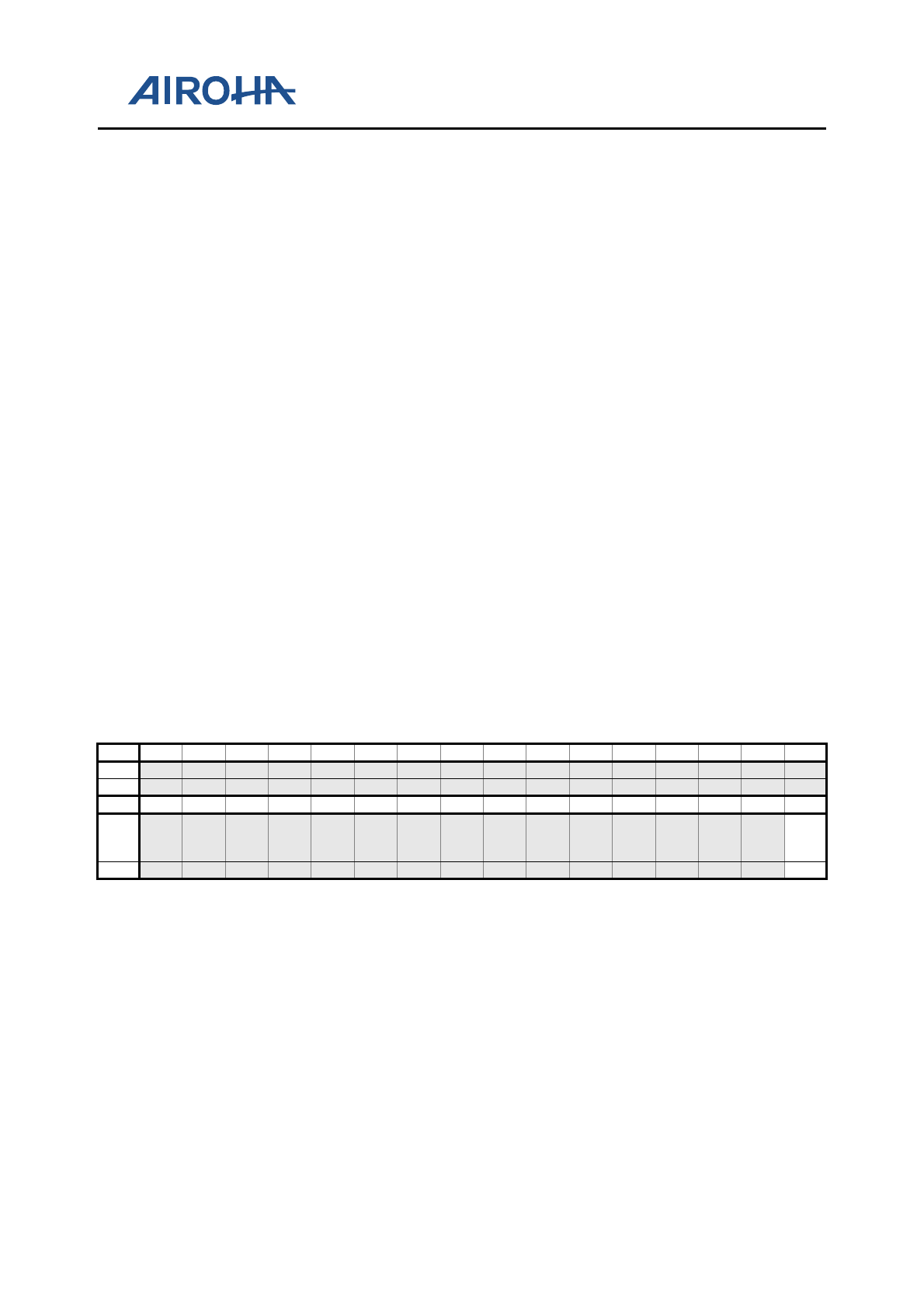
MT2523 Series Reference Manual
© 2015 - 2018 Airoha Technology Corp.
Page 416 of 692
This document contains information that is proprietary to Airoha Technology Corp. (“Airoha”) and/or its licensor(s).
Any unauthorized use, reproduction or disclosure of this document in whole or in part is strictly prohibited.
This register is used by software to parse error message and some events triggered by the engine.
Occurrence of these events/error messages is denoted by flags. Flags can issue interrupt which is level
triggered. To turn on interrupt issue capability, assert IRQ_EN. Note that interrupt will only issue when
engine’s EN is asserted. This behavior give software opportunity to prevent unnecessary interrupt before
start of engine.
For each flag (e.g. FLAG1):
When read:
0 Event/error not took place
1 Event/error took place
When write:
0 Clear flag. To clear flags, Using IRQ_FLAG_CLR register is preferred.
1 Software asserted event/error
For each flag IRQ_EN (e.g. FLAG1_IRQ_EN):
IRQ_EN Interrupt enable. Enable or disable corresponding interrupt issue capability. If the bit is de-
asserted, the corresponding flag will still raise in respond to the event, but will not issue interrupt.
If asserted, the interrupt will issue at EN==1 if the event takes place.
0 Disable.
1 Enable.
Flags descriptions:
FLAG0 This is raised when engine finished the descriptor and INT_EN is asserted.
ROT_DMA+
0008h
Rotator DMA
Interrupt Flag Clear Register ROT_DMA_I
RQ_FLAG_CL
R
Bit
31
30
29
28
27
26
25
24
23
22
21
20
19
18
17
16
Name
Type
Bit
15
14
13
12
11
10
9
8
7
6
5
4
3
2
1
0
Name
FLAG
0_CL
R
Type
WO
FLAGn_CLR Clear interrupt flag number n. When clearing interrupt flag and interrupt flag trigger
event occur at the same time. Event trigger was given higher priority to let software programmer
still notified by the event.
0 Do not clear (no effect on interrupt flag)
1 Clear interrupt flag
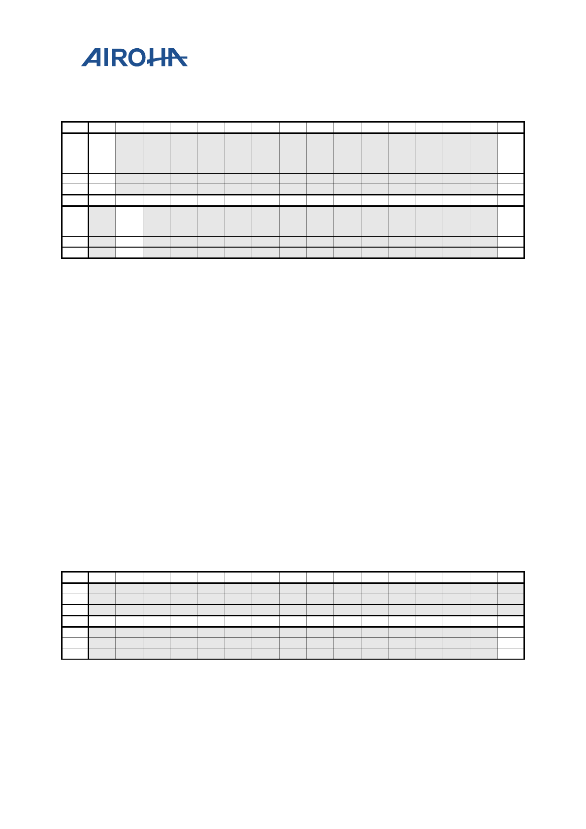
MT2523 Series Reference Manual
© 2015 - 2018 Airoha Technology Corp.
Page 417 of 692
This document contains information that is proprietary to Airoha Technology Corp. (“Airoha”) and/or its licensor(s).
Any unauthorized use, reproduction or disclosure of this document in whole or in part is strictly prohibited.
ROT_DMA+
0018h
Rotator DMA Configuration
ROT_DMA_C
FG
Bit
31
30
29
28
27
26
25
24
23
22
21
20
19
18
17
16
Name
FRAM
E_SY
NC_E
N
YUV_
PITC
H_EN
Type
R/W
Reset
0
Bit
15
14
13
12
11
10
9
8
7
6
5
4
3
2
1
0
Name
DROP
AUTO
_LOO
P
Type
R/W
R/W
Reset
0
0
AUTO_LOOP Auto loop. Automatically loop back to the first command when all commands are
consumed.
0 Disable
1 Enable
DROP this register only takes effect when en=0 (engine at turn off status)
0 stall previous engine’s input data if any
1 drop previous engine’s input data if any
YUV_PITCH_EN Enable pitch mechanism for generic YUV output format. This register only takes
effect when OUTPUT_FORMAT is generic YUV.
0 Y, U, V data will be written to memory in continuous address respectively if
OUTPUT_FORMAT is generic YUV.
1 Y plane data will be written to memory in pitch value, DST_W_IN_BYTE and U, V plane data
will be written to memory in pitch value, DST_W_IN_BYTE/2. The source width must be
multiple of 8.
FRAME_SYNC_EN Frame sync signal from camera. No effect when the DMA engine is not part of
camera image datapath.
0 Disable
1 Enable
ROT_DMA+
0028h
Rotator DMA
Stop Register ROT_DMA_S
TOP
Bit
31
30
29
28
27
26
25
24
23
22
21
20
19
18
17
16
Name
Type
Reset
Bit
15
14
13
12
11
10
9
8
7
6
5
4
3
2
1
0
Name
STOP
Type
R//W
Reset
0
Stop the engine engine by writing this register. When writing 1, DMA engine will stop after finishing the
current frame. When writing 0, DMA stop will be de-asserted. This status will be checked at each end of
frame. During the engine operation, this status has no effect.
STOP Stop (disable) the DMA engine.
0 De-assert stop status
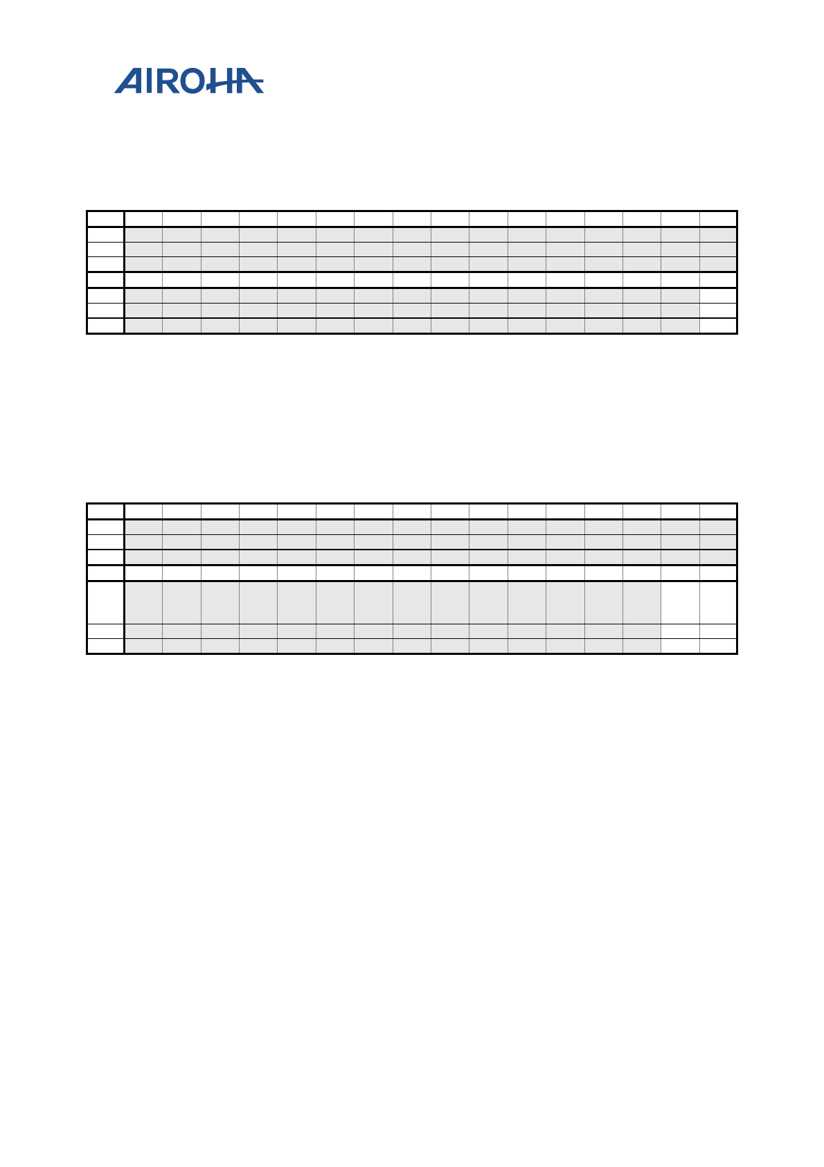
MT2523 Series Reference Manual
© 2015 - 2018 Airoha Technology Corp.
Page 418 of 692
This document contains information that is proprietary to Airoha Technology Corp. (“Airoha”) and/or its licensor(s).
Any unauthorized use, reproduction or disclosure of this document in whole or in part is strictly prohibited.
1 Stop the DMA engine at frame end.
ROT_DMA+
0030h
Rotator DMA Enable Status Register
ROT_DMA_E
N
Bit
31
30
29
28
27
26
25
24
23
22
21
20
19
18
17
16
Name
Type
Reset
Bit
15
14
13
12
11
10
9
8
7
6
5
4
3
2
1
0
Name
EN
Type
R/W
Reset
0
EN Enable Status. When read, this indicates whether DMA is enabled or not. To enable the engine,
write 1 into this register. To stop the engine, use STOP, WARM_RESET or HARD_RESET
instead. In register mode and without auto loop, engine will set en = 0 when finishing its job. In
auto loop, only when SW assert stop/reset can turn off engine.
ROT_DMA+
0038h
Rota
tor DMA Reset Register ROT_DMA_R
ESET
Bit
31
30
29
28
27
26
25
24
23
22
21
20
19
18
17
16
Name
Type
Reset
Bit
15
14
13
12
11
10
9
8
7
6
5
4
3
2
1
0
Name
WAR
M_RS
T
HAR
D_RS
T
Type
R/W
R/W
Reset
0
0
HARD_RST Reset DMA descriptor queue and control register settings. This will clear control settings
and in Image DMA registers immediately. This reset may cause pending bus transactions left in
the DMA engine. Software should determine an amount of safe reset time and assert the reset for
that period of time.
0 De-assert reset
1 Assert reset
WARM_RST Reset DMA descriptor queue and control register settings. This will clear control settings
in Image DMA registers after no pending bus transactions left. This is often so called safe reset.
This bit will be de-asserted automatically after the settings are cleared. Software should wait for
this bit to be de-asserted by hardware before performing other DMA tasks.
0 De-assert reset
1 Assert reset
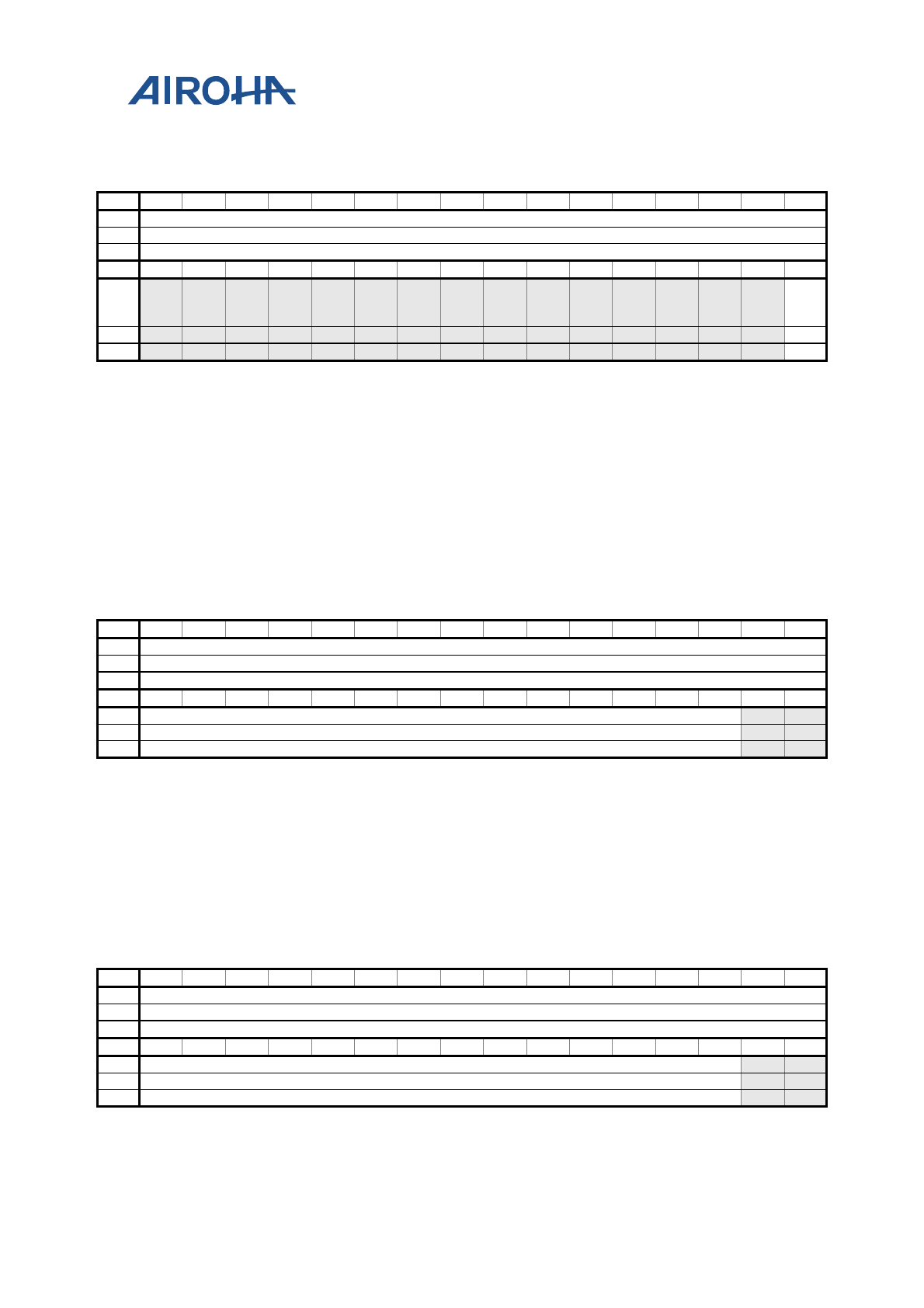
MT2523 Series Reference Manual
© 2015 - 2018 Airoha Technology Corp.
Page 419 of 692
This document contains information that is proprietary to Airoha Technology Corp. (“Airoha”) and/or its licensor(s).
Any unauthorized use, reproduction or disclosure of this document in whole or in part is strictly prohibited.
ROT_DMA+
0300h
Image Rotator DMA SLOW DOWN
ROT_DMA_S
LOW_DOWN
Bit
31
30
29
28
27
26
25
24
23
22
21
20
19
18
17
16
Name
SLOW_CNT
Type
R/W
Reset
0
Bit
15
14
13
12
11
10
9
8
7
6
5
4
3
2
1
0
Name
SLO
W_E
N
Type
R/W
Reset
0
SLOW_EN Slow down enable. Assert this to slow down engine. Amount of slow down is determined
by SLOW_CNT. Enable this to decrease the performance of rotator.
0 Disable
1 Enable
SLOW_CNT Slow down count. Delay SLOW_CNT cycle to issue next hardware bus transaction. This
value is not adjustable during engine operation.
ROT_DMA+
0318h
Image Rotator DMA Y Destination Start
Address
ROT_DMA_
Y_DST_STR_
ADDR
Bit
31
30
29
28
27
26
25
24
23
22
21
20
19
18
17
16
Name
Y_DST_STR_ADDR
Type
R/W
Reset
0
Bit
15
14
13
12
11
10
9
8
7
6
5
4
3
2
1
0
Name
Y_DST_STR_ADDR
Type
R/W
Reset
0
Y_DST_STR_ADDR Destination Y start address. This address indicate the pitch window start
address.
When output format is generic YUV, this address indicate the Y plane’s start address.
When rotation, an offset must be added, please refer to the ”Frame start address” section.
ROT_DMA+
0320h
Image Rotator DMA U Destination Start
Address
ROT_DMA_
U_DST_STR_
ADDR
Bit
31
30
29
28
27
26
25
24
23
22
21
20
19
18
17
16
Name
U_DST_STR_ADDR
Type
R/W
Reset
0
Bit
15
14
13
12
11
10
9
8
7
6
5
4
3
2
1
0
Name
U_DST_STR_ADDR
Type
R/W
Reset
0
U_DST_STR_ADDR Destination U start address. When output format is not generic YUV, this is not
used.
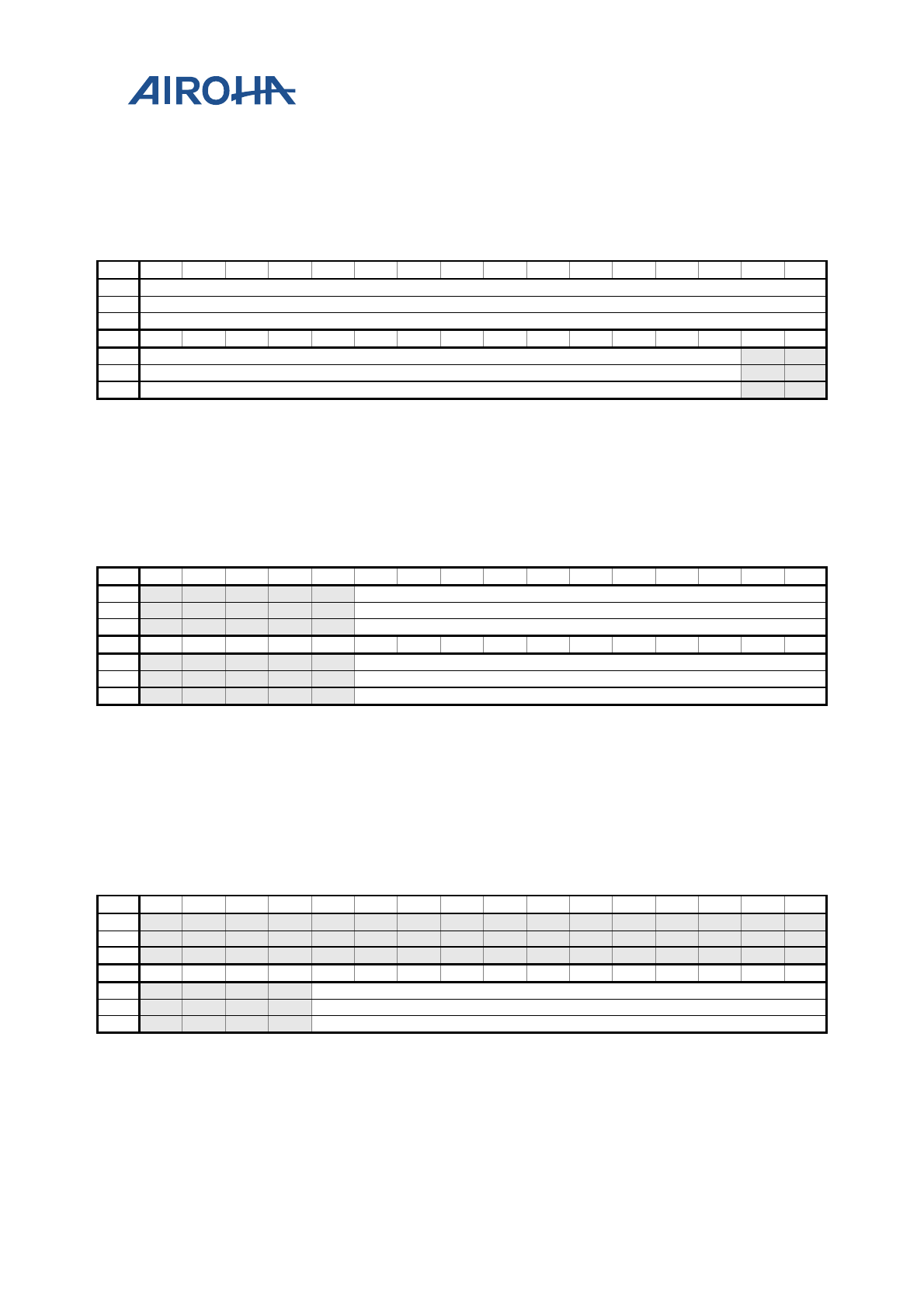
MT2523 Series Reference Manual
© 2015 - 2018 Airoha Technology Corp.
Page 420 of 692
This document contains information that is proprietary to Airoha Technology Corp. (“Airoha”) and/or its licensor(s).
Any unauthorized use, reproduction or disclosure of this document in whole or in part is strictly prohibited.
When output format is generic YUV, this address indicates the U plane’s start address in planar format.
ROT_DMA+
0328h
Image Rotator DMA V Destination Start
Address
ROT_DMA_
V_DST_STR_
ADDR
Bit
31
30
29
28
27
26
25
24
23
22
21
20
19
18
17
16
Name
V_DST_STR_ADDR
Type
R/W
Reset
0
Bit
15
14
13
12
11
10
9
8
7
6
5
4
3
2
1
0
Name
V_DST_STR_ADDR
Type
R/W
Reset
0
V_DST_STR_ADDR Destination V start address. When output format is not generic YUV, this is not
used.
When output format is generic YUV, this address indicates the V plane’s start address.
ROT_DMA+
0330h
Image Rotator DMA
Source Image Size ROT_DMA_S
RC_SIZE
Bit
31
30
29
28
27
26
25
24
23
22
21
20
19
18
17
16
Name
SRC_H
Type
R/W
Reset
0
Bit
15
14
13
12
11
10
9
8
7
6
5
4
3
2
1
0
Name
SRC_W
Type
R/W
Reset
0
SRC_W: (must format Alignment)
Source width. This number indicates the input image’s width in pixel. Width of 0 is not valid
SRC_H: (must format Alignment)
Source height. This number indicates the input image’s height in pixel. Height of 0 is not valid
ROT_DMA+
0348h
I
mage Rotator DMA Destination Image Size ROT_DMA_D
ST_SIZE
Bit
31
30
29
28
27
26
25
24
23
22
21
20
19
18
17
16
Name
Type
Reset
Bit
15
14
13
12
11
10
9
8
7
6
5
4
3
2
1
0
Name
DST_W_IN_BYTE
Type
R/W
Reset
0
DST_W_IN_BYTE: (must format Alignment)
Destination width in bytes. This number indicates the destination image’s width in pixel, and start from 1.
0 means image size = 0 pixels. dst_w_in_byte = dst_w * 2 for UYVY or dst_w*1 for YUV420/YUV422

MT2523 Series Reference Manual
© 2015 - 2018 Airoha Technology Corp.
Page 421 of 692
This document contains information that is proprietary to Airoha Technology Corp. (“Airoha”) and/or its licensor(s).
Any unauthorized use, reproduction or disclosure of this document in whole or in part is strictly prohibited.
ROT_DMA+
0368h
Image Rotator DMA Control Register
ROT_DMA_C
ON
Bit
31
30
29
28
27
26
25
24
23
22
21
20
19
18
17
16
Name
INT_
EN NOP ROT_
EN V_SU
BSAM
PLE
Type
R/W
R/W
R/W
R/W
Reset
0
0
0
0
Bit
15
14
13
12
11
10
9
8
7
6
5
4
3
2
1
0
Name
THRESHOLD
ULTR
A_EN
PROT
_EN
OUTPUT_FORMAT
Type
R/W
R/W
R/W
R/W
Reset
3
0
1
0
OUTPUT_FORMAT Output format
4: UYVY (YUYV422)
7: Generic YUV
Others: Reserved
V_SUBSAMPLE Vertical sub-sampling. If output format is not generic YUV, this bit is meaningless. If
output format is generic YUV
0 YUV422
1 YUV420
THRESHOLD Bus control threshold, the maximum output data size per bus transaction
0 4 bytes
3 16 bytes
7 32 bytes
Others Reserved
ULTRA_EN Enable of bus ultra signal
0 Disable
1 Enable
PROT_EN Enable of bus protect signal. Set this to 1 when the source is from camera. Set this to 0 when
the source is from memory
0 Disable
1 Enable
ROT_EN Rotation angle. Only UYVY output format can be rotated.
0 No rotation
1 90 degree rotation with flip
INT_EN Interrupt enable. When enabled, engine will assert FLAG0 as soon as finishing execution
of the descriptor. Not as the name implied, only this bit alone will not issue interrupt.
FLAG0_IRQ_EN must also enable for interrupt to take effect.
0 Disable
1 Enable
NOP No operation command
0 Command is no operation. DMA engine will drop incoming frame with the size set in
SRC_SIZE
1 Command is effective. DMA engine will process incoming frame.

MT2523 Series Reference Manual
© 2015 - 2018 Airoha Technology Corp.
Page 422 of 692
This document contains information that is proprietary to Airoha Technology Corp. (“Airoha”) and/or its licensor(s).
Any unauthorized use, reproduction or disclosure of this document in whole or in part is strictly prohibited.
Performance guidelines:
1. Threshold set the maximum data bytes per transfer. The greater the threshold, the higher DRAM
utilization rate. Thus achieving better performance. The recommended value of threshold is 7
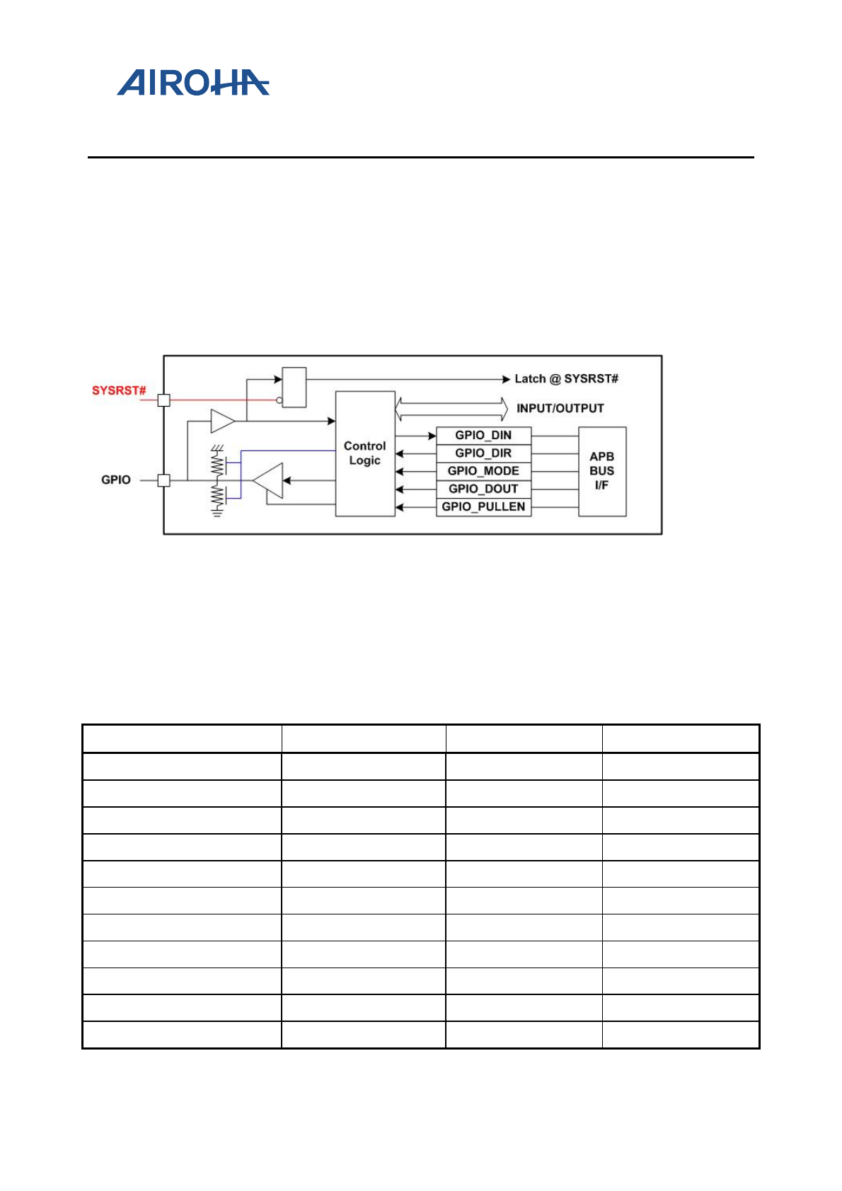
MT2523 Series Reference Manual
© 2015 - 2018 Airoha Technology Corp.
Page 423 of 692
This document contains information that is proprietary to Airoha Technology Corp. (“Airoha”) and/or its licensor(s).
Any unauthorized use, reproduction or disclosure of this document in whole or in part is strictly prohibited.
27. General Purpose Inputs/Outputs
27.1. General Description
MT2523G/D platform offers 48 general purpose I/O pins. By setting up the control registers, the MCU software can
control the direction, the output value, and read the input values on these pins. These GPIOs and GPOs are
multiplexed with other functions to reduce the pin count. To facilitate application use, the software can configure
which clock to send outside the chip. There are six clock-out ports embedded in 48 GPIO pins, and each clock-out
can be programmed to output appropriate clock source. Besides, when two GPIOs function for the same peripheral
IP, the smaller GPIO serial number has higher priority than the one of bigger number.
Figure 27-1. GPIO block diagram
27.2. IO Pull Up/Down Control Truth Table
Table 27-1. GPIO v.s. IO type mapping
GPIO Name IO Type GPIO Name IO Type
GPIO0 IO TYPE 4 GPIO25 IO TYPE 1
GPIO1 IO TYPE 4 GPIO26 IO TYPE 1
GPIO2 IO TYPE 4 GPIO27 IO TYPE 1
GPIO3 IO TYPE 4 GPIO28 IO TYPE 1
GPIO4 IO TYPE 1 GPIO29 IO TYPE 1
GPIO5 IO TYPE 1 GPIO30 IO TYPE 1
GPIO6 IO TYPE 1 GPIO31 IO TYPE 1
GPIO7 IO TYPE 1 GPIO32 IO TYPE 1
GPIO8 IO TYPE 1 GPIO33 IO TYPE 1
GPIO9 IO TYPE 1 GPIO34 IO TYPE 1
GPIO10 IO TYPE 4 GPIO35 IO TYPE 1
MT2523 Series Reference Manual
© 2015 - 2018 Airoha Technology Corp.
Page 424 of 692
This document contains information that is proprietary to Airoha Technology Corp. (“Airoha”) and/or its licensor(s).
Any unauthorized use, reproduction or disclosure of this document in whole or in part is strictly prohibited.
GPIO Name IO Type GPIO Name IO Type
GPIO11
IO TYPE 1 GPIO36
IO TYPE 1
GPIO12
IO TYPE 1 GPIO37
IO TYPE 1
GPIO13 IO TYPE 1 GPIO38 IO TYPE 1
GPIO14 IO TYPE 1 GPIO39 IO TYPE 1
GPIO15 IO TYPE 1 GPIO40 IO TYPE 1
GPIO16 IO TYPE 1 GPIO41 IO TYPE 1
GPIO17 IO TYPE 1 GPIO42 IO TYPE 1
GPIO18 IO TYPE 3 GPIO43 IO TYPE 1
GPIO19 IO TYPE 3 GPIO44 IO TYPE 1
GPIO20 IO TYPE 3 GPIO45 IO TYPE 1
GPIO21 IO TYPE 2 GPIO46 IO TYPE 1
GPIO22 IO TYPE 2 GPIO47 IO TYPE 1
GPIO23 IO TYPE 2 GPIO48 IO TYPE 1
GPIO24 IO TYPE 1
Refer to the truth table of pull-up/down control for the all GPIO pins excludingGPIO_0, GPIO_1, GPIO_2, GPIO_3,
and GPIO_10.
Table 27-2. IO type 1 - pull up/down control
GPIO_DIR GPIO_PUPD GPIO_R1 GPIO_R0 Resistance Value
0 0 0 0 High-Z
0 0 0 1 Pull-Up, 47K
0 0 1 0 Pull-Up, 47K
0 0 1 1 Pull-Up, 23.5K
0 1 0 0 High-Z
0 1 0 1 Pull-Down, 47K
0 1 1 0 Pull-Down, 47K
0 1 1 1 Pull-Down, 23.5K
1 X X X High-Z
MT2523 Series Reference Manual
© 2015 - 2018 Airoha Technology Corp.
Page 425 of 692
This document contains information that is proprietary to Airoha Technology Corp. (“Airoha”) and/or its licensor(s).
Any unauthorized use, reproduction or disclosure of this document in whole or in part is strictly prohibited.
Table 27-3. IO type 2 - pull up/down control
GPIO_DIR GPIO_PUPD GPIO_R1 GPIO_R0 Resistance Value
0 0 0 0 High-Z
0 0 0 1 Pull-up, 75K
0 0 1 0 Pull-up, 200K
0 0 1 1 Pull-up, 75K parallel
200K
0 1 0 0 High-Z
0 1 0 1 Pull-down, 75K
0 1 1 0 Pull-down, 200K
0 1 1 1 Pull-down, 75K
parallel 200K
1 X X X High-Z
Table 27-4. IO type 3 - pull up/down control
GPIO_DIR GPIO_PUPD GPIO_R1 GPIO_R0 Resistance Value
0 0 0 0 High-Z
0 0 0 1 Pull-up, 75K
0 0 1 0 Pull-up, 2K
0 0 1 1 Pull-up, 75K parallel
2K
0 1 0 0 High-Z
0 1 0 1 Pull-down, 75K
0 1 1 0 Pull-down, 2K
0 1 1 1 Pull-down, 75K
parallel 2K
1 X X X High-Z
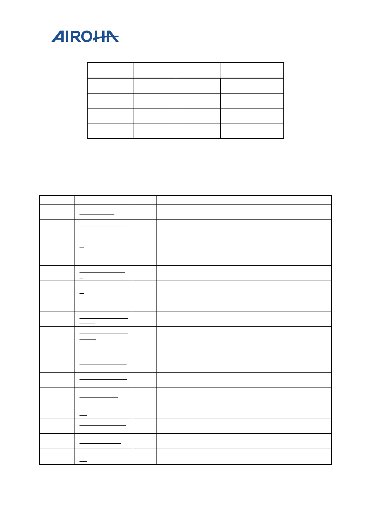
MT2523 Series Reference Manual
© 2015 - 2018 Airoha Technology Corp.
Page 426 of 692
This document contains information that is proprietary to Airoha Technology Corp. (“Airoha”) and/or its licensor(s).
Any unauthorized use, reproduction or disclosure of this document in whole or in part is strictly prohibited.
Table 27-5. IO type 4 - pull up/down control
GPIO_DIR GPIO_PULLEN GPIO_PULLSEL Resistance Value
0 1 1 Pull-up, 75K
0 0 0 High-Z
0 1 0 Pull-down, 75K
1 X X High-Z
27.3. Register Definition
Module name: gpio_reg Base address: (+A2020000h)
Address
Name
Width
Register Function
A2020000 GPIO_DIR0 32 GPIO Direction Control
Configures GPIO direction
A2020004 GPIO_DIR0_SE
T 32
GPIO Direction Control
For bitwise access of GPIO_DIR0
A2020008 GPIO_DIR0_CL
R 32 GPIO Direction Control
For bitwise access of GPIO_DIR0
A2020010 GPIO_DIR1 32
GPIO Direction Control
Configures GPIO direction
A2020014 GPIO_DIR1_SE
T 32 GPIO Direction Control
For bitwise access of GPIO_DIR1
A2020018 GPIO_DIR1_CL
R 32
GPIO Direction Control
For bitwise access of GPIO_DIR1
A2020100 GPIO_PULLEN0 32 GPIO Pull-up/down Enable Control
Configures GPIO pull enabling
A2020104 GPIO_PULLEN0
_SET 32
GPIO Pull-up/down Enable Control
For bitwise access of GPIO_PULLEN0
A2020108 GPIO_PULLEN0
_CLR 32 GPIO Pull-up/down Enable Control
For bitwise access of GPIO_PULLEN0
A2020200 GPIO_DINV0 32
GPIO Data Inversion Control
Configures GPIO inversion enabling
A2020204 GPIO_DINV0_S
ET 32 GPIO Data Inversion Control
For bitwise access of GPIO_DINV0
A2020208 GPIO_DINV0_C
LR 32
GPIO Data Inversion Control
For bitwise access of GPIO_DINV0
A2020210 GPIO_DINV1 32 GPIO Data Inversion Control
Configures GPIO inversion enabling
A2020214 GPIO_DINV1_S
ET 32
GPIO Data Inversion Control
For bitwise access of GPIO_DINV1
A2020218 GPIO_DINV1_C
LR 32 GPIO Data Inversion Control
For bitwise access of GPIO_DINV1
A2020300 GPIO_DOUT0 32
GPIO Output Data Control
Configures GPIO output value
A2020304 GPIO_DOUT0_S
ET 32 GPIO Output Data Control
For bitwise access of GPIO_DIR0
MT2523 Series Reference Manual
© 2015 - 2018 Airoha Technology Corp.
Page 427 of 692
This document contains information that is proprietary to Airoha Technology Corp. (“Airoha”) and/or its licensor(s).
Any unauthorized use, reproduction or disclosure of this document in whole or in part is strictly prohibited.
A2020308 GPIO_DOUT0_
CLR 32
GPIO Output Data Control
For bitwise access of GPIO_DIR0
A2020310 GPIO_DOUT1 32 GPIO Output Data Control
Configures GPIO output value
A2020314 GPIO_DOUT1_S
ET 32
GPIO Output Data Control
For bitwise access of GPIO_DIR1
A2020318 GPIO_DOUT1_C
LR 32 GPIO Output Data Control
For bitwise access of GPIO_DIR1
A2020400 GPIO_DIN0 32
GPIO Input Data Value
Reads GPIO input value
A2020410 GPIO_DIN1 32 GPIO Input Data Value
Reads GPIO input value
A2020500 GPIO_PULLSEL
0 32
GPIO Pullsel Control
Configures GPIO PUPD selection
A2020504 GPIO_PULLSEL
0_SET 32 GPIO Pullsel Control
For bitwise access of GPIO_PULLSEL0
A2020508 GPIO_PULLSEL
0_CLR 32
GPIO Pullsel Control
For bitwise access of GPIO_PULLSEL0
A2020600 GPIO_SMT0 32 GPIO SMT Control
Configures GPIO Schmitt trigger control
A2020604 GPIO_SMT0_SE
T 32
GPIO SMT Control
For bitwise access of GPIO_SMT0
A2020608 GPIO_SMT0_CL
R 32 GPIO SMT Control
For bitwise access of GPIO_SMT0
A2020610 GPIO_SMT1 32
GPIO SMT Control
Configures GPIO Schmitt trigger control
A2020614 GPIO_SMT1_SE
T 32 GPIO SMT Control
For bitwise access of GPIO_SMT1
A2020618 GPIO_SMT1_CL
R 32
GPIO SMT Control
For bitwise access of GPIO_SMT1
A2020700 GPIO_SR0 32 GPIO SR Control
Configures GPIO slew rate control
A2020704 GPIO_SR0_SET 32
GPIO SR Control
For bitwise access of GPIO_SR0
A2020708 GPIO_SR0_CLR 32 GPIO SR Control
For bitwise access of GPIO_SR0
A2020710 GPIO_SR1 32
GPIO SR Control
Configures GPIO slew rate control
A2020714 GPIO_SR1_SET 32 GPIO SR Control
For bitwise access of GPIO_SR1
A2020718 GPIO_SR1_CLR 32
GPIO SR Control
For bitwise access of GPIO_SR1
A2020800 GPIO_DRV0 32 GPIO DRV Control
Configures GPIO driving control
A2020804 GPIO_DRV0_SE
T 32
GPIO DRV Control
For bitwise access of GPIO_DRV0
A2020808 GPIO_DRV0_CL
R 32 GPIO DRV Control
For bitwise access of GPIO_DRV0
A2020810 GPIO_DRV1 32
GPIO DRV Control
Configures GPIO driving control
A2020814 GPIO_DRV1_SE
T 32 GPIO DRV Control
For bitwise access of GPIO_DRV1
A2020818 GPIO_DRV1_CL
R 32
GPIO DRV Control
For bitwise access of GPIO_DRV1
MT2523 Series Reference Manual
© 2015 - 2018 Airoha Technology Corp.
Page 428 of 692
This document contains information that is proprietary to Airoha Technology Corp. (“Airoha”) and/or its licensor(s).
Any unauthorized use, reproduction or disclosure of this document in whole or in part is strictly prohibited.
A2020820 GPIO_DRV2 32
GPIO DRV Control
Configures GPIO driving control
A2020824 GPIO_DRV2_SE
T 32 GPIO DRV Control
For bitwise access of GPIO_DRV2
A2020828 GPIO_DRV2_CL
R 32
GPIO DRV Control
For bitwise access of GPIO_DRV2
A2020830 GPIO_DRV3 32 GPIO DRV Control
Configures GPIO driving control
A2020834 GPIO_DRV3_SE
T 32
GPIO DRV Control
For bitwise access of GPIO_DRV3
A2020838 GPIO_DRV3_CL
R 32 GPIO DRV Control
For bitwise access of GPIO_DRV3
A2020900 GPIO_IES0 32
GPIO IES Control
Configures GPIO input enabling control
A2020904 GPIO_IES0_SE
T 32 GPIO IES Control
For bitwise access of GPIO_IES0
A2020908 GPIO_IES0_CL
R 32
GPIO IES Control
For bitwise access of GPIO_IES0
A2020910 GPIO_IES1 32 GPIO IES Control
Configures GPIO input enabling control
A2020914 GPIO_IES1_SET 32
GPIO IES Control
For bitwise access of GPIO_IES1
A2020918 GPIO_IES1_CLR 32 GPIO IES Control
For bitwise access of GPIO_IES1
A2020A00 GPIO_PUPD0 32
GPIO PUPD Control
Configures GPIO PUPD control
A2020A04 GPIO_PUPD0_S
ET 32 GPIO PUPD Control
For bitwise access of GPIO_PUPD0
A2020A08 GPIO_PUPD0_C
LR 32
GPIO PUPD Control
For bitwise access of GPIO_PUPD0
A2020A10 GPIO_PUPD1 32 GPIO PUPD Control
Configures GPIO PUPD control
A2020A14 GPIO_PUPD1_S
ET 32
GPIO PUPD Control
For bitwise access of GPIO_PUPD1
A2020A18 GPIO_PUPD1_C
LR 32 GPIO PUPD Control
For bitwise access of GPIO_PUPD1
A2020B00 GPIO_RESEN0_
0 32
GPIO R0 Control
Configures GPIO R0 control
A2020B04 GPIO_RESEN0_
0_SET 32 GPIO R0 Control
For bitwise access of GPIO_RESEN0_0
A2020B08 GPIO_RESEN0_
0_CLR 32
GPIO R0 Control
For bitwise access of GPIO_RESEN0_0
A2020B10 GPIO_RESEN0_
1 32 GPIO R0 Control
Configures GPIO R0 control
A2020B14 GPIO_RESEN0_
1_SET 32
GPIO R0 Control
For bitwise access of GPIO_RESEN0_1
A2020B18 GPIO_RESEN0_
1_CLR 32 GPIO R0 Control
For bitwise access of GPIO_RESEN0_1
A2020B20 GPIO_RESEN1_
0 32
GPIO R1 Control
Configures GPIO R1 control
A2020B24 GPIO_RESEN1_
0_SET 32 GPIO R1 Control
For bitwise access of GPIO_RESEN1_0
A2020B28 GPIO_RESEN1_
0_CLR 32
GPIO R1 Control
For bitwise access of GPIO_RESEN1_0
MT2523 Series Reference Manual
© 2015 - 2018 Airoha Technology Corp.
Page 429 of 692
This document contains information that is proprietary to Airoha Technology Corp. (“Airoha”) and/or its licensor(s).
Any unauthorized use, reproduction or disclosure of this document in whole or in part is strictly prohibited.
A2020B30 GPIO_RESEN1_
1 32
GPIO R1 Control
Configures GPIO R1 control
A2020B34 GPIO_RESEN1_
1_SET 32 GPIO R1 Control
For bitwise access of GPIO_RESEN1_1
A2020B38 GPIO_RESEN1_
1_CLR 32
GPIO R1 Control
For bitwise access of GPIO_RESEN1_1
A2020C00 GPIO_MODE0 32 GPIO Mode Control
Configures GPIO aux. mode
A2020C04 GPIO_MODE0_
SET 32
GPIO Mode Control
For bitwise access of GPIO_MODE0
A2020C08 GPIO_MODE0_
CLR 32 GPIO Mode Control
For bitwise access of GPIO_MODE0
A2020C10 GPIO_MODE1 32
GPIO Mode Control
Configures GPIO aux. mode
A2020C14 GPIO_MODE1_S
ET 32 GPIO Mode Control
For bitwise access of GPIO_MODE1
A2020C18 GPIO_MODE1_
CLR 32
GPIO Mode Control
For bitwise access of GPIO_MODE1
A2020C20 GPIO_MODE2 32 GPIO Mode Control
Configures GPIO aux. mode
A2020C24 GPIO_MODE2_
SET 32
GPIO Mode Control
For bitwise access of GPIO_MODE2
A2020C28 GPIO_MODE2_
CLR 32 GPIO Mode Control
For bitwise access of GPIO_MODE2
A2020C30 GPIO_MODE3 32
GPIO Mode Control
Configures GPIO aux. mode
A2020C34 GPIO_MODE3_
SET 32 GPIO Mode Control
For bitwise access of GPIO_MODE3
A2020C38 GPIO_MODE3_
CLR 32
GPIO Mode Control
For bitwise access of GPIO_MODE3
A2020C40 GPIO_MODE4 32 GPIO Mode Control
Configures GPIO aux. mode
A2020C44 GPIO_MODE4_
SET 32
GPIO Mode Control
For bitwise access of GPIO_MODE4
A2020C48 GPIO_MODE4_
CLR 32 GPIO Mode Control
For bitwise access of GPIO_MODE4
A2020C50 GPIO_MODE5 32
GPIO Mode Control
Configures GPIO aux. mode
A2020C54 GPIO_MODE5_
SET 32 GPIO Mode Control
For bitwise access of GPIO_MODE5
A2020C58 GPIO_MODE5_
CLR 32
GPIO Mode Control
For bitwise access of GPIO_MODE5
A2020C60 GPIO_MODE6 32 GPIO Mode Control
Configures GPIO aux. mode
A2020C64 GPIO_MODE6_
SET 32
GPIO Mode Control
For bitwise access of GPIO_MODE6
A2020C68 GPIO_MODE6_
CLR 32 GPIO Mode Control
For bitwise access of GPIO_MODE6
A2020D00 GPIO_TDSEL0 32
GPIO TDSEL Control
GPIO TX duty control register
A2020D04 GPIO_TDSEL0_
SET 32 GPIO TDSEL Control
For bitwise access of GPIO_TDSEL
A2020D08 GPIO_TDSEL0_
CLR 32
GPIO TDSEL Control
For bitwise access of GPIO_TDSEL
MT2523 Series Reference Manual
© 2015 - 2018 Airoha Technology Corp.
Page 430 of 692
This document contains information that is proprietary to Airoha Technology Corp. (“Airoha”) and/or its licensor(s).
Any unauthorized use, reproduction or disclosure of this document in whole or in part is strictly prohibited.
A2020D10 GPIO_TDSEL1 32
GPIO TDSEL Control
GPIO TX duty control register
A2020D14 GPIO_TDSEL1_
SET 32 GPIO TDSEL Control
For bitwise access of GPIO_TDSEL
A2020D18 GPIO_TDSEL1_
CLR 32
GPIO TDSEL Control
For bitwise access of GPIO_TDSEL
A2020D20 GPIO_TDSEL2 32 GPIO TDSEL Control
GPIO TX duty control register
A2020D24 GPIO_TDSEL2_
SET 32
GPIO TDSEL Control
For bitwise access of GPIO_TDSEL
A2020D28 GPIO_TDSEL2_
CLR 32 GPIO TDSEL Control
For bitwise access of GPIO_TDSEL
A2020D30 GPIO_TDSEL3 32
GPIO TDSEL Control
GPIO TX duty control register
A2020D34 GPIO_TDSEL3_
SET 32 GPIO TDSEL Control
For bitwise access of GPIO_TDSEL
A2020D38 GPIO_TDSEL3_
CLR 32
GPIO TDSEL Control
For bitwise access of GPIO_TDSEL
A2020E00 CLK_OUT0 32 CLK Out Selection Control
CLK OUT0 Setting
A2020E10 CLK_OUT1 32
CLK Out Selection Control
CLK OUT1 Setting
A2020E20 CLK_OUT2 32 CLK Out Selection Control
CLK OUT2 Setting
A2020E30 CLK_OUT3 32
CLK Out Selection Control
CLK OUT3 Setting
A2020E40 CLK_OUT4 32 CLK Out Selection Control
CLK OUT4 Setting
A2020E50 CLK_OUT5 32
CLK Out Selection Control
CLK OUT5 Setting
A2020000
GPIO_DIR0
GPIO Direction Control
02020000
Bit
31
30
29
28
27
26
25
24
23
22
21
20
19
18
17
16
Mne
GPIO
31
GPIO
30
GPIO
29
GPIO
28
GPIO
27
GPIO
26
GPIO
25
GPIO
24
GPIO
23
GPIO
22
GPIO
21
GPIO
20
GPIO1
9
GPIO1
8
GPIO1
7
GPIO
16
Type
RW
RW
RW
RW
RW
RW
RW
RW
RW
RW
RW
RW
RW
RW
RW
RW
Reset
0
0
0
0
0
0
1
0
0
0
0
0
0
0
1
0
Bit
15
14
13
12
11
10
9
8
7
6
5
4
3
2
1
0
Mne
GPIO
15
GPIO1
4
GPIO1
3
GPIO1
2
GPIO1
1
GPIO1
0
GPIO
9
GPIO
8
GPIO
7
GPIO
6
GPIO
5
GPIO
4
GPIO
3
GPIO
2
GPIO1
GPIO
0
Type
RW
RW
RW
RW
RW
RW
RW
RW
RW
RW
RW
RW
RW
RW
RW
RW
Reset
0
0
0
0
0
0
0
0
0
0
0
0
0
0
0
0
Overview
Configures GPIO direction
Bit(s)
Mnemonic
Name
Description
31
GPIO31
GPIO31_DIR
GPIO31 direction control
0: GPIO as input
1: GPIO as output
30
GPIO30
GPIO30_DIR
GPIO30 direction control
0: GPIO as input
1: GPIO as output
29
GPIO29
GPIO29_DIR
GPIO29 direction control
0: GPIO as input

MT2523 Series Reference Manual
© 2015 - 2018 Airoha Technology Corp.
Page 431 of 692
This document contains information that is proprietary to Airoha Technology Corp. (“Airoha”) and/or its licensor(s).
Any unauthorized use, reproduction or disclosure of this document in whole or in part is strictly prohibited.
Bit(s)
Mnemonic
Name
Description
1: GPIO as output
28
GPIO28
GPIO28_DIR
GPIO28 direction control
0: GPIO as input
1: GPIO as output
27
GPIO27
GPIO27_DIR
GPIO27 direction control
0: GPIO as input
1: GPIO as output
26
GPIO26
GPIO26_DIR
GPIO26 direction control
0: GPIO as input
1: GPIO as output
25
GPIO25
GPIO25_DIR
GPIO25 direction control
0: GPIO as input
1: GPIO as output
24
GPIO24
GPIO24_DIR
GPIO24 direction control
0: GPIO as input
1: GPIO as output
23
GPIO23
GPIO23_DIR
GPIO23 direction control
0: GPIO as input
1: GPIO as output
22
GPIO22
GPIO22_DIR
GPIO22 direction control
0: GPIO as input
1: GPIO as output
21
GPIO21
GPIO21_DIR
GPIO21 direction control
0: GPIO as input
1: GPIO as output
20
GPIO20
GPIO20_DIR
GPIO20 direction control
0: GPIO as input
1: GPIO as output
19
GPIO19
GPIO19_DIR
GPIO19 direction control
0: GPIO as input
1: GPIO as output
18
GPIO18
GPIO18_DIR
GPIO18 direction control
0: GPIO as input
1: GPIO as output
17
GPIO17
GPIO17_DIR
GPIO17 direction control
0: GPIO as input
1: GPIO as output
16
GPIO16
GPIO16_DIR
GPIO16 direction control
0: GPIO as input
1: GPIO as output
15
GPIO15
GPIO15_DIR
GPIO15 direction control
0: GPIO as input
1: GPIO as output
14
GPIO14
GPIO14_DIR
GPIO14 direction control
0: GPIO as input
1: GPIO as output
13
GPIO13
GPIO13_DIR
GPIO13 direction control
0: GPIO as input
1: GPIO as output
12
GPIO12
GPIO12_DIR
GPIO12 direction control
0: GPIO as input
1: GPIO as output
11
GPIO11
GPIO11_DIR
GPIO11 direction control
0: GPIO as input

MT2523 Series Reference Manual
© 2015 - 2018 Airoha Technology Corp.
Page 432 of 692
This document contains information that is proprietary to Airoha Technology Corp. (“Airoha”) and/or its licensor(s).
Any unauthorized use, reproduction or disclosure of this document in whole or in part is strictly prohibited.
Bit(s)
Mnemonic
Name
Description
1: GPIO as output
10
GPIO10
GPIO10_DIR
GPIO10 direction control
0: GPIO as input
1: GPIO as output
9
GPIO9
GPIO9_DIR
GPIO9 direction control
0: GPIO as input
1: GPIO as output
8
GPIO8
GPIO8_DIR
GPIO8 direction control
0: GPIO as input
1: GPIO as output
7
GPIO7
GPIO7_DIR
GPIO7 direction control
0: GPIO as input
1: GPIO as output
6
GPIO6
GPIO6_DIR
GPIO6 direction control
0: GPIO as input
1: GPIO as output
5
GPIO5
GPIO5_DIR
GPIO5 direction control
0: GPIO as input
1: GPIO as output
4
GPIO4
GPIO4_DIR
GPIO4 direction control
0: GPIO as input
1: GPIO as output
3
GPIO3
GPIO3_DIR
GPIO3 direction control
0: GPIO as input
1: GPIO as output
2
GPIO2
GPIO2_DIR
GPIO2 direction control
0: GPIO as input
1: GPIO as output
1
GPIO1
GPIO1_DIR
GPIO1 direction control
0: GPIO as input
1: GPIO as output
0
GPIO0
GPIO0_DIR
GPIO0 direction control
0: GPIO as input
1: GPIO as output
A2020004
GPIO_DIR0_S
ET
GPIO Direction Control
00000000
Bit
31
30
29
28
27
26
25
24
23
22
21
20
19
18
17
16
Mne
GPIO
31
GPIO
30
GPIO
29
GPIO
28
GPIO
27
GPIO
26
GPIO
25
GPIO
24
GPIO
23
GPIO
22
GPIO
21
GPIO
20
GPIO1
9
GPIO1
8
GPIO1
7
GPIO
16
Type
WO
WO
WO
WO
WO
WO
WO
WO
WO
WO
WO
WO
WO
WO
WO
WO
Reset
0
0
0
0
0
0
0
0
0
0
0
0
0
0
0
0
Bit
15
14
13
12
11
10
9
8
7
6
5
4
3
2
1
0
Mne
GPIO
15
GPIO1
4
GPIO1
3
GPIO1
2
GPIO1
1
GPIO1
0
GPIO
9
GPIO
8
GPIO
7
GPIO
6
GPIO
5
GPIO
4
GPIO
3
GPIO
2
GPIO1
GPIO
0
Type
WO
WO
WO
WO
WO
WO
WO
WO
WO
WO
WO
WO
WO
WO
WO
WO
Reset
0
0
0
0
0
0
0
0
0
0
0
0
0
0
0
0
Overview
For bitwise access of GPIO_DIR0
Bit(s)
Mnemonic
Name
Description
31
GPIO31
GPIO31_DIR
Bitwise SET operation of GPIO31 direction
0: Keep
1: SET bits

MT2523 Series Reference Manual
© 2015 - 2018 Airoha Technology Corp.
Page 433 of 692
This document contains information that is proprietary to Airoha Technology Corp. (“Airoha”) and/or its licensor(s).
Any unauthorized use, reproduction or disclosure of this document in whole or in part is strictly prohibited.
Bit(s)
Mnemonic
Name
Description
30
GPIO30
GPIO30_DIR
Bitwise SET operation of GPIO30 direction
0: Keep
1: SET bits
29
GPIO29
GPIO29_DIR
Bitwise SET operation of GPIO29 direction
0: Keep
1: SET bits
28
GPIO28
GPIO28_DIR
Bitwise SET operation of GPIO28 direction
0: Keep
1: SET bits
27
GPIO27
GPIO27_DIR
Bitwise SET operation of GPIO27 direction
0: Keep
1: SET bits
26
GPIO26
GPIO26_DIR
Bitwise SET operation of GPIO26 direction
0: Keep
1: SET bits
25
GPIO25
GPIO25_DIR
Bitwise SET operation of GPIO25 direction
0: Keep
1: SET bits
24
GPIO24
GPIO24_DIR
Bitwise SET operation of GPIO24 direction
0: Keep
1: SET bits
23
GPIO23
GPIO23_DIR
Bitwise SET operation of GPIO23 direction
0: Keep
1: SET bits
22
GPIO22
GPIO22_DIR
Bitwise SET operation of GPIO22 direction
0: Keep
1: SET bits
21
GPIO21
GPIO21_DIR
Bitwise SET operation of GPIO21 direction
0: Keep
1: SET bits
20
GPIO20
GPIO20_DIR
Bitwise SET operation of GPIO20 direction
0: Keep
1: SET bits
19
GPIO19
GPIO19_DIR
Bitwise SET operation of GPIO19 direction
0: Keep
1: SET bits
18
GPIO18
GPIO18_DIR
Bitwise SET operation of GPIO18 direction
0: Keep
1: SET bits
17
GPIO17
GPIO17_DIR
Bitwise SET operation of GPIO17 direction
0: Keep
1: SET bits
16
GPIO16
GPIO16_DIR
Bitwise SET operation of GPIO16 direction
0: Keep
1: SET bits
15
GPIO15
GPIO15_DIR
Bitwise SET operation of GPIO15 direction
0: Keep
1: SET bits
14
GPIO14
GPIO14_DIR
Bitwise SET operation of GPIO14 direction
0: Keep
1: SET bits
13
GPIO13
GPIO13_DIR
Bitwise SET operation of GPIO13 direction
0: Keep
1: SET bits

MT2523 Series Reference Manual
© 2015 - 2018 Airoha Technology Corp.
Page 434 of 692
This document contains information that is proprietary to Airoha Technology Corp. (“Airoha”) and/or its licensor(s).
Any unauthorized use, reproduction or disclosure of this document in whole or in part is strictly prohibited.
Bit(s)
Mnemonic
Name
Description
12
GPIO12
GPIO12_DIR
Bitwise SET operation of GPIO12 direction
0: Keep
1: SET bits
11
GPIO11
GPIO11_DIR
Bitwise SET operation of GPIO11 direction
0: Keep
1: SET bits
10
GPIO10
GPIO10_DIR
Bitwise SET operation of GPIO10 direction
0: Keep
1: SET bits
9
GPIO9
GPIO9_DIR
Bitwise SET operation of GPIO9 direction
0: Keep
1: SET bits
8
GPIO8
GPIO8_DIR
Bitwise SET operation of GPIO8 direction
0: Keep
1: SET bits
7
GPIO7
GPIO7_DIR
Bitwise SET operation of GPIO7 direction
0: Keep
1: SET bits
6
GPIO6
GPIO6_DIR
Bitwise SET operation of GPIO6 direction
0: Keep
1: SET bits
5
GPIO5
GPIO5_DIR
Bitwise SET operation of GPIO5 direction
0: Keep
1: SET bits
4
GPIO4
GPIO4_DIR
Bitwise SET operation of GPIO4 direction
0: Keep
1: SET bits
3
GPIO3
GPIO3_DIR
Bitwise SET operation of GPIO3 direction
0: Keep
1: SET bits
2
GPIO2
GPIO2_DIR
Bitwise SET operation of GPIO2 direction
0: Keep
1: SET bits
1
GPIO1
GPIO1_DIR
Bitwise SET operation of GPIO1 direction
0: Keep
1: SET bits
0
GPIO0
GPIO0_DIR
Bitwise SET operation of GPIO0 direction
0: Keep
1: SET bits
A2020008
GPIO_DIR0_C
LR
GPIO Direction Control
00000000
Bit
31
30
29
28
27
26
25
24
23
22
21
20
19
18
17
16
Mne
GPIO
31
GPIO
30
GPIO
29
GPIO
28
GPIO
27
GPIO
26
GPIO
25
GPIO
24
GPIO
23
GPIO
22
GPIO
21
GPIO
20
GPIO1
9
GPIO1
8
GPIO1
7
GPIO
16
Type
WO
WO
WO
WO
WO
WO
WO
WO
WO
WO
WO
WO
WO
WO
WO
WO
Reset
0
0
0
0
0
0
0
0
0
0
0
0
0
0
0
0
Bit
15
14
13
12
11
10
9
8
7
6
5
4
3
2
1
0
Mne
GPIO
15
GPIO1
4
GPIO1
3
GPIO1
2
GPIO1
1
GPIO1
0
GPIO
9
GPIO
8
GPIO
7
GPIO
6
GPIO
5
GPIO
4
GPIO
3
GPIO
2
GPIO1
GPIO
0
Type
WO
WO
WO
WO
WO
WO
WO
WO
WO
WO
WO
WO
WO
WO
WO
WO
Reset
0
0
0
0
0
0
0
0
0
0
0
0
0
0
0
0
Overview
For bitwise access of GPIO_DIR0

MT2523 Series Reference Manual
© 2015 - 2018 Airoha Technology Corp.
Page 435 of 692
This document contains information that is proprietary to Airoha Technology Corp. (“Airoha”) and/or its licensor(s).
Any unauthorized use, reproduction or disclosure of this document in whole or in part is strictly prohibited.
Bit(s)
Mnemonic
Name
Description
31
GPIO31
GPIO31_DIR
Bitwise CLR operation of GPIO31 direction
0: Keep
1: CLR bits
30
GPIO30
GPIO30_DIR
Bitwise CLR operation of GPIO30 direction
0: Keep
1: CLR bits
29
GPIO29
GPIO29_DIR
Bitwise CLR operation of GPIO29 direction
0: Keep
1: CLR bits
28
GPIO28
GPIO28_DIR
Bitwise CLR operation of GPIO28 direction
0: Keep
1: CLR bits
27
GPIO27
GPIO27_DIR
Bitwise CLR operation of GPIO27 direction
0: Keep
1: CLR bits
26
GPIO26
GPIO26_DIR
Bitwise CLR operation of GPIO26 direction
0: Keep
1: CLR bits
25
GPIO25
GPIO25_DIR
Bitwise CLR operation of GPIO25 direction
0: Keep
1: CLR bits
24
GPIO24
GPIO24_DIR
Bitwise CLR operation of GPIO24 direction
0: Keep
1: CLR bits
23
GPIO23
GPIO23_DIR
Bitwise CLR operation of GPIO23 direction
0: Keep
1: CLR bits
22
GPIO22
GPIO22_DIR
Bitwise CLR operation of GPIO22 direction
0: Keep
1: CLR bits
21
GPIO21
GPIO21_DIR
Bitwise CLR operation of GPIO21 direction
0: Keep
1: CLR bits
20
GPIO20
GPIO20_DIR
Bitwise CLR operation of GPIO20 direction
0: Keep
1: CLR bits
19
GPIO19
GPIO19_DIR
Bitwise CLR operation of GPIO19 direction
0: Keep
1: CLR bits
18
GPIO18
GPIO18_DIR
Bitwise CLR operation of GPIO18 direction
0: Keep
1: CLR bits
17
GPIO17
GPIO17_DIR
Bitwise CLR operation of GPIO17 direction
0: Keep
1: CLR bits
16
GPIO16
GPIO16_DIR
Bitwise CLR operation of GPIO16 direction
0: Keep
1: CLR bits
15
GPIO15
GPIO15_DIR
Bitwise CLR operation of GPIO15 direction
0: Keep
1: CLR bits
14
GPIO14
GPIO14_DIR
Bitwise CLR operation of GPIO14 direction
0: Keep

MT2523 Series Reference Manual
© 2015 - 2018 Airoha Technology Corp.
Page 436 of 692
This document contains information that is proprietary to Airoha Technology Corp. (“Airoha”) and/or its licensor(s).
Any unauthorized use, reproduction or disclosure of this document in whole or in part is strictly prohibited.
Bit(s)
Mnemonic
Name
Description
1: CLR bits
13
GPIO13
GPIO13_DIR
Bitwise CLR operation of GPIO13 direction
0: Keep
1: CLR bits
12
GPIO12
GPIO12_DIR
Bitwise CLR operation of GPIO12 direction
0: Keep
1: CLR bits
11
GPIO11
GPIO11_DIR
Bitwise CLR operation of GPIO11 direction
0: Keep
1: CLR bits
10
GPIO10
GPIO10_DIR
Bitwise CLR operation of GPIO10 direction
0: Keep
1: CLR bits
9
GPIO9
GPIO9_DIR
Bitwise CLR operation of GPIO9 direction
0: Keep
1: CLR bits
8
GPIO8
GPIO8_DIR
Bitwise CLR operation of GPIO8 direction
0: Keep
1: CLR bits
7
GPIO7
GPIO7_DIR
Bitwise CLR operation of GPIO7 direction
0: Keep
1: CLR bits
6
GPIO6
GPIO6_DIR
Bitwise CLR operation of GPIO6 direction
0: Keep
1: CLR bits
5
GPIO5
GPIO5_DIR
Bitwise CLR operation of GPIO5 direction
0: Keep
1: CLR bits
4
GPIO4
GPIO4_DIR
Bitwise CLR operation of GPIO4 direction
0: Keep
1: CLR bits
3
GPIO3
GPIO3_DIR
Bitwise CLR operation of GPIO3 direction
0: Keep
1: CLR bits
2
GPIO2
GPIO2_DIR
Bitwise CLR operation of GPIO2 direction
0: Keep
1: CLR bits
1
GPIO1
GPIO1_DIR
Bitwise CLR operation of GPIO1 direction
0: Keep
1: CLR bits
0
GPIO0
GPIO0_DIR
Bitwise CLR operation of GPIO0 direction
0: Keep
1: CLR bits
A2020010
GPIO_DIR1
GPIO Direction Control
00180088
Bit
31
30
29
28
27
26
25
24
23
22
21
20
19
18
17
16
Name
GPIO
48
Type
RW
Reset
0
Bit
15
14
13
12
11
10
9
8
7
6
5
4
3
2
1
0
Name
GPIO
47
GPIO
46
GPIO
45
GPIO
44
GPIO
43
GPIO
42
GPIO
41
GPIO
40
GPIO
39
GPIO
38
GPIO
37
GPIO
36
GPIO
35
GPIO
34
GPIO
33
GPIO
32
Type
RW
RW
RW
RW
RW
RW
RW
RW
RW
RW
RW
RW
RW
RW
RW
RW

MT2523 Series Reference Manual
© 2015 - 2018 Airoha Technology Corp.
Page 437 of 692
This document contains information that is proprietary to Airoha Technology Corp. (“Airoha”) and/or its licensor(s).
Any unauthorized use, reproduction or disclosure of this document in whole or in part is strictly prohibited.
Reset
0
0
0
0
0
0
0
0
1
0
0
0
1
0
0
0
Overview
Configures GPIO direction
Bit(s)
Mnemonic
Name
Description
16
GPIO48
GPIO48_DIR
GPIO48 direction control
0: GPIO as input
1: GPIO as output
15
GPIO47
GPIO47_DIR
GPIO47 direction control
0: GPIO as input
1: GPIO as output
14
GPIO46
GPIO46_DIR
GPIO46 direction control
0: GPIO as input
1: GPIO as output
13
GPIO45
GPIO45_DIR
GPIO45 direction control
0: GPIO as input
1: GPIO as output
12
GPIO44
GPIO44_DIR
GPIO44 direction control
0: GPIO as input
1: GPIO as output
11
GPIO43
GPIO43_DIR
GPIO43 direction control
0: GPIO as input
1: GPIO as output
10
GPIO42
GPIO42_DIR
GPIO42 direction control
0: GPIO as input
1: GPIO as output
9
GPIO41
GPIO41_DIR
GPIO41 direction control
0: GPIO as input
1: GPIO as output
8
GPIO40
GPIO40_DIR
GPIO40 direction control
0: GPIO as input
1: GPIO as output
7
GPIO39
GPIO39_DIR
GPIO39 direction control
0: GPIO as input
1: GPIO as output
6
GPIO38
GPIO38_DIR
GPIO38 direction control
0: GPIO as input
1: GPIO as output
5
GPIO37
GPIO37_DIR
GPIO37 direction control
0: GPIO as input
1: GPIO as output
4
GPIO36
GPIO36_DIR
GPIO36 direction control
0: GPIO as input
1: GPIO as output
3
GPIO35
GPIO35_DIR
GPIO35 direction control
0: GPIO as input
1: GPIO as output
2
GPIO34
GPIO34_DIR
GPIO34 direction control
0: GPIO as input
1: GPIO as output
1
GPIO33
GPIO33_DIR
GPIO33 direction control
0: GPIO as input
1: GPIO as output
0
GPIO32
GPIO32_DIR
GPIO32 direction control
0: GPIO as input

MT2523 Series Reference Manual
© 2015 - 2018 Airoha Technology Corp.
Page 438 of 692
This document contains information that is proprietary to Airoha Technology Corp. (“Airoha”) and/or its licensor(s).
Any unauthorized use, reproduction or disclosure of this document in whole or in part is strictly prohibited.
Bit(s)
Mnemonic
Name
Description
1: GPIO as output
A2020014
GPIO_DIR1_S
ET
GPIO Direction Control
00000000
Bit
31
30
29
28
27
26
25
24
23
22
21
20
19
18
17
16
Name
GPIO
48
Type
WO
Reset
0
Bit
15
14
13
12
11
10
9
8
7
6
5
4
3
2
1
0
Name
GPIO
47
GPIO
46
GPIO
45
GPIO
44
GPIO
43
GPIO
42
GPIO
41
GPIO
40
GPIO
39
GPIO
38
GPIO
37
GPIO
36
GPIO
35
GPIO
34
GPIO
33
GPIO
32
Type
WO
WO
WO
WO
WO
WO
WO
WO
WO
WO
WO
WO
WO
WO
WO
WO
Reset
0
0
0
0
0
0
0
0
0
0
0
0
0
0
0
0
Overview
For bitwise access of GPIO_DIR1
Bit(s)
Mnemonic
Name
Description
16
GPIO48
GPIO48_DIR
Bitwise SET operation of GPIO48 direction
0: Keep
1: SET bits
15
GPIO47
GPIO47_DIR
Bitwise SET operation of GPIO47 direction
0: Keep
1: SET bits
14
GPIO46
GPIO46_DIR
Bitwise SET operation of GPIO46 direction
0: Keep
1: SET bits
13
GPIO45
GPIO45_DIR
Bitwise SET operation of GPIO45 direction
0: Keep
1: SET bits
12
GPIO44
GPIO44_DIR
Bitwise SET operation of GPIO44 direction
0: Keep
1: SET bits
11
GPIO43
GPIO43_DIR
Bitwise SET operation of GPIO43 direction
0: Keep
1: SET bits
10
GPIO42
GPIO42_DIR
Bitwise SET operation of GPIO42 direction
0: Keep
1: SET bits
9
GPIO41
GPIO41_DIR
Bitwise SET operation of GPIO41 direction
0: Keep
1: SET bits
8
GPIO40
GPIO40_DIR
Bitwise SET operation of GPIO40 direction
0: Keep
1: SET bits
7
GPIO39
GPIO39_DIR
Bitwise SET operation of GPIO39 direction
0: Keep
1: SET bits
6
GPIO38
GPIO38_DIR
Bitwise SET operation of GPIO38 direction
0: Keep
1: SET bits
5
GPIO37
GPIO37_DIR
Bitwise SET operation of GPIO37 direction
0: Keep
1: SET bits

MT2523 Series Reference Manual
© 2015 - 2018 Airoha Technology Corp.
Page 439 of 692
This document contains information that is proprietary to Airoha Technology Corp. (“Airoha”) and/or its licensor(s).
Any unauthorized use, reproduction or disclosure of this document in whole or in part is strictly prohibited.
Bit(s)
Mnemonic
Name
Description
4
GPIO36
GPIO36_DIR
Bitwise SET operation of GPIO36 direction
0: Keep
1: SET bits
3
GPIO35
GPIO35_DIR
Bitwise SET operation of GPIO35 direction
0: Keep
1: SET bits
2
GPIO34
GPIO34_DIR
Bitwise SET operation of GPIO34 direction
0: Keep
1: SET bits
1
GPIO33
GPIO33_DIR
Bitwise SET operation of GPIO33 direction
0: Keep
1: SET bits
0
GPIO32
GPIO32_DIR
Bitwise SET operation of GPIO32 direction
0: Keep
1: SET bits
A2020018
GPIO_DIR1_C
LR
GPIO Direction Control
00000000
Bit
31
30
29
28
27
26
25
24
23
22
21
20
19
18
17
16
Name
GPIO
48
Type
WO
Reset
0
Bit
15
14
13
12
11
10
9
8
7
6
5
4
3
2
1
0
Name
GPIO
47
GPIO
46
GPIO
45
GPIO
44
GPIO
43
GPIO
42
GPIO
41
GPIO
40
GPIO
39
GPIO
38
GPIO
37
GPIO
36
GPIO
35
GPIO
34
GPIO
33
GPIO
32
Type
WO
WO
WO
WO
WO
WO
WO
WO
WO
WO
WO
WO
WO
WO
WO
WO
Reset
0
0
0
0
0
0
0
0
0
0
0
0
0
0
0
0
Overview
For bitwise access of GPIO_DIR1
Bit(s)
Mnemonic
Name
Description
16
GPIO48
GPIO48_DIR
Bitwise CLR operation of GPIO48 direction
0: Keep
1: CLR bits
15
GPIO47
GPIO47_DIR
Bitwise CLR operation of GPIO47 direction
0: Keep
1: CLR bits
14
GPIO46
GPIO46_DIR
Bitwise CLR operation of GPIO46 direction
0: Keep
1: CLR bits
13
GPIO45
GPIO45_DIR
Bitwise CLR operation of GPIO45 direction
0: Keep
1: CLR bits
12
GPIO44
GPIO44_DIR
Bitwise CLR operation of GPIO44 direction
0: Keep
1: CLR bits
11
GPIO43
GPIO43_DIR
Bitwise CLR operation of GPIO43 direction
0: Keep
1: CLR bits
10
GPIO42
GPIO42_DIR
Bitwise CLR operation of GPIO42 direction
0: Keep
1: CLR bits
MT2523 Series Reference Manual
© 2015 - 2018 Airoha Technology Corp.
Page 440 of 692
This document contains information that is proprietary to Airoha Technology Corp. (“Airoha”) and/or its licensor(s).
Any unauthorized use, reproduction or disclosure of this document in whole or in part is strictly prohibited.
Bit(s)
Mnemonic
Name
Description
9
GPIO41
GPIO41_DIR
Bitwise CLR operation of GPIO41 direction
0: Keep
1: CLR bits
8
GPIO40
GPIO40_DIR
Bitwise CLR operation of GPIO40 direction
0: Keep
1: CLR bits
7
GPIO39
GPIO39_DIR
Bitwise CLR operation of GPIO39 direction
0: Keep
1: CLR bits
6
GPIO38
GPIO38_DIR
Bitwise CLR operation of GPIO38 direction
0: Keep
1: CLR bits
5
GPIO37
GPIO37_DIR
Bitwise CLR operation of GPIO37 direction
0: Keep
1: CLR bits
4
GPIO36
GPIO36_DIR
Bitwise CLR operation of GPIO36 direction
0: Keep
1: CLR bits
3
GPIO35
GPIO35_DIR
Bitwise CLR operation of GPIO35 direction
0: Keep
1: CLR bits
2
GPIO34
GPIO34_DIR
Bitwise CLR operation of GPIO34 direction
0: Keep
1: CLR bits
1
GPIO33
GPIO33_DIR
Bitwise CLR operation of GPIO33 direction
0: Keep
1: CLR bits
0
GPIO32
GPIO32_DIR
Bitwise CLR operation of GPIO32 direction
0: Keep
1: CLR bits
A2020100
GPIO_PULLEN
0
GPIO Pull
-up/down Enable Control
0000040F
Bit
31
30
29
28
27
26
25
24
23
22
21
20
19
18
17
16
Name
Type
Reset
Bit
15
14
13
12
11
10
9
8
7
6
5
4
3
2
1
0
Name
GPIO1
0
GPIO
3
GPIO
2
GPIO1
GPIO
0
Type
RW
RW
RW
RW
RW
Reset
1
1
1
1
1
Overview
Configures GPIO pull enabling
Bit(s)
Mnemonic
Name
Description
10
GPIO10
GPIO10_PULLEN
GPIO10 PULLEN
0: Disable
1: Enable
3
GPIO3
GPIO3_PULLEN
GPIO3 PULLEN
0: Disable
1: Enable
2
GPIO2
GPIO2_PULLEN
GPIO2 PULLEN
MT2523 Series Reference Manual
© 2015 - 2018 Airoha Technology Corp.
Page 441 of 692
This document contains information that is proprietary to Airoha Technology Corp. (“Airoha”) and/or its licensor(s).
Any unauthorized use, reproduction or disclosure of this document in whole or in part is strictly prohibited.
Bit(s)
Mnemonic
Name
Description
0: Disable
1: Enable
1
GPIO1
GPIO1_PULLEN
GPIO1 PULLEN
0: Disable
1: Enable
0
GPIO0
GPIO0_PULLEN
GPIO0 PULLEN
0: Disable
1: Enable
A2020104
GPIO_PULLEN
0_SET
GPIO Pull
-up/down Enable Control
00000000
Bit
31
30
29
28
27
26
25
24
23
22
21
20
19
18
17
16
Name
Type
Reset
Bit
15
14
13
12
11
10
9
8
7
6
5
4
3
2
1
0
Name
GPIO1
0
GPIO
3
GPIO
2
GPIO1
GPIO
0
Type
WO
WO
WO
WO
WO
Reset
0
0
0
0
0
Overview
For bitwise access of GPIO_PULLEN0
Bit(s)
Mnemonic
Name
Description
10
GPIO10
GPIO10_PULLEN
Bitwise SET operation of GPIO10 PULLEN_SET
0: Keep
1: SET bits
3
GPIO3
GPIO3_PULLEN
Bitwise SET operation of GPIO3 PULLEN_SET
0: Keep
1: SET bits
2
GPIO2
GPIO2_PULLEN
Bitwise SET operation of GPIO2 PULLEN_SET
0: Keep
1: SET bits
1
GPIO1
GPIO1_PULLEN
Bitwise SET operation of GPIO1 PULLEN_SET
0: Keep
1: SET bits
0
GPIO0
GPIO0_PULLEN
Bitwise SET operation of GPIO0 PULLEN_SET
0: Keep
1: SET bits
A2020108
GPIO_PULLEN
0_CLR
GPIO Pull
-up/down Enable Control
00000000
Bit
31
30
29
28
27
26
25
24
23
22
21
20
19
18
17
16
Name
Type
Reset
Bit
15
14
13
12
11
10
9
8
7
6
5
4
3
2
1
0
Name
GPIO1
0
GPIO
3
GPIO
2
GPIO1
GPIO
0
Type
WO
WO
WO
WO
WO
Reset
0
0
0
0
0
Overview
For bitwise access of GPIO_PULLEN0
MT2523 Series Reference Manual
© 2015 - 2018 Airoha Technology Corp.
Page 442 of 692
This document contains information that is proprietary to Airoha Technology Corp. (“Airoha”) and/or its licensor(s).
Any unauthorized use, reproduction or disclosure of this document in whole or in part is strictly prohibited.
Bit(s)
Mnemonic
Name
Description
10
GPIO10
GPIO10_PULLEN
Bitwise CLR operation of GPIO10 PULLEN_CLR
0: Keep
1: CLR bits
3
GPIO3
GPIO3_PULLEN
Bitwise CLR operation of GPIO3 PULLEN_CLR
0: Keep
1: CLR bits
2
GPIO2
GPIO2_PULLEN
Bitwise CLR operation of GPIO2 PULLEN_CLR
0: Keep
1: CLR bits
1
GPIO1
GPIO1_PULLEN
Bitwise CLR operation of GPIO1 PULLEN_CLR
0: Keep
1: CLR bits
0
GPIO0
GPIO0_PULLEN
Bitwise CLR operation of GPIO0 PULLEN_CLR
0: Keep
1: CLR bits
A2020200
GPIO_DINV0
GPIO Data Inversion Control
00000000
Bit
31
30
29
28
27
26
25
24
23
22
21
20
19
18
17
16
Name
INV31
INV3
0
INV2
9
INV2
8
INV27
INV2
6
INV25
INV2
4
INV2
3
INV2
2
INV21
INV2
0
INV19
INV18
INV17
INV16
Type
RW
RW
RW
RW
RW
RW
RW
RW
RW
RW
RW
RW
RW
RW
RW
RW
Reset
0
0
0
0
0
0
0
0
0
0
0
0
0
0
0
0
Bit
15
14
13
12
11
10
9
8
7
6
5
4
3
2
1
0
Name
INV15
INV14
INV13
INV12
INV11
INV10
INV9
INV8
INV7
INV6
INV5
INV4
INV3
INV2
INV1
INV0
Type
RW
RW
RW
RW
RW
RW
RW
RW
RW
RW
RW
RW
RW
RW
RW
RW
Reset
0
0
0
0
0
0
0
0
0
0
0
0
0
0
0
0
Overview
Configures GPIO inversion enabling
Bit(s)
Mnemonic
Name
Description
31
INV31
GPIO31_DINV
GPIO31 inversion control
0: Keep input value
1: Invert input value
30
INV30
GPIO30_DINV
GPIO30 inversion control
0: Keep input value
1: Invert input value
29
INV29
GPIO29_DINV
GPIO29 inversion control
0: Keep input value
1: Invert input value
28
INV28
GPIO28_DINV
GPIO28 inversion control
0: Keep input value
1: Invert input value
27
INV27
GPIO27_DINV
GPIO27 inversion control
0: Keep input value
1: Invert input value
26
INV26
GPIO26_DINV
GPIO26 inversion control
0: Keep input value
1: Invert input value
25
INV25
GPIO25_DINV
GPIO25 inversion control
0: Keep input value
1: Invert input value
24
INV24
GPIO24_DINV
GPIO24 inversion control

MT2523 Series Reference Manual
© 2015 - 2018 Airoha Technology Corp.
Page 443 of 692
This document contains information that is proprietary to Airoha Technology Corp. (“Airoha”) and/or its licensor(s).
Any unauthorized use, reproduction or disclosure of this document in whole or in part is strictly prohibited.
Bit(s)
Mnemonic
Name
Description
0: Keep input value
1: Invert input value
23
INV23
GPIO23_DINV
GPIO23 inversion control
0: Keep input value
1: Invert input value
22
INV22
GPIO22_DINV
GPIO22 inversion control
0: Keep input value
1: Invert input value
21
INV21
GPIO21_DINV
GPIO21 inversion control
0: Keep input value
1: Invert input value
20
INV20
GPIO20_DINV
GPIO20 inversion control
0: Keep input value
1: Invert input value
19
INV19
GPIO19_DINV
GPIO19 inversion control
0: Keep input value
1: Invert input value
18
INV18
GPIO18_DINV
GPIO18 inversion control
0: Keep input value
1: Invert input value
17
INV17
GPIO17_DINV
GPIO17 inversion control
0: Keep input value
1: Invert input value
16
INV16
GPIO16_DINV
GPIO16 inversion control
0: Keep input value
1: Invert input value
15
INV15
GPIO15_DINV
GPIO15 inversion control
0: Keep input value
1: Invert input value
14
INV14
GPIO14_DINV
GPIO14 inversion control
0: Keep input value
1: Invert input value
13
INV13
GPIO13_DINV
GPIO13 inversion control
0: Keep input value
1: Invert input value
12
INV12
GPIO12_DINV
GPIO12 inversion control
0: Keep input value
1: Invert input value
11
INV11
GPIO11_DINV
GPIO11 inversion control
0: Keep input value
1: Invert input value
10
INV10
GPIO10_DINV
GPIO10 inversion control
0: Keep input value
1: Invert input value
9
INV9
GPIO9_DINV
GPIO9 inversion control
0: Keep input value
1: Invert input value
8
INV8
GPIO8_DINV
GPIO8 inversion control
0: Keep input value
1: Invert input value
7
INV7
GPIO7_DINV
GPIO7 inversion control
0: Keep input value
1: Invert input value
6
INV6
GPIO6_DINV
GPIO6 inversion control

MT2523 Series Reference Manual
© 2015 - 2018 Airoha Technology Corp.
Page 444 of 692
This document contains information that is proprietary to Airoha Technology Corp. (“Airoha”) and/or its licensor(s).
Any unauthorized use, reproduction or disclosure of this document in whole or in part is strictly prohibited.
Bit(s)
Mnemonic
Name
Description
0: Keep input value
1: Invert input value
5
INV5
GPIO5_DINV
GPIO5 inversion control
0: Keep input value
1: Invert input value
4
INV4
GPIO4_DINV
GPIO4 inversion control
0: Keep input value
1: Invert input value
3
INV3
GPIO3_DINV
GPIO3 inversion control
0: Keep input value
1: Invert input value
2
INV2
GPIO2_DINV
GPIO2 inversion control
0: Keep input value
1: Invert input value
1
INV1
GPIO1_DINV
GPIO1 inversion control
0: Keep input value
1: Invert input value
0
INV0
GPIO0_DINV
GPIO0 inversion control
0: Keep input value
1: Invert input value
A2020204
GPIO_DINV0_
SET
GPIO Data Inversion Control
00000000
Bit
31
30
29
28
27
26
25
24
23
22
21
20
19
18
17
16
Name
INV31
INV3
0
INV2
9
INV2
8
INV27
INV2
6
INV25
INV2
4
INV2
3
INV2
2
INV21
INV2
0
INV19
INV18
INV17
INV16
Type
WO
WO
WO
WO
WO
WO
WO
WO
WO
WO
WO
WO
WO
WO
WO
WO
Reset
0
0
0
0
0
0
0
0
0
0
0
0
0
0
0
0
Bit
15
14
13
12
11
10
9
8
7
6
5
4
3
2
1
0
Name
INV15
INV14
INV13
INV12
INV11
INV10
INV9
INV8
INV7
INV6
INV5
INV4
INV3
INV2
INV1
INV0
Type
WO
WO
WO
WO
WO
WO
WO
WO
WO
WO
WO
WO
WO
WO
WO
WO
Reset
0
0
0
0
0
0
0
0
0
0
0
0
0
0
0
0
Overview
For bitwise access of GPIO_DINV0
Bit(s)
Mnemonic
Name
Description
31
INV31
GPIO31_DINV
Bitwise SET operation of GPIO31 inversion control
0: Keep
1: SET bits
30
INV30
GPIO30_DINV
Bitwise SET operation of GPIO30 inversion control
0: Keep
1: SET bits
29
INV29
GPIO29_DINV
Bitwise SET operation of GPIO29 inversion control
0: Keep
1: SET bits
28
INV28
GPIO28_DINV
Bitwise SET operation of GPIO28 inversion control
0: Keep
1: SET bits
27
INV27
GPIO27_DINV
Bitwise SET operation of GPIO27 inversion control
0: Keep
1: SET bits
26
INV26
GPIO26_DINV
Bitwise SET operation of GPIO26 inversion control
0: Keep
1: SET bits

MT2523 Series Reference Manual
© 2015 - 2018 Airoha Technology Corp.
Page 445 of 692
This document contains information that is proprietary to Airoha Technology Corp. (“Airoha”) and/or its licensor(s).
Any unauthorized use, reproduction or disclosure of this document in whole or in part is strictly prohibited.
Bit(s)
Mnemonic
Name
Description
25
INV25
GPIO25_DINV
Bitwise SET operation of GPIO25 inversion control
0: Keep
1: SET bits
24
INV24
GPIO24_DINV
Bitwise SET operation of GPIO24 inversion control
0: Keep
1: SET bits
23
INV23
GPIO23_DINV
Bitwise SET operation of GPIO23 inversion control
0: Keep
1: SET bits
22
INV22
GPIO22_DINV
Bitwise SET operation of GPIO22 inversion control
0: Keep
1: SET bits
21
INV21
GPIO21_DINV
Bitwise SET operation of GPIO21 inversion control
0: Keep
1: SET bits
20
INV20
GPIO20_DINV
Bitwise SET operation of GPIO20 inversion control
0: Keep
1: SET bits
19
INV19
GPIO19_DINV
Bitwise SET operation of GPIO19 inversion control
0: Keep
1: SET bits
18
INV18
GPIO18_DINV
Bitwise SET operation of GPIO18 inversion control
0: Keep
1: SET bits
17
INV17
GPIO17_DINV
Bitwise SET operation of GPIO17 inversion control
0: Keep
1: SET bits
16
INV16
GPIO16_DINV
Bitwise SET operation of GPIO16 inversion control
0: Keep
1: SET bits
15
INV15
GPIO15_DINV
Bitwise SET operation of GPIO15 inversion control
0: Keep
1: SET bits
14
INV14
GPIO14_DINV
Bitwise SET operation of GPIO14 inversion control
0: Keep
1: SET bits
13
INV13
GPIO13_DINV
Bitwise SET operation of GPIO13 inversion control
0: Keep
1: SET bits
12
INV12
GPIO12_DINV
Bitwise SET operation of GPIO12 inversion control
0: Keep
1: SET bits
11
INV11
GPIO11_DINV
Bitwise SET operation of GPIO11 inversion control
0: Keep
1: SET bits
10
INV10
GPIO10_DINV
Bitwise SET operation of GPIO10 inversion control
0: Keep
1: SET bits
9
INV9
GPIO9_DINV
Bitwise SET operation of GPIO9 inversion control
0: Keep
1: SET bits
8
INV8
GPIO8_DINV
Bitwise SET operation of GPIO8 inversion control
0: Keep
1: SET bits

MT2523 Series Reference Manual
© 2015 - 2018 Airoha Technology Corp.
Page 446 of 692
This document contains information that is proprietary to Airoha Technology Corp. (“Airoha”) and/or its licensor(s).
Any unauthorized use, reproduction or disclosure of this document in whole or in part is strictly prohibited.
Bit(s)
Mnemonic
Name
Description
7
INV7
GPIO7_DINV
Bitwise SET operation of GPIO7 inversion control
0: Keep
1: SET bits
6
INV6
GPIO6_DINV
Bitwise SET operation of GPIO6 inversion control
0: Keep
1: SET bits
5
INV5
GPIO5_DINV
Bitwise SET operation of GPIO5 inversion control
0: Keep
1: SET bits
4
INV4
GPIO4_DINV
Bitwise SET operation of GPIO4 inversion control
0: Keep
1: SET bits
3
INV3
GPIO3_DINV
Bitwise SET operation of GPIO3 inversion control
0: Keep
1: SET bits
2
INV2
GPIO2_DINV
Bitwise SET operation of GPIO2 inversion control
0: Keep
1: SET bits
1
INV1
GPIO1_DINV
Bitwise SET operation of GPIO1 inversion control
0: Keep
1: SET bits
0
INV0
GPIO0_DINV
Bitwise SET operation of GPIO0 inversion control
0: Keep
1: SET bits
A2020208
GPIO_DINV0_
CLR
GPIO Data Inversion Control
00000000
Bit
31
30
29
28
27
26
25
24
23
22
21
20
19
18
17
16
Name
INV31
INV3
0
INV2
9
INV2
8
INV27
INV2
6
INV25
INV2
4
INV2
3
INV2
2
INV21
INV2
0
INV19
INV18
INV17
INV16
Type
WO
WO
WO
WO
WO
WO
WO
WO
WO
WO
WO
WO
WO
WO
WO
WO
Reset
0
0
0
0
0
0
0
0
0
0
0
0
0
0
0
0
Bit
15
14
13
12
11
10
9
8
7
6
5
4
3
2
1
0
Name
INV15
INV14
INV13
INV12
INV11
INV10
INV9
INV8
INV7
INV6
INV5
INV4
INV3
INV2
INV1
INV0
Type
WO
WO
WO
WO
WO
WO
WO
WO
WO
WO
WO
WO
WO
WO
WO
WO
Reset
0
0
0
0
0
0
0
0
0
0
0
0
0
0
0
0
Overview
For bitwise access of GPIO_DINV0
Bit(s)
Mnemonic
Name
Description
31
INV31
GPIO31_DINV
Bitwise CLR operation of GPIO31 inversion control
0: Keep
1: CLR bits
30
INV30
GPIO30_DINV
Bitwise CLR operation of GPIO30 inversion control
0: Keep
1: CLR bits
29
INV29
GPIO29_DINV
Bitwise CLR operation of GPIO29 inversion control
0: Keep
1: CLR bits
28
INV28
GPIO28_DINV
Bitwise CLR operation of GPIO28 inversion control
0: Keep
1: CLR bits
27
INV27
GPIO27_DINV
Bitwise CLR operation of GPIO27 inversion control

MT2523 Series Reference Manual
© 2015 - 2018 Airoha Technology Corp.
Page 447 of 692
This document contains information that is proprietary to Airoha Technology Corp. (“Airoha”) and/or its licensor(s).
Any unauthorized use, reproduction or disclosure of this document in whole or in part is strictly prohibited.
Bit(s)
Mnemonic
Name
Description
0: Keep
1: CLR bits
26
INV26
GPIO26_DINV
Bitwise CLR operation of GPIO26 inversion control
0: Keep
1: CLR bits
25
INV25
GPIO25_DINV
Bitwise CLR operation of GPIO25 inversion control
0: Keep
1: CLR bits
24
INV24
GPIO24_DINV
Bitwise CLR operation of GPIO24 inversion control
0: Keep
1: CLR bits
23
INV23
GPIO23_DINV
Bitwise CLR operation of GPIO23 inversion control
0: Keep
1: CLR bits
22
INV22
GPIO22_DINV
Bitwise CLR operation of GPIO22 inversion control
0: Keep
1: CLR bits
21
INV21
GPIO21_DINV
Bitwise CLR operation of GPIO21 inversion control
0: Keep
1: CLR bits
20
INV20
GPIO20_DINV
Bitwise CLR operation of GPIO20 inversion control
0: Keep
1: CLR bits
19
INV19
GPIO19_DINV
Bitwise CLR operation of GPIO19 inversion control
0: Keep
1: CLR bits
18
INV18
GPIO18_DINV
Bitwise CLR operation of GPIO18 inversion control
0: Keep
1: CLR bits
17
INV17
GPIO17_DINV
Bitwise CLR operation of GPIO17 inversion control
0: Keep
1: CLR bits
16
INV16
GPIO16_DINV
Bitwise CLR operation of GPIO16 inversion control
0: Keep
1: CLR bits
15
INV15
GPIO15_DINV
Bitwise CLR operation of GPIO15 inversion control
0: Keep
1: CLR bits
14
INV14
GPIO14_DINV
Bitwise CLR operation of GPIO14 inversion control
0: Keep
1: CLR bits
13
INV13
GPIO13_DINV
Bitwise CLR operation of GPIO13 inversion control
0: Keep
1: CLR bits
12
INV12
GPIO12_DINV
Bitwise CLR operation of GPIO12 inversion control
0: Keep
1: CLR bits
11
INV11
GPIO11_DINV
Bitwise CLR operation of GPIO11 inversion control
0: Keep
1: CLR bits
10
INV10
GPIO10_DINV
Bitwise CLR operation of GPIO10 inversion control
0: Keep
1: CLR bits
9
INV9
GPIO9_DINV
Bitwise CLR operation of GPIO9 inversion control

MT2523 Series Reference Manual
© 2015 - 2018 Airoha Technology Corp.
Page 448 of 692
This document contains information that is proprietary to Airoha Technology Corp. (“Airoha”) and/or its licensor(s).
Any unauthorized use, reproduction or disclosure of this document in whole or in part is strictly prohibited.
Bit(s)
Mnemonic
Name
Description
0: Keep
1: CLR bits
8
INV8
GPIO8_DINV
Bitwise CLR operation of GPIO8 inversion control
0: Keep
1: CLR bits
7
INV7
GPIO7_DINV
Bitwise CLR operation of GPIO7 inversion control
0: Keep
1: CLR bits
6
INV6
GPIO6_DINV
Bitwise CLR operation of GPIO6 inversion control
0: Keep
1: CLR bits
5
INV5
GPIO5_DINV
Bitwise CLR operation of GPIO5 inversion control
0: Keep
1: CLR bits
4
INV4
GPIO4_DINV
Bitwise CLR operation of GPIO4 inversion control
0: Keep
1: CLR bits
3
INV3
GPIO3_DINV
Bitwise CLR operation of GPIO3 inversion control
0: Keep
1: CLR bits
2
INV2
GPIO2_DINV
Bitwise CLR operation of GPIO2 inversion control
0: Keep
1: CLR bits
1
INV1
GPIO1_DINV
Bitwise CLR operation of GPIO1 inversion control
0: Keep
1: CLR bits
0
INV0
GPIO0_DINV
Bitwise CLR operation of GPIO0 inversion control
0: Keep
1: CLR bits
A2020210
GPIO_DINV1
GPIO Data Inversion Control
00000000
Bit
31
30
29
28
27
26
25
24
23
22
21
20
19
18
17
16
Name
INV4
8
Type
RW
Reset
0
Bit
15
14
13
12
11
10
9
8
7
6
5
4
3
2
1
0
Name
INV4
7
INV4
6
INV45
INV4
4
INV4
3
INV4
2
INV41
INV4
0
INV3
9
INV3
8
INV37
INV3
6
INV35
INV3
4
INV3
3
INV3
2
Type
RW
RW
RW
RW
RW
RW
RW
RW
RW
RW
RW
RW
RW
RW
RW
RW
Reset
0
0
0
0
0
0
0
0
0
0
0
0
0
0
0
0
Overview
Configures GPIO inversion enabling
Bit(s)
Mnemonic
Name
Description
16
INV48
GPIO48_DINV
GPIO48 inversion control
0: Keep input value
1: Invert input value
15
INV47
GPIO47_DINV
GPIO47 inversion control
0: Keep input value
1: Invert input value
14
INV46
GPIO46_DINV
GPIO46 inversion control
0: Keep input value
1: Invert input value

MT2523 Series Reference Manual
© 2015 - 2018 Airoha Technology Corp.
Page 449 of 692
This document contains information that is proprietary to Airoha Technology Corp. (“Airoha”) and/or its licensor(s).
Any unauthorized use, reproduction or disclosure of this document in whole or in part is strictly prohibited.
Bit(s)
Mnemonic
Name
Description
13
INV45
GPIO45_DINV
GPIO45 inversion control
0: Keep input value
1: Invert input value
12
INV44
GPIO44_DINV
GPIO44 inversion control
0: Keep input value
1: Invert input value
11
INV43
GPIO43_DINV
GPIO43 inversion control
0: Keep input value
1: Invert input value
10
INV42
GPIO42_DINV
GPIO42 inversion control
0: Keep input value
1: Invert input value
9
INV41
GPIO41_DINV
GPIO41 inversion control
0: Keep input value
1: Invert input value
8
INV40
GPIO40_DINV
GPIO40 inversion control
0: Keep input value
1: Invert input value
7
INV39
GPIO39_DINV
GPIO39 inversion control
0: Keep input value
1: Invert input value
6
INV38
GPIO38_DINV
GPIO38 inversion control
0: Keep input value
1: Invert input value
5
INV37
GPIO37_DINV
GPIO37 inversion control
0: Keep input value
1: Invert input value
4
INV36
GPIO36_DINV
GPIO36 inversion control
0: Keep input value
1: Invert input value
3
INV35
GPIO35_DINV
GPIO35 inversion control
0: Keep input value
1: Invert input value
2
INV34
GPIO34_DINV
GPIO34 inversion control
0: Keep input value
1: Invert input value
1
INV33
GPIO33_DINV
GPIO33 inversion control
0: Keep input value
1: Invert input value
0
INV32
GPIO32_DINV
GPIO32 inversion control
0: Keep input value
1: Invert input value
A2020214
GPIO_DINV1_
SET
GPIO Data Inversion Control
00000000
Bit
31
30
29
28
27
26
25
24
23
22
21
20
19
18
17
16
Name
INV4
8
Type
WO
Reset
0
Bit
15
14
13
12
11
10
9
8
7
6
5
4
3
2
1
0
Name
INV4
7
INV4
6
INV45
INV4
4
INV4
3
INV4
2
INV41
INV4
0
INV3
9
INV3
8
INV37
INV3
6
INV35
INV3
4
INV3
3
INV3
2
Type
WO
WO
WO
WO
WO
WO
WO
WO
WO
WO
WO
WO
WO
WO
WO
WO

MT2523 Series Reference Manual
© 2015 - 2018 Airoha Technology Corp.
Page 450 of 692
This document contains information that is proprietary to Airoha Technology Corp. (“Airoha”) and/or its licensor(s).
Any unauthorized use, reproduction or disclosure of this document in whole or in part is strictly prohibited.
Reset
0
0
0
0
0
0
0
0
0
0
0
0
0
0
0
0
Overview
For bitwise access of GPIO_DINV1
Bit(s)
Mnemonic
Name
Description
16
INV48
GPIO48_DINV
Bitwise SET operation of GPIO48 inversion control
0: Keep
1: SET bits
15
INV47
GPIO47_DINV
Bitwise SET operation of GPIO47 inversion control
0: Keep
1: SET bits
14
INV46
GPIO46_DINV
Bitwise SET operation of GPIO46 inversion control
0: Keep
1: SET bits
13
INV45
GPIO45_DINV
Bitwise SET operation of GPIO45 inversion control
0: Keep
1: SET bits
12
INV44
GPIO44_DINV
Bitwise SET operation of GPIO44 inversion control
0: Keep
1: SET bits
11
INV43
GPIO43_DINV
Bitwise SET operation of GPIO43 inversion control
0: Keep
1: SET bits
10
INV42
GPIO42_DINV
Bitwise SET operation of GPIO42 inversion control
0: Keep
1: SET bits
9
INV41
GPIO41_DINV
Bitwise SET operation of GPIO41 inversion control
0: Keep
1: SET bits
8
INV40
GPIO40_DINV
Bitwise SET operation of GPIO40 inversion control
0: Keep
1: SET bits
7
INV39
GPIO39_DINV
Bitwise SET operation of GPIO39 inversion control
0: Keep
1: SET bits
6
INV38
GPIO38_DINV
Bitwise SET operation of GPIO38 inversion control
0: Keep
1: SET bits
5
INV37
GPIO37_DINV
Bitwise SET operation of GPIO37 inversion control
0: Keep
1: SET bits
4
INV36
GPIO36_DINV
Bitwise SET operation of GPIO36 inversion control
0: Keep
1: SET bits
3
INV35
GPIO35_DINV
Bitwise SET operation of GPIO35 inversion control
0: Keep
1: SET bits
2
INV34
GPIO34_DINV
Bitwise SET operation of GPIO34 inversion control
0: Keep
1: SET bits
1
INV33
GPIO33_DINV
Bitwise SET operation of GPIO33 inversion control
0: Keep
1: SET bits
0
INV32
GPIO32_DINV
Bitwise SET operation of GPIO32 inversion control
0: Keep
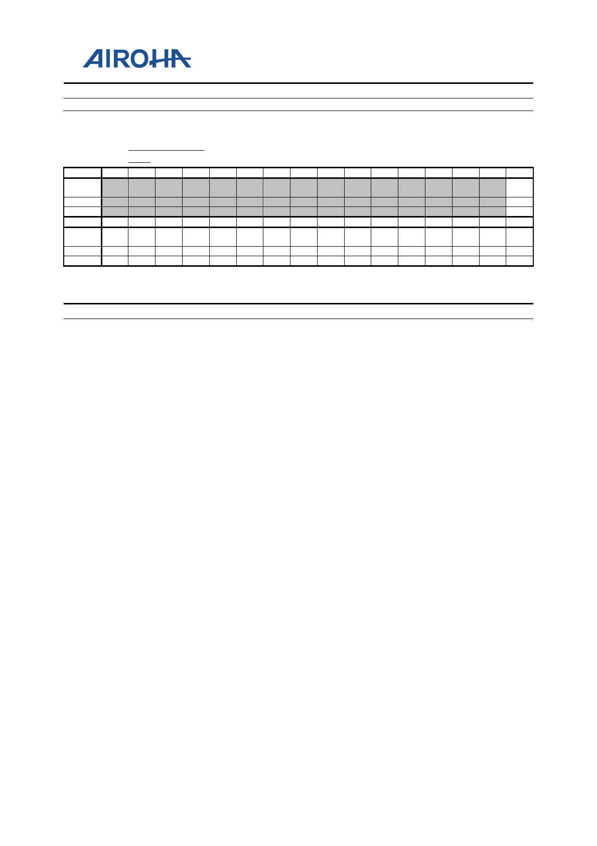
MT2523 Series Reference Manual
© 2015 - 2018 Airoha Technology Corp.
Page 451 of 692
This document contains information that is proprietary to Airoha Technology Corp. (“Airoha”) and/or its licensor(s).
Any unauthorized use, reproduction or disclosure of this document in whole or in part is strictly prohibited.
Bit(s)
Mnemonic
Name
Description
1: SET bits
A2020218
GPIO_DINV1_
CLR
GPIO Data Inversion Control
00000000
Bit
31
30
29
28
27
26
25
24
23
22
21
20
19
18
17
16
Name
INV4
8
Type
WO
Reset
0
Bit
15
14
13
12
11
10
9
8
7
6
5
4
3
2
1
0
Name
INV4
7
INV4
6
INV45
INV4
4
INV4
3
INV4
2
INV41
INV4
0
INV3
9
INV3
8
INV37
INV3
6
INV35
INV3
4
INV3
3
INV3
2
Type
WO
WO
WO
WO
WO
WO
WO
WO
WO
WO
WO
WO
WO
WO
WO
WO
Reset
0
0
0
0
0
0
0
0
0
0
0
0
0
0
0
0
Overview
For bitwise access of GPIO_DINV1
Bit(s)
Mnemonic
Name
Description
16
INV48
GPIO48_DINV
Bitwise CLR operation of GPIO48 inversion control
0: Keep
1: CLR bits
15
INV47
GPIO47_DINV
Bitwise CLR operation of GPIO47 inversion control
0: Keep
1: CLR bits
14
INV46
GPIO46_DINV
Bitwise CLR operation of GPIO46 inversion control
0: Keep
1: CLR bits
13
INV45
GPIO45_DINV
Bitwise CLR operation of GPIO45 inversion control
0: Keep
1: CLR bits
12
INV44
GPIO44_DINV
Bitwise CLR operation of GPIO44 inversion control
0: Keep
1: CLR bits
11
INV43
GPIO43_DINV
Bitwise CLR operation of GPIO43 inversion control
0: Keep
1: CLR bits
10
INV42
GPIO42_DINV
Bitwise CLR operation of GPIO42 inversion control
0: Keep
1: CLR bits
9
INV41
GPIO41_DINV
Bitwise CLR operation of GPIO41 inversion control
0: Keep
1: CLR bits
8
INV40
GPIO40_DINV
Bitwise CLR operation of GPIO40 inversion control
0: Keep
1: CLR bits
7
INV39
GPIO39_DINV
Bitwise CLR operation of GPIO39 inversion control
0: Keep
1: CLR bits
6
INV38
GPIO38_DINV
Bitwise CLR operation of GPIO38 inversion control
0: Keep
1: CLR bits
5
INV37
GPIO37_DINV
Bitwise CLR operation of GPIO37 inversion control
0: Keep
1: CLR bits

MT2523 Series Reference Manual
© 2015 - 2018 Airoha Technology Corp.
Page 452 of 692
This document contains information that is proprietary to Airoha Technology Corp. (“Airoha”) and/or its licensor(s).
Any unauthorized use, reproduction or disclosure of this document in whole or in part is strictly prohibited.
Bit(s)
Mnemonic
Name
Description
4
INV36
GPIO36_DINV
Bitwise CLR operation of GPIO36 inversion control
0: Keep
1: CLR bits
3
INV35
GPIO35_DINV
Bitwise CLR operation of GPIO35 inversion control
0: Keep
1: CLR bits
2
INV34
GPIO34_DINV
Bitwise CLR operation of GPIO34 inversion control
0: Keep
1: CLR bits
1
INV33
GPIO33_DINV
Bitwise CLR operation of GPIO33 inversion control
0: Keep
1: CLR bits
0
INV32
GPIO32_DINV
Bitwise CLR operation of GPIO32 inversion control
0: Keep
1: CLR bits
A2020300
GPIO_DOUT0
GPIO Output Data Control
02020000
Bit
31
30
29
28
27
26
25
24
23
22
21
20
19
18
17
16
Name
GPIO
31
GPIO
30
GPIO
29
GPIO
28
GPIO
27
GPIO
26
GPIO
25
GPIO
24
GPIO
23
GPIO
22
GPIO
21
GPIO
20
GPIO1
9
GPIO1
8
GPIO1
7
GPIO
16
Type
RW
RW
RW
RW
RW
RW
RW
RW
RW
RW
RW
RW
RW
RW
RW
RW
Reset
0
0
0
0
0
0
1
0
0
0
0
0
0
0
1
0
Bit
15
14
13
12
11
10
9
8
7
6
5
4
3
2
1
0
Name
GPIO
15
GPIO1
4
GPIO1
3
GPIO1
2
GPIO1
1
GPIO1
0
GPIO
9
GPIO
8
GPIO
7
GPIO
6
GPIO
5
GPIO
4
GPIO
3
GPIO
2
GPIO1
GPIO
0
Type
RW
RW
RW
RW
RW
RW
RW
RW
RW
RW
RW
RW
RW
RW
RW
RW
Reset
0
0
0
0
0
0
0
0
0
0
0
0
0
0
0
0
Overview
Configures GPIO output value
Bit(s)
Mnemonic
Name
Description
31
GPIO31
GPIO31_OUT
GPIO31 data output value
0: GPIO output LO
1: GPIO output HI
30
GPIO30
GPIO30_OUT
GPIO30 data output value
0: GPIO output LO
1: GPIO output HI
29
GPIO29
GPIO29_OUT
GPIO29 data output value
0: GPIO output LO
1: GPIO output HI
28
GPIO28
GPIO28_OUT
GPIO28 data output value
0: GPIO output LO
1: GPIO output HI
27
GPIO27
GPIO27_OUT
GPIO27 data output value
0: GPIO output LO
1: GPIO output HI
26
GPIO26
GPIO26_OUT
GPIO26 data output value
0: GPIO output LO
1: GPIO output HI
25
GPIO25
GPIO25_OUT
GPIO25 data output value
0: GPIO output LO
1: GPIO output HI
24
GPIO24
GPIO24_OUT
GPIO24 data output value
0: GPIO output LO

MT2523 Series Reference Manual
© 2015 - 2018 Airoha Technology Corp.
Page 453 of 692
This document contains information that is proprietary to Airoha Technology Corp. (“Airoha”) and/or its licensor(s).
Any unauthorized use, reproduction or disclosure of this document in whole or in part is strictly prohibited.
Bit(s)
Mnemonic
Name
Description
1: GPIO output HI
23
GPIO23
GPIO23_OUT
GPIO23 data output value
0: GPIO output LO
1: GPIO output HI
22
GPIO22
GPIO22_OUT
GPIO22 data output value
0: GPIO output LO
1: GPIO output HI
21
GPIO21
GPIO21_OUT
GPIO21 data output value
0: GPIO output LO
1: GPIO output HI
20
GPIO20
GPIO20_OUT
GPIO20 data output value
0: GPIO output LO
1: GPIO output HI
19
GPIO19
GPIO19_OUT
GPIO19 data output value
0: GPIO output LO
1: GPIO output HI
18
GPIO18
GPIO18_OUT
GPIO18 data output value
0: GPIO output LO
1: GPIO output HI
17
GPIO17
GPIO17_OUT
GPIO17 data output value
0: GPIO output LO
1: GPIO output HI
16
GPIO16
GPIO16_OUT
GPIO16 data output value
0: GPIO output LO
1: GPIO output HI
15
GPIO15
GPIO15_OUT
GPIO15 data output value
0: GPIO output LO
1: GPIO output HI
14
GPIO14
GPIO14_OUT
GPIO14 data output value
0: GPIO output LO
1: GPIO output HI
13
GPIO13
GPIO13_OUT
GPIO13 data output value
0: GPIO output LO
1: GPIO output HI
12
GPIO12
GPIO12_OUT
GPIO12 data output value
0: GPIO output LO
1: GPIO output HI
11
GPIO11
GPIO11_OUT
GPIO11 data output value
0: GPIO output LO
1: GPIO output HI
10
GPIO10
GPIO10_OUT
GPIO10 data output value
0: GPIO output LO
1: GPIO output HI
9
GPIO9
GPIO9_OUT
GPIO9 data output value
0: GPIO output LO
1: GPIO output HI
8
GPIO8
GPIO8_OUT
GPIO8 data output value
0: GPIO output LO
1: GPIO output HI
7
GPIO7
GPIO7_OUT
GPIO7 data output value
0: GPIO output LO
1: GPIO output HI
6
GPIO6
GPIO6_OUT
GPIO6 data output value
0: GPIO output LO
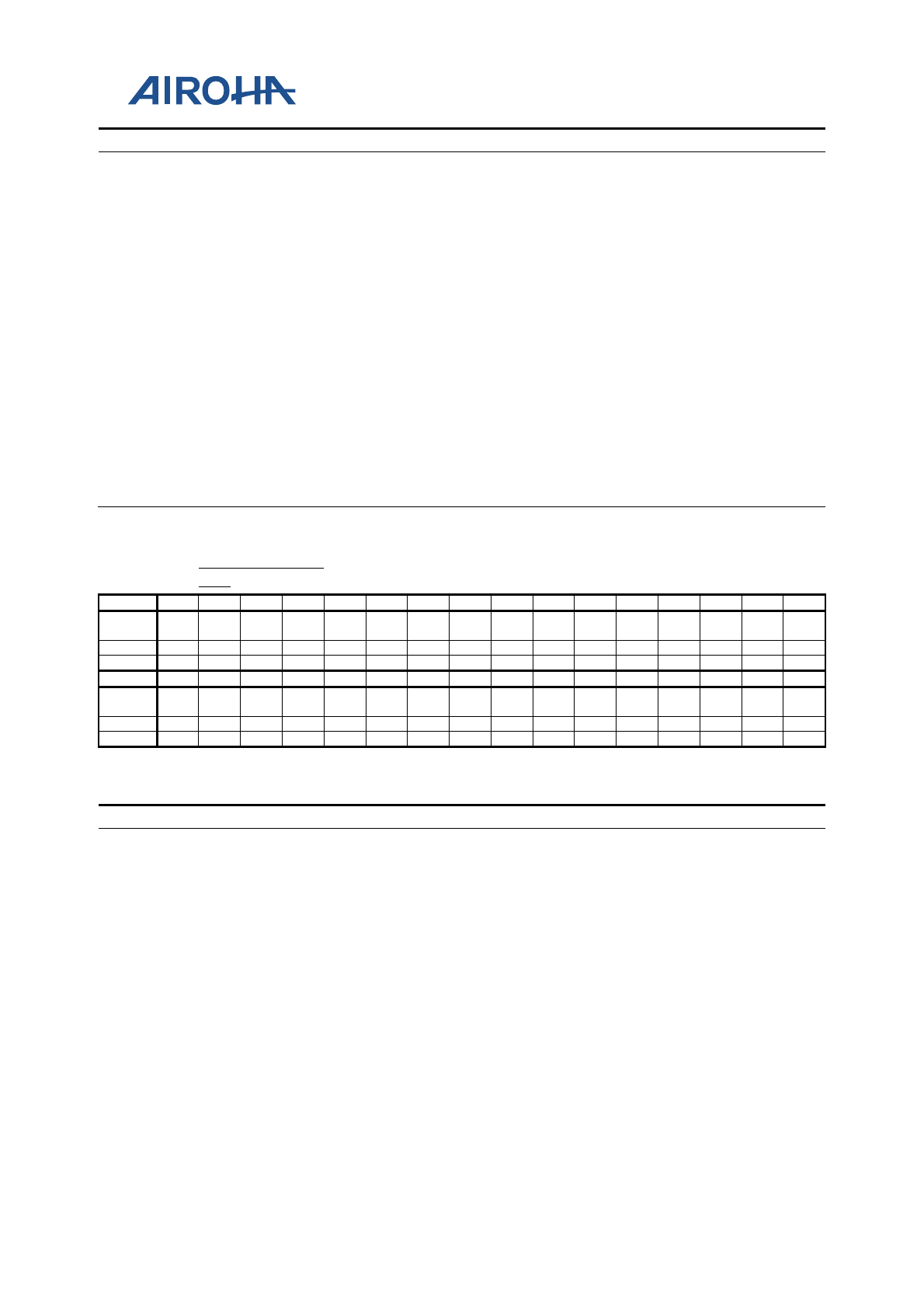
MT2523 Series Reference Manual
© 2015 - 2018 Airoha Technology Corp.
Page 454 of 692
This document contains information that is proprietary to Airoha Technology Corp. (“Airoha”) and/or its licensor(s).
Any unauthorized use, reproduction or disclosure of this document in whole or in part is strictly prohibited.
Bit(s)
Mnemonic
Name
Description
1: GPIO output HI
5
GPIO5
GPIO5_OUT
GPIO5 data output value
0: GPIO output LO
1: GPIO output HI
4
GPIO4
GPIO4_OUT
GPIO4 data output value
0: GPIO output LO
1: GPIO output HI
3
GPIO3
GPIO3_OUT
GPIO3 data output value
0: GPIO output LO
1: GPIO output HI
2
GPIO2
GPIO2_OUT
GPIO2 data output value
0: GPIO output LO
1: GPIO output HI
1
GPIO1
GPIO1_OUT
GPIO1 data output value
0: GPIO output LO
1: GPIO output HI
0
GPIO0
GPIO0_OUT
GPIO0 data output value
0: GPIO output LO
1: GPIO output HI
A2020304
GPIO_DOUT0_
SET
GPIO Output Data Control
00000000
Bit
31
30
29
28
27
26
25
24
23
22
21
20
19
18
17
16
Name
GPIO
31
GPIO
30
GPIO
29
GPIO
28
GPIO
27
GPIO
26
GPIO
25
GPIO
24
GPIO
23
GPIO
22
GPIO
21
GPIO
20
GPIO1
9
GPIO1
8
GPIO1
7
GPIO
16
Type
WO
WO
WO
WO
WO
WO
WO
WO
WO
WO
WO
WO
WO
WO
WO
WO
Reset
0
0
0
0
0
0
0
0
0
0
0
0
0
0
0
0
Bit
15
14
13
12
11
10
9
8
7
6
5
4
3
2
1
0
Name
GPIO
15
GPIO1
4
GPIO1
3
GPIO1
2
GPIO1
1
GPIO1
0
GPIO
9
GPIO
8
GPIO
7
GPIO
6
GPIO
5
GPIO
4
GPIO
3
GPIO
2
GPIO1
GPIO
0
Type
WO
WO
WO
WO
WO
WO
WO
WO
WO
WO
WO
WO
WO
WO
WO
WO
Reset
0
0
0
0
0
0
0
0
0
0
0
0
0
0
0
0
Overview
For bitwise access of GPIO_DIR0
Bit(s)
Mnemonic
Name
Description
31
GPIO31
GPIO31_OUT
Bitwise SET operation of GPIO31 data output value
0: Keep
1: SET bits
30
GPIO30
GPIO30_OUT
Bitwise SET operation of GPIO30 data output value
0: Keep
1: SET bits
29
GPIO29
GPIO29_OUT
Bitwise SET operation of GPIO29 data output value
0: Keep
1: SET bits
28
GPIO28
GPIO28_OUT
Bitwise SET operation of GPIO28 data output value
0: Keep
1: SET bits
27
GPIO27
GPIO27_OUT
Bitwise SET operation of GPIO27 data output value
0: Keep
1: SET bits
26
GPIO26
GPIO26_OUT
Bitwise SET operation of GPIO26 data output value
0: Keep
1: SET bits

MT2523 Series Reference Manual
© 2015 - 2018 Airoha Technology Corp.
Page 455 of 692
This document contains information that is proprietary to Airoha Technology Corp. (“Airoha”) and/or its licensor(s).
Any unauthorized use, reproduction or disclosure of this document in whole or in part is strictly prohibited.
Bit(s)
Mnemonic
Name
Description
25
GPIO25
GPIO25_OUT
Bitwise SET operation of GPIO25 data output value
0: Keep
1: SET bits
24
GPIO24
GPIO24_OUT
Bitwise SET operation of GPIO24 data output value
0: Keep
1: SET bits
23
GPIO23
GPIO23_OUT
Bitwise SET operation of GPIO23 data output value
0: Keep
1: SET bits
22
GPIO22
GPIO22_OUT
Bitwise SET operation of GPIO22 data output value
0: Keep
1: SET bits
21
GPIO21
GPIO21_OUT
Bitwise SET operation of GPIO21 data output value
0: Keep
1: SET bits
20
GPIO20
GPIO20_OUT
Bitwise SET operation of GPIO20 data output value
0: Keep
1: SET bits
19
GPIO19
GPIO19_OUT
Bitwise SET operation of GPIO19 data output value
0: Keep
1: SET bits
18
GPIO18
GPIO18_OUT
Bitwise SET operation of GPIO18 data output value
0: Keep
1: SET bits
17
GPIO17
GPIO17_OUT
Bitwise SET operation of GPIO17 data output value
0: Keep
1: SET bits
16
GPIO16
GPIO16_OUT
Bitwise SET operation of GPIO16 data output value
0: Keep
1: SET bits
15
GPIO15
GPIO15_OUT
Bitwise SET operation of GPIO15 data output value
0: Keep
1: SET bits
14
GPIO14
GPIO14_OUT
Bitwise SET operation of GPIO14 data output value
0: Keep
1: SET bits
13
GPIO13
GPIO13_OUT
Bitwise SET operation of GPIO13 data output value
0: Keep
1: SET bits
12
GPIO12
GPIO12_OUT
Bitwise SET operation of GPIO12 data output value
0: Keep
1: SET bits
11
GPIO11
GPIO11_OUT
Bitwise SET operation of GPIO11 data output value
0: Keep
1: SET bits
10
GPIO10
GPIO10_OUT
Bitwise SET operation of GPIO10 data output value
0: Keep
1: SET bits
9
GPIO9
GPIO9_OUT
Bitwise SET operation of GPIO9 data output value
0: Keep
1: SET bits
8
GPIO8
GPIO8_OUT
Bitwise SET operation of GPIO8 data output value
0: Keep
1: SET bits
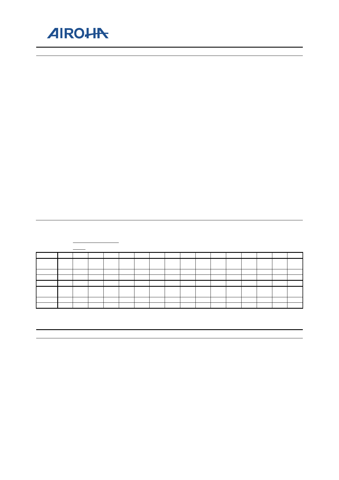
MT2523 Series Reference Manual
© 2015 - 2018 Airoha Technology Corp.
Page 456 of 692
This document contains information that is proprietary to Airoha Technology Corp. (“Airoha”) and/or its licensor(s).
Any unauthorized use, reproduction or disclosure of this document in whole or in part is strictly prohibited.
Bit(s)
Mnemonic
Name
Description
7
GPIO7
GPIO7_OUT
Bitwise SET operation of GPIO7 data output value
0: Keep
1: SET bits
6
GPIO6
GPIO6_OUT
Bitwise SET operation of GPIO6 data output value
0: Keep
1: SET bits
5
GPIO5
GPIO5_OUT
Bitwise SET operation of GPIO5 data output value
0: Keep
1: SET bits
4
GPIO4
GPIO4_OUT
Bitwise SET operation of GPIO4 data output value
0: Keep
1: SET bits
3
GPIO3
GPIO3_OUT
Bitwise SET operation of GPIO3 data output value
0: Keep
1: SET bits
2
GPIO2
GPIO2_OUT
Bitwise SET operation of GPIO2 data output value
0: Keep
1: SET bits
1
GPIO1
GPIO1_OUT
Bitwise SET operation of GPIO1 data output value
0: Keep
1: SET bits
0
GPIO0
GPIO0_OUT
Bitwise SET operation of GPIO0 data output value
0: Keep
1: SET bits
A2020308
GPIO_DOUT0_
CLR
GPIO Output Data Control
00000000
Bit
31
30
29
28
27
26
25
24
23
22
21
20
19
18
17
16
Name
GPIO
31
GPIO
30
GPIO
29
GPIO
28
GPIO
27
GPIO
26
GPIO
25
GPIO
24
GPIO
23
GPIO
22
GPIO
21
GPIO
20
GPIO1
9
GPIO1
8
GPIO1
7
GPIO
16
Type
WO
WO
WO
WO
WO
WO
WO
WO
WO
WO
WO
WO
WO
WO
WO
WO
Reset
0
0
0
0
0
0
0
0
0
0
0
0
0
0
0
0
Bit
15
14
13
12
11
10
9
8
7
6
5
4
3
2
1
0
Name
GPIO
15
GPIO1
4
GPIO1
3
GPIO1
2
GPIO1
1
GPIO1
0
GPIO
9
GPIO
8
GPIO
7
GPIO
6
GPIO
5
GPIO
4
GPIO
3
GPIO
2
GPIO1
GPIO
0
Type
WO
WO
WO
WO
WO
WO
WO
WO
WO
WO
WO
WO
WO
WO
WO
WO
Reset
0
0
0
0
0
0
0
0
0
0
0
0
0
0
0
0
Overview
For bitwise access of GPIO_DIR0
Bit(s)
Mnemonic
Name
Description
31
GPIO31
GPIO31_OUT
Bitwise CLR operation of GPIO31 data output value
0: Keep
1: CLR bits
30
GPIO30
GPIO30_OUT
Bitwise CLR operation of GPIO30 data output value
0: Keep
1: CLR bits
29
GPIO29
GPIO29_OUT
Bitwise CLR operation of GPIO29 data output value
0: Keep
1: CLR bits
28
GPIO28
GPIO28_OUT
Bitwise CLR operation of GPIO28 data output value
0: Keep
1: CLR bits

MT2523 Series Reference Manual
© 2015 - 2018 Airoha Technology Corp.
Page 457 of 692
This document contains information that is proprietary to Airoha Technology Corp. (“Airoha”) and/or its licensor(s).
Any unauthorized use, reproduction or disclosure of this document in whole or in part is strictly prohibited.
Bit(s)
Mnemonic
Name
Description
27
GPIO27
GPIO27_OUT
Bitwise CLR operation of GPIO27 data output value
0: Keep
1: CLR bits
26
GPIO26
GPIO26_OUT
Bitwise CLR operation of GPIO26 data output value
0: Keep
1: CLR bits
25
GPIO25
GPIO25_OUT
Bitwise CLR operation of GPIO25 data output value
0: Keep
1: CLR bits
24
GPIO24
GPIO24_OUT
Bitwise CLR operation of GPIO24 data output value
0: Keep
1: CLR bits
23
GPIO23
GPIO23_OUT
Bitwise CLR operation of GPIO23 data output value
0: Keep
1: CLR bits
22
GPIO22
GPIO22_OUT
Bitwise CLR operation of GPIO22 data output value
0: Keep
1: CLR bits
21
GPIO21
GPIO21_OUT
Bitwise CLR operation of GPIO21 data output value
0: Keep
1: CLR bits
20
GPIO20
GPIO20_OUT
Bitwise CLR operation of GPIO20 data output value
0: Keep
1: CLR bits
19
GPIO19
GPIO19_OUT
Bitwise CLR operation of GPIO19 data output value
0: Keep
1: CLR bits
18
GPIO18
GPIO18_OUT
Bitwise CLR operation of GPIO18 data output value
0: Keep
1: CLR bits
17
GPIO17
GPIO17_OUT
Bitwise CLR operation of GPIO17 data output value
0: Keep
1: CLR bits
16
GPIO16
GPIO16_OUT
Bitwise CLR operation of GPIO16 data output value
0: Keep
1: CLR bits
15
GPIO15
GPIO15_OUT
Bitwise CLR operation of GPIO15 data output value
0: Keep
1: CLR bits
14
GPIO14
GPIO14_OUT
Bitwise CLR operation of GPIO14 data output value
0: Keep
1: CLR bits
13
GPIO13
GPIO13_OUT
Bitwise CLR operation of GPIO13 data output value
0: Keep
1: CLR bits
12
GPIO12
GPIO12_OUT
Bitwise CLR operation of GPIO12 data output value
0: Keep
1: CLR bits
11
GPIO11
GPIO11_OUT
Bitwise CLR operation of GPIO11 data output value
0: Keep
1: CLR bits
10
GPIO10
GPIO10_OUT
Bitwise CLR operation of GPIO10 data output value
0: Keep
1: CLR bits

MT2523 Series Reference Manual
© 2015 - 2018 Airoha Technology Corp.
Page 458 of 692
This document contains information that is proprietary to Airoha Technology Corp. (“Airoha”) and/or its licensor(s).
Any unauthorized use, reproduction or disclosure of this document in whole or in part is strictly prohibited.
Bit(s)
Mnemonic
Name
Description
9
GPIO9
GPIO9_OUT
Bitwise CLR operation of GPIO9 data output value
0: Keep
1: CLR bits
8
GPIO8
GPIO8_OUT
Bitwise CLR operation of GPIO8 data output value
0: Keep
1: CLR bits
7
GPIO7
GPIO7_OUT
Bitwise CLR operation of GPIO7 data output value
0: Keep
1: CLR bits
6
GPIO6
GPIO6_OUT
Bitwise CLR operation of GPIO6 data output value
0: Keep
1: CLR bits
5
GPIO5
GPIO5_OUT
Bitwise CLR operation of GPIO5 data output value
0: Keep
1: CLR bits
4
GPIO4
GPIO4_OUT
Bitwise CLR operation of GPIO4 data output value
0: Keep
1: CLR bits
3
GPIO3
GPIO3_OUT
Bitwise CLR operation of GPIO3 data output value
0: Keep
1: CLR bits
2
GPIO2
GPIO2_OUT
Bitwise CLR operation of GPIO2 data output value
0: Keep
1: CLR bits
1
GPIO1
GPIO1_OUT
Bitwise CLR operation of GPIO1 data output value
0: Keep
1: CLR bits
0
GPIO0
GPIO0_OUT
Bitwise CLR operation of GPIO0 data output value
0: Keep
1: CLR bits
A2020310
GPIO_DOUT1
GPIO Output Data Control
00000080
Bit
31
30
29
28
27
26
25
24
23
22
21
20
19
18
17
16
Name
GPIO
48
Type
RW
Reset
0
Bit
15
14
13
12
11
10
9
8
7
6
5
4
3
2
1
0
Name
GPIO
47
GPIO
46
GPIO
45
GPIO
44
GPIO
43
GPIO
42
GPIO
41
GPIO
40
GPIO
39
GPIO
38
GPIO
37
GPIO
36
GPIO
35
GPIO
34
GPIO
33
GPIO
32
Type
RW
RW
RW
RW
RW
RW
RW
RW
RW
RW
RW
RW
RW
RW
RW
RW
Reset
0
0
0
0
0
0
0
0
1
0
0
0
0
0
0
0
Overview
Configures GPIO output value
Bit(s)
Mnemonic
Name
Description
6
GPIO48
GPIO48_OUT
GPIO48 data output value
0: GPIO output LO
1: GPIO output HI
15
GPIO47
GPIO47_OUT
GPIO47 data output value
0: GPIO output LO
1: GPIO output HI
14
GPIO46
GPIO46_OUT
GPIO46 data output value
0: GPIO output LO

MT2523 Series Reference Manual
© 2015 - 2018 Airoha Technology Corp.
Page 459 of 692
This document contains information that is proprietary to Airoha Technology Corp. (“Airoha”) and/or its licensor(s).
Any unauthorized use, reproduction or disclosure of this document in whole or in part is strictly prohibited.
Bit(s)
Mnemonic
Name
Description
1: GPIO output HI
13
GPIO45
GPIO45_OUT
GPIO45 data output value
0: GPIO output LO
1: GPIO output HI
12
GPIO44
GPIO44_OUT
GPIO44 data output value
0: GPIO output LO
1: GPIO output HI
11
GPIO43
GPIO43_OUT
GPIO43 data output value
0: GPIO output LO
1: GPIO output HI
10
GPIO42
GPIO42_OUT
GPIO42 data output value
0: GPIO output LO
1: GPIO output HI
9
GPIO41
GPIO41_OUT
GPIO41 data output value
0: GPIO output LO
1: GPIO output HI
8
GPIO40
GPIO40_OUT
GPIO40 data output value
0: GPIO output LO
1: GPIO output HI
7
GPIO39
GPIO39_OUT
GPIO39 data output value
0: GPIO output LO
1: GPIO output HI
6
GPIO38
GPIO38_OUT
GPIO38 data output value
0: GPIO output LO
1: GPIO output HI
5
GPIO37
GPIO37_OUT
GPIO37 data output value
0: GPIO output LO
1: GPIO output HI
4
GPIO36
GPIO36_OUT
GPIO36 data output value
0: GPIO output LO
1: GPIO output HI
3
GPIO35
GPIO35_OUT
GPIO35 data output value
0: GPIO output LO
1: GPIO output HI
2
GPIO34
GPIO34_OUT
GPIO34 data output value
0: GPIO output LO
1: GPIO output HI
1
GPIO33
GPIO33_OUT
GPIO33 data output value
0: GPIO output LO
1: GPIO output HI
0
GPIO32
GPIO32_OUT
GPIO32 data output value
0: GPIO output LO
1: GPIO output HI
A2020314
GPIO_DOUT1_
SET
GPIO Output Data Control
00000000
Bit
31
30
29
28
27
26
25
24
23
22
21
20
19
18
17
16
Name
GPIO
48
Type
WO
Reset
0
Bit
15
14
13
12
11
10
9
8
7
6
5
4
3
2
1
0
Name
GPIO
47
GPIO
46
GPIO
45
GPIO
44
GPIO
43
GPIO
42
GPIO
41
GPIO
40
GPIO
39
GPIO
38
GPIO
37
GPIO
36
GPIO
35
GPIO
34
GPIO
33
GPIO
32

MT2523 Series Reference Manual
© 2015 - 2018 Airoha Technology Corp.
Page 460 of 692
This document contains information that is proprietary to Airoha Technology Corp. (“Airoha”) and/or its licensor(s).
Any unauthorized use, reproduction or disclosure of this document in whole or in part is strictly prohibited.
Type
WO
WO
WO
WO
WO
WO
WO
WO
WO
WO
WO
WO
WO
WO
WO
WO
Reset
0
0
0
0
0
0
0
0
0
0
0
0
0
0
0
0
Overview
For bitwise access of GPIO_DIR1
Bit(s)
Mnemonic
Name
Description
16
GPIO48
GPIO48_OUT
Bitwise SET operation of GPIO48 data output value
0: Keep
1: SET bits
15
GPIO47
GPIO47_OUT
Bitwise SET operation of GPIO47 data output value
0: Keep
1: SET bits
14
GPIO46
GPIO46_OUT
Bitwise SET operation of GPIO46 data output value
0: Keep
1: SET bits
13
GPIO45
GPIO45_OUT
Bitwise SET operation of GPIO45 data output value
0: Keep
1: SET bits
12
GPIO44
GPIO44_OUT
Bitwise SET operation of GPIO44 data output value
0: Keep
1: SET bits
11
GPIO43
GPIO43_OUT
Bitwise SET operation of GPIO43 data output value
0: Keep
1: SET bits
10
GPIO42
GPIO42_OUT
Bitwise SET operation of GPIO42 data output value
0: Keep
1: SET bits
9
GPIO41
GPIO41_OUT
Bitwise SET operation of GPIO41 data output value
0: Keep
1: SET bits
8
GPIO40
GPIO40_OUT
Bitwise SET operation of GPIO40 data output value
0: Keep
1: SET bits
7
GPIO39
GPIO39_OUT
Bitwise SET operation of GPIO39 data output value
0: Keep
1: SET bits
6
GPIO38
GPIO38_OUT
Bitwise SET operation of GPIO38 data output value
0: Keep
1: SET bits
5
GPIO37
GPIO37_OUT
Bitwise SET operation of GPIO37 data output value
0: Keep
1: SET bits
4
GPIO36
GPIO36_OUT
Bitwise SET operation of GPIO36 data output value
0: Keep
1: SET bits
3
GPIO35
GPIO35_OUT
Bitwise SET operation of GPIO35 data output value
0: Keep
1: SET bits
2
GPIO34
GPIO34_OUT
Bitwise SET operation of GPIO34 data output value
0: Keep
1: SET bits
1
GPIO33
GPIO33_OUT
Bitwise SET operation of GPIO33 data output value
0: Keep
1: SET bits
0
GPIO32
GPIO32_OUT
Bitwise SET operation of GPIO32 data output value

MT2523 Series Reference Manual
© 2015 - 2018 Airoha Technology Corp.
Page 461 of 692
This document contains information that is proprietary to Airoha Technology Corp. (“Airoha”) and/or its licensor(s).
Any unauthorized use, reproduction or disclosure of this document in whole or in part is strictly prohibited.
Bit(s)
Mnemonic
Name
Description
0: Keep
1: SET bits
A2020318
GPIO_DOUT1_
CLR
GPIO Output Data Control
00000000
Bit
31
30
29
28
27
26
25
24
23
22
21
20
19
18
17
16
Name
GPIO
48
Type
WO
Reset
0
Bit
15
14
13
12
11
10
9
8
7
6
5
4
3
2
1
0
Name
GPIO
47
GPIO
46
GPIO
45
GPIO
44
GPIO
43
GPIO
42
GPIO
41
GPIO
40
GPIO
39
GPIO
38
GPIO
37
GPIO
36
GPIO
35
GPIO
34
GPIO
33
GPIO
32
Type
WO
WO
WO
WO
WO
WO
WO
WO
WO
WO
WO
WO
WO
WO
WO
WO
Reset
0
0
0
0
0
0
0
0
0
0
0
0
0
0
0
0
Overview
For bitwise access of GPIO_DIR1
Bit(s)
Mnemonic
Name
Description
16
GPIO48
GPIO48_OUT
Bitwise CLR operation of GPIO48 data output value
0: Keep
1: CLR bits
15
GPIO47
GPIO47_OUT
Bitwise CLR operation of GPIO47 data output value
0: Keep
1: CLR bits
14
GPIO46
GPIO46_OUT
Bitwise CLR operation of GPIO46 data output value
0: Keep
1: CLR bits
13
GPIO45
GPIO45_OUT
Bitwise CLR operation of GPIO45 data output value
0: Keep
1: CLR bits
12
GPIO44
GPIO44_OUT
Bitwise CLR operation of GPIO44 data output value
0: Keep
1: CLR bits
11
GPIO43
GPIO43_OUT
Bitwise CLR operation of GPIO43 data output value
0: Keep
1: CLR bits
10
GPIO42
GPIO42_OUT
Bitwise CLR operation of GPIO42 data output value
0: Keep
1: CLR bits
9
GPIO41
GPIO41_OUT
Bitwise CLR operation of GPIO41 data output value
0: Keep
1: CLR bits
8
GPIO40
GPIO40_OUT
Bitwise CLR operation of GPIO40 data output value
0: Keep
1: CLR bits
7
GPIO39
GPIO39_OUT
Bitwise CLR operation of GPIO39 data output value
0: Keep
1: CLR bits
6
GPIO38
GPIO38_OUT
Bitwise CLR operation of GPIO38 data output value
0: Keep
1: CLR bits
5
GPIO37
GPIO37_OUT
Bitwise CLR operation of GPIO37 data output value
0: Keep

MT2523 Series Reference Manual
© 2015 - 2018 Airoha Technology Corp.
Page 462 of 692
This document contains information that is proprietary to Airoha Technology Corp. (“Airoha”) and/or its licensor(s).
Any unauthorized use, reproduction or disclosure of this document in whole or in part is strictly prohibited.
Bit(s)
Mnemonic
Name
Description
1: CLR bits
4
GPIO36
GPIO36_OUT
Bitwise CLR operation of GPIO36 data output value
0: Keep
1: CLR bits
3
GPIO35
GPIO35_OUT
Bitwise CLR operation of GPIO35 data output value
0: Keep
1: CLR bits
2
GPIO34
GPIO34_OUT
Bitwise CLR operation of GPIO34 data output value
0: Keep
1: CLR bits
1
GPIO33
GPIO33_OUT
Bitwise CLR operation of GPIO33 data output value
0: Keep
1: CLR bits
0
GPIO32
GPIO32_OUT
Bitwise CLR operation of GPIO32 data output value
0: Keep
1: CLR bits
A2020400
GPIO_DIN0
GPIO Input Data Value
00000000
Bit
31
30
29
28
27
26
25
24
23
22
21
20
19
18
17
16
Name
GPIO
31
GPIO
30
GPIO
29
GPIO
28
GPIO
27
GPIO
26
GPIO
25
GPIO
24
GPIO
23
GPIO
22
GPIO
21
GPIO
20
GPIO1
9
GPIO1
8
GPIO1
7
GPIO
16
Type
RO
RO
RO
RO
RO
RO
RO
RO
RO
RO
RO
RO
RO
RO
RO
RO
Reset
0
0
0
0
0
0
0
0
0
0
0
0
0
0
0
0
Bit
15
14
13
12
11
10
9
8
7
6
5
4
3
2
1
0
Name
GPIO
15
GPIO1
4
GPIO1
3
GPIO1
2
GPIO1
1
GPIO1
0
GPIO
9
GPIO
8
GPIO
7
GPIO
6
GPIO
5
GPIO
4
GPIO
3
GPIO
2
GPIO1
GPIO
0
Type
RO
RO
RO
RO
RO
RO
RO
RO
RO
RO
RO
RO
RO
RO
RO
RO
Reset
0
0
0
0
0
0
0
0
0
0
0
0
0
0
0
0
Overview
Reads GPIO input value
Bit(s)
Mnemonic
Name
Description
31
GPIO31
GPIO31_DIN
GPIO31 data input value
30
GPIO30
GPIO30_DIN
GPIO30 data input value
29
GPIO29
GPIO29_DIN
GPIO29 data input value
28
GPIO28
GPIO28_DIN
GPIO28 data input value
27
GPIO27
GPIO27_DIN
GPIO27 data input value
26
GPIO26
GPIO26_DIN
GPIO26 data input value
25
GPIO25
GPIO25_DIN
GPIO25 data input value
24
GPIO24
GPIO24_DIN
GPIO24 data input value
23
GPIO23
GPIO23_DIN
GPIO23 data input value
22
GPIO22
GPIO22_DIN
GPIO22 data input value
21
GPIO21
GPIO21_DIN
GPIO21 data input value
20
GPIO20
GPIO20_DIN
GPIO20 data input value
19
GPIO19
GPIO19_DIN
GPIO19 data input value
18
GPIO18
GPIO18_DIN
GPIO18 data input value
17
GPIO17
GPIO17_DIN
GPIO17 data input value
16
GPIO16
GPIO16_DIN
GPIO16 data input value
15
GPIO15
GPIO15_DIN
GPIO15 data input value
14
GPIO14
GPIO14_DIN
GPIO14 data input value

MT2523 Series Reference Manual
© 2015 - 2018 Airoha Technology Corp.
Page 463 of 692
This document contains information that is proprietary to Airoha Technology Corp. (“Airoha”) and/or its licensor(s).
Any unauthorized use, reproduction or disclosure of this document in whole or in part is strictly prohibited.
Bit(s)
Mnemonic
Name
Description
13
GPIO13
GPIO13_DIN
GPIO13 data input value
12
GPIO12
GPIO12_DIN
GPIO12 data input value
11
GPIO11
GPIO11_DIN
GPIO11 data input value
10
GPIO10
GPIO10_DIN
GPIO10 data input value
9
GPIO9
GPIO9_DIN
GPIO9 data input value
8
GPIO8
GPIO8_DIN
GPIO8 data input value
7
GPIO7
GPIO7_DIN
GPIO7 data input value
6
GPIO6
GPIO6_DIN
GPIO6 data input value
5
GPIO5
GPIO5_DIN
GPIO5 data input value
4
GPIO4
GPIO4_DIN
GPIO4 data input value
3
GPIO3
GPIO3_DIN
GPIO3 data input value
2
GPIO2
GPIO2_DIN
GPIO2 data input value
1
GPIO1
GPIO1_DIN
GPIO1 data input value
0
GPIO0
GPIO0_DIN
GPIO0 data input value
A2020410
GPIO_DIN1
GPIO Input Data Value
00000000
Bit
31
30
29
28
27
26
25
24
23
22
21
20
19
18
17
16
Name
GPIO
48
Type
RO
Reset
0
Bit
15
14
13
12
11
10
9
8
7
6
5
4
3
2
1
0
Name
GPIO
47
GPIO
46
GPIO
45
GPIO
44
GPIO
43
GPIO
42
GPIO
41
GPIO
40
GPIO
39
GPIO
38
GPIO
37
GPIO
36
GPIO
35
GPIO
34
GPIO
33
GPIO
32
Type
RO
RO
RO
RO
RO
RO
RO
RO
RO
RO
RO
RO
RO
RO
RO
RO
Reset
0
0
0
0
0
0
0
0
0
0
0
0
0
0
0
0
Overview
Reads GPIO input value
Bit(s)
Mnemonic
Name
Description
16
GPIO48
GPIO48_DIN
GPIO48 data input value
15
GPIO47
GPIO47_DIN
GPIO47 data input value
14
GPIO46
GPIO46_DIN
GPIO46 data input value
13
GPIO45
GPIO45_DIN
GPIO45 data input value
12
GPIO44
GPIO44_DIN
GPIO44 data input value
11
GPIO43
GPIO43_DIN
GPIO43 data input value
10
GPIO42
GPIO42_DIN
GPIO42 data input value
9
GPIO41
GPIO41_DIN
GPIO41 data input value
8
GPIO40
GPIO40_DIN
GPIO40 data input value
7
GPIO39
GPIO39_DIN
GPIO39 data input value
6
GPIO38
GPIO38_DIN
GPIO38 data input value
5
GPIO37
GPIO37_DIN
GPIO37 data input value
4
GPIO36
GPIO36_DIN
GPIO36 data input value
3
GPIO35
GPIO35_DIN
GPIO35 data input value
2
GPIO34
GPIO34_DIN
GPIO34 data input value
1
GPIO33
GPIO33_DIN
GPIO33 data input value
0
GPIO32
GPIO32_DIN
GPIO32 data input value
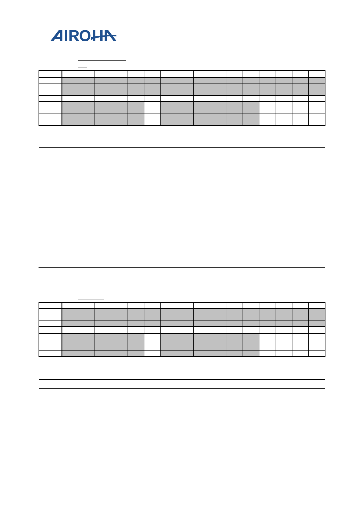
MT2523 Series Reference Manual
© 2015 - 2018 Airoha Technology Corp.
Page 464 of 692
This document contains information that is proprietary to Airoha Technology Corp. (“Airoha”) and/or its licensor(s).
Any unauthorized use, reproduction or disclosure of this document in whole or in part is strictly prohibited.
A2020500
GPIO_PULLSE
L0
GPIO Pullsel Control
0000040F
Bit
31
30
29
28
27
26
25
24
23
22
21
20
19
18
17
16
Name
Type
Reset
Bit
15
14
13
12
11
10
9
8
7
6
5
4
3
2
1
0
Name
GPIO1
0
GPIO
3
GPIO
2
GPIO1
GPIO
0
Type
RW
RW
RW
RW
RW
Reset
1
1
1
1
1
Overview
Configures GPIO PUPD selection
Bit(s)
Mnemonic
Name
Description
10
GPIO10
GPIO10_PULLSEL
GPIO10_PULLSEL
0: Pull down
1: Pull up
3
GPIO3
GPIO3_PULLSEL
GPIO3_PULLSEL
0: Pull down
1: Pull up
2
GPIO2
GPIO2_PULLSEL
GPIO2_PULLSEL
0: Pull down
1: Pull up
1
GPIO1
GPIO1_PULLSEL
GPIO1_PULLSEL
0: Pull down
1: Pull up
0
GPIO0
GPIO0_PULLSEL
GPIO0_PULLSEL
0: Pull down
1: Pull up
A2020504
GPIO_PULLSE
L0_SET
GPIO Pullsel Control
00000000
Bit
31
30
29
28
27
26
25
24
23
22
21
20
19
18
17
16
Name
Type
Reset
Bit
15
14
13
12
11
10
9
8
7
6
5
4
3
2
1
0
Name
GPIO1
0
GPIO
3
GPIO
2
GPIO1
GPIO
0
Type
WO
WO
WO
WO
WO
Reset
0
0
0
0
0
Overview
For bitwise access of GPIO_PULLSEL0
Bit(s)
Mnemonic
Name
Description
10
GPIO10
GPIO10_PULLSEL
Bitwise SET operation of GPIO10 PULLSEL_SET
0: Keep
1: SET bits
3
GPIO3
GPIO3_PULLSEL
Bitwise SET operation of GPIO3 PULLSEL_SET
0: Keep
1: SET bits
2
GPIO2
GPIO2_PULLSEL
Bitwise SET operation of GPIO2 PULLSEL_SET
0: Keep
1: SET bits
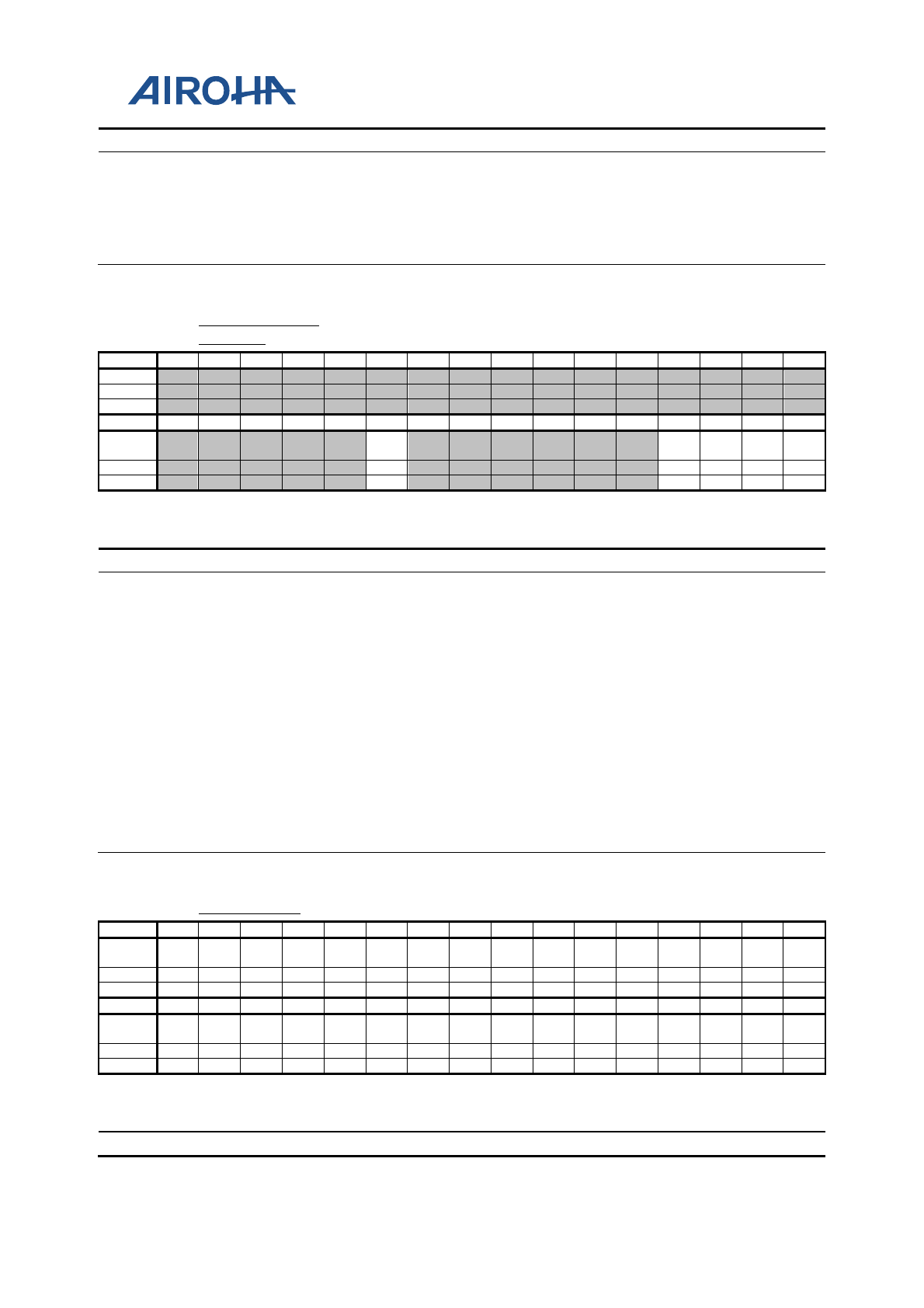
MT2523 Series Reference Manual
© 2015 - 2018 Airoha Technology Corp.
Page 465 of 692
This document contains information that is proprietary to Airoha Technology Corp. (“Airoha”) and/or its licensor(s).
Any unauthorized use, reproduction or disclosure of this document in whole or in part is strictly prohibited.
Bit(s)
Mnemonic
Name
Description
1
GPIO1
GPIO1_PULLSEL
Bitwise SET operation of GPIO1 PULLSEL_SET
0: Keep
1: SET bits
0
GPIO0
GPIO0_PULLSEL
Bitwise SET operation of GPIO0 PULLSEL_SET
0: Keep
1: SET bits
A2020508
GPIO_PULLSE
L0_CLR
GPIO Pullsel Control
00000000
Bit
31
30
29
28
27
26
25
24
23
22
21
20
19
18
17
16
Name
Type
Reset
Bit
15
14
13
12
11
10
9
8
7
6
5
4
3
2
1
0
Name
GPIO1
0
GPIO
3
GPIO
2
GPIO1
GPIO
0
Type
WO
WO
WO
WO
WO
Reset
0
0
0
0
0
Overview
For bitwise access of GPIO_PULLSEL0
Bit(s)
Mnemonic
Name
Description
10
GPIO10
GPIO10_PULLSEL
Bitwise CKR operation of GPIO10 PULLSEL_CLR
0: Keep
1: CLR bits
3
GPIO3
GPIO3_PULLSEL
Bitwise CKR operation of GPIO3 PULLSEL_CLR
0: Keep
1: CLR bits
2
GPIO2
GPIO2_PULLSEL
Bitwise CKR operation of GPIO2 PULLSEL_CLR
0: Keep
1: CLR bits
1
GPIO1
GPIO1_PULLSEL
Bitwise CKR operation of GPIO1 PULLSEL_CLR
0: Keep
1: CLR bits
0
GPIO0
GPIO0_PULLSEL
Bitwise CKR operation of GPIO0 PULLSEL_CLR
0: Keep
1: CLR bits
A2020600
GPIO_SMT0
GPIO SMT Control
00000000
Bit
31
30
29
28
27
26
25
24
23
22
21
20
19
18
17
16
Name
GPIO
31
GPIO
30
GPIO
29
GPIO
28
GPIO
27
GPIO
26
GPIO
25
GPIO
24
GPIO
23
GPIO
22
GPIO
21
GPIO
20
GPIO1
9
GPIO1
8
GPIO1
7
GPIO
16
Type
RW
RW
RW
RW
RW
RW
RW
RW
RW
RW
RW
RW
RW
RW
RW
RW
Reset
0
0
0
0
0
0
0
0
0
0
0
0
0
0
0
0
Bit
15
14
13
12
11
10
9
8
7
6
5
4
3
2
1
0
Name
GPIO
15
GPIO1
4
GPIO1
3
GPIO1
2
GPIO1
1
GPIO1
0
GPIO
9
GPIO
8
GPIO
7
GPIO
6
GPIO
5
GPIO
4
GPIO
3
GPIO
2
GPIO1
GPIO
0
Type
RW
RW
RW
RW
RW
RW
RW
RW
RW
RW
RW
RW
RW
RW
RW
RW
Reset
0
0
0
0
0
0
0
0
0
0
0
0
0
0
0
0
Overview
Configures GPIO Schmitt trigger control
Bit(s)
Mnemonic
Name
Description

MT2523 Series Reference Manual
© 2015 - 2018 Airoha Technology Corp.
Page 466 of 692
This document contains information that is proprietary to Airoha Technology Corp. (“Airoha”) and/or its licensor(s).
Any unauthorized use, reproduction or disclosure of this document in whole or in part is strictly prohibited.
Bit(s)
Mnemonic
Name
Description
31
GPIO31
GPIO31_SMT
SMT for GPIO31
0: Disable
1: Enable
30
GPIO30
GPIO30_SMT
SMT for GPIO30
0: Disable
1: Enable
29
GPIO29
GPIO29_SMT
SMT for GPIO29
0: Disable
1: Enable
28
GPIO28
GPIO28_SMT
SMT for GPIO28
0: Disable
1: Enable
27
GPIO27
GPIO27_SMT
SMT for GPIO27
0: Disable
1: Enable
26
GPIO26
GPIO26_SMT
SMT for GPIO26
0: Disable
1: Enable
25
GPIO25
GPIO25_SMT
SMT for GPIO25
0: Disable
1: Enable
24
GPIO24
GPIO24_SMT
SMT for GPIO24
0: Disable
1: Enable
23
GPIO23
GPIO23_SMT
SMT for GPIO23
0: Disable
1: Enable
22
GPIO22
GPIO22_SMT
SMT for GPIO22
0: Disable
1: Enable
21
GPIO21
GPIO21_SMT
SMT for GPIO21
0: Disable
1: Enable
20
GPIO20
GPIO20_SMT
SMT for GPIO20
0: Disable
1: Enable
19
GPIO19
GPIO19_SMT
SMT for GPIO19
0: Disable
1: Enable
18
GPIO18
GPIO18_SMT
SMT for GPIO18
0: Disable
1: Enable
17
GPIO17
GPIO17_SMT
SMT for GPIO17
0: Disable
1: Enable
16
GPIO16
GPIO16_SMT
SMT for GPIO16
0: Disable
1: Enable
15
GPIO15
GPIO15_SMT
SMT for GPIO15
0: Disable
1: Enable
14
GPIO14
GPIO14_SMT
SMT for GPIO14
0: Disable
1: Enable

MT2523 Series Reference Manual
© 2015 - 2018 Airoha Technology Corp.
Page 467 of 692
This document contains information that is proprietary to Airoha Technology Corp. (“Airoha”) and/or its licensor(s).
Any unauthorized use, reproduction or disclosure of this document in whole or in part is strictly prohibited.
Bit(s)
Mnemonic
Name
Description
13
GPIO13
GPIO13_SMT
SMT for GPIO13
0: Disable
1: Enable
12
GPIO12
GPIO12_SMT
SMT for GPIO12
0: Disable
1: Enable
11
GPIO11
GPIO11_SMT
SMT for GPIO11
0: Disable
1: Enable
10
GPIO10
GPIO10_SMT
SMT for GPIO10
0: Disable
1: Enable
9
GPIO9
GPIO9_SMT
SMT for GPIO9
0: Disable
1: Enable
8
GPIO8
GPIO8_SMT
SMT for GPIO8
0: Disable
1: Enable
7
GPIO7
GPIO7_SMT
SMT for GPIO7
0: Disable
1: Enable
6
GPIO6
GPIO6_SMT
SMT for GPIO6
0: Disable
1: Enable
5
GPIO5
GPIO5_SMT
SMT for GPIO5
0: Disable
1: Enable
4
GPIO4
GPIO4_SMT
SMT for GPIO4
0: Disable
1: Enable
3
GPIO3
GPIO3_SMT
SMT for GPIO3
0: Disable
1: Enable
2
GPIO2
GPIO2_SMT
SMT for GPIO2
0: Disable
1: Enable
1
GPIO1
GPIO1_SMT
SMT for GPIO1
0: Disable
1: Enable
0
GPIO0
GPIO0_SMT
SMT for GPIO0
0: Disable
1: Enable
A2020604
GPIO_SMT0_S
ET
GPIO SMT Control
00000000
Bit
31
30
29
28
27
26
25
24
23
22
21
20
19
18
17
16
Name
GPIO
31
GPIO
30
GPIO
29
GPIO
28
GPIO
27
GPIO
26
GPIO
25
GPIO
24
GPIO
23
GPIO
22
GPIO
21
GPIO
20
GPIO1
9
GPIO1
8
GPIO1
7
GPIO
16
Type
WO
WO
WO
WO
WO
WO
WO
WO
WO
WO
WO
WO
WO
WO
WO
WO
Reset
0
0
0
0
0
0
0
0
0
0
0
0
0
0
0
0
Bit
15
14
13
12
11
10
9
8
7
6
5
4
3
2
1
0
Name
GPIO
15
GPIO1
4
GPIO1
3
GPIO1
2
GPIO1
1
GPIO1
0
GPIO
9
GPIO
8
GPIO
7
GPIO
6
GPIO
5
GPIO
4
GPIO
3
GPIO
2
GPIO1
GPIO
0
Type
WO
WO
WO
WO
WO
WO
WO
WO
WO
WO
WO
WO
WO
WO
WO
WO

MT2523 Series Reference Manual
© 2015 - 2018 Airoha Technology Corp.
Page 468 of 692
This document contains information that is proprietary to Airoha Technology Corp. (“Airoha”) and/or its licensor(s).
Any unauthorized use, reproduction or disclosure of this document in whole or in part is strictly prohibited.
Reset
0
0
0
0
0
0
0
0
0
0
0
0
0
0
0
0
Overview
For bitwise access of GPIO_SMT0
Bit(s)
Mnemonic
Name
Description
31
GPIO31
GPIO31_SMT
Bitwise SET operation of GPIO31 SMT
0: Keep
1: SET bits
30
GPIO30
GPIO30_SMT
Bitwise SET operation of GPIO30 SMT
0: Keep
1: SET bits
29
GPIO29
GPIO29_SMT
Bitwise SET operation of GPIO29 SMT
0: Keep
1: SET bits
28
GPIO28
GPIO28_SMT
Bitwise SET operation of GPIO28 SMT
0: Keep
1: SET bits
27
GPIO27
GPIO27_SMT
Bitwise SET operation of GPIO27 SMT
0: Keep
1: SET bits
26
GPIO26
GPIO26_SMT
Bitwise SET operation of GPIO26 SMT
0: Keep
1: SET bits
25
GPIO25
GPIO25_SMT
Bitwise SET operation of GPIO25 SMT
0: Keep
1: SET bits
24
GPIO24
GPIO24_SMT
Bitwise SET operation of GPIO24 SMT
0: Keep
1: SET bits
23
GPIO23
GPIO23_SMT
Bitwise SET operation of GPIO23 SMT
0: Keep
1: SET bits
22
GPIO22
GPIO22_SMT
Bitwise SET operation of GPIO22 SMT
0: Keep
1: SET bits
21
GPIO21
GPIO21_SMT
Bitwise SET operation of GPIO21 SMT
0: Keep
1: SET bits
20
GPIO20
GPIO20_SMT
Bitwise SET operation of GPIO20 SMT
0: Keep
1: SET bits
19
GPIO19
GPIO19_SMT
Bitwise SET operation of GPIO19 SMT
0: Keep
1: SET bits
18
GPIO18
GPIO18_SMT
Bitwise SET operation of GPIO18 SMT
0: Keep
1: SET bits
17
GPIO17
GPIO17_SMT
Bitwise SET operation of GPIO17 SMT
0: Keep
1: SET bits
16
GPIO16
GPIO16_SMT
Bitwise SET operation of GPIO16 SMT
0: Keep
1: SET bits
15
GPIO15
GPIO15_SMT
Bitwise SET operation of GPIO15 SMT
0: Keep

MT2523 Series Reference Manual
© 2015 - 2018 Airoha Technology Corp.
Page 469 of 692
This document contains information that is proprietary to Airoha Technology Corp. (“Airoha”) and/or its licensor(s).
Any unauthorized use, reproduction or disclosure of this document in whole or in part is strictly prohibited.
Bit(s)
Mnemonic
Name
Description
1: SET bits
14
GPIO14
GPIO14_SMT
Bitwise SET operation of GPIO14 SMT
0: Keep
1: SET bits
13
GPIO13
GPIO13_SMT
Bitwise SET operation of GPIO13 SMT
0: Keep
1: SET bits
12
GPIO12
GPIO12_SMT
Bitwise SET operation of GPIO12 SMT
0: Keep
1: SET bits
11
GPIO11
GPIO11_SMT
Bitwise SET operation of GPIO11 SMT
0: Keep
1: SET bits
10
GPIO10
GPIO10_SMT
Bitwise SET operation of GPIO10 SMT
0: Keep
1: SET bits
9
GPIO9
GPIO9_SMT
Bitwise SET operation of GPIO9 SMT
0: Keep
1: SET bits
8
GPIO8
GPIO8_SMT
Bitwise SET operation of GPIO8 SMT
0: Keep
1: SET bits
7
GPIO7
GPIO7_SMT
Bitwise SET operation of GPIO7 SMT
0: Keep
1: SET bits
6
GPIO6
GPIO6_SMT
Bitwise SET operation of GPIO6 SMT
0: Keep
1: SET bits
5
GPIO5
GPIO5_SMT
Bitwise SET operation of GPIO5 SMT
0: Keep
1: SET bits
4
GPIO4
GPIO4_SMT
Bitwise SET operation of GPIO4 SMT
0: Keep
1: SET bits
3
GPIO3
GPIO3_SMT
Bitwise SET operation of GPIO3 SMT
0: Keep
1: SET bits
2
GPIO2
GPIO2_SMT
Bitwise SET operation of GPIO2 SMT
0: Keep
1: SET bits
1
GPIO1
GPIO1_SMT
Bitwise SET operation of GPIO1 SMT
0: Keep
1: SET bits
0
GPIO0
GPIO0_SMT
Bitwise SET operation of GPIO0 SMT
0: Keep
1: SET bits
A2020608
GPIO_SMT0_C
LR
GPIO SMT Control
00000000
Bit
31
30
29
28
27
26
25
24
23
22
21
20
19
18
17
16
Name
GPIO
31
GPIO
30
GPIO
29
GPIO
28
GPIO
27
GPIO
26
GPIO
25
GPIO
24
GPIO
23
GPIO
22
GPIO
21
GPIO
20
GPIO1
9
GPIO1
8
GPIO1
7
GPIO
16
Type
WO
WO
WO
WO
WO
WO
WO
WO
WO
WO
WO
WO
WO
WO
WO
WO

MT2523 Series Reference Manual
© 2015 - 2018 Airoha Technology Corp.
Page 470 of 692
This document contains information that is proprietary to Airoha Technology Corp. (“Airoha”) and/or its licensor(s).
Any unauthorized use, reproduction or disclosure of this document in whole or in part is strictly prohibited.
Reset
0
0
0
0
0
0
0
0
0
0
0
0
0
0
0
0
Bit
15
14
13
12
11
10
9
8
7
6
5
4
3
2
1
0
Name
GPIO
15
GPIO1
4
GPIO1
3
GPIO1
2
GPIO1
1
GPIO1
0
GPIO
9
GPIO
8
GPIO
7
GPIO
6
GPIO
5
GPIO
4
GPIO
3
GPIO
2
GPIO1
GPIO
0
Type
WO
WO
WO
WO
WO
WO
WO
WO
WO
WO
WO
WO
WO
WO
WO
WO
Reset
0
0
0
0
0
0
0
0
0
0
0
0
0
0
0
0
Overview
For bitwise access of GPIO_SMT0
Bit(s)
Mnemonic
Name
Description
31
GPIO31
GPIO31_SMT
Bitwise CLR operation of GPIO31 SMT
0: Keep
1: CLR bits
30
GPIO30
GPIO30_SMT
Bitwise CLR operation of GPIO30 SMT
0: Keep
1: CLR bits
29
GPIO29
GPIO29_SMT
Bitwise CLR operation of GPIO29 SMT
0: Keep
1: CLR bits
28
GPIO28
GPIO28_SMT
Bitwise CLR operation of GPIO28 SMT
0: Keep
1: CLR bits
27
GPIO27
GPIO27_SMT
Bitwise CLR operation of GPIO27 SMT
0: Keep
1: CLR bits
26
GPIO26
GPIO26_SMT
Bitwise CLR operation of GPIO26 SMT
0: Keep
1: CLR bits
25
GPIO25
GPIO25_SMT
Bitwise CLR operation of GPIO25 SMT
0: Keep
1: CLR bits
24
GPIO24
GPIO24_SMT
Bitwise CLR operation of GPIO24 SMT
0: Keep
1: CLR bits
23
GPIO23
GPIO23_SMT
Bitwise CLR operation of GPIO23 SMT
0: Keep
1: CLR bits
22
GPIO22
GPIO22_SMT
Bitwise CLR operation of GPIO22 SMT
0: Keep
1: CLR bits
21
GPIO21
GPIO21_SMT
Bitwise CLR operation of GPIO21 SMT
0: Keep
1: CLR bits
20
GPIO20
GPIO20_SMT
Bitwise CLR operation of GPIO20 SMT
0: Keep
1: CLR bits
19
GPIO19
GPIO19_SMT
Bitwise CLR operation of GPIO19 SMT
0: Keep
1: CLR bits
18
GPIO18
GPIO18_SMT
Bitwise CLR operation of GPIO18 SMT
0: Keep
1: CLR bits
17
GPIO17
GPIO17_SMT
Bitwise CLR operation of GPIO17 SMT
0: Keep
1: CLR bits
16
GPIO16
GPIO16_SMT
Bitwise CLR operation of GPIO16 SMT

MT2523 Series Reference Manual
© 2015 - 2018 Airoha Technology Corp.
Page 471 of 692
This document contains information that is proprietary to Airoha Technology Corp. (“Airoha”) and/or its licensor(s).
Any unauthorized use, reproduction or disclosure of this document in whole or in part is strictly prohibited.
Bit(s)
Mnemonic
Name
Description
0: Keep
1: CLR bits
15
GPIO15
GPIO15_SMT
Bitwise CLR operation of GPIO15 SMT
0: Keep
1: CLR bits
14
GPIO14
GPIO14_SMT
Bitwise CLR operation of GPIO14 SMT
0: Keep
1: CLR bits
13
GPIO13
GPIO13_SMT
Bitwise CLR operation of GPIO13 SMT
0: Keep
1: CLR bits
12
GPIO12
GPIO12_SMT
Bitwise CLR operation of GPIO12 SMT
0: Keep
1: CLR bits
11
GPIO11
GPIO11_SMT
Bitwise CLR operation of GPIO11 SMT
0: Keep
1: CLR bits
10
GPIO10
GPIO10_SMT
Bitwise CLR operation of GPIO10 SMT
0: Keep
1: CLR bits
9
GPIO9
GPIO9_SMT
Bitwise CLR operation of GPIO9 SMT
0: Keep
1: CLR bits
8
GPIO8
GPIO8_SMT
Bitwise CLR operation of GPIO8 SMT
0: Keep
1: CLR bits
7
GPIO7
GPIO7_SMT
Bitwise CLR operation of GPIO7 SMT
0: Keep
1: CLR bits
6
GPIO6
GPIO6_SMT
Bitwise CLR operation of GPIO6 SMT
0: Keep
1: CLR bits
5
GPIO5
GPIO5_SMT
Bitwise CLR operation of GPIO5 SMT
0: Keep
1: CLR bits
4
GPIO4
GPIO4_SMT
Bitwise CLR operation of GPIO4 SMT
0: Keep
1: CLR bits
3
GPIO3
GPIO3_SMT
Bitwise CLR operation of GPIO3 SMT
0: Keep
1: CLR bits
2
GPIO2
GPIO2_SMT
Bitwise CLR operation of GPIO2 SMT
0: Keep
1: CLR bits
1
GPIO1
GPIO1_SMT
Bitwise CLR operation of GPIO1 SMT
0: Keep
1: CLR bits
0
GPIO0
GPIO0_SMT
Bitwise CLR operation of GPIO0 SMT
0: Keep
1: CLR bits
A2020610
GPIO_SMT1
GPIO SMT Control
00000000

MT2523 Series Reference Manual
© 2015 - 2018 Airoha Technology Corp.
Page 472 of 692
This document contains information that is proprietary to Airoha Technology Corp. (“Airoha”) and/or its licensor(s).
Any unauthorized use, reproduction or disclosure of this document in whole or in part is strictly prohibited.
Bit
31
30
29
28
27
26
25
24
23
22
21
20
19
18
17
16
Name
GPIO
48
Type
RW
Reset
0
Bit
15
14
13
12
11
10
9
8
7
6
5
4
3
2
1
0
Name
GPIO
47
GPIO
46
GPIO
45
GPIO
44
GPIO
43
GPIO
42
GPIO
41
GPIO
40
GPIO
39
GPIO
38
GPIO
37
GPIO
36
GPIO
35
GPIO
34
GPIO
33
GPIO
32
Type
RW
RW
RW
RW
RW
RW
RW
RW
RW
RW
RW
RW
RW
RW
RW
RW
Reset
0
0
0
0
0
0
0
0
0
0
0
0
0
0
0
0
Overview
Configures GPIO Schmitt trigger control
Bit(s)
Mnemonic
Name
Description
16
GPIO48
GPIO48_SMT
SMT for GPIO48
0: Disable
1: Enable
15
GPIO47
GPIO47_SMT
SMT for GPIO47
0: Disable
1: Enable
14
GPIO46
GPIO46_SMT
SMT for GPIO46
0: Disable
1: Enable
13
GPIO45
GPIO45_SMT
SMT for GPIO45
0: Disable
1: Enable
12
GPIO44
GPIO44_SMT
SMT for GPIO44
0: Disable
1: Enable
11
GPIO43
GPIO43_SMT
SMT for GPIO43
0: Disable
1: Enable
10
GPIO42
GPIO42_SMT
SMT for GPIO42
0: Disable
1: Enable
9
GPIO41
GPIO41_SMT
SMT for GPIO41
0: Disable
1: Enable
8
GPIO40
GPIO40_SMT
SMT for GPIO40
0: Disable
1: Enable
7
GPIO39
GPIO39_SMT
SMT for GPIO39
0: Disable
1: Enable
6
GPIO38
GPIO38_SMT
SMT for GPIO38
0: Disable
1: Enable
5
GPIO37
GPIO37_SMT
SMT for GPIO37
0: Disable
1: Enable
4
GPIO36
GPIO36_SMT
SMT for GPIO36
0: Disable
1: Enable
3
GPIO35
GPIO35_SMT
SMT for GPIO35
0: Disable
1: Enable
2
GPIO34
GPIO34_SMT
SMT for GPIO34
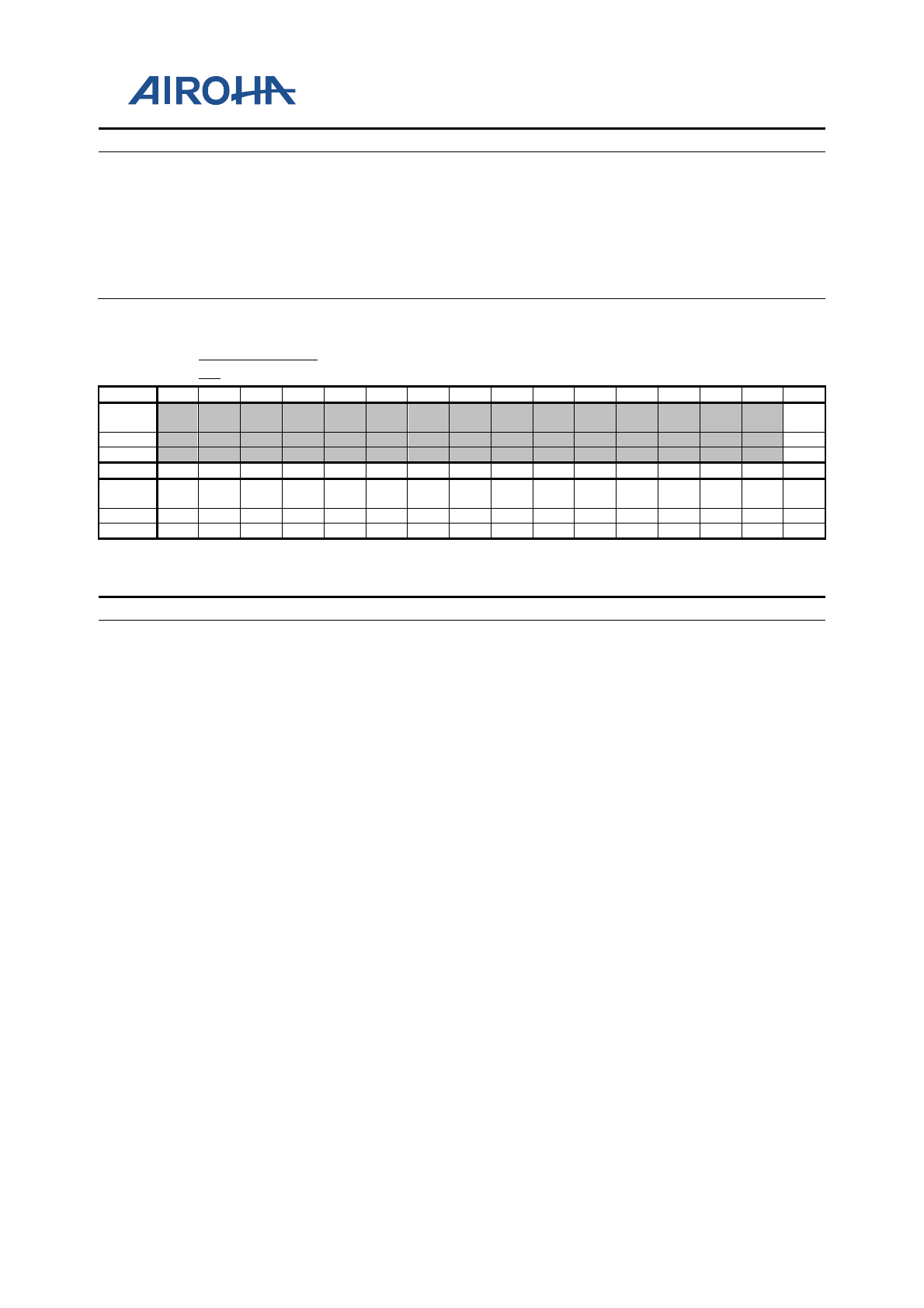
MT2523 Series Reference Manual
© 2015 - 2018 Airoha Technology Corp.
Page 473 of 692
This document contains information that is proprietary to Airoha Technology Corp. (“Airoha”) and/or its licensor(s).
Any unauthorized use, reproduction or disclosure of this document in whole or in part is strictly prohibited.
Bit(s)
Mnemonic
Name
Description
0: Disable
1: Enable
1
GPIO33
GPIO33_SMT
SMT for GPIO33
0: Disable
1: Enable
0
GPIO32
GPIO32_SMT
SMT for GPIO32
0: Disable
1: Enable
A2020614
GPIO_SMT1_S
ET
GPIO SMT Control
00000000
Bit
31
30
29
28
27
26
25
24
23
22
21
20
19
18
17
16
Name
GPIO
48
Type
WO
Reset
0
Bit
15
14
13
12
11
10
9
8
7
6
5
4
3
2
1
0
Name
GPIO
47
GPIO
46
GPIO
45
GPIO
44
GPIO
43
GPIO
42
GPIO
41
GPIO
40
GPIO
39
GPIO
38
GPIO
37
GPIO
36
GPIO
35
GPIO
34
GPIO
33
GPIO
32
Type
WO
WO
WO
WO
WO
WO
WO
WO
WO
WO
WO
WO
WO
WO
WO
WO
Reset
0
0
0
0
0
0
0
0
0
0
0
0
0
0
0
0
Overview
For bitwise access of GPIO_SMT1
Bit(s)
Mnemonic
Name
Description
16
GPIO48
GPIO48_SMT
Bitwise SET operation of GPIO48 SMT
0: Keep
1: SET bits
15
GPIO47
GPIO47_SMT
Bitwise SET operation of GPIO47 SMT
0: Keep
1: SET bits
14
GPIO46
GPIO46_SMT
Bitwise SET operation of GPIO46 SMT
0: Keep
1: SET bits
13
GPIO45
GPIO45_SMT
Bitwise SET operation of GPIO45 SMT
0: Keep
1: SET bits
12
GPIO44
GPIO44_SMT
Bitwise SET operation of GPIO44 SMT
0: Keep
1: SET bits
11
GPIO43
GPIO43_SMT
Bitwise SET operation of GPIO43 SMT
0: Keep
1: SET bits
10
GPIO42
GPIO42_SMT
Bitwise SET operation of GPIO42 SMT
0: Keep
1: SET bits
9
GPIO41
GPIO41_SMT
Bitwise SET operation of GPIO41 SMT
0: Keep
1: SET bits
8
GPIO40
GPIO40_SMT
Bitwise SET operation of GPIO40 SMT
0: Keep
1: SET bits
7
GPIO39
GPIO39_SMT
Bitwise SET operation of GPIO39 SMT
0: Keep

MT2523 Series Reference Manual
© 2015 - 2018 Airoha Technology Corp.
Page 474 of 692
This document contains information that is proprietary to Airoha Technology Corp. (“Airoha”) and/or its licensor(s).
Any unauthorized use, reproduction or disclosure of this document in whole or in part is strictly prohibited.
Bit(s)
Mnemonic
Name
Description
1: SET bits
6
GPIO38
GPIO38_SMT
Bitwise SET operation of GPIO38 SMT
0: Keep
1: SET bits
5
GPIO37
GPIO37_SMT
Bitwise SET operation of GPIO37 SMT
0: Keep
1: SET bits
4
GPIO36
GPIO36_SMT
Bitwise SET operation of GPIO36 SMT
0: Keep
1: SET bits
3
GPIO35
GPIO35_SMT
Bitwise SET operation of GPIO35 SMT
0: Keep
1: SET bits
2
GPIO34
GPIO34_SMT
Bitwise SET operation of GPIO34 SMT
0: Keep
1: SET bits
1
GPIO33
GPIO33_SMT
Bitwise SET operation of GPIO33 SMT
0: Keep
1: SET bits
0
GPIO32
GPIO32_SMT
Bitwise SET operation of GPIO32 SMT
0: Keep
1: SET bits
A2020618
GPIO_SMT1_C
LR
GPIO SMT Control
00000000
Bit
31
30
29
28
27
26
25
24
23
22
21
20
19
18
17
16
Name
GPIO
48
Type
WO
Reset
0
Bit
15
14
13
12
11
10
9
8
7
6
5
4
3
2
1
0
Name
GPIO
47
GPIO
46
GPIO
45
GPIO
44
GPIO
43
GPIO
42
GPIO
41
GPIO
40
GPIO
39
GPIO
38
GPIO
37
GPIO
36
GPIO
35
GPIO
34
GPIO
33
GPIO
32
Type
WO
WO
WO
WO
WO
WO
WO
WO
WO
WO
WO
WO
WO
WO
WO
WO
Reset
0
0
0
0
0
0
0
0
0
0
0
0
0
0
0
0
Overview
For bitwise access of GPIO_SMT1
Bit(s)
Mnemonic
Name
Description
16
GPIO48
GPIO48_SMT
Bitwise CLR operation of GPIO48 SMT
0: Keep
1: CLR bits
15
GPIO47
GPIO47_SMT
Bitwise CLR operation of GPIO47 SMT
0: Keep
1: CLR bits
14
GPIO46
GPIO46_SMT
Bitwise CLR operation of GPIO46 SMT
0: Keep
1: CLR bits
13
GPIO45
GPIO45_SMT
Bitwise CLR operation of GPIO45 SMT
0: Keep
1: CLR bits
12
GPIO44
GPIO44_SMT
Bitwise CLR operation of GPIO44 SMT
0: Keep
1: CLR bits
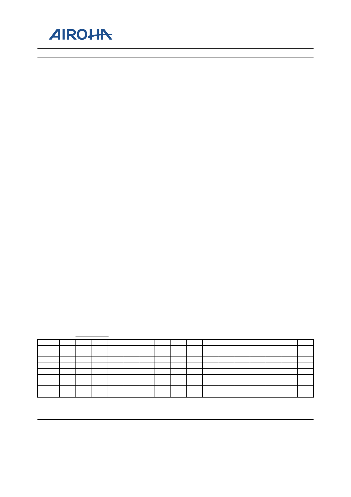
MT2523 Series Reference Manual
© 2015 - 2018 Airoha Technology Corp.
Page 475 of 692
This document contains information that is proprietary to Airoha Technology Corp. (“Airoha”) and/or its licensor(s).
Any unauthorized use, reproduction or disclosure of this document in whole or in part is strictly prohibited.
Bit(s)
Mnemonic
Name
Description
11
GPIO43
GPIO43_SMT
Bitwise CLR operation of GPIO43 SMT
0: Keep
1: CLR bits
10
GPIO42
GPIO42_SMT
Bitwise CLR operation of GPIO42 SMT
0: Keep
1: CLR bits
9
GPIO41
GPIO41_SMT
Bitwise CLR operation of GPIO41 SMT
0: Keep
1: CLR bits
8
GPIO40
GPIO40_SMT
Bitwise CLR operation of GPIO40 SMT
0: Keep
1: CLR bits
7
GPIO39
GPIO39_SMT
Bitwise CLR operation of GPIO39 SMT
0: Keep
1: CLR bits
6
GPIO38
GPIO38_SMT
Bitwise CLR operation of GPIO38 SMT
0: Keep
1: CLR bits
5
GPIO37
GPIO37_SMT
Bitwise CLR operation of GPIO37 SMT
0: Keep
1: CLR bits
4
GPIO36
GPIO36_SMT
Bitwise CLR operation of GPIO36 SMT
0: Keep
1: CLR bits
3
GPIO35
GPIO35_SMT
Bitwise CLR operation of GPIO35 SMT
0: Keep
1: CLR bits
2
GPIO34
GPIO34_SMT
Bitwise CLR operation of GPIO34 SMT
0: Keep
1: CLR bits
1
GPIO33
GPIO33_SMT
Bitwise CLR operation of GPIO33 SMT
0: Keep
1: CLR bits
0
GPIO32
GPIO32_SMT
Bitwise CLR operation of GPIO32 SMT
0: Keep
1: CLR bits
A2020700
GPIO_SR0
GPIO SR
Control
FFFFFFFF
Bit
31
30
29
28
27
26
25
24
23
22
21
20
19
18
17
16
Name
GPIO
31
GPIO
30
GPIO
29
GPIO
28
GPIO
27
GPIO
26
GPIO
25
GPIO
24
GPIO
23
GPIO
22
GPIO
21
GPIO
20
GPIO1
9
GPIO1
8
GPIO1
7
GPIO
16
Type
RW
RW
RW
RW
RW
RW
RW
RW
RW
RW
RW
RW
RW
RW
RW
RW
Reset
1
1
1
1
1
1
1
1
1
1
1
1
1
1
1
1
Bit
15
14
13
12
11
10
9
8
7
6
5
4
3
2
1
0
Name
GPIO
15
GPIO1
4
GPIO1
3
GPIO1
2
GPIO1
1
GPIO1
0
GPIO
9
GPIO
8
GPIO
7
GPIO
6
GPIO
5
GPIO
4
GPIO
3
GPIO
2
GPIO1
GPIO
0
Type
RW
RW
RW
RW
RW
RW
RW
RW
RW
RW
RW
RW
RW
RW
RW
RW
Reset
1
1
1
1
1
1
1
1
1
1
1
1
1
1
1
1
Overview
Configures GPIO slew rate control
Bit(s)
Mnemonic
Name
Description
31
GPIO31
GPIO31_SR
SR for GPIO31
0: Disable

MT2523 Series Reference Manual
© 2015 - 2018 Airoha Technology Corp.
Page 476 of 692
This document contains information that is proprietary to Airoha Technology Corp. (“Airoha”) and/or its licensor(s).
Any unauthorized use, reproduction or disclosure of this document in whole or in part is strictly prohibited.
Bit(s)
Mnemonic
Name
Description
1: Enable
30
GPIO30
GPIO30_SR
SR for GPIO30
0: Disable
1: Enable
29
GPIO29
GPIO29_SR
SR for GPIO29
0: Disable
1: Enable
28
GPIO28
GPIO28_SR
SR for GPIO28
0: Disable
1: Enable
27
GPIO27
GPIO27_SR
SR for GPIO27
0: Disable
1: Enable
26
GPIO26
GPIO26_SR
SR for GPIO26
0: Disable
1: Enable
25
GPIO25
GPIO25_SR
SR for GPIO25
0: Disable
1: Enable
24
GPIO24
GPIO24_SR
SR for GPIO24
0: Disable
1: Enable
23
GPIO23
GPIO23_SR
SR for GPIO23
0: Disable
1: Enable
22
GPIO22
GPIO22_SR
SR for GPIO22
0: Disable
1: Enable
21
GPIO21
GPIO21_SR
SR for GPIO21
0: Disable
1: Enable
20
GPIO20
GPIO20_SR
SR for GPIO20
0: Disable
1: Enable
19
GPIO19
GPIO19_SR
SR for GPIO19
0: Disable
1: Enable
18
GPIO18
GPIO18_SR
SR for GPIO18
0: Disable
1: Enable
17
GPIO17
GPIO17_SR
SR for GPIO17
0: Disable
1: Enable
16
GPIO16
GPIO16_SR
SR for GPIO16
0: Disable
1: Enable
15
GPIO15
GPIO15_SR
SR for GPIO15
0: Disable
1: Enable
14
GPIO14
GPIO14_SR
SR for GPIO14
0: Disable
1: Enable
13
GPIO13
GPIO13_SR
SR for GPIO13
0: Disable

MT2523 Series Reference Manual
© 2015 - 2018 Airoha Technology Corp.
Page 477 of 692
This document contains information that is proprietary to Airoha Technology Corp. (“Airoha”) and/or its licensor(s).
Any unauthorized use, reproduction or disclosure of this document in whole or in part is strictly prohibited.
Bit(s)
Mnemonic
Name
Description
1: Enable
12
GPIO12
GPIO12_SR
SR for GPIO12
0: Disable
1: Enable
11
GPIO11
GPIO11_SR
SR for GPIO11
0: Disable
1: Enable
10
GPIO10
GPIO10_SR
SR for GPIO10
0: Disable
1: Enable
9
GPIO9
GPIO9_SR
SR for GPIO9
0: Disable
1: Enable
8
GPIO8
GPIO8_SR
SR for GPIO8
0: Disable
1: Enable
7
GPIO7
GPIO7_SR
SR for GPIO7
0: Disable
1: Enable
6
GPIO6
GPIO6_SR
SR for GPIO6
0: Disable
1: Enable
5
GPIO5
GPIO5_SR
SR for GPIO5
0: Disable
1: Enable
4
GPIO4
GPIO4_SR
SR for GPIO4
0: Disable
1: Enable
3
GPIO3
GPIO3_SR
SR for GPIO3
0: Disable
1: Enable
2
GPIO2
GPIO2_SR
SR for GPIO2
0: Disable
1: Enable
1
GPIO1
GPIO1_SR
SR for GPIO1
0: Disable
1: Enable
0
GPIO0
GPIO0_SR
SR for GPIO0
0: Disable
1: Enable
A2020704
GPIO_SR0_SE
T
GPIO SR Control
00000000
Bit
31
30
29
28
27
26
25
24
23
22
21
20
19
18
17
16
Name
GPIO
31
GPIO
30
GPIO
29
GPIO
28
GPIO
27
GPIO
26
GPIO
25
GPIO
24
GPIO
23
GPIO
22
GPIO
21
GPIO
20
GPIO1
9
GPIO1
8
GPIO1
7
GPIO
16
Type
WO
WO
WO
WO
WO
WO
WO
WO
WO
WO
WO
WO
WO
WO
WO
WO
Reset
0
0
0
0
0
0
0
0
0
0
0
0
0
0
0
0
Bit
15
14
13
12
11
10
9
8
7
6
5
4
3
2
1
0
Name
GPIO
15
GPIO1
4
GPIO1
3
GPIO1
2
GPIO1
1
GPIO1
0
GPIO
9
GPIO
8
GPIO
7
GPIO
6
GPIO
5
GPIO
4
GPIO
3
GPIO
2
GPIO1
GPIO
0
Type
WO
WO
WO
WO
WO
WO
WO
WO
WO
WO
WO
WO
WO
WO
WO
WO
Reset
0
0
0
0
0
0
0
0
0
0
0
0
0
0
0
0

MT2523 Series Reference Manual
© 2015 - 2018 Airoha Technology Corp.
Page 478 of 692
This document contains information that is proprietary to Airoha Technology Corp. (“Airoha”) and/or its licensor(s).
Any unauthorized use, reproduction or disclosure of this document in whole or in part is strictly prohibited.
Overview
For bitwise access of GPIO_SR0
Bit(s)
Mnemonic
Name
Description
31
GPIO31
GPIO31_SR
Bitwise SET operation of GPIO31 SR
0: Keep
1: SET bits
30
GPIO30
GPIO30_SR
Bitwise SET operation of GPIO30 SR
0: Keep
1: SET bits
29
GPIO29
GPIO29_SR
Bitwise SET operation of GPIO29 SR
0: Keep
1: SET bits
28
GPIO28
GPIO28_SR
Bitwise SET operation of GPIO28 SR
0: Keep
1: SET bits
27
GPIO27
GPIO27_SR
Bitwise SET operation of GPIO27 SR
0: Keep
1: SET bits
26
GPIO26
GPIO26_SR
Bitwise SET operation of GPIO26 SR
0: Keep
1: SET bits
25
GPIO25
GPIO25_SR
Bitwise SET operation of GPIO25 SR
0: Keep
1: SET bits
24
GPIO24
GPIO24_SR
Bitwise SET operation of GPIO24 SR
0: Keep
1: SET bits
23
GPIO23
GPIO23_SR
Bitwise SET operation of GPIO23 SR
0: Keep
1: SET bits
22
GPIO22
GPIO22_SR
Bitwise SET operation of GPIO22 SR
0: Keep
1: SET bits
21
GPIO21
GPIO21_SR
Bitwise SET operation of GPIO21 SR
0: Keep
1: SET bits
20
GPIO20
GPIO20_SR
Bitwise SET operation of GPIO20 SR
0: Keep
1: SET bits
19
GPIO19
GPIO19_SR
Bitwise SET operation of GPIO19 SR
0: Keep
1: SET bits
18
GPIO18
GPIO18_SR
Bitwise SET operation of GPIO18 SR
0: Keep
1: SET bits
17
GPIO17
GPIO17_SR
Bitwise SET operation of GPIO17 SR
0: Keep
1: SET bits
16
GPIO16
GPIO16_SR
Bitwise SET operation of GPIO16 SR
0: Keep
1: SET bits
15
GPIO15
GPIO15_SR
Bitwise SET operation of GPIO15 SR
0: Keep
1: SET bits
14
GPIO14
GPIO14_SR
Bitwise SET operation of GPIO14 SR

MT2523 Series Reference Manual
© 2015 - 2018 Airoha Technology Corp.
Page 479 of 692
This document contains information that is proprietary to Airoha Technology Corp. (“Airoha”) and/or its licensor(s).
Any unauthorized use, reproduction or disclosure of this document in whole or in part is strictly prohibited.
Bit(s)
Mnemonic
Name
Description
0: Keep
1: SET bits
13
GPIO13
GPIO13_SR
Bitwise SET operation of GPIO13 SR
0: Keep
1: SET bits
12
GPIO12
GPIO12_SR
Bitwise SET operation of GPIO12 SR
0: Keep
1: SET bits
11
GPIO11
GPIO11_SR
Bitwise SET operation of GPIO11 SR
0: Keep
1: SET bits
10
GPIO10
GPIO10_SR
Bitwise SET operation of GPIO10 SR
0: Keep
1: SET bits
9
GPIO9
GPIO9_SR
Bitwise SET operation of GPIO9 SR
0: Keep
1: SET bits
8
GPIO8
GPIO8_SR
Bitwise SET operation of GPIO8 SR
0: Keep
1: SET bits
7
GPIO7
GPIO7_SR
Bitwise SET operation of GPIO7 SR
0: Keep
1: SET bits
6
GPIO6
GPIO6_SR
Bitwise SET operation of GPIO6 SR
0: Keep
1: SET bits
5
GPIO5
GPIO5_SR
Bitwise SET operation of GPIO5 SR
0: Keep
1: SET bits
4
GPIO4
GPIO4_SR
Bitwise SET operation of GPIO4 SR
0: Keep
1: SET bits
3
GPIO3
GPIO3_SR
Bitwise SET operation of GPIO3 SR
0: Keep
1: SET bits
2
GPIO2
GPIO2_SR
Bitwise SET operation of GPIO2 SR
0: Keep
1: SET bits
1
GPIO1
GPIO1_SR
Bitwise SET operation of GPIO1 SR
0: Keep
1: SET bits
0
GPIO0
GPIO0_SR
Bitwise SET operation of GPIO0 SR
0: Keep
1: SET bits
A2020708
GPIO_SR0_CL
R
GPIO SR Control
00000000
Bit
31
30
29
28
27
26
25
24
23
22
21
20
19
18
17
16
Name
GPIO
31
GPIO
30
GPIO
29
GPIO
28
GPIO
27
GPIO
26
GPIO
25
GPIO
24
GPIO
23
GPIO
22
GPIO
21
GPIO
20
GPIO1
9
GPIO1
8
GPIO1
7
GPIO
16
Type
WO
WO
WO
WO
WO
WO
WO
WO
WO
WO
WO
WO
WO
WO
WO
WO
Reset
0
0
0
0
0
0
0
0
0
0
0
0
0
0
0
0
Bit
15
14
13
12
11
10
9
8
7
6
5
4
3
2
1
0

MT2523 Series Reference Manual
© 2015 - 2018 Airoha Technology Corp.
Page 480 of 692
This document contains information that is proprietary to Airoha Technology Corp. (“Airoha”) and/or its licensor(s).
Any unauthorized use, reproduction or disclosure of this document in whole or in part is strictly prohibited.
Name
GPIO
15
GPIO1
4
GPIO1
3
GPIO1
2
GPIO1
1
GPIO1
0
GPIO
9
GPIO
8
GPIO
7
GPIO
6
GPIO
5
GPIO
4
GPIO
3
GPIO
2
GPIO1
GPIO
0
Type
WO
WO
WO
WO
WO
WO
WO
WO
WO
WO
WO
WO
WO
WO
WO
WO
Reset
0
0
0
0
0
0
0
0
0
0
0
0
0
0
0
0
Overview
For bitwise access of GPIO_SR0
Bit(s)
Mnemonic
Name
Description
31
GPIO31
GPIO31_SR
Bitwise CLR operation of GPIO31 SR
0: Keep
1: CLR bits
30
GPIO30
GPIO30_SR
Bitwise CLR operation of GPIO30 SR
0: Keep
1: CLR bits
29
GPIO29
GPIO29_SR
Bitwise CLR operation of GPIO29 SR
0: Keep
1: CLR bits
28
GPIO28
GPIO28_SR
Bitwise CLR operation of GPIO28 SR
0: Keep
1: CLR bits
27
GPIO27
GPIO27_SR
Bitwise CLR operation of GPIO27 SR
0: Keep
1: CLR bits
26
GPIO26
GPIO26_SR
Bitwise CLR operation of GPIO26 SR
0: Keep
1: CLR bits
25
GPIO25
GPIO25_SR
Bitwise CLR operation of GPIO25 SR
0: Keep
1: CLR bits
24
GPIO24
GPIO24_SR
Bitwise CLR operation of GPIO24 SR
0: Keep
1: CLR bits
23
GPIO23
GPIO23_SR
Bitwise CLR operation of GPIO23 SR
0: Keep
1: CLR bits
22
GPIO22
GPIO22_SR
Bitwise CLR operation of GPIO22 SR
0: Keep
1: CLR bits
21
GPIO21
GPIO21_SR
Bitwise CLR operation of GPIO21 SR
0: Keep
1: CLR bits
20
GPIO20
GPIO20_SR
Bitwise CLR operation of GPIO20 SR
0: Keep
1: CLR bits
19
GPIO19
GPIO19_SR
Bitwise CLR operation of GPIO19 SR
0: Keep
1: CLR bits
18
GPIO18
GPIO18_SR
Bitwise CLR operation of GPIO18 SR
0: Keep
1: CLR bits
17
GPIO17
GPIO17_SR
Bitwise CLR operation of GPIO17 SR
0: Keep
1: CLR bits
16
GPIO16
GPIO16_SR
Bitwise CLR operation of GPIO16 SR
0: Keep
1: CLR bits

MT2523 Series Reference Manual
© 2015 - 2018 Airoha Technology Corp.
Page 481 of 692
This document contains information that is proprietary to Airoha Technology Corp. (“Airoha”) and/or its licensor(s).
Any unauthorized use, reproduction or disclosure of this document in whole or in part is strictly prohibited.
Bit(s)
Mnemonic
Name
Description
15
GPIO15
GPIO15_SR
Bitwise CLR operation of GPIO15 SR
0: Keep
1: CLR bits
14
GPIO14
GPIO14_SR
Bitwise CLR operation of GPIO14 SR
0: Keep
1: CLR bits
13
GPIO13
GPIO13_SR
Bitwise CLR operation of GPIO13 SR
0: Keep
1: CLR bits
12
GPIO12
GPIO12_SR
Bitwise CLR operation of GPIO12 SR
0: Keep
1: CLR bits
11
GPIO11
GPIO11_SR
Bitwise CLR operation of GPIO11 SR
0: Keep
1: CLR bits
10
GPIO10
GPIO10_SR
Bitwise CLR operation of GPIO10 SR
0: Keep
1: CLR bits
9
GPIO9
GPIO9_SR
Bitwise CLR operation of GPIO9 SR
0: Keep
1: CLR bits
8
GPIO8
GPIO8_SR
Bitwise CLR operation of GPIO8 SR
0: Keep
1: CLR bits
7
GPIO7
GPIO7_SR
Bitwise CLR operation of GPIO7 SR
0: Keep
1: CLR bits
6
GPIO6
GPIO6_SR
Bitwise CLR operation of GPIO6 SR
0: Keep
1: CLR bits
5
GPIO5
GPIO5_SR
Bitwise CLR operation of GPIO5 SR
0: Keep
1: CLR bits
4
GPIO4
GPIO4_SR
Bitwise CLR operation of GPIO4 SR
0: Keep
1: CLR bits
3
GPIO3
GPIO3_SR
Bitwise CLR operation of GPIO3 SR
0: Keep
1: CLR bits
2
GPIO2
GPIO2_SR
Bitwise CLR operation of GPIO2 SR
0: Keep
1: CLR bits
1
GPIO1
GPIO1_SR
Bitwise CLR operation of GPIO1 SR
0: Keep
1: CLR bits
0
GPIO0
GPIO0_SR
Bitwise CLR operation of GPIO0 SR
0: Keep
1: CLR bits
A2020710
GPIO_SR1
GPIO SR Control
0007FFFF
Bit
31
30
29
28
27
26
25
24
23
22
21
20
19
18
17
16
Name
GPIO
48

MT2523 Series Reference Manual
© 2015 - 2018 Airoha Technology Corp.
Page 482 of 692
This document contains information that is proprietary to Airoha Technology Corp. (“Airoha”) and/or its licensor(s).
Any unauthorized use, reproduction or disclosure of this document in whole or in part is strictly prohibited.
Type
RW
Reset
1
Bit
15
14
13
12
11
10
9
8
7
6
5
4
3
2
1
0
Name
GPIO
47
GPIO
46
GPIO
45
GPIO
44
GPIO
43
GPIO
42
GPIO
41
GPIO
40
GPIO
39
GPIO
38
GPIO
37
GPIO
36
GPIO
35
GPIO
34
GPIO
33
GPIO
32
Type
RW
RW
RW
RW
RW
RW
RW
RW
RW
RW
RW
RW
RW
RW
RW
RW
Reset
1
1
1
1
1
1
1
1
1
1
1
1
1
1
1
1
Overview
Configures GPIO slew rate control
Bit(s)
Mnemonic
Name
Description
16
GPIO48
GPIO48_SR
SR for GPIO48
0: Disable
1: Enable
15
GPIO47
GPIO47_SR
SR for GPIO47
0: Disable
1: Enable
14
GPIO46
GPIO46_SR
SR for GPIO46
0: Disable
1: Enable
13
GPIO45
GPIO45_SR
SR for GPIO45
0: Disable
1: Enable
12
GPIO44
GPIO44_SR
SR for GPIO44
0: Disable
1: Enable
11
GPIO43
GPIO43_SR
SR for GPIO43
0: Disable
1: Enable
10
GPIO42
GPIO42_SR
SR for GPIO42
0: Disable
1: Enable
9
GPIO41
GPIO41_SR
SR for GPIO41
0: Disable
1: Enable
8
GPIO40
GPIO40_SR
SR for GPIO40
0: Disable
1: Enable
7
GPIO39
GPIO39_SR
SR for GPIO39
0: Disable
1: Enable
6
GPIO38
GPIO38_SR
SR for GPIO38
0: Disable
1: Enable
5
GPIO37
GPIO37_SR
SR for GPIO37
0: Disable
1: Enable
4
GPIO36
GPIO36_SR
SR for GPIO36
0: Disable
1: Enable
3
GPIO35
GPIO35_SR
SR for GPIO35
0: Disable
1: Enable
2
GPIO34
GPIO34_SR
SR for GPIO34
0: Disable
1: Enable
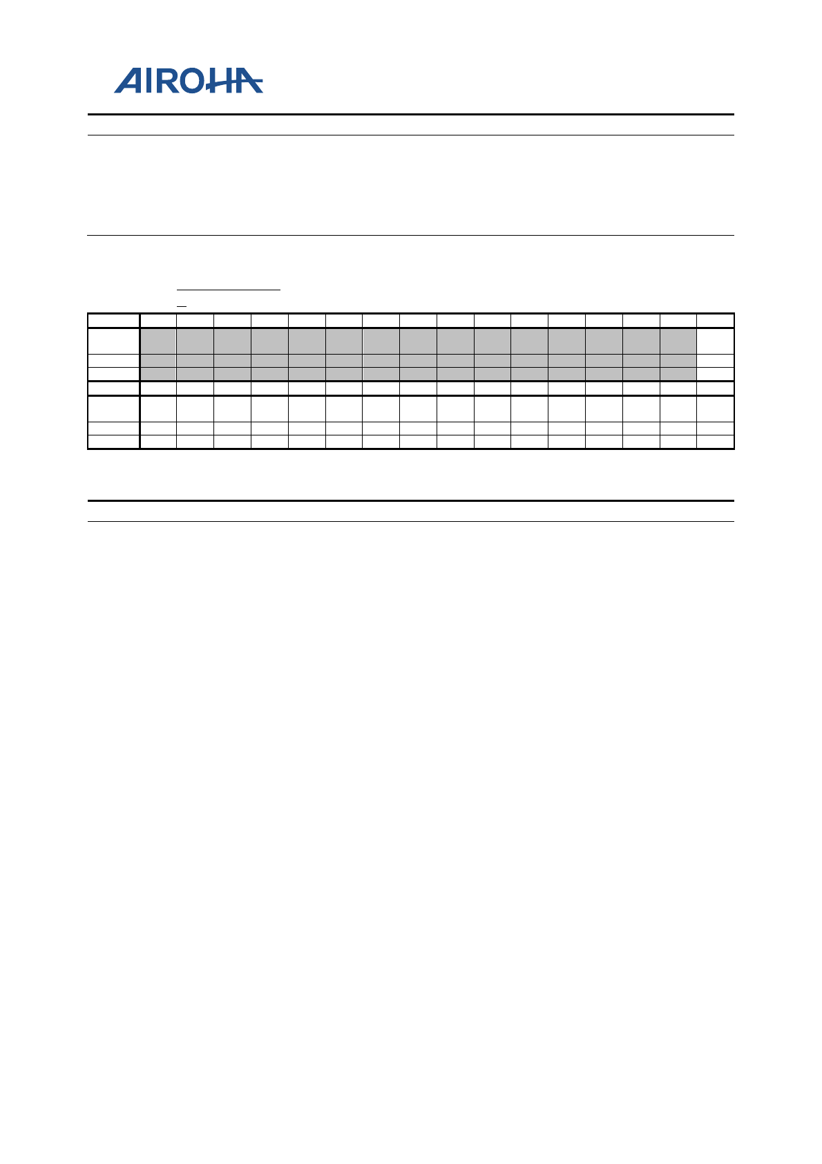
MT2523 Series Reference Manual
© 2015 - 2018 Airoha Technology Corp.
Page 483 of 692
This document contains information that is proprietary to Airoha Technology Corp. (“Airoha”) and/or its licensor(s).
Any unauthorized use, reproduction or disclosure of this document in whole or in part is strictly prohibited.
Bit(s)
Mnemonic
Name
Description
1
GPIO33
GPIO33_SR
SR for GPIO33
0: Disable
1: Enable
0
GPIO32
GPIO32_SR
SR for GPIO32
0: Disable
1: Enable
A2020714
GPIO_SR1_SE
T
GPIO SR Control
00000000
Bit
31
30
29
28
27
26
25
24
23
22
21
20
19
18
17
16
Name
GPIO
48
Type
WO
Reset
0
Bit
15
14
13
12
11
10
9
8
7
6
5
4
3
2
1
0
Name
GPIO
47
GPIO
46
GPIO
45
GPIO
44
GPIO
43
GPIO
42
GPIO
41
GPIO
40
GPIO
39
GPIO
38
GPIO
37
GPIO
36
GPIO
35
GPIO
34
GPIO
33
GPIO
32
Type
WO
WO
WO
WO
WO
WO
WO
WO
WO
WO
WO
WO
WO
WO
WO
WO
Reset
0
0
0
0
0
0
0
0
0
0
0
0
0
0
0
0
Overview
For bitwise access of GPIO_SR1
Bit(s)
Mnemonic
Name
Description
16
GPIO48
GPIO48_SR
Bitwise SET operation of GPIO48 SR
0: Keep
1: SET bits
15
GPIO47
GPIO47_SR
Bitwise SET operation of GPIO47 SR
0: Keep
1: SET bits
14
GPIO46
GPIO46_SR
Bitwise SET operation of GPIO46 SR
0: Keep
1: SET bits
13
GPIO45
GPIO45_SR
Bitwise SET operation of GPIO45 SR
0: Keep
1: SET bits
12
GPIO44
GPIO44_SR
Bitwise SET operation of GPIO44 SR
0: Keep
1: SET bits
11
GPIO43
GPIO43_SR
Bitwise SET operation of GPIO43 SR
0: Keep
1: SET bits
10
GPIO42
GPIO42_SR
Bitwise SET operation of GPIO42 SR
0: Keep
1: SET bits
9
GPIO41
GPIO41_SR
Bitwise SET operation of GPIO41 SR
0: Keep
1: SET bits
8
GPIO40
GPIO40_SR
Bitwise SET operation of GPIO40 SR
0: Keep
1: SET bits
7
GPIO39
GPIO39_SR
Bitwise SET operation of GPIO39 SR
0: Keep
1: SET bits
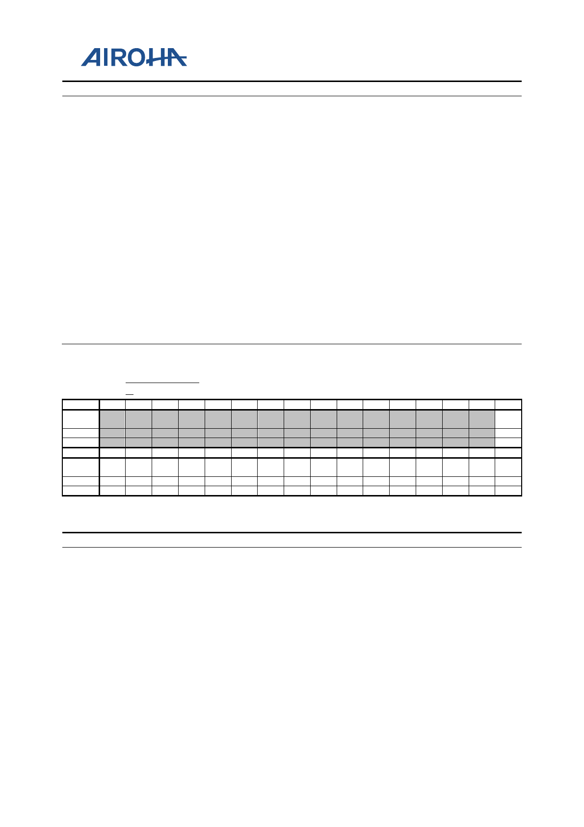
MT2523 Series Reference Manual
© 2015 - 2018 Airoha Technology Corp.
Page 484 of 692
This document contains information that is proprietary to Airoha Technology Corp. (“Airoha”) and/or its licensor(s).
Any unauthorized use, reproduction or disclosure of this document in whole or in part is strictly prohibited.
Bit(s)
Mnemonic
Name
Description
6
GPIO38
GPIO38_SR
Bitwise SET operation of GPIO38 SR
0: Keep
1: SET bits
5
GPIO37
GPIO37_SR
Bitwise SET operation of GPIO37 SR
0: Keep
1: SET bits
4
GPIO36
GPIO36_SR
Bitwise SET operation of GPIO36 SR
0: Keep
1: SET bits
3
GPIO35
GPIO35_SR
Bitwise SET operation of GPIO35 SR
0: Keep
1: SET bits
2
GPIO34
GPIO34_SR
Bitwise SET operation of GPIO34 SR
0: Keep
1: SET bits
1
GPIO33
GPIO33_SR
Bitwise SET operation of GPIO33 SR
0: Keep
1: SET bits
0
GPIO32
GPIO32_SR
Bitwise SET operation of GPIO32 SR
0: Keep
1: SET bits
A2020718
GPIO_SR1_CL
R
GPIO SR Control
00000000
Bit
31
30
29
28
27
26
25
24
23
22
21
20
19
18
17
16
Name
GPIO
48
Type
WO
Reset
0
Bit
15
14
13
12
11
10
9
8
7
6
5
4
3
2
1
0
Name
GPIO
47
GPIO
46
GPIO
45
GPIO
44
GPIO
43
GPIO
42
GPIO
41
GPIO
40
GPIO
39
GPIO
38
GPIO
37
GPIO
36
GPIO
35
GPIO
34
GPIO
33
GPIO
32
Type
WO
WO
WO
WO
WO
WO
WO
WO
WO
WO
WO
WO
WO
WO
WO
WO
Reset
0
0
0
0
0
0
0
0
0
0
0
0
0
0
0
0
Overview
For bitwise access of GPIO_SR1
Bit(s)
Mnemonic
Name
Description
16
GPIO48
GPIO48_SR
Bitwise CLR operation of GPIO48 SR
0: Keep
1: CLR bits
15
GPIO47
GPIO47_SR
Bitwise CLR operation of GPIO47 SR
0: Keep
1: CLR bits
14
GPIO46
GPIO46_SR
Bitwise CLR operation of GPIO46 SR
0: Keep
1: CLR bits
13
GPIO45
GPIO45_SR
Bitwise CLR operation of GPIO45 SR
0: Keep
1: CLR bits
12
GPIO44
GPIO44_SR
Bitwise CLR operation of GPIO44 SR
0: Keep
1: CLR bits

MT2523 Series Reference Manual
© 2015 - 2018 Airoha Technology Corp.
Page 485 of 692
This document contains information that is proprietary to Airoha Technology Corp. (“Airoha”) and/or its licensor(s).
Any unauthorized use, reproduction or disclosure of this document in whole or in part is strictly prohibited.
Bit(s)
Mnemonic
Name
Description
11
GPIO43
GPIO43_SR
Bitwise CLR operation of GPIO43 SR
0: Keep
1: CLR bits
10
GPIO42
GPIO42_SR
Bitwise CLR operation of GPIO42 SR
0: Keep
1: CLR bits
9
GPIO41
GPIO41_SR
Bitwise CLR operation of GPIO41 SR
0: Keep
1: CLR bits
8
GPIO40
GPIO40_SR
Bitwise CLR operation of GPIO40 SR
0: Keep
1: CLR bits
7
GPIO39
GPIO39_SR
Bitwise CLR operation of GPIO39 SR
0: Keep
1: CLR bits
6
GPIO38
GPIO38_SR
Bitwise CLR operation of GPIO38 SR
0: Keep
1: CLR bits
5
GPIO37
GPIO37_SR
Bitwise CLR operation of GPIO37 SR
0: Keep
1: CLR bits
4
GPIO36
GPIO36_SR
Bitwise CLR operation of GPIO36 SR
0: Keep
1: CLR bits
3
GPIO35
GPIO35_SR
Bitwise CLR operation of GPIO35 SR
0: Keep
1: CLR bits
2
GPIO34
GPIO34_SR
Bitwise CLR operation of GPIO34 SR
0: Keep
1: CLR bits
1
GPIO33
GPIO33_SR
Bitwise CLR operation of GPIO33 SR
0: Keep
1: CLR bits
0
GPIO32
GPIO32_SR
Bitwise CLR operation of GPIO32 SR
0: Keep
1: CLR bits
A2020800
GPIO_DRV0
GPIO DRV
Control
00000000
Bit
31
30
29
28
27
26
25
24
23
22
21
20
19
18
17
16
Name
GPIO15
GPIO14
GPIO13
GPIO12
GPIO11
GPIO10
GPIO9
GPIO8
Type
RW
RW
RW
RW
RW
RW
RW
RW
Reset
0
0
0
0
0
0
0
0
0
0
0
0
0
0
0
0
Bit
15
14
13
12
11
10
9
8
7
6
5
4
3
2
1
0
Name
GPIO7
GPIO6
GPIO5
GPIO4
GPIO3
GPIO2
GPIO1
GPIO0
Type
RW
RW
RW
RW
RW
RW
RW
RW
Reset
0
0
0
0
0
0
0
0
0
0
0
0
0
0
0
0
Overview
Configures GPIO driving control
Bit(s)
Mnemonic
Name
Description
31:30
GPIO15
GPIO15_DRV
GPIO15 driving control
29:28
GPIO14
GPIO14_DRV
GPIO14 driving control
27:26
GPIO13
GPIO13_DRV
GPIO13 driving control

MT2523 Series Reference Manual
© 2015 - 2018 Airoha Technology Corp.
Page 486 of 692
This document contains information that is proprietary to Airoha Technology Corp. (“Airoha”) and/or its licensor(s).
Any unauthorized use, reproduction or disclosure of this document in whole or in part is strictly prohibited.
Bit(s)
Mnemonic
Name
Description
25:24
GPIO12
GPIO12_DRV
GPIO12 driving control
23:22
GPIO11
GPIO11_DRV
GPIO11 driving control
21:20
GPIO10
GPIO10_DRV
GPIO10 driving control
19:18
GPIO9
GPIO9_DRV
GPIO9 driving control
17:16
GPIO8
GPIO8_DRV
GPIO8 driving control
15:14
GPIO7
GPIO7_DRV
GPIO7 driving control
13:12
GPIO6
GPIO6_DRV
GPIO6 driving control
11:10
GPIO5
GPIO5_DRV
GPIO5 driving control
9:8
GPIO4
GPIO4_DRV
GPIO4 driving control
7:6
GPIO3
GPIO3_DRV
GPIO3 driving control
5:4
GPIO2
GPIO2_DRV
GPIO2 driving control
3:2
GPIO1
GPIO1_DRV
GPIO1 driving control
1:0
GPIO0
GPIO0_DRV
GPIO0 driving control
A2020804
GPIO_DRV0_S
ET
GPIO DRV Control
00000000
Bit
31
30
29
28
27
26
25
24
23
22
21
20
19
18
17
16
Name
GPIO15
GPIO14
GPIO13
GPIO12
GPIO11
GPIO10
GPIO9
GPIO8
Type
WO
WO
WO
WO
WO
WO
WO
WO
Reset
0
0
0
0
0
0
0
0
0
0
0
0
0
0
0
0
Bit
15
14
13
12
11
10
9
8
7
6
5
4
3
2
1
0
Name
GPIO7
GPIO6
GPIO5
GPIO4
GPIO3
GPIO2
GPIO1
GPIO0
Type
WO
WO
WO
WO
WO
WO
WO
WO
Reset
0
0
0
0
0
0
0
0
0
0
0
0
0
0
0
0
Overview
For bitwise access of GPIO_DRV0
Bit(s)
Mnemonic
Name
Description
31:30
GPIO15
GPIO15_DRV
Bitwise SET operation of GPIO15_DRV
0: Keep
1: SET bits
29:28
GPIO14
GPIO14_DRV
Bitwise SET operation of GPIO14_DRV
0: Keep
1: SET bits
27:26
GPIO13
GPIO13_DRV
Bitwise SET operation of GPIO13_DRV
0: Keep
1: SET bits
25:24
GPIO12
GPIO12_DRV
Bitwise SET operation of GPIO12_DRV
0: Keep
1: SET bits
23:22
GPIO11
GPIO11_DRV
Bitwise SET operation of GPIO11_DRV
0: Keep
1: SET bits
21:20
GPIO10
GPIO10_DRV
Bitwise SET operation of GPIO10_DRV
0: Keep
1: SET bits
19:18
GPIO9
GPIO9_DRV
Bitwise SET operation of GPIO9_DRV
0: Keep
1: SET bits
17:16
GPIO8
GPIO8_DRV
Bitwise SET operation of GPIO8_DRV
0: Keep
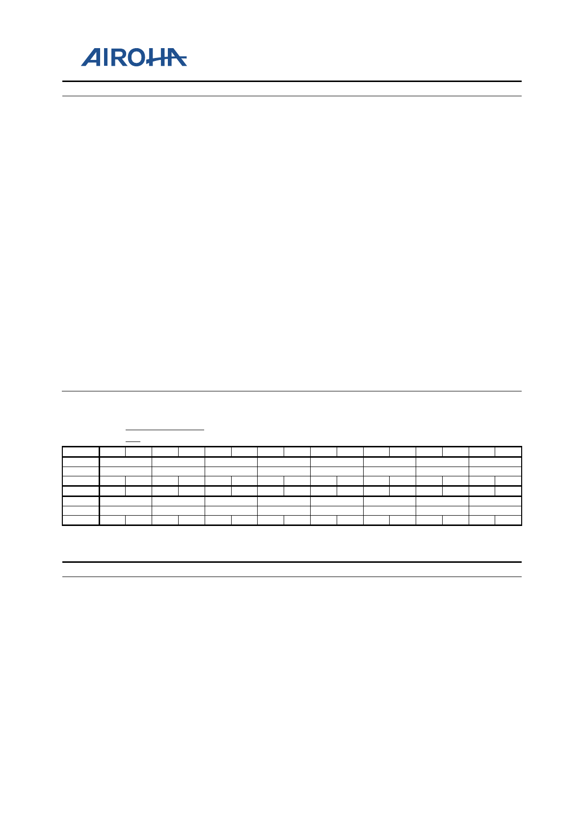
MT2523 Series Reference Manual
© 2015 - 2018 Airoha Technology Corp.
Page 487 of 692
This document contains information that is proprietary to Airoha Technology Corp. (“Airoha”) and/or its licensor(s).
Any unauthorized use, reproduction or disclosure of this document in whole or in part is strictly prohibited.
Bit(s)
Mnemonic
Name
Description
1: SET bits
15:14
GPIO7
GPIO7_DRV
Bitwise SET operation of GPIO7_DRV
0: Keep
1: SET bits
13:12
GPIO6
GPIO6_DRV
Bitwise SET operation of GPIO6_DRV
0: Keep
1: SET bits
11:10
GPIO5
GPIO5_DRV
Bitwise SET operation of GPIO5_DRV
0: Keep
1: SET bits
9:8
GPIO4
GPIO4_DRV
Bitwise SET operation of GPIO4_DRV
0: Keep
1: SET bits
7:6
GPIO3
GPIO3_DRV
Bitwise SET operation of GPIO3_DRV
0: Keep
1: SET bits
5:4
GPIO2
GPIO2_DRV
Bitwise SET operation of GPIO2_DRV
0: Keep
1: SET bits
3:2
GPIO1
GPIO1_DRV
Bitwise SET operation of GPIO1_DRV
0: Keep
1: SET bits
1:0
GPIO0
GPIO0_DRV
Bitwise SET operation of GPIO0_DRV
0: Keep
1: SET bits
A2020808
GPIO_DRV0_C
LR
GPIO DRV Control
00000000
Bit
31
30
29
28
27
26
25
24
23
22
21
20
19
18
17
16
Name
GPIO15
GPIO14
GPIO13
GPIO12
GPIO11
GPIO10
GPIO9
GPIO8
Type
WO
WO
WO
WO
WO
WO
WO
WO
Reset
0
0
0
0
0
0
0
0
0
0
0
0
0
0
0
0
Bit
15
14
13
12
11
10
9
8
7
6
5
4
3
2
1
0
Name
GPIO7
GPIO6
GPIO5
GPIO4
GPIO3
GPIO2
GPIO1
GPIO0
Type
WO
WO
WO
WO
WO
WO
WO
WO
Reset
0
0
0
0
0
0
0
0
0
0
0
0
0
0
0
0
Overview
For bitwise access of GPIO_DRV0
Bit(s)
Mnemonic
Name
Description
31:30
GPIO15
GPIO15_DRV
Bitwise CLR operation of GPIO15_DRV
0: Keep
1: CLR bits
29:28
GPIO14
GPIO14_DRV
Bitwise CLR operation of GPIO14_DRV
0: Keep
1: CLR bits
27:26
GPIO13
GPIO13_DRV
Bitwise CLR operation of GPIO13_DRV
0: Keep
1: CLR bits
25:24
GPIO12
GPIO12_DRV
Bitwise CLR operation of GPIO12_DRV
0: Keep
1: CLR bits
23:22
GPIO11
GPIO11_DRV
Bitwise CLR operation of GPIO11_DRV
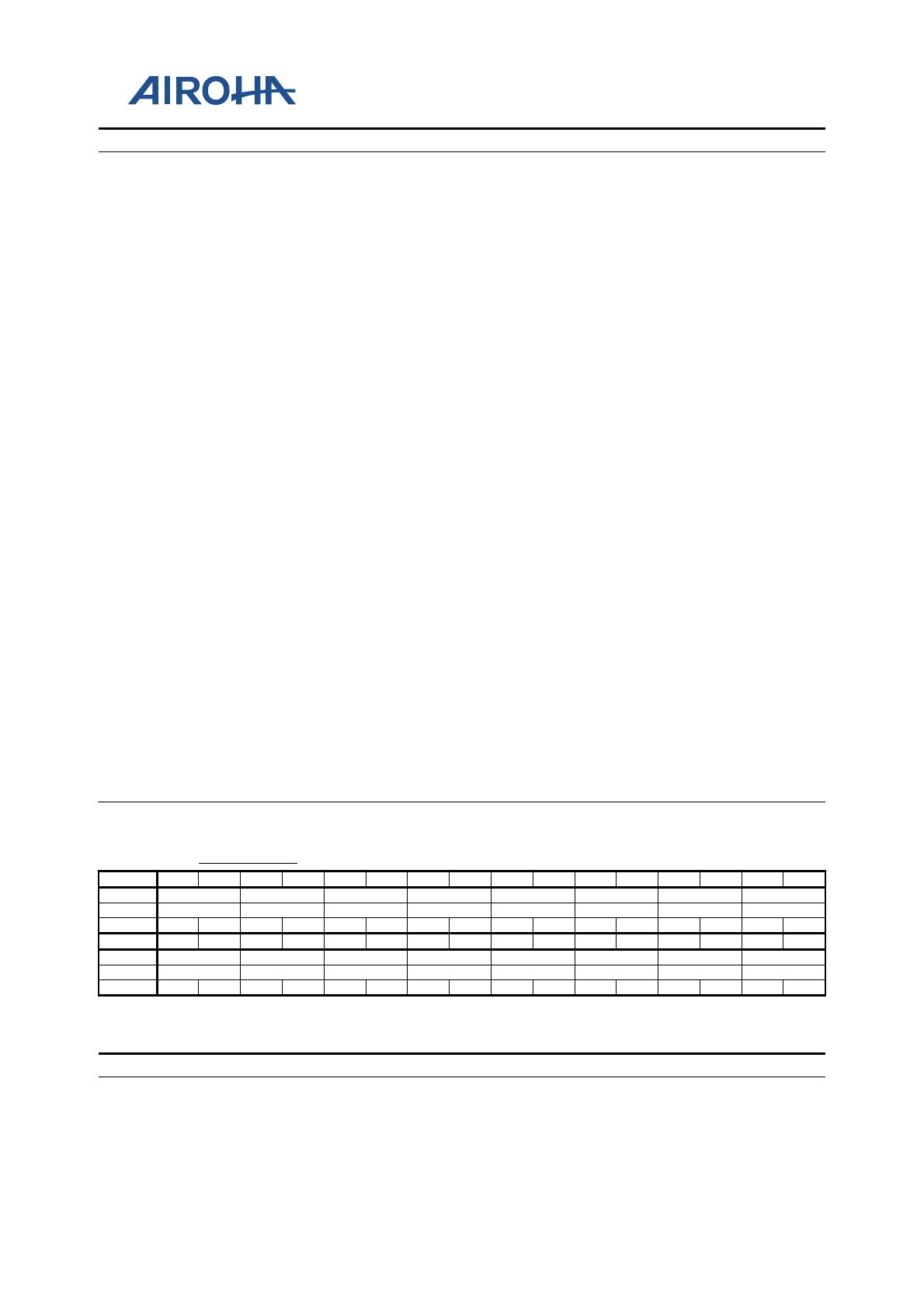
MT2523 Series Reference Manual
© 2015 - 2018 Airoha Technology Corp.
Page 488 of 692
This document contains information that is proprietary to Airoha Technology Corp. (“Airoha”) and/or its licensor(s).
Any unauthorized use, reproduction or disclosure of this document in whole or in part is strictly prohibited.
Bit(s)
Mnemonic
Name
Description
0: Keep
1: CLR bits
21:20
GPIO10
GPIO10_DRV
Bitwise CLR operation of GPIO10_DRV
0: Keep
1: CLR bits
19:18
GPIO9
GPIO9_DRV
Bitwise CLR operation of GPIO9_DRV
0: Keep
1: CLR bits
17:16
GPIO8
GPIO8_DRV
Bitwise CLR operation of GPIO8_DRV
0: Keep
1: CLR bits
15:14
GPIO7
GPIO7_DRV
Bitwise CLR operation of GPIO7_DRV
0: Keep
1: CLR bits
13:12
GPIO6
GPIO6_DRV
Bitwise CLR operation of GPIO6_DRV
0: Keep
1: CLR bits
11:10
GPIO5
GPIO5_DRV
Bitwise CLR operation of GPIO5_DRV
0: Keep
1: CLR bits
9:8
GPIO4
GPIO4_DRV
Bitwise CLR operation of GPIO4_DRV
0: Keep
1: CLR bits
7:6
GPIO3
GPIO3_DRV
Bitwise CLR operation of GPIO3_DRV
0: Keep
1: CLR bits
5:4
GPIO2
GPIO2_DRV
Bitwise CLR operation of GPIO2_DRV
0: Keep
1: CLR bits
3:2
GPIO1
GPIO1_DRV
Bitwise CLR operation of GPIO1_DRV
0: Keep
1: CLR bits
1:0
GPIO0
GPIO0_DRV
Bitwise CLR operation of GPIO0_DRV
0: Keep
1: CLR bits
A2020810
GPIO_DRV1
GPIO DRV Control
00000000
Bit
31
30
29
28
27
26
25
24
23
22
21
20
19
18
17
16
Name
GPIO31
GPIO30
GPIO29
GPIO28
GPIO27
GPIO26
GPIO25
GPIO24
Type
RW
RW
RW
RW
RW
RW
RW
RW
Reset
0
0
0
0
0
0
0
0
0
0
0
0
0
0
0
0
Bit
15
14
13
12
11
10
9
8
7
6
5
4
3
2
1
0
Name
GPIO23
GPIO22
GPIO21
GPIO20
GPIO19
GPIO18
GPIO17
GPIO16
Type
RW
RW
RW
RW
RW
RW
RW
RW
Reset
0
0
0
0
0
0
0
0
0
0
0
0
0
0
0
0
Overview
Configures GPIO driving control
Bit(s)
Mnemonic
Name
Description
31:30
GPIO31
GPIO31_DRV
GPIO31 driving control
29:28
GPIO30
GPIO30_DRV
GPIO30 driving control
27:26
GPIO29
GPIO29_DRV
GPIO29 driving control
25:24
GPIO28
GPIO28_DRV
GPIO28 driving control

MT2523 Series Reference Manual
© 2015 - 2018 Airoha Technology Corp.
Page 489 of 692
This document contains information that is proprietary to Airoha Technology Corp. (“Airoha”) and/or its licensor(s).
Any unauthorized use, reproduction or disclosure of this document in whole or in part is strictly prohibited.
Bit(s)
Mnemonic
Name
Description
23:22
GPIO27
GPIO27_DRV
GPIO27 driving control
21:20
GPIO26
GPIO26_DRV
GPIO26 driving control
19:18
GPIO25
GPIO25_DRV
GPIO25 driving control
17:16
GPIO24
GPIO24_DRV
GPIO24 driving control
15:14
GPIO23
GPIO23_DRV
GPIO23 driving control
13:12
GPIO22
GPIO22_DRV
GPIO22 driving control
11:10
GPIO21
GPIO21_DRV
GPIO21 driving control
9:8
GPIO20
GPIO20_DRV
GPIO20 driving control
7:6
GPIO19
GPIO19_DRV
GPIO19 driving control
5:4
GPIO18
GPIO18_DRV
GPIO18 driving control
3:2
GPIO17
GPIO17_DRV
GPIO17 driving control
1:0
GPIO16
GPIO16_DRV
GPIO16 driving control
A2020814
GPIO_DRV1_S
ET
GPIO DRV Control
00000000
Bit
31
30
29
28
27
26
25
24
23
22
21
20
19
18
17
16
Name
GPIO31
GPIO30
GPIO29
GPIO28
GPIO27
GPIO26
GPIO25
GPIO24
Type
WO
WO
WO
WO
WO
WO
WO
WO
Reset
0
0
0
0
0
0
0
0
0
0
0
0
0
0
0
0
Bit
15
14
13
12
11
10
9
8
7
6
5
4
3
2
1
0
Name
GPIO23
GPIO22
GPIO21
GPIO20
GPIO19
GPIO18
GPIO17
GPIO16
Type
WO
WO
WO
WO
WO
WO
WO
WO
Reset
0
0
0
0
0
0
0
0
0
0
0
0
0
0
0
0
Overview
For bitwise access of GPIO_DRV1
Bit(s)
Mnemonic
Name
Description
31:30
GPIO31
GPIO31_DRV
Bitwise SET operation of GPIO31_DRV
0: Keep
1: SET bits
29:28
GPIO30
GPIO30_DRV
Bitwise SET operation of GPIO30_DRV
0: Keep
1: SET bits
27:26
GPIO29
GPIO29_DRV
Bitwise SET operation of GPIO29_DRV
0: Keep
1: SET bits
25:24
GPIO28
GPIO28_DRV
Bitwise SET operation of GPIO28_DRV
0: Keep
1: SET bits
23:22
GPIO27
GPIO27_DRV
Bitwise SET operation of GPIO27_DRV
0: Keep
1: SET bits
21:20
GPIO26
GPIO26_DRV
Bitwise SET operation of GPIO26_DRV
0: Keep
1: SET bits
19:18
GPIO25
GPIO25_DRV
Bitwise SET operation of GPIO25_DRV
0: Keep
1: SET bits
17:16
GPIO24
GPIO24_DRV
Bitwise SET operation of GPIO24_DRV
0: Keep
1: SET bits
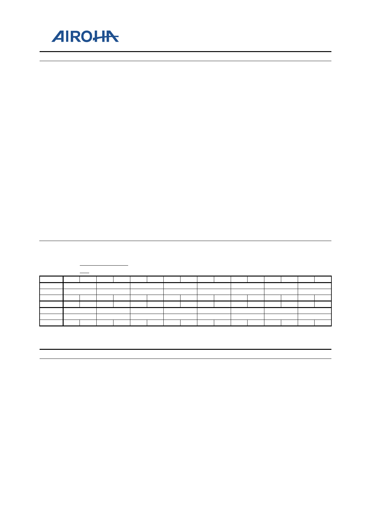
MT2523 Series Reference Manual
© 2015 - 2018 Airoha Technology Corp.
Page 490 of 692
This document contains information that is proprietary to Airoha Technology Corp. (“Airoha”) and/or its licensor(s).
Any unauthorized use, reproduction or disclosure of this document in whole or in part is strictly prohibited.
Bit(s)
Mnemonic
Name
Description
15:14
GPIO23
GPIO23_DRV
Bitwise SET operation of GPIO23_DRV
0: Keep
1: SET bits
13:12
GPIO22
GPIO22_DRV
Bitwise SET operation of GPIO22_DRV
0: Keep
1: SET bits
11:10
GPIO21
GPIO21_DRV
Bitwise SET operation of GPIO21_DRV
0: Keep
1: SET bits
9:8
GPIO20
GPIO20_DRV
Bitwise SET operation of GPIO20_DRV
0: Keep
1: SET bits
7:6
GPIO19
GPIO19_DRV
Bitwise SET operation of GPIO19_DRV
0: Keep
1: SET bits
5:4
GPIO18
GPIO18_DRV
Bitwise SET operation of GPIO18_DRV
0: Keep
1: SET bits
3:2
GPIO17
GPIO17_DRV
Bitwise SET operation of GPIO17_DRV
0: Keep
1: SET bits
1:0
GPIO16
GPIO16_DRV
Bitwise SET operation of GPIO16_DRV
0: Keep
1: SET bits
A2020818
GPIO_DRV1_C
LR
GPIO DRV Control
00000000
Bit
31
30
29
28
27
26
25
24
23
22
21
20
19
18
17
16
Name
GPIO31
GPIO30
GPIO29
GPIO28
GPIO27
GPIO26
GPIO25
GPIO24
Type
WO
WO
WO
WO
WO
WO
WO
WO
Reset
0
0
0
0
0
0
0
0
0
0
0
0
0
0
0
0
Bit
15
14
13
12
11
10
9
8
7
6
5
4
3
2
1
0
Name
GPIO23
GPIO22
GPIO21
GPIO20
GPIO19
GPIO18
GPIO17
GPIO16
Type
WO
WO
WO
WO
WO
WO
WO
WO
Reset
0
0
0
0
0
0
0
0
0
0
0
0
0
0
0
0
Overview
For bitwise access of GPIO_DRV1
Bit(s)
Mnemonic
Name
Description
31:30
GPIO31
GPIO31_DRV
Bitwise CLR operation of GPIO31_DRV
0: Keep
1: CLR bits
29:28
GPIO30
GPIO30_DRV
Bitwise CLR operation of GPIO30_DRV
0: Keep
1: CLR bits
27:26
GPIO29
GPIO29_DRV
Bitwise CLR operation of GPIO29_DRV
0: Keep
1: CLR bits
25:24
GPIO28
GPIO28_DRV
Bitwise CLR operation of GPIO28_DRV
0: Keep
1: CLR bits
23:22
GPIO27
GPIO27_DRV
Bitwise CLR operation of GPIO27_DRV
0: Keep

MT2523 Series Reference Manual
© 2015 - 2018 Airoha Technology Corp.
Page 491 of 692
This document contains information that is proprietary to Airoha Technology Corp. (“Airoha”) and/or its licensor(s).
Any unauthorized use, reproduction or disclosure of this document in whole or in part is strictly prohibited.
Bit(s)
Mnemonic
Name
Description
1: CLR bits
21:20
GPIO26
GPIO26_DRV
Bitwise CLR operation of GPIO26_DRV
0: Keep
1: CLR bits
19:18
GPIO25
GPIO25_DRV
Bitwise CLR operation of GPIO25_DRV
0: Keep
1: CLR bits
17:16
GPIO24
GPIO24_DRV
Bitwise CLR operation of GPIO24_DRV
0: Keep
1: CLR bits
15:14
GPIO23
GPIO23_DRV
Bitwise CLR operation of GPIO23_DRV
0: Keep
1: CLR bits
13:12
GPIO22
GPIO22_DRV
Bitwise CLR operation of GPIO22_DRV
0: Keep
1: CLR bits
11:10
GPIO21
GPIO21_DRV
Bitwise CLR operation of GPIO21_DRV
0: Keep
1: CLR bits
9:8
GPIO20
GPIO20_DRV
Bitwise CLR operation of GPIO20_DRV
0: Keep
1: CLR bits
7:6
GPIO19
GPIO19_DRV
Bitwise CLR operation of GPIO19_DRV
0: Keep
1: CLR bits
5:4
GPIO18
GPIO18_DRV
Bitwise CLR operation of GPIO18_DRV
0: Keep
1: CLR bits
3:2
GPIO17
GPIO17_DRV
Bitwise CLR operation of GPIO17_DRV
0: Keep
1: CLR bits
1:0
GPIO16
GPIO16_DRV
Bitwise CLR operation of GPIO16_DRV
0: Keep
1: CLR bits
A2020820
GPIO_DRV2
GPIO DRV Control
00000000
Bit
31
30
29
28
27
26
25
24
23
22
21
20
19
18
17
16
Name
GPIO47
GPIO46
GPIO45
GPIO44
GPIO43
GPIO42
GPIO41
GPIO40
Type
RW
RW
RW
RW
RW
RW
RW
RW
Reset
0
0
0
0
0
0
0
0
0
0
0
0
0
0
0
0
Bit
15
14
13
12
11
10
9
8
7
6
5
4
3
2
1
0
Name
GPIO39
GPIO38
GPIO37
GPIO36
GPIO35
GPIO34
GPIO33
GPIO32
Type
RW
RW
RW
RW
RW
RW
RW
RW
Reset
0
0
0
0
0
0
0
0
0
0
0
0
0
0
0
0
Overview
Configures GPIO driving control
Bit(s)
Mnemonic
Name
Description
31:30
GPIO47
GPIO47_DRV
GPIO47 driving control
29:28
GPIO46
GPIO46_DRV
GPIO46 driving control
27:26
GPIO45
GPIO45_DRV
GPIO45 driving control
25:24
GPIO44
GPIO44_DRV
GPIO44 driving control
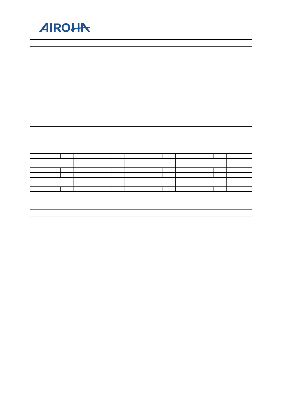
MT2523 Series Reference Manual
© 2015 - 2018 Airoha Technology Corp.
Page 492 of 692
This document contains information that is proprietary to Airoha Technology Corp. (“Airoha”) and/or its licensor(s).
Any unauthorized use, reproduction or disclosure of this document in whole or in part is strictly prohibited.
Bit(s)
Mnemonic
Name
Description
23:22
GPIO43
GPIO43_DRV
GPIO43 driving control
21:20
GPIO42
GPIO42_DRV
GPIO42 driving control
19:18
GPIO41
GPIO41_DRV
GPIO41 driving control
17:16
GPIO40
GPIO40_DRV
GPIO40 driving control
15:14
GPIO39
GPIO39_DRV
GPIO39 driving control
13:12
GPIO38
GPIO38_DRV
GPIO38 driving control
11:10
GPIO37
GPIO37_DRV
GPIO37 driving control
9:8
GPIO36
GPIO36_DRV
GPIO36 driving control
7:6
GPIO35
GPIO35_DRV
GPIO35 driving control
5:4
GPIO34
GPIO34_DRV
GPIO34 driving control
3:2
GPIO33
GPIO33_DRV
GPIO33 driving control
1:0
GPIO32
GPIO32_DRV
GPIO32 driving control
A2020824
GPIO_DRV2_S
ET
GPIO DRV Control
00000000
Bit
31
30
29
28
27
26
25
24
23
22
21
20
19
18
17
16
Name
GPIO47
GPIO46
GPIO45
GPIO44
GPIO43
GPIO42
GPIO41
GPIO40
Type
WO
WO
WO
WO
WO
WO
WO
WO
Reset
0
0
0
0
0
0
0
0
0
0
0
0
0
0
0
0
Bit
15
14
13
12
11
10
9
8
7
6
5
4
3
2
1
0
Name
GPIO39
GPIO38
GPIO37
GPIO36
GPIO35
GPIO34
GPIO33
GPIO32
Type
WO
WO
WO
WO
WO
WO
WO
WO
Reset
0
0
0
0
0
0
0
0
0
0
0
0
0
0
0
0
Overview
For bitwise access of GPIO_DRV2
Bit(s)
Mnemonic
Name
Description
31:30
GPIO47
GPIO47_DRV
Bitwise SET operation of GPIO47_DRV
0: Keep
1: SET bits
29:28
GPIO46
GPIO46_DRV
Bitwise SET operation of GPIO46_DRV
0: Keep
1: SET bits
27:26
GPIO45
GPIO45_DRV
Bitwise SET operation of GPIO45_DRV
0: Keep
1: SET bits
25:24
GPIO44
GPIO44_DRV
Bitwise SET operation of GPIO44_DRV
0: Keep
1: SET bits
23:22
GPIO43
GPIO43_DRV
Bitwise SET operation of GPIO43_DRV
0: Keep
1: SET bits
21:20
GPIO42
GPIO42_DRV
Bitwise SET operation of GPIO42_DRV
0: Keep
1: SET bits
19:18
GPIO41
GPIO41_DRV
Bitwise SET operation of GPIO41_DRV
0: Keep
1: SET bits
17:16
GPIO40
GPIO40_DRV
Bitwise SET operation of GPIO40_DRV
0: Keep
1: SET bits

MT2523 Series Reference Manual
© 2015 - 2018 Airoha Technology Corp.
Page 493 of 692
This document contains information that is proprietary to Airoha Technology Corp. (“Airoha”) and/or its licensor(s).
Any unauthorized use, reproduction or disclosure of this document in whole or in part is strictly prohibited.
Bit(s)
Mnemonic
Name
Description
15:14
GPIO39
GPIO39_DRV
Bitwise SET operation of GPIO39_DRV
0: Keep
1: SET bits
13:12
GPIO38
GPIO38_DRV
Bitwise SET operation of GPIO38_DRV
0: Keep
1: SET bits
11:10
GPIO37
GPIO37_DRV
Bitwise SET operation of GPIO37_DRV
0: Keep
1: SET bits
9:8
GPIO36
GPIO36_DRV
Bitwise SET operation of GPIO36_DRV
0: Keep
1: SET bits
7:6
GPIO35
GPIO35_DRV
Bitwise SET operation of GPIO35_DRV
0: Keep
1: SET bits
5:4
GPIO34
GPIO34_DRV
Bitwise SET operation of GPIO34_DRV
0: Keep
1: SET bits
3:2
GPIO33
GPIO33_DRV
Bitwise SET operation of GPIO33_DRV
0: Keep
1: SET bits
1:0
GPIO32
GPIO32_DRV
Bitwise SET operation of GPIO32_DRV
0: Keep
1: SET bits
A2020828
GPIO_DRV2_C
LR
GPIO DRV Control
00000000
Bit
31
30
29
28
27
26
25
24
23
22
21
20
19
18
17
16
Name
GPIO47
GPIO46
GPIO45
GPIO44
GPIO43
GPIO42
GPIO41
GPIO40
Type
WO
WO
WO
WO
WO
WO
WO
WO
Reset
0
0
0
0
0
0
0
0
0
0
0
0
0
0
0
0
Bit
15
14
13
12
11
10
9
8
7
6
5
4
3
2
1
0
Name
GPIO39
GPIO38
GPIO37
GPIO36
GPIO35
GPIO34
GPIO33
GPIO32
Type
WO
WO
WO
WO
WO
WO
WO
WO
Reset
0
0
0
0
0
0
0
0
0
0
0
0
0
0
0
0
Overview
For bitwise access of GPIO_DRV2
Bit(s)
Mnemonic
Name
Description
31:30
GPIO47
GPIO47_DRV
Bitwise CLR operation of GPIO47_DRV
0: Keep
1: CLR bits
29:28
GPIO46
GPIO46_DRV
Bitwise CLR operation of GPIO46_DRV
0: Keep
1: CLR bits
27:26
GPIO45
GPIO45_DRV
Bitwise CLR operation of GPIO45_DRV
0: Keep
1: CLR bits
25:24
GPIO44
GPIO44_DRV
Bitwise CLR operation of GPIO44_DRV
0: Keep
1: CLR bits
23:22
GPIO43
GPIO43_DRV
Bitwise CLR operation of GPIO43_DRV
0: Keep
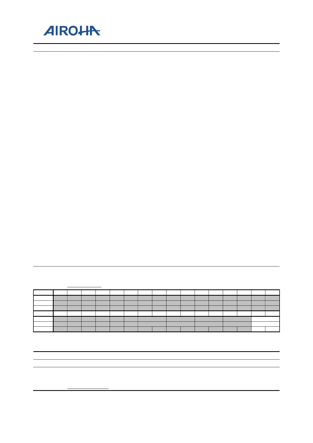
MT2523 Series Reference Manual
© 2015 - 2018 Airoha Technology Corp.
Page 494 of 692
This document contains information that is proprietary to Airoha Technology Corp. (“Airoha”) and/or its licensor(s).
Any unauthorized use, reproduction or disclosure of this document in whole or in part is strictly prohibited.
Bit(s)
Mnemonic
Name
Description
1: CLR bits
21:20
GPIO42
GPIO42_DRV
Bitwise CLR operation of GPIO42_DRV
0: Keep
1: CLR bits
19:18
GPIO41
GPIO41_DRV
Bitwise CLR operation of GPIO41_DRV
0: Keep
1: CLR bits
17:16
GPIO40
GPIO40_DRV
Bitwise CLR operation of GPIO40_DRV
0: Keep
1: CLR bits
15:14
GPIO39
GPIO39_DRV
Bitwise CLR operation of GPIO39_DRV
0: Keep
1: CLR bits
13:12
GPIO38
GPIO38_DRV
Bitwise CLR operation of GPIO38_DRV
0: Keep
1: CLR bits
11:10
GPIO37
GPIO37_DRV
Bitwise CLR operation of GPIO37_DRV
0: Keep
1: CLR bits
9:8
GPIO36
GPIO36_DRV
Bitwise CLR operation of GPIO36_DRV
0: Keep
1: CLR bits
7:6
GPIO35
GPIO35_DRV
Bitwise CLR operation of GPIO35_DRV
0: Keep
1: CLR bits
5:4
GPIO34
GPIO34_DRV
Bitwise CLR operation of GPIO34_DRV
0: Keep
1: CLR bits
3:2
GPIO33
GPIO33_DRV
Bitwise CLR operation of GPIO33_DRV
0: Keep
1: CLR bits
1:0
GPIO32
GPIO32_DRV
Bitwise CLR operation of GPIO32_DRV
0: Keep
1: CLR bits
A2020830
GPIO_DRV3
GPIO DRV Control
00000000
Bit
31
30
29
28
27
26
25
24
23
22
21
20
19
18
17
16
Name
Type
Reset
Bit
15
14
13
12
11
10
9
8
7
6
5
4
3
2
1
0
Name
GPIO48
Type
RW
Reset
0
0
Overview
Configures GPIO driving control
Bit(s)
Mnemonic
Name
Description
1:0
GPIO48
GPIO48_DRV
GPIO48 driving control
A2020834
GPIO_DRV3_S
GPIO DRV Control
00000000
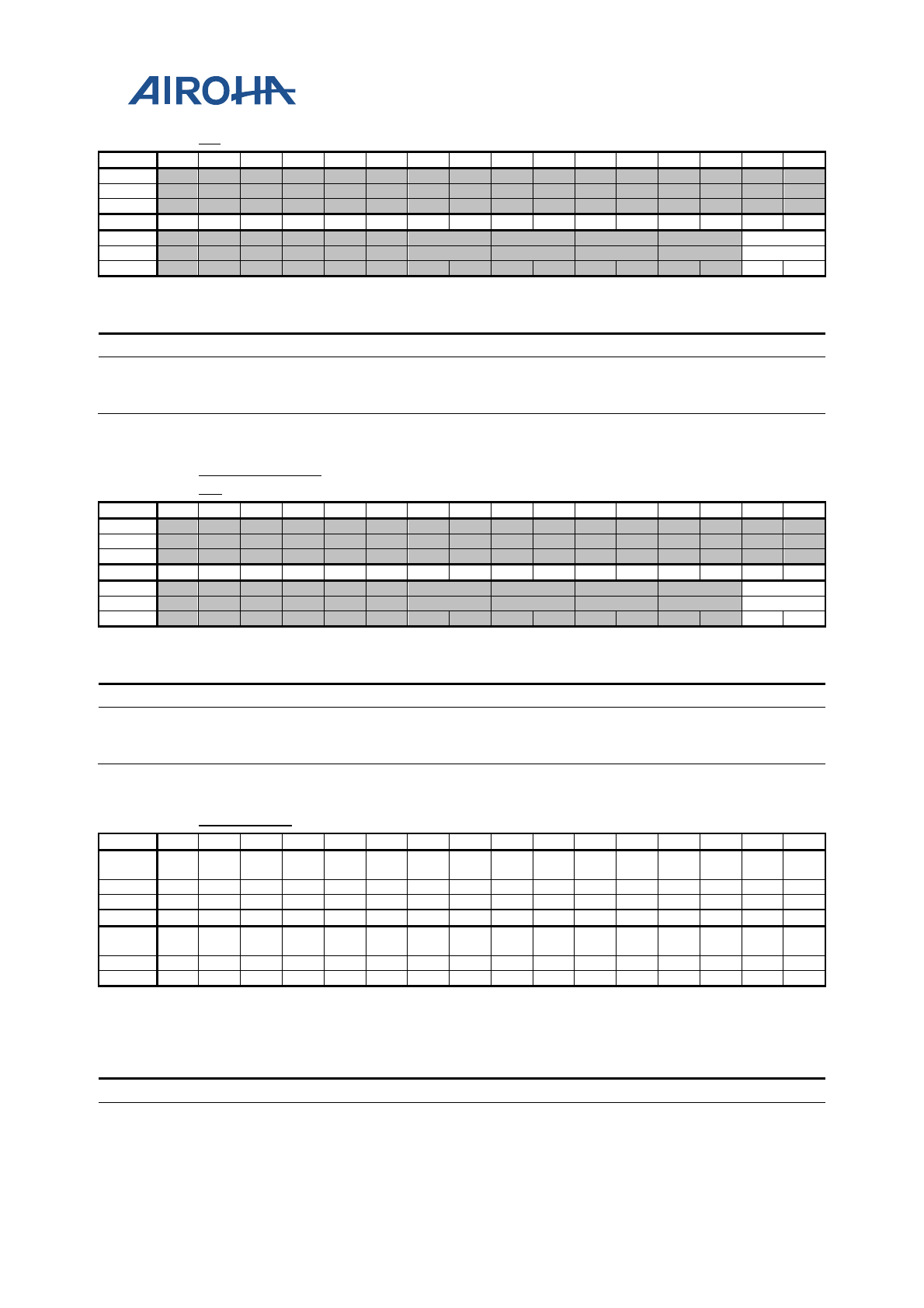
MT2523 Series Reference Manual
© 2015 - 2018 Airoha Technology Corp.
Page 495 of 692
This document contains information that is proprietary to Airoha Technology Corp. (“Airoha”) and/or its licensor(s).
Any unauthorized use, reproduction or disclosure of this document in whole or in part is strictly prohibited.
ET
Bit
31
30
29
28
27
26
25
24
23
22
21
20
19
18
17
16
Name
Type
Reset
Bit
15
14
13
12
11
10
9
8
7
6
5
4
3
2
1
0
Name
GPIO48
Type
WO
Reset
0
0
Overview
For bitwise access of GPIO_DRV3
Bit(s)
Mnemonic
Name
Description
1:0
GPIO48
GPIO48_DRV
Bitwise SET operation of GPIO48_DRV
0: Keep
1: SET bits
A2020838
GPIO_DRV3_C
LR
GPIO DRV Control
00000000
Bit
31
30
29
28
27
26
25
24
23
22
21
20
19
18
17
16
Name
Type
Reset
Bit
15
14
13
12
11
10
9
8
7
6
5
4
3
2
1
0
Name
GPIO48
Type
WO
Reset
0
0
Overview
For bitwise access of GPIO_DRV3
Bit(s)
Mnemonic
Name
Description
1:0
GPIO48
GPIO48_DRV
Bitwise CLR operation of GPIO48_DRV
0: Keep
1: CLR bits
A2020900
GPIO_IES0
GPIO IES Control
FFFFFFFF
Bit
31
30
29
28
27
26
25
24
23
22
21
20
19
18
17
16
Name
GPIO
31
GPIO
30
GPIO
29
GPIO
28
GPIO
27
GPIO
26
GPIO
25
GPIO
24
GPIO
23
GPIO
22
GPIO
21
GPIO
20
GPIO1
9
GPIO1
8
GPIO1
7
GPIO
16
Type
RW
RW
RW
RW
RW
RW
RW
RW
RW
RW
RW
RW
RW
RW
RW
RW
Reset
1
1
1
1
1
1
1
1
1
1
1
1
1
1
1
1
Bit
15
14
13
12
11
10
9
8
7
6
5
4
3
2
1
0
Name
GPIO
15
GPIO1
4
GPIO1
3
GPIO1
2
GPIO1
1
GPIO1
0
GPIO
9
GPIO
8
GPIO
7
GPIO
6
GPIO
5
GPIO
4
GPIO
3
GPIO
2
GPIO1
GPIO
0
Type
RW
RW
RW
RW
RW
RW
RW
RW
RW
RW
RW
RW
RW
RW
RW
RW
Reset
1
1
1
1
1
1
1
1
1
1
1
1
1
1
1
1
Overview
Configures GPIO input enabling control
Note that the GPIO_DIN value is meaningless once GPIO_IES is enabled.
Bit(s)
Mnemonic
Name
Description
31
GPIO31
GPIO31_IES
Input buffer for GPIO31_IES
0: Disable
1: Enable

MT2523 Series Reference Manual
© 2015 - 2018 Airoha Technology Corp.
Page 496 of 692
This document contains information that is proprietary to Airoha Technology Corp. (“Airoha”) and/or its licensor(s).
Any unauthorized use, reproduction or disclosure of this document in whole or in part is strictly prohibited.
Bit(s)
Mnemonic
Name
Description
30
GPIO30
GPIO30_IES
Input buffer for GPIO30_IES
0: Disable
1: Enable
29
GPIO29
GPIO29_IES
Input buffer for GPIO29_IES
0: Disable
1: Enable
28
GPIO28
GPIO28_IES
Input buffer for GPIO28_IES
0: Disable
1: Enable
27
GPIO27
GPIO27_IES
Input buffer for GPIO27_IES
0: Disable
1: Enable
26
GPIO26
GPIO26_IES
Input buffer for GPIO26_IES
0: Disable
1: Enable
25
GPIO25
GPIO25_IES
Input buffer for GPIO25_IES
0: Disable
1: Enable
24
GPIO24
GPIO24_IES
Input buffer for GPIO24_IES
0: Disable
1: Enable
23
GPIO23
GPIO23_IES
Input buffer for GPIO23_IES
0: Disable
1: Enable
22
GPIO22
GPIO22_IES
Input buffer for GPIO22_IES
0: Disable
1: Enable
21
GPIO21
GPIO21_IES
Input buffer for GPIO21_IES
0: Disable
1: Enable
20
GPIO20
GPIO20_IES
Input buffer for GPIO20_IES
0: Disable
1: Enable
19
GPIO19
GPIO19_IES
Input buffer for GPIO19_IES
0: Disable
1: Enable
18
GPIO18
GPIO18_IES
Input buffer for GPIO18_IES
0: Disable
1: Enable
17
GPIO17
GPIO17_IES
Input buffer for GPIO17_IES
0: Disable
1: Enable
16
GPIO16
GPIO16_IES
Input buffer for GPIO16_IES
0: Disable
1: Enable
15
GPIO15
GPIO15_IES
Input buffer for GPIO15_IES
0: Disable
1: Enable
14
GPIO14
GPIO14_IES
Input buffer for GPIO14_IES
0: Disable
1: Enable
13
GPIO13
GPIO13_IES
Input buffer for GPIO13_IES
0: Disable
1: Enable
MT2523 Series Reference Manual
© 2015 - 2018 Airoha Technology Corp.
Page 497 of 692
This document contains information that is proprietary to Airoha Technology Corp. (“Airoha”) and/or its licensor(s).
Any unauthorized use, reproduction or disclosure of this document in whole or in part is strictly prohibited.
Bit(s)
Mnemonic
Name
Description
12
GPIO12
GPIO12_IES
Input buffer for GPIO12_IES
0: Disable
1: Enable
11
GPIO11
GPIO11_IES
Input buffer for GPIO11_IES
0: Disable
1: Enable
10
GPIO10
GPIO10_IES
Input buffer for GPIO10_IES
0: Disable
1: Enable
9
GPIO9
GPIO9_IES
Input buffer for GPIO9_IES
0: Disable
1: Enable
8
GPIO8
GPIO8_IES
Input buffer for GPIO8_IES
0: Disable
1: Enable
7
GPIO7
GPIO7_IES
Input buffer for GPIO7_IES
0: Disable
1: Enable
6
GPIO6
GPIO6_IES
Input buffer for GPIO6_IES
0: Disable
1: Enable
5
GPIO5
GPIO5_IES
Input buffer for GPIO5_IES
0: Disable
1: Enable
4
GPIO4
GPIO4_IES
Input buffer for GPIO4_IES
0: Disable
1: Enable
3
GPIO3
GPIO3_IES
Input buffer for GPIO3_IES
0: Disable
1: Enable
2
GPIO2
GPIO2_IES
Input buffer for GPIO2_IES
0: Disable
1: Enable
1
GPIO1
GPIO1_IES
Input buffer for GPIO1_IES
0: Disable
1: Enable
0
GPIO0
GPIO0_IES
Input buffer for GPIO0_IES
0: Disable
1: Enable
A2020904
GPIO_IES0_SE
T
GPIO IES Control
00000000
Bit
31
30
29
28
27
26
25
24
23
22
21
20
19
18
17
16
Name
GPIO
31
GPIO
30
GPIO
29
GPIO
28
GPIO
27
GPIO
26
GPIO
25
GPIO
24
GPIO
23
GPIO
22
GPIO
21
GPIO
20
GPIO1
9
GPIO1
8
GPIO1
7
GPIO
16
Type
WO
WO
WO
WO
WO
WO
WO
WO
WO
WO
WO
WO
WO
WO
WO
WO
Reset
0
0
0
0
0
0
0
0
0
0
0
0
0
0
0
0
Bit
15
14
13
12
11
10
9
8
7
6
5
4
3
2
1
0
Name
GPIO
15
GPIO1
4
GPIO1
3
GPIO1
2
GPIO1
1
GPIO1
0
GPIO
9
GPIO
8
GPIO
7
GPIO
6
GPIO
5
GPIO
4
GPIO
3
GPIO
2
GPIO1
GPIO
0
Type
WO
WO
WO
WO
WO
WO
WO
WO
WO
WO
WO
WO
WO
WO
WO
WO
Reset
0
0
0
0
0
0
0
0
0
0
0
0
0
0
0
0
Overview
For bitwise access of GPIO_IES0

MT2523 Series Reference Manual
© 2015 - 2018 Airoha Technology Corp.
Page 498 of 692
This document contains information that is proprietary to Airoha Technology Corp. (“Airoha”) and/or its licensor(s).
Any unauthorized use, reproduction or disclosure of this document in whole or in part is strictly prohibited.
Note that the GPIO_DIN value is meaningless once is GPIO_IES enabled.
Bit(s)
Mnemonic
Name
Description
31
GPIO31
GPIO31_IES
Bitwise SET operation of GPIO31 input buffer
0: Keep
1: SET bits
30
GPIO30
GPIO30_IES
Bitwise SET operation of GPIO30 input buffer
0: Keep
1: SET bits
29
GPIO29
GPIO29_IES
Bitwise SET operation of GPIO29 input buffer
0: Keep
1: SET bits
28
GPIO28
GPIO28_IES
Bitwise SET operation of GPIO28 input buffer
0: Keep
1: SET bits
27
GPIO27
GPIO27_IES
Bitwise SET operation of GPIO27 input buffer
0: Keep
1: SET bits
26
GPIO26
GPIO26_IES
Bitwise SET operation of GPIO26 input buffer
0: Keep
1: SET bits
25
GPIO25
GPIO25_IES
Bitwise SET operation of GPIO25 input buffer
0: Keep
1: SET bits
24
GPIO24
GPIO24_IES
Bitwise SET operation of GPIO24 input buffer
0: Keep
1: SET bits
23
GPIO23
GPIO23_IES
Bitwise SET operation of GPIO23 input buffer
0: Keep
1: SET bits
22
GPIO22
GPIO22_IES
Bitwise SET operation of GPIO22 input buffer
0: Keep
1: SET bits
21
GPIO21
GPIO21_IES
Bitwise SET operation of GPIO21 input buffer
0: Keep
1: SET bits
20
GPIO20
GPIO20_IES
Bitwise SET operation of GPIO20 input buffer
0: Keep
1: SET bits
19
GPIO19
GPIO19_IES
Bitwise SET operation of GPIO19 input buffer
0: Keep
1: SET bits
18
GPIO18
GPIO18_IES
Bitwise SET operation of GPIO18 input buffer
0: Keep
1: SET bits
17
GPIO17
GPIO17_IES
Bitwise SET operation of GPIO17 input buffer
0: Keep
1: SET bits
16
GPIO16
GPIO16_IES
Bitwise SET operation of GPIO16 input buffer
0: Keep
1: SET bits
15
GPIO15
GPIO15_IES
Bitwise SET operation of GPIO15 input buffer
0: Keep

MT2523 Series Reference Manual
© 2015 - 2018 Airoha Technology Corp.
Page 499 of 692
This document contains information that is proprietary to Airoha Technology Corp. (“Airoha”) and/or its licensor(s).
Any unauthorized use, reproduction or disclosure of this document in whole or in part is strictly prohibited.
Bit(s)
Mnemonic
Name
Description
1: SET bits
14
GPIO14
GPIO14_IES
Bitwise SET operation of GPIO14 input buffer
0: Keep
1: SET bits
13
GPIO13
GPIO13_IES
Bitwise SET operation of GPIO13 input buffer
0: Keep
1: SET bits
12
GPIO12
GPIO12_IES
Bitwise SET operation of GPIO12 input buffer
0: Keep
1: SET bits
11
GPIO11
GPIO11_IES
Bitwise SET operation of GPIO11 input buffer
0: Keep
1: SET bits
10
GPIO10
GPIO10_IES
Bitwise SET operation of GPIO10 input buffer
0: Keep
1: SET bits
9
GPIO9
GPIO9_IES
Bitwise SET operation of GPIO9 input buffer
0: Keep
1: SET bits
8
GPIO8
GPIO8_IES
Bitwise SET operation of GPIO8 input buffer
0: Keep
1: SET bits
7
GPIO7
GPIO7_IES
Bitwise SET operation of GPIO7 input buffer
0: Keep
1: SET bits
6
GPIO6
GPIO6_IES
Bitwise SET operation of GPIO6 input buffer
0: Keep
1: SET bits
5
GPIO5
GPIO5_IES
Bitwise SET operation of GPIO5 input buffer
0: Keep
1: SET bits
4
GPIO4
GPIO4_IES
Bitwise SET operation of GPIO4 input buffer
0: Keep
1: SET bits
3
GPIO3
GPIO3_IES
Bitwise SET operation of GPIO3 input buffer
0: Keep
1: SET bits
2
GPIO2
GPIO2_IES
Bitwise SET operation of GPIO2 input buffer
0: Keep
1: SET bits
1
GPIO1
GPIO1_IES
Bitwise SET operation of GPIO1 input buffer
0: Keep
1: SET bits
0
GPIO0
GPIO0_IES
Bitwise SET operation of GPIO0 input buffer
0: Keep
1: SET bits
A2020908
GPIO_IES0_C
LR
GPIO IES Control
00000000
Bit
31
30
29
28
27
26
25
24
23
22
21
20
19
18
17
16
Name
GPIO
31
GPIO
30
GPIO
29
GPIO
28
GPIO
27
GPIO
26
GPIO
25
GPIO
24
GPIO
23
GPIO
22
GPIO
21
GPIO
20
GPIO1
9
GPIO1
8
GPIO1
7
GPIO
16
Type
WO
WO
WO
WO
WO
WO
WO
WO
WO
WO
WO
WO
WO
WO
WO
WO

MT2523 Series Reference Manual
© 2015 - 2018 Airoha Technology Corp.
Page 500 of 692
This document contains information that is proprietary to Airoha Technology Corp. (“Airoha”) and/or its licensor(s).
Any unauthorized use, reproduction or disclosure of this document in whole or in part is strictly prohibited.
Reset
0
0
0
0
0
0
0
0
0
0
0
0
0
0
0
0
Bit
15
14
13
12
11
10
9
8
7
6
5
4
3
2
1
0
Name
GPIO
15
GPIO1
4
GPIO1
3
GPIO1
2
GPIO1
1
GPIO1
0
GPIO
9
GPIO
8
GPIO
7
GPIO
6
GPIO
5
GPIO
4
GPIO
3
GPIO
2
GPIO1
GPIO
0
Type
WO
WO
WO
WO
WO
WO
WO
WO
WO
WO
WO
WO
WO
WO
WO
WO
Reset
0
0
0
0
0
0
0
0
0
0
0
0
0
0
0
0
Overview
For bitwise access of GPIO_IES0
Note that the GPIO_DIN value is meaningless once GPIO_IES is enabled.
Bit(s)
Mnemonic
Name
Description
31
GPIO31
GPIO31_IES
Bitwise CLR operation of GPIO31 input buffer
0: Keep
1: CLR bits
30
GPIO30
GPIO30_IES
Bitwise CLR operation of GPIO30 input buffer
0: Keep
1: CLR bits
29
GPIO29
GPIO29_IES
Bitwise CLR operation of GPIO29 input buffer
0: Keep
1: CLR bits
28
GPIO28
GPIO28_IES
Bitwise CLR operation of GPIO28 input buffer
0: Keep
1: CLR bits
27
GPIO27
GPIO27_IES
Bitwise CLR operation of GPIO27 input buffer
0: Keep
1: CLR bits
26
GPIO26
GPIO26_IES
Bitwise CLR operation of GPIO26 input buffer
0: Keep
1: CLR bits
25
GPIO25
GPIO25_IES
Bitwise CLR operation of GPIO25 input buffer
0: Keep
1: CLR bits
24
GPIO24
GPIO24_IES
Bitwise CLR operation of GPIO24 input buffer
0: Keep
1: CLR bits
23
GPIO23
GPIO23_IES
Bitwise CLR operation of GPIO23 input buffer
0: Keep
1: CLR bits
22
GPIO22
GPIO22_IES
Bitwise CLR operation of GPIO22 input buffer
0: Keep
1: CLR bits
21
GPIO21
GPIO21_IES
Bitwise CLR operation of GPIO21 input buffer
0: Keep
1: CLR bits
20
GPIO20
GPIO20_IES
Bitwise CLR operation of GPIO20 input buffer
0: Keep
1: CLR bits
19
GPIO19
GPIO19_IES
Bitwise CLR operation of GPIO19 input buffer
0: Keep
1: CLR bits
18
GPIO18
GPIO18_IES
Bitwise CLR operation of GPIO18 input buffer
0: Keep
1: CLR bits
17
GPIO17
GPIO17_IES
Bitwise CLR operation of GPIO17 input buffer

MT2523 Series Reference Manual
© 2015 - 2018 Airoha Technology Corp.
Page 501 of 692
This document contains information that is proprietary to Airoha Technology Corp. (“Airoha”) and/or its licensor(s).
Any unauthorized use, reproduction or disclosure of this document in whole or in part is strictly prohibited.
Bit(s)
Mnemonic
Name
Description
0: Keep
1: CLR bits
16
GPIO16
GPIO16_IES
Bitwise CLR operation of GPIO16 input buffer
0: Keep
1: CLR bits
15
GPIO15
GPIO15_IES
Bitwise CLR operation of GPIO15 input buffer
0: Keep
1: CLR bits
14
GPIO14
GPIO14_IES
Bitwise CLR operation of GPIO14 input buffer
0: Keep
1: CLR bits
13
GPIO13
GPIO13_IES
Bitwise CLR operation of GPIO13 input buffer
0: Keep
1: CLR bits
12
GPIO12
GPIO12_IES
Bitwise CLR operation of GPIO12 input buffer
0: Keep
1: CLR bits
11
GPIO11
GPIO11_IES
Bitwise CLR operation of GPIO11 input buffer
0: Keep
1: CLR bits
10
GPIO10
GPIO10_IES
Bitwise CLR operation of GPIO10 input buffer
0: Keep
1: CLR bits
9
GPIO9
GPIO9_IES
Bitwise CLR operation of GPIO9 input buffer
0: Keep
1: CLR bits
8
GPIO8
GPIO8_IES
Bitwise CLR operation of GPIO8 input buffer
0: Keep
1: CLR bits
7
GPIO7
GPIO7_IES
Bitwise CLR operation of GPIO7 input buffer
0: Keep
1: CLR bits
6
GPIO6
GPIO6_IES
Bitwise CLR operation of GPIO6 input buffer
0: Keep
1: CLR bits
5
GPIO5
GPIO5_IES
Bitwise CLR operation of GPIO5 input buffer
0: Keep
1: CLR bits
4
GPIO4
GPIO4_IES
Bitwise CLR operation of GPIO4 input buffer
0: Keep
1: CLR bits
3
GPIO3
GPIO3_IES
Bitwise CLR operation of GPIO3 input buffer
0: Keep
1: CLR bits
2
GPIO2
GPIO2_IES
Bitwise CLR operation of GPIO2 input buffer
0: Keep
1: CLR bits
1
GPIO1
GPIO1_IES
Bitwise CLR operation of GPIO1 input buffer
0: Keep
1: CLR bits
0
GPIO0
GPIO0_IES
Bitwise CLR operation of GPIO0 input buffer
0: Keep
1: CLR bits

MT2523 Series Reference Manual
© 2015 - 2018 Airoha Technology Corp.
Page 502 of 692
This document contains information that is proprietary to Airoha Technology Corp. (“Airoha”) and/or its licensor(s).
Any unauthorized use, reproduction or disclosure of this document in whole or in part is strictly prohibited.
A2020910
GPIO_IES1
GPIO IES Control
0007FFFF
Bit
31
30
29
28
27
26
25
24
23
22
21
20
19
18
17
16
Name
GPIO
48
Type
RW
Reset
1
Bit
15
14
13
12
11
10
9
8
7
6
5
4
3
2
1
0
Name
GPIO
47
GPIO
46
GPIO
45
GPIO
44
GPIO
43
GPIO
42
GPIO
41
GPIO
40
GPIO
39
GPIO
38
GPIO
37
GPIO
36
GPIO
35
GPIO
34
GPIO
33
GPIO
32
Type
RW
RW
RW
RW
RW
RW
RW
RW
RW
RW
RW
RW
RW
RW
RW
RW
Reset
1
1
1
1
1
1
1
1
1
1
1
1
1
1
1
1
Overview
Configures GPIO input enabling control
Note that the GPIO_DIN value is meaningless once GPIO_IES is enabled.
Bit(s)
Mnemonic
Name
Description
16
GPIO48
GPIO48_IES
Input buffer for GPIO48_IES
0: Disable
1: Enable
15
GPIO47
GPIO47_IES
Input buffer for GPIO47_IES
0: Disable
1: Enable
14
GPIO46
GPIO46_IES
Input buffer for GPIO46_IES
0: Disable
1: Enable
13
GPIO45
GPIO45_IES
Input buffer for GPIO45_IES
0: Disable
1: Enable
12
GPIO44
GPIO44_IES
Input buffer for GPIO44_IES
0: Disable
1: Enable
11
GPIO43
GPIO43_IES
Input buffer for GPIO43_IES
0: Disable
1: Enable
10
GPIO42
GPIO42_IES
Input buffer for GPIO42_IES
0: Disable
1: Enable
9
GPIO41
GPIO41_IES
Input buffer for GPIO41_IES
0: Disable
1: Enable
8
GPIO40
GPIO40_IES
Input buffer for GPIO40_IES
0: Disable
1: Enable
7
GPIO39
GPIO39_IES
Input buffer for GPIO39_IES
0: Disable
1: Enable
6
GPIO38
GPIO38_IES
Input buffer for GPIO38_IES
0: Disable
1: Enable
5
GPIO37
GPIO37_IES
Input buffer for GPIO37_IES
0: Disable
1: Enable
4
GPIO36
GPIO36_IES
Input buffer for GPIO36_IES

MT2523 Series Reference Manual
© 2015 - 2018 Airoha Technology Corp.
Page 503 of 692
This document contains information that is proprietary to Airoha Technology Corp. (“Airoha”) and/or its licensor(s).
Any unauthorized use, reproduction or disclosure of this document in whole or in part is strictly prohibited.
Bit(s)
Mnemonic
Name
Description
0: Disable
1: Enable
3
GPIO35
GPIO35_IES
Input buffer for GPIO35_IES
0: Disable
1: Enable
2
GPIO34
GPIO34_IES
Input buffer for GPIO34_IES
0: Disable
1: Enable
1
GPIO33
GPIO33_IES
Input buffer for GPIO33_IES
0: Disable
1: Enable
0
GPIO32
GPIO32_IES
Input buffer for GPIO32_IES
0: Disable
1: Enable
A2020914
GPIO_IES1_SE
T
GPIO IES Control
00000000
Bit
31
30
29
28
27
26
25
24
23
22
21
20
19
18
17
16
Name
GPIO
48
Type
WO
Reset
0
Bit
15
14
13
12
11
10
9
8
7
6
5
4
3
2
1
0
Name
GPIO
47
GPIO
46
GPIO
45
GPIO
44
GPIO
43
GPIO
42
GPIO
41
GPIO
40
GPIO
39
GPIO
38
GPIO
37
GPIO
36
GPIO
35
GPIO
34
GPIO
33
GPIO
32
Type
WO
WO
WO
WO
WO
WO
WO
WO
WO
WO
WO
WO
WO
WO
WO
WO
Reset
0
0
0
0
0
0
0
0
0
0
0
0
0
0
0
0
Overview
For bitwise access of GPIO_IES1
Note that the GPIO_DIN value is meaningless once GPIO_IES is enabled.
Bit(s)
Mnemonic
Name
Description
16
GPIO48
GPIO48_IES
Bitwise SET operation of GPIO48 input buffer
0: Keep
1: SET bits
15
GPIO47
GPIO47_IES
Bitwise SET operation of GPIO47 input buffer
0: Keep
1: SET bits
14
GPIO46
GPIO46_IES
Bitwise SET operation of GPIO46 input buffer
0: Keep
1: SET bits
13
GPIO45
GPIO45_IES
Bitwise SET operation of GPIO45 input buffer
0: Keep
1: SET bits
12
GPIO44
GPIO44_IES
Bitwise SET operation of GPIO44 input buffer
0: Keep
1: SET bits
11
GPIO43
GPIO43_IES
Bitwise SET operation of GPIO43 input buffer
0: Keep
1: SET bits
10
GPIO42
GPIO42_IES
Bitwise SET operation of GPIO42 input buffer
0: Keep
1: SET bits
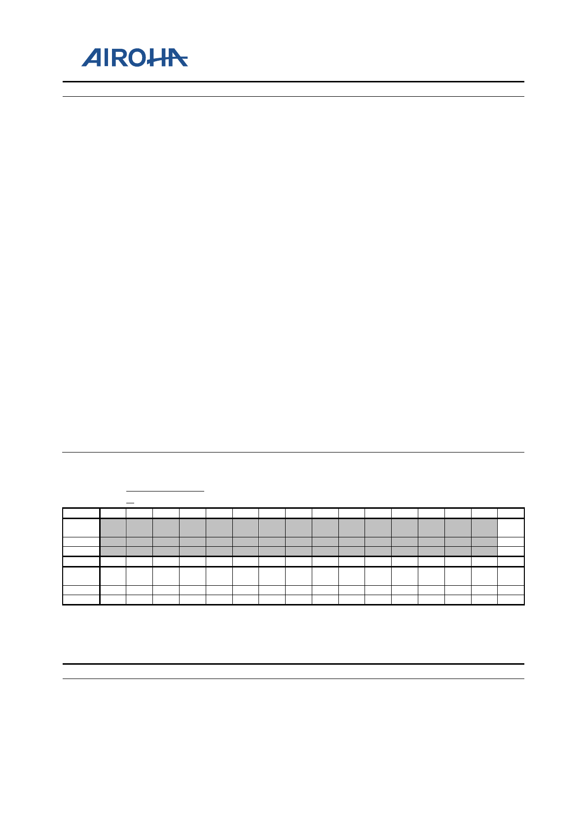
MT2523 Series Reference Manual
© 2015 - 2018 Airoha Technology Corp.
Page 504 of 692
This document contains information that is proprietary to Airoha Technology Corp. (“Airoha”) and/or its licensor(s).
Any unauthorized use, reproduction or disclosure of this document in whole or in part is strictly prohibited.
Bit(s)
Mnemonic
Name
Description
9
GPIO41
GPIO41_IES
Bitwise SET operation of GPIO41 input buffer
0: Keep
1: SET bits
8
GPIO40
GPIO40_IES
Bitwise SET operation of GPIO40 input buffer
0: Keep
1: SET bits
7
GPIO39
GPIO39_IES
Bitwise SET operation of GPIO39 input buffer
0: Keep
1: SET bits
6
GPIO38
GPIO38_IES
Bitwise SET operation of GPIO38 input buffer
0: Keep
1: SET bits
5
GPIO37
GPIO37_IES
Bitwise SET operation of GPIO37 input buffer
0: Keep
1: SET bits
4
GPIO36
GPIO36_IES
Bitwise SET operation of GPIO36 input buffer
0: Keep
1: SET bits
3
GPIO35
GPIO35_IES
Bitwise SET operation of GPIO35 input buffer
0: Keep
1: SET bits
2
GPIO34
GPIO34_IES
Bitwise SET operation of GPIO34 input buffer
0: Keep
1: SET bits
1
GPIO33
GPIO33_IES
Bitwise SET operation of GPIO33 input buffer
0: Keep
1: SET bits
0
GPIO32
GPIO32_IES
Bitwise SET operation of GPIO32 input buffer
0: Keep
1: SET bits
A2020918
GPIO_IES1_CL
R
GPIO IES Control
00000000
Bit
31
30
29
28
27
26
25
24
23
22
21
20
19
18
17
16
Name
GPIO
48
Type
WO
Reset
0
Bit
15
14
13
12
11
10
9
8
7
6
5
4
3
2
1
0
Name
GPIO
47
GPIO
46
GPIO
45
GPIO
44
GPIO
43
GPIO
42
GPIO
41
GPIO
40
GPIO
39
GPIO
38
GPIO
37
GPIO
36
GPIO
35
GPIO
34
GPIO
33
GPIO
32
Type
WO
WO
WO
WO
WO
WO
WO
WO
WO
WO
WO
WO
WO
WO
WO
WO
Reset
0
0
0
0
0
0
0
0
0
0
0
0
0
0
0
0
Overview
For bitwise access of GPIO_IES1
Note that the GPIO_DIN value is meaningless once GPIO_IES is enabled.
Bit(s)
Mnemonic
Name
Description
16
GPIO48
GPIO48_IES
Bitwise CLR operation of GPIO48 input buffer
0: Keep
1: CLR bits
15
GPIO47
GPIO47_IES
Bitwise CLR operation of GPIO47 input buffer
0: Keep

MT2523 Series Reference Manual
© 2015 - 2018 Airoha Technology Corp.
Page 505 of 692
This document contains information that is proprietary to Airoha Technology Corp. (“Airoha”) and/or its licensor(s).
Any unauthorized use, reproduction or disclosure of this document in whole or in part is strictly prohibited.
Bit(s)
Mnemonic
Name
Description
1: CLR bits
14
GPIO46
GPIO46_IES
Bitwise CLR operation of GPIO46 input buffer
0: Keep
1: CLR bits
13
GPIO45
GPIO45_IES
Bitwise CLR operation of GPIO45 input buffer
0: Keep
1: CLR bits
12
GPIO44
GPIO44_IES
Bitwise CLR operation of GPIO44 input buffer
0: Keep
1: CLR bits
11
GPIO43
GPIO43_IES
Bitwise CLR operation of GPIO43 input buffer
0: Keep
1: CLR bits
10
GPIO42
GPIO42_IES
Bitwise CLR operation of GPIO42 input buffer
0: Keep
1: CLR bits
9
GPIO41
GPIO41_IES
Bitwise CLR operation of GPIO41 input buffer
0: Keep
1: CLR bits
8
GPIO40
GPIO40_IES
Bitwise CLR operation of GPIO40 input buffer
0: Keep
1: CLR bits
7
GPIO39
GPIO39_IES
Bitwise CLR operation of GPIO39 input buffer
0: Keep
1: CLR bits
6
GPIO38
GPIO38_IES
Bitwise CLR operation of GPIO38 input buffer
0: Keep
1: CLR bits
5
GPIO37
GPIO37_IES
Bitwise CLR operation of GPIO37 input buffer
0: Keep
1: CLR bits
4
GPIO36
GPIO36_IES
Bitwise CLR operation of GPIO36 input buffer
0: Keep
1: CLR bits
3
GPIO35
GPIO35_IES
Bitwise CLR operation of GPIO35 input buffer
0: Keep
1: CLR bits
2
GPIO34
GPIO34_IES
Bitwise CLR operation of GPIO34 input buffer
0: Keep
1: CLR bits
1
GPIO33
GPIO33_IES
Bitwise CLR operation of GPIO33 input buffer
0: Keep
1: CLR bits
0
GPIO32
GPIO32_IES
Bitwise CLR operation of GPIO32 input buffer
0: Keep
1: CLR bits
A2020A00
GPIO_PUPD0
GPIO
PUPD Control
F9E0FBF0
Bit
31
30
29
28
27
26
25
24
23
22
21
20
19
18
17
16
Name
GPIO
31
GPIO
30
GPIO
29
GPIO
28
GPIO
27
GPIO
26
GPIO
25
GPIO
24
GPIO
23
GPIO
22
GPIO
21
GPIO
20
GPIO1
9
GPIO1
8
GPIO1
7
GPIO
16
Type
RW
RW
RW
RW
RW
RW
RW
RW
RW
RW
RW
RW
RW
RW
RW
RW
Reset
1
1
1
1
1
0
0
1
1
1
1
0
0
0
0
0

MT2523 Series Reference Manual
© 2015 - 2018 Airoha Technology Corp.
Page 506 of 692
This document contains information that is proprietary to Airoha Technology Corp. (“Airoha”) and/or its licensor(s).
Any unauthorized use, reproduction or disclosure of this document in whole or in part is strictly prohibited.
Bit
15
14
13
12
11
10
9
8
7
6
5
4
3
2
1
0
Name
GPIO
15
GPIO1
4
GPIO1
3
GPIO1
2
GPIO1
1
GPIO
9
GPIO
8
GPIO
7
GPIO
6
GPIO
5
GPIO
4
Type
RW
RW
RW
RW
RW
RW
RW
RW
RW
RW
RW
Reset
1
1
1
1
1
1
1
1
1
1
1
Overview
Configures GPIO PUPD control
Bit(s)
Mnemonic
Name
Description
31
GPIO31
GPIO31_PUPD
PUPD for GPIO31_PUPD
0: Disable
1: Enable
30
GPIO30
GPIO30_PUPD
PUPD for GPIO30_PUPD
0: Disable
1: Enable
29
GPIO29
GPIO29_PUPD
PUPD for GPIO29_PUPD
0: Disable
1: Enable
28
GPIO28
GPIO28_PUPD
PUPD for GPIO28_PUPD
0: Disable
1: Enable
27
GPIO27
GPIO27_PUPD
PUPD for GPIO27_PUPD
0: Disable
1: Enable
26
GPIO26
GPIO26_PUPD
PUPD for GPIO26_PUPD
0: Disable
1: Enable
25
GPIO25
GPIO25_PUPD
PUPD for GPIO25_PUPD
0: Disable
1: Enable
24
GPIO24
GPIO24_PUPD
PUPD for GPIO24_PUPD
0: Disable
1: Enable
23
GPIO23
GPIO23_PUPD
PUPD for GPIO23_PUPD
0: Disable
1: Enable
22
GPIO22
GPIO22_PUPD
PUPD for GPIO22_PUPD
0: Disable
1: Enable
21
GPIO21
GPIO21_PUPD
PUPD for GPIO21_PUPD
0: Disable
1: Enable
20
GPIO20
GPIO20_PUPD
PUPD for GPIO20_PUPD
0: Disable
1: Enable
19
GPIO19
GPIO19_PUPD
PUPD for GPIO19_PUPD
0: Disable
1: Enable
18
GPIO18
GPIO18_PUPD
PUPD for GPIO18_PUPD
0: Disable
1: Enable
17
GPIO17
GPIO17_PUPD
PUPD for GPIO17_PUPD
0: Disable
1: Enable
16
GPIO16
GPIO16_PUPD
PUPD for GPIO16_PUPD
0: Disable

MT2523 Series Reference Manual
© 2015 - 2018 Airoha Technology Corp.
Page 507 of 692
This document contains information that is proprietary to Airoha Technology Corp. (“Airoha”) and/or its licensor(s).
Any unauthorized use, reproduction or disclosure of this document in whole or in part is strictly prohibited.
Bit(s)
Mnemonic
Name
Description
1: Enable
15
GPIO15
GPIO15_PUPD
PUPD for GPIO15_PUPD
0: Disable
1: Enable
14
GPIO14
GPIO14_PUPD
PUPD for GPIO14_PUPD
0: Disable
1: Enable
13
GPIO13
GPIO13_PUPD
PUPD for GPIO13_PUPD
0: Disable
1: Enable
12
GPIO12
GPIO12_PUPD
PUPD for GPIO12_PUPD
0: Disable
1: Enable
11
GPIO11
GPIO11_PUPD
PUPD for GPIO11_PUPD
0: Disable
1: Enable
9
GPIO9
GPIO9_PUPD
PUPD for GPIO9_PUPD
0: Disable
1: Enable
8
GPIO8
GPIO8_PUPD
PUPD for GPIO8_PUPD
0: Disable
1: Enable
7
GPIO7
GPIO7_PUPD
PUPD for GPIO7_PUPD
0: Disable
1: Enable
6
GPIO6
GPIO6_PUPD
PUPD for GPIO6_PUPD
0: Disable
1: Enable
5
GPIO5
GPIO5_PUPD
PUPD for GPIO5_PUPD
0: Disable
1: Enable
4
GPIO4
GPIO4_PUPD
PUPD for GPIO4_PUPD
0: Disable
1: Enable
A2020A04
GPIO_PUPD0_
SET
GPIO PUPD Control
00000000
Bit
31
30
29
28
27
26
25
24
23
22
21
20
19
18
17
16
Name
GPIO
31
GPIO
30
GPIO
29
GPIO
28
GPIO
27
GPIO
26
GPIO
25
GPIO
24
GPIO
23
GPIO
22
GPIO
21
GPIO
20
GPIO1
9
GPIO1
8
GPIO1
7
GPIO
16
Type
WO
WO
WO
WO
WO
WO
WO
WO
WO
WO
WO
WO
WO
WO
WO
WO
Reset
0
0
0
0
0
0
0
0
0
0
0
0
0
0
0
0
Bit
15
14
13
12
11
10
9
8
7
6
5
4
3
2
1
0
Name
GPIO
15
GPIO1
4
GPIO1
3
GPIO1
2
GPIO1
1
GPIO
9
GPIO
8
GPIO
7
GPIO
6
GPIO
5
GPIO
4
Type
WO
WO
WO
WO
WO
WO
WO
WO
WO
WO
WO
Reset
0
0
0
0
0
0
0
0
0
0
0
Overview
For bitwise access of GPIO_PUPD0
Bit(s)
Mnemonic
Name
Description
31
GPIO31
GPIO31_PUPD
Bitwise SET operation of GPIO31 PUPD
0: Keep
1: SET bits

MT2523 Series Reference Manual
© 2015 - 2018 Airoha Technology Corp.
Page 508 of 692
This document contains information that is proprietary to Airoha Technology Corp. (“Airoha”) and/or its licensor(s).
Any unauthorized use, reproduction or disclosure of this document in whole or in part is strictly prohibited.
Bit(s)
Mnemonic
Name
Description
30
GPIO30
GPIO30_PUPD
Bitwise SET operation of GPIO30 PUPD
0: Keep
1: SET bits
29
GPIO29
GPIO29_PUPD
Bitwise SET operation of GPIO29 PUPD
0: Keep
1: SET bits
28
GPIO28
GPIO28_PUPD
Bitwise SET operation of GPIO28 PUPD
0: Keep
1: SET bits
27
GPIO27
GPIO27_PUPD
Bitwise SET operation of GPIO27 PUPD
0: Keep
1: SET bits
26
GPIO26
GPIO26_PUPD
Bitwise SET operation of GPIO26 PUPD
0: Keep
1: SET bits
25
GPIO25
GPIO25_PUPD
Bitwise SET operation of GPIO25 PUPD
0: Keep
1: SET bits
24
GPIO24
GPIO24_PUPD
Bitwise SET operation of GPIO24 PUPD
0: Keep
1: SET bits
23
GPIO23
GPIO23_PUPD
Bitwise SET operation of GPIO23 PUPD
0: Keep
1: SET bits
22
GPIO22
GPIO22_PUPD
Bitwise SET operation of GPIO22 PUPD
0: Keep
1: SET bits
21
GPIO21
GPIO21_PUPD
Bitwise SET operation of GPIO21 PUPD
0: Keep
1: SET bits
20
GPIO20
GPIO20_PUPD
Bitwise SET operation of GPIO20 PUPD
0: Keep
1: SET bits
19
GPIO19
GPIO19_PUPD
Bitwise SET operation of GPIO19 PUPD
0: Keep
1: SET bits
18
GPIO18
GPIO18_PUPD
Bitwise SET operation of GPIO18 PUPD
0: Keep
1: SET bits
17
GPIO17
GPIO17_PUPD
Bitwise SET operation of GPIO17 PUPD
0: Keep
1: SET bits
16
GPIO16
GPIO16_PUPD
Bitwise SET operation of GPIO16 PUPD
0: Keep
1: SET bits
15
GPIO15
GPIO15_PUPD
Bitwise SET operation of GPIO15 PUPD
0: Keep
1: SET bits
14
GPIO14
GPIO14_PUPD
Bitwise SET operation of GPIO14 PUPD
0: Keep
1: SET bits
13
GPIO13
GPIO13_PUPD
Bitwise SET operation of GPIO13 PUPD
0: Keep
1: SET bits
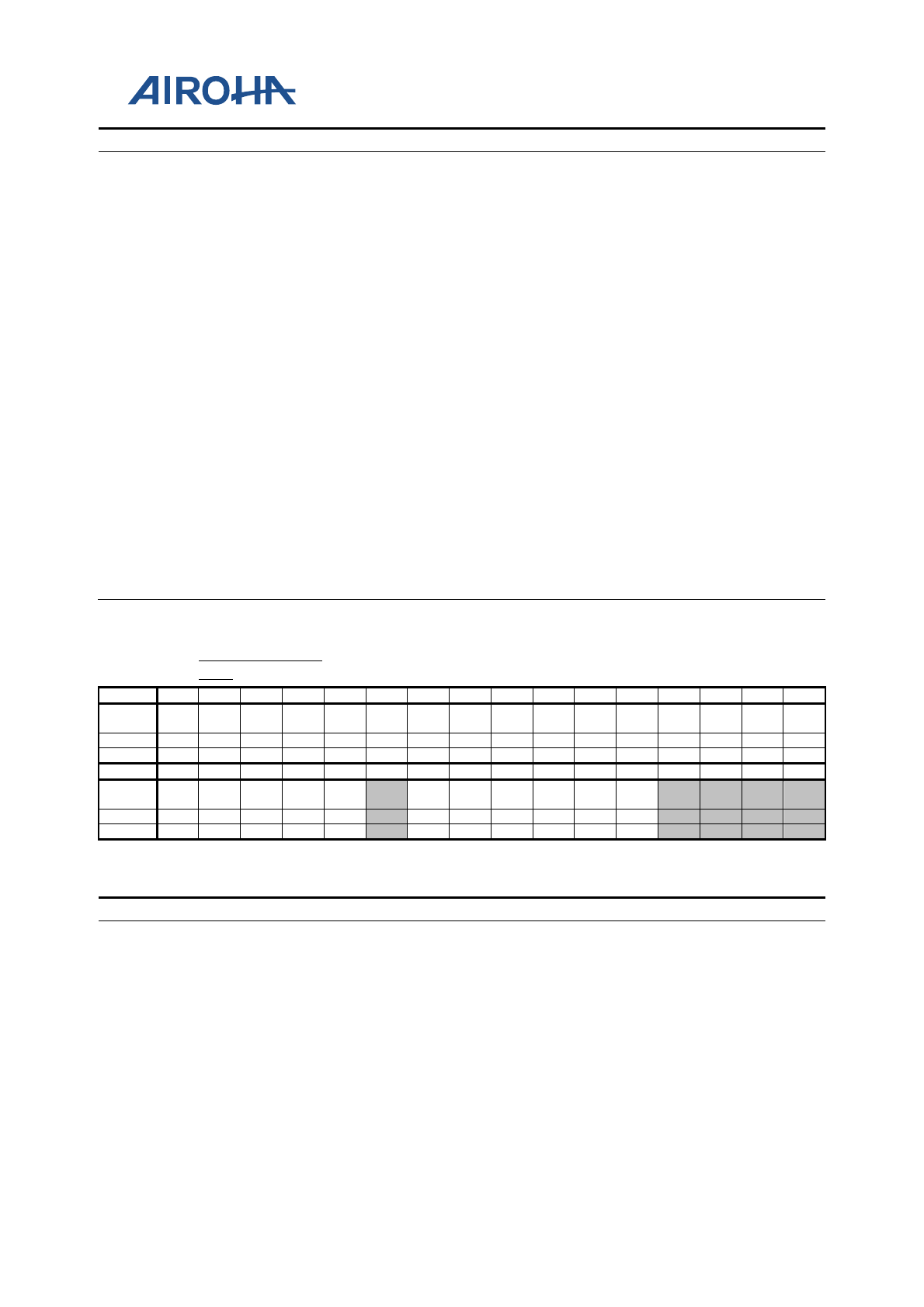
MT2523 Series Reference Manual
© 2015 - 2018 Airoha Technology Corp.
Page 509 of 692
This document contains information that is proprietary to Airoha Technology Corp. (“Airoha”) and/or its licensor(s).
Any unauthorized use, reproduction or disclosure of this document in whole or in part is strictly prohibited.
Bit(s)
Mnemonic
Name
Description
12
GPIO12
GPIO12_PUPD
Bitwise SET operation of GPIO12 PUPD
0: Keep
1: SET bits
11
GPIO11
GPIO11_PUPD
Bitwise SET operation of GPIO11 PUPD
0: Keep
1: SET bits
9
GPIO9
GPIO9_PUPD
Bitwise SET operation of GPIO9 PUPD
0: Keep
1: SET bits
8
GPIO8
GPIO8_PUPD
Bitwise SET operation of GPIO8 PUPD
0: Keep
1: SET bits
7
GPIO7
GPIO7_PUPD
Bitwise SET operation of GPIO7 PUPD
0: Keep
1: SET bits
6
GPIO6
GPIO6_PUPD
Bitwise SET operation of GPIO6 PUPD
0: Keep
1: SET bits
5
GPIO5
GPIO5_PUPD
Bitwise SET operation of GPIO5 PUPD
0: Keep
1: SET bits
4
GPIO4
GPIO4_PUPD
Bitwise SET operation of GPIO4 PUPD
0: Keep
1: SET bits
A2020A08
GPIO_PUPD0_
CLR
GPIO PUPD Control
00000000
Bit
31
30
29
28
27
26
25
24
23
22
21
20
19
18
17
16
Name
GPIO
31
GPIO
30
GPIO
29
GPIO
28
GPIO
27
GPIO
26
GPIO
25
GPIO
24
GPIO
23
GPIO
22
GPIO
21
GPIO
20
GPIO1
9
GPIO1
8
GPIO1
7
GPIO
16
Type
WO
WO
WO
WO
WO
WO
WO
WO
WO
WO
WO
WO
WO
WO
WO
WO
Reset
0
0
0
0
0
0
0
0
0
0
0
0
0
0
0
0
Bit
15
14
13
12
11
10
9
8
7
6
5
4
3
2
1
0
Name
GPIO
15
GPIO1
4
GPIO1
3
GPIO1
2
GPIO1
1
GPIO
9
GPIO
8
GPIO
7
GPIO
6
GPIO
5
GPIO
4
Type
WO
WO
WO
WO
WO
WO
WO
WO
WO
WO
WO
Reset
0
0
0
0
0
0
0
0
0
0
0
Overview
For bitwise access of GPIO_PUPD0
Bit(s)
Mnemonic
Name
Description
31
GPIO31
GPIO31_PUPD
Bitwise CLR operation of GPIO31 PUPD
0: Keep
1: CLR bits
30
GPIO30
GPIO30_PUPD
Bitwise CLR operation of GPIO30 PUPD
0: Keep
1: CLR bits
29
GPIO29
GPIO29_PUPD
Bitwise CLR operation of GPIO29 PUPD
0: Keep
1: CLR bits
28
GPIO28
GPIO28_PUPD
Bitwise CLR operation of GPIO28 PUPD
0: Keep
1: CLR bits

MT2523 Series Reference Manual
© 2015 - 2018 Airoha Technology Corp.
Page 510 of 692
This document contains information that is proprietary to Airoha Technology Corp. (“Airoha”) and/or its licensor(s).
Any unauthorized use, reproduction or disclosure of this document in whole or in part is strictly prohibited.
Bit(s)
Mnemonic
Name
Description
27
GPIO27
GPIO27_PUPD
Bitwise CLR operation of GPIO27 PUPD
0: Keep
1: CLR bits
26
GPIO26
GPIO26_PUPD
Bitwise CLR operation of GPIO26 PUPD
0: Keep
1: CLR bits
25
GPIO25
GPIO25_PUPD
Bitwise CLR operation of GPIO25 PUPD
0: Keep
1: CLR bits
24
GPIO24
GPIO24_PUPD
Bitwise CLR operation of GPIO24 PUPD
0: Keep
1: CLR bits
23
GPIO23
GPIO23_PUPD
Bitwise CLR operation of GPIO23 PUPD
0: Keep
1: CLR bits
22
GPIO22
GPIO22_PUPD
Bitwise CLR operation of GPIO22 PUPD
0: Keep
1: CLR bits
21
GPIO21
GPIO21_PUPD
Bitwise CLR operation of GPIO21 PUPD
0: Keep
1: CLR bits
20
GPIO20
GPIO20_PUPD
Bitwise CLR operation of GPIO20 PUPD
0: Keep
1: CLR bits
19
GPIO19
GPIO19_PUPD
Bitwise CLR operation of GPIO19 PUPD
0: Keep
1: SET bits
18
GPIO18
GPIO18_PUPD
Bitwise CLR operation of GPIO18 PUPD
0: Keep
1: SET bits
17
GPIO17
GPIO17_PUPD
Bitwise CLR operation of GPIO17 PUPD
0: Keep
1: CLR bits
16
GPIO16
GPIO16_PUPD
Bitwise CLR operation of GPIO16 PUPD
0: Keep
1: SET bits
15
GPIO15
GPIO15_PUPD
Bitwise CLR operation of GPIO15 PUPD
0: Keep
1: SET bits
14
GPIO14
GPIO14_PUPD
Bitwise CLR operation of GPIO14 PUPD
0: Keep
1: CLR bits
13
GPIO13
GPIO13_PUPD
Bitwise CLR operation of GPIO13 PUPD
0: Keep
1: SET bits
12
GPIO12
GPIO12_PUPD
Bitwise CLR operation of GPIO12 PUPD
0: Keep
1: SET bits
11
GPIO11
GPIO11_PUPD
Bitwise CLR operation of GPIO11 PUPD
0: Keep
1: CLR bits
9
GPIO9
GPIO9_PUPD
Bitwise CLR operation of GPIO9 PUPD
0: Keep
1: SET bits
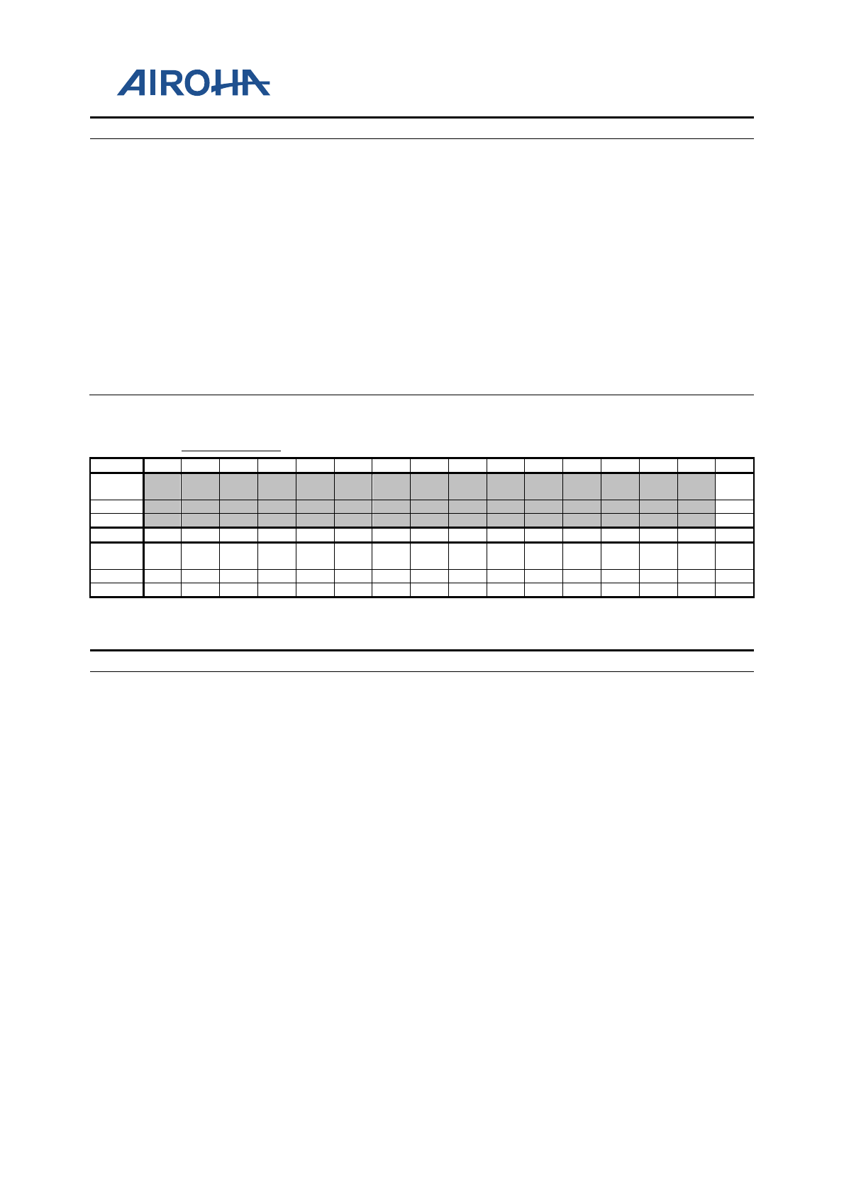
MT2523 Series Reference Manual
© 2015 - 2018 Airoha Technology Corp.
Page 511 of 692
This document contains information that is proprietary to Airoha Technology Corp. (“Airoha”) and/or its licensor(s).
Any unauthorized use, reproduction or disclosure of this document in whole or in part is strictly prohibited.
Bit(s)
Mnemonic
Name
Description
8
GPIO8
GPIO8_PUPD
Bitwise CLR operation of GPIO8 PUPD
0: Keep
1: SET bits
7
GPIO7
GPIO7_PUPD
Bitwise CLR operation of GPIO7 PUPD
0: Keep
1: CLR bits
6
GPIO6
GPIO6_PUPD
Bitwise CLR operation of GPIO6 PUPD
0: Keep
1: SET bits
5
GPIO5
GPIO5_PUPD
Bitwise CLR operation of GPIO5 PUPD
0: Keep
1: SET bits
4
GPIO4
GPIO4_PUPD
Bitwise CLR operation of GPIO4 PUPD
0: Keep
1: CLR bits
A2020A10
GPIO_PUPD1
GPIO PUPD Control
0001FF77
Bit
31
30
29
28
27
26
25
24
23
22
21
20
19
18
17
16
Name
GPIO
48
Type
RW
Reset
1
Bit
15
14
13
12
11
10
9
8
7
6
5
4
3
2
1
0
Name
GPIO
47
GPIO
46
GPIO
45
GPIO
44
GPIO
43
GPIO
42
GPIO
41
GPIO
40
GPIO
39
GPIO
38
GPIO
37
GPIO
36
GPIO
35
GPIO
34
GPIO
33
GPIO
32
Type
RW
RW
RW
RW
RW
RW
RW
RW
RW
RW
RW
RW
RW
RW
RW
RW
Reset
1
1
1
1
1
1
1
1
0
1
1
1
0
1
1
1
Overview
Configures GPIO PUPD control
Bit(s)
Mnemonic
Name
Description
16
GPIO48
GPIO48_PUPD
PUPD for GPIO48
0: Disable
1: Enable
15
GPIO47
GPIO47_PUPD
PUPD for GPIO47
0: Disable
1: Enable
14
GPIO46
GPIO46_PUPD
PUPD for GPIO46
0: Disable
1: Enable
13
GPIO45
GPIO45_PUPD
PUPD for GPIO45
0: Disable
1: Enable
12
GPIO44
GPIO44_PUPD
PUPD for GPIO44
0: Disable
1: Enable
11
GPIO43
GPIO43_PUPD
PUPD for GPIO43
0: Disable
1: Enable
10
GPIO42
GPIO42_PUPD
PUPD for GPIO42
0: Disable
1: Enable
9
GPIO41
GPIO41_PUPD
PUPD for GPIO41
0: Disable
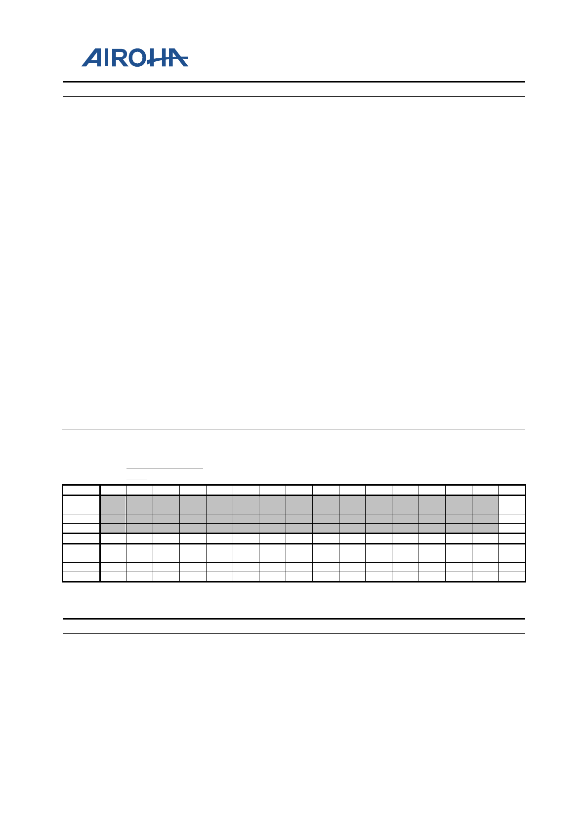
MT2523 Series Reference Manual
© 2015 - 2018 Airoha Technology Corp.
Page 512 of 692
This document contains information that is proprietary to Airoha Technology Corp. (“Airoha”) and/or its licensor(s).
Any unauthorized use, reproduction or disclosure of this document in whole or in part is strictly prohibited.
Bit(s)
Mnemonic
Name
Description
1: Enable
8
GPIO40
GPIO40_PUPD
PUPD for GPIO40
0: Disable
1: Enable
7
GPIO39
GPIO39_PUPD
PUPD for GPIO39
0: Disable
1: Enable
6
GPIO38
GPIO38_PUPD
PUPD for GPIO38
0: Disable
1: Enable
5
GPIO37
GPIO37_PUPD
PUPD for GPIO37
0: Disable
1: Enable
4
GPIO36
GPIO36_PUPD
PUPD for GPIO36
0: Disable
1: Enable
3
GPIO35
GPIO35_PUPD
PUPD for GPIO35
0: Disable
1: Enable
2
GPIO34
GPIO34_PUPD
PUPD for GPIO34
0: Disable
1: Enable
1
GPIO33
GPIO33_PUPD
PUPD for GPIO33
0: Disable
1: Enable
0
GPIO32
GPIO32_PUPD
PUPD for GPIO32
0: Disable
1: Enable
A2020A14
GPIO_PUPD1_
SET
GPIO PUPD Control
00000000
Bit
31
30
29
28
27
26
25
24
23
22
21
20
19
18
17
16
Name
GPIO
48
Type
WO
Reset
0
Bit
15
14
13
12
11
10
9
8
7
6
5
4
3
2
1
0
Name
GPIO
47
GPIO
46
GPIO
45
GPIO
44
GPIO
43
GPIO
42
GPIO
41
GPIO
40
GPIO
39
GPIO
38
GPIO
37
GPIO
36
GPIO
35
GPIO
34
GPIO
33
GPIO
32
Type
WO
WO
WO
WO
WO
WO
WO
WO
WO
WO
WO
WO
WO
WO
WO
WO
Reset
0
0
0
0
0
0
0
0
0
0
0
0
0
0
0
0
Overview
For bitwise access of GPIO_PUPD1
Bit(s)
Mnemonic
Name
Description
16
GPIO48
GPIO48_PUPD
Bitwise SET operation of GPIO48 PUPD
0: Keep
1: SET bits
15
GPIO47
GPIO47_PUPD
Bitwise SET operation of GPIO47 PUPD
0: Keep
1: SET bits
14
GPIO46
GPIO46_PUPD
Bitwise SET operation of GPIO46 PUPD
0: Keep
1: SET bits

MT2523 Series Reference Manual
© 2015 - 2018 Airoha Technology Corp.
Page 513 of 692
This document contains information that is proprietary to Airoha Technology Corp. (“Airoha”) and/or its licensor(s).
Any unauthorized use, reproduction or disclosure of this document in whole or in part is strictly prohibited.
Bit(s)
Mnemonic
Name
Description
13
GPIO45
GPIO45_PUPD
Bitwise SET operation of GPIO45 PUPD
0: Keep
1: SET bits
12
GPIO44
GPIO44_PUPD
Bitwise SET operation of GPIO44 PUPD
0: Keep
1: SET bits
11
GPIO43
GPIO43_PUPD
Bitwise SET operation of GPIO43 PUPD
0: Keep
1: SET bits
10
GPIO42
GPIO42_PUPD
Bitwise SET operation of GPIO42 PUPD
0: Keep
1: SET bits
9
GPIO41
GPIO41_PUPD
Bitwise SET operation of GPIO41 PUPD
0: Keep
1: SET bits
8
GPIO40
GPIO40_PUPD
Bitwise SET operation of GPIO40 PUPD
0: Keep
1: SET bits
7
GPIO39
GPIO39_PUPD
Bitwise SET operation of GPIO39 PUPD
0: Keep
1: SET bits
6
GPIO38
GPIO38_PUPD
Bitwise SET operation of GPIO38 PUPD
0: Keep
1: SET bits
5
GPIO37
GPIO37_PUPD
Bitwise SET operation of GPIO37 PUPD
0: Keep
1: SET bits
4
GPIO36
GPIO36_PUPD
Bitwise SET operation of GPIO36 PUPD
0: Keep
1: SET bits
3
GPIO35
GPIO35_PUPD
Bitwise SET operation of GPIO35 PUPD
0: Keep
1: SET bits
2
GPIO34
GPIO34_PUPD
Bitwise SET operation of GPIO34 PUPD
0: Keep
1: SET bits
1
GPIO33
GPIO33_PUPD
Bitwise SET operation of GPIO33 PUPD
0: Keep
1: SET bits
0
GPIO32
GPIO32_PUPD
Bitwise SET operation of GPIO32 PUPD
0: Keep
1: SET bits
A2020A18
GPIO_PUPD1_
CLR
GPIO PUPD Control
00000000
Bit
31
30
29
28
27
26
25
24
23
22
21
20
19
18
17
16
Name
GPIO
48
Type
WO
Reset
0
Bit
15
14
13
12
11
10
9
8
7
6
5
4
3
2
1
0
Name
GPIO
47
GPIO
46
GPIO
45
GPIO
44
GPIO
43
GPIO
42
GPIO
41
GPIO
40
GPIO
39
GPIO
38
GPIO
37
GPIO
36
GPIO
35
GPIO
34
GPIO
33
GPIO
32
Type
WO
WO
WO
WO
WO
WO
WO
WO
WO
WO
WO
WO
WO
WO
WO
WO

MT2523 Series Reference Manual
© 2015 - 2018 Airoha Technology Corp.
Page 514 of 692
This document contains information that is proprietary to Airoha Technology Corp. (“Airoha”) and/or its licensor(s).
Any unauthorized use, reproduction or disclosure of this document in whole or in part is strictly prohibited.
Reset
0
0
0
0
0
0
0
0
0
0
0
0
0
0
0
0
Overview
For bitwise access of GPIO_PUPD1
Bit(s)
Mnemonic
Name
Description
16
GPIO48
GPIO48_PUPD
Bitwise CLR operation of GPIO48 PUPD
0: Keep
1: CLR bits
15
GPIO47
GPIO47_PUPD
Bitwise CLR operation of GPIO47 PUPD
0: Keep
1: CLR bits
14
GPIO46
GPIO46_PUPD
Bitwise CLR operation of GPIO46 PUPD
0: Keep
1: CLR bits
13
GPIO45
GPIO45_PUPD
Bitwise CLR operation of GPIO45 PUPD
0: Keep
1: CLR bits
12
GPIO44
GPIO44_PUPD
Bitwise CLR operation of GPIO44 PUPD
0: Keep
1: CLR bits
11
GPIO43
GPIO43_PUPD
Bitwise CLR operation of GPIO43 PUPD
0: Keep
1: CLR bits
10
GPIO42
GPIO42_PUPD
Bitwise CLR operation of GPIO42 PUPD
0: Keep
1: CLR bits
9
GPIO41
GPIO41_PUPD
Bitwise CLR operation of GPIO41 PUPD
0: Keep
1: CLR bits
8
GPIO40
GPIO40_PUPD
Bitwise CLR operation of GPIO40 PUPD
0: Keep
1: CLR bits
7
GPIO39
GPIO39_PUPD
Bitwise CLR operation of GPIO39 PUPD
0: Keep
1: CLR bits
6
GPIO38
GPIO38_PUPD
Bitwise CLR operation of GPIO38 PUPD
0: Keep
1: CLR bits
5
GPIO37
GPIO37_PUPD
Bitwise CLR operation of GPIO37 PUPD
0: Keep
1: CLR bits
4
GPIO36
GPIO36_PUPD
Bitwise CLR operation of GPIO36 PUPD
0: Keep
1: CLR bits
3
GPIO35
GPIO35_PUPD
Bitwise CLR operation of GPIO35 PUPD
0: Keep
1: CLR bits
2
GPIO34
GPIO34_PUPD
Bitwise CLR operation of GPIO34 PUPD
0: Keep
1: CLR bits
1
GPIO33
GPIO33_PUPD
Bitwise CLR operation of GPIO33 PUPD
0: Keep
1: CLR bits
0
GPIO32
GPIO32_PUPD
Bitwise CLR operation of GPIO32 PUPD
0: Keep
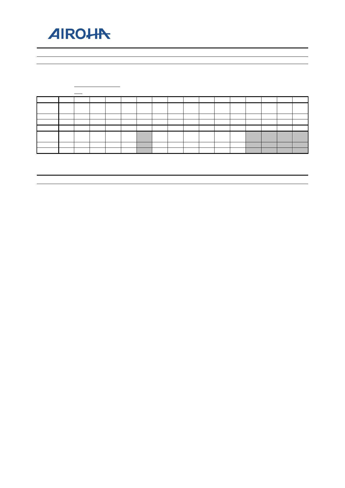
MT2523 Series Reference Manual
© 2015 - 2018 Airoha Technology Corp.
Page 515 of 692
This document contains information that is proprietary to Airoha Technology Corp. (“Airoha”) and/or its licensor(s).
Any unauthorized use, reproduction or disclosure of this document in whole or in part is strictly prohibited.
Bit(s)
Mnemonic
Name
Description
1: CLR bits
A2020B00
GPIO_RESEN0
_0
GPIO R0 Control
FDFDFBF0
Bit
31
30
29
28
27
26
25
24
23
22
21
20
19
18
17
16
Name
GPIO
31
GPIO
30
GPIO
29
GPIO
28
GPIO
27
GPIO
26
GPIO
25
GPIO
24
GPIO
23
GPIO
22
GPIO
21
GPIO
20
GPIO1
9
GPIO1
8
GPIO1
7
GPIO
16
Type
RW
RW
RW
RW
RW
RW
RW
RW
RW
RW
RW
RW
RW
RW
RW
RW
Reset
1
1
1
1
1
1
0
1
1
1
1
1
1
1
0
1
Bit
15
14
13
12
11
10
9
8
7
6
5
4
3
2
1
0
Name
GPIO
15
GPIO1
4
GPIO1
3
GPIO1
2
GPIO1
1
GPIO
9
GPIO
8
GPIO
7
GPIO
6
GPIO
5
GPIO
4
Type
RW
RW
RW
RW
RW
RW
RW
RW
RW
RW
RW
Reset
1
1
1
1
1
1
1
1
1
1
1
Overview
Configures GPIO R0 control
Bit(s)
Mnemonic
Name
Description
31
GPIO31
GPIO31_R0
R0 for GPIO31
0: Disable
1: Enable
30
GPIO30
GPIO30_R0
R0 for GPIO30
0: Disable
1: Enable
29
GPIO29
GPIO29_R0
R0 for GPIO29
0: Disable
1: Enable
28
GPIO28
GPIO28_R0
R0 for GPIO28
0: Disable
1: Enable
27
GPIO27
GPIO27_R0
R0 for GPIO27
0: Disable
1: Enable
26
GPIO26
GPIO26_R0
R0 for GPIO26
0: Disable
1: Enable
25
GPIO25
GPIO25_R0
R0 for GPIO25
0: Disable
1: Enable
24
GPIO24
GPIO24_R0
R0 for GPIO24
0: Disable
1: Enable
23
GPIO23
GPIO23_R0
R0 for GPIO23
0: Disable
1: Enable
22
GPIO22
GPIO22_R0
R0 for GPIO22
0: Disable
1: Enable
21
GPIO21
GPIO21_R0
R0 for GPIO21
0: Disable
1: Enable
20
GPIO20
GPIO20_R0
R0 for GPIO20
0: Disable
1: Enable

MT2523 Series Reference Manual
© 2015 - 2018 Airoha Technology Corp.
Page 516 of 692
This document contains information that is proprietary to Airoha Technology Corp. (“Airoha”) and/or its licensor(s).
Any unauthorized use, reproduction or disclosure of this document in whole or in part is strictly prohibited.
Bit(s)
Mnemonic
Name
Description
19
GPIO19
GPIO19_R0
R0 for GPIO19
0: Disable
1: Enable
18
GPIO18
GPIO18_R0
R0 for GPIO18
0: Disable
1: Enable
17
GPIO17
GPIO17_R0
R0 for GPIO17
0: Disable
1: Enable
16
GPIO16
GPIO16_R0
R0 for GPIO16
0: Disable
1: Enable
15
GPIO15
GPIO15_R0
R0 for GPIO15
0: Disable
1: Enable
14
GPIO14
GPIO14_R0
R0 for GPIO14
0: Disable
1: Enable
13
GPIO13
GPIO13_R0
R0 for GPIO13
0: Disable
1: Enable
12
GPIO12
GPIO12_R0
R0 for GPIO12
0: Disable
1: Enable
11
GPIO11
GPIO11_R0
R0 for GPIO11
0: Disable
1: Enable
9
GPIO9
GPIO9_R0
R0 for GPIO9
0: Disable
1: Enable
8
GPIO8
GPIO8_R0
R0 for GPIO8
0: Disable
1: Enable
7
GPIO7
GPIO7_R0
R0 for GPIO7
0: Disable
1: Enable
6
GPIO6
GPIO6_R0
R0 for GPIO6
0: Disable
1: Enable
5
GPIO5
GPIO5_R0
R0 for GPIO5
0: Disable
1: Enable
4
GPIO4
GPIO4_R0
R0 for GPIO4
0: Disable
1: Enable
A2020B04
GPIO_RESEN0
_0_SET
GPIO R0 Control
00000000
Bit
31
30
29
28
27
26
25
24
23
22
21
20
19
18
17
16
Name
GPIO
31
GPIO
30
GPIO
29
GPIO
28
GPIO
27
GPIO
26
GPIO
25
GPIO
24
GPIO
23
GPIO
22
GPIO
21
GPIO
20
GPIO1
9
GPIO1
8
GPIO1
7
GPIO
16
Type
WO
WO
WO
WO
WO
WO
WO
WO
WO
WO
WO
WO
WO
WO
WO
WO
Reset
0
0
0
0
0
0
0
0
0
0
0
0
0
0
0
0

MT2523 Series Reference Manual
© 2015 - 2018 Airoha Technology Corp.
Page 517 of 692
This document contains information that is proprietary to Airoha Technology Corp. (“Airoha”) and/or its licensor(s).
Any unauthorized use, reproduction or disclosure of this document in whole or in part is strictly prohibited.
Bit
15
14
13
12
11
10
9
8
7
6
5
4
3
2
1
0
Name
GPIO
15
GPIO1
4
GPIO1
3
GPIO1
2
GPIO1
1
GPIO
9
GPIO
8
GPIO
7
GPIO
6
GPIO
5
GPIO
4
Type
WO
WO
WO
WO
WO
WO
WO
WO
WO
WO
WO
Reset
0
0
0
0
0
0
0
0
0
0
0
Overview
For bitwise access of GPIO_RESEN0_0
Bit(s)
Mnemonic
Name
Description
31
GPIO31
GPIO31_R0
Bitwise SET operation of GPIO31 R0
0: Keep
1: SET bits
30
GPIO30
GPIO30_R0
Bitwise SET operation of GPIO30 R0
0: Keep
1: SET bits
29
GPIO29
GPIO29_R0
Bitwise SET operation of GPIO29 R0
0: Keep
1: SET bits
28
GPIO28
GPIO28_R0
Bitwise SET operation of GPIO28 R0
0: Keep
1: SET bits
27
GPIO27
GPIO27_R0
Bitwise SET operation of GPIO27 R0
0: Keep
1: SET bits
26
GPIO26
GPIO26_R0
Bitwise SET operation of GPIO26 R0
0: Keep
1: SET bits
25
GPIO25
GPIO25_R0
Bitwise SET operation of GPIO25 R0
0: Keep
1: SET bits
24
GPIO24
GPIO24_R0
Bitwise SET operation of GPIO24 R0
0: Keep
1: SET bits
23
GPIO23
GPIO23_R0
Bitwise SET operation of GPIO23 R0
0: Keep
1: SET bits
22
GPIO22
GPIO22_R0
Bitwise SET operation of GPIO22 R0
0: Keep
1: SET bits
21
GPIO21
GPIO21_R0
Bitwise SET operation of GPIO21 R0
0: Keep
1: SET bits
20
GPIO20
GPIO20_R0
Bitwise SET operation of GPIO20 R0
0: Keep
1: SET bits
19
GPIO19
GPIO19_R0
Bitwise SET operation of GPIO19 R0
0: Keep
1: SET bits
18
GPIO18
GPIO18_R0
Bitwise SET operation of GPIO18 R0
0: Keep
1: SET bits
17
GPIO17
GPIO17_R0
Bitwise SET operation of GPIO17 R0
0: Keep
1: SET bits
16
GPIO16
GPIO16_R0
Bitwise SET operation of GPIO16 R0
0: Keep
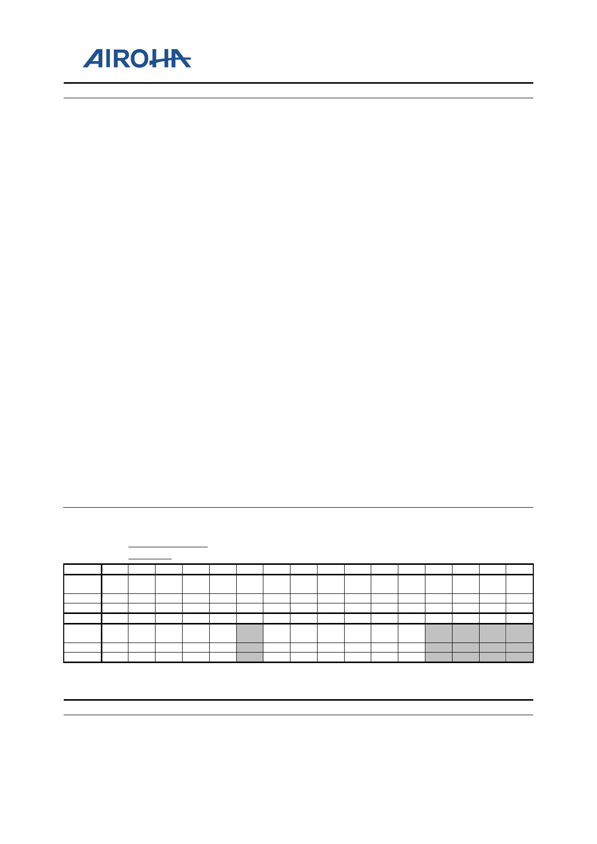
MT2523 Series Reference Manual
© 2015 - 2018 Airoha Technology Corp.
Page 518 of 692
This document contains information that is proprietary to Airoha Technology Corp. (“Airoha”) and/or its licensor(s).
Any unauthorized use, reproduction or disclosure of this document in whole or in part is strictly prohibited.
Bit(s)
Mnemonic
Name
Description
1: SET bits
15
GPIO15
GPIO15_R0
Bitwise SET operation of GPIO15 R0
0: Keep
1: SET bits
14
GPIO14
GPIO14_R0
Bitwise SET operation of GPIO14 R0
0: Keep
1: SET bits
13
GPIO13
GPIO13_R0
Bitwise SET operation of GPIO13 R0
0: Keep
1: SET bits
12
GPIO12
GPIO12_R0
Bitwise SET operation of GPIO12 R0
0: Keep
1: SET bits
11
GPIO11
GPIO11_R0
Bitwise SET operation of GPIO11 R0
0: Keep
1: SET bits
9
GPIO9
GPIO9_R0
Bitwise SET operation of GPIO9 R0
0: Keep
1: SET bits
8
GPIO8
GPIO8_R0
Bitwise SET operation of GPIO8 R0
0: Keep
1: SET bits
7
GPIO7
GPIO7_R0
Bitwise SET operation of GPIO7 R0
0: Keep
1: SET bits
6
GPIO6
GPIO6_R0
Bitwise SET operation of GPIO6 R0
0: Keep
1: SET bits
5
GPIO5
GPIO5_R0
Bitwise SET operation of GPIO5 R0
0: Keep
1: SET bits
4
GPIO4
GPIO4_R0
Bitwise SET operation of GPIO4 R0
0: Keep
1: SET bits
A2020B08
GPIO_RESEN0
_0_CLR
GPIO R0 Control
00000000
Bit
31
30
29
28
27
26
25
24
23
22
21
20
19
18
17
16
Name
GPIO
31
GPIO
30
GPIO
29
GPIO
28
GPIO
27
GPIO
26
GPIO
25
GPIO
24
GPIO
23
GPIO
22
GPIO
21
GPIO
20
GPIO1
9
GPIO1
8
GPIO1
7
GPIO
16
Type
WO
WO
WO
WO
WO
WO
WO
WO
WO
WO
WO
WO
WO
WO
WO
WO
Reset
0
0
0
0
0
0
0
0
0
0
0
0
0
0
0
0
Bit
15
14
13
12
11
10
9
8
7
6
5
4
3
2
1
0
Name
GPIO
15
GPIO1
4
GPIO1
3
GPIO1
2
GPIO1
1
GPIO
9
GPIO
8
GPIO
7
GPIO
6
GPIO
5
GPIO
4
Type
WO
WO
WO
WO
WO
WO
WO
WO
WO
WO
WO
Reset
0
0
0
0
0
0
0
0
0
0
0
Overview
For bitwise access of GPIO_RESEN0_0
Bit(s)
Mnemonic
Name
Description
31
GPIO31
GPIO31_R0
Bitwise CLR operation of GPIO31 R0
0: Keep
1: CLR bits

MT2523 Series Reference Manual
© 2015 - 2018 Airoha Technology Corp.
Page 519 of 692
This document contains information that is proprietary to Airoha Technology Corp. (“Airoha”) and/or its licensor(s).
Any unauthorized use, reproduction or disclosure of this document in whole or in part is strictly prohibited.
Bit(s)
Mnemonic
Name
Description
30
GPIO30
GPIO30_R0
Bitwise CLR operation of GPIO30 R0
0: Keep
1: CLR bits
29
GPIO29
GPIO29_R0
Bitwise CLR operation of GPIO29 R0
0: Keep
1: CLR bits
28
GPIO28
GPIO28_R0
Bitwise CLR operation of GPIO28 R0
0: Keep
1: CLR bits
27
GPIO27
GPIO27_R0
Bitwise CLR operation of GPIO27 R0
0: Keep
1: CLR bits
26
GPIO26
GPIO26_R0
Bitwise CLR operation of GPIO26 R0
0: Keep
1: CLR bits
25
GPIO25
GPIO25_R0
Bitwise CLR operation of GPIO25 R0
0: Keep
1: CLR bits
24
GPIO24
GPIO24_R0
Bitwise CLR operation of GPIO24 R0
0: Keep
1: CLR bits
23
GPIO23
GPIO23_R0
Bitwise CLR operation of GPIO23 R0
0: Keep
1: CLR bits
22
GPIO22
GPIO22_R0
Bitwise CLR operation of GPIO22 R0
0: Keep
1: CLR bits
21
GPIO21
GPIO21_R0
Bitwise CLR operation of GPIO21 R0
0: Keep
1: CLR bits
20
GPIO20
GPIO20_R0
Bitwise CLR operation of GPIO20 R0
0: Keep
1: CLR bits
19
GPIO19
GPIO19_R0
Bitwise CLR operation of GPIO19 R0
0: Keep
1: CLR bits
18
GPIO18
GPIO18_R0
Bitwise CLR operation of GPIO18 R0
0: Keep
1: CLR bits
17
GPIO17
GPIO17_R0
Bitwise CLR operation of GPIO17 R0
0: Keep
1: CLR bits
16
GPIO16
GPIO16_R0
Bitwise CLR operation of GPIO16 R0
0: Keep
1: CLR bits
15
GPIO15
GPIO15_R0
Bitwise CLR operation of GPIO15 R0
0: Keep
1: CLR bits
14
GPIO14
GPIO14_R0
Bitwise CLR operation of GPIO14 R0
0: Keep
1: CLR bits
13
GPIO13
GPIO13_R0
Bitwise CLR operation of GPIO13 R0
0: Keep
1: CLR bits
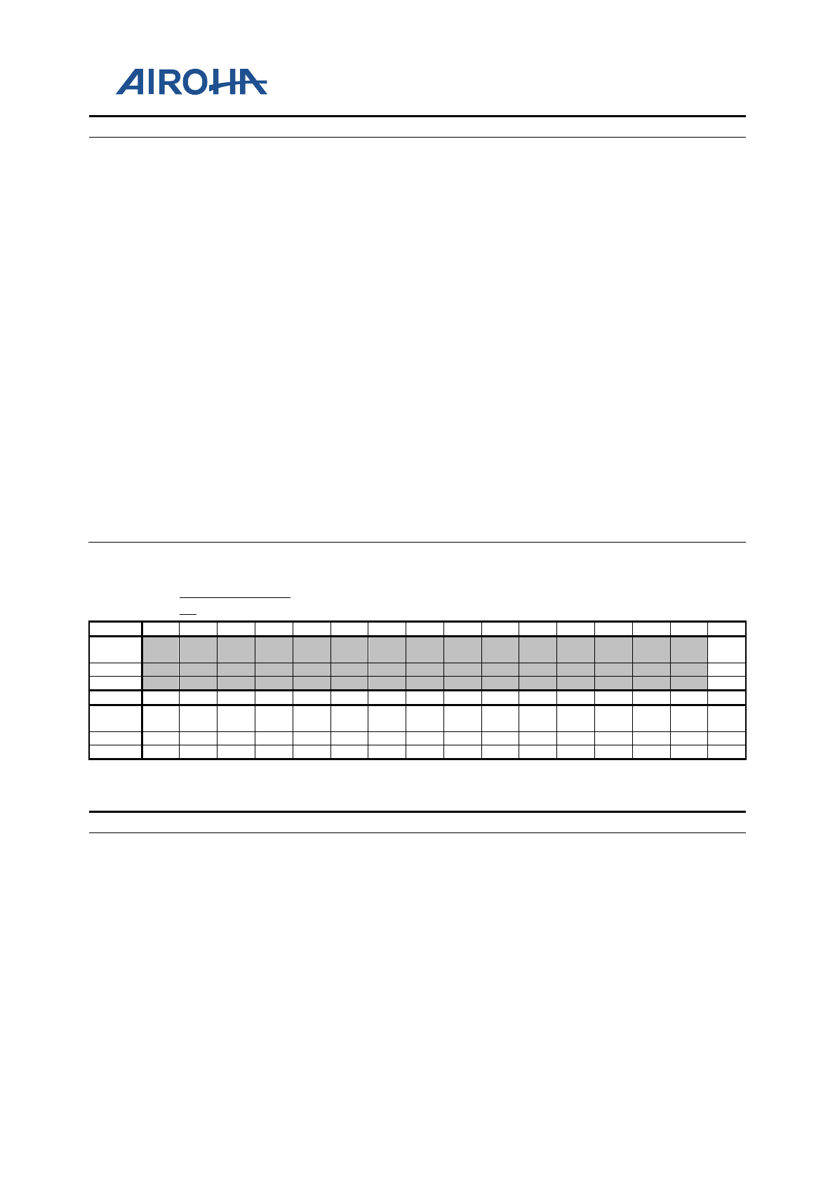
MT2523 Series Reference Manual
© 2015 - 2018 Airoha Technology Corp.
Page 520 of 692
This document contains information that is proprietary to Airoha Technology Corp. (“Airoha”) and/or its licensor(s).
Any unauthorized use, reproduction or disclosure of this document in whole or in part is strictly prohibited.
Bit(s)
Mnemonic
Name
Description
12
GPIO12
GPIO12_R0
Bitwise CLR operation of GPIO12 R0
0: Keep
1: CLR bits
11
GPIO11
GPIO11_R0
Bitwise CLR operation of GPIO11 R0
0: Keep
1: CLR bits
9
GPIO9
GPIO9_R0
Bitwise CLR operation of GPIO9 R0
0: Keep
1: CLR bits
8
GPIO8
GPIO8_R0
Bitwise CLR operation of GPIO8 R0
0: Keep
1: CLR bits
7
GPIO7
GPIO7_R0
Bitwise CLR operation of GPIO7 R0
0: Keep
1: CLR bits
6
GPIO6
GPIO6_R0
Bitwise CLR operation of GPIO6 R0
0: Keep
1: CLR bits
5
GPIO5
GPIO5_R0
Bitwise CLR operation of GPIO5 R0
0: Keep
1: CLR bits
4
GPIO4
GPIO4_R0
Bitwise CLR operation of GPIO4 R0
0: Keep
1: CLR bits
A2020B10
GPIO_RESEN0
_1
GPIO R0 Control
0001FF77
Bit
31
30
29
28
27
26
25
24
23
22
21
20
19
18
17
16
Name
GPIO
48
Type
RW
Reset
1
Bit
15
14
13
12
11
10
9
8
7
6
5
4
3
2
1
0
Name
GPIO
47
GPIO
46
GPIO
45
GPIO
44
GPIO
43
GPIO
42
GPIO
41
GPIO
40
GPIO
39
GPIO
38
GPIO
37
GPIO
36
GPIO
35
GPIO
34
GPIO
33
GPIO
32
Type
RW
RW
RW
RW
RW
RW
RW
RW
RW
RW
RW
RW
RW
RW
RW
RW
Reset
1
1
1
1
1
1
1
1
0
1
1
1
0
1
1
1
Overview
Configures GPIO R0 control
Bit(s)
Mnemonic
Name
Description
16
GPIO48
GPIO48_R0
R0 for GPIO48
0: Disable
1: Enable
15
GPIO47
GPIO47_R0
R0 for GPIO47
0: Disable
1: Enable
14
GPIO46
GPIO46_R0
R0 for GPIO46
0: Disable
1: Enable
13
GPIO45
GPIO45_R0
R0 for GPIO45
0: Disable
1: Enable

MT2523 Series Reference Manual
© 2015 - 2018 Airoha Technology Corp.
Page 521 of 692
This document contains information that is proprietary to Airoha Technology Corp. (“Airoha”) and/or its licensor(s).
Any unauthorized use, reproduction or disclosure of this document in whole or in part is strictly prohibited.
Bit(s)
Mnemonic
Name
Description
12
GPIO44
GPIO44_R0
R0 for GPIO44
0: Disable
1: Enable
11
GPIO43
GPIO43_R0
R0 for GPIO43
0: Disable
1: Enable
10
GPIO42
GPIO42_R0
R0 for GPIO42
0: Disable
1: Enable
9
GPIO41
GPIO41_R0
R0 for GPIO41
0: Disable
1: Enable
8
GPIO40
GPIO40_R0
R0 for GPIO40
0: Disable
1: Enable
7
GPIO39
GPIO39_R0
R0 for GPIO39
0: Disable
1: Enable
6
GPIO38
GPIO38_R0
R0 for GPIO38
0: Disable
1: Enable
5
GPIO37
GPIO37_R0
R0 for GPIO37
0: Disable
1: Enable
4
GPIO36
GPIO36_R0
R0 for GPIO36
0: Disable
1: Enable
3
GPIO35
GPIO35_R0
R0 for GPIO35
0: Disable
1: Enable
2
GPIO34
GPIO34_R0
R0 for GPIO34
0: Disable
1: Enable
1
GPIO33
GPIO33_R0
R0 for GPIO33
0: Disable
1: Enable
0
GPIO32
GPIO32_R0
R0 for GPIO32
0: Disable
1: Enable
A2020B14
GPIO_RESEN0
_1_SET
GPIO R0 Control
00000000
Bit
31
30
29
28
27
26
25
24
23
22
21
20
19
18
17
16
Name
GPIO
48
Type
WO
Reset
0
Bit
15
14
13
12
11
10
9
8
7
6
5
4
3
2
1
0
Name
GPIO
47
GPIO
46
GPIO
45
GPIO
44
GPIO
43
GPIO
42
GPIO
41
GPIO
40
GPIO
39
GPIO
38
GPIO
37
GPIO
36
GPIO
35
GPIO
34
GPIO
33
GPIO
32
Type
WO
WO
WO
WO
WO
WO
WO
WO
WO
WO
WO
WO
WO
WO
WO
WO
Reset
0
0
0
0
0
0
0
0
0
0
0
0
0
0
0
0
Overview
For bitwise access of GPIO_RESEN0_1

MT2523 Series Reference Manual
© 2015 - 2018 Airoha Technology Corp.
Page 522 of 692
This document contains information that is proprietary to Airoha Technology Corp. (“Airoha”) and/or its licensor(s).
Any unauthorized use, reproduction or disclosure of this document in whole or in part is strictly prohibited.
Bit(s)
Mnemonic
Name
Description
16
GPIO48
GPIO48_R0
Bitwise SET operation of GPIO48 R0
0: Keep
1: SET bits
15
GPIO47
GPIO47_R0
Bitwise SET operation of GPIO47 R0
0: Keep
1: SET bits
14
GPIO46
GPIO46_R0
Bitwise SET operation of GPIO46 R0
0: Keep
1: SET bits
13
GPIO45
GPIO45_R0
Bitwise SET operation of GPIO45 R0
0: Keep
1: SET bits
12
GPIO44
GPIO44_R0
Bitwise SET operation of GPIO44 R0
0: Keep
1: SET bits
11
GPIO43
GPIO43_R0
Bitwise SET operation of GPIO43 R0
0: Keep
1: SET bits
10
GPIO42
GPIO42_R0
Bitwise SET operation of GPIO42 R0
0: Keep
1: SET bits
9
GPIO41
GPIO41_R0
Bitwise SET operation of GPIO41 R0
0: Keep
1: SET bits
8
GPIO40
GPIO40_R0
Bitwise SET operation of GPIO40 R0
0: Keep
1: SET bits
7
GPIO39
GPIO39_R0
Bitwise SET operation of GPIO39 R0
0: Keep
1: SET bits
6
GPIO38
GPIO38_R0
Bitwise SET operation of GPIO38 R0
0: Keep
1: SET bits
5
GPIO37
GPIO37_R0
Bitwise SET operation of GPIO37 R0
0: Keep
1: SET bits
4
GPIO36
GPIO36_R0
Bitwise SET operation of GPIO36 R0
0: Keep
1: SET bits
3
GPIO35
GPIO35_R0
Bitwise SET operation of GPIO35 R0
0: Keep
1: SET bits
2
GPIO34
GPIO34_R0
Bitwise SET operation of GPIO34 R0
0: Keep
1: SET bits
1
GPIO33
GPIO33_R0
Bitwise SET operation of GPIO33 R0
0: Keep
1: SET bits
0
GPIO32
GPIO32_R0
Bitwise SET operation of GPIO32 R0
0: Keep
1: SET bits

MT2523 Series Reference Manual
© 2015 - 2018 Airoha Technology Corp.
Page 523 of 692
This document contains information that is proprietary to Airoha Technology Corp. (“Airoha”) and/or its licensor(s).
Any unauthorized use, reproduction or disclosure of this document in whole or in part is strictly prohibited.
A2020B18
GPIO_RESEN0
_1_CLR
GPIO R0 Control
00000000
Bit
31
30
29
28
27
26
25
24
23
22
21
20
19
18
17
16
Name
GPIO
48
Type
WO
Reset
0
Bit
15
14
13
12
11
10
9
8
7
6
5
4
3
2
1
0
Name
GPIO
47
GPIO
46
GPIO
45
GPIO
44
GPIO
43
GPIO
42
GPIO
41
GPIO
40
GPIO
39
GPIO
38
GPIO
37
GPIO
36
GPIO
35
GPIO
34
GPIO
33
GPIO
32
Type
WO
WO
WO
WO
WO
WO
WO
WO
WO
WO
WO
WO
WO
WO
WO
WO
Reset
0
0
0
0
0
0
0
0
0
0
0
0
0
0
0
0
Overview
For bitwise access of GPIO_RESEN0_1
Bit(s)
Mnemonic
Name
Description
16
GPIO48
GPIO48_R0
Bitwise CLR operation of GPIO48 R0
0: Keep
1: CLR bits
15
GPIO47
GPIO47_R0
Bitwise CLR operation of GPIO47 R0
0: Keep
1: CLR bits
14
GPIO46
GPIO46_R0
Bitwise CLR operation of GPIO46 R0
0: Keep
1: CLR bits
13
GPIO45
GPIO45_R0
Bitwise CLR operation of GPIO45 R0
0: Keep
1: CLR bits
12
GPIO44
GPIO44_R0
Bitwise CLR operation of GPIO44 R0
0: Keep
1: CLR bits
11
GPIO43
GPIO43_R0
Bitwise CLR operation of GPIO43 R0
0: Keep
1: CLR bits
10
GPIO42
GPIO42_R0
Bitwise CLR operation of GPIO42 R0
0: Keep
1: CLR bits
9
GPIO41
GPIO41_R0
Bitwise CLR operation of GPIO41 R0
0: Keep
1: CLR bits
8
GPIO40
GPIO40_R0
Bitwise CLR operation of GPIO40 R0
0: Keep
1: CLR bits
7
GPIO39
GPIO39_R0
Bitwise CLR operation of GPIO39 R0
0: Keep
1: CLR bits
6
GPIO38
GPIO38_R0
Bitwise CLR operation of GPIO38 R0
0: Keep
1: CLR bits
5
GPIO37
GPIO37_R0
Bitwise CLR operation of GPIO37 R0
0: Keep
1: CLR bits
4
GPIO36
GPIO36_R0
Bitwise CLR operation of GPIO36 R0
0: Keep
1: CLR bits
3
GPIO35
GPIO35_R0
Bitwise CLR operation of GPIO35 R0
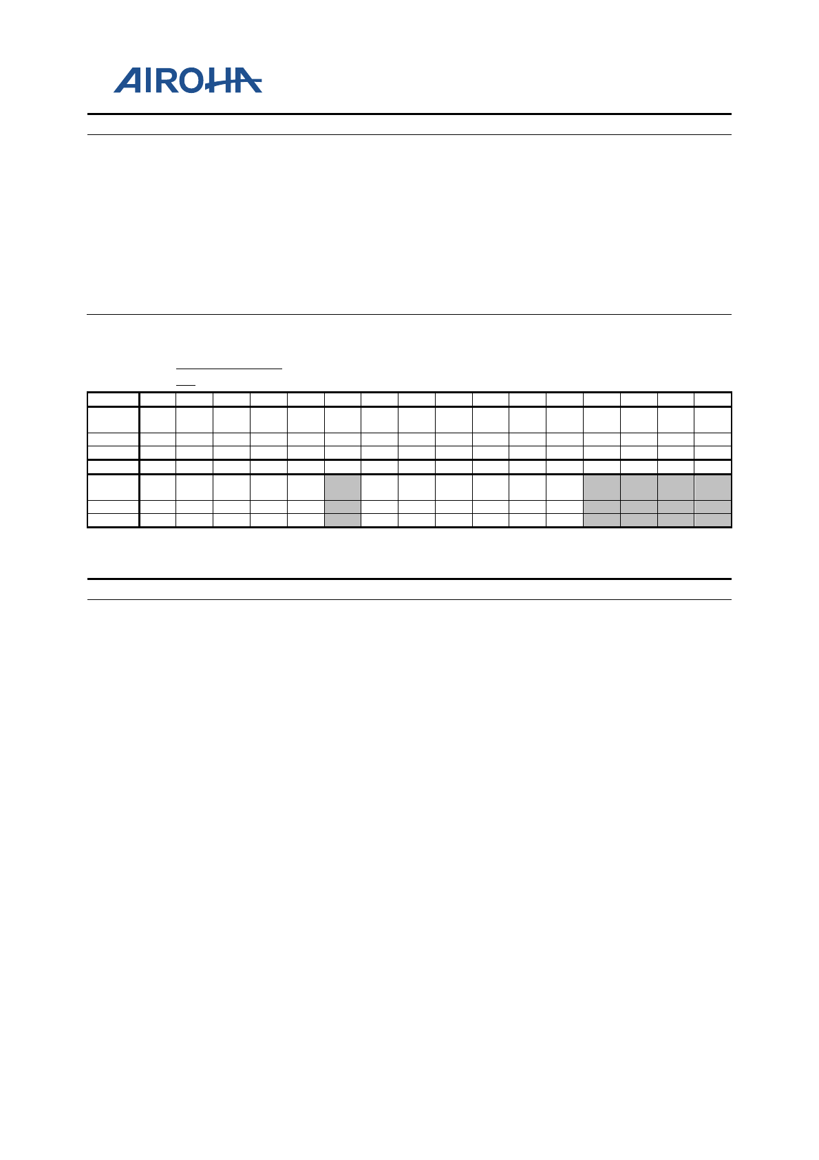
MT2523 Series Reference Manual
© 2015 - 2018 Airoha Technology Corp.
Page 524 of 692
This document contains information that is proprietary to Airoha Technology Corp. (“Airoha”) and/or its licensor(s).
Any unauthorized use, reproduction or disclosure of this document in whole or in part is strictly prohibited.
Bit(s)
Mnemonic
Name
Description
0: Keep
1: CLR bits
2
GPIO34
GPIO34_R0
Bitwise CLR operation of GPIO34 R0
0: Keep
1: CLR bits
1
GPIO33
GPIO33_R0
Bitwise CLR operation of GPIO33 R0
0: Keep
1: CLR bits
0
GPIO32
GPIO32_R0
Bitwise CLR operation of GPIO32 R0
0: Keep
1: CLR bits
A2020B20
GPIO_RESEN1
_0
GPIO R1 Control
00000000
Bit
31
30
29
28
27
26
25
24
23
22
21
20
19
18
17
16
Name
GPIO
31
GPIO
30
GPIO
29
GPIO
28
GPIO
27
GPIO
26
GPIO
25
GPIO
24
GPIO
23
GPIO
22
GPIO
21
GPIO
20
GPIO1
9
GPIO1
8
GPIO1
7
GPIO
16
Type
RW
RW
RW
RW
RW
RW
RW
RW
RW
RW
RW
RW
RW
RW
RW
RW
Reset
0
0
0
0
0
0
0
0
0
0
0
0
0
0
0
0
Bit
15
14
13
12
11
10
9
8
7
6
5
4
3
2
1
0
Name
GPIO
15
GPIO1
4
GPIO1
3
GPIO1
2
GPIO1
1
GPIO
9
GPIO
8
GPIO
7
GPIO
6
GPIO
5
GPIO
4
Type
RW
RW
RW
RW
RW
RW
RW
RW
RW
RW
RW
Reset
0
0
0
0
0
0
0
0
0
0
0
Overview
Configures GPIO R1 control
Bit(s)
Mnemonic
Name
Description
31
GPIO31
GPIO31_R1
R1 for GPIO31
0: Disable
1: Enable
30
GPIO30
GPIO30_R1
R1 for GPIO30
0: Disable
1: Enable
29
GPIO29
GPIO29_R1
R1 for GPIO29
0: Disable
1: Enable
28
GPIO28
GPIO28_R1
R1 for GPIO28
0: Disable
1: Enable
27
GPIO27
GPIO27_R1
R1 for GPIO27
0: Disable
1: Enable
26
GPIO26
GPIO26_R1
R1 for GPIO26
0: Disable
1: Enable
25
GPIO25
GPIO25_R1
R1 for GPIO25
0: Disable
1: Enable
24
GPIO24
GPIO24_R1
R1 for GPIO24
0: Disable
1: Enable
23
GPIO23
GPIO23_R1
R1 for GPIO23
0: Disable

MT2523 Series Reference Manual
© 2015 - 2018 Airoha Technology Corp.
Page 525 of 692
This document contains information that is proprietary to Airoha Technology Corp. (“Airoha”) and/or its licensor(s).
Any unauthorized use, reproduction or disclosure of this document in whole or in part is strictly prohibited.
Bit(s)
Mnemonic
Name
Description
1: Enable
22
GPIO22
GPIO22_R1
R1 for GPIO22
0: Disable
1: Enable
21
GPIO21
GPIO21_R1
R1 for GPIO21
0: Disable
1: Enable
20
GPIO20
GPIO20_R1
R1 for GPIO20
0: Disable
1: Enable
19
GPIO19
GPIO19_R1
R1 for GPIO19
0: Disable
1: Enable
18
GPIO18
GPIO18_R1
R1 for GPIO18
0: Disable
1: Enable
17
GPIO17
GPIO17_R1
R1 for GPIO17
0: Disable
1: Enable
16
GPIO16
GPIO16_R1
R1 for GPIO16
0: Disable
1: Enable
15
GPIO15
GPIO15_R1
R1 for GPIO15
0: Disable
1: Enable
14
GPIO14
GPIO14_R1
R1 for GPIO14
0: Disable
1: Enable
13
GPIO13
GPIO13_R1
R1 for GPIO13
0: Disable
1: Enable
12
GPIO12
GPIO12_R1
R1 for GPIO12
0: Disable
1: Enable
11
GPIO11
GPIO11_R1
R1 for GPIO11
0: Disable
1: Enable
9
GPIO9
GPIO9_R1
R1 for GPIO9
0: Disable
1: Enable
8
GPIO8
GPIO8_R1
R1 for GPIO8
0: Disable
1: Enable
7
GPIO7
GPIO7_R1
R1 for GPIO7
0: Disable
1: Enable
6
GPIO6
GPIO6_R1
R1 for GPIO6
0: Disable
1: Enable
5
GPIO5
GPIO5_R1
R1 for GPIO5
0: Disable
1: Enable
4
GPIO4
GPIO4_R1
R1 for GPIO4
0: Disable

MT2523 Series Reference Manual
© 2015 - 2018 Airoha Technology Corp.
Page 526 of 692
This document contains information that is proprietary to Airoha Technology Corp. (“Airoha”) and/or its licensor(s).
Any unauthorized use, reproduction or disclosure of this document in whole or in part is strictly prohibited.
Bit(s)
Mnemonic
Name
Description
1: Enable
A2020B24
GPIO_RESEN1
_0_SET
GPIO R1 Control
00000000
Bit
31
30
29
28
27
26
25
24
23
22
21
20
19
18
17
16
Name
GPIO
31
GPIO
30
GPIO
29
GPIO
28
GPIO
27
GPIO
26
GPIO
25
GPIO
24
GPIO
23
GPIO
22
GPIO
21
GPIO
20
GPIO1
9
GPIO1
8
GPIO1
7
GPIO
16
Type
WO
WO
WO
WO
WO
WO
WO
WO
WO
WO
WO
WO
WO
WO
WO
WO
Reset
0
0
0
0
0
0
0
0
0
0
0
0
0
0
0
0
Bit
15
14
13
12
11
10
9
8
7
6
5
4
3
2
1
0
Name
GPIO
15
GPIO1
4
GPIO1
3
GPIO1
2
GPIO1
1
GPIO
9
GPIO
8
GPIO
7
GPIO
6
GPIO
5
GPIO
4
Type
WO
WO
WO
WO
WO
WO
WO
WO
WO
WO
WO
Reset
0
0
0
0
0
0
0
0
0
0
0
Overview
For bitwise access of GPIO_RESEN1_0
Bit(s)
Mnemonic
Name
Description
31
GPIO31
GPIO31_R1
Bitwise SET operation of GPIO31 R1
0: Keep
1: SET bits
30
GPIO30
GPIO30_R1
Bitwise SET operation of GPIO30 R1
0: Keep
1: SET bits
29
GPIO29
GPIO29_R1
Bitwise SET operation of GPIO29 R1
0: Keep
1: SET bits
28
GPIO28
GPIO28_R1
Bitwise SET operation of GPIO28 R1
0: Keep
1: SET bits
27
GPIO27
GPIO27_R1
Bitwise SET operation of GPIO27 R1
0: Keep
1: SET bits
26
GPIO26
GPIO26_R1
Bitwise SET operation of GPIO26 R1
0: Keep
1: SET bits
25
GPIO25
GPIO25_R1
Bitwise SET operation of GPIO25 R1
0: Keep
1: SET bits
24
GPIO24
GPIO24_R1
Bitwise SET operation of GPIO24 R1
0: Keep
1: SET bits
23
GPIO23
GPIO23_R1
Bitwise SET operation of GPIO23 R1
0: Keep
1: SET bits
22
GPIO22
GPIO22_R1
Bitwise SET operation of GPIO22 R1
0: Keep
1: SET bits
21
GPIO21
GPIO21_R1
Bitwise SET operation of GPIO21 R1
0: Keep
1: SET bits
20
GPIO20
GPIO20_R1
Bitwise SET operation of GPIO20 R1
0: Keep
1: SET bits

MT2523 Series Reference Manual
© 2015 - 2018 Airoha Technology Corp.
Page 527 of 692
This document contains information that is proprietary to Airoha Technology Corp. (“Airoha”) and/or its licensor(s).
Any unauthorized use, reproduction or disclosure of this document in whole or in part is strictly prohibited.
Bit(s)
Mnemonic
Name
Description
19
GPIO19
GPIO19_R1
Bitwise SET operation of GPIO19 R1
0: Keep
1: SET bits
18
GPIO18
GPIO18_R1
Bitwise SET operation of GPIO18 R1
0: Keep
1: SET bits
17
GPIO17
GPIO17_R1
Bitwise SET operation of GPIO17 R1
0: Keep
1: SET bits
16
GPIO16
GPIO16_R1
Bitwise SET operation of GPIO16 R1
0: Keep
1: SET bits
15
GPIO15
GPIO15_R1
Bitwise SET operation of GPIO15 R1
0: Keep
1: SET bits
14
GPIO14
GPIO14_R1
Bitwise SET operation of GPIO14 R1
0: Keep
1: SET bits
13
GPIO13
GPIO13_R1
Bitwise SET operation of GPIO13 R1
0: Keep
1: SET bits
12
GPIO12
GPIO12_R1
Bitwise SET operation of GPIO12 R1
0: Keep
1: SET bits
11
GPIO11
GPIO11_R1
Bitwise SET operation of GPIO11 R1
0: Keep
1: SET bits
9
GPIO9
GPIO9_R1
Bitwise SET operation of GPIO9 R1
0: Keep
1: SET bits
8
GPIO8
GPIO8_R1
Bitwise SET operation of GPIO8 R1
0: Keep
1: SET bits
7
GPIO7
GPIO7_R1
Bitwise SET operation of GPIO7 R1
0: Keep
1: SET bits
6
GPIO6
GPIO6_R1
Bitwise SET operation of GPIO6 R1
0: Keep
1: SET bits
5
GPIO5
GPIO5_R1
Bitwise SET operation of GPIO5 R1
0: Keep
1: SET bits
4
GPIO4
GPIO4_R1
Bitwise SET operation of GPIO4 R1
0: Keep
1: SET bits
A2020B28
GPIO_RESEN1
_0_CLR
GPIO R1 Control
00000000
Bit
31
30
29
28
27
26
25
24
23
22
21
20
19
18
17
16
Name
GPIO
31
GPIO
30
GPIO
29
GPIO
28
GPIO
27
GPIO
26
GPIO
25
GPIO
24
GPIO
23
GPIO
22
GPIO
21
GPIO
20
GPIO1
9
GPIO1
8
GPIO1
7
GPIO
16
Type
WO
WO
WO
WO
WO
WO
WO
WO
WO
WO
WO
WO
WO
WO
WO
WO
Reset
0
0
0
0
0
0
0
0
0
0
0
0
0
0
0
0

MT2523 Series Reference Manual
© 2015 - 2018 Airoha Technology Corp.
Page 528 of 692
This document contains information that is proprietary to Airoha Technology Corp. (“Airoha”) and/or its licensor(s).
Any unauthorized use, reproduction or disclosure of this document in whole or in part is strictly prohibited.
Bit
15
14
13
12
11
10
9
8
7
6
5
4
3
2
1
0
Name
GPIO
15
GPIO1
4
GPIO1
3
GPIO1
2
GPIO1
1
GPIO
9
GPIO
8
GPIO
7
GPIO
6
GPIO
5
GPIO
4
Type
WO
WO
WO
WO
WO
WO
WO
WO
WO
WO
WO
Reset
0
0
0
0
0
0
0
0
0
0
0
Overview
For bitwise access of GPIO_RESEN1_0
Bit(s)
Mnemonic
Name
Description
31
GPIO31
GPIO31_R1
Bitwise CLR operation of GPIO31 R1
0: Keep
1: CLR bits
30
GPIO30
GPIO30_R1
Bitwise CLR operation of GPIO30 R1
0: Keep
1: CLR bits
29
GPIO29
GPIO29_R1
Bitwise CLR operation of GPIO29 R1
0: Keep
1: CLR bits
28
GPIO28
GPIO28_R1
Bitwise CLR operation of GPIO28 R1
0: Keep
1: CLR bits
27
GPIO27
GPIO27_R1
Bitwise CLR operation of GPIO27 R1
0: Keep
1: CLR bits
26
GPIO26
GPIO26_R1
Bitwise CLR operation of GPIO26 R1
0: Keep
1: CLR bits
25
GPIO25
GPIO25_R1
Bitwise CLR operation of GPIO25 R1
0: Keep
1: CLR bits
24
GPIO24
GPIO24_R1
Bitwise CLR operation of GPIO24 R1
0: Keep
1: CLR bits
23
GPIO23
GPIO23_R1
Bitwise CLR operation of GPIO23 R1
0: Keep
1: CLR bits
22
GPIO22
GPIO22_R1
Bitwise CLR operation of GPIO22 R1
0: Keep
1: CLR bits
21
GPIO21
GPIO21_R1
Bitwise CLR operation of GPIO21 R1
0: Keep
1: CLR bits
20
GPIO20
GPIO20_R1
Bitwise CLR operation of GPIO20 R1
0: Keep
1: CLR bits
19
GPIO19
GPIO19_R1
Bitwise CLR operation of GPIO19 R1
0: Keep
1: CLR bits
18
GPIO18
GPIO18_R1
Bitwise CLR operation of GPIO18 R1
0: Keep
1: CLR bits
17
GPIO17
GPIO17_R1
Bitwise CLR operation of GPIO17 R1
0: Keep
1: CLR bits
16
GPIO16
GPIO16_R1
Bitwise CLR operation of GPIO16 R1
0: Keep
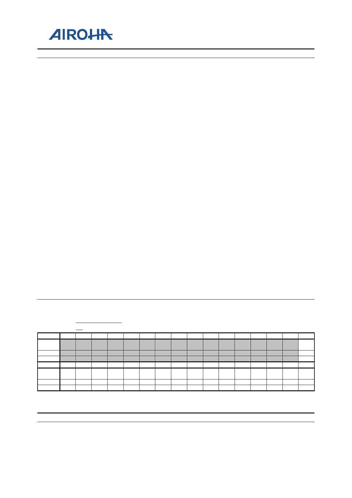
MT2523 Series Reference Manual
© 2015 - 2018 Airoha Technology Corp.
Page 529 of 692
This document contains information that is proprietary to Airoha Technology Corp. (“Airoha”) and/or its licensor(s).
Any unauthorized use, reproduction or disclosure of this document in whole or in part is strictly prohibited.
Bit(s)
Mnemonic
Name
Description
1: CLR bits
15
GPIO15
GPIO15_R1
Bitwise CLR operation of GPIO15 R1
0: Keep
1: CLR bits
14
GPIO14
GPIO14_R1
Bitwise CLR operation of GPIO14 R1
0: Keep
1: CLR bits
13
GPIO13
GPIO13_R1
Bitwise CLR operation of GPIO13 R1
0: Keep
1: CLR bits
12
GPIO12
GPIO12_R1
Bitwise CLR operation of GPIO12 R1
0: Keep
1: CLR bits
11
GPIO11
GPIO11_R1
Bitwise CLR operation of GPIO11 R1
0: Keep
1: CLR bits
9
GPIO9
GPIO9_R1
Bitwise CLR operation of GPIO9 R1
0: Keep
1: CLR bits
8
GPIO8
GPIO8_R1
Bitwise CLR operation of GPIO8 R1
0: Keep
1: CLR bits
7
GPIO7
GPIO7_R1
Bitwise CLR operation of GPIO7 R1
0: Keep
1: CLR bits
6
GPIO6
GPIO6_R1
Bitwise CLR operation of GPIO6 R1
0: Keep
1: CLR bits
5
GPIO5
GPIO5_R1
Bitwise CLR operation of GPIO5 R1
0: Keep
1: CLR bits
4
GPIO4
GPIO4_R1
Bitwise CLR operation of GPIO4 R1
0: Keep
1: CLR bits
A2020B30
GPIO_RESEN1
_1
GPIO R1 Control
00000000
Bit
31
30
29
28
27
26
25
24
23
22
21
20
19
18
17
16
Name
GPIO
48
Type
RW
Reset
0
Bit
15
14
13
12
11
10
9
8
7
6
5
4
3
2
1
0
Name
GPIO
47
GPIO
46
GPIO
45
GPIO
44
GPIO
43
GPIO
42
GPIO
41
GPIO
40
GPIO
39
GPIO
38
GPIO
37
GPIO
36
GPIO
35
GPIO
34
GPIO
33
GPIO
32
Type
RW
RW
RW
RW
RW
RW
RW
RW
RW
RW
RW
RW
RW
RW
RW
RW
Reset
0
0
0
0
0
0
0
0
0
0
0
0
0
0
0
0
Overview
Configures GPIO R1 control
Bit(s)
Mnemonic
Name
Description
16
GPIO48
GPIO48_R1
R1 for GPIO48
0: Disable
1: Enable

MT2523 Series Reference Manual
© 2015 - 2018 Airoha Technology Corp.
Page 530 of 692
This document contains information that is proprietary to Airoha Technology Corp. (“Airoha”) and/or its licensor(s).
Any unauthorized use, reproduction or disclosure of this document in whole or in part is strictly prohibited.
Bit(s)
Mnemonic
Name
Description
15
GPIO47
GPIO47_R1
R1 for GPIO47
0: Disable
1: Enable
14
GPIO46
GPIO46_R1
R1 for GPIO46
0: Disable
1: Enable
13
GPIO45
GPIO45_R1
R1 for GPIO45
0: Disable
1: Enable
12
GPIO44
GPIO44_R1
R1 for GPIO44
0: Disable
1: Enable
11
GPIO43
GPIO43_R1
R1 for GPIO43
0: Disable
1: Enable
10
GPIO42
GPIO42_R1
R1 for GPIO42
0: Disable
1: Enable
9
GPIO41
GPIO41_R1
R1 for GPIO41
0: Disable
1: Enable
8
GPIO40
GPIO40_R1
R1 for GPIO40
0: Disable
1: Enable
7
GPIO39
GPIO39_R1
R1 for GPIO39
0: Disable
1: Enable
6
GPIO38
GPIO38_R1
R1 for GPIO38
0: Disable
1: Enable
5
GPIO37
GPIO37_R1
R1 for GPIO37
0: Disable
1: Enable
4
GPIO36
GPIO36_R1
R1 for GPIO36
0: Disable
1: Enable
3
GPIO35
GPIO35_R1
R1 for GPIO35
0: Disable
1: Enable
2
GPIO34
GPIO34_R1
R1 for GPIO34
0: Disable
1: Enable
1
GPIO33
GPIO33_R1
R1 for GPIO33
0: Disable
1: Enable
0
GPIO32
GPIO32_R1
R1 for GPIO32
0: Disable
1: Enable
A2020B34
GPIO_RESEN1
_1_SET
GPIO R1 Control
00000000
Bit
31
30
29
28
27
26
25
24
23
22
21
20
19
18
17
16

MT2523 Series Reference Manual
© 2015 - 2018 Airoha Technology Corp.
Page 531 of 692
This document contains information that is proprietary to Airoha Technology Corp. (“Airoha”) and/or its licensor(s).
Any unauthorized use, reproduction or disclosure of this document in whole or in part is strictly prohibited.
Name
GPIO
48
Type
WO
Reset
0
Bit
15
14
13
12
11
10
9
8
7
6
5
4
3
2
1
0
Name
GPIO
47
GPIO
46
GPIO
45
GPIO
44
GPIO
43
GPIO
42
GPIO
41
GPIO
40
GPIO
39
GPIO
38
GPIO
37
GPIO
36
GPIO
35
GPIO
34
GPIO
33
GPIO
32
Type
WO
WO
WO
WO
WO
WO
WO
WO
WO
WO
WO
WO
WO
WO
WO
WO
Reset
0
0
0
0
0
0
0
0
0
0
0
0
0
0
0
0
Overview
For bitwise access of GPIO_RESEN1_1
Bit(s)
Mnemonic
Name
Description
16
GPIO48
GPIO48_R1
Bitwise SET operation of GPIO48 R1
0: Keep
1: SET bits
15
GPIO47
GPIO47_R1
Bitwise SET operation of GPIO47 R1
0: Keep
1: SET bits
14
GPIO46
GPIO46_R1
Bitwise SET operation of GPIO46 R1
0: Keep
1: SET bits
13
GPIO45
GPIO45_R1
Bitwise SET operation of GPIO45 R1
0: Keep
1: SET bits
12
GPIO44
GPIO44_R1
Bitwise SET operation of GPIO44 R1
0: Keep
1: SET bits
11
GPIO43
GPIO43_R1
Bitwise SET operation of GPIO43 R1
0: Keep
1: SET bits
10
GPIO42
GPIO42_R1
Bitwise SET operation of GPIO42 R1
0: Keep
1: SET bits
9
GPIO41
GPIO41_R1
Bitwise SET operation of GPIO41 R1
0: Keep
1: SET bits
8
GPIO40
GPIO40_R1
Bitwise SET operation of GPIO40 R1
0: Keep
1: SET bits
7
GPIO39
GPIO39_R1
Bitwise SET operation of GPIO39 R1
0: Keep
1: SET bits
6
GPIO38
GPIO38_R1
Bitwise SET operation of GPIO38 R1
0: Keep
1: SET bits
5
GPIO37
GPIO37_R1
Bitwise SET operation of GPIO37 R1
0: Keep
1: SET bits
4
GPIO36
GPIO36_R1
Bitwise SET operation of GPIO36 R1
0: Keep
1: SET bits
3
GPIO35
GPIO35_R1
Bitwise SET operation of GPIO35 R1
0: Keep
1: SET bits
2
GPIO34
GPIO34_R1
Bitwise SET operation of GPIO34 R1
0: Keep

MT2523 Series Reference Manual
© 2015 - 2018 Airoha Technology Corp.
Page 532 of 692
This document contains information that is proprietary to Airoha Technology Corp. (“Airoha”) and/or its licensor(s).
Any unauthorized use, reproduction or disclosure of this document in whole or in part is strictly prohibited.
Bit(s)
Mnemonic
Name
Description
1: SET bits
1
GPIO33
GPIO33_R1
Bitwise SET operation of GPIO33 R1
0: Keep
1: SET bits
0
GPIO32
GPIO32_R1
Bitwise SET operation of GPIO32 R1
0: Keep
1: SET bits
A2020B38
GPIO_RESEN1
_1_CLR
GPIO R1 Control
00000000
Bit
31
30
29
28
27
26
25
24
23
22
21
20
19
18
17
16
Name
GPIO
48
Type
WO
Reset
0
Bit
15
14
13
12
11
10
9
8
7
6
5
4
3
2
1
0
Name
GPIO
47
GPIO
46
GPIO
45
GPIO
44
GPIO
43
GPIO
42
GPIO
41
GPIO
40
GPIO
39
GPIO
38
GPIO
37
GPIO
36
GPIO
35
GPIO
34
GPIO
33
GPIO
32
Type
WO
WO
WO
WO
WO
WO
WO
WO
WO
WO
WO
WO
WO
WO
WO
WO
Reset
0
0
0
0
0
0
0
0
0
0
0
0
0
0
0
0
Overview
For bitwise access of GPIO_RESEN1_1
Bit(s)
Mnemonic
Name
Description
16
GPIO48
GPIO48_R1
Bitwise CLR operation of GPIO48 R1
0: Keep
1: CLR bits
15
GPIO47
GPIO47_R1
Bitwise CLR operation of GPIO47 R1
0: Keep
1: CLR bits
14
GPIO46
GPIO46_R1
Bitwise CLR operation of GPIO46 R1
0: Keep
1: CLR bits
13
GPIO45
GPIO45_R1
Bitwise CLR operation of GPIO45 R1
0: Keep
1: CLR bits
12
GPIO44
GPIO44_R1
Bitwise CLR operation of GPIO44 R1
0: Keep
1: CLR bits
11
GPIO43
GPIO43_R1
Bitwise CLR operation of GPIO43 R1
0: Keep
1: CLR bits
10
GPIO42
GPIO42_R1
Bitwise CLR operation of GPIO42 R1
0: Keep
1: CLR bits
9
GPIO41
GPIO41_R1
Bitwise CLR operation of GPIO41 R1
0: Keep
1: CLR bits
8
GPIO40
GPIO40_R1
Bitwise CLR operation of GPIO40 R1
0: Keep
1: CLR bits
7
GPIO39
GPIO39_R1
Bitwise CLR operation of GPIO39 R1
0: Keep
1: CLR bits
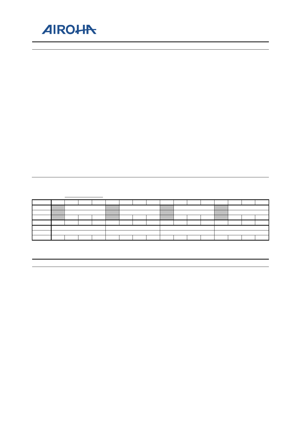
MT2523 Series Reference Manual
© 2015 - 2018 Airoha Technology Corp.
Page 533 of 692
This document contains information that is proprietary to Airoha Technology Corp. (“Airoha”) and/or its licensor(s).
Any unauthorized use, reproduction or disclosure of this document in whole or in part is strictly prohibited.
Bit(s)
Mnemonic
Name
Description
6
GPIO38
GPIO38_R1
Bitwise CLR operation of GPIO38 R1
0: Keep
1: CLR bits
5
GPIO37
GPIO37_R1
Bitwise CLR operation of GPIO37 R1
0: Keep
1: CLR bits
4
GPIO36
GPIO36_R1
Bitwise CLR operation of GPIO36 R1
0: Keep
1: CLR bits
3
GPIO35
GPIO35_R1
Bitwise CLR operation of GPIO35 R1
0: Keep
1: CLR bits
2
GPIO34
GPIO34_R1
Bitwise CLR operation of GPIO34 R1
0: Keep
1: CLR bits
1
GPIO33
GPIO33_R1
Bitwise CLR operation of GPIO33 R1
0: Keep
1: CLR bits
0
GPIO32
GPIO32_R1
Bitwise CLR operation of GPIO32 R1
0: Keep
1: CLR bits
A2020C00
GPIO_MODE0
GPIO Mode
Control
00000000
Bit
31
30
29
28
27
26
25
24
23
22
21
20
19
18
17
16
Name
GPIO7
GPIO6
GPIO5
GPIO4
Type
RW
RW
RW
RW
Reset
0
0
0
0
0
0
0
0
0
0
0
0
Bit
15
14
13
12
11
10
9
8
7
6
5
4
3
2
1
0
Name
GPIO3
GPIO2
GPIO1
GPIO0
Type
RW
RW
RW
RW
Reset
0
0
0
0
0
0
0
0
0
0
0
0
0
0
0
0
Overview
Configures GPIO aux. mode
Bit(s)
Mnemonic
Name
Description
30:28
GPIO7
Aux. mode of GPIO_7
0: GPIO7 (IO)
1: EINT6 (I)
2: MC1_A_DA1 (IO)
3: SLA_EDICK (I)
4: U2TXD (O)
5: Reserved
6: BT_BUCK_EN_HW (O)
7: MA_SPI0_B_MISO (I)
8: Reserved
9: Reserved
26:24
GPIO6
Aux. mode of GPIO_6
0: GPIO6 (IO)
1: EINT5 (I)
2: MC1_A_DA0 (IO)
3: SLA_EDIWS (I)
4: U2RXD (I)
5: Reserved
6: Reserved
7: MA_SPI0_B_MOSI (O)
8: Reserved

MT2523 Series Reference Manual
© 2015 - 2018 Airoha Technology Corp.
Page 534 of 692
This document contains information that is proprietary to Airoha Technology Corp. (“Airoha”) and/or its licensor(s).
Any unauthorized use, reproduction or disclosure of this document in whole or in part is strictly prohibited.
Bit(s)
Mnemonic
Name
Description
9: Reserved
22:20
GPIO5
Aux. mode of GPIO_5
0: GPIO5 (IO)
1: EINT4 (I)
2: MC1_A_CM0 (IO)
3: SLA_EDIDI (I)
4: Reserved
5: Reserved
6: U1TXD (O)
7: MA_SPI0_B_SCK (O)
8: Reserved
9: Reserved
18:16
GPIO4
Aux. mode of GPIO_4
0: GPIO4 (IO)
1: EINT3 (I)
2: MC1_A_CK (IO)
3: SLA_EDIDO (O)
4: Reserved
5: Reserved
6: U1RXD (I)
7: MA_SPI0_B_CS (O)
8: Reserved
9: Reserved
15:12
GPIO3
Aux. mode of GPIO_3
0: GPIO3 (IO)
1: EINT14 (I)
2: AUXADCIN_3 (AIO)
3: U3TXD (I)
4: U0RTS (O)
5: MA_SPI1_A_MISO (I)
6: MA_EDICK (O)
7: MA_SPI0_A_MISO (I)
8: DEBUGMON14 (IO)
9: BTPRI (IO)
11:8
GPIO2
Aux. mode of GPIO_2
0: GPIO2 (IO)
1: EINT2 (I)
2: AUXADCIN_2 (AIO)
3: U3RXD (I)
4: U0CTS (I)
5: MA_SPI1_A_MOSI (O)
6: MA_EDIWS (O)
7: MA_SPI0_A_MOSI (O)
8: DEBUGMON13 (IO)
9: BT_BUCK_EN_HW (O)
7:4
GPIO1
Aux. mode of GPIO_1
0: GPIO1 (IO)
1: EINT1 (I)
2: AUXADCIN_1 (AIO)
3: U2TXD (O)
4: PWM1 (O)
5: MA_SPI1_A_SCK (O)
6: MA_EDIDI (I)
7: MA_SPI0_A_SCK (O)
8: DEBUGMON12 (IO)
9: BTDBGACKN (I)
3:0
GPIO0
Aux. mode of GPIO_0
0: GPIO0 (IO)
1: EINT0 (I)
2: AUXADCIN_0 (AIO)
3: U2RXD (I)
MT2523 Series Reference Manual
© 2015 - 2018 Airoha Technology Corp.
Page 535 of 692
This document contains information that is proprietary to Airoha Technology Corp. (“Airoha”) and/or its licensor(s).
Any unauthorized use, reproduction or disclosure of this document in whole or in part is strictly prohibited.
Bit(s)
Mnemonic
Name
Description
4: PWM0 (O)
5: MA_SPI1_A_CS (O)
6: MA_EDIDO (O)
7: MA_SPI0_A_CS (O)
8: DEBUGMON11 (IO)
9: BTJTDI (O)
A2020C04
GPIO_MODE0
_SET
GPIO Mode Control
00000000
Bit
31
30
29
28
27
26
25
24
23
22
21
20
19
18
17
16
Name
GPIO7
GPIO6
GPIO5
GPIO4
Type
WO
WO
WO
WO
Reset
0
0
0
0
0
0
0
0
0
0
0
0
Bit
15
14
13
12
11
10
9
8
7
6
5
4
3
2
1
0
Name
GPIO3
GPIO2
GPIO1
GPIO0
Type
WO
WO
WO
WO
Reset
0
0
0
0
0
0
0
0
0
0
0
0
0
0
0
0
Overview
For bitwise access of GPIO_MODE0
Bit(s)
Mnemonic
Name
Description
30:28
GPIO7
Bitwise SET operation for Aux. mode of GPIO_7
0: Keep
1: SET bits
26:24
GPIO6
Bitwise SET operation for Aux. mode of GPIO_6
0: Keep
1: SET bits
22:20
GPIO5
Bitwise SET operation for Aux. mode of GPIO_5
0: Keep
1: SET bits
18:16
GPIO4
Bitwise SET operation for Aux. mode of GPIO_4
0: Keep
1: SET bits
15:12
GPIO3
Bitwise SET operation for Aux. mode of GPIO_3
0: Keep
1: SET bits
11:8
GPIO2
Bitwise SET operation for Aux. mode of GPIO_2
0: Keep
1: SET bits
7:4
GPIO1
Bitwise SET operation for Aux. mode of GPIO_1
0: Keep
1: SET bits
3:0
GPIO0
Bitwise SET operation for Aux. mode of GPIO_0
0: Keep
1: SET bits
A2020C08
GPIO_MODE0
_CLR
GPIO Mode
Control
00000000
Bit
31
30
29
28
27
26
25
24
23
22
21
20
19
18
17
16
Name
GPIO7
GPIO6
GPIO5
GPIO4
Type
WO
WO
WO
WO
Reset
0
0
0
0
0
0
0
0
0
0
0
0
Bit
15
14
13
12
11
10
9
8
7
6
5
4
3
2
1
0
MT2523 Series Reference Manual
© 2015 - 2018 Airoha Technology Corp.
Page 536 of 692
This document contains information that is proprietary to Airoha Technology Corp. (“Airoha”) and/or its licensor(s).
Any unauthorized use, reproduction or disclosure of this document in whole or in part is strictly prohibited.
Name
GPIO3
GPIO2
GPIO1
GPIO0
Type
WO
WO
WO
WO
Reset
0
0
0
0
0
0
0
0
0
0
0
0
0
0
0
0
Overview
For bitwise access of GPIO_MODE0
Bit(s)
Mnemonic
Name
Description
30:28
GPIO7
Bitwise CLR operation for Aux. mode of GPIO_7
0: Keep
1: CLR bits
26:24
GPIO6
Bitwise CLR operation for Aux. mode of GPIO_6
0: Keep
1: CLR bits
22:20
GPIO5
Bitwise CLR operation for Aux. mode of GPIO_5
0: Keep
1: CLR bits
18:16
GPIO4
Bitwise CLR operation for Aux. mode of GPIO_4
0: Keep
1: CLR bits
15:12
GPIO3
Bitwise CLR operation for Aux. mode of GPIO_3
0: Keep
1: CLR bits
11:8
GPIO2
Bitwise CLR operation for Aux. mode of GPIO_2
0: Keep
1: CLR bits
7:4
GPIO1
Bitwise CLR operation for Aux. mode of GPIO_1
0: Keep
1: CLR bits
3:0
GPIO0
Bitwise CLR operation for Aux. mode of GPIO_0
0: Keep
1: CLR bits
A2020C10
GPIO_MODE1
GPIO Mode Control
00000000
Bit
31
30
29
28
27
26
25
24
23
22
21
20
19
18
17
16
Name
GPIO15
GPIO14
GPIO13
GPIO12
Type
RW
RW
RW
RW
Reset
0
0
0
0
0
0
0
0
0
0
0
0
Bit
15
14
13
12
11
10
9
8
7
6
5
4
3
2
1
0
Name
GPIO11
GPIO10
GPIO9
GPIO8
Type
RW
RW
RW
RW
Reset
0
0
0
0
0
0
0
0
0
0
0
0
0
Overview
Configures GPIO aux. mode
Bit(s)
Mnemonic
Name
Description
30:28
GPIO15
Aux. mode of GPIO_15
0: GPIO15 (IO)
1: EINT13 (I)
2: Reserved
3: Reserved
4: Reserved
5: PWM4 (O)
6: Reserved
7: Reserved
8: Reserved
9: Reserved

MT2523 Series Reference Manual
© 2015 - 2018 Airoha Technology Corp.
Page 537 of 692
This document contains information that is proprietary to Airoha Technology Corp. (“Airoha”) and/or its licensor(s).
Any unauthorized use, reproduction or disclosure of this document in whole or in part is strictly prohibited.
Bit(s)
Mnemonic
Name
Description
26:24
GPIO14
Aux. mode of GPIO_14
0: GPIO14 (IO)
1: EINT12 (I)
2: CLKO4 (O)
3: MA_EDICK (O)
4: MA_SPI1_B_MISO (O)
5: PWM3 (O)
6: SLA_EDICK (I)
7: Reserved
8: Reserved
9: Reserved
22:20
GPIO13
Aux. mode of GPIO_13
0: GPIO13 (IO)
1: EINT11 (I)
2: CLKO3 (O)
3: MA_EDIWS (O)
4: MA_SPI1_B_MOSI (O)
5: PWM2 (O)
6: SLA_EDIWS (I)
7: Reserved
8: Reserved
9: Reserved
18:16
GPIO12
Aux. mode of GPIO_12
0: GPIO12 (IO)
1: EINT10 (I)
2: Reserved
3: MA_EDIDI (I)
4: MA_SPI1_B_SCK (O)
5: PWM1 (O)
6: SLA_EDIDI (I)
7: Reserved
8: Reserved
9: Reserved
14:12
GPIO11
Aux. mode of GPIO_11
0: GPIO11 (IO)
1: EINT9 (I)
2: BT_BUCK_EN_HW (O)
3: MA_EDIDO (O)
4: MA_SPI1_B_CS (O)
5: PWM0 (O)
6: SLA_EDIDO (O)
7: Reserved
8: Reserved
9: Reserved
11:8
GPIO10
Aux. mode of GPIO_10
0: GPIO10 (IO)
1: EINT15 (I)
2: AUXADCIN_4(AIO)
3: Reserved
4: Reserved
5: Reserved
6: Reserved
7: Reserved
8: DEBUGMON15(IO)
9: BTPRI(IO)
6:4
GPIO9
Aux. mode of GPIO_9
0: GPIO9 (IO)
1: EINT8 (I)
2: MC1_A_DA3 (IO)
3: Reserved
4: Reserved
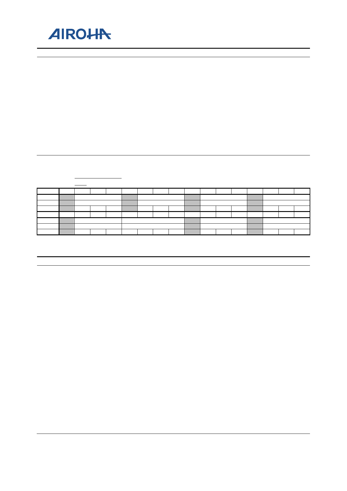
MT2523 Series Reference Manual
© 2015 - 2018 Airoha Technology Corp.
Page 538 of 692
This document contains information that is proprietary to Airoha Technology Corp. (“Airoha”) and/or its licensor(s).
Any unauthorized use, reproduction or disclosure of this document in whole or in part is strictly prohibited.
Bit(s)
Mnemonic
Name
Description
5: Reserved
6: SDA2 (IO)
7: Reserved
8: Reserved
9: Reserved
2:0
GPIO8
Aux. mode of GPIO_8
0: GPIO8 (IO)
1: EINT7 (I)
2: MC1_A_DA2 (IO)
3: Reserved
4: Reserved
5: Reserved
6: SCL2 (IO)
7: Reserved
8: Reserved
9: Reserved
A2020C14
GPIO_MODE1_
SET
GPIO Mode Control
00000000
Bit
31
30
29
28
27
26
25
24
23
22
21
20
19
18
17
16
Name
GPIO15
GPIO14
GPIO13
GPIO12
Type
WO
WO
WO
WO
Reset
0
0
0
0
0
0
0
0
0
0
0
0
Bit
15
14
13
12
11
10
9
8
7
6
5
4
3
2
1
0
Name
GPIO11
GPIO10
GPIO9
GPIO8
Type
WO
WO
WO
WO
Reset
0
0
0
0
0
0
0
0
0
0
0
0
0
Overview
For bitwise access of GPIO_MODE1
Bit(s)
Mnemonic
Name
Description
30:28
GPIO15
Bitwise SET operation for Aux. mode of KCOL1
0: Keep
1: SET bits
26:24
GPIO14
Bitwise SET operation for Aux. mode of KCOL2
0: Keep
1: SET bits
22:20
GPIO13
Bitwise SET operation for Aux. mode of KCOL3
0: Keep
1: SET bits
18:16
GPIO12
Bitwise SET operation for Aux. mode of KCOL4
0: Keep
1: SET bits
14:12
GPIO11
Bitwise SET operation for Aux. mode of UTXD1
0: Keep
1: SET bits
11:8
GPIO10
Bitwise SET operation for Aux. mode of URXD1
0: Keep
1: SET bits
6:4
GPIO9
Bitwise SET operation for Aux. mode of GPIO_9
0: Keep
1: SET bits
2:0
GPIO8
Bitwise SET operation for Aux. mode of GPIO_8
0: Keep
1: SET bits
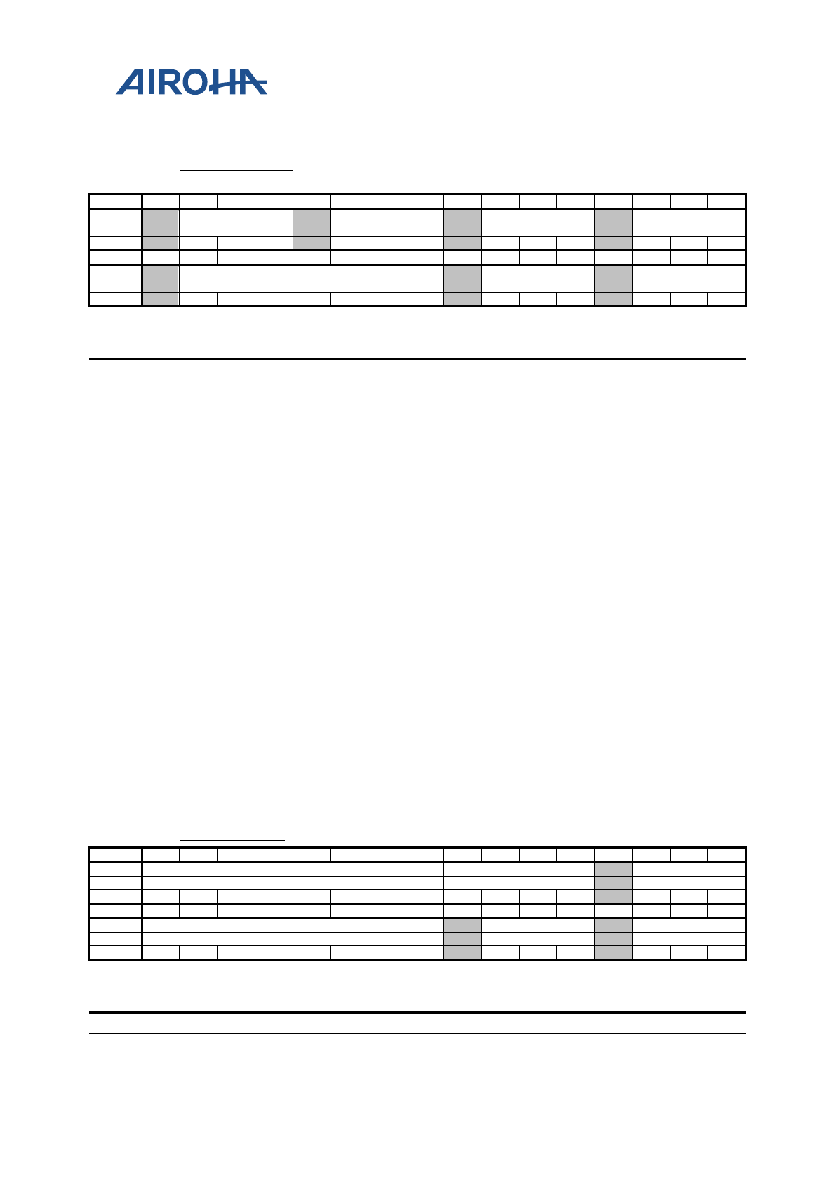
MT2523 Series Reference Manual
© 2015 - 2018 Airoha Technology Corp.
Page 539 of 692
This document contains information that is proprietary to Airoha Technology Corp. (“Airoha”) and/or its licensor(s).
Any unauthorized use, reproduction or disclosure of this document in whole or in part is strictly prohibited.
A2020C18
GPIO_MODE1_
CLR
GPIO Mode Control
00000000
Bit
31
30
29
28
27
26
25
24
23
22
21
20
19
18
17
16
Name
GPIO15
GPIO14
GPIO13
GPIO12
Type
WO
WO
WO
WO
Reset
0
0
0
0
0
0
0
0
0
0
0
0
Bit
15
14
13
12
11
10
9
8
7
6
5
4
3
2
1
0
Name
GPIO11
GPIO10
GPIO9
GPIO8
Type
WO
WO
WO
WO
Reset
0
0
0
0
0
0
0
0
0
0
0
0
0
Overview
For bitwise access of GPIO_MODE1
Bit(s)
Mnemonic
Name
Description
30:28
GPIO15
Bitwise CLR operation for Aux. mode of KCOL1
0: Keep
1: CLR bits
26:24
GPIO14
Bitwise CLR operation for Aux. mode of KCOL2
0: Keep
1: CLR bits
22:20
GPIO13
Bitwise CLR operation for Aux. mode of KCOL3
0: Keep
1: CLR bits
18:16
GPIO12
Bitwise CLR operation for Aux. mode of KCOL4
0: Keep
1: CLR bits
14:12
GPIO11
Bitwise CLR operation for Aux. mode of UTXD1
0: Keep
1: CLR bits
11:8
GPIO10
Bitwise CLR operation for Aux. mode of URXD1
0: Keep
1: CLR bits
6:4
GPIO9
Bitwise CLR operation for Aux. mode of GPIO_9
0: Keep
1: CLR bits
2:0
GPIO8
Bitwise CLR operation for Aux. mode of GPIO_8
0: Keep
1: CLR bits
A2020C20
GPIO_MODE2
GPIO Mode Control
00000011
Bit
31
30
29
28
27
26
25
24
23
22
21
20
19
18
17
16
Name
GPIO23
GPIO22
GPIO21
GPIO20
Type
RW
RW
RW
RW
Reset
0
0
0
0
0
0
0
0
0
0
0
0
0
0
0
Bit
15
14
13
12
11
10
9
8
7
6
5
4
3
2
1
0
Name
GPIO19
GPIO18
GPIO17
GPIO16
Type
RW
RW
RW
RW
Reset
0
0
0
0
0
0
0
0
0
0
1
0
0
1
Overview
Configures GPIO aux. mode
Bit(s)
Mnemonic
Name
Description
31:28
GPIO23
Aux. mode of GPIO_23

MT2523 Series Reference Manual
© 2015 - 2018 Airoha Technology Corp.
Page 540 of 692
This document contains information that is proprietary to Airoha Technology Corp. (“Airoha”) and/or its licensor(s).
Any unauthorized use, reproduction or disclosure of this document in whole or in part is strictly prohibited.
Bit(s)
Mnemonic
Name
Description
0: GPIO23 (IO)
1: KROW0 (IO)
2: EINT19 (I)
3: CLKO0 (O)
4: U1CTS(I)
5: TRACEDATA3 (O)
6: MC_RST (O)
7: DEBUGMON9 (IO)
8: JTRST_B (I)
9: BTJTRSTB (I)
27:24
GPIO22
Aux. mode of GPIO_22
0: GPIO22 (IO)
1: KROW1 (IO)
2: U1TXD (O)
3: U3TXD (O)
4: Reserved
5: TRACEDATA2 (O)
6: TRACE_SWV (O)
7: DEBUGMON5 (IO)
8: JTDO (O)
9: BTDBGIN (I)
23:20
GPIO21
Aux. mode of GPIO_21
0: GPIO21 (IO)
1: KROW2 (IO)
2: Reserved
3: GPCOUNTER_0 (I)
4: U1RTS (O)
5: TRACECLK (O)
6: Reserved
7: DEBUGMON4 (IO)
8: JTCK (I)
9: BTJTCK (I)
18:16
GPIO20
Aux. mode of GPIO_20
0: GPIO20 (IO)
1: KCOL0 (IO)
2: GPSFSYNC (O)
3: U0CTS (I)
4: SDA2 (IO)
5: Reserved
6: MA_SPI2_CS1(O)
7: DEBUGMON7 (IO)
8: Reserved
9: Reserved
15:12
GPIO19
Aux. mode of GPIO_19
0: GPIO19 (IO)
1: KCOL1 (IO)
2: EINT18 (I)
3: U0RTS (O)
4: SCL2 (IO)
5: TRACEDATA1 (O)
6: Reserved
7: DEBUGMON2 (IO)
8: JTMS (IO)
9: BTJTMS (IO)
11:8
GPIO18
Aux. mode of GPIO_18
0: GPIO18 (IO)
1: KCOL2 (IO)
2: U1RXD (I)
3: U3RXD (I)
4: Reserved
5: TRACEDATA0 (O)
6: LSCE1_B1 (O)
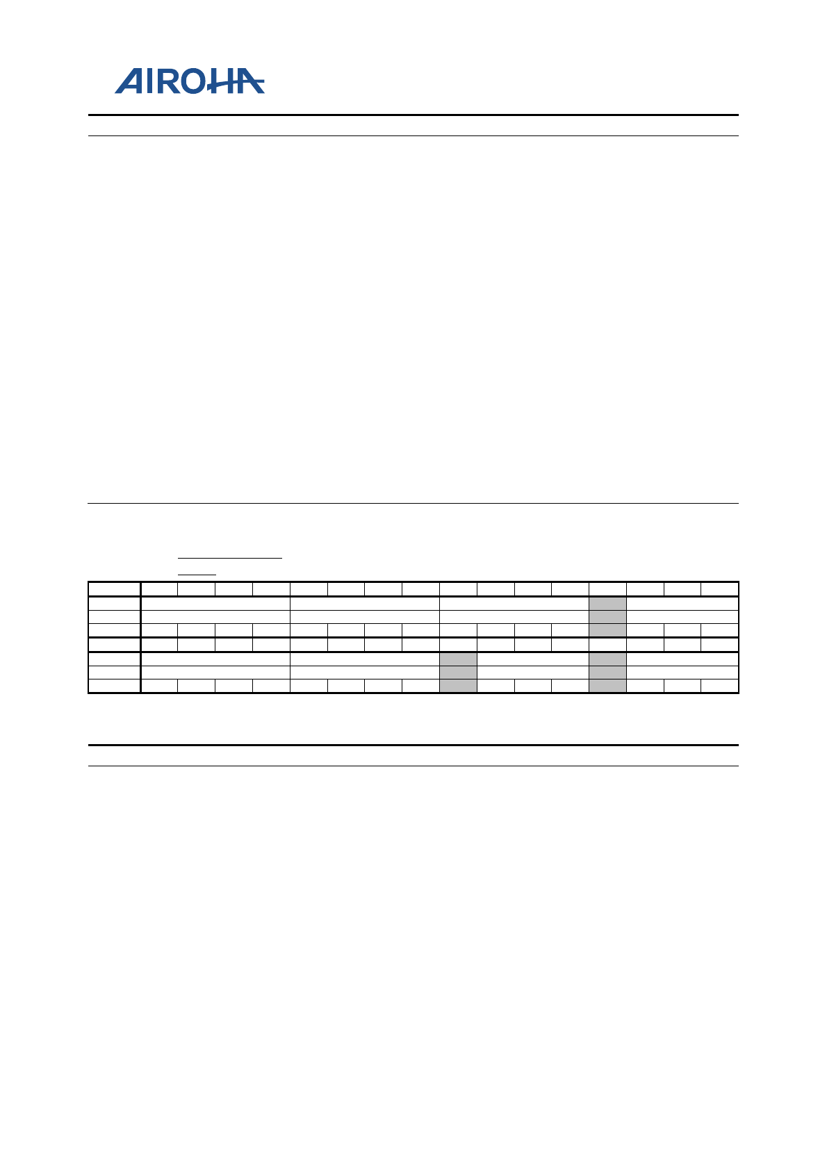
MT2523 Series Reference Manual
© 2015 - 2018 Airoha Technology Corp.
Page 541 of 692
This document contains information that is proprietary to Airoha Technology Corp. (“Airoha”) and/or its licensor(s).
Any unauthorized use, reproduction or disclosure of this document in whole or in part is strictly prohibited.
Bit(s)
Mnemonic
Name
Description
7: DEBUGMON6 (IO)
8: JTDI (I)
9: BTJTDI (IO)
6:4
GPIO17
Aux. mode of GPIO_17
0: GPIO17 (IO)
1: U0TXD (O)
2: Reserved
3: EINT17 (I)
4: Reserved
5: Reserved
6: DEBUGMIN_CK (I)
7: Reserved
8: Reserved
9: Reserved
2:0
GPIO16
Aux. mode of GPIO_16
0: GPIO16 (IO)
1: U0RXD (I)
2: Reserved
3: EINT16 (I)
4: Reserved
5: Reserved
6: DEBUGMIN0 (I)
7: DEBUGMON0 (IO)
8: Reserved
9: Reserved
A2020C24
GPIO_MODE2
_SET
GPIO Mode Control
00000000
Bit
31
30
29
28
27
26
25
24
23
22
21
20
19
18
17
16
Name
GPIO23
GPIO22
GPIO21
GPIO20
Type
WO
WO
WO
WO
Reset
0
0
0
0
0
0
0
0
0
0
0
0
0
0
0
Bit
15
14
13
12
11
10
9
8
7
6
5
4
3
2
1
0
Name
GPIO19
GPIO18
GPIO17
GPIO16
Type
WO
WO
WO
WO
Reset
0
0
0
0
0
0
0
0
0
0
0
0
0
0
Overview
For bitwise access of GPIO_MODE2
Bit(s)
Mnemonic
Name
Description
31:28
GPIO23
Bitwise SET operation for Aux. mode of BPI_BUS1
0: Keep
1: SET bits
27:24
GPIO22
Bitwise SET operation for Aux. mode of BPI_BUS2
0: Keep
1: SET bits
23:20
GPIO21
Bitwise SET operation for Aux. mode of KROW0
0: Keep
1: SET bits
18:16
GPIO20
Bitwise SET operation for Aux. mode of KROW1
0: Keep
1: SET bits
15:12
GPIO19
Bitwise SET operation for Aux. mode of KROW2
0: Keep
1: SET bits
11:8
GPIO18
Bitwise SET operation for Aux. mode of KROW3
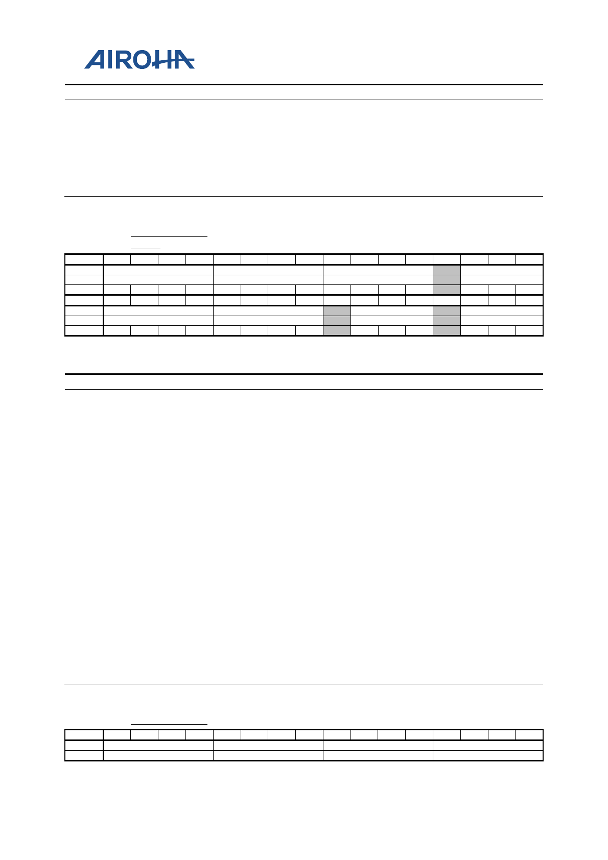
MT2523 Series Reference Manual
© 2015 - 2018 Airoha Technology Corp.
Page 542 of 692
This document contains information that is proprietary to Airoha Technology Corp. (“Airoha”) and/or its licensor(s).
Any unauthorized use, reproduction or disclosure of this document in whole or in part is strictly prohibited.
Bit(s)
Mnemonic
Name
Description
0: Keep
1: SET bits
6:4
GPIO17
Bitwise SET operation for Aux. mode of KROW4
0: Keep
1: SET bits
2:0
GPIO16
Bitwise SET operation for Aux. mode of KCOL0
0: Keep
1: SET bits
A2020C28
GPIO_MODE2
_CLR
GPIO Mode Control
00000000
Bit
31
30
29
28
27
26
25
24
23
22
21
20
19
18
17
16
Name
GPIO23
GPIO22
GPIO21
GPIO20
Type
WO
WO
WO
WO
Reset
0
0
0
0
0
0
0
0
0
0
0
0
0
0
0
Bit
15
14
13
12
11
10
9
8
7
6
5
4
3
2
1
0
Name
GPIO19
GPIO18
GPIO17
GPIO16
Type
WO
WO
WO
WO
Reset
0
0
0
0
0
0
0
0
0
0
0
0
0
0
Overview
For bitwise access of GPIO_MODE2
Bit(s)
Mnemonic
Name
Description
31:28
GPIO23
Bitwise CLR operation for Aux. mode of BPI_BUS1
0: Keep
1: CLR bits
27:24
GPIO22
Bitwise CLR operation for Aux. mode of BPI_BUS2
0: Keep
1: CLR bits
23:20
GPIO21
Bitwise CLR operation for Aux. mode of KROW0
0: Keep
1: CLR bits
18:16
GPIO20
Bitwise CLR operation for Aux. mode of KROW1
0: Keep
1: CLR bits
15:12
GPIO19
Bitwise CLR operation for Aux. mode of KROW2
0: Keep
1: CLR bits
11:8
GPIO18
Bitwise CLR operation for Aux. mode of KROW3
0: Keep
1: CLR bits
6:4
GPIO17
Bitwise CLR operation for Aux. mode of KROW4
0: Keep
1: CLR bits
2:0
GPIO16
Bitwise CLR operation for Aux. mode of KCOL0
0: Keep
1: CLR bits
A2020C30
GPIO_MODE3
GPIO Mode Control
00000000
Bit
31
30
29
28
27
26
25
24
23
22
21
20
19
18
17
16
Name
GPIO31
GPIO30
GPIO29
GPIO28
Type
RW
RW
RW
RW

MT2523 Series Reference Manual
© 2015 - 2018 Airoha Technology Corp.
Page 543 of 692
This document contains information that is proprietary to Airoha Technology Corp. (“Airoha”) and/or its licensor(s).
Any unauthorized use, reproduction or disclosure of this document in whole or in part is strictly prohibited.
Reset
0
0
0
0
0
0
0
0
0
0
0
0
0
0
0
0
Bit
15
14
13
12
11
10
9
8
7
6
5
4
3
2
1
0
Name
GPIO27
GPIO26
GPIO25
GPIO24
Type
RW
RW
RW
RW
Reset
0
0
0
0
0
0
0
0
0
0
0
0
0
0
0
0
Overview
Configures GPIO aux. mode
Bit(s)
Mnemonic
Name
Description
31:28
GPIO31
Aux. mode of GPIO_31
0: GPIO31 (IO)
1: SDA0 (IO)
2: EINT12 (I)
3: PWM1 (O)
4: U1TXD (I)
5: MC0_CM0 (IO)
6: DEBUGMIN1 (I)
7: DEBUGMON1 (IO)
8: BT_RGPIO1 (IO)
9: SDA2 (IO)
27:24
GPIO30
Aux. mode of GPIO_30
0: GPIO30 (IO)
1: SCL0 (IO)
2: EINT11 (I)
3: PWM0 (O)
4: U1RXD (I)
5: MC0_CK (IO)
6: BT_RGPIO0 (IO)
7: DEBUGMON0 (IO)
8: Reserved
9: SCL2 (IO)
23:20
GPIO29
Aux. mode of GPIO_29
0: GPIO29 (IO)
1: CMCSK (I)
2: LPTE (I)
3: Reserved
4: CMCSD2 (I)
5: EINT10 (I)
6: Reserved
7: DEBUGMON15 (IO)
8: MC1_B_DA1(IO)
9: BT_RGPIO2 (IO)
19:16
GPIO28
Aux. mode of GPIO_28
0: GPIO28 (IO)
1: CMMCLK (O)
2: LSA0DA1 (O)
3: DAISYNC (O)
4: MA_SPI2_A_MISO (I)
5: MA_SPI3_A_MISO (I)
6: JTDO (O)
7: DEBUGMON14 (IO)
8: MC1_B_DA0(IO)
9: SLV_SPI0_MISO (O)
15:12
GPIO27
Aux. mode of GPIO_27
0: GPIO27 (IO)
1: CMCSD1 (O)
2: LSDA1 (IO)
3: DAIPCMOUT (I)
4: MA_SPI2_A_MOSI (O)
5: MA_SPI3_A_MOSI (O)
6: JTRST_B (I)
7: DEBUGMON13 (IO)

MT2523 Series Reference Manual
© 2015 - 2018 Airoha Technology Corp.
Page 544 of 692
This document contains information that is proprietary to Airoha Technology Corp. (“Airoha”) and/or its licensor(s).
Any unauthorized use, reproduction or disclosure of this document in whole or in part is strictly prohibited.
Bit(s)
Mnemonic
Name
Description
8: MC1_B_CK(IO)
9: SLV_SPI0_MOSI (I)
11:8
GPIO26
Aux. mode of GPIO_26
0: GPIO26 (IO)
1: CMCSD0 (O)
2: LSCE_B1 (O)
3: DAIPCMIN (I)
4: MA_SPI2_A_SCK (O)
5: MA_SPI3_A_SCK (O)
6: JTCK (I)
7: DEBUGMON12 (IO)
8: MC1_B_CM0 (IO)
9: SLV_SPI0_SCK (I)
7:4
GPIO25
Aux. mode of GPIO_25
0: GPIO25 (IO)
1: CMPDN (O)
2: LSCK1 (O)
3: DAICLK (O)
4: MA_SPI2_A_CS (O)
5: MA_SPI3_A_CS (O)
6: JTMS (IO)
7: DEBUGMON11 (IO)
8: MC1_B_DA2 (IO)
9: SLV_SPI0_CS (I)
3:0
GPIO24
Aux. mode of GPIO_24
0: GPIO24 (IO)
1: CMRST (O)
2: LSRSTB (O)
3: CLKO1 (O)
4: EINT9 (I)
5: GPCOUNTER_0 (I)
6: JTDI (I)
7: DEBUGMON10 (IO)
8: MC1_B_DA3 (IO)
9: Reserved
A2020C34
GPIO_MODE3
_SET
GPIO Mode Control
00000000
Bit
31
30
29
28
27
26
25
24
23
22
21
20
19
18
17
16
Name
GPIO31
GPIO30
GPIO29
GPIO28
Type
WO
WO
WO
WO
Reset
0
0
0
0
0
0
0
0
0
0
0
0
0
0
0
0
Bit
15
14
13
12
11
10
9
8
7
6
5
4
3
2
1
0
Name
GPIO27
GPIO26
GPIO25
GPIO24
Type
WO
WO
WO
WO
Reset
0
0
0
0
0
0
0
0
0
0
0
0
0
0
0
0
Overview
For bitwise access of GPIO_MODE3
Bit(s)
Mnemonic
Name
Description
31:28
GPIO31
Bitwise SET operation for Aux. mode of MCCK
0: Keep
1: SET bits
27:24
GPIO30
Bitwise SET operation for Aux. mode of CMCSK
0: Keep
1: SET bits
23:20
GPIO29
Bitwise SET operation for Aux. mode of CMMCLK
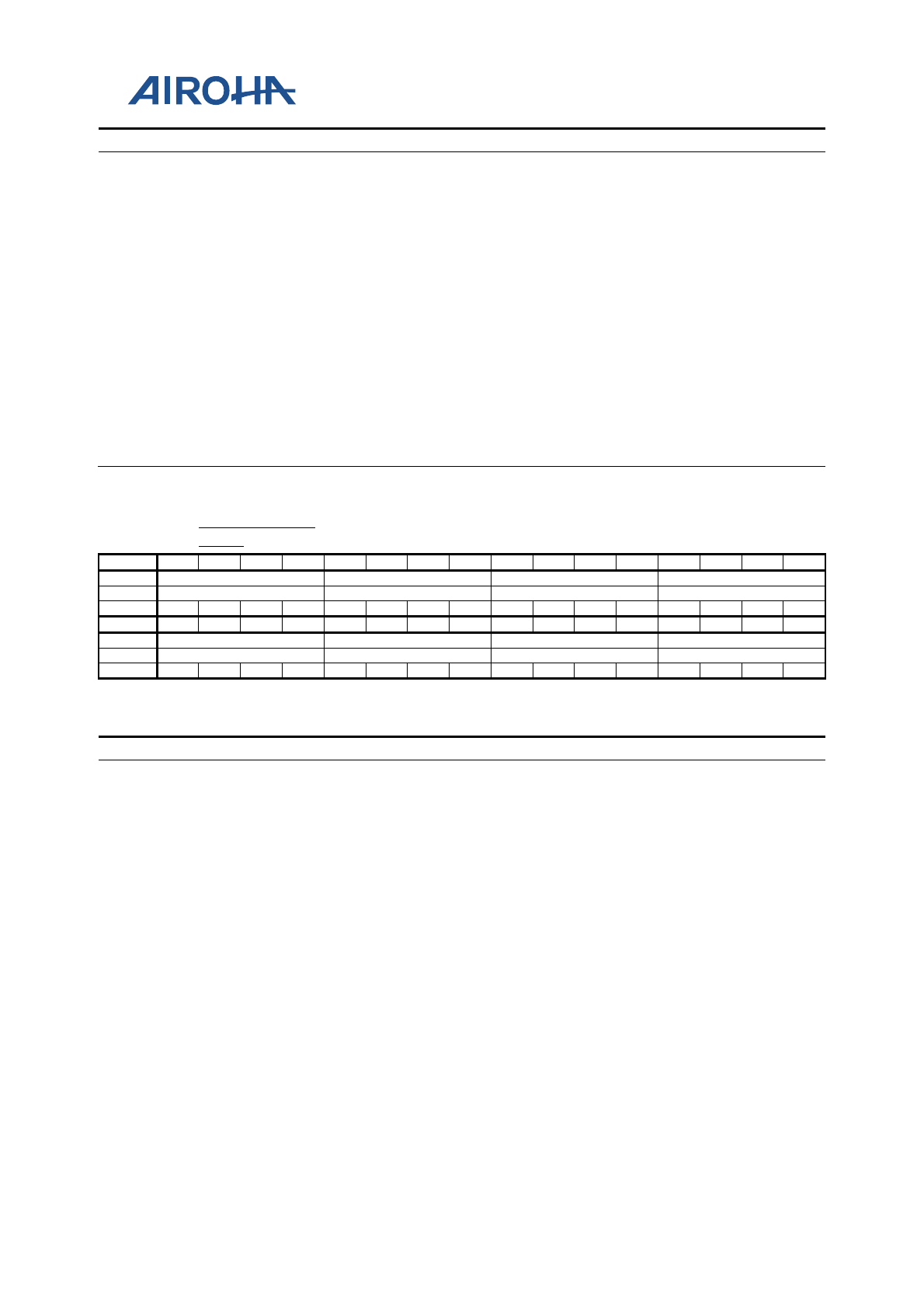
MT2523 Series Reference Manual
© 2015 - 2018 Airoha Technology Corp.
Page 545 of 692
This document contains information that is proprietary to Airoha Technology Corp. (“Airoha”) and/or its licensor(s).
Any unauthorized use, reproduction or disclosure of this document in whole or in part is strictly prohibited.
Bit(s)
Mnemonic
Name
Description
0: Keep
1: SET bits
19:16
GPIO28
Bitwise SET operation for Aux. mode of CMCSD1
0: Keep
1: SET bits
15:12
GPIO27
Bitwise SET operation for Aux. mode of CMCSD0
0: Keep
1: SET bits
11:8
GPIO26
Bitwise SET operation for Aux. mode of CMPDN
0: Keep
1: SET bits
7:4
GPIO25
Bitwise SET operation for Aux. mode of CMRST
0: Keep
1: SET bits
3:0
GPIO24
Bitwise SET operation for Aux. mode of BPI_BUS0
0: Keep
1: SET bits
A2020C38
GPIO_MODE3
_CLR
GPIO Mode Control
00000000
Bit
31
30
29
28
27
26
25
24
23
22
21
20
19
18
17
16
Name
GPIO31
GPIO30
GPIO29
GPIO28
Type
WO
WO
WO
WO
Reset
0
0
0
0
0
0
0
0
0
0
0
0
0
0
0
0
Bit
15
14
13
12
11
10
9
8
7
6
5
4
3
2
1
0
Name
GPIO27
GPIO26
GPIO25
GPIO24
Type
WO
WO
WO
WO
Reset
0
0
0
0
0
0
0
0
0
0
0
0
0
0
0
0
Overview
For bitwise access of GPIO_MODE3
Bit(s)
Mnemonic
Name
Description
31:28
GPIO31
Bitwise CLR operation for Aux. mode of MCCK
0: Keep
1: CLR bits
27:24
GPIO30
Bitwise CLR operation for Aux. mode of CMCSK
0: Keep
1: CLR bits
23:20
GPIO29
Bitwise CLR operation for Aux. mode of CMMCLK
0: Keep
1: CLR bits
19:16
GPIO28
Bitwise CLR operation for Aux. mode of CMCSD1
0: Keep
1: CLR bits
15:12
GPIO27
Bitwise CLR operation for Aux. mode of CMCSD0
0: Keep
1: CLR bits
11:8
GPIO26
Bitwise CLR operation for Aux. mode of CMPDN
0: Keep
1: CLR bits
7:4
GPIO25
Bitwise CLR operation for Aux. mode of CMRST
0: Keep
1: CLR bits
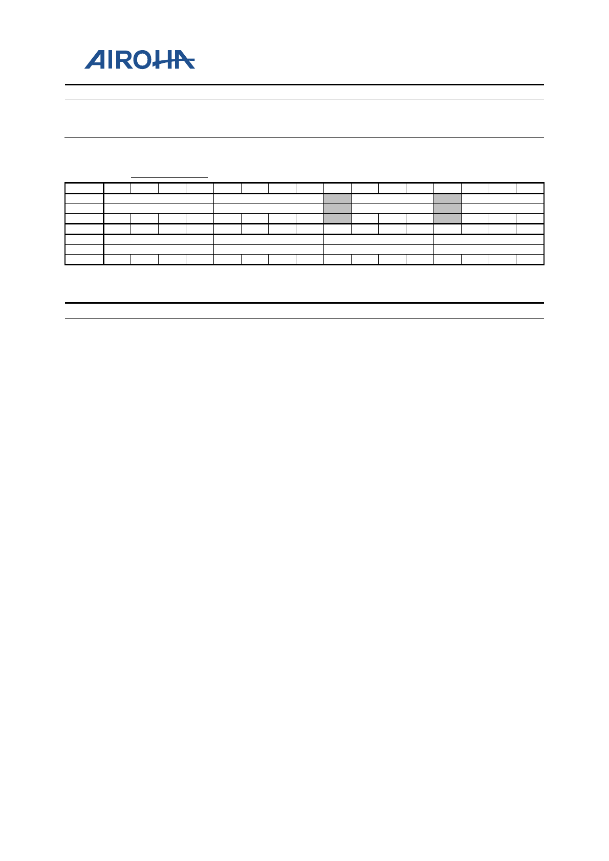
MT2523 Series Reference Manual
© 2015 - 2018 Airoha Technology Corp.
Page 546 of 692
This document contains information that is proprietary to Airoha Technology Corp. (“Airoha”) and/or its licensor(s).
Any unauthorized use, reproduction or disclosure of this document in whole or in part is strictly prohibited.
Bit(s)
Mnemonic
Name
Description
3:0
GPIO24
Bitwise CLR operation for Aux. mode of BPI_BUS0
0: Keep
1: CLR bits
A2020C40
GPIO_MODE4
GPIO Mode Control
10001111
Bit
31
30
29
28
27
26
25
24
23
22
21
20
19
18
17
16
Name
GPIO39
GPIO38
GPIO37
GPIO36
Type
RW
RW
RW
RW
Reset
0
0
0
1
0
0
0
0
0
0
0
0
0
0
Bit
15
14
13
12
11
10
9
8
7
6
5
4
3
2
1
0
Name
GPIO35
GPIO34
GPIO33
GPIO32
Type
RW
RW
RW
RW
Reset
0
0
0
1
0
0
0
1
0
0
0
1
0
0
0
1
Overview
Configures GPIO aux. mode
Bit(s)
Mnemonic
Name
Description
31:28
GPIO39
Aux. mode of GPIO_39
0: GPIO39 (IO)
1: LSCE_B0 (O)
2: EINT4 (I)
3: CMCSD0 (I)
4: CLKO4 (O)
5: SFSCS0 (O)
6: DEBUGMIN5 (I)
7: DEBUGMON5 (IO)
8: SCL1 (IO)
9: MA_SPI2_B_CS (O)
27:24
GPIO38
Aux. mode of GPIO_38
0: GPIO38 (IO)
1: LSRSTB (O)
2: Reserved
3: CMRST (O)
4: CLKO3 (O)
5: SFSWP (O)
6: Reserved
7: DEBUGMON9 (IO)
8: Reserved
9: SCL1(IO)
22:20
GPIO37
Aux. mode of GPIO_37
0: GPIO37 (IO)
1: SDA0 (IO)
2: SDA1 (IO)
3: Reserved
4: Reserved
5: Reserved
6: DEBUGMIN4 (I)
7: DEBUGMON4 (IO)
8: Reserved
9: Reserved
18:16
GPIO36
Aux. mode of GPIO_36
0: GPIO36 (IO)
1: SCL0 (IO)
2: SCL1 (IO)
3: Reserved
4: Reserved
5: Reserved
6: DEBUGMIN3 (I)
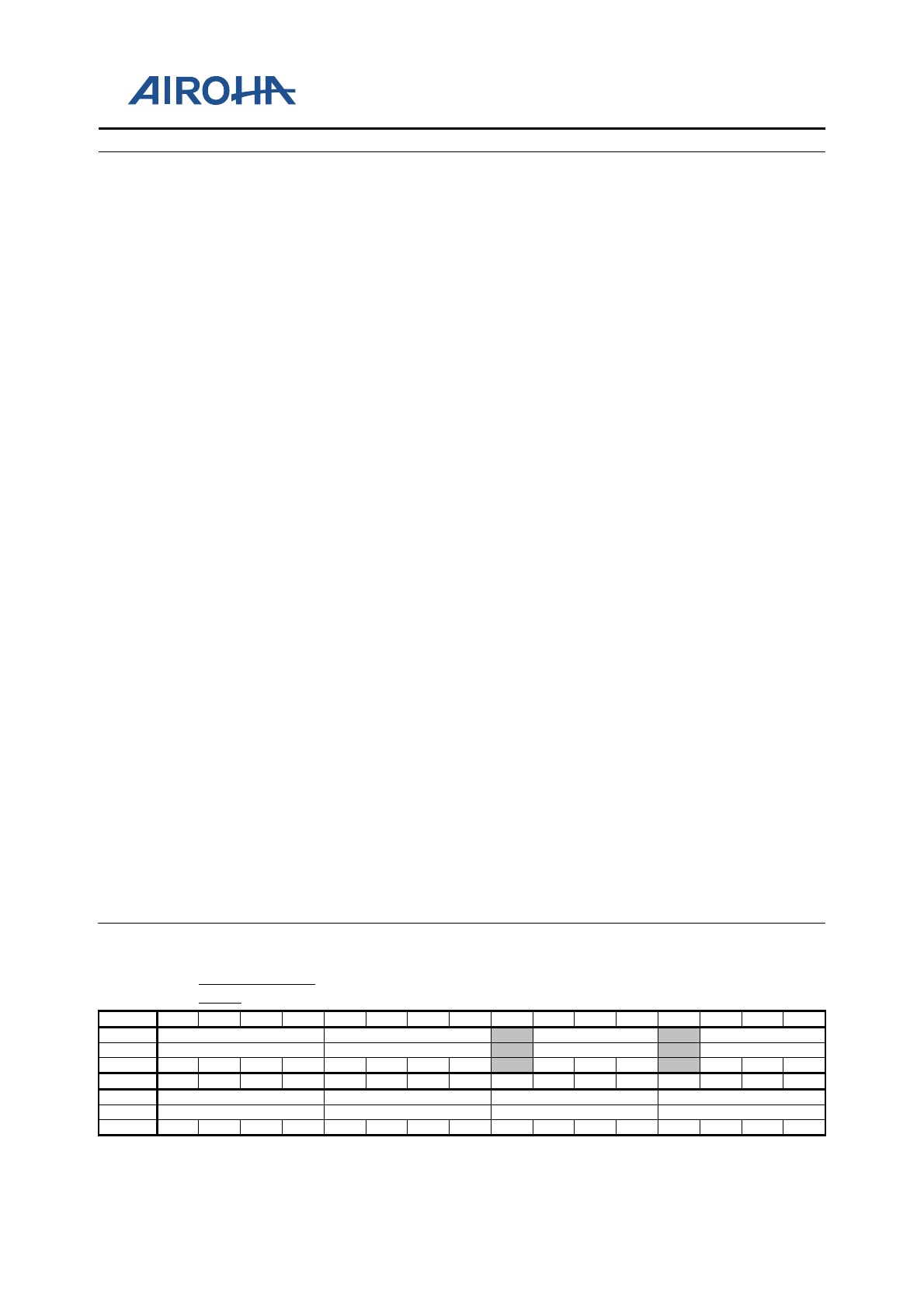
MT2523 Series Reference Manual
© 2015 - 2018 Airoha Technology Corp.
Page 547 of 692
This document contains information that is proprietary to Airoha Technology Corp. (“Airoha”) and/or its licensor(s).
Any unauthorized use, reproduction or disclosure of this document in whole or in part is strictly prohibited.
Bit(s)
Mnemonic
Name
Description
7: DEBUGMON3 (IO)
8: Reserved
9: Reserved
15:12
GPIO35
Aux. mode of GPIO_35
0: GPIO35 (IO)
1: SLV_SPI0_MISO (I)
2: EINT3 (I)
3: PWM5 (O)
4: DAIPCMOUT (I)
5: MC0_DA3 (IO)
6: CLKO2 (O)
7: BT_RGPIO5 (IO)
8: Reserved
9: MA_SPI3_B_MISO (I)
11:8
GPIO34
Aux. mode of GPIO_34
0: GPIO34 (IO)
1: SLV_SPI0_MOSI (I)
2: EINT15 (I)
3: PWM4 (O)
4: DAICLK (I)
5: MC0_DA2 (IO)
6: BT_RGPIO4 (IO)
7: DEBUGMON4 (IO)
8: Reserved
9: MA_SPI3_B_MOSI (O)
7:4
GPIO33
Aux. mode of GPIO_33
0: GPIO33 (IO)
1: SLV_SPI0_SCK (I)
2: EINT14 (I)
3: PWM3 (O)
4: DAIPCMIN (I)
5: MC0_DA1 (IO)
6: BT_RGPIO3 (IO)
7: DEBUGMON3 (IO)
8: Reserved
9: MA_SPI3_B_SCK (O)
3:0
GPIO32
Aux. mode of GPIO_32
0: GPIO32 (IO)
1: SLV_SPI0_CS (I)
2: EINT13 (I)
3: PWM2 (O)
4: DAISYNC (O)
5: MC0_DA0 (IO)
6: DEBUGMIN2 (I)
7: DEBUGMON2 (IO)
8: Reserved
9: MA_SPI3_B_CS (O)
A2020C44
GPIO_MODE4
_SET
GPIO Mode Control
00000000
Bit
31
30
29
28
27
26
25
24
23
22
21
20
19
18
17
16
Name
GPIO39
GPIO38
GPIO37
GPIO36
Type
WO
WO
WO
WO
Reset
0
0
0
0
0
0
0
0
0
0
0
0
0
0
Bit
15
14
13
12
11
10
9
8
7
6
5
4
3
2
1
0
Name
GPIO35
GPIO34
GPIO33
GPIO32
Type
WO
WO
WO
WO
Reset
0
0
0
0
0
0
0
0
0
0
0
0
0
0
0
0
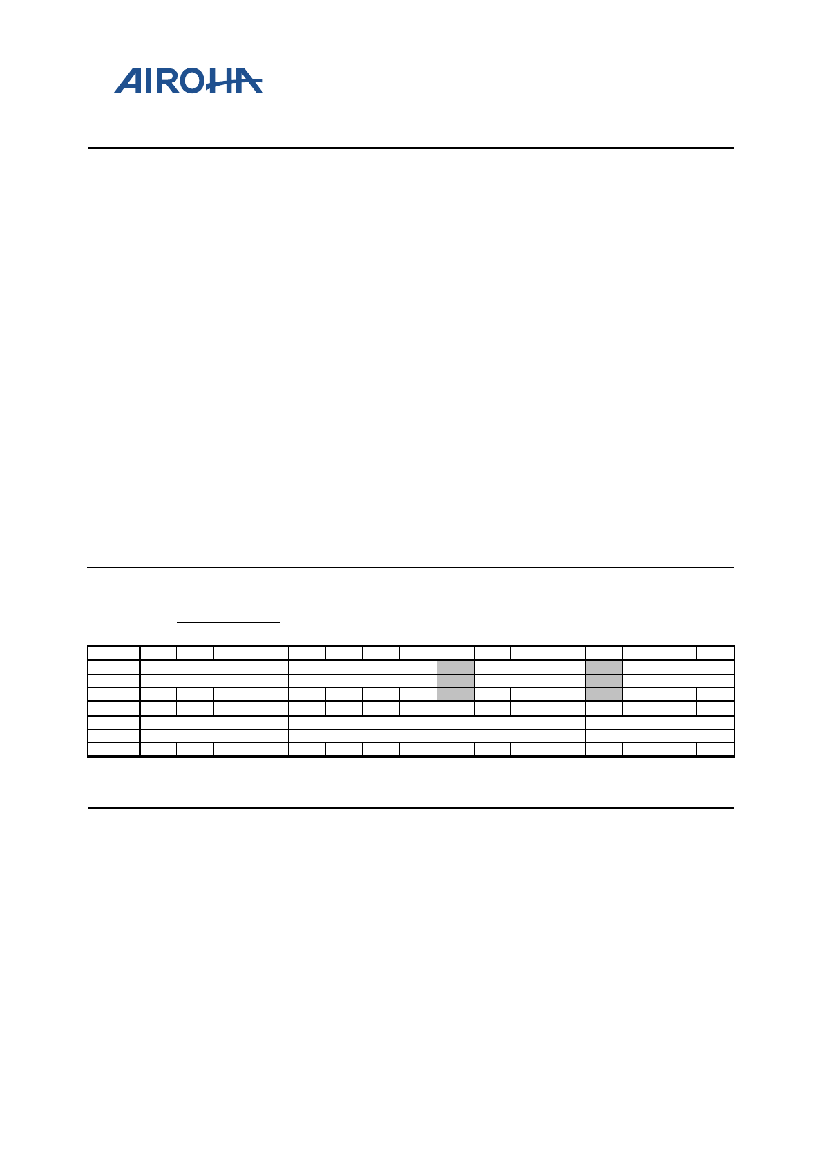
MT2523 Series Reference Manual
© 2015 - 2018 Airoha Technology Corp.
Page 548 of 692
This document contains information that is proprietary to Airoha Technology Corp. (“Airoha”) and/or its licensor(s).
Any unauthorized use, reproduction or disclosure of this document in whole or in part is strictly prohibited.
Overview
For bitwise access of GPIO_MODE4
Bit(s)
Mnemonic
Name
Description
31:28
GPIO39
Bitwise SET operation for Aux. mode of SIM1_SCLK
0: Keep
1: SET bits
27:24
GPIO38
Bitwise SET operation for Aux. mode of SIM1_SRST
0: Keep
1: SET bits
22:20
GPIO37
Bitwise SET operation for Aux. mode of SIM1_SIO
0: Keep
1: SET bits
18:16
GPIO36
Bitwise SET operation for Aux. mode of MCDA3
0: Keep
1: SET bits
15:12
GPIO35
Bitwise SET operation for Aux. mode of MCDA2
0: Keep
1: SET bits
11:8
GPIO34
Bitwise SET operation for Aux. mode of MCDA1
0: Keep
1: SET bits
7:4
GPIO33
Bitwise SET operation for Aux. mode of MCDA0
0: Keep
1: SET bits
3:0
GPIO32
Bitwise SET operation for Aux. mode of MCCM0
0: Keep
1: SET bits
A2020C48
GPIO_MODE4
_CLR
GPIO Mode Control
00000000
Bit
31
30
29
28
27
26
25
24
23
22
21
20
19
18
17
16
Name
GPIO39
GPIO38
GPIO37
GPIO36
Type
WO
WO
WO
WO
Reset
0
0
0
0
0
0
0
0
0
0
0
0
0
0
Bit
15
14
13
12
11
10
9
8
7
6
5
4
3
2
1
0
Name
GPIO35
GPIO34
GPIO33
GPIO32
Type
WO
WO
WO
WO
Reset
0
0
0
0
0
0
0
0
0
0
0
0
0
0
0
0
Overview
For bitwise access of GPIO_MODE4
Bit(s)
Mnemonic
Name
Description
31:28
GPIO39
Bitwise CLR operation for Aux. mode of SIM1_SCLK
0: Keep
1: CLR bits
27:24
GPIO38
Bitwise CLR operation for Aux. mode of SIM1_SRST
0: Keep
1: CLR bits
22:20
GPIO37
Bitwise CLR operation for Aux. mode of SIM1_SIO
0: Keep
1: CLR bits
18:16
GPIO36
Bitwise CLR operation for Aux. mode of MCDA3
0: Keep
1: CLR bits
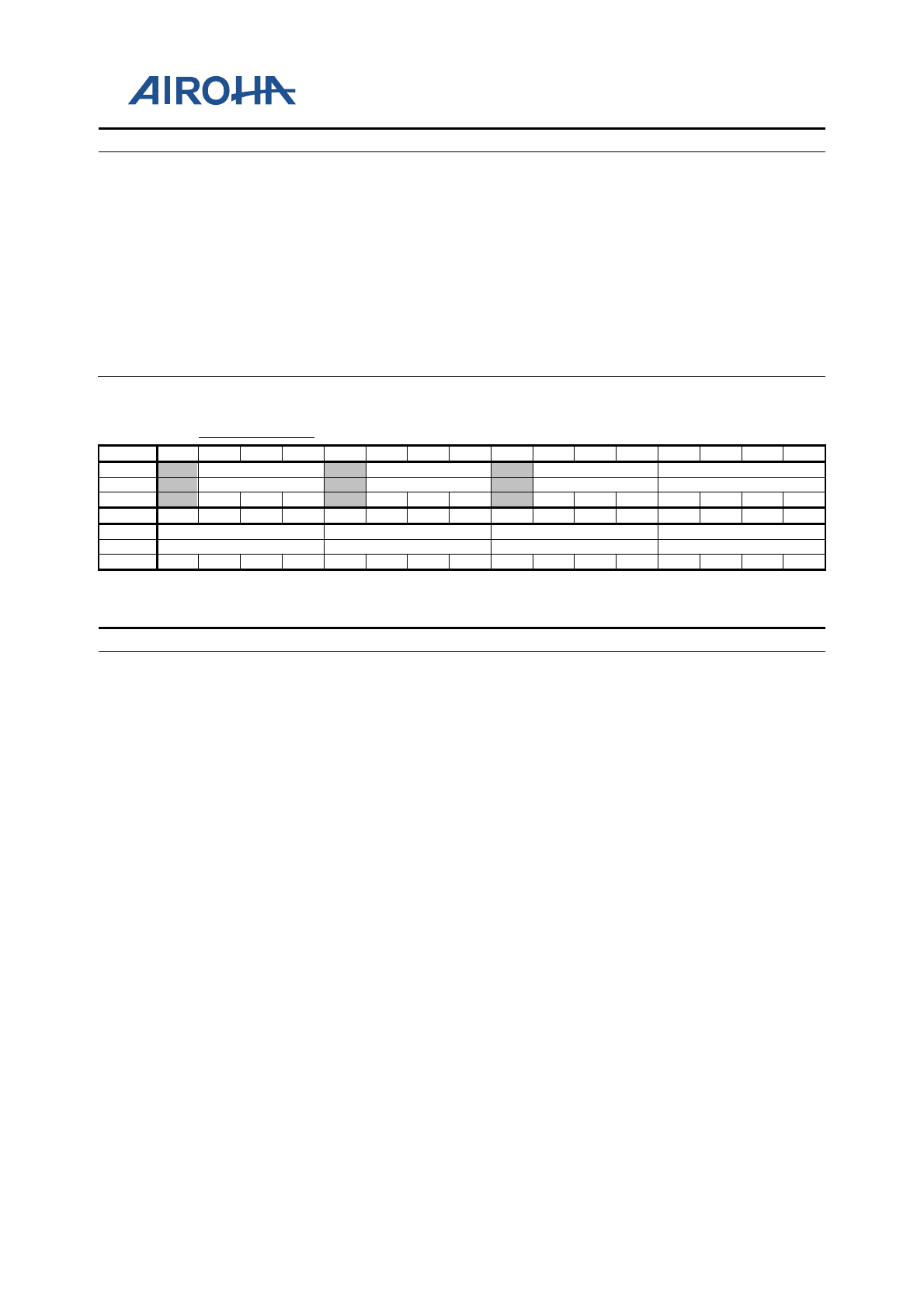
MT2523 Series Reference Manual
© 2015 - 2018 Airoha Technology Corp.
Page 549 of 692
This document contains information that is proprietary to Airoha Technology Corp. (“Airoha”) and/or its licensor(s).
Any unauthorized use, reproduction or disclosure of this document in whole or in part is strictly prohibited.
Bit(s)
Mnemonic
Name
Description
15:12
GPIO35
Bitwise CLR operation for Aux. mode of MCDA2
0: Keep
1: CLR bits
11:8
GPIO34
Bitwise CLR operation for Aux. mode of MCDA1
0: Keep
1: CLR bits
7:4
GPIO33
Bitwise CLR operation for Aux. mode of MCDA0
0: Keep
1: CLR bits
3:0
GPIO32
Bitwise CLR operation for Aux. mode of MCCM0
0: Keep
1: CLR bits
A2020C50
GPIO_MODE5
GPIO Mode Control
00000000
Bit
31
30
29
28
27
26
25
24
23
22
21
20
19
18
17
16
Name
GPIO47
GPIO46
GPIO45
GPIO44
Type
RW
RW
RW
RW
Reset
0
0
0
0
0
0
0
0
0
0
0
0
0
Bit
15
14
13
12
11
10
9
8
7
6
5
4
3
2
1
0
Name
GPIO43
GPIO42
GPIO41
GPIO40
Type
RW
RW
RW
RW
Reset
0
0
0
0
0
0
0
0
0
0
0
0
0
0
0
0
Overview
Configures GPIO aux. mode
Bit(s)
Mnemonic
Name
Description
30:28
GPIO47
Aux. mode of GPIO_47
0: GPIO47 (IO)
1: MA_SPI1_CS1 (O)
2: Reserved
3: Reserved
4: Reserved
5: Reserved
6: Reserved
7: DEBUGMON2 (IO)
8: Reserved
9: Reserved
26:24
GPIO46
Aux. mode of GPIO_46
0: GPIO46 (IO)
1: MA_SPI0_CS1 (O)
2: Reserved
3: Reserved
4: Reserved
5: Reserved
6: Reserved
7: DEBUGMON1 (IO)
8: Reserved
9: Reserved
22:20
GPIO45
Aux. mode of GPIO_45
0: GPIO45 (IO)
1: SRCLKENAI (I)
2: Reserved
3: Reserved
4: Reserved
5: Reserved
6: Reserved
7: Reserved

MT2523 Series Reference Manual
© 2015 - 2018 Airoha Technology Corp.
Page 550 of 692
This document contains information that is proprietary to Airoha Technology Corp. (“Airoha”) and/or its licensor(s).
Any unauthorized use, reproduction or disclosure of this document in whole or in part is strictly prohibited.
Bit(s)
Mnemonic
Name
Description
8: Reserved
9: Reserved
19:16
GPIO44
Aux. mode of GPIO_44
0: GPIO44 (IO)
1: LSCE1_B1 (O)
2: DISP_PWM (O)
3: Reserved
4: Reserved
5: Reserved
6: Reserved
7: DEBUGMON0 (IO)
8: DEBUGMON6 (IO)
9: Reserved
15:12
GPIO43
Aux. mode of GPIO_43
0: GPIO43 (IO)
1: LPTE (I)
2: EINT6 (I)
3: CMCSK (I)
4: CMCSD2 (I)
5: SFSIN (O)
6: Reserved
7: DEBUGMON7 (IO)
8: DEBUGMIN7 (I)
9: SDA1 (IO)
11:8
GPIO42
Aux. mode of GPIO_42
0: GPIO42 (IO)
1: LSA0DA0 (O)
2: LSCE1_B0 (O)
3: CMMCLK (O)
4: Reserved
5: SFSOUT (O)
6: Reserved
7: DEBUGMON8 (IO)
8: CLKO5 (O)
9: MA_SPI2_B_MISO (O)
7:4
GPIO41
Aux. mode of GPIO_41
0: GPIO41 (IO)
1: LSDA0 (IO)
2: EINT5 (I)
3: CMCSD1 (I)
4: WIFITOBT (I)
5: SFSCK (O)
6: DEBUGMIN6 (I)
7: DEBUGMON6 (IO)
8: SDA1 (IO)
9: MA_SPI2_B_MOSI (O)
3:0
GPIO40
Aux. mode of GPIO_40
0: GPIO40 (IO)
1: LSCK0 (O)
2: Reserved
3: CMPDN (O)
4: Reserved
5: SFSHOLD (O)
6: Reserved
7: DEBUGMON10 (IO)
8: Reserved
9: MA_SPI2_B_SCK (O)
A2020C54
GPIO_MODE5
GPIO Mode Control
00000000
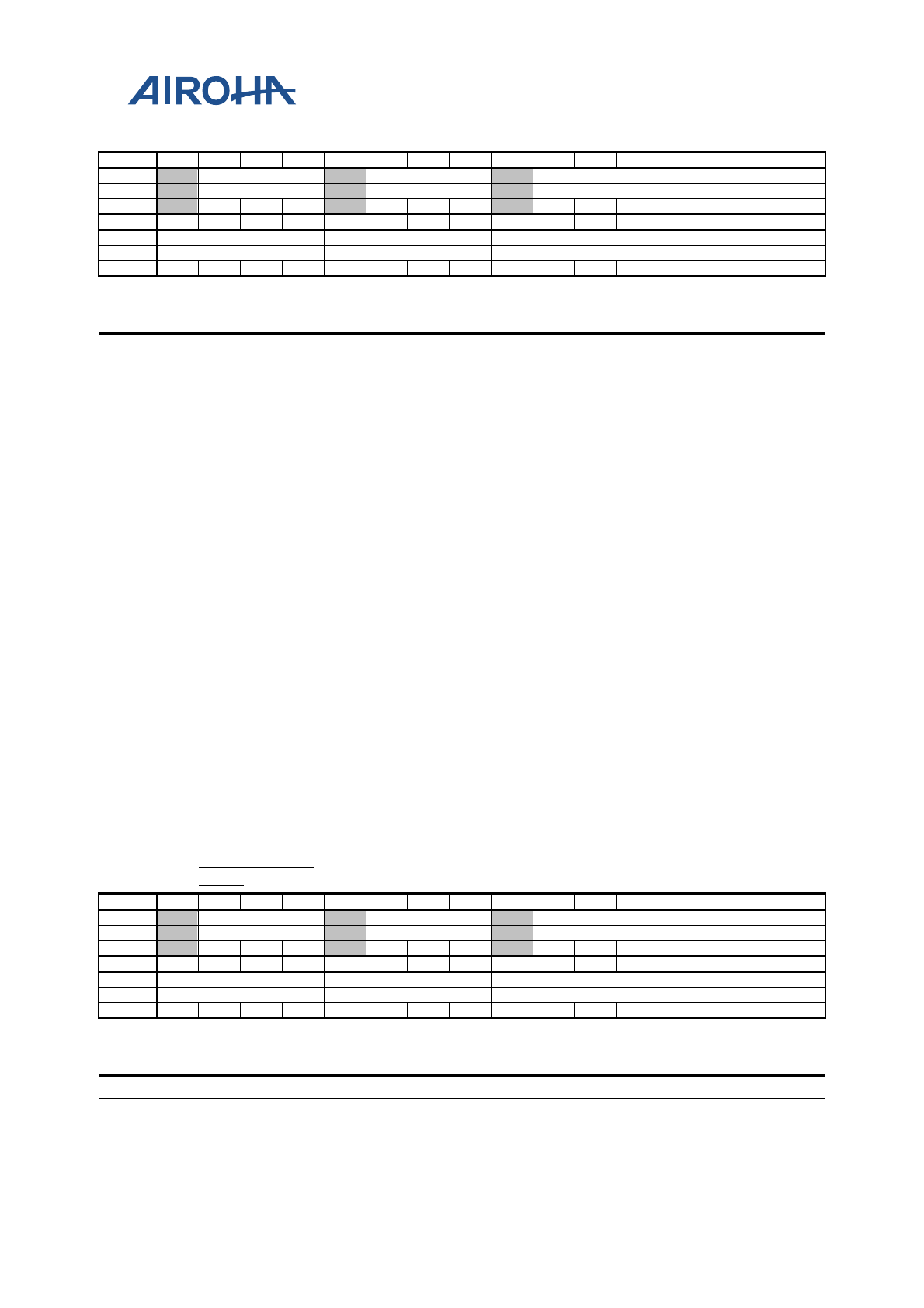
MT2523 Series Reference Manual
© 2015 - 2018 Airoha Technology Corp.
Page 551 of 692
This document contains information that is proprietary to Airoha Technology Corp. (“Airoha”) and/or its licensor(s).
Any unauthorized use, reproduction or disclosure of this document in whole or in part is strictly prohibited.
_SET
Bit
31
30
29
28
27
26
25
24
23
22
21
20
19
18
17
16
Name
GPIO47
GPIO46
GPIO45
GPIO44
Type
WO
WO
WO
WO
Reset
0
0
0
0
0
0
0
0
0
0
0
0
0
Bit
15
14
13
12
11
10
9
8
7
6
5
4
3
2
1
0
Name
GPIO43
GPIO42
GPIO41
GPIO40
Type
WO
WO
WO
WO
Reset
0
0
0
0
0
0
0
0
0
0
0
0
0
0
0
0
Overview
For bitwise access of GPIO_MODE5
Bit(s)
Mnemonic
Name
Description
30:28
GPIO47
Bitwise SET operation for Aux. mode of LSCK
0: Keep
1: SET bits
26:24
GPIO46
Bitwise SET operation for Aux. mode of LSCE_B
0: Keep
1: SET bits
22:20
GPIO45
Bitwise SET operation for Aux. mode of LSRSTB
0: Keep
1: SET bits
19:16
GPIO44
Bitwise SET operation for Aux. mode of SDA28
0: Keep
1: SET bits
15:12
GPIO43
Bitwise SET operation for Aux. mode of SCL28
0: Keep
1: SET bits
11:8
GPIO42
Bitwise SET operation for Aux. mode of SIM2_SCLK
0: Keep
1: SET bits
7:4
GPIO41
Bitwise SET operation for Aux. mode of SIM2_SRST
0: Keep
1: SET bits
3:0
GPIO40
Bitwise SET operation for Aux. mode of SIM2_SIO
0: Keep
1: SET bits
A2020C58
GPIO_MODE5
_CLR
GPIO Mode Control
00000000
Bit
31
30
29
28
27
26
25
24
23
22
21
20
19
18
17
16
Name
GPIO47
GPIO46
GPIO45
GPIO44
Type
WO
WO
WO
WO
Reset
0
0
0
0
0
0
0
0
0
0
0
0
0
Bit
15
14
13
12
11
10
9
8
7
6
5
4
3
2
1
0
Name
GPIO43
GPIO42
GPIO41
GPIO40
Type
WO
WO
WO
WO
Reset
0
0
0
0
0
0
0
0
0
0
0
0
0
0
0
0
Overview
For bitwise access of GPIO_MODE5
Bit(s)
Mnemonic
Name
Description
30:28
GPIO47
Bitwise CLR operation for Aux. mode of LSCK
0: Keep
1: CLR bits
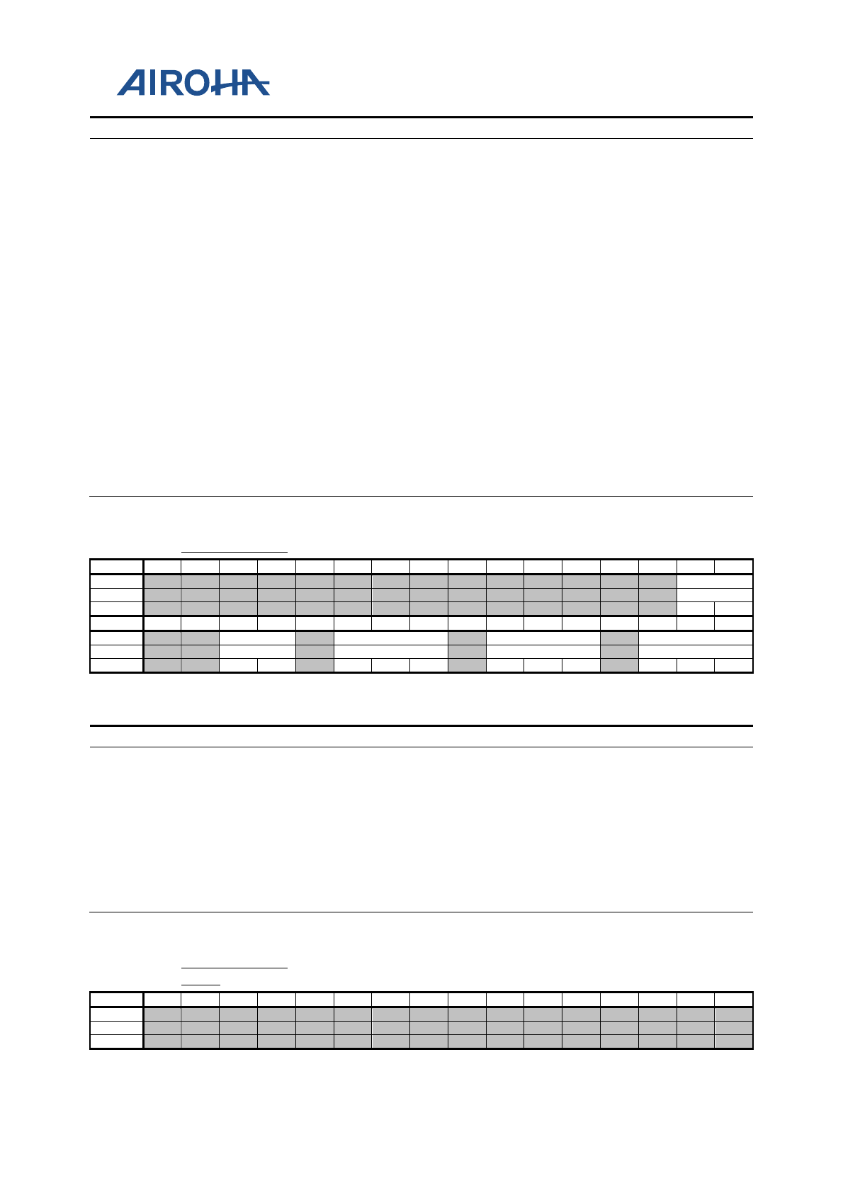
MT2523 Series Reference Manual
© 2015 - 2018 Airoha Technology Corp.
Page 552 of 692
This document contains information that is proprietary to Airoha Technology Corp. (“Airoha”) and/or its licensor(s).
Any unauthorized use, reproduction or disclosure of this document in whole or in part is strictly prohibited.
Bit(s)
Mnemonic
Name
Description
26:24
GPIO46
Bitwise CLR operation for Aux. mode of LSCE_B
0: Keep
1: CLR bits
22:20
GPIO45
Bitwise CLR operation for Aux. mode of LSRSTB
0: Keep
1: CLR bits
19:16
GPIO44
Bitwise CLR operation for Aux. mode of SDA28
0: Keep
1: CLR bits
15:12
GPIO43
Bitwise CLR operation for Aux. mode of SCL28
0: Keep
1: CLR bits
11:8
GPIO42
Bitwise CLR operation for Aux. mode of SIM2_SCLK
0: Keep
1: CLR bits
7:4
GPIO41
Bitwise CLR operation for Aux. mode of SIM2_SRST
0: Keep
1: CLR bits
3:0
GPIO40
Bitwise CLR operation for Aux. mode of SIM2_SIO
0: Keep
1: CLR bits
A2020C60
GPIO_MODE6
GPIO Mode Control
00011110
Bit
31
30
29
28
27
26
25
24
23
22
21
20
19
18
17
16
Name
Type
Reset
Bit
15
14
13
12
11
10
9
8
7
6
5
4
3
2
1
0
Name
GPIO48
Type
RW
Reset
0
0
0
Overview
Configures GPIO aux. mode
Bit(s)
Mnemonic
Name
Description
2:0
GPIO48
Aux. mode of GPIO_48
0: GPIO48 (IO)
1: MA_SPI3_CS1 (O)
2: Reserved
3: Reserved
4: Reserved
5: Reserved
6: Reserved
7: DEBUGMON5 (IO)
8: Reserved
9: Reserved
A2020C64
GPIO_MODE6
_SET
GPIO Mode Control
00000000
Bit
31
30
29
28
27
26
25
24
23
22
21
20
19
18
17
16
Name
Type
Reset
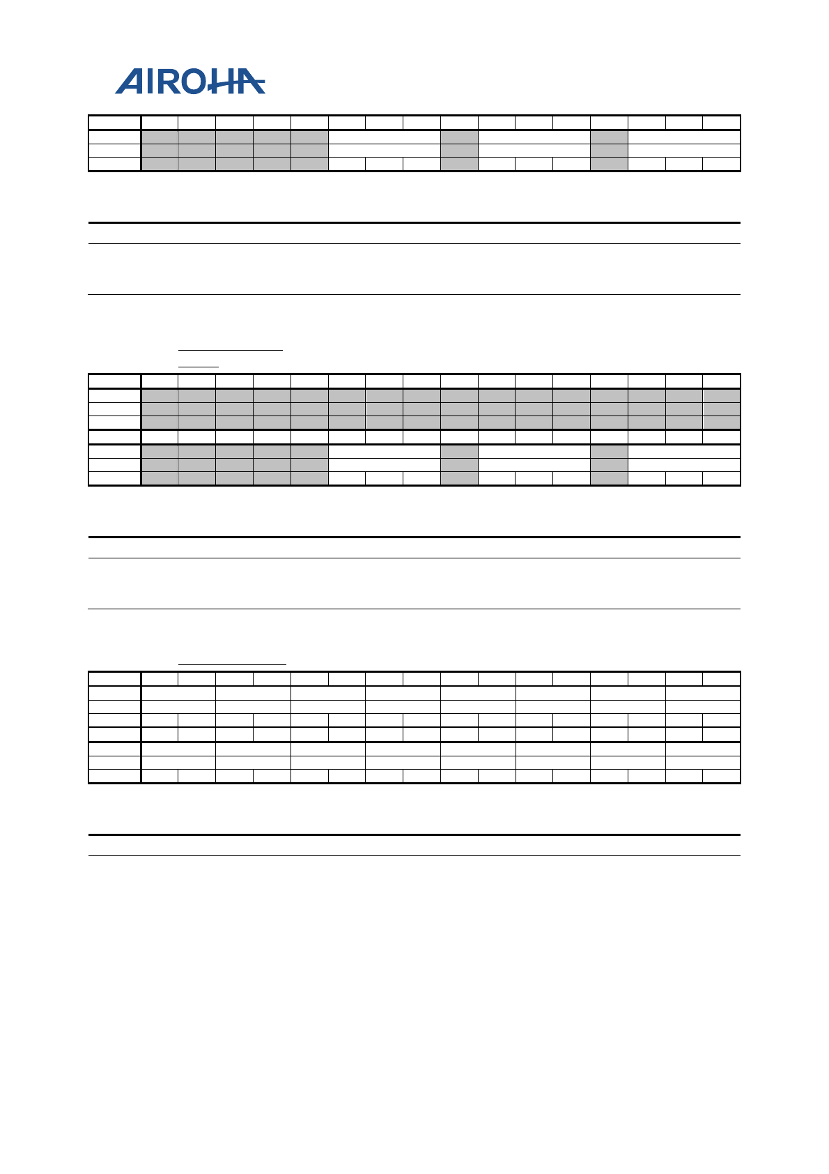
MT2523 Series Reference Manual
© 2015 - 2018 Airoha Technology Corp.
Page 553 of 692
This document contains information that is proprietary to Airoha Technology Corp. (“Airoha”) and/or its licensor(s).
Any unauthorized use, reproduction or disclosure of this document in whole or in part is strictly prohibited.
Bit
15
14
13
12
11
10
9
8
7
6
5
4
3
2
1
0
Name
GPIO48
Type
WO
Reset
0
0
0
Overview
For bitwise access of GPIO_MODE6
Bit(s)
Mnemonic
Name
Description
2:0
GPIO48
Bitwise SET operation for Aux. mode of LSDA
0: Keep
1: SET bits
A2020C68
GPIO_MODE6
_CLR
GPIO Mode
Control
00000000
Bit
31
30
29
28
27
26
25
24
23
22
21
20
19
18
17
16
Name
Type
Reset
Bit
15
14
13
12
11
10
9
8
7
6
5
4
3
2
1
0
Name
GPIO48
Type
WO
Reset
0
0
0
Overview
For bitwise access of GPIO_MODE6
Bit(s)
Mnemonic
Name
Description
2:0
GPIO48
Bitwise CLR operation for Aux. mode of LSDA
0: Keep
1: CLR bits
A2020D00
GPIO_TDSEL0
GPIO TDSEL Control
00000000
Bit
31
30
29
28
27
26
25
24
23
22
21
20
19
18
17
16
Name
GPIO15
GPIO14
GPIO13
GPIO12
GPIO11
GPIO10
GPIO9
GPIO8
Type
RW
RW
RW
RW
RW
RW
RW
RW
Reset
0
0
0
0
0
0
0
0
0
0
0
0
0
0
0
0
Bit
15
14
13
12
11
10
9
8
7
6
5
4
3
2
1
0
Name
GPIO7
GPIO6
GPIO5
GPIO4
GPIO3
GPIO2
GPIO1
GPIO0
Type
RW
RW
RW
RW
RW
RW
RW
RW
Reset
0
0
0
0
0
0
0
0
0
0
0
0
0
0
0
0
Overview
GPIO TX duty control register
Bit(s)
Mnemonic
Name
Description
31:30
GPIO15
GPIO15_TDSEL
GPIO15 Tx duty control
29:28
GPIO14
GPIO14_TDSEL
GPIO14 Tx duty control
27:26
GPIO13
GPIO13_TDSEL
GPIO13 Tx duty control
25:24
GPIO12
GPIO12_TDSEL
GPIO12 Tx duty control
23:22
GPIO11
GPIO11_TDSEL
GPIO11 Tx duty control
21:20
GPIO10
GPIO10_TDSEL
GPIO10 Tx duty control
19:18
GPIO9
GPIO9_TDSEL
GPIO9 Tx duty control
17:16
GPIO8
GPIO8_TDSEL
GPIO8 Tx duty control
15:14
GPIO7
GPIO7_TDSEL
GPIO7 Tx duty control
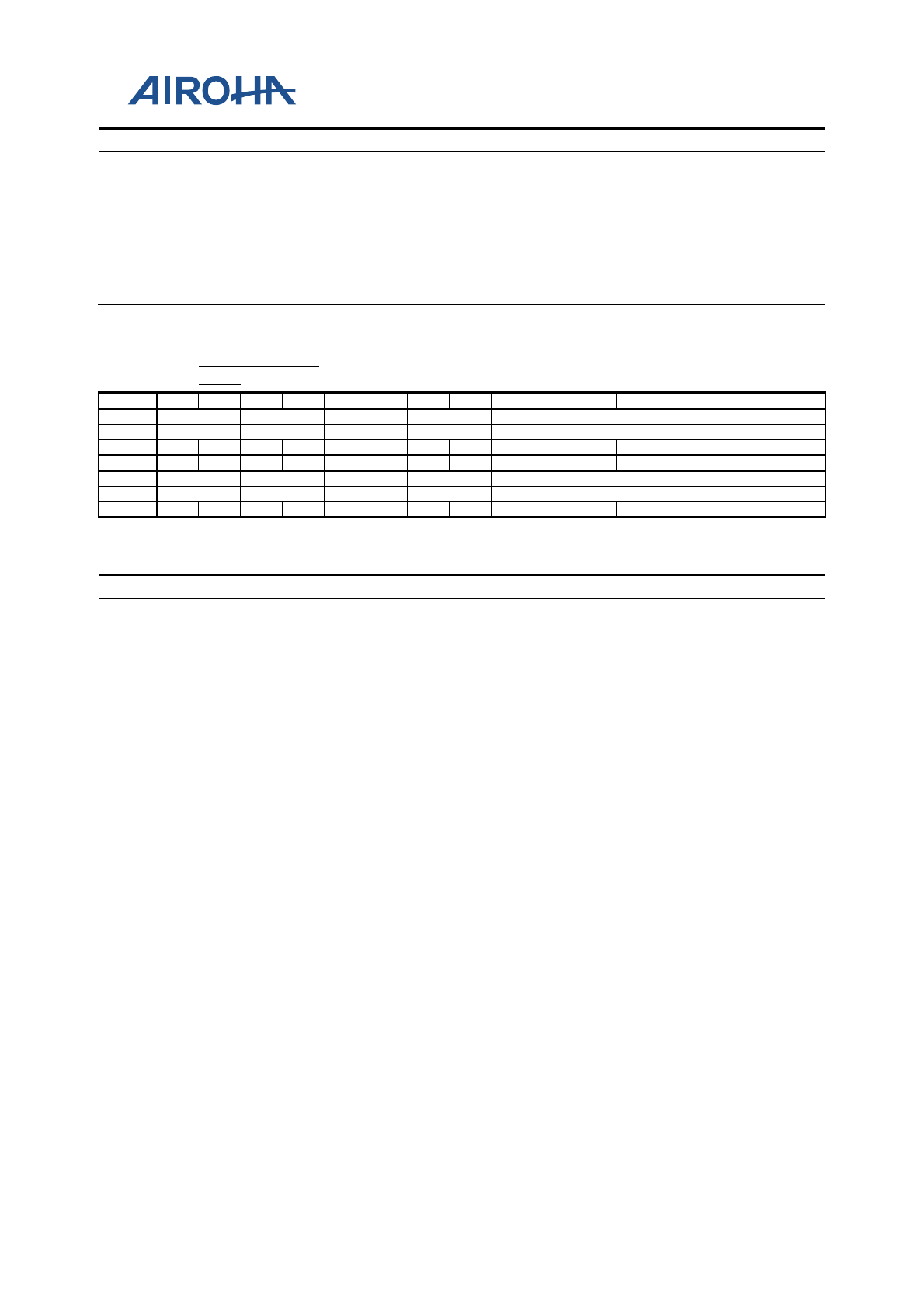
MT2523 Series Reference Manual
© 2015 - 2018 Airoha Technology Corp.
Page 554 of 692
This document contains information that is proprietary to Airoha Technology Corp. (“Airoha”) and/or its licensor(s).
Any unauthorized use, reproduction or disclosure of this document in whole or in part is strictly prohibited.
Bit(s)
Mnemonic
Name
Description
13:12
GPIO6
GPIO6_TDSEL
GPIO6 Tx duty control
11:10
GPIO5
GPIO5_TDSEL
GPIO5 Tx duty control
9:8
GPIO4
GPIO4_TDSEL
GPIO4 Tx duty control
7:6
GPIO3
GPIO3_TDSEL
GPIO3 Tx duty control
5:4
GPIO2
GPIO2_TDSEL
GPIO2 Tx duty control
3:2
GPIO1
GPIO1_TDSEL
GPIO1 Tx duty control
1:0
GPIO0
GPIO0_TDSEL
GPIO0 Tx duty control
A2020D04
GPIO_TDSEL0
_SET
GPIO TDSEL Control
00000000
Bit
31
30
29
28
27
26
25
24
23
22
21
20
19
18
17
16
Name
GPIO15
GPIO14
GPIO13
GPIO12
GPIO11
GPIO10
GPIO9
GPIO8
Type
WO
WO
WO
WO
WO
WO
WO
WO
Reset
0
0
0
0
0
0
0
0
0
0
0
0
0
0
0
0
Bit
15
14
13
12
11
10
9
8
7
6
5
4
3
2
1
0
Name
GPIO7
GPIO6
GPIO5
GPIO4
GPIO3
GPIO2
GPIO1
GPIO0
Type
WO
WO
WO
WO
WO
WO
WO
WO
Reset
0
0
0
0
0
0
0
0
0
0
0
0
0
0
0
0
Overview
For bitwise access of GPIO_TDSEL
Bit(s)
Mnemonic
Name
Description
31:30
GPIO15
GPIO15_TDSEL
Bitwise SET operation of GPIO15_TDSEL Tx duty control
0: Keep
1: SET bits
29:28
GPIO14
GPIO14_TDSEL
Bitwise SET operation of GPIO14_TDSEL Tx duty control
0: Keep
1: SET bits
27:26
GPIO13
GPIO13_TDSEL
Bitwise SET operation of GPIO13_TDSEL Tx duty control
0: Keep
1: SET bits
25:24
GPIO12
GPIO12_TDSEL
Bitwise SET operation of GPIO12_TDSEL Tx duty control
0: Keep
1: SET bits
23:22
GPIO11
GPIO11_TDSEL
Bitwise SET operation of GPIO11_TDSEL Tx duty control
0: Keep
1: SET bits
21:20
GPIO10
GPIO10_TDSEL
Bitwise SET operation of GPIO10_TDSEL Tx duty control
0: Keep
1: SET bits
19:18
GPIO9
GPIO9_TDSEL
Bitwise SET operation of GPIO9_TDSEL Tx duty control
0: Keep
1: SET bits
17:16
GPIO8
GPIO8_TDSEL
Bitwise SET operation of GPIO8_TDSEL Tx duty control
0: Keep
1: SET bits
15:14
GPIO7
GPIO7_TDSEL
Bitwise SET operation of GPIO7_TDSEL Tx duty control
0: Keep
1: SET bits
13:12
GPIO6
GPIO6_TDSEL
Bitwise SET operation of GPIO6_TDSEL Tx duty control
0: Keep
1: SET bits

MT2523 Series Reference Manual
© 2015 - 2018 Airoha Technology Corp.
Page 555 of 692
This document contains information that is proprietary to Airoha Technology Corp. (“Airoha”) and/or its licensor(s).
Any unauthorized use, reproduction or disclosure of this document in whole or in part is strictly prohibited.
Bit(s)
Mnemonic
Name
Description
11:10
GPIO5
GPIO5_TDSEL
Bitwise SET operation of GPIO5_TDSEL Tx duty control
0: Keep
1: SET bits
9:8
GPIO4
GPIO4_TDSEL
Bitwise SET operation of GPIO4_TDSEL Tx duty control
0: Keep
1: SET bits
7:6
GPIO3
GPIO3_TDSEL
Bitwise SET operation of GPIO3_TDSEL Tx duty control
0: Keep
1: SET bits
5:4
GPIO2
GPIO2_TDSEL
Bitwise SET operation of GPIO2_TDSEL Tx duty control
0: Keep
1: SET bits
3:2
GPIO1
GPIO1_TDSEL
Bitwise SET operation of GPIO1_TDSEL Tx duty control
0: Keep
1: SET bits
1:0
GPIO0
GPIO0_TDSEL
Bitwise SET operation of GPIO0_TDSEL Tx duty control
0: Keep
1: SET bits
A2020D08
GPIO_TDSEL0
_CLR
GPIO TDSEL Control
00000000
Bit
31
30
29
28
27
26
25
24
23
22
21
20
19
18
17
16
Name
GPIO15
GPIO14
GPIO13
GPIO12
GPIO11
GPIO10
GPIO9
GPIO8
Type
WO
WO
WO
WO
WO
WO
WO
WO
Reset
0
0
0
0
0
0
0
0
0
0
0
0
0
0
0
0
Bit
15
14
13
12
11
10
9
8
7
6
5
4
3
2
1
0
Name
GPIO7
GPIO6
GPIO5
GPIO4
GPIO3
GPIO2
GPIO1
GPIO0
Type
WO
WO
WO
WO
WO
WO
WO
WO
Reset
0
0
0
0
0
0
0
0
0
0
0
0
0
0
0
0
Overview
For bitwise access of GPIO_TDSEL
Bit(s)
Mnemonic
Name
Description
31:30
GPIO15
GPIO15_TDSEL
Bitwise CLR operation of GPIO15_TDSEL Tx duty control
0: Keep
1: CLR bits
29:28
GPIO14
GPIO14_TDSEL
Bitwise CLR operation of GPIO14_TDSEL Tx duty control
0: Keep
1: CLR bits
27:26
GPIO13
GPIO13_TDSEL
Bitwise CLR operation of GPIO13_TDSEL Tx duty control
0: Keep
1: CLR bits
25:24
GPIO12
GPIO12_TDSEL
Bitwise CLR operation of GPIO12_TDSEL Tx duty control
0: Keep
1: CLR bits
23:22
GPIO11
GPIO11_TDSEL
Bitwise CLR operation of GPIO11_TDSEL Tx duty control
0: Keep
1: CLR bits
21:20
GPIO10
GPIO10_TDSEL
Bitwise CLR operation of GPIO10_TDSEL Tx duty control
0: Keep
1: CLR bits
19:18
GPIO9
GPIO9_TDSEL
Bitwise CLR operation of GPIO9_TDSEL Tx duty control
0: Keep

MT2523 Series Reference Manual
© 2015 - 2018 Airoha Technology Corp.
Page 556 of 692
This document contains information that is proprietary to Airoha Technology Corp. (“Airoha”) and/or its licensor(s).
Any unauthorized use, reproduction or disclosure of this document in whole or in part is strictly prohibited.
Bit(s)
Mnemonic
Name
Description
1: CLR bits
17:16
GPIO8
GPIO8_TDSEL
Bitwise CLR operation of GPIO8_TDSEL Tx duty control
0: Keep
1: CLR bits
15:14
GPIO7
GPIO7_TDSEL
Bitwise CLR operation of GPIO7_TDSEL Tx duty control
0: Keep
1: CLR bits
13:12
GPIO6
GPIO6_TDSEL
Bitwise CLR operation of GPIO6_TDSEL Tx duty control
0: Keep
1: CLR bits
11:10
GPIO5
GPIO5_TDSEL
Bitwise CLR operation of GPIO5_TDSEL Tx duty control
0: Keep
1: CLR bits
9:8
GPIO4
GPIO4_TDSEL
Bitwise CLR operation of GPIO4_TDSEL Tx duty control
0: Keep
1: CLR bits
7:6
GPIO3
GPIO3_TDSEL
Bitwise CLR operation of GPIO3_TDSEL Tx duty control
0: Keep
1: CLR bits
5:4
GPIO2
GPIO2_TDSEL
Bitwise CLR operation of GPIO2_TDSEL Tx duty control
0: Keep
1: CLR bits
3:2
GPIO1
GPIO1_TDSEL
Bitwise CLR operation of GPIO1_TDSEL Tx duty control
0: Keep
1: CLR bits
1:0
GPIO0
GPIO0_TDSEL
Bitwise CLR operation of GPIO0_TDSEL Tx duty control
0: Keep
1: CLR bits
A2020D10
GPIO_TDSEL1
GPIO TDSEL Control
00000000
Bit
31
30
29
28
27
26
25
24
23
22
21
20
19
18
17
16
Name
GPIO31
GPIO30
GPIO29
GPIO28
GPIO27
GPIO26
GPIO25
GPIO24
Type
RW
RW
RW
RW
RW
RW
RW
RW
Reset
0
0
0
0
0
0
0
0
0
0
0
0
0
0
0
0
Bit
15
14
13
12
11
10
9
8
7
6
5
4
3
2
1
0
Name
GPIO23
GPIO22
GPIO21
GPIO20
GPIO19
GPIO18
GPIO17
GPIO16
Type
RW
RW
RW
RW
RW
RW
RW
RW
Reset
0
0
0
0
0
0
0
0
0
0
0
0
0
0
0
0
Overview
GPIO TX duty control register
Bit(s)
Mnemonic
Name
Description
31:30
GPIO31
GPIO31_TDSEL
GPIO31 Tx duty control
29:28
GPIO30
GPIO30_TDSEL
GPIO30 Tx duty control
27:26
GPIO29
GPIO29_TDSEL
GPIO29 Tx duty control
25:24
GPIO28
GPIO28_TDSEL
GPIO28 Tx duty control
23:22
GPIO27
GPIO27_TDSEL
GPIO27 Tx duty control
21:20
GPIO26
GPIO26_TDSEL
GPIO26 Tx duty control
19:18
GPIO25
GPIO25_TDSEL
GPIO25 Tx duty control
17:16
GPIO24
GPIO24_TDSEL
GPIO24 Tx duty control
15:14
GPIO23
GPIO23_TDSEL
GPIO23 Tx duty control

MT2523 Series Reference Manual
© 2015 - 2018 Airoha Technology Corp.
Page 557 of 692
This document contains information that is proprietary to Airoha Technology Corp. (“Airoha”) and/or its licensor(s).
Any unauthorized use, reproduction or disclosure of this document in whole or in part is strictly prohibited.
Bit(s)
Mnemonic
Name
Description
13:12
GPIO22
GPIO22_TDSEL
GPIO22 Tx duty control
11:10
GPIO21
GPIO21_TDSEL
GPIO21 Tx duty control
9:8
GPIO20
GPIO20_TDSEL
GPIO20 Tx duty control
7:6
GPIO19
GPIO19_TDSEL
GPIO19 Tx duty control
5:4
GPIO18
GPIO18_TDSEL
GPIO18 Tx duty control
3:2
GPIO17
GPIO17_TDSEL
GPIO17 Tx duty control
1:0
GPIO16
GPIO16_TDSEL
GPIO16 Tx duty control
A2020D14
GPIO_TDSEL1
_SET
GPIO TDSEL Control
00000000
Bit
31
30
29
28
27
26
25
24
23
22
21
20
19
18
17
16
Name
GPIO31
GPIO30
GPIO29
GPIO28
GPIO27
GPIO26
GPIO25
GPIO24
Type
WO
WO
WO
WO
WO
WO
WO
WO
Reset
0
0
0
0
0
0
0
0
0
0
0
0
0
0
0
0
Bit
15
14
13
12
11
10
9
8
7
6
5
4
3
2
1
0
Name
GPIO23
GPIO22
GPIO21
GPIO20
GPIO19
GPIO18
GPIO17
GPIO16
Type
WO
WO
WO
WO
WO
WO
WO
WO
Reset
0
0
0
0
0
0
0
0
0
0
0
0
0
0
0
0
Overview
For bitwise access of GPIO_TDSEL
Bit(s)
Mnemonic
Name
Description
31:30
GPIO31
GPIO31_TDSEL
Bitwise SET operation of GPIO31_TDSEL Tx duty control
0: Keep
1: SET bits
29:28
GPIO30
GPIO30_TDSEL
Bitwise SET operation of GPIO30_TDSEL Tx duty control
0: Keep
1: SET bits
27:26
GPIO29
GPIO29_TDSEL
Bitwise SET operation of GPIO29_TDSEL Tx duty control
0: Keep
1: SET bits
25:24
GPIO28
GPIO28_TDSEL
Bitwise SET operation of GPIO28_TDSEL Tx duty control
0: Keep
1: SET bits
23:22
GPIO27
GPIO27_TDSEL
Bitwise SET operation of GPIO27_TDSEL Tx duty control
0: Keep
1: SET bits
21:20
GPIO26
GPIO26_TDSEL
Bitwise SET operation of GPIO26_TDSEL Tx duty control
0: Keep
1: SET bits
19:18
GPIO25
GPIO25_TDSEL
Bitwise SET operation of GPIO25_TDSEL Tx duty control
0: Keep
1: SET bits
17:16
GPIO24
GPIO24_TDSEL
Bitwise SET operation of GPIO24_TDSEL Tx duty control
0: Keep
1: SET bits
15:14
GPIO23
GPIO23_TDSEL
Bitwise SET operation of GPIO23_TDSEL Tx duty control
0: Keep
1: SET bits
13:12
GPIO22
GPIO22_TDSEL
Bitwise SET operation of GPIO22_TDSEL Tx duty control
0: Keep
1: SET bits

MT2523 Series Reference Manual
© 2015 - 2018 Airoha Technology Corp.
Page 558 of 692
This document contains information that is proprietary to Airoha Technology Corp. (“Airoha”) and/or its licensor(s).
Any unauthorized use, reproduction or disclosure of this document in whole or in part is strictly prohibited.
Bit(s)
Mnemonic
Name
Description
11:10
GPIO21
GPIO21_TDSEL
Bitwise SET operation of GPIO21_TDSEL Tx duty control
0: Keep
1: SET bits
9:8
GPIO20
GPIO20_TDSEL
Bitwise SET operation of GPIO20_TDSEL Tx duty control
0: Keep
1: SET bits
7:6
GPIO19
GPIO19_TDSEL
Bitwise SET operation of GPIO19_TDSEL Tx duty control
0: Keep
1: SET bits
5:4
GPIO18
GPIO18_TDSEL
Bitwise SET operation of GPIO18_TDSEL Tx duty control
0: Keep
1: SET bits
3:2
GPIO17
GPIO17_TDSEL
Bitwise SET operation of GPIO17_TDSEL Tx duty control
0: Keep
1: SET bits
1:0
GPIO16
GPIO16_TDSEL
Bitwise SET operation of GPIO16_TDSEL Tx duty control
0: Keep
1: SET bits
A2020D18
GPIO_TDSEL1
_CLR
GPIO TDSEL Control
00000000
Bit
31
30
29
28
27
26
25
24
23
22
21
20
19
18
17
16
Name
GPIO31
GPIO30
GPIO29
GPIO28
GPIO27
GPIO26
GPIO25
GPIO24
Type
WO
WO
WO
WO
WO
WO
WO
WO
Reset
0
0
0
0
0
0
0
0
0
0
0
0
0
0
0
0
Bit
15
14
13
12
11
10
9
8
7
6
5
4
3
2
1
0
Name
GPIO23
GPIO22
GPIO21
GPIO20
GPIO19
GPIO18
GPIO17
GPIO16
Type
WO
WO
WO
WO
WO
WO
WO
WO
Reset
0
0
0
0
0
0
0
0
0
0
0
0
0
0
0
0
Overview
For bitwise access of GPIO_TDSEL
Bit(s)
Mnemonic
Name
Description
31:30
GPIO31
GPIO31_TDSEL
Bitwise CLR operation of GPIO31_TDSEL Tx duty control
0: Keep
1: CLR bits
29:28
GPIO30
GPIO30_TDSEL
Bitwise CLR operation of GPIO30_TDSEL Tx duty control
0: Keep
1: CLR bits
27:26
GPIO29
GPIO29_TDSEL
Bitwise CLR operation of GPIO29_TDSEL Tx duty control
0: Keep
1: CLR bits
25:24
GPIO28
GPIO28_TDSEL
Bitwise CLR operation of GPIO28_TDSEL Tx duty control
0: Keep
1: CLR bits
23:22
GPIO27
GPIO27_TDSEL
Bitwise CLR operation of GPIO27_TDSEL Tx duty control
0: Keep
1: CLR bits
21:20
GPIO26
GPIO26_TDSEL
Bitwise CLR operation of GPIO26_TDSEL Tx duty control
0: Keep
1: CLR bits
19:18
GPIO25
GPIO25_TDSEL
Bitwise CLR operation of GPIO25_TDSEL Tx duty control
0: Keep

MT2523 Series Reference Manual
© 2015 - 2018 Airoha Technology Corp.
Page 559 of 692
This document contains information that is proprietary to Airoha Technology Corp. (“Airoha”) and/or its licensor(s).
Any unauthorized use, reproduction or disclosure of this document in whole or in part is strictly prohibited.
Bit(s)
Mnemonic
Name
Description
1: CLR bits
17:16
GPIO24
GPIO24_TDSEL
Bitwise CLR operation of GPIO24_TDSEL Tx duty control
0: Keep
1: CLR bits
15:14
GPIO23
GPIO23_TDSEL
Bitwise CLR operation of GPIO23_TDSEL Tx duty control
0: Keep
1: CLR bits
13:12
GPIO22
GPIO22_TDSEL
Bitwise CLR operation of GPIO22_TDSEL Tx duty control
0: Keep
1: CLR bits
11:10
GPIO21
GPIO21_TDSEL
Bitwise CLR operation of GPIO21_TDSEL Tx duty control
0: Keep
1: CLR bits
9:8
GPIO20
GPIO20_TDSEL
Bitwise CLR operation of GPIO20_TDSEL Tx duty control
0: Keep
1: CLR bits
7:6
GPIO19
GPIO19_TDSEL
Bitwise CLR operation of GPIO19_TDSEL Tx duty control
0: Keep
1: CLR bits
5:4
GPIO18
GPIO18_TDSEL
Bitwise CLR operation of GPIO18_TDSEL Tx duty control
0: Keep
1: CLR bits
3:2
GPIO17
GPIO17_TDSEL
Bitwise CLR operation of GPIO17_TDSEL Tx duty control
0: Keep
1: CLR bits
1:0
GPIO16
GPIO16_TDSEL
Bitwise CLR operation of GPIO16_TDSEL Tx duty control
0: Keep
1: CLR bits
A2020D20
GPIO_TDSEL2
GPIO TDSEL Control
00000000
Bit
31
30
29
28
27
26
25
24
23
22
21
20
19
18
17
16
Name
GPIO47
GPIO46
GPIO45
GPIO44
GPIO43
GPIO42
GPIO41
GPIO40
Type
RW
RW
RW
RW
RW
RW
RW
RW
Reset
0
0
0
0
0
0
0
0
0
0
0
0
0
0
0
0
Bit
15
14
13
12
11
10
9
8
7
6
5
4
3
2
1
0
Name
GPIO39
GPIO38
GPIO37
GPIO36
GPIO35
GPIO34
GPIO33
GPIO32
Type
RW
RW
RW
RW
RW
RW
RW
RW
Reset
0
0
0
0
0
0
0
0
0
0
0
0
0
0
0
0
Overview
GPIO TX duty control register
Bit(s)
Mnemonic
Name
Description
31:30
GPIO47
GPIO47_TDSEL
GPIO47 Tx duty control
29:28
GPIO46
GPIO46_TDSEL
GPIO46 Tx duty control
27:26
GPIO45
GPIO45_TDSEL
GPIO45 Tx duty control
25:24
GPIO44
GPIO44_TDSEL
GPIO44 Tx duty control
23:22
GPIO43
GPIO43_TDSEL
GPIO43 Tx duty control
21:20
GPIO42
GPIO42_TDSEL
GPIO42 Tx duty control
19:18
GPIO41
GPIO41_TDSEL
GPIO41 Tx duty control
17:16
GPIO40
GPIO40_TDSEL
GPIO40 Tx duty control
15:14
GPIO39
GPIO39_TDSEL
GPIO39 Tx duty control

MT2523 Series Reference Manual
© 2015 - 2018 Airoha Technology Corp.
Page 560 of 692
This document contains information that is proprietary to Airoha Technology Corp. (“Airoha”) and/or its licensor(s).
Any unauthorized use, reproduction or disclosure of this document in whole or in part is strictly prohibited.
Bit(s)
Mnemonic
Name
Description
13:12
GPIO38
GPIO38_TDSEL
GPIO38 Tx duty control
11:10
GPIO37
GPIO37_TDSEL
GPIO37 Tx duty control
9:8
GPIO36
GPIO36_TDSEL
GPIO36 Tx duty control
7:6
GPIO35
GPIO35_TDSEL
GPIO35 Tx duty control
5:4
GPIO34
GPIO34_TDSEL
GPIO34 Tx duty control
3:2
GPIO33
GPIO33_TDSEL
GPIO33 Tx duty control
1:0
GPIO32
GPIO32_TDSEL
GPIO32 Tx duty control
A2020D24
GPIO_TDSEL2
_SET
GPIO TDSEL Control
00000000
Bit
31
30
29
28
27
26
25
24
23
22
21
20
19
18
17
16
Name
GPIO47
GPIO46
GPIO45
GPIO44
GPIO43
GPIO42
GPIO41
GPIO40
Type
WO
WO
WO
WO
WO
WO
WO
WO
Reset
0
0
0
0
0
0
0
0
0
0
0
0
0
0
0
0
Bit
15
14
13
12
11
10
9
8
7
6
5
4
3
2
1
0
Name
GPIO39
GPIO38
GPIO37
GPIO36
GPIO35
GPIO34
GPIO33
GPIO32
Type
WO
WO
WO
WO
WO
WO
WO
WO
Reset
0
0
0
0
0
0
0
0
0
0
0
0
0
0
0
0
Overview
For bitwise access of GPIO_TDSEL
Bit(s)
Mnemonic
Name
Description
31:30
GPIO47
GPIO47_TDSEL
Bitwise SET operation of GPIO47_TDSEL Tx duty control
0: Keep
1: SET bits
29:28
GPIO46
GPIO46_TDSEL
Bitwise SET operation of GPIO46_TDSEL Tx duty control
0: Keep
1: SET bits
27:26
GPIO45
GPIO45_TDSEL
Bitwise SET operation of GPIO45_TDSEL Tx duty control
0: Keep
1: SET bits
25:24
GPIO44
GPIO44_TDSEL
Bitwise SET operation of GPIO44_TDSEL Tx duty control
0: Keep
1: SET bits
23:22
GPIO43
GPIO43_TDSEL
Bitwise SET operation of GPIO43_TDSEL Tx duty control
0: Keep
1: SET bits
21:20
GPIO42
GPIO42_TDSEL
Bitwise SET operation of GPIO42_TDSEL Tx duty control
0: Keep
1: SET bits
19:18
GPIO41
GPIO41_TDSEL
Bitwise SET operation of GPIO41_TDSEL Tx duty control
0: Keep
1: SET bits
17:16
GPIO40
GPIO40_TDSEL
Bitwise SET operation of GPIO40_TDSEL Tx duty control
0: Keep
1: SET bits
15:14
GPIO39
GPIO39_TDSEL
Bitwise SET operation of GPIO39_TDSEL Tx duty control
0: Keep
1: SET bits
13:12
GPIO38
GPIO38_TDSEL
Bitwise SET operation of GPIO38_TDSEL Tx duty control
0: Keep
1: SET bits
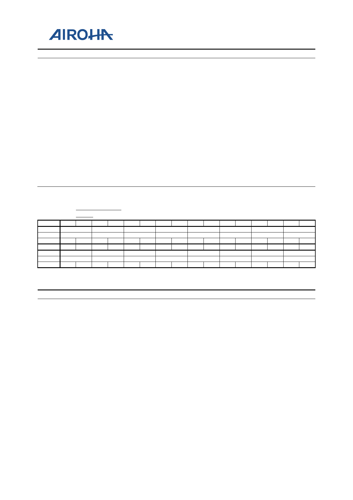
MT2523 Series Reference Manual
© 2015 - 2018 Airoha Technology Corp.
Page 561 of 692
This document contains information that is proprietary to Airoha Technology Corp. (“Airoha”) and/or its licensor(s).
Any unauthorized use, reproduction or disclosure of this document in whole or in part is strictly prohibited.
Bit(s)
Mnemonic
Name
Description
11:10
GPIO37
GPIO37_TDSEL
Bitwise SET operation of GPIO37_TDSEL Tx duty control
0: Keep
1: SET bits
9:8
GPIO36
GPIO36_TDSEL
Bitwise SET operation of GPIO36_TDSEL Tx duty control
0: Keep
1: SET bits
7:6
GPIO35
GPIO35_TDSEL
Bitwise SET operation of GPIO35_TDSEL Tx duty control
0: Keep
1: SET bits
5:4
GPIO34
GPIO34_TDSEL
Bitwise SET operation of GPIO34_TDSEL Tx duty control
0: Keep
1: SET bits
3:2
GPIO33
GPIO33_TDSEL
Bitwise SET operation of GPIO33_TDSEL Tx duty control
0: Keep
1: SET bits
1:0
GPIO32
GPIO32_TDSEL
Bitwise SET operation of GPIO32_TDSEL Tx duty control
0: Keep
1: SET bits
A2020D28
GPIO_TDSEL2
_CLR
GPIO TDSEL Control
00000000
Bit
31
30
29
28
27
26
25
24
23
22
21
20
19
18
17
16
Name
GPIO47
GPIO46
GPIO45
GPIO44
GPIO43
GPIO42
GPIO41
GPIO40
Type
WO
WO
WO
WO
WO
WO
WO
WO
Reset
0
0
0
0
0
0
0
0
0
0
0
0
0
0
0
0
Bit
15
14
13
12
11
10
9
8
7
6
5
4
3
2
1
0
Name
GPIO39
GPIO38
GPIO37
GPIO36
GPIO35
GPIO34
GPIO33
GPIO32
Type
WO
WO
WO
WO
WO
WO
WO
WO
Reset
0
0
0
0
0
0
0
0
0
0
0
0
0
0
0
0
Overview
For bitwise access of GPIO_TDSEL
Bit(s)
Mnemonic
Name
Description
31:30
GPIO47
GPIO47_TDSEL
Bitwise CLR operation of GPIO47_TDSEL Tx duty control
0: Keep
1: CLR bits
29:28
GPIO46
GPIO46_TDSEL
Bitwise CLR operation of GPIO46_TDSEL Tx duty control
0: Keep
1: CLR bits
27:26
GPIO45
GPIO45_TDSEL
Bitwise CLR operation of GPIO45_TDSEL Tx duty control
0: Keep
1: CLR bits
25:24
GPIO44
GPIO44_TDSEL
Bitwise CLR operation of GPIO44_TDSEL Tx duty control
0: Keep
1: CLR bits
23:22
GPIO43
GPIO43_TDSEL
Bitwise CLR operation of GPIO43_TDSEL Tx duty control
0: Keep
1: CLR bits
21:20
GPIO42
GPIO42_TDSEL
Bitwise CLR operation of GPIO42_TDSEL Tx duty control
0: Keep
1: CLR bits
19:18
GPIO41
GPIO41_TDSEL
Bitwise CLR operation of GPIO41_TDSEL Tx duty control
0: Keep
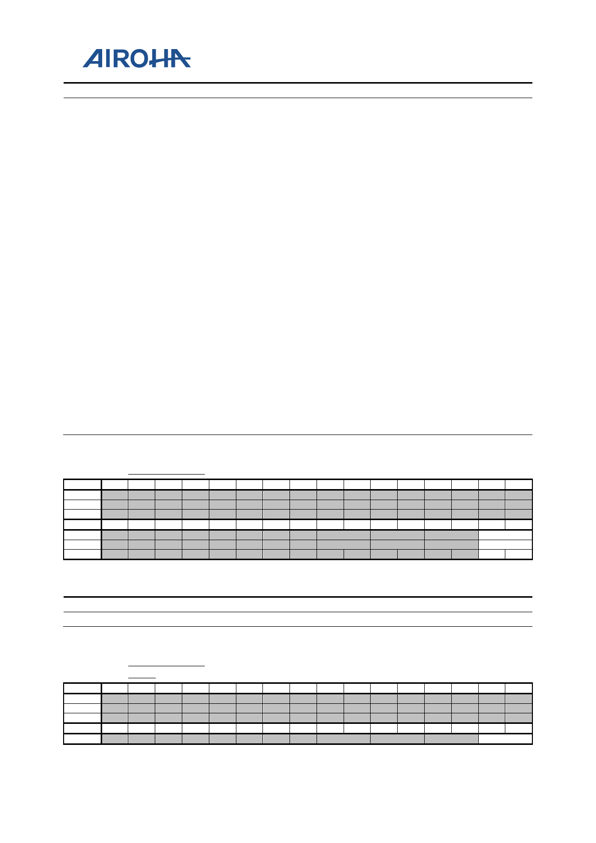
MT2523 Series Reference Manual
© 2015 - 2018 Airoha Technology Corp.
Page 562 of 692
This document contains information that is proprietary to Airoha Technology Corp. (“Airoha”) and/or its licensor(s).
Any unauthorized use, reproduction or disclosure of this document in whole or in part is strictly prohibited.
Bit(s)
Mnemonic
Name
Description
1: CLR bits
17:16
GPIO40
GPIO40_TDSEL
Bitwise CLR operation of GPIO40_TDSEL Tx duty control
0: Keep
1: CLR bits
15:14
GPIO39
GPIO39_TDSEL
Bitwise CLR operation of GPIO39_TDSEL Tx duty control
0: Keep
1: CLR bits
13:12
GPIO38
GPIO38_TDSEL
Bitwise CLR operation of GPIO38_TDSEL Tx duty control
0: Keep
1: CLR bits
11:10
GPIO37
GPIO37_TDSEL
Bitwise CLR operation of GPIO37_TDSEL Tx duty control
0: Keep
1: CLR bits
9:8
GPIO36
GPIO36_TDSEL
Bitwise CLR operation of GPIO36_TDSEL Tx duty control
0: Keep
1: CLR bits
7:6
GPIO35
GPIO35_TDSEL
Bitwise CLR operation of GPIO35_TDSEL Tx duty control
0: Keep
1: CLR bits
5:4
GPIO34
GPIO34_TDSEL
Bitwise CLR operation of GPIO34_TDSEL Tx duty control
0: Keep
1: CLR bits
3:2
GPIO33
GPIO33_TDSEL
Bitwise CLR operation of GPIO33_TDSEL Tx duty control
0: Keep
1: CLR bits
1:0
GPIO32
GPIO32_TDSEL
Bitwise CLR operation of GPIO32_TDSEL Tx duty control
0: Keep
1: CLR bits
A2020D30
GPIO_TDSEL3
GPIO TDSEL Control
00000000
Bit
31
30
29
28
27
26
25
24
23
22
21
20
19
18
17
16
Name
Type
Reset
Bit
15
14
13
12
11
10
9
8
7
6
5
4
3
2
1
0
Name
GPIO48
Type
RW
Reset
0
0
Overview
GPIO TX duty control register
Bit(s)
Mnemonic
Name
Description
1:0
GPIO48
GPIO48_TDSEL
GPIO48 Tx duty control
A2020D34
GPIO_TDSEL3
_SET
GPIO TDSEL Control
00000000
Bit
31
30
29
28
27
26
25
24
23
22
21
20
19
18
17
16
Name
Type
Reset
Bit
15
14
13
12
11
10
9
8
7
6
5
4
3
2
1
0
Name
GPIO48
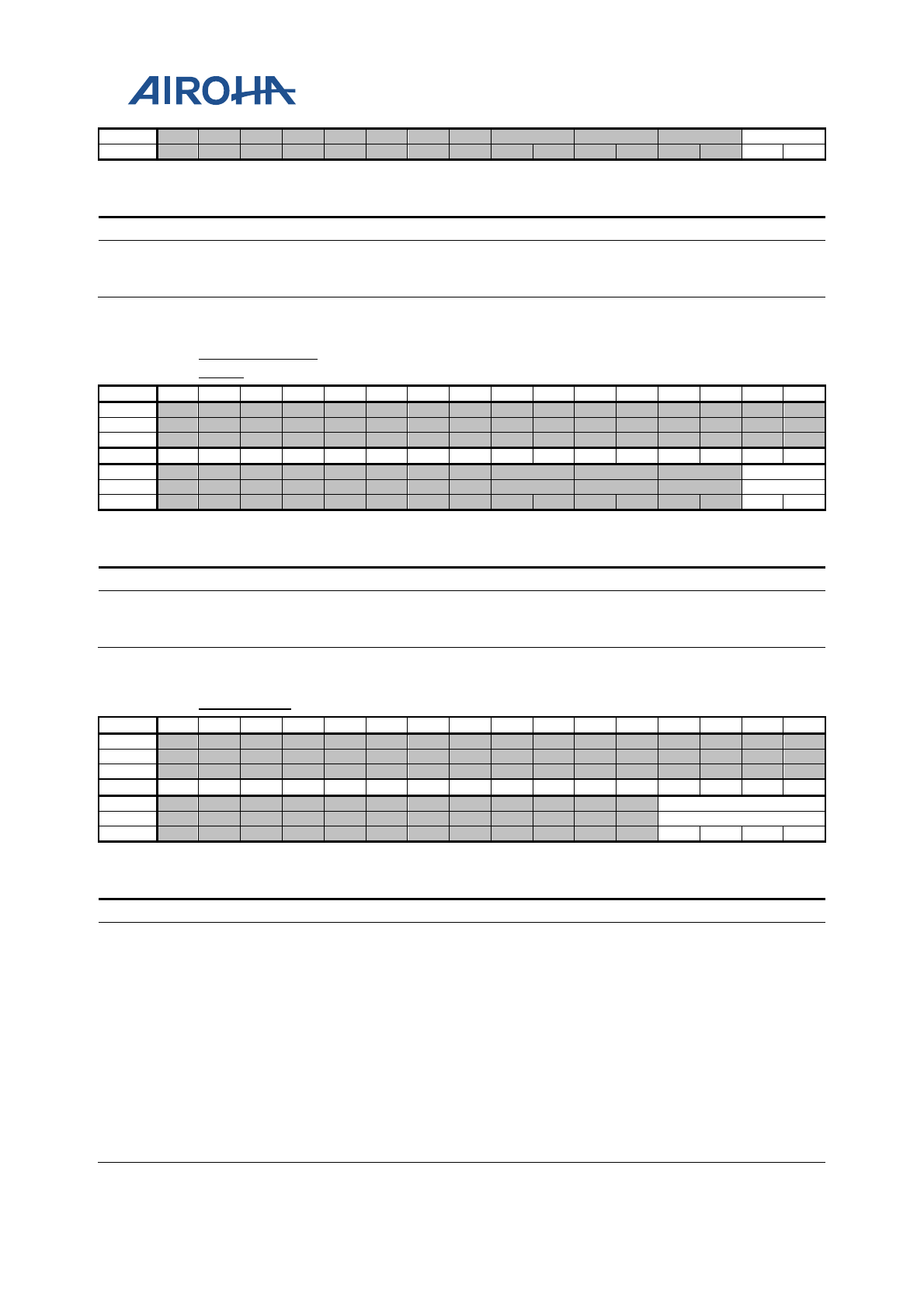
MT2523 Series Reference Manual
© 2015 - 2018 Airoha Technology Corp.
Page 563 of 692
This document contains information that is proprietary to Airoha Technology Corp. (“Airoha”) and/or its licensor(s).
Any unauthorized use, reproduction or disclosure of this document in whole or in part is strictly prohibited.
Type
WO
Reset
0
0
Overview
For bitwise access of GPIO_TDSEL
Bit(s)
Mnemonic
Name
Description
1:0
GPIO48
GPIO48_TDSEL
Bitwise SET operation of GPIO48_TDSEL Tx duty control
0: Keep
1: SET bits
A2020D38
GPIO_TDSEL3
_CLR
GPIO TDSEL Control
00000000
Bit
31
30
29
28
27
26
25
24
23
22
21
20
19
18
17
16
Name
Type
Reset
Bit
15
14
13
12
11
10
9
8
7
6
5
4
3
2
1
0
Name
GPIO48
Type
WO
Reset
0
0
Overview
For bitwise access of GPIO_TDSEL
Bit(s)
Mnemonic
Name
Description
1:0
GPIO48
GPIO48_TDSEL
Bitwise CLR operation of GPIO48_TDSEL Tx duty control
0: Keep
1: CLR bits
A2020E00
CLK_OUT0
CLK Out Selection Control
00000004
Bit
31
30
29
28
27
26
25
24
23
22
21
20
19
18
17
16
Name
Type
Reset
Bit
15
14
13
12
11
10
9
8
7
6
5
4
3
2
1
0
Name
CLK_OUT0
Type
RW
Reset
0
1
0
0
Overview
CLK OUT0 Setting
Bit(s)
Mnemonic
Name
Description
3:0
CLK_OUT0
CFG0
Selects clock output for CLKO_0
[0]: Reserved
[1]: f26m_mcusys_ck
[2]: Reserved
[3]: Reserved
[4]: f32k_mcusys_ck
[5]: Reserved
[6]: Reserved
[7]: Reserved
[8]: Reserved
[9]: Reserved
[10]: Reserved
[11]: Reserved
[12]: Reserved
[13]: Reserved
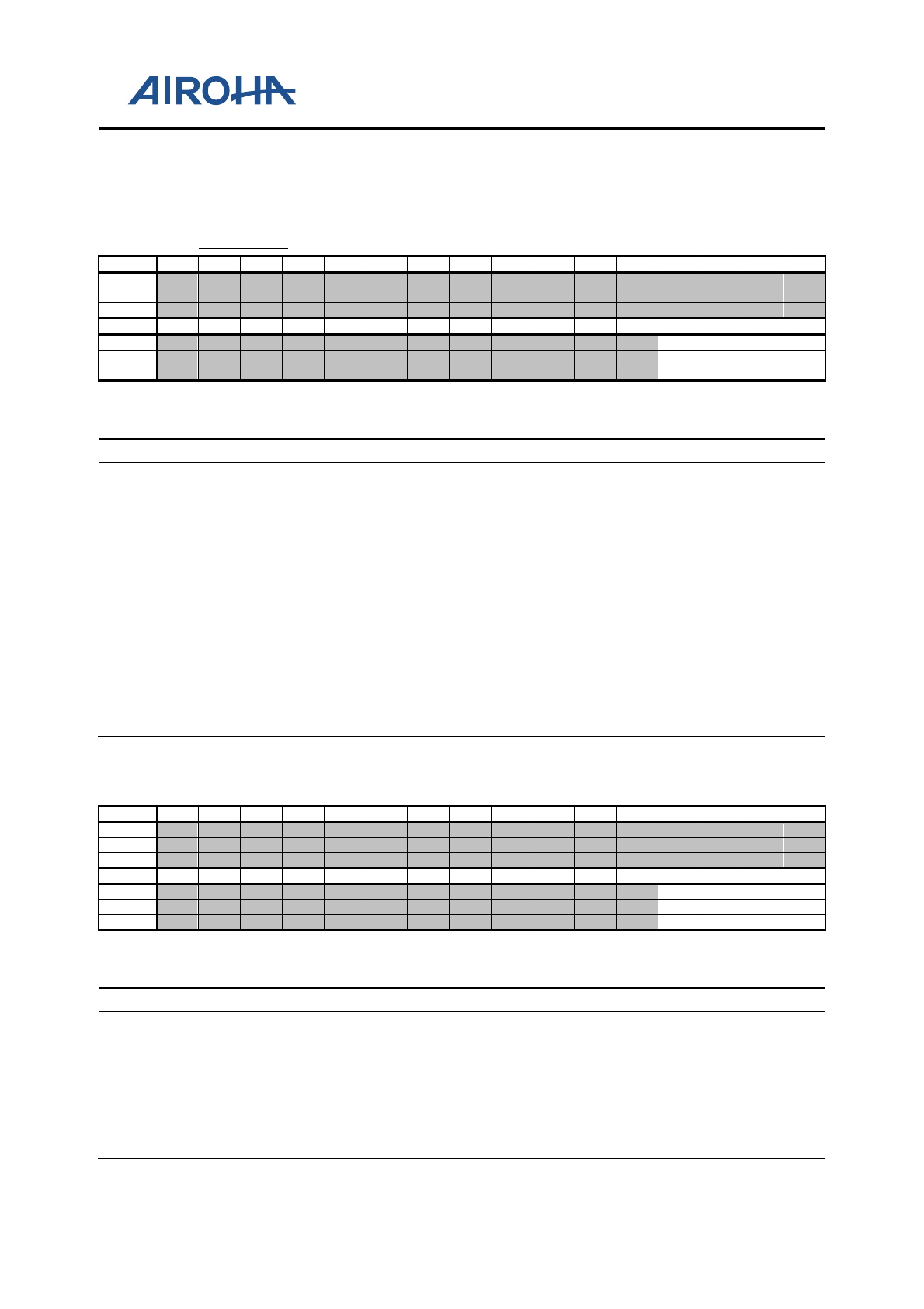
MT2523 Series Reference Manual
© 2015 - 2018 Airoha Technology Corp.
Page 564 of 692
This document contains information that is proprietary to Airoha Technology Corp. (“Airoha”) and/or its licensor(s).
Any unauthorized use, reproduction or disclosure of this document in whole or in part is strictly prohibited.
Bit(s)
Mnemonic
Name
Description
[14]: Reserved
[15]: Reserved
A2020E10
CLK_OUT1
CLK Out Selection Control
00000004
Bit
31
30
29
28
27
26
25
24
23
22
21
20
19
18
17
16
Name
Type
Reset
Bit
15
14
13
12
11
10
9
8
7
6
5
4
3
2
1
0
Name
CLK_OUT1
Type
RW
Reset
0
1
0
0
Overview
CLK OUT1 setting
Bit(s)
Mnemonic
Name
Description
3:0
CLK_OUT1
CFG1
Selects clock output for CLKO_1
[0]: Reserved
[1]: f26m_mcusys_ck
[2]: Reserved
[3]: Reserved
[4]: f32k_mcusys_ck
[5]: Reserved
[6]: Reserved
[7]: Reserved
[8]: Reserved
[9]: Reserved
[10]: Reserved
[11]: Reserved
[12]: Reserved
[13]: Reserved
[14]: Reserved
[15]: Reserved
A2020E20
CLK_OUT2
CLK Out Selection Control
00000004
Bit
31
30
29
28
27
26
25
24
23
22
21
20
19
18
17
16
Name
Type
Reset
Bit
15
14
13
12
11
10
9
8
7
6
5
4
3
2
1
0
Name
CLK_OUT2
Type
RW
Reset
0
1
0
0
Overview
CLK OUT2 setting
Bit(s)
Mnemonic
Name
Description
3:0
CLK_OUT2
CFG2
Selects clock output for CLKO_2
[0]: Reserved
[1]: f26m_mcusys_ck
[2]: Reserved
[3]: Reserved
[4]: f32k_mcusys_ck
[5]: Reserved
[6]: Reserved
[7]: Reserved
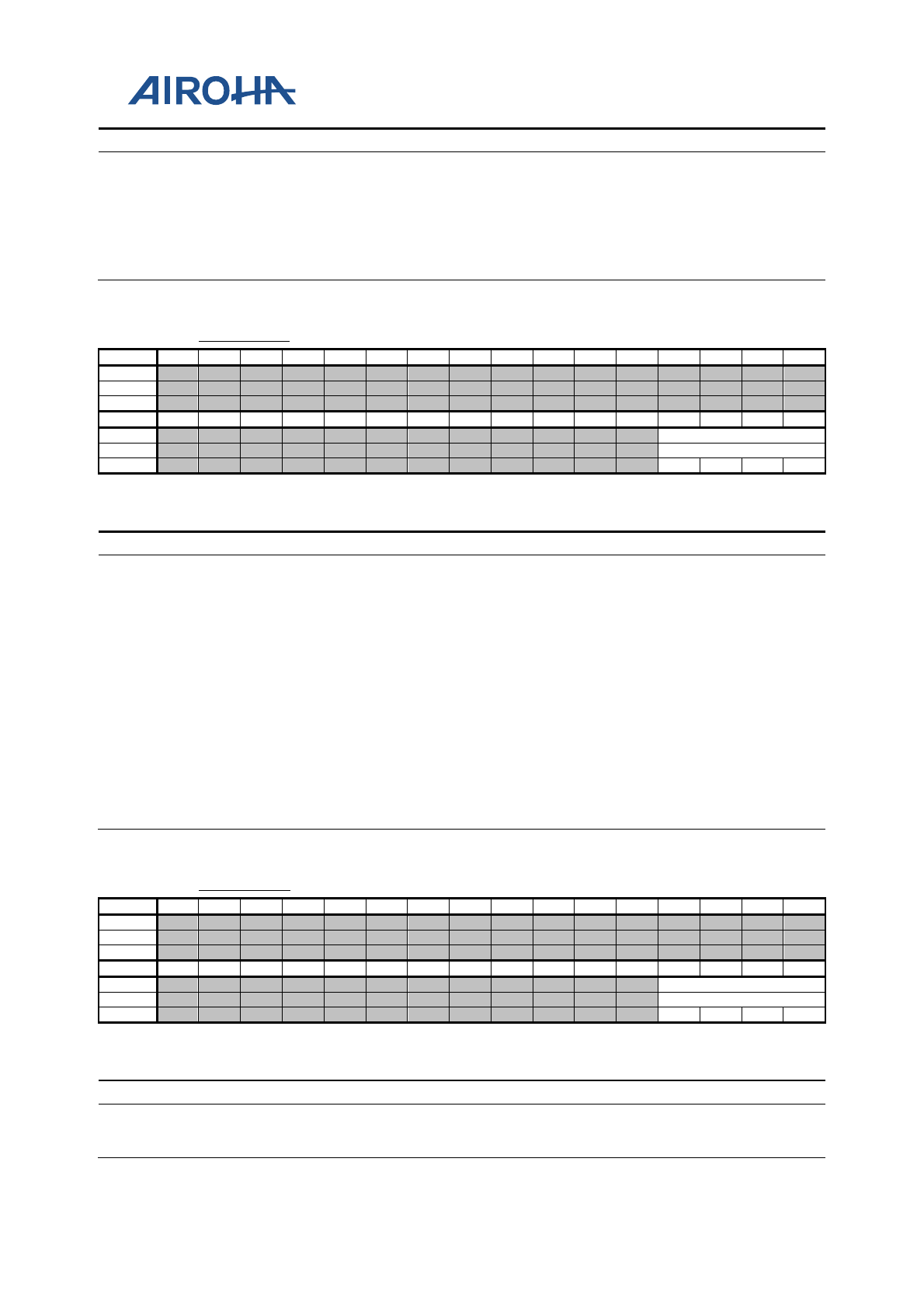
MT2523 Series Reference Manual
© 2015 - 2018 Airoha Technology Corp.
Page 565 of 692
This document contains information that is proprietary to Airoha Technology Corp. (“Airoha”) and/or its licensor(s).
Any unauthorized use, reproduction or disclosure of this document in whole or in part is strictly prohibited.
Bit(s)
Mnemonic
Name
Description
[8]: Reserved
[9]: Reserved
[10]: Reserved
[11]: Reserved
[12]: Reserved
[13]: Reserved
[14]: Reserved
[15]: Reserved
A2020E30
CLK_OUT3
CLK Out Selection Control
00000004
Bit
31
30
29
28
27
26
25
24
23
22
21
20
19
18
17
16
Name
Type
Reset
Bit
15
14
13
12
11
10
9
8
7
6
5
4
3
2
1
0
Name
CLK_OUT3
Type
RW
Reset
0
1
0
0
Overview
CLK OUT3 setting
Bit(s)
Mnemonic
Name
Description
3:0
CLK_OUT3
CFG3
Selects clock output for CLKO_3
[0]: Reserved
[1]: f26m_mcusys_ck
[2]: Reserved
[3]: Reserved
[4]: f32k_mcusys_ck
[5]: Reserved
[6]: Reserved
[7]: Reserved
[8]: Reserved
[9]: Reserved
[10]: Reserved
[11]: Reserved
[12]: Reserved
[13]: Reserved
[14]: Reserved
[15]: Reserved
A2020E40
CLK_OUT4
CLK Out Selection Control
00000004
Bit
31
30
29
28
27
26
25
24
23
22
21
20
19
18
17
16
Name
Type
Reset
Bit
15
14
13
12
11
10
9
8
7
6
5
4
3
2
1
0
Name
CLK_OUT4
Type
RW
Reset
0
1
0
0
Overview
CLK OUT4 setting
Bit(s)
Mnemonic
Name
Description
3:0
CLK_OUT4
CFG4
Selects clock output for CLKO_4
[0]: Reserved
[1]: f26m_mcusys_ck
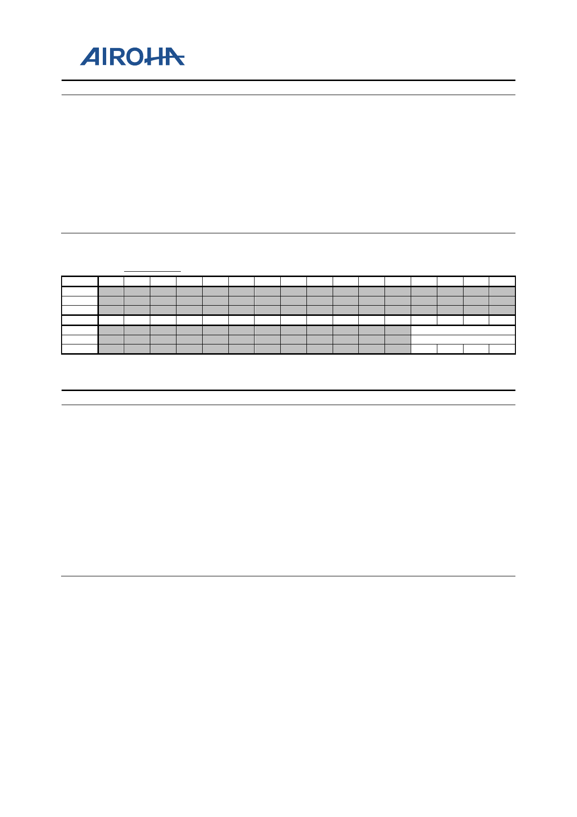
MT2523 Series Reference Manual
© 2015 - 2018 Airoha Technology Corp.
Page 566 of 692
This document contains information that is proprietary to Airoha Technology Corp. (“Airoha”) and/or its licensor(s).
Any unauthorized use, reproduction or disclosure of this document in whole or in part is strictly prohibited.
Bit(s)
Mnemonic
Name
Description
[2]: Reserved
[3]: reserved
[4]: f32k_mcusys_ck
[5]: Reserved
[6]: Reserved
[7]: Reserved
[8]: Reserved
[9]: Reserved
[10]: Reserved
[11]: Reserved
[12]: Reserved
[13]: Reserved
[14]: Reserved
[15]: Reserved
A2020E50
CLK_OUT5
CLK
Out Selection Control
00000004
Bit
31
30
29
28
27
26
25
24
23
22
21
20
19
18
17
16
Name
Type
Reset
Bit
15
14
13
12
11
10
9
8
7
6
5
4
3
2
1
0
Name
CLK_OUT5
Type
RW
Reset
0
1
0
0
Overview
CLK OUT5 setting
Bit(s)
Mnemonic
Name
Description
3:0
CLK_OUT5
CFG5
Selects clock output for CLKO_5
[0]: Reserved
[1]: f26m_mcusys_ck
[2]: Reserved
[3]: Reserved
[4]: f32k_mcusys_ck
[5]: Reserved
[6]: Reserved
[7]: Reserved
[8]: Reserved
[9]: Reserved
[10]: Reserved
[11]: Reserved
[12]: Reserved
[13]: Reserved
[14]: Reserved
[15]: Reserved

MT2523 Series Reference Manual
© 2015 - 2018 Airoha Technology Corp.
Page 567 of 692
This document contains information that is proprietary to Airoha Technology Corp. (“Airoha”) and/or its licensor(s).
Any unauthorized use, reproduction or disclosure of this document in whole or in part is strictly prohibited.
28. MT2523 Top Clock Setting
This chapter defines the clock settings for MT2523.
28.1. MT2523 Clock Scheme
This chapter describes the following settings:
• CM4 MCU clock setting
• Peripheral BUS clock setting
• BSI clock setting
• Serial flash clock setting
• DSP clock setting
• DISP PWM clock
• CAM clock setting
• SLCD clock setting
• MSDC0 clock setting
• MSDC1 clock setting
The USB clock’s frequency typically cannot be changed and so is not described in this chapter.
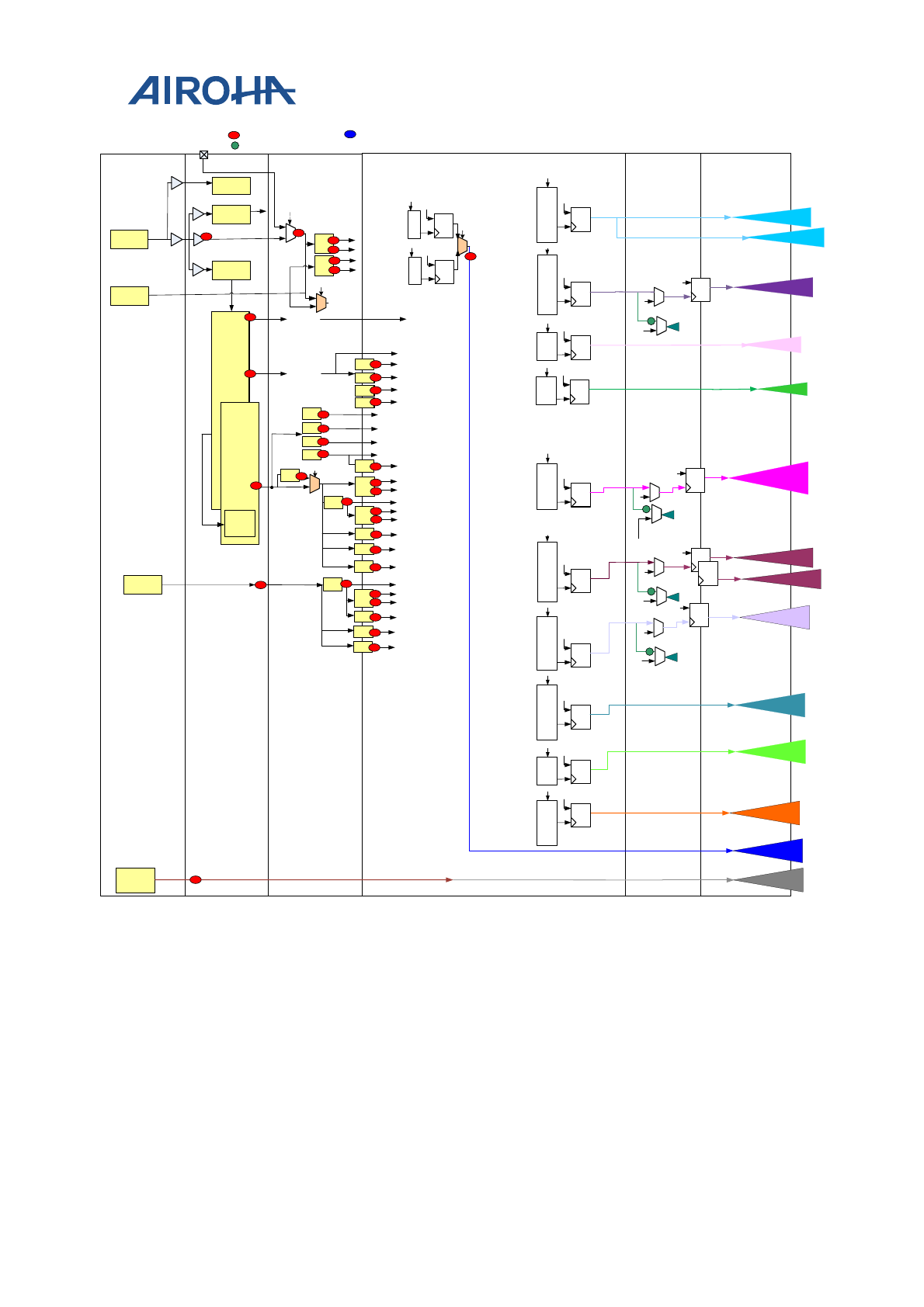
MT2523 Series Reference Manual
© 2015 - 2018 Airoha Technology Corp.
Page 568 of 692
This document contains information that is proprietary to Airoha Technology Corp. (“Airoha”) and/or its licensor(s).
Any unauthorized use, reproduction or disclosure of this document in whole or in part is strictly prohibited.
DCXO
26MHz
UPLL
312M
f32k_ck
UPLL_F48M_CK
RTC
32KHz
PLLs
CSW_F32K_CK
MPLL
624M
Clock Switch - Digital Clock
Frequency DIV
DDS
CLKSQ_F26M_CK
RTC_F32K_CK
UPLL_F208M_CK
UPLL_F62M_CK
MPLL_DIV2_CK
UPLL_F48M_CK
gslcd_ck
Clock Switch – Clock source
selection Top Global Con
create clock root
gmsdc0_ck
CSW_MSDC1_CK
R
R
R
R
R
ignore pin
i
1
0
pad_functest_ck
rg_pad_functest_ck_sel
G create_generated clock root
R
R
/2.5
R
CSW_SFC_CK
CG
EN
gsfc_ck
0
1
test_ck
gusb_ck
CSW_USB48M_CK
gcam_ck
CSW_CAM48M_CK
ghbus_ck
CSW_DSP_CK
CG
EN
gdsp_ck
0
1
test_ck
MPLL_F208M_CK
MPLL_F250M_CK
MPLL_F125M_CK
MPLL_DIV3_CK
MPLL_DIV2P5_CK
hnodcm_bsispi_ck
CSW|_BSISPI_CK
gmsdc1_ck
0
1
i
0
1
i
SW cg
& dcm
SW cg &
HW idle
SW cg &
HW idle
UPLL_F104M_CK
/2
BT PLL
UPLL_F312M_CK
MPLL_DIV4_CK
/3
/6
R
MPLL_DIV6_CK
CSW_SLCD_CK
MPLL_F624M_CK
MPLL_F312M_CK
R
CSW_CLKSQ_CK
HFOSC
312M
LFOSC
26M
R
HFOSC_CK
MIPI PLL
gp_f26m_
gfmux_sel
1
0
UPLL_F312M_CK UPLL_F104M_CK
/3
R
1
0
/2
/1.5
R
/2
/4
R
/3.5
/5
R
mpll_powerful_div[0]
MPLL_DIV3P5_CK
MPLL_DIV5_CK
R
R
R
MPLL_DIV1P5_CK
R
/2.5
R
HFOSC_DIV3_CK
HFOSC_DIV2P5_CK
/3
/6
R
HFOSC_DIV6_CK
/1.5
/3.5
HFOSC_DIV3P5_CK
R
R
HFOSC_DIV1P5_CK
CLKSQ
CSW_GP_F26M_CK
CSW_LP_F26M_CK
LFOSC_F26M_CK
0
1
2
3
4
5
6
7
8
CSW_LP_CLKSQ_CK
CSW_LP_LFOSC_CK
MPLL_DIV3_CK
MPLL_F125M_CK
MPLL_DIV4_CK
MPLL_DIV5_CK
HFOSC_DIV3_CK
HFOSC_DIV4_CK
HFOSC_DIV5_CK
0
1
2
3
4
5
6
7
CSW_LP_CLKSQ_CK
CSW_LP_LFOSC_CK
MPLL_DIV3P5_CK
MPLL_DIV4_CK
MPLL_DIV5_CK
HFOSC_DIV3P5_CK
MPLL_DIV4_CK
HFOSC_DIV5_CK
{rf_msdc_cfg_clksrc_patch, rf_msdc_cfg_pws}
sfc_mux_sel
CG
EN
~(SW cg |
chg_clk)
CG
EN
~(HW cg |
chg_clk)
CSW_MSDC0_CK
0
1
2
3
CSW_LP_CLKSQ_CK
CSW_LP_LFOSC_CK
UPLL_48M_CK
UPLL_F312M_CK
CG
EN
~(SW cg |
chg_clk)
cam_mux_sel
0
1
2
3
CSW_LP_CLKSQ_CK
CSW_LP_LFOSC_CK
UPLL_48M_CK
UPLL_F62M_CK
CG
EN
~(SW cg |
chg_clk)
usb_mux_sel
0
1
2
3
4
5
6
CSW_LP_CLKSQ_CK
CSW_LP_LFOSC_CK
UPLL_F62M_CK
MPLL_DIV5_CK
MPLL_DIV6_CK
HFOSC_DIV5_CK
HFOSC_DIV6_CK
CG
EN
~(HW cg |
chg_clk)
bus_mux_sel
CSW_BUS_CK
CG
EN
0
1
0
1
i
SW cg
& dcm
ghbus_pd_bus_mclk_ck
ghbus_ao_bus_mclk_ck
CSW_CM_CK
CG
EN
gcm_ck
0
1
test_ck
0
1
i
SW cg
& dcm
0
1
2
3
4
5
6
7
8
CSW_LP_CLKSQ_CK
CSW_LP_LFOSC_CK
UPLL_F104M_CK
MPLL_DIV3_CK
HFOSC_DIV3_CK
MPLL_F208M_CK
MPLL_DIV2_CK
HFOSC_DIV1P5_CK
HFOSC_DIV2_CK
cm_mux_sel=efuse_cpu_104m &
(sel_reg > 4'd4) ? 4'd4 : sel_reg
CG
EN
~(HW cg |
chg_clk)
gmems_ck
CG
EN
0
1
2
3
4
5
6
7
CG
EN
~(HW cg |
chg_clk)
dsp_mux_sel
0
1
2
3
4
5
6
7
CSW_LP_CLKSQ_CK
CSW_LP_LFOSC_CK
MPLL_DIV2P5_CK
MPLL_DIV3_CK
MPLL_DIV4_CK
HFOSC_DIV2P5_CK
HFOSC_DIV3_CK
HFOSC_DIV4_CK
CG
EN
~(SW cg |
chg_clk)
slcd_mux_sel
0
1
2
3
CSW_LP_CLKSQ_CK
CSW_LP_LFOSC_CK
UPLL_F104M_CK
HFOSC_DIV3_CK
CG
EN
~(SW cg |
chg_clk)
disp_pwm_mux_sel
gdisp_pwm_ck
CSW_DISP_PWM_CK
0
1
2
3
4
5
6
CSW_LP_CLKSQ_CK
CSW_LP_LFOSC_CK
MPLL_DIV2P5_CK
MPLL_DIV3_CK
HFOSC_DIV2P5_CK
HFOSC_DIV3_CK
1'b0
CG
EN
~(SW cg | HW cg |
chg_clk)
bsi_mux_sel
CSW_LP_F26M_CK
f26m_ck
(to uart)
(to bt/modem/
dpm/mixedsys_d)
/5
HFOSC_DIV5_CK
R
/4.5
R
MPLL_F138M_CK
/2.5
R
/3
/5
/2
/1.5
R
R
R
R
CSW_LP_CLKSQ_CK
CSW_LP_LFOSC_CK
MPLL_DIV2_CK
MPLL_F138M_CK
MPLL_DIV2P5_CK
UPLL_F125M_CK
HFOSC_DIV2_CK
HFOSC_DIV2P5_CK
/3.5
R
MPLL_F178M_CK
/2
/4
lp_f26m_gf
mux_sel
R
/2
/4
CLKSQ_F13M_CK
R
CLKSQ_F6P5M_CK
R
LFOSC_F13M_CK
R
LFOSC_F6P5M_CK
R
0
1
2
3
CLKSQ_F26M_CK
CLKSQ_F13M_CK
CLKSQ_F6P5M_CK
RTC_F32K_CK
CG
EN
~(SW cg |
chg_clk)
lp_clksq_mux
_sel
0
1
2
3
LFOSC_F26M_CK
LFOSC_F13M_CK
LFOSC_F6P5M_CK
RTC_F32K_CK
CG
EN
~(SW cg |
chg_clk)
lp_lfosc_mux
_sel
1
0
CSW_LP_C
LKSQ_CK
CSW_LP_L
FOSC_CK
R
Figure 28-1. MT2523 clock scheme
28.2. Clock Setting Programming Guide
The clock settings of MT2523 are configured by CRs which control some clock dividers and MUXs. This chapter
describes how to switch clock source/frequency for MT2523 system and peripheral devices.
Note that all clock sources should be enabled and stable when S/W switches to it. Follow the minimum VCORE
voltage limitation, or there will be timing violation issues.
MT2523 Series Reference Manual
© 2015 - 2018 Airoha Technology Corp.
Page 569 of 692
This document contains information that is proprietary to Airoha Technology Corp. (“Airoha”) and/or its licensor(s).
Any unauthorized use, reproduction or disclosure of this document in whole or in part is strictly prohibited.
28.2.1. General Slow Clock Setting
There are three types of slow clocks, DCXO (CLKSQ) 26M, LFOSC 26M and 32K. CLKSQ 26M and LFOSC 26M are
divided into 13M and 6.5M. You can select LFOSC for lower power or CLKSQ for more accuracy. CM4/BUS/SFC
default clock is from CSW_LP_CLKSQ_CK; you can switch to CSW_LP_LFOSC_CK or other higher clock frequencies.
The clock source of UART 0 ~ 3 is from CSW_GP_F26M_CK. BT and audio 26M clock is from CLKSQ_F26M_CK.
Other modules’ slow clocks are derived from CSW_LP_F26M_CK, e.g.
PWM/GPTIMER/I2C0/I2C1/SPI/SENSOR_DMA.
Mux select register
(active when chg=1) Mux select option
Powerful divide enable
bit works @
*CLK_CONDB
(0xA2010104) bit[31]=1
Min.
vcore
voltage
(typ)
CSW_LP_CLKSQ_CK
LP_CLKSQ_MUX_SEL =
*CLK_CONDD
(0xA201010C) bit[25:24]
0: CLKSQ_F26M_CK
(26MHz) NA 0.9v
1: CLKSQ_F13M_CK
(13MHz) NA 0.9v
2: CLKSQ_F6P5M_CK
(6.5MHz) NA 0.9v
3: RTC_F32K_CK
(32kHz) NA 0.9v
The configured CRs and steps are:
LP_CLKSQ_MUX_SEL : 0xA201010C[25:24]
CHG_LP_CLKSQ =1 : 0xA21D0150[12]
MUX change will succeed when read 0xA21D0150[12] = 0.
Mux select register
(active when chg=1) Mux select option
Powerful divide enable
bit works @
*CLK_CONDB
(0xA2010104) bit[31]=1
Min.
vcore
voltage
(typ)
CSW_LP_LFOSC_CK
LP_LFOSC_MUX_SEL =
*CLK_CONDD
(0xA201010C) bit[23:22]
0: LFOSC_F26M_CK
(26MHz) NA 0.9v
1: LFOSC_F13M_CK
(13MHz) NA 0.9v
2: LFOSC_F6P5M_CK
(6.5MHz) NA 0.9v
3: RTC_F32K_CK
(32kHz) NA 0.9v
MT2523 Series Reference Manual
© 2015 - 2018 Airoha Technology Corp.
Page 570 of 692
This document contains information that is proprietary to Airoha Technology Corp. (“Airoha”) and/or its licensor(s).
Any unauthorized use, reproduction or disclosure of this document in whole or in part is strictly prohibited.
The configured CRs and steps are:
LP_ LFOSC_MUX_SEL : 0xA201010C[23:22]
CHG_LP_LFOSC =1 : 0xA21D0150[13]
MUX change will succeed when read 0xA21D0150[13] = 0.
Mux select register Mux select option
Powerful divide enable
bit works @
*CLK_CONDB
(0xA2010104) bit[31]=1
Min.
vcore
voltage
(typ)
CSW_LP_F26M_CK
LP_F26M_GFMUX_SEL =
*CLK_CONDB
(0xA2010104) bit[20]
0: CSW_LP_CLKSQ_CK NA 0.9v
1: CSW_LP_LFOSC_CK NA 0.9v
The configured CRs and steps are:
LP_F26M_GFMUX_SEL: 0xA2010104[20]
MUX change will succeed after 2T original clock + 2T target clock.
Mux select register Mux select option
Powerful divide enable
bit works @
*CLK_CONDB
(0xA2010104) bit[31]=1
Min.
vcore
voltage
(typ)
CSW_GP_F26M_CK
GP_F26M_GFMUX_SEL =
*CLK_CONDB
(0xA2010104) bit[21]
0: CLKSQ_F26M_CK
(26MHz) NA 0.9v
1: LFOSC_F26M_CK
(26MHz) NA 0.9v
The configured CRs and steps are:
GP_F26M_GFMUX_SEL: 0xA2010104[21]
MUX change will succeed after 2T original clock + 2T target clock.
28.2.2. CM4 MCU Clock Setting
The CM4 MCU clock supports slow clock, 104MHz and max. 208MHz (divided from PLL). CM4 MCU clock is CM4
CPU clock. CM4 and EMI/SFC/MM AHB BUS (MEMS) clock are derived from CM4 MCU clock and equals half of CM4
MCU clock frequency. EMI needs 50/50 duty clock, so none of 50/50 duty clock source is forbidden with pSRAM
scenario.
MT2523 Series Reference Manual
© 2015 - 2018 Airoha Technology Corp.
Page 571 of 692
This document contains information that is proprietary to Airoha Technology Corp. (“Airoha”) and/or its licensor(s).
Any unauthorized use, reproduction or disclosure of this document in whole or in part is strictly prohibited.
Change bit
(gating when chg,
auto clear)
Mux select
register
(active when
chg=1)
Mux select option
Powerful
divide enable
bit works @
*CLK_CONDB
(0xA2010104)
bit[31]=1
Min.
vcore
voltage
(typ)
CSW_CM_CK
CHG_CM =
*ACFG_CLK_UPDATE
(0XA21D0150) BIT[1]
CM_MUX_SEL =
*CLK_CONDB
(0xA2010104)
bit[6:3]
0: CSW_LP_CLKSQ_CK
(max. 26MHz) NA 0.9v
1: CSW_LP_LFOSC_CK
(max. 26MHz) NA 0.9v
2: UPLL_F104M_CK
(104MHz)
*CLK_CONDA
(0xA2010100)
bit[8+1]=1
1.1v
3: MPLL_DIV3_CK
(104MHz)
*CLK_CONDA
(0xA2010100)
bit[16]=1
*CLK_CONDA
(0xA2010100)
bit[16+4]=1
*CLK_CONDA
(0xA2010100)
bit[16+7]=1
1.1v
4: HFOSC_DIV3_CK
(104MHz)
*CLK_CONDA
(0xA2010100)
bit[0]=1
*CLK_CONDA
(0xA2010100)
bit[3]=1
1.1v
5: MPLL_F208M_CK
(208MHz)
*CLK_CONDA
(0xA2010100)
bit[16+2]=1
1.3v
6: MPLL_DIV2_CK
(156MHz)
*CLK_CONDA
(0xA2010100)
bit[16]=1
*CLK_CONDA
(0xA2010100)
bit[16+5]=1
1.3v
7: HFOSC_DIV1P5_CK
(none 50/50 duty,
forbidden)
*CLK_CONDA
(0xA2010100)
bit[0]=1
NA
8: HFOSC_DIV2_CK
(156MHz)
*CLK_CONDA
(0xA2010100)
bit[1]=1
1.3v
The configured CRs and steps are:
MT2523 Series Reference Manual
© 2015 - 2018 Airoha Technology Corp.
Page 572 of 692
This document contains information that is proprietary to Airoha Technology Corp. (“Airoha”) and/or its licensor(s).
Any unauthorized use, reproduction or disclosure of this document in whole or in part is strictly prohibited.
POWERFUL_DIV_EN : 0xA2010100[31:0]
PLL_DIV_EN=1 : 0xA2010104[31]
CM_MUX_SEL : 0xA2010104[6:3]
CHG_CM =1 : 0xA21D0150[1]
MUX change will succeed when read 0xA21D0150[1] = 0.
28.2.3. Peripheral BUS Clock Setting
The Peripheral BUS clock supports slow clock, 52MHz and max. 62.4MHz. Peripheral BUS clock is for peripheral
I2C_D2D/I2C2/DMA/DMA_AO/SPISLV clock and general BUS clock. Peripheral BUS clock can only run at max.
13MHz in 0.9v. Therefore, setting up BUS DCM signal “RG_BUS_FREE_FSEL” to derive 13MHz clock from 26MHz is
required. Refer to clock API for the setup method.
Change bit
(gating when chg,
auto clear)
Mux select
register
(active when
chg=1)
Mux select option
Powerful
divide enable
bit works @
*CLK_CONDB
(0xA2010104)
bit[31]=1
Min.
vcore
voltage
(typ)
CSW_BUS_CK
CHG_BUS =
*ACFG_CLK_UPDATE
(0XA21D0150) BIT[0]
BUS_MUX_SEL
=
*CLK_CONDB
(0xA2010104)
bit[2:0]
0: CSW_LP_CLKSQ_CK
(max. 26MHz) NA 0.9v
1: CSW_LP_LFOSC_CK
(max. 26MHz) NA 0.9v
2: UPLL_F62M_CK
(62.4MHz)
*CLK_CONDA
(0xA2010100)
bit[8+3]=1
1.1v
3: MPLL_DIV5_CK
(62.4MHz)
*CLK_CONDA
(0xA2010100)
bit[16]=1
*CLK_CONDA
(0xA2010100)
bit[16+9]=1
1.1v
4: MPLL_DIV6_CK
(52MHz)
*CLK_CONDA
(0xA2010100)
bit[16]=1
*CLK_CONDA
(0xA2010100)
bit[16+4]=1
*CLK_CONDA
(0xA2010100)
bit[16+7]=1
1.1v
5: HFOSC_DIV5_CK
(62.4MHz)
*CLK_CONDA
(0xA2010100)
bit[5]=1
1.1v
MT2523 Series Reference Manual
© 2015 - 2018 Airoha Technology Corp.
Page 573 of 692
This document contains information that is proprietary to Airoha Technology Corp. (“Airoha”) and/or its licensor(s).
Any unauthorized use, reproduction or disclosure of this document in whole or in part is strictly prohibited.
Change bit
(gating when chg,
auto clear)
Mux select
register
(active when
chg=1)
Mux select option
Powerful
divide enable
bit works @
*CLK_CONDB
(0xA2010104)
bit[31]=1
Min.
vcore
voltage
(typ)
6: HFOSC_DIV6_CK
(52MHz)
*CLK_CONDA
(0xA2010100)
bit[0]=1
*CLK_CONDA
(0xA2010100)
bit[3]=1
1.1v
The configured CRs and steps are:
POWERFUL_DIV_EN : 0xA2010100[31:0]
PLL_DIV_EN=1 : 0xA2010104[31]
BUS_MUX_SEL : 0xA2010104[2:0]
CHG_BUS =1 : 0xA21D0150[0]
MUX change will succeed when read 0xA21D0150[0] = 0.
28.2.4. BSI BUS Clock Setting
The BSI clock supports slow clock, 104MHz and max. 124.8MHz. BSI clock is for DCXO configuration BSI interface.
BSI clock frequency should be bigger than or equal to twice of Peripheral BUS clock.
Change bit
(gating when chg,
auto clear)
Mux select
register
(active when
chg=1)
Mux select option
Powerful
divide enable
bit works @
*CLK_CONDB
(0xA2010104)
bit[31]=1
Min.
vcore
voltage
(typ)
CSW_BSI_CK
CHG_BSI =
*ACFG_CLK_UPDATE
(0XA21D0150) BIT[5]
BSI_MUX_SEL =
*CLK_CONDB
(0xA2010104)
bit[19:17]
0: CSW_LP_CLKSQ_CK
(max. 26MHz) NA 0.9v
1: CSW_LP_LFOSC_CK
(max. 26MHz) NA 0.9v
2: MPLL_DIV2P5_CK
(none 50/50 duty
124.8MHz)
*CLK_CONDA
(0xA2010100)
bit[16]=1
*CLK_CONDA
(0xA2010100)
bit[16+6]=1
1.1v

MT2523 Series Reference Manual
© 2015 - 2018 Airoha Technology Corp.
Page 574 of 692
This document contains information that is proprietary to Airoha Technology Corp. (“Airoha”) and/or its licensor(s).
Any unauthorized use, reproduction or disclosure of this document in whole or in part is strictly prohibited.
Change bit
(gating when chg,
auto clear)
Mux select
register
(active when
chg=1)
Mux select option
Powerful
divide enable
bit works @
*CLK_CONDB
(0xA2010104)
bit[31]=1
Min.
vcore
voltage
(typ)
3: MPLL_DIV3_CK
(104MHz)
*CLK_CONDA
(0xA2010100)
bit[16]=1
*CLK_CONDA
(0xA2010100)
bit[16+4]=1
*CLK_CONDA
(0xA2010100)
bit[16+7]=1
1.1v
4: HFOSC_DIV2P5_CK
(none 50/50 duty
124.8MHz)
*CLK_CONDA
(0xA2010100)
bit[2]=1
1.1v
5: HFOSC_DIV3_CK
(104MHz)
*CLK_CONDA
(0xA2010100)
bit[0]=1
*CLK_CONDA
(0xA2010100)
bit[3]=1
1.1v
The configured CRs and steps are:
POWERFUL_DIV_EN : 0xA2010100[31:0]
PLL_DIV_EN=1 : 0xA2010104[31]
BSI_MUX_SEL : 0xA2010104[19:17]
RG_BSICSW_FORCE_ON=1 : 0xA201010C[5]
CHG_BSI =1 : 0xA21D0150[5]
MUX change will succeed when read 0xA21D0150[5] = 0.
RG_BSICSW_FORCE_ON=0 : 0xA201010C[5]
MT2523 Series Reference Manual
© 2015 - 2018 Airoha Technology Corp.
Page 575 of 692
This document contains information that is proprietary to Airoha Technology Corp. (“Airoha”) and/or its licensor(s).
Any unauthorized use, reproduction or disclosure of this document in whole or in part is strictly prohibited.
28.2.5. Serial Flash Clock Setting
The serial flash clock supports slow clock, 62.4MHz and max. 78MHz.
Change bit
(gating when chg,
auto clear)
Mux select
register
(active when
chg=1)
Mux select option
Powerful
divide enable
bit works @
*CLK_CONDB
(0xA2010104
) bit[31]=1
Min.
vcore
voltag
e (typ)
CSW_SFC_CK
CHG_SFC =
*ACFG_CLK_UPDAT
E (0XA21D0150)
BIT[3]
SFC_MUX_SEL =
*CLK_CONDB
(0xA2010104)
bit[13:10]
0: CSW_LP_CLKSQ_CK
(max. 26MHz) NA 0.9v
1: CSW_LP_LFOSC_CK
(max. 26MHz) NA 0.9v
2: MPLL_DIV3_CK
(104MHz, forbidden)
*CLK_CONDA
(0xA2010100
) bit[16]=1
*CLK_CONDA
(0xA2010100
) bit[16+4]=1
*CLK_CONDA
(0xA2010100
) bit[16+7]=1
NA
3: MPLL_F125M_CK (
124.8MHz, forbidden)
*CLK_CONDA
(0xA2010100
) bit[16]=1
*CLK_CONDA
(0xA2010100
) bit[16+3]=1
NA
4: MPLL_DIV4_CK
(78MHz)
*CLK_CONDA
(0xA2010100
) bit[16]=1
*CLK_CONDA
(0xA2010100
) bit[16+5]=1
1.1v
5: MPLL_DIV5_CK
(62.4MHz)
*CLK_CONDA
(0xA2010100
) bit[16]=1
*CLK_CONDA
(0xA2010100
) bit[16+9]=1
1.1v
6: HFOSC_DIV3_CK
(104MHz, forbidden)
*CLK_CONDA
(0xA2010100
) bit[0]=1
*CLK_CONDA
(0xA2010100
) bit[3]=1
NA
MT2523 Series Reference Manual
© 2015 - 2018 Airoha Technology Corp.
Page 576 of 692
This document contains information that is proprietary to Airoha Technology Corp. (“Airoha”) and/or its licensor(s).
Any unauthorized use, reproduction or disclosure of this document in whole or in part is strictly prohibited.
Change bit
(gating when chg,
auto clear)
Mux select
register
(active when
chg=1)
Mux select option
Powerful
divide enable
bit works @
*CLK_CONDB
(0xA2010104
) bit[31]=1
Min.
vcore
voltag
e (typ)
7: HFOSC_DIV4_CK
(78MHz)
*CLK_CONDA
(0xA2010100
) bit[1]=1
1.1v
8: HFOSC_DIV5_CK
(62.4MHz)
*CLK_CONDA
(0xA2010100
) bit[5]=1
1.1v
The configured CRs and steps are:
POWERFUL_DIV_EN : 0xA2010100[31:0]
PLL_DIV_EN=1 : 0xA2010104[31]
SFC_MUX_SEL : 0xA2010104[13:10]
RG_SFCCSW_FORCE_ON=1 : 0xA201010C[3]
CHG_SFC =1 : 0xA21D0150[3]
MUX change will succeed when read 0xA21D0150[3] = 0.
RG_SFCCSW_FORCE_ON=0 : 0xA201010C[3]
28.2.6. DSP Clock Setting
The DSP clock supports slow clock, 124.8MHz and max. 156MHz. DSP clock is for audio.
Change bit
(gating when chg,
auto clear)
Mux select
register
(active when
chg=1)
Mux select option
Powerful
divide enable
bit works @
*CLK_CONDB
(0xA2010104
) bit[31]=1
Min.
vcore
voltag
e (typ)
CSW_DSP_CK
CHG_DSP =
*ACFG_CLK_UPDAT
E (0XA21D0150)
BIT[6]
DSP_MUX_SEL =
*CLK_CONDB
(0xA2010104)
bit[30:28]
0: CSW_LP_CLKSQ_CK
(max. 26MHz) NA 0.9v
1: CSW_LP_LFOSC_CK
(max. 26MHz) NA 0.9v
2: MPLL_DIV2_CK
(156MHz)
*CLK_CONDA
(0xA2010100
) bit[16]=1
*CLK_CONDA
(0xA2010100
) bit[16+5]=1
1.3v

MT2523 Series Reference Manual
© 2015 - 2018 Airoha Technology Corp.
Page 577 of 692
This document contains information that is proprietary to Airoha Technology Corp. (“Airoha”) and/or its licensor(s).
Any unauthorized use, reproduction or disclosure of this document in whole or in part is strictly prohibited.
Change bit
(gating when chg,
auto clear)
Mux select
register
(active when
chg=1)
Mux select option
Powerful
divide enable
bit works @
*CLK_CONDB
(0xA2010104
) bit[31]=1
Min.
vcore
voltag
e (typ)
3: MPLL_F138M_CK
(none 50/50 duty
138.68MHz)
*CLK_CONDA
(0xA2010100
)
bit[16+10]=1
1.3v
4: MPLL_DIV2P5_CK
(none 50/50 duty
124.8MHz)
*CLK_CONDA
(0xA2010100
) bit[16]=1
*CLK_CONDA
(0xA2010100
) bit[16+6]=1
1.1v
5: UPLL_F125M_CK
(none 50/50 duty
124.8MHz)
*CLK_CONDA
(0xA2010100
) bit[8+2]=1
1.1v
6: HFOSC_DIV2_CK
(156MHz)
*CLK_CONDA
(0xA2010100
) bit[1]=1
1.3v
7: HFOSC_DIV2P5_CK
(none 50/50 duty
124.8MHz)
*CLK_CONDA
(0xA2010100
) bit[2]=1
1.1v
The configured CRs and steps are:
POWERFUL_DIV_EN : 0xA2010100[31:0]
PLL_DIV_EN=1 : 0xA2010104[31]
RG_DSPCSW_FORCE_ON=1 : 0xA201010C[6]
DSP_MUX_SEL : 0xA2010104[30:28]
CHG_DSP =1 : 0xA21D0150[6]
MUX change will succeed when read 0xA21D0150[6] = 0.
RG_DSPCSW_FORCE_ON=0 : 0xA201010C[6]
MT2523 Series Reference Manual
© 2015 - 2018 Airoha Technology Corp.
Page 578 of 692
This document contains information that is proprietary to Airoha Technology Corp. (“Airoha”) and/or its licensor(s).
Any unauthorized use, reproduction or disclosure of this document in whole or in part is strictly prohibited.
28.2.7. DISP PWM Clock Setting
DISP PWM Clock supports slow clock, and 104MHz. DISP PWM clock is for display module.
Change bit
(gating when chg,
auto clear)
Mux select
register
(active when
chg=1)
Mux select option
Powerful
divide enable
bit works @
*CLK_CONDB
(0xA2010104
) bit[31]=1
Min.
vcore
voltag
e (typ)
CSW_DISP_C
K
CHG_DISP_PWM =
*ACFG_CLK_UPDAT
E (0XA21D0150)
BIT[9]
DISP_PWM_MU
X_SEL =
*CLK_CONDB
(0xA2010104)
bit[27:26]
0: CSW_LP_CLKSQ_CK
(max. 26MHz) NA 0.9v
1: CSW_LP_LFOSC_CK
(max. 26MHz) NA 0.9v
2: UPLL_F104M_CK
(104MHz)
*CLK_CONDA
(0xA2010100
) bit[8+1]=1
1.1v
3: HFOSC_DIV3_CK
(104MHz)
*CLK_CONDA
(0xA2010100
) bit[0]=1
*CLK_CONDA
(0xA2010100
) bit[3]=1
1.1v
The configured CRs and steps are:
POWERFUL_DIV_EN : 0xA2010100[31:0]
PLL_DIV_EN=1 : 0xA2010104[31]
DISP_PWM_MUX_SEL : 0xA2010104[27:26]
RG_DISPPWMCSW_FORCE_ON=1 : 0xA201010C[9]
CHG_DISP_PWM =1 : 0xA21D0150[9]
MUX change will succeed when read 0xA21D0150[9] = 0.
RG_DISPPWMCSW_FORCE_ON=0 : 0xA201010C[9]
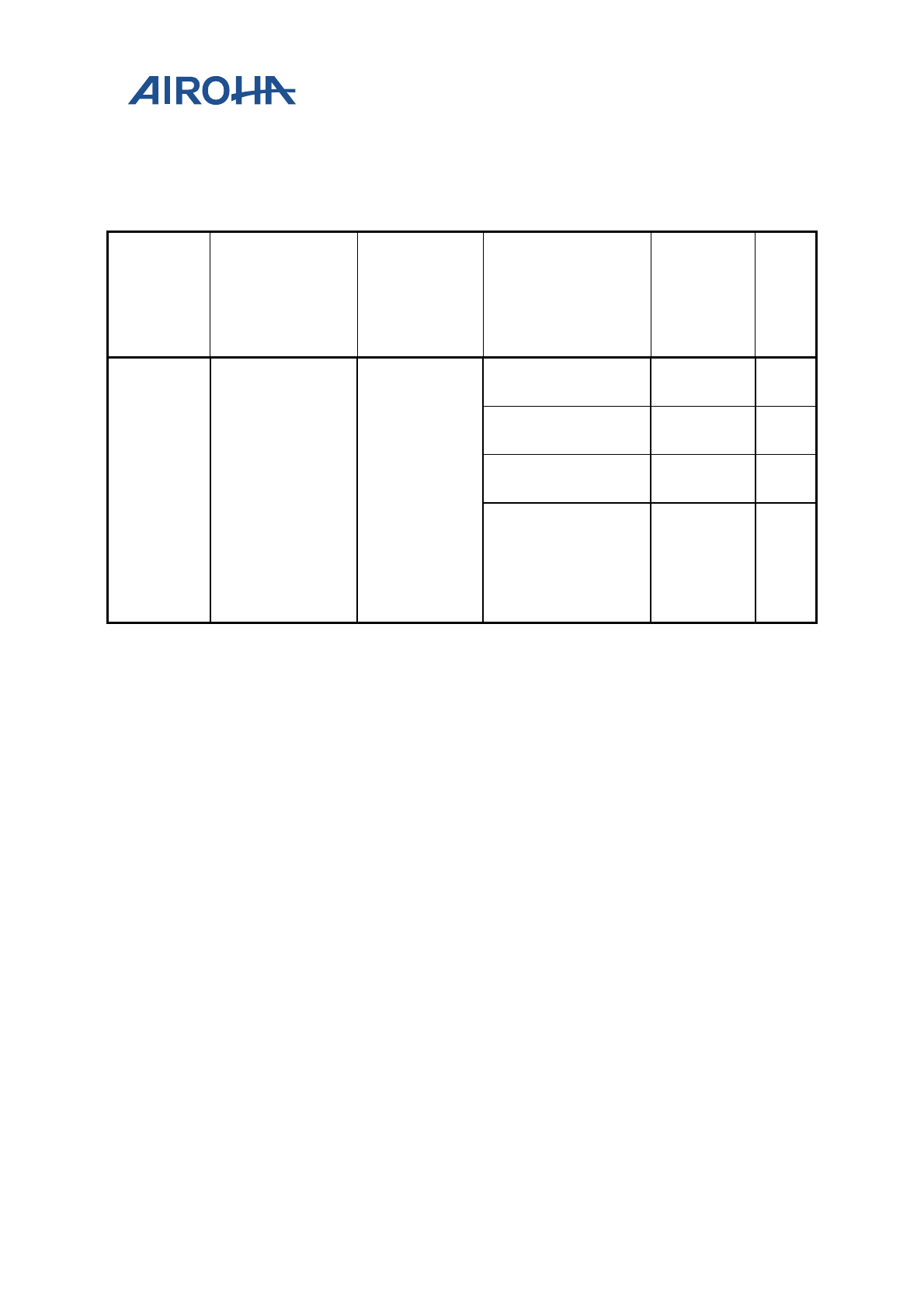
MT2523 Series Reference Manual
© 2015 - 2018 Airoha Technology Corp.
Page 579 of 692
This document contains information that is proprietary to Airoha Technology Corp. (“Airoha”) and/or its licensor(s).
Any unauthorized use, reproduction or disclosure of this document in whole or in part is strictly prohibited.
28.2.8. CAM Clock Setting
The CAM clock supports slow clock, 48MHz and 312MHz. CAM clock is for camera module.
Change bit
(gating when chg,
auto clear)
Mux select
register
(active when
chg=1)
Mux select option
Powerful
divide enable
bit works @
*CLK_CONDB
(0xA2010104
) bit[31]=1
Min.
vcore
voltag
e (typ)
CSW_CAM_C
K
CHG_CAM =
*ACFG_CLK_UPDAT
E (0XA21D0150)
BIT[7]
CAM_MUX_SEL
=
*CLK_CONDB
(0xA2010104)
bit[23:22]
0: CSW_LP_CLKSQ_CK
(max. 26MHz) NA 0.9v
1: CSW_LP_LFOSC_CK
(max. 26MHz) NA 0.9v
2: UPLL_48M_CK
(48MHz) NA 1.1v
3: UPLL_F312M_CK
(312MHz) NA 1.1v
The configured CRs and steps are:
POWERFUL_DIV_EN : 0xA2010100[31:0]
PLL_DIV_EN=1 : 0xA2010104[31]
CAM_MUX_SEL : 0xA2010104[23:22]
RG_CAMCSW_FORCE_ON=1 : 0xA201010C[7]
CHG_CAM =1 : 0xA21D0150[7]
MUX change will succeed when read 0xA21D0150[7] = 0.
RG_CAMCSW_FORCE_ON=0 : 0xA201010C[7]
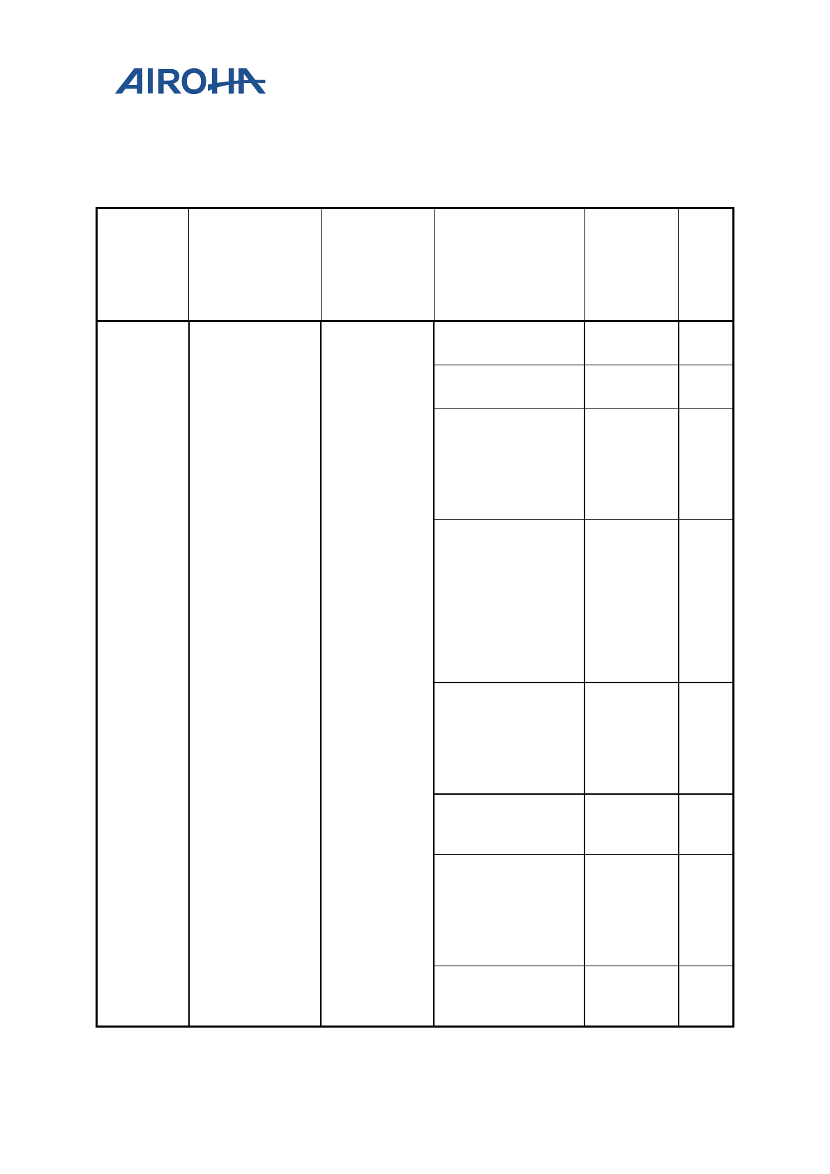
MT2523 Series Reference Manual
© 2015 - 2018 Airoha Technology Corp.
Page 580 of 692
This document contains information that is proprietary to Airoha Technology Corp. (“Airoha”) and/or its licensor(s).
Any unauthorized use, reproduction or disclosure of this document in whole or in part is strictly prohibited.
28.2.9. SLCD Clock Setting
The SLCD clock supports slow clock, 78MHz, 104MHz, and max. 124.8MHz. SLCD clock is for display module.
Change bit
(gating when chg,
auto clear)
Mux select
register
(active when
chg=1)
Mux select option
Powerful
divide enable
bit works @
*CLK_CONDB
(0xA2010104
) bit[31]=1
Min.
vcore
voltag
e (typ)
CSW_SFC_CK
CHG_SLCD =
*ACFG_CLK_UPDAT
E (0XA21D0150)
BIT[4]
{RG_SLCD_CK_SE
L,
SLCD_MUX_SEL}
=
{*CLK_CONDD
(0xA201010C)
bit[21],
*CLK_CONDB
(0xA2010104)
bit[16:14]}
0: CSW_LP_CLKSQ_CK
(max. 26MHz) NA 0.9v
1: CSW_LP_LFOSC_CK
(max. 26MHz) NA 0.9v
2: MPLL_DIV2P5_CK
(none 50/50 duty
124.8MHz)
*CLK_CONDA
(0xA2010100
) bit[16]=1
*CLK_CONDA
(0xA2010100
) bit[16+6]=1
1.1v
3: MPLL_DIV3_CK
(104MHz)
*CLK_CONDA
(0xA2010100
) bit[16]=1
*CLK_CONDA
(0xA2010100
) bit[16+4]=1
*CLK_CONDA
(0xA2010100
) bit[16+7]=1
1.1v
4: MPLL_DIV4_CK
(78MHz)
*CLK_CONDA
(0xA2010100
) bit[16]=1
*CLK_CONDA
(0xA2010100
) bit[16+5]=1
1.1v
5: HFOSC_DIV2P5_CK
(none 50/50 duty
124.8MHz)
*CLK_CONDA
(0xA2010100
) bit[2]=1
1.1v
6: HFOSC_DIV3_CK
(104MHz)
*CLK_CONDA
(0xA2010100
) bit[0]=1
*CLK_CONDA
(0xA2010100
) bit[3]=1
1.1v
7: HFOSC_DIV4_CK
(78MHz)
*CLK_CONDA
(0xA2010100
) bit[1]=1
1.1v
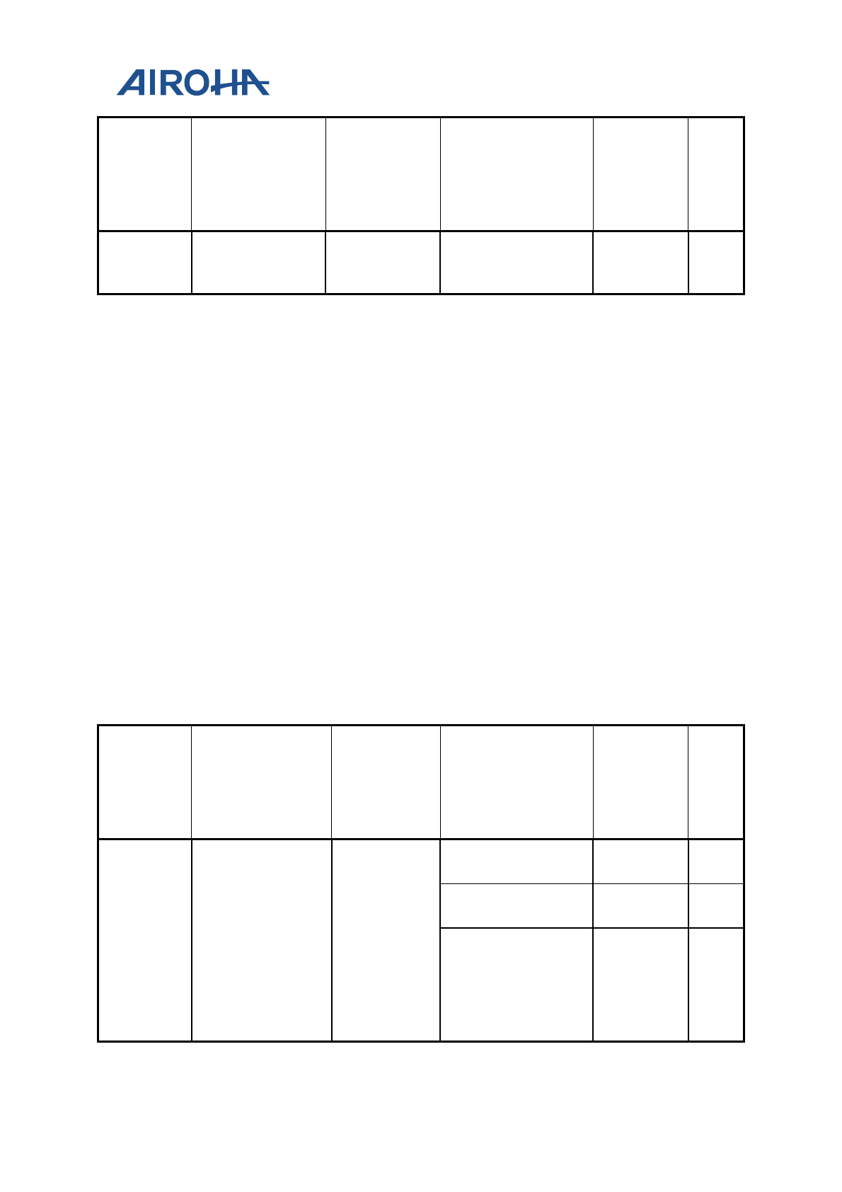
MT2523 Series Reference Manual
© 2015 - 2018 Airoha Technology Corp.
Page 581 of 692
This document contains information that is proprietary to Airoha Technology Corp. (“Airoha”) and/or its licensor(s).
Any unauthorized use, reproduction or disclosure of this document in whole or in part is strictly prohibited.
Change bit
(gating when chg,
auto clear)
Mux select
register
(active when
chg=1)
Mux select option
Powerful
divide enable
bit works @
*CLK_CONDB
(0xA2010104
) bit[31]=1
Min.
vcore
voltag
e (typ)
8: MPLL_F125M_CK
(124.5MHz 50/50 duty)
*CLK_CONDA
(0xA2010100
) bit[16+3]=1
1.1v
The configured CRs and steps are:
POWERFUL_DIV_EN : 0xA2010100[31:0]
PLL_DIV_EN=1 : 0xA2010104[31]
SLCD_MUX_SEL : 0xA2010104[16:14]
RG_SLCD_CK_SEL : 0xA201010C[21]
RG_SLCDCSW_FORCE_ON=1 : 0xA201010C[4]
CHG_SLCD =1 : 0xA21D0150[4]
MUX change will succeed when read 0xA21D0150[4] = 0.
RG_SLCDCSW_FORCE_ON=0 : 0xA201010C[4]
28.2.10. MSDC0 Clock Setting
The MSDC0 clock supports slow clock, 62.4MHz, 78MHz and max. 89.1MHz. MSDC0 clock is for eMMC0 module.
Change bit
(gating when chg,
auto clear)
Mux select
register
(active when
chg=1)
Mux select option
Powerful
divide enable
bit works @
*CLK_CONDB
(0xA2010104
) bit[31]=1
Min.
vcore
voltag
e (typ)
CSW_MSDC0
_CK
CHG_MSDC0 =
*ACFG_CLK_UPDATE
(0XA21D0150)
BIT[10]
{
RF_MSDC0_MS
DC_CFG_CLKSR
C_PATCH,
RF_MSDC0_MS
DC_CFG_PWS }
=
*MSDC0_MSDC
_CFG
(0xA0020000)
bit {[23],[4:3]}
0: CSW_LP_CLKSQ_CK
(max. 26MHz) NA 0.9v
1: CSW_LP_LFOSC_CK
(max. 26MHz) NA 0.9v
2: MPLL_DIV3P5_CK
(89.1MHz)
*CLK_CONDA
(0xA2010100
) bit[16]=1
*CLK_CONDA
(0xA2010100
) bit[16+8]=1
1.3v

MT2523 Series Reference Manual
© 2015 - 2018 Airoha Technology Corp.
Page 582 of 692
This document contains information that is proprietary to Airoha Technology Corp. (“Airoha”) and/or its licensor(s).
Any unauthorized use, reproduction or disclosure of this document in whole or in part is strictly prohibited.
Change bit
(gating when chg,
auto clear)
Mux select
register
(active when
chg=1)
Mux select option
Powerful
divide enable
bit works @
*CLK_CONDB
(0xA2010104
) bit[31]=1
Min.
vcore
voltag
e (typ)
3: MPLL_DIV4_CK
(78MHz)
*CLK_CONDA
(0xA2010100
) bit[16]=1
*CLK_CONDA
(0xA2010100
) bit[16+5]=1
1.2v
4: MPLL_DIV5_CK
(62.4MHz)
*CLK_CONDA
(0xA2010100
) bit[16]=1
*CLK_CONDA
(0xA2010100
) bit[16+9]=1
1.1v
5: HFOSC_DIV3P5_CK
(89.1MHz)
*CLK_CONDA
(0xA2010100
) bit[4]=1
1.3v
6: HFOSC_DIV4_CK
(78MHz)
*CLK_CONDA
(0xA2010100
) bit[1]=1
1.2v
7: HFOSC_DIV5_CK
(62.4MHz)
*CLK_CONDA
(0xA2010100
) bit[5]=1
1.1v
The configured CRs and steps are:
POWERFUL_DIV_EN : 0xA2010100[31:0]
PLL_DIV_EN=1 : 0xA2010104[31]
RF_MSDC0_MSDC_CFG_CLKSRC_PATCH : 0xA0020000[23]
RF_MSDC0_MSDC_CFG_PWS : 0xA0020000[4:3]
RG_MSDC0CSW_FORCE_ON=1 : 0xA201010C[10]
CHG_MSDC0 =1 : 0xA21D0150[10]
MUX change will succeed when read 0xA21D0150[10] = 0.
RG_MSDC0CSW_FORCE_ON=0 : 0xA201010C[10]
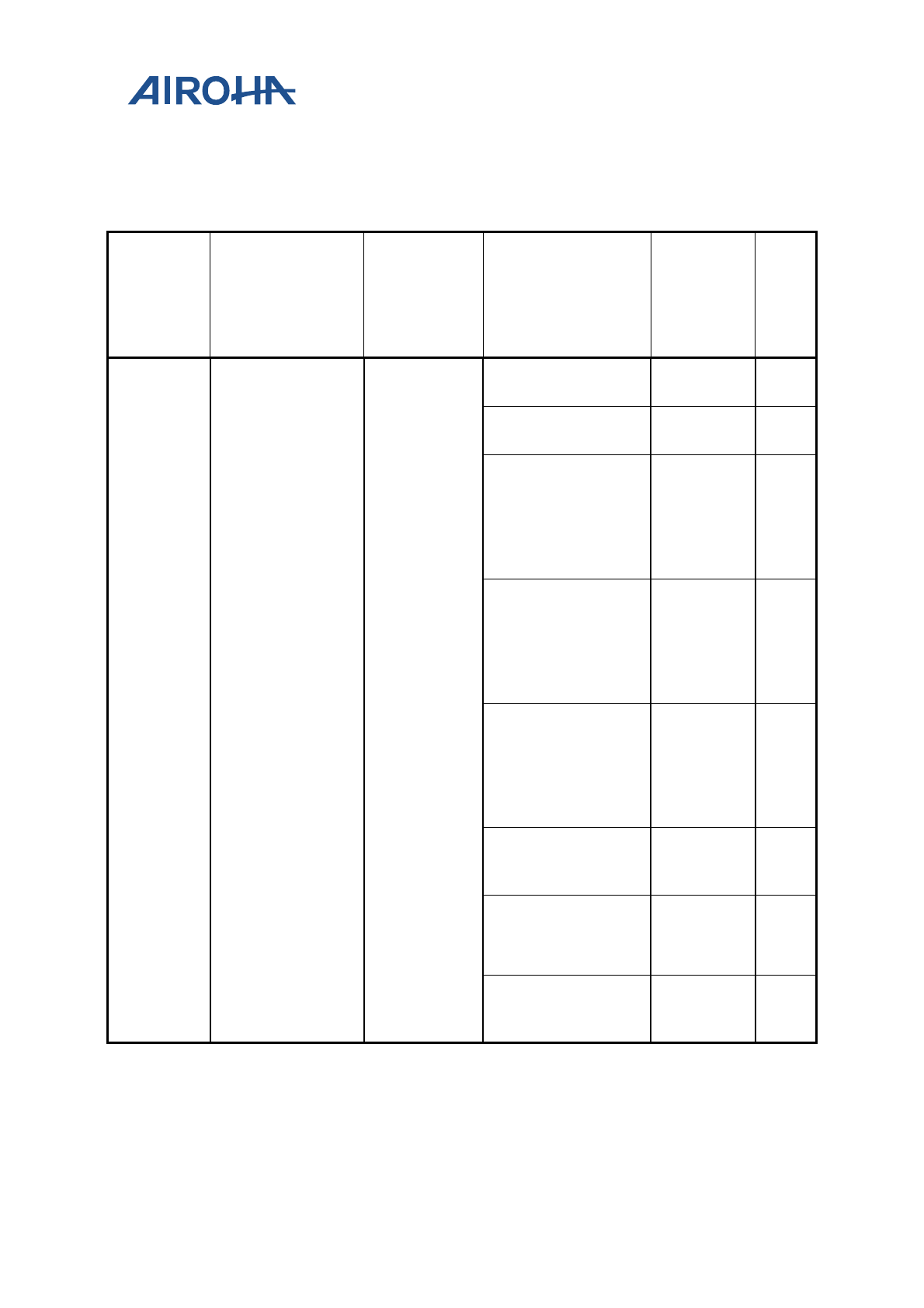
MT2523 Series Reference Manual
© 2015 - 2018 Airoha Technology Corp.
Page 583 of 692
This document contains information that is proprietary to Airoha Technology Corp. (“Airoha”) and/or its licensor(s).
Any unauthorized use, reproduction or disclosure of this document in whole or in part is strictly prohibited.
28.2.11. MSDC1 Clock Setting
The MSDC1 clock supports slow clock, 62.4MHz, 78MHz and max. 89.1MHz. MSDC1 clock is for eMMC1 module.
Change bit
(gating when chg,
auto clear)
Mux select
register
(active when
chg=1)
Mux select option
Powerful
divide enable
bit works @
*CLK_CONDB
(0xA2010104
) bit[31]=1
Min.
vcore
voltag
e (typ)
CSW_MSDC1
_CK
CHG_MSDC1 =
*ACFG_CLK_UPDATE
(0XA21D0150)
BIT[11]
{RF_MSDC1_M
SDC_CFG_CLKS
RC_PATCH,
RF_MSDC1_MS
DC_CFG_PWS}
=
*MSDC1_MSDC
_CFG
(0xA0030000)
bit {[23],[4:3]}
0: CSW_LP_CLKSQ_CK
(max. 26MHz) NA 0.9v
1: CSW_LP_LFOSC_CK
(max. 26MHz) NA 0.9v
2: MPLL_DIV3P5_CK
(89.1MHz)
*CLK_CONDA
(0xA2010100
) bit[16]=1
*CLK_CONDA
(0xA2010100
) bit[16+8]=1
1.3v
3: MPLL_DIV4_CK
(78MHz)
*CLK_CONDA
(0xA2010100
) bit[16]=1
*CLK_CONDA
(0xA2010100
) bit[16+5]=1
1.2v
4: MPLL_DIV5_CK
(62.4MHz)
*CLK_CONDA
(0xA2010100
) bit[16]=1
*CLK_CONDA
(0xA2010100
) bit[16+9]=1
1.1v
5: HFOSC_DIV3P5_CK
(89.1MHz)
*CLK_CONDA
(0xA2010100
) bit[4]=1
1.3v
6: HFOSC_DIV4_CK
(78MHz)
*CLK_CONDA
(0xA2010100
) bit[1]=1
1.2v
7: HFOSC_DIV5_CK
(62.4MHz)
*CLK_CONDA
(0xA2010100
) bit[5]=1
1.1v

MT2523 Series Reference Manual
© 2015 - 2018 Airoha Technology Corp.
Page 584 of 692
This document contains information that is proprietary to Airoha Technology Corp. (“Airoha”) and/or its licensor(s).
Any unauthorized use, reproduction or disclosure of this document in whole or in part is strictly prohibited.
The configured CRs and steps are:
POWERFUL_DIV_EN : 0xA2010100[31:0]
PLL_DIV_EN=1 : 0xA2010104[31]
RF_MSDC1_MSDC_CFG_CLKSRC_PATCH : 0xA0030000[23]
RF_MSDC1_MSDC_CFG_PWS : 0xA0030000[4:3]
RG_MSDC1CSW_FORCE_ON=1 : 0xA201010C[11]
CHG_MSDC1 =1 : 0xA21D0150[11]
MUX change will succeed when read 0xA21D0150[11] = 0.
RG_MSDC1CSW_FORCE_ON=0 : 0xA201010C[11]
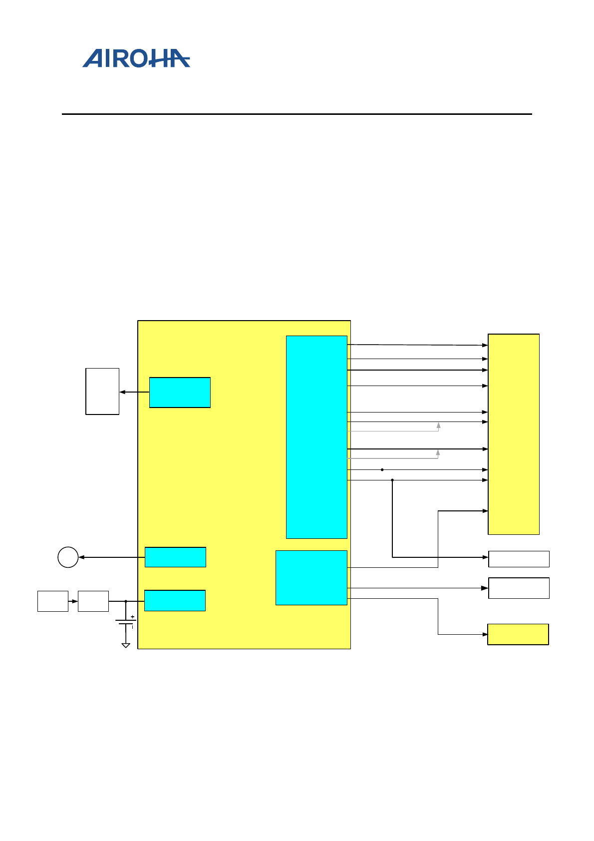
MT2523 Series Reference Manual
© 2015 - 2018 Airoha Technology Corp.
Page 585 of 692
This document contains information that is proprietary to Airoha Technology Corp. (“Airoha”) and/or its licensor(s).
Any unauthorized use, reproduction or disclosure of this document in whole or in part is strictly prohibited.
29. Power Management Unit
The power management unit (PMU) manages the power supply of the entire chip, such as baseband, processor,
memory, camera, vibrator, and more. The digital part of PMU is integrated into the analog part (see Figure 29-1).
PMU includes the following analog functions for signal processing:
• Digital Core Buck Converter (
): The buck converter is optimized for high efficiency and low quiescent
current.
• LDO and power switch. Regulate battery voltage to lower voltage level.
• LED current sink (ISINK) switches: Sink current for the LCM module.
• Start-up (STRUP). Generates power on/off control sequence of start-up circuits.
• Pulse charger (PCHR). Controls battery charging.
MT2523G/D
Base Band
Processor
Memory card
Pulse-Charger
Controller
LCM
Module
Essential LDOs
VCORE
VDIG18
VA18
VIO18
VIO28
VSF
VMC
Basic Feature LDOs
VUSB
VCAM A
VBT
Extra LDOs
Vibrator
VA18
VDIG18
VUSB
MT2523G/D
PMU
BJT
+Rsense
Charger
In
Current Sink *1
VCORE
M
VIBR
VMC
MT2523G/D
Bluetooth RF
Camera sensor
VCAMA
VSF
VBTBATSNS
VDDK
AVDD_RTC
AVDD18_AUXADC
DVDD18_VSWX M
AVDD18_DCXO
VIO18
DVDD18_VIO18
AVDD33_USB
AVDD28_ABB
AVDD28_MI PI
DVDD_VIO_B
VIO18
VIO28
VIO28
AVDD_VBT
AVDD13_BTRF
DVDD_GPO
DVDD_VIO_A
DVDD_VIO_C
VIO28
VIO18
DVDD_VSF
DVDD33_VMC
ISINK
Figure 29-1. MT2523 series PMU architecture

MT2523 Series Reference Manual
© 2015 - 2018 Airoha Technology Corp.
Page 586 of 692
This document contains information that is proprietary to Airoha Technology Corp. (“Airoha”) and/or its licensor(s).
Any unauthorized use, reproduction or disclosure of this document in whole or in part is strictly prohibited.
29.1. Power supply schemes
There are four battery input balls for regulator input. The recommended battery operation range is from 3.15V to
4.8V, which is suitable for Li-ion battery applications.
1) VBAT_BUCK_CTRL and VBAT_CORE are power supplies for VCORE in buck mode, VBAT_LDOS1 is the
power supply for VCORE in LDO mode, VIO18, VA18, VIO28, VUSB and VDIG18.
2) There is a power switch between VBAT_LDOS1 and PWRSW_OUT to reduce sub-block power leakage
current. PWRSW_OUT supplies power for VA28, VCAMA, VBT, VMC and VIBR.
3) VSWXM and VSWDP power switches are supplied with power from VIO18.
4) VSWMP power switch is supplied with power from VIO28.
The LDO input power plan is shown in Table 29-1.
Table 29-1. LDO input power plan
Input power plan Type
Name
VBAT_BUCK_CTRL
VBAT_VCORE Buck VCORE (buck mode)
VBAT_LDOS1 DLDO
VCORE (LDO mode)
VBAT_LDOS2=>PWRSW_OUT ALDO
VA28
VBAT_LDOS2=>PWRSW_OUT ALDO
VCAMA
VBAT_LDOS1 DLDO
VIO18
From VIO18 Power switch
VSWXM
From VIO18 Power switch
VSWDP
VBAT_LDOS2=>PWRSW_OUT ALDO
VBT
VBAT_LDOS1 ALDO
VA18
VBAT_LDOS2 DLDO
VSF
VBAT_LDOS1 DLDO
VIO28
From VIO28 Power switch
VSWMP
VBAT_LDOS1 DLDO
VUSB
VBAT_LDOS2=>PWRSW_OUT DLDO
VMC
VBAT_LDOS2=>PWRSW_OUT DLDO
VIBR
VBAT_LDOS1 DVDD18_DIG
VDIG18
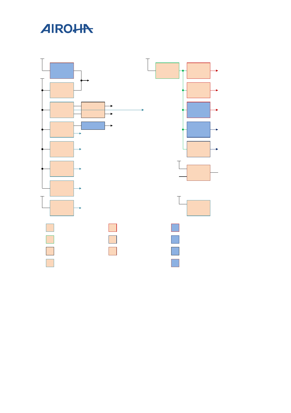
MT2523 Series Reference Manual
© 2015 - 2018 Airoha Technology Corp.
Page 587 of 692
This document contains information that is proprietary to Airoha Technology Corp. (“Airoha”) and/or its licensor(s).
Any unauthorized use, reproduction or disclosure of this document in whole or in part is strictly prohibited.
29.2. Voltage regulator
VCORE
20mA
0.7~1.3V
VCORE
200mA
0.7~1.3V
VBAT_VCORE
VIO18
200mA
1.8V
VA18
2.5mA
1.8V
VIO28
150mA
2.8V
VDIG18
5mA
1.8V
VSWXM
70mA
VSWDP
70mA
SOC Core
(CPU, DSP,
MM, ….)
1. PSRAM I/O PADs
2. 1.8V sensor
3. EXTM (PSRAM)
1. 1.8V LCM
2. PLL
3. Dedicated display
1. GPIO, Peri. I/O PADs
2. 2.8V sensor
3. SOC Efuse
4. 2.8V LCM
1. AUXADC
2. PCHR
3. DCXO
1. RTC Marco
2. 32KHz OSC
3. Start-up digital
VBAT_LDOS2
PWRSW VBT
100mA
2.8V
VA28
150mA
2.8V
VCAMA
100mA
2.8V/OFF
VUSB
80mA
3.3V
1. USB 2.0
2. 3.3V sensor
VIBR
100mA
1.8, 2.8, 3.0,
3.3V/OFF
VMC
230mA
3, 3.3V
Bluetooth
1. AUDIO
2. AUXADC
3. DAC
1. Camera
Vibrator
1. MSDC and interface I/O PADs
2. 3.3V sensor
VSWMP
20mA/OFF MIPI, DSI analog
1. GPIO, Peri. I/O PADs
2. LPOSC
VSF
100mA
1.86V
1. Serial Flash
2. Interface I/O PADs
PCHR
BATSNS
CHRIN
AVDD33
STRUP
VBAT_LDOS2
Default on power block LDO
Default on power block PWRSW
Default on power block ALDO
Default on power block DLDO
Default off power block ALDO
Default off power block DLDO
Default off power block SW
Default off power block BUCK
Default on power block SW Default on power block PCHR
Default on power block STRUP
VSWXM: External SRAM Switch
VSWDP: Dedicate Display Switch
VSWMP: MIPI Switch
PWRSW: Power Switch
VCAMA: Camera Supply Voltage
PCHR: Pulse Charger
CHRIN: Charger In
VBAT_LDOS1
VBAT_LDOS2
Figure 29-2. MT2523 series power domain
29.2.1. LDO
PMU integrates 12 general low dropout regulators (LDO). Performance optimization is achieved using the APIs for
different quiescent current, dropout voltage, line/load regulation, ripple rejection and output noise.
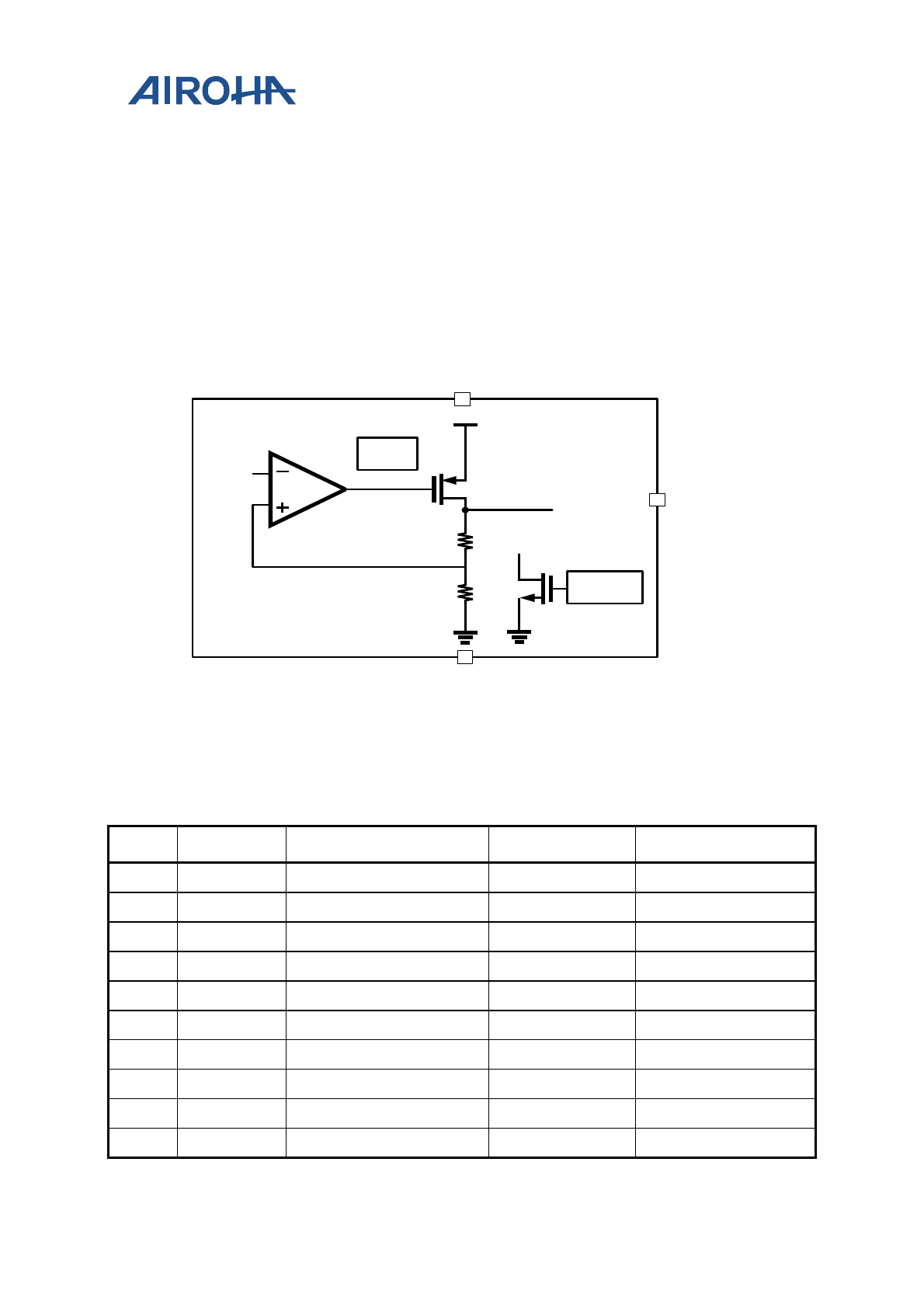
MT2523 Series Reference Manual
© 2015 - 2018 Airoha Technology Corp.
Page 588 of 692
This document contains information that is proprietary to Airoha Technology Corp. (“Airoha”) and/or its licensor(s).
Any unauthorized use, reproduction or disclosure of this document in whole or in part is strictly prohibited.
LDO is capable of maintaining its specified output voltage over a wide range of load current and input voltage,
down to a very small difference between input and output voltages.
The LDO design includes features, such as discharge control, soft start and current limit. Before LDO is enabled, the
output pin of LDO should be first discharged to avoid voltage accumulation on the capacitance. The soft-start limits
inrush current and controls output-voltage rising time during power-up. The current limit is the current protection
to limit LDO’s output current and power dissipation.
There are three types of LDOs in PMU of the MT2523 series platform and the general LDO block diagram is shown
in Figure 29-3. The analog LDO is optimized for low-frequency ripple rejection to reject VBAT ripples. The digital IO
LDO is a linear regulator optimized for very low quiescent current. VDIG18 LDO is a linear regulator that can
charge up a capacitor-type backup coin cell that supplies the RTC module.
VREF
VOUT
R1
R2
Current
Limit
Discharge
Control
VBAT_XXX
VOUT
VOUT
GND
Figure 29-3. General LDO block diagram
29.2.1.1. LDO types
Table 29-2. LDO types and brief specifications
Type LDO name Vout (Volt) Imax (mA) Description
ALDO VBT 2.8 100 Bluetooth
ALDO VA28 2.8 150 Audio
ALDO VA18 1.8 2.5 AUXADC
ALDO VCAMA 2.8 100 Camera sensor
DLDO VIO28 2.8 150 Digital IO and Bluetooth
DLDO VUSB 3.3 80 USB
DLDO VIO18 1.8 200 Digital IO
DLDO VCORE 0.7~1.30 20 Digital baseband
DLDO VIBR 1.3/1.5/1.8/2/2.5/2.8/3/3.3 100 Vibrator
DLDO VMC 1.8/2.8/3.0/3.3 230 Memory card

MT2523 Series Reference Manual
© 2015 - 2018 Airoha Technology Corp.
Page 589 of 692
This document contains information that is proprietary to Airoha Technology Corp. (“Airoha”) and/or its licensor(s).
Any unauthorized use, reproduction or disclosure of this document in whole or in part is strictly prohibited.
Type LDO name Vout (Volt) Imax (mA) Description
DLDO VSF 1.86/3.0/3.3 100 Serial flash
Power
Switch VSWXM 1.8 70 Powered by VIO18
PSRAM I/O.
Power
Switch VSWDP 1.8 70 Powered by VIO18
Dedicated display
Power
Switch VSWMP 2.8 20 MIPI DSI analog
29.2.1.2. Regulator ON
There are three power modes configured by software when the regulator is on − Normal mode, Lite mode and
LP mode. In power-on state, the regulators are powered on by normal mode to achieve fast power-on. The soft
start feature limits the inrush current to avoid battery voltage drop. DIG18 LDO is in ULP mode at power-off
state.
29.2.1.3. Regulator Off
Disabling the regulator and entering the shutdown mode will cause output voltage to discharge through N-MOSFET
to ground. In shutdown mode, the quiescent current can be reduced to below 0.1µA.
29.3. Low power mode
The device supports four low-power modes to achieve the best compromise in low power consumption.
The ULP mode LDO is only implemented in DIG18, VCOR_LOD, VIO18, VIO28 and VSF.
LDO mode selection can be configured through the PSI register.
29.4. Pulse Charger (PCHR)
The charger controller senses the charger input voltage from either a standard AC-DC adapter or a USB charger.
When the charger input voltage is within a pre-determined range, the charging process is activated. This detector
can resist higher input voltage than other parts of the PMU.
29.4.1. Charger detection
Whenever an invalid charging source is detected (> 5.5V), the charger detector will stop the charging process
immediately to prevent the chip even the device from burning out. In addition, if the charger-in level is not high
enough (< 4.15V), the charger will also be disabled to avoid improper charging behavior.
29.4.2. Charging control
When the charger is active, the charger controller will manage the charging phase according to the battery status.
During the charging period, the battery voltage is constantly monitored. The battery charger supports pre-charge
mode (VBAT < 3.45V, PMU power-off state), CC mode (constant current mode or fast charging mode at the
range 3.45V < VBAT < 4.2V) and CV mode (constant voltage mode) to optimize the charging process for Li-ion
battery. Figure 29-4 and Figure 29-5 is the charging block/state diagram.
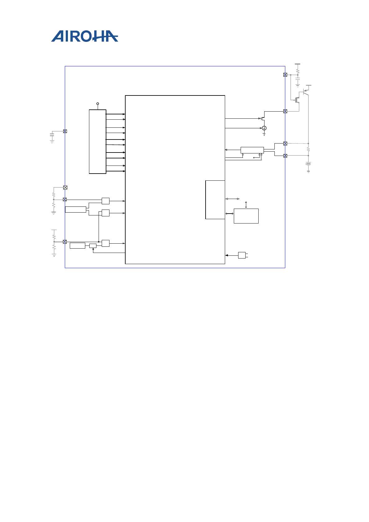
MT2523 Series Reference Manual
© 2015 - 2018 Airoha Technology Corp.
Page 590 of 692
This document contains information that is proprietary to Airoha Technology Corp. (“Airoha”) and/or its licensor(s).
Any unauthorized use, reproduction or disclosure of this document in whole or in part is strictly prohibited.
Rsense
VBAT
CHRIN
8V LDMOS
DRV
ISENSE
BATSNS
(VBAT)
gain
CCHRLDO_DET_CMP
VBGR
Charger Core
And
Digital Controller
CHRIN
CHRLDO
VREF
CHR_LDO_DET
CHR_LDO_DET
Interface
BC12
Controller
To BB
CSDAC_EN
CSDAC_DAT<7:0>
CS_DET
CS_EN
CS_VTH[3:0]
VA18
RNTC
BATON
OTG_BVAILD_EN
CHRIN
VCDT
VBAT_DDLO_DET
VBAT_DDLO_VTH<1:0>
VBAT_UVLO_DET
VBAT_UVLO_VTH<1:0>
VBAT_CC_DET
VBAT_CC_VTH[1:0]
VBAT_CV_DET
VBAT_CV_VTH[1:0]
VBAT_OV_DET
VBAT_OV_VTH[1:0]
BATON_UNDET
OTG_BVALID_DET
VCDT_DET
VCDT_VTH[3:0]
MUX
VTH CGRLDOGOOD
VBAT
Voltage
divider
VBAT
VCDT VREF GEN
OTG/BATON VREF GEN
COMP
COMP
COMP
Current
Sensing
EN vr set
in1
in2
VREF
COMP
ON Chip
Off Chip
Charger block diagram
Figure 29-4. PCHR schematics
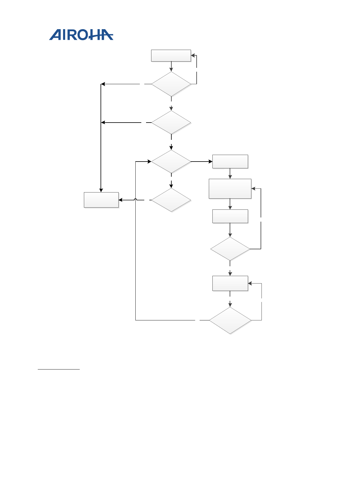
MT2523 Series Reference Manual
© 2015 - 2018 Airoha Technology Corp.
Page 591 of 692
This document contains information that is proprietary to Airoha Technology Corp. (“Airoha”) and/or its licensor(s).
Any unauthorized use, reproduction or disclosure of this document in whole or in part is strictly prohibited.
NON-CHARGING
CHRIN>4.15V
PRECC0 unlock
DeadBATT
VBAT<2.2V?
PreCC
V
BAT
<2.7V
5 min timeout
NO
VBAT>3V
NO
CC Mode
(software initiate)
CV Mode
V
BAT
=4.2V
(Software programmable)
Reduce I
CHG
by
step
I
CHG
<I
TERM
(Software process)
FULL state
Charger OFF
(Software process)
YES
VBAT<4.1V
Battery recharge
(Software programmable)
YES NO
Charger OFF
NO
NO
YES
YES
PreCC
2.7V<VBAT<3.45V
35 min timeout
NO
YES
YES
Figure 29-5. Charging control modes
Pre-charge mode
When the battery voltage is in the UVLO state, the charger will operate in the pre-charge mode. There are two
steps in this mode. When the battery voltage is deeply discharged below 2.2V, PRECC0 trickle charging current will
be applied to the battery.
The PRECC0 trickle charging current is about 550ms pulse 11mA current when VBAT is under 2.2V.
When the battery voltage exceeds 2.2V, called the PRECC1 stage, the closed-loop pre-charge will be enabled. The
voltage drop across the external RSENSE is kept around 3.92mV (despite AC charger or USB host plug-in. The
closed-loop pre-charge current can be calculated:

MT2523 Series Reference Manual
© 2015 - 2018 Airoha Technology Corp.
Page 592 of 692
This document contains information that is proprietary to Airoha Technology Corp. (“Airoha”) and/or its licensor(s).
Any unauthorized use, reproduction or disclosure of this document in whole or in part is strictly prohibited.
= =
SENSE
PRECC1
V3.92mV
IRsense Rsense
Constant current mode
As the battery is charged up and over 3.45V, it can be switched to the CC mode. (CHR_EN should be high.) In CC
mode, several charging currents can be set by programming registers or the external RSENSE resistor. The charging
current can be determined by CS_VTH/RSENSE, where CS_VTH is programmed by registers. For example, if RSENSE
is selected as 0.56Ω, the CC mode charging current can be set from 7 to 150mA. It can accommodate the battery
charger to various charger inputs with different current capabilities.
Constant voltage mode and over-voltage protection (OV)
When the battery voltage reaches about 4.2V, a constant voltage will be used for charging. This is called the full-
voltage charging mode or constant-voltage charging mode in correspondence to a linear charger. When the
battery voltage actually reaches 4.2V, the charging current will gradually decrease, and the end-of-charging
process will start. This may prolong the charging and detecting period for acquiring optimized full charging volume.
The charging process completes once the current automatically reaches zero using different batteries for
optimization.
BC1.2 dead-battery support of Chinese standard
MT2523 series supports dead-battery condition (called BC1.2). The specification protects dead-battery charging by
timer and trickle current. Once the battery voltage is below 2.2V, a period (TUNIT) of trickle current (IUNIT) will be
applied to the battery.
If the battery voltage is still below 2.2V after trickle current is applied, the charger will be disabled. On the other
hand, if the battery voltage is raised to above 2.2V, the charger will enter the PRECC1 stage, and the charging
current will be PRECC1 current.
Under the condition of battery voltage being from 2.2V to 3.45V, the charger will charge the battery with the
PRECC1 current.
A dedicated 5-min (T1) timer will be timed out and disable the charger if the battery voltage is always below 2.7V
under charging. Another 35-min (T2) timer will also be timed out and disable the charger if the battery voltage is
always kept between 2.7V and 3.45V under charging.
The trickle current (IUNIT) and two dedicated timers will protect the charging action if the battery is dead.
29.5. Power On/Off sequence
PMU handles the power-on and power-off of the handset. If the battery voltage is neither in the UVLO state
(
≥ ) nor in thermal condition, there will be three methods to power on the handset.
1) Pulling the PWRKEY low (press PWRKEY).
2) Setting the PWRHOLD to high.
3) Plugging in a valid charger.
The power on/off sequence is shown in Figure 29-6 and Figure 29-7.
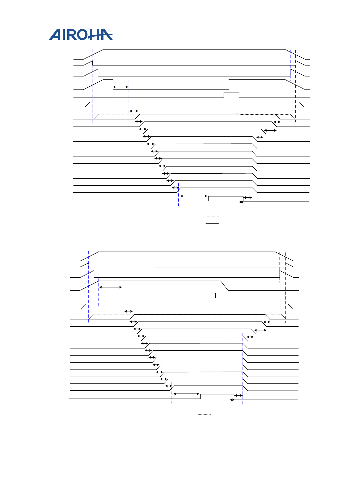
MT2523 Series Reference Manual
© 2015 - 2018 Airoha Technology Corp.
Page 593 of 692
This document contains information that is proprietary to Airoha Technology Corp. (“Airoha”) and/or its licensor(s).
Any unauthorized use, reproduction or disclosure of this document in whole or in part is strictly prohibited.
VBAT
DDLO
UVLO
PWRKEY
PWRHOLD
VA18
VCORE
VIO18
VIO28 / VSF Trapping
VSF
VSWXM
VUSB
RESETB
De-bounce
time = 32ms
2.55ms
0.3ms
3ms
20ms
6ms
VDIG18
VSWDP
VBT
VA28
VA18 on/off controlled by DDLO in 32K removal application
VA18 on/off controlled by Power on/off signal in 32K OSC
application
VMC
1.5ms
3ms
3ms
3ms
1.5ms
1.5ms
1.5ms
1.5ms
1.5ms
1.5ms
2ms
30us
Figure 29-6. Power-on/off control sequence by pressing PWRKEY
VBAT
DDLO
UVLO
Charger in
PWRHOLD
VA18
VCORE
VIO18
VIO28 / VSF Trapping
VSF
VSWXM
VUSB
RESETB
De-bounce
time = 200ms
2.55ms
0.3ms
3ms
20ms
6ms
VSWDP
VBT
VA28
VA18 on/off controlled by DDLO in 32K removal application
VA18 on/off controlled by Power on/off signal in 32K OSC
application
VMC
1.5ms
3ms
3ms
3ms
1.5ms
1.5ms
1.5ms
1.5ms
1.5ms
1.5ms
2ms
30us
VUSB will turn on after Charger in when VBAT>2.2V
VDIG18
Figure 29-7. Power-on/off control sequence by charger plug in

MT2523 Series Reference Manual
© 2015 - 2018 Airoha Technology Corp.
Page 594 of 692
This document contains information that is proprietary to Airoha Technology Corp. (“Airoha”) and/or its licensor(s).
Any unauthorized use, reproduction or disclosure of this document in whole or in part is strictly prohibited.
1) Pushing PWRKEY (pulling the PWRKEY pin to low level).
Pulling PWRKEY low is a typical method to turn on the handset. The system reset ends once all default-on
regulators are sequentially turned on. After that, the baseband will send the BBWAKEUP signal back to PMIC for
acknowledgement. To successfully power on the handset, PWRKEY should be kept low until PMIC receives
BBWAKEUP from the baseband.
2) RTC module generates PWRHOLD to wake up the system.
If the RTC module is scheduled to wake up the handset at some time, the PWRHOLD signal will be directly sent to
PMIC. In this case, PWRHOLD becomes high at specific moment and allows PMIC power-on. This is called the RTC
alarm.
3) Valid charger plug-in (CHRIN voltage within valid range).
The charger plug-in will also turn on the handset if the charger is valid. When PMU_CHGIN input voltage is greater
than CHGIN_VTHH and VSYS>UVLO, the handset will also be powered on.
Under-voltage lockout (UVLO)
The UVLO state in PMIC prevents start-up if the initial voltage of the main battery is below UVLO_VTH. The
judgment is done by VBATSNS. It ensures that the handset is powered on with the battery in good condition. The
UVLO function is performed by a hysteretic comparator to ensure smooth power-on. In addition, when the battery
voltage is getting lower, it will enter the UVLO state and PMIC will be turned off by itself, except for VRTC LDO, to
prevent further discharging. Once PMIC enters the UVLO state, it will draw low quiescent current. RTC LDO will still
be working until DDLO disables it.
Deep discharge lockout (DDLO)
PMIC will enter the deep discharge lockout (DDLO) state when the battery voltage drops below DDLO_VTHL. In this
state, VRTC LDO will be shut down. Otherwise, it will draw very low quiescent current to prevent further
discharging or even damage to the cells.
Reset
PMIC contains a reset control circuit that takes effect at both power-up and power-down. The RESETB pin is held
low in the beginning of power-up and returns to high after the pre-determined delay time. The delay time is
controlled by a large counter, which uses the clock from the internal ring-oscillator. At power-off, the RESETB pin
will return to low immediately without any delay.
Over-temperature protection
If the die temperature of PMIC exceeds 125°C (typical condition), PMIC will automatically disable all regulators
except for VRTC. Once the over-temperature state is resolved, a new power-on sequence will be required to
enable the regulators.
29.6. LED current sink (ISINK)
Maximum of two indicator LED drivers are supported. Figure 29-8 provides the usage of indicator LED drivers. The
LED driver of MT2523 series supports PWM mode and breath mode. The LED current changing from small to large
then descending is the breath mode. The breathing cycle time, including Trising_1, Trising_2, Ton, Toff,
Tfalling_1, and Tfalling_2 period can be modified through software configuration of the registers.
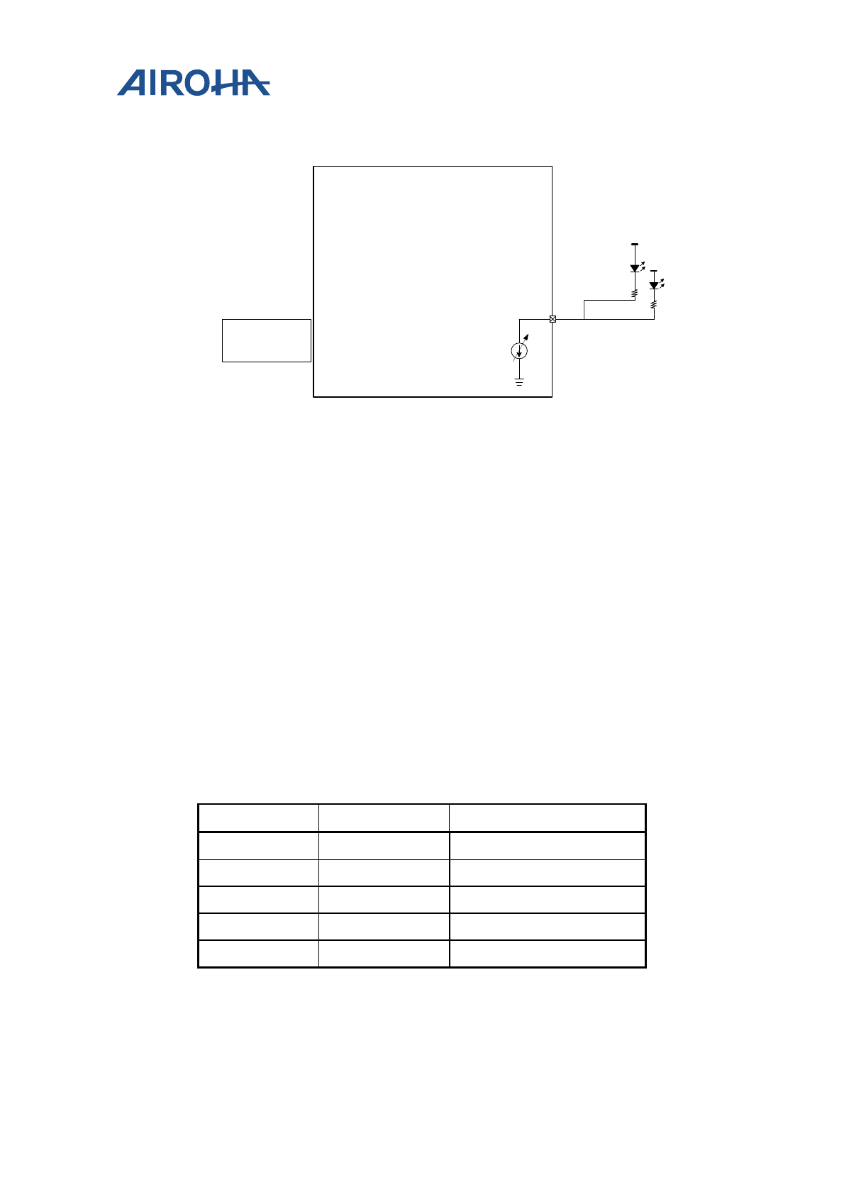
MT2523 Series Reference Manual
© 2015 - 2018 Airoha Technology Corp.
Page 595 of 692
This document contains information that is proprietary to Airoha Technology Corp. (“Airoha”) and/or its licensor(s).
Any unauthorized use, reproduction or disclosure of this document in whole or in part is strictly prohibited.
ISINK
Step[2:0]
ISINK_EN
A2D signals
NI_ISINKS_CH_EN
RG_ISINKS_CH0_STEP[2:0]
Isink
NI_ISINKS0_STATUS
NI_ISINKS1_STATUS
VBAT
VBAT
Figure 29-8. ISINK block diagram
29.7. Vibrator driver
The VIBR driver power allows up to 100mA current for eccentric rotating mass (ERM) or coin type vibrator with
programmable output voltage.
29.8. PMU AUXADC
The PMU auxiliary ADC includes the following functional blocks:
• Analog multiplexer: Selects signals from one of the input channels. The signal, such as temperature, are
monitored and transferred to the voltage domain.
• 15-bit A/D converter: Converts the multiplexed input signal to 15-bit digital data.
The PMU auxiliary ADC input range and specification is shown in Table 29-3.
Table 29-3. Application and input range of ADC channels
Channel Application Input range [V]
0 BATSNS 3.0 ~ 4.8
1 ISENSE 3.0 ~ 4.8
2 VCDT 0 ~ 1.5
3 BATON 0.1 ~ 1.7
Others Internal use N/A
MT2523 Series Reference Manual
© 2015 - 2018 Airoha Technology Corp.
Page 596 of 692
This document contains information that is proprietary to Airoha Technology Corp. (“Airoha”) and/or its licensor(s).
Any unauthorized use, reproduction or disclosure of this document in whole or in part is strictly prohibited.
Module name: PMIC_REG Base address: (+0h)
Address Name
Widt
h Register Function
1D
RSTCFG3
8
Reset config 3
1E INTSTS0 8 Interrupt status/clear 0
1F
INTSTS1
8
Interrupt status/clear 1
20
INTSTS2
8
Interrupt status/clear 2
21
INTSTS3
8
Interrupt status/clear 3
22 INTSTS4 8 Interrupt status/clear 4
23
INTSTS5
8
Interrupt status/clear 5
24
INTSTS6
8
Interrupt status/clear 6
25
INTEN0
8
Interrupt enable 0
26 INTEN1 8 Interrupt enable 1
27
INTEN2
8
Interrupt enable 2
28
INTEN3
8
Interrupt enable 3
29
INTEN4
8
Interrupt enable 4
2A INTEN5 8 Interrupt enable 5
2B
INTEN6
8
Interrupt enable 6
2C
INTMISC
8
interrupt misc register
2D
PONSTS
8
Power on source record register
2E POFFSTS 8 Power off source record register
2F
PDNSTS0
8
Power exception shutdown status 0
30
PDNSTS1
8
Power exception shutdown status 1
31
PDNSTS2
8
Power exception shutdown status 2
32 PSSTS0 8 Power supply status 0 register
33
PSSTS1
8
Power supply status 1 register
34
PSSTS2
8
Power supply status 2 register
35
PSOCSTS0
8
Power supply Overcurrent status 0 register
36 PSOCSTS1 8 Power supply Overcurrent status 1 register
37
PSPGSTS0
8
Power supply PWRGOOD status 0 register
38
PSPGSTS1
8
Power supply PWRGOOD status 1 register
39
PSOMSTS0
8
Power supply Operational mode status 0 register
3A PSOMSTS1 8 Power supply Operational mode status 1 register
3B
PSOMSTS2
8
Power supply Operational mode status 2 register
3C
THMSTS
8
Thermal Status
3D
WKFG_STS
8
Wake Up Fuel Gauge Status
40 PSICTL 8 PSI control register
41
PSISTS
8
PSI status register
48
PPCCFG0
8
PPC configruation 0 register
4A
PPCCFG2
8
PPC configruation 2 register
4B PPCCTL0 8 PPC control 0 register
4D
SHDNCFG1
8
Shutdown configuration 1 register
87
CHR_CON0
8
Charger control register 0
88
CHR_CON1
8
Charger Control Register 1
89 CHR_CON2 8 Charger Control Register 2
8A
CHR_CON3
8
Charger Control Register 3
8B
CHR_CON4
8
Charger Control Register 4
8D
CHR_CON6
8
Charger Control Register 6
MT2523 Series Reference Manual
© 2015 - 2018 Airoha Technology Corp.
Page 597 of 692
This document contains information that is proprietary to Airoha Technology Corp. (“Airoha”) and/or its licensor(s).
Any unauthorized use, reproduction or disclosure of this document in whole or in part is strictly prohibited.
Module name: PMIC_REG Base address: (+0h)
8E
CHR_CON7
8
Charger Control Register 7
8F
CHR_CON7_H
8
Charger Control Register 7_H
92 CHR_CON9 8 Charger Control Register 9
93
CHR_CON10
8
Charger Control Register 10
96
CHR_CON13
8
Charger Control Register 13
97
CHR_CON13_
H 8 Charger Control Register 13_H
99 CHR_CON15 8 Charger Control Register 15
9A
CHR_CON16
8
Charger Control Register 16
9B
CHR_CON16_
H 8 Charger Control Register 16_H
9C
CHR_CON17
8
Charger Control Register 17
9D CHR_CON18 8 Charger Control Register 18
9E
CHR_CON19
8
Charger Control Register 19
9F
CHR_CON20
8
Charger Control Register 20
A0
CHR_CON21
8
Charger Control Register 21
A1 CHR_CON21_
H 8 Charger Control Register 21_H
A3
CHR_CON23
8
Charger Control Register 23
A4
CHR_CON24
8
Charger Control Register 24
A5
CHR_CON25
8
Charger Control Register 25
AA CHR_CON30 8 Charger Control Register 30
AB
CHR_CON30_
H 8 Charger Control Register 30_H
AD
CHR_CON42
8
Charger Control Register 42
AE
BATON_CON0
8
BATON Control Register 0
B0 CHR_CON44 8 Charger Control Register 44
B1
CHR_CON45
8
Charger Control Register 45
B2
CHR_CON45_
H 8 Charger Control Register 45_H
B3
CHR_CON46
8
Charger Control Register 46
B4 CHR_CON46_
H 8 Charger Control Register 46_H
B5
CHR_CON47
8
Charger Control Register 47
DA
VA18CTL0
8
VA18 Control register 0
DB
VA18CTL1
8
VA18 Control register 1
E2 VA18PSI0 8 VA18 LDO PSI register0
E3
VA18PSI1
8
VA18 LDO PSI register1
E4
VBTCTL0
8
VBT Control register 0
E5
VACTL0
8
VA Control register 0
E6 VCLDOCTL0 8 VCORE LDO Control register 0
E8
PSWCTL1
8
PSW Control register 1
E9
VIO18CTL0
8
VIO18 Control register 0
EA
VSFCTL0
8
VSF Control register 0
EB VIO28CTL0 8 VIO28 Control register 0
EC
VMCCTL0
8
VMC Control register 0
ED
VUSBCTL0
8
VUSB Control register 0
EF
VUSBLDO0
8
VUSBLDO0
MT2523 Series Reference Manual
© 2015 - 2018 Airoha Technology Corp.
Page 598 of 692
This document contains information that is proprietary to Airoha Technology Corp. (“Airoha”) and/or its licensor(s).
Any unauthorized use, reproduction or disclosure of this document in whole or in part is strictly prohibited.
Module name: PMIC_REG Base address: (+0h)
F3
VUSBLDOBF0
8
VUSBLDOBF0
F5
VUSBPSI0
8
VUSB LDO PSI register0
F6 VUSBPSI1 8 VUSB LDO PSI register1
F7
VDIG18LDO0
8
VDIG18LDO0
FB
VDIG18LDOBF
0 8 VDIG18LDOBF0
FD
VCLDO0
8
VCORE LDO register 0
FE VCLDO1 8 VCORE LDO register 1
101
VCLDOBF0
8
VCORE LDO buffer register 0
103
VCLDOPSI0
8
VCORE LDO PSI register 0
104
VCLDOPSI1
8
VCORE LDO PSI register 1
105 VCLDOPSI2 8 VCORE LDO PSI register 2
106
VCLDOPSI3
8
VCORE LDO PSI register 3
107
VCLDOPSI4
8
VCORE LDO PSI register 4
108
VCLDOPSI5
8
VCORE LDO PSI register 5
10A VIO18LDO0 8 VIO18LDO0
10E
VIO18LDOBF0
8
VIO18LDOBF0
110
VIO18PSI0
8
VIO18 LDO PSI register0
111
VIO18PSI1
8
VIO18 LDO PSI register1
113 VSFLDO0 8 VSFLDO0
114
VSFLDO1
8
VSFLDO1
117
VSFLDOBF0
8
VSFLDOBF0
119
VSFPSI0
8
VSF LDO PSI register0
11A VSFPSI1 8 VSF LDO PSI register1
11C
SMPSCTL0
8
SMPS Control Register 0
121
SMPSANA3
8
SMPS Analog Control Register 3
135
VCBUCK19
8
VCORE BUCK register 19
13E VCBUCKPSI0 8 VCORE BUCK PSI register 0
13F
VCBUCKPSI1
8
VCORE BUCK PSI register 1
140
VCBUCKPSI2
8
VCORE BUCK PSI register 2
200
AUXADC_ADC
0 8 AUXADC ADC register 0
201 AUXADC_ADC
0_H 8 AUXADC ADC register 0_H
202
AUXADC_ADC
1 8 AUXADC ADC register 1
203
AUXADC_ADC
1_H 8 AUXADC ADC register 1_H
204
AUXADC_ADC
2 8 AUXADC ADC register 2
205 AUXADC_ADC
2_H 8 AUXADC ADC register 2_H
206
AUXADC_ADC
3 8 AUXADC ADC register 3
207
AUXADC_ADC
3_H 8 AUXADC ADC register 3_H
208
AUXADC_ADC
4 8 AUXADC ADC register 4
209 AUXADC_ADC
4_H 8 AUXADC ADC register 4_H
MT2523 Series Reference Manual
© 2015 - 2018 Airoha Technology Corp.
Page 599 of 692
This document contains information that is proprietary to Airoha Technology Corp. (“Airoha”) and/or its licensor(s).
Any unauthorized use, reproduction or disclosure of this document in whole or in part is strictly prohibited.
Module name: PMIC_REG Base address: (+0h)
21A
AUXADC_ADC
13 8 AUXADC ADC register 13
21B
AUXADC_ADC
13_H 8 AUXADC ADC register 13_H
21C AUXADC_ADC
14 8 AUXADC ADC register 14
21D
AUXADC_ADC
14_H 8 AUXADC ADC register 14_H
21E
AUXADC_ADC
15 8 AUXADC ADC register 15
21F
AUXADC_ADC
15_H 8 AUXADC ADC register 15_H
226 AUXADC_ADC
19 8 AUXADC ADC register 19
227
AUXADC_ADC
19_H 8 AUXADC ADC register 19_H
228
AUXADC_ADC
20 8 AUXADC ADC register 20
229
AUXADC_ADC
20_H 8 AUXADC ADC register 20_H
22A AUXADC_ADC
21 8 AUXADC ADC register 21
22B
AUXADC_ADC
21_H 8 AUXADC ADC register 21_H
22C
AUXADC_ADC
22 8 AUXADC ADC register 22
22D
AUXADC_ADC
22_H 8 AUXADC ADC register 22_H
22E AUXADC_ADC
23 8 AUXADC ADC register 23
22F
AUXADC_ADC
23_H 8 AUXADC ADC register 23_H
230
AUXADC_ADC
24 8 AUXADC ADC register 24
231
AUXADC_ADC
24_H 8 AUXADC ADC register 24_H
232 AUXADC_ADC
25 8 AUXADC ADC register 25
233
AUXADC_ADC
25_H 8 AUXADC ADC register 25_H
234
AUXADC_ADC
26 8 AUXADC ADC register 26
235
AUXADC_ADC
26_H 8 AUXADC ADC register 26_H
236 AUXADC_ADC
27 8 AUXADC ADC register 27
237
AUXADC_ADC
27_H 8 AUXADC ADC register 27_H
238
AUXADC_ADC
28 8 AUXADC ADC register 28
239
AUXADC_ADC
28_H 8 AUXADC ADC register 28_H
23A AUXADC_ADC
29 8 AUXADC ADC register 29
23B
AUXADC_ADC
29_H 8 AUXADC ADC register 29_H
MT2523 Series Reference Manual
© 2015 - 2018 Airoha Technology Corp.
Page 600 of 692
This document contains information that is proprietary to Airoha Technology Corp. (“Airoha”) and/or its licensor(s).
Any unauthorized use, reproduction or disclosure of this document in whole or in part is strictly prohibited.
Module name: PMIC_REG Base address: (+0h)
23C
AUXADC_ADC
30 8 AUXADC ADC register 30
23D
AUXADC_ADC
30_H 8 AUXADC1 ADC register 0_H
23E AUXADC_ADC
31 8 AUXADC ADC register 31
23F
AUXADC_ADC
31_H 8 AUXADC1 ADC register 1_H
240
AUXADC_ADC
32 8 AUXADC ADC register 32
241
AUXADC_ADC
32_H 8 AUXADC1 ADC register 2_H
242 AUXADC_ADC
33 8 AUXADC ADC register 33
243
AUXADC_ADC
33_H 8 AUXADC1 ADC register 3_H
244
AUXADC_ADC
34 8 AUXADC ADC register 34
245
AUXADC_ADC
34_H 8 AUXADC1 ADC register 4_H
246 AUXADC_ADC
35 8 AUXADC ADC register 35
247
AUXADC_ADC
35_H 8 AUXADC ADC register 33_H
248
AUXADC_ADC
36 8 AUXADC ADC register 36
249
AUXADC_ADC
36_H 8 AUXADC ADC register _H
24A AUXADC_ADC
37 8 AUXADC ADC register 37
24B
AUXADC_ADC
37_H 8 AUXADC1 ADC register _H
24C
AUXADC_ADC
38 8 AUXADC ADC register 34_H
24D
AUXADC_ADC
38_H 8 AUXADC1 ADC register 34_H
24E AUXADC_STA
0 8 AUXADC_STA0
24F
AUXADC_STA
0_H 8 AUXADC_STA0_H
250
AUXADC_STA
1 8 AUXADC_STA1
251
AUXADC_STA
1_H 8 AUXADC_STA1_H
2BE AUXADC_LBA
T2_4 8 AUXADC_LBAT2_4
2BF
AUXADC_LBA
T2_4_H 8 AUXADC_LBAT2_4_H
2C0
AUXADC_LBA
T2_5 8 AUXADC_LBAT2_5
2C1
AUXADC_LBA
T2_5_H 8 AUXADC_LBAT2_5_H
2EF VBTLDO0 8 VBT LDO register 0
2F3
VBTLDOBF0
8
VBT LDO buffer register 0
2F5
VBTPSI0
8
VBTP LDO PSI register0
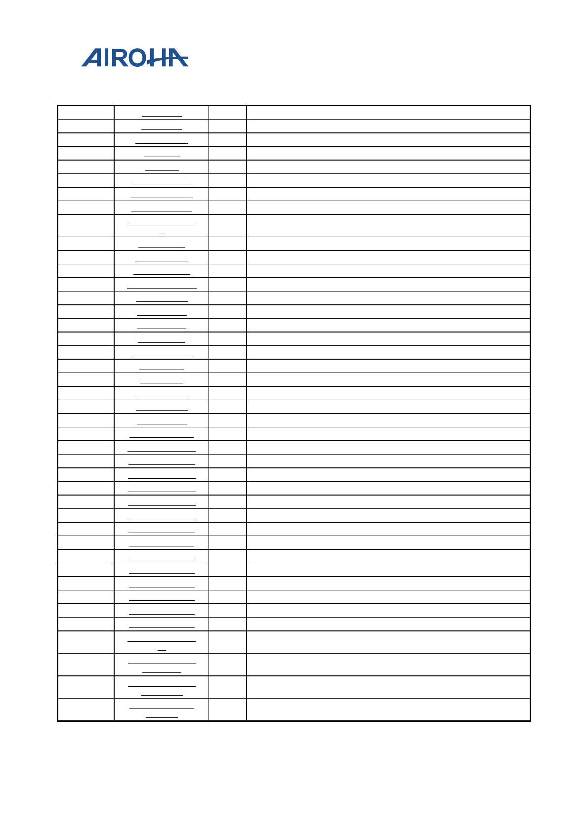
MT2523 Series Reference Manual
© 2015 - 2018 Airoha Technology Corp.
Page 601 of 692
This document contains information that is proprietary to Airoha Technology Corp. (“Airoha”) and/or its licensor(s).
Any unauthorized use, reproduction or disclosure of this document in whole or in part is strictly prohibited.
Module name: PMIC_REG Base address: (+0h)
2F6
VBTPSI1
8
VBTP LDO PSI register1
2F8
VALDO0
8
VA LDO register 0
2FC VALDOBF0 8 VA LDO buffer register 0
2FE
VAPSI0
8
VA LDO PSI register0
2FF
VAPSI1
8
VA LDO PSI register1
300
VCAMACTL0
8
VCAMA Control register 0
302 VCAMALDO0 8 VCAMALDO0
303
VCAMALDO1
8
VCAMA LDO register 1
306
VCAMALDOBF
0 8 VCAMA LDO buffer register 0
30A
PSWCTL0
8
PSW Control register 0
30F SWIO18PSI 8 SWIO18 LDO PSI register
313
VIO28LDO0
8
VIO28LDO0
317
VIO28LDOBF0
8
VIO28LDOBF0
319
VIO28PSI0
8
VIO28 LDO PSI register0
31A VIO28PSI1 8 VIO28 LDO PSI register1
31C
VMCLDO0
8
VMCLDO0
31D
VMCLDO1
8
VMCLDO1
320
VMCLDOBF0
8
VMCLDOBF0
322 VMCPSI0 8 VMC LDO PSI register0
323
VMCPSI1
8
VMC LDO PSI register1
324
VIBRCTL0
8
VIBR Control register 0
326
VIBRLDO0
8
VIBRLDO0
327 VIBRLDO1 8 VIBRLDO1
32A
VIBRLDOBF0
8
VIBRLDOBF0
32C
ISINK0_CON0
8
ISINK0 Control Register 0
32D
ISINK0_CON1
8
ISINK0 Control Register 1
32E ISINK0_CON2 8 ISINK0 Control Register 2
330
ISINK0_CON4
8
ISINK0 Control Register 4
331
ISINK0_CON5
8
ISINK0 Control Register 5
332
ISINK0_CON6
8
ISINK0 Control Register 6
333 ISINK1_CON0 8 ISINK1 Control Register 0
334
ISINK1_CON1
8
ISINK1 Control Register 1
335
ISINK1_CON2
8
ISINK1 Control Register 2
337
ISINK1_CON4
8
ISINK1 Control Register 4
338 ISINK1_CON5 8 ISINK1 Control Register 5
339
ISINK1_CON6
8
ISINK1 Control Register 6
33A
ISINK2_CON1
8
ISINK2 Control Register 1
33C
ISINK3_CON1
8
ISINK3 Control Register 1
33F ISINK_ANA0_
H 8 ISINKS ACD Interface 0 High
344
ISINK_EN_CT
RL_Low 8 ISINK Enable control Low
345
ISINK_EN_CT
RL_High 8 ISINK Enable control High
346
ISINK_MODE
_CTRL 8 ISINK mode control
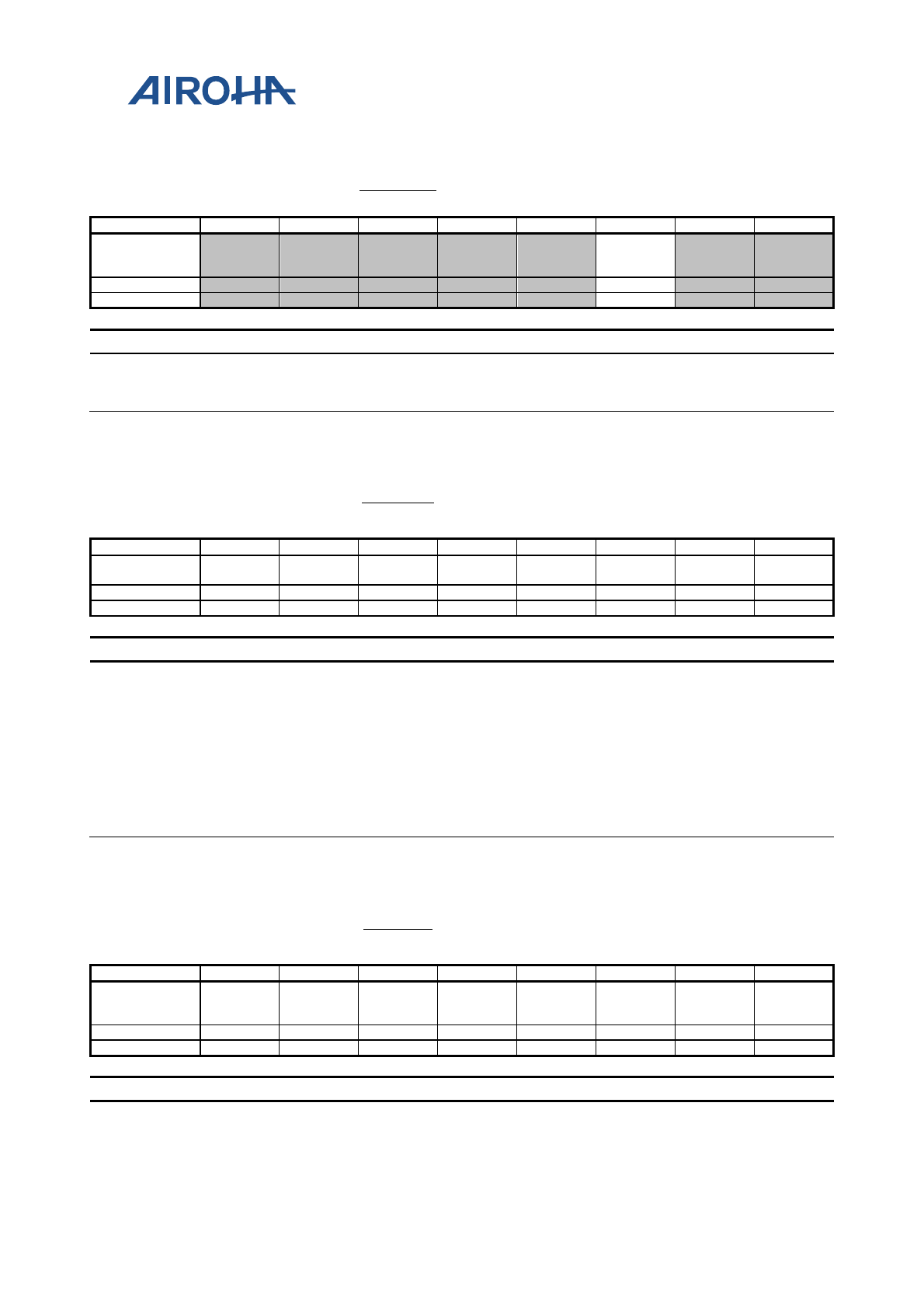
MT2523 Series Reference Manual
© 2015 - 2018 Airoha Technology Corp.
Page 602 of 692
This document contains information that is proprietary to Airoha Technology Corp. (“Airoha”) and/or its licensor(s).
Any unauthorized use, reproduction or disclosure of this document in whole or in part is strictly prohibited.
1D RSTCFG3
Reset
config
3
00
Bit
7
6
5
4
3
2
1
0
Name
WDTRST
B_STAT
US
Type
RO
Reset
0
Bit(s) Name Description
2 WDTRSTB_STATUS
WDTRSTB reset status
1'b0: No occured
1'b1: Occurred
1E INTSTS0
Interru
pt
status/
clear 0
00
Bit
7
6
5
4
3
2
1
0
Name
ints_dldo
_pg_f
ints_dldo
_pg_r
ints_dldo
_oc_f
ints_dldo
_oc_r
ints_aldo
_pg_f
ints_aldo
_pg_r
ints_aldo
_oc_f
ints_aldo
_oc_r
Type
W1C
W1C
W1C
W1C
W1C
W1C
W1C
W1C
Reset
0
0
0
0
0
0
0
0
Bit(s) Name Description
7 ints_dldo_pg_f
6 ints_dldo_pg_r
5 ints_dldo_oc_f
4 ints_dldo_oc_r
3 ints_aldo_pg_f
2 ints_aldo_pg_r
1 ints_aldo_oc_f
0 ints_aldo_oc_r
1F INTSTS1
Interru
pt
status/
clear 1
00
Bit
7
6
5
4
3
2
1
0
Name ints_pke
ylp_f
ints_pke
ylp_r
ints_vc_l
do_oc_f
ints_vc_l
do_oc_r
ints_vcor
e_pg_f
ints_vcor
e_pg_r
ints_vc_
buck_oc
_f
ints_vc_
buck_oc
_r
Type
W1C
W1C
W1C
W1C
W1C
W1C
W1C
W1C
Reset
0
0
0
0
0
0
0
0
Bit(s) Name Description
7 ints_pkeylp_f
6 ints_pkeylp_r
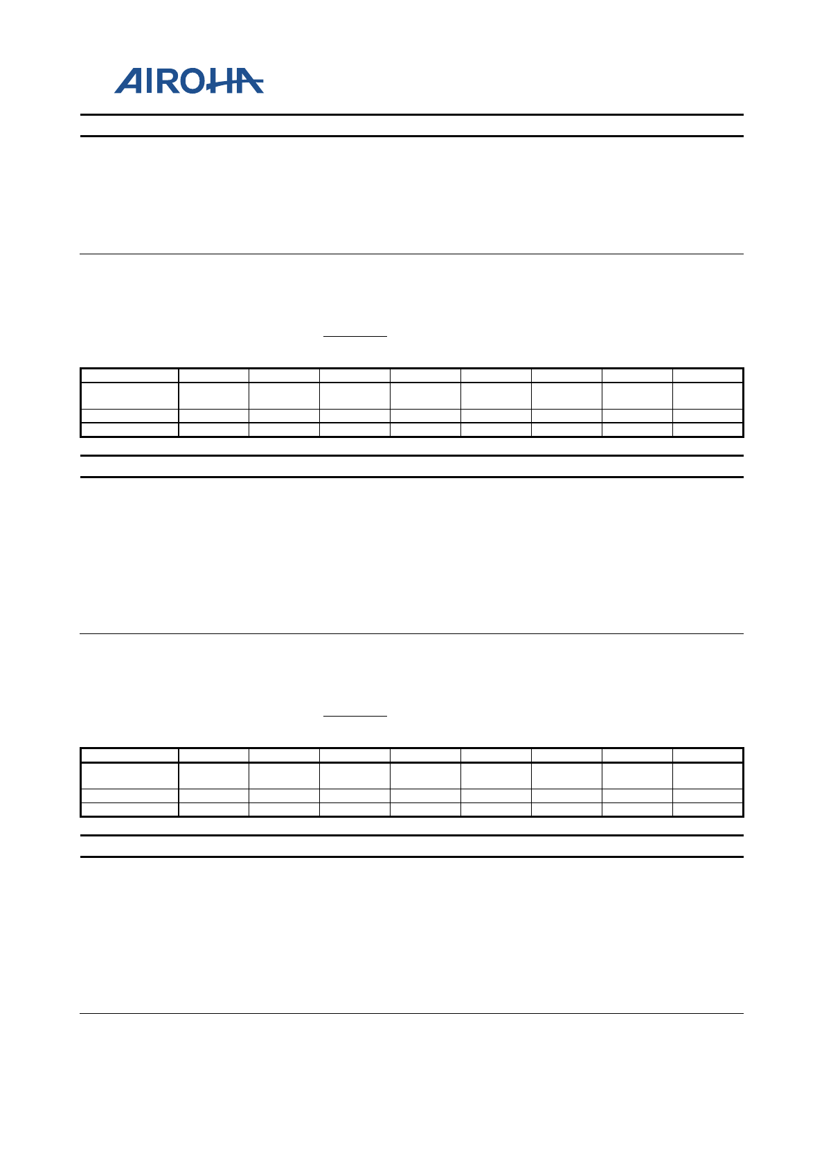
MT2523 Series Reference Manual
© 2015 - 2018 Airoha Technology Corp.
Page 603 of 692
This document contains information that is proprietary to Airoha Technology Corp. (“Airoha”) and/or its licensor(s).
Any unauthorized use, reproduction or disclosure of this document in whole or in part is strictly prohibited.
Bit(s) Name Description
5 ints_vc_ldo_oc_f
4 ints_vc_ldo_oc_r
3 ints_vcore_pg_f
2 ints_vcore_pg_r
1 ints_vc_buck_oc_f
0 ints_vc_buck_oc_r
20 INTSTS2
Interru
pt
status/
clear 2
00
Bit
7
6
5
4
3
2
1
0
Name
ints_pwr
key_f
ints_pwr
key_r
ints_axp
key_f
ints_axp
key_r
ints_thm
2_f
ints_thm
2_r
ints_thm
1_f
ints_thm
1_r
Type
W1C
W1C
W1C
W1C
W1C
W1C
W1C
W1C
Reset
0
0
0
0
0
0
0
0
Bit(s) Name Description
7 ints_pwrkey_f
6 ints_pwrkey_r
5 ints_axpkey_f
4 ints_axpkey_r
3 ints_thm2_f
2 ints_thm2_r
1 ints_thm1_f
0 ints_thm1_r
21 INTSTS3
Interru
pt
status/
clear 3
00
Bit
7
6
5
4
3
2
1
0
Name
ints_thr_
l_f
ints_thr_
l_r
ints_thr_
h_f
ints_thr_
h_r
ints_chr
det_f
ints_chr
det_r
ints_chg
ov_f
ints_chg
ov_r
Type
W1C
W1C
W1C
W1C
W1C
W1C
W1C
W1C
Reset
0
0
0
0
0
0
0
0
Bit(s) Name Description
7 ints_thr_l_f
6 ints_thr_l_r
5 ints_thr_h_f
4 ints_thr_h_r
3 ints_chrdet_f
2 ints_chrdet_r
1 ints_chgov_f
0 ints_chgov_r
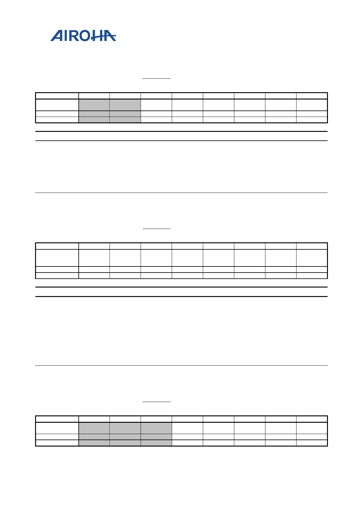
MT2523 Series Reference Manual
© 2015 - 2018 Airoha Technology Corp.
Page 604 of 692
This document contains information that is proprietary to Airoha Technology Corp. (“Airoha”) and/or its licensor(s).
Any unauthorized use, reproduction or disclosure of this document in whole or in part is strictly prohibited.
22 INTSTS4
Interru
pt
status/
clear 4
00
Bit
7
6
5
4
3
2
1
0
Name
ints_psw
_pg_f
ints_psw
_pg_r
ints_over
40_f
ints_over
40_r
ints_over
110_f
ints_over
110_r
Type
W1C
W1C
W1C
W1C
W1C
W1C
Reset
0
0
0
0
0
0
Bit(s) Name Description
5 ints_psw_pg_f
4 ints_psw_pg_r
3 ints_over40_f
2 ints_over40_r
1 ints_over110_f
0 ints_over110_r
23 INTSTS5
Interru
pt
status/
clear 5
00
Bit
7
6
5
4
3
2
1
0
Name ints_war
m_lv
ints_hot
_lv
ints_chr
wdt_lv
ints_bval
id_det_lv
ints_vbat
_undet_l
v
ints_vbat
on_hv_lv
ints_bat_
l_lv
ints_bat_
h_lv
Type
W1C
W1C
W1C
W1C
W1C
W1C
W1C
W1C
Reset
0
0
0
0
0
0
0
0
Bit(s) Name Description
7 ints_warm_lv
6 ints_hot_lv
5 ints_chrwdt_lv
4 ints_bvalid_det_lv
3 ints_vbat_undet_lv
2 ints_vbaton_hv_lv
1 ints_bat_l_lv
0 ints_bat_h_lv
24 INTSTS6
Interru
pt
status/
clear 6
00
Bit
7
6
5
4
3
2
1
0
Name
ints_ad_l
bat_lv
ints_nag
_c_lv
ints_imp
_lv
ints_cold
_lv
ints_cool
_lv
Type
W1C
W1C
W1C
W1C
W1C
Reset
0
0
0
0
0

MT2523 Series Reference Manual
© 2015 - 2018 Airoha Technology Corp.
Page 605 of 692
This document contains information that is proprietary to Airoha Technology Corp. (“Airoha”) and/or its licensor(s).
Any unauthorized use, reproduction or disclosure of this document in whole or in part is strictly prohibited.
Bit(s) Name Description
4 ints_ad_lbat_lv
3 ints_nag_c_lv
2 ints_imp_lv
1 ints_cold_lv
0 ints_cool_lv
25 INTEN0
Interru
pt
enable
0
00
Bit
7
6
5
4
3
2
1
0
Name
inte_dld
o_pg_f
inte_dld
o_pg_r
inte_dld
o_oc_f
inte_dldo
_oc_r
inte_aldo
_pg_f
inte_aldo
_pg_r
inte_aldo
_oc_f
inte_aldo
_oc_r
Type
RW
RW
RW
RW
RW
RW
RW
RW
Reset
0
0
0
0
0
0
0
0
Bit(s) Name Description
7 inte_dldo_pg_f
6 inte_dldo_pg_r
5 inte_dldo_oc_f
4 inte_dldo_oc_r
3 inte_aldo_pg_f
2 inte_aldo_pg_r
1 inte_aldo_oc_f
0 inte_aldo_oc_r
26 INTEN1
Interru
pt
enable
1
00
Bit
7
6
5
4
3
2
1
0
Name inte_pke
ylp_f
inte_pke
ylp_r
inte_vc_l
do_oc_f
inte_vc_l
do_oc_r
inte_vcor
e_pg_f
inte_vcor
e_pg_r
inte_vc_
buck_oc
_f
inte_vc_
buck_oc
_r
Type
RW
RW
RW
RW
RW
RW
RW
RW
Reset
0
0
0
0
0
0
0
0
Bit(s) Name Description
7 inte_pkeylp_f
6 inte_pkeylp_r
5 inte_vc_ldo_oc_f
4 inte_vc_ldo_oc_r
3 inte_vcore_pg_f
2 inte_vcore_pg_r
1 inte_vc_buck_oc_f
0 inte_vc_buck_oc_r
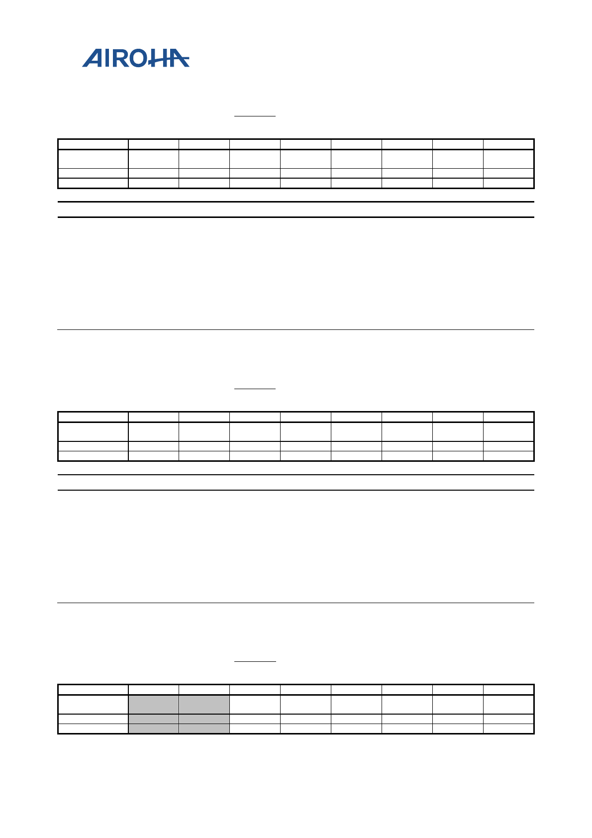
MT2523 Series Reference Manual
© 2015 - 2018 Airoha Technology Corp.
Page 606 of 692
This document contains information that is proprietary to Airoha Technology Corp. (“Airoha”) and/or its licensor(s).
Any unauthorized use, reproduction or disclosure of this document in whole or in part is strictly prohibited.
27 INTEN2
Interru
pt
enable
2
00
Bit
7
6
5
4
3
2
1
0
Name
inte_pwr
key_f
inte_pwr
key_r
inte_axp
key_f
inte_axp
key_r
inte_thm
2_f
inte_thm
2_r
inte_thm
1_f
inte_thm
1_r
Type
RW
RW
RW
RW
RW
RW
RW
RW
Reset
0
0
0
0
0
0
0
0
Bit(s) Name Description
7 inte_pwrkey_f
6 inte_pwrkey_r
5 inte_axpkey_f
4 inte_axpkey_r
3 inte_thm2_f Thermal interrupt 1 falling: T < 40
2 inte_thm2_r Thermal interrupt 1 rising: T > 55
1 inte_thm1_f Thermal interrupt 1 falling: T < 110
0 inte_thm1_r Thermal interrupt 1 rising: T > 125
28 INTEN3
Interru
pt
enable
3
00
Bit
7
6
5
4
3
2
1
0
Name
inte_thr
_l_f
inte_thr_
l_r
inte_thr_
h_f
inte_thr_
h_r
inte_chr
det_f
inte_chr
det_r
inte_chg
ov_f
inte_chg
ov_r
Type
RW
RW
RW
RW
RW
RW
RW
RW
Reset
0
0
0
0
0
0
0
0
Bit(s) Name Description
7 inte_thr_l_f
6 inte_thr_l_r
5 inte_thr_h_f
4 inte_thr_h_r
3 inte_chrdet_f
2 inte_chrdet_r
1 inte_chgov_f
0 inte_chgov_r
29 INTEN4
Interru
pt
enable
4
00
Bit
7
6
5
4
3
2
1
0
Name
inte_psw
_pg_f
inte_psw
_pg_r
inte_over
40_f
inte_over
40_r
inte_over
110_f
inte_over
110_r
Type
RW
RW
RW
RW
RW
RW
Reset
0
0
0
0
0
0
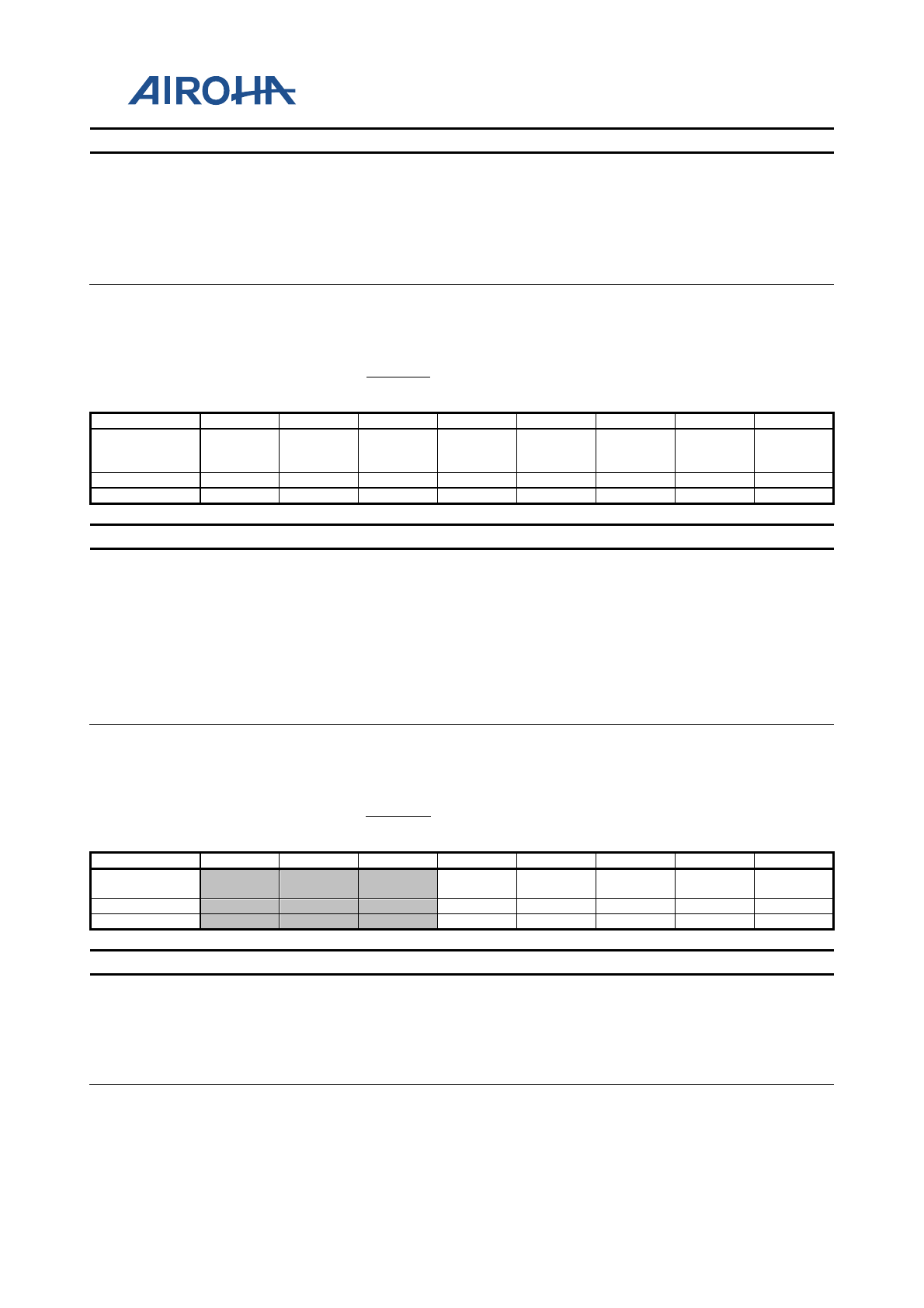
MT2523 Series Reference Manual
© 2015 - 2018 Airoha Technology Corp.
Page 607 of 692
This document contains information that is proprietary to Airoha Technology Corp. (“Airoha”) and/or its licensor(s).
Any unauthorized use, reproduction or disclosure of this document in whole or in part is strictly prohibited.
Bit(s) Name Description
5 inte_psw_pg_f
4 inte_psw_pg_r
3 inte_over40_f
2 inte_over40_r
1 inte_over110_f
0 inte_over110_r
2A INTEN5
Interru
pt
enable
5
00
Bit
7
6
5
4
3
2
1
0
Name inte_war
m_lv
inte_hot
_lv
inte_chr
wdt_lv
inte_bval
id_det_lv
inte_vbat
_undet_l
v
inte_vbat
on_hv_lv
inte_bat
_l_lv
inte_bat
_h_lv
Type
RW
RW
RW
RW
RW
RW
RW
RW
Reset
0
0
0
0
0
0
0
0
Bit(s) Name Description
7 inte_warm_lv
6 inte_hot_lv
5 inte_chrwdt_lv
4 inte_bvalid_det_lv
3 inte_vbat_undet_lv
2 inte_vbaton_hv_lv
1 inte_bat_l_lv
0 inte_bat_h_lv
2B INTEN6
Interru
pt
enable
6
00
Bit
7
6
5
4
3
2
1
0
Name
inte_ad_l
bat_lv
inte_nag
_c_lv
inte_imp
_lv
inte_cold
_lv
inte_cool
_lv
Type
RW
RW
RW
RW
RW
Reset
0
0
0
0
0
Bit(s) Name Description
4 inte_ad_lbat_lv
3 inte_nag_c_lv
2 inte_imp_lv
1 inte_cold_lv
0 inte_cool_lv
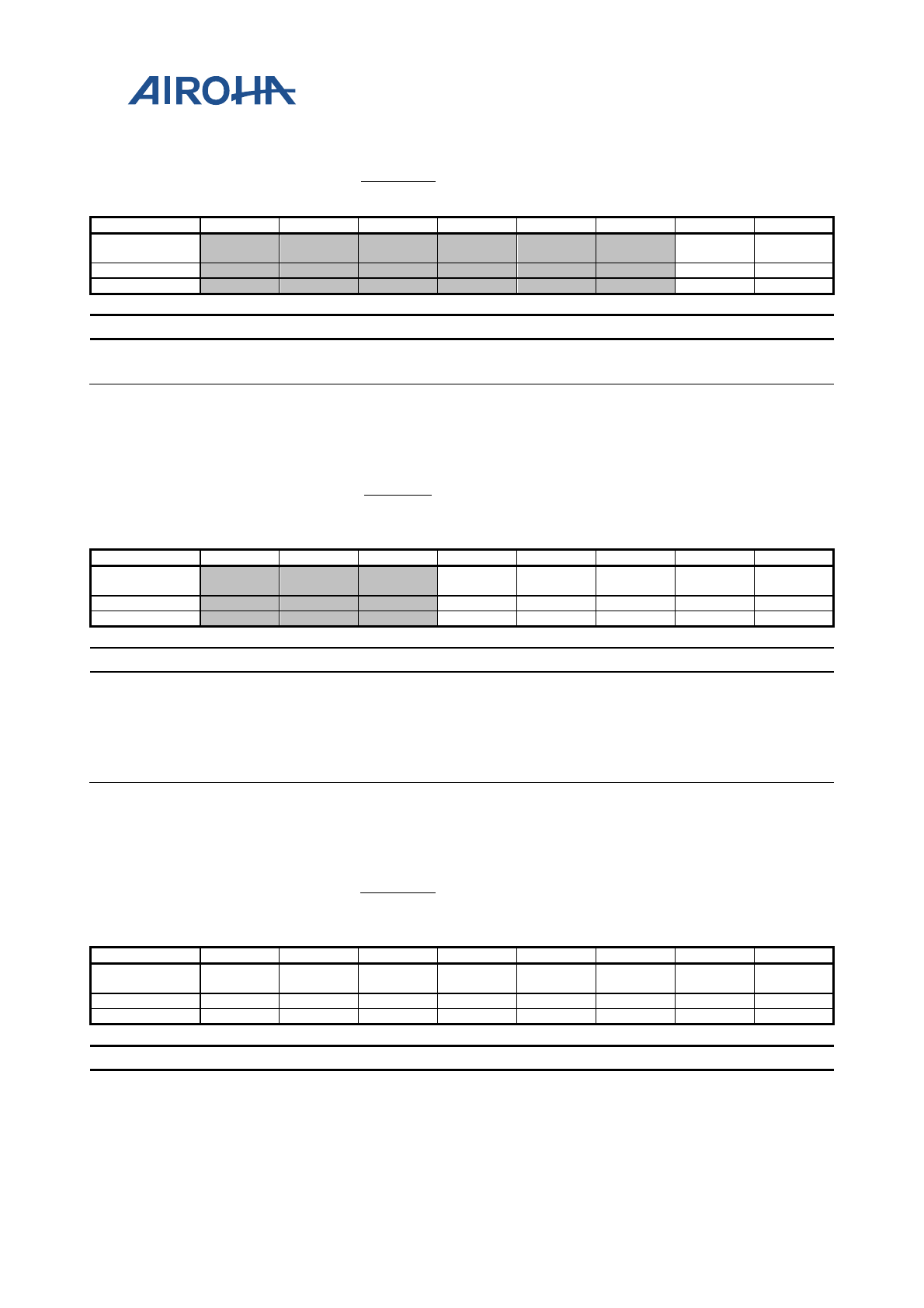
MT2523 Series Reference Manual
© 2015 - 2018 Airoha Technology Corp.
Page 608 of 692
This document contains information that is proprietary to Airoha Technology Corp. (“Airoha”) and/or its licensor(s).
Any unauthorized use, reproduction or disclosure of this document in whole or in part is strictly prohibited.
2C INTMISC
interru
pt misc
registe
r
00
Bit
7
6
5
4
3
2
1
0
Name
rg_intr_
mode_sel
polarity
Type
RW
RW
Reset
0
0
Bit(s) Name Description
1 rg_intr_mode_sel
0 polarity
2D PONSTS
Power
on
source
record
registe
r
00
Bit
7
6
5
4
3
2
1
0
Name
STS_RB
OOT
STS_SPA
R
STS_CH
RIN
STS_RTC
A
STS_PW
RKEY
Type
RO
RO
RO
RO
RO
Reset
0
0
0
0
0
Bit(s) Name Description
4 STS_RBOOT Power on for cold reset
3 STS_SPAR Power on for SPAR event
2 STS_CHRIN Power on for charger insertion
1 STS_RTCA Power on for RTC alarm
0 STS_PWRKEY Power on for PWREKY press
2E POFFSTS
Power
off
source
record
registe
r
00
Bit
7
6
5
4
3
2
1
0
Name
STS_NO
RMOFF
STS_PKE
YLP
STS_CRS
T
STS_WR
ST
STS_TH
RDN
STS_PSO
C
STS_PGF
AIL
STS_UVL
O
Type
RO
RO
RO
RO
RO
RO
RO
RO
Reset
0
0
0
0
0
0
0
0
Bit(s) Name Description
7 STS_NORMOFF Power off for PWRHOLD clear
6 STS_PKEYLP Power off for power key(s) long press
5 STS_CRST Power off for cold reset
4 STS_WRST Power reset for warm reset
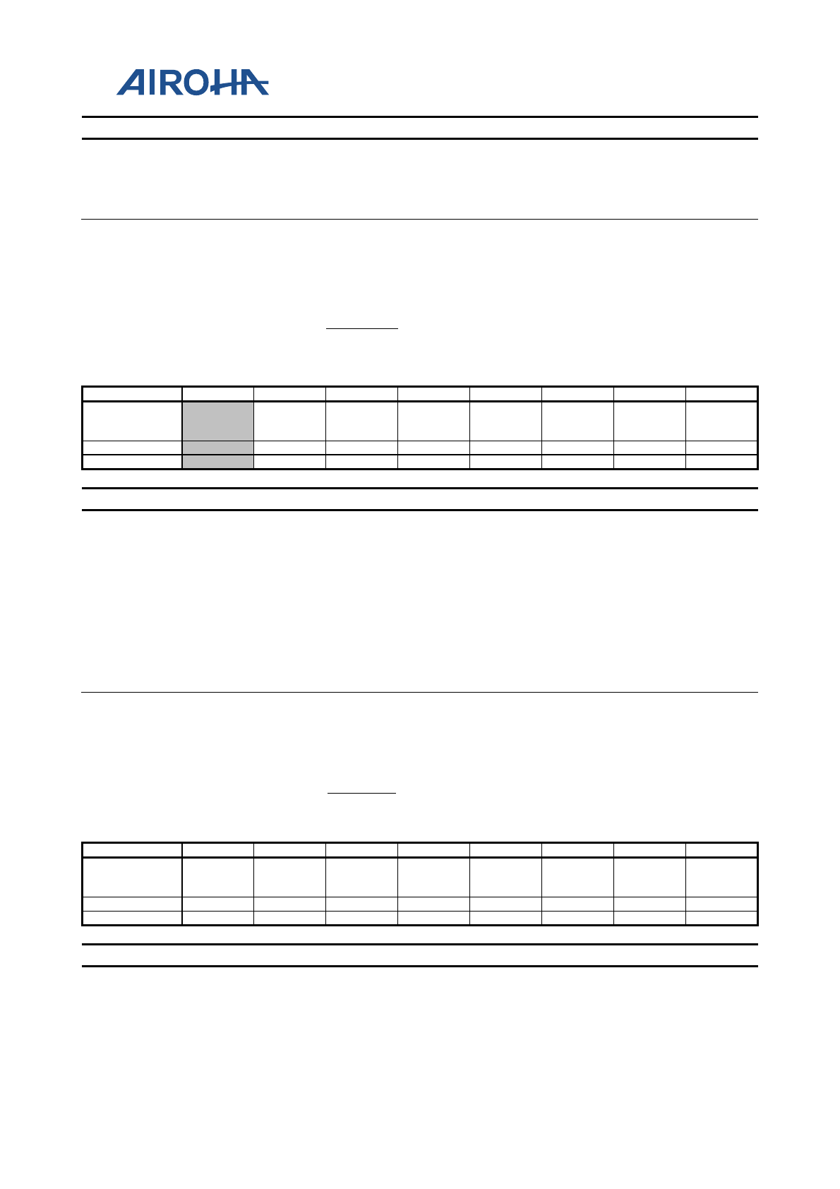
MT2523 Series Reference Manual
© 2015 - 2018 Airoha Technology Corp.
Page 609 of 692
This document contains information that is proprietary to Airoha Technology Corp. (“Airoha”) and/or its licensor(s).
Any unauthorized use, reproduction or disclosure of this document in whole or in part is strictly prohibited.
Bit(s) Name Description
3 STS_THRDN Power off for thermal shutdown
2 STS_PSOC Power off for SOC WDT reset
1 STS_PGFAIL Power off for PWRGOOD failure
0 STS_UVLO Power off for UVLO event
2F PDNSTS0
Power
excepti
on
shutdo
wn
status
0
00
Bit
7
6
5
4
3
2
1
0
Name
STS_PD
N_VSF_
PG
STS_PD
N_VIO18
_PG
STS_PD
N_VCOR
E_PG
STS_PD
N_VA18_
PG
STS_PD
N_VCAM
A_PG
STS_PD
N_VA_P
G
STS_PD
N_VBT_
PG
Type
RO
RO
RO
RO
RO
RO
RO
Reset
0
0
0
0
0
0
0
Bit(s) Name Description
6 STS_PDN_VSF_PG Log the shutdown PG
5 STS_PDN_VIO18_P
G Log the shutdown PG
4 STS_PDN_VCORE_
PG Log the shutdown PG
3 STS_PDN_VA18_PG Log the shutdown PG
2 STS_PDN_VCAMA_
PG Log the shutdown PG
1 STS_PDN_VA_PG Log the shutdown PG
0 STS_PDN_VBT_PG Log the shutdown PG
30 PDNSTS1
Power
excepti
on
shutdo
wn
status 1
00
Bit
7
6
5
4
3
2
1
0
Name
STS_PD
N_SWBA
T_PG
STS_PD
N_VIBR_
PG
STS_PD
N_VUSB
_PG
STS_PD
N_VMC_
PG
STS_PD
N_SWM
P_PG
STS_PD
N_VIO28
_PG
STS_PD
N_SWDP
_PG
STS_PD
N_SWX
M_PG
Type
RO
RO
RO
RO
RO
RO
RO
RO
Reset
0
0
0
0
0
0
0
0
Bit(s) Name Description
7 STS_PDN_SWBAT_
PG Log the shutdown PG
6 STS_PDN_VIBR_PG Log the shutdown PG
5 STS_PDN_VUSB_P
G Log the shutdown PG
MT2523 Series Reference Manual
© 2015 - 2018 Airoha Technology Corp.
Page 610 of 692
This document contains information that is proprietary to Airoha Technology Corp. (“Airoha”) and/or its licensor(s).
Any unauthorized use, reproduction or disclosure of this document in whole or in part is strictly prohibited.
Bit(s) Name Description
4 STS_PDN_VMC_PG Log the shutdown PG
3 STS_PDN_SWMP_P
G Log the shutdown PG
2 STS_PDN_VIO28_P
G Log the shutdown PG
1 STS_PDN_SWDP_P
G Log the shutdown PG
0 STS_PDN_SWXM_P
G Log the shutdown PG
31 PDNSTS2
Power
excepti
on
shutdo
wn
status 2
00
Bit
7
6
5
4
3
2
1
0
Name
STS_PD
N_VIO18
_OC
STS_PD
N_VCOR
E_LDO_
OC
STS_PD
N_VCOR
E_BUCK
_OC
STS_PD
N_VIO28
_OC
STS_PD
N_VA_O
C
STS_PD
N_VMC_
OC
Type
RO
RO
RO
RO
RO
RO
Reset
0
0
0
0
0
0
Bit(s) Name Description
5 STS_PDN_VIO18_O
C Log the shutdown OC
4 STS_PDN_VCORE_
LDO_OC Log the shutdown OC
3 STS_PDN_VCORE_
BUCK_OC Log the shutdown OC
2 STS_PDN_VIO28_O
C Log the shutdown OC
1 STS_PDN_VA_OC Log the shutdown OC
0 STS_PDN_VMC_OC Log the shutdown OC
32 PSSTS0
Power
supply
status
0
registe
r
00
Bit
7
6
5
4
3
2
1
0
Name
STS_VA1
8_ENA
STS_VA_
ENA
STS_VBT
_ENA
STS_VCA
MA_ENA
STS_VUS
B_ENA
STS_OSC
_EN
STS_IVG
EN_EN
Type
RO
RO
RO
RO
RO
RO
RO
Reset
0
0
0
0
0
0
0
Bit(s) Name Description
6 STS_VA18_ENA
5 STS_VA_ENA
MT2523 Series Reference Manual
© 2015 - 2018 Airoha Technology Corp.
Page 611 of 692
This document contains information that is proprietary to Airoha Technology Corp. (“Airoha”) and/or its licensor(s).
Any unauthorized use, reproduction or disclosure of this document in whole or in part is strictly prohibited.
Bit(s) Name Description
4 STS_VBT_ENA
3 STS_VCAMA_ENA
2 STS_VUSB_ENA
1 STS_OSC_EN
0 STS_IVGEN_EN
33 PSSTS1
Power
supply
status 1
registe
r
00
Bit
7
6
5
4
3
2
1
0
Name STS_VIB
R_ENA
STS_VM
C_ENA
STS_VIO
28_ENA
STS_VSF
_ENA
STS_VIO
18_ENA
STS_VC_
LDO_EN
A
STS_VC_
BUCK_E
NA
Type
RO
RO
RO
RO
RO
RO
RO
Reset
0
0
0
0
0
0
0
Bit(s) Name Description
6 STS_VIBR_ENA
5 STS_VMC_ENA
4 STS_VIO28_ENA
3 STS_VSF_ENA
2 STS_VIO18_ENA
1 STS_VC_LDO_ENA
0 STS_VC_BUCK_EN
A
34 PSSTS2
Power
supply
status 2
registe
r
00
Bit
7
6
5
4
3
2
1
0
Name PKEYLP
_VAL
AXPKEY
_VAL
PWRKEY
_VAL
STS_SW
MP_ENA
STS_SW
DP_ENA
STS_SW
XM_ENA
STS_SW
BAT_EN
A
Type
RO
RO
RO
RO
RO
RO
RO
Reset
0
0
0
0
0
0
0
Bit(s) Name Description
6 PKEYLP_VAL
5 AXPKEY_VAL
4 PWRKEY_VAL
3 STS_SWMP_ENA
2 STS_SWDP_ENA
1 STS_SWXM_ENA
0 STS_SWBAT_ENA
MT2523 Series Reference Manual
© 2015 - 2018 Airoha Technology Corp.
Page 612 of 692
This document contains information that is proprietary to Airoha Technology Corp. (“Airoha”) and/or its licensor(s).
Any unauthorized use, reproduction or disclosure of this document in whole or in part is strictly prohibited.
35 PSOCSTS0
Power
supply
Overcu
rrent
status
0
registe
r
00
Bit
7
6
5
4
3
2
1
0
Name STS_VSF
_OC
STS_VIO
18_OC
STS_VC_
LDO_OC
STS_VC_
BUCK_O
C
STS_VA1
8_OC
STS_VA_
OC
STS_VBT
_OC
Type
RO
RO
RO
RO
RO
RO
RO
Reset
0
0
0
0
0
0
0
Bit(s) Name Description
6 STS_VSF_OC
5 STS_VIO18_OC
4 STS_VC_LDO_OC
3 STS_VC_BUCK_OC
2 STS_VA18_OC
1 STS_VA_OC
0 STS_VBT_OC
36 PSOCSTS1
Power
supply
Overcu
rrent
status 1
registe
r
00
Bit
7
6
5
4
3
2
1
0
Name
STS_VIB
R_OC
STS_VCA
MA_OC
STS_VUS
B_OC
STS_VM
C_OC
STS_VIO
28_OC
Type
RO
RO
RO
RO
RO
Reset
0
0
0
0
0
Bit(s) Name Description
4 STS_VIBR_OC
3 STS_VCAMA_OC
2 STS_VUSB_OC
1 STS_VMC_OC
0 STS_VIO28_OC
MT2523 Series Reference Manual
© 2015 - 2018 Airoha Technology Corp.
Page 613 of 692
This document contains information that is proprietary to Airoha Technology Corp. (“Airoha”) and/or its licensor(s).
Any unauthorized use, reproduction or disclosure of this document in whole or in part is strictly prohibited.
37 PSPGSTS0
Power
supply
PWRG
OOD
status
0
registe
r
00
Bit
7
6
5
4
3
2
1
0
Name
STS_VSF
_PG
STS_VIO
18_PG
STS_VCO
RE_PG
STS_VA1
8_PG
STS_VCA
MA_PG
STS_VA_
PG
STS_VBT
_PG
Type
RO
RO
RO
RO
RO
RO
RO
Reset
0
0
0
0
0
0
0
Bit(s) Name Description
6 STS_VSF_PG
5 STS_VIO18_PG
4 STS_VCORE_PG
3 STS_VA18_PG
2 STS_VCAMA_PG
1 STS_VA_PG
0 STS_VBT_PG
38 PSPGSTS1
Power
supply
PWRG
OOD
status 1
registe
r
00
Bit
7
6
5
4
3
2
1
0
Name
STS_SW
BAT_PG
STS_VIB
R_PG
STS_VUS
B_PG
STS_VM
C_PG
STS_SW
MP_PG
STS_VIO
28_PG
STS_SW
DP_PG
STS_SW
XM_PG
Type
RO
RO
RO
RO
RO
RO
RO
RO
Reset
0
0
0
0
0
0
0
0
Bit(s) Name Description
7 STS_SWBAT_PG
6 STS_VIBR_PG
5 STS_VUSB_PG
4 STS_VMC_PG
3 STS_SWMP_PG
2 STS_VIO28_PG
1 STS_SWDP_PG
0 STS_SWXM_PG
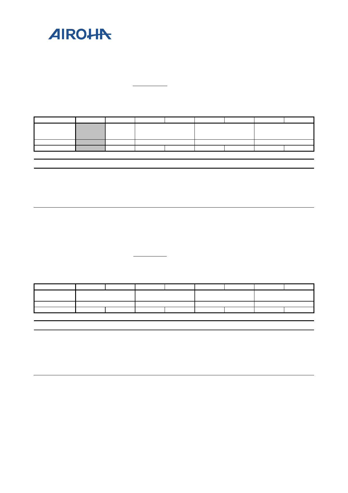
MT2523 Series Reference Manual
© 2015 - 2018 Airoha Technology Corp.
Page 614 of 692
This document contains information that is proprietary to Airoha Technology Corp. (“Airoha”) and/or its licensor(s).
Any unauthorized use, reproduction or disclosure of this document in whole or in part is strictly prohibited.
39 PSOMSTS0
Power
supply
Operati
onal
mode
status
0
registe
r
00
Bit
7
6
5
4
3
2
1
0
Name
STS_VA1
8_OPMO
D
STS_VCAMA_OPMO
D STS_VA_OPMOD STS_VBT_OPMOD
Type
RO
RO
RO
RO
Reset
0
0
0
0
0
0
0
Bit(s) Name Description
6 STS_VA18_OPMOD
5:4 STS_VCAMA_OPMO
D
3:2 STS_VA_OPMOD
1:0 STS_VBT_OPMOD
3A PSOMSTS1
Power
supply
Operati
onal
mode
status 1
registe
r
00
Bit
7
6
5
4
3
2
1
0
Name STS_VSF_OPMOD STS_VIO18_OPMOD
STS_VC_LDO_OPMO
D
STS_VDIG18_OPMO
D
Type
RO
RO
RO
RO
Reset
0
0
0
0
0
0
0
0
Bit(s) Name Description
7:6 STS_VSF_OPMOD
5:4 STS_VIO18_OPMOD
3:2 STS_VC_LDO_OPM
OD
1:0 STS_VDIG18_OPMO
D
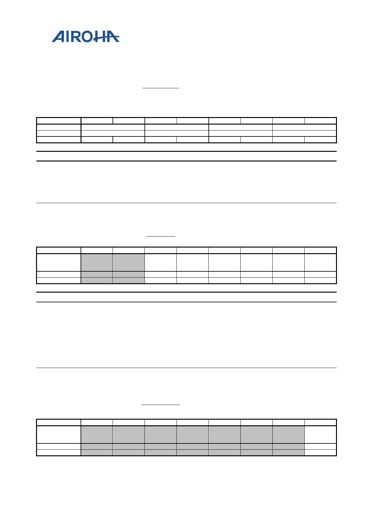
MT2523 Series Reference Manual
© 2015 - 2018 Airoha Technology Corp.
Page 615 of 692
This document contains information that is proprietary to Airoha Technology Corp. (“Airoha”) and/or its licensor(s).
Any unauthorized use, reproduction or disclosure of this document in whole or in part is strictly prohibited.
3B PSOMSTS2
Power
supply
Operati
onal
mode
status 2
registe
r
00
Bit
7
6
5
4
3
2
1
0
Name
STS_VIBR_OPMOD
STS_VUSB_OPMOD
STS_VMC_OPMOD
STS_VIO28_OPMOD
Type
RO
RO
RO
RO
Reset
0
0
0
0
0
0
0
0
Bit(s) Name Description
7:6 STS_VIBR_OPMOD
5:4 STS_VUSB_OPMOD
3:2 STS_VMC_OPMOD
1:0 STS_VIO28_OPMO
D
3C THMSTS
Therm
al
Status
00
Bit
7
6
5
4
3
2
1
0
Name
STS_TH
M_DEB_
STS
STS_TH
M_RAW
_STS
STS_TH
M_OVER
125
STS_TH
M_OVER
110
STS_TH
M_OVER
55
STS_TH
M_OVER
40
Type
RO
RO
RO
RO
RO
RO
Reset
0
0
0
0
0
0
Bit(s) Name Description
5 STS_THM_DEB_ST
S
4 STS_THM_RAW_ST
S
3 STS_THM_OVER125
2 STS_THM_OVER110
1 STS_THM_OVER55
0 STS_THM_OVER40
3D WKFG_STS
Wake
Up Fuel
Gauge
Status
00
Bit
7
6
5
4
3
2
1
0
Name
STS_WK
UP_FG_
DONE
Type
W1C
Reset
0
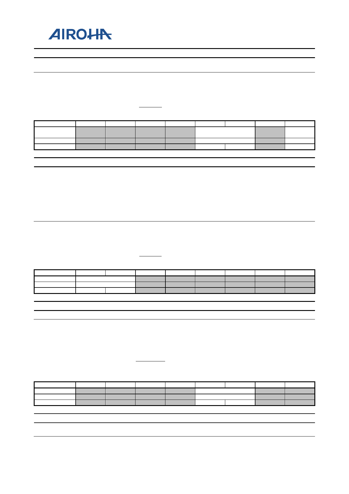
MT2523 Series Reference Manual
© 2015 - 2018 Airoha Technology Corp.
Page 616 of 692
This document contains information that is proprietary to Airoha Technology Corp. (“Airoha”) and/or its licensor(s).
Any unauthorized use, reproduction or disclosure of this document in whole or in part is strictly prohibited.
Bit(s) Name Description
0 STS_WKUP_FG_DO
NE
40 PSICTL
PSI
control
registe
r
01
Bit
7
6
5
4
3
2
1
0
Name RG_HNDOVR_LEN
RG_PSIO
VR
Type
RW
RW
Reset
0
0
1
Bit(s) Name Description
3:2 RG_HNDOVR_LEN
VR handover time interval selection
00: 2T*32K
01: 3T*32K
10: 4T*32K
11: 5T*32K
0 RG_PSIOVR
PSI overwrite enable
0: disable
1: enable
41 PSISTS
PSI
status
registe
r
00
Bit
7
6
5
4
3
2
1
0
Name
RGS_PSI_STS
Type
RO
Reset
0
0
Bit(s) Name Description
7:6 RGS_PSI_STS PSI bus status
48 PPCCFG0
PPC
configr
uation
0
registe
r
3B
Bit
7
6
5
4
3
2
1
0
Name
RG_WDTRST_ACT
Type
RW
Reset
1
0
Bit(s) Name Description
3:2 RG_WDTRST_ACT reg/warm reset may trigger VSF/SWXM power recycle. If
VSF/SWXM power recycle is triggered, the warm reset timing is
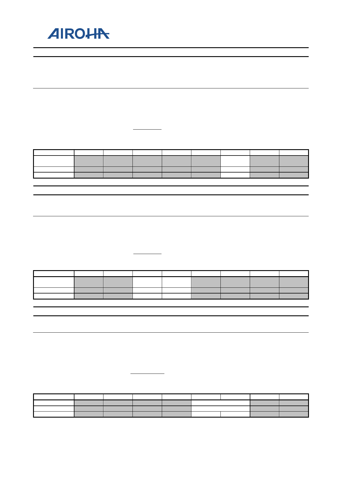
MT2523 Series Reference Manual
© 2015 - 2018 Airoha Technology Corp.
Page 617 of 692
This document contains information that is proprietary to Airoha Technology Corp. (“Airoha”) and/or its licensor(s).
Any unauthorized use, reproduction or disclosure of this document in whole or in part is strictly prohibited.
Bit(s) Name Description
extended to 150ms.
00: pmic reg reset
01: warm reset
10: cold reset
11: reserved
4A PPCCFG2
PPC
configr
uation
2
registe
r
21
Bit
7
6
5
4
3
2
1
0
Name
RG_XRS
T_ACT
Type
RW
Reset
0
Bit(s) Name Description
2 RG_XRST_ACT
Response for EXTRSTB assertion during active modes
0: Warm reset
1: Cold reset
4B PPCCTL0
PPC
control
0
registe
r
00
Bit
7
6
5
4
3
2
1
0
Name
RG_CRS
T
RG_WRS
T
Type
RW
RW
Reset
0
0
Bit(s) Name Description
5 RG_CRST Issue cold reset
4 RG_WRST Issue warm reset
4D SHDNCFG1
Shutdo
wn
configu
ration 1
registe
r
08
Bit
7
6
5
4
3
2
1
0
Name
RG_PKEY_LTIME
Type
RW
Reset
1
0
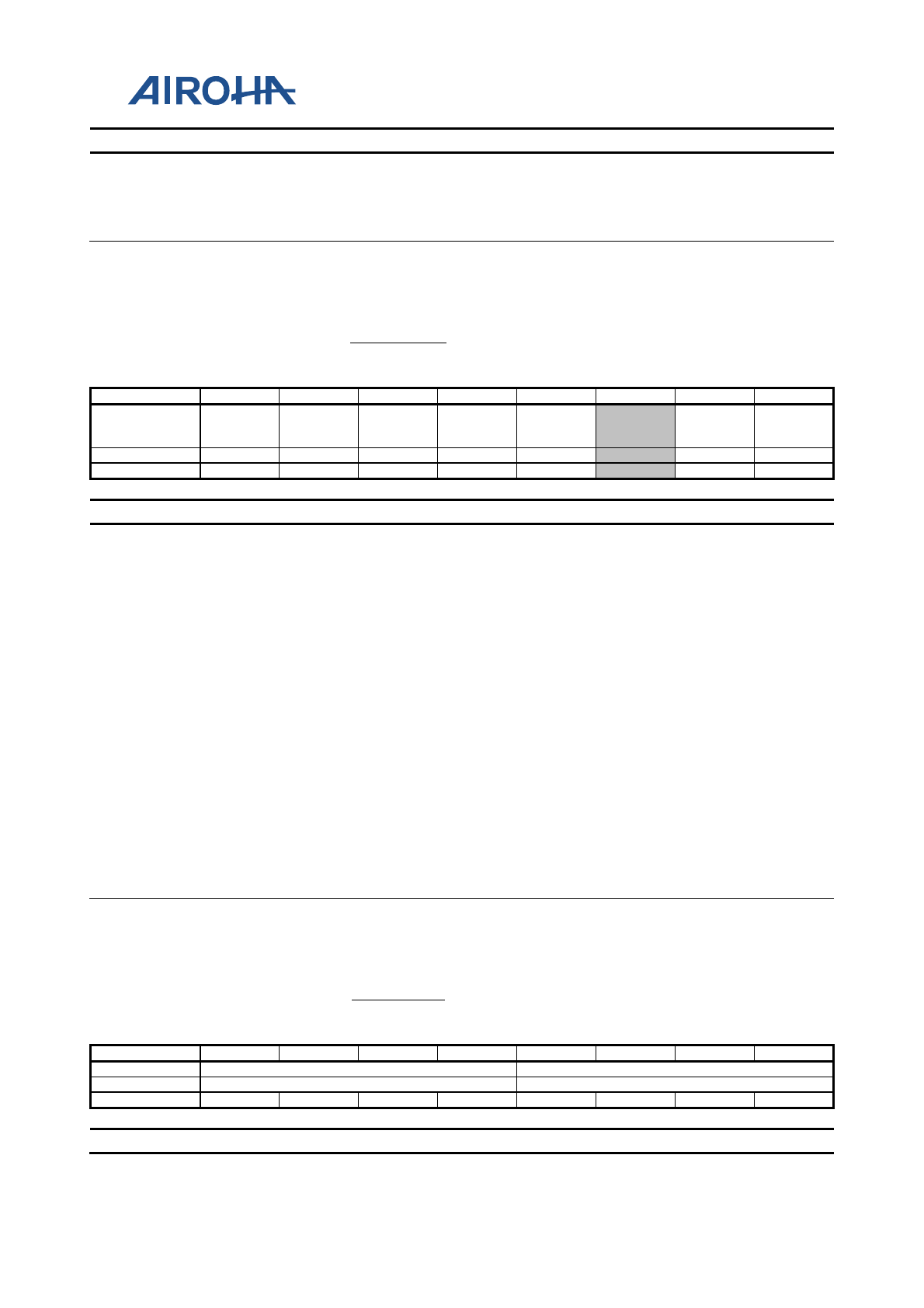
MT2523 Series Reference Manual
© 2015 - 2018 Airoha Technology Corp.
Page 618 of 692
This document contains information that is proprietary to Airoha Technology Corp. (“Airoha”) and/or its licensor(s).
Any unauthorized use, reproduction or disclosure of this document in whole or in part is strictly prohibited.
Bit(s) Name Description
3:2 RG_PKEY_LTIME
PWRKEY long press shutdown timing selection. (typical value)
00: 5 sec
01: 7 sec
10: 8 sec
11: 11 sec
87 CHR_CON0
Charge
r
control
registe
r 0
01
Bit
7
6
5
4
3
2
1
0
Name
RGS_VC
DT_HV_
DET
RGS_VC
DT_LV_
DET
RGS_CH
RDET
RG_NOR
M_CHR_
EN
RG_CSD
AC_EN
RGS_CH
R_LDO_
DET
RG_VCD
T_HV_E
N
Type
RO
RO
RO
RW
RW
RO
RW
Reset
0
0
0
0
0
0
1
Bit(s) Name Description
7 RGS_VCDT_HV_DE
T
Charger-in high voltage detection (with de-bounce).
0: charge-in voltage < VCDT_HV_VTH
1:charge-in voltage > VCDT_HV_VTH
6 RGS_VCDT_LV_DE
T
Charger-in low voltage detection (with de-bounce).
0: charge-in voltage < VCDT_LV_VTH
1:charge-in voltage > VCDT_LV_VTH
5 RGS_CHRDET
Charger-in detect.
0: No valid charger detected
1: Valid charger detected
4 RG_NORM_CHR_E
N
Charger enable setting, which would gated CSDAC_EN, PCHR_AUTO
and HWCV_EN
0: Charger disabled
1: Charger enabled
3 RG_CSDAC_EN
CS DAC enable.
0: CS DAC disabled
1: CS DAC enabled
1 RGS_CHR_LDO_DE
T
Charger LDO detection. If not detected, pulse charger cannot work.
0: Invalid charger LDO
1: Valid charger LDO
0 RG_VCDT_HV_EN ChargerIn HV detection function enable (0: disable, 1: enable)
88 CHR_CON1
Charge
r
Control
Registe
r 1
B2
Bit
7
6
5
4
3
2
1
0
Name
RG_VCDT_HV_VTH
RG_VCDT_LV_VTH
Type
RW
RW
Reset
1
0
1
1
0
0
1
0
Bit(s) Name Description
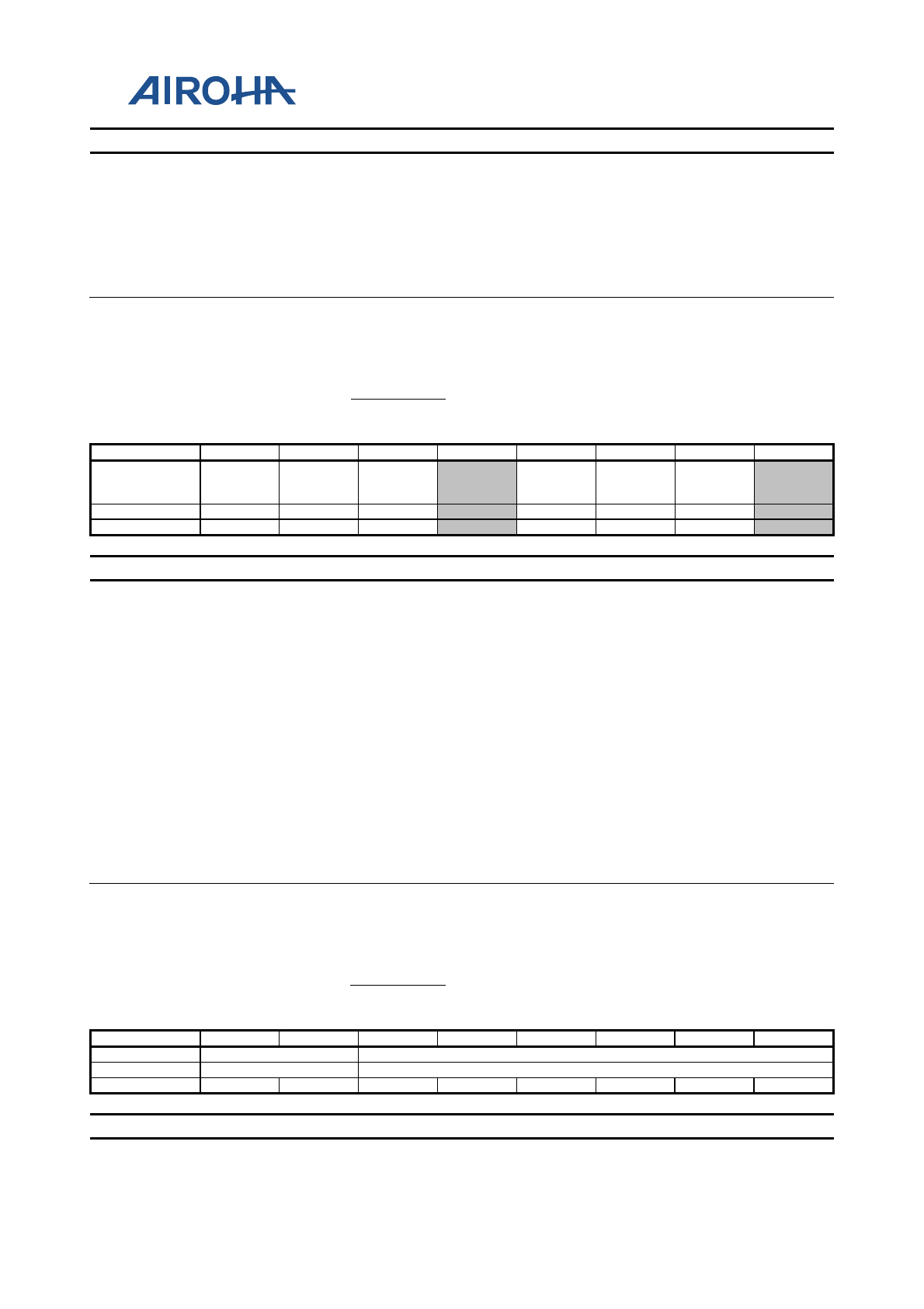
MT2523 Series Reference Manual
© 2015 - 2018 Airoha Technology Corp.
Page 619 of 692
This document contains information that is proprietary to Airoha Technology Corp. (“Airoha”) and/or its licensor(s).
Any unauthorized use, reproduction or disclosure of this document in whole or in part is strictly prohibited.
Bit(s) Name Description
7:4 RG_VCDT_HV_VTH
ChargerIn HV detection threshold, default 4.3/9.5V for VTHL/VTHH
0000~1000: 4.2V~4.6V with 50mV/step
1001~1100: 6V~7.5V with 500mV/step
1101~1111: 8.5V~10.5V with 1000mV/step
3:0 RG_VCDT_LV_VTH
ChargerIn LV detection threshold, default 4.3/9.5V for VTHL/VTHH
0000~1000: 4.2V~4.6V with 50mV/step
1001~1100: 6V~7.5V with 500mV/step
1101~1111: 8.5V~10.5V with 1000mV/step
89 CHR_CON2
Charge
r
Control
Registe
r 2
04
Bit
7
6
5
4
3
2
1
0
Name
RGS_VB
AT_CC_
DET
RGS_VB
AT_CV_
DET
RGS_CS
_DET RG_CS_
EN
RG_VBA
T_CC_E
N
RG_VBA
T_CV_E
N
Type
RO
RO
RO
RW
RW
RW
Reset
0
0
0
0
1
0
Bit(s) Name Description
7 RGS_VBAT_CC_DE
T
VBAT voltage detection for CC.
0: VBAT voltage < VBAT_CC_VTH
1: VBAT voltage > VBAT_CC_VTH
6 RGS_VBAT_CV_DE
T
VBAT voltage detection for CV.
0: VBAT voltage < VBAT_CV_VTH
1: VBAT voltage > VBAT_CV_VTH
5 RGS_CS_DET
Current sense voltage detection.
0: CS voltage < CS_VTH
1: CS voltage > CS_VTH
3 RG_CS_EN
Current sense voltage detection comparator enable.
0: Disabled
1: Enabled
2 RG_VBAT_CC_EN Battery CC detection enable (0: disable, 1: enable)
1 RG_VBAT_CV_EN
Battery CV detection enable
0: Disabled
1: Enabled
8A CHR_CON3
Charge
r
Control
Registe
r 3
CF
Bit
7
6
5
4
3
2
1
0
Name
RG_VBAT_CC_VTH
RG_VBAT_NORM_CV_VTH
Type
RW
RW
Reset
1
1
0
0
1
1
1
1
Bit(s) Name Description
7:6 RG_VBAT_CC_VTH Battery CC dection threshold
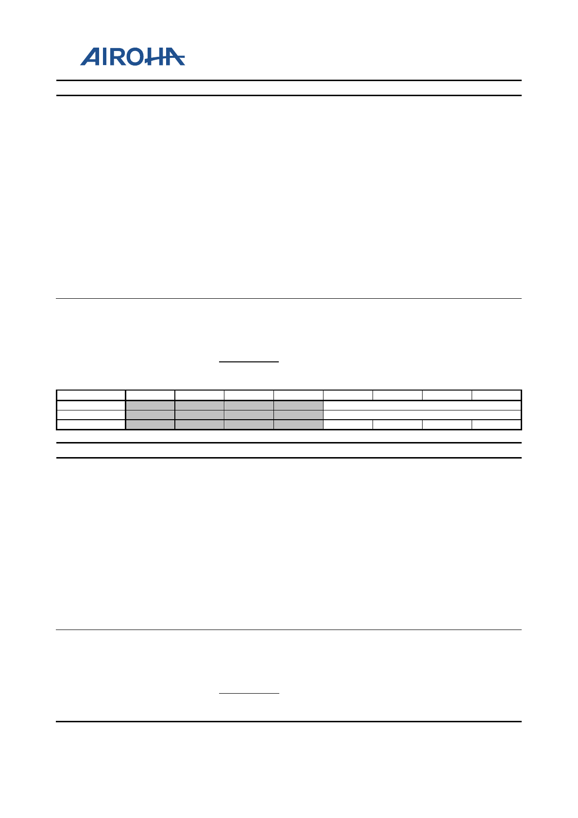
MT2523 Series Reference Manual
© 2015 - 2018 Airoha Technology Corp.
Page 620 of 692
This document contains information that is proprietary to Airoha Technology Corp. (“Airoha”) and/or its licensor(s).
Any unauthorized use, reproduction or disclosure of this document in whole or in part is strictly prohibited.
Bit(s) Name Description
00: 3.3V
01: 3.35V
10: 3.4V
11: 3.45V (default)
5:0 RG_VBAT_NORM_
CV_VTH
Battery CV dection threshold trimming option, default 4.2V
this register is used for FT CV threshold trimming and not for customer's fine
tuning (pchr_dig should invert MSB bit. otherwise, BC1.1 2.2V threshold would
be wrong)
000000~000011:3.5V, 3.6V, 3.7V, 3.8V
000100~000111:3.85V, 3.9V, 4V, 4.05V
001000~001011:4.1V, 4.125V, 4.1375v, 4.15V
001100~001111:4.1625V, 4.175V, 4.1875V, 4.2V (default)
010000~010011:4.2125V, 4.225V, 4.2375V, 4.25V
010100~010111:4.2625V, 4.275V, 4.2875V, 4.3V
011000~011011:4.3125V, 4.325V, 4.3375V, 4.35V
011100~011111:4.3625V, 4.375V, 4.3875V, 4.4V
100000~100011:4.4125V, 4.425V, 4.4375V, 4.45V
100100~100111:4.4625V, 4.475V, 4.4875V, 4.5V
101000:4.6V
111111:2.2V (BC1.1)
8B CHR_CON4
Charge
r
Control
Registe
r 4
0F
Bit
7
6
5
4
3
2
1
0
Name
RG_NORM_CS_VTH
Type
RW
Reset
1
1
1
1
Bit(s) Name Description
3:0 RG_NORM_CS_VT
H
Current sense voltage detection threshold @ Rcs=65mohm
1111: 70mA
1110: 200mA
1101: 300mA
1100: 450mA (usbdl)
1011: 550mA
1010: 650mA
1001: 700mA
1000: 800mA
0111: 900mA
0110: 1000mA
0101: 1100mA
0100: 1200mA
0011: 1350mA
0010: 1500mA
0001: 1600mA
0000: 2000mA
8D CHR_CON6
Charge
r
Control
Registe
r 6
03
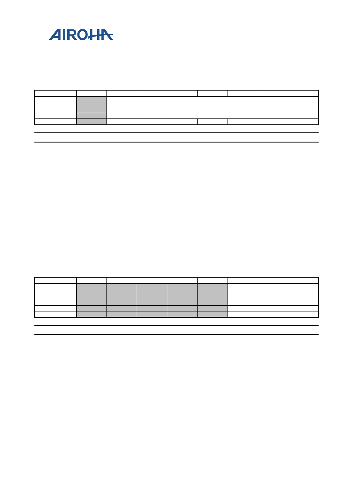
MT2523 Series Reference Manual
© 2015 - 2018 Airoha Technology Corp.
Page 621 of 692
This document contains information that is proprietary to Airoha Technology Corp. (“Airoha”) and/or its licensor(s).
Any unauthorized use, reproduction or disclosure of this document in whole or in part is strictly prohibited.
8D CHR_CON6
Charge
r
Control
Registe
r 6
03
Bit
7
6
5
4
3
2
1
0
Name
RGS_VB
AT_OV_
DET
RG_VBA
T_OV_D
EG
RG_VBAT_OV_VTH
RG_VBA
T_OV_E
N
Type
RO
RW
RW
RW
Reset
0
0
0
0
0
1
1
Bit(s) Name Description
6 RGS_VBAT_OV_DE
T
VBAT_OV voltage detection.
0 VBAT voltage < VBAT_OV_VTH
1 VBAT voltage > VBAT_OV_VTH
5 RG_VBAT_OV_DEG
VBAT OV voltage detection deglitch enable.
0 no debounce
1 debounce one cycle (1us)
4:1 RG_VBAT_OV_VTH
Battery over-voltag detection threshold
0000: 3.900V, 0001: 4.200V (default), 0010: 4.300V, 0011: 4.400V
0100: 4.450V, 0101: 4.500V, 0110: 4.600V, 0111: 4.700V
1000: 3.800V
0 RG_VBAT_OV_EN Battery over-voltag for driving protection (0: disable, 1: enable)
8E CHR_CON7
Charge
r
Control
Registe
r 7
01
Bit
7
6
5
4
3
2
1
0
Name
BATON_
TDET_E
N
RG_BAT
ON_HT_
EN_RSV
0
RG_BAT
ON_EN
Type
RW
RW
RW
Reset
0
0
1
Bit(s) Name Description
2 BATON_TDET_EN 0: N/A
1: Enable BATON Temperature detection
1 RG_BATON_HT_EN
_RSV0
Battery-On HW high temperature detection
0: Disabled
1: Enabled
0 RG_BATON_EN
BATON battery detection comparator enable (gated by
CHR_LDO_DET to default 1 in analog domain)
0: disable
1: enable (Default)
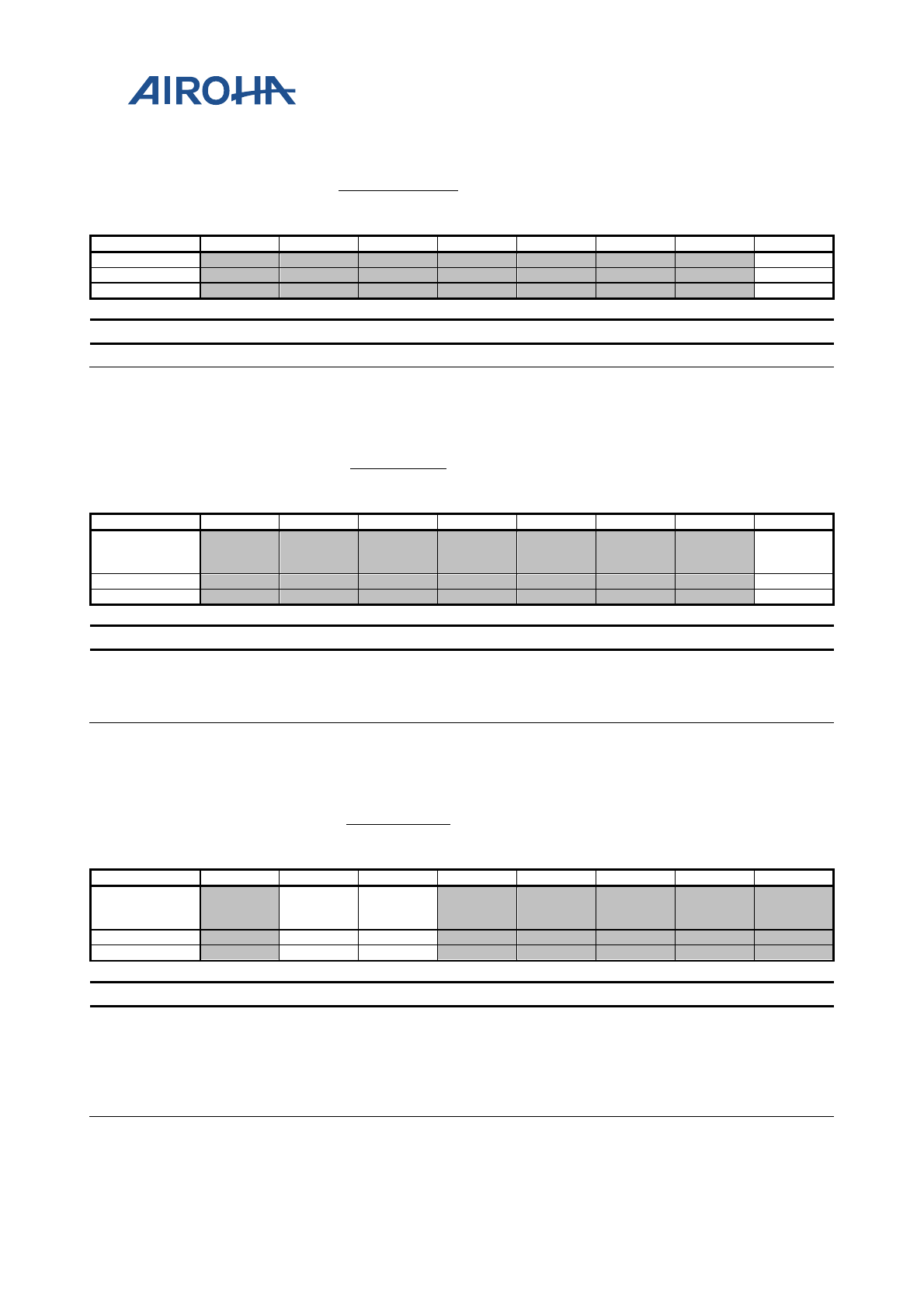
MT2523 Series Reference Manual
© 2015 - 2018 Airoha Technology Corp.
Page 622 of 692
This document contains information that is proprietary to Airoha Technology Corp. (“Airoha”) and/or its licensor(s).
Any unauthorized use, reproduction or disclosure of this document in whole or in part is strictly prohibited.
8F CHR_CON7_H
Charge
r
Control
Registe
r 7_H
00
Bit
7
6
5
4
3
2
1
0
Name
na
Type
RW
Reset
0
Bit(s) Name Description
0 na
92 CHR_CON9
Charge
r
Control
Registe
r 9
00
Bit
7
6
5
4
3
2
1
0
Name
RG_FRC
_CSVTH
_USBDL
Type
RW
Reset
0
Bit(s) Name Description
0 RG_FRC_CSVTH_U
SBDL
Force CS DAC detection threshold to maximum in USB download
mode
0: CS_VTH=450mA in USBDL mode
1: CS_VTH=1600mA in USBDL mode
93 CHR_CON10
Charge
r
Control
Registe
r 10
20
Bit
7
6
5
4
3
2
1
0
Name
RGS_OT
G_BVALI
D_DET
RG_OTG
_BVALID
_EN
Type
RO
RW
Reset
0
1
Bit(s) Name Description
6 RGS_OTG_BVALID
_DET
Indicates if the session for B-peripheral is valid (0.8V<Vth<4V). Here
VBUS is connected to CHRIN.
0: Vbus < 0.8V
1: Vbus > 4V
5 RG_OTG_BVALID_
EN OTG BValid detection enable (1: enable, 0: disable)
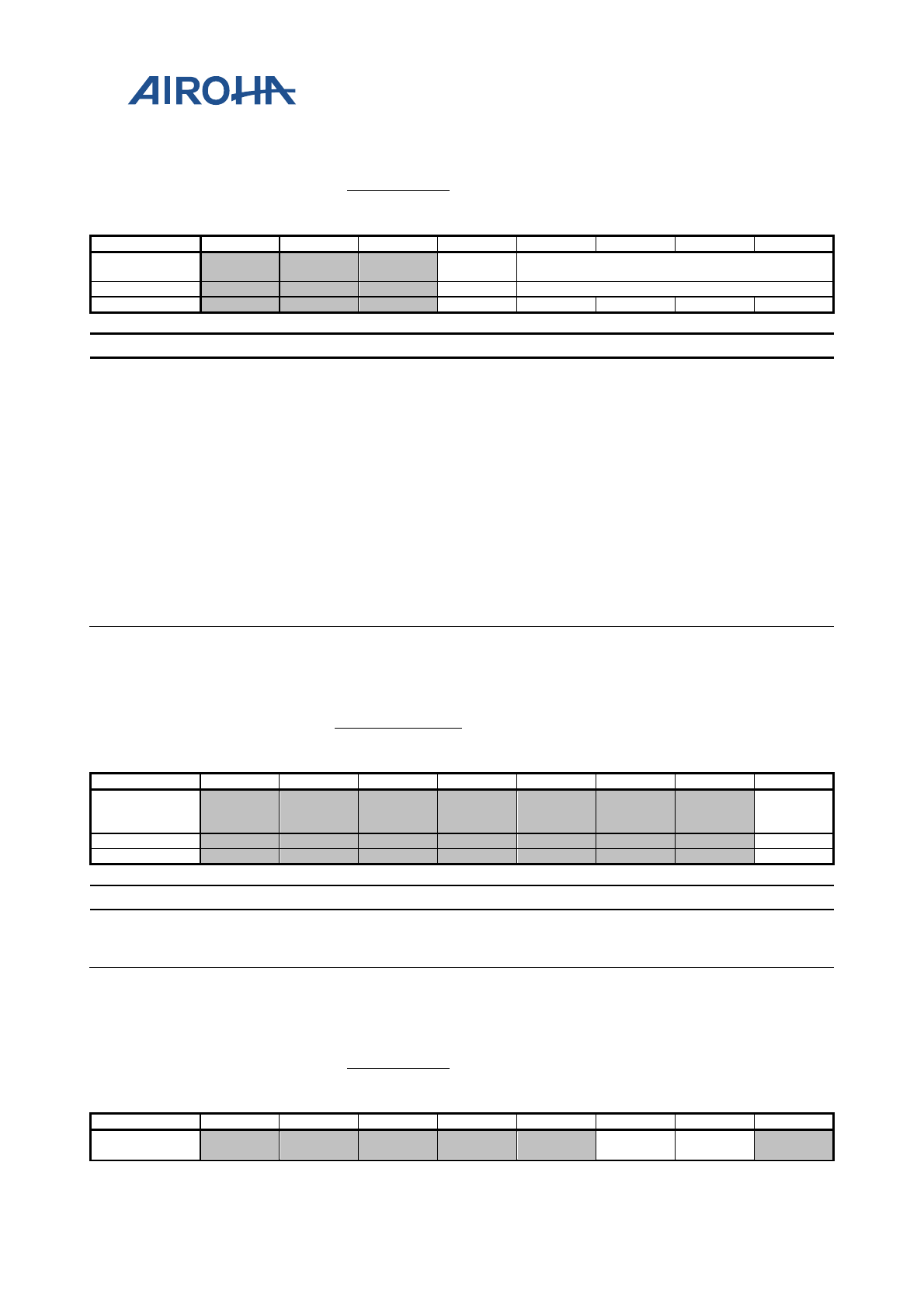
MT2523 Series Reference Manual
© 2015 - 2018 Airoha Technology Corp.
Page 623 of 692
This document contains information that is proprietary to Airoha Technology Corp. (“Airoha”) and/or its licensor(s).
Any unauthorized use, reproduction or disclosure of this document in whole or in part is strictly prohibited.
96 CHR_CON13
Charge
r
Control
Registe
r 13
10
Bit
7
6
5
4
3
2
1
0
Name
RG_CHR
WDT_EN
RG_CHRWDT_TD
Type
RW
RW
Reset
1
0
0
0
0
Bit(s) Name Description
4 RG_CHRWDT_EN
Enable setting for charger watch-dog timer
0 disable
1 enable if (CHR_EN(@CHR_CON0) == 1)
Note1: UVLO don't care this bit and will timeout after 3000s
Note2: PCHR_TESTMODE can force to control watch-dog enable by using this
bit
3:0 RG_CHRWDT_TD
Time constant setting for charger watch-dog timer
0: 4 sec
1: 8 sec
2: 16 sec
3: 32 sec
4: 128 sec
5: 256 sec
6: 512 sec
7: 1024 sec
8~15: 3000 sec
97 CHR_CON13_H
Charge
r
Control
Registe
r 13_H
00
Bit
7
6
5
4
3
2
1
0
Name
RG_CHR
WDT_W
R
Type
W1C
Reset
0
Bit(s) Name Description
0 RG_CHRWDT_WR
To reset charger watch-dog timer and update CHRWDT_TD
0: reset inactive
1: reset active and CHRWDT_TD updated to PCHR_DIG
99 CHR_CON15
Charge
r
Control
Registe
r 15
00
Bit
7
6
5
4
3
2
1
0
Name
RGS_CH
RWDT_O
RG_CHR
WDT_FL
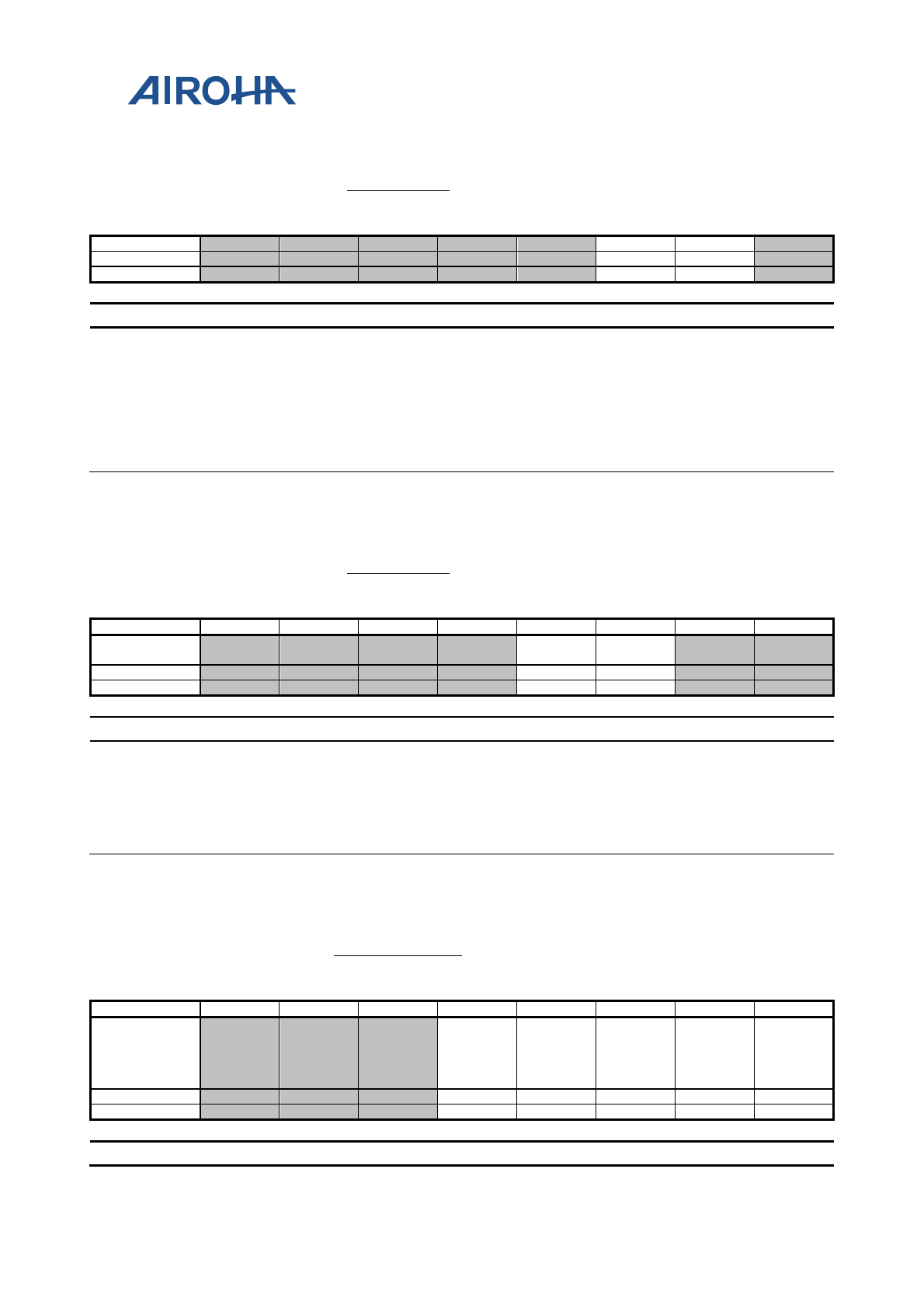
MT2523 Series Reference Manual
© 2015 - 2018 Airoha Technology Corp.
Page 624 of 692
This document contains information that is proprietary to Airoha Technology Corp. (“Airoha”) and/or its licensor(s).
Any unauthorized use, reproduction or disclosure of this document in whole or in part is strictly prohibited.
99 CHR_CON15
Charge
r
Control
Registe
r 15
00
UT
AG_WR
Type
RO
W1C
Reset
0
0
Bit(s) Name Description
2 RGS_CHRWDT_OU
T
Time-out flag for charger watch-dog timer
Read:
0: No time-out status
1: Time-out status asserted
1 RG_CHRWDT_FLA
G_WR
Clear time-out flag for charger watch-dog timer
Read:
0: N/A (while RGS_CHRWDT_OUT=0)
1: Clear time-out flag while RGS_CHRWDT_OUT=1
9A CHR_CON16
Charge
r
Control
Registe
r 16
00
Bit
7
6
5
4
3
2
1
0
Name
RG_USB
DL_SET
RG_USB
DL_RST
Type
RW
RW
Reset
0
0
Bit(s) Name Description
3 RG_USBDL_SET
USBDL_MODE software set control
0: No effect
1: Force enter USBDL MODE
2 RG_USBDL_RST
USBDL_MODE software reset control
0: No effect
1: Force leave USBDL MODE (priority is less than USBDL_DET)
9B CHR_CON16_H
Charge
r
Control
Registe
r 16_H
00
Bit
7
6
5
4
3
2
1
0
Name
RG_ADC
IN_CHR
_EN
RG_ADC
IN_VSEN
_EN
RG_ADC
IN_VBAT
_EN
RG_ADC
IN_VSEN
_EXT_B
ATON_E
N
RG_ADC
IN_VSEN
_MUX_E
N
Type
RW
RW
RW
RW
RW
Reset
0
0
0
0
0
Bit(s) Name Description
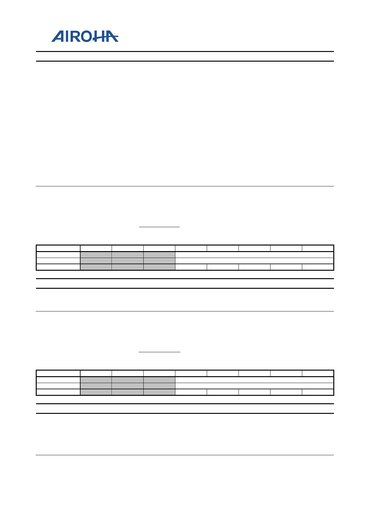
MT2523 Series Reference Manual
© 2015 - 2018 Airoha Technology Corp.
Page 625 of 692
This document contains information that is proprietary to Airoha Technology Corp. (“Airoha”) and/or its licensor(s).
Any unauthorized use, reproduction or disclosure of this document in whole or in part is strictly prohibited.
Bit(s) Name Description
4 RG_ADCIN_CHR_E
N
AUXADC input source enable for CHR
0: Disabled
1: Enabled
3 RG_ADCIN_VSEN_
EN
AUXADC input source enable for VSEN
0: Disabled
1: Enabled
2 RG_ADCIN_VBAT_
EN
AUXADC input source enable for VBAT
0: Disabled
1: Enabled
1 RG_ADCIN_VSEN_
EXT_BATON_EN
AUXADC input source enable for external source to be switched to
AUXADC's Ch3
0: Disabled
1: Enabled
0 RG_ADCIN_VSEN_
MUX_EN
AUXADC input source enable for VSEN to be switched to VBAT's
divider
0: Disabled
1: Enabled
9C CHR_CON17
Charge
r
Control
Registe
r 17
02
Bit
7
6
5
4
3
2
1
0
Name
RG_UVLO_VTHL
Type
RW
Reset
0
0
0
1
0
Bit(s) Name Description
4:0 RG_UVLO_VTHL
UVLO low threshold selection
00000: 2.5V, 00001: 2.55V, 00010: 2.6V (default), 00011: 2.65V
00100: 2.7V, 00101: 2.75V, 00110: 2.8V, 00111: 2.85V, 01000: 2.9V
9D CHR_CON18
Charge
r
Control
Registe
r 18
03
Bit
7
6
5
4
3
2
1
0
Name
RG_LBAT_INT_VTH
Type
RW
Reset
0
0
0
1
1
Bit(s) Name Description
4:0 RG_LBAT_INT_VT
H
LBAT_INT threshold voltage
00000: 2.5V, 00001: 2.55V, 00010: 2.6V (default), 00011: 2.65V
00100: 2.7V, 00101: 2.75V, 00110: 2.8V, 00111: 2.85V,
01000: 2.9V, 01001: 2.95V, 01010: 3.0V, 01011: 3.05V,
01100: 3.1V, 01101: 3.15V, 01110: 3.2V, 01111: 3.25V,
11000: 3.3V, 11001: 3.35V, 11010: 3.4V
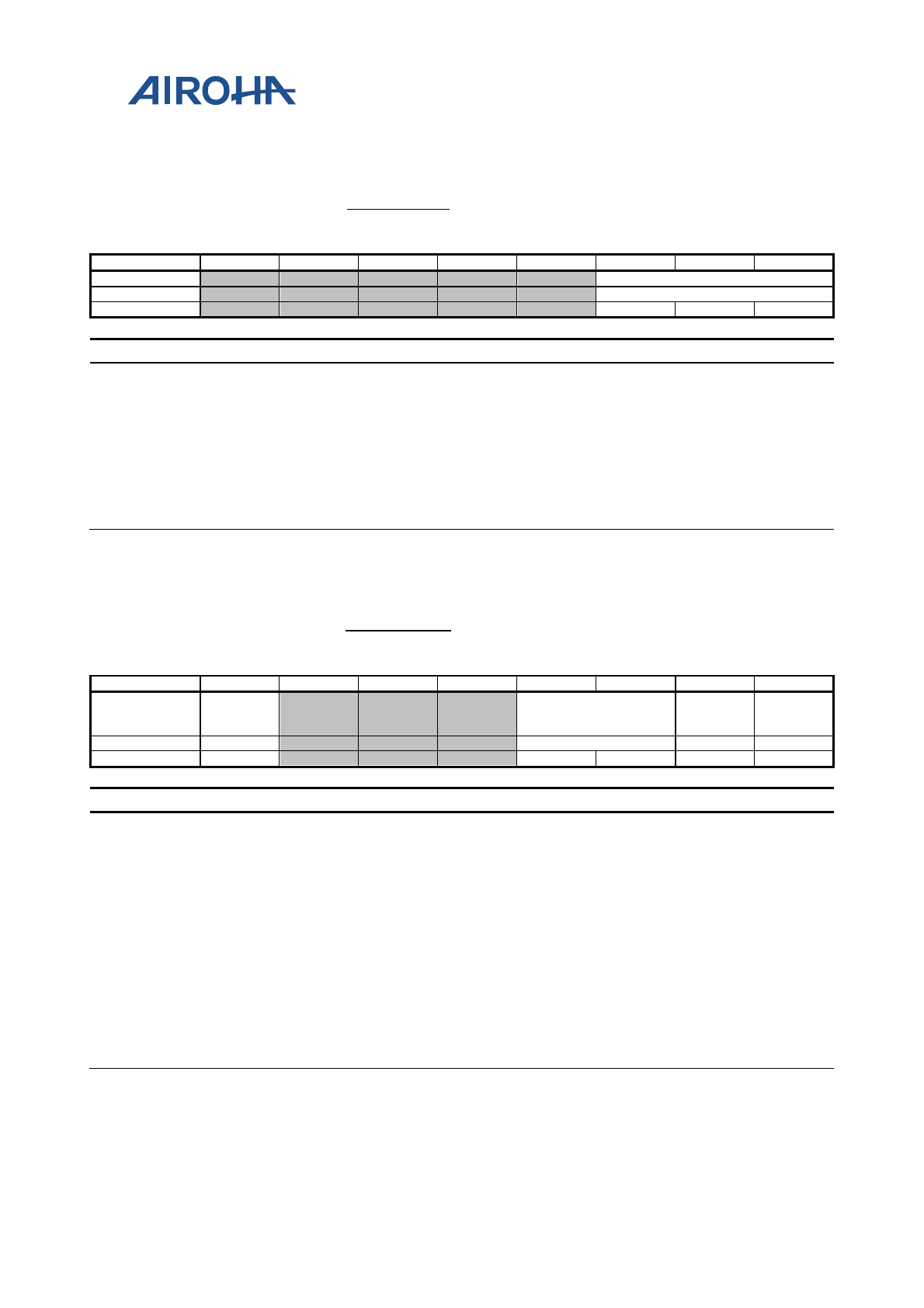
MT2523 Series Reference Manual
© 2015 - 2018 Airoha Technology Corp.
Page 626 of 692
This document contains information that is proprietary to Airoha Technology Corp. (“Airoha”) and/or its licensor(s).
Any unauthorized use, reproduction or disclosure of this document in whole or in part is strictly prohibited.
9E CHR_CON19
Charge
r
Control
Registe
r 19
00
Bit
7
6
5
4
3
2
1
0
Name
RG_BGR_RSEL
Type
RW
Reset
0
0
0
Bit(s) Name Description
2:0 RG_BGR_RSEL
BGR resistor (R0 = R1) selection, R2=85K, and
VBG=(R0/R2)*dVBE+VBE
0: c0, 780K (default)
1: c1, 820K
2: c2, 860K
3: c3, 900K
4: cm4, 620K
5: cm3, 660K
6: cm2, 700K
7: cm1, 740K
9F CHR_CON20
Charge
r
Control
Registe
r 20
00
Bit
7
6
5
4
3
2
1
0
Name
RGS_BC1
1_CMP_
OUT
RG_BC11_VSRC_EN RG_BC11
_RST
RG_BC11
_BB_CT
RL
Type
RO
RW
RW
RW
Reset
0
0
0
0
0
Bit(s) Name Description
7 RGS_BC11_CMP_O
UT
Comparison result of BC11 charger detection
0: DP or DM < BC11_VREF_VTH
1: DP or DM > BC11_VREF_VTH
3:2 RG_BC11_VSRC_EN
BC11 voltage source. Set VDP_SRC = 0.6V
0: disable the voltage
1: enable the voltage source to DM
2: enable the voltage source to DP
3: forbidden
1 RG_BC11_RST
Reset BC11 detection mechanism in PCHR_DIG
0: No effect
1: BC11 detection mechanism is disabled in PCHR_DIG
0 RG_BC11_BB_CTRL
Force BC11 charger detection controlled by baseband
0: BC11 detection by PCHR_DIG (hardware mode)
1: BC11 detection by baseband (software mode)
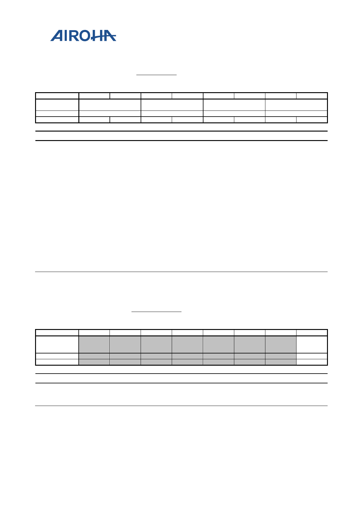
MT2523 Series Reference Manual
© 2015 - 2018 Airoha Technology Corp.
Page 627 of 692
This document contains information that is proprietary to Airoha Technology Corp. (“Airoha”) and/or its licensor(s).
Any unauthorized use, reproduction or disclosure of this document in whole or in part is strictly prohibited.
A0 CHR_CON21
Charge
r
Control
Registe
r 21
00
Bit
7
6
5
4
3
2
1
0
Name RG_BC11_IPU_EN RG_BC11_IPD_EN RG_BC11_CMP_EN
RG_BC11_VREF_VT
H
Type
RW
RW
RW
RW
Reset
0
0
0
0
0
0
0
0
Bit(s) Name Description
7:6 RG_BC11_IPU_EN
BC11 7~15uA pull up current enable
0: disable the pull-up current
1: enable the pull-up current to DM
2: enable the pull-up current to DP
3: forbidden
5:4 RG_BC11_IPD_EN
BC11 50~150uA pull down current
0: disable the pull-down current
1: enable the pull-down current to DM
2: enable the pull-down current to DP
3: forbidden
3:2 RG_BC11_CMP_EN
BC11 comparator connection
0: disable the comparator
1: enable the comparator to DM
2: enable the comparator to DP
3: forbidden
1:0 RG_BC11_VREF_VT
H
VREF threshold voltage for comparator
0: VREF_VTH=0.325V
1: VREF_VTH=1.2V
2 & 3: VREF_VTH=2.6V (for Apple adaptor)
A1 CHR_CON21_H
Charge
r
Control
Registe
r 21_H
00
Bit
7
6
5
4
3
2
1
0
Name
RG_BC11
_BIAS_E
N
Type
RW
Reset
0
Bit(s) Name Description
0 RG_BC11_BIAS_EN
Enable BC11 detection bias circuit
0: Disabled
1: Enabled
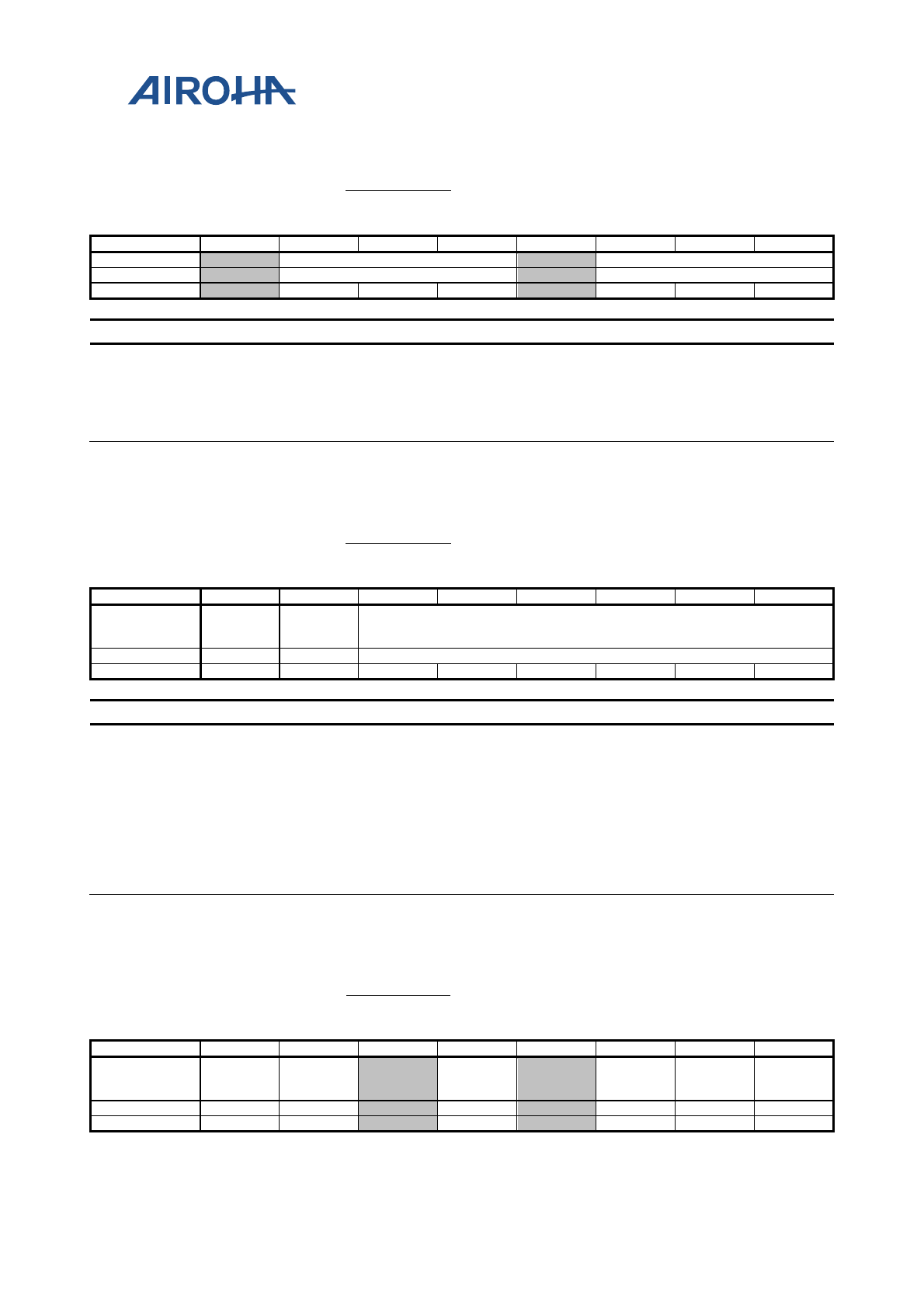
MT2523 Series Reference Manual
© 2015 - 2018 Airoha Technology Corp.
Page 628 of 692
This document contains information that is proprietary to Airoha Technology Corp. (“Airoha”) and/or its licensor(s).
Any unauthorized use, reproduction or disclosure of this document in whole or in part is strictly prohibited.
A3 CHR_CON23
Charge
r
Control
Registe
r 23
04
Bit
7
6
5
4
3
2
1
0
Name
RG_CSDAC_STP
RG_CSDAC_DLY
Type
RW
RW
Reset
0
0
0
1
0
0
Bit(s) Name Description
6:4 RG_CSDAC_STP Current DAC output step timer.
1/1/2/3/4/5/6/7 code/ per-step
2:0 RG_CSDAC_DLY
Current DAC output detection delay control.
16/32/64/128/256/512/1024/2048us
(512us default, reuse in HW CV Mode)
A4 CHR_CON24
Charge
r
Control
Registe
r 24
44
Bit
7
6
5
4
3
2
1
0
Name
RG_CHR
IND_DI
MMING
RG_CHR
IND_ON RG_LOW_ICH_DB
Type
RW
RW
RW
Reset
0
1
0
0
0
1
0
0
Bit(s) Name Description
7 RG_CHRIND_DIM
MING
Enable pre-charge indicator dimming
0: Disabled
1: Enabled
6 RG_CHRIND_ON
Pre-charge indicator on (gated by CHR_LDO_DET to default 0 in
analog domain)
0: disable indicator
1: enable indicator
5:0 RG_LOW_ICH_DB Plug out HW detection debounce time (base=16ms)
Debounce time : Code * 16ms
A5 CHR_CON25
Charge
r
Control
Registe
r 25
10
Bit
7
6
5
4
3
2
1
0
Name
RG_ULC
_DET_E
N
RG_HW
CV_EN
RG_TRA
CKING_
EN
RG_CSD
AC_MOD
E
RG_VCD
T_MODE
RG_CV_
MODE
Type
RW
RW
RW
RW
RW
RW
Reset
0
0
1
0
0
0
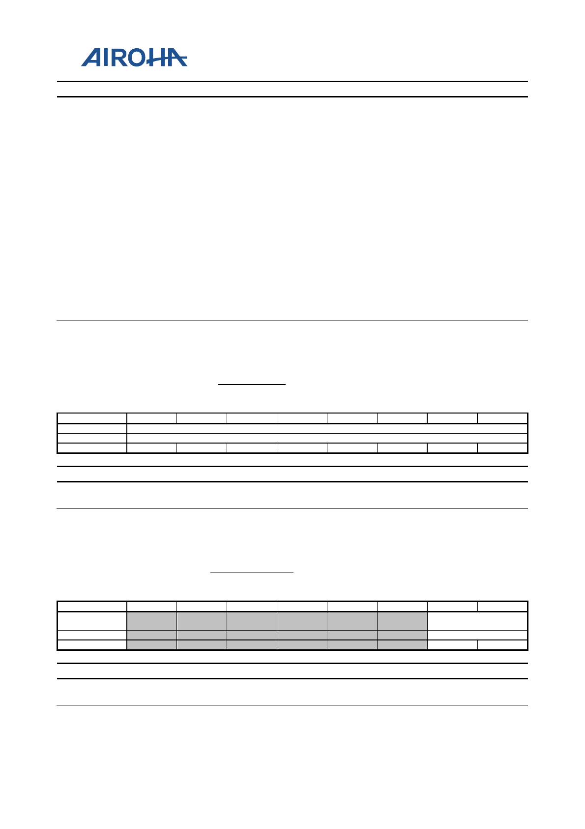
MT2523 Series Reference Manual
© 2015 - 2018 Airoha Technology Corp.
Page 629 of 692
This document contains information that is proprietary to Airoha Technology Corp. (“Airoha”) and/or its licensor(s).
Any unauthorized use, reproduction or disclosure of this document in whole or in part is strictly prohibited.
Bit(s) Name Description
7 RG_ULC_DET_EN
Enable charger plug out auto detection. This fuction has to be applied
with RG_HWCV_EN=1.
0: Disabled
1: Enabled
6 RG_HWCV_EN
Enable hardware CV current tracking
0: Disabled
1: Enabled
4 RG_TRACKING_EN
0 : Current calibration use CS_VTH[n] and CS_VTH[n-1] as high/low
threshold.
1 : Current calibration use CS_VTH[n] and LTH as high/low threshold.
2 RG_CSDAC_MODE
0: If not entering CC, charging is AUTO mode
1: If leaving UVLO, charging is controlled by RG_CSDAC_EN (same as CC
mode)
1 RG_VCDT_MODE
Charger detection mode selection
0: Charger detection can only be active in off state
1: Charger detection is active in both on and off state
0 RG_CV_MODE
Battery CV detection mode selection.
0: CV detection can only be active in off state
1: CV detection is active in both on and off state
AA CHR_CON30
Charge
r
Control
Registe
r 30
8E
Bit
7
6
5
4
3
2
1
0
Name
RG_DAC_USBDL_MAX
Type
RW
Reset
1
0
0
0
1
1
1
0
Bit(s) Name Description
7:0 RG_DAC_USBDL_M
AX
USBDL maximum current setting
Default: 0x28E ==> 1010001110
AB CHR_CON30_H
Charge
r
Control
Registe
r 30_H
02
Bit
7
6
5
4
3
2
1
0
Name
RG_DAC_USBDL_M
AX1
Type
RW
Reset
1
0
Bit(s) Name Description
1:0 RG_DAC_USBDL_M
AX1
USBDL maximum current setting
Default: 0x28E ==> 1010001110
MT2523 Series Reference Manual
© 2015 - 2018 Airoha Technology Corp.
Page 630 of 692
This document contains information that is proprietary to Airoha Technology Corp. (“Airoha”) and/or its licensor(s).
Any unauthorized use, reproduction or disclosure of this document in whole or in part is strictly prohibited.
AD CHR_CON42
Charge
r
Control
Registe
r 42
00
Bit
7
6
5
4
3
2
1
0
Name
RG_ENV
TEM_EN
RG_ENV
TEM_D
Type
W1C
RW
Reset
0
0
Bit(s) Name Description
1 RG_ENVTEM_EN
To block CHR_DET signal to start_up
0: N/A
1: write enable
0 RG_ENVTEM_D
To block CHR_DET signal to start_up
1:block
0: non-block
AE BATON_CON0
BATON
Control
Registe
r 0
00
Bit
7
6
5
4
3
2
1
0
Name
RG_BAT
ON_HT_
EN
Type
RW
Reset
0
Bit(s) Name Description
0 RG_BATON_HT_EN
Battery-On HW high temperature detection
1'b0: disable
1'b1: enable
B0 CHR_CON44
Charge
r
Control
Registe
r 44
01
Bit
7
6
5
4
3
2
1
0
Name
RGS_BA
TON_UN
DET
RG_QI_B
ATON_L
T_EN
Type
RO
RW
Reset
0
1
Bit(s) Name Description
1 RGS_BATON_UNDE
T Battery-On undetected (1: not detected, 0: detected)
0 RG_QI_BATON_LT
_EN
MT2523 Series Reference Manual
© 2015 - 2018 Airoha Technology Corp.
Page 631 of 692
This document contains information that is proprietary to Airoha Technology Corp. (“Airoha”) and/or its licensor(s).
Any unauthorized use, reproduction or disclosure of this document in whole or in part is strictly prohibited.
B1 CHR_CON45
Charge
r
Control
Registe
r 45
0F
Bit
7
6
5
4
3
2
1
0
Name
RG_JW_CS_VTH
Type
RW
Reset
1
1
1
1
Bit(s) Name Description
3:0 RG_JW_CS_VTH
Current sense voltage detection threshold @ Rcs=65mohm
1111: 70mA
1110: 200mA
1101: 300mA
1100: 450mA (usbdl)
1011: 550mA
1010: 650mA
1001: 700mA
1000: 800mA
0111: 900mA
0110: 1000mA
0101: 1100mA
0100: 1200mA
0011: 1350mA
0010: 1500mA
0001: 1600mA
0000: 2000mA
B2 CHR_CON45_H
Charge
r
Control
Registe
r 45_H
0F
Bit
7
6
5
4
3
2
1
0
Name
RG_JW_CV_VTH
Type
RW
Reset
0
0
1
1
1
1
Bit(s) Name Description
5:0 RG_JW_CV_VTH
Battery CV dection threshold trimming option, default 4.2V
this register is used for FT CV threshold trimming and not for customer's fine
tuning (pchr_dig should invert MSB bit. otherwise, BC1.1 2.2V threshold would
be wrong)
000000~000011:3.5V, 3.6V, 3.7V, 3.8V
000100~000111:3.85V, 3.9V, 4V, 4.05V
001000~001011:4.1V, 4.125V, 4.1375v, 4.15V
001100~001111:4.1625V, 4.175V, 4.1875V, 4.2V (default)
010000~010011:4.2125V, 4.225V, 4.2375V, 4.25V
010100~010111:4.2625V, 4.275V, 4.2875V, 4.3V
011000~011011:4.3125V, 4.325V, 4.3375V, 4.35V
011100~011111:4.3625V, 4.375V, 4.3875V, 4.4V
100000~100011:4.4125V, 4.425V, 4.4375V, 4.45V
100100~100111:4.4625V, 4.475V, 4.4875V, 4.5V
101000:4.6V
MT2523 Series Reference Manual
© 2015 - 2018 Airoha Technology Corp.
Page 632 of 692
This document contains information that is proprietary to Airoha Technology Corp. (“Airoha”) and/or its licensor(s).
Any unauthorized use, reproduction or disclosure of this document in whole or in part is strictly prohibited.
Bit(s) Name Description
111111:2.2V (BC1.1)
B3 CHR_CON46
Charge
r
Control
Registe
r 46
0F
Bit
7
6
5
4
3
2
1
0
Name
RG_JC_CS_VTH
Type
RW
Reset
1
1
1
1
Bit(s) Name Description
3:0 RG_JC_CS_VTH
Current sense voltage detection threshold @ Rcs=65mohm
1111: 70mA
1110: 200mA
1101: 300mA
1100: 450mA (usbdl)
1011: 550mA
1010: 650mA
1001: 700mA
1000: 800mA
0111: 900mA
0110: 1000mA
0101: 1100mA
0100: 1200mA
0011: 1350mA
0010: 1500mA
0001: 1600mA
0000: 2000mA
B4 CHR_CON46_H
Charge
r
Control
Registe
r 46_H
0F
Bit
7
6
5
4
3
2
1
0
Name
RG_JC_CV_VTH
Type
RW
Reset
0
0
1
1
1
1
Bit(s) Name Description
5:0 RG_JC_CV_VTH
Battery CV dection threshold trimming option, default 4.2V
this register is used for FT CV threshold trimming and not for customer's fine
tuning (pchr_dig should invert MSB bit. otherwise, BC1.1 2.2V threshold would
be wrong)
000000~000011:3.5V, 3.6V, 3.7V, 3.8V
000100~000111:3.85V, 3.9V, 4V, 4.05V
001000~001011:4.1V, 4.125V, 4.1375v, 4.15V
001100~001111:4.1625V, 4.175V, 4.1875V, 4.2V (default)
010000~010011:4.2125V, 4.225V, 4.2375V, 4.25V
010100~010111:4.2625V, 4.275V, 4.2875V, 4.3V
011000~011011:4.3125V, 4.325V, 4.3375V, 4.35V
011100~011111:4.3625V, 4.375V, 4.3875V, 4.4V
MT2523 Series Reference Manual
© 2015 - 2018 Airoha Technology Corp.
Page 633 of 692
This document contains information that is proprietary to Airoha Technology Corp. (“Airoha”) and/or its licensor(s).
Any unauthorized use, reproduction or disclosure of this document in whole or in part is strictly prohibited.
Bit(s) Name Description
100000~100011:4.4125V, 4.425V, 4.4375V, 4.45V
100100~100111:4.4625V, 4.475V, 4.4875V, 4.5V
101000:4.6V
111111:2.2V (BC1.1)
B5 CHR_CON47
Charge
r
Control
Registe
r 47
00
Bit
7
6
5
4
3
2
1
0
Name
RG_JEIT
A_EN
Type
RW
Reset
0
Bit(s) Name Description
1 RG_JEITA_EN 0:disable JEITA 1: enable JEITA
DA VA18CTL0
VA18
Control
registe
r 0
01
Bit
7
6
5
4
3
2
1
0
Name
RG_OVR
_VA18_P
MOD
RG_VA18
_EN
Type
RW
RW
Reset
0
1
Bit(s) Name Description
2 RG_OVR_VA18_PM
OD
0: Normal mode
1: Low power mode
0 RG_VA18_EN
DB VA18CTL1
VA18
Control
registe
r 1
05
Bit
7
6
5
4
3
2
1
0
Name
RG_OFF
_VA18_P
MOD
Type
RW
Reset
1
Bit(s) Name Description
2 RG_OFF_VA18_PM
OD
VA18 operational mode for system OFF mode
0: Normal mode
1: Low power mode
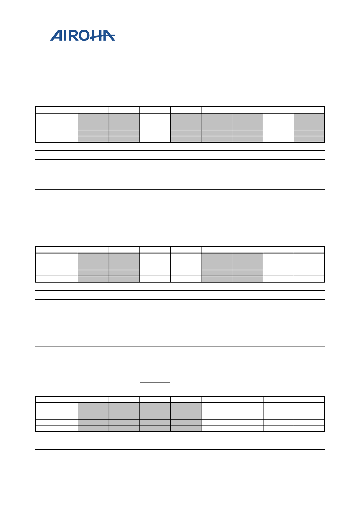
MT2523 Series Reference Manual
© 2015 - 2018 Airoha Technology Corp.
Page 634 of 692
This document contains information that is proprietary to Airoha Technology Corp. (“Airoha”) and/or its licensor(s).
Any unauthorized use, reproduction or disclosure of this document in whole or in part is strictly prohibited.
E2 VA18PSI0
VA18
LDO
PSI
registe
r0
00
Bit
7
6
5
4
3
2
1
0
Name
RG_LP_
VA18_P
MOD
RG_HP_
VA18_P
MOD
Type
RW
RW
Reset
0
0
Bit(s) Name Description
5 RG_LP_VA18_PMO
D
1 RG_HP_VA18_PMO
D
E3 VA18PSI1
VA18
LDO
PSI
registe
r1
00
Bit
7
6
5
4
3
2
1
0
Name
RG_S1_V
A18_PM
OD
RG_S1_V
A18_ON
RG_S0_
VA18_P
MOD
RG_S0_
VA18_O
N
Type
RW
RW
RW
RW
Reset
0
0
0
0
Bit(s) Name Description
5 RG_S1_VA18_PMO
D
4 RG_S1_VA18_ON
1 RG_S0_VA18_PMO
D
0 RG_S0_VA18_ON
E4 VBTCTL0
VBT
Control
registe
r 0
00
Bit
7
6
5
4
3
2
1
0
Name RG_OVR_VBT_PMO
D
RG_VBT
_OCFB_
EN
RG_VBT
_EN
Type
RW
RW
RW
Reset
0
0
0
0
Bit(s) Name Description
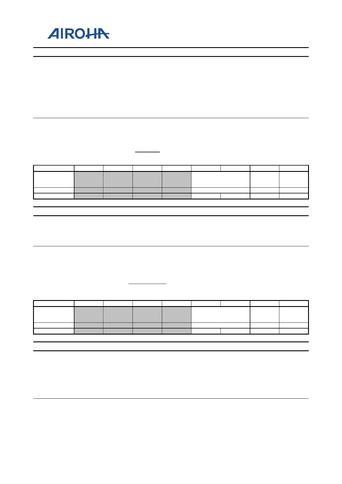
MT2523 Series Reference Manual
© 2015 - 2018 Airoha Technology Corp.
Page 635 of 692
This document contains information that is proprietary to Airoha Technology Corp. (“Airoha”) and/or its licensor(s).
Any unauthorized use, reproduction or disclosure of this document in whole or in part is strictly prohibited.
Bit(s) Name Description
3:2 RG_OVR_VBT_PM
OD
VBT LDO operation mode
00: Normal mode
01: Lite mode
10: LP mode
11: ULP mode
1 RG_VBT_OCFB_EN
0 RG_VBT_EN
VBT LDO enable
0: disable
1: enable
E5 VACTL0
VA
Control
registe
r 0
00
Bit
7
6
5
4
3
2
1
0
Name RG_OVR_VA_PMOD
RG_VA_
OCFB_E
N
RG_VA_
EN
Type
RW
RW
RW
Reset
0
0
0
0
Bit(s) Name Description
3:2 RG_OVR_VA_PMO
D
1 RG_VA_OCFB_EN
0 RG_VA_EN
E6 VCLDOCTL0
VCORE
LDO
Control
registe
r 0
10
Bit
7
6
5
4
3
2
1
0
Name RG_OVR_VC_LDO_P
MOD
RG_VC_
LDO_OC
FB_EN
RG_VC_
LDO_EN
Type
RW
RW
RW
Reset
0
0
0
0
Bit(s) Name Description
3:2 RG_OVR_VC_LDO_
PMOD
00: Normal mode
01: Lite mode
10: LP mode
11: ULP mode
1 RG_VC_LDO_OCFB
_EN
0 RG_VC_LDO_EN
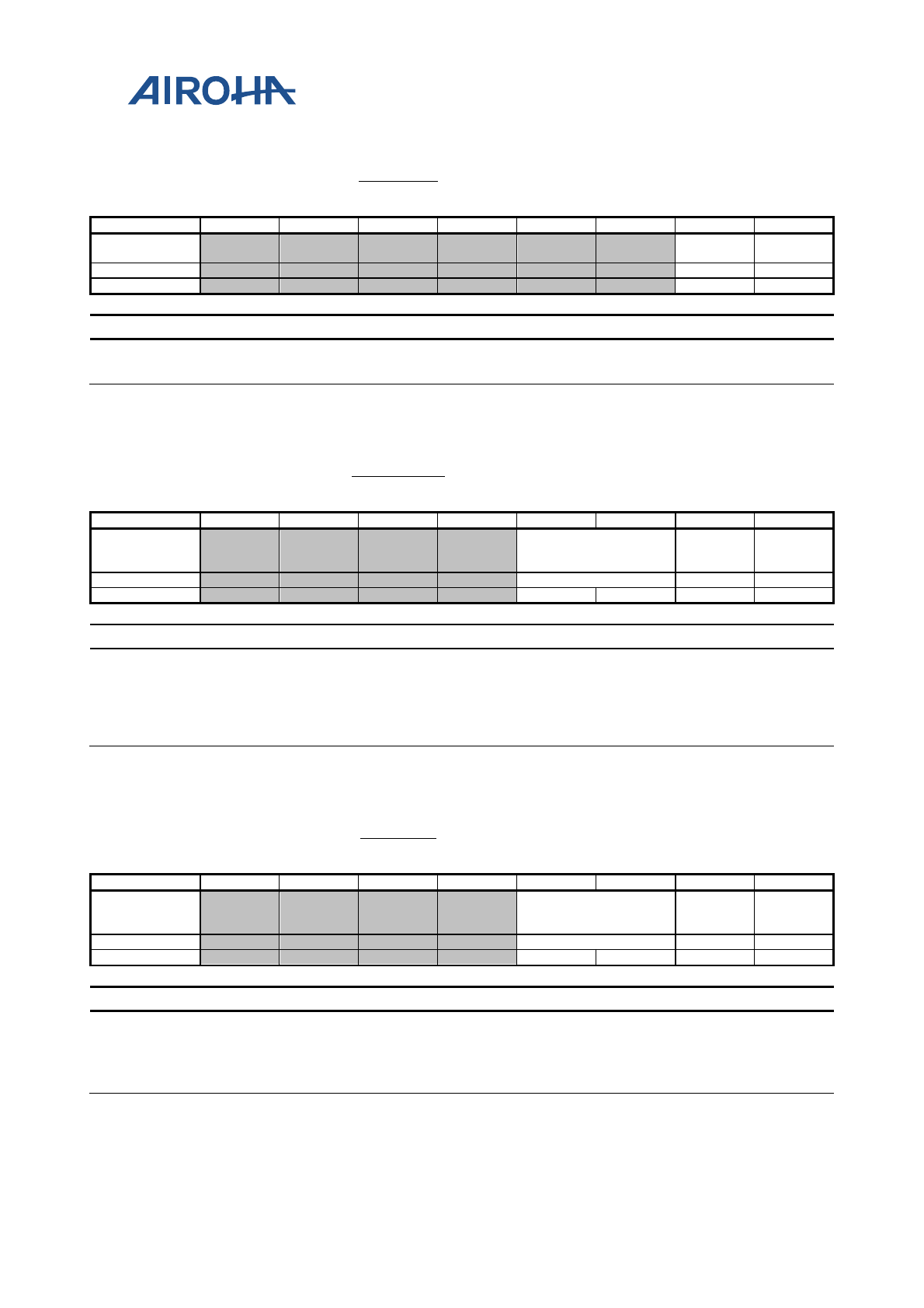
MT2523 Series Reference Manual
© 2015 - 2018 Airoha Technology Corp.
Page 636 of 692
This document contains information that is proprietary to Airoha Technology Corp. (“Airoha”) and/or its licensor(s).
Any unauthorized use, reproduction or disclosure of this document in whole or in part is strictly prohibited.
E8 PSWCTL1
PSW
Control
registe
r 1
00
Bit
7
6
5
4
3
2
1
0
Name
RG_SWD
P_ENA
RG_SWX
M_ENA
Type
RW
RW
Reset
0
0
Bit(s) Name Description
1 RG_SWDP_ENA ECO: optional SWDP enable, enabled by RG_PSEQ_RSV1_LSB[0]
0 RG_SWXM_ENA ECO: optional SWXM enable, enabled by RG_PSEQ_RSV1_LSB[0]
E9 VIO18CTL0
VIO18
Control
registe
r 0
10
Bit
7
6
5
4
3
2
1
0
Name RG_OVR_VIO18_PM
OD
RG_VIO1
8_OCFB
_EN
RG_VIO1
8_EN
Type
RW
RW
RW
Reset
0
0
0
0
Bit(s) Name Description
3:2 RG_OVR_VIO18_P
MOD
1 RG_VIO18_OCFB_E
N
0 RG_VIO18_EN
EA VSFCTL0
VSF
Control
registe
r 0
10
Bit
7
6
5
4
3
2
1
0
Name RG_OVR_VSF_PMO
D
RG_VSF
_OCFB_
EN
RG_VSF
_EN
Type
RW
RW
RW
Reset
0
0
0
0
Bit(s) Name Description
3:2 RG_OVR_VSF_PMO
D
1 RG_VSF_OCFB_EN
0 RG_VSF_EN
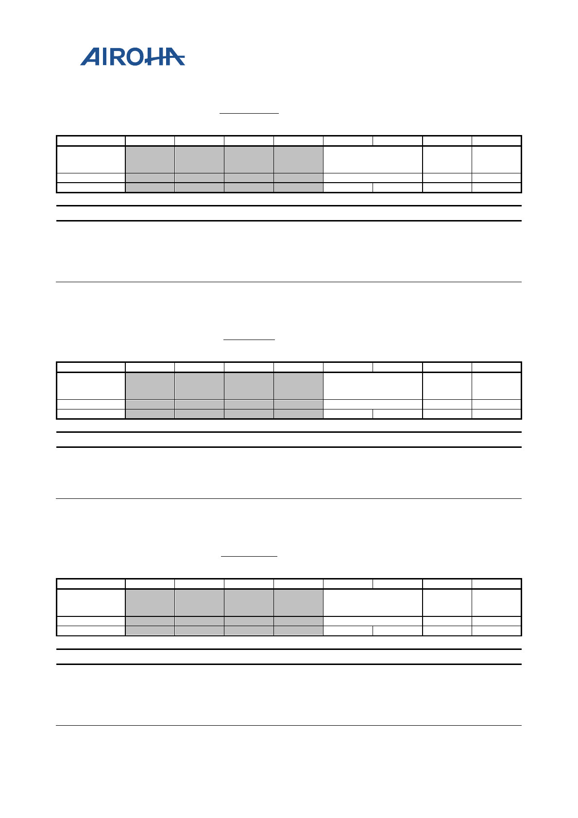
MT2523 Series Reference Manual
© 2015 - 2018 Airoha Technology Corp.
Page 637 of 692
This document contains information that is proprietary to Airoha Technology Corp. (“Airoha”) and/or its licensor(s).
Any unauthorized use, reproduction or disclosure of this document in whole or in part is strictly prohibited.
EB VIO28CTL0
VIO28
Control
registe
r 0
30
Bit
7
6
5
4
3
2
1
0
Name RG_OVR_VIO28_PM
OD
RG_VIO2
8_OCFB
_EN
RG_VIO2
8_EN
Type
RW
RW
RW
Reset
0
0
0
0
Bit(s) Name Description
3:2 RG_OVR_VIO28_P
MOD
1 RG_VIO28_OCFB_E
N
0 RG_VIO28_EN
EC VMCCTL0
VMC
Control
registe
r 0
00
Bit
7
6
5
4
3
2
1
0
Name RG_OVR_VMC_PMO
D
RG_VMC
_OCFB_
EN
RG_VMC
_EN
Type
RW
RW
RW
Reset
0
0
0
0
Bit(s) Name Description
3:2 RG_OVR_VMC_PM
OD
1 RG_VMC_OCFB_EN
0 RG_VMC_EN
ED VUSBCTL0
VUSB
Control
registe
r 0
00
Bit
7
6
5
4
3
2
1
0
Name RG_OVR_VUSB_PM
OD
RG_VUS
B_OCFB
_EN
RG_VUS
B_EN
Type
RW
RW
RW
Reset
0
0
0
0
Bit(s) Name Description
3:2 RG_OVR_VUSB_PM
OD
1 RG_VUSB_OCFB_E
N
0 RG_VUSB_EN
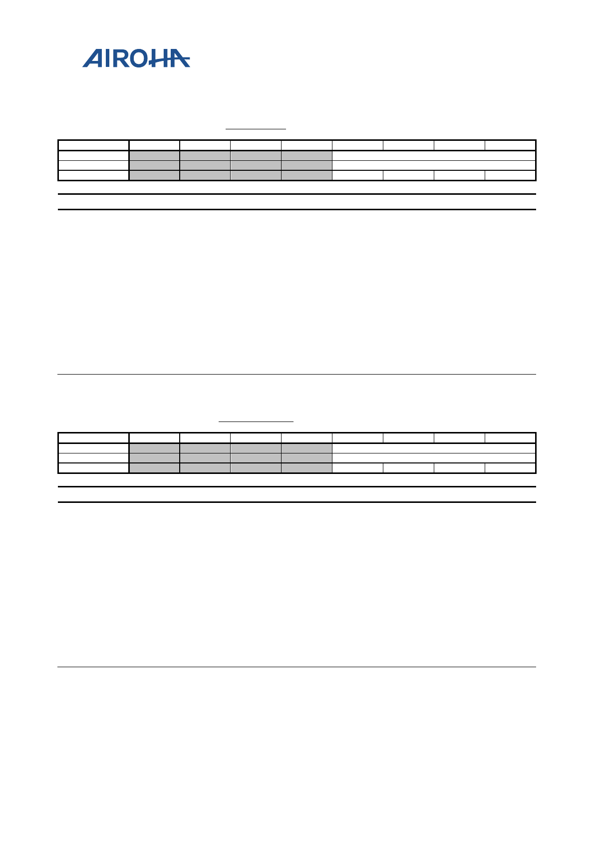
MT2523 Series Reference Manual
© 2015 - 2018 Airoha Technology Corp.
Page 638 of 692
This document contains information that is proprietary to Airoha Technology Corp. (“Airoha”) and/or its licensor(s).
Any unauthorized use, reproduction or disclosure of this document in whole or in part is strictly prohibited.
EF VUSBLDO0 VUSBL
DO0 00
Bit
7
6
5
4
3
2
1
0
Name
RG_VUSB_CAL
Type
RW
Reset
0
0
0
0
Bit(s) Name Description
3:0 RG_VUSB_CAL
4'b0000: 0 mV
4'b0001: -20 mV
4'b0010: -40 mV
4'b0011: -60 mV
4'b0100: -80 mV
4'b0101: -100 mV
4'b0110: -120 mV
4'b0111: -140 mV
4'b1000: +160 mV
4'b1001: +140 mV
4'b1010: +120 mV
4'b1011: +100 mV
4'b1100: +80 mV
4'b1101: +60 mV
4'b1110: +40 mV
4'b1111: +20 mV
F3 VUSBLDOBF0 VUSBL
DOBF0 00
Bit
7
6
5
4
3
2
1
0
Name
RG_VUSB_BUF_CAL
Type
RW
Reset
0
0
0
0
Bit(s) Name Description
3:0 RG_VUSB_BUF_CA
L
4'b0000: 0 mV
4'b0001: -20 mV
4'b0010: -40 mV
4'b0011: -60 mV
4'b0100: -80 mV
4'b0101: -100 mV
4'b0110: -120 mV
4'b0111: -140 mV
4'b1000: +160 mV
4'b1001: +140 mV
4'b1010: +120 mV
4'b1011: +100 mV
4'b1100: +80 mV
4'b1101: +60 mV
4'b1110: +40 mV
4'b1111: +20 mV
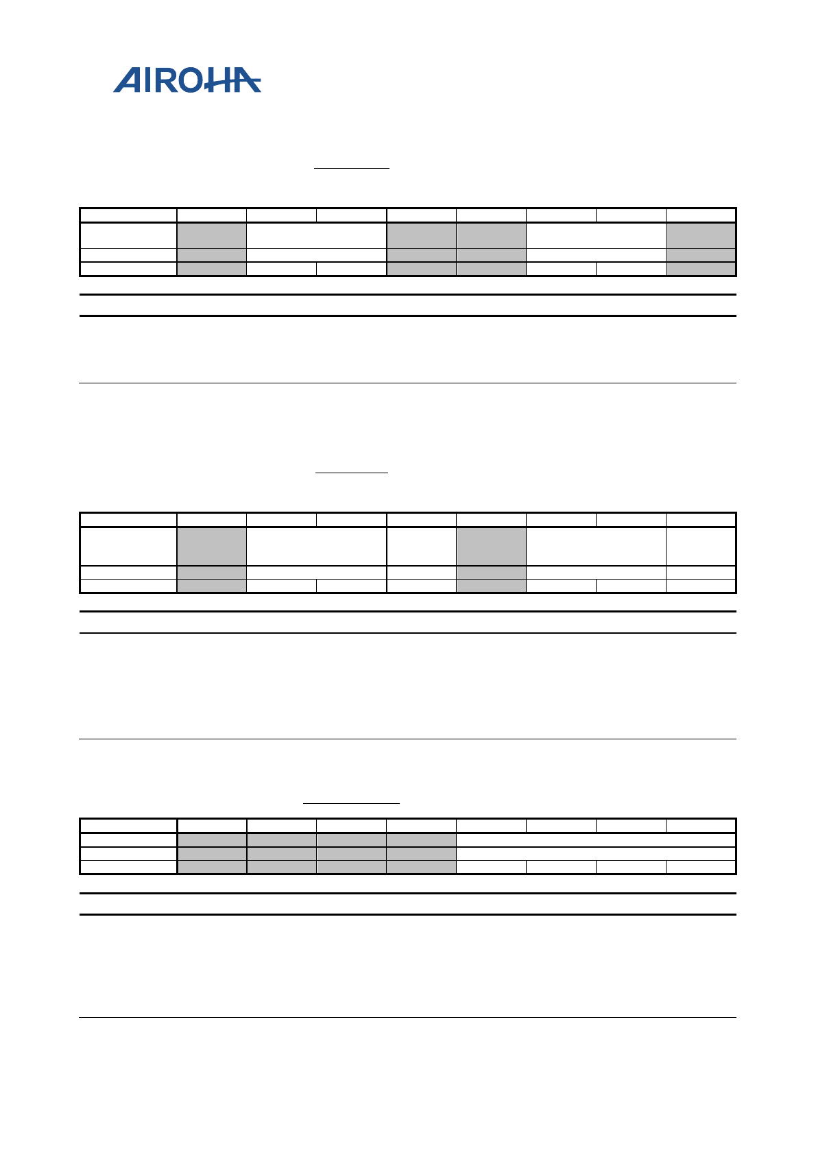
MT2523 Series Reference Manual
© 2015 - 2018 Airoha Technology Corp.
Page 639 of 692
This document contains information that is proprietary to Airoha Technology Corp. (“Airoha”) and/or its licensor(s).
Any unauthorized use, reproduction or disclosure of this document in whole or in part is strictly prohibited.
F5 VUSBPSI0
VUSB
LDO
PSI
registe
r0
00
Bit
7
6
5
4
3
2
1
0
Name
RG_LP_VUSB_PMO
D
RG_HP_VUSB_PMO
D
Type
RW
RW
Reset
0
0
0
0
Bit(s) Name Description
6:5 RG_LP_VUSB_PMO
D
2:1 RG_HP_VUSB_PM
OD
F6 VUSBPSI1
VUSB
LDO
PSI
registe
r1
00
Bit
7
6
5
4
3
2
1
0
Name RG_S1_VUSB_PMOD
RGS_S1_
VUSB_O
N
RG_S0_VUSB_PMO
D
RGS_S0_
VUSB_O
N
Type
RW
RO
RW
RO
Reset
0
0
0
0
0
0
Bit(s) Name Description
6:5 RG_S1_VUSB_PMO
D
4 RGS_S1_VUSB_ON
2:1 RG_S0_VUSB_PMO
D
0 RGS_S0_VUSB_ON
F7 VDIG18LDO0 VDIG1
8LDO0 00
Bit
7
6
5
4
3
2
1
0
Name
RG_OVR_VDIG18_CAL
Type
RW
Reset
0
0
0
0
Bit(s) Name Description
3:0 RG_OVR_VDIG18_C
AL
VDIG18 calibration
4'b0000: 0 mV
4'b0001: -20 mV
4'b0010: -40 mV
4'b0011: -60 mV
4'b0100: -80 mV
4'b0101: -100 mV
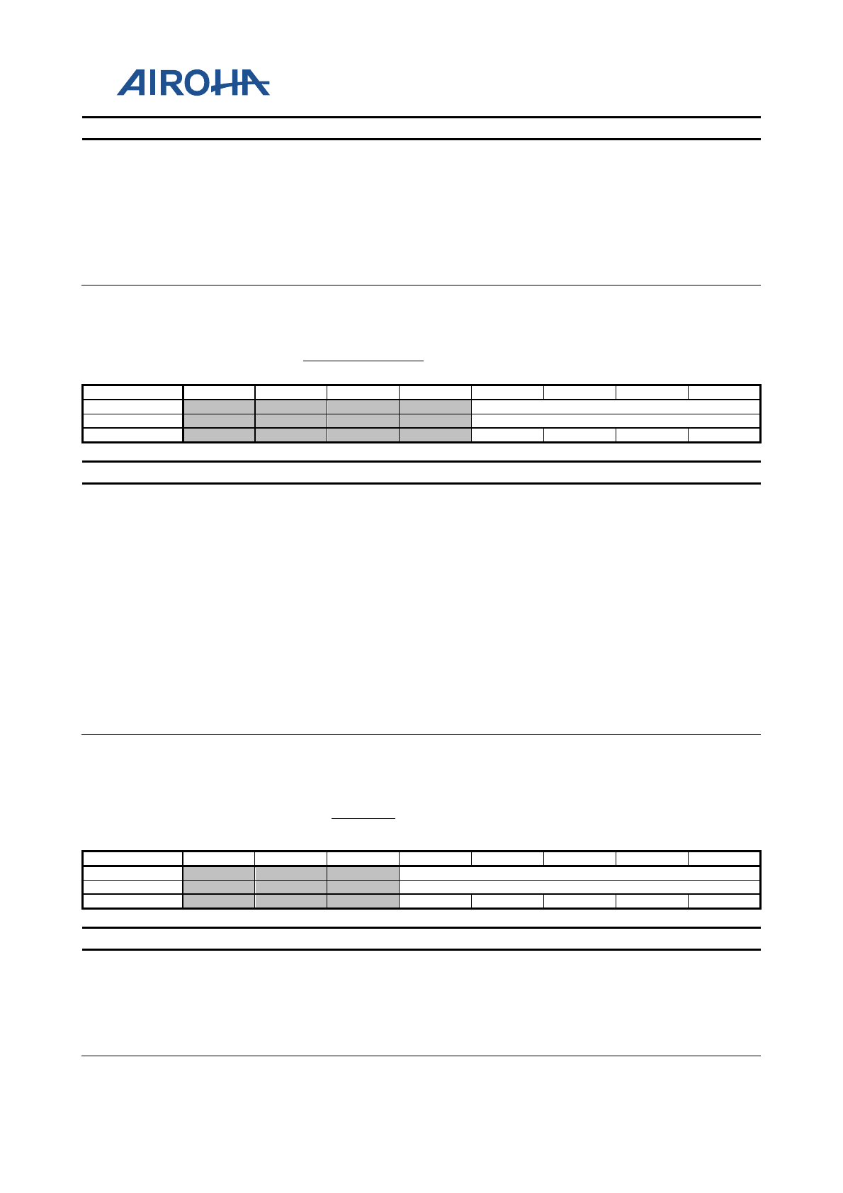
MT2523 Series Reference Manual
© 2015 - 2018 Airoha Technology Corp.
Page 640 of 692
This document contains information that is proprietary to Airoha Technology Corp. (“Airoha”) and/or its licensor(s).
Any unauthorized use, reproduction or disclosure of this document in whole or in part is strictly prohibited.
Bit(s) Name Description
4'b0110: -120 mV
4'b0111: -140 mV
4'b1000: +160 mV
4'b1001: +140 mV
4'b1010: +120 mV
4'b1011: +100 mV
4'b1100: +80 mV
4'b1101: +60 mV
4'b1110: +40 mV
4'b1111: +20 mV
FB VDIG18LDOBF0
VDIG1
8LDOB
F0
00
Bit
7
6
5
4
3
2
1
0
Name
RG_OVR_VDIG18_BUF_CAL
Type
RW
Reset
0
0
0
0
Bit(s) Name Description
3:0 RG_OVR_VDIG18_B
UF_CAL
VDIG18 buffer calibration
4'b0000: 0 mV
4'b0001: -20 mV
4'b0010: -40 mV
4'b0011: -60 mV
4'b0100: -80 mV
4'b0101: -100 mV
4'b0110: -120 mV
4'b0111: -140 mV
4'b1000: +160 mV
4'b1001: +140 mV
4'b1010: +120 mV
4'b1011: +100 mV
4'b1100: +80 mV
4'b1101: +60 mV
4'b1110: +40 mV
4'b1111: +20 mV
FD VCLDO0
VCORE
LDO
registe
r 0
00
Bit
7
6
5
4
3
2
1
0
Name
RG_OVR_VC_LDO_CAL
Type
RW
Reset
0
0
0
0
0
Bit(s) Name Description
4:0 RG_OVR_VC_LDO_
CAL
VC LDO calibration
5'b00000: 0 mV
5'b00001: -5 mV
5'b00010: -10 mV
5'b00011: -15 mV
5'b00100: -20 mV
5'b00101: -25 mV
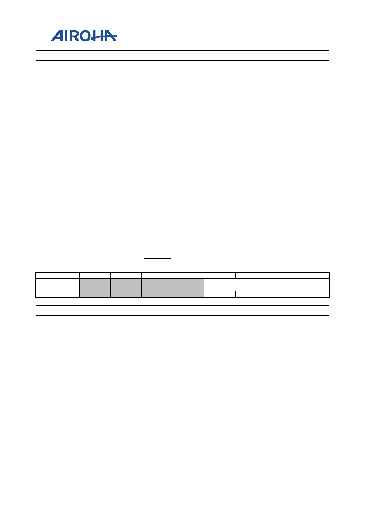
MT2523 Series Reference Manual
© 2015 - 2018 Airoha Technology Corp.
Page 641 of 692
This document contains information that is proprietary to Airoha Technology Corp. (“Airoha”) and/or its licensor(s).
Any unauthorized use, reproduction or disclosure of this document in whole or in part is strictly prohibited.
Bit(s) Name Description
5'b00110: -30 mV
5'b00111: -35 mV
5'b01000: -40 mV
5'b01001: -45 mV
5'b01010: -50 mV
5'b01011: -55 mV
5'b01100: -60 mV
5'b01101: -65 mV
5'b01110: -70 mV
5'b01111: -75 mV
5'b10000: +80 mV
5'b10000: +75 mV
5'b10001: +70 mV
5'b10010: +65 mV
5'b10011: +60 mV
5'b10100: +55 mV
5'b10101: +50 mV
5'b10110: +45 mV
5'b10111: +40 mV
5'b11000: +35 mV
5'b11001: +30 mV
5'b11010: +25 mV
5'b11011: +20 mV
5'b11100: +15 mV
5'b11101: +10 mV
5'b11110: +5 mV
FE VCLDO1
VCORE
LDO
registe
r 1
0A
Bit
7
6
5
4
3
2
1
0
Name
RG_OVR_VC_LDO_VOSEL
Type
RW
Reset
1
0
1
0
Bit(s) Name Description
3:0 RG_OVR_VC_LDO_
VOSEL
VC LDO output voltage
4'b0000: 0.7V
4'b0001: 0.75 V
4'b0010: 0.8 V
4'b0011: 0.85 V
4'b0100: 0.9 V
4'b0101: 0.95 V
4'b0110: 1 V
4'b0111: 1.05 V
4'b1000: 1.1V
4'b1001: 1.15 V
4'b1010: 1.2 V
4'b1011: 1.25 V
4'b1100: 1.3 V
4'b1101: 1.3 V
4'b1110: 1.3 V
4'b1111: 1.3 V
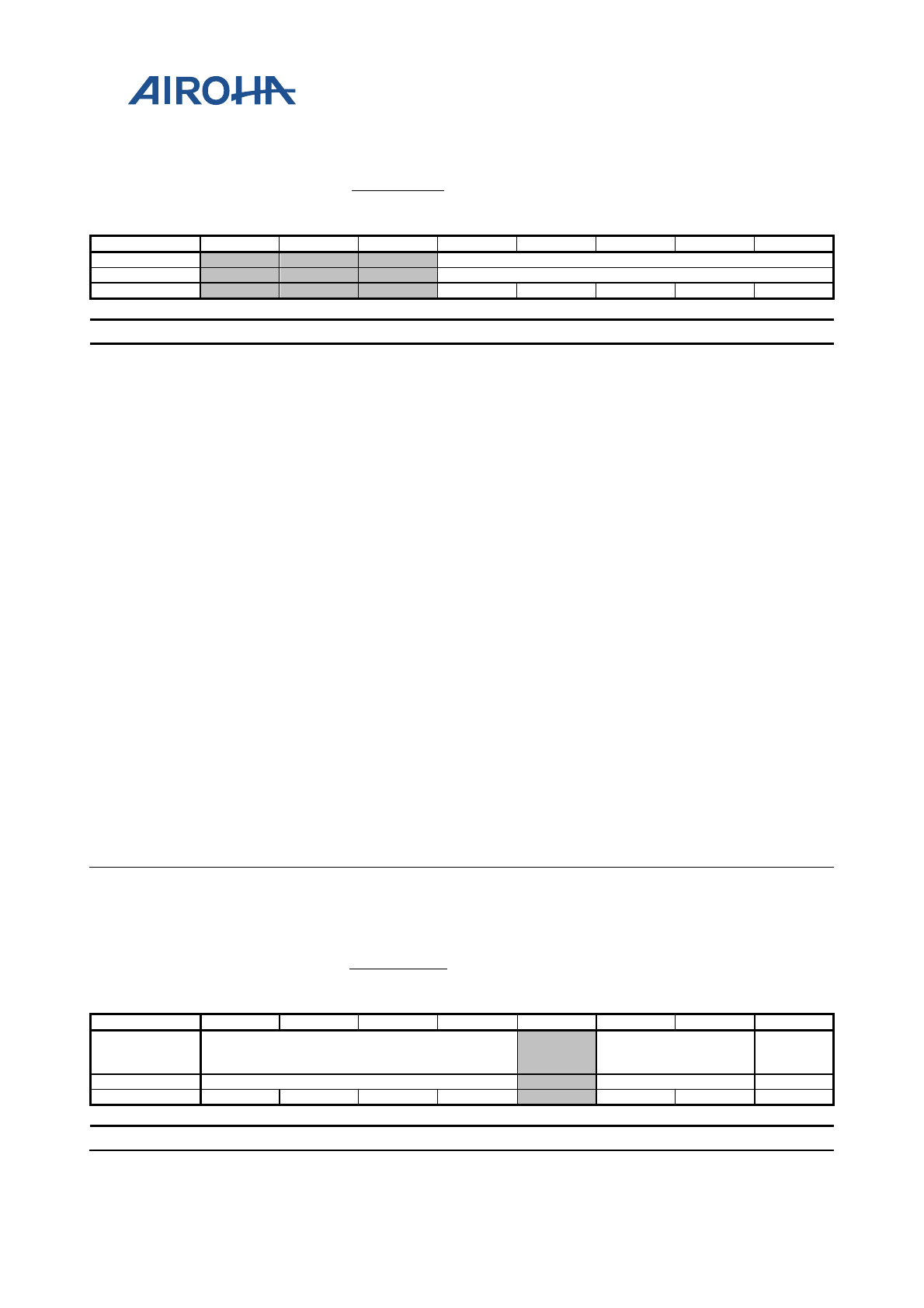
MT2523 Series Reference Manual
© 2015 - 2018 Airoha Technology Corp.
Page 642 of 692
This document contains information that is proprietary to Airoha Technology Corp. (“Airoha”) and/or its licensor(s).
Any unauthorized use, reproduction or disclosure of this document in whole or in part is strictly prohibited.
101 VCLDOBF0
VCORE
LDO
buffer
registe
r 0
00
Bit
7
6
5
4
3
2
1
0
Name
RG_OVR_VC_LDO_BUF_CAL
Type
RW
Reset
0
0
0
0
0
Bit(s) Name Description
4:0 RG_OVR_VC_LDO_
BUF_CAL
VC LDO buffer calibration
5'b00000: 0 mV
5'b00001: -5 mV
5'b00010: -10 mV
5'b00011: -15 mV
5'b00100: -20 mV
5'b00101: -25 mV
5'b00110: -30 mV
5'b00111: -35 mV
5'b01000: -40 mV
5'b01001: -45 mV
5'b01010: -50 mV
5'b01011: -55 mV
5'b01100: -60 mV
5'b01101: -65 mV
5'b01110: -70 mV
5'b01111: -75 mV
5'b10000: +80 mV
5'b10000: +75 mV
5'b10001: +70 mV
5'b10010: +65 mV
5'b10011: +60 mV
5'b10100: +55 mV
5'b10101: +50 mV
5'b10110: +45 mV
5'b10111: +40 mV
5'b11000: +35 mV
5'b11001: +30 mV
5'b11010: +25 mV
5'b11011: +20 mV
5'b11100: +15 mV
5'b11101: +10 mV
5'b11110: +5 mV
103 VCLDOPSI0
VCORE
LDO
PSI
registe
r 0
C0
Bit
7
6
5
4
3
2
1
0
Name RG_HP_VC_LDO_VOSEL RG_HP_VC_LDO_P
MOD
RG_HP_
VC_LDO
_ON
Type
RW
RW
RW
Reset
1
1
0
0
0
0
0
Bit(s) Name Description
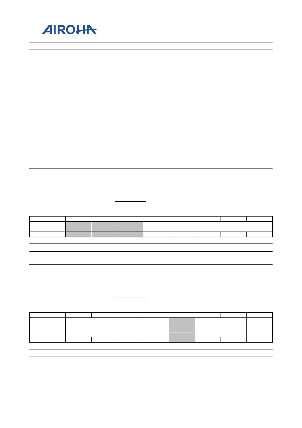
MT2523 Series Reference Manual
© 2015 - 2018 Airoha Technology Corp.
Page 643 of 692
This document contains information that is proprietary to Airoha Technology Corp. (“Airoha”) and/or its licensor(s).
Any unauthorized use, reproduction or disclosure of this document in whole or in part is strictly prohibited.
Bit(s) Name Description
7:4 RG_HP_VC_LDO_V
OSEL
4'b0000: 0.7V
4'b0001: 0.75 V
4'b0010: 0.8 V
4'b0011: 0.85 V
4'b0100: 0.9 V
4'b0101: 0.95 V
4'b0110: 1 V
4'b0111: 1.05 V
4'b1000: 1.1V
4'b1001: 1.15 V
4'b1010: 1.2 V
4'b1011: 1.25 V
4'b1100: 1.3 V
4'b1101: 1.3 V
4'b1110: 1.3 V
4'b1111: 1.3 V
2:1 RG_HP_VC_LDO_P
MOD
00: Normal mode
01: Lite mode
10: LP mode
11: ULP mode
0 RG_HP_VC_LDO_O
N
104 VCLDOPSI1
VCORE
LDO
PSI
registe
r 1
00
Bit
7
6
5
4
3
2
1
0
Name
RG_HP_VC_LDO_CAL
Type
RW
Reset
0
0
0
0
0
Bit(s) Name Description
4:0 RG_HP_VC_LDO_C
AL
105 VCLDOPSI2
VCORE
LDO
PSI
registe
r 2
80
Bit
7
6
5
4
3
2
1
0
Name RG_LP_VC_LDO_VOSEL RG_LP_VC_LDO_PM
OD
RG_LP_
VC_LDO
_ON
Type
RW
RW
RW
Reset
1
0
0
0
0
0
0
Bit(s) Name Description
7:4 RG_LP_VC_LDO_V
OSEL
4'b0000: 0.7V
4'b0001: 0.75 V
4'b0010: 0.8 V
4'b0011: 0.85 V
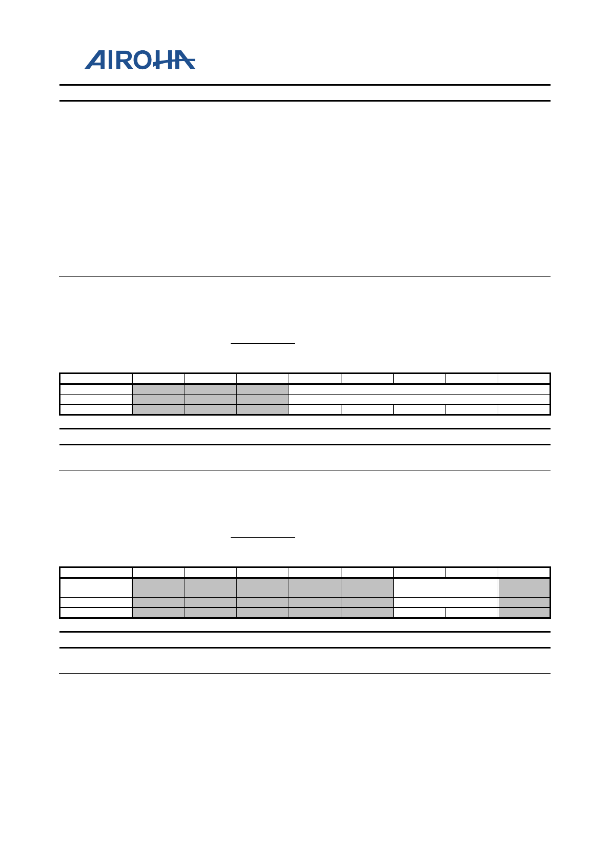
MT2523 Series Reference Manual
© 2015 - 2018 Airoha Technology Corp.
Page 644 of 692
This document contains information that is proprietary to Airoha Technology Corp. (“Airoha”) and/or its licensor(s).
Any unauthorized use, reproduction or disclosure of this document in whole or in part is strictly prohibited.
Bit(s) Name Description
4'b0100: 0.9 V
4'b0101: 0.95 V
4'b0110: 1 V
4'b0111: 1.05 V
4'b1000: 1.1V
4'b1001: 1.15 V
4'b1010: 1.2 V
4'b1011: 1.25 V
4'b1100: 1.3 V
4'b1101: 1.3 V
4'b1110: 1.3 V
4'b1111: 1.3 V
2:1 RG_LP_VC_LDO_P
MOD
0 RG_LP_VC_LDO_O
N
106 VCLDOPSI3
VCORE
LDO
PSI
registe
r 3
00
Bit
7
6
5
4
3
2
1
0
Name
RG_LP_VC_LDO_CAL
Type
RW
Reset
0
0
0
0
0
Bit(s) Name Description
4:0 RG_LP_VC_LDO_C
AL
107 VCLDOPSI4
VCORE
LDO
PSI
registe
r 4
00
Bit
7
6
5
4
3
2
1
0
Name
RG_S0_VC_LDO_PM
OD
Type
RW
Reset
0
0
Bit(s) Name Description
2:1 RG_S0_VC_LDO_P
MOD
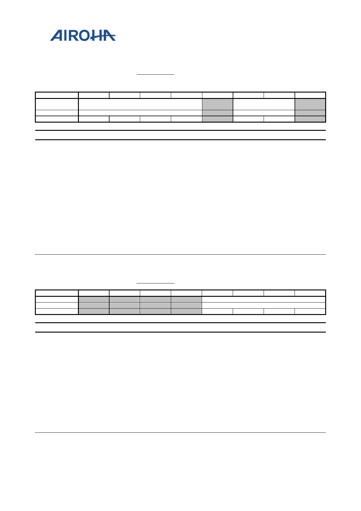
MT2523 Series Reference Manual
© 2015 - 2018 Airoha Technology Corp.
Page 645 of 692
This document contains information that is proprietary to Airoha Technology Corp. (“Airoha”) and/or its licensor(s).
Any unauthorized use, reproduction or disclosure of this document in whole or in part is strictly prohibited.
108 VCLDOPSI5
VCORE
LDO
PSI
registe
r 5
00
Bit
7
6
5
4
3
2
1
0
Name RG_S1_VC_LDO_VOSEL
RG_S1_VC_LDO_PM
OD
Type
RW
RW
Reset
0
0
0
0
0
0
Bit(s) Name Description
7:4 RG_S1_VC_LDO_V
OSEL
4'b0000: 0.7V
4'b0001: 0.75 V
4'b0010: 0.8 V
4'b0011: 0.85 V
4'b0100: 0.9 V
4'b0101: 0.95 V
4'b0110: 1 V
4'b0111: 1.05 V
4'b1000: 1.1V
4'b1001: 1.15 V
4'b1010: 1.2 V
4'b1011: 1.25 V
4'b1100: 1.3 V
4'b1101: 1.3 V
4'b1110: 1.3 V
4'b1111: 1.3 V
2:1 RG_S1_VC_LDO_P
MOD
10A VIO18LDO0 VIO18L
DO0 00
Bit
7
6
5
4
3
2
1
0
Name
RG_VIO18_CAL
Type
RW
Reset
0
0
0
0
Bit(s) Name Description
3:0 RG_VIO18_CAL
4'b0000: 0 mV
4'b0001: -20 mV
4'b0010: -40 mV
4'b0011: -60 mV
4'b0100: -80 mV
4'b0101: -100 mV
4'b0110: -120 mV
4'b0111: -140 mV
4'b1000: +160 mV
4'b1001: +140 mV
4'b1010: +120 mV
4'b1011: +100 mV
4'b1100: +80 mV
4'b1101: +60 mV
4'b1110: +40 mV
4'b1111: +20 mV
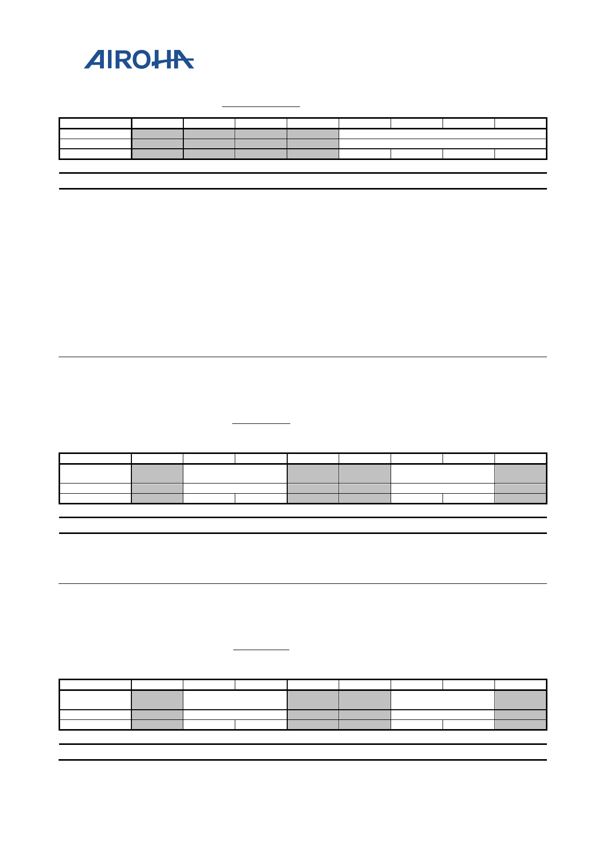
MT2523 Series Reference Manual
© 2015 - 2018 Airoha Technology Corp.
Page 646 of 692
This document contains information that is proprietary to Airoha Technology Corp. (“Airoha”) and/or its licensor(s).
Any unauthorized use, reproduction or disclosure of this document in whole or in part is strictly prohibited.
10E VIO18LDOBF0 VIO18L
DOBF0 00
Bit
7
6
5
4
3
2
1
0
Name
RG_VIO18_BUF_CAL
Type
RW
Reset
0
0
0
0
Bit(s) Name Description
3:0 RG_VIO18_BUF_CA
L
4'b0000: 0 mV
4'b0001: -20 mV
4'b0010: -40 mV
4'b0011: -60 mV
4'b0100: -80 mV
4'b0101: -100 mV
4'b0110: -120 mV
4'b0111: -140 mV
4'b1000: +160 mV
4'b1001: +140 mV
4'b1010: +120 mV
4'b1011: +100 mV
4'b1100: +80 mV
4'b1101: +60 mV
4'b1110: +40 mV
4'b1111: +20 mV
110 VIO18PSI0
VIO18
LDO
PSI
registe
r0
00
Bit
7
6
5
4
3
2
1
0
Name
RG_LP_VIO18_PMO
D
RG_HP_VIO18_PMO
D
Type
RW
RW
Reset
0
0
0
0
Bit(s) Name Description
6:5 RG_LP_VIO18_PMO
D
2:1 RG_HP_VIO18_PM
OD
111 VIO18PSI1
VIO18
LDO
PSI
registe
r1
00
Bit
7
6
5
4
3
2
1
0
Name
RG_S1_VIO18_PMO
D
RG_S0_VIO18_PMO
D
Type
RW
RW
Reset
0
0
0
0
Bit(s) Name Description
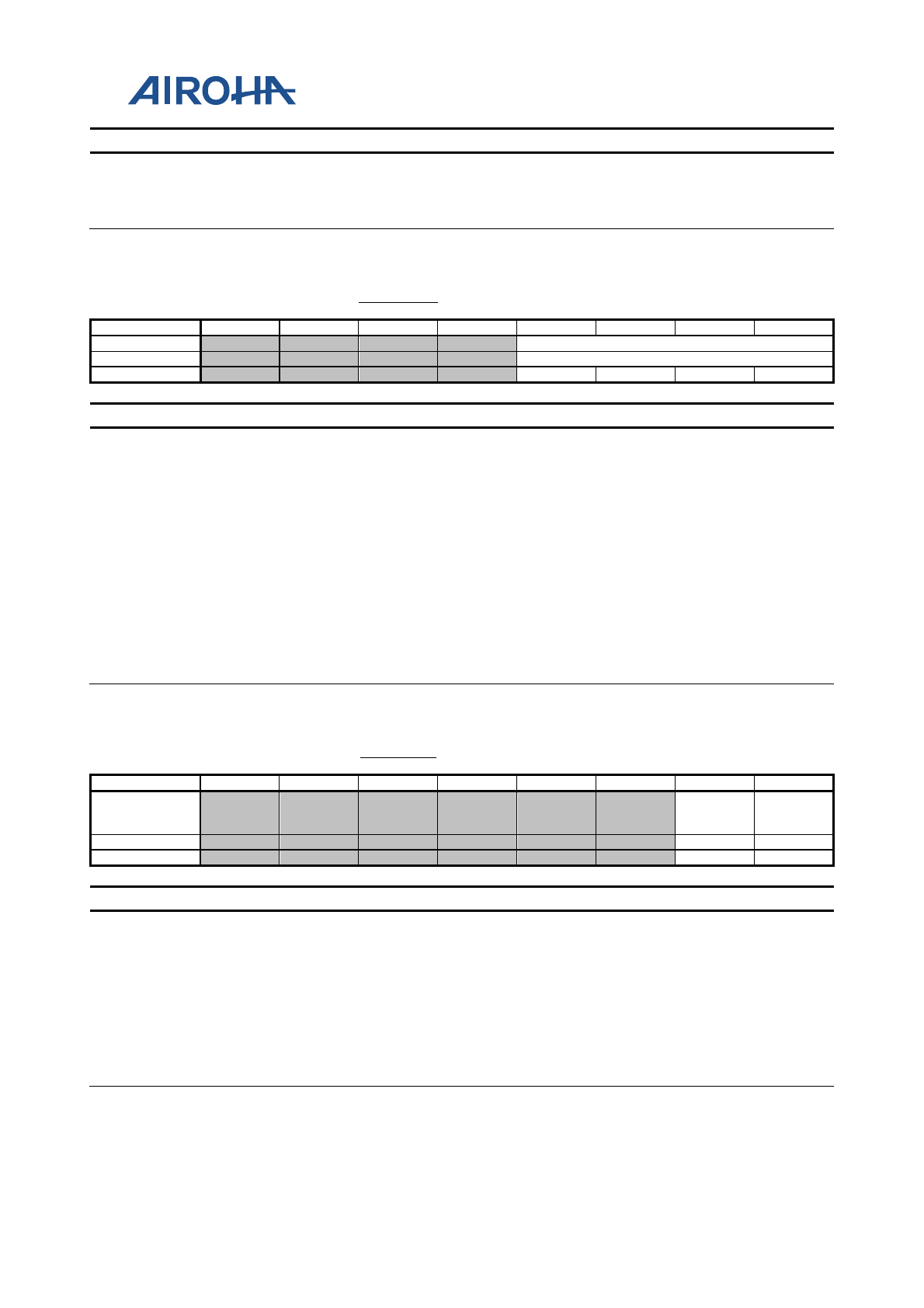
MT2523 Series Reference Manual
© 2015 - 2018 Airoha Technology Corp.
Page 647 of 692
This document contains information that is proprietary to Airoha Technology Corp. (“Airoha”) and/or its licensor(s).
Any unauthorized use, reproduction or disclosure of this document in whole or in part is strictly prohibited.
Bit(s) Name Description
6:5 RG_S1_VIO18_PMO
D
2:1 RG_S0_VIO18_PMO
D
113 VSFLDO0 VSFLD
O0 00
Bit
7
6
5
4
3
2
1
0
Name
RG_VSF_CAL
Type
RW
Reset
0
0
0
0
Bit(s) Name Description
3:0 RG_VSF_CAL
4'b0000: 0 mV
4'b0001: -20 mV
4'b0010: -40 mV
4'b0011: -60 mV
4'b0100: -80 mV
4'b0101: -100 mV
4'b0110: -120 mV
4'b0111: -140 mV
4'b1000: +160 mV
4'b1001: +140 mV
4'b1010: +120 mV
4'b1011: +100 mV
4'b1100: +80 mV
4'b1101: +60 mV
4'b1110: +40 mV
4'b1111: +20 mV
114 VSFLDO1 VSFLD
O1 00
Bit
7
6
5
4
3
2
1
0
Name
RG_VSF
_VOSEL
_1
RG_VSF
_VOSEL
_0
Type
RW
RW
Reset
0
0
Bit(s) Name Description
1 RG_VSF_VOSEL_1
VSF output voltage select bit_1
2'b00: 1.86V
2'b01: 3 V
2'b10: 3.3 V
2b'11: null
0 RG_VSF_VOSEL_0
VSF output voltage select bit_0
2'b00: 1.86V
2'b01: 3 V
2'b10: 3.3 V
2b'11: null
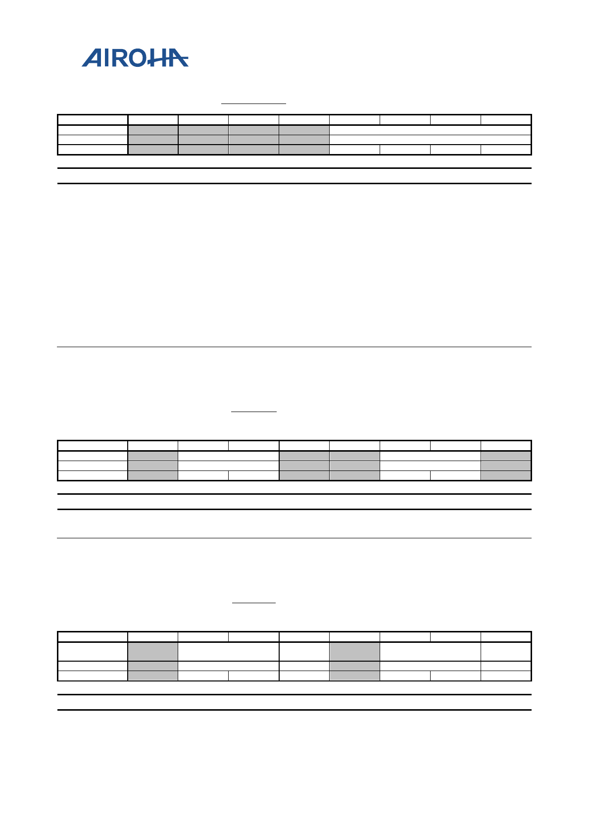
MT2523 Series Reference Manual
© 2015 - 2018 Airoha Technology Corp.
Page 648 of 692
This document contains information that is proprietary to Airoha Technology Corp. (“Airoha”) and/or its licensor(s).
Any unauthorized use, reproduction or disclosure of this document in whole or in part is strictly prohibited.
117 VSFLDOBF0 VSFLD
OBF0 00
Bit
7
6
5
4
3
2
1
0
Name
RG_VSF_BUF_CAL
Type
RW
Reset
0
0
0
0
Bit(s) Name Description
3:0 RG_VSF_BUF_CAL
4'b0000: 0 mV
4'b0001: -20 mV
4'b0010: -40 mV
4'b0011: -60 mV
4'b0100: -80 mV
4'b0101: -100 mV
4'b0110: -120 mV
4'b0111: -140 mV
4'b1000: +160 mV
4'b1001: +140 mV
4'b1010: +120 mV
4'b1011: +100 mV
4'b1100: +80 mV
4'b1101: +60 mV
4'b1110: +40 mV
4'b1111: +20 mV
119 VSFPSI0
VSF
LDO
PSI
registe
r0
00
Bit
7
6
5
4
3
2
1
0
Name
RG_LP_VSF_PMOD
RG_HP_VSF_PMOD
Type
RW
RW
Reset
0
0
0
0
Bit(s) Name Description
6:5 RG_LP_VSF_PMOD
2:1 RG_HP_VSF_PMOD
11A VSFPSI1
VSF
LDO
PSI
registe
r1
00
Bit
7
6
5
4
3
2
1
0
Name RG_S1_VSF_PMOD
RGS_S1_
VSF_ON
RG_S0_VSF_PMOD
RGS_S0_
VSF_ON
Type
RW
RO
RW
RO
Reset
0
0
0
0
0
0
Bit(s) Name Description
6:5 RG_S1_VSF_PMOD
4 RGS_S1_VSF_ON
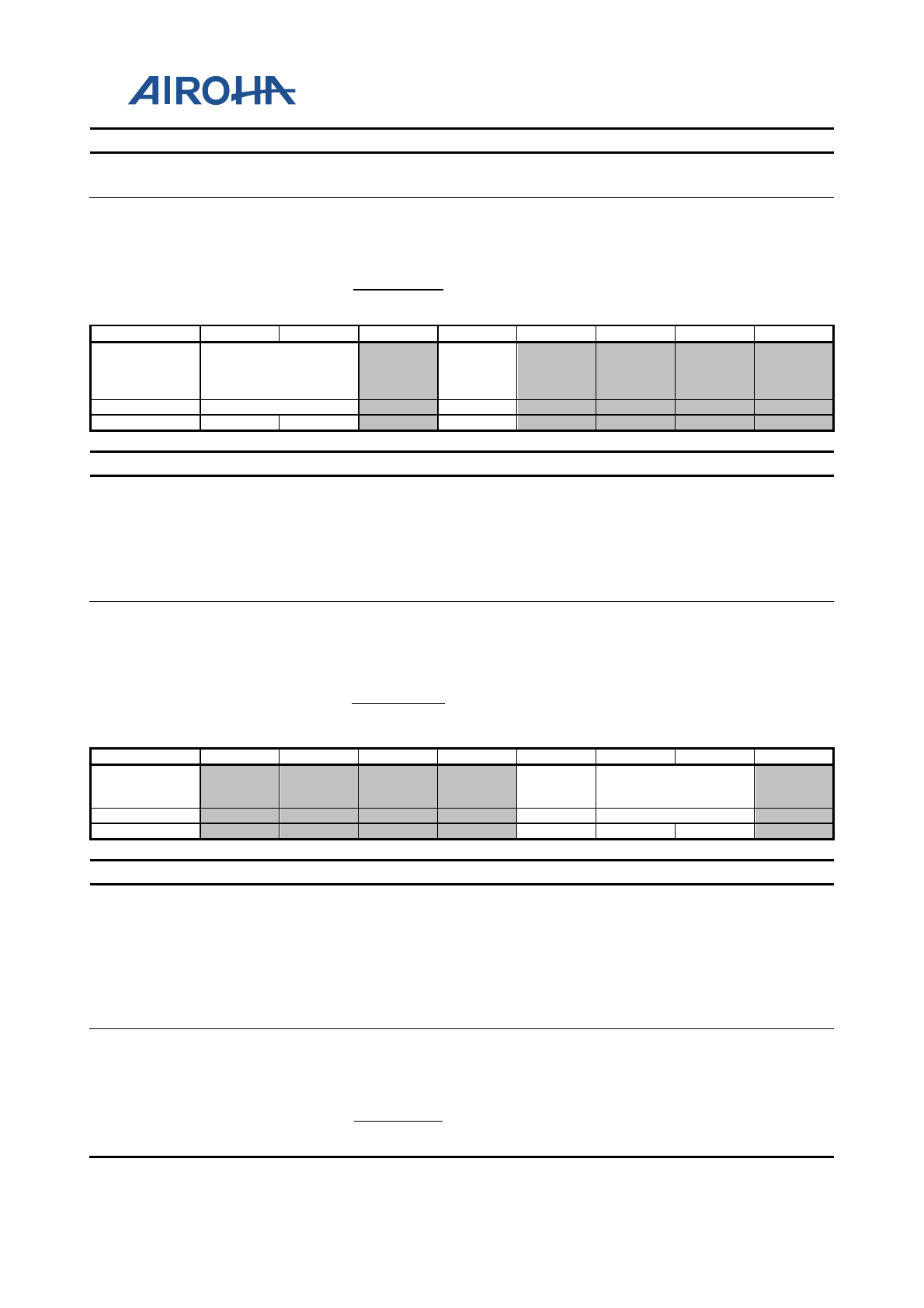
MT2523 Series Reference Manual
© 2015 - 2018 Airoha Technology Corp.
Page 649 of 692
This document contains information that is proprietary to Airoha Technology Corp. (“Airoha”) and/or its licensor(s).
Any unauthorized use, reproduction or disclosure of this document in whole or in part is strictly prohibited.
Bit(s) Name Description
2:1 RG_S0_VSF_PMOD
0 RGS_S0_VSF_ON
11C SMPSCTL0
SMPS
Control
Registe
r 0
16
Bit
7
6
5
4
3
2
1
0
Name RG_VCORE_BUCK_S
CHG_TSTEP
RG_VCO
RE_BUC
K_SCHG
_EN
Type
RW
RW
Reset
0
0
1
Bit(s) Name Description
7:6 RG_VCORE_BUCK_
SCHG_TSTEP
VCORE DVS soft change time step
2'b00: 0.6us (default)
2'b01: 1.3us
2'b10: 2.6us
2'b11: 4.6us
4 RG_VCORE_BUCK_
SCHG_EN VCORE DVS soft change enable
121 SMPSANA3
SMPS
Analog
Control
Registe
r 3
00
Bit
7
6
5
4
3
2
1
0
Name
RG_VOU
TDET_E
N
RG_VCORE_VSLEEP
_SEL
Type
RW
RW
Reset
0
0
0
Bit(s) Name Description
3 RG_VOUTDET_EN
VOUT tied to VBAT detection enable
0: disable
1: enable
2:1 RG_VCORE_VSLEE
P_SEL
sleep mode voltage selection
00: 0.7V
01: 0.75V
10: 0.6V
11: 0.65V
135 VCBUCK19
VCORE
BUCK
registe
r 19
00
MT2523 Series Reference Manual
© 2015 - 2018 Airoha Technology Corp.
Page 650 of 692
This document contains information that is proprietary to Airoha Technology Corp. (“Airoha”) and/or its licensor(s).
Any unauthorized use, reproduction or disclosure of this document in whole or in part is strictly prohibited.
135 VCBUCK19
VCORE
BUCK
registe
r 19
00
Bit
7
6
5
4
3
2
1
0
Name
RGS_QI_
VCORE_
OC_STAT
US
Type
RO
Reset
0
Bit(s) Name Description
1 RGS_QI_VCORE_O
C_STATUS OC status
13E VCBUCKPSI0
VCORE
BUCK
PSI
registe
r 0
E1
Bit
7
6
5
4
3
2
1
0
Name RG_HP_VC_BUCK_VOVAL RG_HP_VC_BUCK_VOADJ
RG_HP_
VC_BUC
K_ON
Type
RW
RW
RW
Reset
1
1
1
0
0
0
0
1
Bit(s) Name Description
7:4 RG_HP_VC_BUCK_
VOVAL
VCORE BUCK output voltage value for HP state
0000: 0.6v
0001: 0.6v + 50mV
0010: 0.6v + 50mV*2
0100: 0.6v + 50mv*4
0110: 0.6v + 50mv*6
1000: 0.6v + 50mv*8
1010: 0.6v + 50mv*10
1100: 0.6v + 50mv*12 = 1.2v
1110: 0.6v + 50mv*14
1111: 0.6v + 50mV*15 = 1.35v
3:1 RG_HP_VC_BUCK_
VOADJ VCORE BUCK voltage adjust value for HP state (6.25mV/bit)
0 RG_HP_VC_BUCK_
ON
VCORE BUCK on/off control for HP state
0: off
1: on
13F VCBUCKPSI1
VCORE
BUCK
PSI
registe
r 1
A1
Bit
7
6
5
4
3
2
1
0
Name RG_LP_VC_BUCK_VOVAL RG_LP_VC_BUCK_VOADJ
RG_LP_
VC_BUC
MT2523 Series Reference Manual
© 2015 - 2018 Airoha Technology Corp.
Page 651 of 692
This document contains information that is proprietary to Airoha Technology Corp. (“Airoha”) and/or its licensor(s).
Any unauthorized use, reproduction or disclosure of this document in whole or in part is strictly prohibited.
13F VCBUCKPSI1
VCORE
BUCK
PSI
registe
r 1
A1
K_ON
Type
RW
RW
RW
Reset
1
0
1
0
0
0
0
1
Bit(s) Name Description
7:4 RG_LP_VC_BUCK_
VOVAL
VCORE BUCK output voltage value for LP state
0000: 0.6v
0001: 0.6v + 50mV
0010: 0.6v + 50mV*2
0100: 0.6v + 50mv*4
0110: 0.6v + 50mv*6
1000: 0.6v + 50mv*8
1010: 0.6v + 50mv*10
1100: 0.6v + 50mv*12 = 1.2v
1110: 0.6v + 50mv*14
1111: 0.6v + 50mV*15 = 1.35v
3:1 RG_LP_VC_BUCK_
VOADJ VCORE BUCK voltage adjust value for LP state (6.25mV/bit)
0 RG_LP_VC_BUCK_
ON
VCORE BUCK on/off control for LP state
0: off
1: on
140 VCBUCKPSI2
VCORE
BUCK
PSI
registe
r 2
20
Bit
7
6
5
4
3
2
1
0
Name
RG_S1_VC_BUCK_VOVAL
RG_S1_VC_BUCK_VOADJ
Type
RW
RW
Reset
0
0
1
0
0
0
0
Bit(s) Name Description
7:4 RG_S1_VC_BUCK_
VOVAL
VCORE BUCK output voltage value for LP state
0000: 0.6v
0001: 0.6v + 50mV
0010: 0.6v + 50mV*2
0100: 0.6v + 50mv*4
0110: 0.6v + 50mv*6
1000: 0.6v + 50mv*8
1010: 0.6v + 50mv*10
1100: 0.6v + 50mv*12 = 1.2v
1110: 0.6v + 50mv*14
1111: 0.6v + 50mV*15 = 1.35v
3:1 RG_S1_VC_BUCK_
VOADJ VCORE BUCK voltage adjust value for LP state (6.25mV/bit)
MT2523 Series Reference Manual
© 2015 - 2018 Airoha Technology Corp.
Page 652 of 692
This document contains information that is proprietary to Airoha Technology Corp. (“Airoha”) and/or its licensor(s).
Any unauthorized use, reproduction or disclosure of this document in whole or in part is strictly prohibited.
200 AUXADC_ADC0
AUXAD
C ADC
registe
r 0
00
Bit
7
6
5
4
3
2
1
0
Name
AUXADC_ADC_OUT_CH0_L
Type
RO
Reset
0
0
0
0
0
0
0
0
Bit(s) Name Description
7:0 AUXADC_ADC_OUT
_CH0_L AUXADC channel 0 output data bit [7:0]
201 AUXADC_ADC0_H
AUXAD
C ADC
registe
r 0_H
00
Bit
7
6
5
4
3
2
1
0
Name
AUXADC
_ADC_R
DY_CH0
AUXADC_ADC_OUT_CH0_H
Type
RO
RO
Reset
0
0
0
0
0
0
0
0
Bit(s) Name Description
7 AUXADC_ADC_RDY
_CH0
AUXADC channel 0 output data ready
0: AUXADC data proceeding
1: AUXADC data ready
6:0 AUXADC_ADC_OUT
_CH0_H AUXADC channel 0 output data bit [14:8]
202 AUXADC_ADC1
AUXAD
C ADC
registe
r 1
00
Bit
7
6
5
4
3
2
1
0
Name
AUXADC_ADC_OUT_CH1_L
Type
RO
Reset
0
0
0
0
0
0
0
0
Bit(s) Name Description
7:0 AUXADC_ADC_OUT
_CH1_L AUXADC channel 1 output data bit [7:0]
203 AUXADC_ADC1_H
AUXAD
C ADC
registe
r 1_H
00
Bit
7
6
5
4
3
2
1
0
Name
AUXADC
AUXADC_ADC_OUT_CH1_H
MT2523 Series Reference Manual
© 2015 - 2018 Airoha Technology Corp.
Page 653 of 692
This document contains information that is proprietary to Airoha Technology Corp. (“Airoha”) and/or its licensor(s).
Any unauthorized use, reproduction or disclosure of this document in whole or in part is strictly prohibited.
203 AUXADC_ADC1_H
AUXAD
C ADC
registe
r 1_H
00
_ADC_R
DY_CH1
Type
RO
RO
Reset
0
0
0
0
0
0
0
0
Bit(s) Name Description
7 AUXADC_ADC_RDY
_CH1
AUXADC channel 1 output data ready
0: AUXADC data proceeding
1: AUXADC data ready
6:0 AUXADC_ADC_OUT
_CH1_H AUXADC channel 1 output data bit [14:8]
204 AUXADC_ADC2
AUXAD
C ADC
registe
r 2
00
Bit
7
6
5
4
3
2
1
0
Name
AUXADC_ADC_OUT_CH2_L
Type
RO
Reset
0
0
0
0
0
0
0
0
Bit(s) Name Description
7:0 AUXADC_ADC_OUT
_CH2_L AUXADC channel 2 output data bit [7:0]
205 AUXADC_ADC2_H
AUXAD
C ADC
registe
r 2_H
00
Bit
7
6
5
4
3
2
1
0
Name
AUXADC
_ADC_R
DY_CH2
AUXADC_ADC_OUT_CH2_H
Type
RO
RO
Reset
0
0
0
0
0
Bit(s) Name Description
7 AUXADC_ADC_RDY
_CH2
AUXADC channel 2 output data ready
0: AUXADC data proceeding
1: AUXADC data ready
3:0 AUXADC_ADC_OUT
_CH2_H AUXADC channel 2 output data bit [11:8]
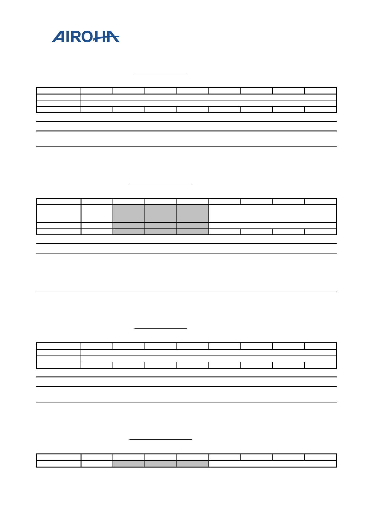
MT2523 Series Reference Manual
© 2015 - 2018 Airoha Technology Corp.
Page 654 of 692
This document contains information that is proprietary to Airoha Technology Corp. (“Airoha”) and/or its licensor(s).
Any unauthorized use, reproduction or disclosure of this document in whole or in part is strictly prohibited.
206 AUXADC_ADC3
AUXAD
C ADC
registe
r 3
00
Bit
7
6
5
4
3
2
1
0
Name
AUXADC_ADC_OUT_CH3_L
Type
RO
Reset
0
0
0
0
0
0
0
0
Bit(s) Name Description
7:0 AUXADC_ADC_OUT
_CH3_L AUXADC channel 3 output data bit [7:0]
207 AUXADC_ADC3_H
AUXAD
C ADC
registe
r 3_H
00
Bit
7
6
5
4
3
2
1
0
Name
AUXADC
_ADC_R
DY_CH3
AUXADC_ADC_OUT_CH3_H
Type
RO
RO
Reset
0
0
0
0
0
Bit(s) Name Description
7 AUXADC_ADC_RDY
_CH3
AUXADC channel 3 output data ready
0: AUXADC data proceeding
1: AUXADC data ready
3:0 AUXADC_ADC_OUT
_CH3_H AUXADC channel 3 output data bit [11:8]
208 AUXADC_ADC4
AUXAD
C ADC
registe
r 4
00
Bit
7
6
5
4
3
2
1
0
Name
AUXADC_ADC_OUT_CH4_L
Type
RO
Reset
0
0
0
0
0
0
0
0
Bit(s) Name Description
7:0 AUXADC_ADC_OUT
_CH4_L AUXADC channel 4 output data bit [7:0]
209 AUXADC_ADC4_H
AUXAD
C ADC
registe
r 4_H
00
Bit
7
6
5
4
3
2
1
0
Name
AUXADC
AUXADC_ADC_OUT_CH4_H
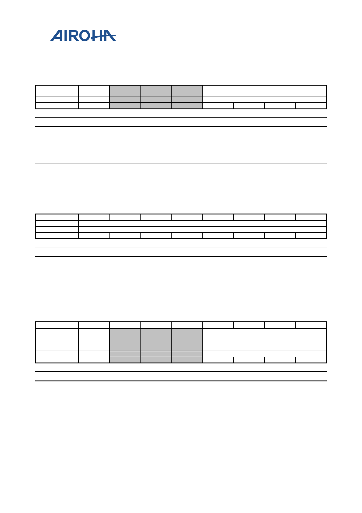
MT2523 Series Reference Manual
© 2015 - 2018 Airoha Technology Corp.
Page 655 of 692
This document contains information that is proprietary to Airoha Technology Corp. (“Airoha”) and/or its licensor(s).
Any unauthorized use, reproduction or disclosure of this document in whole or in part is strictly prohibited.
209 AUXADC_ADC4_H
AUXAD
C ADC
registe
r 4_H
00
_ADC_R
DY_CH4
Type
RO
RO
Reset
0
0
0
0
0
Bit(s) Name Description
7 AUXADC_ADC_RDY
_CH4
AUXADC channel 4 output data ready
0: AUXADC data proceeding
1: AUXADC data ready
3:0 AUXADC_ADC_OUT
_CH4_H AUXADC channel 4 output data bit [11:8]
21A AUXADC_ADC13
AUXAD
C ADC
registe
r 13
00
Bit
7
6
5
4
3
2
1
0
Name
AUXADC_ADC_OUT_THR_HW_L
Type
RO
Reset
0
0
0
0
0
0
0
0
Bit(s) Name Description
7:0 AUXADC_ADC_OUT
_THR_HW_L AUXADC channel 13 output data bit [7:0]
21B AUXADC_ADC13_H
AUXAD
C ADC
registe
r 13_H
00
Bit
7
6
5
4
3
2
1
0
Name
AUXADC
_ADC_R
DY_THR
_HW
AUXADC_ADC_OUT_THR_HW_H
Type
RO
RO
Reset
0
0
0
0
0
Bit(s) Name Description
7 AUXADC_ADC_RDY
_THR_HW
AUXADC channel 13 output data ready
0: AUXADC data proceeding
1: AUXADC data ready
3:0 AUXADC_ADC_OUT
_THR_HW_H AUXADC channel 13 output data bit [11:8]

MT2523 Series Reference Manual
© 2015 - 2018 Airoha Technology Corp.
Page 656 of 692
This document contains information that is proprietary to Airoha Technology Corp. (“Airoha”) and/or its licensor(s).
Any unauthorized use, reproduction or disclosure of this document in whole or in part is strictly prohibited.
21C AUXADC_ADC14
AUXAD
C ADC
registe
r 14
00
Bit
7
6
5
4
3
2
1
0
Name
AUXADC_ADC_OUT_LBAT_L
Type
RO
Reset
0
0
0
0
0
0
0
0
Bit(s) Name Description
7:0 AUXADC_ADC_OUT
_LBAT_L AUXADC channel 14 output data bit [7:0]
21D AUXADC_ADC14_H
AUXAD
C ADC
registe
r 14_H
00
Bit
7
6
5
4
3
2
1
0
Name
AUXADC
_ADC_R
DY_LBA
T
AUXADC_ADC_OUT_LBAT_H
Type
RO
RO
Reset
0
0
0
0
0
Bit(s) Name Description
7 AUXADC_ADC_RDY
_LBAT
AUXADC channel 14 output data ready
0: AUXADC data proceeding
1: AUXADC data ready
3:0 AUXADC_ADC_OUT
_LBAT_H AUXADC channel 14 output data bit [11:8]
21E AUXADC_ADC15
AUXAD
C ADC
registe
r 15
00
Bit
7
6
5
4
3
2
1
0
Name
AUXADC_ADC_OUT_LBAT2_L
Type
RO
Reset
0
0
0
0
0
0
0
0
Bit(s) Name Description
7:0 AUXADC_ADC_OUT
_LBAT2_L AUXADC channel 15 output data bit [7:0]
21F AUXADC_ADC15_H
AUXAD
C ADC
registe
r 15_H
00
Bit
7
6
5
4
3
2
1
0
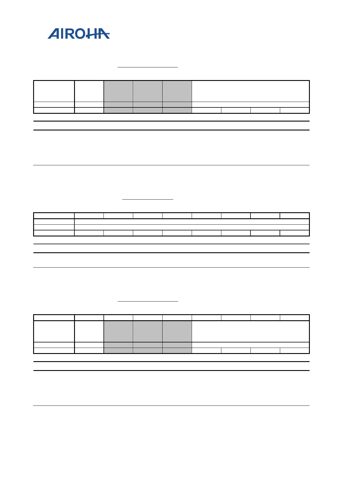
MT2523 Series Reference Manual
© 2015 - 2018 Airoha Technology Corp.
Page 657 of 692
This document contains information that is proprietary to Airoha Technology Corp. (“Airoha”) and/or its licensor(s).
Any unauthorized use, reproduction or disclosure of this document in whole or in part is strictly prohibited.
21F AUXADC_ADC15_H
AUXAD
C ADC
registe
r 15_H
00
Name
AUXADC
_ADC_R
DY_LBA
T2
AUXADC_ADC_OUT_LBAT2_H
Type
RO
RO
Reset
0
0
0
0
0
Bit(s) Name Description
7 AUXADC_ADC_RDY
_LBAT2
AUXADC channel 15 output data ready
0: AUXADC data proceeding
1: AUXADC data ready
3:0 AUXADC_ADC_OUT
_LBAT2_H AUXADC channel 15 output data bit [11:8]
226 AUXADC_ADC19
AUXAD
C ADC
registe
r 19
00
Bit
7
6
5
4
3
2
1
0
Name
AUXADC_ADC_OUT_CH4_BY_MD_L
Type
RO
Reset
0
0
0
0
0
0
0
0
Bit(s) Name Description
7:0 AUXADC_ADC_OUT
_CH4_BY_MD_L AUXADC channel 19 output data bit [7:0]
227 AUXADC_ADC19_H
AUXAD
C ADC
registe
r 19_H
00
Bit
7
6
5
4
3
2
1
0
Name
AUXADC
_ADC_R
DY_CH4
_BY_MD
AUXADC_ADC_OUT_CH4_BY_MD_H
Type
RO
RO
Reset
0
0
0
0
0
Bit(s) Name Description
7 AUXADC_ADC_RDY
_CH4_BY_MD
AUXADC channel 19 output data ready
0: AUXADC data proceeding
1: AUXADC data ready
3:0 AUXADC_ADC_OUT
_CH4_BY_MD_H AUXADC channel 19 output data bit [11:8]
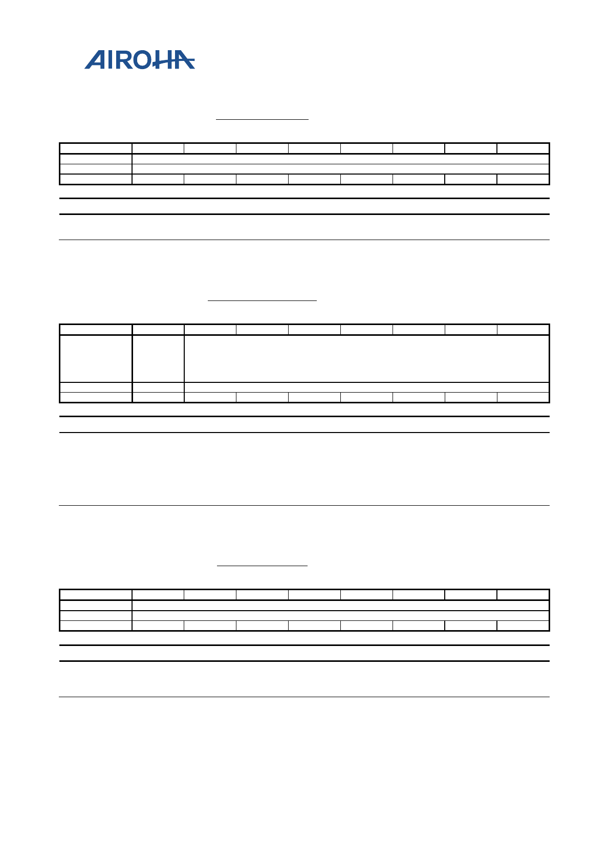
MT2523 Series Reference Manual
© 2015 - 2018 Airoha Technology Corp.
Page 658 of 692
This document contains information that is proprietary to Airoha Technology Corp. (“Airoha”) and/or its licensor(s).
Any unauthorized use, reproduction or disclosure of this document in whole or in part is strictly prohibited.
228 AUXADC_ADC20
AUXAD
C ADC
registe
r 20
00
Bit
7
6
5
4
3
2
1
0
Name
AUXADC_ADC_OUT_WAKEUP_PCHR_L
Type
RO
Reset
0
0
0
0
0
0
0
0
Bit(s) Name Description
7:0 AUXADC_ADC_OUT
_WAKEUP_PCHR_L AUXADC channel 20 output data bit [7:0]
229 AUXADC_ADC20_H
AUXAD
C ADC
registe
r 20_H
00
Bit
7
6
5
4
3
2
1
0
Name
AUXADC
_ADC_R
DY_WAK
EUP_PC
HR
AUXADC_ADC_OUT_WAKEUP_PCHR_H
Type
RO
RO
Reset
0
0
0
0
0
0
0
0
Bit(s) Name Description
7 AUXADC_ADC_RDY
_WAKEUP_PCHR
AUXADC channel 20 output data ready
0: AUXADC data proceeding
1: AUXADC data ready
6:0
AUXADC_ADC_OUT
_WAKEUP_PCHR_
H
AUXADC channel 20 output data bit [14:8]
22A AUXADC_ADC21
AUXAD
C ADC
registe
r 21
00
Bit
7
6
5
4
3
2
1
0
Name
AUXADC_ADC_OUT_WAKEUP_SWCHR_L
Type
RO
Reset
0
0
0
0
0
0
0
0
Bit(s) Name Description
7:0
AUXADC_ADC_OUT
_WAKEUP_SWCHR
_L
AUXADC channel 21 output data bit [7:0]
MT2523 Series Reference Manual
© 2015 - 2018 Airoha Technology Corp.
Page 659 of 692
This document contains information that is proprietary to Airoha Technology Corp. (“Airoha”) and/or its licensor(s).
Any unauthorized use, reproduction or disclosure of this document in whole or in part is strictly prohibited.
22B AUXADC_ADC21_H
AUXAD
C ADC
registe
r 21_H
00
Bit
7
6
5
4
3
2
1
0
Name
AUXADC
_ADC_R
DY_WAK
EUP_SW
CHR
AUXADC_ADC_OUT_WAKEUP_SWCHR_H
Type
RO
RO
Reset
0
0
0
0
0
0
0
0
Bit(s) Name Description
7 AUXADC_ADC_RDY
_WAKEUP_SWCHR
AUXADC channel 21 output data ready
0: AUXADC data proceeding
1: AUXADC data ready
6:0
AUXADC_ADC_OUT
_WAKEUP_SWCHR
_H
AUXADC channel 21 output data bit [14:8]
22C AUXADC_ADC22
AUXAD
C ADC
registe
r 22
00
Bit
7
6
5
4
3
2
1
0
Name
AUXADC_ADC_OUT_CH0_BY_MD_L
Type
RO
Reset
0
0
0
0
0
0
0
0
Bit(s) Name Description
7:0 AUXADC_ADC_OUT
_CH0_BY_MD_L AUXADC channel 22 output data bit [7:0]
22D AUXADC_ADC22_H
AUXAD
C ADC
registe
r 22_H
00
Bit
7
6
5
4
3
2
1
0
Name
AUXADC
_ADC_R
DY_CH0
_BY_MD
AUXADC_ADC_OUT_CH0_BY_MD_H
Type
RO
RO
Reset
0
0
0
0
0
0
0
0
Bit(s) Name Description
7 AUXADC_ADC_RDY
_CH0_BY_MD
AUXADC channel 22 output data ready
0: AUXADC data proceeding
1: AUXADC data ready
6:0 AUXADC_ADC_OUT
_CH0_BY_MD_H AUXADC channel 22 output data bit [14:8]
MT2523 Series Reference Manual
© 2015 - 2018 Airoha Technology Corp.
Page 660 of 692
This document contains information that is proprietary to Airoha Technology Corp. (“Airoha”) and/or its licensor(s).
Any unauthorized use, reproduction or disclosure of this document in whole or in part is strictly prohibited.
22E AUXADC_ADC23
AUXAD
C ADC
registe
r 23
00
Bit
7
6
5
4
3
2
1
0
Name
AUXADC_ADC_OUT_CH0_BY_AP_L
Type
RO
Reset
0
0
0
0
0
0
0
0
Bit(s) Name Description
7:0 AUXADC_ADC_OUT
_CH0_BY_AP_L AUXADC channel 23 output data bit [7:0]
22F AUXADC_ADC23_H
AUXAD
C ADC
registe
r 23_H
00
Bit
7
6
5
4
3
2
1
0
Name
AUXADC
_ADC_R
DY_CH0
_BY_AP
AUXADC_ADC_OUT_CH0_BY_AP_H
Type
RO
RO
Reset
0
0
0
0
0
0
0
0
Bit(s) Name Description
7 AUXADC_ADC_RDY
_CH0_BY_AP
AUXADC channel 23 output data ready
0: AUXADC data proceeding
1: AUXADC data ready
6:0 AUXADC_ADC_OUT
_CH0_BY_AP_H AUXADC channel 23 output data bit [14:8]
230 AUXADC_ADC24
AUXAD
C ADC
registe
r 24
00
Bit
7
6
5
4
3
2
1
0
Name
AUXADC_ADC_OUT_CH1_BY_MD_L
Type
RO
Reset
0
0
0
0
0
0
0
0
Bit(s) Name Description
7:0 AUXADC_ADC_OUT
_CH1_BY_MD_L AUXADC channel 24 output data bit [7:0]
231 AUXADC_ADC24_H
AUXAD
C ADC
registe
r 24_H
00
MT2523 Series Reference Manual
© 2015 - 2018 Airoha Technology Corp.
Page 661 of 692
This document contains information that is proprietary to Airoha Technology Corp. (“Airoha”) and/or its licensor(s).
Any unauthorized use, reproduction or disclosure of this document in whole or in part is strictly prohibited.
231 AUXADC_ADC24_H
AUXAD
C ADC
registe
r 24_H
00
Bit
7
6
5
4
3
2
1
0
Name
AUXADC
_ADC_R
DY_CH1
_BY_MD
AUXADC_ADC_OUT_CH1_BY_MD_H
Type
RO
RO
Reset
0
0
0
0
0
0
0
0
Bit(s) Name Description
7 AUXADC_ADC_RDY
_CH1_BY_MD
AUXADC channel 24 output data ready
0: AUXADC data proceeding
1: AUXADC data ready
6:0 AUXADC_ADC_OUT
_CH1_BY_MD_H AUXADC channel 24 output data bit [14:8]
232 AUXADC_ADC25
AUXAD
C ADC
registe
r 25
00
Bit
7
6
5
4
3
2
1
0
Name
AUXADC_ADC_OUT_CH1_BY_AP_L
Type
RO
Reset
0
0
0
0
0
0
0
0
Bit(s) Name Description
7:0 AUXADC_ADC_OUT
_CH1_BY_AP_L AUXADC channel 25 output data bit [7:0]
233 AUXADC_ADC25_H
AUXAD
C ADC
registe
r 25_H
00
Bit
7
6
5
4
3
2
1
0
Name
AUXADC
_ADC_R
DY_CH1
_BY_AP
AUXADC_ADC_OUT_CH1_BY_AP_H
Type
RO
RO
Reset
0
0
0
0
0
0
0
0
Bit(s) Name Description
7 AUXADC_ADC_RDY
_CH1_BY_AP
AUXADC channel 25 output data ready
0: AUXADC data proceeding
1: AUXADC data ready
6:0 AUXADC_ADC_OUT
_CH1_BY_AP_H AUXADC channel 25 output data bit [14:8]

MT2523 Series Reference Manual
© 2015 - 2018 Airoha Technology Corp.
Page 662 of 692
This document contains information that is proprietary to Airoha Technology Corp. (“Airoha”) and/or its licensor(s).
Any unauthorized use, reproduction or disclosure of this document in whole or in part is strictly prohibited.
234 AUXADC_ADC26
AUXAD
C ADC
registe
r 26
00
Bit
7
6
5
4
3
2
1
0
Name
AUXADC_ADC_OUT_VISMPS0_L
Type
RO
Reset
0
0
0
0
0
0
0
0
Bit(s) Name Description
7:0 AUXADC_ADC_OUT
_VISMPS0_L AUXADC channel 26 output data bit [7:0]
235 AUXADC_ADC26_H
AUXAD
C ADC
registe
r 26_H
00
Bit
7
6
5
4
3
2
1
0
Name
AUXADC
_ADC_R
DY_VIS
MPS0
AUXADC_ADC_OUT_VISMPS0_H
Type
RO
RO
Reset
0
0
0
0
0
Bit(s) Name Description
7 AUXADC_ADC_RDY
_VISMPS0
AUXADC channel 26 output data ready
0: AUXADC data proceeding
1: AUXADC data ready
3:0 AUXADC_ADC_OUT
_VISMPS0_H AUXADC channel 26 output data bit [11:8]
236 AUXADC_ADC27
AUXAD
C ADC
registe
r 27
00
Bit
7
6
5
4
3
2
1
0
Name
AUXADC_ADC_OUT_FGADC1_L
Type
RO
Reset
0
0
0
0
0
0
0
0
Bit(s) Name Description
7:0 AUXADC_ADC_OUT
_FGADC1_L AUXADC channel 27 output data bit [7:0]
237 AUXADC_ADC27_H
AUXAD
C ADC
registe
r 27_H
00
Bit
7
6
5
4
3
2
1
0
MT2523 Series Reference Manual
© 2015 - 2018 Airoha Technology Corp.
Page 663 of 692
This document contains information that is proprietary to Airoha Technology Corp. (“Airoha”) and/or its licensor(s).
Any unauthorized use, reproduction or disclosure of this document in whole or in part is strictly prohibited.
237 AUXADC_ADC27_H
AUXAD
C ADC
registe
r 27_H
00
Name
AUXADC
_ADC_R
DY_FGA
DC1
AUXADC_ADC_OUT_FGADC1_H
Type
RO
RO
Reset
0
0
0
0
0
0
0
0
Bit(s) Name Description
7 AUXADC_ADC_RDY
_FGADC1
AUXADC channel 27 output data ready
0: AUXADC data proceeding
1: AUXADC data ready
6:0 AUXADC_ADC_OUT
_FGADC1_H AUXADC channel 27 output data bit [14:8]
238 AUXADC_ADC28
AUXAD
C ADC
registe
r 28
00
Bit
7
6
5
4
3
2
1
0
Name
AUXADC_ADC_OUT_FGADC2_L
Type
RO
Reset
0
0
0
0
0
0
0
0
Bit(s) Name Description
7:0 AUXADC_ADC_OUT
_FGADC2_L AUXADC channel 28 output data bit [7:0]
239 AUXADC_ADC28_H
AUXAD
C ADC
registe
r 28_H
00
Bit
7
6
5
4
3
2
1
0
Name
AUXADC
_ADC_R
DY_FGA
DC2
AUXADC_ADC_OUT_FGADC2_H
Type
RO
RO
Reset
0
0
0
0
0
0
0
0
Bit(s) Name Description
7 AUXADC_ADC_RDY
_FGADC2
AUXADC channel 28 output data ready
0: AUXADC data proceeding
1: AUXADC data ready
6:0 AUXADC_ADC_OUT
_FGADC2_H AUXADC channel 28 output data bit [14:8]

MT2523 Series Reference Manual
© 2015 - 2018 Airoha Technology Corp.
Page 664 of 692
This document contains information that is proprietary to Airoha Technology Corp. (“Airoha”) and/or its licensor(s).
Any unauthorized use, reproduction or disclosure of this document in whole or in part is strictly prohibited.
23A AUXADC_ADC29
AUXAD
C ADC
registe
r 29
00
Bit
7
6
5
4
3
2
1
0
Name
AUXADC_ADC_OUT_IMP_L
Type
RO
Reset
0
0
0
0
0
0
0
0
Bit(s) Name Description
7:0 AUXADC_ADC_OUT
_IMP_L AUXADC channel 29 output data bit [7:0]
23B AUXADC_ADC29_H
AUXAD
C ADC
registe
r 29_H
00
Bit
7
6
5
4
3
2
1
0
Name
AUXADC
_ADC_R
DY_IMP
AUXADC_ADC_OUT_IMP_H
Type
RO
RO
Reset
0
0
0
0
0
0
0
0
Bit(s) Name Description
7 AUXADC_ADC_RDY
_IMP
AUXADC channel 29 output data ready
0: AUXADC data proceeding
1: AUXADC data ready
6:0 AUXADC_ADC_OUT
_IMP_H AUXADC channel 29 output data bit [14:8]
23C AUXADC_ADC30
AUXAD
C ADC
registe
r 30
00
Bit
7
6
5
4
3
2
1
0
Name
AUXADC_ADC_OUT_IMP_AVG_L
Type
RO
Reset
0
0
0
0
0
0
0
0
Bit(s) Name Description
7:0 AUXADC_ADC_OUT
_IMP_AVG_L AUXADC channel 30 output data bit [7:0]
23D AUXADC_ADC30_H
AUXAD
C1 ADC
registe
r 0_H
00
Bit
7
6
5
4
3
2
1
0
Name
AUXADC
AUXADC_ADC_OUT_IMP_AVG_H
MT2523 Series Reference Manual
© 2015 - 2018 Airoha Technology Corp.
Page 665 of 692
This document contains information that is proprietary to Airoha Technology Corp. (“Airoha”) and/or its licensor(s).
Any unauthorized use, reproduction or disclosure of this document in whole or in part is strictly prohibited.
23D AUXADC_ADC30_H
AUXAD
C1 ADC
registe
r 0_H
00
_ADC_R
DY_IMP
_AVG
Type
RO
RO
Reset
0
0
0
0
0
0
0
0
Bit(s) Name Description
7 AUXADC_ADC_RDY
_IMP_AVG
AUXADC channel 30 output data ready
0: AUXADC data proceeding
1: AUXADC data ready
6:0 AUXADC_ADC_OUT
_IMP_AVG_H AUXADC channel 30 output data bit [14:8]
23E AUXADC_ADC31
AUXAD
C ADC
registe
r 31
00
Bit
7
6
5
4
3
2
1
0
Name
AUXADC_ADC_OUT_RAW_L
Type
RO
Reset
0
0
0
0
0
0
0
0
Bit(s) Name Description
7:0 AUXADC_ADC_OUT
_RAW_L AUXADC channel 31 output data bit [7:0]
23F AUXADC_ADC31_H
AUXAD
C1 ADC
registe
r 1_H
00
Bit
7
6
5
4
3
2
1
0
Name
AUXADC_ADC_OUT_RAW_H
Type
RO
Reset
0
0
0
0
0
0
0
Bit(s) Name Description
6:0 AUXADC_ADC_OUT
_RAW_H AUXADC channel 31 output data bit [14:8]
240 AUXADC_ADC32
AUXAD
C ADC
registe
r 32
00
Bit
7
6
5
4
3
2
1
0
Name
AUXADC_ADC_OUT_MDRT_L
Type
RO
MT2523 Series Reference Manual
© 2015 - 2018 Airoha Technology Corp.
Page 666 of 692
This document contains information that is proprietary to Airoha Technology Corp. (“Airoha”) and/or its licensor(s).
Any unauthorized use, reproduction or disclosure of this document in whole or in part is strictly prohibited.
240 AUXADC_ADC32
AUXAD
C ADC
registe
r 32
00
Reset
0
0
0
0
0
0
0
0
Bit(s) Name Description
7:0 AUXADC_ADC_OUT
_MDRT_L AUXADC channel 32 output data bit [7:0]
241 AUXADC_ADC32_H
AUXAD
C1 ADC
registe
r 2_H
00
Bit
7
6
5
4
3
2
1
0
Name
AUXADC
_ADC_R
DY_MDR
T
AUXADC_ADC_OUT_MDRT_H
Type
RO
RO
Reset
0
0
0
0
0
0
0
0
Bit(s) Name Description
7 AUXADC_ADC_RDY
_MDRT
AUXADC channel 32 output data ready
0: AUXADC data proceeding
1: AUXADC data ready
6:0 AUXADC_ADC_OUT
_MDRT_H AUXADC channel 32 output data bit [14:8]
242 AUXADC_ADC33
AUXAD
C ADC
registe
r 33
00
Bit
7
6
5
4
3
2
1
0
Name
AUXADC_ADC_OUT_JEITA_L
Type
RO
Reset
0
0
0
0
0
0
0
0
Bit(s) Name Description
7:0 AUXADC_ADC_OUT
_JEITA_L AUXADC output data
243 AUXADC_ADC33_H
AUXAD
C1 ADC
registe
r 3_H
00
Bit
7
6
5
4
3
2
1
0
Name
AUXADC
_ADC_R
DY_JEIT
AUXADC_ADC_OUT_JEITA_H
MT2523 Series Reference Manual
© 2015 - 2018 Airoha Technology Corp.
Page 667 of 692
This document contains information that is proprietary to Airoha Technology Corp. (“Airoha”) and/or its licensor(s).
Any unauthorized use, reproduction or disclosure of this document in whole or in part is strictly prohibited.
243 AUXADC_ADC33_H
AUXAD
C1 ADC
registe
r 3_H
00
A
Type
RO
RO
Reset
0
0
0
0
0
Bit(s) Name Description
7 AUXADC_ADC_RDY
_JEITA
AUXADC output data ready
0: AUXADC data proceeding
1: AUXADC data ready
3:0 AUXADC_ADC_OUT
_JEITA_H AUXADC output data
244 AUXADC_ADC34
AUXAD
C ADC
registe
r 34
00
Bit
7
6
5
4
3
2
1
0
Name
AUXADC_ADC_OUT_DCXO_BY_GPS_L
Type
RO
Reset
0
0
0
0
0
0
0
0
Bit(s) Name Description
7:0 AUXADC_ADC_OUT
_DCXO_BY_GPS_L AUXADC channel 4 output data
245 AUXADC_ADC34_H
AUXAD
C1 ADC
registe
r 4_H
00
Bit
7
6
5
4
3
2
1
0
Name
AUXADC
_ADC_R
DY_DCX
O_BY_G
PS
AUXADC_ADC_OUT_DCXO_BY_GPS_H
Type
RO
RO
Reset
0
0
0
0
0
Bit(s) Name Description
7 AUXADC_ADC_RDY
_DCXO_BY_GPS
AUXADC channel 4 output data ready
0: AUXADC data proceeding
1: AUXADC data ready
3:0 AUXADC_ADC_OUT
_DCXO_BY_GPS_H AUXADC channel 4 output data
MT2523 Series Reference Manual
© 2015 - 2018 Airoha Technology Corp.
Page 668 of 692
This document contains information that is proprietary to Airoha Technology Corp. (“Airoha”) and/or its licensor(s).
Any unauthorized use, reproduction or disclosure of this document in whole or in part is strictly prohibited.
246 AUXADC_ADC35
AUXAD
C ADC
registe
r 35
00
Bit
7
6
5
4
3
2
1
0
Name
AUXADC_ADC_OUT_DCXO_BY_MD_L
Type
RO
Reset
0
0
0
0
0
0
0
0
Bit(s) Name Description
7:0 AUXADC_ADC_OUT
_DCXO_BY_MD_L AUXADC channel 4 output data
247 AUXADC_ADC35_H
AUXAD
C ADC
registe
r 33_H
00
Bit
7
6
5
4
3
2
1
0
Name
AUXADC
_ADC_R
DY_DCX
O_BY_M
D
AUXADC_ADC_OUT_DCXO_BY_MD_H
Type
RO
RO
Reset
0
0
0
0
0
Bit(s) Name Description
7 AUXADC_ADC_RDY
_DCXO_BY_MD
AUXADC channel 4 output data ready
0: AUXADC data proceeding
1: AUXADC data ready
3:0 AUXADC_ADC_OUT
_DCXO_BY_MD_H AUXADC channel 4 output data
248 AUXADC_ADC36
AUXAD
C ADC
registe
r 36
00
Bit
7
6
5
4
3
2
1
0
Name
AUXADC_ADC_OUT_DCXO_BY_AP_L
Type
RO
Reset
0
0
0
0
0
0
0
0
Bit(s) Name Description
7:0 AUXADC_ADC_OUT
_DCXO_BY_AP_L
AUXADC channel 4 output data ready
0: AUXADC data proceeding
1: AUXADC data ready
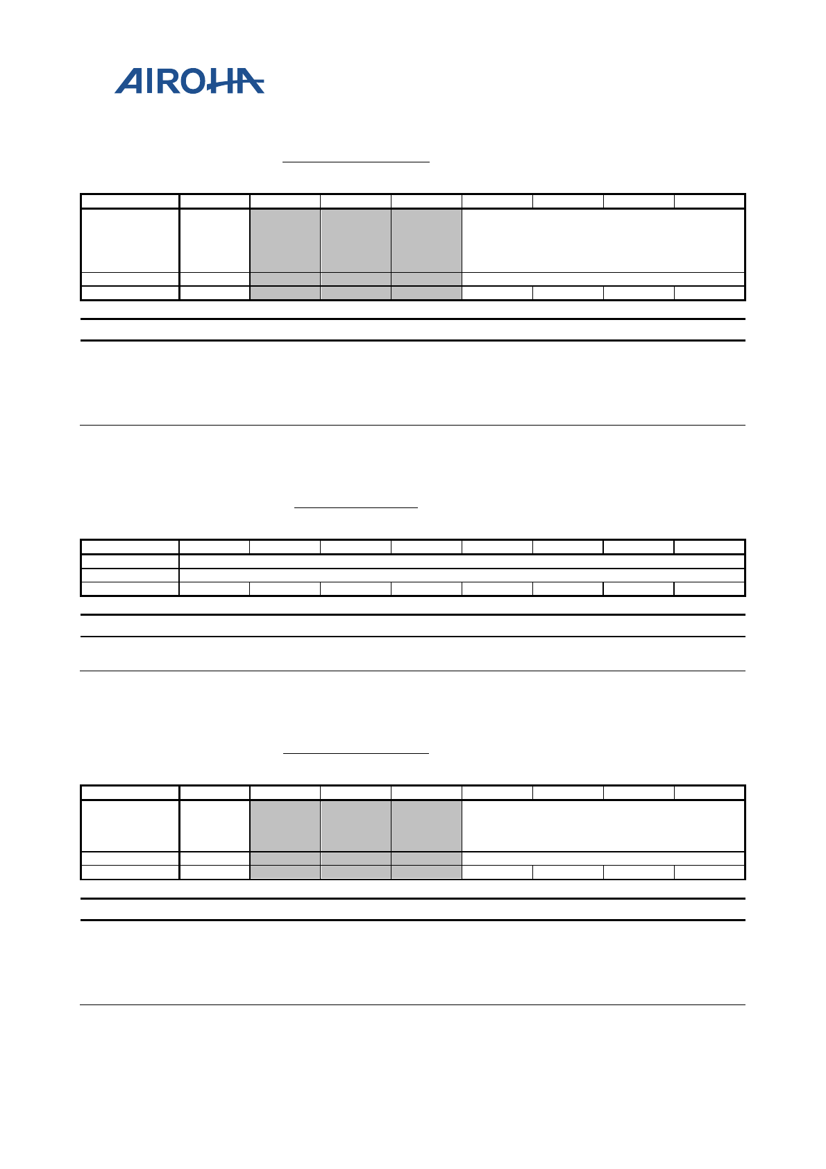
MT2523 Series Reference Manual
© 2015 - 2018 Airoha Technology Corp.
Page 669 of 692
This document contains information that is proprietary to Airoha Technology Corp. (“Airoha”) and/or its licensor(s).
Any unauthorized use, reproduction or disclosure of this document in whole or in part is strictly prohibited.
249 AUXADC_ADC36_H
AUXAD
C ADC
registe
r _H
00
Bit
7
6
5
4
3
2
1
0
Name
AUXADC
_ADC_R
DY_DCX
O_BY_A
P
AUXADC_ADC_OUT_DCXO_BY_AP_H
Type
RO
RO
Reset
0
0
0
0
0
Bit(s) Name Description
7 AUXADC_ADC_RDY
_DCXO_BY_AP
AUXADC channel 4 output data ready
0: AUXADC data proceeding
1: AUXADC data ready
3:0 AUXADC_ADC_OUT
_DCXO_BY_AP_H AUXADC channel 4 output data
24A AUXADC_ADC37
AUXAD
C ADC
registe
r 37
00
Bit
7
6
5
4
3
2
1
0
Name
AUXADC_ADC_OUT_DCXO_MDRT_L
Type
RO
Reset
0
0
0
0
0
0
0
0
Bit(s) Name Description
7:0 AUXADC_ADC_OUT
_DCXO_MDRT_L AUXADC output data
24B AUXADC_ADC37_H
AUXAD
C1 ADC
registe
r _H
00
Bit
7
6
5
4
3
2
1
0
Name
AUXADC
_ADC_R
DY_DCX
O_MDRT
AUXADC_ADC_OUT_DCXO_MDRT_H
Type
RO
RO
Reset
0
0
0
0
0
Bit(s) Name Description
7 AUXADC_ADC_RDY
_DCXO_MDRT
AUXADC output data ready
0: AUXADC data proceeding
1: AUXADC data ready
3:0 AUXADC_ADC_OUT
_DCXO_MDRT_H AUXADC output data
MT2523 Series Reference Manual
© 2015 - 2018 Airoha Technology Corp.
Page 670 of 692
This document contains information that is proprietary to Airoha Technology Corp. (“Airoha”) and/or its licensor(s).
Any unauthorized use, reproduction or disclosure of this document in whole or in part is strictly prohibited.
24C AUXADC_ADC38
AUXAD
C ADC
registe
r 34_H
00
Bit
7
6
5
4
3
2
1
0
Name
AUXADC_ADC_OUT_NAG_L
Type
RO
Reset
0
0
0
0
0
0
0
0
Bit(s) Name Description
7:0 AUXADC_ADC_OUT
_NAG_L
24D AUXADC_ADC38_H
AUXAD
C1 ADC
registe
r 34_H
00
Bit
7
6
5
4
3
2
1
0
Name
AUXADC
_ADC_R
DY_NAG
AUXADC_ADC_OUT_NAG_H
Type
RO
RO
Reset
0
0
0
0
0
0
0
0
Bit(s) Name Description
7 AUXADC_ADC_RDY
_NAG
6:0 AUXADC_ADC_OUT
_NAG_H
24E AUXADC_STA0
AUXAD
C_STA
0
00
Bit
7
6
5
4
3
2
1
0
Name
AUXADC_ADC_BUSY_IN_L
Type
RO
Reset
0
0
0
0
0
0
0
0
Bit(s) Name Description
7:0 AUXADC_ADC_BUS
Y_IN_L
AUXADC ADC BUSY STATUS_L, bit[7] = CH7 ~ bit[0] = CH0
1: BUSY
0: IDLE
24F AUXADC_STA0_H
AUXAD
C_STA
0_H
00
Bit
7
6
5
4
3
2
1
0
Name
AUXADC
_ADC_B
USY_IN_
WAKEUP
AUXADC
_ADC_B
USY_IN_
VISMPS0
AUXADC
_ADC_B
USY_IN_
LBAT2
AUXADC
_ADC_B
USY_IN_
LBAT
AUXADC_ADC_BUSY_IN_H
MT2523 Series Reference Manual
© 2015 - 2018 Airoha Technology Corp.
Page 671 of 692
This document contains information that is proprietary to Airoha Technology Corp. (“Airoha”) and/or its licensor(s).
Any unauthorized use, reproduction or disclosure of this document in whole or in part is strictly prohibited.
24F AUXADC_STA0_H
AUXAD
C_STA
0_H
00
Type
RO
RO
RO
RO
RO
Reset
0
0
0
0
0
0
0
0
Bit(s) Name Description
7 AUXADC_ADC_BUS
Y_IN_WAKEUP
ADC busy status
1: BUSY
0: IDLE
6 AUXADC_ADC_BUS
Y_IN_VISMPS0
ADC busy status
1: BUSY
0: IDLE
5 AUXADC_ADC_BUS
Y_IN_LBAT2
ADC busy status
1: BUSY
0: IDLE
4 AUXADC_ADC_BUS
Y_IN_LBAT
ADC busy status
1: BUSY
0: IDLE
3:0 AUXADC_ADC_BUS
Y_IN_H
AUXADC ADC BUSY STATUS_H, bit[3] = CH11 ~ bit[0] = CH8
1: BUSY
0: IDLE
250 AUXADC_STA1 AUXAD
C_STA1 00
Bit
7
6
5
4
3
2
1
0
Name
AUXADC
_ADC_B
USY_IN_
SHARE
AUXADC
_ADC_B
USY_IN_
MDRT
AUXADC
_ADC_B
USY_IN_
JEITA
AUXADC
_ADC_B
USY_IN_
NAG
AUXADC
_ADC_B
USY_IN_
DCXO_G
PS
AUXADC
_ADC_B
USY_IN_
DCXO_G
PS_MD
AUXADC
_ADC_B
USY_IN_
DCXO_G
PS_AP
AUXADC
_ADC_B
USY_IN_
DCXO_M
DRT
Type
RO
RO
RO
RO
RO
RO
RO
RO
Reset
0
0
0
0
0
0
0
0
Bit(s) Name Description
7 AUXADC_ADC_BUS
Y_IN_SHARE
ADC busy status
1: BUSY
0: IDLE
6 AUXADC_ADC_BUS
Y_IN_MDRT
ADC busy status
1: BUSY
0: IDLE
5 AUXADC_ADC_BUS
Y_IN_JEITA
ADC busy status
1: BUSY
0: IDLE
4 AUXADC_ADC_BUS
Y_IN_NAG
ADC busy status
1: BUSY
0: IDLE
3 AUXADC_ADC_BUS
Y_IN_DCXO_GPS
ADC busy status
1: BUSY
0: IDLE
2
AUXADC_ADC_BUS
Y_IN_DCXO_GPS_
MD
ADC busy status
1: BUSY
0: IDLE
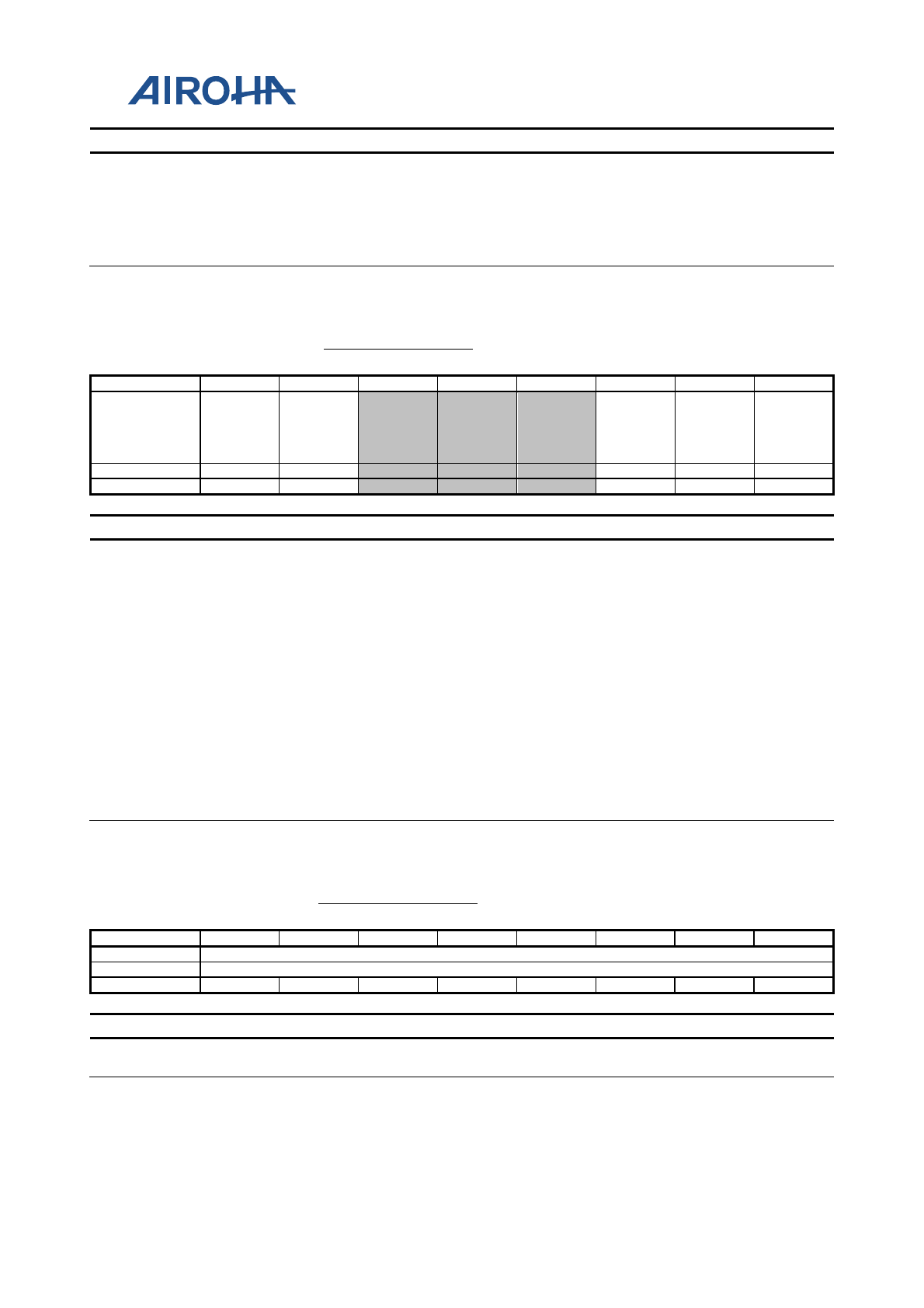
MT2523 Series Reference Manual
© 2015 - 2018 Airoha Technology Corp.
Page 672 of 692
This document contains information that is proprietary to Airoha Technology Corp. (“Airoha”) and/or its licensor(s).
Any unauthorized use, reproduction or disclosure of this document in whole or in part is strictly prohibited.
Bit(s) Name Description
1
AUXADC_ADC_BUS
Y_IN_DCXO_GPS_
AP
ADC busy status
1: BUSY
0: IDLE
0 AUXADC_ADC_BUS
Y_IN_DCXO_MDRT
ADC busy status
1: BUSY
0: IDLE
251 AUXADC_STA1_H
AUXAD
C_STA1
_H
00
Bit
7
6
5
4
3
2
1
0
Name
AUXADC
_ADC_B
USY_IN_
THR_MD
AUXADC
_ADC_B
USY_IN_
THR_H
W
AUXADC
_ADC_B
USY_IN_
FGADC2
AUXADC
_ADC_B
USY_IN_
FGADC1
AUXADC
_ADC_B
USY_IN_
IMP
Type
RO
RO
RO
RO
RO
Reset
0
0
0
0
0
Bit(s) Name Description
7 AUXADC_ADC_BUS
Y_IN_THR_MD
ADC busy status
1: BUSY
0: IDLE
6 AUXADC_ADC_BUS
Y_IN_THR_HW
ADC busy status
1: BUSY
0: IDLE
2 AUXADC_ADC_BUS
Y_IN_FGADC2
ADC busy status
1: BUSY
0: IDLE
1 AUXADC_ADC_BUS
Y_IN_FGADC1
ADC busy status
1: BUSY
0: IDLE
0 AUXADC_ADC_BUS
Y_IN_IMP
ADC busy status
1: BUSY
0: IDLE
2BE AUXADC_LBAT2_4
AUXAD
C_LBA
T2_4
00
Bit
7
6
5
4
3
2
1
0
Name
AUXADC_LBAT2_VOLT_MAX
Type
RW
Reset
0
0
0
0
0
0
0
0
Bit(s) Name Description
7:0 AUXADC_LBAT2_V
OLT_MAX LBAT2 detection voltage setting
MT2523 Series Reference Manual
© 2015 - 2018 Airoha Technology Corp.
Page 673 of 692
This document contains information that is proprietary to Airoha Technology Corp. (“Airoha”) and/or its licensor(s).
Any unauthorized use, reproduction or disclosure of this document in whole or in part is strictly prohibited.
2BF AUXADC_LBAT2_4_H
AUXAD
C_LBA
T2_4_
H
80
Bit
7
6
5
4
3
2
1
0
Name
AUXADC_LBAT2_VOLT_MAXa
Type
RW
Reset
0
0
0
0
Bit(s) Name Description
3:0 AUXADC_LBAT2_V
OLT_MAXa LBAT2 detection voltage setting
2C0 AUXADC_LBAT2_5
AUXAD
C_LBA
T2_5
00
Bit
7
6
5
4
3
2
1
0
Name
AUXADC_LBAT2_VOLT_MIN
Type
RW
Reset
0
0
0
0
0
0
0
0
Bit(s) Name Description
7:0 AUXADC_LBAT2_V
OLT_MIN LBAT2 detection voltage setting
2C1 AUXADC_LBAT2_5_H
AUXAD
C_LBA
T2_5_
H
80
Bit
7
6
5
4
3
2
1
0
Name
AUXADC_LBAT2_VOLT_MINa
Type
RW
Reset
0
0
0
0
Bit(s) Name Description
3:0 AUXADC_LBAT2_V
OLT_MINa LBAT2 detection voltage setting
2EF VBTLDO0
VBT
LDO
registe
r 0
00
Bit
7
6
5
4
3
2
1
0
Name
RG_VBT_CAL
Type
RW
Reset
0
0
0
0
Bit(s) Name Description
3:0 RG_VBT_CAL
MT2523 Series Reference Manual
© 2015 - 2018 Airoha Technology Corp.
Page 674 of 692
This document contains information that is proprietary to Airoha Technology Corp. (“Airoha”) and/or its licensor(s).
Any unauthorized use, reproduction or disclosure of this document in whole or in part is strictly prohibited.
2F3 VBTLDOBF0
VBT
LDO
buffer
registe
r 0
00
Bit
7
6
5
4
3
2
1
0
Name
RG_VBT_BUF_CAL
Type
RW
Reset
0
0
0
0
Bit(s) Name Description
3:0 RG_VBT_BUF_CAL
2F5 VBTPSI0
VBTP
LDO
PSI
registe
r0
00
Bit
7
6
5
4
3
2
1
0
Name
RG_LP_VBT_PMOD
RG_HP_VBT_PMOD
Type
RW
RW
Reset
0
0
0
0
Bit(s) Name Description
6:5 RG_LP_VBT_PMOD
2:1 RG_HP_VBT_PMO
D
2F6 VBTPSI1
VBTP
LDO
PSI
registe
r1
00
Bit
7
6
5
4
3
2
1
0
Name RG_S1_VBT_PMOD
RGS_S1_
VBT_ON
RG_S0_VBT_PMOD
RGS_S0_
VBT_ON
Type
RW
RO
RW
RO
Reset
0
0
0
0
0
0
Bit(s) Name Description
6:5 RG_S1_VBT_PMOD
4 RGS_S1_VBT_ON
2:1 RG_S0_VBT_PMOD
0 RGS_S0_VBT_ON
MT2523 Series Reference Manual
© 2015 - 2018 Airoha Technology Corp.
Page 675 of 692
This document contains information that is proprietary to Airoha Technology Corp. (“Airoha”) and/or its licensor(s).
Any unauthorized use, reproduction or disclosure of this document in whole or in part is strictly prohibited.
2F8 VALDO0
VA
LDO
registe
r 0
00
Bit
7
6
5
4
3
2
1
0
Name
RG_VA_CAL
Type
RW
Reset
0
0
0
0
Bit(s) Name Description
3:0 RG_VA_CAL
2FC VALDOBF0
VA
LDO
buffer
registe
r 0
00
Bit
7
6
5
4
3
2
1
0
Name
RG_VA_BUF_CAL
Type
RW
Reset
0
0
0
0
Bit(s) Name Description
3:0 RG_VA_BUF_CAL
2FE VAPSI0
VA
LDO
PSI
registe
r0
00
Bit
7
6
5
4
3
2
1
0
Name
RG_LP_VA_PMOD
RG_HP_VA_PMOD
Type
RW
RW
Reset
0
0
0
0
Bit(s) Name Description
6:5 RG_LP_VA_PMOD
2:1 RG_HP_VA_PMOD
2FF VAPSI1
VA
LDO
PSI
registe
r1
00
Bit
7
6
5
4
3
2
1
0
Name RG_S1_VA_PMOD
RGS_S1_
VA_ON
RG_S0_VA_PMOD
RGS_S0_
VA_ON
Type
RW
RO
RW
RO
Reset
0
0
0
0
0
0
MT2523 Series Reference Manual
© 2015 - 2018 Airoha Technology Corp.
Page 676 of 692
This document contains information that is proprietary to Airoha Technology Corp. (“Airoha”) and/or its licensor(s).
Any unauthorized use, reproduction or disclosure of this document in whole or in part is strictly prohibited.
Bit(s) Name Description
6:5 RG_S1_VA_PMOD
4 RGS_S1_VA_ON
2:1 RG_S0_VA_PMOD
0 RGS_S0_VA_ON
300 VCAMACTL0
VCAM
A
Control
registe
r 0
00
Bit
7
6
5
4
3
2
1
0
Name RG_OVR_VCAMA_P
MOD
RG_VCA
MA_OCF
B_EN
RG_VCA
MA_EN
Type
RW
RW
RW
Reset
0
0
0
0
Bit(s) Name Description
3:2 RG_OVR_VCAMA_P
MOD
1 RG_VCAMA_OCFB_
EN
0 RG_VCAMA_EN
302 VCAMALDO0 VCAM
ALDO0 00
Bit
7
6
5
4
3
2
1
0
Name
RG_VCAMA_CAL
Type
RW
Reset
0
0
0
0
Bit(s) Name Description
3:0 RG_VCAMA_CAL
303 VCAMALDO1
VCAM
A LDO
registe
r 1
03
Bit
7
6
5
4
3
2
1
0
Name
RG_VCAMA_VOSEL
Type
RW
Reset
0
1
1
Bit(s) Name Description
2:0 RG_VCAMA_VOSEL
3'b000: 1.5 V
3'b001: 1.8 V
3'b010: 2.5 V
3'b011: 2.8 V
MT2523 Series Reference Manual
© 2015 - 2018 Airoha Technology Corp.
Page 677 of 692
This document contains information that is proprietary to Airoha Technology Corp. (“Airoha”) and/or its licensor(s).
Any unauthorized use, reproduction or disclosure of this document in whole or in part is strictly prohibited.
Bit(s) Name Description
3'b100: Reserved
3'b101: Reserved
3'b110: Reserved
3'b111: Reserved
306 VCAMALDOBF0
VCAM
A LDO
buffer
registe
r 0
00
Bit
7
6
5
4
3
2
1
0
Name
RG_VCAMA_COIN_SS_TRIM_BI
AS
RG_VCAMA_BUF_CAL
Type
RW
RW
Reset
0
0
0
0
0
0
0
Bit(s) Name Description
6:4 RG_VCAMA_COIN_
SS_TRIM_BIAS
3:0 RG_VCAMA_BUF_C
AL
30A PSWCTL0
PSW
Control
registe
r 0
00
Bit
7
6
5
4
3
2
1
0
Name
RG_SW
MP_EN
RG_SWD
P_EN
RG_SWX
M_EN
Type
RW
RW
RW
Reset
0
0
0
Bit(s) Name Description
2 RG_SWMP_EN
1 RG_SWDP_EN
0 RG_SWXM_EN
30F SWIO18PSI
SWIO1
8 LDO
PSI
registe
r
00
Bit
7
6
5
4
3
2
1
0
Name
RGS_S1_
SWDP_O
N
RGS_S0_
SWDP_O
N
RGS_S1_
SWXM_
ON
RGS_S0_
SWXM_
ON
Type
RO
RO
RO
RO
Reset
0
0
0
0
Bit(s) Name Description
MT2523 Series Reference Manual
© 2015 - 2018 Airoha Technology Corp.
Page 678 of 692
This document contains information that is proprietary to Airoha Technology Corp. (“Airoha”) and/or its licensor(s).
Any unauthorized use, reproduction or disclosure of this document in whole or in part is strictly prohibited.
Bit(s) Name Description
3 RGS_S1_SWDP_ON
2 RGS_S0_SWDP_ON
1 RGS_S1_SWXM_ON
0 RGS_S0_SWXM_O
N
313 VIO28LDO0 VIO28
LDO0 00
Bit
7
6
5
4
3
2
1
0
Name
RG_VIO28_CAL_E1
Type
RW
Reset
0
0
0
0
Bit(s) Name Description
3:0 RG_VIO28_CAL_E1
4'b0000: 0 mV
4'b0001: -20 mV
4'b0010: -40 mV
4'b0011: -60 mV
4'b0100: -80 mV
4'b0101: -100 mV
4'b0110: -120 mV
4'b0111: -140 mV
4'b1000: +160 mV
4'b1001: +140 mV
4'b1010: +120 mV
4'b1011: +100 mV
4'b1100: +80 mV
4'b1101: +60 mV
4'b1110: +40 mV
4'b1111: +20 mV
317 VIO28LDOBF0
VIO28
LDOBF
0
00
Bit
7
6
5
4
3
2
1
0
Name
RG_VIO28_BUF_CAL_E1
Type
RW
Reset
0
0
0
0
Bit(s) Name Description
3:0 RG_VIO28_BUF_CA
L_E1
4'b0000: 0 mV
4'b0001: -20 mV
4'b0010: -40 mV
4'b0011: -60 mV
4'b0100: -80 mV
4'b0101: -100 mV
4'b0110: -120 mV
4'b0111: -140 mV
4'b1000: +160 mV
4'b1001: +140 mV
4'b1010: +120 mV
4'b1011: +100 mV
4'b1100: +80 mV
4'b1101: +60 mV
MT2523 Series Reference Manual
© 2015 - 2018 Airoha Technology Corp.
Page 679 of 692
This document contains information that is proprietary to Airoha Technology Corp. (“Airoha”) and/or its licensor(s).
Any unauthorized use, reproduction or disclosure of this document in whole or in part is strictly prohibited.
Bit(s) Name Description
4'b1110: +40 mV
4'b1111: +20 mV
319 VIO28PSI0
VIO28
LDO
PSI
registe
r0
00
Bit
7
6
5
4
3
2
1
0
Name
RG_LP_VIO28_PMO
D_E1
RG_HP_VIO28_PMO
D_E1
Type
RW
RW
Reset
0
0
0
0
Bit(s) Name Description
6:5 RG_LP_VIO28_PM
OD_E1
2:1 RG_HP_VIO28_PM
OD_E1
31A VIO28PSI1
VIO28
LDO
PSI
registe
r1
00
Bit
7
6
5
4
3
2
1
0
Name RG_S1_VIO28_PMO
D_E1
RGS_S1_
VIO28_O
N_E1
RG_S0_VIO28_PMO
D_E1
RGS_S0_
VIO28_O
N_E1
Type
RW
RO
RW
RO
Reset
0
0
0
0
0
0
Bit(s) Name Description
6:5 RG_S1_VIO28_PMO
D_E1
4 RGS_S1_VIO28_ON
_E1
2:1 RG_S0_VIO28_PM
OD_E1
0 RGS_S0_VIO28_ON
_E1
31C VMCLDO0 VMCL
DO0 00
Bit
7
6
5
4
3
2
1
0
Name
RG_VMC_CAL
Type
RW
Reset
0
0
0
0
Bit(s) Name Description
MT2523 Series Reference Manual
© 2015 - 2018 Airoha Technology Corp.
Page 680 of 692
This document contains information that is proprietary to Airoha Technology Corp. (“Airoha”) and/or its licensor(s).
Any unauthorized use, reproduction or disclosure of this document in whole or in part is strictly prohibited.
Bit(s) Name Description
3:0 RG_VMC_CAL
31D VMCLDO1 VMCL
DO1 02
Bit
7
6
5
4
3
2
1
0
Name
RG_VMC_VOSEL
Type
RW
Reset
1
0
Bit(s) Name Description
1:0 RG_VMC_VOSEL
2'b00: 1.8V
2'b01: 2.8V
2'b10: 3V
2b'11: 3.3V
320 VMCLDOBF0 VMCL
DOBF0 00
Bit
7
6
5
4
3
2
1
0
Name
RG_VMC_BUF_CAL
Type
RW
Reset
0
0
0
0
Bit(s) Name Description
3:0 RG_VMC_BUF_CAL
322 VMCPSI0
VMC
LDO
PSI
registe
r0
00
Bit
7
6
5
4
3
2
1
0
Name
RG_LP_VMC_PMOD
RG_HP_VMC_PMOD
Type
RW
RW
Reset
0
0
0
0
Bit(s) Name Description
6:5 RG_LP_VMC_PMO
D
2:1 RG_HP_VMC_PMO
D
323 VMCPSI1
VMC
LDO
PSI
registe
r1
00
Bit
7
6
5
4
3
2
1
0
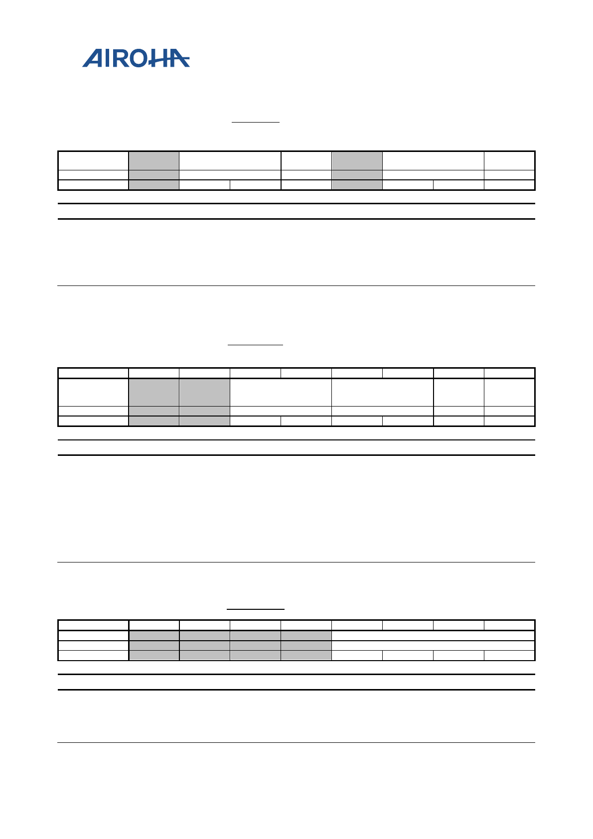
MT2523 Series Reference Manual
© 2015 - 2018 Airoha Technology Corp.
Page 681 of 692
This document contains information that is proprietary to Airoha Technology Corp. (“Airoha”) and/or its licensor(s).
Any unauthorized use, reproduction or disclosure of this document in whole or in part is strictly prohibited.
323 VMCPSI1
VMC
LDO
PSI
registe
r1
00
Name RG_S1_VMC_PMOD
RGS_S1_
VMC_ON
RG_S0_VMC_PMOD
RGS_S0_
VMC_ON
Type
RW
RO
RW
RO
Reset
0
0
0
0
0
0
Bit(s) Name Description
6:5 RG_S1_VMC_PMOD
4 RGS_S1_VMC_ON
2:1 RG_S0_VMC_PMO
D
0 RGS_S0_VMC_ON
324 VIBRCTL0
VIBR
Control
registe
r 0
00
Bit
7
6
5
4
3
2
1
0
Name RG_VIBR_STBTD RG_OVR_VIBR_PMO
D
RG_VIB
R_OCFB
_EN
RG_VIB
R_EN
Type
RW
RW
RW
RW
Reset
0
0
0
0
0
0
Bit(s) Name Description
5:4 RG_VIBR_STBTD
00: 240us (Li-ion) / 1.6ms (coin)
01: 2.4ms (Li-ion) / 15 ms (coin)
10: 90 us (Li-ion) / 1.2 ms (coin)
11: 3 ms (Li-ion) / 17 ms (coin)
3:2 RG_OVR_VIBR_PM
OD
1 RG_VIBR_OCFB_E
N
0 RG_VIBR_EN
326 VIBRLDO0 VIBRL
DO0 00
Bit
7
6
5
4
3
2
1
0
Name
RG_VIBR_CAL
Type
RW
Reset
0
0
0
0
Bit(s) Name Description
3:0 RG_VIBR_CAL
4'b0000: 0 mV
4'b0001: -20 mV
4'b0010: -40 mV
4'b0011: -60 mV
4'b0100: -80 mV
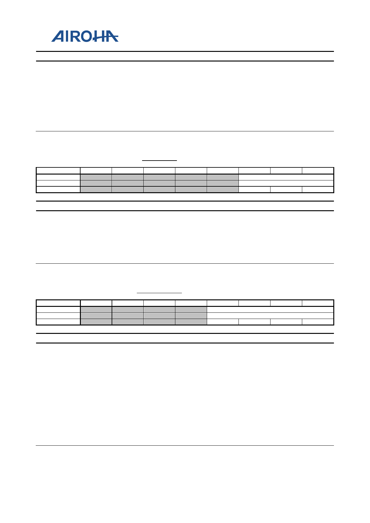
MT2523 Series Reference Manual
© 2015 - 2018 Airoha Technology Corp.
Page 682 of 692
This document contains information that is proprietary to Airoha Technology Corp. (“Airoha”) and/or its licensor(s).
Any unauthorized use, reproduction or disclosure of this document in whole or in part is strictly prohibited.
Bit(s) Name Description
4'b0101: -100 mV
4'b0110: -120 mV
4'b0111: -140 mV
4'b1000: +160 mV
4'b1001: +140 mV
4'b1010: +120 mV
4'b1011: +100 mV
4'b1100: +80 mV
4'b1101: +60 mV
4'b1110: +40 mV
4'b1111: +20 mV
327 VIBRLDO1 VIBRL
DO1 05
Bit
7
6
5
4
3
2
1
0
Name
RG_VIBR_VOSEL
Type
RW
Reset
1
0
1
Bit(s) Name Description
2:0 RG_VIBR_VOSEL
3'b000: 1.3V
3'b001: 1.5 V
3'b010: 1.8 V
3'b011: 2 V
3'b100: 2.5 V
3'b101: 2.8 V
3'b110: 3 V
3'b111: 3.3 V
32A VIBRLDOBF0 VIBRL
DOBF0 00
Bit
7
6
5
4
3
2
1
0
Name
RG_VIBR_BUF_CAL
Type
RW
Reset
0
0
0
0
Bit(s) Name Description
3:0 RG_VIBR_BUF_CA
L
4'b0000: 0 mV
4'b0001: -20 mV
4'b0010: -40 mV
4'b0011: -60 mV
4'b0100: -80 mV
4'b0101: -100 mV
4'b0110: -120 mV
4'b0111: -140 mV
4'b1000: +160 mV
4'b1001: +140 mV
4'b1010: +120 mV
4'b1011: +100 mV
4'b1100: +80 mV
4'b1101: +60 mV
4'b1110: +40 mV
4'b1111: +20 mV
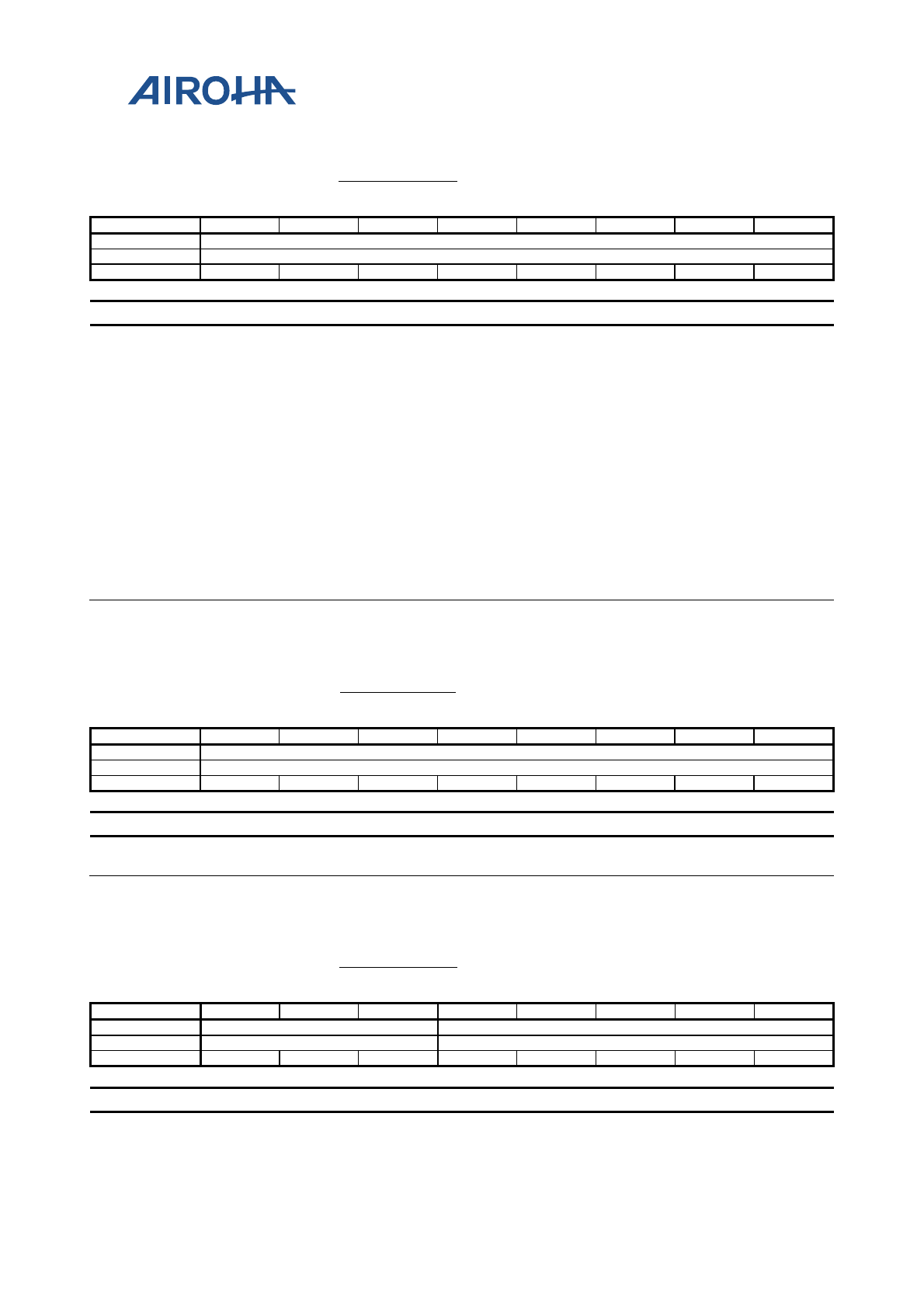
MT2523 Series Reference Manual
© 2015 - 2018 Airoha Technology Corp.
Page 683 of 692
This document contains information that is proprietary to Airoha Technology Corp. (“Airoha”) and/or its licensor(s).
Any unauthorized use, reproduction or disclosure of this document in whole or in part is strictly prohibited.
32C ISINK0_CON0
ISINK0
Control
Registe
r 0
00
Bit
7
6
5
4
3
2
1
0
Name
ISINK_DIM0_FSEL_L
Type
RW
Reset
0
0
0
0
0
0
0
0
Bit(s) Name Description
7:0 ISINK_DIM0_FSEL
_L
ISINK0 dimming frequency selection
backlight: (@ 2MHz)
2: 20k Hz
61: 1k Hz
311: 200 Hz
12499: 5 Hz
31249: 2 Hz
62499: 1Hz
indicator: (@32KHz)
0: 1k Hz
4: 200 Hz
199: 5 Hz
499: 2 Hz
999: 1Hz
1999: 0.5Hz
4999: 0.2 Hz
9999: 0.1 Hz
32D ISINK0_CON1
ISINK0
Control
Registe
r 1
00
Bit
7
6
5
4
3
2
1
0
Name
ISINK_DIM0_FSEL_H
Type
RW
Reset
0
0
0
0
0
0
0
0
Bit(s) Name Description
7:0 ISINK_DIM0_FSEL
_H ISINK0 dimming frequency selection
32E ISINK0_CON2
ISINK0
Control
Registe
r 2
00
Bit
7
6
5
4
3
2
1
0
Name
ISINK_CH0_STEP
ISINK_DIM0_DUTY
Type
RW
RW
Reset
0
0
0
0
0
0
0
0
Bit(s) Name Description
7:5 ISINK_CH0_STEP
Coarse 6 step current level for ISINK CH0
000: 4mA
001: 8mA
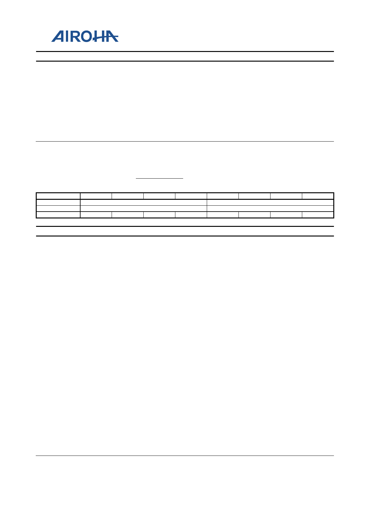
MT2523 Series Reference Manual
© 2015 - 2018 Airoha Technology Corp.
Page 684 of 692
This document contains information that is proprietary to Airoha Technology Corp. (“Airoha”) and/or its licensor(s).
Any unauthorized use, reproduction or disclosure of this document in whole or in part is strictly prohibited.
Bit(s) Name Description
010: 12mA
011: 16mA
100: 20mA
101: 24mA
110: 24mA
111: 24mA
4:0 ISINK_DIM0_DUTY
ISINK ON-duty of dimming0 control
N: (N+1)/32
0: 1/32
1: 2/32
2: 3/32
31: 32/32
330 ISINK0_CON4
ISINK0
Control
Registe
r 4
00
Bit
7
6
5
4
3
2
1
0
Name
ISINK_BREATH0_TR1_SEL
ISINK_BREATH0_TR2_SEL
Type
RW
RW
Reset
0
0
0
0
0
0
0
0
Bit(s) Name Description
7:4 ISINK_BREATH0_T
R1_SEL
ISINK0 breath mode rising time selection for duty 0%~30%
0: 0.123s
1: 0.338s
2: 0.523s
3: 0.707s
4: 0.926s
5: 1.107s
6: 1.291s
7: 1.507s
8: 1.691s
9: 1.876s
10: 2.091s
11: 2.276s
12: 2.460s
13: 2.676s
14: 2.860s
15: 3.075s
3:0 ISINK_BREATH0_T
R2_SEL
ISINK0 breath mode rising time selection for duty 31%~100%
0: 0.123s
1: 0.338s
2: 0.523s
3: 0.707s
4: 0.926s
5: 1.107s
6: 1.291s
7: 1.507s
8: 1.691s
9: 1.876s
10: 2.091s
11: 2.276s
12: 2.460s
13: 2.676s
14: 2.860s
15: 3.075s
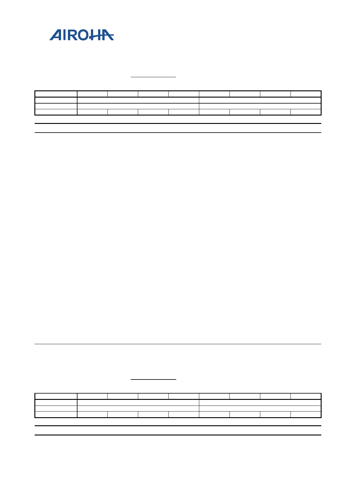
MT2523 Series Reference Manual
© 2015 - 2018 Airoha Technology Corp.
Page 685 of 692
This document contains information that is proprietary to Airoha Technology Corp. (“Airoha”) and/or its licensor(s).
Any unauthorized use, reproduction or disclosure of this document in whole or in part is strictly prohibited.
331 ISINK0_CON5
ISINK0
Control
Registe
r 5
00
Bit
7
6
5
4
3
2
1
0
Name
ISINK_BREATH0_TF1_SEL
ISINK_BREATH0_TF2_SEL
Type
RW
RW
Reset
0
0
0
0
0
0
0
0
Bit(s) Name Description
7:4 ISINK_BREATH0_T
F1_SEL
ISINK0 breath mode falling time selection for duty 0%~30%
0: 0.123s
1: 0.338s
2: 0.523s
3: 0.707s
4: 0.926s
5: 1.107s
6: 1.291s
7: 1.507s
8: 1.691s
9: 1.876s
10: 2.091s
11: 2.276s
12: 2.460s
13: 2.676s
14: 2.860s
15: 3.075s
3:0 ISINK_BREATH0_T
F2_SEL
ISINK0 breath mode falling time selection for duty 31%~100%
0: 0.123s
1: 0.338s
2: 0.523s
3: 0.707s
4: 0.926s
5: 1.107s
6: 1.291s
7: 1.507s
8: 1.691s
9: 1.876s
10: 2.091s
11: 2.276s
12: 2.460s
13: 2.676s
14: 2.860s
15: 3.075s
332 ISINK0_CON6
ISINK0
Control
Registe
r 6
00
Bit
7
6
5
4
3
2
1
0
Name
ISINK_BREATH0_TON_SEL
ISINK_BREATH0_TOFF_SEL
Type
RW
RW
Reset
0
0
0
0
0
0
0
0
Bit(s) Name Description
7:4
ISINK_BREATH0_T
ISINK0 breath mode Ton time selection
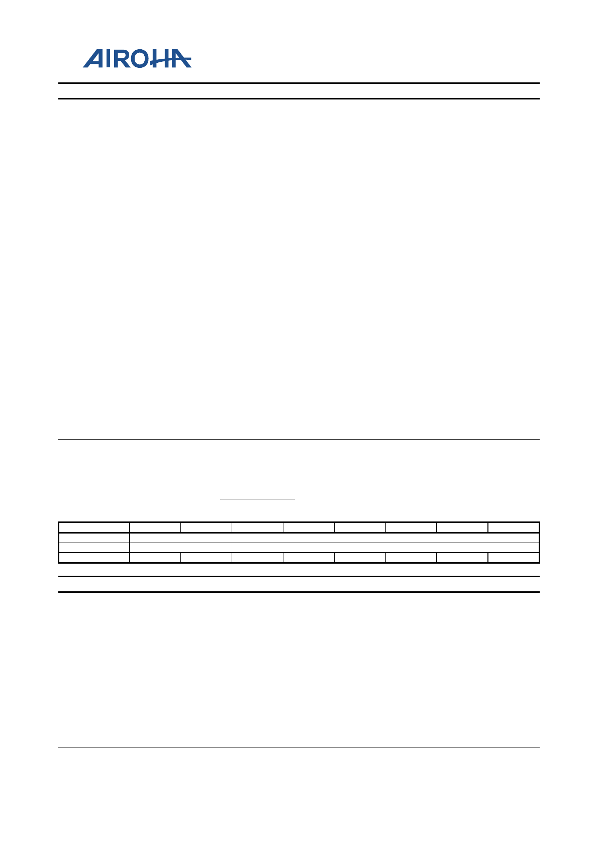
MT2523 Series Reference Manual
© 2015 - 2018 Airoha Technology Corp.
Page 686 of 692
This document contains information that is proprietary to Airoha Technology Corp. (“Airoha”) and/or its licensor(s).
Any unauthorized use, reproduction or disclosure of this document in whole or in part is strictly prohibited.
Bit(s) Name Description
ON_SEL
0: 0.123s
1: 0.338s
2: 0.523s
3: 0.707s
4: 0.926s
5: 1.107s
6: 1.291s
7: 1.507s
8: 1.691s
9: 1.876s
10: 2.091s
11: 2.276s
12: 2.460s
13: 2.676s
14: 2.860s
15: 3.075s
3:0 ISINK_BREATH0_T
OFF_SEL
ISINK0 breath mode Toff time selection
0: 0.246s
1: 0.677s
2: 1.046s
3: 1.417s
4: 1.845s
5: 2.214s
6: 2.583s
7: 3.014s
8: 3.383s
9: 3.752s
10: 4.183s
11: 4.552s
12: 4.921s
13: 5.351s
14: 5.720s
15: 6.151s
333 ISINK1_CON0
ISINK1
Control
Registe
r 0
00
Bit
7
6
5
4
3
2
1
0
Name
ISINK_DIM1_FSEL_L
Type
RW
Reset
0
0
0
0
0
0
0
0
Bit(s) Name Description
7:0 ISINK_DIM1_FSEL_
L
ISINK1 dimming frequency selection
backlight: (@ 2MHz)
2: 20k Hz
61: 1k Hz
311: 200 Hz
12499: 5 Hz
31249: 2 Hz
62499: 1Hz
indicator: (@32KHz)
0: 1k Hz
4: 200 Hz
199: 5 Hz
499: 2 Hz
999: 1Hz
1999: 0.5Hz
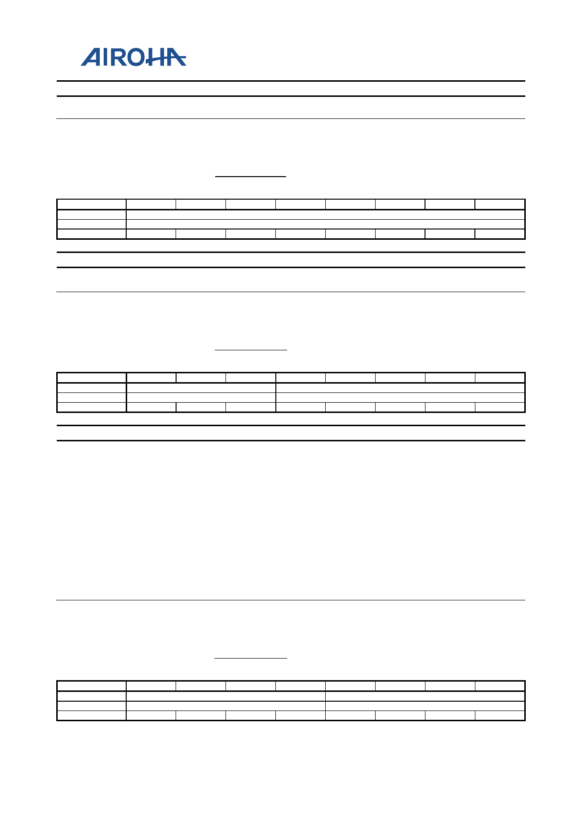
MT2523 Series Reference Manual
© 2015 - 2018 Airoha Technology Corp.
Page 687 of 692
This document contains information that is proprietary to Airoha Technology Corp. (“Airoha”) and/or its licensor(s).
Any unauthorized use, reproduction or disclosure of this document in whole or in part is strictly prohibited.
Bit(s) Name Description
4999: 0.2 Hz
9999: 0.1 Hz
334 ISINK1_CON1
ISINK1
Control
Registe
r 1
00
Bit
7
6
5
4
3
2
1
0
Name
ISINK_DIM1_FSEL_H
Type
RW
Reset
0
0
0
0
0
0
0
0
Bit(s) Name Description
7:0 ISINK_DIM1_FSEL_
H
335 ISINK1_CON2
ISINK1
Control
Registe
r 2
00
Bit
7
6
5
4
3
2
1
0
Name
ISINK_CH1_STEP
ISINK_DIM1_DUTY
Type
RW
RW
Reset
0
0
0
0
0
0
0
0
Bit(s) Name Description
7:5 ISINK_CH1_STEP
Coarse 6 step current level for ISINK CH1
000: 4mA
001: 8mA
010: 12mA
011: 16mA
100: 20mA
101: 24mA
110: 24mA
111: 24mA
4:0 ISINK_DIM1_DUTY
ISINK ON-duty of dimming1 control
N: (N+1)/32
0: 1/32
1: 2/32
2: 3/32
31: 32/32
337 ISINK1_CON4
ISINK1
Control
Registe
r 4
00
Bit
7
6
5
4
3
2
1
0
Name
ISINK_BREATH1_TR1_SEL
ISINK_BREATH1_TR2_SEL
Type
RW
RW
Reset
0
0
0
0
0
0
0
0
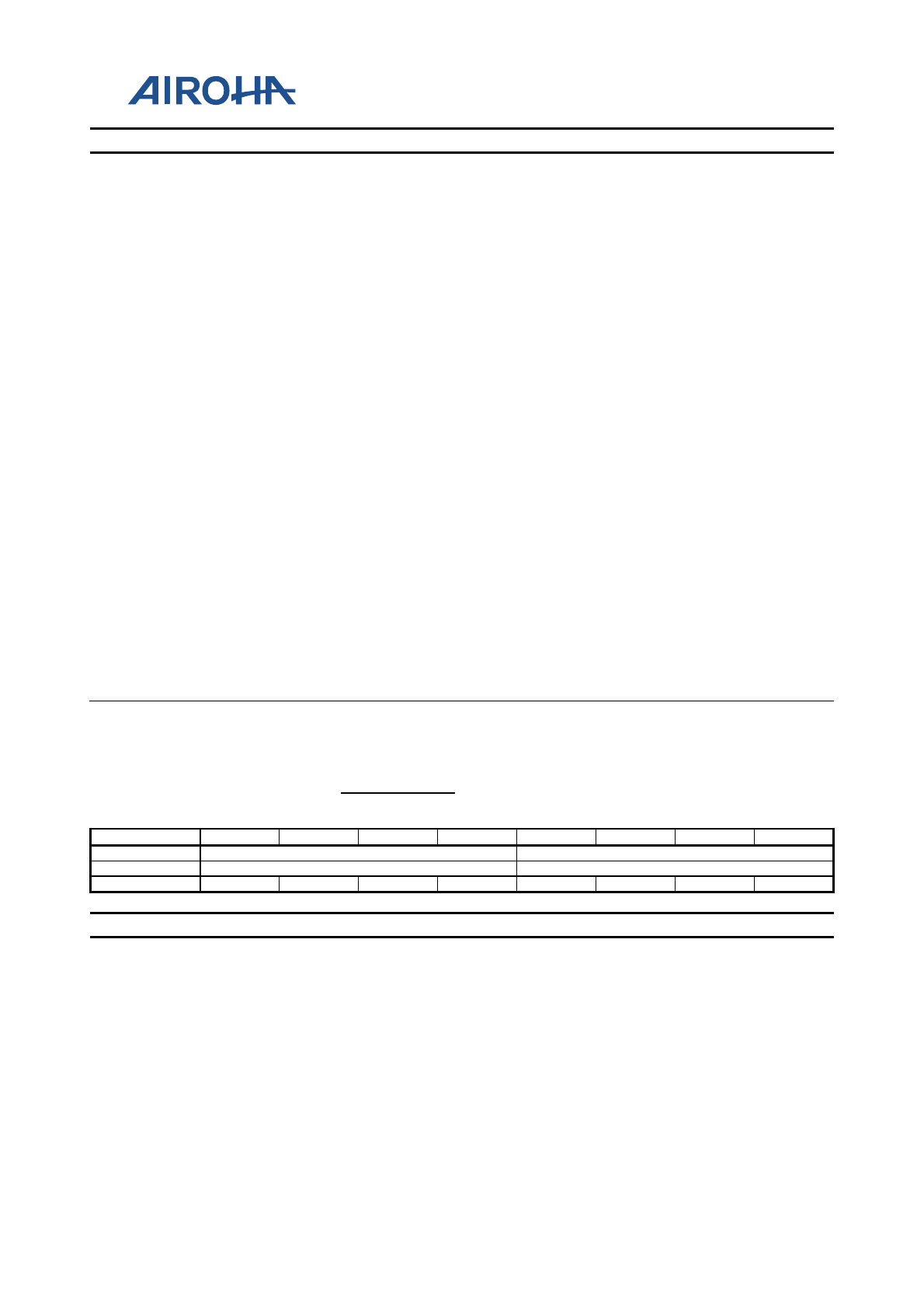
MT2523 Series Reference Manual
© 2015 - 2018 Airoha Technology Corp.
Page 688 of 692
This document contains information that is proprietary to Airoha Technology Corp. (“Airoha”) and/or its licensor(s).
Any unauthorized use, reproduction or disclosure of this document in whole or in part is strictly prohibited.
Bit(s) Name Description
7:4 ISINK_BREATH1_T
R1_SEL
ISINK1 breath mode rising time selection for duty 0%~30%
0: 0.123s
1: 0.338s
2: 0.523s
3: 0.707s
4: 0.926s
5: 1.107s
6: 1.291s
7: 1.507s
8: 1.691s
9: 1.876s
10: 2.091s
11: 2.276s
12: 2.460s
13: 2.676s
14: 2.860s
15: 3.075s
3:0 ISINK_BREATH1_T
R2_SEL
ISINK1 breath mode rising time selection for duty 31%~100%
0: 0.123s
1: 0.338s
2: 0.523s
3: 0.707s
4: 0.926s
5: 1.107s
6: 1.291s
7: 1.507s
8: 1.691s
9: 1.876s
10: 2.091s
11: 2.276s
12: 2.460s
13: 2.676s
14: 2.860s
15: 3.075s
338 ISINK1_CON5
ISINK1
Control
Registe
r 5
00
Bit
7
6
5
4
3
2
1
0
Name
ISINK_BREATH1_TF1_SEL
ISINK_BREATH1_TF2_SEL
Type
RW
RW
Reset
0
0
0
0
0
0
0
0
Bit(s) Name Description
7:4 ISINK_BREATH1_T
F1_SEL
ISINK1 breath mode falling time selection for duty 0% ~ 30%
0: 0.123s
1: 0.338s
2: 0.523s
3: 0.707s
4: 0.926s
5: 1.107s
6: 1.291s
7: 1.507s
8: 1.691s
9: 1.876s
10: 2.091s
11: 2.276s
12: 2.460s
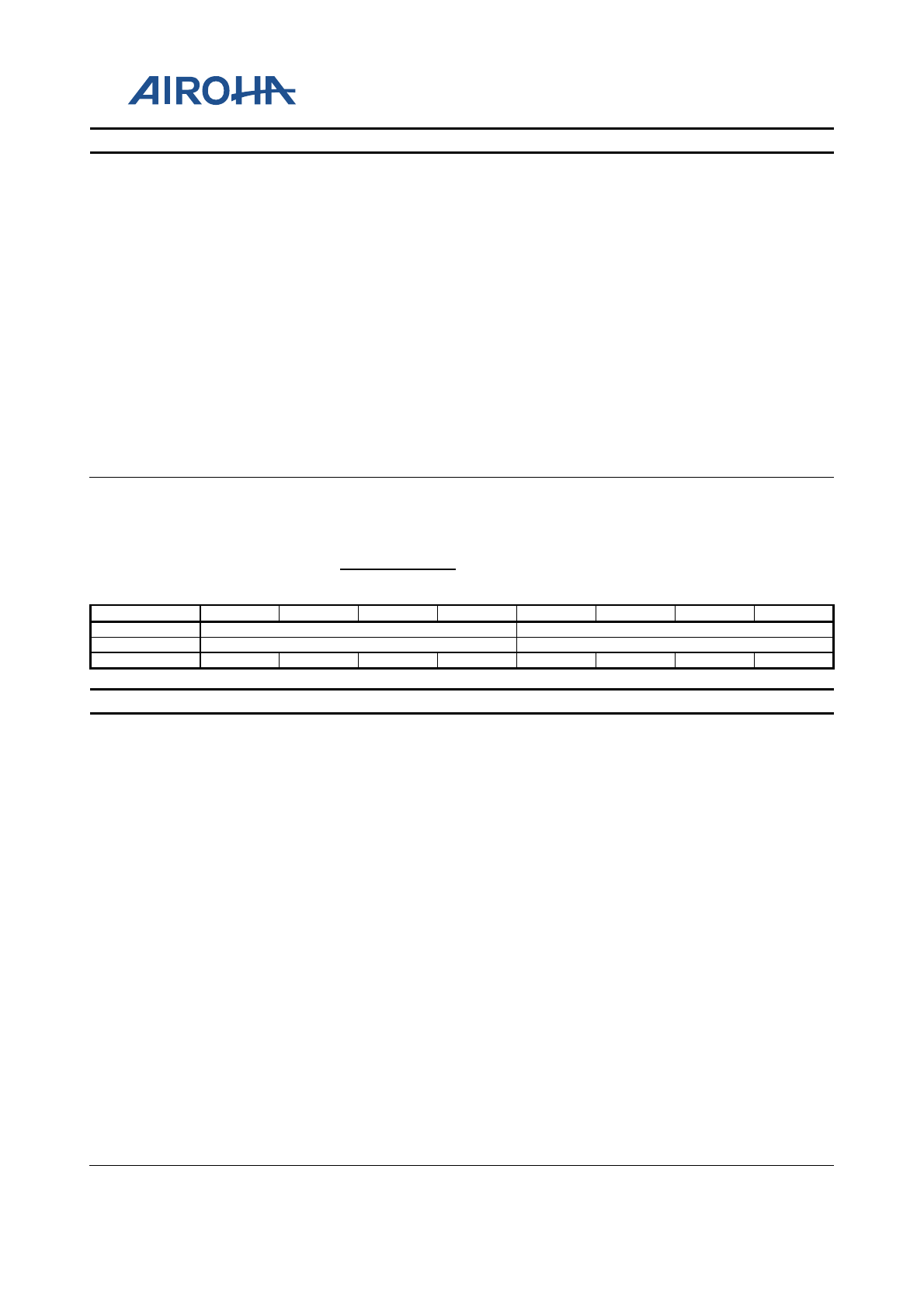
MT2523 Series Reference Manual
© 2015 - 2018 Airoha Technology Corp.
Page 689 of 692
This document contains information that is proprietary to Airoha Technology Corp. (“Airoha”) and/or its licensor(s).
Any unauthorized use, reproduction or disclosure of this document in whole or in part is strictly prohibited.
Bit(s) Name Description
13: 2.676s
14: 2.860s
15: 3.075s
3:0 ISINK_BREATH1_T
F2_SEL
ISINK1 breath mode falling time selection for duty31% ~ 100%
0: 0.123s
1: 0.338s
2: 0.523s
3: 0.707s
4: 0.926s
5: 1.107s
6: 1.291s
7: 1.507s
8: 1.691s
9: 1.876s
10: 2.091s
11: 2.276s
12: 2.460s
13: 2.676s
14: 2.860s
15: 3.075s
339 ISINK1_CON6
ISINK1
Control
Registe
r 6
00
Bit
7
6
5
4
3
2
1
0
Name
ISINK_BREATH1_TON_SEL
ISINK_BREATH1_TOFF_SEL
Type
RW
RW
Reset
0
0
0
0
0
0
0
0
Bit(s) Name Description
7:4 ISINK_BREATH1_T
ON_SEL
ISINK1 breath mode Ton time selection
0: 0.123s
1: 0.338s
2: 0.523s
3: 0.707s
4: 0.926s
5: 1.107s
6: 1.291s
7: 1.507s
8: 1.691s
9: 1.876s
10: 2.091s
11: 2.276s
12: 2.460s
13: 2.676s
14: 2.860s
15: 3.075s
3:0 ISINK_BREATH1_T
OFF_SEL
ISINK1 breath mode Toff time selection
0: 0.246s
1: 0.677s
2: 1.046s
3: 1.417s
4: 1.845s
5: 2.214s
6: 2.583s
7: 3.014s
8: 3.383s
9: 3.752s
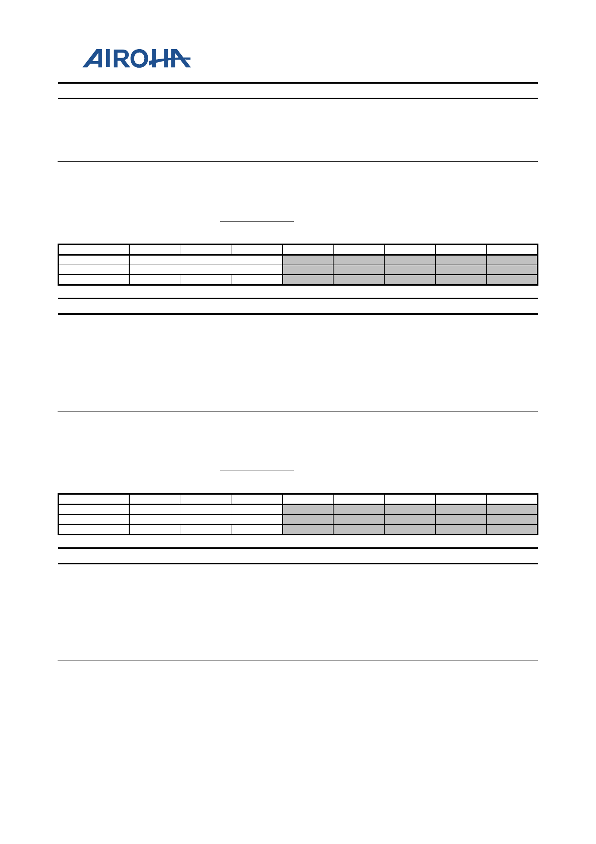
MT2523 Series Reference Manual
© 2015 - 2018 Airoha Technology Corp.
Page 690 of 692
This document contains information that is proprietary to Airoha Technology Corp. (“Airoha”) and/or its licensor(s).
Any unauthorized use, reproduction or disclosure of this document in whole or in part is strictly prohibited.
Bit(s) Name Description
10: 4.183s
11: 4.552s
12: 4.921s
13: 5.351s
14: 5.720s
15: 6.151s
33A ISINK2_CON1
ISINK2
Control
Registe
r 1
00
Bit
7
6
5
4
3
2
1
0
Name
ISINK_CH2_STEP
Type
RW
Reset
0
0
0
Bit(s) Name Description
7:5 ISINK_CH2_STEP
Coarse 6 step current level for ISINK CH2
000: 4mA
001: 8mA
010: 12mA
011: 16mA
100: 20mA
101: 24mA
110: 24mA
111: 24mA
33C ISINK3_CON1
ISINK3
Control
Registe
r 1
00
Bit
7
6
5
4
3
2
1
0
Name
ISINK_CH3_STEP
Type
RW
Reset
0
0
0
Bit(s) Name Description
7:5 ISINK_CH3_STEP
Coarse 6 step current level for ISINK CH3
000: 4mA
001: 8mA
010: 12mA
011: 16mA
100: 20mA
101: 24mA
110: 24mA
111: 24mA
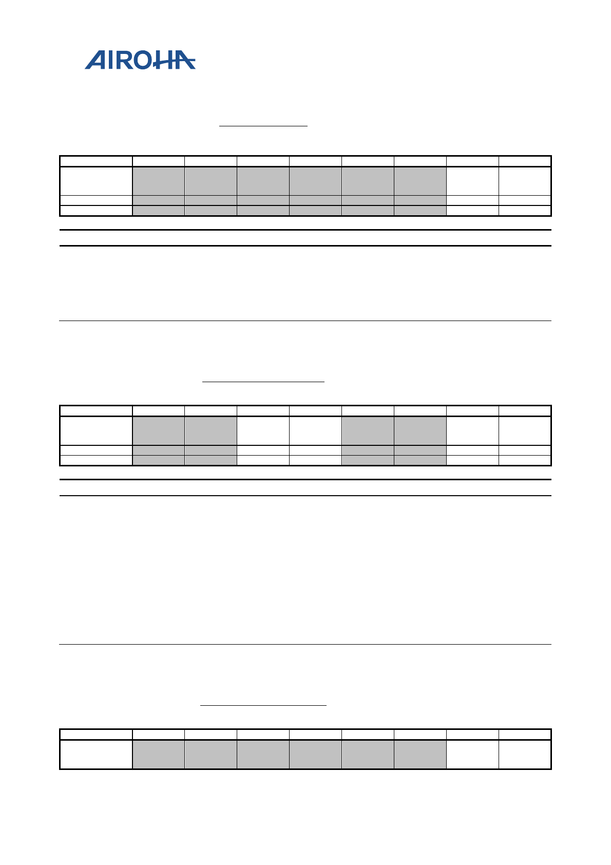
MT2523 Series Reference Manual
© 2015 - 2018 Airoha Technology Corp.
Page 691 of 692
This document contains information that is proprietary to Airoha Technology Corp. (“Airoha”) and/or its licensor(s).
Any unauthorized use, reproduction or disclosure of this document in whole or in part is strictly prohibited.
33F ISINK_ANA0_H
ISINKS
ACD
Interfa
ce 0
High
00
Bit
7
6
5
4
3
2
1
0
Name
RG_ISIN
K1_DOU
BLE
RG_ISIN
K0_DOU
BLE
Type
RW
RW
Reset
0
0
Bit(s) Name Description
1 RG_ISINK1_DOUBL
E
isink surrent doubel
1'b1: enable
1'b0: disable
0 RG_ISINK0_DOUBL
E
isink surrent doubel
1'b1: enable
1'b0: disable
344 ISINK_EN_CTRL_Low
ISINK
Enable
control
Low
F0
Bit
7
6
5
4
3
2
1
0
Name
RG_ISIN
K1_CHO
P_EN
RG_ISIN
K0_CHO
P_EN
ISINK_C
H1_EN
ISINK_C
H0_EN
Type
RW
RW
RW
RW
Reset
1
1
0
0
Bit(s) Name Description
5 RG_ISINK1_CHOP_
EN
ISINK Channel 1 CHOP CLK enable
1'b0: Disable
1'b1: Enable
4 RG_ISINK0_CHOP_
EN
ISINK Channel 0 CHOP CLK enable
1'b0: Disable
1'b1: Enable
1 ISINK_CH1_EN
Turn on ISINK Channel 1
1'b0: Disable
1'b1: Enable
0 ISINK_CH0_EN
Turn on ISINK Channel 0
1'b0: Disable
1'b1: Enable
345 ISINK_EN_CTRL_High
ISINK
Enable
control
High
00
Bit
7
6
5
4
3
2
1
0
Name
ISINK_C
H1_BIAS
_EN
ISINK_C
H0_BIAS
_EN
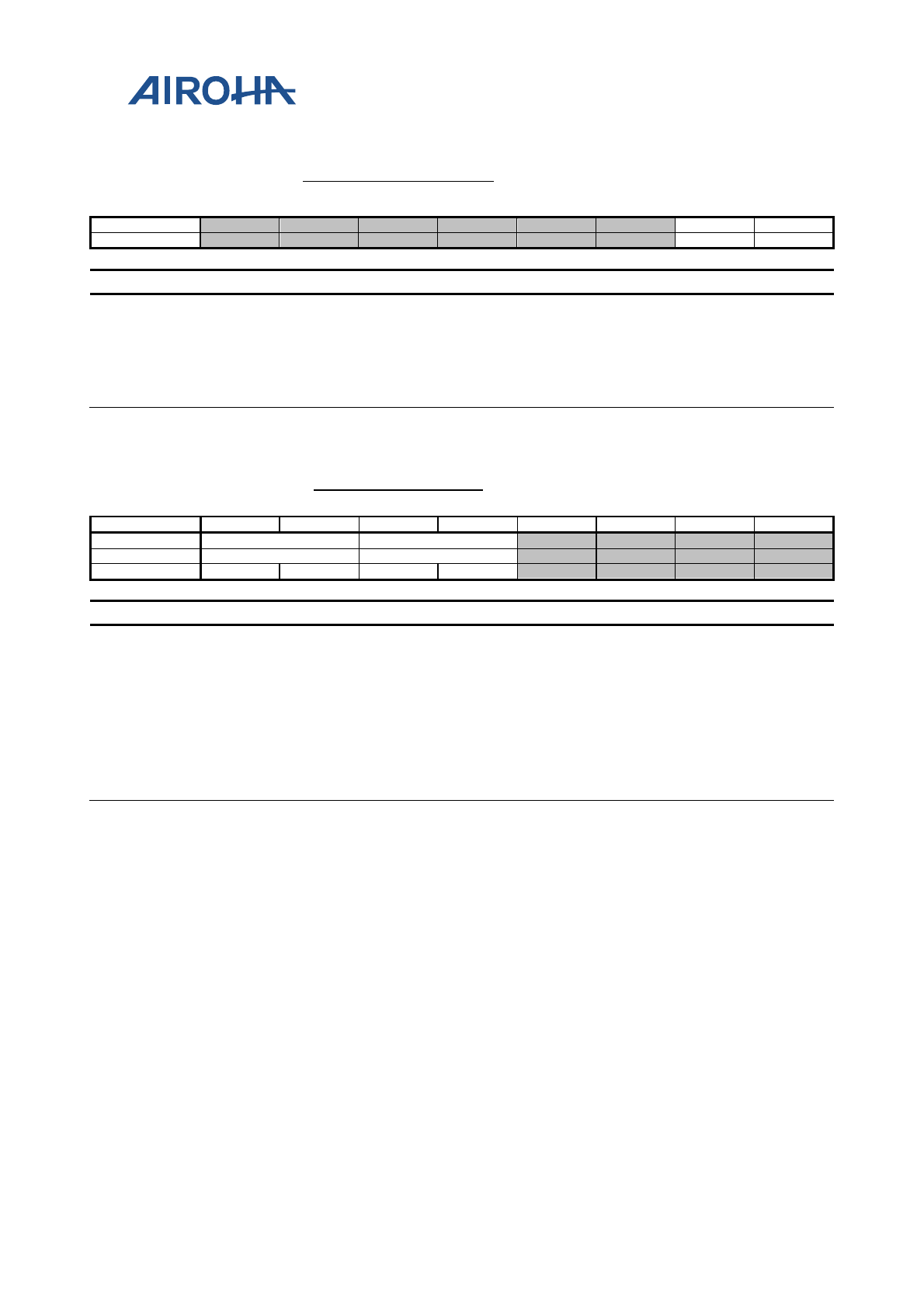
MT2523 Series Reference Manual
© 2015 - 2018 Airoha Technology Corp.
Page 692 of 692
This document contains information that is proprietary to Airoha Technology Corp. (“Airoha”) and/or its licensor(s).
Any unauthorized use, reproduction or disclosure of this document in whole or in part is strictly prohibited.
345 ISINK_EN_CTRL_High
ISINK
Enable
control
High
00
Type
RW
RW
Reset
0
0
Bit(s) Name Description
1 ISINK_CH1_BIAS_E
N
ISINK Channel 1 CHOP CLK enable
1'b0: Disable
1'b1: Enable
0 ISINK_CH0_BIAS_
EN
ISINK Channel 0 CHOP CLK enable
1'b0: Disable
1'b1: Enable
346 ISINK_MODE_CTRL
ISINK
mode
control
08
Bit
7
6
5
4
3
2
1
0
Name
ISINK_CH0_MODE
ISINK_CH1_MODE
Type
RW
RW
Reset
0
0
0
0
Bit(s) Name Description
7:6 ISINK_CH0_MODE
ISINK Channel 0 enable mode select
2'b00: PWM mode
2'b01: Breath mode
2'b10: register mode
2'b11: register mode
5:4 ISINK_CH1_MODE
ISINK Channel 1 enable mode select
2'b00: PWM mode
2'b01: Breath mode
2'b10: register mode
2'b11: register mode
