MT76x7_Reference_Manual MT76x7 Reference Manual
MT76x7_Reference_Manual
MT76x7_Reference_Manual
MT76x7_Reference_Manual
MT76x7_Reference_Manual
MT76x7_Reference_Manual
User Manual:
Open the PDF directly: View PDF ![]() .
.
Page Count: 798 [warning: Documents this large are best viewed by clicking the View PDF Link!]
- Document Revision History
- List of Tables and Figures
- 1. System Overview
- 2. Functional Description
- 2.1. Overview
- 2.2. Power Management Unit (PMU)
- 2.3. Clock and reset generation
- 2.3.1. Clock
- 2.3.1.1. Cortex-M4 MCU clock Settings
- 2.3.1.2. Cortex-M4 serial flash clock setting
- 2.3.1.3. Cortex-M4 SPI master clock setting
- 2.3.1.4. I2S master clock setting for external CODEC
- 2.3.1.5. Audio CODEC clock setting
- 2.3.1.6. PWM clock setting
- 2.3.1.7. AUXADC clock setting
- 2.3.1.8. Cortex-M4 I2C master clock setting
- 2.3.1.9. Cortex-M4 UART clock setting
- 2.3.2. Reset
- 2.3.1. Clock
- 2.4. Application processor subsystem
- 2.5. Peripherals
- 2.6. Radio MCU Subsystem
- 2.7. Wi-Fi subsystem
- 2.8. Bluetooth subsystem
- 2.9. RTC
- 3. Radio Characteristics
- 4. Electrical Characteristics
- 5. Package Specifications

© 2015 - 2017 MediaTek Inc.
This document contains information that is proprietary to MediaTek Inc. (“MediaTek”) and/or its licensor(s). MediaTek cannot grant you permission for
any material that is owned by third parties. You may only use or reproduce this document if you have agreed to and been bound by the applicable
license agreement with MediaTek (“License Agreement”) and been granted explicit permission within the License Agreement (“Permitted User”). If you
are not a Permitted User, please cease any access or use of this document immediately. Any unauthorized use, reproduction or disclosure of this
document in whole or in part is strictly prohibited. THIS DOCUMENT IS PROVIDED ON AN “AS-IS” BASIS ONLY. MEDIATEK EXPRESSLY DISCLAIMS ANY
AND ALL WARRANTIES OF ANY KIND AND SHALL IN NO EVENT BE LIABLE FOR ANY CLAIMS RELATING TO OR ARISING OUT OF THIS DOCUMENT OR ANY
USE OR INABILITY TO USE THEREOF. Specifications contained herein are subject to change without notice.
MT76x7_Reference_Manual Reference
Manual
Version: 1.09
Release date: 31 August 2017

MT76x7
Internet-of-Things Wireless Connectivity
Reference Manual
© 2015 - 2017 MediaTek Inc
Page 2 of 798
This document contains information that is proprietary to MediaTek Inc. (“MediaTek”) and/or its licensor(s).
Any unauthorized use, reproduction or disclosure of this document in whole or in part is strictly prohibited
Document Revision History
Revision
Date
Description
0.77 6 October 2016 Initial draft
0.80 23 June 2016 • 1. Add detail description to CLOCK, GPT, RTC, PWM and SPI
Master module.
• 2. Add register table to section 6.11, 6.12 and 6.13
0.81 2 September 2016 Move register descriptions to individual sections.
0.82 30 September 2016 Add RTC max value and illustrate pinmux don’t care values.
1.00 4 Novermber 2016 • Correct the address of mpu_channel_en.
• Add description of way_replace_policy
• Add SPI Slave interface datasheet of 2.5.9
• Update Auxilliary ADC specifications of Table 4-6
• Correct Xtal frequency supporting values(26/40/52MHz) and
descriptions
1.01 26 December 2016 Remove BT EDR related information
1.02 1 March 2017 Add MT7697F to 1.1 general description and table 1.1
1.03 5 April 2017 Update GPIO description
1.05 5 April 2017 • 1. Updated Clock Generation Block Diagram
• 2. Modify RTC Block Diagram
1.04 20 April 2017 Removed SPI-M DMA & USB description
1.06 23 May 2017 • Removed XTAL note in Boot Strap Test Mode of Chip Mode
• Updated Power States for CM4 Subsystem Wake-up time table
• Updated I2S for Stereo & 44.1KHz/48KHz
1.07 2 Aug 2017 Replaced “full duplex” description with “both directional data” in
section 1.2.5.1, “Introduction” to SPI Master.
1.08 21 Aug 2017 • Updated Pinmux table, section 5.3, “Pin multiplexing”
• Updated PMU electrical characteristics, section 4.5, “PMU
characteristics”
1.09 31 August 2017 • Fixed SPI master transfer data buffer size description, see Figure
2-54
• Updated PMU LDO and BUCK description
• Updated Bootstrap options
• Updated XTAL requirements
• Added 32k XTAL functional specification
• Added PMU UVLO and PMU_EN_WF characteristics

MT76x7
Internet-of-Things Wireless Connectivity
Reference Manual
© 2015 - 2017 MediaTek Inc
Page 3 of 798
This document contains information that is proprietary to MediaTek Inc. (“MediaTek”) and/or its licensor(s).
Any unauthorized use, reproduction or disclosure of this document in whole or in part is strictly prohibited
Table of Contents
Document Revision History ............................................................................................................................... 2
List of Tables and Figures .................................................................................................................................. 7
1. System Overview .................................................................................................................................. 12
1.1. Introduction ..................................................................................................................................... 12
1.2. Features ............................................................................................................................................ 12
1.2.1. Technology and packaging ............................................................................................. 12
1.2.2. Power management and clock source ........................................................................... 12
1.2.3. Platform .......................................................................................................................... 13
1.2.4. WLAN .............................................................................................................................. 13
1.2.5. Bluetooth ........................................................................................................................ 14
1.2.6. Miscellaneous ................................................................................................................. 14
1.3. Applications ...................................................................................................................................... 14
1.4. Block diagram ................................................................................................................................... 15
2. Functional Description .......................................................................................................................... 16
2.1. Overview .......................................................................................................................................... 16
2.2. Power Management Unit (PMU) ...................................................................................................... 16
2.2.1. PMU architecture ........................................................................................................... 16
2.2.1.1. PMU sleep mode ........................................................................................................... 16
2.2.2. Chip power plan ............................................................................................................. 17
2.2.3. Digital power domain and power states ........................................................................ 17
2.3. Clock and reset generation .............................................................................................................. 20
2.3.1. Clock ............................................................................................................................... 20
2.3.1.1. Cortex-M4 MCU clock Settings ...................................................................................... 23
2.3.1.2. Cortex-M4 serial flash clock setting .............................................................................. 25
2.3.1.3. Cortex-M4 SPI master clock setting .............................................................................. 27
2.3.1.4. I2S master clock setting for external CODEC ................................................................. 31
2.3.1.5. Audio CODEC clock setting ............................................................................................ 31
2.3.1.6. PWM clock setting ........................................................................................................ 31
2.3.1.7. AUXADC clock setting .................................................................................................... 32
2.3.1.8. Cortex-M4 I2C master clock setting .............................................................................. 32
2.3.1.9. Cortex-M4 UART clock setting ....................................................................................... 34
2.3.2. Reset ............................................................................................................................... 34
2.4. Application processor subsystem ..................................................................................................... 35
2.4.1. CPU ................................................................................................................................. 35
2.4.2. Cache and tightly coupled memory (TCM) ..................................................................... 35
2.4.2.1. General Description ....................................................................................................... 35
2.4.2.2. Programming guide of cache size configuration ........................................................... 38
2.4.2.3. Organization of cache .................................................................................................... 38
2.4.2.4. Theory of operations ..................................................................................................... 40
2.4.2.5. MPU ............................................................................................................................... 42
2.4.2.6. Remapping .................................................................................................................... 44
2.4.2.7. Register definitions ....................................................................................................... 45
2.4.3. Bus fabric ........................................................................................................................ 56
2.4.4. Serial flash controller ..................................................................................................... 57
2.4.4.1. General Description ....................................................................................................... 57
2.4.4.2. Block diagram ................................................................................................................ 58
2.4.4.3. Serial Flash related waveform ....................................................................................... 59
2.4.4.4. Programming guide ....................................................................................................... 64

MT76x7
Internet-of-Things Wireless Connectivity
Reference Manual
© 2015 - 2017 MediaTek Inc
Page 4 of 798
This document contains information that is proprietary to MediaTek Inc. (“MediaTek”) and/or its licensor(s).
Any unauthorized use, reproduction or disclosure of this document in whole or in part is strictly prohibited
2.4.4.5. Register definitions ....................................................................................................... 65
2.4.5. DMA................................................................................................................................ 83
2.4.5.1. General description ....................................................................................................... 83
2.4.5.2. Full-Size and Half-Size DMA channels ........................................................................... 84
2.4.5.3. Ring buffer and double buffer memory data movement .............................................. 85
2.4.5.4. Unaligned word access .................................................................................................. 85
2.4.5.5. Virtual FIFO DMA ........................................................................................................... 86
2.4.5.6. DMA channels and priority control ............................................................................... 87
2.4.5.7. Register definitions ....................................................................................................... 88
2.4.6. General Purpose Timer................................................................................................. 352
2.4.6.1. Register definitions ..................................................................................................... 353
2.4.7. Watchdog timer ........................................................................................................... 360
2.4.7.1. Register definitions ..................................................................................................... 361
2.4.8. eFuse ............................................................................................................................ 365
2.4.9. Interrupt Controller ...................................................................................................... 365
2.4.9.1. Interrupt Sources......................................................................................................... 366
2.4.9.2. External interrupt ........................................................................................................ 368
2.4.10. Power-on sequence ...................................................................................................... 368
2.4.10.1. Power-on reset (Cold Reset) ....................................................................................... 369
2.4.10.2. Watchdog reset ........................................................................................................... 369
2.4.10.3. Reset scenarios ............................................................................................................ 370
2.4.10.4. Sleep and wakeup sequence ....................................................................................... 370
2.4.11. Memory map ................................................................................................................ 371
2.4.12. SYSRAM_CM4 ............................................................................................................... 376
2.4.13. Crypto engine ............................................................................................................... 376
2.4.13.1. Features ....................................................................................................................... 376
2.4.13.2. Functional description ................................................................................................. 376
2.4.13.3. Programming sequence .............................................................................................. 378
2.4.13.4. Register definitions ..................................................................................................... 383
2.5. Peripherals ..................................................................................................................................... 419
2.5.1. GPIO interface .............................................................................................................. 419
2.5.1.1. GPIO function .............................................................................................................. 419
2.5.1.2. Register definitions ..................................................................................................... 422
2.5.2. UART interface ............................................................................................................. 486
2.5.2.1. General description ..................................................................................................... 486
2.5.2.2. Programming guide ..................................................................................................... 487
2.5.2.3. Register map ............................................................................................................... 488
2.5.2.4. Register definitions ..................................................................................................... 489
2.5.3. I2C serial interface ........................................................................................................ 541
2.5.3.1. General description ..................................................................................................... 541
2.5.3.2. Functions ..................................................................................................................... 541
2.5.3.3. I2C programming sequence ........................................................................................ 542
2.5.3.4. Initialization ................................................................................................................. 542
2.5.3.5. TX/RX Sequence .......................................................................................................... 543
2.5.3.6. Registers definitions .................................................................................................... 549
2.5.4. Auxiliary ADC ................................................................................................................ 570
2.5.4.1. General description ..................................................................................................... 570
2.5.4.2. Function ....................................................................................................................... 570
2.5.4.3. Auxiliary ADC features: ................................................................................................ 572
2.5.4.4. Auxiliary ADC digital averaging FSM ............................................................................ 572
2.5.4.5. ADC FIFO access .......................................................................................................... 574
2.5.4.6. Programming sequence .............................................................................................. 575
2.5.4.7. Auxiliary ADC clock source .......................................................................................... 575
2.5.4.8. Register definitions ..................................................................................................... 576

MT76x7
Internet-of-Things Wireless Connectivity
Reference Manual
© 2015 - 2017 MediaTek Inc
Page 5 of 798
This document contains information that is proprietary to MediaTek Inc. (“MediaTek”) and/or its licensor(s).
Any unauthorized use, reproduction or disclosure of this document in whole or in part is strictly prohibited
2.5.5. SPI master interface ..................................................................................................... 596
2.5.5.1. Introduction................................................................................................................. 596
2.5.5.2. SPI timing diagram....................................................................................................... 597
2.5.5.3. Programming guide .................................................................................................... 598
2.5.5.4. Registers definitions .................................................................................................... 599
2.5.6. SPI slave interface ........................................................................................................ 611
2.5.6.1. General description ..................................................................................................... 611
2.5.6.2. Block diagram .............................................................................................................. 611
2.5.6.3. SPI Slave CR Read/Write protocol ............................................................................... 612
2.5.6.4. Programming sequence .............................................................................................. 613
2.5.6.5. SPI slave protocol timing ............................................................................................. 616
2.5.6.6. Interrupt ...................................................................................................................... 619
2.5.6.7. SPI driver domain registers ......................................................................................... 619
2.5.6.8. SPI MCU domain registers ........................................................................................... 622
2.5.6.9. SPI pinmux configuration ............................................................................................ 628
2.5.7. I2S interface ................................................................................................................. 629
2.5.7.1. Registers definitions .................................................................................................... 630
2.5.8. Pulse Width Modulation (PWM) .................................................................................. 636
2.5.8.1. General description ..................................................................................................... 636
2.5.8.2. PWM block diagram .................................................................................................... 637
2.5.8.3. PWM function ............................................................................................................. 637
2.5.8.4. Programming examples ............................................................................................... 639
2.5.8.5. Notice .......................................................................................................................... 641
2.5.8.6. Register definitions (PWM_NUM = 0~39) ................................................................... 641
2.5.8.7. Application Notes ........................................................................................................ 644
2.5.9. IrDA............................................................................................................................... 644
2.5.9.1. General description ..................................................................................................... 644
2.5.9.2. Block Diagram .............................................................................................................. 644
2.5.9.3. IRTX functions .............................................................................................................. 645
2.5.9.4. Register definitions ..................................................................................................... 648
2.6. Radio MCU Subsystem ................................................................................................................... 664
2.6.1. CPU ............................................................................................................................... 664
2.6.2. RAM/ROM .................................................................................................................... 665
2.6.3. Memory map ................................................................................................................ 665
2.6.4. N9 bus fabric ................................................................................................................ 667
2.6.5. CIRQ .............................................................................................................................. 668
2.6.5.1. General description ..................................................................................................... 668
2.6.5.2. Functions ..................................................................................................................... 668
2.6.5.3. Interrupt sources ......................................................................................................... 669
2.6.5.4. Interrupt Source Masking ............................................................................................ 671
2.6.5.5. External Interrupt ........................................................................................................ 671
2.6.5.6. Programming guide ..................................................................................................... 672
2.6.5.7. Register definitions ..................................................................................................... 673
2.7. Wi-Fi subsystem ............................................................................................................................. 724
2.7.1. Wi-Fi MAC ..................................................................................................................... 724
2.7.2. WLAN baseband ........................................................................................................... 724
2.7.3. WLAN RF ....................................................................................................................... 725
2.8. Bluetooth subsystem...................................................................................................................... 725
2.9. RTC ................................................................................................................................................. 726
2.9.1. Main functions: ............................................................................................................ 726
2.9.2. Power Up/Down Flow .................................................................................................. 726
2.9.3. Register definitions ...................................................................................................... 727
3. Radio Characteristics .......................................................................................................................... 773
3.1. Wi-Fi radio characteristics .............................................................................................................. 773

MT76x7
Internet-of-Things Wireless Connectivity
Reference Manual
© 2015 - 2017 MediaTek Inc
Page 6 of 798
This document contains information that is proprietary to MediaTek Inc. (“MediaTek”) and/or its licensor(s).
Any unauthorized use, reproduction or disclosure of this document in whole or in part is strictly prohibited
3.1.1. Wi-Fi RF block diagram ................................................................................................. 773
3.1.2. Wi-Fi 2.4GHz band RF receiver specifications .............................................................. 773
3.1.3. Wi-Fi 2.4GHz band RF transmitter specifications ......................................................... 775
3.1.4. Wi-Fi 5GHz band RF receiver specifications ................................................................. 775
3.1.5. Wi-Fi 5GHz band RF transmitter specifications ............................................................ 778
3.2. Bluetooth radio characteristics ...................................................................................................... 778
3.2.1. Bluetooth RF block diagram ......................................................................................... 778
3.2.2. Basic Rate receiver specifications ................................................................................ 779
3.2.3. Basic Rate transmitter specifications ........................................................................... 780
3.2.4. Bluetooth LE receiver specifications ............................................................................ 780
3.2.5. Bluetooth LE transmitter specifications ....................................................................... 781
4. Electrical Characteristics ..................................................................................................................... 782
4.1. Absolute Maximum Rating ............................................................................................................. 782
4.2. Recommended operating range .................................................................................................... 782
4.3. DC characteristics ........................................................................................................................... 782
4.4. XTAL oscillator ................................................................................................................................ 783
4.5. PMU characteristics ....................................................................................................................... 783
4.6. Auxiliary ADC characteristics .......................................................................................................... 785
4.7. Thermal characteristics .................................................................................................................. 786
5. Package Specifications ........................................................................................................................ 787
5.1. Pin layout........................................................................................................................................ 787
5.2. Pin description................................................................................................................................ 787
5.3. Pin multiplexing .............................................................................................................................. 790
5.4. Bootstrap ........................................................................................................................................ 796
5.5. Package information ...................................................................................................................... 797
5.6. Ordering information ..................................................................................................................... 797
5.7. Top marking ................................................................................................................................... 798

MT76x7
Internet-of-Things Wireless Connectivity
Reference Manual
© 2015 - 2017 MediaTek Inc
Page 7 of 798
This document contains information that is proprietary to MediaTek Inc. (“MediaTek”) and/or its licensor(s).
Any unauthorized use, reproduction or disclosure of this document in whole or in part is strictly prohibited
List of Tables and Figures
Table 1-1 Differences between MT7697D, MT7697, MT7697F and MT7687F .................................................... 12
Table 2-1. MTCMOS power domain ..................................................................................................................... 17
Table 2-2. Power states for Cortex-M4 subsystem ............................................................................................... 19
Table 2-3. Power states for N9 Subsystem ........................................................................................................... 19
Table 2-4. Power state transition scenarios for N9 .............................................................................................. 20
Table 2-5. Power state transition scenarios for Cortex-M4 .................................................................................. 20
Table 2-6. Cortex-M4 clock rate ........................................................................................................................... 21
Table 2-7. N9 Clock Rate ....................................................................................................................................... 21
Table 2-8. Peripheral clock rate ............................................................................................................................ 22
Table 2-9. Cortex-M4 Clock GEN0 ........................................................................................................................ 25
Table 2-10. CM4 HCLK 2M Clock GEN ................................................................................................................... 27
Table 2-11. SPI master mode register................................................................................................................... 30
Table 2-12. PWM global control ........................................................................................................................... 32
Table 2-13. I2C Master Counting Value Phase ...................................................................................................... 34
Table 2-14. TCM and cache configuration ............................................................................................................ 35
Table 2-15. TCM Address Spaces of Different Cache Size Settings ....................................................................... 37
Table 2-16. Write-back Mode Cache R/W Action Summary ................................................................................. 41
Table 2-17. Write-through Mode Cache R/W Action Summary ........................................................................... 42
Table 2-18. Test patterns for whole chip simulation ............................................................................................ 44
Table 2-19. Flash controller support read mode .................................................................................................. 57
Table 2-20. Available DMA channels .................................................................................................................... 84
Table 2-21. Virtual FIFO Access Port ..................................................................................................................... 86
Table 2-22. DMA use for hardware functions....................................................................................................... 87
Table 2-23. General Purpose Timer Types .......................................................................................................... 352
Table 2-24. Cortex-M4 NVIC interrupt source .................................................................................................... 366
Table 2-25. Cortex-M4 external interrupt de-bounce period ............................................................................. 368
Table 2-26. Cortex-M4 memory map ................................................................................................................. 372
Table 2-27. AES hardware specification ............................................................................................................. 377
Table 2-28. DES hardware specification ............................................................................................................. 377
Table 2-29. AES128 programming sequence ...................................................................................................... 378
Table 2-30. AES192 programming sequence ...................................................................................................... 378
Table 2-31. AES256 programming sequence ...................................................................................................... 379
Table 2-32. DES programming sequence ............................................................................................................ 379
Table 2-33. Triple-DES programming sequence ................................................................................................. 380
Table 2-34. SHA256 programming sequence ..................................................................................................... 380
Table 2-35. SHA224 programming sequence ..................................................................................................... 380
Table 2-36. SHA1 programming sequence ......................................................................................................... 381
Table 2-37. MD5 programming sequence .......................................................................................................... 381
Table 2-38. SHA512 programming sequence ..................................................................................................... 382
Table 2-39. SHA384 programming sequence ..................................................................................................... 382
Table 2-40. Functional description of AGPIO ...................................................................................................... 422

MT76x7
Internet-of-Things Wireless Connectivity
Reference Manual
© 2015 - 2017 MediaTek Inc
Page 8 of 798
This document contains information that is proprietary to MediaTek Inc. (“MediaTek”) and/or its licensor(s).
Any unauthorized use, reproduction or disclosure of this document in whole or in part is strictly prohibited
Table 2-41. Register map with conditional CR (LCR) .......................................................................................... 488
Table 2-42 The initialization of I2C ..................................................................................................................... 542
Table 2-43 The TX sequence of I2C Direct Normal Mode ................................................................................... 543
Table 2-44 The RX sequence of I2C Direct Normal Mode................................................................................... 543
Table 2-45 The TX sequence of I2C Direct General Mode .................................................................................. 544
Table 2-46 The RX sequence of I2C Direct General Mode .................................................................................. 545
Table 2-47 The TX sequence of I2C DMA Normal Mode .................................................................................... 545
Table 2-48 The RX sequence of I2C DMA Normal Mode .................................................................................... 546
Table 2-49 The TX sequence of I2C DMA General Mode .................................................................................... 547
Table 2-50 The RX sequence of I2C DMA General Mode ................................................................................... 548
Table 2-51. SPI pin description ........................................................................................................................... 596
Table 2-52. SPI Interface Pinmux Configuration ................................................................................................. 628
Table 2-53. SPI CPOL/CPHA configuration .......................................................................................................... 628
Table 2-54. I2S pin description ........................................................................................................................... 629
Table 2-55. I2S Slave Mode................................................................................................................................. 629
Table 2-56. I2S Data Format ............................................................................................................................... 629
Table 2-57. PWM Modes .................................................................................................................................... 636
Table 2-58. PWM parameters ............................................................................................................................. 638
Table 2-59. N9 memory map .............................................................................................................................. 665
Table 2-60. Internal interrupt source ................................................................................................................. 672
Table 2-61. External interrupt source ................................................................................................................. 673
Table 3-1. 2.4GHz RF Receiver Specification ...................................................................................................... 774
Table 3-2. 2.4GHz RF Transmitter Specifications ................................................................................................ 775
Table 3-3. 5GHz RF receiver specifications ......................................................................................................... 776
Table 3-4. 5GHz RF Transmitter Specifications ................................................................................................... 778
Table 3-5. Basic Rate transmitter specifications ................................................................................................. 780
Table 3-6. Bluetooth LE receiver specifications .................................................................................................. 780
Table 3-7. Bluetooth LE transmitter specifications............................................................................................. 781
Table 4-1 Absolute maximum rating .................................................................................................................. 782
Table 4-2. Recommended operating range ........................................................................................................ 782
Table 4-3. DC characteristics .............................................................................................................................. 782
Table 4-4. XTAL Oscillator requirements and performance ............................................................................... 783
Table 4-5. 32k XTAL Oscillator functional specifications .................................................................................... 783
Table 4-6. Recommended parameters of 32k XTAL Crystal ............................................................................... 783
Table 4-7. PMU electrical characteristics ........................................................................................................... 783
Table 4-8. PMU UVLO & PMU_EN_WF characteristics ....................................................................................... 784
Table 4-9. Auxiliary ADC specifications .............................................................................................................. 785
Table 4-10. Thermal characteristics .................................................................................................................... 786
Table 5-1. Pin Map .............................................................................................................................................. 787
Table 5-2. Pin descriptions.................................................................................................................................. 788
Table 5-3. Pin multiplexing ................................................................................................................................. 791
Table 5-4. Bootstrap Option– Flash Access Mode .............................................................................................. 796
Table 5-5. Bootstrap Option – XTAL Clock Mode ............................................................................................... 796

MT76x7
Internet-of-Things Wireless Connectivity
Reference Manual
© 2015 - 2017 MediaTek Inc
Page 9 of 798
This document contains information that is proprietary to MediaTek Inc. (“MediaTek”) and/or its licensor(s).
Any unauthorized use, reproduction or disclosure of this document in whole or in part is strictly prohibited
Table 5-6. Bootstrap Option – 32KHz Clock Mode ............................................................................................. 796
Table 5-7. Bootstrap Option — Chip Mode ........................................................................................................ 796
Table 5-8. Ordering Information ......................................................................................................................... 797
Figure 1-1. System-on-chip block diagram ........................................................................................................... 15
Figure 2-1. Chip Power Block Diagram ................................................................................................................. 16
Figure 2-2 PMU sleep and wakeup sequence ....................................................................................................... 17
Figure 2-3. MT76x7 power state ........................................................................................................................... 19
Figure 2-4. Clock generation block diagram ......................................................................................................... 21
Figure 2-5. Clock domains in N9 and Cortex-M4 peripherals ............................................................................... 22
Figure 2-6. Cortex-M4 MCU clock switch ............................................................................................................. 23
Figure 2-7. Cortex-M4 flash clock switch .............................................................................................................. 25
Figure 2-8. Cortex-M4 SPI master clock switch .................................................................................................... 28
Figure 2-9. PWM tick clock switch ....................................................................................................................... 31
Figure 2-10. I2C counting VAL diagram ................................................................................................................ 32
Figure 2-11. Reset structure ................................................................................................................................. 34
Figure 2-12. MCU, cache, TCM and AHB bus connectivity ................................................................................... 36
Figure 2-13. Cache size and TCM settings ............................................................................................................ 37
Figure 2-14. Cache Lookup ................................................................................................................................... 39
Figure 2-15. Cache miss/refill criterion................................................................................................................. 41
Figure 2-16: MPU protection setting example ..................................................................................................... 43
Figure 2-17: Example Settings of Cache Remapping ............................................................................................ 44
Figure 2-18. Cortex-M4 subsystem – bus fabric ................................................................................................... 57
Figure 2-19. Serial flash controller block diagram ................................................................................................ 58
Figure 2-20. The red line block is the SF_TOP in MCUSYS_CM4. .......................................................................... 59
Figure 2-21. Example for direct read for SPI mode............................................................................................... 59
Figure 2-22. Example for quad I/O read in SPI mode ........................................................................................... 60
Figure 2-23. Example for quad I/O read in QPI mode .......................................................................................... 60
Figure 2-24. Direct read waveform for SPI mode ................................................................................................. 61
Figure 2-25. Direct read waveform for QPI mode ................................................................................................ 64
Figure 2-26. Generic DMA controller block diagram ............................................................................................ 84
Figure 2-27. Ring Buffer and Double Buffer Memory Data Movement ................................................................ 85
Figure 2-28. Unaligned Word Accesses ................................................................................................................ 86
Figure 2-29. Virtual FIFO DMA .............................................................................................................................. 86
Figure 2-30. Virtual FIFO Concept ......................................................................................................................... 87
Figure 2-31. The system diagram of the GPT_CM4 ............................................................................................ 353
Figure 2-32. PMU Power-on Sequence ............................................................................................................... 369
Figure 2-33. WDT structure ................................................................................................................................ 370
Figure 2-34. Sleep and wakeup sequence ......................................................................................................... 371
Figure 2-35. Crypto engine system ..................................................................................................................... 377
Figure 2-36. Crypto Engine block diagram .......................................................................................................... 377
Figure 2-37. AGPIO/GPIO Block Diagram (Left: AGPIO; Right: GPIO) ................................................................. 420
Figure 2-38. AGPIO configured as output multiplexing ..................................................................................... 421

MT76x7
Internet-of-Things Wireless Connectivity
Reference Manual
© 2015 - 2017 MediaTek Inc
Page 10 of 798
This document contains information that is proprietary to MediaTek Inc. (“MediaTek”) and/or its licensor(s).
Any unauthorized use, reproduction or disclosure of this document in whole or in part is strictly prohibited
Figure 2-39. AGPIO configured as input multiplexing......................................................................................... 421
Figure 2-40. AGPIO configured as Input, Output or Analog mode ..................................................................... 422
Figure 2-41. UART block diagram ....................................................................................................................... 487
Figure 2-42 The block diagram of I2C module. ................................................................................................... 542
Figure 2-43 SCL clock phases .............................................................................................................................. 543
Figure 2-44. Auxiliary ADC block diagram (Analog Part) ..................................................................................... 571
Figure 2-45. Auxiliary ADC block diagram ........................................................................................................... 571
Figure 2-46. Auxiliary ADC Clock Timing Diagram .............................................................................................. 571
Figure 2-47. Auxiliary ADC digital averaging FSM .............................................................................................. 572
Figure 2-48. Auxiliary ADC FIFO access block diagram ...................................................................................... 574
Figure 2-49. Auxiliary ADC clock source diagram .............................................................................................. 576
Figure 2-50. SPI TX transaction, more_buf_mode=0 .......................................................................................... 597
Figure 2-51. SPI RX transaction, more_buf_mode=0 .......................................................................................... 597
Figure 2-52. SPI TX transaction, more_buf_mode=1 and both_directional_data_mode=0 ............................... 598
Figure 2-53. SPI RX transaction, more_buf_mode=1 and both_directional_data_mode=0 ............................. 598
Figure 2-54. SPI TX/RX transaction, more_buf_mode=1 and both_directional_data_mode=1 ........................ 598
Figure 2-55. SPI Slave block diagram .................................................................................................................. 611
Figure 2-56. SPI Slave CR Read/Write Protocol .................................................................................................. 612
Figure 2-57. SPI Slave otorola protocol .............................................................................................................. 616
Figure 2-58. I2S signal waveform ........................................................................................................................ 630
Figure 2-59. PWM block diagram ....................................................................................................................... 637
Figure 2-60. PWM Cycle...................................................................................................................................... 637
Figure 2-61. PWM Normal Function ................................................................................................................... 639
Figure 2-62. 2-State PWM .................................................................................................................................. 639
Figure 2-63. 2-State Replay Mode PWM ............................................................................................................ 639
Figure 2-64. IRDA block diagram ........................................................................................................................ 645
Figure 2-65. The Logic representation for NEC protocol .................................................................................... 645
Figure 2-66. The Pulse Train in Transmission of NEC Protocol ........................................................................... 646
Figure 2-67. Message is Started by a 9ms AGC Burst ......................................................................................... 646
Figure 2-68. A Repeat Code is Transmitted Every 110ms ................................................................................... 646
Figure 2-69. Coding Method for RC5 Protocol .................................................................................................... 647
Figure 2-70. The Lead Pulse in RC6 Protocol ...................................................................................................... 647
Figure 2-71. Coding Method for RC6 Protocol .................................................................................................... 648
Figure 2-72. The Trailer Pulse in RC6 Protocol ................................................................................................... 648
Figure 2-73. N9 bus fabric ................................................................................................................................... 667
Figure 2-74. N9 interrupt controller ................................................................................................................... 668
Figure 2-75 Interrupt Controller Block Diagram ................................................................................................. 669
Figure 2-76. External Interrupt Controller Block Diagram .................................................................................. 671
Figure 3-1. 2.4/5GHz RF block diagram ............................................................................................................. 773
Figure 3-2. Wi-Fi/Bluetooth RF block diagram ................................................................................................... 779
Figure 3-3. Basic Rate receiver specifications ..................................................................................................... 779
Figure 5-1. Package Outline Drawing.................................................................................................................. 797
Figure 5-2. Top marking ...................................................................................................................................... 798

MT76x7
Internet-of-Things Wireless Connectivity
Reference Manual
© 2015 - 2017 MediaTek Inc
Page 11 of 798
This document contains information that is proprietary to MediaTek Inc. (“MediaTek”) and/or its licensor(s).
Any unauthorized use, reproduction or disclosure of this document in whole or in part is strictly prohibited

MT76x7
Internet-of-Things Wireless Connectivity
Reference Manual
© 2015 - 2017 MediaTek Inc
Page 12 of 798
This document contains information that is proprietary to MediaTek Inc. (“MediaTek”) and/or its licensor(s).
Any unauthorized use, reproduction or disclosure of this document in whole or in part is strictly prohibited
1. System Overview
1.1. Introduction
MT76x7 series chipsets, including MT7697D, MT7697 and MT87F, are highly integrated single chip solutions
featuring an application processor, a low power 1x1 11n Wi-Fi subsystem and a Power Management Unit
(PMU). The application processor subsystem contains an ARM® Cortex-M4 with floating point MCU and
peripherals, including UART, I2C, SPI, I2S, PWM, IrDA and auxiliary ADC. The chipset also contains a 32-bit RISC
CPU that could fully offload the application processor.
MT7697D includes a Wi-Fi dual-band subsystem with the 802.11a/b/g/n radio, baseband and MAC that are
designed to meet both the low power and high throughput application requirements. It also includes
embedded SRAM/ROM. The Bluetooth subsystem contains the Bluetooth radio, baseband and link controller
and uses the same 32-bit RISC CPU for Bluetooth protocols.
MT7697 includes a Wi-Fi dual-band subsystem with the 802.11b/g/n radio, baseband and MAC that are
designed to meet both the low power and high throughput application requirements. It also includes an
embedded SRAM/ROM. The Bluetooth subsystem contains the Bluetooth radio, baseband and link controller
and uses the same 32-bit RISC CPU for Bluetooth protocols.
MT7687F includes a Wi-Fi single-band subsystem with the 802.11b/g/n radio, baseband and MAC that are
designed to meet both the low power and high throughput application requirements. It also includes an
embedded SRAM/ROM and a 2MB serial flash in the package.
For the differences between MT7697D, MT7697, MT7697F and MT7687F family ICs, please refer to the Table
1-1, as shown below.
Table 1-1 Differences between MT7697D, MT7697, MT7697F and MT7687F
MT7697D
MT7697
MT7697F
MT7687F
Flash External SPI Flash External SPI Flash Embedded 2MB Flash Embedded 2MB Flash
Wi-Fi and
Bluetooth
Wi-Fi 1x1n 2G/5G
band
802.11a/b/g/n
Wi-Fi 1x1n 2G band
802.11b/g/n
Wi-Fi 1x1n 2G band
802.11b/g/n
Wi-Fi 1x1n 2G band
802.11b/g/n
Bluetooth Bluetooth LE Bluetooth LE Bluetooth LE None
1.2. Features
1.2.1. Technology and packaging
• Highly integrated 40nm RFCMOS technology
• 8mm x 8mm 68-pin QFN package
1.2.2. Power management and clock source
• Integrate high efficiency power management unit with single 3.3V power supply input
• 40, 26 and 52MHz source crystal clock support with low power operation in idle mode

MT76x7
Internet-of-Things Wireless Connectivity
Reference Manual
© 2015 - 2017 MediaTek Inc
Page 13 of 798
This document contains information that is proprietary to MediaTek Inc. (“MediaTek”) and/or its licensor(s).
Any unauthorized use, reproduction or disclosure of this document in whole or in part is strictly prohibited
1.2.3. Platform
• ARM Cortex-M4 MCU with FPU with up to 192MHz clock speed
• Embedded 352KB SRAM and 64KB boot ROM
• Supports external serial flash with Quad Peripheral Interface (QPI) mode
• Supports eXecute In Place (XIP) on flash
• 32KB cache in XIP mode
• Hardware crypto engines including AES, DES/3DES, SHA2 for network security
• 28 General Purpose IOs multiplexed with other interfaces
• Two UART interfaces with hardware flow control and one UART for debug, all multiplexed with GPIO
• One SPI master interface multiplexed with GPIO
• One SPI slave interface multiplexed with GPIO
• Two I2C master interface multiplexed with GPIO
• One I2S interface multiplexed with GPIO
• Four channel 12-bit ADC multiplexed with GPIO
• 28 PWM multiplexed with GPIO
• 25 channels DMA
• Low power RTC mode with 32KHz crystal support
1.2.4. WLAN
• Dedicated high-performance 32-bit RISC CPU N9 with up to 160MHz clock speed
• IEEE 802.11 a/b/g/n compliant
• Supports 20MHz, 40MHz bandwidth in 2.4GHz and 5GHz bands
• Dual-band 1T1R mode with data rate up to 150Mbps
• Supports STBC, LDPC
• Greenfield, mixed mode, legacy modes support
• IEEE 802.11 d/e/h/i/k/r/w support
• Security support for WFA WPA/WPA2 personal, WPS2.0, WAPI
• Supports 802.11w protected managed frames
• QoS support of WFA WMM, WMM PS
• Integrated LNA, PA, and T/R switch
• Optional external LNA and PA support.
• RX diversity support with additional RX input

MT76x7
Internet-of-Things Wireless Connectivity
Reference Manual
© 2015 - 2017 MediaTek Inc
Page 14 of 798
This document contains information that is proprietary to MediaTek Inc. (“MediaTek”) and/or its licensor(s).
Any unauthorized use, reproduction or disclosure of this document in whole or in part is strictly prohibited
1.2.5. Bluetooth
Bluetooth supports the following features on MT7697 and MT7697D:
• Bluetooth specification 2.1
• Bluetooth 4.2 Low Energy (LE)
• Integrated BALUN and PA
• Scatternet support: up to 7 piconets simultaneously with background inquiry, page scan
• Up to seven simultaneous active ACL links
• Support SCO and eSCO link with re-transmission
• Support wide-band speech and hardware accelerated SBC codec for A2DP streaming
• Packet loss concealment
• Channel quality driven data rate adaptation
• Channel assessment for AFH
1.2.6. Miscellaneous
• Integrates 4kbit eFuse to store device specific information and RF calibration data.
• Advanced Wi-Fi and Bluetooth coexistence scheme
1.3. Applications
MT76x7 is designed for Internet-of-Things applications based on Mediatek’s low power technology, Wi-Fi and
Bluetooth designs.
MT76x7
Internet-of-Things Wireless Connectivity
Reference Manual
© 2015 - 2017 MediaTek Inc
Page 15 of 798
This document contains information that is proprietary to MediaTek Inc. (“MediaTek”) and/or its licensor(s).
Any unauthorized use, reproduction or disclosure of this document in whole or in part is strictly prohibited
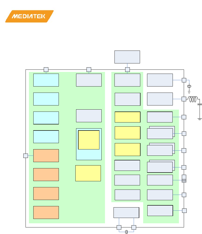
1.4. Block diagram
UART x 2
Clock
generation 40/26/52MHz XTAL
PMU
UART x 2
UART x 2
I2C x 2
4 channel
Auxiliary ADC
SPI
SPI Flash
controller
25 channel
Generic DMA
TCM / Cache
(96KB)
ARM Cortex M4
with FPU
SPI flash
UART x 1
EFUSE
(4Kb)
N9 CPU
ILM/DLM
SRAM/ROM
Debug
UART x 2
GPIO/PWM x 28
Crypto Engine
Watch Dog
Timer
Bluetooth RF
Bluetooth
baseband
Bluetooth link
controller
Bluetooth
audio CODEC
Bluetooth RF
Wi-Fi dual-band
RF
Wi-Fi baseband
Wi-Fi MAC
Wi-Fi PSE
Wi-Fi RF
Cortex-M4
SYSRAM
(256KB)
SYSRAM
N9 subsystem Cortex-M4
subsystem
I2S
IrDA
General
Purpose Timer
RTC
32kHz XTAL
Figure 1-1. System-on-chip block diagram
MT76x7
Internet-of-Things Wireless Connectivity
Reference Manual
© 2015 - 2017 MediaTek Inc
Page 16 of 798
This document contains information that is proprietary to MediaTek Inc. (“MediaTek”) and/or its licensor(s).
Any unauthorized use, reproduction or disclosure of this document in whole or in part is strictly prohibited
2. Functional Description
2.1. Overview
2.2. Power Management Unit (PMU)
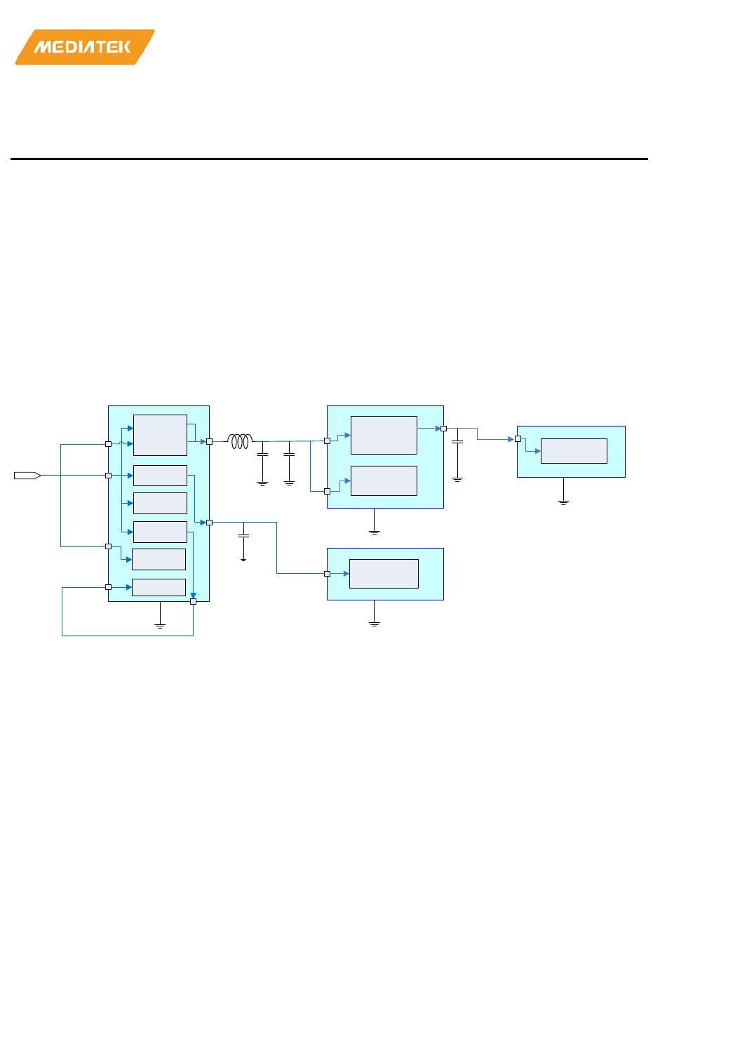
A single regulated 3.3V power supply is required for the MT76x7. It could be from DC-DC converter to convert
higher voltage supply to 3.3V or boost from a lower voltage supply to 3.3V.
The PMU contains Under-Voltage Lockout (UVLO) circuit, several low drop-out regulators (LDOs), a highly
efficient buck converter and a reference band-gap circuit. The circuits are optimized for low quiescent current,
low drop-out voltage, efficient line/load regulation, high ripple rejection, and low output noise.
BUCK
(3.3V to 1.7V) CLDO
(1.7V to 1.15)
AVDD45_BUCK
AVDD12_VCORE
DVDD11
AVDD16_CLDO
LXBK
DVDDIO
AVDD16_WF0_AFE
AVDD16_XO
AVDD16_BT
RF LDO/RF
core (1.6V)
IO (3.3V)
AVDD33_WF0_A_TX
AVDD33_WF0_A_PA
AVDD33_WF0_G_TX
AVDD33_WF0_G_PA
AVDD33_BT
RF(3.3V)
LXBK
1.7V
3.3V
Digital core
(1.15V)
AVSS45_BUCK
VSS
AVDD25_ALDO_OUT
ALDO
(3.3V to 2.5V)
ADC
(2.5V)
AVDD25_AUXADC
ELDO
(3.3V to 2.5V)
AVSS25_AUXADC
VSS
VSS
2.5V
PMU_DIO33_OUT
3.3V
AVDD45_MISC
PWR_SW
(3.3V)
Figure 2-1. Chip Power Block Diagram
2.2.1. PMU architecture
The PMU integrates 3 LDOs and one buck converter.
The buck converter converts 1.55~1.86V output to other subsystems in MT76x7. It can be operated in PFM
mode or PWM mode. Through an external on-board LC filter (2.2µH inductor and 10µF cap), it outputs a low
ripple 1.55~1.86V to Wi-Fi RF system, Bluetooth RF system and CLDO. CLDO is under BUCK domain and then it
outputs 1.15V for all digital logic used on the chip. ALDO is also from the 3.3V chip supply input and generates
2.5V for the auxiliary ADC.
Once MT76x7 goes into deep sleep mode, ALDO shuts down, and BUCK and CLDO are configured into low-
power mode with low Iq.
PMU has an integrated ELDO (eFuse LDO). It provides 2.5V output voltage to the internal eFuse macro in
programming mode.
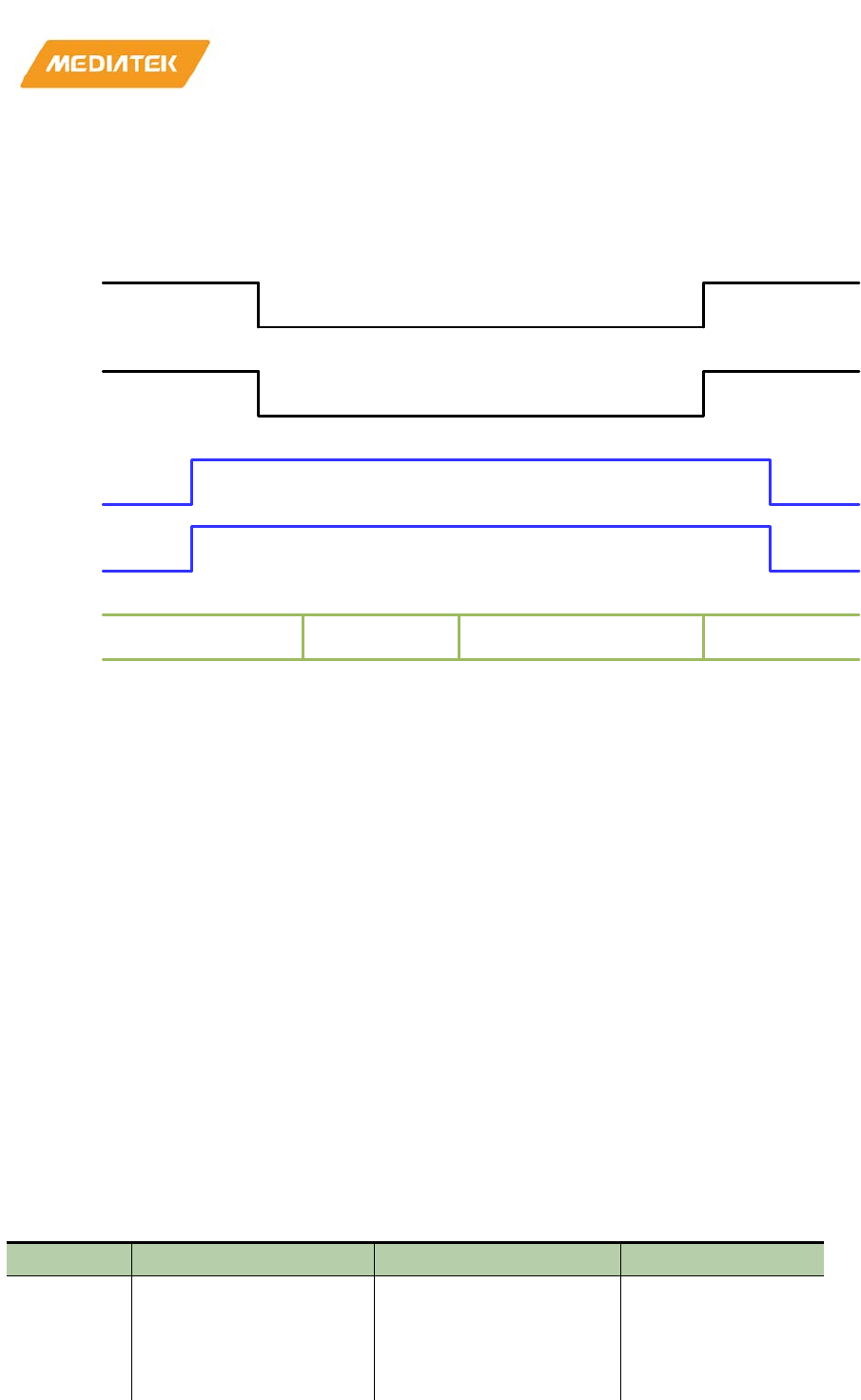
2.2.1.1. PMU sleep mode
When both TOP_OFF (N9) and CM4_OFF power domains enter into sleep mode, the PMU enters the sleep
mode automatically. BUCK and CLDO are turned-off in the PMU sleep mode. SLDOH and SLDOL are turned-on
to provide 1.6V and 1.15V power. By setting the SLDOL parameters, SLDOL can lower its output voltage to save
power consumption in PMU sleep mode.
MT76x7
Internet-of-Things Wireless Connectivity
Reference Manual
© 2015 - 2017 MediaTek Inc
Page 17 of 798
This document contains information that is proprietary to MediaTek Inc. (“MediaTek”) and/or its licensor(s).
Any unauthorized use, reproduction or disclosure of this document in whole or in part is strictly prohibited
TOP_OFF or CM4_OFF leaving sleep mode also wakes up the PMU. In normal mode, BUCK/ CLDO are turned-
on to provide large power for the whole chip and SLDOH/SLDOL are turned-off.
Please refer to Figure 2-2 for PMU sleep and wakeup sequence. The SLDOL TEMP1 and STABLE value setting is
in RG_PMU_08 (0x81021420).
BUCK
ENABLE
SLDOH
ENABLE
SLDOL
ENABLE
CLDO
ENABLE
SLDOL
Voltage 1.15V 1.0V
(VSEL_TEMP1) 0.85 V
(VSEL_STABLE) 1.15V
Figure 2-2 PMU sleep and wakeup sequence
2.2.2. Chip power plan
The 3.3V power source is directly supplied to the switching regulator, digital I/Os, and RF-related circuit. It is
converted to 2.5V by the LDO for ADC analog circuit. It is converted to 1.6V by the buck converter for low
voltage circuits. The built-in digital LDOs and RF LDOs converts 1.6V to 1.15V for digital, RF, and BBPLL core
circuits.
2.2.3. Digital power domain and power states
The digital circuit is separated into five power domains.
• TOP_AON
• TOP_OFF(N9)
• WF_OFF
• BT_OFF
• CM4_SYS.
Except for TOP_AON, each power domain can be turned on and off individually.
Table 2-1. MTCMOS power domain
Domain
Description
Circuit Included
OFF Condition
TOP_AON Always-on power domain,
which keeps the minimum
circuit powered to wake up
from the sleep mode upon
receiving a wake-up event.
It includes:
• Chip level configuration
register.
• Sleep mode controller;
N/A

MT76x7
Internet-of-Things Wireless Connectivity
Reference Manual
© 2015 - 2017 MediaTek Inc
Page 18 of 798
This document contains information that is proprietary to MediaTek Inc. (“MediaTek”) and/or its licensor(s).
Any unauthorized use, reproduction or disclosure of this document in whole or in part is strictly prohibited
Domain
Description
Circuit Included
OFF Condition
•
External interrupt
controller;
• Part of the Wi-Fi MAC
that handles the beacon
filtering.
• Sustain and backup
memory that stores the
RAM code and the
register values that
need to be kept during
sleep mode.
TOP_OFF(N9) The power domain can be
power gated in Wi-Fi power
save mode and Bluetooth
power save mode.
The N9 subsystem with its
peripherals and part of the
Wi-Fi MAC circuit are
included.
N9 is in sleep mode
and no DMA functions
are enabled.
WF_OFF The power domain can be
power gated when Wi-Fi is
not used and in Wi-Fi power
save mode.
The Wi-Fi baseband and part
of the MAC subsystem are
included.
• Wi-Fi is disabled.
• N9 is in standby
mode or in sleep
mode.
BT_OFF The power domain can be
power gated when
Bluetooth is not used and in
Bluetooth power save
mode.
The Bluetooth subsystem is
included.
• Bluetooth is
disabled.
• N9 is in standby
mode or in sleep
mode.
CM4_OFF The power domain is not
powered gated when Cortex
M4 is used.
Cortex-M4 subsystem with
its peripherals is included.
N/A
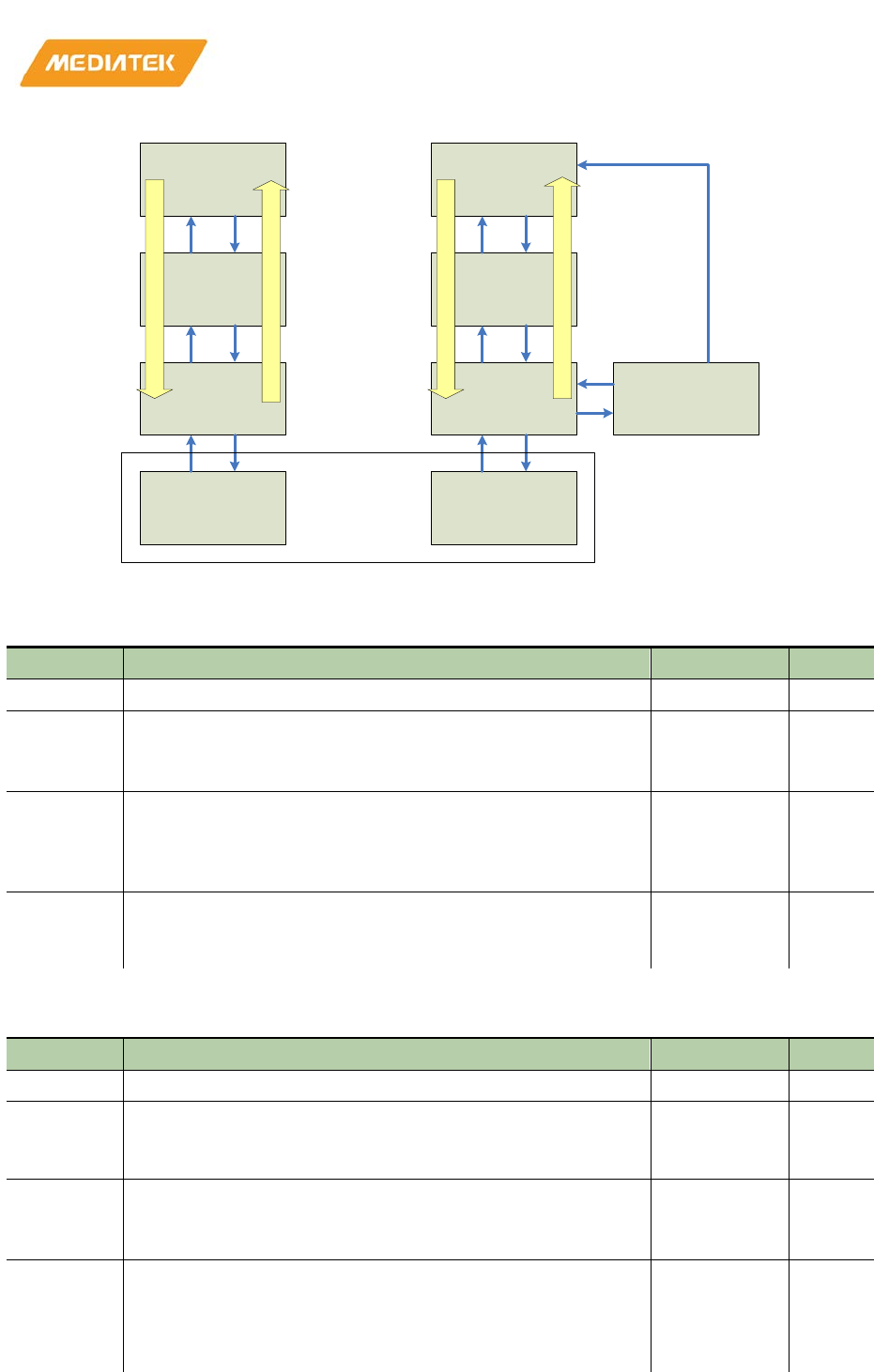
The MT76x7 power state diagram is shown in Figure 2-3. There are two sleep mode controllers, controlled by
N9 and Cortex-M4, respectively.
The N9 power state and Cortex-M4 power state operate independently. When both enter the sleep mode, the
XTAL and PMU can be changed to the low power mode to further lower the current consumption.
MT76x7
Internet-of-Things Wireless Connectivity
Reference Manual
© 2015 - 2017 MediaTek Inc
Page 19 of 798
This document contains information that is proprietary to MediaTek Inc. (“MediaTek”) and/or its licensor(s).
Any unauthorized use, reproduction or disclosure of this document in whole or in part is strictly prohibited
N9 active
Wi-Fi ON
PLL clock
N9 standby
XTAL 26MHz
N9 sleep
XTAL 32KHz
MCU idle
Wi-Fi ON
PLL clock
PMU sleep
XTAL/PMU in low
power mode
Cortex-M4 sleep
XTAL 32KHz
Cortex-M4
standby
XTAL 26MHz
Cortex-M4 active
PLL Clock
PMU sleep
XTAL/PMU in low
power mode
When both Cortex-M4 and N9
are in sleep mode, XTAL
and PMU is changed
to low power mode.
Enter sleep mode
Wake-up from sleep timer expired or interrupt
Wake-up from sleep timer expired or interrupt
Enter sleep mode
Figure 2-3. MT76x7 power state
Table 2-2. Power states for Cortex-M4 subsystem
MCU mode
Description
Wake-up time
Power
CM4 active MCU executing code at PLL clock n/a
CM4
standby
MCU subsystem clocks are gated off and the state of the entire
subsystem is retained. PLL is off.
100 ns
(HCLK comes
from XTAL)
CM4 sleep MCU subsystem clocks are gated off and the state of the entire
subsystem is retained. Only 32KHz clock from XTAL is active. MCU
is configured to wake up on the expiry of the internal timer and
external wake-up events.
850 us 1mA
PMU sleep CM4_OFF is power gated. XTAL and PMU operate in low power
mode. MCU is configured to wake up on the expiry of the internal
timer and external wake-up events.
5.2 ms 0.3mA
Table 2-3. Power states for N9 Subsystem
MCU mode
Description
Wake-up time
Power
N9 active MCU executing code at PLL clock. n/a
MCU idle MCU clock is gated off, while MCU subsystem clocks are on to
maintain the operation of Wi-Fi function, like listening to beacon.
PLL is on.
800 ns
N9 standby MCU subsystem clocks are gated off and the state of the entire
subsystem is retained. PLL is off.
100 ns
(HCLK comes
from XTAL)
N9 sleep • MCU subsystem clocks are gated off and the state of the
entire subsystem is retained.
• Only 32KHz clock from XTAL is active.
• MCU is configured to wake up on the expiry of the internal
1.2 ms 1mA

MT76x7
Internet-of-Things Wireless Connectivity
Reference Manual
© 2015 - 2017 MediaTek Inc
Page 20 of 798
This document contains information that is proprietary to MediaTek Inc. (“MediaTek”) and/or its licensor(s).
Any unauthorized use, reproduction or disclosure of this document in whole or in part is strictly prohibited
MCU mode
Description
Wake-up time
Power
timer, external wake-up events, or the wake-up events from
Wi-Fi radio or Bluetooth ratio.
PMU sleep • TOP_OFF (N9) and WF_OFF are power gated. XTAL and PMU
operate in low power mode.
• The state information is retained in back-up buffer (sleep-
mode memory) and can be restored when wake-up.
• MCU is configured to wake up on the expiry of the internal
timer, external wake-up events, or the wake-up events from
Wi-Fi radio or Bluetooth ratio.
5.2 ms 0.3mA
*XTAL: 40 MHz
The typical scenarios which N9 operates in and the power state transition are summarized in Table 2-4.
Table 2-4. Power state transition scenarios for N9
Scenario
Description
State transition
1 All functions are idle and the N9 firmware triggers to enter the
sleep mode.
Active à Standby à Sleep
2 Wi-Fi DTIM timer is expired and the hardware wakes up to listen
to beacon and then goes to sleep again when It is not necessary
to wake up N9 to process the data.
Sleep à MCU idle (Wi-Fi ON) à
sleep
3 Wi-Fi DTIM timer is expired and the hardware wakes up to listen
to beacon and then wake up N9 to process the data.
Sleep à MCU idle (Wi-Fi ON) à
Active
The typical scenarios which CM4 operates in and the power state transition are summarized in the following
table.
Table 2-5. Power state transition scenarios for Cortex-M4
Scenario
Description
State transition
1 All functions are idle and the CM4 firmware triggers to enter the
sleep mode.
Active à Standby à Sleep
2 The wake-up event (wake-up event from N9 or other sources)
triggers Cortex-M4 to wake up.
Sleep à Standby à Active
2.3. Clock and reset generation
2.3.1. Clock
MT76x7 is connected to the XTAL or external clock source as the single clock source of the whole system. The
XTAL oscillator can support the XTAL frequencies from among 40, 26 and 52MHz.
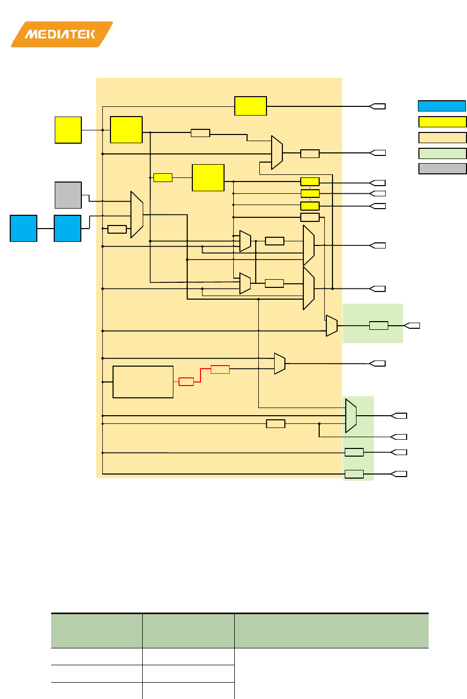
MT76x7
Internet-of-Things Wireless Connectivity
Reference Manual
© 2015 - 2017 MediaTek Inc
Page 21 of 798
This document contains information that is proprietary to MediaTek Inc. (“MediaTek”) and/or its licensor(s).
Any unauthorized use, reproduction or disclosure of this document in whole or in part is strictly prohibited
XTAL
oscillator
f = 40/
26/52MHz
PLL1
DIV
PLL2
DIV 1
DIV 3
DIV 12 WF_RXADC_CLK
80MHz
WF_TXDAC_CLK
960MHz
WF_DIG_CLK
320MHz
32MHz 960MHz
DIV 5
SPI CLOCK
FLASH CLOCK
I2C CLOCK
UART CLOCK
XPLL (Audio Frac-N)
±1% (0.01% granularity)
I2S_MCLK
16MHz
AUXADC CLOCK
PWM CLOCK
DIV 13
2-32 step 0.5
1-160MHz
1-192MHz
832MHz
640MHz
RF PLL
WF RF
DIV 5
2-32 step 0.5
XTAL CLOCK
DIV
PMU
BGCLK
(25KHz)
F32K CLOCK
2MHz
0
0
0
0
1
1
DIV
DIV options:
480, 240, 120, 60,
30, 20, 15, 12, 10
9.6, 19.2, 38.4, 115.2KHz
DIV
DIV options: 2708,1354,677,226
DIV
50, 100, 200, 400KHz
DIV options: 520,260,130,65
N9 CLOCK
160MHz
DIV 8
DIV 794
CM4 CLOCK
192MHz
120MHz
250, 500KHz
1, 2, 4, 6, 8, 10, 12MHz
DIV 64MHz
DIV 16MHz
RF power domain
AON power domain
CM4 power domain
DIV 2
PMU power domain
830081B4[14:13]
0
1
2
80021114[21:20]
81021170[12:8]
830081B0[2:0]
1
4
1
3
830081B0[15:14]
830081B0[9:4]
81021100[2:0] 1
4
81021100[9:4]
830081B4[7:3]
1-32 step 1
0
1
3
81021100[15:14]
81021100[17:16]
81021100[31:21]
2
830081B4[17]
830081B4[23:19]
24000028[27:16]
830B0000[27:24]
2
830081B4[12:8]
8300A600[2:1]
2
0
83090244[15:0] 83090248[15:0]
830A0244[15:0]830A0248[15:0]
1
XTAL
oscillator
f = 32KHz
RTC
RTC power domain
Figure 2-4. Clock generation block diagram
• PLL1 is used to generate the clock sources for Bluetooth and PLL2.
• PLL2 is used to generate the clock sources for Wi-Fi, N9 core, Cortex-M4 core and bus fabric.
• XPLL is used to generate the clock sources for I2S (for external audio CODEC).
The options of clock rate for MCU are listed below.
Table 2-6. Cortex-M4 clock rate
Reference Clock
(MHz)
MCU Clock
(MHz, XTAL mode)
MCU Clock (MHz, PLL mode)
40 40 30, 32, 40, 48, 60, 80, 96, 120, 160, 192
26 26
52 52
Table 2-7. N9 Clock Rate
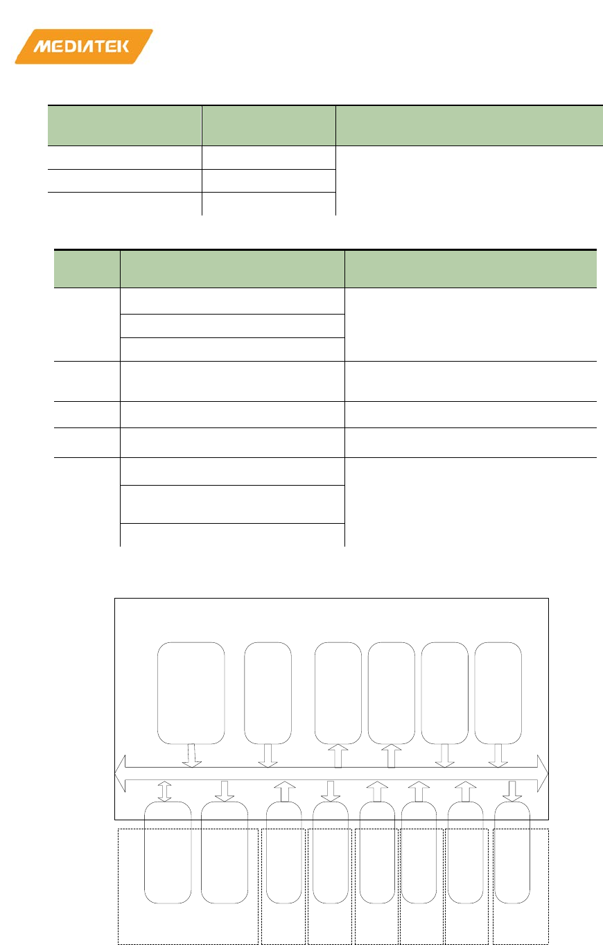
MT76x7
Internet-of-Things Wireless Connectivity
Reference Manual
© 2015 - 2017 MediaTek Inc
Page 22 of 798
This document contains information that is proprietary to MediaTek Inc. (“MediaTek”) and/or its licensor(s).
Any unauthorized use, reproduction or disclosure of this document in whole or in part is strictly prohibited
Reference Clock (MHz)
MCU Clock
(MHz, XTAL mode)
MCU Clock (MHz, PLL mode)
40 40 30, 32, 40, 48, 60, 80, 96, 120, 160, 192
26 26
52 52
Table 2-8. Peripheral clock rate
Peripheral Clock Rate
Supported specifications
PWM
XTAL clock with DIV13 (Default)
200Hz at minimum.
XTAL clock
F32K clock
UART
XTAL clock with DIV
9.6kbps, 19.2kbps, 38.4kbps, 115.2kbps,
3Mbps
I2C
XTAL clock with DIV
50, 100, 200, 400kHz
SPI
XTAL clock with DIV (Default)
0.25, 0.5, 1, 2, 4, 6, 8, 10, 12MHz
Flash XTAL clock with DIV (Default)
64MHz.
BT_DIG_CLK (64MHz) with DIV
Cortex-M4 clock with DIV
I2S
Cortex-M4
TCM
Cache
INT
WDT
GPT SYSRAM GDMA MTK
Security
PWM
x40
UART
x2
I2C
x2
SPI
Flash
CTRL
ADC
HIF SYS
WF/BT
AHB
ASYNC
Bridge
x2
Cortex-M4 Clock
N9 CLOCK
ADC
CLOCK
FLASH
CLOCK
SPI
CLOCK
I2C
CLOCK
UART
CLOCK
PWM
CLOCK
Figure 2-5. Clock domains in N9 and Cortex-M4 peripherals
MT76x7 clock setting is configured by CRs that control some clock dividers and MUXs.
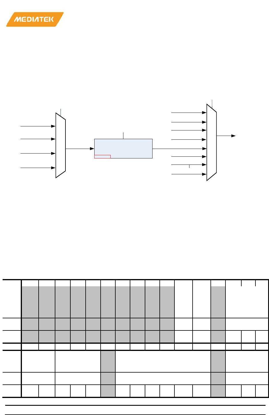
MT76x7
Internet-of-Things Wireless Connectivity
Reference Manual
© 2015 - 2017 MediaTek Inc
Page 23 of 798
This document contains information that is proprietary to MediaTek Inc. (“MediaTek”) and/or its licensor(s).
Any unauthorized use, reproduction or disclosure of this document in whole or in part is strictly prohibited
Note : all the clock sources must be enabled and stable when the software applies a switch.
2.3.1.1. Cortex-M4 MCU clock Settings
Cortex-M4 MCU Clock supports 32kHz, 40MHz(XTAL) and maximum 192MHz (divided from PLL). Cortex-M4
MCU clock is Cortex-M4 CPU and AHB BUS clock.
Figure 2-6. Cortex-M4 MCU clock switch
The configure CRs are
cm4_wbtac_mcu_ck_sel[1:0] : 0x830081B0[15:14]
cm4_mcu_div_sel[5:0] : 0x830081B0[9:4]
cm4_hclk_sel[2:0] : 0x830081B0[2:0]
***reference Table 2-9
830081B0
CM4_CKGEN0
CM4 CLOCK CONTROL REGISTER 0
00040180
Bit
31
30
29
28
27
26
25
24
23
22
21
20
19
18
17
16
Na
me AAAA AAA
A
AAA
A
AAA
A
AAA
A
AAA
A
AAA
A
AAA
A
AAA
A
AAA
A
CM4
_
MPD
_
DUT
Y
CM4
_
MPD
_
DLY
AAA
A CM4_PLL_DIV
_E N
Typ
e
RW RW RW
Res
et
0 0 1 0 0
Bit
15
14
13
12
11
10
9
8
7
6
5
4
3
2
1
0
Na
me
CM4_WBT
AC
_MCU_CK
_S EL
CM4_MPD_CG
_BY PASS
AAA
A CM4_MCU_DIV_SEL AAA
A CM4_HCLK_S
EL
Typ
e
RW RW RW RW
Res
et
0 0 0 0 0 0 1 1 0 0 0 0 0 0
Bit(s)
Name
Description
mcu_p ll_d iv
(1 .5 :0 .5 :32.0 )
cm4 _ wbtac_mcu_ck_sel[1 :0 ]
0
1
2
3
1 'b 0
0
1
2
3
4
5
6
7
sys_64m _ clk
÷ 2 or 4
cm4 _ h clk_sel[2 :0 ]
cm4 _ mcu_d iv_sel[5 :0 ]
Value 1 ~ 62
f32k _ clk
XTAL
ext_clk for testing
XTAL
960MHz (PLL2 )
320MHz (PLL2 )
832MHz (PLL1 )
CM4 MCU Clock
1 'b 0
1 'b 0

MT76x7
Internet-of-Things Wireless Connectivity
Reference Manual
© 2015 - 2017 MediaTek Inc
Page 24 of 798
This document contains information that is proprietary to MediaTek Inc. (“MediaTek”) and/or its licensor(s).
Any unauthorized use, reproduction or disclosure of this document in whole or in part is strictly prohibited
Bit(s)
Name
Description
21
CM4_MPD_DUTY
Duty of mcu_pll_div clock out
20
CM4_MPD_DLY
Delay for change signal in mcu_pll_div (in case of too
large CDC delay)
0 : 4T
1 : 5T
18:16
CM4_PLL_DIV_EN
[2] pll_div_en
[1] pll_div2_en
[0] pll_div4_en
15:14
CM4_WBTAC_MCU_CK_SEL
CM4 MCU clock
frequency selection.
2'b000 : XTAL freq
2'b001 : WIFI PLL 960MHz
2'b010 : WIFI PLL 320MHz
2'b011 : BBPLL1 832MHz (26/52 MHz XTAL) or 640MHz (40
MHz XTAL)
13:11
CM4_MPD_CG_BYPASS
Bypass clock gated function in MCU_PLL_DIV module
9:4
CM4_MCU_DIV_SEL
6'd0
: INVAILD, clock will stop when this field is
cleared to 6'h0
6'd1 : div factor=1.5
6'd2 : div factor=2.0
....
6'd61 : div factor=31.5
6'd62 : div factor=32.0
2:0
CM4_HCLK_SEL
MCUSYS_CM4 root clock source selection
000 : OSC clock 20/26/40/52 MHz
001 :
32K clock out, selected by 32K_SEL[1:0]
010 : SYS 64MHz clock
011 : N/A
100 : PLL after divider :
divider source = CM4_WF/BT PLL
(CM4_WBTAC_MCU_CK_SEL)
divider factor = CM4_MCU_DIV_SEL [5:0]
101 : RBIST clock from PAD
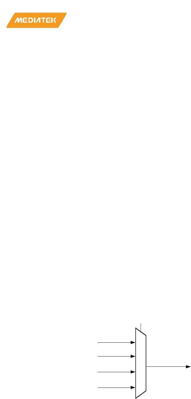
MT76x7
Internet-of-Things Wireless Connectivity
Reference Manual
© 2015 - 2017 MediaTek Inc
Page 25 of 798
This document contains information that is proprietary to MediaTek Inc. (“MediaTek”) and/or its licensor(s).
Any unauthorized use, reproduction or disclosure of this document in whole or in part is strictly prohibited
Table 2-9. Cortex-M4 Clock GEN0
• Set Cortex-M4 MCU clock to 192MHz (divided from PLL2)
o Enable PLL1+PLL2 and polling to ready
o Set cm4_wbtac_mcu_ck_sel[1:0]=2’h1 to switch source clock of CM4 PLL divider to PLL2
(960MHz)
o Set cm4_mcu_div_sel[5:0]=5’h8 to set divider clock output to 192MHz. (divided 960MHz by 5 (1 +
8/2)).
o Set cm4_hclk_sel[2:0]=3’h4 to switch CM4 MCU clock to the output of PLL divider
• Set CM4 MCU clock to 160MHz (divided from PLL2)
o Enable PLL1+PLL2 and polling to ready
o Set cm4_wbtac_mcu_ck_sel[1:0]=2’h2 to switch source clock of CM4 PLL divider to PLL2
(320MHz)
o Set cm4_mcu_div_sel[5:0]=5’h2 to set divider clock output to 160MHz. (divided 320MHz by 2 (1 +
2/2)).
o Set cm4_hclk_sel[2:0]=3’h4 to switch CM4 MCU clock to the output of PLL divider
• Set CM4 MCU clock to 64MHz (divided from PLL1)
o Enable PLL1 and polling to ready
o Set cm4_wbtac_mcu_ck_sel[1:0]=2’h0 to switch source clock of CM4 PLL divider to XTAL
o Set cm4_hclk_sel[2:0]=3’h2 to switch CM4 MCU clock to the sys_64m_clk
• Set CM4 MCU clock to XTAL clock
o Set cm4_wbtac_mcu_ck_sel[1:0]=2’h0 to switch source clock of CM4 PLL divider to XTAL
o Set cm4_hclk_sel[2:0]=3’h0 to switch CM4 MCU clock to the XTAL
2.3.1.2. Cortex-M4 serial flash clock setting
Cortex-M4 Serial Flash clock supports maximum frequency of 83.2MHz. It can be switched to XTAL clock,
64MHz (divided from PLL) and cm4_hclk (the maximum of 83.2MHz).
Figure 2-7. Cortex-M4 flash clock switch
The configure CRs are
sf_top_clk_sel[1:0] : 0x830081B4[14:13]
sf_top_clk_sel[1 :0 ]
0
1
2
3
XTAL
sys_64m _ clk
cm4 _ h clk
f32k _ clk
cm4 _ flash_clk
MT76x7
Internet-of-Things Wireless Connectivity
Reference Manual
© 2015 - 2017 MediaTek Inc
Page 26 of 798
This document contains information that is proprietary to MediaTek Inc. (“MediaTek”) and/or its licensor(s).
Any unauthorized use, reproduction or disclosure of this document in whole or in part is strictly prohibited
***reference Table 2-10
830081B4
HCLK_2M_CKEGN
HCLK_2M_CK CONTROL REGISTER
00390C61
Bit 31 30 29 28 27 26 25 24
2
3
2
2
2
1
2
0
1
9
18 17 16
Nam
e
AAA
A AAAA AAA
A
AAA
A
AAA
A
AAA
A
AAA
A
AAA
A SPIM_120M_DIV
_SEL AAAA
SPIM
_CK
_
SEL
SPIM
_120
M_C
K
_EN
Type
RW
RW
RW
Rese
t
0 0 1 1 1 0 1
Bit
15
14
13
12
11
10
9
8
7
6
5
4
3
2
1
0
Nam
e
AAA
A SF_TOP_C
L K_SEL HCLK_2M_SW_DIV_SEL HCLK_2M_DIV_SE
L
HCL
K
_2M
_
SRC_
CK_S
EL
HCL
K
_2M
_
DIV_
SEL_
SW
HCL
K
_2M
_
CK_E
N
Type
RW
RW
RO
RW
RW
RW
Rese
t
0 0 0 1 1 0 0 0 1 1 0 0 0 0 1
Bit(s)
Name
Description
23:19
SPIM_120M_DIV_SEL
SPIM_120M_DIV_SEL[4:0]
Freq. divider factor
5'd0 : x1 (bypass)
5'd1 : x(1/2)
5'd2 : x(1/3)
....
5'd31: x(1/32)
17
SPIM_CK_SEL
SPIM_CK Select
1'b0 : SPIM_120M_CK
1'b1 : XTAL Clock
16
SPIM_120M_CK_EN
SPIM_120M_CK Output Enable
1'b0
: disable SPIM_120M_CK output
1'b1 : enable SPIM_120M_CK output
14:13
SF_TOP_CLK_SEL
SF_TOP Clock Select
2'b00 : XTAL Clock
2'b01 :SYS 64M Clock
2'b10 :CM4_HCLK_CK

MT76x7
Internet-of-Things Wireless Connectivity
Reference Manual
© 2015 - 2017 MediaTek Inc
Page 27 of 798
This document contains information that is proprietary to MediaTek Inc. (“MediaTek”) and/or its licensor(s).
Any unauthorized use, reproduction or disclosure of this document in whole or in part is strictly prohibited
Bit(s)
Name
Description
2'b11 :AON_F32K_CK
12:8
HCLK_2M_SW_DIV_SEL
HCLK_2M_CK SW DIV SEL
7:3
HCLK_2M_DIV_SEL
HCLK_2M_DIV_SEL[4:0]
Freq. divider factor
5'd0 : x1 (bypass)
5'd1 : x(1/2)
5'd2 : x(1/3)
....
5'd31: x(1/32)
2
HCLK_2M_SRC_CK_SEL
HCLK_2M_CK Source Clock Slect
1'b0 : select XTAL clock
1'b1 : select F32K clock
1
HCLK_2M_DIV_SEL_SW
HCLK_2M_CK SW Mode
1'b0
: HW control
1'b1 : SW control
0
HCLK_2M_CK_EN
HCLK_2M_CK enable
1'b0 : disable HCLK_2M_CK
1'b1 : enable HCLK_2M_CK
Table 2-10. CM4 HCLK 2M Clock GEN
• Set Cortex-M4 serial flash clock to XTAL clock
o Set cm4_sf_top_clk_sel[1:0]=2’h0 to switch Cortex-M4 serial flash clock to XTAL
• Set Cortex-M4 serial flash clock to 64MHz (divided from PLL1)
o If PLL1 is enabled, goes to next step. Otherwise, enable PLL1 and polling to ready
o Set cm4_sf_top_clk_sel[1:0]=2’h1 to switch Cortex-M4 Serial Flash clock to 64MHz (sys_64m_clk)
• Set Cortex-M4 serial flash clock to cm4_hclk (max. frequency is 83.2MHz)
o Set cm4_sf_top_clk_sel[1:0]=2’h2 to switch Cortex-M4 serial flash clock to cm4_hclk.
2.3.1.3. Cortex-M4 SPI master clock setting
Cortex-M4 SPI master clock supports 4, 6, 8, 10 and 12 MHz (divided from 120MHz clock).
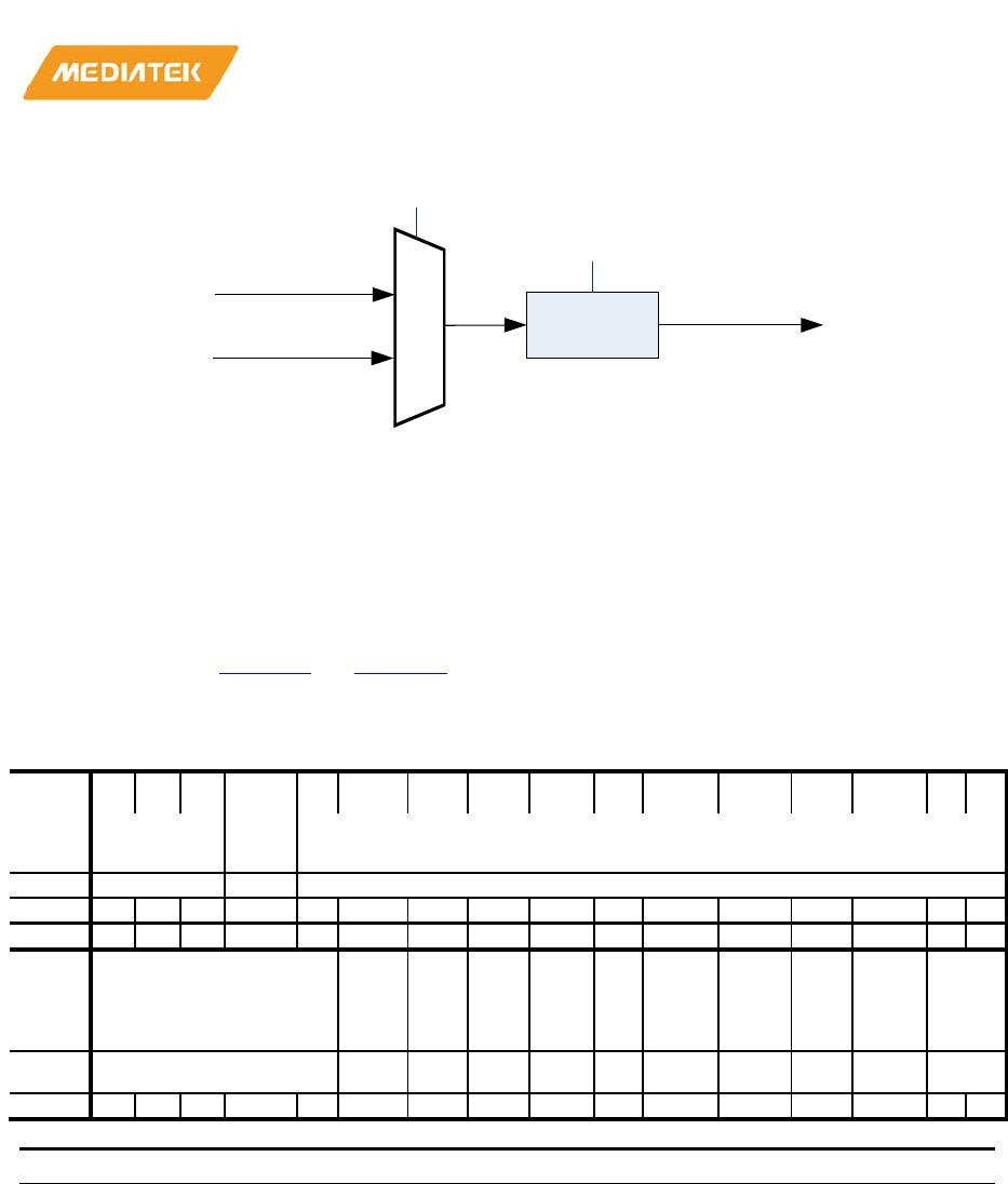
MT76x7
Internet-of-Things Wireless Connectivity
Reference Manual
© 2015 - 2017 MediaTek Inc
Page 28 of 798
This document contains information that is proprietary to MediaTek Inc. (“MediaTek”) and/or its licensor(s).
Any unauthorized use, reproduction or disclosure of this document in whole or in part is strictly prohibited
Figure 2-8. Cortex-M4 SPI master clock switch
The configure CRs are
spim_clk_sel : 0x830081B4[17]
rs_clk_sel[11:0] : 0x24000028[27:16]
***reference Table 2-10 and Table 2-11
24000028
SMMR
SPI master mode register
00018880
Bit 31 30 29 28
2
7
26 25 24 23 22 21 20 19 18
1
7
1
6
Nam
e rs_slave_se
l
clk_
mod
e
rs_clk_sel
Type
RW
RW
RW
Reset
0
0
0
0
0
0
0
0
0
0
0
0
0
0
0
1
Bit
15
14
13
12
11
10
9
8
7
6
5
4
3
2
1
0
Nam
e cs_dsel_cnt full
_du
p lex
int
_
en
spi
_
star
t_se
l
pfet
ch_
e n - CPH
A CPO
L
lsb
_
firs
t
more
_buf
_mo
d e
-
Type RW RW RW RW RW
R
O
RW RW RW RW RO
Reset
1
0
0
0
1
0
0
0
1
0
0
0
0
0
0
0
Bit(s)
Name
Description
31:29
rs_slave_sel
rs_slave_sel.
3'h0: select SPI device #0. (default is flash)
3'h1: select SPI device #1.
~
3'h7: select SPI
device #7.
28
clk_mode
This register is used to specify that period of SCLK HIGH
is longer or period of SCLK LOW is longer when clock
divisor(rs_clk_sel) is odd.
1'b0: period of SCLK LOW is longer.
sp im _ck_sel
0
1
XTAL
sys_120m _ clk
spim _clk
D IV
rs_clk_sel[11:0 ]

MT76x7
Internet-of-Things Wireless Connectivity
Reference Manual
© 2015 - 2017 MediaTek Inc
Page 29 of 798
This document contains information that is proprietary to MediaTek Inc. (“MediaTek”) and/or its licensor(s).
Any unauthorized use, reproduction or disclosure of this document in whole or in part is strictly prohibited
Bit(s)
Name
Description
1'b1: period of SCLK HIGH is longer.
27:16
rs_clk_sel
Register Space SPI clock frequency select.
12'h0: SPI clock frequency is hclk/2. (50% duty cycle, duty cycle is
the ratio of the output high time to the total cycle time)
12'h1: SPI clock frequency is hclk/3. (33.33% or 66.67% duty cycle)
12'h2: SPI clock
frequency is hclk/4. (50% duty cycle)
12'h3: SPI clock frequency is hclk/5. (40% or 60% duty cycle)
~
12'h4095: SPI clock frequency is hclk/4097.
15:11
cs_dsel_cnt
Internal delay the de
-select time of SPI chip select is
configured to occupy the number of
cycles of spim_clk
clock.
10
b
oth-directional data
Both directional data or half duplex mode.
1'b0: half duplex mode.
1'b1:
both-directional data mode.
Note: The
both-directional data is valid only when more_buf_mode
= 1. The transmission is always as hal
f duplex when
more_buf_mode = 0;
9
int_en
Interrupt enable.
1'b0: disable SPI interrupt.
1'b1: enable SPI interrupt.
8
spi_start_sel
The interval between spi_cs_n and spi_sclk.
1'b0: 3 spim_clk
1'b1: 6 spim_clk
7
pfetch_en
SPI pre
-fetch buffer enable
1'b0: disable pre
-fetch buffer.
1'b1: enable pre
-fetch buffer.
6
-
Reserved.
5
CPHA
Initial SPI clock phase for SPI transaction.
There are four SPI modes used to latch data. These SPI modes latch
data in one of four ways, and are defined by the logic
state
combinations of the CLK Polarity (CPOL) in relation to the CLK
Phase (CPHA). The valid logic combinations identify and determine
the SPI modes supported by the SPI device.

MT76x7
Internet-of-Things Wireless Connectivity
Reference Manual
© 2015 - 2017 MediaTek Inc
Page 30 of 798
This document contains information that is proprietary to MediaTek Inc. (“MediaTek”) and/or its licensor(s).
Any unauthorized use, reproduction or disclosure of this document in whole or in part is strictly prohibited
Bit(s)
Name
Description
At CPOL=0 the base value of the clock is zero
For CPHA=0 (mode 0), data is rea
d on the clock's rising edge and
data is changed on a falling edge.
For CPHA=1 (mode 1), data is read on the clock's falling edge and
data is changed on a rising edge.
At CPOL=1 the base value of the clock is one (inversion of CPOL=0)
For CPHA=0 (mode 2),
data is read on clock's falling edge and data
is changed on a rising edge.
For CPHA=1 (mode 3), data is read on clock's rising edge and data is
changed on a falling edge.
4
CPOL
Initial SPI clock polarity for SPI transaction.
3
lsb_first
lsb_first.
1'b0:
MSB(most significant bit) is transferred first for SPI
transaction.
1'b1: LSB(least significant bit) is transferred first for SPI
transaction.
2
more_buf_mode
Select 2 words buffer or 8 words buffer for SPI
transaction.
1'b0: SPI transfer data buffer siz
e is only 2 words. In this mode, SPI
DI/DO data #0 register and SPI opcode/address register are the
data buffer for SPI transaction. And, SPI master follows
mosi_byte_cnt and miso_byte_cnt to complete the transmission
and reception, respectively. This
type
of transaction must operate in
half duplex mode.
1'b1: SPI transfer data buffer size is 8 words. In this mode, SPI
opcode/address register are the data buffer for SPI transaction and
follows cmd_bit_cnt to complete the transaction. SPI DI/DO data
#0~#7 register are the data buffer for SPI transaction an
d follows
do_bit_cnt and di_bit_cnt to complete the transmission and
reception, respectively. In half duplex mode, transmitted data are
loaded from SPI opcode/address register and SPI DI/DO data
#0~#7 registers. And, the received data will overwrite the SP
I
DI/DO data #0~#7 registers. In
both-directional data mode, SPI
DI/DO data #0~#3 registers are used for transmission and SPI
DI/DO #4~#7 registers are used for receipt.
1:0
-
Reserved.
Table 2-11. SPI master mode register
• Set Cortex-M4 SPI Master clock to 120MHz (divided from PLL2)
o If PLL2 is not enabled, enable PLL2 and polling to ready.
o Set spim_clk_sel to 1’b0
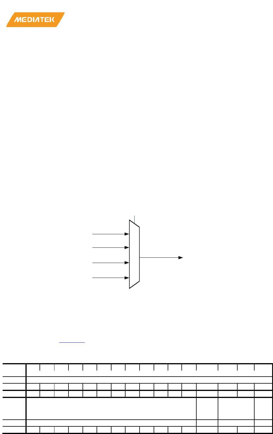
MT76x7
Internet-of-Things Wireless Connectivity
Reference Manual
© 2015 - 2017 MediaTek Inc
Page 31 of 798
This document contains information that is proprietary to MediaTek Inc. (“MediaTek”) and/or its licensor(s).
Any unauthorized use, reproduction or disclosure of this document in whole or in part is strictly prohibited
o Set rs_clk_sel[11:0] to 12’h8/12’hA/12’hD/12’h12/12’h1E, SPI Master clock is 12/10/8/6/4MHz.
(120MHz / (2+n))
• Set Cortex-M4 SPI Master clock to XTAL Clock
o Set spim_clk_sel to 1’b1
o Set rs_clk_sel[11:0] to n, SPI Master clock is (26/(2+n))MHz.
2.3.1.4. I2S master clock setting for external CODEC
I2S Master Clock supports 16MHz (divided from XPLL). Hardware controls the divider and clock MUX. No need
to configure it through software.
2.3.1.5. Audio CODEC clock setting
Audio CODE Clock supports 6.5 MHz (divided from XPLL).
Hardware controls the divider and clock MUX. No need to configure it through software.
2.3.1.6. PWM clock setting
PWM Clock supports 32 kHz, 2 MHz (divided from XTAL and shared with AUXADC) and XTAL.
Figure 2-9. PWM tick clock switch
The configure CRs are
pwm_tick_clock_sel[1:0] : 0x830081B4[14:13]
***reference Table 2-12
8300A600
PWM_GLO_CTRL
PWM global control
00000000
Bit
31
30
29
28
27
26
25
24
23
22
21
20
19
18
17
16
Name
-
Type
RO
Reset
0
0
0
0
0
0
0
0
0
0
0
0
0
0
0
0
Bit
15
14
13
12
11
10
9
8
7
6
5
4
3
2
1
0
Name -
pwm_
glob
al_r
eset
pwm_tick_
clock_sel
glob
al_k
ick
Type
RO
RW
RW
WO
Reset
0
0
0
0
0
0
0
0
0
0
0
0
0
0
0
0
pwm_tick_clock_sel[1 :0 ]
0
1
2
3
XTAL
sys_ 2 m _ clk
f32k _ clk
pwm_tick_clk
1 'b 0
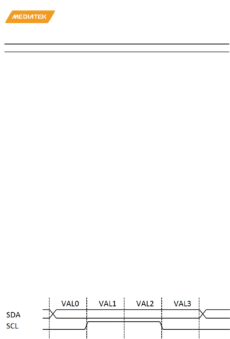
MT76x7
Internet-of-Things Wireless Connectivity
Reference Manual
© 2015 - 2017 MediaTek Inc
Page 32 of 798
This document contains information that is proprietary to MediaTek Inc. (“MediaTek”) and/or its licensor(s).
Any unauthorized use, reproduction or disclosure of this document in whole or in part is strictly prohibited
Bit(s)
Name
Description
31:4
-
Reserved
3
pwm_global_reset
Write 1 and then write 0 to reset all PWM modules and its
parameters
(PWM_CTRL/PWM_PARAM_S0/PWM_PARAM_S1).
2:1
pwm_tick_clock_sel
PWM tick clock select.
2'h0: 32KHz
2'h1: 2MHz
2'h2: XTAL clock
0
global_kick
All PWM modules with "pwm_global_kick_enable" would be
kicked by this bit at the same time
Table 2-12. PWM global control
• Set PWM tick clock to 32kHz
o Set pwm_tick_clock_sel[1:0]=2’h0 to switch PWM Tick Clock to 32KHz (f32k_clk)
• Set PWM tick clock to 2MHz (divided from XTAL)
o Set pwm_tick_clock_sel[1:0]=2’h1 to switch PWM Tick Clock to 2MHz (sys_2m_clk)
• Set PWM tick clock to XTAL clock
o Set pwm_tick_clock_sel[1:0]=2’h2 to switch PWM Tick Clock to XTAL Clock
2.3.1.7. AUXADC clock setting
AUXADC clock only supports 2MHz (divided from XTAL and shared with PWM).
This is the default hardware setting. No need to configure it through software.
2.3.1.8. Cortex-M4 I2C master clock setting
Cortex-M4 I2C Master clock supports 50, 100, 200, 400 kHz. The digital logic clock of I2C Master Controller is
the XTAL clock. I2C Master Interface clock (SCL) is controlled by a state machine configured by 4 VAL registers.
These 4 VAL registers can tune the I2C interface frequency and the phase of SCL and SDA.
Figure 2-10. I2C counting VAL diagram
The configuration CRs are
MT76x7
Internet-of-Things Wireless Connectivity
Reference Manual
© 2015 - 2017 MediaTek Inc
Page 33 of 798
This document contains information that is proprietary to MediaTek Inc. (“MediaTek”) and/or its licensor(s).
Any unauthorized use, reproduction or disclosure of this document in whole or in part is strictly prohibited
MM_CNT_PHASE_VAL0[7:0] : x83090244[7:0]
MM_CNT_PHASE_VAL1[7:0] : x83090244[15:8]
MM_CNT_PHASE_VAL2[7:0] : x83090248[7:0]
MM_CNT_PHASE_VAL3[7:0] : x83090248[15:8]
***reference Table 2-12
83090244
MM_CNT_VAL_PHL
Counting Value Phase Low
0000FFFF
Bit
31
30
29
28
27
26
25
24
23
22
21
20
19
18
17
16
Nam
e
AAA
A
AAA
A
AAA
A
AAA
A
AAA
A
AAA
A
AAA
A
AAA
A
AAA
A
AAA
A
AAA
A
AAA
A
AAA
A
AAA
A
AAA
A
AAA
A
Type
Rese
t
Bit
15
14
13
12
11
10
9
8
7
6
5
4
3
2
1
0
Nam
e
MM_CNT_PHASE_VAL1 MM_CNT_PHASE_VAL0
Type
RW
RW
Rese
t
1 1 1 1 1 1 1 1 1 1 1 1 1 1 1 1
Bit(s)
Name
Description
15:8
MM_CNT_PHASE_VAL1
Phase 1 counting value. SCL rising edge to SDA timing.
The STOP condition period.
7:0
MM_CNT_PHASE_VAL0
Phase 0 counting value. SDA to SCL rising edge timing.
The data setup time.
83090248
MM_CNT_VAL_PHH
Counting Value Phase High
0000FFFF
Bit
31
30
29
28
27
26
25
24
23
22
21
20
19
18
17
16
Nam
e
AAA
A
AAA
A
AAA
A
AAA
A
AAA
A
AAA
A
AAA
A
AAA
A
AAA
A
AAA
A
AAA
A
AAA
A
AAA
A
AAA
A
AAA
A
AAA
A
Type
Rese
t
Bit
15
14
13
12
11
10
9
8
7
6
5
4
3
2
1
0
Nam
e
MM_CNT_PHASE_VAL3 MM_CNT_PHASE_VAL2
Type
RW
RW
Rese
t
1 1 1 1 1 1 1 1 1 1 1 1 1 1 1 1
Bit(s)
Name
Description
15:8
MM_CNT_PHASE_VAL3
Phase 3 counting value. SCL falling edge to SDA timing.
The data hold time.
7:0
MM_CNT_PHASE_VAL2
Phase 2 counting value. SDA to SCL falling edge timing.
The START condition period.
MT76x7
Internet-of-Things Wireless Connectivity
Reference Manual
© 2015 - 2017 MediaTek Inc
Page 34 of 798
This document contains information that is proprietary to MediaTek Inc. (“MediaTek”) and/or its licensor(s).
Any unauthorized use, reproduction or disclosure of this document in whole or in part is strictly prohibited
Bit(s)
Name
Description
Table 2-13. I2C Master Counting Value Phase
• Set I2C Master clock (SCL)
o Set MM_CNT_PHASE_VAL0/1/2/3=w/x/y/z to set the SCL frequency to (26000 / (1+w+x+y+z)) kHz
2.3.1.9. Cortex-M4 UART clock setting
Cortex-M4 UART Clock (baud rate) supports 9.6, 19.2, 38.4, 115.2 kHz (divided from XTAL). And the baud rate
is a complex calculation. It’s recommended to use MediaTek API to configure UART to switch the baud rate.
2.3.2. Reset
MT76x7 has three global resets: XRESETN, CM4_RESETN and N9_RESETN. Figure 2-11 shows the module that
the reset signals are applied to.
Figure 2-11. Reset structure
XRESETN Reset Tree
(1) Cortex-M4 WDT and GPT module
(2) Cortex-M4 WIC module
(3) N9 WDT and GPT module
(4) N9 interrupt module
(5) AON module (top MISC logic always on during sleep)
Cortex-M4 and N9 Reset Tree Architecture
CM4_RESETN Reset Tree
Cortex-M4 MCU and all modules on Cortex-M4 bus other than
XRESETN reset tree
N9_RESETN Reset Tree
N9 MCU and all modules on Cortex-M4 bus other than XRESETN
reset tree
Chip Cold Reset Event
Chip Cold Reset Event
Or
Cortex-M4 Host Reset Event
Chip Cold Reset Event
Or
N9 Host Reset Event

MT76x7
Internet-of-Things Wireless Connectivity
Reference Manual
© 2015 - 2017 MediaTek Inc
Page 35 of 798
This document contains information that is proprietary to MediaTek Inc. (“MediaTek”) and/or its licensor(s).
Any unauthorized use, reproduction or disclosure of this document in whole or in part is strictly prohibited
2.4. Application processor subsystem
The MCU subsystem consists of a 32-bit MCU, the AHB/APB bus matrix, internal RAM/ROM with ROM patch
function, the flash controller, and the system peripherals including Direct Memory Access (DMA) engine and
the General Purpose Timer (GPT).
2.4.1. CPU
MT76x7 features an ARM Cortex-M4 processor - the most energy efficient ARM processor available that
supports clock rates from 1MHz to 192MHz.
The MCU executes the Thumb-2 instruction set for optimal performance and code size, including hardware
division, single cycle multiplication and bit-field manipulation.
MT76x7 includes the memory protection unit (MPU) in Cortex-M4 MCU that provides memory protection
features. It can be used to detect unexpected memory access.
MT76x7 also includes floating point unit (FPU) in Cortex-M4 processor to support DSP related functionality.
2.4.2. Cache and tightly coupled memory (TCM)
2.4.2.1. General Description
MT76x7 has a cache for Cortex-M4 to improve the efficiency of the code and data fetch from the external
flash. The only cacheable memory region is the external flash.
MT76X7 also has a Tightly-Coupled-Memory (TCM), a zero-wait-state memory which is dedicated for Cortex-
M4 and can be accessed by Cortex-M4 exclusively. It is a memory space for a critical code such as interrupt
service routine that requires minimum latency execution. The DMA engines on AHB bus cannot access TCM.
The total size of cache memory and the TCM is 96KB. Four software-configurable options of differerent cache
size, TCM size and the cache associativity are offered. The user can select whichever option maximizes their
application performance.
The cache system has the following features:
• Configurable 1/2/4-way set associative (8KB/16KB/32KB)
• Each way has 256 cache lines with 8-word link size
• 20-bit tag memory: 19-bit high address and 1-bit valid bit
• 2-bit dirty memory: each dirty bit identifies the dirtiness of half cache line
The size of SRAM is 96KB. It can be configured to the following configuration
• 96KB TCM, no cache
• 88KB TCM, 8KB cache (1 way, direct mapped)
• 80KB TCM, 16KB cache (2 way set-associative)
• 64KB TCM, 32KB cache (4 way set-associative)
The configuration setting and the memory configuration are shown in Table 2-14.
Table 2-14. TCM and cache configuration
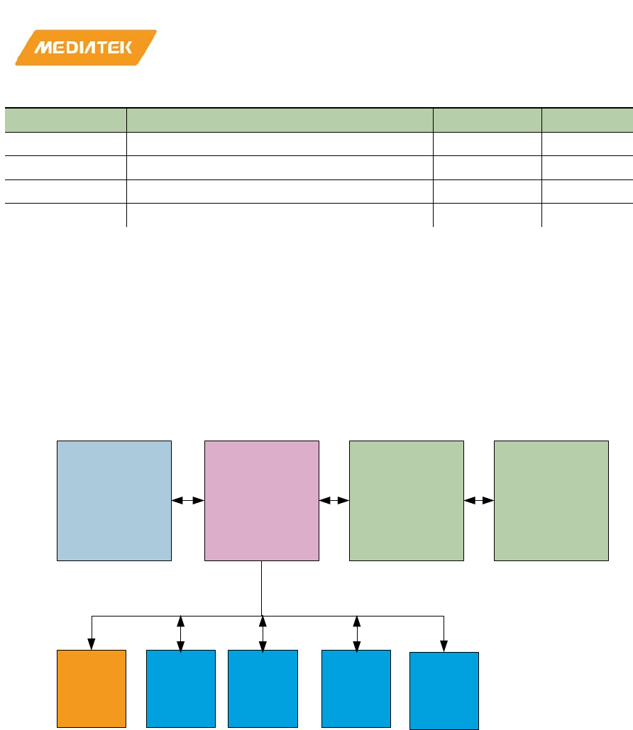
MT76x7
Internet-of-Things Wireless Connectivity
Reference Manual
© 2015 - 2017 MediaTek Inc
Page 36 of 798
This document contains information that is proprietary to MediaTek Inc. (“MediaTek”) and/or its licensor(s).
Any unauthorized use, reproduction or disclosure of this document in whole or in part is strictly prohibited
0x0153_0000[9:8]
Functional Description
Start Address
End Address
00b 96KB TCM, no cache 0x0010_0000 0x0011_7FFF
01b 88KB TCM, 8KB cache, direct mapped 0x0010_0000 0x0011_5FFF
10b 80KB TCM, 16KB cache, 2-way set-associative 0x0010_0000 0x0011_3FFF
11b 64KB TCM, 32KB cache, 4-way set associative 0x0010_0000 0x0010_FFFF
The cache controller provides ways to perform cache operations including invalidate single/all cache lines and
flush one/all cache lines.
To improve the system performance, the cache controller can record the statistics of the cache hit count and
the number of cacheable memory access. Cache hit rate can be obtained by dividing the cache hit count by the
number of memory access.
MT76x7 core processor has been implemented with a TCM subsystem which consists of Core Cache and TCM
(tightly coupled memory). This TCM subsystem is placed between the MCU core and AHB bus interface, as
shown in Figure 2-12.
ARM Cortex-M4 Cache Controller
and MPU
AHB Bus
Interface
Serial Flash
Controller
TCM Cache
Way 1
Cache
Way 2
Cache
Way 2
Cache
Way 3
Figure 2-12. MCU, cache, TCM and AHB bus connectivity
TCM is a high-speed (zero wait state) dedicated memory accessed exclusively by MCU. Due to the latency
penalty when MCU accesses memory or peripherals through the on-chip bus, by moving timing critical code
and data into TCM, the performance of MCU can be enhanced, and the response to particular events can be
guaranteed.
Another method to enhance the MCU performance is the implementation of cache. In this case, the core
cache is a small block of memory containing a copy of small portion of cacheable data in the external memory.
If MCU reads a cacheable datum, the datum will be copied into the core cache. Once MCU requests the same
datum again, it can be obtained directly from the core cache (called cache hit) instead of fetching it again from
the external memory.
Consider the fact that accessing cache is much faster than accessing external memory through the bus TCM
sub-system. A faster instruction fetching can be obtained, and that leads to a higher IPC (Instruction Per Cycle),
which is a major factor in the evaluation of core performance. Since a large external memory maps to a small
cache, the cache can hold only a small portion of external memory. If MCU accesses a datum not found in the
cache (called cache miss), one cache line must be dropped (flushed), the required datum and its neighboring
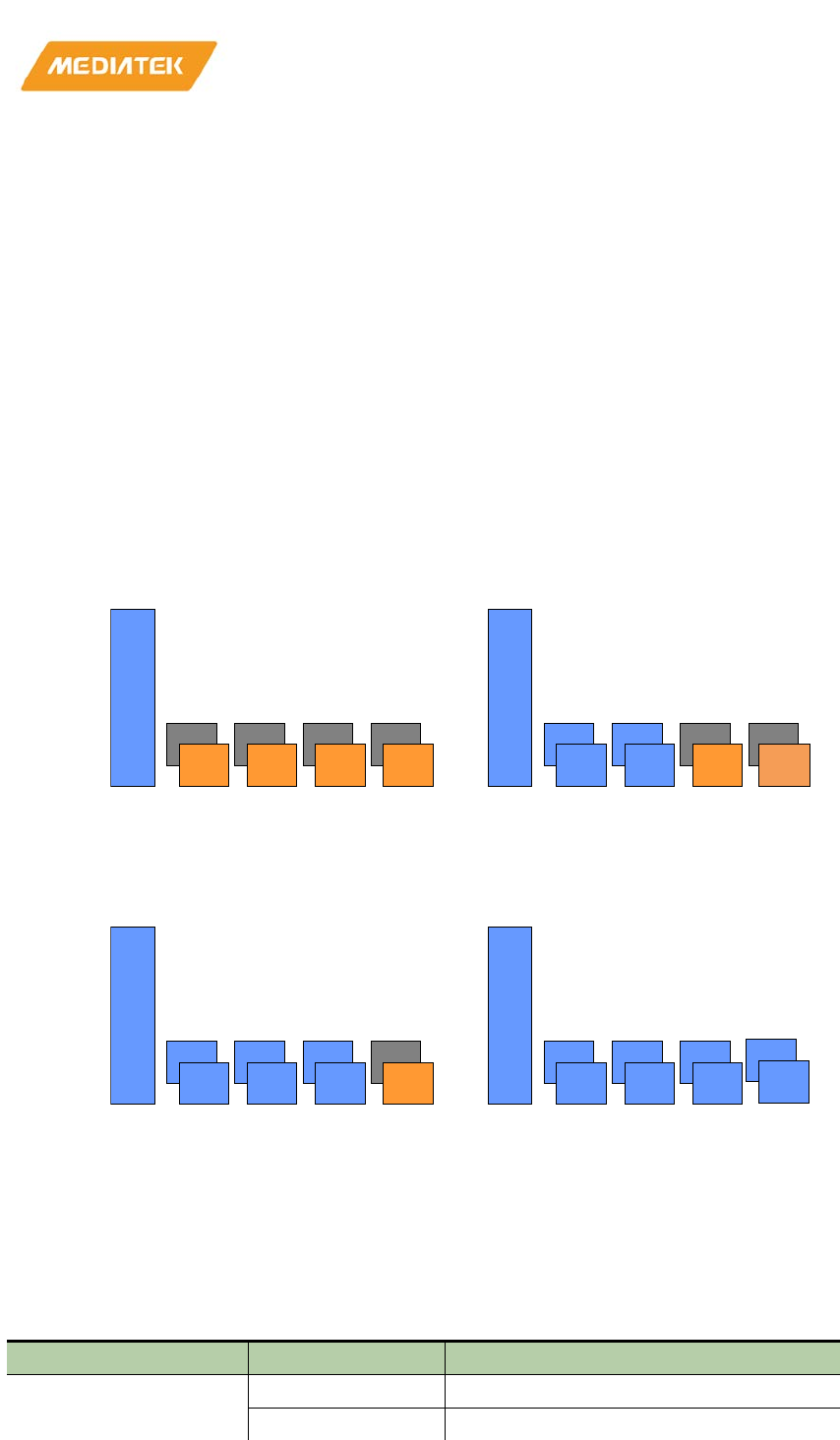
MT76x7
Internet-of-Things Wireless Connectivity
Reference Manual
© 2015 - 2017 MediaTek Inc
Page 37 of 798
This document contains information that is proprietary to MediaTek Inc. (“MediaTek”) and/or its licensor(s).
Any unauthorized use, reproduction or disclosure of this document in whole or in part is strictly prohibited
data are transferred from the external memory to cache (called cache line fill). Before cache line fill, an
important step to maintain data consistency between cache and external memory needs to be performed. This
important step is called “cache write back” (see later sections for details). In this design, a cache line consists
of eight words (8x32 bits) (will be introduced later). The best way to utilize TCM is maintaining the critical
instruction or data in TCM due to the advantage of TCM described above. After power-on reset, the boot
loader copies TCM contents from the external storage (e.g. flash) to the internal TCM. If necessary, MCU can
replace TCM contents with other data in the external storage during the runtime to implement a mechanism
such as “overlay”. TCM is also an ideal place to place stack data.
The sizes of TCM and cache can be set to one of the following 4 configurations:
• 64KB TCM, 32KB cache (4-way)
• 80KB TCM, 16KB cache (2-way)
• 88KB TCM, 8KB cache (1-way)
• 96KB TCM, 0KB cache (no cache)
Figure 2-13. Cache size and TCM settings
These different configurations provide flexibility for software to adjust and reach optimum TCM sub-system
performance.
The address mapping of these memories is shown here:
Table 2-15. TCM Address Spaces of Different Cache Size Settings
Cache size setting
TCM RAM identity
Used as
2’b00
(Total TCM = 96K, cache =
TCM RAM4(8K)
TCM4 (0x0011_6000 ~ 0x0011_7fff)
TCM RAM3(8K)
TCM3(0x0011_4000 ~ 0x0011_5fff)
64KB
8KB
TCM
cache
cache
cache
cache
TCM
TCM
TCM
cache
cache
TCM
TCM
TCM
cache
8KB
8KB
8KB
64KB
8KB
8KB
8KB
64KB
8KB
8KB
8KB
8KB
64KB
8KB
8KB
8KB
8KB
TCM
TCM
TCM
TCM
TCM
4-way cache
2-way cache
1-way cache
No cache
8KB
TCM

MT76x7
Internet-of-Things Wireless Connectivity
Reference Manual
© 2015 - 2017 MediaTek Inc
Page 38 of 798
This document contains information that is proprietary to MediaTek Inc. (“MediaTek”) and/or its licensor(s).
Any unauthorized use, reproduction or disclosure of this document in whole or in part is strictly prohibited
Cache size setting
TCM RAM identity
Used as
0)
TCM RAM2(8K)
TCM2 (0x0011_2000 ~ 0x0011_3fff)
TCM RAM1(8K)
TCM1 (0x0011_0000 ~ 0x0011_1fff)
TCM RAM0(64K)
TCM0 (0x0010_0000 ~ 0x0010_ffff)
2’b01
(Total TCM =
88K, cache =
8K/1way)
TCM RAM4(8K)
Cache way 3
TCM RAM3(8K)
TCM3 (0x0011_4000 ~ 0x0011_5fff)
TCM RAM2(8K)
TCM2 (0x0011_2000 ~ 0x0011_3fff)
TCM RAM1(8K)
TCM1 (0x0011_0000 ~ 0x0011_1fff)
TCM RAM0(64K)
TCM0 (0x0010_0000 ~ 0x0010_ffff)
2’b10
(Total TCM =
80K, cache =
32K/2way)
TCM RAM4(8K)
Cache way 3
TCM RAM3(8K)
Cache way 2
TCM RAM2(8K)
TCM2 (0x0011_2000 ~ 0x0011_3fff)
TCM RAM1(8K)
TCM1 (0x0011_0000 ~ 0x0011_1fff)
TCM RAM0(64K)
TCM0 (0x0010_0000 ~ 0x0010_ffff)
2’b11
(Total TCM =
64K, cache =
32K/4way)
TCM RAM4(8K)
Cache way 3
TCM RAM3(8K)
Cache way 2
TCM RAM2(8K)
Cache way 1
TCM SRAM1(8K)
Cache way 0
TCM RAM0(64K)
TCM0 (0x0010_0000 ~ 0x0010_ffff)
2.4.2.2. Programming guide of cache size configuration
Change cache size must follow the steps listed below, to prevent the cache data from loss in the configuration
of cache size. At initialize, the cache size is set to 0.
1) Flush all cache lines
2) Invalidate all cache lines
3) Configure the tcm and cache size
The example code is as follows:
*(CACHE_OP) = 0x13;//flush all cache lines
*(CACHE_OP) = 0x3;//invalidate all cache lines
int org_cfg = *(CACHE_CON) //read original configuration
*(CACHE_CON)=(org_cfg & 0xffff_fcff) | (cache_size<<8) | 1; //update
cache size
2.4.2.3. Organization of cache
The cache TCM sub-system has the following features:
• Configurable 1/2/4-way set associative (8KB/16KB/32KB)
• Each way has 256 cache lines with 8-word line size (256*8*4 = 8KB)
• 20-bit tag memory: 19-bit high address and 1-bit valid bit
• 2-bit dirty memory (each dirty bit records the dirtiness of half cache line – 4 words)
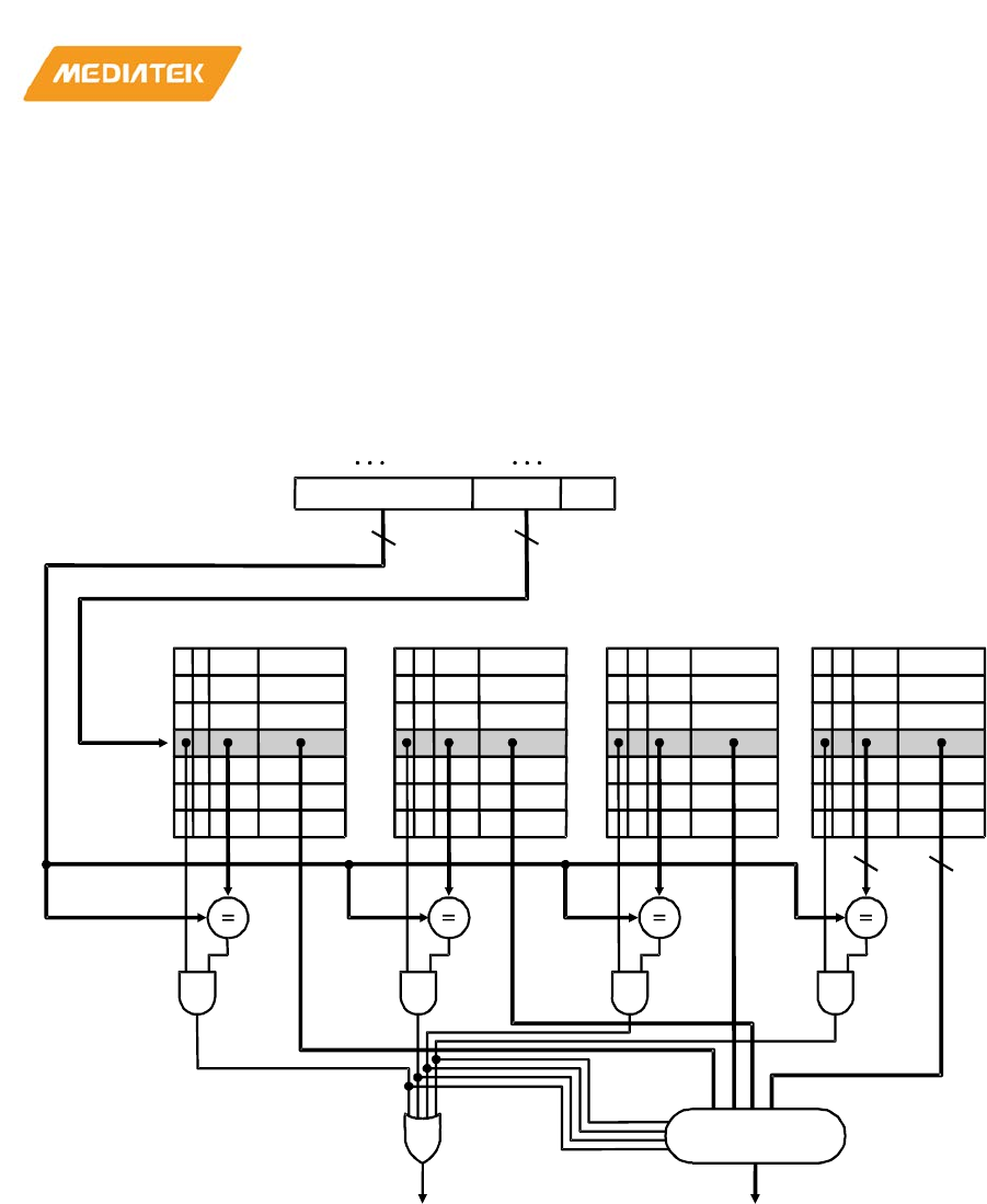
MT76x7
Internet-of-Things Wireless Connectivity
Reference Manual
© 2015 - 2017 MediaTek Inc
Page 39 of 798
This document contains information that is proprietary to MediaTek Inc. (“MediaTek”) and/or its licensor(s).
Any unauthorized use, reproduction or disclosure of this document in whole or in part is strictly prohibited
Each way of cache comprises two memories: tag memory and data memory. The tag memory stores each
line’s valid bit and tag (upper 19 bits of the address). The data memory stores line data. When MCU accesses
the memory, the address is compared to the contents of the tag memory. First, the line index (address bit
[12:5]) is used to locate a line in the tag memory. When a particular line is found in the tag memory, the upper
19 bits (address bit [31:13]), called tag, of the desired memory address are compared with the content of the
found tag line. If an match is found in both line address and tag address plus valid bit is 1, it is said a cache hit,
and the data from that particular cache way is returned to MCU. This process is illustrated here..
Figure 2-14. Cache Lookup
If most memory accesses are cache hit, MCU is able to acquire data immediately without wait states, and the
overall TCM sub-system performance will be higher. There are several factors that may affect the cache hit
rate:
• Cache size and the organization
The larger the cache size, the higher the hit rate. However, the hit rate will start to saturate when the cache
size is larger than a threshold size. Normally the size of 16KB and above and two or four way can achieve a
good hit rate.
• Program behavior
A
d
d
r
e
s
s
19
8
V
T
a
g
I
n
d
e
x
0
1
2
253
254
255
D
a
t
a
V
T
a
g
D
a
t
a
V
T
a
g
D
a
t
a
V
T
a
g
D
a
t
a
3
2
1
9
4
-
t
o
-
1
m
u
l
t
i
p
l
e
x
o
r
H
i
t
D
a
t
a
4
5
12
1
3
3
1
0
D
D
D
D

MT76x7
Internet-of-Things Wireless Connectivity
Reference Manual
© 2015 - 2017 MediaTek Inc
Page 40 of 798
This document contains information that is proprietary to MediaTek Inc. (“MediaTek”) and/or its licensor(s).
Any unauthorized use, reproduction or disclosure of this document in whole or in part is strictly prohibited
If the TCM sub-system performs several tasks and switches frequently between tasks, the cache contents may
have to be flushed out frequently. This is due to the fact that each time a new task runs, the cache will hold its
data for a period of time for the opportunity of likely-be-used-again. However, the stored data might get
flushed out before being used again if the following task requires the data occupying the same cache entries.
Interrupts can cause program flow to change dynamically and reduce the benefit of cache. The interrupt
handler code and the data it processes may cause cache to flush out data used by the current task. Thus, after
returning from the interrupt handler to current task, the flushed data may need to be filled into the cache
again if it is required by the program routine. This will cause performance degradation.
To assist the software engineer to tune the TCM sub-system performance, the cache controller records the
cache hit count and number of cacheable memory accesses. The cache hit rate can be obtained from dividing
these two numbers.
The cache TCM sub-system also comprises a module called MPU (Memory Protection Unit). MPU prevents
illegal memory access and specifies which memory regions are cacheable or non-cacheable. Two fields in the
CACHE_CON register control the enabling of MPU functions. MPU has its own registers to define the memory
region and associated regions. These settings only take effect after the enabling bit in CACHE_CON is set to 1.
For more details on the settings, please refer to the MPU section of this design specification.
2.4.2.4. Theory of operations
1) Write-back/Write-through Configurable Cache
There are two different types of cache designs to maintain the data consistency: cache write-through and
cache write-back.
The write-back cache improves the performance especially when processors generate writes as fast as or
faster than the writes can be handled by the external memory. However, the implementation of write-back is
much harder than that of write-through. When a cache line is dirty, four or eight words will be written back to
the external memory at once, and this will certainly occupy significant bus bandwidth and therefore decrease
the overall efficiency. To solve this problem, a write buffer is necessary in the write-back implementation.
Once the writes get written into the write buffer, the processor can continue the execution.
For TCM sub-systems with large memory write latency, it is possible that the burst write of cache write-back
operation may cause large impact on the TCM sub-system performance. To deal with it, the software can
change the cache to write-through mode if necessary.
2) Write Back Implementation
When a cache hit happens on the write request, only the cache content will be modified, and the dirty bit will
be set (in contrast to write-through, write-through modifies both the contents of cache and the external
memory). Now the content of the cache location which is just modified is inconsistent with that in the external
memory. When the cache misses the read request, line fill will be performed, and a randomly selected cache
line will be replaced, but before that, the dirty bits of that selected cache line have to be checked for the
necessity of write-back. If the dirty bits are not set, line fill can proceed right away, and the selected cache line
can be simply flushed and replaced by a newly fetched line from the external memory which consists of the
requested data. On the other hand, if one of or both the dirty bits are set, write-back has to be performed
before line fill. In that case, half or the entire cache line are written into the write buffer. See the following
figure for summary:

MT76x7
Internet-of-Things Wireless Connectivity
Reference Manual
© 2015 - 2017 MediaTek Inc
Page 41 of 798
This document contains information that is proprietary to MediaTek Inc. (“MediaTek”) and/or its licensor(s).
Any unauthorized use, reproduction or disclosure of this document in whole or in part is strictly prohibited
Figure 2-15. Cache miss/refill criterion
3) Write Buffer
The write buffer consists of address buffer, data buffer, HTRANS buffer, HSIZE buffer, HLOCK buffer, and
HBURST buffer. The write buffer is first-in-first-out (FIFO) design, and the depth of write buffer is eight words.
Since the outputs from code cache meet the AMBA format, the address buffer and data buffer are
independent, and the outputs of write buffer also meet AMBA format and are designed for pipelining.
4) Cache Operation
Upon power-on, the cache memory contains random values, and these numbers are useless for MCU. MCU
needs to flush out the cache content in each cache line before being utilized. The cache controller provides a
register which, when written, can operate on the cache memory to fulfill the necessary prerequisite
mentioned above (called cache operation). The operation involves:
• Invalidate one cache line
The user must give a memory address. If it is found within cache, that particular cache line containing the given
address will be invalidated. The invalidation is done by writing a 0 to the valid bit at the corresponding tag line.
Alternatively, the user can invalidate a cache line by specifying a set/way mapped to that cache line.
• Invalidate all cache lines
The user does not need to specify an address. The cache controller clears valid bits in all tag lines when this
operation is requested.
• Flush one cache line
The user must give a memory address. If it is found within cache and the dirty bit or bits are set, that particular
cache line containing the given address will be flushed into the write buffer. Alternatively, the user can
invalidate a cache line by specifying a set/way mapped to that cache line. This operation is not supported if the
cache is operating in the write-through mode.
• Flush all cache lines
The user needs not to specify an address. The cache controller flushes all the cache lines with the dirty bit or
bits set. This operation is not supported if the cache is operating in the write-through mode.
5) Cache Activity Summary
Table 2-16. Write-back Mode Cache R/W Action Summary
Op
Cacheable
Hit
Dirty
Action
Write Request
Write into
cache only
and set the
dirty bit
Write into
external
memory
Cache Hit
Cache Miss
Read Request
Read From
Cache
Check Dirty
Bits
Line Fill Cache Write
Back
CacheHit
Cache Miss
Dirty
Clean
Write back done
and write buffer contents
ONLY the last set of
write back words

MT76x7
Internet-of-Things Wireless Connectivity
Reference Manual
© 2015 - 2017 MediaTek Inc
Page 42 of 798
This document contains information that is proprietary to MediaTek Inc. (“MediaTek”) and/or its licensor(s).
Any unauthorized use, reproduction or disclosure of this document in whole or in part is strictly prohibited
Op
Cacheable
Hit
Dirty
Action
W0~W3
W4~W7
Rd
N
d
D
d
Single read
Y
Y
d
d
Return data, no stall
N
N
N
Line refill from bus using AHB WRAP8 burst
N
Y
• Evict half line to WBuf.
• Line refill from bus using AHB WRAP8 burst.
• Write back half line from WBuf using AHB INCR4 burst
write.
Y
N
Y
Y
• Evict whole line to WBuf.
• Line refill from bus using AHB WRAP8 burst.
• Write back whole line from WBuf using AHB INCR8 burst
write.
Wr
N
d d
d
• Wait for WBuf space.
• Place write data into write WBuf and let ARM proceed
(CLKEN = 1). Stall ARM by one cycle.
Y
Y
d
d
• Write to data SRAM; meanwhile set up corresponding dirty
bit
• Stall ARM by one cycle to avoid struct hazard.
N
d
d
• Wait for WBuf space.
• Place write data into write WBuf and let ARM proceed
(CLKEN=1). Stall ARM by one cycle.
Legend Y: yes, N: no, d: don’t care
Table 2-17. Write-through Mode Cache R/W Action Summary
Op
Cacheable
Hit
Action
Rd
N
d
Single read
Y
Y
Return data, no stall
N
Line read from bus using AHB WRAP8 burst
Wr
N
d
Wait for WBuf space.
Place write data into write WBuf and let ARM proceed (CLKEN = 1).
Stall ARM by one cycle.
Y
N
Y
Write to data SRAM.
Wait for WBuf space.
Place write data into write WBuf and let ARM proceed (CLKEN = 1).
Stall ARM by one cycle.
Legend Y: yes, N: no, d: don’t care
2.4.2.5. MPU
MPU provides a protection mechanism and cacheable indication of memory, which features:
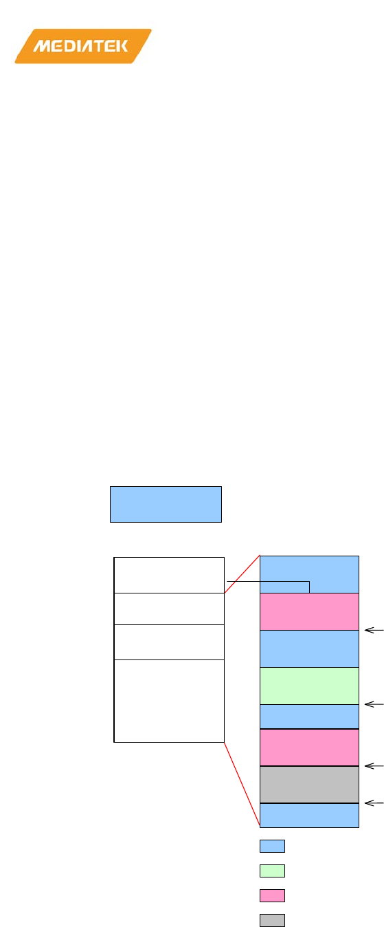
MT76x7
Internet-of-Things Wireless Connectivity
Reference Manual
© 2015 - 2017 MediaTek Inc
Page 43 of 798
This document contains information that is proprietary to MediaTek Inc. (“MediaTek”) and/or its licensor(s).
Any unauthorized use, reproduction or disclosure of this document in whole or in part is strictly prohibited
• Protection settings
Determine if MCU can read/write a memory region. If the setting does not allow MCU’s particular access to a
memory address, MPU will stop the memory access and issue the “ABORT” signal to MCU, making it entering
the “abort” mode. The exception handler must then process the situation.
• Cacheable settings
Determine a memory region is cacheable or not. If cacheable, MCU will keep a small copy in its cache after
read accesses. If MCU requires the same data later, it can acquire it from the high-speed local copy, instead of
from the low-speed external memory.
The 4GB memory space is divided into 16 memory blocks with 256MB size each, i.e. MB0 ~ MB15. EMI takes
MB0 ~ MB3, TCM RAM takes MB4, TCM uses MB5, APB peripherals MB8. The characteristics of these memory
blocks are listed below:
• Read/write protection setting
• All MBs are determined by MPU.
• Cacheable setting
All MBs are determined by MPU. Note that the software should avoid making cache line access to the MB that
does not support burst read/write. Usually only MB0 ~ MB3, mapped to EMI, are set as cacheable regions.
APB Peripherals
MB3
~
MB0
MB4
MB5
Region 0
Region 1
Region 2
Region 3
Region 0 base address
Region 1 base address
Region 2 base address
Region 3 base address
non -
readable/writeable
readable/non
- writeable
no
n
-
readable/non
- writeable
readable/writeable
MB8
MB6 AHB Peripherals
TCM
TCM RAM
EMI
Figure 2-16: MPU protection setting example
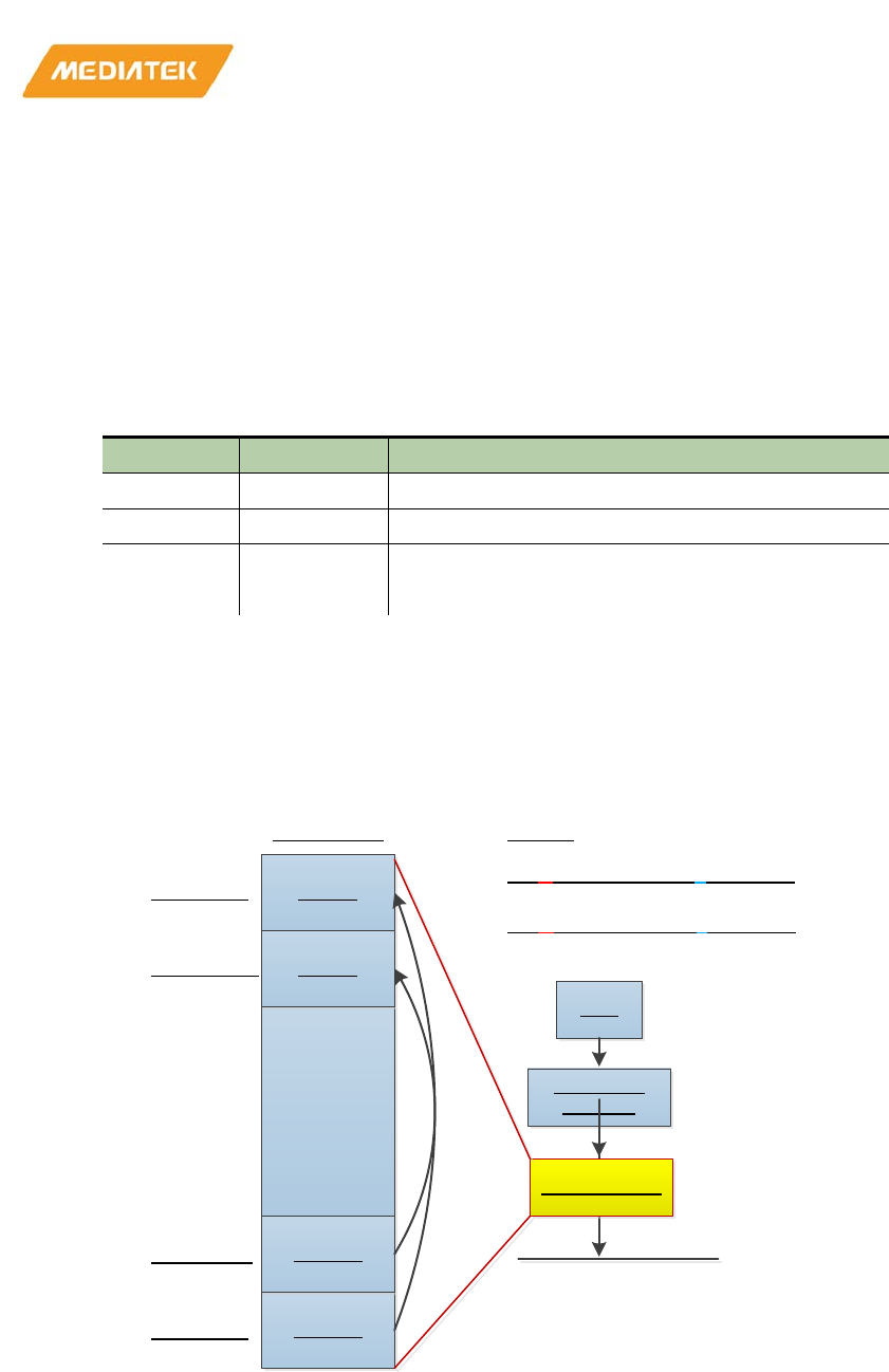
MT76x7
Internet-of-Things Wireless Connectivity
Reference Manual
© 2015 - 2017 MediaTek Inc
Page 44 of 798
This document contains information that is proprietary to MediaTek Inc. (“MediaTek”) and/or its licensor(s).
Any unauthorized use, reproduction or disclosure of this document in whole or in part is strictly prohibited
For example, the figure above illustrates the protection setting in each memory block. Five regions are defined
in the figure. Note that each region can be continuous or non-continuous to each other, and those address
ranges not covered by any region are set to be readable/writeable automatically. There is one restriction:
Different regions must not overlap.
The user can define maximum 16 regions in MB0 ~ MB4 and MB10. Each region has its own setting defined in a
32-bit register:
In chip simulation, three patterns are used to verify L1 cache, as shown in Table 2-18.
Table 2-18. Test patterns for whole chip simulation
Testlist
Testname
Description
mcu_cm4.list Cache_test Test l1cache function
mcu_cm4.list Cache_ram Test tcm ram read/write access
mcu_cm4.list Cm4_xip_flash • Cortex-M4 boot from rom, enable cache controller
• Jump to serial flash to execute XIP
2.4.2.6. Remapping
MT76x7 cache provides two register sets for thesoftware programmer to make the actual memory address
same as different CPU load/store target address. The following figure shows the scenario: The software sets
0x10xxxxxx to cacheable but 0x1Fxxxxxx to non–cacheable, but they are mapped to the same physical address.
Bank 0
Bank 1
vBank 0
vBank 1
0X1000000
0X11000000
0X1
E
00000
0x1
F
00000
0x1
F
0000000 à 0X10XXXXXXX
Memory Map Remap:
0x1
E
0000000 à 0X11XXXXXXX
ARM
Cache/MPU
Controller
Address Remap
Figure 2-17: Example Settings of Cache Remapping
To achieve this:
1) Set region begin with 0x1000_0000 to cacheable using MPU.
2) Set region begin with 0x1F00_0000 to non-cacheable using MPU.
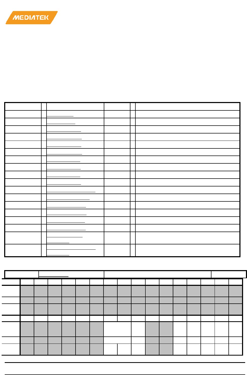
MT76x7
Internet-of-Things Wireless Connectivity
Reference Manual
© 2015 - 2017 MediaTek Inc
Page 45 of 798
This document contains information that is proprietary to MediaTek Inc. (“MediaTek”) and/or its licensor(s).
Any unauthorized use, reproduction or disclosure of this document in whole or in part is strictly prohibited
3) Set BASEADDR field in Remap EntryHi to 0x1F00_0000.
4) Set BASEADDR filed in Remap EntryLo to 0x1000_0000.
2.4.2.7. Register definitions
Module name: l1cache Base address: (+1530000h)
Address
Name
Width
Register Function
01530000
Cache_con
32
Cache general control register
01530004
CACHE_OP
32
Cache operation
01530008
cache_hcnt0L
32
Cache hit count 0 lower part
0153000C
cache_hcnt0U
32
Cache hit count 0 upper part
01530010
cache_Ccnt0L
32
Cacheable access count 0 lower part
01530014
cache_Ccnt0U
32
Cacheable access count 0 upper part
01530018
cache_hcnt1L
32
Cache hit count 1 lower
part
0153001C
cache_hcnt1U
32
Cache hit count 1 upper part
01530020
cache_Ccnt1L
32
Cacheable access count 1 lower part
01530024
cache_Ccnt1U
32
Cacheable
access count 1 upper part
01530028
way_replace_policy
32
Replace policy
0153002C
mpu_channel_en
32
MPU channel enable
01531000
NCREMAP_HI0
32
Remap Entry_HI0
01531004
NCREMAP_LO0
32
Remap Entry_LO0
01531008
NCREMAP_HI1
32
Remap Entry_HI1
0153100C
NCREMAP_LO1
32
Remap Entry_LO1
01540000~
0154003c
mpu_entry [n]
(n=0~15)
32
MPU N
-th channel control
01540040~
0154007c
mpu_End_entry [n]
(n=0~15)
32
MPU N
-th channel control
01530000
Cache_con
Cache general control register
00000000
Bit
31
30
29
28
27
26
25
24
23
22
21
20
19
18
17
16
Nam
e
Type
Rese
t
Bit
15
14
13
12
11
10
9
8
7
6
5
4
3
2
1
0
Nam
e CACHESI
ZE MD
RF
CN
TE
N1
CN
TE
N0
MP
DE
Fen
Mp
en MC
EN
Type
RW
RW
RW
RW
RW
RW
RW
Rese
t
0 0 0 0 0 0 0 0
Bit(s)
Name
Description
9:8
CACHESIZE
Selects cache size

MT76x7
Internet-of-Things Wireless Connectivity
Reference Manual
© 2015 - 2017 MediaTek Inc
Page 46 of 798
This document contains information that is proprietary to MediaTek Inc. (“MediaTek”) and/or its licensor(s).
Any unauthorized use, reproduction or disclosure of this document in whole or in part is strictly prohibited
Bit(s)
Name
Description
00 No cache
01 8KB, 1
-way cache
10 16KB, 2
-way cache
11 32KB, 4
-way cache
7
MDRF
Enables early restart function
0
Disable
1 Enable
4
CNTEN1
Enables cache hit counter 1
If enabled, the cache controller will increment a 48
-bit counter by
one when a cache hit is detected. This number can provide a
reference in performance evaluation for tuning application
programs. This
counter increments only when the data are obtained
from MPU cacheable region 8 ~ 15.
0 Disable
1 Enable
3
CNTEN0
Enables cache hit counter 0
If enabled, the cache controller will increment a 48
-bit counter by
one when a cache hit is detected. This number
can provide a
reference in performance evaluation for tuning application
programs. This counter increments only when the data are obtained
from MPU cacheable region 0 ~ 7.
0 Disable
1 Enable
2
MPDEFen
Enables MPU default protection attribute
If enabled,
the default protection will be in privilege mode
read/write. The user mode is not accessible.
0 Disable
1 Enable
1
Mpen
Enables MPU comparison of read/write permission
setting
If disabled, MCU can access any memory without restriction. If
enabled, MPU will compare the address of MCU to MPU protection
setting. If the MCU accessed address falls into the restricted region,
MPU will stop this memory access and send an "ABORT" signal to
MCU. For details, please refer to the MPU part of this specification.
0 Dis
able
1 Enable
0
MCEN
Enables MPU comparison of cacheable/non-cacheable

MT76x7
Internet-of-Things Wireless Connectivity
Reference Manual
© 2015 - 2017 MediaTek Inc
Page 47 of 798
This document contains information that is proprietary to MediaTek Inc. (“MediaTek”) and/or its licensor(s).
Any unauthorized use, reproduction or disclosure of this document in whole or in part is strictly prohibited
Bit(s)
Name
Description
setting
If disabled, MCU memory accesses are all non
-cacheable, i.e. they
will go through the AHB bus (except for TCM access). If enabled,
the setting in MPU will take effect. If MCU
accesses a cacheable
memory region, the cache controller will return the data in cache if
it is found in cache and will get the data through the AHB bus only
if a cache miss occurs. For details, please refer to the MPU part of
this specification.
0 Disable
1 Enable
01530004
CACHE_OP
Cache operation
00000000
Bit
31
30
29
28
27
26
25
24
23
22
21
20
19
18
17
16
Nam
e
TADDR[31:5]
Type
RW
Rese
t
0 0 0 0 0 0 0 0 0 0 0 0 0 0 0 0
Bit
15
14
13
12
11
10
9
8
7
6
5
4
3
2
1
0
Nam
e
TADDR[31:5] OP[3:0] EN
Type
RW
RW
RW
Rese
t
0 0 0 0 0 0 0 0 0 0 0 0 0 0 0 0
Bit(s)
Name
Description
31:5
TADDR[31:5]
Target address
This field contains the address of invalidation operation. If OP[3:0]
= 0010, TADDR[31:5] will be the address[31:5] of a
memory whose
line will be invalidated if it exists in the cache. If OP[3:0] = 0100,
TADDR[12:5] will indicate the set, while TADDR[19:16] indicate
which way to clear:
0001 way #0
0010 way #1
0100 way #2
1000 way #3
4:1
OP[3:0]
Operation
This field
determines which cache operations will be performed.
0001 invalidate all cache lines
0010 invalidate one cache line using address
0100 invalidate one cache line using set/way
MT76x7
Internet-of-Things Wireless Connectivity
Reference Manual
© 2015 - 2017 MediaTek Inc
Page 48 of 798
This document contains information that is proprietary to MediaTek Inc. (“MediaTek”) and/or its licensor(s).
Any unauthorized use, reproduction or disclosure of this document in whole or in part is strictly prohibited
Bit(s)
Name
Description
1001 flush all cache lines
1010 flush one cache line using address
1100 flush one
cache line using set/way
0
EN
Enables command
This enabling bit must be written 1 to enable the command.
0 Does not enable
1 Enable
01530008
cache_hcnt0L
Cache hit count 0 lower part
00000000
Bit
31
30
29
28
27
26
25
24
23
22
21
20
19
18
17
16
Nam
e
Chit_cnt0[31:0]
Type
RW
Rese
t
0 0 0 0 0 0 0 0 0 0 0 0 0 0 0 0
Bit
15
14
13
12
11
10
9
8
7
6
5
4
3
2
1
0
Nam
e
Chit_cnt0[31:0]
Type
RW
Rese
t
0 0 0 0 0 0 0 0 0 0 0 0 0 0 0 0
Bit(s)
Name
Description
31:0
Chit_cnt0[31:0]
Cache hit count 0
WRITE Write any value to CACHE_HCNT0L or CACHE_HCNT0U
clears CHIT_CNT0 to all 0.
READ Current counter value
0153000C
cache_hcnt0U
Cache hit count 0 upper part
00000000
Bit
31
30
29
28
27
26
25
24
23
22
21
20
19
18
17
16
Nam
e
Type
Rese
t
Bit
15
14
13
12
11
10
9
8
7
6
5
4
3
2
1
0
Nam
e
Chit_cnt0[47:32]
Type
RW
Rese
t
0 0 0 0 0 0 0 0 0 0 0 0 0 0 0 0

MT76x7
Internet-of-Things Wireless Connectivity
Reference Manual
© 2015 - 2017 MediaTek Inc
Page 49 of 798
This document contains information that is proprietary to MediaTek Inc. (“MediaTek”) and/or its licensor(s).
Any unauthorized use, reproduction or disclosure of this document in whole or in part is strictly prohibited
Bit(s)
Name
Description
15:0
Chit_cnt0[47:32]
Cache hit count 0
WRITE Write any value to CACHE_HCNT0L or CACHE_HCNT0U
clears CHIT_CNT0 to all 0.
READ Current counter value
01530010
cache_Ccnt0L
Cacheable access count 0 lower part
00000000
Bit
31
30
29
28
27
26
25
24
23
22
21
20
19
18
17
16
Nam
e
CACC_cnt0[31:0]
Type
RW
Rese
t
0 0 0 0 0 0 0 0 0 0 0 0 0 0 0 0
Bit
15
14
13
12
11
10
9
8
7
6
5
4
3
2
1
0
Nam
e
CACC_cnt0[31:0]
Type
RW
Rese
t
0 0 0 0 0 0 0 0 0 0 0 0 0 0 0 0
Bit(s)
Name
Description
31:0
CACC_cnt0[31:0]
Cache access count 0
WRITE Write any value to CACHE_CCNT0L or CACHE_CCNT0U
clears CACC_CNT0 to all 0.
READ Current counter value
01530014
cache_Ccnt0U
Cacheable access count 0 upper part
00000000
Bit
31
30
29
28
27
26
25
24
23
22
21
20
19
18
17
16
Nam
e
Type
Rese
t
Bit
15
14
13
12
11
10
9
8
7
6
5
4
3
2
1
0
Nam
e
CACC_cnt0[47:32]
Type
RW
Rese
t
0 0 0 0 0 0 0 0 0 0 0 0 0 0 0 0
Bit(s)
Name
Description
15:0
CACC_cnt0[47:32]
Cache access count 0
WRITE Write any value to CACHE_CCNT0L or CACHE_CCNT0U
MT76x7
Internet-of-Things Wireless Connectivity
Reference Manual
© 2015 - 2017 MediaTek Inc
Page 50 of 798
This document contains information that is proprietary to MediaTek Inc. (“MediaTek”) and/or its licensor(s).
Any unauthorized use, reproduction or disclosure of this document in whole or in part is strictly prohibited
Bit(s)
Name
Description
clears CACC_CNT0 to all 0.
READ Current counter value
The best way to use CACHE_HCNT0 and CACHE_CCNT0 is to set
the initial value to 0 for both registers, enable both counters (set
CNTEN0 to 1),
run a portion of program to be benchmarked, stop
the counters and get their values. Therefore, during this period,
The cache hit rate value may help tune the performance of the
application program. Note that CHIT_CNT0 and CACC_CNT0 only
increment if the
cacheable attribute is defined in MPU cacheable
region lower half channels (i.e. channel 0 ~ 7 of the total 16
channels).
01530018
cache_hcnt1L
Cache hit count 1 lower part
00000000
Bit
31
30
29
28
27
26
25
24
23
22
21
20
19
18
17
16
Nam
e
Chit_cnt1[31:0]
Type
RW
Rese
t
0 0 0 0 0 0 0 0 0 0 0 0 0 0 0 0
Bit
15
14
13
12
11
10
9
8
7
6
5
4
3
2
1
0
Nam
e
Chit_cnt1[31:0]
Type
RW
Rese
t
0 0 0 0 0 0 0 0 0 0 0 0 0 0 0 0
Bit(s)
Name
Description
31:0
Chit_cnt1[31:0]
Cache hit count
WRITE Write any value to CACHE_HCNT1L or CACHE_HCNT1U
clears CHIT_CNT1 to all 0.
READ Current counter value
0153001C
cache_hcnt1U
Cache hit count 1 upper part
00000000
Bit
31
30
29
28
27
26
25
24
23
22
21
20
19
18
17
16
Nam
e
Type
Rese
t
Bit
15
14
13
12
11
10
9
8
7
6
5
4
3
2
1
0
Nam
e
Chit_cnt1[47:32]
Type
RW

MT76x7
Internet-of-Things Wireless Connectivity
Reference Manual
© 2015 - 2017 MediaTek Inc
Page 51 of 798
This document contains information that is proprietary to MediaTek Inc. (“MediaTek”) and/or its licensor(s).
Any unauthorized use, reproduction or disclosure of this document in whole or in part is strictly prohibited
Rese
t
0 0 0 0 0 0 0 0 0 0 0 0 0 0 0 0
Bit(s)
Name
Description
15:0
Chit_cnt1[47:32]
Cache hit count
WRITE
Write any value to CACHE_HCNT1L or CACHE_HCNT1U
clears CHIT_CNT1 to all 0.
READ Current counter value
01530020
cache_Ccnt1L
Cacheable access count 1 lower part
00000000
Bit
31
30
29
28
27
26
25
24
23
22
21
20
19
18
17
16
Nam
e
CACC_CNT1[31:0]
Type
RW
Rese
t
0 0 0 0 0 0 0 0 0 0 0 0 0 0 0 0
Bit
15
14
13
12
11
10
9
8
7
6
5
4
3
2
1
0
Nam
e
CACC_CNT1[31:0]
Type
RW
Rese
t
0 0 0 0 0 0 0 0 0 0 0 0 0 0 0 0
Bit(s)
Name
Description
31:0
CACC_CNT1[31:0]
Cache access count 1
WRITE
Write any value to CACHE_CCNT1L or CACHE_CCNT1U
clears CACC_CNT1 to all 0.
READ Current counter value
01530024
cache_Ccnt1U
Cacheable access count 1 upper part
00000000
Bit
31
30
29
28
27
26
25
24
23
22
21
20
19
18
17
16
Nam
e
Type
Rese
t
Bit
15
14
13
12
11
10
9
8
7
6
5
4
3
2
1
0
Nam
e
CACC_CNT1[47:32]
Type
RW
Rese
t
0 0 0 0 0 0 0 0 0 0 0 0 0 0 0 0
Bit(s)
Name
Description
MT76x7
Internet-of-Things Wireless Connectivity
Reference Manual
© 2015 - 2017 MediaTek Inc
Page 52 of 798
This document contains information that is proprietary to MediaTek Inc. (“MediaTek”) and/or its licensor(s).
Any unauthorized use, reproduction or disclosure of this document in whole or in part is strictly prohibited
Bit(s)
Name
Description
15:0
CACC_CNT1[47:32]
Cache access count 1
WRITE
Write any value to CACHE_CCNT1L or CACHE_CCNT1U
clears CACC_CNT1 to all 0.
READ Current counter value
01530028
way_replace_policy
Replace policy
00000001
Bit
31
30
29
28
27
26
25
24
23
22
21
20
19
18
17
16
Nam
e
Type
Rese
t
Bit
15
14
13
12
11
10
9
8
7
6
5
4
3
2
1
0
Nam
e
Re
pla
ce
pol
icy
Type
RW
Rese
t
1
Bit(s)
Name
Description
0
Replace policy
Replace policy
0
Using way_counter which counts in every cycle to make it more
like random.
1
Replace the lower way first if that way is not valid. If all ways are
valid, replace
policy is random.
0153002C
mpu_channel_en
MPU channel enable
00000000
Bit
31
30
29
28
27
26
25
24
23
22
21
20
19
18
17
16
Nam
e
Type
Rese
t
Bit
15
14
13
12
11
10
9
8
7
6
5
4
3
2
1
0
Nam
e
CH15~CH0
Type
RW
Rese
t
0 0 0 0 0 0 0 0 0 0 0 0 0 0 0 0
Bit(s)
Name
Description
MT76x7
Internet-of-Things Wireless Connectivity
Reference Manual
© 2015 - 2017 MediaTek Inc
Page 53 of 798
This document contains information that is proprietary to MediaTek Inc. (“MediaTek”) and/or its licensor(s).
Any unauthorized use, reproduction or disclosure of this document in whole or in part is strictly prohibited
Bit(s)
Name
Description
15:0
CH15~CH0
Enables/Disables the associated region
0 Disable the region setting
1 Enable the region setting
01531000
NCREMAP_HI0
Remap Entry_HI0
00000000
Bit
31
30
29
28
27
26
25
24
23
22
21
20
19
18
17
16
Nam
e
BASEADDR
Type
RW
Rese
t
0 0 0 0 0 0 0 0 0 0 0 0 0 0 0 0
Bit
15
14
13
12
11
10
9
8
7
6
5
4
3
2
1
0
Nam
e
BASEADDR size EN
Type
RW
RW
RW
Rese
t
0 0 0 0 0 0 0 0 0 0 0 0 0
Bit(s)
Name
Description
31:9
BASEADDR
Base address of this region
5:1
size
Size of this region. Actual size = 2^(size +9) Bytes, max
size is 256MB.
0
EN
Enables this region
0 Disable
1 Enable
01531004
NCREMAP_LO0
Remap Entry_LO0
00000000
Bit
31
30
29
28
27
26
25
24
23
22
21
20
19
18
17
16
Nam
e
BASEADDR
Type
RW
Rese
t
0 0 0 0 0 0 0 0 0 0 0 0 0 0 0 0
Bit
15
14
13
12
11
10
9
8
7
6
5
4
3
2
1
0
Nam
e
BASEADDR
Type
RW
Rese
t
0 0 0 0 0 0 0
Bit(s)
Name
Description
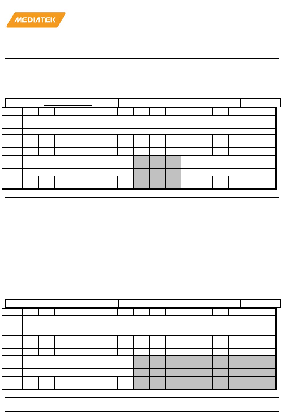
MT76x7
Internet-of-Things Wireless Connectivity
Reference Manual
© 2015 - 2017 MediaTek Inc
Page 54 of 798
This document contains information that is proprietary to MediaTek Inc. (“MediaTek”) and/or its licensor(s).
Any unauthorized use, reproduction or disclosure of this document in whole or in part is strictly prohibited
Bit(s)
Name
Description
31:9
BASEADDR
This register sets up the mapped address base of CPU
access which hits NC
-Remap Entry0_HI.
01531008
NCREMAP_HI1
Remap Entry_HI1
00000000
Bit
31
30
29
28
27
26
25
24
23
22
21
20
19
18
17
16
Nam
e
BASEADDR
Type
RW
Rese
t
0 0 0 0 0 0 0 0 0 0 0 0 0 0 0 0
Bit
15
14
13
12
11
10
9
8
7
6
5
4
3
2
1
0
Nam
e
BASEADDR size EN
Type
RW
RW
RW
Rese
t
0 0 0 0 0 0 0 0 0 0 0 0 0
Bit(s)
Name
Description
31:9
BASEADDR
Base address of this region
5:1
size
Size of this region. Actual size = 2^(size +9) Bytes, max
size is 256MB.
0
EN
Enables this region
0 Disable
1 Enable
0153100C
NCREMAP_LO1
Remap Entry_LO1
00000000
Bit
31
30
29
28
27
26
25
24
23
22
21
20
19
18
17
16
Nam
e
BASEADDR
Type
RW
Rese
t
0 0 0 0 0 0 0 0 0 0 0 0 0 0 0 0
Bit
15
14
13
12
11
10
9
8
7
6
5
4
3
2
1
0
Nam
e
BASEADDR
Type
RW
Rese
t
0 0 0 0 0 0 0
Bit(s)
Name
Description
31:9
BASEADDR
This register sets up the mapped address base of CPU
access which hits NC
-Remap Entry1_HI. Note that the
base and size settings in 2 EntryHi cannot be overlapped.
Otherwise, the resultant mapped address will be
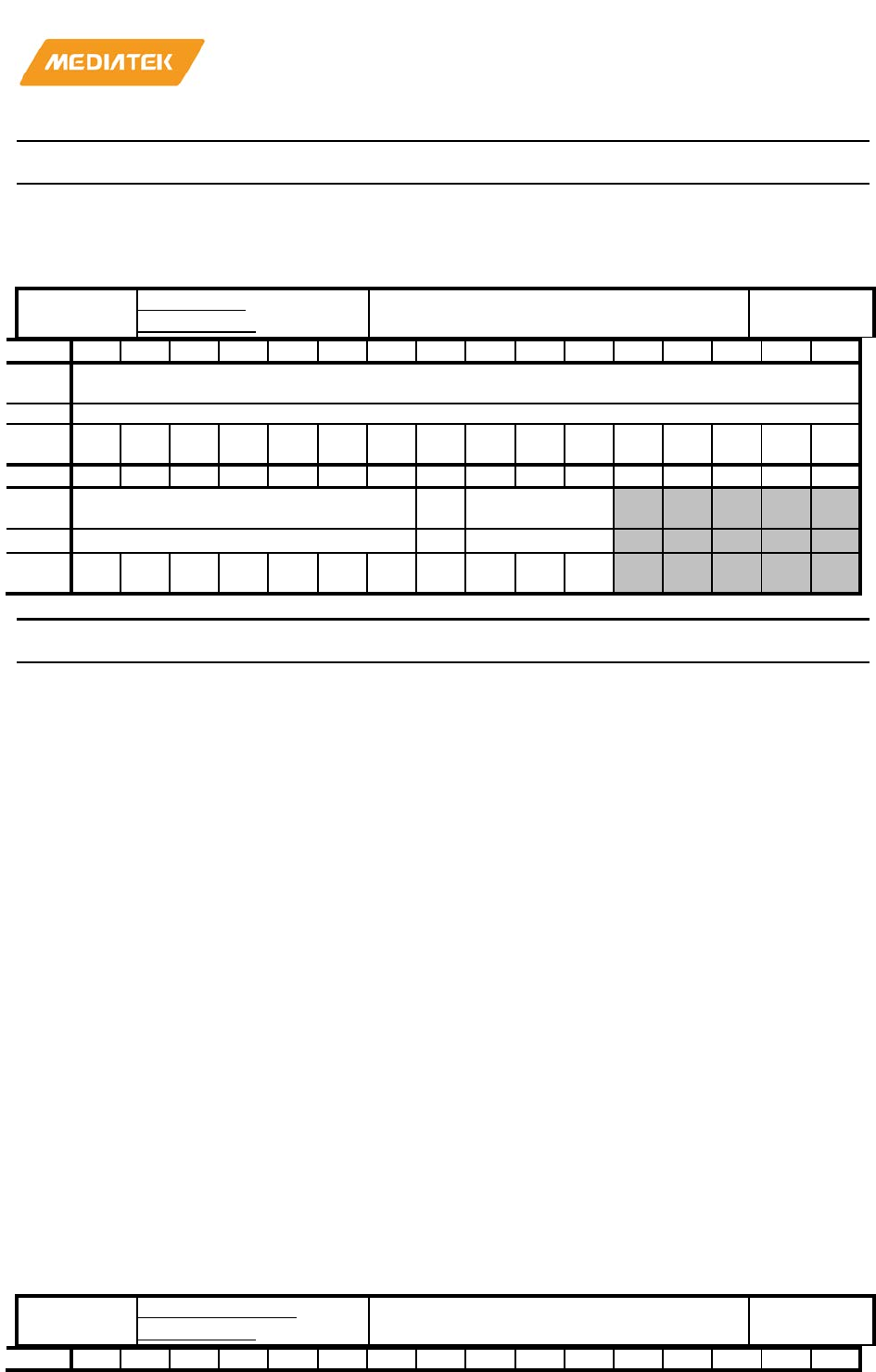
MT76x7
Internet-of-Things Wireless Connectivity
Reference Manual
© 2015 - 2017 MediaTek Inc
Page 55 of 798
This document contains information that is proprietary to MediaTek Inc. (“MediaTek”) and/or its licensor(s).
Any unauthorized use, reproduction or disclosure of this document in whole or in part is strictly prohibited
Bit(s)
Name
Description
undefined.
01540000~
0154003C
mpu_entry
[n](n=0~15)
MPU N-th channel control
00000000
Bit
31
30
29
28
27
26
25
24
23
22
21
20
19
18
17
16
Nam
e
BASEADDR
Type
RW
Rese
t
0 0 0 0 0 0 0 0 0 0 0 0 0 0 0 0
Bit
15
14
13
12
11
10
9
8
7
6
5
4
3
2
1
0
Nam
e
BASEADDR C ATTR
Type
RW
RW
RW
Rese
t
0 0 0 0 0 0 0 0 0 0 0
Bit(s)
Name
Description
31:9
BASEADDR
start addr of MPU
8
C
Cacheable Attribute, Cacheable setting and non-cacheable
setting are similar to cache protection settings .
0: non
-cacheable
1: cacheable
Note that each region can be continuous or non
-continuous to each
other. For those address ranges not covered by any region in the
MPU cacheable settings are set to be uncacheable automatically.
There is one restriction: Different regions must
not overlap.
7:5
ATTR
Protection modes
3'd0: no protection
3'd1:Only R/W for privilege mode access
3'd2: Only R/W for privilege mode access; read access to user mode
3'd3:Only R/W for privilege mode access; write access to user mode
3'd4:Only read for p
rivilege/user mode
3'd5:Both R/W are forbidden
3'd6: Privilege mode read only; no access to user mode
01540040~
0154007C
mpu_End_entry
[n](n=0~15)
MPU N-th channel control
00000000
Bit
31
30
29
28
27
26
25
24
23
22
21
20
19
18
17
16
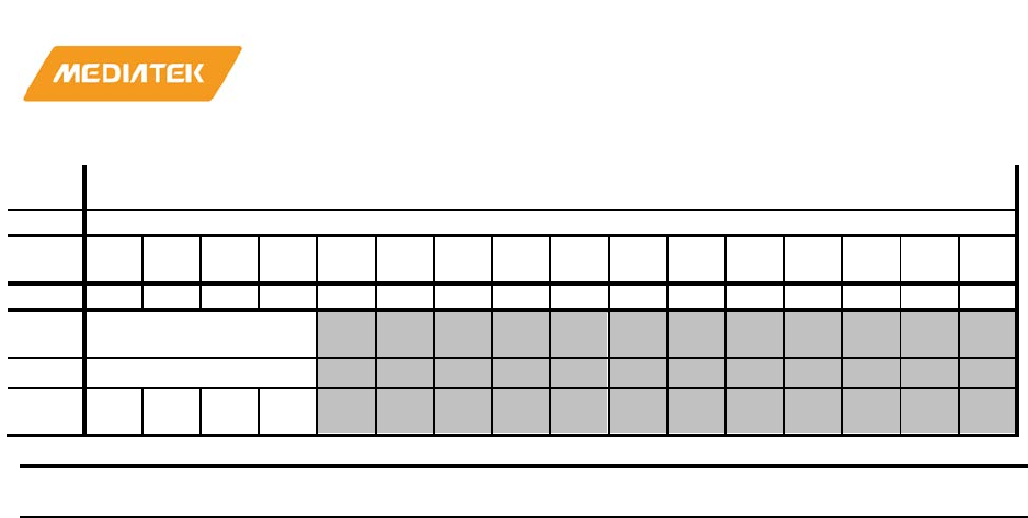
MT76x7
Internet-of-Things Wireless Connectivity
Reference Manual
© 2015 - 2017 MediaTek Inc
Page 56 of 798
This document contains information that is proprietary to MediaTek Inc. (“MediaTek”) and/or its licensor(s).
Any unauthorized use, reproduction or disclosure of this document in whole or in part is strictly prohibited
Nam
e
BASEADDR
Type
RW
Rese
t
0 0 0 0 0 0 0 0 0 0 0 0 0 0 0 0
Bit
15
14
13
12
11
10
9
8
7
6
5
4
3
2
1
0
Nam
e
BASEADDR
Type
RW
Rese
t
0 0 0 0
Bit(s)
Name
Description
31:12
BASEADDR
END addr of MPU
2.4.3. Bus fabric
MT76x7 implements AHB/APB bus fabric to connect the MCU, memory, IO peripherals and the radio
subsystem.
• ILM/DLM: Instruction Local Memory / Data Local Memory, the zero-wait-state local memory for Radio
MCU.
• Wi-Fi HIF: The data interface to Wi-Fi Packet switch engine.
• Bluetooth FIFO I/F: The control/data interface to Bluetooth subsystem.
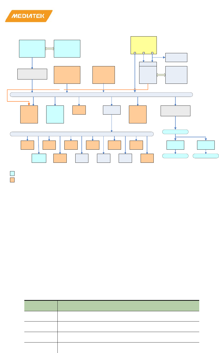
MT76x7
Internet-of-Things Wireless Connectivity
Reference Manual
© 2015 - 2017 MediaTek Inc
Page 57 of 798
This document contains information that is proprietary to MediaTek Inc. (“MediaTek”) and/or its licensor(s).
Any unauthorized use, reproduction or disclosure of this document in whole or in part is strictly prohibited
ARM Cortex M4
Cache
Controller TCM/Cache
(96KB)
Cortex-M4 AHB bus
Generic DMA
SPI flash
APB
bridge
APB2 bus
Wi-Fi HIF
UART1 UART2 I2C-1 I2C-2 SPI-M
I2S
Bluetooth
FIFO I/F AUX
ADC
TOP &
CM4
CONFIG
GPT WDT
N9
Interface to radio subsystem
Peripherals
APB
bridge
SYSRAM_
CM4
(256KB)
APB1 bus
ILM/DLM
PWM
XIP
AHB mux
ICODEDCODESYSTEM
Asyncrhrous AHB-2-
AHB bridge
(N9 bus to CM4 bus)
Asyncrhrous AHB-2-
AHB bridge
(CM4 bus to N9 bus)
APB
bridge
APB0 bus
TCM ROM
N9 AHB bus
GDMA
CONFIG
Crypto
Engine
Figure 2-18. Cortex-M4 subsystem – bus fabric
The AHB bus arbitration adopts round-robin scheme.
The N9 subsystem and Cortex M4 subsystem are in different clock domains, so the asynchronous bridges are
inserted in the bus fabric. N9 has the ability to (but would be rarely used) all the Cortex-M4 peripherals.
2.4.4. Serial flash controller
2.4.4.1. General Description
MT76X7 features a serial flash controller that can support the serial flash with the read mode of (JEDEC)
standard SPI mode, SPI-Quad mode, QPI (Quad Peripheral Interface) mode, Dual IO mode, and Dual-Output
mode.
The frequency of the serial clock rate is up to 64MHz. That provides 256Mbps equivalent throughput on flash
when SPI-quad mode or QPI mode is used.
Table 2-19. Flash controller support read mode
Read Mode Description
SPI 1xIO for receiving command and address, 1xIO for output data
SPI-Quad 1xIO for receiving command, 4xIO for address, 4xIO for output data
QPI 4xIO for receiving command/address and output data
Dual-IO 1xIO for command, 2xIO for address and output data
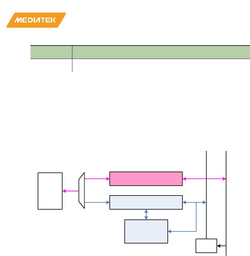
MT76x7
Internet-of-Things Wireless Connectivity
Reference Manual
© 2015 - 2017 MediaTek Inc
Page 58 of 798
This document contains information that is proprietary to MediaTek Inc. (“MediaTek”) and/or its licensor(s).
Any unauthorized use, reproduction or disclosure of this document in whole or in part is strictly prohibited
Read Mode Description
Dual-Output 1xIO for receiving command, 2xIO for address and output data
The Serial Flash Controller Supports Two Operation Modes:
Direct read mode, which supports a high-throughput direct-access through AHB bus
Macro access mode, which supports flash access with arbitrary command and is through APB bus.
2.4.4.2. Block diagram
Direct Read
Serial
Flash
MAC R/W
GPRAM
APB
SF+0000h AHB
0000_0000
SCK
SCS#
SI
SO
WP
HOLD
Bridge
Figure 2-19. Serial flash controller block diagram
See Figure 2-19 for the block diagram of MT7697 serial flash controller. There are two exclusive control paths,
“Direct Read” and “Macro R/W”, and each path can only be enabled to access a device once at a time. Direct
Read supports convenient high-speed serial nor-flash code fetching through AHB and can be used for boot-up
without any register setting. Macro R/W supports flexible command sequence GPRAM (general-purpose
SRAM) through APB.
In Figure 2-20, the SF_TOP in the system block diagram is shown with red line block. The SF_TOP have 2 AHB
interfaces and 1 APB interface. These interfaces are listed as follows:
• AHB interface (direct read): base address = 0x3000_0000, which is connected to AHB layer 5 and used
for dma_cm4.
• AHB interface (direct read): base address = 0x1000_0000, which is connected to cache controller and
used for cm4 only.
• APB interface (mac mode): base address = 0x8307_0000, which is connected to APB layer 2 and
programmed for cm4.
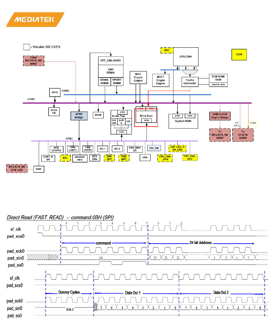
MT76x7
Internet-of-Things Wireless Connectivity
Reference Manual
© 2015 - 2017 MediaTek Inc
Page 59 of 798
This document contains information that is proprietary to MediaTek Inc. (“MediaTek”) and/or its licensor(s).
Any unauthorized use, reproduction or disclosure of this document in whole or in part is strictly prohibited
Figure 2-20. The red line block is the SF_TOP in MCUSYS_CM4.
2.4.4.3. Serial Flash related waveform
1) Direct Read for SPI
Figure 2-21. Example for direct read for SPI mode
2) Quad I/O Read
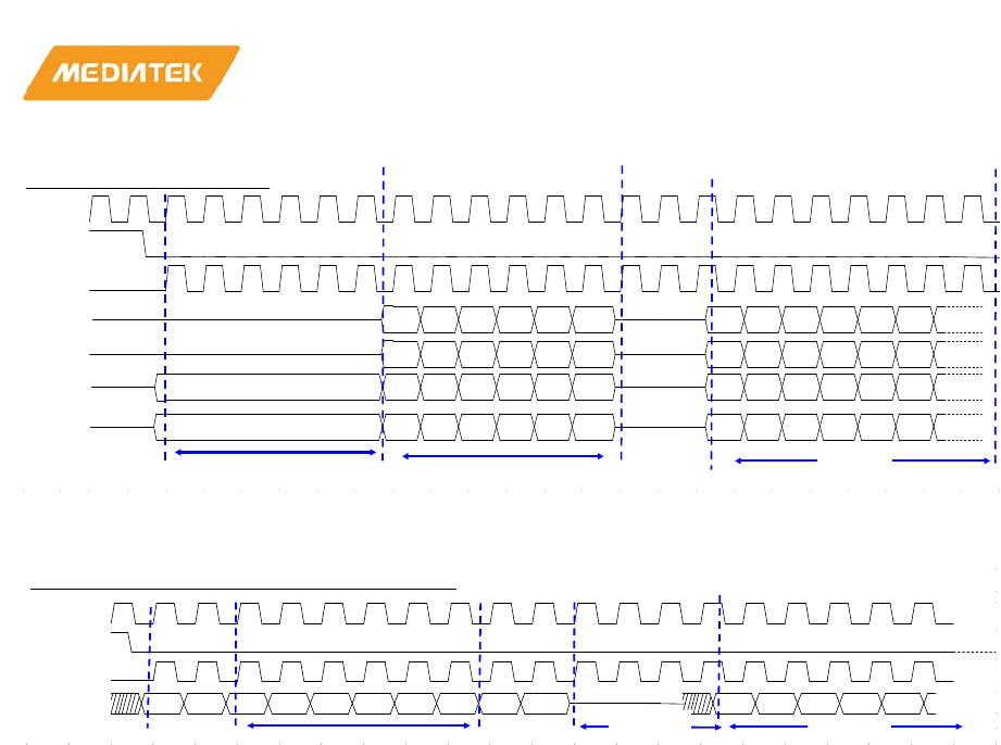
MT76x7
Internet-of-Things Wireless Connectivity
Reference Manual
© 2015 - 2017 MediaTek Inc
Page 60 of 798
This document contains information that is proprietary to MediaTek Inc. (“MediaTek”) and/or its licensor(s).
Any unauthorized use, reproduction or disclosure of this document in whole or in part is strictly prohibited
Figure 2-22. Example for quad I/O read in SPI mode
Figure 2-23. Example for quad I/O read in QPI mode
SIO [3:0] = {pad_hold, pad_wp, pad_sin0, pad_so0}
H0 = MSB of output data 0
L0 = LSB of output data 0
A5 includes address bit 23 to bit 20. A4 includes address bit 19 to bit 16.
A3 includes address bit 15 to bit 12. A2 includes address bit 11 to bit 8.
A1 includes address bit 7 to bit 4. A0 includes address bit 3 to bit 0.
3) Direct Read Behavior Waveform
• Direct Read Mode (SPI)
Quad I/O Read --- E7H (not QPI)
sf_clk
sf_cs
sck
sf_hold
sf_wp
sf_so/sio1
sf_si/sio0
E7h
E7h
bit 23
bit 22
bit 21
bit 20
bit 19
bit 18
bit 17
bit 16
bit 15
bit 14
bit 13
bit 12
bit 11
bit 10
bit 9
bit 8
bit 7
bit 6
bit 5
bit 4
bit 3
bit 2
bit 1
bit 0
bit 3
bit 2
bit 1
bit 0
bit 7
bit 6
bit 5
bit 4
command
24 bit Address
Dummy
Cycles
Data Out
bit 3
bit 2
bit 1
bit 0
bit 3
bit 2
bit 1
bit 0
bit 7
bit 6
bit 5
bit 4
bit 7
bit 6
bit 5
bit 4
Quad I/O Read command --- command = EBH (QPI)
sf_clk
sf_cs
sck
SIO(3:0)
e
b
A5
A4
A3
A2
A0
A1
H0
L0
H1
L1
command
24 bit Address
Dummy
Cycles
Data Out
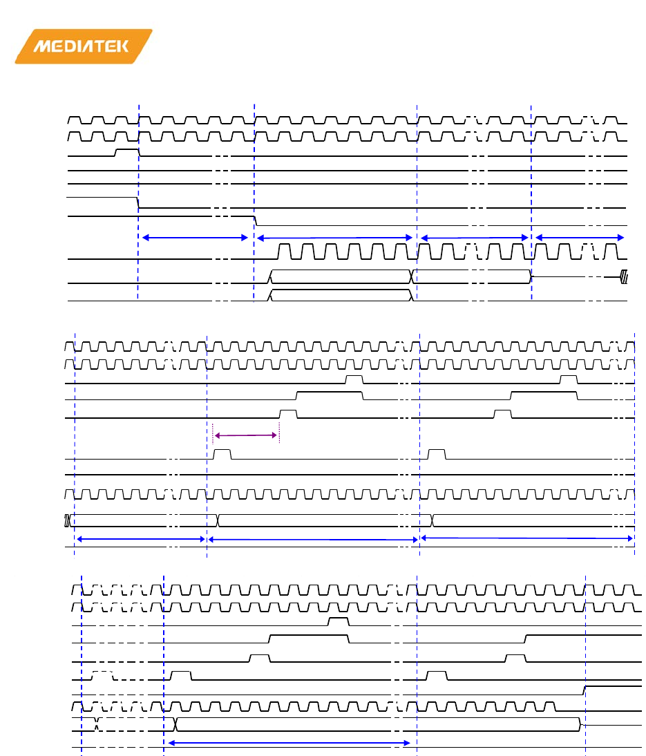
MT76x7
Internet-of-Things Wireless Connectivity
Reference Manual
© 2015 - 2017 MediaTek Inc
Page 61 of 798
This document contains information that is proprietary to MediaTek Inc. (“MediaTek”) and/or its licensor(s).
Any unauthorized use, reproduction or disclosure of this document in whole or in part is strictly prohibited
hclk_ck
sf_clk
sr_req
hready
srack
flash_dle
sf_cs
sck
pad_sin0
pad_so0
SF CS EXT CYC
6 bit command
24 bit address
dummy
cycles
0B
0B
hclk_ck
sf_clk
sr_req
hready
srack
flash_dle
sf_cs
sck
pad_sin0
pad_so0
32 cycles
32 cycles
32 cycles
data 1 ~ data 4
data 5 ~ data 8
data 9 ~ data 12
sync clock
Figure 2-24. Direct read waveform for SPI mode
• Direct Read Mode (QPI)
Overhead transaction cycles (from AHB sending request to AHB finishing reading data)
= (1 request cycle + SF_CS_EXT_CYC) + (2 command cycles) + (6 address cycles) + (dummy cycles ) +
6*(fSFC/fAHB) synchronizing overhead + 2 latency cycles + (8*number of transfers) + AHB_REQ_1TLH_EN +
DEL_LATCH_LATENCY+FIFO_RD_LTC
= SF_CS_EXT_CYC + AHB_REQ_1TLH_EN + DEL_LATCH_LATENCY + FIFO_RD_LTC + (8*number of transfers) +
dummy cycles + 11 cycles + 6*(fSFC/fAHB) synchronizing overhead,
(cycle period = sfc cycle period)
hclk_ck
sf_clk
sr_req
hready
srack
flash_dle
sf_cs
sck
pad_sin0
pad_so0
32 cycles
Last 4 data

MT76x7
Internet-of-Things Wireless Connectivity
Reference Manual
© 2015 - 2017 MediaTek Inc
Page 62 of 798
This document contains information that is proprietary to MediaTek Inc. (“MediaTek”) and/or its licensor(s).
Any unauthorized use, reproduction or disclosure of this document in whole or in part is strictly prohibited
+
=otherwise , 1 4 / Byte Data ReadFlash Serial
4by divided becan Bytes Data ReadFlash Serial if , 4 / Byte Data ReadFlash Serial
Transfer ofNumber
For example, SF_CS_EXT_CYcd C is 2 cycles, AHB_REQ_1TLH_EN = 0, DEL_LATCH_LATENCY = 1, FIFO_RD_LTC =
2, dummy cycle = 6 cycles, serial flash read data byte is 32, serial flash frequency is 78MHz, and AHB frequency
is 52MHz.Therefore, the transaction cycles is 2 + 0 + 1 + 2 + 8*8 + 6 + 11 + 6*(78/52) = 95 cycles
• Direct Read Mode (SPI-Quad with serial flash device not supporting wrap)
Overhead transaction cycles (from AHB sending request to AHB finishing reading data)
= (1 request cycle + SF_CS_EXT_CYC) + (2 command cycles) + (6 address cycles) + (dummy cycles ) +
6*(fSFC/fAHB) synchronizing overhead + 2 latency cycles + (8*number of transfers) + AHB_REQ_1TLH_EN +
DEL_LATCH_LATENCY + FIFO_RD_LTC + 2*(number of transfers data read from pre-fetch buffer)*(fSFC/fAHB)
synchronizing overhead
= SF_CS_EXT_CYC + AHB_REQ_1TLH_EN + DEL_LATCH_LATENCY + FIFO_RD_LTC + (8*number of transfers) +
dummy cycles + 11 cycles + 6*(fSFC/fAHB) + 2*(number of transfers data read from pre-fetch
buffer)*(fSFC/fAHB) synchronizing overhead,
(cycle period = sfc cycle period)
+
=otherwise , 1 4 / Byte DataRead Flash Serial
4by divided becan Bytes DataRead Flash Serial if , 4 / Byte DataRead Flash Serial
Transfer ofNumber
For example, SF_CS_EXT_CYC is 4 cycles, AHB_REQ_1TLH_EN = 1, DEL_LATCH_LATENCY = 1, FIFO_RD_LTC = 2,
dummy cycle = 6 cycles, serial flash read data byte is 32, serial device not supporting wrap, the first access data
from bus is the last 4 bytes of the 32-byte data, serial flash frequency is 78MHz, and AHB frequency is 52MHz.
Therefore, the transaction cycles is 2 + 1 + 1 + 2 + 8*8 + 6 + 11 + 6*(78/52) + 2*[(32-4)/4] = 110 cycles
• Macro Mode (QPI)
Overhead transaction cycles (from AHB sending request to Serial flash controller finishing reading data from
serial flash device)
= 6 cycles (from AHB sending request through APB to Serial Flash controller) + (Serial Flash Macro input data
length + Serial Flash Macro Output data length)*2 * (fAPB/fSFC) + DEL_LATCH_LATENCY * (fAPB/fSFC) + 2
latency cycles
(cycle period = APB cycle period)
For example: Serial flash macro input data length = 3, output data length = 2, DEL_LATCH_LATENCY =1, serial
flash frequency is 78MHz, and APB frequency is 52MHz. Therefore, the transaction cycle is
6+(3+2)*2*(52/78)+1*(52/78)+ 2 = 6 + 7 + 1 + 2 = 16 cycles
Signal explanation:
hclk: AHB clock SIO[3:0]={HOLD, WP, SO, SI}
sf_clk: serial flash controller clk flash_dle: Indicates the serial flash buffer is full
srreq: AHB slave read request sfbuf_count: Serial flash buffer counter
ahb_hsel: AHB hsel signal A5: Address bit 23 to bit 20
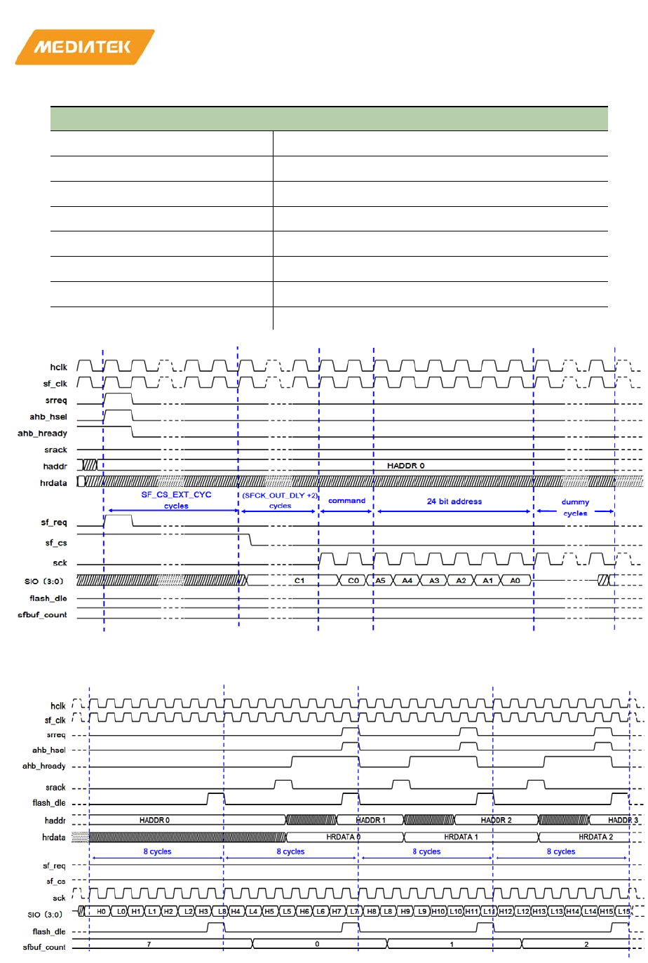
MT76x7
Internet-of-Things Wireless Connectivity
Reference Manual
© 2015 - 2017 MediaTek Inc
Page 63 of 798
This document contains information that is proprietary to MediaTek Inc. (“MediaTek”) and/or its licensor(s).
Any unauthorized use, reproduction or disclosure of this document in whole or in part is strictly prohibited
Signal explanation:
ahb_hready: AHB hready signal A4: Address bit 19 to bit 16
srack: AHB slave read ack signal A3: Address bit 15 to bit 12
haddr: AHB HADDR A2: Address bit 11 to bit 8
hrdata: AHB HRDATA A1: Address bit 7 to bit 4
sf_req: Serial flash request A0: Address bit 3 to bit 0
sf_cs: Serial flash chip select H0: MSB of output data 0
sck: Serial flash clock L0 = LSB of output data 0
SIO[3:0]: Serial flash quad io
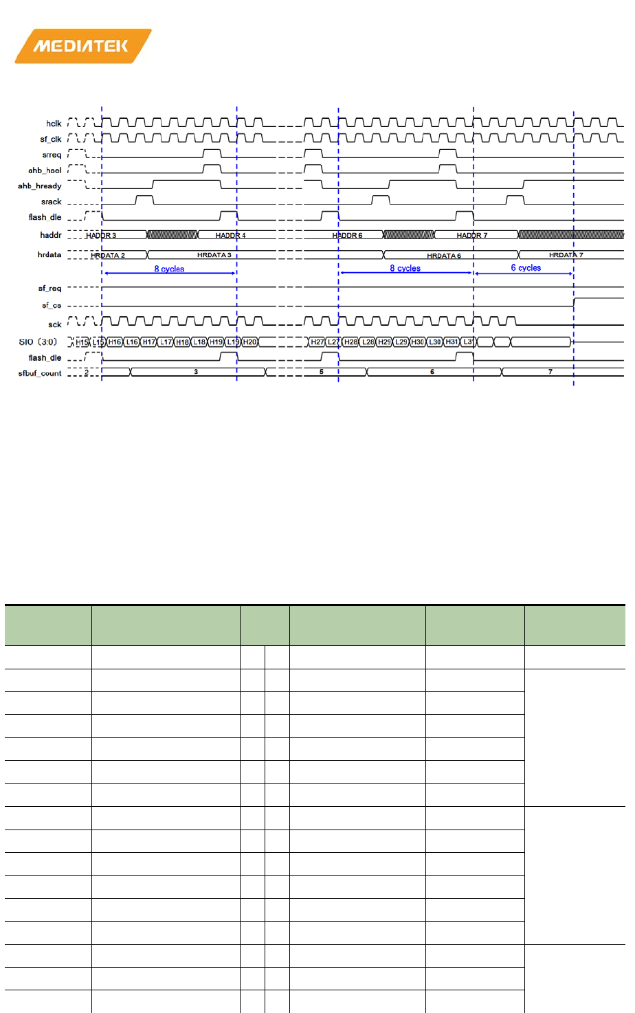
MT76x7
Internet-of-Things Wireless Connectivity
Reference Manual
© 2015 - 2017 MediaTek Inc
Page 64 of 798
This document contains information that is proprietary to MediaTek Inc. (“MediaTek”) and/or its licensor(s).
Any unauthorized use, reproduction or disclosure of this document in whole or in part is strictly prohibited
Figure 2-25. Direct read waveform for QPI mode
2.4.4.4. Programming guide
1) Read Back Register after Value Change
Due to the bridge latency when setting up APB registers (see Figure 2-19), registers affecting AHB such as
SF_DIRECT_CTL may be unstable if AHB is accessed immediately. Therefore, it is suggested that after changing
AHB related registers, e.g. SF_DIRECT_CTL, the registers should be read back again before accessing AHB.
2) Serial Flash Command Sequence Control Example
SF indicates the APB interface base address = 0x8307_0000.
Address Register name R/W Value Loop Flash
command
SF + 0000h SF_MAC_CTL W 0x00000008
SF + 0800h SF_GPRAM_DATA W 0x00000006 WE
(Write Enable)
SF + 0004h SF_MAC_OUTL W 0x00000001
SF + 0008h SF_MAC_INL W 0x00000000
SF + 0000h SF_MAC_CTL W 0x0000000C
SF + 0000h SF_MAC_CTL R [1] = 1, [0] = 0 loop
SF + 0000h SF_MAC_CTL W 0x00000008
SF + 0800h SF_GPRAM_DATA W 0x452301D8 BE
(Block Erase)
SF + 0004h SF_MAC_OUTL W 0x00000004
SF + 0008h SF_MAC_INL W 0x00000000
SF + 0000h SF_MAC_CTL W 0x0000000C
SF + 0000h SF_MAC_CTL R [1] = 1, [0] = 0 loop
SF + 0000h SF_MAC_CTL W 0x00000008
SF + 0800h SF_GPRAM_DATA W 0x00000005 RDSR
(Read Status
Register)
SF + 0004h SF_MAC_OUTL W 0x00000001
SF + 0008h SF_MAC_INL W 0x00000001
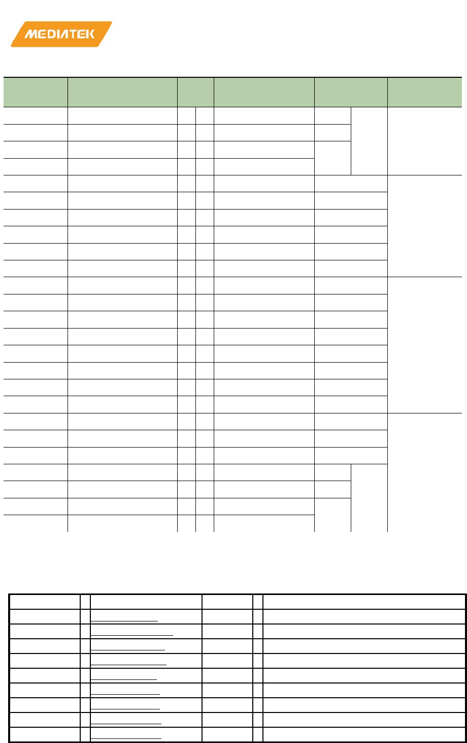
MT76x7
Internet-of-Things Wireless Connectivity
Reference Manual
© 2015 - 2017 MediaTek Inc
Page 65 of 798
This document contains information that is proprietary to MediaTek Inc. (“MediaTek”) and/or its licensor(s).
Any unauthorized use, reproduction or disclosure of this document in whole or in part is strictly prohibited
Address Register name R/W Value Loop Flash
command
SF + 0000h SF_MAC_CTL W 0x0000000C loop
SF + 0000h SF_MAC_CTL R [1] = 1, [0] = 0 loop
SF + 0000h SF_MAC_CTL W 0x00000008
SF + 0800h SF_GPRAM_DATA R [8] = 0 (flash WIP)
SF + 0800h SF_GPRAM_DATA W 0x00000006 WE
(Write Enable)
SF + 0004h SF_MAC_OUTL W 0x00000001
SF + 0008h SF_MAC_INL W 0x00000000
SF + 0000h SF_MAC_CTL W 0x0000000C
SF + 0000h SF_MAC_CTL R [1] = 1, [0] = 0 loop
SF + 0000h SF_MAC_CTL W 0x00000008
SF + 0800h SF_GPRAM_DATA W 0x45230102 PP
(Page Program)
SF + 0804h SF_GPRAM_DATA W 0x78563412
SF + 0808h SF_GPRAM_DATA W 0xddccbbaa
SF + 0004h SF_MAC_OUTL W 0x0000000C
SF + 0008h SF_MAC_INL W 0x00000000
SF + 0000h SF_MAC_CTL W 0x0000000C
SF + 0000h SF_MAC_CTL R [1] = 1, [0] = 0 loop
SF + 0000h SF_MAC_CTL W 0x00000008
SF + 0800h SF_GPRAM_DATA W 0x00000005 RDSR
(Read Status
Register)
SF + 0004h SF_MAC_OUTL W 0x00000001
SF + 0008h SF_MAC_INL W 0x00000001
SF + 0000h SF_MAC_CTL W 0x0000000C loop
SF + 0000h SF_MAC_CTL R [1] = 1, [0] = 0 loop
SF + 0000h SF_MAC_CTL W 0x00000008
SF + 0800h SF_GPRAM_DATA R [8] = 0 (flash WIP)
2.4.4.5. Register definitions
Module name: sf_top Base address: (+83070000h)
Address
Name
Width
Register Function
83070000
SF_MAC_CTL
32
Serial flash macro R/W control
83070004
SF_DIRECT_CTL
32
Serial flash direct read setting
83070008
SF_MISC_CTL1
32
Serial flash clock MISC controller setting 1
83070010
SF_MAC_OUTL
32
Serial flash
macro output data length
83070014
SF_MAC_INL
32
Serial flash macro input data length
8307001C
SF_STA2_CTL
32
Serial flash static control setting 2
83070020
SF_DLY_CTL1
32
Serial flash delay controller setting 1
83070024
SF_DLY_CTL2
32
Serial flash delay controller setting 2
83070028
SF_DLY_CTL3
32
Serial flash delay controller setting 3
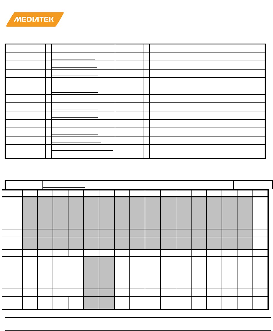
MT76x7
Internet-of-Things Wireless Connectivity
Reference Manual
© 2015 - 2017 MediaTek Inc
Page 66 of 798
This document contains information that is proprietary to MediaTek Inc. (“MediaTek”) and/or its licensor(s).
Any unauthorized use, reproduction or disclosure of this document in whole or in part is strictly prohibited
Address
Name
Width
Register Function
83070044
SF_MISC_CTL3
32
Serial flash MISC control setting 3
83070080
SF_PERF_MON1
32
Serial flash performance monitor 1
83070084
SF_PERF_MON2
32
Serial flash
performance monitor 2
83070088
SF_PERF_MON3
32
Serial flash performance monitor 3
8307008C
SF_PERF_MON4
32
Serial flash performance monitor 4
83070090
SF_PERF_MON5
32
Serial flash performance monitor 5
83070094
SF_PERF_MON6
32
Serial flash performance monitor 6
83070098
SF_PERF_MON7
32
Serial flash performance monitor 7
8307009C
SF_PERF_MON8
32
Serial flash performance monitor 8
830700A0
SF_PERF_MON9
32
Serial flash performance monitor 9
830700A4
SF_PERF_MON10
32
Serial flash performance monitor 10
83070800~
8307089c
SF_GPRAM_DATA [n]
(n=0~39)
32
Serial flash macro R/W memory data (160
bytes)
83070000
SF_MAC_CTL
Serial flash macro R/W control
00010000
Bit
31
30
29
28
27
26
25
24
23
22
21
20
19
18
17
16
Nam
e
RE
LE
AS
E_
MA
C
Type
RW
Rese
t
1
Bit
15
14
13
12
11
10
9
8
7
6
5
4
3
2
1
0
Nam
e
AB
OR
T_
CL
R
SF
_A
BO
RT
SF_ABOT
_REQ_SR
C
SF
_IR
Q_
EN
SF
_IR
Q_
AC
K
H
W_
QPI
MA
C_
MA
SK
_O
P
MA
C_
MA
SK
MA
C_
XI
O_
SE
L
SF
_M
AC
_E
N
SF
_T
RI
G
WI
P_
RE
AD
Y
WI
P
Type
RU
RW
RU
RW
RW
RW
RW
RW
RW
RW
RW
RU
RU
Rese
t
0 0 0 0 0 0 0 0 0 0 0 0 0 0
Bit(s)
Name
Description
16
RELEASE_MAC
Prevents hanging the AHB bus. As the serial flash enters
the MAC mode, it will raises
SF_ABORT to "high" for the
MCU to interrupt the current transaction and check if the
AHB bus is hanged. If Release_MAC is set to 1, SF_ABORT
will not be raised to 1. In the DEBUG develop segment, set
this bit to 1 when the serial flash enters the macro mod
e,
and SF_ABORT will not be raised to 1. The serial flash will
continue the next operation event though the data read
are wrong.
0 Disable
1 Enable
15
ABORT_CLR
Clears serial flash abortion. As we would like to exit the
serial flash abortion status, ABORT_CLR must be set to 1

MT76x7
Internet-of-Things Wireless Connectivity
Reference Manual
© 2015 - 2017 MediaTek Inc
Page 67 of 798
This document contains information that is proprietary to MediaTek Inc. (“MediaTek”) and/or its licensor(s).
Any unauthorized use, reproduction or disclosure of this document in whole or in part is strictly prohibited
Bit(s)
Name
Description
to clear the SF_ABORT status and then set ABORT_CLR
back to 0 to detect another serial flash abortion.
0 Disable
1 Enable
14
SF_ABORT
Serial flash abortion status register. As the AHB bus
raises request in the MAC mode, it will cause the abortion
of the serial flash controller.
0 Does not abort
1 Abort
13:12
SF_ABOT_REQ_SRC
Request source of serial flash abortion
00 Does not abort
01 Abortio
n is caused by MCU.
10 Abortion is caused by ALICE.
9
SF_IRQ_EN
Serial flash interrupt enable during serial flash abortion
0 Disable
1 Enable
8
SF_IRQ_ACK
Serial flash interrupt acknowledged signal
0 Non
-acknowledged
1 Acknowledged
7
HW_QPI
AHB mode for QPI/SPI setting
0 SPI
1 QPI
6
MAC_MASK_OP
Serial flash hardware DIRECT/MAC mode auto switch
setting. If setting MAC_MASK_OP=1 then trigger
SF_TRIG=1, hardware module will auto switch to MAC
mode until MAC mode operation finished.
0 Disable
1 Enable
5
MAC_MASK
Serial flash software DIRECT/MAC mode switch setting. If
MAC_MASK is set to 1, the hardware will switch to the
MAC mode manually and will not permit any DIRECT
mode access until MAC_MASK=0. It is suggested to run
MAC mode in internal sysram code
if MAC_MASK = 1 by
software setting.
0 Disable
1 Enable

MT76x7
Internet-of-Things Wireless Connectivity
Reference Manual
© 2015 - 2017 MediaTek Inc
Page 68 of 798
This document contains information that is proprietary to MediaTek Inc. (“MediaTek”) and/or its licensor(s).
Any unauthorized use, reproduction or disclosure of this document in whole or in part is strictly prohibited
Bit(s)
Name
Description
4
MAC_XIO_SEL
MAC mode for QPI/SPI setting
0 SPI
1 QPI
3
SF_MAC_EN
Switches the serial flash control to update the macro.
Please set up this bit before triggering the update macro
(It is suggested
to run MAC mode in internal sysram code
due to DIRECT/MAC cannot run at the same time.
Another way to switch to hardware auto switch mode by
setting up MAC_MASK_OP)
0 Disable
1 Enable (Direct read is forbidden when SF_MAC_EN = 1)
2
SF_TRIG
Serial flash write macro trigger
0 Disable
1 Enable (Fill command sequence I/O length before SF_TRIG)
1
WIP_READY
WIP register status ready for access. WIP_READY exits
due to asynchronous latency delay before flash responds
to WIP
0 WIP not ready for read
1 WIP ready fo
r read (Check if WIP_READY = 1 before the next
command sequence)
0
WIP
Serial flash command write in process
0 Flash update finished (Check if WIP = 0 before the next
command sequence)
1 Not finished
83070004
SF_DIRECT_CTL
Serial flash direct read setting
0B0B7710
Bit
31
30
29
28
27
26
25
24
23
22
21
20
19
18
17
16
Nam
e
SF_CTRL_CMD1 SF_CTRL_CMD2
Type
RW
RW
Rese
t
0 0 0 0 1 0 1 1 0 0 0 0 1 0 1 1
Bit
15
14
13
12
11
10
9
8
7
6
5
4
3
2
1
0
Nam
e CMD1_DUMMY_CYC CMD2_DUMMY_CYC SF_READ_MOD
E
CM
D2
_E
XT
_A
DD
R_
EN
SF
_C
MD
2_
EN
CM
D1
_E
XT
_A
DD
R_
EN
SF
_Q
PI_
EN
Type
RW
RW
RW
RW
RW
RW
RW
Rese
t
0 1 1 1 0 1 1 1 0 0 1 0 0 0 0

MT76x7
Internet-of-Things Wireless Connectivity
Reference Manual
© 2015 - 2017 MediaTek Inc
Page 69 of 798
This document contains information that is proprietary to MediaTek Inc. (“MediaTek”) and/or its licensor(s).
Any unauthorized use, reproduction or disclosure of this document in whole or in part is strictly prohibited
Bit(s)
Name
Description
31:24
SF_CTRL_CMD1
Serial flash DIRECT read mode command 1 register
setting for DUAL/QIO/QPI
mode.
*value = efuse{0x102[7:0]}
23:16
SF_CTRL_CMD2
Serial flash DIRECT read mode command 2 register
setting for DUAL/QIO/QPI mode.
*value = efuse{0x103[7:0]}
15:12
CMD1_DUMMY_CYC
Serial flash read mode dummy cycles for SF_CTRL_CMD1
setting
4'b0000 1T
4'b0001 2T
4'b 0010 3T
4'b 0011 4T
4'b 0100 5T
4'b 0101 6T
4'b 0110 7T
4'b 0111 8T
4'b 1000 9T
4'b 1001 10T
4'b 1010 11T
4'b 1011 12T
4'b 1100 13T
4'b 1101 14T
4'b 1110 15T
4'b 1111 16T
*value = efuse{0x104[7:4]}
11:8
CMD2_DUMMY_CYC
Serial flash read mode dummy cycles for SF_CTRL_CMD2
setting
4'b 0000 1T
4'b 0001 2T
4'b 0010 3T
4'b 0011 4T
4'b 0100 5T

MT76x7
Internet-of-Things Wireless Connectivity
Reference Manual
© 2015 - 2017 MediaTek Inc
Page 70 of 798
This document contains information that is proprietary to MediaTek Inc. (“MediaTek”) and/or its licensor(s).
Any unauthorized use, reproduction or disclosure of this document in whole or in part is strictly prohibited
Bit(s)
Name
Description
4'b 0101 6T
4'b 0110 7T
4'b 0111 8T
4'b 1000 9T
4'b 1001 10T
4'b 1010 11T
4'b 1011 12T
4'b 1100 13T
4'b 1101 14T
4'b 1110 15T
4'b 1111 16T
*value =
efuse{0x104[3:0]}
6:4
SF_READ_MODE
Selects serial flash read mode
3'b000 Normal read mode
3'b 001 Fast read mode
3'b 010 Dual output mode
3'b 011 Dual I/O mode
3'b 111 Quad I/O mode
3
CMD2_EXT_ADDR_EN
Enabled to send 4-byte address as using SF_CTRL_CMD2
0 Disable
1 Enable
2
SF_CMD2_EN
Enables SF_CTRL_CMD2 command. When SF_CMD2_EN
is set to 1, the serial flash controller will use the
SF_CTRL_CMD2 command to read data as accessing
address exceeds 24 bits.
0 Disable
1 Enable
1
CMD1_EXT_ADDR_EN
Enabled extend address mode for SF_CTRL_CMD1.
0 Disable
1 Enable
0
SF_QPI_EN
Serial flash QPI enable in QIO mode. Set up this bit with
QIO = 1 (SF_READ_MODE = 3'b111)
0 Disable
MT76x7
Internet-of-Things Wireless Connectivity
Reference Manual
© 2015 - 2017 MediaTek Inc
Page 71 of 798
This document contains information that is proprietary to MediaTek Inc. (“MediaTek”) and/or its licensor(s).
Any unauthorized use, reproduction or disclosure of this document in whole or in part is strictly prohibited
Bit(s)
Name
Description
1 Enable
83070008
SF_MISC_CTL1
Serial flash clock MISC controller
setting 1
B2C00000
Bit
31
30
29
28
27
26
25
24
23
22
21
20
19
18
17
16
Nam
e SF_CS_EXT_CYC fifo_rd_lt
c
NO
_R
EL
OA
D
FIF
O_
MA
CR
O_
RS
T
CS
_E
XT
_C
YC
_O
PT
_E
N
fou
rta
p_f
ifo
_en
ahb
_R
EQ
_1T
Lh
_E
N
SF
_D
OU
BL
E_
SY
NC
SF
_S
YN
C_
EN
RE
G_
AD
DR
_S
YN
C_
SE
L
Type
RW
RW
RW
RW
RW
RW
RW
RW
RW
RW
Rese
t
1 0 1 1 1 0 1 1 0 0 0 0 0 0
Bit
15
14
13
12
11
10
9
8
7
6
5
4
3
2
1
0
Nam
e
SFI
O_
EN
_S
EL
CS_SETU
P_LTC
SF
_R
EQ
_I
DL
E
CH
2_
B2
S
SF
_F
BC
LK
_S
EL
SM
PC
K_I
NV
OU
TC
K_I
NV
DEL_LAT
CH_LATE
Ncy
Type
RW
RW
RU
RW
RW
RW
RW
RW
Rese
t
0 0 0 0 0 0 0 0 0 0
Bit(s)
Name
Description
31:28
SF_CS_EXT_CYC
CS pin pulled from high to low extension cycles. Default:
12 cycles
4'b0000 1 cycle
4'b0001 2 cycles
4'b0010 3 cycles
4'b0011 4 cycles
4'b0100 5 cycles
4'b0101 6 cycles
4'b0110 7 cycles
4'b0111 8 cycles
4'b1000 9 cycles
4'b1001 10 cycles
4'b1010 11 cycles
4'b1011 12 cycles

MT76x7
Internet-of-Things Wireless Connectivity
Reference Manual
© 2015 - 2017 MediaTek Inc
Page 72 of 798
This document contains information that is proprietary to MediaTek Inc. (“MediaTek”) and/or its licensor(s).
Any unauthorized use, reproduction or disclosure of this document in whole or in part is strictly prohibited
Bit(s)
Name
Description
4'b1100 13 cycles
4'b1101 14 cycles
*value = efuse{0x105[7:4]}
25:24
fifo_rd_ltc
4 Tap FIFO read latency
*value = efuse{0x105[1:0]}
23
NO_RELOAD
NO_RELOAD setting: RELOAD function is that the serial
flash controller keeps the CS pin low, and the CLK pin
keeps pending after the pre
-fetch buffer is full. If the next
access address continues, the previous address will then
start generating CLK to access the next data with
out any
command/address overhead time suffer to gain better
bandwidth usage.
0 CMD/ADDR will not be issued if the next access address
continues the previous address.
1 CMD/ADDR will be re
-issued.
*value = efuse{0x106[7]}
22
FIFO_MACRO_RST
Serial flash IO module reset control
0 Disable reset
1 Enable reset
21
CS_EXT_CYC_OPT_EN
Enables CS extension cycle optimization. In the DIRECT
READ mode, the CS extension cycle will be added before
each transaction. However, before receiving a new
request, CS might have
been pulled up. If
CS_EXT_CYC_OPT_EN is set to 1, serial flash controller
will base on the CS pulling up cycle before the new request
to reduce the CS extension cycle time .
0 Disable
1 Enable
*value = efuse{0x106[5]}
20
fourtap_fifo_en
Enables 4 Tap FIFO
0 Disable
1 Enable
*value = efuse{0x106[4]}
19
ahb_REQ_1TLh_EN
Enables serial flash controller delay 1T to latch AHB
request
0 No delay
1 Delay 1T to latch AHB request
*value = efuse{0x106[3]}

MT76x7
Internet-of-Things Wireless Connectivity
Reference Manual
© 2015 - 2017 MediaTek Inc
Page 73 of 798
This document contains information that is proprietary to MediaTek Inc. (“MediaTek”) and/or its licensor(s).
Any unauthorized use, reproduction or disclosure of this document in whole or in part is strictly prohibited
Bit(s)
Name
Description
18
SF_DOUBLE_SYNC
Enables serial flash double sync. If the frequency of serial
flash is at the twice of BUS frequency, and we would like
the serial flash controller to work in the synchronous
mode, set SF_SYNC_EN to 1 and SF_DOUBLE_SYNC to 1
0 Disable
1 Enable
*value = efuse{0x106[2]}
17
SF_SYNC_EN
Enables serial flash synchronous mode
0 Asynchronous mode
1 Synchronous mode
*value = efuse{0x106[1]}
16
REG_ADDR_SYNC_SEL
SF address select
0 Synchronous mode
1 Asynchronous mode
14
SFIO_EN_SEL
Serial flash IO PAD Enable signal align with clock positive
edge
select
0 Disable
1 Enable
*value = efuse{0x107[6]}
13:12
CS_SETUP_LTC
Serial flash/CS setup time latency. Set up CS_SETUP_LTC
to increase the /CS setup time. Default /CS setup time for
both MAC and DIRECT READ mode is 1.5 serial flash clock
period.
2'b00
Does not increase serial flash /CS setup time
2'b01 Increase 1T for /CS setup time
2'b10 Increase 2T for /CS setup time
2'b11 Increase 3T for /CS setup time
*value = efuse{0x107[5:4]}
8
SF_REQ_IDLE
Serial flash controller processing transaction status
reg
ister
0 Transaction is being processed.
1 Idle
6
CH2_B2S
Channel 2 of serial flash access switch to single data
access mode for priority arbitration behavior setting. In
MT7637, CPU can access the serial flash through channel
2. If CH2_B2S = 1, the
arbitration will switch to another
agent (MCU) access after every CH2 single access.

MT76x7
Internet-of-Things Wireless Connectivity
Reference Manual
© 2015 - 2017 MediaTek Inc
Page 74 of 798
This document contains information that is proprietary to MediaTek Inc. (“MediaTek”) and/or its licensor(s).
Any unauthorized use, reproduction or disclosure of this document in whole or in part is strictly prohibited
Bit(s)
Name
Description
0 Disable
1 Enable
*value = efuse{0x108[6]}
5
SF_FBCLK_SEL
Serial flash feedback clock selection setting
0 Use non
-feedback clock
1 Use feedback clock for serial flash
*v
alue = efuse{0x108[5]}
4
SMPCK_INV
Sample clock inverse for read data input
0 No inverse
1 Inverse
*value = efuse{0x108[4]}
3
OUTCK_INV
Output clock inverse bit
0 No inverse
1 Inverse
*value = efuse{0x108[3]}
1:0
DEL_LATCH_LATENcy
Selects serial flash latch delay latency
2'b00 Not delay
2'b01 Delay 1T to latch serial flash data
2'b10 Delay 2T to latch serial flash data
2'b11 Delay 3T to latch serial flash data
*value = efuse{0x108[1:0]}
83070010
SF_MAC_OUTL
Serial flash macro output data length
00000000
Bit
31
30
29
28
27
26
25
24
23
22
21
20
19
18
17
16
Nam
e
Type
Rese
t
Bit
15
14
13
12
11
10
9
8
7
6
5
4
3
2
1
0
Nam
e
MAC_OUT_LENGTH
Type
RW
Rese
t
0 0 0 0 0 0 0 0
MT76x7
Internet-of-Things Wireless Connectivity
Reference Manual
© 2015 - 2017 MediaTek Inc
Page 75 of 798
This document contains information that is proprietary to MediaTek Inc. (“MediaTek”) and/or its licensor(s).
Any unauthorized use, reproduction or disclosure of this document in whole or in part is strictly prohibited
Bit(s)
Name
Description
7:0
MAC_OUT_LENGTH
Serial flash write data length, 1 ~ 160 bytes
83070014
SF_MAC_INL
Serial flash macro input data length
00000000
Bit
31
30
29
28
27
26
25
24
23
22
21
20
19
18
17
16
Nam
e
Type
Rese
t
Bit
15
14
13
12
11
10
9
8
7
6
5
4
3
2
1
0
Nam
e
MAC_IN_LENGTH
Type
RW
Rese
t
0 0 0 0 0 0 0 0
Bit(s)
Name
Description
7:0
MAC_IN_LENGTH
Serial flash read data length, 1 ~ 160 bytes
8307001C
SF_STA2_CTL
Serial flash static control setting 2
00000000
Bit
31
30
29
28
27
26
25
24
23
22
21
20
19
18
17
16
Nam
e
KE
EP
_R
EA
D_
SE
TTI
NG
Type
RW
Rese
t
0
Bit
15
14
13
12
11
10
9
8
7
6
5
4
3
2
1
0
Nam
e
Type
Rese
t
Bit(s)
Name
Description
31
KEEP_READ_SETTING
Keep Direct Read mode setting after watch-dog reset
If KEEP_READ_SETTING is set to 1,
the content of
SF_DIRECT_CTL and SF_MISC_CTL2 can only be reset by power
-
on reset and will not be cleared after the watch
-dog reset.
0 Disable
MT76x7
Internet-of-Things Wireless Connectivity
Reference Manual
© 2015 - 2017 MediaTek Inc
Page 76 of 798
This document contains information that is proprietary to MediaTek Inc. (“MediaTek”) and/or its licensor(s).
Any unauthorized use, reproduction or disclosure of this document in whole or in part is strictly prohibited
Bit(s)
Name
Description
1 Enable
83070020
SF_DLY_CTL1
Serial flash delay controller setting 1
00000000
Bit
31
30
29
28
27
26
25
24
23
22
21
20
19
18
17
16
Nam
e
SFIO3_OUT_DLY SFIO2_OUT_DLY
Type
RW
RW
Rese
t
0 0 0 0 0 0 0 0
Bit
15
14
13
12
11
10
9
8
7
6
5
4
3
2
1
0
Nam
e
SFIO1_OUT_DLY SFIO0_OUT_DLY
Type
RW
RW
Rese
t
0 0 0 0 0 0 0 0
Bit(s)
Name
Description
27:24
SFIO3_OUT_DLY
Serial flash SFIO3 pin IO output delay setting
*value = efuse{0x109[7:4]}
19:16
SFIO2_OUT_DLY
Serial flash SFIO2 pin IO output delay setting
*value = efuse{0x109[3:0]}
11:8
SFIO1_OUT_DLY
Serial flash SFIO1 pin IO output delay setting
*value = efuse{0x10A[7:4]}
3:0
SFIO0_OUT_DLY
Serial flash SFIO0 pin IO output delay setting
*value = efuse{0x10A[3:0]}
83070024
SF_DLY_CTL2
Serial flash delay controller setting 2
00000000
Bit
31
30
29
28
27
26
25
24
23
22
21
20
19
18
17
16
Nam
e
SFIO3_IN_DLY SFIO2_IN_DLY
Type
RW
RW
Rese
t
0 0 0 0 0 0 0 0 0 0 0 0
Bit
15
14
13
12
11
10
9
8
7
6
5
4
3
2
1
0
Nam
e
SFIO1_IN_DLY SFIO0_IN_DLY
Type
RW
RW
Rese
t
0 0 0 0 0 0 0 0 0 0 0 0
Bit(s)
Name
Description
MT76x7
Internet-of-Things Wireless Connectivity
Reference Manual
© 2015 - 2017 MediaTek Inc
Page 77 of 798
This document contains information that is proprietary to MediaTek Inc. (“MediaTek”) and/or its licensor(s).
Any unauthorized use, reproduction or disclosure of this document in whole or in part is strictly prohibited
Bit(s)
Name
Description
29:24
SFIO3_IN_DLY
Serial flash SFIO3 pin IO input delay setting
*value[3:0] = efuse{0x10B[7:4]}
21:16
SFIO2_IN_DLY
Serial flash SFIO2 pin IO input delay setting
*value[3:0] =
efuse{0x10B[3:0]}
13:8
SFIO1_IN_DLY
Serial flash SFIO1 pin IO input delay setting
*value[3:0] = efuse{0x10C[7:4]}
5:0
SFIO0_IN_DLY
Serial flash SFIO0 pin IO input delay setting
*value[3:0] = efuse{0x10C[3:0]}
83070028
SF_DLY_CTL3
Serial flash delay controller setting 3
00000000
Bit
31
30
29
28
27
26
25
24
23
22
21
20
19
18
17
16
Nam
e
sfifo_wr_en_dly_sel SFCS_DLY
Type
RW
RW
Rese
t
0 0 0 0 0 0 0 0 0 0
Bit
15
14
13
12
11
10
9
8
7
6
5
4
3
2
1
0
Nam
e
SFCK_OUT_DLY SFCK_SAM_DLY
Type
RW
RW
Rese
t
0 0 0 0 0 0 0 0 0 0
Bit(s)
Name
Description
29:24
sfifo_wr_en_dly_sel
Serial flash FIFO write enable delay select setting
*value = efuse{0x10D[5:0]}
19:16
SFCS_DLY
Serial flash SFCS pin IO output delay setting
*value = efuse{0x10E[7:4]}
11:8
SFCK_OUT_DLY
Serial flash CK pin IO output delay setting
*value = efuse{0x10E[3:0]}
5:0
SFCK_SAM_DLY
Serial flash sample clock delay setting
*value = efuse{0x10F[5:0]}
83070044
SF_MISC_CTL3
Serial flash MISC control setting 3
00003000
Bit
31
30
29
28
27
26
25
24
23
22
21
20
19
18
17
16
Nam
e
MT76x7
Internet-of-Things Wireless Connectivity
Reference Manual
© 2015 - 2017 MediaTek Inc
Page 78 of 798
This document contains information that is proprietary to MediaTek Inc. (“MediaTek”) and/or its licensor(s).
Any unauthorized use, reproduction or disclosure of this document in whole or in part is strictly prohibited
Type
Rese
t
Bit
15
14
13
12
11
10
9
8
7
6
5
4
3
2
1
0
Nam
e
CH
2_
TR
AN
S_I
DL
E
CH
1_T
RA
NS
_I
DL
E
CH
2_
TR
AN
S_
MA
SK
CH
1_T
RA
NS
_M
AS
K
Type
RU
RU
RW
RW
Rese
t
1 1 0 0
Bit(s)
Name
Description
13
CH2_TRANS_IDLE
Idle status of CH2 after setting up CH2_TRANS_MASK
0 Busy
1 Idle
12
CH1_TRANS_IDLE
Idle status of CH1 after setting up CH1_TRANS_MASK
0 Busy
1 Idle
9
CH2_TRANS_MASK
Masks the AHB request for the CH2 of serial flash from
platform bus
0 Disable
1 Enable
8
CH1_TRANS_MASK
Masks the AHB request for the CH1 of serial flash from
platform bus
( CPU cannot access SFC after enable )
0 Disable
1 Enable
83070080
SF_PERF_MON1
Serial flash performance monitor 1
00000000
Bit
31
30
29
28
27
26
25
24
23
22
21
20
19
18
17
16
Nam
e
Type
Rese
t
Bit
15
14
13
12
11
10
9
8
7
6
5
4
3
2
1
0
Nam
e
PE
Rf_
mo
n_c
lr
per
f_
MO
N_
EN
Type
RW
RW
MT76x7
Internet-of-Things Wireless Connectivity
Reference Manual
© 2015 - 2017 MediaTek Inc
Page 79 of 798
This document contains information that is proprietary to MediaTek Inc. (“MediaTek”) and/or its licensor(s).
Any unauthorized use, reproduction or disclosure of this document in whole or in part is strictly prohibited
Rese
t
0 0
Bit(s)
Name
Description
1
PERf_mon_clr
Clears information of performance monitor. If
PERF_MON_CLR is set to 1, all data in the performance
monitor will be set to 0. Set PERF_MON_CLR to 0 to clear
the information in the performance monitor before re
-
starting the performance monitor.
0 Disable
1 Enable
0
perf_MON_EN
Performance monitor enable bit.
0 Disable
1 Enable
83070084
SF_PERF_MON2
Serial flash performance monitor 2
00000000
Bit
31
30
29
28
27
26
25
24
23
22
21
20
19
18
17
16
Nam
e
PERf_mon_CYC
Type
RU
Rese
t
0 0 0 0 0 0 0 0 0 0 0 0 0 0 0 0
Bit
15
14
13
12
11
10
9
8
7
6
5
4
3
2
1
0
Nam
e
PERf_mon_CYC
Type
RU
Rese
t
0 0 0 0 0 0 0 0 0 0 0 0 0 0 0 0
Bit(s)
Name
Description
31:0
PERf_mon_CYC
Cycle counts after enable performance monitor
83070088
SF_PERF_MON3
Serial flash performance monitor 3
00000000
Bit
31
30
29
28
27
26
25
24
23
22
21
20
19
18
17
16
Nam
e
SF_BUSY_CYC
Type
RU
Rese
t
0 0 0 0 0 0 0 0 0 0 0 0 0 0 0 0
Bit
15
14
13
12
11
10
9
8
7
6
5
4
3
2
1
0
Nam
e
SF_BUSY_CYC
Type
RU
Rese
t
0 0 0 0 0 0 0 0 0 0 0 0 0 0 0 0
MT76x7
Internet-of-Things Wireless Connectivity
Reference Manual
© 2015 - 2017 MediaTek Inc
Page 80 of 798
This document contains information that is proprietary to MediaTek Inc. (“MediaTek”) and/or its licensor(s).
Any unauthorized use, reproduction or disclosure of this document in whole or in part is strictly prohibited
Bit(s)
Name
Description
31:0
SF_BUSY_CYC
Serial Flash Busy Cycle counts after enabling performance
monitor. SF_BUSY_CYC is the summation of MAC mode
and 3 AHB channels busy cycle.
8307008C
SF_PERF_MON4
Serial flash performance monitor 4
00000000
Bit
31
30
29
28
27
26
25
24
23
22
21
20
19
18
17
16
Nam
e
SF_MAC_CYC
Type
RU
Rese
t
0 0 0 0 0 0 0 0 0 0 0 0 0 0 0 0
Bit
15
14
13
12
11
10
9
8
7
6
5
4
3
2
1
0
Nam
e
SF_MAC_CYC
Type
RU
Rese
t
0 0 0 0 0 0 0 0 0 0 0 0 0 0 0 0
Bit(s)
Name
Description
31:0
SF_MAC_CYC
Serial Flash MAC Mode Cycle counts after enabling
performance monitor
83070090
SF_PERF_MON5
Serial flash performance monitor 5
00000000
Bit
31
30
29
28
27
26
25
24
23
22
21
20
19
18
17
16
Nam
e
CH1_BUSY_CYC
Type
RU
Rese
t
0 0 0 0 0 0 0 0 0 0 0 0 0 0 0 0
Bit
15
14
13
12
11
10
9
8
7
6
5
4
3
2
1
0
Nam
e
CH1_BUSY_CYC
Type
RU
Rese
t
0 0 0 0 0 0 0 0 0 0 0 0 0 0 0 0
Bit(s)
Name
Description
31:0
CH1_BUSY_CYC
Serial Flash channel 1 busy cycle (access serial flash
device) counts after enabling performance monitor
83070094
SF_PERF_MON6
Serial flash performance monitor 6
00000000
Bit
31
30
29
28
27
26
25
24
23
22
21
20
19
18
17
16
Nam
e
CH1_REQ_COUNT
MT76x7
Internet-of-Things Wireless Connectivity
Reference Manual
© 2015 - 2017 MediaTek Inc
Page 81 of 798
This document contains information that is proprietary to MediaTek Inc. (“MediaTek”) and/or its licensor(s).
Any unauthorized use, reproduction or disclosure of this document in whole or in part is strictly prohibited
Type
RU
Rese
t
0 0 0 0 0 0 0 0 0 0 0 0 0 0 0 0
Bit
15
14
13
12
11
10
9
8
7
6
5
4
3
2
1
0
Nam
e
CH1_REQ_COUNT
Type
RU
Rese
t
0 0 0 0 0 0 0 0 0 0 0 0 0 0 0 0
Bit(s)
Name
Description
31:0
CH1_REQ_COUNT
The number of AHB bus requests channel 1 of the serial
flash controller receives after enabling performance
monitor
83070098
SF_PERF_MON7
Serial flash performance monitor 7
00000000
Bit
31
30
29
28
27
26
25
24
23
22
21
20
19
18
17
16
Nam
e
ch1_DATA_BYTE_COUNT
Type
RU
Rese
t
0 0 0 0 0 0 0 0 0 0 0 0 0 0 0 0
Bit
15
14
13
12
11
10
9
8
7
6
5
4
3
2
1
0
Nam
e
ch1_DATA_BYTE_COUNT
Type
RU
Rese
t
0 0 0 0 0 0 0 0 0 0 0 0 0 0 0 0
Bit(s)
Name
Description
31:0
ch1_DATA_BYTE_COUNT
The number of data bytes AHB bus transferred through
channel 1 of the serial flash controller after enabling
performance monitor
8307009C
SF_PERF_MON8
Serial flash performance monitor 8
00000000
Bit
31
30
29
28
27
26
25
24
23
22
21
20
19
18
17
16
Nam
e
ch2_BUSY_CYC
Type
RU
Rese
t
0 0 0 0 0 0 0 0 0 0 0 0 0 0 0 0
Bit
15
14
13
12
11
10
9
8
7
6
5
4
3
2
1
0
Nam
e
ch2_BUSY_CYC
Type
RU
Rese
t
0 0 0 0 0 0 0 0 0 0 0 0 0 0 0 0
MT76x7
Internet-of-Things Wireless Connectivity
Reference Manual
© 2015 - 2017 MediaTek Inc
Page 82 of 798
This document contains information that is proprietary to MediaTek Inc. (“MediaTek”) and/or its licensor(s).
Any unauthorized use, reproduction or disclosure of this document in whole or in part is strictly prohibited
Bit(s)
Name
Description
31:0
ch2_BUSY_CYC
Serial Flash channel 2 busy cycle (access serial flash
device) counts after enabling performance monitor
830700A0
SF_PERF_MON9
Serial flash performance monitor 9
00000000
Bit
31
30
29
28
27
26
25
24
23
22
21
20
19
18
17
16
Nam
e
CH2_REQ_COUNT
Type
RU
Rese
t
0 0 0 0 0 0 0 0 0 0 0 0 0 0 0 0
Bit
15
14
13
12
11
10
9
8
7
6
5
4
3
2
1
0
Nam
e
CH2_REQ_COUNT
Type
RU
Rese
t
0 0 0 0 0 0 0 0 0 0 0 0 0 0 0 0
Bit(s)
Name
Description
31:0
CH2_REQ_COUNT
The number of AHB bus requests channel 2 of the serial
flash controller receives after enabling performance
monitor
830700A4
SF_PERF_MON10
Serial flash performance monitor 10
00000000
Bit
31
30
29
28
27
26
25
24
23
22
21
20
19
18
17
16
Nam
e
CH2_DATA_BYTE_COUNT
Type
RU
Rese
t
0 0 0 0 0 0 0 0 0 0 0 0 0 0 0 0
Bit
15
14
13
12
11
10
9
8
7
6
5
4
3
2
1
0
Nam
e
CH2_DATA_BYTE_COUNT
Type
RU
Rese
t
0 0 0 0 0 0 0 0 0 0 0 0 0 0 0 0
Bit(s)
Name
Description
31:0
CH2_DATA_BYTE_COUNT
The number of data bytes AHB bus transferred through
channel 2 of the serial flash controller after enabling
performance monitor
83070800~
8307089C
SF_GPRAM_DATA
[n](n=0~39)
Serial flash macro R/W memory data
(160 bytes)
00000000
Bit
31
30
29
28
27
26
25
24
23
22
21
20
19
18
17
16
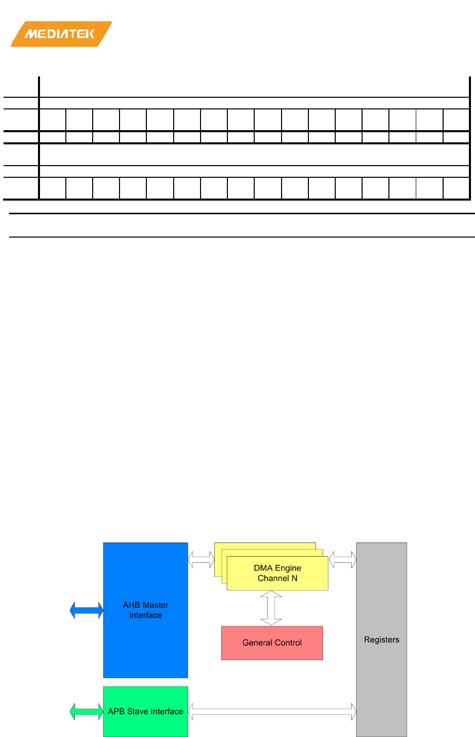
MT76x7
Internet-of-Things Wireless Connectivity
Reference Manual
© 2015 - 2017 MediaTek Inc
Page 83 of 798
This document contains information that is proprietary to MediaTek Inc. (“MediaTek”) and/or its licensor(s).
Any unauthorized use, reproduction or disclosure of this document in whole or in part is strictly prohibited
Nam
e
GPRAM_DATA
Type
RW
Rese
t
0 0 0 0 0 0 0 0 0 0 0 0 0 0 0 0
Bit
15
14
13
12
11
10
9
8
7
6
5
4
3
2
1
0
Nam
e
GPRAM_DATA
Type
RW
Rese
t
0 0 0 0 0 0 0 0 0 0 0 0 0 0 0 0
Bit(s)
Name
Description
31:0
GPRAM_DATA
R/W SRAM data by register address (0x800 ~ 0x89f).
SRAM data are composed of MAC_OUT_LENGTH +
MAC_IN_LENGTH bytes. Please read "twice" to access the
data when the address is changed. ( APB_CON[1] have to
set 1'b1 to read APB using 2T pclk )
2.4.5. DMA
2.4.5.1. General description
A generic DMA Controller is placed on AHB Bus to support fast data transfers and to off-load the processor.
With this controller, specific devices on AHB or APB buses can benefit greatly from quick completion of data
movement from or to memory modules such as Internal System RAM or External SRAM. Such Generic DMA
Controller can also be used to connect any two devices other than memory module as long as they can be
addressed in memory space.
Each channel has a similar set of registers to be configured to different scheme as desired. Once the service
candidate is decided, the responsible device driver should configure the Generic DMA Controller properly in
order to conduct DMA transfers. Both Interrupt- and Polling-based schemes in handling the completion event
are supported.
MT76x7
Internet-of-Things Wireless Connectivity
Reference Manual
© 2015 - 2017 MediaTek Inc
Page 84 of 798
This document contains information that is proprietary to MediaTek Inc. (“MediaTek”) and/or its licensor(s).
Any unauthorized use, reproduction or disclosure of this document in whole or in part is strictly prohibited
Figure 2-26. Generic DMA controller block diagram
The table below presents the available DMA Channels:
Table 2-20. Available DMA channels
DMA number Type Ring Buffer Two Buffer Burst Mode Unaligned Word
Access
DMA1 Full Size ● ● ●
DMA2 Full Size ● ● ●
DMA3 Half Size ● ● ● ●
DMA4 Half Size ● ● ● ●
DMA5 Half Size ● ● ● ●
DMA6 Half Size ● ● ● ●
DMA7 Half Size ● ● ● ●
DMA8 Half Size ● ● ● ●
DMA9 Half Size ● ● ● ●
DMA10 Half Size ● ● ● ●
DMA11 Half Size ● ● ● ●
DMA12 Virtual FIFO ●
DMA13 Virtual FIFO ●
DMA14 Virtual FIFO ●
DMA15 Virtual FIFO ●
DMA16 Virtual FIFO ●
DMA17 Virtual FIFO ●
DMA18 Virtual FIFO ●
DMA19 Virtual FIFO ●
DMA20 Virtual FIFO ●
DMA21 Virtual FIFO ●
DMA22 Virtual FIFO ●
DMA23 Virtual FIFO ●
DMA24 Virtual FIFO ●
DMA25 Virtual FIFO ●
2.4.5.2. Full-Size and Half-Size DMA channels
There are three types of DMA channels supported in MT76X7.
• Full-size DMA: Both the source address and the destination address are programmable. It is normally
used for memory copy.
• Half-size DMA: Either the source address or the destination address is programmable. It is normally
used for data movement between memory and peripherals.
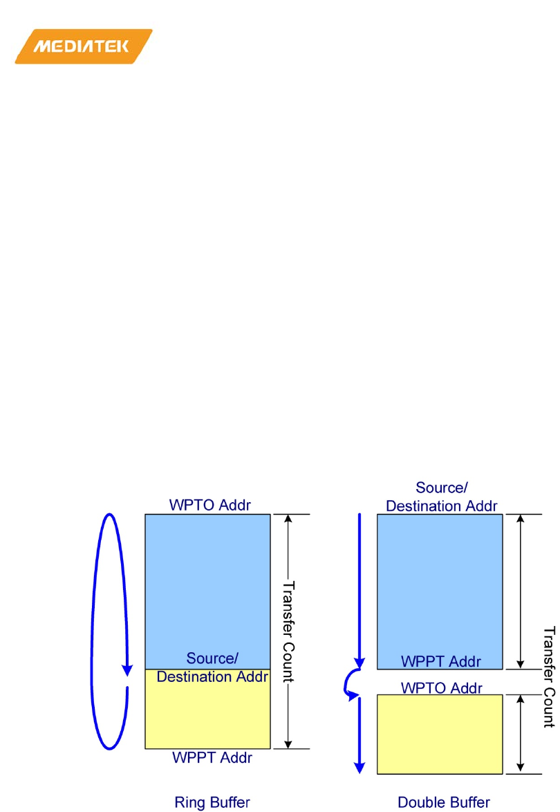
MT76x7
Internet-of-Things Wireless Connectivity
Reference Manual
© 2015 - 2017 MediaTek Inc
Page 85 of 798
This document contains information that is proprietary to MediaTek Inc. (“MediaTek”) and/or its licensor(s).
Any unauthorized use, reproduction or disclosure of this document in whole or in part is strictly prohibited
• Virtual FIFO DMA (VFF DMA): It is a half-size DMA with an additional FIFO control engine. It is used to
provide the buffering capacity for peripherals including UART.
• Full-size DMA channel—channels 1 and 2
• Half-size DMA channel—Channels 3-11
• Virtual FIFO DMA—Channels 12-25
The difference between the first two types of DMA channels is that both source and destination address are
programmable in full-size DMA channels, but only the address of one side can be programmed in half-size
DMA channel. In half-size channels, only either the source or destination address can be programmed, while
the addresses of the other side are preset. Which preset address is used depends on the setting of MAS in
DMA Channel Control Register. Refer to the Register Definition section for more detail.
2.4.5.3. Ring buffer and double buffer memory data movement
DMA channels 1 through 11 support ring-buffer and double-buffer memory data movement. This can be
achieved by programming DMA_WPPT and DMA_WPTO, as well as setting WPEN in DMA_CON register to
enable. The following figure illustrates how this function works. Once the transfer counter reaches the value
of WPPT, the next address jumps to the WPTO address after completing the WPPT data transfer. Note that
only one side can be configured as ring-buffer or double-buffer memory, and this is controlled by WPSD in
DMA_CON register.
Figure 2-27. Ring Buffer and Double Buffer Memory Data Movement
2.4.5.4. Unaligned word access
The word access address on AHB bus must be aligned to word boundary, or the 2 LSB is truncated to 00b. If
programmers do not notice this, it may cause an incorrect data fetch. In the case where data is to be moved
from unaligned addresses to aligned addresses, the word is usually first split into four bytes and then moved
byte by byte. This action results in four read and four write transfers on the bus.
To improve bus efficiency, unaligned-word access is provided in DMA3~11. While this function is enabled,
DMAs move data from unaligned address to aligned address by executing four continuous byte-read access
and one word-write access, reducing the number of transfers on the bus by three.
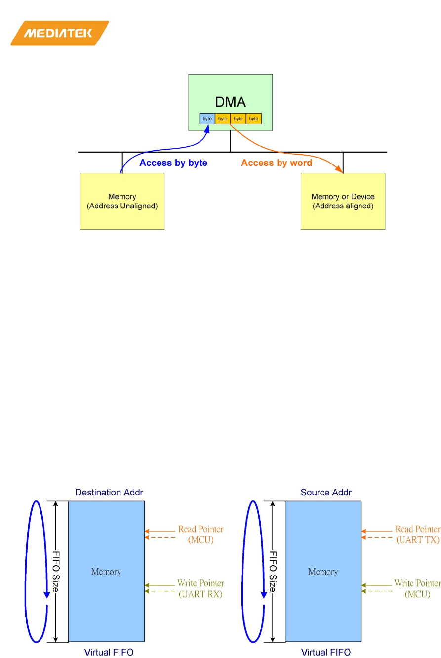
MT76x7
Internet-of-Things Wireless Connectivity
Reference Manual
© 2015 - 2017 MediaTek Inc
Page 86 of 798
This document contains information that is proprietary to MediaTek Inc. (“MediaTek”) and/or its licensor(s).
Any unauthorized use, reproduction or disclosure of this document in whole or in part is strictly prohibited
Figure 2-28. Unaligned Word Accesses
2.4.5.5. Virtual FIFO DMA
Virtual FIFO DMA is used to ease UART control. The difference between the Virtual FIFO DMAs and the
ordinary DMAs is that Virtual FIFO DMA contains an additional FIFO controller. The read and write pointers
are kept in the Virtual FIFO DMA. During a read from the FIFO, the read pointer points to the address of the
next data. During a write to the FIFO, the write pointer moves to the next address. If the FIFO is empty, a FIFO
read is not allowed. Similarly, data is not written into the FIFO if the FIFO is full. Due to UART flow control
requirements, an alert length is programmed. Once the FIFO Space is less than this value, an alert signal is
issued to enable UART flow control. The type of flow control performed depends on the setting in UART.
Each Virtual FIFO DMA can be programmed as RX or TX FIFO. This depends on the setting of DIR in DMA_CON
register. If DIR is “0”(READ), it means TX FIFO. On the other hand, if DIR is “1”(WRITE), the Virtual FIFO DMA is
specified as a RX FIFO.
Virtual FIFO DMA provides an interrupt to MCU. This interrupt informs MCU that there is data in the FIFO, and
the amount of data is over or under the value defined in DMA_COUNT register. With this, MCU does not need
to poll DMA to know when data must be removed from or put into the FIFO.
Note that Virtual FIFO DMAs cannot be used as generic DMAs.
Figure 2-29. Virtual FIFO DMA
Table 2-21. Virtual FIFO Access Port
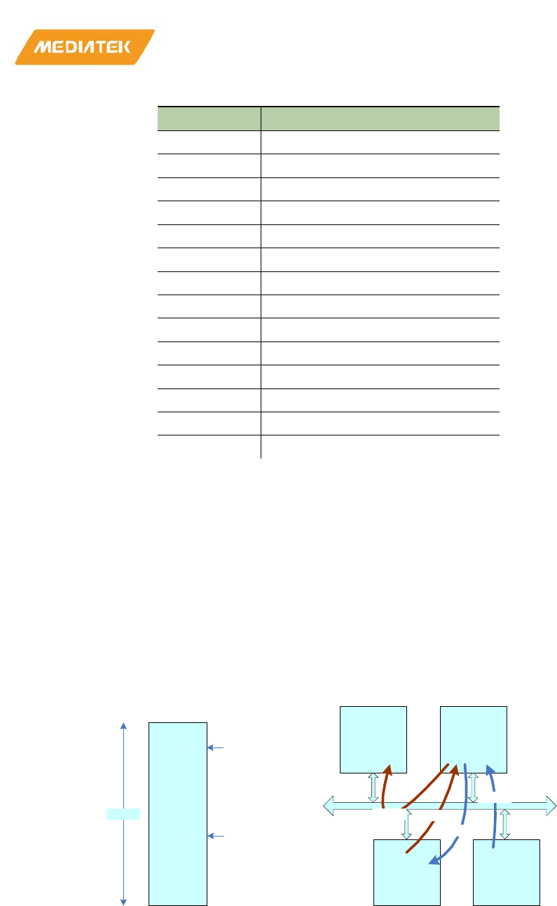
MT76x7
Internet-of-Things Wireless Connectivity
Reference Manual
© 2015 - 2017 MediaTek Inc
Page 87 of 798
This document contains information that is proprietary to MediaTek Inc. (“MediaTek”) and/or its licensor(s).
Any unauthorized use, reproduction or disclosure of this document in whole or in part is strictly prohibited
DMA number Address of Virtual FIFO Access Port
DMA12 7900_0000h
DMA13 7900_0100h
DMA14 7900_0200h
DMA15 7900_0300h
DMA16 7900_0400h
DMA17 7900_0500h
DMA18 7900_0600h
DMA19 7900_0700h
DMA20 7900_0800h
DMA21 7900_0900h
DMA22 7900_0A00h
DMA23 7900_0B00h
DMA24 7900_0C00h
DMA25 7900_0D00h
The figure below illustrates the operations of virtual FIFO DMA used for UART RX.
• READ: DMA controller reads data from UART and increments the WRITE pointer of the FIFO
controller.
• WRITE; DMA controller writes data that was area from UART to SRAM in the area defined before
enabling the virtual FIFO.
• READ: MCU reads data when FIFO is not empty and the amount of data is over a pre-defined
threshold. The read transaction will be finished only when DMA controller reads back the data from
SRAM.
• READ: DMA controller reads data from SRAM and increments the READ pointer of the FIFO controller.
Figure 2-30. Virtual FIFO Concept
2.4.5.6. DMA channels and priority control
There are two full-size DMA channels, 8 half- size DMA channels, and 13 virtual FIFO DMA channels in MT76x7.
Table 2-22. DMA use for hardware functions
DMA
UART
SRAM
MCU
(1) READ
(2) WRITE
(3) READ (4) READ
memory
FIFO size
Destination Address
READ pointer
(MCU)
WRITE pointer
(UART RX)

MT76x7
Internet-of-Things Wireless Connectivity
Reference Manual
© 2015 - 2017 MediaTek Inc
Page 88 of 798
This document contains information that is proprietary to MediaTek Inc. (“MediaTek”) and/or its licensor(s).
Any unauthorized use, reproduction or disclosure of this document in whole or in part is strictly prohibited
Hardware Function DMA Type
Radio (Bluetooth) Virtual FIFO DMA x 2
Radio (Wi-Fi) Half size DMA x 1
UART (x2) Virtual FIFO DMA x 4
I2S Virtual FIFO DMA x 2
ADC Virtual FIFO DMA x 1
I2C (x2) Half size DMA x 4
Security boot Full size DMA x 1
Reserved Full size DMA x 1, half size DMA x 5 and virtual FIFO DMA x 4.
The DMA provides two levels of scheduling scheme among all channels.
1) The first level scheduling follows the strict-priority scheme. All channels can be grouped into four
priority groups. Group one gets the highest priority, then group two, and so on.
2) The second level scheduling follows the round-robin scheme. Every channel in the same priority group
has equal opportunity to use the bandwidth and was served sequentially.
The arbitration is done per AHB transaction. When one AHB transaction is finished, the scheduler will follow
the above mechanism to select the next DMA channel to serve.
2.4.5.7. Register definitions
Register programming tips:
• Start registers shall be cleared, when associated channels are being programmed.
• PGMADDR, i.e. programmable address, only exists in half-size DMA channels. If DIR in Control
Register is high, PGMADDR represents Destination Address. Conversely, If DIR in Control Register is
low, PGMADDR represents Source Address.
• Functions of ring-buffer and double-buffer memory data movement can be activated on either source
side or destination side by programming DMA_WPPT & and DMA_WPTO, as well as setting WPEN in
DMA_CON register high. WPSD in DMA_CON register determines the activated side.
Module name: dma_cm4 Base address: (+83010000h)
Address
Name
Width
Register Function
83010000
DMA_CM4_GLBSTA0
32
DMA CR4 Global Status Register 0. This
register helps software program keep
track of the global status of DMA channels.
83010004
DMA_CM4_GLBSTA1
32
DMA CR4 Global Status Register 1. This
register helps
software program keep
track of the global status of DMA channels.
83010010
DMA_CM4_GROUP0
32
DMA CR4 Group Setting Register 0
83010014
DMA_CM4_GROUP1
32
DMA CR4 Group Setting Register 1
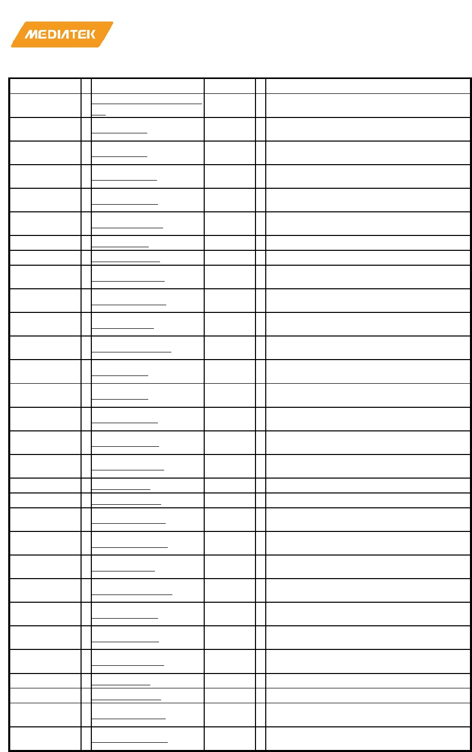
MT76x7
Internet-of-Things Wireless Connectivity
Reference Manual
© 2015 - 2017 MediaTek Inc
Page 89 of 798
This document contains information that is proprietary to MediaTek Inc. (“MediaTek”) and/or its licensor(s).
Any unauthorized use, reproduction or disclosure of this document in whole or in part is strictly prohibited
Address
Name
Width
Register Function
83010028
DMA_CM4_GLBLIMIT
ER
32
DMA CR4 Global Bandwidth Limiter
Register
83010100
DMA1_SRC
32
DMA CR4 Channel 1 Source Address
Register
83010104
DMA1_DST
32
DMA CR4 Channel 1 Destination Address
Register
83010108
DMA1_WPPT
32
DMA CR4 Channel 1 Wrap Point Address
Register
8301010C
DMA1_WPTO
32
DMA CR4 Channel 1 Wrap To Address
Register
83010110
DMA1_COUNT
32
DMA CR4 Channel 1 Transfer Count
Register
83010114
DMA1_CON
32
DMA CR4 Channel 1 Control Register
83010118
DMA1_START
32
DMA CR4 Channel 1 Start Register
8301011C
DMA1_INTSTA
32
DMA CR4 Channel 1 Interrupt Status
Register
83010120
DMA1_ACKINT
32
DMA CR4 Channel 1 Interrupt
Acknowledge Register
83010124
DMA1_RLCT
32
DMA CR4 Channel 1 Remaining Length of
Current Transfer
83010128
DMA1_LIMITER
32
DMA CR4 Channel 1 Bandwidth Limiter
Register
83010200
DMA2_SRC
32
DMA CR4 Channel 2 Source Address
Register
83010204
DMA2_DST
32
DMA CR4 Channel 2 Destination Address
Register
83010208
DMA2_WPPT
32
DMA CR4 Channel 2 Wrap Point Address
Register
8301020C
DMA2_WPTO
32
DMA CR4 Channel 2 Wrap To Address
Register
83010210
DMA2_COUNT
32
DMA CR4 Channel 2 Transfer Count
Register
83010214
DMA2_CON
32
DMA CR4 Channel 2 Control Register
83010218
DMA2_START
32
DMA CR4 Channel 2 Start Register
8301021C
DMA2_INTSTA
32
DMA CR4 Channel 2 Interrupt Status
Register
83010220
DMA2_ACKINT
32
DMA CR4 Channel 2 Interrupt
Acknowledge Register
83010224
DMA2_RLCT
32
DMA CR4 Channel 2 Remaining Length of
Current Transfer
83010228
DMA2_LIMITER
32
DMA CR4 Channel 2 Bandwidth Limiter
Register
83010308
DMA3_WPPT
32
DMA CR4 Channel 3 Wrap Point Address
Register
8301030C
DMA3_WPTO
32
DMA CR4 Channel 3 Wrap To Address
Register
83010310
DMA3_COUNT
32
DMA CR4 Channel 3 Transfer Count
Register
83010314
DMA3_CON
32
DMA CR4 Channel 3 Control Register
83010318
DMA3_START
32
DMA CR4 Channel 3 Start
Register
8301031C
DMA3_INTSTA
32
DMA CR4 Channel 3 Interrupt Status
Register
83010320
DMA3_ACKINT
32
DMA CR4 Channel 3 Interrupt
Acknowledge Register

MT76x7
Internet-of-Things Wireless Connectivity
Reference Manual
© 2015 - 2017 MediaTek Inc
Page 90 of 798
This document contains information that is proprietary to MediaTek Inc. (“MediaTek”) and/or its licensor(s).
Any unauthorized use, reproduction or disclosure of this document in whole or in part is strictly prohibited
Address
Name
Width
Register Function
83010324
DMA3_RLCT
32
DMA CR4 Channel 3 Remaining Length of
Current Transfer
83010328
DMA3_LIMITER
32
DMA CR4 Channel 3 Bandwidth Limiter
Register
8301032C
DMA3_PGMADDR
32
DMA CR4 Channel 3 Programmable
Address Register
83010408
DMA4_WPPT
32
DMA CR4 Channel 4 Wrap Point Address
Register
8301040C
DMA4_WPTO
32
DMA CR4 Channel 4 Wrap To Address
Register
83010410
DMA4_COUNT
32
DMA CR4 Channel 4 Transfer Count
Register
83010414
DMA4_CON
32
DMA CR4 Channel 4 Control Register
83010418
DMA4_START
32
DMA CR4 Channel 4 Start Register
8301041C
DMA4_INTSTA
32
DMA CR4 Channel 4 Interrupt Status
Register
83010420
DMA4_ACKINT
32
DMA CR4 Channel 4 Interrupt
Acknowledge Register
83010424
DMA4_RLCT
32
DMA CR4 Channel 4 Remaining Length of
Current Transfer
83010428
DMA4_LIMITER
32
DMA CR4 Channel 4 Bandwidth Limiter
Register
8301042C
DMA4_PGMADDR
32
DMA CR4 Channel 4 Programmable
Address Register
83010508
DMA5_WPPT
32
DMA CR4 Channel 5 Wrap Point Address
Register
8301050C
DMA5_WPTO
32
DMA CR4 Channel 5 Wrap To Address
Register
83010510
DMA5_COUNT
32
DMA CR4 Channel 5 Transfer Count
Register
83010514
DMA5_CON
32
DMA CR4 Channel 5 Control Register
83010518
DMA5_START
32
DMA CR4 Channel 5 Start
Register
8301051C
DMA5_INTSTA
32
DMA CR4 Channel 5 Interrupt Status
Register
83010520
DMA5_ACKINT
32
DMA CR4 Channel 5 Interrupt
Acknowledge Register
83010524
DMA5_RLCT
32
DMA CR4 Channel 5 Remaining Length of
Current Transfer
83010528
DMA5_LIMITER
32
DMA CR4 Channel 5 Bandwidth Limiter
Register
8301052C
DMA5_PGMADDR
32
DMA CR4 Channel 5 Programmable
Address Register
83010608
DMA6_WPPT
32
DMA CR4 Channel 6 Wrap Point Address
Register
8301060C
DMA6_WPTO
32
DMA CR4 Channel 6 Wrap To Address
Register
83010610
DMA6_COUNT
32
DMA CR4 Channel 6 Transfer Count
Register
83010614
DMA6_CON
32
DMA CR4 Channel 6 Control Register
83010618
DMA6_START
32
DMA CR4 Channel 6 Start
Register
8301061C
DMA6_INTSTA
32
DMA CR4 Channel 6 Interrupt Status
Register
83010620
DMA6_ACKINT
32
DMA CR4 Channel 6 Interrupt
Acknowledge Register
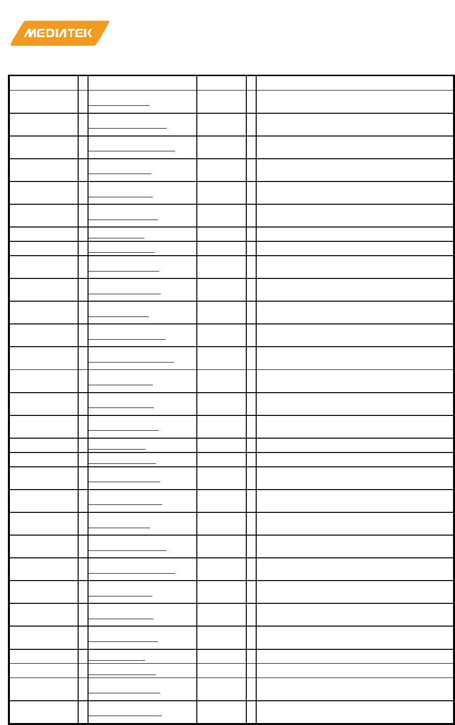
MT76x7
Internet-of-Things Wireless Connectivity
Reference Manual
© 2015 - 2017 MediaTek Inc
Page 91 of 798
This document contains information that is proprietary to MediaTek Inc. (“MediaTek”) and/or its licensor(s).
Any unauthorized use, reproduction or disclosure of this document in whole or in part is strictly prohibited
Address
Name
Width
Register Function
83010624
DMA6_RLCT
32
DMA CR4 Channel 6 Remaining Length of
Current Transfer
83010628
DMA6_LIMITER
32
DMA CR4 Channel 6 Bandwidth Limiter
Register
8301062C
DMA6_PGMADDR
32
DMA CR4 Channel 6 Programmable
Address Register
83010708
DMA7_WPPT
32
DMA CR4 Channel 7 Wrap Point Address
Register
8301070C
DMA7_WPTO
32
DMA CR4 Channel 7 Wrap To Address
Register
83010710
DMA7_COUNT
32
DMA CR4 Channel 7 Transfer Count
Register
83010714
DMA7_CON
32
DMA CR4 Channel 7 Control Register
83010718
DMA7_START
32
DMA CR4 Channel 7 Start Register
8301071C
DMA7_INTSTA
32
DMA CR4 Channel 7 Interrupt Status
Register
83010720
DMA7_ACKINT
32
DMA CR4 Channel 7 Interrupt
Acknowledge Register
83010724
DMA7_RLCT
32
DMA CR4 Channel 7 Remaining Length of
Current Transfer
83010728
DMA7_LIMITER
32
DMA CR4 Channel 7 Bandwidth Limiter
Register
8301072C
DMA7_PGMADDR
32
DMA CR4 Channel 7 Programmable
Address Register
83010808
DMA8_WPPT
32
DMA CR4 Channel 8 Wrap Point Address
Register
8301080C
DMA8_WPTO
32
DMA CR4 Channel 8 Wrap To Address
Register
83010810
DMA8_COUNT
32
DMA CR4 Channel 8 Transfer Count
Register
83010814
DMA8_CON
32
DMA CR4 Channel 8 Control Register
83010818
DMA8_START
32
DMA CR4 Channel 8 Start
Register
8301081C
DMA8_INTSTA
32
DMA CR4 Channel 8 Interrupt Status
Register
83010820
DMA8_ACKINT
32
DMA CR4 Channel 8 Interrupt
Acknowledge Register
83010824
DMA8_RLCT
32
DMA CR4 Channel 8 Remaining Length of
Current Transfer
83010828
DMA8_LIMITER
32
DMA CR4 Channel 8 Bandwidth Limiter
Register
8301082C
DMA8_PGMADDR
32
DMA CR4 Channel 8 Programmable
Address Register
83010908
DMA9_WPPT
32
DMA CR4 Channel 9 Wrap Point Address
Register
8301090C
DMA9_WPTO
32
DMA CR4 Channel 9 Wrap To Address
Register
83010910
DMA9_COUNT
32
DMA CR4 Channel 9 Transfer Count
Register
83010914
DMA9_CON
32
DMA CR4 Channel 9 Control Register
83010918
DMA9_START
32
DMA CR4 Channel 9 Start
Register
8301091C
DMA9_INTSTA
32
DMA CR4 Channel 9 Interrupt Status
Register
83010920
DMA9_ACKINT
32
DMA CR4 Channel 9 Interrupt
Acknowledge Register

MT76x7
Internet-of-Things Wireless Connectivity
Reference Manual
© 2015 - 2017 MediaTek Inc
Page 92 of 798
This document contains information that is proprietary to MediaTek Inc. (“MediaTek”) and/or its licensor(s).
Any unauthorized use, reproduction or disclosure of this document in whole or in part is strictly prohibited
Address
Name
Width
Register Function
83010924
DMA9_RLCT
32
DMA CR4 Channel 9 Remaining Length of
Current Transfer
83010928
DMA9_LIMITER
32
DMA CR4 Channel 9 Bandwidth Limiter
Register
8301092C
DMA9_PGMADDR
32
DMA CR4 Channel 9 Programmable
Address Register
83010A08
DMA10_WPPT
32
DMA CR4 Channel 10 Wrap Point Address
Register
83010A0C
DMA10_WPTO
32
DMA CR4 Channel 10 Wrap To Address
Register
83010A10
DMA10_COUNT
32
DMA CR4 Channel 10 Transfer Count
Register
83010A14
DMA10_CON
32
DMA CR4 Channel 10 Control Register
83010A18
DMA10_START
32
DMA CR4 Channel 10 Start Register
83010A1C
DMA10_INTSTA
32
DMA CR4 Channel 10 Interrupt Status
Register
83010A20
DMA10_ACKINT
32
DMA CR4 Channel 10 Interrupt
Acknowledge Register
83010A24
DMA10_RLCT
32
DMA CR4 Channel 10 Remaining Length of
Current Transfer
83010A28
DMA10_LIMITER
32
DMA CR4 Channel 10 Bandwidth Limiter
Register
83010A2C
DMA10_PGMADDR
32
DMA CR4 Channel 10 Programmable
Address Register
83010B08
DMA11_WPPT
32
DMA CR4 Channel 11 Wrap Point Address
Register
83010B0C
DMA11_WPTO
32
DMA CR4 Channel 11 Wrap To Address
Register
83010B10
DMA11_COUNT
32
DMA CR4 Channel 11 Transfer Count
Register
83010B14
DMA11_CON
32
DMA CR4 Channel 11 Control Register
83010B18
DMA11_START
32
DMA CR4 Channel 11 Start Register
83010B1C
DMA11_INTSTA
32
DMA CR4 Channel 11 Interrupt Status
Register
83010B20
DMA11_ACKINT
32
DMA CR4 Channel 11 Interrupt
Acknowledge
Register
83010B24
DMA11_RLCT
32
DMA CR4 Channel 11 Remaining Length of
Current Transfer
83010B28
DMA11_LIMITER
32
DMA CR4 Channel 11 Bandwidth Limiter
Register
83010B2C
DMA11_PGMADDR
32
DMA CR4 Channel 11 Programmable
Address Register
83010C10
DMA12_COUNT
32
DMA CR4 Channel 12 Transfer Count
Register
83010C14
DMA12_CON
32
DMA
CR4 Channel 12 Control Register
83010C18
DMA12_START
32
DMA CR4 Channel 12 Start Register
83010C1C
DMA12_INTSTA
32
DMA CR4 Channel 12 Interrupt Status
Register
83010C20
DMA12_ACKINT
32
DMA CR4 Channel 12 Interrupt
Acknowledge Register
83010C28
DMA12_LIMITER
32
DMA CR4 Channel 12 Bandwidth Limiter
Register
83010C2C
DMA12_PGMADDR
32
DMA CR4 Channel 12 Programmable
Address Register
MT76x7
Internet-of-Things Wireless Connectivity
Reference Manual
© 2015 - 2017 MediaTek Inc
Page 93 of 798
This document contains information that is proprietary to MediaTek Inc. (“MediaTek”) and/or its licensor(s).
Any unauthorized use, reproduction or disclosure of this document in whole or in part is strictly prohibited
Address
Name
Width
Register Function
83010C30
DMA12_WRPTR
32
DMA CR4 Channel 12 Write Pointer
83010C34
DMA12_RDPTR
32
DMA CR4 Channel 12 Read Pointer
83010C38
DMA12_FFCNT
32
DMA CR4 Channel 12 FIFO Count
83010C3C
DMA12_FFSTA
32
DMA CR4 Channel 12 FIFO Status
83010C40
DMA12_ALTLEN
32
DMA CR4 Channel 12 Alert Length
Register
83010C44
DMA12_FFSIZE
32
DMA CR4 Channel 12 Virtual FIFO Size
Register
83010C48
DMA12_CVFF
32
DMA CR4 Channel 12 Cascade Virtual
FIFO Control Register
83010C50
DMA12_TO
32
DMA CR4 Channel 12 Timeout Value
Register
83010D10
DMA13_COUNT
32
DMA CR4 Channel 13 Transfer Count
Register
83010D14
DMA13_CON
32
DMA CR4 Channel 13
Control Register
83010D18
DMA13_START
32
DMA CR4 Channel 13 Start Register
83010D1C
DMA13_INTSTA
32
DMA CR4 Channel 13 Interrupt Status
Register
83010D20
DMA13_ACKINT
32
DMA CR4 Channel 13 Interrupt
Acknowledge Register
83010D28
DMA13_LIMITER
32
DMA CR4 Channel 13 Bandwidth Limiter
Register
83010D2C
DMA13_PGMADDR
32
DMA CR4 Channel 13 Programmable
Address Register
83010D30
DMA13_WRPTR
32
DMA CR4 Channel 13 Write Pointer
83010D34
DMA13_RDPTR
32
DMA CR4 Channel 13 Read Pointer
83010D38
DMA13_FFCNT
32
DMA CR4 Channel 13 FIFO Count
83010D3C
DMA13_FFSTA
32
DMA CR4 Channel 13 FIFO Status
83010D40
DMA13_ALTLEN
32
DMA CR4 Channel 13 Alert Length
Register
83010D44
DMA13_FFSIZE
32
DMA CR4 Channel 13 Virtual FIFO Size
Register
83010D48
DMA13_CVFF
32
DMA CR4 Channel 13 Cascade Virtual
FIFO Control Register
83010D50
DMA13_TO
32
DMA CR4 Channel 13 Timeout Value
Register
83010E10
DMA14_COUNT
32
DMA CR4 Channel 14 Transfer Count
Register
83010E14
DMA14_CON
32
DMA CR4 Channel 14 Control Register
83010E18
DMA14_START
32
DMA CR4 Channel 14 Start Register
83010E1C
DMA14_INTSTA
32
DMA CR4 Channel 14 Interrupt Status
Register
83010E20
DMA14_ACKINT
32
DMA CR4 Channel 14 Interrupt
Acknowledge Register
83010E28
DMA14_LIMITER
32
DMA CR4 Channel 14 Bandwidth Limiter
Register
83010E2C
DMA14_PGMADDR
32
DMA CR4 Channel 14 Programmable
Address Register
83010E30
DMA14_WRPTR
32
DMA CR4 Channel 14 Write Pointer
83010E34
DMA14_RDPTR
32
DMA CR4 Channel 14 Read Pointer
83010E38
DMA14_FFCNT
32
DMA CR4 Channel 14 FIFO Count
83010E3C
DMA14_FFSTA
32
DMA CR4 Channel 14 FIFO Status
MT76x7
Internet-of-Things Wireless Connectivity
Reference Manual
© 2015 - 2017 MediaTek Inc
Page 94 of 798
This document contains information that is proprietary to MediaTek Inc. (“MediaTek”) and/or its licensor(s).
Any unauthorized use, reproduction or disclosure of this document in whole or in part is strictly prohibited
Address
Name
Width
Register Function
83010E40
DMA14_ALTLEN
32
DMA CR4 Channel 14 Alert Length
Register
83010E44
DMA14_FFSIZE
32
DMA CR4 Channel 14 Virtual FIFO Size
Register
83010E48
DMA14_CVFF
32
DMA CR4 Channel 14 Cascade Virtual
FIFO Control Register
83010E50
DMA14_TO
32
DMA CR4 Channel 14 Timeout Value
Register
83010F10
DMA15_COUNT
32
DMA CR4 Channel 15 Transfer Count
Register
83010F14
DMA15_CON
32
DMA CR4 Channel 15 Control Register
83010F18
DMA15_START
32
DMA CR4 Channel 15 Start Register
83010F1C
DMA15_INTSTA
32
DMA CR4 Channel 15 Interrupt Status
Register
83010F20
DMA15_ACKINT
32
DMA CR4 Channel 15 Interrupt
Acknowledge Register
83010F28
DMA15_LIMITER
32
DMA CR4 Channel 15 Bandwidth Limiter
Register
83010F2C
DMA15_PGMADDR
32
DMA CR4 Channel 15 Programmable
Address Register
83010F30
DMA15_WRPTR
32
DMA CR4 Channel 15 Write Pointer
83010F34
DMA15_RDPTR
32
DMA CR4 Channel 15 Read Pointer
83010F38
DMA15_FFCNT
32
DMA CR4 Channel 15 FIFO Count
83010F3C
DMA15_FFSTA
32
DMA CR4 Channel 15 FIFO Status
83010F40
DMA15_ALTLEN
32
DMA CR4 Channel 15 Alert Length
Register
83010F44
DMA15_FFSIZE
32
DMA CR4 Channel 15 Virtual FIFO Size
Register
83010F48
DMA15_CVFF
32
DMA CR4 Channel 15 Cascade Virtual
FIFO Control Register
83010F50
DMA15_TO
32
DMA CR4 Channel 15 Timeout Value
Register
83011010
DMA16_COUNT
32
DMA CR4 Channel 16 Transfer Count
Register
83011014
DMA16_CON
32
DMA CR4 Channel 16 Control Register
83011018
DMA16_START
32
DMA CR4 Channel 16 Start Register
8301101C
DMA16_INTSTA
32
DMA CR4 Channel 16 Interrupt Status
Register
83011020
DMA16_ACKINT
32
DMA CR4 Channel 16 Interrupt
Acknowledge Register
83011028
DMA16_LIMITER
32
DMA CR4 Channel 16 Bandwidth Limiter
Register
8301102C
DMA16_PGMADDR
32
DMA CR4 Channel 16 Programmable
Address Register
83011030
DMA16_WRPTR
32
DMA CR4 Channel 16 Write Pointer
83011034
DMA16_RDPTR
32
DMA CR4 Channel 16 Read Pointer
83011038
DMA16_FFCNT
32
DMA CR4 Channel 16 FIFO Count
8301103C
DMA16_FFSTA
32
DMA CR4 Channel 16 FIFO Status
83011040
DMA16_ALTLEN
32
DMA CR4 Channel 16 Alert Length
Register
83011044
DMA16_FFSIZE
32
DMA CR4 Channel 16 Virtual FIFO Size
Register
MT76x7
Internet-of-Things Wireless Connectivity
Reference Manual
© 2015 - 2017 MediaTek Inc
Page 95 of 798
This document contains information that is proprietary to MediaTek Inc. (“MediaTek”) and/or its licensor(s).
Any unauthorized use, reproduction or disclosure of this document in whole or in part is strictly prohibited
Address
Name
Width
Register Function
83011048
DMA16_CVFF
32
DMA CR4 Channel 16 Cascade Virtual
FIFO Control Register
83011050
DMA16_TO
32
DMA CR4 Channel 16 Timeout Value
Register
83011110
DMA17_COUNT
32
DMA CR4 Channel 17 Transfer Count
Register
83011114
DMA17_CON
32
DMA CR4 Channel 17 Control Register
83011118
DMA17_START
32
DMA CR4 Channel 17 Start Register
8301111C
DMA17_INTSTA
32
DMA CR4 Channel 17 Interrupt Status
Register
83011120
DMA17_ACKINT
32
DMA CR4 Channel 17 Interrupt
Acknowledge Register
83011128
DMA17_LIMITER
32
DMA CR4 Channel 17 Bandwidth Limiter
Register
8301112C
DMA17_PGMADDR
32
DMA CR4 Channel 17 Programmable
Address Register
83011130
DMA17_WRPTR
32
DMA CR4 Channel 17 Write Pointer
83011134
DMA17_RDPTR
32
DMA CR4 Channel 17 Read Pointer
83011138
DMA17_FFCNT
32
DMA CR4 Channel 17 FIFO Count
8301113C
DMA17_FFSTA
32
DMA CR4 Channel 17 FIFO Status
83011140
DMA17_ALTLEN
32
DMA CR4 Channel 17 Alert Length
Register
83011144
DMA17_FFSIZE
32
DMA CR4 Channel 17 Virtual FIFO Size
Register
83011148
DMA17_CVFF
32
DMA CR4 Channel 17 Cascade Virtual
FIFO Control Register
83011150
DMA17_TO
32
DMA CR4 Channel 17 Timeout Value
Register
83011210
DMA18_COUNT
32
DMA CR4 Channel 18 Transfer Count
Register
83011214
DMA18_CON
32
DMA CR4 Channel 18 Control Register
83011218
DMA18_START
32
DMA CR4 Channel 18 Start Register
8301121C
DMA18_INTSTA
32
DMA CR4 Channel 18 Interrupt Status
Register
83011220
DMA18_ACKINT
32
DMA CR4 Channel 18 Interrupt
Acknowledge Register
83011228
DMA18_LIMITER
32
DMA CR4 Channel 18 Bandwidth Limiter
Register
8301122C
DMA18_PGMADDR
32
DMA CR4 Channel 18 Programmable
Address Register
83011230
DMA18_WRPTR
32
DMA CR4 Channel 18 Write Pointer
83011234
DMA18_RDPTR
32
DMA CR4 Channel 18 Read Pointer
83011238
DMA18_FFCNT
32
DMA CR4 Channel 18 FIFO Count
8301123C
DMA18_FFSTA
32
DMA CR4 Channel 18 FIFO Status
83011240
DMA18_ALTLEN
32
DMA CR4 Channel 18 Alert Length
Register
83011244
DMA18_FFSIZE
32
DMA CR4 Channel 18 Virtual FIFO Size
Register
83011248
DMA18_CVFF
32
DMA CR4 Channel 18 Cascade Virtual
FIFO Control Register
83011250
DMA18_TO
32
DMA CR4 Channel 18 Timeout Value
Register
MT76x7
Internet-of-Things Wireless Connectivity
Reference Manual
© 2015 - 2017 MediaTek Inc
Page 96 of 798
This document contains information that is proprietary to MediaTek Inc. (“MediaTek”) and/or its licensor(s).
Any unauthorized use, reproduction or disclosure of this document in whole or in part is strictly prohibited
Address
Name
Width
Register Function
83011310
DMA19_COUNT
32
DMA CR4 Channel 19 Transfer Count
Register
83011314
DMA19_CON
32
DMA CR4 Channel 19
Control Register
83011318
DMA19_START
32
DMA CR4 Channel 19 Start Register
8301131C
DMA19_INTSTA
32
DMA CR4 Channel 19 Interrupt Status
Register
83011320
DMA19_ACKINT
32
DMA CR4 Channel 19 Interrupt
Acknowledge Register
83011328
DMA19_LIMITER
32
DMA CR4 Channel 19 Bandwidth Limiter
Register
8301132C
DMA19_PGMADDR
32
DMA CR4 Channel 19 Programmable
Address Register
83011330
DMA19_WRPTR
32
DMA CR4 Channel 19 Write Pointer
83011334
DMA19_RDPTR
32
DMA CR4 Channel 19 Read Pointer
83011338
DMA19_FFCNT
32
DMA CR4 Channel 19 FIFO Count
8301133C
DMA19_FFSTA
32
DMA CR4 Channel 19 FIFO Status
83011340
DMA19_ALTLEN
32
DMA CR4 Channel 19 Alert Length
Register
83011344
DMA19_FFSIZE
32
DMA CR4 Channel 19 Virtual FIFO Size
Register
83011348
DMA19_CVFF
32
DMA CR4 Channel 19 Cascade Virtual
FIFO Control Register
83011350
DMA19_TO
32
DMA CR4 Channel 19 Timeout Value
Register
83011410
DMA20_COUNT
32
DMA CR4 Channel 20 Transfer Count
Register
83011414
DMA20_CON
32
DMA CR4 Channel 20 Control Register
83011418
DMA20_START
32
DMA CR4 Channel 20 Start Register
8301141C
DMA20_INTSTA
32
DMA CR4 Channel 20 Interrupt Status
Register
83011420
DMA20_ACKINT
32
DMA CR4 Channel 20 Interrupt
Acknowledge Register
83011428
DMA20_LIMITER
32
DMA CR4 Channel 20 Bandwidth Limiter
Register
8301142C
DMA20_PGMADDR
32
DMA CR4 Channel 20 Programmable
Address Register
83011430
DMA20_WRPTR
32
DMA CR4 Channel 20 Write Pointer
83011434
DMA20_RDPTR
32
DMA CR4 Channel 20 Read Pointer
83011438
DMA20_FFCNT
32
DMA CR4 Channel 20 FIFO Count
8301143C
DMA20_FFSTA
32
DMA CR4 Channel 20 FIFO Status
83011440
DMA20_ALTLEN
32
DMA CR4 Channel 20 Alert Length
Register
83011444
DMA20_FFSIZE
32
DMA CR4 Channel 20 Virtual FIFO Size
Register
83011448
DMA20_CVFF
32
DMA CR4 Channel 20 Cascade Virtual
FIFO Control Register
83011450
DMA20_TO
32
DMA CR4 Channel 20 Timeout Value
Register
83011510
DMA21_COUNT
32
DMA CR4 Channel 21 Transfer Count
Register
83011514
DMA21_CON
32
DMA CR4 Channel 21 Control Register
83011518
DMA21_START
32
DMA CR4 Channel
21 Start Register

MT76x7
Internet-of-Things Wireless Connectivity
Reference Manual
© 2015 - 2017 MediaTek Inc
Page 97 of 798
This document contains information that is proprietary to MediaTek Inc. (“MediaTek”) and/or its licensor(s).
Any unauthorized use, reproduction or disclosure of this document in whole or in part is strictly prohibited
Address
Name
Width
Register Function
8301151C
DMA21_INTSTA
32
DMA CR4 Channel 21 Interrupt Status
Register
83011520
DMA21_ACKINT
32
DMA CR4 Channel 21 Interrupt
Acknowledge Register
83011528
DMA21_LIMITER
32
DMA CR4 Channel 21 Bandwidth Limiter
Register
8301152C
DMA21_PGMADDR
32
DMA CR4 Channel 21 Programmable
Address Register
83011530
DMA21_WRPTR
32
DMA CR4 Channel 21 Write Pointer
83011534
DMA21_RDPTR
32
DMA CR4 Channel 21 Read Pointer
83011538
DMA21_FFCNT
32
DMA CR4 Channel 21 FIFO Count
8301153C
DMA21_FFSTA
32
DMA CR4 Channel 21 FIFO Status
83011540
DMA21_ALTLEN
32
DMA CR4 Channel 21 Alert Length
Register
83011544
DMA21_FFSIZE
32
DMA CR4 Channel 21 Virtual FIFO Size
Register
83011548
DMA21_CVFF
32
DMA CR4 Channel 21 Cascade Virtual
FIFO Control Register
83011550
DMA21_TO
32
DMA CR4 Channel 21 Timeout Value
Register
83011610
DMA22_COUNT
32
DMA CR4 Channel 22 Transfer Count
Register
83011614
DMA22_CON
32
DMA CR4 Channel 22 Control Register
83011618
DMA22_START
32
DMA CR4 Channel 22 Start Register
8301161C
DMA22_INTSTA
32
DMA CR4 Channel 22 Interrupt Status
Register
83011620
DMA22_ACKINT
32
DMA CR4 Channel 22 Interrupt
Acknowledge Register
83011628
DMA22_LIMITER
32
DMA CR4 Channel 22 Bandwidth Limiter
Register
8301162C
DMA22_PGMADDR
32
DMA CR4 Channel 22 Programmable
Address Register
83011630
DMA22_WRPTR
32
DMA CR4 Channel 22 Write Pointer
83011634
DMA22_RDPTR
32
DMA CR4 Channel 22 Read Pointer
83011638
DMA22_FFCNT
32
DMA CR4 Channel 22 FIFO Count
8301163C
DMA22_FFSTA
32
DMA CR4 Channel 22 FIFO Status
83011640
DMA22_ALTLEN
32
DMA CR4 Channel 22 Alert Length
Register
83011644
DMA22_FFSIZE
32
DMA CR4 Channel 22 Virtual FIFO Size
Register
83011648
DMA22_CVFF
32
DMA CR4 Channel 22 Cascade Virtual
FIFO Control Register
83011650
DMA22_TO
32
DMA CR4 Channel 22 Timeout Value
Register
83011710
DMA23_COUNT
32
DMA CR4 Channel 23 Transfer Count
Register
83011714
DMA23_CON
32
DMA CR4 Channel 23 Control Register
83011718
DMA23_START
32
DMA CR4 Channel 23 Start Register
8301171C
DMA23_INTSTA
32
DMA CR4 Channel 23 Interrupt Status
Register
83011720
DMA23_ACKINT
32
DMA CR4 Channel 23 Interrupt
Acknowledge Register
MT76x7
Internet-of-Things Wireless Connectivity
Reference Manual
© 2015 - 2017 MediaTek Inc
Page 98 of 798
This document contains information that is proprietary to MediaTek Inc. (“MediaTek”) and/or its licensor(s).
Any unauthorized use, reproduction or disclosure of this document in whole or in part is strictly prohibited
Address
Name
Width
Register Function
83011728
DMA23_LIMITER
32
DMA CR4 Channel 23 Bandwidth Limiter
Register
8301172C
DMA23_PGMADDR
32
DMA CR4 Channel 23 Programmable
Address Register
83011730
DMA23_WRPTR
32
DMA CR4 Channel 23 Write Pointer
83011734
DMA23_RDPTR
32
DMA CR4
Channel 23 Read Pointer
83011738
DMA23_FFCNT
32
DMA CR4 Channel 23 FIFO Count
8301173C
DMA23_FFSTA
32
DMA CR4 Channel 23 FIFO Status
83011740
DMA23_ALTLEN
32
DMA CR4 Channel 23 Alert Length
Register
83011744
DMA23_FFSIZE
32
DMA CR4 Channel 23 Virtual FIFO Size
Register
83011748
DMA23_CVFF
32
DMA CR4 Channel 23 Cascade Virtual
FIFO Control Register
83011750
DMA23_TO
32
DMA CR4 Channel 23 Timeout Value
Register
83011810
DMA24_COUNT
32
DMA CR4 Channel 24 Transfer Count
Register
83011814
DMA24_CON
32
DMA CR4 Channel 24 Control Register
83011818
DMA24_START
32
DMA CR4 Channel 24 Start Register
8301181C
DMA24_INTSTA
32
DMA CR4 Channel 24 Interrupt Status
Register
83011820
DMA24_ACKINT
32
DMA CR4 Channel 24 Interrupt
Acknowledge Register
83011828
DMA24_LIMITER
32
DMA CR4 Channel 24 Bandwidth Limiter
Register
8301182C
DMA24_PGMADDR
32
DMA CR4 Channel 24 Programmable
Address Register
83011830
DMA24_WRPTR
32
DMA CR4 Channel 24 Write Pointer
83011834
DMA24_RDPTR
32
DMA CR4 Channel 24 Read Pointer
83011838
DMA24_FFCNT
32
DMA CR4 Channel 24 FIFO Count
8301183C
DMA24_FFSTA
32
DMA CR4 Channel 24 FIFO Status
83011840
DMA24_ALTLEN
32
DMA CR4 Channel 24 Alert Length
Register
83011844
DMA24_FFSIZE
32
DMA CR4 Channel 24 Virtual FIFO Size
Register
83011848
DMA24_CVFF
32
DMA CR4 Channel 24 Cascade Virtual
FIFO Control Register
83011850
DMA24_TO
32
DMA CR4 Channel 24 Timeout Value
Register
83011910
DMA25_COUNT
32
DMA CR4 Channel 25 Transfer Count
Register
83011914
DMA25_CON
32
DMA CR4 Channel 25
Control Register
83011918
DMA25_START
32
DMA CR4 Channel 25 Start Register
8301191C
DMA25_INTSTA
32
DMA CR4 Channel 25 Interrupt Status
Register
83011920
DMA25_ACKINT
32
DMA CR4 Channel 25 Interrupt
Acknowledge Register
83011928
DMA25_LIMITER
32
DMA CR4 Channel 25 Bandwidth Limiter
Register
8301192C
DMA25_PGMADDR
32
DMA CR4 Channel 25 Programmable
Address Register
MT76x7
Internet-of-Things Wireless Connectivity
Reference Manual
© 2015 - 2017 MediaTek Inc
Page 99 of 798
This document contains information that is proprietary to MediaTek Inc. (“MediaTek”) and/or its licensor(s).
Any unauthorized use, reproduction or disclosure of this document in whole or in part is strictly prohibited
Address
Name
Width
Register Function
83011930
DMA25_WRPTR
32
DMA CR4 Channel 25 Write Pointer
83011934
DMA25_RDPTR
32
DMA CR4 Channel 25 Read Pointer
83011938
DMA25_FFCNT
32
DMA CR4 Channel 25 FIFO Count
8301193C
DMA25_FFSTA
32
DMA CR4 Channel 25 FIFO Status
83011940
DMA25_ALTLEN
32
DMA CR4 Channel 25 Alert Length
Register
83011944
DMA25_FFSIZE
32
DMA CR4 Channel 25 Virtual FIFO Size
Register
83011948
DMA25_CVFF
32
DMA CR4 Channel 25 Cascade Virtual
FIFO Control Register
83011950
DMA25_TO
32
DMA CR4 Channel 25 Timeout Value
Register
83010000
DMA_CM4_GLBSTA0
DMA CR4 Global Status Register 0.
This register helps software program
keep track of the global status of DMA
channels.
00000000
Bit
31
30
29
28
27
26
25
24
23
22
21
20
19
18
17
16
Nam
e IT1
6
RU
N1
6
IT1
5 RU
N15 IT1
4
RU
N1
4
IT1
3 RU
N13 IT1
2 RU
N12 IT1
1 RU
N11 IT1
0
RU
N1
0
IT9 RU
N9
Type
RO
RO
RO
RO
RO
RO
RO
RO
RO
RO
RO
RO
RO
RO
RO
RO
Rese
t
0 0 0 0 0 0 0 0 0 0 0 0 0 0 0 0
Bit
15
14
13
12
11
10
9
8
7
6
5
4
3
2
1
0
Nam
e
IT8 RU
N8
IT7 RU
N7
IT6 RU
N6
IT5 RU
N5
IT4 RU
N4
IT3 RU
N3
IT2 RU
N2
IT1 RU
N1
Type
RO
RO
RO
RO
RO
RO
RO
RO
RO
RO
RO
RO
RO
RO
RO
RO
Rese
t
0 0 0 0 0 0 0 0 0 0 0 0 0 0 0 0
Bit(s)
Name
Description
31
IT16
ITN Interrupt status for channel 16
0 : No
interrupt is generated.
1 : An interrupt is pending and waiting for service.
30
RUN16
RUNN DMA channel 16 status
0 Channel 16 is stopped or has completed the transfer already.
1 Channel 16 is currently running
29
IT15
ITN Interrupt status for channel 15
0 : No interrupt is generated.
1 : An interrupt is pending and waiting for service.
28
RUN15
RUNN DMA channel 15 status
0 Channel 15 is stopped or has completed the transfer already.

MT76x7
Internet-of-Things Wireless Connectivity
Reference Manual
© 2015 - 2017 MediaTek Inc
Page 100 of 798
This document contains information that is proprietary to MediaTek Inc. (“MediaTek”) and/or its licensor(s).
Any unauthorized use, reproduction or disclosure of this document in whole or in part is strictly prohibited
Bit(s)
Name
Description
1 Channel 15 is currently running
27
IT14
ITN Interrupt status for channel 14
0 : No interrupt is generated.
1 : An interrupt is pending and waiting for service.
26
RUN14
RUNN DMA channel 14 status
0 Channel 14 is stopped or has completed the transfer already.
1 Channel 14 is currently running
25
IT13
ITN Interrupt status for channel 13
0 : No interrupt is generated.
1 : An interrupt is pending and waiting for service.
24
RUN13
RUNN DMA channel 13 status
0 Channel 13 is stopped or has completed the transfer already.
1 Channel 13 is currently running
23
IT12
ITN Interrupt status for channel 12
0 : No interrupt is generated.
1 : An interrupt is pending and waiting for service.
22
RUN12
RUNN DMA channel 12 status
0 Channel 12 is stopped or has completed the transfer already.
1 Channel 12 is currently running
21
IT11
ITN Interrupt status for channel 11
0 : No interrupt is generated.
1 : An interrupt is pending and waiting for service.
20
RUN11
RUNN DMA channel 11 status
0 Channel 11 is stopped or has completed the transfer already.
1 Channel 11 is currently running
19
IT10
ITN Interrupt status for channel 10
0 : No interrupt is generated.
1 : An interrupt is pending and waiting for service.
18
RUN10
RUNN DMA channel 10 status
0 Channel 10 is stopped or has completed the transfer already.
1 Channel 10 is currently running

MT76x7
Internet-of-Things Wireless Connectivity
Reference Manual
© 2015 - 2017 MediaTek Inc
Page 101 of 798
This document contains information that is proprietary to MediaTek Inc. (“MediaTek”) and/or its licensor(s).
Any unauthorized use, reproduction or disclosure of this document in whole or in part is strictly prohibited
Bit(s)
Name
Description
17
IT9
ITN Interrupt status for channel 9
0 : No interrupt is generated.
1 : An interrupt is pending and waiting for service.
16
RUN9
RUNN DMA channel 9 status
0 Channel 9 is stopped or has completed the transfer already.
1 Channel 9 is currently running
15
IT8
ITN Interrupt status for channel 8
0 : No interrupt is generated.
1 : An interrupt is pending and waiting for service.
14
RUN8
RUNN DMA channel 8 status
0 Channel 8 is stopped or has completed the transfer already.
1 Channel 8 is currently running
13
IT7
ITN Interrupt status for channel 7
0 : No interrupt is generated.
1 : An interrupt is pending and waiting for service.
12
RUN7
RUNN DMA channel 7 status
0 Channel 7 is stopped or has completed the transfer already.
1 Channel 7 is currently
running
11
IT6
ITN Interrupt status for channel 6
0 : No interrupt is generated.
1 : An interrupt is pending and waiting for service.
10
RUN6
RUNN DMA channel 6 status
0 Channel 6 is stopped or has completed the transfer already.
1 Channel 6 is currently
running
9
IT5
ITN Interrupt status for channel 5
0 : No interrupt is generated.
1 : An interrupt is pending and waiting for service.
8
RUN5
RUNN DMA channel 5 status
0 Channel 5 is stopped or has completed the transfer already.
1 Channel 5 is currently
running
7
IT4
ITN Interrupt status for channel 4

MT76x7
Internet-of-Things Wireless Connectivity
Reference Manual
© 2015 - 2017 MediaTek Inc
Page 102 of 798
This document contains information that is proprietary to MediaTek Inc. (“MediaTek”) and/or its licensor(s).
Any unauthorized use, reproduction or disclosure of this document in whole or in part is strictly prohibited
Bit(s)
Name
Description
0 : No interrupt is generated.
1 : An interrupt is pending and waiting for service.
6
RUN4
RUNN DMA channel 4 status
0 Channel 4 is stopped or has completed the transfer already.
1 Channel 4 is currently
running
5
IT3
ITN Interrupt status for channel 3
0 : No interrupt is generated.
1 : An interrupt is pending and waiting for service.
4
RUN3
RUNN DMA channel 3 status
0 Channel 3 is stopped or has completed the transfer already.
1 Channel 3 is currently r
unning
3
IT2
ITN Interrupt status for channel 2
0 : No interrupt is generated.
1 : An interrupt is pending and waiting for service.
2
RUN2
RUNN DMA channel 2 status
0 Channel 2 is stopped or has completed the transfer already.
1 Channel 2 is currently
running
1
IT1
ITN Interrupt status for channel 1
0 : No interrupt is generated.
1 : An interrupt is pending and waiting for service.
0
RUN1
RUNN DMA channel 1 status
0 Channel 1 is stopped or has completed the transfer already.
1 Channel 1 is currently
running
83010004
DMA_CM4_GLBSTA1
DMA CR4 Global Status Register 1. This
register helps software program keep
track of the global status of DMA
channels.
00000000
Bit
31
30
29
28
27
26
25
24
23
22
21
20
19
18
17
16
Nam
e IT2
5
RU
N2
5
Type
RO
RO
Rese
t
0 0
MT76x7
Internet-of-Things Wireless Connectivity
Reference Manual
© 2015 - 2017 MediaTek Inc
Page 103 of 798
This document contains information that is proprietary to MediaTek Inc. (“MediaTek”) and/or its licensor(s).
Any unauthorized use, reproduction or disclosure of this document in whole or in part is strictly prohibited
Bit
15
14
13
12
11
10
9
8
7
6
5
4
3
2
1
0
Nam
e IT2
4
RU
N2
4
IT2
3
RU
N2
3
IT2
2
RU
N2
2
IT2
1 RU
N21 IT2
0
RU
N2
0
IT1
9
RU
N1
9
IT1
8
RU
N1
8
IT1
7 RU
N17
Type
RO
RO
RO
RO
RO
RO
RO
RO
RO
RO
RO
RO
RO
RO
RO
RO
Rese
t
0 0 0 0 0 0 0 0 0 0 0 0 0 0 0 0
Bit(s)
Name
Description
17
IT25
ITN Interrupt status for channel 25
0 : No interrupt is generated.
1 : An interrupt is pending and waiting for service.
16
RUN25
RUNN DMA channel 25 status
0 Channel 25 is
stopped or has completed the transfer already.
1 Channel 25 is currently running
15
IT24
ITN Interrupt status for channel 24
0 : No interrupt is generated.
1 : An interrupt is pending and waiting for service.
14
RUN24
RUNN DMA channel 24 status
0 Channel
24 is stopped or has completed the transfer already.
1 Channel 24 is currently running
13
IT23
ITN Interrupt status for channel 23
0 : No interrupt is generated.
1 : An interrupt is pending and waiting for service.
12
RUN23
RUNN DMA channel 23 status
0
Channel 23 is stopped or has completed the transfer already.
1 Channel 23 is currently running
11
IT22
ITN Interrupt status for channel 22
0 : No interrupt is generated.
1 : An interrupt is pending and waiting for service.
10
RUN22
RUNN DMA channel 22 status
0 Channel 22 is stopped or has completed the transfer already.
1 Channel 22 is currently running
9
IT21
ITN Interrupt status for channel 21
0 : No interrupt is generated.
1 : An interrupt is pending and waiting for service.

MT76x7
Internet-of-Things Wireless Connectivity
Reference Manual
© 2015 - 2017 MediaTek Inc
Page 104 of 798
This document contains information that is proprietary to MediaTek Inc. (“MediaTek”) and/or its licensor(s).
Any unauthorized use, reproduction or disclosure of this document in whole or in part is strictly prohibited
Bit(s)
Name
Description
8
RUN21
RUNN DMA channel 21 status
0 Channel 21 is stopped or has completed the transfer already.
1 Channel 21 is currently running
7
IT20
ITN Interrupt status for channel 20
0 : No interrupt is generated.
1 : An interrupt is pending and waiting for service.
6
RUN20
RUNN DMA channel 20 status
0 Channel 20 is stopped or has completed the transfer already.
1 Channel 20 is currently running
5
IT19
ITN Interrupt status for channel 19
0 : No interrupt is generated.
1 : An interrupt is pending and waiting for service.
4
RUN19
RUNN DMA channel 19 status
0 Channel 19 is stopped or has completed the transfer already.
1 Channel 19 is currently running
3
IT18
ITN Interrupt status for channel 18
0 : No interrupt is generated.
1 : An interrupt is pending and waiting for service.
2
RUN18
RUNN DMA channel 18 status
0 Channel 18 is stopped or has completed the transfer already.
1 Channel 18 is currently running
1
IT17
ITN Interrupt status for channel 17
0 : No interrupt is generated.
1 : An interrupt is pending and waiting for service.
0
RUN17
RUNN DMA channel 17 status
0 Channel 17 is stopped or has completed the transfer already.
1 Channel 17 is currently running
83010010
DMA_CM4_GROUP0
DMA CR4 Group Setting Register 0
00000000
Bit
31
30
29
28
27
26
25
24
23
22
21
20
19
18
17
16
Nam
e
GROUP_
CH16
GROUP_
CH15
GROUP_
CH14
GROUP_
CH13
GROUP_
CH12
GROUP_
CH11
GROUP_
CH10
GROUP_
CH9
MT76x7
Internet-of-Things Wireless Connectivity
Reference Manual
© 2015 - 2017 MediaTek Inc
Page 105 of 798
This document contains information that is proprietary to MediaTek Inc. (“MediaTek”) and/or its licensor(s).
Any unauthorized use, reproduction or disclosure of this document in whole or in part is strictly prohibited
Type
RW
RW
RW
RW
RW
RW
RW
RW
Rese
t
0 0 0 0 0 0 0 0 0 0 0 0 0 0 0 0
Bit
15
14
13
12
11
10
9
8
7
6
5
4
3
2
1
0
Nam
e
GROUP_
CH8
GROUP_
CH7
GROUP_
CH6
GROUP_
CH5
GROUP_
CH4
GROUP_
CH3
GROUP_
CH2
GROUP_
CH1
Type
RW
RW
RW
RW
RW
RW
RW
RW
Rese
t
0 0 0 0 0 0 0 0 0 0 0 0 0 0 0 0
Bit(s)
Name
Description
31:30
GROUP_CH16
This will identified which priority group that Channel 16
is.
29:28
GROUP_CH15
This will identified which priority group that Channel 15
is.
27:26
GROUP_CH14
This will identified which priority group that Channel 14
is.
25:24
GROUP_CH13
This will identified which priority group that Channel 13
is.
23:22
GROUP_CH12
This will identified which priority group that Channel 12
is.
21:20
GROUP_CH11
This will identified which priority group that Channel 11
is.
19:18
GROUP_CH10
This will identified which priority group that Channel 10
is.
17:16
GROUP_CH9
This will identified which priority group that Channel 9 is.
15:14
GROUP_CH8
This will identified which priority group that Channel 8 is.
13:12
GROUP_CH7
This will identified which priority group that Channel 7 is.
11:10
GROUP_CH6
This will identified which priority group that Channel 6 is.
9:8
GROUP_CH5
This will identified which priority group that Channel 5 is.
7:6
GROUP_CH4
This will identified which priority group that Channel 4 is.
5:4
GROUP_CH3
This will identified which priority group that Channel 3 is.
3:2
GROUP_CH2
This will identified which priority group that Channel 2 is.
1:0
GROUP_CH1
This will identified which priority group that Channel 1 is.
83010014
DMA_CM4_GROUP1
DMA CR4 Group Setting Register 1
00000000
Bit
31
30
29
28
27
26
25
24
23
22
21
20
19
18
17
16
Nam
e
GROUP_
CH25
Type
RW
Rese
t
0 0
MT76x7
Internet-of-Things Wireless Connectivity
Reference Manual
© 2015 - 2017 MediaTek Inc
Page 106 of 798
This document contains information that is proprietary to MediaTek Inc. (“MediaTek”) and/or its licensor(s).
Any unauthorized use, reproduction or disclosure of this document in whole or in part is strictly prohibited
Bit
15
14
13
12
11
10
9
8
7
6
5
4
3
2
1
0
Nam
e
GROUP_
CH24
GROUP_
CH23
GROUP_
CH22
GROUP_
CH21
GROUP_
CH20
GROUP_
CH19
GROUP_
CH18
GROUP_
CH17
Type
RW
RW
RW
RW
RW
RW
RW
RW
Rese
t
0 0 0 0 0 0 0 0 0 0 0 0 0 0 0 0
Bit(s)
Name
Description
17:16
GROUP_CH25
This will identified which priority group that Channel 0 is.
15:14
GROUP_CH24
This will identified which priority group that Channel 24
is.
13:12
GROUP_CH23
This will identified which priority group that Channel 23
is.
11:10
GROUP_CH22
This will identified which priority group that Channel 22
is.
9:8
GROUP_CH21
This will identified which priority group that Channel 21
is.
7:6
GROUP_CH20
This will identified which priority group that Channel 20
is.
5:4
GROUP_CH19
This will identified which priority group that Channel 19
is.
3:2
GROUP_CH18
This will identified which priority group that Channel 18
is.
1:0
GROUP_CH17
This will identified which priority group that Channel 17
is.
83010028
DMA_CM4_GLBLIMIT
ER
DMA CR4 Global Bandwidth Limiter
Register
00000000
Bit
31
30
29
28
27
26
25
24
23
22
21
20
19
18
17
16
Nam
e
Type
Rese
t
Bit
15
14
13
12
11
10
9
8
7
6
5
4
3
2
1
0
Nam
e
GLBLIMITER
Type
WO
Rese
t
0 0 0 0 0 0 0 0
Bit(s)
Name
Description
7:0
GLBLIMITER
Please refer to the expression in DMAn_LIMITER for
detailed note. The value of
DMA_GLBLIMITER is set to
all DMA channels.
MT76x7
Internet-of-Things Wireless Connectivity
Reference Manual
© 2015 - 2017 MediaTek Inc
Page 107 of 798
This document contains information that is proprietary to MediaTek Inc. (“MediaTek”) and/or its licensor(s).
Any unauthorized use, reproduction or disclosure of this document in whole or in part is strictly prohibited
Bit(s)
Name
Description
83010100
DMA1_SRC
DMA CR4 Channel 1 Source Address
Register
00000000
Bit
31
30
29
28
27
26
25
24
23
22
21
20
19
18
17
16
Nam
e
SRC
Type
RW
Rese
t
0 0 0 0 0 0 0 0 0 0 0 0 0 0 0 0
Bit
15
14
13
12
11
10
9
8
7
6
5
4
3
2
1
0
Nam
e
SRC
Type
RW
Rese
t
0 0 0 0 0 0 0 0 0 0 0 0 0 0 0 0
Bit(s)
Name
Description
31:0
SRC
SRC[31:0] specifies the base or current address of
transfer source for a DMA channel N.
WRITE : Base address of transfer
source
READ : Address from which DMA is reading
83010104
DMA1_DST
DMA CR4 Channel 1 Destination
Address Register
00000000
Bit
31
30
29
28
27
26
25
24
23
22
21
20
19
18
17
16
Nam
e
DST
Type
RW
Rese
t
0 0 0 0 0 0 0 0 0 0 0 0 0 0 0 0
Bit
15
14
13
12
11
10
9
8
7
6
5
4
3
2
1
0
Nam
e
DST
Type
RW
Rese
t
0 0 0 0 0 0 0 0 0 0 0 0 0 0 0 0
Bit(s)
Name
Description
31:0
DST
DST[31:0] specifies the base or current address of
transfer destination for a DMA channel.
WRITE Base
address of transfer destination.
READ Address to which DMA is writing.
MT76x7
Internet-of-Things Wireless Connectivity
Reference Manual
© 2015 - 2017 MediaTek Inc
Page 108 of 798
This document contains information that is proprietary to MediaTek Inc. (“MediaTek”) and/or its licensor(s).
Any unauthorized use, reproduction or disclosure of this document in whole or in part is strictly prohibited
83010108
DMA1_WPPT
DMA CR4 Channel 1 Wrap Point
Address Register
00000000
Bit
31
30
29
28
27
26
25
24
23
22
21
20
19
18
17
16
Nam
e
Type
Rese
t
Bit
15
14
13
12
11
10
9
8
7
6
5
4
3
2
1
0
Nam
e
WPPT
Type
RW
Rese
t
0 0 0 0 0 0 0 0 0 0 0 0 0 0 0 0
Bit(s)
Name
Description
15:0
WPPT
WPPT[15:0] specifies the amount of the transfer count
from start to
jumping point for a DMA channel.
WRITE :Address of the jump point.
READ :Value set by the programmer.
8301010C
DMA1_WPTO
DMA CR4 Channel 1 Wrap To Address
Register
00000000
Bit
31
30
29
28
27
26
25
24
23
22
21
20
19
18
17
16
Nam
e
WPTO
Type
RW
Rese
t
0 0 0 0 0 0 0 0 0 0 0 0 0 0 0 0
Bit
15
14
13
12
11
10
9
8
7
6
5
4
3
2
1
0
Nam
e
WPTO
Type
RW
Rese
t
0 0 0 0 0 0 0 0 0 0 0 0 0 0 0 0
Bit(s)
Name
Description
31:0
WPTO
WPTO[31:0] specifies the address of the jump point for a
DMA channel, i.e. channel.
WRITE :Address of the jump destination.
READ :Value set by the programmer.
83010110
DMA1_COUNT
DMA CR4 Channel 1 Transfer Count
Register
00000000
MT76x7
Internet-of-Things Wireless Connectivity
Reference Manual
© 2015 - 2017 MediaTek Inc
Page 109 of 798
This document contains information that is proprietary to MediaTek Inc. (“MediaTek”) and/or its licensor(s).
Any unauthorized use, reproduction or disclosure of this document in whole or in part is strictly prohibited
Bit
31
30
29
28
27
26
25
24
23
22
21
20
19
18
17
16
Nam
e
Type
Rese
t
Bit
15
14
13
12
11
10
9
8
7
6
5
4
3
2
1
0
Nam
e
LEN
Type
RW
Rese
t
0 0 0 0 0 0 0 0 0 0 0 0 0 0 0 0
Bit(s)
Name
Description
15:0
LEN
The amount of total transfer count
This
register specifies the amount of total transfer count that the
DMA channel is required to perform. Upon completion, the DMA
channel generates an interrupt request to the processor while ITEN
in DMAn_CON is set as '1'. Note that the total size of data bei
ng
transferred by a DMA channel is determined by LEN together with
the SIZE in DMAn_CON, i.e. LEN x SIZE.
83010114
DMA1_CON
DMA CR4 Channel 1 Control Register
03F00000
Bit
31
30
29
28
27
26
25
24
23
22
21
20
19
18
17
16
Nam
e
MAS
WP
EN
WP
SD
Type
RW
RW
RW
Rese
t
1 1 1 1 1 1 0 0
Bit
15
14
13
12
11
10
9
8
7
6
5
4
3
2
1
0
Nam
e
ITE
N
TO
EN
BURST
DR
EQ
DI
NC
SIN
C
SIZE
Type
RW
RW
RW
RW
RW
RW
RW
Rese
t
0 0 0 0 0 0 0 0 0 0
Bit(s)
Name
Description
25:20
MAS
Master selection.
Specifies which master occupies this DMA channel.
Once assigned to certain master, the corresponding DREQ and
DACK are connected. For half
-size and Virtual FIFO DMA
channels, i.e. channels 3 ~ 25, a predefined ad
dress is assigned as
well.
Value Selected Master SADDR
6'd0 : Don't Use
6'd1 : Don't Use

MT76x7
Internet-of-Things Wireless Connectivity
Reference Manual
© 2015 - 2017 MediaTek Inc
Page 110 of 798
This document contains information that is proprietary to MediaTek Inc. (“MediaTek”) and/or its licensor(s).
Any unauthorized use, reproduction or disclosure of this document in whole or in part is strictly prohibited
Bit(s)
Name
Description
6'd2 : I2C-0 (HALF) TX 0x83090000
6'd3 : I2C
-0 (HALF) RX 0x83090000
6'd4 : I2C
-1(HALF) TX 0x830A0000
6'd5 : I2C
-1 (HALF) RX 0x830A0000
6'd6 : I2S/Audio (VFF) TX 0x22000000
6'd7 : I2S/Audio (VFF) RX 0x22000000
6'd8 : UART0(VFF) TX 0x83030000
6'd9 : UART0(VFF) RX 0x83030000
6'd10 : UART1(VFF) TX 0x83040000
6'd11 : UART1(VFF) RX 0x83040000
6'd12 : BTIF(VFF) TX 0x83
0E0000
6'd13 : BTIF(VFF) RX 0x830E0000
6'd14 :
not used 0x50310000
6'd15 :
not used 0x50310004
6'd16 :
not used 0x50310008
6'd
17 : not used 0x5031000C
6'd18 :
not used 0x50310010
6'd19 :
not used 0x50310014
6'd20 : ADC(VFF) RX 0x830D0000
6'd21 : WIFI
HIF(HALF) TRX 0x50201000
6'd22 : not used 0x830B0000
6'd23 : not used 0x830B0000
6'd24~37 : VFF Data Port 0x79000m00
*m is N
-12
other: reserved
default :6'h3f
If you u
se dma moving data from memory to memory ( ex :full-
size
dma) , please select default value asyour master setting
17
WPEN
Address-wrapping for ring buffer. The next address of
DMA jumps to
WRAP TO address when the current address matches WRAP
POINT
count.

MT76x7
Internet-of-Things Wireless Connectivity
Reference Manual
© 2015 - 2017 MediaTek Inc
Page 111 of 798
This document contains information that is proprietary to MediaTek Inc. (“MediaTek”) and/or its licensor(s).
Any unauthorized use, reproduction or disclosure of this document in whole or in part is strictly prohibited
Bit(s)
Name
Description
0 Disable
1 Enable
No effect on channel 12~25 (Virtual FIFO).
16
WPSD
The side using address-wrapping function. Only one side
of a DMA
channel can activate address-wrapping function at a time.
0 Address
-wrapping on source .
1 Address
-wrapping on destination.
No effect on channel 12~25 (Virtual FIFO).
15
ITEN
DMA transfer completion interrupt enable.
0 Disable
1 Enable
14
TOEN
DMA transfer timeout interrupt enable.
0 Disable
1 Enable
No effect on channel 1~11 (Full and Half
-size).
10:8
BURST
Transfer Type. Burst-type transfers have better bus
efficiency. Mass data movement is recommended to use
this kind of transfer. However, note that burst
-type
transfer does not stop until all of the beats in a burst are
completed or transfer length is re
ached. FIFO threshold
of peripherals must be configured carefully while being
used to move data from/to the peripherals.
What transfer type can be used is restricted by the SIZE. If SIZE is
00b, i.e. byte transfer, all of the four transfer types can be
used.
If SIZE is 01b, i.e. half
-word transfer, 16-beat incrementing burst
cannot be used. If SIZE is 10b, i.e. word transfer, only single and 4
-
beat incrementing burst can be used.
000 Single
001 Reserved
010 4
-beat incrementing burst
011 Reserved
100
8-beat incrementing burst
101 Reserved
110 16
-beat incrementing burst
111 Reserved

MT76x7
Internet-of-Things Wireless Connectivity
Reference Manual
© 2015 - 2017 MediaTek Inc
Page 112 of 798
This document contains information that is proprietary to MediaTek Inc. (“MediaTek”) and/or its licensor(s).
Any unauthorized use, reproduction or disclosure of this document in whole or in part is strictly prohibited
Bit(s)
Name
Description
4
DREQ
Throttle and handshake control for DMA transfer
0 No throttle control during DMA transfer or transfers occurred
only between memories
1 Hardware handshake
management
The DMA master is able to throttle down the transfer rate by
way of request
-grant handshake.
suggest DREQ = 0
3
DINC
Incremental destination address. Destination addresses
increase every transfer. If the setting of SIZE is Byte,
Destination
addresses increase by 1 every single transfer.
If Half
-Word, increase by 2; and if Word, increase by 4.
0 Disable
1 Enable
No effect on channel 12~25 (Virtual FIFO). Destination address is
the master fixed address for read(TX) or the Virtual FIFO write
p
ointer for write(RX)
2
SINC
Incremental source address. Source addresses increase
every transfer. If the setting of SIZE is Byte, Source
addresses increase by 1 every single transfer. If Half
-
Word, increase by 2; and if Word, increase by 4.
0 Disable
1
Enable
No effect on channel 12~25 (Virtual FIFO). Source address is the
Virtual FIFO read pointer for read(TX) or the master fixed address
for write(RX).
1:0
SIZE
Data size within the confine of a bus cycle per
transfer.These bits confines the data transfer size between
source and destination to the
specified value for individual bus cycle. The size is in terms of byte
and has maximum value of 4 bytes. It is mainly decided by the data
width of
a DMA master.
00 Byte transfer/1 byte
01 Half
-word transfer/2 bytes
10 Word transfer/4 bytes
11 Reserved
83010118
DMA1_START
DMA CR4 Channel 1 Start Register
00000000
MT76x7
Internet-of-Things Wireless Connectivity
Reference Manual
© 2015 - 2017 MediaTek Inc
Page 113 of 798
This document contains information that is proprietary to MediaTek Inc. (“MediaTek”) and/or its licensor(s).
Any unauthorized use, reproduction or disclosure of this document in whole or in part is strictly prohibited
Bit
31
30
29
28
27
26
25
24
23
22
21
20
19
18
17
16
Nam
e
Type
Rese
t
Bit
15
14
13
12
11
10
9
8
7
6
5
4
3
2
1
0
Nam
e
ST
R
Type
RW
Rese
t
0
Bit(s)
Name
Description
15
STR
Start control for a DMA channel.
0 The DMA channel is stopped.
1 The DMA channel is started
and running.
8301011C
DMA1_INTSTA
DMA CR4 Channel 1 Interrupt Status
Register
00000000
Bit
31
30
29
28
27
26
25
24
23
22
21
20
19
18
17
16
Nam
e
TOI
NT
Type
RO
Rese
t
0
Bit
15
14
13
12
11
10
9
8
7
6
5
4
3
2
1
0
Nam
e
INT
Type
RO
Rese
t
0
Bit(s)
Name
Description
16
TOINT
Timeout Interrupt Status for DMA Channel
0 No interrupt request is generated.
1 One interrupt request is pending
and waiting for service.
No effect on channel 1~11 (Full and Half
-size).
15
INT
Interrupt Status for DMA Channel
0 No interrupt request is generated.
1 One interrupt request is pending and waiting for service.
MT76x7
Internet-of-Things Wireless Connectivity
Reference Manual
© 2015 - 2017 MediaTek Inc
Page 114 of 798
This document contains information that is proprietary to MediaTek Inc. (“MediaTek”) and/or its licensor(s).
Any unauthorized use, reproduction or disclosure of this document in whole or in part is strictly prohibited
83010120
DMA1_ACKINT
DMA CR4 Channel 1 Interrupt
Acknowledge Register
00000000
Bit
31
30
29
28
27
26
25
24
23
22
21
20
19
18
17
16
Nam
e
TO
AC
K
Type
WO
Rese
t
0
Bit
15
14
13
12
11
10
9
8
7
6
5
4
3
2
1
0
Nam
e
AC
K
Type
WO
Rese
t
0
Bit(s)
Name
Description
16
TOACK
TOACK Timeout Interrupt acknowledge for the DMA
channel
0 No effect
1 Interrupt request is acknowledged and should be relinquished.
No effect on channel 1~11
(Full and Half-size).
15
ACK
ACK Interrupt acknowledge for the DMA channel
0 No effect
1 Interrupt request is acknowledged and should be relinquished.
83010124
DMA1_RLCT
DMA CR4 Channel 1 Remaining Length
of Current Transfer
00000000
Bit
31
30
29
28
27
26
25
24
23
22
21
20
19
18
17
16
Nam
e
Type
Rese
t
Bit
15
14
13
12
11
10
9
8
7
6
5
4
3
2
1
0
Nam
e
RLCT
Type
RO
Rese
t
0 0 0 0 0 0 0 0 0 0 0 0 0 0 0 0
Bit(s)
Name
Description
15:0
RLCT
This register is to reflect the left amount of the transfer.
MT76x7
Internet-of-Things Wireless Connectivity
Reference Manual
© 2015 - 2017 MediaTek Inc
Page 115 of 798
This document contains information that is proprietary to MediaTek Inc. (“MediaTek”) and/or its licensor(s).
Any unauthorized use, reproduction or disclosure of this document in whole or in part is strictly prohibited
83010128
DMA1_LIMITER
DMA CR4 Channel 1 Bandwidth Limiter
Register
00000000
Bit
31
30
29
28
27
26
25
24
23
22
21
20
19
18
17
16
Nam
e
Type
Rese
t
Bit
15
14
13
12
11
10
9
8
7
6
5
4
3
2
1
0
Nam
e
LIMITER
Type
RW
Rese
t
0 0 0 0 0 0 0 0
Bit(s)
Name
Description
7:0
LIMITER
from 0 to 255. 0 means no limitation, 255 means totally
banned, and others mean Bus access permission every (4
X n) AHB clock
83010200
DMA2_SRC
DMA CR4 Channel 2 Source Address
Register
00000000
Bit
31
30
29
28
27
26
25
24
23
22
21
20
19
18
17
16
Nam
e
SRC
Type
RW
Rese
t
0 0 0 0 0 0 0 0 0 0 0 0 0 0 0 0
Bit
15
14
13
12
11
10
9
8
7
6
5
4
3
2
1
0
Nam
e
SRC
Type
RW
Rese
t
0 0 0 0 0 0 0 0 0 0 0 0 0 0 0 0
Bit(s)
Name
Description
31:0
SRC
SRC[31:0] specifies the base or current address of
transfer source for a DMA
channel N.
WRITE : Base address of transfer source
READ : Address from which DMA is reading
83010204
DMA2_DST
DMA CR4 Channel 2 Destination
Address Register
00000000
Bit
31
30
29
28
27
26
25
24
23
22
21
20
19
18
17
16
Nam
e
DST
Type
RW
MT76x7
Internet-of-Things Wireless Connectivity
Reference Manual
© 2015 - 2017 MediaTek Inc
Page 116 of 798
This document contains information that is proprietary to MediaTek Inc. (“MediaTek”) and/or its licensor(s).
Any unauthorized use, reproduction or disclosure of this document in whole or in part is strictly prohibited
Rese
t
0 0 0 0 0 0 0 0 0 0 0 0 0 0 0 0
Bit
15
14
13
12
11
10
9
8
7
6
5
4
3
2
1
0
Nam
e
DST
Type
RW
Rese
t
0 0 0 0 0 0 0 0 0 0 0 0 0 0 0 0
Bit(s)
Name
Description
31:0
DST
DST[31:0] specifies the base or current address of
transfer
destination for a DMA channel.
WRITE Base address of transfer destination.
READ Address to which DMA is writing.
83010208
DMA2_WPPT
DMA CR4 Channel 2 Wrap Point
Address Register
00000000
Bit
31
30
29
28
27
26
25
24
23
22
21
20
19
18
17
16
Nam
e
Type
Rese
t
Bit
15
14
13
12
11
10
9
8
7
6
5
4
3
2
1
0
Nam
e
WPPT
Type
RW
Rese
t
0 0 0 0 0 0 0 0 0 0 0 0 0 0 0 0
Bit(s)
Name
Description
15:0
WPPT
WPPT[15:0] specifies the amount of the transfer count
from start to jumping point for a DMA channel.
WRITE :Address of the jump point.
READ :Value set by the programmer.
8301020C
DMA2_WPTO
DMA CR4 Channel 2 Wrap To Address
Register
00000000
Bit
31
30
29
28
27
26
25
24
23
22
21
20
19
18
17
16
Nam
e
WPTO
Type
RW
Rese
t
0 0 0 0 0 0 0 0 0 0 0 0 0 0 0 0
Bit
15
14
13
12
11
10
9
8
7
6
5
4
3
2
1
0
Nam
WPTO
MT76x7
Internet-of-Things Wireless Connectivity
Reference Manual
© 2015 - 2017 MediaTek Inc
Page 117 of 798
This document contains information that is proprietary to MediaTek Inc. (“MediaTek”) and/or its licensor(s).
Any unauthorized use, reproduction or disclosure of this document in whole or in part is strictly prohibited
e
Type
RW
Rese
t
0 0 0 0 0 0 0 0 0 0 0 0 0 0 0 0
Bit(s)
Name
Description
31:0
WPTO
WPTO[31:0] specifies the address of the jump point for a
DMA channel, i.e. channel.
WRITE :Address of the jump destination.
READ :Value set by the programmer.
83010210
DMA2_COUNT
DMA CR4 Channel 2 Transfer Count
Register
00000000
Bit
31
30
29
28
27
26
25
24
23
22
21
20
19
18
17
16
Nam
e
Type
Rese
t
Bit
15
14
13
12
11
10
9
8
7
6
5
4
3
2
1
0
Nam
e
LEN
Type
RW
Rese
t
0 0 0 0 0 0 0 0 0 0 0 0 0 0 0 0
Bit(s)
Name
Description
15:0
LEN
The amount of total transfer count
This register specifies the amount of total transfer count that the
DMA channel is required to perform. Upon completion, the DMA
channel generates an interrupt request to the processor while ITEN
in DMAn_CON is set as '1'.
Note that the total size of data being
transferred by a DMA channel is determined by LEN together with
the SIZE in DMAn_CON, i.e. LEN x SIZE.
83010214
DMA2_CON
DMA CR4 Channel 2 Control Register
03F00000
Bit
31
30
29
28
27
26
25
24
23
22
21
20
19
18
17
16
Nam
e
MAS
WP
EN
WP
SD
Type
RW
RW
RW
Rese
t
1 1 1 1 1 1 0 0
Bit
15
14
13
12
11
10
9
8
7
6
5
4
3
2
1
0
Nam
e
ITE
N
TO
EN
BURST
DR
EQ
DI
NC
SIN
C
SIZE
Type
RW
RW
RW
RW
RW
RW
RW
Rese
0
0
0
0
0
0
0
0
0
0

MT76x7
Internet-of-Things Wireless Connectivity
Reference Manual
© 2015 - 2017 MediaTek Inc
Page 118 of 798
This document contains information that is proprietary to MediaTek Inc. (“MediaTek”) and/or its licensor(s).
Any unauthorized use, reproduction or disclosure of this document in whole or in part is strictly prohibited
t
Bit(s)
Name
Description
25:20
MAS
Master selection.
Specifies which master occupies this DMA channel.
Once assigned to certain master, the corresponding DREQ and
DACK are connected. For half
-size and Virtual FIFO DMA
channels, i.e.
channels 3 ~ 25, a predefined address is assigned as
well.
Value Selected Master SADDR
6'd0 : Don't Use
6'd1 : Don't Use
6'd2 : I2C
-0 (HALF) TX 0x83090000
6'd3 : I2C
-0 (HALF) RX 0x83090000
6'd4 : I2C
-1 (HALF) TX 0x830A0000
6'd5 : I2C
-1 (HALF) RX 0x830A0000
6'd6 : I2S/Audio (VFF) TX 0x22000000
6'd7 : I2S/Audio (VFF) RX 0x22000000
6'd8 : UART0(VFF) TX 0x83030000
6'd9 : UART0(VFF) RX 0x83030000
6'd10 : UART1(VFF) TX 0x83040000
6'd11 : UART1(VFF) RX 0x83040000
6'd12 : BTIF(VFF) TX 0x830E0000
6'd13 : BTIF(VFF) RX 0x830E0000
6'd14 : not used 0x50310000
6'd15 : not used
0x50310004
6'd16 : not used
0x50310008
6'd17 : not used
0x5031000C
6'd18 : not used
0x50310010
6'd19 : not used
0x50310014
6'd20 : ADC(VFF)
RX 0x830D0000
6'd21 : WIFI HIF(HALF) TRX 0x50201000
6'd22 : not used 0x830B0000
6'd23 : not used 0x830B0000

MT76x7
Internet-of-Things Wireless Connectivity
Reference Manual
© 2015 - 2017 MediaTek Inc
Page 119 of 798
This document contains information that is proprietary to MediaTek Inc. (“MediaTek”) and/or its licensor(s).
Any unauthorized use, reproduction or disclosure of this document in whole or in part is strictly prohibited
Bit(s)
Name
Description
6'd24~37 : VFF Data Port 0x79000m00
*
m is N-12
other: reserved
default :6'h3f
If you use dma moving data from memory to memory ( ex :full
-
size
dma) , please select default value asyour master setting
17
WPEN
Address-wrapping for ring buffer. The next address of
DMA jumps to
WRAP TO address when the current address matches WRAP
POINT
count.
0 Disable
1 Enable
No effect on channel 12~25 (Virtual FIFO).
16
WPSD
The side using address-wrapping function. Only one side
of a DMA
channel can activate address-wrapping function at a time.
0 Address
-wrapping on source .
1 Address
-wrapping on destination.
No effect on channel 12~25 (Virtual FIFO).
15
ITEN
DMA transfer completion interrupt enable.
0 Disable
1 Enable
14
TOEN
DMA transfer timeout interrupt enable.
0 Disable
1 Enable
No effect on channel 1~11 (Full and Half
-size).
10:8
BURST
Transfer Type. Burst-type transfers have better bus
efficiency. Mass data movement is recommended to use
this kind of transfer. However, note that burst
-type
transfer does not stop until all o
f the beats in a burst are
completed or transfer length is reached. FIFO threshold
of peripherals must be configured carefully while being
used to move data from/to the peripherals.
What transfer type can be used is restricted by the SIZE. If SIZE is
00
b, i.e. byte transfer, all of the four transfer types can be used.
If SIZE is 01b, i.e. half-word transfer, 16-beat incrementing burst

MT76x7
Internet-of-Things Wireless Connectivity
Reference Manual
© 2015 - 2017 MediaTek Inc
Page 120 of 798
This document contains information that is proprietary to MediaTek Inc. (“MediaTek”) and/or its licensor(s).
Any unauthorized use, reproduction or disclosure of this document in whole or in part is strictly prohibited
Bit(s)
Name
Description
cannot be used. If SIZE is 10b, i.e. word transfer, only single and 4-
beat incrementing burst can be used.
000 Single
001 Reserved
010 4
-beat incrementing burst
011 Reserved
100 8
-beat incrementing burst
101 Reserved
110 16
-beat incrementing burst
111 Reserved
4
DREQ
Throttle and handshake control for DMA transfer
0 No throttle control during DMA transfer or transfers
occurred
only between memories
1 Hardware handshake management
The DMA master is able to throttle down the transfer rate by
way of request
-grant handshake.
suggest DREQ = 0
3
DINC
Incremental destination address. Destination addresses
increase every
transfer. If the setting of SIZE is Byte,
Destination addresses increase by 1 every single transfer.
If Half
-Word, increase by 2; and if Word, increase by 4.
0 Disable
1 Enable
No effect on channel 12~25 (Virtual FIFO). Destination address is
the master
fixed address for read(TX) or the Virtual FIFO write
pointer for write(RX)
2
SINC
Incremental source address. Source addresses increase
every transfer. If the setting of SIZE is Byte, Source
addresses increase by 1 every single transfer. If Half
-
Word,
increase by 2; and if Word, increase by 4.
0 Disable
1 Enable
No effect on channel 12~25 (Virtual FIFO). Source address is the
Virtual FIFO read pointer for read(TX) or the master fixed address
for write(RX).
1:0
SIZE
Data size within the confine of a bus cycle per
transfer.These bits confines the data transfer size between
source and destination to the
MT76x7
Internet-of-Things Wireless Connectivity
Reference Manual
© 2015 - 2017 MediaTek Inc
Page 121 of 798
This document contains information that is proprietary to MediaTek Inc. (“MediaTek”) and/or its licensor(s).
Any unauthorized use, reproduction or disclosure of this document in whole or in part is strictly prohibited
Bit(s)
Name
Description
specified value for individual bus cycle. The size is in terms of byte
and has maximum value of 4 bytes. It is mainly decided by the data
width of
a DMA master.
00 Byte transfer/1 byte
01 Half
-word transfer/2 bytes
10 Word transfer/4 bytes
11 Reserved
83010218
DMA2_START
DMA CR4 Channel 2 Start Register
00000000
Bit
31
30
29
28
27
26
25
24
23
22
21
20
19
18
17
16
Nam
e
Type
Rese
t
Bit
15
14
13
12
11
10
9
8
7
6
5
4
3
2
1
0
Nam
e
ST
R
Type
RW
Rese
t
0
Bit(s)
Name
Description
15
STR
Start control for a DMA channel.
0 The
DMA channel is stopped.
1 The DMA channel is started and running.
8301021C
DMA2_INTSTA
DMA CR4 Channel 2 Interrupt Status
Register
00000000
Bit
31
30
29
28
27
26
25
24
23
22
21
20
19
18
17
16
Nam
e
TOI
NT
Type
RO
Rese
t
0
Bit
15
14
13
12
11
10
9
8
7
6
5
4
3
2
1
0
Nam
e
INT
Type
RO
Rese
t
0
MT76x7
Internet-of-Things Wireless Connectivity
Reference Manual
© 2015 - 2017 MediaTek Inc
Page 122 of 798
This document contains information that is proprietary to MediaTek Inc. (“MediaTek”) and/or its licensor(s).
Any unauthorized use, reproduction or disclosure of this document in whole or in part is strictly prohibited
Bit(s)
Name
Description
16
TOINT
Timeout Interrupt Status for DMA Channel
0 No interrupt
request is generated.
1 One interrupt request is pending and waiting for service.
No effect on channel 1~11 (Full and Half
-size).
15
INT
Interrupt Status for DMA Channel
0 No interrupt request is generated.
1 One interrupt request is pending and waiting
for service.
83010220
DMA2_ACKINT
DMA CR4 Channel 2 Interrupt
Acknowledge Register
00000000
Bit
31
30
29
28
27
26
25
24
23
22
21
20
19
18
17
16
Nam
e
TO
AC
K
Type
WO
Rese
t
0
Bit
15
14
13
12
11
10
9
8
7
6
5
4
3
2
1
0
Nam
e
AC
K
Type
WO
Rese
t
0
Bit(s)
Name
Description
16
TOACK
TOACK Timeout Interrupt acknowledge for the DMA
channel
0 No effect
1 Interrupt request is acknowledged
and should be relinquished.
No effect on channel 1~11 (Full and Half
-size).
15
ACK
ACK Interrupt acknowledge for the DMA channel
0 No effect
1 Interrupt request is acknowledged and should be relinquished.
83010224
DMA2_RLCT
DMA CR4 Channel 2 Remaining Length
of Current Transfer
00000000
Bit
31
30
29
28
27
26
25
24
23
22
21
20
19
18
17
16
MT76x7
Internet-of-Things Wireless Connectivity
Reference Manual
© 2015 - 2017 MediaTek Inc
Page 123 of 798
This document contains information that is proprietary to MediaTek Inc. (“MediaTek”) and/or its licensor(s).
Any unauthorized use, reproduction or disclosure of this document in whole or in part is strictly prohibited
Nam
e
Type
Rese
t
Bit
15
14
13
12
11
10
9
8
7
6
5
4
3
2
1
0
Nam
e
RLCT
Type
RO
Rese
t
0 0 0 0 0 0 0 0 0 0 0 0 0 0 0 0
Bit(s)
Name
Description
15:0
RLCT
This register is to reflect the left amount of the transfer.
83010228
DMA2_LIMITER
DMA CR4 Channel 2 Bandwidth
Limiter Register
00000000
Bit
31
30
29
28
27
26
25
24
23
22
21
20
19
18
17
16
Nam
e
Type
Rese
t
Bit
15
14
13
12
11
10
9
8
7
6
5
4
3
2
1
0
Nam
e
LIMITER
Type
RW
Rese
t
0 0 0 0 0 0 0 0
Bit(s)
Name
Description
7:0
LIMITER
from 0 to 255. 0 means no limitation, 255 means totally
banned, and others mean Bus access permission every (4
X n) AHB clock
83010308
DMA3_WPPT
DMA CR4 Channel 3 Wrap Point
Address Register
00000000
Bit
31
30
29
28
27
26
25
24
23
22
21
20
19
18
17
16
Nam
e
Type
Rese
t
Bit
15
14
13
12
11
10
9
8
7
6
5
4
3
2
1
0
Nam
e
WPPT
Type
RW
Rese
t
0 0 0 0 0 0 0 0 0 0 0 0 0 0 0 0
MT76x7
Internet-of-Things Wireless Connectivity
Reference Manual
© 2015 - 2017 MediaTek Inc
Page 124 of 798
This document contains information that is proprietary to MediaTek Inc. (“MediaTek”) and/or its licensor(s).
Any unauthorized use, reproduction or disclosure of this document in whole or in part is strictly prohibited
Bit(s)
Name
Description
15:0
WPPT
WPPT[15:0] specifies the amount of the transfer count
from start to jumping point for a DMA channel.
WRITE :Address of the jump point.
READ :Value set by the programmer.
8301030C
DMA3_WPTO
DMA CR4 Channel 3 Wrap To Address
Register
00000000
Bit
31
30
29
28
27
26
25
24
23
22
21
20
19
18
17
16
Nam
e
WPTO
Type
RW
Rese
t
0 0 0 0 0 0 0 0 0 0 0 0 0 0 0 0
Bit
15
14
13
12
11
10
9
8
7
6
5
4
3
2
1
0
Nam
e
WPTO
Type
RW
Rese
t
0 0 0 0 0 0 0 0 0 0 0 0 0 0 0 0
Bit(s)
Name
Description
31:0
WPTO
WPTO[31:0] specifies the address of the jump point for a
DMA channel, i.e. channel.
WRITE :Address of the jump destination.
READ :Value set by the programmer.
83010310
DMA3_COUNT
DMA CR4 Channel 3 Transfer Count
Register
00000000
Bit
31
30
29
28
27
26
25
24
23
22
21
20
19
18
17
16
Nam
e
Type
Rese
t
Bit
15
14
13
12
11
10
9
8
7
6
5
4
3
2
1
0
Nam
e
LEN
Type
RW
Rese
t
0 0 0 0 0 0 0 0 0 0 0 0 0 0 0 0
Bit(s)
Name
Description
MT76x7
Internet-of-Things Wireless Connectivity
Reference Manual
© 2015 - 2017 MediaTek Inc
Page 125 of 798
This document contains information that is proprietary to MediaTek Inc. (“MediaTek”) and/or its licensor(s).
Any unauthorized use, reproduction or disclosure of this document in whole or in part is strictly prohibited
Bit(s)
Name
Description
15:0
LEN
The amount of total transfer count
This register specifies the amount of total transfer count that the
DMA channel is required to perform. Upon completion, the DMA
channel generates an interrupt request to the processor while ITEN
in
DMAn_CON is set as '1'. Note that the total size of data being
transferred by a DMA channel is determined by LEN together with
the SIZE in DMAn_CON, i.e. LEN x SIZE.
83010314
DMA3_CON
DMA CR4 Channel 3 Control Register
03F00000
Bit
31
30
29
28
27
26
25
24
23
22
21
20
19
18
17
16
Nam
e
MAS
DI
R
WP
EN
WP
SD
Type
RW
RW
RW
RW
Rese
t
1 1 1 1 1 1 0 0 0
Bit
15
14
13
12
11
10
9
8
7
6
5
4
3
2
1
0
Nam
e
ITE
N
TO
EN
BURST
B2
W
DR
EQ
DI
NC
SIN
C
SIZE
Type
RW
RW
RW
RW
RW
RW
RW
RW
Rese
t
0 0 0 0 0 0 0 0 0 0 0
Bit(s)
Name
Description
25:20
MAS
Master selection.
Specifies which master occupies this DMA channel.
Once assigned to certain master, the corresponding DREQ and
DACK are connected. For
half-size and Virtual FIFO DMA
channels, i.e. channels 3 ~ 25, a predefined address is assigned as
well.
Value Selected Master SADDR
6'd0 : Don't Use
6'd1 : Don't Use
6'd2 : I2C
-0 (HALF) TX 0x83090000
6'd3 : I2C
-0 (HALF) RX 0x83090000
6'd4 : I2C
-1 (HALF) TX 0x830A0000
6'd5 : I2C
-1 (HALF) RX 0x830A0000
6'd6 : I2S/Audio (VFF) TX 0x22000000
6'd7 : I2S/Audio (VFF) RX 0x22000000
6'd8 : UART0(VFF) TX 0x83030000
6'd9 : UART0(VFF) RX 0x83030000

MT76x7
Internet-of-Things Wireless Connectivity
Reference Manual
© 2015 - 2017 MediaTek Inc
Page 126 of 798
This document contains information that is proprietary to MediaTek Inc. (“MediaTek”) and/or its licensor(s).
Any unauthorized use, reproduction or disclosure of this document in whole or in part is strictly prohibited
Bit(s)
Name
Description
6'd10 : UART1(VFF) TX 0x83040000
6'd11 : UART1(VFF) RX 0x83040000
6'd12 : BTIF(VFF) TX 0x830E0000
6'd13 : BTIF(VFF) RX 0x830E0000
6'd14 : not used 0x50310000
6'd15 : not used
0x50310004
6'd16 : not used
0x50310008
6'd17 : not used
0x5031000C
6'd18 : not used
0x50310010
6'd19 : not used
0x50310014
6'd20 : ADC(VFF)
RX 0x830D0000
6'd21 : WIFI HIF(HALF) TRX 0x50201000
6'd22 : not used 0x830B0000
6'd23 : not used 0x830B0000
6'd24~37 : VFF Data Port 0x79000m00
*
m is N-12
other: reserved
default :6'h3f
If you use dma moving data from memory to memory ( ex :full
-
size
dma) , please select default value asyour master setting
18
DIR
Directions of DMA transfer for half-size and Virtual FIFO
DMA channels, i.e. channels 3~25. The direction is from
the perspective of the DMA masters. WRITE means read
from master device and then write to the address
specified in DMA_PGMADDR, and vice ver
sa.
0 Read (read from system RAM and write to device)
1 Write (read from device and write to system RAM)
17
WPEN
Address-wrapping for ring buffer. The next address of
DMA jumps to
WRAP TO address when the current address matches WRAP
POINT
count.
0 D
isable
1 Enable
No effect on channel 12~25 (Virtual FIFO).

MT76x7
Internet-of-Things Wireless Connectivity
Reference Manual
© 2015 - 2017 MediaTek Inc
Page 127 of 798
This document contains information that is proprietary to MediaTek Inc. (“MediaTek”) and/or its licensor(s).
Any unauthorized use, reproduction or disclosure of this document in whole or in part is strictly prohibited
Bit(s)
Name
Description
16
WPSD
The side using address-wrapping function. Only one side
of a DMA
channel can activate address-wrapping function at a time.
0 Address
-wrapping on source .
1 Address
-wrapping on destination.
No effect on channel 12~25 (Virtual FIFO).
15
ITEN
DMA transfer completion interrupt enable.
0 Disable
1 Enable
14
TOEN
DMA transfer timeout interrupt enable.
0 Disable
1 Enable
No effect on channel 1~11 (Full and Half
-size).
10:8
BURST
Transfer Type. Burst-type transfers have better bus
efficiency. Mass data movement is recommended to use
this kind of transfer. However, note that burst
-type
transfer does not stop until all of the beats in a burst are
completed or transfer length is re
ached. FIFO threshold
of peripherals must be configured carefully while being
used to move data from/to the peripherals.
What transfer type can be used is restricted by the SIZE. If SIZE is
00b, i.e. byte transfer, all of the four transfer types can be
used.
If SIZE is 01b, i.e. half
-word transfer, 16-beat incrementing burst
cannot be used. If SIZE is 10b, i.e. word transfer, only single and 4
-
beat incrementing burst can be used.
000 Single
001 Reserved
010 4
-beat incrementing burst
011 Reserved
100
8-beat incrementing burst
101 Reserved
110 16
-beat incrementing burst
111 Reserved
5
B2W
Word to Byte or Byte to Word transfer for the applications
of transferring non
-word-aligned-address data to word-
aligned
-address data. Note that BURST is set to 4-beat
burst while enabling this function, and the SIZE is set to
Byte.

MT76x7
Internet-of-Things Wireless Connectivity
Reference Manual
© 2015 - 2017 MediaTek Inc
Page 128 of 798
This document contains information that is proprietary to MediaTek Inc. (“MediaTek”) and/or its licensor(s).
Any unauthorized use, reproduction or disclosure of this document in whole or in part is strictly prohibited
Bit(s)
Name
Description
NO effect on channel 1 , 2, 12-25
0 Disable
1 Enable
4
DREQ
Throttle and handshake control for DMA transfer
0 No throttle control during DMA transfer or transfers occurred
only between
memories
1 Hardware handshake management
The DMA master is able to throttle down the transfer rate by
way of request
-grant handshake.
MAS Selected Master suggest DREQ setting
6'd2 : I2C
-0 (HALF) TX 1
6'd3
: I2C-0 (HALF) RX 1
6'd4 : I2C
-1 (HALF) TX 1
6'd5 : I2C
-1 (HALF) RX 1
6'd21 : WIFI HIF(HALF) TRX 0
3
DINC
Incremental destination address. Destination addresses
increase every
transfer. If the setting of SIZE is Byte,
Destination addresses increase by 1 every single transfer.
If Half
-Word, increase by 2; and if Word, increase by 4.
0 Disable
1 Enable
No effect on channel 12~25 (Virtual FIFO). Destination address is
the master
fixed address for read(TX) or the Virtual FIFO write
pointer for write(RX)
2
SINC
Incremental source address. Source addresses increase
every transfer. If the setting of SIZE is Byte, Source
addresses increase by 1 every single transfer. If Half
-
Word,
increase by 2; and if Word, increase by 4.
0 Disable
1 Enable
No effect on channel 12~25 (Virtual FIFO). Source address is the
Virtual FIFO read pointer for read(TX) or the master fixed address
for write(RX).
1:0
SIZE
Data size within the confine of a bus cycle per
transfer.These bits confines the data transfer size between
source and destination to the
specified value for individual bus cycle. The size is in terms of byte
and has maximum value of 4 bytes. It is mainly decided by the data
MT76x7
Internet-of-Things Wireless Connectivity
Reference Manual
© 2015 - 2017 MediaTek Inc
Page 129 of 798
This document contains information that is proprietary to MediaTek Inc. (“MediaTek”) and/or its licensor(s).
Any unauthorized use, reproduction or disclosure of this document in whole or in part is strictly prohibited
Bit(s)
Name
Description
width of
a DMA master.
00 Byte transfer/1 byte
01 Half
-word transfer/2 bytes
10 Word transfer/4 bytes
11 Reserved
83010318
DMA3_START
DMA CR4 Channel 3 Start Register
00000000
Bit
31
30
29
28
27
26
25
24
23
22
21
20
19
18
17
16
Nam
e
Type
Rese
t
Bit
15
14
13
12
11
10
9
8
7
6
5
4
3
2
1
0
Nam
e
ST
R
Type
RW
Rese
t
0
Bit(s)
Name
Description
15
STR
Start control for a DMA channel.
0 The
DMA channel is stopped.
1 The DMA channel is started and running.
8301031C
DMA3_INTSTA
DMA CR4 Channel 3 Interrupt Status
Register
00000000
Bit
31
30
29
28
27
26
25
24
23
22
21
20
19
18
17
16
Nam
e
TOI
NT
Type
RO
Rese
t
0
Bit
15
14
13
12
11
10
9
8
7
6
5
4
3
2
1
0
Nam
e
INT
Type
RO
Rese
t
0

MT76x7
Internet-of-Things Wireless Connectivity
Reference Manual
© 2015 - 2017 MediaTek Inc
Page 130 of 798
This document contains information that is proprietary to MediaTek Inc. (“MediaTek”) and/or its licensor(s).
Any unauthorized use, reproduction or disclosure of this document in whole or in part is strictly prohibited
Bit(s)
Name
Description
16
TOINT
Timeout Interrupt Status for DMA Channel
0 No interrupt
request is generated.
1 One interrupt request is pending and waiting for service.
No effect on channel 1~11 (Full and Half
-size).
15
INT
Interrupt Status for DMA Channel
0 No interrupt request is generated.
1 One interrupt request is pending and waiting
for service.
83010320
DMA3_ACKINT
DMA CR4 Channel 3 Interrupt
Acknowledge Register
00000000
Bit
31
30
29
28
27
26
25
24
23
22
21
20
19
18
17
16
Nam
e
TO
AC
K
Type
WO
Rese
t
0
Bit
15
14
13
12
11
10
9
8
7
6
5
4
3
2
1
0
Nam
e
AC
K
Type
WO
Rese
t
0
Bit(s)
Name
Description
16
TOACK
TOACK Timeout Interrupt acknowledge for the DMA
channel
0 No effect
1 Interrupt request is acknowledged
and should be relinquished.
No effect on channel 1~11 (Full and Half
-size).
15
ACK
ACK Interrupt acknowledge for the DMA channel
0 No effect
1 Interrupt request is acknowledged and should be relinquished.
83010324
DMA3_RLCT
DMA CR4 Channel 3 Remaining Length
of Current Transfer
00000000
Bit
31
30
29
28
27
26
25
24
23
22
21
20
19
18
17
16
Nam
e
MT76x7
Internet-of-Things Wireless Connectivity
Reference Manual
© 2015 - 2017 MediaTek Inc
Page 131 of 798
This document contains information that is proprietary to MediaTek Inc. (“MediaTek”) and/or its licensor(s).
Any unauthorized use, reproduction or disclosure of this document in whole or in part is strictly prohibited
Type
Rese
t
Bit
15
14
13
12
11
10
9
8
7
6
5
4
3
2
1
0
Nam
e
RLCT
Type
RO
Rese
t
0 0 0 0 0 0 0 0 0 0 0 0 0 0 0 0
Bit(s)
Name
Description
15:0
RLCT
This register is to reflect the left amount of the transfer.
83010328
DMA3_LIMITER
DMA CR4 Channel 3 Bandwidth
Limiter Register
00000000
Bit
31
30
29
28
27
26
25
24
23
22
21
20
19
18
17
16
Nam
e
Type
Rese
t
Bit
15
14
13
12
11
10
9
8
7
6
5
4
3
2
1
0
Nam
e
LIMITER
Type
RW
Rese
t
0 0 0 0 0 0 0 0
Bit(s)
Name
Description
7:0
LIMITER
from 0 to 255. 0 means no limitation, 255 means totally
banned, and others mean Bus access permission every (4
X n) AHB clock
8301032C
DMA3_PGMADDR
DMA CR4 Channel 3 Programmable
Address Register
00000000
Bit
31
30
29
28
27
26
25
24
23
22
21
20
19
18
17
16
Nam
e
PGMADDR
Type
RW
Rese
t
0 0 0 0 0 0 0 0 0 0 0 0 0 0 0 0
Bit
15
14
13
12
11
10
9
8
7
6
5
4
3
2
1
0
Nam
e
PGMADDR
Type
RW
Rese
t
0 0 0 0 0 0 0 0 0 0 0 0 0 0 0 0
MT76x7
Internet-of-Things Wireless Connectivity
Reference Manual
© 2015 - 2017 MediaTek Inc
Page 132 of 798
This document contains information that is proprietary to MediaTek Inc. (“MediaTek”) and/or its licensor(s).
Any unauthorized use, reproduction or disclosure of this document in whole or in part is strictly prohibited
Bit(s)
Name
Description
31:0
PGMADDR
PGMADDR[31:0]specifies the addresses for a half-size
DMA channel or
virtual FIFO
WRITE : address of the source/destination.
READ : current address of the transfer.
This address represents a source address if DIR in DMA_CON is set
to 0, and represents
a destination address if DIR in DMA_CON is
set to 1. Before being able to program these register, the software
should make sure that STR in DMAn_START is set to '0', that is the
DMA channel is stopped and disabled completely. Otherwise, the
DMA channel m
ay run out of order.
83010408
DMA4_WPPT
DMA CR4 Channel 4 Wrap Point
Address Register
00000000
Bit
31
30
29
28
27
26
25
24
23
22
21
20
19
18
17
16
Nam
e
Type
Rese
t
Bit
15
14
13
12
11
10
9
8
7
6
5
4
3
2
1
0
Nam
e
WPPT
Type
RW
Rese
t
0 0 0 0 0 0 0 0 0 0 0 0 0 0 0 0
Bit(s)
Name
Description
15:0
WPPT
WPPT[15:0] specifies the amount of the transfer count
from start to jumping point for a DMA channel.
WRITE :Address of the
jump point.
READ :Value set by the programmer.
8301040C
DMA4_WPTO
DMA CR4 Channel 4 Wrap To Address
Register
00000000
Bit
31
30
29
28
27
26
25
24
23
22
21
20
19
18
17
16
Nam
e
WPTO
Type
RW
Rese
t
0 0 0 0 0 0 0 0 0 0 0 0 0 0 0 0
Bit
15
14
13
12
11
10
9
8
7
6
5
4
3
2
1
0
Nam
e
WPTO

MT76x7
Internet-of-Things Wireless Connectivity
Reference Manual
© 2015 - 2017 MediaTek Inc
Page 133 of 798
This document contains information that is proprietary to MediaTek Inc. (“MediaTek”) and/or its licensor(s).
Any unauthorized use, reproduction or disclosure of this document in whole or in part is strictly prohibited
Type
RW
Rese
t
0 0 0 0 0 0 0 0 0 0 0 0 0 0 0 0
Bit(s)
Name
Description
31:0
WPTO
WPTO[31:0] specifies the address of the jump point for a
DMA channel, i.e. channel.
WRITE :Address of the
jump destination.
READ :Value set by the programmer.
83010410
DMA4_COUNT
DMA CR4 Channel 4 Transfer Count
Register
00000000
Bit
31
30
29
28
27
26
25
24
23
22
21
20
19
18
17
16
Nam
e
Type
Rese
t
Bit
15
14
13
12
11
10
9
8
7
6
5
4
3
2
1
0
Nam
e
LEN
Type
RW
Rese
t
0 0 0 0 0 0 0 0 0 0 0 0 0 0 0 0
Bit(s)
Name
Description
15:0
LEN
The amount of total transfer count
This register specifies the amount of total transfer count
that the
DMA channel is required to perform. Upon completion, the DMA
channel generates an interrupt request to the processor while ITEN
in DMAn_CON is set as '1'. Note that the total size of data being
transferred by a DMA channel is determined by LEN t
ogether with
the SIZE in DMAn_CON, i.e. LEN x SIZE.
83010414
DMA4_CON
DMA CR4 Channel 4 Control Register
03F00000
Bit
31
30
29
28
27
26
25
24
23
22
21
20
19
18
17
16
Nam
e
MAS DI
R
WP
EN
WP
SD
Type
RW
RW
RW
RW
Rese
t
1 1 1 1 1 1 0 0 0
Bit
15
14
13
12
11
10
9
8
7
6
5
4
3
2
1
0
Nam
e
ITE
N
TO
EN
BURST
B2
W
DR
EQ
DI
NC
SIN
C
SIZE
Type
RW
RW
RW
RW
RW
RW
RW
RW
Rese
t
0 0 0 0 0 0 0 0 0 0 0

MT76x7
Internet-of-Things Wireless Connectivity
Reference Manual
© 2015 - 2017 MediaTek Inc
Page 134 of 798
This document contains information that is proprietary to MediaTek Inc. (“MediaTek”) and/or its licensor(s).
Any unauthorized use, reproduction or disclosure of this document in whole or in part is strictly prohibited
Bit(s)
Name
Description
25:20
MAS
Master selection.
Specifies which master occupies this DMA channel.
Once assigned to certain master, the corresponding DREQ and
DACK are connected. For half
-size and Virtual FIFO DMA
channels, i.e. channels 3 ~ 25, a predefined address is assigned as
well.
Value Selecte
d Master SADDR
6'd0 : Don't Use
6'd1 : Don't Use
6'd2 : I2C
-0(HALF) TX 0x83090000
6'd3 : I2C
-0 (HALF) RX 0x83090000
6'd4 : I2C
-1 (HALF) TX 0x830A0000
6'd5 : I2
C-1 (HALF) RX 0x830A0000
6'd6 : I2S/Audio (VFF) TX 0x22000000
6'd7 : I2S/Audio (VFF) RX 0x22000000
6'd8 : UART0(VFF) TX 0x83030000
6'd9 : UART0(VFF) RX 0x83030000
6'd10 : UART1(VFF) TX 0x83040000
6'd11 : UART1(VFF) RX 0x83040000
6'd12 : BTIF(VFF) TX 0x830E0000
6'd13 : BTIF(VFF) RX 0x830E0000
6'd14 : not used
0x50310000
6'd15 : not used
0x50310004
6'd16 : not used
0x50310008
6'd17 : not used
0x5031000C
6'd18 : not used
0x50310010
6'd19 : not used
0x50310014
6'd20 : ADC(VFF) RX 0x830D0000
6'd21 : WIFI HIF(HALF) TRX 0x50201000
6'd22 : not used
0x830B0000
6'd23 : not used 0x830B0000
6'd24~37 : VFF Data Port 0x79000m00

MT76x7
Internet-of-Things Wireless Connectivity
Reference Manual
© 2015 - 2017 MediaTek Inc
Page 135 of 798
This document contains information that is proprietary to MediaTek Inc. (“MediaTek”) and/or its licensor(s).
Any unauthorized use, reproduction or disclosure of this document in whole or in part is strictly prohibited
Bit(s)
Name
Description
*m is N-12
other: reserved
default :6'h3f
If you use dma moving data from memory to memory ( ex :full
-
size
dma) , please select
default value asyour master setting
18
DIR
Directions of DMA transfer for half-size and Virtual FIFO
DMA channels, i.e. channels 3~25. The direction is from
the perspective of the DMA masters. WRITE means read
from master device and then write to the address
specified in DMA_PGMADDR, and vice ver
sa.
0 Read (read from system RAM and write to device)
1 Write (read from device and write to system RAM)
17
WPEN
Address-wrapping for ring buffer. The next address of
DMA jumps to
WRAP TO address when the current address matches WRAP
POINT
count.
0 D
isable
1 Enable
No effect on channel 12~25 (Virtual FIFO).
16
WPSD
The side using address-wrapping function. Only one side
of a DMA
channel can activate address-wrapping function at a time.
0 Address
-wrapping on source .
1 Address
-wrapping on destination.
No effect on channel 12~25 (Virtual FIFO).
15
ITEN
DMA transfer completion interrupt enable.
0 Disable
1 Enable
14
TOEN
DMA transfer timeout interrupt enable.
0 Disable
1 Enable
No effect on channel 1~11 (Full and Half
-size).
10:8
BURST
Transfer Type. Burst-type transfers have better bus
efficiency. Mass data movement is recommended to use
this kind of transfer. However, note that burst
-type
transfer does not stop until all of the beats in a burst are

MT76x7
Internet-of-Things Wireless Connectivity
Reference Manual
© 2015 - 2017 MediaTek Inc
Page 136 of 798
This document contains information that is proprietary to MediaTek Inc. (“MediaTek”) and/or its licensor(s).
Any unauthorized use, reproduction or disclosure of this document in whole or in part is strictly prohibited
Bit(s)
Name
Description
completed or transfer length is reached. FIFO threshold
of peripherals must be configured carefully while being
used to move data from/to the peripherals.
What transfer type can be used is restricted by the SIZE. If SIZE is
00b, i.e. byte transfer, all of the four transfer types can be
used.
If SIZE is 01b, i.e. half
-word transfer, 16-beat incrementing burst
cannot be used. If SIZE is 10b, i.e. word transfer, only single and 4
-
beat incrementing burst can be used.
000 Single
001 Reserved
010 4
-beat incrementing burst
011 Reserved
100 8
-beat incrementing burst
101 Reserved
110 16
-beat incrementing burst
111 Reserved
5
B2W
Word to Byte or Byte to Word transfer for the applications
of transferring non
-word-aligned-address data to word-
aligned
-address data. Note that BURST is set to 4-beat
burst while enabling this function, and the SIZE is set to
Byte.
NO effect on channel 1 , 2, 12-25
0 Disable
1 Enable
4
DREQ
Throttle and handshake control for DMA transfer
0 No throttle control during DMA transfer or transfers occurred
only between
memories
1 Hardware handshake management
The DMA master is able to throttle down the transfer rate by
way of request
-grant handshake.
MAS Selected Master suggest DREQ setting
6'd2 : I2C
-0 (HALF) TX 1
6'd3 : I2C
-0 (HALF) RX 1
6'd4 : I2C
-1 (HALF) TX 1
6'd5 : I2C
-1 (HALF) RX 1
6'd21 : WIFI HIF(HALF) TRX 0

MT76x7
Internet-of-Things Wireless Connectivity
Reference Manual
© 2015 - 2017 MediaTek Inc
Page 137 of 798
This document contains information that is proprietary to MediaTek Inc. (“MediaTek”) and/or its licensor(s).
Any unauthorized use, reproduction or disclosure of this document in whole or in part is strictly prohibited
Bit(s)
Name
Description
3
DINC
Incremental destination address. Destination addresses
increase every
transfer. If the setting of SIZE is Byte,
Destination addresses increase by 1 every single transfer.
If Half
-Word, increase by 2; and if Word, increase by 4.
0 Disable
1 Enable
No effect on channel 12~25 (Virtual FIFO). Destination address is
the master
fixed address for read(TX) or the Virtual FIFO write
pointer for write(RX)
2
SINC
Incremental source address. Source addresses increase
every transfer. If the setting of SIZE is Byte, Source
addresses increase by 1 every single transfer. If Half
-
Word,
increase by 2; and if Word, increase by 4.
0 Disable
1 Enable
No effect on channel 12~25 (Virtual FIFO). Source address is the
Virtual FIFO read pointer for read(TX) or the master fixed address
for write(RX).
1:0
SIZE
Data size within the confine of a bus cycle per
transfer.These bits confines the data transfer size between
source and destination to the
specified value for individual bus cycle. The size is in terms of byte
and has maximum value of 4 bytes. It is mainly decided by the data
width of
a DMA master.
00 Byte transfer/1 byte
01 Half
-word transfer/2 bytes
10 Word transfer/4 bytes
11 Reserved
83010418
DMA4_START
DMA CR4 Channel 4 Start Register
00000000
Bit
31
30
29
28
27
26
25
24
23
22
21
20
19
18
17
16
Nam
e
Type
Rese
t
Bit
15
14
13
12
11
10
9
8
7
6
5
4
3
2
1
0
Nam
e
ST
R
Type
RW
Rese
t
0
MT76x7
Internet-of-Things Wireless Connectivity
Reference Manual
© 2015 - 2017 MediaTek Inc
Page 138 of 798
This document contains information that is proprietary to MediaTek Inc. (“MediaTek”) and/or its licensor(s).
Any unauthorized use, reproduction or disclosure of this document in whole or in part is strictly prohibited
Bit(s)
Name
Description
15
STR
Start control for a DMA channel.
0 The
DMA channel is stopped.
1 The DMA channel is started and running.
8301041C
DMA4_INTSTA
DMA CR4 Channel 4 Interrupt Status
Register
00000000
Bit
31
30
29
28
27
26
25
24
23
22
21
20
19
18
17
16
Nam
e
TOI
NT
Type
RO
Rese
t
0
Bit
15
14
13
12
11
10
9
8
7
6
5
4
3
2
1
0
Nam
e
INT
Type
RO
Rese
t
0
Bit(s)
Name
Description
16
TOINT
Timeout Interrupt Status for DMA Channel
0 No interrupt
request is generated.
1 One interrupt request is pending and waiting for service.
No effect on channel 1~11 (Full and Half
-size).
15
INT
Interrupt Status for DMA Channel
0 No interrupt request is generated.
1 One interrupt request is pending and waiting
for service.
83010420
DMA4_ACKINT
DMA CR4 Channel 4 Interrupt
Acknowledge Register
00000000
Bit
31
30
29
28
27
26
25
24
23
22
21
20
19
18
17
16
Nam
e
TO
AC
K
Type
WO
Rese
t
0
Bit
15
14
13
12
11
10
9
8
7
6
5
4
3
2
1
0
Nam
e
AC
K

MT76x7
Internet-of-Things Wireless Connectivity
Reference Manual
© 2015 - 2017 MediaTek Inc
Page 139 of 798
This document contains information that is proprietary to MediaTek Inc. (“MediaTek”) and/or its licensor(s).
Any unauthorized use, reproduction or disclosure of this document in whole or in part is strictly prohibited
Type
WO
Rese
t
0
Bit(s)
Name
Description
16
TOACK
TOACK Timeout Interrupt acknowledge for the DMA
channel
0 No effect
1 Interrupt request is acknowledged
and should be relinquished.
No effect on channel 1~11 (Full and Half
-size).
15
ACK
ACK Interrupt acknowledge for the DMA channel
0 No effect
1 Interrupt request is acknowledged and should be relinquished.
83010424
DMA4_RLCT
DMA CR4 Channel 4 Remaining Length
of Current Transfer
00000000
Bit
31
30
29
28
27
26
25
24
23
22
21
20
19
18
17
16
Nam
e
Type
Rese
t
Bit
15
14
13
12
11
10
9
8
7
6
5
4
3
2
1
0
Nam
e
RLCT
Type
RO
Rese
t
0 0 0 0 0 0 0 0 0 0 0 0 0 0 0 0
Bit(s)
Name
Description
15:0
RLCT
This register is to reflect the left amount of the transfer.
83010428
DMA4_LIMITER
DMA CR4 Channel 4 Bandwidth
Limiter Register
00000000
Bit
31
30
29
28
27
26
25
24
23
22
21
20
19
18
17
16
Nam
e
Type
Rese
t
Bit
15
14
13
12
11
10
9
8
7
6
5
4
3
2
1
0
Nam
e
LIMITER
Type
RW
MT76x7
Internet-of-Things Wireless Connectivity
Reference Manual
© 2015 - 2017 MediaTek Inc
Page 140 of 798
This document contains information that is proprietary to MediaTek Inc. (“MediaTek”) and/or its licensor(s).
Any unauthorized use, reproduction or disclosure of this document in whole or in part is strictly prohibited
Rese
t
0 0 0 0 0 0 0 0
Bit(s)
Name
Description
7:0
LIMITER
from 0 to 255. 0 means no limitation, 255 means totally
banned, and others mean Bus access permission every (4
X n) AHB clock
8301042C
DMA4_PGMADDR
DMA CR4 Channel 4 Programmable
Address Register
00000000
Bit
31
30
29
28
27
26
25
24
23
22
21
20
19
18
17
16
Nam
e
PGMADDR
Type
RW
Rese
t
0 0 0 0 0 0 0 0 0 0 0 0 0 0 0 0
Bit
15
14
13
12
11
10
9
8
7
6
5
4
3
2
1
0
Nam
e
PGMADDR
Type
RW
Rese
t
0 0 0 0 0 0 0 0 0 0 0 0 0 0 0 0
Bit(s)
Name
Description
31:0
PGMADDR
PGMADDR[31:0]specifies the addresses for a half-size
DMA channel or
virtual FIFO
WRITE : address of the source/destination.
READ : current address of the transfer.
This address represents a source address if DIR in DMA_CON is set
to 0, and represents
a destination address if DIR in DMA_CON is
set to 1. Before being able to program these register, the software
should make sure that STR in DMAn_START is set to '0', that is the
DMA channel is stopped and disabled completely. Otherwise, the
DMA channel m
ay run out of order.
83010508
DMA5_WPPT
DMA CR4 Channel 5 Wrap Point
Address Register
00000000
Bit
31
30
29
28
27
26
25
24
23
22
21
20
19
18
17
16
Nam
e
Type
Rese
t
Bit
15
14
13
12
11
10
9
8
7
6
5
4
3
2
1
0
Nam
WPPT
MT76x7
Internet-of-Things Wireless Connectivity
Reference Manual
© 2015 - 2017 MediaTek Inc
Page 141 of 798
This document contains information that is proprietary to MediaTek Inc. (“MediaTek”) and/or its licensor(s).
Any unauthorized use, reproduction or disclosure of this document in whole or in part is strictly prohibited
e
Type
RW
Rese
t
0 0 0 0 0 0 0 0 0 0 0 0 0 0 0 0
Bit(s)
Name
Description
15:0
WPPT
WPPT[15:0] specifies the amount of the transfer count
from start to jumping point for a DMA channel.
WRITE :Address of the
jump point.
READ :Value set by the programmer.
8301050C
DMA5_WPTO
DMA CR4 Channel 5 Wrap To Address
Register
00000000
Bit
31
30
29
28
27
26
25
24
23
22
21
20
19
18
17
16
Nam
e
WPTO
Type
RW
Rese
t
0 0 0 0 0 0 0 0 0 0 0 0 0 0 0 0
Bit
15
14
13
12
11
10
9
8
7
6
5
4
3
2
1
0
Nam
e
WPTO
Type
RW
Rese
t
0 0 0 0 0 0 0 0 0 0 0 0 0 0 0 0
Bit(s)
Name
Description
31:0
WPTO
WPTO[31:0] specifies the address of the jump point for a
DMA channel, i.e. channel.
WRITE :Address of the
jump destination.
READ :Value set by the programmer.
83010510
DMA5_COUNT
DMA CR4 Channel 5 Transfer Count
Register
00000000
Bit
31
30
29
28
27
26
25
24
23
22
21
20
19
18
17
16
Nam
e
Type
Rese
t
Bit
15
14
13
12
11
10
9
8
7
6
5
4
3
2
1
0
Nam
e
LEN
Type
RW
Rese
t
0 0 0 0 0 0 0 0 0 0 0 0 0 0 0 0

MT76x7
Internet-of-Things Wireless Connectivity
Reference Manual
© 2015 - 2017 MediaTek Inc
Page 142 of 798
This document contains information that is proprietary to MediaTek Inc. (“MediaTek”) and/or its licensor(s).
Any unauthorized use, reproduction or disclosure of this document in whole or in part is strictly prohibited
Bit(s)
Name
Description
15:0
LEN
The amount of total transfer count
This register specifies the amount of total transfer count
that the
DMA channel is required to perform. Upon completion, the DMA
channel generates an interrupt request to the processor while ITEN
in DMAn_CON is set as '1'. Note that the total size of data being
transferred by a DMA channel is determined by LEN t
ogether with
the SIZE in DMAn_CON, i.e. LEN x SIZE.
83010514
DMA5_CON
DMA CR4 Channel 5 Control Register
03F00000
Bit
31
30
29
28
27
26
25
24
23
22
21
20
19
18
17
16
Nam
e
MAS
DI
R
WP
EN
WP
SD
Type
RW
RW
RW
RW
Rese
t
1 1 1 1 1 1 0 0 0
Bit
15
14
13
12
11
10
9
8
7
6
5
4
3
2
1
0
Nam
e
ITE
N
TO
EN
BURST B2
W
DR
EQ
DI
NC
SIN
C
SIZE
Type
RW
RW
RW
RW
RW
RW
RW
RW
Rese
t
0 0 0 0 0 0 0 0 0 0 0
Bit(s)
Name
Description
25:20
MAS
Master selection.
Specifies which master occupies this DMA channel.
Once assigned to certain master, the corresponding DREQ and
DACK are connected. For half
-size and Virtual FIFO DMA
channels, i.e. channels 3 ~ 25, a predefined address is assigned as
well.
Value Selecte
d Master SADDR
6'd0 : Don't Use
6'd1 : Don't Use
6'd2 : I2C
-0 (HALF) TX 0x83090000
6'd3 : I2C
-0 (HALF) RX 0x83090000
6'd4 : I2C
-1 (HALF) TX 0x830A0000
6'd5 : I2C
-1 (HALF) RX 0x830A0000
6'd6 : I2S/Audio (VFF) TX 0x22000000
6'd7 : I2S/Audio (VFF) RX 0x22000000
6'd8 : UART0(VFF) TX 0x83030000

MT76x7
Internet-of-Things Wireless Connectivity
Reference Manual
© 2015 - 2017 MediaTek Inc
Page 143 of 798
This document contains information that is proprietary to MediaTek Inc. (“MediaTek”) and/or its licensor(s).
Any unauthorized use, reproduction or disclosure of this document in whole or in part is strictly prohibited
Bit(s)
Name
Description
6'd9 : UART0(VFF) RX 0x83030000
6'd10 : UART1(VFF) TX 0x83040000
6'd11 : UART1(VFF) RX 0x83040000
6'd12 : BTIF(VFF) TX 0x830E0000
6'd13 : BTIF(VFF) RX
0x830E0000
6'd14 : not used 0x50310000
6'd15 : not used
0x50310004
6'd16 : not used
0x50310008
6'd17 : not used
0x5031000C
6'd18 : not used
0x50310010
6'd19 : not used
0x50310014
6'd20 : ADC(VFF) RX 0x830D0000
6'd21 : WIFI HIF(HALF) TRX 0x50201000
6'd22 : not used
0x830B0000
6'd23 : not used 0x830B0000
6'd24~37 : VFF Data Port 0x79000m00
*m is N
-12
other: reserved
default :6'h3f
If you use dma moving data from memory to memory ( ex :full
-
size
dma) , please select default value asyour master setting
18
DIR
Directions of DMA transfer for half-size and Virtual FIFO
DMA channels, i.e. channels 3~25. The direction is from
the perspective of the DMA masters. WRITE means read
from master device and then write to the address
specified in DMA_PGMADDR, and vice ver
sa.
0 Read (read from system RAM and write to device)
1 Write (read from device and write to system RAM)
17
WPEN
Address-wrapping for ring buffer. The next address of
DMA jumps to
WRAP TO address when the current address matches WRAP
POINT
count.
0
Disable
1 Enable

MT76x7
Internet-of-Things Wireless Connectivity
Reference Manual
© 2015 - 2017 MediaTek Inc
Page 144 of 798
This document contains information that is proprietary to MediaTek Inc. (“MediaTek”) and/or its licensor(s).
Any unauthorized use, reproduction or disclosure of this document in whole or in part is strictly prohibited
Bit(s)
Name
Description
No effect on channel 12~25 (Virtual FIFO).
16
WPSD
The side using address-wrapping function. Only one side
of a DMA
channel can activate address-wrapping function at a time.
0 Address
-wrapping on source .
1 Address
-wrapping on destination.
No effect on channel 12~25 (Virtual FIFO).
15
ITEN
DMA transfer completion interrupt enable.
0 Disable
1 Enable
14
TOEN
DMA transfer timeout interrupt enable.
0 Disable
1 Enable
No effect on channel 1~11 (Full and Half
-size).
10:8
BURST
Transfer Type. Burst-type transfers have better bus
efficiency. Mass data movement is recommended to use
this kind of transfer. However, note that burst
-type
transfer does not stop until all of the beats in a burst are
completed or transfer length is re
ached. FIFO threshold
of peripherals must be configured carefully while being
used to move data from/to the peripherals.
What transfer type can be used is restricted by the SIZE. If SIZE is
00b, i.e. byte transfer, all of the four transfer types can be
used.
If SIZE is 01b, i.e. half
-word transfer, 16-beat incrementing burst
cannot be used. If SIZE is 10b, i.e. word transfer, only single and 4
-
beat incrementing burst can be used.
000 Single
001 Reserved
010 4
-beat incrementing burst
011 Reserved
100 8
-beat incrementing burst
101 Reserved
110 16
-beat incrementing burst
111 Reserved
5
B2W
Word to Byte or Byte to Word transfer for the applications
of transferring non
-word-aligned-address data to word-
aligned
-address data. Note that BURST is set to 4-beat
burst while enabling this function, and the SIZE is set to

MT76x7
Internet-of-Things Wireless Connectivity
Reference Manual
© 2015 - 2017 MediaTek Inc
Page 145 of 798
This document contains information that is proprietary to MediaTek Inc. (“MediaTek”) and/or its licensor(s).
Any unauthorized use, reproduction or disclosure of this document in whole or in part is strictly prohibited
Bit(s)
Name
Description
Byte.
NO effect on channel 1 , 2, 12-25
0 Disable
1 Enable
4
DREQ
Throttle and handshake control for DMA transfer
0 No throttle control during DMA transfer or transfers occurred
only between memories
1 Hardware handshake management
The DMA master is able t
o throttle down the transfer rate by
way of request
-grant handshake.
MAS Selected Master suggest DREQ setting
6'd2 : I2C
-0 (HALF) TX 1
6'd3 : I2C
-0 (HALF) RX 1
6'd4 : I2C
-1 (HALF) TX 1
6'd5 : I2C
-1 (HALF) RX 1
6'd21 : WIFI HIF(HALF) TRX 0
3
DINC
Incremental destination address. Destination addresses
increase every transfer. If the setting of SIZE is Byte,
Destination addresses increase by
1 every single transfer.
If Half
-Word, increase by 2; and if Word, increase by 4.
0 Disable
1 Enable
No effect on channel 12~25 (Virtual FIFO). Destination address is
the master fixed address for read(TX) or the Virtual FIFO write
pointer for write(RX)
2
SINC
Incremental source address. Source addresses increase
every transfer. If the setting of SIZE is Byte, Source
addresses increase by 1 every single transfer. If Half
-
Word, increase by 2; and if Word, increase by 4.
0 Disable
1 Enable
No effect
on channel 12~25 (Virtual FIFO). Source address is the
Virtual FIFO read pointer for read(TX) or the master fixed address
for write(RX).
1:0
SIZE
Data size within the confine of a bus cycle per
transfer.These bits confines the data transfer size between
source and destination to the
specified value for individual bus cycle. The size is in terms of byte

MT76x7
Internet-of-Things Wireless Connectivity
Reference Manual
© 2015 - 2017 MediaTek Inc
Page 146 of 798
This document contains information that is proprietary to MediaTek Inc. (“MediaTek”) and/or its licensor(s).
Any unauthorized use, reproduction or disclosure of this document in whole or in part is strictly prohibited
Bit(s)
Name
Description
and has maximum value of 4 bytes. It is mainly decided by the data
width of
a DMA master.
00 Byte transfer/1 byte
01 Half
-word transfer/2 bytes
10 Word
transfer/4 bytes
11 Reserved
83010518
DMA5_START
DMA CR4 Channel 5 Start Register
00000000
Bit
31
30
29
28
27
26
25
24
23
22
21
20
19
18
17
16
Nam
e
Type
Rese
t
Bit
15
14
13
12
11
10
9
8
7
6
5
4
3
2
1
0
Nam
e
ST
R
Type
RW
Rese
t
0
Bit(s)
Name
Description
15
STR
Start control for a DMA channel.
0 The DMA channel is stopped.
1 The DMA channel is started and running.
8301051C
DMA5_INTSTA
DMA CR4 Channel 5 Interrupt Status
Register
00000000
Bit
31
30
29
28
27
26
25
24
23
22
21
20
19
18
17
16
Nam
e
TOI
NT
Type
RO
Rese
t
0
Bit
15
14
13
12
11
10
9
8
7
6
5
4
3
2
1
0
Nam
e
INT
Type
RO
Rese
t
0
MT76x7
Internet-of-Things Wireless Connectivity
Reference Manual
© 2015 - 2017 MediaTek Inc
Page 147 of 798
This document contains information that is proprietary to MediaTek Inc. (“MediaTek”) and/or its licensor(s).
Any unauthorized use, reproduction or disclosure of this document in whole or in part is strictly prohibited
Bit(s)
Name
Description
16
TOINT
Timeout Interrupt Status for DMA Channel
0 No interrupt request is generated.
1 One interrupt request is pending and waiting for
service.
No effect on channel 1~11 (Full and Half
-size).
15
INT
Interrupt Status for DMA Channel
0 No interrupt request is generated.
1 One interrupt request is pending and waiting for service.
83010520
DMA5_ACKINT
DMA CR4 Channel 5 Interrupt
Acknowledge Register
00000000
Bit
31
30
29
28
27
26
25
24
23
22
21
20
19
18
17
16
Nam
e
TO
AC
K
Type
WO
Rese
t
0
Bit
15
14
13
12
11
10
9
8
7
6
5
4
3
2
1
0
Nam
e
AC
K
Type
WO
Rese
t
0
Bit(s)
Name
Description
16
TOACK
TOACK Timeout Interrupt acknowledge for the DMA
channel
0 No effect
1 Interrupt request is acknowledged and should be relinquished.
No effect on channel 1~11 (Full and Half
-size).
15
ACK
ACK Interrupt acknowledge for the DMA channel
0 No effect
1 Interrupt request is acknowledged and should be relinquished.
83010524
DMA5_RLCT
DMA CR4 Channel 5 Remaining Length
of Current Transfer
00000000
Bit
31
30
29
28
27
26
25
24
23
22
21
20
19
18
17
16
Nam
e

MT76x7
Internet-of-Things Wireless Connectivity
Reference Manual
© 2015 - 2017 MediaTek Inc
Page 148 of 798
This document contains information that is proprietary to MediaTek Inc. (“MediaTek”) and/or its licensor(s).
Any unauthorized use, reproduction or disclosure of this document in whole or in part is strictly prohibited
Type
Rese
t
Bit
15
14
13
12
11
10
9
8
7
6
5
4
3
2
1
0
Nam
e
RLCT
Type
RO
Rese
t
0 0 0 0 0 0 0 0 0 0 0 0 0 0 0 0
Bit(s)
Name
Description
15:0
RLCT
This register is to reflect the left amount of the transfer.
83010528
DMA5_LIMITER
DMA CR4 Channel 5 Bandwidth
Limiter Register
00000000
Bit
31
30
29
28
27
26
25
24
23
22
21
20
19
18
17
16
Nam
e
Type
Rese
t
Bit
15
14
13
12
11
10
9
8
7
6
5
4
3
2
1
0
Nam
e
LIMITER
Type
RW
Rese
t
0 0 0 0 0 0 0 0
Bit(s)
Name
Description
7:0
LIMITER
from 0 to 255. 0 means no limitation, 255 means totally
banned, and others
mean Bus access permission every (4
X n) AHB clock
8301052C
DMA5_PGMADDR
DMA CR4 Channel 5 Programmable
Address Register
00000000
Bit
31
30
29
28
27
26
25
24
23
22
21
20
19
18
17
16
Nam
e
PGMADDR
Type
RW
Rese
t
0 0 0 0 0 0 0 0 0 0 0 0 0 0 0 0
Bit
15
14
13
12
11
10
9
8
7
6
5
4
3
2
1
0
Nam
e
PGMADDR
Type
RW
Rese
t
0 0 0 0 0 0 0 0 0 0 0 0 0 0 0 0

MT76x7
Internet-of-Things Wireless Connectivity
Reference Manual
© 2015 - 2017 MediaTek Inc
Page 149 of 798
This document contains information that is proprietary to MediaTek Inc. (“MediaTek”) and/or its licensor(s).
Any unauthorized use, reproduction or disclosure of this document in whole or in part is strictly prohibited
Bit(s)
Name
Description
31:0
PGMADDR
PGMADDR[31:0]specifies the addresses for a half-size
DMA channel or
virtual FIFO
WRITE :
address of the source/destination.
READ : current address of the transfer.
This address represents a source address if DIR in DMA_CON is set
to 0, and represents a destination address if DIR in DMA_CON is
set to 1. Before being able to program these r
egister, the software
should make sure that STR in DMAn_START is set to '0', that is the
DMA channel is stopped and disabled completely. Otherwise, the
DMA channel may run out of order.
83010608
DMA6_WPPT
DMA CR4 Channel 6 Wrap Point
Address Register
00000000
Bit
31
30
29
28
27
26
25
24
23
22
21
20
19
18
17
16
Nam
e
Type
Rese
t
Bit
15
14
13
12
11
10
9
8
7
6
5
4
3
2
1
0
Nam
e
WPPT
Type
RW
Rese
t
0 0 0 0 0 0 0 0 0 0 0 0 0 0 0 0
Bit(s)
Name
Description
15:0
WPPT
WPPT[15:0] specifies the amount of the transfer count
from start to jumping point for a DMA channel.
WRITE :Address of the jump point.
READ :Value set by the programmer.
8301060C
DMA6_WPTO
DMA CR4 Channel 6 Wrap To Address
Register
00000000
Bit
31
30
29
28
27
26
25
24
23
22
21
20
19
18
17
16
Nam
e
WPTO
Type
RW
Rese
t
0 0 0 0 0 0 0 0 0 0 0 0 0 0 0 0
Bit
15
14
13
12
11
10
9
8
7
6
5
4
3
2
1
0
Nam
e
WPTO
MT76x7
Internet-of-Things Wireless Connectivity
Reference Manual
© 2015 - 2017 MediaTek Inc
Page 150 of 798
This document contains information that is proprietary to MediaTek Inc. (“MediaTek”) and/or its licensor(s).
Any unauthorized use, reproduction or disclosure of this document in whole or in part is strictly prohibited
Type
RW
Rese
t
0 0 0 0 0 0 0 0 0 0 0 0 0 0 0 0
Bit(s)
Name
Description
31:0
WPTO
WPTO[31:0] specifies the address of the jump point for a
DMA channel, i.e. channel.
WRITE :Address of the jump destination.
READ :Value set by the programmer.
83010610
DMA6_COUNT
DMA CR4 Channel 6 Transfer Count
Register
00000000
Bit
31
30
29
28
27
26
25
24
23
22
21
20
19
18
17
16
Nam
e
Type
Rese
t
Bit
15
14
13
12
11
10
9
8
7
6
5
4
3
2
1
0
Nam
e
LEN
Type
RW
Rese
t
0 0 0 0 0 0 0 0 0 0 0 0 0 0 0 0
Bit(s)
Name
Description
15:0
LEN
The amount of total transfer count
This register specifies the amount of total transfer count that the
DMA channel is required to perform. Upon completion, the DMA
channel generates an interrupt request to the processor while ITEN
in DMAn_CON is set as '1'. Note that the total size of data being
transferred by a DMA channel is determined by LEN together with
the SIZE in DMAn_CON, i.e. LEN x SIZE.
83010614
DMA6_CON
DMA CR4 Channel 6 Control Register
03F00000
Bit
31
30
29
28
27
26
25
24
23
22
21
20
19
18
17
16
Nam
e
MAS DI
R
WP
EN
WP
SD
Type
RW
RW
RW
RW
Rese
t
1 1 1 1 1 1 0 0 0
Bit
15
14
13
12
11
10
9
8
7
6
5
4
3
2
1
0
Nam
e
ITE
N
TO
EN
BURST
B2
W
DR
EQ
DI
NC
SIN
C
SIZE
Type
RW
RW
RW
RW
RW
RW
RW
RW
Rese
t
0 0 0 0 0 0 0 0 0 0 0

MT76x7
Internet-of-Things Wireless Connectivity
Reference Manual
© 2015 - 2017 MediaTek Inc
Page 151 of 798
This document contains information that is proprietary to MediaTek Inc. (“MediaTek”) and/or its licensor(s).
Any unauthorized use, reproduction or disclosure of this document in whole or in part is strictly prohibited
Bit(s)
Name
Description
25:20
MAS
Master selection.
Specifies which master occupies this DMA channel.
Once assigned to certain
master, the corresponding DREQ and
DACK are connected. For half
-size and Virtual FIFO DMA
channels, i.e. channels 3 ~ 25, a predefined address is assigned as
well.
Value Selected Master SADDR
6'd0 : Don't Use
6'd1 : Do
n't Use
6'd2 : I2C
-0 (HALF) TX 0x83090000
6'd3 : I2C
-0 (HALF) RX 0x83090000
6'd4 : I2C
-1 (HALF) TX 0x830A0000
6'd5 : I2C
-1 (HALF) RX 0x830A0000
6'd6 : I2S/Audio (VFF) TX 0x22000000
6'd7 : I2S/Audio (VFF) RX 0x22000000
6'd8 : UART0(VFF) TX 0x83030000
6'd9 : UART0(VFF) RX 0x83030000
6'd10 : UART1(VFF) TX 0x83040000
6'd11 : UART1(VFF) RX 0x83040000
6'd12 : BTIF(VFF) TX 0x830E0000
6'd13 : BTIF(VFF) RX 0x830E0000
6'd14 : not used
0x50310000
6'd15 : not used
0x50310004
6'd16 : not used
0x50310008
6'd17 : not used
0x5031000C
6'd18 : not used
0x50310010
6'd19 : not used
0x50310014
6'd20 : ADC(VFF) RX 0x830D0000
6'd21 : WIFI HIF(HALF) TRX 0x50201000
6'd22 : not used 0x830B0000
6'd23 : n
ot used 0x830B0000
6'd24~37 : VFF Data Port 0x79000m00

MT76x7
Internet-of-Things Wireless Connectivity
Reference Manual
© 2015 - 2017 MediaTek Inc
Page 152 of 798
This document contains information that is proprietary to MediaTek Inc. (“MediaTek”) and/or its licensor(s).
Any unauthorized use, reproduction or disclosure of this document in whole or in part is strictly prohibited
Bit(s)
Name
Description
*m is N-12
other: reserved
default :6'h3f
If you use dma moving data from memory to memory ( ex :full
-
size
dma) , please select default value asyour master
setting
18
DIR
Directions of DMA transfer for half-size and Virtual FIFO
DMA channels, i.e. channels 3~25. The direction is from
the perspective of the DMA masters. WRITE means read
from master device and then write to the address
specified in DMA_PGMADDR, and vice ver
sa.
0 Read (read from system RAM and write to device)
1 Write (read from device and write to system RAM)
17
WPEN
Address-wrapping for ring buffer. The next address of
DMA jumps to
WRAP TO address when the current address matches WRAP
POINT
count.
0
Disable
1 Enable
No effect on channel 12~25 (Virtual FIFO).
16
WPSD
The side using address-wrapping function. Only one side
of a DMA
channel can activate address-wrapping function at a time.
0 Address
-wrapping on source .
1 Address
-wrapping on destination.
No effect on channel 12~25 (Virtual FIFO).
15
ITEN
DMA transfer completion interrupt enable.
0 Disable
1 Enable
14
TOEN
DMA transfer timeout interrupt enable.
0 Disable
1 Enable
No effect on channel 1~11 (Full and Half
-size).
10:8
BURST
Transfer Type. Burst-type transfers have better bus
efficiency. Mass data movement is recommended to use
this kind of transfer. However, note that burst
-type
transfer does not stop until all of the beats in a burst are

MT76x7
Internet-of-Things Wireless Connectivity
Reference Manual
© 2015 - 2017 MediaTek Inc
Page 153 of 798
This document contains information that is proprietary to MediaTek Inc. (“MediaTek”) and/or its licensor(s).
Any unauthorized use, reproduction or disclosure of this document in whole or in part is strictly prohibited
Bit(s)
Name
Description
completed or transfer length is reached. FIFO threshold
of peripherals must be configured carefully while being
used to move data from/to the peripherals.
What transfer type can be used is restricted by the SIZE. If SIZE is
00b, i.e. byte transfer, all of the four transfer types can be
used.
If SIZE is 01b, i.e. half
-word transfer, 16-beat incrementing burst
cannot be used. If SIZE is 10b, i.e. word transfer, only single and 4
-
beat incrementing burst can be used.
000 Single
001 Reserved
010 4
-beat incrementing burst
011 Reserved
100 8
-beat incrementing burst
101 Reserved
110 16
-beat incrementing burst
111 Reserved
5
B2W
Word to Byte or Byte to Word transfer for the applications
of transferring non
-word-aligned-address data to word-
aligned
-address data. Note that BURST is set to 4-beat
burst while enabling this function, and the SIZE is set to
Byte.
NO effect on channel 1 , 2, 12-25
0 Disable
1 Enable
4
DREQ
Throttle and handshake control for DMA transfer
0 No throttle control during DMA transfer or transfers occurred
only
between memories
1 Hardware handshake management
The DMA master is able to throttle down the transfer rate by
way of request
-grant handshake.
MAS Selected Master suggest DREQ setting
6'd2 : I2C
-0 (HALF) TX 1
6'd3 : I2C
-0 (HALF) RX 1
6'd4 : I2C
-1 (HALF) TX 1
6'd5 : I2C
-1 (HALF) RX 1
6'd21 : WIFI HIF(HALF) TRX 0

MT76x7
Internet-of-Things Wireless Connectivity
Reference Manual
© 2015 - 2017 MediaTek Inc
Page 154 of 798
This document contains information that is proprietary to MediaTek Inc. (“MediaTek”) and/or its licensor(s).
Any unauthorized use, reproduction or disclosure of this document in whole or in part is strictly prohibited
Bit(s)
Name
Description
3
DINC
Incremental destination address. Destination addresses
increase every
transfer. If the setting of SIZE is Byte,
Destination addresses increase by 1 every single transfer.
If Half
-Word, increase by 2; and if Word, increase by 4.
0 Disable
1 Enable
No effect on channel 12~25 (Virtual FIFO). Destination address is
the master
fixed address for read(TX) or the Virtual FIFO write
pointer for write(RX)
2
SINC
Incremental source address. Source addresses increase
every transfer. If the setting of SIZE is Byte, Source
addresses increase by 1 every single transfer. If Half
-
Word,
increase by 2; and if Word, increase by 4.
0 Disable
1 Enable
No effect on channel 12~25 (Virtual FIFO). Source address is the
Virtual FIFO read pointer for read(TX) or the master fixed address
for write(RX).
1:0
SIZE
Data size within the confine of a bus cycle per
transfer.These bits confines the data transfer size between
source and destination to the
specified value for individual bus cycle. The size is in terms of byte
and has maximum value of 4 bytes. It is mainly decided by the data
width of
a DMA master.
00 Byte transfer/1 byte
01 Half
-word transfer/2 bytes
10 Word transfer/4 bytes
11 Reserved
83010618
DMA6_START
DMA CR4 Channel 6 Start Register
00000000
Bit
31
30
29
28
27
26
25
24
23
22
21
20
19
18
17
16
Nam
e
Type
Rese
t
Bit
15
14
13
12
11
10
9
8
7
6
5
4
3
2
1
0
Nam
e
ST
R
Type
RW
Rese
t
0

MT76x7
Internet-of-Things Wireless Connectivity
Reference Manual
© 2015 - 2017 MediaTek Inc
Page 155 of 798
This document contains information that is proprietary to MediaTek Inc. (“MediaTek”) and/or its licensor(s).
Any unauthorized use, reproduction or disclosure of this document in whole or in part is strictly prohibited
Bit(s)
Name
Description
15
STR
Start control for a DMA channel.
0 The
DMA channel is stopped.
1 The DMA channel is started and running.
8301061C
DMA6_INTSTA
DMA CR4 Channel 6 Interrupt Status
Register
00000000
Bit
31
30
29
28
27
26
25
24
23
22
21
20
19
18
17
16
Nam
e
TOI
NT
Type
RO
Rese
t
0
Bit
15
14
13
12
11
10
9
8
7
6
5
4
3
2
1
0
Nam
e
INT
Type
RO
Rese
t
0
Bit(s)
Name
Description
16
TOINT
Timeout Interrupt Status for DMA Channel
0 No interrupt
request is generated.
1 One interrupt request is pending and waiting for service.
No effect on channel 1~11 (Full and Half
-size).
15
INT
Interrupt Status for DMA Channel
0 No interrupt request is generated.
1 One interrupt request is pending and waiting
for service.
83010620
DMA6_ACKINT
DMA CR4 Channel 6 Interrupt
Acknowledge Register
00000000
Bit
31
30
29
28
27
26
25
24
23
22
21
20
19
18
17
16
Nam
e
TO
AC
K
Type
WO
Rese
t
0
Bit
15
14
13
12
11
10
9
8
7
6
5
4
3
2
1
0
Nam
e
AC
K
MT76x7
Internet-of-Things Wireless Connectivity
Reference Manual
© 2015 - 2017 MediaTek Inc
Page 156 of 798
This document contains information that is proprietary to MediaTek Inc. (“MediaTek”) and/or its licensor(s).
Any unauthorized use, reproduction or disclosure of this document in whole or in part is strictly prohibited
Type
WO
Rese
t
0
Bit(s)
Name
Description
16
TOACK
TOACK Timeout Interrupt acknowledge for the DMA
channel
0 No effect
1 Interrupt request is acknowledged
and should be relinquished.
No effect on channel 1~11 (Full and Half
-size).
15
ACK
ACK Interrupt acknowledge for the DMA channel
0 No effect
1 Interrupt request is acknowledged and should be relinquished.
83010624
DMA6_RLCT
DMA CR4 Channel 6 Remaining Length
of Current Transfer
00000000
Bit
31
30
29
28
27
26
25
24
23
22
21
20
19
18
17
16
Nam
e
Type
Rese
t
Bit
15
14
13
12
11
10
9
8
7
6
5
4
3
2
1
0
Nam
e
RLCT
Type
RO
Rese
t
0 0 0 0 0 0 0 0 0 0 0 0 0 0 0 0
Bit(s)
Name
Description
15:0
RLCT
This register is to reflect the left amount of the transfer.
83010628
DMA6_LIMITER
DMA CR4 Channel 6 Bandwidth
Limiter Register
00000000
Bit
31
30
29
28
27
26
25
24
23
22
21
20
19
18
17
16
Nam
e
Type
Rese
t
Bit
15
14
13
12
11
10
9
8
7
6
5
4
3
2
1
0
Nam
e
LIMITER
Type
RW

MT76x7
Internet-of-Things Wireless Connectivity
Reference Manual
© 2015 - 2017 MediaTek Inc
Page 157 of 798
This document contains information that is proprietary to MediaTek Inc. (“MediaTek”) and/or its licensor(s).
Any unauthorized use, reproduction or disclosure of this document in whole or in part is strictly prohibited
Rese
t
0 0 0 0 0 0 0 0
Bit(s)
Name
Description
7:0
LIMITER
from 0 to 255. 0 means no limitation, 255 means totally
banned, and others mean Bus access permission every (4
X n) AHB clock
8301062C
DMA6_PGMADDR
DMA CR4 Channel 6 Programmable
Address Register
00000000
Bit
31
30
29
28
27
26
25
24
23
22
21
20
19
18
17
16
Nam
e
PGMADDR
Type
RW
Rese
t
0 0 0 0 0 0 0 0 0 0 0 0 0 0 0 0
Bit
15
14
13
12
11
10
9
8
7
6
5
4
3
2
1
0
Nam
e
PGMADDR
Type
RW
Rese
t
0 0 0 0 0 0 0 0 0 0 0 0 0 0 0 0
Bit(s)
Name
Description
31:0
PGMADDR
PGMADDR[31:0]specifies the addresses for a half-size
DMA channel or
virtual FIFO
WRITE : address of the source/destination.
READ : current address of the transfer.
This address represents a source address if DIR in DMA_CON is set
to 0, and represents
a destination address if DIR in DMA_CON is
set to 1. Before being able to program these register, the software
should make sure that STR in DMAn_START is set to '0', that is the
DMA channel is stopped and disabled completely. Otherwise, the
DMA channel m
ay run out of order.
83010708
DMA7_WPPT
DMA CR4 Channel 7 Wrap Point
Address Register
00000000
Bit
31
30
29
28
27
26
25
24
23
22
21
20
19
18
17
16
Nam
e
Type
Rese
t
Bit
15
14
13
12
11
10
9
8
7
6
5
4
3
2
1
0
Nam
WPPT

MT76x7
Internet-of-Things Wireless Connectivity
Reference Manual
© 2015 - 2017 MediaTek Inc
Page 158 of 798
This document contains information that is proprietary to MediaTek Inc. (“MediaTek”) and/or its licensor(s).
Any unauthorized use, reproduction or disclosure of this document in whole or in part is strictly prohibited
e
Type
RW
Rese
t
0 0 0 0 0 0 0 0 0 0 0 0 0 0 0 0
Bit(s)
Name
Description
15:0
WPPT
WPPT[15:0] specifies the amount of the transfer count
from start to jumping point for a DMA channel.
WRITE :Address of the
jump point.
READ :Value set by the programmer.
8301070C
DMA7_WPTO
DMA CR4 Channel 7 Wrap To Address
Register
00000000
Bit
31
30
29
28
27
26
25
24
23
22
21
20
19
18
17
16
Nam
e
WPTO
Type
RW
Rese
t
0 0 0 0 0 0 0 0 0 0 0 0 0 0 0 0
Bit
15
14
13
12
11
10
9
8
7
6
5
4
3
2
1
0
Nam
e
WPTO
Type
RW
Rese
t
0 0 0 0 0 0 0 0 0 0 0 0 0 0 0 0
Bit(s)
Name
Description
31:0
WPTO
WPTO[31:0] specifies the address of the jump point for a
DMA channel, i.e. channel.
WRITE :Address of the
jump destination.
READ :Value set by the programmer.
83010710
DMA7_COUNT
DMA CR4 Channel 7 Transfer Count
Register
00000000
Bit
31
30
29
28
27
26
25
24
23
22
21
20
19
18
17
16
Nam
e
Type
Rese
t
Bit
15
14
13
12
11
10
9
8
7
6
5
4
3
2
1
0
Nam
e
LEN
Type
RW
Rese
t
0 0 0 0 0 0 0 0 0 0 0 0 0 0 0 0
MT76x7
Internet-of-Things Wireless Connectivity
Reference Manual
© 2015 - 2017 MediaTek Inc
Page 159 of 798
This document contains information that is proprietary to MediaTek Inc. (“MediaTek”) and/or its licensor(s).
Any unauthorized use, reproduction or disclosure of this document in whole or in part is strictly prohibited
Bit(s)
Name
Description
15:0
LEN
The amount of total transfer count
This register specifies the amount of total transfer count
that the
DMA channel is required to perform. Upon completion, the DMA
channel generates an interrupt request to the processor while ITEN
in DMAn_CON is set as '1'. Note that the total size of data being
transferred by a DMA channel is determined by LEN t
ogether with
the SIZE in DMAn_CON, i.e. LEN x SIZE.
83010714
DMA7_CON
DMA CR4 Channel 7 Control Register
03F00000
Bit
31
30
29
28
27
26
25
24
23
22
21
20
19
18
17
16
Nam
e
MAS
DI
R
WP
EN
WP
SD
Type
RW
RW
RW
RW
Rese
t
1 1 1 1 1 1 0 0 0
Bit
15
14
13
12
11
10
9
8
7
6
5
4
3
2
1
0
Nam
e
ITE
N
TO
EN
BURST B2
W
DR
EQ
DI
NC
SIN
C
SIZE
Type
RW
RW
RW
RW
RW
RW
RW
RW
Rese
t
0 0 0 0 0 0 0 0 0 0 0
Bit(s)
Name
Description
25:20
MAS
Master selection.
Specifies which master occupies this DMA channel.
Once assigned to certain master, the corresponding DREQ and
DACK are connected. For half
-size and Virtual FIFO DMA
channels, i.e. channels 3 ~ 25, a predefined address is assigned as
well.
Value Selecte
d Master SADDR
6'd0 : Don't Use
6'd1 : Don't Use
6'd2 : I2C
-0 (HALF) TX 0x83090000
6'd3 : I2C
-0 (HALF) RX 0x83090000
6'd4 : I2C
-1 (HALF) TX 0x830A0000
6'd5 : I2C
-1 (HALF) RX 0x830A0000
6'd6 : I2S/Audio (VFF) TX 0x22000000
6'd7 : I2S/Audio (VFF) RX 0x22000000
6'd8 : UART0(VFF) TX 0x83030000

MT76x7
Internet-of-Things Wireless Connectivity
Reference Manual
© 2015 - 2017 MediaTek Inc
Page 160 of 798
This document contains information that is proprietary to MediaTek Inc. (“MediaTek”) and/or its licensor(s).
Any unauthorized use, reproduction or disclosure of this document in whole or in part is strictly prohibited
Bit(s)
Name
Description
6'd9 : UART0(VFF) RX 0x83030000
6'd10 : UART1(VFF) TX 0x83040000
6'd11 : UART1(VFF) RX 0x83040000
6'd12 : BTIF(VFF) TX 0x830E0000
6'd13 : BTIF(VFF) RX
0x830E0000
6'd14 : not used 0x50310000
6'd15 : not used
0x50310004
6'd16 : not used
0x50310008
6'd17 : not used
0x5031000C
6'd18 : not used
0x50310010
6'd19 : not used
0x50310014
6'd20 : ADC(VFF) RX 0x830D0000
6'd21 : WIFI HIF(HALF) TRX 0x50201000
6'd22 : not used
0x830B0000
6'd23 : not used 0x830B0000
6'd24~37 : VFF Data Port 0x79000m00
*m is N
-12
other: reserved
default :6'h3f
If you use dma moving data from memory to memory ( ex :full
-
size
dma) , please select default value asyour master setting
18
DIR
Directions of DMA transfer for half-size and Virtual FIFO
DMA channels, i.e. channels 3~25. The direction is from
the perspective of the DMA masters. WRITE means read
from master device and then write to the address
specified in DMA_PGMADDR, and vice ver
sa.
0 Read (read from system RAM and write to device)
1 Write (read from device and write to system RAM)
17
WPEN
Address-wrapping for ring buffer. The next address of
DMA jumps to
WRAP TO address when the current address matches WRAP
POINT
count.
0
Disable
1 Enable

MT76x7
Internet-of-Things Wireless Connectivity
Reference Manual
© 2015 - 2017 MediaTek Inc
Page 161 of 798
This document contains information that is proprietary to MediaTek Inc. (“MediaTek”) and/or its licensor(s).
Any unauthorized use, reproduction or disclosure of this document in whole or in part is strictly prohibited
Bit(s)
Name
Description
No effect on channel 12~25 (Virtual FIFO).
16
WPSD
The side using address-wrapping function. Only one side
of a DMA
channel can activate address-wrapping function at a time.
0 Address
-wrapping on source .
1 Address
-wrapping on destination.
No effect on channel 12~25 (Virtual FIFO).
15
ITEN
DMA transfer completion interrupt enable.
0 Disable
1 Enable
14
TOEN
DMA transfer timeout interrupt enable.
0 Disable
1 Enable
No effect on channel 1~11 (Full and Half
-size).
10:8
BURST
Transfer Type. Burst-type transfers have better bus
efficiency. Mass data movement is recommended to use
this kind of transfer. However, note that burst
-type
transfer does not stop until all of the beats in a burst are
completed or transfer length is re
ached. FIFO threshold
of peripherals must be configured carefully while being
used to move data from/to the peripherals.
What transfer type can be used is restricted by the SIZE. If SIZE is
00b, i.e. byte transfer, all of the four transfer types can be
used.
If SIZE is 01b, i.e. half
-word transfer, 16-beat incrementing burst
cannot be used. If SIZE is 10b, i.e. word transfer, only single and 4
-
beat incrementing burst can be used.
000 Single
001 Reserved
010 4
-beat incrementing burst
011 Reserved
100 8
-beat incrementing burst
101 Reserved
110 16
-beat incrementing burst
111 Reserved
5
B2W
Word to Byte or Byte to Word transfer for the applications
of transferring non
-word-aligned-address data to word-
aligned
-address data. Note that BURST is set to 4-beat
burst while enabling this function, and the SIZE is set to

MT76x7
Internet-of-Things Wireless Connectivity
Reference Manual
© 2015 - 2017 MediaTek Inc
Page 162 of 798
This document contains information that is proprietary to MediaTek Inc. (“MediaTek”) and/or its licensor(s).
Any unauthorized use, reproduction or disclosure of this document in whole or in part is strictly prohibited
Bit(s)
Name
Description
Byte.
NO effect on channel 1 , 2, 12-25
0 Disable
1 Enable
4
DREQ
Throttle and handshake control for DMA transfer
0 No throttle control during DMA transfer or transfers occurred
only between memories
1 Hardware handshake management
The DMA master is able t
o throttle down the transfer rate by
way of request
-grant handshake.
MAS Selected Master suggest DREQ setting
6'd2 : I2C
-0 (HALF) TX 1
6'd3 : I2C
-0 (HALF) RX 1
6'd4 : I2C
-1 (HALF) TX 1
6'd5 : I2C
-1 (HALF) RX 1
6'd21 : WIFI HIF(HALF) TRX 0
3
DINC
Incremental destination address. Destination addresses
increase every transfer. If the setting of SIZE is Byte,
Destination addresses increase by
1 every single transfer.
If Half
-Word, increase by 2; and if Word, increase by 4.
0 Disable
1 Enable
No effect on channel 12~25 (Virtual FIFO). Destination address is
the master fixed address for read(TX) or the Virtual FIFO write
pointer for write(RX)
2
SINC
Incremental source address. Source addresses increase
every transfer. If the setting of SIZE is Byte, Source
addresses increase by 1 every single transfer. If Half
-
Word, increase by 2; and if Word, increase by 4.
0 Disable
1 Enable
No effect
on channel 12~25 (Virtual FIFO). Source address is the
Virtual FIFO read pointer for read(TX) or the master fixed address
for write(RX).
1:0
SIZE
Data size within the confine of a bus cycle per
transfer.These bits confines the data transfer size between
source and destination to the
specified value for individual bus cycle. The size is in terms of byte

MT76x7
Internet-of-Things Wireless Connectivity
Reference Manual
© 2015 - 2017 MediaTek Inc
Page 163 of 798
This document contains information that is proprietary to MediaTek Inc. (“MediaTek”) and/or its licensor(s).
Any unauthorized use, reproduction or disclosure of this document in whole or in part is strictly prohibited
Bit(s)
Name
Description
and has maximum value of 4 bytes. It is mainly decided by the data
width of
a DMA master.
00 Byte transfer/1 byte
01 Half
-word transfer/2 bytes
10 Word
transfer/4 bytes
11 Reserved
83010718
DMA7_START
DMA CR4 Channel 7 Start Register
00000000
Bit
31
30
29
28
27
26
25
24
23
22
21
20
19
18
17
16
Nam
e
Type
Rese
t
Bit
15
14
13
12
11
10
9
8
7
6
5
4
3
2
1
0
Nam
e
ST
R
Type
RW
Rese
t
0
Bit(s)
Name
Description
15
STR
Start control for a DMA channel.
0 The DMA channel is stopped.
1 The DMA channel is started and running.
8301071C
DMA7_INTSTA
DMA CR4 Channel 7 Interrupt Status
Register
00000000
Bit
31
30
29
28
27
26
25
24
23
22
21
20
19
18
17
16
Nam
e
TOI
NT
Type
RO
Rese
t
0
Bit
15
14
13
12
11
10
9
8
7
6
5
4
3
2
1
0
Nam
e
INT
Type
RO
Rese
t
0

MT76x7
Internet-of-Things Wireless Connectivity
Reference Manual
© 2015 - 2017 MediaTek Inc
Page 164 of 798
This document contains information that is proprietary to MediaTek Inc. (“MediaTek”) and/or its licensor(s).
Any unauthorized use, reproduction or disclosure of this document in whole or in part is strictly prohibited
Bit(s)
Name
Description
16
TOINT
Timeout Interrupt Status for DMA Channel
0 No interrupt request is generated.
1 One interrupt request is pending and waiting for
service.
No effect on channel 1~11 (Full and Half
-size).
15
INT
Interrupt Status for DMA Channel
0 No interrupt request is generated.
1 One interrupt request is pending and waiting for service.
83010720
DMA7_ACKINT
DMA CR4 Channel 7 Interrupt
Acknowledge Register
00000000
Bit
31
30
29
28
27
26
25
24
23
22
21
20
19
18
17
16
Nam
e
TO
AC
K
Type
WO
Rese
t
0
Bit
15
14
13
12
11
10
9
8
7
6
5
4
3
2
1
0
Nam
e
AC
K
Type
WO
Rese
t
0
Bit(s)
Name
Description
16
TOACK
TOACK Timeout Interrupt acknowledge for the DMA
channel
0 No effect
1 Interrupt request is acknowledged and should be relinquished.
No effect on channel 1~11 (Full and Half
-size).
15
ACK
ACK Interrupt acknowledge for the DMA channel
0 No effect
1 Interrupt request is acknowledged and should be relinquished.
83010724
DMA7_RLCT
DMA CR4 Channel 7 Remaining Length
of Current Transfer
00000000
Bit
31
30
29
28
27
26
25
24
23
22
21
20
19
18
17
16
Nam
e

MT76x7
Internet-of-Things Wireless Connectivity
Reference Manual
© 2015 - 2017 MediaTek Inc
Page 165 of 798
This document contains information that is proprietary to MediaTek Inc. (“MediaTek”) and/or its licensor(s).
Any unauthorized use, reproduction or disclosure of this document in whole or in part is strictly prohibited
Type
Rese
t
Bit
15
14
13
12
11
10
9
8
7
6
5
4
3
2
1
0
Nam
e
RLCT
Type
RO
Rese
t
0 0 0 0 0 0 0 0 0 0 0 0 0 0 0 0
Bit(s)
Name
Description
15:0
RLCT
This register is to reflect the left amount of the transfer.
83010728
DMA7_LIMITER
DMA CR4 Channel 7 Bandwidth
Limiter Register
00000000
Bit
31
30
29
28
27
26
25
24
23
22
21
20
19
18
17
16
Nam
e
Type
Rese
t
Bit
15
14
13
12
11
10
9
8
7
6
5
4
3
2
1
0
Nam
e
LIMITER
Type
RW
Rese
t
0 0 0 0 0 0 0 0
Bit(s)
Name
Description
7:0
LIMITER
from 0 to 255. 0 means no limitation, 255 means totally
banned, and others
mean Bus access permission every (4
X n) AHB clock
8301072C
DMA7_PGMADDR
DMA CR4 Channel 7 Programmable
Address Register
00000000
Bit
31
30
29
28
27
26
25
24
23
22
21
20
19
18
17
16
Nam
e
PGMADDR
Type
RW
Rese
t
0 0 0 0 0 0 0 0 0 0 0 0 0 0 0 0
Bit
15
14
13
12
11
10
9
8
7
6
5
4
3
2
1
0
Nam
e
PGMADDR
Type
RW
Rese
t
0 0 0 0 0 0 0 0 0 0 0 0 0 0 0 0

MT76x7
Internet-of-Things Wireless Connectivity
Reference Manual
© 2015 - 2017 MediaTek Inc
Page 166 of 798
This document contains information that is proprietary to MediaTek Inc. (“MediaTek”) and/or its licensor(s).
Any unauthorized use, reproduction or disclosure of this document in whole or in part is strictly prohibited
Bit(s)
Name
Description
31:0
PGMADDR
PGMADDR[31:0]specifies the addresses for a half-size
DMA channel or
virtual FIFO
WRITE :
address of the source/destination.
READ : current address of the transfer.
This address represents a source address if DIR in DMA_CON is set
to 0, and represents a destination address if DIR in DMA_CON is
set to 1. Before being able to program these r
egister, the software
should make sure that STR in DMAn_START is set to '0', that is the
DMA channel is stopped and disabled completely. Otherwise, the
DMA channel may run out of order.
83010808
DMA8_WPPT
DMA CR4 Channel 8 Wrap Point
Address Register
00000000
Bit
31
30
29
28
27
26
25
24
23
22
21
20
19
18
17
16
Nam
e
Type
Rese
t
Bit
15
14
13
12
11
10
9
8
7
6
5
4
3
2
1
0
Nam
e
WPPT
Type
RW
Rese
t
0 0 0 0 0 0 0 0 0 0 0 0 0 0 0 0
Bit(s)
Name
Description
15:0
WPPT
WPPT[15:0] specifies the amount of the transfer count
from start to jumping point for a DMA channel.
WRITE :Address of the jump point.
READ :Value set by the programmer.
8301080C
DMA8_WPTO
DMA CR4 Channel 8 Wrap To Address
Register
00000000
Bit
31
30
29
28
27
26
25
24
23
22
21
20
19
18
17
16
Nam
e
WPTO
Type
RW
Rese
t
0 0 0 0 0 0 0 0 0 0 0 0 0 0 0 0
Bit
15
14
13
12
11
10
9
8
7
6
5
4
3
2
1
0
Nam
e
WPTO

MT76x7
Internet-of-Things Wireless Connectivity
Reference Manual
© 2015 - 2017 MediaTek Inc
Page 167 of 798
This document contains information that is proprietary to MediaTek Inc. (“MediaTek”) and/or its licensor(s).
Any unauthorized use, reproduction or disclosure of this document in whole or in part is strictly prohibited
Type
RW
Rese
t
0 0 0 0 0 0 0 0 0 0 0 0 0 0 0 0
Bit(s)
Name
Description
31:0
WPTO
WPTO[31:0] specifies the address of the jump point for a
DMA channel, i.e. channel.
WRITE :Address of the jump destination.
READ :Value set by the programmer.
83010810
DMA8_COUNT
DMA CR4 Channel 8 Transfer Count
Register
00000000
Bit
31
30
29
28
27
26
25
24
23
22
21
20
19
18
17
16
Nam
e
Type
Rese
t
Bit
15
14
13
12
11
10
9
8
7
6
5
4
3
2
1
0
Nam
e
LEN
Type
RW
Rese
t
0 0 0 0 0 0 0 0 0 0 0 0 0 0 0 0
Bit(s)
Name
Description
15:0
LEN
The amount of total transfer count
This register specifies the amount of total transfer count that the
DMA channel is required to perform. Upon completion, the DMA
channel generates an interrupt request to the processor while ITEN
in DMAn_CON is set as '1'. Note that the total size of data being
transferred by a DMA channel is determined by LEN together with
the SIZE in DMAn_CON, i.e. LEN x SIZE.
83010814
DMA8_CON
DMA CR4 Channel 8 Control Register
03F00000
Bit
31
30
29
28
27
26
25
24
23
22
21
20
19
18
17
16
Nam
e
MAS DI
R
WP
EN
WP
SD
Type
RW
RW
RW
RW
Rese
t
1 1 1 1 1 1 0 0 0
Bit
15
14
13
12
11
10
9
8
7
6
5
4
3
2
1
0
Nam
e
ITE
N
TO
EN
BURST
B2
W
DR
EQ
DI
NC
SIN
C
SIZE
Type
RW
RW
RW
RW
RW
RW
RW
RW
Rese
t
0 0 0 0 0 0 0 0 0 0 0

MT76x7
Internet-of-Things Wireless Connectivity
Reference Manual
© 2015 - 2017 MediaTek Inc
Page 168 of 798
This document contains information that is proprietary to MediaTek Inc. (“MediaTek”) and/or its licensor(s).
Any unauthorized use, reproduction or disclosure of this document in whole or in part is strictly prohibited
Bit(s)
Name
Description
25:20
MAS
Master selection.
Specifies which master occupies this DMA channel.
Once assigned to certain
master, the corresponding DREQ and
DACK are connected. For half
-size and Virtual FIFO DMA
channels, i.e. channels 3 ~ 25, a predefined address is assigned as
well.
Value Selected Master SADDR
6'd0 : Don't Use
6'd1 : Do
n't Use
6'd2 : I2C
-0 (HALF) TX 0x83090000
6'd3 : I2C
-0 (HALF) RX 0x83090000
6'd4 : I2C
-1 (HALF) TX 0x830A0000
6'd5 : I2C
-1 (HALF) RX 0x830A0000
6'd6 : I2S/Audio (VFF) TX 0x22000000
6'd7 : I2S/Audio (VFF) RX 0x22000000
6'd8 : UART0(VFF) TX 0x83030000
6'd9 : UART0(VFF) RX 0x83030000
6'd10 : UART1(VFF) TX 0x83040000
6'd11 : UART1(VFF) RX 0x83040000
6'd12 : BTIF(VFF) TX 0x830E0000
6'd13 : BTIF(VFF) RX 0x830E0000
6'd14 : not used
0x50310000
6'd15 : not used
0x50310004
6'd16 : not used
0x50310008
6'd17 : not used
0x5031000C
6'd18 : not used
0x50310010
6'd19 : not used
0x50310014
6'd20 : ADC(VFF) RX 0x830D0000
6'd21 : WIFI HIF(HALF) TRX 0x50201000
6'd22 : not used 0x830B0000
6'd23 : n
ot used 0x830B0000
6'd24~37 : VFF Data Port 0x79000m00

MT76x7
Internet-of-Things Wireless Connectivity
Reference Manual
© 2015 - 2017 MediaTek Inc
Page 169 of 798
This document contains information that is proprietary to MediaTek Inc. (“MediaTek”) and/or its licensor(s).
Any unauthorized use, reproduction or disclosure of this document in whole or in part is strictly prohibited
Bit(s)
Name
Description
*m is N-12
other: reserved
default :6'h3f
If you use dma moving data from memory to memory ( ex :full
-
size
dma) , please select default value asyour master
setting
18
DIR
Directions of DMA transfer for half-size and Virtual FIFO
DMA channels, i.e. channels 3~25. The direction is from
the perspective of the DMA masters. WRITE means read
from master device and then write to the address
specified in DMA_PGMADDR, and vice ver
sa.
0 Read (read from system RAM and write to device)
1 Write (read from device and write to system RAM)
17
WPEN
Address-wrapping for ring buffer. The next address of
DMA jumps to
WRAP TO address when the current address matches WRAP
POINT
count.
0
Disable
1 Enable
No effect on channel 12~25 (Virtual FIFO).
16
WPSD
The side using address-wrapping function. Only one side
of a DMA
channel can activate address-wrapping function at a time.
0 Address
-wrapping on source .
1 Address
-wrapping on destination.
No effect on channel 12~25 (Virtual FIFO).
15
ITEN
DMA transfer completion interrupt enable.
0 Disable
1 Enable
14
TOEN
DMA transfer timeout interrupt enable.
0 Disable
1 Enable
No effect on channel 1~11 (Full and Half
-size).
10:8
BURST
Transfer Type. Burst-type transfers have better bus
efficiency. Mass data movement is recommended to use
this kind of transfer. However, note that burst
-type
transfer does not stop until all of the beats in a burst are

MT76x7
Internet-of-Things Wireless Connectivity
Reference Manual
© 2015 - 2017 MediaTek Inc
Page 170 of 798
This document contains information that is proprietary to MediaTek Inc. (“MediaTek”) and/or its licensor(s).
Any unauthorized use, reproduction or disclosure of this document in whole or in part is strictly prohibited
Bit(s)
Name
Description
completed or transfer length is reached. FIFO threshold
of peripherals must be configured carefully while being
used to move data from/to the peripherals.
What transfer type can be used is restricted by the SIZE. If SIZE is
00b, i.e. byte transfer, all of the four transfer types can be
used.
If SIZE is 01b, i.e. half
-word transfer, 16-beat incrementing burst
cannot be used. If SIZE is 10b, i.e. word transfer, only single and 4
-
beat incrementing burst can be used. For fool
-
proofing mechanism,
when 16
-beat incrementing burst is applied for word transfer,
actually only 4 beats are sent.
000 Single
001 Reserved
010 4
-beat incrementing burst
011 Reserved
100 8
-beat incrementing burst
101 Reserved
110 16
-beat incrementing burst
111 Reserved
5
B2W
Word to Byte or Byte to Word transfer for the applications
of transferring non
-word-aligned-address data to word-
aligned
-address data. Note that BURST is set to 4-beat
burst while enabling this function, and the SIZE is set to
Byte.
NO effect on channel 1 , 2, 12-25
0 Disable
1 Enable
4
DREQ
Throttle and handshake control for DMA transfer
0 No throttle control during DMA transfer or transfers occurred
only between memories
1 Hardware handshake management
The DMA master is able to throttle down the transfer rate by
way of request
-grant handshake.
MAS Selected Master suggest DREQ setting
6'd2 : I2C
-0 (HALF) TX 1
6'd3 : I2C
-0 (HALF) RX 1
6'd4 : I2C
-1 (HALF) TX 1
6'd5 : I2C
-1 (HALF) RX 1

MT76x7
Internet-of-Things Wireless Connectivity
Reference Manual
© 2015 - 2017 MediaTek Inc
Page 171 of 798
This document contains information that is proprietary to MediaTek Inc. (“MediaTek”) and/or its licensor(s).
Any unauthorized use, reproduction or disclosure of this document in whole or in part is strictly prohibited
Bit(s)
Name
Description
6'd21 : WIFI HIF(HALF) TRX 0
3
DINC
Incremental destination address. Destination addresses
increase every transfer. If the setting of SIZE is Byte,
Destination addresses increase by 1 every single transfer.
If Half
-Word, increase by 2; and if Word, increase by 4.
0 Disable
1 Enable
No effect on channel 12~25 (Virtual FIFO). Destination address is
the master fixed address for read(TX) or the Virtual FIFO write
pointer for write(RX)
2
SINC
Incremental source address. Source addresses increase
every transfer. If the setting of SIZE is Byte, Source
addresses increase by 1 every single transfer. If Half
-
Word, increase by 2; and if Word, increase by 4.
0 Disable
1 Enable
No effect on channel 12~25 (Virtual FIFO). Source address is the
Virtua
l FIFO read pointer for read(TX) or the master fixed address
for write(RX).
1:0
SIZE
Data size within the confine of a bus cycle per
transfer.These bits confines the data transfer size between
source and destination to the
specified value for individual
bus cycle. The size is in terms of byte
and has maximum value of 4 bytes. It is mainly decided by the data
width of
a DMA master.
00 Byte transfer/1 byte
01 Half
-word transfer/2 bytes
10 Word transfer/4 bytes
11 Reserved
83010818
DMA8_START
DMA CR4 Channel 8 Start Register
00000000
Bit
31
30
29
28
27
26
25
24
23
22
21
20
19
18
17
16
Nam
e
Type
Rese
t
Bit
15
14
13
12
11
10
9
8
7
6
5
4
3
2
1
0
Nam
e
ST
R
Type
RW
MT76x7
Internet-of-Things Wireless Connectivity
Reference Manual
© 2015 - 2017 MediaTek Inc
Page 172 of 798
This document contains information that is proprietary to MediaTek Inc. (“MediaTek”) and/or its licensor(s).
Any unauthorized use, reproduction or disclosure of this document in whole or in part is strictly prohibited
Rese
t
0
Bit(s)
Name
Description
15
STR
Start control for a DMA channel.
0 The DMA channel is stopped.
1 The DMA channel is started and running.
8301081C
DMA8_INTSTA
DMA CR4 Channel 8 Interrupt Status
Register
00000000
Bit
31
30
29
28
27
26
25
24
23
22
21
20
19
18
17
16
Nam
e
TOI
NT
Type
RO
Rese
t
0
Bit
15
14
13
12
11
10
9
8
7
6
5
4
3
2
1
0
Nam
e
INT
Type
RO
Rese
t
0
Bit(s)
Name
Description
16
TOINT
Timeout Interrupt Status for DMA Channel
0 No interrupt request is generated.
1 One interrupt request is pending and waiting for service.
No effect on channel 1~11 (Full and Half
-size).
15
INT
Interrupt Status for DMA Channel
0 No interrupt request is generated.
1 One interrupt request is pending and waiting for service.
83010820
DMA8_ACKINT
DMA CR4 Channel 8 Interrupt
Acknowledge Register
00000000
Bit
31
30
29
28
27
26
25
24
23
22
21
20
19
18
17
16
Nam
e
TO
AC
K
Type
WO
Rese
t
0
Bit
15
14
13
12
11
10
9
8
7
6
5
4
3
2
1
0
MT76x7
Internet-of-Things Wireless Connectivity
Reference Manual
© 2015 - 2017 MediaTek Inc
Page 173 of 798
This document contains information that is proprietary to MediaTek Inc. (“MediaTek”) and/or its licensor(s).
Any unauthorized use, reproduction or disclosure of this document in whole or in part is strictly prohibited
Nam
e
AC
K
Type
WO
Rese
t
0
Bit(s)
Name
Description
16
TOACK
TOACK Timeout Interrupt acknowledge for the DMA
channel
0 No effect
1 Interrupt request is acknowledged and should be relinquished.
No effect on channel 1~11 (Full and Half
-size).
15
ACK
ACK Interrupt acknowledge for the DMA channel
0 No effect
1 Interrupt request is acknowledged and should be relinquished.
83010824
DMA8_RLCT
DMA CR4 Channel 8 Remaining Length
of Current Transfer
00000000
Bit
31
30
29
28
27
26
25
24
23
22
21
20
19
18
17
16
Nam
e
Type
Rese
t
Bit
15
14
13
12
11
10
9
8
7
6
5
4
3
2
1
0
Nam
e
RLCT
Type
RO
Rese
t
0 0 0 0 0 0 0 0 0 0 0 0 0 0 0 0
Bit(s)
Name
Description
15:0
RLCT
This register is to reflect the left amount of the transfer.
83010828
DMA8_LIMITER
DMA CR4 Channel 8 Bandwidth
Limiter Register
00000000
Bit
31
30
29
28
27
26
25
24
23
22
21
20
19
18
17
16
Nam
e
Type
Rese
t
Bit
15
14
13
12
11
10
9
8
7
6
5
4
3
2
1
0
Nam
LIMITER
MT76x7
Internet-of-Things Wireless Connectivity
Reference Manual
© 2015 - 2017 MediaTek Inc
Page 174 of 798
This document contains information that is proprietary to MediaTek Inc. (“MediaTek”) and/or its licensor(s).
Any unauthorized use, reproduction or disclosure of this document in whole or in part is strictly prohibited
e
Type
RW
Rese
t
0 0 0 0 0 0 0 0
Bit(s)
Name
Description
7:0
LIMITER
from 0 to 255. 0 means no limitation, 255 means totally
banned, and others mean Bus access permission every (4
X n) AHB
clock
8301082C
DMA8_PGMADDR
DMA CR4 Channel 8 Programmable
Address Register
00000000
Bit
31
30
29
28
27
26
25
24
23
22
21
20
19
18
17
16
Nam
e
PGMADDR
Type
RW
Rese
t
0 0 0 0 0 0 0 0 0 0 0 0 0 0 0 0
Bit
15
14
13
12
11
10
9
8
7
6
5
4
3
2
1
0
Nam
e
PGMADDR
Type
RW
Rese
t
0 0 0 0 0 0 0 0 0 0 0 0 0 0 0 0
Bit(s)
Name
Description
31:0
PGMADDR
PGMADDR[31:0]specifies the addresses for a half-size
DMA channel or
virtual FIFO
WRITE : address of the source/destination.
READ :
current address of the transfer.
This address represents a source address if DIR in DMA_CON is set
to 0, and represents a destination address if DIR in DMA_CON is
set to 1. Before being able to program these register, the software
should make sure that STR in DMAn_START is set to '0', that is the
DMA channel is stopped and disabled completely. Otherwise, the
DMA channel may run out of order.
83010908
DMA9_WPPT
DMA CR4 Channel 9 Wrap Point
Address Register
00000000
Bit
31
30
29
28
27
26
25
24
23
22
21
20
19
18
17
16
Nam
e
Type
Rese
t
MT76x7
Internet-of-Things Wireless Connectivity
Reference Manual
© 2015 - 2017 MediaTek Inc
Page 175 of 798
This document contains information that is proprietary to MediaTek Inc. (“MediaTek”) and/or its licensor(s).
Any unauthorized use, reproduction or disclosure of this document in whole or in part is strictly prohibited
Bit
15
14
13
12
11
10
9
8
7
6
5
4
3
2
1
0
Nam
e
WPPT
Type
RW
Rese
t
0 0 0 0 0 0 0 0 0 0 0 0 0 0 0 0
Bit(s)
Name
Description
15:0
WPPT
WPPT[15:0] specifies the amount of the transfer count
from start to jumping point for a DMA channel.
WRITE :Address of the jump point.
READ :Value set by the programmer.
8301090C
DMA9_WPTO
DMA CR4 Channel 9 Wrap To Address
Register
00000000
Bit
31
30
29
28
27
26
25
24
23
22
21
20
19
18
17
16
Nam
e
WPTO
Type
RW
Rese
t
0 0 0 0 0 0 0 0 0 0 0 0 0 0 0 0
Bit
15
14
13
12
11
10
9
8
7
6
5
4
3
2
1
0
Nam
e
WPTO
Type
RW
Rese
t
0 0 0 0 0 0 0 0 0 0 0 0 0 0 0 0
Bit(s)
Name
Description
31:0
WPTO
WPTO[31:0] specifies the address of the jump point for a
DMA channel, i.e. channel.
WRITE :Address of the jump destination.
READ :Value set by the programmer.
83010910
DMA9_COUNT
DMA CR4 Channel 9 Transfer Count
Register
00000000
Bit
31
30
29
28
27
26
25
24
23
22
21
20
19
18
17
16
Nam
e
Type
Rese
t
Bit
15
14
13
12
11
10
9
8
7
6
5
4
3
2
1
0
Nam
e
LEN
Type
RW
MT76x7
Internet-of-Things Wireless Connectivity
Reference Manual
© 2015 - 2017 MediaTek Inc
Page 176 of 798
This document contains information that is proprietary to MediaTek Inc. (“MediaTek”) and/or its licensor(s).
Any unauthorized use, reproduction or disclosure of this document in whole or in part is strictly prohibited
Rese
t
0 0 0 0 0 0 0 0 0 0 0 0 0 0 0 0
Bit(s)
Name
Description
15:0
LEN
The amount of total transfer count
This register specifies the amount of total transfer count that the
DMA channel is required to perform. Upon completion, the DMA
channel generates an interrupt request to the processor while ITEN
in DMAn_CON is set as '1'. Note that the total size of data being
transferred by a DMA channel is determined by LEN together with
the SIZE in DMAn_CON, i.e. LEN x SIZE.
83010914
DMA9_CON
DMA CR4 Channel 9 Control Register
03F00000
Bit
31
30
29
28
27
26
25
24
23
22
21
20
19
18
17
16
Nam
e
MAS DI
R
WP
EN
WP
SD
Type
RW
RW
RW
RW
Rese
t
1 1 1 1 1 1 0 0 0
Bit
15
14
13
12
11
10
9
8
7
6
5
4
3
2
1
0
Nam
e
ITE
N
TO
EN
BURST
B2
W
DR
EQ
DI
NC
SIN
C
SIZE
Type
RW
RW
RW
RW
RW
RW
RW
RW
Rese
t
0 0 0 0 0 0 0 0 0 0 0
Bit(s)
Name
Description
25:20
MAS
Master selection.
Specifies which master occupies this DMA channel.
Once assigned to certain master, the corresponding DREQ and
DACK are
connected. For half-size and Virtual FIFO DMA
channels, i.e. channels 3 ~ 25, a predefined address is assigned as
well.
Value Selected Master SADDR
6'd0 : Don't Use
6'd1 : Don't Use
6'd2 : I2C
-0 (HALF) TX 0x83090000
6'd3 : I2C
-0 (HALF) RX 0x83090000
6'd4 : I2C
-1 (HALF) TX 0x830A0000
6'd5 : I2C
-1 (HALF) RX 0x830A0000
6'd6 : I2S/Audio (VFF) TX 0x22000000
6'd7 : I2S/Audio (VFF) RX 0x22000000

MT76x7
Internet-of-Things Wireless Connectivity
Reference Manual
© 2015 - 2017 MediaTek Inc
Page 177 of 798
This document contains information that is proprietary to MediaTek Inc. (“MediaTek”) and/or its licensor(s).
Any unauthorized use, reproduction or disclosure of this document in whole or in part is strictly prohibited
Bit(s)
Name
Description
6'd8 : UART0(VFF) TX 0x83030000
6'd9 : UART0(VFF) RX 0x83030000
6'd10 : UART1(VFF) TX 0x83040000
6'd11 : UART1(VFF) RX 0x83040000
6'd12 : BTIF(VFF) TX 0x830E0000
6'd13 : BTIF(VFF) RX 0x830E0000
6'd14 : not used 0x50310000
6'd15 : not used
0x50310004
6'd16 : not used
0x50310008
6'd17 : not used
0x5031000C
6'd18 : not used
0x50310010
6'd19 : not used
0x50310014
6'd20 : ADC(VFF)
RX 0x830D0000
6'd21 : WIFI HIF(HALF) TRX 0x50201000
6'd22 : not used 0x830B0000
6'd23 : not used 0x830B0000
6'd24~37 : VFF Data Port 0x79000m00
*
m is N-12
other: reserved
default :6'h3f
If you use dma moving data from memory to memory ( ex :full
-
size
dma) , please select default value asyour master setting
18
DIR
Directions of DMA transfer for half-size and Virtual FIFO
DMA channels, i.e. channels 3~25. The direction is from
the perspective of the DMA masters. WRITE means read
from master device and then write to the address
specified in DMA_PGMADDR, and vice ver
sa.
0 Read (read from system RAM and write to device)
1 Write (read from device and write to system RAM)
17
WPEN
Address-wrapping for ring buffer. The next address of
DMA jumps to
WRAP TO address when the current address matches WRAP
POINT
count.
0
Disable

MT76x7
Internet-of-Things Wireless Connectivity
Reference Manual
© 2015 - 2017 MediaTek Inc
Page 178 of 798
This document contains information that is proprietary to MediaTek Inc. (“MediaTek”) and/or its licensor(s).
Any unauthorized use, reproduction or disclosure of this document in whole or in part is strictly prohibited
Bit(s)
Name
Description
1 Enable
No effect on channel 12~25 (Virtual FIFO).
16
WPSD
The side using address-wrapping function. Only one side
of a DMA
channel can activate address-wrapping function at a time.
0 Address
-wrapping on source .
1 Address
-wrapping on destination.
No effect on channel 12~25 (Virtual FIFO).
15
ITEN
DMA transfer completion interrupt enable.
0 Disable
1 Enable
14
TOEN
DMA transfer timeout interrupt enable.
0 Disable
1 Enable
No effect on channel 1~11 (Full and Half
-size).
10:8
BURST
Transfer Type. Burst-type transfers have better bus
efficiency. Mass data movement is recommended to use
this kind of transfer. However, note that burst
-type
transfer does not stop until all of the beats in a burst are
completed or transfer length is re
ached. FIFO threshold
of peripherals must be configured carefully while being
used to move data from/to the peripherals.
What transfer type can be used is restricted by the SIZE. If SIZE is
00b, i.e. byte transfer, all of the four transfer types can be
used.
If SIZE is 01b, i.e. half
-word transfer, 16-beat incrementing burst
cannot be used. If SIZE is 10b, i.e. word transfer, only single and 4
-
beat incrementing burst can be used.
000 Single
001 Reserved
010 4
-beat incrementing burst
011 Reserved
100 8
-beat incrementing burst
101 Reserved
110 16
-beat incrementing burst
111 Reserved
5
B2W
Word to Byte or Byte to Word transfer for the applications
of transferring non-word-aligned-address data to word-

MT76x7
Internet-of-Things Wireless Connectivity
Reference Manual
© 2015 - 2017 MediaTek Inc
Page 179 of 798
This document contains information that is proprietary to MediaTek Inc. (“MediaTek”) and/or its licensor(s).
Any unauthorized use, reproduction or disclosure of this document in whole or in part is strictly prohibited
Bit(s)
Name
Description
aligned-address data. Note that BURST is set to 4-beat
burst while enabling this function, and the SIZE is set to
Byte.
NO effect on channel 1 , 2, 12-25
0 Disable
1 Enable
4
DREQ
Throttle and handshake control for DMA transfer
0 No throttle control during DMA transfer or transfers occurred
only
between memories
1 Hardware handshake management
The DMA master is able to throttle down the transfer rate by
way of request
-grant handshake.
MAS Selected Master suggest DREQ setting
6'd2 : I2C
-0 (HALF) TX 1
6'd3 : I2C
-0 (HALF) RX 1
6'd4 : I2C
-1 (HALF) TX 1
6'd5 : I2C
-1 (HALF) RX 1
6'd21 : WIFI HIF(HALF) TRX 0
3
DINC
Incremental destination address. Destination addresses
increase every
transfer. If the setting of SIZE is Byte,
Destination addresses increase by 1 every single transfer.
If Half
-Word, increase by 2; and if Word, increase by 4.
0 Disable
1 Enable
No effect on channel 12~25 (Virtual FIFO). Destination address is
the master
fixed address for read(TX) or the Virtual FIFO write
pointer for write(RX)
2
SINC
Incremental source address. Source addresses increase
every transfer. If the setting of SIZE is Byte, Source
addresses increase by 1 every single transfer. If Half
-
Word,
increase by 2; and if Word, increase by 4.
0 Disable
1 Enable
No effect on channel 12~25 (Virtual FIFO). Source address is the
Virtual FIFO read pointer for read(TX) or the master fixed address
for write(RX).
1:0
SIZE
Data size within the confine of a bus cycle per
transfer.These bits confines the data transfer size between
MT76x7
Internet-of-Things Wireless Connectivity
Reference Manual
© 2015 - 2017 MediaTek Inc
Page 180 of 798
This document contains information that is proprietary to MediaTek Inc. (“MediaTek”) and/or its licensor(s).
Any unauthorized use, reproduction or disclosure of this document in whole or in part is strictly prohibited
Bit(s)
Name
Description
source and destination to the
specified value for individual bus cycle. The size is in terms of byte
and has maximum value of 4 bytes. It is mainly decided by the data
width of
a DMA master.
00 Byte transfer/1 byte
01 Half
-word transfer/2 bytes
10 Word transfer/4 bytes
11 Reserved
83010918
DMA9_START
DMA CR4 Channel 9 Start Register
00000000
Bit
31
30
29
28
27
26
25
24
23
22
21
20
19
18
17
16
Nam
e
Type
Rese
t
Bit
15
14
13
12
11
10
9
8
7
6
5
4
3
2
1
0
Nam
e
ST
R
Type
RW
Rese
t
0
Bit(s)
Name
Description
15
STR
Start control for a DMA channel.
0 The
DMA channel is stopped.
1 The DMA channel is started and running.
8301091C
DMA9_INTSTA
DMA CR4 Channel 9 Interrupt Status
Register
00000000
Bit
31
30
29
28
27
26
25
24
23
22
21
20
19
18
17
16
Nam
e
TOI
NT
Type
RO
Rese
t
0
Bit
15
14
13
12
11
10
9
8
7
6
5
4
3
2
1
0
Nam
e
INT
Type
RO

MT76x7
Internet-of-Things Wireless Connectivity
Reference Manual
© 2015 - 2017 MediaTek Inc
Page 181 of 798
This document contains information that is proprietary to MediaTek Inc. (“MediaTek”) and/or its licensor(s).
Any unauthorized use, reproduction or disclosure of this document in whole or in part is strictly prohibited
Rese
t
0
Bit(s)
Name
Description
16
TOINT
Timeout Interrupt Status for DMA Channel
0 No interrupt
request is generated.
1 One interrupt request is pending and waiting for service.
No effect on channel 1~11 (Full and Half
-size).
15
INT
Interrupt Status for DMA Channel
0 No interrupt request is generated.
1 One interrupt request is pending and waiting
for service.
83010920
DMA9_ACKINT
DMA CR4 Channel 9 Interrupt
Acknowledge Register
00000000
Bit
31
30
29
28
27
26
25
24
23
22
21
20
19
18
17
16
Nam
e
TO
AC
K
Type
WO
Rese
t
0
Bit
15
14
13
12
11
10
9
8
7
6
5
4
3
2
1
0
Nam
e
AC
K
Type
WO
Rese
t
0
Bit(s)
Name
Description
16
TOACK
TOACK Timeout Interrupt acknowledge for the DMA
channel
0 No effect
1 Interrupt request is acknowledged
and should be relinquished.
No effect on channel 1~11 (Full and Half
-size).
15
ACK
ACK Interrupt acknowledge for the DMA channel
0 No effect
1 Interrupt request is acknowledged and should be relinquished.
83010924
DMA9_RLCT
DMA CR4 Channel 9 Remaining Length
of Current Transfer
00000000
MT76x7
Internet-of-Things Wireless Connectivity
Reference Manual
© 2015 - 2017 MediaTek Inc
Page 182 of 798
This document contains information that is proprietary to MediaTek Inc. (“MediaTek”) and/or its licensor(s).
Any unauthorized use, reproduction or disclosure of this document in whole or in part is strictly prohibited
Bit
31
30
29
28
27
26
25
24
23
22
21
20
19
18
17
16
Nam
e
Type
Rese
t
Bit
15
14
13
12
11
10
9
8
7
6
5
4
3
2
1
0
Nam
e
RLCT
Type
RO
Rese
t
0 0 0 0 0 0 0 0 0 0 0 0 0 0 0 0
Bit(s)
Name
Description
15:0
RLCT
This register is to reflect the left amount of the transfer.
83010928
DMA9_LIMITER
DMA CR4 Channel 9 Bandwidth
Limiter Register
00000000
Bit
31
30
29
28
27
26
25
24
23
22
21
20
19
18
17
16
Nam
e
Type
Rese
t
Bit
15
14
13
12
11
10
9
8
7
6
5
4
3
2
1
0
Nam
e
LIMITER
Type
RW
Rese
t
0 0 0 0 0 0 0 0
Bit(s)
Name
Description
7:0
LIMITER
from 0 to 255. 0 means no limitation, 255 means totally
banned, and others mean Bus access permission every (4
X n) AHB clock
8301092C
DMA9_PGMADDR
DMA CR4 Channel 9 Programmable
Address Register
00000000
Bit
31
30
29
28
27
26
25
24
23
22
21
20
19
18
17
16
Nam
e
PGMADDR
Type
RW
Rese
t
0 0 0 0 0 0 0 0 0 0 0 0 0 0 0 0
Bit
15
14
13
12
11
10
9
8
7
6
5
4
3
2
1
0
Nam
e
PGMADDR
Type
RW
Rese
0
0
0
0
0
0
0
0
0
0
0
0
0
0
0
0
MT76x7
Internet-of-Things Wireless Connectivity
Reference Manual
© 2015 - 2017 MediaTek Inc
Page 183 of 798
This document contains information that is proprietary to MediaTek Inc. (“MediaTek”) and/or its licensor(s).
Any unauthorized use, reproduction or disclosure of this document in whole or in part is strictly prohibited
t
Bit(s)
Name
Description
31:0
PGMADDR
PGMADDR[31:0]specifies the addresses for a half-size
DMA channel or
virtual FIFO
WRITE : address of the source/destination.
READ : current address of the transfer.
This address represents a source address if DIR in DMA_CON is set
to 0, and represents
a destination address if DIR in DMA_CON is
set to 1. Before being able to program these register, the software
should make sure that STR in DMAn_START is set to '0', that is the
DMA channel is stopped and disabled completely. Otherwise, the
DMA channel m
ay run out of order.
83010A08
DMA10_WPPT
DMA CR4 Channel 10 Wrap Point
Address Register
00000000
Bit
31
30
29
28
27
26
25
24
23
22
21
20
19
18
17
16
Nam
e
Type
Rese
t
Bit
15
14
13
12
11
10
9
8
7
6
5
4
3
2
1
0
Nam
e
WPPT
Type
RW
Rese
t
0 0 0 0 0 0 0 0 0 0 0 0 0 0 0 0
Bit(s)
Name
Description
15:0
WPPT
WPPT[15:0] specifies the amount of the transfer count
from start to jumping point for a DMA channel.
WRITE :Address of the
jump point.
READ :Value set by the programmer.
83010A0C
DMA10_WPTO
DMA CR4 Channel 10 Wrap To Address
Register
00000000
Bit
31
30
29
28
27
26
25
24
23
22
21
20
19
18
17
16
Nam
e
WPTO
Type
RW
Rese
t
0 0 0 0 0 0 0 0 0 0 0 0 0 0 0 0
Bit
15
14
13
12
11
10
9
8
7
6
5
4
3
2
1
0
MT76x7
Internet-of-Things Wireless Connectivity
Reference Manual
© 2015 - 2017 MediaTek Inc
Page 184 of 798
This document contains information that is proprietary to MediaTek Inc. (“MediaTek”) and/or its licensor(s).
Any unauthorized use, reproduction or disclosure of this document in whole or in part is strictly prohibited
Nam
e
WPTO
Type
RW
Rese
t
0 0 0 0 0 0 0 0 0 0 0 0 0 0 0 0
Bit(s)
Name
Description
31:0
WPTO
WPTO[31:0] specifies the address of the jump point for a
DMA channel, i.e. channel.
WRITE :Address of the
jump destination.
READ :Value set by the programmer.
83010A10
DMA10_COUNT
DMA CR4 Channel 10 Transfer Count
Register
00000000
Bit
31
30
29
28
27
26
25
24
23
22
21
20
19
18
17
16
Nam
e
Type
Rese
t
Bit
15
14
13
12
11
10
9
8
7
6
5
4
3
2
1
0
Nam
e
LEN
Type
RW
Rese
t
0 0 0 0 0 0 0 0 0 0 0 0 0 0 0 0
Bit(s)
Name
Description
15:0
LEN
The amount of total transfer count
This register specifies the amount of total transfer count
that the
DMA channel is required to perform. Upon completion, the DMA
channel generates an interrupt request to the processor while ITEN
in DMAn_CON is set as '1'. Note that the total size of data being
transferred by a DMA channel is determined by LEN t
ogether with
the SIZE in DMAn_CON, i.e. LEN x SIZE.
83010A14
DMA10_CON
DMA CR4 Channel 10 Control Register
03F00000
Bit
31
30
29
28
27
26
25
24
23
22
21
20
19
18
17
16
Nam
e
MAS
DI
R
WP
EN
WP
SD
Type
RW
RW
RW
RW
Rese
t
1 1 1 1 1 1 0 0 0
Bit
15
14
13
12
11
10
9
8
7
6
5
4
3
2
1
0
Nam
e
ITE
N
TO
EN
BURST B2
W
DR
EQ
DI
NC
SIN
C
SIZE
Type
RW
RW
RW
RW
RW
RW
RW
RW

MT76x7
Internet-of-Things Wireless Connectivity
Reference Manual
© 2015 - 2017 MediaTek Inc
Page 185 of 798
This document contains information that is proprietary to MediaTek Inc. (“MediaTek”) and/or its licensor(s).
Any unauthorized use, reproduction or disclosure of this document in whole or in part is strictly prohibited
Rese
t
0 0 0 0 0 0 0 0 0 0 0
Bit(s)
Name
Description
25:20
MAS
Master selection.
Specifies which master occupies this DMA channel.
Once assigned to certain master, the corresponding DREQ and
DACK are connected. For half
-size and Virtual FIFO DMA
channels, i.e. channels 3 ~ 25, a predefined address is assigned as
well.
Value Selecte
d Master SADDR
6'd0 : Don't Use
6'd1 : Don't Use
6'd2 : I2C
-0 (HALF) TX 0x83090000
6'd3 : I2C
-0 (HALF) RX 0x83090000
6'd4 : I2C
-1 (HALF) TX 0x830A0000
6'd5 : I2C
-1 (HALF) RX 0x830A0000
6'd6 : I2S/Audio (VFF) TX 0x22000000
6'd7 : I2S/Audio (VFF) RX 0x22000000
6'd8 : UART0(VFF) TX 0x83030000
6'd9 : UART0(VFF) RX 0x83030000
6'd10 : UART1(VFF) TX 0x83040000
6'd11 : UART1(VFF) RX 0x83040000
6'd12 : BTIF(VFF) TX 0x830E0000
6'd13 : BTIF(VFF) RX
0x830E0000
6'd14 : not used 0x50310000
6'd15 : not used
0x50310004
6'd16 : not used
0x50310008
6'd17 : not used
0x5031000C
6'd18 : not used
0x50310010
6'd19 : not used
0x50310014
6'd20 : ADC(VFF) RX 0x830D0000
6'd21 : WIFI HIF(HALF) TRX 0x50201000
6'd22 : not used
0x830B0000
6'd23 : not used 0x830B0000

MT76x7
Internet-of-Things Wireless Connectivity
Reference Manual
© 2015 - 2017 MediaTek Inc
Page 186 of 798
This document contains information that is proprietary to MediaTek Inc. (“MediaTek”) and/or its licensor(s).
Any unauthorized use, reproduction or disclosure of this document in whole or in part is strictly prohibited
Bit(s)
Name
Description
6'd24~37 : VFF Data Port 0x79000m00
*m is N
-12
other: reserved
default :6'h3f
If you use dma moving data from memory to memory ( ex :full
-
size
dma) , please select default value asyour master setting
18
DIR
Directions of DMA transfer for half-size and Virtual FIFO
DMA channels, i.e. channels 3~25. The direction is from
the perspective of the DMA masters. WRITE means read
from master device and then write to the address
specified in DMA_PGMADDR, and vice ver
sa.
0 Read (read from system RAM and write to device)
1 Write (read from device and write to system RAM)
17
WPEN
Address-wrapping for ring buffer. The next address of
DMA jumps to
WRAP TO address when the current address matches WRAP
POINT
count.
0
Disable
1 Enable
No effect on channel 12~25 (Virtual FIFO).
16
WPSD
The side using address-wrapping function. Only one side
of a DMA
channel can activate address-wrapping function at a time.
0 Address
-wrapping on source .
1 Address
-wrapping on destination.
No effect on channel 12~25 (Virtual FIFO).
15
ITEN
DMA transfer completion interrupt enable.
0 Disable
1 Enable
14
TOEN
DMA transfer timeout interrupt enable.
0 Disable
1 Enable
No effect on channel 1~11 (Full and Half
-size).
10:8
BURST
Transfer Type. Burst-type transfers have better bus

MT76x7
Internet-of-Things Wireless Connectivity
Reference Manual
© 2015 - 2017 MediaTek Inc
Page 187 of 798
This document contains information that is proprietary to MediaTek Inc. (“MediaTek”) and/or its licensor(s).
Any unauthorized use, reproduction or disclosure of this document in whole or in part is strictly prohibited
Bit(s)
Name
Description
efficiency. Mass
data movement is recommended to use this kind of transfer.
However,
note that burst
-type transfer does not stop until all of the beats in a
burst
are completed or transfer length is
reached. FIFO threshold of
peripherals must be configured carefully while being used to move
data
from/to the peripherals.
What transfer type can be used is restricted by the SIZE. If SIZE is
00b, i.e. byte transfer, all of the four transfer types can
be used.
If SIZE is 01b, i.e. half
-word transfer, 16-beat incrementing burst
cannot
be used. If SIZE is 10b, i.e. word transfer, only single and 4
-beat
incrementing burst can be used. For fool
-proofing mechanism,
when 16
-beat incrementing burst is applied for word transfer,
actually only 4 beats are sent.
3'b000 Single
3'b001 Reserved
3'b010 4
-beat incrementing burst
3'b011 Reserved
3'b100 8
-beat incrementing burst
3'b101 Reserved
3'b110 16
-beat incrementing burst
3'b111 Reserved
No effect on channel 12~25
(Virtual FIFO)
5
B2W
Word to Byte or Byte to Word transfer for the applications
of transferring non
-word-aligned-address data to word-
aligned
-address data. Note that BURST is set to 4-beat
burst while enabling this function, and the SIZE is set to
Byte.
NO effect on channel 1 , 2, 12-25
0 Disable
1 Enable
4
DREQ
Throttle and handshake control for DMA transfer
0 No throttle control during DMA transfer or transfers occurred
only between memories

MT76x7
Internet-of-Things Wireless Connectivity
Reference Manual
© 2015 - 2017 MediaTek Inc
Page 188 of 798
This document contains information that is proprietary to MediaTek Inc. (“MediaTek”) and/or its licensor(s).
Any unauthorized use, reproduction or disclosure of this document in whole or in part is strictly prohibited
Bit(s)
Name
Description
1 Hardware handshake management
The DMA master is able
to throttle down the transfer rate by
way of request
-grant handshake.
MAS Selected Master suggest DREQ setting
6'd2 : I2C
-0 (HALF) TX 1
6'd3 : I2C
-0 (HALF) RX 1
6'd4 : I2C
-1 (HALF) TX 1
6'd5 : I2C
-1 (HALF) RX 1
6'd21 : WIFI HIF(HALF) TRX 0
3
DINC
Incremental destination address. Destination addresses
increase every transfer. If the setting of SIZE is Byte,
Dest
ination addresses increase by 1 every single transfer.
If Half
-Word, increase by 2; and if Word, increase by 4.
0 Disable
1 Enable
No effect on channel 12~25 (Virtual FIFO). Destination address is
the master fixed address for read(TX) or the Virtual FIFO
write
pointer for write(RX)
2
SINC
Incremental source address. Source addresses increase
every transfer. If the setting of SIZE is Byte, Source
addresses increase by 1 every single transfer. If Half
-
Word, increase by 2; and if Word, increase by 4.
0 Di
sable
1 Enable
No effect on channel 12~25 (Virtual FIFO). Source address is the
Virtual FIFO read pointer for read(TX) or the master fixed address
for write(RX).
1:0
SIZE
Data size within the confine of a bus cycle per
transfer.These bits confines the data transfer size between
source and destination to the
specified value for individual bus cycle. The size is in terms of byte
and has maximum value of 4 bytes. It is mainly decided by the data
width of
a DMA master.
00 Byte transfer/1 byte
01 Half
-word transfer/2 bytes
10 Word transfer/4 bytes
11 Reserved

MT76x7
Internet-of-Things Wireless Connectivity
Reference Manual
© 2015 - 2017 MediaTek Inc
Page 189 of 798
This document contains information that is proprietary to MediaTek Inc. (“MediaTek”) and/or its licensor(s).
Any unauthorized use, reproduction or disclosure of this document in whole or in part is strictly prohibited
Bit(s)
Name
Description
83010A18
DMA10_START
DMA CR4 Channel 10 Start Register
00000000
Bit
31
30
29
28
27
26
25
24
23
22
21
20
19
18
17
16
Nam
e
Type
Rese
t
Bit
15
14
13
12
11
10
9
8
7
6
5
4
3
2
1
0
Nam
e
ST
R
Type
RW
Rese
t
0
Bit(s)
Name
Description
15
STR
Start control for a DMA channel.
0 The DMA channel is stopped.
1 The DMA channel is started and running.
83010A1C
DMA10_INTSTA
DMA CR4 Channel 10 Interrupt Status
Register
00000000
Bit
31
30
29
28
27
26
25
24
23
22
21
20
19
18
17
16
Nam
e
TOI
NT
Type
RO
Rese
t
0
Bit
15
14
13
12
11
10
9
8
7
6
5
4
3
2
1
0
Nam
e
INT
Type
RO
Rese
t
0
Bit(s)
Name
Description
16
TOINT
Timeout Interrupt Status for DMA Channel
0 No interrupt request is generated.
1 One interrupt request is pending and waiting for service.
No effect on channel 1~11 (Full and Half
-size).
15
INT
Interrupt Status for DMA Channel
MT76x7
Internet-of-Things Wireless Connectivity
Reference Manual
© 2015 - 2017 MediaTek Inc
Page 190 of 798
This document contains information that is proprietary to MediaTek Inc. (“MediaTek”) and/or its licensor(s).
Any unauthorized use, reproduction or disclosure of this document in whole or in part is strictly prohibited
Bit(s)
Name
Description
0 No interrupt request is generated.
1 One interrupt
request is pending and waiting for service.
83010A20
DMA10_ACKINT
DMA CR4 Channel 10 Interrupt
Acknowledge Register
00000000
Bit
31
30
29
28
27
26
25
24
23
22
21
20
19
18
17
16
Nam
e
TO
AC
K
Type
WO
Rese
t
0
Bit
15
14
13
12
11
10
9
8
7
6
5
4
3
2
1
0
Nam
e
AC
K
Type
WO
Rese
t
0
Bit(s)
Name
Description
16
TOACK
TOACK Timeout Interrupt acknowledge for the DMA
channel
0 No effect
1
Interrupt request is acknowledged and should be relinquished.
No effect on channel 1~11 (Full and Half
-size).
15
ACK
ACK Interrupt acknowledge for the DMA channel
0 No effect
1 Interrupt request is acknowledged and should be relinquished.
83010A24
DMA10_RLCT
DMA CR4 Channel 10 Remaining
Length of Current Transfer
00000000
Bit
31
30
29
28
27
26
25
24
23
22
21
20
19
18
17
16
Nam
e
Type
Rese
t
Bit
15
14
13
12
11
10
9
8
7
6
5
4
3
2
1
0
Nam
e
RLCT
Type
RO
Rese
t
0 0 0 0 0 0 0 0 0 0 0 0 0 0 0 0
MT76x7
Internet-of-Things Wireless Connectivity
Reference Manual
© 2015 - 2017 MediaTek Inc
Page 191 of 798
This document contains information that is proprietary to MediaTek Inc. (“MediaTek”) and/or its licensor(s).
Any unauthorized use, reproduction or disclosure of this document in whole or in part is strictly prohibited
Bit(s)
Name
Description
15:0
RLCT
This register is to reflect the left amount of the transfer.
83010A28
DMA10_LIMITER
DMA CR4 Channel 10 Bandwidth
Limiter Register
00000000
Bit
31
30
29
28
27
26
25
24
23
22
21
20
19
18
17
16
Nam
e
Type
Rese
t
Bit
15
14
13
12
11
10
9
8
7
6
5
4
3
2
1
0
Nam
e
LIMITER
Type
RW
Rese
t
0 0 0 0 0 0 0 0
Bit(s)
Name
Description
7:0
LIMITER
from 0 to 255. 0 means no limitation, 255 means totally
banned, and others mean Bus access permission every (4
X n) AHB clock
83010A2C
DMA10_PGMADDR
DMA CR4 Channel 10 Programmable
Address Register
00000000
Bit
31
30
29
28
27
26
25
24
23
22
21
20
19
18
17
16
Nam
e
PGMADDR
Type
RW
Rese
t
0 0 0 0 0 0 0 0 0 0 0 0 0 0 0 0
Bit
15
14
13
12
11
10
9
8
7
6
5
4
3
2
1
0
Nam
e
PGMADDR
Type
RW
Rese
t
0 0 0 0 0 0 0 0 0 0 0 0 0 0 0 0
Bit(s)
Name
Description
31:0
PGMADDR
PGMADDR[31:0]specifies the addresses for a half-size
DMA channel or
virtual FIFO
WRITE : address of the source/destination.
READ : current address of the transfer.
MT76x7
Internet-of-Things Wireless Connectivity
Reference Manual
© 2015 - 2017 MediaTek Inc
Page 192 of 798
This document contains information that is proprietary to MediaTek Inc. (“MediaTek”) and/or its licensor(s).
Any unauthorized use, reproduction or disclosure of this document in whole or in part is strictly prohibited
Bit(s)
Name
Description
This address represents a source address if DIR in DMA_CON is set
to 0, and represents a destination address if DIR in DMA_CON is
set to 1. Before being able to program these register, the software
should make sure that STR in DMAn_START is set to '0', that is the
DMA channel is stopped and disabled completely
. Otherwise, the
DMA channel may run out of order.
83010B08
DMA11_WPPT
DMA CR4 Channel 11 Wrap Point
Address Register
00000000
Bit
31
30
29
28
27
26
25
24
23
22
21
20
19
18
17
16
Nam
e
Type
Rese
t
Bit
15
14
13
12
11
10
9
8
7
6
5
4
3
2
1
0
Nam
e
WPPT
Type
RW
Rese
t
0 0 0 0 0 0 0 0 0 0 0 0 0 0 0 0
Bit(s)
Name
Description
15:0
WPPT
WPPT[15:0] specifies the amount of the transfer count
from start to jumping point for a DMA
channel.
WRITE :Address of the jump point.
READ :Value set by the programmer.
83010B0C
DMA11_WPTO
DMA CR4 Channel 11 Wrap To Address
Register
00000000
Bit
31
30
29
28
27
26
25
24
23
22
21
20
19
18
17
16
Nam
e
WPTO
Type
RW
Rese
t
0 0 0 0 0 0 0 0 0 0 0 0 0 0 0 0
Bit
15
14
13
12
11
10
9
8
7
6
5
4
3
2
1
0
Nam
e
WPTO
Type
RW
Rese
t
0 0 0 0 0 0 0 0 0 0 0 0 0 0 0 0
Bit(s)
Name
Description
31:0
WPTO
WPTO[31:0] specifies the address of the jump point for a
MT76x7
Internet-of-Things Wireless Connectivity
Reference Manual
© 2015 - 2017 MediaTek Inc
Page 193 of 798
This document contains information that is proprietary to MediaTek Inc. (“MediaTek”) and/or its licensor(s).
Any unauthorized use, reproduction or disclosure of this document in whole or in part is strictly prohibited
Bit(s)
Name
Description
DMA channel, i.e. channel.
WRITE :Address of the jump destination.
READ :Value set by the programmer.
83010B10
DMA11_COUNT
DMA CR4 Channel 11 Transfer Count
Register
00000000
Bit
31
30
29
28
27
26
25
24
23
22
21
20
19
18
17
16
Nam
e
Type
Rese
t
Bit
15
14
13
12
11
10
9
8
7
6
5
4
3
2
1
0
Nam
e
LEN
Type
RW
Rese
t
0 0 0 0 0 0 0 0 0 0 0 0 0 0 0 0
Bit(s)
Name
Description
15:0
LEN
The amount of total transfer count
This register specifies the
amount of total transfer count that the
DMA channel is required to perform. Upon completion, the DMA
channel generates an interrupt request to the processor while ITEN
in DMAn_CON is set as '1'. Note that the total size of data being
transferred by a DMA
channel is determined by LEN together with
the SIZE in DMAn_CON, i.e. LEN x SIZE.
83010B14
DMA11_CON
DMA CR4 Channel 11 Control Register
03F00000
Bit
31
30
29
28
27
26
25
24
23
22
21
20
19
18
17
16
Nam
e
MAS DI
R
WP
EN
WP
SD
Type
RW
RW
RW
RW
Rese
t
1 1 1 1 1 1 0 0 0
Bit
15
14
13
12
11
10
9
8
7
6
5
4
3
2
1
0
Nam
e
ITE
N
TO
EN
BURST B2
W
DR
EQ
DI
NC
SIN
C
SIZE
Type
RW
RW
RW
RW
RW
RW
RW
RW
Rese
t
0 0 0 0 0 0 0 0 0 0 0
Bit(s)
Name
Description
25:20
MAS
Master selection.

MT76x7
Internet-of-Things Wireless Connectivity
Reference Manual
© 2015 - 2017 MediaTek Inc
Page 194 of 798
This document contains information that is proprietary to MediaTek Inc. (“MediaTek”) and/or its licensor(s).
Any unauthorized use, reproduction or disclosure of this document in whole or in part is strictly prohibited
Bit(s)
Name
Description
Specifies which master occupies this DMA channel.
Once assigned to certain master, the corresponding DREQ and
DACK are connected. For half
-size and Virtual FIFO DMA
channels, i.e. channels 3 ~ 25, a predefined address is ass
igned as
well.
Value Selected Master SADDR
6'd0 : Don't Use
6'd1 : Don't Use
6'd2 : I2C
-0 (HALF) TX 0x83090000
6'd3 : I2C
-0 (HALF) RX 0x83090000
6'd4 : I2C
-1 (HALF) TX 0x830A0000
6'd5 : I2C
-1 (HALF) RX 0x830A0000
6'd6 : I2S/Audio (VFF) TX 0x22000000
6'd7 : I2S/Audio (VFF) RX 0x22000000
6'd8 : UART0(VFF) TX 0x83030000
6'd9 : UART0(VFF) RX 0x83030000
6'd10 : UART1(VFF) TX 0x83040000
6'd11 : UART1(VFF) RX 0x83040000
6'd12 : BTIF(VFF) TX 0x830E0000
6'd13 : BTIF(VFF) RX
0x830E0000
6'd14 : not used 0x50310000
6'd15 : not used
0x50310004
6'd16 : not used
0x50310008
6'd17 : not used
0x5031000C
6'd18 : not used
0x50310010
6'd19 : not used
0x50310014
6'd20 : ADC(VFF) RX 0x830D0000
6'd21 : WIFI HIF(HALF) TRX
0x50201000
6'd22 : not used 0x830B0000
6'd23 : not used 0x830B0000
6'd24~37 : VFF Data Port 0x79000m00
*m is N
-12
other: reserved

MT76x7
Internet-of-Things Wireless Connectivity
Reference Manual
© 2015 - 2017 MediaTek Inc
Page 195 of 798
This document contains information that is proprietary to MediaTek Inc. (“MediaTek”) and/or its licensor(s).
Any unauthorized use, reproduction or disclosure of this document in whole or in part is strictly prohibited
Bit(s)
Name
Description
default :6'h3f
If you use dma moving
data from memory to memory ( ex :full-
size
dma) , please select default value asyour master setting
18
DIR
Directions of DMA transfer for half-size and Virtual FIFO
DMA channels, i.e. channels 3~25. The direction is from
the perspective of the DMA masters. WRITE means read
from master device and then write to the address
specified in DMA_PGMADDR, and vice ver
sa.
0 Read (read from system RAM and write to device)
1 Write (read from device and write to system RAM)
17
WPEN
Address-wrapping for ring buffer. The next address of
DMA jumps to
WRAP TO address when the current address matches WRAP
POINT
count.
0 D
isable
1 Enable
No effect on channel 12~25 (Virtual FIFO).
16
WPSD
The side using address-wrapping function. Only one side
of a DMA
channel can activate address-wrapping function at a time.
0 Address
-wrapping on source .
1 Address
-wrapping on destination.
No effect on channel 12~25 (Virtual FIFO).
15
ITEN
DMA transfer completion interrupt enable.
0 Disable
1 Enable
14
TOEN
DMA transfer timeout interrupt enable.
0 Disable
1 Enable
No effect on channel 1~11 (Full and Half
-size).
10:8
BURST
Transfer Type. Burst-type transfers have better bus
efficiency. Mass
data movement is recommended to use this kind of transfer.
However,
note that burst-type transfer does not stop until all of the beats in a

MT76x7
Internet-of-Things Wireless Connectivity
Reference Manual
© 2015 - 2017 MediaTek Inc
Page 196 of 798
This document contains information that is proprietary to MediaTek Inc. (“MediaTek”) and/or its licensor(s).
Any unauthorized use, reproduction or disclosure of this document in whole or in part is strictly prohibited
Bit(s)
Name
Description
burst
are completed or transfer length is
reached. FIFO threshold of
peripherals must be configured carefully while being used to move
data
from/to the peripherals.
What transfer type can be used is restricted by the SIZE. If SIZE is
00b, i.e. byte transfer, all of the four transfer types can
be used.
If SIZE is 01b, i.e. half
-word transfer, 16-beat incrementing burst
cannot
be used. If SIZE is 10b, i.e. word transfer, only single and 4
-beat
incrementing burst can be used. For fool
-proofing mechanism,
when 16
-beat incrementing burst is applied for word transfer,
actually only 4 beats are sent.
3'b000 Single
3'b001 Reserved
3'b010 4
-beat incrementing burst
3'b011 Reserved
3'b100 8
-beat incrementing burst
3'b101 Reserved
3'b110 16
-beat incrementing burst
3'b111 Reserved
No effect on channel 12~25
(Virtual FIFO)
5
B2W
Word to Byte or Byte to Word transfer for the applications
of transferring non
-word-aligned-address data to word-
aligned
-address data. Note that BURST is set to 4-beat
burst while enabling this function, and the SIZE is set to
Byte.
NO effect on channel 1 , 2, 12-25
0 Disable
1 Enable
4
DREQ
Throttle and handshake control for DMA transfer
0 No throttle control during DMA transfer or transfers occurred
only between memories
1 Hardware handshake management
The DMA master is able to throttle down the transfer rate by
way of request
-grant handshake.

MT76x7
Internet-of-Things Wireless Connectivity
Reference Manual
© 2015 - 2017 MediaTek Inc
Page 197 of 798
This document contains information that is proprietary to MediaTek Inc. (“MediaTek”) and/or its licensor(s).
Any unauthorized use, reproduction or disclosure of this document in whole or in part is strictly prohibited
Bit(s)
Name
Description
MAS Selected Master suggest DREQ setting
6'd2 : I2C
-0 (HALF) TX 1
6'd3 : I2C
-0 (HALF) RX 1
6'd4 : I2C
-1 (HALF) TX 1
6'd5 : I2C
-1 (HALF) RX 1
6'd21 : WIFI HIF(HALF) TRX 0
3
DINC
Incremental destination address. Destination addresses
increase every transfer. If the setting of SIZE is Byte,
Dest
ination addresses increase by 1 every single transfer.
If Half
-Word, increase by 2; and if Word, increase by 4.
0 Disable
1 Enable
No effect on channel 12~25 (Virtual FIFO). Destination address is
the master fixed address for read(TX) or the Virtual FIFO
write
pointer for write(RX)
2
SINC
Incremental source address. Source addresses increase
every transfer. If the setting of SIZE is Byte, Source
addresses increase by 1 every single transfer. If Half
-
Word, increase by 2; and if Word, increase by 4.
0 Di
sable
1 Enable
No effect on channel 12~25 (Virtual FIFO). Source address is the
Virtual FIFO read pointer for read(TX) or the master fixed address
for write(RX).
1:0
SIZE
Data size within the confine of a bus cycle per
transfer.These bits confines the data transfer size between
source and destination to the
specified value for individual bus cycle. The size is in terms of byte
and has maximum value of 4 bytes. It is mainly decided by the data
width of
a DMA master.
00 Byte transfer/1 byte
01 Half
-word transfer/2 bytes
10 Word transfer/4 bytes
11 Reserved
83010B18
DMA11_START
DMA CR4 Channel 11 Start Register
00000000
Bit
31
30
29
28
27
26
25
24
23
22
21
20
19
18
17
16
MT76x7
Internet-of-Things Wireless Connectivity
Reference Manual
© 2015 - 2017 MediaTek Inc
Page 198 of 798
This document contains information that is proprietary to MediaTek Inc. (“MediaTek”) and/or its licensor(s).
Any unauthorized use, reproduction or disclosure of this document in whole or in part is strictly prohibited
Nam
e
Type
Rese
t
Bit
15
14
13
12
11
10
9
8
7
6
5
4
3
2
1
0
Nam
e
ST
R
Type
RW
Rese
t
0
Bit(s)
Name
Description
15
STR
Start control for a DMA channel.
0 The DMA channel is stopped.
1 The DMA channel is started and running.
83010B1C
DMA11_INTSTA
DMA CR4 Channel 11 Interrupt Status
Register
00000000
Bit
31
30
29
28
27
26
25
24
23
22
21
20
19
18
17
16
Nam
e
TOI
NT
Type
RO
Rese
t
0
Bit
15
14
13
12
11
10
9
8
7
6
5
4
3
2
1
0
Nam
e
INT
Type
RO
Rese
t
0
Bit(s)
Name
Description
16
TOINT
Timeout Interrupt Status for DMA Channel
0 No interrupt request is generated.
1 One interrupt request is pending and waiting for service.
No effect on channel 1~11 (Full and Half
-size).
15
INT
Interrupt Status for DMA Channel
0 No interrupt request is generated.
1 One interrupt
request is pending and waiting for service.
83010B20
DMA11_ACKINT
DMA CR4 Channel 11 Interrupt
00000000
MT76x7
Internet-of-Things Wireless Connectivity
Reference Manual
© 2015 - 2017 MediaTek Inc
Page 199 of 798
This document contains information that is proprietary to MediaTek Inc. (“MediaTek”) and/or its licensor(s).
Any unauthorized use, reproduction or disclosure of this document in whole or in part is strictly prohibited
Acknowledge Register
Bit
31
30
29
28
27
26
25
24
23
22
21
20
19
18
17
16
Nam
e
TO
AC
K
Type
WO
Rese
t
0
Bit
15
14
13
12
11
10
9
8
7
6
5
4
3
2
1
0
Nam
e
AC
K
Type
WO
Rese
t
0
Bit(s)
Name
Description
16
TOACK
TOACK Timeout Interrupt acknowledge for the DMA
channel
0 No effect
1
Interrupt request is acknowledged and should be relinquished.
No effect on channel 1~11 (Full and Half
-size).
15
ACK
ACK Interrupt acknowledge for the DMA channel
0 No effect
1 Interrupt request is acknowledged and should be relinquished.
83010B24
DMA11_RLCT
DMA CR4 Channel 11 Remaining
Length of Current Transfer
00000000
Bit
31
30
29
28
27
26
25
24
23
22
21
20
19
18
17
16
Nam
e
Type
Rese
t
Bit
15
14
13
12
11
10
9
8
7
6
5
4
3
2
1
0
Nam
e
RLCT
Type
RO
Rese
t
0 0 0 0 0 0 0 0 0 0 0 0 0 0 0 0
Bit(s)
Name
Description
15:0
RLCT
This register is to reflect the left amount of the transfer.
83010B28
DMA11_LIMITER
DMA CR4 Channel 11 Bandwidth
00000000
MT76x7
Internet-of-Things Wireless Connectivity
Reference Manual
© 2015 - 2017 MediaTek Inc
Page 200 of 798
This document contains information that is proprietary to MediaTek Inc. (“MediaTek”) and/or its licensor(s).
Any unauthorized use, reproduction or disclosure of this document in whole or in part is strictly prohibited
Limiter Register
Bit
31
30
29
28
27
26
25
24
23
22
21
20
19
18
17
16
Nam
e
Type
Rese
t
Bit
15
14
13
12
11
10
9
8
7
6
5
4
3
2
1
0
Nam
e
LIMITER
Type
RW
Rese
t
0 0 0 0 0 0 0 0
Bit(s)
Name
Description
7:0
LIMITER
from 0 to 255. 0 means no limitation, 255 means totally
banned, and others mean Bus access permission every (4
X n) AHB clock
83010B2C
DMA11_PGMADDR
DMA CR4 Channel 11 Programmable
Address Register
00000000
Bit
31
30
29
28
27
26
25
24
23
22
21
20
19
18
17
16
Nam
e
PGMADDR
Type
RW
Rese
t
0 0 0 0 0 0 0 0 0 0 0 0 0 0 0 0
Bit
15
14
13
12
11
10
9
8
7
6
5
4
3
2
1
0
Nam
e
PGMADDR
Type
RW
Rese
t
0 0 0 0 0 0 0 0 0 0 0 0 0 0 0 0
Bit(s)
Name
Description
31:0
PGMADDR
PGMADDR[31:0]specifies the addresses for a half-size
DMA channel or
virtual FIFO
WRITE : address of the source/destination.
READ : current address of the transfer.
This address represents a source address if DIR in DMA_CON is set
to 0, and represents a destination address if DIR in DMA_CON is
set to 1. Before being able to program these register, the software
should make sure that STR in DMAn_START is set to '0', that is the
DMA channel is stopped and disabled completely
. Otherwise, the
DMA channel may run out of order.
MT76x7
Internet-of-Things Wireless Connectivity
Reference Manual
© 2015 - 2017 MediaTek Inc
Page 201 of 798
This document contains information that is proprietary to MediaTek Inc. (“MediaTek”) and/or its licensor(s).
Any unauthorized use, reproduction or disclosure of this document in whole or in part is strictly prohibited
83010C10
DMA12_COUNT
DMA CR4 Channel 12 Transfer Count
Register
00000000
Bit
31
30
29
28
27
26
25
24
23
22
21
20
19
18
17
16
Nam
e
Type
Rese
t
Bit
15
14
13
12
11
10
9
8
7
6
5
4
3
2
1
0
Nam
e
LEN
Type
RW
Rese
t
0 0 0 0 0 0 0 0 0 0 0 0 0 0 0 0
Bit(s)
Name
Description
15:0
LEN
The amount of total transfer count
This register specifies the amount of total transfer count
that the
DMA channel is required to perform. Upon completion, the DMA
channel generates an interrupt request to the processor while ITEN
in DMAn_CON is set as '1'. Note that the total size of data being
transferred by a DMA channel is determined by LEN t
ogether with
the SIZE in DMAn_CON, i.e. LEN x SIZE.
83010C14
DMA12_CON
DMA CR4 Channel 12 Control Register
03F00000
Bit
31
30
29
28
27
26
25
24
23
22
21
20
19
18
17
16
Nam
e
MAS
DI
R
WP
EN
WP
SD
Type
RW
RW
RW
RW
Rese
t
1 1 1 1 1 1 0 0 0
Bit
15
14
13
12
11
10
9
8
7
6
5
4
3
2
1
0
Nam
e
ITE
N
TO
EN
DR
EQ
DI
NC
SIN
C
SIZE
Type
RW
RW
RW
RW
RW
RW
Rese
t
0 0 0 0 0 0 0
Bit(s)
Name
Description
25:20
MAS
Master selection.
Specifies which master occupies this DMA channel.
Once assigned to certain master, the corresponding DREQ and
DACK are connected. For half
-size and Virtual FIFO DMA
channels, i.e. channels 3 ~ 25, a predefined address is assigned as
well.
Value Selecte
d Master SADDR

MT76x7
Internet-of-Things Wireless Connectivity
Reference Manual
© 2015 - 2017 MediaTek Inc
Page 202 of 798
This document contains information that is proprietary to MediaTek Inc. (“MediaTek”) and/or its licensor(s).
Any unauthorized use, reproduction or disclosure of this document in whole or in part is strictly prohibited
Bit(s)
Name
Description
6'd0 : Don't Use
6'd1 : Don't Use
6'd2 : I2C
-0 (HALF) TX 0x83090000
6'd3 : I2C
-0 (HALF) RX 0x83090000
6'd4 : I2C
-1 (HALF) TX 0x830A0000
6'd5 : I
2C-1 (HALF) RX 0x830A0000
6'd6 : I2S/Audio (VFF) TX 0x22000000
6'd7 : I2S/Audio (VFF) RX 0x22000000
6'd8 : UART0(VFF) TX 0x83030000
6'd9 : UART0(VFF) RX 0x83030000
6'd10 : UART1(VFF) TX 0x83040000
6'd11 : UART1(VFF) RX 0x83040000
6'd12 : BTIF(VFF) TX 0x830E0000
6'd13 : BTIF(VFF) RX 0x830E0000
6'd14 : not used
0x50310000
6'd15 : not used
0x50310004
6'd16 : not used
0x50310008
6'd17 : not used
0x5031000C
6'd18 : not used
0x50310010
6'd19 : not used
0x50310014
6'd20 : ADC(VFF) RX 0x830D0000
6'd21 : WIFI HIF(HALF) TRX 0x50201000
6'd22 : not used 0x830B0000
6'd23 : n
ot used 0x830B0000
6'd24~37 : VFF Data Port 0x79000m00
*m is N
-12
other: reserved
default :6'h3f
If you use dma moving data from memory to memory ( ex :full
-
size
dma) , please select default value asyour master
setting
18
DIR
Directions of DMA transfer for half-size and Virtual FIFO
DMA channels, i.e. channels 3~25. The direction is from
the perspective of the DMA masters. WRITE means read
from master device and then write to the address

MT76x7
Internet-of-Things Wireless Connectivity
Reference Manual
© 2015 - 2017 MediaTek Inc
Page 203 of 798
This document contains information that is proprietary to MediaTek Inc. (“MediaTek”) and/or its licensor(s).
Any unauthorized use, reproduction or disclosure of this document in whole or in part is strictly prohibited
Bit(s)
Name
Description
specified in DMA_PGMADDR, and vice versa.
0 Read (read from system RAM and write to device)
1 Write (read from device and write to system RAM)
17
WPEN
Address-wrapping for ring buffer. The next address of
DMA jumps to
WRAP TO address when the current address matches WRAP
POINT
count.
0 Disable
1 Enable
No effect on channel 12~25 (Virtual FIFO).
16
WPSD
The side using address-wrapping function. Only one side
of a DMA
channel can activate address-wrapping function at a time.
0 Address
-wrapping on source .
1 Address
-wrapping on destination.
No effect on channel 12~25 (Virtual FIFO).
15
ITEN
DMA transfer completion interrupt enable.
0 Disable
1 Enable
14
TOEN
DMA transfer timeout interrupt enable.
0 Disable
1 Enable
No effect on channel 1~11 (Full
and Half-size).
4
DREQ
Throttle and handshake control for DMA transfer
0 No throttle control during DMA transfer or transfers occurred
only between memories
1 Hardware handshake management
The DMA master is able to throttle down the transfer rate by
way of request
-grant handshake.
MAS Selected Master suggest DREQ setting
6'd6 : I2S/Audio (VFF) TX 1
6'd7 : I2S/Audio (VFF) RX 1

MT76x7
Internet-of-Things Wireless Connectivity
Reference Manual
© 2015 - 2017 MediaTek Inc
Page 204 of 798
This document contains information that is proprietary to MediaTek Inc. (“MediaTek”) and/or its licensor(s).
Any unauthorized use, reproduction or disclosure of this document in whole or in part is strictly prohibited
Bit(s)
Name
Description
6'd8 : UART0(VFF) TX 1
6'd9 : UART0(VFF) RX 1
6'd10 : UART1(VFF) TX 1
6'd11 : UART1(VFF) RX 1
6'd12 : BTIF(VFF) TX 1
6'd13 : BTIF(VFF) RX 1
6'd20 : ADC(VFF) RX
1
3
DINC
Incremental destination address. Destination addresses
increase every transfer. If the setting of SIZE is Byte,
Destination addresses increase by 1 every single transfer.
If Half
-Word, increase by 2; and if Word, increase by 4.
0
Disable
1 Enable
No effect on channel 12~25 (Virtual FIFO). Destination address is
the master fixed address for read(TX) or the Virtual FIFO write
pointer for write(RX)
2
SINC
Incremental source address. Source addresses increase
every transfer. If the
setting of SIZE is Byte, Source
addresses increase by 1 every single transfer. If Half
-
Word, increase by 2; and if Word, increase by 4.
0 Disable
1 Enable
No effect on channel 12~25 (Virtual FIFO). Source address is the
Virtual FIFO read pointer for
read(TX) or the master fixed address
for write(RX).
1:0
SIZE
Data size within the confine of a bus cycle per
transfer.These bits confines the data transfer size between
source and destination to the
specified value for individual bus cycle. The size is in terms of byte
and has maximum value of 4 bytes. It is mainly decided by the data
width of
a DMA master.
00 Byte transfer/1 byte
01 Half
-word transfer/2 bytes
10 Word transfer/4 bytes
11 Reserved
T
he SIZE register setting depends on devices. The following table
lists all VFIFO channels, associated devices, and data width per
beat.
MT76x7
Internet-of-Things Wireless Connectivity
Reference Manual
© 2015 - 2017 MediaTek Inc
Page 205 of 798
This document contains information that is proprietary to MediaTek Inc. (“MediaTek”) and/or its licensor(s).
Any unauthorized use, reproduction or disclosure of this document in whole or in part is strictly prohibited
Bit(s)
Name
Description
channel Module Support DMA beat size
VFIFO12 I2S TX
4Byte
VFIFO13 I2S RX 4Byte
VFIFO14 UART0 TX 1Byte
VFIFO15 UART0 RX 1Byte
VFIFO16 UART1 TX 1Byte
VFIFO17 UA
RT1 RX 1Byte
VFIFO18 BTIF TX 1Byte
VFIFO19 BTIF RX 1Byte
VFIFO25 ADC(VFF) RX 4Byte
83010C18
DMA12_START
DMA CR4 Channel 12 Start Register
00000000
Bit
31
30
29
28
27
26
25
24
23
22
21
20
19
18
17
16
Nam
e
Type
Rese
t
Bit
15
14
13
12
11
10
9
8
7
6
5
4
3
2
1
0
Nam
e
ST
R
Type
RW
Rese
t
0
Bit(s)
Name
Description
15
STR
Start control for a DMA channel.
0 The DMA channel is stopped.
1 The DMA channel is started and running.
83010C1C
DMA12_INTSTA
DMA CR4 Channel 12 Interrupt Status
Register
00000000
Bit
31
30
29
28
27
26
25
24
23
22
21
20
19
18
17
16
Nam
e
TOI
NT
Type
RO
Rese
t
0
Bit
15
14
13
12
11
10
9
8
7
6
5
4
3
2
1
0
MT76x7
Internet-of-Things Wireless Connectivity
Reference Manual
© 2015 - 2017 MediaTek Inc
Page 206 of 798
This document contains information that is proprietary to MediaTek Inc. (“MediaTek”) and/or its licensor(s).
Any unauthorized use, reproduction or disclosure of this document in whole or in part is strictly prohibited
Nam
e
INT
Type
RO
Rese
t
0
Bit(s)
Name
Description
16
TOINT
Timeout Interrupt Status for DMA Channel
0 No interrupt request is generated.
1 One interrupt request is pending and waiting for service.
No effect on channel 1~11 (Full and Half
-size).
15
INT
Interrupt Status for DMA Channel
0 No interrupt request is generated.
1 One interrupt request is pending and waiting for service.
83010C20
DMA12_ACKINT
DMA CR4 Channel 12 Interrupt
Acknowledge Register
00000000
Bit
31
30
29
28
27
26
25
24
23
22
21
20
19
18
17
16
Nam
e
TO
AC
K
Type
WO
Rese
t
0
Bit
15
14
13
12
11
10
9
8
7
6
5
4
3
2
1
0
Nam
e
AC
K
Type
WO
Rese
t
0
Bit(s)
Name
Description
16
TOACK
TOACK Timeout Interrupt acknowledge for the DMA
channel
0 No effect
1 Interrupt request is acknowledged and should be relinquished.
No effect on channel 1~11 (Full and Half
-size).
15
ACK
ACK Interrupt acknowledge for the DMA channel
0 No effect
1
Interrupt request is acknowledged and should be relinquished.
MT76x7
Internet-of-Things Wireless Connectivity
Reference Manual
© 2015 - 2017 MediaTek Inc
Page 207 of 798
This document contains information that is proprietary to MediaTek Inc. (“MediaTek”) and/or its licensor(s).
Any unauthorized use, reproduction or disclosure of this document in whole or in part is strictly prohibited
83010C28
DMA12_LIMITER
DMA CR4 Channel 12 Bandwidth
Limiter Register
00000000
Bit
31
30
29
28
27
26
25
24
23
22
21
20
19
18
17
16
Nam
e
Type
Rese
t
Bit
15
14
13
12
11
10
9
8
7
6
5
4
3
2
1
0
Nam
e
LIMITER
Type
RW
Rese
t
0 0 0 0 0 0 0 0
Bit(s)
Name
Description
7:0
LIMITER
from 0 to 255. 0 means no limitation, 255 means totally
banned, and
others mean Bus access permission every (4
X n) AHB clock
83010C2C
DMA12_PGMADDR
DMA CR4 Channel 12 Programmable
Address Register
00000000
Bit
31
30
29
28
27
26
25
24
23
22
21
20
19
18
17
16
Nam
e
PGMADDR
Type
RW
Rese
t
0 0 0 0 0 0 0 0 0 0 0 0 0 0 0 0
Bit
15
14
13
12
11
10
9
8
7
6
5
4
3
2
1
0
Nam
e
PGMADDR
Type
RW
Rese
t
0 0 0 0 0 0 0 0 0 0 0 0 0 0 0 0
Bit(s)
Name
Description
31:0
PGMADDR
PGMADDR[31:0]specifies the addresses for a half-size
DMA channel or
virtual
FIFO
WRITE : address of the source/destination.
READ : current address of the transfer.
This address represents a source address if DIR in DMA_CON is set
to 0, and represents a destination address if DIR in DMA_CON is
set to 1. Before being able to pro
gram these register, the software
should make sure that STR in DMAn_START is set to '0', that is the
DMA channel is stopped and disabled completely. Otherwise, the
DMA channel may run out of order.
MT76x7
Internet-of-Things Wireless Connectivity
Reference Manual
© 2015 - 2017 MediaTek Inc
Page 208 of 798
This document contains information that is proprietary to MediaTek Inc. (“MediaTek”) and/or its licensor(s).
Any unauthorized use, reproduction or disclosure of this document in whole or in part is strictly prohibited
Bit(s)
Name
Description
83010C30
DMA12_WRPTR
DMA CR4 Channel 12 Write Pointer
00000000
Bit
31
30
29
28
27
26
25
24
23
22
21
20
19
18
17
16
Nam
e
WRPTR
Type
RO
Rese
t
0 0 0 0 0 0 0 0 0 0 0 0 0 0 0 0
Bit
15
14
13
12
11
10
9
8
7
6
5
4
3
2
1
0
Nam
e
WRPTR
Type
RO
Rese
t
0 0 0 0 0 0 0 0 0 0 0 0 0 0 0 0
Bit(s)
Name
Description
31:0
WRPTR
Virtual FIFO Write Pointer
83010C34
DMA12_RDPTR
DMA CR4 Channel 12 Read Pointer
00000000
Bit
31
30
29
28
27
26
25
24
23
22
21
20
19
18
17
16
Nam
e
RDPTR
Type
RO
Rese
t
0 0 0 0 0 0 0 0 0 0 0 0 0 0 0 0
Bit
15
14
13
12
11
10
9
8
7
6
5
4
3
2
1
0
Nam
e
RDPTR
Type
RO
Rese
t
0 0 0 0 0 0 0 0 0 0 0 0 0 0 0 0
Bit(s)
Name
Description
31:0
RDPTR
Virtual FIFO Read Pointer
83010C38
DMA12_FFCNT
DMA CR4 Channel 12 FIFO Count
00000000
Bit
31
30
29
28
27
26
25
24
23
22
21
20
19
18
17
16
Nam
e
Type
Rese
t
Bit
15
14
13
12
11
10
9
8
7
6
5
4
3
2
1
0
Nam
FFCNT
MT76x7
Internet-of-Things Wireless Connectivity
Reference Manual
© 2015 - 2017 MediaTek Inc
Page 209 of 798
This document contains information that is proprietary to MediaTek Inc. (“MediaTek”) and/or its licensor(s).
Any unauthorized use, reproduction or disclosure of this document in whole or in part is strictly prohibited
e
Type
RW
Rese
t
0 0 0 0 0 0 0 0 0 0 0 0 0 0 0 0
Bit(s)
Name
Description
15:0
FFCNT
To display the number of data stored in Virtual FIFO
83010C3C
DMA12_FFSTA
DMA CR4 Channel 12 FIFO Status
00000000
Bit
31
30
29
28
27
26
25
24
23
22
21
20
19
18
17
16
Nam
e
Type
Rese
t
Bit
15
14
13
12
11
10
9
8
7
6
5
4
3
2
1
0
Nam
e AL
T
EM
PT
Y
FU
LL
Type
RO
RO
RO
Rese
t
0 0 0
Bit(s)
Name
Description
2
ALT
To indicate FIFO Count is larger than ALTLEN.
DMA issues
an alert signal to UART to enable UART flow control.
0 Not reach alert region.
1 Reach alert region.
1
EMPTY
To indicate FIFO is empty.
0 Not Empty
1 Empty
0
FULL
To indicate FIFO is full.
0 Not Full
1 Full
83010C40
DMA12_ALTLEN
DMA CR4 Channel 12 Alert Length
Register
00000000
Bit
31
30
29
28
27
26
25
24
23
22
21
20
19
18
17
16
Nam
e
AL
TS
CM
Type
RW
MT76x7
Internet-of-Things Wireless Connectivity
Reference Manual
© 2015 - 2017 MediaTek Inc
Page 210 of 798
This document contains information that is proprietary to MediaTek Inc. (“MediaTek”) and/or its licensor(s).
Any unauthorized use, reproduction or disclosure of this document in whole or in part is strictly prohibited
Rese
t
0
Bit
15
14
13
12
11
10
9
8
7
6
5
4
3
2
1
0
Nam
e
ALTLEN
Type
RW
Rese
t
0 0 0 0 0 0 0 0 0 0 0 0 0 0 0 0
Bit(s)
Name
Description
31
ALTSCM
Specifies the compare equation between ALTLEN and
FIFO_SIZE
-FIFO_CNT.
1'b0: if ALTLEN > FIFO_SIZE
-
FIFO_CNT, trigger fifo_alt signal to
device for warning device that VFIFO will be
full soon.
1'b1: if ALTLEN >= FIFO_SIZE
-FIFO_CNT, trigger fifo_alt signal
to device for warning device that VFIFO will be full soon.
15:0
ALTLEN
Specifies the Alert Length of Virtual FIFO DMA. Once the
remaining FIFO space is less than ALTLEN, an alert signal
is issued to UART to enable flow control. If ALTSCM is set
to 1, remaining FIFO space == ALTLEN also trigger the
alert signal. Normally, ALTLEN shall be larger than 16 for
UART application.
83010C44
DMA12_FFSIZE
DMA CR4 Channel 12 Virtual FIFO Size
Register
00000000
Bit
31
30
29
28
27
26
25
24
23
22
21
20
19
18
17
16
Nam
e
Type
Rese
t
Bit
15
14
13
12
11
10
9
8
7
6
5
4
3
2
1
0
Nam
e
FFSIZE
Type
RW
Rese
t
0 0 0 0 0 0 0 0 0 0 0 0 0 0 0 0
Bit(s)
Name
Description
15:0
FFSIZE
Specifies the FIFO Size of Virtual FIFO DMA
83010C48
DMA12_CVFF
DMA CR4 Channel 12 Cascade Virtual
FIFO Control Register
00000000
Bit
31
30
29
28
27
26
25
24
23
22
21
20
19
18
17
16
Nam
e
CASCADED_PORT_ADDR
Type
RW
MT76x7
Internet-of-Things Wireless Connectivity
Reference Manual
© 2015 - 2017 MediaTek Inc
Page 211 of 798
This document contains information that is proprietary to MediaTek Inc. (“MediaTek”) and/or its licensor(s).
Any unauthorized use, reproduction or disclosure of this document in whole or in part is strictly prohibited
Rese
t
0 0 0 0 0 0 0 0 0 0 0 0 0 0 0 0
Bit
15
14
13
12
11
10
9
8
7
6
5
4
3
2
1
0
Nam
e CASCADED_PORT_ADDR
CV
FF
_E
B
Type
RW
RW
Rese
t
0 0 0 0 0 0 0 0 0 0 0 0 0 0 0 0
Bit(s)
Name
Description
31:1
CASCADED_PORT_ADDR
Please fill in the other peripheral's virtual port address.
0
CVFF_EB
When CVFF_EN is set to 1 , DMA will change the
source/destination from sysram to the other fixed
address.
83010C50
DMA12_TO
DMA CR4 Channel 12 Timeout Value
Register
00000000
Bit
31
30
29
28
27
26
25
24
23
22
21
20
19
18
17
16
Nam
e
TIMEOUT_COUNTER
Type
RW
Rese
t
0 0 0 0 0 0 0 0 0 0 0 0 0 0 0 0
Bit
15
14
13
12
11
10
9
8
7
6
5
4
3
2
1
0
Nam
e
TIMEOUT_COUNTER
Type
RW
Rese
t
0 0 0 0 0 0 0 0 0 0 0 0 0 0 0 0
Bit(s)
Name
Description
31:0
TIMEOUT_COUNTER
Interrupt will assert if there is no new data into fifo more
than n T(bus clock).
83010D10
DMA13_COUNT
DMA CR4 Channel 13 Transfer Count
Register
00000000
Bit
31
30
29
28
27
26
25
24
23
22
21
20
19
18
17
16
Nam
e
Type
Rese
t
Bit
15
14
13
12
11
10
9
8
7
6
5
4
3
2
1
0
Nam
e
LEN
Type
RW
Rese
0
0
0
0
0
0
0
0
0
0
0
0
0
0
0
0

MT76x7
Internet-of-Things Wireless Connectivity
Reference Manual
© 2015 - 2017 MediaTek Inc
Page 212 of 798
This document contains information that is proprietary to MediaTek Inc. (“MediaTek”) and/or its licensor(s).
Any unauthorized use, reproduction or disclosure of this document in whole or in part is strictly prohibited
t
Bit(s)
Name
Description
15:0
LEN
The amount of total transfer count
This register specifies the amount of total transfer count that the
DMA channel is required to perform. Upon completion, the DMA
channel generates an interrupt request to the processor while ITEN
in DMAn_CON is
set as '1'. Note that the total size of data being
transferred by a DMA channel is determined by LEN together with
the SIZE in DMAn_CON, i.e. LEN x SIZE.
83010D14
DMA13_CON
DMA CR4 Channel 13 Control Register
03F00000
Bit
31
30
29
28
27
26
25
24
23
22
21
20
19
18
17
16
Nam
e
MAS DI
R
WP
EN
WP
SD
Type
RW
RW
RW
RW
Rese
t
1 1 1 1 1 1 0 0 0
Bit
15
14
13
12
11
10
9
8
7
6
5
4
3
2
1
0
Nam
e
ITE
N
TO
EN
DR
EQ
DI
NC
SIN
C
SIZE
Type
RW
RW
RW
RW
RW
RW
Rese
t
0 0 0 0 0 0 0
Bit(s)
Name
Description
25:20
MAS
Master selection.
Specifies which master occupies this DMA channel.
Once assigned to certain master, the corresponding DREQ and
DACK are connected. For half
-size and Virtual FIFO DMA
channels, i.e. channels 3 ~ 25, a predefined address is assigned as
well.
Value Selected Master SADDR
6'd0 : Don't Use
6'd1 : Don't Use
6'd2 : I2C
-0(HALF) TX 0x83090000
6'd3 : I2C
-0 (HALF) RX 0x83090000
6'd4 : I2C
-1 (HALF) TX 0x830A0000
6'd5 : I2C
-1 (HALF) RX 0x830A0000
6'd6 : I2S/Audio (VFF) TX 0x22000000
6'd7 : I2S/Audio (VFF) RX 0x22000000
6'd8 : UART0(VFF) TX 0x83030000

MT76x7
Internet-of-Things Wireless Connectivity
Reference Manual
© 2015 - 2017 MediaTek Inc
Page 213 of 798
This document contains information that is proprietary to MediaTek Inc. (“MediaTek”) and/or its licensor(s).
Any unauthorized use, reproduction or disclosure of this document in whole or in part is strictly prohibited
Bit(s)
Name
Description
6'd9 : UART0(VFF) RX 0x83030000
6'd10 : UART1(VFF) TX 0x83040000
6'd11 : UART1(VFF) RX 0x83040000
6'd12 : BTIF(VFF) TX 0x83
0E0000
6'd13 : BTIF(VFF) RX 0x830E0000
6'd14 : not used 0x50310000
6'd15 : not used
0x50310004
6'd16 : not used
0x50310008
6'd
17 : not used 0x5031000C
6'd18 : not used
0x50310010
6'd19 : not used
0x50310014
6'd20 : ADC(VFF) RX 0x830D0000
6'd21 : WIFI
HIF(HALF) TRX 0x50201000
6'd22 : not used 0x830B0000
6'd23 : not used 0x830B0000
6'd24~37 : VFF Data Port 0x79000m00
*m is N
-12
other: reserved
default :6'h3f
If you u
se dma moving data from memory to memory ( ex :full-
size
dma) , please select default value asyour master setting
18
DIR
Directions of DMA transfer for half-size and Virtual FIFO
DMA channels, i.e. channels 3~25. The direction is from
the perspective of the DMA masters. WRITE means read
from master device and then write to the address
specified in DMA_PGMADDR, and vice ver
sa.
0 Read (read from system RAM and write to device)
1 Write (read from device and write to system RAM)
17
WPEN
Address-wrapping for ring buffer. The next address of
DMA jumps to
WRAP TO address when the current address matches WRAP
POINT
count.
0
Disable
1 Enable

MT76x7
Internet-of-Things Wireless Connectivity
Reference Manual
© 2015 - 2017 MediaTek Inc
Page 214 of 798
This document contains information that is proprietary to MediaTek Inc. (“MediaTek”) and/or its licensor(s).
Any unauthorized use, reproduction or disclosure of this document in whole or in part is strictly prohibited
Bit(s)
Name
Description
No effect on channel 12~25 (Virtual FIFO).
16
WPSD
The side using address-wrapping function. Only one side
of a DMA
channel can activate address-wrapping function at a time.
0 Address
-wrapping on source .
1 Address
-wrapping on destination.
No effect on channel 12~25 (Virtual FIFO).
15
ITEN
DMA transfer completion interrupt enable.
0 Disable
1 Enable
14
TOEN
DMA transfer timeout interrupt enable.
0 Disable
1 Enable
No effect on channel 1~11 (Full and Half
-size).
4
DREQ
Throttle and handshake control for DMA transfer
0 No throttle control during DMA transfer or transfers occurred
only between memories
1 Hardware handshake management
The DMA master is able to throttle down the transfer rate by
way of request
-grant handshake.
MAS Selected Master suggest DREQ setting
6'd6 : I2S/Audio (VFF) TX 1
6'd7 : I2S/Audio (VFF) RX 1
6'd8 : UART0(VFF) TX 1
6'd9 : UART0(VFF) RX 1
6'd10 : UART1(VFF)
TX 1
6'd11 : UART1(VFF) RX 1
6'd12 : BTIF(VFF) TX 1
6'd13 : BTIF(VFF) RX 1
6'd20 : ADC(VFF) RX 1
3
DINC
Incremental destination address. Destination addresses
increase every transfer. If the setting of SIZE is Byte,
Destination addresses increase by 1 every single transfer.
If Half
-Word, increase by 2; and if Word, increase by 4.

MT76x7
Internet-of-Things Wireless Connectivity
Reference Manual
© 2015 - 2017 MediaTek Inc
Page 215 of 798
This document contains information that is proprietary to MediaTek Inc. (“MediaTek”) and/or its licensor(s).
Any unauthorized use, reproduction or disclosure of this document in whole or in part is strictly prohibited
Bit(s)
Name
Description
0 Disable
1 Enable
No effect on channel 12~25 (Virtual FIFO
). Destination address is
the master fixed address for read(TX) or the Virtual FIFO write
pointer for write(RX)
2
SINC
Incremental source address. Source addresses increase
every transfer. If the setting of SIZE is Byte, Source
addresses increase by 1 e
very single transfer. If Half-
Word, increase by 2; and if Word, increase by 4.
0 Disable
1 Enable
No effect on channel 12~25 (Virtual FIFO). Source address is the
Virtual FIFO read pointer for read(TX) or the master fixed address
for write(RX).
1:0
SIZE
Data size within the confine of a bus cycle per
transfer.These bits confines the data transfer size between
source and destination to the
specified value for individual bus cycle. The size is in terms of byte
and has maximum value of 4 bytes. It is mainly decided by the data
width of
a DMA master.
00 Byte transfer/1 byte
01 Half
-word transfer/2 bytes
10 Word transfer/4 bytes
11 Reserved
T
he SIZE register setting depends on devices. The following table
lists all VFIFO channels, associated devices, and data width per
beat.
channel Module Support DMA beat size
VFIFO12 I2S TX
4Byte
VFIFO13 I2S RX 4Byte
VFIFO14 UART0 TX 1Byte
VFIFO15 UART0 RX 1Byte
VFIFO16 UART1 TX 1Byte
VFIFO17 UART1
RX 1Byte
VFIFO18 BTIF TX 1Byte
VFIFO19 BTIF RX 1Byte
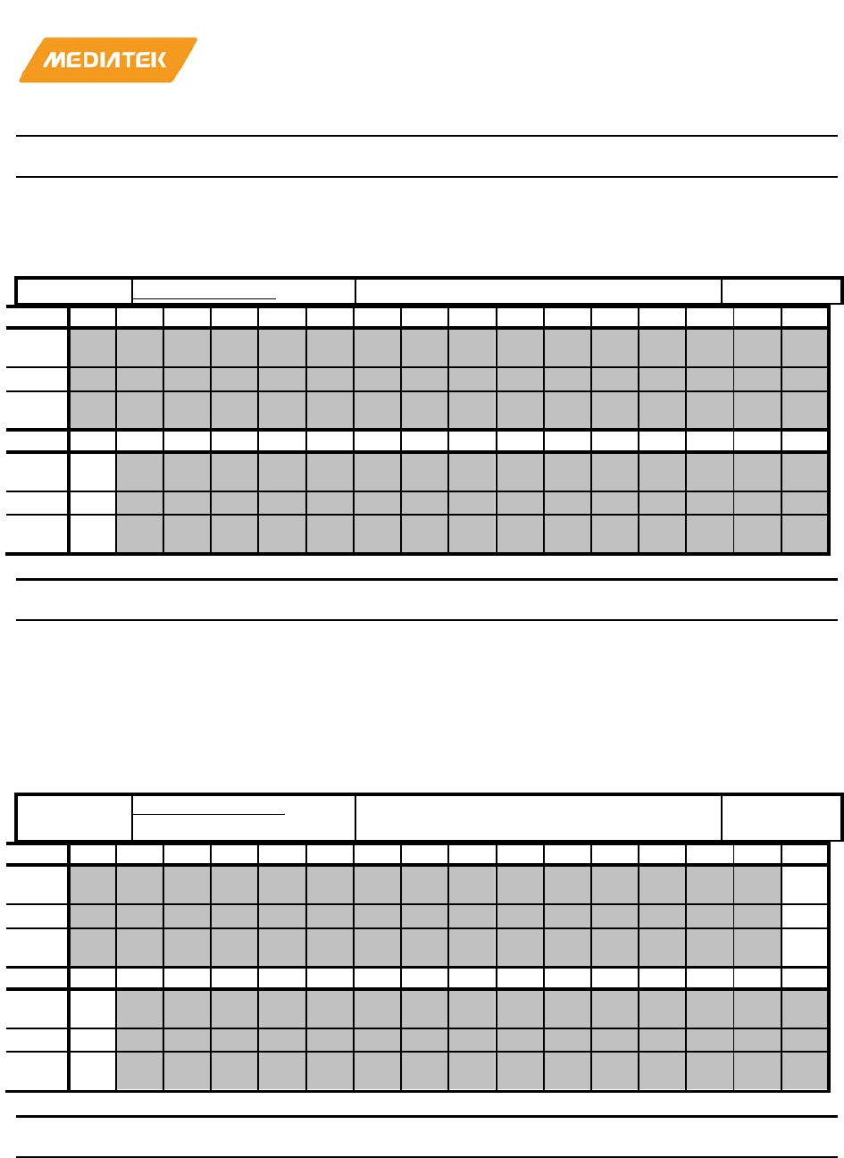
MT76x7
Internet-of-Things Wireless Connectivity
Reference Manual
© 2015 - 2017 MediaTek Inc
Page 216 of 798
This document contains information that is proprietary to MediaTek Inc. (“MediaTek”) and/or its licensor(s).
Any unauthorized use, reproduction or disclosure of this document in whole or in part is strictly prohibited
Bit(s)
Name
Description
VFIFO25 ADC(VFF) RX 4Byte
83010D18
DMA13_START
DMA CR4 Channel 13 Start Register
00000000
Bit
31
30
29
28
27
26
25
24
23
22
21
20
19
18
17
16
Nam
e
Type
Rese
t
Bit
15
14
13
12
11
10
9
8
7
6
5
4
3
2
1
0
Nam
e
ST
R
Type
RW
Rese
t
0
Bit(s)
Name
Description
15
STR
Start control for a DMA channel.
0 The DMA channel is stopped.
1 The DMA channel is started and running.
83010D1C
DMA13_INTSTA
DMA CR4 Channel 13 Interrupt Status
Register
00000000
Bit
31
30
29
28
27
26
25
24
23
22
21
20
19
18
17
16
Nam
e
TOI
NT
Type
RO
Rese
t
0
Bit
15
14
13
12
11
10
9
8
7
6
5
4
3
2
1
0
Nam
e
INT
Type
RO
Rese
t
0
Bit(s)
Name
Description
16
TOINT
Timeout Interrupt Status for DMA Channel
0 No interrupt request is generated.
1 One interrupt request is pending and waiting for service.
No effect on channel 1~11 (Full and Half
-size).
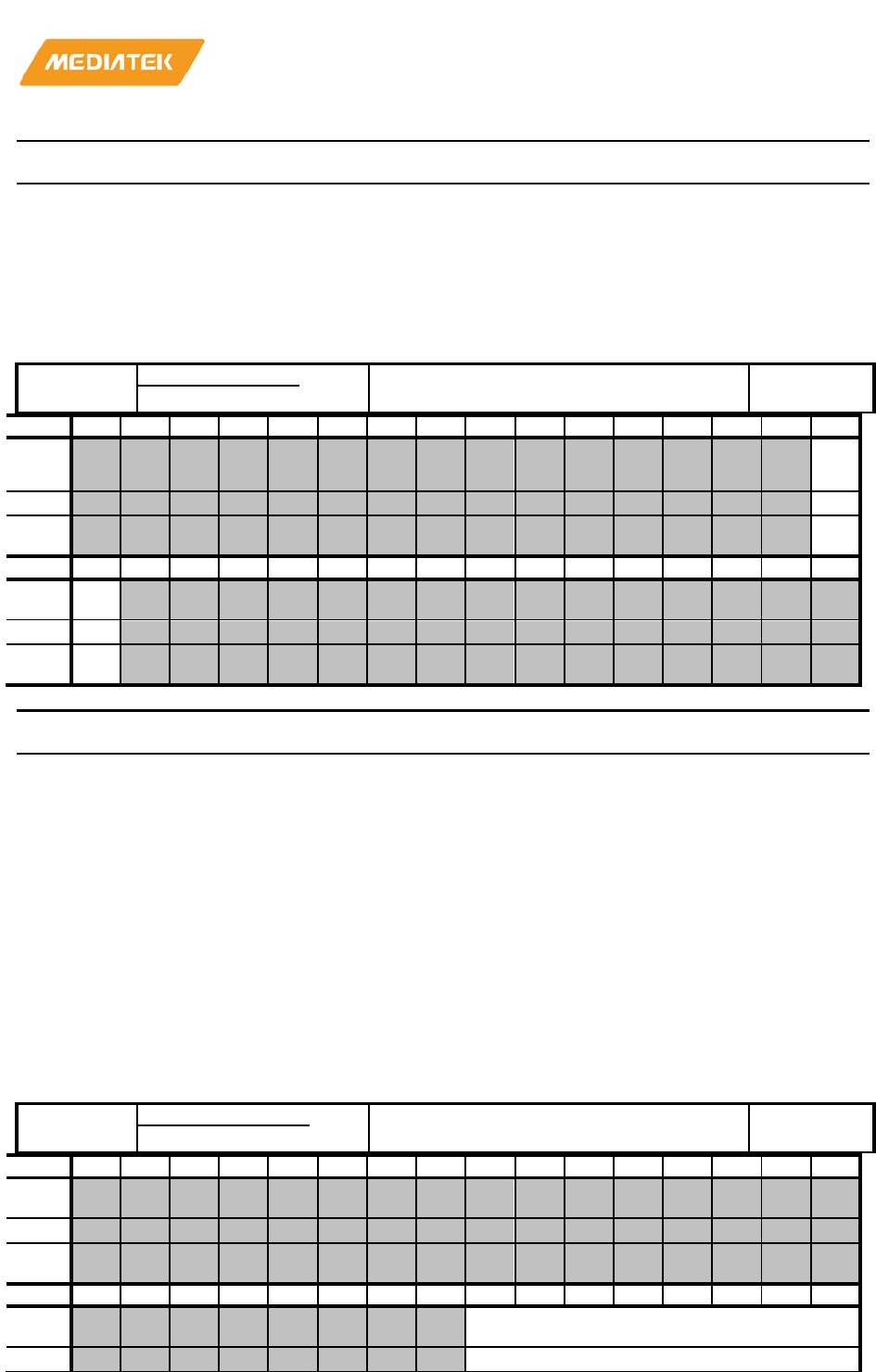
MT76x7
Internet-of-Things Wireless Connectivity
Reference Manual
© 2015 - 2017 MediaTek Inc
Page 217 of 798
This document contains information that is proprietary to MediaTek Inc. (“MediaTek”) and/or its licensor(s).
Any unauthorized use, reproduction or disclosure of this document in whole or in part is strictly prohibited
Bit(s)
Name
Description
15
INT
Interrupt Status for DMA Channel
0 No interrupt request is generated.
1 One interrupt request is pending and waiting for service.
83010D20
DMA13_ACKINT
DMA CR4 Channel 13 Interrupt
Acknowledge Register
00000000
Bit
31
30
29
28
27
26
25
24
23
22
21
20
19
18
17
16
Nam
e
TO
AC
K
Type
WO
Rese
t
0
Bit
15
14
13
12
11
10
9
8
7
6
5
4
3
2
1
0
Nam
e
AC
K
Type
WO
Rese
t
0
Bit(s)
Name
Description
16
TOACK
TOACK Timeout Interrupt acknowledge for the DMA
channel
0 No effect
1 Interrupt request is acknowledged and should be relinquished.
No effect on channel 1~11 (Full and Half
-size).
15
ACK
ACK Interrupt acknowledge for the DMA channel
0 No effect
1
Interrupt request is acknowledged and should be relinquished.
83010D28
DMA13_LIMITER
DMA CR4 Channel 13 Bandwidth
Limiter Register
00000000
Bit
31
30
29
28
27
26
25
24
23
22
21
20
19
18
17
16
Nam
e
Type
Rese
t
Bit
15
14
13
12
11
10
9
8
7
6
5
4
3
2
1
0
Nam
e
LIMITER
Type
RW
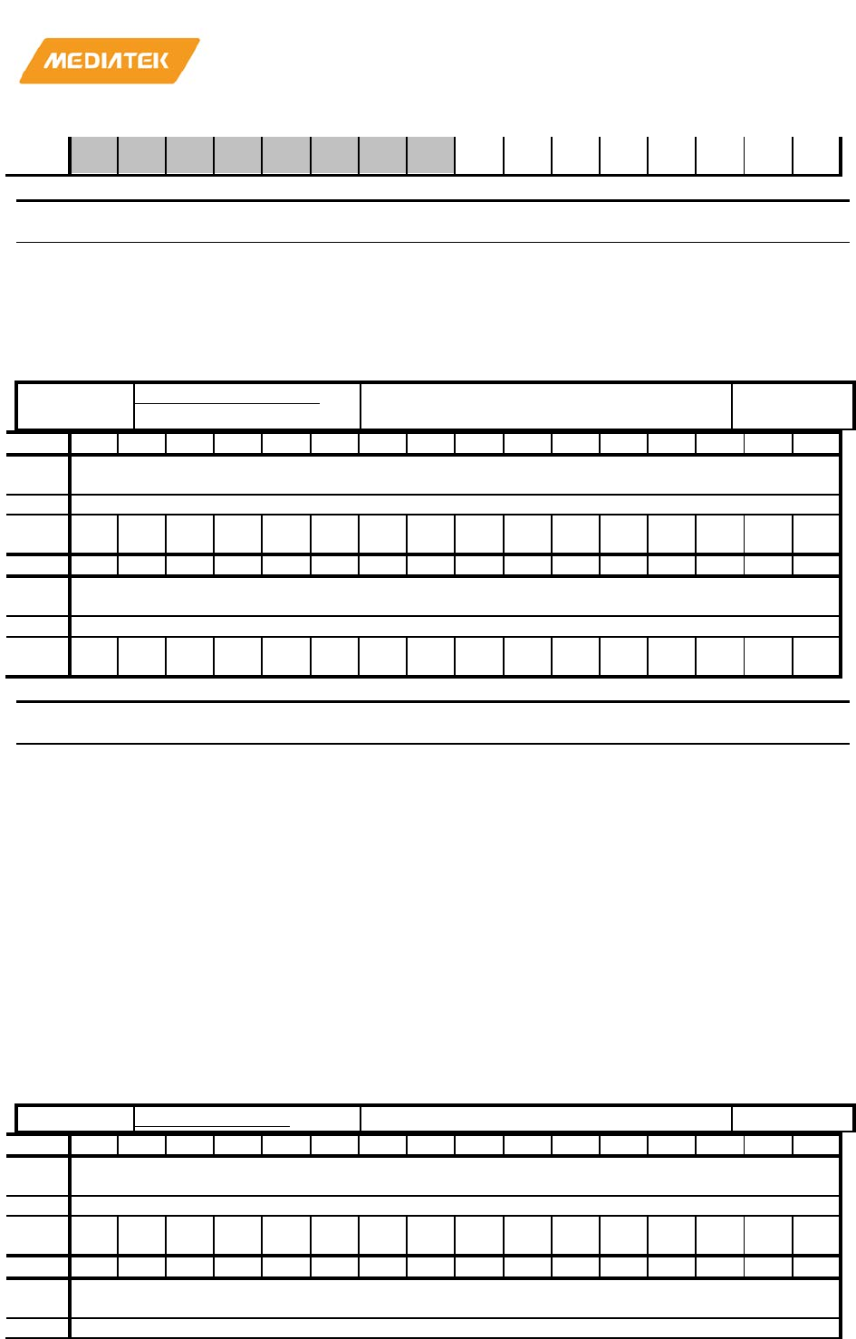
MT76x7
Internet-of-Things Wireless Connectivity
Reference Manual
© 2015 - 2017 MediaTek Inc
Page 218 of 798
This document contains information that is proprietary to MediaTek Inc. (“MediaTek”) and/or its licensor(s).
Any unauthorized use, reproduction or disclosure of this document in whole or in part is strictly prohibited
Rese
t
0 0 0 0 0 0 0 0
Bit(s)
Name
Description
7:0
LIMITER
from 0 to 255. 0 means no limitation, 255 means totally
banned, and
others mean Bus access permission every (4
X n) AHB clock
83010D2C
DMA13_PGMADDR
DMA CR4 Channel 13 Programmable
Address Register
00000000
Bit
31
30
29
28
27
26
25
24
23
22
21
20
19
18
17
16
Nam
e
PGMADDR
Type
RW
Rese
t
0 0 0 0 0 0 0 0 0 0 0 0 0 0 0 0
Bit
15
14
13
12
11
10
9
8
7
6
5
4
3
2
1
0
Nam
e
PGMADDR
Type
RW
Rese
t
0 0 0 0 0 0 0 0 0 0 0 0 0 0 0 0
Bit(s)
Name
Description
31:0
PGMADDR
PGMADDR[31:0]specifies the addresses for a half-size
DMA channel or
virtual
FIFO
WRITE : address of the source/destination.
READ : current address of the transfer.
This address represents a source address if DIR in DMA_CON is set
to 0, and represents a destination address if DIR in DMA_CON is
set to 1. Before being able to pro
gram these register, the software
should make sure that STR in DMAn_START is set to '0', that is the
DMA channel is stopped and disabled completely. Otherwise, the
DMA channel may run out of order.
83010D30
DMA13_WRPTR
DMA CR4 Channel 13 Write Pointer
00000000
Bit
31
30
29
28
27
26
25
24
23
22
21
20
19
18
17
16
Nam
e
WRPTR
Type
RO
Rese
t
0 0 0 0 0 0 0 0 0 0 0 0 0 0 0 0
Bit
15
14
13
12
11
10
9
8
7
6
5
4
3
2
1
0
Nam
e
WRPTR
Type
RO
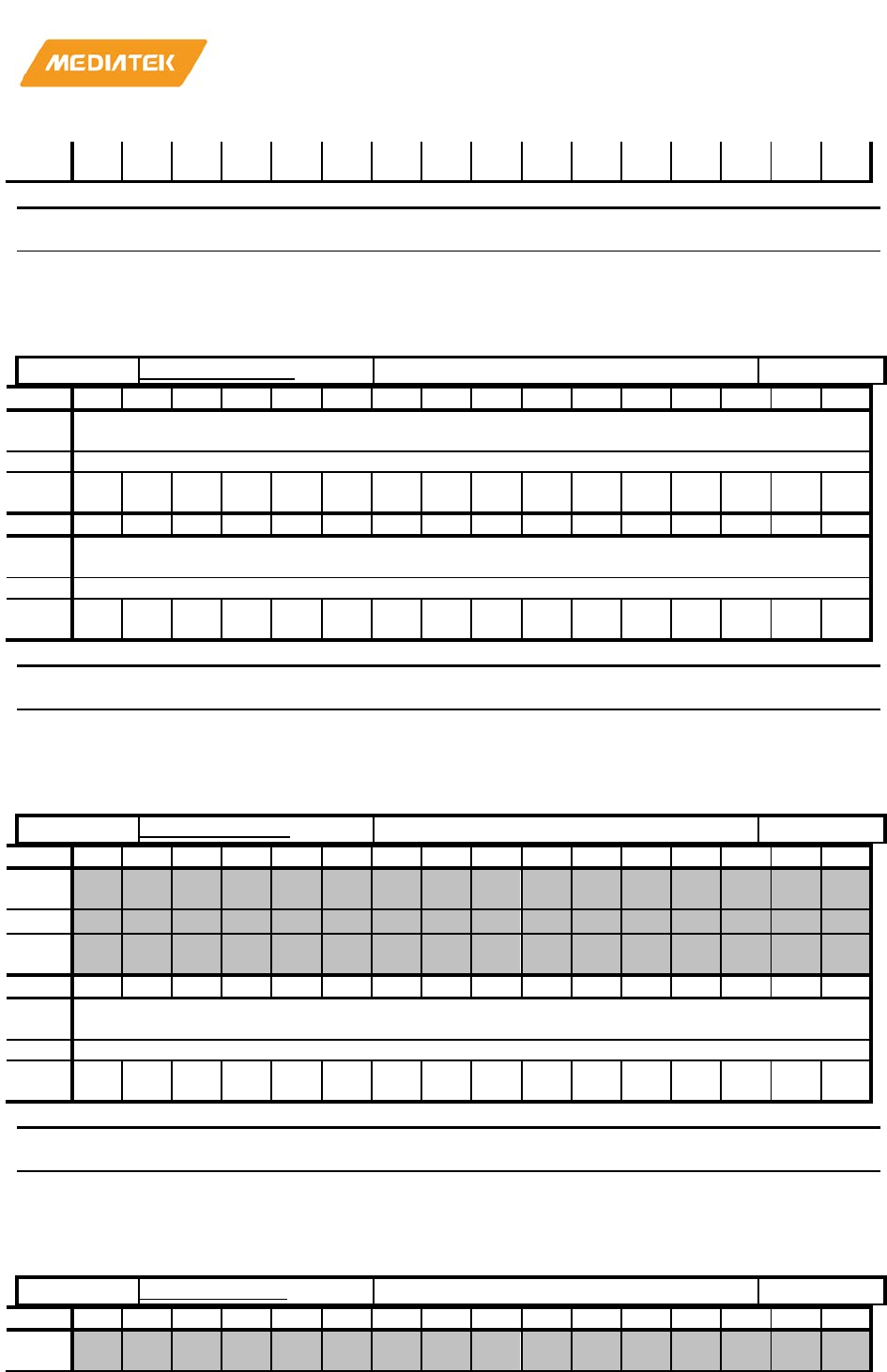
MT76x7
Internet-of-Things Wireless Connectivity
Reference Manual
© 2015 - 2017 MediaTek Inc
Page 219 of 798
This document contains information that is proprietary to MediaTek Inc. (“MediaTek”) and/or its licensor(s).
Any unauthorized use, reproduction or disclosure of this document in whole or in part is strictly prohibited
Rese
t
0 0 0 0 0 0 0 0 0 0 0 0 0 0 0 0
Bit(s)
Name
Description
31:0
WRPTR
Virtual FIFO Write Pointer
83010D34
DMA13_RDPTR
DMA CR4 Channel 13 Read Pointer
00000000
Bit
31
30
29
28
27
26
25
24
23
22
21
20
19
18
17
16
Nam
e
RDPTR
Type
RO
Rese
t
0 0 0 0 0 0 0 0 0 0 0 0 0 0 0 0
Bit
15
14
13
12
11
10
9
8
7
6
5
4
3
2
1
0
Nam
e
RDPTR
Type
RO
Rese
t
0 0 0 0 0 0 0 0 0 0 0 0 0 0 0 0
Bit(s)
Name
Description
31:0
RDPTR
Virtual FIFO Read Pointer
83010D38
DMA13_FFCNT
DMA CR4 Channel 13 FIFO Count
00000000
Bit
31
30
29
28
27
26
25
24
23
22
21
20
19
18
17
16
Nam
e
Type
Rese
t
Bit
15
14
13
12
11
10
9
8
7
6
5
4
3
2
1
0
Nam
e
FFCNT
Type
RW
Rese
t
0 0 0 0 0 0 0 0 0 0 0 0 0 0 0 0
Bit(s)
Name
Description
15:0
FFCNT
To display the number of data stored in Virtual FIFO
83010D3C
DMA13_FFSTA
DMA CR4 Channel 13 FIFO Status
00000000
Bit
31
30
29
28
27
26
25
24
23
22
21
20
19
18
17
16
Nam
e
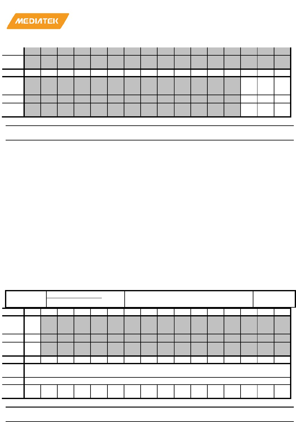
MT76x7
Internet-of-Things Wireless Connectivity
Reference Manual
© 2015 - 2017 MediaTek Inc
Page 220 of 798
This document contains information that is proprietary to MediaTek Inc. (“MediaTek”) and/or its licensor(s).
Any unauthorized use, reproduction or disclosure of this document in whole or in part is strictly prohibited
Type
Rese
t
Bit
15
14
13
12
11
10
9
8
7
6
5
4
3
2
1
0
Nam
e AL
T
EM
PT
Y
FU
LL
Type
RO
RO
RO
Rese
t
0 0 0
Bit(s)
Name
Description
2
ALT
To indicate FIFO Count is larger than ALTLEN.
DMA issues
an alert signal to UART to enable UART flow control.
0 Not reach alert region.
1 Reach alert region.
1
EMPTY
To indicate FIFO is empty.
0 Not Empty
1 Empty
0
FULL
To indicate FIFO is full.
0 Not Full
1 Full
83010D40
DMA13_ALTLEN
DMA CR4 Channel 13 Alert Length
Register
00000000
Bit
31
30
29
28
27
26
25
24
23
22
21
20
19
18
17
16
Nam
e
AL
TS
CM
Type
RW
Rese
t
0
Bit
15
14
13
12
11
10
9
8
7
6
5
4
3
2
1
0
Nam
e
ALTLEN
Type
RW
Rese
t
0 0 0 0 0 0 0 0 0 0 0 0 0 0 0 0
Bit(s)
Name
Description
31
ALTSCM
Specifies the compare equation between ALTLEN and
FIFO_SIZE
-FIFO_CNT.
1'b0: if ALTLEN > FIFO_SIZE
-
FIFO_CNT, trigger fifo_alt signal to
device for warning device that VFIFO will be
full soon.
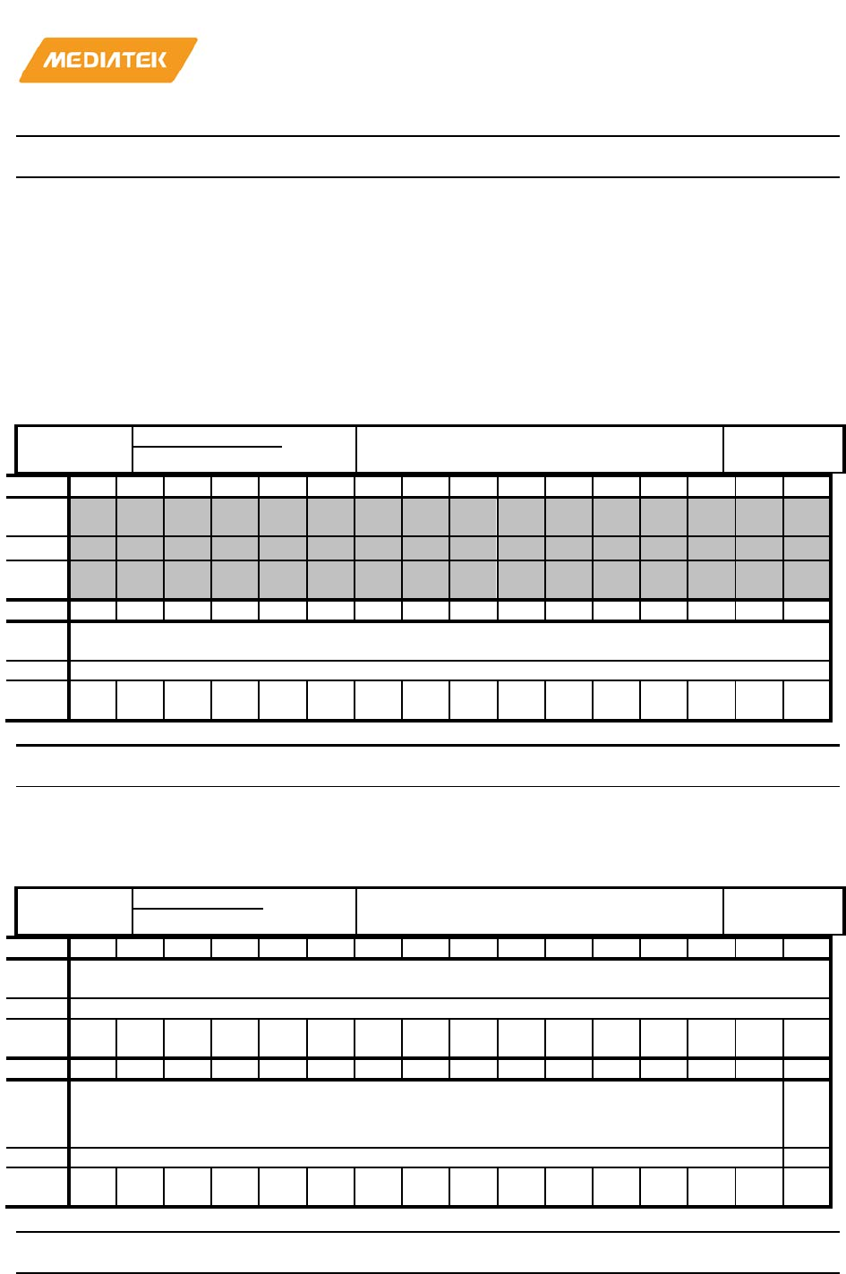
MT76x7
Internet-of-Things Wireless Connectivity
Reference Manual
© 2015 - 2017 MediaTek Inc
Page 221 of 798
This document contains information that is proprietary to MediaTek Inc. (“MediaTek”) and/or its licensor(s).
Any unauthorized use, reproduction or disclosure of this document in whole or in part is strictly prohibited
Bit(s)
Name
Description
1'b1: if ALTLEN >= FIFO_SIZE-FIFO_CNT, trigger fifo_alt signal
to device for warning device that VFIFO will be full soon.
15:0
ALTLEN
Specifies the Alert Length of Virtual FIFO DMA. Once the
remaining FIFO space is less than ALTLEN, an alert signal
is issued to UART to enable flow control. If ALTSCM is set
to 1, remaining FIFO space == ALTLEN also trigger the
alert signal. Normally, ALTLEN shall be larger than 16 for
UART application.
83010D44
DMA13_FFSIZE
DMA CR4 Channel 13 Virtual FIFO Size
Register
00000000
Bit
31
30
29
28
27
26
25
24
23
22
21
20
19
18
17
16
Nam
e
Type
Rese
t
Bit
15
14
13
12
11
10
9
8
7
6
5
4
3
2
1
0
Nam
e
FFSIZE
Type
RW
Rese
t
0 0 0 0 0 0 0 0 0 0 0 0 0 0 0 0
Bit(s)
Name
Description
15:0
FFSIZE
Specifies the FIFO Size of Virtual FIFO DMA
83010D48
DMA13_CVFF
DMA CR4 Channel 13 Cascade Virtual
FIFO Control Register
00000000
Bit
31
30
29
28
27
26
25
24
23
22
21
20
19
18
17
16
Nam
e
CASCADED_PORT_ADDR
Type
RW
Rese
t
0 0 0 0 0 0 0 0 0 0 0 0 0 0 0 0
Bit
15
14
13
12
11
10
9
8
7
6
5
4
3
2
1
0
Nam
e CASCADED_PORT_ADDR
CV
FF
_E
B
Type
RW
RW
Rese
t
0 0 0 0 0 0 0 0 0 0 0 0 0 0 0 0
Bit(s)
Name
Description
31:1
CASCADED_PORT_ADDR
Please fill in the other peripheral's virtual port address.
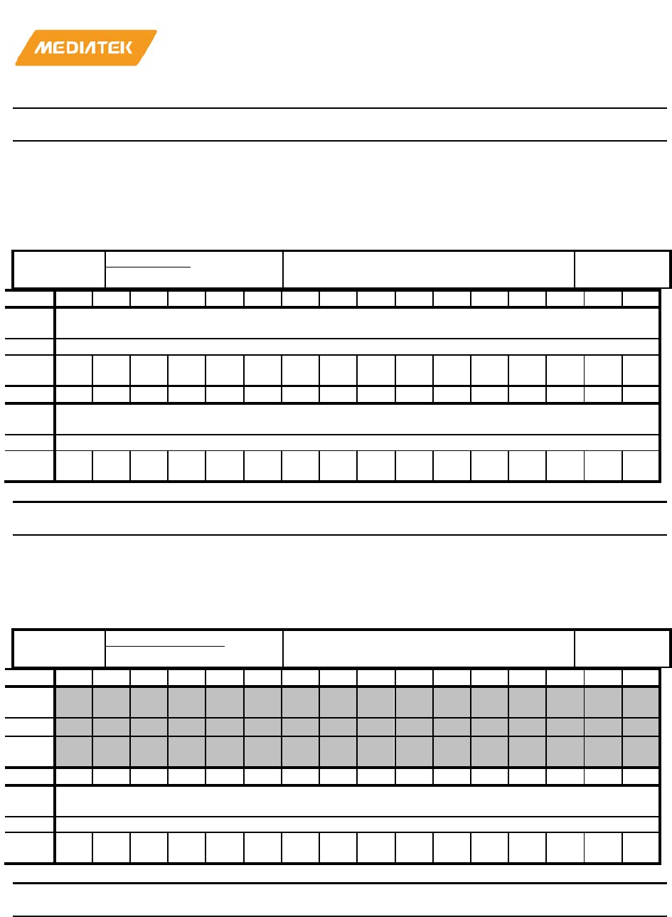
MT76x7
Internet-of-Things Wireless Connectivity
Reference Manual
© 2015 - 2017 MediaTek Inc
Page 222 of 798
This document contains information that is proprietary to MediaTek Inc. (“MediaTek”) and/or its licensor(s).
Any unauthorized use, reproduction or disclosure of this document in whole or in part is strictly prohibited
Bit(s)
Name
Description
0
CVFF_EB
When CVFF_EN is set to 1 , DMA will change the
source/destination from sysram to the other fixed
address.
83010D50
DMA13_TO
DMA CR4 Channel 13 Timeout Value
Register
00000000
Bit
31
30
29
28
27
26
25
24
23
22
21
20
19
18
17
16
Nam
e
TIMEOUT_COUNTER
Type
RW
Rese
t
0 0 0 0 0 0 0 0 0 0 0 0 0 0 0 0
Bit
15
14
13
12
11
10
9
8
7
6
5
4
3
2
1
0
Nam
e
TIMEOUT_COUNTER
Type
RW
Rese
t
0 0 0 0 0 0 0 0 0 0 0 0 0 0 0 0
Bit(s)
Name
Description
31:0
TIMEOUT_COUNTER
Interrupt will assert if there is no new data into fifo more
than n T(bus clock).
83010E10
DMA14_COUNT
DMA CR4 Channel 14 Transfer Count
Register
00000000
Bit
31
30
29
28
27
26
25
24
23
22
21
20
19
18
17
16
Nam
e
Type
Rese
t
Bit
15
14
13
12
11
10
9
8
7
6
5
4
3
2
1
0
Nam
e
LEN
Type
RW
Rese
t
0 0 0 0 0 0 0 0 0 0 0 0 0 0 0 0
Bit(s)
Name
Description
15:0
LEN
The amount of total transfer count
This register specifies the amount of total transfer count that the
DMA channel is required to perform. Upon completion, the DMA
channel generates an interrupt request to the processor while ITEN
in DMAn_CON is
set as '1'. Note that the total size of data being
transferred by a DMA channel is determined by LEN together with
the SIZE in DMAn_CON, i.e. LEN x SIZE.
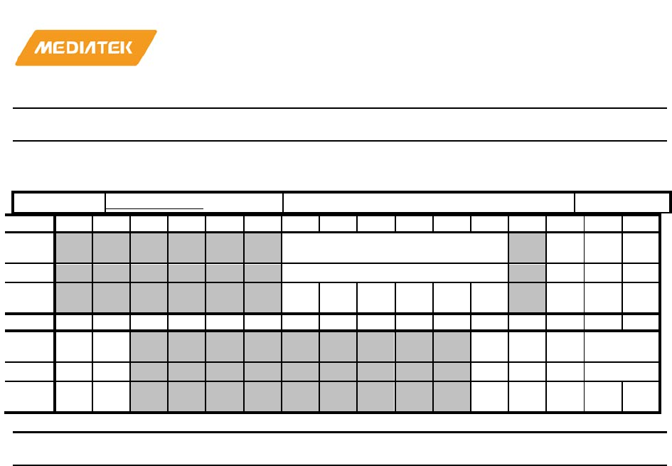
MT76x7
Internet-of-Things Wireless Connectivity
Reference Manual
© 2015 - 2017 MediaTek Inc
Page 223 of 798
This document contains information that is proprietary to MediaTek Inc. (“MediaTek”) and/or its licensor(s).
Any unauthorized use, reproduction or disclosure of this document in whole or in part is strictly prohibited
Bit(s)
Name
Description
83010E14
DMA14_CON
DMA CR4 Channel 14 Control Register
03F00000
Bit
31
30
29
28
27
26
25
24
23
22
21
20
19
18
17
16
Nam
e
MAS DI
R
WP
EN
WP
SD
Type
RW
RW
RW
RW
Rese
t
1 1 1 1 1 1 0 0 0
Bit
15
14
13
12
11
10
9
8
7
6
5
4
3
2
1
0
Nam
e
ITE
N
TO
EN
DR
EQ
DI
NC
SIN
C
SIZE
Type
RW
RW
RW
RW
RW
RW
Rese
t
0 0 0 0 0 0 0
Bit(s)
Name
Description
25:20
MAS
Master selection.
Specifies which master occupies this DMA channel.
Once assigned to certain master, the corresponding DREQ and
DACK are connected. For half
-size and Virtual FIFO DMA
channels, i.e. channels 3 ~ 25, a predefined address is assigned as
well.
Value Selected Master SADDR
6'd0 : Don't Use
6'd1 : Don't Use
6'd2 : I2C
-0 (HALF) TX 0x83090000
6'd3 : I2C
-0 (HALF) RX 0x83090000
6'd4 : I2C
-1 (HALF) TX 0x830A0000
6'd5 : I2C
-1 (HALF) RX 0x830A0000
6'd6 : I2S/Audio (VFF) TX 0x22000000
6'd7 : I2S/Audio (VFF) RX 0x22000000
6'd8 : UART0(VFF) TX 0x83030000
6'd9 : UART0(VFF) RX 0x83030000
6'd10 : UART1(VFF) TX 0x83040000
6'd11 : UART1(VFF) RX 0x83040000
6'd12 : BTIF(VFF) TX 0x83
0E0000
6'd13 : BTIF(VFF) RX 0x830E0000

MT76x7
Internet-of-Things Wireless Connectivity
Reference Manual
© 2015 - 2017 MediaTek Inc
Page 224 of 798
This document contains information that is proprietary to MediaTek Inc. (“MediaTek”) and/or its licensor(s).
Any unauthorized use, reproduction or disclosure of this document in whole or in part is strictly prohibited
Bit(s)
Name
Description
6'd14 : not used 0x50310000
6'd15 : not used
0x50310004
6'd16 : not used
0x50310008
6'd17 : not used
0x5031000C
6'd18 : not used
0x50310010
6'd19 : not used
0x50310014
6'd20 : ADC(VFF) RX 0x830D0000
6'd21 : W
IFI HIF(HALF) TRX 0x50201000
6'd22 : not used 0x830B0000
6'd23 : not used 0x830B0000
6'd24~37 : VFF Data Port 0x79000m00
*m is N
-12
other: reserved
default :6'h3f
If yo
u use dma moving data from memory to memory ( ex :full-
size
dma) , please select default value asyour master setting
18
DIR
Directions of DMA transfer for half-size and Virtual FIFO
DMA channels, i.e. channels 3~25. The direction is from
the perspective of the DMA masters. WRITE means read
from master device and then write to the address
specified in DMA_PGMADDR, and vice ver
sa.
0 Read (read from system RAM and write to device)
1 Write (read from device and write to system RAM)
17
WPEN
Address-wrapping for ring buffer. The next address of
DMA jumps to
WRAP TO address when the current address matches WRAP
POINT
count.
0 D
isable
1 Enable
No effect on channel 12~25 (Virtual FIFO).
16
WPSD
The side using address-wrapping function. Only one side
of a DMA
channel can activate address-wrapping function at a time.
0 Address
-wrapping on source .

MT76x7
Internet-of-Things Wireless Connectivity
Reference Manual
© 2015 - 2017 MediaTek Inc
Page 225 of 798
This document contains information that is proprietary to MediaTek Inc. (“MediaTek”) and/or its licensor(s).
Any unauthorized use, reproduction or disclosure of this document in whole or in part is strictly prohibited
Bit(s)
Name
Description
1 Address-wrapping on destination.
No effect on channel 12~25 (Virtual FIFO).
15
ITEN
DMA transfer completion interrupt enable.
0 Disable
1 Enable
14
TOEN
DMA transfer timeout interrupt enable.
0 Disable
1 Enable
No effect on channel 1~11 (Full and Half
-size).
4
DREQ
Throttle and handshake control for DMA transfer
0 No throttle control during DMA transfer or transfers occurred
only between memories
1 Hardware handshake management
The DMA master is able to throttle down the transfer rate by
way of request
-grant handshake.
MAS Selected Master suggest DREQ setting
6'd6 : I2S/Audio (VFF) TX 1
6'd7 : I2S/Audio (VFF) RX 1
6'd8 : UART0(VFF) TX 1
6'd9 : UART0(VFF) RX 1
6'd10 : UART1(VFF)
TX 1
6'd11 : UART1(VFF) RX 1
6'd12 : BTIF(VFF) TX 1
6'd13 : BTIF(VFF) RX 1
6'd20 : ADC(VFF) RX 1
3
DINC
Incremental destination address. Destination addresses
increase every transfer. If the setting of SIZE is Byte,
Destination addresses increase by 1 every single transfer.
If Half
-Word, increase by 2; and if Word, increase by 4.
0 Disable
1 Enable
No effect on channel 12~25 (Virtual FIFO
). Destination address is
the master fixed address for read(TX) or the Virtual FIFO write
pointer for write(RX)

MT76x7
Internet-of-Things Wireless Connectivity
Reference Manual
© 2015 - 2017 MediaTek Inc
Page 226 of 798
This document contains information that is proprietary to MediaTek Inc. (“MediaTek”) and/or its licensor(s).
Any unauthorized use, reproduction or disclosure of this document in whole or in part is strictly prohibited
Bit(s)
Name
Description
2
SINC
Incremental source address. Source addresses increase
every transfer. If the setting of SIZE is Byte, Source
addresses increase by 1 e
very single transfer. If Half-
Word, increase by 2; and if Word, increase by 4.
0 Disable
1 Enable
No effect on channel 12~25 (Virtual FIFO). Source address is the
Virtual FIFO read pointer for read(TX) or the master fixed address
for write(RX).
1:0
SIZE
Data size within the confine of a bus cycle per
transfer.These bits confines the data transfer size between
source and destination to the
specified value for individual bus cycle. The size is in terms of byte
and has maximum value of 4 bytes. It is mainly decided by the data
width of
a DMA master.
00 Byte transfer/1 byte
01 Half
-word transfer/2 bytes
10 Word transfer/4 bytes
11 Reserved
T
he SIZE register setting depends on devices. The following table
lists all VFIFO channels, associated devices, and data width per
beat.
channel Module Support DMA beat size
VFIFO12 I2S TX
4Byte
VFIFO13 I2S RX 4Byte
VFIFO14 UART0 TX 1Byte
VFIFO15 UART0 RX 1Byte
VFIFO16 UART1 TX 1Byte
VFIFO17 UART1
RX 1Byte
VFIFO18 BTIF TX 1Byte
VFIFO19 BTIF RX 1Byte
VFIFO25 ADC(VFF) RX 4Byte
83010E18
DMA14_START
DMA CR4 Channel 14 Start Register
00000000
Bit
31
30
29
28
27
26
25
24
23
22
21
20
19
18
17
16
Nam
MT76x7
Internet-of-Things Wireless Connectivity
Reference Manual
© 2015 - 2017 MediaTek Inc
Page 227 of 798
This document contains information that is proprietary to MediaTek Inc. (“MediaTek”) and/or its licensor(s).
Any unauthorized use, reproduction or disclosure of this document in whole or in part is strictly prohibited
e
Type
Rese
t
Bit
15
14
13
12
11
10
9
8
7
6
5
4
3
2
1
0
Nam
e
ST
R
Type
RW
Rese
t
0
Bit(s)
Name
Description
15
STR
Start control for a DMA channel.
0 The DMA channel is stopped.
1 The DMA channel is started and running.
83010E1C
DMA14_INTSTA
DMA CR4 Channel 14 Interrupt Status
Register
00000000
Bit
31
30
29
28
27
26
25
24
23
22
21
20
19
18
17
16
Nam
e
TOI
NT
Type
RO
Rese
t
0
Bit
15
14
13
12
11
10
9
8
7
6
5
4
3
2
1
0
Nam
e
INT
Type
RO
Rese
t
0
Bit(s)
Name
Description
16
TOINT
Timeout Interrupt Status for DMA Channel
0 No interrupt request is generated.
1 One interrupt request is pending and waiting for service.
No effect on channel 1~11 (Full and Half
-size).
15
INT
Interrupt Status for DMA Channel
0 No interrupt request is generated.
1 One interrupt request is pending and waiting for service.
83010E20
DMA14_ACKINT
DMA CR4 Channel 14 Interrupt
Acknowledge Register
00000000
MT76x7
Internet-of-Things Wireless Connectivity
Reference Manual
© 2015 - 2017 MediaTek Inc
Page 228 of 798
This document contains information that is proprietary to MediaTek Inc. (“MediaTek”) and/or its licensor(s).
Any unauthorized use, reproduction or disclosure of this document in whole or in part is strictly prohibited
Bit
31
30
29
28
27
26
25
24
23
22
21
20
19
18
17
16
Nam
e
TO
AC
K
Type
WO
Rese
t
0
Bit
15
14
13
12
11
10
9
8
7
6
5
4
3
2
1
0
Nam
e
AC
K
Type
WO
Rese
t
0
Bit(s)
Name
Description
16
TOACK
TOACK Timeout Interrupt acknowledge for the DMA
channel
0 No effect
1 Interrupt request is acknowledged and should be relinquished.
No effect on channel 1~11 (Full and Half
-size).
15
ACK
ACK Interrupt acknowledge for the DMA channel
0 No effect
1
Interrupt request is acknowledged and should be relinquished.
83010E28
DMA14_LIMITER
DMA CR4 Channel 14 Bandwidth
Limiter Register
00000000
Bit
31
30
29
28
27
26
25
24
23
22
21
20
19
18
17
16
Nam
e
Type
Rese
t
Bit
15
14
13
12
11
10
9
8
7
6
5
4
3
2
1
0
Nam
e
LIMITER
Type
RW
Rese
t
0 0 0 0 0 0 0 0
Bit(s)
Name
Description
7:0
LIMITER
from 0 to 255. 0 means no limitation, 255 means totally
banned, and
others mean Bus access permission every (4
X n) AHB clock
MT76x7
Internet-of-Things Wireless Connectivity
Reference Manual
© 2015 - 2017 MediaTek Inc
Page 229 of 798
This document contains information that is proprietary to MediaTek Inc. (“MediaTek”) and/or its licensor(s).
Any unauthorized use, reproduction or disclosure of this document in whole or in part is strictly prohibited
83010E2C
DMA14_PGMADDR
DMA CR4 Channel 14 Programmable
Address Register
00000000
Bit
31
30
29
28
27
26
25
24
23
22
21
20
19
18
17
16
Nam
e
PGMADDR
Type
RW
Rese
t
0 0 0 0 0 0 0 0 0 0 0 0 0 0 0 0
Bit
15
14
13
12
11
10
9
8
7
6
5
4
3
2
1
0
Nam
e
PGMADDR
Type
RW
Rese
t
0 0 0 0 0 0 0 0 0 0 0 0 0 0 0 0
Bit(s)
Name
Description
31:0
PGMADDR
PGMADDR[31:0]specifies the addresses for a half-size
DMA channel or
virtual
FIFO
WRITE : address of the source/destination.
READ : current address of the transfer.
This address represents a source address if DIR in DMA_CON is set
to 0, and represents a destination address if DIR in DMA_CON is
set to 1. Before being able to pro
gram these register, the software
should make sure that STR in DMAn_START is set to '0', that is the
DMA channel is stopped and disabled completely. Otherwise, the
DMA channel may run out of order.
83010E30
DMA14_WRPTR
DMA CR4 Channel 14 Write Pointer
00000000
Bit
31
30
29
28
27
26
25
24
23
22
21
20
19
18
17
16
Nam
e
WRPTR
Type
RO
Rese
t
0 0 0 0 0 0 0 0 0 0 0 0 0 0 0 0
Bit
15
14
13
12
11
10
9
8
7
6
5
4
3
2
1
0
Nam
e
WRPTR
Type
RO
Rese
t
0 0 0 0 0 0 0 0 0 0 0 0 0 0 0 0
Bit(s)
Name
Description
31:0
WRPTR
Virtual FIFO Write Pointer
83010E34
DMA14_RDPTR
DMA CR4 Channel 14 Read Pointer
00000000

MT76x7
Internet-of-Things Wireless Connectivity
Reference Manual
© 2015 - 2017 MediaTek Inc
Page 230 of 798
This document contains information that is proprietary to MediaTek Inc. (“MediaTek”) and/or its licensor(s).
Any unauthorized use, reproduction or disclosure of this document in whole or in part is strictly prohibited
Bit
31
30
29
28
27
26
25
24
23
22
21
20
19
18
17
16
Nam
e
RDPTR
Type
RO
Rese
t
0 0 0 0 0 0 0 0 0 0 0 0 0 0 0 0
Bit
15
14
13
12
11
10
9
8
7
6
5
4
3
2
1
0
Nam
e
RDPTR
Type
RO
Rese
t
0 0 0 0 0 0 0 0 0 0 0 0 0 0 0 0
Bit(s)
Name
Description
31:0
RDPTR
Virtual FIFO Read Pointer
83010E38
DMA14_FFCNT
DMA CR4 Channel 14 FIFO Count
00000000
Bit
31
30
29
28
27
26
25
24
23
22
21
20
19
18
17
16
Nam
e
Type
Rese
t
Bit
15
14
13
12
11
10
9
8
7
6
5
4
3
2
1
0
Nam
e
FFCNT
Type
RW
Rese
t
0 0 0 0 0 0 0 0 0 0 0 0 0 0 0 0
Bit(s)
Name
Description
15:0
FFCNT
To display the number of data stored in Virtual FIFO
83010E3C
DMA14_FFSTA
DMA CR4 Channel 14 FIFO Status
00000000
Bit
31
30
29
28
27
26
25
24
23
22
21
20
19
18
17
16
Nam
e
Type
Rese
t
Bit
15
14
13
12
11
10
9
8
7
6
5
4
3
2
1
0
Nam
e AL
T
EM
PT
Y
FU
LL
Type
RO
RO
RO
Rese
t
0 0 0

MT76x7
Internet-of-Things Wireless Connectivity
Reference Manual
© 2015 - 2017 MediaTek Inc
Page 231 of 798
This document contains information that is proprietary to MediaTek Inc. (“MediaTek”) and/or its licensor(s).
Any unauthorized use, reproduction or disclosure of this document in whole or in part is strictly prohibited
Bit(s)
Name
Description
2
ALT
To indicate FIFO Count is larger than ALTLEN.
DMA issues
an alert signal to UART to enable UART flow control.
0 Not reach alert region.
1 Reach alert region.
1
EMPTY
To indicate FIFO is empty.
0 Not Empty
1 Empty
0
FULL
To indicate FIFO is full.
0 Not Full
1 Full
83010E40
DMA14_ALTLEN
DMA CR4 Channel 14 Alert Length
Register
00000000
Bit
31
30
29
28
27
26
25
24
23
22
21
20
19
18
17
16
Nam
e
AL
TS
CM
Type
RW
Rese
t
0
Bit
15
14
13
12
11
10
9
8
7
6
5
4
3
2
1
0
Nam
e
ALTLEN
Type
RW
Rese
t
0 0 0 0 0 0 0 0 0 0 0 0 0 0 0 0
Bit(s)
Name
Description
31
ALTSCM
Specifies the compare equation between ALTLEN and
FIFO_SIZE
-FIFO_CNT.
1'b0: if ALTLEN > FIFO_SIZE
-
FIFO_CNT, trigger fifo_alt signal to
device for warning device that VFIFO will be
full soon.
1'b1: if ALTLEN >= FIFO_SIZE
-FIFO_CNT, trigger fifo_alt signal
to device for warning device that VFIFO will be full soon.
15:0
ALTLEN
Specifies the Alert Length of Virtual FIFO DMA. Once the
remaining FIFO space is less than ALTLEN, an alert signal
is issued to UART to enable flow control. If ALTSCM is set
to 1, remaining FIFO space == ALTLEN also trigger the
alert signal. Normally, ALTLEN shall be larger than 16 for
UART application.

MT76x7
Internet-of-Things Wireless Connectivity
Reference Manual
© 2015 - 2017 MediaTek Inc
Page 232 of 798
This document contains information that is proprietary to MediaTek Inc. (“MediaTek”) and/or its licensor(s).
Any unauthorized use, reproduction or disclosure of this document in whole or in part is strictly prohibited
83010E44
DMA14_FFSIZE
DMA CR4 Channel 14 Virtual FIFO Size
Register
00000000
Bit
31
30
29
28
27
26
25
24
23
22
21
20
19
18
17
16
Nam
e
Type
Rese
t
Bit
15
14
13
12
11
10
9
8
7
6
5
4
3
2
1
0
Nam
e
FFSIZE
Type
RW
Rese
t
0 0 0 0 0 0 0 0 0 0 0 0 0 0 0 0
Bit(s)
Name
Description
15:0
FFSIZE
Specifies the FIFO Size of Virtual FIFO DMA
83010E48
DMA14_CVFF
DMA CR4 Channel 14 Cascade Virtual
FIFO Control Register
00000000
Bit
31
30
29
28
27
26
25
24
23
22
21
20
19
18
17
16
Nam
e
CASCADED_PORT_ADDR
Type
RW
Rese
t
0 0 0 0 0 0 0 0 0 0 0 0 0 0 0 0
Bit
15
14
13
12
11
10
9
8
7
6
5
4
3
2
1
0
Nam
e CASCADED_PORT_ADDR
CV
FF
_E
B
Type
RW
RW
Rese
t
0 0 0 0 0 0 0 0 0 0 0 0 0 0 0 0
Bit(s)
Name
Description
31:1
CASCADED_PORT_ADDR
Please fill in the other peripheral's virtual port address.
0
CVFF_EB
When CVFF_EN is set to 1 , DMA will change the
source/destination from sysram to the other fixed
address.
83010E50
DMA14_TO
DMA CR4 Channel 14 Timeout Value
Register
00000000
Bit
31
30
29
28
27
26
25
24
23
22
21
20
19
18
17
16
Nam
e
TIMEOUT_COUNTER
Type
RW

MT76x7
Internet-of-Things Wireless Connectivity
Reference Manual
© 2015 - 2017 MediaTek Inc
Page 233 of 798
This document contains information that is proprietary to MediaTek Inc. (“MediaTek”) and/or its licensor(s).
Any unauthorized use, reproduction or disclosure of this document in whole or in part is strictly prohibited
Rese
t
0 0 0 0 0 0 0 0 0 0 0 0 0 0 0 0
Bit
15
14
13
12
11
10
9
8
7
6
5
4
3
2
1
0
Nam
e
TIMEOUT_COUNTER
Type
RW
Rese
t
0 0 0 0 0 0 0 0 0 0 0 0 0 0 0 0
Bit(s)
Name
Description
31:0
TIMEOUT_COUNTER
Interrupt will assert if there is no new data into fifo more
than n T(bus clock).
83010F10
DMA15_COUNT
DMA CR4 Channel 15 Transfer Count
Register
00000000
Bit
31
30
29
28
27
26
25
24
23
22
21
20
19
18
17
16
Nam
e
Type
Rese
t
Bit
15
14
13
12
11
10
9
8
7
6
5
4
3
2
1
0
Nam
e
LEN
Type
RW
Rese
t
0 0 0 0 0 0 0 0 0 0 0 0 0 0 0 0
Bit(s)
Name
Description
15:0
LEN
The amount of total transfer count
This register specifies the amount of total transfer count that the
DMA channel is required to perform. Upon completion, the DMA
channel generates an interrupt request to the processor while ITEN
in DMAn_CON is
set as '1'. Note that the total size of data being
transferred by a DMA channel is determined by LEN together with
the SIZE in DMAn_CON, i.e. LEN x SIZE.
83010F14
DMA15_CON
DMA CR4 Channel 15 Control Register
03F00000
Bit
31
30
29
28
27
26
25
24
23
22
21
20
19
18
17
16
Nam
e
MAS
DI
R
WP
EN
WP
SD
Type
RW
RW
RW
RW
Rese
t
1 1 1 1 1 1 0 0 0
Bit
15
14
13
12
11
10
9
8
7
6
5
4
3
2
1
0
Nam
e
ITE
N
TO
EN
DR
EQ
DI
NC
SIN
C
SIZE
Type
RW
RW
RW
RW
RW
RW

MT76x7
Internet-of-Things Wireless Connectivity
Reference Manual
© 2015 - 2017 MediaTek Inc
Page 234 of 798
This document contains information that is proprietary to MediaTek Inc. (“MediaTek”) and/or its licensor(s).
Any unauthorized use, reproduction or disclosure of this document in whole or in part is strictly prohibited
Rese
t
0 0 0 0 0 0 0
Bit(s)
Name
Description
25:20
MAS
Master selection.
Specifies which master occupies this DMA channel.
Once assigned to certain master, the corresponding DREQ and
DACK are connected. For half
-size and Virtual FIFO DMA
channels, i.e. channels 3 ~ 25, a predefined address is assigned as
well.
Value Selected Master SADDR
6'd0 : Don't Use
6'd1 : Don't Use
6'd2 : I2C
-0 (HALF) TX 0x83090000
6'd3 : I2C
-0 (HALF) RX 0x83090000
6'd4 : I2C
-1 (HALF) TX 0x830A0000
6'd5 : I2C
-1 (HALF) RX 0x830A0000
6'd6 : I2S/Audio (VFF) TX 0x22000000
6'd7 : I2S/Audio (VFF) RX 0x22000000
6'd8 : UART0(VFF) TX 0x83030000
6'd9 : UART0(VFF) RX 0x83030000
6'd10 : UART1(VFF) TX 0x83040000
6'd11 : UART1(VFF) RX 0x83040000
6'd12 : BTIF(VFF) TX 0x83
0E0000
6'd13 : BTIF(VFF) RX 0x830E0000
6'd14 : not used 0x50310000
6'd15 : not used
0x50310004
6'd16 : not used
0x50310008
6'd
17 : not used 0x5031000C
6'd18 : not used
0x50310010
6'd19 : not used
0x50310014
6'd20 : ADC(VFF) RX 0x830D0000
6'd21 : WIFI
HIF(HALF) TRX 0x50201000
6'd22 : not used 0x830B0000
6'd23 : not used 0x830B0000

MT76x7
Internet-of-Things Wireless Connectivity
Reference Manual
© 2015 - 2017 MediaTek Inc
Page 235 of 798
This document contains information that is proprietary to MediaTek Inc. (“MediaTek”) and/or its licensor(s).
Any unauthorized use, reproduction or disclosure of this document in whole or in part is strictly prohibited
Bit(s)
Name
Description
6'd24~37 : VFF Data Port 0x79000m00
*m is N
-12
other: reserved
default :6'h3f
If you u
se dma moving data from memory to memory ( ex :full-
size
dma) , please select default value asyour master setting
18
DIR
Directions of DMA transfer for half-size and Virtual FIFO
DMA channels, i.e. channels 3~25. The direction is from
the perspective of the DMA masters. WRITE means read
from master device and then write to the address
specified in DMA_PGMADDR, and vice ver
sa.
0 Read (read from system RAM and write to device)
1 Write (read from device and write to system RAM)
17
WPEN
Address-wrapping for ring buffer. The next address of
DMA jumps to
WRAP TO address when the current address matches WRAP
POINT
count.
0 D
isable
1 Enable
No effect on channel 12~25 (Virtual FIFO).
16
WPSD
The side using address-wrapping function. Only one side
of a DMA
channel can activate address-wrapping function at a time.
0 Address
-wrapping on source .
1 Address
-wrapping on destination.
No effect on channel 12~25 (Virtual FIFO).
15
ITEN
DMA transfer completion interrupt enable.
0 Disable
1 Enable
14
TOEN
DMA transfer timeout interrupt enable.
0 Disable
1 Enable
No effect on channel 1~11 (Full and Half
-size).
4
DREQ
Throttle and handshake control for DMA transfer

MT76x7
Internet-of-Things Wireless Connectivity
Reference Manual
© 2015 - 2017 MediaTek Inc
Page 236 of 798
This document contains information that is proprietary to MediaTek Inc. (“MediaTek”) and/or its licensor(s).
Any unauthorized use, reproduction or disclosure of this document in whole or in part is strictly prohibited
Bit(s)
Name
Description
0 No throttle control during DMA transfer or transfers occurred
only between memories
1 Hardware handshake management
The DMA master is able to throttle down the transfer rate by
way of request
-grant handshake.
MAS Selected Master suggest DREQ setting
6'd6 : I2S/Audio (VFF) TX 1
6'd7 : I2S/Audio (VFF) RX 1
6'd8 : UART0(VFF) TX 1
6'd9 : UART0(VFF) RX 1
6'd10 : UART1(VFF) TX 1
6'd11 : UART1(VFF) RX 1
6'd12 : BTIF(VFF) TX 1
6'd13 : BTIF(VFF) RX 1
6'd20 : ADC(VFF) RX 1
3
DINC
Incremental destination address. Destination addresses
increase every transfer. If the setting of SIZE is Byte,
Destination addresses increase by 1 every single transfer.
If Half
-Word, increase by 2; and if Word, increase by 4.
0 Disable
1 Enable
No effect on channel 12~25 (Vi
rtual FIFO). Destination address is
the master fixed address for read(TX) or the Virtual FIFO write
pointer for write(RX)
2
SINC
Incremental source address. Source addresses increase
every transfer. If the setting of SIZE is Byte, Source
addresses incre
ase by 1 every single transfer. If Half-
Word, increase by 2; and if Word, increase by 4.
0 Disable
1 Enable
No effect on channel 12~25 (Virtual FIFO). Source address is the
Virtual FIFO read pointer for read(TX) or the master fixed address
for write(
RX).
1:0
SIZE
Data size within the confine of a bus cycle per
transfer.These bits confines the data transfer size between
source and destination to the
specified value for individual bus cycle. The size is in terms of byte
and has maximum value of 4 bytes. It is mainly decided by the data

MT76x7
Internet-of-Things Wireless Connectivity
Reference Manual
© 2015 - 2017 MediaTek Inc
Page 237 of 798
This document contains information that is proprietary to MediaTek Inc. (“MediaTek”) and/or its licensor(s).
Any unauthorized use, reproduction or disclosure of this document in whole or in part is strictly prohibited
Bit(s)
Name
Description
width of
a DMA master.
00 Byte transfer/1 byte
01 Half
-word transfer/2 bytes
10 Word transfer/4 bytes
11 Reserved
T
he SIZE register setting depends on devices. The following table
lists all VFIFO channels, associated devices, and data width per
beat.
channel Module Support DMA beat size
VFIFO12 I2S TX
4Byte
VFIFO13 I2S RX 4Byte
VFIFO14 UART0 TX 1Byte
VFIFO15 UART0 RX 1Byte
VFIFO16 UART1 TX 1Byte
VFIFO17 UART1
RX 1Byte
VFIFO18 BTIF TX 1Byte
VFIFO19 BTIF RX 1Byte
VFIFO25 ADC(VFF) RX 4Byte
83010F18
DMA15_START
DMA CR4 Channel 15 Start Register
00000000
Bit
31
30
29
28
27
26
25
24
23
22
21
20
19
18
17
16
Nam
e
Type
Rese
t
Bit
15
14
13
12
11
10
9
8
7
6
5
4
3
2
1
0
Nam
e
ST
R
Type
RW
Rese
t
0
Bit(s)
Name
Description
15
STR
Start control for a DMA channel.
0 The DMA channel is stopped.

MT76x7
Internet-of-Things Wireless Connectivity
Reference Manual
© 2015 - 2017 MediaTek Inc
Page 238 of 798
This document contains information that is proprietary to MediaTek Inc. (“MediaTek”) and/or its licensor(s).
Any unauthorized use, reproduction or disclosure of this document in whole or in part is strictly prohibited
Bit(s)
Name
Description
1 The DMA channel is started and running.
83010F1C
DMA15_INTSTA
DMA CR4 Channel 15 Interrupt Status
Register
00000000
Bit
31
30
29
28
27
26
25
24
23
22
21
20
19
18
17
16
Nam
e
TOI
NT
Type
RO
Rese
t
0
Bit
15
14
13
12
11
10
9
8
7
6
5
4
3
2
1
0
Nam
e
INT
Type
RO
Rese
t
0
Bit(s)
Name
Description
16
TOINT
Timeout Interrupt Status for DMA Channel
0 No interrupt request is generated.
1 One interrupt request is pending and waiting for service.
No effect on channel 1~11 (Full and Half
-size).
15
INT
Interrupt Status for DMA Channel
0 No interrupt request is generated.
1 One interrupt request is pending and waiting for service.
83010F20
DMA15_ACKINT
DMA CR4 Channel 15 Interrupt
Acknowledge Register
00000000
Bit
31
30
29
28
27
26
25
24
23
22
21
20
19
18
17
16
Nam
e
TO
AC
K
Type
WO
Rese
t
0
Bit
15
14
13
12
11
10
9
8
7
6
5
4
3
2
1
0
Nam
e
AC
K
Type
WO
Rese
t
0

MT76x7
Internet-of-Things Wireless Connectivity
Reference Manual
© 2015 - 2017 MediaTek Inc
Page 239 of 798
This document contains information that is proprietary to MediaTek Inc. (“MediaTek”) and/or its licensor(s).
Any unauthorized use, reproduction or disclosure of this document in whole or in part is strictly prohibited
Bit(s)
Name
Description
16
TOACK
TOACK Timeout Interrupt acknowledge for the DMA
channel
0 No effect
1 Interrupt request is acknowledged and should be relinquished.
No effect on channel 1~11 (Full and Half
-size).
15
ACK
ACK Interrupt acknowledge for the DMA channel
0 No effect
1
Interrupt request is acknowledged and should be relinquished.
83010F28
DMA15_LIMITER
DMA CR4 Channel 15 Bandwidth
Limiter Register
00000000
Bit
31
30
29
28
27
26
25
24
23
22
21
20
19
18
17
16
Nam
e
Type
Rese
t
Bit
15
14
13
12
11
10
9
8
7
6
5
4
3
2
1
0
Nam
e
LIMITER
Type
RW
Rese
t
0 0 0 0 0 0 0 0
Bit(s)
Name
Description
7:0
LIMITER
from 0 to 255. 0 means no limitation, 255 means totally
banned, and
others mean Bus access permission every (4
X n) AHB clock
83010F2C
DMA15_PGMADDR
DMA CR4 Channel 15 Programmable
Address Register
00000000
Bit
31
30
29
28
27
26
25
24
23
22
21
20
19
18
17
16
Nam
e
PGMADDR
Type
RW
Rese
t
0 0 0 0 0 0 0 0 0 0 0 0 0 0 0 0
Bit
15
14
13
12
11
10
9
8
7
6
5
4
3
2
1
0
Nam
e
PGMADDR
Type
RW
Rese
t
0 0 0 0 0 0 0 0 0 0 0 0 0 0 0 0
MT76x7
Internet-of-Things Wireless Connectivity
Reference Manual
© 2015 - 2017 MediaTek Inc
Page 240 of 798
This document contains information that is proprietary to MediaTek Inc. (“MediaTek”) and/or its licensor(s).
Any unauthorized use, reproduction or disclosure of this document in whole or in part is strictly prohibited
Bit(s)
Name
Description
31:0
PGMADDR
PGMADDR[31:0]specifies the addresses for a half-size
DMA channel or
virtual
FIFO
WRITE : address of the source/destination.
READ : current address of the transfer.
This address represents a source address if DIR in DMA_CON is set
to 0, and represents a destination address if DIR in DMA_CON is
set to 1. Before being able to pro
gram these register, the software
should make sure that STR in DMAn_START is set to '0', that is the
DMA channel is stopped and disabled completely. Otherwise, the
DMA channel may run out of order.
83010F30
DMA15_WRPTR
DMA CR4 Channel 15 Write Pointer
00000000
Bit
31
30
29
28
27
26
25
24
23
22
21
20
19
18
17
16
Nam
e
WRPTR
Type
RO
Rese
t
0 0 0 0 0 0 0 0 0 0 0 0 0 0 0 0
Bit
15
14
13
12
11
10
9
8
7
6
5
4
3
2
1
0
Nam
e
WRPTR
Type
RO
Rese
t
0 0 0 0 0 0 0 0 0 0 0 0 0 0 0 0
Bit(s)
Name
Description
31:0
WRPTR
Virtual FIFO Write Pointer
83010F34
DMA15_RDPTR
DMA CR4 Channel 15 Read Pointer
00000000
Bit
31
30
29
28
27
26
25
24
23
22
21
20
19
18
17
16
Nam
e
RDPTR
Type
RO
Rese
t
0 0 0 0 0 0 0 0 0 0 0 0 0 0 0 0
Bit
15
14
13
12
11
10
9
8
7
6
5
4
3
2
1
0
Nam
e
RDPTR
Type
RO
Rese
t
0 0 0 0 0 0 0 0 0 0 0 0 0 0 0 0
MT76x7
Internet-of-Things Wireless Connectivity
Reference Manual
© 2015 - 2017 MediaTek Inc
Page 241 of 798
This document contains information that is proprietary to MediaTek Inc. (“MediaTek”) and/or its licensor(s).
Any unauthorized use, reproduction or disclosure of this document in whole or in part is strictly prohibited
Bit(s)
Name
Description
31:0
RDPTR
Virtual FIFO Read Pointer
83010F38
DMA15_FFCNT
DMA CR4 Channel 15 FIFO Count
00000000
Bit
31
30
29
28
27
26
25
24
23
22
21
20
19
18
17
16
Nam
e
Type
Rese
t
Bit
15
14
13
12
11
10
9
8
7
6
5
4
3
2
1
0
Nam
e
FFCNT
Type
RW
Rese
t
0 0 0 0 0 0 0 0 0 0 0 0 0 0 0 0
Bit(s)
Name
Description
15:0
FFCNT
To display the number of data stored in Virtual FIFO
83010F3C
DMA15_FFSTA
DMA CR4 Channel 15 FIFO Status
00000000
Bit
31
30
29
28
27
26
25
24
23
22
21
20
19
18
17
16
Nam
e
Type
Rese
t
Bit
15
14
13
12
11
10
9
8
7
6
5
4
3
2
1
0
Nam
e AL
T
EM
PT
Y
FU
LL
Type
RO
RO
RO
Rese
t
0 0 0
Bit(s)
Name
Description
2
ALT
To indicate FIFO Count is larger than ALTLEN.
DMA issues
an alert signal to UART to enable UART flow control.
0 Not reach alert region.
1 Reach alert region.
1
EMPTY
To indicate FIFO is empty.
0 Not Empty
MT76x7
Internet-of-Things Wireless Connectivity
Reference Manual
© 2015 - 2017 MediaTek Inc
Page 242 of 798
This document contains information that is proprietary to MediaTek Inc. (“MediaTek”) and/or its licensor(s).
Any unauthorized use, reproduction or disclosure of this document in whole or in part is strictly prohibited
Bit(s)
Name
Description
1 Empty
0
FULL
To indicate FIFO is full.
0 Not Full
1 Full
83010F40
DMA15_ALTLEN
DMA CR4 Channel 15 Alert Length
Register
00000000
Bit
31
30
29
28
27
26
25
24
23
22
21
20
19
18
17
16
Nam
e
AL
TS
CM
Type
RW
Rese
t
0
Bit
15
14
13
12
11
10
9
8
7
6
5
4
3
2
1
0
Nam
e
ALTLEN
Type
RW
Rese
t
0 0 0 0 0 0 0 0 0 0 0 0 0 0 0 0
Bit(s)
Name
Description
31
ALTSCM
Specifies the compare equation between ALTLEN and
FIFO_SIZE
-FIFO_CNT.
1'b0: if ALTLEN > FIFO_SIZE
-
FIFO_CNT, trigger fifo_alt signal to
device for warning device that VFIFO will be
full soon.
1'b1: if ALTLEN >= FIFO_SIZE
-FIFO_CNT, trigger fifo_alt signal
to device for warning device that VFIFO will be full soon.
15:0
ALTLEN
Specifies the Alert Length of Virtual FIFO DMA. Once the
remaining FIFO space is less than ALTLEN, an alert signal
is issued to UART to enable flow control. If ALTSCM is set
to 1, remaining FIFO space == ALTLEN also trigger the
alert signal. Normally, ALTLEN shall be larger than 16 for
UART application.
83010F44
DMA15_FFSIZE
DMA CR4 Channel 15 Virtual FIFO Size
Register
00000000
Bit
31
30
29
28
27
26
25
24
23
22
21
20
19
18
17
16
Nam
e
Type
Rese
t
Bit
15
14
13
12
11
10
9
8
7
6
5
4
3
2
1
0
MT76x7
Internet-of-Things Wireless Connectivity
Reference Manual
© 2015 - 2017 MediaTek Inc
Page 243 of 798
This document contains information that is proprietary to MediaTek Inc. (“MediaTek”) and/or its licensor(s).
Any unauthorized use, reproduction or disclosure of this document in whole or in part is strictly prohibited
Nam
e
FFSIZE
Type
RW
Rese
t
0 0 0 0 0 0 0 0 0 0 0 0 0 0 0 0
Bit(s)
Name
Description
15:0
FFSIZE
Specifies the FIFO Size of Virtual FIFO DMA
83010F48
DMA15_CVFF
DMA CR4 Channel 15 Cascade Virtual
FIFO Control Register
00000000
Bit
31
30
29
28
27
26
25
24
23
22
21
20
19
18
17
16
Nam
e
CASCADED_PORT_ADDR
Type
RW
Rese
t
0 0 0 0 0 0 0 0 0 0 0 0 0 0 0 0
Bit
15
14
13
12
11
10
9
8
7
6
5
4
3
2
1
0
Nam
e CASCADED_PORT_ADDR
CV
FF
_E
B
Type
RW
RW
Rese
t
0 0 0 0 0 0 0 0 0 0 0 0 0 0 0 0
Bit(s)
Name
Description
31:1
CASCADED_PORT_ADDR
Please fill in the other peripheral's virtual port address.
0
CVFF_EB
When CVFF_EN is set to 1 , DMA will change the
source/destination from sysram to the other fixed
address.
83010F50
DMA15_TO
DMA CR4 Channel 15 Timeout Value
Register
00000000
Bit
31
30
29
28
27
26
25
24
23
22
21
20
19
18
17
16
Nam
e
TIMEOUT_COUNTER
Type
RW
Rese
t
0 0 0 0 0 0 0 0 0 0 0 0 0 0 0 0
Bit
15
14
13
12
11
10
9
8
7
6
5
4
3
2
1
0
Nam
e
TIMEOUT_COUNTER
Type
RW
Rese
t
0 0 0 0 0 0 0 0 0 0 0 0 0 0 0 0
Bit(s)
Name
Description
MT76x7
Internet-of-Things Wireless Connectivity
Reference Manual
© 2015 - 2017 MediaTek Inc
Page 244 of 798
This document contains information that is proprietary to MediaTek Inc. (“MediaTek”) and/or its licensor(s).
Any unauthorized use, reproduction or disclosure of this document in whole or in part is strictly prohibited
Bit(s)
Name
Description
31:0
TIMEOUT_COUNTER
Interrupt will assert if there is no new data into fifo more
than n T(bus clock).
83011010
DMA16_COUNT
DMA CR4 Channel 16 Transfer Count
Register
00000000
Bit
31
30
29
28
27
26
25
24
23
22
21
20
19
18
17
16
Nam
e
Type
Rese
t
Bit
15
14
13
12
11
10
9
8
7
6
5
4
3
2
1
0
Nam
e
LEN
Type
RW
Rese
t
0 0 0 0 0 0 0 0 0 0 0 0 0 0 0 0
Bit(s)
Name
Description
15:0
LEN
The amount of total transfer count
This register specifies the amount of total transfer count that the
DMA channel is required to perform. Upon completion, the DMA
channel generates an interrupt request to the processor while ITEN
in DMAn_CON is
set as '1'. Note that the total size of data being
transferred by a DMA channel is determined by LEN together with
the SIZE in DMAn_CON, i.e. LEN x SIZE.
83011014
DMA16_CON
DMA CR4 Channel 16 Control Register
03F00000
Bit
31
30
29
28
27
26
25
24
23
22
21
20
19
18
17
16
Nam
e
MAS
DI
R
WP
EN
WP
SD
Type
RW
RW
RW
RW
Rese
t
1 1 1 1 1 1 0 0 0
Bit
15
14
13
12
11
10
9
8
7
6
5
4
3
2
1
0
Nam
e
ITE
N
TO
EN
DR
EQ
DI
NC
SIN
C
SIZE
Type
RW
RW
RW
RW
RW
RW
Rese
t
0 0 0 0 0 0 0
Bit(s)
Name
Description
25:20
MAS
Master selection.
Specifies which master occupies this DMA channel.
Once assigned to certain master, the corresponding DREQ and

MT76x7
Internet-of-Things Wireless Connectivity
Reference Manual
© 2015 - 2017 MediaTek Inc
Page 245 of 798
This document contains information that is proprietary to MediaTek Inc. (“MediaTek”) and/or its licensor(s).
Any unauthorized use, reproduction or disclosure of this document in whole or in part is strictly prohibited
Bit(s)
Name
Description
DACK are connected. For half-size and Virtual FIFO DMA
channels, i.e. channels 3 ~ 25, a predefined address is assigned as
well.
Value Selected Master SADDR
6'd0 : Don't Use
6'd1 : Don't Use
6'd2 : I2C
-0 (HALF) TX 0x83090000
6'd3 : I2C
-0 (HALF) RX 0x83090000
6'd4 : I2C
-1 (HALF) TX 0x830A0000
6'd5 : I2C
-1 (HALF) RX 0x830A0000
6'd6 : I2S/Audio (VFF) TX 0x22000000
6'd7 : I2S/Audio (VFF) RX 0x22000000
6'd8 : UART0(VFF) TX 0x83030000
6'd9 : UART0(VFF) RX 0x83030000
6'd10 : UART1(VFF) TX 0x83040000
6'd11 : UART1(VFF) RX 0x83040000
6'd12 : BTIF(VFF) TX 0x83
0E0000
6'd13 : BTIF(VFF) RX 0x830E0000
6'd14 : not used 0x50310000
6'd15 : not used
0x50310004
6'd16 : not used
0x50310008
6'd17 : not used
0x5031000C
6'd18 : not used
0x50310010
6'd19 : not used
0x50310014
6'd20 : ADC(VFF) RX 0x830D0000
6'd21 : W
IFI HIF(HALF) TRX 0x50201000
6'd22 : not used 0x830B0000
6'd23 : not used 0x830B0000
6'd24~37 : VFF Data Port 0x79000m00
*m is N
-12
other: reserved
default :6'h3f
If you use dma moving data from memory to memory ( ex :full-size

MT76x7
Internet-of-Things Wireless Connectivity
Reference Manual
© 2015 - 2017 MediaTek Inc
Page 246 of 798
This document contains information that is proprietary to MediaTek Inc. (“MediaTek”) and/or its licensor(s).
Any unauthorized use, reproduction or disclosure of this document in whole or in part is strictly prohibited
Bit(s)
Name
Description
dma) , please select default value asyour master setting
18
DIR
Directions of DMA transfer for half-size and Virtual FIFO
DMA channels, i.e. channels 3~25. The direction is from
the perspective of the DMA masters. WRITE means read
from master device and then write to the address
specified in DMA_PGMADDR, and vice ver
sa.
0 Read (read from system RAM and write to device)
1 Write (read from device and write to system RAM)
17
WPEN
Address-wrapping for ring buffer. The next address of
DMA jumps to
WRAP TO address when the current address matches WRAP
POINT
count.
0 D
isable
1 Enable
No effect on channel 12~25 (Virtual FIFO).
16
WPSD
The side using address-wrapping function. Only one side
of a DMA
channel can activate address-wrapping function at a time.
0 Address
-wrapping on source .
1 Address
-wrapping on destination.
No effect on channel 12~25 (Virtual FIFO).
15
ITEN
DMA transfer completion interrupt enable.
0 Disable
1 Enable
14
TOEN
DMA transfer timeout interrupt enable.
0 Disable
1 Enable
No effect on channel 1~11 .
4
DREQ
Throttle and handshake control for DMA transfer
0 No throttle control during DMA transfer or transfers occurred
only between memories
1 Hardware handshake management
The DMA master is able to throttle down the transfer rate by
way of request
-grant handshake.

MT76x7
Internet-of-Things Wireless Connectivity
Reference Manual
© 2015 - 2017 MediaTek Inc
Page 247 of 798
This document contains information that is proprietary to MediaTek Inc. (“MediaTek”) and/or its licensor(s).
Any unauthorized use, reproduction or disclosure of this document in whole or in part is strictly prohibited
Bit(s)
Name
Description
MAS Selected Master suggest DREQ setting
6'd6 : I2S/Audio (VFF) TX 1
6'd7 : I2S/Audio (VFF) RX 1
6'd8 : UART0(VFF) TX 1
6'd9 : UART0(VFF) RX 1
6'd10 : UART1(VFF) TX 1
6'd11 : UART1(VFF) RX 1
6'd12 : BTIF(VFF) TX 1
6'd13 : BTIF(VFF) RX 1
6'd20 : ADC(VFF) RX 1
3
DINC
Incremental destination address. Destination addresses
increase
every transfer. If the setting of SIZE is Byte,
Destination addresses increase by 1 every single transfer.
If Half
-Word, increase by 2; and if Word, increase by 4.
0 Disable
1 Enable
No effect on channel 12~25 (Virtual FIFO). Destination address is
the m
aster fixed address for read(TX) or the Virtual FIFO write
pointer for write(RX)
2
SINC
Incremental source address. Source addresses increase
every transfer. If the setting of SIZE is Byte, Source
addresses increase by 1 every single transfer. If Half
-
Word, increase by 2; and if Word, increase by 4.
0 Disable
1 Enable
No effect on channel 12~25 (Virtual FIFO). Source address is the
Virtual FIFO read pointer for read(TX) or the master fixed address
for write(RX).
1:0
SIZE
Data size within the confine of a bus cycle per
transfer.These bits confines the data transfer size between
source and destination to the
specified value for individual bus cycle. The size is in terms of byte
and has maximum value of 4 bytes. It is mainly decided by the data
width of
a DMA master.
00 Byte transfer/1 byte
01 Half
-word transfer/2 bytes
10 Word transfer/4 bytes
MT76x7
Internet-of-Things Wireless Connectivity
Reference Manual
© 2015 - 2017 MediaTek Inc
Page 248 of 798
This document contains information that is proprietary to MediaTek Inc. (“MediaTek”) and/or its licensor(s).
Any unauthorized use, reproduction or disclosure of this document in whole or in part is strictly prohibited
Bit(s)
Name
Description
11 Reserved
T
he SIZE register setting depends on devices. The following table
lists all VFIFO channels, associated devices, and data width per
beat.
channel Module Support DMA beat size
VFIFO12 I2S TX
4Byte
VFIFO13 I2S RX 4Byte
VFIFO14 UART0 TX 1Byte
VFIFO15 UART0 RX 1Byte
VFIFO16 UART1 TX 1Byte
VFIFO17 UART1
RX 1Byte
VFIFO18 BTIF TX 1Byte
VFIFO19 BTIF RX 1Byte
VFIFO25 ADC(VFF) RX 4Byte
83011018
DMA16_START
DMA CR4 Channel 16 Start Register
00000000
Bit
31
30
29
28
27
26
25
24
23
22
21
20
19
18
17
16
Nam
e
Type
Rese
t
Bit
15
14
13
12
11
10
9
8
7
6
5
4
3
2
1
0
Nam
e
ST
R
Type
RW
Rese
t
0
Bit(s)
Name
Description
15
STR
Start control for a DMA channel.
0 The DMA channel is stopped.
1 The DMA channel is started and running.
8301101C
DMA16_INTSTA
DMA CR4 Channel 16 Interrupt Status
Register
00000000
Bit
31
30
29
28
27
26
25
24
23
22
21
20
19
18
17
16

MT76x7
Internet-of-Things Wireless Connectivity
Reference Manual
© 2015 - 2017 MediaTek Inc
Page 249 of 798
This document contains information that is proprietary to MediaTek Inc. (“MediaTek”) and/or its licensor(s).
Any unauthorized use, reproduction or disclosure of this document in whole or in part is strictly prohibited
Nam
e
TOI
NT
Type
RO
Rese
t
0
Bit
15
14
13
12
11
10
9
8
7
6
5
4
3
2
1
0
Nam
e
INT
Type
RO
Rese
t
0
Bit(s)
Name
Description
16
TOINT
Timeout Interrupt Status for DMA Channel
0 No interrupt request is generated.
1 One interrupt request is pending and waiting for service.
No effect on channel 1~11 (Full and Half
-size).
15
INT
Interrupt Status for DMA Channel
0 No interrupt request is generated.
1 One interrupt request is pending and waiting for service.
83011020
DMA16_ACKINT
DMA CR4 Channel 16 Interrupt
Acknowledge Register
00000000
Bit
31
30
29
28
27
26
25
24
23
22
21
20
19
18
17
16
Nam
e
TO
AC
K
Type
WO
Rese
t
0
Bit
15
14
13
12
11
10
9
8
7
6
5
4
3
2
1
0
Nam
e
AC
K
Type
WO
Rese
t
0
Bit(s)
Name
Description
16
TOACK
TOACK Timeout Interrupt acknowledge for the DMA
channel
0 No effect
1 Interrupt request is acknowledged and should be relinquished.
No effect on channel 1~11 (Full and Half
-size).
15
ACK
ACK Interrupt acknowledge for the DMA channel

MT76x7
Internet-of-Things Wireless Connectivity
Reference Manual
© 2015 - 2017 MediaTek Inc
Page 250 of 798
This document contains information that is proprietary to MediaTek Inc. (“MediaTek”) and/or its licensor(s).
Any unauthorized use, reproduction or disclosure of this document in whole or in part is strictly prohibited
Bit(s)
Name
Description
0 No effect
1
Interrupt request is acknowledged and should be relinquished.
83011028
DMA16_LIMITER
DMA CR4 Channel 16 Bandwidth
Limiter Register
00000000
Bit
31
30
29
28
27
26
25
24
23
22
21
20
19
18
17
16
Nam
e
Type
Rese
t
Bit
15
14
13
12
11
10
9
8
7
6
5
4
3
2
1
0
Nam
e
LIMITER
Type
RW
Rese
t
0 0 0 0 0 0 0 0
Bit(s)
Name
Description
7:0
LIMITER
from 0 to 255. 0 means no limitation, 255 means totally
banned, and
others mean Bus access permission every (4
X n) AHB clock
8301102C
DMA16_PGMADDR
DMA CR4 Channel 16 Programmable
Address Register
00000000
Bit
31
30
29
28
27
26
25
24
23
22
21
20
19
18
17
16
Nam
e
PGMADDR
Type
RW
Rese
t
0 0 0 0 0 0 0 0 0 0 0 0 0 0 0 0
Bit
15
14
13
12
11
10
9
8
7
6
5
4
3
2
1
0
Nam
e
PGMADDR
Type
RW
Rese
t
0 0 0 0 0 0 0 0 0 0 0 0 0 0 0 0
Bit(s)
Name
Description
31:0
PGMADDR
PGMADDR[31:0]specifies the addresses for a half-size
DMA channel or
virtual
FIFO
WRITE : address of the source/destination.
MT76x7
Internet-of-Things Wireless Connectivity
Reference Manual
© 2015 - 2017 MediaTek Inc
Page 251 of 798
This document contains information that is proprietary to MediaTek Inc. (“MediaTek”) and/or its licensor(s).
Any unauthorized use, reproduction or disclosure of this document in whole or in part is strictly prohibited
Bit(s)
Name
Description
READ : current address of the transfer.
This address represents a source address if DIR in DMA_CON is set
to 0, and represents a destination address if DIR in DMA_CON is
set to 1. Before being able to pro
gram these register, the software
should make sure that STR in DMAn_START is set to '0', that is the
DMA channel is stopped and disabled completely. Otherwise, the
DMA channel may run out of order.
83011030
DMA16_WRPTR
DMA CR4 Channel 16 Write Pointer
00000000
Bit
31
30
29
28
27
26
25
24
23
22
21
20
19
18
17
16
Nam
e
WRPTR
Type
RO
Rese
t
0 0 0 0 0 0 0 0 0 0 0 0 0 0 0 0
Bit
15
14
13
12
11
10
9
8
7
6
5
4
3
2
1
0
Nam
e
WRPTR
Type
RO
Rese
t
0 0 0 0 0 0 0 0 0 0 0 0 0 0 0 0
Bit(s)
Name
Description
31:0
WRPTR
Virtual FIFO Write Pointer
83011034
DMA16_RDPTR
DMA CR4 Channel 16 Read Pointer
00000000
Bit
31
30
29
28
27
26
25
24
23
22
21
20
19
18
17
16
Nam
e
RDPTR
Type
RO
Rese
t
0 0 0 0 0 0 0 0 0 0 0 0 0 0 0 0
Bit
15
14
13
12
11
10
9
8
7
6
5
4
3
2
1
0
Nam
e
RDPTR
Type
RO
Rese
t
0 0 0 0 0 0 0 0 0 0 0 0 0 0 0 0
Bit(s)
Name
Description
31:0
RDPTR
Virtual FIFO Read Pointer
83011038
DMA16_FFCNT
DMA CR4 Channel 16 FIFO Count
00000000
MT76x7
Internet-of-Things Wireless Connectivity
Reference Manual
© 2015 - 2017 MediaTek Inc
Page 252 of 798
This document contains information that is proprietary to MediaTek Inc. (“MediaTek”) and/or its licensor(s).
Any unauthorized use, reproduction or disclosure of this document in whole or in part is strictly prohibited
Bit
31
30
29
28
27
26
25
24
23
22
21
20
19
18
17
16
Nam
e
Type
Rese
t
Bit
15
14
13
12
11
10
9
8
7
6
5
4
3
2
1
0
Nam
e
FFCNT
Type
RW
Rese
t
0 0 0 0 0 0 0 0 0 0 0 0 0 0 0 0
Bit(s)
Name
Description
15:0
FFCNT
To display the number of data stored in Virtual FIFO
8301103C
DMA16_FFSTA
DMA CR4 Channel 16 FIFO Status
00000000
Bit
31
30
29
28
27
26
25
24
23
22
21
20
19
18
17
16
Nam
e
Type
Rese
t
Bit
15
14
13
12
11
10
9
8
7
6
5
4
3
2
1
0
Nam
e AL
T
EM
PT
Y
FU
LL
Type
RO
RO
RO
Rese
t
0 0 0
Bit(s)
Name
Description
2
ALT
To indicate FIFO Count is larger than ALTLEN.
DMA issues
an alert signal to UART to enable UART flow control.
0 Not reach alert region.
1 Reach alert region.
1
EMPTY
To indicate FIFO is empty.
0 Not Empty
1 Empty
0
FULL
To indicate FIFO is full.
0 Not Full
1 Full

MT76x7
Internet-of-Things Wireless Connectivity
Reference Manual
© 2015 - 2017 MediaTek Inc
Page 253 of 798
This document contains information that is proprietary to MediaTek Inc. (“MediaTek”) and/or its licensor(s).
Any unauthorized use, reproduction or disclosure of this document in whole or in part is strictly prohibited
83011040
DMA16_ALTLEN
DMA CR4 Channel 16 Alert Length
Register
00000000
Bit
31
30
29
28
27
26
25
24
23
22
21
20
19
18
17
16
Nam
e
AL
TS
CM
Type
RW
Rese
t
0
Bit
15
14
13
12
11
10
9
8
7
6
5
4
3
2
1
0
Nam
e
ALTLEN
Type
RW
Rese
t
0 0 0 0 0 0 0 0 0 0 0 0 0 0 0 0
Bit(s)
Name
Description
31
ALTSCM
Specifies the compare equation between ALTLEN and
FIFO_SIZE
-FIFO_CNT.
1'b0: if ALTLEN > FIFO_SIZE
-
FIFO_CNT, trigger fifo_alt signal to
device for warning device that VFIFO will be
full soon.
1'b1: if ALTLEN >= FIFO_SIZE
-FIFO_CNT, trigger fifo_alt signal
to device for warning device that VFIFO will be full soon.
15:0
ALTLEN
Specifies the Alert Length of Virtual FIFO DMA. Once the
remaining FIFO space is less than ALTLEN, an alert signal
is issued to UART to enable flow control. If ALTSCM is set
to 1, remaining FIFO space == ALTLEN also trigger the
alert signal. Normally, ALTLEN shall be larger than 16 for
UART application.
83011044
DMA16_FFSIZE
DMA CR4 Channel 16 Virtual FIFO Size
Register
00000000
Bit
31
30
29
28
27
26
25
24
23
22
21
20
19
18
17
16
Nam
e
Type
Rese
t
Bit
15
14
13
12
11
10
9
8
7
6
5
4
3
2
1
0
Nam
e
FFSIZE
Type
RW
Rese
t
0 0 0 0 0 0 0 0 0 0 0 0 0 0 0 0
Bit(s)
Name
Description
15:0
FFSIZE
Specifies the FIFO Size of Virtual FIFO DMA

MT76x7
Internet-of-Things Wireless Connectivity
Reference Manual
© 2015 - 2017 MediaTek Inc
Page 254 of 798
This document contains information that is proprietary to MediaTek Inc. (“MediaTek”) and/or its licensor(s).
Any unauthorized use, reproduction or disclosure of this document in whole or in part is strictly prohibited
Bit(s)
Name
Description
83011048
DMA16_CVFF
DMA CR4 Channel 16 Cascade Virtual
FIFO Control Register
00000000
Bit
31
30
29
28
27
26
25
24
23
22
21
20
19
18
17
16
Nam
e
CASCADED_PORT_ADDR
Type
RW
Rese
t
0 0 0 0 0 0 0 0 0 0 0 0 0 0 0 0
Bit
15
14
13
12
11
10
9
8
7
6
5
4
3
2
1
0
Nam
e CASCADED_PORT_ADDR
CV
FF
_E
B
Type
RW
RW
Rese
t
0 0 0 0 0 0 0 0 0 0 0 0 0 0 0 0
Bit(s)
Name
Description
31:1
CASCADED_PORT_ADDR
Please fill in the other peripheral's virtual port address.
0
CVFF_EB
When CVFF_EN is set to 1 , DMA will change the
source/destination from sysram to the other fixed
address.
83011050
DMA16_TO
DMA CR4 Channel 16 Timeout Value
Register
00000000
Bit
31
30
29
28
27
26
25
24
23
22
21
20
19
18
17
16
Nam
e
TIMEOUT_COUNTER
Type
RW
Rese
t
0 0 0 0 0 0 0 0 0 0 0 0 0 0 0 0
Bit
15
14
13
12
11
10
9
8
7
6
5
4
3
2
1
0
Nam
e
TIMEOUT_COUNTER
Type
RW
Rese
t
0 0 0 0 0 0 0 0 0 0 0 0 0 0 0 0
Bit(s)
Name
Description
31:0
TIMEOUT_COUNTER
Interrupt will assert if there is no new data into fifo more
than n T(bus clock).
83011110
DMA17_COUNT
DMA CR4 Channel 17 Transfer Count
Register
00000000
MT76x7
Internet-of-Things Wireless Connectivity
Reference Manual
© 2015 - 2017 MediaTek Inc
Page 255 of 798
This document contains information that is proprietary to MediaTek Inc. (“MediaTek”) and/or its licensor(s).
Any unauthorized use, reproduction or disclosure of this document in whole or in part is strictly prohibited
Bit
31
30
29
28
27
26
25
24
23
22
21
20
19
18
17
16
Nam
e
Type
Rese
t
Bit
15
14
13
12
11
10
9
8
7
6
5
4
3
2
1
0
Nam
e
LEN
Type
RW
Rese
t
0 0 0 0 0 0 0 0 0 0 0 0 0 0 0 0
Bit(s)
Name
Description
15:0
LEN
The amount of total transfer count
This register specifies the amount of total transfer count that the
DMA channel is required to perform. Upon completion, the DMA
channel generates an interrupt request to the processor while ITEN
in DMAn_CON is
set as '1'. Note that the total size of data being
transferred by a DMA channel is determined by LEN together with
the SIZE in DMAn_CON, i.e. LEN x SIZE.
83011114
DMA17_CON
DMA CR4 Channel 17 Control Register
03F00000
Bit
31
30
29
28
27
26
25
24
23
22
21
20
19
18
17
16
Nam
e
MAS
DI
R
WP
EN
WP
SD
Type
RW
RW
RW
RW
Rese
t
1 1 1 1 1 1 0 0 0
Bit
15
14
13
12
11
10
9
8
7
6
5
4
3
2
1
0
Nam
e
ITE
N
TO
EN
DR
EQ
DI
NC
SIN
C
SIZE
Type
RW
RW
RW
RW
RW
RW
Rese
t
0 0 0 0 0 0 0
Bit(s)
Name
Description
25:20
MAS
Master selection.
Specifies which master occupies this DMA channel.
Once assigned to certain master, the corresponding DREQ and
DACK are connected. For half
-size and Virtual FIFO DMA
channels, i.e. channels 3 ~ 25, a predefined address is assigned as
well.
Value Selected Master SADDR
6'd0 : Don't Use
6'd1 : Don't Use

MT76x7
Internet-of-Things Wireless Connectivity
Reference Manual
© 2015 - 2017 MediaTek Inc
Page 256 of 798
This document contains information that is proprietary to MediaTek Inc. (“MediaTek”) and/or its licensor(s).
Any unauthorized use, reproduction or disclosure of this document in whole or in part is strictly prohibited
Bit(s)
Name
Description
6'd2 : I2C-0 (HALF) TX 0x83090000
6'd3 : I2C
-0 (HALF) RX 0x83090000
6'd4 : I2C
-1 (HALF) TX 0x830A0000
6'd5 : I2C
-1 (HALF) RX 0x830A0000
6'd6 : I2S/Audio (VFF) TX 0x22000000
6'd7 : I2S/Audio (VFF) RX 0x22000000
6'd8 : UART0(VFF) TX 0x83030000
6'd9 : UART0(VFF) RX 0x83030000
6'd10 : UART1(VFF) TX 0x83040000
6'd11 : UART1(VFF) RX 0x83040000
6'd12 : BTIF(VFF) TX 0x83
0E0000
6'd13 : BTIF(VFF) RX 0x830E0000
6'd14 : not used 0x50310000
6'd15 : not used
0x50310004
6'd16 : not used
0x50310008
6'd
17 : not used 0x5031000C
6'd18 : not used
0x50310010
6'd19 : not used
0x50310014
6'd20 : ADC(VFF) RX 0x830D0000
6'd21 : WIFI
HIF(HALF) TRX 0x50201000
6'd22 : not used 0x830B0000
6'd23 : not used 0x830B0000
6'd24~37 : VFF Data Port 0x79000m00
*m is N
-12
other: reserved
default :6'h3f
If you u
se dma moving data from memory to memory ( ex :full-
size
dma) , please select default value asyour master setting
18
DIR
Directions of DMA transfer for half-size and Virtual FIFO
DMA channels, i.e. channels 3~25. The direction is from
the perspective of the DMA masters. WRITE means read
from master device and then write to the address
specified in DMA_PGMADDR, and vice ver
sa.
0 Read (read from system RAM and write to device)

MT76x7
Internet-of-Things Wireless Connectivity
Reference Manual
© 2015 - 2017 MediaTek Inc
Page 257 of 798
This document contains information that is proprietary to MediaTek Inc. (“MediaTek”) and/or its licensor(s).
Any unauthorized use, reproduction or disclosure of this document in whole or in part is strictly prohibited
Bit(s)
Name
Description
1 Write (read from device and write to system RAM)
17
WPEN
Address-wrapping for ring buffer. The next address of
DMA jumps to
WRAP TO address when the current address matches WRAP
POINT
count.
0 D
isable
1 Enable
No effect on channel 12~25 (Virtual FIFO).
16
WPSD
The side using address-wrapping function. Only one side
of a DMA
channel can activate address-wrapping function at a time.
0 Address
-wrapping on source .
1 Address
-wrapping on destination.
No effect on channel 12~25 (Virtual FIFO).
15
ITEN
DMA transfer completion interrupt enable.
0 Disable
1 Enable
14
TOEN
DMA transfer timeout interrupt enable.
0 Disable
1 Enable
No effect on channel 1~11 (Full and Half
-size).
4
DREQ
Throttle and handshake control for DMA transfer
0 No throttle control during DMA transfer or transfers occurred
only between memories
1 Hardware handshake management
The DMA master is able to throttle down the transfer rate by
way of request
-grant handshake.
MAS Selected Master suggest DREQ setting
6'd6 : I2S/Audio (VFF) TX 1
6'd7 : I2S/Audio (VFF) RX 1
6'd8 : UART0(VFF) TX 1
6'd9 : UART0(VFF) RX 1

MT76x7
Internet-of-Things Wireless Connectivity
Reference Manual
© 2015 - 2017 MediaTek Inc
Page 258 of 798
This document contains information that is proprietary to MediaTek Inc. (“MediaTek”) and/or its licensor(s).
Any unauthorized use, reproduction or disclosure of this document in whole or in part is strictly prohibited
Bit(s)
Name
Description
6'd10 : UART1(VFF) TX 1
6'd11 : UART1(VFF) RX 1
6'd12 : BTIF(VFF) TX 1
6'd13 : BTIF(VFF) RX 1
6'd20 : ADC(VFF) RX 1
3
DINC
Incremental destination address. Destination addresses
increase every transfer. If the setting of SIZE is Byte,
Destination addresses increase by 1 every single transfer.
If Half
-Word, increase by 2; and if Word, increase by 4.
0 Disable
1 Enable
No effect on channel 12~25 (Vi
rtual FIFO). Destination address is
the master fixed address for read(TX) or the Virtual FIFO write
pointer for write(RX)
2
SINC
Incremental source address. Source addresses increase
every transfer. If the setting of SIZE is Byte, Source
addresses incre
ase by 1 every single transfer. If Half-
Word, increase by 2; and if Word, increase by 4.
0 Disable
1 Enable
No effect on channel 12~25 (Virtual FIFO). Source address is the
Virtual FIFO read pointer for read(TX) or the master fixed address
for write(
RX).
1:0
SIZE
Data size within the confine of a bus cycle per
transfer.These bits confines the data transfer size between
source and destination to the
specified value for individual bus cycle. The size is in terms of byte
and has maximum value of 4 bytes. It is mainly decided by the data
width of
a DMA master.
00 Byte transfer/1 byte
01 Half
-word transfer/2 bytes
10 Word transfer/4 bytes
11 Reserved
T
he SIZE register setting depends on devices. The following table
lists all VFIFO channels, associated devices, and data width per
beat.
channel Module Support DMA beat size
VFIFO12 I2S TX
4Byte

MT76x7
Internet-of-Things Wireless Connectivity
Reference Manual
© 2015 - 2017 MediaTek Inc
Page 259 of 798
This document contains information that is proprietary to MediaTek Inc. (“MediaTek”) and/or its licensor(s).
Any unauthorized use, reproduction or disclosure of this document in whole or in part is strictly prohibited
Bit(s)
Name
Description
VFIFO13 I2S RX 4Byte
VFIFO14 UART0 TX 1Byte
VFIFO15 UART0 RX 1Byte
VFIFO16 UART1 TX 1Byte
VFIFO17 UART1
RX 1Byte
VFIFO18 BTIF TX 1Byte
VFIFO19 BTIF RX 1Byte
VFIFO25 ADC(VFF) RX 4Byte
83011118
DMA17_START
DMA CR4 Channel 17 Start Register
00000000
Bit
31
30
29
28
27
26
25
24
23
22
21
20
19
18
17
16
Nam
e
Type
Rese
t
Bit
15
14
13
12
11
10
9
8
7
6
5
4
3
2
1
0
Nam
e
ST
R
Type
RW
Rese
t
0
Bit(s)
Name
Description
15
STR
Start control for a DMA channel.
0 The DMA channel is stopped.
1 The DMA channel is started and running.
8301111C
DMA17_INTSTA
DMA CR4 Channel 17 Interrupt Status
Register
00000000
Bit
31
30
29
28
27
26
25
24
23
22
21
20
19
18
17
16
Nam
e
TOI
NT
Type
RO
Rese
t
0
Bit
15
14
13
12
11
10
9
8
7
6
5
4
3
2
1
0
Nam
e
INT
Type
RO
MT76x7
Internet-of-Things Wireless Connectivity
Reference Manual
© 2015 - 2017 MediaTek Inc
Page 260 of 798
This document contains information that is proprietary to MediaTek Inc. (“MediaTek”) and/or its licensor(s).
Any unauthorized use, reproduction or disclosure of this document in whole or in part is strictly prohibited
Rese
t
0
Bit(s)
Name
Description
16
TOINT
Timeout Interrupt Status for DMA Channel
0 No interrupt request is generated.
1 One interrupt request is pending and waiting for service.
No effect on channel 1~11 (Full and Half
-size).
15
INT
Interrupt Status for DMA Channel
0 No interrupt request is generated.
1 One interrupt request is pending and waiting for service.
83011120
DMA17_ACKINT
DMA CR4 Channel 17 Interrupt
Acknowledge Register
00000000
Bit
31
30
29
28
27
26
25
24
23
22
21
20
19
18
17
16
Nam
e
TO
AC
K
Type
WO
Rese
t
0
Bit
15
14
13
12
11
10
9
8
7
6
5
4
3
2
1
0
Nam
e
AC
K
Type
WO
Rese
t
0
Bit(s)
Name
Description
16
TOACK
TOACK Timeout Interrupt acknowledge for the DMA
channel
0 No effect
1 Interrupt request is acknowledged and should be relinquished.
No effect on channel 1~11 (Full and Half
-size).
15
ACK
ACK Interrupt acknowledge for the DMA channel
0 No effect
1
Interrupt request is acknowledged and should be relinquished.
83011128
DMA17_LIMITER
DMA CR4 Channel 17 Bandwidth
Limiter Register
00000000
MT76x7
Internet-of-Things Wireless Connectivity
Reference Manual
© 2015 - 2017 MediaTek Inc
Page 261 of 798
This document contains information that is proprietary to MediaTek Inc. (“MediaTek”) and/or its licensor(s).
Any unauthorized use, reproduction or disclosure of this document in whole or in part is strictly prohibited
Bit
31
30
29
28
27
26
25
24
23
22
21
20
19
18
17
16
Nam
e
Type
Rese
t
Bit
15
14
13
12
11
10
9
8
7
6
5
4
3
2
1
0
Nam
e
LIMITER
Type
RW
Rese
t
0 0 0 0 0 0 0 0
Bit(s)
Name
Description
7:0
LIMITER
from 0 to 255. 0 means no limitation, 255 means totally
banned, and
others mean Bus access permission every (4
X n) AHB clock
8301112C
DMA17_PGMADDR
DMA CR4 Channel 17 Programmable
Address Register
00000000
Bit
31
30
29
28
27
26
25
24
23
22
21
20
19
18
17
16
Nam
e
PGMADDR
Type
RW
Rese
t
0 0 0 0 0 0 0 0 0 0 0 0 0 0 0 0
Bit
15
14
13
12
11
10
9
8
7
6
5
4
3
2
1
0
Nam
e
PGMADDR
Type
RW
Rese
t
0 0 0 0 0 0 0 0 0 0 0 0 0 0 0 0
Bit(s)
Name
Description
31:0
PGMADDR
PGMADDR[31:0]specifies the addresses for a half-size
DMA channel or
virtual
FIFO
WRITE : address of the source/destination.
READ : current address of the transfer.
This address represents a source address if DIR in DMA_CON is set
to 0, and represents a destination address if DIR in DMA_CON is
set to 1. Before being able to pro
gram these register, the software
should make sure that STR in DMAn_START is set to '0', that is the
DMA channel is stopped and disabled completely. Otherwise, the
DMA channel may run out of order.
MT76x7
Internet-of-Things Wireless Connectivity
Reference Manual
© 2015 - 2017 MediaTek Inc
Page 262 of 798
This document contains information that is proprietary to MediaTek Inc. (“MediaTek”) and/or its licensor(s).
Any unauthorized use, reproduction or disclosure of this document in whole or in part is strictly prohibited
83011130
DMA17_WRPTR
DMA CR4 Channel 17 Write Pointer
00000000
Bit
31
30
29
28
27
26
25
24
23
22
21
20
19
18
17
16
Nam
e
WRPTR
Type
RO
Rese
t
0 0 0 0 0 0 0 0 0 0 0 0 0 0 0 0
Bit
15
14
13
12
11
10
9
8
7
6
5
4
3
2
1
0
Nam
e
WRPTR
Type
RO
Rese
t
0 0 0 0 0 0 0 0 0 0 0 0 0 0 0 0
Bit(s)
Name
Description
31:0
WRPTR
Virtual FIFO Write Pointer
83011134
DMA17_RDPTR
DMA CR4 Channel 17 Read Pointer
00000000
Bit
31
30
29
28
27
26
25
24
23
22
21
20
19
18
17
16
Nam
e
RDPTR
Type
RO
Rese
t
0 0 0 0 0 0 0 0 0 0 0 0 0 0 0 0
Bit
15
14
13
12
11
10
9
8
7
6
5
4
3
2
1
0
Nam
e
RDPTR
Type
RO
Rese
t
0 0 0 0 0 0 0 0 0 0 0 0 0 0 0 0
Bit(s)
Name
Description
31:0
RDPTR
Virtual FIFO Read Pointer
83011138
DMA17_FFCNT
DMA CR4 Channel 17 FIFO Count
00000000
Bit
31
30
29
28
27
26
25
24
23
22
21
20
19
18
17
16
Nam
e
Type
Rese
t
Bit
15
14
13
12
11
10
9
8
7
6
5
4
3
2
1
0
Nam
e
FFCNT
Type
RW
Rese
t
0 0 0 0 0 0 0 0 0 0 0 0 0 0 0 0

MT76x7
Internet-of-Things Wireless Connectivity
Reference Manual
© 2015 - 2017 MediaTek Inc
Page 263 of 798
This document contains information that is proprietary to MediaTek Inc. (“MediaTek”) and/or its licensor(s).
Any unauthorized use, reproduction or disclosure of this document in whole or in part is strictly prohibited
Bit(s)
Name
Description
15:0
FFCNT
To display the number of data stored in Virtual FIFO
8301113C
DMA17_FFSTA
DMA CR4 Channel 17 FIFO Status
00000000
Bit
31
30
29
28
27
26
25
24
23
22
21
20
19
18
17
16
Nam
e
Type
Rese
t
Bit
15
14
13
12
11
10
9
8
7
6
5
4
3
2
1
0
Nam
e AL
T
EM
PT
Y
FU
LL
Type
RO
RO
RO
Rese
t
0 0 0
Bit(s)
Name
Description
2
ALT
To indicate FIFO Count is larger than ALTLEN.
DMA issues
an alert signal to UART to enable UART flow control.
0 Not reach alert region.
1 Reach alert region.
1
EMPTY
To indicate FIFO is empty.
0 Not Empty
1 Empty
0
FULL
To indicate FIFO is full.
0 Not Full
1 Full
83011140
DMA17_ALTLEN
DMA CR4 Channel 17 Alert Length
Register
00000000
Bit
31
30
29
28
27
26
25
24
23
22
21
20
19
18
17
16
Nam
e
AL
TS
CM
Type
RW
Rese
t
0
Bit
15
14
13
12
11
10
9
8
7
6
5
4
3
2
1
0
Nam
e
ALTLEN
MT76x7
Internet-of-Things Wireless Connectivity
Reference Manual
© 2015 - 2017 MediaTek Inc
Page 264 of 798
This document contains information that is proprietary to MediaTek Inc. (“MediaTek”) and/or its licensor(s).
Any unauthorized use, reproduction or disclosure of this document in whole or in part is strictly prohibited
Type
RW
Rese
t
0 0 0 0 0 0 0 0 0 0 0 0 0 0 0 0
Bit(s)
Name
Description
31
ALTSCM
Specifies the compare equation between ALTLEN and
FIFO_SIZE
-FIFO_CNT.
1'b0: if ALTLEN > FIFO_SIZE
-
FIFO_CNT, trigger fifo_alt signal to
device for warning device that VFIFO will be
full soon.
1'b1: if ALTLEN >= FIFO_SIZE
-FIFO_CNT, trigger fifo_alt signal
to device for warning device that VFIFO will be full soon.
15:0
ALTLEN
Specifies the Alert Length of Virtual FIFO DMA. Once the
remaining FIFO space is less than ALTLEN, an alert signal
is issued to UART to enable flow control. If ALTSCM is set
to 1, remaining FIFO space == ALTLEN also trigger the
alert signal. Normally, ALTLEN shall be larger than 16 for
UART application.
83011144
DMA17_FFSIZE
DMA CR4 Channel 17 Virtual FIFO Size
Register
00000000
Bit
31
30
29
28
27
26
25
24
23
22
21
20
19
18
17
16
Nam
e
Type
Rese
t
Bit
15
14
13
12
11
10
9
8
7
6
5
4
3
2
1
0
Nam
e
FFSIZE
Type
RW
Rese
t
0 0 0 0 0 0 0 0 0 0 0 0 0 0 0 0
Bit(s)
Name
Description
15:0
FFSIZE
Specifies the FIFO Size of Virtual FIFO DMA
83011148
DMA17_CVFF
DMA CR4 Channel 17 Cascade Virtual
FIFO Control Register
00000000
Bit
31
30
29
28
27
26
25
24
23
22
21
20
19
18
17
16
Nam
e
CASCADED_PORT_ADDR
Type
RW
Rese
t
0 0 0 0 0 0 0 0 0 0 0 0 0 0 0 0
Bit
15
14
13
12
11
10
9
8
7
6
5
4
3
2
1
0
Nam
e CASCADED_PORT_ADDR
CV
FF
_E
MT76x7
Internet-of-Things Wireless Connectivity
Reference Manual
© 2015 - 2017 MediaTek Inc
Page 265 of 798
This document contains information that is proprietary to MediaTek Inc. (“MediaTek”) and/or its licensor(s).
Any unauthorized use, reproduction or disclosure of this document in whole or in part is strictly prohibited
B
Type
RW
RW
Rese
t
0 0 0 0 0 0 0 0 0 0 0 0 0 0 0 0
Bit(s)
Name
Description
31:1
CASCADED_PORT_ADDR
Please fill in the other peripheral's virtual port address.
0
CVFF_EB
When CVFF_EN is set to 1 , DMA will change the
source/destination from sysram to the other fixed
address.
83011150
DMA17_TO
DMA CR4 Channel 17 Timeout Value
Register
00000000
Bit
31
30
29
28
27
26
25
24
23
22
21
20
19
18
17
16
Nam
e
TIMEOUT_COUNTER
Type
RW
Rese
t
0 0 0 0 0 0 0 0 0 0 0 0 0 0 0 0
Bit
15
14
13
12
11
10
9
8
7
6
5
4
3
2
1
0
Nam
e
TIMEOUT_COUNTER
Type
RW
Rese
t
0 0 0 0 0 0 0 0 0 0 0 0 0 0 0 0
Bit(s)
Name
Description
31:0
TIMEOUT_COUNTER
Interrupt will assert if there is no new data into fifo more
than n T(bus clock).
83011210
DMA18_COUNT
DMA CR4 Channel 18 Transfer Count
Register
00000000
Bit
31
30
29
28
27
26
25
24
23
22
21
20
19
18
17
16
Nam
e
Type
Rese
t
Bit
15
14
13
12
11
10
9
8
7
6
5
4
3
2
1
0
Nam
e
LEN
Type
RW
Rese
t
0 0 0 0 0 0 0 0 0 0 0 0 0 0 0 0
Bit(s)
Name
Description

MT76x7
Internet-of-Things Wireless Connectivity
Reference Manual
© 2015 - 2017 MediaTek Inc
Page 266 of 798
This document contains information that is proprietary to MediaTek Inc. (“MediaTek”) and/or its licensor(s).
Any unauthorized use, reproduction or disclosure of this document in whole or in part is strictly prohibited
Bit(s)
Name
Description
15:0
LEN
The amount of total transfer count
This register specifies the amount of total transfer count that the
DMA channel is required to perform. Upon completion, the DMA
channel generates an interrupt request to the processor while ITEN
in DMAn_CON is
set as '1'. Note that the total size of data being
transferred by a DMA channel is determined by LEN together with
the SIZE in DMAn_CON, i.e. LEN x SIZE.
83011214
DMA18_CON
DMA CR4 Channel 18 Control Register
03F00000
Bit
31
30
29
28
27
26
25
24
23
22
21
20
19
18
17
16
Nam
e
MAS
DI
R
WP
EN
WP
SD
Type
RW
RW
RW
RW
Rese
t
1 1 1 1 1 1 0 0 0
Bit
15
14
13
12
11
10
9
8
7
6
5
4
3
2
1
0
Nam
e
ITE
N
TO
EN
DR
EQ
DI
NC
SIN
C
SIZE
Type
RW
RW
RW
RW
RW
RW
Rese
t
0 0 0 0 0 0 0
Bit(s)
Name
Description
25:20
MAS
Master selection.
Specifies which master occupies this DMA channel.
Once assigned to certain master, the corresponding DREQ and
DACK are connected. For half
-size and Virtual FIFO DMA
channels, i.e. channels 3 ~ 25, a predefined address is assigned as
well.
Value Selected Master SADDR
6'd0 : Don't Use
6'd1 : Don't Use
6'd2 : I2C
-0 (HALF) TX 0x83090000
6'd3 : I2C
-0 (HALF) RX 0x83090000
6'd4 : I2C
-1 (HALF) TX 0x830A0000
6'd5 : I2C
-1 (HALF) RX 0x830A0000
6'd6 : I2S/Audio (VFF) TX 0x22000000
6'd7 : I2S/Audio (VFF) RX 0x22000000
6'd8 : UART0(VFF) TX 0x83030000
6'd9 : UART0(VFF) RX 0x83030000

MT76x7
Internet-of-Things Wireless Connectivity
Reference Manual
© 2015 - 2017 MediaTek Inc
Page 267 of 798
This document contains information that is proprietary to MediaTek Inc. (“MediaTek”) and/or its licensor(s).
Any unauthorized use, reproduction or disclosure of this document in whole or in part is strictly prohibited
Bit(s)
Name
Description
6'd10 : UART1(VFF) TX 0x83040000
6'd11 : UART1(VFF) RX 0x83040000
6'd12 : BTIF(VFF) TX 0x83
0E0000
6'd13 : BTIF(VFF) RX 0x830E0000
6'd14 : not used 0x50310000
6'd15 : not used
0x50310004
6'd16 : not used
0x50310008
6'd17 : not used
0x5031000C
6'd18 : not used
0x50310010
6'd19 : not used
0x50310014
6'd20 : ADC(VFF) RX 0x830D0000
6'd21 : W
IFI HIF(HALF) TRX 0x50201000
6'd22 : not used 0x830B0000
6'd23 : not used 0x830B0000
6'd24~37 : VFF Data Port 0x79000m00
*m is N
-12
other: reserved
default :6'h3f
If yo
u use dma moving data from memory to memory ( ex :full-
size
dma) , please select default value asyour master setting
18
DIR
Directions of DMA transfer for half-size and Virtual FIFO
DMA channels, i.e. channels 3~25. The direction is from
the perspective of the DMA masters. WRITE means read
from master device and then write to the address
specified in DMA_PGMADDR, and vice ver
sa.
0 Read (read from system RAM and write to device)
1 Write (read from device and write to system RAM)
17
WPEN
Address-wrapping for ring buffer. The next address of
DMA jumps to
WRAP TO address when the current address matches WRAP
POINT
count.
0 D
isable
1 Enable
No effect on channel 12~25 (Virtual FIFO).

MT76x7
Internet-of-Things Wireless Connectivity
Reference Manual
© 2015 - 2017 MediaTek Inc
Page 268 of 798
This document contains information that is proprietary to MediaTek Inc. (“MediaTek”) and/or its licensor(s).
Any unauthorized use, reproduction or disclosure of this document in whole or in part is strictly prohibited
Bit(s)
Name
Description
16
WPSD
The side using address-wrapping function. Only one side
of a DMA
channel can activate address-wrapping function at a time.
0 Address
-wrapping on source .
1 Address
-wrapping on destination.
No effect on channel 12~25 (Virtual FIFO).
15
ITEN
DMA transfer completion interrupt enable.
0 Disable
1 Enable
14
TOEN
DMA transfer timeout interrupt enable.
0 Disable
1 Enable
No effect on channel 1~11 (Full and Half
-size).
4
DREQ
Throttle and handshake control for DMA transfer
0 No throttle control during DMA transfer or transfers occurred
only between memories
1 Hardware handshake management
The DMA master is able to throttle down the transfer rate by
way of request
-grant handshake.
MAS Selected Master suggest DREQ setting
6'd6 : I2S/Audio (VFF) TX 1
6'd7 : I2S/Audio (VFF) RX 1
6'd8 : UART0(VFF) TX 1
6'd9 : UART0(VFF) RX 1
6'd10 : UART1(VFF)
TX 1
6'd11 : UART1(VFF) RX 1
6'd12 : BTIF(VFF) TX 1
6'd13 : BTIF(VFF) RX 1
6'd20 : ADC(VFF) RX 1
3
DINC
Incremental destination address. Destination addresses
increase every transfer. If the setting of SIZE is Byte,
Destination addresses increase by 1 every single transfer.
If Half
-Word, increase by 2; and if Word, increase by 4.
0 Disable

MT76x7
Internet-of-Things Wireless Connectivity
Reference Manual
© 2015 - 2017 MediaTek Inc
Page 269 of 798
This document contains information that is proprietary to MediaTek Inc. (“MediaTek”) and/or its licensor(s).
Any unauthorized use, reproduction or disclosure of this document in whole or in part is strictly prohibited
Bit(s)
Name
Description
1 Enable
No effect on channel 12~25 (Virtual FIFO
). Destination address is
the master fixed address for read(TX) or the Virtual FIFO write
pointer for write(RX)
2
SINC
Incremental source address. Source addresses increase
every transfer. If the setting of SIZE is Byte, Source
addresses increase by 1 e
very single transfer. If Half-
Word, increase by 2; and if Word, increase by 4.
0 Disable
1 Enable
No effect on channel 12~25 (Virtual FIFO). Source address is the
Virtual FIFO read pointer for read(TX) or the master fixed address
for write(RX).
1:0
SIZE
Data size within the confine of a bus cycle per
transfer.These bits confines the data transfer size between
source and destination to the
specified value for individual bus cycle. The size is in terms of byte
and has maximum value of 4 bytes. It is mainly decided by the data
width of
a DMA master.
00 Byte transfer/1 byte
01 Half
-word transfer/2 bytes
10 Word transfer/4 bytes
11 Reserved
T
he SIZE register setting depends on devices. The following table
lists all VFIFO channels, associated devices, and data width per
beat.
channel Module Support DMA beat size
VFIFO12 I2S TX
4Byte
VFIFO13 I2S RX 4Byte
VFIFO14 UART0 TX 1Byte
VFIFO15 UART0 RX 1Byte
VFIFO16 UART1 TX 1Byte
VFIFO17 UART1
RX 1Byte
VFIFO18 BTIF TX 1Byte
VFIFO19 BTIF RX 1Byte
VFIFO25 ADC(VFF) RX 4Byte
MT76x7
Internet-of-Things Wireless Connectivity
Reference Manual
© 2015 - 2017 MediaTek Inc
Page 270 of 798
This document contains information that is proprietary to MediaTek Inc. (“MediaTek”) and/or its licensor(s).
Any unauthorized use, reproduction or disclosure of this document in whole or in part is strictly prohibited
Bit(s)
Name
Description
83011218
DMA18_START
DMA CR4 Channel 18 Start Register
00000000
Bit
31
30
29
28
27
26
25
24
23
22
21
20
19
18
17
16
Nam
e
Type
Rese
t
Bit
15
14
13
12
11
10
9
8
7
6
5
4
3
2
1
0
Nam
e
ST
R
Type
RW
Rese
t
0
Bit(s)
Name
Description
15
STR
Start control for a DMA channel.
0 The DMA channel is stopped.
1 The DMA channel is started and running.
8301121C
DMA18_INTSTA
DMA CR4 Channel 18 Interrupt Status
Register
00000000
Bit
31
30
29
28
27
26
25
24
23
22
21
20
19
18
17
16
Nam
e
TOI
NT
Type
RO
Rese
t
0
Bit
15
14
13
12
11
10
9
8
7
6
5
4
3
2
1
0
Nam
e
INT
Type
RO
Rese
t
0
Bit(s)
Name
Description
16
TOINT
Timeout Interrupt Status for DMA Channel
0 No interrupt request is generated.
1 One interrupt request is pending and waiting for service.
No effect on channel 1~11 (Full and Half
-size).
15
INT
Interrupt Status for DMA Channel
MT76x7
Internet-of-Things Wireless Connectivity
Reference Manual
© 2015 - 2017 MediaTek Inc
Page 271 of 798
This document contains information that is proprietary to MediaTek Inc. (“MediaTek”) and/or its licensor(s).
Any unauthorized use, reproduction or disclosure of this document in whole or in part is strictly prohibited
Bit(s)
Name
Description
0 No interrupt request is generated.
1 One interrupt request is pending and waiting for service.
83011220
DMA18_ACKINT
DMA CR4 Channel 18 Interrupt
Acknowledge Register
00000000
Bit
31
30
29
28
27
26
25
24
23
22
21
20
19
18
17
16
Nam
e
TO
AC
K
Type
WO
Rese
t
0
Bit
15
14
13
12
11
10
9
8
7
6
5
4
3
2
1
0
Nam
e
AC
K
Type
WO
Rese
t
0
Bit(s)
Name
Description
16
TOACK
TOACK Timeout Interrupt acknowledge for the DMA
channel
0 No effect
1 Interrupt request is acknowledged and should be relinquished.
No effect on channel 1~11 (Full and Half
-size).
15
ACK
ACK Interrupt acknowledge for the DMA channel
0 No effect
1
Interrupt request is acknowledged and should be relinquished.
83011228
DMA18_LIMITER
DMA CR4 Channel 18 Bandwidth
Limiter Register
00000000
Bit
31
30
29
28
27
26
25
24
23
22
21
20
19
18
17
16
Nam
e
Type
Rese
t
Bit
15
14
13
12
11
10
9
8
7
6
5
4
3
2
1
0
Nam
e
LIMITER
Type
RW
Rese
0
0
0
0
0
0
0
0
MT76x7
Internet-of-Things Wireless Connectivity
Reference Manual
© 2015 - 2017 MediaTek Inc
Page 272 of 798
This document contains information that is proprietary to MediaTek Inc. (“MediaTek”) and/or its licensor(s).
Any unauthorized use, reproduction or disclosure of this document in whole or in part is strictly prohibited
t
Bit(s)
Name
Description
7:0
LIMITER
from 0 to 255. 0 means no limitation, 255 means totally
banned, and
others mean Bus access permission every (4
X n) AHB clock
8301122C
DMA18_PGMADDR
DMA CR4 Channel 18 Programmable
Address Register
00000000
Bit
31
30
29
28
27
26
25
24
23
22
21
20
19
18
17
16
Nam
e
PGMADDR
Type
RW
Rese
t
0 0 0 0 0 0 0 0 0 0 0 0 0 0 0 0
Bit
15
14
13
12
11
10
9
8
7
6
5
4
3
2
1
0
Nam
e
PGMADDR
Type
RW
Rese
t
0 0 0 0 0 0 0 0 0 0 0 0 0 0 0 0
Bit(s)
Name
Description
31:0
PGMADDR
PGMADDR[31:0]specifies the addresses for a half-size
DMA channel or
virtual
FIFO
WRITE : address of the source/destination.
READ : current address of the transfer.
This address represents a source address if DIR in DMA_CON is set
to 0, and represents a destination address if DIR in DMA_CON is
set to 1. Before being able to pro
gram these register, the software
should make sure that STR in DMAn_START is set to '0', that is the
DMA channel is stopped and disabled completely. Otherwise, the
DMA channel may run out of order.
83011230
DMA18_WRPTR
DMA CR4 Channel 18 Write Pointer
00000000
Bit
31
30
29
28
27
26
25
24
23
22
21
20
19
18
17
16
Nam
e
WRPTR
Type
RO
Rese
t
0 0 0 0 0 0 0 0 0 0 0 0 0 0 0 0
Bit
15
14
13
12
11
10
9
8
7
6
5
4
3
2
1
0
Nam
e
WRPTR
Type
RO
Rese
0
0
0
0
0
0
0
0
0
0
0
0
0
0
0
0
MT76x7
Internet-of-Things Wireless Connectivity
Reference Manual
© 2015 - 2017 MediaTek Inc
Page 273 of 798
This document contains information that is proprietary to MediaTek Inc. (“MediaTek”) and/or its licensor(s).
Any unauthorized use, reproduction or disclosure of this document in whole or in part is strictly prohibited
t
Bit(s)
Name
Description
31:0
WRPTR
Virtual FIFO Write Pointer
83011234
DMA18_RDPTR
DMA CR4 Channel 18 Read Pointer
00000000
Bit
31
30
29
28
27
26
25
24
23
22
21
20
19
18
17
16
Nam
e
RDPTR
Type
RO
Rese
t
0 0 0 0 0 0 0 0 0 0 0 0 0 0 0 0
Bit
15
14
13
12
11
10
9
8
7
6
5
4
3
2
1
0
Nam
e
RDPTR
Type
RO
Rese
t
0 0 0 0 0 0 0 0 0 0 0 0 0 0 0 0
Bit(s)
Name
Description
31:0
RDPTR
Virtual FIFO Read Pointer
83011238
DMA18_FFCNT
DMA CR4 Channel 18 FIFO Count
00000000
Bit
31
30
29
28
27
26
25
24
23
22
21
20
19
18
17
16
Nam
e
Type
Rese
t
Bit
15
14
13
12
11
10
9
8
7
6
5
4
3
2
1
0
Nam
e
FFCNT
Type
RW
Rese
t
0 0 0 0 0 0 0 0 0 0 0 0 0 0 0 0
Bit(s)
Name
Description
15:0
FFCNT
To display the number of data stored in Virtual FIFO
8301123C
DMA18_FFSTA
DMA CR4 Channel 18 FIFO Status
00000000
Bit
31
30
29
28
27
26
25
24
23
22
21
20
19
18
17
16
Nam
e
Type
MT76x7
Internet-of-Things Wireless Connectivity
Reference Manual
© 2015 - 2017 MediaTek Inc
Page 274 of 798
This document contains information that is proprietary to MediaTek Inc. (“MediaTek”) and/or its licensor(s).
Any unauthorized use, reproduction or disclosure of this document in whole or in part is strictly prohibited
Rese
t
Bit
15
14
13
12
11
10
9
8
7
6
5
4
3
2
1
0
Nam
e AL
T
EM
PT
Y
FU
LL
Type
RO
RO
RO
Rese
t
0 0 0
Bit(s)
Name
Description
2
ALT
To indicate FIFO Count is larger than ALTLEN.
DMA issues
an alert signal to UART to enable UART flow control.
0 Not reach alert region.
1 Reach alert region.
1
EMPTY
To indicate FIFO is empty.
0 Not Empty
1 Empty
0
FULL
To indicate FIFO is full.
0 Not Full
1 Full
83011240
DMA18_ALTLEN
DMA CR4 Channel 18 Alert Length
Register
00000000
Bit
31
30
29
28
27
26
25
24
23
22
21
20
19
18
17
16
Nam
e
AL
TS
CM
Type
RW
Rese
t
0
Bit
15
14
13
12
11
10
9
8
7
6
5
4
3
2
1
0
Nam
e
ALTLEN
Type
RW
Rese
t
0 0 0 0 0 0 0 0 0 0 0 0 0 0 0 0
Bit(s)
Name
Description
31
ALTSCM
Specifies the compare equation between ALTLEN and
FIFO_SIZE
-FIFO_CNT.
1'b0: if ALTLEN > FIFO_SIZE
-
FIFO_CNT, trigger fifo_alt signal to
device for warning device that VFIFO will be
full soon.
1'b1: if ALTLEN >= FIFO_SIZE-FIFO_CNT, trigger fifo_alt signal

MT76x7
Internet-of-Things Wireless Connectivity
Reference Manual
© 2015 - 2017 MediaTek Inc
Page 275 of 798
This document contains information that is proprietary to MediaTek Inc. (“MediaTek”) and/or its licensor(s).
Any unauthorized use, reproduction or disclosure of this document in whole or in part is strictly prohibited
Bit(s)
Name
Description
to device for warning device that VFIFO will be full soon.
15:0
ALTLEN
Specifies the Alert Length of Virtual FIFO DMA. Once the
remaining FIFO space is less than ALTLEN, an alert signal
is issued to UART to enable flow control. If ALTSCM is set
to 1, remaining FIFO space == ALTLEN also trigger the
alert signal. Normally, ALTLEN shall be larger than 16 for
UART application.
83011244
DMA18_FFSIZE
DMA CR4 Channel 18 Virtual FIFO Size
Register
00000000
Bit
31
30
29
28
27
26
25
24
23
22
21
20
19
18
17
16
Nam
e
Type
Rese
t
Bit
15
14
13
12
11
10
9
8
7
6
5
4
3
2
1
0
Nam
e
FFSIZE
Type
RW
Rese
t
0 0 0 0 0 0 0 0 0 0 0 0 0 0 0 0
Bit(s)
Name
Description
15:0
FFSIZE
Specifies the FIFO Size of Virtual FIFO DMA
83011248
DMA18_CVFF
DMA CR4 Channel 18 Cascade Virtual
FIFO Control Register
00000000
Bit
31
30
29
28
27
26
25
24
23
22
21
20
19
18
17
16
Nam
e
CASCADED_PORT_ADDR
Type
RW
Rese
t
0 0 0 0 0 0 0 0 0 0 0 0 0 0 0 0
Bit
15
14
13
12
11
10
9
8
7
6
5
4
3
2
1
0
Nam
e CASCADED_PORT_ADDR
CV
FF
_E
B
Type
RW
RW
Rese
t
0 0 0 0 0 0 0 0 0 0 0 0 0 0 0 0
Bit(s)
Name
Description
31:1
CASCADED_PORT_ADDR
Please fill in the other peripheral's virtual port address.

MT76x7
Internet-of-Things Wireless Connectivity
Reference Manual
© 2015 - 2017 MediaTek Inc
Page 276 of 798
This document contains information that is proprietary to MediaTek Inc. (“MediaTek”) and/or its licensor(s).
Any unauthorized use, reproduction or disclosure of this document in whole or in part is strictly prohibited
Bit(s)
Name
Description
0
CVFF_EB
When CVFF_EN is set to 1 , DMA will change the
source/destination from sysram to the other fixed
address.
83011250
DMA18_TO
DMA CR4 Channel 18 Timeout Value
Register
00000000
Bit
31
30
29
28
27
26
25
24
23
22
21
20
19
18
17
16
Nam
e
TIMEOUT_COUNTER
Type
RW
Rese
t
0 0 0 0 0 0 0 0 0 0 0 0 0 0 0 0
Bit
15
14
13
12
11
10
9
8
7
6
5
4
3
2
1
0
Nam
e
TIMEOUT_COUNTER
Type
RW
Rese
t
0 0 0 0 0 0 0 0 0 0 0 0 0 0 0 0
Bit(s)
Name
Description
31:0
TIMEOUT_COUNTER
Interrupt will assert if there is no new data into fifo more
than n T(bus clock).
83011310
DMA19_COUNT
DMA CR4 Channel 19 Transfer Count
Register
00000000
Bit
31
30
29
28
27
26
25
24
23
22
21
20
19
18
17
16
Nam
e
Type
Rese
t
Bit
15
14
13
12
11
10
9
8
7
6
5
4
3
2
1
0
Nam
e
LEN
Type
RW
Rese
t
0 0 0 0 0 0 0 0 0 0 0 0 0 0 0 0
Bit(s)
Name
Description
15:0
LEN
The amount of total transfer count
This register specifies the amount of total transfer count that the
DMA channel is required to perform. Upon completion, the DMA
channel generates an interrupt request to the processor while ITEN
in DMAn_CON is
set as '1'. Note that the total size of data being
transferred by a DMA channel is determined by LEN together with
the SIZE in DMAn_CON, i.e. LEN x SIZE.

MT76x7
Internet-of-Things Wireless Connectivity
Reference Manual
© 2015 - 2017 MediaTek Inc
Page 277 of 798
This document contains information that is proprietary to MediaTek Inc. (“MediaTek”) and/or its licensor(s).
Any unauthorized use, reproduction or disclosure of this document in whole or in part is strictly prohibited
Bit(s)
Name
Description
83011314
DMA19_CON
DMA CR4 Channel 19 Control Register
03F00000
Bit
31
30
29
28
27
26
25
24
23
22
21
20
19
18
17
16
Nam
e
MAS DI
R
WP
EN
WP
SD
Type
RW
RW
RW
RW
Rese
t
1 1 1 1 1 1 0 0 0
Bit
15
14
13
12
11
10
9
8
7
6
5
4
3
2
1
0
Nam
e
ITE
N
TO
EN
DR
EQ
DI
NC
SIN
C
SIZE
Type
RW
RW
RW
RW
RW
RW
Rese
t
0 0 0 0 0 0 0
Bit(s)
Name
Description
25:20
MAS
Master selection.
Specifies which master occupies this DMA channel.
Once assigned to certain master, the corresponding DREQ and
DACK are connected. For half
-size and Virtual FIFO DMA
channels, i.e. channels 3 ~ 25, a predefined address is assigned as
well.
Value Selected Master SADDR
6'd0 : Don't Use
6'd1 : Don't Use
6'd2 : I2C
-0 (HALF) TX 0x83090000
6'd3 : I2C
-0 (HALF) RX 0x83090000
6'd4 : I2C
-1 (HALF) TX 0x830A0000
6'd5 : I2C
-1 (HALF) RX 0x830A0000
6'd6 : I2S/Audio (VFF) TX 0x22000000
6'd7 : I2S/Audio (VFF) RX 0x22000000
6'd8 : UART0(VFF) TX 0x83030000
6'd9 : UART0(VFF) RX 0x83030000
6'd10 : UART1(VFF) TX 0x83040000
6'd11 : UART1(VFF) RX 0x83040000
6'd12 : BTIF(VFF) TX 0x83
0E0000
6'd13 : BTIF(VFF) RX 0x830E0000

MT76x7
Internet-of-Things Wireless Connectivity
Reference Manual
© 2015 - 2017 MediaTek Inc
Page 278 of 798
This document contains information that is proprietary to MediaTek Inc. (“MediaTek”) and/or its licensor(s).
Any unauthorized use, reproduction or disclosure of this document in whole or in part is strictly prohibited
Bit(s)
Name
Description
6'd14 : not used 0x50310000
6'd15 : not used
0x50310004
6'd16 : not used
0x50310008
6'd
17 : not used 0x5031000C
6'd18 : not used
0x50310010
6'd19 : not used
0x50310014
6'd20 : ADC(VFF) RX 0x830D0000
6'd21 : WIFI
HIF(HALF) TRX 0x50201000
6'd22 : not used 0x830B0000
6'd23 : not used 0x830B0000
6'd24~37 : VFF Data Port 0x79000m00
*m is N
-12
other: reserved
default :6'h3f
If you u
se dma moving data from memory to memory ( ex :full-
size
dma) , please select default value asyour master setting
18
DIR
Directions of DMA transfer for half-size and Virtual FIFO
DMA channels, i.e. channels 3~25. The direction is from
the perspective of the DMA masters. WRITE means read
from master device and then write to the address
specified in DMA_PGMADDR, and vice ver
sa.
0 Read (read from system RAM and write to device)
1 Write (read from device and write to system RAM)
17
WPEN
Address-wrapping for ring buffer. The next address of
DMA jumps to
WRAP TO address when the current address matches WRAP
POINT
count.
0 D
isable
1 Enable
No effect on channel 12~25 (Virtual FIFO).
16
WPSD
The side using address-wrapping function. Only one side
of a DMA
channel can activate address-wrapping function at a time.
0 Address
-wrapping on source .

MT76x7
Internet-of-Things Wireless Connectivity
Reference Manual
© 2015 - 2017 MediaTek Inc
Page 279 of 798
This document contains information that is proprietary to MediaTek Inc. (“MediaTek”) and/or its licensor(s).
Any unauthorized use, reproduction or disclosure of this document in whole or in part is strictly prohibited
Bit(s)
Name
Description
1 Address-wrapping on destination.
No effect on channel 12~25 (Virtual FIFO).
15
ITEN
DMA transfer completion interrupt enable.
0 Disable
1 Enable
14
TOEN
DMA transfer timeout interrupt enable.
0 Disable
1 Enable
No effect on channel 1~11 (Full and Half
-size).
4
DREQ
Throttle and handshake control for DMA transfer
0 No throttle control during DMA transfer or transfers occurred
only between memories
1 Hardware handshake management
The DMA master is able to throttle down the transfer rate by
way of request
-grant handshake.
MAS Selected Master suggest DREQ setting
6'd6 : I2S/Audio (VFF) TX 1
6'd7 : I2S/Audio (VFF) RX 1
6'd8 : UART0(VFF) TX 1
6'd9 : UART0(VFF) RX 1
6'd10 : UART1(VFF) TX 1
6'd11 : UART1(VFF) RX 1
6'd12 : BTIF(VFF) TX 1
6'd13 : BTIF(VFF) RX 1
6'd20 : ADC(VFF) RX 1
3
DINC
Incremental destination address. Destination addresses
increase every transfer. If the setting of SIZE is Byte,
Destination addresses increase by 1 every single transfer.
If Half
-Word, increase by 2; and if Word, increase by 4.
0 Disable
1 Enable
No effect on channel 12~25 (Vi
rtual FIFO). Destination address is
the master fixed address for read(TX) or the Virtual FIFO write
pointer for write(RX)

MT76x7
Internet-of-Things Wireless Connectivity
Reference Manual
© 2015 - 2017 MediaTek Inc
Page 280 of 798
This document contains information that is proprietary to MediaTek Inc. (“MediaTek”) and/or its licensor(s).
Any unauthorized use, reproduction or disclosure of this document in whole or in part is strictly prohibited
Bit(s)
Name
Description
2
SINC
Incremental source address. Source addresses increase
every transfer. If the setting of SIZE is Byte, Source
addresses incre
ase by 1 every single transfer. If Half-
Word, increase by 2; and if Word, increase by 4.
0 Disable
1 Enable
No effect on channel 12~25 (Virtual FIFO). Source address is the
Virtual FIFO read pointer for read(TX) or the master fixed address
for write(
RX).
1:0
SIZE
Data size within the confine of a bus cycle per
transfer.These bits confines the data transfer size between
source and destination to the
specified value for individual bus cycle. The size is in terms of byte
and has maximum value of 4 bytes. It is mainly decided by the data
width of
a DMA master.
00 Byte transfer/1 byte
01 Half
-word transfer/2 bytes
10 Word transfer/4 bytes
11 Reserved
T
he SIZE register setting depends on devices. The following table
lists all VFIFO channels, associated devices, and data width per
beat.
channel Module Support DMA beat size
VFIFO12 I2S TX
4Byte
VFIFO13 I2S RX 4Byte
VFIFO14 UART0 TX 1Byte
VFIFO15 UART0 RX 1Byte
VFIFO16 UART1 TX 1Byte
VFIFO17 UART1
RX 1Byte
VFIFO18 BTIF TX 1Byte
VFIFO19 BTIF RX 1Byte
VFIFO25 ADC(VFF) RX 4Byte
83011318
DMA19_START
DMA CR4 Channel 19 Start Register
00000000
Bit
31
30
29
28
27
26
25
24
23
22
21
20
19
18
17
16
Nam

MT76x7
Internet-of-Things Wireless Connectivity
Reference Manual
© 2015 - 2017 MediaTek Inc
Page 281 of 798
This document contains information that is proprietary to MediaTek Inc. (“MediaTek”) and/or its licensor(s).
Any unauthorized use, reproduction or disclosure of this document in whole or in part is strictly prohibited
e
Type
Rese
t
Bit
15
14
13
12
11
10
9
8
7
6
5
4
3
2
1
0
Nam
e
ST
R
Type
RW
Rese
t
0
Bit(s)
Name
Description
15
STR
Start control for a DMA channel.
0 The DMA channel is stopped.
1 The DMA channel is started and running.
8301131C
DMA19_INTSTA
DMA CR4 Channel 19 Interrupt Status
Register
00000000
Bit
31
30
29
28
27
26
25
24
23
22
21
20
19
18
17
16
Nam
e
TOI
NT
Type
RO
Rese
t
0
Bit
15
14
13
12
11
10
9
8
7
6
5
4
3
2
1
0
Nam
e
INT
Type
RO
Rese
t
0
Bit(s)
Name
Description
16
TOINT
Timeout Interrupt Status for DMA Channel
0 No interrupt request is generated.
1 One interrupt request is pending and waiting for service.
No effect on channel 1~11 (Full and Half
-size).
15
INT
Interrupt Status for DMA Channel
0 No interrupt request is generated.
1 One interrupt request is pending and waiting for service.
83011320
DMA19_ACKINT
DMA CR4 Channel 19 Interrupt
Acknowledge Register
00000000

MT76x7
Internet-of-Things Wireless Connectivity
Reference Manual
© 2015 - 2017 MediaTek Inc
Page 282 of 798
This document contains information that is proprietary to MediaTek Inc. (“MediaTek”) and/or its licensor(s).
Any unauthorized use, reproduction or disclosure of this document in whole or in part is strictly prohibited
Bit
31
30
29
28
27
26
25
24
23
22
21
20
19
18
17
16
Nam
e
TO
AC
K
Type
WO
Rese
t
0
Bit
15
14
13
12
11
10
9
8
7
6
5
4
3
2
1
0
Nam
e
AC
K
Type
WO
Rese
t
0
Bit(s)
Name
Description
16
TOACK
TOACK Timeout Interrupt acknowledge for the DMA
channel
0 No effect
1 Interrupt request is acknowledged and should be relinquished.
No effect on channel 1~11 (Full and Half
-size).
15
ACK
ACK Interrupt acknowledge for the DMA channel
0 No effect
1
Interrupt request is acknowledged and should be relinquished.
83011328
DMA19_LIMITER
DMA CR4 Channel 19 Bandwidth
Limiter Register
00000000
Bit
31
30
29
28
27
26
25
24
23
22
21
20
19
18
17
16
Nam
e
Type
Rese
t
Bit
15
14
13
12
11
10
9
8
7
6
5
4
3
2
1
0
Nam
e
LIMITER
Type
RW
Rese
t
0 0 0 0 0 0 0 0
Bit(s)
Name
Description
7:0
LIMITER
from 0 to 255. 0 means no limitation, 255 means totally
banned, and
others mean Bus access permission every (4
X n) AHB clock

MT76x7
Internet-of-Things Wireless Connectivity
Reference Manual
© 2015 - 2017 MediaTek Inc
Page 283 of 798
This document contains information that is proprietary to MediaTek Inc. (“MediaTek”) and/or its licensor(s).
Any unauthorized use, reproduction or disclosure of this document in whole or in part is strictly prohibited
8301132C
DMA19_PGMADDR
DMA CR4 Channel 19 Programmable
Address Register
00000000
Bit
31
30
29
28
27
26
25
24
23
22
21
20
19
18
17
16
Nam
e
PGMADDR
Type
RW
Rese
t
0 0 0 0 0 0 0 0 0 0 0 0 0 0 0 0
Bit
15
14
13
12
11
10
9
8
7
6
5
4
3
2
1
0
Nam
e
PGMADDR
Type
RW
Rese
t
0 0 0 0 0 0 0 0 0 0 0 0 0 0 0 0
Bit(s)
Name
Description
31:0
PGMADDR
PGMADDR[31:0]specifies the addresses for a half-size
DMA channel or
virtual
FIFO
WRITE : address of the source/destination.
READ : current address of the transfer.
This address represents a source address if DIR in DMA_CON is set
to 0, and represents a destination address if DIR in DMA_CON is
set to 1. Before being able to pro
gram these register, the software
should make sure that STR in DMAn_START is set to '0', that is the
DMA channel is stopped and disabled completely. Otherwise, the
DMA channel may run out of order.
83011330
DMA19_WRPTR
DMA CR4 Channel 19 Write Pointer
00000000
Bit
31
30
29
28
27
26
25
24
23
22
21
20
19
18
17
16
Nam
e
WRPTR
Type
RO
Rese
t
0 0 0 0 0 0 0 0 0 0 0 0 0 0 0 0
Bit
15
14
13
12
11
10
9
8
7
6
5
4
3
2
1
0
Nam
e
WRPTR
Type
RO
Rese
t
0 0 0 0 0 0 0 0 0 0 0 0 0 0 0 0
Bit(s)
Name
Description
31:0
WRPTR
Virtual FIFO Write Pointer
83011334
DMA19_RDPTR
DMA CR4 Channel 19 Read Pointer
00000000
MT76x7
Internet-of-Things Wireless Connectivity
Reference Manual
© 2015 - 2017 MediaTek Inc
Page 284 of 798
This document contains information that is proprietary to MediaTek Inc. (“MediaTek”) and/or its licensor(s).
Any unauthorized use, reproduction or disclosure of this document in whole or in part is strictly prohibited
Bit
31
30
29
28
27
26
25
24
23
22
21
20
19
18
17
16
Nam
e
RDPTR
Type
RO
Rese
t
0 0 0 0 0 0 0 0 0 0 0 0 0 0 0 0
Bit
15
14
13
12
11
10
9
8
7
6
5
4
3
2
1
0
Nam
e
RDPTR
Type
RO
Rese
t
0 0 0 0 0 0 0 0 0 0 0 0 0 0 0 0
Bit(s)
Name
Description
31:0
RDPTR
Virtual FIFO Read Pointer
83011338
DMA19_FFCNT
DMA CR4 Channel 19 FIFO Count
00000000
Bit
31
30
29
28
27
26
25
24
23
22
21
20
19
18
17
16
Nam
e
Type
Rese
t
Bit
15
14
13
12
11
10
9
8
7
6
5
4
3
2
1
0
Nam
e
FFCNT
Type
RW
Rese
t
0 0 0 0 0 0 0 0 0 0 0 0 0 0 0 0
Bit(s)
Name
Description
15:0
FFCNT
To display the number of data stored in Virtual FIFO
8301133C
DMA19_FFSTA
DMA CR4 Channel 19 FIFO Status
00000000
Bit
31
30
29
28
27
26
25
24
23
22
21
20
19
18
17
16
Nam
e
Type
Rese
t
Bit
15
14
13
12
11
10
9
8
7
6
5
4
3
2
1
0
Nam
e AL
T
EM
PT
Y
FU
LL
Type
RO
RO
RO
Rese
t
0 0 0

MT76x7
Internet-of-Things Wireless Connectivity
Reference Manual
© 2015 - 2017 MediaTek Inc
Page 285 of 798
This document contains information that is proprietary to MediaTek Inc. (“MediaTek”) and/or its licensor(s).
Any unauthorized use, reproduction or disclosure of this document in whole or in part is strictly prohibited
Bit(s)
Name
Description
2
ALT
To indicate FIFO Count is larger than ALTLEN.
DMA issues
an alert signal to UART to enable UART flow control.
0 Not reach alert region.
1 Reach alert region.
1
EMPTY
To indicate FIFO is empty.
0 Not Empty
1 Empty
0
FULL
To indicate FIFO is full.
0 Not Full
1 Full
83011340
DMA19_ALTLEN
DMA CR4 Channel 19 Alert Length
Register
00000000
Bit
31
30
29
28
27
26
25
24
23
22
21
20
19
18
17
16
Nam
e
AL
TS
CM
Type
RW
Rese
t
0
Bit
15
14
13
12
11
10
9
8
7
6
5
4
3
2
1
0
Nam
e
ALTLEN
Type
RW
Rese
t
0 0 0 0 0 0 0 0 0 0 0 0 0 0 0 0
Bit(s)
Name
Description
31
ALTSCM
Specifies the compare equation between ALTLEN and
FIFO_SIZE
-FIFO_CNT.
1'b0: if ALTLEN > FIFO_SIZE
-
FIFO_CNT, trigger fifo_alt signal to
device for warning device that VFIFO will be
full soon.
1'b1: if ALTLEN >= FIFO_SIZE
-FIFO_CNT, trigger fifo_alt signal
to device for warning device that VFIFO will be full soon.
15:0
ALTLEN
Specifies the Alert Length of Virtual FIFO DMA. Once the
remaining FIFO space is less than ALTLEN, an alert signal
is issued to UART to enable flow control. If ALTSCM is set
to 1, remaining FIFO space == ALTLEN also trigger the
alert signal. Normally, ALTLEN shall be larger than 16 for
UART application.

MT76x7
Internet-of-Things Wireless Connectivity
Reference Manual
© 2015 - 2017 MediaTek Inc
Page 286 of 798
This document contains information that is proprietary to MediaTek Inc. (“MediaTek”) and/or its licensor(s).
Any unauthorized use, reproduction or disclosure of this document in whole or in part is strictly prohibited
83011344
DMA19_FFSIZE
DMA CR4 Channel 19 Virtual FIFO Size
Register
00000000
Bit
31
30
29
28
27
26
25
24
23
22
21
20
19
18
17
16
Nam
e
Type
Rese
t
Bit
15
14
13
12
11
10
9
8
7
6
5
4
3
2
1
0
Nam
e
FFSIZE
Type
RW
Rese
t
0 0 0 0 0 0 0 0 0 0 0 0 0 0 0 0
Bit(s)
Name
Description
15:0
FFSIZE
Specifies the FIFO Size of Virtual FIFO DMA
83011348
DMA19_CVFF
DMA CR4 Channel 19 Cascade Virtual
FIFO Control Register
00000000
Bit
31
30
29
28
27
26
25
24
23
22
21
20
19
18
17
16
Nam
e
CASCADED_PORT_ADDR
Type
RW
Rese
t
0 0 0 0 0 0 0 0 0 0 0 0 0 0 0 0
Bit
15
14
13
12
11
10
9
8
7
6
5
4
3
2
1
0
Nam
e CASCADED_PORT_ADDR
CV
FF
_E
B
Type
RW
RW
Rese
t
0 0 0 0 0 0 0 0 0 0 0 0 0 0 0 0
Bit(s)
Name
Description
31:1
CASCADED_PORT_ADDR
Please fill in the other peripheral's virtual port address.
0
CVFF_EB
When CVFF_EN is set to 1 , DMA will change the
source/destination from sysram to the other fixed
address.
83011350
DMA19_TO
DMA CR4 Channel 19 Timeout Value
Register
00000000
Bit
31
30
29
28
27
26
25
24
23
22
21
20
19
18
17
16
Nam
e
TIMEOUT_COUNTER
Type
RW

MT76x7
Internet-of-Things Wireless Connectivity
Reference Manual
© 2015 - 2017 MediaTek Inc
Page 287 of 798
This document contains information that is proprietary to MediaTek Inc. (“MediaTek”) and/or its licensor(s).
Any unauthorized use, reproduction or disclosure of this document in whole or in part is strictly prohibited
Rese
t
0 0 0 0 0 0 0 0 0 0 0 0 0 0 0 0
Bit
15
14
13
12
11
10
9
8
7
6
5
4
3
2
1
0
Nam
e
TIMEOUT_COUNTER
Type
RW
Rese
t
0 0 0 0 0 0 0 0 0 0 0 0 0 0 0 0
Bit(s)
Name
Description
31:0
TIMEOUT_COUNTER
Interrupt will assert if there is no new data into fifo more
than n T(bus clock).
83011410
DMA20_COUNT
DMA CR4 Channel 20 Transfer Count
Register
00000000
Bit
31
30
29
28
27
26
25
24
23
22
21
20
19
18
17
16
Nam
e
Type
Rese
t
Bit
15
14
13
12
11
10
9
8
7
6
5
4
3
2
1
0
Nam
e
LEN
Type
RW
Rese
t
0 0 0 0 0 0 0 0 0 0 0 0 0 0 0 0
Bit(s)
Name
Description
15:0
LEN
The amount of total transfer count
This register specifies the amount of total transfer count that the
DMA channel is required to perform. Upon completion, the DMA
channel generates an interrupt request to the processor while ITEN
in DMAn_CON is
set as '1'. Note that the total size of data being
transferred by a DMA channel is determined by LEN together with
the SIZE in DMAn_CON, i.e. LEN x SIZE.
83011414
DMA20_CON
DMA CR4 Channel 20 Control Register
03F00000
Bit
31
30
29
28
27
26
25
24
23
22
21
20
19
18
17
16
Nam
e
MAS
DI
R
WP
EN
WP
SD
Type
RW
RW
RW
RW
Rese
t
1 1 1 1 1 1 0 0 0
Bit
15
14
13
12
11
10
9
8
7
6
5
4
3
2
1
0
Nam
e
ITE
N
TO
EN
DR
EQ
DI
NC
SIN
C
SIZE
Type
RW
RW
RW
RW
RW
RW

MT76x7
Internet-of-Things Wireless Connectivity
Reference Manual
© 2015 - 2017 MediaTek Inc
Page 288 of 798
This document contains information that is proprietary to MediaTek Inc. (“MediaTek”) and/or its licensor(s).
Any unauthorized use, reproduction or disclosure of this document in whole or in part is strictly prohibited
Rese
t
0 0 0 0 0 0 0
Bit(s)
Name
Description
25:20
MAS
Master selection.
Specifies which master occupies this DMA channel.
Once assigned to certain master, the corresponding DREQ and
DACK are connected. For half
-size and Virtual FIFO DMA
channels, i.e. channels 3 ~ 25, a predefined address is assigned as
well.
Value Selected Master SADDR
6'd0 : Don't Use
6'd1 : Don't Use
6'd2 : I2C
-0 (HALF) TX 0x83090000
6'd3 : I2C
-0 (HALF) RX 0x83090000
6'd4 : I2C
-1 (HALF) TX 0x830A0000
6'd5 : I2C
-1 (HALF) RX 0x830A0000
6'd6 : I2S/Audio (VFF) TX 0x22000000
6'd7 : I2S/Audio (VFF) RX 0x22000000
6'd8 : UART0(VFF) TX 0x83030000
6'd9 : UART0(VFF) RX 0x83030000
6'd10 : UART1(VFF) TX 0x83040000
6'd11 : UART1(VFF) RX 0x83040000
6'd12 : BTIF(VFF) TX 0x83
0E0000
6'd13 : BTIF(VFF) RX 0x830E0000
6'd14 : not used 0x50310000
6'd15 : not used
0x50310004
6'd16 : not used
0x50310008
6'd17 : not used
0x5031000C
6'd18 : not used
0x50310010
6'd19 : not used
0x50310014
6'd20 : ADC(VFF) RX 0x830D0000
6'd21 : W
IFI HIF(HALF) TRX 0x50201000
6'd22 : not used 0x830B0000
6'd23 : not used 0x830B0000

MT76x7
Internet-of-Things Wireless Connectivity
Reference Manual
© 2015 - 2017 MediaTek Inc
Page 289 of 798
This document contains information that is proprietary to MediaTek Inc. (“MediaTek”) and/or its licensor(s).
Any unauthorized use, reproduction or disclosure of this document in whole or in part is strictly prohibited
Bit(s)
Name
Description
6'd24~37 : VFF Data Port 0x79000m00
*m is N
-12
other: reserved
default :6'h3f
If yo
u use dma moving data from memory to memory ( ex :full-
size
dma) , please select default value asyour master setting
18
DIR
Directions of DMA transfer for half-size and Virtual FIFO
DMA channels, i.e. channels 3~25. The direction is from
the perspective of the DMA masters. WRITE means read
from master device and then write to the address
specified in DMA_PGMADDR, and vice ver
sa.
0 Read (read from system RAM and write to device)
1 Write (read from device and write to system RAM)
17
WPEN
Address-wrapping for ring buffer. The next address of
DMA jumps to
WRAP TO address when the current address matches WRAP
POINT
count.
0 D
isable
1 Enable
No effect on channel 12~25 (Virtual FIFO).
16
WPSD
The side using address-wrapping function. Only one side
of a DMA
channel can activate address-wrapping function at a time.
0 Address
-wrapping on source .
1 Address
-wrapping on destination.
No effect on channel 12~25 (Virtual FIFO).
15
ITEN
DMA transfer completion interrupt enable.
0 Disable
1 Enable
14
TOEN
DMA transfer timeout interrupt enable.
0 Disable
1 Enable
No effect on channel 1~11 (Full and Half
-size).
4
DREQ
Throttle and handshake control for DMA transfer

MT76x7
Internet-of-Things Wireless Connectivity
Reference Manual
© 2015 - 2017 MediaTek Inc
Page 290 of 798
This document contains information that is proprietary to MediaTek Inc. (“MediaTek”) and/or its licensor(s).
Any unauthorized use, reproduction or disclosure of this document in whole or in part is strictly prohibited
Bit(s)
Name
Description
0 No throttle control during DMA transfer or transfers occurred
only between memories
1 Hardware handshake management
The DMA master is able to throttle down the transfer rate by
way of request
-grant handshake.
MAS Selected Master suggest DREQ setting
6'd6 : I2S/Audio (VFF) TX 1
6'd7 : I2S/Audio (VFF) RX 1
6'd8 : UART0(VFF) TX 1
6'd9 : UART0(VFF) RX 1
6'd10 : UART1(VFF)
TX 1
6'd11 : UART1(VFF) RX 1
6'd12 : BTIF(VFF) TX 1
6'd13 : BTIF(VFF) RX 1
6'd20 : ADC(VFF) RX 1
3
DINC
Incremental destination address. Destination addresses
increase every transfer. If the setting of SIZE is Byte,
Destination addresses increase by 1 every single transfer.
If Half
-Word, increase by 2; and if Word, increase by 4.
0 Disable
1 Enable
No effect on channel 12~25 (Virtual FIFO
). Destination address is
the master fixed address for read(TX) or the Virtual FIFO write
pointer for write(RX)
2
SINC
Incremental source address. Source addresses increase
every transfer. If the setting of SIZE is Byte, Source
addresses increase by 1 e
very single transfer. If Half-
Word, increase by 2; and if Word, increase by 4.
0 Disable
1 Enable
No effect on channel 12~25 (Virtual FIFO). Source address is the
Virtual FIFO read pointer for read(TX) or the master fixed address
for write(RX).
1:0
SIZE
Data size within the confine of a bus cycle per
transfer.These bits confines the data transfer size between
source and destination to the
specified value for individual bus cycle. The size is in terms of byte
and has maximum value of 4 bytes. It is mainly decided by the data

MT76x7
Internet-of-Things Wireless Connectivity
Reference Manual
© 2015 - 2017 MediaTek Inc
Page 291 of 798
This document contains information that is proprietary to MediaTek Inc. (“MediaTek”) and/or its licensor(s).
Any unauthorized use, reproduction or disclosure of this document in whole or in part is strictly prohibited
Bit(s)
Name
Description
width of
a DMA master.
00 Byte transfer/1 byte
01 Half
-word transfer/2 bytes
10 Word transfer/4 bytes
11 Reserved
T
he SIZE register setting depends on devices. The following table
lists all VFIFO channels, associated devices, and data width per
beat.
channel Module Support DMA beat size
VFIFO12 I2S TX
4Byte
VFIFO13 I2S RX 4Byte
VFIFO14 UART0 TX 1Byte
VFIFO15 UART0 RX 1Byte
VFIFO16 UART1 TX 1Byte
VFIFO17 UART1
RX 1Byte
VFIFO18 BTIF TX 1Byte
VFIFO19 BTIF RX 1Byte
VFIFO25 ADC(VFF) RX 4Byte
83011418
DMA20_START
DMA CR4 Channel 20 Start Register
00000000
Bit
31
30
29
28
27
26
25
24
23
22
21
20
19
18
17
16
Nam
e
Type
Rese
t
Bit
15
14
13
12
11
10
9
8
7
6
5
4
3
2
1
0
Nam
e
ST
R
Type
RW
Rese
t
0
Bit(s)
Name
Description
15
STR
Start control for a DMA channel.
0 The DMA channel is stopped.
MT76x7
Internet-of-Things Wireless Connectivity
Reference Manual
© 2015 - 2017 MediaTek Inc
Page 292 of 798
This document contains information that is proprietary to MediaTek Inc. (“MediaTek”) and/or its licensor(s).
Any unauthorized use, reproduction or disclosure of this document in whole or in part is strictly prohibited
Bit(s)
Name
Description
1 The DMA channel is started and running.
8301141C
DMA20_INTSTA
DMA CR4 Channel 20 Interrupt Status
Register
00000000
Bit
31
30
29
28
27
26
25
24
23
22
21
20
19
18
17
16
Nam
e
TOI
NT
Type
RO
Rese
t
0
Bit
15
14
13
12
11
10
9
8
7
6
5
4
3
2
1
0
Nam
e
INT
Type
RO
Rese
t
0
Bit(s)
Name
Description
16
TOINT
Timeout Interrupt Status for DMA Channel
0 No interrupt request is generated.
1 One interrupt request is pending and waiting for service.
No effect on channel 1~11 (Full and Half
-size).
15
INT
Interrupt Status for DMA Channel
0 No interrupt request is generated.
1 One interrupt request is pending and waiting for service.
83011420
DMA20_ACKINT
DMA CR4 Channel 20 Interrupt
Acknowledge Register
00000000
Bit
31
30
29
28
27
26
25
24
23
22
21
20
19
18
17
16
Nam
e
TO
AC
K
Type
WO
Rese
t
0
Bit
15
14
13
12
11
10
9
8
7
6
5
4
3
2
1
0
Nam
e
AC
K
Type
WO
Rese
t
0
MT76x7
Internet-of-Things Wireless Connectivity
Reference Manual
© 2015 - 2017 MediaTek Inc
Page 293 of 798
This document contains information that is proprietary to MediaTek Inc. (“MediaTek”) and/or its licensor(s).
Any unauthorized use, reproduction or disclosure of this document in whole or in part is strictly prohibited
Bit(s)
Name
Description
16
TOACK
TOACK Timeout Interrupt acknowledge for the DMA
channel
0 No effect
1 Interrupt request is acknowledged and should be relinquished.
No effect on channel 1~11 (Full and Half
-size).
15
ACK
ACK Interrupt acknowledge for the DMA channel
0 No effect
1
Interrupt request is acknowledged and should be relinquished.
83011428
DMA20_LIMITER
DMA CR4 Channel 20 Bandwidth
Limiter Register
00000000
Bit
31
30
29
28
27
26
25
24
23
22
21
20
19
18
17
16
Nam
e
Type
Rese
t
Bit
15
14
13
12
11
10
9
8
7
6
5
4
3
2
1
0
Nam
e
LIMITER
Type
RW
Rese
t
0 0 0 0 0 0 0 0
Bit(s)
Name
Description
7:0
LIMITER
from 0 to 255. 0 means no limitation, 255 means totally
banned, and
others mean Bus access permission every (4
X n) AHB clock
8301142C
DMA20_PGMADDR
DMA CR4 Channel 20 Programmable
Address Register
00000000
Bit
31
30
29
28
27
26
25
24
23
22
21
20
19
18
17
16
Nam
e
PGMADDR
Type
RW
Rese
t
0 0 0 0 0 0 0 0 0 0 0 0 0 0 0 0
Bit
15
14
13
12
11
10
9
8
7
6
5
4
3
2
1
0
Nam
e
PGMADDR
Type
RW
Rese
t
0 0 0 0 0 0 0 0 0 0 0 0 0 0 0 0

MT76x7
Internet-of-Things Wireless Connectivity
Reference Manual
© 2015 - 2017 MediaTek Inc
Page 294 of 798
This document contains information that is proprietary to MediaTek Inc. (“MediaTek”) and/or its licensor(s).
Any unauthorized use, reproduction or disclosure of this document in whole or in part is strictly prohibited
Bit(s)
Name
Description
31:0
PGMADDR
PGMADDR[31:0]specifies the addresses for a half-size
DMA channel or
virtual
FIFO
WRITE : address of the source/destination.
READ : current address of the transfer.
This address represents a source address if DIR in DMA_CON is set
to 0, and represents a destination address if DIR in DMA_CON is
set to 1. Before being able to pro
gram these register, the software
should make sure that STR in DMAn_START is set to '0', that is the
DMA channel is stopped and disabled completely. Otherwise, the
DMA channel may run out of order.
83011430
DMA20_WRPTR
DMA CR4 Channel 20 Write Pointer
00000000
Bit
31
30
29
28
27
26
25
24
23
22
21
20
19
18
17
16
Nam
e
WRPTR
Type
RO
Rese
t
0 0 0 0 0 0 0 0 0 0 0 0 0 0 0 0
Bit
15
14
13
12
11
10
9
8
7
6
5
4
3
2
1
0
Nam
e
WRPTR
Type
RO
Rese
t
0 0 0 0 0 0 0 0 0 0 0 0 0 0 0 0
Bit(s)
Name
Description
31:0
WRPTR
Virtual FIFO Write Pointer
83011434
DMA20_RDPTR
DMA CR4 Channel 20 Read Pointer
00000000
Bit
31
30
29
28
27
26
25
24
23
22
21
20
19
18
17
16
Nam
e
RDPTR
Type
RO
Rese
t
0 0 0 0 0 0 0 0 0 0 0 0 0 0 0 0
Bit
15
14
13
12
11
10
9
8
7
6
5
4
3
2
1
0
Nam
e
RDPTR
Type
RO
Rese
t
0 0 0 0 0 0 0 0 0 0 0 0 0 0 0 0

MT76x7
Internet-of-Things Wireless Connectivity
Reference Manual
© 2015 - 2017 MediaTek Inc
Page 295 of 798
This document contains information that is proprietary to MediaTek Inc. (“MediaTek”) and/or its licensor(s).
Any unauthorized use, reproduction or disclosure of this document in whole or in part is strictly prohibited
Bit(s)
Name
Description
31:0
RDPTR
Virtual FIFO Read Pointer
83011438
DMA20_FFCNT
DMA CR4 Channel 20 FIFO Count
00000000
Bit
31
30
29
28
27
26
25
24
23
22
21
20
19
18
17
16
Nam
e
Type
Rese
t
Bit
15
14
13
12
11
10
9
8
7
6
5
4
3
2
1
0
Nam
e
FFCNT
Type
RW
Rese
t
0 0 0 0 0 0 0 0 0 0 0 0 0 0 0 0
Bit(s)
Name
Description
15:0
FFCNT
To display the number of data stored in Virtual FIFO
8301143C
DMA20_FFSTA
DMA CR4 Channel 20 FIFO Status
00000000
Bit
31
30
29
28
27
26
25
24
23
22
21
20
19
18
17
16
Nam
e
Type
Rese
t
Bit
15
14
13
12
11
10
9
8
7
6
5
4
3
2
1
0
Nam
e AL
T
EM
PT
Y
FU
LL
Type
RO
RO
RO
Rese
t
0 0 0
Bit(s)
Name
Description
2
ALT
To indicate FIFO Count is larger than ALTLEN.
DMA issues
an alert signal to UART to enable UART flow control.
0 Not reach alert region.
1 Reach alert region.
1
EMPTY
To indicate FIFO is empty.
0 Not Empty

MT76x7
Internet-of-Things Wireless Connectivity
Reference Manual
© 2015 - 2017 MediaTek Inc
Page 296 of 798
This document contains information that is proprietary to MediaTek Inc. (“MediaTek”) and/or its licensor(s).
Any unauthorized use, reproduction or disclosure of this document in whole or in part is strictly prohibited
Bit(s)
Name
Description
1 Empty
0
FULL
To indicate FIFO is full.
0 Not Full
1 Full
83011440
DMA20_ALTLEN
DMA CR4 Channel 20 Alert Length
Register
00000000
Bit
31
30
29
28
27
26
25
24
23
22
21
20
19
18
17
16
Nam
e
AL
TS
CM
Type
RW
Rese
t
0
Bit
15
14
13
12
11
10
9
8
7
6
5
4
3
2
1
0
Nam
e
ALTLEN
Type
RW
Rese
t
0 0 0 0 0 0 0 0 0 0 0 0 0 0 0 0
Bit(s)
Name
Description
31
ALTSCM
Specifies the compare equation between ALTLEN and
FIFO_SIZE
-FIFO_CNT.
1'b0: if ALTLEN > FIFO_SIZE
-
FIFO_CNT, trigger fifo_alt signal to
device for warning device that VFIFO will be
full soon.
1'b1: if ALTLEN >= FIFO_SIZE
-FIFO_CNT, trigger fifo_alt signal
to device for warning device that VFIFO will be full soon.
15:0
ALTLEN
Specifies the Alert Length of Virtual FIFO DMA. Once the
remaining FIFO space is less than ALTLEN, an alert signal
is issued to UART to enable flow control. If ALTSCM is set
to 1, remaining FIFO space == ALTLEN also trigger the
alert signal. Normally, ALTLEN shall be larger than 16 for
UART application.
83011444
DMA20_FFSIZE
DMA CR4 Channel 20 Virtual FIFO Size
Register
00000000
Bit
31
30
29
28
27
26
25
24
23
22
21
20
19
18
17
16
Nam
e
Type
Rese
t
Bit
15
14
13
12
11
10
9
8
7
6
5
4
3
2
1
0

MT76x7
Internet-of-Things Wireless Connectivity
Reference Manual
© 2015 - 2017 MediaTek Inc
Page 297 of 798
This document contains information that is proprietary to MediaTek Inc. (“MediaTek”) and/or its licensor(s).
Any unauthorized use, reproduction or disclosure of this document in whole or in part is strictly prohibited
Nam
e
FFSIZE
Type
RW
Rese
t
0 0 0 0 0 0 0 0 0 0 0 0 0 0 0 0
Bit(s)
Name
Description
15:0
FFSIZE
Specifies the FIFO Size of Virtual FIFO DMA
83011448
DMA20_CVFF
DMA CR4 Channel 20 Cascade Virtual
FIFO Control Register
00000000
Bit
31
30
29
28
27
26
25
24
23
22
21
20
19
18
17
16
Nam
e
CASCADED_PORT_ADDR
Type
RW
Rese
t
0 0 0 0 0 0 0 0 0 0 0 0 0 0 0 0
Bit
15
14
13
12
11
10
9
8
7
6
5
4
3
2
1
0
Nam
e CASCADED_PORT_ADDR
CV
FF
_E
B
Type
RW
RW
Rese
t
0 0 0 0 0 0 0 0 0 0 0 0 0 0 0 0
Bit(s)
Name
Description
31:1
CASCADED_PORT_ADDR
Please fill in the other peripheral's virtual port address.
0
CVFF_EB
When CVFF_EN is set to 1 , DMA will change the
source/destination from sysram to the other fixed
address.
83011450
DMA20_TO
DMA CR4 Channel 20 Timeout Value
Register
00000000
Bit
31
30
29
28
27
26
25
24
23
22
21
20
19
18
17
16
Nam
e
TIMEOUT_COUNTER
Type
RW
Rese
t
0 0 0 0 0 0 0 0 0 0 0 0 0 0 0 0
Bit
15
14
13
12
11
10
9
8
7
6
5
4
3
2
1
0
Nam
e
TIMEOUT_COUNTER
Type
RW
Rese
t
0 0 0 0 0 0 0 0 0 0 0 0 0 0 0 0
Bit(s)
Name
Description

MT76x7
Internet-of-Things Wireless Connectivity
Reference Manual
© 2015 - 2017 MediaTek Inc
Page 298 of 798
This document contains information that is proprietary to MediaTek Inc. (“MediaTek”) and/or its licensor(s).
Any unauthorized use, reproduction or disclosure of this document in whole or in part is strictly prohibited
Bit(s)
Name
Description
31:0
TIMEOUT_COUNTER
Interrupt will assert if there is no new data into fifo more
than n T(bus clock).
83011510
DMA21_COUNT
DMA CR4 Channel 21 Transfer Count
Register
00000000
Bit
31
30
29
28
27
26
25
24
23
22
21
20
19
18
17
16
Nam
e
Type
Rese
t
Bit
15
14
13
12
11
10
9
8
7
6
5
4
3
2
1
0
Nam
e
LEN
Type
RW
Rese
t
0 0 0 0 0 0 0 0 0 0 0 0 0 0 0 0
Bit(s)
Name
Description
15:0
LEN
The amount of total transfer count
This register specifies the amount of total transfer count that the
DMA channel is required to perform. Upon completion, the DMA
channel generates an interrupt request to the processor while ITEN
in DMAn_CON is
set as '1'. Note that the total size of data being
transferred by a DMA channel is determined by LEN together with
the SIZE in DMAn_CON, i.e. LEN x SIZE.
83011514
DMA21_CON
DMA CR4 Channel 21 Control Register
03F00000
Bit
31
30
29
28
27
26
25
24
23
22
21
20
19
18
17
16
Nam
e
MAS
DI
R
WP
EN
WP
SD
Type
RW
RW
RW
RW
Rese
t
1 1 1 1 1 1 0 0 0
Bit
15
14
13
12
11
10
9
8
7
6
5
4
3
2
1
0
Nam
e
ITE
N
TO
EN
DR
EQ
DI
NC
SIN
C
SIZE
Type
RW
RW
RW
RW
RW
RW
Rese
t
0 0 0 0 0 0 0
Bit(s)
Name
Description
25:20
MAS
Master selection.
Specifies which master occupies this DMA channel.
Once assigned to certain master, the corresponding DREQ and

MT76x7
Internet-of-Things Wireless Connectivity
Reference Manual
© 2015 - 2017 MediaTek Inc
Page 299 of 798
This document contains information that is proprietary to MediaTek Inc. (“MediaTek”) and/or its licensor(s).
Any unauthorized use, reproduction or disclosure of this document in whole or in part is strictly prohibited
Bit(s)
Name
Description
DACK are connected. For half-size and Virtual FIFO DMA
channels, i.e. channels 3 ~ 25, a predefined address is assigned as
well.
Value Selected Master SADDR
6'd0 : Don't Use
6'd1 : Don't Use
6'd2 : I2C
-0 (HALF) TX 0x83090000
6'd3 : I2C
-0 (HALF) RX 0x83090000
6'd4 : I2C
-1 (HALF) TX 0x830A0000
6'd5 : I2C
-1 (HALF) RX 0x830A0000
6'd6 : I2S/Audio (VFF) TX 0x22000000
6'd7 : I2S/Audio (VFF) RX 0x22000000
6'd8 : UART0(VFF) TX 0x83030000
6'd9 : UART0(VFF) RX 0x83030000
6'd10 : UART1(VFF) TX 0x83040000
6'd11 : UART1(VFF) RX 0x83040000
6'd12 : BTIF(VFF) TX 0x83
0E0000
6'd13 : BTIF(VFF) RX 0x830E0000
6'd14 : not used 0x50310000
6'd15 : not used
0x50310004
6'd16 : not used
0x50310008
6'd
17 : not used 0x5031000C
6'd18 : not used
0x50310010
6'd19 : not used
0x50310014
6'd20 : ADC(VFF) RX 0x830D0000
6'd21 : WIFI
HIF(HALF) TRX 0x50201000
6'd22 : not used 0x830B0000
6'd23 : not used 0x830B0000
6'd24~37 : VFF Data Port 0x79000m00
*m is N
-12
other: reserved
default :6'h3f
If you use dma moving data from memory to memory ( ex :full-size

MT76x7
Internet-of-Things Wireless Connectivity
Reference Manual
© 2015 - 2017 MediaTek Inc
Page 300 of 798
This document contains information that is proprietary to MediaTek Inc. (“MediaTek”) and/or its licensor(s).
Any unauthorized use, reproduction or disclosure of this document in whole or in part is strictly prohibited
Bit(s)
Name
Description
dma) , please select default value asyour master setting
18
DIR
Directions of DMA transfer for half-size and Virtual FIFO
DMA channels, i.e. channels 3~25. The direction is from
the perspective of the DMA masters. WRITE means read
from master device and then write to the address
specified in DMA_PGMADDR, and vice ver
sa.
0 Read (read from system RAM and write to device)
1 Write (read from device and write to system RAM)
17
WPEN
Address-wrapping for ring buffer. The next address of
DMA jumps to
WRAP TO address when the current address matches WRAP
POINT
count.
0 D
isable
1 Enable
No effect on channel 12~25 (Virtual FIFO).
16
WPSD
The side using address-wrapping function. Only one side
of a DMA
channel can activate address-wrapping function at a time.
0 Address
-wrapping on source .
1 Address
-wrapping on destination.
No effect on channel 12~25 (Virtual FIFO).
15
ITEN
DMA transfer completion interrupt enable.
0 Disable
1 Enable
14
TOEN
DMA transfer timeout interrupt enable.
0 Disable
1 Enable
No effect on channel 1~11 (Full and Half
-size).
4
DREQ
Throttle and handshake control for DMA transfer
0 No throttle control during DMA transfer or transfers occurred
only between memories
1 Hardware handshake management
The DMA master is able to throttle down the transfer rate by
way of request
-grant handshake.

MT76x7
Internet-of-Things Wireless Connectivity
Reference Manual
© 2015 - 2017 MediaTek Inc
Page 301 of 798
This document contains information that is proprietary to MediaTek Inc. (“MediaTek”) and/or its licensor(s).
Any unauthorized use, reproduction or disclosure of this document in whole or in part is strictly prohibited
Bit(s)
Name
Description
MAS Selected Master suggest DREQ setting
6'd6 : I2S/Audio (VFF) TX 1
6'd7 : I2S/Audio (VFF) RX 1
6'd8 : UART0(VFF) TX 1
6'd9 : UART0(VFF) RX 1
6'd10 : UART1(VFF) TX 1
6'd11 : UART1(VFF) RX 1
6'd12 : BTIF(VFF) TX 1
6'd13 : BTIF(VFF) RX 1
6'd20 : ADC(VFF) RX 1
3
DINC
Incremental destination address. Destination addresses
increase every transfer. If the setting of SIZE is Byte,
Destination addresses increase by 1 every single transfer.
If Half
-Word, increase by 2; and if Word, increase by 4.
0 Disable
1 Enable
No effect on channel 12~25 (Vi
rtual FIFO). Destination address is
the master fixed address for read(TX) or the Virtual FIFO write
pointer for write(RX)
2
SINC
Incremental source address. Source addresses increase
every transfer. If the setting of SIZE is Byte, Source
addresses incre
ase by 1 every single transfer. If Half-
Word, increase by 2; and if Word, increase by 4.
0 Disable
1 Enable
No effect on channel 12~25 (Virtual FIFO). Source address is the
Virtual FIFO read pointer for read(TX) or the master fixed address
for write(
RX).
1:0
SIZE
Data size within the confine of a bus cycle per
transfer.These bits confines the data transfer size between
source and destination to the
specified value for individual bus cycle. The size is in terms of byte
and has maximum value of 4 bytes. It is mainly decided by the data
width of
a DMA master.
00 Byte transfer/1 byte
01 Half
-word transfer/2 bytes
10 Word transfer/4 bytes

MT76x7
Internet-of-Things Wireless Connectivity
Reference Manual
© 2015 - 2017 MediaTek Inc
Page 302 of 798
This document contains information that is proprietary to MediaTek Inc. (“MediaTek”) and/or its licensor(s).
Any unauthorized use, reproduction or disclosure of this document in whole or in part is strictly prohibited
Bit(s)
Name
Description
11 Reserved
T
he SIZE register setting depends on devices. The following table
lists all VFIFO channels, associated devices, and data width per
beat.
channel Module Support DMA beat size
VFIFO12 I2S TX
4Byte
VFIFO13 I2S RX 4Byte
VFIFO14 UART0 TX 1Byte
VFIFO15 UART0 RX 1Byte
VFIFO16 UART1 TX 1Byte
VFIFO17 UART1
RX 1Byte
VFIFO18 BTIF TX 1Byte
VFIFO19 BTIF RX 1Byte
VFIFO25 ADC(VFF) RX 4Byte
83011518
DMA21_START
DMA CR4 Channel 21 Start Register
00000000
Bit
31
30
29
28
27
26
25
24
23
22
21
20
19
18
17
16
Nam
e
Type
Rese
t
Bit
15
14
13
12
11
10
9
8
7
6
5
4
3
2
1
0
Nam
e
ST
R
Type
RW
Rese
t
0
Bit(s)
Name
Description
15
STR
Start control for a DMA channel.
0 The DMA channel is stopped.
1 The DMA channel is started and running.
8301151C
DMA21_INTSTA
DMA CR4 Channel 21 Interrupt Status
Register
00000000
Bit
31
30
29
28
27
26
25
24
23
22
21
20
19
18
17
16
MT76x7
Internet-of-Things Wireless Connectivity
Reference Manual
© 2015 - 2017 MediaTek Inc
Page 303 of 798
This document contains information that is proprietary to MediaTek Inc. (“MediaTek”) and/or its licensor(s).
Any unauthorized use, reproduction or disclosure of this document in whole or in part is strictly prohibited
Nam
e
TOI
NT
Type
RO
Rese
t
0
Bit
15
14
13
12
11
10
9
8
7
6
5
4
3
2
1
0
Nam
e
INT
Type
RO
Rese
t
0
Bit(s)
Name
Description
16
TOINT
Timeout Interrupt Status for DMA Channel
0 No interrupt request is generated.
1 One interrupt request is pending and waiting for service.
No effect on channel 1~11 (Full and Half
-size).
15
INT
Interrupt Status for DMA Channel
0 No interrupt request is generated.
1 One interrupt request is pending and waiting for service.
83011520
DMA21_ACKINT
DMA CR4 Channel 21 Interrupt
Acknowledge Register
00000000
Bit
31
30
29
28
27
26
25
24
23
22
21
20
19
18
17
16
Nam
e
TO
AC
K
Type
WO
Rese
t
0
Bit
15
14
13
12
11
10
9
8
7
6
5
4
3
2
1
0
Nam
e
AC
K
Type
WO
Rese
t
0
Bit(s)
Name
Description
16
TOACK
TOACK Timeout Interrupt acknowledge for the DMA
channel
0 No effect
1 Interrupt request is acknowledged and should be relinquished.
No effect on channel 1~11 (Full and Half
-size).
15
ACK
ACK Interrupt acknowledge for the DMA channel
MT76x7
Internet-of-Things Wireless Connectivity
Reference Manual
© 2015 - 2017 MediaTek Inc
Page 304 of 798
This document contains information that is proprietary to MediaTek Inc. (“MediaTek”) and/or its licensor(s).
Any unauthorized use, reproduction or disclosure of this document in whole or in part is strictly prohibited
Bit(s)
Name
Description
0 No effect
1
Interrupt request is acknowledged and should be relinquished.
83011528
DMA21_LIMITER
DMA CR4 Channel 21 Bandwidth
Limiter Register
00000000
Bit
31
30
29
28
27
26
25
24
23
22
21
20
19
18
17
16
Nam
e
Type
Rese
t
Bit
15
14
13
12
11
10
9
8
7
6
5
4
3
2
1
0
Nam
e
LIMITER
Type
RW
Rese
t
0 0 0 0 0 0 0 0
Bit(s)
Name
Description
7:0
LIMITER
from 0 to 255. 0 means no limitation, 255 means totally
banned, and
others mean Bus access permission every (4
X n) AHB clock
8301152C
DMA21_PGMADDR
DMA CR4 Channel 21 Programmable
Address Register
00000000
Bit
31
30
29
28
27
26
25
24
23
22
21
20
19
18
17
16
Nam
e
PGMADDR
Type
RW
Rese
t
0 0 0 0 0 0 0 0 0 0 0 0 0 0 0 0
Bit
15
14
13
12
11
10
9
8
7
6
5
4
3
2
1
0
Nam
e
PGMADDR
Type
RW
Rese
t
0 0 0 0 0 0 0 0 0 0 0 0 0 0 0 0
Bit(s)
Name
Description
31:0
PGMADDR
PGMADDR[31:0]specifies the addresses for a half-size
DMA channel or
virtual
FIFO
WRITE : address of the source/destination.

MT76x7
Internet-of-Things Wireless Connectivity
Reference Manual
© 2015 - 2017 MediaTek Inc
Page 305 of 798
This document contains information that is proprietary to MediaTek Inc. (“MediaTek”) and/or its licensor(s).
Any unauthorized use, reproduction or disclosure of this document in whole or in part is strictly prohibited
Bit(s)
Name
Description
READ : current address of the transfer.
This address represents a source address if DIR in DMA_CON is set
to 0, and represents a destination address if DIR in DMA_CON is
set to 1. Before being able to pro
gram these register, the software
should make sure that STR in DMAn_START is set to '0', that is the
DMA channel is stopped and disabled completely. Otherwise, the
DMA channel may run out of order.
83011530
DMA21_WRPTR
DMA CR4 Channel 21 Write Pointer
00000000
Bit
31
30
29
28
27
26
25
24
23
22
21
20
19
18
17
16
Nam
e
WRPTR
Type
RO
Rese
t
0 0 0 0 0 0 0 0 0 0 0 0 0 0 0 0
Bit
15
14
13
12
11
10
9
8
7
6
5
4
3
2
1
0
Nam
e
WRPTR
Type
RO
Rese
t
0 0 0 0 0 0 0 0 0 0 0 0 0 0 0 0
Bit(s)
Name
Description
31:0
WRPTR
Virtual FIFO Write Pointer
83011534
DMA21_RDPTR
DMA CR4 Channel 21 Read Pointer
00000000
Bit
31
30
29
28
27
26
25
24
23
22
21
20
19
18
17
16
Nam
e
RDPTR
Type
RO
Rese
t
0 0 0 0 0 0 0 0 0 0 0 0 0 0 0 0
Bit
15
14
13
12
11
10
9
8
7
6
5
4
3
2
1
0
Nam
e
RDPTR
Type
RO
Rese
t
0 0 0 0 0 0 0 0 0 0 0 0 0 0 0 0
Bit(s)
Name
Description
31:0
RDPTR
Virtual FIFO Read Pointer
83011538
DMA21_FFCNT
DMA CR4 Channel 21 FIFO Count
00000000

MT76x7
Internet-of-Things Wireless Connectivity
Reference Manual
© 2015 - 2017 MediaTek Inc
Page 306 of 798
This document contains information that is proprietary to MediaTek Inc. (“MediaTek”) and/or its licensor(s).
Any unauthorized use, reproduction or disclosure of this document in whole or in part is strictly prohibited
Bit
31
30
29
28
27
26
25
24
23
22
21
20
19
18
17
16
Nam
e
Type
Rese
t
Bit
15
14
13
12
11
10
9
8
7
6
5
4
3
2
1
0
Nam
e
FFCNT
Type
RW
Rese
t
0 0 0 0 0 0 0 0 0 0 0 0 0 0 0 0
Bit(s)
Name
Description
15:0
FFCNT
To display the number of data stored in Virtual FIFO
8301153C
DMA21_FFSTA
DMA CR4 Channel 21 FIFO Status
00000000
Bit
31
30
29
28
27
26
25
24
23
22
21
20
19
18
17
16
Nam
e
Type
Rese
t
Bit
15
14
13
12
11
10
9
8
7
6
5
4
3
2
1
0
Nam
e AL
T
EM
PT
Y
FU
LL
Type
RO
RO
RO
Rese
t
0 0 0
Bit(s)
Name
Description
2
ALT
To indicate FIFO Count is larger than ALTLEN.
DMA issues
an alert signal to UART to enable UART flow control.
0 Not reach alert region.
1 Reach alert region.
1
EMPTY
To indicate FIFO is empty.
0 Not Empty
1 Empty
0
FULL
To indicate FIFO is full.
0 Not Full
1 Full
MT76x7
Internet-of-Things Wireless Connectivity
Reference Manual
© 2015 - 2017 MediaTek Inc
Page 307 of 798
This document contains information that is proprietary to MediaTek Inc. (“MediaTek”) and/or its licensor(s).
Any unauthorized use, reproduction or disclosure of this document in whole or in part is strictly prohibited
83011540
DMA21_ALTLEN
DMA CR4 Channel 21 Alert Length
Register
00000000
Bit
31
30
29
28
27
26
25
24
23
22
21
20
19
18
17
16
Nam
e
AL
TS
CM
Type
RW
Rese
t
0
Bit
15
14
13
12
11
10
9
8
7
6
5
4
3
2
1
0
Nam
e
ALTLEN
Type
RW
Rese
t
0 0 0 0 0 0 0 0 0 0 0 0 0 0 0 0
Bit(s)
Name
Description
31
ALTSCM
Specifies the compare equation between ALTLEN and
FIFO_SIZE
-FIFO_CNT.
1'b0: if ALTLEN > FIFO_SIZE
-
FIFO_CNT, trigger fifo_alt signal to
device for warning device that VFIFO will be
full soon.
1'b1: if ALTLEN >= FIFO_SIZE
-FIFO_CNT, trigger fifo_alt signal
to device for warning device that VFIFO will be full soon.
15:0
ALTLEN
Specifies the Alert Length of Virtual FIFO DMA. Once the
remaining FIFO space is less than ALTLEN, an alert signal
is issued to UART to enable flow control. If ALTSCM is set
to 1, remaining FIFO space == ALTLEN also trigger the
alert signal. Normally, ALTLEN shall be larger than 16 for
UART application.
83011544
DMA21_FFSIZE
DMA CR4 Channel 21 Virtual FIFO Size
Register
00000000
Bit
31
30
29
28
27
26
25
24
23
22
21
20
19
18
17
16
Nam
e
Type
Rese
t
Bit
15
14
13
12
11
10
9
8
7
6
5
4
3
2
1
0
Nam
e
FFSIZE
Type
RW
Rese
t
0 0 0 0 0 0 0 0 0 0 0 0 0 0 0 0
Bit(s)
Name
Description
15:0
FFSIZE
Specifies the FIFO Size of Virtual FIFO DMA
MT76x7
Internet-of-Things Wireless Connectivity
Reference Manual
© 2015 - 2017 MediaTek Inc
Page 308 of 798
This document contains information that is proprietary to MediaTek Inc. (“MediaTek”) and/or its licensor(s).
Any unauthorized use, reproduction or disclosure of this document in whole or in part is strictly prohibited
Bit(s)
Name
Description
83011548
DMA21_CVFF
DMA CR4 Channel 21 Cascade Virtual
FIFO Control Register
00000000
Bit
31
30
29
28
27
26
25
24
23
22
21
20
19
18
17
16
Nam
e
CASCADED_PORT_ADDR
Type
RW
Rese
t
0 0 0 0 0 0 0 0 0 0 0 0 0 0 0 0
Bit
15
14
13
12
11
10
9
8
7
6
5
4
3
2
1
0
Nam
e CASCADED_PORT_ADDR
CV
FF
_E
B
Type
RW
RW
Rese
t
0 0 0 0 0 0 0 0 0 0 0 0 0 0 0 0
Bit(s)
Name
Description
31:1
CASCADED_PORT_ADDR
Please fill in the other peripheral's virtual port address.
0
CVFF_EB
When CVFF_EN is set to 1 , DMA will change the
source/destination from sysram to the other fixed
address.
83011550
DMA21_TO
DMA CR4 Channel 21 Timeout Value
Register
00000000
Bit
31
30
29
28
27
26
25
24
23
22
21
20
19
18
17
16
Nam
e
TIMEOUT_COUNTER
Type
RW
Rese
t
0 0 0 0 0 0 0 0 0 0 0 0 0 0 0 0
Bit
15
14
13
12
11
10
9
8
7
6
5
4
3
2
1
0
Nam
e
TIMEOUT_COUNTER
Type
RW
Rese
t
0 0 0 0 0 0 0 0 0 0 0 0 0 0 0 0
Bit(s)
Name
Description
31:0
TIMEOUT_COUNTER
Interrupt will assert if there is no new data into fifo more
than n T(bus clock).
83011610
DMA22_COUNT
DMA CR4 Channel 22 Transfer Count
Register
00000000

MT76x7
Internet-of-Things Wireless Connectivity
Reference Manual
© 2015 - 2017 MediaTek Inc
Page 309 of 798
This document contains information that is proprietary to MediaTek Inc. (“MediaTek”) and/or its licensor(s).
Any unauthorized use, reproduction or disclosure of this document in whole or in part is strictly prohibited
Bit
31
30
29
28
27
26
25
24
23
22
21
20
19
18
17
16
Nam
e
Type
Rese
t
Bit
15
14
13
12
11
10
9
8
7
6
5
4
3
2
1
0
Nam
e
LEN
Type
RW
Rese
t
0 0 0 0 0 0 0 0 0 0 0 0 0 0 0 0
Bit(s)
Name
Description
15:0
LEN
The amount of total transfer count
This register specifies the amount of total transfer count that the
DMA channel is required to perform. Upon completion, the DMA
channel generates an interrupt request to the processor while ITEN
in DMAn_CON is
set as '1'. Note that the total size of data being
transferred by a DMA channel is determined by LEN together with
the SIZE in DMAn_CON, i.e. LEN x SIZE.
83011614
DMA22_CON
DMA CR4 Channel 22 Control Register
03F00000
Bit
31
30
29
28
27
26
25
24
23
22
21
20
19
18
17
16
Nam
e
MAS
DI
R
WP
EN
WP
SD
Type
RW
RW
RW
RW
Rese
t
1 1 1 1 1 1 0 0 0
Bit
15
14
13
12
11
10
9
8
7
6
5
4
3
2
1
0
Nam
e
ITE
N
TO
EN
DR
EQ
DI
NC
SIN
C
SIZE
Type
RW
RW
RW
RW
RW
RW
Rese
t
0 0 0 0 0 0 0
Bit(s)
Name
Description
25:20
MAS
Master selection.
Specifies which master occupies this DMA channel.
Once assigned to certain master, the corresponding DREQ and
DACK are connected. For half
-size and Virtual FIFO DMA
channels, i.e. channels 3 ~ 25, a predefined address is assigned as
well.
Value Selected Master SADDR
6'd0 : Don't Use
6'd1 : Don't Use

MT76x7
Internet-of-Things Wireless Connectivity
Reference Manual
© 2015 - 2017 MediaTek Inc
Page 310 of 798
This document contains information that is proprietary to MediaTek Inc. (“MediaTek”) and/or its licensor(s).
Any unauthorized use, reproduction or disclosure of this document in whole or in part is strictly prohibited
Bit(s)
Name
Description
6'd2 : I2C-0 (HALF) TX 0x83090000
6'd3 : I2C
-0 (HALF) RX 0x83090000
6'd4 : I2C
-1 (HALF) TX 0x830A0000
6'd5 : I2C
-1 (HALF) RX 0x830A0000
6'd6 : I2S/Audio (VFF) TX 0x22000000
6'd7 : I2S/Audio (VFF) RX 0x22000000
6'd8 : UART0(VFF) TX 0x83030000
6'd9 : UART0(VFF) RX 0x83030000
6'd10 : UART1(VFF) TX 0x83040000
6'd11 : UART1(VFF) RX 0x83040000
6'd12 : BTIF(VFF) TX 0x83
0E0000
6'd13 : BTIF(VFF) RX 0x830E0000
6'd14 : not used 0x50310000
6'd15 : not used
0x50310004
6'd16 : not used
0x50310008
6'd17 : not used
0x5031000C
6'd18 : not used
0x50310010
6'd19 : not used
0x50310014
6'd20 : ADC(VFF) RX 0x830D0000
6'd21 : W
IFI HIF(HALF) TRX 0x50201000
6'd22 : not used 0x830B0000
6'd23 : not used 0x830B0000
6'd24~37 : VFF Data Port 0x79000m00
*m is N
-12
other: reserved
default :6'h3f
If yo
u use dma moving data from memory to memory ( ex :full-
size
dma) , please select default value asyour master setting
18
DIR
Directions of DMA transfer for half-size and Virtual FIFO
DMA channels, i.e. channels 3~25. The direction is from
the perspective of the DMA masters. WRITE means read
from master device and then write to the address
specified in DMA_PGMADDR, and vice ver
sa.
0 Read (read from system RAM and write to device)

MT76x7
Internet-of-Things Wireless Connectivity
Reference Manual
© 2015 - 2017 MediaTek Inc
Page 311 of 798
This document contains information that is proprietary to MediaTek Inc. (“MediaTek”) and/or its licensor(s).
Any unauthorized use, reproduction or disclosure of this document in whole or in part is strictly prohibited
Bit(s)
Name
Description
1 Write (read from device and write to system RAM)
17
WPEN
Address-wrapping for ring buffer. The next address of
DMA jumps to
WRAP TO address when the current address matches WRAP
POINT
count.
0 D
isable
1 Enable
No effect on channel 12~25 (Virtual FIFO).
16
WPSD
The side using address-wrapping function. Only one side
of a DMA
channel can activate address-wrapping function at a time.
0 Address
-wrapping on source .
1 Address
-wrapping on destination.
No effect on channel 12~25 (Virtual FIFO).
15
ITEN
DMA transfer completion interrupt enable.
0 Disable
1 Enable
14
TOEN
DMA transfer timeout interrupt enable.
0 Disable
1 Enable
No effect on channel 1~11 (Full and Half
-size).
4
DREQ
Throttle and handshake control for DMA transfer
0 No throttle control during DMA transfer or transfers occurred
only between memories
1 Hardware handshake management
The DMA master is able to throttle down the transfer rate by
way of request
-grant handshake.
MAS Selected Master suggest DREQ setting
6'd6 : I2S/Audio (VFF) TX 1
6'd7 : I2S/Audio (VFF) RX 1
6'd8 : UART0(VFF) TX 1
6'd9 : UART0(VFF) RX 1

MT76x7
Internet-of-Things Wireless Connectivity
Reference Manual
© 2015 - 2017 MediaTek Inc
Page 312 of 798
This document contains information that is proprietary to MediaTek Inc. (“MediaTek”) and/or its licensor(s).
Any unauthorized use, reproduction or disclosure of this document in whole or in part is strictly prohibited
Bit(s)
Name
Description
6'd10 : UART1(VFF) TX 1
6'd11 : UART1(VFF) RX 1
6'd12 : BTIF(VFF) TX 1
6'd13 : BTIF(VFF) RX 1
6'd20 : ADC(VFF) RX 1
3
DINC
Incremental destination address. Destination addresses
increase every transfer. If the setting of SIZE is Byte,
Destination addresses increase by 1 every single transfer.
If Half
-Word, increase by 2; and if Word, increase by 4.
0 Disable
1 Enable
No effect on channel 12~25 (Virtual FIFO
). Destination address is
the master fixed address for read(TX) or the Virtual FIFO write
pointer for write(RX)
2
SINC
Incremental source address. Source addresses increase
every transfer. If the setting of SIZE is Byte, Source
addresses increase by 1 e
very single transfer. If Half-
Word, increase by 2; and if Word, increase by 4.
0 Disable
1 Enable
No effect on channel 12~25 (Virtual FIFO). Source address is the
Virtual FIFO read pointer for read(TX) or the master fixed address
for write(RX).
1:0
SIZE
Data size within the confine of a bus cycle per
transfer.These bits confines the data transfer size between
source and destination to the
specified value for individual bus cycle. The size is in terms of byte
and has maximum value of 4 bytes. It is mainly decided by the data
width of
a DMA master.
00 Byte transfer/1 byte
01 Half
-word transfer/2 bytes
10 Word transfer/4 bytes
11 Reserved
T
he SIZE register setting depends on devices. The following table
lists all VFIFO channels, associated devices, and data width per
beat.
channel Module Support DMA beat size
VFIFO12 I2S TX
4Byte

MT76x7
Internet-of-Things Wireless Connectivity
Reference Manual
© 2015 - 2017 MediaTek Inc
Page 313 of 798
This document contains information that is proprietary to MediaTek Inc. (“MediaTek”) and/or its licensor(s).
Any unauthorized use, reproduction or disclosure of this document in whole or in part is strictly prohibited
Bit(s)
Name
Description
VFIFO13 I2S RX 4Byte
VFIFO14 UART0 TX 1Byte
VFIFO15 UART0 RX 1Byte
VFIFO16 UART1 TX 1Byte
VFIFO17 UART1
RX 1Byte
VFIFO18 BTIF TX 1Byte
VFIFO19 BTIF RX 1Byte
VFIFO25 ADC(VFF) RX 4Byte
83011618
DMA22_START
DMA CR4 Channel 22 Start Register
00000000
Bit
31
30
29
28
27
26
25
24
23
22
21
20
19
18
17
16
Nam
e
Type
Rese
t
Bit
15
14
13
12
11
10
9
8
7
6
5
4
3
2
1
0
Nam
e
ST
R
Type
RW
Rese
t
0
Bit(s)
Name
Description
15
STR
Start control for a DMA channel.
0 The DMA channel is stopped.
1 The DMA channel is started and running.
8301161C
DMA22_INTSTA
DMA CR4 Channel 22 Interrupt Status
Register
00000000
Bit
31
30
29
28
27
26
25
24
23
22
21
20
19
18
17
16
Nam
e
TOI
NT
Type
RO
Rese
t
0
Bit
15
14
13
12
11
10
9
8
7
6
5
4
3
2
1
0
Nam
e
INT
Type
RO

MT76x7
Internet-of-Things Wireless Connectivity
Reference Manual
© 2015 - 2017 MediaTek Inc
Page 314 of 798
This document contains information that is proprietary to MediaTek Inc. (“MediaTek”) and/or its licensor(s).
Any unauthorized use, reproduction or disclosure of this document in whole or in part is strictly prohibited
Rese
t
0
Bit(s)
Name
Description
16
TOINT
Timeout Interrupt Status for DMA Channel
0 No interrupt request is generated.
1 One interrupt request is pending and waiting for service.
No effect on channel 1~11 (Full and Half
-size).
15
INT
Interrupt Status for DMA Channel
0 No interrupt request is generated.
1 One interrupt request is pending and waiting for service.
83011620
DMA22_ACKINT
DMA CR4 Channel 22 Interrupt
Acknowledge Register
00000000
Bit
31
30
29
28
27
26
25
24
23
22
21
20
19
18
17
16
Nam
e
TO
AC
K
Type
WO
Rese
t
0
Bit
15
14
13
12
11
10
9
8
7
6
5
4
3
2
1
0
Nam
e
AC
K
Type
WO
Rese
t
0
Bit(s)
Name
Description
16
TOACK
TOACK Timeout Interrupt acknowledge for the DMA
channel
0 No effect
1 Interrupt request is acknowledged and should be relinquished.
No effect on channel 1~11 (Full and Half
-size).
15
ACK
ACK Interrupt acknowledge for the DMA channel
0 No effect
1
Interrupt request is acknowledged and should be relinquished.
83011628
DMA22_LIMITER
DMA CR4 Channel 22 Bandwidth
Limiter Register
00000000

MT76x7
Internet-of-Things Wireless Connectivity
Reference Manual
© 2015 - 2017 MediaTek Inc
Page 315 of 798
This document contains information that is proprietary to MediaTek Inc. (“MediaTek”) and/or its licensor(s).
Any unauthorized use, reproduction or disclosure of this document in whole or in part is strictly prohibited
Bit
31
30
29
28
27
26
25
24
23
22
21
20
19
18
17
16
Nam
e
Type
Rese
t
Bit
15
14
13
12
11
10
9
8
7
6
5
4
3
2
1
0
Nam
e
LIMITER
Type
RW
Rese
t
0 0 0 0 0 0 0 0
Bit(s)
Name
Description
7:0
LIMITER
from 0 to 255. 0 means no limitation, 255 means totally
banned, and
others mean Bus access permission every (4
X n) AHB clock
8301162C
DMA22_PGMADDR
DMA CR4 Channel 22 Programmable
Address Register
00000000
Bit
31
30
29
28
27
26
25
24
23
22
21
20
19
18
17
16
Nam
e
PGMADDR
Type
RW
Rese
t
0 0 0 0 0 0 0 0 0 0 0 0 0 0 0 0
Bit
15
14
13
12
11
10
9
8
7
6
5
4
3
2
1
0
Nam
e
PGMADDR
Type
RW
Rese
t
0 0 0 0 0 0 0 0 0 0 0 0 0 0 0 0
Bit(s)
Name
Description
31:0
PGMADDR
PGMADDR[31:0]specifies the addresses for a half-size
DMA channel or
virtual
FIFO
WRITE : address of the source/destination.
READ : current address of the transfer.
This address represents a source address if DIR in DMA_CON is set
to 0, and represents a destination address if DIR in DMA_CON is
set to 1. Before being able to pro
gram these register, the software
should make sure that STR in DMAn_START is set to '0', that is the
DMA channel is stopped and disabled completely. Otherwise, the
DMA channel may run out of order.

MT76x7
Internet-of-Things Wireless Connectivity
Reference Manual
© 2015 - 2017 MediaTek Inc
Page 316 of 798
This document contains information that is proprietary to MediaTek Inc. (“MediaTek”) and/or its licensor(s).
Any unauthorized use, reproduction or disclosure of this document in whole or in part is strictly prohibited
83011630
DMA22_WRPTR
DMA CR4 Channel 22 Write Pointer
00000000
Bit
31
30
29
28
27
26
25
24
23
22
21
20
19
18
17
16
Nam
e
WRPTR
Type
RO
Rese
t
0 0 0 0 0 0 0 0 0 0 0 0 0 0 0 0
Bit
15
14
13
12
11
10
9
8
7
6
5
4
3
2
1
0
Nam
e
WRPTR
Type
RO
Rese
t
0 0 0 0 0 0 0 0 0 0 0 0 0 0 0 0
Bit(s)
Name
Description
31:0
WRPTR
Virtual FIFO Write Pointer
83011634
DMA22_RDPTR
DMA CR4 Channel 22 Read Pointer
00000000
Bit
31
30
29
28
27
26
25
24
23
22
21
20
19
18
17
16
Nam
e
RDPTR
Type
RO
Rese
t
0 0 0 0 0 0 0 0 0 0 0 0 0 0 0 0
Bit
15
14
13
12
11
10
9
8
7
6
5
4
3
2
1
0
Nam
e
RDPTR
Type
RO
Rese
t
0 0 0 0 0 0 0 0 0 0 0 0 0 0 0 0
Bit(s)
Name
Description
31:0
RDPTR
Virtual FIFO Read Pointer
83011638
DMA22_FFCNT
DMA CR4 Channel 22 FIFO Count
00000000
Bit
31
30
29
28
27
26
25
24
23
22
21
20
19
18
17
16
Nam
e
Type
Rese
t
Bit
15
14
13
12
11
10
9
8
7
6
5
4
3
2
1
0
Nam
e
FFCNT
Type
RW
Rese
t
0 0 0 0 0 0 0 0 0 0 0 0 0 0 0 0
MT76x7
Internet-of-Things Wireless Connectivity
Reference Manual
© 2015 - 2017 MediaTek Inc
Page 317 of 798
This document contains information that is proprietary to MediaTek Inc. (“MediaTek”) and/or its licensor(s).
Any unauthorized use, reproduction or disclosure of this document in whole or in part is strictly prohibited
Bit(s)
Name
Description
15:0
FFCNT
To display the number of data stored in Virtual FIFO
8301163C
DMA22_FFSTA
DMA CR4 Channel 22 FIFO Status
00000000
Bit
31
30
29
28
27
26
25
24
23
22
21
20
19
18
17
16
Nam
e
Type
Rese
t
Bit
15
14
13
12
11
10
9
8
7
6
5
4
3
2
1
0
Nam
e AL
T
EM
PT
Y
FU
LL
Type
RO
RO
RO
Rese
t
0 0 0
Bit(s)
Name
Description
2
ALT
To indicate FIFO Count is larger than ALTLEN.
DMA issues
an alert signal to UART to enable UART flow control.
0 Not reach alert region.
1 Reach alert region.
1
EMPTY
To indicate FIFO is empty.
0 Not Empty
1 Empty
0
FULL
To indicate FIFO is full.
0 Not Full
1 Full
83011640
DMA22_ALTLEN
DMA CR4 Channel 22 Alert Length
Register
00000000
Bit
31
30
29
28
27
26
25
24
23
22
21
20
19
18
17
16
Nam
e
AL
TS
CM
Type
RW
Rese
t
0
Bit
15
14
13
12
11
10
9
8
7
6
5
4
3
2
1
0
Nam
e
ALTLEN

MT76x7
Internet-of-Things Wireless Connectivity
Reference Manual
© 2015 - 2017 MediaTek Inc
Page 318 of 798
This document contains information that is proprietary to MediaTek Inc. (“MediaTek”) and/or its licensor(s).
Any unauthorized use, reproduction or disclosure of this document in whole or in part is strictly prohibited
Type
RW
Rese
t
0 0 0 0 0 0 0 0 0 0 0 0 0 0 0 0
Bit(s)
Name
Description
31
ALTSCM
Specifies the compare equation between ALTLEN and
FIFO_SIZE
-FIFO_CNT.
1'b0: if ALTLEN > FIFO_SIZE
-
FIFO_CNT, trigger fifo_alt signal to
device for warning device that VFIFO will be
full soon.
1'b1: if ALTLEN >= FIFO_SIZE
-FIFO_CNT, trigger fifo_alt signal
to device for warning device that VFIFO will be full soon.
15:0
ALTLEN
Specifies the Alert Length of Virtual FIFO DMA. Once the
remaining FIFO space is less than ALTLEN, an alert signal
is issued to UART to enable flow control. If ALTSCM is set
to 1, remaining FIFO space == ALTLEN also trigger the
alert signal. Normally, ALTLEN shall be larger than 16 for
UART application.
83011644
DMA22_FFSIZE
DMA CR4 Channel 22 Virtual FIFO Size
Register
00000000
Bit
31
30
29
28
27
26
25
24
23
22
21
20
19
18
17
16
Nam
e
Type
Rese
t
Bit
15
14
13
12
11
10
9
8
7
6
5
4
3
2
1
0
Nam
e
FFSIZE
Type
RW
Rese
t
0 0 0 0 0 0 0 0 0 0 0 0 0 0 0 0
Bit(s)
Name
Description
15:0
FFSIZE
Specifies the FIFO Size of Virtual FIFO DMA
83011648
DMA22_CVFF
DMA CR4 Channel 22 Cascade Virtual
FIFO Control Register
00000000
Bit
31
30
29
28
27
26
25
24
23
22
21
20
19
18
17
16
Nam
e
CASCADED_PORT_ADDR
Type
RW
Rese
t
0 0 0 0 0 0 0 0 0 0 0 0 0 0 0 0
Bit
15
14
13
12
11
10
9
8
7
6
5
4
3
2
1
0
Nam
e CASCADED_PORT_ADDR
CV
FF
_E

MT76x7
Internet-of-Things Wireless Connectivity
Reference Manual
© 2015 - 2017 MediaTek Inc
Page 319 of 798
This document contains information that is proprietary to MediaTek Inc. (“MediaTek”) and/or its licensor(s).
Any unauthorized use, reproduction or disclosure of this document in whole or in part is strictly prohibited
B
Type
RW
RW
Rese
t
0 0 0 0 0 0 0 0 0 0 0 0 0 0 0 0
Bit(s)
Name
Description
31:1
CASCADED_PORT_ADDR
Please fill in the other peripheral's virtual port address.
0
CVFF_EB
When CVFF_EN is set to 1 , DMA will change the
source/destination from sysram to the other fixed
address.
83011650
DMA22_TO
DMA CR4 Channel 22 Timeout Value
Register
00000000
Bit
31
30
29
28
27
26
25
24
23
22
21
20
19
18
17
16
Nam
e
TIMEOUT_COUNTER
Type
RW
Rese
t
0 0 0 0 0 0 0 0 0 0 0 0 0 0 0 0
Bit
15
14
13
12
11
10
9
8
7
6
5
4
3
2
1
0
Nam
e
TIMEOUT_COUNTER
Type
RW
Rese
t
0 0 0 0 0 0 0 0 0 0 0 0 0 0 0 0
Bit(s)
Name
Description
31:0
TIMEOUT_COUNTER
Interrupt will assert if there is no new data into fifo more
than n T(bus clock).
83011710
DMA23_COUNT
DMA CR4 Channel 23 Transfer Count
Register
00000000
Bit
31
30
29
28
27
26
25
24
23
22
21
20
19
18
17
16
Nam
e
Type
Rese
t
Bit
15
14
13
12
11
10
9
8
7
6
5
4
3
2
1
0
Nam
e
LEN
Type
RW
Rese
t
0 0 0 0 0 0 0 0 0 0 0 0 0 0 0 0
Bit(s)
Name
Description
MT76x7
Internet-of-Things Wireless Connectivity
Reference Manual
© 2015 - 2017 MediaTek Inc
Page 320 of 798
This document contains information that is proprietary to MediaTek Inc. (“MediaTek”) and/or its licensor(s).
Any unauthorized use, reproduction or disclosure of this document in whole or in part is strictly prohibited
Bit(s)
Name
Description
15:0
LEN
The amount of total transfer count
This register specifies the amount of total transfer count that the
DMA channel is required to perform. Upon completion, the DMA
channel generates an interrupt request to the processor while ITEN
in DMAn_CON is
set as '1'. Note that the total size of data being
transferred by a DMA channel is determined by LEN together with
the SIZE in DMAn_CON, i.e. LEN x SIZE.
83011714
DMA23_CON
DMA CR4 Channel 23 Control Register
03F00000
Bit
31
30
29
28
27
26
25
24
23
22
21
20
19
18
17
16
Nam
e
MAS
DI
R
WP
EN
WP
SD
Type
RW
RW
RW
RW
Rese
t
1 1 1 1 1 1 0 0 0
Bit
15
14
13
12
11
10
9
8
7
6
5
4
3
2
1
0
Nam
e
ITE
N
TO
EN
DR
EQ
DI
NC
SIN
C
SIZE
Type
RW
RW
RW
RW
RW
RW
Rese
t
0 0 0 0 0 0 0
Bit(s)
Name
Description
25:20
MAS
Master selection.
Specifies which master occupies this DMA channel.
Once assigned to certain master, the corresponding DREQ and
DACK are connected. For half
-size and Virtual FIFO DMA
channels, i.e. channels 3 ~ 25, a predefined address is assigned as
well.
Value Selected Master SADDR
6'd0 : Don't Use
6'd1 : Don't Use
6'd2 : I2C
-0 (HALF) TX 0x83090000
6'd3 : I2C
-0 (HALF) RX 0x83090000
6'd4 : I2C
-1 (HALF) TX 0x830A0000
6'd5 : I2C
-1 (HALF) RX 0x830A0000
6'd6 : I2S/Audio (VFF) TX 0x22000000
6'd7 : I2S/Audio (VFF) RX 0x22000000
6'd8 : UART0(VFF) TX 0x83030000
6'd9 : UART0(VFF) RX 0x83030000

MT76x7
Internet-of-Things Wireless Connectivity
Reference Manual
© 2015 - 2017 MediaTek Inc
Page 321 of 798
This document contains information that is proprietary to MediaTek Inc. (“MediaTek”) and/or its licensor(s).
Any unauthorized use, reproduction or disclosure of this document in whole or in part is strictly prohibited
Bit(s)
Name
Description
6'd10 : UART1(VFF) TX 0x83040000
6'd11 : UART1(VFF) RX 0x83040000
6'd12 : BTIF(VFF) TX 0x83
0E0000
6'd13 : BTIF(VFF) RX 0x830E0000
6'd14 : not used 0x50310000
6'd15 : not used
0x50310004
6'd16 : not used
0x50310008
6'd
17 : not used 0x5031000C
6'd18 : not used
0x50310010
6'd19 : not used
0x50310014
6'd20 : ADC(VFF) RX 0x830D0000
6'd21 : WIFI
HIF(HALF) TRX 0x50201000
6'd22 : not used 0x830B0000
6'd23 : not used 0x830B0000
6'd24~37 : VFF Data Port 0x79000m00
*m is N
-12
other: reserved
default :6'h3f
If you u
se dma moving data from memory to memory ( ex :full-
size
dma) , please select default value asyour master setting
18
DIR
Directions of DMA transfer for half-size and Virtual FIFO
DMA channels, i.e. channels 3~25. The direction is from
the perspective of the DMA masters. WRITE means read
from master device and then write to the address
specified in DMA_PGMADDR, and vice ver
sa.
0 Read (read from system RAM and write to device)
1 Write (read from device and write to system RAM)
17
WPEN
Address-wrapping for ring buffer. The next address of
DMA jumps to
WRAP TO address when the current address matches WRAP
POINT
count.
0 D
isable
1 Enable
No effect on channel 12~25 (Virtual FIFO).

MT76x7
Internet-of-Things Wireless Connectivity
Reference Manual
© 2015 - 2017 MediaTek Inc
Page 322 of 798
This document contains information that is proprietary to MediaTek Inc. (“MediaTek”) and/or its licensor(s).
Any unauthorized use, reproduction or disclosure of this document in whole or in part is strictly prohibited
Bit(s)
Name
Description
16
WPSD
The side using address-wrapping function. Only one side
of a DMA
channel can activate address-wrapping function at a time.
0 Address
-wrapping on source .
1 Address
-wrapping on destination.
No effect on channel 12~25 (Virtual FIFO).
15
ITEN
DMA transfer completion interrupt enable.
0 Disable
1 Enable
14
TOEN
DMA transfer timeout interrupt enable.
0 Disable
1 Enable
No effect on channel 1~11 (Full and Half
-size).
4
DREQ
Throttle and handshake control for DMA transfer
0 No throttle control during DMA transfer or transfers occurred
only between memories
1 Hardware handshake management
The DMA master is able to throttle down the transfer rate by
way of request
-grant handshake.
MAS Selected Master suggest DREQ setting
6'd6 : I2S/Audio (VFF) TX 1
6'd7 : I2S/Audio (VFF) RX 1
6'd8 : UART0(VFF) TX 1
6'd9 : UART0(VFF) RX 1
6'd10 : UART1(VFF) TX 1
6'd11 : UART1(VFF) RX 1
6'd12 : BTIF(VFF) TX 1
6'd13 : BTIF(VFF) RX 1
6'd20 : ADC(VFF) RX 1
3
DINC
Incremental destination address. Destination addresses
increase every transfer. If the setting of SIZE is Byte,
Destination addresses increase by 1 every single transfer.
If Half
-Word, increase by 2; and if Word, increase by 4.
0 Disable

MT76x7
Internet-of-Things Wireless Connectivity
Reference Manual
© 2015 - 2017 MediaTek Inc
Page 323 of 798
This document contains information that is proprietary to MediaTek Inc. (“MediaTek”) and/or its licensor(s).
Any unauthorized use, reproduction or disclosure of this document in whole or in part is strictly prohibited
Bit(s)
Name
Description
1 Enable
No effect on channel 12~25 (Vi
rtual FIFO). Destination address is
the master fixed address for read(TX) or the Virtual FIFO write
pointer for write(RX)
2
SINC
Incremental source address. Source addresses increase
every transfer. If the setting of SIZE is Byte, Source
addresses incre
ase by 1 every single transfer. If Half-
Word, increase by 2; and if Word, increase by 4.
0 Disable
1 Enable
No effect on channel 12~25 (Virtual FIFO). Source address is the
Virtual FIFO read pointer for read(TX) or the master fixed address
for write(
RX).
1:0
SIZE
Data size within the confine of a bus cycle per
transfer.These bits confines the data transfer size between
source and destination to the
specified value for individual bus cycle. The size is in terms of byte
and has maximum value of 4 bytes. It is mainly decided by the data
width of
a DMA master.
00 Byte transfer/1 byte
01 Half
-word transfer/2 bytes
10 Word transfer/4 bytes
11 Reserved
T
he SIZE register setting depends on devices. The following table
lists all VFIFO channels, associated devices, and data width per
beat.
channel Module Support DMA beat size
VFIFO12 I2S TX
4Byte
VFIFO13 I2S RX 4Byte
VFIFO14 UART0 TX 1Byte
VFIFO15 UART0 RX 1Byte
VFIFO16 UART1 TX 1Byte
VFIFO17 UART1
RX 1Byte
VFIFO18 BTIF TX 1Byte
VFIFO19 BTIF RX 1Byte
VFIFO25 ADC(VFF) RX 4Byte

MT76x7
Internet-of-Things Wireless Connectivity
Reference Manual
© 2015 - 2017 MediaTek Inc
Page 324 of 798
This document contains information that is proprietary to MediaTek Inc. (“MediaTek”) and/or its licensor(s).
Any unauthorized use, reproduction or disclosure of this document in whole or in part is strictly prohibited
Bit(s)
Name
Description
83011718
DMA23_START
DMA CR4 Channel 23 Start Register
00000000
Bit
31
30
29
28
27
26
25
24
23
22
21
20
19
18
17
16
Nam
e
Type
Rese
t
Bit
15
14
13
12
11
10
9
8
7
6
5
4
3
2
1
0
Nam
e
ST
R
Type
RW
Rese
t
0
Bit(s)
Name
Description
15
STR
Start control for a DMA channel.
0 The DMA channel is stopped.
1 The DMA channel is started and running.
8301171C
DMA23_INTSTA
DMA CR4 Channel 23 Interrupt Status
Register
00000000
Bit
31
30
29
28
27
26
25
24
23
22
21
20
19
18
17
16
Nam
e
TOI
NT
Type
RO
Rese
t
0
Bit
15
14
13
12
11
10
9
8
7
6
5
4
3
2
1
0
Nam
e
INT
Type
RO
Rese
t
0
Bit(s)
Name
Description
16
TOINT
Timeout Interrupt Status for DMA Channel
0 No interrupt request is generated.
1 One interrupt request is pending and waiting for service.
No effect on channel 1~11 (Full and Half
-size).
15
INT
Interrupt Status for DMA Channel

MT76x7
Internet-of-Things Wireless Connectivity
Reference Manual
© 2015 - 2017 MediaTek Inc
Page 325 of 798
This document contains information that is proprietary to MediaTek Inc. (“MediaTek”) and/or its licensor(s).
Any unauthorized use, reproduction or disclosure of this document in whole or in part is strictly prohibited
Bit(s)
Name
Description
0 No interrupt request is generated.
1 One interrupt request is pending and waiting for service.
83011720
DMA23_ACKINT
DMA CR4 Channel 23 Interrupt
Acknowledge Register
00000000
Bit
31
30
29
28
27
26
25
24
23
22
21
20
19
18
17
16
Nam
e
TO
AC
K
Type
WO
Rese
t
0
Bit
15
14
13
12
11
10
9
8
7
6
5
4
3
2
1
0
Nam
e
AC
K
Type
WO
Rese
t
0
Bit(s)
Name
Description
16
TOACK
TOACK Timeout Interrupt acknowledge for the DMA
channel
0 No effect
1 Interrupt request is acknowledged and should be relinquished.
No effect on channel 1~11 (Full and Half
-size).
15
ACK
ACK Interrupt acknowledge for the DMA channel
0 No effect
1
Interrupt request is acknowledged and should be relinquished.
83011728
DMA23_LIMITER
DMA CR4 Channel 23 Bandwidth
Limiter Register
00000000
Bit
31
30
29
28
27
26
25
24
23
22
21
20
19
18
17
16
Nam
e
Type
Rese
t
Bit
15
14
13
12
11
10
9
8
7
6
5
4
3
2
1
0
Nam
e
LIMITER
Type
RW
Rese
0
0
0
0
0
0
0
0

MT76x7
Internet-of-Things Wireless Connectivity
Reference Manual
© 2015 - 2017 MediaTek Inc
Page 326 of 798
This document contains information that is proprietary to MediaTek Inc. (“MediaTek”) and/or its licensor(s).
Any unauthorized use, reproduction or disclosure of this document in whole or in part is strictly prohibited
t
Bit(s)
Name
Description
7:0
LIMITER
from 0 to 255. 0 means no limitation, 255 means totally
banned, and
others mean Bus access permission every (4
X n) AHB clock
8301172C
DMA23_PGMADDR
DMA CR4 Channel 23 Programmable
Address Register
00000000
Bit
31
30
29
28
27
26
25
24
23
22
21
20
19
18
17
16
Nam
e
PGMADDR
Type
RW
Rese
t
0 0 0 0 0 0 0 0 0 0 0 0 0 0 0 0
Bit
15
14
13
12
11
10
9
8
7
6
5
4
3
2
1
0
Nam
e
PGMADDR
Type
RW
Rese
t
0 0 0 0 0 0 0 0 0 0 0 0 0 0 0 0
Bit(s)
Name
Description
31:0
PGMADDR
PGMADDR[31:0]specifies the addresses for a half-size
DMA channel or
virtual
FIFO
WRITE : address of the source/destination.
READ : current address of the transfer.
This address represents a source address if DIR in DMA_CON is set
to 0, and represents a destination address if DIR in DMA_CON is
set to 1. Before being able to pro
gram these register, the software
should make sure that STR in DMAn_START is set to '0', that is the
DMA channel is stopped and disabled completely. Otherwise, the
DMA channel may run out of order.
83011730
DMA23_WRPTR
DMA CR4 Channel 23 Write Pointer
00000000
Bit
31
30
29
28
27
26
25
24
23
22
21
20
19
18
17
16
Nam
e
WRPTR
Type
RO
Rese
t
0 0 0 0 0 0 0 0 0 0 0 0 0 0 0 0
Bit
15
14
13
12
11
10
9
8
7
6
5
4
3
2
1
0
Nam
e
WRPTR
Type
RO
Rese
0
0
0
0
0
0
0
0
0
0
0
0
0
0
0
0

MT76x7
Internet-of-Things Wireless Connectivity
Reference Manual
© 2015 - 2017 MediaTek Inc
Page 327 of 798
This document contains information that is proprietary to MediaTek Inc. (“MediaTek”) and/or its licensor(s).
Any unauthorized use, reproduction or disclosure of this document in whole or in part is strictly prohibited
t
Bit(s)
Name
Description
31:0
WRPTR
Virtual FIFO Write Pointer
83011734
DMA23_RDPTR
DMA CR4 Channel 23 Read Pointer
00000000
Bit
31
30
29
28
27
26
25
24
23
22
21
20
19
18
17
16
Nam
e
RDPTR
Type
RO
Rese
t
0 0 0 0 0 0 0 0 0 0 0 0 0 0 0 0
Bit
15
14
13
12
11
10
9
8
7
6
5
4
3
2
1
0
Nam
e
RDPTR
Type
RO
Rese
t
0 0 0 0 0 0 0 0 0 0 0 0 0 0 0 0
Bit(s)
Name
Description
31:0
RDPTR
Virtual FIFO Read Pointer
83011738
DMA23_FFCNT
DMA CR4 Channel 23 FIFO Count
00000000
Bit
31
30
29
28
27
26
25
24
23
22
21
20
19
18
17
16
Nam
e
Type
Rese
t
Bit
15
14
13
12
11
10
9
8
7
6
5
4
3
2
1
0
Nam
e
FFCNT
Type
RW
Rese
t
0 0 0 0 0 0 0 0 0 0 0 0 0 0 0 0
Bit(s)
Name
Description
15:0
FFCNT
To display the number of data stored in Virtual FIFO
8301173C
DMA23_FFSTA
DMA CR4 Channel 23 FIFO Status
00000000
Bit
31
30
29
28
27
26
25
24
23
22
21
20
19
18
17
16
Nam
e
Type

MT76x7
Internet-of-Things Wireless Connectivity
Reference Manual
© 2015 - 2017 MediaTek Inc
Page 328 of 798
This document contains information that is proprietary to MediaTek Inc. (“MediaTek”) and/or its licensor(s).
Any unauthorized use, reproduction or disclosure of this document in whole or in part is strictly prohibited
Rese
t
Bit
15
14
13
12
11
10
9
8
7
6
5
4
3
2
1
0
Nam
e AL
T
EM
PT
Y
FU
LL
Type
RO
RO
RO
Rese
t
0 0 0
Bit(s)
Name
Description
2
ALT
To indicate FIFO Count is larger than ALTLEN.
DMA issues
an alert signal to UART to enable UART flow control.
0 Not reach alert region.
1 Reach alert region.
1
EMPTY
To indicate FIFO is empty.
0 Not Empty
1 Empty
0
FULL
To indicate FIFO is full.
0 Not Full
1 Full
83011740
DMA23_ALTLEN
DMA CR4 Channel 23 Alert Length
Register
00000000
Bit
31
30
29
28
27
26
25
24
23
22
21
20
19
18
17
16
Nam
e
AL
TS
CM
Type
RW
Rese
t
0
Bit
15
14
13
12
11
10
9
8
7
6
5
4
3
2
1
0
Nam
e
ALTLEN
Type
RW
Rese
t
0 0 0 0 0 0 0 0 0 0 0 0 0 0 0 0
Bit(s)
Name
Description
31
ALTSCM
Specifies the compare equation between ALTLEN and
FIFO_SIZE
-FIFO_CNT.
1'b0: if ALTLEN > FIFO_SIZE
-
FIFO_CNT, trigger fifo_alt signal to
device for warning device that VFIFO will be
full soon.
1'b1: if ALTLEN >= FIFO_SIZE-FIFO_CNT, trigger fifo_alt signal

MT76x7
Internet-of-Things Wireless Connectivity
Reference Manual
© 2015 - 2017 MediaTek Inc
Page 329 of 798
This document contains information that is proprietary to MediaTek Inc. (“MediaTek”) and/or its licensor(s).
Any unauthorized use, reproduction or disclosure of this document in whole or in part is strictly prohibited
Bit(s)
Name
Description
to device for warning device that VFIFO will be full soon.
15:0
ALTLEN
Specifies the Alert Length of Virtual FIFO DMA. Once the
remaining FIFO space is less than ALTLEN, an alert signal
is issued to UART to enable flow control. If ALTSCM is set
to 1, remaining FIFO space == ALTLEN also trigger the
alert signal. Normally, ALTLEN shall be larger than 16 for
UART application.
83011744
DMA23_FFSIZE
DMA CR4 Channel 23 Virtual FIFO Size
Register
00000000
Bit
31
30
29
28
27
26
25
24
23
22
21
20
19
18
17
16
Nam
e
Type
Rese
t
Bit
15
14
13
12
11
10
9
8
7
6
5
4
3
2
1
0
Nam
e
FFSIZE
Type
RW
Rese
t
0 0 0 0 0 0 0 0 0 0 0 0 0 0 0 0
Bit(s)
Name
Description
15:0
FFSIZE
Specifies the FIFO Size of Virtual FIFO DMA
83011748
DMA23_CVFF
DMA CR4 Channel 23 Cascade Virtual
FIFO Control Register
00000000
Bit
31
30
29
28
27
26
25
24
23
22
21
20
19
18
17
16
Nam
e
CASCADED_PORT_ADDR
Type
RW
Rese
t
0 0 0 0 0 0 0 0 0 0 0 0 0 0 0 0
Bit
15
14
13
12
11
10
9
8
7
6
5
4
3
2
1
0
Nam
e CASCADED_PORT_ADDR
CV
FF
_E
B
Type
RW
RW
Rese
t
0 0 0 0 0 0 0 0 0 0 0 0 0 0 0 0
Bit(s)
Name
Description
31:1
CASCADED_PORT_ADDR
Please fill in the other peripheral's virtual port address.

MT76x7
Internet-of-Things Wireless Connectivity
Reference Manual
© 2015 - 2017 MediaTek Inc
Page 330 of 798
This document contains information that is proprietary to MediaTek Inc. (“MediaTek”) and/or its licensor(s).
Any unauthorized use, reproduction or disclosure of this document in whole or in part is strictly prohibited
Bit(s)
Name
Description
0
CVFF_EB
When CVFF_EN is set to 1 , DMA will change the
source/destination from sysram to the other fixed
address.
83011750
DMA23_TO
DMA CR4 Channel 23 Timeout Value
Register
00000000
Bit
31
30
29
28
27
26
25
24
23
22
21
20
19
18
17
16
Nam
e
TIMEOUT_COUNTER
Type
RW
Rese
t
0 0 0 0 0 0 0 0 0 0 0 0 0 0 0 0
Bit
15
14
13
12
11
10
9
8
7
6
5
4
3
2
1
0
Nam
e
TIMEOUT_COUNTER
Type
RW
Rese
t
0 0 0 0 0 0 0 0 0 0 0 0 0 0 0 0
Bit(s)
Name
Description
31:0
TIMEOUT_COUNTER
Interrupt will assert if there is no new data into fifo more
than n T(bus clock).
83011810
DMA24_COUNT
DMA CR4 Channel 24 Transfer Count
Register
00000000
Bit
31
30
29
28
27
26
25
24
23
22
21
20
19
18
17
16
Nam
e
Type
Rese
t
Bit
15
14
13
12
11
10
9
8
7
6
5
4
3
2
1
0
Nam
e
LEN
Type
RW
Rese
t
0 0 0 0 0 0 0 0 0 0 0 0 0 0 0 0
Bit(s)
Name
Description
15:0
LEN
The amount of total transfer count
This register specifies the amount of total transfer count that the
DMA channel is required to perform. Upon completion, the DMA
channel generates an interrupt request to the processor while ITEN
in DMAn_CON is
set as '1'. Note that the total size of data being
transferred by a DMA channel is determined by LEN together with
the SIZE in DMAn_CON, i.e. LEN x SIZE.

MT76x7
Internet-of-Things Wireless Connectivity
Reference Manual
© 2015 - 2017 MediaTek Inc
Page 331 of 798
This document contains information that is proprietary to MediaTek Inc. (“MediaTek”) and/or its licensor(s).
Any unauthorized use, reproduction or disclosure of this document in whole or in part is strictly prohibited
Bit(s)
Name
Description
83011814
DMA24_CON
DMA CR4 Channel 24 Control Register
03F00000
Bit
31
30
29
28
27
26
25
24
23
22
21
20
19
18
17
16
Nam
e
MAS DI
R
WP
EN
WP
SD
Type
RW
RW
RW
RW
Rese
t
1 1 1 1 1 1 0 0 0
Bit
15
14
13
12
11
10
9
8
7
6
5
4
3
2
1
0
Nam
e
ITE
N
TO
EN
DR
EQ
DI
NC
SIN
C
SIZE
Type
RW
RW
RW
RW
RW
RW
Rese
t
0 0 0 0 0 0 0
Bit(s)
Name
Description
25:20
MAS
Master selection.
Specifies which master occupies this DMA channel.
Once assigned to certain master, the corresponding DREQ and
DACK are connected. For half
-size and Virtual FIFO DMA
channels, i.e. channels 3 ~ 25, a predefined address is assigned as
well.
Value Selected Master SADDR
6'd0 : Don't Use
6'd1 : Don't Use
6'd2 : I2C
-0 (HALF) TX 0x83090000
6'd3 : I2C
-0 (HALF) RX 0x83090000
6'd4 : I2C
-1 (HALF) TX 0x830A0000
6'd5 : I2C
-1 (HALF) RX 0x830A0000
6'd6 : I2S/Audio (VFF) TX 0x22000000
6'd7 : I2S/Audio (VFF) RX 0x22000000
6'd8 : UART0(VFF) TX 0x83030000
6'd9 : UART0(VFF) RX 0x83030000
6'd10 : UART1(VFF) TX 0x83040000
6'd11 : UART1(VFF) RX 0x83040000
6'd12 : BTIF(VFF) TX 0x83
0E0000
6'd13 : BTIF(VFF) RX 0x830E0000

MT76x7
Internet-of-Things Wireless Connectivity
Reference Manual
© 2015 - 2017 MediaTek Inc
Page 332 of 798
This document contains information that is proprietary to MediaTek Inc. (“MediaTek”) and/or its licensor(s).
Any unauthorized use, reproduction or disclosure of this document in whole or in part is strictly prohibited
Bit(s)
Name
Description
6'd14 : not used 0x50310000
6'd15 : not used
0x50310004
6'd16 : not used
0x50310008
6'd17 : not used
0x5031000C
6'd18 : not used
0x50310010
6'd19 : not used
0x50310014
6'd20 : ADC(VFF) RX 0x830D0000
6'd21 : W
IFI HIF(HALF) TRX 0x50201000
6'd22 : not used 0x830B0000
6'd23 : not used 0x830B0000
6'd24~37 : VFF Data Port 0x79000m00
*m is N
-12
other: reserved
default :6'h3f
If yo
u use dma moving data from memory to memory ( ex :full-
size
dma) , please select default value asyour master setting
18
DIR
Directions of DMA transfer for half-size and Virtual FIFO
DMA channels, i.e. channels 3~25. The direction is from
the perspective of the DMA masters. WRITE means read
from master device and then write to the address
specified in DMA_PGMADDR, and vice ver
sa.
0 Read (read from system RAM and write to device)
1 Write (read from device and write to system RAM)
17
WPEN
Address-wrapping for ring buffer. The next address of
DMA jumps to
WRAP TO address when the current address matches WRAP
POINT
count.
0 D
isable
1 Enable
No effect on channel 12~25 (Virtual FIFO).
16
WPSD
The side using address-wrapping function. Only one side
of a DMA
channel can activate address-wrapping function at a time.
0 Address
-wrapping on source .

MT76x7
Internet-of-Things Wireless Connectivity
Reference Manual
© 2015 - 2017 MediaTek Inc
Page 333 of 798
This document contains information that is proprietary to MediaTek Inc. (“MediaTek”) and/or its licensor(s).
Any unauthorized use, reproduction or disclosure of this document in whole or in part is strictly prohibited
Bit(s)
Name
Description
1 Address-wrapping on destination.
No effect on channel 12~25 (Virtual FIFO).
15
ITEN
DMA transfer completion interrupt enable.
0 Disable
1 Enable
14
TOEN
DMA transfer timeout interrupt enable.
0 Disable
1 Enable
No effect on channel 1~11 (Full and Half
-size).
4
DREQ
Throttle and handshake control for DMA transfer
0 No throttle control during DMA transfer or transfers occurred
only between memories
1 Hardware handshake management
The DMA master is able to throttle down the transfer rate by
way of request
-grant handshake.
MAS Selected Master suggest DREQ setting
6'd6 : I2S/Audio (VFF) TX 1
6'd7 : I2S/Audio (VFF) RX 1
6'd8 : UART0(VFF) TX 1
6'd9 : UART0(VFF) RX 1
6'd10 : UART1(VFF)
TX 1
6'd11 : UART1(VFF) RX 1
6'd12 : BTIF(VFF) TX 1
6'd13 : BTIF(VFF) RX 1
6'd20 : ADC(VFF) RX 1
3
DINC
Incremental destination address. Destination addresses
increase every transfer. If the setting of SIZE is Byte,
Destination addresses increase by 1 every single transfer.
If Half
-Word, increase by 2; and if Word, increase by 4.
0 Disable
1 Enable
No effect on channel 12~25 (Virtual FIFO
). Destination address is
the master fixed address for read(TX) or the Virtual FIFO write
pointer for write(RX)

MT76x7
Internet-of-Things Wireless Connectivity
Reference Manual
© 2015 - 2017 MediaTek Inc
Page 334 of 798
This document contains information that is proprietary to MediaTek Inc. (“MediaTek”) and/or its licensor(s).
Any unauthorized use, reproduction or disclosure of this document in whole or in part is strictly prohibited
Bit(s)
Name
Description
2
SINC
Incremental source address. Source addresses increase
every transfer. If the setting of SIZE is Byte, Source
addresses increase by 1 e
very single transfer. If Half-
Word, increase by 2; and if Word, increase by 4.
0 Disable
1 Enable
No effect on channel 12~25 (Virtual FIFO). Source address is the
Virtual FIFO read pointer for read(TX) or the master fixed address
for write(RX).
1:0
SIZE
Data size within the confine of a bus cycle per
transfer.These bits confines the data transfer size between
source and destination to the
specified value for individual bus cycle. The size is in terms of byte
and has maximum value of 4 bytes. It is mainly decided by the data
width of
a DMA master.
00 Byte transfer/1 byte
01 Half
-word transfer/2 bytes
10 Word transfer/4 bytes
11 Reserved
T
he SIZE register setting depends on devices. The following table
lists all VFIFO channels, associated devices, and data width per
beat.
channel Module Support DMA beat size
VFIFO12 I2S TX
4Byte
VFIFO13 I2S RX 4Byte
VFIFO14 UART0 TX 1Byte
VFIFO15 UART0 RX 1Byte
VFIFO16 UART1 TX 1Byte
VFIFO17 UART1
RX 1Byte
VFIFO18 BTIF TX 1Byte
VFIFO19 BTIF RX 1Byte
VFIFO25 ADC(VFF) RX 4Byte
83011818
DMA24_START
DMA CR4 Channel 24 Start Register
00000000
Bit
31
30
29
28
27
26
25
24
23
22
21
20
19
18
17
16
Nam

MT76x7
Internet-of-Things Wireless Connectivity
Reference Manual
© 2015 - 2017 MediaTek Inc
Page 335 of 798
This document contains information that is proprietary to MediaTek Inc. (“MediaTek”) and/or its licensor(s).
Any unauthorized use, reproduction or disclosure of this document in whole or in part is strictly prohibited
e
Type
Rese
t
Bit
15
14
13
12
11
10
9
8
7
6
5
4
3
2
1
0
Nam
e
ST
R
Type
RW
Rese
t
0
Bit(s)
Name
Description
15
STR
Start control for a DMA channel.
0 The DMA channel is stopped.
1 The DMA channel is started and running.
8301181C
DMA24_INTSTA
DMA CR4 Channel 24 Interrupt Status
Register
00000000
Bit
31
30
29
28
27
26
25
24
23
22
21
20
19
18
17
16
Nam
e
TOI
NT
Type
RO
Rese
t
0
Bit
15
14
13
12
11
10
9
8
7
6
5
4
3
2
1
0
Nam
e
INT
Type
RO
Rese
t
0
Bit(s)
Name
Description
16
TOINT
Timeout Interrupt Status for DMA Channel
0 No interrupt request is generated.
1 One interrupt request is pending and waiting for service.
No effect on channel 1~11 (Full and Half
-size).
15
INT
Interrupt Status for DMA Channel
0 No interrupt request is generated.
1 One interrupt request is pending and waiting for service.
83011820
DMA24_ACKINT
DMA CR4 Channel 24 Interrupt
Acknowledge Register
00000000

MT76x7
Internet-of-Things Wireless Connectivity
Reference Manual
© 2015 - 2017 MediaTek Inc
Page 336 of 798
This document contains information that is proprietary to MediaTek Inc. (“MediaTek”) and/or its licensor(s).
Any unauthorized use, reproduction or disclosure of this document in whole or in part is strictly prohibited
Bit
31
30
29
28
27
26
25
24
23
22
21
20
19
18
17
16
Nam
e
TO
AC
K
Type
WO
Rese
t
0
Bit
15
14
13
12
11
10
9
8
7
6
5
4
3
2
1
0
Nam
e
AC
K
Type
WO
Rese
t
0
Bit(s)
Name
Description
16
TOACK
TOACK Timeout Interrupt acknowledge for the DMA
channel
0 No effect
1 Interrupt request is acknowledged and should be relinquished.
No effect on channel 1~11 (Full and Half
-size).
15
ACK
ACK Interrupt acknowledge for the DMA channel
0 No effect
1
Interrupt request is acknowledged and should be relinquished.
83011828
DMA24_LIMITER
DMA CR4 Channel 24 Bandwidth
Limiter Register
00000000
Bit
31
30
29
28
27
26
25
24
23
22
21
20
19
18
17
16
Nam
e
Type
Rese
t
Bit
15
14
13
12
11
10
9
8
7
6
5
4
3
2
1
0
Nam
e
LIMITER
Type
RW
Rese
t
0 0 0 0 0 0 0 0
Bit(s)
Name
Description
7:0
LIMITER
from 0 to 255. 0 means no limitation, 255 means totally
banned, and
others mean Bus access permission every (4
X n) AHB clock

MT76x7
Internet-of-Things Wireless Connectivity
Reference Manual
© 2015 - 2017 MediaTek Inc
Page 337 of 798
This document contains information that is proprietary to MediaTek Inc. (“MediaTek”) and/or its licensor(s).
Any unauthorized use, reproduction or disclosure of this document in whole or in part is strictly prohibited
8301182C
DMA24_PGMADDR
DMA CR4 Channel 24 Programmable
Address Register
00000000
Bit
31
30
29
28
27
26
25
24
23
22
21
20
19
18
17
16
Nam
e
PGMADDR
Type
RW
Rese
t
0 0 0 0 0 0 0 0 0 0 0 0 0 0 0 0
Bit
15
14
13
12
11
10
9
8
7
6
5
4
3
2
1
0
Nam
e
PGMADDR
Type
RW
Rese
t
0 0 0 0 0 0 0 0 0 0 0 0 0 0 0 0
Bit(s)
Name
Description
31:0
PGMADDR
PGMADDR[31:0]specifies the addresses for a half-size
DMA channel or
virtual
FIFO
WRITE : address of the source/destination.
READ : current address of the transfer.
This address represents a source address if DIR in DMA_CON is set
to 0, and represents a destination address if DIR in DMA_CON is
set to 1. Before being able to pro
gram these register, the software
should make sure that STR in DMAn_START is set to '0', that is the
DMA channel is stopped and disabled completely. Otherwise, the
DMA channel may run out of order.
83011830
DMA24_WRPTR
DMA CR4 Channel 24 Write Pointer
00000000
Bit
31
30
29
28
27
26
25
24
23
22
21
20
19
18
17
16
Nam
e
WRPTR
Type
RO
Rese
t
0 0 0 0 0 0 0 0 0 0 0 0 0 0 0 0
Bit
15
14
13
12
11
10
9
8
7
6
5
4
3
2
1
0
Nam
e
WRPTR
Type
RO
Rese
t
0 0 0 0 0 0 0 0 0 0 0 0 0 0 0 0
Bit(s)
Name
Description
31:0
WRPTR
Virtual FIFO Write Pointer
83011834
DMA24_RDPTR
DMA CR4 Channel 24 Read Pointer
00000000

MT76x7
Internet-of-Things Wireless Connectivity
Reference Manual
© 2015 - 2017 MediaTek Inc
Page 338 of 798
This document contains information that is proprietary to MediaTek Inc. (“MediaTek”) and/or its licensor(s).
Any unauthorized use, reproduction or disclosure of this document in whole or in part is strictly prohibited
Bit
31
30
29
28
27
26
25
24
23
22
21
20
19
18
17
16
Nam
e
RDPTR
Type
RO
Rese
t
0 0 0 0 0 0 0 0 0 0 0 0 0 0 0 0
Bit
15
14
13
12
11
10
9
8
7
6
5
4
3
2
1
0
Nam
e
RDPTR
Type
RO
Rese
t
0 0 0 0 0 0 0 0 0 0 0 0 0 0 0 0
Bit(s)
Name
Description
31:0
RDPTR
Virtual FIFO Read Pointer
83011838
DMA24_FFCNT
DMA CR4 Channel 24 FIFO Count
00000000
Bit
31
30
29
28
27
26
25
24
23
22
21
20
19
18
17
16
Nam
e
Type
Rese
t
Bit
15
14
13
12
11
10
9
8
7
6
5
4
3
2
1
0
Nam
e
FFCNT
Type
RW
Rese
t
0 0 0 0 0 0 0 0 0 0 0 0 0 0 0 0
Bit(s)
Name
Description
15:0
FFCNT
To display the number of data stored in Virtual FIFO
8301183C
DMA24_FFSTA
DMA CR4 Channel 24 FIFO Status
00000000
Bit
31
30
29
28
27
26
25
24
23
22
21
20
19
18
17
16
Nam
e
Type
Rese
t
Bit
15
14
13
12
11
10
9
8
7
6
5
4
3
2
1
0
Nam
e AL
T
EM
PT
Y
FU
LL
Type
RO
RO
RO
Rese
t
0 0 0
MT76x7
Internet-of-Things Wireless Connectivity
Reference Manual
© 2015 - 2017 MediaTek Inc
Page 339 of 798
This document contains information that is proprietary to MediaTek Inc. (“MediaTek”) and/or its licensor(s).
Any unauthorized use, reproduction or disclosure of this document in whole or in part is strictly prohibited
Bit(s)
Name
Description
2
ALT
To indicate FIFO Count is larger than ALTLEN.
DMA issues
an alert signal to UART to enable UART flow control.
0 Not reach alert region.
1 Reach alert region.
1
EMPTY
To indicate FIFO is empty.
0 Not Empty
1 Empty
0
FULL
To indicate FIFO is full.
0 Not Full
1 Full
83011840
DMA24_ALTLEN
DMA CR4 Channel 24 Alert Length
Register
00000000
Bit
31
30
29
28
27
26
25
24
23
22
21
20
19
18
17
16
Nam
e
AL
TS
CM
Type
RW
Rese
t
0
Bit
15
14
13
12
11
10
9
8
7
6
5
4
3
2
1
0
Nam
e
ALTLEN
Type
RW
Rese
t
0 0 0 0 0 0 0 0 0 0 0 0 0 0 0 0
Bit(s)
Name
Description
31
ALTSCM
Specifies the compare equation between ALTLEN and
FIFO_SIZE
-FIFO_CNT.
1'b0: if ALTLEN > FIFO_SIZE
-
FIFO_CNT, trigger fifo_alt signal to
device for warning device that VFIFO will be
full soon.
1'b1: if ALTLEN >= FIFO_SIZE
-FIFO_CNT, trigger fifo_alt signal
to device for warning device that VFIFO will be full soon.
15:0
ALTLEN
Specifies the Alert Length of Virtual FIFO DMA. Once the
remaining FIFO space is less than ALTLEN, an alert signal
is issued to UART to enable flow control. If ALTSCM is set
to 1, remaining FIFO space == ALTLEN also trigger the
alert signal. Normally, ALTLEN shall be larger than 16 for
UART application.

MT76x7
Internet-of-Things Wireless Connectivity
Reference Manual
© 2015 - 2017 MediaTek Inc
Page 340 of 798
This document contains information that is proprietary to MediaTek Inc. (“MediaTek”) and/or its licensor(s).
Any unauthorized use, reproduction or disclosure of this document in whole or in part is strictly prohibited
83011844
DMA24_FFSIZE
DMA CR4 Channel 24 Virtual FIFO Size
Register
00000000
Bit
31
30
29
28
27
26
25
24
23
22
21
20
19
18
17
16
Nam
e
Type
Rese
t
Bit
15
14
13
12
11
10
9
8
7
6
5
4
3
2
1
0
Nam
e
FFSIZE
Type
RW
Rese
t
0 0 0 0 0 0 0 0 0 0 0 0 0 0 0 0
Bit(s)
Name
Description
15:0
FFSIZE
Specifies the FIFO Size of Virtual FIFO DMA
83011848
DMA24_CVFF
DMA CR4 Channel 24 Cascade Virtual
FIFO Control Register
00000000
Bit
31
30
29
28
27
26
25
24
23
22
21
20
19
18
17
16
Nam
e
CASCADED_PORT_ADDR
Type
RW
Rese
t
0 0 0 0 0 0 0 0 0 0 0 0 0 0 0 0
Bit
15
14
13
12
11
10
9
8
7
6
5
4
3
2
1
0
Nam
e CASCADED_PORT_ADDR
CV
FF
_E
B
Type
RW
RW
Rese
t
0 0 0 0 0 0 0 0 0 0 0 0 0 0 0 0
Bit(s)
Name
Description
31:1
CASCADED_PORT_ADDR
Please fill in the other peripheral's virtual port address.
0
CVFF_EB
When CVFF_EN is set to 1 , DMA will change the
source/destination from sysram to the other fixed
address.
83011850
DMA24_TO
DMA CR4 Channel 24 Timeout Value
Register
00000000
Bit
31
30
29
28
27
26
25
24
23
22
21
20
19
18
17
16
Nam
e
TIMEOUT_COUNTER
Type
RW
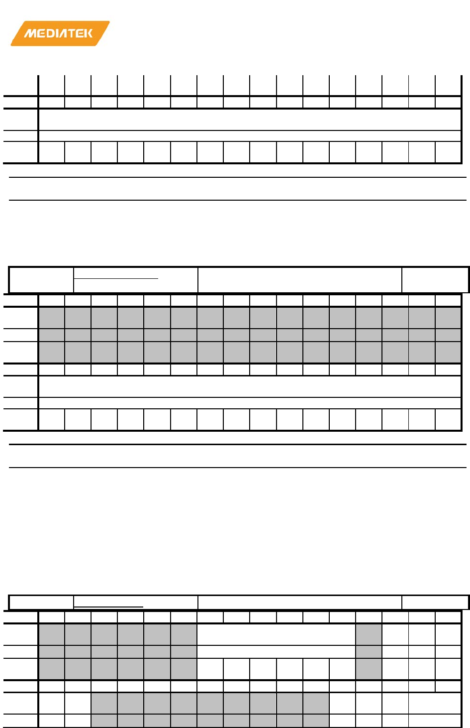
MT76x7
Internet-of-Things Wireless Connectivity
Reference Manual
© 2015 - 2017 MediaTek Inc
Page 341 of 798
This document contains information that is proprietary to MediaTek Inc. (“MediaTek”) and/or its licensor(s).
Any unauthorized use, reproduction or disclosure of this document in whole or in part is strictly prohibited
Rese
t
0 0 0 0 0 0 0 0 0 0 0 0 0 0 0 0
Bit
15
14
13
12
11
10
9
8
7
6
5
4
3
2
1
0
Nam
e
TIMEOUT_COUNTER
Type
RW
Rese
t
0 0 0 0 0 0 0 0 0 0 0 0 0 0 0 0
Bit(s)
Name
Description
31:0
TIMEOUT_COUNTER
Interrupt will assert if there is no new data into fifo more
than n T(bus clock).
83011910
DMA25_COUNT
DMA CR4 Channel 25 Transfer Count
Register
00000000
Bit
31
30
29
28
27
26
25
24
23
22
21
20
19
18
17
16
Nam
e
Type
Rese
t
Bit
15
14
13
12
11
10
9
8
7
6
5
4
3
2
1
0
Nam
e
LEN
Type
RW
Rese
t
0 0 0 0 0 0 0 0 0 0 0 0 0 0 0 0
Bit(s)
Name
Description
15:0
LEN
The amount of total transfer count
This register specifies the amount of total transfer count that the
DMA channel is required to perform. Upon completion, the DMA
channel generates an interrupt request to the processor while ITEN
in DMAn_CON is
set as '1'. Note that the total size of data being
transferred by a DMA channel is determined by LEN together with
the SIZE in DMAn_CON, i.e. LEN x SIZE.
83011914
DMA25_CON
DMA CR4 Channel 25 Control Register
03F00000
Bit
31
30
29
28
27
26
25
24
23
22
21
20
19
18
17
16
Nam
e
MAS
DI
R
WP
EN
WP
SD
Type
RW
RW
RW
RW
Rese
t
1 1 1 1 1 1 0 0 0
Bit
15
14
13
12
11
10
9
8
7
6
5
4
3
2
1
0
Nam
e
ITE
N
TO
EN
DR
EQ
DI
NC
SIN
C
SIZE
Type
RW
RW
RW
RW
RW
RW

MT76x7
Internet-of-Things Wireless Connectivity
Reference Manual
© 2015 - 2017 MediaTek Inc
Page 342 of 798
This document contains information that is proprietary to MediaTek Inc. (“MediaTek”) and/or its licensor(s).
Any unauthorized use, reproduction or disclosure of this document in whole or in part is strictly prohibited
Rese
t
0 0 0 0 0 0 0
Bit(s)
Name
Description
25:20
MAS
Master selection.
Specifies which master occupies this DMA channel.
Once assigned to certain master, the corresponding DREQ and
DACK are connected. For half
-size and Virtual FIFO DMA
channels, i.e. channels 3 ~ 25, a predefined address is assigned as
well.
Value Selected Master SADDR
6'd0 : Don't Use
6'd1 : Don't Use
6'd2 : I2C
-0 (HALF) TX 0x83090000
6'd3 : I2C
-0 (HALF) RX 0x83090000
6'd4 : I2C
-1 (HALF) TX 0x830A0000
6'd5 : I2C
-1 (HALF) RX 0x830A0000
6'd6 : I2S/Audio (VFF) TX 0x22000000
6'd7 : I2S/Audio (VFF) RX 0x22000000
6'd8 : UART0(VFF) TX 0x83030000
6'd9 : UART0(VFF) RX 0x83030000
6'd10 : UART1(VFF) TX 0x83040000
6'd11 : UART1(VFF) RX 0x83040000
6'd12 : BTIF(VFF) TX 0x83
0E0000
6'd13 : BTIF(VFF) RX 0x830E0000
6'd14 : not used 0x50310000
6'd15 : not used
0x50310004
6'd16 : not used
0x50310008
6'd
17 : not used 0x5031000C
6'd18 : not used
0x50310010
6'd19 : not used
0x50310014
6'd20 : ADC(VFF) RX 0x830D0000
6'd21 : WIFI
HIF(HALF) TRX 0x50201000
6'd22 : not used 0x830B0000
6'd23 : not used 0x830B0000

MT76x7
Internet-of-Things Wireless Connectivity
Reference Manual
© 2015 - 2017 MediaTek Inc
Page 343 of 798
This document contains information that is proprietary to MediaTek Inc. (“MediaTek”) and/or its licensor(s).
Any unauthorized use, reproduction or disclosure of this document in whole or in part is strictly prohibited
Bit(s)
Name
Description
6'd24~37 : VFF Data Port 0x79000m00
*m is N
-12
other: reserved
default :6'h3f
If you u
se dma moving data from memory to memory ( ex :full-
size
dma) , please select default value asyour master setting
18
DIR
Directions of DMA transfer for half-size and Virtual FIFO
DMA channels, i.e. channels 3~25. The direction is from
the perspective of the DMA masters. WRITE means read
from master device and then write to the address
specified in DMA_PGMADDR, and vice ver
sa.
0 Read (read from system RAM and write to device)
1 Write (read from device and write to system RAM)
17
WPEN
Address-wrapping for ring buffer. The next address of
DMA jumps to
WRAP TO address when the current address matches WRAP
POINT
count.
0 D
isable
1 Enable
No effect on channel 12~25 (Virtual FIFO).
16
WPSD
The side using address-wrapping function. Only one side
of a DMA
channel can activate address-wrapping function at a time.
0 Address
-wrapping on source .
1 Address
-wrapping on destination.
No effect on channel 12~25 (Virtual FIFO).
15
ITEN
DMA transfer completion interrupt enable.
0 Disable
1 Enable
14
TOEN
DMA transfer timeout interrupt enable.
0 Disable
1 Enable
No effect on channel 1~11 (Full and Half
-size).
4
DREQ
Throttle and handshake control for DMA transfer

MT76x7
Internet-of-Things Wireless Connectivity
Reference Manual
© 2015 - 2017 MediaTek Inc
Page 344 of 798
This document contains information that is proprietary to MediaTek Inc. (“MediaTek”) and/or its licensor(s).
Any unauthorized use, reproduction or disclosure of this document in whole or in part is strictly prohibited
Bit(s)
Name
Description
0 No throttle control during DMA transfer or transfers occurred
only between memories
1 Hardware handshake management
The DMA master is able to throttle down the transfer rate by
way of request
-grant handshake.
MAS Selected Master suggest DREQ setting
6'd6 : I2S/Audio (VFF) TX 1
6'd7 : I2S/Audio (VFF) RX 1
6'd8 : UART0(VFF) TX 1
6'd9 : UART0(VFF) RX 1
6'd10 : UART1(VFF) TX 1
6'd11 : UART1(VFF) RX 1
6'd12 : BTIF(VFF) TX 1
6'd13 : BTIF(VFF) RX 1
6'd20 : ADC(VFF) RX 1
3
DINC
Incremental destination address. Destination addresses
increase every transfer. If the setting of SIZE is Byte,
Destination addresses increase by 1 every single transfer.
If Half
-Word, increase by 2; and if Word, increase by 4.
0 Disable
1 Enable
No effect on channel 12~25 (Vi
rtual FIFO). Destination address is
the master fixed address for read(TX) or the Virtual FIFO write
pointer for write(RX)
2
SINC
Incremental source address. Source addresses increase
every transfer. If the setting of SIZE is Byte, Source
addresses incre
ase by 1 every single transfer. If Half-
Word, increase by 2; and if Word, increase by 4.
0 Disable
1 Enable
No effect on channel 12~25 (Virtual FIFO). Source address is the
Virtual FIFO read pointer for read(TX) or the master fixed address
for write(
RX).
1:0
SIZE
Data size within the confine of a bus cycle per
transfer.These bits confines the data transfer size between
source and destination to the
specified value for individual bus cycle. The size is in terms of byte
and has maximum value of 4 bytes. It is mainly decided by the data

MT76x7
Internet-of-Things Wireless Connectivity
Reference Manual
© 2015 - 2017 MediaTek Inc
Page 345 of 798
This document contains information that is proprietary to MediaTek Inc. (“MediaTek”) and/or its licensor(s).
Any unauthorized use, reproduction or disclosure of this document in whole or in part is strictly prohibited
Bit(s)
Name
Description
width of
a DMA master.
00 Byte transfer/1 byte
01 Half
-word transfer/2 bytes
10 Word transfer/4 bytes
11 Reserved
T
he SIZE register setting depends on devices. The following table
lists all VFIFO channels, associated devices, and data width per
beat.
channel Module Support DMA beat size
VFIFO12 I2S TX
4Byte
VFIFO13 I2S RX 4Byte
VFIFO14 UART0 TX 1Byte
VFIFO15 UART0 RX 1Byte
VFIFO16 UART1 TX 1Byte
VFIFO17 UART1
RX 1Byte
VFIFO18 BTIF TX 1Byte
VFIFO19 BTIF RX 1Byte
VFIFO25 ADC(VFF) RX 4Byte
83011918
DMA25_START
DMA CR4 Channel 25 Start Register
00000000
Bit
31
30
29
28
27
26
25
24
23
22
21
20
19
18
17
16
Nam
e
Type
Rese
t
Bit
15
14
13
12
11
10
9
8
7
6
5
4
3
2
1
0
Nam
e
ST
R
Type
RW
Rese
t
0
Bit(s)
Name
Description
15
STR
Start control for a DMA channel.
0 The DMA channel is stopped.

MT76x7
Internet-of-Things Wireless Connectivity
Reference Manual
© 2015 - 2017 MediaTek Inc
Page 346 of 798
This document contains information that is proprietary to MediaTek Inc. (“MediaTek”) and/or its licensor(s).
Any unauthorized use, reproduction or disclosure of this document in whole or in part is strictly prohibited
Bit(s)
Name
Description
1 The DMA channel is started and running.
8301191C
DMA25_INTSTA
DMA CR4 Channel 25 Interrupt Status
Register
00000000
Bit
31
30
29
28
27
26
25
24
23
22
21
20
19
18
17
16
Nam
e
TOI
NT
Type
RO
Rese
t
0
Bit
15
14
13
12
11
10
9
8
7
6
5
4
3
2
1
0
Nam
e
INT
Type
RO
Rese
t
0
Bit(s)
Name
Description
16
TOINT
Timeout Interrupt Status for DMA Channel
0 No interrupt request is generated.
1 One interrupt request is pending and waiting for service.
No effect on channel 1~11 (Full and Half
-size).
15
INT
Interrupt Status for DMA Channel
0 No interrupt request is generated.
1 One interrupt request is pending and waiting for service.
83011920
DMA25_ACKINT
DMA CR4 Channel 25 Interrupt
Acknowledge Register
00000000
Bit
31
30
29
28
27
26
25
24
23
22
21
20
19
18
17
16
Nam
e
TO
AC
K
Type
WO
Rese
t
0
Bit
15
14
13
12
11
10
9
8
7
6
5
4
3
2
1
0
Nam
e
AC
K
Type
WO
Rese
t
0

MT76x7
Internet-of-Things Wireless Connectivity
Reference Manual
© 2015 - 2017 MediaTek Inc
Page 347 of 798
This document contains information that is proprietary to MediaTek Inc. (“MediaTek”) and/or its licensor(s).
Any unauthorized use, reproduction or disclosure of this document in whole or in part is strictly prohibited
Bit(s)
Name
Description
16
TOACK
TOACK Timeout Interrupt acknowledge for the DMA
channel
0 No effect
1 Interrupt request is acknowledged and should be relinquished.
No effect on channel 1~11 (Full and Half
-size).
15
ACK
ACK Interrupt acknowledge for the DMA channel
0 No effect
1
Interrupt request is acknowledged and should be relinquished.
83011928
DMA25_LIMITER
DMA CR4 Channel 25 Bandwidth
Limiter Register
00000000
Bit
31
30
29
28
27
26
25
24
23
22
21
20
19
18
17
16
Nam
e
Type
Rese
t
Bit
15
14
13
12
11
10
9
8
7
6
5
4
3
2
1
0
Nam
e
LIMITER
Type
RW
Rese
t
0 0 0 0 0 0 0 0
Bit(s)
Name
Description
7:0
LIMITER
from 0 to 255. 0 means no limitation, 255 means totally
banned, and
others mean Bus access permission every (4
X n) AHB clock
8301192C
DMA25_PGMADDR
DMA CR4 Channel 25 Programmable
Address Register
00000000
Bit
31
30
29
28
27
26
25
24
23
22
21
20
19
18
17
16
Nam
e
PGMADDR
Type
RW
Rese
t
0 0 0 0 0 0 0 0 0 0 0 0 0 0 0 0
Bit
15
14
13
12
11
10
9
8
7
6
5
4
3
2
1
0
Nam
e
PGMADDR
Type
RW
Rese
t
0 0 0 0 0 0 0 0 0 0 0 0 0 0 0 0
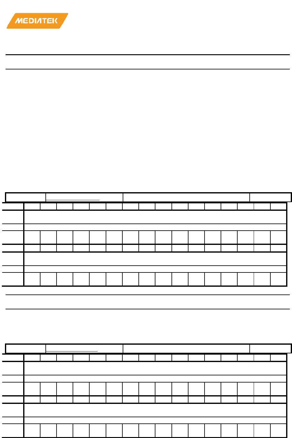
MT76x7
Internet-of-Things Wireless Connectivity
Reference Manual
© 2015 - 2017 MediaTek Inc
Page 348 of 798
This document contains information that is proprietary to MediaTek Inc. (“MediaTek”) and/or its licensor(s).
Any unauthorized use, reproduction or disclosure of this document in whole or in part is strictly prohibited
Bit(s)
Name
Description
31:0
PGMADDR
PGMADDR[31:0]specifies the addresses for a half-size
DMA channel or
virtual
FIFO
WRITE : address of the source/destination.
READ : current address of the transfer.
This address represents a source address if DIR in DMA_CON is set
to 0, and represents a destination address if DIR in DMA_CON is
set to 1. Before being able to pro
gram these register, the software
should make sure that STR in DMAn_START is set to '0', that is the
DMA channel is stopped and disabled completely. Otherwise, the
DMA channel may run out of order.
83011930
DMA25_WRPTR
DMA CR4 Channel 25 Write Pointer
00000000
Bit
31
30
29
28
27
26
25
24
23
22
21
20
19
18
17
16
Nam
e
WRPTR
Type
RO
Rese
t
0 0 0 0 0 0 0 0 0 0 0 0 0 0 0 0
Bit
15
14
13
12
11
10
9
8
7
6
5
4
3
2
1
0
Nam
e
WRPTR
Type
RO
Rese
t
0 0 0 0 0 0 0 0 0 0 0 0 0 0 0 0
Bit(s)
Name
Description
31:0
WRPTR
Virtual FIFO Write Pointer
83011934
DMA25_RDPTR
DMA CR4 Channel 25 Read Pointer
00000000
Bit
31
30
29
28
27
26
25
24
23
22
21
20
19
18
17
16
Nam
e
RDPTR
Type
RO
Rese
t
0 0 0 0 0 0 0 0 0 0 0 0 0 0 0 0
Bit
15
14
13
12
11
10
9
8
7
6
5
4
3
2
1
0
Nam
e
RDPTR
Type
RO
Rese
t
0 0 0 0 0 0 0 0 0 0 0 0 0 0 0 0

MT76x7
Internet-of-Things Wireless Connectivity
Reference Manual
© 2015 - 2017 MediaTek Inc
Page 349 of 798
This document contains information that is proprietary to MediaTek Inc. (“MediaTek”) and/or its licensor(s).
Any unauthorized use, reproduction or disclosure of this document in whole or in part is strictly prohibited
Bit(s)
Name
Description
31:0
RDPTR
Virtual FIFO Read Pointer
83011938
DMA25_FFCNT
DMA CR4 Channel 25 FIFO Count
00000000
Bit
31
30
29
28
27
26
25
24
23
22
21
20
19
18
17
16
Nam
e
Type
Rese
t
Bit
15
14
13
12
11
10
9
8
7
6
5
4
3
2
1
0
Nam
e
FFCNT
Type
RW
Rese
t
0 0 0 0 0 0 0 0 0 0 0 0 0 0 0 0
Bit(s)
Name
Description
15:0
FFCNT
To display the number of data stored in Virtual FIFO
8301193C
DMA25_FFSTA
DMA CR4 Channel 25 FIFO Status
00000000
Bit
31
30
29
28
27
26
25
24
23
22
21
20
19
18
17
16
Nam
e
Type
Rese
t
Bit
15
14
13
12
11
10
9
8
7
6
5
4
3
2
1
0
Nam
e AL
T
EM
PT
Y
FU
LL
Type
RO
RO
RO
Rese
t
0 0 0
Bit(s)
Name
Description
2
ALT
To indicate FIFO Count is larger than ALTLEN.
DMA issues
an alert signal to UART to enable UART flow control.
0 Not reach alert region.
1 Reach alert region.
1
EMPTY
To indicate FIFO is empty.
0 Not Empty

MT76x7
Internet-of-Things Wireless Connectivity
Reference Manual
© 2015 - 2017 MediaTek Inc
Page 350 of 798
This document contains information that is proprietary to MediaTek Inc. (“MediaTek”) and/or its licensor(s).
Any unauthorized use, reproduction or disclosure of this document in whole or in part is strictly prohibited
Bit(s)
Name
Description
1 Empty
0
FULL
To indicate FIFO is full.
0 Not Full
1 Full
83011940
DMA25_ALTLEN
DMA CR4 Channel 25 Alert Length
Register
00000000
Bit
31
30
29
28
27
26
25
24
23
22
21
20
19
18
17
16
Nam
e
AL
TS
CM
Type
RW
Rese
t
0
Bit
15
14
13
12
11
10
9
8
7
6
5
4
3
2
1
0
Nam
e
ALTLEN
Type
RW
Rese
t
0 0 0 0 0 0 0 0 0 0 0 0 0 0 0 0
Bit(s)
Name
Description
31
ALTSCM
Specifies the compare equation between ALTLEN and
FIFO_SIZE
-FIFO_CNT.
1'b0: if ALTLEN > FIFO_SIZE
-
FIFO_CNT, trigger fifo_alt signal to
device for warning device that VFIFO will be
full soon.
1'b1: if ALTLEN >= FIFO_SIZE
-FIFO_CNT, trigger fifo_alt signal
to device for warning device that VFIFO will be full soon.
15:0
ALTLEN
Specifies the Alert Length of Virtual FIFO DMA. Once the
remaining FIFO space is less than ALTLEN, an alert signal
is issued to UART to enable flow control. If ALTSCM is set
to 1, remaining FIFO space == ALTLEN also trigger the
alert signal. Normally, ALTLEN shall be larger than 16 for
UART application.
83011944
DMA25_FFSIZE
DMA CR4 Channel 25 Virtual FIFO Size
Register
00000000
Bit
31
30
29
28
27
26
25
24
23
22
21
20
19
18
17
16
Nam
e
Type
Rese
t
Bit
15
14
13
12
11
10
9
8
7
6
5
4
3
2
1
0

MT76x7
Internet-of-Things Wireless Connectivity
Reference Manual
© 2015 - 2017 MediaTek Inc
Page 351 of 798
This document contains information that is proprietary to MediaTek Inc. (“MediaTek”) and/or its licensor(s).
Any unauthorized use, reproduction or disclosure of this document in whole or in part is strictly prohibited
Nam
e
FFSIZE
Type
RW
Rese
t
0 0 0 0 0 0 0 0 0 0 0 0 0 0 0 0
Bit(s)
Name
Description
15:0
FFSIZE
Specifies the FIFO Size of Virtual FIFO DMA
83011948
DMA25_CVFF
DMA CR4 Channel 25 Cascade Virtual
FIFO Control Register
00000000
Bit
31
30
29
28
27
26
25
24
23
22
21
20
19
18
17
16
Nam
e
CASCADED_PORT_ADDR
Type
RW
Rese
t
0 0 0 0 0 0 0 0 0 0 0 0 0 0 0 0
Bit
15
14
13
12
11
10
9
8
7
6
5
4
3
2
1
0
Nam
e CASCADED_PORT_ADDR
CV
FF
_E
B
Type
RW
RW
Rese
t
0 0 0 0 0 0 0 0 0 0 0 0 0 0 0 0
Bit(s)
Name
Description
31:1
CASCADED_PORT_ADDR
Please fill in the other peripheral's virtual port address.
0
CVFF_EB
When CVFF_EN is set to 1 , DMA will change the
source/destination from sysram to the other fixed
address.
83011950
DMA25_TO
DMA CR4 Channel 25 Timeout Value
Register
00000000
Bit
31
30
29
28
27
26
25
24
23
22
21
20
19
18
17
16
Nam
e
TIMEOUT_COUNTER
Type
RW
Rese
t
0 0 0 0 0 0 0 0 0 0 0 0 0 0 0 0
Bit
15
14
13
12
11
10
9
8
7
6
5
4
3
2
1
0
Nam
e
TIMEOUT_COUNTER
Type
RW
Rese
t
0 0 0 0 0 0 0 0 0 0 0 0 0 0 0 0
Bit(s)
Name
Description

MT76x7
Internet-of-Things Wireless Connectivity
Reference Manual
© 2015 - 2017 MediaTek Inc
Page 352 of 798
This document contains information that is proprietary to MediaTek Inc. (“MediaTek”) and/or its licensor(s).
Any unauthorized use, reproduction or disclosure of this document in whole or in part is strictly prohibited
Bit(s)
Name
Description
31:0
TIMEOUT_COUNTER
Interrupt will assert if there is no new data into fifo more
than n T(bus clock).
2.4.6. General Purpose Timer
MT76x7 includes the General Purpose Timer (GPT).
Five independent timers are included. Timer 0, 1, and 3 are interrupt-based timers, while timer 1 and timer 4
are free-run timers.
GPT provides counter in 32k clock and asserts interrupt when needed. There are two interrupt counters and
two free counters in GPT.
• Interrupt counter: counts from a programmable initial value and asserts interrupt when count to 0.
The interrupt can be one-shot or auto-repeat form. The unit of counter can be 1kHz(32/32kHz) or 1 x
32kHz cycle.
• Freer-run counter: counts freely when it is enabled. The unit of counter is 1kHz(32/32kHz) cycle or 1 x
32kHz cycle.
Two modes are defined in interrupt-based timers:
• One-shot mode—the timer stops when the timer counts down to 0.
• Auto-repeat mode—the timer re-starts when the timer counts down to 0.
Table 2-23. General Purpose Timer Types
Mode Clock speed Interrupt Source
GPT0 Interrupt-based 1KHz(GPT0_CTRL[2]=0) or
32KHz(GPT0_CTRL[2]=1)
GPT
GPT1 Interrupt-based 1KHz(GPT1_CTRL[2]=0) or
32KHz(GPT1_CTRL[2]=1)
GPT2 Free-run 1KHz(GPT2_CTRL[1]=0) or
32KHz(GPT2_CTRL[1]=1)
n/a
GPT3 Interrupt based 26MHz (oscillator clock) GPT3
GPT4 Free-run Bus clock or bus clock / 2 n/a
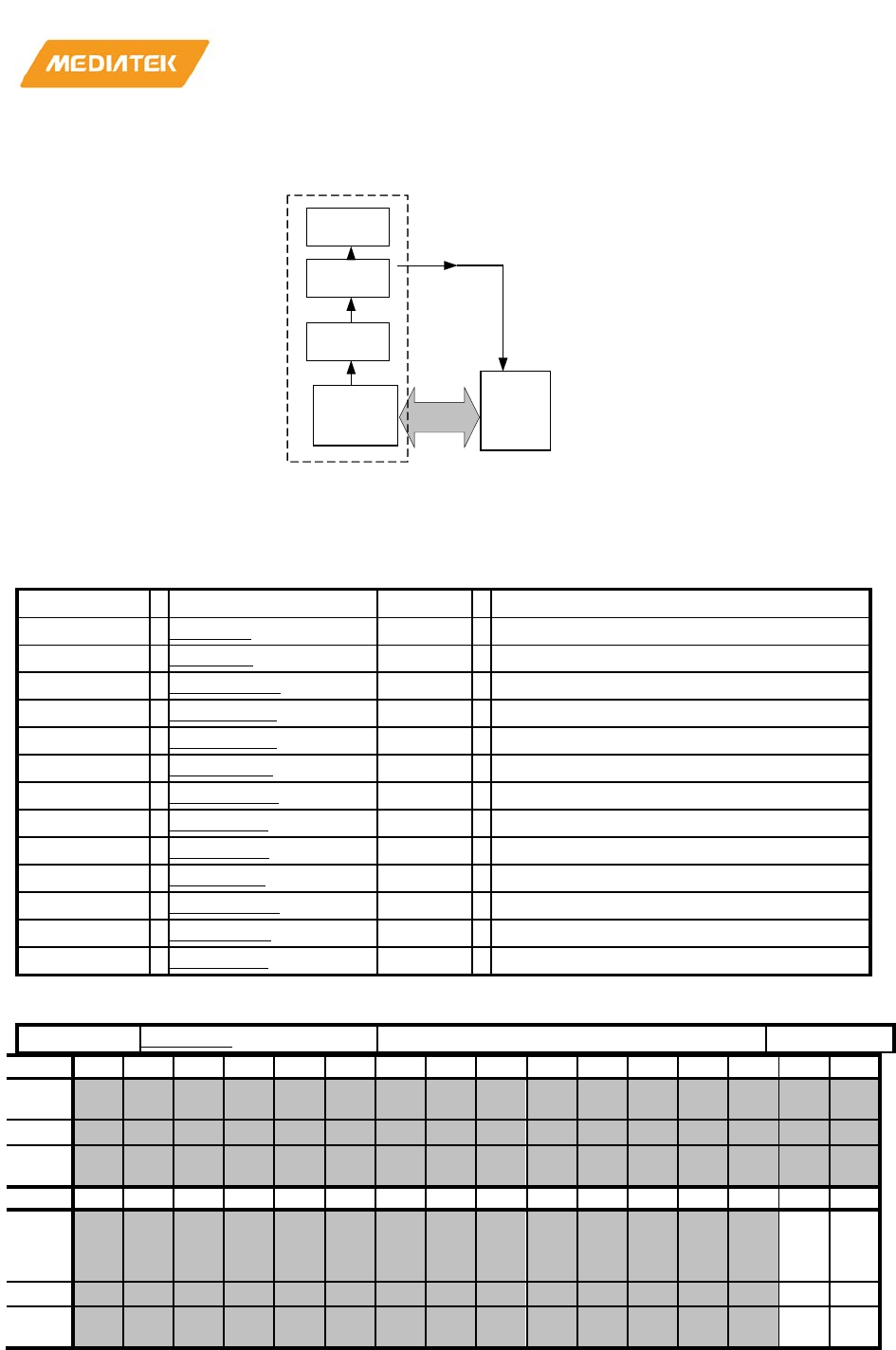
MT76x7
Internet-of-Things Wireless Connectivity
Reference Manual
© 2015 - 2017 MediaTek Inc
Page 353 of 798
This document contains information that is proprietary to MediaTek Inc. (“MediaTek”) and/or its licensor(s).
Any unauthorized use, reproduction or disclosure of this document in whole or in part is strictly prohibited
Figure 2-31. The system diagram of the GPT_CM4
2.4.6.1. Register definitions
Module name: gpt_cm4 Base address: (+83050000h)
Address
Name
Width
Register Function
83050000
GPT_ISR
32
GPT Interrupt Status Register
83050004
GPT_IER
32
GPT Interrupt Enable Register
83050010
GPT0_CTRL
32
GPT0 Control Register
83050014
GPT0_ICNT
32
GPT0 Initial Counter Register
83050020
GPT1_CTRL
32
GPT1 Control Register
83050024
GPT1_ICNT
32
GPT1 Initial Counter Register
83050030
GPT2_CTRL
32
GPT2 Control Register
83050034
GPT2_CNT
32
GPT2 Counter Register
83050040
GPT0_CNT
32
GPT0 Counter Register
83050044
GPT1_CNT
32
GPT1 Counter Register
83050060
GPT4_CTRL
32
GPT4 Control Register
83050064
GPT4_INIT
32
GPT4 Initial Value
83050068
GPT4_CNT
32
GPT4 Counter Register
83050000
GPT_ISR
GPT Interrupt Status Register
00000000
Bit
31
30
29
28
27
26
25
24
23
22
21
20
19
18
17
16
Nam
e
Type
Rese
t
Bit
15
14
13
12
11
10
9
8
7
6
5
4
3
2
1
0
Nam
e GP
T1_
INT
GP
T0
_I
NT
Type
RW
RW
Rese
t
0 0
Registers APB BUS CM4
GPT_CM4
int
counter
counter
counter
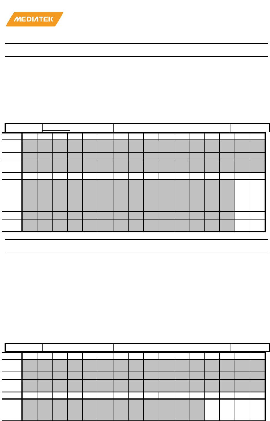
MT76x7
Internet-of-Things Wireless Connectivity
Reference Manual
© 2015 - 2017 MediaTek Inc
Page 354 of 798
This document contains information that is proprietary to MediaTek Inc. (“MediaTek”) and/or its licensor(s).
Any unauthorized use, reproduction or disclosure of this document in whole or in part is strictly prohibited
Bit(s)
Name
Description
1
GPT1_INT
Timer 1 interrupt.
Firmware writes 1 to clear this bit, write 0 is meaningless.
0
GPT0_INT
Timer 0 interrupt.
Firmware writes 1 to clear this bit, write 0 is meaningless.
83050004
GPT_IER
GPT Interrupt Enable Register
00000000
Bit
31
30
29
28
27
26
25
24
23
22
21
20
19
18
17
16
Nam
e
Type
Rese
t
Bit
15
14
13
12
11
10
9
8
7
6
5
4
3
2
1
0
Nam
e
GP
T1_
INT
_E
N
GP
T0
_I
NT
_E
N
Type
RW
RW
Rese
t
0 0
Bit(s)
Name
Description
1
GPT1_INT_EN
Timer 1 interrupt enable
0: Disable interrupt
1: Enable interrupt
0
GPT0_INT_EN
Timer 0 interrupt enable
0: Disable interrupt
1: Enable
interrupt
83050010
GPT0_CTRL
GPT0 Control Register
00000000
Bit
31
30
29
28
27
26
25
24
23
22
21
20
19
18
17
16
Nam
e
Type
Rese
t
Bit
15
14
13
12
11
10
9
8
7
6
5
4
3
2
1
0
Nam
e
RE
ST
AR
T
SP
EE
D
MO
DE EN
MT76x7
Internet-of-Things Wireless Connectivity
Reference Manual
© 2015 - 2017 MediaTek Inc
Page 355 of 798
This document contains information that is proprietary to MediaTek Inc. (“MediaTek”) and/or its licensor(s).
Any unauthorized use, reproduction or disclosure of this document in whole or in part is strictly prohibited
Type
RW
RW
RW
RW
Rese
t
0 0 0 0
Bit(s)
Name
Description
3
RESTART
This register will be auto-clear after restart the counter
0: No any change
1: Restart counter
2
SPEED
This register controls the unit of counter.
0: unit of 32 x 32.768/32KHz cycle
1: unit of 1 x 32.768KHz cycle
1
MODE
This register controls the timer to count repeatedly (in a
loop) or just one
-shot.
SW needs to set this register when GPT0_CTRL[0] = 0.
0: One
-shot mode is selected.
1: Auto
-repeat mode is selected.
0
EN
This register controls timer to start counting or to stop.
0: timer is disabled.
1: timer is enabled
83050014
GPT0_ICNT
GPT0 Initial Counter Register
00000000
Bit
31
30
29
28
27
26
25
24
23
22
21
20
19
18
17
16
Nam
e
CNT
Type
RW
Rese
t
0 0 0 0 0 0 0 0 0 0 0 0 0 0 0 0
Bit
15
14
13
12
11
10
9
8
7
6
5
4
3
2
1
0
Nam
e
CNT
Type
RW
Rese
t
0 0 0 0 0 0 0 0 0 0 0 0 0 0 0 0
Bit(s)
Name
Description
31:0
CNT
Initial counting value, in unit of 32 x 32.768/32KHz (or 1 x
32.768KHz) cycle.
The unit depends on the value of GPT0_CTRL[2].
The timer runs on 32.768KHz and counts down from this value
whenever enabled. When timer counts down to zero, an interrupt is
g
enerated. SW needs to set this register when GPT0_CTRL[0] = 0.
MT76x7
Internet-of-Things Wireless Connectivity
Reference Manual
© 2015 - 2017 MediaTek Inc
Page 356 of 798
This document contains information that is proprietary to MediaTek Inc. (“MediaTek”) and/or its licensor(s).
Any unauthorized use, reproduction or disclosure of this document in whole or in part is strictly prohibited
Bit(s)
Name
Description
83050020
GPT1_CTRL
GPT1 Control Register
00000000
Bit
31
30
29
28
27
26
25
24
23
22
21
20
19
18
17
16
Nam
e
Type
Rese
t
Bit
15
14
13
12
11
10
9
8
7
6
5
4
3
2
1
0
Nam
e
RE
ST
AR
T
SP
EE
D
MO
DE EN
Type
RW
RW
RW
RW
Rese
t
0 0 0 0
Bit(s)
Name
Description
3
RESTART
This register will be auto-clear after restart the counter
0: No any
change
1: Restart counter
2
SPEED
This register controls the unit of counter.
0: unit of 32 x 32.768/32KHz cycle
1: unit of 1 x 32.768KHz cycle
1
MODE
This register controls the timer to count repeatedly (in a
loop) or just one
-shot.
SW needs to set
this register when GPT1_CTRL[0] = 0.
0: One
-shot mode is selected.
1: Auto
-repeat mode is selected.
0
EN
This register controls timer to start counting or to stop.
0: timer is disabled.
1: timer is enabled
83050024
GPT1_ICNT
GPT1 Initial Counter Register
00000000
Bit
31
30
29
28
27
26
25
24
23
22
21
20
19
18
17
16
Nam
e
CNT
Type
RW
Rese
t
0 0 0 0 0 0 0 0 0 0 0 0 0 0 0 0
MT76x7
Internet-of-Things Wireless Connectivity
Reference Manual
© 2015 - 2017 MediaTek Inc
Page 357 of 798
This document contains information that is proprietary to MediaTek Inc. (“MediaTek”) and/or its licensor(s).
Any unauthorized use, reproduction or disclosure of this document in whole or in part is strictly prohibited
Bit
15
14
13
12
11
10
9
8
7
6
5
4
3
2
1
0
Nam
e
CNT
Type
RW
Rese
t
0 0 0 0 0 0 0 0 0 0 0 0 0 0 0 0
Bit(s)
Name
Description
31:0
CNT
Initial counting value, in unit of 32 x 32.768/32KHz (or 1 x
32.768KHz) cycle.
The unit depends on the value of GPT1_CTRL[2].
The timer runs on 32.768KHz and counts down from this value
whenever enabled. When timer counts down to zero, an interrupt is
generated. SW needs to set this register when GPT1_CTRL[0] = 0.
83050030
GPT2_CTRL
GPT2 Control Register
00000000
Bit
31
30
29
28
27
26
25
24
23
22
21
20
19
18
17
16
Nam
e
Type
Rese
t
Bit
15
14
13
12
11
10
9
8
7
6
5
4
3
2
1
0
Nam
e
SP
EE
D
EN
Type
RW
RW
Rese
t
0 0
Bit(s)
Name
Description
1
SPEED
This register controls the unit of counter.
0: unit of 32.768/32KHz cycle
1: unit of 1 x 32.768KHz cycle
0
EN
This register controls timer to start counting or to stop.
0: timer is disabled.
1: timer is enabled
83050034
GPT2_CNT
GPT2 Counter Register
00000000
Bit
31
30
29
28
27
26
25
24
23
22
21
20
19
18
17
16
Nam
e
CNT
Type
RW
Rese
0
0
0
0
0
0
0
0
0
0
0
0
0
0
0
0
MT76x7
Internet-of-Things Wireless Connectivity
Reference Manual
© 2015 - 2017 MediaTek Inc
Page 358 of 798
This document contains information that is proprietary to MediaTek Inc. (“MediaTek”) and/or its licensor(s).
Any unauthorized use, reproduction or disclosure of this document in whole or in part is strictly prohibited
t
Bit
15
14
13
12
11
10
9
8
7
6
5
4
3
2
1
0
Nam
e
CNT
Type
RW
Rese
t
0 0 0 0 0 0 0 0 0 0 0 0 0 0 0 0
Bit(s)
Name
Description
31:0
CNT
Initial / Counting value, in unit of 32 x 32.768/32KHz
cycle.
This counter counts from initial value after enable. When
GPT2_CTRL[0] (ie. gpt2_en) is 0, this register is used to for
counter initial value setting. Its type is R/W. When GPT2_CTRL[0]
(ie. gpt2_en) is 1
, this register is used to for current counting value
reading. Once the gpt2_en is turned on, the current counting value
can be read out after 3T 32kHz clock.
83050040
GPT0_CNT
GPT0 Counter Register
00000000
Bit
31
30
29
28
27
26
25
24
23
22
21
20
19
18
17
16
Nam
e
CNT
Type
RW
Rese
t
0 0 0 0 0 0 0 0 0 0 0 0 0 0 0 0
Bit
15
14
13
12
11
10
9
8
7
6
5
4
3
2
1
0
Nam
e
CNT
Type
RW
Rese
t
0 0 0 0 0 0 0 0 0 0 0 0 0 0 0 0
Bit(s)
Name
Description
31:0
CNT
Current counter value, in unit of 32 x 32.768/32KHz cycle
(or 1 x 32.768KHz cycle).
Once the gpt0_en is turned on, the current counting value can be
read out after 3T 32kHz clock.
83050044
GPT1_CNT
GPT1 Counter Register
00000000
Bit
31
30
29
28
27
26
25
24
23
22
21
20
19
18
17
16
Nam
e
CNT
Type
RW
Rese
t
0 0 0 0 0 0 0 0 0 0 0 0 0 0 0 0
Bit
15
14
13
12
11
10
9
8
7
6
5
4
3
2
1
0
Nam
e
CNT
MT76x7
Internet-of-Things Wireless Connectivity
Reference Manual
© 2015 - 2017 MediaTek Inc
Page 359 of 798
This document contains information that is proprietary to MediaTek Inc. (“MediaTek”) and/or its licensor(s).
Any unauthorized use, reproduction or disclosure of this document in whole or in part is strictly prohibited
Type
RW
Rese
t
0 0 0 0 0 0 0 0 0 0 0 0 0 0 0 0
Bit(s)
Name
Description
31:0
CNT
Current counter value, in unit of 32 x 32.768/32KHz cycle
(or 1 x 32.768KHz cycle).
Once the gpt1_en is turned on, the current counting value can be
read out after 3T 32kHz clock.
83050060
GPT4_CTRL
GPT4 Control Register
00000000
Bit
31
30
29
28
27
26
25
24
23
22
21
20
19
18
17
16
Nam
e
Type
Rese
t
Bit
15
14
13
12
11
10
9
8
7
6
5
4
3
2
1
0
Nam
e SP
EE
D
GP
T4
_E
N
Type
RW
RW
Rese
t
0 0
Bit(s)
Name
Description
1
SPEED
This register controls the unit of counter.
0: the freq of the half of bus clock
1: the freq of bus clock (For FPGA the Bus clock is 40Mhz, for ASIC
the Bus clock is 160Mhz)
0
GPT4_EN
This register controls counter to start counting or to stop.
0:
counter is disabled.
1: counter is enabled
83050064
GPT4_INIT
GPT4 Initial Value
00000000
Bit
31
30
29
28
27
26
25
24
23
22
21
20
19
18
17
16
Nam
e
GPT4_INIT
Type
RW
Rese
t
0 0 0 0 0 0 0 0 0 0 0 0 0 0 0 0
Bit
15
14
13
12
11
10
9
8
7
6
5
4
3
2
1
0
Nam
e
GPT4_INIT
MT76x7
Internet-of-Things Wireless Connectivity
Reference Manual
© 2015 - 2017 MediaTek Inc
Page 360 of 798
This document contains information that is proprietary to MediaTek Inc. (“MediaTek”) and/or its licensor(s).
Any unauthorized use, reproduction or disclosure of this document in whole or in part is strictly prohibited
Type
RW
Rese
t
0 0 0 0 0 0 0 0 0 0 0 0 0 0 0 0
Bit(s)
Name
Description
31:0
GPT4_INIT
Initial value of GPT4.
When GPT4 is disabled, this value will be automatically loaded into
GPT4 counter.
83050068
GPT4_CNT
GPT4 Counter Register
00000000
Bit
31
30
29
28
27
26
25
24
23
22
21
20
19
18
17
16
Nam
e
GPT4_CNT
Type
RO
Rese
t
0 0 0 0 0 0 0 0 0 0 0 0 0 0 0 0
Bit
15
14
13
12
11
10
9
8
7
6
5
4
3
2
1
0
Nam
e
GPT4_CNT
Type
RO
Rese
t
0 0 0 0 0 0 0 0 0 0 0 0 0 0 0 0
Bit(s)
Name
Description
31:0
GPT4_CNT
Current counter value of GPT4 when GPT4 is enabled
(GPT4_EN=1)
2.4.7. Watchdog timer
MT76X7 features the watchdog timer for CM4, which is used to recover the system to the initial status when
the system hangs due to some malfunction.
WDT provides two ways to generate the WDT event:
• Triggered by the time-out event (by configuring WDT_MODE:0x83080030 and
WDT_LENGTH:0x83080034). The WDT has an 11-bit counter and it uses the 32 KHz clock. The
software regularly restarts the timer to prevent it from expiring. If it fails to restart the WDT, the
timer would expire and generate a WDT event.
• Triggered by software programming (WDT_SWRST:0x83080044).
WDT provides the following options when a WDT event is generated:
• 0x83080030[3]=0: Reset mode
o 0x8300917C[16] = 1: WDT whole chip mode. Reset the whole chip including CM4 and N9
subsystems.
o 0x8300917C[16] = 0: WDT MCU mode. Reset CM4 subsystem only.
MT76x7
Internet-of-Things Wireless Connectivity
Reference Manual
© 2015 - 2017 MediaTek Inc
Page 361 of 798
This document contains information that is proprietary to MediaTek Inc. (“MediaTek”) and/or its licensor(s).
Any unauthorized use, reproduction or disclosure of this document in whole or in part is strictly prohibited
• 0x83080030[3]=1: Interrupt mode
o -Issue an interrupt to CM4 instead of resetting whole chip or CM4 subsystem.
The WDT module can only be reset by the external reset (SYS_RST_N) and the PMU reset. Some WDT control
registers feature a key protection mechanism such that an unintentional access would be prevented.
WDT also provides the capability for CM4 software to interrupt N9 or reset N9 (by configuring
WDT_DUAL_CORE:0x83080080).
2.4.7.1. Register definitions
Module name: wdt_cm4 Base address: (+83080000h)
Address
Name
Width
Register Function
83080030
WDT_MODE
32
Watchdog Timer Control Register
83080034
WDT_LENGTH
32
Watchdog Time
-Out Interval Register
83080038
WDT_RESTART
32
Watchdog Timer Restart Register
8308003C
WDT_STA
32
Watchdog Timer Status Register
83080040
WDT_INTERVAL
32
Watchdog Reset Duration Register
83080044
WDT_SWRST
32
Watchdog Timer Software Reset Register
83080080
WDT_DUAL_CORE
32
Watchdog Timer Dual Core
Reset/Interrupt Register
83080030
WDT_MODE
Watchdog Timer Control Register
00000000
Bit
31
30
29
28
27
26
25
24
23
22
21
20
19
18
17
16
Nam
e
Type
Rese
t
Bit
15
14
13
12
11
10
9
8
7
6
5
4
3
2
1
0
Nam
e KEY IR
Q RS
V1 RS
V2
EN
AB
LE
Type
WO
RW
RW
RW
RW
Rese
t
0 0 0 0 0 0 0 0 0 0 0 0
Bit(s)
Name
Description
15:8
KEY
Write access is allowed if KEY=0x22
3
IRQ
Issue an interrupt instead of a Watchdog Timer reset.
For debug purposes, RGU issues an interrupt to the MCU instead of
resetting the system.
1'b0:
WDT reset mode
1'b1: WDT interrupt mode
2
RSV1
Reserve for future use
1
RSV2
Reserve for future use
MT76x7
Internet-of-Things Wireless Connectivity
Reference Manual
© 2015 - 2017 MediaTek Inc
Page 362 of 798
This document contains information that is proprietary to MediaTek Inc. (“MediaTek”) and/or its licensor(s).
Any unauthorized use, reproduction or disclosure of this document in whole or in part is strictly prohibited
Bit(s)
Name
Description
0
ENABLE
Enables the Watchdog Timer. Default watchdog timer is
disabled.
1'b0: Disables the Watchdog Timer.
1'b1: Enables the Watchdog Timer.
83080034
WDT_LENGTH
Watchdog Time-Out Interval Register
0000FFE0
Bit
31
30
29
28
27
26
25
24
23
22
21
20
19
18
17
16
Nam
e
Type
Rese
t
Bit
15
14
13
12
11
10
9
8
7
6
5
4
3
2
1
0
Nam
e
TIMEOUT KEY
Type
RW
WO
Rese
t
1 1 1 1 1 1 1 1 1 1 1 0 0 0 0 0
Bit(s)
Name
Description
15:5
TIMEOUT
The Watchdog time-out down count counter is started
with {TIMEOUT [10:0], 11_1111_1111b}. Thus the
Watchdog Timer time
-out period is a multiple of 1024*
T32k =32ms*(TIMEOUT + 1) if T32k is ideal.
When the Watchdog time
-out counter down count to zero, it will
trigger the Watchdog event.
4:0
KEY
Write access is allowed if KEY=08h
83080038
WDT_RESTART
Watchdog Timer Restart Register
00000000
Bit
31
30
29
28
27
26
25
24
23
22
21
20
19
18
17
16
Nam
e
KEY
Type
WO
Rese
t
0 0 0 0 0 0 0 0 0 0 0 0 0 0 0 0
Bit
15
14
13
12
11
10
9
8
7
6
5
4
3
2
1
0
Nam
e
KEY
Type
WO
Rese
t
0 0 0 0 0 0 0 0 0 0 0 0 0 0 0 0
Bit(s)
Name
Description
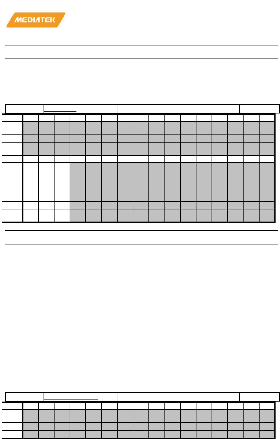
MT76x7
Internet-of-Things Wireless Connectivity
Reference Manual
© 2015 - 2017 MediaTek Inc
Page 363 of 798
This document contains information that is proprietary to MediaTek Inc. (“MediaTek”) and/or its licensor(s).
Any unauthorized use, reproduction or disclosure of this document in whole or in part is strictly prohibited
Bit(s)
Name
Description
31:0
KEY
Restart the Watchdog time-out counter if KEY=1971h.
Only when counter is restarted, the
WDT_LENGTH and
WDT_INTERVAL are loaded into the time
-out counter.
8308003C
WDT_STA
Watchdog Timer Status Register
00000000
Bit
31
30
29
28
27
26
25
24
23
22
21
20
19
18
17
16
Nam
e
Type
Rese
t
Bit
15
14
13
12
11
10
9
8
7
6
5
4
3
2
1
0
Nam
e WD
T
SW
_W
DT
DU
AL
_C
OR
E_
WD
T
Type
RO
RO
RO
Rese
t
0 0 0
Bit(s)
Name
Description
15
WDT
Indicates if the Watchdog reset /interrupt was triggered
by
hardware timer time-out.
1'b0: No event
1'b1: Watchdog reset/interrupt due to hardware timer time
-out
period expired.
14
SW_WDT
Indicates if the Watchdog reset/interrupt was triggered by
software.
1'b0: No event
1'b1: Watchdog reset/interrupt due to
software-triggered.
13
DUAL_CORE_WDT
Indicate software triggered reset to the other Core
1'b0: No event
1'b1: Software has triggered reset to the other Core
83080040
WDT_INTERVAL
Watchdog Reset Duration Register
00000FFF
Bit
31
30
29
28
27
26
25
24
23
22
21
20
19
18
17
16
Nam
e
Type
Rese
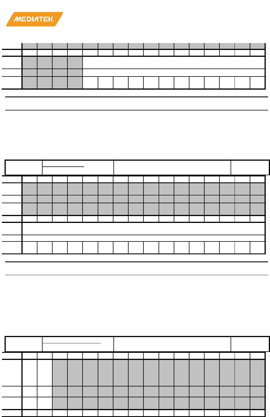
MT76x7
Internet-of-Things Wireless Connectivity
Reference Manual
© 2015 - 2017 MediaTek Inc
Page 364 of 798
This document contains information that is proprietary to MediaTek Inc. (“MediaTek”) and/or its licensor(s).
Any unauthorized use, reproduction or disclosure of this document in whole or in part is strictly prohibited
t
Bit
15
14
13
12
11
10
9
8
7
6
5
4
3
2
1
0
Nam
e
LENGTH
Type
RW
Rese
t
1 1 1 1 1 1 1 1 1 1 1 1
Bit(s)
Name
Description
11:0
LENGTH
This register indicates the reset duration when
WDT_MODE register IRQ bit is set to 0. The reset
duration counter is T32k base. If the WDT_MODE register
IRQ bit is set to 1, an interrupt is issued instead of a reset.
83080044
WDT_SWRST
Watchdog Timer Software Reset
Register
00000000
Bit
31
30
29
28
27
26
25
24
23
22
21
20
19
18
17
16
Nam
e
Type
Rese
t
Bit
15
14
13
12
11
10
9
8
7
6
5
4
3
2
1
0
Nam
e
KEY
Type
WO
Rese
t
0 0 0 0 0 0 0 0 0 0 0 0 0 0 0 0
Bit(s)
Name
Description
15:0
KEY
Software-triggered reset/interrupt. If the register content
matches the KEY, a watchdog reset is issued. However, if
the WDT_MODE register IRQ bit is set to 1, an interrupt is
issued instead of a reset.
KEY = 1209h
83080080
WDT_DUAL_CORE
Watchdog Timer Dual Core
Reset/Interrupt Register
00000000
Bit
31
30
29
28
27
26
25
24
23
22
21
20
19
18
17
16
Nam
e
SW
_I
NT
SW
_I
NT
_C
LR
Type RW
W1
C
Rese
t
0 0
Bit
15
14
13
12
11
10
9
8
7
6
5
4
3
2
1
0
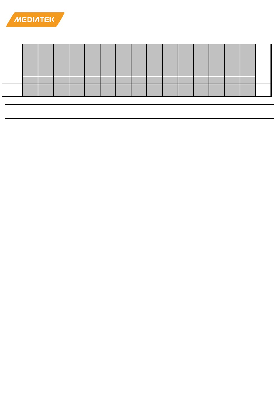
MT76x7
Internet-of-Things Wireless Connectivity
Reference Manual
© 2015 - 2017 MediaTek Inc
Page 365 of 798
This document contains information that is proprietary to MediaTek Inc. (“MediaTek”) and/or its licensor(s).
Any unauthorized use, reproduction or disclosure of this document in whole or in part is strictly prohibited
Nam
e
Du
al_
Cor
e_
RS
T
Type
RW
Rese
t
0
Bit(s)
Name
Description
31
SW_INT
Write 1 trigger software interrupt to the other Core.
CM4 software trigger interrupt to N9 EINT No.3
1'b1: Software trigger interrupt status
1'b0: No event
30
SW_INT_CLR
Write 1 clear SW_INT status
0
Dual_Core_RST
Write 1 trigger software reset to the other Core. This bit
will be auto cleared and the
reset signal duration will
depends on LENGTH setting.
2.4.8. eFuse
MT76x7 uses embedded Efuse to store device specific configuration information such as MAC addresses, and
power control settings.
The major fields defined in the Efuse:
• Wi-Fi MAC addresses
• Wi-Fi country code
• Wi-Fi TSSI parameters, TX power level
• Wi-Fi NIC configuration: RF front-end configuration, LED mode, baseband configuration
• Bluetooth MAC address
• Bluetooth TX power level.
2.4.9. Interrupt Controller
MT76x7 integrates the Nested Vectored Interrupt Controller (NVIC) for Cortex M4. The NVIC supports
• Level and pulse detection of interrupt signals
• Configurable priority
• Wake-up interrupt controller (WIC) providing ultra-low power sleep mode support

MT76x7
Internet-of-Things Wireless Connectivity
Reference Manual
© 2015 - 2017 MediaTek Inc
Page 366 of 798
This document contains information that is proprietary to MediaTek Inc. (“MediaTek”) and/or its licensor(s).
Any unauthorized use, reproduction or disclosure of this document in whole or in part is strictly prohibited
2.4.9.1. Interrupt Sources
The table below listed the NVIC and WIC interrupt sources. In total, there are 49 NVICs, while 23 of them are
external interrupts multiplexed with GPIO functions.
The power domain/subsystem lists the power domain and the subsystem from which the interrupt is
generated.
Table 2-24. Cortex-M4 NVIC interrupt source
NVIC
No.
Interrupt
source
Power domain
/subsystem
External
interrup
t
Wake-up
capability
(1)
De-
bounce
Description
INT0 UART1 CM4_OFF/MCUSYS_CM4 UART 1
INT1 DMA_CM4 CM4_OFF/MCUSYS_CM4 Generic DMA in
CM4 subsystem
INT2 HIF_CM4 TOP_AON/HIFSYS Wi-Fi host
interface for CM4
INT3 I2C1 CM4_OFF/MCUSYS_CM4 I2C 1
INT4 I2C2 CM4_OFF/MCUSYS_CM4 I2C 2
INT5 UART2 CM4_OFF/MCUSYS_CM4 UART 2
INT6 CRYPTO CM4_OFF/MCUSYS_CM4 Crypto engine
INT7 SF CM4_OFF/MCUSYS_CM4 Serial flash
controller, for
debug
INT8 BTIF_N9_W
AKE
TOP_OFF(N9)/MCUSYS_
N9
Bluetooth interface
in N9 subsystem to
wake up CM4
INT9 BTIF CM4_OFF/MCUSYS_CM4 Bluetooth interface
in CM4 subsystem
INT10 WDT_CM4 TOP_AON/MCUSYS_CM
4
Watchdog timer in
CM4 subsystem
INT11 N9_TO_CM
4_SW1
TOP_AON/MCUSYS_N9 N9 software
interrupt to CM4
INT12 SPI_S CM4_OFF/MCUSYS_CM4 SPI slave
INT13 WDT_N9 TOP_AON/MCUSYS_N9 Watchdog timer in
N9 subsystem
INT14 ADC CM4_OFF/MCUSYS_CM4 Auxiliary ADC FIFO
INT15 IRTX CM4_OFF/MCUSYS_CM4 IrDA TX
INT16 IRRX CM4_OFF/MCUSYS_CM4 IrDA RX
INT17 (Reserved)
INT18 (Reserved)
INT19 RTC_TIMER RTC RTC timer interrupt
INT20 GPT3 CM4_OFF/MCUSYS_CM4 GPT3 time-out
INT21 RTC_ALARM RTC RTC alarm
interrupt

MT76x7
Internet-of-Things Wireless Connectivity
Reference Manual
© 2015 - 2017 MediaTek Inc
Page 367 of 798
This document contains information that is proprietary to MediaTek Inc. (“MediaTek”) and/or its licensor(s).
Any unauthorized use, reproduction or disclosure of this document in whole or in part is strictly prohibited
NVIC
No.
Interrupt
source
Power domain
/subsystem
External
interrup
t
Wake-up
capability
(1)
De-
bounce
Description
INT22 (Reserved)
INT23 N9_TO_CM
4_SW2
TOP_AON/MCUSYS_N9 N9 software
interrupt to CM4
INT24 GPT TOP_CON/MCUSYS_CM4 GPT0 or GPT1
time-out
INT25 ADC_COMP TOP_AON ADC comparison
mode
INT26 (Reserved)
INT27 SPI CM4_OFF/MCUSYS_CM4 SPI transaction
INT28 (Reserved)
INT29 (Reserved)
INT30 (Reserved)
INT31 WIC TOP_AON/MCUSYS_CM
4
(2)
WIC WAKEUP
interrupt CM4
INT32 SWD_CLK TOP_AON WIC[0] Available GPIO[2]
INT33 I2C1_DATA TOP_AON WIC[1] Available GPIO[25]
INT34 I2C0_CLK TOP_AON WIC[2] Available GPIO[27]
INT35 I2S_MCLK_S
PI_MOSI
TOP_AON WIC[3] Available GPIO[29]
INT36 I2S_BCLK_S
PI_CS
TOP_AON WIC[4] Available GPIO[32]
INT37 ANT_SEL0 TOP_AON WIC[5] Available GPIO[33]
INT38 ANT_SEL1 TOP_AON WIC[6] Available GPIO[34]
INT39 GPIO17 TOP_AON WIC[7] Available GPIO[36]
INT40 ADC0 TOP_AON WIC[8] Available GPIO[57]
INT41 ADC1 TOP_AON WIC[9] Available GPIO[58]
INT42 ADC2 TOP_AON WIC[10] Available GPIO[59]
INT43 ADC3 TOP_AON WIC[11] Available GPIO[60]
INT56 PWM0 TOP_AON EINT[0] Available GPIO[0]
INT57 PWM1 TOP_AON EINT[1] Available GPIO[1]
INT58 SWD_DIO TOP_AON EINT[2] Available GPIO[3]
INT59 GPIO0 TOP_AON EINT[3] Available GPIO[4]
INT60 GPIO1 TOP_AON EINT[4] Available GPIO[5]
INT61 GPIO2 TOP_AON EINT[5] Available GPIO[6]
INT62 GPIO3 TOP_AON EINT[6] Available GPIO[7]
INT75 GPIO16 TOP_AON EINT[19
]
Available GPIO[35]
INT76 GPIO18 TOP_AON EINT[20
]
Available GPIO[37]
MT76x7
Internet-of-Things Wireless Connectivity
Reference Manual
© 2015 - 2017 MediaTek Inc
Page 368 of 798
This document contains information that is proprietary to MediaTek Inc. (“MediaTek”) and/or its licensor(s).
Any unauthorized use, reproduction or disclosure of this document in whole or in part is strictly prohibited
NVIC
No.
Interrupt
source
Power domain
/subsystem
External
interrup
t
Wake-up
capability
(1)
De-
bounce
Description
INT77 GPIO19 TOP_AON EINT[21
]
Available GPIO[38]
INT78 GPIO20 TOP_AON EINT[22
]
Available GPIO[39]
Note 1: Capable to wake up Cortex-M4 when Cortex-M4 is in sleep mode.
Note 2: This interrupt is associated with other wake-up interrupts for CM4 to differentiate wake-up interrupts
from non wake-up interrupts.
2.4.9.2. External interrupt
MT76x7 has the optionally enabled hardware de-bouncing circuit for each interrupt source.
Table 2-25. Cortex-M4 external interrupt de-bounce period
3-bit prescaler Reference clock rate for de-
bounce counter (KHz)
Minimum de-bounce
period (ms)
Maximum de-bounce
period (ms)
000 8 0.13 2
001 4 0.25 4
010 2 0.5 8
011 1 1 16
100 0.5 2 32
101 0.25 4 64
110 0.125 8 128
111 0.0625 16 256
2.4.10. Power-on sequence
The power-on control sequence diagram shows how the code reset (PMU_RESET_N) is generated on chip.
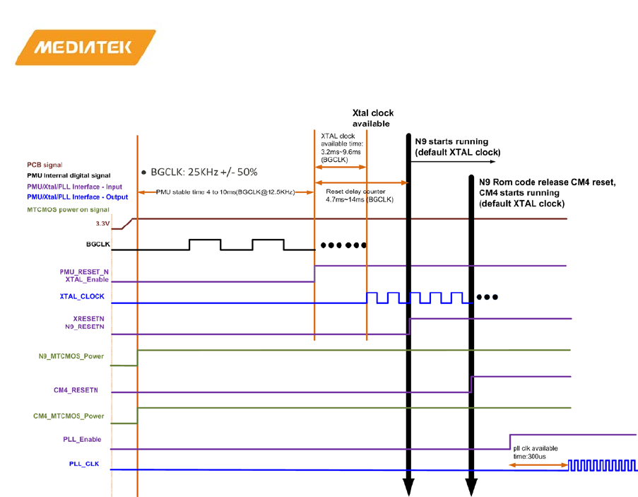
MT76x7
Internet-of-Things Wireless Connectivity
Reference Manual
© 2015 - 2017 MediaTek Inc
Page 369 of 798
This document contains information that is proprietary to MediaTek Inc. (“MediaTek”) and/or its licensor(s).
Any unauthorized use, reproduction or disclosure of this document in whole or in part is strictly prohibited
Figure 2-32. PMU Power-on Sequence
2.4.10.1. Power-on reset (Cold Reset)
The power on reset sequence after chip power on is shown below.
1) N9 reset is de-asserted and boot from ROM (Cortex-M4 reset state is still asserted)
2) N9 sets up top configuration registers (such as PLL) and then de-asserts CM4 reset
3) Cortex-M4 boots from ROM while N9 polls the PDA (Patch Decryption Accelerator) status
4) Cortex-M4 fetch flash header (N9 FW download length information)
5) Cortex-M4 setup PDA and PDA address generator
6) PDA loads firmware from the flash to N9 IDLM
7) N9 executes from IDLM after PDA completes and CM4 executes from Cache/Flash or TCM.
2.4.10.2. Watchdog reset
Watchdog reset WDT_N9 is the watchdog timer for N9, and WDT_CM4 is the watchdog timer for CM4.
When the WDT event of WDT_N9 occurs, WDT_N9 has the capability to
• Reset N9 or issue an interrupt to N9.
• Issue an interrupt to Cortex-M4 (can be masked by CM4 if it is not required to be received).
When the WDT event of WDT_CM4 occurs, WDT_CM4 has the capability to
• Reset whole chip or reset Cortex-M4 only or issue an interrupt to CM4.
• Issue an interrupt to N9 (can be masked by N9 if it’s not required to be received).
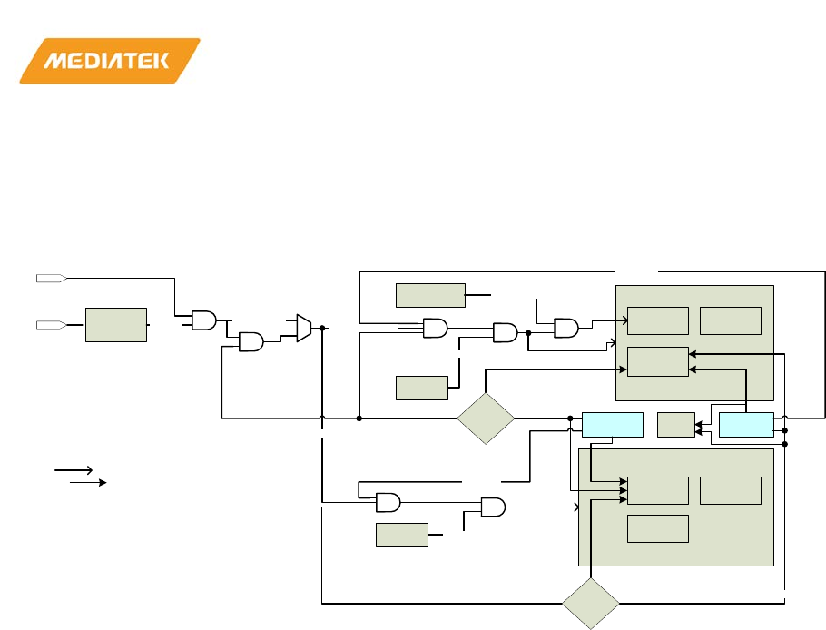
MT76x7
Internet-of-Things Wireless Connectivity
Reference Manual
© 2015 - 2017 MediaTek Inc
Page 370 of 798
This document contains information that is proprietary to MediaTek Inc. (“MediaTek”) and/or its licensor(s).
Any unauthorized use, reproduction or disclosure of this document in whole or in part is strictly prohibited
For both WDT_N9 and WDT_CM4, the WDT events can be triggered by time-out and software programming.
For both WDT_N9 and WDT_CM4, the WDT has the capability to reset the other CPU or issue an interrupt to
the other CPU.
TOP_OFF (N9)
CM4_OFF
CIRQ
WDT_N9
NVIC
WDT_CM4
CM4_SW_RST_B
81080080[0]
N9_SW_RST_B
83080080[0]
PMU
D12: SYS_RST_N
PMU_RST_B
R16: AVDD45_BUCK
CM4_AON_XRESET_RST_B
POR_XRESET_RST_B SEL: 8300917C[16]
CM4 MTCMOS
power CTRL
CM4_HW_RST_B
N9 RELEASE CM4
81020018[0] RELEASE_CM4_RST_B
ARM CM4
WIC
CM4
peripherals
AON_XRESET_RST_B
N9
RGU_HRESET_RST_B
N9 MTCMOS
power CTRL N9_HW_RST_B
N9
peripherals
CM4 to N9 interrupt: 83080080[31:30]
WDT_DUAL_CORE_SW_INTàCIRQ EINT 3
N9_TO_CM4_SW2 ingterrupt: 81080080[31:30]
WDT_DUAL_CORE_SW_INTàINT23
Note:
PMU_RST_B: power-on or over-current protection
CM4_WDT_RST_B: CM4 WDT reset
N9_WDT_RST_B: N9 WDT reset
CM4_AON_
HRESET_RST_B
CM4_RGU_HRESET_RST_B
WDT_N9 interrupt
N9_WDT_RST_BàINT13
81080030[3]
=1?
N9_WDT_RST_B
CIRQ INT10
CIRQ INT22
CIRQ EINT3
Y
N
83080030[3]
=1?
Y
N
INT10
INT13
INT23
Legend:
Reset:
Interrupt:
CM4_WDT_RST_B
Figure 2-33. WDT structure
2.4.10.3. Reset scenarios
The definitions of the cold reset and the warm reset are shown below:
• Cold Reset: Power on reset and both RAM or peripheral devices will be initialized by firmware.
• Warm Reset: CPU is reset but RAM content is still retained (without firmware re-download). It’s
triggered by
o Software reset: Software set WDT reset control register to reset CPU.
o WDT reset: WDT expiration cause CPU to reset if enabled, otherwise interrupt.
o Core reset: Reset by the other CPU (e.g. N9 to reset CM4 or CM4 to reset N9).
o Wake-up from deep sleep mode: Reset by the MTCMOS power control.
2.4.10.4. Sleep and wakeup sequence
The sleep/wakeup control sequence is shown in the diagram below.
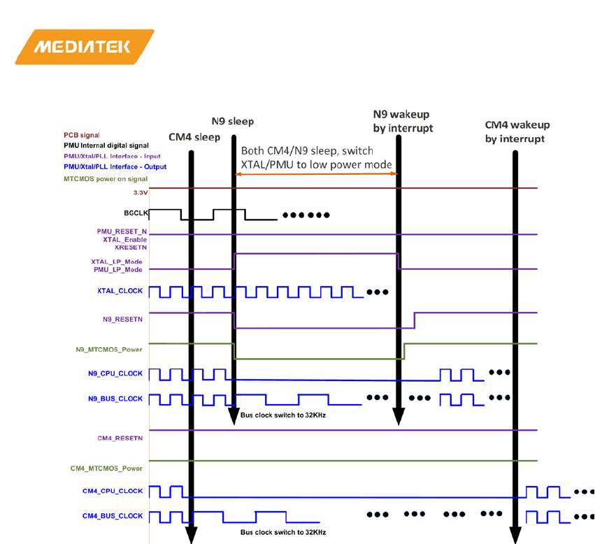
MT76x7
Internet-of-Things Wireless Connectivity
Reference Manual
© 2015 - 2017 MediaTek Inc
Page 371 of 798
This document contains information that is proprietary to MediaTek Inc. (“MediaTek”) and/or its licensor(s).
Any unauthorized use, reproduction or disclosure of this document in whole or in part is strictly prohibited
Figure 2-34. Sleep and wakeup sequence
2.4.11. Memory map
Table 2-26 describes how the peripherals are mapped to the Cortex-M4 memory.
When the MCU performs a read transaction to an undefined address, the bus returns 0. When the MCU
performs a write transaction to an undefined address, the bus regards it as an invalid transaction and does
nothing. The memory space of 0x5040_0000 to 0x5FFF_FFFF is an undefined region and shall not be accessed.
The power domain is identified in the table. The hardware clock gating is associated with the power control.
When the CPU power domain is in power-off mode, it implies that the clock is also gated.
The software clock gating control, identified in the table below, provides the way to disable the function and
lower its power consumption when the function is not used.

MT76x7
Internet-of-Things Wireless Connectivity
Reference Manual
© 2015 - 2017 MediaTek Inc
Page 372 of 798
This document contains information that is proprietary to MediaTek Inc. (“MediaTek”) and/or its licensor(s).
Any unauthorized use, reproduction or disclosure of this document in whole or in part is strictly prohibited
Table 2-26. Cortex-M4 memory map
Start
address
End address Function Power Domain Software Clock
gating control
Description
0x0000_000
0
0x0000_FFFF TCM ROM CM4_OFF Tightly Coupled
ROM for Cortex-
M4
0x0010_000
0
0x0010_FFFF TCM RAM0 CM4_OFF Tightly Coupled
RAM for Cortex-
M4 (64KB)
0x0011_000
0
0x0011_1FFF TCM RAM1 CM4_OFF Tightly Coupled
RAM for Cortex-
M4 (8KB)
0x0011_200
0
0x0011_3FFF TCM RAM2 CM4_OFF Tightly Coupled
RAM for Cortex-
M4 (8KB)
0x0011_400
0
0x0011_5FFF TCM RAM3 CM4_OFF Tightly Coupled
RAM for Cortex-
M4 (8KB)
0x0011_600
0
0x0011_7FFF TCM RAM4 CM4_OFF Tightly Coupled
RAM for Cortex-
M4 (8KB)
0x1000_000
0
0x1FFF_FFFF Serial Flash CM4 CM4_OFF Serial flash of
CM4
0x2000_000
0
0x2003_FFFF SYSRAM_CM4 CM4_OFF System RAM for
Cortex-M4,
256Kbytes
0x2100_000
0
0x2100_FFFF SPI-S CM4_OFF 0x8300_0200[21
]
SPI slave
0x2200_000
0
0x2200_FFFF I2S/Audio CM4_OFF 0x8300_0200[14
]
I2S
0x2400_000
0
0x2400_FFFF SPI-M CM4_OFF 0x8300_0200[22
]
SPI master
0x2500_000
0
0x2500_CFFF SYSRAM_N9 TOP_OFF(N9) System RAM for
N9, 52Kbytes
0x3000_000
0
0x3FFF_FFFF Serial Flash CM4 CM4_OFF Serial flash of
Cortex-M4
through system
bus
0x5000_000
0
0x501F_FFFF HIF_device TOP_OFF(N9) Host interface
device controller
0x5020_000
0
0x502F_FFFF HIF_host_CM4 TOP_AON Host interface
host controller of
Wi-Fi radio
0x5040_000
0
0x5FFF_FFFF (Undefined)
0x6000_000 0x6FFF_FFFF WIFISYS TOP_OFF(N9) 0x8000_0100[5] Wi-Fi subsystem

MT76x7
Internet-of-Things Wireless Connectivity
Reference Manual
© 2015 - 2017 MediaTek Inc
Page 373 of 798
This document contains information that is proprietary to MediaTek Inc. (“MediaTek”) and/or its licensor(s).
Any unauthorized use, reproduction or disclosure of this document in whole or in part is strictly prohibited
Start
address
End address Function Power Domain Software Clock
gating control
Description
0
0x7000_000
0
0x70FF_FFFF PDA DMA port Patch Decryption
Accelerator DMA
slave
0x7800_000
0
0x7800_FFFF VFF access port TOP_OFF(N9) Virtual FIFO
access ports of N9
DMA
0x7900_000
0
0x7900_FFFF VFF_CM4 access
port
CM4_OFF 0x8300_0200[3] Virtual FIFO
access ports of
Cortex-M4 DMA
0x8000_000
0
0x800C_FFFF APB0 TOP_OFF(N9) APB bridge 0
(synchronous to
N9)
0x8000_000
0
0x8000_FFFF CONFG TOP_OFF(N9) N9 subsystem
configuration
0x8001_000
0
0x8001_FFFF DMA TOP_OFF(N9) Generic DMA
engine for N9
0x8002_000
0
0x8002_FFFF TOP_CFG_OFF TOP_OFF(N9) TOP_OFF(N9)
power domain
chip level
configuration
(GPIO, PINMUX,
RF, CLK control)
0x8003_000
0
0x8003_FFFF UART/BTIF TOP_OFF(N9) 0x8000_0100[6] UART or
Bluetooth host
interface for N9
0x8005_000
0
0x8005_FFFF UART_P TA TOP_OFF(N9) 0x8000_0100[11
]
Inter-chip
communication
for PTA
0x8008_000
0
0x8008_FFFF AHB_MON TOP_OFF(N9) 0x8000_0100[10
]
AHB bus monitor
0x8009_000
0
0x8009_FFFF ACCLR TOP_OFF(N9) 0x8000_0100[13
]
Bluetooth audio
Packet Loss
Concealment
accelerator
0x800A_000
0
0x800A_FFFF UART_DSN TOP_OFF(N9) 0x8000_0100[7] UART for N9
debug
0x800B_000
0
0x800B_FFFF SEC TOP_OFF(N9) Security boot
configuration
0x800C_000
0
0x800C_FFFF HIF TOP_OFF(N9) Host interface
configuration
0x8100_000
0
0x810C_FFFF APB1 TOP_OFF(N9) APB bridge 1
(synchronous to
N9)

MT76x7
Internet-of-Things Wireless Connectivity
Reference Manual
© 2015 - 2017 MediaTek Inc
Page 374 of 798
This document contains information that is proprietary to MediaTek Inc. (“MediaTek”) and/or its licensor(s).
Any unauthorized use, reproduction or disclosure of this document in whole or in part is strictly prohibited
Start
address
End address Function Power Domain Software Clock
gating control
Description
0x8100_000
0
0x8100_FFFF BTSYS TOP_OFF(N9) 0x8000_0100[24
]
Bluetooth
subsystem
0x8102_000
0
0x8102_FFFF TOP_CFG_AON TOP_AON TOP_AON power
domain chip level
configuration
(RGU, PINMUX,
PLL, PMU, XTAL,
CLK control)
0x8103_000
0
0x8103_FFFF DBG_CIRQ TOP_AON Debug interrupt
controller for N9
0x8104_000
0
0x8104_FFFF CIRQ TOP_AON Interrupt
controller for N9
0x8105_800
0
0x8105_FFFF GPT TOP_AON General Purpose
Timer for N9
0x8106_000
0
0x8106_FFFF PTA TOP_OFF(N9) 0x8000_0100[14
]
Packet Traffic
Arbitrator for Wi-
Fi/Bluetooth
coexistence
0x8107_000
0
0x8107_FFFF EFUSE_MAC TOP_OFF(N9) 0x8000_0100[12
]
Efuse controller
0x8108_000
0
0x8108_FFFF WDT TOP_AON Watchdog Timer
for N9
0x8109_000
0
0x8109_FFFF PDA TOP_OFF(N9) Patch Decryption
Accelerator
0x810A_000
0
0x810A_FFFF RDD TOP_OFF(N9) 0x8000_0100[23
]
Wi-Fi debug
0x810B_000
0
0x810B_FFFF BTSBC TOP_OFF(N9) 0x8000_0100[15
]
Bluetooth SBC
accelerator
0x810C_000
0
0x810C_FFFF RBIST TOP_OFF(N9) RF BIST
configuration
0x8300_000
0
0x810C_FFFF APB2 CM4_OFF APB bridge 1
(synchronous to
Cortex-M4)
0x8300_000
0
0x8300_7FFF CONFG_CM4 CM4_OFF System
configuration for
Cortex-M4
0x8300_800
0
0x8300_BFFF TOP_CFG_AON_
CM4
TOP_AON TOP_AON
configuration
0x8300_C00
0
0x8300_EFFF CONFG_CM4_A
ON
TOP_AON System
configuration for
Cortex-M4 in
TOP_AON domain

MT76x7
Internet-of-Things Wireless Connectivity
Reference Manual
© 2015 - 2017 MediaTek Inc
Page 375 of 798
This document contains information that is proprietary to MediaTek Inc. (“MediaTek”) and/or its licensor(s).
Any unauthorized use, reproduction or disclosure of this document in whole or in part is strictly prohibited
Start
address
End address Function Power Domain Software Clock
gating control
Description
0x8300_F00
0
0x8300_FFFF SEC_TOP_CM4 CM4_OFF 0x8300_0200[0] JTAG security for
CM4
0x8301_000
0
0x8301_FFFF DMA_CM4 CM4_OFF 0x8300_0200[3] Generic DMA
engine for Cortex-
M4
0x8302_000
0
0x8302_FFFF UART_DSN CM4_OFF 0x8300_0200[4] UART for Cortex-
M4 debugging
0x8303_000
0
0x8303_FFFF UART1 CM4_OFF 0x8300_0200[5] UART 1 for
Cortex-M4
0x8304_000
0
0x8304_FFFF UART2 CM4_OFF 0x8300_0200[6] UART 2 for
Cortex-M4
0x8305_000
0
0x8305_FFFF GPT_CM4 TOP_AON General Purpose
Timer for Cortex-
M4
0x8306_000
0
0x8306_FFFF IrDA CM4_OFF 0x8300_0200[8] IrDA
0x8300_0200[9]
0x8307_000
0
0x8307_FFFF Serial flash CM4_OFF 0x8300_0200[10
]
Serial flash macro
access
0x8308_000
0
0x8308_FFFF WDT_CM4 TOP_AON Watchdog timer
for Cortex-M4
0x8309_000
0
0x8309_FFFF I2C_1 CM4_OFF 0x8300_0200[12
]
I2C 1
0x8300_0200[23
]
0x830A_000
0
0x830A_FFFF I2C_2 CM4_OFF 0x8300_0200[13
]
I2C 2
0x8300_0200[24
]
0x830B_000
0
0x830B_0FFF I2S CM4_OFF 0x8300_0200[14
]
I2S configuration
0x830C_000
0
0x830C_FFFF RTC RTC Real time clock
0x830D_000
0
0x830D_FFFF AUXADC CM4_OFF 0x8300_0200[16
]
Auxiliary ADC
configuration
0x830E_000
0
0x830E_FFFF BTIF CM4_OFF 0x8300_0200[17
]
Host Interface for
Bluetooth radio
0x830F_000
0
0x830F_FFFF Crypto CM4_OFF 0x8300_0200[18
]
Crypto engine
0xA000_000
0
0xAFFF_FFFF PSE CM4_OFF Packet switch
engine memory
0xE000_E00
0
0xE000_EFFF NVIC, SYSTICK,
FPU
CM4_OFF Nested vectored
interrupt
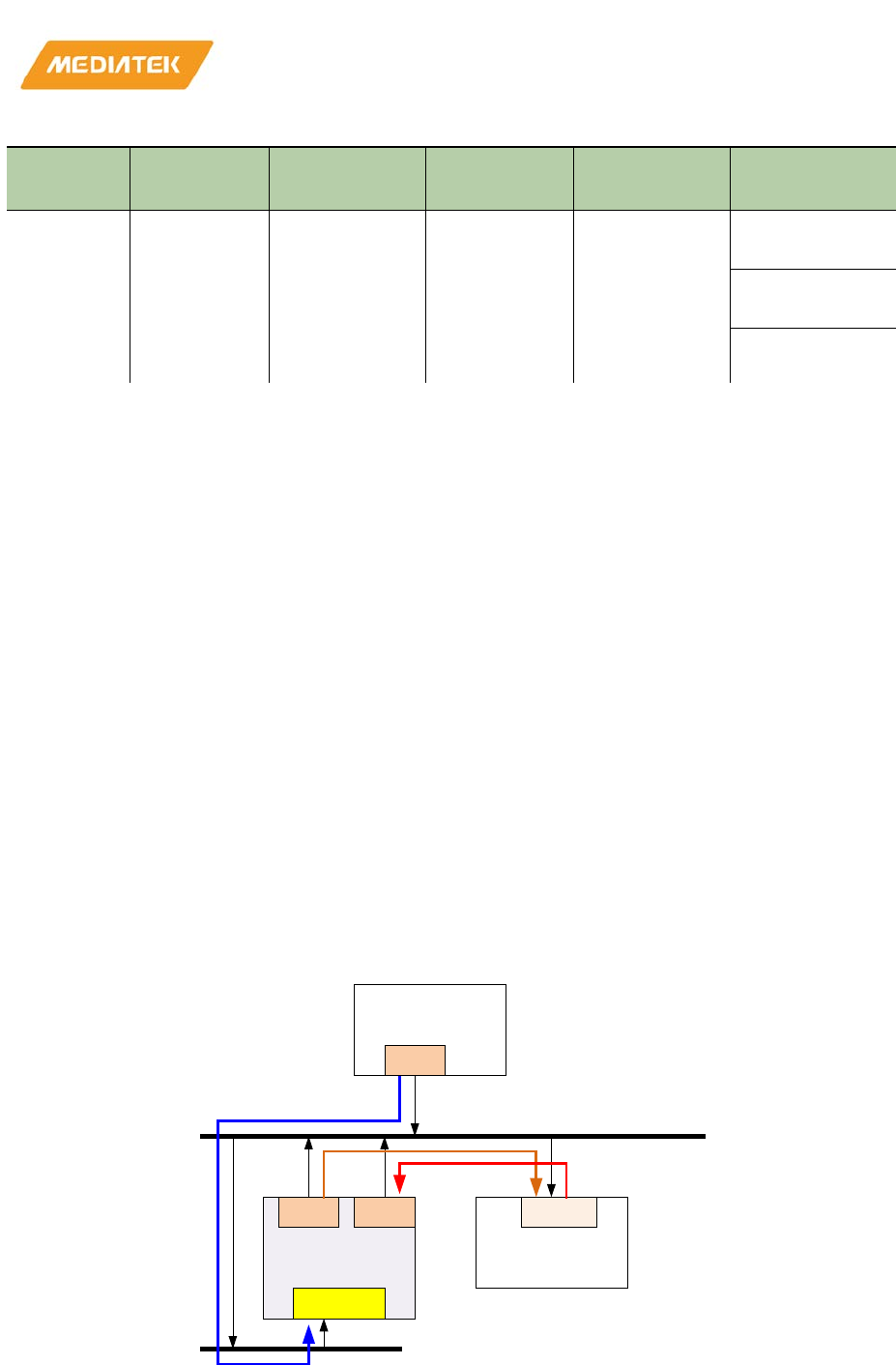
MT76x7
Internet-of-Things Wireless Connectivity
Reference Manual
© 2015 - 2017 MediaTek Inc
Page 376 of 798
This document contains information that is proprietary to MediaTek Inc. (“MediaTek”) and/or its licensor(s).
Any unauthorized use, reproduction or disclosure of this document in whole or in part is strictly prohibited
Start
address
End address Function Power Domain Software Clock
gating control
Description
controller
System Control
Space (SYSTICK)
Floating-point
unit
2.4.12. SYSRAM_CM4
SYSRAM, the internal SRAM, is mapped on the system bus interface of Cortex M4. M4 can carry out
instruction fetches and data accesses to the SYSRAM.
SYSRAM is the internal SRAM that the DMA engine can access. It can be used as a GDMA or VFIFO buffer, the
source and the destination of GDMA controller, for memory-to-memory transfer as well the transfer between
memory and peripherals.
2.4.13. Crypto engine
2.4.13.1. Features
• Provides two AHB bus master port to read/write sysram data for crypto engine
• Provides one APB bus slave port for CR control
• Supports AES128/AES192/AES256/DES/3DES algorithm (block cipher)
• Supports SHA1/SHA224/SHA256/SHA384/SHA512/MD5 (hash function)
2.4.13.2. Functional description
CM4
Crypto
engine sysram
AHB SAHB M
APB
AHB M
2
3
AHB M
AHB5
APB2
MT76x7
Internet-of-Things Wireless Connectivity
Reference Manual
© 2015 - 2017 MediaTek Inc
Page 377 of 798
This document contains information that is proprietary to MediaTek Inc. (“MediaTek”) and/or its licensor(s).
Any unauthorized use, reproduction or disclosure of this document in whole or in part is strictly prohibited
Figure 2-35. Crypto engine system
In system view, as shown above in Figure 2-35, the control flow of crypto engine is as follows:
1) Cortex-M4 sets the CR of crypto engine through APB interface; the CR contains Key,
source/destination memory address, and crypto algorithm.
2) Crypto engine fetches plaintext (ciphertext) from source address into crypto sub function and start
Encryption (Decryption).
3) After Encryption (Decryption) is completed, crypto engine stores ciphertext (plaintext) to destination
address.
The block diagram of crypto engine is shown here in Figure 2-36. The Crypto Engine supports AES (Advanced
Encryption Standard), DES (Data Encryption Standard), and 3DES for block cipher. The Crypto Engine also
supports SHA 1(Secure Hash Algorithm)/SHA224/SHA256/SHA384/SHA512/MD5 for hash function.
Figure 2-36. Crypto Engine block diagram
1) AES (Advanced Encryption Standard)
Supports these specifications:
Table 2-27. AES hardware specification
AES ECB 128 bits Encrypt Decrypt
192 bits Encrypt Decrypt
256 bits Encrypt Decrypt
CBC 128 bits Encrypt Decrypt
192 bits Encrypt Decrypt
256 bits Encrypt Decrypt
2) DES (Data Encryption Standard)
Table 2-28. DES hardware specification
AHB M
CR
AHB M
Crypto engine
AES
DES/3DES
SHA1/SHA224/
SHA256/MD5
SHA512/SHA384
APB
DMA1DMA2
Source
Addr
Destination
Addr
Data Result
MT76x7
Internet-of-Things Wireless Connectivity
Reference Manual
© 2015 - 2017 MediaTek Inc
Page 378 of 798
This document contains information that is proprietary to MediaTek Inc. (“MediaTek”) and/or its licensor(s).
Any unauthorized use, reproduction or disclosure of this document in whole or in part is strictly prohibited
Supports these specifications:
DES/3DES ECB 64 bits( DES) Encrypt Decrypt
192 bits(3DES) Encrypt Decrypt
CBC 64 bits( DES) Encrypt Decrypt
192 bits(3DES) Encrypt Decrypt
3) SHA Engine (Security Hash Algorithm Engine)
There are two hash engines in the SHA engine. It includes SHA1, SHA224, SHA256, SHA384, SHA512, and MD5.
2.4.13.3. Programming sequence
Table 2-29. AES128 programming sequence
step Programming sequence Control register
AES128 1 select engine is AES
select key source (sw or efuse)
if key is from effuse, select key1 or key2
ENGINE_CTRL
2 source address
destination address
SOUR_ADR
DEST_ADR
3 setting data length (data length = 128 bits * n)
Example1: 128 bits, TOTAL_LEN=4
Example2: 256 bits, TOTAL_LEN=8
TOTAL_LEN
4 setting AES key length
setting encryption or decryption
ECB ,CBC or CTR mode
AES_MODE
5 if key is from sw, setting KEY AES_KEY5~AES_KEY8
6 unmask NVIC 0xE000E100
7 start crypto engine ENGINE_CTRL
Table 2-30. AES192 programming sequence
Step Programming sequence Control register
AES192 1 select engine is AES
select key source (sw or efuse)
if key is from effuse, select key1 or key2
ENGINE_CTRL
2 source address
destination address
SOUR_ADR
DEST_ADR
3 setting data length (data length = 128 bits * n)
Example1: 128 bits, TOTAL_LEN=4
Example2: 256 bits, TOTAL_LEN=8
TOTAL_LEN
4 setting AES key length
setting encryption or decryption
ECB ,CBC or CTR mode
AES_MODE
5 if key is from sw, setting KEY AES_KEY3~AES_KEY8

MT76x7
Internet-of-Things Wireless Connectivity
Reference Manual
© 2015 - 2017 MediaTek Inc
Page 379 of 798
This document contains information that is proprietary to MediaTek Inc. (“MediaTek”) and/or its licensor(s).
Any unauthorized use, reproduction or disclosure of this document in whole or in part is strictly prohibited
Step Programming sequence Control register
6 unmask NVIC 0xE000E100
7 start crypto engine ENGINE_CTRL
Table 2-31. AES256 programming sequence
Step Programming sequence Control register
AES256 1 select engine is AES
select key source (sw or efuse)
if key is from effuse, select key1 or key2
ENGINE_CTRL
2 source address
destination address
SOUR_ADR
DEST_ADR
3 setting data length (data length = 128 bits *
n)
Example1: 128 bits, TOTAL_LEN=4
Example2: 256 bits, TOTAL_LEN=8
TOTAL_LEN
4 setting AES key length
setting encryption or decryption
ECB ,CBC or CTR mode
AES_MODE
5 if key is from sw, setting KEY AES_KEY1~AES_KEY8
6 unmask NVIC 0xE000E100
7 start crypto engine ENGINE_CTRL
Table 2-32. DES programming sequence
Step Programming sequence Control register
DES 1 select engine is DES
select key source (sw or efuse)
if key is from effuse, select key1 or key2
ENGINE_CTRL
2 source address
destination address
SOUR_ADR
DEST_ADR
3 setting data length (data length = 128 bits *
n)
If data length is only 64 bits, please do
padding to make sure data length larger than
128bits, please fill TOTAL_LEN as 4
Example1: 128 bits, TOTAL_LEN=4
Example2: 256 bits, TOTAL_LEN=8
TOTAL_LEN
4 setting DES key length
setting encryption or decryption
ECB or CBC mode
DES_MODE
5 if key is from sw, setting KEY DES_KEY5~AES_KEY6
6 unmask NVIC 0xE000E100

MT76x7
Internet-of-Things Wireless Connectivity
Reference Manual
© 2015 - 2017 MediaTek Inc
Page 380 of 798
This document contains information that is proprietary to MediaTek Inc. (“MediaTek”) and/or its licensor(s).
Any unauthorized use, reproduction or disclosure of this document in whole or in part is strictly prohibited
Step Programming sequence Control register
7 start crypto engine ENGINE_CTRL
Table 2-33. Triple-DES programming sequence
Step Programming sequence Control register
Triple-DES 1 select engine is DES
select key source (sw or efuse)
if key is from effuse, select key1 or key2
ENGINE_CTRL
2 source address
destination address
SOUR_ADR
DEST_ADR
3 setting data length (data length = 128 bits * n)
if data is not multiple of 128 bits, please pad
to multiple of 128 bits
Example1: 128 bits, TOTAL_LEN=4
Example2: 256 bits, TOTAL_LEN=8
TOTAL_LEN
4 setting DES key length
setting encryption or decryption
ECB or CBC mode
DES_MODE
5 if key is from sw, setting KEY DES_KEY1~AES_KEY6
6 unmask NVIC 0xE000E100
7 start crypto engine ENGINE_CTRL
Table 2-34. SHA256 programming sequence
Step Programming sequence Control register
SHA256 1 select engine is SHA256
select key source (sw or efuse)
ENGINE_CTRL
2 source address
destination address
SOUR_ADR
DEST_ADR
3 setting data length ( data length = 128 bits *
n)
Example1: 128 bits, TOTAL_LEN=4
Example2: 256 bits, TOTAL_LEN=8
TOTAL_LEN
4 setting initial vector SHA256_IV1~SHA512_IV8
5 select SHA256 engine
(SHA256/SHA224/SHA1/MD5)
setting restart enable (write 1)
SHA256_MODE
7 unmask NVIC 0xE000E100
8 start crypto engine ENGINE_CTRL
Table 2-35. SHA224 programming sequence

MT76x7
Internet-of-Things Wireless Connectivity
Reference Manual
© 2015 - 2017 MediaTek Inc
Page 381 of 798
This document contains information that is proprietary to MediaTek Inc. (“MediaTek”) and/or its licensor(s).
Any unauthorized use, reproduction or disclosure of this document in whole or in part is strictly prohibited
Step Programming sequence Control register
SHA224 1 select engine is SHA256
select key source (sw or efuse)
ENGINE_CTRL
2 source address
destination address
SOUR_ADR
DEST_ADR
3 setting data length (data length = 128 bits * n)
Example1: 128 bits, TOTAL_LEN=4
Example2: 256 bits, TOTAL_LEN=8
TOTAL_LEN
4 setting initial vector SHA256_IV1~SHA512_IV8
5 select SHA224 engine
(SHA256/SHA224/SHA1/MD5)
setting restart enable (write 1)
SHA256_MODE
7 unmask NVIC 0xE000E100
8 start crypto engine ENGINE_CTRL
Table 2-36. SHA1 programming sequence
Step Programming sequence Control register
SHA1 1 select engine is SHA256
select key source (sw or efuse)
ENGINE_CTRL
2 source address
destination address
SOUR_ADR
DEST_ADR
3 setting data length (data length = 128 bits * n)
Example1: 128 bits, TOTAL_LEN=4
Example2: 256 bits, TOTAL_LEN=8
TOTAL_LEN
4 setting initial vector SHA256_IV1~SHA512_IV8
5 select SHA1 engine
(SHA256/SHA224/SHA1/MD5)
setting restart enable (write 1)
SHA256_MODE
7 unmask NVIC 0xE000E100
8 start crypto engine ENGINE_CTRL
Table 2-37. MD5 programming sequence
Step Programming sequence Control register
MD5 1 select engine is SHA256
select key source (sw or efuse)
ENGINE_CTRL
2 source address
destination address
SOUR_ADR
DEST_ADR
3 setting data length (data length = 128 bits * n)
Example1: 128 bits, TOTAL_LEN=4
Example2: 256 bits, TOTAL_LEN=8
TOTAL_LEN
4 setting initial vector SHA256_IV1~SHA512_IV8
5 select MD5 engine SHA256_MODE

MT76x7
Internet-of-Things Wireless Connectivity
Reference Manual
© 2015 - 2017 MediaTek Inc
Page 382 of 798
This document contains information that is proprietary to MediaTek Inc. (“MediaTek”) and/or its licensor(s).
Any unauthorized use, reproduction or disclosure of this document in whole or in part is strictly prohibited
Step Programming sequence Control register
(SHA256/SHA224/SHA1/MD5)
setting restart enable (write 1)
7 unmask NVIC 0xE000E100
8 start crypto engine ENGINE_CTRL
Table 2-38. SHA512 programming sequence
Step Programming sequence Control register
SHA512 1 select engine is SHA512
select key source (sw or efuse)
ENGINE_CTRL
2 source address
destination address
SOUR_ADR
DEST_ADR
3 setting data length (data length = 128 bits *
n)
Example1: 128 bits, TOTAL_LEN=4
Example2: 256 bits, TOTAL_LEN=8
TOTAL_LEN
4 setting initial vector SHA512_IV11, SHA512_IV12
~SHA512_IV81,SHA512_IV82
5 select SHA512 engine (SHA512/SHA384)
setting restart enable (write 1)
SHA512_MODE
7 unmask NVIC 0xE000E100
8 start crypto engine ENGINE_CTRL
Table 2-39. SHA384 programming sequence
Step Programming sequence Control register
SHA384 1 select engine is SHA512
select key source (sw or efuse)
ENGINE_CTRL
2 source address
destination address
SOUR_ADR
DEST_ADR
3 setting data length (data length = 128 bits *
n)
Example1: 128 bits, TOTAL_LEN=4
Example2: 256 bits, TOTAL_LEN=8
TOTAL_LEN
4 setting initial vector SHA512_IV11, SHA512_IV12
~SHA512_IV81,SHA512_IV82
5 select SHA384 engine (SHA512/SHA384)
setting restart enable (write 1)
SHA512_MODE
7 unmask NVIC 0xE000E100
8 start crypto engine ENGINE_CTRL
MT76x7
Internet-of-Things Wireless Connectivity
Reference Manual
© 2015 - 2017 MediaTek Inc
Page 383 of 798
This document contains information that is proprietary to MediaTek Inc. (“MediaTek”) and/or its licensor(s).
Any unauthorized use, reproduction or disclosure of this document in whole or in part is strictly prohibited
2.4.13.4. Register definitions
Module name: mtk_crypto Base address: (+830f0000h)
Address
Name Width
Register Function
830F0004
ENGINE_CTRL
32
CRYPTO ENGINE CONTROL REGISTER
830F0008
ENGINE_STA
32
CRYPTO ENGINE STATUS REGISTER
830F000C
TOTAL_LEN
32
TOTAL ENCRYPTED DATA LENGTH
830F0010
SOUR_ADR
32
THE START OF SOURCE ADDRESS
830F0020
DEST_ADR
32
THE
START OF DESTINATION ADDRESS
830F1000
AES_DATA1
32
ADVANCED ENCRYPTION STANDARD
DATA1
830F1010
AES_DATA2
32
ADVANCED ENCRYPTION STANDARD
DATA2
830F1020
AES_DATA3
32
ADVANCED ENCRYPTION STANDARD
DATA3
830F1030
AES_DATA4
32
ADVANCED ENCRYPTION STANDARD
DATA4
830F1040
AES_KEY1
32
ADVANCED ENCRYPTION STANDARD
KEY1
830F1050
AES_KEY2
32
ADVANCED ENCRYPTION STANDARD
KEY2
830F1060
AES_KEY3
32
ADVANCED ENCRYPTION STANDARD
KEY3
830F1070
AES_KEY4
32
ADVANCED ENCRYPTION STANDARD
KEY4
830F1080
AES_KEY5
32
ADVANCED ENCRYPTION STANDARD
KEY5
830F1090
AES_KEY6
32
ADVANCED ENCRYPTION STANDARD
KEY6
830F10A0
AES_KEY7
32
ADVANCED ENCRYPTION STANDARD
KEY7
830F10B0
AES_KEY8
32
ADVANCED ENCRYPTION STANDARD
KEY8
830F10C0
AES_EOD1
32
ADVANCED ENCRYPTION STANDARD
EXORSIVE OR DATA1
830F10D0
AES_EOD2
32
ADVANCED ENCRYPTION STANDARD
EXORSIVE OR DATA2
830F10E0
AES_EOD3
32
ADVANCED ENCRYPTION STANDARD
EXORSIVE OR DATA3
830F10F0
AES_EOD4
32
ADVANCED ENCRYPTION STANDARD
EXORSIVE OR DATA4
830F1200
AES_MODE
32
ADVANCED ENCRYPTION STANDARD
MODE
830F2000
DES_DATA1
32
DATA ENCRYPTION STANDARD DATA1
830F2010
DES_DATA2
32
DATA ENCRYPTION STANDARD
DATA2
830F2040
DES_KEY1
32
DATA ENCRYPTION STANDARD KEY1
830F2050
DES_KEY2
32
DATA ENCRYPTION STANDARD KEY2
830F2060
DES_KEY3
32
DATA ENCRYPTION STANDARD
KEY3
830F2070
DES_KEY4
32
DATA ENCRYPTION STANDARD KEY4
830F2080
DES_KEY5
32
DATA ENCRYPTION STANDARD KEY5
830F2090
DES_KEY6
32
DATA ENCRYPTION STANDARD KEY6
830F20C0
DES_IV1
32
DATA ENCRYPTION STANDARD INITIAL
VECTOR1

MT76x7
Internet-of-Things Wireless Connectivity
Reference Manual
© 2015 - 2017 MediaTek Inc
Page 384 of 798
This document contains information that is proprietary to MediaTek Inc. (“MediaTek”) and/or its licensor(s).
Any unauthorized use, reproduction or disclosure of this document in whole or in part is strictly prohibited
Address
Name
Width
Register Function
830F20D0
DES_IV2
32
DATA ENCRYPTION STANDARD INITIAL
VECTOR2
830F2200
DES_MODE
32
DATA
ENCRYPTION STANDARD MODE
830F3200
SHA256_MODE
32
SECURE HASH ALGORITHM 256 MODE
830F3000
SHA256_IV1
32
SECURE HASH ALGORITHM 256 INITIAL
VECTOR1
830F3010
SHA256_IV2
32
SECURE HASH ALGORITHM 256 INITIAL
VECTOR2
830F3020
SHA256_IV3
32
SECURE HASH ALGORITHM 256 INITIAL
VECTOR3
830F3030
SHA256_IV4
32
SECURE HASH ALGORITHM 256 INITIAL
VECTOR4
830F3040
SHA256_IV5
32
SECURE HASH ALGORITHM 256 INITIAL
VECTOR5
830F3050
SHA256_IV6
32
SECURE HASH ALGORITHM 256 INITIAL
VECTOR6
830F3060
SHA256_IV7
32
SECURE HASH ALGORITHM 256 INITIAL
VECTOR7
830F3070
SHA256_IV8
32
SECURE HASH ALGORITHM 256 INITIAL
VECTOR8
830F4200
SHA512_MODE
32
SECURE HASH ALGORITHM 512 MODE
830F4000
SHA512_IV11
32
SECURE HASH ALGORITHM 512 INITIAL
VECTOR11
830F4004
SHA512_IV12
32
SECURE HASH ALGORITHM 512 INITIAL
VECTOR12
830F4010
SHA512_IV21
32
SECURE HASH ALGORITHM 512 INITIAL
VECTOR21
830F4014
SHA512_IV22
32
SECURE HASH ALGORITHM 512 INITIAL
VECTOR22
830F4020
SHA512_IV31
32
SECURE HASH ALGORITHM 512 INITIAL
VECTOR31
830F4024
SHA512_IV32
32
SECURE HASH ALGORITHM 512 INITIAL
VECTOR32
830F4030
SHA512_IV41
32
SECURE HASH ALGORITHM 512 INITIAL
VECTOR41
830F4034
SHA512_IV42
32
SECURE HASH ALGORITHM 512 INITIAL
VECTOR42
830F4040
SHA512_IV51
32
SECURE HASH ALGORITHM 512 INITIAL
VECTOR51
830F4044
SHA512_IV52
32
SECURE HASH ALGORITHM 512 INITIAL
VECTOR52
830F4050
SHA512_IV61
32
SECURE HASH ALGORITHM 512 INITIAL
VECTOR61
830F4054
SHA512_IV62
32
SECURE HASH ALGORITHM 512 INITIAL
VECTOR62
830F4060
SHA512_IV71
32
SECURE HASH ALGORITHM 512 INITIAL
VECTOR71
830F4064
SHA512_IV72
32
SECURE HASH ALGORITHM 512 INITIAL
VECTOR72
830F4070
SHA512_IV81
32
SECURE HASH ALGORITHM 512 INITIAL
VECTOR81
830F4074
SHA512_IV82
32
SECURE HASH ALGORITHM 512 INITIAL
VECTOR82
830F8000
DMA1_SRC
32
DMA CHANNEL 1 SOURCE ADDRESS
REGISTER
MT76x7
Internet-of-Things Wireless Connectivity
Reference Manual
© 2015 - 2017 MediaTek Inc
Page 385 of 798
This document contains information that is proprietary to MediaTek Inc. (“MediaTek”) and/or its licensor(s).
Any unauthorized use, reproduction or disclosure of this document in whole or in part is strictly prohibited
Address
Name
Width
Register Function
830F8008
DMA1_WPPT
32
DMA CHANNEL 1 WRAP POINT COUNT
REGISTER
830F800C
DMA1_WPTO
32
DMA CHANNEL 1 WRAP TO ADDRESS
REGISTER
830F8014
DMA1_CON
32
DMA CHANNEL 1 CONTROL REGISTER
830F8024
DMA2_RLCT
32
DMA CHANNEL 1 REMAINING LENGTH
OF CURRENT TRANSFER
830F9000
DMA2_DST
32
DMA CHANNEL 2 DESTINATION
ADDRESS REGISTER
830F9008
DMA2_WPPT
32
DMA CHANNEL 2 WRAP POINT COUNT
REGISTER
830F900C
DMA2_WPTO
32
DMA CHANNEL 2 WRAP TO ADDRESS
REGISTER
830F9014
DMA2_CON
32
DMA CHANNEL 2 CONTROL REGISTER
830F9024
DMA2_RLCT
32
DMA CHANNEL 2 REMAINING LENGTH
OF CURRENT TRANSFER
830F0004
ENGINE_CTRL
CRYPTO ENGINE CONTROL
REGISTER
00000100
Bit
31
30
29
28
27
26
25
24
23
22
21
20
19
18
17
16
Nam
e
Type
Rese
t
Bit
15
14
13
12
11
10
9
8
7
6
5
4
3
2
1
0
Nam
e KEY_BA
NK ST
AR
T
KE
Y_
MO
DE
ES
Type
RW
WO
RW
RW
Rese
t
0 1 0 0 0 0
Bit(s)
Name
Description
9:8
KEY_BANK
choose KEY from effuse
01: key_in1 (from eef_top.aes_kek[255:0])
10: key_in2 (from
eef_top.aes_usecret[255:0])
reference document: key_ctl_connection
4
START
0: crypto engine no work
1: crypto engine start to work
2
KEY_MODE
the key source about AES/DES:
0:from effuse
1:sw mode (AES, DES/3DES use)
1:0
ES
Engine select:
MT76x7
Internet-of-Things Wireless Connectivity
Reference Manual
© 2015 - 2017 MediaTek Inc
Page 386 of 798
This document contains information that is proprietary to MediaTek Inc. (“MediaTek”) and/or its licensor(s).
Any unauthorized use, reproduction or disclosure of this document in whole or in part is strictly prohibited
Bit(s)
Name
Description
00: AES (default)
01: DES/3DES
10:MD5/SHA
11:SHA512
830F0008
ENGINE_STA
CRYPTO ENGINE STATUS REGISTER
00000000
Bit
31
30
29
28
27
26
25
24
23
22
21
20
19
18
17
16
Nam
e
Type
Rese
t
Bit
15
14
13
12
11
10
9
8
7
6
5
4
3
2
1
0
Nam
e
SH
A51
2_
ST
A
SH
A2
56_
ST
A
DS
TA AS
TA
Type
RO
RO
RO
RO
Rese
t
0 0 0 0
Bit(s)
Name
Description
3
SHA512_STA
SHA512 engine work status:
0: hash engine is no work
1:hash engine
is busy
2
SHA256_STA
SHA256 engine work status:
0: hash engine is no work
1:hash engine is busy
1
DSTA
DES/3DES engine work status:
0: DES/3DES engine is no work
1: DES/3DES engine is busy
0
ASTA
AES engine work status:
0: AES engine is no work
1: AES
engine is busy
830F000C
TOTAL_LEN
TOTAL ENCRYPTED DATA LENGTH
00000000

MT76x7
Internet-of-Things Wireless Connectivity
Reference Manual
© 2015 - 2017 MediaTek Inc
Page 387 of 798
This document contains information that is proprietary to MediaTek Inc. (“MediaTek”) and/or its licensor(s).
Any unauthorized use, reproduction or disclosure of this document in whole or in part is strictly prohibited
Bit
31
30
29
28
27
26
25
24
23
22
21
20
19
18
17
16
Nam
e
LEN
Type
RW
Rese
t
0 0 0 0 0 0 0 0 0 0 0 0 0 0 0 0
Bit
15
14
13
12
11
10
9
8
7
6
5
4
3
2
1
0
Nam
e
LEN
Type
RW
Rese
t
0 0 0 0 0 0 0 0 0 0 0 0 0 0 0 0
Bit(s)
Name
Description
31:0
LEN
The amount of data be encrypted or decrypted. (unit byte,
data size = 4*n = LEN4)
830F0010
SOUR_ADR
THE START OF SOURCE ADDRESS
00000000
Bit
31
30
29
28
27
26
25
24
23
22
21
20
19
18
17
16
Nam
e
SADDR
Type
RW
Rese
t
0 0 0 0 0 0 0 0 0 0 0 0 0 0 0 0
Bit
15
14
13
12
11
10
9
8
7
6
5
4
3
2
1
0
Nam
e
SADDR
Type
RW
Rese
t
0 0 0 0 0 0 0 0 0 0 0 0 0 0 0 0
Bit(s)
Name
Description
31:0
SADDR
The amount of data be encrypted or decrypted.
830F0020
DEST_ADR
THE START OF DESTINATION
ADDRESS
00000000
Bit
31
30
29
28
27
26
25
24
23
22
21
20
19
18
17
16
Nam
e
DADDR
Type
RW
Rese
t
0 0 0 0 0 0 0 0 0 0 0 0 0 0 0 0
Bit
15
14
13
12
11
10
9
8
7
6
5
4
3
2
1
0
Nam
e
DADDR
Type
RW
Rese
t
0 0 0 0 0 0 0 0 0 0 0 0 0 0 0 0
MT76x7
Internet-of-Things Wireless Connectivity
Reference Manual
© 2015 - 2017 MediaTek Inc
Page 388 of 798
This document contains information that is proprietary to MediaTek Inc. (“MediaTek”) and/or its licensor(s).
Any unauthorized use, reproduction or disclosure of this document in whole or in part is strictly prohibited
Bit(s)
Name
Description
31:0
DADDR
The amount of data be encrypted or decrypted.
830F1000
AES_DATA1
ADVANCED ENCRYPTION STANDARD
DATA1
00000000
Bit
31
30
29
28
27
26
25
24
23
22
21
20
19
18
17
16
Nam
e
DATA1
Type
RW
Rese
t
0 0 0 0 0 0 0 0 0 0 0 0 0 0 0 0
Bit
15
14
13
12
11
10
9
8
7
6
5
4
3
2
1
0
Nam
e
DATA1
Type
RW
Rese
t
0 0 0 0 0 0 0 0 0 0 0 0 0 0 0 0
Bit(s)
Name
Description
31:0
DATA1
want to be encrypted or decrypted data, the most right
32bits
830F1010
AES_DATA2
ADVANCED ENCRYPTION STANDARD
DATA2
00000000
Bit
31
30
29
28
27
26
25
24
23
22
21
20
19
18
17
16
Nam
e
DATA2
Type
RW
Rese
t
0 0 0 0 0 0 0 0 0 0 0 0 0 0 0 0
Bit
15
14
13
12
11
10
9
8
7
6
5
4
3
2
1
0
Nam
e
DATA2
Type
RW
Rese
t
0 0 0 0 0 0 0 0 0 0 0 0 0 0 0 0
Bit(s)
Name
Description
31:0
DATA2
want to be encrypted or decrypted data
830F1020
AES_DATA3
ADVANCED ENCRYPTION STANDARD
DATA3
00000000
Bit
31
30
29
28
27
26
25
24
23
22
21
20
19
18
17
16
Nam
e
DATA3
MT76x7
Internet-of-Things Wireless Connectivity
Reference Manual
© 2015 - 2017 MediaTek Inc
Page 389 of 798
This document contains information that is proprietary to MediaTek Inc. (“MediaTek”) and/or its licensor(s).
Any unauthorized use, reproduction or disclosure of this document in whole or in part is strictly prohibited
Type
RW
Rese
t
0 0 0 0 0 0 0 0 0 0 0 0 0 0 0 0
Bit
15
14
13
12
11
10
9
8
7
6
5
4
3
2
1
0
Nam
e
DATA3
Type
RW
Rese
t
0 0 0 0 0 0 0 0 0 0 0 0 0 0 0 0
Bit(s)
Name
Description
31:0
DATA3
want to be encrypted or decrypted data
830F1030
AES_DATA4
ADVANCED ENCRYPTION STANDARD
DATA4
00000000
Bit
31
30
29
28
27
26
25
24
23
22
21
20
19
18
17
16
Nam
e
DATA4
Type
RW
Rese
t
0 0 0 0 0 0 0 0 0 0 0 0 0 0 0 0
Bit
15
14
13
12
11
10
9
8
7
6
5
4
3
2
1
0
Nam
e
DATA4
Type
RW
Rese
t
0 0 0 0 0 0 0 0 0 0 0 0 0 0 0 0
Bit(s)
Name
Description
31:0
DATA4
want to be encrypted or decrypted data
830F1040
AES_KEY1
ADVANCED ENCRYPTION STANDARD
KEY1
00000000
Bit
31
30
29
28
27
26
25
24
23
22
21
20
19
18
17
16
Nam
e
KEY1
Type
RW
Rese
t
0 0 0 0 0 0 0 0 0 0 0 0 0 0 0 0
Bit
15
14
13
12
11
10
9
8
7
6
5
4
3
2
1
0
Nam
e
KEY1
Type
RW
Rese
t
0 0 0 0 0 0 0 0 0 0 0 0 0 0 0 0
Bit(s)
Name
Description
MT76x7
Internet-of-Things Wireless Connectivity
Reference Manual
© 2015 - 2017 MediaTek Inc
Page 390 of 798
This document contains information that is proprietary to MediaTek Inc. (“MediaTek”) and/or its licensor(s).
Any unauthorized use, reproduction or disclosure of this document in whole or in part is strictly prohibited
Bit(s)
Name
Description
31:0
KEY1
the initial key to encrypt or decrypt data
830F1050
AES_KEY2
ADVANCED ENCRYPTION STANDARD
KEY2
00000000
Bit
31
30
29
28
27
26
25
24
23
22
21
20
19
18
17
16
Nam
e
KEY2
Type
RW
Rese
t
0 0 0 0 0 0 0 0 0 0 0 0 0 0 0 0
Bit
15
14
13
12
11
10
9
8
7
6
5
4
3
2
1
0
Nam
e
KEY2
Type
RW
Rese
t
0 0 0 0 0 0 0 0 0 0 0 0 0 0 0 0
Bit(s)
Name
Description
31:0
KEY2
the initial key to encrypt or decrypt data
830F1060
AES_KEY3
ADVANCED ENCRYPTION STANDARD
KEY3
00000000
Bit
31
30
29
28
27
26
25
24
23
22
21
20
19
18
17
16
Nam
e
KEY3
Type
RW
Rese
t
0 0 0 0 0 0 0 0 0 0 0 0 0 0 0 0
Bit
15
14
13
12
11
10
9
8
7
6
5
4
3
2
1
0
Nam
e
KEY3
Type
RW
Rese
t
0 0 0 0 0 0 0 0 0 0 0 0 0 0 0 0
Bit(s)
Name
Description
31:0
KEY3
the initial key to encrypt or decrypt data
830F1070
AES_KEY4
ADVANCED ENCRYPTION STANDARD
KEY4
00000000
Bit
31
30
29
28
27
26
25
24
23
22
21
20
19
18
17
16
Nam
e
KEY4
Type
RW

MT76x7
Internet-of-Things Wireless Connectivity
Reference Manual
© 2015 - 2017 MediaTek Inc
Page 391 of 798
This document contains information that is proprietary to MediaTek Inc. (“MediaTek”) and/or its licensor(s).
Any unauthorized use, reproduction or disclosure of this document in whole or in part is strictly prohibited
Rese
t
0 0 0 0 0 0 0 0 0 0 0 0 0 0 0 0
Bit
15
14
13
12
11
10
9
8
7
6
5
4
3
2
1
0
Nam
e
KEY4
Type
RW
Rese
t
0 0 0 0 0 0 0 0 0 0 0 0 0 0 0 0
Bit(s)
Name
Description
31:0
KEY4
the initial key to encrypt or decrypt data
830F1080
AES_KEY5
ADVANCED ENCRYPTION STANDARD
KEY5
00000000
Bit
31
30
29
28
27
26
25
24
23
22
21
20
19
18
17
16
Nam
e
KEY5
Type
RW
Rese
t
0 0 0 0 0 0 0 0 0 0 0 0 0 0 0 0
Bit
15
14
13
12
11
10
9
8
7
6
5
4
3
2
1
0
Nam
e
KEY5
Type
RW
Rese
t
0 0 0 0 0 0 0 0 0 0 0 0 0 0 0 0
Bit(s)
Name
Description
31:0
KEY5
the initial key to encrypt or decrypt data
830F1090
AES_KEY6
ADVANCED ENCRYPTION STANDARD
KEY6
00000000
Bit
31
30
29
28
27
26
25
24
23
22
21
20
19
18
17
16
Nam
e
KEY6
Type
RW
Rese
t
0 0 0 0 0 0 0 0 0 0 0 0 0 0 0 0
Bit
15
14
13
12
11
10
9
8
7
6
5
4
3
2
1
0
Nam
e
KEY6
Type
RW
Rese
t
0 0 0 0 0 0 0 0 0 0 0 0 0 0 0 0
Bit(s)
Name
Description
31:0
KEY6
the initial key to encrypt or decrypt data

MT76x7
Internet-of-Things Wireless Connectivity
Reference Manual
© 2015 - 2017 MediaTek Inc
Page 392 of 798
This document contains information that is proprietary to MediaTek Inc. (“MediaTek”) and/or its licensor(s).
Any unauthorized use, reproduction or disclosure of this document in whole or in part is strictly prohibited
Bit(s)
Name
Description
830F10A0
AES_KEY7
ADVANCED ENCRYPTION STANDARD
KEY7
00000000
Bit
31
30
29
28
27
26
25
24
23
22
21
20
19
18
17
16
Nam
e
KEY7
Type
RW
Rese
t
0 0 0 0 0 0 0 0 0 0 0 0 0 0 0 0
Bit
15
14
13
12
11
10
9
8
7
6
5
4
3
2
1
0
Nam
e
KEY7
Type
RW
Rese
t
0 0 0 0 0 0 0 0 0 0 0 0 0 0 0 0
Bit(s)
Name
Description
31:0
KEY7
the initial key to encrypt or decrypt data
830F10B0
AES_KEY8
ADVANCED ENCRYPTION STANDARD
KEY8
00000000
Bit
31
30
29
28
27
26
25
24
23
22
21
20
19
18
17
16
Nam
e
KEY8
Type
RW
Rese
t
0 0 0 0 0 0 0 0 0 0 0 0 0 0 0 0
Bit
15
14
13
12
11
10
9
8
7
6
5
4
3
2
1
0
Nam
e
KEY8
Type
RW
Rese
t
0 0 0 0 0 0 0 0 0 0 0 0 0 0 0 0
Bit(s)
Name
Description
31:0
KEY8
the initial key to encrypt or decrypt data
830F10C0
AES_EOD1
ADVANCED ENCRYPTION STANDARD
EXORSIVE OR DATA1
00000000
Bit
31
30
29
28
27
26
25
24
23
22
21
20
19
18
17
16
Nam
e
XOR_DATA1
Type
RW
Rese
0
0
0
0
0
0
0
0
0
0
0
0
0
0
0
0
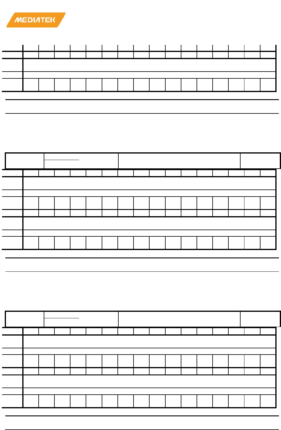
MT76x7
Internet-of-Things Wireless Connectivity
Reference Manual
© 2015 - 2017 MediaTek Inc
Page 393 of 798
This document contains information that is proprietary to MediaTek Inc. (“MediaTek”) and/or its licensor(s).
Any unauthorized use, reproduction or disclosure of this document in whole or in part is strictly prohibited
t
Bit
15
14
13
12
11
10
9
8
7
6
5
4
3
2
1
0
Nam
e
XOR_DATA1
Type
RW
Rese
t
0 0 0 0 0 0 0 0 0 0 0 0 0 0 0 0
Bit(s)
Name
Description
31:0
XOR_DATA1
exorsive or data which is used with xoreod or xoro or xori
in AES_MODE
830F10D0
AES_EOD2
ADVANCED ENCRYPTION STANDARD
EXORSIVE OR DATA2
00000000
Bit
31
30
29
28
27
26
25
24
23
22
21
20
19
18
17
16
Nam
e
XOR_DATA2
Type
RW
Rese
t
0 0 0 0 0 0 0 0 0 0 0 0 0 0 0 0
Bit
15
14
13
12
11
10
9
8
7
6
5
4
3
2
1
0
Nam
e
XOR_DATA2
Type
RW
Rese
t
0 0 0 0 0 0 0 0 0 0 0 0 0 0 0 0
Bit(s)
Name
Description
31:0
XOR_DATA2
exorsive or data which is used with xoreod or xoro or xori
in AES_MODE
830F10E0
AES_EOD3
ADVANCED ENCRYPTION STANDARD
EXORSIVE OR DATA3
00000000
Bit
31
30
29
28
27
26
25
24
23
22
21
20
19
18
17
16
Nam
e
XOR_DATA3
Type
RW
Rese
t
0 0 0 0 0 0 0 0 0 0 0 0 0 0 0 0
Bit
15
14
13
12
11
10
9
8
7
6
5
4
3
2
1
0
Nam
e
XOR_DATA3
Type
RW
Rese
t
0 0 0 0 0 0 0 0 0 0 0 0 0 0 0 0
Bit(s)
Name
Description
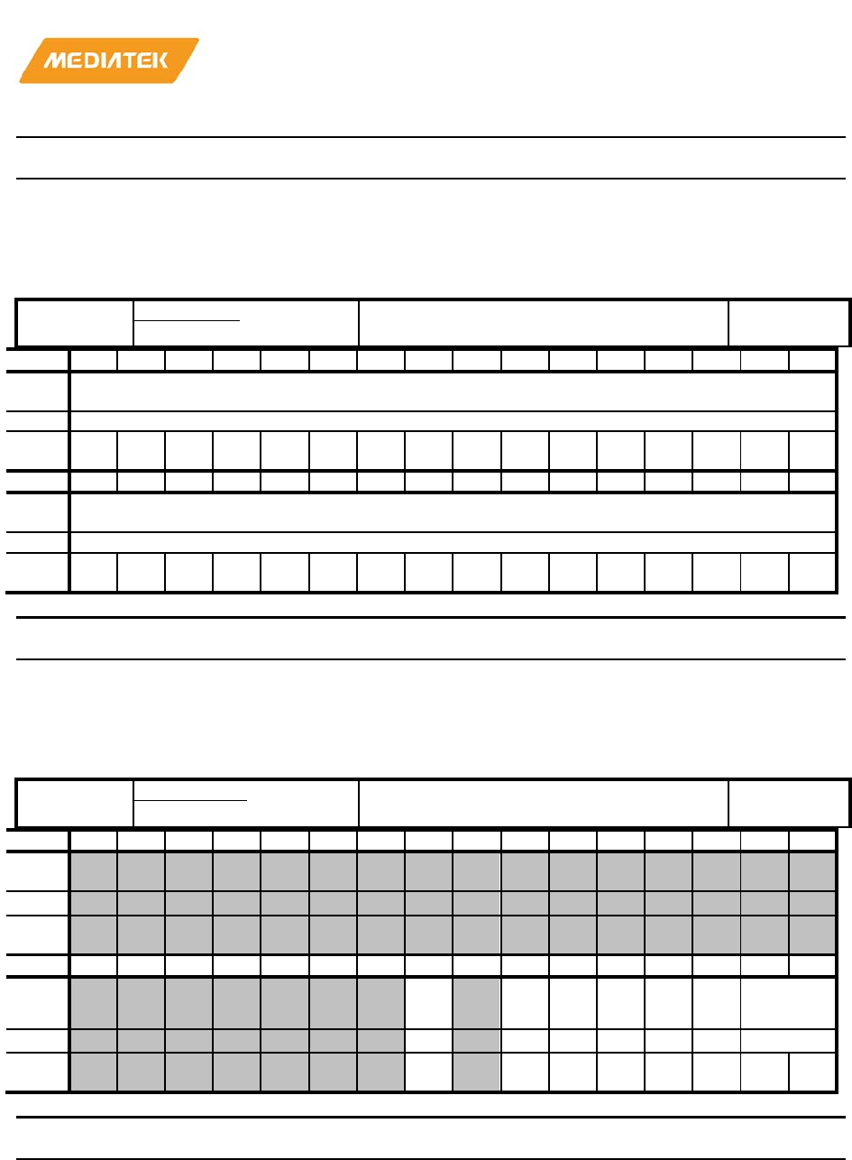
MT76x7
Internet-of-Things Wireless Connectivity
Reference Manual
© 2015 - 2017 MediaTek Inc
Page 394 of 798
This document contains information that is proprietary to MediaTek Inc. (“MediaTek”) and/or its licensor(s).
Any unauthorized use, reproduction or disclosure of this document in whole or in part is strictly prohibited
Bit(s)
Name
Description
31:0
XOR_DATA3
exorsive or data which is used with xoreod or xoro or xori
in AES_MODE
830F10F0
AES_EOD4
ADVANCED ENCRYPTION STANDARD
EXORSIVE OR DATA4
00000000
Bit
31
30
29
28
27
26
25
24
23
22
21
20
19
18
17
16
Nam
e
XOR_DATA4
Type
RW
Rese
t
0 0 0 0 0 0 0 0 0 0 0 0 0 0 0 0
Bit
15
14
13
12
11
10
9
8
7
6
5
4
3
2
1
0
Nam
e
XOR_DATA4
Type
RW
Rese
t
0 0 0 0 0 0 0 0 0 0 0 0 0 0 0 0
Bit(s)
Name
Description
31:0
XOR_DATA4
exorsive or data which is used with xoreod or xoro or xori
in AES_MODE
830F1200
AES_MODE
ADVANCED ENCRYPTION STANDARD
MODE
00000000
Bit
31
30
29
28
27
26
25
24
23
22
21
20
19
18
17
16
Nam
e
Type
Rese
t
Bit
15
14
13
12
11
10
9
8
7
6
5
4
3
2
1
0
Nam
e
XO
RE
OD
UK
XO
RD
AT
XO
RO XO
RI EN
C KEY_LEN
Type
RW
RW
RW
RW
RW
RW
RW
Rese
t
0 0 0 0 0 0 0 0
Bit(s)
Name
Description
8
XOREOD
EOD XOR option. When this bit is set, the AES_EOD is
XORed with result after execution
6
UK
Update key option. When this bit is set, the 128-bit result
will also be updated to the key.
5
XORDAT
The XOR data source. When this bit is set, the AES_DAT is
copied to the AES_EOD before operation

MT76x7
Internet-of-Things Wireless Connectivity
Reference Manual
© 2015 - 2017 MediaTek Inc
Page 395 of 798
This document contains information that is proprietary to MediaTek Inc. (“MediaTek”) and/or its licensor(s).
Any unauthorized use, reproduction or disclosure of this document in whole or in part is strictly prohibited
Bit(s)
Name
Description
4
XORO
Output XOR option.
When this bit is set, the result is XORed with AES_EOD after
operation. After execution, the original AES_DAT is stored to
AES_EOD. (CBC mode : for decryption)
3
XORI
Input XOR option. When this bit is set, the data is XORed
with AES_E
OD before operation. After execution, the
result is stored to AES_EOD. (CBC mode : for encryption)
2
ENC
AES encryption or decryption mode.
0: decryption mode
1: encryption mode
1:0
KEY_LEN
The key length of AES operation. Read this bit to get the
status; one represents busy.
0: 128 bit
1: 192 bit
2 :256 bit
3 :revised
830F2000
DES_DATA1
DATA ENCRYPTION STANDARD
DATA1
00000000
Bit
31
30
29
28
27
26
25
24
23
22
21
20
19
18
17
16
Nam
e
DATA1
Type
RW
Rese
t
0 0 0 0 0 0 0 0 0 0 0 0 0 0 0 0
Bit
15
14
13
12
11
10
9
8
7
6
5
4
3
2
1
0
Nam
e
DATA1
Type
RW
Rese
t
0 0 0 0 0 0 0 0 0 0 0 0 0 0 0 0
Bit(s)
Name
Description
31:0
DATA1
want to be encrypted or decrypted data
830F2010
DES_DATA2
DATA ENCRYPTION STANDARD
DATA2
00000000
Bit
31
30
29
28
27
26
25
24
23
22
21
20
19
18
17
16
Nam
e
DATA2
Type
RW
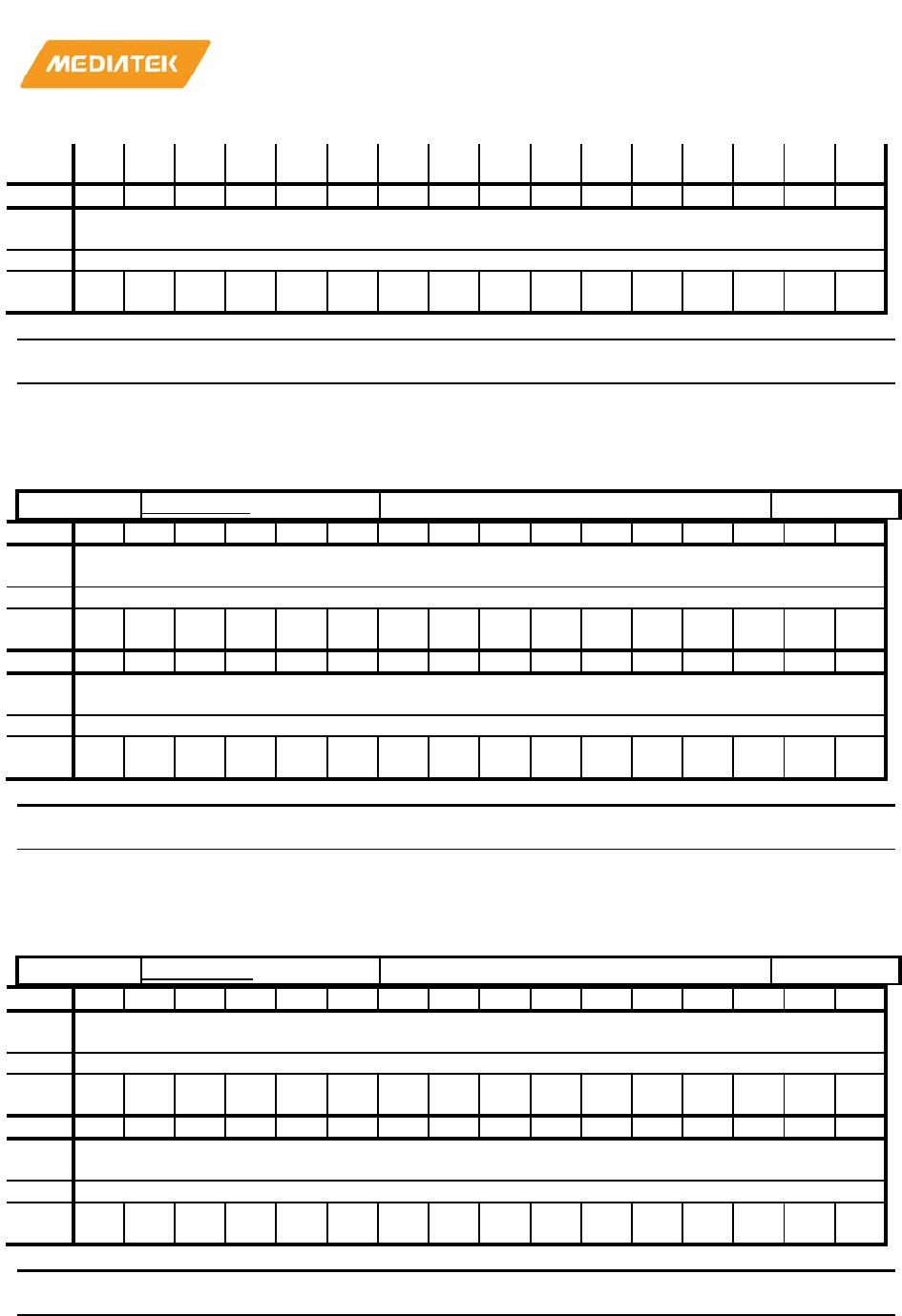
MT76x7
Internet-of-Things Wireless Connectivity
Reference Manual
© 2015 - 2017 MediaTek Inc
Page 396 of 798
This document contains information that is proprietary to MediaTek Inc. (“MediaTek”) and/or its licensor(s).
Any unauthorized use, reproduction or disclosure of this document in whole or in part is strictly prohibited
Rese
t
0 0 0 0 0 0 0 0 0 0 0 0 0 0 0 0
Bit
15
14
13
12
11
10
9
8
7
6
5
4
3
2
1
0
Nam
e
DATA2
Type
RW
Rese
t
0 0 0 0 0 0 0 0 0 0 0 0 0 0 0 0
Bit(s)
Name
Description
31:0
DATA2
want to be encrypted or decrypted data
830F2040
DES_KEY1
DATA ENCRYPTION STANDARD KEY1
00000000
Bit
31
30
29
28
27
26
25
24
23
22
21
20
19
18
17
16
Nam
e
KEY1
Type
RW
Rese
t
0 0 0 0 0 0 0 0 0 0 0 0 0 0 0 0
Bit
15
14
13
12
11
10
9
8
7
6
5
4
3
2
1
0
Nam
e
KEY1
Type
RW
Rese
t
0 0 0 0 0 0 0 0 0 0 0 0 0 0 0 0
Bit(s)
Name
Description
31:0
KEY1
the initial key to encrypt or decrypt data
830F2050
DES_KEY2
DATA ENCRYPTION STANDARD KEY2
00000000
Bit
31
30
29
28
27
26
25
24
23
22
21
20
19
18
17
16
Nam
e
KEY2
Type
RW
Rese
t
0 0 0 0 0 0 0 0 0 0 0 0 0 0 0 0
Bit
15
14
13
12
11
10
9
8
7
6
5
4
3
2
1
0
Nam
e
KEY2
Type
RW
Rese
t
0 0 0 0 0 0 0 0 0 0 0 0 0 0 0 0
Bit(s)
Name
Description
31:0
KEY2
the initial key to encrypt or decrypt data
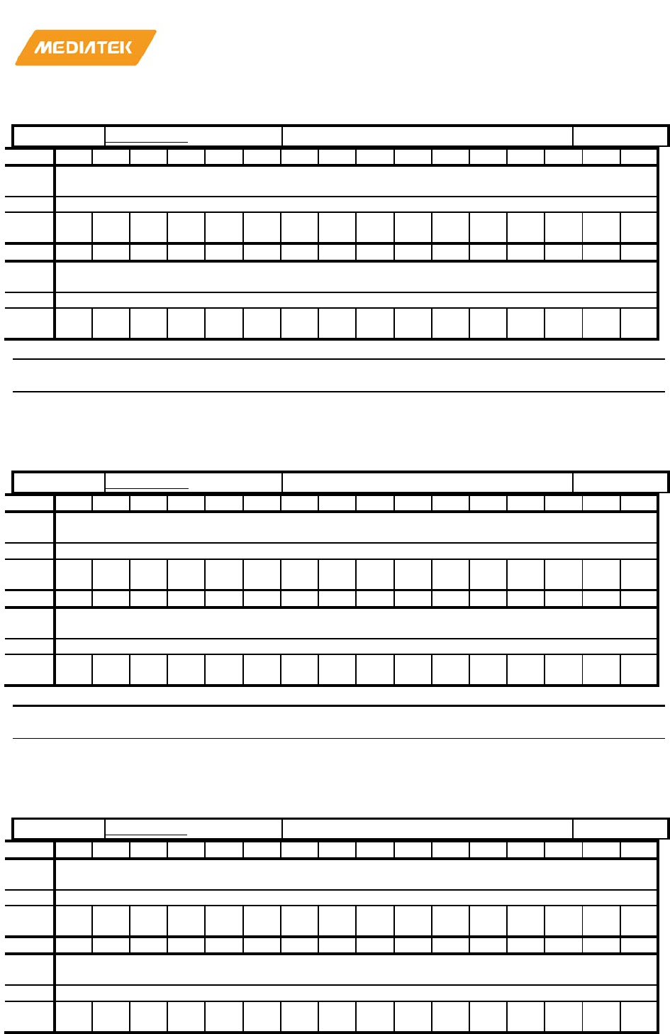
MT76x7
Internet-of-Things Wireless Connectivity
Reference Manual
© 2015 - 2017 MediaTek Inc
Page 397 of 798
This document contains information that is proprietary to MediaTek Inc. (“MediaTek”) and/or its licensor(s).
Any unauthorized use, reproduction or disclosure of this document in whole or in part is strictly prohibited
830F2060
DES_KEY3
DATA ENCRYPTION STANDARD KEY3
00000000
Bit
31
30
29
28
27
26
25
24
23
22
21
20
19
18
17
16
Nam
e
KEY3
Type
RW
Rese
t
0 0 0 0 0 0 0 0 0 0 0 0 0 0 0 0
Bit
15
14
13
12
11
10
9
8
7
6
5
4
3
2
1
0
Nam
e
KEY3
Type
RW
Rese
t
0 0 0 0 0 0 0 0 0 0 0 0 0 0 0 0
Bit(s)
Name
Description
31:0
KEY3
the initial key to encrypt or decrypt data
830F2070
DES_KEY4
DATA ENCRYPTION STANDARD KEY4
00000000
Bit
31
30
29
28
27
26
25
24
23
22
21
20
19
18
17
16
Nam
e
KEY4
Type
RW
Rese
t
0 0 0 0 0 0 0 0 0 0 0 0 0 0 0 0
Bit
15
14
13
12
11
10
9
8
7
6
5
4
3
2
1
0
Nam
e
KEY4
Type
RW
Rese
t
0 0 0 0 0 0 0 0 0 0 0 0 0 0 0 0
Bit(s)
Name
Description
31:0
KEY4
the initial key to encrypt or decrypt data
830F2080
DES_KEY5
DATA ENCRYPTION STANDARD KEY5
00000000
Bit
31
30
29
28
27
26
25
24
23
22
21
20
19
18
17
16
Nam
e
KEY5
Type
RW
Rese
t
0 0 0 0 0 0 0 0 0 0 0 0 0 0 0 0
Bit
15
14
13
12
11
10
9
8
7
6
5
4
3
2
1
0
Nam
e
KEY5
Type
RW
Rese
t
0 0 0 0 0 0 0 0 0 0 0 0 0 0 0 0
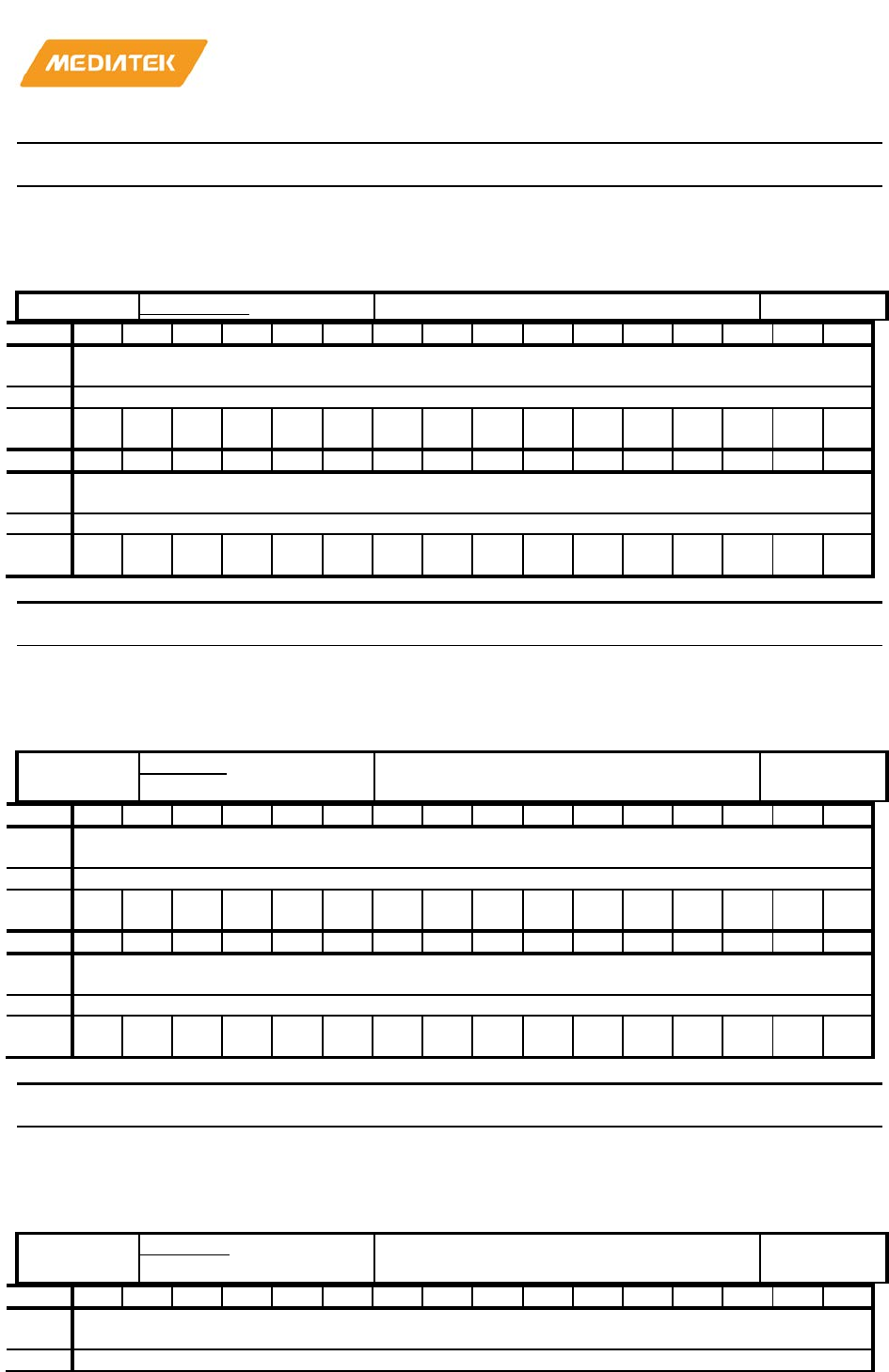
MT76x7
Internet-of-Things Wireless Connectivity
Reference Manual
© 2015 - 2017 MediaTek Inc
Page 398 of 798
This document contains information that is proprietary to MediaTek Inc. (“MediaTek”) and/or its licensor(s).
Any unauthorized use, reproduction or disclosure of this document in whole or in part is strictly prohibited
Bit(s)
Name
Description
31:0
KEY5
the initial key to encrypt or decrypt data
830F2090
DES_KEY6
DATA ENCRYPTION STANDARD KEY6
00000000
Bit
31
30
29
28
27
26
25
24
23
22
21
20
19
18
17
16
Nam
e
KEY6
Type
RW
Rese
t
0 0 0 0 0 0 0 0 0 0 0 0 0 0 0 0
Bit
15
14
13
12
11
10
9
8
7
6
5
4
3
2
1
0
Nam
e
KEY6
Type
RW
Rese
t
0 0 0 0 0 0 0 0 0 0 0 0 0 0 0 0
Bit(s)
Name
Description
31:0
KEY6
the initial key to encrypt or decrypt data
830F20C0
DES_IV1
DATA ENCRYPTION STANDARD
INITIAL VECTOR1
00000000
Bit
31
30
29
28
27
26
25
24
23
22
21
20
19
18
17
16
Nam
e
IV1
Type
RW
Rese
t
0 0 0 0 0 0 0 0 0 0 0 0 0 0 0 0
Bit
15
14
13
12
11
10
9
8
7
6
5
4
3
2
1
0
Nam
e
IV1
Type
RW
Rese
t
0 0 0 0 0 0 0 0 0 0 0 0 0 0 0 0
Bit(s)
Name
Description
31:0
IV1
the initial vector for CBC mode
830F20D0
DES_IV2
DATA ENCRYPTION STANDARD
INITIAL VECTOR2
00000000
Bit
31
30
29
28
27
26
25
24
23
22
21
20
19
18
17
16
Nam
e
IV2
Type
RW
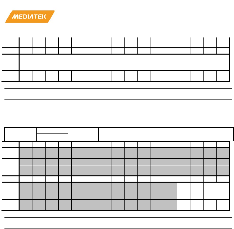
MT76x7
Internet-of-Things Wireless Connectivity
Reference Manual
© 2015 - 2017 MediaTek Inc
Page 399 of 798
This document contains information that is proprietary to MediaTek Inc. (“MediaTek”) and/or its licensor(s).
Any unauthorized use, reproduction or disclosure of this document in whole or in part is strictly prohibited
Rese
t
0 0 0 0 0 0 0 0 0 0 0 0 0 0 0 0
Bit
15
14
13
12
11
10
9
8
7
6
5
4
3
2
1
0
Nam
e
IV2
Type
RW
Rese
t
0 0 0 0 0 0 0 0 0 0 0 0 0 0 0 0
Bit(s)
Name
Description
31:0
IV2
the initial vector for CBC mode
830F2200
DES_MODE
DATA ENCRYPTION STANDARD
MODE
00000000
Bit
31
30
29
28
27
26
25
24
23
22
21
20
19
18
17
16
Nam
e
Type
Rese
t
Bit
15
14
13
12
11
10
9
8
7
6
5
4
3
2
1
0
Nam
e
CB
C
EN
C
KEY_LEN
Type
RW
RW
RW
Rese
t
0 0 0 0
Bit(s)
Name
Description
3
CBC
DES cipher mode
0: EBC mode
1:CBC mode
2
ENC
DES encryption or decryption mode.
0: decryption mode
1: encryption mode
1:0
KEY_LEN
The key length of DES operation. Read this bit to get the
status; one represents busy.
0: 64 bit
1: 128 bit
2 :192 bit
3 :revised
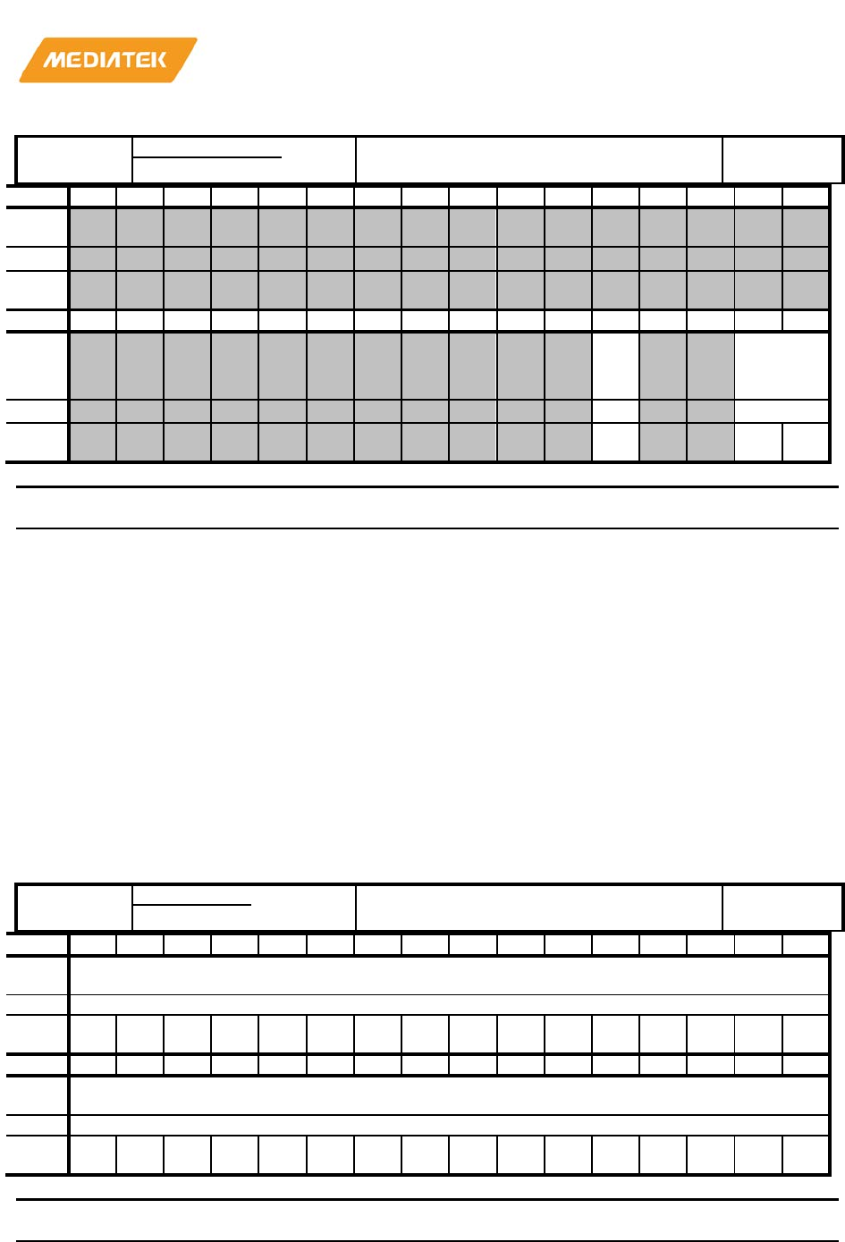
MT76x7
Internet-of-Things Wireless Connectivity
Reference Manual
© 2015 - 2017 MediaTek Inc
Page 400 of 798
This document contains information that is proprietary to MediaTek Inc. (“MediaTek”) and/or its licensor(s).
Any unauthorized use, reproduction or disclosure of this document in whole or in part is strictly prohibited
830F3200
SHA256_MODE
SECURE HASH ALGORITHM 256
MODE
00000000
Bit
31
30
29
28
27
26
25
24
23
22
21
20
19
18
17
16
Nam
e
Type
Rese
t
Bit
15
14
13
12
11
10
9
8
7
6
5
4
3
2
1
0
Nam
e
RE
ST
AR
T
TYPE
Type
WO
RW
Rese
t
0 0 0
Bit(s)
Name
Description
4
RESTART
If restart crypto_engine
1: yes
0:no
1:0
TYPE
SHA256 or SHA224 or SHA1 or MD5
11: MD5
10: SHA1
01: SHA224
00: SHA256 (default)
830F3000
SHA256_IV1
SECURE HASH ALGORITHM 256
INITIAL VECTOR1
00000000
Bit
31
30
29
28
27
26
25
24
23
22
21
20
19
18
17
16
Nam
e
IV1
Type
RW
Rese
t
0 0 0 0 0 0 0 0 0 0 0 0 0 0 0 0
Bit
15
14
13
12
11
10
9
8
7
6
5
4
3
2
1
0
Nam
e
IV1
Type
RW
Rese
t
0 0 0 0 0 0 0 0 0 0 0 0 0 0 0 0
Bit(s)
Name
Description
31:0
IV1
the initial vector
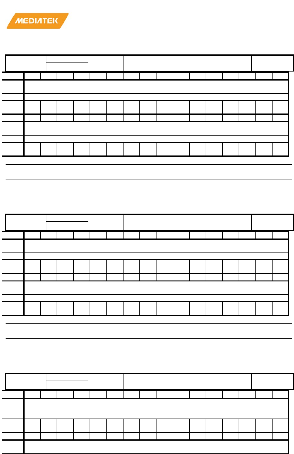
MT76x7
Internet-of-Things Wireless Connectivity
Reference Manual
© 2015 - 2017 MediaTek Inc
Page 401 of 798
This document contains information that is proprietary to MediaTek Inc. (“MediaTek”) and/or its licensor(s).
Any unauthorized use, reproduction or disclosure of this document in whole or in part is strictly prohibited
830F3010
SHA256_IV2
SECURE HASH ALGORITHM 256
INITIAL VECTOR2
00000000
Bit
31
30
29
28
27
26
25
24
23
22
21
20
19
18
17
16
Nam
e
IV2
Type
RW
Rese
t
0 0 0 0 0 0 0 0 0 0 0 0 0 0 0 0
Bit
15
14
13
12
11
10
9
8
7
6
5
4
3
2
1
0
Nam
e
IV2
Type
RW
Rese
t
0 0 0 0 0 0 0 0 0 0 0 0 0 0 0 0
Bit(s)
Name
Description
31:0
IV2
the initial vector
830F3020
SHA256_IV3
SECURE HASH ALGORITHM 256
INITIAL VECTOR3
00000000
Bit
31
30
29
28
27
26
25
24
23
22
21
20
19
18
17
16
Nam
e
IV3
Type
RW
Rese
t
0 0 0 0 0 0 0 0 0 0 0 0 0 0 0 0
Bit
15
14
13
12
11
10
9
8
7
6
5
4
3
2
1
0
Nam
e
IV3
Type
RW
Rese
t
0 0 0 0 0 0 0 0 0 0 0 0 0 0 0 0
Bit(s)
Name
Description
31:0
IV3
the initial vector
830F3030
SHA256_IV4
SECURE HASH ALGORITHM 256
INITIAL VECTOR4
00000000
Bit
31
30
29
28
27
26
25
24
23
22
21
20
19
18
17
16
Nam
e
IV4
Type
RW
Rese
t
0 0 0 0 0 0 0 0 0 0 0 0 0 0 0 0
Bit
15
14
13
12
11
10
9
8
7
6
5
4
3
2
1
0
Nam
e
IV4
MT76x7
Internet-of-Things Wireless Connectivity
Reference Manual
© 2015 - 2017 MediaTek Inc
Page 402 of 798
This document contains information that is proprietary to MediaTek Inc. (“MediaTek”) and/or its licensor(s).
Any unauthorized use, reproduction or disclosure of this document in whole or in part is strictly prohibited
Type
RW
Rese
t
0 0 0 0 0 0 0 0 0 0 0 0 0 0 0 0
Bit(s)
Name
Description
31:0
IV4
the initial vector
830F3040
SHA256_IV5
SECURE HASH ALGORITHM 256
INITIAL VECTOR5
00000000
Bit
31
30
29
28
27
26
25
24
23
22
21
20
19
18
17
16
Nam
e
IV5
Type
RW
Rese
t
0 0 0 0 0 0 0 0 0 0 0 0 0 0 0 0
Bit
15
14
13
12
11
10
9
8
7
6
5
4
3
2
1
0
Nam
e
IV5
Type
RW
Rese
t
0 0 0 0 0 0 0 0 0 0 0 0 0 0 0 0
Bit(s)
Name
Description
31:0
IV5
the initial vector
830F3050
SHA256_IV6
SECURE HASH ALGORITHM 256
INITIAL VECTOR6
00000000
Bit
31
30
29
28
27
26
25
24
23
22
21
20
19
18
17
16
Nam
e
IV6
Type
RW
Rese
t
0 0 0 0 0 0 0 0 0 0 0 0 0 0 0 0
Bit
15
14
13
12
11
10
9
8
7
6
5
4
3
2
1
0
Nam
e
IV6
Type
RW
Rese
t
0 0 0 0 0 0 0 0 0 0 0 0 0 0 0 0
Bit(s)
Name
Description
31:0
IV6
the initial vector
830F3060
SHA256_IV7
SECURE HASH ALGORITHM 256
INITIAL VECTOR7
00000000
MT76x7
Internet-of-Things Wireless Connectivity
Reference Manual
© 2015 - 2017 MediaTek Inc
Page 403 of 798
This document contains information that is proprietary to MediaTek Inc. (“MediaTek”) and/or its licensor(s).
Any unauthorized use, reproduction or disclosure of this document in whole or in part is strictly prohibited
Bit
31
30
29
28
27
26
25
24
23
22
21
20
19
18
17
16
Nam
e
IV7
Type
RW
Rese
t
0 0 0 0 0 0 0 0 0 0 0 0 0 0 0 0
Bit
15
14
13
12
11
10
9
8
7
6
5
4
3
2
1
0
Nam
e
IV7
Type
RW
Rese
t
0 0 0 0 0 0 0 0 0 0 0 0 0 0 0 0
Bit(s)
Name
Description
31:0
IV7
the initial vector
830F3070
SHA256_IV8
SECURE HASH ALGORITHM 256
INITIAL VECTOR8
00000000
Bit
31
30
29
28
27
26
25
24
23
22
21
20
19
18
17
16
Nam
e
IV8
Type
RW
Rese
t
0 0 0 0 0 0 0 0 0 0 0 0 0 0 0 0
Bit
15
14
13
12
11
10
9
8
7
6
5
4
3
2
1
0
Nam
e
IV8
Type
RW
Rese
t
0 0 0 0 0 0 0 0 0 0 0 0 0 0 0 0
Bit(s)
Name
Description
31:0
IV8
the initial vector
830F4200
SHA512_MODE
SECURE HASH ALGORITHM 512
MODE
00000000
Bit
31
30
29
28
27
26
25
24
23
22
21
20
19
18
17
16
Nam
e
Type
Rese
t
Bit
15
14
13
12
11
10
9
8
7
6
5
4
3
2
1
0
Nam
e
RE
ST
AR
T
TY
PE
Type
WO
RW
Rese
0
0
MT76x7
Internet-of-Things Wireless Connectivity
Reference Manual
© 2015 - 2017 MediaTek Inc
Page 404 of 798
This document contains information that is proprietary to MediaTek Inc. (“MediaTek”) and/or its licensor(s).
Any unauthorized use, reproduction or disclosure of this document in whole or in part is strictly prohibited
t
Bit(s)
Name
Description
4
RESTART
If restart crypto_engine
1: yes
0:no
0
TYPE
SHA512 or SHA384
1: SHA384
0: SHA512 (default)
830F4000
SHA512_IV11
SECURE HASH ALGORITHM 512
INITIAL VECTOR11
00000000
Bit
31
30
29
28
27
26
25
24
23
22
21
20
19
18
17
16
Nam
e
IV1_1
Type
RW
Rese
t
0 0 0 0 0 0 0 0 0 0 0 0 0 0 0 0
Bit
15
14
13
12
11
10
9
8
7
6
5
4
3
2
1
0
Nam
e
IV1_1
Type
RW
Rese
t
0 0 0 0 0 0 0 0 0 0 0 0 0 0 0 0
Bit(s)
Name
Description
31:0
IV1_1
the initial vector
830F4004
SHA512_IV12
SECURE HASH ALGORITHM 512
INITIAL VECTOR12
00000000
Bit
31
30
29
28
27
26
25
24
23
22
21
20
19
18
17
16
Nam
e
IV12
Type
RW
Rese
t
0 0 0 0 0 0 0 0 0 0 0 0 0 0 0 0
Bit
15
14
13
12
11
10
9
8
7
6
5
4
3
2
1
0
Nam
e
IV12
Type
RW
Rese
t
0 0 0 0 0 0 0 0 0 0 0 0 0 0 0 0
Bit(s)
Name
Description
MT76x7
Internet-of-Things Wireless Connectivity
Reference Manual
© 2015 - 2017 MediaTek Inc
Page 405 of 798
This document contains information that is proprietary to MediaTek Inc. (“MediaTek”) and/or its licensor(s).
Any unauthorized use, reproduction or disclosure of this document in whole or in part is strictly prohibited
Bit(s)
Name
Description
31:0
IV12
the initial vector
830F4010
SHA512_IV21
SECURE HASH ALGORITHM 512
INITIAL VECTOR21
00000000
Bit
31
30
29
28
27
26
25
24
23
22
21
20
19
18
17
16
Nam
e
IV2_1
Type
RW
Rese
t
0 0 0 0 0 0 0 0 0 0 0 0 0 0 0 0
Bit
15
14
13
12
11
10
9
8
7
6
5
4
3
2
1
0
Nam
e
IV2_1
Type
RW
Rese
t
0 0 0 0 0 0 0 0 0 0 0 0 0 0 0 0
Bit(s)
Name
Description
31:0
IV2_1
the initial vector
830F4014
SHA512_IV22
SECURE HASH ALGORITHM 512
INITIAL VECTOR22
00000000
Bit
31
30
29
28
27
26
25
24
23
22
21
20
19
18
17
16
Nam
e
IV2_2
Type
RW
Rese
t
0 0 0 0 0 0 0 0 0 0 0 0 0 0 0 0
Bit
15
14
13
12
11
10
9
8
7
6
5
4
3
2
1
0
Nam
e
IV2_2
Type
RW
Rese
t
0 0 0 0 0 0 0 0 0 0 0 0 0 0 0 0
Bit(s)
Name
Description
31:0
IV2_2
the initial vector
830F4020
SHA512_IV31
SECURE HASH ALGORITHM 512
INITIAL VECTOR31
00000000
Bit
31
30
29
28
27
26
25
24
23
22
21
20
19
18
17
16
Nam
e
IV3_1
Type
RW
MT76x7
Internet-of-Things Wireless Connectivity
Reference Manual
© 2015 - 2017 MediaTek Inc
Page 406 of 798
This document contains information that is proprietary to MediaTek Inc. (“MediaTek”) and/or its licensor(s).
Any unauthorized use, reproduction or disclosure of this document in whole or in part is strictly prohibited
Rese
t
0 0 0 0 0 0 0 0 0 0 0 0 0 0 0 0
Bit
15
14
13
12
11
10
9
8
7
6
5
4
3
2
1
0
Nam
e
IV3_1
Type
RW
Rese
t
0 0 0 0 0 0 0 0 0 0 0 0 0 0 0 0
Bit(s)
Name
Description
31:0
IV3_1
the initial vector
830F4024
SHA512_IV32
SECURE HASH ALGORITHM 512
INITIAL VECTOR32
00000000
Bit
31
30
29
28
27
26
25
24
23
22
21
20
19
18
17
16
Nam
e
IV3_2
Type
RW
Rese
t
0 0 0 0 0 0 0 0 0 0 0 0 0 0 0 0
Bit
15
14
13
12
11
10
9
8
7
6
5
4
3
2
1
0
Nam
e
IV3_2
Type
RW
Rese
t
0 0 0 0 0 0 0 0 0 0 0 0 0 0 0 0
Bit(s)
Name
Description
31:0
IV3_2
the initial vector
830F4030
SHA512_IV41
SECURE HASH ALGORITHM 512
INITIAL VECTOR41
00000000
Bit
31
30
29
28
27
26
25
24
23
22
21
20
19
18
17
16
Nam
e
IV4_1
Type
RW
Rese
t
0 0 0 0 0 0 0 0 0 0 0 0 0 0 0 0
Bit
15
14
13
12
11
10
9
8
7
6
5
4
3
2
1
0
Nam
e
IV4_1
Type
RW
Rese
t
0 0 0 0 0 0 0 0 0 0 0 0 0 0 0 0
Bit(s)
Name
Description
31:0
IV4_1
the initial vector
MT76x7
Internet-of-Things Wireless Connectivity
Reference Manual
© 2015 - 2017 MediaTek Inc
Page 407 of 798
This document contains information that is proprietary to MediaTek Inc. (“MediaTek”) and/or its licensor(s).
Any unauthorized use, reproduction or disclosure of this document in whole or in part is strictly prohibited
Bit(s)
Name
Description
830F4034
SHA512_IV42
SECURE HASH ALGORITHM 512
INITIAL VECTOR42
00000000
Bit
31
30
29
28
27
26
25
24
23
22
21
20
19
18
17
16
Nam
e
IV4_2
Type
RW
Rese
t
0 0 0 0 0 0 0 0 0 0 0 0 0 0 0 0
Bit
15
14
13
12
11
10
9
8
7
6
5
4
3
2
1
0
Nam
e
IV4_2
Type
RW
Rese
t
0 0 0 0 0 0 0 0 0 0 0 0 0 0 0 0
Bit(s)
Name
Description
31:0
IV4_2
the initial vector
830F4040
SHA512_IV51
SECURE HASH ALGORITHM 512
INITIAL VECTOR51
00000000
Bit
31
30
29
28
27
26
25
24
23
22
21
20
19
18
17
16
Nam
e
IV5_1
Type
RW
Rese
t
0 0 0 0 0 0 0 0 0 0 0 0 0 0 0 0
Bit
15
14
13
12
11
10
9
8
7
6
5
4
3
2
1
0
Nam
e
IV5_1
Type
RW
Rese
t
0 0 0 0 0 0 0 0 0 0 0 0 0 0 0 0
Bit(s)
Name
Description
31:0
IV5_1
the initial vector
830F4044
SHA512_IV52
SECURE HASH ALGORITHM 512
INITIAL VECTOR52
00000000
Bit
31
30
29
28
27
26
25
24
23
22
21
20
19
18
17
16
Nam
e
IV5_2
Type
RW
Rese
0
0
0
0
0
0
0
0
0
0
0
0
0
0
0
0
MT76x7
Internet-of-Things Wireless Connectivity
Reference Manual
© 2015 - 2017 MediaTek Inc
Page 408 of 798
This document contains information that is proprietary to MediaTek Inc. (“MediaTek”) and/or its licensor(s).
Any unauthorized use, reproduction or disclosure of this document in whole or in part is strictly prohibited
t
Bit
15
14
13
12
11
10
9
8
7
6
5
4
3
2
1
0
Nam
e
IV5_2
Type
RW
Rese
t
0 0 0 0 0 0 0 0 0 0 0 0 0 0 0 0
Bit(s)
Name
Description
31:0
IV5_2
the initial vector
830F4050
SHA512_IV61
SECURE HASH ALGORITHM 512
INITIAL VECTOR61
00000000
Bit
31
30
29
28
27
26
25
24
23
22
21
20
19
18
17
16
Nam
e
IV6_1
Type
RW
Rese
t
0 0 0 0 0 0 0 0 0 0 0 0 0 0 0 0
Bit
15
14
13
12
11
10
9
8
7
6
5
4
3
2
1
0
Nam
e
IV6_1
Type
RW
Rese
t
0 0 0 0 0 0 0 0 0 0 0 0 0 0 0 0
Bit(s)
Name
Description
31:0
IV6_1
the initial vector
830F4054
SHA512_IV62
SECURE HASH ALGORITHM 512
INITIAL VECTOR62
00000000
Bit
31
30
29
28
27
26
25
24
23
22
21
20
19
18
17
16
Nam
e
IV6_2
Type
RW
Rese
t
0 0 0 0 0 0 0 0 0 0 0 0 0 0 0 0
Bit
15
14
13
12
11
10
9
8
7
6
5
4
3
2
1
0
Nam
e
IV6_2
Type
RW
Rese
t
0 0 0 0 0 0 0 0 0 0 0 0 0 0 0 0
Bit(s)
Name
Description
31:0
IV6_2
the initial vector

MT76x7
Internet-of-Things Wireless Connectivity
Reference Manual
© 2015 - 2017 MediaTek Inc
Page 409 of 798
This document contains information that is proprietary to MediaTek Inc. (“MediaTek”) and/or its licensor(s).
Any unauthorized use, reproduction or disclosure of this document in whole or in part is strictly prohibited
Bit(s)
Name
Description
830F4060
SHA512_IV71
SECURE HASH ALGORITHM 512
INITIAL VECTOR71
00000000
Bit
31
30
29
28
27
26
25
24
23
22
21
20
19
18
17
16
Nam
e
IV7_1
Type
RW
Rese
t
0 0 0 0 0 0 0 0 0 0 0 0 0 0 0 0
Bit
15
14
13
12
11
10
9
8
7
6
5
4
3
2
1
0
Nam
e
IV7_1
Type
RW
Rese
t
0 0 0 0 0 0 0 0 0 0 0 0 0 0 0 0
Bit(s)
Name
Description
31:0
IV7_1
the initial vector
830F4064
SHA512_IV72
SECURE HASH ALGORITHM 512
INITIAL VECTOR72
00000000
Bit
31
30
29
28
27
26
25
24
23
22
21
20
19
18
17
16
Nam
e
IV7_2
Type
RW
Rese
t
0 0 0 0 0 0 0 0 0 0 0 0 0 0 0 0
Bit
15
14
13
12
11
10
9
8
7
6
5
4
3
2
1
0
Nam
e
IV7_2
Type
RW
Rese
t
0 0 0 0 0 0 0 0 0 0 0 0 0 0 0 0
Bit(s)
Name
Description
31:0
IV7_2
the initial vector
830F4070
SHA512_IV81
SECURE HASH ALGORITHM 512
INITIAL VECTOR81
00000000
Bit
31
30
29
28
27
26
25
24
23
22
21
20
19
18
17
16
Nam
e
IV8_1
Type
RW
Rese
0
0
0
0
0
0
0
0
0
0
0
0
0
0
0
0

MT76x7
Internet-of-Things Wireless Connectivity
Reference Manual
© 2015 - 2017 MediaTek Inc
Page 410 of 798
This document contains information that is proprietary to MediaTek Inc. (“MediaTek”) and/or its licensor(s).
Any unauthorized use, reproduction or disclosure of this document in whole or in part is strictly prohibited
t
Bit
15
14
13
12
11
10
9
8
7
6
5
4
3
2
1
0
Nam
e
IV8_1
Type
RW
Rese
t
0 0 0 0 0 0 0 0 0 0 0 0 0 0 0 0
Bit(s)
Name
Description
31:0
IV8_1
the initial vector
830F4074
SHA512_IV82
SECURE HASH ALGORITHM 512
INITIAL VECTOR82
00000000
Bit
31
30
29
28
27
26
25
24
23
22
21
20
19
18
17
16
Nam
e
IV8_2
Type
RW
Rese
t
0 0 0 0 0 0 0 0 0 0 0 0 0 0 0 0
Bit
15
14
13
12
11
10
9
8
7
6
5
4
3
2
1
0
Nam
e
IV8_2
Type
RW
Rese
t
0 0 0 0 0 0 0 0 0 0 0 0 0 0 0 0
Bit(s)
Name
Description
31:0
IV8_2
the initial vector
830F8000
DMA1_SRC
DMA CHANNEL 1 SOURCE ADDRESS
REGISTER
00000000
Bit
31
30
29
28
27
26
25
24
23
22
21
20
19
18
17
16
Nam
e
SRC[31:0]
Type
RO
Rese
t
0 0 0 0 0 0 0 0 0 0 0 0 0 0 0 0
Bit
15
14
13
12
11
10
9
8
7
6
5
4
3
2
1
0
Nam
e
SRC[31:0]
Type
RO
Rese
t
0 0 0 0 0 0 0 0 0 0 0 0 0 0 0 0
Bit(s)
Name
Description
31:0
SRC[31:0]
the initial vector SRC[31:0] specifies the base or current
address of transfer source for a DMA channel N.
MT76x7
Internet-of-Things Wireless Connectivity
Reference Manual
© 2015 - 2017 MediaTek Inc
Page 411 of 798
This document contains information that is proprietary to MediaTek Inc. (“MediaTek”) and/or its licensor(s).
Any unauthorized use, reproduction or disclosure of this document in whole or in part is strictly prohibited
Bit(s)
Name
Description
WRITE : Base address of transfer source
READ : Address from which DMA is reading
830F8008
DMA1_WPPT
DMA CHANNEL 1 WRAP POINT
COUNT REGISTER
00000000
Bit
31
30
29
28
27
26
25
24
23
22
21
20
19
18
17
16
Nam
e
Type
Rese
t
Bit
15
14
13
12
11
10
9
8
7
6
5
4
3
2
1
0
Nam
e
WPPT[15:0]
Type
RW
Rese
t
0 0 0 0 0 0 0 0 0 0 0 0 0 0 0 0
Bit(s)
Name
Description
15:0
WPPT[15:0]
WPPT[15:0] specifies the amount of the transfer count
from start to
jumping point for a DMA channel.
WRITE :Address of the jump point.
READ :Value set by the programmer.
830F800C
DMA1_WPTO
DMA CHANNEL 1 WRAP TO ADDRESS
REGISTER
00000000
Bit
31
30
29
28
27
26
25
24
23
22
21
20
19
18
17
16
Nam
e
WPTO[31:0]
Type
RW
Rese
t
0 0 0 0 0 0 0 0 0 0 0 0 0 0 0 0
Bit
15
14
13
12
11
10
9
8
7
6
5
4
3
2
1
0
Nam
e
WPTO[31:0]
Type
RW
Rese
t
0 0 0 0 0 0 0 0 0 0 0 0 0 0 0 0
Bit(s)
Name
Description
31:0
WPTO[31:0]
WPTO[31:0] specifies the address of the jump point for a
DMA channel, i.e. channel.
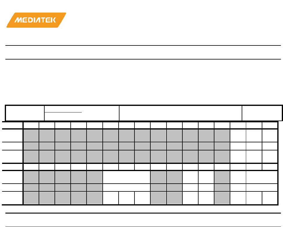
MT76x7
Internet-of-Things Wireless Connectivity
Reference Manual
© 2015 - 2017 MediaTek Inc
Page 412 of 798
This document contains information that is proprietary to MediaTek Inc. (“MediaTek”) and/or its licensor(s).
Any unauthorized use, reproduction or disclosure of this document in whole or in part is strictly prohibited
Bit(s)
Name
Description
WRITE :Address of the jump destination.
READ :Value set by the programmer.
830F8014
DMA1_CON
DMA CHANNEL 1 CONTROL
REGISTER
00000206
Bit
31
30
29
28
27
26
25
24
23
22
21
20
19
18
17
16
Nam
e
DI
R
WP
EN
WP
SD
Type
RO
RW
RW
Rese
t
0 0 0
Bit
15
14
13
12
11
10
9
8
7
6
5
4
3
2
1
0
Nam
e
BURST B2
W
DR
EQ
SIN
C
SIZE
Type
RW
RW
RW
RO
RO
Rese
t
0 1 0 0 0 1 1 0
Bit(s)
Name
Description
18
DIR
Directions of DMA transfer for half-size and Virtual FIFO
DMA
channels, i.e. channels 2~7. The direction is from the perspective of
the
DMA masters. WRITE means read from master device and then
write
to the address specified in DMA_PGMADDR, and vice versa.
0 Read (read from system RAM and write to device)
1 Write (read from device and write to system RAM)
17
WPEN
Address-wrapping for ring buffer. The next address of
DMA jumps to
WRAP TO address when the current address matches WRAP
POINT
count.
0 Disable
1 Enable
16
WPSD
The side using address-wrapping function. Only one side
of a DMA
channel can activate address-wrapping function at a time.
0 Address
-wrapping on source .

MT76x7
Internet-of-Things Wireless Connectivity
Reference Manual
© 2015 - 2017 MediaTek Inc
Page 413 of 798
This document contains information that is proprietary to MediaTek Inc. (“MediaTek”) and/or its licensor(s).
Any unauthorized use, reproduction or disclosure of this document in whole or in part is strictly prohibited
Bit(s)
Name
Description
1 Address-wrapping on destination.
10:8
BURST
Transfer Type. Burst-type transfers have better bus
efficiency. Mass
data movement is recommended to use this kind of transfer.
However,
note that burst
-type transfer does not stop until all of the beats in a
burst
are completed or transfer length is reached. FIFO threshold of
peripherals must be configured carefully while being used to move
data
from/to the peripherals.
What transfer type can be used is restricted by the SIZE. If
SIZE is 00b, i.e. byte transfer, all of the four transfer types can be
used.
If SIZE is 01b, i.e. half
-word transfer, 16-beat incrementing burst
cannot
be used. If SIZE is 10b, i.e. word transfer, only s
ingle and 4-beat
incrementing burst can be used.
000 Single
001 Reserved
010 4
-beat incrementing burst (default)
5
B2W
Word to Byte or Byte to Word transfer for the applications
of
transferring non-word-aligned-address data to word-aligned-
address
data. Note that BURST is set to 4
-beat burst while enabling this
function, and the SIZE is set to Byte.
NO effect on channel 1 , 9, 10
0 Disable
1 Enable
4
DREQ
Throttle and handshake control for DMA transfer
0 No throttle control during DMA transfer o
r transfers occurred
only between memories
1 Hardware handshake management
The DMA master is able to throttle down the transfer rate by
way of request
-grant handshake.

MT76x7
Internet-of-Things Wireless Connectivity
Reference Manual
© 2015 - 2017 MediaTek Inc
Page 414 of 798
This document contains information that is proprietary to MediaTek Inc. (“MediaTek”) and/or its licensor(s).
Any unauthorized use, reproduction or disclosure of this document in whole or in part is strictly prohibited
Bit(s)
Name
Description
2
SINC
Incremental source address. Source addresses increase
every transfer. If
the setting of SIZE is Byte, Source addresses increase by 1 every
single
transfer. If Half
-Word, increase by 2; and if Word, increase by 4.
0 Disable
1 Enable
1:0
SIZE
Data size within the confine of a bus cycle per
transfer.These bits
confines the data transfer size between source and destination to
the
specified value for individual bus cycle. The size is in terms of byte
and
has maximum value of 4 bytes. It is mainly decided by the data
width of
a DMA master.
00 Byte transfer/1 b
yte
01 Half
-word transfer/2 bytes
10 Word transfer/4 bytes
11 Reserved
830F8024
DMA2_RLCT
DMA CHANNEL 1 REMAINING
LENGTH OF CURRENT TRANSFER
00000000
Bit
31
30
29
28
27
26
25
24
23
22
21
20
19
18
17
16
Nam
e
Type
Rese
t
Bit
15
14
13
12
11
10
9
8
7
6
5
4
3
2
1
0
Nam
e
RLCT
Type
RO
Rese
t
0 0 0 0 0 0 0 0 0 0 0 0 0 0 0 0
Bit(s)
Name
Description
15:0
RLCT
This register is to reflect the left amount of the transfer.
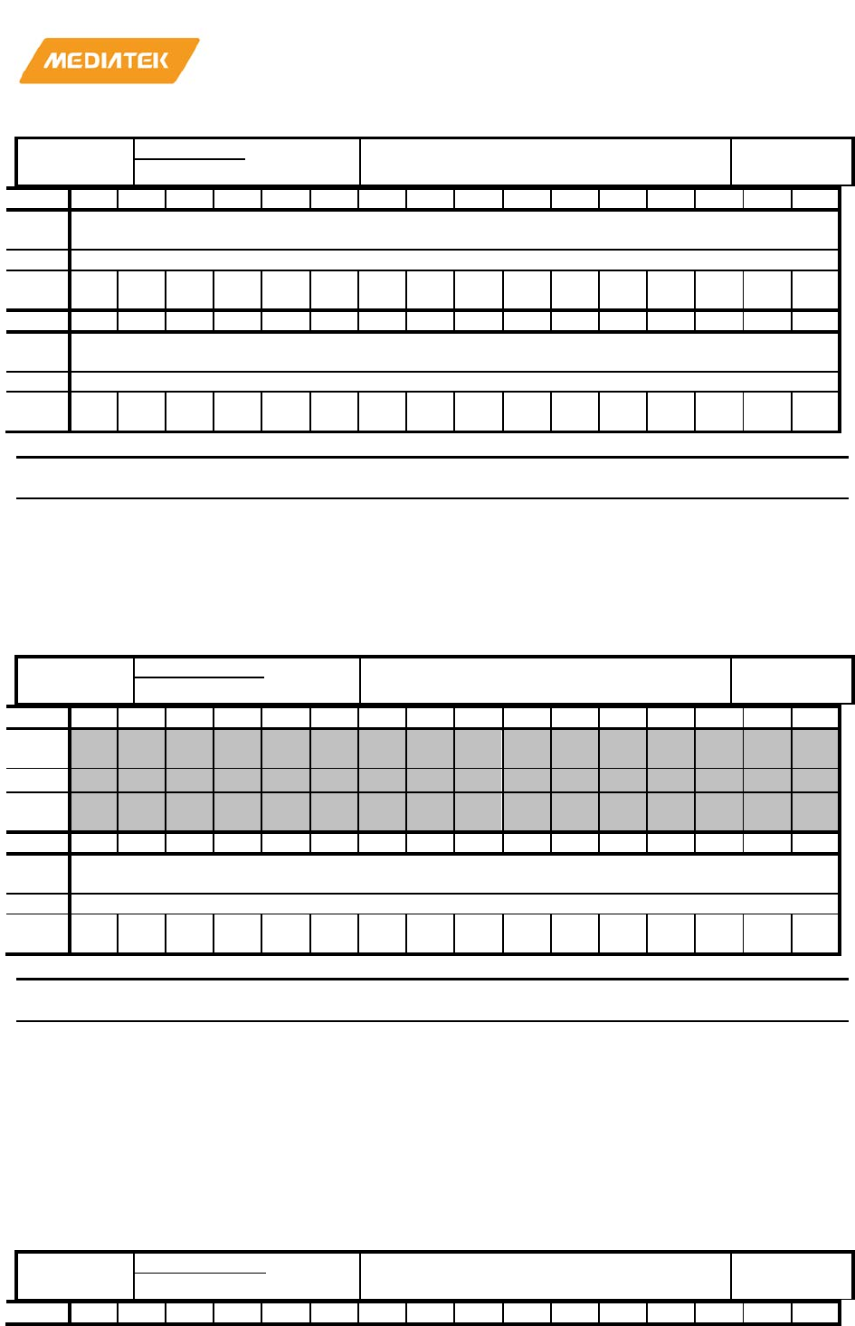
MT76x7
Internet-of-Things Wireless Connectivity
Reference Manual
© 2015 - 2017 MediaTek Inc
Page 415 of 798
This document contains information that is proprietary to MediaTek Inc. (“MediaTek”) and/or its licensor(s).
Any unauthorized use, reproduction or disclosure of this document in whole or in part is strictly prohibited
830F9000
DMA2_DST
DMA CHANNEL 2 DESTINATION
ADDRESS REGISTER
00000000
Bit
31
30
29
28
27
26
25
24
23
22
21
20
19
18
17
16
Nam
e
DST[31:0]
Type
RO
Rese
t
0 0 0 0 0 0 0 0 0 0 0 0 0 0 0 0
Bit
15
14
13
12
11
10
9
8
7
6
5
4
3
2
1
0
Nam
e
DST[31:0]
Type
RO
Rese
t
0 0 0 0 0 0 0 0 0 0 0 0 0 0 0 0
Bit(s)
Name
Description
31:0
DST[31:0]
DST[31:0] specifies the base or current address of
transfer source for a DMA channel N.
READ : Address from which DMA is reading
830F9008
DMA2_WPPT
DMA CHANNEL 2 WRAP POINT
COUNT REGISTER
00000000
Bit
31
30
29
28
27
26
25
24
23
22
21
20
19
18
17
16
Nam
e
Type
Rese
t
Bit
15
14
13
12
11
10
9
8
7
6
5
4
3
2
1
0
Nam
e
WPPT[15:0]
Type
RW
Rese
t
0 0 0 0 0 0 0 0 0 0 0 0 0 0 0 0
Bit(s)
Name
Description
15:0
WPPT[15:0]
WPPT[15:0] specifies the amount of the transfer count
from start to
jumping point for a DMA channel.
WRITE :Address of the jump point.
READ :Value set
by the programmer.
830F900C
DMA2_WPTO
DMA CHANNEL 2 WRAP TO ADDRESS
REGISTER
00000000
Bit
31
30
29
28
27
26
25
24
23
22
21
20
19
18
17
16
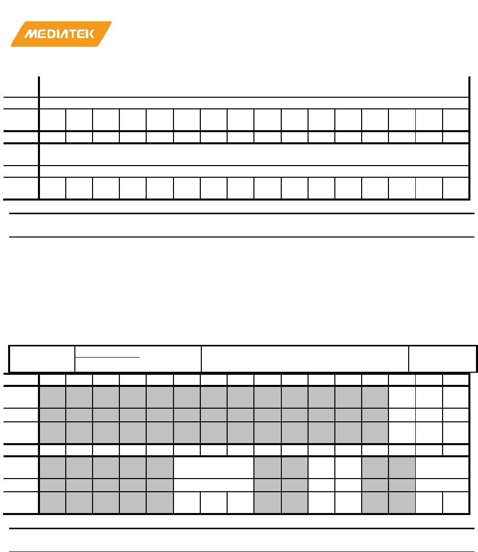
MT76x7
Internet-of-Things Wireless Connectivity
Reference Manual
© 2015 - 2017 MediaTek Inc
Page 416 of 798
This document contains information that is proprietary to MediaTek Inc. (“MediaTek”) and/or its licensor(s).
Any unauthorized use, reproduction or disclosure of this document in whole or in part is strictly prohibited
Nam
e
WPTO[31:0]
Type
RW
Rese
t
0 0 0 0 0 0 0 0 0 0 0 0 0 0 0 0
Bit
15
14
13
12
11
10
9
8
7
6
5
4
3
2
1
0
Nam
e
WPTO[31:0]
Type
RW
Rese
t
0 0 0 0 0 0 0 0 0 0 0 0 0 0 0 0
Bit(s)
Name
Description
31:0
WPTO[31:0]
WPTO[31:0] specifies the address of the jump point for a
DMA channel, i.e. channel.
WRITE :Address of the jump destination.
READ :Value set by the programmer.
830F9014
DMA2_CON
DMA CHANNEL 2 CONTROL
REGISTER
00000202
Bit
31
30
29
28
27
26
25
24
23
22
21
20
19
18
17
16
Nam
e
DI
R
WP
EN
WP
SD
Type
RO
RW
RW
Rese
t
0 0 0
Bit
15
14
13
12
11
10
9
8
7
6
5
4
3
2
1
0
Nam
e
BURST
B2
W
DR
EQ
SIZE
Type
RW
RW
RW
RO
Rese
t
0 1 0 0 0 1 0
Bit(s)
Name
Description
18
DIR
Directions of DMA transfer for half-size and Virtual FIFO
DMA
channels, i.e. channels 2~7. The direction is from the perspective of
the
DMA masters. WRITE means read from master device and then
write
to the address specified in DMA_PGMADDR, and vice versa.
0 Read (read from system RAM and write to device)
1 Write (read from d
evice and write to system RAM)
17
WPEN
Address-wrapping for ring buffer. The next address of
DMA jumps to
WRAP TO address when the current address matches WRAP

MT76x7
Internet-of-Things Wireless Connectivity
Reference Manual
© 2015 - 2017 MediaTek Inc
Page 417 of 798
This document contains information that is proprietary to MediaTek Inc. (“MediaTek”) and/or its licensor(s).
Any unauthorized use, reproduction or disclosure of this document in whole or in part is strictly prohibited
Bit(s)
Name
Description
POINT
count.
0 Disable
1 Enable
16
WPSD
The side using address-wrapping function. Only one side
of a DMA
channel can activate address-wrapping function at a time.
0 Address
-wrapping on source .
1 Address
-wrapping on destination.
10:8
BURST
Transfer Type. Burst-type transfers have better bus
efficiency. Mass
data movement is recommended to use this kind of transfer.
However,
note that burst
-type transfer does not stop until all of the beats in a
burst
are completed or transfer length is reached. FIFO threshold of
peripherals must be configured carefully
while being used to move
data
from/to the peripherals.
What transfer type can be used is restricted by the SIZE. If
SIZE is 00b, i.e. byte transfer, all of the four transfer types can be
used.
If SIZE is 01b, i.e. half
-word transfer, 16-beat incrementing burst
cannot
be used. If SIZE is 10b, i.e. word transfer, only single and 4
-beat
incrementing burst can be used.
000 Single
001 Reserved
010 4
-beat incrementing burst (default)
5
B2W
Word to Byte or Byte to Word transfer for the applications
of
transferring non-word-aligned-address data to word-aligned-
address
data. Note that BURST is set to 4
-beat burst while enabling this
function, and the SIZE is set to Byte.
NO effect on channel 1 , 9, 10

MT76x7
Internet-of-Things Wireless Connectivity
Reference Manual
© 2015 - 2017 MediaTek Inc
Page 418 of 798
This document contains information that is proprietary to MediaTek Inc. (“MediaTek”) and/or its licensor(s).
Any unauthorized use, reproduction or disclosure of this document in whole or in part is strictly prohibited
Bit(s)
Name
Description
0 Disable
1 Enable
4
DREQ
Throttle and handshake control for DMA transfer
0 No throttle control during DMA transfer or transfers occurred
only between memories
1 Hardware handshake management
The DMA master is able to t
hrottle down the transfer rate by
way of request
-grant handshake.
1:0
SIZE
Data size within the confine of a bus cycle per
transfer.These bits
confines the data transfer size between source and destination to
the
specified value for individual bus cycle. The size is in terms of byte
and
has maximum value of 4 bytes. It is mainly decided by the data
width of
a DMA master.
00 Byte transfer/1 byte
01 Half
-word transfer/2 bytes
10 Word transfer/4 bytes
11 Reserved
830F9024
DMA2_RLCT
DMA CHANNEL 2 REMAINING
LENGTH OF CURRENT TRANSFER
00000000
Bit
31
30
29
28
27
26
25
24
23
22
21
20
19
18
17
16
Nam
e
Type
Rese
t
Bit
15
14
13
12
11
10
9
8
7
6
5
4
3
2
1
0
Nam
e
RLCT
Type
RO
Rese
t
0 0 0 0 0 0 0 0 0 0 0 0 0 0 0 0
Bit(s)
Name
Description
15:0
RLCT
This register is to reflect the left amount of the transfer.

MT76x7
Internet-of-Things Wireless Connectivity
Reference Manual
© 2015 - 2017 MediaTek Inc
Page 419 of 798
This document contains information that is proprietary to MediaTek Inc. (“MediaTek”) and/or its licensor(s).
Any unauthorized use, reproduction or disclosure of this document in whole or in part is strictly prohibited
Bit(s)
Name
Description
2.5. Peripherals
Several peripheral are multiplexed GPIOs. MT76x7 has two dedicated UART interfaces with flow control, one
dedicated I2C interface, and one dedicated IrDA interface.
MT76X7 also has the 2nd I2C interface, the SPI slave interface, the I2S interface, and the SPI master interface,
but only 2 of the above interfaces can be effective at a time.
The section describes the function of all the peripherals.
2.5.1. GPIO interface
2.5.1.1. GPIO function
There are two types of GPIO (General purpose IO) designs in MT76x7: GPIO and AGPIO.
Floating-well design is used in GPIO and AGPIO. It prevents potential leakage problem when the DVDD33
power supply is not enabled but the pin input is pulled up to 3.3V source.
MT76X7 offers GPIO, each with the following configuration options:
• Input / Output mode
• Slew rate control
• Schmitt trigger hysteresis control
• Input mode: Floating (Hi-Z), pull-up, or pull-down
• Output mode: Active driving
• Pull up/down control. The pull-up and pull-down resistance is 75KΩ with ±20% variation over PVT
condition
• Driving strength: 4mA, 8mA, 12mA, 16mA
• Input and output duty cycle tuning
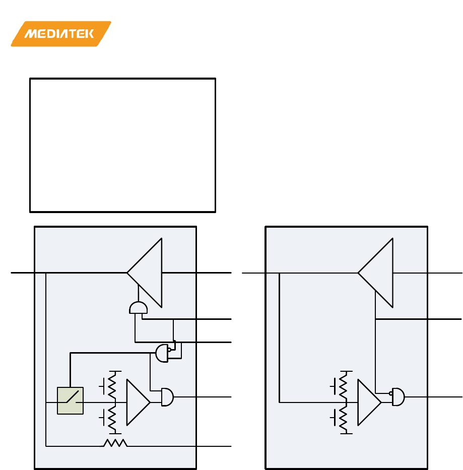
MT76x7
Internet-of-Things Wireless Connectivity
Reference Manual
© 2015 - 2017 MediaTek Inc
Page 420 of 798
This document contains information that is proprietary to MediaTek Inc. (“MediaTek”) and/or its licensor(s).
Any unauthorized use, reproduction or disclosure of this document in whole or in part is strictly prohibited
PU
PD
IO
E
G
O
AIO_ANALOG_DONT_TOUCH
Logic 1 -> Switch on
I
AGPIO
PU
PD
IO
E
O
I
GPIO
AGPIO Function Table
G E Function
=============================
0 0 Analog Function (IO <- -> AIO)
0 1 Analog Function (IO <- -> AIO)
---------------------------------------------------
1 0 Digital Function (IO -----> O)
1 1 Digital Function (IO <- -- I)
(4 – 16 mA Driving)
Floating Well
4 – 16 mA
Floating Well
4 – 16 mA
Figure 2-37. AGPIO/GPIO Block Diagram (Left: AGPIO; Right: GPIO)
The digital IO AGPIO function is equivalent to GPIO as shown above. A dedicated internal control signal is used
to select between the digital and analog functions. The IOs are multiplexed with 16 channels ADC.
1) Output Signal Multiplexing
Function-[9:1]-AON and Function-[9:0] can all be output to PINX by setting pinx_pinmux_aon_sel and
pinx_pinmux_off_sel, as shown in Figure 2-12 below. Function-[9:1]-AON signals are part of TOP_AON domain
and Function-[9:0] signals are part of TOP_OFF (N9) domain. The output of the pad is enabled through E and G
pad controls which require 2’b11 for digital output mode.
For a specific pin there could be only a limited number of functions available, these functions are mapped
anywhere to the different inputs of the muxes (not always in an incremental scheme).
TOP_AON domain means the circuit is always powered on when PMU supplies the power. TOP_OFF (N9)
domain means the N9 related circuit is powered off in some scenarios when PMU supplies the power.
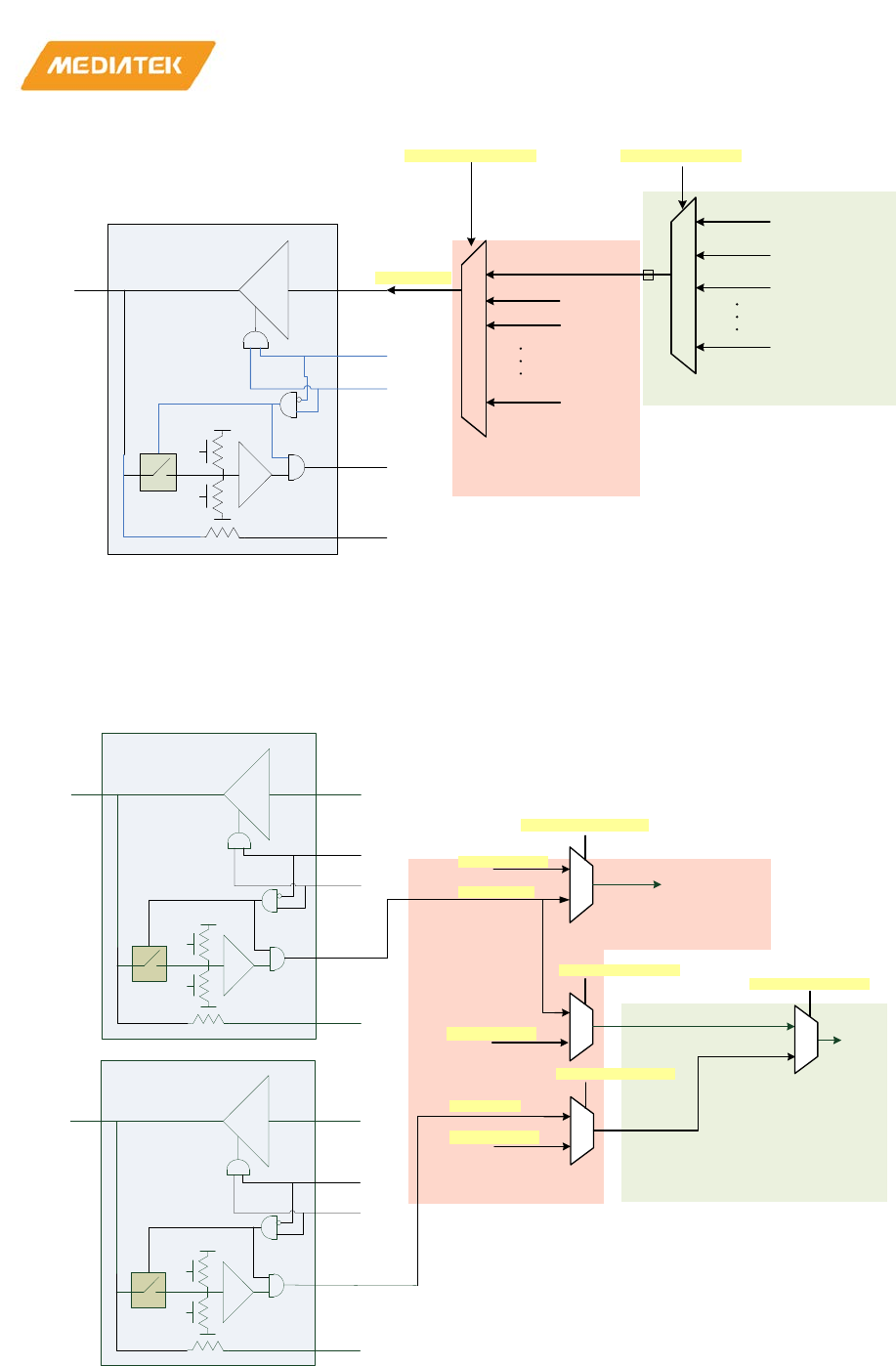
MT76x7
Internet-of-Things Wireless Connectivity
Reference Manual
© 2015 - 2017 MediaTek Inc
Page 421 of 798
This document contains information that is proprietary to MediaTek Inc. (“MediaTek”) and/or its licensor(s).
Any unauthorized use, reproduction or disclosure of this document in whole or in part is strictly prohibited
PU
PD
IO
E
G
O
AIO_ANALOG_DONT_TOUCH
Logic 1
->Switch on
0
1
pinx_pinmux_aon_sel pinx_pinmux_off_sel
Function 0 (O)
Function 1 AON (O)
PAD_PINX
Function 1 (O)
Function 2 (O)
Function 9 (O)
2Function 2 AON (O)
0
1
2
9
I
PINX
1'b1
1'b1 TOP_OFF(N9) domain
TOP_AON domain
ISO
Function 9 AON (O)
9
Figure 2-38. AGPIO configured as output multiplexing
2) Input Signal Multiplexing
Figure 2-39 below shows that PINX is the source of Function-AON-0, while PINX and PINY can both be the input
source for Function-1. The (E, G) setting for both IO is 2’b01 for digital input mode.
TOP_OFF domain
Function AON 0
0
1
1'b0
PINX
1
0
pinx_pinmux_aon_sel
pinx_pinmux_aon_sel
1
0
piny_pinmux_aon_sel
PINY
1'b0
1'b0
Function 1
1
0
pinx_pinmux_sel
PU
PD
IO
E
G
O
AIO_ANALOG_DONT_TOUCH
Logic 1
->Switch on
I
PINX
1'b0
1'b1
PU
PD
IO
E
G
O
AIO_ANALOG_DONT_TOUCH
Logic 1
->Switch on
I
PINY
1'b0
1'b1
TOP_AON domain
Figure 2-39. AGPIO configured as input multiplexing
3) Input / Output / Analog Signal Multiplexing
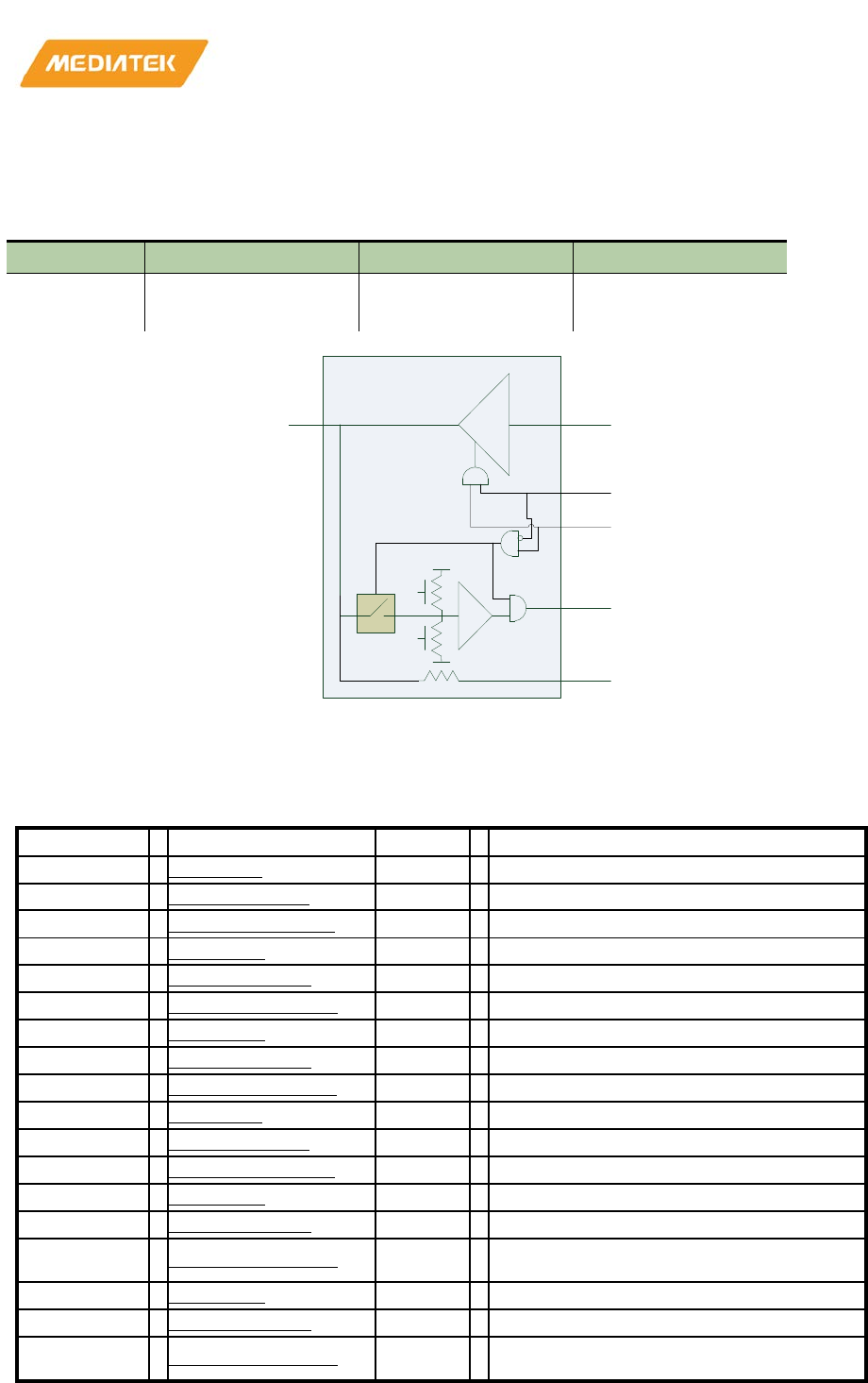
MT76x7
Internet-of-Things Wireless Connectivity
Reference Manual
© 2015 - 2017 MediaTek Inc
Page 422 of 798
This document contains information that is proprietary to MediaTek Inc. (“MediaTek”) and/or its licensor(s).
Any unauthorized use, reproduction or disclosure of this document in whole or in part is strictly prohibited
This figure below shows how function-0, function-1 and Analog-function share the same IO (PINX) by
configuring (E, G) pair internally. G is controlled in off domain.
Table 2-40. Functional description of AGPIO
(G,E) value 2’b11 2’b10 2’b0x
Function PINX=Function-0
(output mode)
Function-1=PINX
(input mode)
Analog-function=PINX
(analog mode)
PU
PD
IO
E
G
O
AIO_ANALOG_DONT_TOUCH
Logic 1
->Switch on
I
PINX
Analog function
Function 0
Function 1
Figure 2-40. AGPIO configured as Input, Output or Analog mode
2.5.1.2. Register definitions
Module name: CM4_GPIO Base address: (+8300b000h)
Address
Name Width
Register Function
8300B000
GPIO_PU1
32
PAD Pull
-UP Control Register 1
8300B004
GPIO_PU1_SET
32
PAD Pull
-UP SET Control Register 1
8300B008
GPIO_PU1_RESET
32
PAD Pull
-UP RESET Control Register 1
8300B010
GPIO_PU2
32
PAD Pull
-UP Control Register 2
8300B014
GPIO_PU2_SET
32
PAD Pull
-UP SET Control Register 2
8300B018
GPIO_PU2_RESET
32
PAD Pull
-UP RESET Control Register 2
8300B020
GPIO_PU3
32
PAD Pull-UP Control Register 3
8300B024
GPIO_PU3_SET
32
PAD
Pull-UP SET Control Register 3
8300B028
GPIO_PU3_RESET
32
PAD Pull-UP RESET Control Register 3
8300B030
GPIO_PD1
32
PAD Pull
-DOWN Control Register 1
8300B034
GPIO_PD1_SET
32
PAD Pull-DOWN SET Control Register 1
8300B038
GPIO_PD1_RESET
32
PAD Pull
-DOWN RESET Control Register 1
8300B040
GPIO_PD2
32
PAD Pull-DOWN Control Register 2
8300B044
GPIO_PD2_SET
32
PAD Pull
-DOWN SET Control Register 2
8300B048
GPIO_PD2_RESET
32
PAD Pull-DOWN RESET Control Register
2
8300B050
GPIO_PD3
32
PAD Pull
-DOWN Control Register 3
8300B054
GPIO_PD3_SET
32
PAD Pull
-DOWN SET Control Register 3
8300B058
GPIO_PD3_RESET
32
PAD Pull-DOWN RESET Control Register
3
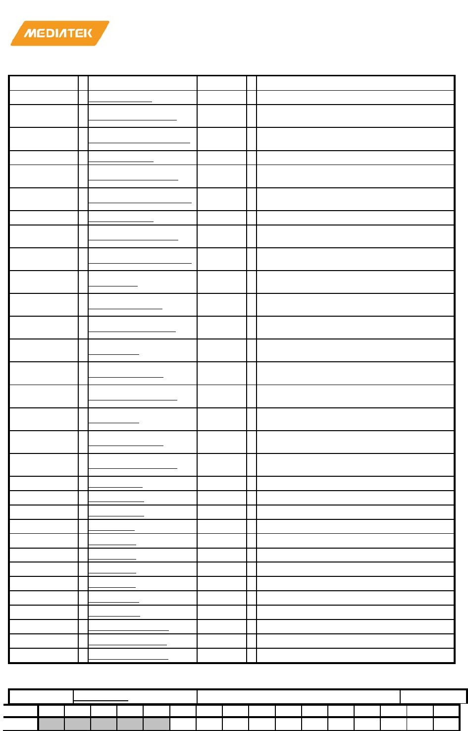
MT76x7
Internet-of-Things Wireless Connectivity
Reference Manual
© 2015 - 2017 MediaTek Inc
Page 423 of 798
This document contains information that is proprietary to MediaTek Inc. (“MediaTek”) and/or its licensor(s).
Any unauthorized use, reproduction or disclosure of this document in whole or in part is strictly prohibited
Address
Name
Width
Register Function
8300B060
GPIO_DOUT1
32
PAD GPO DATA Output Control Register 1
8300B064
GPIO_DOUT1_SET
32
PAD GPO DATA Output Control Set
Register 1
8300B068
GPIO_DOUT1_RESET
32
PAD GPO DATA Output Control Reset
Register 1
8300B070
GPIO_DOUT2
32
PAD GPO DATA Output Control Register 2
8300B074
GPIO_DOUT2_SET
32
PAD GPO DATA Output Control Set
Register 2
8300B078
GPIO_DOUT2_RESET
32
PAD GPO DATA Output Control Reset
Register 2
8300B080
GPIO_DOUT3
32
PAD GPO DATA Output Control Register 3
8300B084
GPIO_DOUT3_SET
32
PAD GPO DATA Output Control Set
Register 3
8300B088
GPIO_DOUT3_RESET
32
PAD GPO DATA Output Control Reset
Register 3
8300B090
GPIO_OE1
32
PAD GPO Output Enable Control Register
1
8300B094
GPIO_OE1_SET
32
PAD GPO Output Enable Set Control
Register 1
8300B098
GPIO_OE1_RESET
32
PAD GPO Output Enable Reset Control
Register 1
8300B0A0
GPIO_OE2
32
PAD GPO Output Enable Control Register
2
8300B0A4
GPIO_OE2_SET
32
PAD GPO Output Enable Set Control
Register2
8300B0A8
GPIO_OE2_RESET
32
PAD GPO Output Enable Reset Control
Register 2
8300B0B0
GPIO_OE3
32
PAD GPO Output Enable Control Register
2
8300B0B4
GPIO_OE3_SET
32
PAD GPO Output Enable Set Control
Register2
8300B0B8
GPIO_OE3_RESET
32
PAD GPO Output Enable Reset Control
Register 2
8300B0C0
GPIO_DIN1
32
PAD GPI Input Data Control Register 1
8300B0C4
GPIO_DIN2
32
PAD GPI Input Data Control Register 2
8300B0C8
GPIO_DIN3
32
PAD GPI Input Data Control Register 3
8300B0D0
PADDRV1
32
PAD Driving Control Register1
8300B0D4
PADDRV2
32
PAD Driving Control Register2
8300B0D8
PADDRV3
32
PAD Driving Control Register3
8300B0DC
PADDRV4
32
PAD Driving Control Register4
8300B0E0
PADDRV5
32
PAD Driving Control Register5
8300B0F0
PADCTRL1
32
PAD Control Register1
8300B0F4
PADCTRL2
32
PAD Control Register2
8300B100
PAD_GPIO_IES0
32
GPIO PAD IES Control Register 0
8300B104
PAD_GPIO_IES1
32
GPIO PAD IES Control Register 1
8300B108
PAD_GPIO_IES2
32
GPIO PAD IES Control Register 2
8300B000
GPIO_PU1
PAD Pull-UP Control Register 1
00000000
Bit
31
30
29
28
27
26
25
24
23
22
21
20
19
18
17
16
Nam
CL
WA
PE
IN
IN
IN
IN
IN
IN
IN
IN

MT76x7
Internet-of-Things Wireless Connectivity
Reference Manual
© 2015 - 2017 MediaTek Inc
Page 424 of 798
This document contains information that is proprietary to MediaTek Inc. (“MediaTek”) and/or its licensor(s).
Any unauthorized use, reproduction or disclosure of this document in whole or in part is strictly prohibited
e
K_
RE
Q_
N_
PU
KE
_N
_P
U
RS
T_
N_
PU
_U
AR
T0
_T
XD
_P
U
_G
PIO
22_
PU
_G
PIO
21_
PU
_G
PIO
20
_P
U
_G
PIO
19_
PU
_G
PIO
18_
PU
_G
PIO
17_
PU
_G
PIO
16_
PU
Type
RW
RW
RW
RW
RW
RW
RW
RW
RW
RW
RW
Rese
t
0 0 0 0 0 0 0 0 0 0 0
Bit
15
14
13
12
11
10
9
8
7
6
5
4
3
2
1
0
Nam
e
IN
_G
PIO
15_
PU
IN
_G
PIO
14_
PU
IN
_G
PIO
13_
PU
IN
_G
PIO
12_
PU
IN
_G
PIO
11_
PU
IN
_G
PIO
10_
PU
IN
_G
PIO
9_
PU
IN
_G
PIO
8_
PU
AN
TS
EL7
_P
U
AN
TS
EL
6_
PU
AN
TS
EL
5_
PU
AN
TS
EL
4_
PU
AN
TS
EL
3_
PU
AN
TS
EL
2_
PU
AN
TS
EL1
_P
U
AN
TS
EL
0_
PU
Type
RW
RW
RW
RW
RW
RW
RW
RW
RW
RW
RW
RW
RW
RW
RW
RW
Rese
t
0 0 0 0 0 0 0 0 0 0 0 0 0 0 0 0
Bit(s)
Mnemonic
Name
Description
26
CLK_REQ_N_PU
CLK_REQ_N_PU
PAD CLK_REQ_N pull-up control register
1: pull
-up
0: no pull
-up
25
WAKE_N_PU
WAKE_N_PU
PAD WAKE_N pull-up control register
1: pull
-up
0: no pull
-up
24
PERST_N_PU
PERST_N_PU
PAD PERST_N pull-up control register
1: pull
-up
0: no pull
-up
23
IN_UART0_TXD_PU
IN_UART0_TXD_PU
PAD IN_UART0_TXD pull-up control register
1: pull
-up
0: no pull
-up
22
IN_GPIO22_PU
IN_GPIO22_PU
PAD IN_GPIO22 pull-up control register
1: pull
-up
0: no pull
-up
21
IN_GPIO21_PU
IN_GPIO21_PU
PAD IN_GPIO21 pull-up control register
1: pull
-up
0: no pull
-up
20
IN_GPIO20_PU
IN_GPIO20_PU
PAD IN_GPIO20 pull-up control register
1:
pull-up
0: no pull
-up

MT76x7
Internet-of-Things Wireless Connectivity
Reference Manual
© 2015 - 2017 MediaTek Inc
Page 425 of 798
This document contains information that is proprietary to MediaTek Inc. (“MediaTek”) and/or its licensor(s).
Any unauthorized use, reproduction or disclosure of this document in whole or in part is strictly prohibited
Bit(s)
Mnemonic
Name
Description
19
IN_GPIO19_PU
IN_GPIO19_PU
PAD IN_GPIO19 pull-up control register
1: pull
-up
0: no pull
-up
18
IN_GPIO18_PU
IN_GPIO18_PU
PAD IN_GPIO18 pull-up control register
1: pull
-up
0: no pull
-up
17
IN_GPIO17_PU
IN_GPIO17_PU
PAD IN_GPIO17 pull-up control register
1: pull
-up
0: no pull
-up
16
IN_GPIO16_PU
IN_GPIO16_PU
PAD IN_GPIO16 pull-up control register
1: pull
-up
0: no pull
-up
15
IN_GPIO15_PU
IN_GPIO15_PU
PAD IN_GPIO15 pull-up control register
1: pull
-up
0: no pull
-up
14
IN_GPIO14_PU
IN_GPIO14_PU
PAD IN_GPIO14 pull-up control register
1: pull
-up
0: no pull
-up
13
IN_GPIO13_PU
IN_GPIO13_PU
PAD IN_GPIO13 pull-up control register
1: pull
-up
0: no pull
-up
12
IN_GPIO12_PU
IN_GPIO12_PU
PAD IN_GPIO12 pull-up control register
1: pull
-up
0: no
pull-up
11
IN_GPIO11_PU
IN_GPIO11_PU
PAD IN_GPIO11 pull-up control register
1: pull
-up
0: no pull
-up
10
IN_GPIO10_PU
IN_GPIO10_PU
PAD IN_GPIO10 pull-up control register
1: pull
-up
0: no pull
-up
9
IN_GPIO9_PU
IN_GPIO9_PU
PAD IN_GPIO9 pull-up control register

MT76x7
Internet-of-Things Wireless Connectivity
Reference Manual
© 2015 - 2017 MediaTek Inc
Page 426 of 798
This document contains information that is proprietary to MediaTek Inc. (“MediaTek”) and/or its licensor(s).
Any unauthorized use, reproduction or disclosure of this document in whole or in part is strictly prohibited
Bit(s)
Mnemonic
Name
Description
1: pull-up
0: no pull
-up
8
IN_GPIO8_PU
IN_GPIO8_PU
PAD IN_GPIO8 pull-up control register
1: pull
-up
0: no pull
-up
7
ANTSEL7_PU
ANTSEL7_PU
PAD ANTSEL7 pull-up control register
1: pull
-up
0: no pull
-up
6
ANTSEL6_PU
ANTSEL6_PU
PAD ANTSEL6 pull-up control register
1: pull
-up
0: no pull
-up
5
ANTSEL5_PU
ANTSEL5_PU
PAD ANTSEL5 pull-up control register
1: pull
-up
0: no pull
-up
4
ANTSEL4_PU
ANTSEL4_PU
PAD ANTSEL4 pull-up control register
1: pull
-up
0: no pull
-up
3
ANTSEL3_PU
ANTSEL3_PU
PAD ANTSEL3 pull-up control register
1: pull
-up
0: no pull
-up
2
ANTSEL2_PU
ANTSEL2_PU
PAD ANTSEL2 pull-up control register
1: pull
-up
0: no pull
-up
1
ANTSEL1_PU
ANTSEL1_PU
PAD ANTSEL1 pull-up control register
1: pull
-up
0: no pull
-up
0
ANTSEL0_PU
ANTSEL0_PU
PAD ANTSEL0 pull-up control register
1: pull
-up
0: no pull
-up
8300B004
GPIO_PU1_SET
PAD Pull-UP SET Control Register 1
00000000
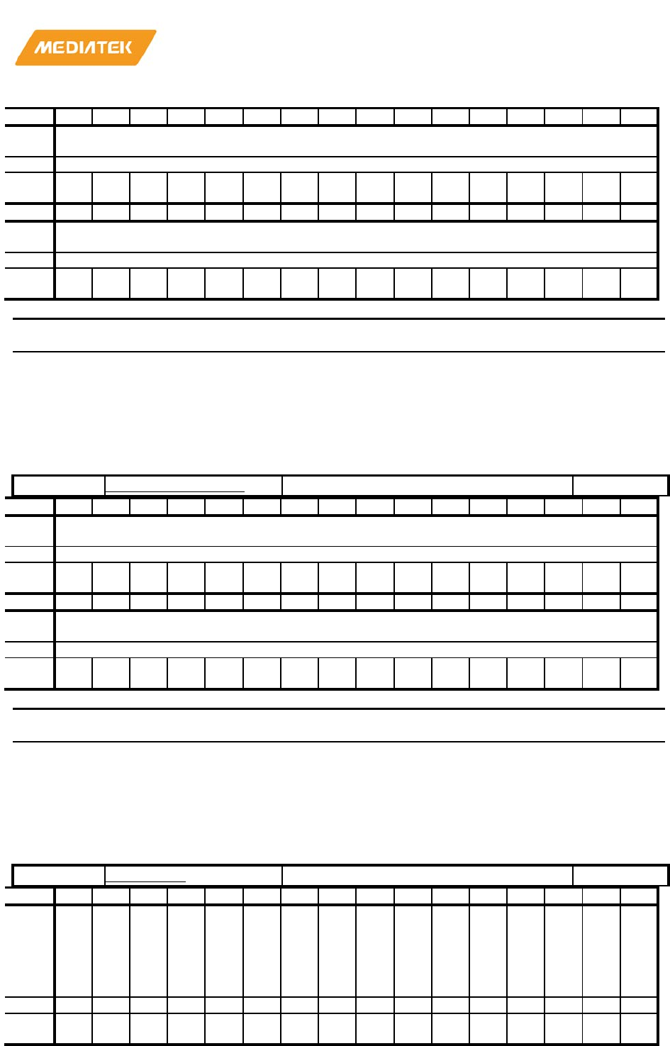
MT76x7
Internet-of-Things Wireless Connectivity
Reference Manual
© 2015 - 2017 MediaTek Inc
Page 427 of 798
This document contains information that is proprietary to MediaTek Inc. (“MediaTek”) and/or its licensor(s).
Any unauthorized use, reproduction or disclosure of this document in whole or in part is strictly prohibited
Bit
31
30
29
28
27
26
25
24
23
22
21
20
19
18
17
16
Nam
e
GPIO_PU1_SET
Type
RW
Rese
t
0 0 0 0 0 0 0 0 0 0 0 0 0 0 0 0
Bit
15
14
13
12
11
10
9
8
7
6
5
4
3
2
1
0
Nam
e
GPIO_PU1_SET
Type
RW
Rese
t
0 0 0 0 0 0 0 0 0 0 0 0 0 0 0 0
Bit(s)
Mnemonic
Name
Description
31:0
GPIO_PU1_SET
GPIO_PU1_SET
Write '1' to SET pull-up. The pull-up PAD is
corresponding
to GPIO_PU1
Read always return '0'
8300B008
GPIO_PU1_RESET
PAD Pull-UP RESET Control Register 1
00000000
Bit
31
30
29
28
27
26
25
24
23
22
21
20
19
18
17
16
Nam
e
GPIO_PU1_RESET
Type
RW
Rese
t
0 0 0 0 0 0 0 0 0 0 0 0 0 0 0 0
Bit
15
14
13
12
11
10
9
8
7
6
5
4
3
2
1
0
Nam
e
GPIO_PU1_RESET
Type
RW
Rese
t
0 0 0 0 0 0 0 0 0 0 0 0 0 0 0 0
Bit(s)
Mnemonic
Name
Description
31:0
GPIO_PU1_RESET
GPIO_PU1_RESET
Write '1' to RESET pull-up. The pull-up PAD is
corresponding to
GPIO_PU1
Read always return '0'
8300B010
GPIO_PU2
PAD Pull-UP Control Register 2
00000000
Bit
31
30
29
28
27
26
25
24
23
22
21
20
19
18
17
16
Nam
e
IN
_A
DC
6_
PU
IN
_A
DC
5_
PU
IN
_A
DC
4_
PU
BT
_L
ED
_B
_P
U
WF
_L
ED
_B
_P
U
BT
_R
F_
DIS
_B
_P
U
WF
_R
F_
DIS
_B
_P
U
IN
_P
W
M7
_P
U
IN
_P
W
M6
_P
U
IN
_P
W
M5
_P
U
IN
_P
W
M4
_P
U
IN
_P
W
M3
_P
U
IN
_P
W
M2
_P
U
IN
_G
PIO
54_
PU
IN
_G
PIO
53_
PU
IN
_G
PIO
52_
PU
Type
RW
RW
RW
RW
RW
RW
RW
RW
RW
RW
RW
RW
RW
RW
RW
RW
Rese
t
0 0 0 0 0 0 0 0 0 0 0 0 0 0 0 0
MT76x7
Internet-of-Things Wireless Connectivity
Reference Manual
© 2015 - 2017 MediaTek Inc
Page 428 of 798
This document contains information that is proprietary to MediaTek Inc. (“MediaTek”) and/or its licensor(s).
Any unauthorized use, reproduction or disclosure of this document in whole or in part is strictly prohibited
Bit
15
14
13
12
11
10
9
8
7
6
5
4
3
2
1
0
Nam
e
IN
_G
PIO
51_
PU
IN
_G
PIO
50
_P
U
IN
_G
PIO
49
_P
U
IN
_G
PIO
48
_P
U
IN
_G
PIO
47_
PU
IN
_G
PIO
46
_P
U
IN
_G
PIO
45_
PU
IN
_G
PIO
44
_P
U
UA
RT
_C
TS
_P
U
UA
RT
_R
TS
_P
U
UA
RT
_T
X_
PU
UA
RT
_R
X_
PU
UA
RT
_D
BG
_P
U
GPI
O1
_P
U
GPI
O0
_P
U
Type
RW
RW
RW
RW
RW
RW
RW
RW
RW
RW
RW
RW
RW
RW
RW
Rese
t
0 0 0 0 0 0 0 0 0 0 0 0 0 0 0
Bit(s)
Mnemonic
Name
Description
31
IN_ADC6_PU
IN_ADC6_PU
PAD IN_ADC6 pull-up control register
1: pull
-up
0: no pull
-up
30
IN_ADC5_PU
IN_ADC5_PU
PAD IN_ADC5 pull-up control register
1: pull
-up
0: no pull
-up
29
IN_ADC4_PU
IN_ADC4_PU
PAD IN_ADC4 pull-up control register
1: pull
-up
0: no pull
-up
28
BT_LED_B_PU
BT_LED_B_PU
PAD BT_LED_B pull-up control register
1: pull
-up
0: no pull
-up
27
WF_LED_B_PU
WF_LED_B_PU
PAD WF_LED_B pull-up control register
1: pull
-up
0: no pull
-up
26
BT_RF_DIS_B_PU
BT_RF_DIS_B_PU
PAD BT_RF_DIS_B pull-up control register
1: pull
-up
0: no pull
-up
25
WF_RF_DIS_B_PU
WF_RF_DIS_B_PU
PAD WF_RF_DIS_B pull-up control register
1: pull
-up
0: no pull
-up
24
IN_PWM7_PU
IN_PWM7_PU
PAD IN_PWM7 pull-up control register
1: pull
-up
0: no pull
-up
23
IN_PWM6_PU
IN_PWM6_PU
PAD IN_PWM6 pull-up control register

MT76x7
Internet-of-Things Wireless Connectivity
Reference Manual
© 2015 - 2017 MediaTek Inc
Page 429 of 798
This document contains information that is proprietary to MediaTek Inc. (“MediaTek”) and/or its licensor(s).
Any unauthorized use, reproduction or disclosure of this document in whole or in part is strictly prohibited
Bit(s)
Mnemonic
Name
Description
1: pull-up
0: no pull
-up
22
IN_PWM5_PU
IN_PWM5_PU
PAD IN_PWM5 pull-up control register
1: pull
-up
0: no pull
-up
21
IN_PWM4_PU
IN_PWM4_PU
PAD IN_PWM4 pull-up control register
1: pull
-up
0: no pull
-up
20
IN_PWM3_PU
IN_PWM3_PU
PAD IN_PWM3 pull-up control register
1: pull
-up
0: no pull
-up
19
IN_PWM2_PU
IN_PWM2_PU
PAD IN_PWM2 pull-up control register
1: pull
-up
0: no pull
-up
18
IN_GPIO54_PU
IN_GPIO54_PU
PAD IN_GPIO54 pull-up control register
1: pull
-up
0: no pull
-up
17
IN_GPIO53_PU
IN_GPIO53_PU
PAD IN_GPIO53 pull-up control register
1: pull
-up
0: no pull
-up
16
IN_GPIO52_PU
IN_GPIO52_PU
PAD IN_GPIO52 pull-up control register
1: pull
-up
0: no pull
-up
15
IN_GPIO51_PU
IN_GPIO51_PU
PAD IN_GPIO51 pull-up control register
1: pull
-up
0: no pull
-up
14
IN_GPIO50_PU
IN_GPIO50_PU
PAD IN_GPIO50 pull-up control register
1: pull
-up
0: no pull
-up
13
IN_GPIO49_PU
IN_GPIO49_PU
PAD IN_GPIO49 pull-up control register
1:
pull-up

MT76x7
Internet-of-Things Wireless Connectivity
Reference Manual
© 2015 - 2017 MediaTek Inc
Page 430 of 798
This document contains information that is proprietary to MediaTek Inc. (“MediaTek”) and/or its licensor(s).
Any unauthorized use, reproduction or disclosure of this document in whole or in part is strictly prohibited
Bit(s)
Mnemonic
Name
Description
0: no pull-up
12
IN_GPIO48_PU
IN_GPIO48_PU
PAD IN_GPIO48 pull-up control register
1: pull
-up
0: no pull
-up
11
IN_GPIO47_PU
IN_GPIO47_PU
PAD IN_GPIO47 pull-up control register
1: pull
-up
0: no pull
-up
10
IN_GPIO46_PU
IN_GPIO46_PU
PAD IN_GPIO46 pull-up control register
1: pull
-up
0: no pull
-up
9
IN_GPIO45_PU
IN_GPIO45_PU
PAD IN_GPIO45 pull-up control register
1: pull
-up
0: no pull
-up
8
IN_GPIO44_PU
IN_GPIO44_PU
PAD IN_GPIO44 pull-up control register
1: pull
-up
0: no pull
-up
7
UART_CTS_PU
UART_CTS_PU
PAD UART_CTS pull-up control register
1: pull
-up
0: no pull
-up
6
UART_RTS_PU
UART_RTS_PU
PAD UART_RTS pull-up control register
1: pull
-up
0: no pull
-up
5
UART_TX_PU
UART_TX_PU
PAD UART_TX pull-up control register
1: pull
-up
0: no pull
-up
4
UART_RX_PU
UART_RX_PU
PAD UART_RX pull-up control register
1: pull
-up
0: no pull
-up
3
UART_DBG_PU
UART_DBG_PU
PAD UART_DBG pull-up control register
1: pull
-up
0: no pull
-up
MT76x7
Internet-of-Things Wireless Connectivity
Reference Manual
© 2015 - 2017 MediaTek Inc
Page 431 of 798
This document contains information that is proprietary to MediaTek Inc. (“MediaTek”) and/or its licensor(s).
Any unauthorized use, reproduction or disclosure of this document in whole or in part is strictly prohibited
Bit(s)
Mnemonic
Name
Description
2
GPIO1_PU
GPIO1_PU
PAD GPIO1 pull-up control register
1: pull
-up
0: no pull
-up
1
GPIO0_PU
GPIO0_PU
PAD GPIO0 pull-up control register
1: pull
-up
0: no pull
-up
8300B014
GPIO_PU2_SET
PAD Pull-UP SET Control Register 2
00000000
Bit
31
30
29
28
27
26
25
24
23
22
21
20
19
18
17
16
Nam
e
GPIO_PU1_SET
Type
RW
Rese
t
0 0 0 0 0 0 0 0 0 0 0 0 0 0 0 0
Bit
15
14
13
12
11
10
9
8
7
6
5
4
3
2
1
0
Nam
e
GPIO_PU1_SET
Type
RW
Rese
t
0 0 0 0 0 0 0 0 0 0 0 0 0 0 0 0
Bit(s)
Mnemonic
Name
Description
31:0
GPIO_PU1_SET
GPIO_PU1_SET
Write '1' to SET pull-up. The pull-up PAD is
corresponding to GPIO_PU1
Read always return '0'
8300B018
GPIO_PU2_RESET
PAD Pull-UP RESET Control Register 2
00000000
Bit
31
30
29
28
27
26
25
24
23
22
21
20
19
18
17
16
Nam
e
GPIO_PU1_RESET
Type
RW
Rese
t
0 0 0 0 0 0 0 0 0 0 0 0 0 0 0 0
Bit
15
14
13
12
11
10
9
8
7
6
5
4
3
2
1
0
Nam
e
GPIO_PU1_RESET
Type
RW
Rese
t
0 0 0 0 0 0 0 0 0 0 0 0 0 0 0 0
Bit(s)
Mnemonic
Name
Description
31:0
GPIO_PU1_RESET
GPIO_PU1_RESET
Write '1' to RESET pull-up. The pull-up PAD is
MT76x7
Internet-of-Things Wireless Connectivity
Reference Manual
© 2015 - 2017 MediaTek Inc
Page 432 of 798
This document contains information that is proprietary to MediaTek Inc. (“MediaTek”) and/or its licensor(s).
Any unauthorized use, reproduction or disclosure of this document in whole or in part is strictly prohibited
Bit(s)
Mnemonic
Name
Description
corresponding to GPIO_PU1
Read always return '0'
8300B020
GPIO_PU3
PAD Pull-UP Control Register 3
00000000
Bit
31
30
29
28
27
26
25
24
23
22
21
20
19
18
17
16
Nam
e
Type
Rese
t
Bit
15
14
13
12
11
10
9
8
7
6
5
4
3
2
1
0
Nam
e
IN
_H
SPI
N_
PU
SIP
_D
3_
PU
SIP
_D
2_
PU
SIP
_D
1_P
U
SIP
_D
0_
PU
SIP
_C
S_
PU
SIP
_C
K_
PU
IN
_A
DC
15_
PU
IN
_A
DC
14_
PU
IN
_A
DC
13_
PU
IN
_A
DC
12_
PU
IN
_A
DC
11_
PU
IN
_A
DC
10_
PU
IN
_A
DC
9_
PU
IN
_A
DC
8_
PU
IN
_A
DC
7_P
U
Type
RW
RW
RW
RW
RW
RW
RW
RW
RW
RW
RW
RW
RW
RW
RW
RW
Rese
t
0 0 0 0 0 0 0 0 0 0 0 0 0 0 0 0
Bit(s)
Mnemonic
Name
Description
15
IN_HSPIN_PU
IN_HSPIN_PU
PAD IN_HSPIN pull-up control register
1: pull
-up
0: no pull
-up
14
SIP_D3_PU
SIP_D3_PU
PAD SIP_D3 pull-up control register
1: pull
-up
0: no pull
-up
13
SIP_D2_PU
SIP_D2_PU
PAD SIP_D2 pull-up control register
1: pull
-up
0: no pull
-up
12
SIP_D1_PU
SIP_D1_PU
PAD SIP_D1 pull-up control register
1: pull
-up
0: no pull
-up
11
SIP_D0_PU
SIP_D0_PU
PAD SIP_D0 pull-up control register
1: pull
-up
0: no pull
-up
10
SIP_CS_PU
SIP_CS_PU
PAD SIP_CS pull-up control register
1: pull
-up

MT76x7
Internet-of-Things Wireless Connectivity
Reference Manual
© 2015 - 2017 MediaTek Inc
Page 433 of 798
This document contains information that is proprietary to MediaTek Inc. (“MediaTek”) and/or its licensor(s).
Any unauthorized use, reproduction or disclosure of this document in whole or in part is strictly prohibited
Bit(s)
Mnemonic
Name
Description
0: no pull-up
9
SIP_CK_PU
SIP_CK_PU
PAD SIP_CK pull-up control register
1: pull
-up
0: no pull
-up
8
IN_ADC15_PU
IN_ADC15_PU
PAD IN_ADC15 pull-up control register
1: pull
-up
0: no pull
-up
7
IN_ADC14_PU
IN_ADC14_PU
PAD IN_ADC14 pull-up control register
1: pull
-up
0: no pull
-up
6
IN_ADC13_PU
IN_ADC13_PU
PAD IN_ADC13 pull-up control register
1: pull
-up
0: no pull
-up
5
IN_ADC12_PU
IN_ADC12_PU
PAD IN_ADC12 pull-up control register
1: pull
-up
0: no pull
-up
4
IN_ADC11_PU
IN_ADC11_PU
PAD IN_ADC11 pull-up control register
1: pull
-up
0: no pull
-up
3
IN_ADC10_PU
IN_ADC10_PU
PAD IN_ADC10 pull-up control register
1: pull
-up
0: no pull
-up
2
IN_ADC9_PU
IN_ADC9_PU
PAD IN_ADC9 pull-up control register
1: pull
-up
0: no pull
-up
1
IN_ADC8_PU
IN_ADC8_PU
PAD IN_ADC8 pull-up control register
1: pull
-up
0: no pull
-up
0
IN_ADC7_PU
IN_ADC7_PU
PAD IN_ADC7 pull-up control register
1:
pull-up
0: no pull
-up
MT76x7
Internet-of-Things Wireless Connectivity
Reference Manual
© 2015 - 2017 MediaTek Inc
Page 434 of 798
This document contains information that is proprietary to MediaTek Inc. (“MediaTek”) and/or its licensor(s).
Any unauthorized use, reproduction or disclosure of this document in whole or in part is strictly prohibited
Bit(s)
Mnemonic
Name
Description
8300B024
GPIO_PU3_SET
PAD Pull-UP SET Control Register 3
00000000
Bit
31
30
29
28
27
26
25
24
23
22
21
20
19
18
17
16
Nam
e
Type
Rese
t
Bit
15
14
13
12
11
10
9
8
7
6
5
4
3
2
1
0
Nam
e
GPIO_PU3_SET
Type
RW
Rese
t
0 0 0 0 0 0 0 0 0
Bit(s)
Mnemonic
Name
Description
8:0
GPIO_PU3_SET
GPIO_PU3_SET
Write '1' to SET pull-up. The pull-up PAD is
corresponding to GPIO_PU3
Read always
return '0'
8300B028
GPIO_PU3_RESET
PAD Pull-UP RESET Control Register 3
00000000
Bit
31
30
29
28
27
26
25
24
23
22
21
20
19
18
17
16
Nam
e
Type
Rese
t
Bit
15
14
13
12
11
10
9
8
7
6
5
4
3
2
1
0
Nam
e
GPIO_PU3_RESET
Type
RW
Rese
t
0 0 0 0 0 0 0 0 0
Bit(s)
Mnemonic
Name
Description
8:0
GPIO_PU3_RESET
GPIO_PU3_RESET
Write '1' to RESET pull-up. The pull-up PAD is
corresponding to GPIO_PU3
Read always
return '0'
8300B030
GPIO_PD1
PAD Pull-DOWN Control Register 1
00000000
Bit
31
30
29
28
27
26
25
24
23
22
21
20
19
18
17
16
Nam
CL
K_
WA
KE
PE
RS
IN
_U
IN
_G
IN
_G
IN
_G
IN
_G
IN
_G
IN
_G
IN
_G
MT76x7
Internet-of-Things Wireless Connectivity
Reference Manual
© 2015 - 2017 MediaTek Inc
Page 435 of 798
This document contains information that is proprietary to MediaTek Inc. (“MediaTek”) and/or its licensor(s).
Any unauthorized use, reproduction or disclosure of this document in whole or in part is strictly prohibited
e
RE
Q_
N_
PD
_N
_P
D
T_
N_
PD
AR
T0
_T
XD
_P
D
PIO
22_
PD
PIO
21_
PD
PIO
20
_P
D
PIO
19_
PD
PIO
18_
PD
PIO
17_
PD
PIO
16_
PD
Type
RW
RW
RW
RW
RW
RW
RW
RW
RW
RW
RW
Rese
t
0 0 0 0 0 0 0 0 0 0 0
Bit
15
14
13
12
11
10
9
8
7
6
5
4
3
2
1
0
Nam
e
IN
_G
PIO
15_
PD
IN
_G
PIO
14_
PD
IN
_G
PIO
13_
PD
IN
_G
PIO
12_
PD
IN
_G
PIO
11_
PD
IN
_G
PIO
10_
PD
IN
_G
PIO
9_
PD
IN
_G
PIO
8_
PD
AN
TS
EL7
_P
D
AN
TS
EL
6_
PD
AN
TS
EL
5_
PD
AN
TS
EL
4_
PD
AN
TS
EL
3_
PD
AN
TS
EL
2_
PD
AN
TS
EL1
_P
D
AN
TS
EL
0_
PD
Type
RW
RW
RW
RW
RW
RW
RW
RW
RW
RW
RW
RW
RW
RW
RW
RW
Rese
t
0 0 0 0 0 0 0 0 0 0 0 0 0 0 0 0
Bit(s)
Mnemonic
Name
Description
26
CLK_REQ_N_PD
CLK_REQ_N_PD
PAD CLK_REQ_N pull-down control register
1: pull
-down
0: no pull
-down
25
WAKE_N_PD
WAKE_N_PD
PAD WAKE_N pull-down control register
1: pull
-down
0: no pull
-down
24
PERST_N_PD
PERST_N_PD
PAD PERST_N pull-down control register
1:
pull-down
0: no pull
-down
23
IN_UART0_TXD_PD
IN_UART0_TXD_PD
PAD IN_UART0_TXD pull-down control
register
1: pull
-down
0: no pull
-down
22
IN_GPIO22_PD
IN_GPIO22_PD
PAD IN_GPIO22 pull-down control register
1: pull
-down
0: no pull
-down
21
IN_GPIO21_PD
IN_GPIO21_PD
PAD IN_GPIO21 pull-down control register
1: pull
-down
0: no pull
-down
20
IN_GPIO20_PD
IN_GPIO20_PD
PAD IN_GPIO20 pull-down control register
1: pull
-down
0: no pull
-down

MT76x7
Internet-of-Things Wireless Connectivity
Reference Manual
© 2015 - 2017 MediaTek Inc
Page 436 of 798
This document contains information that is proprietary to MediaTek Inc. (“MediaTek”) and/or its licensor(s).
Any unauthorized use, reproduction or disclosure of this document in whole or in part is strictly prohibited
Bit(s)
Mnemonic
Name
Description
19
IN_GPIO19_PD
IN_GPIO19_PD
PAD IN_GPIO19 pull-down control register
1:
pull-down
0: no pull
-down
18
IN_GPIO18_PD
IN_GPIO18_PD
PAD IN_GPIO18 pull-down control register
1: pull
-down
0: no pull
-down
17
IN_GPIO17_PD
IN_GPIO17_PD
PAD IN_GPIO17 pull-down control register
1: pull
-down
0: no pull
-down
16
IN_GPIO16_PD
IN_GPIO16_PD
PAD IN_GPIO16 pull-down control register
1: pull
-down
0: no pull
-down
15
IN_GPIO15_PD
IN_GPIO15_PD
PAD IN_GPIO15 pull-down control register
1: pull
-down
0: no pull
-down
14
IN_GPIO14_PD
IN_GPIO14_PD
PAD IN_GPIO14 pull-down control register
1: pull
-down
0: no pull
-down
13
IN_GPIO13_PD
IN_GPIO13_PD
PAD IN_GPIO13 pull-down control register
1: pull
-down
0: no pull
-down
12
IN_GPIO12_PD
IN_GPIO12_PD
PAD IN_GPIO12 pull-down control register
1: pull
-down
0: no pull
-down
11
IN_GPIO11_PD
IN_GPIO11_PD
PAD IN_GPIO11 pull-down control register
1: pull
-down
0: no pull
-down
10
IN_GPIO10_PD
IN_GPIO10_PD
PAD IN_GPIO10 pull-down control register
1: pull
-down
0: no pull
-down
9
IN_GPIO9_PD
IN_GPIO9_PD
PAD IN_GPIO9 pull-down control register

MT76x7
Internet-of-Things Wireless Connectivity
Reference Manual
© 2015 - 2017 MediaTek Inc
Page 437 of 798
This document contains information that is proprietary to MediaTek Inc. (“MediaTek”) and/or its licensor(s).
Any unauthorized use, reproduction or disclosure of this document in whole or in part is strictly prohibited
Bit(s)
Mnemonic
Name
Description
1: pull-down
0: no
pull-down
8
IN_GPIO8_PD
IN_GPIO8_PD
PAD IN_GPIO8 pull-down control register
1: pull
-down
0: no pull
-down
7
ANTSEL7_PD
ANTSEL7_PD
PAD ANTSEL7 pull-down control register
1: pull
-down
0: no pull
-down
6
ANTSEL6_PD
ANTSEL6_PD
PAD ANTSEL6 pull-down control register
1: pull
-down
0: no pull
-down
5
ANTSEL5_PD
ANTSEL5_PD
PAD ANTSEL5 pull-down control register
1: pull
-down
0: no pull
-down
4
ANTSEL4_PD
ANTSEL4_PD
PAD ANTSEL4 pull-down control register
1: pull
-down
0: no pull
-down
3
ANTSEL3_PD
ANTSEL3_PD
PAD ANTSEL3 pull-down control register
1: pull
-down
0: no pull
-down
2
ANTSEL2_PD
ANTSEL2_PD
PAD ANTSEL2 pull-down control register
1: pull
-down
0: no pull
-down
1
ANTSEL1_PD
ANTSEL1_PD
PAD ANTSEL1 pull-down control register
1: pull
-down
0: no pull
-down
0
ANTSEL0_PD
ANTSEL0_PD
PAD ANTSEL0 pull-down control register
1: pull
-down
0: no pull
-down
8300B034
GPIO_PD1_SET
PAD Pull-DOWN SET Control Register
00000000
MT76x7
Internet-of-Things Wireless Connectivity
Reference Manual
© 2015 - 2017 MediaTek Inc
Page 438 of 798
This document contains information that is proprietary to MediaTek Inc. (“MediaTek”) and/or its licensor(s).
Any unauthorized use, reproduction or disclosure of this document in whole or in part is strictly prohibited
1
Bit
31
30
29
28
27
26
25
24
23
22
21
20
19
18
17
16
Nam
e
GPIO_PD1_SET
Type
RW
Rese
t
0 0 0 0 0 0 0 0 0 0 0 0 0 0 0 0
Bit
15
14
13
12
11
10
9
8
7
6
5
4
3
2
1
0
Nam
e
GPIO_PD1_SET
Type
RW
Rese
t
0 0 0 0 0 0 0 0 0 0 0 0 0 0 0 0
Bit(s)
Mnemonic
Name
Description
31:0
GPIO_PD1_SET
GPIO_PD1_SET
Write '1' to SET pull-down. The pull-down PAD
is corresponding to GPIO_PD1
Read always return '0'
8300B038
GPIO_PD1_RESET
PAD Pull-DOWN RESET Control
Register 1
00000000
Bit
31
30
29
28
27
26
25
24
23
22
21
20
19
18
17
16
Nam
e
GPIO_PD1_RESET
Type
RW
Rese
t
0 0 0 0 0 0 0 0 0 0 0 0 0 0 0 0
Bit
15
14
13
12
11
10
9
8
7
6
5
4
3
2
1
0
Nam
e
GPIO_PD1_RESET
Type
RW
Rese
t
0 0 0 0 0 0 0 0 0 0 0 0 0 0 0 0
Bit(s)
Mnemonic
Name
Description
31:0
GPIO_PD1_RESET
GPIO_PD1_RESET
Write '1' to RESET pull-down. The pull-down
PAD is corresponding to GPIO_PD1
Read always return '0'
8300B040
GPIO_PD2
PAD Pull-DOWN Control Register 2
00000000
Bit
31
30
29
28
27
26
25
24
23
22
21
20
19
18
17
16
Nam
e
IN
_A
DC
6_
PD
IN
_A
DC
5_
PD
IN
_A
DC
4_
PD
BT
_L
ED
_B
_P
D
WF
_L
ED
_B
_P
D
BT
_R
F_
DIS
_B
_P
D
WF
_R
F_
DIS
_B
_P
D
IN
_P
W
M7
_P
D
IN
_P
W
M6
_P
D
IN
_P
W
M5
_P
D
IN
_P
W
M4
_P
D
IN
_P
W
M3
_P
D
IN
_P
W
M2
_P
D
IN
_G
PIO
54_
PD
IN
_G
PIO
53_
PD
IN
_G
PIO
52_
PD
MT76x7
Internet-of-Things Wireless Connectivity
Reference Manual
© 2015 - 2017 MediaTek Inc
Page 439 of 798
This document contains information that is proprietary to MediaTek Inc. (“MediaTek”) and/or its licensor(s).
Any unauthorized use, reproduction or disclosure of this document in whole or in part is strictly prohibited
Type
RW
RW
RW
RW
RW
RW
RW
RW
RW
RW
RW
RW
RW
RW
RW
RW
Rese
t
0 0 0 0 0 0 0 0 0 0 0 0 0 0 0 0
Bit
15
14
13
12
11
10
9
8
7
6
5
4
3
2
1
0
Nam
e
IN
_G
PIO
51_
PD
IN
_G
PIO
50
_P
D
IN
_G
PIO
49
_P
D
IN
_G
PIO
48
_P
D
IN
_G
PIO
47_
PD
IN
_G
PIO
46
_P
D
IN
_G
PIO
45_
PD
IN
_G
PIO
44
_P
D
UA
RT
_C
TS
_P
D
UA
RT
_R
TS
_P
D
UA
RT
_T
X_
PD
UA
RT
_R
X_
PD
UA
RT
_D
BG
_P
D
GPI
O1
_P
D
GPI
O0
_P
D
Type
RW
RW
RW
RW
RW
RW
RW
RW
RW
RW
RW
RW
RW
RW
RW
Rese
t
0 0 0 0 0 0 0 0 0 0 0 0 0 0 0
Bit(s)
Mnemonic
Name
Description
31
IN_ADC6_PD
IN_ADC6_PD
PAD IN_ADC6 pull-down control register
1: pull
-down
0: no pull
-down
30
IN_ADC5_PD
IN_ADC5_PD
PAD IN_ADC5 pull-down control register
1: pull
-down
0: no pull
-down
29
IN_ADC4_PD
IN_ADC4_PD
PAD IN_ADC4 pull-down control register
1: pull
-down
0: no pull
-down
28
BT_LED_B_PD
BT_LED_B_PD
PAD BT_LED_B pull-down control register
1: pull
-down
0: no pull
-down
27
WF_LED_B_PD
WF_LED_B_PD
PAD WF_LED_B pull-down control register
1: pull
-down
0: no pull
-down
26
BT_RF_DIS_B_PD
BT_RF_DIS_B_PD
PAD BT_RF_DIS_B pull-down control register
1: pull
-down
0: no pull
-down
25
WF_RF_DIS_B_PD
WF_RF_DIS_B_PD
PAD WF_RF_DIS_B pull-down control register
1: pull
-down
0: no pull
-down
24
IN_PWM7_PD
IN_PWM7_PD
PAD IN_PWM7 pull-down control register
1: pull
-down
0: no pull
-down

MT76x7
Internet-of-Things Wireless Connectivity
Reference Manual
© 2015 - 2017 MediaTek Inc
Page 440 of 798
This document contains information that is proprietary to MediaTek Inc. (“MediaTek”) and/or its licensor(s).
Any unauthorized use, reproduction or disclosure of this document in whole or in part is strictly prohibited
Bit(s)
Mnemonic
Name
Description
23
IN_PWM6_PD
IN_PWM6_PD
PAD IN_PWM6 pull-down control register
1: pull
-down
0: no pull
-down
22
IN_PWM5_PD
IN_PWM5_PD
PAD IN_PWM5 pull-down control register
1: pull
-down
0: no pull
-down
21
IN_PWM4_PD
IN_PWM4_PD
PAD IN_PWM4 pull-down control register
1: pull
-down
0: no pull
-down
20
IN_PWM3_PD
IN_PWM3_PD
PAD IN_PWM3 pull-down control register
1:
pull-down
0: no pull
-down
19
IN_PWM2_PD
IN_PWM2_PD
PAD IN_PWM2 pull-down control register
1: pull
-down
0: no pull
-down
18
IN_GPIO54_PD
IN_GPIO54_PD
PAD IN_GPIO54 pull-down control register
1: pull
-down
0: no pull
-down
17
IN_GPIO53_PD
IN_GPIO53_PD
PAD IN_GPIO53 pull-down control register
1: pull
-down
0: no pull
-down
16
IN_GPIO52_PD
IN_GPIO52_PD
PAD IN_GPIO52 pull-down control register
1: pull
-down
0: no pull
-down
15
IN_GPIO51_PD
IN_GPIO51_PD
PAD IN_GPIO51 pull-down control register
1: pull
-down
0: no
pull-down
14
IN_GPIO50_PD
IN_GPIO50_PD
PAD IN_GPIO50 pull-down control register
1: pull
-down
0: no pull
-down
13
IN_GPIO49_PD
IN_GPIO49_PD
PAD IN_GPIO49 pull-down control register

MT76x7
Internet-of-Things Wireless Connectivity
Reference Manual
© 2015 - 2017 MediaTek Inc
Page 441 of 798
This document contains information that is proprietary to MediaTek Inc. (“MediaTek”) and/or its licensor(s).
Any unauthorized use, reproduction or disclosure of this document in whole or in part is strictly prohibited
Bit(s)
Mnemonic
Name
Description
1: pull-down
0: no pull
-down
12
IN_GPIO48_PD
IN_GPIO48_PD
PAD IN_GPIO48 pull-down control register
1: pull
-down
0: no pull
-down
11
IN_GPIO47_PD
IN_GPIO47_PD
PAD IN_GPIO47 pull-down control register
1: pull
-down
0: no pull
-down
10
IN_GPIO46_PD
IN_GPIO46_PD
PAD IN_GPIO46 pull-down control register
1: pull
-down
0: no pull
-down
9
IN_GPIO45_PD
IN_GPIO45_PD
PAD IN_GPIO45 pull-down control register
1: pull
-down
0: no pull
-down
8
IN_GPIO44_PD
IN_GPIO44_PD
PAD IN_GPIO44 pull-down control register
1: pull
-down
0: no pull
-down
7
UART_CTS_PD
UART_CTS_PD
PAD UART_CTS pull-down control register
1: pull
-down
0: no pull
-down
6
UART_RTS_PD
UART_RTS_PD
PAD UART_RTS pull-down control register
1: pull
-down
0: no pull
-down
5
UART_TX_PD
UART_TX_PD
PAD UART_TX pull-down control register
1: pull
-down
0: no pull
-down
4
UART_RX_PD
UART_RX_PD
PAD UART_RX pull-down control register
1: pull
-down
0: no pull
-down
3
UART_DBG_PD
UART_DBG_PD
PAD UART_DBG pull-down control register
1: pull
-down
MT76x7
Internet-of-Things Wireless Connectivity
Reference Manual
© 2015 - 2017 MediaTek Inc
Page 442 of 798
This document contains information that is proprietary to MediaTek Inc. (“MediaTek”) and/or its licensor(s).
Any unauthorized use, reproduction or disclosure of this document in whole or in part is strictly prohibited
Bit(s)
Mnemonic
Name
Description
0: no pull-down
2
GPIO1_PD
GPIO1_PD
PAD GPIO1 pull-down control register
1: pull
-down
0: no pull
-down
1
GPIO0_PD
GPIO0_PD
PAD GPIO0 pull-down control register
1: pull
-down
0: no pull
-down
8300B044
GPIO_PD2_SET
PAD Pull-DOWN SET Control Register
2
00000000
Bit
31
30
29
28
27
26
25
24
23
22
21
20
19
18
17
16
Nam
e
GPIO_PD2_SET
Type
RW
Rese
t
0 0 0 0 0 0 0 0 0 0 0 0 0 0 0 0
Bit
15
14
13
12
11
10
9
8
7
6
5
4
3
2
1
0
Nam
e
GPIO_PD2_SET
Type
RW
Rese
t
0 0 0 0 0 0 0 0 0 0 0 0 0 0 0 0
Bit(s)
Mnemonic
Name
Description
31:0
GPIO_PD2_SET
GPIO_PD2_SET
Write '1' to SET pull-down. The pull-down PAD
is corresponding to GPIO_PD2
Read always return '0'
8300B048
GPIO_PD2_RESET
PAD Pull-DOWN RESET Control
Register 2
00000000
Bit
31
30
29
28
27
26
25
24
23
22
21
20
19
18
17
16
Nam
e
GPIO_PD2_RESET
Type
RW
Rese
t
0 0 0 0 0 0 0 0 0 0 0 0 0 0 0 0
Bit
15
14
13
12
11
10
9
8
7
6
5
4
3
2
1
0
Nam
e
GPIO_PD2_RESET
Type
RW
Rese
t
0 0 0 0 0 0 0 0 0 0 0 0 0 0 0 0
MT76x7
Internet-of-Things Wireless Connectivity
Reference Manual
© 2015 - 2017 MediaTek Inc
Page 443 of 798
This document contains information that is proprietary to MediaTek Inc. (“MediaTek”) and/or its licensor(s).
Any unauthorized use, reproduction or disclosure of this document in whole or in part is strictly prohibited
Bit(s)
Mnemonic
Name
Description
31:0
GPIO_PD2_RESET
GPIO_PD2_RESET
Write '1' to RESET pull-down. The pull-down
PAD is corresponding to GPIO_PD2
Read always return '0'
8300B050
GPIO_PD3
PAD Pull-DOWN Control Register 3
00000000
Bit
31
30
29
28
27
26
25
24
23
22
21
20
19
18
17
16
Nam
e
Type
Rese
t
Bit
15
14
13
12
11
10
9
8
7
6
5
4
3
2
1
0
Nam
e
IN
_H
SPI
N_
PD
SIP
_D
3_
PD
SIP
_D
2_
PD
SIP
_D
1_P
D
SIP
_D
0_
PD
SIP
_C
S_
PD
SIP
_C
K_
PD
IN
_A
DC
15_
PD
IN
_A
DC
14_
PD
IN
_A
DC
13_
PD
IN
_A
DC
12_
PD
IN
_A
DC
11_
PD
IN
_A
DC
10_
PD
IN
_A
DC
9_
PD
IN
_A
DC
8_
PD
IN
_A
DC
7_P
D
Type
RW
RW
RW
RW
RW
RW
RW
RW
RW
RW
RW
RW
RW
RW
RW
RW
Rese
t
0 0 0 0 0 0 0 0 0 0 0 0 0 0 0 0
Bit(s)
Mnemonic
Name
Description
15
IN_HSPIN_PD
IN_HSPIN_PD
PAD IN_HSPIN pull-down control register
1: pull
-down
0: no pull
-down
14
SIP_D3_PD
SIP_D3_PD
PAD SIP_D3 pull-down control register
1: pull
-down
0: no pull
-down
13
SIP_D2_PD
SIP_D2_PD
PAD SIP_D2 pull-down control register
1: pull
-down
0: no pull
-down
12
SIP_D1_PD
SIP_D1_PD
PAD SIP_D1 pull-down control register
1: pull
-down
0: no pull
-down
11
SIP_D0_PD
SIP_D0_PD
PAD SIP_D0 pull-down control register
1: pull
-down
0: no pull
-down
10
SIP_CS_PD
SIP_CS_PD
PAD SIP_CS pull-down control register

MT76x7
Internet-of-Things Wireless Connectivity
Reference Manual
© 2015 - 2017 MediaTek Inc
Page 444 of 798
This document contains information that is proprietary to MediaTek Inc. (“MediaTek”) and/or its licensor(s).
Any unauthorized use, reproduction or disclosure of this document in whole or in part is strictly prohibited
Bit(s)
Mnemonic
Name
Description
1: pull-down
0: no pull
-down
9
SIP_CK_PD
SIP_CK_PD
PAD SIP_CK pull-down control register
1: pull
-down
0:
no pull-down
8
IN_ADC15_PD
IN_ADC15_PD
PAD IN_ADC15 pull-down control register
1: pull
-down
0: no pull
-down
7
IN_ADC14_PD
IN_ADC14_PD
PAD IN_ADC14 pull-down control register
1: pull
-down
0: no pull
-down
6
IN_ADC13_PD
IN_ADC13_PD
PAD IN_ADC13 pull-down control register
1: pull
-down
0: no pull
-down
5
IN_ADC12_PD
IN_ADC12_PD
PAD IN_ADC12 pull-down control register
1: pull
-down
0: no pull
-down
4
IN_ADC11_PD
IN_ADC11_PD
PAD IN_ADC11 pull-down control register
1: pull
-down
0: no pull
-down
3
IN_ADC10_PD
IN_ADC10_PD
PAD IN_ADC10 pull-down control register
1: pull
-down
0: no pull
-down
2
IN_ADC9_PD
IN_ADC9_PD
PAD IN_ADC9 pull-down control register
1: pull
-down
0: no pull
-down
1
IN_ADC8_PD
IN_ADC8_PD
PAD IN_ADC8 pull-down control register
1: pull
-down
0: no
pull-down
0
IN_ADC7_PD
IN_ADC7_PD
PAD IN_ADC7 pull-down control register
1: pull
-down
MT76x7
Internet-of-Things Wireless Connectivity
Reference Manual
© 2015 - 2017 MediaTek Inc
Page 445 of 798
This document contains information that is proprietary to MediaTek Inc. (“MediaTek”) and/or its licensor(s).
Any unauthorized use, reproduction or disclosure of this document in whole or in part is strictly prohibited
Bit(s)
Mnemonic
Name
Description
0: no pull-down
8300B054
GPIO_PD3_SET
PAD Pull-DOWN SET Control Register
3
00000000
Bit
31
30
29
28
27
26
25
24
23
22
21
20
19
18
17
16
Nam
e
Type
Rese
t
Bit
15
14
13
12
11
10
9
8
7
6
5
4
3
2
1
0
Nam
e
GPIO_PD3_SET
Type
RW
Rese
t
0 0 0 0 0 0 0 0 0
Bit(s)
Mnemonic
Name
Description
8:0
GPIO_PD3_SET
GPIO_PD3_SET
Write '1' to SET pull-down. The pull-down PAD
is corresponding to GPIO_PD3
Read always return '0'
8300B058
GPIO_PD3_RESET
PAD Pull-DOWN RESET Control
Register 3
00000000
Bit
31
30
29
28
27
26
25
24
23
22
21
20
19
18
17
16
Nam
e
Type
Rese
t
Bit
15
14
13
12
11
10
9
8
7
6
5
4
3
2
1
0
Nam
e
GPIO_PD3_RESET
Type
RW
Rese
t
0 0 0 0 0 0 0 0 0
Bit(s)
Mnemonic
Name
Description
8:0
GPIO_PD3_RESET
GPIO_PD3_RESET
Write '1' to RESET pull-down. The pull-down
PAD is corresponding to GPIO_PD3
Read always return '0'
MT76x7
Internet-of-Things Wireless Connectivity
Reference Manual
© 2015 - 2017 MediaTek Inc
Page 446 of 798
This document contains information that is proprietary to MediaTek Inc. (“MediaTek”) and/or its licensor(s).
Any unauthorized use, reproduction or disclosure of this document in whole or in part is strictly prohibited
8300B060
GPIO_DOUT1
PAD GPO DATA Output Control
Register 1
00000000
Bit
31
30
29
28
27
26
25
24
23
22
21
20
19
18
17
16
Nam
e
GP
O_
DO
UT
31
GP
O_
DO
UT
30
GP
O_
DO
UT
29
GP
O_
DO
UT
28
GP
O_
DO
UT
27
GP
O_
DO
UT
26
GP
O_
DO
UT
25
GP
O_
DO
UT
24
GP
O_
DO
UT
23
GP
O_
DO
UT
22
GP
O_
DO
UT
21
GP
O_
DO
UT
20
GP
O_
DO
UT
19
GP
O_
DO
UT
18
GP
O_
DO
UT
17
GP
O_
DO
UT
16
Type
RW
RW
RW
RW
RW
RW
RW
RW
RW
RW
RW
RW
RW
RW
RW
RW
Rese
t
0 0 0 0 0 0 0 0 0 0 0 0 0 0 0 0
Bit
15
14
13
12
11
10
9
8
7
6
5
4
3
2
1
0
Nam
e
GP
O_
DO
UT
15
GP
O_
DO
UT
14
GP
O_
DO
UT
13
GP
O_
DO
UT
12
GP
O_
DO
UT
11
GP
O_
DO
UT
10
GP
O_
DO
UT
9
GP
O_
DO
UT
8
GP
O_
DO
UT
7
GP
O_
DO
UT
6
GP
O_
DO
UT
5
GP
O_
DO
UT
4
GP
O_
DO
UT
3
GP
O_
DO
UT
2
GP
O_
DO
UT
1
GP
O_
DO
UT
0
Type
RW
RW
RW
RW
RW
RW
RW
RW
RW
RW
RW
RW
RW
RW
RW
RW
Rese
t
0 0 0 0 0 0 0 0 0 0 0 0 0 0 0 0
Bit(s)
Mnemonic
Name
Description
31
GPO_DOUT31
GPO_DOUT31
GPO_DOUT31 output control register
1: output high
0: ouptut low
30
GPO_DOUT30
GPO_DOUT30
GPO_DOUT30 output control register
1: output high
0: ouptut low
29
GPO_DOUT29
GPO_DOUT29
GPO_DOUT29 output control register
1: output high
0: ouptut low
28
GPO_DOUT28
GPO_DOUT28
GPO_DOUT28 output control register
1: output high
0: ouptut low
27
GPO_DOUT27
GPO_DOUT27
GPO_DOUT27 output control register
1: output high
0: ouptut low
26
GPO_DOUT26
GPO_DOUT26
GPO_DOUT26 output control register
1: output high
0: ouptut low
25
GPO_DOUT25
GPO_DOUT25
GPO_DOUT25 output control register
1: output high

MT76x7
Internet-of-Things Wireless Connectivity
Reference Manual
© 2015 - 2017 MediaTek Inc
Page 447 of 798
This document contains information that is proprietary to MediaTek Inc. (“MediaTek”) and/or its licensor(s).
Any unauthorized use, reproduction or disclosure of this document in whole or in part is strictly prohibited
Bit(s)
Mnemonic
Name
Description
0: ouptut low
24
GPO_DOUT24
GPO_DOUT24
GPO_DOUT24 output control register
1: output high
0: ouptut low
23
GPO_DOUT23
GPO_DOUT23
GPO_DOUT23 output control register
1: output high
0: ouptut low
22
GPO_DOUT22
GPO_DOUT22
GPO_DOUT22 output control register
1: output high
0: ouptut low
21
GPO_DOUT21
GPO_DOUT21
GPO_DOUT21 output control register
1: output high
0: ouptut low
20
GPO_DOUT20
GPO_DOUT20
GPO_DOUT20 output control register
1: output high
0: ouptut low
19
GPO_DOUT19
GPO_DOUT19
GPO_DOUT19 output control register
1: output high
0:
ouptut low
18
GPO_DOUT18
GPO_DOUT18
GPO_DOUT18 output control register
1: output high
0: ouptut low
17
GPO_DOUT17
GPO_DOUT17
GPO_DOUT17 output control register
1: output high
0: ouptut low
16
GPO_DOUT16
GPO_DOUT16
GPO_DOUT16 output control register
1:
output high
0: ouptut low
15
GPO_DOUT15
GPO_DOUT15
GPO_DOUT15 output control register
1: output high
0: ouptut low

MT76x7
Internet-of-Things Wireless Connectivity
Reference Manual
© 2015 - 2017 MediaTek Inc
Page 448 of 798
This document contains information that is proprietary to MediaTek Inc. (“MediaTek”) and/or its licensor(s).
Any unauthorized use, reproduction or disclosure of this document in whole or in part is strictly prohibited
Bit(s)
Mnemonic
Name
Description
14
GPO_DOUT14
GPO_DOUT14
GPO_DOUT14 output control register
1: output high
0: ouptut low
13
GPO_DOUT13
GPO_DOUT13
GPO_DOUT13 output control register
1: output high
0: ouptut low
12
GPO_DOUT12
GPO_DOUT12
GPO_DOUT12 output control register
1: output high
0: ouptut low
11
GPO_DOUT11
GPO_DOUT11
GPO_DOUT11 output control register
1: output high
0: ouptut low
10
GPO_DOUT10
GPO_DOUT10
GPO_DOUT10 output control register
1: output high
0: ouptut low
9
GPO_DOUT9
GPO_DOUT9
GPO_DOUT9 output control register
1: output high
0: ouptut low
8
GPO_DOUT8
GPO_DOUT8
GPO_DOUT8 output control register
1: output high
0: ouptut low
7
GPO_DOUT7
GPO_DOUT7
GPO_DOUT7 output control register
1: output high
0: ouptut low
6
GPO_DOUT6
GPO_DOUT6
GPO_DOUT6 output control register
1: output high
0: ouptut low
5
GPO_DOUT5
GPO_DOUT5
GPO_DOUT5 output control register
1: output high
0: ouptut low
4
GPO_DOUT4
GPO_DOUT4
GPO_DOUT4 output control register

MT76x7
Internet-of-Things Wireless Connectivity
Reference Manual
© 2015 - 2017 MediaTek Inc
Page 449 of 798
This document contains information that is proprietary to MediaTek Inc. (“MediaTek”) and/or its licensor(s).
Any unauthorized use, reproduction or disclosure of this document in whole or in part is strictly prohibited
Bit(s)
Mnemonic
Name
Description
1: output high
0: ouptut low
3
GPO_DOUT3
GPO_DOUT3
GPO_DOUT3 output control register
1: output high
0: ouptut low
2
GPO_DOUT2
GPO_DOUT2
GPO_DOUT2 output control register
1: output high
0: ouptut low
1
GPO_DOUT1
GPO_DOUT1
GPO_DOUT1 output control register
1: output high
0: ouptut low
0
GPO_DOUT0
GPO_DOUT0
GPO_DOUT0 output control register
1: output high
0: ouptut low
8300B064
GPIO_DOUT1_SET
PAD GPO DATA Output Control Set
Register 1
00000000
Bit
31
30
29
28
27
26
25
24
23
22
21
20
19
18
17
16
Nam
e
GPIO_DOUT1_SET
Type
RW
Rese
t
0 0 0 0 0 0 0 0 0 0 0 0 0 0 0 0
Bit
15
14
13
12
11
10
9
8
7
6
5
4
3
2
1
0
Nam
e
GPIO_DOUT1_SET
Type
RW
Rese
t
0 0 0 0 0 0 0 0 0 0 0 0 0 0 0 0
Bit(s)
Mnemonic
Name
Description
31:0
GPIO_DOUT1_SET
GPIO_DOUT1_SET
Write '1' to SET GPO output value. The GPO
PAD is corresponding to GPIO_DOUT1
Read always return '0'
8300B068
GPIO_DOUT1_RESET
PAD GPO DATA Output Control Reset
Register 1
00000000
MT76x7
Internet-of-Things Wireless Connectivity
Reference Manual
© 2015 - 2017 MediaTek Inc
Page 450 of 798
This document contains information that is proprietary to MediaTek Inc. (“MediaTek”) and/or its licensor(s).
Any unauthorized use, reproduction or disclosure of this document in whole or in part is strictly prohibited
Bit
31
30
29
28
27
26
25
24
23
22
21
20
19
18
17
16
Nam
e
GPIO_DOUT1_RESET
Type
RW
Rese
t
0 0 0 0 0 0 0 0 0 0 0 0 0 0 0 0
Bit
15
14
13
12
11
10
9
8
7
6
5
4
3
2
1
0
Nam
e
GPIO_DOUT1_RESET
Type
RW
Rese
t
0 0 0 0 0 0 0 0 0 0 0 0 0 0 0 0
Bit(s)
Mnemonic
Name
Description
31:0
GPIO_DOUT1_RESE
T
GPIO_DOUT1_RESET
Write '1' to RESET GPO output value. The GPO
PAD is corresponding to GPIO_DOUT1
Read always return '0'
8300B070
GPIO_DOUT2
PAD GPO DATA Output Control
Register 2
00000000
Bit
31
30
29
28
27
26
25
24
23
22
21
20
19
18
17
16
Nam
e
GP
O_
DO
UT
63
GP
O_
DO
UT
62
GP
O_
DO
UT
61
GP
O_
DO
UT
60
GP
O_
DO
UT
59
GP
O_
DO
UT
58
GP
O_
DO
UT
57
GP
O_
DO
UT
56
GP
O_
DO
UT
55
GP
O_
DO
UT
54
GP
O_
DO
UT
53
GP
O_
DO
UT
52
GP
O_
DO
UT
51
GP
O_
DO
UT
50
GP
O_
DO
UT
49
GP
O_
DO
UT
48
Type
RW
RW
RW
RW
RW
RW
RW
RW
RW
RW
RW
RW
RW
RW
RW
RW
Rese
t
0 0 0 0 0 0 0 0 0 0 0 0 0 0 0 0
Bit
15
14
13
12
11
10
9
8
7
6
5
4
3
2
1
0
Nam
e
GP
O_
DO
UT
47
GP
O_
DO
UT
46
GP
O_
DO
UT
45
GP
O_
DO
UT
44
GP
O_
DO
UT
43
GP
O_
DO
UT
42
GP
O_
DO
UT
41
GP
O_
DO
UT
40
GP
O_
DO
UT
39
GP
O_
DO
UT
38
GP
O_
DO
UT
37
GP
O_
DO
UT
36
GP
O_
DO
UT
35
GP
O_
DO
UT
34
GP
O_
DO
UT
33
GP
O_
DO
UT
32
Type
RW
RW
RW
RW
RW
RW
RW
RW
RW
RW
RW
RW
RW
RW
RW
RW
Rese
t
0 0 0 0 0 0 0 0 0 0 0 0 0 0 0 0
Bit(s)
Mnemonic
Name
Description
31
GPO_DOUT63
GPO_DOUT63
GPO_DOUT63 output control register
1: output high
0: ouptut low
30
GPO_DOUT62
GPO_DOUT62
GPO_DOUT62 output control register
1: output high
0: ouptut low
29
GPO_DOUT61
GPO_DOUT61
GPO_DOUT61 output control register

MT76x7
Internet-of-Things Wireless Connectivity
Reference Manual
© 2015 - 2017 MediaTek Inc
Page 451 of 798
This document contains information that is proprietary to MediaTek Inc. (“MediaTek”) and/or its licensor(s).
Any unauthorized use, reproduction or disclosure of this document in whole or in part is strictly prohibited
Bit(s)
Mnemonic
Name
Description
1: output high
0: ouptut low
28
GPO_DOUT60
GPO_DOUT60
GPO_DOUT60 output control register
1: output high
0: ouptut low
27
GPO_DOUT59
GPO_DOUT59
GPO_DOUT59 output control register
1: output high
0: ouptut low
26
GPO_DOUT58
GPO_DOUT58
GPO_DOUT58 output control register
1: output high
0: ouptut low
25
GPO_DOUT57
GPO_DOUT57
GPO_DOUT57 output control register
1: output high
0: ouptut low
24
GPO_DOUT56
GPO_DOUT56
GPO_DOUT56 output control register
1: output high
0: ouptut low
23
GPO_DOUT55
GPO_DOUT55
GPO_DOUT55 output control register
1: output high
0: ouptut low
22
GPO_DOUT54
GPO_DOUT54
GPO_DOUT54 output control register
1: output high
0: ouptut low
21
GPO_DOUT53
GPO_DOUT53
GPO_DOUT53 output control register
1: output high
0: ouptut low
20
GPO_DOUT52
GPO_DOUT52
GPO_DOUT52 output control register
1: output high
0: ouptut low
19
GPO_DOUT51
GPO_DOUT51
GPO_DOUT51 output control register
1: output high

MT76x7
Internet-of-Things Wireless Connectivity
Reference Manual
© 2015 - 2017 MediaTek Inc
Page 452 of 798
This document contains information that is proprietary to MediaTek Inc. (“MediaTek”) and/or its licensor(s).
Any unauthorized use, reproduction or disclosure of this document in whole or in part is strictly prohibited
Bit(s)
Mnemonic
Name
Description
0: ouptut low
18
GPO_DOUT50
GPO_DOUT50
GPO_DOUT50 output control register
1: output high
0: ouptut low
17
GPO_DOUT49
GPO_DOUT49
GPO_DOUT49 output control register
1: output high
0: ouptut low
16
GPO_DOUT48
GPO_DOUT48
GPO_DOUT48 output control register
1: output high
0: ouptut low
15
GPO_DOUT47
GPO_DOUT47
GPO_DOUT47 output control register
1: output high
0: ouptut low
14
GPO_DOUT46
GPO_DOUT46
GPO_DOUT46 output control register
1: output high
0: ouptut low
13
GPO_DOUT45
GPO_DOUT45
GPO_DOUT45 output control register
1: output high
0: ouptut low
12
GPO_DOUT44
GPO_DOUT44
GPO_DOUT44 output control register
1: output high
0: ouptut low
11
GPO_DOUT43
GPO_DOUT43
GPO_DOUT43 output control register
1: output high
0: ouptut low
10
GPO_DOUT42
GPO_DOUT42
GPO_DOUT42 output control register
1: output high
0: ouptut low
9
GPO_DOUT41
GPO_DOUT41
GPO_DOUT41 output control register
1: output high
0:
ouptut low

MT76x7
Internet-of-Things Wireless Connectivity
Reference Manual
© 2015 - 2017 MediaTek Inc
Page 453 of 798
This document contains information that is proprietary to MediaTek Inc. (“MediaTek”) and/or its licensor(s).
Any unauthorized use, reproduction or disclosure of this document in whole or in part is strictly prohibited
Bit(s)
Mnemonic
Name
Description
8
GPO_DOUT40
GPO_DOUT40
GPO_DOUT40 output control register
1: output high
0: ouptut low
7
GPO_DOUT39
GPO_DOUT39
GPO_DOUT39 output control register
1: output high
0: ouptut low
6
GPO_DOUT38
GPO_DOUT38
GPO_DOUT38 output control register
1:
output high
0: ouptut low
5
GPO_DOUT37
GPO_DOUT37
GPO_DOUT37 output control register
1: output high
0: ouptut low
4
GPO_DOUT36
GPO_DOUT36
GPO_DOUT36 output control register
1: output high
0: ouptut low
3
GPO_DOUT35
GPO_DOUT35
GPO_DOUT35 output control register
1: output high
0: ouptut low
2
GPO_DOUT34
GPO_DOUT34
GPO_DOUT34 output control register
1: output high
0: ouptut low
1
GPO_DOUT33
GPO_DOUT33
GPO_DOUT33 output control register
1: output high
0: ouptut low
0
GPO_DOUT32
GPO_DOUT32
GPO_DOUT32 output control register
1: output high
0: ouptut low
8300B074
GPIO_DOUT2_SET
PAD GPO DATA Output Control Set
Register 2
00000000
Bit
31
30
29
28
27
26
25
24
23
22
21
20
19
18
17
16
Nam
GPIO_DOUT2_SET
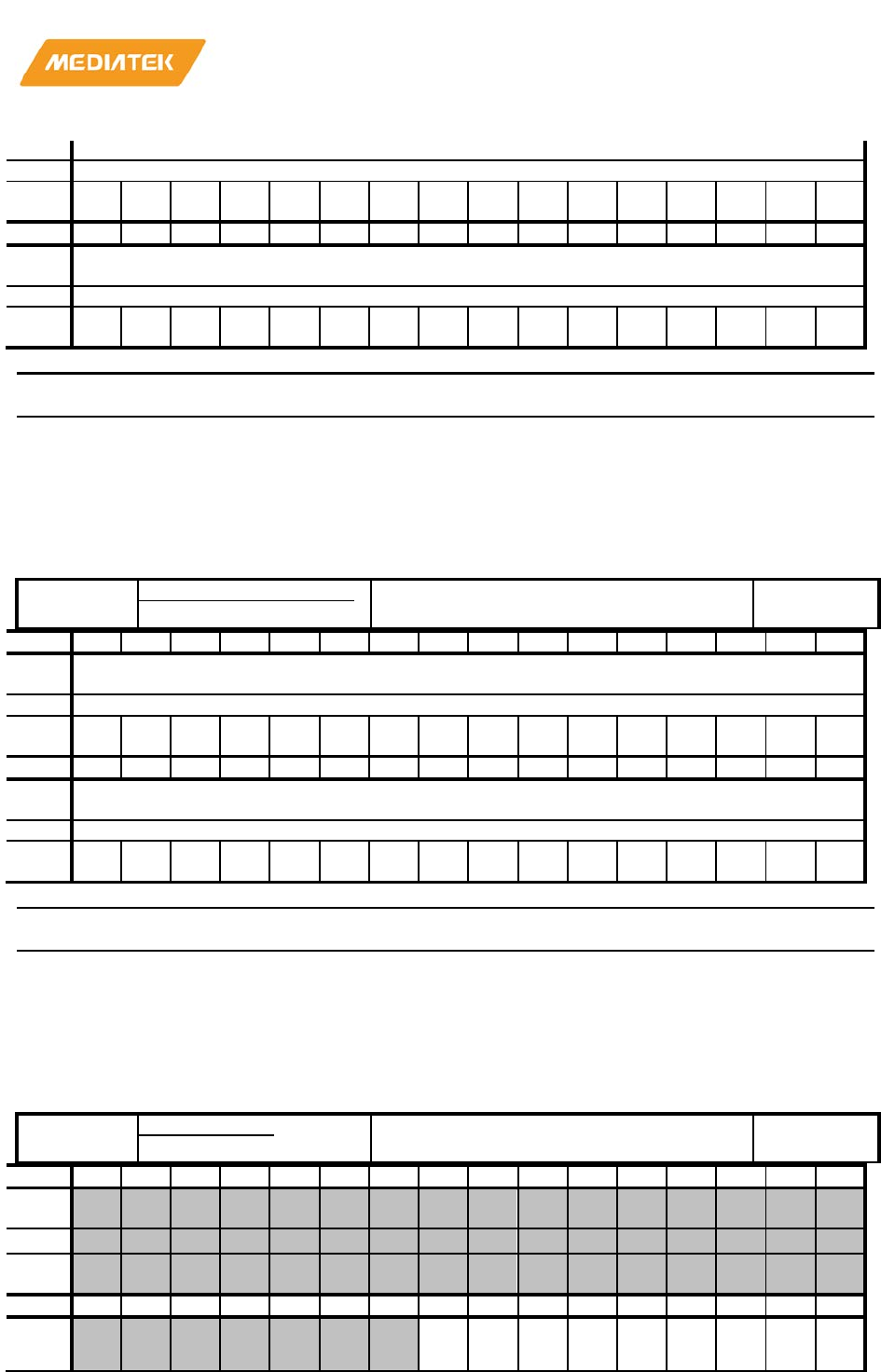
MT76x7
Internet-of-Things Wireless Connectivity
Reference Manual
© 2015 - 2017 MediaTek Inc
Page 454 of 798
This document contains information that is proprietary to MediaTek Inc. (“MediaTek”) and/or its licensor(s).
Any unauthorized use, reproduction or disclosure of this document in whole or in part is strictly prohibited
e
Type
RW
Rese
t
0 0 0 0 0 0 0 0 0 0 0 0 0 0 0 0
Bit
15
14
13
12
11
10
9
8
7
6
5
4
3
2
1
0
Nam
e
GPIO_DOUT2_SET
Type
RW
Rese
t
0 0 0 0 0 0 0 0 0 0 0 0 0 0 0 0
Bit(s)
Mnemonic
Name
Description
31:0
GPIO_DOUT2_SET
GPIO_DOUT2_SET
Write '1' to SET GPO output value. The GPO
PAD is corresponding to GPIO_DOUT2
Read always return '0'
8300B078
GPIO_DOUT2_RESET
PAD GPO DATA Output Control Reset
Register 2
00000000
Bit
31
30
29
28
27
26
25
24
23
22
21
20
19
18
17
16
Nam
e
GPIO_DOUT2_RESET
Type
RW
Rese
t
0 0 0 0 0 0 0 0 0 0 0 0 0 0 0 0
Bit
15
14
13
12
11
10
9
8
7
6
5
4
3
2
1
0
Nam
e
GPIO_DOUT2_RESET
Type
RW
Rese
t
0 0 0 0 0 0 0 0 0 0 0 0 0 0 0 0
Bit(s)
Mnemonic
Name
Description
31:0
GPIO_DOUT2_RESE
T
GPIO_DOUT2_RESET
Write '1' to RESET GPO output value. The GPO
PAD is corresponding to GPIO_DOUT2
Read always return '0'
8300B080
GPIO_DOUT3
PAD GPO DATA Output Control
Register 3
00000000
Bit
31
30
29
28
27
26
25
24
23
22
21
20
19
18
17
16
Nam
e
Type
Rese
t
Bit
15
14
13
12
11
10
9
8
7
6
5
4
3
2
1
0
Nam
e
GP
O_
DO
GP
O_
DO
GP
O_
DO
GP
O_
DO
GP
O_
DO
GP
O_
DO
GP
O_
DO
GP
O_
DO
GP
O_
DO
MT76x7
Internet-of-Things Wireless Connectivity
Reference Manual
© 2015 - 2017 MediaTek Inc
Page 455 of 798
This document contains information that is proprietary to MediaTek Inc. (“MediaTek”) and/or its licensor(s).
Any unauthorized use, reproduction or disclosure of this document in whole or in part is strictly prohibited
UT
72
UT
71
UT
70
UT
69
UT
68
UT
67
UT
66
UT
65
UT
64
Type
RW
RW
RW
RW
RW
RW
RW
RW
RW
Rese
t
0 0 0 0 0 0 0 0 0
Bit(s)
Mnemonic
Name
Description
8
GPO_DOUT72
GPO_DOUT72
GPO_DOUT72 output control register
1: output high
0: ouptut low
7
GPO_DOUT71
GPO_DOUT71
GPO_DOUT71 output control register
1: output high
0: ouptut low
6
GPO_DOUT70
GPO_DOUT70
GPO_DOUT70 output control register
1: output high
0: ouptut low
5
GPO_DOUT69
GPO_DOUT69
GPO_DOUT69 output control register
1: output high
0: ouptut low
4
GPO_DOUT68
GPO_DOUT68
GPO_DOUT68 output control register
1: output high
0: ouptut low
3
GPO_DOUT67
GPO_DOUT67
GPO_DOUT67 output control register
1: output high
0: ouptut low
2
GPO_DOUT66
GPO_DOUT66
GPO_DOUT66 output control register
1: output high
0: ouptut low
1
GPO_DOUT65
GPO_DOUT65
GPO_DOUT65 output control register
1: output high
0: ouptut low
0
GPO_DOUT64
GPO_DOUT64
GPO_DOUT64 output control register
1: output high
0: ouptut low
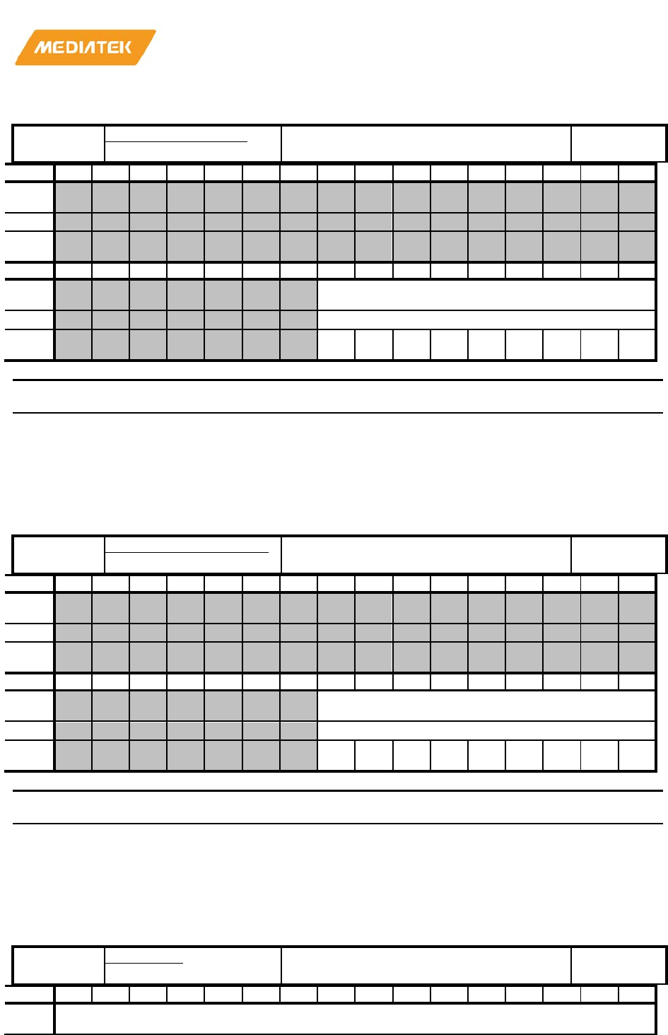
MT76x7
Internet-of-Things Wireless Connectivity
Reference Manual
© 2015 - 2017 MediaTek Inc
Page 456 of 798
This document contains information that is proprietary to MediaTek Inc. (“MediaTek”) and/or its licensor(s).
Any unauthorized use, reproduction or disclosure of this document in whole or in part is strictly prohibited
8300B084
GPIO_DOUT3_SET
PAD GPO DATA Output Control Set
Register 3
00000000
Bit
31
30
29
28
27
26
25
24
23
22
21
20
19
18
17
16
Nam
e
Type
Rese
t
Bit
15
14
13
12
11
10
9
8
7
6
5
4
3
2
1
0
Nam
e
GPIO_DOUT2_SET
Type
RW
Rese
t
0 0 0 0 0 0 0 0 0
Bit(s)
Mnemonic
Name
Description
8:0
GPIO_DOUT2_SET
GPIO_DOUT2_SET
Write '1' to SET GPO output value. The GPO
PAD is corresponding to GPIO_DOUT2
Read always return '0'
8300B088
GPIO_DOUT3_RESET
PAD GPO DATA Output Control Reset
Register 3
00000000
Bit
31
30
29
28
27
26
25
24
23
22
21
20
19
18
17
16
Nam
e
Type
Rese
t
Bit
15
14
13
12
11
10
9
8
7
6
5
4
3
2
1
0
Nam
e
GPIO_DOUT2_RESET
Type
RW
Rese
t
0 0 0 0 0 0 0 0 0
Bit(s)
Mnemonic
Name
Description
8:0
GPIO_DOUT2_RESE
T
GPIO_DOUT2_RESET
Write '1' to RESET GPO output value. The GPO
PAD is corresponding to GPIO_DOUT2
Read always return '0'
8300B090
GPIO_OE1
PAD GPO Output Enable Control
Register 1
00000000
Bit
31
30
29
28
27
26
25
24
23
22
21
20
19
18
17
16
Nam
e
GPIO_OE1
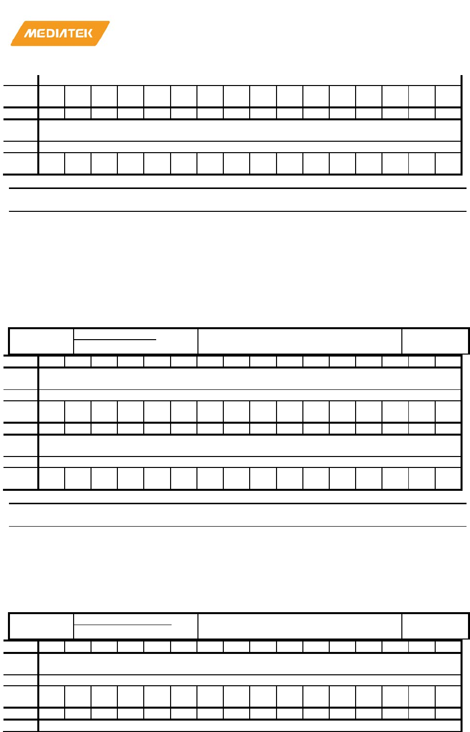
MT76x7
Internet-of-Things Wireless Connectivity
Reference Manual
© 2015 - 2017 MediaTek Inc
Page 457 of 798
This document contains information that is proprietary to MediaTek Inc. (“MediaTek”) and/or its licensor(s).
Any unauthorized use, reproduction or disclosure of this document in whole or in part is strictly prohibited
Type
RW
Rese
t
0 0 0 0 0 0 0 0 0 0 0 0 0 0 0 0
Bit
15
14
13
12
11
10
9
8
7
6
5
4
3
2
1
0
Nam
e
GPIO_OE1
Type
RW
Rese
t
0 0 0 0 0 0 0 0 0 0 0 0 0 0 0 0
Bit(s)
Mnemonic
Name
Description
31:0
GPIO_OE1
GPIO_OE1
PAD GPO Output Enable
The GPO PAD is corresponding to GPIO_DOUT1.
1:GPO output is Enable
0:GPO outupt is Disable
8300B094
GPIO_OE1_SET
PAD GPO Output Enable Set Control
Register 1
00000000
Bit
31
30
29
28
27
26
25
24
23
22
21
20
19
18
17
16
Nam
e
GPIO_OE1_SET
Type
RW
Rese
t
0 0 0 0 0 0 0 0 0 0 0 0 0 0 0 0
Bit
15
14
13
12
11
10
9
8
7
6
5
4
3
2
1
0
Nam
e
GPIO_OE1_SET
Type
RW
Rese
t
0 0 0 0 0 0 0 0 0 0 0 0 0 0 0 0
Bit(s)
Mnemonic
Name
Description
31:0
GPIO_OE1_SET
GPIO_OE1_SET
Write '1' to SET GPO output enable. The GPO
PAD is corresponding to GPIO_OE1.
Read always return "0"
8300B098
GPIO_OE1_RESET
PAD GPO Output Enable Reset Control
Register 1
00000000
Bit
31
30
29
28
27
26
25
24
23
22
21
20
19
18
17
16
Nam
e
GPIO_OE1_RESET
Type
RW
Rese
t
0 0 0 0 0 0 0 0 0 0 0 0 0 0 0 0
Bit
15
14
13
12
11
10
9
8
7
6
5
4
3
2
1
0
Nam
GPIO_OE1_RESET
MT76x7
Internet-of-Things Wireless Connectivity
Reference Manual
© 2015 - 2017 MediaTek Inc
Page 458 of 798
This document contains information that is proprietary to MediaTek Inc. (“MediaTek”) and/or its licensor(s).
Any unauthorized use, reproduction or disclosure of this document in whole or in part is strictly prohibited
e
Type
RW
Rese
t
0 0 0 0 0 0 0 0 0 0 0 0 0 0 0 0
Bit(s)
Mnemonic
Name
Description
31:0
GPIO_OE1_RESET
GPIO_OE1_RESET
Write '1' to RESET GPO output enable. The GPO
PAD is corresponding to GPIO_OE1.
Read always return "0"
8300B0A0
GPIO_OE2
PAD GPO Output Enable Control
Register 2
00000000
Bit
31
30
29
28
27
26
25
24
23
22
21
20
19
18
17
16
Nam
e
GPIO_OE2
Type
RW
Rese
t
0 0 0 0 0 0 0 0 0 0 0 0 0 0 0 0
Bit
15
14
13
12
11
10
9
8
7
6
5
4
3
2
1
0
Nam
e
GPIO_OE2
Type
RW
Rese
t
0 0 0 0 0 0 0 0 0 0 0 0 0 0 0 0
Bit(s)
Mnemonic
Name
Description
31:0
GPIO_OE2
GPIO_OE2
PAD GPO Output Enable
The GPO PAD is corresponding to GPIO_DOUT2.
1:GPO output is Enable
0:GPO outupt is Disable
8300B0A4
GPIO_OE2_SET
PAD GPO Output Enable Set Control
Register2
00000000
Bit
31
30
29
28
27
26
25
24
23
22
21
20
19
18
17
16
Nam
e
GPIO_OE2_SET
Type
RW
Rese
t
0 0 0 0 0 0 0 0 0 0 0 0 0 0 0 0
Bit
15
14
13
12
11
10
9
8
7
6
5
4
3
2
1
0
Nam
e
GPIO_OE2_SET
Type
RW
Rese
t
0 0 0 0 0 0 0 0 0 0 0 0 0 0 0 0
MT76x7
Internet-of-Things Wireless Connectivity
Reference Manual
© 2015 - 2017 MediaTek Inc
Page 459 of 798
This document contains information that is proprietary to MediaTek Inc. (“MediaTek”) and/or its licensor(s).
Any unauthorized use, reproduction or disclosure of this document in whole or in part is strictly prohibited
Bit(s)
Mnemonic
Name
Description
31:0
GPIO_OE2_SET
GPIO_OE2_SET
Write '1' to SET GPO output enable. The GPO
PAD is corresponding to GPIO_OE2.
Read always return "0"
8300B0A8
GPIO_OE2_RESET
PAD GPO Output Enable Reset Control
Register 2
00000000
Bit
31
30
29
28
27
26
25
24
23
22
21
20
19
18
17
16
Nam
e
GPIO_OE2_RESET
Type
RW
Rese
t
0 0 0 0 0 0 0 0 0 0 0 0 0 0 0 0
Bit
15
14
13
12
11
10
9
8
7
6
5
4
3
2
1
0
Nam
e
GPIO_OE2_RESET
Type
RW
Rese
t
0 0 0 0 0 0 0 0 0 0 0 0 0 0 0 0
Bit(s)
Mnemonic
Name
Description
31:0
GPIO_OE2_RESET
GPIO_OE2_RESET
Write '1' to RESET GPO output enable. The GPO
PAD is corresponding to GPIO_OE2.
Read always return "0"
8300B0B0
GPIO_OE3
PAD GPO Output Enable Control
Register 2
00000000
Bit
31
30
29
28
27
26
25
24
23
22
21
20
19
18
17
16
Nam
e
Type
Rese
t
Bit
15
14
13
12
11
10
9
8
7
6
5
4
3
2
1
0
Nam
e
GPIO_OE3
Type
RW
Rese
t
0 0 0 0 0 0 0 0 0
Bit(s)
Mnemonic
Name
Description
8:0
GPIO_OE3
GPIO_OE3
PAD GPO Output Enable
The GPO PAD is corresponding to GPIO_DOUT3.
1:GPO output is Enable
MT76x7
Internet-of-Things Wireless Connectivity
Reference Manual
© 2015 - 2017 MediaTek Inc
Page 460 of 798
This document contains information that is proprietary to MediaTek Inc. (“MediaTek”) and/or its licensor(s).
Any unauthorized use, reproduction or disclosure of this document in whole or in part is strictly prohibited
Bit(s)
Mnemonic
Name
Description
0:GPO outupt is Disable
8300B0B4
GPIO_OE3_SET
PAD GPO Output Enable Set Control
Register2
00000000
Bit
31
30
29
28
27
26
25
24
23
22
21
20
19
18
17
16
Nam
e
Type
Rese
t
Bit
15
14
13
12
11
10
9
8
7
6
5
4
3
2
1
0
Nam
e
GPIO_OE3_SET
Type
RW
Rese
t
0 0 0 0 0 0 0 0 0
Bit(s)
Mnemonic
Name
Description
8:0
GPIO_OE3_SET
GPIO_OE3_SET
Write '1' to SET GPO output enable. The GPO
PAD is corresponding to GPIO_OE3.
Read always return "0"
8300B0B8
GPIO_OE3_RESET
PAD GPO Output Enable Reset Control
Register 2
00000000
Bit
31
30
29
28
27
26
25
24
23
22
21
20
19
18
17
16
Nam
e
Type
Rese
t
Bit
15
14
13
12
11
10
9
8
7
6
5
4
3
2
1
0
Nam
e
GPIO_OE3_RESET
Type
RW
Rese
t
0 0 0 0 0 0 0 0 0 0 0 0 0 0 0 0
Bit(s)
Mnemonic
Name
Description
15:0
GPIO_OE3_RESET
GPIO_OE3_RESET
Write '1' to RESET GPO output enable. The GPO
PAD is corresponding to GPIO_OE3.
Read always return "0"
MT76x7
Internet-of-Things Wireless Connectivity
Reference Manual
© 2015 - 2017 MediaTek Inc
Page 461 of 798
This document contains information that is proprietary to MediaTek Inc. (“MediaTek”) and/or its licensor(s).
Any unauthorized use, reproduction or disclosure of this document in whole or in part is strictly prohibited
8300B0C0
GPIO_DIN1
PAD GPI Input Data Control Register 1
00000000
Bit
31
30
29
28
27
26
25
24
23
22
21
20
19
18
17
16
Nam
e
GP
O_
DI
N31
GP
O_
DI
N3
0
GP
O_
DI
N2
9
GP
O_
DI
N2
8
GP
O_
DI
N2
7
GP
O_
DI
N2
6
GP
O_
DI
N2
5
GP
O_
DI
N2
4
GP
O_
DI
N2
3
GP
O_
DI
N2
2
GP
O_
DI
N21
GP
O_
DI
N2
0
GP
O_
DI
N1
9
GP
O_
DI
N1
8
GP
O_
DI
N17
GP
O_
DI
N1
6
Type
RO
RO
RO
RO
RO
RO
RO
RO
RO
RO
RO
RO
RO
RO
RO
RO
Rese
t
0 0 0 0 0 0 0 0 0 0 0 0 0 0 0 0
Bit
15
14
13
12
11
10
9
8
7
6
5
4
3
2
1
0
Nam
e
GP
O_
DI
N15
GP
O_
DI
N1
4
GP
O_
DI
N13
GP
O_
DI
N12
GP
O_
DI
N11
GP
O_
DI
N1
0
GP
O_
DI
N9
GP
O_
DI
N8
GP
O_
DI
N7
GP
O_
DI
N6
GP
O_
DI
N5
GP
O_
DI
N4
GP
O_
DI
N3
GP
O_
DI
N2
GP
O_
DI
N1
GP
O_
DI
N0
Type
RO
RO
RO
RO
RO
RO
RO
RO
RO
RO
RO
RO
RO
RO
RO
RO
Rese
t
0 0 0 0 0 0 0 0 0 0 0 0 0 0 0 0
Bit(s)
Mnemonic
Name
Description
31
GPO_DIN31
GPO_DIN31
GPO_DIN31 from PAD SDIO_DAT1
1: input High
0: input Low
30
GPO_DIN30
GPO_DIN30
GPO_DIN30 from PAD SDIO_DAT2
1: input High
0:
input Low
29
GPO_DIN29
GPO_DIN29
GPO_DIN29 from PAD SDIO_DAT3
1: input High
0: input Low
28
GPO_DIN28
GPO_DIN28
GPO_DIN28 from PAD SDIO_CMD
1: input High
0: input Low
27
GPO_DIN27
GPO_DIN27
GPO_DIN27 from PAD SDIO_CLK
1: input High
0: input Low
26
GPO_DIN26
GPO_DIN26
GPO_DIN26 from PAD CLK_REQ_N
1: input High
0: input Low
25
GPO_DIN25
GPO_DIN25
GPO_DIN25 from PAD WAKE_N
1: input High

MT76x7
Internet-of-Things Wireless Connectivity
Reference Manual
© 2015 - 2017 MediaTek Inc
Page 462 of 798
This document contains information that is proprietary to MediaTek Inc. (“MediaTek”) and/or its licensor(s).
Any unauthorized use, reproduction or disclosure of this document in whole or in part is strictly prohibited
Bit(s)
Mnemonic
Name
Description
0: input Low
24
GPO_DIN24
GPO_DIN24
GPO_DIN24 from PAD PERST_N
1: input High
0: input Low
23
GPO_DIN23
GPO_DIN23
GPO_DIN23 from PAD IN_UART0_TXD
1: input High
0: input Low
22
GPO_DIN22
GPO_DIN22
GPO_DIN22 from PAD IN_GPIO22
1: input High
0: input Low
21
GPO_DIN21
GPO_DIN21
GPO_DIN21 from PAD IN_GPIO21
1: input High
0: input Low
20
GPO_DIN20
GPO_DIN20
GPO_DIN20 from PAD IN_GPIO20
1: input High
0: input Low
19
GPO_DIN19
GPO_DIN19
GPO_DIN19 from PAD IN_GPIO19
1: input High
0: input Low
18
GPO_DIN18
GPO_DIN18
GPO_DIN18 from PAD IN_GPIO18
1: input High
0: input Low
17
GPO_DIN17
GPO_DIN17
GPO_DIN17 from PAD IN_GPIO17
1: input High
0: input Low
16
GPO_DIN16
GPO_DIN16
GPO_DIN16 from PAD IN_GPIO16
1: input High
0: input Low
15
GPO_DIN15
GPO_DIN15
GPO_DIN15 from PAD IN_GPIO15
1: input High
0: input Low

MT76x7
Internet-of-Things Wireless Connectivity
Reference Manual
© 2015 - 2017 MediaTek Inc
Page 463 of 798
This document contains information that is proprietary to MediaTek Inc. (“MediaTek”) and/or its licensor(s).
Any unauthorized use, reproduction or disclosure of this document in whole or in part is strictly prohibited
Bit(s)
Mnemonic
Name
Description
14
GPO_DIN14
GPO_DIN14
GPO_DIN14 from PAD IN_GPIO14
1:
input High
0: input Low
13
GPO_DIN13
GPO_DIN13
GPO_DIN13 from PAD IN_GPIO13
1: input High
0: input Low
12
GPO_DIN12
GPO_DIN12
GPO_DIN12 from PAD IN_GPIO12
1: input High
0: input Low
11
GPO_DIN11
GPO_DIN11
GPO_DIN11 from PAD IN_GPIO11
1: input High
0:
input Low
10
GPO_DIN10
GPO_DIN10
GPO_DIN10 from PAD IN_GPIO10
1: input High
0: input Low
9
GPO_DIN9
GPO_DIN9
GPO_DIN9 from PAD IN_GPIO9
1: input High
0: input Low
8
GPO_DIN8
GPO_DIN8
GPO_DIN8 from PAD IN_GPIO8
1: input High
0: input Low
7
GPO_DIN7
GPO_DIN7
GPO_DIN7 from PAD ANTSEL7
1: input High
0: input Low
6
GPO_DIN6
GPO_DIN6
GPO_DIN6 from PAD ANTSEL6
1: input High
0: input Low
5
GPO_DIN5
GPO_DIN5
GPO_DIN5 from PAD ANTSEL5
1: input High
0: input Low
4
GPO_DIN4
GPO_DIN4
GPO_DIN4 from PAD ANTSEL4

MT76x7
Internet-of-Things Wireless Connectivity
Reference Manual
© 2015 - 2017 MediaTek Inc
Page 464 of 798
This document contains information that is proprietary to MediaTek Inc. (“MediaTek”) and/or its licensor(s).
Any unauthorized use, reproduction or disclosure of this document in whole or in part is strictly prohibited
Bit(s)
Mnemonic
Name
Description
1: input High
0: input Low
3
GPO_DIN3
GPO_DIN3
GPO_DIN3 from PAD ANTSEL3
1: input High
0: input Low
2
GPO_DIN2
GPO_DIN2
GPO_DIN2 from PAD ANTSEL2
1: input High
0: input Low
1
GPO_DIN1
GPO_DIN1
GPO_DIN1 from PAD ANTSEL1
1: input High
0: input Low
0
GPO_DIN0
GPO_DIN0
GPO_DIN0 from PAD ANTSEL0
1: input High
0: input Low
8300B0C4
GPIO_DIN2
PAD GPI Input Data Control Register 2
00000000
Bit
31
30
29
28
27
26
25
24
23
22
21
20
19
18
17
16
Nam
e
GP
O_
DI
N6
3
GP
O_
DI
N6
2
GP
O_
DI
N6
1
GP
O_
DI
N6
0
GP
O_
DI
N5
9
GP
O_
DI
N5
8
GP
O_
DI
N5
7
GP
O_
DI
N5
6
GP
O_
DI
N5
5
GP
O_
DI
N5
4
GP
O_
DI
N5
3
GP
O_
DI
N5
2
GP
O_
DI
N51
GP
O_
DI
N5
0
GP
O_
DI
N4
9
GP
O_
DI
N4
8
Type
RO
RO
RO
RO
RO
RO
RO
RO
RO
RO
RO
RO
RO
RO
RO
RO
Rese
t
0 0 0 0 0 0 0 0 0 0 0 0 0 0 0 0
Bit
15
14
13
12
11
10
9
8
7
6
5
4
3
2
1
0
Nam
e
GP
O_
DI
N4
7
GP
O_
DI
N4
6
GP
O_
DI
N4
5
GP
O_
DI
N4
4
GP
O_
DI
N4
3
GP
O_
DI
N4
2
GP
O_
DI
N4
1
GP
O_
DI
N4
0
GP
O_
DI
N3
9
GP
O_
DI
N3
8
GP
O_
DI
N3
7
GP
O_
DI
N3
6
GP
O_
DI
N3
5
GP
O_
DI
N3
4
GP
O_
DI
N3
3
GP
O_
DI
N3
2
Type
RO
RO
RO
RO
RO
RO
RO
RO
RO
RO
RO
RO
RO
RO
RO
RO
Rese
t
0 0 0 0 0 0 0 0 0 0 0 0 0 0 0 0
Bit(s)
Mnemonic
Name
Description
31
GPO_DIN63
GPO_DIN63
GPO_DIN63 from PAD IN_ADC6
1: input High
0: input Low
30
GPO_DIN62
GPO_DIN62
GPO_DIN62 from PAD IN_ADC5

MT76x7
Internet-of-Things Wireless Connectivity
Reference Manual
© 2015 - 2017 MediaTek Inc
Page 465 of 798
This document contains information that is proprietary to MediaTek Inc. (“MediaTek”) and/or its licensor(s).
Any unauthorized use, reproduction or disclosure of this document in whole or in part is strictly prohibited
Bit(s)
Mnemonic
Name
Description
1: input High
0: input Low
29
GPO_DIN61
GPO_DIN61
GPO_DIN61 from PAD IN_ADC4
1: input High
0: input Low
28
GPO_DIN60
GPO_DIN60
GPO_DIN60 from PAD BT_LED_B
1: input High
0: input Low
27
GPO_DIN59
GPO_DIN59
GPO_DIN59 from PAD WF_LED_B
1: input High
0: input Low
26
GPO_DIN58
GPO_DIN58
GPO_DIN58 from PAD BT_RF_DIS_B
1:
input High
0: input Low
25
GPO_DIN57
GPO_DIN57
GPO_DIN57 from PAD WF_RF_DIS_B
1: input High
0: input Low
24
GPO_DIN56
GPO_DIN56
GPO_DIN56 from PAD IN_PWM7
1: input High
0: input Low
23
GPO_DIN55
GPO_DIN55
GPO_DIN55 from PAD IN_PWM6
1: input High
0:
input Low
22
GPO_DIN54
GPO_DIN54
GPO_DIN54 from PAD IN_PWM5
1: input High
0: input Low
21
GPO_DIN53
GPO_DIN53
GPO_DIN53 from PAD IN_PWM4
1: input High
0: input Low
20
GPO_DIN52
GPO_DIN52
GPO_DIN52 from PAD IN_PWM3
1: input High

MT76x7
Internet-of-Things Wireless Connectivity
Reference Manual
© 2015 - 2017 MediaTek Inc
Page 466 of 798
This document contains information that is proprietary to MediaTek Inc. (“MediaTek”) and/or its licensor(s).
Any unauthorized use, reproduction or disclosure of this document in whole or in part is strictly prohibited
Bit(s)
Mnemonic
Name
Description
0: input Low
19
GPO_DIN51
GPO_DIN51
GPO_DIN51 from PAD IN_PWM2
1: input High
0: input Low
18
GPO_DIN50
GPO_DIN50
GPO_DIN50 from PAD IN_GPIO54
1: input High
0: input Low
17
GPO_DIN49
GPO_DIN49
GPO_DIN49 from PAD IN_GPIO53
1: input High
0: input Low
16
GPO_DIN48
GPO_DIN48
GPO_DIN48 from PAD IN_GPIO52
1: input High
0: input Low
15
GPO_DIN47
GPO_DIN47
GPO_DIN47 from PAD IN_GPIO51
1: input High
0: input Low
14
GPO_DIN46
GPO_DIN46
GPO_DIN46 from PAD IN_GPIO50
1: input High
0: input Low
13
GPO_DIN45
GPO_DIN45
GPO_DIN45 from PAD IN_GPIO49
1: input High
0: input Low
12
GPO_DIN44
GPO_DIN44
GPO_DIN44 from PAD IN_GPIO48
1: input High
0: input Low
11
GPO_DIN43
GPO_DIN43
GPO_DIN43 from PAD IN_GPIO47
1: input High
0: input Low
10
GPO_DIN42
GPO_DIN42
GPO_DIN42 from PAD IN_GPIO46
1: input High
0: input Low

MT76x7
Internet-of-Things Wireless Connectivity
Reference Manual
© 2015 - 2017 MediaTek Inc
Page 467 of 798
This document contains information that is proprietary to MediaTek Inc. (“MediaTek”) and/or its licensor(s).
Any unauthorized use, reproduction or disclosure of this document in whole or in part is strictly prohibited
Bit(s)
Mnemonic
Name
Description
9
GPO_DIN41
GPO_DIN41
GPO_DIN41 from PAD IN_GPIO45
1: input High
0: input Low
8
GPO_DIN40
GPO_DIN40
GPO_DIN40 from PAD IN_GPIO44
1: input High
0: input Low
7
GPO_DIN39
GPO_DIN39
GPO_DIN39 from PAD UART_CTS
1:
input High
0: input Low
6
GPO_DIN38
GPO_DIN38
GPO_DIN38 from PAD UART_RTS
1: input High
0: input Low
5
GPO_DIN37
GPO_DIN37
GPO_DIN37 from PAD UART_TX
1: input High
0: input Low
4
GPO_DIN36
GPO_DIN36
GPO_DIN36 from PAD UART_RX
1: input High
0: input Low
3
GPO_DIN35
GPO_DIN35
GPO_DIN35 from PAD UART_DBG
1: input High
0: input Low
2
GPO_DIN34
GPO_DIN34
GPO_DIN34 from PAD GPIO1
1: input High
0: input Low
1
GPO_DIN33
GPO_DIN33
GPO_DIN33 from PAD GPIO0
1: input High
0: input Low
0
GPO_DIN32
GPO_DIN32
GPO_DIN32 from PAD SDIO_DAT0
1: input High
0: input Low
MT76x7
Internet-of-Things Wireless Connectivity
Reference Manual
© 2015 - 2017 MediaTek Inc
Page 468 of 798
This document contains information that is proprietary to MediaTek Inc. (“MediaTek”) and/or its licensor(s).
Any unauthorized use, reproduction or disclosure of this document in whole or in part is strictly prohibited
8300B0C8
GPIO_DIN3
PAD GPI Input Data Control Register 3
00000000
Bit
31
30
29
28
27
26
25
24
23
22
21
20
19
18
17
16
Nam
e
Type
Rese
t
Bit
15
14
13
12
11
10
9
8
7
6
5
4
3
2
1
0
Nam
e
GP
O_
DI
N7
2
GP
O_
DI
N71
GP
O_
DI
N7
0
GP
O_
DI
N6
9
GP
O_
DI
N6
8
GP
O_
DI
N6
7
GP
O_
DI
N6
6
GP
O_
DI
N6
5
GP
O_
DI
N6
4
Type
RO
RO
RO
RO
RO
RO
RO
RO
RO
Rese
t
0 0 0 0 0 0 0 0 0
Bit(s)
Mnemonic
Name
Description
8
GPO_DIN72
GPO_DIN72
GPO_DIN72 from PAD IN_ADC15
1: input High
0: input Low
7
GPO_DIN71
GPO_DIN71
GPO_DIN71 from PAD IN_ADC14
1: input High
0: input Low
6
GPO_DIN70
GPO_DIN70
GPO_DIN70 from PAD IN_ADC13
1: input High
0: input
Low
5
GPO_DIN69
GPO_DIN69
GPO_DIN69 from PAD IN_ADC12
1: input High
0: input Low
4
GPO_DIN68
GPO_DIN68
GPO_DIN68 from PAD IN_ADC11
1: input High
0: input Low
3
GPO_DIN67
GPO_DIN67
GPO_DIN67 from PAD IN_ADC10
1: input High
0: input Low
2
GPO_DIN66
GPO_DIN66
GPO_DIN66 from PAD IN_ADC9
1: input High
0: input Low
MT76x7
Internet-of-Things Wireless Connectivity
Reference Manual
© 2015 - 2017 MediaTek Inc
Page 469 of 798
This document contains information that is proprietary to MediaTek Inc. (“MediaTek”) and/or its licensor(s).
Any unauthorized use, reproduction or disclosure of this document in whole or in part is strictly prohibited
Bit(s)
Mnemonic
Name
Description
1
GPO_DIN65
GPO_DIN65
GPO_DIN65 from PAD IN_ADC8
1: input High
0: input Low
0
GPO_DIN64
GPO_DIN64
GPO_DIN64 from PAD IN_ADC7
1: input High
0: input Low
8300B0D0
PADDRV1
PAD Driving Control Register1
00000000
Bit
31
30
29
28
27
26
25
24
23
22
21
20
19
18
17
16
Nam
e
IN_GPIO1
5_DRV
IN_GPIO1
4_DRV
IN_GPIO1
3_DRV
IN_GPIO1
2_DRV
IN_GPIO1
1_DRV
IN_GPIO1
0_DRV
IN_GPIO
9_DRV
IN_GPIO
8_DRV
Type
RW
RW
RW
RW
RW
RW
RW
RW
Rese
t
0 0 0 0 0 0 0 0 0 0 0 0 0 0 0 0
Bit
15
14
13
12
11
10
9
8
7
6
5
4
3
2
1
0
Nam
e
ANTSEL7
_DRV
ANTSEL6
_DRV
ANTSEL5
_DRV
ANTSEL4
_DRV
ANTSEL3
_DRV
ANTSEL2
_DRV
ANTSEL1
_DRV
ANTSEL0
_DRV
Type
RW
RW
RW
RW
RW
RW
RW
RW
Rese
t
0 0 0 0 0 0 0 0 0 0 0 0 0 0 0 0
Bit(s)
Mnemonic
Name
Description
31:30
IN_GPIO15_DRV
IN_GPIO15_DRV
IN_GPIO15 driving setting
The same as ANTSEL0_DRV
29:28
IN_GPIO14_DRV
IN_GPIO14_DRV
IN_GPIO14 driving setting
The same as ANTSEL0_DRV
27:26
IN_GPIO13_DRV
IN_GPIO13_DRV
IN_GPIO13 driving setting
The same as ANTSEL0_DRV
25:24
IN_GPIO12_DRV
IN_GPIO12_DRV
IN_GPIO12 driving setting
The same as ANTSEL0_DRV
23:22
IN_GPIO11_DRV
IN_GPIO11_DRV
IN_GPIO11 driving setting
The same as ANTSEL0_DRV
21:20
IN_GPIO10_DRV
IN_GPIO10_DRV
IN_GPIO10 driving setting
The same as ANTSEL0_DRV
19:18
IN_GPIO9_DRV
IN_GPIO9_DRV
IN_GPIO9 driving setting
The same as ANTSEL0_DRV

MT76x7
Internet-of-Things Wireless Connectivity
Reference Manual
© 2015 - 2017 MediaTek Inc
Page 470 of 798
This document contains information that is proprietary to MediaTek Inc. (“MediaTek”) and/or its licensor(s).
Any unauthorized use, reproduction or disclosure of this document in whole or in part is strictly prohibited
Bit(s)
Mnemonic
Name
Description
17:16
IN_GPIO8_DRV
IN_GPIO8_DRV
IN_GPIO8 driving setting
The same as ANTSEL0_DRV
15:14
ANTSEL7_DRV
ANTSEL7_DRV
ANTSEL7 driving setting
The same as ANTSEL0_DRV
13:12
ANTSEL6_DRV
ANTSEL6_DRV
ANTSEL6 driving setting
The same as ANTSEL0_DRV
11:10
ANTSEL5_DRV
ANTSEL5_DRV
ANTSEL5 driving setting
The same as ANTSEL0_DRV
9:8
ANTSEL4_DRV
ANTSEL4_DRV
ANTSEL4 driving setting
The same as ANTSEL0_DRV
7:6
ANTSEL3_DRV
ANTSEL3_DRV
ANTSEL3 driving setting
The same as ANTSEL0_DRV
5:4
ANTSEL2_DRV
ANTSEL2_DRV
ANTSEL2 driving setting
The same as ANTSEL0_DRV
3:2
ANTSEL1_DRV
ANTSEL1_DRV
ANTSEL1 driving setting
The same as ANTSEL0_DRV
1:0
ANTSEL0_DRV
ANTSEL0_DRV
ANTSEL0 driving setting
00:4mA
01:8mA
10:12mA
11:16mA
8300B0D4
PADDRV2
PAD Driving Control Register2
00000000
Bit
31
30
29
28
27
26
25
24
23
22
21
20
19
18
17
16
Nam
e
CLK_REQ
_N_DRV
WAKE_N
_DRV
PERST_N
_DRV
Type
RW
RW
RW
Rese
t
0 0 0 0 0 0
Bit
15
14
13
12
11
10
9
8
7
6
5
4
3
2
1
0
Nam
e
IN_UART
0_TXD_D
RV
IN_GPIO
22_DRV IN_GPIO
21_DRV IN_GPIO
20_DRV IN_GPIO1
9_DRV IN_GPIO1
8_DRV IN_GPIO1
7_DRV IN_GPIO1
6_DRV
Type
RW
RW
RW
RW
RW
RW
RW
RW
Rese
t
0 0 0 0 0 0 0 0 0 0 0 0 0 0 0 0

MT76x7
Internet-of-Things Wireless Connectivity
Reference Manual
© 2015 - 2017 MediaTek Inc
Page 471 of 798
This document contains information that is proprietary to MediaTek Inc. (“MediaTek”) and/or its licensor(s).
Any unauthorized use, reproduction or disclosure of this document in whole or in part is strictly prohibited
Bit(s)
Mnemonic
Name
Description
21:20
CLK_REQ_N_DRV
CLK_REQ_N_DRV
CLK_REQ_N driving setting
The same as ANTSEL0_DRV
19:18
WAKE_N_DRV
WAKE_N_DRV
WAKE_N driving setting
The same as ANTSEL0_DRV
17:16
PERST_N_DRV
PERST_N_DRV
PERST_N driving setting
The same as ANTSEL0_DRV
15:14
IN_UART0_TXD_D
RV
IN_UART0_TXD_DRV
IN_UART0_TXD driving setting
The same as ANTSEL0_DRV
13:12
IN_GPIO22_DRV
IN_GPIO22_DRV
IN_GPIO22 driving setting
The same as ANTSEL0_DRV
11:10
IN_GPIO21_DRV
IN_GPIO21_DRV
IN_GPIO21 driving setting
The same as ANTSEL0_DRV
9:8
IN_GPIO20_DRV
IN_GPIO20_DRV
IN_GPIO20 driving setting
The same as ANTSEL0_DRV
7:6
IN_GPIO19_DRV
IN_GPIO19_DRV
IN_GPIO19 driving setting
The same as ANTSEL0_DRV
5:4
IN_GPIO18_DRV
IN_GPIO18_DRV
IN_GPIO18 driving setting
The same as ANTSEL0_DRV
3:2
IN_GPIO17_DRV
IN_GPIO17_DRV
IN_GPIO17 driving setting
The same as ANTSEL0_DRV
1:0
IN_GPIO16_DRV
IN_GPIO16_DRV
IN_GPIO16 driving setting
The same as ANTSEL0_DRV
8300B0D8
PADDRV3
PAD Driving Control Register3
00000000
Bit
31
30
29
28
27
26
25
24
23
22
21
20
19
18
17
16
Nam
e
IN_GPIO
51_DRV
IN_GPIO
50_DRV
IN_GPIO
49_DRV
IN_GPIO
48_DRV
IN_GPIO
47_DRV
IN_GPIO
46_DRV
IN_GPIO
45_DRV
IN_GPIO
44_DRV
Type
RW
RW
RW
RW
RW
RW
RW
RW
Rese
t
0 0 0 0 0 0 0 0 0 0 0 0 0 0 0 0
Bit
15
14
13
12
11
10
9
8
7
6
5
4
3
2
1
0
Nam
e
UART_CT
S_DRV
UART_RT
S_DRV
UART_TX
_DRV
UART_R
X_DRV
UART_D
BG_DRV
GPIO1_D
RV
GPIO0_D
RV
Type
RW
RW
RW
RW
RW
RW
RW
Rese
t
0 0 0 0 0 0 0 0 0 0 0 0 0 0

MT76x7
Internet-of-Things Wireless Connectivity
Reference Manual
© 2015 - 2017 MediaTek Inc
Page 472 of 798
This document contains information that is proprietary to MediaTek Inc. (“MediaTek”) and/or its licensor(s).
Any unauthorized use, reproduction or disclosure of this document in whole or in part is strictly prohibited
Bit(s)
Mnemonic
Name
Description
31:30
IN_GPIO51_DRV
IN_GPIO51_DRV
IN_GPIO51 driving setting
The same as ANTSEL0_DRV
29:28
IN_GPIO50_DRV
IN_GPIO50_DRV
IN_GPIO50 driving setting
The same as ANTSEL0_DRV
27:26
IN_GPIO49_DRV
IN_GPIO49_DRV
IN_GPIO49 driving setting
The same as ANTSEL0_DRV
25:24
IN_GPIO48_DRV
IN_GPIO48_DRV
IN_GPIO48 driving setting
The same as ANTSEL0_DRV
23:22
IN_GPIO47_DRV
IN_GPIO47_DRV
IN_GPIO47 driving setting
The same as ANTSEL0_DRV
21:20
IN_GPIO46_DRV
IN_GPIO46_DRV
IN_GPIO46 driving setting
The same as ANTSEL0_DRV
19:18
IN_GPIO45_DRV
IN_GPIO45_DRV
IN_GPIO45 driving setting
The same as ANTSEL0_DRV
17:16
IN_GPIO44_DRV
IN_GPIO44_DRV
IN_GPIO44 driving setting
The same as ANTSEL0_DRV
15:14
UART_CTS_DRV
UART_CTS_DRV
UART_CTS driving setting
The same as ANTSEL0_DRV
13:12
UART_RTS_DRV
UART_RTS_DRV
UART_RTS driving setting
The same as ANTSEL0_DRV
11:10
UART_TX_DRV
UART_TX_DRV
UART_TX driving setting
The same as ANTSEL0_DRV
9:8
UART_RX_DRV
UART_RX_DRV
UART_RX driving setting
The same as ANTSEL0_DRV
7:6
UART_DBG_DRV
UART_DBG_DRV
UART_DBG driving setting
The same as ANTSEL0_DRV
5:4
GPIO1_DRV
GPIO1_DRV
GPIO1 driving setting
The same as ANTSEL0_DRV
3:2
GPIO0_DRV
GPIO0_DRV
GPIO0 driving setting
The same as ANTSEL0_DRV
MT76x7
Internet-of-Things Wireless Connectivity
Reference Manual
© 2015 - 2017 MediaTek Inc
Page 473 of 798
This document contains information that is proprietary to MediaTek Inc. (“MediaTek”) and/or its licensor(s).
Any unauthorized use, reproduction or disclosure of this document in whole or in part is strictly prohibited
Bit(s)
Mnemonic
Name
Description
8300B0DC
PADDRV4
PAD Driving Control Register4
00000000
Bit
31
30
29
28
27
26
25
24
23
22
21
20
19
18
17
16
Nam
e IN_ADC6
_DRV IN_ADC5
_DRV IN_ADC4
_DRV BT_LED_
B_DRV WF_LED
_B_DRV
BT_RF_D
IS_B_DR
V
WF_RF_
DIS_B_D
RV
IN_PWM
7_DRV
Type
RW
RW
RW
RW
RW
RW
RW
RW
Rese
t
0 0 0 0 0 0 0 0 0 0 0 0 0 0 0 0
Bit
15
14
13
12
11
10
9
8
7
6
5
4
3
2
1
0
Nam
e
IN_PWM
6_DRV
IN_PWM
5_DRV
IN_PWM
4_DRV
IN_PWM
3_DRV
IN_PWM
2_DRV
IN_GPIO
54_DRV
IN_GPIO
53_DRV
IN_GPIO
52_DRV
Type
RW
RW
RW
RW
RW
RW
RW
RW
Rese
t
0 0 0 0 0 0 0 0 0 0 0 0 0 0 0 0
Bit(s)
Mnemonic
Name
Description
31:30
IN_ADC6_DRV
IN_ADC6_DRV
IN_ADC6 driving setting
The
same as ANTSEL0_DRV
29:28
IN_ADC5_DRV
IN_ADC5_DRV
IN_ADC5 driving setting
The same as ANTSEL0_DRV
27:26
IN_ADC4_DRV
IN_ADC4_DRV
IN_ADC4 driving setting
The same as ANTSEL0_DRV
25:24
BT_LED_B_DRV
BT_LED_B_DRV
BT_LED_B driving setting
The same as
ANTSEL0_DRV
23:22
WF_LED_B_DRV
WF_LED_B_DRV
WF_LED_B driving setting
The same as ANTSEL0_DRV
21:20
BT_RF_DIS_B_DRV
BT_RF_DIS_B_DRV
BT_RF_DIS_B driving setting
The same as ANTSEL0_DRV
19:18
WF_RF_DIS_B_DR
V
WF_RF_DIS_B_DRV
WF_RF_DIS_B driving setting
The same as ANTSEL0_DRV
17:16
IN_PWM7_DRV
IN_PWM7_DRV
IN_PWM7 driving setting
The same as ANTSEL0_DRV
15:14
IN_PWM6_DRV
IN_PWM6_DRV
IN_PWM6 driving setting
The same as ANTSEL0_DRV
13:12
IN_PWM5_DRV
IN_PWM5_DRV
IN_PWM5 driving setting
The same as
ANTSEL0_DRV
MT76x7
Internet-of-Things Wireless Connectivity
Reference Manual
© 2015 - 2017 MediaTek Inc
Page 474 of 798
This document contains information that is proprietary to MediaTek Inc. (“MediaTek”) and/or its licensor(s).
Any unauthorized use, reproduction or disclosure of this document in whole or in part is strictly prohibited
Bit(s)
Mnemonic
Name
Description
11:10
IN_PWM4_DRV
IN_PWM4_DRV
IN_PWM4 driving setting
The same as ANTSEL0_DRV
9:8
IN_PWM3_DRV
IN_PWM3_DRV
IN_PWM3 driving setting
The same as ANTSEL0_DRV
7:6
IN_PWM2_DRV
IN_PWM2_DRV
IN_PWM2 driving setting
The same as ANTSEL0_DRV
5:4
IN_GPIO54_DRV
IN_GPIO54_DRV
IN_GPIO54 driving setting
The same as ANTSEL0_DRV
3:2
IN_GPIO53_DRV
IN_GPIO53_DRV
IN_GPIO53 driving setting
The same as ANTSEL0_DRV
1:0
IN_GPIO52_DRV
IN_GPIO52_DRV
IN_GPIO52 driving setting
The same as ANTSEL0_DRV
8300B0E0
PADDRV5
PAD Driving Control Register5
00000000
Bit
31
30
29
28
27
26
25
24
23
22
21
20
19
18
17
16
Nam
e
IN_HSPI
N_DRV
SIP_D3_
DRV
SIP_D2_
DRV
SIP_D1_
DRV
SIP_D0_
DRV
SIP_CS_
DRV
SIP_CK_
DRV
IN_ADC1
5_DRV
Type
RW
RW
RW
RW
RW
RW
RW
RW
Rese
t
0 0 0 0 0 0 0 0 0 0 0 0 0 0 0 0
Bit
15
14
13
12
11
10
9
8
7
6
5
4
3
2
1
0
Nam
e
IN_ADC1
4_DRV
IN_ADC1
3_DRV
IN_ADC1
2_DRV
IN_ADC11
_DRV
IN_ADC1
0_DRV
IN_ADC9
_DRV
IN_ADC8
_DRV
IN_ADC7
_DRV
Type
RW
RW
RW
RW
RW
RW
RW
RW
Rese
t
0 0 0 0 0 0 0 0 0 0 0 0 0 0 0 0
Bit(s)
Mnemonic
Name
Description
31:30
IN_HSPIN_DRV
IN_HSPIN_DRV
IN_HSPIN driving setting
The same as ANTSEL0_DRV
29:28
SIP_D3_DRV
SIP_D3_DRV
SIP_D3 driving setting
The same as ANTSEL0_DRV
27:26
SIP_D2_DRV
SIP_D2_DRV
SIP_D2 driving setting
The same as ANTSEL0_DRV
25:24
SIP_D1_DRV
SIP_D1_DRV
SIP_D1 driving setting
The same as ANTSEL0_DRV

MT76x7
Internet-of-Things Wireless Connectivity
Reference Manual
© 2015 - 2017 MediaTek Inc
Page 475 of 798
This document contains information that is proprietary to MediaTek Inc. (“MediaTek”) and/or its licensor(s).
Any unauthorized use, reproduction or disclosure of this document in whole or in part is strictly prohibited
Bit(s)
Mnemonic
Name
Description
23:22
SIP_D0_DRV
SIP_D0_DRV
SIP_D0 driving setting
The same as ANTSEL0_DRV
21:20
SIP_CS_DRV
SIP_CS_DRV
SIP_CS driving setting
The same as ANTSEL0_DRV
19:18
SIP_CK_DRV
SIP_CK_DRV
SIP_CK driving setting
The same as ANTSEL0_DRV
17:16
IN_ADC15_DRV
IN_ADC15_DRV
IN_ADC15 driving setting
The same as ANTSEL0_DRV
15:14
IN_ADC14_DRV
IN_ADC14_DRV
IN_ADC14 driving setting
The same as ANTSEL0_DRV
13:12
IN_ADC13_DRV
IN_ADC13_DRV
IN_ADC13 driving setting
The same as ANTSEL0_DRV
11:10
IN_ADC12_DRV
IN_ADC12_DRV
IN_ADC12 driving setting
The same as ANTSEL0_DRV
9:8
IN_ADC11_DRV
IN_ADC11_DRV
IN_ADC11 driving setting
The same as ANTSEL0_DRV
7:6
IN_ADC10_DRV
IN_ADC10_DRV
IN_ADC10 driving setting
The same as ANTSEL0_DRV
5:4
IN_ADC9_DRV
IN_ADC9_DRV
IN_ADC9 driving setting
The same as ANTSEL0_DRV
3:2
IN_ADC8_DRV
IN_ADC8_DRV
IN_ADC8 driving setting
The same as ANTSEL0_DRV
1:0
IN_ADC7_DRV
IN_ADC7_DRV
IN_ADC7 driving setting
The same as ANTSEL0_DRV
8300B0F0
PADCTRL1
PAD Control Register1
00000010
Bit
31
30
29
28
27
26
25
24
23
22
21
20
19
18
17
16
Nam
e
Type
Rese
t
Bit
15
14
13
12
11
10
9
8
7
6
5
4
3
2
1
0
Nam
GPI TDSEL
RDSEL
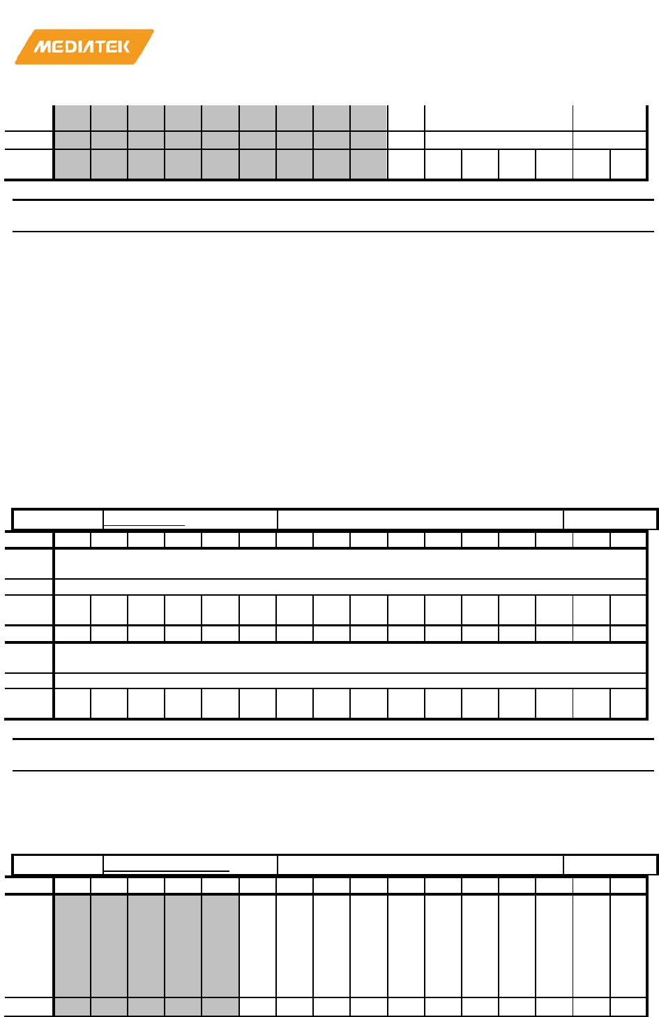
MT76x7
Internet-of-Things Wireless Connectivity
Reference Manual
© 2015 - 2017 MediaTek Inc
Page 476 of 798
This document contains information that is proprietary to MediaTek Inc. (“MediaTek”) and/or its licensor(s).
Any unauthorized use, reproduction or disclosure of this document in whole or in part is strictly prohibited
e
O_
SR
Type
RW
RW
RW
Rese
t
0 0 1 0 0 0 0
Bit(s)
Mnemonic
Name
Description
6
GPIO_SR
GPIO_SR
GPIO PADs slew rate control
1: Slow
0: Fast
Related PADs: All
PADs except for PAD_SDIO_XXX
5:2
TDSEL
TDSEL
PAD TD selection
Related PADs: All PADs except for PAD_SDIO_XXX
1:0
RDSEL
RDSEL
PAD RD selection
Related PADs: All PADs except for PAD_SDIO_XXX
8300B0F4
PADCTRL2
PAD Control Register2
00000000
Bit
31
30
29
28
27
26
25
24
23
22
21
20
19
18
17
16
Nam
e
Reserved
Type
RW
Rese
t
0 0 0 0 0 0 0 0 0 0 0 0 0 0 0 0
Bit
15
14
13
12
11
10
9
8
7
6
5
4
3
2
1
0
Nam
e
Reserved
Type
RW
Rese
t
0 0 0 0 0 0 0 0 0 0 0 0 0 0 0 0
Bit(s)
Mnemonic
Name
Description
31:0
Reserved
Reserved
8300B100
PAD_GPIO_IES0
GPIO PAD IES Control Register 0
07FFFFFF
Bit
31
30
29
28
27
26
25
24
23
22
21
20
19
18
17
16
Nam
e
CL
K_
RE
Q_
N_
IES
WA
KE
_N
_IE
S
PE
RS
T_
N_
IES
IN
_U
AR
T0
_T
XD
_IE
S
IN
_G
PIO
22_
IES
IN
_G
PIO
21_
IES
IN
_G
PIO
20
_IE
S
IN
_G
PIO
19_
IES
IN
_G
PIO
18_
IES
IN
_G
PIO
17_
IES
IN
_G
PIO
16_
IES
Type
RW
RW
RW
RW
RW
RW
RW
RW
RW
RW
RW
MT76x7
Internet-of-Things Wireless Connectivity
Reference Manual
© 2015 - 2017 MediaTek Inc
Page 477 of 798
This document contains information that is proprietary to MediaTek Inc. (“MediaTek”) and/or its licensor(s).
Any unauthorized use, reproduction or disclosure of this document in whole or in part is strictly prohibited
Rese
t
1 1 1 1 1 1 1 1 1 1 1
Bit
15
14
13
12
11
10
9
8
7
6
5
4
3
2
1
0
Nam
e
IN
_G
PIO
15_
IES
IN
_G
PIO
14_
IES
IN
_G
PIO
13_
IES
IN
_G
PIO
12_
IES
IN
_G
PIO
11_
IES
IN
_G
PIO
10_
IES
IN
_G
PIO
9_I
ES
IN
_G
PIO
8_I
ES
AN
TS
EL7
_IE
S
AN
TS
EL
6_I
ES
AN
TS
EL
5_I
ES
AN
TS
EL
4_I
ES
AN
TS
EL
3_I
ES
AN
TS
EL
2_I
ES
AN
TS
EL1
_IE
S
AN
TS
EL
0_I
ES
Type
RW
RW
RW
RW
RW
RW
RW
RW
RW
RW
RW
RW
RW
RW
RW
RW
Rese
t
1 1 1 1 1 1 1 1 1 1 1 1 1 1 1 1
Bit(s)
Mnemonic
Name
Description
26
CLK_REQ_N_IES
CLK_REQ_N_IES
PAD CLK_REQ_N input enable signal control
register
1: Enable
0: Disable
25
WAKE_N_IES
WAKE_N_IES
PAD WAKE_N input enable signal control
register
1: Enable
0:
Disable
24
PERST_N_IES
PERST_N_IES
PAD PERST_N input enable signal control
register
1: Enable
0: Disable
23
IN_UART0_TXD_IE
S
IN_UART0_TXD_IES
PAD IN_UART0_TXD input enable signal
control register
1: Enable
0: Disable
22
IN_GPIO22_IES
IN_GPIO22_IES
PAD IN_GPIO22 input enable signal control
register
1: Enable
0: Disable
21
IN_GPIO21_IES
IN_GPIO21_IES
PAD IN_GPIO21 input enable signal control
register
1: Enable
0: Disable
20
IN_GPIO20_IES
IN_GPIO20_IES
PAD IN_GPIO20 input enable signal control
register
1: Enable
0: Disable

MT76x7
Internet-of-Things Wireless Connectivity
Reference Manual
© 2015 - 2017 MediaTek Inc
Page 478 of 798
This document contains information that is proprietary to MediaTek Inc. (“MediaTek”) and/or its licensor(s).
Any unauthorized use, reproduction or disclosure of this document in whole or in part is strictly prohibited
Bit(s)
Mnemonic
Name
Description
19
IN_GPIO19_IES
IN_GPIO19_IES
PAD IN_GPIO19 input enable signal control
register
1: Enable
0: Disable
18
IN_GPIO18_IES
IN_GPIO18_IES
PAD IN_GPIO18 input enable signal control
register
1: Enable
0: Disable
17
IN_GPIO17_IES
IN_GPIO17_IES
PAD IN_GPIO17 input enable signal control
register
1: Enable
0: Disable
16
IN_GPIO16_IES
IN_GPIO16_IES
PAD IN_GPIO16 input enable signal control
register
1: Enable
0: Disable
15
IN_GPIO15_IES
IN_GPIO15_IES
PAD IN_GPIO15 input enable signal control
register
1: Enable
0: Disable
14
IN_GPIO14_IES
IN_GPIO14_IES
PAD IN_GPIO14 input enable signal control
register
1: Enable
0: Disable
13
IN_GPIO13_IES
IN_GPIO13_IES
PAD IN_GPIO13 input enable signal control
register
1: Enable
0: Disable
12
IN_GPIO12_IES
IN_GPIO12_IES
PAD IN_GPIO12 input enable signal control
register
1: Enable
0: Disable
11
IN_GPIO11_IES
IN_GPIO11_IES
PAD IN_GPIO11 input enable signal control
register
1: Enable

MT76x7
Internet-of-Things Wireless Connectivity
Reference Manual
© 2015 - 2017 MediaTek Inc
Page 479 of 798
This document contains information that is proprietary to MediaTek Inc. (“MediaTek”) and/or its licensor(s).
Any unauthorized use, reproduction or disclosure of this document in whole or in part is strictly prohibited
Bit(s)
Mnemonic
Name
Description
0: Disable
10
IN_GPIO10_IES
IN_GPIO10_IES
PAD IN_GPIO10 input enable signal control
register
1: Enable
0: Disable
9
IN_GPIO9_IES
IN_GPIO9_IES
PAD IN_GPIO9 input enable signal control
register
1: Enable
0: Disable
8
IN_GPIO8_IES
IN_GPIO8_IES
PAD IN_GPIO8 input enable signal control
register
1: Enable
0: Disable
7
ANTSEL7_IES
ANTSEL7_IES
PAD ANTSEL7 input enable signal control
register
1: Enable
0: Disable
6
ANTSEL6_IES
ANTSEL6_IES
PAD ANTSEL6 input enable signal control
register
1: Enable
0: Disable
5
ANTSEL5_IES
ANTSEL5_IES
PAD ANTSEL5 input enable signal control
register
1: Enable
0: Disable
4
ANTSEL4_IES
ANTSEL4_IES
PAD ANTSEL4 input enable signal control
register
1: Enable
0: Disable
3
ANTSEL3_IES
ANTSEL3_IES
PAD ANTSEL3 input enable signal control
register
1: Enable
0: Disable
2
ANTSEL2_IES
ANTSEL2_IES
PAD ANTSEL2 input enable signal control
register

MT76x7
Internet-of-Things Wireless Connectivity
Reference Manual
© 2015 - 2017 MediaTek Inc
Page 480 of 798
This document contains information that is proprietary to MediaTek Inc. (“MediaTek”) and/or its licensor(s).
Any unauthorized use, reproduction or disclosure of this document in whole or in part is strictly prohibited
Bit(s)
Mnemonic
Name
Description
1: Enable
0: Disable
1
ANTSEL1_IES
ANTSEL1_IES
PAD ANTSEL1 input enable signal control
register
1: Enable
0: Disable
0
ANTSEL0_IES
ANTSEL0_IES
PAD ANTSEL0 input enable signal control
register
1: Enable
0: Disable
8300B104
PAD_GPIO_IES1
GPIO PAD IES Control Register 1
FFFFFFFE
Bit
31
30
29
28
27
26
25
24
23
22
21
20
19
18
17
16
Nam
e
IN
_A
DC
6_I
ES
IN
_A
DC
5_I
ES
IN
_A
DC
4_I
ES
BT
_L
ED
_B
_IE
S
WF
_L
ED
_B
_IE
S
BT
_R
F_
DIS
_B
_IE
S
WF
_R
F_
DIS
_B
_IE
S
IN
_P
W
M7
_IE
S
IN
_P
W
M6
_IE
S
IN
_P
W
M5
_IE
S
IN
_P
W
M4
_IE
S
IN
_P
W
M3
_IE
S
IN
_P
W
M2
_IE
S
IN
_G
PIO
54_
IES
IN
_G
PIO
53_
IES
IN
_G
PIO
52_
IES
Type
RW
RW
RW
RW
RW
RW
RW
RW
RW
RW
RW
RW
RW
RW
RW
RW
Rese
t
1 1 1 1 1 1 1 1 1 1 1 1 1 1 1 1
Bit
15
14
13
12
11
10
9
8
7
6
5
4
3
2
1
0
Nam
e
IN
_G
PIO
51_
IES
IN
_G
PIO
50
_IE
S
IN
_G
PIO
49
_IE
S
IN
_G
PIO
48
_IE
S
IN
_G
PIO
47_
IES
IN
_G
PIO
46
_IE
S
IN
_G
PIO
45_
IES
IN
_G
PIO
44
_IE
S
UA
RT
_C
TS
_IE
S
UA
RT
_R
TS
_IE
S
UA
RT
_T
X_I
ES
UA
RT
_R
X_I
ES
UA
RT
_D
BG
_IE
S
GPI
O1
_IE
S
GPI
O0
_IE
S
Type
RW
RW
RW
RW
RW
RW
RW
RW
RW
RW
RW
RW
RW
RW
RW
Rese
t
1 1 1 1 1 1 1 1 1 1 1 1 1 1 1
Bit(s)
Mnemonic
Name
Description
31
IN_ADC6_IES
IN_ADC6_IES
PAD IN_ADC6 input enable signal control
register
1: Enable
0: Disable
30
IN_ADC5_IES
IN_ADC5_IES
PAD IN_ADC5 input enable signal control
register
1: Enable
0: Disable

MT76x7
Internet-of-Things Wireless Connectivity
Reference Manual
© 2015 - 2017 MediaTek Inc
Page 481 of 798
This document contains information that is proprietary to MediaTek Inc. (“MediaTek”) and/or its licensor(s).
Any unauthorized use, reproduction or disclosure of this document in whole or in part is strictly prohibited
Bit(s)
Mnemonic
Name
Description
29
IN_ADC4_IES
IN_ADC4_IES
PAD IN_ADC4 input enable signal control
register
1: Enable
0: Disable
28
BT_LED_B_IES
BT_LED_B_IES
PAD BT_LED_B input enable signal control
register
1: Enable
0: Disable
27
WF_LED_B_IES
WF_LED_B_IES
PAD WF_LED_B input enable signal control
register
1: Enable
0: Disable
26
BT_RF_DIS_B_IES
BT_RF_DIS_B_IES
PAD BT_RF_DIS_B input enable signal control
register
1: Enable
0: Disable
25
WF_RF_DIS_B_IES
WF_RF_DIS_B_IES
PAD WF_RF_DIS_B input enable signal
control register
1: Enable
0: Disable
24
IN_PWM7_IES
IN_PWM7_IES
PAD IN_PWM7 input enable signal control
register
1: Enable
0: Disable
23
IN_PWM6_IES
IN_PWM6_IES
PAD IN_PWM6 input enable signal control
register
1: Enable
0: Disable
22
IN_PWM5_IES
IN_PWM5_IES
PAD IN_PWM5 input enable signal control
register
1: Enable
0: Disable
21
IN_PWM4_IES
IN_PWM4_IES
PAD IN_PWM4 input enable signal control
register
1: Enable

MT76x7
Internet-of-Things Wireless Connectivity
Reference Manual
© 2015 - 2017 MediaTek Inc
Page 482 of 798
This document contains information that is proprietary to MediaTek Inc. (“MediaTek”) and/or its licensor(s).
Any unauthorized use, reproduction or disclosure of this document in whole or in part is strictly prohibited
Bit(s)
Mnemonic
Name
Description
0: Disable
20
IN_PWM3_IES
IN_PWM3_IES
PAD IN_PWM3 input enable signal control
register
1: Enable
0: Disable
19
IN_PWM2_IES
IN_PWM2_IES
PAD IN_PWM2 input enable signal control
register
1: Enable
0: Disable
18
IN_GPIO54_IES
IN_GPIO54_IES
PAD IN_GPIO54 input enable signal control
register
1: Enable
0: Disable
17
IN_GPIO53_IES
IN_GPIO53_IES
PAD IN_GPIO53 input enable signal control
register
1: Enable
0: Disable
16
IN_GPIO52_IES
IN_GPIO52_IES
PAD IN_GPIO52 input enable signal control
register
1: Enable
0: Disable
15
IN_GPIO51_IES
IN_GPIO51_IES
PAD IN_GPIO51 input enable signal control
register
1: Enable
0: Disable
14
IN_GPIO50_IES
IN_GPIO50_IES
PAD IN_GPIO50 input enable signal control
register
1: Enable
0: Disable
13
IN_GPIO49_IES
IN_GPIO49_IES
PAD IN_GPIO49 input enable signal control
register
1: Enable
0: Disable
12
IN_GPIO48_IES
IN_GPIO48_IES
PAD IN_GPIO48 input enable signal control
register

MT76x7
Internet-of-Things Wireless Connectivity
Reference Manual
© 2015 - 2017 MediaTek Inc
Page 483 of 798
This document contains information that is proprietary to MediaTek Inc. (“MediaTek”) and/or its licensor(s).
Any unauthorized use, reproduction or disclosure of this document in whole or in part is strictly prohibited
Bit(s)
Mnemonic
Name
Description
1: Enable
0: Disable
11
IN_GPIO47_IES
IN_GPIO47_IES
PAD IN_GPIO47 input enable signal control
register
1: Enable
0: Disable
10
IN_GPIO46_IES
IN_GPIO46_IES
PAD IN_GPIO46 input enable signal control
register
1: Enable
0: Disable
9
IN_GPIO45_IES
IN_GPIO45_IES
PAD IN_GPIO45 input enable signal control
register
1: Enable
0: Disable
8
IN_GPIO44_IES
IN_GPIO44_IES
PAD IN_GPIO44 input enable signal control
register
1: Enable
0: Disable
7
UART_CTS_IES
UART_CTS_IES
PAD UART_CTS input enable signal control
register
1: Enable
0: Disable
6
UART_RTS_IES
UART_RTS_IES
PAD UART_RTS input enable signal control
register
1: Enable
0: Disable
5
UART_TX_IES
UART_TX_IES
PAD UART_TX input enable signal control
register
1: Enable
0: Disable
4
UART_RX_IES
UART_RX_IES
PAD UART_RX input enable signal control
register
1: Enable
0: Disable
3
UART_DBG_IES
UART_DBG_IES
PAD UART_DBG input enable signal control
MT76x7
Internet-of-Things Wireless Connectivity
Reference Manual
© 2015 - 2017 MediaTek Inc
Page 484 of 798
This document contains information that is proprietary to MediaTek Inc. (“MediaTek”) and/or its licensor(s).
Any unauthorized use, reproduction or disclosure of this document in whole or in part is strictly prohibited
Bit(s)
Mnemonic
Name
Description
register
1: Enable
0: Disable
2
GPIO1_IES
GPIO1_IES
PAD GPIO1 input enable signal control register
1: Enable
0: Disable
1
GPIO0_IES
GPIO0_IES
PAD GPIO0 input enable signal control register
1: Enable
0: Disable
8300B108
PAD_GPIO_IES2
GPIO PAD IES Control Register 2
0000FFFF
Bit
31
30
29
28
27
26
25
24
23
22
21
20
19
18
17
16
Nam
e
Type
Rese
t
Bit
15
14
13
12
11
10
9
8
7
6
5
4
3
2
1
0
Nam
e
IN
_H
SPI
N_
IES
SIP
_D
3_I
ES
SIP
_D
2_I
ES
SIP
_D
1_I
ES
SIP
_D
0_I
ES
SIP
_C
S_I
ES
SIP
_C
K_I
ES
IN
_A
DC
15_
IES
IN
_A
DC
14_
IES
IN
_A
DC
13_
IES
IN
_A
DC
12_
IES
IN
_A
DC
11_
IES
IN
_A
DC
10_
IES
IN
_A
DC
9_I
ES
IN
_A
DC
8_I
ES
IN
_A
DC
7_I
ES
Type
RW
RW
RW
RW
RW
RW
RW
RW
RW
RW
RW
RW
RW
RW
RW
RW
Rese
t
1 1 1 1 1 1 1 1 1 1 1 1 1 1 1 1
Bit(s)
Mnemonic
Name
Description
15
IN_HSPIN_IES
IN_HSPIN_IES
PAD IN_HSPIN input enable signal control
register
1: Enable
0: Disable
14
SIP_D3_IES
SIP_D3_IES
PAD SIP_D3 input enable signal control
register
1: Enable
0: Disable
13
SIP_D2_IES
SIP_D2_IES
PAD SIP_D2 input enable signal control
register
1: Enable

MT76x7
Internet-of-Things Wireless Connectivity
Reference Manual
© 2015 - 2017 MediaTek Inc
Page 485 of 798
This document contains information that is proprietary to MediaTek Inc. (“MediaTek”) and/or its licensor(s).
Any unauthorized use, reproduction or disclosure of this document in whole or in part is strictly prohibited
Bit(s)
Mnemonic
Name
Description
0: Disable
12
SIP_D1_IES
SIP_D1_IES
PAD SIP_D1 input enable signal control
register
1: Enable
0: Disable
11
SIP_D0_IES
SIP_D0_IES
PAD SIP_D0 input enable signal control
register
1: Enable
0: Disable
10
SIP_CS_IES
SIP_CS_IES
PAD SIP_CS input enable signal control
register
1: Enable
0: Disable
9
SIP_CK_IES
SIP_CK_IES
PAD SIP_CK input enable signal control
register
1: Enable
0: Disable
8
IN_ADC15_IES
IN_ADC15_IES
PAD IN_ADC15 input enable signal control
register
1: Enable
0: Disable
7
IN_ADC14_IES
IN_ADC14_IES
PAD IN_ADC14 input enable signal control
register
1: Enable
0: Disable
6
IN_ADC13_IES
IN_ADC13_IES
PAD IN_ADC13 input enable signal control
register
1: Enable
0: Disable
5
IN_ADC12_IES
IN_ADC12_IES
PAD IN_ADC12 input enable signal control
register
1: Enable
0: Disable
4
IN_ADC11_IES
IN_ADC11_IES
PAD IN_ADC11 input enable signal control
register

MT76x7
Internet-of-Things Wireless Connectivity
Reference Manual
© 2015 - 2017 MediaTek Inc
Page 486 of 798
This document contains information that is proprietary to MediaTek Inc. (“MediaTek”) and/or its licensor(s).
Any unauthorized use, reproduction or disclosure of this document in whole or in part is strictly prohibited
Bit(s)
Mnemonic
Name
Description
1: Enable
0: Disable
3
IN_ADC10_IES
IN_ADC10_IES
PAD IN_ADC10 input enable signal control
register
1: Enable
0: Disable
2
IN_ADC9_IES
IN_ADC9_IES
PAD IN_ADC9 input enable signal control
register
1: Enable
0: Disable
1
IN_ADC8_IES
IN_ADC8_IES
PAD IN_ADC8 input enable signal control
register
1: Enable
0: Disable
0
IN_ADC7_IES
IN_ADC7_IES
PAD IN_ADC7 input enable signal control
register
1: Enable
0: Disable
2.5.2. UART interface
MT76x7 has two UART interfaces. The UART has M16C450 and M16550A modes of operation, which are
compatible with a range of standard software drivers. MT76X7 supports UART with configurable BAUD rates
from 9.6kbps, 19.2kbps, 38.4kbps, 115.2kbps, 921.6kbps, 3Mbps.
2.5.2.1. General description
The UARTs provide full duplex serial communication channels between bluetooth chip and external devices.
The UART has M16C450 and M16550A modes of operation, which are compatible with a range of standard
software drivers. The extensions have been designed to be broadly software compatible with 16550A variants,
but certain areas offer no consensus.
In compliance with the UART standard M16550A, the UART supports word lengths from five to eight bits, an
optional parity bit and one or two stop bits, and is fully programmable by an 8-bit CPU interface. A 16-bit
programmable baud rate generator and an 8-bit scratch register are included, together with separate transmit
and receive FIFOs. Eight modem control lines and a diagnostic loop-back mode are provided. The UART also
includes two DMA handshake lines, used to indicate when the FIFOs are ready to transfer data to the CPU.
Interrupts can be generated from any of the 10 sources.

MT76x7
Internet-of-Things Wireless Connectivity
Reference Manual
© 2015 - 2017 MediaTek Inc
Page 487 of 798
This document contains information that is proprietary to MediaTek Inc. (“MediaTek”) and/or its licensor(s).
Any unauthorized use, reproduction or disclosure of this document in whole or in part is strictly prohibited
After a hardware reset, the UART is in M16C450 mode. Its FIFOs can be enabled and the UART can then enter
M16550A mode. The UART adds further functionality beyond M16550A mode. Each of the extended
functions can be selected individually under software control.
The UART provides more powerful enhancements than the industry-standard 16550:
• Hardware flow control: Use two dedicated signals, clear to send(CTS) and request to send(RTS)
signals, to indicate ready to get data or send data. When CTS is low, UART can start to transmit data.
As long as CTS is active, UART is not allowed to send data. RTS goes low means UART FIFO in received
circuit is sufficient to receive data. UART is not allowed to receive data when RTS is high. Aa This
feature is very useful when the ISR latency is hard to predict and control in the embedded
applications. The MCU is relieved of having to fetch the received data within a fixed amount of time.
• Software flow control: Use special character Xon/Xoff to do software flow control. The special
character Xon/Xoff is software programmable. When Xoff is received, UART transmission is halted.
When Xon is received, transmission is resumed.
The supported maximal baud rate is up to 4Mbps when UART crystal clock is operated in 26MHz.
To enable any of the enhancements, the Enhanced Mode bit, EFR[4], must be set. If EFR[4] is not set, IER[7:5],
FCR[5:4], ISR[5:4] and MCR[7:6] cannot be written. The Enhanced Mode bit ensures that the UART is backward
compatible with software that has been written for 16C450 and 16550A devices. Refer to Figure 2-41 below.
When the oversampling ratio between UART clock and baud rate is less than 8, it is necessary to enable guard
time function in customer’s UART TX device to make our UART RX work properly. Otherwise, it a frame error
could and corrupt the received data.
The UART IP is controlled by APB interface. Through APB interface, we can set the baud rate by baud rate
generator which is divided by crystal clock frequency. The Tx data is pushed into the TX FIFO, and waits for
sending by TX machine. The Rx data is received by RX machine and pushed into RX FIFO. The UART IP can be
controlled by DMA or MCU directly.
Figure 2-41. UART block diagram
2.5.2.2. Programming guide
The following is the example of UART 1 programming sequence. It can support dynamically calculated CR
settings for different xtal frequency and baud rate.
APB
BUS
I/F
Baud Rate
Generator
TX FIFO
TX Machine
RX FIFO
RX Machine
APB Bus
clock
divisor
uart_tx
_data
uart_rx
_data
baud
CM4

MT76x7
Internet-of-Things Wireless Connectivity
Reference Manual
© 2015 - 2017 MediaTek Inc
Page 488 of 798
This document contains information that is proprietary to MediaTek Inc. (“MediaTek”) and/or its licensor(s).
Any unauthorized use, reproduction or disclosure of this document in whole or in part is strictly prohibited
DRV_WriteReg32(0x83030024, 0x00000003); //high speed mode 3
DRV_WriteReg32(0x83030028, 0x000000ac); //= xtal freq/baud rate-1
DRV_WriteReg32(0x8303002C, 0x00000056); //= xtal freq/2/baud rate
DRV_WriteReg32(0x8303003C, 0x00000012); //set only when guard time
is required
DRV_WriteReg32(0x8303004C, 0x00000001); //set only when DMA enable
DRV_WriteReg32(0x83030054, 0x00000000); //baud rate adjust
DRV_WriteReg32(0x83030058, 0x00000001); //baud rate adjust
DRV_WriteReg32(0x8303000C, 0x000000BF); //switch CR meaning
DRV_WriteReg32(0x83030000, 0x00000001); //baud rate setting
DRV_WriteReg32(0x83030008, 0x00000010); //enable enhancement feature
DRV_WriteReg32(0x8303000C, 0x00000003); //switch CR meaning back
DRV_WriteReg32(0x83030008, 0x00000031); //enable FIFO and TX
threshold=14
2.5.2.3. Register map
In the UART register map, certain CRs are shared with multiple meanings. These CRs with multiple meanings
are switched by LCR register. The orange blocks are set by LCR[7], and the blue blocks are controlled by LCR
value(UART_BASE+0xC).
Table 2-41. Register map with conditional CR (LCR)
Address Condition 1 Condition 2
LCR[7]==0 LCR[7]==1
UART_BASE+0x00 Tx holding register/rx buffer
register
Divisor Latch (LS)
UART_BASE+0x04 Interrupt Enable Register Divisor Latch (MS)
LCR != 0xBF LCR == 0xBF
UART_BASE+0x08 FIFO Control Register/ Interrupt
Identification Register
Enhanced Feature Register
UART_BASE+0x0C Line Control Register
UART_BASE+0x10 Modem Control Register XON1
UART_BASE+0x14 Line Status Register XON2
UART_BASE+0x18 Modem Status Register XOFF1
UART_BASE+0x1C Scratch Register XOFF2
UART_BASE+0x24 HIGH SPEED UART
UART_BASE+0x28 SAMPLE_COUNT
UART_BASE+0x2C SAMPLE_POINT
UART_BASE+0x34 Rate Fix Address
UART_BASE+0x3C Guard time added register
UART_BASE+0x40 Escape character register
UART_BASE+0x44 Escape enable register
UART_BASE+0x48 Sleep enable register
UART_BASE+0x4C Virtual FIFO enable register
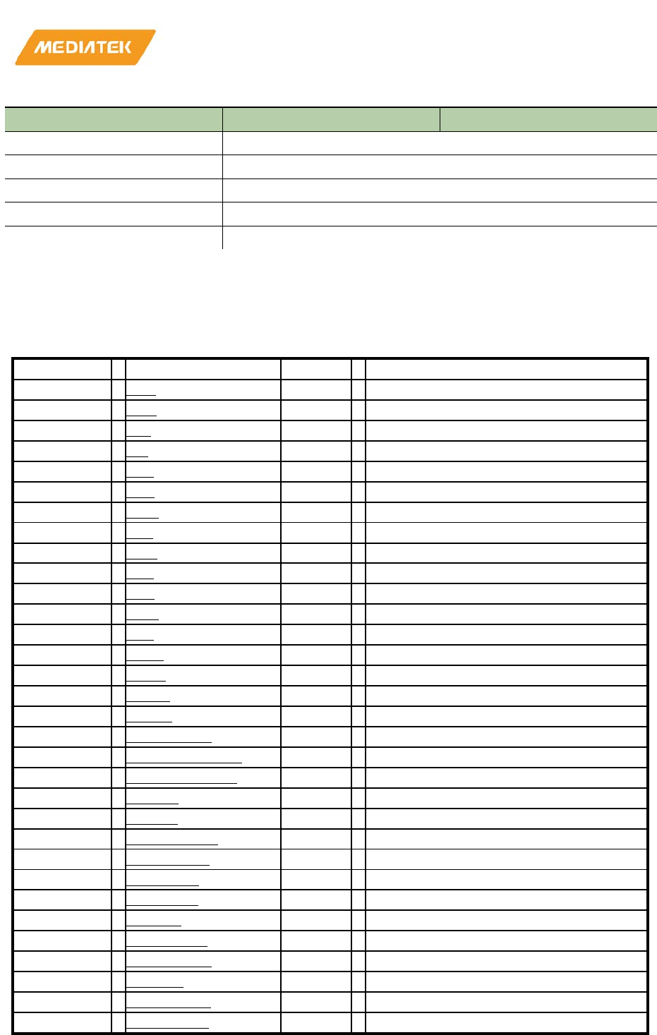
MT76x7
Internet-of-Things Wireless Connectivity
Reference Manual
© 2015 - 2017 MediaTek Inc
Page 489 of 798
This document contains information that is proprietary to MediaTek Inc. (“MediaTek”) and/or its licensor(s).
Any unauthorized use, reproduction or disclosure of this document in whole or in part is strictly prohibited
Address Condition 1 Condition 2
UART_BASE+0x50 Rx Trigger Address
UART_BASE+0x54 Fractional Divider LSB Address
UART_BASE+0x58 Fractional Divider MSB Address
UART_BASE+0x5C FIFO Control Register
UART_BASE+0x60 TX Active Enable Address
2.5.2.4. Register definitions
1) UART0
Module name: uart0 Base address: (+83030000h)
Address
Name
Width
Register Function
83030000
RBR
32
RX Buffer Register
83030000
THR
32
TX Holding Register
83030004
IER
32
Interrupt Enable Register
83030008
IIR
32
Interrupt Identification Register
83030008
FCR
32
FIFO Control Register
8303000C
LCR
32
Line Control Register.
83030010
MCR
32
Modem Control Register.
83030014
LSR
32
Line Status Register.
83030018
MSR
32
Modem status register.
8303001C
SCR
32
Scratch Register
83030000
DLL
32
Divisor Latch (LS)
83030004
DLM
32
Divisor Latch (MS)
83030008
EFR
32
Enhanced Feature Register
83030010
XON1
32
software flow control on 1
83030014
XON2
32
software flow control on 2
83030018
XOFF1
32
software flow control off 1
8303001C
XOFF2
32
software flow control off 2
83030024
HIGHSPEED
32
HIGH SPEED UART
83030028
SAMPLE_COUNT
32
sample
count
8303002C
SAMPLE_POINT
32
sample point
83030034
rate_fix
32
Rate Fix Address
8303003C
GUARD
32
Guard time added register
83030040
ESCAPE_DAT
32
Escape character register
83030044
ESCAPE_EN
32
Escape enable register
83030048
SLEEP_EN
32
Sleep enable register
8303004C
VFIFO_EN
32
Virtual FIFO enable register
83030050
RXTRIG
32
Rx Trigger Address
83030054
FRACDIV_L
32
Fractional Divider LSB Address
83030058
FRACDIV_M
32
Fractional Divider MSB Address
8303005C
FCR_RD
32
FIFO Control Register
83030060
tx_active_en
32
TX Active Enable Address
83030068
RX_OFFSET
32
RX OFFSET
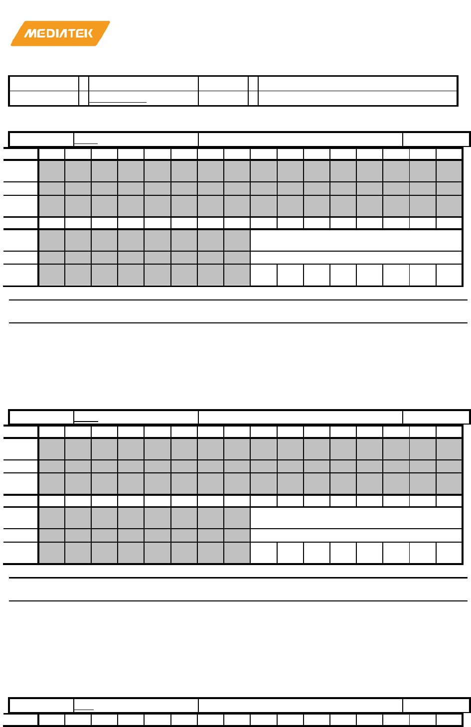
MT76x7
Internet-of-Things Wireless Connectivity
Reference Manual
© 2015 - 2017 MediaTek Inc
Page 490 of 798
This document contains information that is proprietary to MediaTek Inc. (“MediaTek”) and/or its licensor(s).
Any unauthorized use, reproduction or disclosure of this document in whole or in part is strictly prohibited
Address
Name
Width
Register Function
8303006C
TX_OFFSET
32
TX OFFSET
83030000
RBR
RX Buffer Register
00000000
Bit
31
30
29
28
27
26
25
24
23
22
21
20
19
18
17
16
Nam
e
Type
Rese
t
Bit
15
14
13
12
11
10
9
8
7
6
5
4
3
2
1
0
Nam
e
RBR
Type
RU
Rese
t
0 0 0 0 0 0 0 0
Bit(s)
Name
Description
7:0
RBR
RX Buffer Register. Read-only register. The received data
can be read by accessing this register.
Modified when LCR[7] = 0.
83030000
THR
TX Holding Register
00000000
Bit
31
30
29
28
27
26
25
24
23
22
21
20
19
18
17
16
Nam
e
Type
Rese
t
Bit
15
14
13
12
11
10
9
8
7
6
5
4
3
2
1
0
Nam
e
THR
Type
WO
Rese
t
0 0 0 0 0 0 0 0
Bit(s)
Name
Description
7:0
THR
TX Holding Register. Write-only register. The data to be
transmitted is written to this register, and then
sent to the
PC via serial communication.
Modified when LCR[7] = 0.
83030004
IER
Interrupt Enable Register
00000000
Bit
31
30
29
28
27
26
25
24
23
22
21
20
19
18
17
16
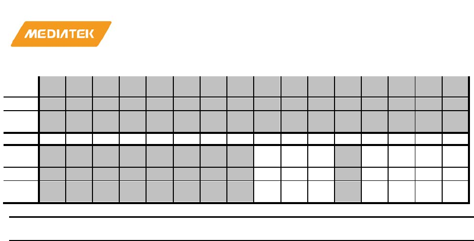
MT76x7
Internet-of-Things Wireless Connectivity
Reference Manual
© 2015 - 2017 MediaTek Inc
Page 491 of 798
This document contains information that is proprietary to MediaTek Inc. (“MediaTek”) and/or its licensor(s).
Any unauthorized use, reproduction or disclosure of this document in whole or in part is strictly prohibited
Nam
e
Type
Rese
t
Bit
15
14
13
12
11
10
9
8
7
6
5
4
3
2
1
0
Nam
e
CT
SI
RT
SI
XO
FFI
ED
SSI
EL
SI
ET
BEI
ER
BFI
Type
RW
RW
RW
RW
RW
RW
RW
Rese
t
0 0 0 0 0 0 0
Bit(s)
Name
Description
7
CTSI
By storing a '1' to a specific bit position, the interrupt
associated with that bit is enabled. Otherwise, the
interrupt is disabled.
IER[3:0] are modified when LCR[7] = 0.
IER[7:4] are modified when LCR[7] = 0 & EFR[4] = 1
Masks an interrupt that is generated when a rising edge is detected
on the C
TS modem control line.
Note: This interrupt is only enabled when hardware flow control is
enabled.
0 Unmask an interrupt that is generated when a rising edge is
detected on the CTS modem control line.
1 Mask an interrupt that is generated when a rising edge is detected
on the CTS modem control line.
6
RTSI
Masks an interrupt that is generated when a rising edge is
detected on the RTS modem control line.
Note: This interrupt is only enabled when hardware flow control is
enabled.
0 Unmask an interrupt
that is generated when a rising edge is
detected on the RTS modem control line.
1 Mask an interrupt that is generated when a rising edge is detected
on the RTS modem control line.
5
XOFFI
Masks an interrupt that is generated when an XOFF
character is rece
ived.
Note: This interrupt is only enabled when software flow control is
enabled.
0 Unmask an interrupt that is generated when an XOFF character is
received.
1 Mask an interrupt that is generated when an XOFF character is
received.
3
EDSSI
When set ("1"), an interrupt is generated if DDCD, TERI,
DDSR or DCTS (MSR[4:1]) becomes set.
0 No interrupt is generated if DDCD, TERI, DDSR or DCTS
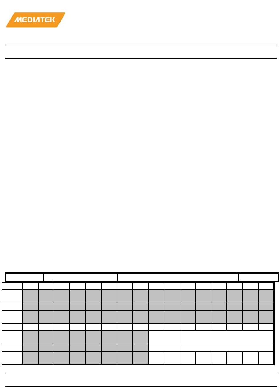
MT76x7
Internet-of-Things Wireless Connectivity
Reference Manual
© 2015 - 2017 MediaTek Inc
Page 492 of 798
This document contains information that is proprietary to MediaTek Inc. (“MediaTek”) and/or its licensor(s).
Any unauthorized use, reproduction or disclosure of this document in whole or in part is strictly prohibited
Bit(s)
Name
Description
(MSR[4:1]) becomes set.
1 An interrupt is generated if DDCD, TERI, DDSR or DCTS
(MSR[4:1]) becomes set.
2
ELSI
When set ("1"), an interrupt is generated if BI, FE, PE or
OE (LSR[4:1]) becomes set.
0 No interrupt is generated if BI, FE, PE or OE (LSR[4:1]) becomes
set.
1 An interrupt is generated if BI, FE, PE or OE (LSR[4:1]) becomes
set.
1
ETBEI
When set ("1"), an interrupt is generated if the TX Holding
Register is empty or the contents of the TX FIFO
have been reduced to its Trigger Level.
0 No interrupt is generated if the TX Holding Register is empty or
the contents of the TX FIFO have been reduced to its Trigg
er Level.
1 An interrupt is generated if the TX Holding Register is empty or
the contents of the TX FIFO have been reduced to its Trigger Level
0
ERBFI
When set ("1"), an interrupt is generated if the RX Buffer
contains data.
0 No interrupt is generated
if the RX Buffer contains data.
1 An interrupt is generated if the RX Buffer contains data.
83030008
IIR
Interrupt Identification Register
00000001
Bit
31
30
29
28
27
26
25
24
23
22
21
20
19
18
17
16
Nam
e
Type
Rese
t
Bit
15
14
13
12
11
10
9
8
7
6
5
4
3
2
1
0
Nam
e
FIFOE IIR_ID
Type
RO
RO
Rese
t
0 0 0 0 0 0 0 1
Bit(s)
Name
Description
7:6
FIFOE
fifo enable
5:0
IIR_ID
Identify if there are pending interrupts; ID4 and ID3 are
presented only when EFR[4] = 1.
The following table gives the IIR[5:0] codes associated with the
possible interrupts:

MT76x7
Internet-of-Things Wireless Connectivity
Reference Manual
© 2015 - 2017 MediaTek Inc
Page 493 of 798
This document contains information that is proprietary to MediaTek Inc. (“MediaTek”) and/or its licensor(s).
Any unauthorized use, reproduction or disclosure of this document in whole or in part is strictly prohibited
Bit(s)
Name
Description
IIR[5:0] Priority Level Interrupt Source
000001
- No interrupt pending
000110 1 Line Status Interrupt BI, FE, PE or
OE set in LSR
000100 2 RX Data Received RX Data
received or RX Trigger Level reached.
001100 2
RX Data Timeout Timeout on
character in RX FIFO.
000010 3 TX Holding Register Empty TX Holding
Register empty or TX FIFO Trigger Level reached.
000000 4
Modem Status change DDCD, TERI,
DDSR or DCTS set in MSR
010000 5 Software Flow Control XOFF
Character received
100000 6 Hardware Flow Control CTS or RTS
Rising Edge
Table
1 The IIR[5:0] codes associated with the possible interrupts
Line Status Interrupt: A RX Line Status Interrupt (IIR[5:0`] ==
000110b) is generated if ELSI (IER[2]) is set and any of BI, FE, PE
or OE (LSR[4:1]) becomes set. The interrupt is cleared by rea
ding
the Line Status Register.
RX Data Received Interrupt: A RX Received interrupt (IER[5:0] ==
000100b) is generated if EFRBI (IER[0]) is set and either RX Data
is placed in the RX Buffer Register or the RX Trigger Level is
reached. The interrupt is cleared by reading the RX Buffer Register
or the RX FIFO (if enabled).
RX Data Timeout Interrupt:
When virtual FIFO mode is disabled, RX Data Timeout Interrupt is
generated if all of the following apply:
1. FIFO contains at least one character;
2. The most rec
ent character was received longer than four
character periods ago (including all start, parity and stop bits);
3. The most recent CPU read of the FIFO was longer than four
character periods ago.
The timeout timer is restarted on receipt of a new byte from
the RX
Shift Register, or on a CPU read from the RX FIFO.
The RX Data Timeout Interrupt is enabled by setting EFRBI
(IER[0]) to 1, and is cleared by reading RX FIFO.
When virtual FIFO mode is enabled, RX Data Timeout Interrupt is
generated if all of the fo
llowing apply:
1. FIFO is non
-empty;

MT76x7
Internet-of-Things Wireless Connectivity
Reference Manual
© 2015 - 2017 MediaTek Inc
Page 494 of 798
This document contains information that is proprietary to MediaTek Inc. (“MediaTek”) and/or its licensor(s).
Any unauthorized use, reproduction or disclosure of this document in whole or in part is strictly prohibited
Bit(s)
Name
Description
2. The most recent character was received longer than SCR *
symbol periods ago;
3. The most recent CPU read of the FIFO was longer than SCR *
symbol periods ago.
The timeout timer is restarted on receipt of a new byte f
rom the RX
Shift Register.
RX Holding Register Empty Interrupt: A TX Holding Register
Empty Interrupt (IIR[5:0] = 000010b) is generated if ETRBI
(IER[1]) is set and either the TX Holding Register or, if FIFOs are
enabled, the TX FIFO becomes empty. The in
terrupt is cleared by
writing to the TX Holding Register or TX FIFO if FIFO enabled.
Modem Status Change Interrupt: A Modem Status Change
Interrupt (IIR[5:0] = 000000b) is generated if EDSSI (IER[3]) is
set and either DDCD, TERI, DDSR or DCTS (MSR[3:0])
becomes
set. The interrupt is cleared by reading the Modem Status Register.
Software Flow Control Interrupt: A Software Flow Control Interrupt
(IIR[5:0] = 010000b) is generated if Software Flow Control is
enabled and XOFFI (IER[5]) becomes set, indicating
that an XOFF
character has been received. The interrupt is cleared by reading the
Interrupt Identification Register.
Hardware Flow Control Interrupt: A Hardware Flow Control
Interrupt (IER[5:0] = 100000b) is generated if Hardware Flow
Control is enabled
and either RTSI (IER[6]) or CTSI (IER[7])
becomes set indicating that a rising edge has been detected on
either the RTS/CTS Modem Control line. The interrupt is cleared
by reading the Interrupt Identification Register.
83030008
FCR
FIFO Control Register
00000000
Bit
31
30
29
28
27
26
25
24
23
22
21
20
19
18
17
16
Nam
e
Type
Rese
t
Bit
15
14
13
12
11
10
9
8
7
6
5
4
3
2
1
0
Nam
e
RFTL TFTL
DM
A1
CL
RT
CL
RR
FIF
OE
Type
WO
WO
WO
WO
WO
WO
Rese
t
0 0 0 0 0 0 0 0
Bit(s)
Name
Description
7:6
RFTL
RX FIFO trigger threshold
0 1
1 6

MT76x7
Internet-of-Things Wireless Connectivity
Reference Manual
© 2015 - 2017 MediaTek Inc
Page 495 of 798
This document contains information that is proprietary to MediaTek Inc. (“MediaTek”) and/or its licensor(s).
Any unauthorized use, reproduction or disclosure of this document in whole or in part is strictly prohibited
Bit(s)
Name
Description
2 12
3 RXTRIG
5:4
TFTL
TX FIFO trigger threshold
0 1
1 4
2 8
3 14 (FIFOSIZE
- 2)
3
DMA1
This bit determines the DMA mode, which the TXRDY and
RXRDY pins support. TXRDY and RXRDY act to support
single
-byte transfers between the UART and memory
(DMA mode 0) or multiple byte transfers (DMA mode1).
Note that this bit has no effect unless the FIFOE bit is set
as well.
0
The device operates in DMA Mode 0.
1 The device operates in DMA Mode 1. (not used)
TXRDY
- mode0: Goes active (low) when TX FIFO is not full.
Becomes inactive when the TX FIFO is full.
TXRDY
- mode1: Goes active (low) when the TX FIFO or the TX
Holding Register is empty. Becomes inactive when a byte is written
to the Transmit channel.
RXRDY
- mode0: Becomes active (low) when at least one character
is in the RX FIFO or the RX Buffer Register is full. Becomes
inactive when there are no more characters in
the RX FIFO or RX
Buffer register.
RXRDY
- mode1: Becomes active (low) when the RX FIFO Trigger
Level is reached or an RX FIFO Character Timeout occurs. Goes
inactive when the RX FIFO is empty.
2
CLRT
Clear Transmit FIFO. This bit is self-clearing.
0
Leave TX FIFO intact.
1 Clear all the bytes in the TX FIFO.
1
CLRR
Clear Receive FIFO. This bit is self-clearing.
0 Leave RX FIFO intact.
1 Clear all the bytes in the RX FIFO.
0
FIFOE
FIFO Enabled. This bit must be set to 1 for any of the
other bits in
the registers to have any effect.
0 Disable both the RX and TX FIFOs.
1 Enable both the RX and TX FIFOs.
FCR is used to control the trigger levels of the FIFOs, or flush the
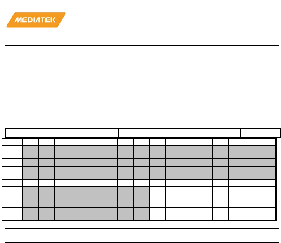
MT76x7
Internet-of-Things Wireless Connectivity
Reference Manual
© 2015 - 2017 MediaTek Inc
Page 496 of 798
This document contains information that is proprietary to MediaTek Inc. (“MediaTek”) and/or its licensor(s).
Any unauthorized use, reproduction or disclosure of this document in whole or in part is strictly prohibited
Bit(s)
Name
Description
FIFOs.
FCR[7:6] is modified when LCR != BFh
FCR[5:4] is modified when LCR != BFh
& EFR[4] = 1
FCR[4:0] is modified when LCR != BFh
8303000C
LCR
Line Control Register.
00000000
Bit
31
30
29
28
27
26
25
24
23
22
21
20
19
18
17
16
Nam
e
Type
Rese
t
Bit
15
14
13
12
11
10
9
8
7
6
5
4
3
2
1
0
Nam
e
DL
AB
SB SP
EP
S
PE
N
ST
B
WLS
Type
RW
RW
RW
RW
RW
RW
RW
Rese
t
0 0 0 0 0 0 0 0
Bit(s)
Name
Description
7
DLAB
Divisor Latch Access Bit.
0 The RX and TX Registers are read/written at Address
0 and the
IER register is read/written at Address 4.
1 The Divisor Latch LS is read/written at Address 0 and the Divisor
Latch MS is read/written at Address 4.
6
SB
Set Break
0 No effect
1 SOUT signal is forced into the "0" state.
5
SP
Stick Parity
0 No
effect.
1 The Parity bit is forced into a defined state, depending on the
states of EPS and PEN:
If EPS=1 & PEN=1, the Parity bit is set and checked = 0.
If EPS=0 & PEN=1, the Parity bit is set and checked = 1.
4
EPS
Even Parity Select
0 Whe
n EPS=0, an odd number of ones is sent and checked.
1 When EPS=1, an even number of ones is sent and checked.
MT76x7
Internet-of-Things Wireless Connectivity
Reference Manual
© 2015 - 2017 MediaTek Inc
Page 497 of 798
This document contains information that is proprietary to MediaTek Inc. (“MediaTek”) and/or its licensor(s).
Any unauthorized use, reproduction or disclosure of this document in whole or in part is strictly prohibited
Bit(s)
Name
Description
3
PEN
Parity Enable
0 The Parity is neither transmitted nor checked.
1 The Parity is transmitted and checked.
2
STB
Number of STOP bits
0 One
STOP bit is always added.
1 Two STOP bits are added after each character is sent; unless the
character length is 5 when 1 STOP bit is added.
1:0
WLS
Word Length Select.
0 5 bits
1 6 bits
2 7 bits
3 8 bits
Determines characteristics of serial communication signals.
Modified when LCR[7] = 0.
83030010
MCR
Modem Control Register.
00000000
Bit
31
30
29
28
27
26
25
24
23
22
21
20
19
18
17
16
Nam
e
Type
Rese
t
Bit
15
14
13
12
11
10
9
8
7
6
5
4
3
2
1
0
Nam
e
XO
FF
_St
atu
s
DC
M_
EN
OU
T2 OU
T1 RT
S DT
R
Type
RU
RW
RW
RW
RW
RW
Rese
t
0 0 0 0 0 0
Bit(s)
Name
Description
7
XOFF_Status
This is a read-only bit.
0 When an XON character is received.
1 When an XOFF character is received.
4
DCM_EN
UART DCM function enable bit
0 UART DCM is disabled.

MT76x7
Internet-of-Things Wireless Connectivity
Reference Manual
© 2015 - 2017 MediaTek Inc
Page 498 of 798
This document contains information that is proprietary to MediaTek Inc. (“MediaTek”) and/or its licensor(s).
Any unauthorized use, reproduction or disclosure of this document in whole or in part is strictly prohibited
Bit(s)
Name
Description
1 UART DCM is enabled.
3
OUT2
Controls the state of the output NOUT2, even in loop
mode.
0 NOUT2=1.
1 NOUT2=0.
2
OUT1
Controls the state of the output NOUT1, even in loop
mode.
0 NOUT1=1.
1 NOUT1=0.
1
RTS
Controls the state of the output NRTS, even in loop mode.
0 NRTS=1.
1 NRTS=0.
0
DTR
Control the state of the output NDTR, even in loop mode.
0 NDTR=1.
1 NDTR=0.
Control interface signals of the UART.
MCR[4:0] are modified when LCR[7] = 0,
MCR[7:6] are modified when LCR[7] = 0 & EFR[4] = 1.
83030014
LSR
Line Status Register.
00000040
Bit
31
30
29
28
27
26
25
24
23
22
21
20
19
18
17
16
Nam
e
Type
Rese
t
Bit
15
14
13
12
11
10
9
8
7
6
5
4
3
2
1
0
Nam
e
FIF
OE
RR
TE
MT TH
RE BI FE PE OE DR
Type
RU
RU
RU
RU
RU
RU
RU
RU
Rese
t
0 1 0 0 0 0 0 0
Bit(s)
Name
Description
7
FIFOERR
RX FIFO Error Indicator.
0 No PE, FE, BI set in the RX FIFO.
1 Set to 1 when there is at least one PE, FE or BI in the RX FIFO.

MT76x7
Internet-of-Things Wireless Connectivity
Reference Manual
© 2015 - 2017 MediaTek Inc
Page 499 of 798
This document contains information that is proprietary to MediaTek Inc. (“MediaTek”) and/or its licensor(s).
Any unauthorized use, reproduction or disclosure of this document in whole or in part is strictly prohibited
Bit(s)
Name
Description
6
TEMT
TX Holding Register (or TX FIFO) and the TX Shift
Register are empty.
0 Empty conditions below are not met.
1
If FIFOs are enabled, the bit is set whenever the TX FIFO and the
TX Shift Register are empty. If FIFOs are disabled, the bit is set
whenever TX Holding Register and TX Shift Register are empty.
5
THRE
Indicates if there is room for TX Holding Register or TX
FIFO is reduced to its Trigger Level.
0 Reset whenever the contents of the TX FIFO are more than its
Trigger Level (FIFOs are enabled), or whenever TX Holding
Register is not empty(FIFOs are disabled).
1 Set whenever the contents of the TX FIFO are
reduced to its
Trigger Level (FIFOs are enabled), or whenever TX Holding
Register is empty and ready to accept new data (FIFOs are
disabled).
4
BI
Break Interrupt.
0 Reset by the CPU reading this register
1 If the FIFOs are disabled, this bit is set whene
ver the SIN is held
in the 0 state for more than one transmission time (START bit +
DATA bits + PARITY + STOP bits).
If the FIFOs are enabled, this error is associated with a
corresponding character in the FIFO and is flagged when this byte
is at the top o
f the FIFO. When a break occurs, only one zero
character is loaded into the FIFO: the next character transfer is
enabled when SIN goes into the marking state and receives the next
valid start bit.
3
FE
Framing Error.
0 Reset by the CPU reading this
register
1 If the FIFOs are disabled, this bit is set if the received data did not
have a valid STOP bit. If the FIFOs are enabled, the state of this bit
is revealed when the byte it refers to is the next to be read.
2
PE
Parity Error
0 Reset by the CPU
reading this register
1 If the FIFOs are disabled, this bit is set if the received data did not
have a valid parity bit. If the FIFOs are enabled, the state of this bit
is revealed when the referred byte is the next to be read.
1
OE
Overrun Error.
0 Rese
t by the CPU reading this register.
1 If the FIFOs are disabled, this bit is set if the RX Buffer was not
read by the CPU before new data from the RX Shift Register
overwrote the previous contents.
If the FIFOs are enabled, an overrun error occurs when the RX
FIFO is full and the RX Shift Register becomes full. OE is set as

MT76x7
Internet-of-Things Wireless Connectivity
Reference Manual
© 2015 - 2017 MediaTek Inc
Page 500 of 798
This document contains information that is proprietary to MediaTek Inc. (“MediaTek”) and/or its licensor(s).
Any unauthorized use, reproduction or disclosure of this document in whole or in part is strictly prohibited
Bit(s)
Name
Description
soon as this happens. The character in the Shift Register is then
overwritten, but not transferred to the FIFO.
0
DR
Data Ready.
0 Cleared by the CPU reading the RX Buffer or by reading all the
FIFO bytes.
1 Set by the RX Buffer becoming full or by a byte being transferred
into the FIFO.
Modified when LCR[7] = 0.
83030018
MSR
Modem status register.
00000000
Bit
31
30
29
28
27
26
25
24
23
22
21
20
19
18
17
16
Nam
e
Type
Rese
t
Bit
15
14
13
12
11
10
9
8
7
6
5
4
3
2
1
0
Nam
e
DC
D
RI DS
R
CT
S
DD
CD
TE
RI
DD
SR
DC
TS
Type
RU
RU
RU
RU
RU
RU
RU
RU
Rese
t
0 0 0 0 0 0 0 0
Bit(s)
Name
Description
7
DCD
Data Carry Detect.
When Loop = "0", this value is the complement of the NDCD
input signal.
When Loop = "1", this value is equal to the OUT2 bit in the
Modem Control Register.
6
RI
Ring Indicator.
When Loop = "0", this value is the complement of the NRI input
signal.
When Loop = "1", this value is equal to the OUT1 bit in the
Modem Control Register.
5
DSR
Data Set Ready
When Loop = "0", this value is the complement of the NDSR
input signal.
When Loop = "1", this value is equal to the DTR bit in the
Modem Control Register.
4
CTS
Clear To Send.
When Loop = "0", this value is the complement of the NCTS

MT76x7
Internet-of-Things Wireless Connectivity
Reference Manual
© 2015 - 2017 MediaTek Inc
Page 501 of 798
This document contains information that is proprietary to MediaTek Inc. (“MediaTek”) and/or its licensor(s).
Any unauthorized use, reproduction or disclosure of this document in whole or in part is strictly prohibited
Bit(s)
Name
Description
input signal.
When Loop = "1", this value is equal to the RTS bit in the
Modem Control Register.
3
DDCD
Delta Data Carry Detect.
0 The
state of DCD has not changed since the Modem Status
Register was last read
1 Set if the state of DCD has changed since the Modem Status
Register was last read.
2
TERI
Trailing Edge Ring Indicator
0 The NRI input does not change since this register was las
t read.
1 Set if the NRI input changes from "0" to "1" since this register was
last read.
1
DDSR
Delta Data Set Ready
0 Cleared if the state of DSR has not changed since this register was
last read.
1 Set if the state of DSR has changed since this registe
r was last
read.
0
DCTS
Delta Clear To Send
0 Cleared if the state of CTS has not changed since this register was
last read.
1 Set if the state of CTS has changed since this register was last read.
Note: After a reset, D4
-D7 are inputs. A modem status interrupt
can be cleared by writing '0' or set by writing '1' to this register. D0
-
D3 can be written to.
Modified when LCR[7] = 0.
8303001C
SCR
Scratch Register
00000000
Bit
31
30
29
28
27
26
25
24
23
22
21
20
19
18
17
16
Nam
e
Type
Rese
t
Bit
15
14
13
12
11
10
9
8
7
6
5
4
3
2
1
0
Nam
e
SCR
Type
RW
Rese
t
0 0 0 0 0 0 0 0

MT76x7
Internet-of-Things Wireless Connectivity
Reference Manual
© 2015 - 2017 MediaTek Inc
Page 502 of 798
This document contains information that is proprietary to MediaTek Inc. (“MediaTek”) and/or its licensor(s).
Any unauthorized use, reproduction or disclosure of this document in whole or in part is strictly prohibited
Bit(s)
Name
Description
7:0
SCR
A register to store the counter limit for rx timeout. After
reset, its value is 40.
Modified when LCR[7] = 0.
83030000
DLL
Divisor Latch (LS)
00000001
Bit
31
30
29
28
27
26
25
24
23
22
21
20
19
18
17
16
Nam
e
Type
Rese
t
Bit
15
14
13
12
11
10
9
8
7
6
5
4
3
2
1
0
Nam
e
DLL
Type
RW
Rese
t
0 0 0 0 0 0 0 1
Bit(s)
Name
Description
7:0
DLL
Note: DLL & DLM can only be updated if DLAB is set
("1").. Note too that division by 1 generates a BAUD signal
that is constantly high.
83030004
DLM
Divisor Latch (MS)
00000000
Bit
31
30
29
28
27
26
25
24
23
22
21
20
19
18
17
16
Nam
e
Type
Rese
t
Bit
15
14
13
12
11
10
9
8
7
6
5
4
3
2
1
0
Nam
e
DLM
Type
RW
Rese
t
0 0 0 0 0 0 0 0
Bit(s)
Name
Description
7:0
DLM
Note: DLL & DLM can only be updated if DLAB is set
("1").. Note too that division by 1 generates a BAUD signal
that is constantly high.
Modified when LCR[7] = 1.
The table below shows the divisor needed to generate a given baud
rate from CLK inputs of 13, 26 MHz and 52 MHz. The effective
MT76x7
Internet-of-Things Wireless Connectivity
Reference Manual
© 2015 - 2017 MediaTek Inc
Page 503 of 798
This document contains information that is proprietary to MediaTek Inc. (“MediaTek”) and/or its licensor(s).
Any unauthorized use, reproduction or disclosure of this document in whole or in part is strictly prohibited
Bit(s)
Name
Description
clock enable generated is 16 x the required baud rate.
BAUD 13MHz 26MHz 52MHz
110 7386 14773
29545
300 2708 5417 10833
1200 677 1354 2708
2400 338 677 1354
4800 169 339 677
9600 85 169 339
19200 42 85 169
38400 21 42 85
57600 14 28 56
115200 6 14 28
Table 2 Divisor needed to generate a given baud rate
83030008
EFR
Enhanced Feature Register
00000000
Bit
31
30
29
28
27
26
25
24
23
22
21
20
19
18
17
16
Nam
e
Type
Rese
t
Bit
15
14
13
12
11
10
9
8
7
6
5
4
3
2
1
0
Nam
e
Aut
o_
CT
S
Aut
o_
RT
S
En
abl
e_
E
SW_FLOW_CONT
Type
RW
RW
RW
RW
Rese
t
0 0 0 0 0 0 0
Bit(s)
Name
Description
7
Auto_CTS
Enables hardware transmission flow control
0 Disabled.
1 Enabled.
6
Auto_RTS
Enables hardware reception flow control
0 Disabled.
1 Enabled.

MT76x7
Internet-of-Things Wireless Connectivity
Reference Manual
© 2015 - 2017 MediaTek Inc
Page 504 of 798
This document contains information that is proprietary to MediaTek Inc. (“MediaTek”) and/or its licensor(s).
Any unauthorized use, reproduction or disclosure of this document in whole or in part is strictly prohibited
Bit(s)
Name
Description
4
Enable_E
Enable enhancement features.
0 Disabled.
1 Enabled.
3:0
SW_FLOW_CONT
Software flow control bits.
00xx No TX Flow Control
10xx Transmit
XON1/XOFF1 as flow control bytes
01xx Transmit XON2/XOFF2 as flow control bytes
11xx Transmit XON1 & XON2 and XOFF1 & XOFF2 as flow control
words
xx00 No RX Flow Control
xx10 Receive XON1/XOFF1 as flow control bytes
xx01 Receive XON2/XOFF2 as flow control
bytes
xx11 Receive XON1 & XON2 and XOFF1 & XOFF2 as flow control
words
NOTE: Only when LCR=BF'h
83030010
XON1
software flow control on 1
00000000
Bit
31
30
29
28
27
26
25
24
23
22
21
20
19
18
17
16
Nam
e
Type
Rese
t
Bit
15
14
13
12
11
10
9
8
7
6
5
4
3
2
1
0
Nam
e
XON1
Type
RW
Rese
t
0 0 0 0 0 0 0 0
Bit(s)
Name
Description
7:0
XON1
valid only when LCR=BFh.
83030014
XON2
software flow control on 2
00000000
Bit
31
30
29
28
27
26
25
24
23
22
21
20
19
18
17
16
Nam
e
Type

MT76x7
Internet-of-Things Wireless Connectivity
Reference Manual
© 2015 - 2017 MediaTek Inc
Page 505 of 798
This document contains information that is proprietary to MediaTek Inc. (“MediaTek”) and/or its licensor(s).
Any unauthorized use, reproduction or disclosure of this document in whole or in part is strictly prohibited
Rese
t
Bit
15
14
13
12
11
10
9
8
7
6
5
4
3
2
1
0
Nam
e
XON2
Type
RW
Rese
t
0 0 0 0 0 0 0 0
Bit(s)
Name
Description
7:0
XON2
valid only when LCR=BFh.
83030018
XOFF1
software flow control off 1
00000000
Bit
31
30
29
28
27
26
25
24
23
22
21
20
19
18
17
16
Nam
e
Type
Rese
t
Bit
15
14
13
12
11
10
9
8
7
6
5
4
3
2
1
0
Nam
e
XOFF1
Type
RW
Rese
t
0 0 0 0 0 0 0 0
Bit(s)
Name
Description
7:0
XOFF1
valid only when LCR=BFh.
8303001C
XOFF2
software flow control off 2
00000000
Bit
31
30
29
28
27
26
25
24
23
22
21
20
19
18
17
16
Nam
e
Type
Rese
t
Bit
15
14
13
12
11
10
9
8
7
6
5
4
3
2
1
0
Nam
e
XOFF2
Type
RW
Rese
t
0 0 0 0 0 0 0 0
Bit(s)
Name
Description
7:0
XOFF2
valid only when LCR=BFh.

MT76x7
Internet-of-Things Wireless Connectivity
Reference Manual
© 2015 - 2017 MediaTek Inc
Page 506 of 798
This document contains information that is proprietary to MediaTek Inc. (“MediaTek”) and/or its licensor(s).
Any unauthorized use, reproduction or disclosure of this document in whole or in part is strictly prohibited
Bit(s)
Name
Description
83030024
HIGHSPEED
HIGH SPEED UART
00000000
Bit
31
30
29
28
27
26
25
24
23
22
21
20
19
18
17
16
Nam
e
Type
Rese
t
Bit
15
14
13
12
11
10
9
8
7
6
5
4
3
2
1
0
Nam
e
SPEED
Type
RW
Rese
t
0 0
Bit(s)
Name
Description
1:0
SPEED
SPEED UART sample counter base
0 based on 16*baud_pulse, baud_rate = system clock
frequency/16/{DLM, DLL}
1 based on 8*baud_pulse, baud_rate = system clock
frequency/8/{DLM, DLL}
2 based on 4*baud_pulse, baud_rate = system clock
frequency/4/{DLM, DLL}
3 based on sampe_count * baud_pulse, baud_rate = system clock
frequency / sampe_count
When HIGHSPEED=3, the value (A * B) means ({DLM, DLL} *
SAMPLE_COUNT).
When the Baudrate is more than 115200, it will be more accurate if
we set HIGHSPEED=3.
The table below shows the divisor needed to generate a given baud
rate from CLK inputs of 13M Hz
based on different HIGHSPEED
value.
BAUD HIGHSPEED = 0 HIGHSPEED = 1 HIGHSPEED = 2
HIGHSPEED = 3
110 7386 14773 29545 7386 * 16
300 2708 7386 14773
2708 * 16
1200 677 2708 7386 677 * 16
2400 338 677 2708 338 * 16
4800 169 338 677
169 * 16
9600 85 169 338 85 * 16

MT76x7
Internet-of-Things Wireless Connectivity
Reference Manual
© 2015 - 2017 MediaTek Inc
Page 507 of 798
This document contains information that is proprietary to MediaTek Inc. (“MediaTek”) and/or its licensor(s).
Any unauthorized use, reproduction or disclosure of this document in whole or in part is strictly prohibited
Bit(s)
Name
Description
19200 42 85 169 9 * 75
38400 21 42 85
13 * 26
57600 14 21 42 8 * 28
115200 7 14 21 4 * 28
230400 * 7 14
2 * 28
460800 * * 7 1 * 28
921600 * * * 1 * 14
Table 3 Divisor needed to generate a given baud rate from 13MH
z
based on different HIGHSPEED value
The table below shows the divisor needed to generate a given baud
rate from CLK inputs of 26 MHz based on different HIGHSPEED
value.
BAUD HIGHSPEED = 0 HIGHSPEED = 1 HIGHSPEED = 2
HIGHSPEED = 3
110 14773
29545 59091 7386 * 32
300 5417 14773 29545 2708 * 32
1200 1354 5417 14773 677 * 32
2400 677
1354 5417 338 * 32
4800 339 677 1354 169 * 32
9600 169 339 667 85 * 32
19200 85
169 339 18 * 75
38400 42 85 169 26 * 26
57600 28 42 85 1
6 * 28
115200 14 28 42 8 * 28
230400 7 14 28 4 * 28
460800 * 7 14
2 * 28
921600 * * 7 1 * 28
Table 4 Divisor needed to generate a given baud rate from 26 MHz
based on different HIGHSPEED value
The table below shows the divisor nee
ded to generate a given baud
rate from CLK inputs of 52MHz based on different HIGHSPEED
value.
BAUD HIGHSPEED = 0 HIGHSPEED = 1 HIGHSPEED = 2
HIGHSPEED = 3
110 29545 59091 118182 14773 * 32

MT76x7
Internet-of-Things Wireless Connectivity
Reference Manual
© 2015 - 2017 MediaTek Inc
Page 508 of 798
This document contains information that is proprietary to MediaTek Inc. (“MediaTek”) and/or its licensor(s).
Any unauthorized use, reproduction or disclosure of this document in whole or in part is strictly prohibited
Bit(s)
Name
Description
300 10833 29545 59091 5417 * 32
1200 2708 10833 29545 1354 * 32
2400 1354 2708 10833 667 * 32
4800 677
1354 2708 339 * 32
9600 339 677 1354 169 * 32
19200 169 339 677 36 * 75
38400 85
169 339 52 * 26
57600 56 85 169 32 * 28
115200 28 56 85 16 * 28
230400 1
4 28 56 8 * 28
460800 7 14 28 4 * 28
921600 * 7 14 2 *
28
Table 5 Divisor needed to generate a given baud rate from 52 MHz
based on different HIGHSPEED value
83030028
SAMPLE_COUNT
sample count
00000000
Bit
31
30
29
28
27
26
25
24
23
22
21
20
19
18
17
16
Nam
e
Type
Rese
t
Bit
15
14
13
12
11
10
9
8
7
6
5
4
3
2
1
0
Nam
e
SAMPLE_COUNT
Type
RW
Rese
t
0 0 0 0 0 0 0 0
Bit(s)
Name
Description
7:0
SAMPLE_COUNT
When HIGHSPEED=3, the sample_count is the threshold
value for UART sample counter (sample_num).
Count from 0 to sample_count.
8303002C
SAMPLE_POINT
sample point
000000FF
Bit
31
30
29
28
27
26
25
24
23
22
21
20
19
18
17
16
Nam
e

MT76x7
Internet-of-Things Wireless Connectivity
Reference Manual
© 2015 - 2017 MediaTek Inc
Page 509 of 798
This document contains information that is proprietary to MediaTek Inc. (“MediaTek”) and/or its licensor(s).
Any unauthorized use, reproduction or disclosure of this document in whole or in part is strictly prohibited
Type
Rese
t
Bit
15
14
13
12
11
10
9
8
7
6
5
4
3
2
1
0
Nam
e
SAMPLE_POINT
Type
RW
Rese
t
1 1 1 1 1 1 1 1
Bit(s)
Name
Description
7:0
SAMPLE_POINT
When HIGHSPEED=3, UART gets the input data when
sample_count=sample_num.
e.g. system clock = 13MHz, 921600 = 13000000 / 14
sample_count = 14-1=13 and sample point = 14/2-2 (sample the
central point to decrease the inaccuracy)
The SAMPLE_POINT is usually (=(SAMPLE_COUNT+1)/2
-2).
The
-2 comes from 1 cycle: IDLE-
>START state and the other cycle:
counter start from 0.
83030034
rate_fix
Rate Fix Address
00000000
Bit
31
30
29
28
27
26
25
24
23
22
21
20
19
18
17
16
Nam
e
Type
Rese
t
Bit
15
14
13
12
11
10
9
8
7
6
5
4
3
2
1
0
Nam
e
rat
e_f
ix
Type
RW
Rese
t
0
Bit(s)
Name
Description
0
rate_fix
When you set "rate_fix"(34H[0]), you can transmit and
receive data
only if the input f16m_en is enable.
8303003C
GUARD
Guard time added register
0000000F
Bit
31
30
29
28
27
26
25
24
23
22
21
20
19
18
17
16
Nam
e
Type
Rese
t
MT76x7
Internet-of-Things Wireless Connectivity
Reference Manual
© 2015 - 2017 MediaTek Inc
Page 510 of 798
This document contains information that is proprietary to MediaTek Inc. (“MediaTek”) and/or its licensor(s).
Any unauthorized use, reproduction or disclosure of this document in whole or in part is strictly prohibited
Bit
15
14
13
12
11
10
9
8
7
6
5
4
3
2
1
0
Nam
e
GU
AR
D_
EN
GUARD_CNT
Type
RW
RW
Rese
t
0 1 1 1 1
Bit(s)
Name
Description
4
GUARD_EN
Guard interval count value. Guard interval = (1/(system
clock / div_step / div )) * GUARD_CNT.
3:0
GUARD_CNT
Guard interval add enable signal.
0 No guard interval added.
1 Add guard interval after stop bit.
83030040
ESCAPE_DAT
Escape character register
000000FF
Bit
31
30
29
28
27
26
25
24
23
22
21
20
19
18
17
16
Nam
e
Type
Rese
t
Bit
15
14
13
12
11
10
9
8
7
6
5
4
3
2
1
0
Nam
e
ESCAPE_DAT
Type
WO
Rese
t
1 1 1 1 1 1 1 1
Bit(s)
Name
Description
7:0
ESCAPE_DAT
Escape character added before software flow control data
and escape character, i.e. if tx data is xon (31h), with
esc_en =1, uart transmits data as esc + CEh (~xon).
83030044
ESCAPE_EN
Escape enable register
00000000
Bit
31
30
29
28
27
26
25
24
23
22
21
20
19
18
17
16
Nam
e
Type
Rese
t
Bit
15
14
13
12
11
10
9
8
7
6
5
4
3
2
1
0
Nam
e
ES
C_
EN
Type
RW
MT76x7
Internet-of-Things Wireless Connectivity
Reference Manual
© 2015 - 2017 MediaTek Inc
Page 511 of 798
This document contains information that is proprietary to MediaTek Inc. (“MediaTek”) and/or its licensor(s).
Any unauthorized use, reproduction or disclosure of this document in whole or in part is strictly prohibited
Rese
t
0
Bit(s)
Name
Description
0
ESC_EN
Add escape character in transmitter and remove escape
character in receiver by UART.
0 Do not deal with the escape character.
1 Add escape character in transmitter and remove escape character
in receiver.
83030048
SLEEP_EN
Sleep enable register
00000000
Bit
31
30
29
28
27
26
25
24
23
22
21
20
19
18
17
16
Nam
e
Type
Rese
t
Bit
15
14
13
12
11
10
9
8
7
6
5
4
3
2
1
0
Nam
e
SL
EE
P_
EN
Type
RW
Rese
t
0
Bit(s)
Name
Description
0
SLEEP_EN
For sleep mode issue
0 Do not deal with sleep mode indicate signal
1 To activate hardware flow control or software control according to
software initial setting when chip enters sleep mode. Releasing
hardware flow when
chip wakes up; but for software control, uart
sends xon when awaken and when FIFO does not reach threshold
level.
8303004C
VFIFO_EN
Virtual FIFO enable register
00000000
Bit
31
30
29
28
27
26
25
24
23
22
21
20
19
18
17
16
Nam
e
Type
Rese
t
Bit
15
14
13
12
11
10
9
8
7
6
5
4
3
2
1
0
Nam
e
DM
A_
VFI
FO
MT76x7
Internet-of-Things Wireless Connectivity
Reference Manual
© 2015 - 2017 MediaTek Inc
Page 512 of 798
This document contains information that is proprietary to MediaTek Inc. (“MediaTek”) and/or its licensor(s).
Any unauthorized use, reproduction or disclosure of this document in whole or in part is strictly prohibited
_E
N
Type
RW
Rese
t
0
Bit(s)
Name
Description
0
DMA_VFIFO_EN
Virtual FIFO mechanism enable signal.
0 Disable VFIFO mode.
1 Enable VFIFO mode. When virtual mode is enabled, the flow
control is based on the DMA threshold, and generates a timeout
interrupt for DMA.
83030050
RXTRIG
Rx Trigger Address
00000000
Bit
31
30
29
28
27
26
25
24
23
22
21
20
19
18
17
16
Nam
e
Type
Rese
t
Bit
15
14
13
12
11
10
9
8
7
6
5
4
3
2
1
0
Nam
e
RXTRIG
Type
RW
Rese
t
0 0 0 0 0
Bit(s)
Name
Description
4:0
RXTRIG
When (rtm,rtl)=2'b11, The Rx FIFO threshold will be
Rxtrig.
83030054
FRACDIV_L
Fractional Divider LSB Address
00000000
Bit
31
30
29
28
27
26
25
24
23
22
21
20
19
18
17
16
Nam
e
Type
Rese
t
Bit
15
14
13
12
11
10
9
8
7
6
5
4
3
2
1
0
Nam
e
FRACDIV_L
Type
RW
Rese
t
0 0 0 0 0 0 0 0
Bit(s)
Name
Description
MT76x7
Internet-of-Things Wireless Connectivity
Reference Manual
© 2015 - 2017 MediaTek Inc
Page 513 of 798
This document contains information that is proprietary to MediaTek Inc. (“MediaTek”) and/or its licensor(s).
Any unauthorized use, reproduction or disclosure of this document in whole or in part is strictly prohibited
Bit(s)
Name
Description
7:0
FRACDIV_L
Add sampling count (+1) from state data7 to state data0,
in
order to contribute fractional divisor.
83030058
FRACDIV_M
Fractional Divider MSB Address
00000000
Bit
31
30
29
28
27
26
25
24
23
22
21
20
19
18
17
16
Nam
e
Type
Rese
t
Bit
15
14
13
12
11
10
9
8
7
6
5
4
3
2
1
0
Nam
e
FRACDIV
_M
Type
RW
Rese
t
0 0
Bit(s)
Name
Description
1:0
FRACDIV_M
Add sampling count in state stop and state parity, in order
to contribute fractional divisor.
8303005C
FCR_RD
FIFO Control Register
00000000
Bit
31
30
29
28
27
26
25
24
23
22
21
20
19
18
17
16
Nam
e
Type
Rese
t
Bit
15
14
13
12
11
10
9
8
7
6
5
4
3
2
1
0
Nam
e
RFTL TFTL
DM
A1
FIF
OE
Type
RO
RO
RO
RO
Rese
t
0 0 0 0 0 0
Bit(s)
Name
Description
7:6
RFTL
Read out UARTn_FCR register.
5:4
TFTL
Read out UARTn_FCR register.
3
DMA1
Read out UARTn_FCR register.
0
FIFOE
Read out UARTn_FCR register.
MT76x7
Internet-of-Things Wireless Connectivity
Reference Manual
© 2015 - 2017 MediaTek Inc
Page 514 of 798
This document contains information that is proprietary to MediaTek Inc. (“MediaTek”) and/or its licensor(s).
Any unauthorized use, reproduction or disclosure of this document in whole or in part is strictly prohibited
83030060
tx_active_en
TX Active Enable Address
00000003
Bit
31
30
29
28
27
26
25
24
23
22
21
20
19
18
17
16
Nam
e
Type
Rese
t
Bit
15
14
13
12
11
10
9
8
7
6
5
4
3
2
1
0
Nam
e
TX
_O
E_
EN
TX
_P
U_
EN
Type
RW
RW
Rese
t
1 1
Bit(s)
Name
Description
1
TX_OE_EN
Enable UART_TX_OE switching function. TX_OE is to
control UART_TX output enable.
0
TX_PU_EN
Enable UART_TX_PU switching function. TX_PU is to
control UART_TX pull up enable.
83030068
RX_OFFSET
RX OFFSET
00000000
Bit
31
30
29
28
27
26
25
24
23
22
21
20
19
18
17
16
Nam
e
Type
Rese
t
Bit
15
14
13
12
11
10
9
8
7
6
5
4
3
2
1
0
Nam
e
RX_OFFSET
Type
RU
Rese
t
0 0 0 0 0 0
Bit(s)
Name
Description
5:0
RX_OFFSET
Data length in RX FIFO
8303006C
TX_OFFSET
TX OFFSET
00000000
Bit
31
30
29
28
27
26
25
24
23
22
21
20
19
18
17
16
Nam
e
Type
Rese
t
Bit
15
14
13
12
11
10
9
8
7
6
5
4
3
2
1
0
Nam
TX_OFFSET
MT76x7
Internet-of-Things Wireless Connectivity
Reference Manual
© 2015 - 2017 MediaTek Inc
Page 515 of 798
This document contains information that is proprietary to MediaTek Inc. (“MediaTek”) and/or its licensor(s).
Any unauthorized use, reproduction or disclosure of this document in whole or in part is strictly prohibited
e
Type
RU
Rese
t
0 0 0 0 0
Bit(s)
Name
Description
4:0
TX_OFFSET
Data length in TX FIFO
2) UART1
Module name: uart1 Base address: (+83040000h)
Address
Name Width
Register Function
83040000
RBR
32
RX Buffer Register
83040000
THR
32
TX Holding Register
83040004
IER
32
Interrupt Enable Register
83040008
IIR
32
Interrupt Identification Register
83040008
FCR
32
FIFO Control Register
8304000C
LCR
32
Line Control Register.
83040010
MCR
32
Modem Control Register.
83040014
LSR
32
Line Status Register.
83040018
MSR
32
Modem status register.
8304001C
SCR
32
Scratch Register
83040000
DLL
32
Divisor Latch (LS)
83040004
DLM
32
Divisor Latch (MS)
83040008
EFR
32
Enhanced Feature Register
83040010
XON1
32
software flow control on 1
83040014
XON2
32
software flow control on 2
83040018
XOFF1
32
software flow control off 1
8304001C
XOFF2
32
software flow control off 2
83040024
HIGHSPEED
32
HIGH SPEED UART
83040028
SAMPLE_COUNT
32
sample
count
8304002C
SAMPLE_POINT
32
sample point
83040034
rate_fix
32
Rate Fix Address
8304003C
GUARD
32
Guard time added register
83040040
ESCAPE_DAT
32
Escape character register
83040044
ESCAPE_EN
32
Escape enable register
83040048
SLEEP_EN
32
Sleep enable register
8304004C
VFIFO_EN
32
Virtual FIFO enable register
83040050
RXTRIG
32
Rx Trigger Address
83040054
FRACDIV_L
32
Fractional Divider LSB Address
83040058
FRACDIV_M
32
Fractional Divider MSB Address
8304005C
FCR_RD
32
FIFO Control Register
83040060
tx_active_en
32
TX Active Enable Address
83040068
RX_OFFSET
32
RX OFFSET

MT76x7
Internet-of-Things Wireless Connectivity
Reference Manual
© 2015 - 2017 MediaTek Inc
Page 516 of 798
This document contains information that is proprietary to MediaTek Inc. (“MediaTek”) and/or its licensor(s).
Any unauthorized use, reproduction or disclosure of this document in whole or in part is strictly prohibited
Address
Name
Width
Register Function
8304006C
TX_OFFSET
32
TX OFFSET
83040000
RBR
RX Buffer Register
00000000
Bit
31
30
29
28
27
26
25
24
23
22
21
20
19
18
17
16
Nam
e
Type
Rese
t
Bit
15
14
13
12
11
10
9
8
7
6
5
4
3
2
1
0
Nam
e
RBR
Type
RU
Rese
t
0 0 0 0 0 0 0 0
Bit(s)
Name
Description
7:0
RBR
RX Buffer Register. Read-only register. The received data
can be read by accessing this register.
Modified when LCR[7] = 0.
83040000
THR
TX Holding Register
00000000
Bit
31
30
29
28
27
26
25
24
23
22
21
20
19
18
17
16
Nam
e
Type
Rese
t
Bit
15
14
13
12
11
10
9
8
7
6
5
4
3
2
1
0
Nam
e
THR
Type
WO
Rese
t
0 0 0 0 0 0 0 0
Bit(s)
Name
Description
7:0
THR
TX Holding Register. Write-only register. The data to be
transmitted is written to this register, and then
sent to the
PC via serial communication.
Modified when LCR[7] = 0.
83040004
IER
Interrupt Enable Register
00000000
Bit
31
30
29
28
27
26
25
24
23
22
21
20
19
18
17
16

MT76x7
Internet-of-Things Wireless Connectivity
Reference Manual
© 2015 - 2017 MediaTek Inc
Page 517 of 798
This document contains information that is proprietary to MediaTek Inc. (“MediaTek”) and/or its licensor(s).
Any unauthorized use, reproduction or disclosure of this document in whole or in part is strictly prohibited
Nam
e
Type
Rese
t
Bit
15
14
13
12
11
10
9
8
7
6
5
4
3
2
1
0
Nam
e
CT
SI
RT
SI
XO
FFI
ED
SSI
EL
SI
ET
BEI
ER
BFI
Type
RW
RW
RW
RW
RW
RW
RW
Rese
t
0 0 0 0 0 0 0
Bit(s)
Name
Description
7
CTSI
By storing a '1' to a specific bit position, the interrupt
associated with that bit is enabled. Otherwise, the
interrupt is disabled.
IER[3:0] are modified when LCR[7] = 0.
IER[7:4] are modified when LCR[7] = 0 & EFR[4] = 1
Masks an interrupt that is generated when a rising edge is detected
on the
CTS modem control line.
Note: This interrupt is only enabled when hardware flow control is
enabled.
0 Unmask an interrupt that is generated when a rising edge is
detected on the CTS modem control line.
1 Mask an interrupt that is generated when a rising edge is detected
on the CTS modem control line.
6
RTSI
Masks an interrupt that is generated when a rising edge is
detected on the RTS modem control line.
Note: This interrupt is only enabled when hardware flow control is
enabled.
0 Unmask an interrupt that
is generated when a rising edge is
detected on the RTS modem control line.
1 Mask an interrupt that is generated when a rising edge is detected
on the RTS modem control line.
5
XOFFI
Masks an interrupt that is generated when an XOFF
character is received.
Note: This interrupt is only enabled when software flow control is
enabled.
0 Unmask an interrupt that is generated when an XOFF character is
received.
1 Mask an interrupt that is generated when an XOFF character is
received.
3
EDSSI
When set ("1"), an interrupt is generated if DDCD, TERI,
DDSR or DCTS (MSR[4:1]) becomes set.
0 No interrupt is generated if DDCD, TERI, DDSR or DCTS

MT76x7
Internet-of-Things Wireless Connectivity
Reference Manual
© 2015 - 2017 MediaTek Inc
Page 518 of 798
This document contains information that is proprietary to MediaTek Inc. (“MediaTek”) and/or its licensor(s).
Any unauthorized use, reproduction or disclosure of this document in whole or in part is strictly prohibited
Bit(s)
Name
Description
(MSR[4:1]) becomes set.
1 An interrupt is generated if DDCD, TERI, DDSR or DCTS
(MSR[4:1]) becomes set.
2
ELSI
When set ("1"), an interrupt is generated if BI, FE, PE or
OE (LSR[4:1]) becomes set.
0 No interrupt is generated if BI, FE, PE or OE (LSR[4:1]) becomes
set.
1 An interrupt is generated if BI, FE, PE or OE (LSR[4:1]) becomes
set.
1
ETBEI
When set ("1"), an interrupt is generated if the TX Holding
Register is empty or the contents of the TX FIFO
have been reduced to its Trigger Level.
0 No interrupt is generated if the TX Holding Register is empty or
the contents of the TX FIFO have been reduced to its Trigg
er Level.
1 An interrupt is generated if the TX Holding Register is empty or
the contents of the TX FIFO have been reduced to its Trigger Level
0
ERBFI
When set ("1"), an interrupt is generated if the RX Buffer
contains data.
0 No interrupt is generated
if the RX Buffer contains data.
1 An interrupt is generated if the RX Buffer contains data.
83040008
IIR
Interrupt Identification Register
00000001
Bit
31
30
29
28
27
26
25
24
23
22
21
20
19
18
17
16
Nam
e
Type
Rese
t
Bit
15
14
13
12
11
10
9
8
7
6
5
4
3
2
1
0
Nam
e
FIFOE IIR_ID
Type
RO
RO
Rese
t
0 0 0 0 0 0 0 1
Bit(s)
Name
Description
7:6
FIFOE
fifo enable
5:0
IIR_ID
Identify if there are pending interrupts; ID4 and ID3 are
presented only when EFR[4] = 1.
The following table gives the IIR[5:0] codes associated with the
possible interrupts:

MT76x7
Internet-of-Things Wireless Connectivity
Reference Manual
© 2015 - 2017 MediaTek Inc
Page 519 of 798
This document contains information that is proprietary to MediaTek Inc. (“MediaTek”) and/or its licensor(s).
Any unauthorized use, reproduction or disclosure of this document in whole or in part is strictly prohibited
Bit(s)
Name
Description
IIR[5:0] Priority Level Interrupt Source
000001
- No interrupt pending
000110 1 Line Status Interrupt BI, FE, PE or
OE set in LSR
000100 2 RX Data Received RX Data
received or RX Trigger Level reached.
001100 2
RX Data Timeout Timeout on
character in RX FIFO.
000010 3 TX Holding Register Empty TX Holding
Register empty or TX FIFO Trigger Level reached.
000000 4
Modem Status change DDCD, TERI,
DDSR or DCTS set in MSR
010000 5 Software Flow Control XOFF
Character received
100000 6 Hardware Flow Control CTS or RTS
Rising Edge
Table
1 The IIR[5:0] codes associated with the possible interrupts
Line Status Interrupt: A RX Line Status Interrupt (IIR[5:0`] ==
000110b) is generated if ELSI (IER[2]) is set and any of BI, FE, PE
or OE (LSR[4:1]) becomes set. The interrupt is cleared by rea
ding
the Line Status Register.
RX Data Received Interrupt: A RX Received interrupt (IER[5:0] ==
000100b) is generated if EFRBI (IER[0]) is set and either RX Data
is placed in the RX Buffer Register or the RX Trigger Level is
reached. The interrupt is cleared by reading the RX Buffer Register
or the RX FIFO (if enabled).
RX Data Timeout Interrupt:
When virtual FIFO mode is disabled, RX Data Timeout Interrupt is
generated if all of the following apply:
1. FIFO contains at least one character;
2. The most rec
ent character was received longer than four
character periods ago (including all start, parity and stop bits);
3. The most recent CPU read of the FIFO was longer than four
character periods ago.
The timeout timer is restarted on receipt of a new byte from
the RX
Shift Register, or on a CPU read from the RX FIFO.
The RX Data Timeout Interrupt is enabled by setting EFRBI
(IER[0]) to 1, and is cleared by reading RX FIFO.
When virtual FIFO mode is enabled, RX Data Timeout Interrupt is
generated if all of the fo
llowing apply:
1. FIFO is non
-empty;

MT76x7
Internet-of-Things Wireless Connectivity
Reference Manual
© 2015 - 2017 MediaTek Inc
Page 520 of 798
This document contains information that is proprietary to MediaTek Inc. (“MediaTek”) and/or its licensor(s).
Any unauthorized use, reproduction or disclosure of this document in whole or in part is strictly prohibited
Bit(s)
Name
Description
2. The most recent character was received longer than SCR *
symbol periods ago;
3. The most recent CPU read of the FIFO was longer than SCR *
symbol periods ago.
The timeout timer is restarted on receipt of a new byte f
rom the RX
Shift Register.
RX Holding Register Empty Interrupt: A TX Holding Register
Empty Interrupt (IIR[5:0] = 000010b) is generated if ETRBI
(IER[1]) is set and either the TX Holding Register or, if FIFOs are
enabled, the TX FIFO becomes empty. The in
terrupt is cleared by
writing to the TX Holding Register or TX FIFO if FIFO enabled.
Modem Status Change Interrupt: A Modem Status Change
Interrupt (IIR[5:0] = 000000b) is generated if EDSSI (IER[3]) is
set and either DDCD, TERI, DDSR or DCTS (MSR[3:0])
becomes
set. The interrupt is cleared by reading the Modem Status Register.
Software Flow Control Interrupt: A Software Flow Control Interrupt
(IIR[5:0] = 010000b) is generated if Software Flow Control is
enabled and XOFFI (IER[5]) becomes set, indicating
that an XOFF
character has been received. The interrupt is cleared by reading the
Interrupt Identification Register.
Hardware Flow Control Interrupt: A Hardware Flow Control
Interrupt (IER[5:0] = 100000b) is generated if Hardware Flow
Control is enabled
and either RTSI (IER[6]) or CTSI (IER[7])
becomes set indicating that a rising edge has been detected on
either the RTS/CTS Modem Control line. The interrupt is cleared
by reading the Interrupt Identification Register.
83040008
FCR
FIFO Control Register
00000000
Bit
31
30
29
28
27
26
25
24
23
22
21
20
19
18
17
16
Nam
e
Type
Rese
t
Bit
15
14
13
12
11
10
9
8
7
6
5
4
3
2
1
0
Nam
e
RFTL TFTL
DM
A1
CL
RT
CL
RR
FIF
OE
Type
WO
WO
WO
WO
WO
WO
Rese
t
0 0 0 0 0 0 0 0
Bit(s)
Name
Description
7:6
RFTL
RX FIFO trigger threshold
0 1
1 6

MT76x7
Internet-of-Things Wireless Connectivity
Reference Manual
© 2015 - 2017 MediaTek Inc
Page 521 of 798
This document contains information that is proprietary to MediaTek Inc. (“MediaTek”) and/or its licensor(s).
Any unauthorized use, reproduction or disclosure of this document in whole or in part is strictly prohibited
Bit(s)
Name
Description
2 12
3 RXTRIG
5:4
TFTL
TX FIFO trigger threshold
0 1
1 4
2 8
3 14 (FIFOSIZE
- 2)
3
DMA1
This bit determines the DMA mode, which the TXRDY and
RXRDY pins support. TXRDY and RXRDY act to support
single
-byte transfers between the UART and memory
(DMA mode 0) or multiple byte transfers (DMA mode1).
Note that this bit has no effect unless the FIFOE bit is set
as well.
0
The device operates in DMA Mode 0.
1 The device operates in DMA Mode 1.
TXRDY
- mode0: Goes active (low) when TX FIFO is not full.
Becomes inactive when the TX FIFO is full.
TXRDY
- mode1: Goes active (low) when the TX FIFO or the TX
Holding Register is empty. Becomes inactive when a byte is written
to the Transmit channel.
RXRDY
- mode0: Becomes active (low) when at least one character
is in the RX FIFO or the RX Buffer Register is full. Becomes
inactive when there are no more characters in the RX FIFO
or RX
Buffer register.
RXRDY
- mode1: Becomes active (low) when the RX FIFO Trigger
Level is reached or an RX FIFO Character Timeout occurs. Goes
inactive when the RX FIFO is empty.
2
CLRT
Clear Transmit FIFO. This bit is self-clearing.
0 Leave TX FIFO
intact.
1 Clear all the bytes in the TX FIFO.
1
CLRR
Clear Receive FIFO. This bit is self-clearing.
0 Leave RX FIFO intact.
1 Clear all the bytes in the RX FIFO.
0
FIFOE
FIFO Enabled. This bit must be set to 1 for any of the
other bits in the register
s to have any effect.
0 Disable both the RX and TX FIFOs.
1 Enable both the RX and TX FIFOs.
FCR is used to control the trigger levels of the FIFOs, or flush the

MT76x7
Internet-of-Things Wireless Connectivity
Reference Manual
© 2015 - 2017 MediaTek Inc
Page 522 of 798
This document contains information that is proprietary to MediaTek Inc. (“MediaTek”) and/or its licensor(s).
Any unauthorized use, reproduction or disclosure of this document in whole or in part is strictly prohibited
Bit(s)
Name
Description
FIFOs.
FCR[7:6] is modified when LCR != BFh
FCR[5:4] is modified when LCR != BFh & EFR[4] = 1
FCR[4:0] is modified when LCR != BFh
8304000C
LCR
Line Control Register.
00000000
Bit
31
30
29
28
27
26
25
24
23
22
21
20
19
18
17
16
Nam
e
Type
Rese
t
Bit
15
14
13
12
11
10
9
8
7
6
5
4
3
2
1
0
Nam
e
DL
AB
SB SP
EP
S
PE
N
ST
B
WLS
Type
RW
RW
RW
RW
RW
RW
RW
Rese
t
0 0 0 0 0 0 0 0
Bit(s)
Name
Description
7
DLAB
Divisor Latch Access Bit.
0 The RX and TX Registers are read/written at Address 0 and the
IER
register is read/written at Address 4.
1 The Divisor Latch LS is read/written at Address 0 and the Divisor
Latch MS is read/written at Address 4.
6
SB
Set Break
0 No effect
1 SOUT signal is forced into the "0" state.
5
SP
Stick Parity
0 No effect.
1 The
Parity bit is forced into a defined state, depending on the
states of EPS and PEN:
If EPS=1 & PEN=1, the Parity bit is set and checked = 0.
If EPS=0 & PEN=1, the Parity bit is set and checked = 1.
4
EPS
Even Parity Select
0 When EPS=0, an od
d number of ones is sent and checked.
1 When EPS=1, an even number of ones is sent and checked.

MT76x7
Internet-of-Things Wireless Connectivity
Reference Manual
© 2015 - 2017 MediaTek Inc
Page 523 of 798
This document contains information that is proprietary to MediaTek Inc. (“MediaTek”) and/or its licensor(s).
Any unauthorized use, reproduction or disclosure of this document in whole or in part is strictly prohibited
Bit(s)
Name
Description
3
PEN
Parity Enable
0 The Parity is neither transmitted nor checked.
1 The Parity is transmitted and checked.
2
STB
Number of STOP bits
0 One STOP bit is
always added.
1 Two STOP bits are added after each character is sent; unless the
character length is 5 when 1 STOP bit is added.
1:0
WLS
Word Length Select.
0 5 bits
1 6 bits
2 7 bits
3 8 bits
Determines characteristics of serial communication signals.
Modified when LCR[7] = 0.
83040010
MCR
Modem Control Register.
00000000
Bit
31
30
29
28
27
26
25
24
23
22
21
20
19
18
17
16
Nam
e
Type
Rese
t
Bit
15
14
13
12
11
10
9
8
7
6
5
4
3
2
1
0
Nam
e
XO
FF
Sta
tus
DC
M_
EN
OU
T2 OU
T1 RT
S DT
R
Type
RO
RW
RW
RW
RW
RW
Rese
t
0 0 0 0 0 0
Bit(s)
Name
Description
7
XOFF Status
This is a read-only bit.
0 When an XON character is received.
1 When an XOFF
character is received.
4
DCM_EN
UART DCM function enable bit
0 UART DCM is disabled.
1 UART DCM is enabled.
MT76x7
Internet-of-Things Wireless Connectivity
Reference Manual
© 2015 - 2017 MediaTek Inc
Page 524 of 798
This document contains information that is proprietary to MediaTek Inc. (“MediaTek”) and/or its licensor(s).
Any unauthorized use, reproduction or disclosure of this document in whole or in part is strictly prohibited
Bit(s)
Name
Description
3
OUT2
Controls the state of the output NOUT2, even in loop
mode.
0 NOUT2=1.
1 NOUT2=0.
2
OUT1
Controls the state of the output NOUT1, even in loop
mode.
0 NOUT1=1.
1 NOUT1=0.
1
RTS
Controls the state of the output NRTS, even in loop mode.
0 NRTS=1.
1 NRTS=0.
0
DTR
Control the state of the output NDTR, even in loop mode.
0 NDTR=1.
1 NDTR=0.
Control interface signals of the UART.
MCR[4:0] are
modified when LCR[7] = 0,
MCR[7:6] are modified when LCR[7] = 0 & EFR[4] = 1.
83040014
LSR
Line Status Register.
00000000
Bit
31
30
29
28
27
26
25
24
23
22
21
20
19
18
17
16
Nam
e
Type
Rese
t
Bit
15
14
13
12
11
10
9
8
7
6
5
4
3
2
1
0
Nam
e
FIF
OE
RR
TE
MT TH
RE BI FE PE OE DR
Type
RW
RW
RW
RW
RW
RW
RW
RW
Rese
t
0 0 0 0 0 0 0 0
Bit(s)
Name
Description
7
FIFOERR
RX FIFO Error Indicator.
0 No PE, FE,
BI set in the RX FIFO.
1 Set to 1 when there is at least one PE, FE or BI in the RX FIFO.

MT76x7
Internet-of-Things Wireless Connectivity
Reference Manual
© 2015 - 2017 MediaTek Inc
Page 525 of 798
This document contains information that is proprietary to MediaTek Inc. (“MediaTek”) and/or its licensor(s).
Any unauthorized use, reproduction or disclosure of this document in whole or in part is strictly prohibited
Bit(s)
Name
Description
6
TEMT
TX Holding Register (or TX FIFO) and the TX Shift
Register are empty.
0 Empty conditions below are not met.
1 If FIFOs are enabled, the bit is set whenever
the TX FIFO and the
TX Shift Register are empty. If FIFOs are disabled, the bit is set
whenever TX Holding Register and TX Shift Register are empty.
5
THRE
Indicates if there is room for TX Holding Register or TX
FIFO is reduced to its Trigger Level.
0 R
eset whenever the contents of the TX FIFO are more than its
Trigger Level (FIFOs are enabled), or whenever TX Holding
Register is not empty(FIFOs are disabled).
1 Set whenever the contents of the TX FIFO are reduced to its
Trigger Level (FIFOs are
enabled), or whenever TX Holding
Register is empty and ready to accept new data (FIFOs are
disabled).
4
BI
Break Interrupt.
0 Reset by the CPU reading this register
1 If the FIFOs are disabled, this bit is set whenever the SIN is held
in the 0 state for m
ore than one transmission time (START bit +
DATA bits + PARITY + STOP bits).
If the FIFOs are enabled, this error is associated with a
corresponding character in the FIFO and is flagged when this byte
is at the top of the FIFO. When a break occurs, only o
ne zero
character is loaded into the FIFO: the next character transfer is
enabled when SIN goes into the marking state and receives the next
valid start bit.
3
FE
Framing Error.
0 Reset by the CPU reading this register
1 If the FIFOs are disabled, this bit is set if the received data did not
have a valid STOP bit. If the FIFOs are enabled, the state of this bit
is revealed when the byte it refers to is the next to be read.
2
PE
Parity Error
0 Reset by the CPU reading this register
1 If the FIFOs are disabled, this bit is set if the received data did not
have a valid parity bit. If the FIFOs are enabled, the state of this bit
is revealed when the referred byte is the next to be read.
1
OE
Overrun Error.
0 Reset by the CPU reading this register.
1 If th
e FIFOs are disabled, this bit is set if the RX Buffer was not
read by the CPU before new data from the RX Shift Register
overwrote the previous contents.
If the FIFOs are enabled, an overrun error occurs when the RX
FIFO is full and the RX Shift Register becomes full. OE is set as

MT76x7
Internet-of-Things Wireless Connectivity
Reference Manual
© 2015 - 2017 MediaTek Inc
Page 526 of 798
This document contains information that is proprietary to MediaTek Inc. (“MediaTek”) and/or its licensor(s).
Any unauthorized use, reproduction or disclosure of this document in whole or in part is strictly prohibited
Bit(s)
Name
Description
soon as this happens. The character in the Shift Register is then
overwritten, but not transferred to the FIFO.
0
DR
Data Ready.
0 Cleared by the CPU reading the RX Buffer or by reading all the
FIFO bytes.
1 Set by the RX Buffer becoming full or by a byte being transferred
into the FIFO.
Modified when LCR[7] = 0.
83040018
MSR
Modem status register.
00000000
Bit
31
30
29
28
27
26
25
24
23
22
21
20
19
18
17
16
Nam
e
Type
Rese
t
Bit
15
14
13
12
11
10
9
8
7
6
5
4
3
2
1
0
Nam
e
DC
D
RI DS
R
CT
S
DD
CD
TE
RI
DD
SR
DC
TS
Type
RW
RW
RW
RW
RW
RW
RW
RW
Rese
t
0 0 0 0 0 0 0 0
Bit(s)
Name
Description
7
DCD
Data Carry Detect.
When Loop = "0", this value is the complement of the NDCD
input signal.
When Loop = "1", this value is equal to the OUT2 bit in the
Modem Control Register.
6
RI
Ring Indicator.
When Loop = "0", this value is the complement of the NRI input
signal.
When Loop = "1", this value is equal to the OUT1 bit in the
Modem Control Register.
5
DSR
Data Set Ready
When Loop = "0", this value is the complement of the NDSR
input signal.
When Loop = "1", this value is equal to the DTR bit in the
Modem Control Register.
4
CTS
Clear To Send.
When Loop = "0", this value is the complement of the NCTS

MT76x7
Internet-of-Things Wireless Connectivity
Reference Manual
© 2015 - 2017 MediaTek Inc
Page 527 of 798
This document contains information that is proprietary to MediaTek Inc. (“MediaTek”) and/or its licensor(s).
Any unauthorized use, reproduction or disclosure of this document in whole or in part is strictly prohibited
Bit(s)
Name
Description
input signal.
When Loop = "1", this value is equal to the RTS bit in the
Modem Control Register.
3
DDCD
Delta Data Carry Detect.
0 The
state of DCD has not changed since the Modem Status
Register was last read
1 Set if the state of DCD has changed since the Modem Status
Register was last read.
2
TERI
Trailing Edge Ring Indicator
0 The NRI input does not change since this register was las
t read.
1 Set if the NRI input changes from "0" to "1" since this register was
last read.
1
DDSR
Delta Data Set Ready
0 Cleared if the state of DSR has not changed since this register was
last read.
1 Set if the state of DSR has changed since this registe
r was last
read.
0
DCTS
Delta Clear To Send
0 Cleared if the state of CTS has not changed since this register was
last read.
1 Set if the state of CTS has changed since this register was last read.
Note: After a reset, D4
-D7 are inputs. A modem status interrupt
can be cleared by writing '0' or set by writing '1' to this register. D0
-
D3 can be written to.
Modified when LCR[7] = 0.
8304001C
SCR
Scratch Register
00000028
Bit
31
30
29
28
27
26
25
24
23
22
21
20
19
18
17
16
Nam
e
Type
Rese
t
Bit
15
14
13
12
11
10
9
8
7
6
5
4
3
2
1
0
Nam
e
SCR
Type
RW
Rese
t
0 0 1 0 1 0 0 0
MT76x7
Internet-of-Things Wireless Connectivity
Reference Manual
© 2015 - 2017 MediaTek Inc
Page 528 of 798
This document contains information that is proprietary to MediaTek Inc. (“MediaTek”) and/or its licensor(s).
Any unauthorized use, reproduction or disclosure of this document in whole or in part is strictly prohibited
Bit(s)
Name
Description
7:0
SCR
A register to store the counter limit for rx timeout. After
reset, its value is 40.
Modified when LCR[7] = 0.
83040000
DLL
Divisor Latch (LS)
00000001
Bit
31
30
29
28
27
26
25
24
23
22
21
20
19
18
17
16
Nam
e
Type
Rese
t
Bit
15
14
13
12
11
10
9
8
7
6
5
4
3
2
1
0
Nam
e
DLL
Type
RW
Rese
t
0 0 0 0 0 0 0 1
Bit(s)
Name
Description
7:0
DLL
Note: DLL & DLM can only be updated if DLAB is set
("1").. Note too that division by 1 generates a BAUD signal
that is constantly high.
83040004
DLM
Divisor Latch (MS)
00000000
Bit
31
30
29
28
27
26
25
24
23
22
21
20
19
18
17
16
Nam
e
Type
Rese
t
Bit
15
14
13
12
11
10
9
8
7
6
5
4
3
2
1
0
Nam
e
DLM
Type
RW
Rese
t
0 0 0 0 0 0 0 0
Bit(s)
Name
Description
7:0
DLM
Note: DLL & DLM can only be updated if DLAB is set
("1").. Note too that division by 1 generates a BAUD signal
that is constantly high.
Modified when LCR[7] = 1.
The table below shows the divisor needed to generate a given baud
rate from CLK inputs of 13, 26 MHz and 52 MHz. The effective

MT76x7
Internet-of-Things Wireless Connectivity
Reference Manual
© 2015 - 2017 MediaTek Inc
Page 529 of 798
This document contains information that is proprietary to MediaTek Inc. (“MediaTek”) and/or its licensor(s).
Any unauthorized use, reproduction or disclosure of this document in whole or in part is strictly prohibited
Bit(s)
Name
Description
clock enable generated is 16 x the required baud rate.
BAUD 13MHz 26MHz 52MHz
110 7386 14773
29545
300 2708 5417 10833
1200 677 1354 2708
2400 338 677 1354
4800 169 339 677
9600 85 169 339
19200 42 85 169
38400 21 42 85
57600 14 28 56
115200 6 14 28
Table 2 Divisor needed to generate a given baud rate
83040008
EFR
Enhanced Feature Register
00000000
Bit
31
30
29
28
27
26
25
24
23
22
21
20
19
18
17
16
Nam
e
Type
Rese
t
Bit
15
14
13
12
11
10
9
8
7
6
5
4
3
2
1
0
Nam
e
Aut
o
CT
S
Aut
o
RT
S
En
abl
e-E SW FLOW CONT
Type
RW
RW
RW
RW
Rese
t
0 0 0 0 0 0 0
Bit(s)
Name
Description
7
Auto CTS
Enables hardware transmission flow control
0 Disabled.
1 Enabled.
6
Auto RTS
Enables hardware reception flow control
0 Disabled.
1 Enabled.
MT76x7
Internet-of-Things Wireless Connectivity
Reference Manual
© 2015 - 2017 MediaTek Inc
Page 530 of 798
This document contains information that is proprietary to MediaTek Inc. (“MediaTek”) and/or its licensor(s).
Any unauthorized use, reproduction or disclosure of this document in whole or in part is strictly prohibited
Bit(s)
Name
Description
4
Enable-E
Enable enhancement features.
0 Disabled.
1 Enabled.
3:0
SW FLOW CONT
Software flow control bits.
00xx No TX Flow Control
10xx Transmit
XON1/XOFF1 as flow control bytes
01xx Transmit XON2/XOFF2 as flow control bytes
11xx Transmit XON1 & XON2 and XOFF1 & XOFF2 as flow control
words
xx00 No RX Flow Control
xx10 Receive XON1/XOFF1 as flow control bytes
xx01 Receive XON2/XOFF2 as flow control
bytes
xx11 Receive XON1 & XON2 and XOFF1 & XOFF2 as flow control
words
NOTE: Only when LCR=BF'h
83040010
XON1
software flow control on 1
00000000
Bit
31
30
29
28
27
26
25
24
23
22
21
20
19
18
17
16
Nam
e
Type
Rese
t
Bit
15
14
13
12
11
10
9
8
7
6
5
4
3
2
1
0
Nam
e
XON1
Type
RW
Rese
t
0 0 0 0 0 0 0 0
Bit(s)
Name
Description
7:0
XON1
valid only when LCR=BFh.
83040014
XON2
software flow control on 2
00000000
Bit
31
30
29
28
27
26
25
24
23
22
21
20
19
18
17
16
Nam
e
Type

MT76x7
Internet-of-Things Wireless Connectivity
Reference Manual
© 2015 - 2017 MediaTek Inc
Page 531 of 798
This document contains information that is proprietary to MediaTek Inc. (“MediaTek”) and/or its licensor(s).
Any unauthorized use, reproduction or disclosure of this document in whole or in part is strictly prohibited
Rese
t
Bit
15
14
13
12
11
10
9
8
7
6
5
4
3
2
1
0
Nam
e
XON2
Type
RW
Rese
t
0 0 0 0 0 0 0 0
Bit(s)
Name
Description
7:0
XON2
valid only when LCR=BFh.
83040018
XOFF1
software flow control off 1
00000000
Bit
31
30
29
28
27
26
25
24
23
22
21
20
19
18
17
16
Nam
e
Type
Rese
t
Bit
15
14
13
12
11
10
9
8
7
6
5
4
3
2
1
0
Nam
e
XOFF1
Type
RW
Rese
t
0 0 0 0 0 0 0 0
Bit(s)
Name
Description
7:0
XOFF1
valid only when LCR=BFh.
8304001C
XOFF2
software flow control off 2
00000000
Bit
31
30
29
28
27
26
25
24
23
22
21
20
19
18
17
16
Nam
e
Type
Rese
t
Bit
15
14
13
12
11
10
9
8
7
6
5
4
3
2
1
0
Nam
e
XOFF2
Type
RW
Rese
t
0 0 0 0 0 0 0 0
Bit(s)
Name
Description
7:0
XOFF2
valid only when LCR=BFh.
MT76x7
Internet-of-Things Wireless Connectivity
Reference Manual
© 2015 - 2017 MediaTek Inc
Page 532 of 798
This document contains information that is proprietary to MediaTek Inc. (“MediaTek”) and/or its licensor(s).
Any unauthorized use, reproduction or disclosure of this document in whole or in part is strictly prohibited
Bit(s)
Name
Description
83040024
HIGHSPEED
HIGH SPEED UART
00000000
Bit
31
30
29
28
27
26
25
24
23
22
21
20
19
18
17
16
Nam
e
Type
Rese
t
Bit
15
14
13
12
11
10
9
8
7
6
5
4
3
2
1
0
Nam
e
SPEED
Type
RW
Rese
t
0 0
Bit(s)
Name
Description
1:0
SPEED
SPEED UART sample counter base
0 based on 16*baud_pulse, baud_rate = system clock
frequency/16/{DLH, DLL}
1 based on 8*baud_pulse, baud_rate = system clock
frequency/8/{DLH, DLL}
2 based on 4*baud_pulse, baud_rate = system clock
frequency/4/{DLH, DLL}
3 based on sampe_count * baud_pulse, baud_rate = system clock
frequency / sampe_count
When HIGHSPEED=3, the value (A * B) means ({DLM, DLL} *
SAMPLE_COUNT).
When the Baudrate is more than 115200, it will be more accurate if
we set HIGHSPEED=3.
The table below shows the divisor needed to generate a given baud
rate from CLK inputs of 13M Hz
based on different HIGHSPEED
value.
BAUD HIGHSPEED = 0 HIGHSPEED = 1 HIGHSPEED = 2
HIGHSPEED = 3
110 7386 14773 29545 7386 * 16
300 2708 7386 14773 2708 * 16
1200 677 2708 7386 677 * 16
2400 338 677 2708 338 * 16
4800 169 338 677 169 * 16
9600 85 169 338
85 * 16

MT76x7
Internet-of-Things Wireless Connectivity
Reference Manual
© 2015 - 2017 MediaTek Inc
Page 533 of 798
This document contains information that is proprietary to MediaTek Inc. (“MediaTek”) and/or its licensor(s).
Any unauthorized use, reproduction or disclosure of this document in whole or in part is strictly prohibited
Bit(s)
Name
Description
19200 42 85 169 9 * 75
38400 21 42 85 13 * 26
57600 14 21 42 8 * 28
115200 7 14 21 4 * 28
230400 * 7 14 2 * 28
460800 * * 7 1 * 28
921600 * * * 1 * 14
Table 3 Divisor needed to generate a given baud rate from 13MHz
based on different HIGHSPEED valu
e
The table below shows the divisor needed to generate a given baud
rate from CLK inputs of 26 MHz based on different HIGHSPEED
value.
BAUD HIGHSPEED = 0 HIGHSPEED = 1 HIGHSPEED = 2
HIGHSPEED = 3
110 14773 29545 59091
7386 * 32
300 5417 14773 29545 2708 * 32
1200 1354 5417 14773 677 * 32
2400 677 1354 5
417 338 * 32
4800 339 677 1354 169 * 32
9600 169 339 667 85 * 32
19200 85 169
339 18 * 75
38400 42 85 169 26 * 26
57600 28 42 85 16 * 28
115200 14
28 42 8 * 28
230400 7 14 28 4 * 28
460800 * 7 14 2 * 28
921600 *
* 7 1 * 28
Table 4 Divisor needed to generate a given baud rate from 26 MHz
based on different HIGHSPEED value
The table below shows the divisor needed to generate a given baud
rate f
rom CLK inputs of 52MHz based on different HIGHSPEED
value.
BAUD HIGHSPEED = 0 HIGHSPEED = 1 HIGHSPEED = 2
HIGHSPEED = 3
110 29545 59091 118182 14773 * 32
MT76x7
Internet-of-Things Wireless Connectivity
Reference Manual
© 2015 - 2017 MediaTek Inc
Page 534 of 798
This document contains information that is proprietary to MediaTek Inc. (“MediaTek”) and/or its licensor(s).
Any unauthorized use, reproduction or disclosure of this document in whole or in part is strictly prohibited
Bit(s)
Name
Description
300 10833 29545 59091 5417 * 32
1200 2708 10833 29545 1354 * 32
2400 1354 2708 10833 667 * 32
4800 6
77 1354 2708 339 * 32
9600 339 677 1354 169 * 32
19200 169 339 677 36 * 75
38400 85 169 339 52 * 26
57600 56 85 169 32 * 28
115200 28 56 85 16 * 28
230400 14 28 56 8 * 28
460800 7 14 28 4 * 28
921600 * 7 14 2 * 28
Table 5 Divisor needed to generate a given
baud rate from 52 MHz
based on different HIGHSPEED value
83040028
SAMPLE_COUNT
sample count
00000000
Bit
31
30
29
28
27
26
25
24
23
22
21
20
19
18
17
16
Nam
e
Type
Rese
t
Bit
15
14
13
12
11
10
9
8
7
6
5
4
3
2
1
0
Nam
e
SAMPLE_COUNT
Type
RW
Rese
t
0 0 0 0 0 0 0 0
Bit(s)
Name
Description
7:0
SAMPLE_COUNT
When HIGHSPEED=3, the sample_count is the threshold
value for UART sample counter (sample_num).
Count from 0 to sample_count.
8304002C
SAMPLE_POINT
sample point
00000000
Bit
31
30
29
28
27
26
25
24
23
22
21
20
19
18
17
16
Nam
e
MT76x7
Internet-of-Things Wireless Connectivity
Reference Manual
© 2015 - 2017 MediaTek Inc
Page 535 of 798
This document contains information that is proprietary to MediaTek Inc. (“MediaTek”) and/or its licensor(s).
Any unauthorized use, reproduction or disclosure of this document in whole or in part is strictly prohibited
Type
Rese
t
Bit
15
14
13
12
11
10
9
8
7
6
5
4
3
2
1
0
Nam
e
SAMPLE_POINT
Type
RW
Rese
t
0 0 0 0 0 0 0 0
Bit(s)
Name
Description
7:0
SAMPLE_POINT
When HIGHSPEED=3, UART gets the input data when
sample_count=sample_num.
e.g. system clock = 13MHz, 921600 = 13000000 / 14
sample_count = 14-1=13 and sample point = 14/2-2 (sample the
central point to decrease the inaccuracy)
The SAMPLE_POINT is usually (=(SAMPLE_COUNT+1)/2
-2).
The
-2 comes from 1 cycle: IDLE-
>START state and the other cycle:
counter start from 0.
83040034
rate_fix
Rate Fix Address
00000000
Bit
31
30
29
28
27
26
25
24
23
22
21
20
19
18
17
16
Nam
e
Type
Rese
t
Bit
15
14
13
12
11
10
9
8
7
6
5
4
3
2
1
0
Nam
e
rat
e_f
ix
Type
RW
Rese
t
0
Bit(s)
Name
Description
0
rate_fix
When you set "rate_fix"(34H[0]), you can transmit and
receive data
only if the input f16m_en is enable.
8304003C
GUARD
Guard time added register
00000000
Bit
31
30
29
28
27
26
25
24
23
22
21
20
19
18
17
16
Nam
e
Type
Rese
t

MT76x7
Internet-of-Things Wireless Connectivity
Reference Manual
© 2015 - 2017 MediaTek Inc
Page 536 of 798
This document contains information that is proprietary to MediaTek Inc. (“MediaTek”) and/or its licensor(s).
Any unauthorized use, reproduction or disclosure of this document in whole or in part is strictly prohibited
Bit
15
14
13
12
11
10
9
8
7
6
5
4
3
2
1
0
Nam
e
GU
AR
D_
EN
GUARD_CNT
Type
RW
RW
Rese
t
0 0 0 0 0
Bit(s)
Name
Description
4
GUARD_EN
Guard interval count value. Guard interval = (1/(system
clock / div_step / div )) * GUARD_CNT.
3:0
GUARD_CNT
Guard interval add enable signal.
0 No guard interval added.
1 Add guard interval after stop bit.
83040040
ESCAPE_DAT
Escape character register
000000FF
Bit
31
30
29
28
27
26
25
24
23
22
21
20
19
18
17
16
Nam
e
Type
Rese
t
Bit
15
14
13
12
11
10
9
8
7
6
5
4
3
2
1
0
Nam
e
ESCAPE_DAT
Type
WO
Rese
t
1 1 1 1 1 1 1 1
Bit(s)
Name
Description
7:0
ESCAPE_DAT
Escape character added before software flow control data
and escape character, i.e. if tx data is xon (31h), with
esc_en =1, uart transmits data as esc + CEh (~xon).
83040044
ESCAPE_EN
Escape enable register
00000000
Bit
31
30
29
28
27
26
25
24
23
22
21
20
19
18
17
16
Nam
e
Type
Rese
t
Bit
15
14
13
12
11
10
9
8
7
6
5
4
3
2
1
0
Nam
e
ES
C_
EN
Type
RW
MT76x7
Internet-of-Things Wireless Connectivity
Reference Manual
© 2015 - 2017 MediaTek Inc
Page 537 of 798
This document contains information that is proprietary to MediaTek Inc. (“MediaTek”) and/or its licensor(s).
Any unauthorized use, reproduction or disclosure of this document in whole or in part is strictly prohibited
Rese
t
0
Bit(s)
Name
Description
0
ESC_EN
Add escape character in transmitter and remove escape
character in receiver by UART.
0 Do not deal with the escape character.
1 Add escape character in transmitter and remove escape character
in receiver.
83040048
SLEEP_EN
Sleep enable register
00000000
Bit
31
30
29
28
27
26
25
24
23
22
21
20
19
18
17
16
Nam
e
Type
Rese
t
Bit
15
14
13
12
11
10
9
8
7
6
5
4
3
2
1
0
Nam
e
SL
EE
P_
EN
Type
RW
Rese
t
0
Bit(s)
Name
Description
0
SLEEP_EN
For sleep mode issue
0 Do not deal with sleep mode indicate signal
1 To activate hardware flow control or software control according to
software initial setting when chip enters sleep mode. Releasing
hardware flow when
chip wakes up; but for software control, uart
sends xon when awaken and when FIFO does not reach threshold
level.
8304004C
VFIFO_EN
Virtual FIFO enable register
00000000
Bit
31
30
29
28
27
26
25
24
23
22
21
20
19
18
17
16
Nam
e
Type
Rese
t
Bit
15
14
13
12
11
10
9
8
7
6
5
4
3
2
1
0
Nam
e
RX
_TI
ME
_E
VFI
FO
_E
N
MT76x7
Internet-of-Things Wireless Connectivity
Reference Manual
© 2015 - 2017 MediaTek Inc
Page 538 of 798
This document contains information that is proprietary to MediaTek Inc. (“MediaTek”) and/or its licensor(s).
Any unauthorized use, reproduction or disclosure of this document in whole or in part is strictly prohibited
N_
RX
Type
RW
RW
Rese
t
0 0
Bit(s)
Name
Description
7
RX_TIME_EN_RX
data time stamp enable signal
0 Disable to record RX time stamp
1 Enable to record RX time stamp
0
VFIFO_EN
Virtual FIFO mechanism enable signal.
0 Disable VFIFO mode.
1 Enable VFIFO mode. When virtual mode is enabled, the flow
control is based on the DMA
threshold, and generates a timeout
interrupt for DMA.
83040050
RXTRIG
Rx Trigger Address
00000006
Bit
31
30
29
28
27
26
25
24
23
22
21
20
19
18
17
16
Nam
e
Type
Rese
t
Bit
15
14
13
12
11
10
9
8
7
6
5
4
3
2
1
0
Nam
e
RXTRIG
Type
RW
Rese
t
0 1 1 0
Bit(s)
Name
Description
3:0
RXTRIG
When (rtm,rtl)=2'b11, The Rx FIFO threshold will be
Rxtrig.
83040054
FRACDIV_L
Fractional Divider LSB Address
00000000
Bit
31
30
29
28
27
26
25
24
23
22
21
20
19
18
17
16
Nam
e
Type
Rese
t
Bit
15
14
13
12
11
10
9
8
7
6
5
4
3
2
1
0
Nam
e
FRACDIV_L
Type
RW
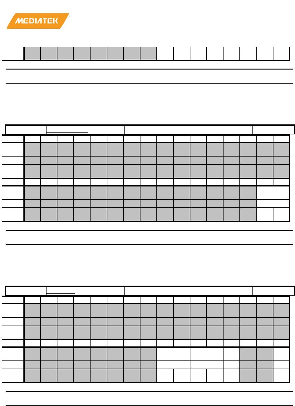
MT76x7
Internet-of-Things Wireless Connectivity
Reference Manual
© 2015 - 2017 MediaTek Inc
Page 539 of 798
This document contains information that is proprietary to MediaTek Inc. (“MediaTek”) and/or its licensor(s).
Any unauthorized use, reproduction or disclosure of this document in whole or in part is strictly prohibited
Rese
t
0 0 0 0 0 0 0 0
Bit(s)
Name
Description
7:0
FRACDIV_L
Add sampling count (+1) from state data7 to state data0,
in order to contribute fractional divisor.
83040058
FRACDIV_M
Fractional Divider MSB Address
00000000
Bit
31
30
29
28
27
26
25
24
23
22
21
20
19
18
17
16
Nam
e
Type
Rese
t
Bit
15
14
13
12
11
10
9
8
7
6
5
4
3
2
1
0
Nam
e
FRACDIV
_M
Type
RW
Rese
t
0 0
Bit(s)
Name
Description
1:0
FRACDIV_M
Add sampling count in state stop and state parity, in order
to contribute fractional divisor.
8304005C
FCR_RD
FIFO Control Register
00000000
Bit
31
30
29
28
27
26
25
24
23
22
21
20
19
18
17
16
Nam
e
Type
Rese
t
Bit
15
14
13
12
11
10
9
8
7
6
5
4
3
2
1
0
Nam
e
RFTL TFTL
DM
A1
FIF
OE
Type
RO
RO
RO
RO
Rese
t
0 0 0 0 0 0
Bit(s)
Name
Description
7:6
RFTL
Read out UARTn_FCR register.
5:4
TFTL
Read out UARTn_FCR register.
3
DMA1
Read out UARTn_FCR register.
0
FIFOE
Read out UARTn_FCR register.
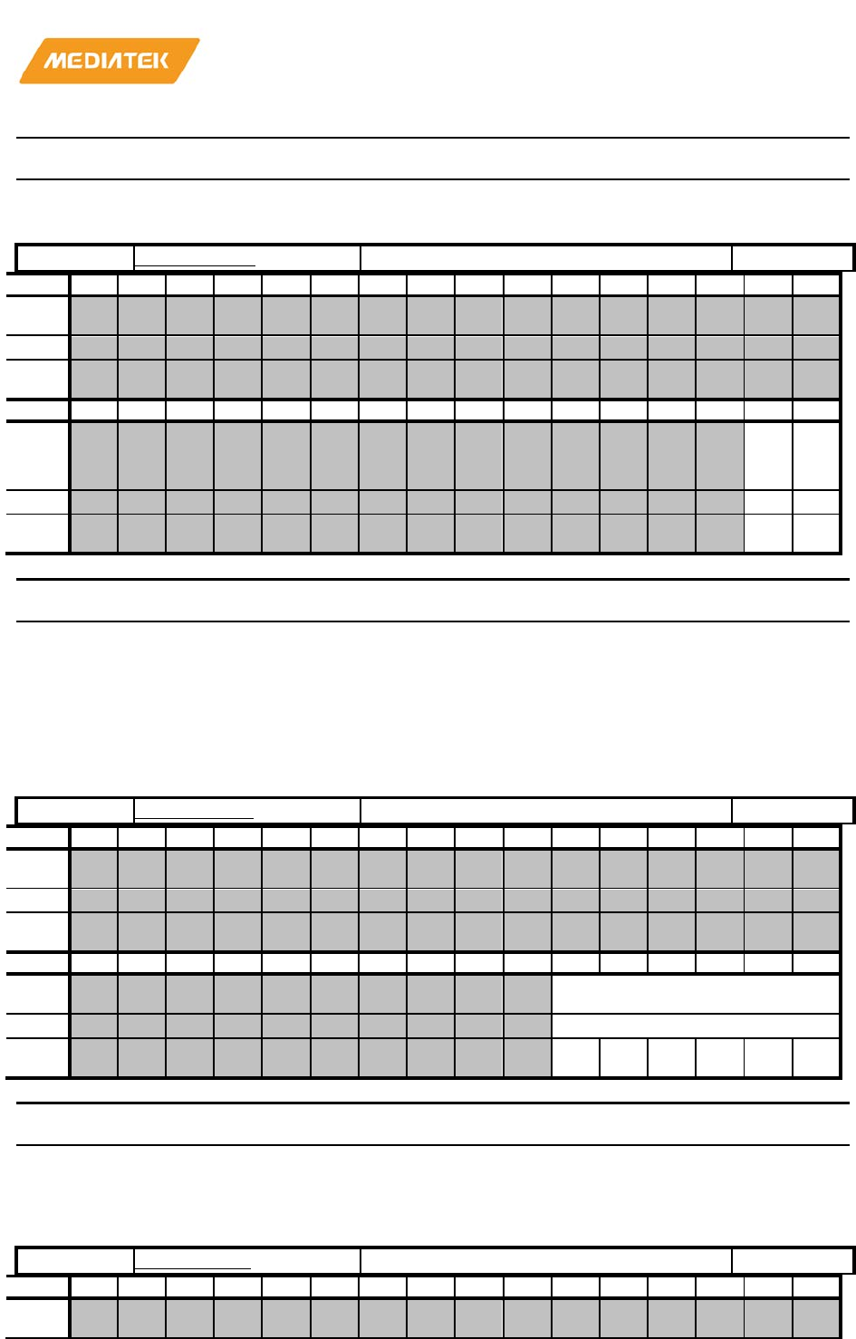
MT76x7
Internet-of-Things Wireless Connectivity
Reference Manual
© 2015 - 2017 MediaTek Inc
Page 540 of 798
This document contains information that is proprietary to MediaTek Inc. (“MediaTek”) and/or its licensor(s).
Any unauthorized use, reproduction or disclosure of this document in whole or in part is strictly prohibited
Bit(s)
Name
Description
83040060
tx_active_en
TX Active Enable Address
00000000
Bit
31
30
29
28
27
26
25
24
23
22
21
20
19
18
17
16
Nam
e
Type
Rese
t
Bit
15
14
13
12
11
10
9
8
7
6
5
4
3
2
1
0
Nam
e
TX
_O
E_
EN
TX
_P
U_
EN
Type
RW
RW
Rese
t
0 0
Bit(s)
Name
Description
1
TX_OE_EN
Enable UART_TX_OE switching function. TX_OE is to
control UART_TX output enable.
0
TX_PU_EN
Enable UART_TX_PU switching function. TX_PU is to
control UART_TX pull up enable.
83040068
RX_OFFSET
RX OFFSET
00000000
Bit
31
30
29
28
27
26
25
24
23
22
21
20
19
18
17
16
Nam
e
Type
Rese
t
Bit
15
14
13
12
11
10
9
8
7
6
5
4
3
2
1
0
Nam
e
RX_OFFSET
Type
RO
Rese
t
0 0 0 0 0 0
Bit(s)
Name
Description
5:0
RX_OFFSET
Data length in RX FIFO
8304006C
TX_OFFSET
TX OFFSET
00000000
Bit
31
30
29
28
27
26
25
24
23
22
21
20
19
18
17
16
Nam
e
MT76x7
Internet-of-Things Wireless Connectivity
Reference Manual
© 2015 - 2017 MediaTek Inc
Page 541 of 798
This document contains information that is proprietary to MediaTek Inc. (“MediaTek”) and/or its licensor(s).
Any unauthorized use, reproduction or disclosure of this document in whole or in part is strictly prohibited
Type
Rese
t
Bit
15
14
13
12
11
10
9
8
7
6
5
4
3
2
1
0
Nam
e
TX_OFFSET
Type
RO
Rese
t
0 0 0 0 0
Bit(s)
Name
Description
4:0
TX_OFFSET
Data length in TX FIFO
2.5.3. I2C serial interface
2.5.3.1. General description
MT76x7 features two I2C serial interface master controllers. The two signals of I2C channel 0 are I2C0_CLK and
I2C0_DATA.
• I2C0_CLK is a clock signal that is driven by the master.
• I2C0_DATA is a bi-directional data signal that can be driven by either the master or the slave. It
supports the clock rates of 50, 100, 200, and 400 KHz.
• I2C channel 1 supports the same feature as channel 0.
2.5.3.2. Functions
The I2C module operates with XTAL clock and can support up to 400 kHz I2C protocol. This module can be used
as I2C master, not slave, and has two different modes, which are Normal and General mode.
There is a FIFO for both TX and RX direction in this I2C module. During the TX transaction, data is pushed into
the TX FIFO; and during the RX transaction, data is popped from the RX FIFO. The block diagram of the I2C
module is shown in Figure 2-42.
In Normal mode, I2C transfer consists of one packet only. For TX, there is no need to specify the length of
transfer. I2C ends when TX FIFO is empty. For RX, it is required to specify the length of transfer in advance.
In General mode, I2C transfer can support up to 3 consecutive packet transfers. The length and the direction of
each packet can be specified separately. Such behavior can be used to perform I2C combined format transfer.
The data transfer between TX/RX FIFO and the memory can be performed by CM4 or GDMA. It is defined as
Direct mode if CM4 is used for the data transfer, and is defined as DMA mode if GDMA is used instead. In
Direct mode, CM4 keeps pushing/popping the data into/from the TX/RX FIFO during the I2C transaction. While
in DMA mode, GDMA will handle the work after CM4 enables both I2C and GDMA properly.
It is worth noticing that the depth of both TX and RX FIFO is 8, and overflow/underflow is not allowed during
the transaction. If DMA mode is used, a hardware handshaking between I2C and GDMA is applied to ensure
the correctness. However, if Direct mode is used, the software program is responsible to manage the usage of
TX/RX FIFO.
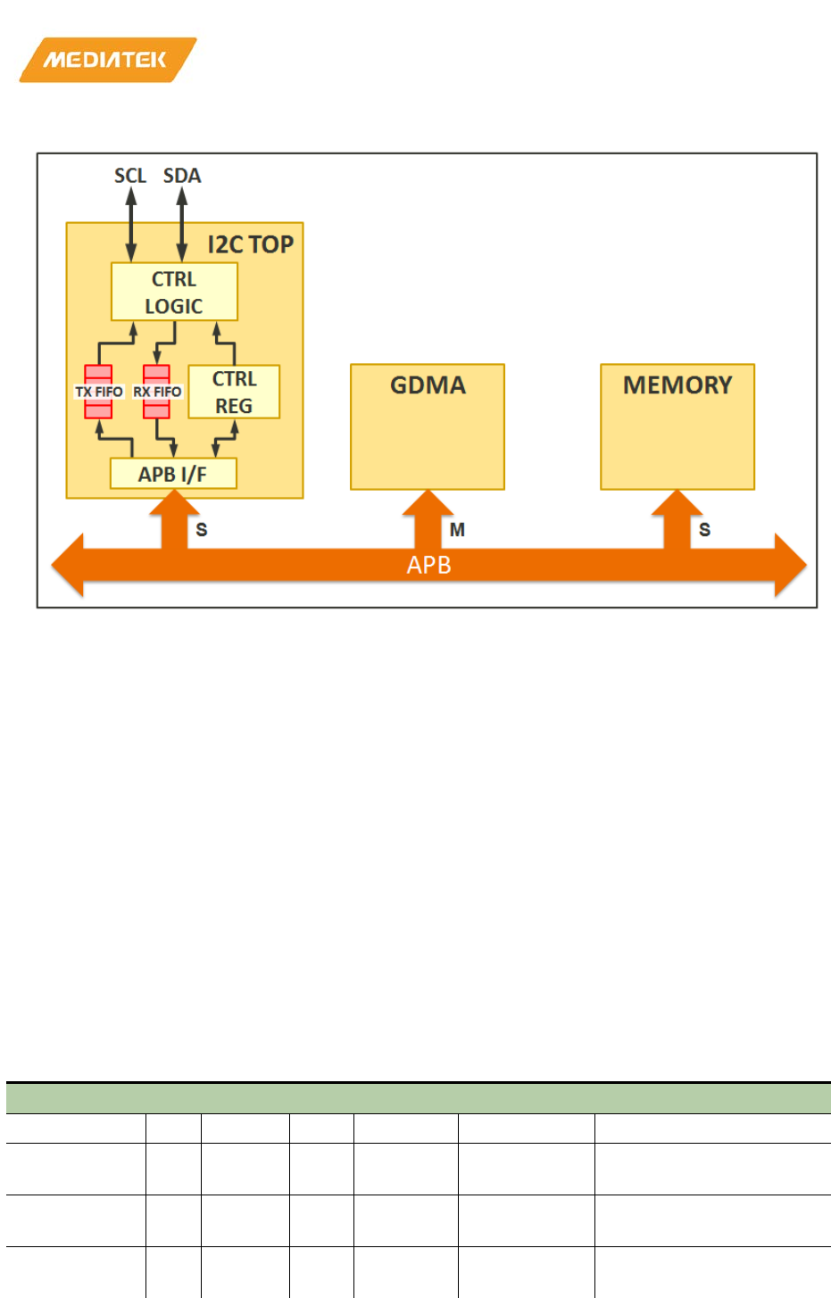
MT76x7
Internet-of-Things Wireless Connectivity
Reference Manual
© 2015 - 2017 MediaTek Inc
Page 542 of 798
This document contains information that is proprietary to MediaTek Inc. (“MediaTek”) and/or its licensor(s).
Any unauthorized use, reproduction or disclosure of this document in whole or in part is strictly prohibited
Figure 2-42 The block diagram of I2C module.
2.5.3.3. I2C programming sequence
The programming sequence can be divided into two parts, initialization and TX/RX sequence. The TX/RX
sequence can be further divided in to four due to the different combinations of Normal/General mode and
Direct/DMA mode.
2.5.3.4. Initialization
The initialization of I2C module includes setting the synchronizing circuit, the de-glitch circuit, and the
operating frequency of I2C. As shown in Table 2-42.
In the initial sequence, the I2C counting value of the four phases are determined by the XTAL frequency, the
I2C frequency required, and the ratio of each phase in a SCL clock cycle. The I2C frequency can vary from 50 to
400 kHz. By dividing the XTAL frequency by the I2C frequency required, a ratio r can be calculated.
Each SCL clock cycle is composed of four phases, as shown in Figure 2-43. By distributing the ratio r into the
four phases, the counting value is thus calculated.
Table 2-42 The initialization of I2C
Initialization Sequence
Description R/W Address Bit MACRO Value Note
Set I2C PAD
Control
W I2C_BASE
+ 0x240
[7:0] MM_PAD_
CON0
16'h0000 Disable SYNC_EN and De-
glitch counter
Set I2C Counting
Value
W I2C_BASE
+ 0x244
[15:0] MM_CNT_
VAL_PHL
USER_DEFINED Set the counting value of
phase 1 & phase 0
Set I2C Counting
Value
W I2C_BASE
+ 0x248
[15:0] MM_CNT_
VAL_PHH
USER_DEFINED Set the counting value of
phase 3 & phase 2
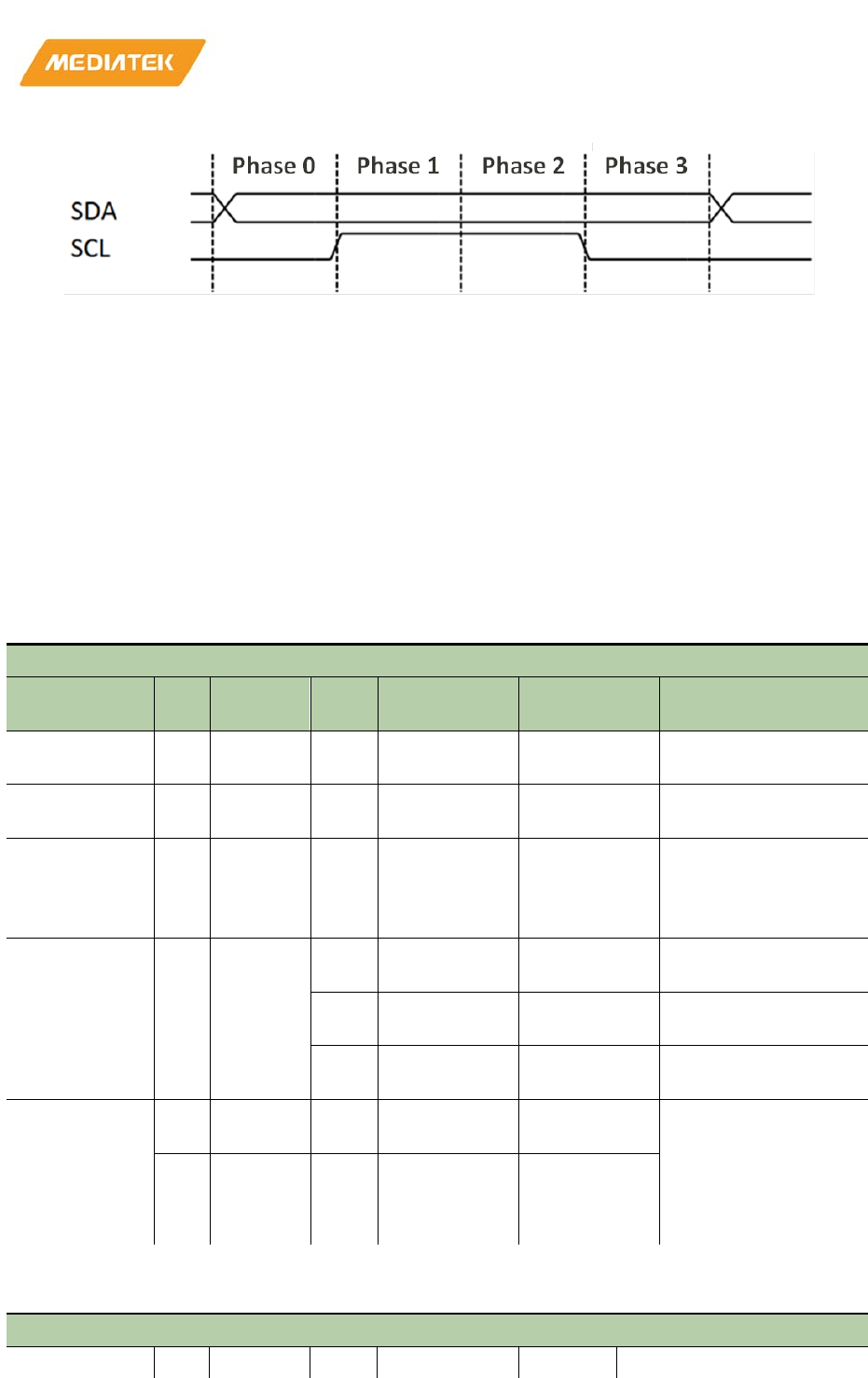
MT76x7
Internet-of-Things Wireless Connectivity
Reference Manual
© 2015 - 2017 MediaTek Inc
Page 543 of 798
This document contains information that is proprietary to MediaTek Inc. (“MediaTek”) and/or its licensor(s).
Any unauthorized use, reproduction or disclosure of this document in whole or in part is strictly prohibited
Figure 2-43 SCL clock phases
2.5.3.5. TX/RX Sequence
The four modes of I2C operation
As previously described in Section, I2C in MT76x7 has two different operating mode, Normal mode and
General mode. Moreover, I2C can be controlled by either CM4 or GDMA, defined as Direct mode and DMA
mode respectively. This leads to a fact that I2C has up to four operating modes. The programming sequence of
each mode is shown in the following tables.
1) Direct Normal Mode
Table 2-43 The TX sequence of I2C Direct Normal Mode
Direct Normal Mode TX Sequence
Description R/
W
Address Bit MACRO Value Note
Set I2C slave ID W I2C_BASE
+ 0x260
[6:0] MM_SLAVE_ID USER_DEFINED Set the ID of I2C slave
Set I2C transfer
direction
W I2C_BASE
+ 0x268
[3:0] MM_PACK_RW 4'b0000 Set 0 for I2C TX
Push data into
TX FIFO
W I2C_BASE
+ 0x27C
[7:0] MM_DATA_W_
REG
USER_DEFINED Repeat this step for
multiple bytes
Up to 8 bytes can be
pushed before start
Enable I2C
transfer
W I2C_BASE
+ 0x270
[15] MASTER_EN 1'b1 Set 1 to enable master
mode
[14] MM_GMODE 1'b0 Set 0 to disable general
mode (normal mode)
[0] MM_START_EN 1'b1 Set 1 to start I2C
transfer
Calculate TX
FIFO empty
space
Push the
remaining data
into TX FIFO
R I2C_BASE
+ 0x284
[15:8] MM_TX_FIFO_
WPTR/RPTR
Repeat this step until
the end of transfer
SW has to ensure TX
FIFO won't
under/overflow
W I2C_BASE
+ 0x27C
[7:0] MM_DATA_W_
REG
USER_DEFINED
Table 2-44 The RX sequence of I2C Direct Normal Mode
Direct Normal Mode RX Sequence
Description R/ Address Bit MACRO Value Note
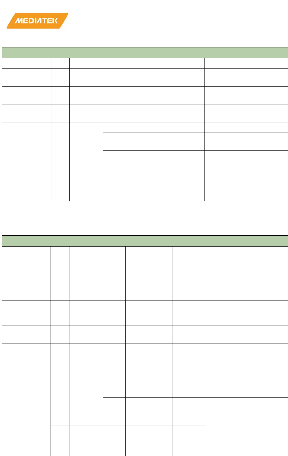
MT76x7
Internet-of-Things Wireless Connectivity
Reference Manual
© 2015 - 2017 MediaTek Inc
Page 544 of 798
This document contains information that is proprietary to MediaTek Inc. (“MediaTek”) and/or its licensor(s).
Any unauthorized use, reproduction or disclosure of this document in whole or in part is strictly prohibited
Direct Normal Mode RX Sequence
W
Set I2C slave ID W I2C_BASE
+ 0x260
[6:0] MM_SLAVE_ID USER_DE
FINED
Set the ID of I2C slave
Set I2C transfer
direction
W I2C_BASE
+ 0x268
[3:0] MM_PACK_RW 4'b0001 Set 1 for I2C RX
Set I2C RX
length
W I2C_BASE
+ 0x254
[15:0] MM_CNT_BYTE
_VAL_PK0
USER_DE
FINED
Unit is byte
Enable I2C
transfer
W I2C_BASE
+ 0x270
[15] MASTER_EN 1'b1 Set 1 to enable master mode
[14] MM_GMODE 1'b0 Set 0 to disable general mode
(normal mode)
[0] MM_START_EN 1'b1 Set 1 to start I2C transfer
Calculate RX
FIFO byte count
Pop the received
data from RX
FIFO
R I2C_BASE
+ 0x284
[7:0] MM_RX_FIFO_
WPTR/RPTR
Repeat this step until the end
of transfer
SW has to ensure RX FIFO
won't under/overflow
R I2C_BASE
+ 0x27C
[7:0] MM_DATA_R_R
EG
2) Direct General Mode
Table 2-45 The TX sequence of I2C Direct General Mode
Direct General Mode TX Sequence
Description R/W Address Bit MACRO Value Note
Set I2C slave ID W I2C_BASE
+ 0x260
[6:0] MM_SLAVE_ID USER_DEF
INED
Set the ID of I2C slave
Set I2C TX
length
W I2C_BASE
+ 0x254
[15:0] MM_CNT_BYTE
_VAL_PK0
USER_DEF
INED + 1
Set the data length to be
transferred
(Add 1 byte for word address)
Set I2C packet
count
and direction
W I2C_BASE
+ 0x268
[5:4] MM_PACK_VAL 2'd0 Set 0 for 1 packet
[3:0] MM_PACK_RW 4'b0000 Set 0 for I2C TX
Set I2C word
address
W I2C_BASE
+ 0x27C
[7:0] MM_DATA_W_
REG
USER_DEF
INED
Set the word address in I2C
slave
Push data into
TX FIFO
W I2C_BASE
+ 0x27C
[7:0] MM_DATA_W_
REG
USER_DEF
INED
Repeat this step for multiple
bytes
Up to 7 bytes can be pushed
before start
Enable I2C
transfer
W I2C_BASE
+ 0x270
[15] MASTER_EN 1'b1 Set 1 to enable master mode
[14] MM_GMODE 1'b1 Set 1 to enable general mode
[0] MM_START_EN 1'b1 Set 1 to start I2C transfer
Calculate TX
FIFO empty
space
Push the
remaining data
into TX FIFO
R I2C_BASE
+ 0x284
[15:8] MM_TX_FIFO_
WPTR/RPTR
Repeat this step until the end
of transfer
SW has to ensure TX FIFO
won't under/overflow
W I2C_BASE
+ 0x27C
[7:0] MM_DATA_W_
REG
USER_DEF
INED
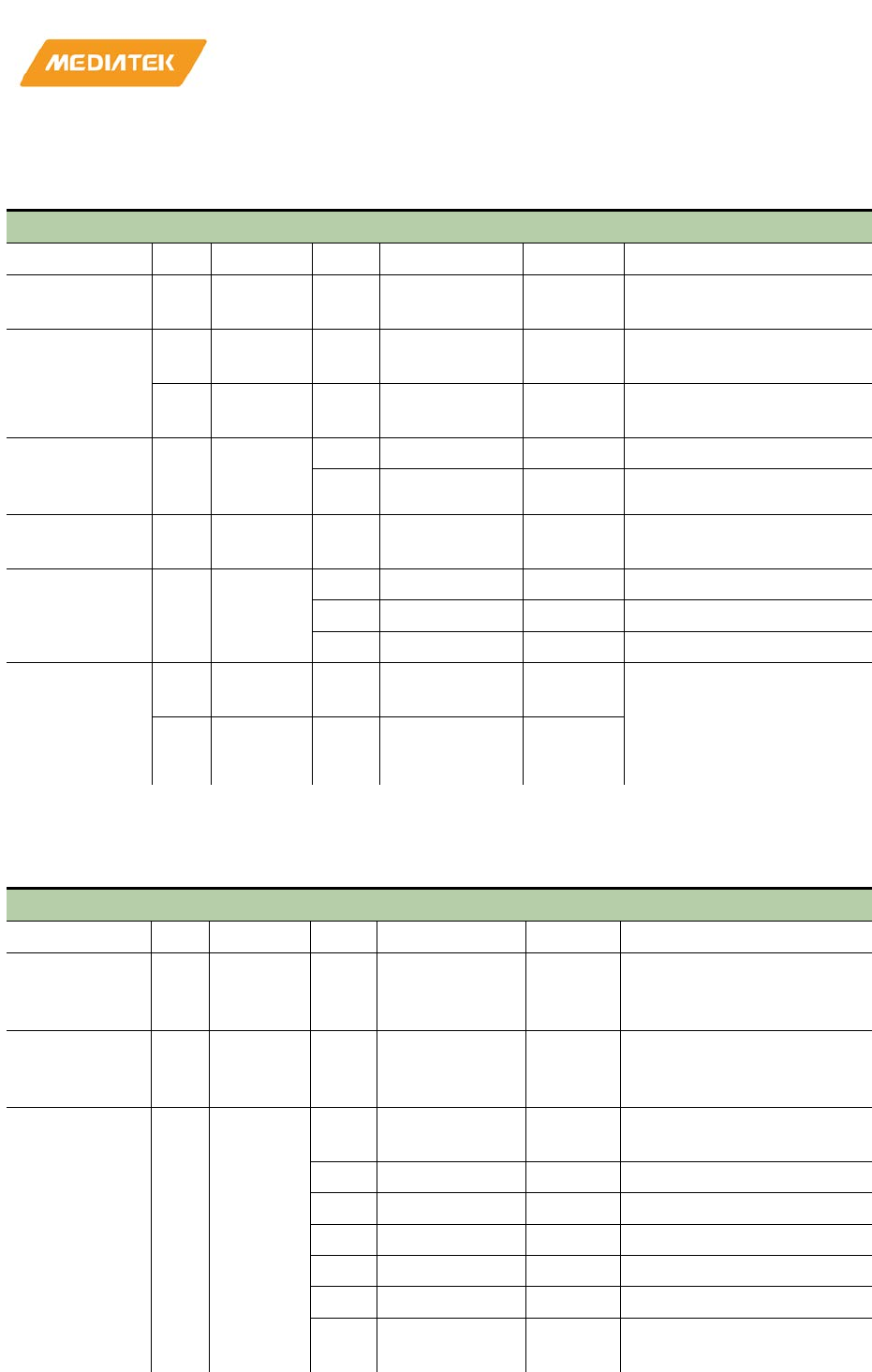
MT76x7
Internet-of-Things Wireless Connectivity
Reference Manual
© 2015 - 2017 MediaTek Inc
Page 545 of 798
This document contains information that is proprietary to MediaTek Inc. (“MediaTek”) and/or its licensor(s).
Any unauthorized use, reproduction or disclosure of this document in whole or in part is strictly prohibited
Table 2-46 The RX sequence of I2C Direct General Mode
Direct General Mode RX Sequence
Description R/W Address Bit MACRO Value Note
Set I2C slave ID W I2C_BASE
+ 0x260
[6:0] MM_SLAVE_ID USER_DEF
INED
Set the ID of I2C slave
Set I2C RX
length
W I2C_BASE
+ 0x254
[15:0] MM_CNT_BYTE
_VAL_PK0
16'd1 1 byte for word address
W I2C_BASE
+ 0x258
[15:0] MM_CNT_BYTE
_VAL_PK1
USER_DEF
INED
Set the data length to be
transferred
Set I2C packet
count
and direction
W I2C_BASE
+ 0x268
[5:4] MM_PACK_VAL 2'd1 Set 1 for 2 packets
[3:0] MM_PACK_RW 4'b0010 Set 1 for I2C RX
Set I2C word
address
W I2C_BASE
+ 0x27C
[7:0] MM_DATA_W_
REG
USER_DEF
INED
Set the word address in I2C
slave
Enable I2C
transfer
W I2C_BASE
+ 0x270
[15] MASTER_EN 1'b1 Set 1 to enable master mode
[14] MM_GMODE 1'b1 Set 1 to enable general mode
[0] MM_START_EN 1'b1 Set 1 to start I2C transfer
Calculate RX
FIFO byte count
Pop the
received data
from RX FIFO
R I2C_BASE
+ 0x284
[7:0] MM_RX_FIFO_
WPTR/RPTR
Repeat this step until the end
of transfer
SW has to ensure RX FIFO
won't under/overflow
R I2C_BASE
+ 0x27C
[7:0] MM_DATA_R_R
EG
3) DMA Normal Mode
Table 2-47 The TX sequence of I2C DMA Normal Mode
DMA Normal Mode TX Sequence
Description R/W Address Bit MACRO Value Note
Set GDMA
transfer count
W GDMA_B
ASE +
0x0N10
[15:0] LEN USER_DE
FINED
Unit is byte
Set GDMA
source address
W GDMA_B
ASE +
0x0N2C
[31:0] PGMADDR USER_DE
FINED
The address in memory
Set GDMA
configurations
W GDMA_B
ASE +
0x0N14
[25:2
0]
MAS 6'd2 or
6'd4
Set 6'd2/6'd4 for I2C-1/2 TX
respectively
[18] DIR 1'b0 Set 0 for Read (RAM to I2C)
[17] WPEN 1'b0 Set 0 to disable wrapping
[15] ITEN 1'b0 Set 0 to disable interrupt
[10:8] BURST 3'b000 Set 0 for single-byte burst
[5] B2W 1'b0 Set 0 to disable
[4] DREQ 1'b1 Set 1 to enable HW
handshake

MT76x7
Internet-of-Things Wireless Connectivity
Reference Manual
© 2015 - 2017 MediaTek Inc
Page 546 of 798
This document contains information that is proprietary to MediaTek Inc. (“MediaTek”) and/or its licensor(s).
Any unauthorized use, reproduction or disclosure of this document in whole or in part is strictly prohibited
DMA Normal Mode TX Sequence
[3] DINC 1'b0 Set 0 to disable incremental
address
[2] SINC 1'b1 Set 1 to enable incremental
address
[1:0] SIZE 2'b00 Set 0 for single-byte transfer
Enable GDMA W GDMA_B
ASE +
0x0N18
[15] STR 1'b0 Set 0 to reset DMA transfer
W GDMA_B
ASE +
0x0N18
[15] STR 1'b1 Set 1 to start DMA transfer
Set I2C slave ID W I2C_BASE
+ 0x260
[6:0] MM_SLAVE_ID USER_DE
FINED
Set the ID of I2C slave
Set I2C transfer
direction
W I2C_BASE
+ 0x268
[3:0] MM_PACK_RW 4'b0000 Set 0 for I2C TX
Enable I2C
transfer
W I2C_BASE
+ 0x270
[15] MASTER_EN 1'b1 Set 1 to enable master mode
[14] MM_GMODE 1'b0 Set 0 to disable general mode
(normal mode)
[0] MM_START_EN 1'b1 Set 1 to start I2C transfer
Table 2-48 The RX sequence of I2C DMA Normal Mode
DMA Normal Mode RX Sequence
Description R/W Address Bit MACRO Value Note
Set GDMA
transfer count
W GDMA_BA
SE +
0x0N10
[15:0] LEN USER_DEF
INED
Unit is byte
Set GDMA
destination
address
W GDMA_BA
SE +
0x0N2C
[31:0] PGMADDR USER_DEF
INED
The address in memory
Set GDMA
configurations
W GDMA_BA
SE +
0x0N14
[25:2
0]
MAS 6'd3 or
6'd5
Set 6'd3/6'd5 for I2C-1/2 RX
respectively
[18] DIR 1'b1 Set 1 for Write (I2C to RAM)
[17] WPEN 1'b0 Set 0 to disable wrapping
[15] ITEN 1'b0 Set 0 to disable interrupt
[10:8] BURST 3'b000 Set 0 for single-byte burst
[5] B2W 1'b0 Set 0 to disable
[4] DREQ 1'b1 Set 1 to enable HW handshake
[3] DINC 1'b1 Set 1 to enable incremental
address
[2] SINC 1'b0 Set 0 to disable incremental
address
[1:0] SIZE 2'b00 Set 0 for single-byte transfer

MT76x7
Internet-of-Things Wireless Connectivity
Reference Manual
© 2015 - 2017 MediaTek Inc
Page 547 of 798
This document contains information that is proprietary to MediaTek Inc. (“MediaTek”) and/or its licensor(s).
Any unauthorized use, reproduction or disclosure of this document in whole or in part is strictly prohibited
DMA Normal Mode RX Sequence
Enable GDMA W GDMA_BA
SE +
0x0N18
[15] STR 1'b0 Set 0 to reset DMA transfer
W GDMA_BA
SE +
0x0N18
[15] STR 1'b1 Set 1 to start DMA transfer
Set I2C slave ID W I2C_BASE
+ 0x260
[6:0] MM_SLAVE_ID USER_DEF
INED
Set the ID of I2C slave
Set I2C transfer
direction
W I2C_BASE
+ 0x268
[3:0] MM_PACK_RW 4'b0001 Set 1 for I2C RX
Set I2C RX
length
W I2C_BASE
+ 0x254
[15:0] MM_CNT_BYTE
_VAL_PK0
USER_DEF
INED
Unit is byte
Enable I2C
transfer
W I2C_BASE
+ 0x270
[15] MASTER_EN 1'b1 Set 1 to enable master mode
[14] MM_GMODE 1'b0 Set 0 to disable general mode
(normal mode)
[0] MM_START_EN 1'b1 Set 1 to start I2C transfer
4) DMA General Mode
Table 2-49 The TX sequence of I2C DMA General Mode
DMA General Mode TX Sequence
Description R/
W
Address Bit MACRO Value Note
Set I2C word
address
W I2C_BASE +
0x27C
[7:0] MM_DATA_W_R
EG
USER_DEFI
NED
Set the word address in
I2C slave
Set GDMA
transfer count
W GDMA_BASE +
0x0N10
[15:
0]
LEN USER_DEFI
NED
Unit is byte
Set GDMA
source address
W GDMA_BASE +
0x0N2C
[31:
0]
PGMADDR USER_DEFI
NED
The address in memory
Set GDMA
configurations
W GDMA_BASE +
0x0N14
[25:
20]
MAS 6'd2 or 6'd4 Set 6'd2/6'd4 for I2C-1/2
TX respectively
[18] DIR 1'b0 Set 0 for Read (RAM to
I2C)
[17] WPEN 1'b0 Set 0 to disable wrapping
[15] ITEN 1'b0 Set 0 to disable interrupt
[10:
8]
BURST 3'b000 Set 0 for single-byte burst
[5] B2W 1'b0 Set 0 to disable
[4] DREQ 1'b1 Set 1 to enable HW
handshake
[3] DINC 1'b0 Set 0 to disable
incremental address
[2] SINC 1'b1 Set 1 to enable
incremental address

MT76x7
Internet-of-Things Wireless Connectivity
Reference Manual
© 2015 - 2017 MediaTek Inc
Page 548 of 798
This document contains information that is proprietary to MediaTek Inc. (“MediaTek”) and/or its licensor(s).
Any unauthorized use, reproduction or disclosure of this document in whole or in part is strictly prohibited
DMA General Mode TX Sequence
[1:0] SIZE 2'b00 Set 0 for single-byte
transfer
Enable GDMA W GDMA_BASE +
0x0N18
[15] STR 1'b0 Set 0 to reset DMA
transfer
W GDMA_BASE +
0x0N18
[15] STR 1'b1 Set 1 to start DMA
transfer
Set I2C slave ID W I2C_BASE +
0x260
[6:0] MM_SLAVE_ID USER_DEFI
NED
Set the ID of I2C slave
Set I2C TX
length
W I2C_BASE +
0x254
[15:
0]
MM_CNT_BYTE_
VAL_PK0
USER_DEFI
NED + 1
Set the data length to be
transferred
(Add 1 byte for word
address)
Set I2C packet
count
and direction
W I2C_BASE +
0x268
[5:4] MM_PACK_VAL 2'd0 Set 0 for 1 packets
[3:0] MM_PACK_RW 4'b0000 Set 0 for I2C TX
Enable I2C
transfer
W I2C_BASE +
0x270
[15] MASTER_EN 1'b1 Set 1 to enable master
mode
[14] MM_GMODE 1'b1 Set 1 to enable general
mode
[0] MM_START_EN 1'b1 Set 1 to start I2C transfer
Table 2-50 The RX sequence of I2C DMA General Mode
DMA General Mode RX Sequence
Description R/
W
Address Bit MACRO Value Note
Set I2C word
address
W I2C_BASE +
0x27C
[7:0] MM_DATA_W_R
EG
USER_DE
FINED
Set the word address in
I2C slave
Set GDMA
transfer count
W GDMA_BASE +
0x0N10
[15:
0]
LEN USER_DE
FINED
Unit is byte
Set GDMA
destination
address
W GDMA_BASE +
0x0N2C
[31:
0]
PGMADDR USER_DE
FINED
The address in memory
Set GDMA
configurations
W GDMA_BASE +
0x0N14
[25:
20]
MAS 6'd3 or
6'd5
Set 6'd3/6'd5 for I2C-1/2
RX respectively
[18] DIR 1'b0 Set 0 for Read (RAM to
I2C)
[17] WPEN 1'b0 Set 0 to disable wrapping
[15] ITEN 1'b0 Set 0 to disable interrupt
[10:
8]
BURST 3'b000 Set 0 for single-byte burst
[5] B2W 1'b0 Set 0 to disable
[4] DREQ 1'b1 Set 1 to enable HW
handshake
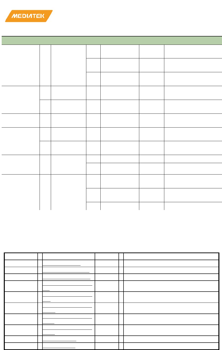
MT76x7
Internet-of-Things Wireless Connectivity
Reference Manual
© 2015 - 2017 MediaTek Inc
Page 549 of 798
This document contains information that is proprietary to MediaTek Inc. (“MediaTek”) and/or its licensor(s).
Any unauthorized use, reproduction or disclosure of this document in whole or in part is strictly prohibited
DMA General Mode RX Sequence
[3] DINC 1'b1 Set 1 to enable
incremental address
[2] SINC 1'b0 Set 0 to disable
incremental address
[1:0] SIZE 2'b00 Set 0 for single-byte
transfer
Enable GDMA W GDMA_BASE +
0x0N18
[15] STR 1'b0 Set 0 to reset DMA
transfer
W GDMA_BASE +
0x0N18
[15] STR 1'b1 Set 1 to start DMA transfer
Set I2C slave ID W I2C_BASE +
0x260
[6:0] MM_SLAVE_ID USER_DE
FINED
Set the ID of I2C slave
Set I2C RX length W I2C_BASE +
0x254
[15:
0]
MM_CNT_BYTE_
VAL_PK0
16'd1 1 byte for word address
W I2C_BASE +
0x258
[15:
0]
MM_CNT_BYTE_
VAL_PK1
USER_DE
FINED
Set the data length to be
transferred
Set I2C packet
count
and direction
W I2C_BASE +
0x268
[5:4] MM_PACK_VAL 2'd1 Set 1 for 2 packets
[3:0] MM_PACK_RW 4'b0010 Set 1 for I2C RX
Enable I2C
transfer
W I2C_BASE +
0x270
[15] MASTER_EN 1'b1 Set 1 to enable master
mode
[14] MM_GMODE 1'b1 Set 1 to enable general
mode
[0] MM_START_EN 1'b1 Set 1 to start I2C transfer
2.5.3.6. Registers definitions
1) I2C-1
Module name: I2C-1 Base address: (+83090000h)
Address
Name
Width
Register Function
83090240
MM_PAD_CON0
16
Pad Control
83090244
MM_CNT_VAL_PHL
16
Counting Value Phase Low
83090248
MM_CNT_VAL_PHH
16
Counting Value Phase High
8309024C
MM_CNT_VAL_HS_P
HL
16
Counting Value High
-Speed Phase Low
83090250
MM_CNT_VAL_HS_P
HH
16
Counting Value High
-Speed Phase High
83090254
MM_CNT_BYTE_VAL
_PK0
16
Byte
value of packet 0
83090258
MM_CNT_BYTE_VAL
_PK1
16
Byte value of packet 1
8309025C
MM_CNT_BYTE_VAL
_PK2
16
Byte value of packet 2
83090260
MM_ID_CON0
16
ID Control 0
83090264
MM_ID_CON1
16
ID Control 1
MT76x7
Internet-of-Things Wireless Connectivity
Reference Manual
© 2015 - 2017 MediaTek Inc
Page 550 of 798
This document contains information that is proprietary to MediaTek Inc. (“MediaTek”) and/or its licensor(s).
Any unauthorized use, reproduction or disclosure of this document in whole or in part is strictly prohibited
Address
Name
Width
Register Function
83090268
MM_PACK_CON0
16
Packet Control
8309026C
MM_ACK_VAL
16
Ack Value
83090270
MM_CON0
16
I2C Control
83090274
MM_STATUS
16
I2C Status
83090278
MM_FIFO_CON0
16
FIFO Control
8309027C
MM_FIFO_DATA
16
FIFO Data
Write/Read
83090280
MM_FIFO_STATUS
16
FIFO Status
83090284
MM_FIFO_PTR
16
FIFO Pointer
830902C0
DMA_CON0
16
DMA Control
830902FC
RESERVED0
16
Reserved CR
83090240
MM_PAD_CON0
Pad Control
00000000
Bit
31
30
29
28
27
26
25
24
23
22
21
20
19
18
17
16
Nam
e
Type
Rese
t
Bit
15
14
13
12
11
10
9
8
7
6
5
4
3
2
1
0
Nam
e
SY
NC
_E
N
SD
A_
DR
VH
_E
N
SC
L_
DR
VH
_E
N
DE_CNT
Type
RW
RW
RW
RW
Rese
t
0 0 0 0 0 0 0 0
Bit(s)
Name
Description
7
SYNC_EN
Set 1 to enable the I2C internal synchronization functions
on sda_i and
scl_i, inducing 2 cycles of latency.
6
SDA_DRVH_EN
Set 1 to enable SDA pad driving high. Default is pull high.
5
SCL_DRVH_EN
Set 1 to enable SCL pad driving high. Default is pull high.
4:0
DE_CNT
Deglitch counting number. Set 0 to disable the deglitch
circuit.
83090244
MM_CNT_VAL_PHL
Counting Value Phase Low
0000FFFF
Bit
31
30
29
28
27
26
25
24
23
22
21
20
19
18
17
16
Nam
e
Type
Rese
t
Bit
15
14
13
12
11
10
9
8
7
6
5
4
3
2
1
0
Nam
MM_CNT_PHASE_VAL1
MM_CNT_PHASE_VAL0
MT76x7
Internet-of-Things Wireless Connectivity
Reference Manual
© 2015 - 2017 MediaTek Inc
Page 551 of 798
This document contains information that is proprietary to MediaTek Inc. (“MediaTek”) and/or its licensor(s).
Any unauthorized use, reproduction or disclosure of this document in whole or in part is strictly prohibited
e
Type
RW
RW
Rese
t
1 1 1 1 1 1 1 1 1 1 1 1 1 1 1 1
Bit(s)
Name
Description
15:8
MM_CNT_PHASE_VAL1
Phase 1 counting value. SCL rising edge to SDA timing.
The STOP condition period.
Unit: Depends on XTAL
frequency (1/XTAL_FREQ)
7:0
MM_CNT_PHASE_VAL0
Phase 0 counting value. SDA to SCL rising edge timing.
The data setup time.
Unit: Depends on XTAL frequency (1/XTAL_FREQ)
83090248
MM_CNT_VAL_PHH
Counting Value Phase High
0000FFFF
Bit
31
30
29
28
27
26
25
24
23
22
21
20
19
18
17
16
Nam
e
Type
Rese
t
Bit
15
14
13
12
11
10
9
8
7
6
5
4
3
2
1
0
Nam
e
MM_CNT_PHASE_VAL3 MM_CNT_PHASE_VAL2
Type
RW
RW
Rese
t
1 1 1 1 1 1 1 1 1 1 1 1 1 1 1 1
Bit(s)
Name
Description
15:8
MM_CNT_PHASE_VAL3
Phase 3 counting value. SCL falling edge to SDA timing.
The data hold time.
Unit: Depends on XTAL frequency (1/XTAL_FREQ)
7:0
MM_CNT_PHASE_VAL2
Phase 2 counting value. SDA to SCL falling edge timing.
The START condition period.
Unit: Depends on XTAL frequency (1/XTAL_FREQ)
8309024C
MM_CNT_VAL_HS_P
HL
Counting Value High-Speed Phase Low
0000FFFF
Bit
31
30
29
28
27
26
25
24
23
22
21
20
19
18
17
16
Nam
e
Type
Rese
t
Bit
15
14
13
12
11
10
9
8
7
6
5
4
3
2
1
0
MT76x7
Internet-of-Things Wireless Connectivity
Reference Manual
© 2015 - 2017 MediaTek Inc
Page 552 of 798
This document contains information that is proprietary to MediaTek Inc. (“MediaTek”) and/or its licensor(s).
Any unauthorized use, reproduction or disclosure of this document in whole or in part is strictly prohibited
Nam
e
Type
Rese
t
Bit(s)
Name
Description
83090250
MM_CNT_VAL_HS_P
HH
Counting Value High-Speed Phase High
0000FFFF
Bit
31
30
29
28
27
26
25
24
23
22
21
20
19
18
17
16
Nam
e
Type
Rese
t
Bit
15
14
13
12
11
10
9
8
7
6
5
4
3
2
1
0
Nam
e
Type
Rese
t
Bit(s)
Name
Description
83090254
MM_CNT_BYTE_VAL_
PK0
Byte value of packet 0
00000000
Bit
31
30
29
28
27
26
25
24
23
22
21
20
19
18
17
16
Nam
e
Type
Rese
t
Bit
15
14
13
12
11
10
9
8
7
6
5
4
3
2
1
0
Nam
e
MM_CNT_BYTE_VAL_PK0
Type
RW
Rese
t
0 0 0 0 0 0 0 0 0 0 0 0 0 0 0 0
Bit(s)
Name
Description
15:0
MM_CNT_BYTE_VAL_PK0
The first packet length for general case. But in normal
read mode, it need to set the read
data length.
83090258
MM_CNT_BYTE_VAL_
PK1
Byte value of packet 1
00000000
MT76x7
Internet-of-Things Wireless Connectivity
Reference Manual
© 2015 - 2017 MediaTek Inc
Page 553 of 798
This document contains information that is proprietary to MediaTek Inc. (“MediaTek”) and/or its licensor(s).
Any unauthorized use, reproduction or disclosure of this document in whole or in part is strictly prohibited
Bit
31
30
29
28
27
26
25
24
23
22
21
20
19
18
17
16
Nam
e
Type
Rese
t
Bit
15
14
13
12
11
10
9
8
7
6
5
4
3
2
1
0
Nam
e
MM_CNT_BYTE_VAL_PK1
Type
RW
Rese
t
0 0 0 0 0 0 0 0 0 0 0 0 0 0 0 0
Bit(s)
Name
Description
15:0
MM_CNT_BYTE_VAL_PK1
The second packet length for general case.
8309025C
MM_CNT_BYTE_VAL_
PK2
Byte value of packet 2
00000000
Bit
31
30
29
28
27
26
25
24
23
22
21
20
19
18
17
16
Nam
e
Type
Rese
t
Bit
15
14
13
12
11
10
9
8
7
6
5
4
3
2
1
0
Nam
e
MM_CNT_BYTE_VAL_PK2
Type
RW
Rese
t
0 0 0 0 0 0 0 0 0 0 0 0 0 0 0 0
Bit(s)
Name
Description
15:0
MM_CNT_BYTE_VAL_PK2
The third packet length for general case.
83090260
MM_ID_CON0
ID Control 0
00000038
Bit
31
30
29
28
27
26
25
24
23
22
21
20
19
18
17
16
Nam
e
Type
Rese
t
Bit
15
14
13
12
11
10
9
8
7
6
5
4
3
2
1
0
Nam
e
MM_SLAVE_ID
Type
RW
Rese
t
0 1 1 1 0 0 0
MT76x7
Internet-of-Things Wireless Connectivity
Reference Manual
© 2015 - 2017 MediaTek Inc
Page 554 of 798
This document contains information that is proprietary to MediaTek Inc. (“MediaTek”) and/or its licensor(s).
Any unauthorized use, reproduction or disclosure of this document in whole or in part is strictly prohibited
Bit(s)
Name
Description
6:0
MM_SLAVE_ID
The slave address.
83090264
MM_ID_CON1
ID Control 1
0000000F
Bit
31
30
29
28
27
26
25
24
23
22
21
20
19
18
17
16
Nam
e
Type
Rese
t
Bit
15
14
13
12
11
10
9
8
7
6
5
4
3
2
1
0
Nam
e
Type
Rese
t
Bit(s)
Name
Description
83090268
MM_PACK_CON0
Packet Control
00000000
Bit
31
30
29
28
27
26
25
24
23
22
21
20
19
18
17
16
Nam
e
Type
Rese
t
Bit
15
14
13
12
11
10
9
8
7
6
5
4
3
2
1
0
Nam
e MM_PAC
K_VAL
M
M_
PA
CK
_R
W[
3]
M
M_
PA
CK
_R
W[
2]
M
M_
PA
CK
_R
W[
1]
M
M_
PA
CK
_R
W[
0]
Type
RW
RW
RW
RW
RW
Rese
t
0 0 0 0 0 0
Bit(s)
Name
Description
5:4
MM_PACK_VAL
Number of packet in general case.
2'h0: means 1
packet
2'h1: means 2 packet
2'h2: means 3 packet
2'h3: Reserved.
3
MM_PACK_RW[3]
Read/write signal for each packet in general case. Only
MT76x7
Internet-of-Things Wireless Connectivity
Reference Manual
© 2015 - 2017 MediaTek Inc
Page 555 of 798
This document contains information that is proprietary to MediaTek Inc. (“MediaTek”) and/or its licensor(s).
Any unauthorized use, reproduction or disclosure of this document in whole or in part is strictly prohibited
Bit(s)
Name
Description
MM_PACK_RW[0] is used when not in general case.
0: write
1: read
2
MM_PACK_RW[2]
Read/write signal for each packet in general case. Only
MM_PACK_RW[0] is used when not in general case.
0: write
1: read
1
MM_PACK_RW[1]
Read/write signal for each packet in general case. Only
MM_PACK_RW[0] is used when not in general case.
0: write
1: read
0
MM_PACK_RW[0]
Read/write signal for each packet in general case. Only
MM_PACK_RW[0] is used when not in general case.
0: write
1: read
8309026C
MM_ACK_VAL
Ack Value
00000FFF
Bit
31
30
29
28
27
26
25
24
23
22
21
20
19
18
17
16
Nam
e
Type
Rese
t
Bit
15
14
13
12
11
10
9
8
7
6
5
4
3
2
1
0
Nam
e
MM_ACK_ID MM_ACK_DATA
Type
RO
RO
Rese
t
1 1 1 1 1 1 1 1 1 1 1 1
Bit(s)
Name
Description
11:8
MM_ACK_ID
The received ACK data bits after ID data in each packet.
7:0
MM_ACK_DATA
The last 8 received ACK data bits.
83090270
MM_CON0
I2C Control
00000800
Bit
31
30
29
28
27
26
25
24
23
22
21
20
19
18
17
16
Nam
e
MT76x7
Internet-of-Things Wireless Connectivity
Reference Manual
© 2015 - 2017 MediaTek Inc
Page 556 of 798
This document contains information that is proprietary to MediaTek Inc. (“MediaTek”) and/or its licensor(s).
Any unauthorized use, reproduction or disclosure of this document in whole or in part is strictly prohibited
Type
Rese
t
Bit
15
14
13
12
11
10
9
8
7
6
5
4
3
2
1
0
Nam
e
MA
ST
ER
_E
N
M
M_
GM
OD
E
M
M_
ST
AR
T_
EN
Type
RW
RW
RW
Rese
t
0 0 0
Bit(s)
Name
Description
15
MASTER_EN
Master enable
14
MM_GMODE
Master general mode enable.
0: Normal
mode. BYTE_VAL_PK0/1/2 is disabled for TX, I2C
stops as TX FIFO is empty. BYTE_VAL_PK1/2 is disabled for RX,
while BYTE_VAL_PK0 is used to indicate the byte count to be read.
1: General mode. This mode supports up to 3 packet transfer, which
the length is
defined by BYTE_VAL_PK0/1/2 respectively.
0
MM_START_EN
Master starts transfer trigger. When DSP write 1 to this
bit, the hardware initiates to transfer data until
BUS_BUSY equals 0. When data starts to transfer, this bit
will go to low immediately.
83090274
MM_STATUS
I2C Status
00000004
Bit
31
30
29
28
27
26
25
24
23
22
21
20
19
18
17
16
Nam
e
Type
Rese
t
Bit
15
14
13
12
11
10
9
8
7
6
5
4
3
2
1
0
Nam
e
M
M_
ST
AR
T_
RE
AD
Y
M
M_
AR
B_
HA
D_
LO
SE
BU
S_
BU
SY
Type
RO
RO
RO
Rese
t
1 0 0
Bit(s)
Name
Description
2
MM_START_READY
The master is ready for start trigger when read 1. When
DSP set MM_START_EN to 1, this will go to low
immediately. When data transfers finished, this signal
will go to high. DSP can read this bit to decide the next
MT76x7
Internet-of-Things Wireless Connectivity
Reference Manual
© 2015 - 2017 MediaTek Inc
Page 557 of 798
This document contains information that is proprietary to MediaTek Inc. (“MediaTek”) and/or its licensor(s).
Any unauthorized use, reproduction or disclosure of this document in whole or in part is strictly prohibited
Bit(s)
Name
Description
data packet transfer.
1
MM_ARB_HAD_LOSE
The master had an arbitration lose when read 1. DSP
writes 1 to clear this bit.
0
BUS_BUSY
The SDA and SCL are active when read 1. When the START
signal was detected on I2C, the BUS_BUSY will set to high.
When the STOP signal is detected on the bus, the
B
US_BUSY will set to low.
83090278
MM_FIFO_CON0
FIFO Control
00000000
Bit
31
30
29
28
27
26
25
24
23
22
21
20
19
18
17
16
Nam
e
Type
Rese
t
Bit
15
14
13
12
11
10
9
8
7
6
5
4
3
2
1
0
Nam
e
M
M_
TX
_FI
FO
_C
LR
M
M_
RX
_FI
FO
_C
LR
Type
W1
C
W1
C
Rese
t
0 0
Bit(s)
Name
Description
1
MM_TX_FIFO_CLR
Clear the master TX FIFO when write 1.
0
MM_RX_FIFO_CLR
Clear the master RX FIFO when write 1.
8309027C
MM_FIFO_DATA
FIFO Data Write/Read
00000000
Bit
31
30
29
28
27
26
25
24
23
22
21
20
19
18
17
16
Nam
e
Type
Rese
t
Bit
15
14
13
12
11
10
9
8
7
6
5
4
3
2
1
0
Nam
e
MM_DATA_W/R_REG
Type
RW
Rese
t
0 0 0 0 0 0 0 0
MT76x7
Internet-of-Things Wireless Connectivity
Reference Manual
© 2015 - 2017 MediaTek Inc
Page 558 of 798
This document contains information that is proprietary to MediaTek Inc. (“MediaTek”) and/or its licensor(s).
Any unauthorized use, reproduction or disclosure of this document in whole or in part is strictly prohibited
Bit(s)
Name
Description
7:0
MM_DATA_W/R_REG
Write/Read to push/pop data into/from TX/RX FIFO.
(FIFO Depth: 8 bytes)
83090280
MM_FIFO_STATUS
FIFO Status
00000011
Bit
31
30
29
28
27
26
25
24
23
22
21
20
19
18
17
16
Nam
e
Type
Rese
t
Bit
15
14
13
12
11
10
9
8
7
6
5
4
3
2
1
0
Nam
e
M
M_
TX
_FI
FO
_O
VF
M
M_
TX
_FI
FO
_U
ND
R
M
M_
TX
_FI
FO
_F
UL
L
M
M_
TX
_FI
FO
_E
MP
M
M_
RX
_FI
FO
_O
VF
M
M_
RX
_FI
FO
_U
ND
R
M
M_
RX
_FI
FO
_F
UL
L
M
M_
RX
_FI
FO
_E
MP
Type
RO
RO
RO
RO
RO
RO
RO
RO
Rese
t
0 0 0 1 0 0 0 1
Bit(s)
Name
Description
7
MM_TX_FIFO_OVF
Master TX FIFO overflow. It can only be cleared when
write MM_TX_FIFO_CLR 1.
6
MM_TX_FIFO_UNDR
Master TX FIFO underflow. It can only be cleared when
write MM_TX_FIFO_CLR 1.
5
MM_TX_FIFO_FULL
Master TX FIFO full.
4
MM_TX_FIFO_EMP
Master TX FIFO empty.
3
MM_RX_FIFO_OVF
Master RX FIFO overflow. It can only be cleared when
write
MM_RX_FIFO_CLR 1.
2
MM_RX_FIFO_UNDR
Master RX FIFO underflow. It can only be cleared when
write MM_RX_FIFO_CLR 1.
1
MM_RX_FIFO_FULL
Master RX FIFO full.
0
MM_RX_FIFO_EMP
Master RX FIFO empty.
83090284
MM_FIFO_PTR
FIFO Pointer
00000000
Bit
31
30
29
28
27
26
25
24
23
22
21
20
19
18
17
16
Nam
e
Type
Rese
t
MT76x7
Internet-of-Things Wireless Connectivity
Reference Manual
© 2015 - 2017 MediaTek Inc
Page 559 of 798
This document contains information that is proprietary to MediaTek Inc. (“MediaTek”) and/or its licensor(s).
Any unauthorized use, reproduction or disclosure of this document in whole or in part is strictly prohibited
Bit
15
14
13
12
11
10
9
8
7
6
5
4
3
2
1
0
Nam
e
MM_TX_FIFO_WPTR MM_TX_FIFO_RPTR MM_RX_FIFO_WPTR MM_RX_FIFO_RPTR
Type
RO
RO
RO
RO
Rese
t
0 0 0 0 0 0 0 0 0 0 0 0 0 0 0 0
Bit(s)
Name
Description
15:12
MM_TX_FIFO_WPTR
Master TX FIFO write pointer
11:8
MM_TX_FIFO_RPTR
Master TX FIFO read pointer
7:4
MM_RX_FIFO_WPTR
Master RX FIFO write pointer
3:0
MM_RX_FIFO_RPTR
Master RX FIFO read pointer
830902C0
DMA_CON0
DMA Control
00000000
Bit
31
30
29
28
27
26
25
24
23
22
21
20
19
18
17
16
Nam
e
Type
Rese
t
Bit
15
14
13
12
11
10
9
8
7
6
5
4
3
2
1
0
Nam
e
Type
Rese
t
Bit(s)
Name
Description
830902FC
RESERVED0
Reserved CR
00000002
Bit
31
30
29
28
27
26
25
24
23
22
21
20
19
18
17
16
Nam
e
Type
Rese
t
Bit
15
14
13
12
11
10
9
8
7
6
5
4
3
2
1
0
Nam
e
Type
Rese
t
Bit(s)
Name
Description
MT76x7
Internet-of-Things Wireless Connectivity
Reference Manual
© 2015 - 2017 MediaTek Inc
Page 560 of 798
This document contains information that is proprietary to MediaTek Inc. (“MediaTek”) and/or its licensor(s).
Any unauthorized use, reproduction or disclosure of this document in whole or in part is strictly prohibited
2) I2C-2
Module name: I2C-2 Base address: (+830a0000h)
Address
Name
Width
Register Function
830A0240
MM_PAD_CON0
16
Pad Control
830A0244
MM_CNT_VAL_PHL
16
Counting Value Phase Low
830A0248
MM_CNT_VAL_PHH
16
Counting Value Phase High
830A024C
MM_CNT_VAL_HS_P
HL
16
Counting Value High
-Speed Phase Low
830A0250
MM_CNT_VAL_HS_P
HH
16
Counting Value High
-Speed Phase High
830A0254
MM_CNT_BYTE_VAL
_PK0
16
Byte value of packet 0
830A0258
MM_CNT_BYTE_VAL
_PK1
16
Byte value of packet 1
830A025C
MM_CNT_BYTE_VAL
_PK2
16
Byte value of packet 2
830A0260
MM_ID_CON0
16
ID Control 0
830A0264
MM_ID_CON1
16
ID Control 1
830A0268
MM_PACK_CON0
16
Packet Control
830A026C
MM_ACK_VAL
16
Ack Value
830A0270
MM_CON0
16
I2C Control
830A0274
MM_STATUS
16
I2C Status
830A0278
MM_FIFO_CON0
16
FIFO Control
830A027C
MM_FIFO_DATA
16
FIFO Data Write/Read
830A0280
MM_FIFO_STATUS
16
FIFO Status
830A0284
MM_FIFO_PTR
16
FIFO Pointer
830A02C0
DMA_CON0
16
DMA Control
830A02FC
RESERVED0
16
Reserved CR
830A0240
MM_PAD_CON0
Pad Control
00000000
Bit
31
30
29
28
27
26
25
24
23
22
21
20
19
18
17
16
Nam
e
Type
Rese
t
Bit
15
14
13
12
11
10
9
8
7
6
5
4
3
2
1
0
Nam
e
SY
NC
_E
N
SD
A_
DR
VH
_E
N
SC
L_
DR
VH
_E
N
DE_CNT
Type
RW
RW
RW
RW
Rese
t
0 0 0 0 0 0 0 0
Bit(s)
Name
Description
MT76x7
Internet-of-Things Wireless Connectivity
Reference Manual
© 2015 - 2017 MediaTek Inc
Page 561 of 798
This document contains information that is proprietary to MediaTek Inc. (“MediaTek”) and/or its licensor(s).
Any unauthorized use, reproduction or disclosure of this document in whole or in part is strictly prohibited
Bit(s)
Name
Description
7
SYNC_EN
Set 1 to enable the I2C internal synchronization functions
on sda_i and
scl_i, inducing 2 cycles of latency.
6
SDA_DRVH_EN
Set 1 to enable SDA pad driving high. Default is pull high.
5
SCL_DRVH_EN
Set 1 to enable SCL pad driving high. Default is pull high.
4:0
DE_CNT
Deglitch counting number. Set 0 to disable the deglitch
circuit.
830A0244
MM_CNT_VAL_PHL
Counting Value Phase Low
0000FFFF
Bit
31
30
29
28
27
26
25
24
23
22
21
20
19
18
17
16
Nam
e
Type
Rese
t
Bit
15
14
13
12
11
10
9
8
7
6
5
4
3
2
1
0
Nam
e
MM_CNT_PHASE_VAL1 MM_CNT_PHASE_VAL0
Type
RW
RW
Rese
t
1 1 1 1 1 1 1 1 1 1 1 1 1 1 1 1
Bit(s)
Name
Description
15:8
MM_CNT_PHASE_VAL1
Phase 1 counting value. SCL rising edge to SDA timing.
The STOP condition period.
Unit: Depends on XTAL
frequency (1/XTAL_FREQ)
7:0
MM_CNT_PHASE_VAL0
Phase 0 counting value. SDA to SCL rising edge timing.
The data setup time.
Unit: Depends on XTAL frequency (1/XTAL_FREQ)
830A0248
MM_CNT_VAL_PHH
Counting Value Phase High
0000FFFF
Bit
31
30
29
28
27
26
25
24
23
22
21
20
19
18
17
16
Nam
e
Type
Rese
t
Bit
15
14
13
12
11
10
9
8
7
6
5
4
3
2
1
0
Nam
e
MM_CNT_PHASE_VAL3 MM_CNT_PHASE_VAL2
Type
RW
RW
Rese
t
1 1 1 1 1 1 1 1 1 1 1 1 1 1 1 1
MT76x7
Internet-of-Things Wireless Connectivity
Reference Manual
© 2015 - 2017 MediaTek Inc
Page 562 of 798
This document contains information that is proprietary to MediaTek Inc. (“MediaTek”) and/or its licensor(s).
Any unauthorized use, reproduction or disclosure of this document in whole or in part is strictly prohibited
Bit(s)
Name
Description
15:8
MM_CNT_PHASE_VAL3
Phase 3 counting value. SCL falling edge to SDA timing.
The data hold time.
Unit: Depends on XTAL frequency (1/XTAL_FREQ)
7:0
MM_CNT_PHASE_VAL2
Phase 2 counting value. SDA to SCL falling edge timing.
The START condition period.
Unit: Depends on XTAL frequency (1/XTAL_FREQ)
830A024C
MM_CNT_VAL_HS_P
HL
Counting Value High-Speed Phase Low
0000FFFF
Bit
31
30
29
28
27
26
25
24
23
22
21
20
19
18
17
16
Nam
e
Type
Rese
t
Bit
15
14
13
12
11
10
9
8
7
6
5
4
3
2
1
0
Nam
e
Type
Rese
t
Bit(s)
Name
Description
830A0250
MM_CNT_VAL_HS_P
HH
Counting Value High-Speed Phase High
0000FFFF
Bit
31
30
29
28
27
26
25
24
23
22
21
20
19
18
17
16
Nam
e
Type
Rese
t
Bit
15
14
13
12
11
10
9
8
7
6
5
4
3
2
1
0
Nam
e
Type
Rese
t
Bit(s)
Name
Description
830A0254
MM_CNT_BYTE_VAL_
Byte value of packet 0
00000000
MT76x7
Internet-of-Things Wireless Connectivity
Reference Manual
© 2015 - 2017 MediaTek Inc
Page 563 of 798
This document contains information that is proprietary to MediaTek Inc. (“MediaTek”) and/or its licensor(s).
Any unauthorized use, reproduction or disclosure of this document in whole or in part is strictly prohibited
PK0
Bit
31
30
29
28
27
26
25
24
23
22
21
20
19
18
17
16
Nam
e
Type
Rese
t
Bit
15
14
13
12
11
10
9
8
7
6
5
4
3
2
1
0
Nam
e
MM_CNT_BYTE_VAL_PK0
Type
RW
Rese
t
0 0 0 0 0 0 0 0 0 0 0 0 0 0 0 0
Bit(s)
Name
Description
15:0
MM_CNT_BYTE_VAL_PK0
The first packet length for general case. But in normal
read mode, it need to set the read
data length.
830A0258
MM_CNT_BYTE_VAL_
PK1
Byte value of packet 1
00000000
Bit
31
30
29
28
27
26
25
24
23
22
21
20
19
18
17
16
Nam
e
Type
Rese
t
Bit
15
14
13
12
11
10
9
8
7
6
5
4
3
2
1
0
Nam
e
MM_CNT_BYTE_VAL_PK1
Type
RW
Rese
t
0 0 0 0 0 0 0 0 0 0 0 0 0 0 0 0
Bit(s)
Name
Description
15:0
MM_CNT_BYTE_VAL_PK1
The second packet length for general case.
830A025C
MM_CNT_BYTE_VAL_
PK2
Byte value of packet 2
00000000
Bit
31
30
29
28
27
26
25
24
23
22
21
20
19
18
17
16
Nam
e
Type
Rese
t
Bit
15
14
13
12
11
10
9
8
7
6
5
4
3
2
1
0
Nam
e
MM_CNT_BYTE_VAL_PK2
Type
RW
MT76x7
Internet-of-Things Wireless Connectivity
Reference Manual
© 2015 - 2017 MediaTek Inc
Page 564 of 798
This document contains information that is proprietary to MediaTek Inc. (“MediaTek”) and/or its licensor(s).
Any unauthorized use, reproduction or disclosure of this document in whole or in part is strictly prohibited
Rese
t
0 0 0 0 0 0 0 0 0 0 0 0 0 0 0 0
Bit(s)
Name
Description
15:0
MM_CNT_BYTE_VAL_PK2
The third packet length for general case.
830A0260
MM_ID_CON0
ID Control 0
00000038
Bit
31
30
29
28
27
26
25
24
23
22
21
20
19
18
17
16
Nam
e
Type
Rese
t
Bit
15
14
13
12
11
10
9
8
7
6
5
4
3
2
1
0
Nam
e
MM_SLAVE_ID
Type
RW
Rese
t
0 1 1 1 0 0 0
Bit(s)
Name
Description
6:0
MM_SLAVE_ID
The slave address.
830A0264
MM_ID_CON1
ID Control 1
0000000F
Bit
31
30
29
28
27
26
25
24
23
22
21
20
19
18
17
16
Nam
e
Type
Rese
t
Bit
15
14
13
12
11
10
9
8
7
6
5
4
3
2
1
0
Nam
e
Type
Rese
t
Bit(s)
Name
Description
830A0268
MM_PACK_CON0
Packet Control
00000000
Bit
31
30
29
28
27
26
25
24
23
22
21
20
19
18
17
16
Nam
e
Type
MT76x7
Internet-of-Things Wireless Connectivity
Reference Manual
© 2015 - 2017 MediaTek Inc
Page 565 of 798
This document contains information that is proprietary to MediaTek Inc. (“MediaTek”) and/or its licensor(s).
Any unauthorized use, reproduction or disclosure of this document in whole or in part is strictly prohibited
Rese
t
Bit
15
14
13
12
11
10
9
8
7
6
5
4
3
2
1
0
Nam
e MM_PAC
K_VAL
M
M_
PA
CK
_R
W[
3]
M
M_
PA
CK
_R
W[
2]
M
M_
PA
CK
_R
W[
1]
M
M_
PA
CK
_R
W[
0]
Type
RW
RW
RW
RW
RW
Rese
t
0 0 0 0 0 0
Bit(s)
Name
Description
5:4
MM_PACK_VAL
Number of packet in general case.
2'h0: means 1
packet
2'h1: means 2 packet
2'h2: means 3 packet
2'h3: Reserved.
3
MM_PACK_RW[3]
Read/write signal for each packet in general case. Only
MM_PACK_RW[0] is used when not in general case.
0: write
1: read
2
MM_PACK_RW[2]
Read/write signal for each packet in general case. Only
MM_PACK_RW[0] is used when not in general case.
0: write
1: read
1
MM_PACK_RW[1]
Read/write signal for each packet in general case. Only
MM_PACK_RW[0] is used when not in general case.
0: write
1: read
0
MM_PACK_RW[0]
Read/write signal for each packet in general case. Only
MM_PACK_RW[0] is used when not in general case.
0: write
1: read
830A026C
MM_ACK_VAL
Ack Value
00000FFF
Bit
31
30
29
28
27
26
25
24
23
22
21
20
19
18
17
16
Nam
e
Type
MT76x7
Internet-of-Things Wireless Connectivity
Reference Manual
© 2015 - 2017 MediaTek Inc
Page 566 of 798
This document contains information that is proprietary to MediaTek Inc. (“MediaTek”) and/or its licensor(s).
Any unauthorized use, reproduction or disclosure of this document in whole or in part is strictly prohibited
Rese
t
Bit
15
14
13
12
11
10
9
8
7
6
5
4
3
2
1
0
Nam
e
MM_ACK_ID MM_ACK_DATA
Type
RO
RO
Rese
t
1 1 1 1 1 1 1 1 1 1 1 1
Bit(s)
Name
Description
11:8
MM_ACK_ID
The received ACK data bits after ID data in each packet.
7:0
MM_ACK_DATA
The last 8 received ACK data bits.
830A0270
MM_CON0
I2C Control
00000800
Bit
31
30
29
28
27
26
25
24
23
22
21
20
19
18
17
16
Nam
e
Type
Rese
t
Bit
15
14
13
12
11
10
9
8
7
6
5
4
3
2
1
0
Nam
e
MA
ST
ER
_E
N
M
M_
GM
OD
E
M
M_
ST
AR
T_
EN
Type
RW
RW
RW
Rese
t
0 0 0
Bit(s)
Name
Description
15
MASTER_EN
Master enable
14
MM_GMODE
Master general mode enable.
0: Normal
mode. BYTE_VAL_PK0/1/2 is disabled for TX, I2C
stops as TX FIFO is empty. BYTE_VAL_PK1/2 is disabled for RX,
while BYTE_VAL_PK0 is used to indicate the byte count to be read.
1: General mode. This mode supports up to 3 packet transfer, which
the length is
defined by BYTE_VAL_PK0/1/2 respectively.
0
MM_START_EN
Master starts transfer trigger. When DSP write 1 to this
bit, the hardware initiates to transfer data until
BUS_BUSY equals 0. When data starts to transfer, this bit
will go to low immediately.
830A0274
MM_STATUS
I2C Status
00000004
Bit
31
30
29
28
27
26
25
24
23
22
21
20
19
18
17
16
MT76x7
Internet-of-Things Wireless Connectivity
Reference Manual
© 2015 - 2017 MediaTek Inc
Page 567 of 798
This document contains information that is proprietary to MediaTek Inc. (“MediaTek”) and/or its licensor(s).
Any unauthorized use, reproduction or disclosure of this document in whole or in part is strictly prohibited
Nam
e
Type
Rese
t
Bit
15
14
13
12
11
10
9
8
7
6
5
4
3
2
1
0
Nam
e
M
M_
ST
AR
T_
RE
AD
Y
M
M_
AR
B_
HA
D_
LO
SE
BU
S_
BU
SY
Type
RO
RO
RO
Rese
t
1 0 0
Bit(s)
Name
Description
2
MM_START_READY
The master is ready for start trigger when read 1. When
DSP set MM_START_EN to 1, this will go to low
immediately.
When data transfers finished, this signal
will go to high. DSP can read this bit to decide the next
data packet transfer.
1
MM_ARB_HAD_LOSE
The master had an arbitration lose when read 1. DSP
writes 1 to clear this bit.
0
BUS_BUSY
The SDA and SCL are active when read 1. When the START
signal was detected on I2C, the BUS_BUSY will set to high.
When the STOP signal is detected on the bus, the
BUS_BUSY will set to low.
830A0278
MM_FIFO_CON0
FIFO Control
00000000
Bit
31
30
29
28
27
26
25
24
23
22
21
20
19
18
17
16
Nam
e
Type
Rese
t
Bit
15
14
13
12
11
10
9
8
7
6
5
4
3
2
1
0
Nam
e
M
M_
TX
_FI
FO
_C
LR
M
M_
RX
_FI
FO
_C
LR
Type
W1
C
W1
C
Rese
t
0 0
Bit(s)
Name
Description
1
MM_TX_FIFO_CLR
Clear the master TX FIFO when write 1.
MT76x7
Internet-of-Things Wireless Connectivity
Reference Manual
© 2015 - 2017 MediaTek Inc
Page 568 of 798
This document contains information that is proprietary to MediaTek Inc. (“MediaTek”) and/or its licensor(s).
Any unauthorized use, reproduction or disclosure of this document in whole or in part is strictly prohibited
Bit(s)
Name
Description
0
MM_RX_FIFO_CLR
Clear the master RX FIFO when write 1.
830A027C
MM_FIFO_DATA
FIFO Data Write/Read
00000000
Bit
31
30
29
28
27
26
25
24
23
22
21
20
19
18
17
16
Nam
e
Type
Rese
t
Bit
15
14
13
12
11
10
9
8
7
6
5
4
3
2
1
0
Nam
e
MM_DATA_W/R_REG
Type
RW
Rese
t
0 0 0 0 0 0 0 0
Bit(s)
Name
Description
7:0
MM_DATA_W/R_REG
Write/Read to push/pop data into/from TX/RX FIFO.
(FIFO Depth: 8 bytes)
830A0280
MM_FIFO_STATUS
FIFO Status
00000011
Bit
31
30
29
28
27
26
25
24
23
22
21
20
19
18
17
16
Nam
e
Type
Rese
t
Bit
15
14
13
12
11
10
9
8
7
6
5
4
3
2
1
0
Nam
e
M
M_
TX
_FI
FO
_O
VF
M
M_
TX
_FI
FO
_U
ND
R
M
M_
TX
_FI
FO
_F
UL
L
M
M_
TX
_FI
FO
_E
MP
M
M_
RX
_FI
FO
_O
VF
M
M_
RX
_FI
FO
_U
ND
R
M
M_
RX
_FI
FO
_F
UL
L
M
M_
RX
_FI
FO
_E
MP
Type
RO
RO
RO
RO
RO
RO
RO
RO
Rese
t
0 0 0 1 0 0 0 1
Bit(s)
Name
Description
7
MM_TX_FIFO_OVF
Master TX FIFO overflow. It can only be cleared when
write MM_TX_FIFO_CLR 1.
6
MM_TX_FIFO_UNDR
Master TX FIFO underflow. It can only be cleared when
write MM_TX_FIFO_CLR 1.
5
MM_TX_FIFO_FULL
Master TX FIFO full.
MT76x7
Internet-of-Things Wireless Connectivity
Reference Manual
© 2015 - 2017 MediaTek Inc
Page 569 of 798
This document contains information that is proprietary to MediaTek Inc. (“MediaTek”) and/or its licensor(s).
Any unauthorized use, reproduction or disclosure of this document in whole or in part is strictly prohibited
Bit(s)
Name
Description
4
MM_TX_FIFO_EMP
Master TX FIFO empty.
3
MM_RX_FIFO_OVF
Master RX FIFO overflow. It can only be cleared when
write MM_RX_FIFO_CLR 1.
2
MM_RX_FIFO_UNDR
Master RX FIFO underflow. It can only be cleared when
write MM_RX_FIFO_CLR 1.
1
MM_RX_FIFO_FULL
Master RX FIFO full.
0
MM_RX_FIFO_EMP
Master RX FIFO empty.
830A0284
MM_FIFO_PTR
FIFO Pointer
00000000
Bit
31
30
29
28
27
26
25
24
23
22
21
20
19
18
17
16
Nam
e
Type
Rese
t
Bit
15
14
13
12
11
10
9
8
7
6
5
4
3
2
1
0
Nam
e
MM_TX_FIFO_WPTR MM_TX_FIFO_RPTR MM_RX_FIFO_WPTR MM_RX_FIFO_RPTR
Type
RO
RO
RO
RO
Rese
t
0 0 0 0 0 0 0 0 0 0 0 0 0 0 0 0
Bit(s)
Name
Description
15:12
MM_TX_FIFO_WPTR
Master TX FIFO write pointer
11:8
MM_TX_FIFO_RPTR
Master TX FIFO read pointer
7:4
MM_RX_FIFO_WPTR
Master RX FIFO write pointer
3:0
MM_RX_FIFO_RPTR
Master RX FIFO read pointer
830A02C0
DMA_CON0
DMA Control
00000000
Bit
31
30
29
28
27
26
25
24
23
22
21
20
19
18
17
16
Nam
e
Type
Rese
t
Bit
15
14
13
12
11
10
9
8
7
6
5
4
3
2
1
0
Nam
e
Type
Rese
t
MT76x7
Internet-of-Things Wireless Connectivity
Reference Manual
© 2015 - 2017 MediaTek Inc
Page 570 of 798
This document contains information that is proprietary to MediaTek Inc. (“MediaTek”) and/or its licensor(s).
Any unauthorized use, reproduction or disclosure of this document in whole or in part is strictly prohibited
Bit(s)
Name
Description
830A02FC
RESERVED0
Reserved CR
00000002
Bit
31
30
29
28
27
26
25
24
23
22
21
20
19
18
17
16
Nam
e
Type
Rese
t
Bit
15
14
13
12
11
10
9
8
7
6
5
4
3
2
1
0
Nam
e
Type
Rese
t
Bit(s)
Name
Description
2.5.4. Auxiliary ADC
2.5.4.1. General description
MT76x7 features one auxiliary ADC function. The ADC function contains a 4-channel analog switch, a single-
end input asynchronous 12-bit SAR (Successive Approximation Register) ADC, and a digital averaging function.
The digital averaging function can perform on-the-fly averaging function of 1/2/4/8/16/32/64 points. The ADC
features the dithering function to enhance the DNL performance.
2.5.4.2. Function
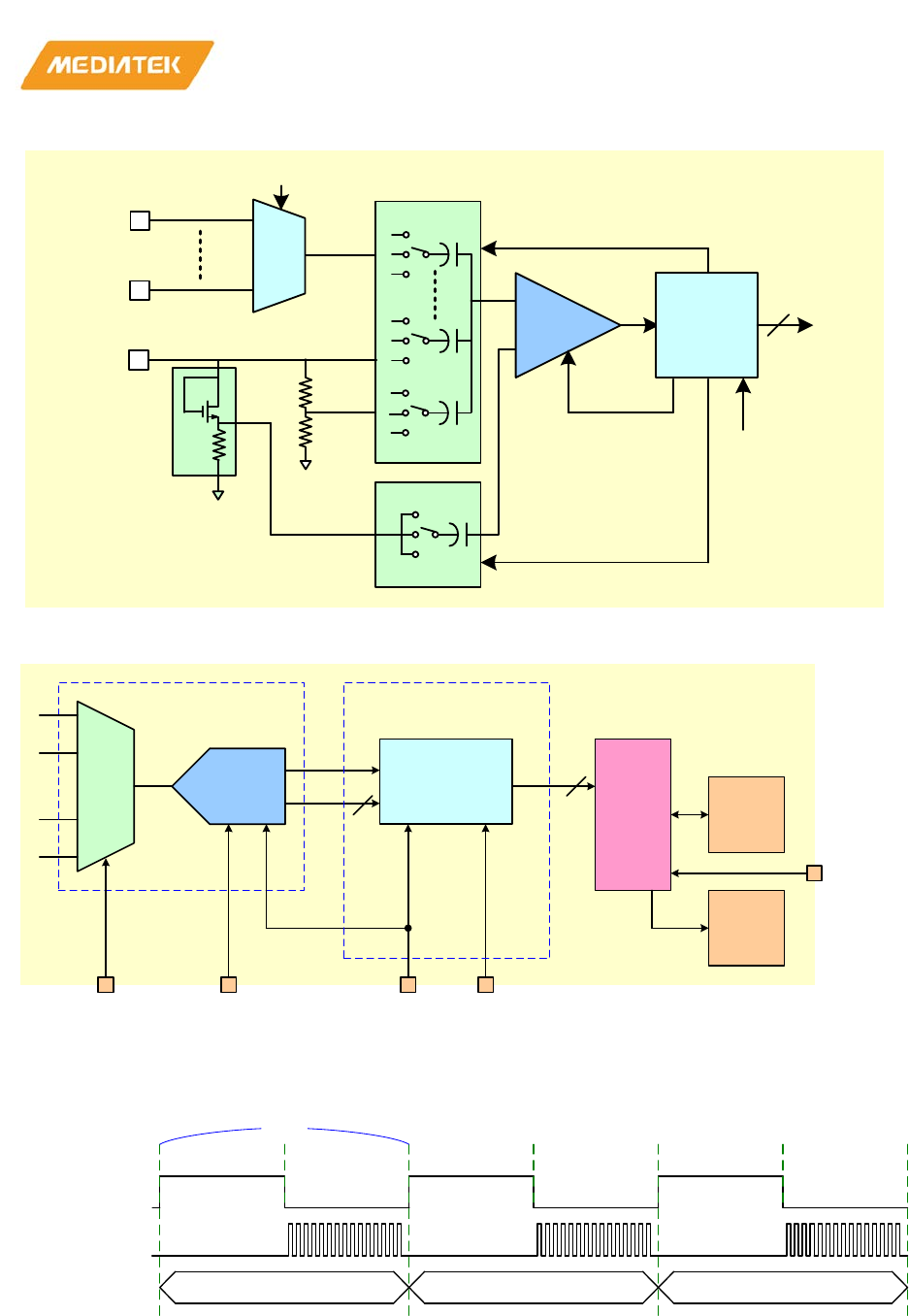
MT76x7
Internet-of-Things Wireless Connectivity
Reference Manual
© 2015 - 2017 MediaTek Inc
Page 571 of 798
This document contains information that is proprietary to MediaTek Inc. (“MediaTek”) and/or its licensor(s).
Any unauthorized use, reproduction or disclosure of this document in whole or in part is strictly prohibited
MUX
Vin
Vref
0
Vin
Vref
0
Vin
Vrdac
0
Vin
Vref
CMP
RDAC
AUXADC0
Vcm buf VCM
Vrdac
CDAC
AUXADC3
Vref=1.8V
SAR
Control
Logic
CLK
(2MHz)
12 Digital
Output
VREF20
AUXADC_MUX[3:0]
Figure 2-44. Auxiliary ADC block diagram (Analog Part)
ADC IP (Analog)
AUXADC_MUX[3:0] ADC_EN
12 1/2/4/8/16/32/64
average
Bus
interface
Memory
hclk_ck
MCU
Interrupt
12
4-to-1
MUX ADC
Digital averaging
CLKOUT(2MS/s)
REG_AVG_MODE[2:0]
CLK(2MS/s)
Figure 2-45. Auxiliary ADC block diagram
2MHz Clock
Internal asyn. Clock
ADC sampling ADC bit-cycling ADC sampling ADC bit-cycling
0.5 uS
ADC sampling ADC bit-cycling
Sample #3 Sample #4 Sample #5
DOUT #1 DOUT #2 DOUT #3AUXADC_DOUT
Figure 2-46. Auxiliary ADC Clock Timing Diagram
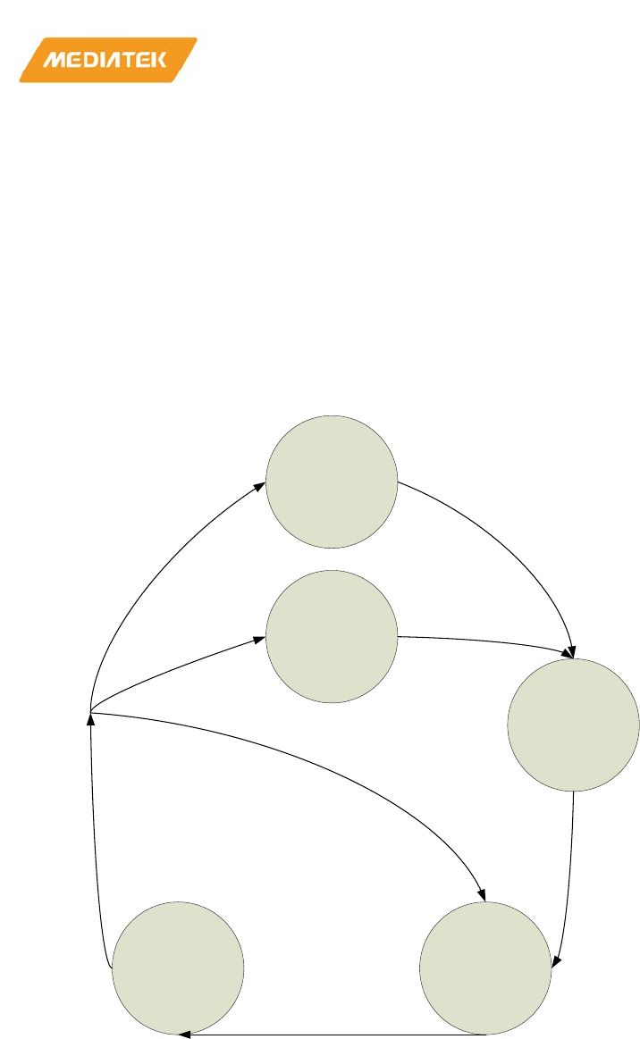
MT76x7
Internet-of-Things Wireless Connectivity
Reference Manual
© 2015 - 2017 MediaTek Inc
Page 572 of 798
This document contains information that is proprietary to MediaTek Inc. (“MediaTek”) and/or its licensor(s).
Any unauthorized use, reproduction or disclosure of this document in whole or in part is strictly prohibited
2.5.4.3. Auxiliary ADC features:
• Input channel number: 4 channels
• Sampling and output data rate: 2MS/s
• DNL without dithering and averaging: <±2LSB
• DNL with dithering and averaging: <±1LSB
• Dithering function: 16 levels with step size of 4LSB.
2.5.4.4. Auxiliary ADC digital averaging FSM
S_IDLE
S_WAIT_INIT
S_WAIT_CH
S_AVG
ADC_FSM_EN=1
C_t=(reg_t_init(100)-1)
C_t=(reg_t_ch(8)-1)
CH !=CH(last)
C_t=(reg_avg_num(32)-1)
S_IDLE_PERIOD
ADC_EN=0
C_period=0
ADC_FSM_EN=1
ADC_EN=1
C_t=C_t+1
C_period=C_period+1
ADC_FSM_EN=1
ADC_EN=1
CH=CH updated
C_t=c_t+1
C_period=C_period+1
ADC_FSM_EN=1
ADC_EN=1
C_t=c_t+1
C_period=C_period+1
PMODE_EN=0
CH =CH(last)
C_t=(reg_avg_num(32)-1)
PMODE_EN=1
CH =CH(last)
C_t=(reg_avg_num(32)-1)
ADC_FSM_EN=1
ADC_EN=0
C_period=C_period+1
C_period=
(reg_period(8000)-1)
a
b
c
d
f
g
e
Figure 2-47. Auxiliary ADC digital averaging FSM
1) FSM operation example
a) State=S_IDLE, set REG_CH_MAP[15:0] =16’b1000_0100_1111_1010 , then set ADC_FSM_EN=1(a)
to enable FSM, then change to next state.
b) State=S_WAIT_INIT, ADC_EN=1 to enable ADC hardware, C_t count from 0 to
C_t=reg_t_init(100)-1 (b) for ADC initial stable time, then change to next statE

MT76x7
Internet-of-Things Wireless Connectivity
Reference Manual
© 2015 - 2017 MediaTek Inc
Page 573 of 798
This document contains information that is proprietary to MediaTek Inc. (“MediaTek”) and/or its licensor(s).
Any unauthorized use, reproduction or disclosure of this document in whole or in part is strictly prohibited
c) State=S_WAIT_CH, CH update as CH1(init)( REG_CH_MAP[15:0]
=16’b1000_0100_1111_1010),C_t count from 0 to C_t=reg_t_ch(8)-1 (c) for CH stable time , then
change to next state
d) State=S_AVG, C_t count from 0 to C_t=reg_avg_num(32)-1 (d) for sample average number, The
averaged sample will also be written to FIFO at this moment, then change to next state.
e) State=S_WAIT_CH, CH update as CH3(16’b1000_0100_1111_1010), then repeat step (c) and (d) .
f) State=S_AVG, if CH=CH15(last channel for REG_CH_MAP[15:0] =16’b1000_0100_1111_1010) and
C_t=32-1 (e) , because PMODE_EN=1, the state wiil be changed to S_IDLE_PERIOD.
g) State=S_IDLE_PERIOD, FSM HW keep ADC_FSM_EN as 1, but change ADC_EN=0 to disable ADC
Hardware for power saving, when C_peroid count to reg_period (8000)-1 (g) , the state will be
changed to S_WAIT_INIT.
h) Repeat step (b) to (g) for 8ms non-stop periodic operation.
If the PMODE_EN=0 and CH equals the last CH number of the CH bit map register, the state will go back to
S_IDLE state and ADC_EN will be set as 1’b0 by FSM. User should set ADC_FSM_EN=0 before enable the next
run (Re-start from (a)).
2) Format of each average sample:
Each 12 bit averaged sample data will be combined with CH number information(4bits) to composite an 16 bits
and write to fifo
(In REG_CH_MAP[15:0] =16’b1000_0100_1111_1010 case, CH sequence is 1,3,4,…15)
FIFO[0]= {sample0[15:0], CH1[3:0]}
FIFO[1]= {sample1[15:0], CH3[3:0]}
FIFO[2]= {sample2[15:0], CH4[3:0]}
…
FIFO[7]= {sample7[15:0], CH15[3:0]}
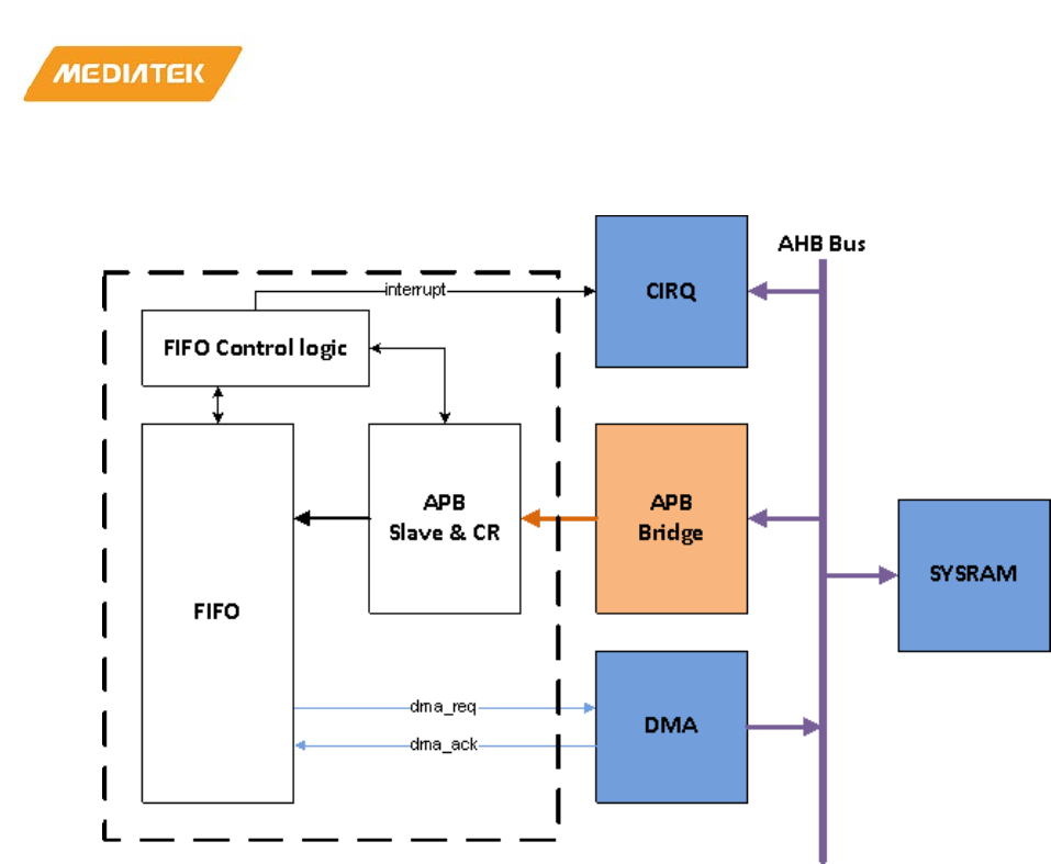
MT76x7
Internet-of-Things Wireless Connectivity
Reference Manual
© 2015 - 2017 MediaTek Inc
Page 574 of 798
This document contains information that is proprietary to MediaTek Inc. (“MediaTek”) and/or its licensor(s).
Any unauthorized use, reproduction or disclosure of this document in whole or in part is strictly prohibited
2.5.4.5. ADC FIFO access
Figure 2-48. Auxiliary ADC FIFO access block diagram
1) Feature of the I/O interface:
• APB interface
• Hardware handshake with DMA
• An interrupt to CIRQ (fifo full/over threshold/timeout)
• Support both CPU direct mode/DMA mode
2) Sequence of DMA mode: (Recommended use)
a) Set DMA VFIFO channel
b) Set ADC FIFO to dma mode
c) ADC put data into FIFO
d) assert dma_req if you want dma move data from fifo to sysram
e) deassert dma_req after dma_ack received
f) dma will read data through apb slave interface.(fixed address).
g) dma will write this data into sysram.
h) Repeat (c) to (g)
i) When sysram over the threshold ,dma will assert an interrupt to CPU.
3) Sequence of CPU direct access mode (SW mode):
• ADC put data into FIFO

MT76x7
Internet-of-Things Wireless Connectivity
Reference Manual
© 2015 - 2017 MediaTek Inc
Page 575 of 798
This document contains information that is proprietary to MediaTek Inc. (“MediaTek”) and/or its licensor(s).
Any unauthorized use, reproduction or disclosure of this document in whole or in part is strictly prohibited
• Need additional maintain a GPT interrupt to CPU. GPT time should be SW control and guarantee
longer than ADC conversion time.
• CPU read RX_PTR and calculate RX data length n
• CPU read data port n times
Note: In this mode, ADC_IER[0] (RXFEN) should be set 0 to disable ADC_FIFO interrupt.
2.5.4.6. Programming sequence
All channels, 32 samples average, 125Hz(8ms) operation frequency for example.
Steps:
1) Start up setting before enable AUXADC.
• Set RG_PMU_03[22]=1 and RG_PMU_03[14]=1
• Set ADC_CTL4[29:28]=2’b10, ADC_CTL4[31]=1, ADC_CTL3[17:16]=2’b11
• ADC_CTL3[31:0]=32’h70F3AA15
• Set RG_PMU_14[1]=1 (RG_ALDO_EN_ADC), then wait 200us for 2.5V output ready.
2) ADC_EN will be set to 1 when user set ADC_FSM_EN to enable ADC control FSM.
3) wait 100 clock cycles for ADC reference generator settled
4) AUXADC_MUX will change to the target channel depends on the REG_CH_MAP setting.
5) Wait 8 clock cycles for channel switches settled & ADC latency (2 clock cycles)
6) 32 clock cycles for averaging
7) Repeat step 3~5 for all channels
8) ADC_EN will be set to 0 when ADC control FSM goes to IDLE state.
9) User can disable ALDO after disable AUXADC for power saving.
• Set RG_PMU_14[1]=0 (RG_ALDO_EN_ADC)
• Note: If the ALDO on/off period smaller than 200ms, we suggest let ALDO keep on to reduce power
consumption.
• I_avg=ΔQ/ΔT=(2.1uF*2.5V)/200ms=26.25uA ~=quiescent current 26µA
2.5.4.7. Auxiliary ADC clock source
By below diagram, the adc_clk_clk_mux can select three difference clock sources for AUXADC Contrl/Macro.
• From AUXADC clock divider
• From 8-1 multiplexer output of PMU buck input clock delay chain
• From PMU buck output clock
The default setting/path is marked as red color to get a better AUXADC SNR performance.
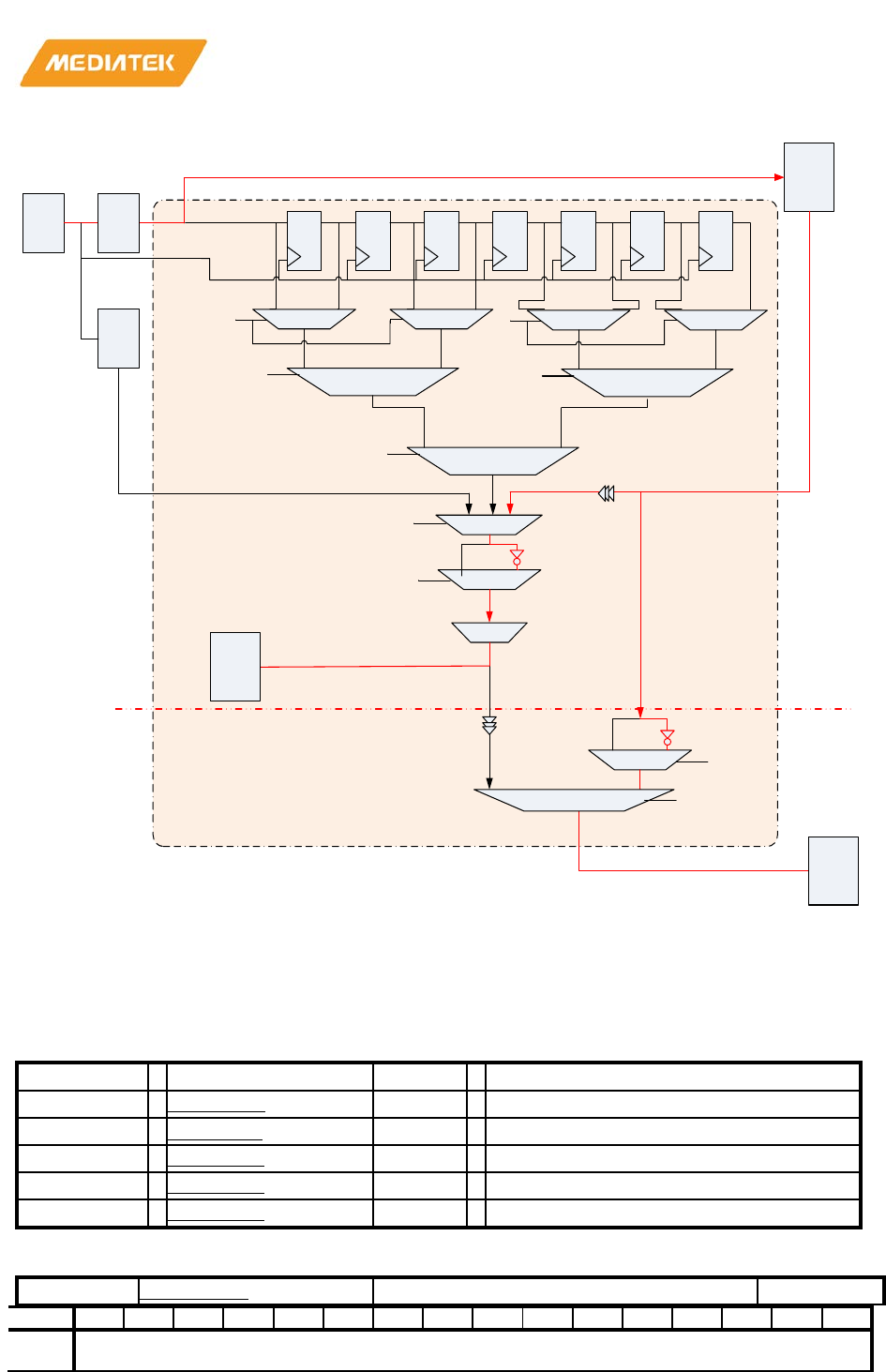
MT76x7
Internet-of-Things Wireless Connectivity
Reference Manual
© 2015 - 2017 MediaTek Inc
Page 576 of 798
This document contains information that is proprietary to MediaTek Inc. (“MediaTek”) and/or its licensor(s).
Any unauthorized use, reproduction or disclosure of this document in whole or in part is strictly prohibited
S0
S1
40/26/
52MHz
Xtal 2MHz
0 1 0 1
0 1
PMU
DIV
0 1adc_ma cro_buck_inv_en
S0
S1
0 1 0 1
0 1
S2 0 1
ADC
ADC
DIV
adc_macro_clk_sel
0 1 2
0 1
adc_clk_ctl_mux[1:0]
ADC
ctrl
0 1
adc_clk_ctl_inv_en
osc_hclk_2m_ck_aon
Osc_hclk_2m_ck_ori
Osc_hclk_2m_ck_adc
scan
Osc_hclk_2m_ck_tmp
Osc_hclk_2m_ck_dly
osc_hclk_2m_ck
adc_buck_clk_dly_sel[2:0]
Figure 2-49. Auxiliary ADC clock source diagram
2.5.4.8. Register definitions
1) Configure Control
Module name: top_cfg_aon_cm4 Base address: (+83008000h)
Address
Name
Width
Register Function
83008180
ADC_CTL0
32
AUXADC control
register 0
83008184
ADC_CTL1
32
AUXADC control register 1
83008188
ADC_CTL2
32
AUXADC control register 2
8300818C
ADC_CTL3
32
AUXADC control register 3
83008190
ADC_CTL4
32
AUXADC control register 4
83008180
ADC_CTL0
AUXADC control register 0
03FFC98A
Bit
31
30
29
28
27
26
25
24
23
22
21
20
19
18
17
16
Nam
e
REG_CH_MAP

MT76x7
Internet-of-Things Wireless Connectivity
Reference Manual
© 2015 - 2017 MediaTek Inc
Page 577 of 798
This document contains information that is proprietary to MediaTek Inc. (“MediaTek”) and/or its licensor(s).
Any unauthorized use, reproduction or disclosure of this document in whole or in part is strictly prohibited
Type
RW
Rese
t
0 0 0 0 0 0 1 1 1 1 1 1 1 1 1 1
Bit
15
14
13
12
11
10
9
8
7
6
5
4
3
2
1
0
Nam
e REG_T_INIT
PM
OD
E_
EN
REG_T_CH REG_AVG_MO
DE
AD
C_
FS
M_
EN
Type
RW
RW
RW
RW
RW
Rese
t
1 1 0 0 1 0 0 1 1 0 0 0 1 0 1 0
Bit(s)
Name
Description
31:16
REG_CH_MAP
ADC Channel bit map register, you can enable random CH
by setting each corresponding bit
EX: REG_CH_MAP[15:0] =16'b1000_0100_1111_1010 => Channel
# 1,3,4,5,6,7,10 and 15 is enable.
Note: User should set the adc_fifo register "RX_TRI_LVL"
according to the channel number. For a
bove example is 8 channels
enable, so the "RX_TRI_LVL" should set to 4'd8.
15:9
REG_T_INIT
ADC initial stable time value
8
PMODE_EN
Periodic mode enable
1'b0: FSM will run one time then back to IDLE state
1'b1: FSM will run periodically (non
-stop)
7:4
REG_T_CH
ADC Channel stable time value
3:1
REG_AVG_MODE
Select ADC sample average number
3'd0: avg 1 sample (REG_AVG_NUMBER=1)
3'd1: avg 2 samples (REG_AVG_NUMBER=2)
3'd2: avg 4 samples (REG_AVG_NUMBER=4)
3'd3: avg 8 samples (REG_AVG_NUMBER=8)
3'd4: avg 1
6 samples (REG_AVG_NUMBER=16)
3'd5: avg 32 samples (REG_AVG_NUMBER=32)
3'd6: avg 64 samples (REG_AVG_NUMBER=64)
3'd7: avg 64 samples (REG_AVG_NUMBER=64)
0
ADC_FSM_EN
ADC FSM enable
1'b0:Force ADC FSM in IDLE state
1'b1:ADC FSM start to run
83008184
ADC_CTL1
AUXADC control register 1
00001F40
MT76x7
Internet-of-Things Wireless Connectivity
Reference Manual
© 2015 - 2017 MediaTek Inc
Page 578 of 798
This document contains information that is proprietary to MediaTek Inc. (“MediaTek”) and/or its licensor(s).
Any unauthorized use, reproduction or disclosure of this document in whole or in part is strictly prohibited
Bit
31
30
29
28
27
26
25
24
23
22
21
20
19
18
17
16
Nam
e
REG_PERIOD
Type
RW
Rese
t
0 0 0 0 0 0 0 0 0 0 0 0 0 0 0 0
Bit
15
14
13
12
11
10
9
8
7
6
5
4
3
2
1
0
Nam
e
REG_PERIOD
Type
RW
Rese
t
0 0 0 1 1 1 1 1 0 1 0 0 0 0 0 0
Bit(s)
Name
Description
31:0
REG_PERIOD
The clock cycle count period in periodic mode
83008188
ADC_CTL2
AUXADC control register 2
0000FFF0
Bit
31
30
29
28
27
26
25
24
23
22
21
20
19
18
17
16
Nam
e RESERVED
RE
G_
AD
C_
TI
ME
ST
AM
P_
EN
RE
G_
AD
C_
DA
TA
_S
YN
C_
MO
DE
RO_ADC_COMP_FLA
G
Type
RO
RW
RW
RO
Rese
t
0 0 0 0 0 0 0 0 0 0 0 0 0 0 0 0
Bit
15
14
13
12
11
10
9
8
7
6
5
4
3
2
1
0
Nam
e
REG_COMP_THRESHOLD REG_COMP_IRQ_EN
Type
RW
RW
Rese
t
1 1 1 1 1 1 1 1 1 1 1 1 0 0 0 0
Bit(s)
Name
Description
31:22
RESERVED
Reserved
21
REG_ADC_TIMESTAMP_EN
Free-run counter enable for timestamp.
20
REG_ADC_DATA_SYNC_MODE
AUXADC_DOUT is sampled by ADC_CLK_OUT.
1'b0: positive edge sample.
1'b1: negative edge
sample.
19:16
RO_ADC_COMP_FLAG
Indicate which channel trigger the adc_comp_irq_b.
Bit0~3 means CH0~3.
15:4
REG_COMP_THRESHOLD
Comparator mode threshold value. When ADC result is
larger than this value, the interrupt (adc_comp_irq_b)
MT76x7
Internet-of-Things Wireless Connectivity
Reference Manual
© 2015 - 2017 MediaTek Inc
Page 579 of 798
This document contains information that is proprietary to MediaTek Inc. (“MediaTek”) and/or its licensor(s).
Any unauthorized use, reproduction or disclosure of this document in whole or in part is strictly prohibited
Bit(s)
Name
Description
will be assert.
3:0
REG_COMP_IRQ_EN
Comparator mode IRQ enable.
Bit0~3 means CH0~3.
8300818C
ADC_CTL3
AUXADC control register 3
F0F0AA55
Bit
31
30
29
28
27
26
25
24
23
22
21
20
19
18
17
16
Nam
e
REG_AUXADC
Type
RW
Rese
t
1 1 1 1 0 0 0 0 1 1 1 1 0 0 0 0
Bit
15
14
13
12
11
10
9
8
7
6
5
4
3
2
1
0
Nam
e
REG_AUXADC
Type
RW
Rese
t
1 0 1 0 1 0 1 0 0 1 0 1 0 1 0 1
Bit(s)
Name
Description
31:0
REG_AUXADC
AUXADC analog macro settings.
RG_AUXADC[31]:
AUXADC VCM generator setting
1'd 0:
When VREF=2.5V(default for MT76x7)
1'd 1:
When VREF=1.8V
RG_AUXADC[30:18]: reserved register
RG_AUXADC[17]: Register to select the clock source of ADC
macro.
1'd0: The same as ADC controller
1'd1: PMU buck output clock
RG_AUXADC[16]: Register to invert PMU buck
output clock for
ADC macro clock source.
1'd0: Keep original clock
1'd1: Invert original clock
RG_AUXADC[15]: AUXADC clock generator enable to generate
difference clock phase for ADC , ex clk1, clk1b, clk2, clk2b
1'd 0:disable
1'd 1:enable(default)
RG_A
UXADC[14]: reserved register
RG_AUXADC[13]: enable VCM(common
-mode voltage) generator

MT76x7
Internet-of-Things Wireless Connectivity
Reference Manual
© 2015 - 2017 MediaTek Inc
Page 580 of 798
This document contains information that is proprietary to MediaTek Inc. (“MediaTek”) and/or its licensor(s).
Any unauthorized use, reproduction or disclosure of this document in whole or in part is strictly prohibited
Bit(s)
Name
Description
1'd 0:
1'd 1:enable(default)
RG_AUXADC[12]: reserved register
RG_AUXADC[11]: AUXADC input MUX enable
1'd 0:disable
1'd 1:enable(default)
RG_AUXADC[10]: reserved register
RG_AUXADC[9:8]: Dithering function step size
2'd 0: 2 steps
2'd 1: 4 steps
2'd 2: 8 steps (default)
2'd 3: 16 steps
RG_AUXADC[7]: reserved register
RG_AUXADC[6]: Dithering function enable.
1'd 0:disable
1'd 1:enable
RG_AUXADC[5]: reserved register
RG_AUXADC[4]: comparator pre
-amplifier enable.
1'd 0:disable
1'd 1:enable
RG_AUXADC[3:2]: comparator pre
-amplifier current
2'd 0: 40uA(typical corner)
2'd 1: 80uA (typical corner)
2'd 2: 160uA(typical corner)
2'd 3: 160uA (typical corner)
RG_AUXADC[1:0]: c
omparator timing loop delay time
2'd 0: 3ns(typical corner)
2'd 1: 6ns(typical corner)
2'd 2: 9ns(typical corner)
2'd 3: 12ns(typical corner)
MT76x7
Internet-of-Things Wireless Connectivity
Reference Manual
© 2015 - 2017 MediaTek Inc
Page 581 of 798
This document contains information that is proprietary to MediaTek Inc. (“MediaTek”) and/or its licensor(s).
Any unauthorized use, reproduction or disclosure of this document in whole or in part is strictly prohibited
83008190
ADC_CTL4
AUXADC control register 4
00000000
Bit
31
30
29
28
27
26
25
24
23
22
21
20
19
18
17
16
Nam
e
adc
_cl
k_c
tl_i
nv_
en
RE
SE
RV
ED
adc_clk_c
tl_mux
RE
SE
RV
ED
adc_buck_clk_d
ly_sel RESERVED
Type
RW
RO
RW
RO
RW
RO
Rese
t
0 0 0 0 0 0 0 0 0 0 0 0 0 0 0 0
Bit
15
14
13
12
11
10
9
8
7
6
5
4
3
2
1
0
Nam
e RESERVED
cr_
adc
_en
_s
w
cr_
adc
_en
_s
w_
sel
Type
RO
RW
RW
Rese
t
0 0 0 0 0 0 0 0 0 0 0 0 0 0 0 0
Bit(s)
Name
Description
31
adc_clk_ctl_inv_en
Register to invert 3-1 multiplexer output clock for ADC
controller clock source
1'b0: Keep original clock
1'b1: Invert original clock
30
RESERVED
Reserved
29:28
adc_clk_ctl_mux
Register to select 3-1 multiplexer output as the clock
source of ADC controller
2'b00: Clock source is from ADC clock divider
2'b01:Clock source is from 8 to 1 multiplexer output of PMU buck
input clock delay
chain
2'b10: Clock source is from PMU buck output clock
27
RESERVED
Reserved
26:24
adc_buck_clk_dly_sel
Register to select 8-1 multiplexer output of PMU buck
input clock delay chain as ADC controller clock source
3'b000: No delay of PMU buck input clock
3'b001: 1 Xtal clock delay of PMU buck input clock
....
3'b111: 7 Xtal clock delay of PMU buck input clock
23:2
RESERVED
Reserved
1
cr_adc_en_sw
adc_en software control
0
cr_adc_en_sw_sel
adc_en software mode select or not
MT76x7
Internet-of-Things Wireless Connectivity
Reference Manual
© 2015 - 2017 MediaTek Inc
Page 582 of 798
This document contains information that is proprietary to MediaTek Inc. (“MediaTek”) and/or its licensor(s).
Any unauthorized use, reproduction or disclosure of this document in whole or in part is strictly prohibited
Bit(s)
Name
Description
1'b0: adc_en control by hardware fsm
1'b1: adc_en control by "cr_adc_en_sw"
1. FIFO Control
Module name: adc_fifo Base address: (+830d0000h)
Address
Name
Width
Register Function
830D0000
ADC_RBR
32
RX Buffer Register
830D0004
ADC_IER
32
Interrupt Enable Register
830D0008
ADC_IIR
32
Interrupt Identification Register
830D0008
ADC_FIFOCTRL
32
FIFO Control Register
830D000C
ADC_FAKELCR
32
Fake Control Register
830D0014
ADC_LSR
32
Line Status Register
830D0048
ADC_SLEEP_EN
32
Sleep Enable Register
830D004C
ADC_DMA_EN
32
DMA Enable Register
830D0054
ADC_RTOCNT
32
RX Timeout Count
830D0060
ADC_TRI_LVL
32
TRX FIFO Trigger Level Register
830D0064
ADC_WAK
32
Wakeup Register
830D0068
ADC_WAT_TIME
32
Asynchorous Timer Regiser
830D006C
ADC_HANDSHAKE
32
New Handshake Control Register
830D0070
ADC_DEBUG_RX_FIF
O_0
32
RX FIFO Address 0 Debug Regiser
830D0074
ADC_DEBUG_RX_FIF
O_1
32
RX FIFO Address 1 Debug Regiser
830D0078
ADC_DEBUG_RX_FIF
O_2
32
RX FIFO
Address 2 Debug Regiser
830D007C
ADC_DEBUG_RX_FIF
O_3
32
RX FIFO Address 3 Debug Regiser
830D0080
ADC_DEBUG_RX_FIF
O_4
32
RX FIFO Address 4 Debug Regiser
830D0084
ADC_DEBUG_RX_FIF
O_5
32
RX FIFO Address 5 Debug Regiser
830D0058
ADC_DEBUG_RX_FIF
O_6
32
RX FIFO Address 6 Debug Regiser
830D008C
ADC_DEBUG_RX_FIF
O_7
32
RX FIFO
Address 7 Debug Regiser
830D0090
ADC_DEBUG_RX_FIF
O_8
32
RX FIFO Address 8 Debug Regiser
830D0094
ADC_DEBUG_RX_FIF
O_9
32
RX FIFO Address 9 Debug Regiser
830D0098
ADC_DEBUG_RX_FIF
O_a
32
RX FIFO Address 10 Debug Regiser
830D009C
ADC_DEBUG_RX_FIF
O_b
32
RX FIFO Address 11 Debug Regiser
830D00A0
ADC_DEBUG_RX_FIF
O_c
32
RX FIFO
Address 12 Debug Regiser
830D00A4
ADC_DEBUG_RX_FIF
32
RX FIFO Address 13 Debug Regiser
MT76x7
Internet-of-Things Wireless Connectivity
Reference Manual
© 2015 - 2017 MediaTek Inc
Page 583 of 798
This document contains information that is proprietary to MediaTek Inc. (“MediaTek”) and/or its licensor(s).
Any unauthorized use, reproduction or disclosure of this document in whole or in part is strictly prohibited
Address
Name
Width
Register Function
O_d
830D00A8
ADC_DEBUG_RX_FIF
O_e
32
RX FIFO Address 14 Debug Regiser
830D00AC
ADC_DEBUG_RX_FIF
O_f
32
RX FIFO Address 15 Debug Regiser
830D00D4
ADC_DEBUG_RX_PT
R
32
RX FIFO Pointer Debug Register
830D0000
ADC_RBR
RX Buffer Register
00000000
Bit
31
30
29
28
27
26
25
24
23
22
21
20
19
18
17
16
Nam
e
ADC_RBR
Type
RO
Rese
t
0 0 0 0 0 0 0 0 0 0 0 0 0 0 0 0
Bit
15
14
13
12
11
10
9
8
7
6
5
4
3
2
1
0
Nam
e
ADC_RBR
Type
RO
Rese
t
0 0 0 0 0 0 0 0 0 0 0 0 0 0 0 0
Bit(s)
Mnemonic
Name
Description
31:0
ADC_RBR
ADC_RBR
The received data can be read by accessing this
register.
This register is valid only when ADC_FAKELCR[7]
(0x0C) is equal to 0.
830D0004
ADC_IER
Interrupt Enable Register
00000000
Bit
31
30
29
28
27
26
25
24
23
22
21
20
19
18
17
16
Nam
e
Type
Rese
t
Bit
15
14
13
12
11
10
9
8
7
6
5
4
3
2
1
0
Nam
e
RX
FE
N
Type
RU
Rese
t
0
Bit(s)
Mnemonic
Name
Description
0
RXFEN
RXFEN
Enables RX full and time-out interrupt
This register is valid only when ADC_FAKELCR[7] is
equal to 0.
MT76x7
Internet-of-Things Wireless Connectivity
Reference Manual
© 2015 - 2017 MediaTek Inc
Page 584 of 798
This document contains information that is proprietary to MediaTek Inc. (“MediaTek”) and/or its licensor(s).
Any unauthorized use, reproduction or disclosure of this document in whole or in part is strictly prohibited
Bit(s)
Mnemonic
Name
Description
0 :No interrupt will be generated if the RX buffer
contains data or timed out.
1: An interrupt will be generated if the RX Buffer
contains
data or timed out.
830D0008
ADC_IIR
Interrupt Identification Register
00000001
Bit
31
30
29
28
27
26
25
24
23
22
21
20
19
18
17
16
Nam
e
Type
Rese
t
Bit
15
14
13
12
11
10
9
8
7
6
5
4
3
2
1
0
Nam
e
ADC_IIR
Type
RU
Rese
t
0 0 0 1
Bit(s)
Mnemonic
Name
Description
3:0
ADC_IIR
ADC_IIR
Interrupt identification
This register is valid only when ADC_FAKELCR
(0x0C) is not equal to 0xBF.
4'h1: No interrupt pending
4'h4: RX data Received
4'hc: RX data Timeout
4'h2 :Not used
830D0008
ADC_FIFOCTRL
FIFO Control Register
00000000
Bit
31
30
29
28
27
26
25
24
23
22
21
20
19
18
17
16
Nam
e
Type
Rese
t
Bit
15
14
13
12
11
10
9
8
7
6
5
4
3
2
1
0
Nam
e
CL
RR
Type
WO
Rese
t
0
MT76x7
Internet-of-Things Wireless Connectivity
Reference Manual
© 2015 - 2017 MediaTek Inc
Page 585 of 798
This document contains information that is proprietary to MediaTek Inc. (“MediaTek”) and/or its licensor(s).
Any unauthorized use, reproduction or disclosure of this document in whole or in part is strictly prohibited
Bit(s)
Mnemonic
Name
Description
1
CLRR
CLRR
Clears receive FIFO
This register is
valid only when ADC_FAKELCR
(0x0C) is not equal to 0xBF.
0: Leave RX FIFO intact
1: Clear all bytes in RX FIFO
830D000C
ADC_FAKELCR
Fake Control Register
00000000
Bit
31
30
29
28
27
26
25
24
23
22
21
20
19
18
17
16
Nam
e
Type
Rese
t
Bit
15
14
13
12
11
10
9
8
7
6
5
4
3
2
1
0
Nam
e
ADC_FAKELCR
Type
RU
Rese
t
0 0 0 0 0 0 0 0
Bit(s)
Mnemonic
Name
Description
7:0
ADC_FAKELCR
ADC_FAKELCR
Synchronizes SW control method of UART
When FAKELCR[7] is equal to 1, RBR(0x00),
and IER(0x04) will not be readable/writable.
When FAKELCR is equal to 0xBF, RBR(0x00),
IER(0x04), IIR(0x08) and LSR(0x14) will not
be readable/writable.
830D0014
ADC_LSR
Line Status Register
00000000
Bit
31
30
29
28
27
26
25
24
23
22
21
20
19
18
17
16
Nam
e
Type
Rese
t
Bit
15
14
13
12
11
10
9
8
7
6
5
4
3
2
1
0
Nam
e
DR
Type
RU
Rese
t
0
Bit(s)
Mnemonic
Name
Description
MT76x7
Internet-of-Things Wireless Connectivity
Reference Manual
© 2015 - 2017 MediaTek Inc
Page 586 of 798
This document contains information that is proprietary to MediaTek Inc. (“MediaTek”) and/or its licensor(s).
Any unauthorized use, reproduction or disclosure of this document in whole or in part is strictly prohibited
Bit(s)
Mnemonic
Name
Description
0
DR
DR
Data ready
Readable when LCR != 0xBF.
0: Cleared by reading RX buffer
1: Set by RX buffer becoming full
830D0048
ADC_SLEEP_EN
Sleep Enable Register
00000000
Bit
31
30
29
28
27
26
25
24
23
22
21
20
19
18
17
16
Nam
e
Type
Rese
t
Bit
15
14
13
12
11
10
9
8
7
6
5
4
3
2
1
0
Nam
e
AD
C_
SL
EE
P_
EN
Type
RW
Rese
t
0
Bit(s)
Mnemonic
Name
Description
0
ADC_SLEEP_EN
ADC_SLEEP_EN
For sleep mode issue
0: Does not deal with sleep mode indication signal
1: Activate flow control according to software initial
setting when chip enters sleep mode. Release hardware
flow when chip wakes up.
830D004C
ADC_DMA_EN
DMA Enable Register
00000000
Bit
31
30
29
28
27
26
25
24
23
22
21
20
19
18
17
16
Nam
e
Type
Rese
t
Bit
15
14
13
12
11
10
9
8
7
6
5
4
3
2
1
0
Nam
e
TO
_C
NT
_A
UT
OR
ST
RX
_D
MA
_E
N
MT76x7
Internet-of-Things Wireless Connectivity
Reference Manual
© 2015 - 2017 MediaTek Inc
Page 587 of 798
This document contains information that is proprietary to MediaTek Inc. (“MediaTek”) and/or its licensor(s).
Any unauthorized use, reproduction or disclosure of this document in whole or in part is strictly prohibited
Type
RW
RW
Rese
t
0 0
Bit(s)
Mnemonic
Name
Description
2
TO_CNT_AUTORST
TO_CNT_AUTORST
Time-out counter auto reset register
0: After RX time-out happens, SW shall reset the
interrupt by reading ADC 0x4C.
1: The timeout counter will be auto reset.
0
RX_DMA_EN
RX_DMA_EN
RX_DMA mechanism enabling signal
0 :Does not use DMA in RX
1: Use DMA in RX. When this register is enabled, the
flow control is based on the DMA threshold and
generates a time
-out interrupt.
830D0054
ADC_RTOCNT
RX Timeout Count
00000040
Bit
31
30
29
28
27
26
25
24
23
22
21
20
19
18
17
16
Nam
e
Type
Rese
t
Bit
15
14
13
12
11
10
9
8
7
6
5
4
3
2
1
0
Nam
e
ADC_RTOCNT
Type
RW
Rese
t
0 1 0 0 0 0 0 0
Bit(s)
Mnemonic
Name
Description
7:0
ADC_RTOCNT
ADC_RTOCNT
Used for RX time-out interrupt
The RX time
-out interrupt will be generated when:
1. RXRTOEN (0x04[0]) is set to 1.
2. RX buffer is empty.
3. The most recent character is received longer than
(RTOCNT*bclk period*4).
830D0060
ADC_TRI_LVL
TRX FIFO Trigger Level Register
00000028
Bit
31
30
29
28
27
26
25
24
23
22
21
20
19
18
17
16
Nam
e
MT76x7
Internet-of-Things Wireless Connectivity
Reference Manual
© 2015 - 2017 MediaTek Inc
Page 588 of 798
This document contains information that is proprietary to MediaTek Inc. (“MediaTek”) and/or its licensor(s).
Any unauthorized use, reproduction or disclosure of this document in whole or in part is strictly prohibited
Type
Rese
t
Bit
15
14
13
12
11
10
9
8
7
6
5
4
3
2
1
0
Nam
e
AD
C_
LO
OP
RX_TRI_LVL
Type
RW
RW
Rese
t
0 0 1 0 1
Bit(s)
Mnemonic
Name
Description
7
ADC_LOOP
ADC_LOOP
Used to enable ADC loop back mode
The data output from TX will be received by RX.
6:3
RX_TRI_LVL
RX_TRI_LVL
Used for RX FIFO trigger threshold
A RX trigger interrupt (IIR(0x08]) = 4) will be set
if
the data in RXFIFO is more than RX_TRI_LVL. The
output flow control signal will also be set if the data in
RXFIFO is more than RX_TRI_LVL.
830D0064
ADC_WAK
Wakeup Register
00000001
Bit
31
30
29
28
27
26
25
24
23
22
21
20
19
18
17
16
Nam
e
Type
Rese
t
Bit
15
14
13
12
11
10
9
8
7
6
5
4
3
2
1
0
Nam
e
AD
C_
WA
K
Type
RW
Rese
t
1
Bit(s)
Mnemonic
Name
Description
0
ADC_WAK
ADC_WAK
Wakeup ADC module
830D0068
ADC_WAT_TIME
Asynchorous Timer Regiser
00000012
Bit
31
30
29
28
27
26
25
24
23
22
21
20
19
18
17
16
Nam
e
Type
Rese
t
MT76x7
Internet-of-Things Wireless Connectivity
Reference Manual
© 2015 - 2017 MediaTek Inc
Page 589 of 798
This document contains information that is proprietary to MediaTek Inc. (“MediaTek”) and/or its licensor(s).
Any unauthorized use, reproduction or disclosure of this document in whole or in part is strictly prohibited
Bit
15
14
13
12
11
10
9
8
7
6
5
4
3
2
1
0
Nam
e
WAT_TIME_2 WAT_TIME_1
Type
RW
RW
Rese
t
0 1 0 0 1 0
Bit(s)
Mnemonic
Name
Description
5:3
WAT_TIME_2
WAT_TIME_2
The second level of wait time
WAT_TIME_2 cannot be less than 0x2.
2:0
WAT_TIME_1
WAT_TIME_1
The first level of wait time
WAT_TIME_1 cannot be less than 0x2.
830D006C
ADC_HANDSHAKE
New Handshake Control Register
00000003
Bit
31
30
29
28
27
26
25
24
23
22
21
20
19
18
17
16
Nam
e
Type
Rese
t
Bit
15
14
13
12
11
10
9
8
7
6
5
4
3
2
1
0
Nam
e
RT
O_
EX
T
HI
GH
_S
PE
ED
_E
N
HA
ND
SH
AK
E_
EN
Type
RW
RW
RW
Rese
t
0 1 1
Bit(s)
Mnemonic
Name
Description
2
RTO_EXT
RTO_EXT
Extends the value of RX time-out counter
(16*rto_time)
1
HIGH_SPEED_EN
HIGH_SPEED_EN
Enables high speed mode
0
HANDSHAKE_EN
HANDSHAKE_EN
Enables handshake mode
830D0070
ADC_DEBUG_RX_FIF
O_0
RX FIFO Address 0 Debug Regiser
00000000
Bit
31
30
29
28
27
26
25
24
23
22
21
20
19
18
17
16
Nam
e
ADC_DEBUG_RX_FIFO_0
Type
RO
Rese
t
0 0 0 0 0 0 0 0 0 0 0 0 0 0 0 0
MT76x7
Internet-of-Things Wireless Connectivity
Reference Manual
© 2015 - 2017 MediaTek Inc
Page 590 of 798
This document contains information that is proprietary to MediaTek Inc. (“MediaTek”) and/or its licensor(s).
Any unauthorized use, reproduction or disclosure of this document in whole or in part is strictly prohibited
Bit
15
14
13
12
11
10
9
8
7
6
5
4
3
2
1
0
Nam
e
ADC_DEBUG_RX_FIFO_0
Type
RO
Rese
t
0 0 0 0 0 0 0 0 0 0 0 0 0 0 0 0
Bit(s)
Mnemonic
Name
Description
31:0
ADC_DEBUG_RX_FI
FO_0
ADC_DEBUG_RX_FIF
O_0
Debugging RX FIFO address 0
830D0074
ADC_DEBUG_RX_FIF
O_1
RX FIFO Address 1 Debug Regiser
00000000
Bit
31
30
29
28
27
26
25
24
23
22
21
20
19
18
17
16
Nam
e
ADC_DEBUG_RX_FIFO_1
Type
RO
Rese
t
0 0 0 0 0 0 0 0 0 0 0 0 0 0 0 0
Bit
15
14
13
12
11
10
9
8
7
6
5
4
3
2
1
0
Nam
e
ADC_DEBUG_RX_FIFO_1
Type
RO
Rese
t
0 0 0 0 0 0 0 0 0 0 0 0 0 0 0 0
Bit(s)
Mnemonic
Name
Description
31:0
ADC_DEBUG_RX_FI
FO_1
ADC_DEBUG_RX_FIF
O_1
Debugging RX FIFO address 1
830D0078
ADC_DEBUG_RX_FIF
O_2
RX FIFO Address 2 Debug Regiser
00000000
Bit
31
30
29
28
27
26
25
24
23
22
21
20
19
18
17
16
Nam
e
ADC_DEBUG_RX_FIFO_2
Type
RO
Rese
t
0 0 0 0 0 0 0 0 0 0 0 0 0 0 0 0
Bit
15
14
13
12
11
10
9
8
7
6
5
4
3
2
1
0
Nam
e
ADC_DEBUG_RX_FIFO_2
Type
RO
Rese
t
0 0 0 0 0 0 0 0 0 0 0 0 0 0 0 0
Bit(s)
Mnemonic
Name
Description
31:0
ADC_DEBUG_RX_FI
ADC_DEBUG_RX_FIF
Debugging RX FIFO address 2
MT76x7
Internet-of-Things Wireless Connectivity
Reference Manual
© 2015 - 2017 MediaTek Inc
Page 591 of 798
This document contains information that is proprietary to MediaTek Inc. (“MediaTek”) and/or its licensor(s).
Any unauthorized use, reproduction or disclosure of this document in whole or in part is strictly prohibited
Bit(s)
Mnemonic
Name
Description
FO_2
O_2
830D007C
ADC_DEBUG_RX_FIF
O_3
RX FIFO Address 3 Debug Regiser
00000000
Bit
31
30
29
28
27
26
25
24
23
22
21
20
19
18
17
16
Nam
e
ADC_DEBUG_RX_FIFO_3
Type
RO
Rese
t
0 0 0 0 0 0 0 0 0 0 0 0 0 0 0 0
Bit
15
14
13
12
11
10
9
8
7
6
5
4
3
2
1
0
Nam
e
ADC_DEBUG_RX_FIFO_3
Type
RO
Rese
t
0 0 0 0 0 0 0 0 0 0 0 0 0 0 0 0
Bit(s)
Mnemonic
Name
Description
31:0
ADC_DEBUG_RX_FI
FO_3
ADC_DEBUG_RX_FIF
O_3
Debugging RX FIFO address 3
830D0080
ADC_DEBUG_RX_FIF
O_4
RX FIFO Address 4 Debug Regiser
00000000
Bit
31
30
29
28
27
26
25
24
23
22
21
20
19
18
17
16
Nam
e
ADC_DEBUG_RX_FIFO_4
Type
RO
Rese
t
0 0 0 0 0 0 0 0 0 0 0 0 0 0 0 0
Bit
15
14
13
12
11
10
9
8
7
6
5
4
3
2
1
0
Nam
e
ADC_DEBUG_RX_FIFO_4
Type
RO
Rese
t
0 0 0 0 0 0 0 0 0 0 0 0 0 0 0 0
Bit(s)
Mnemonic
Name
Description
31:0
ADC_DEBUG_RX_FI
FO_4
ADC_DEBUG_RX_FIF
O_4
Debugging RX FIFO address 4
830D0084
ADC_DEBUG_RX_FIF
O_5
RX FIFO Address 5 Debug Regiser
00000000
Bit
31
30
29
28
27
26
25
24
23
22
21
20
19
18
17
16
Nam
ADC_DEBUG_RX_FIFO_5

MT76x7
Internet-of-Things Wireless Connectivity
Reference Manual
© 2015 - 2017 MediaTek Inc
Page 592 of 798
This document contains information that is proprietary to MediaTek Inc. (“MediaTek”) and/or its licensor(s).
Any unauthorized use, reproduction or disclosure of this document in whole or in part is strictly prohibited
e
Type
RO
Rese
t
0 0 0 0 0 0 0 0 0 0 0 0 0 0 0 0
Bit
15
14
13
12
11
10
9
8
7
6
5
4
3
2
1
0
Nam
e
ADC_DEBUG_RX_FIFO_5
Type
RO
Rese
t
0 0 0 0 0 0 0 0 0 0 0 0 0 0 0 0
Bit(s)
Mnemonic
Name
Description
31:0
ADC_DEBUG_RX_FI
FO_5
ADC_DEBUG_RX_FIF
O_5
Debugging RX FIFO address 5
830D0058
ADC_DEBUG_RX_FIF
O_6
RX FIFO Address 6 Debug Regiser
00000000
Bit
31
30
29
28
27
26
25
24
23
22
21
20
19
18
17
16
Nam
e
ADC_DEBUG_RX_FIFO_6
Type
RO
Rese
t
0 0 0 0 0 0 0 0 0 0 0 0 0 0 0 0
Bit
15
14
13
12
11
10
9
8
7
6
5
4
3
2
1
0
Nam
e
ADC_DEBUG_RX_FIFO_6
Type
RO
Rese
t
0 0 0 0 0 0 0 0 0 0 0 0 0 0 0 0
Bit(s)
Mnemonic
Name
Description
31:0
ADC_DEBUG_RX_FI
FO_6
ADC_DEBUG_RX_FIF
O_6
Debugging RX FIFO address 6
830D008C
ADC_DEBUG_RX_FIF
O_7
RX FIFO Address 7 Debug Regiser
00000000
Bit
31
30
29
28
27
26
25
24
23
22
21
20
19
18
17
16
Nam
e
ADC_DEBUG_RX_FIFO_7
Type
RO
Rese
t
0 0 0 0 0 0 0 0 0 0 0 0 0 0 0 0
Bit
15
14
13
12
11
10
9
8
7
6
5
4
3
2
1
0
Nam
e
ADC_DEBUG_RX_FIFO_7
Type
RO
Rese
t
0 0 0 0 0 0 0 0 0 0 0 0 0 0 0 0
MT76x7
Internet-of-Things Wireless Connectivity
Reference Manual
© 2015 - 2017 MediaTek Inc
Page 593 of 798
This document contains information that is proprietary to MediaTek Inc. (“MediaTek”) and/or its licensor(s).
Any unauthorized use, reproduction or disclosure of this document in whole or in part is strictly prohibited
Bit(s)
Mnemonic
Name
Description
31:0
ADC_DEBUG_RX_FI
FO_7
ADC_DEBUG_RX_FIF
O_7
Debugging RX FIFO address 7
830D0090
ADC_DEBUG_RX_FIF
O_8
RX FIFO Address 8 Debug Regiser
00000000
Bit
31
30
29
28
27
26
25
24
23
22
21
20
19
18
17
16
Nam
e
ADC_DEBUG_RX_FIFO_8
Type
RO
Rese
t
0 0 0 0 0 0 0 0 0 0 0 0 0 0 0 0
Bit
15
14
13
12
11
10
9
8
7
6
5
4
3
2
1
0
Nam
e
ADC_DEBUG_RX_FIFO_8
Type
RO
Rese
t
0 0 0 0 0 0 0 0 0 0 0 0 0 0 0 0
Bit(s)
Mnemonic
Name
Description
31:0
ADC_DEBUG_RX_FI
FO_8
ADC_DEBUG_RX_FIF
O_8
Debugging RX FIFO address 8
830D0094
ADC_DEBUG_RX_FIF
O_9
RX FIFO Address 9 Debug Regiser
00000000
Bit
31
30
29
28
27
26
25
24
23
22
21
20
19
18
17
16
Nam
e
ADC_DEBUG_RX_FIFO_9
Type
RO
Rese
t
0 0 0 0 0 0 0 0 0 0 0 0 0 0 0 0
Bit
15
14
13
12
11
10
9
8
7
6
5
4
3
2
1
0
Nam
e
ADC_DEBUG_RX_FIFO_9
Type
RO
Rese
t
0 0 0 0 0 0 0 0 0 0 0 0 0 0 0 0
Bit(s)
Mnemonic
Name
Description
31:0
ADC_DEBUG_RX_FI
FO_9
ADC_DEBUG_RX_FIF
O_9
Debugging RX FIFO address 9
830D0098
ADC_DEBUG_RX_FIF
O_a
RX FIFO Address 10 Debug Regiser
00000000
Bit
31
30
29
28
27
26
25
24
23
22
21
20
19
18
17
16

MT76x7
Internet-of-Things Wireless Connectivity
Reference Manual
© 2015 - 2017 MediaTek Inc
Page 594 of 798
This document contains information that is proprietary to MediaTek Inc. (“MediaTek”) and/or its licensor(s).
Any unauthorized use, reproduction or disclosure of this document in whole or in part is strictly prohibited
Nam
e
ADC_DEBUG_RX_FIFO_a
Type
RO
Rese
t
0 0 0 0 0 0 0 0 0 0 0 0 0 0 0 0
Bit
15
14
13
12
11
10
9
8
7
6
5
4
3
2
1
0
Nam
e
ADC_DEBUG_RX_FIFO_a
Type
RO
Rese
t
0 0 0 0 0 0 0 0 0 0 0 0 0 0 0 0
Bit(s)
Mnemonic
Name
Description
31:0
ADC_DEBUG_RX_FI
FO_a
ADC_DEBUG_RX_FIF
O_a
Debugging RX FIFO address 10
830D009C
ADC_DEBUG_RX_FIF
O_b
RX FIFO Address 11 Debug Regiser
00000000
Bit
31
30
29
28
27
26
25
24
23
22
21
20
19
18
17
16
Nam
e
ADC_DEBUG_RX_FIFO_b
Type
RO
Rese
t
0 0 0 0 0 0 0 0 0 0 0 0 0 0 0 0
Bit
15
14
13
12
11
10
9
8
7
6
5
4
3
2
1
0
Nam
e
ADC_DEBUG_RX_FIFO_b
Type
RO
Rese
t
0 0 0 0 0 0 0 0 0 0 0 0 0 0 0 0
Bit(s)
Mnemonic
Name
Description
31:0
ADC_DEBUG_RX_FI
FO_b
ADC_DEBUG_RX_FIF
O_b
Debugging RX FIFO address 11
830D00A0
ADC_DEBUG_RX_FIF
O_c
RX FIFO Address 12 Debug Regiser
00000000
Bit
31
30
29
28
27
26
25
24
23
22
21
20
19
18
17
16
Nam
e
ADC_DEBUG_RX_FIFO_c
Type
RO
Rese
t
0 0 0 0 0 0 0 0 0 0 0 0 0 0 0 0
Bit
15
14
13
12
11
10
9
8
7
6
5
4
3
2
1
0
Nam
e
ADC_DEBUG_RX_FIFO_c
Type
RO
Rese
t
0 0 0 0 0 0 0 0 0 0 0 0 0 0 0 0
MT76x7
Internet-of-Things Wireless Connectivity
Reference Manual
© 2015 - 2017 MediaTek Inc
Page 595 of 798
This document contains information that is proprietary to MediaTek Inc. (“MediaTek”) and/or its licensor(s).
Any unauthorized use, reproduction or disclosure of this document in whole or in part is strictly prohibited
Bit(s)
Mnemonic
Name
Description
31:0
ADC_DEBUG_RX_FI
FO_c
ADC_DEBUG_RX_FIF
O_c
Debugging RX FIFO address 12
830D00A4
ADC_DEBUG_RX_FIF
O_d
RX FIFO Address 13 Debug Regiser
00000000
Bit
31
30
29
28
27
26
25
24
23
22
21
20
19
18
17
16
Nam
e
ADC_DEBUG_RX_FIFO_d
Type
RO
Rese
t
0 0 0 0 0 0 0 0 0 0 0 0 0 0 0 0
Bit
15
14
13
12
11
10
9
8
7
6
5
4
3
2
1
0
Nam
e
ADC_DEBUG_RX_FIFO_d
Type
RO
Rese
t
0 0 0 0 0 0 0 0 0 0 0 0 0 0 0 0
Bit(s)
Mnemonic
Name
Description
31:0
ADC_DEBUG_RX_FI
FO_d
ADC_DEBUG_RX_FIF
O_d
Debugging RX FIFO address 13
830D00A8
ADC_DEBUG_RX_FIF
O_e
RX FIFO Address 14 Debug Regiser
00000000
Bit
31
30
29
28
27
26
25
24
23
22
21
20
19
18
17
16
Nam
e
ADC_DEBUG_RX_FIFO_e
Type
RO
Rese
t
0 0 0 0 0 0 0 0 0 0 0 0 0 0 0 0
Bit
15
14
13
12
11
10
9
8
7
6
5
4
3
2
1
0
Nam
e
ADC_DEBUG_RX_FIFO_e
Type
RO
Rese
t
0 0 0 0 0 0 0 0 0 0 0 0 0 0 0 0
Bit(s)
Mnemonic
Name
Description
31:0
ADC_DEBUG_RX_FI
FO_e
ADC_DEBUG_RX_FIF
O_e
Debugging RX FIFO address 14
830D00AC
ADC_DEBUG_RX_FIF
O_f
RX FIFO Address 15 Debug Regiser
00000000
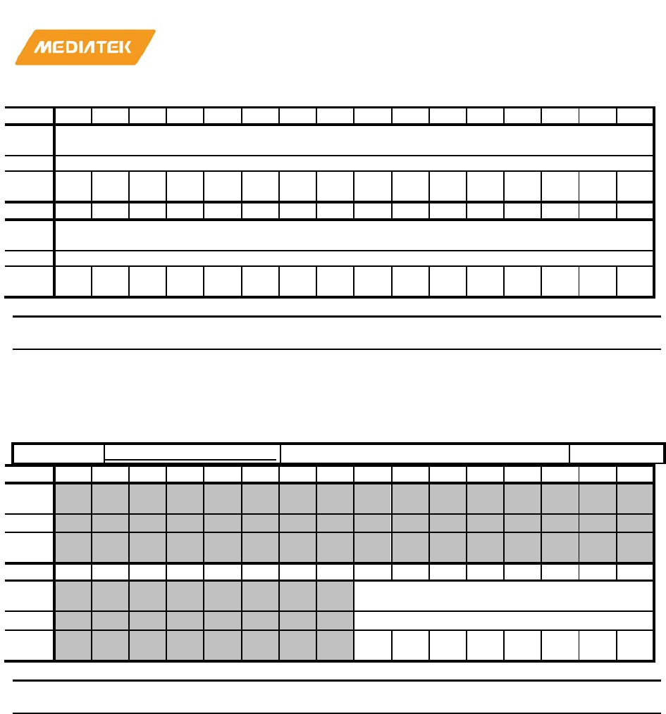
MT76x7
Internet-of-Things Wireless Connectivity
Reference Manual
© 2015 - 2017 MediaTek Inc
Page 596 of 798
This document contains information that is proprietary to MediaTek Inc. (“MediaTek”) and/or its licensor(s).
Any unauthorized use, reproduction or disclosure of this document in whole or in part is strictly prohibited
Bit
31
30
29
28
27
26
25
24
23
22
21
20
19
18
17
16
Nam
e
ADC_DEBUG_RX_FIFO_f
Type
RO
Rese
t
0 0 0 0 0 0 0 0 0 0 0 0 0 0 0 0
Bit
15
14
13
12
11
10
9
8
7
6
5
4
3
2
1
0
Nam
e
ADC_DEBUG_RX_FIFO_f
Type
RO
Rese
t
0 0 0 0 0 0 0 0 0 0 0 0 0 0 0 0
Bit(s)
Mnemonic
Name
Description
31:0
ADC_DEBUG_RX_FI
FO_f
ADC_DEBUG_RX_FIF
O_f
Debugging RX FIFO address 15
830D00D4
ADC_DEBUG_RX_PTR
RX FIFO Pointer Debug Register
00000000
Bit
31
30
29
28
27
26
25
24
23
22
21
20
19
18
17
16
Nam
e
Type
Rese
t
Bit
15
14
13
12
11
10
9
8
7
6
5
4
3
2
1
0
Nam
e
ADC_DEBUG_RX_PTR
Type
RU
Rese
t
0 0 0 0 0 0 0 0
Bit(s)
Mnemonic
Name
Description
7:0
ADC_DEBUG_RX_P
TR
ADC_DEBUG_RX_PTR
Debugging RX FIFO pointer
Bit 0~3 are read poiners; bit 4~7 are writer pointers.
2.5.5. SPI master interface
2.5.5.1. Introduction
MT76x7 features one SPI master controller used as an extension interface to control the peripheral device on
expansion port. The SPI master controller supports the clock rates of 0.25, 0.5, 1, 2, 4, 6, 8, 10 and 12MHz. It
supports two options of clock polarity (CPOL) and two options of initial clock phase (CPHA). SPI pins are
multiplexed with I2S pins.
Table 2-51. SPI pin description
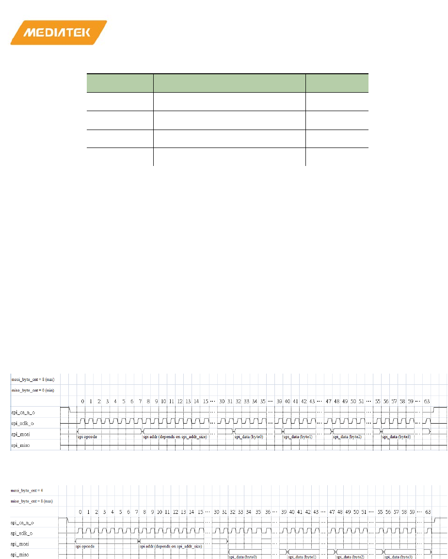
MT76x7
Internet-of-Things Wireless Connectivity
Reference Manual
© 2015 - 2017 MediaTek Inc
Page 597 of 798
This document contains information that is proprietary to MediaTek Inc. (“MediaTek”) and/or its licensor(s).
Any unauthorized use, reproduction or disclosure of this document in whole or in part is strictly prohibited
Signal Name Signal Description Direction
CS Chip select Output
SCK Serial clock Output
MISO Master in, Slave out Input
MOSI Master out, Slave in Output
The SPI master controller supports two modes of operation: more_buf_mode=0, and more_buf_mode=1.
When more_buf_mode = 0, the SPI master controller is compatible with Winbond SPI flash.
When more_buf_mode = 1, the SPI master controller can support configurable length of opcode/address and
data. In this mode, it can also support data operation in both directions simultaneously
(both_directional_data_mode) (command stage is in half duplex mode and data stage is in full duplex mode).
Theterm both_directional_data_mode is applied for the rest of the section.
2.5.5.2. SPI timing diagram
1) more_buf_mode = 0 mode
SPI transfer data buffer size is 8 bytes. In this mode, SPI DI/DO data #0 register and SPI opcode/address
register are used as a the data buffer for SPI transaction. The length of the transaction is controlled by
mosi_byte_cnt and miso_byte_cnt.
Figure 2-50. SPI TX transaction, more_buf_mode=0
Figure 2-51. SPI RX transaction, more_buf_mode=0
2) more_buf_mode = 1 mode
SPI transfer data buffer size is 32 bytes. In this mode, SPI opcode/address register are the data buffer for the
command phase of SPI transaction and the length of command is controlled by cmd_bit_cnt . SPI DI/DO data
#0~#7 register are the data buffer for the data phase of SPI transaction and the length of data of output and
input is controlled by mosi_bit_cnt and miso_bit_cnt , respectively.
In half duplex mode, transmitted data are loaded from SPI opcode/address register and SPI DI/DO data #0~#7
registers. And, the received data will overwrite the SPI DI/DO data #0~#7 registers.
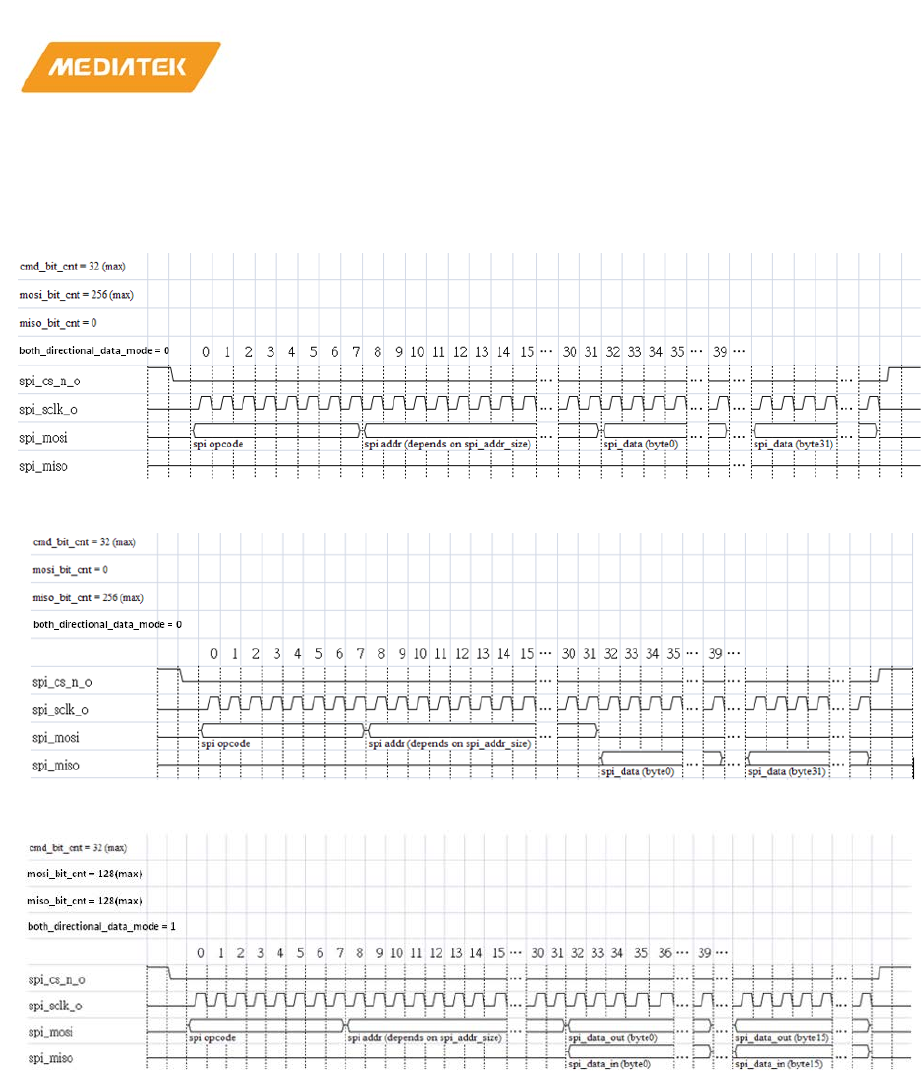
MT76x7
Internet-of-Things Wireless Connectivity
Reference Manual
© 2015 - 2017 MediaTek Inc
Page 598 of 798
This document contains information that is proprietary to MediaTek Inc. (“MediaTek”) and/or its licensor(s).
Any unauthorized use, reproduction or disclosure of this document in whole or in part is strictly prohibited
In both_directional_data_mode, SPI DI/DO data #0~#3 registers are used for transmission and SPI DI/DO #4~#7
registers are used for receive operations.
Figure 2-52. SPI TX transaction, more_buf_mode=1 and both_directional_data_mode=0
Figure 2-53. SPI RX transaction, more_buf_mode=1 and both_directional_data_mode=0
Figure 2-54. SPI TX/RX transaction, more_buf_mode=1 and both_directional_data_mode=1
2.5.5.3. Programming guide
CPU Direct Access Mode
1) SPI Write:
a) CPU direct configure the SPI-M register space, include opcode, address, data and other settings.
b) Program the “spi_master_start” to 1 in “SPI transaction control/status register” to kick the spi
transaction.
c) CPU polling the “spi_busy” in “SPI transaction control/status register” to indicate the spi
transactions done or not.
2) SPI Read:

MT76x7
Internet-of-Things Wireless Connectivity
Reference Manual
© 2015 - 2017 MediaTek Inc
Page 599 of 798
This document contains information that is proprietary to MediaTek Inc. (“MediaTek”) and/or its licensor(s).
Any unauthorized use, reproduction or disclosure of this document in whole or in part is strictly prohibited
a) CPU direct configure the SPI-M register space, include opcode, address and other settings.
b) Program the “spi_master_start” to 1 in “SPI transaction control/status register” to kick the spi
transaction.
c) CPU polling the “spi_busy” in “SPI transaction control/status register” to indicate the spi
transactions done or not.
d) CPU can get the read data in “SPI DI/DO data #0~#7 register”.
2.5.5.4. Registers definitions
Module name: MT7637_SPIM_TOP Base address: (+24000000h)
Address
Name
Width
Register Function
24000000
STCSR
32
SPI transaction control/status register
24000004
SOAR
32
SPI opcode/address register
24000008
SDIDOR0
32
SPI DI/DO data #0 register
2400000C
SDIDOR1
32
SPI DI/DO data #1 register
24000010
SDIDOR2
32
SPI DI/DO data #2 register
24000014
SDIDOR3
32
SPI DI/DO data #3 register
24000018
SDIDOR4
32
SPI DI/DO data #4 register
2400001C
SDIDOR5
32
SPI DI/DO data #5 register
24000020
SDIDOR6
32
SPI DI/DO data #6 register
24000024
SDIDOR7
32
SPI DI/DO data #7 register
24000028
SMMR
32
SPI master mode register
2400002C
SMBCR
32
SPI more buf control register
24000030
RSV
32
Reserved
24000034
SCSR
32
SPI controller status register
24000038
CSPOL
32
SPI controller control register
24000000
STCSR
SPI transaction control/status register
00160001
Bit
31
30
29
28
27
26
25
24
23
22
21
20
19
18
17
16
Nam
e spi_addr_ext - spi_addr
_size -
spi
_m
ast
er_
bus
y
Type
RW
RO
RW
RO
RO
Rese
t
0 0 0 0 0 0 0 0 0 0 0 1 0 1 1 0
Bit
15
14
13
12
11
10
9
8
7
6
5
4
3
2
1
0
Nam
e -
spi
_m
ast
er_
sta
rt
miso_byte_cnt mosi_byte_cnt
Type
RO
WO
RW
RW
Rese
t
0 0 0 0 0 0 0 0 0 0 0 0 0 0 0 1
Bit(s)
Name
Description

MT76x7
Internet-of-Things Wireless Connectivity
Reference Manual
© 2015 - 2017 MediaTek Inc
Page 600 of 798
This document contains information that is proprietary to MediaTek Inc. (“MediaTek”) and/or its licensor(s).
Any unauthorized use, reproduction or disclosure of this document in whole or in part is strictly prohibited
Bit(s)
Name
Description
31:24
spi_addr_ext
Spi address extenstion for 32-bit SPI address size. Usually
this field specifies the first byte of the address phase to
transmit to SPI device when more_buf_mode = 0 and
spi_addr_size = 3. And spi_addr[31:24], spi_addr[23:16],
and spi_addr[15:0] are respec
tively the second, third and
fourth byte of the address phase
Note: When more_buf_mode =1, The spi_addr_ext and SPI
opcode/address register(SOAR) are treated as a command register:
cmd_reg[39:0] = {spi_addr_ext[7:0], SOAR[31:0]} The
transmitted data bits
is based on cmd_bit_cnt and the transmission
sequence is as follows:
lsb_first = 0: cmd_reg[cmd_bit_cnt
-1], cmd_reg[cmd_bit_cnt -
2],
~ , cmd_reg[0]
lsb_first = 1: cmd_reg[0], cmd_reg[1], ~ , cmd_reg[cmd_bit_cnt
-
1]
23:21
-
Reserved.
20:19
spi_addr_size
SPI address size.
2'h0: reserved.
2'h1: spi_addr[15:0] of SPI DI data register are valid (16
-bit size).
2'h2: spi_addr[23:0] of SPI DI data register are valid (24
-bit size).
2'h3: {spi_addr_ext[7:0], spi_addr[23:0]} of SPI DI data register
are valid (32
-bit size).
Note: The spi_addr_size is valid only when more_buf_mode = 0.
18:17
-
Reserved.
16
spi_master_busy
Transaction busy indication.
1'b0: No SPI transaction is ongoing. Software may start a new SPI
transaction by writing to the SPI transaction
start bit within this
register.
1'b1: An SPI transaction presently is underway. Software must not
try to start a new SPI transaction. Software may not alter the value
of any field of the SPI master control registers.
15:9
-
Reserved.
8
spi_master_start
SPI transaction start. Only writes to this field are
meaningful, reads always return 0.
1'b0: No effect
1'b1: Starts SPI transaction.
7:4
miso_byte_cnt
SPI MISO (rx) byte count. Determines the number of bytes
received from the SPI device from the SPI opcode/address
register and the SPI DI/DO data #0 register. Values of 0 ~
8 are valid, other values are illegal.
Note: The miso_byte_cnt is valid only when more_buf_mode = 0.
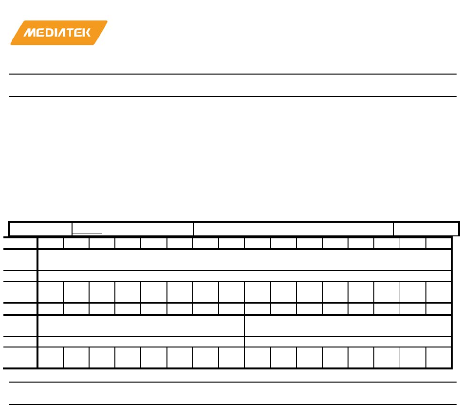
MT76x7
Internet-of-Things Wireless Connectivity
Reference Manual
© 2015 - 2017 MediaTek Inc
Page 601 of 798
This document contains information that is proprietary to MediaTek Inc. (“MediaTek”) and/or its licensor(s).
Any unauthorized use, reproduction or disclosure of this document in whole or in part is strictly prohibited
Bit(s)
Name
Description
3:0
mosi_byte_cnt
SPI MOSI (tx) byte count. Determines the number of bytes
transmitted from the SPI opcode/address register and the
SPI DI/DO data #0 register to the SPI device. Values of 1 ~
8 are valid, other values are illegal.
Note: The mosi_byte_cnt is valid only when more_buf_mode = 0.
The transmitted data sequence is as fo
llows: spi_opcode, spi_addr
(conditional) and d0_byte ~ d3_byte (conditional).
24000004
SOAR
SPI opcode/address register
00000000
Bit
31
30
29
28
27
26
25
24
23
22
21
20
19
18
17
16
Nam
e
spi_addr
Type
RW
Rese
t
0 0 0 0 0 0 0 0 0 0 0 0 0 0 0 0
Bit
15
14
13
12
11
10
9
8
7
6
5
4
3
2
1
0
Nam
e
spi_addr spi_opcode
Type
RW
RW
Rese
t
0 0 0 0 0 0 0 0 0 0 0 0 0 0 0 0
Bit(s)
Name
Description
31:8
spi_addr
SPI address. Usually this field specifies the 24-bits
address to transmit
to the SPI device when
more_buf_mode = 0.
modeI: (16
-bits SPI address size), spi_addr[23:16] is the 1st byte of
the address phase and spi_addr[15:8] is the 2nd byte of the address
phase.
modeII: (24
-bits SPI address size), spi_addr[31:24] is the 1st byte
of the address phase and spi_addr[23:16] is the 2nd byte of the
address phase and spi_addr[15:8] is the 3rd byte of the address
phase.
modeIII: (32
-
bits SPI address size), spi_addr[31:24] is the 2nd byte
of the address phase and spi_addr[23:16] is the 3rd
byte of the
address phase and spi_addr[15:8] is the 4th byte of the address
phase
Note: For SPI read transaction and more_buf_mode = 0
Field [15:8] is also used to store the 6
-th byte of data read phase.
Field [23:16] is also used to store the 7
-th byte of data read phase.
Field [31:24] is also used to store the 8
-th byte of data read phase.
7:0
spi_opcode
SPI opcode. Usually this field specifies the 8-bits opcode
(instruction) to transmit to the SPI device as the first byte
of a SPI transaction when
more_buf_mode = 0.
Note: For SPI read transaction and more_buf_mode = 0, this byte
MT76x7
Internet-of-Things Wireless Connectivity
Reference Manual
© 2015 - 2017 MediaTek Inc
Page 602 of 798
This document contains information that is proprietary to MediaTek Inc. (“MediaTek”) and/or its licensor(s).
Any unauthorized use, reproduction or disclosure of this document in whole or in part is strictly prohibited
Bit(s)
Name
Description
is also used to store the 5-th byte of data read phase according to
the rx byte count miso_byte_cnt.
24000008
SDIDOR0
SPI DI/DO data #0 register
00000000
Bit
31
30
29
28
27
26
25
24
23
22
21
20
19
18
17
16
Nam
e
d0_byte d1_byte
Type
RW
RW
Rese
t
0 0 0 0 0 0 0 0 0 0 0 0 0 0 0 0
Bit
15
14
13
12
11
10
9
8
7
6
5
4
3
2
1
0
Nam
e
d2_byte d3_byte
Type
RW
RW
Rese
t
0 0 0 0 0 0 0 0 0 0 0 0 0 0 0 0
Bit(s)
Name
Description
31:24
d0_byte
The 1 data byte of data read/write phase.
23:16
d1_byte
The 2 data byte of data read/write phase.
15:8
d2_byte
The 3 data byte of data read/write phase.
7:0
d3_byte
The 4 data byte of data read/write phase.
2400000C
SDIDOR1
SPI DI/DO data #1 register
00000000
Bit
31
30
29
28
27
26
25
24
23
22
21
20
19
18
17
16
Nam
e
d4_byte d5_byte
Type
RW
RW
Rese
t
0 0 0 0 0 0 0 0 0 0 0 0 0 0 0 0
Bit
15
14
13
12
11
10
9
8
7
6
5
4
3
2
1
0
Nam
e
d6_byte d7_byte
Type
RW
RW
Rese
t
0 0 0 0 0 0 0 0 0 0 0 0 0 0 0 0
Bit(s)
Name
Description
31:24
d4_byte
The 5 data byte of data read/write phase.
23:16
d5_byte
The 6 data byte of data read/write phase.
15:8
d6_byte
The 7 data byte of data read/write phase.
7:0
d7_byte
The 8 data byte of data read/write phase.
MT76x7
Internet-of-Things Wireless Connectivity
Reference Manual
© 2015 - 2017 MediaTek Inc
Page 603 of 798
This document contains information that is proprietary to MediaTek Inc. (“MediaTek”) and/or its licensor(s).
Any unauthorized use, reproduction or disclosure of this document in whole or in part is strictly prohibited
Bit(s)
Name
Description
24000010
SDIDOR2
SPI DI/DO data #2 register
00000000
Bit
31
30
29
28
27
26
25
24
23
22
21
20
19
18
17
16
Nam
e
d8_byte d9_byte
Type
RW
RW
Rese
t
0 0 0 0 0 0 0 0 0 0 0 0 0 0 0 0
Bit
15
14
13
12
11
10
9
8
7
6
5
4
3
2
1
0
Nam
e
d10_byte d11_byte
Type
RW
RW
Rese
t
0 0 0 0 0 0 0 0 0 0 0 0 0 0 0 0
Bit(s)
Name
Description
31:24
d8_byte
The 9 data byte of data read/write phase.
23:16
d9_byte
The 10 data byte of data read/write phase.
15:8
d10_byte
The 11 data byte of data read/write phase.
7:0
d11_byte
The 12 data byte of data read/write phase.
24000014
SDIDOR3
SPI DI/DO data #3 register
00000000
Bit
31
30
29
28
27
26
25
24
23
22
21
20
19
18
17
16
Nam
e
d12_byte d13_byte
Type
RW
RW
Rese
t
0 0 0 0 0 0 0 0 0 0 0 0 0 0 0 0
Bit
15
14
13
12
11
10
9
8
7
6
5
4
3
2
1
0
Nam
e
d14_byte d15_byte
Type
RW
RW
Rese
t
0 0 0 0 0 0 0 0 0 0 0 0 0 0 0 0
Bit(s)
Name
Description
31:24
d12_byte
The 13 data byte of data read/write phase.
23:16
d13_byte
The 14 data byte of data read/write phase.
15:8
d14_byte
The 15 data byte of data read/write phase.
7:0
d15_byte
The 16 data byte of data read/write phase.
MT76x7
Internet-of-Things Wireless Connectivity
Reference Manual
© 2015 - 2017 MediaTek Inc
Page 604 of 798
This document contains information that is proprietary to MediaTek Inc. (“MediaTek”) and/or its licensor(s).
Any unauthorized use, reproduction or disclosure of this document in whole or in part is strictly prohibited
24000018
SDIDOR4
SPI DI/DO data #4 register
00000000
Bit
31
30
29
28
27
26
25
24
23
22
21
20
19
18
17
16
Nam
e
d16_byte d17_byte
Type
RW
RW
Rese
t
0 0 0 0 0 0 0 0 0 0 0 0 0 0 0 0
Bit
15
14
13
12
11
10
9
8
7
6
5
4
3
2
1
0
Nam
e
d18_byte d19_byte
Type
RW
RW
Rese
t
0 0 0 0 0 0 0 0 0 0 0 0 0 0 0 0
Bit(s)
Name
Description
31:24
d16_byte
The 17 data byte of data read/write phase (half duplex
mode) or the 1 data byte of data read phase (
both
directional
data mode).
23:16
d17_byte
The 18 data byte of data read/write phase (half duplex
mode) or the 2 data byte of data read phase (
both
directional data mode
).
15:8
d18_byte
The 19 data byte of data read/write phase (half duplex
mode) or the 3 data byte of data read phase (
both
directional
data mode).
7:0
d19_byte
The 20 data byte of data read/write phase (half duplex
mode) or the 4 data byte of data read phase (
both
directional data mode
).
2400001C
SDIDOR5
SPI DI/DO data #5 register
00000000
Bit
31
30
29
28
27
26
25
24
23
22
21
20
19
18
17
16
Nam
e
d20_byte d21_byte
Type
RW
RW
Rese
t
0 0 0 0 0 0 0 0 0 0 0 0 0 0 0 0
Bit
15
14
13
12
11
10
9
8
7
6
5
4
3
2
1
0
Nam
e
d22_byte d23_byte
Type
RW
RW
Rese
t
0 0 0 0 0 0 0 0 0 0 0 0 0 0 0 0
Bit(s)
Name
Description
31:24
d20_byte
The 21 data byte of data read/write phase (half duplex
mode) or the 5 data byte of data read phase (
both
directional data mode
).
23:16
d21_byte
The 22 data byte of data read/write phase (half duplex
mode) or the 6 data byte of data read phase (both
MT76x7
Internet-of-Things Wireless Connectivity
Reference Manual
© 2015 - 2017 MediaTek Inc
Page 605 of 798
This document contains information that is proprietary to MediaTek Inc. (“MediaTek”) and/or its licensor(s).
Any unauthorized use, reproduction or disclosure of this document in whole or in part is strictly prohibited
Bit(s)
Name
Description
directional data mode).
15:8
d22_byte
The 23 data byte of data read/write phase (half duplex
mode) or the 7 data byte of data read phase (
both
directional data mode
).
7:0
d23_byte
The 24 data byte of data read/write phase (half duplex
mode)
or the 8 data byte of data read phase (both
directional data mode
).
24000020
SDIDOR6
SPI DI/DO data #6 register
00000000
Bit
31
30
29
28
27
26
25
24
23
22
21
20
19
18
17
16
Nam
e
d24_byte d25_byte
Type
RW
RW
Rese
t
0 0 0 0 0 0 0 0 0 0 0 0 0 0 0 0
Bit
15
14
13
12
11
10
9
8
7
6
5
4
3
2
1
0
Nam
e
d26_byte d27_byte
Type
RW
RW
Rese
t
0 0 0 0 0 0 0 0 0 0 0 0 0 0 0 0
Bit(s)
Name
Description
31:24
d24_byte
The 25 data byte of data read/write phase (half duplex
mode) or the 9
data byte of data read phase (both
directional data mode
).
23:16
d25_byte
The 26 data byte of data read/write phase (half duplex
mode) or the 10 data byte of data read phase (
both
directional data mode
).
15:8
d26_byte
The 27 data byte of data read/write phase (half duplex
mode) or the 11 data byte of data read phase (
both
directional data mode
).
7:0
d27_byte
The 28 data byte of data read/write phase (half duplex
mode) or the 12 data byte of data read phase (
both
directional data mode
).
24000024
SDIDOR7
SPI DI/DO data #7 register
00000000
Bit
31
30
29
28
27
26
25
24
23
22
21
20
19
18
17
16
Nam
e
d28_byte d29_byte
Type
RW
RW
Rese
t
0 0 0 0 0 0 0 0 0 0 0 0 0 0 0 0
Bit
15
14
13
12
11
10
9
8
7
6
5
4
3
2
1
0
Nam
d30_byte
d31_byte
MT76x7
Internet-of-Things Wireless Connectivity
Reference Manual
© 2015 - 2017 MediaTek Inc
Page 606 of 798
This document contains information that is proprietary to MediaTek Inc. (“MediaTek”) and/or its licensor(s).
Any unauthorized use, reproduction or disclosure of this document in whole or in part is strictly prohibited
e
Type
RW
RW
Rese
t
0 0 0 0 0 0 0 0 0 0 0 0 0 0 0 0
Bit(s)
Name
Description
31:24
d28_byte
The 29 data byte of data read/write phase (half duplex
mode) or the 13 data byte of data read phase (
both
directional data mode
).
23:16
d29_byte
The 30 data byte of data read/write phase (half duplex
mode) or the 14 data byte of data read phase (
both
directional data mode
).
15:8
d30_byte
The 31 data byte of data read/write phase (half duplex
mode) or the 15 data byte of data read phase (
both
directional
data mode).
7:0
d31_byte
The 32 data byte of data read/write phase (half duplex
mode) or the 16 data byte of data read phase (
both
directional data mode
).
24000028
SMMR
SPI master mode register
00018880
Bit
31
30
29
28
27
26
25
24
23
22
21
20
19
18
17
16
Nam
e rs_slave_sel
clk
_m
ode
rs_clk_sel
Type
RW
RW
RW
Rese
t
0 0 0 0 0 0 0 0 0 0 0 0 0 0 0 1
Bit
15
14
13
12
11
10
9
8
7
6
5
4
3
2
1
0
Nam
e cs_dsel_cnt
bot
h_
dir
ecti
ona
l_
dat
a_
mo
de
int
_en
spi
_st
art
_se
l
pfe
tch
_en - CP
HA CP
OL
lsb
_fir
st
mo
re_
buf
_m
ode
-
Type
RW
RW
RW
RW
RW
RO
RW
RW
RW
RW
RO
Rese
t
1 0 0 0 1 0 0 0 1 0 0 0 0 0 0 0
Bit(s)
Name
Description
31:29
rs_slave_sel
rs_slave_sel.
3'h0: select SPI device #0. (default is flash)
3'h1: select SPI device #1.
~

MT76x7
Internet-of-Things Wireless Connectivity
Reference Manual
© 2015 - 2017 MediaTek Inc
Page 607 of 798
This document contains information that is proprietary to MediaTek Inc. (“MediaTek”) and/or its licensor(s).
Any unauthorized use, reproduction or disclosure of this document in whole or in part is strictly prohibited
Bit(s)
Name
Description
3'h7: select SPI device #7.
28
clk_mode
This register is used to specify that period of SCLK HIGH
is longer or period of SCLK LOW is longer when clock
divisor(rs_clk_sel) is odd.
1'b0: period of SCLK LOW is longer.
1'b1: period of SCLK HIGH is longer.
27:16
rs_clk_sel
Register Space SPI clock frequency select.
12'h0: SPI clock frequency is hclk/2. (50% duty cycle, duty cycle is
the ratio of the output high time to the total cycle time)
12'h1: SPI clock frequency is hclk/3. (33.33% or 66.67% duty cycle)
12'h2:
SPI clock frequency is hclk/4. (50% duty cycle)
12'h3: SPI clock frequency is hclk/5. (40% or 60% duty cycle)
~
12'h4095: SPI clock frequency is hclk/4097.
15:11
cs_dsel_cnt
Internal delay the de-select time of SPI chip select is
configured to occupy the
number of cycles of spim_clk
clock.
10
both_directional_data_mode
Both_directional_data_mode or half duplex mode.
1'b0: half duplex mode.
1'b1:
both_directional_data_mode.
Note: The
both_directional_data_mode is valid only when
more_buf_mode = 1. The
transmission is always as half duplex
when more_buf_mode = 0;
9
int_en
Interrupt enable.
1'b0: disable SPI interrupt.
1'b1: enable SPI interrupt.
8
spi_start_sel
The interval between spi_cs_n and spi_sclk.
1'b0: 3 spim_clk
1'b1: 6 spim_clk
7
pfetch_en
SPI pre-fetch buffer enable
1'b0: disable pre
-fetch buffer.
1'b1: enable pre
-fetch buffer.
6
-
Reserved.
5
CPHA
Initial SPI clock phase for SPI transaction.
There are four SPI modes used to latch data. These SPI modes latch

MT76x7
Internet-of-Things Wireless Connectivity
Reference Manual
© 2015 - 2017 MediaTek Inc
Page 608 of 798
This document contains information that is proprietary to MediaTek Inc. (“MediaTek”) and/or its licensor(s).
Any unauthorized use, reproduction or disclosure of this document in whole or in part is strictly prohibited
Bit(s)
Name
Description
data in one of four ways, and are defined by the logic state
combinations of the CLK Polarity (CPOL) in relation to the CLK
Phase (CPHA). The valid logic combinations identify and determine
the SPI modes supported by the SPI device.
At CPOL=0 the base value of the clock is zero
For
CPHA=0 (mode 0), data is read on the clock's rising edge and
data is changed on a falling edge.
For CPHA=1 (mode 1), data is read on the clock's falling edge and
data is changed on a rising edge.
At CPOL=1 the base value of the clock is one (inversion of C
POL=0)
For CPHA=0 (mode 2), data is read on clock's falling edge and data
is changed on a rising edge.
For CPHA=1 (mode 3), data is read on clock's rising edge and data
is changed on a falling edge.
4
CPOL
Initial SPI clock polarity for SPI transaction.
3
lsb_first
lsb_first.
1'b0: MSB(most significant bit) is transferred first for SPI
transaction.
1'b1: LSB(least significant bit) is transferred first for SPI
transaction.
2
more_buf_mode
Select 2 words buffer or 8 words buffer for SPI
transaction.
1'b0: SPI transfer data buffer size is only 2 words. In this mode, SPI
DI/DO data #0 register and SPI opcode/address register are the
data buffer for SPI transaction. And, SPI master follows
mosi_byte_cnt and miso_byte_cnt to complete the transmission
and recep
tion, respectively. This kind of transaction must operate
in half duplex mode.
1'b1: SPI transfer data buffer size is 8 words. In this mode, SPI
opcode/address register are the data buffer for SPI transaction and
follows cmd_bit_cnt to complete the transac
tion. SPI DI/DO data
#0~#7 register are the data buffer for SPI transaction and follows
do_bit_cnt and di_bit_cnt to complete the transmission and
reception, respectively. In half duplex mode, transmitted data are
loaded from SPI opcode/address register a
nd SPI DI/DO data
#0~#7 registers. And, the received data will overwrite the SPI
DI/DO data #0~#7 registers. In
both_directional_data_mode, SPI
DI/DO data #0~#3 registers are used for transmission and SPI
DI/DO #4~#7 registers are used for receipt.
1:0
-
Reserved.
2400002C
SMBCR
SPI more buf control register
00000000
Bit
31
30
29
28
27
26
25
24
23
22
21
20
19
18
17
16
Nam
-
cmd_bit_cnt
-
miso_bit_cnt
MT76x7
Internet-of-Things Wireless Connectivity
Reference Manual
© 2015 - 2017 MediaTek Inc
Page 609 of 798
This document contains information that is proprietary to MediaTek Inc. (“MediaTek”) and/or its licensor(s).
Any unauthorized use, reproduction or disclosure of this document in whole or in part is strictly prohibited
e
Type
RO
RW
RO
RW
Rese
t
0 0 0 0 0 0 0 0 0 0 0 0 0 0 0 0
Bit
15
14
13
12
11
10
9
8
7
6
5
4
3
2
1
0
Nam
e
miso_bit_cnt - mosi_bit_cnt
Type
RW
RO
RW
Rese
t
0 0 0 0 0 0 0 0 0 0 0 0 0 0 0 0
Bit(s)
Name
Description
31:30
-
Reserved.
29:24
cmd_bit_cnt
SPI command phase MOSI (tx) bit count. Determines the
number of command bits transmitted from the SPI
opcode/address register to the SPI device. Values of
0
~ 32
are valid
in half-duplex mode, Values of 1 ~ 32 are valid in
b
oth_directional_data_mode.Other values are illegal.
Note: The cmd_bit_cnt is valid only when more_buf_mode = 1 and
the SPI opcode/address register is treated as a command register.
23:21
-
Reserved.
20:12
miso_bit_cnt
SPI data phase MISO (rx) bit count. Determines the
number of bits received from the SPI device into the SPI
DI/DO data #0~#7 register. Values of 0 ~ 256 are valid,
but other values are illegal. Maximum value is 256 for half
duplex mode and 128 for
both_directional_data_mode.
Please note that mosi_bit_cnt must be equal to
miso_bit_cnt in
both_directional_data_mode.
Note: The miso_bit_cnt is valid only when more_buf_mode = 1
11:9
-
Reserved.
8:0
mosi_bit_cnt
SPI data phase MOSI (tx) bit count. Determines the
number of data bits transmitted from the SPI DI/DO data
#0~#7 register to the SPI device. Values of 0 ~ 256 are
valid, but other values are illegal. Maximum value is 256
for half duplex mode and 128 for
b
oth_directional_data_mode.
Note: The mosi_bit_cnt is valid only when more_buf_mode = 1.
24000030
RSV
Reserved
00000000
Bit
31
30
29
28
27
26
25
24
23
22
21
20
19
18
17
16
Nam
e
-
Type
RO
Rese
t
0 0 0 0 0 0 0 0 0 0 0 0 0 0 0 0
Bit
15
14
13
12
11
10
9
8
7
6
5
4
3
2
1
0
Nam
e
-
Type
RO
MT76x7
Internet-of-Things Wireless Connectivity
Reference Manual
© 2015 - 2017 MediaTek Inc
Page 610 of 798
This document contains information that is proprietary to MediaTek Inc. (“MediaTek”) and/or its licensor(s).
Any unauthorized use, reproduction or disclosure of this document in whole or in part is strictly prohibited
Rese
t
0 0 0 0 0 0 0 0 0 0 0 0 0 0 0 0
Bit(s)
Name
Description
31:0
-
Reserved.
24000034
SCSR
SPI controller status register
00000000
Bit
31
30
29
28
27
26
25
24
23
22
21
20
19
18
17
16
Nam
e
-
Type
RO
Rese
t
0 0 0 0 0 0 0 0 0 0 0 0 0 0 0 0
Bit
15
14
13
12
11
10
9
8
7
6
5
4
3
2
1
0
Nam
e
-
spi
_ok
Type
RO
RC
Rese
t
0 0 0 0 0 0 0 0 0 0 0 0 0 0 0 0
Bit(s)
Name
Description
31:1
-
Reserved.
0
spi_ok
When SPI transaction complete, SPI master controller
will set this bit and assert SPI interrupt to notify software.
Reading this register will clear this bit and de
-assert SPI
interrupt.
24000038
CSPOL
SPI controller control register
00000000
Bit
31
30
29
28
27
26
25
24
23
22
21
20
19
18
17
16
Nam
e
-
Type
RO
Rese
t
0 0 0 0 0 0 0 0 0 0 0 0 0 0 0 0
Bit
15
14
13
12
11
10
9
8
7
6
5
4
3
2
1
0
Nam
e
- cs_polar
Type
RO
RW
Rese
t
0 0 0 0 0 0 0 0 0 0 0 0 0 0 0 0
Bit(s)
Name
Description
31:8
-
Reserved.
7:0
cs_polar
cs polarity for device #0~#7. Initial SPI chip select
polarity for SPI transaction.
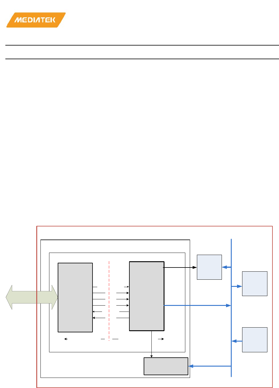
MT76x7
Internet-of-Things Wireless Connectivity
Reference Manual
© 2015 - 2017 MediaTek Inc
Page 611 of 798
This document contains information that is proprietary to MediaTek Inc. (“MediaTek”) and/or its licensor(s).
Any unauthorized use, reproduction or disclosure of this document in whole or in part is strictly prohibited
Bit(s)
Name
Description
1'b0: cs operate low active
1'b1: cs operate high active
2.5.6. SPI slave interface
2.5.6.1. General description
The simple SPI slave module translates 16bits SPI serial protocol to create AHB master transaction for
accessing SYSRAM or configuration registers.
2.5.6.2. Block diagram
The block diagram shows SPI slave controller, spis_top, was integrated in the Cortex-M4 system. SPI Host can
write data into Cortex-M4 SYSRAM by controlling slave controller.
SPI slave controller supports interrupt to Cortex-M4 system. SPI host can configure register in slave controller
to interrupt CM4 MCU. When CM4 MCU gets the interrupt, it can read status from SPI slave controller and
clear the interrupt. Also, it can read data from SYSRAM.
spis2ahb_spi spis2ahb_ahbif
spitoahb_start
Intf_busy
reg00
reg02
reg03
reg01
spi_ck / spi_cs
spi_mosi / spi_miso
spis2ahb_top
spis_top
SPI clock domain system clock domain
spis_ahbslv_adr_if
Reg00~06
SPIS_IRQ CIRQ
AHB BUS
SYSRAM
CM4
MCU
CM4_SYS
Figure 2-55. SPI Slave block diagram
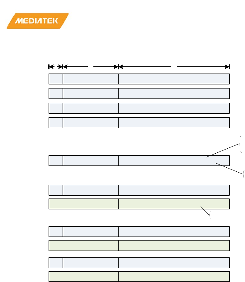
MT76x7
Internet-of-Things Wireless Connectivity
Reference Manual
© 2015 - 2017 MediaTek Inc
Page 612 of 798
This document contains information that is proprietary to MediaTek Inc. (“MediaTek”) and/or its licensor(s).
Any unauthorized use, reproduction or disclosure of this document in whole or in part is strictly prohibited
2.5.6.3. SPI Slave CR Read/Write protocol
AHB write data[15:0]
reg_addr 15'h04
W
ahb_wd
(reg01[15:0])
AHB write data[31:16]
reg_addr 15'h06
W
ahb_wd
(reg01[31:16])
15
116
AHB bus address[15:0]
reg_addr 15'h08
W
ahb_addr
(reg02[15:0])
AHB bus address[31:16]
reg_addr 15'h0A
W
ahb_addr
(reg02[31:16])
16 bits cmd = {12'h0, 1'h0, size, r_w}
reg_addr 15'h0C
W
ahb_CMD
(reg03[15:0])
1'b0: read
1'b1: write
16'h0
reg_addr 15'h10
R
ahb_ack
(reg04[15:0])
1'b0: AHB intf idle
1'b1: AHB intf executing cmd
16'h0
reg_addr 15'h00
R
ahb_rd
(reg00[15:0])
AHB read data[15:0]
16 bits ack = {15'h0, intf_busy}
16'h0
reg_addr 15'h02
R
ahb_rd
(reg00[31:16])
AHB read data[31:16]
SPI MOSI
SPI MOSI
SPI MOSI
SPI MOSI
SPI MOSI
SPI MOSI
SPI MOSI
SPI MOSI
SPI MISO
SPI MISO
SPI MISO
2'b00: reserved
2'b01: reserved
2'b10: word(4bytes)
2'b11: reserved
16'hxx
16'hxx
16'hxx
Figure 2-56. SPI Slave CR Read/Write Protocol
MT7687 SPI slave use SPI2AHB protocol. In AHB write transaction, it should write AHB 32bits data and 32bits
address into spi controller register first, and then kick the AHB_cmd to start AHB write transaction. After start
AHB_cmd, 32bits data will be written into specified 32bits address. In AHB read transaction, it should write
32bits address into spi controller register first, and then kick the AHB_cmd to start AHB read transaction. After
start AHB_cmd, 32 bits data will be read from specified 32bits address and stored in spi slave controller.
There are five registers in this slave controller. Reg00 is the read data from AHB. Reg01 is the write data that
programmer want to write to AHB. Reg02 is the address that programmer want to write/read to/from AHB,
the configured value must be a physical address in the CM4 system. Reg03 is the command that applies to AHB
protocol. Reg04 is the status for polling to make sure AHB bus is idle or busy.
MT7687 SPI slave use SPI2AHB protocol. In AHB write transaction, it should write AHB 32bits data and 32bits
address into spi controller register first, and then kick the AHB_cmd to start AHB write transaction. After start
AHB_cmd, 32bits data will be written into specified 32bits address. In AHB read transaction, it should write
32bits address into spi controller register first, and then kick the AHB_cmd to start AHB read transaction. After
start AHB_cmd, 32 bits data will be read from specified 32bits address and stored in spi slave controller.

MT76x7
Internet-of-Things Wireless Connectivity
Reference Manual
© 2015 - 2017 MediaTek Inc
Page 613 of 798
This document contains information that is proprietary to MediaTek Inc. (“MediaTek”) and/or its licensor(s).
Any unauthorized use, reproduction or disclosure of this document in whole or in part is strictly prohibited
Before programming AHB/APB registers, the programmer should check reg04 bit0 to check if AHB is idle. The
programmer can set reg03 (cmd register) to kick SPI slave2AHB module to write/read one
byte/halfword/word/dword to/from AHB/APB.
Before SPI master write/read to/from AHB, programmer should guarantee AHB bus is non-busy by check
spitoahb_spi.reg04[0] if equal to 1’b0.
2.5.6.4. Programming sequence
1) Standard mode
Example 1: Write 0x0123_4567 data to the register at address 0x1013_0004
Step 1.
• Check SPI slave is idle, SPI master asserts following data on SPI_MOSI
• {8’h00, 8’h10, 16’hxx} // Read SPI slave status reg04
• Wait until the SPI_MISO returned data bit[0] = 0, which indicates the AHB interface of SPI slave is idle
and ready to execute a new access command.
Step 2
• Prepare command for bus accessing, SPI master asserts following data on SPI_MOSI respectively.
• {8’h80, 8’h04, 16’h4567} // put bus write data [15:0] into SPI slave reg01[15:0]
• {8’h80, 8’h06, 16’h0123} // put bus write data [31:16] into SPI slave reg01[31:16]
• {8’h80, 8’h08, 16’h0004} // put bus address [15:0] into SPI slave reg02[15:0]
• {8’h80, 8’h0A, 16’h1013} // put bus address [31:16] into SPI slave reg02[31:16]
• {8’h80, 8’h0C, {13’b0, 2’b10, 1’b1}} // Start the bus write access via AHB master interface
Step 3
• Wait bus accessing done, SPI master asserts following data on SPI_MOSI
• {8’h00, 8’h10, 16’hxx} // Read SPI slave bus interface status
• Wait until the SPI_MISO returned data bit[0] = 0, make sure that either AHB finish the bus access
Example 2: Read 0x0123_4567 data from the register at address 0x1013_0004
Step 1
• Check SPI slave is idle, SPI master asserts following data on SPI_MOSI
• {8’h00, 8’h10, 16’hxx} // Read SPI slave status reg04
• Wait until the SPI_MISO returned data bit[0] = 0, which indicates the AHB interface of SPI slave is idle
and ready to execute a new access command.
Step 2
• Prepare command for bus accessing, SPI master asserts following data on SPI_MOSI respectively
• {8’h80, 8’h08, 16’h0004} // put bus address [15:0] into SPI slave reg02[15:0]

MT76x7
Internet-of-Things Wireless Connectivity
Reference Manual
© 2015 - 2017 MediaTek Inc
Page 614 of 798
This document contains information that is proprietary to MediaTek Inc. (“MediaTek”) and/or its licensor(s).
Any unauthorized use, reproduction or disclosure of this document in whole or in part is strictly prohibited
• {8’h80, 8’h0A, 16’h1013} // put bus address [31:16] into SPI slave reg02[31:16]
• {8’h80, 8’h0C, {13’b0, 2’b10, 1’b0}} // Start the bus read access via AHB master interface
Step 3
• Wait bus accessing done, SPI master asserts following data on SPI_MOSI
• {8’h00, 8’h10, 16’hxx} // Read SPI slave bus interface status
• Wait until the SPI_MISO returned data bit[0] = 0, make sure that either AHB finish the bus access
Step 4
• Get read data, SPI master asserts following data on SPI_MOSI respectively
• {8’h00, 8’h00, 16’hxx} // get bus read data [15:0] from SPI slave reg00[15:0]
• SPI slave_MISO return data 16’h4567
• {8’h00, 8’h02, 16’hxx} // get bus read data [31:16] from SPI slave reg00[31:16]
• SPI slave_MISO return data 16’h0123
2) Fast Mode (Address Auto Increment)
Address auto increment mode can reduce bus address write time when SPI Slave access CM4 SYSRAM.Fast
write example:
• Write 0x0123_4567 data to the register at address 0x1013_0004
• Write 0x89ab_cdef data to the register at address 0x1013_0008
• Note: User doesn’t need to check busy status during write transaction.
Step 1
• Prepare command for bus accessing, SPI master asserts following data on SPI_MOSI respectively.
• {8’h80, 8’h04, 16’h4567} // put bus write data [15:0] into SPI slave reg01[15:0]
• {8’h80, 8’h06, 16’h0123} // put bus write data [31:16] into SPI slave reg01[31:16]
• {8’h80, 8’h08, 16’h0004} // put bus address [15:0] into SPI slave reg02[15:0]
• {8’h80, 8’h0A, 16’h1013} // put bus address [31:16] into SPI slave reg02[31:16]
• {8’h80, 8’h0C, {13’b0, 2’b10, 1’b1}} // Start the bus write access via AHB master interface
Step 2
• // Address will auto increment by 4 after last AHB master transation
• Prepare command for bus accessing, SPI master asserts following data on SPI_MOSI respectively.
• {8’h80, 8’h04, 16’hcdef} // put bus write data [15:0] into SPI slave reg01[15:0]
• {8’h80, 8’h06, 16’h89ab} // put bus write data [31:16] into SPI slave reg01[31:16]
• // User doesn’t need to write bus address

MT76x7
Internet-of-Things Wireless Connectivity
Reference Manual
© 2015 - 2017 MediaTek Inc
Page 615 of 798
This document contains information that is proprietary to MediaTek Inc. (“MediaTek”) and/or its licensor(s).
Any unauthorized use, reproduction or disclosure of this document in whole or in part is strictly prohibited
• {8’h80, 8’h0C, {13’b0, 2’b10, 1’b1}} // Start the bus write access via AHB master interface
3) Fast read example:
Read 0x0123_4567 data from the register at address 0x1013_0004
Read 0x89ab_cdef data from the register at address 0x1013_0008
Note: User needs to check busy status before read bus data from SPIS controller.Step 1
• Prepare command for bus accessing, SPI master asserts following data on SPI_MOSI respectively
• {8’h80, 8’h08, 16’h0004} // put bus address [15:0] into SPI slave reg02[15:0]
• {8’h80, 8’h0A, 16’h1013} // put bus address [31:16] into SPI slave reg02[31:16]
•
• {8’h80, 8’h0C, {13’b0, 2’b10, 1’b0}} // Start the bus read access via AHB master interface
Step 2
• Wait bus accessing done, SPI master asserts following data on SPI_MOSI
• {8’h00, 8’h10, 16’hxx} // Read SPI slave status
• Wait until the SPI_MISO returned data bit[0] = 0, make sure that either AHB finish the bus access
Step 3
• Get read data, SPI master asserts following data on SPI_MOSI respectively
• {8’h00, 8’h00, 16’hxx} // get bus read data [15:0] from SPI slave reg00[15:0]
• SPI slave_MISO return data 16’h4567
• {8’h00, 8’h02, 16’hxx} // get bus read data [31:16] from SPI slave reg00[31:16]
• SPI slave_MISO return data 16’h0123
Step 4
• // User doesn’t need to write AHB address into reg02
• // User can start AHB bus read immediately.
• {8’h80, 8’h0C, {13’b0, 2’b10, 1’b0}} // Start the bus read access via AHB master interface
Step 5
• Wait bus accessing done, SPI master asserts following data on SPI_MOSI
• {8’h00, 8’h10, 16’hxx} // Read SPI slave status
• Wait until the SPI_MISO returned data bit[0] = 0, make sure that either AHB finish the bus access
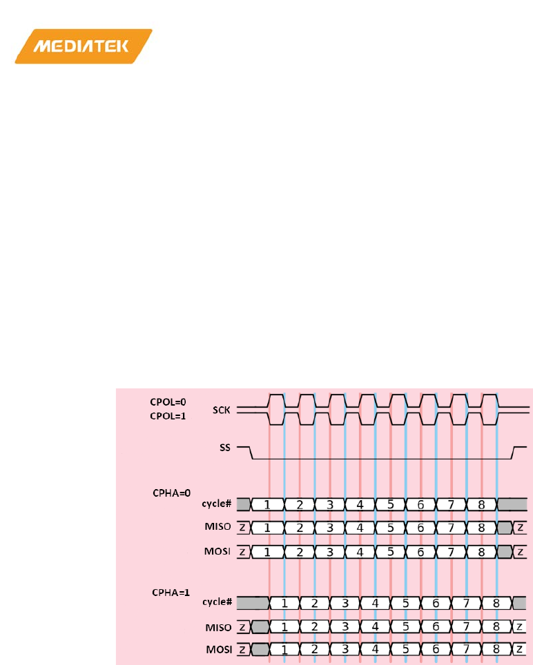
MT76x7
Internet-of-Things Wireless Connectivity
Reference Manual
© 2015 - 2017 MediaTek Inc
Page 616 of 798
This document contains information that is proprietary to MediaTek Inc. (“MediaTek”) and/or its licensor(s).
Any unauthorized use, reproduction or disclosure of this document in whole or in part is strictly prohibited
Step 6
• Get read data at address 0x1013_0008, SPI master asserts following data on SPI_MOSI respectively
• {8’h00, 8’h00, 16’hxx} // get bus read data [15:0] from SPI slave reg00[15:0]
• SPI slave_MISO return data 16’hcdef
• {8’h00, 8’h02, 16’hxx} // get bus read data [31:16] from SPI slave reg00[31:16]
• SPI slave_MISO return data 16’h89ab
2.5.6.5. SPI slave protocol timing
Limitation: Max clock frequency : 20MHz
Figure 2-57. SPI Slave otorola protocol
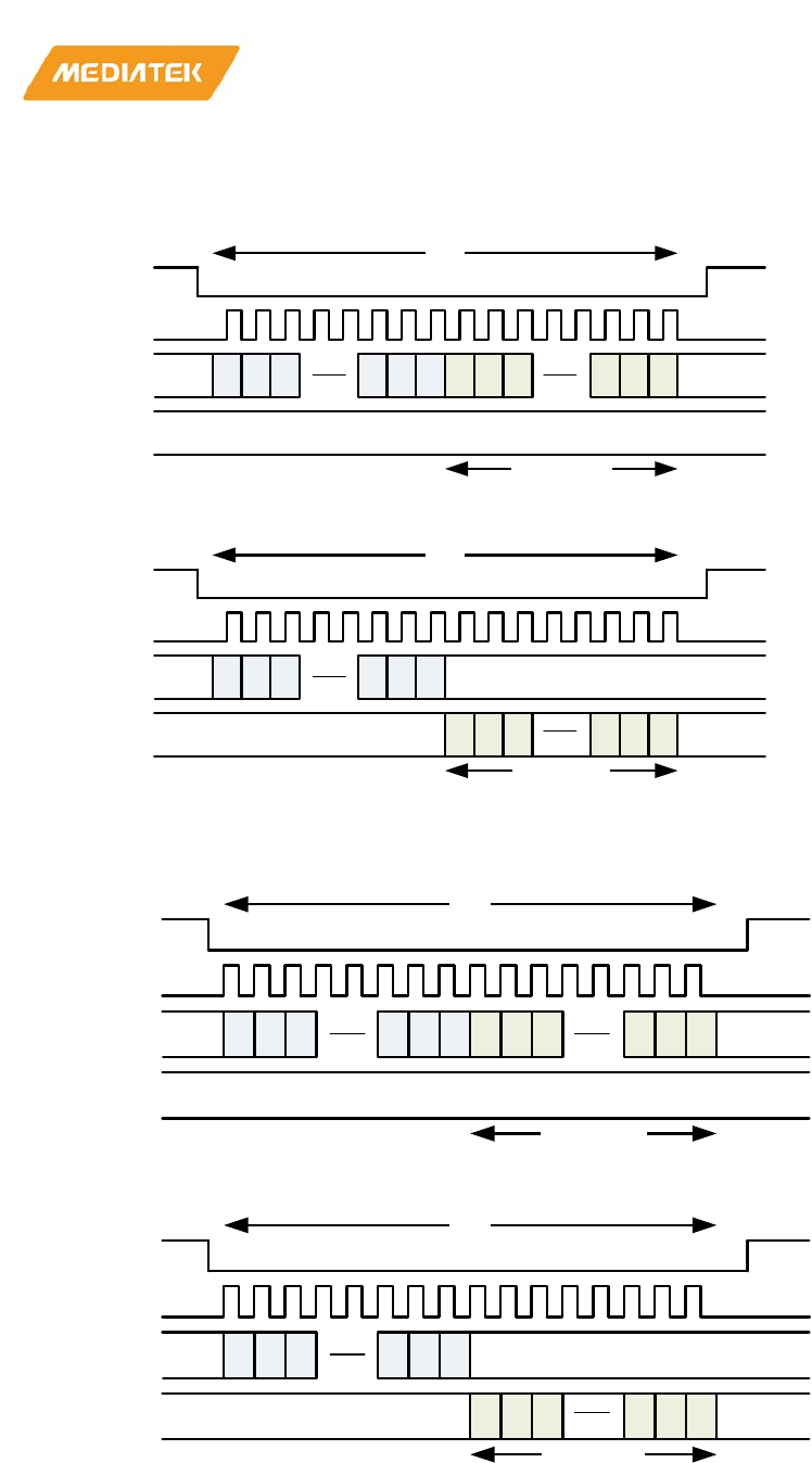
MT76x7
Internet-of-Things Wireless Connectivity
Reference Manual
© 2015 - 2017 MediaTek Inc
Page 617 of 798
This document contains information that is proprietary to MediaTek Inc. (“MediaTek”) and/or its licensor(s).
Any unauthorized use, reproduction or disclosure of this document in whole or in part is strictly prohibited
• CPOL=0, CPHA=0
SPI_CS
WA1
4D1
3
D1
4
A0A1A2
A1
3D1
5D0D1D2
SPI_CK
SPI_MOSI
SPI_MISO
XXX
XXX XXX
32 bits
write data 16-bits
SPIS Write Mode CPOL=0/CPHA=0
SPI_CS
RA1
4
D1
3
D1
4
A0A1A2
A1
3
D1
5D0D1
D2
SPI_CK
SPI_MOSI
SPI_MISO
XXX
32 bits
read data 16-bits
SPIS Read Mode CPOL=0/CPHA=0
XXX
XXX
XXX
• CPOL=0, CPHA=1
SPI_CS
WA1
4D1
3
D1
4
A0
A1
A2
A1
3D1
5D0
D1
D2
SPI_CK
SPI_MOSI
SPI_MISO
XXX
XXX XXX
32 bits
write data 16-bits
SPIS Write Mode CPOL=0/CPHA=1
SPI_CS
RA1
4
D1
3
D1
4
A0
A1
A2
A1
3
D1
5D0
D1
D2
SPI_CK
SPI_MOSI
SPI_MISO
XXX
32 bits
read data 16-bits
SPIS Read Mode CPOL=0/CPHA=1
XXX
XXX
XXX
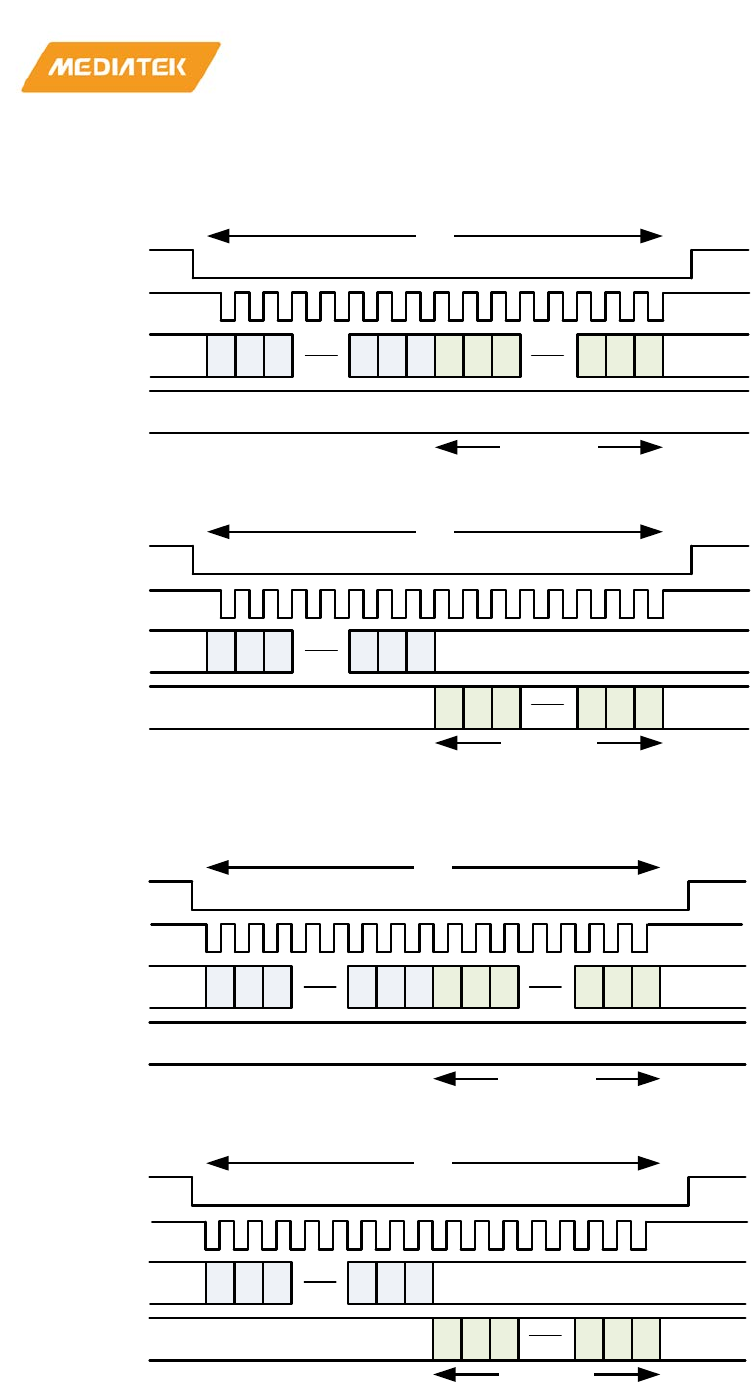
MT76x7
Internet-of-Things Wireless Connectivity
Reference Manual
© 2015 - 2017 MediaTek Inc
Page 618 of 798
This document contains information that is proprietary to MediaTek Inc. (“MediaTek”) and/or its licensor(s).
Any unauthorized use, reproduction or disclosure of this document in whole or in part is strictly prohibited
• CPOL=1, CPHA=0
SPI_CS
WA1
4D1
3
D1
4
A0A1A2
A1
3D1
5D0
D1
D2
SPI_CK
SPI_MOSI
SPI_MISO
XXX
XXX XXX
32 bits
write data 16-bits
SPIS Write Mode CPOL=1/CPHA=0
SPI_CS
RA1
4
D1
3
D1
4
A0A1A2
A1
3
D1
5D0D1D2
SPI_CK
SPI_MOSI
SPI_MISO
XXX
32 bits
read data 16-bits
SPIS Read Mode CPOL=1/CPHA=0
XXX
XXX
XXX
• CPOL=1, CPHA=1
SPI_CS
WA1
4D1
3
D1
4
A0A1A2
A1
3D1
5D0D1D2
SPI_CK
SPI_MOSI
SPI_MISO
XXX
XXX XXX
32 bits
write data 16-bits
SPIS Write Mode CPOL=1/CPHA=1
SPI_CS
RA1
4
D1
3
D1
4
A0A1A2
A1
3
D1
5D0D1D2
SPI_CK
SPI_MOSI
SPI_MISO
XXX
32 bits
read data 16-bits
SPIS Read Mode CPOL=1/CPHA=1
XXX
XXX
XXX

MT76x7
Internet-of-Things Wireless Connectivity
Reference Manual
© 2015 - 2017 MediaTek Inc
Page 619 of 798
This document contains information that is proprietary to MediaTek Inc. (“MediaTek”) and/or its licensor(s).
Any unauthorized use, reproduction or disclosure of this document in whole or in part is strictly prohibited
2.5.6.6. Interrupt
SPI slave doesn’t have a dedicated hardware interrupt indication signal. SPI master could configure
“spi_sw_irq” in REG05 to interrupt MCU. When MCU gets the software interrupt, MCU could clear the IRQ
interrupt by setting SPI slave_REG05.
2.5.6.7. SPI driver domain registers
Register of SPI Slave Interface
Module name: cm4_spi_slave (driver) Base address: (+0h)
Address
Name
Width
Register Function
00000000
REG00
32
SPI SLAVE Register 00
00000004
REG01
32
SPI SLAVE Register 01
00000008
REG02
32
SPI SLAVE Register 02
0000000C
REG03
32
SPI SLAVE Register 03
00000010
REG04
32
SPI SLAVE Register 04
00000014
REG05
32
SPI SLAVE Register 05 (SPI Slave IRQ)
00000018
REG06
32
SPI SLAVE Register 06 (Device to Host
received Mail Box)
0000001C
REG07
32
SPI SLAVE Register 07 (Host to Device
send Mail Box)
00000000
REG00
SPI SLAVE Register 00
00000000
Bit
31
30
29
28
27
26
25
24
23
22
21
20
19
18
17
16
Nam
e
bus_read_data
Type
RO
Rese
t
0 0 0 0 0 0 0 0 0 0 0 0 0 0 0 0
Bit
15
14
13
12
11
10
9
8
7
6
5
4
3
2
1
0
Nam
e
bus_read_data
Type
RO
Rese
t
0 0 0 0 0 0 0 0 0 0 0 0 0 0 0 0
Bit(s)
Name
Description
31:0
bus_read_data
SPI Slave Register 00 for bus read data
00000004
REG01
SPI SLAVE Register 01
00000000
Bit
31
30
29
28
27
26
25
24
23
22
21
20
19
18
17
16
Nam
e
bus_write_data
Type
RW
Rese
t
0 0 0 0 0 0 0 0 0 0 0 0 0 0 0 0
Bit
15
14
13
12
11
10
9
8
7
6
5
4
3
2
1
0
Nam
e
bus_write_data
Type
RW
Rese
0
0
0
0
0
0
0
0
0
0
0
0
0
0
0
0
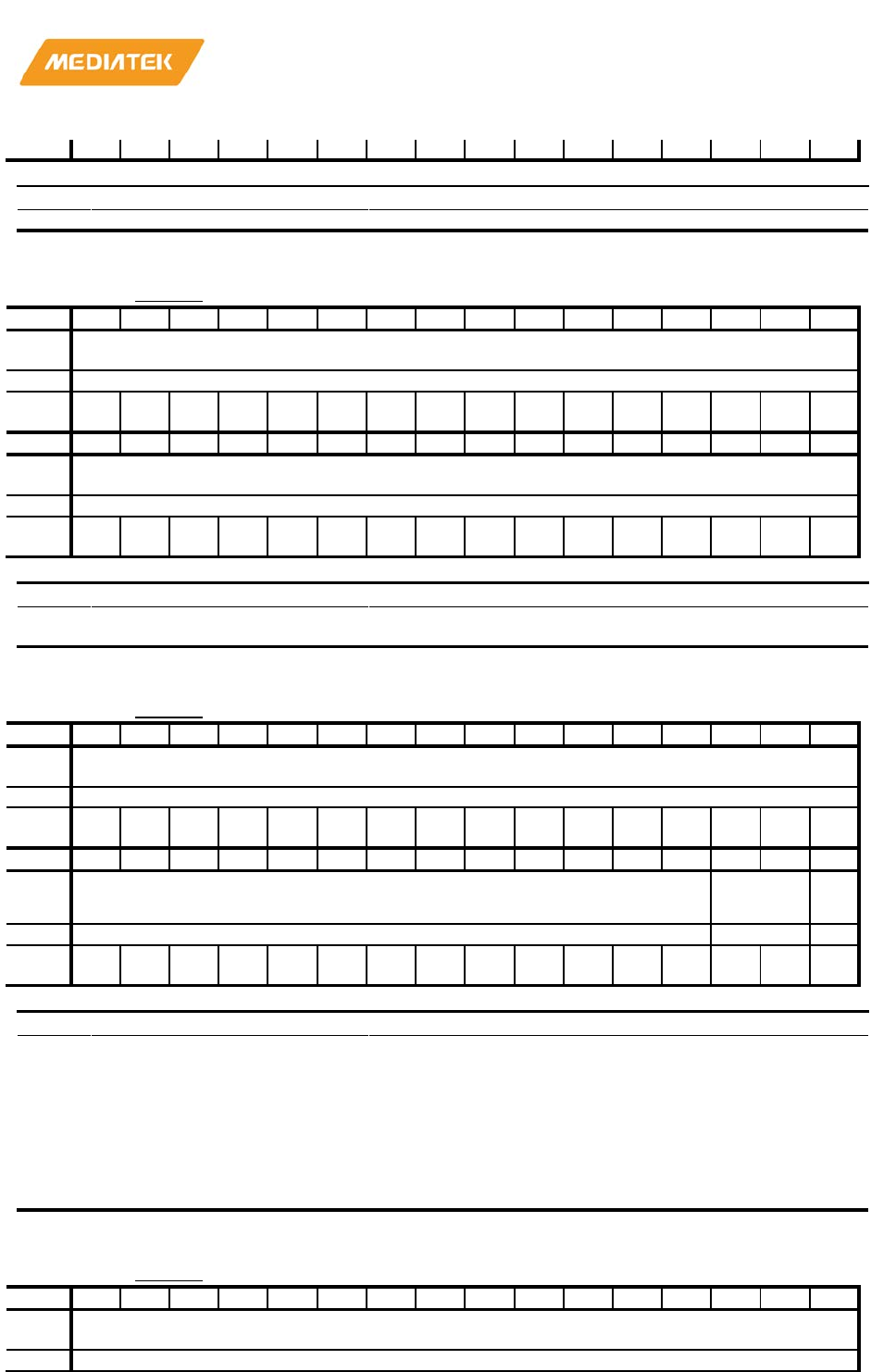
MT76x7
Internet-of-Things Wireless Connectivity
Reference Manual
© 2015 - 2017 MediaTek Inc
Page 620 of 798
This document contains information that is proprietary to MediaTek Inc. (“MediaTek”) and/or its licensor(s).
Any unauthorized use, reproduction or disclosure of this document in whole or in part is strictly prohibited
t
Bit(s)
Name
Description
31:0
bus_write_data
SPI Slave Register 01 for bus write data
00000008
REG02
SPI SLAVE Register 02
00000000
Bit
31
30
29
28
27
26
25
24
23
22
21
20
19
18
17
16
Nam
e
bus_address
Type
RW
Rese
t
0 0 0 0 0 0 0 0 0 0 0 0 0 0 0 0
Bit
15
14
13
12
11
10
9
8
7
6
5
4
3
2
1
0
Nam
e
bus_address
Type
RW
Rese
t
0 0 0 0 0 0 0 0 0 0 0 0 0 0 0 0
Bit(s)
Name
Description
31:0
bus_address
SPI Slave Register 02 for bus address
This address must be physical address
0000000C
REG03
SPI SLAVE Register 03
00000000
Bit
31
30
29
28
27
26
25
24
23
22
21
20
19
18
17
16
Nam
e
reserved
Type
RW
Rese
t
0 0 0 0 0 0 0 0 0 0 0 0 0 0 0 0
Bit
15
14
13
12
11
10
9
8
7
6
5
4
3
2
1
0
Nam
e reserved bus_size
bus
_r_
w
Type
RW
RW
RW
Rese
t
0 0 0 0 0 0 0 0 0 0 0 0 0 0 0 0
Bit(s)
Name
Description
31:3
reserved
reserved
2:1
bus_size
Bus access size
00: reserved
01: reserved
10: word (4bytes)
11: reserved
0
bus_r_w
Bus access type
0: read
1: write
00000010
REG04
SPI SLAVE Register 04
00000000
Bit
31
30
29
28
27
26
25
24
23
22
21
20
19
18
17
16
Nam
e
reserved
Type
RO
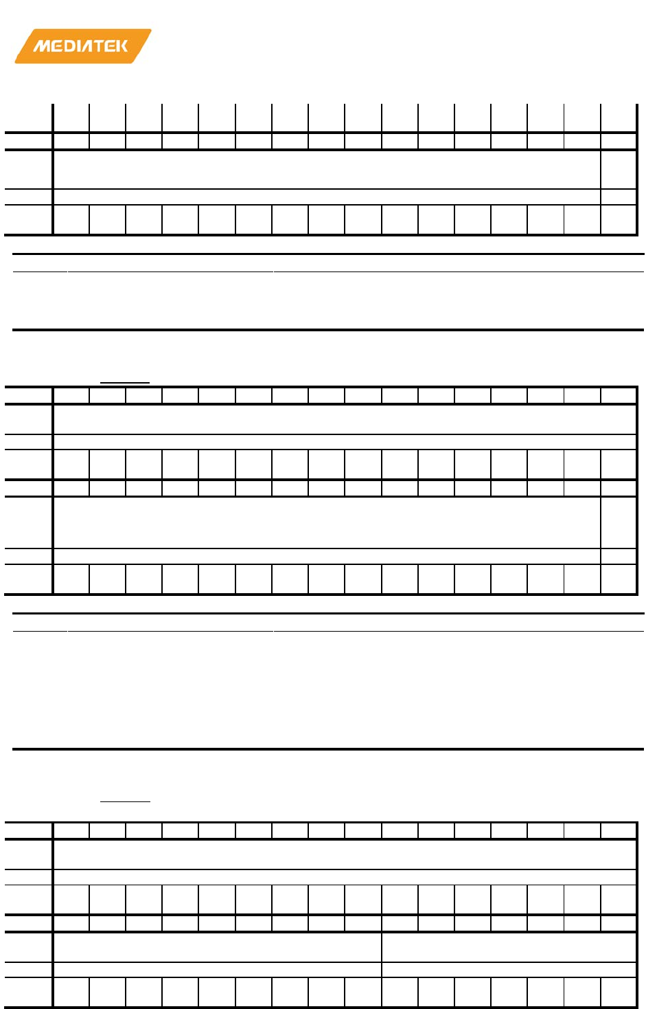
MT76x7
Internet-of-Things Wireless Connectivity
Reference Manual
© 2015 - 2017 MediaTek Inc
Page 621 of 798
This document contains information that is proprietary to MediaTek Inc. (“MediaTek”) and/or its licensor(s).
Any unauthorized use, reproduction or disclosure of this document in whole or in part is strictly prohibited
Rese
t
0 0 0 0 0 0 0 0 0 0 0 0 0 0 0 0
Bit
15
14
13
12
11
10
9
8
7
6
5
4
3
2
1
0
Nam
e reserved
bus
_b
usy
Type
RO
RO
Rese
t
0 0 0 0 0 0 0 0 0 0 0 0 0 0 0 0
Bit(s)
Name
Description
31:1
reserved
reserved
0
bus_busy
Bus interface status
0: SPIS bus interface is idle for next access command
1: SPIS bus interface is busy
00000014
REG05
SPI SLAVE Register 05 (SPI Slave IRQ)
00000000
Bit
31
30
29
28
27
26
25
24
23
22
21
20
19
18
17
16
Nam
e
reserved
Type
RO
Rese
t
0 0 0 0 0 0 0 0 0 0 0 0 0 0 0 0
Bit
15
14
13
12
11
10
9
8
7
6
5
4
3
2
1
0
Nam
e reserved
spi
_s
w_i
rq
Type
RO
W1S
Rese
t
0 0 0 0 0 0 0 0 0 0 0 0 0 0 0 0
Bit(s)
Name
Description
31:1
reserved
reserved
0
spi_sw_irq
SPI host can set this bit to enable interrupt. This bit was
used to inform MCU that Tx data ready. Write 1 to activate
software IRQ interrupt, Write 0 is meaningless.
SPI host read software IRQ status
0: SPI slave IRQ is inactive
1: SPI slave IRQ is active.
00000018
REG06
SPI SLAVE Register 06 (Device to Host
received Mail Box)
00000000
Bit
31
30
29
28
27
26
25
24
23
22
21
20
19
18
17
16
Nam
e
reserved
Type
RO
Rese
t
0 0 0 0 0 0 0 0 0 0 0 0 0 0 0 0
Bit
15
14
13
12
11
10
9
8
7
6
5
4
3
2
1
0
Nam
e
reserved D2HRMB5_0
Type
RO
W1C
Rese
t
0 0 0 0 0 0 0 0 0 0 0 0 0 0 0 0
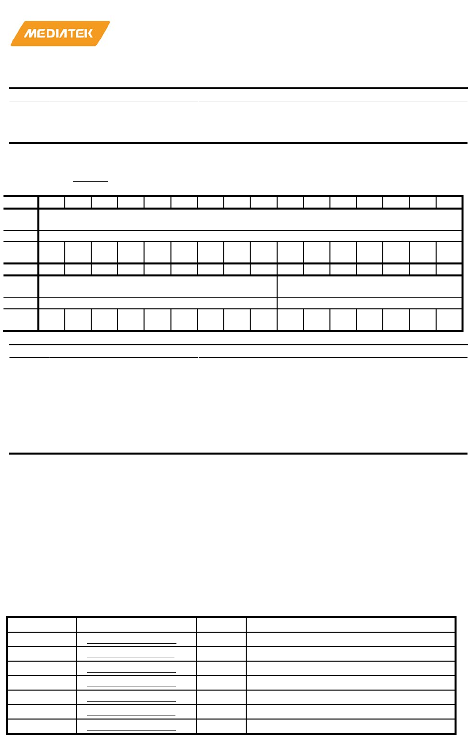
MT76x7
Internet-of-Things Wireless Connectivity
Reference Manual
© 2015 - 2017 MediaTek Inc
Page 622 of 798
This document contains information that is proprietary to MediaTek Inc. (“MediaTek”) and/or its licensor(s).
Any unauthorized use, reproduction or disclosure of this document in whole or in part is strictly prohibited
Bit(s)
Name
Description
31:7
reserved
reserved
6:0
D2HRMB5_0
When MCU write D2HSMB5-0 in the SPIS_REG06, this
bit will be set to 1. SPI host can write 1 to clear D2HRMB5
-
0 and D2HSMB5-0 in the SPIS_REG06.
0000001C
REG07
SPI SLAVE Register 07 (Host to Device
send Mail Box)
00000000
Bit
31
30
29
28
27
26
25
24
23
22
21
20
19
18
17
16
Nam
e
reserved
Type
RO
Rese
t
0 0 0 0 0 0 0 0 0 0 0 0 0 0 0 0
Bit
15
14
13
12
11
10
9
8
7
6
5
4
3
2
1
0
Nam
e
reserved H2DSMB6_0
Type
RO
W1S
Rese
t
0 0 0 0 0 0 0 0 0 0 0 0 0 0 0 0
Bit(s)
Name
Description
31:7
reserved
reserved
6:0
H2DSMB6_0
Host to Device send mailbox bit6 - bit0
SPI Host could set individual bit to inform MCU. When SPI Host
set this bit, MCU can read H2DRMB6
-0 in the SPIS_REG07. SPI
Host writes 0 is meaningless.
SPI Host read H2DSMB6
-0
0: MCU clear the H2DRMB6
-0
1: MCU does not clear the H2DRMB6-0
2.5.6.8. SPI MCU domain registers
The MCU at SPI slave side could access this AHB slave interface to probe the SPI slave internal registers
reg00~reg07 status, and control the SPI polarity/phase.
MCU Domain SPI Slave Register
Module name: cm4_spi_slave Base address: (+21000700h)
Address
Name
Width
Register Function
21000700
SPIS_AHB_REG00
32
SPI AHB Register 00
21000704
SPIS_AHB_REG01
32
SPI AHB Register 01
21000708
SPIS_AHB_REG02
32
SPI AHB Register 02
2100070C
SPIS_AHB_REG03
32
SPI AHB Register 03
21000710
SPIS_AHB_REG04
32
SPI AHB Register 04
21000714
SPIS_AHB_REG05
32
SPI AHB Register 05 (Interrupt Status)
21000718
SPIS_AHB_REG06
32
SPI AHB Register 06 (Device to Host send
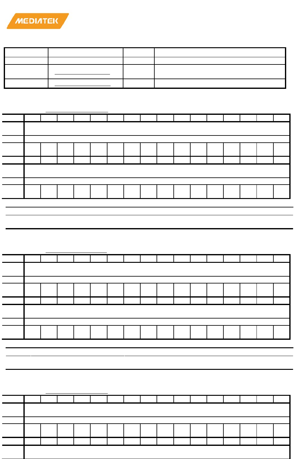
MT76x7
Internet-of-Things Wireless Connectivity
Reference Manual
© 2015 - 2017 MediaTek Inc
Page 623 of 798
This document contains information that is proprietary to MediaTek Inc. (“MediaTek”) and/or its licensor(s).
Any unauthorized use, reproduction or disclosure of this document in whole or in part is strictly prohibited
Address
Name
Width
Register Function
Mail Box)
2100071C
SPIS_AHB_REG07
32
SPI AHB Register 07 (Host to Device
received Mail Box)
21000740
SPIS_AHB_REG08
32
SPI AHB Configuration
21000700
SPIS_AHB_REG00
SPI AHB Register 00
00000000
Bit
31
30
29
28
27
26
25
24
23
22
21
20
19
18
17
16
Nam
e
bus_read_data
Type
RO
Rese
t
0 0 0 0 0 0 0 0 0 0 0 0 0 0 0 0
Bit
15
14
13
12
11
10
9
8
7
6
5
4
3
2
1
0
Nam
e
bus_read_data
Type
RO
Rese
t
0 0 0 0 0 0 0 0 0 0 0 0 0 0 0 0
Bit(s)
Name
Description
31:0
bus_read_data
Read SPI Slave REG00
SPI Slave Register 00 for bus read data
21000704
SPIS_AHB_REG01
SPI AHB Register 01
00000000
Bit
31
30
29
28
27
26
25
24
23
22
21
20
19
18
17
16
Nam
e
bus_write_data
Type
RO
Rese
t
0 0 0 0 0 0 0 0 0 0 0 0 0 0 0 0
Bit
15
14
13
12
11
10
9
8
7
6
5
4
3
2
1
0
Nam
e
bus_write_data
Type
RO
Rese
t
0 0 0 0 0 0 0 0 0 0 0 0 0 0 0 0
Bit(s)
Name
Description
31:0
bus_write_data
Read SPI Slave REG01
SPI Slave Register 01 for bus write data
21000708
SPIS_AHB_REG02
SPI AHB Register 02
00000000
Bit
31
30
29
28
27
26
25
24
23
22
21
20
19
18
17
16
Nam
e
bus_address
Type
RO
Rese
t
0 0 0 0 0 0 0 0 0 0 0 0 0 0 0 0
Bit
15
14
13
12
11
10
9
8
7
6
5
4
3
2
1
0
Nam
e
bus_address
MT76x7
Internet-of-Things Wireless Connectivity
Reference Manual
© 2015 - 2017 MediaTek Inc
Page 624 of 798
This document contains information that is proprietary to MediaTek Inc. (“MediaTek”) and/or its licensor(s).
Any unauthorized use, reproduction or disclosure of this document in whole or in part is strictly prohibited
Type
RO
Rese
t
0 0 0 0 0 0 0 0 0 0 0 0 0 0 0 0
Bit(s)
Name
Description
31:0
bus_address
Read SPI Slave REG02
SPI Slave
Register 02 for bus address
This address must be physical address
2100070C
SPIS_AHB_REG03
SPI AHB Register 03
00000000
Bit
31
30
29
28
27
26
25
24
23
22
21
20
19
18
17
16
Nam
e
reserved
Type
RO
Rese
t
0 0 0 0 0 0 0 0 0 0 0 0 0 0 0 0
Bit
15
14
13
12
11
10
9
8
7
6
5
4
3
2
1
0
Nam
e reserved bus_size
bus
_r_
w
Type
RO
RO
RO
Rese
t
0 0 0 0 0 0 0 0 0 0 0 0 0 0 0 0
Bit(s)
Name
Description
31:3
reserved
reserved
2:1
bus_size
Read SPI Slave REG03
Bus access size
00: reserved
01: reserved
10: word (4bytes)
11: reserved
0
bus_r_w
Read SPI Slave REG03
Bus access type
0: read
1: write
21000710
SPIS_AHB_REG04
SPI AHB Register 04
00000000
Bit
31
30
29
28
27
26
25
24
23
22
21
20
19
18
17
16
Nam
e
reserved
Type
RO
Rese
t
0 0 0 0 0 0 0 0 0 0 0 0 0 0 0 0
Bit
15
14
13
12
11
10
9
8
7
6
5
4
3
2
1
0
Nam
e reserved
bus
_b
usy
Type
RO
RO
Rese
t
0 0 0 0 0 0 0 0 0 0 0 0 0 0 0 0
Bit(s)
Name
Description
31:1
reserved
reserved
0
bus_busy
Read SPI Slave REG04
Bus interface status
MT76x7
Internet-of-Things Wireless Connectivity
Reference Manual
© 2015 - 2017 MediaTek Inc
Page 625 of 798
This document contains information that is proprietary to MediaTek Inc. (“MediaTek”) and/or its licensor(s).
Any unauthorized use, reproduction or disclosure of this document in whole or in part is strictly prohibited
Bit(s)
Name
Description
0: SPIS bus interface is idle for next access command
1: SPIS bus interface is busy
21000714
SPIS_AHB_REG05
SPI AHB Register 05 (Interrupt Status)
00000000
Bit
31
30
29
28
27
26
25
24
23
22
21
20
19
18
17
16
Nam
e
reserved
Type
RO
Rese
t
0 0 0 0 0 0 0 0 0 0 0 0 0 0 0 0
Bit
15
14
13
12
11
10
9
8
7
6
5
4
3
2
1
0
Nam
e reserved
spi
_s
w_i
rq
Type RO
W1
C
Rese
t
0 0 0 0 0 0 0 0 0 0 0 0 0 0 0 0
Bit(s)
Name
Description
31:1
reserved
reserved
0
spi_sw_irq
If SPI host write 1 to spi_sw_irq in REG05, this bit will be
set to 1.
0: SPI slave software IRQ is inactive
1: SPI slave software IRQ is active.
MCU can clear this bit by write 1. Write 0 is meaningless.
21000718
SPIS_AHB_REG06
SPI AHB Register 06 (Device to Host
send Mail Box)
00000000
Bit
31
30
29
28
27
26
25
24
23
22
21
20
19
18
17
16
Nam
e
reserved
Type
RO
Rese
t
0 0 0 0 0 0 0 0 0 0 0 0 0 0 0 0
Bit
15
14
13
12
11
10
9
8
7
6
5
4
3
2
1
0
Nam
e reserved
SPI
_2
0M
hz_
Opt
oin
D2HSMB5_0
Type
RO
W1
W1S
Rese
t
0 0 0 0 0 0 0 0 0 0 0 0 0 0 0 0
Bit(s)
Name
Description
31:7
reserved
reserved
6
SPI_20Mhz_Optoin
Internal option for 20Mhz SPI clock configuration.
This configuration is write only. Read will return 0.
5:0
D2HSMB5_0
Device to Host send mailbox bit5 - bit0
MCU could set individual bit to inform SPI host. When MCU set
this bit, SPI host can read D2HRMB5
-
0 in the REG06. MCU write 0
is meaningless.
MT76x7
Internet-of-Things Wireless Connectivity
Reference Manual
© 2015 - 2017 MediaTek Inc
Page 626 of 798
This document contains information that is proprietary to MediaTek Inc. (“MediaTek”) and/or its licensor(s).
Any unauthorized use, reproduction or disclosure of this document in whole or in part is strictly prohibited
Bit(s)
Name
Description
MCU read D2HSMB6-0
0: SPI host clear the D2HRMB6
-0
1: SPI host does not clear the D2HRMB6-0
2100071C
SPIS_AHB_REG07
SPI AHB Register 07 (Host to Device
received Mail Box)
00000000
Bit
31
30
29
28
27
26
25
24
23
22
21
20
19
18
17
16
Nam
e
reserved
Type
RO
Rese
t
0 0 0 0 0 0 0 0 0 0 0 0 0 0 0 0
Bit
15
14
13
12
11
10
9
8
7
6
5
4
3
2
1
0
Nam
e
reserved H2DRMB6_0
Type
RO
W1C
Rese
t
0 0 0 0 0 0 0 0 0 0 0 0 0 0 0 0
Bit(s)
Name
Description
31:7
reserved
reserved
6:0
H2DRMB6_0
When SPI Host write H2DSMB6-0 in the REG07, this bit
will be set to 1. MCU can write 1 to clear H2DRMB6
-0 and
H2DSMB6-0 in the REG07.
21000740
SPIS_AHB_REG08
SPI AHB Configuration
00000000
Bit
31
30
29
28
27
26
25
24
23
22
21
20
19
18
17
16
Nam
e
reserved
Type
RW
Rese
t
0 0 0 0 0 0 0 0 0 0 0 0 0 0 0 0
Bit
15
14
13
12
11
10
9
8
7
6
5
4
3
2
1
0
Nam
e reserved
ahb
_ad
dr_
inc
_di
sab
le
reserved spis_mod
e
Type
RW
RW
RW
RW
Rese
t
0 0 0 0 0 0 0 0 0 0 0 0 0 0 0 0
Bit(s)
Name
Description
31:5
reserved
reserved
4
ahb_addr_inc_disable
The address auto increment function for AHB Master
0: The address will auto increment after AHB Master read/write
done.
1: The address will disable auto increment function.
3:2
reserved
reserved
1:0
spis_mode
SPI slave clock polarity and phase configuration
2'b00: CPOL=0, CPHA=0
2'b01: CPOL=0, CPHA=1
2'b10: CPOL=1, CPHA=0
2'b11: CPOL=1, CPHA=1

MT76x7
Internet-of-Things Wireless Connectivity
Reference Manual
© 2015 - 2017 MediaTek Inc
Page 627 of 798
This document contains information that is proprietary to MediaTek Inc. (“MediaTek”) and/or its licensor(s).
Any unauthorized use, reproduction or disclosure of this document in whole or in part is strictly prohibited
Bit(s)
Name
Description

MT76x7
Internet-of-Things Wireless Connectivity
Reference Manual
© 2015 - 2017 MediaTek Inc
Page 628 of 798
This document contains information that is proprietary to MediaTek Inc. (“MediaTek”) and/or its licensor(s).
Any unauthorized use, reproduction or disclosure of this document in whole or in part is strictly prohibited
2.5.6.9. SPI pinmux configuration
MT76x7 needs to setup pinmux configuration to select fast-speed GPIO for SPI Slave interface. Also, it needs to
setup internal option for 20Mhz SPI clock.
Table 2-52. SPI Interface Pinmux Configuration
PINMUX Configuration (AON FUNC6)
Write address [0x8102302c], Bit[31:20] = 0x666
Write address [0x81023030], Bit[3:0] = 0x6
MT76x7 SPI slave needs to setup internal option for 20Mhz SPI Clock. Following table list configuration for
CPOL/CPHA setting.
Table 2-53. SPI CPOL/CPHA configuration
SPI Slave CPOL/CPHA Configuration
Mode 1 (CPOL =0 / CPHA=0)
Write address [0x21000718], Bit[6] = 0x1
Write address [0x21000740], Bit[1:0] = 0x0
Write address [0x81023058], Bit[5] = 0x1
Write address [0x8102305c], Bit[5] = 0x0
Mode 2 (CPOL =0 / CPHA=1)
Write address [0x21000718], Bit[6] = 0x1
Write address [0x21000740], Bit[1:0] = 0x1
Write address [0x81023058], Bit[5] = 0x1
Write address [0x8102305c], Bit[5] = 0x1
Mode 3 (CPOL =1 / CPHA=0)
Write address [0x21000718], Bit[6] = 0x1
Write address [0x21000740], Bit[1:0] = 0x2
Write address [0x81023058], Bit[5] = 0x1
Write address [0x8102305c], Bit[5] = 0x1
Mode 4 (CPOL =1 / CPHA=1)
Write address [0x21000718], Bit[6] = 0x1
Write address [0x21000740], Bit[1:0] = 0x3
Write address [0x81023058], Bit[5] = 0x1
Write address [0x8102305c], Bit[5] = 0x0
MT76x7
Internet-of-Things Wireless Connectivity
Reference Manual
© 2015 - 2017 MediaTek Inc
Page 629 of 798
This document contains information that is proprietary to MediaTek Inc. (“MediaTek”) and/or its licensor(s).
Any unauthorized use, reproduction or disclosure of this document in whole or in part is strictly prohibited
2.5.7. I2S interface
MT76x7 features one I2S interface, which is used to connect to an external audio codec. The I2S interface can
support the I2S slave mode only. The five I2S signals are shown below. The I2S_MLK clock frequency is 16MHz.
Table 2-54. I2S pin description
Signal Name Signal Description Direction (Slave Mode)
I2S_MCLK The base clock of the function. Output
I2S_BCLK The bit clock of the interface Input
I2S_FS (LRCLK) The left/right word select line
of the interface
Input
I2S_TX Digital audio output Output
I2S_RX Digital audio input Input
MT76x7 supplies the MCLK of 16MHz. The external CODEC generates BCLK and LRCLK from MCLK. When
configured as the I2S slave mode, the I2S interface can support two modes.
Table 2-55. I2S Slave Mode
Slave Mode Bit Width Input Sample (Uplink) Output Sample
(Downlink)
BCLK
(Input)
FS (Input)
Mode 1 16b 16KHz, mono/stereo 16KHz, mono/stereo 512KHz 16KHz
Mode 2 16b 24KHz, mono/stereo 24KHz, mono/stereo 768KHz 24KHz
Mode 3 16b 44.1KHz, mono/stereo 44.1KHz, mono/stereo 1.4112MHz 44.1KHz
Mode 4 16b 48KHz, mono/stereo 48KHz, mono/stereo 1.536MHz 48KHz
Table 2-56. I2S Data Format
Byte 3
Byte 2
Byte 1
Byte 0
Stereo(2 CH)
R[15:8]
R[7:0]
L[15:8]
L[7:0]
Mono(1 CH)
8’b0
8’b0
L[15:8]
L[7:0]
The mono data is transferred across the I2S bus as left channel information.
In all of the modes above, when the input data is mono, the data of interest is transferred across the I2S bus
on the left channel.
The I2S pins are multiplexed with SPI pins.
The signal waveform of I2S is shown below.
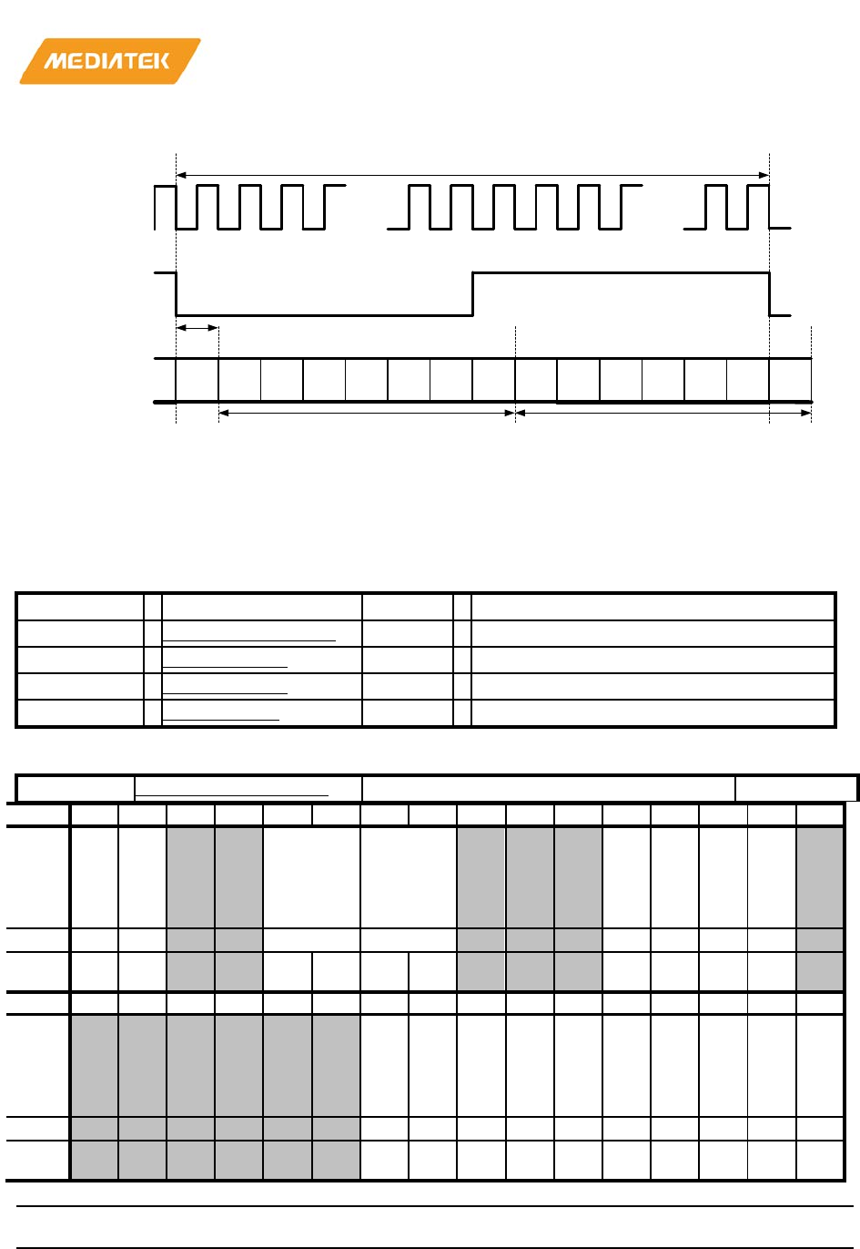
MT76x7
Internet-of-Things Wireless Connectivity
Reference Manual
© 2015 - 2017 MediaTek Inc
Page 630 of 798
This document contains information that is proprietary to MediaTek Inc. (“MediaTek”) and/or its licensor(s).
Any unauthorized use, reproduction or disclosure of this document in whole or in part is strictly prohibited
I2S_FS
I2S_TX/RX
L[15] L[14] L[13] L[2] L[1]
…L[0] R[15] R[14] R[13] R[2] R[1]
…R[0]
I2S_BCLK
……
R[0]
1T delay
Left channel Right channel
1/SR
Figure 2-58. I2S signal waveform
2.5.7.1. Registers definitions
Module name: audio_top Base address: (+830b0000h)
Address
Name
Width
Register Function
830B0000
GLOBAL_CONTROL
32
AUDIO TOP CONTROL REGISTER
830B0004
DL_CONTROL
32
DL I2S CONTROL REGISTER
830B0008
UL_CONTROL
32
UL I2S CONTROL REGISTER
830B000C
SOFT_RESET
32
DLUL SOFT RESET REGISTER
830B0000
GLOBAL_CONTROL
AUDIO TOP CONTROL REGISTER
00000000
Bit
31
30
29
28
27
26
25
24
23
22
21
20
19
18
17
16
Nam
e
LO
OP
BA
CK
BT
_M
OD
E
CLK_SEL
_OUT CLK_SEL
_IN
NE
G_
CA
P
CK
_I
NV
X2
6M
_S
EL
CO
DE
C_
26
M_
EN
Type
RW
WO
RW
RW
RW
RW
RW
WO
Rese
t
0 0 0 0 0 0 0 0 0 0
Bit
15
14
13
12
11
10
9
8
7
6
5
4
3
2
1
0
Nam
e
DL
_M
ON
O_
DU
P
DL
_M
ON
O
DL
_L
RS
W
EX
T_
LR
SW
EX
T
EX
T_I
O_
CK
EN
GE
N_
EN
UL
FIF
O_
EN
DL
FIF
O_
EN
EN
Type
RW
RW
RW
RW
RW
WO
RW
RW
RW
RW
Rese
t
0 0 0 0 0 0 0 0 0 0
Bit(s)
Name
Description
31
LOOPBACK
I2S out to I2S in loopback
0: disable

MT76x7
Internet-of-Things Wireless Connectivity
Reference Manual
© 2015 - 2017 MediaTek Inc
Page 631 of 798
This document contains information that is proprietary to MediaTek Inc. (“MediaTek”) and/or its licensor(s).
Any unauthorized use, reproduction or disclosure of this document in whole or in part is strictly prohibited
Bit(s)
Name
Description
1: enable
30
BT_MODE
external I2S is from PAD/BT
0: PAD
1: BT
27:26
CLK_SEL_OUT
I2S out clock source selection
00 : 13M(depend on 26M_SEL) (master)
01 : 26M(depend on 26M_SEL)
10 : XPLL 16M
11 : external bclk in (slave)
25:24
CLK_SEL_IN
I2S in source selection
00 : 13M(depend on 26M_SEL) (master)
01 : 26M(depend on 26M_SEL)
10 :
XPLL 16M
11 : external bclk in (slave)
20
NEG_CAP
Negative edge capture RX data
0: disable
1: enable
19
CK_INV
MCLK clock inverse
0: disable
1: enable
18
X26M_SEL
26M clock source selection
0 : XTAL
Clock
1 : XPLL 26M
17
CODEC_26M_EN
cg of internal codec(default on)
9
DL_MONO_DUP
When DL_MONO=1, if right channel send duplicate data.
0: right channel send all 0.
1: right channel send the same data as the left.
8
DL_MONO
DL MONO mode
0: STEREO
1: MONO
7
DL_LRSW
DL with LR switch

MT76x7
Internet-of-Things Wireless Connectivity
Reference Manual
© 2015 - 2017 MediaTek Inc
Page 632 of 798
This document contains information that is proprietary to MediaTek Inc. (“MediaTek”) and/or its licensor(s).
Any unauthorized use, reproduction or disclosure of this document in whole or in part is strictly prohibited
Bit(s)
Name
Description
0: LR no swap
1: LR
swap
6
EXT_LRSW
External codec with LR switch
0: LR no swap
1: LR swap
5
EXT
External codec mode(slave)
0: internal codec
1: external codec
4
EXT_IO_CK
Clk source of external codec mode(slave)
0: from i2s_in
1: from i2s_out
3
ENGEN_EN
Engen enable
0:
disable
1: enable
2
ULFIFO_EN
UL_FIFO enable
0: disable
1: enable
1
DLFIFO_EN
DL_FIFO enable
0: disable
1: enable
0
EN
Audio top enable
830B0004
DL_CONTROL
DL I2S CONTROL REGISTER
00000008
Bit
31
30
29
28
27
26
25
24
23
22
21
20
19
18
17
16
Nam
e
LR
_S
WA
P
CH_PER_
S MSB_OFFSET
Type
RW
RW
RW
Rese
t
0 0 0 0 0 0 0 0 0 0
Bit
15
14
13
12
11
10
9
8
7
6
5
4
3
2
1
0
Nam
e
WS
_R
SY
NC
BIT_PER
_S HD
EN SR WS
IN
V
DI
R FM
T SR
C WL
EN EN
Type
RW
RW
RO
RW
RW
RO
RW
RW
RO
RW

MT76x7
Internet-of-Things Wireless Connectivity
Reference Manual
© 2015 - 2017 MediaTek Inc
Page 633 of 798
This document contains information that is proprietary to MediaTek Inc. (“MediaTek”) and/or its licensor(s).
Any unauthorized use, reproduction or disclosure of this document in whole or in part is strictly prohibited
Rese
t
0 0 0 0 0 0 0 0 0 0 1 0 0 0
Bit(s)
Name
Description
31
LR_SWAP
Swap the data of Right and Left channel
0: no swap
1: swap
30:29
CH_PER_S
Number of channel in each FS cycle (just used in TDM
mode)
00: 2 channels
01: 4 channels
23:17
MSB_OFFSET
Delay cycle from rising edge of FS to first channel MSB
0 : 0T
n : nT
15
WS_RSYNC
WS sync function enable for external codec, the LR I2S
data will be aligned with every WS edge
0: WS sync function disable
1: WS sync function enable
14:13
BIT_PER_S
Number of bits in each FS cycle
00: 32 bits
01: 64 bits
10: 128 bits
12
HDEN
0: ENGEN source is 26M
11:8
SR
Sample rate
0000 : 8k
0010 : 12k
0100 : 16k
0110 : 24k
1000 : 32k
1010 : 48k
else : reserved
5
WSINV
WS reverse
0 : no reverse
1 :
reverse
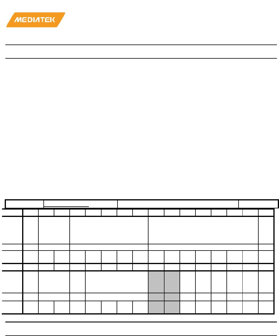
MT76x7
Internet-of-Things Wireless Connectivity
Reference Manual
© 2015 - 2017 MediaTek Inc
Page 634 of 798
This document contains information that is proprietary to MediaTek Inc. (“MediaTek”) and/or its licensor(s).
Any unauthorized use, reproduction or disclosure of this document in whole or in part is strictly prohibited
Bit(s)
Name
Description
4
DIR
0 : TX
3
FMT
Data Format
1 : I2S
0 : TDM
2
SRC
Master/Slave mode
0 : master
1 : slave
1
WLEN
Sample Size
0: 16bits
0
EN
I2S out enable
830B0008
UL_CONTROL
UL I2S CONTROL REGISTER
00000018
Bit
31
30
29
28
27
26
25
24
23
22
21
20
19
18
17
16
Nam
e
LR
_S
WA
P
CH_PER_
S UPDATE_WORD MSB_OFFSET
DO
WN
_R
AT
E
Type
RW
RW
RW
RW
RW
Rese
t
0 0 0 0 0 0 0 0 0 0 0 0 0 0 0 0
Bit
15
14
13
12
11
10
9
8
7
6
5
4
3
2
1
0
Nam
e
WS
_R
SY
NC
BIT_PER
_S HD
EN SR WS
IN
V
DI
R FM
T SR
C WL
EN EN
Type
RW
RW
RO
RW
RW
RO
RW
RW
RO
RW
Rese
t
0 0 0 0 0 0 0 0 0 1 1 0 0 0
Bit(s)
Name
Description
31
LR_SWAP
Swap the data of Right and Left channel
0: no swap
1: swap
30:29
CH_PER_S
Number of channel in each FS cycle (just used in TDM
mode)
00: 2 channels
01: 4 channels
28:24
UPDATE_WORD
Which cycle will I2S in update FIFO

MT76x7
Internet-of-Things Wireless Connectivity
Reference Manual
© 2015 - 2017 MediaTek Inc
Page 635 of 798
This document contains information that is proprietary to MediaTek Inc. (“MediaTek”) and/or its licensor(s).
Any unauthorized use, reproduction or disclosure of this document in whole or in part is strictly prohibited
Bit(s)
Name
Description
23:17
MSB_OFFSET
Delay cycle from rising edge of FS to first channel MSB
0 : 0T
n : nT
16
DOWN_RATE
Will UL real sample rate is 1/2 of SR
0: real sample rate = SR
1:
drop 1 sample in each 2 input samples
15
WS_RSYNC
WS sync function enable for external codec, the LR I2S
data will be aligned with every WS edge
0: WS sync function disable
1: WS sync function enable
14:13
BIT_PER_S
Number of bits in each FS cycle
00: 32
bits
01: 64 bits
10: 128 bits
12
HDEN
0: ENGEN source is 26M
11:8
SR
Sample rate
0000 : 8k
0010 : 12k
0100 : 16k
0110 : 24k
1000 : 32k
1010 : 48k
else : reserved
5
WSINV
WS reverse
0 : no reverse
1 : reverse
4
DIR
1 : RX
3
FMT
Data Format
1 : I2S
0
: TDM
2
SRC
Master/Slave mode
0 : master
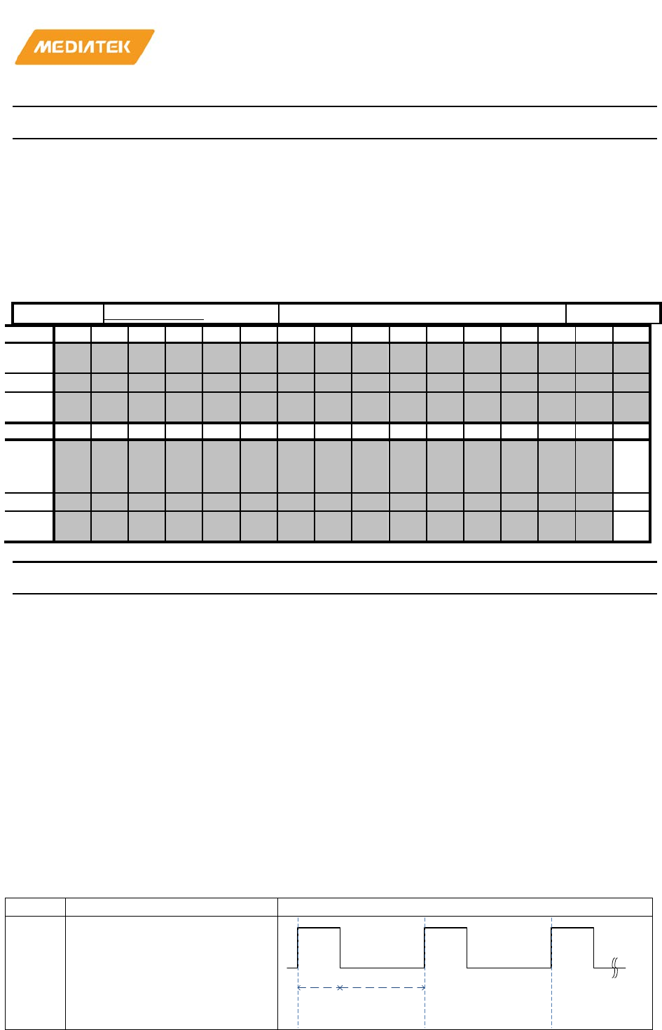
MT76x7
Internet-of-Things Wireless Connectivity
Reference Manual
© 2015 - 2017 MediaTek Inc
Page 636 of 798
This document contains information that is proprietary to MediaTek Inc. (“MediaTek”) and/or its licensor(s).
Any unauthorized use, reproduction or disclosure of this document in whole or in part is strictly prohibited
Bit(s)
Name
Description
1 : slave
1
WLEN
Sample Size
0: 16bits
0
EN
I2S out enable
830B000C
SOFT_RESET
DLUL SOFT RESET REGISTER
00000000
Bit
31
30
29
28
27
26
25
24
23
22
21
20
19
18
17
16
Nam
e
Type
Rese
t
Bit
15
14
13
12
11
10
9
8
7
6
5
4
3
2
1
0
Nam
e
SO
FT
_R
ST
Type
RW
Rese
t
0
Bit(s)
Name
Description
0
SOFT_RST
soft reset audio_top and codec, active high.
If you want to reset ,please write this bit to 1 and then write 0.
2.5.8. Pulse Width Modulation (PWM)
2.5.8.1. General description
MT76x7 features 28 generic PWMs to generate pulse sequences with programmable frequency and duration
for LCD, vibrators, and other devices. The PMU features three configurable pattern options with three PWM
clock frequency sources: 32KHz/2MHz/XTAL
Table 2-57. PWM Modes
Mode
Description
Waveform
1
Basic PWM:
LED ON time (duration) and LED
OFF time (duration) are
configurable.
LED ON
Time
LED OFF
Time
LED ON LED OFF
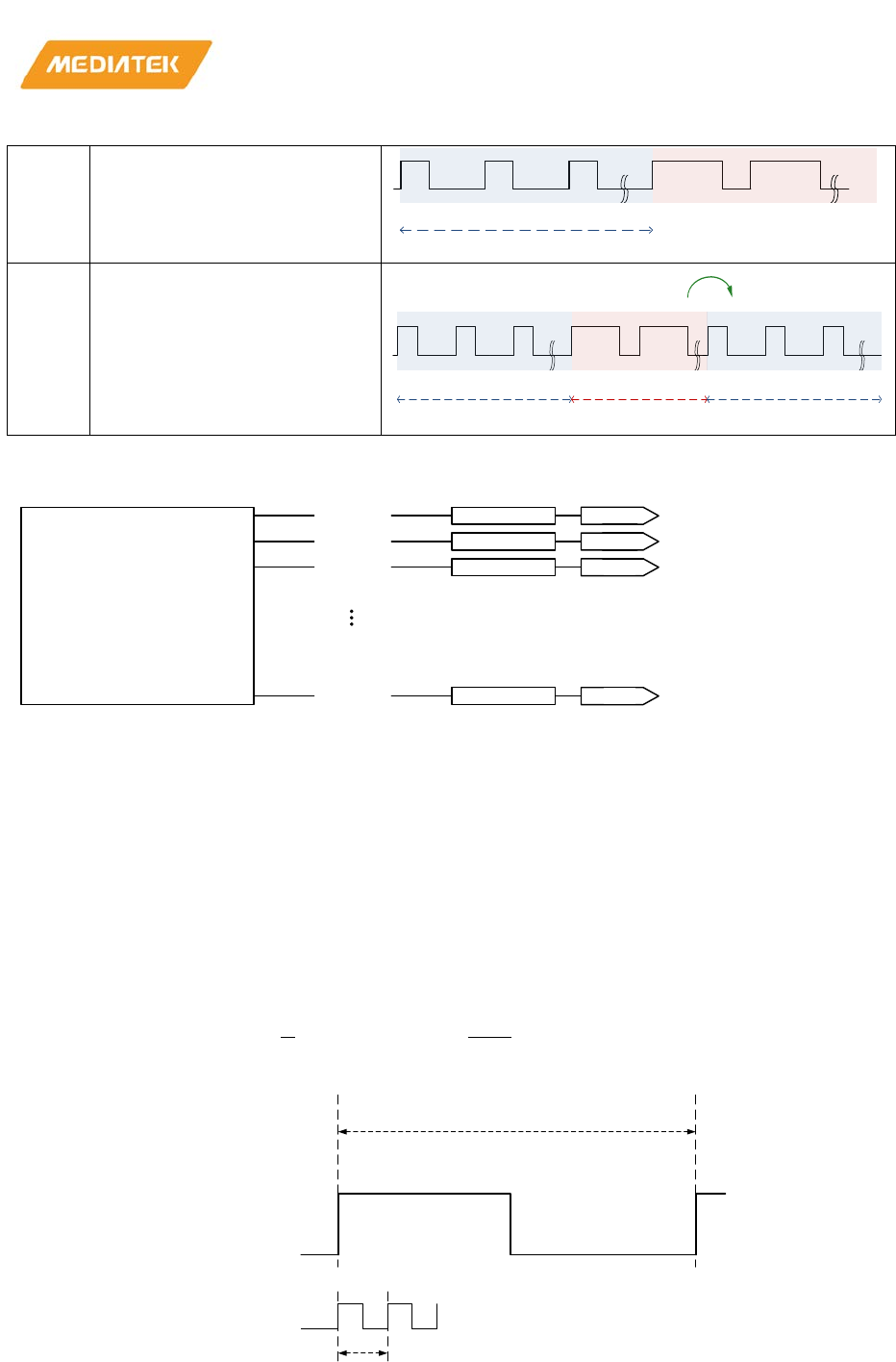
MT76x7
Internet-of-Things Wireless Connectivity
Reference Manual
© 2015 - 2017 MediaTek Inc
Page 637 of 798
This document contains information that is proprietary to MediaTek Inc. (“MediaTek”) and/or its licensor(s).
Any unauthorized use, reproduction or disclosure of this document in whole or in part is strictly prohibited
2
Two-State PWM:
There are two configurable states
(S0 and S1) for PWM LED.
S0S1
S0 Lastingtime
3
Two-State replay mode:
User can set replay mode with
specified S1_Lasting_Time. PWM
LED would act as
[S0àS1àS0àS1àS0…] with
period time of (S0_Lasting_Time +
S1_Lasting_Time)
2.5.8.2. PWM block diagram
PWM_TOP
PWM_00
PWM_01
PWM_02
PWM_39
IO MUX
IO MUX
IO MUX
IO MUX
PAD
PAD
PAD
PAD
Figure 2-59. PWM block diagram
There are total 40 PWM modules in MT76X7 which can be configured individually. All PWM-related HW
modules belong to always-on power domain, including the output pinmux selection logic.
SW programmers should refer to iomux/pinmux table to enable the corresponding output multiplexer of each
PWM module.
2.5.8.3. PWM function
The PWM function is described below.
• PWM Formula
User can set pwm_on_time (X) ≈ Df
F , pwm_off_time (Y) ≈ (1−D)f
F to approach the target PWM duty cycle (D)
and PWM frequency (F) with tick clock frequency (f)
tick_clk
t
T
PWM output
Figure 2-60. PWM Cycle
S0 S1
S0 Lastingtime S1 Lastingtime
S0
S0 Lastingtime
replay
MT76x7
Internet-of-Things Wireless Connectivity
Reference Manual
© 2015 - 2017 MediaTek Inc
Page 638 of 798
This document contains information that is proprietary to MediaTek Inc. (“MediaTek”) and/or its licensor(s).
Any unauthorized use, reproduction or disclosure of this document in whole or in part is strictly prohibited
Table 2-58. PWM parameters
T(second) PWM period
F (Hz) PWM frequency = 1/T
t (second) Tick clk period
f (Hz) Tick clk frequency = 1/t
D (%) Duty cycle
X (unit t) Value of configurable register pwm_on_time[15:0], in unit t
Y (unit t) Value of configurable register pwm_off_time[15:0], in unit t
Res (step) PWM resolution of duty cycle on certain F, f
Below is the derivation of PWM function.
(X + Y) t = T
(X + Y) = T
t = f
F =Res
D = X
(X+Y)
X = D(X+Y) = Df
F
Y = f
F – X = f
F - Df
F = (1−D)f
F
• PWM Modes
There are three modes in this PWM IP:
• Basic mode
• 2-state PWM
• 2-state with reply mode.
1) Basic PWM
PWM_ON duration and PWM_OFF duration are configurable by setting
pwm_on_time[15:0] and pwm_off_time[15:0]. Once these parameters are set, PWM
would act periodically with
a) Period: (PWM_ON duration + PWM_OFF duration)
b) Duty cycle: PWM_ON duration
(PWM_ON duration + PWM_OFF duration)
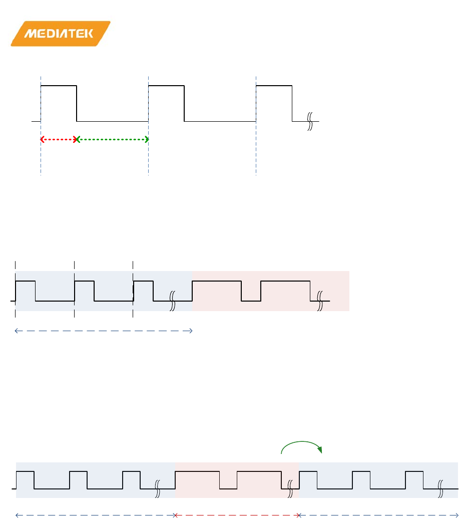
MT76x7
Internet-of-Things Wireless Connectivity
Reference Manual
© 2015 - 2017 MediaTek Inc
Page 639 of 798
This document contains information that is proprietary to MediaTek Inc. (“MediaTek”) and/or its licensor(s).
Any unauthorized use, reproduction or disclosure of this document in whole or in part is strictly prohibited
PWM_ON duration PWM_OFF duration
PWM_ON PWM_OFF
Figure 2-61. PWM Normal Function
2) 2-State PWM
There are two configurable states (S0 and S1) for PWM. User can set individual blink behaviors for these two
states. User can also specify S0_stay_cycle to configure the stay cycles of S0.
S0 S1
S0_stay_cycle
Cycle N Cycle N+1
Figure 2-62. 2-State PWM
3) 2-state Replay Mode
User can set replay mode with specified S0_stay_cycle and S1_stay_cycle. PWM would act as
[S0àS1àS0àS1àS0…]
Figure 2-63. 2-State Replay Mode PWM
• Configurable Tick Clock
MT76x7 supports three tick clock sources for PWM
• 2MHz
• 32KHz
• XTAL clock (by customer platform, should be 40MHz/26MHz/52MHz)
2.5.8.4. Programming examples
1) Make PWM frequency = 200Hz, Duty cycle = 50%
S0 S1
S0_stay_cycle S1_stay_cycle
S0
S0_stay_cycle
replay
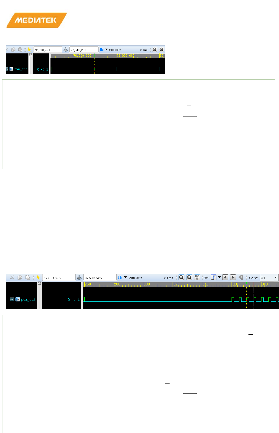
MT76x7
Internet-of-Things Wireless Connectivity
Reference Manual
© 2015 - 2017 MediaTek Inc
Page 640 of 798
This document contains information that is proprietary to MediaTek Inc. (“MediaTek”) and/or its licensor(s).
Any unauthorized use, reproduction or disclosure of this document in whole or in part is strictly prohibited
PWM_GLO_CTRL.pwm_tick_clock_sel = 1 // tick selection =
2MHz (f = 2M)
PWM_CTRL.pwm_clock_en = 1 // Enable PWM clock
PWM_PARAM_S0.S0_pwm_on_time = 5000 // X = Df
F = 5000
PWM_PARAM_S0.S0_pwm_off_time = 5000 // Y = (1−D)f
F = 5000
PWM_CTRL.S0_stay_cycle = 1 // S0 exists, set S0 stay
cycle to non-zero value
PWM_CTRL.S1_stay_cycle = 0 // No S1 exists, set S1 stay
cycle to zero
PWM_CTRL.kick = 1 // Play button, PWM would
behave as setting
2) What’s the resolution when PWM frequency (F) = 1KHz?
a) If user chooses tick clock f = 2M
b) Resolution = f
F = 2000 (steps)
c) If user chooses tick clock f = 32K
d) Resolution = f
F = 32 (steps)
e) à If user wants to get bigger resolution, use faster tick clock (f)
3) Make PWM off 100ms, and then blink with 200Hz, Duty cycle 30%
1. PWM_GLO_CTRL .PWM_tick_clock_sel = 1 // tick selection = 2MHz (f =
2M)
2. PWM_PARAM_S0.S0_pwm_on_time = 0 // PWM always off for S0, X = Df
F =
0
3.1 PWM_PARAM_S0.S0_pwm_off_time = 2000 // PWM_OFF duration = 1ms =
Yt à Y = 1ms
1/(2MHz) = 2000
3.2 PWM_ CTRL.S0_stay_cycle = 100 // PWM_OFF duration x
stay_cycle = 1ms x 100 = 100ms
PWM_PARAM_S1.S1_pwm_on_time = 3000 // X = Df
F = 3000
PWM_PARAM_S1.S1_pwm_off_time = 7000 // Y = (1−D)f
F = 7000
PWM_CTRL.S1_stay_cycle = 1 // Make S1 exist
PWM_CTRL.replay_mode = 0 // No replay
PWM_CTRL.kick = 1 // Play button, PWM would
behave as setting

MT76x7
Internet-of-Things Wireless Connectivity
Reference Manual
© 2015 - 2017 MediaTek Inc
Page 641 of 798
This document contains information that is proprietary to MediaTek Inc. (“MediaTek”) and/or its licensor(s).
Any unauthorized use, reproduction or disclosure of this document in whole or in part is strictly prohibited
2.5.8.5. Notice
1) For individual PWM, if PWM_CTRL.S1_stay_cycle = 0, means “S1 does not exist”. PWM would repeat
S0 forever.
2) For individual PWM, setting PWM_CTRL.S0_stay_cycle = 0 is invalid. However, when user set as this,
waveform would act as PWM_OFF.
3) For individual PWM, setting both PWM_PARAM_S0.S0_pwm_off_time and
PWM_PARAM_S0.S0_pwm_on_time = 0 is invalid. However, when user set as this, waveform would
act as PWM_OFF.
4) For individual PWM, if S1 exists, setting both PWM_PARAM_S1.S1_pwm_off_time and
PWM_PARAM_S1.S1_pwm_on_time = 0 is invalid. However, when user set as this, waveform would
act as PWM_OFF.
5) Suggested switch tick clock flow
a) Set PWM_GLO_CTRL.pwm_global_reset = 1
b) Clear PWM_GLO_CTRL.pwm_global_reset = 0
c) Configure PWM_GLO_CTRL.pwm_tick_clock_sel
Before switching tick clock, resetting PWM modules and parameters is suggested. After toggling global reset,
all PWM modules stop and behave as PWM_OFF.
1) Individual PWM kick (PWM_CTRL.kick) operation shall synchronize on the PWM period cycle. Kick
takes effect when the current cycle finishes.
2) Global kick (PWM_GLO_CTRL.global_kick) operation shall start the cycle of all the PWM’s at the same
time.
2.5.8.6. Register definitions (PWM_NUM = 0~39)
Module name: pwm_top Base address: (+8300a600h)
Address
Name
Width
Register Function
8300A600
PWM_GLO_CTRL
32
PWM global control
8300A700 +
n*(0x00000010
)
PWM_CTRL [n]
(n=0~39)
32
PWM control
8300A704 +
n*(0x00000010
)
PWM_PARAM_S0 [n]
(n=0~39)
32
8300A708 +
n*(0x00000010
)
PWM_PARAM_S1 [n]
(n=0~39)
32
8300A600
PWM_GLO_CTRL
PWM global control
00000000
Bit
31
30
29
28
27
26
25
24
23
22
21
20
19
18
17
16
Nam
e
-
Type
RO
Rese
t
0 0 0 0 0 0 0 0 0 0 0 0 0 0 0 0
Bit
15
14
13
12
11
10
9
8
7
6
5
4
3
2
1
0
Nam
e -
pw
m_
glo
pwm_tick
_clock_se
l
glo
bal
_ki
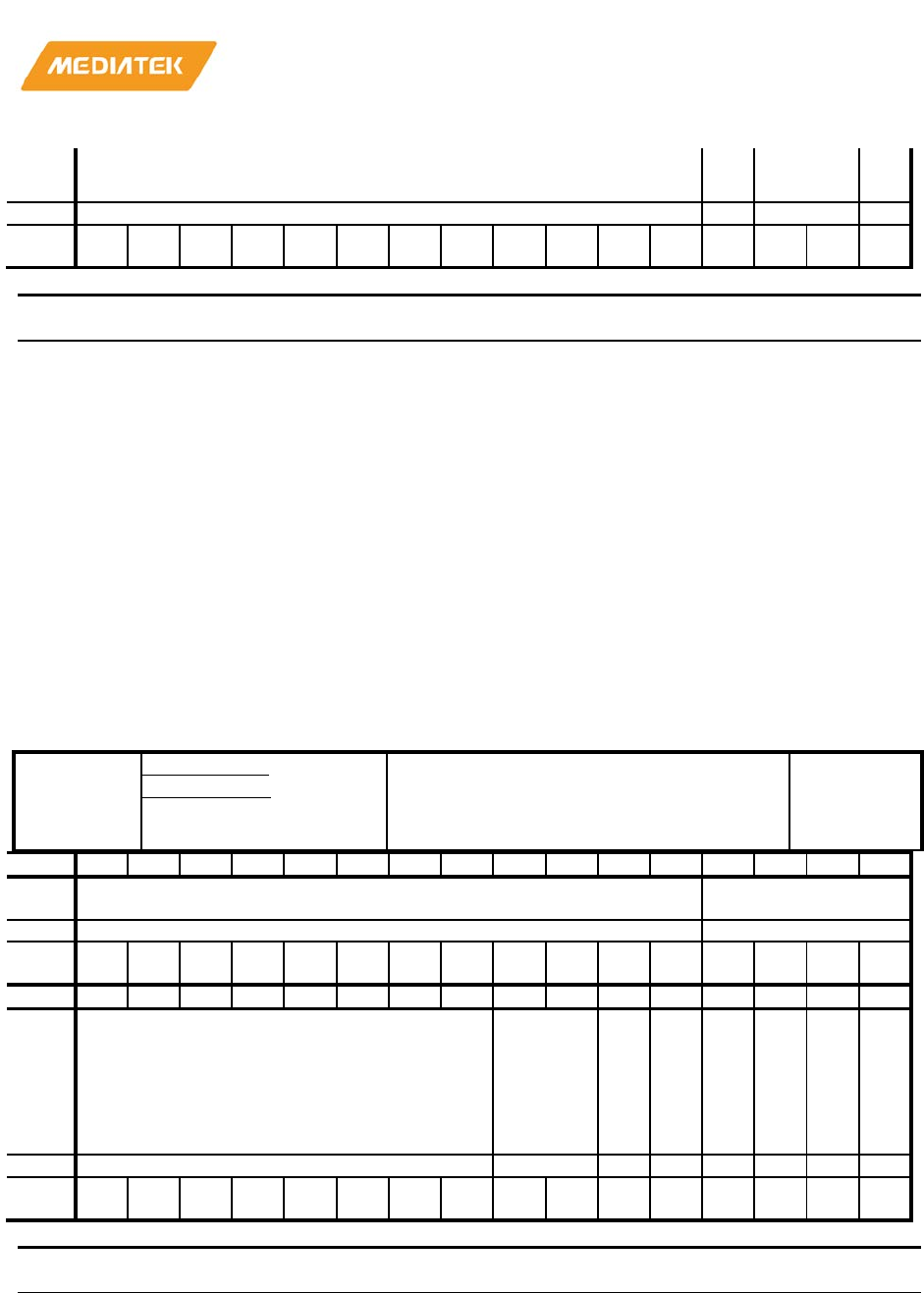
MT76x7
Internet-of-Things Wireless Connectivity
Reference Manual
© 2015 - 2017 MediaTek Inc
Page 642 of 798
This document contains information that is proprietary to MediaTek Inc. (“MediaTek”) and/or its licensor(s).
Any unauthorized use, reproduction or disclosure of this document in whole or in part is strictly prohibited
bal
_re
set
ck
Type
RO
RW
RW
WO
Rese
t
0 0 0 0 0 0 0 0 0 0 0 0 0 0 0 0
Bit(s)
Name
Description
31:4
-
Reserved
3
pwm_global_reset
Write 1 and then write 0 to reset all PWM modules and its
parameters
(PWM_CTRL/PWM_PARAM_S0/PWM_PARAM_S1).
2:1
pwm_tick_clock_sel
PWM tick clock select.
2'h0: 32KHz
2'h1: 2MHz
2'h2: XTAL clock
0
global_kick
All PWM modules with "pwm_global_kick_enable" would
be kicked by this bit
at the same time
8300A700
+
n*(0X0000
0010)
PWM_CTRL
[n](n=0~39)
PWM control
0000000C
Bit
31
30
29
28
27
26
25
24
23
22
21
20
19
18
17
16
Nam
e
S1_stay_cycle S0_stay_cycle
Type
RW
RW
Rese
t
0 0 0 0 0 0 0 0 0 0 0 0 0 0 0 0
Bit
15
14
13
12
11
10
9
8
7
6
5
4
3
2
1
0
Nam
e S0_stay_cycle -
pw
m_
glo
bal
_ki
ck_
ena
ble
pw
m_
clo
ck_
en
pw
m_
io_
ctrl
pol
arit
y
rep
lay
_m
ode
kic
k
Type
RW
RO
RW
RW
RW
RW
RW
WO
Rese
t
0 0 0 0 0 0 0 0 0 0 0 0 1 1 0 0
Bit(s)
Name
Description
31:20
S1_stay_cycle
The stay cycles of S1 (If this field is 0, S1 does not exist)
19:8
S0_stay_cycle
The stay cycles of S0
7:6
-
Reserved
5
pwm_global_kick_enable
PWM would be kicked by global kick if this bit is set
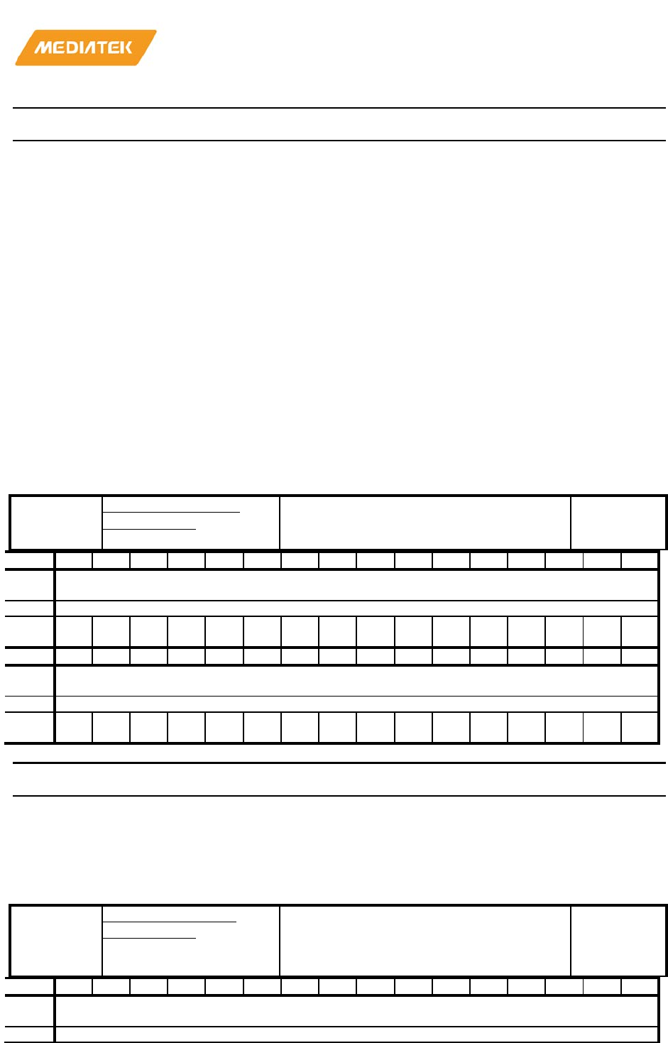
MT76x7
Internet-of-Things Wireless Connectivity
Reference Manual
© 2015 - 2017 MediaTek Inc
Page 643 of 798
This document contains information that is proprietary to MediaTek Inc. (“MediaTek”) and/or its licensor(s).
Any unauthorized use, reproduction or disclosure of this document in whole or in part is strictly prohibited
Bit(s)
Name
Description
4
pwm_clock_en
PWM clock enable.
1'h0: Gating tick clock for PWM
3
pwm_io_ctrl
PWM IO control.
1'h0: PIO (as output)
1'h1: open drain (as output when active low)
2
polarity
PWM polarity setting.
1'h0: active high
1'h1:active low
1
replay_mode
Replay mode indication (Only available when S1 exists)
0
kick
Module load PWM parameter setting and generate
waveform
8300A704 +
n*(0X0000
0010)
PWM_PARAM_S0
[n](n=0~39)
00000000
Bit
31
30
29
28
27
26
25
24
23
22
21
20
19
18
17
16
Nam
e
S0_pwm_off_time
Type
RW
Rese
t
0 0 0 0 0 0 0 0 0 0 0 0 0 0 0 0
Bit
15
14
13
12
11
10
9
8
7
6
5
4
3
2
1
0
Nam
e
S0_pwm_on_time
Type
RW
Rese
t
0 0 0 0 0 0 0 0 0 0 0 0 0 0 0 0
Bit(s)
Name
Description
31:16
S0_pwm_off_time
S0 PWM_OFF duration (unit: tick clock period)
15:0
S0_pwm_on_time
S0 PWM_ON duration (unit: tick clock period)
8300A708
+
n*(0X0000
0010)
PWM_PARAM_S1
[n](n=0~39)
00000000
Bit
31
30
29
28
27
26
25
24
23
22
21
20
19
18
17
16
Nam
e
S1_pwm_off_time
Type
RW
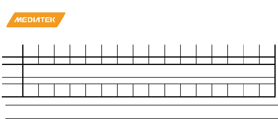
MT76x7
Internet-of-Things Wireless Connectivity
Reference Manual
© 2015 - 2017 MediaTek Inc
Page 644 of 798
This document contains information that is proprietary to MediaTek Inc. (“MediaTek”) and/or its licensor(s).
Any unauthorized use, reproduction or disclosure of this document in whole or in part is strictly prohibited
Rese
t
0 0 0 0 0 0 0 0 0 0 0 0 0 0 0 0
Bit
15
14
13
12
11
10
9
8
7
6
5
4
3
2
1
0
Nam
e
S1_pwm_on_time
Type
RW
Rese
t
0 0 0 0 0 0 0 0 0 0 0 0 0 0 0 0
Bit(s)
Name
Description
31:16
S1_pwm_off_time
S1 PWM_OFF duration (unit: tick clock period)
15:0
S1_pwm_on_time
S1 PWM_ON duration (unit: tick clock period)
2.5.8.7. Application Notes
1) Following Section 2.5.7.5 Note(6)
• There is a HW limitation in MT76X7.
• The setting below would make the next individual kick for PWM #N invalid, pwm_global_reset can
recover it.
a) PWM_PARAM_S0. S0_pwm_off_time = 1 when only S0 exists.
b) PWM_PARAM_S1. S1_pwm_off_time = 1 when S1 exits and turn off replay mode.
c) Both PWM_PARAM_S0. S0_pwm_off_time = 1 and PWM_PARAM_S1. S1_pwm_off_time = 1
when both S0 and S1 exist and turn on replay mode.
Base on this HW limitation, SW is recommended not to set either PWM_PARAM_S0. S0_pwm_off_time = 1 or
PWM_PARAM_S1. S1_pwm_off_time = 1.
2.5.9. IrDA
2.5.9.1. General description
IrDA TX module supports consumer IR protocols including NEC, RC-5, RC-6, and the software-based pulse-
width mode. IrDA RX module supports protocols including RC-5 and pulse-width detection mode.
2.5.9.2. Block Diagram
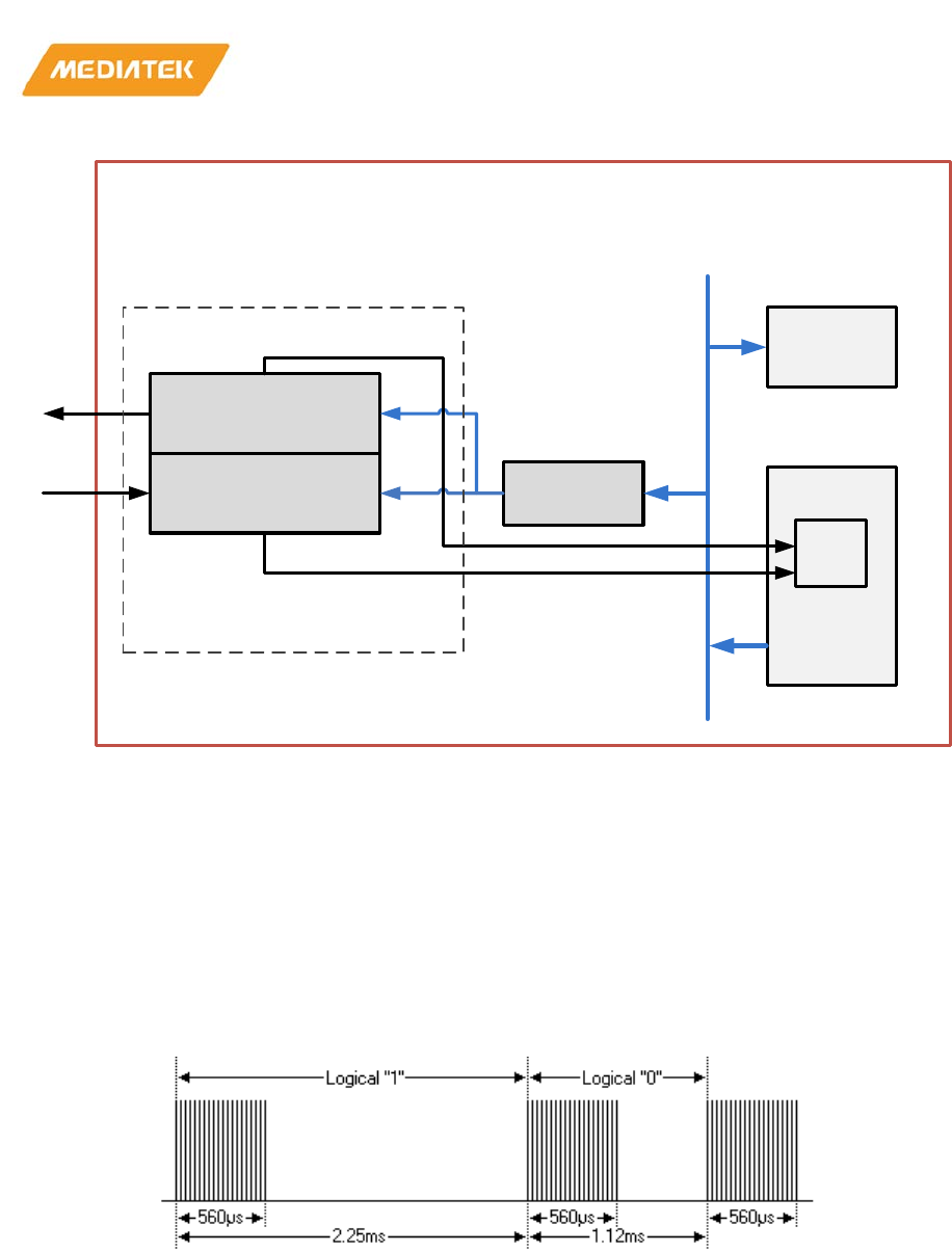
MT76x7
Internet-of-Things Wireless Connectivity
Reference Manual
© 2015 - 2017 MediaTek Inc
Page 645 of 798
This document contains information that is proprietary to MediaTek Inc. (“MediaTek”) and/or its licensor(s).
Any unauthorized use, reproduction or disclosure of this document in whole or in part is strictly prohibited
CM4
MCU
IRTX
IR_RX
IrDA
APB Bridge
Ir_txirq
AHB BUS
CM4_SYS
IRRX
IR_TX
Ir_rxirq
NVIC
SYSRAM
Figure 2-64. IRDA block diagram
2.5.9.3. IRTX functions
1) NEC
The NEC protocol uses pulse distance encoding of the bits. Each pulse is a 560µs long 38kHz carrier burst
(about 21 cycles). A logical "1" takes 2.25ms to transmit, while a logical "0" is only half of that, being 1.125ms
as shorn in Figure 1-1. The recommended carrier duty-cycle is 1/4 or 1/3.
Figure 2-65. The Logic representation for NEC protocol
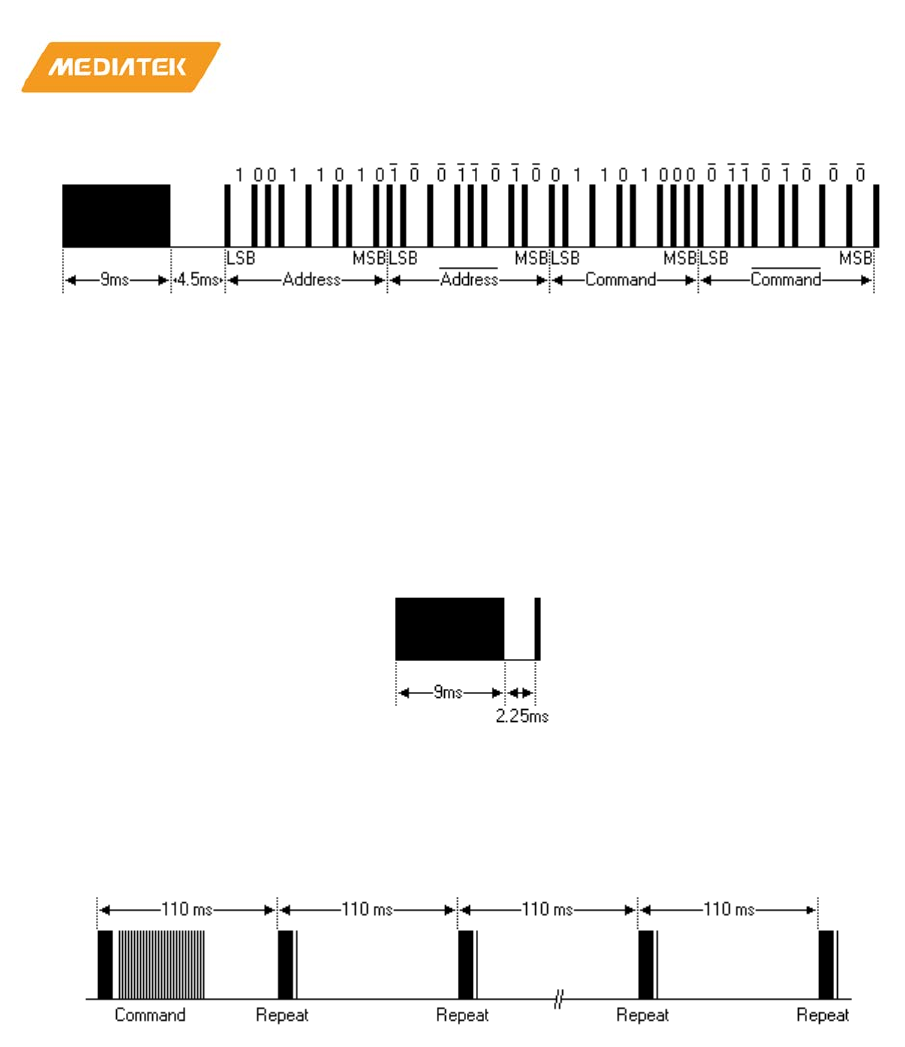
MT76x7
Internet-of-Things Wireless Connectivity
Reference Manual
© 2015 - 2017 MediaTek Inc
Page 646 of 798
This document contains information that is proprietary to MediaTek Inc. (“MediaTek”) and/or its licensor(s).
Any unauthorized use, reproduction or disclosure of this document in whole or in part is strictly prohibited
Figure 2-66. The Pulse Train in Transmission of NEC Protocol
The figure above shows a typical pulse train of the NEC protocol. With this protocol the LSB is transmitted first.
In this case Address $59 and Command $16 is transmitted. A message is started by a 9ms AGC burst, which
was used to set the gain of the earlier IR receivers. This AGC burst is then followed by a 4.5ms space, which is
then followed by the Address and Command. Address and Command are transmitted twice. The second time
all bits are inverted and can be used for verification of the received message. The total transmission time is
constant because every bit is repeated with its inverted length.
Figure 2-67. Message is Started by a 9ms AGC Burst
A command is transmitted only once, even when the key on the remote control remains pressed. Every 110ms
a repeat code is transmitted for as long as the key remains down. This repeat code is simply a 9ms AGC pulse
followed by a 2.25ms space and a 560µs burst.
Figure 2-68. A Repeat Code is Transmitted Every 110ms
2) Features
• 8 bit address and 8 bit command length
• Address and command are transmitted twice for reliability
• Pulse distance modulation
• Carrier frequency of 38kHz
• Bit time of 1.125ms or 2.25ms
3) Philips RC-5 Protocol
The protocol uses bi-phase modulation (or so-called Manchester coding) of a 36kHz IR carrier frequency. All
bits are of equal length of 1.778ms in this protocol, with half of the bit time filled with a burst of the 36kHz
carrier and the other half being idle. A logical zero is represented by a burst in the first half of the bit time. A
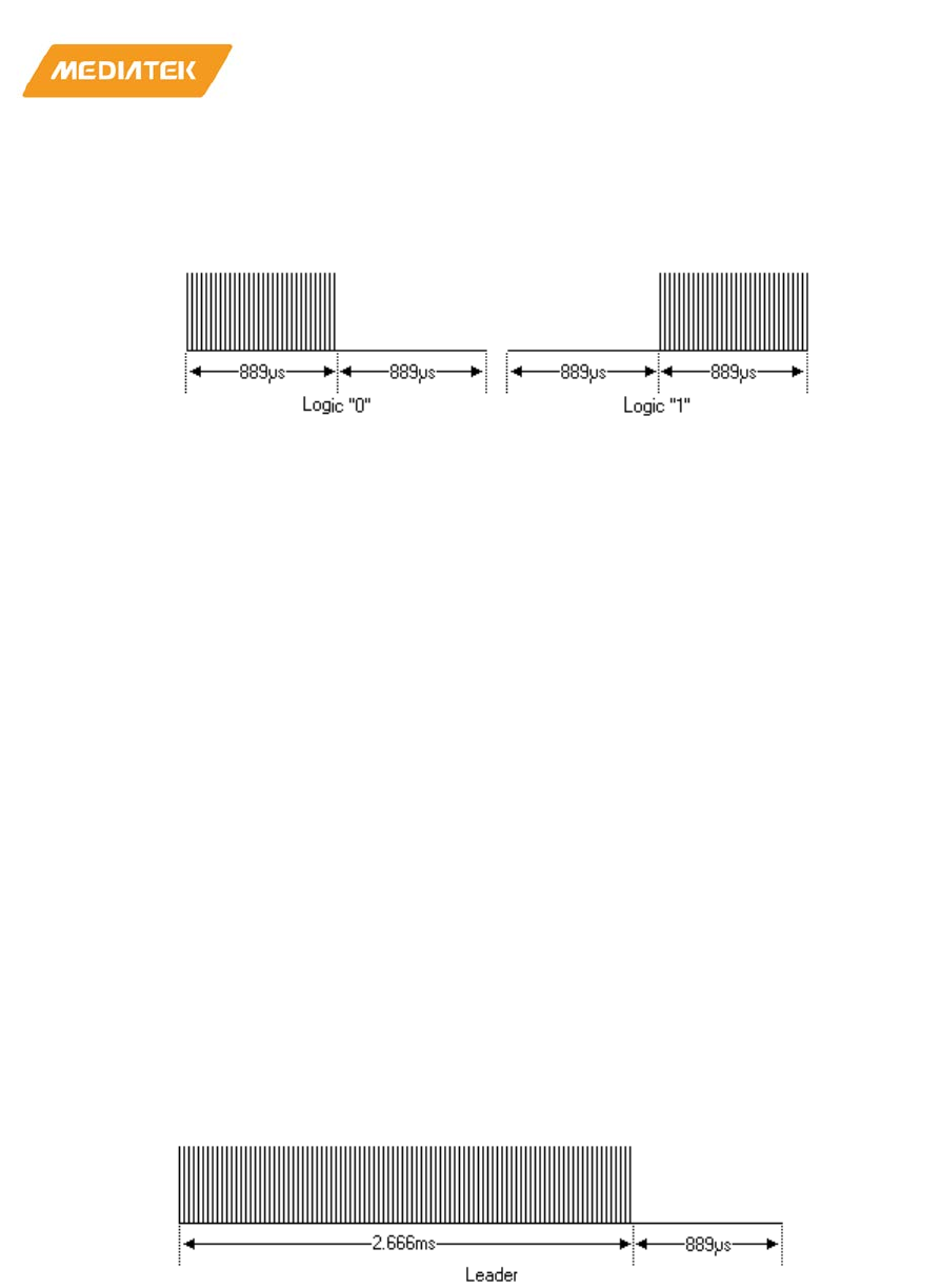
MT76x7
Internet-of-Things Wireless Connectivity
Reference Manual
© 2015 - 2017 MediaTek Inc
Page 647 of 798
This document contains information that is proprietary to MediaTek Inc. (“MediaTek”) and/or its licensor(s).
Any unauthorized use, reproduction or disclosure of this document in whole or in part is strictly prohibited
logical one is represented by a burst in the second half of the bit time. The pulse/pause ratio of the 36kHz
carrier frequency is 1/3 or 1/4 which reduces power consumption.
Figure 2-69. Coding Method for RC5 Protocol
4) Features
• 5 bit address and 6 bit command length (7 command bits for RC5X)
• Bi-phase coding (aka Manchester coding)
• Carrier frequency of 36kHz
• Constant bit time of 1.778ms (64 cycles of 36 kHz)
• Manufacturer Philips
5) Philips RC-6 Protocol
RC-6 is the successor of the RC-5 protocol. Like RC-5 the new RC-6 protocol was also defined by Philips. It is a
very versatile and well defined protocol. Because of this versatility its original definition is many pages long.
Here on my page I will only summarize the most important properties of this protocol. RC-6 signals are
modulated on a 36 kHz Infra Red carrier. The duty cycle of this carrier has to be between 25% and 50%.
Data is modulated using Manchester coding. This means that each bit (or symbol) will have both a mark and
space in the output signal. If the symbol is a "1" the first half of the bit time is a mark and the second half is a
space. If the symbol is a "0" the first half of the bit time is a space and the second half is a mark.
The main timing unit is 1t, which is 16 times the carrier period (1/36k * 16 = 444µs). With RC-6 a total of 5
different symbols are defined:
• The leader pulse, which has a mark time of 6t (2.666ms) and a space time of 2t (0.889ms). This leader
pulse is normally used to set the gain of the IR receiver unit.
Figure 2-70. The Lead Pulse in RC6 Protocol
Normal bits, which have a mark time of 1t (0.444ms) and space time of 1t (0.444ms). A "0" and "1" are
encoded by the position of the mark and space in the bit time.
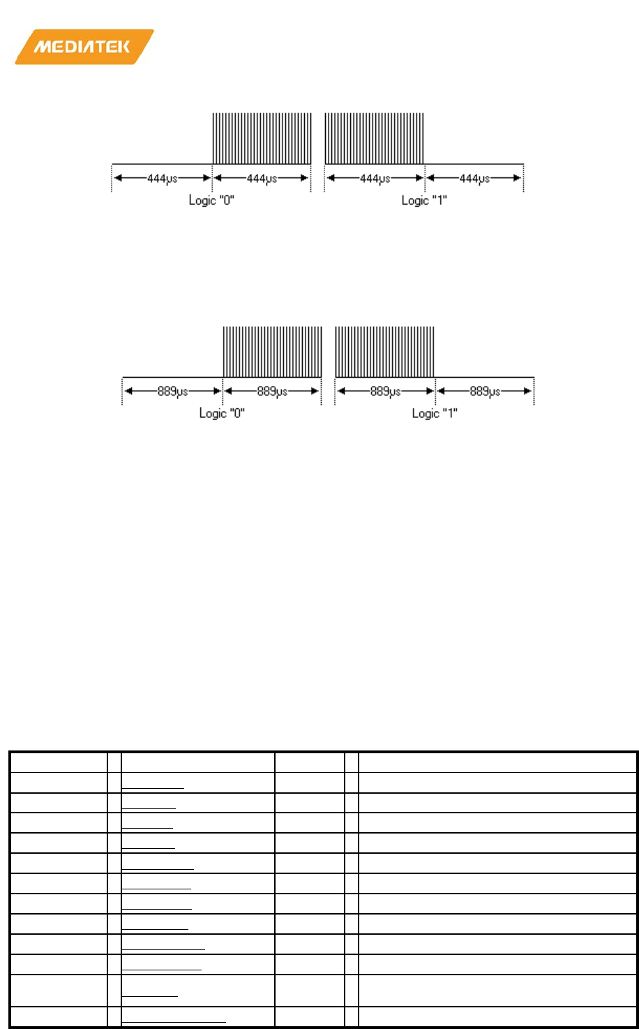
MT76x7
Internet-of-Things Wireless Connectivity
Reference Manual
© 2015 - 2017 MediaTek Inc
Page 648 of 798
This document contains information that is proprietary to MediaTek Inc. (“MediaTek”) and/or its licensor(s).
Any unauthorized use, reproduction or disclosure of this document in whole or in part is strictly prohibited
Figure 2-71. Coding Method for RC6 Protocol
Trailer bits, which have a mark time of 2t (0.889ms) and a space time of 2t (0.889ms). Again a "0" and "1" are
encoded by the position of the mark and space in the bit time.
Figure 2-72. The Trailer Pulse in RC6 Protocol
The leader and trailer symbols are only used in the header field of the messages.
6) Features
• Different modes of operation, depending on the intended use
• Dedicated Philips modes and OEM modes
• Variable command length, depending on the operation mode
• Bi-phase coding (aka Manchester coding)
• Carrier frequency of 36kHz
• Manufacturer Philips
2.5.9.4. Register definitions
Module name: IRTX Base address: (+83060000h)
Address
Name Width
Register Function
83060000
IRTXCFG
32
IRTX CONFIGURATION REGISTER
83060004
IRTXD0
32
IRTX TRANSMISSION DATA 0 REGISTER
83060008
IRTXD1
32
IRTX TRANSMISSION DATA 1 REGISTER
8306000C
IRTXD2
32
IRTX TRANSMISSION DATA 2 REGISTER
83060010
IRTX_L0H
32
IRTX LOGIC 0 HIGH PERIOD REGISTER
83060014
IRTX_L0L
32
IRTX LOGIC 0 LOW PERIOD REGISTER
83060018
IRTX_L1H
32
IRTX LOGIC 1 HIGH PERIOD
REGISTER
8306001C
IRTX_L1L
32
IRTX LOGIC 1 LOW PERIOD REGISTER
83060020
IRTXSYNCH
32
IRTX SYNC HIGH PERIOD REGISTER
83060024
IRTXSYNCL
32
IRTX SYNC LOW
PERIOD REGISTER
83060028
IRTXMT
32
IRTX MODULATION PARAMETER
REGISTER
8306002C
IRTX_INT_CLR
32
IRTX INTERRUPT CLEAR REGISTER

MT76x7
Internet-of-Things Wireless Connectivity
Reference Manual
© 2015 - 2017 MediaTek Inc
Page 649 of 798
This document contains information that is proprietary to MediaTek Inc. (“MediaTek”) and/or its licensor(s).
Any unauthorized use, reproduction or disclosure of this document in whole or in part is strictly prohibited
Address
Name
Width
Register Function
83060030
IRTX_SWM_BP
32
IRTX SOFTWARE MODE BASE PERIOD
REGISTER
83060034
IRTX_SWM_PW0
32
IRTX SOFTWARE MODE PULSE WIDTH
REGISTER 0
83060038
IRTX_SWM_PW1
32
IRTX SOFTWARE MODE PULSE WIDTH
REGISTER 1
8306003C
IRTX_SWM_PW2
32
IRTX SOFTWARE MODE PULSE WIDTH
REGISTER 2
83060040
IRTX_SWM_PW3
32
IRTX SOFTWARE MODE PULSE WIDTH
REGISTER 3
83060044
IRTX_SWM_PW4
32
IRTX SOFTWARE MODE PULSE WIDTH
REGISTER 4
83060048
IRTX_SWM_PW5
32
IRTX SOFTWARE MODE PULSE WIDTH
REGISTER 5
8306004C
IRTX_SWM_PW6
32
IRTX SOFTWARE MODE PULSE WIDTH
REGISTER 6
83060050
IRTX_SWM_PW7
32
IRTX SOFTWARE MODE PULSE WIDTH
REGISTER 7
83060054
IRTX_SWM_PW8
32
IRTX SOFTWARE MODE PULSE WIDTH
REGISTER 8
83060058
IRTX_SWM_PW9
32
IRTX SOFTWARE MODE PULSE WIDTH
REGISTER 9
8306005C
IRTX_SWM_PW10
32
IRTX SOFTWARE MODE PULSE WIDTH
REGISTER 10
83060060
IRTX_SWM_PW11
32
IRTX SOFTWARE MODE PULSE WIDTH
REGISTER 11
83060064
IRTX_SWM_PW12
32
IRTX SOFTWARE MODE PULSE WIDTH
REGISTER 12
83060068
IRTX_SWM_PW13
32
IRTX SOFTWARE MODE PULSE WIDTH
REGISTER 13
8306006C
IRTX_SWM_PW14
32
IRTX SOFTWARE MODE PULSE WIDTH
REGISTER 14
83060070
IRTX_SWM_PW15
32
IRTX SOFTWARE MODE PULSE WIDTH
REGISTER 15
83060074
IRTX_SWM_PW16
32
IRTX SOFTWARE MODE PULSE WIDTH
REGISTER 16
83060000
IRTXCFG
IRTX CONFIGURATION REGISTER
00000000
Bit
31
30
29
28
27
26
25
24
23
22
21
20
19
18
17
16
Nam
e
Type
Rese
t
Bit
15
14
13
12
11
10
9
8
7
6
5
4
3
2
1
0
Nam
e
DA
TA
_I
NV
IRTX_BITNUM
IRT
X_I
RI
NV
IRT
X_I
RO
S
IRT
X_
RO
DR
IRT
X_
BO
DR
IRTX_MODE
IRT
X_
ST
RT
Type
RW
RW
RW
RW
RW
RW
RW
RW
Rese
t
0 0 0 0 0 0 0 0 0 0 0 0 0 0 0 0
Bit(s)
Name
Description

MT76x7
Internet-of-Things Wireless Connectivity
Reference Manual
© 2015 - 2017 MediaTek Inc
Page 650 of 798
This document contains information that is proprietary to MediaTek Inc. (“MediaTek”) and/or its licensor(s).
Any unauthorized use, reproduction or disclosure of this document in whole or in part is strictly prohibited
Bit(s)
Name
Description
15
DATA_INV
IR N inverter
Set this bit as '1' to invert IR data waveform only
(Disabled
in Software Pulse-Width Mode)
14:8
IRTX_BITNUM
Bit Number
Number of IR bits will be transmitted
(Disabled in Software Pulse
-Width Mode)
7
IRTX_IRINV
IR inverter
Set this bit as '1' to invert IR output
6
IRTX_IROS
IR output select
0: IR output is IRTX
baseband signal
1: IR output is IRTX modulated signal
5
IRTX_RODR
Register transmission order
0: IRTX_R0 first, IRTX_R11 last (R0, R1 ~ R11)
1: IRTX_R11 first, IRTX_R0 last (R11, R10 ~R0)
4
IRTX_BODR
Bit transmission order
0: MSB first, LSB last (ex.
R0[7], R0[6] ~ R0[0])
1: LSB first, MSB last (ex. R0[0], R0[1] ~ R0[7])
3:1
IRTX_MODE
IR output protocol
3'd0: pulse
-width coded protocol
3'd1: RC5 protocol
3'd2: RC6 protocol
3'd3: software mode
3'd4: software pulse
-width mode
0
IRTX_STRT
IR trigger bit
0: IR code transfer completed
1: Start to transfer IR code
When IRTX output protocol is set to software mode, this bit is set as
0 to terminate IR transmission.
83060004
IRTXD0
IRTX TRANSMISSION DATA 0
REGISTER
00000000
Bit
31
30
29
28
27
26
25
24
23
22
21
20
19
18
17
16
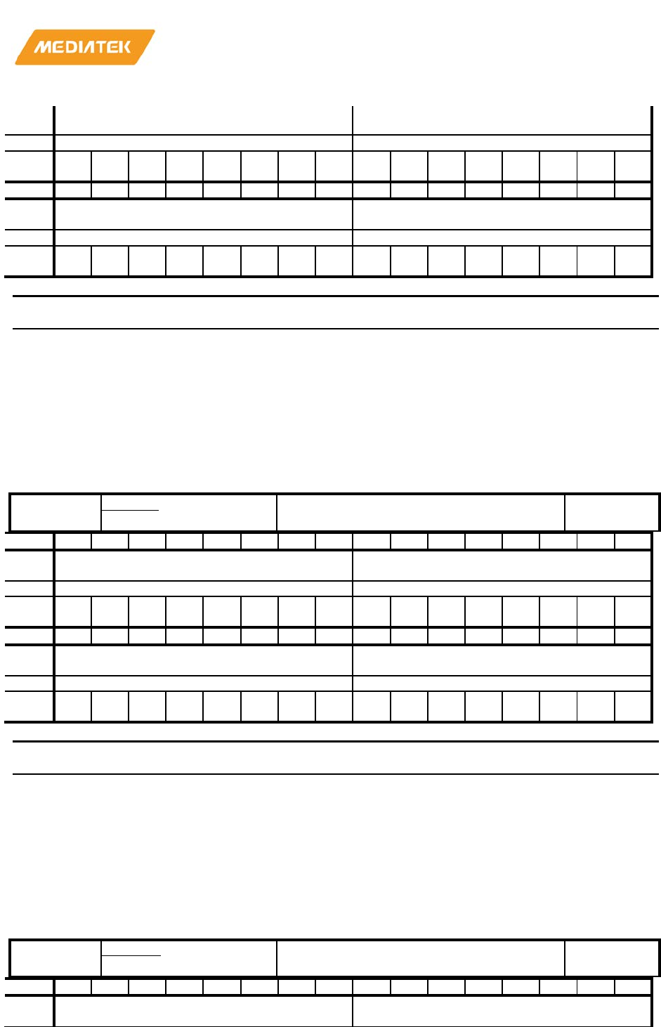
MT76x7
Internet-of-Things Wireless Connectivity
Reference Manual
© 2015 - 2017 MediaTek Inc
Page 651 of 798
This document contains information that is proprietary to MediaTek Inc. (“MediaTek”) and/or its licensor(s).
Any unauthorized use, reproduction or disclosure of this document in whole or in part is strictly prohibited
Nam
e
IRTX_R3 IRTX_R2
Type
RW
RW
Rese
t
0 0 0 0 0 0 0 0 0 0 0 0 0 0 0 0
Bit
15
14
13
12
11
10
9
8
7
6
5
4
3
2
1
0
Nam
e
IRTX_R1 IRTX_R0
Type
RW
RW
Rese
t
0 0 0 0 0 0 0 0 0 0 0 0 0 0 0 0
Bit(s)
Name
Description
31:24
IRTX_R3
IRTX byte 3
23:16
IRTX_R2
IRTX byte 2
15:8
IRTX_R1
IRTX byte 1
7:0
IRTX_R0
IRTX byte 0
83060008
IRTXD1
IRTX TRANSMISSION DATA 1
REGISTER
00000000
Bit
31
30
29
28
27
26
25
24
23
22
21
20
19
18
17
16
Nam
e
IRTX_R7 IRTX_R6
Type
RW
RW
Rese
t
0 0 0 0 0 0 0 0 0 0 0 0 0 0 0 0
Bit
15
14
13
12
11
10
9
8
7
6
5
4
3
2
1
0
Nam
e
IRTX_R5 IRTX_R4
Type
RW
RW
Rese
t
0 0 0 0 0 0 0 0 0 0 0 0 0 0 0 0
Bit(s)
Name
Description
31:24
IRTX_R7
IRTX byte 7
23:16
IRTX_R6
IRTX byte 6
15:8
IRTX_R5
IRTX byte 5
7:0
IRTX_R4
IRTX byte 4
8306000C
IRTXD2
IRTX TRANSMISSION DATA 2
REGISTER
00000000
Bit
31
30
29
28
27
26
25
24
23
22
21
20
19
18
17
16
Nam
e
IRTX_R11 IRTX_R10
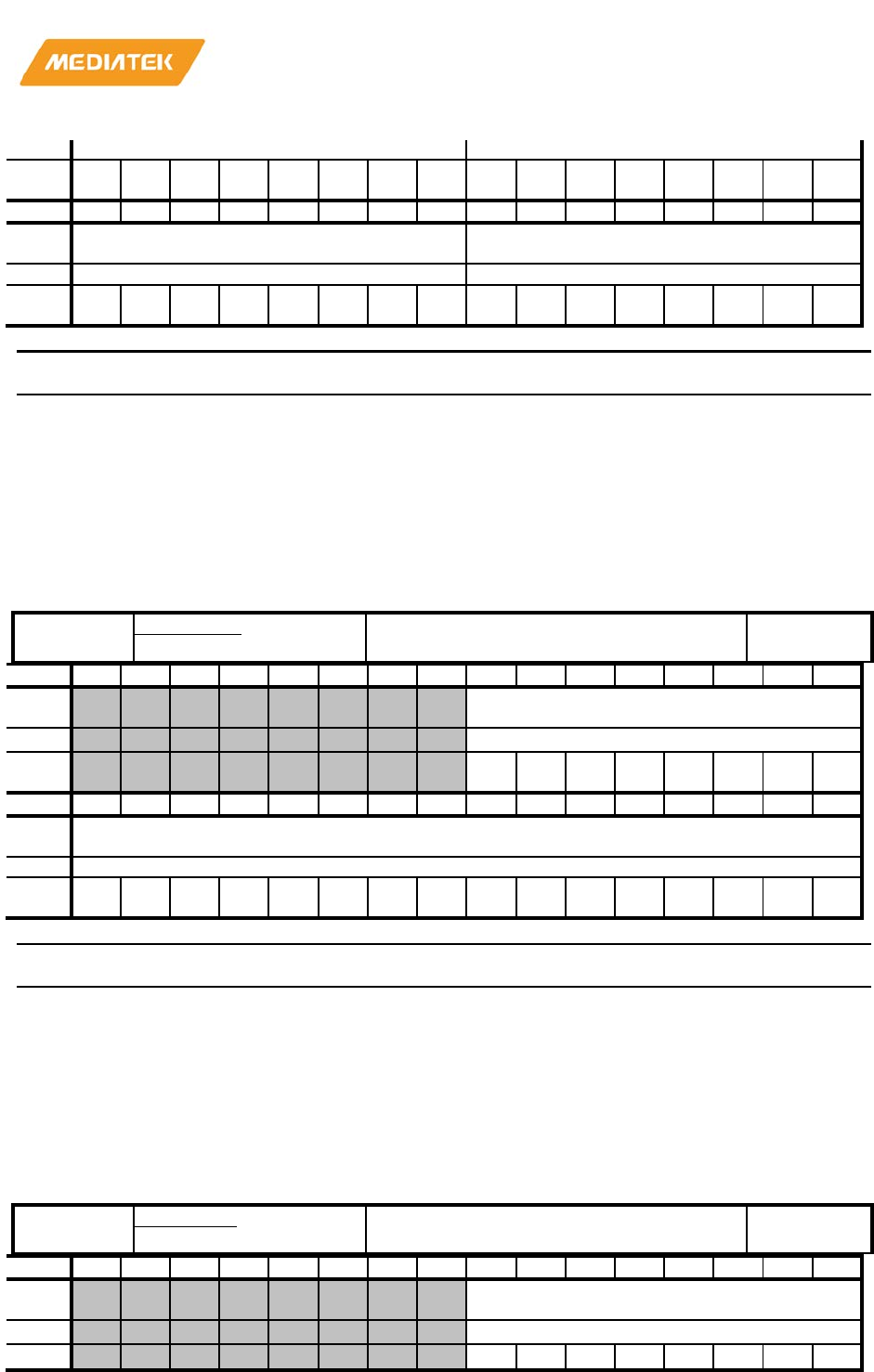
MT76x7
Internet-of-Things Wireless Connectivity
Reference Manual
© 2015 - 2017 MediaTek Inc
Page 652 of 798
This document contains information that is proprietary to MediaTek Inc. (“MediaTek”) and/or its licensor(s).
Any unauthorized use, reproduction or disclosure of this document in whole or in part is strictly prohibited
Type
RW
RW
Rese
t
0 0 0 0 0 0 0 0 0 0 0 0 0 0 0 0
Bit
15
14
13
12
11
10
9
8
7
6
5
4
3
2
1
0
Nam
e
IRTX_R9 IRTX_R8
Type
RW
RW
Rese
t
0 0 0 0 0 0 0 0 0 0 0 0 0 0 0 0
Bit(s)
Name
Description
31:24
IRTX_R11
IRTX byte 11
23:16
IRTX_R10
IRTX byte 10
15:8
IRTX_R9
IRTX byte 9
7:0
IRTX_R8
IRTX byte 8
83060010
IRTX_L0H
IRTX LOGIC 0 HIGH PERIOD
REGISTER
00000000
Bit
31
30
29
28
27
26
25
24
23
22
21
20
19
18
17
16
Nam
e
IRTX_L0H
Type
RW
Rese
t
0 0 0 0 0 0 0 0
Bit
15
14
13
12
11
10
9
8
7
6
5
4
3
2
1
0
Nam
e
IRTX_L0H
Type
RW
Rese
t
0 0 0 0 0 0 0 0 0 0 0 0 0 0 0 0
Bit(s)
Name
Description
23:0
IRTX_L0H
Logic 0 pulse high period
The period is equal to L0H/2MHz.
This register is also valid in RC5/RC6 protocol.
RC5 T
= 1778 (0x6F2), so T = 1778/2MHz = 0.889ms
83060014
IRTX_L0L
IRTX LOGIC 0 LOW PERIOD
REGISTER
00000000
Bit
31
30
29
28
27
26
25
24
23
22
21
20
19
18
17
16
Nam
e
IRTX_L0L
Type
RW
Rese
0
0
0
0
0
0
0
0
MT76x7
Internet-of-Things Wireless Connectivity
Reference Manual
© 2015 - 2017 MediaTek Inc
Page 653 of 798
This document contains information that is proprietary to MediaTek Inc. (“MediaTek”) and/or its licensor(s).
Any unauthorized use, reproduction or disclosure of this document in whole or in part is strictly prohibited
t
Bit
15
14
13
12
11
10
9
8
7
6
5
4
3
2
1
0
Nam
e
IRTX_L0L
Type
RW
Rese
t
0 0 0 0 0 0 0 0 0 0 0 0 0 0 0 0
Bit(s)
Name
Description
23:0
IRTX_L0L
Logic 0 pulse low period
The period is equal to L0L/2MHz.
83060018
IRTX_L1H
IRTX LOGIC 1 HIGH PERIOD
REGISTER
00000000
Bit
31
30
29
28
27
26
25
24
23
22
21
20
19
18
17
16
Nam
e
IRTX_L1H
Type
RW
Rese
t
0 0 0 0 0 0 0 0
Bit
15
14
13
12
11
10
9
8
7
6
5
4
3
2
1
0
Nam
e
IRTX_L1H
Type
RW
Rese
t
0 0 0 0 0 0 0 0 0 0 0 0 0 0 0 0
Bit(s)
Name
Description
23:0
IRTX_L1H
Logic 1 pulse high period
The period is equal to L1H/2MHz.
8306001C
IRTX_L1L
IRTX LOGIC 1 LOW PERIOD
REGISTER
00000000
Bit
31
30
29
28
27
26
25
24
23
22
21
20
19
18
17
16
Nam
e
IRTX_L1L
Type
RW
Rese
t
0 0 0 0 0 0 0 0
Bit
15
14
13
12
11
10
9
8
7
6
5
4
3
2
1
0
Nam
e
IRTX_L1L
Type
RW
Rese
t
0 0 0 0 0 0 0 0 0 0 0 0 0 0 0 0
MT76x7
Internet-of-Things Wireless Connectivity
Reference Manual
© 2015 - 2017 MediaTek Inc
Page 654 of 798
This document contains information that is proprietary to MediaTek Inc. (“MediaTek”) and/or its licensor(s).
Any unauthorized use, reproduction or disclosure of this document in whole or in part is strictly prohibited
Bit(s)
Name
Description
23:0
IRTX_L1L
Logic 1 pulse low period
The period is equal to L1L/2MHz.
83060020
IRTXSYNCH
IRTX SYNC HIGH PERIOD REGISTER
00000000
Bit
31
30
29
28
27
26
25
24
23
22
21
20
19
18
17
16
Nam
e
IRTX_SYNCH
Type
RW
Rese
t
0 0 0 0 0 0 0 0
Bit
15
14
13
12
11
10
9
8
7
6
5
4
3
2
1
0
Nam
e
IRTX_SYNCH
Type
RW
Rese
t
0 0 0 0 0 0 0 0 0 0 0 0 0 0 0 0
Bit(s)
Name
Description
23:0
IRTX_SYNCH
SYNCH leading pulse high period
The period is equal to SYNCH/2MHz. SYNCH will be ignored if
RC5/RC6
protocol is adopted.
83060024
IRTXSYNCL
IRTX SYNC LOW PERIOD REGISTER
00000000
Bit
31
30
29
28
27
26
25
24
23
22
21
20
19
18
17
16
Nam
e
IRTX_SYNCL
Type
RW
Rese
t
0 0 0 0 0 0 0 0
Bit
15
14
13
12
11
10
9
8
7
6
5
4
3
2
1
0
Nam
e
IRTX_SYNCL
Type
RW
Rese
t
0 0 0 0 0 0 0 0 0 0 0 0 0 0 0 0
Bit(s)
Name
Description
23:0
IRTX_SYNCL
SYNCL leading pulse low period
The period is equal to SYNCL/2MHz. SYNCL will be ignored if
RC5/RC6 protocol is adopted.
MT76x7
Internet-of-Things Wireless Connectivity
Reference Manual
© 2015 - 2017 MediaTek Inc
Page 655 of 798
This document contains information that is proprietary to MediaTek Inc. (“MediaTek”) and/or its licensor(s).
Any unauthorized use, reproduction or disclosure of this document in whole or in part is strictly prohibited
83060028
IRTXMT
IRTX MODULATION PARAMETER
REGISTER
00110033
Bit
31
30
29
28
27
26
25
24
23
22
21
20
19
18
17
16
Nam
e
IRTX_CDT
Type
RW
Rese
t
0 0 0 0 0 0 0 0 0 0 0 1 0 0 0 1
Bit
15
14
13
12
11
10
9
8
7
6
5
4
3
2
1
0
Nam
e
IRTX_CWT
Type
RW
Rese
t
0 0 0 0 0 0 0 0 0 0 1 1 0 0 1 1
Bit(s)
Name
Description
31:16
IRTX_CDT
Carrier waveform duty time
Duty cycle = CDT/CWT
Default duty cycle = 17/51 =33%
15:0
IRTX_CWT
Carrier waveform period
8306002C
IRTX_INT_CLR
IRTX INTERRUPT CLEAR REGISTER
00000000
Bit
31
30
29
28
27
26
25
24
23
22
21
20
19
18
17
16
Nam
e
Type
Rese
t
Bit
15
14
13
12
11
10
9
8
7
6
5
4
3
2
1
0
Nam
e
INT
_C
LR
Type
W1
C
Rese
t
0
Bit(s)
Name
Description
0
INT_CLR
Interrupt Clear
83060030
IRTX_SWM_BP
IRTX SOFTWARE MODE BASE
PERIOD REGISTER
00000000
Bit
31
30
29
28
27
26
25
24
23
22
21
20
19
18
17
16
Nam
e
Type
MT76x7
Internet-of-Things Wireless Connectivity
Reference Manual
© 2015 - 2017 MediaTek Inc
Page 656 of 798
This document contains information that is proprietary to MediaTek Inc. (“MediaTek”) and/or its licensor(s).
Any unauthorized use, reproduction or disclosure of this document in whole or in part is strictly prohibited
Rese
t
Bit
15
14
13
12
11
10
9
8
7
6
5
4
3
2
1
0
Nam
e
IRTX_SWM_BP
Type
RW
Rese
t
0 0 0 0 0 0 0 0
Bit(s)
Name
Description
7:0
IRTX_SWM_BP
Base Period in Software Pulse-Width Mode
Unit: 0.5 us (2 MHz operating clock)
83060034
IRTX_SWM_PW0
IRTX SOFTWARE MODE PULSE
WIDTH REGISTER 0
00000000
Bit
31
30
29
28
27
26
25
24
23
22
21
20
19
18
17
16
Nam
e
IRTX_SWM_PW3 IRTX_SWM_PW2
Type
RW
RW
Rese
t
0 0 0 0 0 0 0 0 0 0 0 0 0 0 0 0
Bit
15
14
13
12
11
10
9
8
7
6
5
4
3
2
1
0
Nam
e
IRTX_SWM_PW1 IRTX_SWM_PW0
Type
RW
RW
Rese
t
0 0 0 0 0 0 0 0 0 0 0 0 0 0 0 0
Bit(s)
Name
Description
31:24
IRTX_SWM_PW3
IRTX Pulse-Width in Software Pulse-Width Mode
23:16
IRTX_SWM_PW2
IRTX Pulse-Width in Software Pulse-Width Mode
15:8
IRTX_SWM_PW1
IRTX Pulse-Width in Software Pulse-Width Mode
7:0
IRTX_SWM_PW0
IRTX Pulse-Width in Software Pulse-Width Mode
83060038
IRTX_SWM_PW1
IRTX SOFTWARE MODE PULSE
WIDTH REGISTER 1
00000000
Bit
31
30
29
28
27
26
25
24
23
22
21
20
19
18
17
16
Nam
e
IRTX_SWM_PW7 IRTX_SWM_PW6
Type
RW
RW
Rese
t
0 0 0 0 0 0 0 0 0 0 0 0 0 0 0 0
Bit
15
14
13
12
11
10
9
8
7
6
5
4
3
2
1
0
Nam
e
IRTX_SWM_PW5 IRTX_SWM_PW4
Type
RW
RW
MT76x7
Internet-of-Things Wireless Connectivity
Reference Manual
© 2015 - 2017 MediaTek Inc
Page 657 of 798
This document contains information that is proprietary to MediaTek Inc. (“MediaTek”) and/or its licensor(s).
Any unauthorized use, reproduction or disclosure of this document in whole or in part is strictly prohibited
Rese
t
0 0 0 0 0 0 0 0 0 0 0 0 0 0 0 0
Bit(s)
Name
Description
31:24
IRTX_SWM_PW7
IRTX Pulse-Width in Software Pulse-Width Mode
23:16
IRTX_SWM_PW6
IRTX Pulse-Width in Software Pulse-Width Mode
15:8
IRTX_SWM_PW5
IRTX Pulse-Width in Software Pulse-Width Mode
7:0
IRTX_SWM_PW4
IRTX Pulse-Width in Software Pulse-Width Mode
8306003C
IRTX_SWM_PW2
IRTX SOFTWARE MODE PULSE
WIDTH REGISTER 2
00000000
Bit
31
30
29
28
27
26
25
24
23
22
21
20
19
18
17
16
Nam
e
IRTX_SWM_PW11 IRTX_SWM_PW10
Type
RW
RW
Rese
t
0 0 0 0 0 0 0 0 0 0 0 0 0 0 0 0
Bit
15
14
13
12
11
10
9
8
7
6
5
4
3
2
1
0
Nam
e
IRTX_SWM_PW9 IRTX_SWM_PW8
Type
RW
RW
Rese
t
0 0 0 0 0 0 0 0 0 0 0 0 0 0 0 0
Bit(s)
Name
Description
31:24
IRTX_SWM_PW11
IRTX Pulse-Width in Software Pulse-Width Mode
23:16
IRTX_SWM_PW10
IRTX Pulse-Width in Software Pulse-Width Mode
15:8
IRTX_SWM_PW9
IRTX Pulse-Width in Software Pulse-Width Mode
7:0
IRTX_SWM_PW8
IRTX Pulse-Width in Software Pulse-Width Mode
83060040
IRTX_SWM_PW3
IRTX SOFTWARE MODE PULSE
WIDTH REGISTER 3
00000000
Bit
31
30
29
28
27
26
25
24
23
22
21
20
19
18
17
16
Nam
e
IRTX_SWM_PW15 IRTX_SWM_PW14
Type
RW
RW
Rese
t
0 0 0 0 0 0 0 0 0 0 0 0 0 0 0 0
Bit
15
14
13
12
11
10
9
8
7
6
5
4
3
2
1
0
Nam
e
IRTX_SWM_PW13 IRTX_SWM_PW12
Type
RW
RW
Rese
t
0 0 0 0 0 0 0 0 0 0 0 0 0 0 0 0
MT76x7
Internet-of-Things Wireless Connectivity
Reference Manual
© 2015 - 2017 MediaTek Inc
Page 658 of 798
This document contains information that is proprietary to MediaTek Inc. (“MediaTek”) and/or its licensor(s).
Any unauthorized use, reproduction or disclosure of this document in whole or in part is strictly prohibited
Bit(s)
Name
Description
31:24
IRTX_SWM_PW15
IRTX Pulse-Width in Software Pulse-Width Mode
23:16
IRTX_SWM_PW14
IRTX Pulse-Width in Software Pulse-Width Mode
15:8
IRTX_SWM_PW13
IRTX Pulse-Width in Software Pulse-Width Mode
7:0
IRTX_SWM_PW12
IRTX Pulse-Width in Software Pulse-Width Mode
83060044
IRTX_SWM_PW4
IRTX SOFTWARE MODE PULSE
WIDTH REGISTER 4
00000000
Bit
31
30
29
28
27
26
25
24
23
22
21
20
19
18
17
16
Nam
e
IRTX_SWM_PW19 IRTX_SWM_PW18
Type
RW
RW
Rese
t
0 0 0 0 0 0 0 0 0 0 0 0 0 0 0 0
Bit
15
14
13
12
11
10
9
8
7
6
5
4
3
2
1
0
Nam
e
IRTX_SWM_PW17 IRTX_SWM_PW16
Type
RW
RW
Rese
t
0 0 0 0 0 0 0 0 0 0 0 0 0 0 0 0
Bit(s)
Name
Description
31:24
IRTX_SWM_PW19
IRTX Pulse-Width in Software Pulse-Width Mode
23:16
IRTX_SWM_PW18
IRTX Pulse-Width in Software Pulse-Width Mode
15:8
IRTX_SWM_PW17
IRTX Pulse-Width in Software Pulse-Width Mode
7:0
IRTX_SWM_PW16
IRTX Pulse-Width in Software Pulse-Width Mode
83060048
IRTX_SWM_PW5
IRTX SOFTWARE MODE PULSE
WIDTH REGISTER 5
00000000
Bit
31
30
29
28
27
26
25
24
23
22
21
20
19
18
17
16
Nam
e
IRTX_SWM_PW23 IRTX_SWM_PW22
Type
RW
RW
Rese
t
0 0 0 0 0 0 0 0 0 0 0 0 0 0 0 0
Bit
15
14
13
12
11
10
9
8
7
6
5
4
3
2
1
0
Nam
e
IRTX_SWM_PW21 IRTX_SWM_PW20
Type
RW
RW
Rese
t
0 0 0 0 0 0 0 0 0 0 0 0 0 0 0 0

MT76x7
Internet-of-Things Wireless Connectivity
Reference Manual
© 2015 - 2017 MediaTek Inc
Page 659 of 798
This document contains information that is proprietary to MediaTek Inc. (“MediaTek”) and/or its licensor(s).
Any unauthorized use, reproduction or disclosure of this document in whole or in part is strictly prohibited
Bit(s)
Name
Description
31:24
IRTX_SWM_PW23
IRTX Pulse-Width in Software Pulse-Width Mode
23:16
IRTX_SWM_PW22
IRTX Pulse-Width in Software Pulse-Width Mode
15:8
IRTX_SWM_PW21
IRTX Pulse-Width in Software Pulse-Width Mode
7:0
IRTX_SWM_PW20
IRTX Pulse-Width in Software Pulse-Width Mode
8306004C
IRTX_SWM_PW6
IRTX SOFTWARE MODE PULSE
WIDTH REGISTER 6
00000000
Bit
31
30
29
28
27
26
25
24
23
22
21
20
19
18
17
16
Nam
e
IRTX_SWM_PW27 IRTX_SWM_PW26
Type
RW
RW
Rese
t
0 0 0 0 0 0 0 0 0 0 0 0 0 0 0 0
Bit
15
14
13
12
11
10
9
8
7
6
5
4
3
2
1
0
Nam
e
IRTX_SWM_PW25 IRTX_SWM_PW24
Type
RW
RW
Rese
t
0 0 0 0 0 0 0 0 0 0 0 0 0 0 0 0
Bit(s)
Name
Description
31:24
IRTX_SWM_PW27
IRTX Pulse-Width in Software Pulse-Width Mode
23:16
IRTX_SWM_PW26
IRTX Pulse-Width in Software Pulse-Width Mode
15:8
IRTX_SWM_PW25
IRTX Pulse-Width in Software Pulse-Width Mode
7:0
IRTX_SWM_PW24
IRTX Pulse-Width in Software Pulse-Width Mode
83060050
IRTX_SWM_PW7
IRTX SOFTWARE MODE PULSE
WIDTH REGISTER 7
00000000
Bit
31
30
29
28
27
26
25
24
23
22
21
20
19
18
17
16
Nam
e
IRTX_SWM_PW31 IRTX_SWM_PW30
Type
RW
RW
Rese
t
0 0 0 0 0 0 0 0 0 0 0 0 0 0 0 0
Bit
15
14
13
12
11
10
9
8
7
6
5
4
3
2
1
0
Nam
e
IRTX_SWM_PW29 IRTX_SWM_PW28
Type
RW
RW
Rese
t
0 0 0 0 0 0 0 0 0 0 0 0 0 0 0 0
Bit(s)
Name
Description
MT76x7
Internet-of-Things Wireless Connectivity
Reference Manual
© 2015 - 2017 MediaTek Inc
Page 660 of 798
This document contains information that is proprietary to MediaTek Inc. (“MediaTek”) and/or its licensor(s).
Any unauthorized use, reproduction or disclosure of this document in whole or in part is strictly prohibited
Bit(s)
Name
Description
31:24
IRTX_SWM_PW31
IRTX Pulse-Width in Software Pulse-Width Mode
23:16
IRTX_SWM_PW30
IRTX Pulse-Width in Software Pulse-Width Mode
15:8
IRTX_SWM_PW29
IRTX Pulse-Width in Software Pulse-Width Mode
7:0
IRTX_SWM_PW28
IRTX Pulse-Width in Software Pulse-Width Mode
83060054
IRTX_SWM_PW8
IRTX SOFTWARE MODE PULSE
WIDTH REGISTER 8
00000000
Bit
31
30
29
28
27
26
25
24
23
22
21
20
19
18
17
16
Nam
e
IRTX_SWM_PW35 IRTX_SWM_PW34
Type
RW
RW
Rese
t
0 0 0 0 0 0 0 0 0 0 0 0 0 0 0 0
Bit
15
14
13
12
11
10
9
8
7
6
5
4
3
2
1
0
Nam
e
IRTX_SWM_PW33 IRTX_SWM_PW32
Type
RW
RW
Rese
t
0 0 0 0 0 0 0 0 0 0 0 0 0 0 0 0
Bit(s)
Name
Description
31:24
IRTX_SWM_PW35
IRTX Pulse-Width in Software Pulse-Width Mode
23:16
IRTX_SWM_PW34
IRTX Pulse-Width in Software Pulse-Width Mode
15:8
IRTX_SWM_PW33
IRTX Pulse-Width in Software Pulse-Width Mode
7:0
IRTX_SWM_PW32
IRTX Pulse-Width in Software Pulse-Width Mode
83060058
IRTX_SWM_PW9
IRTX SOFTWARE MODE PULSE
WIDTH REGISTER 9
00000000
Bit
31
30
29
28
27
26
25
24
23
22
21
20
19
18
17
16
Nam
e
IRTX_SWM_PW39 IRTX_SWM_PW38
Type
RW
RW
Rese
t
0 0 0 0 0 0 0 0 0 0 0 0 0 0 0 0
Bit
15
14
13
12
11
10
9
8
7
6
5
4
3
2
1
0
Nam
e
IRTX_SWM_PW37 IRTX_SWM_PW36
Type
RW
RW
Rese
t
0 0 0 0 0 0 0 0 0 0 0 0 0 0 0 0
Bit(s)
Name
Description

MT76x7
Internet-of-Things Wireless Connectivity
Reference Manual
© 2015 - 2017 MediaTek Inc
Page 661 of 798
This document contains information that is proprietary to MediaTek Inc. (“MediaTek”) and/or its licensor(s).
Any unauthorized use, reproduction or disclosure of this document in whole or in part is strictly prohibited
Bit(s)
Name
Description
31:24
IRTX_SWM_PW39
IRTX Pulse-Width in Software Pulse-Width Mode
23:16
IRTX_SWM_PW38
IRTX Pulse-Width in Software Pulse-Width Mode
15:8
IRTX_SWM_PW37
IRTX Pulse-Width in Software Pulse-Width Mode
7:0
IRTX_SWM_PW36
IRTX Pulse-Width in Software Pulse-Width Mode
8306005C
IRTX_SWM_PW10
IRTX SOFTWARE MODE PULSE
WIDTH REGISTER 10
00000000
Bit
31
30
29
28
27
26
25
24
23
22
21
20
19
18
17
16
Nam
e
IRTX_SWM_PW43 IRTX_SWM_PW42
Type
RW
RW
Rese
t
0 0 0 0 0 0 0 0 0 0 0 0 0 0 0 0
Bit
15
14
13
12
11
10
9
8
7
6
5
4
3
2
1
0
Nam
e
IRTX_SWM_PW41 IRTX_SWM_PW40
Type
RW
RW
Rese
t
0 0 0 0 0 0 0 0 0 0 0 0 0 0 0 0
Bit(s)
Name
Description
31:24
IRTX_SWM_PW43
IRTX Pulse-Width in Software Pulse-Width Mode
23:16
IRTX_SWM_PW42
IRTX Pulse-Width in Software Pulse-Width Mode
15:8
IRTX_SWM_PW41
IRTX Pulse-Width in Software Pulse-Width Mode
7:0
IRTX_SWM_PW40
IRTX Pulse-Width in Software Pulse-Width Mode
83060060
IRTX_SWM_PW11
IRTX SOFTWARE MODE PULSE
WIDTH REGISTER 11
00000000
Bit
31
30
29
28
27
26
25
24
23
22
21
20
19
18
17
16
Nam
e
IRTX_SWM_PW47 IRTX_SWM_PW46
Type
RW
RW
Rese
t
0 0 0 0 0 0 0 0 0 0 0 0 0 0 0 0
Bit
15
14
13
12
11
10
9
8
7
6
5
4
3
2
1
0
Nam
e
IRTX_SWM_PW45 IRTX_SWM_PW44
Type
RW
RW
Rese
t
0 0 0 0 0 0 0 0 0 0 0 0 0 0 0 0
Bit(s)
Name
Description

MT76x7
Internet-of-Things Wireless Connectivity
Reference Manual
© 2015 - 2017 MediaTek Inc
Page 662 of 798
This document contains information that is proprietary to MediaTek Inc. (“MediaTek”) and/or its licensor(s).
Any unauthorized use, reproduction or disclosure of this document in whole or in part is strictly prohibited
Bit(s)
Name
Description
31:24
IRTX_SWM_PW47
IRTX Pulse-Width in Software Pulse-Width Mode
23:16
IRTX_SWM_PW46
IRTX Pulse-Width in Software Pulse-Width Mode
15:8
IRTX_SWM_PW45
IRTX Pulse-Width in Software Pulse-Width Mode
7:0
IRTX_SWM_PW44
IRTX Pulse-Width in Software Pulse-Width Mode
83060064
IRTX_SWM_PW12
IRTX SOFTWARE MODE PULSE
WIDTH REGISTER 12
00000000
Bit
31
30
29
28
27
26
25
24
23
22
21
20
19
18
17
16
Nam
e
IRTX_SWM_PW51 IRTX_SWM_PW50
Type
RW
RW
Rese
t
0 0 0 0 0 0 0 0 0 0 0 0 0 0 0 0
Bit
15
14
13
12
11
10
9
8
7
6
5
4
3
2
1
0
Nam
e
IRTX_SWM_PW49 IRTX_SWM_PW48
Type
RW
RW
Rese
t
0 0 0 0 0 0 0 0 0 0 0 0 0 0 0 0
Bit(s)
Name
Description
31:24
IRTX_SWM_PW51
IRTX Pulse-Width in Software Pulse-Width Mode
23:16
IRTX_SWM_PW50
IRTX Pulse-Width in Software Pulse-Width Mode
15:8
IRTX_SWM_PW49
IRTX Pulse-Width in Software Pulse-Width Mode
7:0
IRTX_SWM_PW48
IRTX Pulse-Width in Software Pulse-Width Mode
83060068
IRTX_SWM_PW13
IRTX SOFTWARE MODE PULSE
WIDTH REGISTER 13
00000000
Bit
31
30
29
28
27
26
25
24
23
22
21
20
19
18
17
16
Nam
e
IRTX_SWM_PW55 IRTX_SWM_PW54
Type
RW
RW
Rese
t
0 0 0 0 0 0 0 0 0 0 0 0 0 0 0 0
Bit
15
14
13
12
11
10
9
8
7
6
5
4
3
2
1
0
Nam
e
IRTX_SWM_PW53 IRTX_SWM_PW52
Type
RW
RW
Rese
t
0 0 0 0 0 0 0 0 0 0 0 0 0 0 0 0
Bit(s)
Name
Description

MT76x7
Internet-of-Things Wireless Connectivity
Reference Manual
© 2015 - 2017 MediaTek Inc
Page 663 of 798
This document contains information that is proprietary to MediaTek Inc. (“MediaTek”) and/or its licensor(s).
Any unauthorized use, reproduction or disclosure of this document in whole or in part is strictly prohibited
Bit(s)
Name
Description
31:24
IRTX_SWM_PW55
IRTX Pulse-Width in Software Pulse-Width Mode
23:16
IRTX_SWM_PW54
IRTX Pulse-Width in Software Pulse-Width Mode
15:8
IRTX_SWM_PW53
IRTX Pulse-Width in Software Pulse-Width Mode
7:0
IRTX_SWM_PW52
IRTX Pulse-Width in Software Pulse-Width Mode
8306006C
IRTX_SWM_PW14
IRTX SOFTWARE MODE PULSE
WIDTH REGISTER 14
00000000
Bit
31
30
29
28
27
26
25
24
23
22
21
20
19
18
17
16
Nam
e
IRTX_SWM_PW59 IRTX_SWM_PW58
Type
RW
RW
Rese
t
0 0 0 0 0 0 0 0 0 0 0 0 0 0 0 0
Bit
15
14
13
12
11
10
9
8
7
6
5
4
3
2
1
0
Nam
e
IRTX_SWM_PW57 IRTX_SWM_PW56
Type
RW
RW
Rese
t
0 0 0 0 0 0 0 0 0 0 0 0 0 0 0 0
Bit(s)
Name
Description
31:24
IRTX_SWM_PW59
IRTX Pulse-Width in Software Pulse-Width Mode
23:16
IRTX_SWM_PW58
IRTX Pulse-Width in Software Pulse-Width Mode
15:8
IRTX_SWM_PW57
IRTX Pulse-Width in Software Pulse-Width Mode
7:0
IRTX_SWM_PW56
IRTX Pulse-Width in Software Pulse-Width Mode
83060070
IRTX_SWM_PW15
IRTX SOFTWARE MODE PULSE
WIDTH REGISTER 15
00000000
Bit
31
30
29
28
27
26
25
24
23
22
21
20
19
18
17
16
Nam
e
IRTX_SWM_PW63 IRTX_SWM_PW62
Type
RW
RW
Rese
t
0 0 0 0 0 0 0 0 0 0 0 0 0 0 0 0
Bit
15
14
13
12
11
10
9
8
7
6
5
4
3
2
1
0
Nam
e
IRTX_SWM_PW61 IRTX_SWM_PW60
Type
RW
RW
Rese
t
0 0 0 0 0 0 0 0 0 0 0 0 0 0 0 0
Bit(s)
Name
Description
MT76x7
Internet-of-Things Wireless Connectivity
Reference Manual
© 2015 - 2017 MediaTek Inc
Page 664 of 798
This document contains information that is proprietary to MediaTek Inc. (“MediaTek”) and/or its licensor(s).
Any unauthorized use, reproduction or disclosure of this document in whole or in part is strictly prohibited
Bit(s)
Name
Description
31:24
IRTX_SWM_PW63
IRTX Pulse-Width in Software Pulse-Width Mode
23:16
IRTX_SWM_PW62
IRTX Pulse-Width in Software Pulse-Width Mode
15:8
IRTX_SWM_PW61
IRTX Pulse-Width in Software Pulse-Width Mode
7:0
IRTX_SWM_PW60
IRTX Pulse-Width in Software Pulse-Width Mode
83060074
IRTX_SWM_PW16
IRTX SOFTWARE MODE PULSE
WIDTH REGISTER 16
00000000
Bit
31
30
29
28
27
26
25
24
23
22
21
20
19
18
17
16
Nam
e
IRTX_SWM_PW67 IRTX_SWM_PW66
Type
RW
RW
Rese
t
0 0 0 0 0 0 0 0 0 0 0 0 0 0 0 0
Bit
15
14
13
12
11
10
9
8
7
6
5
4
3
2
1
0
Nam
e
IRTX_SWM_PW65 IRTX_SWM_PW64
Type
RW
RW
Rese
t
0 0 0 0 0 0 0 0 0 0 0 0 0 0 0 0
Bit(s)
Name
Description
31:24
IRTX_SWM_PW67
IRTX Pulse-Width in Software Pulse-Width Mode
23:16
IRTX_SWM_PW66
IRTX Pulse-Width in Software Pulse-Width Mode
15:8
IRTX_SWM_PW65
IRTX Pulse-Width in Software Pulse-Width Mode
7:0
IRTX_SWM_PW64
IRTX Pulse-Width in Software Pulse-Width Mode
2.6. Radio MCU Subsystem
2.6.1. CPU
MT76X7 features 32-bit CPU N9, with the following features:
• 5-stage pipeline with extensive clock-gating
• Dynamic branch prediction with BTB
• 16/32-bit mixed instruction format
• Multiply-accumulate and multiply-subtract instructions
• Instructions optimized for audio applications
• Instruction and data local memory

MT76x7
Internet-of-Things Wireless Connectivity
Reference Manual
© 2015 - 2017 MediaTek Inc
Page 665 of 798
This document contains information that is proprietary to MediaTek Inc. (“MediaTek”) and/or its licensor(s).
Any unauthorized use, reproduction or disclosure of this document in whole or in part is strictly prohibited
• JTAG based debug interface
• Programmable data endian control
2.6.2. RAM/ROM
The Radio MCU subsystem features ILM (Instruction Local Memory), DLM (Data Local Memory), and the
SYSRAM. The ROM code is in ILM.
2.6.3. Memory map
The table below describes how the peripherals are mapped to the memory space in Radio MCU subsystem.
When the MCU performs a read transaction to an undefined address, the bus returns 0. When the MCU
performs a write transaction to an undefined address, the bus regards it as an invalid transaction and does
nothing.
Table 2-59. N9 memory map
Start address End address Function Description
0x0000_0000 0x000C_FFFF ILM ROM Instruction local memory ROM
for N9
0x000D_0000 0x0011_FFFF ILM RAM Instruction local memory RAM
for N9
0x0200_0000 0x0200_021C Patch & CR N9 ROM patch engine
0x0209_0000 0x020C_1FFF DLM RAM Data local memory for N9
0x0040_0000 0x0040_CFFF SYSRAM N9 System RAM for N9
0x2000_0000 0x2003_FFFF SYSRAM CM4 System RAM for CM4 (256KB)
0x2100_0000 0x2100_FFFF SPI-S SPI slave
0x2200_0000 0x2200_FFFF I2S/Audio I2S
0x2400_0000 0x2400_FFFF (Reserved)
0x3000_0000 0x3FFF_FFFF Serial Flash CM4 Serial flash controller of CM4
0x5000_0000 0x501F_FFFF HIF_device Host interface device controller
0x5020_0000 0x502F_FFFF HIF_host_CM4 Host interface host controller
of Wi-Fi radio
0x6000_0000 0x6FFF_FFFF WIFISYS Wi-Fi subsystem
0x7000_0000 0x70FF_FFFF PDA DMA port Patch Decryption Accelerator
DMA slave
0x7800_0000 0x7800_0000 VFF access port0 Virtual FIFO access port 0 of N9
DMA
0x7800_0100 0x7800_0100 VFF access port1 Virtual FIFO access port 1 of N9
DMA
0x7900_0000 0x7900_FFFF VFF_CM4 access
port
Virtual FIFO access ports of
CM4 DMA
0x8000_0000 0x800C_FFFF APB0 APB bridge 0 (synchronous to
N9)
0x8000_0000 0x8000_FFFF CONFG N9 subsystem configuration

MT76x7
Internet-of-Things Wireless Connectivity
Reference Manual
© 2015 - 2017 MediaTek Inc
Page 666 of 798
This document contains information that is proprietary to MediaTek Inc. (“MediaTek”) and/or its licensor(s).
Any unauthorized use, reproduction or disclosure of this document in whole or in part is strictly prohibited
Start address End address Function Description
0x8001_0000 0x8001_FFFF DMA Generic DMA engine for N9
0x8002_0000 0x8002_FFFF TOP_CFG_OFF TOP_OFF(N9) power domain
chip level configuration (GPIO,
PINMUX, RF, PLL, CLK control)
0x8003_0000 0x8003_FFFF UART/BTIF UART or Bluetooth host
interface for N9
0x8005_0000 0x8005_FFFF UART_PTA Inter-chip communication for
PTA
0x8008_0000 0x8008_FFFF AHB_MON AHB bus monitor
0x8009_0000 0x8009_FFFF ACCLR Bluetooth audio Packet Loss
Concealment accelerator
0x800A_0000 0x800A_FFFF UART_DSN UART for N9 debug
0x800B_0000 0x800B_FFFF SEC Security boot configuration
0x800C_0000 0x800C_FFFF HIF Host interface configuration
0x8100_0000 0x810C_FFFF APB1 APB bridge 1 (synchronous to
N9)
0x8100_0000 0x8100_FFFF BTSYS Bluetooth subsystem
0x8102_0000 0x8102_FFFF TOP_CFG_AON TOP_AON power domain chip
level configuration (RGU,
PINMUX, PMU, XTAL, CLK
control)
0x8103_0000 0x8103_FFFF DBG_CIRQ Debug interrupt controller for
N9
0x8104_0000 0x8104_FFFF CIRQ Interrupt controller for N9
0x8105_8000 0x8105_FFFF GPT General Purpose Timer for N9
0x8106_0000 0x8106_FFFF PTA Packet Traffic Arbitrator for Wi-
Fi/Bluetooth coexistence
0x8107_0000 0x8107_FFFF EFUSE Efuse controller
0x8108_0000 0x8108_FFFF WDT Watchdog Timer for N9
0x8109_0000 0x8109_FFFF PDA Patch Decryption Accelerator
0x810A_0000 0x810A_FFFF RDD Wi-Fi debug
0x810B_0000 0x810B_FFFF BTSBC Bluetooth SBC accelerator
0x810C_0000 0x810C_FFFF RBIST RF BIST configuration
0x8300_0000 0x810C_FFFF APB2 APB bridge 1 (synchronous to
CM4)
0x8300_0000 0x8300_FFFF CONFG_CM4 System configuration for CM4
0x8301_0000 0x8301_FFFF DMA_CM4 Generic DMA engine for CM4
0x8302_0000 0x8302_FFFF UART_DSN UART for CM4 debug
MT76x7
Internet-of-Things Wireless Connectivity
Reference Manual
© 2015 - 2017 MediaTek Inc
Page 667 of 798
This document contains information that is proprietary to MediaTek Inc. (“MediaTek”) and/or its licensor(s).
Any unauthorized use, reproduction or disclosure of this document in whole or in part is strictly prohibited
Start address End address Function Description
0x8303_0000 0x8303_FFFF UART1 UART 1 for CM4
0x8304_0000 0x8304_FFFF UART2 UART 2 for CM4
0x8305_0000 0x8305_FFFF GPT_CM4 General Purpose Timer for CM4
0x8306_0000 0x8306_FFFF IrDA IrDA
0x8307_0000 0x8307_FFFF Serial flash Serial flash macro access
0x8308_0000 0x8308_FFFF WDT_CM4 Watchdog Timer for CM4
0x8309_0000 0x8309_FFFF I2C_1 I2C 1
0x830A_0000 0x830A_FFFF I2C_2 I2C 2
0x830B_0000 0x830B_FFFF I2S I2S configuration
0x830D_0000 0x830D_FFFF AUXADC Auxiliary ADC configuration
0x830E_0000 0x830E_FFFF BTIF Host Interface for Bluetooth
radio
0x830F_0000 0x830F_FFFF Crypto Crypto engine
0xA000_0000 0xAFFF_FFFF PSE Packet switch engine memory
2.6.4. N9 bus fabric
N9
ILM ROM (832KB)
ILM RAM (320KB)
DLM RAM (200KB)
N9 AHB bus
Generic DMA
APB
bridge
APB1 bus
PSE
GPT CIRQ PDA
GDMA
CONFIG UART_D
SN UART_P
TA
RDD BT_SBC EFUSE
MAC ACCLR UART
/BTIF
CM4
Interface to CM4 bus/peripheral
N9 peripheral
APB
bridge SYSRAM_N9
(52KB)
APB0 bus
TOP
CONFIG
N9
CONFIG
PTA
Command Batch
(low power data
retention)
WiFi HIF
Asyncrhrous AHB-2-
AHB bridge
(CM4 bus to N9 bus)
SYSTEM BUS
Asyncrhrous AHB-2-
AHB bridge
(N9 bus to CM4 bus)
CM4 AHB bus
WIFI MAC
WDT
HIF
CONFIG
BTSYS
WIFI Baseband
WIFI RF
Figure 2-73. N9 bus fabric
MT76x7
Internet-of-Things Wireless Connectivity
Reference Manual
© 2015 - 2017 MediaTek Inc
Page 668 of 798
This document contains information that is proprietary to MediaTek Inc. (“MediaTek”) and/or its licensor(s).
Any unauthorized use, reproduction or disclosure of this document in whole or in part is strictly prohibited
Functional description:
• Command batch: Used to save/restore the critical CR and memory data when entering and leaving
the low power mode.
• Wi-Fi HIF: The host control and data interface from N9 to Wi-Fi subsystem.
• Wi-Fi PSE: The Packet switch engine used to transfer packet from N9 to Wi-Fi MAC/Radio or from CM4
to Wi-Fi MAC/Radio, and vice versa.
• PDA: Packet Decryption Agent, used to download firmware and decipher the firmware which is
encrypted to avoid eavesdrop.
• PTA: Packet Traffic Arbitration, used to do the traffic arbitration of Wi-Fi and Bluetooth when the two
radios are transmitting and receiving at the same time.
• RDD: The Wi-Fi debug function.
• BT_SBC: The hardware accelerating engine for Bluetooth audio codec.
• EFUSE: The Efuse macro used for the configuration of Wi-Fi/Bluetooth MAC and Radio.
• ACCLR: The hardware accelerating engine for Bluetooth Packet Loss Concealment.
2.6.5. CIRQ
2.6.5.1. General description
N9 subsystem uses the interrupt controller CIRQ to control the source selection, mask, edge/level sensitivity,
and software enabling for internal interrupts, as well as the mask and the edge/level sensitivity for external
interrupts.
CIRQ also integrates the de-bounce circuit for external interrupts.
FIQ control
IRQ contro
Interrupt
select
Control register
External
interrupt
control
De-bounce
De-bounce
De-bounce
Figure 2-74. N9 interrupt controller
2.6.5.2. Functions
Figure 2-75 presents the major functionality of the MCU Interrupt Controller. The interrupt controller
processes all interrupt sources coming from external lines and internal MCU peripherals. This controller
generates two request signals: FIQ for fast, low latency interrupt request and IRQ for more general interrupts
MT76x7
Internet-of-Things Wireless Connectivity
Reference Manual
© 2015 - 2017 MediaTek Inc
Page 669 of 798
This document contains information that is proprietary to MediaTek Inc. (“MediaTek”) and/or its licensor(s).
Any unauthorized use, reproduction or disclosure of this document in whole or in part is strictly prohibited
with lower priority. FIQ connects to N903s input port int_req[0] with highest priority, which IRQ connects to
int_req[1].
Figure 2-75 Interrupt Controller Block Diagram
One and only one of the interrupt sources can be assigned to FIQ Controller and have the highest priority in
requesting timing critical service. All the others share the same IRQ signal by connecting them to IRQ
Controller. The IRQ Controller manages up 18 interrupt lines of IRQ0 to IRQ11 with fixed priority in descending
order.
The interrupt controller provides a simple software interface by mean of registers to manipulate the interrupt
request shared system. IRQ Selection Registers and FIQ Selection Register determine the source priority and
connecting relation among sources and interrupt lines. IRQ Source Status Register allows software program to
identify the source of interrupt that generates the interrupt request. IRQ Mask Register provides software to
mask out undesired sources some time. End of Interrupt Register permits software program to indicate to the
controller that a certain interrupt service routine has been finished.
Binary coded version of IRQ Source Status Register is also made available for software program to helpfully
identify the interrupt source. While taking advantage of this feature, it should also take the binary coded
version of End of Interrupt Register coincidently.
2.6.5.3. Interrupt sources
The tables below lists the interrupt sources of internal and external interrupts.
There are totally 23 interrupts and 14 external interrupts.
The power domain/subsystem lists the power domain and the subsystem from which the interrupt is
generated.
IRQ No.
Interrupt source
Power domain
/subsystem
External
interrupt
Wake-up
capability
(1)
De-
bounce
Description
INT0
UART
TOP_OFF(N9)/MCUSY
UART/BTIF module
Interrupt
input
multiplex
FIQ
controller
IRQ
controller
IRQ0
IRQ1
IRQ2
IRQ3
Registers
SEL SOFT
APB BUS
nFIQ
nIRQ
hif_irq_b
therm_irq_b
wifi_irq_b
icap_irq_b
pse_irq_b
MCU
CIRQ

MT76x7
Internet-of-Things Wireless Connectivity
Reference Manual
© 2015 - 2017 MediaTek Inc
Page 670 of 798
This document contains information that is proprietary to MediaTek Inc. (“MediaTek”) and/or its licensor(s).
Any unauthorized use, reproduction or disclosure of this document in whole or in part is strictly prohibited
S
INT1
DMA
TOP_OFF(N9)/MCUSY
S
Generic DMA in N9 subsystem
INT2
HIFSYS
TOP_AON/HIF
WIFI_HIF(SDIO)
INT3
BT_TIMCON
TOP_AON/BTSYS
Bluetooth TIMCON module
INT4
THERM
TOP_OFF(N9)
Thermometer
INT5
(Reserved)
INT6
WIFI
WF_OFF
Wi-Fi subsystem
INT7
ICAP
TOP_OFF(N9)/MCUSY
S
Internal capture in RBIST module
INT8
EINT
TOP_AON/MCUSYS
External interrupt
INT9
(Reserved)
INT10
WDT_N9
TOP_AON/MCUSYS
Watch dog timer in N9 subsystem
INT11
AHB_MONITOR
TOP_OFF(N9)/MCUSY
S
AHB monitor
INT12
(Reserved)
INT13
PLC_ACCLR
TOP_OFF(N9)/MCUSY
S
Packet Loss Concealment accelerator
INT14
(Reserved)
INT15
PSE
WF_OFF/PSE
Packet switch engine
INT16
MSBC
TOP_OFF(N9)/MCUSY
S
Bluetooth SBC CODEC accelerator
INT17
HIFSYS
TOP_OFF(N9)/HIFSYS
HIF subsystem
INT18
UART_PTA *
TOP_OFF(N9)/MCUSY
S
UART_PTA module
INT19
PTA *
TOP_OFF(N9)/MCUSY
S
PTA module
INT20
CMBT
TOP_OFF(N9)
Command batch module
INT21
GPT3
TOP_AON/MCUSYS
General purpose timer module
INT22
WDT_CM4
TOP_AON/MCUSYS_C
M4
CM4 WDT interrupt N9
EINT0
UART_RX
TOP_AON
V
V
Available
Wake up from UART
EINT1
(Reserved)
V
V
Available
EINT2
HIFSYS
TOP_AON/HIF
V
V
Available
WIFI_HIF (SDIO)
EINT3
CM4_TO_N9_S
W
TOP_AON/MCUSYS_C
M4
V
V
Available
CM4 SW interrupt N9
83080080[31:30] SW_INT
EINT4
Bluetooth
TOP_AON/BTSYS
V
V
Available
Wake up from Bluetooth
EINT5
PCIE *
TOP_OFF(N9)/HIFSYS
V
V
Available
Wake up from PCIe
EINT6
GPT
TOP_AON/MCUSYS
V
V
Available
General purpose timer module (GPT0
timer and GPT1 timer)
EINT7
External interrupt
TOP_AON
V
V
Available
External interrupt
Pin: GPIO58
EINT8
External interrupt
TOP_AON
V
V
Available
External interrupt
Pin: GPIO57
EINT9
External interrupt
TOP_AON
V
V
Available
External interrupt
Pin: GPIO30
EINT10
(Reserved)
V
V
Available
EINT11
External interrupt
TOP_AON
V
V
Available
External interrupt
Pin: GPIO38
EINT12
External interrupt
TOP_AON
V
V
Available
External interrupt
Pin: GPIO39
EINT13
CM4_TO_N9_B
TIF_WAKEUP
TOP_AON
V
V
Available
CM4 to N9 BTIF wake-up
830E0064[0] BTIF_WAK
*: Not used for MT7697D
Note 1; Capable to wake up N9 when N9 is in sleep mode.
MT76x7
Internet-of-Things Wireless Connectivity
Reference Manual
© 2015 - 2017 MediaTek Inc
Page 671 of 798
This document contains information that is proprietary to MediaTek Inc. (“MediaTek”) and/or its licensor(s).
Any unauthorized use, reproduction or disclosure of this document in whole or in part is strictly prohibited
2.6.5.4. Interrupt Source Masking
The Interrupt Controller provides the function of Interrupt Source Masking by the way of programming MASK
register. Any of them can be masked individually.
However, because of the bus latency, the masking takes effect no earlier than three clock cycles later. In this
time, the to-be-masked interrupts could come in and generate an IRQ pulse to MCU, and then disappear
immediately. This IRQ forces MCU going to Interrupt Service Routine and polling Status Register (IRQ_STA2),
but the register shows there is no interrupt. This might cause MCU malfunction.
There are two ways for programmers to protect their software.
1) Return from ISR (Interrupt Service Routine) immediately while the Status register shows no interrupt.
2) Set I bit of MCU before doing Interrupt Masking, and then clear it after Interrupt Masking done.
Both avoid the problem, but the first item is recommended in the ISR.
2.6.5.5. External Interrupt
This interrupt controller also integrates an External Interrupt Controller that can support up to 11 interrupt
requests coming from external sources, the EINT0~A, WakeUp interrupt requests.
The external interrupts can be used for different kind of applications, mainly for event detections: detection of
hand free connection, detection of hood opening, detection of battery charger connection.
Since the external event may be unstable in a certain period, a de-bounce mechanism is introduced to ensure
the functionality. The circuitry is mainly used to verify that the input signal remains stable for a programmable
number of periods of the clock. When this condition is satisfied, for the appearance or the disappearance of
the input, the output of the de-bounce logic changes to the desired state. Note that, because it uses the
32768Hz slow clock for performing the de-bounce process, the parameter of de-bounce period and de-bounce
enable takes effect no sooner than one 32768Hz clock cycle (~30.52us) after the software program sets them.
When the sources of External Interrupt Controller are used to resume the system clock in sleep mode, the de-
bounce mechanism must be enabled. However, the polarities of EINTs are clocked with the system clock. Any
changes to them take effect immediately.
Interrupt
Control
EINT_IRQ
Debounce Logic
EINT0-A
Register
APB BUS
Figure 2-76. External Interrupt Controller Block Diagram
If you have to change the debounce setting of some EINT, please follow the steps:
1) mask the EINT which you want to change the debounce setting
2) disable debounce (EN=0)
3) delay at least 5 32K cycles

MT76x7
Internet-of-Things Wireless Connectivity
Reference Manual
© 2015 - 2017 MediaTek Inc
Page 672 of 798
This document contains information that is proprietary to MediaTek Inc. (“MediaTek”) and/or its licensor(s).
Any unauthorized use, reproduction or disclosure of this document in whole or in part is strictly prohibited
4) Enable the debounce (EN=1) and change the debounce setting
5) unmask the EINT
2.6.5.6. Programming guide
The interrupt sources are listed as the following table.
Table 2-60. Internal interrupt source
SUBSYS Source Pin Description / Note
INT0 MCUSYS_OFF uart0_irq_b from uart0 or btif module
INT1 MCUSYS_OFF dma_irq_b from dma module
INT2 HIFSYS_AON / OFF hif_irq_b_wrapper HIF_AON SDIO
INT3 BTSYS_AON bt_timcon_irq_b
INT4 TOP_OFF therm_irq_b from u_top_therm_ctl module
INT5 NA
INT6 WF_OFF wifi_irq_b from u_wifi_on_top module
INT7 MCUSYS_OFF icap_irq_b from u_rbist_top module
INT8 MCUSYS_AON eint_irq_b EINT interrupt
INT9 NA
INT10 MCUSYS_AON wdt_irq_b[0] N9 wdt interrupt mode
INT11 MCUSYS_OFF ahb_mon_irq_b from mdahbmon_top module
INT12 NA
INT13 MCUSYS_OFF plc_acclr_irq_b from acclr module
INT14 TOP_OFF adc_irq_b from u_top_sadc_ctl
INT15 WF_PSE_OFF pse_irq_b
INT16 MCUSYS_OFF msbc_irq_b from bt_sbc module
INT17 HIFSYS_OFF client_irq_b
INT18 MCUSYS_OFF uart_pta_irq_b from uart_pta module
INT19 MCUSYS_OFF lte_chg_frm_int from pta module
INT20 TOP_OFF cmbt_irq_b from u_top_cmdbt module
INT21 MCUSYS_AON gpt3_irq_b N9 gpt3 timer timeout
INT22 MCUSYS_CM4_AON cm4_n9_wdt_irq_b CM4 reset self and interrupt N9
MT76x7
Internet-of-Things Wireless Connectivity
Reference Manual
© 2015 - 2017 MediaTek Inc
Page 673 of 798
This document contains information that is proprietary to MediaTek Inc. (“MediaTek”) and/or its licensor(s).
Any unauthorized use, reproduction or disclosure of this document in whole or in part is strictly prohibited
Table 2-61. External interrupt source
SUBSYS Source Pin Note
EINT0 PAD_UART_RX
EINT1 NA
EINT2 HIFSYS_AON / OFF hif_mcu_int_b HIF_AON SDIO
EINT3 MCUSYS_CM4_AON cm4_n9_sw_irq_b CM4 software interrupt N9
EINT4 BTSYS_AON bt_ext_irq
EINT5 HIFSYS_OFF hifsys_pcie_int_b pcie_wake
EINT6 MCUSYS_AON gpt_int_b N9 gpt0 timer or gpt1 timer
interrupt
EINT7 PAD_BT_RF_DIS_B host_eint_b[0]
EINT8 PAD_WF_RF_DIS_B host_eint_b[1]
EINT9 PAD_SDIO_DAT2 host_eint_b[2]
EINT10 TOP_AON dslp_irq_b from u_top_cfg_aon
EINT11 PAD_UART_RTS
EINT12 PAD_UART_CTS
EINT13 MCUSYS_CM4_OFF cm4ton9_btif_wakeup_irq_b CM4 btif wakeup N9
2.6.5.7. Register definitions
Module name: cirq Base address: (+81040000h)
Address
Name
Width
Register Function
81040000
IRQ_SEL0
32
IRQ Selection 0 Register
81040004
IRQ_SEL1
32
IRQ Selection 1 Register
81040008
IRQ_SEL2
32
IRQ Selection 2 Register
8104000C
IRQ_SEL3
32
IRQ Selection 3 Register
81040010
IRQ_SEL4
32
IRQ Selection 4 Register
81040014
IRQ_SEL5
32
IRQ
Selection 5 Register
8104006C
FIQ_SEL
32
FIQ Selection Register
81040070
IRQ_MASK
32
IRQ Mask Register
81040080
IRQ_MASK_CLR
32
IRQ Mask Clear Register
81040090
IRQ_MASK_SET
32
IRQ Mask Set Register
810400A0
IRQ_EOI
32
IRQ End of Interrupt Register
810400B0
IRQ_SENS
32
IRQ Sensitive Register
810400C0
IRQ_SOFT
32
IRQ Software Interrupt Register
810400D0
FIQ_CON
32
FIQ Control Register
810400D4
FIQ_EOI
32
FIQ End of Interrupt Register
810400D8
IRQ_STA2
32
Binary Coded Value of IRQ_STATUS
810400DC
IRQ_EOI2
32
Binary Coded Value of IRQ_EOI
810400E0
IRQ_ASTA
32
Binary Value of IRQ Source Status
MT76x7
Internet-of-Things Wireless Connectivity
Reference Manual
© 2015 - 2017 MediaTek Inc
Page 674 of 798
This document contains information that is proprietary to MediaTek Inc. (“MediaTek”) and/or its licensor(s).
Any unauthorized use, reproduction or disclosure of this document in whole or in part is strictly prohibited
Address
Name
Width
Register Function
810400F0
IRQ_EEVT
32
Binary Value of EINT Event
81040100
EINT_STA
32
EINT Status Register
81040104
EINT_MASK
32
EINT Mask Register
81040108
EINT_MASK_CLR
32
EINT Mask Clear Register
8104010C
EINT_MASK_SET
32
EINT Mask Set Register
81040110
EINT_INTACK
32
EINT Interrupt Acknowledge Register
81040114
EINT_SENS
32
EINT Sensitive Register
81040118
EINT_SOFT
32
EINT Software Interrupt Register
81040120
EINT0_CON
32
EINT 0 De-bounce Control Register
81040130
EINT1_CON
32
EINT 1 De
-bounce Control Register
81040140
EINT2_CON
32
EINT 2 De-bounce Control Register
81040150
EINT3_CON
32
EINT 3 De
-bounce Control Register
81040160
EINT4_CON
32
EINT 4 De
-bounce Control Register
81040170
EINT5_CON
32
EINT 5 De
-bounce Control Register
81040180
EINT6_CON
32
EINT 6 De
-bounce Control Register
81040190
EINT7_CON
32
EINT 7 De
-bounce Control Register
810401A0
EINT8_CON
32
EINT 8 De
-bounce Control Register
810401B0
EINT9_CON
32
EINT 9
De-bounce Control Register
810401C0
EINTA_CON
32
EINT A De
-bounce Control Register
810401D0
EINTB_CON
32
EINT A De-bounce Control Register
810401E0
EINTC_CON
32
EINT A De
-bounce Control Register
810401F0
EINTD_CON
32
EINT A De-bounce Control Register
81040000
IRQ_SEL0
IRQ Selection 0 Register
03020100
Bit
31
30
29
28
27
26
25
24
23
22
21
20
19
18
17
16
Nam
e
IRQ3_SEL IRQ2_SEL
Type
RW
RW
Rese
t
0 0 0 1 1 0 0 0 1 0
Bit
15
14
13
12
11
10
9
8
7
6
5
4
3
2
1
0
Nam
e
IRQ1_SEL IRQ0_SEL
Type
RW
RW
Rese
t
0 0 0 0 1 0 0 0 0 0
Bit(s)
Name
Description
28:24
IRQ3_SEL
Interrupt source selector
5'h0~5'h17: Please reference to interrupt source table
20:16
IRQ2_SEL
Interrupt source selector
5'h0~5'h17: Please reference to interrupt source table
12:8
IRQ1_SEL
Interrupt source selector
MT76x7
Internet-of-Things Wireless Connectivity
Reference Manual
© 2015 - 2017 MediaTek Inc
Page 675 of 798
This document contains information that is proprietary to MediaTek Inc. (“MediaTek”) and/or its licensor(s).
Any unauthorized use, reproduction or disclosure of this document in whole or in part is strictly prohibited
Bit(s)
Name
Description
5'h0~5'h17: Please reference to interrupt source table
4:0
IRQ0_SEL
Interrupt source selector
5'h0~5'h17: Please reference to interrupt source table
81040004
IRQ_SEL1
IRQ Selection 1 Register
07060504
Bit
31
30
29
28
27
26
25
24
23
22
21
20
19
18
17
16
Nam
e
IRQ7_SEL IRQ6_SEL
Type
RW
RW
Rese
t
0 0 1 1 1 0 0 1 1 0
Bit
15
14
13
12
11
10
9
8
7
6
5
4
3
2
1
0
Nam
e
IRQ5_SEL IRQ4_SEL
Type
RW
RW
Rese
t
0 0 1 0 1 0 0 1 0 0
Bit(s)
Name
Description
28:24
IRQ7_SEL
Interrupt source selector
5'h0~5'h17: Please reference to interrupt source table
20:16
IRQ6_SEL
Interrupt source selector
5'h0~5'h17: Please reference to interrupt source table
12:8
IRQ5_SEL
Interrupt source selector
5'h0~5'h17: Please reference to interrupt
source table
4:0
IRQ4_SEL
Interrupt source selector
5'h0~5'h17: Please reference to interrupt source table
81040008
IRQ_SEL2
IRQ Selection 2 Register
0B0A0908
Bit
31
30
29
28
27
26
25
24
23
22
21
20
19
18
17
16
Nam
e
IRQB_SEL IRQA_SEL
Type
RW
RW
Rese
t
0 1 0 1 1 0 1 0 1 0
Bit
15
14
13
12
11
10
9
8
7
6
5
4
3
2
1
0
Nam
e
IRQ9_SEL IRQ8_SEL
Type
RW
RW
Rese
0
1
0
0
1
0
1
0
0
0
MT76x7
Internet-of-Things Wireless Connectivity
Reference Manual
© 2015 - 2017 MediaTek Inc
Page 676 of 798
This document contains information that is proprietary to MediaTek Inc. (“MediaTek”) and/or its licensor(s).
Any unauthorized use, reproduction or disclosure of this document in whole or in part is strictly prohibited
t
Bit(s)
Name
Description
28:24
IRQB_SEL
Interrupt source selector
5'h0~5'h17: Please reference to interrupt source table
20:16
IRQA_SEL
Interrupt source selector
5'h0~5'h17: Please reference to interrupt source table
12:8
IRQ9_SEL
Interrupt source selector
5'h0~5'h17: Please reference to interrupt source table
4:0
IRQ8_SEL
Interrupt source selector
5'h0~5'h17: Please reference to interrupt source table
8104000C
IRQ_SEL3
IRQ Selection 3 Register
0F0E0D0C
Bit
31
30
29
28
27
26
25
24
23
22
21
20
19
18
17
16
Nam
e
IRQF_SEL IRQE_SEL
Type
RW
RW
Rese
t
0 1 1 1 1 0 1 1 1 0
Bit
15
14
13
12
11
10
9
8
7
6
5
4
3
2
1
0
Nam
e
IRQD_SEL IRQC_SEL
Type
RW
RW
Rese
t
0 1 1 0 1 0 1 1 0 0
Bit(s)
Name
Description
28:24
IRQF_SEL
Interrupt source selector
5'h0~5'h17: Please reference to interrupt source table
20:16
IRQE_SEL
Interrupt source selector
5'h0~5'h17: Please reference to interrupt source table
12:8
IRQD_SEL
Interrupt source selector
5'h0~5'h17: Please reference to interrupt source table
4:0
IRQC_SEL
Interrupt source selector
5'h0~5'h17: Please reference to interrupt source table
81040010
IRQ_SEL4
IRQ Selection 4 Register
13121110
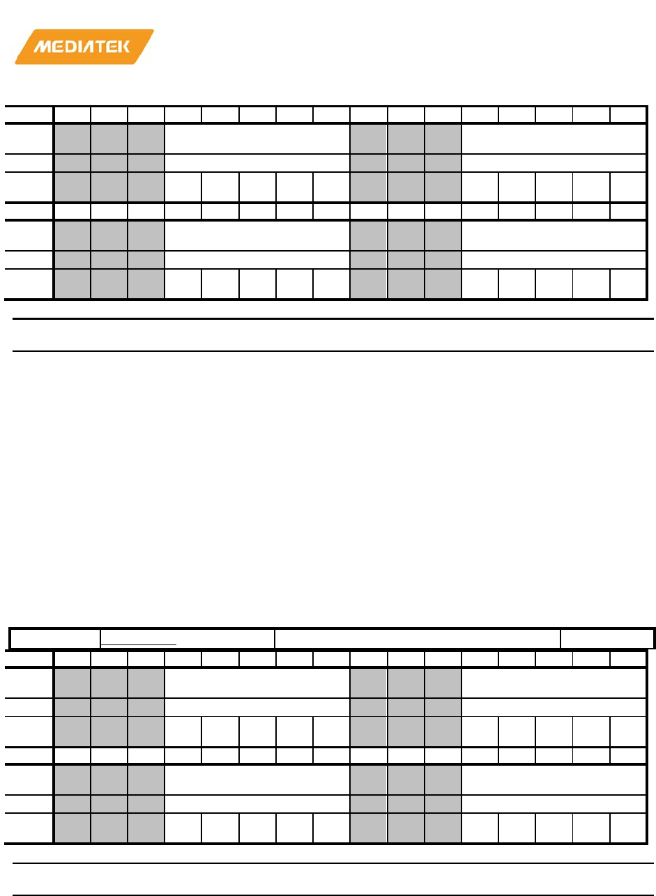
MT76x7
Internet-of-Things Wireless Connectivity
Reference Manual
© 2015 - 2017 MediaTek Inc
Page 677 of 798
This document contains information that is proprietary to MediaTek Inc. (“MediaTek”) and/or its licensor(s).
Any unauthorized use, reproduction or disclosure of this document in whole or in part is strictly prohibited
Bit
31
30
29
28
27
26
25
24
23
22
21
20
19
18
17
16
Nam
e
IRQ13_SEL IRQ12_SEL
Type
RW
RW
Rese
t
1 0 0 1 1 1 0 0 1 0
Bit
15
14
13
12
11
10
9
8
7
6
5
4
3
2
1
0
Nam
e
IRQ11_SEL IRQ10_SEL
Type
RW
RW
Rese
t
1 0 0 0 1 1 0 0 0 0
Bit(s)
Name
Description
28:24
IRQ13_SEL
Interrupt source selector
5'h0~5'h17: Please reference to interrupt source table
20:16
IRQ12_SEL
Interrupt source selector
5'h0~5'h17: Please reference to interrupt source table
12:8
IRQ11_SEL
Interrupt source selector
5'h0~5'h17: Please reference to interrupt source table
4:0
IRQ10_SEL
Interrupt source selector
5'h0~5'h17: Please reference to interrupt source table
81040014
IRQ_SEL5
IRQ Selection 5 Register
17161514
Bit
31
30
29
28
27
26
25
24
23
22
21
20
19
18
17
16
Nam
e
IRQ17_SEL IRQ16_SEL
Type
RW
RW
Rese
t
1 0 1 1 1 1 0 1 1 0
Bit
15
14
13
12
11
10
9
8
7
6
5
4
3
2
1
0
Nam
e
IRQ15_SEL IRQ14_SEL
Type
RW
RW
Rese
t
1 0 1 0 1 1 0 1 0 0
Bit(s)
Name
Description
28:24
IRQ17_SEL
Interrupt source selector
5'h0~5'h17: Please reference to interrupt source table
20:16
IRQ16_SEL
Interrupt source selector
5'h0~5'h17: Please reference to interrupt source table
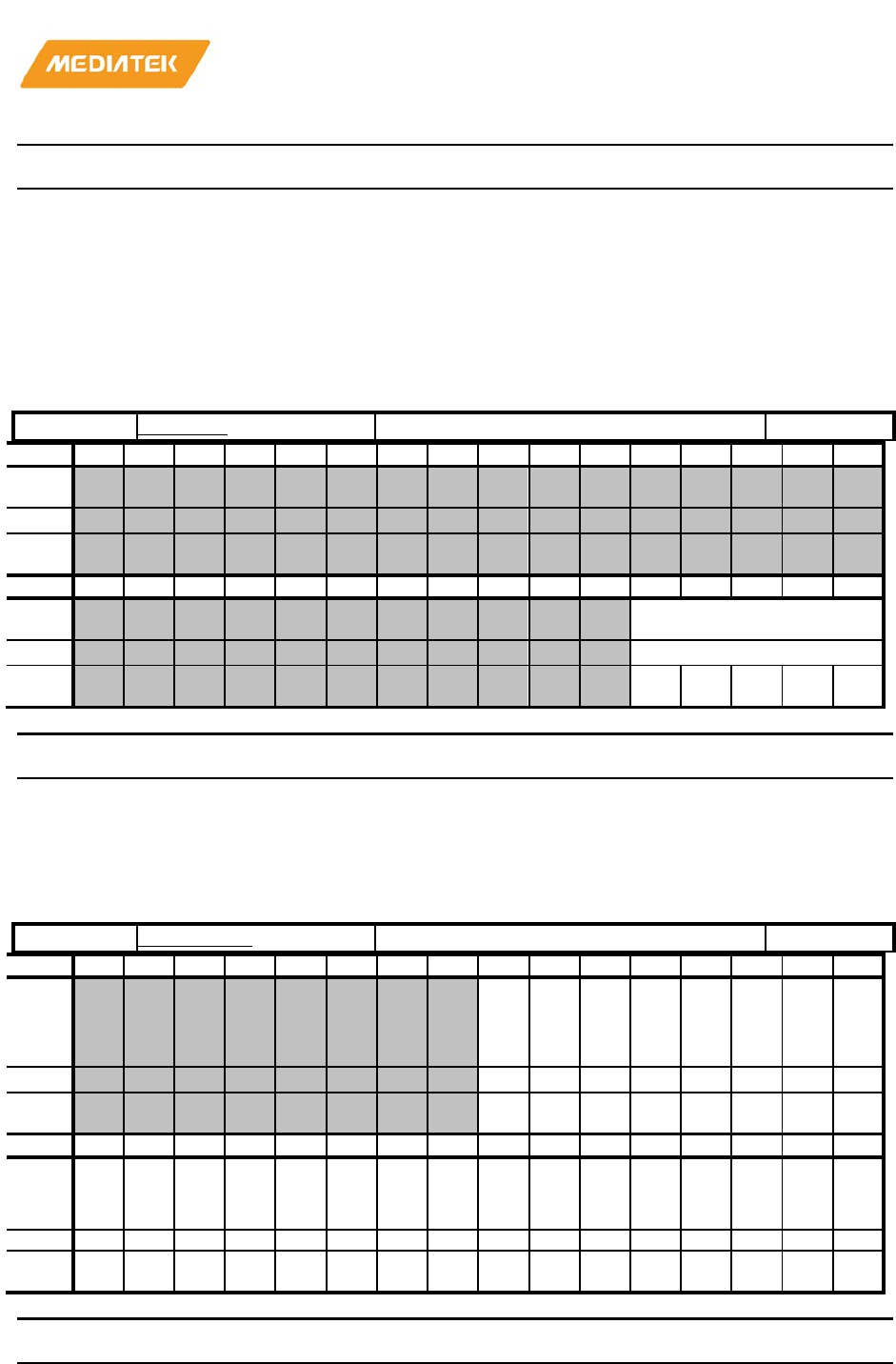
MT76x7
Internet-of-Things Wireless Connectivity
Reference Manual
© 2015 - 2017 MediaTek Inc
Page 678 of 798
This document contains information that is proprietary to MediaTek Inc. (“MediaTek”) and/or its licensor(s).
Any unauthorized use, reproduction or disclosure of this document in whole or in part is strictly prohibited
Bit(s)
Name
Description
12:8
IRQ15_SEL
Interrupt source selector
5'h0~5'h17: Please reference to interrupt source table
4:0
IRQ14_SEL
Interrupt source selector
5'h0~5'h17: Please reference to interrupt source table
8104006C
FIQ_SEL
FIQ Selection Register
00000000
Bit
31
30
29
28
27
26
25
24
23
22
21
20
19
18
17
16
Nam
e
Type
Rese
t
Bit
15
14
13
12
11
10
9
8
7
6
5
4
3
2
1
0
Nam
e
FIQ_SEL
Type
RW
Rese
t
0 0 0 0 0
Bit(s)
Name
Description
4:0
FIQ_SEL
Interrupt source selector
5'h0~5'h17: Please reference to
interrupt source table
81040070
IRQ_MASK
IRQ Mask Register
00FFFFFF
Bit
31
30
29
28
27
26
25
24
23
22
21
20
19
18
17
16
Nam
e
IR
Q17
_M
SK
IR
Q16
_M
SK
IR
Q15
_M
SK
IR
Q14
_M
SK
IR
Q13
_M
SK
IR
Q12
_M
SK
IR
Q11
_M
SK
IR
Q1
0_
MS
K
Type
RW
RW
RW
RW
RW
RW
RW
RW
Rese
t
1 1 1 1 1 1 1 1
Bit
15
14
13
12
11
10
9
8
7
6
5
4
3
2
1
0
Nam
e
IR
QF
_M
SK
IR
QE
_M
SK
IR
QD
_M
SK
IR
QC
_M
SK
IR
QB
_M
SK
IR
QA
_M
SK
IR
Q9
_M
SK
IR
Q8
_M
SK
IR
Q7
_M
SK
IR
Q6
_M
SK
IR
Q5
_M
SK
IR
Q4
_M
SK
IR
Q3
_M
SK
IR
Q2
_M
SK
IR
Q1
_M
SK
IR
Q0
_M
SK
Type
RW
RW
RW
RW
RW
RW
RW
RW
RW
RW
RW
RW
RW
RW
RW
RW
Rese
t
1 1 1 1 1 1 1 1 1 1 1 1 1 1 1 1
Bit(s)
Name
Description
23
IRQ17_MSK
Mask control for the associated interrupt source in the

MT76x7
Internet-of-Things Wireless Connectivity
Reference Manual
© 2015 - 2017 MediaTek Inc
Page 679 of 798
This document contains information that is proprietary to MediaTek Inc. (“MediaTek”) and/or its licensor(s).
Any unauthorized use, reproduction or disclosure of this document in whole or in part is strictly prohibited
Bit(s)
Name
Description
IRQ controller
0: Interrupt is enabled
1: Interrupt is disabled
22
IRQ16_MSK
Mask control for the associated interrupt source in the
IRQ controller
0: Interrupt is enabled
1: Interrupt is disabled
21
IRQ15_MSK
Mask control for the associated interrupt source in the
IRQ controller
0: Interrupt is enabled
1: Interrupt is d
isabled
20
IRQ14_MSK
Mask control for the associated interrupt source in the
IRQ controller
0: Interrupt is enabled
1: Interrupt is disabled
19
IRQ13_MSK
Mask control for the associated interrupt source in the
IRQ controller
0: Interrupt is enabled
1:
Interrupt is disabled
18
IRQ12_MSK
Mask control for the associated interrupt source in the
IRQ controller
0: Interrupt is enabled
1: Interrupt is disabled
17
IRQ11_MSK
Mask control for the associated interrupt source in the
IRQ controller
0: Interrupt is
enabled
1: Interrupt is disabled
16
IRQ10_MSK
Mask control for the associated interrupt source in the
IRQ controller
0: Interrupt is enabled
1: Interrupt is disabled
15
IRQF_MSK
Mask control for the associated interrupt source in the
IRQ controller
0:
Interrupt is enabled
1: Interrupt is disabled

MT76x7
Internet-of-Things Wireless Connectivity
Reference Manual
© 2015 - 2017 MediaTek Inc
Page 680 of 798
This document contains information that is proprietary to MediaTek Inc. (“MediaTek”) and/or its licensor(s).
Any unauthorized use, reproduction or disclosure of this document in whole or in part is strictly prohibited
Bit(s)
Name
Description
14
IRQE_MSK
Mask control for the associated interrupt source in the
IRQ controller
0: Interrupt is enabled
1: Interrupt is disabled
13
IRQD_MSK
Mask control for the associated interrupt source in the
IRQ
controller
0: Interrupt is enabled
1: Interrupt is disabled
12
IRQC_MSK
Mask control for the associated interrupt source in the
IRQ controller
0: Interrupt is enabled
1: Interrupt is disabled
11
IRQB_MSK
Mask control for the associated interrupt source in the
IRQ controller
0: Interrupt is enabled
1: Interrupt is disabled
10
IRQA_MSK
Mask control for the associated interrupt source in the
IRQ controller
0: Interrupt is enabled
1: Interrupt is disabled
9
IRQ9_MSK
Mask control for the associated interrupt source in the
IRQ controller
0: Interrupt is enabled
1: Interrupt is disabled
8
IRQ8_MSK
Mask control for the associated interrupt source in the
IRQ controller
0: Interrupt is enabled
1: Interrupt is disabled
7
IRQ7_MSK
Mask control for the associated interrupt source in the
IRQ controller
0: Interrupt is enabled
1: Interrupt is disabled
6
IRQ6_MSK
Mask control for the associated interrupt source in the
IRQ controller
0: Interrupt is enabled

MT76x7
Internet-of-Things Wireless Connectivity
Reference Manual
© 2015 - 2017 MediaTek Inc
Page 681 of 798
This document contains information that is proprietary to MediaTek Inc. (“MediaTek”) and/or its licensor(s).
Any unauthorized use, reproduction or disclosure of this document in whole or in part is strictly prohibited
Bit(s)
Name
Description
1: Interrupt is disabled
5
IRQ5_MSK
Mask control for the associated interrupt source in the
IRQ controller
0: Interrupt is enabled
1: Interrupt is disabled
4
IRQ4_MSK
Mask control for the associated interrupt source in the
IRQ controller
0: Interrupt is enabled
1: Interrupt is disabled
3
IRQ3_MSK
Mask control for the associated interrupt source in the
IRQ controller
0: Interrupt is enabled
1: Interrupt is disabled
2
IRQ2_MSK
Mask control for the associated interrupt source in the
IRQ controller
0: Interrupt is enabled
1: Interrupt is disabled
1
IRQ1_MSK
Mask control for the associated interrupt source in the
IRQ controller
0: Interrupt is enabled
1: Interrupt is disabled
0
IRQ0_MSK
Mask control for the associated interrupt source in the
IRQ controller
0: Interrupt is enabled
1: Interrupt is disabled
81040080
IRQ_MASK_CLR
IRQ Mask Clear Register
00000000
Bit
31
30
29
28
27
26
25
24
23
22
21
20
19
18
17
16
Nam
e
IR
Q17
_M
CL
R
IR
Q16
_M
CL
R
IR
Q15
_M
CL
R
IR
Q14
_M
CL
R
IR
Q13
_M
CL
R
IR
Q12
_M
CL
R
IR
Q11
_M
CL
R
IR
Q1
0_
MC
LR
Type
WO
WO
WO
WO
WO
WO
WO
WO
Rese
t
0 0 0 0 0 0 0 0
Bit
15
14
13
12
11
10
9
8
7
6
5
4
3
2
1
0
Nam
e
IR
QF
_M
IR
QE
_M
IR
QD
_M
IR
QC
_M
IR
QB
_M
IR
QA
_M
IR
Q9
_M
IR
Q8
_M
IR
Q7
_M
IR
Q6
_M
IR
Q5
_M
IR
Q4
_M
IR
Q3
_M
IR
Q2
_M
IR
Q1
_M
IR
Q0
_M
MT76x7
Internet-of-Things Wireless Connectivity
Reference Manual
© 2015 - 2017 MediaTek Inc
Page 682 of 798
This document contains information that is proprietary to MediaTek Inc. (“MediaTek”) and/or its licensor(s).
Any unauthorized use, reproduction or disclosure of this document in whole or in part is strictly prohibited
CL
R
CL
R
CL
R
CL
R
CL
R
CL
R
CL
R
CL
R
CL
R
CL
R
CL
R
CL
R
CL
R
CL
R
CL
R
CL
R
Type
WO
WO
WO
WO
WO
WO
WO
WO
WO
WO
WO
WO
WO
WO
WO
WO
Rese
t
0 0 0 0 0 0 0 0 0 0 0 0 0 0 0 0
Bit(s)
Name
Description
23
IRQ17_MCLR
Clear corresponding bits in IRQ Mask Register.
0: No effect
1: Disable the corresponding MASK bit
22
IRQ16_MCLR
Clear corresponding bits in IRQ Mask Register.
0: No effect
1: Disable the corresponding MASK bit
21
IRQ15_MCLR
Clear corresponding bits in IRQ Mask Register.
0: No effect
1: Disable the corresponding MASK bit
20
IRQ14_MCLR
Clear corresponding bits in IRQ Mask Register.
0: No effect
1: Disable the corresponding MASK bit
19
IRQ13_MCLR
Clear corresponding bits in IRQ Mask Register.
0: No effect
1: Disable the corresponding MASK bit
18
IRQ12_MCLR
Clear corresponding bits in IRQ Mask Register.
0: No effect
1:
Disable the corresponding MASK bit
17
IRQ11_MCLR
Clear corresponding bits in IRQ Mask Register.
0: No effect
1: Disable the corresponding MASK bit
16
IRQ10_MCLR
Clear corresponding bits in IRQ Mask Register.
0: No effect
1: Disable the corresponding
MASK bit
15
IRQF_MCLR
Clear corresponding bits in IRQ Mask Register.
0: No effect
1: Disable the corresponding MASK bit
14
IRQE_MCLR
Clear corresponding bits in IRQ Mask Register.

MT76x7
Internet-of-Things Wireless Connectivity
Reference Manual
© 2015 - 2017 MediaTek Inc
Page 683 of 798
This document contains information that is proprietary to MediaTek Inc. (“MediaTek”) and/or its licensor(s).
Any unauthorized use, reproduction or disclosure of this document in whole or in part is strictly prohibited
Bit(s)
Name
Description
0: No effect
1: Disable the corresponding MASK bit
13
IRQD_MCLR
Clear corresponding bits in IRQ Mask Register.
0: No effect
1: Disable the corresponding MASK bit
12
IRQC_MCLR
Clear corresponding bits in IRQ Mask Register.
0: No effect
1: Disable the corresponding MASK bit
11
IRQB_MCLR
Clear corresponding bits in IRQ Mask Register.
0: No effect
1: Disable the corresponding MASK bit
10
IRQA_MCLR
Clear corresponding bits in IRQ Mask Register.
0: No effect
1: Disable the corresponding MASK bit
9
IRQ9_MCLR
Clear corresponding bits in IRQ Mask Register.
0: No effect
1: Disable
the corresponding MASK bit
8
IRQ8_MCLR
Clear corresponding bits in IRQ Mask Register.
0: No effect
1: Disable the corresponding MASK bit
7
IRQ7_MCLR
Clear corresponding bits in IRQ Mask Register.
0: No effect
1: Disable the corresponding MASK bit
6
IRQ6_MCLR
Clear corresponding bits in IRQ Mask Register.
0: No effect
1: Disable the corresponding MASK bit
5
IRQ5_MCLR
Clear corresponding bits in IRQ Mask Register.
0: No effect
1: Disable the corresponding MASK bit
4
IRQ4_MCLR
Clear corresponding bits in IRQ Mask Register.
0: No effect
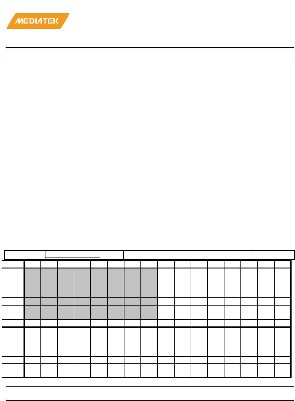
MT76x7
Internet-of-Things Wireless Connectivity
Reference Manual
© 2015 - 2017 MediaTek Inc
Page 684 of 798
This document contains information that is proprietary to MediaTek Inc. (“MediaTek”) and/or its licensor(s).
Any unauthorized use, reproduction or disclosure of this document in whole or in part is strictly prohibited
Bit(s)
Name
Description
1: Disable the corresponding MASK bit
3
IRQ3_MCLR
Clear corresponding bits in IRQ Mask Register.
0: No effect
1: Disable the corresponding MASK bit
2
IRQ2_MCLR
Clear corresponding bits in IRQ Mask Register.
0: No effec
t
1: Disable the corresponding MASK bit
1
IRQ1_MCLR
Clear corresponding bits in IRQ Mask Register.
0: No effect
1: Disable the corresponding MASK bit
0
IRQ0_MCLR
Clear corresponding bits in IRQ Mask Register.
0: No effect
1: Disable the corresponding
MASK bit
81040090
IRQ_MASK_SET
IRQ Mask Set Register
00000000
Bit
31
30
29
28
27
26
25
24
23
22
21
20
19
18
17
16
Nam
e
IR
Q17
_M
SE
T
IR
Q16
_M
SE
T
IR
Q15
_M
SE
T
IR
Q14
_M
SE
T
IR
Q13
_M
SE
T
IR
Q12
_M
SE
T
IR
Q11
_M
SE
T
IR
Q1
0_
MS
ET
Type
WO
WO
WO
WO
WO
WO
WO
WO
Rese
t
0 0 0 0 0 0 0 0
Bit
15
14
13
12
11
10
9
8
7
6
5
4
3
2
1
0
Nam
e
IR
QF
_M
SE
T
IR
QE
_M
SE
T
IR
QD
_M
SE
T
IR
QC
_M
SE
T
IR
QB
_M
SE
T
IR
QA
_M
SE
T
IR
Q9
_M
SE
T
IR
Q8
_M
SE
T
IR
Q7
_M
SE
T
IR
Q6
_M
SE
T
IR
Q5
_M
SE
T
IR
Q4
_M
SE
T
IR
Q3
_M
SE
T
IR
Q2
_M
SE
T
IR
Q1
_M
SE
T
IR
Q0
_M
SE
T
Type
WO
WO
WO
WO
WO
WO
WO
WO
WO
WO
WO
WO
WO
WO
WO
WO
Rese
t
0 0 0 0 0 0 0 0 0 0 0 0 0 0 0 0
Bit(s)
Name
Description
23
IRQ17_MSET
Set corresponding bits in IRQ Mask Register.
0: No effect
1: Enable corresponding MASK bit
22
IRQ16_MSET
Set corresponding bits in IRQ Mask Register.

MT76x7
Internet-of-Things Wireless Connectivity
Reference Manual
© 2015 - 2017 MediaTek Inc
Page 685 of 798
This document contains information that is proprietary to MediaTek Inc. (“MediaTek”) and/or its licensor(s).
Any unauthorized use, reproduction or disclosure of this document in whole or in part is strictly prohibited
Bit(s)
Name
Description
0: No effect
1: Enable corresponding MASK bit
21
IRQ15_MSET
Set corresponding bits in IRQ Mask Register.
0: No effect
1: Enable corresponding MASK bit
20
IRQ14_MSET
Set corresponding bits in IRQ Mask Register.
0: No effect
1: Enable corresponding MASK bit
19
IRQ13_MSET
Set corresponding bits in IRQ Mask Register.
0: No effect
1: Enable corresponding MASK bit
18
IRQ12_MSET
Set corresponding bits in IRQ Mask Register.
0: No effect
1: Enable
corresponding MASK bit
17
IRQ11_MSET
Set corresponding bits in IRQ Mask Register.
0: No effect
1: Enable corresponding MASK bit
16
IRQ10_MSET
Set corresponding bits in IRQ Mask Register.
0: No effect
1: Enable corresponding MASK bit
15
IRQF_MSET
Set corresponding bits in IRQ Mask Register.
0: No effect
1: Enable corresponding MASK bit
14
IRQE_MSET
Set corresponding bits in IRQ Mask Register.
0: No effect
1: Enable corresponding MASK bit
13
IRQD_MSET
Set corresponding bits in IRQ Mask Register.
0: No
effect
1: Enable corresponding MASK bit
12
IRQC_MSET
Set corresponding bits in IRQ Mask Register.
0: No effect

MT76x7
Internet-of-Things Wireless Connectivity
Reference Manual
© 2015 - 2017 MediaTek Inc
Page 686 of 798
This document contains information that is proprietary to MediaTek Inc. (“MediaTek”) and/or its licensor(s).
Any unauthorized use, reproduction or disclosure of this document in whole or in part is strictly prohibited
Bit(s)
Name
Description
1: Enable corresponding MASK bit
11
IRQB_MSET
Set corresponding bits in IRQ Mask Register.
0: No effect
1: Enable corresponding MASK bit
10
IRQA_MSET
Set corresponding bits in IRQ Mask Register.
0: No effect
1: Enable corresponding MASK bit
9
IRQ9_MSET
Set corresponding bits in IRQ Mask Register.
0: No effect
1: Enable corresponding MASK bit
8
IRQ8_MSET
Set corresponding bits in IRQ Mask Register.
0: No effect
1: Enable corresponding MASK bit
7
IRQ7_MSET
Set corresponding bits in IRQ Mask Register.
0: No effect
1: Enable corresponding MASK bit
6
IRQ6_MSET
Set corresponding bits in IRQ Mask Register.
0: No effect
1: Enable corresponding MASK
bit
5
IRQ5_MSET
Set corresponding bits in IRQ Mask Register.
0: No effect
1: Enable corresponding MASK bit
4
IRQ4_MSET
Set corresponding bits in IRQ Mask Register.
0: No effect
1: Enable corresponding MASK bit
3
IRQ3_MSET
Set corresponding bits in IRQ Mask Register.
0: No effect
1: Enable corresponding MASK bit
2
IRQ2_MSET
Set corresponding bits in IRQ Mask Register.
0: No effect
1: Enable corresponding MASK bit
MT76x7
Internet-of-Things Wireless Connectivity
Reference Manual
© 2015 - 2017 MediaTek Inc
Page 687 of 798
This document contains information that is proprietary to MediaTek Inc. (“MediaTek”) and/or its licensor(s).
Any unauthorized use, reproduction or disclosure of this document in whole or in part is strictly prohibited
Bit(s)
Name
Description
1
IRQ1_MSET
Set corresponding bits in IRQ Mask Register.
0: No effect
1: Enable
corresponding MASK bit
0
IRQ0_MSET
Set corresponding bits in IRQ Mask Register.
0: No effect
1: Enable corresponding MASK bit
810400A0
IRQ_EOI
IRQ End of Interrupt Register
00000000
Bit
31
30
29
28
27
26
25
24
23
22
21
20
19
18
17
16
Nam
e
IR
Q17
_E
OI
IR
Q16
_E
OI
IR
Q15
_E
OI
IR
Q14
_E
OI
IR
Q13
_E
OI
IR
Q12
_E
OI
IR
Q11
_E
OI
IR
Q1
0_
EO
I
Type
WO
WO
WO
WO
WO
WO
WO
WO
Rese
t
0 0 0 0 0 0 0 0
Bit
15
14
13
12
11
10
9
8
7
6
5
4
3
2
1
0
Nam
e
IR
QF
_E
OI
IR
QE
_E
OI
IR
QD
_E
OI
IR
QC
_E
OI
IR
QB
_E
OI
IR
QA
_E
OI
IR
Q9
_E
OI
IR
Q8
_E
OI
IR
Q7
_E
OI
IR
Q6
_E
OI
IR
Q5
_E
OI
IR
Q4
_E
OI
IR
Q3
_E
OI
IR
Q2
_E
OI
IR
Q1
_E
OI
IR
Q0
_E
OI
Type
WO
WO
WO
WO
WO
WO
WO
WO
WO
WO
WO
WO
WO
WO
WO
WO
Rese
t
0 0 0 0 0 0 0 0 0 0 0 0 0 0 0 0
Bit(s)
Name
Description
23
IRQ17_EOI
End of Interrupt command for the associated interrupt
line.
0: No service is currently in progress or pending
1: Interrupt request is in
-service
22
IRQ16_EOI
End of Interrupt command for the associated interrupt
line.
0: No service is currently in progress or
pending
1: Interrupt request is in
-service
21
IRQ15_EOI
End of Interrupt command for the associated interrupt
line.
0: No service is currently in progress or pending
1: Interrupt request is in
-service
20
IRQ14_EOI
End of Interrupt command for the associated interrupt
line.

MT76x7
Internet-of-Things Wireless Connectivity
Reference Manual
© 2015 - 2017 MediaTek Inc
Page 688 of 798
This document contains information that is proprietary to MediaTek Inc. (“MediaTek”) and/or its licensor(s).
Any unauthorized use, reproduction or disclosure of this document in whole or in part is strictly prohibited
Bit(s)
Name
Description
0: No service is currently in progress or pending
1: Interrupt request is in
-service
19
IRQ13_EOI
End of Interrupt command for the associated interrupt
line.
0: No service is currently in progress or pending
1: Interrupt request is
in-service
18
IRQ12_EOI
End of Interrupt command for the associated interrupt
line.
0: No service is currently in progress or pending
1: Interrupt request is in
-service
17
IRQ11_EOI
End of Interrupt command for the associated interrupt
line.
0: No servic
e is currently in progress or pending
1: Interrupt request is in
-service
16
IRQ10_EOI
End of Interrupt command for the associated interrupt
line.
0: No service is currently in progress or pending
1: Interrupt request is in
-service
15
IRQF_EOI
End of Interrupt command for the associated interrupt
line.
0: No service is currently in progress or pending
1: Interrupt request is in
-service
14
IRQE_EOI
End of Interrupt command for the associated interrupt
line.
0: No service is currently in progress or pen
ding
1: Interrupt request is in
-service
13
IRQD_EOI
End of Interrupt command for the associated interrupt
line.
0: No service is currently in progress or pending
1: Interrupt request is in
-service
12
IRQC_EOI
End of Interrupt command for the associated interrupt
line.
0: No service is currently in progress or pending
1: Interrupt request is in
-service
11
IRQB_EOI
End of Interrupt command for the associated interrupt

MT76x7
Internet-of-Things Wireless Connectivity
Reference Manual
© 2015 - 2017 MediaTek Inc
Page 689 of 798
This document contains information that is proprietary to MediaTek Inc. (“MediaTek”) and/or its licensor(s).
Any unauthorized use, reproduction or disclosure of this document in whole or in part is strictly prohibited
Bit(s)
Name
Description
line.
0: No service is currently in progress or pending
1: Interrupt request is
in-service
10
IRQA_EOI
End of Interrupt command for the associated interrupt
line.
0: No service is currently in progress or pending
1: Interrupt request is in
-service
9
IRQ9_EOI
End of Interrupt command for the associated interrupt
line.
0: No service
is currently in progress or pending
1: Interrupt request is in
-service
8
IRQ8_EOI
End of Interrupt command for the associated interrupt
line.
0: No service is currently in progress or pending
1: Interrupt request is in
-service
7
IRQ7_EOI
End of Interrupt command for the associated interrupt
line.
0: No service is currently in progress or pending
1: Interrupt request is in
-service
6
IRQ6_EOI
End of Interrupt command for the associated interrupt
line.
0: No service is currently in progress or pending
1: In
terrupt request is in-service
5
IRQ5_EOI
End of Interrupt command for the associated interrupt
line.
0: No service is currently in progress or pending
1: Interrupt request is in
-service
4
IRQ4_EOI
End of Interrupt command for the associated interrupt
line.
0: No service is currently in progress or pending
1: Interrupt request is in
-service
3
IRQ3_EOI
End of Interrupt command for the associated interrupt
line.
0: No service is currently in progress or pending
1: Interrupt request is in
-service
MT76x7
Internet-of-Things Wireless Connectivity
Reference Manual
© 2015 - 2017 MediaTek Inc
Page 690 of 798
This document contains information that is proprietary to MediaTek Inc. (“MediaTek”) and/or its licensor(s).
Any unauthorized use, reproduction or disclosure of this document in whole or in part is strictly prohibited
Bit(s)
Name
Description
2
IRQ2_EOI
End of Interrupt command for the associated interrupt
line.
0: No service is currently in progress or pending
1: Interrupt request is in
-service
1
IRQ1_EOI
End of Interrupt command for the associated interrupt
line.
0: No service is currently in
progress or pending
1: Interrupt request is in
-service
0
IRQ0_EOI
End of Interrupt command for the associated interrupt
line.
0: No service is currently in progress or pending
1: Interrupt request is in
-service
810400B0
IRQ_SENS
IRQ Sensitive Register
00000000
Bit
31
30
29
28
27
26
25
24
23
22
21
20
19
18
17
16
Nam
e
IR
Q17
_S
EN
S
IR
Q16
_S
EN
S
IR
Q15
_S
EN
S
IR
Q14
_S
EN
S
IR
Q13
_S
EN
S
IR
Q12
_S
EN
S
IR
Q11
_S
EN
S
IR
Q1
0_
SE
NS
Type
RW
RW
RW
RW
RW
RW
RW
RW
Rese
t
0 0 0 0 0 0 0 0
Bit
15
14
13
12
11
10
9
8
7
6
5
4
3
2
1
0
Nam
e
IR
QF
_S
EN
S
IR
QE
_S
EN
S
IR
QD
_S
EN
S
IR
QC
_S
EN
S
IR
QB
_S
EN
S
IR
QA
_S
EN
S
IR
Q9
_S
EN
S
IR
Q8
_S
EN
S
IR
Q7
_S
EN
S
IR
Q6
_S
EN
S
IR
Q5
_S
EN
S
IR
Q4
_S
EN
S
IR
Q3
_S
EN
S
IR
Q2
_S
EN
S
IR
Q1
_S
EN
S
IR
Q0
_S
EN
S
Type
RW
RW
RW
RW
RW
RW
RW
RW
RW
RW
RW
RW
RW
RW
RW
RW
Rese
t
0 0 0 0 0 0 0 0 0 0 0 0 0 0 0 0
Bit(s)
Name
Description
23
IRQ17_SENS
Sensitivity type of the associated Interrupt Source
0: Edge sensitivity with active LOW
1: Level sensitivity with active LOW
22
IRQ16_SENS
Sensitivity type of the associated Interrupt Source
0: Edge sensitivity with active LOW
1: Level sensitivity with active LOW
21
IRQ15_SENS
Sensitivity type of the associated Interrupt Source

MT76x7
Internet-of-Things Wireless Connectivity
Reference Manual
© 2015 - 2017 MediaTek Inc
Page 691 of 798
This document contains information that is proprietary to MediaTek Inc. (“MediaTek”) and/or its licensor(s).
Any unauthorized use, reproduction or disclosure of this document in whole or in part is strictly prohibited
Bit(s)
Name
Description
0: Edge sensitivity with active LOW
1: Level sensitivity with active LOW
20
IRQ14_SENS
Sensitivity type of the associated Interrupt Source
0: Edge sensitivity with active LOW
1: Level sensitivity with active LOW
19
IRQ13_SENS
Sensitivity type of the associated Interrupt Source
0: Edge sensitivity with active LOW
1: Level
sensitivity with active LOW
18
IRQ12_SENS
Sensitivity type of the associated Interrupt Source
0: Edge sensitivity with active LOW
1: Level sensitivity with active LOW
17
IRQ11_SENS
Sensitivity type of the associated Interrupt Source
0: Edge sensitivity w
ith active LOW
1: Level sensitivity with active LOW
16
IRQ10_SENS
Sensitivity type of the associated Interrupt Source
0: Edge sensitivity with active LOW
1: Level sensitivity with active LOW
15
IRQF_SENS
Sensitivity type of the associated Interrupt Source
0: Edge sensitivity with active LOW
1: Level sensitivity with active LOW
14
IRQE_SENS
Sensitivity type of the associated Interrupt Source
0: Edge sensitivity with active LOW
1: Level sensitivity with active LOW
13
IRQD_SENS
Sensitivity type of the associated Interrupt Source
0: Edge sensitivity with active LOW
1: Level sensitivity with active LOW
12
IRQC_SENS
Sensitivity type of the associated Interrupt Source
0: Edge sensitivity with active LOW
1: Level sensitivity with active LOW
11
IRQB_SENS
Sensitivity type of the associated Interrupt Source
0: Edge sensitivity with active LOW

MT76x7
Internet-of-Things Wireless Connectivity
Reference Manual
© 2015 - 2017 MediaTek Inc
Page 692 of 798
This document contains information that is proprietary to MediaTek Inc. (“MediaTek”) and/or its licensor(s).
Any unauthorized use, reproduction or disclosure of this document in whole or in part is strictly prohibited
Bit(s)
Name
Description
1: Level sensitivity with active LOW
10
IRQA_SENS
Sensitivity type of the associated Interrupt Source
0: Edge sensitivity with active LOW
1: Level sensitivity with
active LOW
9
IRQ9_SENS
Sensitivity type of the associated Interrupt Source
0: Edge sensitivity with active LOW
1: Level sensitivity with active LOW
8
IRQ8_SENS
Sensitivity type of the associated Interrupt Source
0: Edge sensitivity with active LOW
1: Lev
el sensitivity with active LOW
7
IRQ7_SENS
Sensitivity type of the associated Interrupt Source
0: Edge sensitivity with active LOW
1: Level sensitivity with active LOW
6
IRQ6_SENS
Sensitivity type of the associated Interrupt Source
0: Edge sensitivity
with active LOW
1: Level sensitivity with active LOW
5
IRQ5_SENS
Sensitivity type of the associated Interrupt Source
0: Edge sensitivity with active LOW
1: Level sensitivity with active LOW
4
IRQ4_SENS
Sensitivity type of the associated Interrupt Source
0: Edge sensitivity with active LOW
1: Level sensitivity with active LOW
3
IRQ3_SENS
Sensitivity type of the associated Interrupt Source
0: Edge sensitivity with active LOW
1: Level sensitivity with active LOW
2
IRQ2_SENS
Sensitivity type of the associated Interrupt Source
0: Edge sensitivity with active LOW
1: Level sensitivity with active LOW
1
IRQ1_SENS
Sensitivity type of the associated Interrupt Source
0: Edge sensitivity with active LOW
1: Level sensitivity with active LOW
MT76x7
Internet-of-Things Wireless Connectivity
Reference Manual
© 2015 - 2017 MediaTek Inc
Page 693 of 798
This document contains information that is proprietary to MediaTek Inc. (“MediaTek”) and/or its licensor(s).
Any unauthorized use, reproduction or disclosure of this document in whole or in part is strictly prohibited
Bit(s)
Name
Description
0
IRQ0_SENS
Sensitivity type of the associated Interrupt Source
0: Edge sensitivity with active LOW
1: Level sensitivity with active LOW
810400C0
IRQ_SOFT
IRQ Software Interrupt Register
00000000
Bit
31
30
29
28
27
26
25
24
23
22
21
20
19
18
17
16
Nam
e
IR
Q17
_S
OF
T
IR
Q16
_S
OF
T
IR
Q15
_S
OF
T
IR
Q14
_S
OF
T
IR
Q13
_S
OF
T
IR
Q12
_S
OF
T
IR
Q11
_S
OF
T
IR
Q1
0_
SO
FT
Type
RW
RW
RW
RW
RW
RW
RW
RW
Rese
t
0 0 0 0 0 0 0 0
Bit
15
14
13
12
11
10
9
8
7
6
5
4
3
2
1
0
Nam
e
IR
QF
_S
OF
T
IR
QE
_S
OF
T
IR
QD
_S
OF
T
IR
QC
_S
OF
T
IR
QB
_S
OF
T
IR
QA
_S
OF
T
IR
Q9
_S
OF
T
IR
Q8
_S
OF
T
IR
Q7
_S
OF
T
IR
Q6
_S
OF
T
IR
Q5
_S
OF
T
IR
Q4
_S
OF
T
IR
Q3
_S
OF
T
IR
Q2
_S
OF
T
IR
Q1
_S
OF
T
IR
Q0
_S
OF
T
Type
RW
RW
RW
RW
RW
RW
RW
RW
RW
RW
RW
RW
RW
RW
RW
RW
Rese
t
0 0 0 0 0 0 0 0 0 0 0 0 0 0 0 0
Bit(s)
Name
Description
23
IRQ17_SOFT
Software Interrupt
22
IRQ16_SOFT
Software Interrupt
21
IRQ15_SOFT
Software Interrupt
20
IRQ14_SOFT
Software Interrupt
19
IRQ13_SOFT
Software Interrupt
18
IRQ12_SOFT
Software Interrupt
17
IRQ11_SOFT
Software Interrupt
16
IRQ10_SOFT
Software Interrupt
15
IRQF_SOFT
Software Interrupt
14
IRQE_SOFT
Software Interrupt
13
IRQD_SOFT
Software Interrupt
12
IRQC_SOFT
Software Interrupt
11
IRQB_SOFT
Software Interrupt
10
IRQA_SOFT
Software Interrupt
MT76x7
Internet-of-Things Wireless Connectivity
Reference Manual
© 2015 - 2017 MediaTek Inc
Page 694 of 798
This document contains information that is proprietary to MediaTek Inc. (“MediaTek”) and/or its licensor(s).
Any unauthorized use, reproduction or disclosure of this document in whole or in part is strictly prohibited
Bit(s)
Name
Description
9
IRQ9_SOFT
Software Interrupt
8
IRQ8_SOFT
Software Interrupt
7
IRQ7_SOFT
Software Interrupt
6
IRQ6_SOFT
Software Interrupt
5
IRQ5_SOFT
Software Interrupt
4
IRQ4_SOFT
Software Interrupt
3
IRQ3_SOFT
Software Interrupt
2
IRQ2_SOFT
Software Interrupt
1
IRQ1_SOFT
Software Interrupt
0
IRQ0_SOFT
Software Interrupt
810400D0
FIQ_CON
FIQ Control Register
00000001
Bit
31
30
29
28
27
26
25
24
23
22
21
20
19
18
17
16
Nam
e
Type
Rese
t
Bit
15
14
13
12
11
10
9
8
7
6
5
4
3
2
1
0
Nam
e
FIQ
_S
EN
S
FIQ
_M
AS
K
Type
RW
RW
Rese
t
0 1
Bit(s)
Name
Description
1
FIQ_SENS
Sensitivity type of the FIQ Interrupt Source
0: Edge sensitivity with active LOW
1: Level sensitivity with active
LOW
0
FIQ_MASK
Mask control for the FIQ Interrupt Source
0: Interrupt is enabled
1: Interrupt is disabled
810400D4
FIQ_EOI
FIQ End of Interrupt Register
00000000
Bit
31
30
29
28
27
26
25
24
23
22
21
20
19
18
17
16
MT76x7
Internet-of-Things Wireless Connectivity
Reference Manual
© 2015 - 2017 MediaTek Inc
Page 695 of 798
This document contains information that is proprietary to MediaTek Inc. (“MediaTek”) and/or its licensor(s).
Any unauthorized use, reproduction or disclosure of this document in whole or in part is strictly prohibited
Nam
e
Type
Rese
t
Bit
15
14
13
12
11
10
9
8
7
6
5
4
3
2
1
0
Nam
e
FIQ
_E
OI
Type
WO
Rese
t
0
Bit(s)
Name
Description
0
FIQ_EOI
End of Interrupt command
0: No interrupt
request is generated
1: Interrupt request is in
-service
810400D8
IRQ_STA2
Binary Coded Value of IRQ_STATUS
00000100
Bit
31
30
29
28
27
26
25
24
23
22
21
20
19
18
17
16
Nam
e
Type
Rese
t
Bit
15
14
13
12
11
10
9
8
7
6
5
4
3
2
1
0
Nam
e
NO
IR
Q
IRQ_STA2
Type
RC
RC
Rese
t
1 0 0 0 0 0
Bit(s)
Name
Description
8
NOIRQ
Indicating if there is an IRQ or not. If there is no IRQ, this
bit is HIGH
4:0
IRQ_STA2
Binary coded value of IRQ_STA
810400DC
IRQ_EOI2
Binary Coded Value of IRQ_EOI
00000000
Bit
31
30
29
28
27
26
25
24
23
22
21
20
19
18
17
16
Nam
e
Type
Rese
t
Bit
15
14
13
12
11
10
9
8
7
6
5
4
3
2
1
0
Nam
IRQ_EOI
MT76x7
Internet-of-Things Wireless Connectivity
Reference Manual
© 2015 - 2017 MediaTek Inc
Page 696 of 798
This document contains information that is proprietary to MediaTek Inc. (“MediaTek”) and/or its licensor(s).
Any unauthorized use, reproduction or disclosure of this document in whole or in part is strictly prohibited
e
Type
RW
Rese
t
0 0 0 0 0
Bit(s)
Name
Description
4:0
IRQ_EOI
Binary coded value of IRQ_EOI
810400E0
IRQ_ASTA
Binary Value of IRQ Source Status
00000000
Bit
31
30
29
28
27
26
25
24
23
22
21
20
19
18
17
16
Nam
e
IR
Q17
_A
ST
A
IR
Q16
_A
ST
A
IR
Q15
_A
ST
A
IR
Q14
_A
ST
A
IR
Q13
_A
ST
A
IR
Q12
_A
ST
A
IR
Q11
_A
ST
A
IR
Q1
0_
AS
TA
Type
RO
RO
RO
RO
RO
RO
RO
RO
Rese
t
0 0 0 0 0 0 0 0
Bit
15
14
13
12
11
10
9
8
7
6
5
4
3
2
1
0
Nam
e
IR
QF
_A
ST
A
IR
QE
_A
ST
A
IR
QD
_A
ST
A
IR
QC
_A
ST
A
IR
QB
_A
ST
A
IR
QA
_A
ST
A
IR
Q9
_A
ST
A
IR
Q8
_A
ST
A
IR
Q7
_A
ST
A
IR
Q6
_A
ST
A
IR
Q5
_A
ST
A
IR
Q4
_A
ST
A
IR
Q3
_A
ST
A
IR
Q2
_A
ST
A
IR
Q1
_A
ST
A
IR
Q0
_A
ST
A
Type
RO
RO
RO
RO
RO
RO
RO
RO
RO
RO
RO
RO
RO
RO
RO
RO
Rese
t
0 0 0 0 0 0 0 0 0 0 0 0 0 0 0 0
Bit(s)
Name
Description
23
IRQ17_ASTA
Status of interrupt source
0: no interrupt.
1: interrupt occurs
22
IRQ16_ASTA
Status of interrupt source
0: no interrupt.
1: interrupt occurs
21
IRQ15_ASTA
Status of interrupt source
0: no interrupt.
1: interrupt occurs
20
IRQ14_ASTA
Status of interrupt source
0: no interrupt.
1: interrupt occurs
19
IRQ13_ASTA
Status of interrupt source
0: no interrupt.

MT76x7
Internet-of-Things Wireless Connectivity
Reference Manual
© 2015 - 2017 MediaTek Inc
Page 697 of 798
This document contains information that is proprietary to MediaTek Inc. (“MediaTek”) and/or its licensor(s).
Any unauthorized use, reproduction or disclosure of this document in whole or in part is strictly prohibited
Bit(s)
Name
Description
1: interrupt occurs
18
IRQ12_ASTA
Status of interrupt source
0: no interrupt.
1:
interrupt occurs
17
IRQ11_ASTA
Status of interrupt source
0: no interrupt.
1: interrupt occurs
16
IRQ10_ASTA
Status of interrupt source
0: no interrupt.
1: interrupt occurs
15
IRQF_ASTA
Status of interrupt source
0: no interrupt.
1: interrupt occurs
14
IRQE_ASTA
Status of interrupt source
0: no interrupt.
1: interrupt occurs
13
IRQD_ASTA
Status of interrupt source
0: no interrupt.
1: interrupt occurs
12
IRQC_ASTA
Status of interrupt source
0: no interrupt.
1: interrupt occurs
11
IRQB_ASTA
Status of interrupt source
0: no interrupt.
1: interrupt occurs
10
IRQA_ASTA
Status of interrupt source
0: no interrupt.
1: interrupt occurs
9
IRQ9_ASTA
Status of interrupt source
0: no interrupt.
1: interrupt occurs

MT76x7
Internet-of-Things Wireless Connectivity
Reference Manual
© 2015 - 2017 MediaTek Inc
Page 698 of 798
This document contains information that is proprietary to MediaTek Inc. (“MediaTek”) and/or its licensor(s).
Any unauthorized use, reproduction or disclosure of this document in whole or in part is strictly prohibited
Bit(s)
Name
Description
8
IRQ8_ASTA
Status of interrupt source
0: no
interrupt.
1: interrupt occurs
7
IRQ7_ASTA
Status of interrupt source
0: no interrupt.
1: interrupt occurs
6
IRQ6_ASTA
Status of interrupt source
0: no interrupt.
1: interrupt occurs
5
IRQ5_ASTA
Status of interrupt source
0: no interrupt.
1: interrupt
occurs
4
IRQ4_ASTA
Status of interrupt source
0: no interrupt.
1: interrupt occurs
3
IRQ3_ASTA
Status of interrupt source
0: no interrupt.
1: interrupt occurs
2
IRQ2_ASTA
Status of interrupt source
0: no interrupt.
1: interrupt occurs
1
IRQ1_ASTA
Status of interrupt source
0: no interrupt.
1: interrupt occurs
0
IRQ0_ASTA
Status of interrupt source
0: no interrupt.
1: interrupt occurs
810400F0
IRQ_EEVT
Binary Value of EINT Event
00000000
Bit
31
30
29
28
27
26
25
24
23
22
21
20
19
18
17
16
Nam
e
EI
NT
MT76x7
Internet-of-Things Wireless Connectivity
Reference Manual
© 2015 - 2017 MediaTek Inc
Page 699 of 798
This document contains information that is proprietary to MediaTek Inc. (“MediaTek”) and/or its licensor(s).
Any unauthorized use, reproduction or disclosure of this document in whole or in part is strictly prohibited
_S
YN
C_
MO
DE
Type
RW
Rese
t
0
Bit
15
14
13
12
11
10
9
8
7
6
5
4
3
2
1
0
Nam
e
EI
NT
_E
VE
NT
Type
RO
Rese
t
0
Bit(s)
Name
Description
31
EINT_SYNC_MODE
EINT event sync mode enable
0: EINT event no sync by 32k clock
1: EINT event sync by 32k clock
0
EINT_EVENT
EINT event status
0: no EINT event.
1: EINT event occurs.
81040100
EINT_STA
EINT Status Register
00000000
Bit
31
30
29
28
27
26
25
24
23
22
21
20
19
18
17
16
Nam
e
Type
Rese
t
Bit
15
14
13
12
11
10
9
8
7
6
5
4
3
2
1
0
Nam
e
EI
NT
D_
ST
A
EI
NT
C_
ST
A
EI
NT
B_
ST
A
EI
NT
A_
ST
A
EI
NT
9_
ST
A
EI
NT
8_
ST
A
EI
NT
7_S
TA
EI
NT
6_
ST
A
EI
NT
5_S
TA
EI
NT
4_
ST
A
EI
NT
3_
ST
A
EI
NT
2_
ST
A
EI
NT
1_S
TA
EI
NT
0_
ST
A
Type
RO
RO
RO
RO
RO
RO
RO
RO
RO
RO
RO
RO
RO
RO
Rese
t
0 0 0 0 0 0 0 0 0 0 0 0 0 0
Bit(s)
Name
Description
13
EINTD_STA
Interrupt Status
0: No interrupt request is
generated
1: Interrupt request is pending

MT76x7
Internet-of-Things Wireless Connectivity
Reference Manual
© 2015 - 2017 MediaTek Inc
Page 700 of 798
This document contains information that is proprietary to MediaTek Inc. (“MediaTek”) and/or its licensor(s).
Any unauthorized use, reproduction or disclosure of this document in whole or in part is strictly prohibited
Bit(s)
Name
Description
12
EINTC_STA
Interrupt Status
0: No interrupt request is generated
1: Interrupt request is pending
11
EINTB_STA
Interrupt Status
0: No interrupt request is generated
1: Interrupt request is pending
10
EINTA_STA
Interrupt Status
0: No interrupt request is generated
1: Interrupt request is pending
9
EINT9_STA
Interrupt Status
0: No interrupt request is generated
1: Interrupt request is pending
8
EINT8_STA
Interrupt Status
0: No interrupt request is generated
1:
Interrupt request is pending
7
EINT7_STA
Interrupt Status
0: No interrupt request is generated
1: Interrupt request is pending
6
EINT6_STA
Interrupt Status
0: No interrupt request is generated
1: Interrupt request is pending
5
EINT5_STA
Interrupt Status
0: No interrupt request is generated
1: Interrupt request is pending
4
EINT4_STA
Interrupt Status
0: No interrupt request is generated
1: Interrupt request is pending
3
EINT3_STA
Interrupt Status
0: No interrupt request is generated
1: Interrupt request
is pending
2
EINT2_STA
Interrupt Status
MT76x7
Internet-of-Things Wireless Connectivity
Reference Manual
© 2015 - 2017 MediaTek Inc
Page 701 of 798
This document contains information that is proprietary to MediaTek Inc. (“MediaTek”) and/or its licensor(s).
Any unauthorized use, reproduction or disclosure of this document in whole or in part is strictly prohibited
Bit(s)
Name
Description
0: No interrupt request is generated
1: Interrupt request is pending
1
EINT1_STA
Interrupt Status
0: No interrupt request is generated
1: Interrupt request is pending
0
EINT0_STA
Interrupt Status
0: No interrupt
request is generated
1: Interrupt request is pending
81040104
EINT_MASK
EINT Mask Register
00003FFF
Bit
31
30
29
28
27
26
25
24
23
22
21
20
19
18
17
16
Nam
e
Type
Rese
t
Bit
15
14
13
12
11
10
9
8
7
6
5
4
3
2
1
0
Nam
e
EI
NT
D_
MA
SK
EI
NT
C_
MA
SK
EI
NT
B_
MA
SK
EI
NT
A_
MA
SK
EI
NT
9_
MA
SK
EI
NT
8_
MA
SK
EI
NT
7_
MA
SK
EI
NT
6_
MA
SK
EI
NT
5_
MA
SK
EI
NT
4_
MA
SK
EI
NT
3_
MA
SK
EI
NT
2_
MA
SK
EI
NT
1_
MA
SK
EI
NT
0_
MA
SK
Type
RW
RW
RW
RW
RW
RW
RW
RW
RW
RW
RW
RW
RW
RW
Rese
t
1 1 1 1 1 1 1 1 1 1 1 1 1 1
Bit(s)
Name
Description
13
EINTD_MASK
Mask control for the associated interrupt source in the
IRQ controller
0: Interrupt is enabled
1: Interrupt is disabled
12
EINTC_MASK
Mask control for the associated interrupt source in the
IRQ controller
0: Interrupt is enabled
1: Interrupt is disabled
11
EINTB_MASK
Mask control for the associated interrupt source in the
IRQ controller
0: Interrupt is enabled
1: Interrupt is disabled

MT76x7
Internet-of-Things Wireless Connectivity
Reference Manual
© 2015 - 2017 MediaTek Inc
Page 702 of 798
This document contains information that is proprietary to MediaTek Inc. (“MediaTek”) and/or its licensor(s).
Any unauthorized use, reproduction or disclosure of this document in whole or in part is strictly prohibited
Bit(s)
Name
Description
10
EINTA_MASK
Mask control for the associated interrupt source in the
IRQ controller
0: Interrupt is enabled
1: Interrupt is disabled
9
EINT9_MASK
Mask control for the associated interrupt source in the
IRQ controller
0: Interrupt is enabled
1: Interrupt is disabled
8
EINT8_MASK
Mask control for the associated interrupt source in the
IRQ controller
0: Interrupt is enabled
1: Interrupt is disabled
7
EINT7_MASK
Mask control for the associated interrupt source in the
IRQ controller
0: Interrupt is enabled
1: Interrupt is disabled
6
EINT6_MASK
Mask control for the associated interrupt source in the
IRQ controller
0: Interrupt is enabled
1: Interrupt is disabled
5
EINT5_MASK
Mask control for the associated interrupt source in the
IRQ controller
0: Interrupt is enabled
1: Interrupt is
disabled
4
EINT4_MASK
Mask control for the associated interrupt source in the
IRQ controller
0: Interrupt is enabled
1: Interrupt is disabled
3
EINT3_MASK
Mask control for the associated interrupt source in the
IRQ controller
0: Interrupt is enabled
1:
Interrupt is disabled
2
EINT2_MASK
Mask control for the associated interrupt source in the
IRQ controller
0: Interrupt is enabled

MT76x7
Internet-of-Things Wireless Connectivity
Reference Manual
© 2015 - 2017 MediaTek Inc
Page 703 of 798
This document contains information that is proprietary to MediaTek Inc. (“MediaTek”) and/or its licensor(s).
Any unauthorized use, reproduction or disclosure of this document in whole or in part is strictly prohibited
Bit(s)
Name
Description
1: Interrupt is disabled
1
EINT1_MASK
Mask control for the associated interrupt source in the
IRQ controller
0: Interrupt is
enabled
1: Interrupt is disabled
0
EINT0_MASK
Mask control for the associated interrupt source in the
IRQ controller
0: Interrupt is enabled
1: Interrupt is disabled
81040108
EINT_MASK_CLR
EINT Mask Clear Register
00000000
Bit
31
30
29
28
27
26
25
24
23
22
21
20
19
18
17
16
Nam
e
Type
Rese
t
Bit
15
14
13
12
11
10
9
8
7
6
5
4
3
2
1
0
Nam
e
EI
NT
D_
MC
LR
EI
NT
C_
MC
LR
EI
NT
B_
MC
LR
EI
NT
A_
MC
LR
EI
NT
9_
MC
LR
EI
NT
8_
MC
LR
EI
NT
7_
MC
LR
EI
NT
6_
MC
LR
EI
NT
5_
MC
LR
EI
NT
4_
MC
LR
EI
NT
3_
MC
LR
EI
NT
2_
MC
LR
EI
NT
1_
MC
LR
EI
NT
0_
MC
LR
Type
WO
WO
WO
WO
WO
WO
WO
WO
WO
WO
WO
WO
WO
WO
Rese
t
0 0 0 0 0 0 0 0 0 0 0 0 0 0
Bit(s)
Name
Description
13
EINTD_MCLR
Mask control for the associated interrupt source in the
IRQ controller
0: Interrupt is enabled
1: Interrupt is disabled
12
EINTC_MCLR
Disable mask for the associated external interrupt source
0: No effect.
1: Disable the corresponding MASK bit.
11
EINTB_MCLR
Disable mask for the associated external interrupt source
0: No effect.
1: Disable the corresponding MASK bit.
10
EINTA_MCLR
Disable mask for the associated external interrupt source

MT76x7
Internet-of-Things Wireless Connectivity
Reference Manual
© 2015 - 2017 MediaTek Inc
Page 704 of 798
This document contains information that is proprietary to MediaTek Inc. (“MediaTek”) and/or its licensor(s).
Any unauthorized use, reproduction or disclosure of this document in whole or in part is strictly prohibited
Bit(s)
Name
Description
0: No effect.
1: Disable the corresponding MASK bit.
9
EINT9_MCLR
Disable mask for the associated external interrupt source
0: No effect.
1: Disable the corresponding MASK bit.
8
EINT8_MCLR
Disable mask for the associated external interrupt source
0: No effect.
1: Disable the corresponding MASK bit.
7
EINT7_MCLR
Disable mask for the associated external interrupt source
0: No effect.
1: Disable the corresponding MASK bit.
6
EINT6_MCLR
Disable mask for the associated external interrupt source
0: No effect.
1: Disable the corresponding MASK bit.
5
EINT5_MCLR
Disable mask for the associated external interrupt source
0: No effect.
1: Disable the corresponding MASK bit.
4
EINT4_MCLR
Disable mask for the associated external interrupt source
0: No effect.
1: Disable the corresponding MASK bit.
3
EINT3_MCLR
Disable mask for the associated external interrupt source
0: No
effect.
1: Disable the corresponding MASK bit.
2
EINT2_MCLR
Disable mask for the associated external interrupt source
0: No effect.
1: Disable the corresponding MASK bit.
1
EINT1_MCLR
Disable mask for the associated external interrupt source
0: No
effect.
1: Disable the corresponding MASK bit.
0
EINT0_MCLR
Disable mask for the associated external interrupt source
0: No effect.
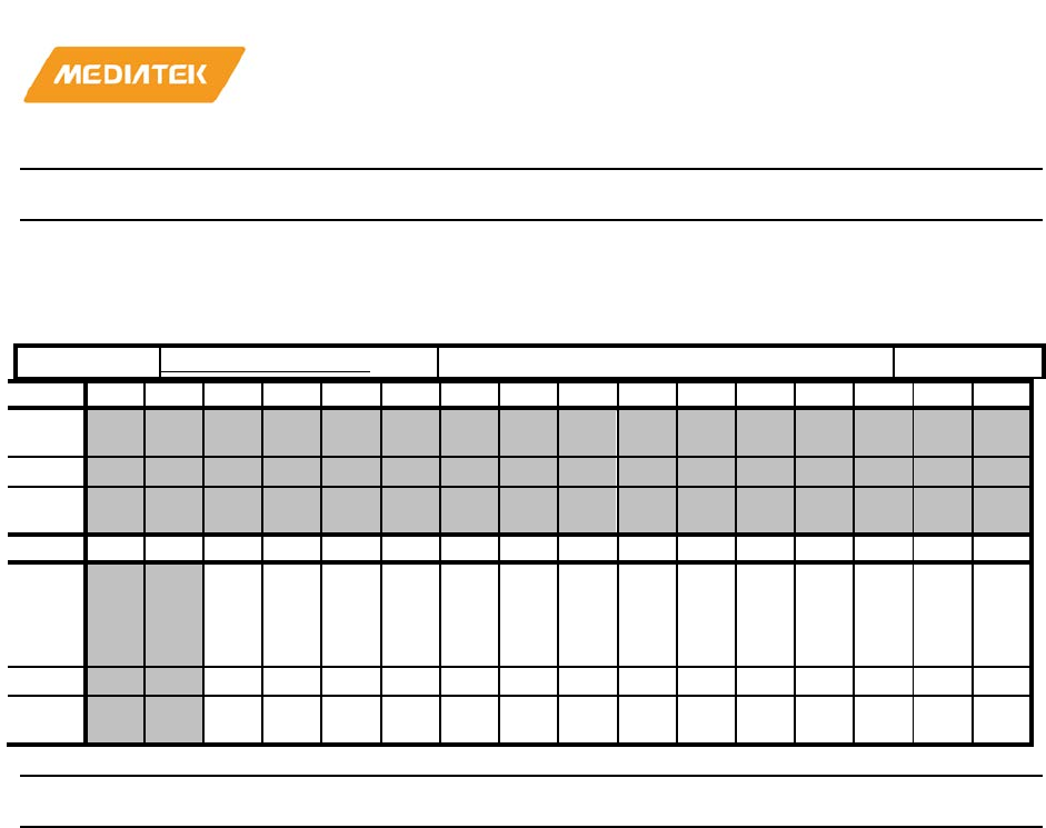
MT76x7
Internet-of-Things Wireless Connectivity
Reference Manual
© 2015 - 2017 MediaTek Inc
Page 705 of 798
This document contains information that is proprietary to MediaTek Inc. (“MediaTek”) and/or its licensor(s).
Any unauthorized use, reproduction or disclosure of this document in whole or in part is strictly prohibited
Bit(s)
Name
Description
1: Disable the corresponding MASK bit.
8104010C
EINT_MASK_SET
EINT Mask Set Register
00000000
Bit
31
30
29
28
27
26
25
24
23
22
21
20
19
18
17
16
Nam
e
Type
Rese
t
Bit
15
14
13
12
11
10
9
8
7
6
5
4
3
2
1
0
Nam
e
EI
NT
D_
MS
ET
EI
NT
C_
MS
ET
EI
NT
B_
MS
ET
EI
NT
A_
MS
ET
EI
NT
9_
MS
ET
EI
NT
8_
MS
ET
EI
NT
7_
MS
ET
EI
NT
6_
MS
ET
EI
NT
5_
MS
ET
EI
NT
4_
MS
ET
EI
NT
3_
MS
ET
EI
NT
2_
MS
ET
EI
NT
1_
MS
ET
EI
NT
0_
MS
ET
Type
WO
WO
WO
WO
WO
WO
WO
WO
WO
WO
WO
WO
WO
WO
Rese
t
0 0 0 0 0 0 0 0 0 0 0 0 0 0
Bit(s)
Name
Description
13
EINTD_MSET
Enable mask for the associated external interrupt source.
0: No effect.
1: Enable corresponding MASK bit.
12
EINTC_MSET
Enable mask for the associated external interrupt source.
0: No effect.
1: Enable corresponding MASK bit.
11
EINTB_MSET
Enable mask for the associated external interrupt source.
0: No
effect.
1: Enable corresponding MASK bit.
10
EINTA_MSET
Enable mask for the associated external interrupt source.
0: No effect.
1: Enable corresponding MASK bit.
9
EINT9_MSET
Enable mask for the associated external interrupt source.
0: No effect.
1:
Enable corresponding MASK bit.
8
EINT8_MSET
Enable mask for the associated external interrupt source.
0: No effect.
1: Enable corresponding MASK bit.

MT76x7
Internet-of-Things Wireless Connectivity
Reference Manual
© 2015 - 2017 MediaTek Inc
Page 706 of 798
This document contains information that is proprietary to MediaTek Inc. (“MediaTek”) and/or its licensor(s).
Any unauthorized use, reproduction or disclosure of this document in whole or in part is strictly prohibited
Bit(s)
Name
Description
7
EINT7_MSET
Enable mask for the associated external interrupt source.
0: No effect.
1: Enable correspon
ding MASK bit.
6
EINT6_MSET
Enable mask for the associated external interrupt source.
0: No effect.
1: Enable corresponding MASK bit.
5
EINT5_MSET
Enable mask for the associated external interrupt source.
0: No effect.
1: Enable corresponding MASK bit.
4
EINT4_MSET
Enable mask for the associated external interrupt source.
0: No effect.
1: Enable corresponding MASK bit.
3
EINT3_MSET
Enable mask for the associated external interrupt source.
0: No effect.
1: Enable corresponding MASK bit.
2
EINT2_MSET
Enable mask for the associated external interrupt source.
0: No effect.
1: Enable corresponding MASK bit.
1
EINT1_MSET
Enable mask for the associated external interrupt source.
0: No effect.
1: Enable corresponding MASK bit.
0
EINT0_MSET
Enable mask for the associated external interrupt source.
0: No effect.
1: Enable corresponding MASK bit.
81040110
EINT_INTACK
EINT Interrupt Acknowledge Register
00000000
Bit
31
30
29
28
27
26
25
24
23
22
21
20
19
18
17
16
Nam
e
Type
Rese
t
Bit
15
14
13
12
11
10
9
8
7
6
5
4
3
2
1
0
Nam
EI
NT
EI
NT
EI
NT
EI
NT
EI
NT
EI
NT
EI
NT
EI
NT
EI
NT
EI
NT
EI
NT
EI
NT
EI
NT
EI
NT
MT76x7
Internet-of-Things Wireless Connectivity
Reference Manual
© 2015 - 2017 MediaTek Inc
Page 707 of 798
This document contains information that is proprietary to MediaTek Inc. (“MediaTek”) and/or its licensor(s).
Any unauthorized use, reproduction or disclosure of this document in whole or in part is strictly prohibited
e
D_
AC
K
C_
AC
K
B_
AC
K
A_
AC
K
9_
AC
K
8_
AC
K
7_
AC
K
6_
AC
K
5_
AC
K
4_
AC
K
3_
AC
K
2_
AC
K
1_A
CK
0_
AC
K
Type
WO
WO
WO
WO
WO
WO
WO
WO
WO
WO
WO
WO
WO
WO
Rese
t
0 0 0 0 0 0 0 0 0 0 0 0 0 0
Bit(s)
Name
Description
13
EINTD_ACK
Interrupt acknowledgement
0: No effect.
1: Interrupt Request is acknowledged.
12
EINTC_ACK
Interrupt acknowledgement
0: No effect.
1:
Interrupt Request is acknowledged.
11
EINTB_ACK
Interrupt acknowledgement
0: No effect.
1: Interrupt Request is acknowledged.
10
EINTA_ACK
Interrupt acknowledgement
0: No effect.
1: Interrupt Request is acknowledged.
9
EINT9_ACK
Interrupt acknowledgement
0: No effect.
1: Interrupt Request is acknowledged.
8
EINT8_ACK
Interrupt acknowledgement
0: No effect.
1: Interrupt Request is acknowledged.
7
EINT7_ACK
Interrupt acknowledgement
0: No effect.
1: Interrupt Request is acknowledged.
6
EINT6_ACK
Interrupt acknowledgement
0: No effect.
1: Interrupt Request is acknowledged.
5
EINT5_ACK
Interrupt acknowledgement
0: No effect.
1: Interrupt Request is acknowledged.

MT76x7
Internet-of-Things Wireless Connectivity
Reference Manual
© 2015 - 2017 MediaTek Inc
Page 708 of 798
This document contains information that is proprietary to MediaTek Inc. (“MediaTek”) and/or its licensor(s).
Any unauthorized use, reproduction or disclosure of this document in whole or in part is strictly prohibited
Bit(s)
Name
Description
4
EINT4_ACK
Interrupt acknowledgement
0: No effect.
1: Interrupt Request is
acknowledged.
3
EINT3_ACK
Interrupt acknowledgement
0: No effect.
1: Interrupt Request is acknowledged.
2
EINT2_ACK
Interrupt acknowledgement
0: No effect.
1: Interrupt Request is acknowledged.
1
EINT1_ACK
Interrupt acknowledgement
0: No effect.
1:
Interrupt Request is acknowledged.
0
EINT0_ACK
Interrupt acknowledgement
0: No effect.
1: Interrupt Request is acknowledged.
81040114
EINT_SENS
EINT Sensitive Register
00003FFF
Bit
31
30
29
28
27
26
25
24
23
22
21
20
19
18
17
16
Nam
e
Type
Rese
t
Bit
15
14
13
12
11
10
9
8
7
6
5
4
3
2
1
0
Nam
e
EI
NT
D_
SE
NS
EI
NT
C_
SE
NS
EI
NT
B_
SE
NS
EI
NT
A_
SE
NS
EI
NT
9_
SE
NS
EI
NT
8_
SE
NS
EI
NT
7_S
EN
S
EI
NT
6_
SE
NS
EI
NT
5_S
EN
S
EI
NT
4_
SE
NS
EI
NT
3_
SE
NS
EI
NT
2_
SE
NS
EI
NT
1_S
EN
S
EI
NT
0_
SE
NS
Type
RW
RW
RW
RW
RW
RW
RW
RW
RW
RW
RW
RW
RW
RW
Rese
t
1 1 1 1 1 1 1 1 1 1 1 1 1 1
Bit(s)
Name
Description
13
EINTD_SENS
Sensitive type of the associated external interrupt source
0: Edge sensitivity.
1: Level sensitivity.
12
EINTC_SENS
Sensitive type of the associated external interrupt source

MT76x7
Internet-of-Things Wireless Connectivity
Reference Manual
© 2015 - 2017 MediaTek Inc
Page 709 of 798
This document contains information that is proprietary to MediaTek Inc. (“MediaTek”) and/or its licensor(s).
Any unauthorized use, reproduction or disclosure of this document in whole or in part is strictly prohibited
Bit(s)
Name
Description
0: Edge sensitivity.
1: Level sensitivity.
11
EINTB_SENS
Sensitive type of the associated external interrupt source
0: Edge sensitivity.
1: Level sensitivity.
10
EINTA_SENS
Sensitive type of the associated external interrupt source
0: Edge sensitivity.
1: Level sensitivity.
9
EINT9_SENS
Sensitive type of the associated external interrupt source
0: Edge sensitivity.
1: Level sensitivity.
8
EINT8_SENS
Sensitive type of the associated external interrupt source
0: Edge sensitivity.
1: Level sensitivity.
7
EINT7_SENS
Sensitive type of the associated external interrupt source
0: Edge sensitivity.
1: Level sensitivity.
6
EINT6_SENS
Sensitive type of the associated external interrupt source
0: Edge sensitivity.
1: Level sensitivity.
5
EINT5_SENS
Sensitive type of the associated external interrupt source
0: Edge sensitivity.
1: Level sensitivity.
4
EINT4_SENS
Sensitive type of the associated external interrupt source
0: Edge
sensitivity.
1: Level sensitivity.
3
EINT3_SENS
Sensitive type of the associated external interrupt source
0: Edge sensitivity.
1: Level sensitivity.
2
EINT2_SENS
Sensitive type of the associated external interrupt source
0: Edge sensitivity.

MT76x7
Internet-of-Things Wireless Connectivity
Reference Manual
© 2015 - 2017 MediaTek Inc
Page 710 of 798
This document contains information that is proprietary to MediaTek Inc. (“MediaTek”) and/or its licensor(s).
Any unauthorized use, reproduction or disclosure of this document in whole or in part is strictly prohibited
Bit(s)
Name
Description
1: Level sensitivity.
1
EINT1_SENS
Sensitive type of the associated external interrupt source
0: Edge sensitivity.
1: Level sensitivity.
0
EINT0_SENS
Sensitive type of the associated external interrupt source
0: Edge sensitivity.
1: Level sensitivity.
81040118
EINT_SOFT
EINT Software Interrupt Register
00000000
Bit
31
30
29
28
27
26
25
24
23
22
21
20
19
18
17
16
Nam
e
Type
Rese
t
Bit
15
14
13
12
11
10
9
8
7
6
5
4
3
2
1
0
Nam
e
EI
NT
D_
SO
FT
EI
NT
C_
SO
FT
EI
NT
B_
SO
FT
EI
NT
A_
SO
FT
EI
NT
9_
SO
FT
EI
NT
8_
SO
FT
EI
NT
7_S
OF
T
EI
NT
6_
SO
FT
EI
NT
5_S
OF
T
EI
NT
4_
SO
FT
EI
NT
3_
SO
FT
EI
NT
2_
SO
FT
EI
NT
1_S
OF
T
EI
NT
0_
SO
FT
Type
RW
RW
RW
RW
RW
RW
RW
RW
RW
RW
RW
RW
RW
RW
Rese
t
0 0 0 0 0 0 0 0 0 0 0 0 0 0
Bit(s)
Name
Description
13
EINTD_SOFT
Software Interrupt
12
EINTC_SOFT
Software Interrupt
11
EINTB_SOFT
Software Interrupt
10
EINTA_SOFT
Software Interrupt
9
EINT9_SOFT
Software Interrupt
8
EINT8_SOFT
Software Interrupt
7
EINT7_SOFT
Software Interrupt
6
EINT6_SOFT
Software Interrupt
5
EINT5_SOFT
Software Interrupt
4
EINT4_SOFT
Software Interrupt
3
EINT3_SOFT
Software Interrupt
2
EINT2_SOFT
Software Interrupt
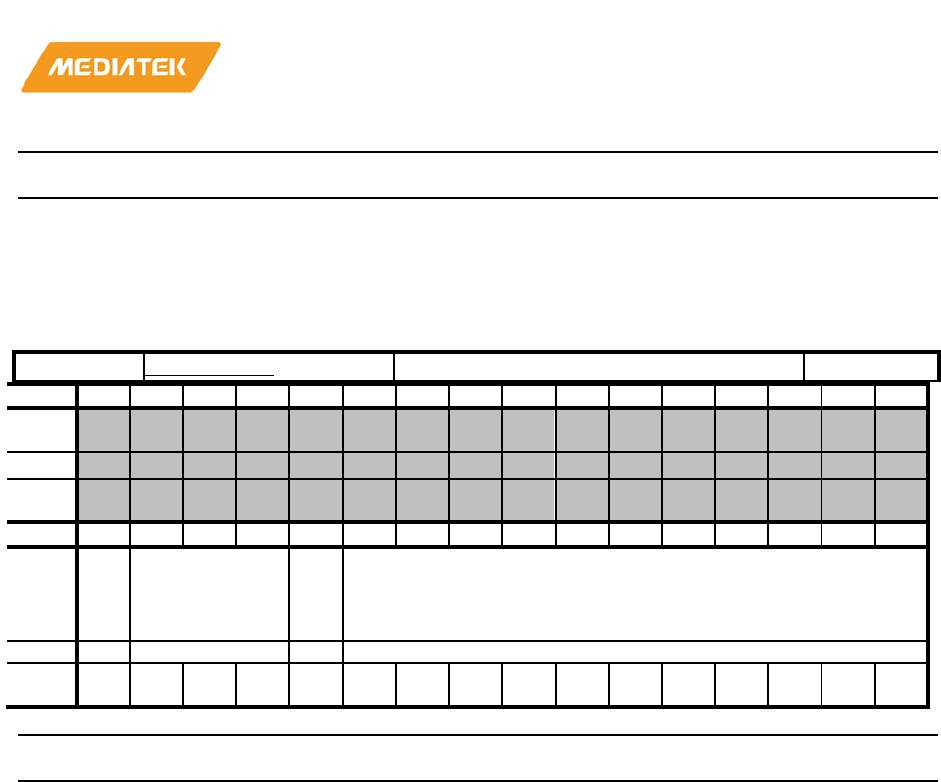
MT76x7
Internet-of-Things Wireless Connectivity
Reference Manual
© 2015 - 2017 MediaTek Inc
Page 711 of 798
This document contains information that is proprietary to MediaTek Inc. (“MediaTek”) and/or its licensor(s).
Any unauthorized use, reproduction or disclosure of this document in whole or in part is strictly prohibited
Bit(s)
Name
Description
1
EINT1_SOFT
Software Interrupt
0
EINT0_SOFT
Software Interrupt
81040120
EINT0_CON
EINT 0 De-bounce Control Register
00000000
Bit
31
30
29
28
27
26
25
24
23
22
21
20
19
18
17
16
Nam
e
Type
Rese
t
Bit
15
14
13
12
11
10
9
8
7
6
5
4
3
2
1
0
Nam
e
EI
NT
0_
EN
EINT0_PRESCA
LER
EI
NT
0_
PO
L
EINT0_CNT
Type
RW
RW
RW
RW
Rese
t
0 0 0 0 0 0 0 0 0 0 0 0 0 0 0 0
Bit(s)
Name
Description
15
EINT0_EN
De-bounce control circuit
0: Disable
1: Enable
14:12
EINT0_PRESCALER
Determine the clock cycle period for debounce count.
3'b000: 32768Hz, max
3'b001: 16384Hz
3'b010: 8192Hz
3'b011: 4096Hz
3'b100: 2048Hz, max
3'b101: 1024Hz
3'b110: 512Hz
3'b111: 256Hz, max
11
EINT0_POL
Activation type of the EINT source
0: Negative polarity
1: Positive polarity
10:0
EINT0_CNT
De-bounce duration in terms of numbers of 32768Hz
clock cycles. The cycle length is determined by
PRESCALER
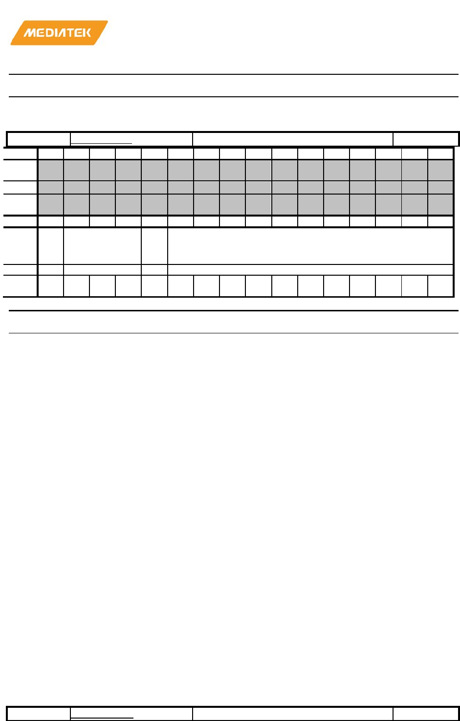
MT76x7
Internet-of-Things Wireless Connectivity
Reference Manual
© 2015 - 2017 MediaTek Inc
Page 712 of 798
This document contains information that is proprietary to MediaTek Inc. (“MediaTek”) and/or its licensor(s).
Any unauthorized use, reproduction or disclosure of this document in whole or in part is strictly prohibited
Bit(s)
Name
Description
81040130
EINT1_CON
EINT 1 De-bounce Control Register
00000000
Bit
31
30
29
28
27
26
25
24
23
22
21
20
19
18
17
16
Nam
e
Type
Rese
t
Bit
15
14
13
12
11
10
9
8
7
6
5
4
3
2
1
0
Nam
e
EI
NT
1_E
N
EINT1_PRESCA
LER
EI
NT
1_P
OL
EINT1_CNT
Type
RW
RW
RW
RW
Rese
t
0 0 0 0 0 0 0 0 0 0 0 0 0 0 0 0
Bit(s)
Name
Description
15
EINT1_EN
De-bounce control circuit
0: Disable
1: Enable
14:12
EINT1_PRESCALER
Determine the clock cycle period for debounce count.
3'b000: 32768Hz, max
3'b001: 16384Hz
3'b010: 8192Hz
3'b011: 4096Hz
3'b100: 2048Hz, max
3'b101: 1024Hz
3'b110: 512Hz
3'b111: 256Hz, max
11
EINT1_POL
Activation type of the EINT source
0: Negative polarity
1: Positive polarity
10:0
EINT1_CNT
De-bounce duration in terms of numbers of 32768Hz
clock cycles. The cycle length is determined by
PRESCALER
81040140
EINT2_CON
EINT 2 De-bounce Control Register
00000000
MT76x7
Internet-of-Things Wireless Connectivity
Reference Manual
© 2015 - 2017 MediaTek Inc
Page 713 of 798
This document contains information that is proprietary to MediaTek Inc. (“MediaTek”) and/or its licensor(s).
Any unauthorized use, reproduction or disclosure of this document in whole or in part is strictly prohibited
Bit
31
30
29
28
27
26
25
24
23
22
21
20
19
18
17
16
Nam
e
Type
Rese
t
Bit
15
14
13
12
11
10
9
8
7
6
5
4
3
2
1
0
Nam
e
EI
NT
2_
EN
EINT2_PRESCA
LER
EI
NT
2_
PO
L
EINT2_CNT
Type
RW
RW
RW
RW
Rese
t
0 0 0 0 0 0 0 0 0 0 0 0 0 0 0 0
Bit(s)
Name
Description
15
EINT2_EN
De-bounce control circuit
0: Disable
1: Enable
14:12
EINT2_PRESCALER
Determine the clock cycle period for debounce count.
3'b000: 32768Hz, max
3'b001: 16384Hz
3'b010: 8192Hz
3'b011: 4096Hz
3'b100: 2048Hz, max
3'b101: 1024Hz
3'b110: 512Hz
3'b111: 256Hz, max
11
EINT2_POL
Activation type of the EINT source
0: Negative polarity
1: Positive polarity
10:0
EINT2_CNT
De-bounce duration in terms of numbers of 32768Hz
clock cycles. The cycle length is determined by
PRESCALER
81040150
EINT3_CON
EINT 3 De-bounce Control Register
00000000
Bit
31
30
29
28
27
26
25
24
23
22
21
20
19
18
17
16
Nam
e
Type
Rese
MT76x7
Internet-of-Things Wireless Connectivity
Reference Manual
© 2015 - 2017 MediaTek Inc
Page 714 of 798
This document contains information that is proprietary to MediaTek Inc. (“MediaTek”) and/or its licensor(s).
Any unauthorized use, reproduction or disclosure of this document in whole or in part is strictly prohibited
t
Bit
15
14
13
12
11
10
9
8
7
6
5
4
3
2
1
0
Nam
e
EI
NT
3_
EN
EINT3_PRESCA
LER
EI
NT
3_
PO
L
EINT3_CNT
Type
RW
RW
RW
RW
Rese
t
0 0 0 0 0 0 0 0 0 0 0 0 0 0 0 0
Bit(s)
Name
Description
15
EINT3_EN
De-bounce control circuit
0:
Disable
1: Enable
14:12
EINT3_PRESCALER
Determine the clock cycle period for debounce count.
3'b000: 32768Hz, max
3'b001: 16384Hz
3'b010: 8192Hz
3'b011: 4096Hz
3'b100: 2048Hz, max
3'b101: 1024Hz
3'b110: 512Hz
3'b111: 256Hz, max
11
EINT3_POL
Activation type of the EINT source
0: Negative polarity
1: Positive polarity
10:0
EINT3_CNT
De-bounce duration in terms of numbers of 32768Hz
clock cycles. The cycle length is determined by
PRESCALER
81040160
EINT4_CON
EINT 4 De-bounce Control Register
00000000
Bit
31
30
29
28
27
26
25
24
23
22
21
20
19
18
17
16
Nam
e
Type
Rese
t
Bit
15
14
13
12
11
10
9
8
7
6
5
4
3
2
1
0
Nam
e
EI
NT
4_
EN
EINT4_PRESCA
LER
EI
NT
4_
PO
EINT4_CNT
MT76x7
Internet-of-Things Wireless Connectivity
Reference Manual
© 2015 - 2017 MediaTek Inc
Page 715 of 798
This document contains information that is proprietary to MediaTek Inc. (“MediaTek”) and/or its licensor(s).
Any unauthorized use, reproduction or disclosure of this document in whole or in part is strictly prohibited
L
Type
RW
RW
RW
RW
Rese
t
0 0 0 0 0 0 0 0 0 0 0 0 0 0 0 0
Bit(s)
Name
Description
15
EINT4_EN
De-bounce control circuit
0: Disable
1: Enable
14:12
EINT4_PRESCALER
Determine the clock cycle period for debounce count.
3'b000: 32768Hz, max
3'b001: 16384Hz
3'b010: 8192Hz
3'b011: 4096Hz
3'b100: 2048Hz, max
3'b101: 1024Hz
3'b110: 512Hz
3'b111: 256Hz, max
11
EINT4_POL
Activation type of the EINT source
0: Negative polarity
1: Positive polarity
10:0
EINT4_CNT
De-bounce duration in terms of numbers of 32768Hz
clock cycles. The cycle length is determined by
PRESCALER
81040170
EINT5_CON
EINT 5 De-bounce Control Register
00000000
Bit
31
30
29
28
27
26
25
24
23
22
21
20
19
18
17
16
Nam
e
Type
Rese
t
Bit
15
14
13
12
11
10
9
8
7
6
5
4
3
2
1
0
Nam
e
EI
NT
5_
EN
EINT5_PRESCA
LER
EI
NT
5_
PO
L
EINT5_CNT
Type
RW
RW
RW
RW
Rese
t
0 0 0 0 0 0 0 0 0 0 0 0 0 0 0 0

MT76x7
Internet-of-Things Wireless Connectivity
Reference Manual
© 2015 - 2017 MediaTek Inc
Page 716 of 798
This document contains information that is proprietary to MediaTek Inc. (“MediaTek”) and/or its licensor(s).
Any unauthorized use, reproduction or disclosure of this document in whole or in part is strictly prohibited
Bit(s)
Name
Description
15
EINT5_EN
De-bounce control circuit
0: Disable
1: Enable
14:12
EINT5_PRESCALER
Determine the clock cycle period for debounce count.
3'b000: 32768Hz, max
3'b001: 16384Hz
3'b010: 8192Hz
3'b011: 4096Hz
3'b100: 2048Hz, max
3'b101: 1024Hz
3'b110: 512Hz
3'b111: 256Hz, max
11
EINT5_POL
Activation type of the EINT source
0: Negative polarity
1: Positive polarity
10:0
EINT5_CNT
De-bounce duration in terms of numbers of 32768Hz
clock cycles. The cycle length is determined by
PRESCALER
81040180
EINT6_CON
EINT 6 De-bounce Control Register
00000000
Bit
31
30
29
28
27
26
25
24
23
22
21
20
19
18
17
16
Nam
e
Type
Rese
t
Bit
15
14
13
12
11
10
9
8
7
6
5
4
3
2
1
0
Nam
e
EI
NT
6_
EN
EINT6_PRESCA
LER
EI
NT
6_
PO
L
EINT6_CNT
Type
RW
RW
RW
RW
Rese
t
0 0 0 0 0 0 0 0 0 0 0 0 0 0 0 0
Bit(s)
Name
Description
15
EINT6_EN
De-bounce control circuit
0: Disable

MT76x7
Internet-of-Things Wireless Connectivity
Reference Manual
© 2015 - 2017 MediaTek Inc
Page 717 of 798
This document contains information that is proprietary to MediaTek Inc. (“MediaTek”) and/or its licensor(s).
Any unauthorized use, reproduction or disclosure of this document in whole or in part is strictly prohibited
Bit(s)
Name
Description
1: Enable
14:12
EINT6_PRESCALER
Determine the clock cycle period for debounce count.
3'b000: 32768Hz, max
3'b001: 16384Hz
3'b010: 8192Hz
3'b011: 4096Hz
3'b100: 2048Hz, max
3'b101: 1024Hz
3'b110: 512Hz
3'b111: 256Hz, max
11
EINT6_POL
Activation type of the EINT source
0: Negative polarity
1: Positive polarity
10:0
EINT6_CNT
De-bounce duration in terms of numbers of 32768Hz
clock cycles. The cycle length
is determined by
PRESCALER
81040190
EINT7_CON
EINT 7 De-bounce Control Register
00000000
Bit
31
30
29
28
27
26
25
24
23
22
21
20
19
18
17
16
Nam
e
Type
Rese
t
Bit
15
14
13
12
11
10
9
8
7
6
5
4
3
2
1
0
Nam
e
EI
NT
7_
EN
EINT7_PRESCA
LER
EI
NT
7_P
OL
EINT7_CNT
Type
RW
RW
RW
RW
Rese
t
0 0 0 0 0 0 0 0 0 0 0 0 0 0 0 0
Bit(s)
Name
Description
15
EINT7_EN
De-bounce control circuit
0: Disable
1: Enable
14:12
EINT7_PRESCALER
Determine the clock cycle period for debounce count.
MT76x7
Internet-of-Things Wireless Connectivity
Reference Manual
© 2015 - 2017 MediaTek Inc
Page 718 of 798
This document contains information that is proprietary to MediaTek Inc. (“MediaTek”) and/or its licensor(s).
Any unauthorized use, reproduction or disclosure of this document in whole or in part is strictly prohibited
Bit(s)
Name
Description
3'b000: 32768Hz, max
3'b001: 16384Hz
3'b010: 8192Hz
3'b011: 4096Hz
3'b100: 2048Hz, max
3'b101: 1024Hz
3'b110: 512Hz
3'b111: 256Hz, max
11
EINT7_POL
Activation type of the EINT source
0: Negative polarity
1: Posit
ive polarity
10:0
EINT7_CNT
De-bounce duration in terms of numbers of 32768Hz
clock cycles. The cycle length is determined by
PRESCALER
810401A0
EINT8_CON
EINT 8 De-bounce Control Register
00000000
Bit
31
30
29
28
27
26
25
24
23
22
21
20
19
18
17
16
Nam
e
Type
Rese
t
Bit
15
14
13
12
11
10
9
8
7
6
5
4
3
2
1
0
Nam
e
EI
NT
8_
EN
EINT8_PRESCA
LER
EI
NT
8_
PO
L
EINT8_CNT
Type
RW
RW
RW
RW
Rese
t
0 0 0 0 0 0 0 0 0 0 0 0 0 0 0 0
Bit(s)
Name
Description
15
EINT8_EN
De-bounce control circuit
0: Disable
1: Enable
14:12
EINT8_PRESCALER
Determine the clock cycle period for debounce count.
3'b000: 32768Hz, max
3'b001: 16384Hz
MT76x7
Internet-of-Things Wireless Connectivity
Reference Manual
© 2015 - 2017 MediaTek Inc
Page 719 of 798
This document contains information that is proprietary to MediaTek Inc. (“MediaTek”) and/or its licensor(s).
Any unauthorized use, reproduction or disclosure of this document in whole or in part is strictly prohibited
Bit(s)
Name
Description
3'b010: 8192Hz
3'b011: 4096Hz
3'b100: 2048Hz, max
3'b101: 1024Hz
3'b110: 512Hz
3'b111: 256Hz, max
11
EINT8_POL
Activation type of the EINT source
0: Negative polarity
1: Positive polarity
10:0
EINT8_CNT
De-bounce duration in terms of numbers of 32768Hz
clock cycles. The cycle length is determined by
PRESCALER
810401B0
EINT9_CON
EINT 9 De-bounce Control Register
00000000
Bit
31
30
29
28
27
26
25
24
23
22
21
20
19
18
17
16
Nam
e
Type
Rese
t
Bit
15
14
13
12
11
10
9
8
7
6
5
4
3
2
1
0
Nam
e
EI
NT
9_
EN
EINT9_PRESCA
LER
EI
NT
9_
PO
L
EINT9_CNT
Type
RW
RW
RW
RW
Rese
t
0 0 0 0 0 0 0 0 0 0 0 0 0 0 0 0
Bit(s)
Name
Description
15
EINT9_EN
De-bounce control circuit
0: Disable
1: Enable
14:12
EINT9_PRESCALER
Determine the clock cycle period for debounce count.
3'b000: 32768Hz, max
3'b001: 16384Hz
3'b010: 8192Hz
3'b011: 4096Hz
MT76x7
Internet-of-Things Wireless Connectivity
Reference Manual
© 2015 - 2017 MediaTek Inc
Page 720 of 798
This document contains information that is proprietary to MediaTek Inc. (“MediaTek”) and/or its licensor(s).
Any unauthorized use, reproduction or disclosure of this document in whole or in part is strictly prohibited
Bit(s)
Name
Description
3'b100: 2048Hz, max
3'b101: 1024Hz
3'b110: 512Hz
3'b111: 256Hz, max
11
EINT9_POL
Activation type of the EINT source
0: Negative polarity
1: Positive polarity
10:0
EINT9_CNT
De-bounce duration in terms of numbers of 32768Hz
clock cycles. The cycle length is determined by
PRESCALER
810401C0
EINTA_CON
EINT A De-bounce Control Register
00000000
Bit
31
30
29
28
27
26
25
24
23
22
21
20
19
18
17
16
Nam
e
Type
Rese
t
Bit
15
14
13
12
11
10
9
8
7
6
5
4
3
2
1
0
Nam
e
EI
NT
A_
EN
EINTA_PRESCA
LER
EI
NT
A_
PO
L
EINTA_CNT
Type
RW
RW
RW
RW
Rese
t
0 0 0 0 0 0 0 0 0 0 0 0 0 0 0 0
Bit(s)
Name
Description
15
EINTA_EN
De-bounce control circuit
0: Disable
1: Enable
14:12
EINTA_PRESCALER
Determine the clock cycle period for debounce count.
3'b000: 32768Hz, max
3'b001: 16384Hz
3'b010: 8192Hz
3'b011: 4096Hz
3'b100: 2048Hz, max
3'b101: 1024Hz
MT76x7
Internet-of-Things Wireless Connectivity
Reference Manual
© 2015 - 2017 MediaTek Inc
Page 721 of 798
This document contains information that is proprietary to MediaTek Inc. (“MediaTek”) and/or its licensor(s).
Any unauthorized use, reproduction or disclosure of this document in whole or in part is strictly prohibited
Bit(s)
Name
Description
3'b110: 512Hz
3'b111:
256Hz, max
11
EINTA_POL
Activation type of the EINT source
0: Negative polarity
1: Positive polarity
10:0
EINTA_CNT
De-bounce duration in terms of numbers of 32768Hz
clock cycles. The cycle length is determined by
PRESCALER
810401D0
EINTB_CON
EINT A De-bounce Control Register
00000000
Bit
31
30
29
28
27
26
25
24
23
22
21
20
19
18
17
16
Nam
e
Type
Rese
t
Bit
15
14
13
12
11
10
9
8
7
6
5
4
3
2
1
0
Nam
e
EI
NT
B_
EN
EINTB_PRESCA
LER
EI
NT
B_
PO
L
EINTB_CNT
Type
RW
RW
RW
RW
Rese
t
0 0 0 0 0 0 0 0 0 0 0 0 0 0 0 0
Bit(s)
Name
Description
15
EINTB_EN
De-bounce control circuit
0: Disable
1: Enable
14:12
EINTB_PRESCALER
Determine the clock cycle period for debounce count.
3'b000: 32768Hz, max
3'b001: 16384Hz
3'b010: 8192Hz
3'b011: 4096Hz
3'b100: 2048Hz, max
3'b101: 1024Hz
3'b110: 512Hz
3'b111: 256Hz, max
MT76x7
Internet-of-Things Wireless Connectivity
Reference Manual
© 2015 - 2017 MediaTek Inc
Page 722 of 798
This document contains information that is proprietary to MediaTek Inc. (“MediaTek”) and/or its licensor(s).
Any unauthorized use, reproduction or disclosure of this document in whole or in part is strictly prohibited
Bit(s)
Name
Description
11
EINTB_POL
Activation type of the EINT source
0: Negative polarity
1: Positive polarity
10:0
EINTB_CNT
De-bounce duration in terms of numbers of 32768Hz
clock cycles. The cycle length is determined by
PRESCALER
810401E0
EINTC_CON
EINT A De-bounce Control Register
00000000
Bit
31
30
29
28
27
26
25
24
23
22
21
20
19
18
17
16
Nam
e
Type
Rese
t
Bit
15
14
13
12
11
10
9
8
7
6
5
4
3
2
1
0
Nam
e
EI
NT
C_
EN
EINTC_PRESCA
LER
EI
NT
C_
PO
L
EINTC_CNT
Type
RW
RW
RW
RW
Rese
t
0 0 0 0 0 0 0 0 0 0 0 0 0 0 0 0
Bit(s)
Name
Description
15
EINTC_EN
De-bounce control circuit
0: Disable
1: Enable
14:12
EINTC_PRESCALER
Determine the clock cycle period for debounce count.
3'b000: 32768Hz, max
3'b001: 16384Hz
3'b010: 8192Hz
3'b011: 4096Hz
3'b100: 2048Hz, max
3'b101: 1024Hz
3'b110: 512Hz
3'b111: 256Hz, max
11
EINTC_POL
Activation type of the EINT source
0: Negative polarity
MT76x7
Internet-of-Things Wireless Connectivity
Reference Manual
© 2015 - 2017 MediaTek Inc
Page 723 of 798
This document contains information that is proprietary to MediaTek Inc. (“MediaTek”) and/or its licensor(s).
Any unauthorized use, reproduction or disclosure of this document in whole or in part is strictly prohibited
Bit(s)
Name
Description
1: Positive polarity
10:0
EINTC_CNT
De-bounce duration in terms of numbers of 32768Hz
clock cycles. The cycle length is determined by
PRESCALER
810401F0
EINTD_CON
EINT A De-bounce Control Register
00000000
Bit
31
30
29
28
27
26
25
24
23
22
21
20
19
18
17
16
Nam
e
Type
Rese
t
Bit
15
14
13
12
11
10
9
8
7
6
5
4
3
2
1
0
Nam
e
EI
NT
D_
EN
EINTD_PRESCA
LER
EI
NT
D_
PO
L
EINTD_CNT
Type
RW
RW
RW
RW
Rese
t
0 0 0 0 0 0 0 0 0 0 0 0 0 0 0 0
Bit(s)
Name
Description
15
EINTD_EN
De-bounce control circuit
0: Disable
1: Enable
14:12
EINTD_PRESCALER
Determine the clock cycle period for debounce count.
3'b000: 32768Hz, max
3'b001: 16384Hz
3'b010: 8192Hz
3'b011: 4096Hz
3'b100: 2048Hz, max
3'b101: 1024Hz
3'b110: 512Hz
3'b111: 256Hz, max
11
EINTD_POL
Activation type of the EINT source
0: Negative polarity
1: Positive polarity
10:0
EINTD_CNT
De-bounce duration in terms of numbers of 32768Hz
clock cycles. The cycle length is determined by

MT76x7
Internet-of-Things Wireless Connectivity
Reference Manual
© 2015 - 2017 MediaTek Inc
Page 724 of 798
This document contains information that is proprietary to MediaTek Inc. (“MediaTek”) and/or its licensor(s).
Any unauthorized use, reproduction or disclosure of this document in whole or in part is strictly prohibited
Bit(s)
Name
Description
PRESCALER
2.7. Wi-Fi subsystem
2.7.1. Wi-Fi MAC
MT76x7 MAC supports the following features:
• Supports all data rates of 802.11a (MT7697, MT7697D), 802.11g including 6, 9, 12, 18, 24, 36, 48, and
54Mbps
• Supports short GI and all data rates of 802.11n including MCS0 to MCS7
• 802.11 to 802.3 header translation offload
• RX TCP/UDP/IP checksum offload
• Supports multiple concurrent clients as an access point
• Supports multiple concurrent clients as a repeater
• Aggregate MPDU RX (de-aggregation) and TX (aggregation) support
• Transmits beamforming as a beamformee
• Transmits rate adaptation
• Transmits power control
• Security
• 64-bit WEP (WEP-40) and 128-bit WEP (WEP-104) encryption with hardware TKIP and CKIP processing
• AES-CCMP hardware processing
• SMS4-WPI (WAPI) hardware processing
2.7.2. WLAN baseband
MT76x7 baseband supports the following features:
• 20 and 40MHz channels
• MCS0-7 (BPSK, r=1/2 through 64QAM, r=5/6)
• Short Guard Interval
• STBC support
• Low Density Parity check (LDPC) coding
• Support digital pre-distortion to enhance PA performance
• Smoothing (channel estimation) extension to MIMO case

MT76x7
Internet-of-Things Wireless Connectivity
Reference Manual
© 2015 - 2017 MediaTek Inc
Page 725 of 798
This document contains information that is proprietary to MediaTek Inc. (“MediaTek”) and/or its licensor(s).
Any unauthorized use, reproduction or disclosure of this document in whole or in part is strictly prohibited
2.7.3. WLAN RF
MT7697D RF supports the following features:
• Integrated 2.4GHz/5GHz PA and LNA, and T/R switch
• Integrated 5GHz Balun
• Support frequency band
• 2400-2497MHz
• 5150-5350MHz
• 5470-5725MHz
• 5725-5850MHz
• 5850-5925MHz
• Support RX antenna diversity for both 2.4GHz/5GHz band to eliminate the requirement of an external
SPDT
MT7697 and MT7687F RF support the following features:
• Integrated 2.4GHzPA and LNA, and T/R switch
• Support frequency band
• 2400-2497MHz
• Support RX antenna diversity for both 2.4GHz band to eliminate the requirement of an external SPDT
2.8. Bluetooth subsystem
MT7697 and MT7697D Bluetooth surpports the following features:
• Bluetooth v4.2 + LE compliance
• Bluetooth and Bluetooth low energy dual mode
• Single-ended, RF port with integrated Balun and T/R switch
• Integrated high efficiency PA
• Baseband and radio BDR packet type: 1Mbps (GFSK).
• Fully functional Bluetooth baseband: AFH, forward error correction, header error control, access code
correlation, CRC, whitening.
• Standard pairing, authentication, link key, and encryption operation.
• Standard power saving mechanisms: sniff mode and sniff-subrating.
• Interlaced scan for faster connection setup
• Full master and slave piconet support
• Up to seven simultaneous active ACL connections with background inquiry and page scan
• Scatternet support
• Channel quality driven data rate control
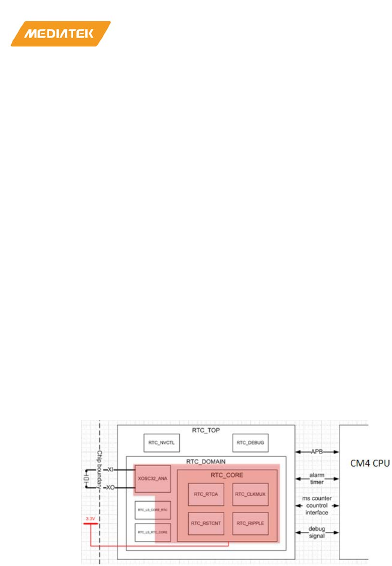
MT76x7
Internet-of-Things Wireless Connectivity
Reference Manual
© 2015 - 2017 MediaTek Inc
Page 726 of 798
This document contains information that is proprietary to MediaTek Inc. (“MediaTek”) and/or its licensor(s).
Any unauthorized use, reproduction or disclosure of this document in whole or in part is strictly prohibited
2.9. RTC
MT76X7 features one RTC (Real Time Clock) module. The clock source is the 32.768 KHz Crystal or an external
clock source. RTC has built in an accurate timer to wake up the system when it expires.
RTC uses a different power rail from PMU. In the hibernate mode, the PMU is turned off while the RTC module
is remained powered on. The RTC module only consumes 3uA in hibernate mode.
RTC has a dedicated PMU control pin PMU_EN_RTC (pin 23) used to turn on the power to the chip when the
RTC timer expires and turn off the power to the chip when it intends to enter the hibernate mode.
2.9.1. Main functions:
• Real-Time Clock
o Year, month, day, hour, minute, second
• Alarm
o Year, month, day, hour, minute, second, each with an enable bit
o Alarm time can be over 100 years with all options enabled
• Timer
o With 1/32 sec (31.25ms) precision
o Down count value can be up to 2048 seconds
• Independent power supply
o RTC domain uses its own 3.3V source
o Protecting mechanism is applied when core is powered down
• External PMU_EN signal control
o Can power core down as SW sets specific CR
o Can also power core up when specific criteria is met
2.9.2. Power Up/Down Flow
• RTC power up –
o XTAL clock starts oscillating
o De-bounce circuit is stabilized

MT76x7
Internet-of-Things Wireless Connectivity
Reference Manual
© 2015 - 2017 MediaTek Inc
Page 727 of 798
This document contains information that is proprietary to MediaTek Inc. (“MediaTek”) and/or its licensor(s).
Any unauthorized use, reproduction or disclosure of this document in whole or in part is strictly prohibited
o RTC is ready to be accessed
o MCU needs to set all the protection CRs to the correct value, otherwise all the RTC functions are
disabled
o RTC starts functioning
• Core power down –
o MCU sets the alarm/timer to a proper value
o MCU sets the PMU-disabling CR to de-assert PMU_EN
o Core is then powered down while RTC will be still functioning
• Core power up –
o The wake up criteria is triggered (alarm/timer/external event)
o RTC asserts PMU_EN
o Core is then powered up
2.9.3. Register definitions
Module name: MT7637_RTC Base address: (+830c0000h)
Address
Name
Width
Register Function
830C0004
RTC_PWRCHK1
8
RTC power ready check1
830C0008
RTC_PWRCHK2
8
RTC power
ready check2
830C000C
RTC_KEY
8
RTC security
-check protection key
830C0010
RTC_PROT1
8
RTC security
-check protection write test 1
830C0014
RTC_PROT2
8
RTC
security-check protection write test 2
830C0018
RTC_PROT3
8
RTC security
-check protection write test 3
830C001C
RTC_PROT4
8
RTC security
-check protection write test 4
830C0020
RTC_CTL
8
RTC internal control registers
830C0024
RTC_LPD_CTL
8
RTC low power detection
830C0028
RTC_XOSC_CFG
8
RTC XOSC control registers
830C002C
RTC_DEBNCE
8
RTC de
-bounce control
830C0030
RTC_PMU_EN
8
RTC PMU_EN control
830C003C
RTC_WAVEOUT
8
RTC waveout for internal test
830C0040
RTC_TC_YEA
8
RTC time counter year
830C0044
RTC_TC_MON
8
RTC time counter month
830C0048
RTC_TC_DOM
8
RTC time counter day of month
830C004C
RTC_TC_DOW
8
RTC time counter day of week
830C0050
RTC_TC_HOU
8
RTC time counter hour
830C0054
RTC_TC_MIN
8
RTC time counter minute
830C0058
RTC_TC_SEC
8
RTC time counter second
830C0060
RTC_AL_YEAR
8
RTC alarm year
830C0064
RTC_AL_MON
8
RTC alarm month
830C0068
RTC_AL_DOM
8
RTC alarm day of month
830C006C
RTC_AL_DOW
8
RTC alarm day of week
830C0070
RTC_AL_HOUR
8
RTC alarm hour
830C0074
RTC_AL_MIN
8
RTC alarm minute
830C0078
RTC_AL_SEC
8
RTC alarm second
MT76x7
Internet-of-Things Wireless Connectivity
Reference Manual
© 2015 - 2017 MediaTek Inc
Page 728 of 798
This document contains information that is proprietary to MediaTek Inc. (“MediaTek”) and/or its licensor(s).
Any unauthorized use, reproduction or disclosure of this document in whole or in part is strictly prohibited
Address
Name
Width
Register Function
830C007C
RTC_AL_CTL
8
RTC alarm control
830C0080
RTC_RIP_CTL
8
RTC ripple counter read control
830C0084
RTC_RIP_CNTH
8
RTC ripple counter bits [14:8]
830C0088
RTC_RIP_CNTL
8
RTC ripple counter bits [7:0]
830C0090
RTC_TIMER_CTL
8
RTC timer function control
830C0094
RTC_TIMER_CNTH
8
RTC timer count bits [15:8]
830C0098
RTC_TIMER_CNTL
8
RTC timer count bits [7:0]
830C00C0
RTC_SPARE0
8
RTC spare registers 0
830C00C4
RTC_SPARE1
8
RTC spare registers 1
830C00C8
RTC_SPARE2
8
RTC spare registers 2
830C00CC
RTC_SPARE3
8
RTC spare registers 3
830C00D0
RTC_SPARE4
8
RTC spare registers 4
830C00D4
RTC_SPARE5
8
RTC spare registers 5
830C00D8
RTC_SPARE6
8
RTC spare registers 6
830C00DC
RTC_SPARE7
8
RTC spare registers 7
830C00E0
RTC_SPARE8
8
RTC spare registers 8
830C00E4
RTC_SPARE9
8
RTC spare registers 9
830C00E8
RTC_SPARE10
8
RTC spare registers 10
830C00EC
RTC_SPARE11
8
RTC spare registers 11
830C00F0
RTC_SPARE12
8
RTC spare registers 12
830C00F4
RTC_SPARE13
8
RTC spare registers 13
830C00F8
RTC_SPARE14
8
RTC spare registers 14
830C00FC
RTC_SPARE15
8
RTC spare registers 15
830C0100
RTC_COREPDN
8
Core domain power down indicator
830C0104
MSTIME3
8
Correlator MS counter bit[31:24]
830C0108
MSTIME2
8
Correlator MS counter bit[23:16]
830C010C
MSTIME1
8
Correlator MS counter bit[15:8]
830C0110
MSTIME0
8
Correlator MS counter bit[7:0]
830C0114
SUBMSTIME1
8
Correlator SUBMS counter bit[14:8]
830C0118
SUBMSTIME0
8
Correlator SUBMS counter bit[7:0]
830C011C
MSDIFF3
8
MS counter difference bit[31:24]
830C0120
MSDIFF2
8
MS counter difference bit[23:16]
830C0124
MSDIFF1
8
MS counter difference bit[15:8]
830C0128
MSDIFF0
8
MS counter difference bit[7:0]
830C012C
SUBMSDIFF1
8
SUBMS counter difference bit[14:8]
830C0130
SUBMSDIFF0
8
SUBMS counter difference bit[7:0]
830C0134
MSTIMEMOD
8
Correlator ms time modification control
830C0140
RTC_BACKUP00
32
RTC backup
memory 00
830C0144
RTC_BACKUP01
32
RTC backup memory 01
830C0148
RTC_BACKUP02
32
RTC backup memory 02
830C014C
RTC_BACKUP03
32
RTC backup memory 03
830C0150
RTC_BACKUP04
32
RTC backup memory 04
830C0154
RTC_BACKUP05
32
RTC backup memory 05
830C0158
RTC_BACKUP06
32
RTC backup memory 06
MT76x7
Internet-of-Things Wireless Connectivity
Reference Manual
© 2015 - 2017 MediaTek Inc
Page 729 of 798
This document contains information that is proprietary to MediaTek Inc. (“MediaTek”) and/or its licensor(s).
Any unauthorized use, reproduction or disclosure of this document in whole or in part is strictly prohibited
Address
Name
Width
Register Function
830C015C
RTC_BACKUP07
32
RTC backup memory 07
830C0160
RTC_BACKUP08
32
RTC backup memory 08
830C0164
RTC_BACKUP09
32
RTC backup memory 09
830C0168
RTC_BACKUP10
32
RTC backup memory 10
830C016C
RTC_BACKUP11
32
RTC backup memory 11
830C0170
RTC_BACKUP12
32
RTC backup memory 12
830C0174
RTC_BACKUP13
32
RTC backup memory 13
830C0178
RTC_BACKUP14
32
RTC backup memory 14
830C017C
RTC_BACKUP15
32
RTC backup memory 15
830C0180
RTC_BACKUP16
32
RTC backup memory 16
830C0184
RTC_BACKUP17
32
RTC backup memory 17
830C0188
RTC_BACKUP18
32
RTC backup memory 18
830C018C
RTC_BACKUP19
32
RTC backup memory 19
830C0190
RTC_BACKUP20
32
RTC backup memory 20
830C0194
RTC_BACKUP21
32
RTC backup memory 21
830C0198
RTC_BACKUP22
32
RTC backup memory 22
830C019C
RTC_BACKUP23
32
RTC backup memory 23
830C01A0
RTC_BACKUP24
32
RTC backup memory 24
830C01A4
RTC_BACKUP25
32
RTC backup memory 25
830C01A8
RTC_BACKUP26
32
RTC backup memory 26
830C01AC
RTC_BACKUP27
32
RTC backup memory 27
830C01B0
RTC_BACKUP28
32
RTC backup memory 28
830C01B4
RTC_BACKUP29
32
RTC backup memory 29
830C01B8
RTC_BACKUP30
32
RTC backup memory 30
830C01BC
RTC_BACKUP31
32
RTC backup memory 31
830C01C0
RTC_BACKUP32
32
RTC backup memory 32
830C01C4
RTC_BACKUP33
32
RTC backup memory 33
830C01C8
RTC_BACKUP34
32
RTC backup memory 34
830C01CC
RTC_BACKUP35
32
RTC backup memory 35
830C0004
RTC_PWRCHK1
RTC power ready check1
00000000
Bit
31
30
29
28
27
26
25
24
23
22
21
20
19
18
17
16
Nam
e
Type
Rese
t
Bit
15
14
13
12
11
10
9
8
7
6
5
4
3
2
1
0
Nam
e
PWRCHK1
Type
RW
Rese
t
0 0 0 0 0 0 0 0
Bit(s)
Name
Description
MT76x7
Internet-of-Things Wireless Connectivity
Reference Manual
© 2015 - 2017 MediaTek Inc
Page 730 of 798
This document contains information that is proprietary to MediaTek Inc. (“MediaTek”) and/or its licensor(s).
Any unauthorized use, reproduction or disclosure of this document in whole or in part is strictly prohibited
Bit(s)
Name
Description
7:0
PWRCHK1
RTC power ready check 1 (0xC6)
830C0008
RTC_PWRCHK2
RTC power ready check2
00000000
Bit
31
30
29
28
27
26
25
24
23
22
21
20
19
18
17
16
Nam
e
Type
Rese
t
Bit
15
14
13
12
11
10
9
8
7
6
5
4
3
2
1
0
Nam
e
PWRCHK2
Type
RW
Rese
t
0 0 0 0 0 0 0 0
Bit(s)
Name
Description
7:0
PWRCHK2
RTC power ready check 2 (0x9A)
830C000C
RTC_KEY
RTC security-check protection key
00000000
Bit
31
30
29
28
27
26
25
24
23
22
21
20
19
18
17
16
Nam
e
Type
Rese
t
Bit
15
14
13
12
11
10
9
8
7
6
5
4
3
2
1
0
Nam
e
RTCKEY
Type
RW
Rese
t
0 0 0 0 0 0 0 0
Bit(s)
Name
Description
7:0
RTCKEY
RTC write protection KEY (0x59)
830C0010
RTC_PROT1
RTC security-check protection write
test 1
00000000
Bit
31
30
29
28
27
26
25
24
23
22
21
20
19
18
17
16
Nam
e
Type
MT76x7
Internet-of-Things Wireless Connectivity
Reference Manual
© 2015 - 2017 MediaTek Inc
Page 731 of 798
This document contains information that is proprietary to MediaTek Inc. (“MediaTek”) and/or its licensor(s).
Any unauthorized use, reproduction or disclosure of this document in whole or in part is strictly prohibited
Rese
t
Bit
15
14
13
12
11
10
9
8
7
6
5
4
3
2
1
0
Nam
e
RTCPROT1
Type
RW
Rese
t
0 0 0 0 0 0 0 0
Bit(s)
Name
Description
7:0
RTCPROT1
RTC security-check protection write test 1 (0xA3)
830C0014
RTC_PROT2
RTC security-check protection write
test 2
00000000
Bit
31
30
29
28
27
26
25
24
23
22
21
20
19
18
17
16
Nam
e
Type
Rese
t
Bit
15
14
13
12
11
10
9
8
7
6
5
4
3
2
1
0
Nam
e
RTCPROT2
Type
RW
Rese
t
0 0 0 0 0 0 0 0
Bit(s)
Name
Description
7:0
RTCPROT2
RTC security-check protection write test 2 (0x57)
830C0018
RTC_PROT3
RTC security-check protection write
test 3
00000000
Bit
31
30
29
28
27
26
25
24
23
22
21
20
19
18
17
16
Nam
e
Type
Rese
t
Bit
15
14
13
12
11
10
9
8
7
6
5
4
3
2
1
0
Nam
e
RTCPROT3
Type
RW
Rese
t
0 0 0 0 0 0 0 0
Bit(s)
Name
Description
MT76x7
Internet-of-Things Wireless Connectivity
Reference Manual
© 2015 - 2017 MediaTek Inc
Page 732 of 798
This document contains information that is proprietary to MediaTek Inc. (“MediaTek”) and/or its licensor(s).
Any unauthorized use, reproduction or disclosure of this document in whole or in part is strictly prohibited
Bit(s)
Name
Description
7:0
RTCPROT3
RTC security-check protection write test 3 (0x67)
830C001C
RTC_PROT4
RTC security-check protection write
test 4
00000000
Bit
31
30
29
28
27
26
25
24
23
22
21
20
19
18
17
16
Nam
e
Type
Rese
t
Bit
15
14
13
12
11
10
9
8
7
6
5
4
3
2
1
0
Nam
e
RTCPROT4
Type
RW
Rese
t
0 0 0 0 0 0 0 0
Bit(s)
Name
Description
7:0
RTCPROT4
RTC security-check protection write test 4 (0xD2)
830C0020
RTC_CTL
RTC internal control registers
00000000
Bit
31
30
29
28
27
26
25
24
23
22
21
20
19
18
17
16
Nam
e
Type
Rese
t
Bit
15
14
13
12
11
10
9
8
7
6
5
4
3
2
1
0
Nam
e
DE
BN
CE
_O
K
IN
HI
BIT
PR
OT
_P
AS
S
KE
Y_
PA
SS
PW
R_
PA
SS
SI
M_
RT
C
RC
_S
TO
P
Type
RU
RU
RU
RU
RU
RW
RW
Rese
t
0 0 0 0 0 0 0
Bit(s)
Name
Description
7
DEBNCE_OK
De-bounce period finish indicator
0: RTC is still de
-bouncing.
1: RTC de
-bounce ready.
6
INHIBIT
Inhibit status indicator.
Before reading the registers of YEAR, MONTH, WEEK, DAY,
HOUR, MIN, and SEC, read this bit first. If timer is enabled, this bit

MT76x7
Internet-of-Things Wireless Connectivity
Reference Manual
© 2015 - 2017 MediaTek Inc
Page 733 of 798
This document contains information that is proprietary to MediaTek Inc. (“MediaTek”) and/or its licensor(s).
Any unauthorized use, reproduction or disclosure of this document in whole or in part is strictly prohibited
Bit(s)
Name
Description
must also be checked before writing or reading the registers of
TIMERCTL, TIMERH, and TIMERL.
0: UP is OK to read/write RTC
1: RTC is updating RTC clock, inhibit UP write timer related
registers and read following command YEAR, MONTH, WEEK,
DAY, HOUR, MIN, SEC, TIMERCTL, TIMERH, and TIMERL.
4
PROT_PASS
RTC security-check protection
0: Fail to pas
s RTC security-check protection.
1: Pass RTC security check protection.
3
KEY_PASS
RTC write protection key check
0: Fail to pass RTC write protection.
1: Pass RTC write protection.
2
PWR_PASS
RTC power stable check
0: Fail to pass RTC power stable
check.
1: Pass RTC power stable check.
1
SIM_RTC
For RTC simulation
0: Normal operation, divided clock = 1Hz
1: Simulation, divided clock = 39.0625Hz
0
RC_STOP
Stop the ripple counter
0: normal operation.
1: stop and reset ripple counter.
830C0024
RTC_LPD_CTL
RTC low power detection
00000000
Bit
31
30
29
28
27
26
25
24
23
22
21
20
19
18
17
16
Nam
e
Type
Rese
t
Bit
15
14
13
12
11
10
9
8
7
6
5
4
3
2
1
0
Nam
e
Type
Rese
t
Bit(s)
Name
Description
MT76x7
Internet-of-Things Wireless Connectivity
Reference Manual
© 2015 - 2017 MediaTek Inc
Page 734 of 798
This document contains information that is proprietary to MediaTek Inc. (“MediaTek”) and/or its licensor(s).
Any unauthorized use, reproduction or disclosure of this document in whole or in part is strictly prohibited
Bit(s)
Name
Description
830C0028
RTC_XOSC_CFG
RTC XOSC control registers
00000007
Bit
31
30
29
28
27
26
25
24
23
22
21
20
19
18
17
16
Nam
e
Type
Rese
t
Bit
15
14
13
12
11
10
9
8
7
6
5
4
3
2
1
0
Nam
e OS
CP
DN
AM
PC
TL
_E
N
AM
P_
GS
EL
OSCCALI
Type
RW
RW
RW
RW
Rese
t
0 0 0 0 1 1 1
Bit(s)
Name
Description
7
OSCPDN
Clock 32K Power down control
0: Normal
operation
1: Power down 32k clock
5
AMPCTL_EN
Amplitude control function enable
4
AMP_GSEL
Amplitude control loop gain select
3:0
OSCCALI
Clock 32K PAD drive control
0000:
0001:
0010:
0011:
0100:
0101:
0110:
0111:
1000:
1001:
1010:
1011:
1100:
MT76x7
Internet-of-Things Wireless Connectivity
Reference Manual
© 2015 - 2017 MediaTek Inc
Page 735 of 798
This document contains information that is proprietary to MediaTek Inc. (“MediaTek”) and/or its licensor(s).
Any unauthorized use, reproduction or disclosure of this document in whole or in part is strictly prohibited
Bit(s)
Name
Description
1101:
1110:
1111:
830C002C
RTC_DEBNCE
RTC de-bounce control
00000003
Bit
31
30
29
28
27
26
25
24
23
22
21
20
19
18
17
16
Nam
e
Type
Rese
t
Bit
15
14
13
12
11
10
9
8
7
6
5
4
3
2
1
0
Nam
e
RTC_DMY DEBOUNCE
Type
RW
RW
Rese
t
0 0 0 0 0 0 1 1
Bit(s)
Name
Description
7:3
RTC_DMY
Dummy registers for ECO purpose
2:0
DEBOUNCE
RTC de-bounce time setting
This duration prevent abnormal write during losing
core power
000: Wait 2^5
-1 ~ 2^5 cycle of RTC clock
001: Wait 2^6
-4 ~ 2^6 cycle of RTC clock
010: Wait 2^8
-2^4~2^8 cycle of RTC clock
011: Wait 2^10
-2^6~2^10 cycle of RTC clock
100: Wait 2^12
-2^8~2^12 cycle of RTC clock
101: Wait 2^13
-2^9~2^13 cycle of RTC clock
110: Wait 2^14
-2^10~2^14 cycle of RTC clock
111: Wait 2^15
-2^11~2^15 cycle of RTC clock
Default value of DEBOUNCE[2:0] before passing RTC security
check is 3'b011. This register must be setup after passing RTC
security check.
830C0030
RTC_PMU_EN
RTC PMU_EN control
0000000F
Bit
31
30
29
28
27
26
25
24
23
22
21
20
19
18
17
16
Nam
e
MT76x7
Internet-of-Things Wireless Connectivity
Reference Manual
© 2015 - 2017 MediaTek Inc
Page 736 of 798
This document contains information that is proprietary to MediaTek Inc. (“MediaTek”) and/or its licensor(s).
Any unauthorized use, reproduction or disclosure of this document in whole or in part is strictly prohibited
Type
Rese
t
Bit
15
14
13
12
11
10
9
8
7
6
5
4
3
2
1
0
Nam
e
TI
ME
R_
ST
A
AL
AR
M_
ST
A
PMU_EN
_STATE
PM
U_
EN
_E
XT
PM
U_
EN
Type
W1
C
W1
C
RO RO RW
Rese
t
0 0 1 1 1 1
Bit(s)
Name
Description
5
TIMER_STA
Interrupt Status of timer, asserted with timer_hit
Write 1 to clear this bit
4
ALARM_STA
Interrupt Status of alarm, asserted with alarm_hit
Write 1 to clear this bit
3:2
PMU_EN_STATE
State Machine controlling PMU Enable signals
11: PMU is enabled
10: PMU is about to be disabled
00: PMU is disabled
1
PMU_EN_EXT
PMU Enable signal sent to external power switch
1:
rtc_pmu_en_ext is high
0: rtc_pmu_en_ext is low
0
PMU_EN
PMU Enable signal sent to PMU
Write 0 to disable PMU_EN, and PMU_EN_EXT will be disabled
afterwards
Write 1 to enable both PMU_EN and PMU_EN_EXT at the same
time
1: rtc_pmu_en is high
0: rtc_pmu_en
is low
830C003C
RTC_WAVEOUT
RTC waveout for internal test
00000000
Bit
31
30
29
28
27
26
25
24
23
22
21
20
19
18
17
16
Nam
e
Type
Rese
t
Bit
15
14
13
12
11
10
9
8
7
6
5
4
3
2
1
0
Nam
WA WAVEOUT_SEL
MT76x7
Internet-of-Things Wireless Connectivity
Reference Manual
© 2015 - 2017 MediaTek Inc
Page 737 of 798
This document contains information that is proprietary to MediaTek Inc. (“MediaTek”) and/or its licensor(s).
Any unauthorized use, reproduction or disclosure of this document in whole or in part is strictly prohibited
e
VE
OU
T_
EN
Type
RW
RW
Rese
t
0 0 0 0 0
Bit(s)
Name
Description
4
WAVEOUT_EN
RTC debug clock output enable
0: waveout = 0
1: Enable waveout signal output.
3:0
WAVEOUT_SEL
RTC debug clock output select
0000: ripple counter [14]
0001: ripple counter [13]
0010: ripple counter [12]
0011: ripple counter [11]
0100: ripple counter [10]
0101: ripple counter [9]
0110: ripple counter [8]
0111: ripple counter [7]
1000: ripple counter [6]
1001: ripple counte
r [5]
1010: ripple counter [4]
1011: ripple counter [3]
1100: ripple counter [2]
1101: ripple counter [1]
1110: ripple counter [0]
1111: 32K clock output
830C0040
RTC_TC_YEA
RTC time counter year
00000000
Bit
31
30
29
28
27
26
25
24
23
22
21
20
19
18
17
16
Nam
e
Type
Rese
t
Bit
15
14
13
12
11
10
9
8
7
6
5
4
3
2
1
0
Nam
YEAR
MT76x7
Internet-of-Things Wireless Connectivity
Reference Manual
© 2015 - 2017 MediaTek Inc
Page 738 of 798
This document contains information that is proprietary to MediaTek Inc. (“MediaTek”) and/or its licensor(s).
Any unauthorized use, reproduction or disclosure of this document in whole or in part is strictly prohibited
e
Type
RW
Rese
t
0 0 0 0 0 0 0
Bit(s)
Name
Description
6:0
YEAR
Year.
Value: 0x0 ~ 0x63 ( 0 ~ 99 )
830C0044
RTC_TC_MON
RTC time counter month
00000001
Bit
31
30
29
28
27
26
25
24
23
22
21
20
19
18
17
16
Nam
e
Type
Rese
t
Bit
15
14
13
12
11
10
9
8
7
6
5
4
3
2
1
0
Nam
e
MONTH
Type
RW
Rese
t
0 0 0 1
Bit(s)
Name
Description
3:0
MONTH
Month.
Value: 0x1 ~ 0xc (1 ~ 12)
830C0048
RTC_TC_DOM
RTC time counter day of month
00000001
Bit
31
30
29
28
27
26
25
24
23
22
21
20
19
18
17
16
Nam
e
Type
Rese
t
Bit
15
14
13
12
11
10
9
8
7
6
5
4
3
2
1
0
Nam
e
DOM
Type
RW
Rese
t
0 0 0 0 1
Bit(s)
Name
Description
4:0
DOM
Day of month.
Value: 0x1 ~ 0x1f (1 ~ 31)
MT76x7
Internet-of-Things Wireless Connectivity
Reference Manual
© 2015 - 2017 MediaTek Inc
Page 739 of 798
This document contains information that is proprietary to MediaTek Inc. (“MediaTek”) and/or its licensor(s).
Any unauthorized use, reproduction or disclosure of this document in whole or in part is strictly prohibited
Bit(s)
Name
Description
830C004C
RTC_TC_DOW
RTC time counter day of week
00000000
Bit
31
30
29
28
27
26
25
24
23
22
21
20
19
18
17
16
Nam
e
Type
Rese
t
Bit
15
14
13
12
11
10
9
8
7
6
5
4
3
2
1
0
Nam
e
DOW
Type
RW
Rese
t
0 0 0
Bit(s)
Name
Description
2:0
DOW
Day of week.
Value: 0~6
830C0050
RTC_TC_HOU
RTC time counter hour
00000000
Bit
31
30
29
28
27
26
25
24
23
22
21
20
19
18
17
16
Nam
e
Type
Rese
t
Bit
15
14
13
12
11
10
9
8
7
6
5
4
3
2
1
0
Nam
e
HOUR
Type
RW
Rese
t
0 0 0 0 0
Bit(s)
Name
Description
4:0
HOUR
Hour.
Value: 0x0 ~ 0x17 (0 ~ 23)
830C0054
RTC_TC_MIN
RTC time counter minute
00000000
Bit
31
30
29
28
27
26
25
24
23
22
21
20
19
18
17
16
Nam
e
Type
MT76x7
Internet-of-Things Wireless Connectivity
Reference Manual
© 2015 - 2017 MediaTek Inc
Page 740 of 798
This document contains information that is proprietary to MediaTek Inc. (“MediaTek”) and/or its licensor(s).
Any unauthorized use, reproduction or disclosure of this document in whole or in part is strictly prohibited
Rese
t
Bit
15
14
13
12
11
10
9
8
7
6
5
4
3
2
1
0
Nam
e
MIN
Type
RW
Rese
t
0 0 0 0 0 0
Bit(s)
Name
Description
5:0
MIN
Minute.
Value: 0x0 ~ 0x3b (0 ~ 59)
830C0058
RTC_TC_SEC
RTC time counter second
00000000
Bit
31
30
29
28
27
26
25
24
23
22
21
20
19
18
17
16
Nam
e
Type
Rese
t
Bit
15
14
13
12
11
10
9
8
7
6
5
4
3
2
1
0
Nam
e
SEC
Type
RW
Rese
t
0 0 0 0 0 0
Bit(s)
Name
Description
5:0
SEC
Second.
Value: 0x0 ~ 0x3b (0 ~ 59)
830C0060
RTC_AL_YEAR
RTC alarm year
00000000
Bit
31
30
29
28
27
26
25
24
23
22
21
20
19
18
17
16
Nam
e
Type
Rese
t
Bit
15
14
13
12
11
10
9
8
7
6
5
4
3
2
1
0
Nam
e
AYEAR
Type
RW
Rese
t
0 0 0 0 0 0 0
Bit(s)
Name
Description
MT76x7
Internet-of-Things Wireless Connectivity
Reference Manual
© 2015 - 2017 MediaTek Inc
Page 741 of 798
This document contains information that is proprietary to MediaTek Inc. (“MediaTek”) and/or its licensor(s).
Any unauthorized use, reproduction or disclosure of this document in whole or in part is strictly prohibited
Bit(s)
Name
Description
6:0
AYEAR
Alarm year
Value: 0x0 ~ 0x63 ( 0 ~ 99 )
830C0064
RTC_AL_MON
RTC alarm month
00000001
Bit
31
30
29
28
27
26
25
24
23
22
21
20
19
18
17
16
Nam
e
Type
Rese
t
Bit
15
14
13
12
11
10
9
8
7
6
5
4
3
2
1
0
Nam
e
AMONTH
Type
RW
Rese
t
0 0 0 1
Bit(s)
Name
Description
3:0
AMONTH
Alarm month
Value: 0x1 ~ 0xc (1 ~ 12)
830C0068
RTC_AL_DOM
RTC alarm day of month
00000001
Bit
31
30
29
28
27
26
25
24
23
22
21
20
19
18
17
16
Nam
e
Type
Rese
t
Bit
15
14
13
12
11
10
9
8
7
6
5
4
3
2
1
0
Nam
e
ADOM
Type
RW
Rese
t
0 0 0 0 1
Bit(s)
Name
Description
4:0
ADOM
Alarm day of month
Value: 0x1 ~ 0x1f (1 ~ 31)
830C006C
RTC_AL_DOW
RTC alarm day of week
00000000
MT76x7
Internet-of-Things Wireless Connectivity
Reference Manual
© 2015 - 2017 MediaTek Inc
Page 742 of 798
This document contains information that is proprietary to MediaTek Inc. (“MediaTek”) and/or its licensor(s).
Any unauthorized use, reproduction or disclosure of this document in whole or in part is strictly prohibited
Bit
31
30
29
28
27
26
25
24
23
22
21
20
19
18
17
16
Nam
e
Type
Rese
t
Bit
15
14
13
12
11
10
9
8
7
6
5
4
3
2
1
0
Nam
e
ADOW
Type
RW
Rese
t
0 0 0
Bit(s)
Name
Description
2:0
ADOW
Alarm day of week.
Value: 0~6
830C0070
RTC_AL_HOUR
RTC alarm hour
00000000
Bit
31
30
29
28
27
26
25
24
23
22
21
20
19
18
17
16
Nam
e
Type
Rese
t
Bit
15
14
13
12
11
10
9
8
7
6
5
4
3
2
1
0
Nam
e
AHOUR
Type
RW
Rese
t
0 0 0 0 0
Bit(s)
Name
Description
4:0
AHOUR
Alarm hour.
Value: 0x0 ~ 0x17 (0 ~ 23)
830C0074
RTC_AL_MIN
RTC alarm minute
00000000
Bit
31
30
29
28
27
26
25
24
23
22
21
20
19
18
17
16
Nam
e
Type
Rese
t
Bit
15
14
13
12
11
10
9
8
7
6
5
4
3
2
1
0
Nam
e
AMIN
Type
RW
MT76x7
Internet-of-Things Wireless Connectivity
Reference Manual
© 2015 - 2017 MediaTek Inc
Page 743 of 798
This document contains information that is proprietary to MediaTek Inc. (“MediaTek”) and/or its licensor(s).
Any unauthorized use, reproduction or disclosure of this document in whole or in part is strictly prohibited
Rese
t
0 0 0 0 0 0
Bit(s)
Name
Description
5:0
AMIN
Alarm minute.
Value: 0x0 ~ 0x3b (0 ~ 59)
830C0078
RTC_AL_SEC
RTC alarm second
00000000
Bit
31
30
29
28
27
26
25
24
23
22
21
20
19
18
17
16
Nam
e
Type
Rese
t
Bit
15
14
13
12
11
10
9
8
7
6
5
4
3
2
1
0
Nam
e
ASEC
Type
RW
Rese
t
0 0 0 0 0 0
Bit(s)
Name
Description
5:0
ASEC
Alarm second.
Value: 0x0 ~ 0x3b (0 ~ 59)
830C007C
RTC_AL_CTL
RTC alarm control
00000000
Bit
31
30
29
28
27
26
25
24
23
22
21
20
19
18
17
16
Nam
e
Type
Rese
t
Bit
15
14
13
12
11
10
9
8
7
6
5
4
3
2
1
0
Nam
e AL
MY
R
AL
M
MO
N
AL
MD
OM
AL
MD
OW
AL
MH
R
AL
M
MI
N
AL
MS
EC
AL
ME
N
Type
RW
RW
RW
RW
RW
RW
RW
RW
Rese
t
0 0 0 0 0 0 0 0
Bit(s)
Name
Description
7
ALMYR
Alarm year enable
0: Alarm does not compare year.

MT76x7
Internet-of-Things Wireless Connectivity
Reference Manual
© 2015 - 2017 MediaTek Inc
Page 744 of 798
This document contains information that is proprietary to MediaTek Inc. (“MediaTek”) and/or its licensor(s).
Any unauthorized use, reproduction or disclosure of this document in whole or in part is strictly prohibited
Bit(s)
Name
Description
1: Alarm compares year.
6
ALMMON
Alarm month enable
0: Alarm does not compare month.
1: Alarm compares month.
5
ALMDOM
Alarm day of month enable
0: Alarm does not compare day of month.
1: Alarm compares day of month.
4
ALMDOW
Alarm day of week enable
0: Alarm does not compare day of week.
1: Alarm
compares day of week.
3
ALMHR
Alarm hour enable
0: Alarm does not compare hour.
1: Alarm compares hour.
2
ALMMIN
Alarm minute enable
0: Alarm does not compare minute.
1: Alarm compares minute.
1
ALMSEC
Alarm second enable
0: Alarm does not compare
second.
1: Alarm compares second.
0
ALMEN
Alarm enable
0: Disable alarm.
1: Enable alarm.
830C0080
RTC_RIP_CTL
RTC ripple counter read control
00000000
Bit
31
30
29
28
27
26
25
24
23
22
21
20
19
18
17
16
Nam
e
Type
Rese
t
Bit
15
14
13
12
11
10
9
8
7
6
5
4
3
2
1
0
Nam
e
RIP
_R
D_
OK
RIP
_T
RG
_R
D
Type
RU
RW
MT76x7
Internet-of-Things Wireless Connectivity
Reference Manual
© 2015 - 2017 MediaTek Inc
Page 745 of 798
This document contains information that is proprietary to MediaTek Inc. (“MediaTek”) and/or its licensor(s).
Any unauthorized use, reproduction or disclosure of this document in whole or in part is strictly prohibited
Rese
t
0 0
Bit(s)
Name
Description
1
RIP_RD_OK
Ripple counter read status
0:
RIP_CNT is not ready yet.
1: RIP_CNT is ready for read.
0
RIP_TRG_RD
Ripple counter read trigger signal
It should be paired with RIP_RD_OK
0: clear RIP_RD_OK status
1: trigger read RTC ripple counter
830C0084
RTC_RIP_CNTH
RTC ripple counter bits [14:8]
00000000
Bit
31
30
29
28
27
26
25
24
23
22
21
20
19
18
17
16
Nam
e
Type
Rese
t
Bit
15
14
13
12
11
10
9
8
7
6
5
4
3
2
1
0
Nam
e
RIP_CNT[14:8]
Type
RU
Rese
t
0 0 0 0 0 0 0
Bit(s)
Name
Description
6:0
RIP_CNT[14:8]
RTC ripple counter bit[14:8]
830C0088
RTC_RIP_CNTL
RTC ripple counter bits [7:0]
00000000
Bit
31
30
29
28
27
26
25
24
23
22
21
20
19
18
17
16
Nam
e
Type
Rese
t
Bit
15
14
13
12
11
10
9
8
7
6
5
4
3
2
1
0
Nam
e
RIP_CNT[7:0]
Type
RU
Rese
t
0 0 0 0 0 0 0 0
MT76x7
Internet-of-Things Wireless Connectivity
Reference Manual
© 2015 - 2017 MediaTek Inc
Page 746 of 798
This document contains information that is proprietary to MediaTek Inc. (“MediaTek”) and/or its licensor(s).
Any unauthorized use, reproduction or disclosure of this document in whole or in part is strictly prohibited
Bit(s)
Name
Description
7:0
RIP_CNT[7:0]
RTC ripple counter bit[7:0]
830C0090
RTC_TIMER_CTL
RTC timer function control
000000D0
Bit
31
30
29
28
27
26
25
24
23
22
21
20
19
18
17
16
Nam
e
Type
Rese
t
Bit
15
14
13
12
11
10
9
8
7
6
5
4
3
2
1
0
Nam
e
TR
_I
NT
EN
Type
RW
Rese
t
0
Bit(s)
Name
Description
1
TR_INTEN
Enable timer to generate internal interrupt
0: Disable timer interrupt.
1: Start to count down TIMER_CNT.
830C0094
RTC_TIMER_CNTH
RTC timer count bits [15:8]
000000FF
Bit
31
30
29
28
27
26
25
24
23
22
21
20
19
18
17
16
Nam
e
Type
Rese
t
Bit
15
14
13
12
11
10
9
8
7
6
5
4
3
2
1
0
Nam
e
TIMER_CNT[15:8]
Type
RW
Rese
t
1 1 1 1 1 1 1 1
Bit(s)
Name
Description
7:0
TIMER_CNT[15:8]
Timer count control bit[15:8]
Count down every 1/32 sec. When TIMER_CNT equals to 0, assert
internal interrupt or external pull down pad.
Modify TIMER_CNT during TR_INTEN =
0 and TR_EXTEN = 0
in RTC_TIMER_CTL bit 1 and bit 0.
MT76x7
Internet-of-Things Wireless Connectivity
Reference Manual
© 2015 - 2017 MediaTek Inc
Page 747 of 798
This document contains information that is proprietary to MediaTek Inc. (“MediaTek”) and/or its licensor(s).
Any unauthorized use, reproduction or disclosure of this document in whole or in part is strictly prohibited
Bit(s)
Name
Description
If TR_INTEN = 1 or/and TR_EXTEN = 1, TIMER_CNT can read to
show the countdown status.
830C0098
RTC_TIMER_CNTL
RTC timer count bits [7:0]
000000FF
Bit
31
30
29
28
27
26
25
24
23
22
21
20
19
18
17
16
Nam
e
Type
Rese
t
Bit
15
14
13
12
11
10
9
8
7
6
5
4
3
2
1
0
Nam
e
TIMER_CNT[7:0]
Type
RW
Rese
t
1 1 1 1 1 1 1 1
Bit(s)
Name
Description
7:0
TIMER_CNT[7:0]
Timer count control bit[7:0]
Count down every 1/32 sec. When TIMER_CNT equals to 0, assert
internal interrupt or external pull down pad.
Modify TIMER_CNT during TR_INTEN = 0 and TR_EXTEN = 0
in RTC_TIMER_CTL bit 1 and bit 0.
If TR_INTEN = 1 or/and TR_EXTEN = 1, TIMER_CNT can read to
show the countdown status.
830C00C0
RTC_SPARE0
RTC spare registers 0
00000000
Bit
31
30
29
28
27
26
25
24
23
22
21
20
19
18
17
16
Nam
e
Type
Rese
t
Bit
15
14
13
12
11
10
9
8
7
6
5
4
3
2
1
0
Nam
e
RTC_SPARE0
Type
RW
Rese
t
0 0 0 0 0 0 0 0
Bit(s)
Name
Description
7:0
RTC_SPARE0
RTC spare registers
MT76x7
Internet-of-Things Wireless Connectivity
Reference Manual
© 2015 - 2017 MediaTek Inc
Page 748 of 798
This document contains information that is proprietary to MediaTek Inc. (“MediaTek”) and/or its licensor(s).
Any unauthorized use, reproduction or disclosure of this document in whole or in part is strictly prohibited
830C00C4
RTC_SPARE1
RTC spare registers 1
00000000
Bit
31
30
29
28
27
26
25
24
23
22
21
20
19
18
17
16
Nam
e
Type
Rese
t
Bit
15
14
13
12
11
10
9
8
7
6
5
4
3
2
1
0
Nam
e
RTC_SPARE1
Type
RW
Rese
t
0 0 0 0 0 0 0 0
Bit(s)
Name
Description
7:0
RTC_SPARE1
RTC spare registers
830C00C8
RTC_SPARE2
RTC spare registers 2
00000000
Bit
31
30
29
28
27
26
25
24
23
22
21
20
19
18
17
16
Nam
e
Type
Rese
t
Bit
15
14
13
12
11
10
9
8
7
6
5
4
3
2
1
0
Nam
e
RTC_SPARE2
Type
RW
Rese
t
0 0 0 0 0 0 0 0
Bit(s)
Name
Description
7:0
RTC_SPARE2
RTC spare registers
830C00CC
RTC_SPARE3
RTC spare registers 3
00000000
Bit
31
30
29
28
27
26
25
24
23
22
21
20
19
18
17
16
Nam
e
Type
Rese
t
Bit
15
14
13
12
11
10
9
8
7
6
5
4
3
2
1
0
Nam
e
RTC_SPARE3
Type
RW
Rese
t
0 0 0 0 0 0 0 0
MT76x7
Internet-of-Things Wireless Connectivity
Reference Manual
© 2015 - 2017 MediaTek Inc
Page 749 of 798
This document contains information that is proprietary to MediaTek Inc. (“MediaTek”) and/or its licensor(s).
Any unauthorized use, reproduction or disclosure of this document in whole or in part is strictly prohibited
Bit(s)
Name
Description
7:0
RTC_SPARE3
RTC spare registers
830C00D0
RTC_SPARE4
RTC spare registers 4
00000000
Bit
31
30
29
28
27
26
25
24
23
22
21
20
19
18
17
16
Nam
e
Type
Rese
t
Bit
15
14
13
12
11
10
9
8
7
6
5
4
3
2
1
0
Nam
e
RTC_SPARE4
Type
RW
Rese
t
0 0 0 0 0 0 0 0
Bit(s)
Name
Description
7:0
RTC_SPARE4
RTC spare registers
830C00D4
RTC_SPARE5
RTC spare registers 5
00000000
Bit
31
30
29
28
27
26
25
24
23
22
21
20
19
18
17
16
Nam
e
Type
Rese
t
Bit
15
14
13
12
11
10
9
8
7
6
5
4
3
2
1
0
Nam
e
RTC_SPARE5
Type
RW
Rese
t
0 0 0 0 0 0 0 0
Bit(s)
Name
Description
7:0
RTC_SPARE5
RTC spare registers
830C00D8
RTC_SPARE6
RTC spare registers 6
00000000
Bit
31
30
29
28
27
26
25
24
23
22
21
20
19
18
17
16
Nam
e
Type
MT76x7
Internet-of-Things Wireless Connectivity
Reference Manual
© 2015 - 2017 MediaTek Inc
Page 750 of 798
This document contains information that is proprietary to MediaTek Inc. (“MediaTek”) and/or its licensor(s).
Any unauthorized use, reproduction or disclosure of this document in whole or in part is strictly prohibited
Rese
t
Bit
15
14
13
12
11
10
9
8
7
6
5
4
3
2
1
0
Nam
e
RTC_SPARE6
Type
RW
Rese
t
0 0 0 0 0 0 0 0
Bit(s)
Name
Description
7:0
RTC_SPARE6
RTC spare registers
830C00DC
RTC_SPARE7
RTC spare registers 7
00000000
Bit
31
30
29
28
27
26
25
24
23
22
21
20
19
18
17
16
Nam
e
Type
Rese
t
Bit
15
14
13
12
11
10
9
8
7
6
5
4
3
2
1
0
Nam
e
RTC_SPARE7
Type
RW
Rese
t
0 0 0 0 0 0 0 0
Bit(s)
Name
Description
7:0
RTC_SPARE7
RTC spare registers
830C00E0
RTC_SPARE8
RTC spare registers 8
00000000
Bit
31
30
29
28
27
26
25
24
23
22
21
20
19
18
17
16
Nam
e
Type
Rese
t
Bit
15
14
13
12
11
10
9
8
7
6
5
4
3
2
1
0
Nam
e
RTC_SPARE8
Type
RW
Rese
t
0 0 0 0 0 0 0 0
Bit(s)
Name
Description
7:0
RTC_SPARE8
RTC spare registers
MT76x7
Internet-of-Things Wireless Connectivity
Reference Manual
© 2015 - 2017 MediaTek Inc
Page 751 of 798
This document contains information that is proprietary to MediaTek Inc. (“MediaTek”) and/or its licensor(s).
Any unauthorized use, reproduction or disclosure of this document in whole or in part is strictly prohibited
Bit(s)
Name
Description
830C00E4
RTC_SPARE9
RTC spare registers 9
00000000
Bit
31
30
29
28
27
26
25
24
23
22
21
20
19
18
17
16
Nam
e
Type
Rese
t
Bit
15
14
13
12
11
10
9
8
7
6
5
4
3
2
1
0
Nam
e
RTC_SPARE9
Type
RW
Rese
t
0 0 0 0 0 0 0 0
Bit(s)
Name
Description
7:0
RTC_SPARE9
RTC spare registers
830C00E8
RTC_SPARE10
RTC spare registers 10
00000000
Bit
31
30
29
28
27
26
25
24
23
22
21
20
19
18
17
16
Nam
e
Type
Rese
t
Bit
15
14
13
12
11
10
9
8
7
6
5
4
3
2
1
0
Nam
e
RTC_SPARE10
Type
RW
Rese
t
0 0 0 0 0 0 0 0
Bit(s)
Name
Description
7:0
RTC_SPARE10
RTC spare registers
830C00EC
RTC_SPARE11
RTC spare registers 11
00000000
Bit
31
30
29
28
27
26
25
24
23
22
21
20
19
18
17
16
Nam
e
Type
Rese
t
Bit
15
14
13
12
11
10
9
8
7
6
5
4
3
2
1
0
MT76x7
Internet-of-Things Wireless Connectivity
Reference Manual
© 2015 - 2017 MediaTek Inc
Page 752 of 798
This document contains information that is proprietary to MediaTek Inc. (“MediaTek”) and/or its licensor(s).
Any unauthorized use, reproduction or disclosure of this document in whole or in part is strictly prohibited
Nam
e
RTC_SPARE11
Type
RW
Rese
t
0 0 0 0 0 0 0 0
Bit(s)
Name
Description
7:0
RTC_SPARE11
RTC spare registers
830C00F0
RTC_SPARE12
RTC spare registers 12
00000000
Bit
31
30
29
28
27
26
25
24
23
22
21
20
19
18
17
16
Nam
e
Type
Rese
t
Bit
15
14
13
12
11
10
9
8
7
6
5
4
3
2
1
0
Nam
e
RTC_SPARE12
Type
RW
Rese
t
0 0 0 0 0 0 0 0
Bit(s)
Name
Description
7:0
RTC_SPARE12
RTC spare registers
830C00F4
RTC_SPARE13
RTC spare registers 13
00000000
Bit
31
30
29
28
27
26
25
24
23
22
21
20
19
18
17
16
Nam
e
Type
Rese
t
Bit
15
14
13
12
11
10
9
8
7
6
5
4
3
2
1
0
Nam
e
RTC_SPARE13
Type
RW
Rese
t
0 0 0 0 0 0 0 0
Bit(s)
Name
Description
7:0
RTC_SPARE13
RTC spare registers
830C00F8
RTC_SPARE14
RTC spare registers 14
00000000
MT76x7
Internet-of-Things Wireless Connectivity
Reference Manual
© 2015 - 2017 MediaTek Inc
Page 753 of 798
This document contains information that is proprietary to MediaTek Inc. (“MediaTek”) and/or its licensor(s).
Any unauthorized use, reproduction or disclosure of this document in whole or in part is strictly prohibited
Bit
31
30
29
28
27
26
25
24
23
22
21
20
19
18
17
16
Nam
e
Type
Rese
t
Bit
15
14
13
12
11
10
9
8
7
6
5
4
3
2
1
0
Nam
e
RTC_SPARE14
Type
RW
Rese
t
0 0 0 0 0 0 0 0
Bit(s)
Name
Description
7:0
RTC_SPARE14
RTC spare registers
830C00FC
RTC_SPARE15
RTC spare registers 15
00000000
Bit
31
30
29
28
27
26
25
24
23
22
21
20
19
18
17
16
Nam
e
Type
Rese
t
Bit
15
14
13
12
11
10
9
8
7
6
5
4
3
2
1
0
Nam
e
RTC_SPARE15
Type
RW
Rese
t
0 0 0 0 0 0 0 0
Bit(s)
Name
Description
7:0
RTC_SPARE15
RTC spare registers
830C0100
RTC_COREPDN
Core domain power down indicator
00000000
Bit
31
30
29
28
27
26
25
24
23
22
21
20
19
18
17
16
Nam
e
Type
Rese
t
Bit
15
14
13
12
11
10
9
8
7
6
5
4
3
2
1
0
Nam
e
G_
EN
AB
LE
CO
RE
_S
HU
TD
OW
N
Type
RU
RW
MT76x7
Internet-of-Things Wireless Connectivity
Reference Manual
© 2015 - 2017 MediaTek Inc
Page 754 of 798
This document contains information that is proprietary to MediaTek Inc. (“MediaTek”) and/or its licensor(s).
Any unauthorized use, reproduction or disclosure of this document in whole or in part is strictly prohibited
Rese
t
0 0
Bit(s)
Name
Description
1
G_ENABLE
RTC domain R/W enable indicator
0: ARM can not
access RTC domain.
1: When the protection does not pass, ARM can only write
protection pass. When the protection passes, ARM can write all
RTC command registers.
0
CORE_SHUTDOWN
Core domain power down indicator for RTC domain.
0: disable.
1: Trigger
core_shutdown signal for RTC domain.
Before core power shut down, write this bit to disable RTC domain
interface.
830C0104
MSTIME3
Correlator MS counter bit[31:24]
00000000
Bit
31
30
29
28
27
26
25
24
23
22
21
20
19
18
17
16
Nam
e
Type
Rese
t
Bit
15
14
13
12
11
10
9
8
7
6
5
4
3
2
1
0
Nam
e
Type
Rese
t
Bit(s)
Name
Description
830C0108
MSTIME2
Correlator MS counter bit[23:16]
00000000
Bit
31
30
29
28
27
26
25
24
23
22
21
20
19
18
17
16
Nam
e
Type
Rese
t
Bit
15
14
13
12
11
10
9
8
7
6
5
4
3
2
1
0
Nam
e
Type
Rese
t
MT76x7
Internet-of-Things Wireless Connectivity
Reference Manual
© 2015 - 2017 MediaTek Inc
Page 755 of 798
This document contains information that is proprietary to MediaTek Inc. (“MediaTek”) and/or its licensor(s).
Any unauthorized use, reproduction or disclosure of this document in whole or in part is strictly prohibited
Bit(s)
Name
Description
830C010C
MSTIME1
Correlator MS counter bit[15:8]
00000000
Bit
31
30
29
28
27
26
25
24
23
22
21
20
19
18
17
16
Nam
e
Type
Rese
t
Bit
15
14
13
12
11
10
9
8
7
6
5
4
3
2
1
0
Nam
e
Type
Rese
t
Bit(s)
Name
Description
830C0110
MSTIME0
Correlator MS counter bit[7:0]
00000000
Bit
31
30
29
28
27
26
25
24
23
22
21
20
19
18
17
16
Nam
e
Type
Rese
t
Bit
15
14
13
12
11
10
9
8
7
6
5
4
3
2
1
0
Nam
e
Type
Rese
t
Bit(s)
Name
Description
830C0114
SUBMSTIME1
Correlator SUBMS counter bit[14:8]
00000000
Bit
31
30
29
28
27
26
25
24
23
22
21
20
19
18
17
16
Nam
e
Type
Rese
t
Bit
15
14
13
12
11
10
9
8
7
6
5
4
3
2
1
0
Nam
e
Type
Rese
MT76x7
Internet-of-Things Wireless Connectivity
Reference Manual
© 2015 - 2017 MediaTek Inc
Page 756 of 798
This document contains information that is proprietary to MediaTek Inc. (“MediaTek”) and/or its licensor(s).
Any unauthorized use, reproduction or disclosure of this document in whole or in part is strictly prohibited
t
Bit(s)
Name
Description
830C0118
SUBMSTIME0
Correlator SUBMS counter bit[7:0]
00000000
Bit
31
30
29
28
27
26
25
24
23
22
21
20
19
18
17
16
Nam
e
Type
Rese
t
Bit
15
14
13
12
11
10
9
8
7
6
5
4
3
2
1
0
Nam
e
Type
Rese
t
Bit(s)
Name
Description
830C011C
MSDIFF3
MS counter difference bit[31:24]
00000000
Bit
31
30
29
28
27
26
25
24
23
22
21
20
19
18
17
16
Nam
e
Type
Rese
t
Bit
15
14
13
12
11
10
9
8
7
6
5
4
3
2
1
0
Nam
e
Type
Rese
t
Bit(s)
Name
Description
830C0120
MSDIFF2
MS counter difference bit[23:16]
00000000
Bit
31
30
29
28
27
26
25
24
23
22
21
20
19
18
17
16
Nam
e
Type
Rese
t
Bit
15
14
13
12
11
10
9
8
7
6
5
4
3
2
1
0
Nam
e
MT76x7
Internet-of-Things Wireless Connectivity
Reference Manual
© 2015 - 2017 MediaTek Inc
Page 757 of 798
This document contains information that is proprietary to MediaTek Inc. (“MediaTek”) and/or its licensor(s).
Any unauthorized use, reproduction or disclosure of this document in whole or in part is strictly prohibited
Type
Rese
t
Bit(s)
Name
Description
830C0124
MSDIFF1
MS counter difference bit[15:8]
00000000
Bit
31
30
29
28
27
26
25
24
23
22
21
20
19
18
17
16
Nam
e
Type
Rese
t
Bit
15
14
13
12
11
10
9
8
7
6
5
4
3
2
1
0
Nam
e
Type
Rese
t
Bit(s)
Name
Description
830C0128
MSDIFF0
MS counter difference bit[7:0]
00000000
Bit
31
30
29
28
27
26
25
24
23
22
21
20
19
18
17
16
Nam
e
Type
Rese
t
Bit
15
14
13
12
11
10
9
8
7
6
5
4
3
2
1
0
Nam
e
Type
Rese
t
Bit(s)
Name
Description
830C012C
SUBMSDIFF1
SUBMS counter difference bit[14:8]
00000000
Bit
31
30
29
28
27
26
25
24
23
22
21
20
19
18
17
16
Nam
e
Type
Rese
t
Bit
15
14
13
12
11
10
9
8
7
6
5
4
3
2
1
0
MT76x7
Internet-of-Things Wireless Connectivity
Reference Manual
© 2015 - 2017 MediaTek Inc
Page 758 of 798
This document contains information that is proprietary to MediaTek Inc. (“MediaTek”) and/or its licensor(s).
Any unauthorized use, reproduction or disclosure of this document in whole or in part is strictly prohibited
Nam
e
Type
Rese
t
Bit(s)
Name
Description
830C0130
SUBMSDIFF0
SUBMS counter difference bit[7:0]
00000000
Bit
31
30
29
28
27
26
25
24
23
22
21
20
19
18
17
16
Nam
e
Type
Rese
t
Bit
15
14
13
12
11
10
9
8
7
6
5
4
3
2
1
0
Nam
e
Type
Rese
t
Bit(s)
Name
Description
830C0134
MSTIMEMOD
Correlator ms time modification
control
00000000
Bit
31
30
29
28
27
26
25
24
23
22
21
20
19
18
17
16
Nam
e
Type
Rese
t
Bit
15
14
13
12
11
10
9
8
7
6
5
4
3
2
1
0
Nam
e
Type
Rese
t
Bit(s)
Name
Description
830C0140
RTC_BACKUP00
RTC backup memory 00
00000000
Bit
31
30
29
28
27
26
25
24
23
22
21
20
19
18
17
16
Nam
e
RTC_BACKUP00
Type
RW
MT76x7
Internet-of-Things Wireless Connectivity
Reference Manual
© 2015 - 2017 MediaTek Inc
Page 759 of 798
This document contains information that is proprietary to MediaTek Inc. (“MediaTek”) and/or its licensor(s).
Any unauthorized use, reproduction or disclosure of this document in whole or in part is strictly prohibited
Rese
t
0 0 0 0 0 0 0 0 0 0 0 0 0 0 0 0
Bit
15
14
13
12
11
10
9
8
7
6
5
4
3
2
1
0
Nam
e
RTC_BACKUP00
Type
RW
Rese
t
0 0 0 0 0 0 0 0 0 0 0 0 0 0 0 0
Bit(s)
Name
Description
31:0
RTC_BACKUP00
RTC backup memory
830C0144
RTC_BACKUP01
RTC backup memory 01
00000000
Bit
31
30
29
28
27
26
25
24
23
22
21
20
19
18
17
16
Nam
e
RTC_BACKUP01
Type
RW
Rese
t
0 0 0 0 0 0 0 0 0 0 0 0 0 0 0 0
Bit
15
14
13
12
11
10
9
8
7
6
5
4
3
2
1
0
Nam
e
RTC_BACKUP01
Type
RW
Rese
t
0 0 0 0 0 0 0 0 0 0 0 0 0 0 0 0
Bit(s)
Name
Description
31:0
RTC_BACKUP01
RTC backup memory
830C0148
RTC_BACKUP02
RTC backup memory 02
00000000
Bit
31
30
29
28
27
26
25
24
23
22
21
20
19
18
17
16
Nam
e
RTC_BACKUP02
Type
RW
Rese
t
0 0 0 0 0 0 0 0 0 0 0 0 0 0 0 0
Bit
15
14
13
12
11
10
9
8
7
6
5
4
3
2
1
0
Nam
e
RTC_BACKUP02
Type
RW
Rese
t
0 0 0 0 0 0 0 0 0 0 0 0 0 0 0 0
Bit(s)
Name
Description
31:0
RTC_BACKUP02
RTC backup memory
MT76x7
Internet-of-Things Wireless Connectivity
Reference Manual
© 2015 - 2017 MediaTek Inc
Page 760 of 798
This document contains information that is proprietary to MediaTek Inc. (“MediaTek”) and/or its licensor(s).
Any unauthorized use, reproduction or disclosure of this document in whole or in part is strictly prohibited
830C014C
RTC_BACKUP03
RTC backup memory 03
00000000
Bit
31
30
29
28
27
26
25
24
23
22
21
20
19
18
17
16
Nam
e
RTC_BACKUP03
Type
RW
Rese
t
0 0 0 0 0 0 0 0 0 0 0 0 0 0 0 0
Bit
15
14
13
12
11
10
9
8
7
6
5
4
3
2
1
0
Nam
e
RTC_BACKUP03
Type
RW
Rese
t
0 0 0 0 0 0 0 0 0 0 0 0 0 0 0 0
Bit(s)
Name
Description
31:0
RTC_BACKUP03
RTC backup memory
830C0150
RTC_BACKUP04
RTC backup memory 04
00000000
Bit
31
30
29
28
27
26
25
24
23
22
21
20
19
18
17
16
Nam
e
RTC_BACKUP04
Type
RW
Rese
t
0 0 0 0 0 0 0 0 0 0 0 0 0 0 0 0
Bit
15
14
13
12
11
10
9
8
7
6
5
4
3
2
1
0
Nam
e
RTC_BACKUP04
Type
RW
Rese
t
0 0 0 0 0 0 0 0 0 0 0 0 0 0 0 0
Bit(s)
Name
Description
31:0
RTC_BACKUP04
RTC backup memory
830C0154
RTC_BACKUP05
RTC backup memory 05
00000000
Bit
31
30
29
28
27
26
25
24
23
22
21
20
19
18
17
16
Nam
e
RTC_BACKUP05
Type
RW
Rese
t
0 0 0 0 0 0 0 0 0 0 0 0 0 0 0 0
Bit
15
14
13
12
11
10
9
8
7
6
5
4
3
2
1
0
Nam
e
RTC_BACKUP05
Type
RW
Rese
t
0 0 0 0 0 0 0 0 0 0 0 0 0 0 0 0

MT76x7
Internet-of-Things Wireless Connectivity
Reference Manual
© 2015 - 2017 MediaTek Inc
Page 761 of 798
This document contains information that is proprietary to MediaTek Inc. (“MediaTek”) and/or its licensor(s).
Any unauthorized use, reproduction or disclosure of this document in whole or in part is strictly prohibited
Bit(s)
Name
Description
31:0
RTC_BACKUP05
RTC backup memory
830C0158
RTC_BACKUP06
RTC backup memory 06
00000000
Bit
31
30
29
28
27
26
25
24
23
22
21
20
19
18
17
16
Nam
e
RTC_BACKUP06
Type
RW
Rese
t
0 0 0 0 0 0 0 0 0 0 0 0 0 0 0 0
Bit
15
14
13
12
11
10
9
8
7
6
5
4
3
2
1
0
Nam
e
RTC_BACKUP06
Type
RW
Rese
t
0 0 0 0 0 0 0 0 0 0 0 0 0 0 0 0
Bit(s)
Name
Description
31:0
RTC_BACKUP06
RTC backup memory
830C015C
RTC_BACKUP07
RTC backup memory 07
00000000
Bit
31
30
29
28
27
26
25
24
23
22
21
20
19
18
17
16
Nam
e
RTC_BACKUP07
Type
RW
Rese
t
0 0 0 0 0 0 0 0 0 0 0 0 0 0 0 0
Bit
15
14
13
12
11
10
9
8
7
6
5
4
3
2
1
0
Nam
e
RTC_BACKUP07
Type
RW
Rese
t
0 0 0 0 0 0 0 0 0 0 0 0 0 0 0 0
Bit(s)
Name
Description
31:0
RTC_BACKUP07
RTC backup memory
830C0160
RTC_BACKUP08
RTC backup memory 08
00000000
Bit
31
30
29
28
27
26
25
24
23
22
21
20
19
18
17
16
Nam
e
RTC_BACKUP08
Type
RW
Rese
t
0 0 0 0 0 0 0 0 0 0 0 0 0 0 0 0
Bit
15
14
13
12
11
10
9
8
7
6
5
4
3
2
1
0

MT76x7
Internet-of-Things Wireless Connectivity
Reference Manual
© 2015 - 2017 MediaTek Inc
Page 762 of 798
This document contains information that is proprietary to MediaTek Inc. (“MediaTek”) and/or its licensor(s).
Any unauthorized use, reproduction or disclosure of this document in whole or in part is strictly prohibited
Nam
e
RTC_BACKUP08
Type
RW
Rese
t
0 0 0 0 0 0 0 0 0 0 0 0 0 0 0 0
Bit(s)
Name
Description
31:0
RTC_BACKUP08
RTC backup memory
830C0164
RTC_BACKUP09
RTC backup memory 09
00000000
Bit
31
30
29
28
27
26
25
24
23
22
21
20
19
18
17
16
Nam
e
RTC_BACKUP09
Type
RW
Rese
t
0 0 0 0 0 0 0 0 0 0 0 0 0 0 0 0
Bit
15
14
13
12
11
10
9
8
7
6
5
4
3
2
1
0
Nam
e
RTC_BACKUP09
Type
RW
Rese
t
0 0 0 0 0 0 0 0 0 0 0 0 0 0 0 0
Bit(s)
Name
Description
31:0
RTC_BACKUP09
RTC backup memory
830C0168
RTC_BACKUP10
RTC backup memory 10
00000000
Bit
31
30
29
28
27
26
25
24
23
22
21
20
19
18
17
16
Nam
e
RTC_BACKUP10
Type
RW
Rese
t
0 0 0 0 0 0 0 0 0 0 0 0 0 0 0 0
Bit
15
14
13
12
11
10
9
8
7
6
5
4
3
2
1
0
Nam
e
RTC_BACKUP10
Type
RW
Rese
t
0 0 0 0 0 0 0 0 0 0 0 0 0 0 0 0
Bit(s)
Name
Description
31:0
RTC_BACKUP10
RTC backup memory
830C016C
RTC_BACKUP11
RTC backup memory 11
00000000
Bit
31
30
29
28
27
26
25
24
23
22
21
20
19
18
17
16
MT76x7
Internet-of-Things Wireless Connectivity
Reference Manual
© 2015 - 2017 MediaTek Inc
Page 763 of 798
This document contains information that is proprietary to MediaTek Inc. (“MediaTek”) and/or its licensor(s).
Any unauthorized use, reproduction or disclosure of this document in whole or in part is strictly prohibited
Nam
e
RTC_BACKUP11
Type
RW
Rese
t
0 0 0 0 0 0 0 0 0 0 0 0 0 0 0 0
Bit
15
14
13
12
11
10
9
8
7
6
5
4
3
2
1
0
Nam
e
RTC_BACKUP11
Type
RW
Rese
t
0 0 0 0 0 0 0 0 0 0 0 0 0 0 0 0
Bit(s)
Name
Description
31:0
RTC_BACKUP11
RTC backup memory
830C0170
RTC_BACKUP12
RTC backup memory 12
00000000
Bit
31
30
29
28
27
26
25
24
23
22
21
20
19
18
17
16
Nam
e
RTC_BACKUP12
Type
RW
Rese
t
0 0 0 0 0 0 0 0 0 0 0 0 0 0 0 0
Bit
15
14
13
12
11
10
9
8
7
6
5
4
3
2
1
0
Nam
e
RTC_BACKUP12
Type
RW
Rese
t
0 0 0 0 0 0 0 0 0 0 0 0 0 0 0 0
Bit(s)
Name
Description
31:0
RTC_BACKUP12
RTC backup memory
830C0174
RTC_BACKUP13
RTC backup memory 13
00000000
Bit
31
30
29
28
27
26
25
24
23
22
21
20
19
18
17
16
Nam
e
RTC_BACKUP13
Type
RW
Rese
t
0 0 0 0 0 0 0 0 0 0 0 0 0 0 0 0
Bit
15
14
13
12
11
10
9
8
7
6
5
4
3
2
1
0
Nam
e
RTC_BACKUP13
Type
RW
Rese
t
0 0 0 0 0 0 0 0 0 0 0 0 0 0 0 0
Bit(s)
Name
Description

MT76x7
Internet-of-Things Wireless Connectivity
Reference Manual
© 2015 - 2017 MediaTek Inc
Page 764 of 798
This document contains information that is proprietary to MediaTek Inc. (“MediaTek”) and/or its licensor(s).
Any unauthorized use, reproduction or disclosure of this document in whole or in part is strictly prohibited
Bit(s)
Name
Description
31:0
RTC_BACKUP13
RTC backup memory
830C0178
RTC_BACKUP14
RTC backup memory 14
00000000
Bit
31
30
29
28
27
26
25
24
23
22
21
20
19
18
17
16
Nam
e
RTC_BACKUP14
Type
RW
Rese
t
0 0 0 0 0 0 0 0 0 0 0 0 0 0 0 0
Bit
15
14
13
12
11
10
9
8
7
6
5
4
3
2
1
0
Nam
e
RTC_BACKUP14
Type
RW
Rese
t
0 0 0 0 0 0 0 0 0 0 0 0 0 0 0 0
Bit(s)
Name
Description
31:0
RTC_BACKUP14
RTC backup memory
830C017C
RTC_BACKUP15
RTC backup memory 15
00000000
Bit
31
30
29
28
27
26
25
24
23
22
21
20
19
18
17
16
Nam
e
RTC_BACKUP15
Type
RW
Rese
t
0 0 0 0 0 0 0 0 0 0 0 0 0 0 0 0
Bit
15
14
13
12
11
10
9
8
7
6
5
4
3
2
1
0
Nam
e
RTC_BACKUP15
Type
RW
Rese
t
0 0 0 0 0 0 0 0 0 0 0 0 0 0 0 0
Bit(s)
Name
Description
31:0
RTC_BACKUP15
RTC backup memory
830C0180
RTC_BACKUP16
RTC backup memory 16
00000000
Bit
31
30
29
28
27
26
25
24
23
22
21
20
19
18
17
16
Nam
e
RTC_BACKUP16
Type
RW
Rese
t
0 0 0 0 0 0 0 0 0 0 0 0 0 0 0 0
Bit
15
14
13
12
11
10
9
8
7
6
5
4
3
2
1
0
MT76x7
Internet-of-Things Wireless Connectivity
Reference Manual
© 2015 - 2017 MediaTek Inc
Page 765 of 798
This document contains information that is proprietary to MediaTek Inc. (“MediaTek”) and/or its licensor(s).
Any unauthorized use, reproduction or disclosure of this document in whole or in part is strictly prohibited
Nam
e
RTC_BACKUP16
Type
RW
Rese
t
0 0 0 0 0 0 0 0 0 0 0 0 0 0 0 0
Bit(s)
Name
Description
31:0
RTC_BACKUP16
RTC backup memory
830C0184
RTC_BACKUP17
RTC backup memory 17
00000000
Bit
31
30
29
28
27
26
25
24
23
22
21
20
19
18
17
16
Nam
e
RTC_BACKUP17
Type
RW
Rese
t
0 0 0 0 0 0 0 0 0 0 0 0 0 0 0 0
Bit
15
14
13
12
11
10
9
8
7
6
5
4
3
2
1
0
Nam
e
RTC_BACKUP17
Type
RW
Rese
t
0 0 0 0 0 0 0 0 0 0 0 0 0 0 0 0
Bit(s)
Name
Description
31:0
RTC_BACKUP17
RTC backup memory
830C0188
RTC_BACKUP18
RTC backup memory 18
00000000
Bit
31
30
29
28
27
26
25
24
23
22
21
20
19
18
17
16
Nam
e
RTC_BACKUP18
Type
RW
Rese
t
0 0 0 0 0 0 0 0 0 0 0 0 0 0 0 0
Bit
15
14
13
12
11
10
9
8
7
6
5
4
3
2
1
0
Nam
e
RTC_BACKUP18
Type
RW
Rese
t
0 0 0 0 0 0 0 0 0 0 0 0 0 0 0 0
Bit(s)
Name
Description
31:0
RTC_BACKUP18
RTC backup memory
830C018C
RTC_BACKUP19
RTC backup memory 19
00000000
Bit
31
30
29
28
27
26
25
24
23
22
21
20
19
18
17
16

MT76x7
Internet-of-Things Wireless Connectivity
Reference Manual
© 2015 - 2017 MediaTek Inc
Page 766 of 798
This document contains information that is proprietary to MediaTek Inc. (“MediaTek”) and/or its licensor(s).
Any unauthorized use, reproduction or disclosure of this document in whole or in part is strictly prohibited
Nam
e
RTC_BACKUP19
Type
RW
Rese
t
0 0 0 0 0 0 0 0 0 0 0 0 0 0 0 0
Bit
15
14
13
12
11
10
9
8
7
6
5
4
3
2
1
0
Nam
e
RTC_BACKUP19
Type
RW
Rese
t
0 0 0 0 0 0 0 0 0 0 0 0 0 0 0 0
Bit(s)
Name
Description
31:0
RTC_BACKUP19
RTC backup memory
830C0190
RTC_BACKUP20
RTC backup memory 20
00000000
Bit
31
30
29
28
27
26
25
24
23
22
21
20
19
18
17
16
Nam
e
RTC_BACKUP20
Type
RW
Rese
t
0 0 0 0 0 0 0 0 0 0 0 0 0 0 0 0
Bit
15
14
13
12
11
10
9
8
7
6
5
4
3
2
1
0
Nam
e
RTC_BACKUP20
Type
RW
Rese
t
0 0 0 0 0 0 0 0 0 0 0 0 0 0 0 0
Bit(s)
Name
Description
31:0
RTC_BACKUP20
RTC backup memory
830C0194
RTC_BACKUP21
RTC backup memory 21
00000000
Bit
31
30
29
28
27
26
25
24
23
22
21
20
19
18
17
16
Nam
e
RTC_BACKUP21
Type
RW
Rese
t
0 0 0 0 0 0 0 0 0 0 0 0 0 0 0 0
Bit
15
14
13
12
11
10
9
8
7
6
5
4
3
2
1
0
Nam
e
RTC_BACKUP21
Type
RW
Rese
t
0 0 0 0 0 0 0 0 0 0 0 0 0 0 0 0
Bit(s)
Name
Description
MT76x7
Internet-of-Things Wireless Connectivity
Reference Manual
© 2015 - 2017 MediaTek Inc
Page 767 of 798
This document contains information that is proprietary to MediaTek Inc. (“MediaTek”) and/or its licensor(s).
Any unauthorized use, reproduction or disclosure of this document in whole or in part is strictly prohibited
Bit(s)
Name
Description
31:0
RTC_BACKUP21
RTC backup memory
830C0198
RTC_BACKUP22
RTC backup memory 22
00000000
Bit
31
30
29
28
27
26
25
24
23
22
21
20
19
18
17
16
Nam
e
RTC_BACKUP22
Type
RW
Rese
t
0 0 0 0 0 0 0 0 0 0 0 0 0 0 0 0
Bit
15
14
13
12
11
10
9
8
7
6
5
4
3
2
1
0
Nam
e
RTC_BACKUP22
Type
RW
Rese
t
0 0 0 0 0 0 0 0 0 0 0 0 0 0 0 0
Bit(s)
Name
Description
31:0
RTC_BACKUP22
RTC backup memory
830C019C
RTC_BACKUP23
RTC backup memory 23
00000000
Bit
31
30
29
28
27
26
25
24
23
22
21
20
19
18
17
16
Nam
e
RTC_BACKUP23
Type
RW
Rese
t
0 0 0 0 0 0 0 0 0 0 0 0 0 0 0 0
Bit
15
14
13
12
11
10
9
8
7
6
5
4
3
2
1
0
Nam
e
RTC_BACKUP23
Type
RW
Rese
t
0 0 0 0 0 0 0 0 0 0 0 0 0 0 0 0
Bit(s)
Name
Description
31:0
RTC_BACKUP23
RTC backup memory
830C01A0
RTC_BACKUP24
RTC backup memory 24
00000000
Bit
31
30
29
28
27
26
25
24
23
22
21
20
19
18
17
16
Nam
e
RTC_BACKUP24
Type
RW
Rese
t
0 0 0 0 0 0 0 0 0 0 0 0 0 0 0 0
Bit
15
14
13
12
11
10
9
8
7
6
5
4
3
2
1
0

MT76x7
Internet-of-Things Wireless Connectivity
Reference Manual
© 2015 - 2017 MediaTek Inc
Page 768 of 798
This document contains information that is proprietary to MediaTek Inc. (“MediaTek”) and/or its licensor(s).
Any unauthorized use, reproduction or disclosure of this document in whole or in part is strictly prohibited
Nam
e
RTC_BACKUP24
Type
RW
Rese
t
0 0 0 0 0 0 0 0 0 0 0 0 0 0 0 0
Bit(s)
Name
Description
31:0
RTC_BACKUP24
RTC backup memory
830C01A4
RTC_BACKUP25
RTC backup memory 25
00000000
Bit
31
30
29
28
27
26
25
24
23
22
21
20
19
18
17
16
Nam
e
RTC_BACKUP25
Type
RW
Rese
t
0 0 0 0 0 0 0 0 0 0 0 0 0 0 0 0
Bit
15
14
13
12
11
10
9
8
7
6
5
4
3
2
1
0
Nam
e
RTC_BACKUP25
Type
RW
Rese
t
0 0 0 0 0 0 0 0 0 0 0 0 0 0 0 0
Bit(s)
Name
Description
31:0
RTC_BACKUP25
RTC backup memory
830C01A8
RTC_BACKUP26
RTC backup memory 26
00000000
Bit
31
30
29
28
27
26
25
24
23
22
21
20
19
18
17
16
Nam
e
RTC_BACKUP26
Type
RW
Rese
t
0 0 0 0 0 0 0 0 0 0 0 0 0 0 0 0
Bit
15
14
13
12
11
10
9
8
7
6
5
4
3
2
1
0
Nam
e
RTC_BACKUP26
Type
RW
Rese
t
0 0 0 0 0 0 0 0 0 0 0 0 0 0 0 0
Bit(s)
Name
Description
31:0
RTC_BACKUP26
RTC backup memory
830C01AC
RTC_BACKUP27
RTC backup memory 27
00000000
Bit
31
30
29
28
27
26
25
24
23
22
21
20
19
18
17
16

MT76x7
Internet-of-Things Wireless Connectivity
Reference Manual
© 2015 - 2017 MediaTek Inc
Page 769 of 798
This document contains information that is proprietary to MediaTek Inc. (“MediaTek”) and/or its licensor(s).
Any unauthorized use, reproduction or disclosure of this document in whole or in part is strictly prohibited
Nam
e
RTC_BACKUP27
Type
RW
Rese
t
0 0 0 0 0 0 0 0 0 0 0 0 0 0 0 0
Bit
15
14
13
12
11
10
9
8
7
6
5
4
3
2
1
0
Nam
e
RTC_BACKUP27
Type
RW
Rese
t
0 0 0 0 0 0 0 0 0 0 0 0 0 0 0 0
Bit(s)
Name
Description
31:0
RTC_BACKUP27
RTC backup memory
830C01B0
RTC_BACKUP28
RTC backup memory 28
00000000
Bit
31
30
29
28
27
26
25
24
23
22
21
20
19
18
17
16
Nam
e
RTC_BACKUP28
Type
RW
Rese
t
0 0 0 0 0 0 0 0 0 0 0 0 0 0 0 0
Bit
15
14
13
12
11
10
9
8
7
6
5
4
3
2
1
0
Nam
e
RTC_BACKUP28
Type
RW
Rese
t
0 0 0 0 0 0 0 0 0 0 0 0 0 0 0 0
Bit(s)
Name
Description
31:0
RTC_BACKUP28
RTC backup memory
830C01B4
RTC_BACKUP29
RTC backup memory 29
00000000
Bit
31
30
29
28
27
26
25
24
23
22
21
20
19
18
17
16
Nam
e
RTC_BACKUP29
Type
RW
Rese
t
0 0 0 0 0 0 0 0 0 0 0 0 0 0 0 0
Bit
15
14
13
12
11
10
9
8
7
6
5
4
3
2
1
0
Nam
e
RTC_BACKUP29
Type
RW
Rese
t
0 0 0 0 0 0 0 0 0 0 0 0 0 0 0 0
Bit(s)
Name
Description

MT76x7
Internet-of-Things Wireless Connectivity
Reference Manual
© 2015 - 2017 MediaTek Inc
Page 770 of 798
This document contains information that is proprietary to MediaTek Inc. (“MediaTek”) and/or its licensor(s).
Any unauthorized use, reproduction or disclosure of this document in whole or in part is strictly prohibited
Bit(s)
Name
Description
31:0
RTC_BACKUP29
RTC backup memory
830C01B8
RTC_BACKUP30
RTC backup memory 30
00000000
Bit
31
30
29
28
27
26
25
24
23
22
21
20
19
18
17
16
Nam
e
RTC_BACKUP30
Type
RW
Rese
t
0 0 0 0 0 0 0 0 0 0 0 0 0 0 0 0
Bit
15
14
13
12
11
10
9
8
7
6
5
4
3
2
1
0
Nam
e
RTC_BACKUP30
Type
RW
Rese
t
0 0 0 0 0 0 0 0 0 0 0 0 0 0 0 0
Bit(s)
Name
Description
31:0
RTC_BACKUP30
RTC backup memory
830C01BC
RTC_BACKUP31
RTC backup memory 31
00000000
Bit
31
30
29
28
27
26
25
24
23
22
21
20
19
18
17
16
Nam
e
RTC_BACKUP31
Type
RW
Rese
t
0 0 0 0 0 0 0 0 0 0 0 0 0 0 0 0
Bit
15
14
13
12
11
10
9
8
7
6
5
4
3
2
1
0
Nam
e
RTC_BACKUP31
Type
RW
Rese
t
0 0 0 0 0 0 0 0 0 0 0 0 0 0 0 0
Bit(s)
Name
Description
31:0
RTC_BACKUP31
RTC backup memory
830C01C0
RTC_BACKUP32
RTC backup memory 32
00000000
Bit
31
30
29
28
27
26
25
24
23
22
21
20
19
18
17
16
Nam
e
RTC_BACKUP32
Type
RW
Rese
t
0 0 0 0 0 0 0 0 0 0 0 0 0 0 0 0
Bit
15
14
13
12
11
10
9
8
7
6
5
4
3
2
1
0

MT76x7
Internet-of-Things Wireless Connectivity
Reference Manual
© 2015 - 2017 MediaTek Inc
Page 771 of 798
This document contains information that is proprietary to MediaTek Inc. (“MediaTek”) and/or its licensor(s).
Any unauthorized use, reproduction or disclosure of this document in whole or in part is strictly prohibited
Nam
e
RTC_BACKUP32
Type
RW
Rese
t
0 0 0 0 0 0 0 0 0 0 0 0 0 0 0 0
Bit(s)
Name
Description
31:0
RTC_BACKUP32
RTC backup memory
830C01C4
RTC_BACKUP33
RTC backup memory 33
00000000
Bit
31
30
29
28
27
26
25
24
23
22
21
20
19
18
17
16
Nam
e
RTC_BACKUP33
Type
RW
Rese
t
0 0 0 0 0 0 0 0 0 0 0 0 0 0 0 0
Bit
15
14
13
12
11
10
9
8
7
6
5
4
3
2
1
0
Nam
e
RTC_BACKUP33
Type
RW
Rese
t
0 0 0 0 0 0 0 0 0 0 0 0 0 0 0 0
Bit(s)
Name
Description
31:0
RTC_BACKUP33
RTC backup memory
830C01C8
RTC_BACKUP34
RTC backup memory 34
00000000
Bit
31
30
29
28
27
26
25
24
23
22
21
20
19
18
17
16
Nam
e
RTC_BACKUP34
Type
RW
Rese
t
0 0 0 0 0 0 0 0 0 0 0 0 0 0 0 0
Bit
15
14
13
12
11
10
9
8
7
6
5
4
3
2
1
0
Nam
e
RTC_BACKUP34
Type
RW
Rese
t
0 0 0 0 0 0 0 0 0 0 0 0 0 0 0 0
Bit(s)
Name
Description
31:0
RTC_BACKUP34
RTC backup memory
830C01CC
RTC_BACKUP35
RTC backup memory 35
00000000
Bit
31
30
29
28
27
26
25
24
23
22
21
20
19
18
17
16
MT76x7
Internet-of-Things Wireless Connectivity
Reference Manual
© 2015 - 2017 MediaTek Inc
Page 772 of 798
This document contains information that is proprietary to MediaTek Inc. (“MediaTek”) and/or its licensor(s).
Any unauthorized use, reproduction or disclosure of this document in whole or in part is strictly prohibited
Nam
e
RTC_BACKUP35
Type
RW
Rese
t
0 0 0 0 0 0 0 0 0 0 0 0 0 0 0 0
Bit
15
14
13
12
11
10
9
8
7
6
5
4
3
2
1
0
Nam
e
RTC_BACKUP35
Type
RW
Rese
t
0 0 0 0 0 0 0 0 0 0 0 0 0 0 0 0
Bit(s)
Name
Description
31:0
RTC_BACKUP35
RTC backup memory
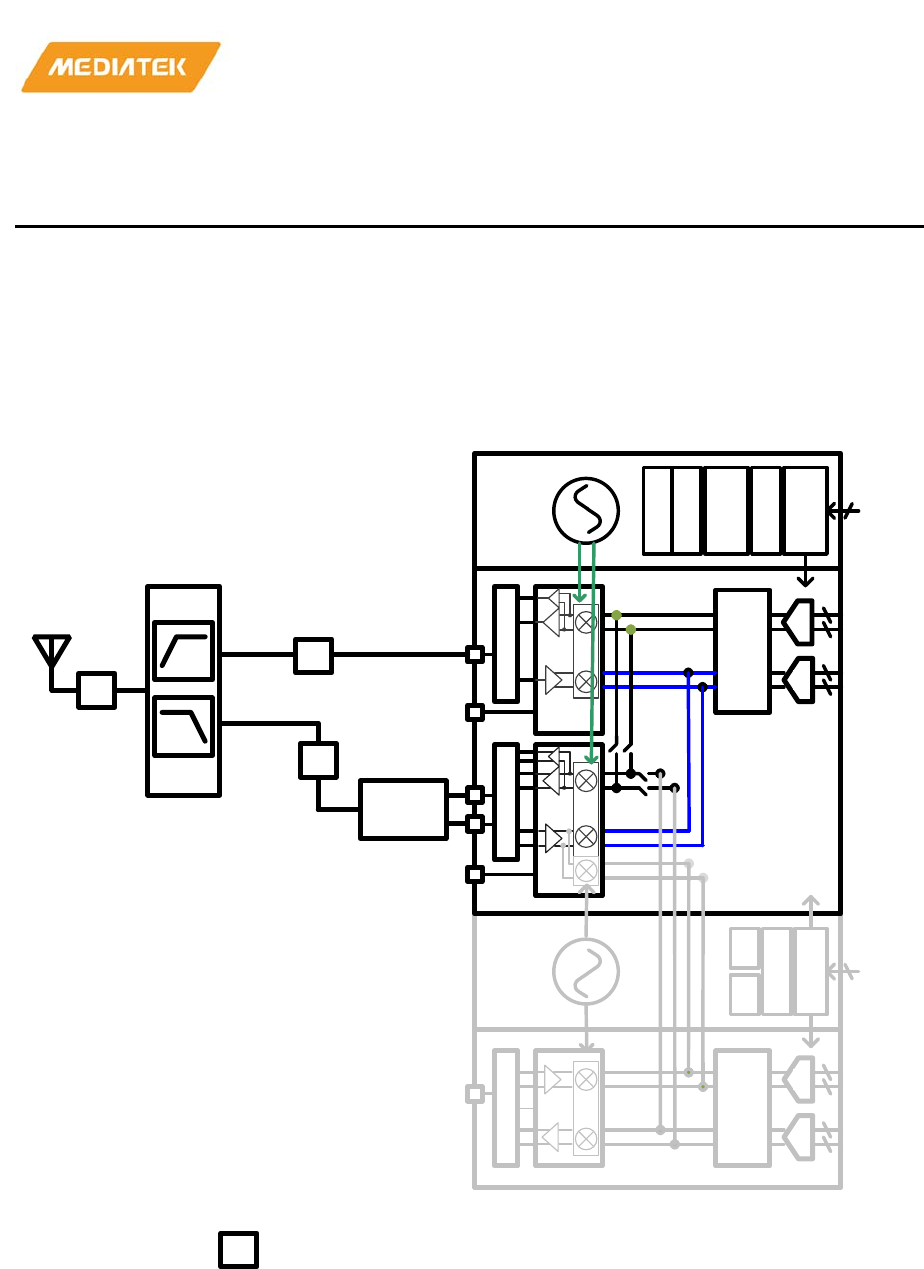
MT76x7
Internet-of-Things Wireless Connectivity
Reference Manual
© 2015 - 2017 MediaTek Inc
Page 773 of 798
This document contains information that is proprietary to MediaTek Inc. (“MediaTek”) and/or its licensor(s).
Any unauthorized use, reproduction or disclosure of this document in whole or in part is strictly prohibited
3. Radio Characteristics
3.1. Wi-Fi radio characteristics
3.1.1. Wi-Fi RF block diagram
Front-end loss with external Balun (2.4GHz band) and diplexer: 2.4GHz band insertion loss is 2dB, and 5GHz
band insertion loss 1.6dB.
BW20/40/80
IF_LPF
IFLPF
ADC
ADC
XFMR
RFDIG
shared
BT SX
(6GHz)
ac TRX
BG
R-cal
TRSW
BBPLL
L
C
-
C
L
B
a
l
u
n
RFDIG
SX0
(3~4GHz)
BG
R-cal
RC-cal
BBPLL
BT TRX
WF0_A_RFIO
WF0_G_RFIOP
TRX
TRSW
ISM TRX
Antenna port
M
M
M
WF0_G_RFION
Note: is matching circuits for 50Ω impedance tuning.
M
Figure 3-1. 2.4/5GHz RF block diagram
Note, that dual band Wi-Fi is only supported for MT7697D.
3.1.2. Wi-Fi 2.4GHz band RF receiver specifications
The specifications noted in the table below is measured at the antenna port, which includes the front-end loss.

MT76x7
Internet-of-Things Wireless Connectivity
Reference Manual
© 2015 - 2017 MediaTek Inc
Page 774 of 798
This document contains information that is proprietary to MediaTek Inc. (“MediaTek”) and/or its licensor(s).
Any unauthorized use, reproduction or disclosure of this document in whole or in part is strictly prohibited
Table 3-1. 2.4GHz RF Receiver Specification
Parameter Description Performance
MIN TYP MAX Unit
Frequency range Center channel frequency 2412 2484 MHz
RX sensitivity 1 Mbps CCK - -96.4 - dBm
2 Mbps CCK - -93.4 - dBm
5.5 Mbps CCK - -91.4 - dBm
11 Mbps CCK - -88.4 - dBm
RX sensitivity BPSK rate 1/2, 6 Mbps OFDM - -93.4 - dBm
BPSK rate 3/4, 9 Mbps OFDM - -91.1 - dBm
QPSK rate 1/2, 12 Mbps OFDM - -90.3 - dBm
QPSK rate 3/4, 18 Mbps OFDM - -87.9 - dBm
16QAM rate 1/2, 24 Mbps OFDM - -84.6 - dBm
16QAM rate 3/4, 36 Mbps OFDM - -81.2 - dBm
64QAM rate 1/2, 48 Mbps OFDM - -77.0 - dBm
64QAM rate 3/4, 54 Mbps OFDM - -75.7 - dBm
RX Sensitivity
BW=20MHz
Mixed mode
800ns Guard
Interval
Non-STBC
MCS 0, BPSK rate 1/2 - -92.7 - dBm
MCS 1, QPSK rate 1/2 - -89.5 - dBm
MCS 2, QPSK rate 3/4 - -87.1 - dBm
MCS 3, 16QAM rate 1/2 - -84.1 - dBm
MCS 4, 16QAM rate 3/4 - -80.6 - dBm
MCS 5, 64QAM rate 2/3 - -76.2 - dBm
MCS 6, 64QAM rate 3/4 - -74.8 - dBm
MCS 7, 64QAM rate 5/6 - -73.6 - dBm
RX Sensitivity
BW=40MHz
Mixed mode
800ns Guard
Interval
Non-STBC
MCS 0, BPSK rate 1/2 - -89.6 - dBm
MCS 1, QPSK rate 1/2 - -86.8 - dBm
MCS 2, QPSK rate 3/4 - -84.3 - dBm
MCS 3, 16QAM rate 1/2 - -80.8 - dBm
MCS 4, 16QAM rate 3/4 - -77.7 - dBm
MCS 5, 64QAM rate 2/3 - -73.1 - dBm
MCS 6, 64QAM rate 3/4 - -71.8 - dBm
MCS 7, 64QAM rate 5/6 - -70.6 - dBm
Maximum Receive
Level
6 Mbps OFDM - -10 - dBm
54 Mbps OFDM - -10 - dBm
MCS0 - -10 - dBm
MCS7 - -20 - dBm
Receive Adjacent 1 Mbps CCK - 40 - dBm
MT76x7
Internet-of-Things Wireless Connectivity
Reference Manual
© 2015 - 2017 MediaTek Inc
Page 775 of 798
This document contains information that is proprietary to MediaTek Inc. (“MediaTek”) and/or its licensor(s).
Any unauthorized use, reproduction or disclosure of this document in whole or in part is strictly prohibited
Parameter Description Performance
Channel Rejection
11 Mbps CCK - 40 - dBm
BPSK rate 1/2, 6 Mbps OFDM - 34 - dBm
64QAM rate 3/4, 54 Mbps OFDM - 22 - dBm
HT20, MCS 0, BPSK rate 1/2 - 33 - dBm
HT20, MCS 7, 64QAM rate 5/6 - 15 - dBm
HT40, MCS 0, BPSK rate 1/2 - 29 - dBm
HT40, MCS 7, 64QAM rate 5/6 - 9 - dBm
3.1.3. Wi-Fi 2.4GHz band RF transmitter specifications
The specifications in table are measured at the antenna port, which includes the front-end loss.
Table 3-2. 2.4GHz RF Transmitter Specifications
Parameter Description Performance
MIN TYP MAX Unit
Frequency range 2412 - 2484 MHz
Output power with
spectral mask and
EVM compliance
1 Mbps CCK - 21 - dBm
11 Mbps CCK - 21 - dBm
6 Mbps OFDM - 19 - dBm
54 Mbps OFDM - 18 - dBm
HT20, MCS 0 - 18 - dBm
HT20, MCS 7 - 17.5 - dBm
HT40, MCS 0 - 17 - dBm
HT40, MCS 7 - 16.5 - dBm
TX EVM 6 Mbps OFDM - - -5 dB
54 Mbps OFDM - - -25 dB
HT20, MCS 0 - - -5 dB
HT20, MCS 7 - - -28 dB
HT40, MCS 0 - - -5 dB
HT40, MCS 7 - - -28 dB
Output power
variation(1)
TSSI closed-loop control across all temperature
range and channels and VSWR ≦ 1.5:1.
-1.5 - 1.5 dB
Carrier suppression - - -30 dBc
Harmonic Output
Power
2nd Harmonic - -45 -43 dBm/MHz
3nd Harmonic - -45 -43 dBm/MHz
Note 1: VDD33 voltage is within ±5% of typical value.
3.1.4. Wi-Fi 5GHz band RF receiver specifications
The specifications in table below are measured at the antenna port, which includes the front-end loss.

MT76x7
Internet-of-Things Wireless Connectivity
Reference Manual
© 2015 - 2017 MediaTek Inc
Page 776 of 798
This document contains information that is proprietary to MediaTek Inc. (“MediaTek”) and/or its licensor(s).
Any unauthorized use, reproduction or disclosure of this document in whole or in part is strictly prohibited
Table 3-3. 5GHz RF receiver specifications
Parameter Description Performance
MIN TYP MAX Unit
Frequency range Center channel frequency 5180 - 5825 MHz
RX sensitivity BPSK rate 1/2, 6 Mbps OFDM - -92.8 - dBm
BPSK rate 3/4, 9 Mbps OFDM - -90.5 - dBm
QPSK rate 1/2, 12 Mbps OFDM - -89.8 - dBm
QPSK rate 3/4, 18 Mbps OFDM - -87.3 - dBm
16QAM rate 1/2, 24 Mbps OFDM - -84.1 - dBm
16QAM rate 3/4, 36 Mbps OFDM - -80.8 - dBm
64QAM rate 1/2, 48 Mbps OFDM - -76.4 - dBm
64QAM rate 3/4, 54 Mbps OFDM - -75.0 - dBm
RX Sensitivity
BW=20MHz HT
Mixed mode
800ns Guard
Interval
Non-STBC
MCS 0, BPSK rate 1/2 - -92.1 - dBm
MCS 1, QPSK rate 1/2 - -89.1 - dBm
MCS 2, QPSK rate 3/4 - -86.6 - dBm
MCS 3, 16QAM rate 1/2 - -83.6 - dBm
MCS 4, 16QAM rate 3/4 - -80.1 - dBm
MCS 5, 64QAM rate 2/3 - -75.6 - dBm
MCS 6, 64QAM rate 3/4 - -74.2 - dBm
MCS 7, 64QAM rate 5/6 - -73.0 - dBm
RX Sensitivity
BW=40MHz HT
Mixed mode
800ns Guard
Interval
Non-STBC
MCS 0, BPSK rate 1/2 - -89.1 - dBm
MCS 1, QPSK rate 1/2 - -85.9 - dBm
MCS 2, QPSK rate 3/4 - -83.5 - dBm
MCS 3, 16QAM rate 1/2 - -80.2 - dBm
MCS 4, 16QAM rate 3/4 - -76.9 - dBm
MCS 5, 64QAM rate 2/3 - -72.6 - dBm
MCS 6, 64QAM rate 3/4 - -71.2 - dBm
MCS 7, 64QAM rate 5/6 - -70.1 - dBm
Maximum Receive
Level
6 Mbps OFDM - -10 - dBm
54 Mbps OFDM - -20 - dBm
MCS0 - -15 - dBm
MCS7 - -20 - dBm
Receive Adjacent
Channel Rejection
BPSK rate 1/2, 6 Mbps OFDM - 25 - dBm
64QAM rate 3/4, 54 Mbps OFDM - 7 - dBm
HT20, MCS 0, BPSK rate 1/2 - 24 - dBm
HT20, MCS 7, 64QAM rate 5/6 - 3 - dBm
HT40, MCS 0, BPSK rate 1/2 - 24 - dBm
HT40, MCS 7, 64QAM rate 5/6 - 3 - dBm

MT76x7
Internet-of-Things Wireless Connectivity
Reference Manual
© 2015 - 2017 MediaTek Inc
Page 777 of 798
This document contains information that is proprietary to MediaTek Inc. (“MediaTek”) and/or its licensor(s).
Any unauthorized use, reproduction or disclosure of this document in whole or in part is strictly prohibited
MT76x7
Internet-of-Things Wireless Connectivity
Reference Manual
© 2015 - 2017 MediaTek Inc
Page 778 of 798
This document contains information that is proprietary to MediaTek Inc. (“MediaTek”) and/or its licensor(s).
Any unauthorized use, reproduction or disclosure of this document in whole or in part is strictly prohibited
3.1.5. Wi-Fi 5GHz band RF transmitter specifications
The specifications in table below are measured at the antenna port, which includes the front-end loss.
Table 3-4. 5GHz RF Transmitter Specifications
Parameter Description Performance
MIN TYP MAX Unit
Frequency range 5180 - 5825 MHz
Output power
with spectral
mask and EVM
compliance
6 Mbps OFDM - 16.9 - dBm
54 Mbps OFDM - 16.9 - dBm
HT20, MCS 0 - 16.9 - dBm
HT20, MCS 7 - 15.9 - dBm
HT40, MCS 0 - 15.9 - dBm
HT40, MCS 7 - 15.9 - dBm
TX EVM 6 Mbps OFDM - - -5 dB
54 Mbps OFDM - - -25 dB
HT20, MCS 0 - - -5 dB
HT20, MCS 7 - - -28 dB
HT40, MCS 0 - - -5 dB
HT40, MCS 7 - - -28 dB
Output power
variation(1)
TSSI closed-loop control across all temperature
range and channels and VSWR ≦1.5:1.
-1.5 - 1.5 dB
Carrier
suppression
- - -30 dBc
Harmonic
Output Power
2nd Harmonic - -45 -43 dBm/MHz
3nd Harmonic - -45 -43 dBm/MHz
Note 1: VDD33 voltage is within ±5% of typical value.
3.2. Bluetooth radio characteristics
MT7697 and MT7697D support Bluetooth system.
3.2.1. Bluetooth RF block diagram
Front-end loss with external Balun and diplexer: 2.4GHz insertion loss 2dB.
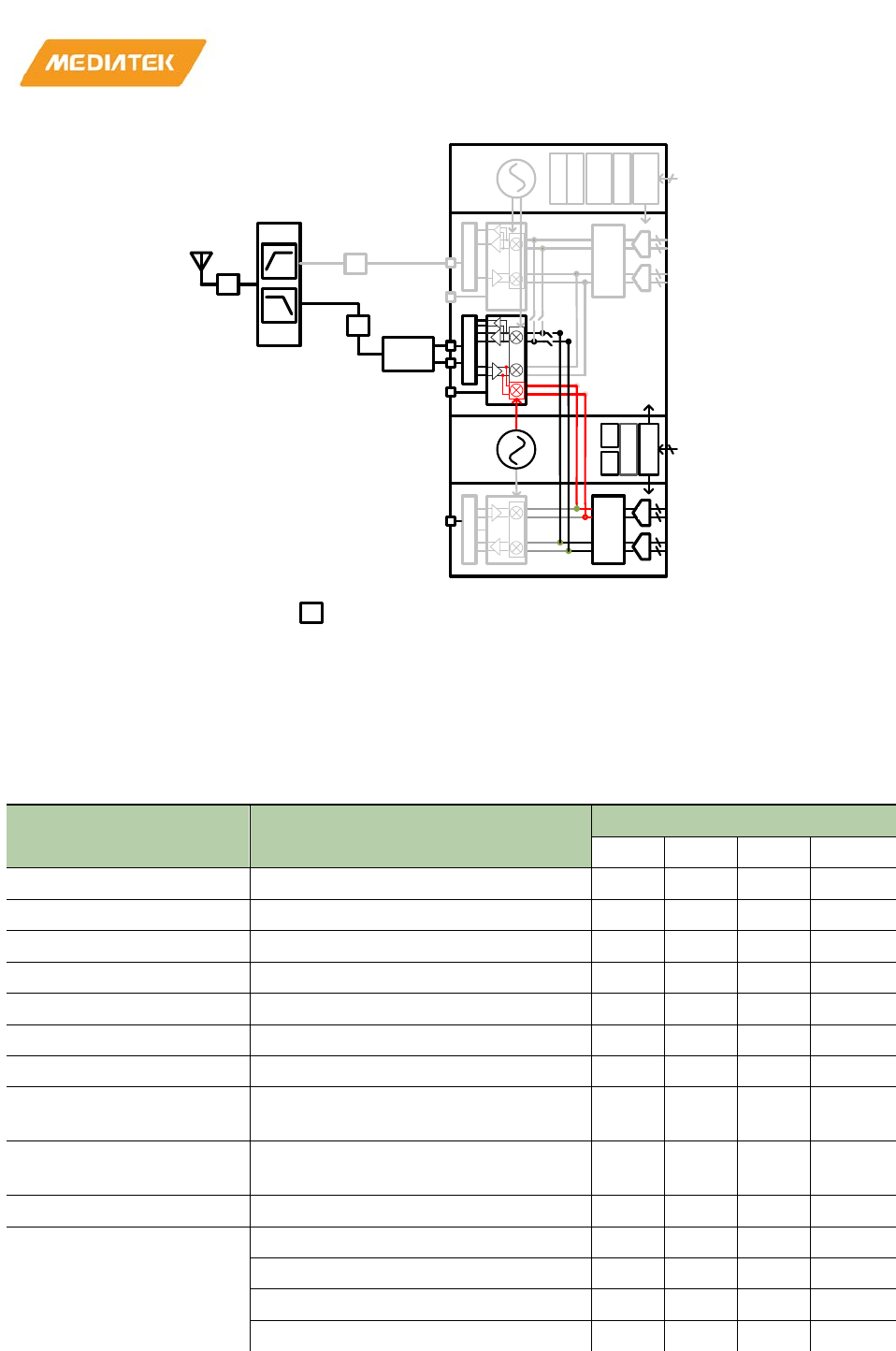
MT76x7
Internet-of-Things Wireless Connectivity
Reference Manual
© 2015 - 2017 MediaTek Inc
Page 779 of 798
This document contains information that is proprietary to MediaTek Inc. (“MediaTek”) and/or its licensor(s).
Any unauthorized use, reproduction or disclosure of this document in whole or in part is strictly prohibited
BW20/40/80
IF_LPF
IFLPF
ADC
ADC
XFMR
RFDIG
shared
BT SX
(6GHz)
ac TRX
BG
R-cal
TRSW
BBPLL
L
C
-
C
L
B
a
l
u
n
RFDIG
SX0
(3~4GHz)
BG
R-cal
RC-cal
BBPLL
BT TRX
WF0_A_RFIO
WF0_G_RFIOP
TRX
TRSW
ISM TRX
Antenna port
M
M
M
WF0_G_RFION
Note: is matching circuits for 50ohm impedance tuning.
M
Figure 3-2. Wi-Fi/Bluetooth RF block diagram
3.2.2. Basic Rate receiver specifications
The specifications in table below are measured at the antenna port, which includes the front-end loss.
Figure 3-3. Basic Rate receiver specifications
Parameter Description Performance
MIN TYP MAX Unit
Frequency range 2402 - 2480 MHz
Receiver sensitivity
1
BER<0.1% - -92 - dBm
Maximum usable signal BER<0.1% - -5 - dBm
C/I co-channel (BER<0.1%) Co channel selectivity - 6 11 dB
C/I 1MHz (BER<0.1%) Adjacent channel selectivity - -7 0 dB
C/I 2MHz (BER<0.1%) 2
nd
adjacent channel selectivity - -40 -30 dB
C/I≥3MHz (BER<0.1%) 3
rd
adjacent channel selectivity - -43 -40 dB
C/I Image channel
(BER<0.1%)
Image channel selectivity - -20 -9 dB
C/I Image 1MHz (BER<0.1%) 1MHz adjacent to image channel
selectivity
- -35 -20 dB
Inter-modulation -39 -30 - dBm
Out-of-band blocking
30MHz to 2000MHz -10 - - dBm
2000MHz to 2399MHz -27 - - dBm
2498MHz to 3000MHz -27 - - dBm
3000MHz to 12.75GHz -10 - - dBm
Note 1: The receiver sensitivity is measured at the antenna port.
MT76x7
Internet-of-Things Wireless Connectivity
Reference Manual
© 2015 - 2017 MediaTek Inc
Page 780 of 798
This document contains information that is proprietary to MediaTek Inc. (“MediaTek”) and/or its licensor(s).
Any unauthorized use, reproduction or disclosure of this document in whole or in part is strictly prohibited
3.2.3. Basic Rate transmitter specifications
The specifications in table below are measured at the antenna port, which includes the front-end loss.
Table 3-5. Basic Rate transmitter specifications
Parameter Description Performance
MIN TYP MAX Unit
Frequency range 2402 - 2480 MHz
Maximum transmit
power1
At maximum power output level - 10 - dBm
Gain step 2 4 8 dB
Modulation
characteristics
∆f1avg 140 157 175 KHz
∆f2max (For at least 99.9% of all ∆f2max) 115 121 - KHz
∆f1avg /∆f2avg 0.8 0.85 - KHz
ICFT Initial carrier frequency tolerance -75 ±20 +75 KHz
Carrier frequency
drift
One slot packet (DH1) -25 ±15 +25 KHz
Two slot packet (DH3) -40 ±15 +40 KHz
Five slot packet (DH5) -40 ±15 +40 KHz
Max drift rate -20 ±15 20 KHz/50μs
TX output spectrum 20dB bandwidth - - 1000 KHz
In-Band spurious
emission
±2MHz offset - -40 -20 dBm
±3MHz offset - -45 -40 dBm
>±3MHz offset - -45 -40 dBm
Note 1: The output power is measured at the antenna port.
3.2.4. Bluetooth LE receiver specifications
The specifications in table below are measured at the antenna port, which includes the front-end loss.
Table 3-6. Bluetooth LE receiver specifications
Parameter Description Min. Typ. Max. Unit
Frequency Range 2402 - 2480 MHz
Receiver Sensitivity
(*)
PER < 30.8% - -95 - dBm
Max. Usable Signal PER < 30.8% -10 -5 - dBm
C/I Co-channel Co-channel selectivity (PER < 30.8%) - 6 21 dB
C/I 1MHz Adjacent channel selectivity (PER <
30.8%)
- -7 15 dB
C/I 2MHz 2nd adjacent channel selectivity (PER
< 30.8%)
- -30 -17 dB
C/I ≧3MHz 3rd adjacent channel selectivity
(PER < 30.8%)
- -33 -27 dB
C/I Image channel Image channel selectivity (PER <
30.8%)
- -20 -9 dB
MT76x7
Internet-of-Things Wireless Connectivity
Reference Manual
© 2015 - 2017 MediaTek Inc
Page 781 of 798
This document contains information that is proprietary to MediaTek Inc. (“MediaTek”) and/or its licensor(s).
Any unauthorized use, reproduction or disclosure of this document in whole or in part is strictly prohibited
Parameter Description Min. Typ. Max. Unit
C/I Image 1MHz 1MHz adjacent to image channel
selectivity (PER < 30.8%)
- -30 -15 dB
Inter-modulation -50 -35 dBm
Out-of-band Blocking 30MHz to 2000MHz -30 - - dBm
2001MHz to 2339MHz -35 - - dBm
2501MHz to 3000MHz -35 - - dBm
3001MHz to 12.75GHz -30 - - dBm
3.2.5. Bluetooth LE transmitter specifications
The specifications in table below are measured at the antenna port, which includes the front-end loss.
Table 3-7. Bluetooth LE transmitter specifications
Parameter Description Min. Typ. Max. Unit
Frequency Range 2402 - 2480 MHz
Output Power (*) At max power output level -20 6 10 dBm
Carrier Frequency
Offset and Drift
Frequency offset -150 - 150 kHz
Frequency drift -50 - 50 kHz
Max. drift rate -20 - 20 Hz/us
Modulation
Characteristic
△
f1avg 225 - 275 kHz
△
f2max (For at least 99% of all
△
f2max) 185 - - kHz
△
f2avg/
△
f1avg 0.8 0.94 - Hz/Hz
In-band
Spurious Emission
±2M offset - - -20 dBm
>±3MHz offset - - -30 dBm
Note 1: The output power is measured at the antenna port.

MT76x7
Internet-of-Things Wireless Connectivity
Reference Manual
© 2015 - 2017 MediaTek Inc
Page 782 of 798
This document contains information that is proprietary to MediaTek Inc. (“MediaTek”) and/or its licensor(s).
Any unauthorized use, reproduction or disclosure of this document in whole or in part is strictly prohibited
4. Electrical Characteristics
4.1. Absolute Maximum Rating
Table 4-1 Absolute maximum rating
Symbol Parameters Maximum rating Unit
VDD33 3.3V Supply Voltage -0.3 to 3.63 V
TSTG Storage Temperature -40 to +125 °C
VESD ESD protection (HBM) 2000 V
4.2. Recommended operating range
Table 4-2. Recommended operating range
Symbol Supply Voltage Source Min Typ Max Unit
AVDD45 AVDD45_BUCK,
AVDD45_MISC
To be connected to external 3.3V supply 2.97 3.3 3.63 V
RTC_3V3 RTC_3V3 To be connected to external supply 1.6 3.63 V
AVDD33 AVDD33_WF0_A_PA,
AVDD33_WF0_G_PA,
AVDD33_WF0_A_TX,
AVDD33_WF0_G_TX,
AVDD33_BT
To be connected to external 3.3V supply 2.97 3.3 3.63 V
DVDDIO DVDDIO_D, DVDDIO_L,
DVDDIO_R
To be connected to PMU_DIO33_OUT 2.97 3.3 3.63
AVDD25 AVDD25_AUXADC To be connected to PMU ALDO output 2.3 2.5 2.7 V
AVDD16 AVDD16_CLDO, AVDD16_BT,
AVDD16_XO,
AVDD16_WF0_AFE
To be connected to PMU BUCK output 1.6 1.7 1.8 V
DVDD11 DVDD11 To be connected to PMU CLDO output 0.86 1.15 1.3 V
Ta Operating Ambient
Temperature
MT76X7N 0 70 C
MT76x7IDN -40 85 C
Tj Operating Junction
Temperature
MT76X7N 0 125 C
MT76x7IDN -40 125 C
4.3. DC characteristics
Table 4-3. DC characteristics
Symbol Parameter Conditions MIN MAX Unit
VIL Input Low Voltage LVTTL -0.28 0.8 V
VIH Input High Voltage 2 3.63 V
MT76x7
Internet-of-Things Wireless Connectivity
Reference Manual
© 2015 - 2017 MediaTek Inc
Page 783 of 798
This document contains information that is proprietary to MediaTek Inc. (“MediaTek”) and/or its licensor(s).
Any unauthorized use, reproduction or disclosure of this document in whole or in part is strictly prohibited
Symbol Parameter Conditions MIN MAX Unit
VOL Output Low Voltage |IOL| = 4~16 mA -0.28 0.4 V
VOH Output High Voltage |IOH| = 4~16 mA 2.4 VDD33+0.33 V
RPU Input Pull-Up Resistance PU=high, PD=low 40 190 KΩ
RPD Input Pull-Down Resistance PU=low, PD=high 40 190 KΩ
4.4. XTAL oscillator
The table below lists the XTAL requirements for the XTAL.
Table 4-4. XTAL Oscillator requirements and performance
Parameter
Condition/Notes
Min
Typ
Max
Units
Frequency 2.4G and 5G bands, IEEE 802.11n
operation
26 40 52 MHz
Frequency tolerance All Normal temperature -10 - +10 ppm
Frequency stability over
temperature
Over temperature -15 - +15 ppm
Crystal load
capacitance (CL)
9.5 - 11.5 pF
Equivalent Series
Resistance (ESR)
- - 30 Ω
Table 4-5. 32k XTAL Oscillator functional specifications
Symbol Parameter Min Typ Max Units
Tosc Start-up time 1 Sec
Dcyc Duty cycle 35 %
Current concumption 25 µA
Table 4-6. Recommended parameters of 32k XTAL Crystal
Symbol Parameter Min Typ Max Units
F Frequency range 32768 Hz
GL Drive level 1 uW
ESR Series Resistance 70 90 K Ω
C0 Static capacitance 1.2 pF
CL Load capacitance 18 pF
4.5. PMU characteristics
Table 4-7. PMU electrical characteristics
MT76x7
Internet-of-Things Wireless Connectivity
Reference Manual
© 2015 - 2017 MediaTek Inc
Page 784 of 798
This document contains information that is proprietary to MediaTek Inc. (“MediaTek”) and/or its licensor(s).
Any unauthorized use, reproduction or disclosure of this document in whole or in part is strictly prohibited
Parameter Reference Conditions Min Typ Max Unit
Switching regulator (BUCK)
Vin
Input Voltage
AVDD45_BUCK
2.97
3.3
3.63
V
Vout
Output Voltage
LXBK
Switching operation/ Deep
Sleep mode
1.55
1.7
1.86
V
Iout
Output Current
Switching operation
800
mA
Deep Sleep mode, SLDO-H
enabled
10
mA
.
Over-current shutdown
960
1600
4000
mA
Iq
Quiescent
Current
Iload < 1mA
150
uA
DC/DC
Line Regulation
Iload = 0mA
1
%
Load regulation
Iload = 200-400mA
0.05
mV/mA
Efficiency
Vin = 3.3V, Iload = 400mA
80
85
%
Core LDO (CLDO)
Vin
Input
AVDD16_CLDO
1.55
1.7
1.86
V
Vout
Output Voltage
AVDD12_VCORE
Normal operation/Deep
Sleep mode
0.8
1.15
1.25
V
Iout
Output Current
Normal operation
420
mA
Deep Sleep mode, SLDO-L
enabled
10
mA
Iq
Quiescent
Current
40
50
uA
Analog LDO (ALDO)
Vin
Input Voltage
2.97
3.3
3.63
V
Vout
Output Voltage
AVDD25_ALDO
Normal operation
2.3
2.5
2.7
V
Deep Sleep mode, OFF
0
V
Iout
Output Current
Normal operation
50
mA
Iq
Quiescent
Current
25
50
uA
PMU
Vin
Input Voltage
AVDD45, AVDD33
and DVDDIO
2.97
3.3
3.63
V
Iq
Quiescent
Current
In Deep Sleep State
50
uA
Table 4-8. PMU UVLO & PMU_EN_WF characteristics
Parameter Condition/Notes Min Typ Max Unit
UVLO On Threshold
2.2
2.25
2.3
V
Off Threshold 2.1 2.15 2.2 V
Hysteresis 100 mV
PMU_EN_WF High Voltage 1.6 V
Low Voltage 0.6 V

MT76x7
Internet-of-Things Wireless Connectivity
Reference Manual
© 2015 - 2017 MediaTek Inc
Page 785 of 798
This document contains information that is proprietary to MediaTek Inc. (“MediaTek”) and/or its licensor(s).
Any unauthorized use, reproduction or disclosure of this document in whole or in part is strictly prohibited
4.6. Auxiliary ADC characteristics
This section specifies the electrical characteristics of the auxiliary ADC.
Table 4-9. Auxiliary ADC specifications
Symbol Parameter Min Typical Max Unit
N Resolution - 12 - Bit
FS Sampling Rate @ N-Bit(1) - 2 - MSPS
VPP Input Swing(2) - - AVDD25
(2.45~2.55V
)
V
VIN Input voltage(3) 0 - AVDD25
(2.45~2.55V
)
V
RIN Input Impedance:
Unselected channel
Selected channel
400M
-
-
10K
-
-
Ω
DNL Differential Nonlinearity without dithering and
averaging
- ± 1 ± 2 LSB
INL Integral Nonlinearity without dithering and
averaging
- ± 2 ± 4 LSB
DNLdither+average Differential Nonlinearity with dithering and
averaging
- ± 0.5 ± 1 LSB
INLdither+average Integral Nonlinearity with dithering and
averaging
- - ± 2 LSB
OE Offset Error - - ± 10 mV
FSE Full Swing Error - - ± 50 mV
SNR Signal to Noise Ratio(2) 60 63 66 dB
Current Consumption - - 400 μA
Power-Down Current - - 1 μA
Note 1: Given that FS=2MHz
Note 2: At 1K Hz Input Frequency
Note 3: The voltage level is lowered by 0.04V when dithering is on.
MT76x7
Internet-of-Things Wireless Connectivity
Reference Manual
© 2015 - 2017 MediaTek Inc
Page 786 of 798
This document contains information that is proprietary to MediaTek Inc. (“MediaTek”) and/or its licensor(s).
Any unauthorized use, reproduction or disclosure of this document in whole or in part is strictly prohibited
4.7. Thermal characteristics
ΘJC assumes that all the heat is dissipated through the top of the package, while ΨJt assumes that the heat is
dissipated through the top, sides, and the bottom of the package. Thus it is suggested to use ΨJt to estimate
the junction temperature.
Table 4-10. Thermal characteristics
Symbol Description Performance
Typical Unit
TJ Maximum Junction Temperature (Plastic Package) 125 °C
ΘJA Junction to ambient temperature thermal resistance[1] 19.21 °C/W
ΘJC Junction to case temperature thermal resistance 7.33 °C/W
ΨJt Junction to the package thermal resistance
[2]
1.65 °C/W
Note 1: JEDEC 51-7 system FR4 PCB size: 76.2mm x 114.3mm
Note 2: 8mm x 8mm QFN-68 package
MT76x7
Internet-of-Things Wireless Connectivity
Reference Manual
© 2015 - 2017 MediaTek Inc
Page 787 of 798
This document contains information that is proprietary to MediaTek Inc. (“MediaTek”) and/or its licensor(s).
Any unauthorized use, reproduction or disclosure of this document in whole or in part is strictly prohibited
5. Package Specifications
5.1. Pin layout
MT76X7 uses 8mm x 8mm QFN package of 68-pin with 0.4mm pitch.
Table 5-1. Pin Map
68 67 66 65 64 63 62 61 60 59 58 57 56 55 54 53 52
WF0_A_RFIO
AVDD33_WF0_A_TX
WF0_RXA_AUX_IN
AVDD33_WF0_G_TX
WF0_G_RFIOP
WF0_G_RFION
AVDD33_WF0_G_PA
WF0_RXG_AUX_IN
AVDD16_BT
AVDD33_BT
BT_RFIP
GPIO33
GPIO34
GPIO35
GPIO36
GPIO37
GPIO38
1 AVDD33_WF0_A_PA
SYSRST_B 51
2 AVDD16_WF0_AFE
VSS
GPIO39 50
3 AVDD16_XO
DVDD11 49
4 XO
DVDDIO_L 48
5 GPIO0
GPIO57 47
6 GPIO1
GPIO58 46
7 GPIO2
GPIO59 45
8 GPIO3
GPIO60 44
9 GPIO4
AVDD25_AUXADC
43
10
GPIO5
AVSS25_AUXADC
42
11
GPIO6
AVSS45_BUCK 41
12
GPIO7
LXBK 40
13
DVDDIO_R
AVDD45_BUCK 39
14
DVDD11
AVDD15_V2P5NA 38
15
GPIO24
AVDD16_CLDO 37
16
DVDDIO_D
AVDD12_VCORE 36
17
DVDD11
PMU_TEST 35
GPIO25
GPIO26
RTC_3V3
RTC_32K_XO
RTC_32K_XI
PMU_EN_RTC
GPIO32
GPIO31
GPIO27
GPIO30
GPIO28
GPIO29
PMU_DIO33_OUT
AVDD25_ALDO_OUT
PMU_EN_WF
ISO_INT_PMU_EN
AVDD45_MISC
18 19 20 21 22 23 24 25 26 27 28 29 30 31 32 33 34
5.2. Pin description
The section describes the pin functionality of MT76x7 chip.
MT76x7
Internet-of-Things Wireless Connectivity
Reference Manual
© 2015 - 2017 MediaTek Inc
Page 788 of 798
This document contains information that is proprietary to MediaTek Inc. (“MediaTek”) and/or its licensor(s).
Any unauthorized use, reproduction or disclosure of this document in whole or in part is strictly prohibited
Table 5-2. Pin descriptions
QF
N
Pin Name Pin description PU/PD I/O Supply
domain
Reset and Clocks
51 SYSRST_B External system reset active low PU Input DVDDIO
4 XO Crystal input or external clock input N/A Input AVDD16_XO
3 AVDD16_XO RF 1.6V power supply N/A Power
Programmable I/O
5 GPIO0 Programmable input/output PU/PD In/out DVDDIO
6 GPIO1 Programmable input/output PU/PD In/out DVDDIO
7 GPIO2 Programmable input/output PU/PD In/out DVDDIO
8 GPIO3 Programmable input/output PU/PD In/out DVDDIO
9 GPIO4 Programmable input/output PU/PD In/out DVDDIO
10 GPIO5 Programmable input/output PU/PD In/out DVDDIO
11 GPIO6 Programmable input/output PU/PD In/out DVDDIO
12 GPIO7 Programmable input/output PU/PD In/out DVDDIO
15 GPIO24 Programmable input/output PU/PD In/out DVDDIO
18 GPIO25 Programmable input/output PU/PD In/out DVDDIO
19 GPIO26 Programmable input/output PU/PD In/out DVDDIO
26 GPIO27 Programmable input/output PU/PD In/out DVDDIO
28 GPIO28 Programmable input/output PU/PD In/out DVDDIO
29 GPIO29 Programmable input/output PU/PD In/out DVDDIO
27 GPIO30 Programmable input/output PU/PD In/out DVDDIO
25 GPIO31 Programmable input/output PU/PD In/out DVDDIO
24 GPIO32 Programmable input/output PU/PD In/out DVDDIO
57 GPIO33 Programmable input/output PU/PD In/out DVDDIO
56 GPIO34 Programmable input/output PU/PD In/out DVDDIO
55 GPIO35 Programmable input/output PU/PD In/out DVDDIO
54 GPIO36 Programmable input/output PU/PD In/out DVDDIO
53 GPIO37 Programmable input/output PU/PD In/out DVDDIO
52 GPIO38 Programmable input/output PU/PD In/out DVDDIO
50 GPIO39 Programmable input/output PU/PD In/out DVDDIO
47 GPIO57 Programmable input/output PU/PD In/out DVDDIO
46 GPIO58 Programmable input/output PU/PD In/out DVDDIO
MT76x7
Internet-of-Things Wireless Connectivity
Reference Manual
© 2015 - 2017 MediaTek Inc
Page 789 of 798
This document contains information that is proprietary to MediaTek Inc. (“MediaTek”) and/or its licensor(s).
Any unauthorized use, reproduction or disclosure of this document in whole or in part is strictly prohibited
QF
N
Pin Name Pin description PU/PD I/O Supply
domain
45 GPIO59 Programmable input/output PU/PD In/out DVDDIO
44 GPIO60 Programmable input/output PU/PD In/out DVDDIO
RTC
20 RTC_3V3 RTC domain power supply N/A
Power
21 RTC_32K_XO 32KHz crystal N/A
Analog
RTC_3V3
22 RTC_32K_XI 32KHz crystal N/A
Analog
RTC_3V3
23 PMU_EN_RTC PMU enable N/A
Output
RTC_3V3
WIFI Radio Interface
1 AVDD33_WF0_A_PA RF 3.3v power supply N/A Power
62 AVDD33_WF0_G_PA
RF 3.3v power supply
N/A Power
67 AVDD33_WF0_A_TX RF 3.3v power supply N/A Power
65 AVDD33_WF0_G_TX RF 3.3v power supply N/A Power
2 AVDD16_WF0_AFE RF 1.6v power supply N/A Power
68 WF0_A_RFIO RF a-band RF port N/A
Input
AVDD33_WF0_
A
66 WF0_RXA_AUX_IN RF a-band auxiliary RF LNA port N/A
Input
AVDD33_WF0_
A
61 WF0_RXG_AUX_IN RF g-band auxiliary RF LNA port N/A
Input
AVDD33_WF0_
G
64 WF0_G_RFIOP RF g-band RF port N/A
In/out
AVDD33_WF0_
G
63 WF0_G_RFION RF g-band RF port N/A In/out AVDD33_WF0_
G
Bluetooth Radio Interface
59 AVDD33_BT RF 3.3v power supply N/A Power
60 AVDD16_BT RF 1.6v power supply N/A Power
58 BT_RFIO RF Bluetooth port N/A In/out AVDD33_BT
PMU/BUCK
41 AVSS45_BUCK
BUCK ground
N/A Ground
40 LXBK BUCK output N/A Output
39 AVDD45_BUCK BUCK power supply N/A Input
38 AVDD15_V2P5NA BUCK internal circuit output cap N/A Output
37 AVDD16_CLDO CLDO supply N/A Input
36 AVDD12_VCORE CLDO output N/A Output
34 AVDD45_MISC PMU supply N/A Input
31 AVDD25_ALDO_OUT 2.5V ALDO output with external cap. N/A Output
30 PMU_DIO33_OUT This pin output is to provide 3.3V for
all DVDDIO.
N/A Output
MT76x7
Internet-of-Things Wireless Connectivity
Reference Manual
© 2015 - 2017 MediaTek Inc
Page 790 of 798
This document contains information that is proprietary to MediaTek Inc. (“MediaTek”) and/or its licensor(s).
Any unauthorized use, reproduction or disclosure of this document in whole or in part is strictly prohibited
QF
N
Pin Name Pin description PU/PD I/O Supply
domain
And in OFF mode, this pin is 0V.
35 PMU_TEST PMU test pin N/A Output
33 ISO_INT_PMU_EN Input 0V for non-RTC platform.
Input 3.3V for RTC platform.
N/A Input
32 PMU_EN_WF External PMU enable N/A Input
Power Supplies
43 AVDD25_AUXAD
C
Auxiliary ADC 2.5v power supply N/A Power
42 AVSS25_AUXADC
Auxiliary ADC ground
N/A Ground
13 DVDDIO_R
Digital 3.3V input
N/A Power
16 DVDDIO_D
Digital 3.3V input
N/A Power
48 DVDDIO_L
Digital 3.3V input
N/A Power
14, 17, 30,
49
DVDD11
Digital 1.15V input
N/A Power
E-PAD VSS
Common Ground
N/A Ground
5.3. Pin multiplexing
The pin multiplexing could be controlled via the configuration register A (in TOP_AON domain) and the
configuration register B (in TOP_OFF/N9 domain). When configuration register A is set to 0, the configuration
register B determines the pin function. When configuration register A is not set to 0, the configuration register
A determines the pin function.
Please be notified that the “-” symbol in Table 5-3 is “don’t care”, means either TOP_AON domain or TOP_OFF
domain doesn’t have pin multiplexing option in this entry.
The default function of each pin is highlighted with blue background.
The driving strength of all pins is programmable: 4mA, 8mA, 12mA, and 16mA. The default setting for all pins
are 4mA.
MT76x7
Internet-of-Things Wireless Connectivity
Reference Manual
© 2015 - 2017 MediaTek Inc
Page 791 of 798
This document contains information that is proprietary to MediaTek Inc. (“MediaTek”) and/or its licensor(s).
Any unauthorized use, reproduction or disclosure of this document in whole or in part is strictly prohibited
Table 5-3. Pin multiplexing
Pin
Pin
Alias
APGIO/
GPIO
Name
Dir
Default
Directio
n
Default
PU/PD
Description
Mode
Pinx_pinmux_aon_sel
Pinx_pinmux_off_sel
Address
Value
Address
Value
5
GPIO0
AGPIO
[Reserved]
I
I
PD
[Reserved]
0
0x8102_3020[3:0]
0
0x8002_5100[3:0]
(0x8102_3020[3:0]=0)
0
ANTSEL[0]
O
RF control
-
-
1
UART0_RTS_CM4
O
UART0 RTS (CM4)
7
7
3
GPIO[0]
O
General purpose input output
8
8
-
PWM[0]
I/O
Pulse-width-modulated output
9
9
-
EINT[0]
I
External interrupt
3
3
-
6
GPIO1
AGPIO
[Reserved]
I
I
PD
[Reserved]
0
0x8102_3020[7:4]
0
0x8002_5100[7:4]
(0x8102_3020[7:4]=0)
0
ANTSEL[1]
O
RF control
-
-
1
UART0_CTS_CM4
I
UART0 CTS (CM4)
7
7
3
GPIO[1]
I/O
General purpose input output
8
8
-
PWM[1]
O
Pulse-width-modulated output
9
9
-
EINT[1]
I
External interrupt
3
3
-
7
GPIO2
AGPIO
[Reserved]
I
I
PD
[Reserved]
0
0x8102_3020[11:8]
0
0x8002_5100[11:8]
(0x8102_3020[11:8]=0)
0
ANTSEL[2]
O
RF control
-
-
1
UART0_RX_CM4
I
UART0 RX (CM4)
7
7
3
SWD_CLK
O
CM4 SWD debug port
4
4
4
GPIO[2]
I/O
General purpose input output
8
8
-
PWM[23]
O
Pulse-width-modulated output
9
9
-
WIC[0]
I
External interrupt
3
3
-
8
GPIO3
AGPIO
[Reserved]
I
I
PD
[Reserved]
0
0x8102_3020[15:12]
0
0x8002_5100[15:12]
(0x8102_3020[15:12]=0)
0
ANTSEL[3]
O
RF control
-
-
1
UART0_TX_CM4
O
UART0 TX (CM4)
7
7
3
SWD_DIO
I/O
CM4 SWD debug port
4
4
4
GPIO[3]
I/O
General purpose input output
8
8
-
PWM[24]
O
Pulse-width-modulated output
9
9
-
EINT[2]
I
External interrupt
3
3
-
9
GPIO4
GPIO
[Reserved]
I
I
PD
[Reserved]
0
0x8102_3020[19:16]
0
0x8002_5100[19:16]
(0x8102_3020[19:16]=0)
0
ANTSEL[4]
O
RF control
-
-
1
SPI_DATA0_EXT(*)
I/O
External flash interface
7
7
3
GPIO[4]
I/O
General purpose input output
8
8
-
PWM[2]
O
Pulse-width-modulated output
9
9
-
EINT[3]
I
External interrupt
3
3
-
10
GPIO5
GPIO
[Reserved]
O
O (Low)
[Reserved]
0
0x8102_3020[23:20]
0
0x8002_5100[23:20]
(0x8102_3020[23:20]=0)
0
ANTSEL[5]
O
RF control
-
-
1
SPI_DATA1_EXT(*)
O
External flash interface
7
7
3
GPIO[5]
I/O
General purpose input output
8
8
-
MT76x7
Internet-of-Things Wireless Connectivity
Reference Manual
© 2015 - 2017 MediaTek Inc
Page 792 of 798
This document contains information that is proprietary to MediaTek Inc. (“MediaTek”) and/or its licensor(s).
Any unauthorized use, reproduction or disclosure of this document in whole or in part is strictly prohibited
Pin
Pin
Alias
APGIO/
GPIO
Name
Dir
Default
Directio
n
Default
PU/PD
Description
Mode
Pinx_pinmux_aon_sel
Pinx_pinmux_off_sel
Address
Value
Address
Value
PWM[3]
O
Pulse-width-modulated output
9
9
-
EINT[4]
I
External interrupt
3
3
-
11
GPIO6
GPIO
[Reserved]
O
O
[Reserved]
0
0x8102_3020[27:24]
0
0x8002_5100[27:24]
(0x8102_3020[27:24]=0)
0
ANTSEL[6]
O
RF control
-
-
1
SPI_CS_1_M_CM4
O
SPI master chip select 1
7
7
3
GPIO[6]
I/O
General purpose input output
8
8
-
PWM[4]
O
Pulse-width-modulated output
9
9
-
EINT[5]
I
External interrupt
3
3
-
12
GPIO7
GPIO
[Reserved]
O
O (Low)
[Reserved]
0
0x8102_3020[31:28]
0
0x8002_5100[31:28]
(0x8102_3020[31:28]=0)
0
ANTSEL[7]
O
RF control
-
-
1
SPI_MISO_S_CM4
O
SPI slave MISO (CM4)
5
5
-
SPI_CS_0_M_CM4
O
SPI master chip select 0
6
6
2
SPI_CS_EXT(*)
O
External flash interface
7
7
3
GPIO[7]
General purpose input output
8
8
-
PWM[5]
O
Pulse-width-modulated output
9
9
-
EINT[6]
I
External interrupt
3
3
-
15
GPIO24
GPIO
[Reserved]
I
I
PU
[Reserved]
1
0x8102_302C[3:0]
1
0x8002_510C[3:0]
(0x8102_302C[2:0]=0)
-
UART_DSN_TXD_N9
O
UART_DSN TX (N9)
-
-
1
SPI_MOSI_S_CM4
I
SPI slave MOSI (CM4)
5
5
-
SPI_MOSI_M_CM4
O
SPI master MOSI
6
6
2
SPI_DATA2_EXT(*)
I/O
External flash interface
7
7
3
I2C1_CLK
I/O
I2C1 CLK
4
4
4
GPIO[24]
I/O
General purpose input output
8
8
-
PWM[25]
O
Pulse width modulation
9
9
-
18
GPIO25
GPIO
[Reserved]
I/O
O
PU
Default: Low.
1
0x8102_302C[7:4]
1
0x8002_510C[7:4]
(0x8102_302C[7:4]=0)
-
SPI_SCK_S_CM4
I
SPI slave SCK (CM4)
5
5
-
SPI_MISO_M_CM4
I
SPI master MISO
6
6
2
SPI_DATA3_EXT(*)
I/O
External flash interface
7
7
3
I2C1_DATA
I/O
I2C1 DATA
4
4
4
GPIO[25]
I/O
General purpose input output
8
8
-
PWM[26]
O
Pulse width modulation
9
9
-
WIC[1]
I
External interrupt
3
3
-
19
GPIO26
GPIO
[Reserved]
I/O
O
PU
Default: Low.
1
0x8102_302C[11:8]
1
0x8002_510C[11:8]
(0x8102_302C[11:8]=0)
-
SPI_CS_0_S_CM4
I
SPI slave CS (CM4)
5
5
-
SPI_SCK_M_CM4
O
SPI master SCK
6
6
2
SPI_CLK_EXT (*)
O
External flash interface
7
7
3
I2S_TX
O
I2S TX
4
4
4
MT76x7
Internet-of-Things Wireless Connectivity
Reference Manual
© 2015 - 2017 MediaTek Inc
Page 793 of 798
This document contains information that is proprietary to MediaTek Inc. (“MediaTek”) and/or its licensor(s).
Any unauthorized use, reproduction or disclosure of this document in whole or in part is strictly prohibited
Pin
Pin
Alias
APGIO/
GPIO
Name
Dir
Default
Directio
n
Default
PU/PD
Description
Mode
Pinx_pinmux_aon_sel
Pinx_pinmux_off_sel
Address
Value
Address
Value
GPIO[26]
I/O
General purpose input output
8
8
-
PWM[27]
O
Pulse width modulation
9
9
-
26
GPIO27
GPIO
[Reserved]
I
I
[Reserved]
1
0x8102_302C[15:12]
1
0x8002_510C[15:12]
(0x8102_302C[15:12]=0)
-
SWD_DIO
I/O
CM4 SWD debug port
5
5
1
I2C0_CLK
O
I2C0 CLK
4
4
3
GPIO[27]
I/O
General purpose input output
8
8
-
PWM[28]
O
Pulse width modulation
9
9
-
WIC[2]
I
External interrupt
3
3
-
28
GPIO28
GPIO
[Reserved]
I/O
I
[Reserved]
1
0x8102_302C[19:16]
1
0x8002_510C[19:16]
(0x8102_302C[19:16]=0)
-
SWD_CLK
I
CM4 SWD debug port
5
5
1
I2C0_DATA
O
I2C0 DATA
4
4
3
GPIO[28]
I/O
General purpose input output
8
8
-
PWM[29]
O
Pulse width modulation
9
9
-
29
GPIO29
GPIO
[Reserved]
I/O
I
[Reserved]
1
0x8102_302C[23:20]
1
0x8002_510C[23:20]
(0x8102_302C[23:20]=0)
-
SPI_MOSI_S_CM4
I
SPI slave MOSI (CM4)
6
6
1
SPI_MOSI_M_CM4
O
SPI master MOSI
7
7
3
I2S_MCLK_S
O
I2S MCLK slave
4
4
4
GPIO[29]
I/O
General purpose input output
8
8
-
PWM[30]
O
Pulse width modulation
9
9
-
WIC[3]
I
External interrupt
3
3
-
27
GPIO30
GPIO
[Reserved]
I/O
I
[Reserved]
1
0x8102_302C[27:24]
1
0x8002_5108[27:24]
(0x8102_302C[27:24]=0)
-
SPI_MISO_S_CM4
O
SPI slave MISO (CM4)
6
6
1
SPI_MISO_M_CM4
I
SPI master MISO
7
7
3
I2S_FS
I
I2S slave FS
4
4
4
GPIO[30]
I/O
General purpose input output
8
8
-
PWM[31]
O
Pulse width modulation
9
9
-
25
GPIO31
GPIO
[Reserved]
I/O
I
[Reserved]
1
0x8102_302C[31:28]
1
0x8002_510C[31:28]
(0x8102_302C[31:28]=0)
-
I2S_TX
O
I2S TX
5
5
0
SPI_SCK_S_CM4
I
SPI slave SCK (CM4)
6
6
1
SPI_SCK_M
O
SPI master SCK
7
7
3
I2S_RX
I
I2S slave RX
4
4
4
GPIO[31]
I/O
General purpose input output
8
8
-
PWM[32]
O
Pulse width modulation
9
9
-
24
GPIO32
GPIO
[Reserved]
I/O
I
[Reserved]
1
0x8102_3030[3:0]
1
0x8002_5110 [3:0]
(0x8102_3030[3:0]=0)
-
SPI_CS_0_S_CM4
I
SPI slave CS (CM4)
6
6
1
SPI_CS_0_M
O
SPI master CS
7
7
3
I2S_BCLK
I
I2S BCLK slave
4
4
4
GPIO[32]
I/O
General purpose input output
8
8
-
MT76x7
Internet-of-Things Wireless Connectivity
Reference Manual
© 2015 - 2017 MediaTek Inc
Page 794 of 798
This document contains information that is proprietary to MediaTek Inc. (“MediaTek”) and/or its licensor(s).
Any unauthorized use, reproduction or disclosure of this document in whole or in part is strictly prohibited
Pin
Pin
Alias
APGIO/
GPIO
Name
Dir
Default
Directio
n
Default
PU/PD
Description
Mode
Pinx_pinmux_aon_sel
Pinx_pinmux_off_sel
Address
Value
Address
Value
PWM[33]
O
Pulse width modulation
9
9
-
WIC[4]
I
External interrupt
3
3
-
57
GPIO33
AGPIO
[Reserved]
I/O
O
PU
[Reserved]
0
0x8102_3030 [7:4]
0
0x8002_5110 [7:4]
(0x8102_3030 [7:4]=0)
0
SWD_DIO
I/O
CM4 SWD debug port
6
6
2
IR_TX
O
IrDA TX
7
7
3
ANTSEL[5]
O
RF control
-
4
4
GPIO[33]
I/O
General purpose input output
8
8
-
PWM[34]
O
Pulse width modulation
9
9
-
WIC[5]
I
External interrupt
3
3
-
56
GPIO34
AGPIO
[Reserved]
I/O
O
PU
[Reserved]
0
0x8102_3030 [11:8]
0
0x8002_5110 [11:8]
(0x8102_3030 [11:8]=0]
0
SWD_CLK
I
CM4 SWD debug port
6
6
2
IR_RX
I
IrDA RX
7
7
3
ANTSEL[6]
O
RF control
-
4
4
GPIO[34]
I/O
General purpose input output
8
8
-
PWM[35]
O
Pulse width modulation
9
9
-
WIC[6]
I
External interrupt
3
3
-
55
GPIO35
GPIO
UART_DSN_TXD_N9
O
O
PD
UART DSN TX (N9)
0
0x8102_3030 [15:12]
0
0x8002_5110 [15:12]
(0x8102_3030 [15:12]=0)
0
I2S_TX
O
I2S TX
5
5
-
GPIO[35]
I/O
General purpose input output
8
8
-
PWM[18]
O
Pulse-width-modulated output
9
9
-
EINT[19]
I
External interrupt
3
3
-
54
GPIO36
GPIO
[Reserved]
I
I
PU
[Reserved]
1
0x8102_3030 [19:16]
1
0x8002_5110 [19:16]
(0x8102_3030 [19:16]=0)
-
UART1_RX_CM4
I
UART1 RX (CM4)
7
7
3
GPIO[36]
I/O
General purpose input output
8
8
-
PWM[19]
O
Pulse-width-modulated output
9
9
-
WIC[7]
I
External interrupt
3
3
-
53
GPIO37
GPIO
[Reserved]
O
O
PD
[Reserved]
0
0x8102_3030 [23:20]
0
0x8002_5110 [23:20]
(0x8102_3030 [23:20]=0)
0
UART1_TX_CM4
O
UART1 TX (CM4)
7
7
3
GPIO]37]
I/O
General purpose input output
8
8
-
PWM[20]
O
Pulse-width-modulated output
9
9
-
EINT[20]
I
External interrupt
3
3
-
52
GPIO38
GPIO
[Reserved]
O
O
PD
[Reserved]
0
0x8102_3030 [27:24]
0
0x8002_5110 [27:24]
(0x8102_3030 [26:24]=0)
0
SWD_DIO
I/O
CM4 SWD debug port
6
6
-
UART1_RTS_CM4
O
UART1 RTS (CM4)
7
7
3
GPIO[38]
I/O
General purpose input output
8
8
-
PWM[21]
O
Pulse-width-modulated output
9
9
-
EINT[21]
I
External interrupt
3
3
-
MT76x7
Internet-of-Things Wireless Connectivity
Reference Manual
© 2015 - 2017 MediaTek Inc
Page 795 of 798
This document contains information that is proprietary to MediaTek Inc. (“MediaTek”) and/or its licensor(s).
Any unauthorized use, reproduction or disclosure of this document in whole or in part is strictly prohibited
Pin
Pin
Alias
APGIO/
GPIO
Name
Dir
Default
Directio
n
Default
PU/PD
Description
Mode
Pinx_pinmux_aon_sel
Pinx_pinmux_off_sel
Address
Value
Address
Value
50
GPIO39
GPIO
[Reserved]
I
I
PU
[Reserved]
0
0x8102_3030 [31:28]
0
0x8002_5110[31:28]
(0x8102_3030 [31:28]=0)
0
SWD_CLK
I
CM4 SWD debug port
6
6
-
UART1_CTS_CM4
O
UART1 CTS (CM4)
7
7
3
GPIO[39]
I/O
General purpose input output
8
8
-
PWM[22]
O
Pulse-width-modulated output
9
9
-
EINT[22]
I
External interrupt
3
3
-
47
GPIO57
AGPIO
[Reserved]
I
I
PU
[Reserved]
1
0x8102_303C [7:4]
(0x8102_300C[6]=0)
1
0x8002_511C [7:4]
(0x8102_303C [7:4]=0,
0x8102_300C[6]=0)
-
GPIO[57]
I/O
General purpose input output
8
8
-
PWM[36]
O
Pulse-width-modulated output
9
9
-
PCM_CLK
I/O
PCM interface for Bluetooth
0
-
0
WIC[8]
I
External interrupt
3
3
-
ADC_IN0
I
Auxiliary ADC input
-
0x8102_300C[6]
1
-
46
GPIO58
AGPIO
[Reserved]
I
I
PU
[Reserved]
1
0x8102_303C[11:8]=0
(0x8102_300C[7]=0)
1
0x8002_511C [11:8]
(0x8102_303C[11:8]=0,
0x8102_300C[7]=0)
-
GPIO[58]
I/O
General purpose input output
8
8
-
PWM[37]
O
Pulse-width-modulated output
9
9
-
PCM_SYNC
I/O
PCM interface for Bluetooth
0
-
0
WIC[9]
I
External interrupt
3
3
-
ADC_IN1
I
Auxiliary ADC input
-
0x8102_300C[7]
1
-
45
GPIO59
AGPIO
PCM_OUT
O
PCM interface for Bluetooth
0
0x8102_303C [15:12]
(0x8102_300C[8]=0)
-
0x8002_511C [15:12]
(0x8102_303C [15:12]=0,
0x8102_300C[8]=0)
0
UART_DSN_TXD_N9
O
UART DSN TX (N9)
1
-
1
SWD_DIO
I/O
I
CM4 debug port
6
6
2
GPIO[59]
I/O
General purpose input output
8
8
-
PWM[38]
O
Pulse-width-modulated output
9
9
-
WIC[10]
I
External interrupt
3
3
-
ADC_IN2
I
Auxiliary ADC input
-
0x8102_300C[8]
1
-
44
GPIO60
AGPIO
PCM_IN
I
PCM interface for Bluetooth
0
0x8102_303C [19:16]=0
(0x8102_300C[9]=0)
-
0x8002_511C [19:16]
(0x8102_303C [19:16]=0,
0x8102_300C[9]=0)
0
SWD_CLK
I
I
CM4 SWD debug port
6
6
2
GPIO[60]
I/O
General purpose input output
8
8
-
PWM[39]
O
Pulse-width-modulated output
9
9
-
WIC[11]
I
External interrupt
3
3
-
ADC_IN3
I
Auxiliary ADC input
-
0x8102_300C[9]
1
-
Note: * Function RESERVED for use in MT7697/MT7697D; NOT used in MT7697F.
MT76x7
Internet-of-Things Wireless Connectivity
Reference Manual
© 2015 - 2017 MediaTek Inc
Page 796 of 798
This document contains information that is proprietary to MediaTek Inc. (“MediaTek”) and/or its licensor(s).
Any unauthorized use, reproduction or disclosure of this document in whole or in part is strictly prohibited
5.4. Bootstrap
The section describes the bootstrap function.
The chip modes are sensed from the device pin during power up. After chip reset, the pull configuration are
stored in a register and determine the device operation mode.
Table 5-4. Bootstrap Option– Flash Access Mode
Flash Access Mode PIN53 (GPIO37) Description
Normal mode Pull-down
(1)
Firmware jumps to flash.
Recovery mode Pull-up Firmware does not jump to flash and wait for UART
command.
This mode is used for the firmware to jump to SYSRAM
after downloading code from UART.
Note 1: No external pull-down resistor is required because internal pull-down is active during power up.
Table 5-5. Bootstrap Option – XTAL Clock Mode
XTAL Clock Mode PIN12 (GPIO7) PIN52 (GPIO38) Description
40MHz Pull-down Pull-up Uses 40MHz XTAL.
26MHz Pull-up Pull-down
(1)
Uses 26MHz XTAL.
52MHz Pull-up Pull-up Uses 52MHz XTAL.
Note 1: No external pull-down resistor is required because internal pull-down is active during power up.
Table 5-6. Bootstrap Option – 32KHz Clock Mode
32kHz clock mode PIN11 (GPIO6) Description
Internal 32kHz clock Pull-down 32kHz clock sources from 40/26/52MHz clock.
External 32kHz clock Pull-up 32kHz clock sources from external pin.
Table 5-7. Bootstrap Option — Chip Mode
Chip mode PIN55
(GPIO35)
PIN11
(GPIO6)
PIN12
(GPIO7)
PIN52
(GPIO38)
Description
Normal mode Pull-
down(1)
32KHz clock
mode control
XTAL clock mode control Chip operates
in normal
mode.
Test mode Pull-up Chip operates
in test mode.
Note 1: No external pull-down resistor is required because internal pull-down is active during power up.
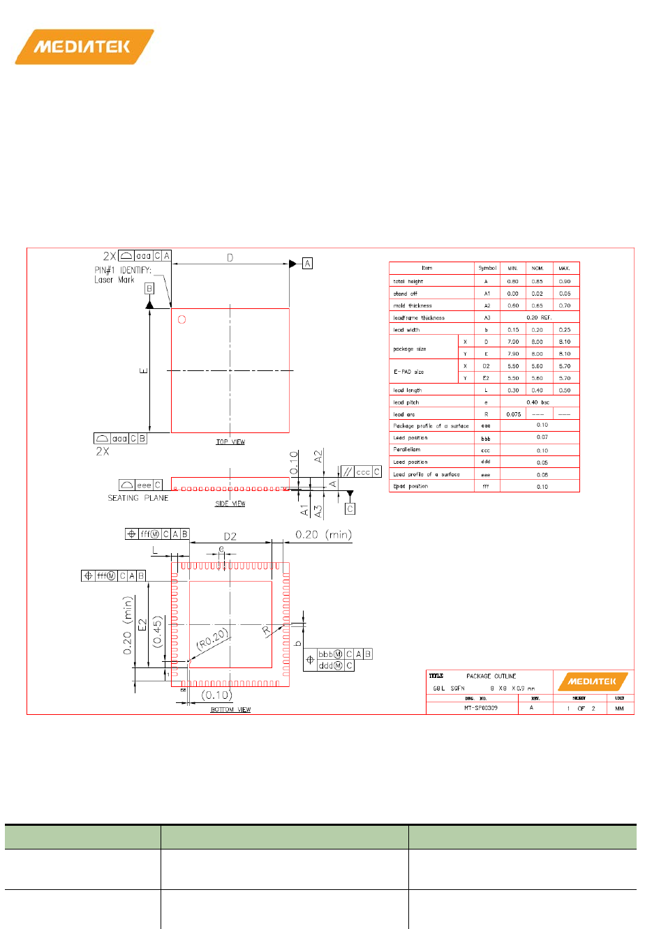
MT76x7
Internet-of-Things Wireless Connectivity
Reference Manual
© 2015 - 2017 MediaTek Inc
Page 797 of 798
This document contains information that is proprietary to MediaTek Inc. (“MediaTek”) and/or its licensor(s).
Any unauthorized use, reproduction or disclosure of this document in whole or in part is strictly prohibited
Pins 10, 11, 12, 52, 53, and 55 are is used for bootstrap. The system design should follow the following
guideline:
• Those pins shall not be used as input functions because the signals from another device might affect
the values sensed.
5.5. Package information
Figure 5-1. Package Outline Drawing
5.6. Ordering information
Table 5-8. Ordering Information
Part number Package Operational temperature range
MT7687FN MT7697N
MT7697DN
8mm x 8mm x 0.8 mm QFN68 0~70°C
MT7687FIN MT7697IN
MT7697DIN
8mm x 8mm x 0.8 mm QFN68 -40~85°C

MT76x7
Internet-of-Things Wireless Connectivity
Reference Manual
© 2015 - 2017 MediaTek Inc
Page 798 of 798
This document contains information that is proprietary to MediaTek Inc. (“MediaTek”) and/or its licensor(s).
Any unauthorized use, reproduction or disclosure of this document in whole or in part is strictly prohibited
5.7. Top marking
MEDIATEK
ARM
MT7697DN
DDDD-####
BBBBBBB
FFFFFFFF
MT7697DN: Part number
DDDD : Date code
#### : Internal control code
BBBBBBB : Main die lot number
FFFFFFF : Flash die lot number
MEDIATEK
ARM
MT7697N
DDDD-####
BBBBBBB
FFFFFFFF
MT7697N: Part number
DDDD : Date code
#### : Internal control code
BBBBBBB : Main die lot number
FFFFFFF : Flash die lot number
MEDIATEK
ARM
MT7687FN
DDDD-####
BBBBBBB
FFFFFFFF
MT7687FN: Part number
DDDD : Date code
#### : Internal control code
BBBBBBB : Main die lot number
FFFFFFF : Flash die lot number
Figure 5-2. Top marking