68007024097_DSMFrntcover MTR3000 Detailed Service Manual 68007024097 A
User Manual: MTR3000 Detailed service manual 68007024097-A
Open the PDF directly: View PDF ![]() .
.
Page Count: 329 [warning: Documents this large are best viewed by clicking the View PDF Link!]
- Front Cover.pdf
- 68007024097_a.pdf
- Foreword
- General Safety and Installation Standards and Guidelines
- Environmental Information
- Document History
- Table of Contents
- Foreword i
- General Safety and Installation Standards and Guidelines ii
- Environmental Information v
- Commercial Warranty xix
- Appendix A EMEA Warranty, Service and Technical Support A-1
- Appendix B LACR Replacement Parts Ordering and Motorola Service Centers B-1
- Appendix C NAG Replacement Parts Ordering and Motorola Service Centers C-1
- Glossary of Terms and Acronyms Glossary-1
- List of Figures
- List of Tables
- Summary of Printed Circuit Boards and Bands
- Commercial Warranty
- Chapter 1 MTR3000 Base Station/Repeater
- Chapter 2 Maintenance
- Chapter 3 MTR3000 Power Amplifier
- 3.1 Overview
- 3.2 Theory of Operation
- 3.3 Troubleshooting
- 3.4 Power Amplifier (PA) Schematics (UHF)
- 3.5 Power Amplifier (PA) PCB (UHF)
- 3.6 Power Amplifier Parts List (UHF) – CLE1333
- 3.7 Power Amplifier Parts List (UHF) – CLE1334
- 3.8 Power Amplifier Parts List (UHF) – CLE6215
- 3.9 Power Amplifier Parts List (UHF) – CLE6216
- 3.10 Power Amplifier Parts List (UHF) – CLE6217
- 3.11 Power Amplifier Parts List (UHF) – CLE6218
- 3.12 Power Amplifier Parts List (UHF) – CLE6219
- 3.13 Power Amplifier Parts List (UHF) – CLN8504
- Chapter 4 MTR3000 Station Control Module
- 4.1 Overview
- 4.2 Theory of Operation
- 4.2.1 Tx/Rx OMAP
- 4.2.2 Serial Peripheral Interface (SPI)
- 4.2.3 Station Reference
- 4.2.4 MAKO
- 4.2.5 Field Programmable Gate Array (FPGA)
- 4.2.6 Audio
- 4.2.7 Ethernet Interface
- 4.2.8 Backplane
- 4.2.9 Exciter
- 4.2.10 Receiver
- 4.2.11 Front Panel (FP) Connectors and Switch
- 4.2.12 Front Panel LEDs
- 4.2.13 Supply Voltage Circuitry
- 4.3 Troubleshooting
- 4.4 Controller Schematics (UHF)
- 4.5 Controller PCB (UHF)
- 4.6 Controller Parts List (UHF)
- Chapter 5 MTR3000 Power Supply
- Chapter 6 MTR3000 Receiver Module
- Chapter 7 MTR3000 Exciter Module
- Appendix A EMEA Warranty, Service and Technical Support
- Appendix B LACR Replacement Parts Ordering and Motorola Service Centers
- Appendix C NAG Replacement Parts Ordering and Motorola Service Centers
- Glossary of Terms and Acronyms
- Back Cover.pdf

i
Foreword
This manual covers all models of the MTR3000 Base Station/Repeater, unless otherwise specified. This manual provides
sufficient information to enable qualified service technicians to troubleshoot and repair the MTR3000 Base Station/
Repeater to the component level (for the selective FRUs). For details on radio operation or basic troubleshooting, refer to
the applicable manuals available separately.
General Safety Precautions
See “General Safety and Installation Standards and Guidelines,” on page ii
Computer Software Copyrights
The Motorola products described in this manual may include copyrighted Motorola computer programs stored in
semiconductor memories or other media. Laws in the United States and other countries preserve for Motorola certain
exclusive rights for copyrighted computer programs, including, but not limited to, the exclusive right to copy or reproduce
in any form the copyrighted computer program. Accordingly, any copyrighted Motorola computer programs contained in
the Motorola products described in this manual may not be copied, reproduced, modified, reverse-engineered, or
distributed in any manner without the express written permission of Motorola. Furthermore, the purchase of Motorola
products shall not be deemed to grant either directly or by implication, estoppel, or otherwise, any license under the
copyrights, patents or patent applications of Motorola, except for the normal non-exclusive license to use that arises by
operation of law in the sale of a product.
Document Copyrights
No duplication or distribution of this document or any portion thereof shall take place without the express written
permission of Motorola. No part of this manual may be reproduced, distributed, or transmitted in any form or by any
means, electronic or mechanical, for any purpose without the express written permission of Motorola.
Disclaimer
The information in this document is carefully examined, and is believed to be entirely reliable. However, no responsibility is
assumed for inaccuracies. Furthermore, Motorola reserves the right to make changes to any products herein to improve
readability, function, or design. Motorola does not assume any liability arising out of the applications or use of any product
or circuit described herein; nor does it cover any license under its patent rights nor the rights of others.
Trademarks
MOTOROLA and the Stylized M logo are registered in the U.S. Patent & Trademark Office. All other product or service
names are the property of their respective owners.
© 2010 by Motorola, Inc.
All rights reserved.
These servicing instructions are for use by qualified personnel only. To
reduce the risk of electric shock, do not perform any servicing other than
that contained in the Operating Instructions unless you are qualified to do
so. Refer all servicing to qualified service personnel.

General Safety and Installation
Standards and Guidelines
ATTENTION!
Compliance with FCC guidelines for human exposure to Electromagnetic
Energy (EME) at Transmitter Antenna sites generally requires that
Personnel working at a site shall be aware of the potential for exposure to
EME and can exercise control of exposure by appropriate means, such as
adhering to warning sign instructions, using standard operating
procedures (work practices), wearing personal protective equipment, or
limiting the duration of exposure. For more details and specific guidelines,
see Appendix A of the R56 Standards and Guidelines for Communications
Sites (6881089E50) manual.
Observe the following general safety precautions during all phases of operation, service
and repair of the equipment described in this manual. Follow the safety precautions listed
below and all other warnings and cautions necessary for the safe operation of all
equipment. Refer to the appropriate section of the product service manual for additional
pertinent safety information. Because of the danger of introducing additional hazards, do
not install substitute parts or perform any unauthorized modifications of equipment.
The installation process requires preparation and knowledge of the site before installation
begins. Review installation procedures and precautions in the Motorola R56 manual
Standards and Guidelines for Communications Sites (6881089E50) before performing any
site or component installation.
Always follow all applicable safety procedures, such as Occupational Safety and Health
Administration (OSHA) requirements, National Electrical Code (NEC) requirements, local
code requirements, safe working practices, and good judgment must be used by personnel.
General safety precautions include the following:
• Read and follow all warning notices and instructions marked on the product or
included in this manual before installing, servicing, or operating the equipment.
Retain these safety instructions for future reference.
• If troubleshooting the equipment while power is on, be aware of the live circuits.
• Do not operate the radio transmitters unless all RF connectors are secure and all
connectors are properly terminated.
• All equipment must be properly grounded in accordance with the Motorola R56
manual Standards and Guidelines for Communications Sites (6881089E50) and
specified installation instructions for safe operation.
• Slots and openings in the cabinet are provided for ventilation. Do not block or
cover openings that protect the devices from overheating.
• Only a qualified technician familiar with similar electronic equipment should
service equipment.
• Some equipment components can become extremely hot during operation. Turn
off all power to the equipment and wait until sufficiently cool before touching.
• Maintain emergency first aid kits at the site.
• Have personnel call in with their travel routes to help ensure their safety while
traveling between remote sites.
• Institute a communications routine during certain higher risk procedures where
the on-site technician continually updates management or safety personnel of the
progress so that help can be dispatched if needed.
• Never store combustible materials in or near equipment racks. The combination
of combustible material, heat and electrical energy increases the risk of a fire
safety hazard.
• Equipment shall be installed in a site that meets the requirements of a “restricted
access location,” per UL60950-1, which is defined as follows: “Access can only
be gained by service persons or by users who have been instructed about the
reasons for the restrictions applied to the location and about any precautions that
shall be taken; and access is through the use of a tool or lock and key, or other
means of security, and is controlled by the authority responsible for the location.”
IMPORTANT: All equipment must be serviced by Motorola trained personnel.
Burn hazard. The metal housing of the product
may become extremely hot. Use caution when
working around the equipment. The warning
label for hot surfaces is shown on the right.
RF energy burn hazard. Disconnect power in the cabinet to
prevent injury while disconnecting and connecting antennas.
All Tx and Rx RF cables’ outer shields must be grounded per
Motorola R56 requirements.
DC input voltage shall be no higher than 60VDC. This
maximum voltage shall include consideration of the battery
charging "float voltage" associated with the intended supply
system, regardless of the marked power rating of the
equipment. Failure to follow this guideline may result in
electric shock.
All Tx and Rx RF cables shall be connected to a surge
protection device according to Motorola R56 documents. Do
not connect Tx and Rx RF cables directly to an outside
antenna.
W A R N I N G
W A R N I N G
C a u t i o n
C a u t i o n
C a u t i o n

Notes

Environmental Information v
Environmental Information
Material Content
Disposal of your Electronic and Electric Equipment
Please do not dispose of electronic and electric equipment or electronic and electric accessories with
your household waste. In some countries or regions, collection systems have been set up to handle
waste of electrical and electronic equipment.
In European Union countries, please contact your local equipment supplier representative or service
center for information about the waste collection system in your country.
Disposal Guideline
The following symbol on a Motorola product indicates that the product should not be disposed of with
household waste.
NOTE The Motorola MOTOTRBOTM MTR3000 Base Station/Repeater system and its subsystems
have been created in compliance with the environmental goals of the European Union’s
Restriction of Hazardous Substances (RoHS) and the Waste Electrical and Electronic
Equipment (WEEE) Directive 2002/96/EC as well as Motorola’s corporate goals to
minimize environmental impact of its products.
This Motorola policy is reflected throughout the entire design, procurement, assembly, and
packaging process.
In support of these efforts to provide environmentally-responsible products, please comply
with the information in the following sections regarding product disposal for systems being
replaced.

Notes
vi Environmental Information

vii
Document History
The following major changes have been implemented in this manual since the previous edition:
Edition Description Date
68007024097-A Initial Release January 2010

viii
Notes

Table of Contents ix
Table of Contents
Foreword..........................................................................................................i
General Safety Precautions..........................................................................................................................i
Computer Software Copyrights ....................................................................................................................i
Document Copyrights...................................................................................................................................i
Disclaimer.....................................................................................................................................................i
Trademarks ..................................................................................................................................................i
General Safety and Installation Standards and Guidelines .......................ii
Environmental Information............................................................................v
Material Content ..........................................................................................................................................v
Disposal of your Electronic and Electric Equipment....................................................................................v
Disposal Guideline.......................................................................................................................................v
Document History ....................................................................................... vii
Commercial Warranty .................................................................................xix
Chapter 1 MTR3000 Base Station/Repeater ...................................... 1-1
1.1 Notations Used in This Manual ................................................................................................... 1-1
1.2 Description .................................................................................................................................. 1-1
1.2.1 Operating Features ..................................................................................................... 1-4
1.2.2 Features not offered .................................................................................................... 1-5
1.2.3 Frequency Ranges and Power Levels ........................................................................ 1-5
1.3 Specifications .............................................................................................................................. 1-6
1.4 Theory of Operation .................................................................................................................... 1-8
1.5 Basic Troubleshooting .............................................................................................................. 1-10
Chapter 2 Maintenance ....................................................................... 2-1
2.1 Introduction ................................................................................................................................. 2-1
2.1.1 Routine Maintenance .................................................................................................. 2-1
2.1.2 Preventive Maintenance .............................................................................................. 2-1
2.1.2.1 Inspection...................................................................................................... 2-1
2.1.2.2 Cleaning Procedures .................................................................................... 2-1
2.1.3 Safe Handling of CMOS Devices ................................................................................ 2-2
2.1.4 Repair Procedures and Techniques – General ........................................................... 2-3
2.1.5 Test Equipment ........................................................................................................... 2-6
2.1.6 Service Aids ................................................................................................................ 2-7

xTable of Contents
Chapter 3 MTR3000 Power Amplifier................................................. 3-1
3.1 Overview ..................................................................................................................................... 3-1
3.2 Theory of Operation .................................................................................................................... 3-1
3.2.1 RF Board .....................................................................................................................3-4
3.2.1.1 Driver Amplifier.............................................................................................. 3-5
3.2.1.2 Final Amplifier ............................................................................................... 3-5
3.2.1.3 Module I/Os................................................................................................... 3-5
3.2.2 Isolator ......................................................................................................................... 3-5
3.2.3 Output Board ............................................................................................................... 3-6
3.2.3.1 Harmonic Filter.............................................................................................. 3-6
3.2.3.2 Directional Couplers...................................................................................... 3-6
3.2.3.3 Surge Suppression........................................................................................ 3-6
3.2.3.4 Module I/Os................................................................................................... 3-6
3.2.4 Distribution Board ........................................................................................................3-6
3.2.4.1 SPI ................................................................................................................ 3-7
3.2.4.2 Power Control ............................................................................................... 3-7
3.2.4.3 Metering ........................................................................................................ 3-7
3.2.4.4 Fan Supply .................................................................................................... 3-7
3.2.4.5 Module I/Os................................................................................................... 3-8
3.3 Troubleshooting .......................................................................................................................... 3-9
3.3.1 Application and Removal of Thermal Grease .............................................................. 3-9
3.3.2 Disassembly and Reassembly Procedures ............................................................... 3-10
3.3.2.1 Output Board............................................................................................... 3-10
3.3.2.1.1 Disassembly .............................................................................. 3-10
3.3.2.1.2 Reassembly ............................................................................... 3-10
3.3.2.2 Distribution Board........................................................................................ 3-11
3.3.2.2.1 Disassembly .............................................................................. 3-11
3.3.2.2.2 Reassembly ............................................................................... 3-11
3.3.2.3 RF board ..................................................................................................... 3-12
3.3.2.3.1 Disassembly .............................................................................. 3-12
3.3.2.3.2 Reassembly ............................................................................... 3-13
3.3.2.4 Circulator..................................................................................................... 3-13
3.3.2.4.1 Disassembly .............................................................................. 3-13
3.3.2.4.2 Reassembly ............................................................................... 3-13
3.3.2.5 Load resistor ............................................................................................... 3-14
3.3.2.5.1 Disassembly .............................................................................. 3-14
3.3.2.5.2 Reassembly ............................................................................... 3-14
3.3.3 Troubleshooting Chart ............................................................................................... 3-15
3.3.4 Detailed Troubleshooting ...........................................................................................3-17
3.3.4.1 Setup Instructions ....................................................................................... 3-17
3.3.4.1.1 Main DC Supplies ...................................................................... 3-17
3.3.4.1.2 Sequencing................................................................................ 3-19
3.3.4.2 Troubleshooting Details .............................................................................. 3-20
3.3.4.2.1 Troubleshooting the Fan Switch ................................................ 3-20
3.3.4.2.2 Troubleshooting the Driver Amplifier.......................................... 3-21
3.3.4.2.3 Troubleshooting the Final Amplifier ........................................... 3-22
3.3.4.2.4 Troubleshooting the Output Board............................................. 3-23
3.3.4.2.5 Troubleshooting the Isolator Load ............................................. 3-23
3.3.4.2.6 Troubleshooting the Circulator................................................... 3-23
3.3.4.2.7 Troubleshooting the Power Control Loop .................................. 3-24
3.4 Power Amplifier (PA) Schematics (UHF) .................................................................................. 3-25
3.5 Power Amplifier (PA) PCB (UHF) ............................................................................................. 3-40
3.6 Power Amplifier Parts List (UHF) – CLE1333 ........................................................................... 3-48

Table of Contents xi
3.7 Power Amplifier Parts List (UHF) – CLE1334 ........................................................................... 3-49
3.8 Power Amplifier Parts List (UHF) – CLE6215 ........................................................................... 3-50
3.9 Power Amplifier Parts List (UHF) – CLE6216 ........................................................................... 3-55
3.10 Power Amplifier Parts List (UHF) – CLE6217 ........................................................................... 3-60
3.11 Power Amplifier Parts List (UHF) – CLE6218 ........................................................................... 3-61
3.12 Power Amplifier Parts List (UHF) – CLE6219 ........................................................................... 3-62
3.13 Power Amplifier Parts List (UHF) – CLN8504 ........................................................................... 3-66
Chapter 4 MTR3000 Station Control Module..................................... 4-1
4.1 Overview ..................................................................................................................................... 4-1
4.2 Theory of Operation .................................................................................................................... 4-1
4.2.1 Tx/Rx OMAP ............................................................................................................... 4-2
4.2.1.1 External Memory........................................................................................... 4-2
4.2.2 Serial Peripheral Interface (SPI) .................................................................................. 4-3
4.2.3 Station Reference ........................................................................................................ 4-7
4.2.3.2 MTR3000 Controller Clocks.......................................................................... 4-8
4.2.4 MAKO .......................................................................................................................... 4-9
4.2.5 Field Programmable Gate Array (FPGA) .................................................................. 4-11
4.2.6 Audio ......................................................................................................................... 4-13
4.2.7 Ethernet Interface ...................................................................................................... 4-14
4.2.7.3 LAN9500i Power-up Configuration ............................................................. 4-15
4.2.8 Backplane .................................................................................................................. 4-16
4.2.9 Exciter ....................................................................................................................... 4-16
4.2.10 Receiver .................................................................................................................... 4-17
4.2.11 Front Panel (FP) Connectors and Switch .................................................................. 4-18
4.2.12 Front Panel LEDs ...................................................................................................... 4-22
4.2.13 Supply Voltage Circuitry ............................................................................................ 4-22
4.3 Troubleshooting ........................................................................................................................ 4-23
4.3.14 Disassembly and Reassembly Procedures ............................................................... 4-23
4.3.15 Troubleshooting Chart ............................................................................................... 4-24
4.3.16 Calibration Procedure ................................................................................................ 4-33
4.4 Controller Schematics (UHF) .................................................................................................... 4-34
4.5 Controller PCB (UHF) ............................................................................................................... 4-51
4.6 Controller Parts List (UHF) ....................................................................................................... 4-53
Chapter 5 MTR3000 Power Supply..................................................... 5-1
5.1 Overview ..................................................................................................................................... 5-1
5.2 Troubleshooting .......................................................................................................................... 5-1
5.2.1 Basic Voltage Check Procedure .................................................................................. 5-1
Chapter 6 MTR3000 Receiver Module................................................ 6-1
6.1 Overview ..................................................................................................................................... 6-1
6.2 Receiver Schematics (UHF) ....................................................................................................... 6-3
6.3 Receiver PCB (UHF) ................................................................................................................ 6-47
6.4 Receiver Parts List (UHF) – CRE4007 ..................................................................................... 6-49
6.5 Receiver Parts List (UHF) – CRE4008 ..................................................................................... 6-62

xii Table of Contents
Chapter 7 MTR3000 Exciter Module................................................... 7-1
7.1 Overview ..................................................................................................................................... 7-1
7.2 Exciter Schematics (UHF) ...........................................................................................................7-3
7.3 Exciter PCB (UHF) ....................................................................................................................7-29
7.4 Exciter Parts List (UHF) – CTE4003 ......................................................................................... 7-31
7.5 Exciter Parts List (UHF) – CTE4004 ......................................................................................... 7-37
Appendix A EMEA Warranty, Service and Technical Support.............A-1
Appendix B LACR Replacement Parts Ordering and Motorola Service
Centers ..............................................................................................B-1
Limited Warranty......................................................................................................................................B-1
MOTOROLA COMMUNICATION PRODUCTS ...........................................................................B-1
I. What This Warranty Covers And For How Long ..................................................................B-1
II. General Provisions ..............................................................................................................B-2
III. How To Get Warranty Service............................................................................................B-2
IV. What This Warranty Does Not Cover.................................................................................B-2
V. Governing Law....................................................................................................................B-3
Appendix C NAG Replacement Parts Ordering and Motorola Service
Centers ..............................................................................................C-1
Limited Warranty..................................................................................................................................... C-1
MOTOROLA COMMUNICATION PRODUCTS .......................................................................... C-1
I. What This Warranty Covers And For How Long ................................................................. C-1
II. General Provisions ............................................................................................................. C-2
III. How To Get Warranty Service........................................................................................... C-2
IV. What This Warranty Does Not Cover................................................................................ C-2
V. Governing Law................................................................................................................... C-3
Glossary of Terms and Acronyms...............................................Glossary-1

List of Figures xiii
List of Figures
Figure 1-1 Front view (with front bezel) of MTR3000 Base Station/Repeater .................................. 1-2
Figure 1-2 Front view (without front bezel) of MTR3000 Base Station/Repeater ............................. 1-3
Figure 1-3 Rear view of MTR3000 Base Station/Repeater .............................................................. 1-3
Figure 1-4 RDAC’s Diagnostic Screen ........................................................................................... 1-10
Figure 3-1 PA sub-modules .............................................................................................................. 3-1
Figure 3-2 PA Functional Block Diagram.......................................................................................... 3-3
Figure 3-3 PA DC Power Structure................................................................................................... 3-4
Figure 3-4 PA Signal Connectors ..................................................................................................... 3-9
Figure 3-5 Areas to apply thermal grease on the PA metal casting ............................................... 3-10
Figure 3-6 Sequence to tighten back screws on the output board ................................................. 3-11
Figure 3-7 Sequence to tighten back screws on the distribution board .......................................... 3-12
Figure 3-8 Sequence to tighten back screws on the RF board....................................................... 3-13
Figure 3-9 Fan Troubleshooting Flow Chart (PA)........................................................................... 3-15
Figure 3-10 Power Troubleshooting Flow Chart (PA)....................................................................... 3-16
Figure 4-1 MTR3000 Controller Block Diagram................................................................................ 4-2
Figure 4-2 MTR3000 Controller SPI connection............................................................................... 4-5
Figure 4-3 MTR3000 Controller Clock Configuration........................................................................ 4-9
Figure 4-4 MAKO Block Diagram and usage of MTR3000 Controller ............................................ 4-10
Figure 4-5 MTR3000 Controller FPGA Block Diagram................................................................... 4-12
Figure 4-6 Station Control Module (SCM) Audio Path.................................................................... 4-13
Figure 4-7 MTR3000 Controller Ethernet Connection .................................................................... 4-15
Figure 4-8 USB connector pin-out .................................................................................................. 4-19
Figure 4-9 MTR3000 power up block diagram ............................................................................... 4-22
Figure 4-10 Controller Troubleshooting Flow Chart.......................................................................... 4-24
Figure 4-11 Power Troubleshooting Flow Chart (Controller) ............................................................ 4-25
Figure 4-12 Clock and Reset Troubleshooting Flow Chart (Controller)............................................ 4-26
Figure 4-13 Ethernet Troubleshooting Flow Chart (Controller)......................................................... 4-27
Figure 4-14 Transmit Path Troubleshooting Flow Chart (Controller)................................................ 4-28
Figure 4-15 Receive Path Troubleshooting Flow Chart (Controller)................................................. 4-29
Figure 4-16 Audio Troubleshooting Flow Chart (Sheet 1 of 2) ......................................................... 4-30
Figure 4-17 Audio Troubleshooting Flow Chart (Sheet 2 of 2) ......................................................... 4-31
Figure 5-1 Measuring 14.2 VDC and 5.1 VDC (other voltmeter probe to chassis)........................... 5-1
Figure 5-2 Pin-out of connector (measuring 14.2 VDC and 5.1 VDC).............................................. 5-2
Figure 5-3 Measuring 14.2 VDC and 28.6 VDC (other voltmeter probe to chassis)......................... 5-2
Figure 5-4 Pin-out of connector (measuring 14.2 VDC and 28.6 VDC)............................................ 5-2

xiv List of Figures
Notes

List of Tables xv
List of Tables
Table 1-1 MTR3000 Frequency Ranges and Power Levels............................................................ 1-5
Table 1-2 MTR2000 MOTOTRBO Digital Upgrade Frequency Ranges and Power Levels ............ 1-5
Table 1-3 MTR3000 Base Station/Repeater General Specifications (All Bands)............................ 1-6
Table 1-4 MTR3000 Base Station/Repeater Specifications ............................................................ 1-6
Table 1-5 Front Panel LED indicators ........................................................................................... 1-11
Table 1-6 MTR3000 Software and Hardware Controlled LEDs..................................................... 1-12
Table 1-7 MTR3000 Alarm Diagnosis Table ................................................................................. 1-13
Table 2-1 Lead Free Solder Wire Part Number List ........................................................................ 2-4
Table 2-2 Lead Free Solder Paste Part Number List ...................................................................... 2-4
Table 2-3 Recommended Test Equipment...................................................................................... 2-6
Table 2-4 Service Aids .................................................................................................................... 2-7
Table 3-1 PA Supply Connector (J6001)......................................................................................... 3-8
Table 3-2 PA Signal Connector (J6000).......................................................................................... 3-8
Table 4-1 SPI decoding truth table .................................................................................................. 4-3
Table 4-2 Tx/Rx OMAP SPI Module and Device Parameters ......................................................... 4-6
Table 4-3 SCM FCC Frequency Stability Requirement................................................................... 4-8
Table 4-4 SCM FPGA output Frequencies...................................................................................... 4-8
Table 4-5 MAKO General Purpose ADC Allocation ...................................................................... 4-11
Table 4-6 SCM Audio Level........................................................................................................... 4-14
Table 4-7 SMSC LAN9500i Default Configuration after Power-up................................................ 4-15
Table 4-8 MTR3000 Controller Exciter Connector connection ...................................................... 4-16
Table 4-9 MTR3000 Controller Receiver Connector connection................................................... 4-17
Table 4-10 SCM FP Connectors .....................................................................................................4-18
Table 4-11 SCM FP USB Connector Pin-out .................................................................................. 4-19
Table 4-12 SCM FP Microphone Connector Pin-out ....................................................................... 4-19
Table 4-13 SCM FP Speaker Connector Pin-out ............................................................................ 4-20
Table 4-14 SCM FP Ethernet Connector Pin-out ............................................................................ 4-20
Table 4-15 SCM FP External Reference Connector Pin-out ........................................................... 4-21

xvi List of Tables
Related Publications
MOTOTRBOTM MTR3000 Base Station/Repeater Installation and User Manual ................. 68007024098
MOTOTRBOTM MTR3000 Base Station/Repeater Basic Service Manual............................ 68007024096
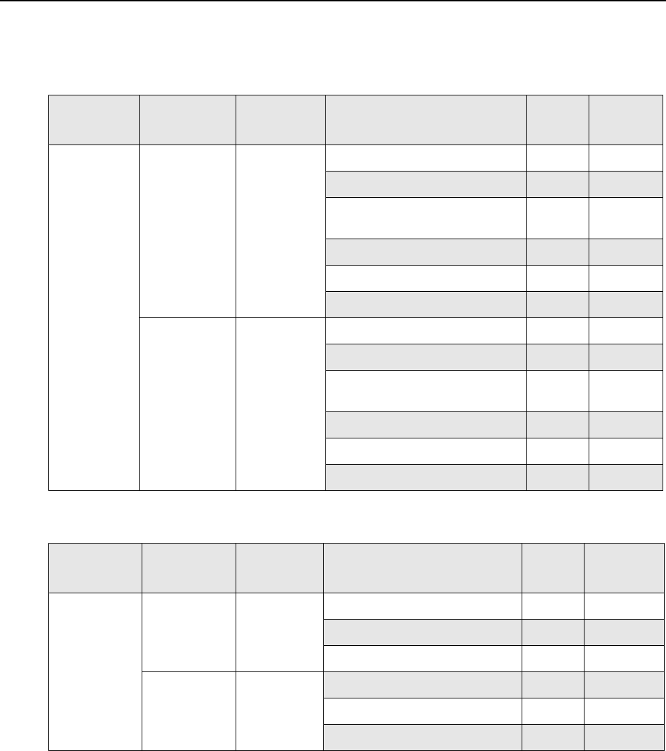
Summary of Printed Circuit Boards and Bands xvii
Summary of Printed Circuit Boards and Bands
Table below lists the band available in this manual.
The following table lists the MTR2000 MOTOTRBO Digital Upgrade bands that are available.
Frequency
Band Bandwidth Power
Level PCB Part No. Board
Rev. Chapter
UHF 403–470 MHz 8 W–100 W 84009277001 (RF Board) A 3
84009274001 (Output Board) A 3
84009279002 (Distribution
Board)
B3
8475374H02 (Controller Board) B 4
84009273002 (Receiver Board) B 6
84009272002 (Exciter Board) B 7
470–524 MHz 8 W–100 W 84009296001 (RF Board) A 3
84009274001 (Output Board) A 3
84009279002 (Distribution
Board)
B3
8475374H02 (Controller Board) B 4
84009273002 (Receiver Board) B 6
84009272002 (Exciter Board) B 7
Frequency
Band Bandwidth Power
Level PCB Part No. Board
Rev. Chapter
UHF 403–435 MHz 25 W–100 W 8475374H02 (Controller Board) B 4
84009273002 (Receiver Board) B 6
84009272002 (Exciter Board) B 7
435–470 MHz 25 W–100 W 8475374H02 (Controller Board) B 4
84009273002 (Receiver Board) B 6
84009272002 (Exciter Board) B 7

xviii
Notes

Commercial Warranty xix
Commercial Warranty
For details on the regional Motorola Service Centers, Replacement Parts Ordering and Technical Support
assistance, refer to the relevant regions in the Appendix section of this manual.

Notes
xx Commercial Warranty
1-1
Chapter 1 MTR3000 Base Station/Repeater
1.1 Notations Used in This Manual
Throughout the text in this publication, you will notice the use of note and caution notations. These
notations are used to emphasize that safety hazards exist, and due care must be taken and
observed.
1.2 Description
The Motorola MTR3000 Base Station/Repeater (BR) provides a modular, flexible analog and digital
station design for today's communication systems and for the future. The station is available for use
in these configurations:
• Analog Conventional
• Digital Conventional (MOTOTRBO)
- MOTOTRBO DMR Tier 2 Conventional – Single Site
- MOTOTRBO DMR Tier 2 Conventional – IP Site Connect
- MOTOTRBO Capacity Plus Trunking
- MOTOTRBO Connect Plus Trunking
•LTR Trunking
• Passport Trunking
Note An operational procedure, practice, or condition that is important.
CAUTION indicates a potentially hazardous situation which, if
not avoided, might result in equipment damage.
WARNING indicates a potentially hazardous situation which,
if not avoided, could result in death or injury.
C a u t i o n
W A R N I N G

1-2 Description
The base station/repeater can either be configured as a stand-alone base station/repeater or as a
base station/repeater connected to a back-end network, as in the case of operating in IP Site
Connect mode. As a base station/repeater, it listens on one uplink frequency, and then re-transmits
on a downlink frequency, thus providing the RF interface to the field subscribers. When configured
for analog station operation, the base station/repeater is designed to operate with most existing
analog systems, which enables a smooth migration to the MOTOTRBO system.
When configured for digital operation, the base station/repeater offers additional services. The digital
base station/repeater operates in TDMA mode, which essentially divides one channel into two virtual
channels using time slots; therefore the user capacity is doubled. The base station/repeater utilizes
embedded signaling to inform the field radios of the busy/idle status of each channel (time slot), the
type of traffic, and even the source and destination information.
The MTR3000 base station/repeater is divided into functional modules that separate the frequency
band specific and transmitter power specific circuits from other circuits and has separate modules for
the control interface. These modules are self contained functional blocks with module-specific
alarms. This design facilitates the field replaceable unit (FRU) concept of field repair to maximize
system uptime.
The FRU architecture also allows another important feature, which is the upgrading of an existing
MTR2000 base station/repeater to support MOTOTRBO functionality. With MTR2000 MOTOTRBO
Digital Upgrade kit, a current user of the MTR2000 base station/repeater can upgrade their base
station/repeater to support all MOTOTRBO digital functionality as that of a factory produced
MTR3000.
Currently, the MTR2000 MOTOTRBO Digital Upgrade is limited to the high power (100 W) UHF.
Additionally, once the upgrade is performed, the wireline and Auxiliary I/O board functionality will no
longer be supported.
A MTR2000 MOTOTRBO Digital Upgrade comprises the following:
• New Exciter Module
• New Receiver Module
• New Station Control Module
• New Front Bezel
Refer to Figure 1-1 for the front view (with front bezel) and Figure 1-2 for the front view (without front
bezel) of MTR3000 base station/repeater. Figure 1-3 shows the rear view portion of the base station/
repeater.
Note When configured in Digital Mode, the base station/repeater can only be used as a repeater.
Note At any given time, the base station/repeater either operates as a digital repeater or as an
analog repeater.
Description 1-3
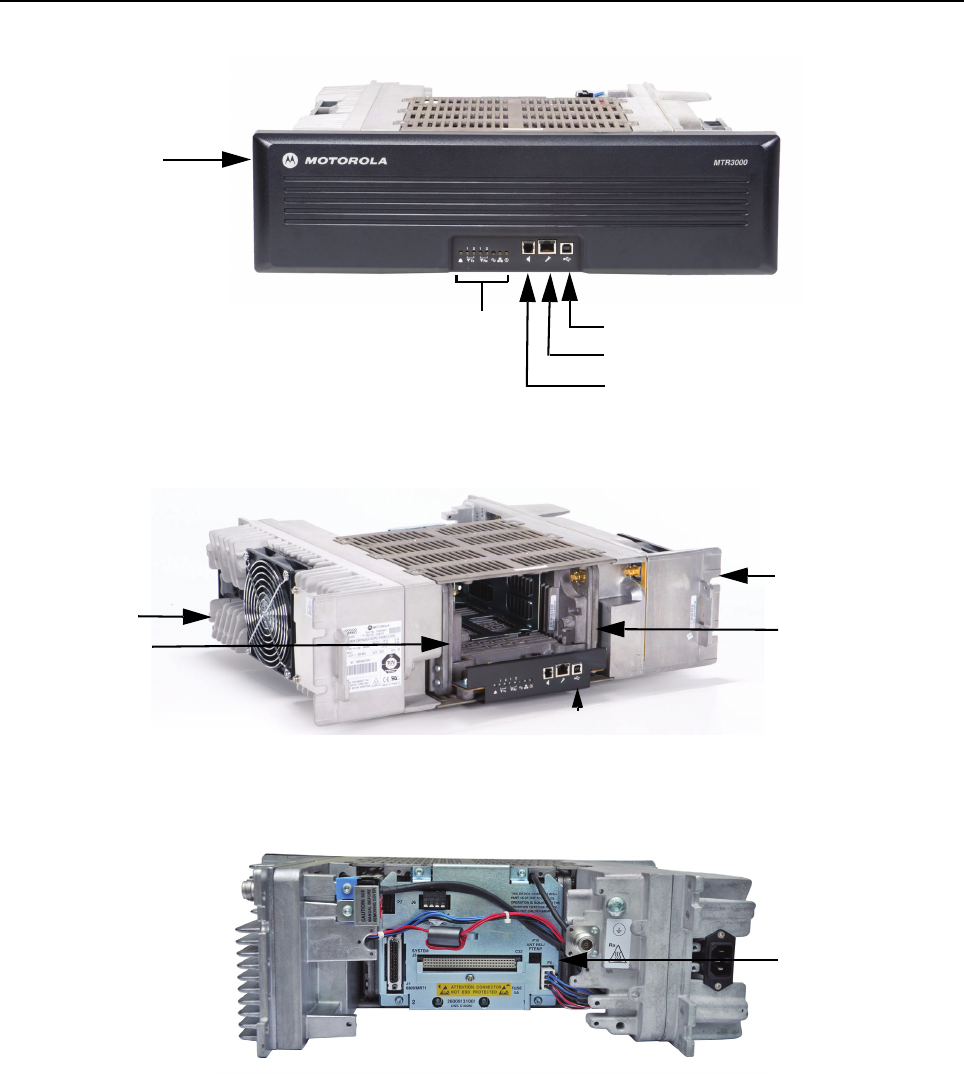
Figure 1-1 Front view (with front bezel) of MTR3000 Base Station/Repeater
Figure 1-2 Front view (without front bezel) of MTR3000 Base Station/Repeater
Figure 1-3 Rear view of MTR3000 Base Station/Repeater
The MTR3000 model ships preconfigured for analog conventional operation. Additional
configurations can be selected and created through the Customer Programming Software (CPS) on
a per-channel basis, based on the modulation type selected during station configuration.
Front Bezel
Front Panel LED Indicators
Speaker Port
Microphone Port
USB Port
Power Supply
Module
Power Amplifier
Module
Station Control Module
Exciter Module Receiver Module
Backplane

1-4 Description
1.2.1 Operating Features
The following are the standard features of a MTR3000 model:
• MOTOTRBO Conventional Operation (2-Slot TDMA, 4FSK Modulation)
• Analog Conventional Operation (FM)
• Continuous Duty Cycle Operation over -30°C to +60°C
• Meets or exceeds these TIA603D, ETSI 086, ETSI 113 requirements
- TIA603D
-ETSI 086
-ETSI 113
- ETSI TS 102 361-1 Part 1: DMR Air Interface Protocol
- ETSI TS 102 361-2 Part 2: DMR Voice and Generic Services and Facilities
- ETSI TS 102 361-3 Part 3: DMR Packet Data Protocol
• Synthesized Frequency Generation
• Two Female N-type Antenna Connectors (Rx and Tx)
• Ethernet Port (Network)
• Front mounted USB Port (Service)
• Front mounted microphone port
• Front mounted speaker port
• 9 configurable GPIO/GPI ports
• Power for third party controllers (1 Amp)
• 1.5 PPM Frequency Stability (Temperature AND 1-Year Aging)
• External Reference Capability
• Switching Power Supply operates from 85–264 VAC (47–63 Hz)
• Multi-Power Source configurable (AC, DC, or AC with Battery Revert)
• Station Diagnostic
• Physical Dimensions: 5.25" H x 19" W x 16.5" D (133 x 483 x 419 mm) 3RU
• Weight: 40 pounds (19 kg) excluding cabinet or other peripheral equipment
Motorola Network Interface for
• IP Site Connect
• Repeater Diagnostics and Control (RDAC)
Third Party Controller Interface:
• Phone Patch
• Multi Coded Squelch Interface (Repeater Panel)
• Tone Remote Adapter
• LTR Trunking
• Passport Trunking
Optionally, the MTR3000 station may be configured with
Note The MTR3000 base station/repeater only supports the third party controllers noted above
when it is configured in analog mode.

Description 1-5
• External Pre-selector
• Antenna Relay
• Duplexer
• External Dual Circulator Tray
In addition, the following features are also included. These features are shipped in a preset
condition, but may be altered through the use of the CPS.
• 16 Tx/Rx Frequencies – Factory Programmed with 1 Tx, 1 Rx
• 12.5 kHz or 25 kHz Operation – Factory Programmed to 12.5 kHz
• 6.25e compliant
• 1 Tx and 1 Rx (PL or DPL) Squelch Code per channel – Factory Programmed to CSQ
• Base Station Identification (BSI) – Factory Programmed as BLANK
• Push-To-Talk Priority – Factory Programmed to Repeat Path
1.2.2 Features not offered
Please disregard any references to the following items, as they are not available for the MTR3000
first release (T3000A).
• Wireline Interface Board
• Auxiliary I/O Option Board
• Peripheral temperature sensing device
• Voting or standalone Receiver
• RSSI Output (via RDAC only)
• Simplex operation (Tx=Rx)
• Integrated Tone Remote Control.
1.2.3 Frequency Ranges and Power Levels
The MTR3000 Base Station/Repeater and MTR2000 MOTOTRBO Digital Upgrade is available in the
following frequency ranges and power levels as specified in Table 1-1 and Table 1-2.
Table 1-1 MTR3000 Frequency Ranges and Power Levels
Frequency
Band Bandwidth Power Level
UHF 403–470 MHz 8–100 W
470–524 MHz 8–100 W
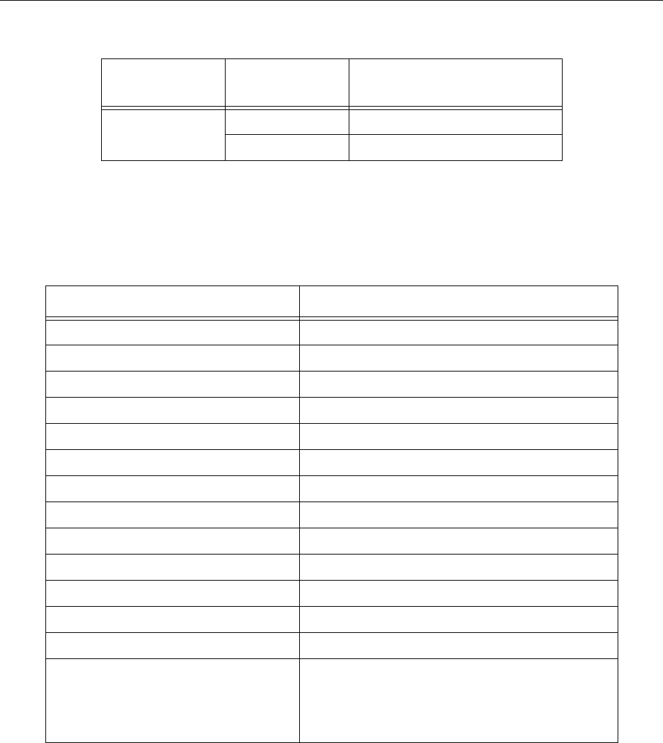
1-6 Specifications
1.3 Specifications
Table 1-3 shows the specifications of the MTR3000 Base Station/Repeater.
Table 1-2 MTR2000 MOTOTRBO Digital Upgrade Frequency Ranges and Power Levels
Frequency
Band Bandwidth Power Level
UHF 403–435 MHz 25–100 W
435–470 MHz 25–100 W
Table 1-3 MTR3000 Base Station/Repeater General Specifications (All Bands)
Parameter Specifications
Number of Channels 16
Frequency Generation Synthesized
Input Voltage AC 85–264 VAC (47–63 Hz)
Input Voltage DC 28.6 VDC (25.7–30.7 VDC full rated output power)
Power Supply Type Switching
Station Weight 40 lbs (19 kg)
Temperature Range -30°C to +60°C (-22°F to +140°F)
Antenna Connectors Tx/Rx N-Type
Modes of Operation Half-Duplex / Duplex
Rack Units 3
Height 5.25” (133 mm)
Width 19” (483 mm)
Depth 16.5” (419 mm)
Industry Canada
• IC certification / registration number
• IC model number
• Tx / Rx Frequency range
109AB-T3000
T3000-UHF R1
406.1–430 MHz, 450–470 MHz

Specifications 1-7
Table 1-4 MTR3000 Base Station/Repeater Specifications
Parameter
Specifications
UHF
Input Power (All Modulations)
100 W Standby (AC Line 117 V / 220 V) 0.4 A / 0.2 A
100 W Transmit at Rated Power
(AC Line 117 V / 220 V)
3.3 A / 1.8 A
100 W Standby (28 VDC) 0.8 A
100 W Transmit at Rated Power (28 VDC) 11.5 A
Frequency Reference
Internal Frequency Stability (PPM) 1.5 PPM
External Reference Capable Yes
Frequency Bands
Electronic Bandwidth 403–470 MHz (UHF R1), 470–524 MHz (UHF R2)
Receiver
Selectivity* 25 kHz / 12.5 kHz 80 dB / 75 dB
Sensitivity‡ (12 dB Sinad) 0.3 uV
Sensitivity‡** (5% BER) 0.3 uV
Sensitivity with External Peripherals (Antenna
Relay and/or Preselector)
0.35 uV
Intermodulation Rejection 25 kHz / 12.5 kHz 85 dB
Spurious Rejection 85 dB (without External Preselector)
Spurious and Image Response Rejection with
Narrow Preselector (Optional)
90 dB
Audio Distortion <3%
FM Hum and Noise 25 kHz / 12.5 kHz 50 dB / 45 dB
FCC Designation ABZ89FR4824 (UHF R1) or
ABZ89FR4826 (UHF R2)
Transmitter
Rated Output Power (Continuous Duty) 8–100 W
Intermodulation Attenuation 55 dB
Adjacent Channel Power 25 kHz / 12.5 kHz 75 dB / 60 dB
Wideband Noise (1 MHz) -152 dBc/Hz
RSD 25 kHz / 12.5 kHz 5 kHz / 2.5 kHz
Spurious Harmonics and Emissions -90 dBc
1-8 Theory of Operation
All specifications noted above are in accordance to TIA603D unless otherwise noted as below.
1.4 Theory of Operation
The MTR3000 Base Station/Repeater (BR) provides the radio frequency (RF) link between the base
station/repeater and the subscriber radios. The base station/repeater acquires inbound signals via its
external receive (Rx) antenna and then amplifies, filters and demodulates the signals into data or
voice packets. From that point, the data is either forwarded to the base station/repeater transmitter to
be re-modulated and amplified for delivery to subscriber radios, and/or the data is delivered via a
wired interface for distribution to networked base station/repeaters, consoles, or other networked
infrastructure.
The MTR3000 base station/repeater consists of a Receiver module, Exciter module, station control
module (SCM), power amplifier (PA) and power supply (PS). These modules are also known as field
replaceable units (FRU).
• The Receiver Module is a dual heterodyne Receiver which receives the RF signal from the
subscriber’s transmitter. It then converts the resulting final intermediate frequency (IF) from
an analog signal to that of a digital word in IQ signal format. Finally, the Receiver delivers the
IQ signal, via the SSI bus, to the SCM for demodulation. Additionally, the Receiver also
provides for its own metering and diagnostics via software, as well as a self-contained
calibration (no field tuning needed for Receiver Module).
• The Exciter Module converts a two-port base band data signal, sent over the SSI bus from
the SCM, to an analog signal representation. The analog signal is then modulated with a low
power RF transmitter carrier that is generated by the Exciter. The low power modulated RF
carrier is then amplified and delivered to the PA at approximately +14 dBm for further
amplification. The Exciter and PA constitute the transmitter of the MTR3000. Additionally, the
Exciter also provides its own metering and diagnostics via software, as well as a self-
contained calibration (no field tuning needed for Exciter Module).
Audio Distortion <3%
FM Hum and Noise 25 kHz / 12.5 kHz 50 dB / 45 dB
FCC Designation ABZ89FC4823 (403–470 MHz) or
ABZ89FC4825 (470–524 MHz)
Note (*) Per TIA603
(**) Per TIA102 Method
(‡) Without Rx peripherals attached
Note To determine the proper amount of air conditioning at a radio site, refer to the “Power
Dissipation” and “BTU Energy” specifications in the MTR3000 Product Planner located in
the link: http://ecat.comm.mot.com/ecat/pricebooks/dup/MTR3000.htm.
Table 1-4 MTR3000 Base Station/Repeater Specifications (Continued)
Parameter
Specifications
UHF

Theory of Operation 1-9
• The heart of the SCM Module is the two Texas Instruments OMAP1710 processors. Each
OMAP processor contains an ARM Host and a C55 DSP processor. One of these OMAP
processor is dedicated to Receiver DSP operations, while the other OMAP provides for all
other operations, including the transmitter functions.
In general, the SCM controls the entire coordination of the base station/repeater functions.
Specifically, the SCM provides for the following functionalities:
- Contains and runs the preloaded base station/repeater software
- Manages inbound and outbound RF and Audio traffic
- Provides external speaker and microphone ports
- Provides an on-board USB port for local configuring, alignment and diagnostics via the
following applications:
- Customer Programming Software (CPS)
- Tuner application
- Repeater Diagnostic and Control (RDAC) software
- Online Help
- Provides an Ethernet port for IP site connectivity and remote RDAC
- Provides GPIO connectivity for third party controller interfaces
- Provides for analog base station/repeater audio connectivity
- Data and Control to the Receiver via the SPI and SSI respectively
- Data and Control to the Exciter via the SPI and SSI respectively
- Control of the PA’s set power via the SPI
- Generates the internal station reference
- Provides control of the front panel status indicators.
• The PA Module amplifies the low level modulated RF signal from the Exciter module. It then
delivers the amplified signal to the transmitter antenna port at a power level within the rated
power band of the base station/repeater, for transmission to the subscriber radios. In addition
to its primary task of amplification, the PA provides the following hardware functions for the
base station/repeater.
- Harmonic attenuation
- Inter-modulation attenuation (IMA) suppression
- VSWR detection
- RF power control (primary means)
- Self contained cooling fan and control circuit
- Meters for diagnostics
- Power rollback for temperature, VSWR, and voltage
- Self-Contained calibration (no field alignment needed for PA Module).
• The PS Module provides DC power to the Receiver, Exciter, SCM and PA Module via one or
more of the three DC output taps; 28.6 VDC, 14.2 VDC, and 5.1 VDC. It can also be used to
provide auxiliary power (14 VDC) to a number of third party controllers. Additionally, it can
operate in three different input modes:
- AC Input Only
- DC Input Only
- AC with Battery Revert.
1-10 Basic Troubleshooting
In addition to providing power to the noted FRU and controllers, the PS also provides the
following:
- AC Failure detect signaling to the SCM
- Output over-current protection for all three outputs
- Self contained cooling fan and control circuit (thermal shut down if the environmental
temperatures exceed the cooling capacity provided by the fan).
• Further details can be found in the individual “Theory of Operation” sections of the respective
FRU chapters in the MOTOTRBOTM MTR3000 Base Station/Repeater Basic Service Manual
(68007024096).
1.5 Basic Troubleshooting
Diagnostic tests are available for the SCM, Exciter, PA, and Receiver Modules. If a problem occurs
during station operation, it is logged as an alarm that is read with the Repeater Diagnostic and
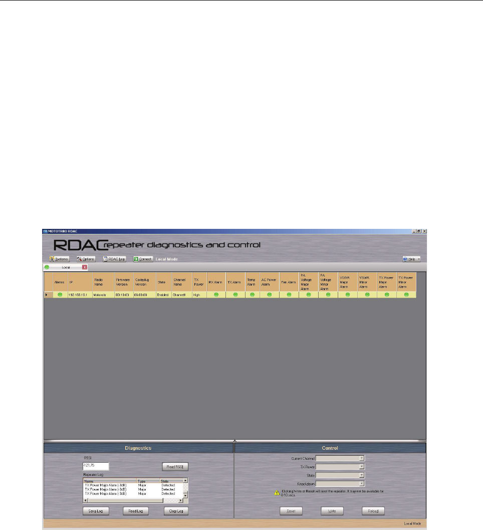
Control application (RDAC). Refer to Figure 1-4 for the RDAC’s diagnostic screen.
Figure 1-4. RDAC’s Diagnostic Screen
The station operator can then evaluate the problem locally or remotely, as the station will maintain an
Alarm Log with the name of the alarm that has failed since the last power up. Via the RDAC
application’s Alarm Log, the alarm messages will aid in identifying the FRU that failed along with the
fault condition.
After booting up the base station/repeater, the 6 LEDs (Power/Status, Tx Slot 1, Tx Slot 2, Rx Slot 1,
Rx Slot 2 and the Mode LEDs) flashes in unison.
Basic Troubleshooting 1-11
The general status and condition of the MTR3000 base station/repeater can be obtained by
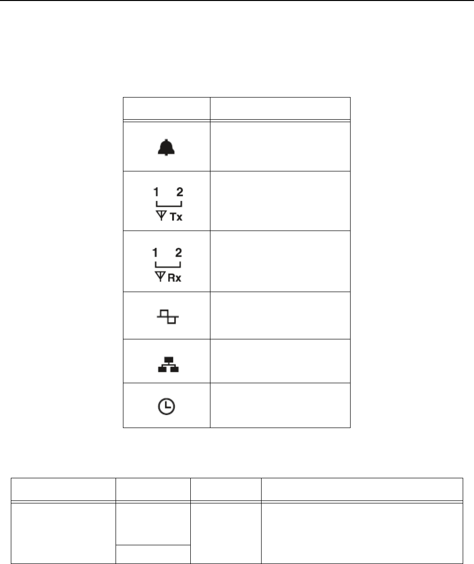
observing the eight LED indicators on the front panel. Table 1-5 shows the LED symbols and their
meaning, while Table 1-6 identifies the information conveyed via the LED indicators. Table 1-7 shows
the alarm diagnosis table and probable diagnosis to aid in identifying the fault.
Table 1-5. Front Panel LED indicators
LED Definition
Status
Tx Slot 1 (for label number 1)
Tx Slot 2 (for label number 2)
Rx Slot 1 (for label number 1)
Rx Slot 2 (for label number 2)
Mode
Ethernet Link
Reference
Table 1-6. MTR3000 Software and Hardware Controlled LEDs
LED Function Name LED Color LED State Status Indication
Power/Status, Tx Slot 1,
Tx Slot 2, Rx Slot 1, Rx
Slot 2
Mode
Amber Flashing Station booting up
Blue
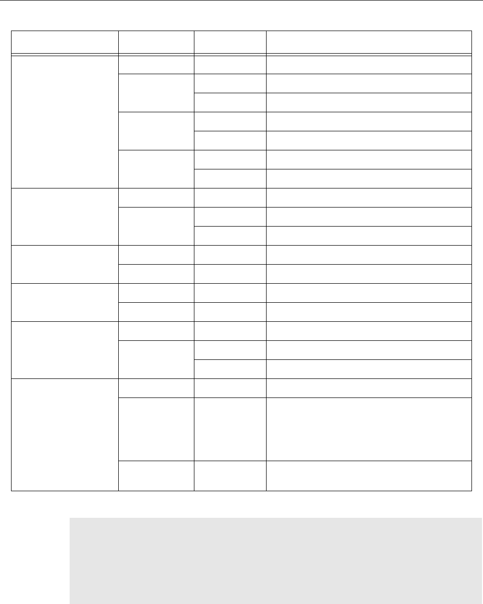
1-12 Basic Troubleshooting
Power/Status Off Off Station Off
Green Flashing Station Operating Normally, with DC power
Solid Station Operating Normally, with AC power
Red Flashing Station Operational – Minor Alarm
Solid Station Not Operational – Major Alarm
Amber Flashing Station in Service Mode
Solid Station is Disabled (Dekeyed)
Tx Slot 1
Tx Slot 2
Off Off Transmitter is not transmitting
Green Solid Transmitter is transmitting
Flashing Transmitter is transmitting, but at reduced power
Rx Slot 1
Rx Slot 2
Off Off Receiver qualifier has not been met
Green Solid Receiver qualifier has been met
Mode Off Off Analog Mode (FM)
Blue Solid Digital Mode (2 Slot TDMA, 4FSK)
Ethernet Link Off Off No Ethernet connection
Green Solid Linked
Flashing Network traffic
Reference Off Off No external reference is present
Green Solid Training process is completed, and the
calibration data has been written to the
EEPROM, or an external reference is present
after training (which the base station/repeater
has phase locked to).
Amber Solid Locked to external reference, and training is in
progress
Note The RDAC application will be needed when the Status LED is red (solid or flashing). This
status indicates a minor or major alarm. The RDAC application is used to identify the
specific alarm and probable diagnosis to aid in identifying the FRU at fault.
If the Reference LED remains amber for more than one minute after the alignment, then
verify the integrity of the source used to train the base station/repeater’s internal reference.
If the integrity of the source is verified to be good, then the SCM will need to be replaced.
Table 1-6. MTR3000 Software and Hardware Controlled LEDs (Continued)
LED Function Name LED Color LED State Status Indication

Basic Troubleshooting 1-13
Table 1-7 MTR3000 Alarm Diagnosis Table
Sub-system Alarm
Name
Alarm
Class
Diag.
View
Diag.
Repeater
Log
Diagnosis Probable Remedy
Receiver Rx Alarm Major Yes Yes The Receiver
PLL has lost
lock.
Local Dealer:
Replace Receiver FRU
Motorola Repair Depot:
Repair or replace the
Receiver FRU
Receiver
EEPROM
Corruption
Type 1
Minor No Yes The Receiver
EEPROM has
incurred non-
recoverable
corruption in a
semi-critical
memory
location.
Local Dealer:
Replace Receiver FRU
Motorola Repair Depot:
Recalibrate the Receiver
FRU
Receiver
EEPROM
Corruption
Type 2
Minor No Yes The Receiver
EEPROM has
incurred a
recoverable
corruption in
critical memory
location or non-
recoverable
corruption in a
non-critical area
of memory.
No action needed. This is
informational only.
Receiver
EEPROM
Corruption
Type 3
Major No Yes The Receiver
EEPROM has
incurred non-
recoverable
corruption in a
critical memory
location.
Local Dealer:
Replace Receiver FRU
Motorola Repair Depot:
Recalibrate the Receiver
FRU

1-14 Basic Troubleshooting
Transmitter Tx Alarm Major Yes Yes The Exciter PLL
has lost lock.
Local Dealer:
Replace Exciter FRU
Motorola Repair Depot:
Repair/recalibrate or
replace the Exciter FRU
Fan Alarm Minor Yes Yes The PA fan has
failed.
Local Dealer:
Replace PA fan
Motorola Repair Depot:
Replace the PA fan
Note: The PA and PS fans
should be replaced in
pairs.
Tx Power
Minor Alarm
Minor Yes No The PA output
power is
between 2 dB to
3 dB below the
set output power,
or the output
power is more
than 3 dB below
the set output
power with one
or more of the
following alarms
already
detected: Fan
Alarm, Temp
Alarm, PA
Voltage Minor
Alarm, PA
Voltage Major
Alarm, VSWR
Minor Alarm or
VSWR Major
Alarm.
When this alarm is
detected, check the
Diagnostic Repeater Log
to determine which failure
– “Tx Power Minor Alarm
(-2 dB)” or “Tx Power
Minor Alarm (-3 dB)” – has
occurred.
Table 1-7 MTR3000 Alarm Diagnosis Table (Continued)
Sub-system Alarm
Name
Alarm
Class
Diag.
View
Diag.
Repeater
Log
Diagnosis Probable Remedy

Basic Troubleshooting 1-15
Transmitter Tx Power
Major Alarm
Major Yes No The PA output
power is more
than 3 dB below
the set output
power.
Local Dealer:
Remedy 1: Verify that the
“Exciter to PA” cable is
properly installed
Remedy 2: If Remedy 1
does not solve this issue,
replace the PA FRU
Motorola Repair Depot:
Remedy 1: Verify that the
“Exciter to PA” cable is
properly installed
Remedy 2: If Remedy 1
does not solve this issue,
repair/recalibrate or
replace the PA FRU
Tx Power
Minor Alarm
(-2 dB)
Minor No Yes
Counterpart
to “Tx Power
Minor Alarm”
The PA output
power is
between 2 dB to
3 dB below the
set output power
of the station.
Local Dealer:
Replace PA FRU
Motorola Repair Depot:
Repair/recalibrate or
replace the PA FRU
Tx Power
Minor Alarm
(-3 dB)
Minor No Yes
Counterpart
to “Tx Power
Minor Alarm”
The PA output
power is more
than 3 dB below
the set output
power of the
station, but at
least one of the
following “
primary” alarms
is also present:
Fan Alarm,
Temp Alarm, PA
Voltage Minor
Alarm, PA
Voltage Major
Alarm, VSWR
Minor Alarm or
VSWR Major
Alarm.
Local Dealer:
Attend to the primary
alarms (see appropriate
remedies at the relevant
alarm sections)
Motorola Repair Depot:
Attend to the primary
alarms (see appropriate
remedies at the relevant
alarm sections)
Table 1-7 MTR3000 Alarm Diagnosis Table (Continued)
Sub-system Alarm
Name
Alarm
Class
Diag.
View
Diag.
Repeater
Log
Diagnosis Probable Remedy

1-16 Basic Troubleshooting
Transmitter Tx Power
Major Alarm
(-3 dB)
Major No Yes
Counterpart
to “Tx Power
Major Alarm”
The PA output
power is more
than 3 dB below
the set output
power.
Motorola Repair Depot:
Remedy 1: Verify that the
“Exciter to PA” cable is
properly installed.
Remedy 2: If Remedy 1
does not solve this issue,
repair/recalibrate or
replace the PA FRU
PA
EEPROM
Corruption
Type 1
Minor No Yes The PA
EEPROM has
incurred non-
recoverable
corruption in a
semi-critical
memory
location.
Note : Alarm is
not applicable to
the MTR2000
MOTOTRBO
Digital Upgrade,
as the MTR2000
Power Amplifier
(PA) does not
have an
EEPROM
Local Dealer:
Replace PA FRU
Motorola Repair Depot:
Recalibrate the PA FRU
PA
EEPROM
Corruption
Type 2
Minor No Yes The PA
EEPROM has
incurred
recoverable
corruption in a
critical memory
location or non-
recoverable
corruption in a
non-critical area
of memory.
Note : Alarm is
not applicable to
the MTR2000
MOTOTRBO
Digital Upgrade,
as the MTR2000
Power Amplifier
(PA) does not
have an
EEPROM
No action needed. This is
informational only.
Table 1-7 MTR3000 Alarm Diagnosis Table (Continued)
Sub-system Alarm
Name
Alarm
Class
Diag.
View
Diag.
Repeater
Log
Diagnosis Probable Remedy

Basic Troubleshooting 1-17
Transmitter PA
EEPROM
Corruption
Type 3
Major No Yes The PA
EEPROM has
incurred non-
recoverable
corruption in a
critical memory
location.
Note : Alarm is
not applicable to
the MTR2000
MOTOTRBO
Digital Upgrade,
as the MTR2000
Power Amplifier
(PA) does not
have an
EEPROM
Local Dealer:
Replace PA FRU
Motorola Repair Depot:
Recalibrate the PA FRU
Exciter
EEPROM
Corruption
Type 1
Minor No Yes The Exciter
EEPROM has
incurred non-
recoverable
corruption in a
semi-critical
memory
location.
Local Dealer:
Replace Exciter FRU
Motorola Repair Depot:
Recalibrate the Exciter
FRU
Exciter
EEPROM
Corruption
Type 2
Minor No Yes The Exciter
EEPROM has
incurred
recoverable
corruption in a
critical memory
location or non-
recoverable
corruption in a
non-critical area
of memory.
No action needed. This is
informational only.
Exciter
EEPROM
Corruption
Type 3
Major No Yes The Exciter
EEPROM has
incurred non-
recoverable
corruption in a
critical memory
location.
Local Dealer:
Replace Exciter FRU
Motorola Repair Depot:
Recalibrate the Exciter
FRU
Table 1-7 MTR3000 Alarm Diagnosis Table (Continued)
Sub-system Alarm
Name
Alarm
Class
Diag.
View
Diag.
Repeater
Log
Diagnosis Probable Remedy

1-18 Basic Troubleshooting
Transmitter Interopera-
bility
Between
Exciter and
PA
Major No Yes The PA and
Exciter do not
have a
compatible
frequency range
with each other.
Local Dealer:
Remedy 1: Verify that the
correct PA or Exciter is
installed in the station.
Remedy 2: If Remedy 1
does not solve this issue,
verify that the backplane
and PS cables to the PA
are correctly installed.
Remedy 3: If Remedy 1 or
Remedy 2 does not solve
this issue, replace the
Exciter or PA FRU.
Motorola Repair Depot:
Remedy 1: Verify that the
correct PA or Exciter is
installed in the station.
Remedy 2: If Remedy 1
does not solve this issue,
verify that the backplane
and PS cables to the PA
are correctly installed.
Remedy 3: If Remedy 1 or
Remedy 2 does not solve
this issue, repair/
recalibrate or replace the
Exciter or PA FRU.
Power System AC Power
Alarm
Minor Yes Yes The station is not
at fault. The AC
power source
has been
interrupted and
the station is
operating on DC
power.
Local Dealer:
The alarm will clear when
the AC power source is
brought back on line.
Note: This alarm will be
masked if the station is set
for “DC Operation Only” in
the “General Settings” of
the CPS.
Table 1-7 MTR3000 Alarm Diagnosis Table (Continued)
Sub-system Alarm
Name
Alarm
Class
Diag.
View
Diag.
Repeater
Log
Diagnosis Probable Remedy

Basic Troubleshooting 1-19
Power System PA Voltage
Minor Alarm
Minor Yes No The station is not
at fault. This
alarm occurs
when the station
is operating from
a DC source with
an output
voltage that
cannot sustain
the maximum
rated output
power from the
PA.
Local Dealer:
When this alarm is
detected, check the
Diagnostic Repeater Log
to determine whether the
voltage is at an
intermediate level “PA
Voltage alarm
(Intermediate)” or it is too
high “PA Voltage alarm
(High)”.
PA Voltage
Major Alarm
Major Yes No The station is not
at fault. This
alarm occurs
when the station
is operating from
a DC source that
has an output
voltage which is
too low to
sustain any level
of output power
from the PA.
Local Dealer:
The site batteries are near
depletion and station shut
down is imminent. Service
personnel should be
dispatched to the site to
restore AC power or
provide alternate power.
This alarm will clear when
either the AC is restored
or the DC voltage levels
are restored to the working
limits required by the
station.
PA Voltage
Alarm
(High)
Minor No Yes
Counterpart
to “PA
Voltage Minor
Alarm”
The station is not
at fault. This
alarm occurs
when the station
is operating from
a DC source with
an output
voltage that is
too high to
sustain the
maximum rated
output power
from the PA.
Local Dealer:
Proper operation of the
battery charger / rectifier
should be verified, or
verify that the battery plant
is designed to the
specified voltage
operating limits of the
station. This alarm will
clear when either the AC
is restored or the DC
voltage levels are restored
to the working limits
required by the station.
Table 1-7 MTR3000 Alarm Diagnosis Table (Continued)
Sub-system Alarm
Name
Alarm
Class
Diag.
View
Diag.
Repeater
Log
Diagnosis Probable Remedy

1-20 Basic Troubleshooting
Power System PA
Voltage
Alarm
(Intermedi-
ate)
Minor No Yes
Counterpart
to “PA
Voltage Minor
Alarm”
The station is not
at fault. This
alarm occurs
when the station
is operating from
a DC source with
an intermediate
output voltage
level that can not
sustain the
maximum rated
output power
from the PA.
Local Dealer:
The site batteries are
within their normal
discharge curve. This
alarm will clear when AC
power is restored.
PA Voltage
Alarm (low)
Major No Yes
Counterpart
to “PA
Voltage Major
Alarm”
The station is not
at fault. This
alarm occurs
when the station
is operating from
a DC source that
has an output
voltage which is
too low to
sustain any level
of output power
from the PA.
Local Dealer:
The site batteries are near
depletion and station shut
down is imminent. Service
personnel should be
dispatched to the site to
restore AC power or
provide alternate power.
This alarm will clear when
either the AC is restored
or the DC voltage levels
are restored to the working
limits required by the
station.
Codeplug
Configuration
Incorrect
Carrier
Frequency
Major No Yes At least one
personality
(analog or digital
channel) exists
in the codeplug
which has a
frequency
outside of the
supported
electronic
bandwidth of the
Receiver,
Exciter, or PA.
Local Dealer:
Correct the invalid
personality with the CPS
application.
Note: Upon reading the
codeplug, CPS will
automatically set the
invalid personality to a
default value that falls
within the valid limits of the
hardware. The user must
then set the defaulted
personality to the required
setting.
Incorrect
Codeplug
for
MTR2000
PA
Major No Yes The MTR3000
codeplug
contains an
unsupported
MTR2000 PA.
Local Dealer:
Correct the invalid
MTR2000 sticker code
with the Tuner application.
Table 1-7 MTR3000 Alarm Diagnosis Table (Continued)
Sub-system Alarm
Name
Alarm
Class
Diag.
View
Diag.
Repeater
Log
Diagnosis Probable Remedy

Basic Troubleshooting 1-21
Environmental --
External to
Station
Temp Alarm Minor Yes Yes The station has
exceeded the
temperature limit
that will allow
maximum rated
output power
from the PA
Local Dealer:
Remedy 1: If the “Fan
Alarm” is present, this can
cause the “Temp Alarm” to
be issued as a secondary
alarm. If applicable,
correct the “Fan Alarm”
first, see “Fan Alarm”.
Remedy 2: If Remedy 1
does not solve this issue,
verify that there is not a
problem with the site
temperature itself. The
station will clear the “Temp
Alarm” and allow
maximum rated output
power when the
temperature of the site is
lowered.
Remedy 3: If Remedy 1
and Remedy 2 does not
solve this issue, verify that
the rack and cabinet
installations of the station
are in accordance with the
product planner
instructions.
Remedy 4: If Remedy 1,
Remedy 2 and Remedy 3
does not solve this issue,
replace the PA FRU.
Environmental --
External to
Station
Temp Alarm Minor Yes Yes The station has
exceeded the
temperature limit
that will allow
maximum rated
output power
from the PA
Motorola Repair Depot:
Remedy 1: If the “Fan
Alarm” is present, this can
cause the “Temp Alarm” to
be issued as a secondary
alarm. If applicable,
correct the “Fan Alarm”
first, see “Fan Alarm”.
Remedy 2: If Remedy 1
does not solve this issue,
repair/replace/recalibrate
the PA FRU.
Table 1-7 MTR3000 Alarm Diagnosis Table (Continued)
Sub-system Alarm
Name
Alarm
Class
Diag.
View
Diag.
Repeater
Log
Diagnosis Probable Remedy

1-22 Basic Troubleshooting
Environmental --
External to
Station
VSWR
Minor Alarm
Minor Yes Yes The Voltage
Standing Wave
Ratio (VSWR),
of the equipment
the station is
coupled to, is
between a 3:1 to
5:1. If needed,
the station will
roll back power
in order to
protect the PA.
Local Dealer:
Remedy 1: Verify the
operational load coupled
to the station is better than
a 2:1 VSWR (minimally).
The load should be better
than a 1.5:1.
Remedy 2: If Remedy 1
does not solve this issue,
replace the PA FRU.
Motorola Repair Depot:
Replace/repair/recalibrate
the PA FRU.
VSWR
Major Alarm
Major Yes Yes The Voltage
Standing Wave
Ratio (VSWR),
of the equipment
the station is
coupled to, is
greater than a
5:1. The station
disables itself
since very little
power, if any, is
being delivered
to the transmitter
antenna.
Local Dealer:
Remedy 1: Verify the
operational load coupled
to the station is better than
a 2:1 VSWR (minimally).
The load should be better
than a 1.5:1.
Remedy 2: If Remedy 1
does not solve this issue,
replace the PA FRU.
Motorola Repair Depot:
Replace/repair/recalibrate
the PA FRU.
Table 1-7 MTR3000 Alarm Diagnosis Table (Continued)
Sub-system Alarm
Name
Alarm
Class
Diag.
View
Diag.
Repeater
Log
Diagnosis Probable Remedy

2-1
Chapter 2 Maintenance
2.1 Introduction
This chapter provides details about the following:
•Routine Maintenance
•Preventive maintenance (inspection and cleaning)
•Safe handling of CMOS devices
•Repair procedures and techniques
•Recommended Test Equipment
•Service Aids.
2.1.1 Routine Maintenance
The station and ancillary equipment have been designed with state-of-the-art technology and
operate under software control, thus requiring minimal routine maintenance. Virtually all station
operating parameters are monitored and self-corrected by the Station Control Module (SCM) and the
firmware it runs, which makes adjustments and tuning virtually unnecessary.
Provided that the equipment is installed in an area which meets the specified environmental
requirements, the only routine maintenance task required is the calibration of the station reference
oscillator circuit.
2.1.2 Preventive Maintenance
Periodic visual inspection and cleaning is recommended.
2.1.2.1 Inspection
Check that the external surfaces of the repeater are clean. It is not recommended to inspect the
interior electronic circuitry.
2.1.2.2 Cleaning Procedures
The following procedures describe the recommended cleaning agents and the methods to be used
when cleaning the external and internal surfaces of the repeater. External surfaces include the top
cover and repeater enclosure.
Periodically clean smudges and grime from exterior enclosure. Use a soft, non-abrasive cloth
moistened in a 0.5% mild dishwashing detergent-water solution. Rinse the surface using a second
cloth moistened in clean water, and clean any dirt or debris from the fan grill and louvers on the front
side.
Note It is recommended that the station is cleaned with a soft dry cloth while in service.

2-2 Introduction
The only factory recommended liquid for cleaning the printed circuit boards and their components is
isopropyl alcohol (100% by volume).
Cleaning Internal Circuit Boards and Components
Isopropyl alcohol (100%) may be applied with a stiff, non-metallic, short-bristled brush to dislodge
embedded or caked materials located in hard-to-reach areas. The brush stroke should direct the
dislodged material out and away from the inside of the repeater. Make sure that controls or tunable
components are not soaked with alcohol. Do not use high-pressure air to hasten the drying process
since this could cause the liquid to collect in unwanted places. Once the cleaning process is
complete, use a soft, absorbent, lintless cloth to dry the area. Do not brush or apply any isopropyl
alcohol to the top cover and repeater enclosure.
2.1.3 Safe Handling of CMOS Devices
Complementary metal-oxide semiconductor (CMOS) devices are used in this family of stations, and
are susceptible to damage by electrostatic or high voltage charges. Damage can be latent, resulting
in failures occurring weeks or months later. Therefore, special precautions must be taken to prevent
device damage during disassembly, troubleshooting, and repair.
Handling precautions are mandatory for CMOS circuits and are especially important in low humidity
conditions.
Note Internal surfaces should be cleaned only when the station is disassembled for service or
repair.
Note Always use a fresh supply of alcohol and a clean container to prevent contamination by
dissolved material (from previous usage).

Introduction 2-3
DO NOT attempt to disassemble the base station/repeater without first referring to the following
CAUTION statement.
2.1.4 Repair Procedures and Techniques – General
Any rework or repair on Environmentally Preferred Products must be done using the appropriate
lead-free solder wire and lead-free solder paste as stated in the following table:
This station contains static-sensitive devices. Do not open the base station/repeater
unless you are properly grounded. Take the following precautions when working on
this unit:
• Store and transport all CMOS devices in conductive material so
that all exposed leads are shorted together. Do not insert CMOS
devices into conventional plastic “snow” trays used for storage
and transportation of other semiconductor devices.
• Ground the working surface of the service bench to protect the
CMOS device. We recommend using a wrist strap, two ground
cords, a table mat, and a floor mat.
• Wear a conductive wrist strap in series with a 100k resistor to
ground (replacement wrist straps that connect to the bench top
covering can be ordered using the Motorola part number
4280385A59).
• Do not wear nylon clothing while handling CMOS devices.
• Do not insert or remove CMOS devices with power applied.
Check all power supplies used for testing CMOS devices to be
certain that there are no voltage transients present.
• When straightening CMOS Pins, provide ground straps for the
apparatus used.
• When soldering, use a grounded soldering iron.
• Where possible, handle CMOS devices by the package and not
by the leads. Prior to touching the unit, touch an electrical ground
to remove any static charge that you may have accumulated. The
package and substrate may be electrically common. If so, the
reaction of a discharge to the case would cause the same
damage as touching the leads.
Note The Motorola MOTOTRBOTM MTR3000 Base Station/Repeater system and its subsystems
have been created in compliance with the environmental goals of the European Union’s
Restriction of Hazardous Substances (RoHS) and the Waste Electrical and Electronic
Equipment (WEEE) Directive 2002/96/EC as well as Motorola’s corporate goals to
minimize environmental impact of its products.
This Motorola policy is reflected throughout the entire design, procurement, assembly, and
packaging process.
In support of these efforts to provide environmentally-responsible products, please comply
with the information in the following sections regarding any rework or repair on RoHS-
compliant products.
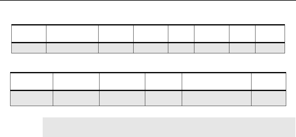
2-4 Introduction
Parts Replacement and Substitution
When damaged parts are replaced, identical parts should be used. If the identical replacement part
is not locally available, check the parts list for the proper Motorola part number and order the part
from the nearest Motorola Radio Products and Solutions Organization listed in the respective
Appendix chapters in this manual.
Rigid Circuit Boards
The repeater uses bonded, multi-layer, printed circuit boards. Since the inner layers are not
accessible, some special considerations are required when soldering and unsoldering components.
The printed through holes may interconnect multiple layers of the printed circuit. Therefore, exercise
care to avoid pulling the plated circuit out of the hole.
When soldering near a connector:
•Avoid accidentally getting solder in the connector
•Be careful not to form solder bridges between the connector pins
•Examine your work closely for shorts due to solder bridges.
Chip Components
Use the RLN4062 Hot-Air Repair Station for chip component replacement. Adjust the temperature
control to 370 °C (700 °F), and adjust the airflow to a minimum setting. Airflow can vary due to
component density.
•To remove a chip component:
1. Use a hot-air hand piece, and position the nozzle of the hand piece approximately 0.3
cm (1/8") above the component to be removed.
2. Begin applying the hot air. Once the solder reflows, remove the component using a pair
of tweezers.
3. Using a solder wick and a soldering iron or a power desoldering station, remove the
excess solder from the pads.
Table 2-1 Lead Free Solder Wire Part Number List
Motorola
Part Number Alloy Flux Type Flux Content
by Weight
Melting
Point
Supplier Part
number Diameter Weight
1088929Y01 95.5Sn/3.8Ag/0.7Cu RMAVersion 2.7-3.2% 217C 52171 0.015 1lb spool
Table 2-2 Lead Free Solder Paste Part Number List
Motorola Part
Number
Manufacturer Part
Number Viscosity Type Composition & Percent Metal Liquid
Temperature
1085674C03 NC-SMQ230 900-1000KCPs
Brookfield (5rpm)
Type 3
(-325/+500)
(95.5%Sn-3.8%Ag-0.7%Cu)
89.3%
217°C
Note MTR3000 Power Amplifier with Solder Wire Part Number 1010041C24 and Solder Paste
Part Number 1010041C20 uses leaded solder.

Introduction 2-5
•To replace a chip component using a soldering iron:
1. Select the appropriate micro-tipped soldering iron and apply fresh solder to one of the
solder pads.
2. Using a pair of tweezers, position the new chip component in place while heating the
fresh solder.
3. Once solder wicks onto the new component, remove the heat from the solder.
4. Heat the remaining pad with the soldering iron and apply solder until it wicks to the
component. If necessary, touch up the first side. All solder joints should be smooth and
shiny.
•To replace a chip component using hot air:
1. Use the hot-air hand piece and reflow the solder on the solder pads to smooth it.
2. Apply a drop of solder paste flux to each pad.
3. Using a pair of tweezers, position the new component in place.
4. Position the hot-air hand piece approximately 0.3 cm (1/8”) above the component and
begin applying heat.
5. Once the solder wicks to the component, remove the heat and inspect the repair. All
joints should be smooth and shiny.
Shields
Removing and replacing shields is recommended to be done with an Air Blower,
BOSCH GHG 600-3 or equivalent. The temperature should be set to approximately 400°C (752°F).
•To remove the shield:
1. Place the circuit board in the circuit board holder.
2. Add solder paste flux around the base of the shield.
3. Position the heat-focus head onto the shield.
4. Turn on the heater, and wait until the shield lifts off the circuit board.
5. Once the shield is off, turn off the heat, and grab the part with a pair of tweezers.
6. Remove the circuit board from the circuit board holder.
•To replace the shield:
1. Add solder to the shield if necessary, using a micro-tipped soldering iron.
2. Next, rub the soldering iron tip along the edge of the shield to smooth out any excess
solder. Use solder wick and a soldering iron to remove excess solder from the solder
pads on the circuit board.
3. Place the circuit board back in the circuit board holder.
4. Place the shield on the circuit board using a pair of tweezers.
5. Position the heat-focus head over the shield.
6. Turn on the heater, and wait for the solder to reflow.
7. Once complete, turn off the heat, raise the heat-focus head, and wait approximately one
minute for the part to cool.
8. Remove the circuit board and inspect the repair. No cleaning should be necessary.

2-6 Introduction
2.1.5 Test Equipment
The list of equipment contained in Table 2-3 includes most of the standard test equipment required
for servicing Motorola repeaters.
Table 2-3 Recommended Test Equipment
Equipment Characteristic Example Application
Service Monitor Can be used as a
substitute for items
marked with an asterisk
(*)
Aeroflex 3900 Series
(www.aeroflex.com), Aeroflex
3900 Series Communications
System Analyzer, Aeroflex
Option 400 or equivalent
Frequency/deviation meter and
signal generator for wide-range
troubleshooting and alignment
To test the radio using digital
MOTOTRBO modulation
(Aeroflex Option 400)
Digital rms
Multimeter*
100 µV to 300V
5 Hz to 1 MHz
10 MegΩ Impedance
Fluke 179 or equivalent
(www.fluke.com)
AC/DC voltage and current
measurements. Audio voltage
measurements
Oscilloscope* 2 Channel
100 MHz Bandwidth
5 mV/div to 20V/div
Leader LS8050
(www.leaderusa.com), Tektronix
TDS1001b
(www.tektronix.com), or
equivalent
Waveform measurements
Power Meter and
Sensor*
5% Accuracy
100 MHz to 500 MHz
50 Watts
Bird 43 Thruline Watt Meter
(www.bird-electronic.com) or
equivalent
Power Output measurements for
use on “analog” channels
RF Millivolt Meter 100 mV to 3V RF
10 kHz to 1 GHz
Boonton 92EA
(www.boonton.com) or
equivalent
RF level measurements

Introduction 2-7
2.1.6 Service Aids
Table 2-4 lists the service aids recommended for working on the Base Station/Repeater (BR). While
all of these items are available from Motorola, most are standard workshop equipment items, and
any equivalent item capable of the same performance may be substituted for the item listed.
Table 2-4 Service Aids
Motorola
Part Number
Schroff Part
number Description Application
CLN8665A –Standard Type "A" to Type
"B" USB Programming
cable
Connects the Base Station/Repeater’s front
connector to a USB port for programming,
testing and alignment.
HSN1006 – Speaker To listen to any active audible alarms
Note : Use speaker type HSN1000 (older
model) or HSN1006 via adapter cable Part.No.
0185180U01.
3083191X02 –RJ-45 to BNC cable /
Receiver Audio Test Cable
Connects the external speaker RJ-45 jack to
the Oscilloscope input BNC connector.
GMMN4063 – Microphone To transmit voice by connecting it to
microphone connector on SCM.
Note : Use microphone type GMN6147 (older
model) or GMMN4063.
0185180U01 –Speaker adapter cable To connect the speaker to speaker connector
on SCM.
RVN5115 – Customer Programming
Software (CPS) Package
(Includes CPS, Air Tracer,
Tuner, Radio Diagnostic
and Control (RDAC))
Program customer option and channel data.
–23021653 Extender Card To power up the cluster module (Exciter,
Receiver, Station Control Module) external from
the MTR3000 Base Station/Repeater (BR).
6683334X01 – Option Card tool To pull the option boards (e.g. Wireline
Interface Board or the Auxiliary I/O Board).

2-8 Introduction
Notes

3-1
Chapter 3 MTR3000 Power Amplifier
3.1 Overview
This section provides an overview, detailed Theory of Operation and troubleshooting information for
the Power Amplifier (PA) Module. The block diagrams, schematic diagrams, overlays, and parts lists
are provided on foldout sheets. Each block diagram shows the location and reference designation
for all electrical components. A complete list of all parts is provided with the parts ordered according
to the schematic reference number.
For specifications of the PA, refer to the MOTOTRBOTM MTR3000 Base Station/Repeater Basic
Service Manual (68007024096).
3.2 Theory of Operation
The following theory of operation describes the operation of the Power Amplifier circuitry at a
detailed level. The information is presented to give the service technician an understanding of the
functions performed by the module in order to facilitate maintenance and troubleshooting to the
component level.
The Power Amplifier (PA) module is designed for continuous-duty operation across its specified
frequency band and transmit power range. It is a multi-stage RF amplifier, and contains various
metering, control, and protection circuitry that govern its operation. The PA module will accept a
fixed-level RF input signal from the Exciter module, and amplify it to the desired transmit power and
deliver it to the PA output connector, which is the Base Station/Repeater (BR) antenna port. Through
a combination of software (SW) and hardware (HW) controls, the PA transmit power is determined.
The PA module contains the sub-modules below:
•RF Board (replaceable)
•Output Board (replaceable)
•Distribution Board (replaceable)
•Internal isolator (replaceable) which consists of a Circulator and isolation load.
Refer to Figure 3-1 for the PA sub-modules.
Figure 3-1 PA sub-modules

3-2 Theory of Operation
The RF Board is a multi-stage power amplifier board that contains the Driver Amplifier and final
amplifier circuits, and is the interface to the Exciter module output. The Output Board contains the
harmonic (low-pass) filter and directional couplers for forward and reverse power sensors, and is
connected to the PA output/antenna port. The Distribution Board contains the PA SPI circuitry,
diagnostic metering circuitry, RF power control circuitry, and the fan power supply, and is the
interface to the site control module (SCM) and power supply module (PS). The SPI circuitry within
the PA includes the analog to digital converter (A/D), digital to analog converter (D/A), non-volatile
memory (NVM), and the customer programmable logic device (CPLD). The PA and its sub-modules
are broad-band and require no manual tuning or alignment to operate at the station site over the
specified rated conditions.
The station PS provides 28.6 V and 14.2 V supplies to the PA through a direct connection. The PA
utilizes these voltages to supply power within the PA to the various sub-circuits described herein.
Additional internal voltages of 3.3 V and 5 V are derived from the 14.2 V supply within the PA, and
these are used to supply certain peripheral circuitry within the PA.
Within the PA, the input RF signal is initially amplified by the Driver Amplifier stages, and is then
further amplified by the final amplifier stage. The Driver Amplifier is gain-controlled by a control
voltage, V_Control, provided by the power control loop within the PA. The final amplifier is a fixed-
gain amplifier stage, and is the last stage of RF amplification within the PA. The amplified RF signal
then passes from the final amplifier through an isolator and harmonic filter, through the directional
couplers for power detection, and then out of the PA output port.
The directional coupler is a calibrated wattmeter, with its calibration information stored in the PA
NVM. The forward power wattmeter provides a DC voltage corresponding to the measured output
power to the A/D for metering purposes, so that SW can monitor the PA or the base station/repeater
output power. Also, this voltage is provided to the power control circuitry within the PA to serve as
the feedback signal in the power control loop. Using the unique PA calibration information stored in
the NVM, SW can control the PA output power level via the SPI bus from the SCM through the PA
signal connector. SW controls the transmit power by programming the D/A within the PA power
control circuit to a specific DC reference voltage corresponding to the desired output power based
on the calibration information. Under normal operating conditions, the power control circuitry
compares the DC voltage from the directional coupler to the reference voltage from the D/A, and
based on the comparison a control voltage is generated that controls the PA gain to yield the
requested output power from the PA module.
The SW requested output power level may include one or more SW controlled adjustments based
on various alarm conditions generated from monitored PA metering signals which are fed back to
the SCM via an A/D converter (also connected to the SPI bus). Using the A/D metering circuits, SW
monitors for conditions such as high reflected power/VSWR or high/low supply voltages and takes
action to reduce output power or dekey the station accordingly to protect the HW from damage or
improper operation. During excessive output VSWR, the ratio of the forward and reflected voltages
from the directional coupler may be used by software to reduce, or turn off, the transmitter power
based on the reflected power level and severity of the VSWR. Likewise when the main PA supply
voltage level is outside of its nominal range, the output power is reduced by SW accordingly to
protect the HW.
Temperature sense circuitry is also contained within the PA and is used to monitor the PA internal
temperature. When the temperature reaches a certain threshold, the PA fan will power on to reduce
the operating temperature of the PA. If the temperature continues to rise and reaches another
predefined threshold, it will begin to impact the power control loop and will result in an output power
reduction in order to protect the HW from thermal failure. When this latter threshold is exceeded, it
provides a voltage contribution into the power control loop feedback and results in a reduced output
power. Both the fan control and the power control manipulation for thermal protection is fully HW
Theory of Operation 3-3
controlled, and requires no SW interaction for this to occur. Additionally, the PA also contains
metering circuitry to monitor for low output power and fan failure alarming, although these are
informational in nature and do not result in a HW or SW action on the PA.
The PA can be placed in standby mode when not transmitting. This is achieved through the
PA_Enable signal controlled by the SCM through the PA signal connector. When this signal is in the
high state, the PA is enabled. When the PA is placed in standby mode, the power consumption of
the PA is significantly reduced.
The PA HW type is identified by way of the PA_IDA and PA_IDB meters within the PA. These signals
are provided to the A/D, and are also controlled by the D/A to result in multiple states for each A/D
input. These meter values are used to determine HW type.
Refer to Figure 3-2 for the functional block diagram of the PA and Figure 3-3 for the PA DC Power
Structure.
Figure 3-2 PA Functional Block Diagram
DC Distribution Board
Power Control
Circuitry
RF Board
Output
Board
Driver Amplifier
Q2100 Q2300
Final Amplifier
Q4300
Q4400
Q4600
Q4500
RF Input
Connector
U4110
U4120
U4130
U4920
U4930
U4910
Forward
Power
Detector
Harmonic
Filter
Circulator
Reverse
Power
Detector
50 Ohm
Load
RF Output
Connector
Backplane
Connector
(10 Pin)
SPI Circuitry
-CPLD
-DAC
-ADC
-NVM
SPI
Buss
Metering
Circuitry
Power
Control
Voltage
28.6V
Buss
14.2V
Buss
Power Supply
Connector
3-4 Theory of Operation
Figure 3-3 PA DC Power Structure
PA DC Load Definitions:
•Load A – Metering Circuit
•Load B – Final Amplifier RF Devices
•Load C – Driver Amplifier RF Devices
•Load D – SPI, Metering, Power Control
•Load E – SPI, Metering, Power Control
•Load F – Metering, Power Control, PA Fan
•Load G – Final Amplifier Bias Circuitry
•Load H – Driver Amplifier Bias Circuitry, Driver Amplifier RF Device
3.2.1 RF Board
The RF Board is a replaceable module within the PA, and contains the driver and final amplifier
circuits, as well as the PA input BNC connector. This board performs all of the RF amplification
within the PA required to achieve the desired transmit power. The output power of the RF Board is
greater than the PA output power, as it must overcome the losses introduced by the elements
following the RF board within the PA, such as the isolator and harmonic filter.
The RF board utilizes local heat spreaders under the main RF amplifier devices and final amplifier
combiner isolation loads. These heat spreaders contact the PA cast heat sink and provide a thermal
path to maintain adequate operational temperatures of these components. Thermal grease is used
between the heat spreader and the PA cast heat sink interface to maintain a proper thermal
interface.
28.6V Input
from PS
14.2V Input
from PS
Driver Amplifier (Load H)
Final Amplifier (Load G)
Distribution
Board (Load A)
5V Linear
Regulator
3.3V Linear
Regulator
Distribution
Board (Load F)
Distribution
Board (Load D)
Distribution Board
Driver Amplifier (Load C)
Final Amplifier (Load B)
RF Board
Distribution
Board (Load E)

Theory of Operation 3-5
3.2.1.1 Driver Amplifier
The Driver Amplifier is the first amplifier within the PA, and is capable of reaching output power
levels of approximately 4 W max. The Driver Amplifier consists of three adjustable-gain amplifier
stages and supporting matching circuits and attenuators. The Driver Amplifier and supporting
circuitry is denoted by reference designators in the 2000’s (i.e. R2000, C2450, etc). The driver gain
stages are gain-controlled, by way of V_Control, in order to adjust the PA output power to the
desired level through the power control loop within the PA. Depending on the PA input level and the
desired PA output level, the control voltage will be adjusted to yield the necessary driver gain, up to
a maximum of approximately 25 dB, in order to achieve the desired PA output power.
3.2.1.2 Final Amplifier
The RF output signal delivered from the Driver Amplifier is then further amplified by the final
amplifier stage within the PA. This is the last RF amplification stage, and will yield the output power
required to deliver the requested power to the base station/repeater’s antenna port. The final
amplifier and supporting circuitry is denoted by reference designators in the 4000’s (i.e. R4000,
C4450, etc). The final amplifier is a fixed-gain stage with approximately 20 dB of gain, which will
vary depending on the frequency band of operation. The final amplifier consists of four discrete
devices operating in a parallel configuration. A multi-stage hybrid splitter/combiner distributes the
Driver Amplifier output signal to these final amplifier devices, and then later recombines the
amplified signals from these devices to deliver combined power to the next element within the PA.
3.2.1.3 Module I/Os
RF INPUT (J2000) – RF input from the Exciter to the PA
ISOL_RF_INPUT (M2050) – RF output from the final amplifier to the isolator input
28V_A (M2021) – 28 V supply input from Distribution Board for final amp
28V_B (M2020) – 28 V supply input from Distribution Board for final and driver amps
14V (M2022) – 14 V supply input from Distribution Board, for final and driver amps
V_CONTROL (M2023) – Control voltage input from Distribution Board
V_OMNI (M2024) – Metering signal output supplied from driver to A/D
PA_ENABLE (M2025) – PA enable signal input from Distribution Board
PA_ID (M2026) – PA_ID metering circuit input from Distribution Board for PA ID
3.2.2 Isolator
The PA internal isolator (which is comprised of a discrete circulator and a bolt-down isolation load)
follows the final amplifier within the PA. It maintains good loading for the final amplifier (regardless of
the PA's external load) by preventing a high VSWR at the output of the PA from damaging the final
amplifier stage. Also, by providing additional isolation to the final amplifier, the isolator improves the
intermodulation attenuation (IMA) performance of the transmitter.

3-6 Theory of Operation
3.2.3 Output Board
The Output Board is a replaceable module within the PA, and contains the harmonic filter, directional
couplers, and surge suppression circuitry within the PA. The Output Board circuitry is denoted by
reference designators in the 8000’s (i.e. R8000, C8450, etc). The Output Board connects the
isolator output to the PA N-Type output connector that is mounted to the PA cast heat sink.
3.2.3.1 Harmonic Filter
The harmonic filter is located following the isolator stage of the PA. This filter attenuates the
harmonic energy created by the final amplifier stage prior to reaching the antenna port. The
harmonic filter will be fully distributed for some frequency bands and will contain lumped elements
(capacitors and inductors) for other frequency bands, but will be located in the same location for all
bands.
3.2.3.2 Directional Couplers
The forward and reverse directional couplers on the output board utilize edge-coupled lines and
isolation loads with a coupling coefficient of approximately 30 dB, and perform a diode rectification
of the coupled RF signal to provide a DC voltage back to the distribution board that will be routed to
the A/D for metering. The forward power sensor voltage is also tied into the power control loop, and
is used to balance the loop for the desired output power.
3.2.3.3 Surge Suppression
For suppression of surges entering the PA output port, an air-wound inductor is placed between the
output line and ground to provide a high impedance within the specified frequency band of the PA.
During a surge event such as a nearby lightning strike, this will reduce the energy entering the PA
output port prior to reaching other PA internal components, and help to prevent damage during
these types of events.
3.2.3.4 Module I/Os
RF_IN (M8002) – RF input from the isolator output
RFOUT (M8000) – RF output to the antenna port
REV_DET (M8001) – Reverse power sensor output to Distribution Board
FWD_DET (M8003) – Forward power sensor output to Distribution Board
3.2.4 Distribution Board
The Distribution Board is a replaceable module within the PA, and contains the PA SPI circuitry,
diagnostic metering circuitry, RF power control circuitry, and the fan supply. The Distribution Board
circuitry is denoted by reference designators in the 6000’s (i.e. R6000, C6450, etc).
A 10-pin signal connector (J6000) is located on this board and is the external interface to the
backplane through a ribbon cable for communication with the SCM. A 6-pin power connector
(J6001) is also located on this board and is the interface to the PS for supplying main supply bus
voltages to the PA, with 2 pins dedicated to 28.6 V, 2 pins for 14.2 V, and the other 2 pins are ground

Theory of Operation 3-7
although the ground return path in the base station/repeater is also achieved through the station
chassis.
In addition to the signal and power connectors, a 4-pin header (J6002) and 2-pin jumper is located in
this same area. This is not supported, and has no impact on HW functionality regardless of jumper
position.
3.2.4.1 SPI
The SPI circuitry within the PA includes the analog to digital converter (A/D), digital to analog
converter (D/A), non-volatile memory (NVM), and the customer programmable logic device (CPLD).
A brief description of the PA SPI devices is shown below.
•CPLD – Main PA SPI interface, with all other PA SPI devices connected through this device.
This device performs addressing to the other SPI devices using the two address lines from
the SCM. One single bit output on the CPLD controls the PA fan for diagnostic purposes, and
another single bit output is used for the PA identification meters
•NVM – EEPROM that is used to store PA calibration data and identification information
•D/A – Converts SW digital signals to analog within the PA. This controls the PA power control
circuit
•A/D – Converts analog signals within the PA to digital for SW interface. These signals are
used by SW for HW metering.
3.2.4.2 Power Control
A combination of SW and HW controls are used to regulate the PA transmit power level. The PA
output power is regulated by the power control loop within the PA. This control loop uses a reference
voltage from a digital-to-analog (D/A) converter that is programmed by SW through the SPI bus. The
D/A programmed value is determined based on the calibration information stored in the PA NVM.
Once programmed, the PA power control loop will level the output power to the requested level, if
possible.
The temperature sense circuit within the PA can also affect the power control loop, and if an
excessive thermal condition exists, the control loop will be forced to reduce output power in order to
protect the PA HW from damage. The more excessive the thermal condition, the greater the amount
of output power reduction.
3.2.4.3 Metering
The DC Distribution Board contains the PA metering circuitry used by both SW and internal PA HW
for determining when fault conditions are present and take appropriate action when needed.
Metering is performed in order to support the PA related alarms including high temperature, VSWR,
low/high main supply voltage, low output power, and fan failure. The metering signals are tied to the
A/D, and are monitored by SW as required in order to determine when fault conditions exist.
3.2.4.4 Fan Supply
The PA fan is powered through the Distribution Board. The supply to the fan is connected through a
feed-through capacitor on the fin side of the PA cast heat sink. The fan ground connection is
attached to the PA cast heat sink. The fan supply is controlled by either SW or HW. When a thermal
limit defined by the PA HW has been exceeded, the HW control circuit will enable the fan supply
3-8 Theory of Operation
switch (Q6590) to power the fan, to attempt to lower the PA temperature. This is entirely HW
controlled and does not require any SW action to occur. The SW control is only required for periodic
monitoring of fan functionality. During these diagnostic tests, SW will force the fan on for a short
period so that the fan current can be calculated in order to determine if the current is high or low
which would indicate if the fan is failing or has already failed. The fan current is determined by
measuring a voltage drop across a fixed series resistance located in the fan supply line (R6595/
R6596).
3.2.4.5 Module I/Os
For PA Supply Connector (J6001), refer to Table 3-1
For PA Signal Connector (J6000), refer to Table 3-2
V_FWD_DST (M6910) – V_Forward input from Output Board
V_REV_DST (M6911) – V_Reverse input from Output Board
Table 3-1 PA Supply Connector (J6001)
Pin Name Description Input/Output
114.2V +14.2 V Supply Input
2 Ground Ground NA
328.6V +28.6 V Supply Input
4 14.2V +14.2 V Supply Input
5Ground Ground NA
6 28.6V +28.6V Supply Input
Table 3-2 PA Signal Connector (J6000)
Pin Name Description Input/Output
1UNUSED Unused – No-Connect NA
2 BP_PA_ENABLE PA Enable Input
3BP_RESET_N Reset Line Input
4 V_CONTROL V_Control analog (Not
base station/repeater
Interface)
Input/Output
5UNUSED Unused – No-Connect NA
6 BP_PA_ADDR0 PA Address Line 0 Input
7BP_CLK SPI Clock Input
8 BP_MOSI SPI MOSI Line Input
9BP_MISO SPI MISO Line Output
10 BP_PA_ADDR1 PA Address Line 1 Input
Troubleshooting 3-9
28V_DST (M6900) – 28 V output to RF Board
28V_DST (M6901) – 28 V output to RF Board
14V_DST (M6902) – 14 V output to RF Board
V_CTRL_DST (M6903) – Control voltage output to RF Board
V_OMNI_DST (M6904) – Metering signal input from RF Board
PA_EN_DST (M6905) – PA enable signal output to RF Board
PA_IDA_DST (M6906) – PA_ID metering circuit output to RF Board
BAND_ID_JUMPER (J6002) – Unsupported
Refer to Figure 3-4 for the external power and signal connector pin-outs.
Figure 3-4 PA Signal Connectors
3.3 Troubleshooting
3.3.1 Application and Removal of Thermal Grease
In the procedures below, there are instances where thermal grease is used to help disperse heat
generated by the various boards. If boards are to be reused, please make sure the old thermal
grease is removed completely by using 100% denatured alcohol before reapplying new thermal
grease; this will ensure good thermal interface. Please use the appropriate application brush to
apply an even layer of thermal grease in the stated areas.
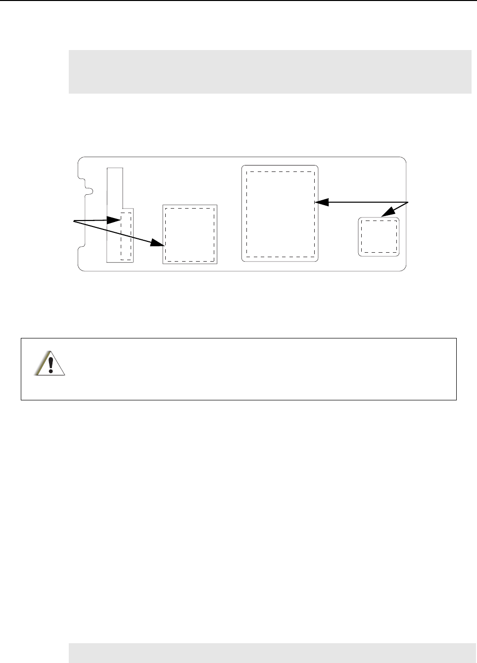
3-10 Troubleshooting
3.3.2 Disassembly and Reassembly Procedures
To reapply thermal grease on the PA metal casting when reassembling the Output and RF Board,
refer to Figure 3-5.
Figure 3-5 Areas to apply thermal grease on the PA metal casting
3.3.2.1 Output Board
3.3.2.1.1 Disassembly
1. Remove the 5 screws (M3.5, Tx15) from the board using a Torque driver.
2. Unsolder the output connector from the board.
3. Unsolder the lead which connects the board to the Circulator.
4. Unsolder the 2 omega straps on the output board, which connect it to the distribution
board.
3.3.2.1.2 Reassembly
1. Apply thermal grease to the marked section on the reverse side of the replacement
output board as shown in Figure 3-6.
2. On the metal casting, remove the old thermal grease, and apply the new grease on the
four outline areas as shown in Figure 3-5.
3. Install the replacement output board.
4. Secure the board with the 5 screws (M3.5, Tx15 at 15 in-lbs) according to the order
shown in Figure 3-6.
Note The Distribution Board omega straps and the Circulator leads overlap onto the RF Board
and Output Board, and should be the first to be removed and the last to be replaced if
either the RF Board or Output Board requires removal/replacement.
The PA will require recalibration if the Output Board is replaced. Recalibration is not
necessary if the RF Board is replaced. If recalibration is not possible but is required,
the PA module will need to be replaced.
Note Ensure that the output board is placed under the Circulator lead.
Thermal
Compound
Outline Marking
Thermal
Compound
Outline Marking
C a u t i o n
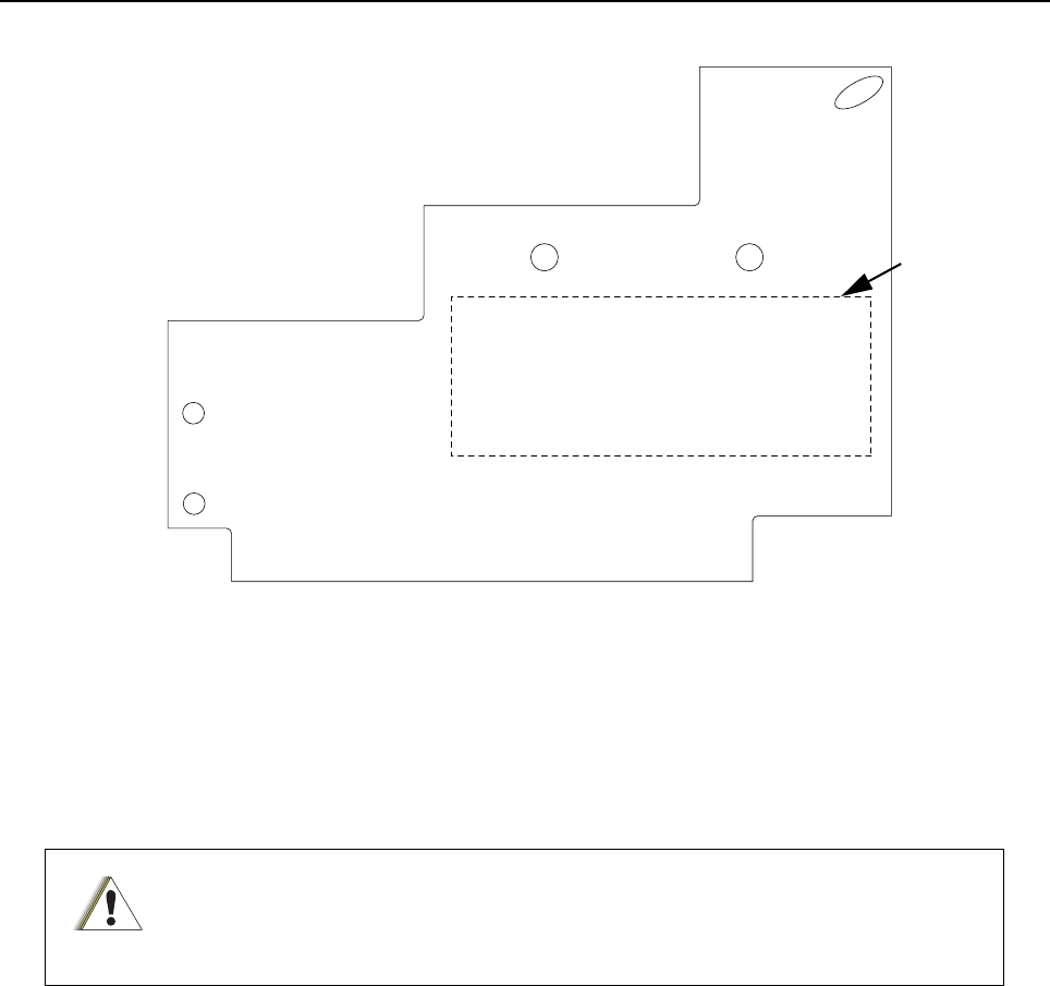
Troubleshooting 3-11
Figure 3-6 Sequence to tighten back screws on the output board
5. Solder the 2 omega straps, which connect the output board to the distribution board.
6. Solder the lead that connects the board to the Circulator.
7. Solder the output connector to the board.
3.3.2.2 Distribution Board
3.3.2.2.1 Disassembly
1. Remove the 2 screws (M3.5, Tx15) from the board using a Torque driver.
2. Unsolder the lead which connects the fan connector to the board.
3. Unsolder the 2 omega straps on the output board, which connect the distribution board
to the output board.
4. Unsolder the 7 omega straps on the RF board, which connect the distribution board to
the RF board.
3.3.2.2.2 Reassembly
1. Install the replacement distribution board.
2. Secure the board with the 2 screws (M3.5, Tx15 at 15 in-lbs) according to the order
shown in Figure 3-7.
The PA will require recalibration if the Distribution Board is replaced. Recalibration is
not necessary if the RF Board is replaced. If recalibration is not possible but is
required, the PA module will need to be replaced.
4
1
2
53Thermal
Compound
Outline Marking
C a u t i o n
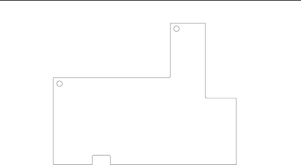
3-12 Troubleshooting
Figure 3-7 Sequence to tighten back screws on the distribution board
3. Solder the 7 omega straps, which connect the board to the RF board.
4. Solder the 2 omega straps, which connect the board to the output board.
5. Solder the lead that connects the board to the fan connector.
3.3.2.3 RF board
3.3.2.3.1 Disassembly
1. Remove the 8 screws (M3.5, Tx15) from the board using a Torque driver.
2. Unsolder the Circulator from the board.
3. Unsolder the 7 omega straps on the RF board, which connect it to the distribution board.
4. Disassemble the Circulator and the load resistor according to the procedures outlined at
Section 3.3.2.4.1 and Section 3.3.2.5.1.
5. Gently lift the RF board to remove it. Some additional force may be needed to overcome
the thermal grease bonds under the board.
2
1
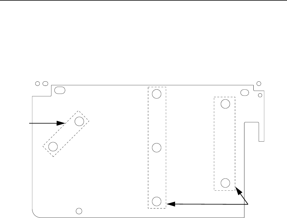
Troubleshooting 3-13
3.3.2.3.2 Reassembly
1. Apply thermal grease to the three coins (driver coin, final device coin, final combiner
coin) on the reverse side of the replacement RF board as shown in Figure 3-8.
2. On the metal casting, remove the old thermal grease, and apply the new grease on the
four outline areas as shown in Figure 3-5.
3. Install the replacement RF board.
4. Secure the board with the 8 screws (M3.5, Tx15 at 15 in-lbs) according to the order
shown in Figure 3-8.
Figure 3-8 Sequence to tighten back screws on the RF board
5. Solder the 7 omega straps, which connect the board to the distribution board.
6. Solder the lead that connects the board to the Circulator.
7. Reassemble the Circulator and the load resistor according to the procedures outlined at
Section 3.3.2.4.2 and Section 3.3.2.5.2.
3.3.2.4 Circulator
3.3.2.4.1 Disassembly
1. Remove the 4 screws (M3, Tx10) from the Circulator using a Torque driver.
2. Unsolder the Circulator from the RF board.
3. Unsolder the Circulator from the output board.
4. Unsolder the Circulator from the load resistor.
3.3.2.4.2 Reassembly
1. On the replacement Circulator, apply thermal grease to the underside of the Circulator
as well as the Circulator pocket on the metal casting.
2. Install the replacement Circulator.
3. Secure the Circulator with the 4 screws (M3, Tx10 at 10 in-lbs) which was previously
removed.
1
2
3
45
6
7
8
Thermal
Compound
Outline Marking
Thermal
Compound
Outline
Marking

3-14 Troubleshooting
4. Solder the lead that connects the Circulator to the load resistor.
5. Solder the lead that connects the Circulator to the output board.
6. Solder the lead that connects the Circulator to the RF board.
3.3.2.5 Load resistor
3.3.2.5.1 Disassembly
1. Remove the 2 screws (M3, Tx10) from the load resistor using a Torque driver.
2. Unsolder the lead which connects the load resistor to the Circulator.
3.3.2.5.2 Reassembly
1. Install the replacement load resistor.
2. Secure the load resistor with the 2 screws (M3, Tx10 at 10 in-lbs) which was previously
removed.
3. Solder the lead that connects the load resistor to the Circulator.
Troubleshooting 3-15
3.3.3 Troubleshooting Chart
Follow the procedures in the troubleshooting charts below to isolate the cause of PA problems.
Figure 3-9 Fan Troubleshooting Flow Chart (PA)
Note 1. PA fan supply should be measured at feed-through capacitor output.
HIGH PA TEMP
or PA FAN
FAILURE
Is PA
Fan On?
Check Fan
Supply
Voltage
1
Check Fan
Supply
Voltage
1
Replace Fan
if Needed
Unplug Fan
and
Remeasure
Supply
Voltage
1
Is V
>10V?
Is V
>10V?
Troubleshoot
Fan Switch
Replace Fan
if Needed
Yes
No
Yes
No
No
Yes
Is V
>10V?
Replace Fan
if Needed
No
Yes
Troubleshoot
Fan Switch
3-16 Troubleshooting
Figure 3-10 Power Troubleshooting Flow Chart (PA)
LOW or NO
OUTPUT
POWER
Is 0.6A <
Idc < 1.0A
Set rated RF output
power and measure
V_Control at M2023
on RF Board
With PA Enabled and
No RF Output Power,
Measure 28.6V Idc
Measure pins
9 and 10 of
U6410 on
Distribution
Board
Is
V_Control
< 11V?
Is 28.6V
PA Idc >
2.5A?
Troubleshoot
Final Amp,
Output Board, and
Circulator
Troubleshoot
Final Amp
Yes
No
Yes No
Yes
Are they
equal?
Troubleshoot
Power Control
Loop, and
Output Board
No
Yes
Troubleshoot
Output Board
No
Troubleshoot
Driver Amp
Troubleshooting 3-17
3.3.4 Detailed Troubleshooting
3.3.4.1 Setup Instructions
3.3.4.1.1 Main DC Supplies
When troubleshooting the PA module, if it is required to apply 28.6 V and 14.2 V DC power to the PA
it can be done one of two ways. These are explained below.
If a mule base station/repeater or base station/repeater PS is used for testing, or if the bench power
supplies do not have accurate current metering, the currents of the 28.6 V and 14.2 V buses should
be monitored. This can be achieved by an inline current meter, or a clamp-on current probe onto the
supply lines. If multiple wires are supplying a given voltage supply, all wires for that supply must be
monitored together.
Be aware of the dangers involved with high power RF and DC
circuitry, and take extra care when testing a PA.
The PA output should always be terminated into an RF load
capable of a minimum of 500 W for any functional testing
when troubleshooting. Certain failure modes may result in
loads measuring in excess of 300 W.
The circuit boards are sensitive to electrostatic discharge
(ESD). Always wear a properly grounded wrist strap, and
observe anti-static precautions when handling the circuit
boards.
The sequencing of the DC supply voltages of the PA is critical,
and failure to follow the proper sequencing can result in
damage to the PA HW. If removal of a circuit board is required,
the proper disassembly/reassembly procedure must be
adhered to. Failure to do so may result in HW failure due to
electrical and/or mechanical stress.
W A R N I N G
C a u t i o n
C a u t i o n
C a u t i o n

3-18 Troubleshooting
Method 1 (Using a Mule Base Station/Repeater for DC Power and Control)
This method most faithfully recreates the application, although the setup is more limited in the ability
to separate out the key-up or dekey process, and it may not be possible to troubleshoot all circuitry
as described herein. With the base station/repeater’s controlled key/dekey sequence, the PA enable
signal will be controlled by SW, and it will not be possible to measure the enabled current draws of
the PA supply lines, should that be required to debug the PA HW.
A base station/repeater may be connected to the PA, and can be used to supply DC power to the
PA, as well as control the PA through the application SW (firmware). The PA will need to be removed
from the base station/repeater, and the cover will need to be removed in order to access the circuit
boards. For this, the base station/repeater’s cable connecting the PS to PA can be used to supply
main 28.6 V and 14.2 VDC power to the PA. The 10 pin signal cable will need to be replaced with a
slightly longer cable. This is a standard 10 pin ribbon cable, and approximately 1 foot of length
should be sufficient to connect the PA to the base station/repeater. This signal cable length should
be kept as short as possible to prevent signal integrity issues.
A longer RF cable will be required to connect the Exciter module output to the PA input, and the
length will be dictated by the setup constraints. This cable should be kept as short as possible to
minimize insertion loss.
Method 2 (Using a Mule Base Station/Repeater Power Supply for DC Power with Manual
Control)
This method offers the additional flexibility that method 1 does not allow, and the PA can be placed
into an enabled state without RF output power present. This will allow for troubleshooting of
additional circuitry within the PA. The advantage of this method is that it does not require high power
lab supplies to provide the DC power required by the PA.
A base station/repeater PS may be used to provide the main DC supplies of 28.6 V and 14.2 V to
the PA. As in method 1, the base station/repeater PS to PA cable can be used. Two additional low
power voltage supply lines will be required for this method. Neither of these lines will draw
appreciable current, and supplies capable of 100 mA are sufficient.
The first of the additional supplies needed is the PA_Enable signal. This will require a 5 V level to
enable the PA, applied to pin 2 of J6000 when prompted, and 0 V on this pin to disable the PA and
put it into standby mode.
The other of the additional supplies needed is for a control voltage signal to manually adjust the gain
of the PA. Note that this supply must be capable of sinking several milliamps of current; otherwise it
will be unable to override the control loop voltage. This supply must be capable of up to 14 V
potentials.
Method 3 (Using Lab Power Supplies for DC Power and Control)
This method is essentially the same as method 2, except lab DC power supplies are also used to
supply the PA mains. These supplies will need to be capable of 15 A for the 28.6 V supply, and 5 A
for the 14.2 V supply. The PA enable and control voltage supply requirements are the same as
outlined in method 2.
Troubleshooting 3-19
3.3.4.1.2 Sequencing
The sequence of applying the supply and control voltages is critical, and if not followed exactly then
the PA HW may fail. The following sequences for power up and power down are to be followed for
any functional testing performed.
If method 1 is used, and a mule base station/repeater with application firmware controlling the full
base station/repeater HW is used, the correct sequencing will occur automatically and this section
does not apply in that case.
If method 2 above is used, and a mule base station/repeater PS only is used, the 28.6 V and 14.2 V
power supplies will come up or go down in the proper order. Note that voltages may not be exactly
28.6 V and
14.2 V, but must be within the power supply tolerances. For this method, the power supply should be
plugged in at the step where 28.6 V and 14.2 V potentials are applied or removed, but all steps
preceding and following those steps must be followed as shown.
If method 3 above is used, the following sequence applies.
Powering Up the PA:
1. Disable PA by applying 0 V to pins 2 and 4 of J6000
2. Apply 28.6 V main supply voltage to pins 3 and 6 of J6001
3. Apply 14.2 V main supply voltage to pins 1 and 4 of J6001
4. Apply 12 dBm for UHF to RF input connector J2000
5. Apply the PA Enable signal 5.0 V to pin 2 of J6000, if the PA is to be enabled
6. If RF output power required, very slowly increase V_Control signal from 0 V on pin 4 of
J6000 until desired output power is achieved. Step size of less than 0.05 V should be
taken, else severe RF output power may result and damage to the HW could occur.
During this step, main supply voltage bus currents should be monitored to make sure
excessive currents do not result.
Powering Down the PA:
1. Slowly decrease V_Control to 0V on pin 4 of J6000
2. Disable PA by applying 0 V to pin 2 of J6000
3. Disable RF input to PA
4. Remove 14.2 V main supply voltage (set to 0 V) to pins 1 and 4 of J6001
5. Remove 28.6 V main supply voltage (set to 0 V) to pins 3 and 6 of J6001
If supply currents for either 28.6 V or 14.2 V bus become
excessive for the resulting output power, then the
troubleshooting steps for low or no output power should be
followed to determine the problem.
C a u t i o n

3-20 Troubleshooting
3.3.4.2 Troubleshooting Details
Prior to any detailed troubleshooting, once the cover is off, it is suggested to inspect all of the circuit
boards of the PA to look for evidence of damage. This may include loose components, charred PCB/
components, black residue surrounding components or black residue on inside of cover. This may
help to guide you to the problematic area, or indicate a secondary failure mode that may have
resulted but was not diagnosed.
The details below will indicate when DC and/or RF power is to be applied. It should be assumed that
no DC or RF power is to be applied until stated.
PA circuitry is grounded to the PA cast heat sink, and measurement equipment should be connected
to the same ground when performing any testing of the PA.
3.3.4.2.1 Troubleshooting the Fan Switch
1. Disconnect the fan connector from the feed-through capacitor on the fin side of the PA
heat sink.
2. Check for DC continuity through feed-through capacitor to determine if component
failure has occurred, and replace if necessary. Severe electrical or mechanical stress
could result in failure of this component.
3. Verify resistance of R6595 (if placed), R6596, and R6597 to determine if component
failure has occurred, and replace if necessary. A fan failure could result in over-
dissipation of these resistors.
4. Apply 28.6 V and 14.2 V DC power to the PA. Measure pin 3 of Q6590, and it should be
approximately equal to the 14.2 V input voltage to the PA (pins 1 and 4 of J6001). If not,
something between these points is disconnected. If it is, then the only way to force the
fan to turn on is to use the mule base station/repeater, and it will attempt to turn on the
fan on upon the base station/repeater boot up for a diagnostic test, at which point pin 4
of Q6590 should be approximately equal to pin 3.
5. When the fan circuit is energized during the fan test during the base station/repeater
boot up, the voltage drop across resistor R6596 should be approximately 2 V. If it is
significantly more or less than this, this indicates abnormal current draw of the fan, and
the fan should be replaced.
6. If no specific failure is found, replace the fan and/or distribution board. Recalibration and
retest is required, if the distribution board is replaced.
Technicians troubleshooting and repairing the circuit boards
must be trained, and capable of removing and replacing
surface-mount components of the appropriate package sizes.
Failure to properly install/replace any component may result
in failure and/or reduced reliability.
The PA will require recalibration if the Output Board is
replaced. Recalibration is not necessary if the RF Board is
replaced. If recalibration is not possible but is required, the PA
module will need to be replaced.
C a u t i o n
C a u t i o n

Troubleshooting 3-21
3.3.4.2.2 Troubleshooting the Driver Amplifier
1. Check for blown fuses F2400, F2100. If any of these fuses is blown, this indicates a
damaged device that has shorted to ground. Inspect for failures downstream. If Q2300
has failed, it cannot be repaired and the kit must be replaced.
2. Apply 28.6 V and 14.2 V main DC supplies. Measure output voltage at pin 2 of U2500
linear regulator; it should be ~28.6 V. Measure drain voltage at final driver stage U2300
pins 13 and 23; they should be ~28.6 V.
3. Enable the PA, and measure output voltage at pin 2 of U2500 linear regulator; it should
be ~25 V, when PA is enabled. Measure drain voltage at final driver stage U2300 pins 13
and 23; they should be ~25 V.
4. Key the PA to rated output power, and measure drain voltage at final driver stage U2300
pins 13 and 23; they should be ~25 V.
5. Measure V_Omni at pin 4 of Q2400; it should equal ~1.5 times V_Control at M2023.
6. Measure pin 3 of predriver stage Q2100 (AH101 device); it should equal a few volts
below V_Omni. If it is notably less than this, the AH101 device is damaged and should
be replaced.
7. Measure pins 10 and 20 of final driver stage U2300; they should equal 2 V to 3 V each.
8. If no issues are found in the steps above, and the 28 V current indicates a final amplifier
related issue, perform troubleshooting steps on the Circulator and Output Board. This
can be additionally verified by sniffing the RF levels at the various stages of the driver to
ensure that the correct diagnosis has been performed.
9. If no issues are found in the steps above, and 28 V current does indicate increased final
amplifier current draw with increased V_Control, perform the final amplifier
troubleshooting steps.
When working on the RF Board, do not use a heat gun or hot
plate. Damage to the circuit board can result.
Do not attempt to replace RF amplifier devices Q2300,
Q4300, Q4400, Q4500, or Q4600 on the RF Board. If any of
these devices fail, the entire RF Board kit must be replaced.
C a u t i o n
C a u t i o n
3-22 Troubleshooting
3.3.4.2.3 Troubleshooting the Final Amplifier
1. Inspect all final amplifier RF devices for signs of failure: Q4300, Q4400, Q4500, and
Q4600. Signs of failure may include a pin hole on the top of the device package, charred
marks at the output lead, or black marks around or on the inside of the PA cover above
any of these devices. Also inspect the combiner isolation loads – R4911, R2912, R4921,
R4922, R4931, and R4932 – for signs of over dissipation, as this is also indicative of a
final amplifier device failure. If any of Q4300, Q4400, Q4500, or Q4600 is found to be
damaged, it cannot be repaired and the kit must be replaced.
2. Check for blown fuses at F4316, F4416, F4516, and F4616. If a fuse is blown, this
indicates a damaged device that has shorted to ground. Inspect for failures downstream.
If Q4300, Q4400, Q4500, or Q4600 has failed, it cannot be repaired and the kit must be
replaced.
3. Apply 28.6 V and 14.2 V main DC supplies. Measure drain voltages at final amplifier
devices Q4300, Q4400, Q4500, and Q4600, which should be ~28.6 V.
4. Enable the PA and measure gate voltage at pin 5 of U4337, U4437, U4537, and U4637,
which should be approximately 3 V each and approximately equal to each other.
5. Measure voltage drop across each R4315, R4415, R4515, and R4615, which are 10 mΩ
sense resistors for drain current. Top side probe pads are present adjacent to each of
these resistors (TP4301/TP4302, TP4401/TP4402, TP4501/TP4502, and TP4601/
TP4602 respectively) to accomodate probing across the resistors. Each resistor should
have approximately 2 mV of drop across it indicating 200 mA. Note that this value can
vary with temperature, but all devices should be approximately equal.
6. Key the PA to rated output power, and measure drain voltage at final amplifier devices
Q4300, Q4400, Q4500, and Q4600, which should be ~28 V.
7. Measure voltage drop across each R4315, R4415, R4515, and R4615, which are
10 mΩ sense resistors for drain current. Each resistor should have approximately
20 mV of drop across it indicating 2 A of current drain. Note that this value can vary with
temperature, but all devices should be approximately equal.
8. If no issues are found in the steps above, and 28 V current does indicate a final amplifier
related issue, perform the troubleshooting steps on the Circulator and Output Board.
Do not use a hot plate when working on the RF Board, and do
not use a heat gun at/or around the coined areas, as this will
cause damage to the PCB.
Do not attempt to replace RF amplifier devices Q2300,
Q4300, Q4400, Q4500, or Q4600 on the RF Board. If any of
these devices fail, the entire RF Board kit must be replaced.
C a u t i o n
C a u t i o n

Troubleshooting 3-23
3.3.4.2.4 Troubleshooting the Output Board
1. Inspect the PCB micro-strip traces for signs thermal failure (severe discoloration,
charred PCB, etc). If damage is found, replace the Output Board kit, and retest and
calibrate the PA.
2. Check for presence and condition of L8000, L8001, L8002, and L8003 of LPF for UHF
and VHF. If severe VSWR is presented to PA and SW does not react (i.e. when using
Tuner Application), these components could reflow from the PCB or could melt the air
wound coil finish resulting in shorted windings. If the coil has reflowed from the PCB or
shows signs of thermal stress but no signs of damage are visible to the PCB, replace the
air wound coil and retest PA to ensure the issue has been corrected. Recalibration may
be required if power set or detection accuracy performance is not restored.
3. Check for presence and condition of L8004. If a severe surge even occurs, this
component could become damaged. If the coil has reflowed from the PCB but no signs
of damage are visible, replace the air wound coil and retest PA to ensure the issue has
been corrected. Recalibration may be required if power set or detection accuracy
performance is not restored.
4. Key the PA to rated power, and measure the voltage at M8003. It should be
approximately 5 V at rated power.
3.3.4.2.5 Troubleshooting the Isolator Load
If a severe reflected power condition or surge event occurred, it is possible that damage to the
isolation load may occur. Although unlikely, this should be verified whenever it is suspected that this
type of event occurred.
1. Inspect the load for signs of severe thermal stress (i.e. discoloration or solder joint
fatigue).
2. Verify load impedance is ~50 Ω. When verifying the isolation load impedance, it is
required to disconnect the conductor from the Circulator tab or it will not be possible to
accurately measure the load impedance.
3.3.4.2.6 Troubleshooting the Circulator
When low or no output power is observed, but current draw indicates that the final amplifiers are
working properly and are providing notable RF output power to the Circulator, it is possible that the
Circulator has failed. Although this is unlikely and it is more likely to be an issue on another board, it
should be verified if no other reason is found for the low or no output power condition.
1. Inspect load for signs of arcing at the I/Os of the Circulator. If found, replace the
Circulator and retest the PA to verify if this corrected the issue.
2. Perform DC continuity testing between the I/Os of the Circulator. For UHF, the result
should be high impedance to ground and near 0 Ω between any of the ports. If an
internal short is discovered, replace the Circulator and retest the PA to ensure it has
corrected the issue. Note that disconnection of the isolator leads from the interfacing
circuit boards and isolation load may be required to properly verify the continuity and
impedance.

3-24 Troubleshooting
3.3.4.2.7 Troubleshooting the Power Control Loop
If the individual pieces of the PA are working properly, the power control loop response should be
verified. For this, the entire loop will be checked to make sure it is working properly.
1. Apply 28.6 V and 14.2 V main DC supplies.
2. Check 3.3 V regulator output U6050 pin 2 to make sure it is ~3.3 V.
3. Check 5 V regulator output U6060 pin 2 to make sure it is ~5 V.
4. Key the PA to rated output power, and measure V_Forward at M8003; it should increase
with output power to several volts at rated Pout. If not, replace Output Board.
5. If using a mule base station/repeater to control the PA, when keyed, pin 16 of U6170
should decrease with increased output power, ranging from ~3.3 V in standby mode and
down to lower voltages for increased output power. Likewise the output on pin 14 of
U6410 should track, as it is a level shifted version of the voltage on pin 16 of U6170.
6. If output power can be manually set using method 2 or 3 of the setup, but cannot be set
using method 1, this would indicate an issue with the SPI circuitry, which could include
the NVM, DAC, or CPLD devices, or with the communication lines for SPI
communication. The ribbon cable to the backplane should be replaced first to determine
if that is the issue.
Power Amplifier (PA) Schematics (UHF) 3-25
3.4 Power Amplifier (PA) Schematics (UHF)
RF INPUT CONNECTOR
G4
G3
G2
G1
C
J2000
CONN_J
28V_DRV
14V_DRV
V_OMNI_DRV
V_CTRL_DRV
PA_EN_DRV
RF_DRV_OUT
RF_DRV_IN
IN
DRIVER
OUT
IN
IN
OUT
IN
IN
RF_FNL_OUT
14V_FNL_IN
PA_EN_FNL_IN
RF_FNL_IN
28V_FNL_IN_A
28V_FNL_IN_B
IN
FINALTO CIRCULATOR
TO: ISOL_RF_INPUT
1M2050
DNP
OUT
IN
IN
IN
IN
C2033
C2031C2030 C2032
100PF
100PF .01UF .01UF
PA_ID
V_OMNI
PA_ENABLE
14V
28V_B
V_CONTROL
28V_A
R2027 R2026
1M2026
1M2025
1M2024
1M2023
1M2022
1M2021
1M2020
4.53K
DNP
15K
DNP
DNP
DNP
DNP
DNP
DNP
DNP
C2037C2036C2035
C2034
100PF .01UF100PF
.01UF
C2041C2039 C2040C2038
100PF .01UF .01UF
100PF
TO DISTRIBUTION BOARD
Power Amplifier – RF Board Root Schematic Diagram (Kit No. CLE6215)
3-26 Power Amplifier (PA) Schematics (UHF)
PA_EN_FNL_IN
28V_FNL_IN_B
28V_FNL_IN_A
14V_FNL_IN
IN
IN
IN
IN
-90 DEGREES
-180 DEGREES
1
1
-90 DEGREES
IN
ISOL
0 DEGREES
PIN3
PIN4
PIN2
GND
PIN14
32
1
5
U4120
1
XC0450L03
IN
ISOL
PIN3
PIN4
PIN2
GND
PIN14
32
1
5
U4110
1
1112
3R4111
12
3R4112
XC0450L03
100
RF_FNL_IN
DNP
50
IN
0 DEGREES
-90 DEGREES
IN
ISOL
PIN3
PIN4
PIN2
GND
PIN14
32
1
5
U4130
1
1
1
12
3R4131
12
3R4132
12
R4122
DNP
100
XC0450L03
100
50
DNP
1
1
2
3R4121 3
50
1
1
1
C4210
R4217
R4124
C4216
2
1
3
Q4201
2
1
3
Q4200
R4211
R4212
15K 100PF
2N7002LT1G
10K
1K
10K
100PF
NTR0202PL
-180 DEGREES
-90 DEGREES
VCCA
RF_IN_1
RF_IN_2
EPOT_INC
EPOT_UD
EPOT_CS4
EPOT_CS3
28V
BIASRF_OUT_1
RF_OUT_2
1
OUT
IN
IN
OUT
OUT
IN
IN
Q4300_Q4400
1
1
TP4281
1
TP4280
R4281
R4280
DNP
TEST_POINT
10K 10K
TEST_POINT
IN
IN
IN
IN
EPOT_INC
EPOT_UD
EPOT_CS6
EPOT_CS5
RF_OUT_1
BIAS
RF_IN_1
28V
RF_OUT_2
RF_IN_2
IN
IN
IN
IN
IN
IN
IN
IN
Q4500_Q4600
-90 DEGREES
0 DEGREES
2
1
U4930
1
1
XC0450L03
OUT
OUT
ISOL
PIN3
PIN4
PIN2
GND
PIN14
3
5
1
12
3R4931
12
3R4932
100
100
ISOL
PIN3
PIN4
PIN2
GND
PIN14
32
1
U4920
1
1
12
3R4921
1
2
3R4922
XC0450L03
100 100
PIN3
PIN4
PIN2
GND
PIN14
32
1
5
U4910
1
XC0450L03
ISOL
-180 DEGREES
0
-90
-180
5
1
1
1
12
3R4911
12
3R4912
100 100
RF_FNL_OUT
OUT
TP4282
1
TP4283
R4290 R4282 R4283
10K
TEST_POINT
10K
DNP
1.13K
DNP
TEST_POINT
R4291
1
1
R4288 R4289
1K
0
1K
DNP
1
INC
UP/DN
1
TP4287
1
TP4284
R4287
R4286
R4285
R4284
DNP
10K
DNP
DNP
TEST_POINT
10K
TEST_POINT
10K
10K
DNP
Power Amplifier – Final Amplifier Main Schematic Diagram (Kit No. CLE6215)
Power Amplifier (PA) Schematics (UHF) 3-27
R4343
1
1
TP4301
1
TP4302
E4311
R4312
R4350
C4392
C4344
C4313C4314
R4315
R4342
C4341
F4316
R4352
C4343
8.25
100PF
100
1000PF
100
8.25
10UF
DNP
68PF
125V
28V
.01
5A
22.1
39PF
TEST_POINT
DNP
TEST_POINT
15PF
IN
C4340
RF_IN_1
47PF
IN
C4391
C4390
C4382C4380
C4383C4381
C4374C4372C4370
C4375C4373C4371
C4362C4360
C4363C4361
100PF
RF_OUT_1
7.5PF
5.6PF
7.5PF
7.5PF18PF
7.5PF
8.2PF
18PF8.2PF
2.4PF
7.5PF12PF
12PF
2.4PF
OUT
7.5PF
D
1
M4300
1
C4310
2
1
Q4300
MRFE6S9045NR1
100PF
S
R4344
C4338
R4336
100PF 1MEG
1K
1
H
L
VCC
W
GND
CS
U_D*
INC
1
1
R4444 C4438
R4433
5
8
26
1
3
4
7
U4437
R4434
8.2K
1MEG100PF
15K
DS1804
H
L
VCC
W
GND
CS
U_D*
INC
1
1
1
R4333
R4334
5
8
26
1
3
7
U4337
R4436
1K
15K
8.2K
DS1804
4
EPOT_CS3
EPOT_CS4
EPOT_INC
EPOT_UD
IN
IN
IN
IN
1
1
1TP4402
1
TP4401
C4414C4413
E4411
R4412
C4410
22.1
TEST_POINT
DNP
DNP
10UF
100PF 39PF
TEST_POINT
F4416
R4415
.01
5A
125V
NC
1
1
1
1
C4228
R4222
R4221
R4220
R4223
C4227
2
3
1
D4220
2
3
1
D4221
13
2VR4222
BIAS
0
100PF
DNP
BAV99LT1G
0
0DNP
MMBZ5237B
8.2V
BAV99LT1G
100PF 180
VCCA
OUT
IN
1
R4241
R4240
1K
1K
C4491
C4490
C4482C4480C4474C4472
C4483C4481C4475C4473
C4470
C4471
C4462C4460
C4463C4461
5.6PF
7.5PF
7.5PF
7.5PF
7.5PF
7.5PF
18PF
18PF8.2PF
12PF 8.2PF
2.4PF
2.4PF 7.5PF
12PF
100PF RF_OUT_2
OUT
D
1
M4400
2
1
Q4400
MRFE6S9045NR1
S
R4443
1
1
R4450
C4492
R4452
C4444
R4442
C4441
C4440
C4443
1
2
RT4248
1
2
RT4247 R4246
68PF
510
100PF
100
1K 1K
DNP
RF_IN_2
1000PF
47PF
8.25
8.25
15PF 100
IN
1
C4249
R4244
R4245
C4243
R4242
100PF 1K
DNP
1K
1K 100PF
Power Amplifier – Final Amplifier Q4300, Q4400 Circuit Schematic Diagram (Kit No. CLE6215)
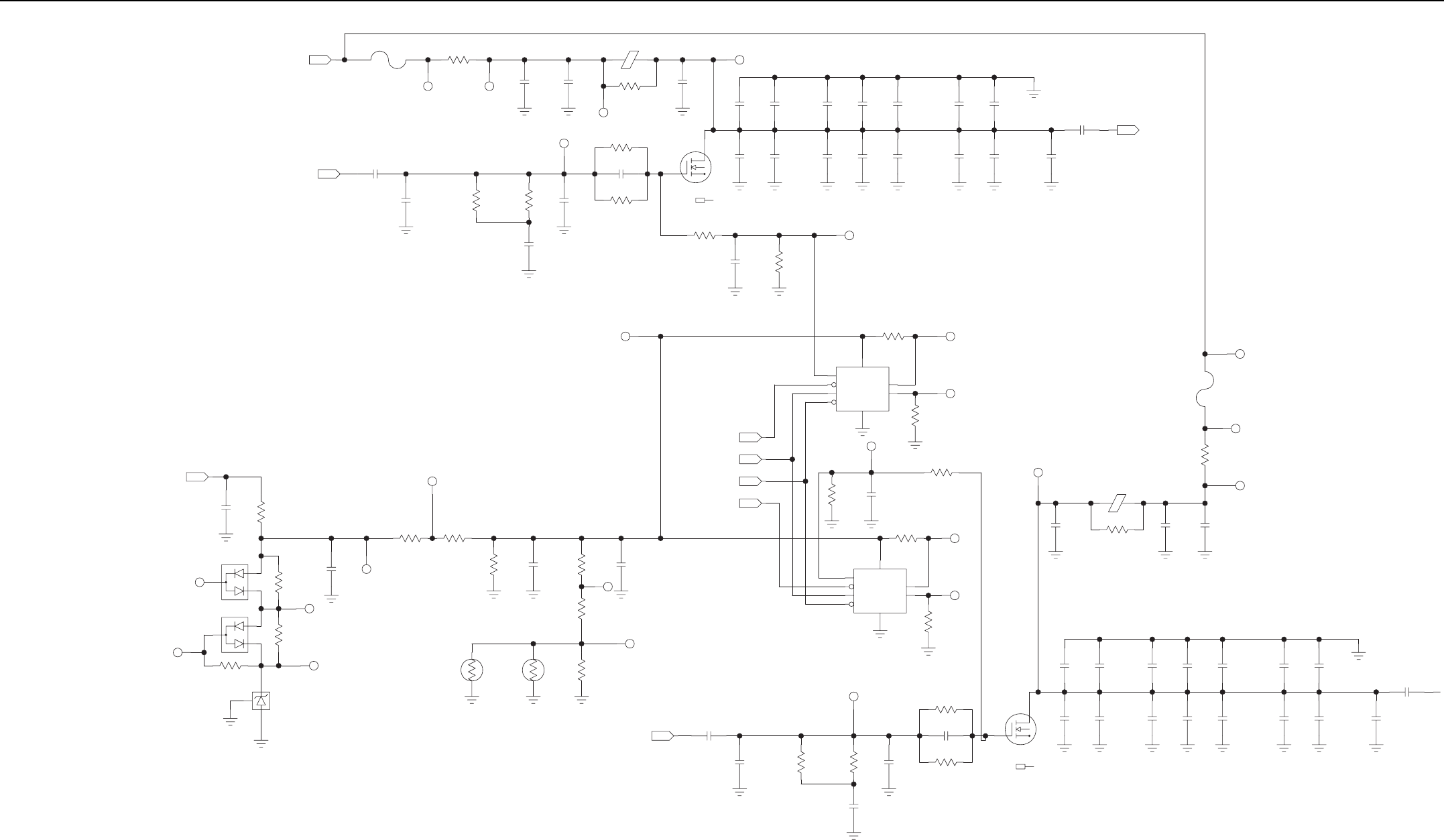
3-28 Power Amplifier (PA) Schematics (UHF)
1
TP4501
R4515
F4516
DNP
TEST_POINT
5A
.01
28V
125V
IN1
1
1
TP4502
C4510
E4511
R4512
C4513C4514
22.1
DNP
100PF
39PF
TEST_POINT
10UF
C4591
C4590
C4582
C4583
C4580
C4581
C4574
C4575
C4572
C4573
C4570
C4571
C4562
C4563
C4560
C4561
5.6PF
RF_OUT_1
7.5PF
7.5PF7.5PF12PF
12PF 7.5PF
100PF
2.4PF
18PF
18PF7.5PF
8.2PF
8.2PF
7.5PF2.4PF
OUT
D
1
M4500
R4543
1
2
1
Q4500
R4550
R4536
C4592
R4552
C4544
R4542
C4541
C4543
C4540
MRFE6S9045NR1
100 68PF
8.25
100
RF_IN_1
1000PF
100PF
1K
47PF
8.25
15PF
S
IN
1
R4544
C4538 1MEG
100PF
1
EPOT_CS6
EPOT_UD
EPOT_INC
EPOT_CS5 IN
IN
IN
IN
H
L
VCC
W
GND
CS
U_D*
INC
1
1
R4533
5
8
26
1
3
7
U4537
R4534
R4636
DS1804
8.2K
1K
15K
1
R4644 C4638
4
100PF
1MEG
VCC
W
GND
CS
U_D*
INC
1
1
R4633
R4634
5
8
26
1
3
4
7
U4637
8.2K
15K
DS1804
H
L
1
1
1TP4602
1TP4601
F4616
R4615
C4614
C4613
E4611
C4610
R4612
125V
39PF
22.1
5A
TEST_POINT
100PF
DNP
TEST_POINT
DNP
.01
10UF
NC
1
1
1
1
C4258
R4252
R4251
R4250
R4270
R4253
C4257
13
2VR4252
2
3
1
D4250
2
3
1
D4251
0
DNP
8.2V
MMBZ5237B
0DNP
100PF
180
100PF
BAV99LT1G
0
BIAS
1K
BAV99LT1G
IN
1
1
1
C4279
R4274
R4275
12
RT4278
12
RT4277
C4273
R4272
R4276
R4271
DNP
DNP
100PF
1K
1K 1K
1K
1K
1K
100PF
510 C4691
C4690
C4682
C4683
C4680
C4681
C4674
C4675
C4672
C4673
C4670
C4671
C4662
C4663
C4660
C4661
5.6PF7.5PF
7.5PF
7.5PF
7.5PF
18PF
18PF
8.2PF
8.2PF
2.4PF 7.5PF
7.5PF
12PF
12PF2.4PF
100PF
D
1
M4600
2
1
Q4600
MRFE6S9045NR1
S
R4643
1
C4692
R4650
R4652
C4644
R4642
C4643
68PF
1000PF
8.25
100 100
100PF
8.25
C4641
C4640
47PF
RF_IN_2
15PF
IN
Power Amplifier – Final Amplifier Q4500, Q4600 Circuit Schematic Diagram (Kit No. CLE6215)
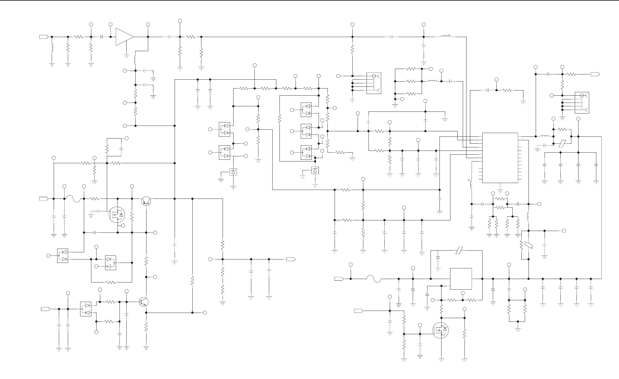
Power Amplifier (PA) Schematics (UHF) 3-29
1
1
G1
OUT
IN
1
1
1
R2101
C2100
L2100
3
1
2
Q2100
R2102
R2100
422NH
11.5
100PF
AH101
432
432
RF2
RF1
RF3
RF_DRV_IN
IN
NC 1
1
C2201C2200
R2203
D2202
2
3
1
D2200
R2202
R2201 R2200
V_OMNI_TRUE
.01UF 100PF
499
475
VGG1
1K
BAV99LT1G
499
BAV99LT1G
NC
1
1
2
3
1
13
2VR2200
MMBZ5225BLT1G
3V
C2411
1
TP44
1
TP45
1TP53
R2414
R2412 R2413
R2411
1
TP40
1
1
1
R2106
R2105 R2107
R2104
R2103
L2101
C2103
C2102
C2101
DNP
28V
DNP
TEST_POINT
DNP
TEST_POINTDNP
1K
.01UF
TEST_POINT
6.81
330PF
TEST_POINT
100PF
294
6.81
294
150NH
RF4 17.8
1K 1K
100PF
1K
DNP
1
1
R2400
F2400 1.5
125V
14V_DRV
3A
IN
Q2402
1
34
1
Q2400
R2401
MJD2955
10K
DNP
NTR0202PL
1TP75
2
1
3
C2410
1
C2408C2400
C2401
100PF
DNP
TEST_POINT
470PF
100PF
.01UF
1
1
1
1
C2403
C2402 C2409
23
1Q2401
R2406
2
3
1
D2404
C2404
R2404
R2403
MMBT3904
V_CTRL_DRV
1K
DNP
.01UF
10UF
DNP
100PF.01UF
267
267
BAV99LT1G
IN
NC
NC
1
1
2
3
1
D2402
2
3
1
D2400
R2405
R2402
BAV99LT1G
BAV99LT1G
0
1K
R2410
1
1
C2406
R2408
R2409
C2405
R2407
1K
10UF
(DNP)
V_OMNI_DRV
2.2
1K
1K
2.49K 100PF
DNP.01UF
DNP
OUT
C2407
1
1
C2505
C2506
R2510
R2504
2
1
3
Q2500
R2511
R2502
10K
2N7002LT1G
28V_DRV
.01UF
DNP
10K
15K 100PF
0
DNP
PA_EN_DRV
IN
IN
1
C2501
F2100
C2500
125V
28V
100PF1UF
3A
OUTIN
ADJUST
C2507
1
1
C2502 R2501 R2500
3
1
U2500
267
100PF
267
.01UF
LM317BD2T
1
C2503
R2514R2503
2
C2504
0
VDD
100PF 1UF
0
C2307 C2308
C2306C2305
DNP
10UF .01UF 10PF 150PF
C2329
1
1
E2301
R2304
DNP
470PF
DNP
20
NC
R2210
11
2
1
D2208
13
2VR2201
R2208
294
75
BAV99LT1G
9.1V
MMBZ5239BLT1G
NC
NC
1
1
1
1
1
1
1
R2209 R2207
R2206
3
2
3
1
D2206
2
3
1
D2204
R2205
R2204
BAV99LT1G
49.9
49.9
BAV99LT1G
475
549
DNP
0
VGG2
1
C2303 C2304
C2302
C2301
C2300
R2300
R2301
R2302
R2303
120PF
DNP
.01UF 10PF
12.1K
DNP
0
.01UF
1UF
DNP
DNP
0
DNP
1K
DNP
1
1
C2317
R2306
R2307
R2305
0
DNP
1K
.01UF
DNP
0
DNP
C2315 C2316
C2314C2313 R2308
1UF 12.1K
DNPDNP
120PF
10PF.01UF
DNP
1
E2500
DNP
NC9
NC10
NC13
NC7
NC5
NC4NC14
VTTS2
VGS2_1
VGS1
CTGND
NC2
NC3
RFOUTS1_VDS1
NC1
RFOUTS2_VDS2
RFINS1
VGGS1
VGS2_2
NC12
NC8
VTTS1
NC11
RFINS2
NC6
13
23
15
14
12
11
9
24
21
18
17
16
Q2300
MW7IC008N
21
L2300
19
7
20
10
1
6
22
5
8
4
3
2
4.7NH
R2323R2322
1
TP80
1
TP81
C2327
C2325
R2318
R2321
R2320
R2319 1
C2326
25
1.74K 1.74K
.01UF
TEST_POINT
11.5
TEST_POINT
3.3PF
.01UF
11.5
1.74K
1.74K
L2301
150NH
G4
G3
G1
C
G2
1
1
1
R2316
R2315
5
4
3
2
1
J2301
C2319
100PF
DNP
0
0RF_DRV_OUT
OUT
C2328
1
1
L2305
R2312
E2300
C2321 C2322 C2323 C2324
10PF
DNP
20 DNP
DNP
10UF
470PF
.01UF
150NH
150PF
1
TP140
1
TP141
1
1
1
R2314
21
L2303
C2311
L2304
C2310
C2318
R2310
R2311
R2309
.01UF
DNP
90.9
90.9
100PF
2.2PF
RF8
0
1.5NH
90.9
4.7NH
TEST_POINT
TEST_POINT
G4
G3
G1
C
G2
5
4
3
2
1
J2300
1
C2309
R2317
.01UF
43.2
1
Power Amplifier – Driver Amplifier Schematic Diagram (Kit No. CLE6215)
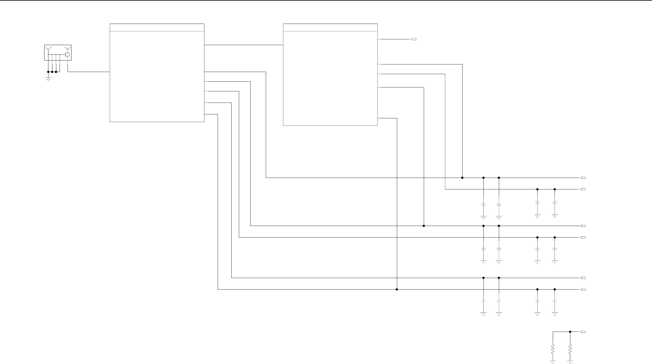
3-30 Power Amplifier (PA) Schematics (UHF)
RF INPUT CONNECTOR
RF_DRV_IN
G4
G3
G2
G1
C
J2000
IN
CONN_J
28V_DRV
14V_DRV
V_OMNI_DRV
V_CTRL_DRV
PA_EN_DRV
RF_DRV_OUT OUT
IN
IN
OUT
IN
IN
IN
DRIVER
RF_FNL_OUT
14V_FNL_IN
PA_EN_FNL_IN
RF_FNL_IN
28V_FNL_IN_A
28V_FNL_IN_B
OUT
IN
IN
IN
IN
FINALTO CIRCULATOR
TO: ISOL_RF_INPUT
1M2050
DNP
TO DISTRIBUTION BOARD
PA_ID
V_OMNI
PA_ENABLE
14V
28V_B
V_CONTROL
28V_A
R2027
C2041C2039
C2037
C2040
C2036
C2038
C2035
C2033
C2031
C2034
C2030 C2032
R2026
1M2026
1M2025
1M2024
1M2023
1M2022
1M2021
1M2020
12.1K15K
.01UF
100PF
100PF
DNP
DNP
DNP
.01UF
DNP
.01UF
100PF
DNP
100PF
DNP
100PF
.01UF .01UF
.01UF
DNP
100PF
Power Amplifier – RF Board Root Schematic Diagram (Kit No. CLE6216)
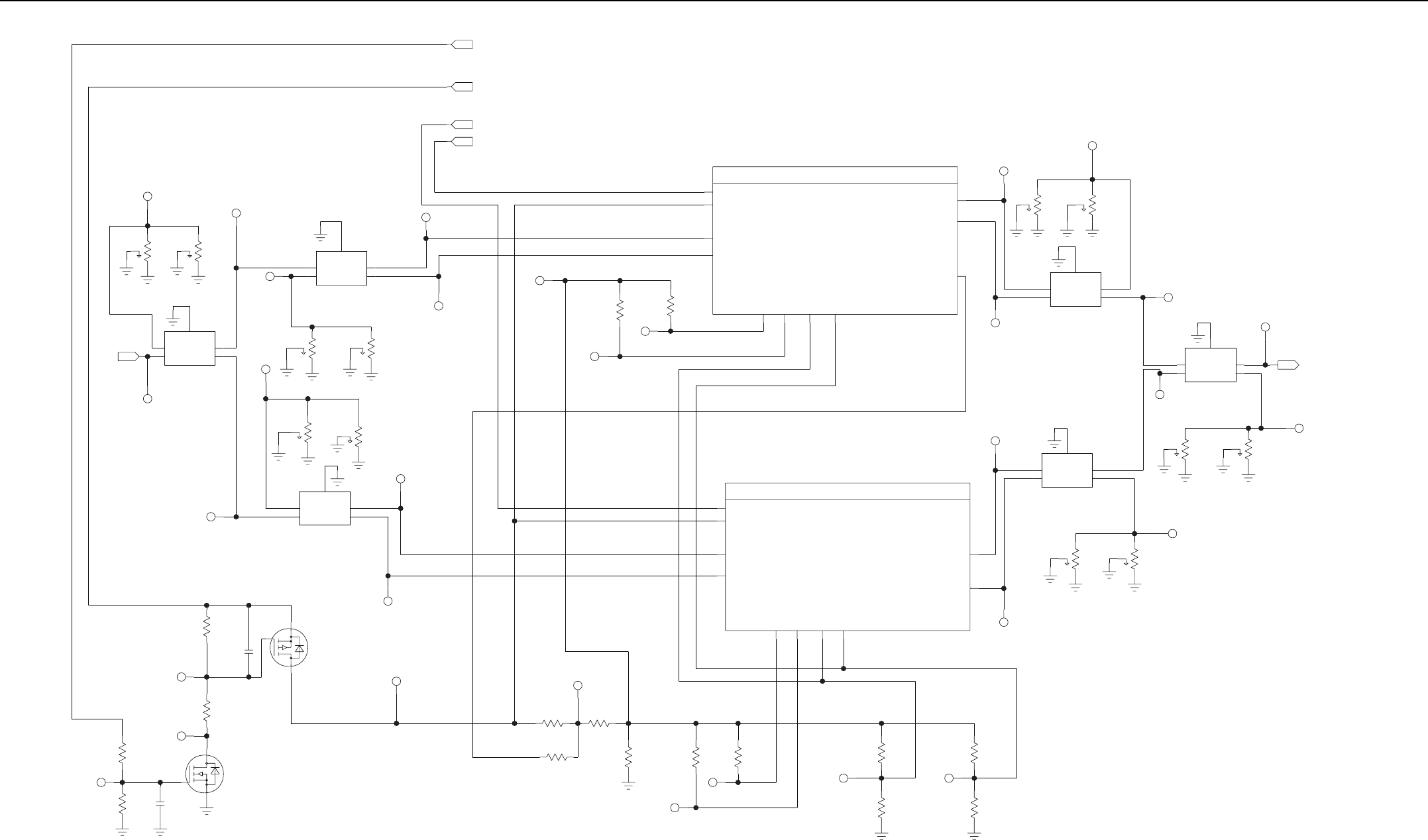
Power Amplifier (PA) Schematics (UHF) 3-31
1
1
IN
PA_EN_FNL_IN
28V_FNL_IN_B
28V_FNL_IN_A
14V_FNL_IN
IN
IN
IN
IN
IN
ISOL
ISO
OUT0
INOUT90
GND2
1
3
4
G1
U4120
QHDZ2H
1
1
1
C4210
R4217
R4124
C4216
2
1
Q4201
2
1
3
Q4200
R4211
R4212
NTR0202PL
100PF
10K
1K
10K
2N7002LT1G
100PF
15K
IN
ISOL
IN
ISOL
0 DEGREES
-90 DEGREES
0 DEGREES
-90 DEGREES
ISO
OUT0
INOUT90
GND
ISO
OUT0
IN
OUT90
GND
2
1
3
4
G1
U4130
2
1
3
4
G1
U4110
1
1
1
1
1
2
3R4131
1
2
3R4132
3
QHDZ2H
QHDZ2H
DNP
100
50
RF_FNL_IN
IN
1
112
3R4111
12
3R4112
100
50 DNP
1
1
2
3R4121
12
3R4122
DNP
50
100
-180 DEGREES
-90 DEGREES
1
1
1
1
TP4281
1
TP4280
R4281
R4280
TEST_POINT
10K
10K
TEST_POINT
DNP
VCCA
RF_IN_1
RF_IN_2
EPOT_INC
EPOT_UD
EPOT_CS4
EPOT_CS3
28V
BIASRF_OUT_1
RF_OUT_2
IN
IN
IN
IN
IN
IN
IN
Q4300_Q4400
ISOL
-180
ISO
OUT0
IN
OUT90
GND
2
1
3
4
U4910
1
1
12
3R4911
12
3R4912
RF_FNL_OUT
QHDZ2H
100
100
OUT
0
-90
-180 DEGREES
G1
1
ISOL
-90 DEGREES
-180 DEGREES
ISO
OUT0
INOUT90
GND2
1
3
4
U4920
1
1
1
1
12
3R4921
1
2
R4922
OUT
OUT
QHDZ2H
100
OUT 100
G1
3
0 DEGREES
-90 DEGREES
ISO
OUT0
INOUT90
GND
2
1
3
4
G1
U4930
1
OUT
OUT
QHDZ2H
ISOL
1
1
1
2
3R4931
1
2
3R4932
100 100
EPOT_INC
EPOT_UD
EPOT_CS6
EPOT_CS5
RF_OUT_1
BIAS
RF_IN_1
28V
RF_OUT_2
RF_IN_2
IN
IN
IN
IN
Q4500_Q4600
IN
IN
IN
IN
R4291
1
1
TP4282
1
TP4283
R4288
R4290
R4289
R4282 R4283
0
TEST_POINT
1K
1K
DNP
DNP
1.13K
DNP
10K
TEST_POINT
10K
INC
UP/DN
1
TP4287
1
TP4284
R4287
R4286
R4285
R4284
DNP
10K
10K
TEST_POINT
10K
TEST_POINT
DNP
DNP
10K DNP
Power Amplifier – Final Amplifier Main Schematic Diagram (Kit No. CLE6216)
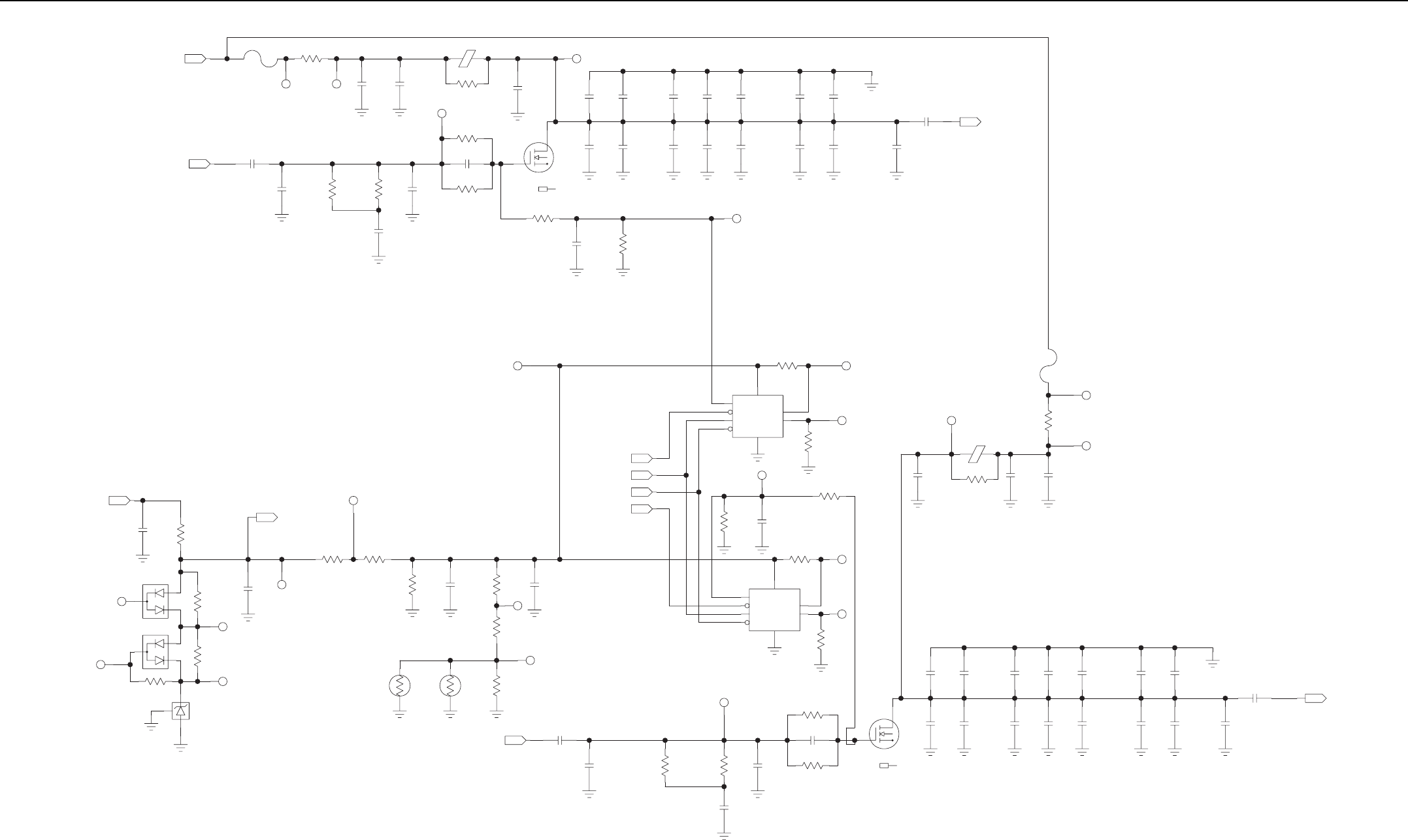
3-32 Power Amplifier (PA) Schematics (UHF)
R4343
1
1
TP4301
1
TP4302
E4311
R4312
R4350
C4392
C4344
C4313C4314
R4315
R4342
C4341
F4316
R4352
C4343
8.25
100PF
100
1000PF
100
8.25
10UF
DNP
68PF
125V
28V
.01
5A
22.1
39PF
TEST_POINT
DNP
TEST_POINT
15PF
IN
C4340
RF_IN_1
47PF
IN
C4391
C4390
C4382C4380
C4383C4381
C4374C4372C4370
C4375C4373C4371
C4362C4360
C4363C4361
100PF
RF_OUT_1
7.5PF
5.6PF
7.5PF
7.5PF18PF
7.5PF
8.2PF
18PF8.2PF
2.4PF
7.5PF12PF
12PF
2.4PF
OUT
7.5PF
D
1
M4300
1
C4310
2
1
Q4300
MRFE6S9045NR1
100PF
S
R4344
C4338
R4336
100PF 1MEG
1K
1
H
L
VCC
W
GND
CS
U_D*
INC
1
1
R4444 C4438
R4433
5
8
26
1
3
4
7
U4437
R4434
8.2K
1MEG100PF
15K
DS1804
H
L
VCC
W
GND
CS
U_D*
INC
1
1
1
R4333
R4334
5
8
26
1
3
7
U4337
R4436
1K
15K
8.2K
DS1804
4
EPOT_CS3
EPOT_CS4
EPOT_INC
EPOT_UD
IN
IN
IN
IN
1
1
1TP4402
1
TP4401
C4414C4413
E4411
R4412
C4410
22.1
TEST_POINT
DNP
DNP
10UF
100PF 39PF
TEST_POINT
F4416
R4415
.01
5A
125V
NC
1
1
1
1
C4228
R4222
R4221
R4220
R4223
C4227
2
3
1
D4220
2
3
1
D4221
13
2VR4222
BIAS
0
100PF
DNP
BAV99LT1G
0
0DNP
MMBZ5237B
8.2V
BAV99LT1G
100PF 180
VCCA
OUT
IN
1
R4241
R4240
1K
1K
C4491
C4490
C4482C4480C4474C4472
C4483C4481C4475C4473
C4470
C4471
C4462C4460
C4463C4461
5.6PF
7.5PF
7.5PF
7.5PF
7.5PF
7.5PF
18PF
18PF8.2PF
12PF 8.2PF
2.4PF
2.4PF 7.5PF
12PF
100PF RF_OUT_2
OUT
D
1
M4400
2
1
Q4400
MRFE6S9045NR1
S
R4443
1
1
R4450
C4492
R4452
C4444
R4442
C4441
C4440
C4443
1
2
RT4248
1
2
RT4247 R4246
68PF
510
100PF
100
1K 1K
DNP
RF_IN_2
1000PF
47PF
8.25
8.25
15PF 100
IN
1
C4249
R4244
R4245
C4243
R4242
100PF 1K
DNP
1K
1K 100PF
Power Amplifier – Final Amplifier Q4300, Q4400 Circuit Schematic Diagram (Kit No. CLE6216)
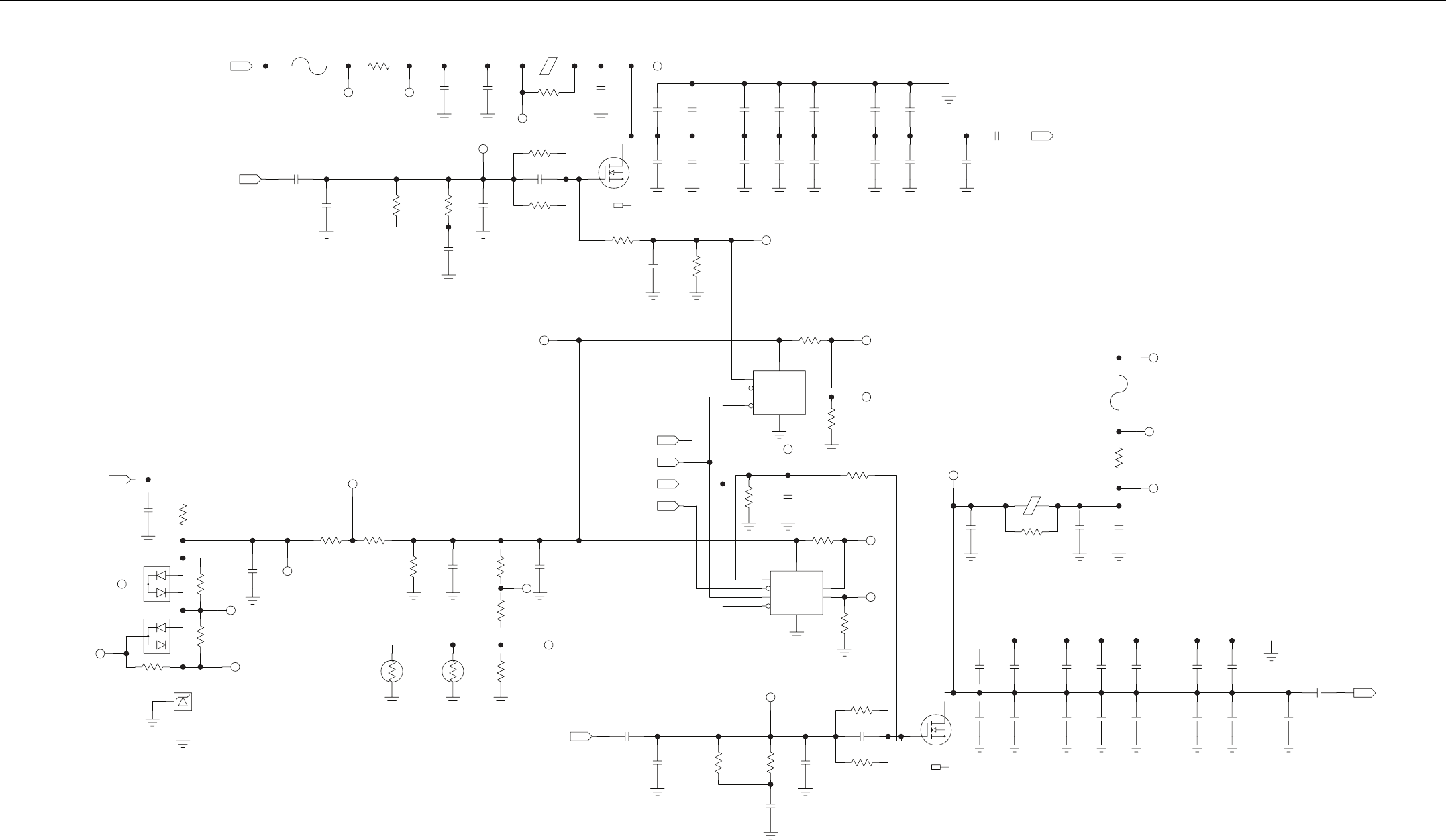
Power Amplifier (PA) Schematics (UHF) 3-33
1
1
1
1
TP4502
1
TP4501
C4510
E4511
R4512
R4550
C4513C4514
R4515
F4516
C4540
DNP
TEST_POINT
TEST_POINT
RF_IN_1
22.1
10UF
5A
.01
100PF
39PF
28V
125V
47PF
DNP
8.25
IN
IN
R4543
C4592
R4552
C4544
R4542
C4541
C4543
100PF
100 100 47PF
1000PF
8.25
15PF
D
1
M4500
C4591
C4590
C4582
C4583
C4580
C4581
C4574
C4575
C4572
C4573
C4570
C4571
C4562
C4563
C4560
C4561
2
1
Q4500
MRFE6S9045NR1
6.8PF
100PF
6.8PF
6.8PF5.6PF
11PF
11PF
8.2PF
8.2PF
6.8PF 4.7PF5.6PF
12PF
12PF6.8PF
6.8PF
RF_OUT_1
S
OUT
1
1
R4544
C4538
R4536
1MEG
1K
100PF
H
L
VCC
W
GND
CS
U_D*
INC
1
1
R4533
5
8
26
1
3
4
7
U4537
R4534
EPOT_CS6
DS1804
8.2K
EPOT_UD
EPOT_INC
EPOT_CS5
15K
IN
IN
IN
IN
H
L
VCC
W
GND
CS
U_D*
INC
1
1
1
R4644 C4638
R4636
R4633
R4634
5
8
26
1
3
4
7
U4637
15K
100PF
8.2K
1K
1MEG
DS1804
1
1
1TP4602
1TP4601
F4616
R4615
C4614
C4613
E4611
C4610
R4612
39PF
22.1
125V
5A
TEST_POINT
100PF
DNP
TEST_POINT
DNP
.01
10UF
C4682C4680C4674C4672
C4670C4662C4660
5.6PF
8.2PF 6.8PF11PF12PF6.8PF6.8PF C4691
100PF RF_OUT_2
OUT
C4690C4683C4681C4675C4673
C4671C4663C4661
6.8PF 6.8PF8.2PF 11PF 4.7PF5.6PF12PF6.8PF
D
1
M4600
2
1
Q4600
MRFE6S9045NR1
S
R4643
1
C4692
R4650
R4652
C4644
R4642
C4643
C4641
C4640
8.25
100PF
1000PF
100 100
47PF
RF_IN_2
15PF 47PF
8.25
IN
1
1
2
RT4278
12
RT4277 R4276
DNP
1K 1K 510
1
C4279
R4274
R4275
1K 100PF
1K
C4273
R4272
DNP100PF
1K
1
1
R4271R4270
C4257
100PF
1K1K
NC
1
1
1
C4258
R4252
R4251
R4250
R4253
13
2VR4252
2
3
1
D4250
2
3
1
D4251
0
DNP
8.2V
MMBZ5237B
0
DNP
180
100PF
BAV99LT1G
0
BIAS
BAV99LT1G
IN
Power Amplifier – Final Amplifier Q4500, Q4600 Circuit Schematic Diagram (Kit No. CLE6216)
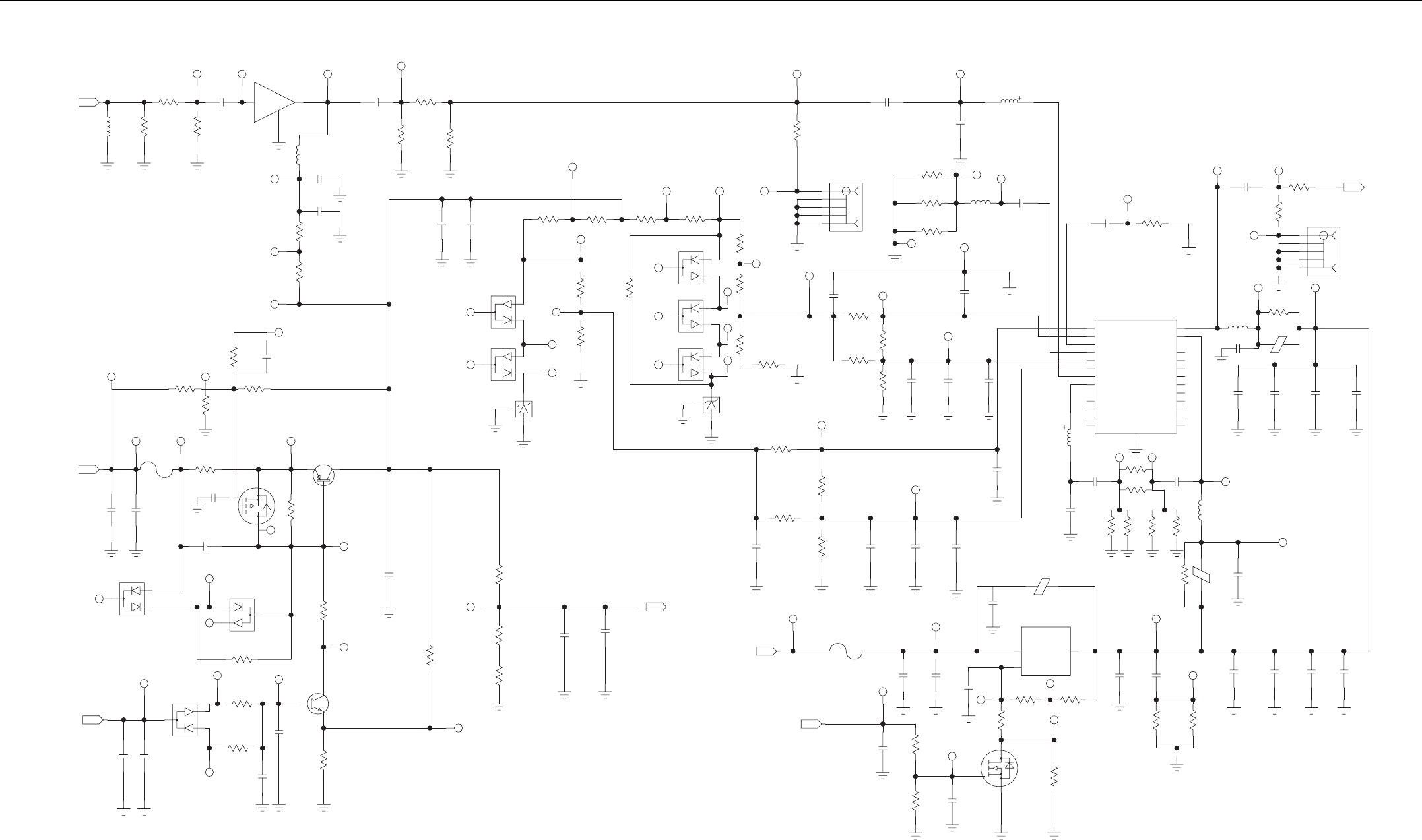
3-34 Power Amplifier (PA) Schematics (UHF)
1
1
OUTIN
1
TP40
1
1
1
R2106
R2105 R2107
R2101
C2101
C2100
L2100
3
1
2
Q2100
R2102
R2100
294 294
17.8
11.5
TEST_POINT
422NH
100PF
RF_DRV_IN
AH101
100PF
432
RF3
432
RF2
RF4
RF1
G1
IN
C2411
1
TP44
1
TP45
TP53
R2412 R2413
R2411
DNP
TEST_POINTDNP
TEST_POINT
1K 100PF
DNP
TEST_POINT
1K
DNP
1K
1
R2414
1
1
R2104
R2103
L2101
C2103
C2102
6.81
330PF
150NH
.01UF
28V
6.81
1K
DNP
1
NC
1
C2410
1
2
3
1
D2402
C2401
R2402
BAV99LT1G
0
100PF
DNP
470PF
1
1
C2403
C2402 C2409
2
3
1
D2404
C2404
R2404
BAV99LT1G
100PF
.01UF
267
V_CTRL_DRV
DNP
10UF
DNP
.01UF
IN
1
1
1
23
1Q2401
R2406
R2405
R2403
1K
MMBT3904
267
1K
1TP42
1
TP75
3
C2405
R2401
TEST_POINT
10K
10UF
DNP
TEST_POINT
2
Q2402
R2400
NTR0202PL
DNP
1.5
1
F2400
34
1
Q2400
MJD2955
1
1
C2408C2400
125V
100PF
3A
.01UF
14V_DRV
IN
NC 2
3
1
D2400
BAV99LT1G
R2410
C2406
R2409
R2407
1K
2.49K
DNP.01UF
DNP
1K
1
R2408
2.2
1K
C2407
V_OMNI_DRV
100PF
OUT
28V_DRV
PA_EN_DRV
IN
IN
1
C2505
C2506
R2510
R2504
2
1
3
Q2500
100PF
DNP
.01UF 10K 2N7002LT1G
15K
1
1
R2501
R2511
R2500
R2502
10K
267 267
0
DNP
OUTIN
ADJUST
C2507
E2500
1
C2502
C2501
23
1
U2500
C2500
LM317BD2T
100PF
.01UF
1UF 100PF
DNP
1
F2100
125V
3A
28V
1
C2307 C2308
C2306C2305
DNP
10UF 10PF 150PF
.01UF
1
C2503
R2514R2503
C2504
1UF100PF
00
1
VDD
C2329
1
E2301
R2304
DNP
470PF
DNP
20
19
7
20
10
1
6
22
5
8
4
3
2
13
23
15
14
12
11
9
24
21
18
17
16
NC9
NC10
NC13
NC7
NC5
NC4NC14
VTTS2
VGS2_1
VGS1
CTGND
NC2
NC3
RFOUTS1_VDS1
NC1
RFOUTS2_VDS2
RFINS1
VGGS1
VGS2_2
NC12
NC8
VTTS1
NC11
RFINS2
NC6
Q2300
MW7IC008N
1
TP80
C2325
25
.01UF
TEST_POINT
21
L2300
4.7NH
R2323
R2322
1
TP81
C2327
R2318
R2321
R2320
R2319 1
L2301
C2326
3.3PF
1.74K
11.5
1.74K
150NH
1.74K
11.5
1.74K
TEST_POINT
.01UF
C2321 C2322 C2323 C2324
DNP
150PF 10UF
10PF .01UF
C2328
1
1
L2305
R2312
E2300
150NH
DNP
20
DNP
470PF
1
1
1
R2316
R2315
5
4
3
2
1
J2301
C2319 RF_DRV_OUT
100PF
DNP
0
0
OUT
G4
G3
G1
C
G2
1
C2309 R2317
.01UF 43.2
TP140
R2310
R2311
R2309
TEST_POINT
90.9
90.9
90.9
1
1
TP141
1
1
L2304
C2301
C2318
TEST_POINT
.01UF
DNP
.01UF
1.5NH
G4
G3
G1
C
G2
J2300
1
21
L2303
C2311
C2310
RF8
100PF 4.7NH
2.2PF
1
R2314
DNP
0
1
5
4
3
2
1
1
1
R2207
R2206
549
475
VGG2
C2303 C2304C2302
R2302
R2303
.01UF
0
12.1K 10PF
DNP
120PF
DNP
1
1
R2300
R2301
1K
DNP0
DNP
C2300
DNP
1UF
1
C2315 C2316
C2317
C2314
R2308
.01UF
DNP
.01UF 120PF
12.1K
DNP
10PF
DNP
C2313
R2307
R2305
DNP
1UF
0
0
DNP
NC
NC
NC
111
1
R2209
2
3
1
D2208
2
3
1
D2206
2
3
1
D2204
13
2VR2201
R2208
R2306
BAV99LT1G
BAV99LT1G
BAV99LT1G
9.1V
MMBZ5239BLT1G
294
DNP
1K
DNP
0
R2210
75
R2203
R2202
1K
VGG1
475
NC
NC
1
1
1
1
1
C2201C2200
2
3
1
D2202
2
3
1
D2200
13
2VR2200
R2201 R2200
V_OMNI_TRUE
MMBZ5225BLT1G
BAV99LT1G
BAV99LT1G
499
100PF
499
3V
.01UF
1
1
R2205
R2204
49.9 49.9
Power Amplifier – Driver Schematic Diagram (Kit No. CLE6216)
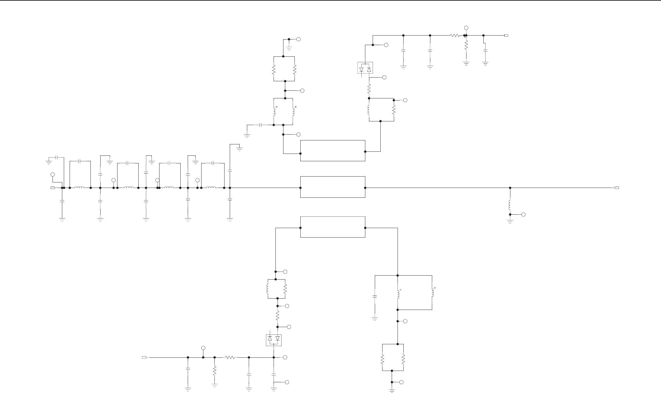
Power Amplifier (PA) Schematics (UHF) 3-35
1
TEST_POINT
DNP
C8014
3PF
1.8PF
C8015
1
TP4
1
TP3
1
TP2
TP1
1
M8002
C8007
C8011
L8003
L8002
L8001
L8000
C8009
C8008
C8012
C8006
C8005
C8004
C8003
C8010
C8002
C8001 3.6PF
1.8PF
DNP
DNP
RF_IN
4.7PF
18NH
.5PF
TEST_POINT
1.8PF
.5PF
3PF
DNP
2PF
TEST_POINT
.5PF
18NH
TEST_POINT
.5PF
18NH
3PF
18NH
3PF
1
TP13
L8022
2
3
1
CR8001
TP19
1
TP14
1TP16
1
R8025
1M8001
C8023C8022C8021
R8023
R8022
R8024
20K
100PF
267
HSMS2812
100PF
TEST_POINT
9.1PF
5.62K
DNP
REV_DET
DNP
TEST_POINT
150NH
TEST_POINT
TEST_POINT
47.5
REVERSE
FORWARD
COUPLER C=27DB
TP11
TEST_POINT
8.2NH
L8021
L8020
8.2NH
TEST_POINT
100
1TP18
TP12
R8021
C8020
R8020
100
TEST_POINT
DNP
1.5PF
1
1
TP5
TEST_POINT
R8014
C8032
TEST_POINT
1TP15
1
1TP8
1TP10
1TP9
1TP7
R8015
C8031
1
M8003
R8013
C8013
2
3
1
CR8000
L8012 R8012
36.5K
150NH267
TEST_POINT
DNP
TEST_POINT
FWD_DET
TEST_POINT
100PF 100PF
9.1PF
DNP
5.62K
HSMS2812
TEST_POINT
47.5
1.5PF 8.2NH8.2NH
DNP
L8011
1
1TP20
1TP17
C8030
R8011
2
L8010
R8010
TEST_POINT
TEST_POINT
100 100
1TP21
L8004
TEST_POINT
422NH
M8000
RFOUT
Power Amplifier – Output Board Schematic Diagram (Kit No. CLE6217)
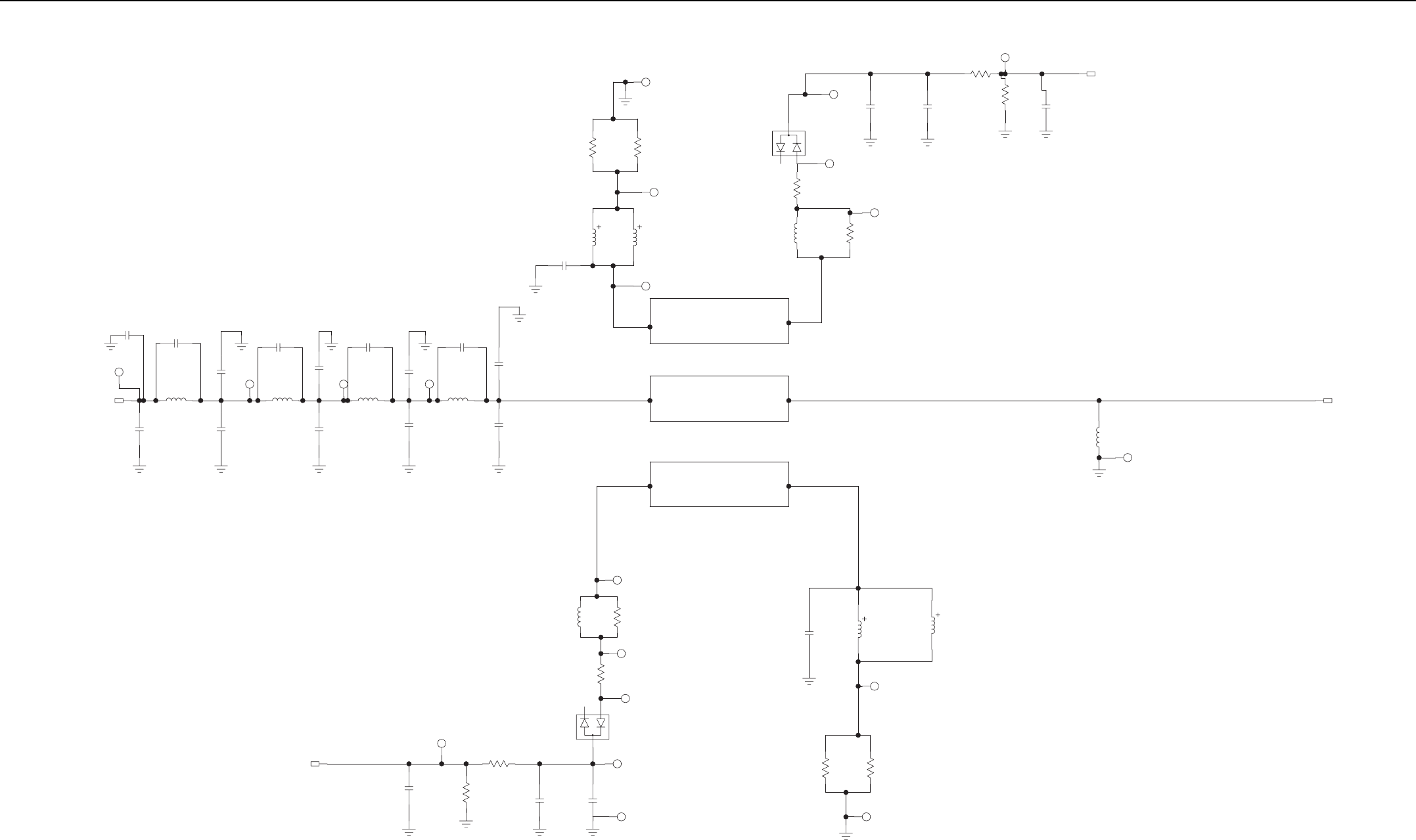
3-36 Power Amplifier (PA) Schematics (UHF)
1
TEST_POINT
TEST_POINT
DNP
REV_DET
DNP
5.62K
9.1PF
TEST_POINT
100PF
TEST_POINT
HSMS2812
100PF
20K
R8024
C8021 C8022 C8023
M8001
1
R8025
1
TP14
1
TP19
TP18
1
CR8001
1
3
2
TP13
TEST_POINT
R8023
1
L8022 R8022
249
47.5
TP16
150NH
TP12
TEST_POINT
95.3
R8020
95.3
R8021
1
1TP11
L8021
5.6NH
L8020
5.6NH
TEST_POINT
REVERSE
FORWARD
COUPLER C=27DB
DNP
1.5PF
C8020
DNP
3PF
C8014
C8009
2.7PF
2PF
DNP
TEST_POINT
1
TP1
1
C8015
18NH
TEST_POINT
RF_IN
DNP
1.8PF
L8003
C8007
M8002
TP2
1
1
C8010
18NH
C8001
1.5PF
L8000
.3PF
C8002
.3PF
18NH
C8008
.3PF
C8012
3.3PF
C8006
.3PF
TP3
TEST_POINT
1.8PF
DNP
C8005
1PF
1PF
C8003
2PF
L8001
1
18NH
TP4
TEST_POINT
L8002
C8011
C8004
RFOUT M8000
422NH
TEST_POINT
L8004
TP21
1
47.5
HSMS2812
5.62K
DNP
9.1PF
100PF
100PF
FWD_DET
TEST_POINT
DNP
TEST_POINT
CR8000
1
3
2
C8013
M8003 1
C8032 C8031
TP7
1
1
TP8
1
TP5
1
TP15
1
TEST_POINT
TP9
TEST_POINT
TP10
TEST_POINT
R8015
36.5K
R8014
TEST_POINT
1
R8013
150NH
L8012
249
R8012
TEST_POINT
C8030
TP17
DNP
1.5PF
L8010
5.6NH
L8011
5.6NH
1
1TP20
TEST_POINT
R8011
95.3
R8010
95.3
Power Amplifier – Output Board Schematic Diagram (Kit No. CLE6218)
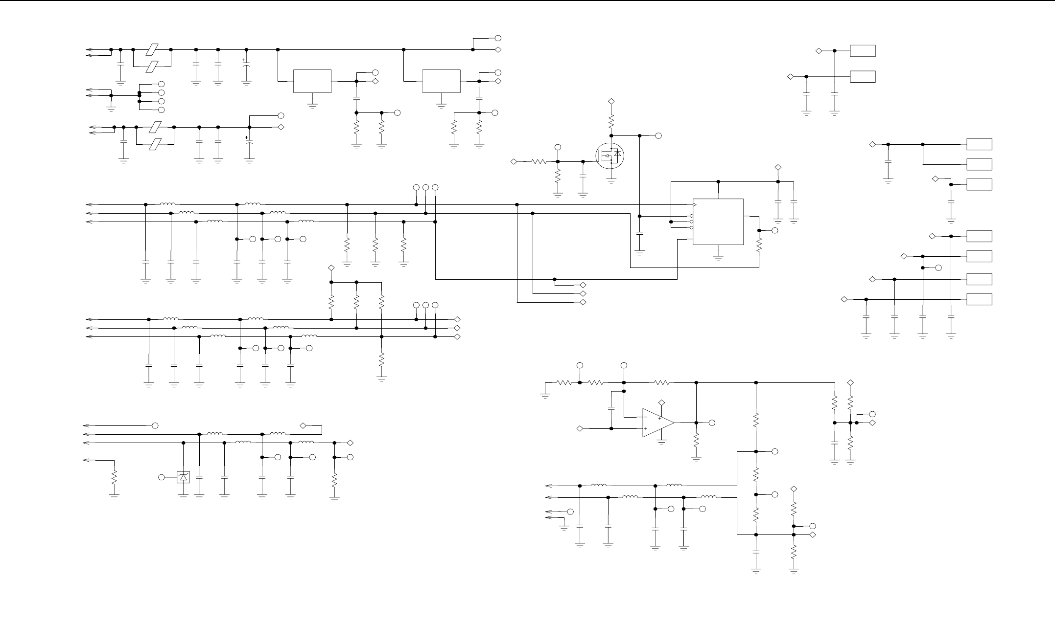
Power Amplifier (PA) Schematics (UHF) 3-37
14V IN
TO POWER SUPPLY
28V IN
430PF
J6001
1
J6001
2
J6001
3
J6001
4
J6001
5
J6001
6
C6010
3.3V REGULATOR
3.3V
680PF
680PF
10UF
430PF
150PF 330UF
1
32
E6011
E6012 C6013
E6021
C6023
E6022
C6020
C6015
12
C6014
1
1
1
1
1
1
C6051
1
28V_DST
MC33269
U6050
R6053
1
R6052
1
GND
VINVOUT
330UF150PF
C6025
12
C6024
NOTE 2
NOTE 3
NOTE 2
NOTE 3
TO OUTPUT BOARD
V_FWD_DST
FG4961
FG4961
430PF 430PF
DNPDNP
V_REV_DST
M6910
1
M6911
1
C6911C6910
PINA
PINA
NVM ENABLE INVERT
0
10K
2N7002LT1G
DNP
430PF
Q6136
3
1
2
R6134
R6137
C6138
1
10K
1
R6131
5V
5V REGULATOR
10UF
14V_DST
NVM_ENABLE
U6060
1
32
C6061
1
1
1
R6062
1
R6063
1
5V
IN
ADJ
OUT
MC33269
SPI_CLK
SPI_MISO
SPI_MOSI
J6000 7
J6000 8
J6000 9
1
DNP
10K
R6127
5V
10K 10K
10K
ADDR1
ADDR0
RESET
R6121 R6122R6120
R6124 R6125
1
1
1
1
1
10K
10K
DNP
470NH
8.2PF 430PF 430PF 430PF
150NH470NH
470NH
150NH
8.2PF
150NH
8.2PF
C6100 C6110
L6100 L6110
L6111
C6111
L6101
C6101 C6102 C6112
L6112
L6102
11 1
J6000
J6000
J6000
J6000
J6000
J6000
J6000
TO CONTROLLER
PA_ADDR1
PA_ADDR0
PA_RESET
430PF
150NH
150NH
470NH
8.2PF 430PF8.2PF 430PF
150NH
8.2PF
470NH
470NH
3
6
10
L6115
C6115
L6114
L6113
C6114C6113
L6104
L6103
L6105
C6105C6104C6103
11 1
NOTE 2
NOTE 3
SPARE
VCTRL
PA_ENABLE
NOTE 2
470NH
150NH
8.2PF
0
DNP
MMBZ5237B
8.2V
8.2PF
VCTRL_DST
PA_EN_DST
150NH
1
2
4
5
L6117L6107
L6106
C6106C6107
R6090
1
VR6107
2
3
1
NC
NC
470NH
430PF
430PF 10K
L6116
C6116C6117 R6126
1
1
R6123
10K
TO ADC
NOTE 3
MOSI
CLK
MISO
6
1
7
5
3
430PF
C6139
AT25640A
U6130
2
8
CLK_S
EN_CSSO
SI
HOLD
VCC
WP
GND
NVM
.1UF
5V
0
430PF
4
C6132 C6133
R6135
1
430PF
28V_DST
C6900
430PF
14V_DST
C6902
FG4961
FG4961
FG4961
FG4961
FG4961
FG4961
FG4961
M6900
M6902
M6903
M6904
M6905
M6906
M6901
PINA
PINA
PINA
PINA
PINA
PINA
PINA
TO RF BOARD
1
1
1
1
1
1
1
1
430PF430PF 430PF 430PF
C6925 C6924 C6923
C6926
NOTE 1
NOTE 2
NOTE 1
NOTE 3
NOTE 1
NOTE 3
NOTE 2
NOTE 3
VCTRL_DST
VOMNI_DST
PA_IDA_DST
PA_EN_DST
NOTE 1
NOTE 3
430PF
5.62K 5.62K
5V
PA_IDA_DST
DNP
1K
R6226
R6227
R6225
C6251
1
NOTE 3
15K
15K
430PF
5V
5.62K
R6220
R6221
C6259
R6224
R6223
1
PA_IDB
15K
1
1
8.2PF 430PF 430PF
8.2PF
C6190 C6191 C6192 C6193
470NH
470NH
L6192
11
L6193
499
R6211
4
6.81K
430PF
CPLD_PA_ID
R6210
9
10
11
1
1
C6404
1
6.81K
R6212 R6213
6.81K
14V_DST
MC3303
U6400
8
BAND ID JUMPER
J6002 1
J6002 2
J6002 3
J6002 4NC
150NH
150NH
L6191
L6190
2.21K
R6222
NOTE 1 : DC Distribution Board I/O, NVM (Kit No. CLE6219)
NOTE 2 : DC Distribution Board Power Control (Kit No. CLE6219)
NOTE 3 : DC Distribution Board ADC, CPLD, DAC (Kit No. CLE6219)
Power Amplifier – DC Distribution Board I/O, NVM (Kit No. CLE6219)
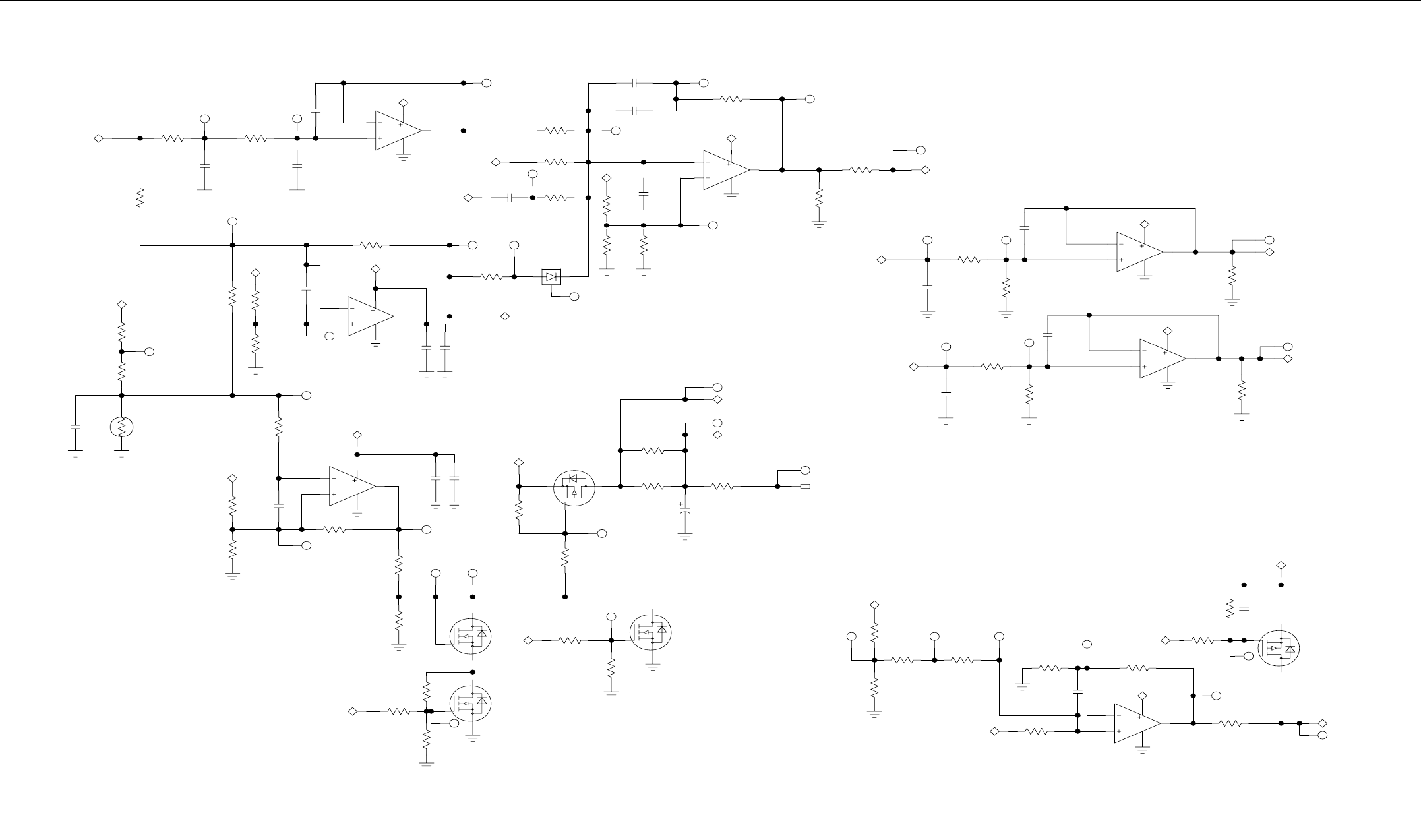
3-38 Power Amplifier (PA) Schematics (UHF)
TEMP SENSE
21.5K
5.62K
R6560
R6552
1
RT6553
100K
1
2
C6554
R6551
47.5K
430PF
5V
NOTE 3
TO FEEDTHROUGH CAP
14V_FAN_OUT
NOTE 3
FAN_SUPPLY
FAN_VOLTAGE
3.9
TP5
1
1
330UF
C6597
DNP
DNP
M6950
3.9
3.9
R6597
R6596
1
R6595
1
1
2
NOTE 3
MMBD6050LT1
3
R6558
6.81K
2
D6559
PA_TEMP
1
NC
1
1
NOTE 2
NOTE 3
NOTE 1
C6411
R6500
C6505
.068UF
1000PF
0.033UF
C6511
DNP
R6503
2.21K
V_FWD
VOMNI_DST
1
R6504
1
14V_DST
10K
MC3303
C6501
100K
PWR_SET
U6410
15K
R6502
11
1
5
1
1
R6501
C6500
R6550
4
7
6
0
1000PF
DNPDNP
0
430PF
TEMP ROLLBACK
1
47.5K
R6557
1
R6555
430PF
5V
C6416
10K
14V_DST
U6410
4
MC3303
1
C6413
R6556
3
2
10K
430PF
11
100K
R6579
1
FAN CONTROL
14V_DST
430PF
U6400
R6582
.1UF
C6405
430PF
1
R6580
6
5
C6401
R6581
2.21K
1.5K
4
MC3303
C6406
11
7
5V
100K
R6588
15K
1
NOTE 1
2N7002LT1G
2N7002LT1G
1
1
1
R6598
R6587
Q6592
3
Q6591
2
1
3
Q6593
R6586
0
DNP
2N7002LT1G
1K
FAN_ENABLE
10K
2
1
R6589
1
2
1
3
5.62K
NOTE 1
NOTE 2
R6599
R6584
0
0
DNP
PA_EN_DST
FAN ONLY WHEN PA IS ENABLED
TO ENABLE TEMP CONTROLLED
THIS TRANSISTOR CAN BE USED
R6583
0
10K
4
R6585
1
3
1
14V_DST
MTD5P06V
Q6590
POWER CONTROL
8
U6410
4
14V_DST
1
0.068UF
C6510
R6512
1K
MC3303
1
R6516
6.81K DNP
9
10
C6412
5.62K
R6517
R6515
1
11
5V
6.81K
430PF
NOTE 1
NOTE 3
R6518
VCTRL_DST
R6513
1
1K
10K
C6415
.1UF
POWER SET SCALE, BUFFER AND ENABLE INTERLOCK
NOTE 1
NOTE 2
NOTE 3
DAC_PWR_SET
R6285
1
R6281
5V
PA_EN_DST
1
1
1
R6289
11 4
14
12
13 U6410
C6414
R6284
R6283
R6282
R6280
430PF
8.66K
1K 14V_DST
MC3303
10K
0
2.21K
10K
10K
R6288
PWR_SET
430PF
R6290
5V
DNP
1
1
1
R6286
C6290
2
1
3
Q6287
1K
0
NTR0202PL
0
DNP
POWER DETECTOR SCALE AND BUFFER
NOTE 1
NOTE 3
14V_DST
4
V_REV
1
MC3303
14
U6400
V_REV_DST
11
1
1
R6754
R6751
R6752
C6753
C6403
12
13
21.5K
47.5K
430PF
430PF
1K
NOTE 1
V_FWD_DST
R6701
21.5K
1
1
C6703 R6702
47.5K
430PF
C6402
430PF
11 4
2
3
U6400
1
14V_DST
MC3303
NOTE 2
NOTE 3
499
R6704
1
V_FWD
NOTE 1 : DC Distribution Board I/O, NVM (Kit No. CLE6219)
NOTE 2 : DC Distribution Board Power Control (Kit No. CLE6219)
NOTE 3 : DC Distribution Board ADC, CPLD, DAC (Kit No. CLE6219)
Power Amplifier – DC Distribution Board Power Control (Kit No. CLE6219)
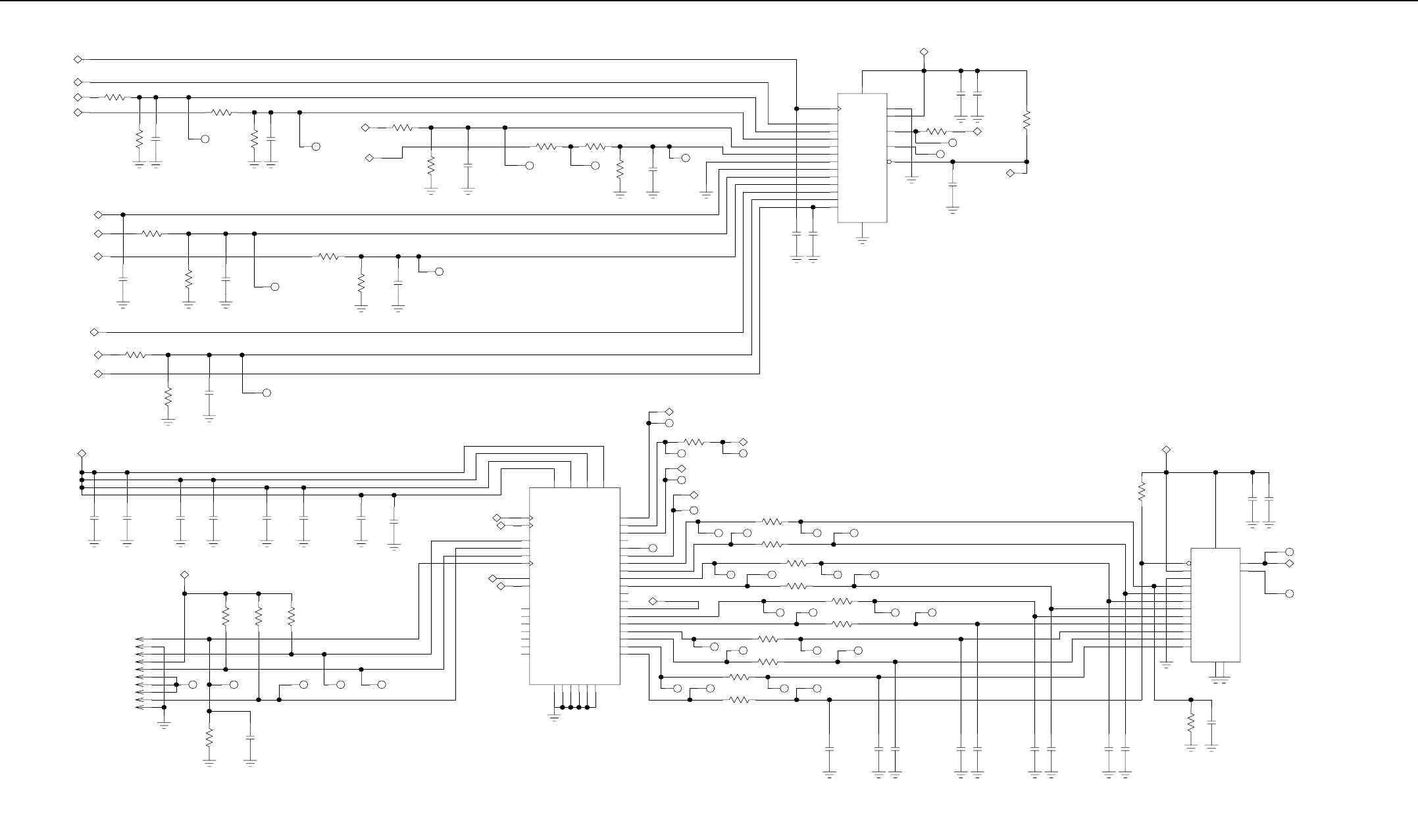
Power Amplifier (PA) Schematics (UHF) 3-39
NOTE 1
NOTE 2
NOTE 2
NOTE 2
NOTE 1
NOTE 2
1TP124
1
TP75
R6264
R6262
R6263
R6261
1
1
1
R6239
C6255
R6229
R6228
C6250
R6230
R6231
C6257
C6256 430PF
FAN_SUPPLY
CLK
1K 430PF 1.5K 430PF
1.5K 2.21K
V_REV
V_FWD
1K
1K
DNP
430PF
0
DNP
PA_IDA_DST
0
2.21K
FAN_VOLTAGE
NOTE 2
NOTES 1 2
NOTE 1
NOTE 1
NOTE 1
NOTE 1
1
1
R6233
R6232
C6258
C6253
R6238
R6237
C6252
430PF
430PF
PA_IDB
MOSI
28V_DST 47.5K
430PF
VOMNI_DST
PA_TEMP
VCTRL_DST 15K
6.81K
8.66K
1
C6254
R6236
R6235
1.5K
1.5K
430PF
CPLD
C6166C6163C6165C6161 C6160
C6164C6167C6162
430PF .1UF 430PF
.1UF430PF.1UF
3.3V
.1UF
430PF
R6159R6157R6156
1K1K1K
CPLD PROGRAM
2
J6155
1
J6155
5
J6155
4
J6155
3
J6155
6
J6155 7
J6155 8
J6155
10
J6155
9
J6155
C6168
111
R6158
1
430PF
1K
NC
3.3V
7
32
1
26
40
38
31
28
27
25
35
34
33
39
37
ADDR0
RESET
MOSI
CLK
29
9
41
17
OE2_GCLK2
TDO
GNDIO0
GNDIO2
GNDIO1
IO_B11
IO_B12
IO_B9
IO_B10
IO_B8
IO_B6
IO_B7
GCLRN
OE1
TDI
TMS
TCK
GCLK1
VCCIO0
VCCIO1
GNDINT0
GNDIO3
GNDINT1
IO_B4
IO_B5
IO_B3
IO_B2
IO_B1
IO_A12
IO_B0
IO_A9
IO_A10
IO_A11
IO_A7
IO_A8
IO_A4
IO_A5
IO_A6
IO_A3
IO_A2
IO_A1
IO_A0
VCCINT0
VCCINT1
30
24
11
4
36
16
43
15
12
5
6
23
22
21
20
19
18
14
13
10
8
44
42
3
2
ADDR1
NC
CPLD PIN 8 RESERVED
FOR FUTURE DAC USE
U6150
EPM3064ATI44
C6182
C6184 C6181C6183C6185
C6187 C6186
C6188
C6189
430PF
DNP
430PF 430PF
DNPDNP
DNP
430PF
DNPDNP
430PF
DNP
430PF430PF
DNP
430PF 430PF
DNP
C6180
R6173
DNP
430PF
10K
DNP
14
17
4
3
2
5
6
7
8
9
10
11
12
13
GND
D7
D6
D5
D3
D4
D2
D0
D1
A0
SHDN
REF
WR
VDD
CTGND
OUTB
OUTA
NOTE 2
1
1
1
15
16
U6170
DAC_PWR_SET
MAX5102
DAC
C6172C6171
R6174
10K
3.3V
.1UF
430PF
NOTE 2
NOTE 1
1
1
1
1
11
1
R6180
1
R6185
R6181
R6182
R6183
R6191
1
1
1
11
1
1
ADC_CS
NVM_ENABLE
FAN_ENABLE
49.9
49.9
49.9
49.9
49.9 49.9
1
R6189
R6188
1
11
1
R6186
1
1
R6187
11
1
R6184
49.9
49.9
49.9
49.9
49.9
SIGNALS WITH _DST APPENDED SIGNIFY EXTERNAL CONNECTIONS
NOTE 1
CPLD_PA_ID
1 0 ADC
0 1 DAC
0 0 NVM
ADDR0 ADDR1 DEVICE
DIGITAL DEVICE SELECT TRUTH TABLE
1 1 NONE
18
17
11
9
8
7
6
5
4
3
12
2
1
C6247 C6246
10
DNP
430PF
430PF
DNP
20
GND
ADDRESSIN
A10
A9
A8
A7
A6
A5
A4
A3
A2
A1
A0
IOCLK
VCC
EOC
DATAOUT
REFPOS
REFNEG
U6240
TLC542I
CS
14
13
19
16
15
NOTE 1
1
C6245
R6244
C6242C6241
R6243
430PF
ADC_CS
0
DNP
430PF
MISO
.1UF
10K
NC
5V
NOTE 1 : DC Distribution Board I/O, NVM (Kit No. CLE6219)
NOTE 2 : DC Distribution Board Power Control (Kit No. CLE6219)
NOTE 3 : DC Distribution Board ADC, CPLD, DAC (Kit No. CLE6219)
Power Amplifier – DC Distribution Board ADC, CPLD, DAC (Kit No. CLE6219)
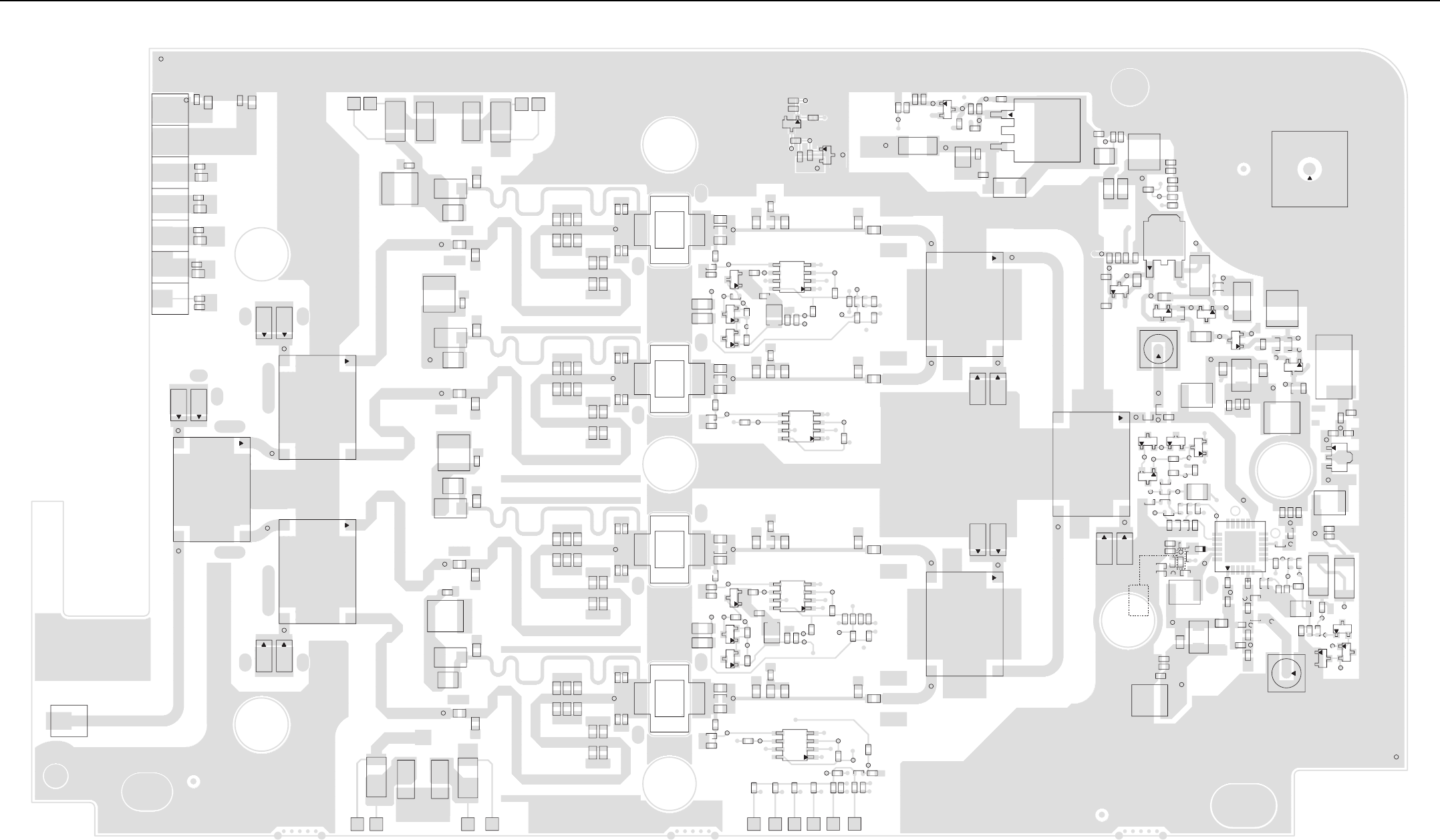
3-40 Power Amplifier (PA) PCB (UHF)
3.5 Power Amplifier (PA) PCB (UHF)
3
4
2
3
4
2
TP23
R4911
TP24
M2026
M2025
M2024
M2022
M2023
M2021
M2020
U4910
R4912
R2027
R2026
C2040
C2041
C2039
C2038
C2036
C2037
C2035
C2034
TP21
TP26
R4932
U4930
R4931
TP22
3
4
2
U4920
R4921
TP20
R4922
M2050
TP4402
TP4401
TP4301
TP4302
R4415
F4416
TP18
R4315
F4316
C4391
E4311
R4312
C4314
C4390 C4310
C4313
C4491
TP16
C4490
R4412
E4411
C4414
C4410 C4413
TP4602
TP4601
TP122
TP17
C4614
R4615
F4616
C4613
C4591
E4511
C4513
C4514
C4691
R4612
TP19
E4611
F4516
C4590
R4512
C4510 C4690 C4610
R4515
TP4501
TP4502
C4675
C4673
C4682
C4680
C4662
C4683
C4681
TP136
C4671
C4663
C4660
C4661
C4574
C4572
C4575
C4573
C4674
C4672
C4582
C4580
C4570
C4562
C4583
C4581
TP127
C4571
C4563
C4670
C4560
C4561
8
4
5
85
4
3
32
32
2
R4533
TP131
C4541 R4275 R4274
R4271
TP123 C4279
R4633
TP125
TP133
C4641
C4540
R4276
C4273
R4272
C4640
Q4500
RT4278
R4544
C4538
M4500
C4592
RT4277
TP124
R4534
R4536
TP128
R4550
C4544
R4552
TP121
D4250
R4251
R4250
TP117
R4634
R4252
TP116
TP118
TP130
U4537
TP132
R4543
R4542
R4270
C4257
C4543
R4253
TP120
TP119
U4637
C4258
TP134
D4251
Q4600 C4638
R4644
M4600
C4692
VR4252
R4650
R4636
TP129
C4644
R4652
R4642 C4643
R4643
32
3
2
Q4201
TP44
R4211
TP10
TP61
TP66
Q4200
C4216
R4124
R4217
TP5
TP4
C4210
R4212 TP1
3
2
3
C2505
R2504
F2100
R2511
TP68
C2506
R2510
Q2500
TP70
C2500
C2507
C2501
C2502
TP73
R2502
R2501
R2500
TP79
TP78
E2500
2
U2500 C2503
TP84
R2503
R2514
C2504
R2406
R2407
R2408
C2405
R2409
R2410
C2201
C2407
C2406
TP47
TP37
C2200
TP13
R4122
R4121
TP9
C4441
C4440
C4462
C4463
TP114
C4460
C4461
C4475
C4473
C4482
C4480
C4483
C4481
C4471
C4374
C4372
C4375
C4373
C4474
C4472
C4382
C4380
C4362
C4370
C4383
C4381
TP104
C4371
C4363
C4470
C4360
Q4300
C4361
M4300
R4344
C4338
R4334
R4336
TP106 TP108
TP4284
TP4280
TP4282
TP4283
TP4281
TP4287
R4285
R4281
R4283
R4280
R4282
R4284
R4287
R4286
R4290
R4289 R4288
TP15
R4291
TP14
R4333
TP102
TP112
85
4
C4344
R4350
U4337
R4343
R4342
R4241
R4433
TP101
TP109
C4340
R4246
C4243
R4242
TP96
TP97
C4341
R4245
C4249
R4244
32
C4392
D4220
R4352
TP99
85
4
3
2
32
Q4400
R4444
RT4248
RT4247
TP103
C4438
R4220
TP94
VR4222
C4228
R4222
R4221
D4221
TP95
TP93
R4436
R4434
TP107
R4240
C4227
C4343
U4437
R4223 TP110
M4400
C4492
R4450
C4444
R4452
TP105
R4442 C4443
R4443
TP137
TP72
C2031
C2030
C2033
C2032
3
4
2
TP12
U4120
3
4
2
TP11
TP25
R4131
R4132
U4130
TP8
TP6
4
3
32
32
5
2
32
Q2402
R2413
C2410
TP45
TP53
D2402
R2401
TP42
TP75
C2411
R2414
R2412
R2411
TP89
J2301
R2402
TP30
C2401
Q2400
TP39
R2405
TP29
TP43
D2400
R2400
C2400
C2408
F2400
TP34
C2403
3
3
32
2
C2322
C2323
E2300
C2328
Q2401
R2309
R2310
C2324
C2321
C2402
R2312
TP27
TP83
R2403
R2404
C2404
TP32
TP46
L2101
R2311
TP141
TP41
C2100
R2101
TP33
L2100
D2404
C2409
TP31
TP38
C2102
C2103
Q2100
R2100
R2102
TP28
3
2
32
3
2
54
3
2
R2105
J2300
C2101
TP40
R2106
TP60
R2314
TP62
VR2200
R2202
TP48
TP49
R2200
R2203
R2201
TP51
TP52
D2202
D2200
TP36
C2314
R2308
C2316
C2315
L2303
TP67
C2313
R2305
TP50
C2305
C2308
C2307
C2306
TP91
R2304
TP87
L2301
C2329
E2301
TP71
C2311
R2317
R2107
TP82
C2309
C2310
32
2
3
2
3
R2315
D2206
TP3
TP88
C2319
R2316
D2208
TP90
TP57
L2305
VR2201
2
3
D2204
TP59
TP56
R2205
R2209
TP63
R2206
R2207
TP54
TP58
TP55
R2204
R4112
R4111
R2322
R2323
R2321
R2210
R2320
TP69
TP2
TP80
R2318
TP81 C2327
R2319
R2300
R2301
C2325
C2303
C2302
R2208
R2302
R2303
L2300
C2326
TP86
C2304
C2301
TP65
C2300
3
4
2
TP7
U4110
24
19
18
7
6
13
12
Q2300
C2317
TP64
C2318
TP85
R2104
R2307
R2306
TP74
TP35
L2304
R2103
G4
G3
G1
G2
J2000
TP140
RF Board PCB – Top View (PCB No. 84009277001)
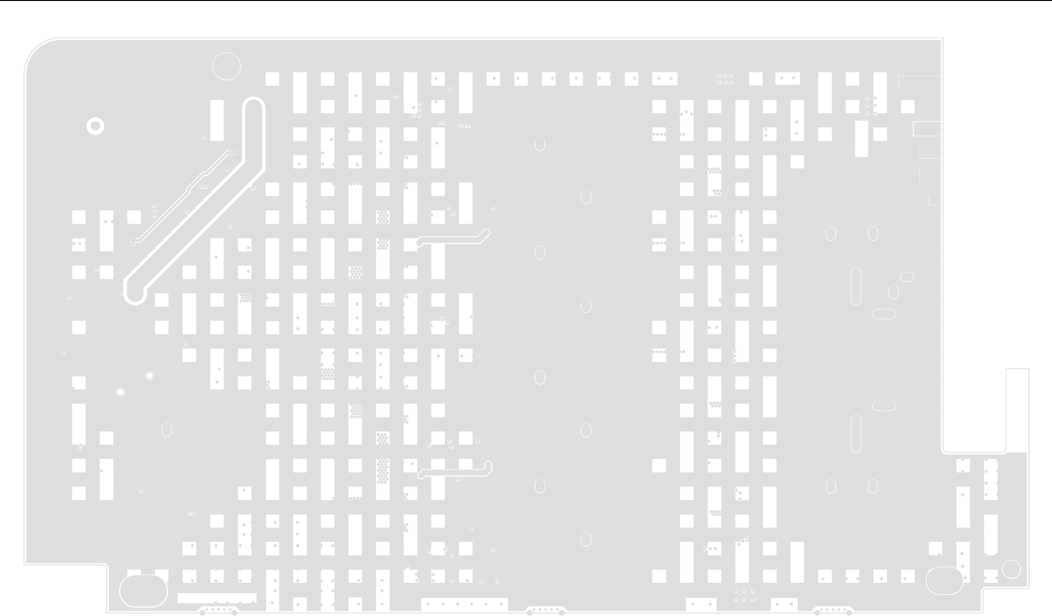
Power Amplifier (PA) PCB (UHF) 3-41
84009277001_A
RF Board PCB – Bottom View (PCB No. 84009277001)
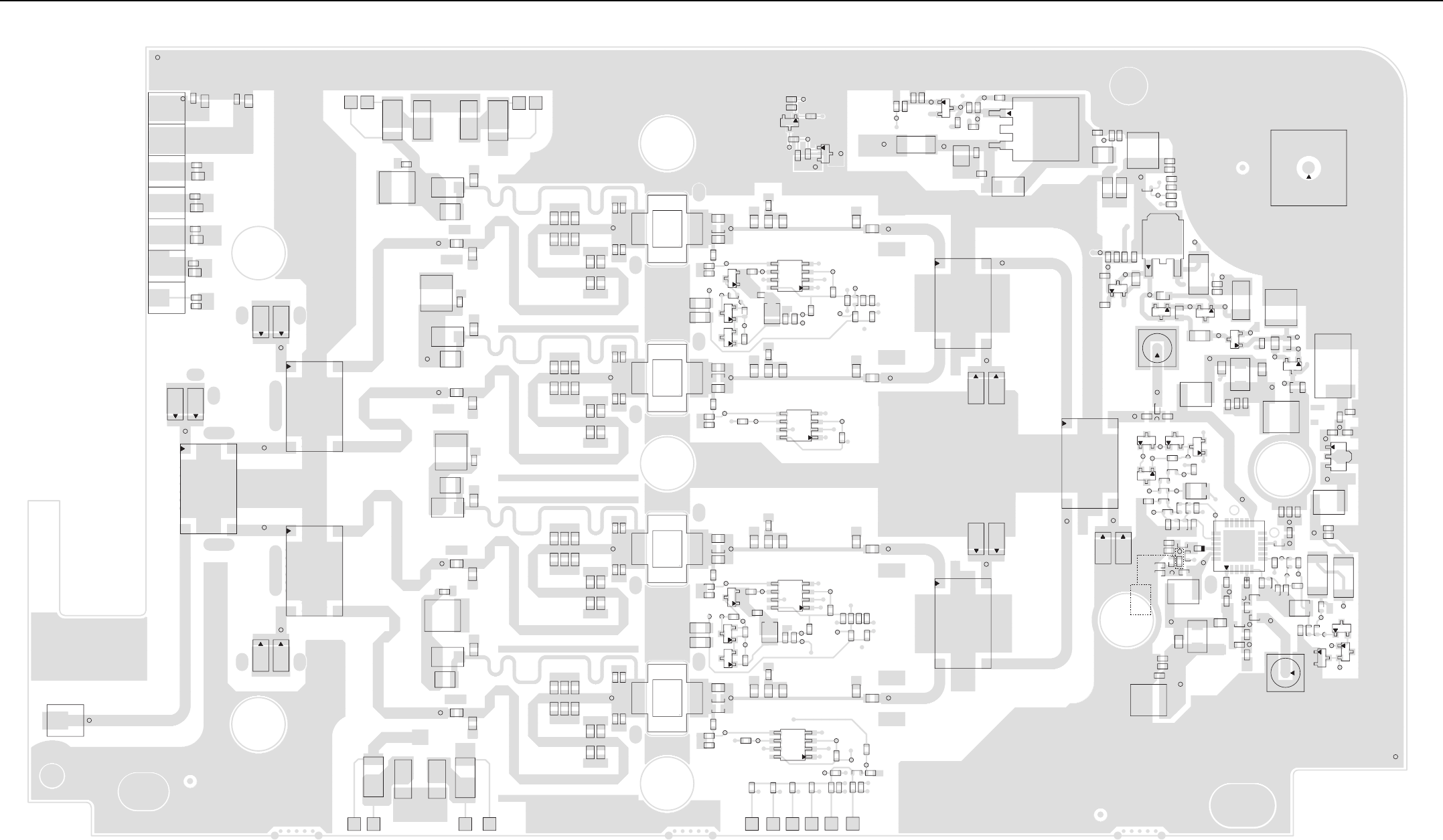
3-42 Power Amplifier (PA) PCB (UHF)
M2025
M2026
M2024
M2023
M2022
M2021
M2020
TP137
TP72
C2030
R2027
C2041
R2026
C2037
C2038
C2039
C2040
C2035
C2036
C2034
U4910
23
4
R4911
TP24
R4912
TP21
TP26
TP22
R4932
U4930
R4931
23
4
C4614
C4613
R4612
TP19
C4691
E4611
C4690 C4610
TP122
C4591
TP17
R4512
C4513
E4511
C4514
C4510
C4314
C4491
C4313
TP16
E4411
R4412
C4414
C4490 C4413
C4410 C4590
C4391
TP18
R4312
E4311
C4390 C4310
R4415
F4416
F4316
R4315
TP4401
TP4402 TP4301 TP4302
C4374
C4372
C4375
C4373
C4382
C4380
C4362
C4370
C4381
C4383
C4363
C4371
TP104
C4360 C4361
C4472
C4474
C4473
C4475
C4482
C4480
C4462
C4470
C4483
C4481
C4463
C4471
C4460 C4461
TP114 M4400
R4244
R4433
TP101
R4241
TP109
C4243
R4242
R4246
R4245
Q4400
R4444
RT4247
RT4248
TP103
R4436
C4438
R4220
D4220
TP94
D4221
R4222 C4228
VR4222
R4221
TP93 TP95
TP105
R4450
R4434
TP107
C4444
R4452
C4492
TP96
R4240
C4227
TP110
R4223
TP97
U4437
C4443
R4443
R4442
C4249
85
4
32
32
32
R4285
R4288
TP15
R4291
TP12
C4340
TP4280 R4281
TP4282
TP4281
R4282
R4283
R4280
TP4283
TP4284
R4284
R4287
TP4287 R4286
R4289
R4333
R4290
TP102
TP14
C4341
TP112
Q4300
M4300
R4344
C4338
R4336
R4334
R4350 TP99
TP108
TP106
C4344
R4352
C4392
U4337
R4343
R4342
C4343
85
4
R4921
TP20
R4922
U4920
2
3
4
M2050 TP23
C2031
C2033
C2032
TP4602
R4615
F4616
TP4601
F4516
R4515
TP4501
TP4502
C4572
C4574 C4575
C4573 C4672
C4675
C4674
C4673
C4582
C4580
C4562
C4583
C4581
C4570
C4563
C4571
TP127
C4682
C4680
C4662
C4683
C4681
C4670 C4671
TP136
C4663
C4560
Q4600
M4600
C4660 C4661
C4561
R4533
TP131
C4541
TP11
C4540
R4536
C4538
R4544
TP132
R4534
TP128
C4544
R4552
C4592 TP121
R4550
U4537
C4543
R4542
R4543
8
4
5
R4271
TP123
R4275
R4274
C4279
TP125
R4633
TP133
R4276
C4273
R4272
TP120
R4270
C4257
TP119
U4637
85
4
C4641
TP25
C4640
Q4500
M4500
RT4277
C4638
R4644
RT4278
TP124
R4636
R4251
D4250
TP117
R4250
D4251
C4258
R4634
R4252
VR4252
TP116
TP118
R4650
TP130
R4253 TP134
R4643
R4642
3
32
32
2
C2505
R2511
TP70
C2506
R2510
R2504
TP73
C2502
TP78
R2500
R2501
R2502
TP79
3
2
TP66
TP61 F2100
TP68
C2507
C2500
C2501
E2500
U2500
3
2
Q2500
TP44
TP10
Q4201
C4216
R4124
TP5
R4217
R4211
Q4200 TP4
C4210
R4212 TP1
32
3
2
C4644
R4652
C4692
TP129
C4643
R4132
R4131
TP8
U4130
2
3
TP6
4
C4441
TP13
C4440
U4120
TP9
R4122
R4121
2
3
4
TP7
R4111
R4112
TP2
U4110
2
3
4
J2000
G4
G3
G1
G2
C2504
C2503
TP84
R2514
R2503
R2414
R2412
R2411
C2411
R2407
R2408
C2405
TP39
Q2400
TP47 R2410
R2409
C2407
C2406
C2201
TP37
C2200
R2406
C2410
Q2402
R2413
TP45
TP53
D2402
TP42
R2401
TP75
R2402
J2301
TP30
C2401
TP89
R2405
D2400
TP43 C2408
TP34
R2400
C2400
4
3
32
5
2
32
TP29
F2400
C2403
32
C2328
E2300
Q2401
TP83
R2312
TP32
TP27
R2404
R2403
C2404
TP46
L2100
C2409
C2402
D2404
TP31
TP38
3
32
2
C2322
C2323
C2318
R2310
R2309
TP141
TP85
C2321
C2324
R2311
C2103
C2102
TP35
L2304
TP74
L2101
TP41
TP33
C2100
R2101
Q2100
R2102
R2100
TP28
3
TP60
R2308
C2314
R2307
C2315 C2317
TP64
TP67
TP49
VR2200
TP48
R2200
TP51
TP52
R2201
R2202
R2203
C2313
R2306
R2305
R2104
TP50
D2202
TP36
D2200
R2103
3
2
32
3
2
C2305
C2306
C2307
TP91
C2308
R2304
TP87
C2101
R2105
C2329
E2301
R2107
J2300
TP40
R2106
3
2
54
R2317
TP82
C2311
C2309
L2303
TP71
R2314
TP62
C2310
C2316
Q2300
24
19
18
7
6
13
12
R2323
R2321
TP69
R2210
TP59
D2204
C2327
R2319
C2326
R2318
R2322
L2301
TP81
C2325
TP80
R2320
C2303
C2302
R2303
R2301
R2302
R2300
R2208
C2300
R2207
R2206
R2205 TP54
TP63
TP55
TP86
L2300
C2304
C2301
TP65
R2204
2
3
TP140
TP56
R2315
D2206
TP3
R2209
TP58
C2319
R2316
D2208
TP57
TP90
TP88
L2305
VR2201
32
2
32
3
RF Board PCB – Top View (PCB No. 84009296001)
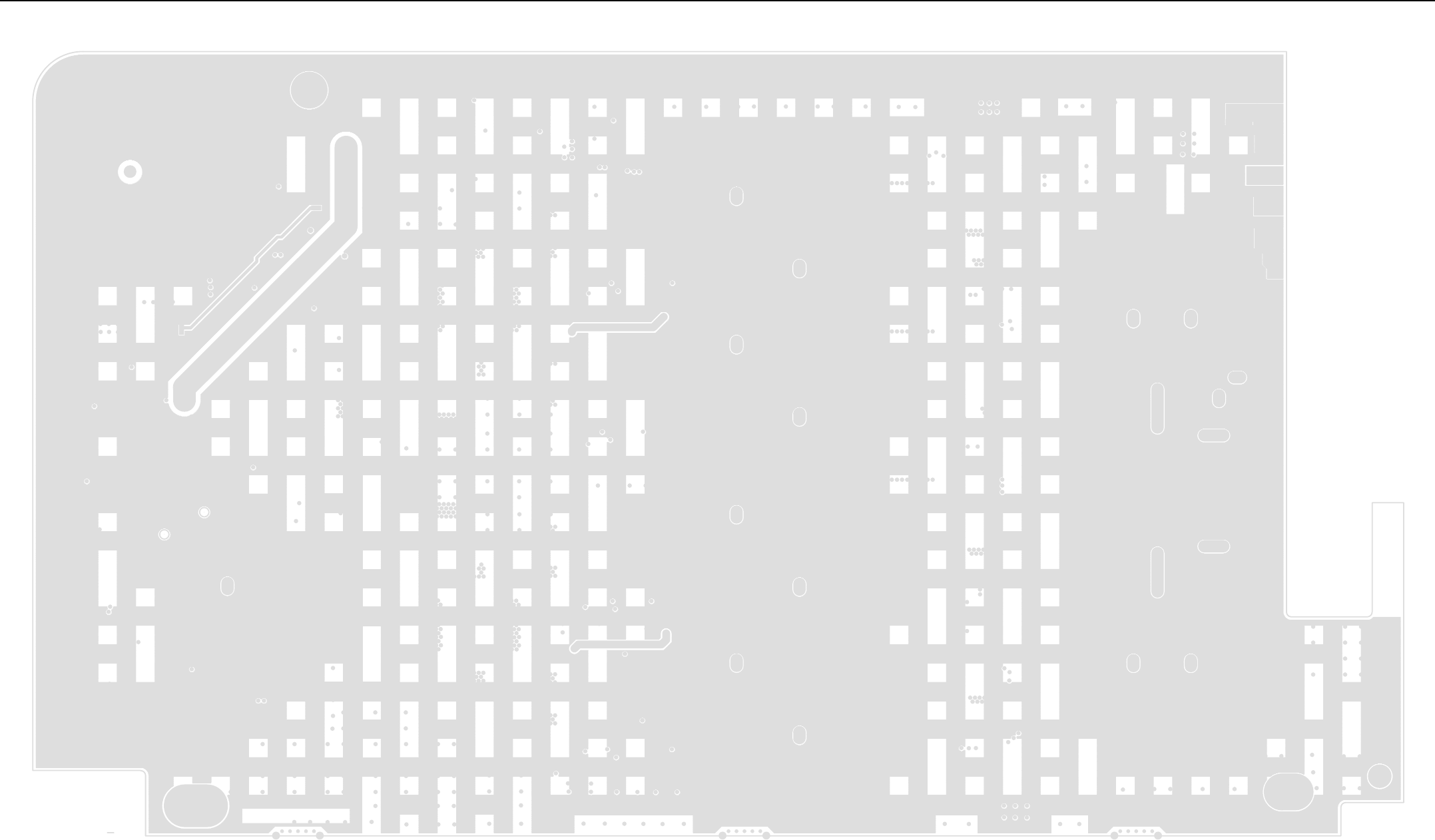
Power Amplifier (PA) PCB (UHF) 3-43
84009296001_A
RF Board PCB – Bottom View (PCB No. 84009296001)
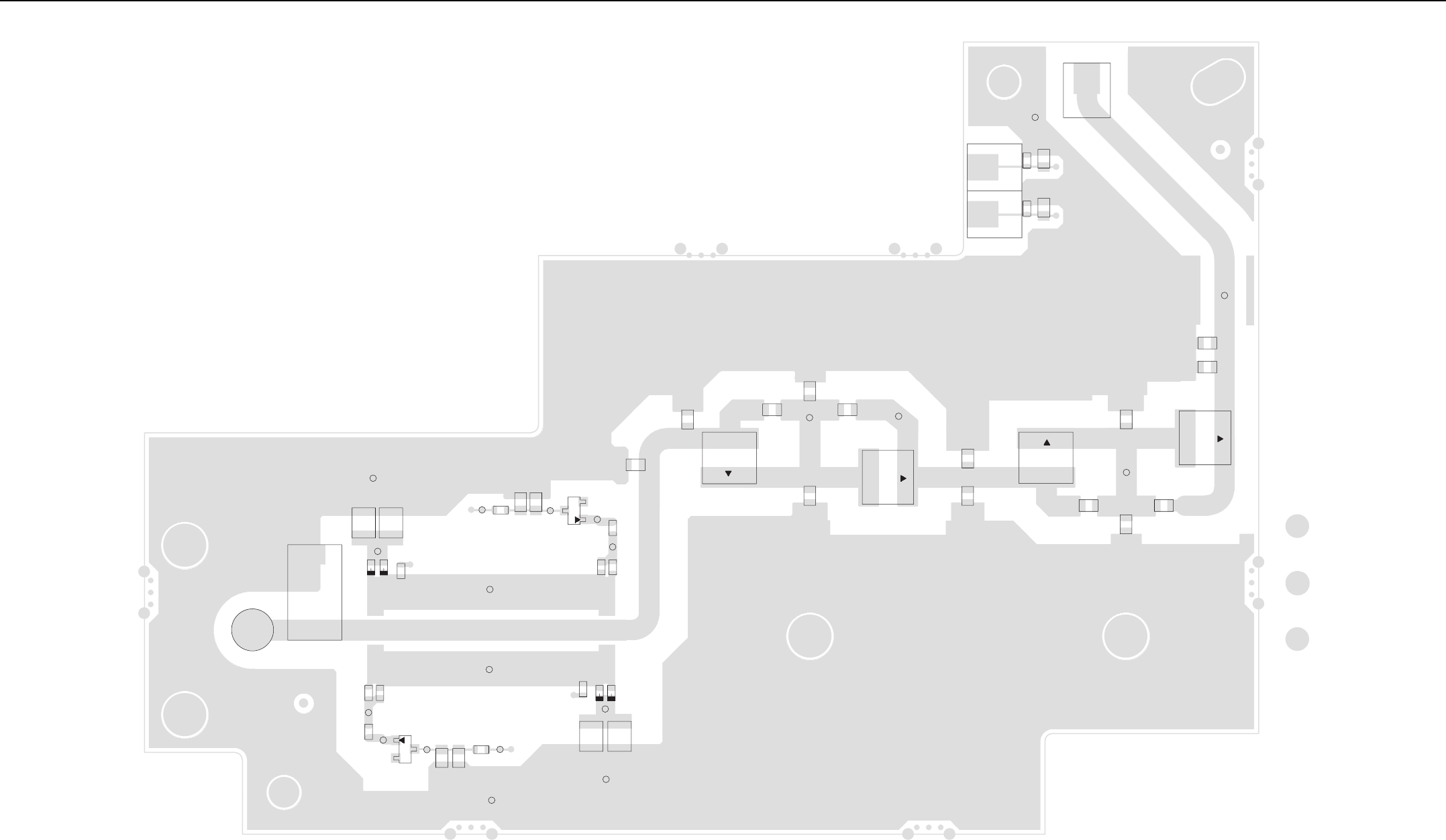
3-44 Power Amplifier (PA) PCB (UHF)
R8011
TP17
L8011
TP15
C8030
R8010
L8010
M8000
L8004
3
2
R8023 R8022
TP16
CR8001
C8021
TP14
L8022
TP13
C8022
R8024
TP19
TP20
TP11
R8021
C8020
R8020
TP18
TP12
L8021
L8020
3
2
TP7
R8014
TP5
CR8000
C8031
C8032
TP8 TP10
L8012
R8012
R8013
TP9
L8003
C8009
C8008
TP4
C8012
L8002
C8006
C8007
TP3
C8014
C8011 C8005
C8004
L8001
C8010
C8002
TP2
C8003
L8000
C8001
C8015
TP1
M8001
M8003
R8025
C8023 C8013
M8002
R8015
TP21
Output Board PCB – Top View (PCB No. 84009274001)
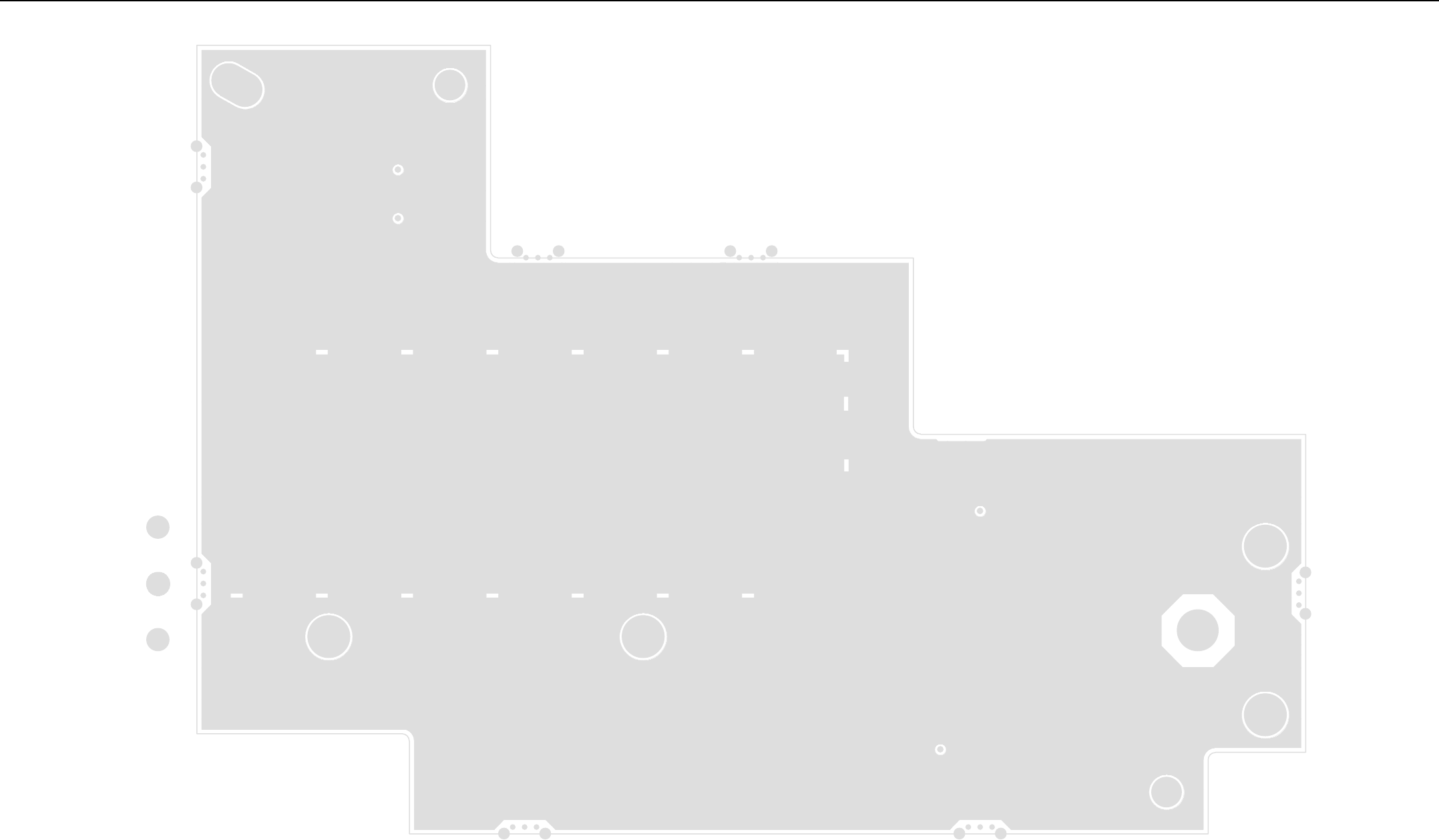
Power Amplifier (PA) PCB (UHF) 3-45
Output Board PCB – Bottom View (PCB No. 84009274001)
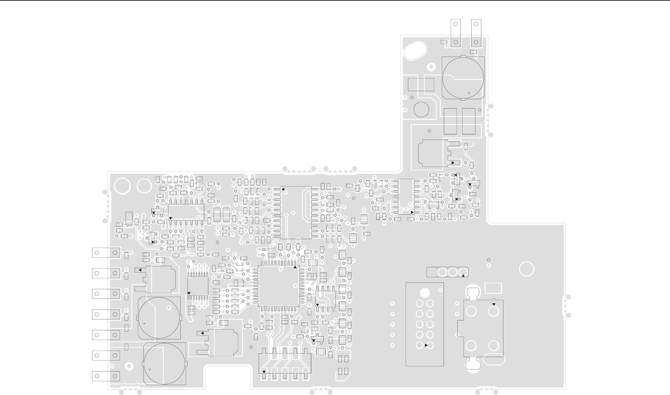
3-46 Power Amplifier (PA) PCB (UHF)
M6900
M6901
M6902
M6903
M6904
M6905
M6906
14
3
2
8
7
TP78 R6552
R6560
C6554
Q6287
R6579
R6290
RT6553
R6558
TP82
TP90
C6290
R6285
R6288
TP112
TP113
TP114
R6282
R6281
R6284
R6289
TP103
TP109
C6413 C6416
C6501
R6501
TP83
TP86
TP92
C6414
U6410
R6280 TP99
C6412
R6283
R6515
R6517
R6516
TP105
TP106
C6411
C6500
R6502
3
2
3
2
C6900 C6902 C6924
C6923 C6925
R6062
C6926
R6286
R6063
C6015
C6025
U6060
R6550
C6061
D6559
R6551
R6557
TP44
TP84
TP93
R6500
TP76
TP77
C6415
R6556
R6555
TP81
3
2
U6050
TP57
C6184
R6158
R6174
R6184
TP74
TP79
TP50
TP59
TP60
TP61
TP62
TP63
C6166
R6180
R6181
TP56
TP58
C6180
C6168
TP3
TP55
8
9
16
R6053
C6171
C6172
C6187
C6188
C6189
R6052
U6170
C6051
C6186 R6186
R6187
R6189
TP37
TP65
TP67
TP66
TP68
C6163
C6181
C6182
C6183
C6185
R6182
R6183
TP69
TP70
TP71
TP72
R6173 TP73
R6185
R6188
23
22
12
11
34
33
44
U6150
10
9
2
J6155
C6116
L6116
Q6136
R6123
C6013
C6014
C6023
C6024
C6115
L6115
TP25
TP29
TP31
3
2
C6162
C6138
R6159
R6137
C6167 TP4
R6134
R6131
TP47
C6139
85
4
R6135
U6130
R6124
R6125
TP49
TP64
TP43
C6117
R6122
L6117
C6113
L6113
TP23
TP28
C6161
C6132
C6165
C6133
R6121
L6114
TP41
C6114
TP27
TP39
C6112 C6111
C6110
L6110
L6112
TP22
TP24
L6111
C6505
R6504
R6503
TP80
TP94
R6230
R6512
C6511
C6510
TP96
TP98
TP118
R6513
R6518
TP102
TP104
TP10
C6160
C6252
C6164
R6236
R6232
R6233
R6235
R6239
TP35
TP54
TP119
TP121
TP125
C6250
C6258
R6231
TP117
TP122
TP124
C6251
R6226
R6227
R6225
R6223
TP36
TP75
TP51
C6254
R6156
R6157
R6191
TP2
TP1
TP52
R6120
R6229
C6255
R6224
TP30
R6228
R6262
R6263
R6264
C6256
R6261
C6257
10
1120
U6240
C6242
C6241
R6212
R6210
TP6
TP33
TP46
R6222
C6253C6259
R6238
TP32
TP120
C6246
C6245
R6244
TP38
TP42
TP123
C6247
R6220
R6221
R6237
L6193
TP21
C6193
R6243
R6127
L6192
TP26
TP40
TP48
TP108
C6403
C6192
R6752
TP16
TP116
C6753
C6404
R6751
R6754
TP111
R6213
R6211
TP7
TP20
TP53
14 8
7
U6400
3
2
2
3
3
2
TP115
R6704
TP110 C6401
TP87
C6402
C6703
R6702
R6701
TP107
C6406
C6405
R6580
R6581
R6599
TP45
R6582
R6589
R6588
TP85
TP88
Q6590
Q6592
R6583
R6584
R6126
R6598
TP34
TP89
TP97
Q6591
Q6593
R6587
R6586
TP91
R6585
TP95
M6950
R6597
TP101
R6596
TP100
R6595
TP5
C6597
C6911
C6910
M6910
M6911
234
J6002
TP9
01
2
9
J6000
3
6
4
J6001
Distribution Board PCB – Top View (PCB No. 84009279002)
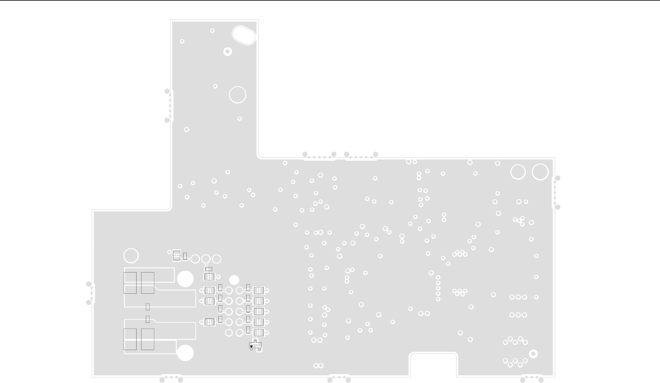
Power Amplifier (PA) PCB (UHF) 3-47
3
2
L6103
L6106
L6107
L6102
L6104
VR6107
C6103
C6106
C6107
C6102
C6104
C6105
R6090
C6100
C6101
L6191
C6191
L6105
L6100
L6101
C6190
L6190
E6012
C6010
E6021
E6011 E6022
C6020
Distribution Board PCB – Bottom View (PCB No. 84009279002)

3-48 Power Amplifier Parts List (UHF) – CLE1333
3.6 Power Amplifier Parts List
(UHF) – CLE1333
Circuit
Ref
Motorola Part
No Description
*5884911T04 CIRCULATOR
* CLE6215 PA RF BRD UHF 403–
470MHZ
*CLE6217 PA OUTPUT UHF 403–
470MHZ
* CLE6219 PA DIST UHF 403–
527MHZ
*CLN8504 PA HDWR HIGH POWER
MTR3000

Power Amplifier Parts List (UHF) – CLE1334 3-49
3.7 Power Amplifier Parts List
(UHF) – CLE1334
Circuit
Ref
Motorola Part
No Description
*5884911T18 UHF CIRCULATOR 470–
524MHZ
* CLE6216 PA RF BRD UHF 450–
527MHZ
*CLE6218 PA OUTPUT UHF 450–
527MHZ
* CLE6219 PA DIST UHF 403–
527MHZ
*CLN8504 PA HDWR HIGH POWER
MTR3000
3-50 Power Amplifier Parts List (UHF) – CLE6215
3.8 Power Amplifier Parts List
(UHF) – CLE6215
Circuit
Ref
Motorola Part
No Description
C2030 2113944C45 CAP CER CHP 100.0PF
50V 5%
C2031 2113945G45 CAP,FXD,.01UF,+5%,-
5%,50V-DC,0805,X7R,-
55DEG CMIN,125DEG
CMAX,P
C2032 2113944C45 CAP CER CHP 100.0PF
50V 5%
C2033 2113945G45 CAP,FXD,.01UF,+5%,-
5%,50V-DC,0805,X7R,-
55DEG CMIN,125DEG
CMAX,P
C2034 2113944C45 CAP CER CHP 100.0PF
50V 5%
C2035 2113945G45 CAP,FXD,.01UF,+5%,-
5%,50V-DC,0805,X7R,-
55DEG CMIN,125DEG
CMAX,P
C2036 2113944C45 CAP CER CHP 100.0PF
50V 5%
C2037 2113945G45 CAP,FXD,.01UF,+5%,-
5%,50V-DC,0805,X7R,-
55DEG CMIN,125DEG
CMAX,P
C2038 2113944C45 CAP CER CHP 100.0PF
50V 5%
C2039 2113945G45 CAP,FXD,.01UF,+5%,-
5%,50V-DC,0805,X7R,-
55DEG CMIN,125DEG
CMAX,P
C2040 2113944C45 CAP CER CHP 100.0PF
50V 5%
C2041 2113945G45 CAP,FXD,.01UF,+5%,-
5%,50V-DC,0805,X7R,-
55DEG CMIN,125DEG
CMAX,P
C2100 2113944C45 CAP CER CHP 100.0PF
50V 5%
C2101 2113944C45 CAP CER CHP 100.0PF
50V 5%
C2102 2113944C04 CAP CER CHP 330.0PF
50V 5%
C2103 2113945C02 CAP CER CHP 10,000PF
50V 10%
C2200 2113945C02 CAP CER CHP 10,000PF
50V 10%
C2201 2113944C45 CAP CER CHP 100.0PF
50V 5%
C2304 2113944C46 CAP CER CHP 120.0PF
50V 5%
C2306 2113945C02 CAP CER CHP 10,000PF
50V 10%
C2307 2113944C30 CAP CER CHP 10.0PF
50V +/- 0.5PF
C2308 2113944C47 CAP CER CHP 150.0PF
50V 5%
C2309 2113945C02 CAP CER CHP 10,000PF
50V 10%
C2310 2113951A18 CAP NPO 2.20PF +/-.1PF
250V HI FREQ
C2311 2113944C45 CAP CER CHP 100.0PF
50V 5%
C2316 2113944C46 CAP CER CHP 120.0PF
50V 5%
C2318 2113945C02 CAP CER CHP 10,000PF
50V 10%
C2319 2113944C45 CAP CER CHP 100.0PF
50V 5%
C2321 2113944C47 CAP CER CHP 150.0PF
50V 5%
C2322 2113944C30 CAP CER CHP 10.0PF
50V +/- 0.5PF
C2323 2113945C02 CAP CER CHP 10,000PF
50V 10%
C2325 2113945C02 CAP CER CHP 10,000PF
50V 10%
C2326 2113951A22 CAP NPO 3.30PF +/-.1PF
250V HI FREQ
C2327 2113945C02 CAP CER CHP 10,000PF
50V 10%
Circuit
Ref
Motorola Part
No Description
C2400 2113945C02 CAP CER CHP 10,000PF
50V 10%
C2401 2113944F05 CAP,CHIP,470PF,+5%,-
5%,50V-DC,0805,C0G,-
55DEG CMIN,125DEG
CMAX
C2402 2113945C02 CAP CER CHP 10,000PF
50V 10%
C2404 2113945C02 CAP CER CHP 10,000PF
50V 10%
C2406 2113945C02 CAP CER CHP 10,000PF
50V 10%
C2407 2113944C45 CAP CER CHP 100.0PF
50V 5%
C2408 2113944C45 CAP CER CHP 100.0PF
50V 5%
C2409 2113944C45 CAP CER CHP 100.0PF
50V 5%
C2500 2113955E11 CAP,FXD,1UF,+10%,-
10%,50V-DC,X7R,-55DEG
CMIN,125DEG CMAX,PB-
FR
C2501 2113944C45 CAP CER CHP 100.0PF
50V 5%
C2502 2113945C02 CAP CER CHP 10,000PF
50V 10%
C2503 2113944C45 CAP CER CHP 100.0PF
50V 5%
C2504 2113955E11 CAP,FXD,1UF,+10%,-
10%,50V-DC,X7R,-55DEG
CMIN,125DEG CMAX,PB-
FR
C2506 2113944C45 CAP CER CHP 100.0PF
50V 5%
C2507 2113944C45 CAP CER CHP 100.0PF
50V 5%
C4210 2113944C45 CAP CER CHP 100.0PF
50V 5%
C4216 2113944C45 CAP CER CHP 100.0PF
50V 5%
C4227 2113944C45 CAP CER CHP 100.0PF
50V 5%
Circuit
Ref
Motorola Part
No Description
C4228 2113944C45 CAP CER CHP 100.0PF
50V 5%
C4243 2113944C45 CAP CER CHP 100.0PF
50V 5%
C4249 2113944C45 CAP CER CHP 100.0PF
50V 5%
C4257 2113944C45 CAP CER CHP 100.0PF
50V 5%
C4258 2113944C45 CAP CER CHP 100.0PF
50V 5%
C4273 2113944C45 CAP CER CHP 100.0PF
50V 5%
C4279 2113944C45 CAP CER CHP 100.0PF
50V 5%
C4310 2113951B56 CAP NPO HIGH FREQ 100
+/- 5V
C4313 2113944C37 CAP CER CHP 39.0PF
50V 5%
C4314 2185457Y01 CAP CHIP CER 10UF 35V
W18
C4338 2113951A56 CAP NPO 100.0PF +/-5%
250V HI FREQ
C4340 2113951B48 CAP NPO HIGH FREQ
47.0 +/- 5% 250V
C4341 2113951B37 CAP NPO 15.0PF +/- 5%
250V HI FREQ
C4343 2113945C13 CAP CER CHP 1000PF
50V 10%
C4344 2113951B52 CAP NPO HIGH FREQ
68.0 +/- 5% 250V
C4360 2113951C19 CAP,FXD,2.4PF,.05PF+/-
,250V-DC,0603,C0G,-
55DEG CMIN,125DEG
CMA
C4361 2113951C19 CAP,FXD,2.4PF,.05PF+/-
,250V-DC,0603,C0G,-
55DEG CMIN,125DEG
CMA
C4362 2113951C36 CAP,FXD,12PF,+1%,-
1%,250V-DC,0603,C0G,-
55DEG CMIN,125DEG
CMAX,P
Circuit
Ref
Motorola Part
No Description
Power Amplifier Parts List (UHF) – CLE6215 3-51
C4363 2113951C36 CAP,FXD,12PF,+1%,-
1%,250V-DC,0603,C0G,-
55DEG CMIN,125DEG
CMAX,P
C4370 2113951B31 CAP NPO 7.50PF +/- 5%
250V HI FREQ
C4371 2113951B31 CAP NPO 7.50PF +/- 5%
250V HI FREQ
C4372 2113951B32 CAP NPO 8.20PF +/- 5%
250V HI FREQ
C4373 2113951B32 CAP NPO 8.20PF +/- 5%
250V HI FREQ
C4374 2113951B38 CAP NPO 18.0PF +/- 5%
250V HI FREQ
C4375 2113951B38 CAP NPO 18.0PF +/- 5%
250V HI FREQ
C4380 2113951B31 CAP NPO 7.50PF +/- 5%
250V HI FREQ
C4381 2113951B31 CAP NPO 7.50PF +/- 5%
250V HI FREQ
C4382 2113951B31 CAP NPO 7.50PF +/- 5%
250V HI FREQ
C4383 2113951B31 CAP NPO 7.50PF +/- 5%
250V HI FREQ
C4390 2113951B28 CAP NPO 5.60PF +/-
0.25PF 250V HI-F
C4391 2113951B56 CAP NPO HIGH FREQ 100
+/- 5V
C4392 2113951B56 CAP NPO HIGH FREQ 100
+/- 5V
C4410 2113951B56 CAP NPO HIGH FREQ 100
+/- 5V
C4413 2113944C37 CAP CER CHP 39.0PF
50V 5%
C4414 2185457Y01 CAP CHIP CER 10UF 35V
W18
C4438 2113951A56 CAP NPO 100.0PF +/-5%
250V HI FREQ
C4440 2113951B48 CAP NPO HIGH FREQ
47.0 +/- 5% 250V
Circuit
Ref
Motorola Part
No Description
C4441 2113951B37 CAP NPO 15.0PF +/- 5%
250V HI FREQ
C4443 2113945C13 CAP CER CHP 1000PF
50V 10%
C4444 2113951B52 CAP NPO HIGH FREQ
68.0 +/- 5% 250V
C4460 2113951C19 CAP,FXD,2.4PF,.05PF+/-
,250V-DC,0603,C0G,-
55DEG CMIN,125DEG
CMA
C4461 2113951C19 CAP,FXD,2.4PF,.05PF+/-
,250V-DC,0603,C0G,-
55DEG CMIN,125DEG
CMA
C4462 2113951C36 CAP,FXD,12PF,+1%,-
1%,250V-DC,0603,C0G,-
55DEG CMIN,125DEG
CMAX,P
C4463 2113951C36 CAP,FXD,12PF,+1%,-
1%,250V-DC,0603,C0G,-
55DEG CMIN,125DEG
CMAX,P
C4470 2113951B31 CAP NPO 7.50PF +/- 5%
250V HI FREQ
C4471 2113951B31 CAP NPO 7.50PF +/- 5%
250V HI FREQ
C4472 2113951B32 CAP NPO 8.20PF +/- 5%
250V HI FREQ
C4473 2113951B32 CAP NPO 8.20PF +/- 5%
250V HI FREQ
C4474 2113951B38 CAP NPO 18.0PF +/- 5%
250V HI FREQ
C4475 2113951B38 CAP NPO 18.0PF +/- 5%
250V HI FREQ
C4480 2113951B31 CAP NPO 7.50PF +/- 5%
250V HI FREQ
C4481 2113951B31 CAP NPO 7.50PF +/- 5%
250V HI FREQ
C4482 2113951B31 CAP NPO 7.50PF +/- 5%
250V HI FREQ
C4483 2113951B31 CAP NPO 7.50PF +/- 5%
250V HI FREQ
Circuit
Ref
Motorola Part
No Description
C4490 2113951B28 CAP NPO 5.60PF +/-
0.25PF 250V HI-F
C4491 2113951B56 CAP NPO HIGH FREQ 100
+/- 5V
C4492 2113951B56 CAP NPO HIGH FREQ 100
+/- 5V
C4510 2113951B56 CAP NPO HIGH FREQ 100
+/- 5V
C4513 2113944C37 CAP CER CHP 39.0PF
50V 5%
C4514 2185457Y01 CAP CHIP CER 10UF 35V
W18
C4538 2113951A56 CAP NPO 100.0PF +/-5%
250V HI FREQ
C4540 2113951B48 CAP NPO HIGH FREQ
47.0 +/- 5% 250V
C4541 2113951B37 CAP NPO 15.0PF +/- 5%
250V HI FREQ
C4543 2113945C13 CAP CER CHP 1000PF
50V 10%
C4544 2113951B52 CAP NPO HIGH FREQ
68.0 +/- 5% 250V
C4560 2113951C19 CAP,FXD,2.4PF,.05PF+/-
,250V-DC,0603,C0G,-
55DEG CMIN,125DEG
CMA
C4561 2113951C19 CAP,FXD,2.4PF,.05PF+/-
,250V-DC,0603,C0G,-
55DEG CMIN,125DEG
CMA
C4562 2113951C36 CAP,FXD,12PF,+1%,-
1%,250V-DC,0603,C0G,-
55DEG CMIN,125DEG
CMAX,P
C4563 2113951C36 CAP,FXD,12PF,+1%,-
1%,250V-DC,0603,C0G,-
55DEG CMIN,125DEG
CMAX,P
C4570 2113951B31 CAP NPO 7.50PF +/- 5%
250V HI FREQ
C4571 2113951B31 CAP NPO 7.50PF +/- 5%
250V HI FREQ
Circuit
Ref
Motorola Part
No Description
C4572 2113951B32 CAP NPO 8.20PF +/- 5%
250V HI FREQ
C4573 2113951B32 CAP NPO 8.20PF +/- 5%
250V HI FREQ
C4574 2113951B38 CAP NPO 18.0PF +/- 5%
250V HI FREQ
C4575 2113951B38 CAP NPO 18.0PF +/- 5%
250V HI FREQ
C4580 2113951B31 CAP NPO 7.50PF +/- 5%
250V HI FREQ
C4581 2113951B31 CAP NPO 7.50PF +/- 5%
250V HI FREQ
C4582 2113951B31 CAP NPO 7.50PF +/- 5%
250V HI FREQ
C4583 2113951B31 CAP NPO 7.50PF +/- 5%
250V HI FREQ
C4590 2113951B28 CAP NPO 5.60PF +/-
0.25PF 250V HI-F
C4591 2113951B56 CAP NPO HIGH FREQ 100
+/- 5V
C4592 2113951B56 CAP NPO HIGH FREQ 100
+/- 5V
C4610 2113951B56 CAP NPO HIGH FREQ 100
+/- 5V
C4613 2113944C37 CAP CER CHP 39.0PF
50V 5%
C4614 2185457Y01 CAP CHIP CER 10UF 35V
W18
C4638 2113951A56 CAP NPO 100.0PF +/-5%
250V HI FREQ
C4640 2113951B48 CAP NPO HIGH FREQ
47.0 +/- 5% 250V
C4641 2113951B37 CAP NPO 15.0PF +/- 5%
250V HI FREQ
C4643 2113945C13 CAP CER CHP 1000PF
50V 10%
C4644 2113951B52 CAP NPO HIGH FREQ
68.0 +/- 5% 250V
Circuit
Ref
Motorola Part
No Description
3-52 Power Amplifier Parts List (UHF) – CLE6215
C4660 2113951C19 CAP,FXD,2.4PF,.05PF+/-
,250V-DC,0603,C0G,-
55DEG CMIN,125DEG
CMA
C4661 2113951C19 CAP,FXD,2.4PF,.05PF+/-
,250V-DC,0603,C0G,-
55DEG CMIN,125DEG
CMA
C4662 2113951C36 CAP,FXD,12PF,+1%,-
1%,250V-DC,0603,C0G,-
55DEG CMIN,125DEG
CMAX,P
C4663 2113951C36 CAP,FXD,12PF,+1%,-
1%,250V-DC,0603,C0G,-
55DEG CMIN,125DEG
CMAX,P
C4670 2113951B31 CAP NPO 7.50PF +/- 5%
250V HI FREQ
C4671 2113951B31 CAP NPO 7.50PF +/- 5%
250V HI FREQ
C4672 2113951B32 CAP NPO 8.20PF +/- 5%
250V HI FREQ
C4673 2113951B32 CAP NPO 8.20PF +/- 5%
250V HI FREQ
C4674 2113951B38 CAP NPO 18.0PF +/- 5%
250V HI FREQ
C4675 2113951B38 CAP NPO 18.0PF +/- 5%
250V HI FREQ
C4680 2113951B31 CAP NPO 7.50PF +/- 5%
250V HI FREQ
C4681 2113951B31 CAP NPO 7.50PF +/- 5%
250V HI FREQ
C4682 2113951B31 CAP NPO 7.50PF +/- 5%
250V HI FREQ
C4683 2113951B31 CAP NPO 7.50PF +/- 5%
250V HI FREQ
C4690 2113951B28 CAP NPO 5.60PF +/-
0.25PF 250V HI-F
C4691 2113951B56 CAP NPO HIGH FREQ 100
+/- 5V
C4692 2113951B56 CAP NPO HIGH FREQ 100
+/- 5V
Circuit
Ref
Motorola Part
No Description
D2200 4813978P05 DIODE ARRAY,SIGNL/
SWG,BAV99,SM,SOT-
23,215MA,70V,.225W,SHT
K,2,PB-
D2202 4813978P05 DIODE ARRAY,SIGNL/
SWG,BAV99,SM,SOT-
23,215MA,70V,.225W,SHT
K,2,PB-
D2204 4813978P05 DIODE ARRAY,SIGNL/
SWG,BAV99,SM,SOT-
23,215MA,70V,.225W,SHT
K,2,PB-
D2206 4813978P05 DIODE ARRAY,SIGNL/
SWG,BAV99,SM,SOT-
23,215MA,70V,.225W,SHT
K,2,PB-
D2208 4813978P05 DIODE ARRAY,SIGNL/
SWG,BAV99,SM,SOT-
23,215MA,70V,.225W,SHT
K,2,PB-
D2400 4813978P05 DIODE ARRAY,SIGNL/
SWG,BAV99,SM,SOT-
23,215MA,70V,.225W,SHT
K,2,PB-
D2402 4813978P05 DIODE ARRAY,SIGNL/
SWG,BAV99,SM,SOT-
23,215MA,70V,.225W,SHT
K,2,PB-
D2404 4813978P05 DIODE ARRAY,SIGNL/
SWG,BAV99,SM,SOT-
23,215MA,70V,.225W,SHT
K,2,PB-
D4220 4813978P05 DIODE ARRAY,SIGNL/
SWG,BAV99,SM,SOT-
23,215MA,70V,.225W,SHT
K,2,PB-
D4221 4813978P05 DIODE ARRAY,SIGNL/
SWG,BAV99,SM,SOT-
23,215MA,70V,.225W,SHT
K,2,PB-
D4250 4813978P05 DIODE ARRAY,SIGNL/
SWG,BAV99,SM,SOT-
23,215MA,70V,.225W,SHT
K,2,PB-
Circuit
Ref
Motorola Part
No Description
D4251 4813978P05 DIODE ARRAY,SIGNL/
SWG,BAV99,SM,SOT-
23,215MA,70V,.225W,SHT
K,2,PB-
E2300 2485011Y01 INDUCTOR BEAD CHP
PB-FREE
E2301 2485011Y01 INDUCTOR BEAD CHP
PB-FREE
E4311 2485011Y01 INDUCTOR BEAD CHP
PB-FREE
E4411 2485011Y01 INDUCTOR BEAD CHP
PB-FREE
E4511 2485011Y01 INDUCTOR BEAD CHP
PB-FREE
E4611 2485011Y01 INDUCTOR BEAD CHP
PB-FREE
F2100 6585118Y06 FUSE,3A,125V,FAST
ACT,SM
F2400 6585118Y06 FUSE,3A,125V,FAST
ACT,SM
F4316 6585118Y03 FUSE 5A, 125V FAST ACT
W18
F4416 6585118Y03 FUSE 5A, 125V FAST ACT
W18
F4516 6585118Y03 FUSE 5A, 125V FAST ACT
W18
F4616 6585118Y03 FUSE 5A, 125V FAST ACT
W18
J2000 0982492W01 BNC CONN PCB
VERTICAL RECEPT
L2100 2471604H03 SMD AIR WOUND COIL,
422NH, 5.0%
L2101 2416077H21 150NH MIDI SPRING COIL
L2300 2414017N08 IDCTR,FXD,4.7NH,6.38%,
1A,.17Ω,CER,10
Q,3.3GHZ SRF,SM,0603
L2301 2416077H21 150NH MIDI SPRING COIL
L2303 2414017N08 IDCTR,FXD,4.7NH,6.38%,
1A,.17Ω,CER,10
Q,3.3GHZ SRF,SM,0603
Circuit
Ref
Motorola Part
No Description
L2304 2414017N02 IDCTR,CHIP,1.5NH,1A,.1Ω
,CER,8 Q,6GHZ
SRF,SM,0603,PB-FREE
L2305 2416077H21 150NH MIDI SPRING COIL
M4300 1084806Y05 SOLDER, PREFRM, TR
7.0X4.6 PB
M4400 1084806Y05 SOLDER, PREFRM, TR
7.0X4.6 PB
M4500 1084806Y05 SOLDER, PREFRM, TR
7.0X4.6 PB
M4600 1084806Y05 SOLDER, PREFRM, TR
7.0X4.6 PB
PWB 0180706J22 RF BOARD COIN
ASSEMBLY
Q2100 5185337Y01 IC, HIGH LINEARITY
AMPLIFIER, W18
Q2300 4888606T31 HIGH POWER
DISTRIUBTED
AMPLIFIER
Q2400 4813971A10 XSTR,BIP GP
POWER,BIPLR,NPN,MJD
2955,DPAK,SM,60V,20W,1
0A,2MHZ,P
Q2401 4813973M07 XSTR,BIP GP
SS,NPN,T3904,SM,SOT-
23,SMT,40V,.225W,200MA
,300MHZ
Q2500 4813972M07 PB-FREE,NOT
COMPLETELY ENRICHED
Q4200 4813972M07 PB-FREE,NOT
COMPLETELY ENRICHED
Q4201 4813970M64 XSTR,FET GP
PWR,MOSFET,P-
CH,ENHN,SM,SOT-23,-
20V,.225W,PB-FRE
Q4300 4878031A01 RF POWER FET,
MRFE6S9045NR1
Q4400 4878031A01 RF POWER FET,
MRFE6S9045NR1
Q4500 4878031A01 RF POWER FET,
MRFE6S9045NR1
Circuit
Ref
Motorola Part
No Description
Power Amplifier Parts List (UHF) – CLE6215 3-53
Q4600 4878031A01 RF POWER FET,
MRFE6S9045NR1
R2026 0613952D64 CER CHIP RES 4530Ω 1%
0603
R2100 0613952C62 CER CHIP RES 432Ω 1%
0603
R2101 0613952B07 CER CHIP RES 11.5Ω 1%
0603
R2102 0613952C62 CER CHIP RES 432Ω 1%
0603
R2103 0613959S81 CER CHIP RESΩ 1% 2512
R2104 0613959S81 CER CHIP RESΩ 1% 2512
R2105 0613952C46 CER CHIP RES 294Ω 1%
0603
R2106 0613952B25 CER CHIP RES 17.8Ω 1%
0603
R2107 0613952C46 CER CHIP RES 294Ω 1%
0603
R2200 0613952C68 CER CHIP RES 499Ω 1%
0603
R2201 0613952C68 CER CHIP RES 499Ω 1%
0603
R2202 0613952C66 CER CHIP RES 475Ω 1%
0603
R2203 0613952D01 CER CHIP RES 1000Ω 1%
0603
R2204 0613952B68 CER CHIP RES 49.9Ω 1%
0603
R2205 0613952B68 CER CHIP RES 49.9Ω 1%
0603
R2206 0613952C72 CER CHIP RES 549Ω 1%
0603
R2207 0613952C66 CER CHIP RES 475Ω 1%
0603
R2208 0613952C46 CER CHIP RES 294Ω 1%
0603
R2210 0613952B85 CER CHIP RES 75.0Ω 1%
0603
R2302 0613952G67 CER CHIP RES 0.0 +/-
0.050Ω
Circuit
Ref
Motorola Part
No Description
R2303 0613952E09 CER CHIP RES 12.1KΩ
1% 0603
R2305 0613952G67 CER CHIP RES 0.0 +/-
0.050Ω
R2308 0613952E09 CER CHIP RES 12.1KΩ
1% 0603
R2309 0613952B93 CER CHIP RES 90.9Ω 1%
R2310 0613952B93 CER CHIP RES 90.9Ω 1%
R2311 0613952B93 CER CHIP RES 90.9Ω 1%
R2315 0613952G67 CER CHIP RES 0.0 +/-
0.050Ω
R2317 0613952B62 CER CHIP RES 43.2Ω 1%
R2318 0613952B07 CER CHIP RES 11.5Ω 1%
0603
R2319 0613952B07 CER CHIP RES 11.5Ω 1%
0603
R2320 0613952D24 CER CHIP RES 1740Ω 1%
0603
R2321 0613952D24 CER CHIP RES 1740Ω 1%
0603
R2322 0613952D24 CER CHIP RES 1740Ω 1%
0603
R2323 0613952D24 CER CHIP RES 1740Ω 1%
0603
R2400 0613959S18 CER CHIP RESΩ 1% 2512
R2401 0613958E01 CER CHIP RES 10.0KΩ
1% 0805
R2402 0613958J74 CER CHIP RES 0.0Ω JMP
0805
R2403 0613958E01 CER CHIP RES 10.0KΩ
1% 0805
R2404 0613958E01 CER CHIP RES 10.0KΩ
1% 0805
R2405 0613958N01 CER CHIP RES 1000Ω 1%
R2406 0613958N01 CER CHIP RES 1000Ω 1%
R2407 0613958N01 CER CHIP RES 1000Ω 1%
R2408 0613952D34 CER CHIP RES 2210Ω 1%
0603
Circuit
Ref
Motorola Part
No Description
R2500 0613952C42 CER CHIP RES 267Ω 1%
0603
R2501 0613952C42 CER CHIP RES 267Ω 1%
0603
R2502 0613952E01 CER CHIP RES 10.0KΩ
1% 0603
R2503 0613952G67 CER CHIP RES 0.0 +/-
0.050Ω
R2504 0613952E01 CER CHIP RES 10.0KΩ
1% 0603
R2510 0613952E18 CER CHIP RES 15.0KΩ
1% 0603
R2514 0613952G67 CER CHIP RES 0.0 +/-
0.050Ω
R4111 06009095002 RES CHIP 3-TERM ALN
50Ω 10W 2% EPP
R4121 06009095002 RES CHIP 3-TERM ALN
50Ω 10W 2% EPP
R4124 0613952E01 CER CHIP RES 10.0KΩ
1% 0603
R4131 06009095002 RES CHIP 3-TERM ALN
50Ω 10W 2% EPP
R4211 0613952E01 CER CHIP RES 10.0KΩ
1% 0603
R4212 0613952E18 CER CHIP RES 15.0KΩ
1% 0603
R4217 0613952D01 CER CHIP RES 1000Ω 1%
0603
R4220 0613952G67 CER CHIP RES 0.0 +/-
0.050Ω
R4223 0613959G55 CER CHIP RES 180Ω 5%
1210
R4240 0613952H73 CER CHIP RES 1000Ω 5%
0603
R4241 0613952H73 CER CHIP RES 1000Ω 5%
0603
R4244 0613952H73 CER CHIP RES 1000Ω 5%
0603
R4245 0613952H73 CER CHIP RES 1000Ω 5%
0603
Circuit
Ref
Motorola Part
No Description
R4246 0613952H66 CER CHIP RES 510Ω 5%
0603
R4250 0613952G67 CER CHIP RES 0.0 +/-
0.050Ω
R4253 0613959G55 CER CHIP RES 180Ω 5%
1210
R4270 0613952H73 CER CHIP RES 1000Ω 5%
0603
R4271 0613952H73 CER CHIP RES 1000Ω 5%
0603
R4274 0613952H73 CER CHIP RES 1000Ω 5%
0603
R4275 0613952H73 CER CHIP RES 1000Ω 5%
0603
R4276 0613952H66 CER CHIP RES 510Ω 5%
0603
R4280 0613952E01 CER CHIP RES 10.0KΩ
1% 0603
R4281 0613952E01 CER CHIP RES 10.0KΩ
1% 0603
R4282 0613952E01 CER CHIP RES 10.0KΩ
1% 0603
R4283 0613952E01 CER CHIP RES 10.0KΩ
1% 0603
R4284 0613952E01 CER CHIP RES 10.0KΩ
1% 0603
R4286 0613952E01 CER CHIP RES 10.0KΩ
1% 0603
R4289 0613952D01 CER CHIP RES 1000Ω 1%
0603
R4290 0613952D06 CER CHIP RES 1130Ω 1%
0603
R4291 0613952G67 CER CHIP RES 0.0 +/-
0.050Ω
R4312 0613959B34 CER CHIP RES 22.1Ω 1%
1210
R4315 0685357Y01 RES FIXED CHIP .0100 1
1W EPP
R4333 0613952H95 CER CHIP RES 8200Ω 5%
0603
Circuit
Ref
Motorola Part
No Description
3-54 Power Amplifier Parts List (UHF) – CLE6215
R4334 0613952J05 CER CHIP RES 15KΩ 5%
0603
R4336 0613952H73 CER CHIP RES 1000Ω 5%
0603
R4342 0613958H49 CER CHIP RES 100Ω 5%
0805
R4343 0613958H49 CER CHIP RES 100Ω 5%
0805
R4344 0613952J49 CER CHIP RES 1.0MΩ 5%
0603
R4350 0613958A89 CER CHIP RES 8.25Ω 1%
0805
R4352 0613958A89 CER CHIP RES 8.25Ω 1%
0805
R4412 0613959B34 CER CHIP RES 22.1Ω 1%
1210
R4415 0685357Y01 RES FIXED CHIP .0100 1
1W EPP
R4433 0613952H95 CER CHIP RES 8200Ω 5%
0603
R4434 0613952J05 CER CHIP RES 15KΩ 5%
0603
R4436 0613952H73 CER CHIP RES 1000Ω 5%
0603
R4442 0613958H49 CER CHIP RES 100Ω 5%
0805
R4443 0613958H49 CER CHIP RES 100Ω 5%
0805
R4444 0613952J49 CER CHIP RES 1.0MΩ 5%
0603
R4450 0613958A89 CER CHIP RES 8.25Ω 1%
0805
R4452 0613958A89 CER CHIP RES 8.25Ω 1%
0805
R4512 0613959B34 CER CHIP RES 22.1Ω 1%
1210
R4515 0685357Y01 RES FIXED CHIP .0100 1
1W EPP
R4533 0613952H95 CER CHIP RES 8200Ω 5
0603
Circuit
Ref
Motorola Part
No Description
R4534 0613952J05 CER CHIP RES 15KΩ 5%
0603
R4536 0613952H73 CER CHIP RES 1000Ω 5%
0603
R4542 0613958H49 CER CHIP RES 100Ω 5%
0805
R4543 0613958H49 CER CHIP RES 100Ω 5%
0805
R4544 0613952J49 CER CHIP RES 1.0MΩ 5%
0603
R4550 0613958A89 CER CHIP RES 8.25Ω 1%
0805
R4552 0613958A89 CER CHIP RES 8.25Ω 1%
0805
R4612 0613959B34 CER CHIP RES 22.1Ω 1%
1210
R4615 0685357Y01 RES FIXED CHIP .0100 1
1W EPP
R4633 0613952H95 CER CHIP RES 8200Ω 5%
0603
R4634 0613952J05 CER CHIP RES 15KΩ 5%
0603
R4636 0613952H73 CER CHIP RES 1000Ω 5%
0603
R4642 0613958H49 CER CHIP RES 100Ω 5%
0805
R4643 0613958H49 CER CHIP RES 100Ω 5%
0805
R4644 0613952J49 CER CHIP RES 1.0MΩ 5%
0603
R4650 0613958A89 CER CHIP RES 8.25Ω 1%
0805
R4652 0613958A89 CER CHIP RES 8.25Ω 1%
0805
R4911 0685609Y06 RES CHIP 3-TERM ALN
10W 100Ω 2%
R4912 0685609Y06 RES CHIP 3-TERM ALN
10W 100Ω 2%
R4921 0685609Y06 RES CHIP 3-TERM ALN
10W 100Ω 2%
Circuit
Ref
Motorola Part
No Description
R4922 0685609Y06 RES CHIP 3-TERM ALN
10W 100Ω 2%
R4931 0685609Y06 RES CHIP 3-TERM ALN
10W 100Ω 2%
R4932 0685609Y06 RES CHIP 3-TERM ALN
10W 100Ω 2%
RT4247 0685191Y02 THERMISTOR CHIP 1 KΩ
W18
RT4278 0685191Y02 THERMISTOR CHIP 1 KΩ
W18
U2500 5114014M27 IC,LNR V
REGLTR,ADJUSTABLE,1.
2V TO
37V,1.5A,SM,D2PAK,PB-
FREE
U4110 5885163Y02 UHF 3DB HYBRID
COUPLER
U4120 5885163Y02 UHF 3DB HYBRID
COUPLER
U4130 5885163Y02 UHF 3DB HYBRID
COUPLER
U4337 5185560Y01 IC, DIG POT,10K,SOIC
U4437 5185560Y01 IC, DIG POT,10K,SOIC
U4537 5185560Y01 IC, DIG POT,10K,SOIC
U4637 5185560Y01 IC, DIG POT,10K,SOIC
U4910 5885163Y02 UHF 3DB HYBRID
COUPLER
U4920 5885163Y02 UHF 3DB HYBRID
COUPLER
U4930 5885163Y02 UHF 3DB HYBRID
COUPLER
VR2200 4813977M04 DIODE,ZEN,MMBZ5225,S
M,SOT-
23,3V,10MA,.225W,ZEN,P
B-FREE
VR2201 4813977M18 DIODE,ZEN,MBZ5239,SM,
SOT-
23,9.1V,10MA,.225W,ZEN,
PB-FREE
Circuit
Ref
Motorola Part
No Description
VR4222 4813977M16 DIODE,ZEN,MBZ5237,SM,
SOT-
23,8.2V,10MA,.225W,ZEN,
PB-FREE
VR4252 4813977M16 DIODE,ZEN,MBZ5237,SM,
SOT-
23,8.2V,10MA,.225W,ZEN,
PB-FREE
Circuit
Ref
Motorola Part
No Description
Power Amplifier Parts List (UHF) – CLE6216 3-55
3.9 Power Amplifier Parts List
(UHF) – CLE6216
Circuit
Ref
Motorola Part
No Description
C2030 2113944C45 CAP CER CHP 100.0PF
50V 5%
C2031 2113945G45 CAP,FXD,.01UF,+5%,-
5%,50V-DC,0805,X7R,-
55DEG CMIN,125DEG
CMAX,P
C2032 2113944C45 CAP CER CHP 100.0PF
50V 5%
C2033 2113945G45 CAP,FXD,.01UF,+5%,-
5%,50V-DC,0805,X7R,-
55DEG CMIN,125DEG
CMAX,P
C2034 2113944C45 CAP CER CHP 100.0PF
50V 5%
C2035 2113945G45 CAP,FXD,.01UF,+5%,-
5%,50V-DC,0805,X7R,-
55DEG CMIN,125DEG
CMAX,P
C2036 2113944C45 CAP CER CHP 100.0PF
50V 5%
C2037 2113945G45 CAP,FXD,.01UF,+5%,-
5%,50V-DC,0805,X7R,-
55DEG CMIN,125DEG
CMAX,P
C2038 2113944C45 CAP CER CHP 100.0PF
50V 5%
C2039 2113945G45 CAP,FXD,.01UF,+5%,-
5%,50V-DC,0805,X7R,-
55DEG CMIN,125DEG
CMAX,P
C2040 2113944C45 CAP CER CHP 100.0PF
50V 5%
C2041 2113945G45 CAP,FXD,.01UF,+5%,-
5%,50V-DC,0805,X7R,-
55DEG CMIN,125DEG
CMAX,P
C2100 2113944C45 CAP CER CHP 100.0PF
50V 5%
C2101 2113944C45 CAP CER CHP 100.0PF
50V 5%
C2102 2113944C04 CAP CER CHP 330.0PF
50V 5%
C2103 2113945C02 CAP CER CHP 10,000PF
50V 10%
C2200 2113945C02 CAP CER CHP 10,000PF
50V 10%
C2201 2113944C45 CAP CER CHP 100.0PF
50V 5%
C2304 2113944C46 CAP CER CHP 120.0PF
50V 5%
C2306 2113945C02 CAP CER CHP 10,000PF
50V 10%
C2307 2113944C30 CAP CER CHP 10.0PF
50V +/- 0.5PF
C2308 2113944C47 CAP CER CHP 150.0PF
50V 5%
C2309 2113945C02 CAP CER CHP 10,000PF
50V 10%
C2310 2113951A18 CAP NPO 2.20PF +/-.1PF
250V HI FREQ
C2311 2113944C45 CAP CER CHP 100.0PF
50V 5%
C2316 2113944C46 CAP CER CHP 120.0PF
50V 5%
C2318 2113945C02 CAP CER CHP 10,000PF
50V 10%
C2319 2113944C45 CAP CER CHP 100.0PF
50V 5%
C2321 2113944C47 CAP CER CHP 150.0PF
50V 5%
C2322 2113944C30 CAP CER CHP 10.0PF
50V +/- 0.5PF
C2323 2113945C02 CAP CER CHP 10,000PF
50V 10%
C2325 2113945C02 CAP CER CHP 10,000PF
50V 10%
C2326 2113951A22 CAP NPO 3.30PF +/-.1PF
250V HI FREQ
C2327 2113945C02 CAP CER CHP 10,000PF
50V 10%
Circuit
Ref
Motorola Part
No Description
C2400 2113945C02 CAP CER CHP 10,000PF
50V 10%
C2401 2113944F05 CAP,CHIP,470PF,+5%,-
5%,50V-DC,0805,C0G,-
55DEG CMIN,125DEG
CMAX
C2402 2113945C02 CAP CER CHP 10,000PF
50V 10%
C2404 2113945C02 CAP CER CHP 10,000PF
50V 10%
C2406 2113945C02 CAP CER CHP 10,000PF
50V 10%
C2407 2113944C45 CAP CER CHP 100.0PF
50V 5%
C2408 2113944C45 CAP CER CHP 100.0PF
50V 5%
C2409 2113944C45 CAP CER CHP 100.0PF
50V 5%
C2500 2113955E11 CAP,FXD,1UF,+10%,-
10%,50V-DC,X7R,-55DEG
CMIN,125DEG CMAX,PB-
FR
C2501 2113944C45 CAP CER CHP 100.0PF
50V 5%
C2502 2113945C02 CAP CER CHP 10,000PF
50V 10%
C2503 2113944C45 CAP CER CHP 100.0PF
50V 5%
C2504 2113955E11 CAP,FXD,1UF,+10%,-
10%,50V-DC,X7R,-55DEG
CMIN,125DEG CMAX,PB-
FR
C2506 2113944C45 CAP CER CHP 100.0PF
50V 5%
C2507 2113944C45 CAP CER CHP 100.0PF
50V 5%
C4210 2113944C45 CAP CER CHP 100.0PF
50V 5%
C4216 2113944C45 CAP CER CHP 100.0PF
50V 5%
C4227 2113944C45 CAP CER CHP 100.0PF
50V 5%
Circuit
Ref
Motorola Part
No Description
C4228 2113944C45 CAP CER CHP 100.0PF
50V 5%
C4243 2113944C45 CAP CER CHP 100.0PF
50V 5%
C4249 2113944C45 CAP CER CHP 100.0PF
50V 5%
C4257 2113944C45 CAP CER CHP 100.0PF
50V 5%
C4258 2113944C45 CAP CER CHP 100.0PF
50V 5%
C4273 2113944C45 CAP CER CHP 100.0PF
50V 5%
C4279 2113944C45 CAP CER CHP 100.0PF
50V 5%
C4310 2113951B56 CAP NPO HIGH FREQ 100
+/- 5V
C4313 2113944C37 CAP CER CHP 39.0PF
50V 5%
C4314 2185457Y01 CAP CHIP CER 10UF 35V
W18
C4338 2113951A56 CAP NPO 100.0PF +/-5%
250V HI FREQ
C4340 2113951B48 CAP NPO HIGH FREQ
47.0 +/- 5% 250V
C4341 2113951B37 CAP NPO 15.0PF +/- 5%
250V HI FREQ
C4343 2113945C13 CAP CER CHP 1000PF
50V 10%
C4344 2113951B48 CAP NPO HIGH FREQ
47.0 +/- 5% 250V
C4360 2113951C30 CAP,FXD,6.8PF,.25PF+/-
,250V-DC,0603,C0G,-
55DEG CMIN,125DEG
CMA
C4361 2113951C30 CAP,FXD,6.8PF,.25PF+/-
,250V-DC,0603,C0G,-
55DEG CMIN,125DEG
CMA
C4362 2113951C30 CAP,FXD,6.8PF,.25PF+/-
,250V-DC,0603,C0G,-
55DEG CMIN,125DEG
CMA
Circuit
Ref
Motorola Part
No Description
3-56 Power Amplifier Parts List (UHF) – CLE6216
C4363 2113951C30 CAP,FXD,6.8PF,.25PF+/-
,250V-DC,0603,C0G,-
55DEG CMIN,125DEG
CMA
C4370 2113951B32 CAP NPO 8.20PF +/- 5%
250V HI FREQ
C4371 2113951B32 CAP NPO 8.20PF +/- 5%
250V HI FREQ
C4372 2113951B36 CAP NPO 12.0PF +/- 5%
250V HI FREQ
C4373 2113951B36 CAP NPO 12.0PF +/- 5%
250V HI FREQ
C4374 2113951B35 CAP NPO 11.0PF +/- 5%
250V HI FREQ
C4375 2113951B35 CAP NPO 11.0PF +/- 5%
250V HI FREQ
C4380 2113951B28 CAP NPO 5.60PF +/-
0.25PF 250V HI-F
C4381 2113951B28 CAP NPO 5.60PF +/-
0.25PF 250V HI-F
C4382 2113951B30 CAP NPO 6.80PF +/- 5%
250V HI FREQ
C4383 2113951B30 CAP NPO 6.80PF +/- 5%
250V HI FREQ
C4390 2113951B26 CAP NPO 4.70PF +/-
0.25PF 250V HI-F
C4391 2113951B56 CAP NPO HIGH FREQ 100
+/- 5V
C4392 2113951B56 CAP NPO HIGH FREQ 100
+/- 5V
C4410 2113951B56 CAP NPO HIGH FREQ 100
+/- 5V
C4413 2113944C37 CAP CER CHP 39.0PF
50V 5%
C4414 2185457Y01 CAP CHIP CER 10UF 35V
W18
C4438 2113951A56 CAP NPO 100.0PF +/-5%
250V HI FREQ
C4440 2113951B48 CAP NPO HIGH FREQ
47.0 +/- 5% 250V
Circuit
Ref
Motorola Part
No Description
C4441 2113951B37 CAP NPO 15.0PF +/- 5%
250V HI FREQ
C4443 2113945C13 CAP CER CHP 1000PF
50V 10%
C4444 2113951B48 CAP NPO HIGH FREQ
47.0 +/- 5% 250V
C4460 2113951C30 CAP,FXD,6.8PF,.25PF+/-
,250V-DC,0603,C0G,-
55DEG CMIN,125DEG
CMA
C4461 2113951C30 CAP,FXD,6.8PF,.25PF+/-
,250V-DC,0603,C0G,-
55DEG CMIN,125DEG
CMA
C4462 2113951C30 CAP,FXD,6.8PF,.25PF+/-
,250V-DC,0603,C0G,-
55DEG CMIN,125DEG
CMA
C4463 2113951C30 CAP,FXD,6.8PF,.25PF+/-
,250V-DC,0603,C0G,-
55DEG CMIN,125DEG
CMA
C4470 2113951B32 CAP NPO 8.20PF +/- 5%
250V HI FREQ
C4471 2113951B32 CAP NPO 8.20PF +/- 5%
250V HI FREQ
C4472 2113951B36 CAP NPO 12.0PF +/- 5%
250V HI FREQ
C4473 2113951B36 CAP NPO 12.0PF +/- 5%
250V HI FREQ
C4474 2113951B35 CAP NPO 11.0PF +/- 5%
250V HI FREQ
C4475 2113951B35 CAP NPO 11.0PF +/- 5%
250V HI FREQ
C4480 2113951B28 CAP NPO 5.60PF +/-
0.25PF 250V HI-F
C4481 2113951B28 CAP NPO 5.60PF +/-
0.25PF 250V HI-F
C4482 2113951B30 CAP NPO 6.80PF +/- 5%
250V HI FREQ
C4483 2113951B30 CAP NPO 6.80PF +/- 5%
250V HI FREQ
Circuit
Ref
Motorola Part
No Description
C4490 2113951B26 CAP NPO 4.70PF +/-
0.25PF 250V HI-F
C4491 2113951B56 CAP NPO HIGH FREQ 100
+/- 5V
C4492 2113951B56 CAP NPO HIGH FREQ 100
+/- 5V
C4510 2113951B56 CAP NPO HIGH FREQ 100
+/- 5V
C4513 2113944C37 CAP CER CHP 39.0PF
50V 5%
C4514 2185457Y01 CAP CHIP CER 10UF 35V
W18
C4538 2113951A56 CAP NPO 100.0PF +/-5%
250V HI FREQ
C4540 2113951B48 CAP NPO HIGH FREQ
47.0 +/- 5% 250V
C4541 2113951B37 CAP NPO 15.0PF +/- 5%
250V HI FREQ
C4543 2113945C13 CAP CER CHP 1000PF
50V 10%
C4544 2113951B48 CAP NPO HIGH FREQ
47.0 +/- 5% 250V
C4560 2113951C30 CAP,FXD,6.8PF,.25PF+/-
,250V-DC,0603,C0G,-
55DEG CMIN,125DEG
CMA
C4561 2113951C30 CAP,FXD,6.8PF,.25PF+/-
,250V-DC,0603,C0G,-
55DEG CMIN,125DEG
CMA
C4562 2113951C30 CAP,FXD,6.8PF,.25PF+/-
,250V-DC,0603,C0G,-
55DEG CMIN,125DEG
CMA
C4563 2113951C30 CAP,FXD,6.8PF,.25PF+/-
,250V-DC,0603,C0G,-
55DEG CMIN,125DEG
CMA
C4570 2113951B32 CAP NPO 8.20PF +/- 5%
250V HI FREQ
C4571 2113951B32 CAP NPO 8.20PF +/- 5%
250V HI FREQ
Circuit
Ref
Motorola Part
No Description
C4572 2113951B36 CAP NPO 12.0PF +/- 5%
250V HI FREQ
C4573 2113951B36 CAP NPO 12.0PF +/- 5%
250V HI FREQ
C4574 2113951B35 CAP NPO 11.0PF +/- 5%
250V HI FREQ
C4575 2113951B35 CAP NPO 11.0PF +/- 5%
250V HI FREQ
C4580 2113951B28 CAP NPO 5.60PF +/-
0.25PF 250V HI-F
C4581 2113951B28 CAP NPO 5.60PF +/-
0.25PF 250V HI-F
C4582 2113951B30 CAP NPO 6.80PF +/- 5%
250V HI FREQ
C4583 2113951B30 CAP NPO 6.80PF +/- 5%
250V HI FREQ
C4590 2113951B26 CAP NPO 4.70PF +/-
0.25PF 250V HI-F
C4591 2113951B56 CAP NPO HIGH FREQ 100
+/- 5V
C4592 2113951B56 CAP NPO HIGH FREQ 100
+/- 5V
C4610 2113951B56 CAP NPO HIGH FREQ 100
+/- 5V
C4613 2113944C37 CAP CER CHP 39.0PF
50V 5%
C4614 2185457Y01 CAP CHIP CER 10UF 35V
W18
C4638 2113951A56 CAP NPO 100.0PF +/-5%
250V HI FREQ
C4640 2113951B48 CAP NPO HIGH FREQ
47.0 +/- 5% 250V
C4641 2113951B37 CAP NPO 15.0PF +/- 5%
250V HI FREQ
C4643 2113945C13 CAP CER CHP 1000PF
50V 10%
C4644 2113951B48 CAP NPO HIGH FREQ
47.0 +/- 5% 250V
Circuit
Ref
Motorola Part
No Description
Power Amplifier Parts List (UHF) – CLE6216 3-57
C4660 2113951C30 CAP,FXD,6.8PF,.25PF+/-
,250V-DC,0603,C0G,-
55DEG CMIN,125DEG
CMA
C4661 2113951C30 CAP,FXD,6.8PF,.25PF+/-
,250V-DC,0603,C0G,-
55DEG CMIN,125DEG
CMA
C4662 2113951C30 CAP,FXD,6.8PF,.25PF+/-
,250V-DC,0603,C0G,-
55DEG CMIN,125DEG
CMA
C4663 2113951C30 CAP,FXD,6.8PF,.25PF+/-
,250V-DC,0603,C0G,-
55DEG CMIN,125DEG
CMA
C4670 2113951B32 CAP NPO 8.20PF +/- 5%
250V HI FREQ
C4671 2113951B32 CAP NPO 8.20PF +/- 5%
250V HI FREQ
C4672 2113951B36 CAP NPO 12.0PF +/- 5%
250V HI FREQ
C4673 2113951B36 CAP NPO 12.0PF +/- 5%
250V HI FREQ
C4674 2113951B35 CAP NPO 11.0PF +/- 5%
250V HI FREQ
C4675 2113951B35 CAP NPO 11.0PF +/- 5%
250V HI FREQ
C4680 2113951B28 CAP NPO 5.60PF +/-
0.25PF 250V HI-F
C4681 2113951B28 CAP NPO 5.60PF +/-
0.25PF 250V HI-F
C4682 2113951B30 CAP NPO 6.80PF +/- 5%
250V HI FREQ
C4683 2113951B30 CAP NPO 6.80PF +/- 5%
250V HI FREQ
C4690 2113951B26 CAP NPO 4.70PF +/-
0.25PF 250V HI-F
C4691 2113951B56 CAP NPO HIGH FREQ 100
+/- 5V
C4692 2113951B56 CAP NPO HIGH FREQ 100
+/- 5V
Circuit
Ref
Motorola Part
No Description
D2200 4813978P05 DIODE ARRAY,SIGNL/
SWG,BAV99,SM,SOT-
23,215MA,70V,.225W,SHT
K,2,PB-
D2202 4813978P05 DIODE ARRAY,SIGNL/
SWG,BAV99,SM,SOT-
23,215MA,70V,.225W,SHT
K,2,PB-
D2204 4813978P05 DIODE ARRAY,SIGNL/
SWG,BAV99,SM,SOT-
23,215MA,70V,.225W,SHT
K,2,PB-
D2206 4813978P05 DIODE ARRAY,SIGNL/
SWG,BAV99,SM,SOT-
23,215MA,70V,.225W,SHT
K,2,PB-
D2208 4813978P05 DIODE ARRAY,SIGNL/
SWG,BAV99,SM,SOT-
23,215MA,70V,.225W,SHT
K,2,PB-
D2400 4813978P05 DIODE ARRAY,SIGNL/
SWG,BAV99,SM,SOT-
23,215MA,70V,.225W,SHT
K,2,PB-
D2402 4813978P05 DIODE ARRAY,SIGNL/
SWG,BAV99,SM,SOT-
23,215MA,70V,.225W,SHT
K,2,PB-
D2404 4813978P05 DIODE ARRAY,SIGNL/
SWG,BAV99,SM,SOT-
23,215MA,70V,.225W,SHT
K,2,PB-
D4220 4813978P05 DIODE ARRAY,SIGNL/
SWG,BAV99,SM,SOT-
23,215MA,70V,.225W,SHT
K,2,PB-
D4221 4813978P05 DIODE ARRAY,SIGNL/
SWG,BAV99,SM,SOT-
23,215MA,70V,.225W,SHT
K,2,PB-
D4250 4813978P05 DIODE ARRAY,SIGNL/
SWG,BAV99,SM,SOT-
23,215MA,70V,.225W,SHT
K,2,PB-
Circuit
Ref
Motorola Part
No Description
D4251 4813978P05 DIODE ARRAY,SIGNL/
SWG,BAV99,SM,SOT-
23,215MA,70V,.225W,SHT
K,2,PB-
E2300 2485011Y01 INDUCTOR BEAD CHP
PB-FREE
E2301 2485011Y01 INDUCTOR BEAD CHP
PB-FREE
E4311 2485011Y01 INDUCTOR BEAD CHP
PB-FREE
E4411 2485011Y01 INDUCTOR BEAD CHP
PB-FREE
E4511 2485011Y01 INDUCTOR BEAD CHP
PB-FREE
E4611 2485011Y01 INDUCTOR BEAD CHP
PB-FREE
F2100 6585118Y06 FUSE,3A,125V,FAST
ACT,SM
F2400 6585118Y06 FUSE,3A,125V,FAST
ACT,SM
F4316 6585118Y03 FUSE 5A, 125V FAST ACT
W18
F4416 6585118Y03 FUSE 5A, 125V FAST ACT
W18
F4516 6585118Y03 FUSE 5A, 125V FAST ACT
W18
F4616 6585118Y03 FUSE 5A, 125V FAST ACT
W18
J2000 0982492W01 BNC CONN PCB
VERTICAL RECEPT
L2100 2471604H03 SMD AIR WOUND COIL,
422NH, 5.0%
L2101 2416077H21 150NH MIDI SPRING COIL
L2300 2414017N08 IDCTR,FXD,4.7NH,6.38%,
1A,.17Ω,CER,10
Q,3.3GHZ SRF,SM,0603
L2301 2416077H21 150NH MIDI SPRING COIL
L2303 2414017N08 IDCTR,FXD,4.7NH,6.38%,
1A,.17Ω,CER,10
Q,3.3GHZ SRF,SM,0603
Circuit
Ref
Motorola Part
No Description
L2304 2414017N02 IDCTR,CHIP,1.5NH,1A,.1Ω
,CER,8 Q,6GHZ
SRF,SM,0603,PB-FREE
L2305 2416077H21 150NH MIDI SPRING COIL
M4300 1084806Y05 SOLDER, PREFRM, TR
7.0X4.6 PB
M4400 1084806Y05 SOLDER, PREFRM, TR
7.0X4.6 PB
M4500 1084806Y05 SOLDER, PREFRM, TR
7.0X4.6 PB
M4600 1084806Y05 SOLDER, PREFRM, TR
7.0X4.6 PB
PWB 0180706J25 RF BOARD COIN
ASSEMBLY
Q2100 5185337Y01 IC, HIGH LINEARITY
AMPLIFIER, W18
Q2300 4888606T31 HIGH POWER
DISTRIUBTED
AMPLIFIER
Q2400 4813971A10 XSTR,BIP GP
POWER,BIPLR,NPN,MJD
2955,DPAK,SM,60V,20W,1
0A,2MHZ,P
Q2401 4813973M07 XSTR,BIP GP
SS,NPN,T3904,SM,SOT-
23,SMT,40V,.225W,200MA
,300MHZ
Q2500 4813972M07 PB-FREE,NOT
COMPLETELY ENRICHED
Q4200 4813972M07 PB-FREE,NOT
COMPLETELY ENRICHED
Q4201 4813970M64 XSTR,FET GP
PWR,MOSFET,P-
CH,ENHN,SM,SOT-23,-
20V,.225W,PB-FRE
Q4300 4878031A01 RF POWER FET,
MRFE6S9045NR1
Q4400 4878031A01 RF POWER FET,
MRFE6S9045NR1
Q4500 4878031A01 RF POWER FET,
MRFE6S9045NR1
Circuit
Ref
Motorola Part
No Description
3-58 Power Amplifier Parts List (UHF) – CLE6216
Q4600 4878031A01 RF POWER FET,
MRFE6S9045NR1
R2026 0613952E09 CER CHIP RES 12.1KΩ
1% 0603
R2027 0613952E18 CER CHIP RES 15.0KΩ
1% 0603
R2100 0613952C62 CER CHIP RES 432Ω 1%
0603
R2101 0613952B07 CER CHIP RES 11.5Ω 1%
0603
R2102 0613952C62 CER CHIP RES 432Ω 1%
0603
R2103 0613959S81 CER CHIP RESΩ 1% 2512
R2104 0613959S81 CER CHIP RESΩ 1% 2512
R2105 0613952C46 CER CHIP RES 294Ω 1%
0603
R2106 0613952B25 CER CHIP RES 17.8Ω 1%
0603
R2107 0613952C46 CER CHIP RES 294Ω 1%
0603
R2200 0613952C68 CER CHIP RES 499Ω 1%
0603
R2201 0613952C68 CER CHIP RES 499Ω 1%
0603
R2202 0613952C66 CER CHIP RES 475Ω 1%
0603
R2203 0613952D01 CER CHIP RES 1000Ω 1%
0603
R2204 0613952B68 CER CHIP RES 49.9Ω 1%
0603
R2205 0613952B68 CER CHIP RES 49.9Ω 1%
0603
R2206 0613952C72 CER CHIP RES 549Ω 1%
0603
R2207 0613952C66 CER CHIP RES 475Ω 1%
0603
R2208 0613952C46 CER CHIP RES 294Ω 1%
0603
R2210 0613952B85 CER CHIP RES 75.0Ω 1%
0603
Circuit
Ref
Motorola Part
No Description
R2302 0613952G67 CER CHIP RES 0.0 +/-
0.050Ω
R2303 0613952E09 CER CHIP RES 12.1KΩ 1
0603
R2305 0613952G67 CER CHIP RES 0.0 +/-
0.050Ω
R2308 0613952E09 CER CHIP RES 12.1KΩ
1% 0603
R2309 0613952B93 CER CHIP RES 90.9Ω 1%
R2310 0613952B93 CER CHIP RES 90.9Ω 1%
R2311 0613952B93 CER CHIP RES 90.9Ω 1%
R2315 0613952G67 CER CHIP RES 0.0 +/-
0.050Ω
R2317 0613952B62 CER CHIP RES 43.2Ω 1%
R2318 0613952B07 CER CHIP RES 11.5Ω 1%
0603
R2319 0613952B07 CER CHIP RES 11.5Ω 1%
0603
R2320 0613952D24 CER CHIP RES 1740Ω 1%
0603
R2321 0613952D24 CER CHIP RES 1740Ω 1%
0603
R2322 0613952D24 CER CHIP RES 1740Ω 1%
0603
R2323 0613952D24 CER CHIP RES 1740Ω 1%
0603
R2400 0613959S18 CER CHIP RESΩ 1% 2512
R2401 0613958E01 CER CHIP RES 10.0KΩ
1% 0805
R2402 0613958J74 CER CHIP RES 0.0Ω JMP
0805
R2403 0613958E01 CER CHIP RES 10.0KΩ
1% 0805
R2404 0613958E01 CER CHIP RES 10.0KΩ
1% 0805
R2405 0613958N01 CER CHIP RES 1000Ω 1%
R2406 0613958N01 CER CHIP RES 1000Ω 1%
R2407 0613958N01 CER CHIP RES 1000Ω 1%
Circuit
Ref
Motorola Part
No Description
R2408 0613952D34 CER CHIP RES 2210Ω 1%
0603
R2500 0613952C42 CER CHIP RES 267Ω 1%
0603
R2501 0613952C42 CER CHIP RES 267Ω 1%
0603
R2502 0613952E01 CER CHIP RES 10.0KΩ
1% 0603
R2503 0613952G67 CER CHIP RES 0.0 +/-
0.050Ω
R2504 0613952E01 CER CHIP RES 10.0KΩ
1% 0603
R2510 0613952E18 CER CHIP RES 15.0KΩ
1% 0603
R2514 0613952G67 CER CHIP RES 0.0 +/-
0.050Ω
R4111 06009095002 RES CHIP 3-TERM ALN
50Ω 10W 2% EPP
R4121 06009095002 RES CHIP 3-TERM ALN
50Ω 10W 2% EPP
R4124 0613952E01 CER CHIP RES 10.0KΩ
1% 0603
R4131 06009095002 RES CHIP 3-TERM ALN
50Ω 10W 2% EPP
R4211 0613952E01 CER CHIP RES 10.0KΩ
1% 0603
R4212 0613952E18 CER CHIP RES 15.0KΩ
1% 0603
R4217 0613952D01 CER CHIP RES 1000Ω 1%
0603
R4220 0613952G67 CER CHIP RES 0.0 +/-
0.050Ω
R4223 0613959G55 CER CHIP RES 180Ω 5%
1210
R4240 0613952H73 CER CHIP RES 1000Ω 5%
0603
R4241 0613952H73 CER CHIP RES 1000Ω 5%
0603
R4244 0613952H73 CER CHIP RES 1000Ω 5%
0603
Circuit
Ref
Motorola Part
No Description
R4245 0613952H73 CER CHIP RES 1000Ω 5%
0603
R4246 0613952H66 CER CHIP RES 510Ω 5
0603
R4250 0613952G67 CER CHIP RES 0.0 +/-
0.050Ω
R4253 0613959G55 CER CHIP RES 180Ω 5%
1210
R4270 0613952H73 CER CHIP RES 1000Ω 5%
0603
R4271 0613952H73 CER CHIP RES 1000Ω 5%
0603
R4274 0613952H73 CER CHIP RES 1000Ω 5%
0603
R4275 0613952H73 CER CHIP RES 1000Ω 5%
0603
R4276 0613952H66 CER CHIP RES 510Ω 5
0603
R4280 0613952E01 CER CHIP RES 10.0KΩ
1% 0603
R4281 0613952E01 CER CHIP RES 10.0KΩ
1% 0603
R4282 0613952E01 CER CHIP RES 10.0KΩ
1% 0603
R4283 0613952E01 CER CHIP RES 10.0KΩ
1% 0603
R4284 0613952E01 CER CHIP RES 10.0KΩ
1% 0603
R4286 0613952E01 CER CHIP RES 10.0KΩ
1% 0603
R4289 0613952D01 CER CHIP RES 1000Ω 1%
0603
R4290 0613952D06 CER CHIP RES 1130Ω 1
0603
R4291 0613952G67 CER CHIP RES 0.0 +/-
0.050Ω
R4312 0613959B34 CER CHIP RES 22.1Ω 1%
1210
R4315 0685357Y01 RES FIXED CHIP .0100 1
1W EPP
Circuit
Ref
Motorola Part
No Description
Power Amplifier Parts List (UHF) – CLE6216 3-59
R4333 0613952H95 CER CHIP RES 8200Ω 5%
0603
R4334 0613952J05 CER CHIP RES 15KΩ 5%
0603
R4336 0613952H73 CER CHIP RES 1000Ω 5%
0603
R4342 0613958H49 CER CHIP RES 100Ω 5%
0805
R4343 0613958H49 CER CHIP RES 100Ω 5%
0805
R4344 0613952J49 CER CHIP RES 1.0MΩ 5%
0603
R4350 0613958A89 CER CHIP RES 8.25Ω 1%
0805
R4352 0613958A89 CER CHIP RES 8.25Ω 1%
0805
R4412 0613959B34 CER CHIP RES 22.1Ω 1%
1210
R4415 0685357Y01 RES FIXED CHIP .0100 1
1W EPP
R4433 0613952H95 CER CHIP RES 8200Ω 5%
0603
R4434 0613952J05 CER CHIP RES 15KΩ 5%
0603
R4436 0613952H73 CER CHIP RES 1000Ω 5%
0603
R4442 0613958H49 CER CHIP RES 100Ω 5%
0805
R4443 0613958H49 CER CHIP RES 100Ω 5%
0805
R4444 0613952J49 CER CHIP RES 1.0MΩ 5%
0603
R4450 0613958A89 CER CHIP RES 8.25Ω 1%
0805
R4452 0613958A89 CER CHIP RES 8.25Ω 1%
0805
R4512 0613959B34 CER CHIP RES 22.1Ω 1%
1210
R4515 0685357Y01 RES FIXED CHIP .0100 1
1W EPP
Circuit
Ref
Motorola Part
No Description
R4533 0613952H95 CER CHIP RES 8200Ω 5%
0603
R4534 0613952J05 CER CHIP RES 15KΩ 5%
0603
R4536 0613952H73 CER CHIP RES 1000Ω 5%
0603
R4542 0613958H49 CER CHIP RES 100Ω 5%
0805
R4543 0613958H49 CER CHIP RES 100Ω 5%
0805
R4544 0613952J49 CER CHIP RES 1.0MΩ 5%
0603
R4550 0613958A89 CER CHIP RES 8.25Ω 1%
0805
R4552 0613958A89 CER CHIP RES 8.25Ω 1%
0805
R4612 0613959B34 CER CHIP RES 22.1Ω 1%
1210
R4615 0685357Y01 RES FIXED CHIP .0100 1
1W EPP
R4633 0613952H95 CER CHIP RES 8200Ω 5%
0603
R4634 0613952J05 CER CHIP RES 15KΩ 5%
0603
R4636 0613952H73 CER CHIP RES 1000Ω 5%
0603
R4642 0613958H49 CER CHIP RES 100Ω 5%
0805
R4643 0613958H49 CER CHIP RES 100Ω 5%
0805
R4644 0613952J49 CER CHIP RES 1.0MΩ 5%
0603
R4650 0613958A89 CER CHIP RES 8.25Ω 1%
0805
R4652 0613958A89 CER CHIP RES 8.25Ω 1%
0805
R4911 0685609Y06 RES CHIP 3-TERM ALN
10W 100Ω 2%
R4912 0685609Y06 RES CHIP 3-TERM ALN
10W 100Ω 2%
Circuit
Ref
Motorola Part
No Description
R4921 0685609Y06 RES CHIP 3-TERM ALN
10W 100Ω 2%
R4922 0685609Y06 RES CHIP 3-TERM ALN
10W 100Ω 2%
R4931 0685609Y06 RES CHIP 3-TERM ALN
10W 100Ω 2%
R4932 0685609Y06 RES CHIP 3-TERM ALN
10W 100Ω 2%
RT4247 0685191Y02 THERMISTOR CHIP 1 KΩ
W18
RT4278 0685191Y02 THERMISTOR CHIP 1 KΩ
W18
U2500 5114014M27 IC,LNR V
REGLTR,ADJUSTABLE,1.
2V TO
37V,1.5A,SM,D2PAK,PB-
FREE
U4110 5871224H02 COUPLER 435-524MHZ 3
DB HYBRID
U4120 5871224H02 COUPLER 435-524MHZ 3
DB HYBRID
U4130 5871224H02 COUPLER 435-524MHZ 3
DB HYBRID
U4337 5185560Y01 IC, DIG POT,10K,SOIC
U4437 5185560Y01 IC, DIG POT,10K,SOIC
U4537 5185560Y01 IC, DIG POT,10K,SOIC
U4637 5185560Y01 IC, DIG POT,10K,SOIC
U4910 5871224H02 COUPLER 435-524MHZ 3
DB HYBRID
U4920 5871224H02 COUPLER 435-524MHZ 3
DB HYBRID
U4930 5871224H02 COUPLER 435-524MHZ 3
DB HYBRID
VR2200 4813977M04 DIODE,ZEN,MMBZ5225,S
M,SOT-
23,3V,10MA,.225W,ZEN,P
B-FREE
VR2201 4813977M18 DIODE,ZEN,MBZ5239,SM,
SOT-
23,9.1V,10MA,.225W,ZEN,
PB-FREE
Circuit
Ref
Motorola Part
No Description
VR4222 4813977M16 DIODE,ZEN,MBZ5237,SM,
SOT-
23,8.2V,10MA,.225W,ZEN,
PB-FREE
VR4252 4813977M16 DIODE,ZEN,MBZ5237,SM,
SOT-
23,8.2V,10MA,.225W,ZEN,
PB-FREE
Circuit
Ref
Motorola Part
No Description
3-60 Power Amplifier Parts List (UHF) – CLE6217
3.10 Power Amplifier Parts List
(UHF) – CLE6217
Circuit
Ref
Motorola Part
No Description
C8001 2113951D21 CAP,FXD,3PF,.05PF,250V-
DC,0805,C0G,-55DEG
CMIN,125DEG CMAX
C8002 2113951D05 CAP,FXD,.5PF,.05PF,250V
-DC,0805,C0G,-55DEG
CMIN,125DEG CMAX
C8003 2113951D16 CAP,FXD,1.8PF,.05PF,250
V-DC,0805,C0G,-55DEG
CMIN,125DEG CMA
C8004 2113951D05 CAP,FXD,.5PF,.05PF,250V
-DC,0805,C0G,-55DEG
CMIN,125DEG CMAX
C8005 2113951D21 CAP,FXD,3PF,.05PF,250V-
DC,0805,C0G,-55DEG
CMIN,125DEG CMAX
C8006 2113951D05 CAP,FXD,.5PF,.05PF,250V
-DC,0805,C0G,-55DEG
CMIN,125DEG CMAX
C8008 2113951D05 CAP,FXD,.5PF,.05PF,250V
-DC,0805,C0G,-55DEG
CMIN,125DEG CMAX
C8009 2113951D23 CAP,FXD,3.6PF,.05PF,250
V-DC,0805,C0G,-55DEG
CMIN,125DEG CMA
C8010 2113951D21 CAP,FXD,3PF,.05PF,250V-
DC,0805,C0G,-55DEG
CMIN,125DEG CMAX
C8012 2113951D26 CAP,FXD,4.7PF,.05PF,250
V-DC,0805,C0G,-55DEG
CMIN,125DEG CMA
C8013 2113951B33 CAP NPO 9.10PF 5%
250V HI FREQ
C8021 2113951B56 CAP NPO HIGH FREQ 100
5V
C8023 2113951B33 CAP NPO 9.10PF 5%
250V HI FREQ
C8031 2113951B56 CAP NPO HIGH FREQ 100
5V
CR8000 4885046Y01 DIODE RF SCHOTTKY
PB-FREE
CR8001 4885046Y01 DIODE RF SCHOTTKY
PB-FREE
L8000 2485873L01 ENCAPSULATED AIR
WOUND COIL
L8001 2485873L01 ENCAPSULATED AIR
WOUND COIL
L8002 2485873L01 ENCAPSULATED AIR
WOUND COIL
L8003 2485873L01 ENCAPSULATED AIR
WOUND COIL
L8004 2471604H03 SMD AIR WOUND COIL,
422NH, 5.0%
L8010 2414017N11 IDCTR,CHIP,8.2NH,5%,60
0MA,.26Ω,CER,10
Q,2.5GHZ SRF,SM,0603
L8011 2414017N11 IDCTR,CHIP,8.2NH,5%,60
0MA,.26Ω,CER,10
Q,2.5GHZ SRF,SM,0603
L8012 2414017N26 IDCTR,CHIP,150NH,5%,20
0MA,2.4Ω,CER,11
Q,550MHZ SRF,SM,0603
L8020 2414017N11 IDCTR,CHIP,8.2NH,5%,60
0MA,.26Ω,CER,10
Q,2.5GHZ SRF,SM,0603
L8021 2414017N11 IDCTR,CHIP,8.2NH,5%,60
0MA,.26Ω,CER,10
Q,2.5GHZ SRF,SM,0603
L8022 2414017N26 IDCTR,CHIP,150NH,5%,20
0MA,2.4Ω,CER,11
Q,550MHZ SRF,SM,0603
PWB 84009274001 PA OUTPUT PCB 403 -
470MHZ
R8010 0613959C01 CER CHIP RES 100Ω 1%
1210
R8011 0613959C01 CER CHIP RES 100Ω 1%
1210
R8012 0613952C42 CER CHIP RES 267Ω 1%
0603
R8013 0613952B66 CER CHIP RES 47.5Ω 1%
0603
R8014 0613952E55 CER CHIP RES 36.5KΩ
1% 0603
Circuit
Ref
Motorola Part
No Description
R8020 0613959C01 CER CHIP RES 100Ω 1%
1210
R8021 0613959C01 CER CHIP RES 100Ω 1%
1210
R8022 0613952C42 CER CHIP RES 267Ω 1%
0603
R8023 0613952B66 CER CHIP RES 47.5Ω 1%
0603
R8024 0613952E30 CER CHIP RES 20.0KΩ
1% 0603
Circuit
Ref
Motorola Part
No Description

Power Amplifier Parts List (UHF) – CLE6218 3-61
3.11 Power Amplifier Parts List
(UHF) – CLE6218
Circuit
Ref
Motorola Part
No Description
C8001 2113951D14 CAP,FXD,1.5PF,.05PF,250
V-DC,0805,C0G,-55DEG
CMIN,125DEG CMA
C8002 2113951D03 CAP,FXD,.3PF,.05PF,250V
-DC,0805,C0G,-55DEG
CMIN,125DEG CMAX
C8003 2113951D10 CAP,FXD,1PF,.05PF,250V-
DC,0805,C0G,-55DEG
CMIN,125DEG CMAX
C8004 2113951D03 CAP,FXD,.3PF,.05PF,250V
-DC,0805,C0G,-55DEG
CMIN,125DEG CMAX
C8005 2113951D10 CAP,FXD,1PF,.05PF,250V-
DC,0805,C0G,-55DEG
CMIN,125DEG CMAX
C8006 2113951D03 CAP,FXD,.3PF,.05PF,250V
-DC,0805,C0G,-55DEG
CMIN,125DEG CMAX
C8008 2113951D03 CAP,FXD,.3PF,.05PF,250V
-DC,0805,C0G,-55DEG
CMIN,125DEG CMAX
C8009 2113951D20 CAP,FXD,2.7PF,.05PF,250
V-DC,0805,C0G,-55DEG
CMIN,125DEG CMA
C8010 2113951D17 CAP,FXD,2PF,.05PF,250V-
DC,0805,C0G,-55DEG
CMIN,125DEG CMAX
C8012 2113951D22 CAP,FXD,3.3PF,.05PF,250
V-DC,0805,C0G,-55DEG
CMIN,125DEG CMA
C8013 2113951B33 CAP NPO 9.10PF 5%
250V HI FREQ
C8021 2113951B56 CAP NPO HIGH FREQ 100
5V
C8023 2113951B33 CAP NPO 9.10PF 5%
250V HI FREQ
C8031 2113951B56 CAP NPO HIGH FREQ 100
5V
CR8000 4885046Y01 DIODE RF SCHOTTKY
PB-FREE
CR8001 4885046Y01 DIODE RF SCHOTTKY
PB-FREE
L8000 2485873L01 ENCAPSULATED AIR
WOUND COIL
L8001 2485873L01 ENCAPSULATED AIR
WOUND COIL
L8002 2485873L01 ENCAPSULATED AIR
WOUND COIL
L8003 2485873L01 ENCAPSULATED AIR
WOUND COIL
L8004 2471604H03 SMD AIR WOUND COIL,
422NH, 5.0%
L8010 2414017N09 IDCTR,FXD,5.6NH,5.35%,
600MA,.2Ω,CER,10
Q,3GHZ SRF,SM,0603
L8011 2414017N09 IDCTR,FXD,5.6NH,5.35%,
600MA,.2Ω,CER,10
Q,3GHZ SRF,SM,0603
L8012 2414017N26 IDCTR,CHIP,150NH,5%,20
0MA,2.4Ω,CER,11
Q,550MHZ SRF,SM,0603
L8020 2414017N09 IDCTR,FXD,5.6NH,5.35%,
600MA,.2Ω,CER,10
Q,3GHZ SRF,SM,0603
L8021 2414017N09 IDCTR,FXD,5.6NH,5.35%,
600MA,.2Ω,CER,10
Q,3GHZ SRF,SM,0603
L8022 2414017N26 IDCTR,CHIP,150NH,5%,20
0MA,2.4Ω,CER,11
Q,550MHZ SRF,SM,0603
PWB 84009274001 PA OUTPUT PCB
403– 470 MHZ
R8010 0613959B95 CER CHIP RES 95.3Ω 1%
1210
R8011 0613959B95 CER CHIP RES 95.3Ω 1%
1210
R8012 0613952C39 CER CHIP RES 249Ω 1%
0603
R8013 0613952B66 CER CHIP RES 47.5Ω 1%
0603
R8014 0613952E55 CER CHIP RES 36.5KΩ
1% 0603
Circuit
Ref
Motorola Part
No Description
R8020 0613959B95 CER CHIP RES 95.3Ω 1%
1210
R8021 0613959B95 CER CHIP RES 95.3Ω 1%
1210
R8022 0613952C39 CER CHIP RES 249Ω 1%
0603
R8023 0613952B66 CER CHIP RES 47.5Ω 1%
0603
R8024 0613952E30 CER CHIP RES 20.0KΩ
1% 0603
Circuit
Ref
Motorola Part
No Description
3-62 Power Amplifier Parts List (UHF) – CLE6219
3.12 Power Amplifier Parts List
(UHF) – CLE6219
Circuit
Ref
Motorola Part
No Description
*1010041C20 SOLDER PASTE(SN62/
PB36/AG2)
C6010 2113944C93 CAP,FXD,430PF,+5%,-
5%,50V-DC,0603,C0G,-
55DEG CMIN,125DEG
CMAX,P
C6013 2113944C49 CAP CER CHP 680.OPF
50V 5
C6014 2113944C47 CAP CER CHP 150.0PF
50V 5%
C6015 2385169Y04 CAP ALU LYT 330UF 35V
20%
C6020 2113944C93 CAP,FXD,430PF,+5%,-
5%,50V-DC,0603,C0G,-
55DEG CMIN,125DEG
CMAX,P
C6023 2113944C49 CAP CER CHP 680.OPF
50V 5
C6024 2113944C47 CAP CER CHP 150.0PF
50V 5%
C6025 2385169Y04 CAP ALU LYT 330UF 35V
20%
C6051 2113946F05 CAP,CHIP,10UF,+10%,-
10%,6.3V-DC,0805,X5R,-
55DEG CMIN,85DEG
CMAX
C6061 2113946F05 CAP,CHIP,10UF,+10%,-
10%,6.3V-DC,0805,X5R,-
55DEG CMIN,85DEG
CMAX
C6100 2113944C28 CAP CER CHP 8.2PF 50V
+/- 0.5PF
C6101 2113944C28 CAP CER CHP 8.2PF 50V
+/- 0.5PF
C6102 2113944C28 CAP CER CHP 8.2PF 50V
+/- 0.5PF
C6103 2113944C28 CAP CER CHP 8.2PF 50V
+/- 0.5PF
C6104 2113944C28 CAP CER CHP 8.2PF 50V
+/- 0.5PF
C6105 2113944C28 CAP CER CHP 8.2PF 50V
+/- 0.5PF
C6106 2113944C28 CAP CER CHP 8.2PF 50V
+/- 0.5PF
C6107 2113944C28 CAP CER CHP 8.2PF 50V
+/- 0.5PF
C6110 2113944C93 CAP,FXD,430PF,+5%,-
5%,50V-DC,0603,C0G,-
55DEG CMIN,125DEG
CMAX,P
C6111 2113944C93 CAP,FXD,430PF,+5%,-
5%,50V-DC,0603,C0G,-
55DEG CMIN,125DEG
CMAX,P
C6112 2113944C93 CAP,FXD,430PF,+5%,-
5%,50V-DC,0603,C0G,-
55DEG CMIN,125DEG
CMAX,P
C6113 2113944C93 CAP,FXD,430PF,+5%,-
5%,50V-DC,0603,C0G,-
55DEG CMIN,125DEG
CMAX,P
C6114 2113944C93 CAP,FXD,430PF,+5%,-
5%,50V-DC,0603,C0G,-
55DEG CMIN,125DEG
CMAX,P
C6115 2113944C93 CAP,FXD,430PF,+5%,-
5%,50V-DC,0603,C0G,-
55DEG CMIN,125DEG
CMAX,P
C6116 2113944C93 CAP,FXD,430PF,+5%,-
5%,50V-DC,0603,C0G,-
55DEG CMIN,125DEG
CMAX,P
C6117 2113944C93 CAP,FXD,430PF,+5%,-
5%,50V-DC,0603,C0G,-
55DEG CMIN,125DEG
CMAX,P
C6132 2113944C93 CAP,FXD,430PF,+5%,-
5%,50V-DC,0603,C0G,-
55DEG CMIN,125DEG
CMAX,P
C6133 2113945D04 CAP CER CHP 100,000PF
25V 10%
Circuit
Ref
Motorola Part
No Description
C6160 2113944C93 CAP,FXD,430PF,+5%,-
5%,50V-DC,0603,C0G,-
55DEG CMIN,125DEG
CMAX,P
C6161 2113944C93 CAP,FXD,430PF,+5%,-
5%,50V-DC,0603,C0G,-
55DEG CMIN,125DEG
CMAX,P
C6162 2113944C93 CAP,FXD,430PF,+5%,-
5%,50V-DC,0603,C0G,-
55DEG CMIN,125DEG
CMAX,P
C6163 2113944C93 CAP,FXD,430PF,+5%,-
5%,50V-DC,0603,C0G,-
55DEG CMIN,125DEG
CMAX,P
C6164 2113945D04 CAP CER CHP 100,000PF
25V 10%
C6165 2113945D04 CAP CER CHP 100,000PF
25V 10%
C6166 2113945D04 CAP CER CHP 100,000PF
25V 10%
C6167 2113945D04 CAP CER CHP 100,000PF
25V 10%
C6168 2113944C93 CAP,FXD,430PF,+5%,-
5%,50V-DC,0603,C0G,-
55DEG CMIN,125DEG
CMAX,P
C6171 2113944C93 CAP,FXD,430PF,+5%,-
5%,50V-DC,0603,C0G,-
55DEG CMIN,125DEG
CMAX,P
C6172 2113945D04 CAP CER CHP 100,000PF
25V 10%
C6190 2113944C28 CAP CER CHP 8.2PF 50V
+/- 0.5PF
C6191 2113944C28 CAP CER CHP 8.2PF 50V
+/- 0.5PF
C6192 2113944C93 CAP,FXD,430PF,+5%,-
5%,50V-DC,0603,C0G,-
55DEG CMIN,125DEG
CMAX,P
Circuit
Ref
Motorola Part
No Description
C6193 2113944C93 CAP,FXD,430PF,+5%,-
5%,50V-DC,0603,C0G,-
55DEG CMIN,125DEG
CMAX,P
C6241 2113944C93 CAP,FXD,430PF,+5%,-
5%,50V-DC,0603,C0G,-
55DEG CMIN,125DEG
CMAX,P
C6242 2113945D04 CAP CER CHP 100,000PF
25V 10%
C6250 2113944C93 CAP,FXD,430PF,+5%,-
5%,50V-DC,0603,C0G,-
55DEG CMIN,125DEG
CMAX,P
C6251 2113944C93 CAP,FXD,430PF,+5%,-
5%,50V-DC,0603,C0G,-
55DEG CMIN,125DEG
CMAX,P
C6252 2113944C93 CAP,FXD,430PF,+5%,-
5%,50V-DC,0603,C0G,-
55DEG CMIN,125DEG
CMAX,P
C6253 2113944C93 CAP,FXD,430PF,+5%,-
5%,50V-DC,0603,C0G,-
55DEG CMIN,125DEG
CMAX,P
C6254 2113944C93 CAP,FXD,430PF,+5%,-
5%,50V-DC,0603,C0G,-
55DEG CMIN,125DEG
CMAX,P
C6255 2113944C93 CAP,FXD,430PF,+5%,-
5%,50V-DC,0603,C0G,-
55DEG CMIN,125DEG
CMAX,P
C6256 2113944C93 CAP,FXD,430PF,+5%,-
5%,50V-DC,0603,C0G,-
55DEG CMIN,125DEG
CMAX,P
C6257 2113944C93 CAP,FXD,430PF,+5%,-
5%,50V-DC,0603,C0G,-
55DEG CMIN,125DEG
CMAX,P
C6258 2113944C93 CAP,FXD,430PF,+5%,-
5%,50V-DC,0603,C0G,-
55DEG CMIN,125DEG
CMAX,P
Circuit
Ref
Motorola Part
No Description
Power Amplifier Parts List (UHF) – CLE6219 3-63
C6259 2113944C93 CAP,FXD,430PF,+5%,-
5%,50V-DC,0603,C0G,-
55DEG CMIN,125DEG
CMAX,P
C6401 2113944C93 CAP,FXD,430PF,+5%,-
5%,50V-DC,0603,C0G,-
55DEG CMIN,125DEG
CMAX,P
C6402 2113944C93 CAP,FXD,430PF,+5%,-
5%,50V-DC,0603,C0G,-
55DEG CMIN,125DEG
CMAX,P
C6403 2113944C93 CAP,FXD,430PF,+5%,-
5%,50V-DC,0603,C0G,-
55DEG CMIN,125DEG
CMAX,P
C6404 2113944C93 CAP,FXD,430PF,+5%,-
5%,50V-DC,0603,C0G,-
55DEG CMIN,125DEG
CMAX,P
C6405 2113945D04 CAP CER CHP 100,000PF
25V 10%
C6406 2113944C93 CAP,FXD,430PF,+5%,-
5%,50V-DC,0603,C0G,-
55DEG CMIN,125DEG
CMAX,P
C6411 2113944C93 CAP,FXD,430PF,+5%,-
5%,50V-DC,0603,C0G,-
55DEG CMIN,125DEG
CMAX,P
C6412 2113944C93 CAP,FXD,430PF,+5%,-
5%,50V-DC,0603,C0G,-
55DEG CMIN,125DEG
CMAX,P
C6413 2113944C93 CAP,FXD,430PF,+5%,-
5%,50V-DC,0603,C0G,-
55DEG CMIN,125DEG
CMAX,P
C6414 2113944C93 CAP,FXD,430PF,+5%,-
5%,50V-DC,0603,C0G,-
55DEG CMIN,125DEG
CMAX,P
C6415 2113945D04 CAP CER CHP 100,000PF
25V 10%
Circuit
Ref
Motorola Part
No Description
C6416 2113944C93 CAP,FXD,430PF,+5%,-
5%,50V-DC,0603,C0G,-
55DEG CMIN,125DEG
CMAX,P
C6505 2113945D03 CAP CER CHP 68,000PF
25V 10%
C6510 2113944G96 CAP,FXD,.068UF,+5%,-
5%,50V-DC,1206,C0G,-
55DEG CMIN,125DEG
CMAX
C6554 2113944C93 CAP,FXD,430PF,+5%,-
5%,50V-DC,0603,C0G,-
55DEG CMIN,125DEG
CMAX,P
C6597 2385169Y04 CAP ALU LYT 330UF 35V
20%
C6703 2113944C93 CAP,FXD,430PF,+5%,-
5%,50V-DC,0603,C0G,-
55DEG CMIN,125DEG
CMAX,P
C6753 2113944C93 CAP,FXD,430PF,+5%,-
5%,50V-DC,0603,C0G,-
55DEG CMIN,125DEG
CMAX,P
C6900 2113944C93 CAP,FXD,430PF,+5%,-
5%,50V-DC,0603,C0G,-
55DEG CMIN,125DEG
CMAX,P
C6902 2113944C93 CAP,FXD,430PF,+5%,-
5%,50V-DC,0603,C0G,-
55DEG CMIN,125DEG
CMAX,P
C6923 2113944C93 CAP,FXD,430PF,+5%,-
5%,50V-DC,0603,C0G,-
55DEG CMIN,125DEG
CMAX,P
C6924 2113944C93 CAP,FXD,430PF,+5%,-
5%,50V-DC,0603,C0G,-
55DEG CMIN,125DEG
CMAX,P
C6925 2113944C93 CAP,FXD,430PF,+5%,-
5%,50V-DC,0603,C0G,-
55DEG CMIN,125DEG
CMAX,P
Circuit
Ref
Motorola Part
No Description
C6926 2113944C93 CAP,FXD,430PF,+5%,-
5%,50V-DC,0603,C0G,-
55DEG CMIN,125DEG
CMAX,P
D6559 4813978P10 DIODE,SWG,MMBD6050,
SM,SOT-
23,200MA,70V,.225W,PB-
FREE
E6011 2485011Y01 INDUCTOR BEAD CHP
PB-FREE
E6012 2485011Y01 INDUCTOR BEAD CHP
PB-FREE
E6021 2485011Y01 INDUCTOR BEAD CHP
PB-FREE
E6022 2485011Y01 INDUCTOR BEAD CHP
PB-FREE
J6000 2875367H01 10 PIN SIGNAL
CONNECTOR
J6001 2884490T03 HDR 2X3 VERT PWR
J6002 28009262001 HEADER 1X4 VERTICAL
L6100 2485364Y16 CHIP IND 150 NH 5% 0805
EPP
L6101 2485364Y16 CHIP IND 150 NH 5% 0805
EPP
L6102 2485364Y16 CHIP IND 150 NH 5% 0805
EPP
L6103 2485364Y16 CHIP IND 150 NH 5% 0805
EPP
L6104 2485364Y16 CHIP IND 150 NH 5% 0805
EPP
L6105 2485364Y16 CHIP IND 150 NH 5% 0805
EPP
L6106 2485364Y16 CHIP IND 150 NH 5% 0805
EPP
L6107 2485364Y16 CHIP IND 150 NH 5% 0805
EPP
L6110 2485364Y21 IND CHIP 470 NH 5% EPP
L6111 2485364Y21 IND CHIP 470 NH 5% EPP
L6112 2485364Y21 IND CHIP 470 NH 5% EPP
L6113 2485364Y21 IND CHIP 470 NH 5% EPP
Circuit
Ref
Motorola Part
No Description
L6114 2485364Y21 IND CHIP 470 NH 5% EPP
L6115 2485364Y21 IND CHIP 470 NH 5% EPP
L6116 2485364Y21 IND CHIP 470 NH 5% EPP
L6117 2485364Y21 IND CHIP 470 NH 5% EPP
L6190 2485364Y16 CHIP IND 150 NH 5% 0805
EPP
L6191 2485364Y16 CHIP IND 150 NH 5% 0805
EPP
L6192 2485364Y21 IND CHIP 470 NH 5% EPP
L6193 2485364Y21 IND CHIP 470 NH 5% EPP
M6900 4280500F01 T & R VER OF
4282981X01
M6901 4280500F01 T & R VER OF
4282981X01
M6902 4280500F01 T & R VER OF
4282981X01
M6903 4280500F01 T & R VER OF
4282981X01
M6904 4280500F01 T & R VER OF
4282981X01
M6905 4280500F01 T & R VER OF
4282981X01
M6906 4280500F01 T & R VER OF
4282981X01
M6910 4280500F01 T & R VER OF
4282981X01
M6911 4280500F01 T & R VER OF
4282981X01
PWB 84009279002 PCB, PA, DC
DISTRIBUTION
Q6136 4813972M07 PB-FREE,NOT
COMPLETELY ENRICHED
Q6287 4813970M64 XSTR,FET GP
PWR,MOSFET,P-
CH,ENHN,SM,SOT-23,-
20V,.225W,PB-FRE
Q6590 4813970A20 XSTR,FET GP
PWR,MOSFET,P,ENHN,S
M,DPAK,SMT,60V,40W,PB
-FREE
Circuit
Ref
Motorola Part
No Description

3-64 Power Amplifier Parts List (UHF) – CLE6219
Q6591 4813972M07 PB-FREE,NOT
COMPLETELY ENRICHED
Q6593 4813972M07 PB-FREE,NOT
COMPLETELY ENRICHED
R6052 0613952A01 CER CHIP RES 1.00Ω 1%
0603
R6053 0613952A01 CER CHIP RES 1.00Ω 1%
0603
R6062 0613952A01 CER CHIP RES 1.00Ω 1%
0603
R6063 0613952A01 CER CHIP RES 1.00Ω 1%
0603
R6120 0613952E01 CER CHIP RES 10.0KΩ
1% 0603
R6121 0613952E01 CER CHIP RES 10.0KΩ
1% 0603
R6123 0613952E01 CER CHIP RES 10.0KΩ
1% 0603
R6124 0613952E01 CER CHIP RES 10.0KΩ
1% 0603
R6125 0613952E01 CER CHIP RES 10.0KΩ
1% 0603
R6126 0613952E01 CER CHIP RES 10.0KΩ
1% 0603
R6131 0613952E01 CER CHIP RES 10.0KΩ
1% 0603
R6134 0613952E01 CER CHIP RES 10.0KΩ
1% 0603
R6135 0613952G67 CER CHIP RES 0.0 +/-
0.050Ω
R6137 0613952G67 CER CHIP RES 0.0 +/-
0.050Ω
R6156 0613952D01 CER CHIP RES 1000Ω 1%
0603
R6157 0613952D01 CER CHIP RES 1000Ω 1%
0603
R6158 0613952D01 CER CHIP RES 1000Ω 1%
0603
R6159 0613952D01 CER CHIP RES 1000Ω 1%
0603
Circuit
Ref
Motorola Part
No Description
R6174 0613952E01 CER CHIP RES 10.0KΩ
1% 0603
R6180 0613952B68 CER CHIP RES 49.9Ω 1%
0603
R6181 0613952B68 CER CHIP RES 49.9Ω 1%
0603
R6182 0613952B68 CER CHIP RES 49.9Ω 1%
0603
R6183 0613952B68 CER CHIP RES 49.9Ω 1%
0603
R6184 0613952B68 CER CHIP RES 49.9Ω 1%
0603
R6185 0613952B68 CER CHIP RES 49.9Ω 1%
0603
R6186 0613952B68 CER CHIP RES 49.9Ω 1%
0603
R6187 0613952B68 CER CHIP RES 49.9Ω 1%
0603
R6188 0613952B68 CER CHIP RES 49.9Ω 1%
0603
R6189 0613952B68 CER CHIP RES 49.9Ω 1%
0603
R6191 0613952B68 CER CHIP RES 49.9Ω 1%
0603
R6210 0613952D81 CER CHIP RES 6810Ω 1%
0603
R6211 0613952C68 CER CHIP RES 499Ω 1%
0603
R6212 0613952D81 CER CHIP RES 6810Ω 1%
0603
R6213 0613952D81 CER CHIP RES 6810Ω 1%
0603
R6220 0613952E18 CER CHIP RES 15.0KΩ
1% 0603
R6221 0613952E18 CER CHIP RES 15.0KΩ
1% 0603
R6222 0613952D34 CER CHIP RES 2210Ω 1%
0603
R6223 0613952D73 CER CHIP RES 5620Ω 1%
0603
Circuit
Ref
Motorola Part
No Description
R6224 0613952E18 CER CHIP RES 15.0KΩ
1% 0603
R6225 0613952D73 CER CHIP RES 5620Ω 1%
0603
R6226 0613952D73 CER CHIP RES 5620Ω 1%
0603
R6228 0613952D34 CER CHIP RES 2210Ω 1%
0603
R6229 0613952D01 CER CHIP RES 1000Ω 1%
0603
R6230 0613952D18 CER CHIP RES 1500Ω 1%
0603
R6231 0613952D18 CER CHIP RES 1500Ω 1%
0603
R6232 0613952E18 CER CHIP RES 15.0KΩ
1% 0603
R6233 0613952D81 CER CHIP RES 6810Ω 1%
0603
R6235 0613952D18 CER CHIP RES 1500Ω 1%
0603
R6236 0613952D18 CER CHIP RES 1500Ω 1%
0603
R6237 0613952E66 CER CHIP RES 47.5KΩ 1
0603
R6238 0613952D91 CER CHIP RES 8660Ω 1%
0603
R6239 0613952D34 CER CHIP RES 2210Ω 1%
0603
R6243 0613952E01 CER CHIP RES 10.0KΩ
1% 0603
R6244 0613952G67 CER CHIP RES 0.0 +/-
0.050Ω
R6261 0613952G67 CER CHIP RES 0.0 +/-
0.050Ω
R6263 0613952G67 CER CHIP RES 0.0 +/-
0.050Ω
R6280 0613952E01 CER CHIP RES 10.0KΩ
1% 0603
R6281 0613952D34 CER CHIP RES 2210Ω 1%
0603
Circuit
Ref
Motorola Part
No Description
R6282 0613952G67 CER CHIP RES 0.0 +/-
0.050Ω
R6283 0613952E01 CER CHIP RES 10.0KΩ
1% 0603
R6284 0613952E01 CER CHIP RES 10.0KΩ
1% 0603
R6285 0613952D91 CER CHIP RES 8660Ω 1%
0603
R6286 0613952G67 CER CHIP RES 0.0 +/-
0.050Ω
R6288 0613952D01 CER CHIP RES 1000Ω 1%
0603
R6289 0613952D01 CER CHIP RES 1000Ω 1%
0603
R6500 0613952G67 CER CHIP RES 0.0 +/-
0.050Ω
R6501 0613952G67 CER CHIP RES 0.0 +/-
0.050Ω
R6502 0613952E01 CER CHIP RES 10.0KΩ
1% 0603
R6503 0613952E18 CER CHIP RES 15.0KΩ
1% 0603
R6504 0613952D34 CER CHIP RES 2210Ω 1%
0603
R6512 0613952D01 CER CHIP RES 1000Ω 1%
0603
R6513 0613952D01 CER CHIP RES 1000Ω 1%
0603
R6515 0613952D73 CER CHIP RES 5620Ω 1%
0603
R6516 0613952D81 CER CHIP RES 6810Ω 1%
0603
R6518 0613952E01 CER CHIP RES 10.0KΩ
1% 0603
R6550 0613952F01 CER CHIP RES 100KΩ 1%
0603
R6551 0613952E66 CER CHIP RES 47.5KΩ
1% 0603
R6552 0613952E33 CER CHIP RES 21.5KΩ
1% 0603
Circuit
Ref
Motorola Part
No Description
Power Amplifier Parts List (UHF) – CLE6219 3-65
R6555 0613952E01 CER CHIP RES 10.0KΩ
1% 0603
R6556 0613952E01 CER CHIP RES 10.0KΩ
1% 0603
R6557 0613952E66 CER CHIP RES 47.5KΩ
1% 0603
R6558 0613952D81 CER CHIP RES 6810Ω 1%
0603
R6560 0613952D73 CER CHIP RES 5620Ω 1%
0603
R6579 0613952F01 CER CHIP RES 100KΩ 1%
0603
R6580 0613952D18 CER CHIP RES 1500Ω 1%
0603
R6581 0613952D34 CER CHIP RES 2210Ω 1%
0603
R6582 0613952F01 CER CHIP RES 100KΩ 1%
0603
R6583 0613952G67 CER CHIP RES 0.0 +/-
0.050Ω
R6585 0613952E01 CER CHIP RES 10.0KΩ
1% 0603
R6586 0613952D01 CER CHIP RES 1000Ω 1%
0603
R6587 0613952E01 CER CHIP RES 10.0KΩ
1% 0603
R6588 0613952E18 CER CHIP RES 15.0KΩ
1% 0603
R6589 0613952D73 CER CHIP RES 5620Ω 1%
0603
R6596 0613959Y15 CER CHIP RESΩ 5% 2512
R6597 0613959Y15 CER CHIP RESΩ 5% 2512
R6598 0613952G67 CER CHIP RES 0.0 +/-
0.050Ω
R6599 0613952G67 CER CHIP RES 0.0 +/-
0.050Ω
R6701 0613952E33 CER CHIP RES 21.5KΩ
1% 0603
R6702 0613952E66 CER CHIP RES 47.5KΩ
1% 0603
Circuit
Ref
Motorola Part
No Description
R6704 0613952C68 CER CHIP RES 499Ω 1%
0603
R6751 0613952E33 CER CHIP RES 21.5KΩ
1% 0603
R6752 0613952E66 CER CHIP RES 47.5KΩ
1% 0603
R6754 0613952D01 CER CHIP RES 1000Ω 1%
0603
RT6553 0685191Y01 THERMISTOR CHIP 100
KΩ W18
U6050 5114014A30 IC,LNR V
REGLTR,FXD,3.3V,800MA
,SM,DPAK,PB-FREE
U6060 5114014A21 IC,LNR V
REGLTR,FXD,5V,800MA,S
M,DPAK,PB-FREE
U6130 5184943Y01 64KB SERIAL EEPROM
8192X8
U6150 5185130Y02 CPLD EPM3064ATI44
W18 CMPLNT
U6170 51009279001 DAC, 8 BIT, 2 CH,
PARALLEL
U6240 51009278001 ADC, 8 BIT, 10 CH, SPI
U6400 5114016A02 IC,OP AMP,4PER
PKG,GP,SM,SO-14,PB-
FREE
U6410 5114016A02 IC,OP AMP,4PER
PKG,GP,SM,SO-14,PB-
FREE
VR6107 4813977M16 DIODE,ZEN,MBZ5237,SM,
SOT-
23,8.2V,10MA,.225W,ZEN,
PB-FREE
Circuit
Ref
Motorola Part
No Description

3-66 Power Amplifier Parts List (UHF) – CLN8504
3.13 Power Amplifier Parts List
(UHF) – CLN8504
Circuit
Ref
Motorola Part
No Description
*0310909B31 SCREW,SCRMCH
(M3X0.5X8) ROHSWEEE
REPLACEMENT
0310907A19
* 0310909B45 SCRMCH(M3.5X0.6X8)ST
ARPAN STLZNC
*0310909B65 SCRMCH(M4X0.7X25)ST
ARPAN STLZNC &
* 0385539Y01 SCREW,M3.5 WASHER
FACED PAN HEAD
*06009258001 TERMINATION, 250 W,
FLANGED
* 0984169Y01 CONNECTOR,RECEPT
\N\ CAST HSG
*0984728L01 SKT CONN
* 1010041C24 SLDR
WIRE,SN63PB37,031DIA,
245 NOCLN
*1383852R01 GRILLE FAN
* 15009280001 COVER PA CASTING
*2182805H09 CAP CER FEEDTHRU
1000 GMV X5U
* 26009259002 HT SINK HIPWR PA,R2
*3282610Y02 GASKET, RF
* 5485212U03 LABEL MIRS/IDEN
*59009254002 FAN DC 1
THKX120MMX120MM

4-1
Chapter 4 MTR3000 Station Control Module
4.1 Overview
This section provides an overview, detailed Theory of Operation and troubleshooting information for
the Station Control Module (SCM). The block diagrams, schematic diagrams, overlays, and parts
lists are provided on foldout sheets. Each block diagram shows the location and reference
designation for all electrical components. A complete list of all parts is provided with the parts
ordered according to the schematic reference number.
For specifications of the SCM, refer to the MOTOTRBOTM MTR3000 Base Station/Repeater Basic
Service Manual (68007024096).
4.2 Theory of Operation
The following theory of operation describes the operation of the SCM circuitry at a detailed level.
The information is presented to give the service technician an understanding of the functions
performed by the module in order to facilitate maintenance and troubleshooting to the component
level.
The MTR3000 Controller circuitry performs the digital signal processing, data formatting and audio
routing for the base station/repeater (BR) and provides external interfaces to the rest of the site.
The controller uses two TI OMAP1710 processors:
•Transmit and overall base station/repeater control functionality
•All receive functionality
Both OMAP1710 processors have their independent boot Flash and RAM, therefore can boot
independently. ARMIO12 on each OMAP1710 is used for the software to differentiate between Tx
and Rx OMAP1710. Tx OMAP has ARMIO12 tied high and Rx OMAP has ARMIO12 tied low.
The general functionality includes:
•Data and Control interface to the Receiver’s Abacus III devices
•Data and Control interface to the Receiver’s Trident chip set
•Data and Control interface to the Exciter’s Trident chip set
•Audio Codec interface with MAKO IC
•Host memory size, speed, and types supported
•External ports (Ethernet, USB, speaker and microphone)
•External physical interfaces (switches, connectors, LEDs, external references etc.)
•Tx/Rx DSP MCBSP interfaces
•Intermodule communication (SPI)
•Internal station reference generation
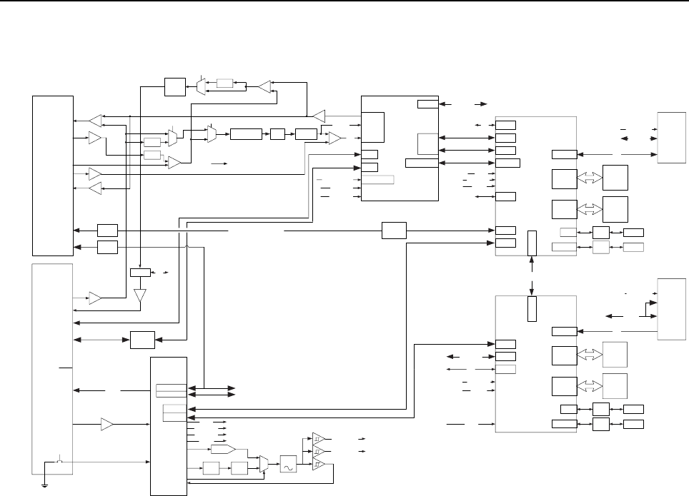
4-2 Theory of Operation
Refer to Figure 4-1 for the MTR3000 Controller Block Diagram.
Figure 4-1 MTR3000 Controller Block Diagram
4.2.1 Tx/Rx OMAP
The Tx DSP is a TI OMAP Multimedia Processor. The OMAP1710 consists of a microprocessor unit
(MPU) subsystem and a digital signal processor (DSP) subsystem.
OMAP1710 has dedicated external memory interface that allow point-to-point connection to
standard mobile SDRAM/DDR and mobile flash devices. It is a low-power device (1.4 V Core and
1.8 V I/O supply). Tx OMAP (U1000M1) handles all transmit tasks of the SCM while Rx OMAP
(U1001M1) handles receiving tasks of the SCM only.
4.2.1.1 External Memory
Both transmit and receive DSP’s support independent external memory banks.
4.2.1.1.1 RAM
The SCM supports Tx/Rx OMAP Mobile Double Data Rate (U1003M1 and U1601M1) SDRAM
respectively. It has the following basic characteristics:
• 32 MB organized as 4 Mb x 16 x 4 Banks
• Four internal banks for concurrent operation
• Programmable burst lengths: 2, 4, or 8 bytes
Add/Data
Add/Data
OMAP1710
Receive
DDR
FLASH
32MByte
16Mx16
32MByte
16Mx16
Receiver
Connector
SSI
OMAP1710
Transmit
Add/Data
Add/Data
Exciter
Connector
SSI
TX
MAKO McBSP2
EMIFS
EMIFF
McBSP2
EMIFS
EMIFF
SPI
McBSP3M c BS P3 SSI
Abacus SSI
McBSP1CODEC SSI
PORESET
SPIF
PORESET
Back plane
Connector
Rx SPI
Trident SSI
SPIF
32.768KHz
24.576MHz
XTAL32IN
XIN
12MHz
32.768KHz CLK 32K
CLK PLL
MTR2K WL12 & WL34 SSI
USB2
USB0
USB
Front
Panel
+
Rx Audio CODEC
AUDIO
Mic In
Speaker Out
Audio
Attenuator
I2C
To Tx OMAP
Mic
Tx Audio (PRE)
USB0
USB2
USB-To-
Ethernet
USB
10BaseT Ethernet
(RJ45)
MTR2K Wireline12
SSI
MTR2K Wireline34
SSI
Backplane SPI
Station
Reference
FPGA
Reference In
(BNC)
A/D Inputs
Analog Monitor
I2C
I2C
To Audio Attn
Level
Shift
Level
Shift
RX 16.8MHz
EX 16.8MHz
MCSI1
AUX Rx Audio
UART1 RS232
XCVR
Test
Header
LEDs
LEDs
Power/Status
Tx Status 1
Tx Status 2
Rx Status 1
Rx Status 2
Mode
Ethernet
Ext Ref
FP GA
Aba SPI
DDR
32MByte
16Mx16
FLASH
32MByte
16Mx16
+
Limiter
1.0 Vpp Max
Splatter
filter
USB1
I2C
I2C
To WB CODEC
USB
XCVRTest
Header
UART1 RS232
XCVR
USB1 USB
XCVR
Test
Header
Test
Header
Aux Mic
MCSI1
Codec SSI
ResetTo Rx & Tx OMAP
16.8MHz
16.8MHz
TCXO
Charge
Pump
Loop
Filter
Mux
DAC
EX 16.8MHZ
RX 16.8MHZ
32.768KHz
24.576MHz
12MHz
Reset
From FPGA
From FPGA Reset
12MHz
32.768KHz CLK 32K
CLK PLL
Control &
StatusGPIO
TX SP IF
RX SP IF
EX/BP SPI
RX SPI
Ex SPI
EX/BP SPI
From FPGA
EX/BP SPI From FPGA
To Mako and Exciter
To Receiver
RX SPI
From FPGA
FP PUSH
BUTTON RST
Note: MTR2K Wireline is not a supported feature for Bandit
releases. The circuit will not be replaced and reserved in case of this
requirement changed in the future.
High
Pass
Filter
+
De-
Attn
TOMAP MPUIO0
0
1
Tx Data/PL/DPL
Pre-
Emphasis
Pre-
Emphasis
Emphasis
+
TXOMAP
MPUIO10
0
1
0
1
TXOMAP
MPUIO13
Default Path selected
Tx Audio (Flat)

Theory of Operation 4-3
• Auto refresh and self refresh modes
• Selectable output drive (DS)
• VDD/VDDQ = 1.7–1.95 V
The maximum external clock rate for the DDR is 90 MHz. Since data is transferred on both clock
edges, the effective data rate is 180 Mwords/s.
4.2.1.1.2 Flash
The SCM supports 256 MB external Tx/Rx OMAP flash memory (U1002M1 and U1600M1). The
device has the following basic characteristics:
• Four 32 KBytes Bottom Boot Sectors
• 128 KBytes main blocks (254 for 256 Mbit part, 514 for 512 MBit part)
• 1.8V VCC and VCCO
4.2.2 Serial Peripheral Interface (SPI)
The station local and Intermodule SPI Bus is controlled by both Tx and Rx OMAP1710 processors,
which has an on-chip SPIF (fast SPI) interface. The OMAP1710 SPIF supports master and slave
modes, programmable clock rate, phase, polarity, programmable word size, programmable bit
ordering, and loopback.
Before an SPI data transfer can take place, the SPI master (initiator) must assert the select line of
the slave (target) device. The OMAP1710 is always the SPI master for MTR3000 base station/
repeater. To simplify overall SPI architecture for MTR3000 base station/repeater, address decoding
is used instead of individual device chip signals. This approach not only minimizes the number of
GPIOs needed for device chip select, it also provides flexibility for future expansion. This device
address decoding is handled by an Field Programmable Gate Array (FPGA) on the SCM and a
Customer Programmable Logic Device (CPLD) on each FRU’s, except the power supply.
The FPGA SPI module performs address and chip select decoding, level shifting, and signal mixing
for both the Tx OMAP SPI bus and the Rx OMAP SPI bus. Simultaneous Rx and Tx SPI accesses
are allowed. The Tx and Rx SPI are 100% independent.
Table 4-1 SPI decoding truth table
Signal Name Section Device CS
(DCS4:DCS1)
SPI Address
(A2:A0)
OMAP
GPIO16
OMAP
SPI_NCS3x
Enable Enable
Default No device selected 1111 111 x 1
OP1_CS1x BP 0000 111 x 0
OP1_CS2x BP 0001 111 x 0
OP1_CS3x BP 0010 111 x 0
OP2_CS1x BP 0011 111 x 0
OP2_CS2x BP 0100 111 x 0
OP2_CS3x BP 0101 111 x 0
4-4 Theory of Operation
Refer to Figure 4-2 for the MTR3000 Controller SPI connection.
WL_CS1x Wireline 0110 111 x 0
WL_CS1x Wireline 0111 111 x 0
MAKO Control 1000 111 x 0
Metering Exciter 1001 000 x 0
Trident IC Exciter 1001 001 x 0
EEPROM Exciter 1001 010 x 0
TRIDENT_RST_N1Exciter 1001 011 x 0
EX_STANDBY1Exciter 1001 110 x 0
EEPROM PA 1010 x00 x 0
DAC PA 1010 x01 x 0
ADC PA 1010 x10 x 0
PA Inactive PA 1010 x11 x 1
FPGA SPI Control 1011 000 1 0
Metering RCVR xxxx 000 0 1
Trident IC RCVR xxxx 001 0 1
EEPROM RCVR xxxx 010 0 1
TRIDENT_RST_N1RCVR xxxx 011 0 1
Abacus RCVR xxxx 100 1 0
RX_STANDBY1RCVR xxxx 110 0 1
Reserved NA xxxx xxx 1 1
Note 1. SPI Write to the Exciter/Receiver CPLD.
Table 4-1 SPI decoding truth table (Continued)
Signal Name Section Device CS
(DCS4:DCS1)
SPI Address
(A2:A0)
OMAP
GPIO16
OMAP
SPI_NCS3x
Enable Enable
Theory of Operation 4-5
Figure 4-2 MTR3000 Controller SPI connection
TX OMAP 1.8V
(U1000M1)
GPIO_xx
GPIO_xx
GPIO_xx
GPIO_xx
SPI_NCS1x
OP1-CS1x
OP1-CS2x
OP1-CS3x
OP2-CS1x
OP2-CS2x
OP2-CS3x
Wireline12_Latch_CSx
Wireline34_Latch_CSx
PA_Addr0
PA_Addr1
SPI_MISO_BP_In
Backplane 5V
(P3200M3)
FPGA 1.8C/3.3V
CS
Mosi
Clk
Miso
MAKO 1.8V
(U1402M1)
MISO
SPI_CS
Addr0
Addr1
Addr2
Exciter 3.3V (U3601M3)
GPIO_xx
GPIO_xx
GPIO_xx
Addr0
Addr1
Addr2
RCVR 3.3V
(U3603M3 and U3604M3)
Aba_PE
Aba_PC
Aba_PD
DOUT
SPI_NCS3x
SPI_CLK
SPI_MOSI
SPI_MISO
Address
Chip Selects
SPI_CS
Addr0
Addr1
Addr2
MISO
MOSI
CLK
RX OMAP 1.8V
(U1001M1)
SPI_NCS1x
GPIO_xx
GPIO_xx
GPIO_xx
SPI_CLK
SPI_MOSI
SPI_MISO
DCS1
DCS2
DCS3
DCS4
Addr0_out
Addr1_out
Addr2_out
Exciter_CS
Mako_CS
Mako_Mosi
Mako_Clk
Mako_Miso
BP1_CS1x
BP1_CS2x
BP1_CS3x
BP2_CS1x
BP2_CS2x
BP2_CS3x
WL12_CSx
WL34_CSx
PA_Addr0
PA_Addr1
Spi_miso_bp
CSx
Rcv_CSx
Rad0
Rad1
Rad2
Rcv_CS_out
Rad0_out
Rad1_out
Rad2_out
SPI_CLK_out
SPI_MOSI_out
SPI_MISO_in
SPI_CLK
SPI_MOSI
SPI_MISO
Aba_CSx
RSPI_Clk
RSPI_MOSI
RSPI_MISO
Aba_CSx_out
Aba_Clk_out
Aba_mosi_out
Aba_miso_in
To / from all modules
(except RCVR and Mako)
RSPI_MISO
RSPI_MOSI
RSPI_CLK
(U2000M5)

4-6 Theory of Operation
Refer to Table 4-2 for the Tx/Rx OMAP SPI Module and Device Parameters.
Table 4-2 Tx/Rx OMAP SPI Module and Device Parameters
Module SPI Device
Device
Enable
(active
high/
low)
MOSI
Data
Latched
(rising/
falling
edge of
SPI
clock)
Minimum
number
of bits
per
access
Max
Clock
Rate
Module
Select
active
to 1st
clock
edge
(min)
Data
complete
to
Module
select
negated
(min)
Exciter SPI CPLD High rising 8 bits 1 MHz – –
EEPROM
(Atmel
AT25640)
Low rising 32 bits32 MHz 50 ns 50 ns
Trident IC Low rising 24 bits 20 MHz/
10 MHz110 ns/
20 ns10 ns
Metering ADC
(Maxim
Max149B)
Low rising 24 bits 1.8 MHz 100 ns 0 ns
PA EEPROM
(AT25640)
Low rising 32 bits32 MHz 50 ns 50 ns
DAC (Motorola
5183977M73)
Low rising 24 bits 500 kHz – 0 ns
ADC (TI
TLC542C)
Low rising 8 bits 1 MHz 3.8 us 0 ns
CNTL FPGA Low rising 16 bit 12 MHz – 0 ns
MAKO High rising 48 bit for
RTC
register
access
32 bit for
non-
RTC
register
access
10 MHz 11 ns 0 ns
WL MTR3000
Wireline FPGA
Low rising 8 bits 3.3 MHz – 0 ns
AUXIO MC74HC595A Low rising 8 bits 3.3 MHz –0 ns
MC74HC598A Low rising 8 bits 3.3 MHz – 0 ns
Theory of Operation 4-7
4.2.3 Station Reference
A Temperature Compensated Crystal Oscillator (TCXO) or Oven Controlled Crystal Oscillator
(OCXO) constitute two different SCMs and provide frequency reference for the base station/
repeater. The TCXO or OCXO is 16.8 MHz.
The stability of the TCXO is ±0.5 ppm over temperature (-30ºC to +85ºC) with an aging rate of
±1.0 ppm per year and ±3.0 ppm over 10 years. This stability is sufficient for some applications but
not for others. The MTR3000 controller will also have the option to use an OCXO for high stability
applications (800/900 MHz). This change will be transparent to the software. The stability of the
OCXO is ±50 ppb over temperature (-30ºC to +80ºC) with an aging rate of ±50 ppb per year. The
OCXO will not be placed for all applications other than 800/900 MHz.
RCVR2SPI CPLD High rising 8 bits 1 MHz – –
Metering_1
ADC (Maxim
Max149B)
Low rising 24 bits 1.8 MHz 100 ns 0 ns
Metering_2
ADC (Maxim
Max149B)
Low rising 24 bits 1.8 MHz 100 ns 0 ns
Trident IC Low rising 24 bits 20 MHz/
10 MHz110 ns/
20 ns10 ns
EEPROM
(AT25640)
Low rising 32 bits32 MHz 50 ns 50 ns
Abacus Low rising 16 bits310 MHz 5 ns 5 ns
Note 1. Write specifications or Read specifications for Trident IC.
2. Applied to Rx OMAP only.
3. Subsequent location(s) can be accessed if the CS* remain asserted.
Table 4-2 Tx/Rx OMAP SPI Module and Device Parameters (Continued)
Module SPI Device
Device
Enable
(active
high/
low)
MOSI
Data
Latched
(rising/
falling
edge of
SPI
clock)
Minimum
number
of bits
per
access
Max
Clock
Rate
Module
Select
active
to 1st
clock
edge
(min)
Data
complete
to
Module
select
negated
(min)
4-8 Theory of Operation
Table 4-3 summarizes the frequency stability and service intervals for the TCXO and OCXO.
4.2.3.2 MTR3000 Controller Clocks
The FPGA is used to create other clocks locked to the Temperature Compensated Crystal Oscillator
(TCXO) or Oven Controlled Crystal Oscillator (OCXO) which are needed by various devices on the
Control Board. The clocks are summarized in Table 4-4.
Table 4-3 SCM FCC Frequency Stability Requirement
Required
Stability
(ppm)
TCXO Service
Interval
OCXO
Service
Interval
55 years 10 years
2.5 2 years 10 years
1.5 1 year 10 years
1 6 months 10 years
0.5 Ext Ref Required 5 years
0.1 Ext Ref Required 1 year
Table 4-4 SCM FPGA output Frequencies
Frequency Destination
12 MHz Tx OMAP, Rx OMAP
24.576 MHz MAKO
32.768 kHz Tx OMAP, Rx OMAP
Theory of Operation 4-9
Refer to Figure 4-3 for the MTR3000 Controller Clock Configuration.
Figure 4-3 MTR3000 Controller Clock Configuration
4.2.4 MAKO
MAKO IC (U1402M1) is a customized IC and the SCM uses this device to leverage some unique
functionality that it provides.
Most of the MAKO functionality are not used on the SCM. Only the MAKO codec, USB driver, ADC,
DAC, and some voltage regulators are used for MTR3000 base station/repeater. The 9 channel
general purpose ADC is used for various controller metering.
Refer to Figure 4-4 for the MAKO block diagram and usage of MTR3000 Controller.
Note For the OCXO kit, the controller must be warmed up for a minimum of 15 minutes before the
base station/repeater is enabled for transmit.
Y0
Charge
Pump
Loop
Filter
16.8MHz
Y1 CLK_RX_16_8MHZ J3601 – B15
Y2 CLK_EX_16_8MHZ J3600 – B1
CLKIN
FPGA
MAKO
OSC_IN
CLK32K_IN
OSC_IN
CLK32K_IN
RXOMAP_12MHZ
RXOMAP_32.768KHZ
TXOMAP_32.768KHZ
TXOMAP_12MHZ
XTAL32_IN
TCXO_IN
MAKO_32.768KHZ
MAKO_24.576MHZ
XTAL32_OUT
TXOMAP
U1000M1
Y1400M1
U1402M1
RXOMAP
U1001M1
U2000M5
DAC
U2401M5
Mux
U2403M5
16.8MHz
OCXO
Y2401M5
16.8MHz
TCXO
Y2400M5
CLOCK
BUFFER
U2402M5
Note: OCXO (Y2401M5) will be placed for CLN8565 kits only.
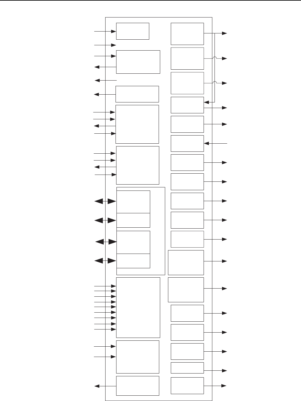
4-10 Theory of Operation
Figure 4-4 MAKO Block Diagram and usage of MTR3000 Controller
Switch 1 3.6V
LDO 10 Not Used
Not Used
Not Used
Not Used
Not Used
Not Used
Not Used
Not Used
Not Used
Not Used
LDO 9
LDO 8 9.3V
LDO 7
LDO 6
LDO 4 2.75V, Trident logic
level translator
LDO 3
LDO 2
Switch 2 Not Used
Switch 5
USB USB
RTC32.768KHz from FPGA
24.576MHz from FPGA TCXO_IN
MAKO_INT_N to Tx OMAPINT_x
BBP SYNC
GEN
Not Used
CLK
SPI_CLK from FPGA
MOSI
SPI_MOSI from FPGA
MISO
SPI_MISO to FPGA
CS
SPI_CS from FPGA
SPI
Power
Management
MECH_SW from FPGA
RESETx to FPGA
VC_DCLK
SSI_CLK to Tx OMAP
VC_FSYNC
SSI_FS to Tx OMAP
VC_TX
SSI_DI to Tx OMAP
VC_RX
SSI_DOUT from Tx OMAPSSI
USB0 from Tx OMAP
USB
USB1_OE
USB1_DAT
USB1_SE0
USB2_OE
USB2_DAT
USB2_SE0
USB1_DP
USB1_DM
FP USB service port
USB2_DP
USB2_DM
USB2 from Tx OMAP
Ethernet to USB ICLegacy
Accessory
Interface
Accessory
Option
Detect
DAC2
DAC3
ATOD_2
ATOD_1
ATOD_5
ATOD_3
ATOD_4
ATOD_8
ATOD_6
ATOD_7
ADC
Option1 ID
Option2 ID
MIC push button
1.875V
PTEMP
3.3V
ATOD_0
Wireline ID
INT_MIC_P
AUX MIC AUDIO
EXT_MIC_P
MIC AUDIO
Voice Codec Pre-Amp VC_OUT/codec
Audio out
Audio
Amp
ASIC Test
Not Used
1.875v, MAKO Logic
Supply
DAC1BP_RSSI
14.2V
5V

Theory of Operation 4-11
Refer to Table 4-5 for the MAKO general purpose ADC allocation.
4.2.5 Field Programmable Gate Array (FPGA)
The SCM FPGA includes the following major functions:
• External reference watchdog
• SPI Address decoding and buffering
• OCXO and TCXO Phase detection and compensation
• Clock generation
• Reset controller
• External Interface (Wireline SSI, LED, etc.)
FPGA field upgrade capability is also supported on MTR3000 base station/repeater.
Refer to Figure 4-5 for the block diagram of MTR3000 Controller FPGA.
Table 4-5 MAKO General Purpose ADC Allocation
Channel # Metering Module Voltage (V) Value (Hex) Comment
0Wireline ID MTR3000
Wireline
2.5 0x359 Wireline identification number. Read
during initialization when wireline
module is present.
1 Option1 ID AUX IO 0.373 0x080 AUXIO identification number. Read
during initialization when AUXIO
module is present on Option 1 slot.
2Option2 ID AUX IO 0.373 0x0BC AUXIO identification number. Read
during initialization when AUXIO
module is present on Option 2 slot.
3 PTEMP+ NA 0.55–2.269 0x0BD–0x30A Peripheral Temp from 3 pin
connector on backplane.
4RESERVED NA NA NA Pin is reserved for future expansion.
5 14_2V Control 1.79 0x25C For factory to check PS 14.2 V
voltage level.
65V Control 1.55 0x20B For factory to check PS 5 V voltage
level.
7 1.875V Control 1.875 0x283 For factory to check main 1.875 V
voltage level.
83.3V Control 3.3 0x324 For factory to check main 3.3 V
voltage level.
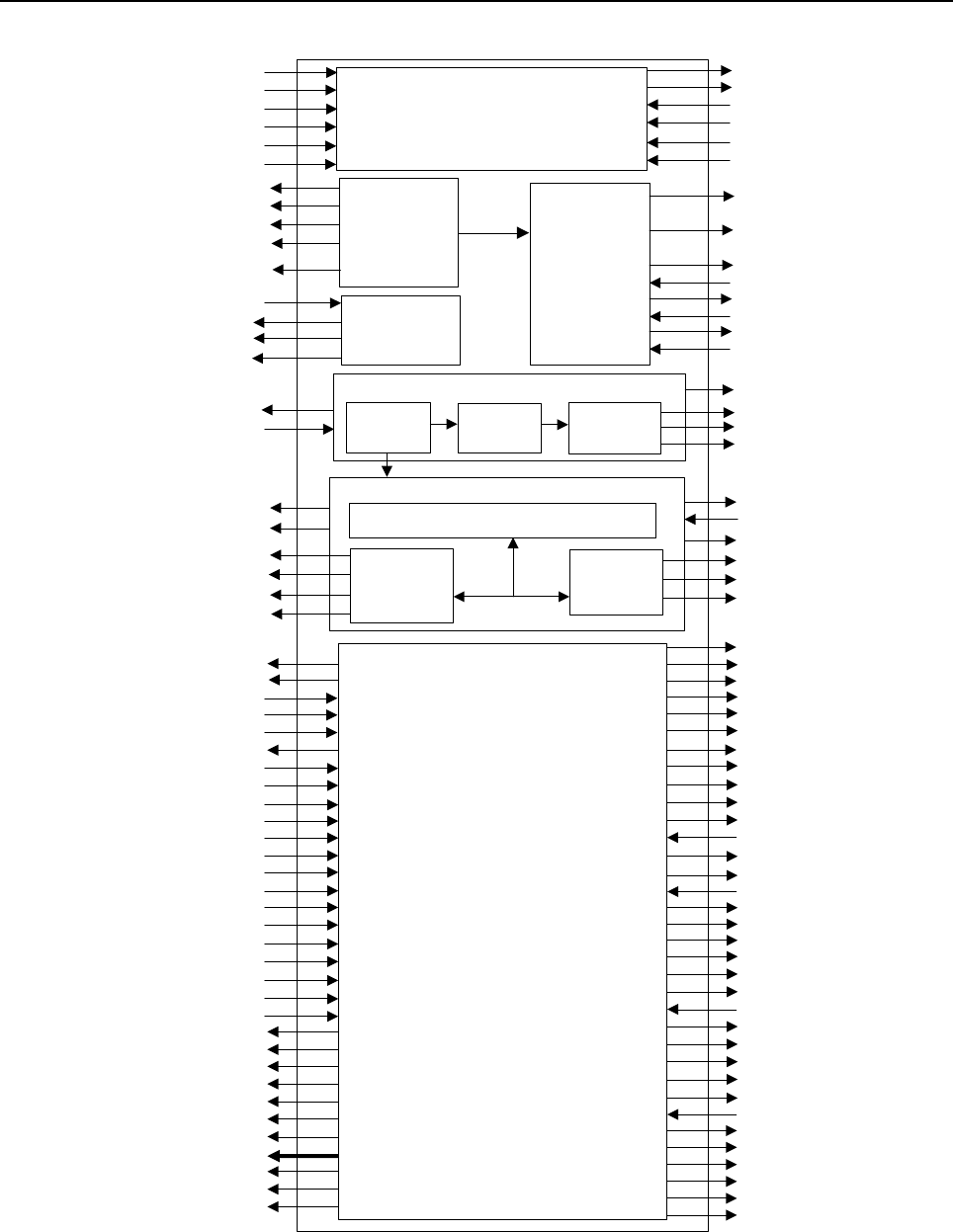
4-12 Theory of Operation
Figure 4-5 MTR3000 Controller FPGA Block Diagram
Mode_LED
TX1_LED_R
TX1_LED_G
RX1_LED_R
RX1_LED_GPower_LED_G
Power_LED_R
TX2_LED_R
TX2_LED_G
RX2_LED_R
RX2_LED_G
PLLs
16.8MHz
24.576MHz
12MHz_TX
12MHz_RX
Clock
Gen
Station Ref
FLASH
Intf
Ref
Detect
Phase
Detector
Ref
WD
Reference Block
DAC
Intf
Flash_SPI_CSx
Flash_SPI_Clk
Flash_SPI_MOSI
Flash_SPI_MISO
SPI
Ref Fail
Ext Ref
Auto_Det_Ref
Station_ref_lock
Phase_det_u
Phase_det_d
Steer_Volt_Cntl
Comp_In
Align_Fail
DAC_CSx
DAC_Clk
DAC_Data
WL12_CSx
WL34_CSx
SPI_CSx
SPI_Clk
SPI_MOSI
SPI_MISO
DCS1
DCS2
DCS3
DCS4
SPI_Addr0
SPI_Addr1
SPI_Addr2
SPI_IRQx
Rcv_CSx
Rad0
Rad1
Rad2
Aba_CSx
RSPI_Clk
RSPI_MOSI
RSPI_MISO
Mako_usb_cl
Compensation Cntrl
Codec
Interface
MSCI1_Data_Clk
MSCI1_FS_Clk
32.768KHz_ROMAP
32.768KHz_TOMAP
Codec12_Data_Clk
Codec12_FS_Clk
MSCI1_Rxd
MSCI1_Txd
Codec12_DR
Codec12_DT
Codec34_DR
Codec34_DT
Station_Ref_LED_R
Station_Ref_LED_G
Reset
TOMAP_WD_RSTx
ROMAP_WD_RSTx
Mako_detect
FP_RSTx
Vmon_5v
Mako_resetx
Master_RSTx
Mako_On_Offx
Resetx
Ldo_1
Tx_rst
RX_Rst
GP_Out(0-7)
Exc_SPI_CS
PA_EX_Disablex
OP1_CS1x
OP1_CS2x
OP1_CS3x
OP2_CS1x
OP2_CS2x
OP2_CS3x
Mako_CS
Mako_MOSI
Mako_Clk
Mako_MISO
SPI_CLK_Out
SPI_MOSI_Out
SPI_MISO_In
PA_Addr0
PA_Addr1
RCV_CS_Out
RAD0_Out
RAD1_Out
RAD2_Out
RSPI_MISO_In
RSPI_MOSI_Out
RSPI_Clk_Out
Aba_CSx_out
Aba_Clk_Out
Aba_MOSI_Out
Aba_MISO_In
SPI_Addr0_Out
SPI_Addr1_Out
SPI_Addr2_Out
12MHz_WB
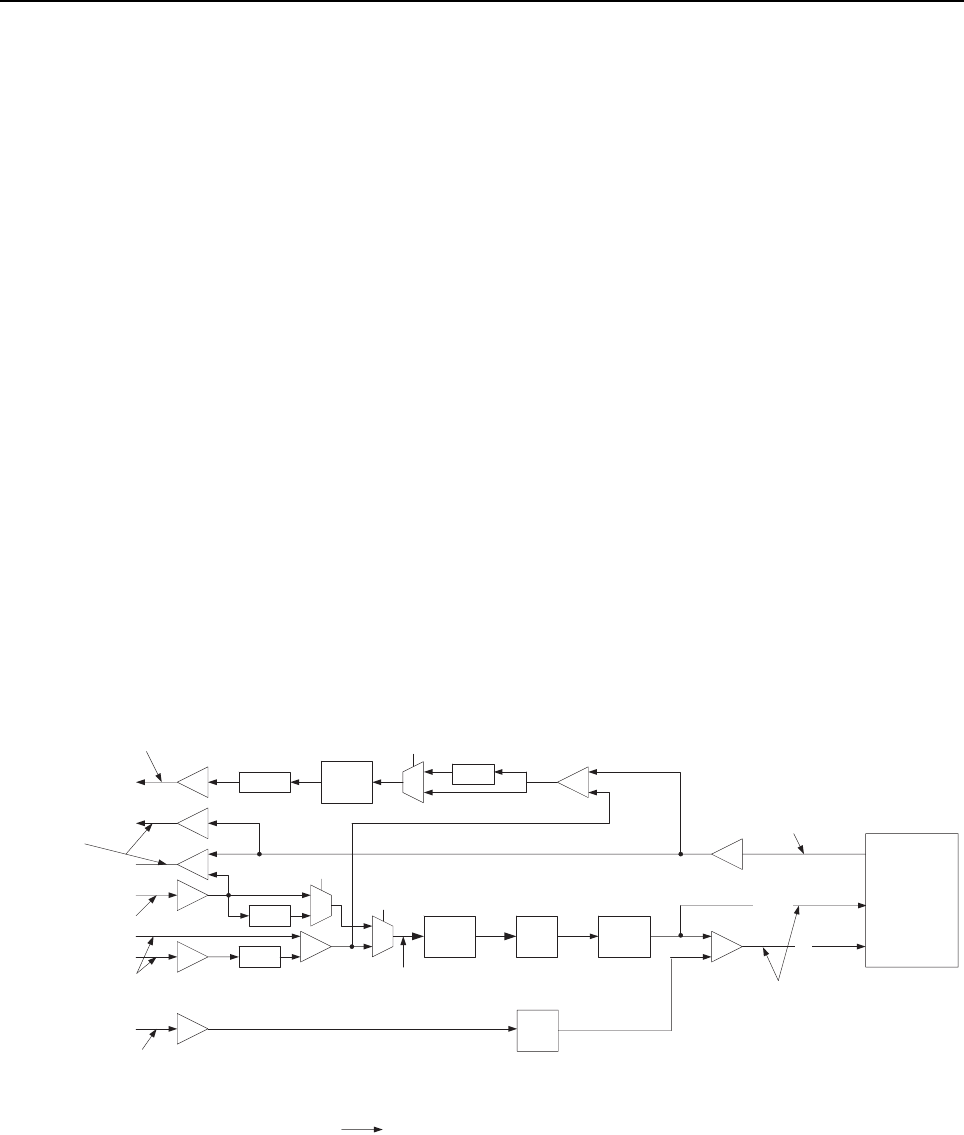
Theory of Operation 4-13
4.2.6 Audio
There are four transmit inputs: Tx Audio, Tx Audio-Pre and Tx Data on the backplane DB25
connector, and the Microphone input on a front panel RJ45 connector.
Tx Audio is a flat (not pre-emphasized) input which is used if the incoming transmit audio signal is
already pre-emphasized, if hardware pre-emphasis is not needed, or if the CPS has pre-emphasis
enabled. The Tx Audio-Pre input provides a hardware pre-emphasis filter. The Tx Data input is used
for low speed data, Private-Line (PL) and Digital Private Line (DPL) signals. The microphone input
can be selected under software control to be flat or pre-emphasized using an OMAP GPIO.
The Tx Audio, Tx Audio-Pre and microphone inputs pass through a hardware modulation limiter and
splatter filter before being summed with Tx Data, which bypasses the limiter and splatter filter. Mic is
never summed with TDATA. This summed signal is applied to the MAKO codec “mic” input. The
audio signal without Tx Data is provided on the MAKO codec “aux_mic” input. The MAKO codec
“aux_mic” is used for microphone audio only.
There are three receive outputs: Rx Audio and Aux Rx Audio on the backplane DB25 connector and
speaker audio on a front panel RJ11.
The speaker audio is the sum of the MAKO codec output (demodulated audio) and transmit audio.
The speaker audio can be selected under software control to be flat or pre-emphasized using an
OMAP GPIO. A high pass filter removes any data, PL or DPL from the speaker audio. A
programmable attenuator is used to adjust the speaker audio level before being output on the RJ11
connector.
Aux Rx Audio is the output of the MAKO codec (demodulated audio), and Rx Audio is the sum of the
MAKO codec output and microphone audio.
Refer to Figure 4-6 for audio paths and voltage levels.
Figure 4-6 Station Control Module (SCM) Audio Path
+
Rx Audio
Mic
+ +
Limiter
1.0 Vpp
Max
MPUIO0
Splatter
filter
Aux Mic
Mic In
Speaker Out
(to amplified speaker)
80 mVrms
226 mVpp
Attn
330 mVrms
933 mVpp
(into 50K Ohms)
56 mVrms
158 mVpp
0 to 500mVrms
0to 1.4 Vpp
Nominal levels for 60% FSD with
1KHz tone
High
Pass
Filter
I2C Audio
Attenuator0
1
MPUIO13
+
De-
Emphasis
Pre-
Emphasis
0
1
0
1
Pre-
Emphasis
MPUIO10
Aux Rx Audio
VC_OUT
AUX_MIC
MIC
MAKO
CODEC
Default Path selected
221 mVrms
600 mVpp
Attn
80 mVrms Voice
16mVrms data
74 mVrms
209 mVpp
Tx Data/PL/DPL
80 mVrms
226 mVpp
Tx Audio - Pre
Tx Audio - Flat
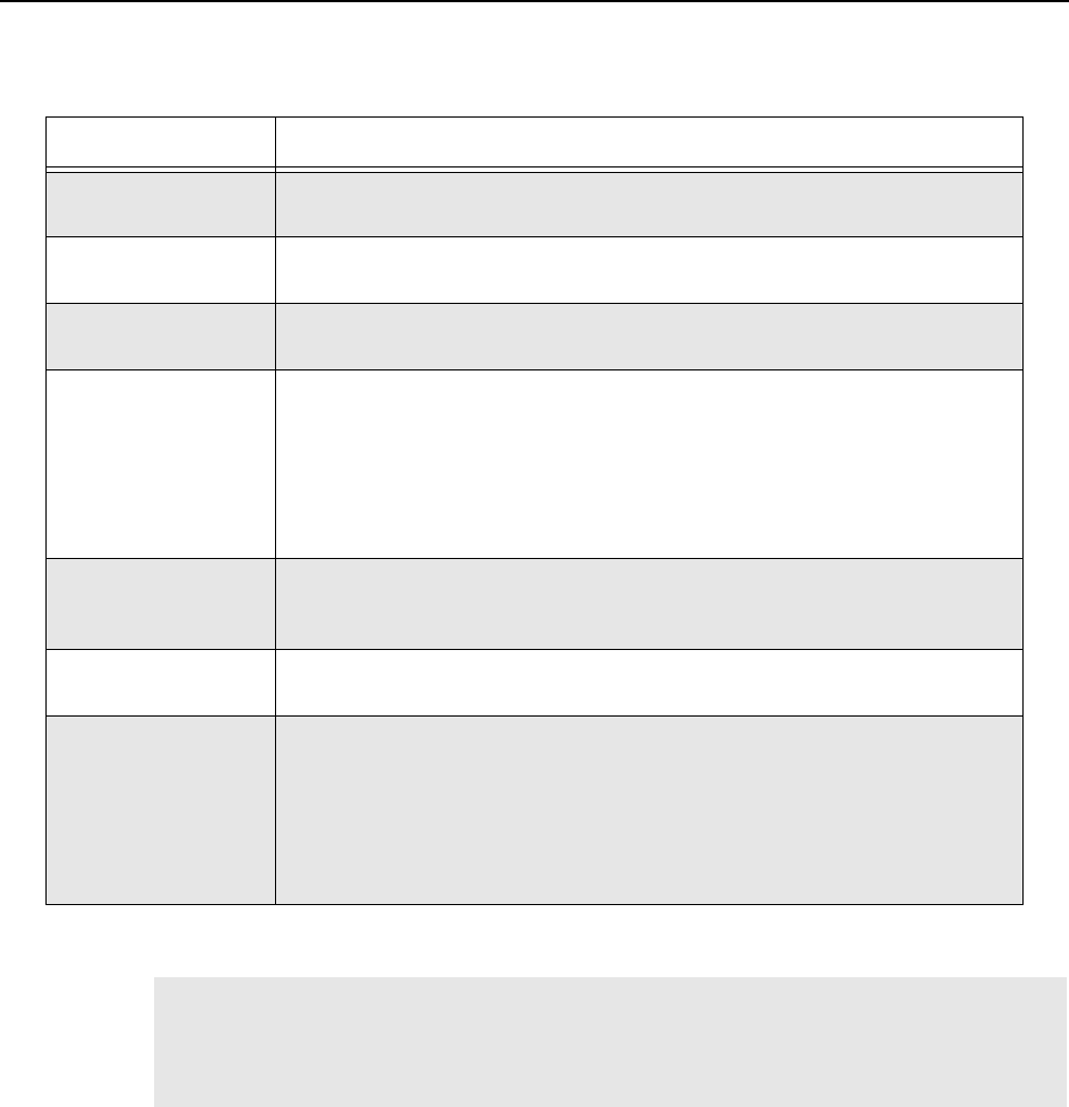
4-14 Theory of Operation
Refer to Table 4-6 for description on audio signals.
4.2.7 Ethernet Interface
Since OMAP1710 does not support a direct Ethernet interface, a bridge device (U3005M7) is
needed to support Ethernet on the SCM. The bridge device is a high performance hi-speed USB2.0
to 10/100 Ethernet controller. The device contains an integrated 10/100 Ethernet PHY, USB PHY,
Hi-Speed USB 2.0 device controller, 10/100 Ethernet MAC, TAP controller, EEPROM controller and
a FIFO controller with a total of 30 KBytes of internal packet buffering. The following is a list for
functionality that the Ethernet Interface can provide:
• Fully Compliant with IEEE 802.3 and 802.3u Compatible Ethernet Controller
• 10Base-T and 100Base-Tx support
• Integrated Media Access Control (MAC) and PHYsical (PHY)
Table 4-6 SCM Audio Level
Audio Signal Description
Tx Audio The Tx Audio input provides no hardware pre-emphasis. The nominal level of
80 mVrms (158 mVpp) produces 60% Relative Standard Deviation (RSD).
Tx Audio-Pre The Tx Audio-Pre input provides a hardware pre-emphasis network. The nominal
level of 80 mVrms (158 mVpp) produces 60% RSD.
Tx Data Transmit data, PL or DPL signaling. The nominal level of 80 mVrms (158 mVpp)
produces 12% RSD.
Mic Local microphone input. Use microphone type GMN6147 (older model) or
GMMN4063. Modulation sensitivity for 60% system deviation is typically 56
mVrms (158 mVpp).
Note : The Mic port is only supported in analog mode regardless of the Mic used.
For older model of microphone (GMN6147), the 3 control buttons for speaker
volume control, Rx monitor and Intercom control functions are not supported.
Aux Rx Audio An RF input signal with 60% RSD provides an Rx Audio output of 330 mVrms into
50 kΩ. Also a microphone input of 56 mVrms provides an Aux Rx Audio output of
330 mVrms into 50 kΩ. The Rx Audio output has DC bias of 2.5 VDC.
Rx Audio An RF input signal with 60% RSD provides an Rx Audio output of 330 mVrms into
50 kΩ. The Rx Audio output has a DC bias of 2.5 VDC.
Speaker Output to Powered Voice speaker. Adjustable between 0 to 500 mVrms (1.4 Vpp)
across 1 kΩ @ 60% system deviation. Audio signal appears between Pins 3 and 4
on the connector. Must use speaker type HSN1000 (older model) or HSN1006 via
adapter cable Part.No. 0185180U01.
Note : The Speaker port is only supported in analog mode regardless of the
speaker used.
Note When using third party controllers, refer to MTR3000 Third Party Controllers (Appendix G)
section in the MOTOTRBOTM MTR3000 Base Station/Repeater Basic Service Manual
(68007024096) for CPS configuration in conjunction with the selection of the correct Tx
Audio paths to prevent a double pre-emphasis.
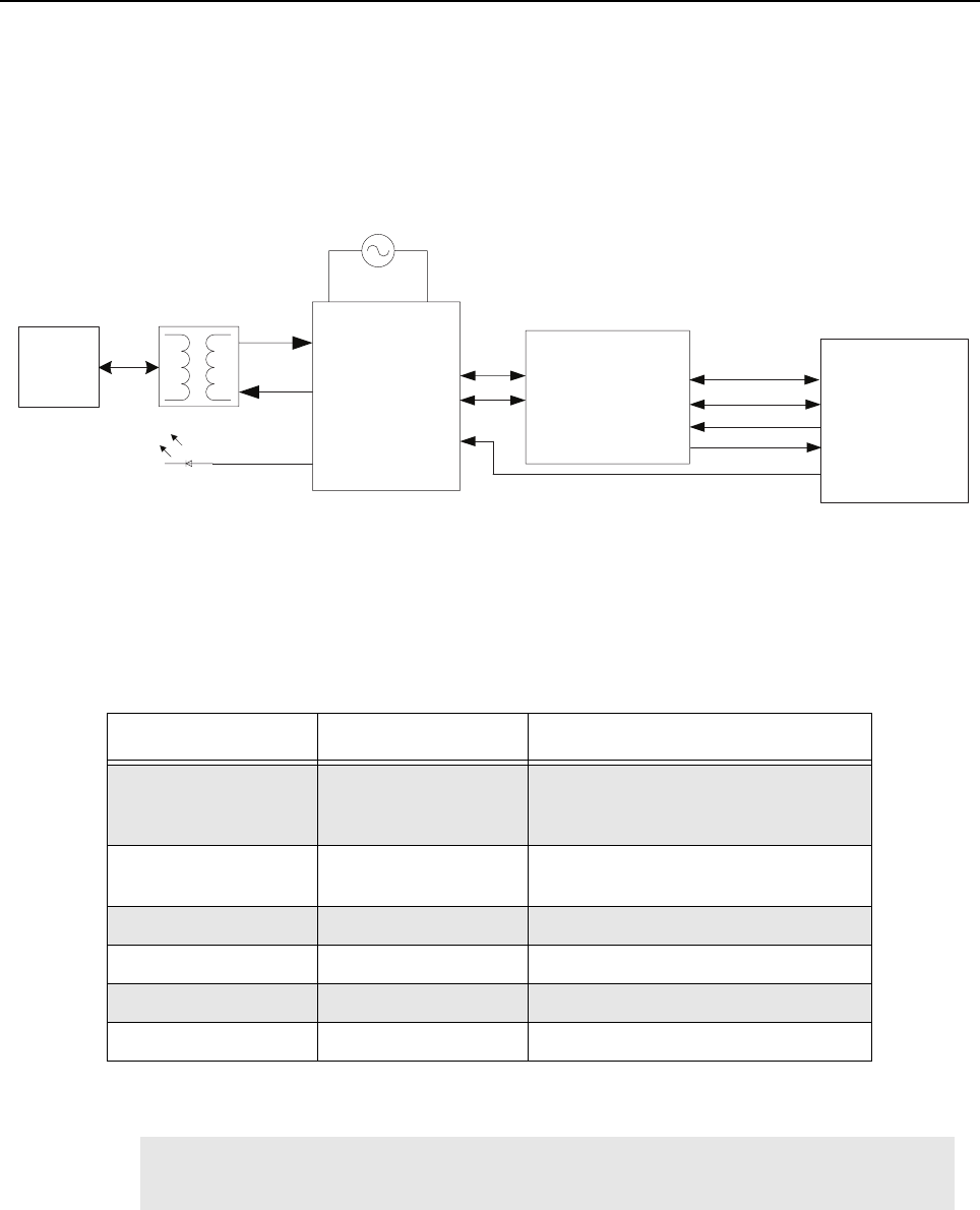
Theory of Operation 4-15
• Supports one 10BT port with automatic polarity detection and correction
• Supports full and half duplex mode and flow control
• Universal Serial Bus (USB) and Joint Test Action Group (JTAG) parameters
Refer to Figure 4-7 for the MTR3000 Ethernet bridge IC connection.
Figure 4-7 MTR3000 Controller Ethernet Connection
4.2.7.3 LAN9500i Power-up Configuration
SMSC LAN9500i will be configured into the following mode after power-up.
Table 4-7 SMSC LAN9500i Default Configuration after Power-up
Pin Name Default Setting Description
EEP_SIZE PU 1 = 256/512 byte EEPROM is attached
and a total of nine address bits are
used.1, 2
PORT_SWAP PD 0 = USBDP maps to the USB D+ line
and USBDM maps to the USB D- line.1
RMT_WKP PD 0 = Remote wakeup is not supported.1
EEP_DISABLE PD 0 = EEPROM is recognized if present.1
AUTOMDIX_EN PU 1 = Auto-MDIX is enabled.1
PWR_SEL PD 0 = The LAN9500i is bus powered.
Note 1. Internal PU and PD are used, no external connections.
2. No external EEPROM is connected.
LAN9500i
USBDM
25MHz Oscillator
TXP
TXN
RJ45
NLNKA
TXOMAP
USB2_TXEN
USB2_DAT
USB2_SE0
ARMIO15
GREEN
USBDP
VBUS_DET
MAKO
USB2DM
USB2DP
USB2_OE
USB2_DAT
USB2_SE0
GPIO38
USB_INTX
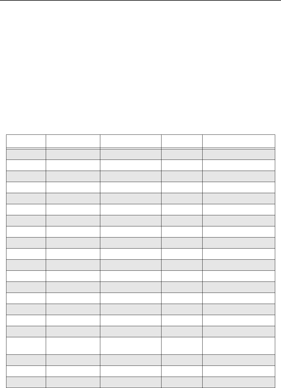
4-16 Theory of Operation
4.2.8 Backplane
The connector that connects the controller to the backplane is a right angle, 96-Pin Connector. It
provides connectivity between the MTR3000 controller and other station FRU, such as the Wireline
card, the AUXIO card as well as, third party equipment. For details on backplane connection, refer to
MTR3000 Backplane chapter in the MOTOTRBOTM MTR3000 Base Station/Repeater Basic Service
Manual (68007024096).
4.2.9 Exciter
The connector (J3600M3) used to connect the controller to the Exciter is a dual row, right angle,
early entry receptacle, without flange, 30-Pin Connector. It provides 16.8 MHz reference clock,
14.2 V, 10 V and 8 V supply voltage, SPI, Trident SSI and other digital handshake signals with the
Exciter.
Refer to Table 4-8 for pinout for the Exciter connector.
Table 4-8 MTR3000 Controller Exciter Connector connection
Pin Signal Name Description Signal Level Controller Connection
A1 Ground Ground
A2 Ground Ground
A3 TXD_EX Trident SSI data 2.775 V Tx OMAP McBSP2.DX
A4 TXFS_EX Trident SSI frame sync 2.775 V Tx OMAP McBSP2.FSX
A5 Ground Ground
A6 EX_ENABLE_EX Ex Slot Enable 3.3 V Tx OMAP GPIO28
A7 NC No Connect on Controller
A8 NC No Connect on Controller
A9 +8V Ex 8.0 V supply 8 V 8VDC
A10 Ground Ground
A11 EX_CPLD_ADD_0 CPLD SPI address 0 3.3 V FPGA
A12 Ground Ground
A13 EX_CPLD_CLK CPLD SPI input clock 3.3 V Clock Buffer
A14 EX_CPLD_CE CPLD SPI chip enable 3.3 V Ground
A15 NC No connect on Controller
B1 CLK_EX_16_8MHZ Station Reference 3.3 V Clock Buffer
B2 Ground Ground
B3 DMCS_EX Trident SSI data
enable
2.775 V Tx OMAP GPIO2
B4 TXCLK_EX Trident SSI data clock 2.775 V Tx OMAP McBSP2.SCK
B5 Ground Ground
B6 NC No Connect on Controller
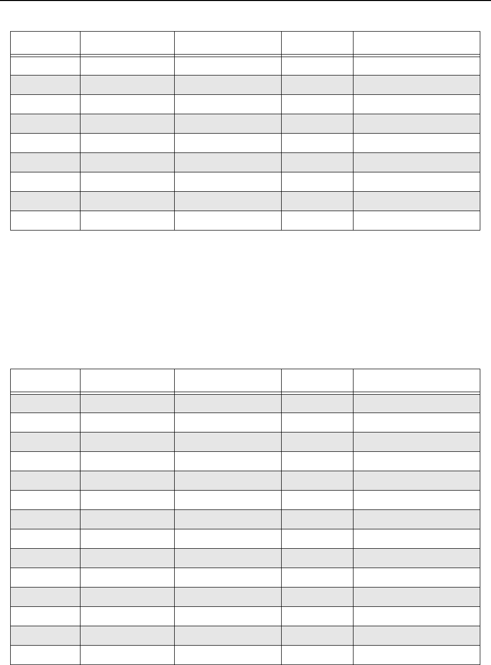
Theory of Operation 4-17
4.2.10 Receiver
The connector (J3601M3) used to connect the controller to the Receiver is a dual row, right angle,
early entry receptacle, without flange, 30-Pin Connector. It provides 16.8 MHz reference clock,
14.2 V, 10 V and 8 V supply voltage, SPI, Abacus SPI/SSI and other digital handshake signals with
the Receiver.
Refer to Table 4-9 for pinout for the Receiver connector.
B7 NC No Connect on Controller
B8 +10V Ex 10.0 V supply 10 V 10VDC
B9 +14_2V Ex 14.2 V supply 14.2 V 14.2VDC
B10 Ground Ground
B11 EX_CPLD_ADD_2 CPLD SPI address 2 3.3 V FPGA
B12 EX_CPLD_ADD_1 CPLD SPI address 1 3.3 V FPGA
B13 EX_CPLD_MOSI CPLD SPI MOSI 3.3 V FPGA
B14 EX_CPLD_MISO CPLD SPI MISO 3.3 V FPGA
B15 NC No Connect on Controller
Table 4-9 MTR3000 Controller Receiver Connector connection
Pin Signal Name Description Signal Level Controller Connection
A1 ABA_ODC Abacus SSI clock 3.3 V Rx OMAP McBSP2.CLKR
A2 Ground Ground
A3 ABA_SYNCB Abacus SYNCB 3.3 V Rx OMAP GPIO40
A4 ABA_PE Abacus SPI chip select 3.3 V FPGA
A5 ABA_PC Abacus SPI clock 3.3 V FPGA
A6 Ground Ground
A7 RX_CPLD_CE CPLD SPI chip select 3.3 V FPGA
A8 RX_CPLD_MISO CPLD SPI MISO 3.3 V FPGA
A9 RX_CPLD_ADD_1 CPLD SPI Address 1 3.3 V FPGA
A10 RX_CPLD_ADD_0 CPLD SPI Address 0 3.3 V FPGA
A11 NC No Connect on Controller
A12 Ground Ground
A13 +10V Rx 10.0 V supply 10 V 10VDC
A14 RX_ATTEN Rx Attenuation Control 3.3 V Rx OMAP GPIO18
Table 4-8 MTR3000 Controller Exciter Connector connection (Continued)
Pin Signal Name Description Signal Level Controller Connection
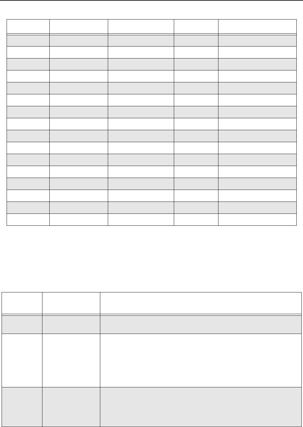
4-18 Theory of Operation
4.2.11 Front Panel (FP) Connectors and Switch
Table 4-10 to Table 4-15 describe the front panel connectors and switch.
Figure 4-8 describes the USB connector pin-out.
A15 Ground Ground
B1 ABA_RX Abacus SSI Data 3.3 V Rx OMAP McBSP2.DR
B2 ABA_FS Abacus SSI FS 3.3 V Rx OMAP McBSP2.FSR
B3 Ground Ground
B4 ABA_PD Abacus SPI MOSI 3.3 V FPGA
B5 ABA_DOUTB Abacus SPI MISO 3.3 V FPGA
B6 NC No Connect on Controller
B7 RX_CPLD_CLK CPLD SPI CLK 3.3 V FPGA
B8 RX_CPLD_MOSI CPLD SPI MOSI 3.3 V FPGA
B9 RX_CPLD_ADD_2 CPLD SPI Address 2 3.3 V FPGA
B10 Ground Ground
B11 NC No Connect on Controller
B12 +8V Rx 8.0 V supply 8.0 V 8VDC
B13 +14_2V Rx 14.2 V supply 14.2 V 14.2VDC
B14 Ground Ground
B15 CLK_RX_16_8MHZ Station Reference 3.3 V Clock Buffer
Table 4-10 SCM FP Connectors
Connector
Name Connector Type Purpose
USB Service
(J3009M7)
USB Type B Service Computer connection. This connector is accessible with front cover in
place.VBUS (+5 V) is not provided on the USB connector.
Mic
(J3000M7)
RJ45 (8 Pin) Microphone connection. Compatible with microphone GMN6147 (older model)
or GMMN4063. This connector is accessible with front cover in place.
Note : The Mic port is only supported in analog mode regardless of the Mic
used. For older model of microphone (GMN6147), the 3 control buttons for
speaker volume control, Rx monitor and Intercom control functions are not
supported.
Speaker
(J3010M7)
4P4C Speaker connection. Compatible with Service Speaker HSN1000 (older
model) or HSN1006 This connector is accessible with front cover in place.
Note : The Speaker port is only supported in analog mode regardless
of the speaker used.
Table 4-9 MTR3000 Controller Receiver Connector connection (Continued)
Pin Signal Name Description Signal Level Controller Connection
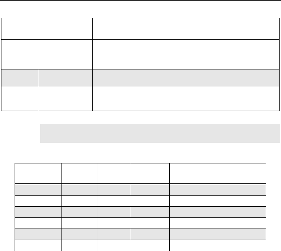
Theory of Operation 4-19
Ethernet
(J3006M7)
RJ45 (8 Pin)
(Vertical)
Network connection to Trunking Controller. The front cover must be removed
to access this connector. An optional extension cable can also be used to
route this input to the rear of the station. Alternatively, the Ethernet cable can
also be routed out through the slots provided in the front panel.
Debug/Sync
(P3013M7)
Header (8 Pin) Provide service access to Rx OMAP Trigger in/out, Tx OMAP trigger in, and
Rx SSI port.
Ext Ref
(J3008M7)
BNC (Vertical) External reference input. The front cover must be removed to access this
connector. Alternatively, an extension cable can be used to route this input to
the rear of the station.
Note USB Host mode is not supported by the MTR3000 SCM. Therefore, it cannot supply 5VDC
to USB accessories.
Table 4-11 SCM FP USB Connector Pin-out
Pin Number Pin Name I/O Voltage
Level (V) Pin Description
1VCC VCC 5Supply Voltage for USB Client mode
2 DM I/O 3.3 Connects to MAKO USB1 transceiver
3DP I/O 3.3 Connects to MAKO USB1 transceiver
4 GND GND GND Ground
G1 GND GND GND Ground
G2 GND GND GND Ground
Table 4-10 SCM FP Connectors (Continued)
Connector
Name Connector Type Purpose
4-20 Theory of Operation
Figure 4-8 USB connector pin-out
Table 4-12 SCM FP Microphone Connector Pin-out
MIC
Connector Pin
Number
Schematic
Pin Number Pin Name I/O Voltage Level Pin Description
1 5 NC NC NC No Connect
2 4 Reserved Input Reserved for future
use. DO NOT
CONNECT
3 6 MIC_PTT* Input 0 to 5 V Voltage generated by
PTT button
4 3 MIC_AUDIO Input 850 mVpp Audio Input, Level
indicated here is the
maximum value
5 7 GND GND GND Ground
6 2 NC NC NC No Connect
7 8 NC NC NC No Connect
8 1 NC NC NC No Connect
G1 G1 GND GND GND Ground
G2 G2 GND GND GND Ground
From the base station/repeater front view, the MIC connector pin 1 to pin 8 are arranged from right to left sequentially.
Note The schematic pin number and MIC pin number does not match due to imprecise
geometry and this will remain, since it is widely used in many other kits within Motorola.
4 3
1 2
G1G2
USB TYPE B
CONNECTOR
(BOTTOM VIEW)
Theory of Operation 4-21
Table 4-13 SCM FP Speaker Connector Pin-out
Pin Number Pin Name I/O Voltage Level (V) Pin Description
1GND GND GND Ground
2 14.2V 14.2V 14.2 V 14.2 V supplied to the speaker
3GND GND GND Ground
4 SPEAKER_AUDIO Output 1.4 Vpp Audio Output. Level indicated
here is the maximum value
G1 GND GND GND Ground
G2 GND GND GND Ground
From the base station/repeater front view, the SPEAKER connector pin 1 to pin 4 are arranged from left to
right sequentially.
Table 4-14 SCM FP Ethernet Connector Pin-out
Pin Number Pin Name I/O Voltage
Level Pin Description
1ENET_TXN_FP Output 5 V Ethernet Tx negative
2 ENET_TXN_FP Output 5 V Ethernet Tx positive
3ENET_RXN_FP Input 5 V Ethernet Rx negative
4 GND GND GND Ground
5GND GND GND Ground
6 ENET_RXP_FP Input 5 V Ethernet Rx positive
7GND GND GND Ground
8 GND GND GND Ground
G1 GND GND GND Ground
G2 GND GND GND Ground
Table 4-15 SCM FP External Reference Connector Pin-out
Pin Number Pin Name I/O Voltage
Level Pin Description
CEXT_REFERENCE Input 5 V 5 MHz or 10 MHz external reference. This can
be either a sine or a square wave.
G1 GND GND GND Ground
G2 GND GND GND Ground

4-22 Theory of Operation
4.2.12 Front Panel LEDs
For details on this section, refer to Table 1-5 on page 1-11.
4.2.13 Supply Voltage Circuitry
The SCM contains on-board regulator and filtering circuitry to generate the various operating
voltages required by the SCM circuitry. The SCM routes +10 V and +8 V from two regulators on the
backplane to the Receiver and Exciter modules. +14.2 V and +5.1 V from the power supply (via the
backplane) are used as sources for the following supply voltage circuits:
• +14.2V Regulator Circuitry – input to generate 9.3 V for MAKO, 5 V analog for audio circuit.
This regulator also routes 14 VDC to the Receiver and Exciter modules.
• +5.1V Regulator Circuitry – input to generate the following voltage: 3.3 V, 3.3 V analog,
2.775 V analog, 1.875 V, 1.4 V Core for Tx and Rx OMAP1710, 1.2 V Core for FPGA.
The SCM requires a specific power-up and reset sequence. At initial power-up, the power supply of
the base station/repeater provides 14 V and 5 V directly to the SCM. The SCM also provides 10 V
and 8 V through the base station/repeater backplane directly to Exciter and Receiver without any
additional delay. 14 V is used only to derive a 9.3 V supply voltage for the Mako IC and a 5 V supply
voltage for the audio section. The 14 V is also used to derive a 12 V supply voltage for the OCXO.
The majority of supply voltages on the SCM are derived from the 5 V using linear regulators. Each
regulator outputs are enabled in the sequence shown in Figure 4-9 to meet all the device power-up
sequences. 1 indicates the first power-rail that reaches steady state, and 7 is the last voltage rail
that reaches the steady state.
During the power-up sequence, the SCM is held in a reset state. Once the power-up sequence is
completed, the FPGA and the MAKO IC complete their internal initialization; then the main-reset is
released, and the SCM starts its normal operation. There are several sources, both hardware and
software, that can reset the SCM. From a hardware perspective, when the 5 V, Tx OMAP or Rx
OMAP core voltage dip below the minimum operation threshold, then the SCM enters and stays in
the reset state, until the voltage reaches its operation level again. From the software perspective,
both the Tx OMAP and Rx OMAP have the means to initiate SCM reset. This can be done from
either the CPS or RDAC application.
Refer to Figure 4-9 for the MTR3000 power up block diagram.
G3 GND GND GND Ground
G4 GND GND GND Ground
Table 4-15 SCM FP External Reference Connector Pin-out (Continued)
Pin Number Pin Name I/O Voltage
Level Pin Description
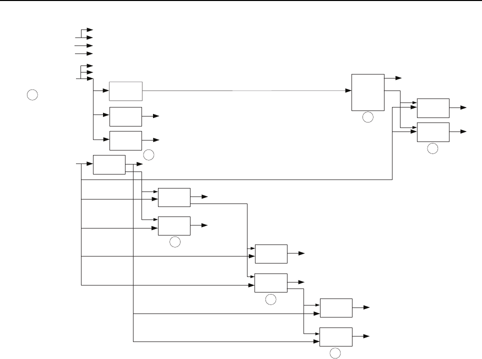
Troubleshooting 4-23
Figure 4-9 MTR3000 power up block diagram
4.3 Troubleshooting
4.3.14 Disassembly and Reassembly Procedures
1. Make sure the station power is turned off at the breaker to the AC or DC source.
2. Disconnect the cables, as follows:
- Rx cable from Receiver Module
- Exciter-to-PA coaxial Cable
- Front Panel USB cable (if connected)
- Front Panel Mic cable (if connected)
- Front Panel Speaker cable (if connected)
- Front Panel External Reference cable (if connected)
- Front Panel Ethernet cable (if connected)
3. Remove the two screws holding the transceiver assembly to the bottom plate.
4. Pull forward on the cast knobs (above the front panel that projects horizontally from the
Exciter and Receiver module), carefully slide the transceiver assembly (Exciter Module,
Receiver Module, Station Control Module (SCM)) out of station.
5V – P3200M3-A3,B3,C3
8V – P3200M3-A4
J3600M3 – A9, To Exciter
J3601M3 – B12, To Receiver
10V_EX – P3200M3-A14,B14 J3600M3 – B8, To Exciter
10V_RX – P3200M3-A15,B15 J3601M3 – A13, To Receiver
14.2V – P3200M3-A1,B1,C1
J3600M3 – B0, To Exciter
J3601M3 – B13, To Receiver
U3831M4 9.3V
U3838M4 5VA, AUDIO SECTION
U3893M4
12VA, OCXO
Only populated for 800/
900 MHz kit
U3874M4 1.875V
PG
U3801M4 3.3V
U3883M4
3.3VA,
STATION
REFERENCE
U3906M4
2.775VA,
STATION
REFERENCE
U3826M4 1.2V, FPGA CORE
PG
U3850M4
1.4V,
RXOMAP
CORE
U3800M4
1.4V,
TXOMAP
CORE
PG
U1404M1 3.6V
U1402M1
MAKO
2.775V,
Trident SSI
buffer supply
U1406M1 2.2V
ENABLE
1
2
3
4
5
6
7
NOTE:
- PG => power-good signal from the switch or
regulator. Open-drain output, active high
indicate power is good.
- Number in the block diagram indicate power-
on sequence.

4-24 Troubleshooting
5. Remove four screws securing Exciter Module, and four screws securing Receiver
Module to the SCM, and disconnect both modules from the SCM.
6. Remove the six screws securing the SCM casting to the SCM board.
7. Ensure that the correct SCM board is being installed. Fasten the board into the casting
with the six screws.
8. Plug back the Exciter Module and the Receiver Module into the respective connectors
on the SCM. Tighten the screws and slide the transceiver assembly back into the station
(along the guide rails) to mate with the connector on the backplane.
9. Reconnect all the cables.
10. Fasten the transceiver assembly into the unit using the two screws.
11. Restore power to the station.
4.3.15 Troubleshooting Chart
Follow the procedures in the troubleshooting charts below to isolate the cause of SCM problems.
The following assumptions should be taken note of before carrying out the troubleshooting
procedures.
•Depot Repair Centres will have a golden MTR3000 base station/repeater
•Depot Repair Centres will not replace BGA devices
•Depot Repair Centres will not have capability to program FPGA
•Audio Flow Chart is based on the usage of CPS. Factory will use the controller’s 12M,
schematics and flow charts to perform troubleshooting.
Note Do not slam the transceiver assembly against the backplane or push any harder than
necessary to seat the connector.
Note 1. Reference Designator with/without M suffix are identical in the design
2. Factory should reprogram FPGA with test fixture prior to replacing the device
3. Factory should replace the failure device prior to replacing the controller
4. Transmitter output refers to PA RF output. Test equipment that is capable of
demodulating the signal is required to perform this test.
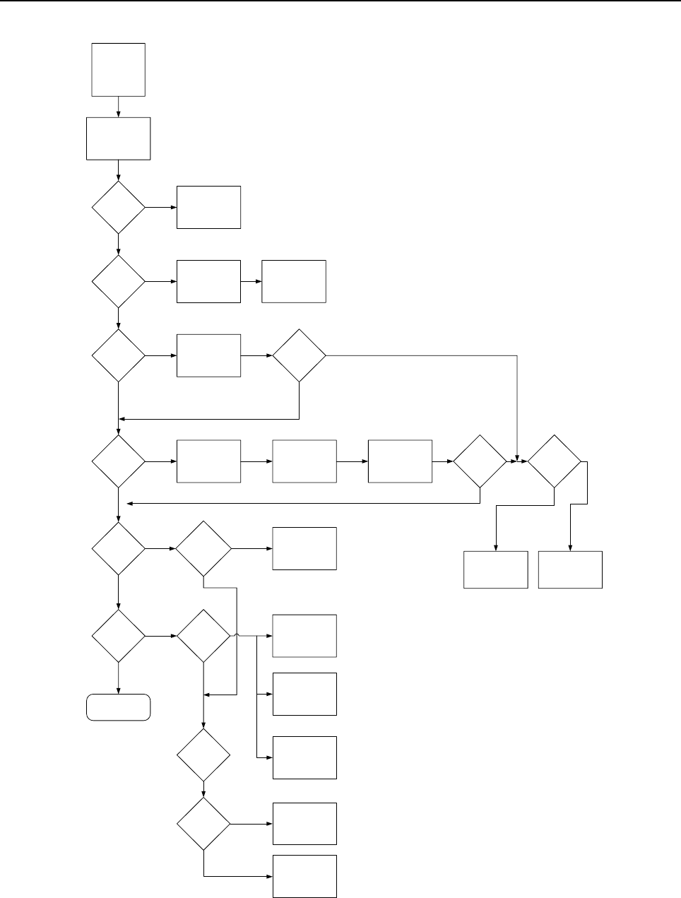
Troubleshooting 4-25
Figure 4-10 Controller Troubleshooting Flow Chart
Status LED
Solid
Green?
Check
J3009M7
pin1 = 5V
pin 2,3 =
Activity?
USB cable
connected?
-Check Audio
-See Audio
Troubleshooting Flow
Chart
Yes
Yes
No
-Plug-in USB Cable
-Establish connection
with PC.
No
Yes
See Ethernet
Troubleshooting Flow
Chart
Replace J3009M7
-Check Transmit
Path
- See Transmit Path
Troubleshooting
Flow Chart
-Check Receive Path
- See Receive Path
Troubleshooting
Flow Chart
Can SCM
Communicate
via USB Port?
No
The Individual
Controller
Power-up
Controller
All LED off?
-Remove Controller
from Clam-shell
- Perform visual
inspection.
-Check Power
-See Power
Troubleshooting Flow
Chart
Mode LED
(blue) Solid
on?
-FPGA not
programmed or
corrupted
-Replace Controller
Mode LED
(blue)
Flashing?
-Controller is in boot-
loader mode.
-Reprogram flash.
Flash
Program
successful?
-Potential OMAP/
Flash/DDR failure.
-Replace Controller
All LED
Flashing
Indefinitly?
See Power
Troubleshooting Flow
Chart
See Clock & Reset
Troubleshooting Flow
Chart
-Force Controller in
bootloader mode
(Connect P3200M3,
C31, C32 to GND)
-Reprogram Flash.
Flash
Program
successful?
Yes
No
Yes
No
Yes
No
Yes
No
Yes
-Check Power
-See Power
Troubleshooting Flow
Chart
Series
Components
ok? See
Schematic
Check/Replace series
components
No
No
No Yes
See Note 2, 3
See Note 3
Status LED
(red) Solid
on?
-Controller In lock
mode
-This is expected
mode of operation in
SCM stand-alone
mode.
Yes Can SCM
Communicate via
USB Port?
Yes
No Yes
No
No
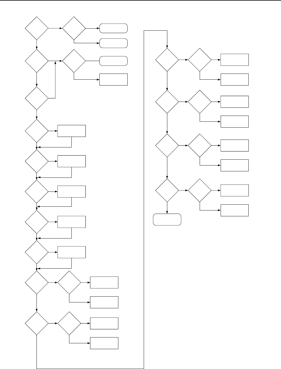
4-26 Troubleshooting
Figure 4-11 Power Troubleshooting Flow Chart (Controller)
Power Cable
Plug in?
Battery Back
up OK? Controller ok
No No
P3200M3
Pin A1, B1,
C1 = 14.2V?
Is P3200M3
damaged?
BR PS issue,
Controller ok
Yes
No No
Replace P3200M3
Yes
Plug in Power-cable
Yes
P3200M3
Pin A3, B3,
C3 = 5V?
No
Yes
U3831M4
Pin 4 = 9.3? Replace U3831M4
U3838M4
Pin 4 = 5V? Replace U3838M4
U2802M2
Pin 1 = 2.5
and Pin 7 =
4.65V?
Replace U2802M4
Yes
No
No
Yes
Yes
No
U3893M4
Pin 5 =
12V?
Replace U3893M4
No
Yes
This check is only
applicable to CLN8565
U3874M4
Pin A, B,
C(1-4) =
1.875V?
Replace U3874M4
No
Yes
U3801M4
Pin 9 =
3.3V?
No
Yes
U3801M4
Pin 5 =
1.875V?
Replace U3801M4
Yes
Replace R3876M4
No
U3883M4
Pin 9 =
3.3V?
No
Yes
U3883M4
Pin 5 =
1.875V?
Replace U3883M4
Yes
Replace R3876M4
No
U3906M4
Pin 9 =
2.775V?
No
Yes
U3906M4
Pin 5 =
3.3V?
Replace U3906M4
Yes
Replace R3861M4
No
Yes
Yes
U3826M4
Pin 9 =
1.2V?
No U3826M4
Pin 5 =
3.3V?
Replace U3826M4
Yes
Replace R3861M4
No
U3850M4
Pin 9 =
1.4V?
No U3850M4
Pin 5 =
3.3V?
Replace U3850M4
Yes
Replace R3844M4
No
Yes
U3800M4
Pin 9 =
1.4V?
No U3800M4
Pin 5 =
3.3V?
Replace U3800M4
Yes
Replace R3844M4
No
Yes
Yes
Power Section is
okay
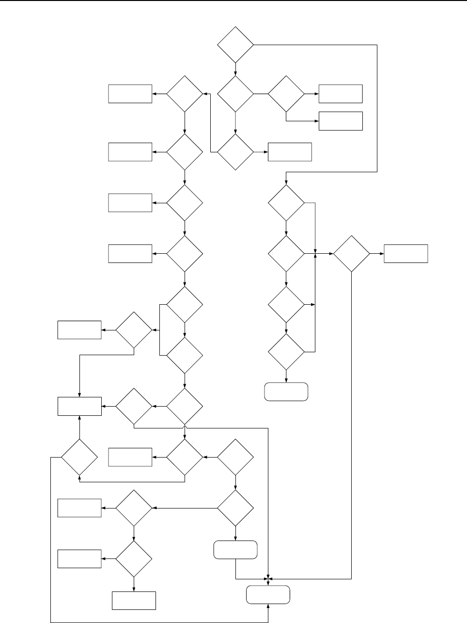
Troubleshooting 4-27
Figure 4-12 Clock and Reset Troubleshooting Flow Chart (Controller)
Main Reset
High?
U2208M5
pin 4,5,6,7
16.8MHz
ok?
U2402M6
pin 3,5,7
Oscillator ok?
Y2400M6 pin
3, or Y2401M6
pin 4
Replace Y2400M6,
Y2401M6
No No
Check/Replace
U2400M6, U2402M6
Yes
FPGA input
clock ok?
TP2017M5
Series
Components
ok? See
Schematic
Yes
Tx OMAP
12MHz ok?
TP1201M1
Tx OMAP
32.768KHz
ok?
TP1202M1
Rx OMAP
12MHz ok?
TP1800M1
Rx OMAP
32.768KHz
ok?
TP1801M1
Check/Replace
Series Components.
See Schematic
No
Yes
Yes
Yes
No
No
Check/Replace
Series Components.
See Schematic
FPGA (U2000M5)
Failure
Replace Controller
Clock Section is ok
Yes
No
5V_MON =
3.3V?
TP3821M4
Check/Replace
R3820M4, U3819M4
1.4V Tx
OMAP_PG
= 3.3V?
R3853M4
Check/Replace
R3853M4, U3800M4
1.4V Rx
OMAP_PG
= 3.3V?
R3844M4
Check/Replace
R3844M4, U3850M4
FP FPGA
RST =
3.3V?
TP2016M5
Check/Replace
R3160M7
MAKO
MECH SW =
2.5V?
R1416M1
MAKO V9
DET =
2.9V?
TP2019M5
MAKO
RESET =
1.8V?
TP2021M5
Reset is okay
Tx OMAP
FPGA RST
= 1.8V?
TP2020M5
Series
Components
ok? See
Schematic
Rx OMAP
FPGA RST
= 1.8V?
TP2029M5
OMAP (U1000M1,
U1001M1) Failure
Replace Controller
Series
Components
ok? See
Schematic
Series
Components
ok? See
Schematic
U1404M1
pin 9 =
3.6V?
MAKO (U1402M1)
Failure
Replace Controller
Check/Replace
U1404M1
U1406M1
pin 5 =
2.2V?
Check/Replace
U1406M1
No
Yes
No
Yes
No
Yes
No
Yes
No
No
Yes
Yes
Yes
Yes
No
No
Yes
No
Yes
Yes
Yes
Check/Replace
Series Components.
See Schematic
No
No
No
Yes
No
MAKO (U1402M1)
Failure
Replace Controller
No
Yes
Yes
Yes
MAKO
24.576MHz
ok?
R1408M1
No
NoYes
No
Yes
See Note 2, 3
See Note 3
See Note 3
See Note 3
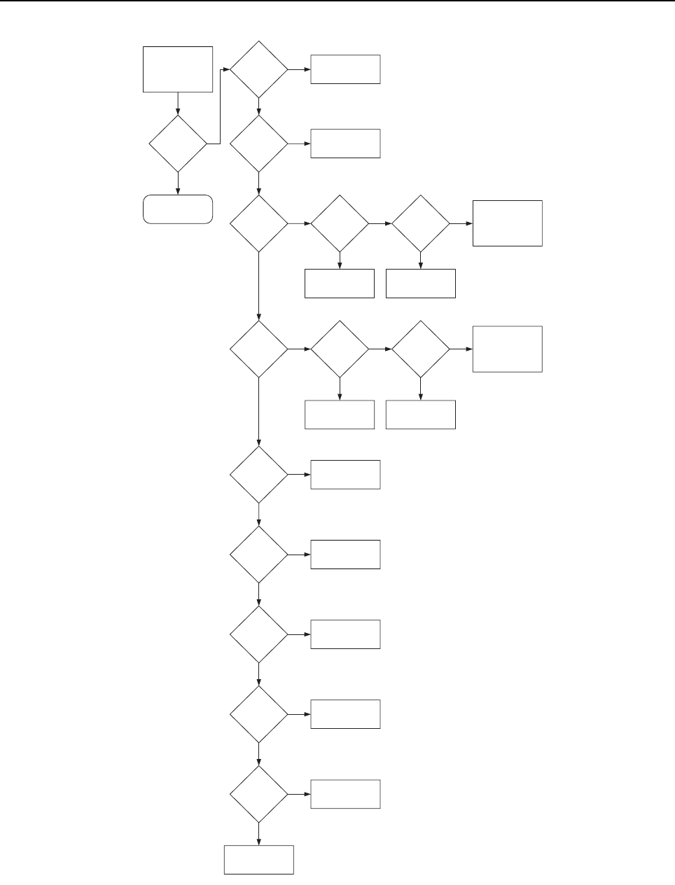
4-28 Troubleshooting
Figure 4-13 Ethernet Troubleshooting Flow Chart (Controller)
Ethernet
Link LED
(green) solid
on/flashing?
Ethernet Option
Ethernet
Cable plug
in?
Ethernet is okEthernet
RESET =
3.3V?
U3020M7
pin 4
Check/Plug in
Ethernet Cable
U3020M7
pin 3 =
1.875V?
U2208M5
pin 4,5,6,7 =
1.875V?
No
Replace U3020M7 Replace U3020M7
No
Yes
See Clock & Reset
Troubleshooting Flow
Chart
No
Yes
Ethernet
Enable =
3.3V?
U3025M7
pin 4
U3025M7
pin 3 =
1.875V?
Series
Components
ok? See
Schematic
Replace U3025M7 Check/Replace
Series Component
Tx OMAP (U1000M1)
failure
Replace Controller
See Note 3
Y3038M7
pin 3 =
25MHz?
Replace Y3038M7
Activity on
J3006M7 pin
1,2,3,6
Replace J3006M7
Activity on
T3106M7
pin 1,3,6,8
Replace T3106M7
Activity on
U3005M7
pin 11,12
Ethernet-USB IC
(U3005M7) failure
Replace Controller
MAKO IC (U1402M1)
failure
Replace Controller
See Note 3
See Note 3
Yes
No
No
Yes
No No Yes
Yes
Yes No
No
No
Yes
No
Yes
No
Yes
U3005M7
supply ok?
E3041M7 =
3.3V
Replace E3041M7
Yes
No
Yes
MAC/IP
programmed
?
Program MAC/IP
No
Yes
Yes
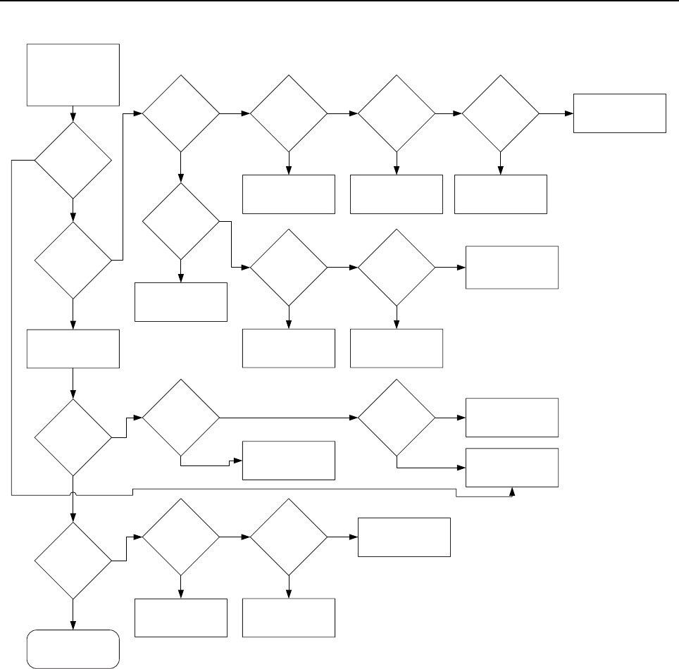
Troubleshooting 4-29
Figure 4-14 Transmit Path Troubleshooting Flow Chart (Controller)
Controller Must be in
the “golden” BR
Reset BR
SPI activity at
J3600M3 pin
A13, A14,
B13?
Wait for Status LED
to turn solid green
SSI CLK, FS
valid?
U3602M3 pin
13, 11
SSI Data
valid?
U3600M3 pin
11
Yes
Yes
Yes
Transmit Path is ok
SPI activity at
input of
U3601M3?
Series
Components
ok?
See
Schematic
No
No SPIF_TXOMA
P<3..0> input
to U2000M5
ok?
Yes
Series
Components
ok?
See
Schematic
No TxOMAP issue
(U1000M1)
Replace Controller
Yes
Check/Replace series
components
FPGA (U2000M5)
issue
Replace Controller
See Note 2, 3
Check/Replace series
components
Check/Replace
U3601M3
No Yes No
Series
Components
ok?
See
Schematic
Check/Replace series
components
Is J3600M3
Damaged?
Replace J3600M3
Potential Timing issue
Replace Controller
No
No
Yes Yes
No
SSI Data valid
at input of
U3600M3
pin6?
Series
Components
ok?
See
Schematic
Check/Replace series
components
No
Check/Replace
U3600M3
Yes
TxOMAP issue
(U1000M1)
Replace Controller
See Note 3
See Note 3
No
No Yes
U3601M3 pin
1 = 0V?
U2208M5 pin
4,5,6,7 =
1.875V?
Check/Replace series
components
Series
Components
ok?
See
Schematic
Check/Replace
U2208M5
Check Reset
See Clock & Reset
Troubleshooting Flow
Chart
Yes
Yes
No
No
Yes
Yes
No
16.8MHz
Present?
J3600M3 pin
B1
Yes
No
Yes
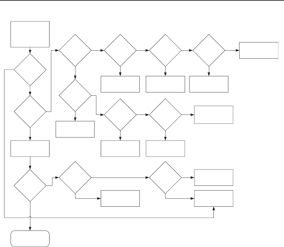
4-30 Troubleshooting
Figure 4-15 Receive Path Troubleshooting Flow Chart (Controller)
Controller Must be in
the “golden” BR
Reset BR
SPI activity at
J3601M3 pin A4,
A5, B4, A13,
A14, B13?
Wait for Status LED
to turn solid green
SSI CLK, FS,
Data valid?
U3605M3 pin
13,12, 11
Yes
Yes
Receive Path is ok
SPI activity at
input of
U3603M3,U3604
M3?
Series
Components
ok?
See
Schematic
No
No SPIF_RXOMAP
<4..0> input to
U2000M5 ok?
Yes
Series
Components
ok?
See
Schematic
No RxOMAP issue
(U1001M1)
Replace Controller
Yes
Check/Replace series
components
FPGA (U2000M5)
issue
Replace Controller
Check/Replace series
components
Check/Replace
U3603M3, U3604M3
No Yes No
Series
Components
ok?
See
Schematic
Check/Replace series
components
Is J3600M3
Damaged?
Replace J3600M3
Potential Timing issue
See Note 3
See Note 3
See Note 2, 3
Replace Controller
No
No
Yes Yes
No
U3603M3 pin
1, U3604M3
pin 1 = 0V?
U2208M5 pin
4,5,6,7 =
1.875V?
Check/Replace series
components
Series
Components
ok?
See
Schematic
Check/Replace
U2208M5
Check Reset
See Clock & Reset
Troubleshooting Flow
Chart
Yes
Yes
No
No
Yes
Yes
No
16.8MHz
Present?
J3600M3 pin
B1
Yes
No
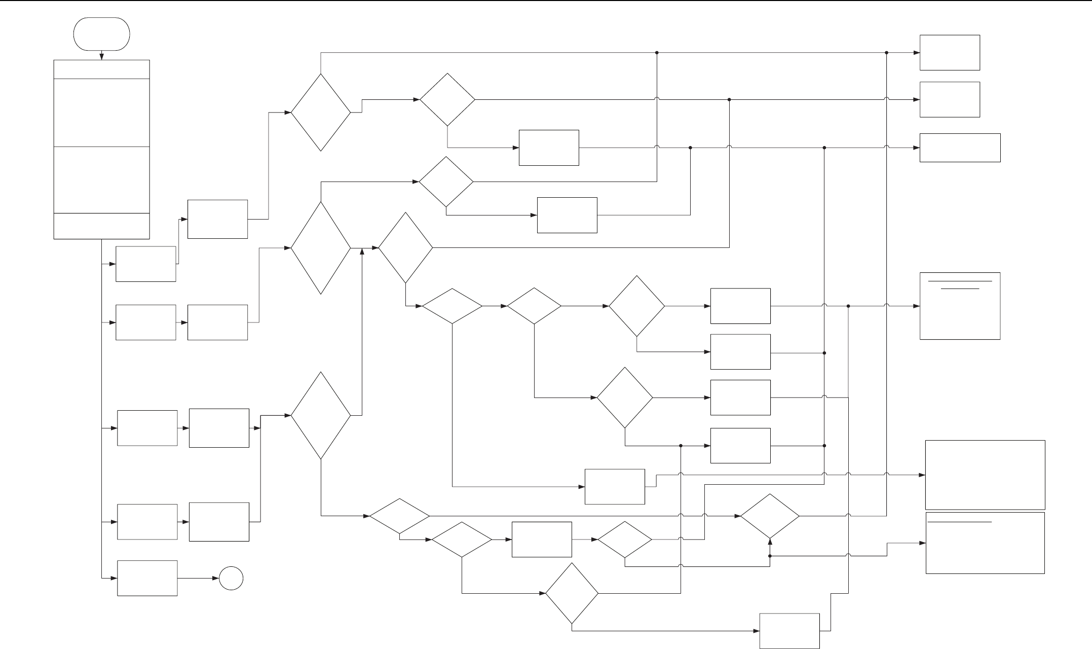
4-31
Audio Verification
Using CPS, set the SW
emphasis either De & Pre or
none and audio type RX & TX
Filtered Squelch or RX & TX
Flat respectively. Set channel
bandwidth for 25KHz. Set the
GPIO pins accordingly so the
proper PTT can be issued.
the radio will be based on
what mod limit value is set to
100%, 92%, etc. See BSM
chapter 12 for further
assistance.
This test assumes standard
RF input 60% full deviation
1KHz audio tone. Input level to
This test requires a full base
radio.
Choose the appropriate audio
path below you intend to
verify.
MICROPHONE
J3000M7
Tx Audio
Backplane conn
J7
Pin 1
Emph Tx Audio
Backplane conn
J7
Pin 22
RECEIEVER
Base Radio rcvr
port.
Inject a 56mVRMS
1KHz tone into the
mic port and apply
front panel PTT.
Audio verification
complete
Is audio
present at
U1402 pin J2
MIC/ K2 for
TXAUD?
Replace Board
See Note 3
Is audio
present at
C2800?
Verify limiter and
splatter filter
Is audio
present at
U2800 pin 7
and U2603
pin 8?
Verify U2607
connections
before replacing.
U2602/U2607/U2608
Analog MUX
Pin 5: +5v
Pin 2: GND
Pin 6: 5v or GND
Pin 4: Matches pin 1 if
pin 6 is 5v. Matches pin
3 if pin 6 is GND.
Verify Mic audio
input before
replacing U2800
or U2603.
Tx DATA
Backplane conn
J7
Pin 13
Limiter/Splatter filter
Probe between R2819 and R2822.
Level should be around 80mVRMS.
If level does not match, then refer to
the schematic to verify the limiter
circuitry. If level matches, then use
the schematic to verify the splatter
filter.
Inject a 80mVRMS
1KHz tone into the
TX_Audio port and
apply backplane
PTT.
Inject a 80mVRMS
1KHz tone into the
TX_Audio_PRE
port and apply
backplane PTT.
Inject a 80mVRMS
1KHz tone into the
TXDATA port and
apply backplane
PTT.
Is audio
present at
U1402 pin
K2?
Is there
demodulated
audio at BR
transmitter
output?
Is there
demodulated
audio at BR
transmitter
output?
Is there
demodulated
audio at BR
transmitter
See Note 4
See Note 4
See Note 4
output?
Yes
No Yes
Verify TDATA
input before
replacing U2800
or U2802.
See schematic for
assistance
No
Is audio
present at
DB25 pin 7?
Yes
Verify U2604
connections
before replacing.
No
Yes
No Yes
No
Yes
YesNo
No
No
Is audio
present at
speaker?
Yes
Mic
Is audio
present at
U2603 pin 1?
Verify U2602
connections
before replacing.
Yes
Tx_aud
Verify TX_AUDIO/
TX_AUDIO_PRE
input before
replacing U2603.
No
Can the
volume be
adjusted using
tuner?
Yes Yes
Audio EEPOT U2601
Pin 9: +5v
Pin 7: GND
Pin 2: +2.5v bias
Pin 1: Audio in; 254mVRMS
Pin 10: Audio out; vary with tuner
setting.
No
Is audio
present at
C2858?
Verify high pass
filter and audio
eepot.
1Is audio
present at
U2604 pin 7
and U2800
pin 8?
Verify U2608
connections
before replacing.
Yes
No
Yes
No
No
MIC or
TXAUD
Path?
HPF or
EEPOT?
Hpf
Eepot
Figure 4-16 Audio Troubleshooting Flow Chart (Sheet 1 of 2)
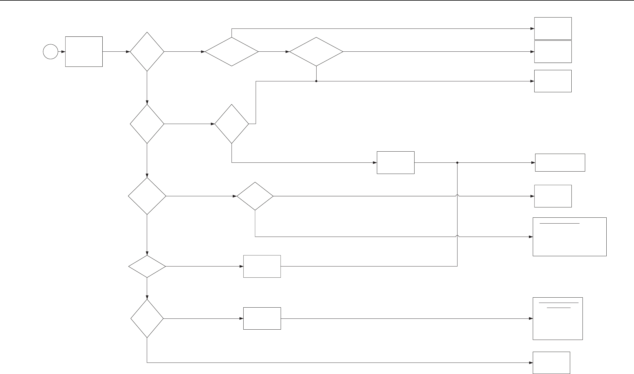
4-32
Inject a 1KHz tone
with 3KHz
modulation into
the receiver with
the correct carrier
frequency.
Is there
See Note 4
demodulated
audio at BR
transmitter
output?
Verify SSI clk, FS,
data at J3601
Verify SSI clk, FS,
data at TP1819,
TP1820, TP1823
Check J3601 for
continuity
Replace U3605
No
NoYesNo
1
Replace Board
See Note 3
Yes
Is audio
present at J7
BP-conn pins
3,7
Is audio
present at
C2637
NoNo
Verify audio at
U2604 pin 1
U2604 pin 8
U2604 pin 14
See schematic for
assistance
Yes
Is audio
present at
speaker
J3010M7?
Can the
volume be
adjusted using
tuner?
Audio verification
complete
Audio EEPOT U2601
Pin 9: +5v
Pin 7: GND
Pin 2: +2.5v bias
Pin 1: Audio in; 254mVRMS
Pin 10: Audio out; vary with tuner
setting.
Yes
No
Is audio
present at
C2858?
Yes
Yes
No
Verify high pass
filter and audio
eepot.
Is audio
present at
U2604 pin 7
and U2800
pin 8?
No
Yes
Replace U2604/
U2800 pending on
result from last
step.
Yes
Verify U2608
connections
before replacing.
U2602/U2607/U2608
Analog MUX
Pin 5: +5v
Pin 2: GND
Pin 6: 5v or GND
Pin 4: Matches pin 1 if
pin 6 is 5v. Matches pin
3 if pin 6 is GND.
Yes
No
Figure 4-17 Audio Troubleshooting Flow Chart (Sheet 2 of 2)

4-33
4.3.16 Calibration Procedure
1. Remove the base station/repeater’s front bezel from its chassis.
2. Power-up the base station/repeater and allow it to boot up normally.
3. Plug in the External Reference to J3008M7 on the SCM. The SCM accepts 5/10 MHz
Sine/Square wave with amplitude of 3.3 Vpp.
4. Monitor the station reference LED. The LED will stay solid amber to indicate that the
station is locked to external reference and is in alignment process.
5. When the station completes the alignment, the station reference LED will turn solid
green.
6. Power down the base station/repeater and remove the External Reference.
7. Replace the base station/repeater’s front bezel and power-up the base station/repeater.
Note For the OCXO kit, the controller must be power-up for a minimum of 15 minutes before the
execution of the following calibration procedures.
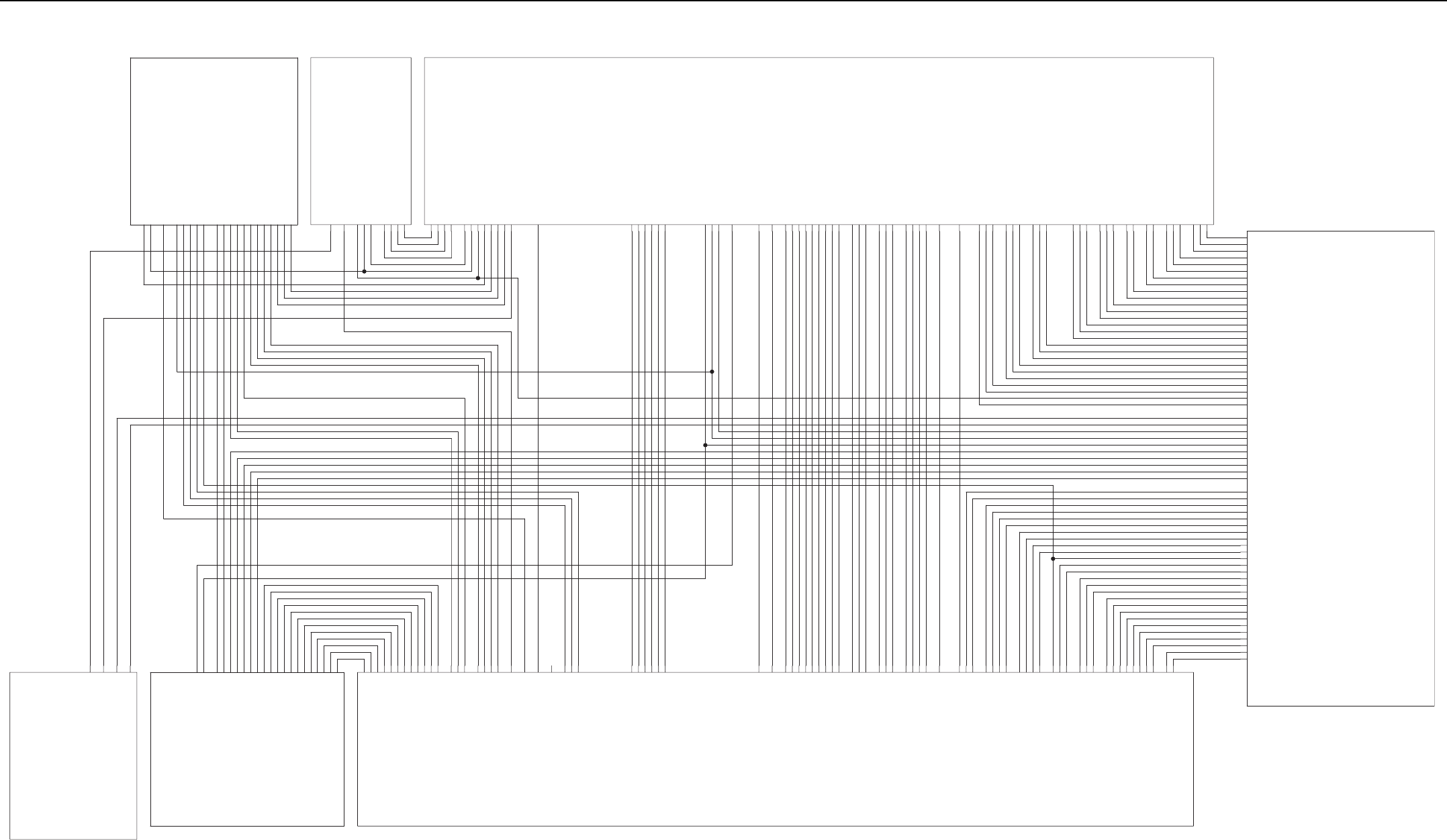
4-34 Controller Schematics (UHF)
4.4 Controller Schematics (UHF)
5MHZ_BNC_IN
USB1_MAKO_DP
USB2_MAKO_DP
USB2_MAKO_DM
FP_LED<0..12>
FP_FPGA_RST_N
USB1_MAKO_DM
MIC_BUTTON_INT_N
MIC_BUTTON
MIC_PTT_N
SPEAKER_AUDIO
MIC_AUDIO
SSI_ABACUS<2..0>
RXOMAP_SYNC_IN
TXOMAP_SYNC_TRIG_OUT
FPGA_ENET_RX_RESET_N
ETHERNET_ENABLE
RXOMAP_SYNC_OUT
1_4V_ROMAP_PG
BUFFERED_1_4V_ROMAP_PG
2_775VA_PG
BOUNDARY_SCAN<9..0>
1_4V_TOMAP_PG
1_4V_ROMAP_PG
5V_MON
FPGA_TDO
FPGA_TMS
FPGA_TDI
FPGA_TCK
TXOMAP_SPARE3
FPGA_BP_OP1_CS1_N
FPGA_SPI<0..6>
RCVR_SPI<0..7>
ABA_SPI<0..3>
RXOMAP_SPARE2
TXOMAP_SPARE2
TXOMAP_SPARE1
RXOMAP_SPARE3
FP_FPGA_RST_N
RXOMAP_SPARE1
BP_FPGA_MISO
FPGA_BP_SPI_CLK
FPGA_BP_WIRELINE_BCLK
FPGA_BP_WIRELINEL34_FSYNC
FPGA_BP_WIRELINE34_RXD
BP_FPGA_WIRELINE34_TXD
FPGA_BP_WIRELINE12_FSYNC
FPGA_BP_WIRELINE12_RXD
BP_FPGA_WIRELINE12_TXD
STA_FPGA<0..7>
FP_FPGA_EXT_REF
FP_LED<0..12>
MAKO_USB_CRNT_LIMIT
FPGA_BP_WIRELINE_MCLK
FPGA_BP_WL1_CS_N
FPGA_BP_WL2_CS_N
FPGA_BP_MOSI
FPGA_BP_OP2_CS1_N
FPGA_BP_OP1_CS3_N
FPGA_BP_OP1_CS2_N
CLK_FPGA_RXOMAP_32_768KHZ
CLK_FPGA_TXOMAP_32_768KHZ
FPGA_EX_DISABLE_N
FPGA_GPIO_<7..0>
FPGA_BP_PA_ADDR1
FPGA_BP_PA_ADDR0
FPGA_BP_OP2_CS3_N
FPGA_BP_OP2_CS2_N
RCVR_ADDR<2..0>
MAKO_FPGA_RST_DET_N
MAKO_FPGA_V9_DET
FPGA_MAKO_MECH_SW_N
FPGA_EX_ADDR<2..0>
SPI_CS_ADDR<3..0>
FPGA_MAKO_SPI<3..0>
SPIF_TXOMAP<3..0>
SPIF_RXOMAP<4..0>
CLK_FPGA_WBCODEC_12MHZ
CLK_FPGA_TXOMAP_12MHZ
CLK_FPGA_RXOMAP_12MHZ
FPGA_EX_RESET_N
FPGA_ENET_RX_RESET_N
FPGA_WBCODEC_BP_RESET_N
FPGA_TXOMAP_SPI_IRQ_N
CLK_FPGA_MAKO_24_576MHZ
BUFFERED_1_4V_ROMAP_PG
1_4V_TOMAP_PG
1_4V_ROMAP_PG
FPGA_TDO
FPGA_TMS
FPGA_TDI
FPGA_TCK
SSI_CODEC12<3..0>
RXOMAP_FPGA_RST
TXOMAP_FPGA_RST
FPGA_RESET_TXOMAP_N
FPGA_RESET_RXOMAP_N
ROMAP_FPGA_WDRST_N
TOMAP_FPGA_WDRST_N
574 HEC_AC_FPGAHEC_AC_PBJHEC_AC_FP
WIRELINE_ID
MAKO_BP_RSSI
RF_RELAY_CONTROL
AUX_RX_AUDIO
TX_AUDIO_PRE
TX_AUDIO
FPGA_BP_PA_ADDR0
AC_FAIL
OPT_IRQ_N
OPTION1_ID
OPTION2_ID
FPGA_BP_WIRELINE12_FSYNC
FPGA_BP_WIRELINE12_RXD
RCVR_SPI_<0..7>
FPGA_BP_WL1_CS_N
FPGA_BP_WIRELINE_MCLK
FPGA_BP_WIRELINE34_RXD
FPGA_BP_MOSI
FPGA_BP_WIRELINE34_FSYNC
PTEMP+
BP_FPGA_WIRELINE12_TXD
BP_FPGA_WIRELINE34_TXD
FPGA_BP_WIRELINE_BCLK
FPGA_BP_WL2_CS_N
DMCS
OMAP_GPIO_7
OMAP_GPIO_9
BP_FPGA_MISO
FPGA_SPI_<0..6>
CLK_EX_16_8MHZ
TXDATA_PL_DPL
ABA_SPI_<0..3>
FPGA_BP_SPI_CLK
SSI_ABACUS<2..0>
OMAP_GPIO_10
OMAP_GPIO_8
OMAP_GPIO_6
EX_ENABLE
RX_AUDIO
FPGA_BP_PA_ADDR1
FPGA_EX_RESET_N
SSI_TRIDENT<2..0>
FPGA_ENET_RX_RESET_N
FPGA_WBCODEC_BP_RESET_N
PA_ENABLE
ANTENNA_RELAY
ABACUS_SYNCB
RX_ATTEN
OMAP_GPIO_5
OMAP_GPI_1
OMAP_GPI_4
OMAP_GPIO_2
OMAP_GPIO_3
1_4V_TOMAP_PG
FPGA_GPIO_<7..0>
CLK_RX_16_8MHZ
FPGA_BP_OP2_CS3_N
FPGA_BP_OP2_CS2_N
FPGA_BP_OP2_CS1_N
FPGA_BP_OP1_CS3_N
FPGA_BP_OP1_CS2_N
FPGA_BP_OP1_CS1_N
3
HEC_AC_EXT_INT
FPGA_WBCODEC_BP_RESET_N
TXDATA_PL_DPL
AUX_RX_AUDIO
ANALOG_MUX1
ANALOG_MUX2
I2C_TXOMAP_SDA
CLK_FPGA_WBCODEC_12MHZ
ANALOG_MUX3
SPEAKER_AUDIO
TX_AUDIO_PRE
TXAUD_MIC_FLTR
ANALOG_MUX0
I2C_TXOMAP_SCL
I2C_RXOMAP_SDA
I2C_RXOMAP_SCL
MAKO_CODEC_AUDIO_P
TXAUD_MIC_TDATA
SSI_CODEC_WB<3..0>
MIC_AUDIO
RX_AUDIO
TX_AUDIO
TXOMAP_SYNC_TRIG_OUT
RXOMAP_SYNC_OUT
I2C_TXOMAP_SDA
I2C_RXOMAP_SCL
I2C_RXOMAP_SDA
ANALOG_MUX2
ANALOG_MUX3
GPI_4
GPIO_2
GPIO_3
GPIO_6
GPIO_7
GPIO_8
GPIO_9
GPIO_10
EX_ENABLE
SSI_TRIDENT<2..0>
SSI_ABACUS<2..0>
AC_FAIL
OPTION2_ID
RF_RELAY_CONTROL
CLK_FPGA_MAKO_24_576MHZ
RCVR_ADDR<2..0>
MAKO_MECH_SW_N
RESET_OUT_RXOMAP_N
TXOMAP_FPGA_RST
SSI_CODEC12<3..0>
FPGA_IRQ_N
RXOMAP_FPGA_RST
I2C_TXOMAP_SCL
SPI_ENET<3..0>
GPI_1
MIC_BUTTON
SSI_CODEC_WB<3..0>
ANALOG_MUX0
TXAUD_MIC_FLTR
ANALOG_MUX1
MAKO_CODEC_AUDIO_P
TXAUD_MIC_DATA
MAKO_USB_CRNT_LIMIT
RXOMAP_SYNC_IN
CLK_FPGA_RXOMAP_12MHZ
CLK_FPGA_TXOMAP_12MHZ
BOUNDARY_SCAN<9..0>
USB1_MAKO_DM
ETHERNET_ENABLE
RXOMAP_SPARE1
SPIF_RXOMAP<4..0>
FPGA_MAKO_SPI<3..0>
USB2_MAKO_DP
RXOMAP_SPARE3
OPTION1_ID
FPGA_EX_DISABLE_N
MAKO_BP_RSSI
WIRELINE_ID
MIC_BUTTON_INT_N
TXOMAP_SPARE1
RX_ATTEN
DMCS
TXOMAP_SPARE2
MIC_PTT_N
TXOMAP_SPARE3
RXOMAP_SPARE2
USB1_MAKO_DP
USB2_MAKO_DM
ABACUS_SYNCB
GPIO_5
RESET_OUT_TXOMAP_N
MAKO_FPGA_V9_DET
RESET_IN_TXOMAP_N
RESET_IN_RXOMAP_N
MAKO_FPGA_RST_DET_N
SPIF_TXOMAP<3..0>
CLK_FPGA_TXOMAP_32_768KHZ
CLK_FPGA_RXOMAP_32_768KHZ
PTEMP+
OPT_IRQ_N
ANTENNA_RELAY
PA_ENABLE
SPI_CS_ADDR<3..0>
FPGA_EX_ADDR<2..0>
2_775VA_PG
STA_FPGA_<0..7>
CLK_RX_16_8_MHZ
CLK_EX_16_8MHZ
6
1
2
HEC_AC_STATREF
HEC_OMAP1710
HEC_AC_ANALOG
5V_MON
Controller – Main Schematic Diagram (Kit No. CLN8502)
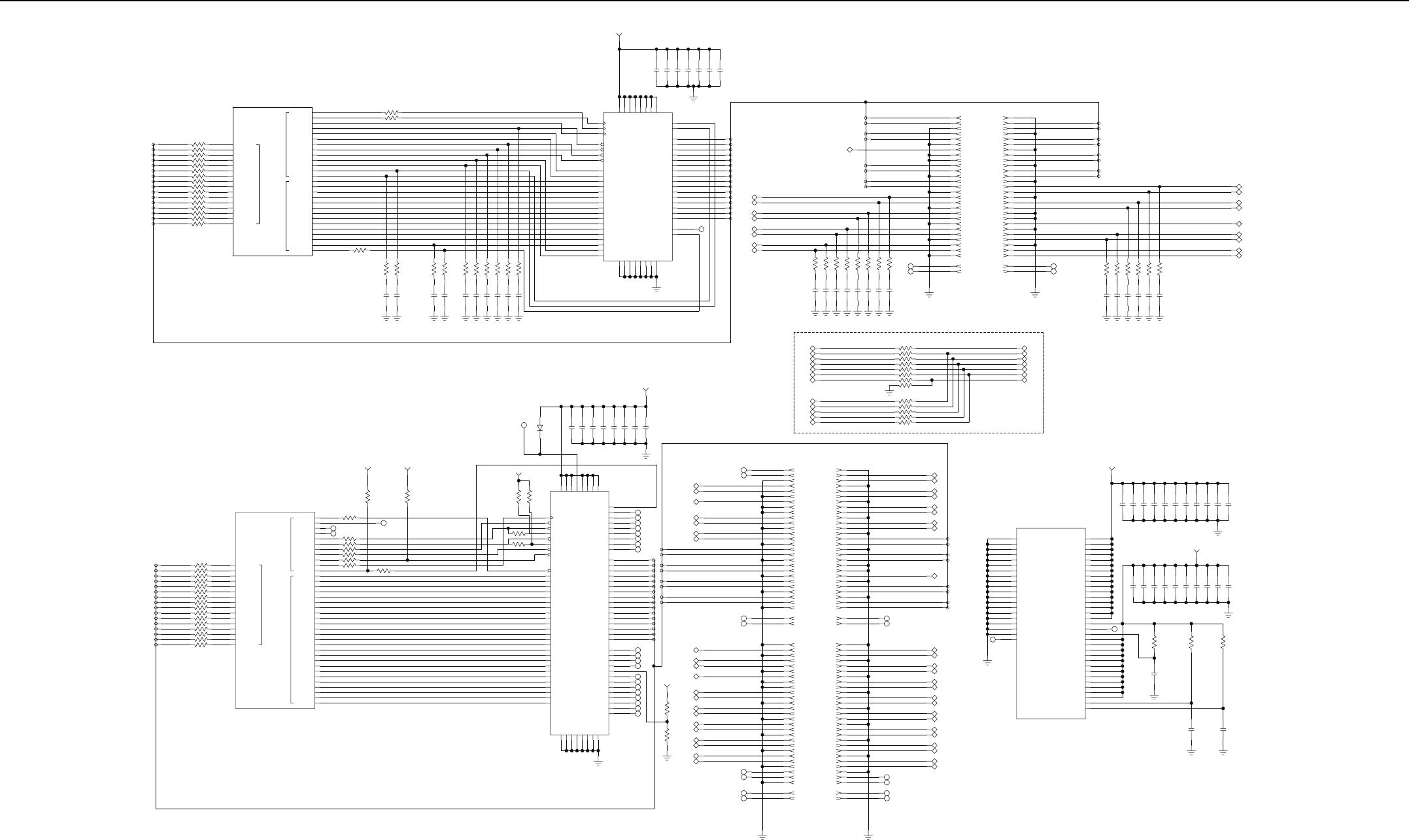
Controller Schematics (UHF) 4-35
R1015M1
R1014M1
R1013M1
R1012M1
R1011M1
R1010M1
R1009M1
R1008M1
R1007M1
R1006M1
R1005M1
R1004M1
R1003M1
R1002M1
R1001M1
R1000M1 10
10
10
10
10
10
10
10
10
10
10
10
10
10
10
10
5
2
0
1
8
14
13
10
7
3
6
9
15
11
12
4
D6
C6
D11
C13
C11
D13
D12
C12
C5
D7
D5
C7
C4
D8
C10
D14
SADD_3
SADD_4
SADD_5
SADD_6
SADD_7
SADD_8
SADD_9
SADD_10
SADD_11
SADD_12
SADD_13
SDATA_2
SDATA_1
SDATA_0
SDATA_15
SDCLKX
SDCLK
SDCLK_EN
NSWE
SBANK_0
SBANK_1
NSRAS
NSCAS
CS_SDRAM
NSDQMU
NSDQML
DSQ_H
DSQ_L
SDATA_14
SDATA_13
SDATA_12
SDATA_11
SDATA_10
SDATA_9
SDATA_8
SDATA_7
SDATA_3
SDATA_4
SDATA_5
SDATA_6
SADD_0
SADD_1
SADD_2
CONTROL
DATA
ADDRESS
U1000M1
OMAP1710
DDR_TX_ADDR_6
DDR_TX_ADDR_9
DDR_TX_CS_N
DDR_TX_DQMU
DDR_TX_RAS_N
DDR_TX_CLK_EN
DDR_TX_BA0
DDR_TX_ADDR_4
DDR_TX_ADDR_5
DDR_TX_DQSU
DDR_TX_DQML
DDR_TX_ADDR_3
DDR_TX_ADDR_2
DDR_TX_ADDR_1
DDR_TX_ADDR_0
DDR_TX_DQSL
DDR_TX_ADDR_8
DDR_TX_ADDR_10
DDR_TX_ADDR_11
DDR_TX_ADDR_13
DDR_TX_CLKN
DDR_TX_CLK
DDR_TX_WE_N
DDR_TX_BA1
DDR_TX_CAS_N
DDR_TX_ADDR_12
DDR_TX_ADDR_7
R1061M1
R1060M1 0
0
DDR_TX_CLKN_
DDR_TX_CLK_
G8
C14
D4
B4
C8
D10
H7
H8
A2
B2
B8
H10
H9
H11
B6
A1
G10
B9
G12
G11
G9
B12
B3
C3
C9
H12
D9
R1086M1
R1070M1
R1069M1
R1068M1
R1067M1
R1066M1
R1065M1
R1064M1
R1063M1
R1062M1
R1039M1
C1061M1
C1046M1
C1045M1
C1044M1
C1043M1
C1042M1
C1041M1
C1040M1
C1039M1
C1038M1 1.1PF
1.1PF
DNP
4.7PF
DNP 4.7PF
DNP 4.7PF
4.7PF
4.7PF
4.7PF
4.7PF
4.7PF
DNP0
49.9
49.9
49.9
49.9
DNP
DNP
DNP
49.9
49.9
49.9
49.9
49.9
49.9
DDR_TX_DATA<15..0>
J8
J9
J7
H2
H3
K7
K8
K2
K3
J1
J2
J3
H1
H8
H9
G8
G2
G3
G1
H7
F8
G9
F2
G7
A9
F9
K9
A7
B1
C9
D1
E9
U1003M1
MT46H16M16LF
A1
F1
K1
A3
B9
C1
D9
E1
NC
A8
B7
D3
C2
C3
B2
B3
A2
B8
C7
C8
D7
D8
E7
E3
D2
E8
F3
F7
E2
UDQS
DQ0
DQ2
DQ3
DQ4
DQ5
DQ6
DQ7
DQ8
DQ9
DQ11
DQ10
DQ13
DQ12
DQ14
DQ15
NC2
NC1
VSSQ5
VSSQ3
VSSQ4
BA0
BA1
A0
A2
A1
A3
A4
A5
A6
A7
A8
A10_AP
A9
A11
VSSQ1
VSSQ2
VSS3
VSS2
VSS1
A12
UDM
LDM
DQ1
VDD1
VDD2
VDD3
VDDQ1
VDDQ2
VDDQ3
VDDQ4
VDDQ5
LDQS
CLK
CLK*
EN_CS
RAS
CAS
EN_CLKE
WE
13
12
11
10
1
0
3
15
2
5
4
6
8
14
7
9
DDR_TX_BA0
DDR_TX_ADDR_6
DDR_TX_ADDR_2
DDR_TX_ADDR_3
DDR_TX_ADDR_7
DDR_TX_ADDR_8
DDR_TX_ADDR_9
DDR_TX_BA1
0
1
4
5
10
11
14
15
LA_TX_CLK_0
NC
NC
R1078M1
R1077M1
R1076M1
R1075M1
R1074M1
R1073M1
R1072M1
R1071M1
C1054M1
C1053M1
C1052M1
C1051M1
C1050M1
C1049M1
C1048M1
C1047M1
4.7PF
4.7PF
4.7PF
4.7PF
4.7PF
4.7PF
4.7PF
4.7PF
49.9
49.9
49.9
49.9
49.9
49.9
49.9
49.9
A1
A2
A3
A4
A5
A6
A7
A8
A9
A10
A11
A12
A13
A14
A15
A16
A17
A18
A19
A20
A21
A22
A23
A24
A25
A26
A27
G1
G2 J1000M1
J1000M1
J1000M1
J1000M1
J1000M1
J1000M1
J1000M1
J1000M1
J1000M1
J1000M1
J1000M1
J1000M1
J1000M1
J1000M1
J1000M1
J1000M1
J1000M1
J1000M1
J1000M1
J1000M1
J1000M1
J1000M1
J1000M1
J1000M1
J1000M1
J1000M1
J1000M1
J1000M1
J1000M1
J1000M1
J1000M1
J1000M1
J1000M1
J1000M1
J1000M1
J1000M1
J1000M1
J1000M1
J1000M1
J1000M1
J1000M1
J1000M1
J1000M1
J1000M1
J1000M1
J1000M1
J1000M1
J1000M1
J1000M1
J1000M1
J1000M1
J1000M1
J1000M1
J1000M1
J1000M1
J1000M1
J1000M1
J1000M1 B1
B2
B3
B4
B5
B6
B7
B8
B9
B10
B11
B12
B13
B14
B15
B16
B17
B18
B19
B20
B21
B22
B23
B24
B25
B26
B27
G3
G4
2
3
6
7
8
9
12
13
LA_TX_CLK_1
DDR_TX_DQMU
DDR_TX_DQML
DDR_TX_ADDR_11
DDR_TX_ADDR_10
DDR_TX_ADDR_5
DDR_TX_ADDR_4
DDR_TX_ADDR_1
DDR_TX_ADDR_0
NC
NC
C1060M1
C1059M1
C1058M1
C1057M1
C1056M1
C1055M1
4.7PF
4.7PF
4.7PF
4.7PF
4.7PF
4.7PF
R1084M1
R1083M1
R1082M1
R1081M1
R1080M1
R1079M1 49.9
49.9
49.9
49.9
49.9
49.9
1_875V
C1014M1
C1013M1
C1012M1
C1011M1
C1010M1
C1009M1
C1008M1 .1UF
.1UF
.1UF
.1UF
.01UF
100PF
4.7UF
DDR_TX_CLK
FLASH_TX_CLK
FLASH_TX_OE_N
FLASH_TX_CE_N
FLASH_TX_LE_N
FLASH_TX_WE_N
DDR_TX_RAS_N
DDR_TX_CAS_N
DDR_TX_CS_N
DDR_TX_WE_N
DDR_TX_CLK_EN
DDR_TX_CLKN
DNP
DNP
DNP
DNP
DNP
DNP
DNP
DNP
DNP
DNP
DNP
DNP
R1056M1
R1055M1
R1054M1
R1053M1
R1052M1
R1051M1
R1050M1
R1049M1
R1048M1
R1047M1
R1046M1
R1045M1
R1044M1 0
0
0
0
0
0
0
0
0
0
0
0
0
LOGIC ANALYZER CLK INPUT SELECT
LA_TX_CLKN_5
LA_TX_CLK_0
LA_TX_CLK_1
LA_TX_CLK_2
LA_TX_CLK_3
LA_TX_CLK_4
LA_TX_CLK_5
FLASH_TX_ADDR_12
FLASH_TX_ADDR_9
FLASH_TX_ADDR_6
DDR_TX_WE_N
DDR_TX_RAS_N
FLASH_TX_ADDR_3
FLASH_TX_ADDR_2
FLASH_TX_CLK
FLASH_TX_LE_N
FLASH_TX_CE_N
FLASH_TX_OE_N
DDR_TX_CLK_EN
FLASH_TX_ADDR_8
FLASH_TX_ADDR_7
FLASH_TX_ADDR_17
FLASH_TX_ADDR_16
FLASH_TX_ADDR_13
FLASH_TX_WAIT_N
LA_TX_CLK_3
DDR_TX_CLK
DDR_TX_CLKN
LA_TX_CLK_5
LA_TX_CLKN_5
FLASH_TX_ADDR_21
FLASH_TX_ADDR_20
NC
NC
15
14
11
10
4
5
1
0
NC
NC
NC
NC
NC
E5
B5
AA21
Y13
AA7
Y3
AA1
U2
N1
K2
G1
B1
B7
A13
B16
A21
F20
K20
R21
W20
VDDSHV7
VDDSHV8
VDDSHV9
VSS_1
VSS_2
VSS_3
VSS_4
VSS_5
VSS_6
VSS_7
VSS_8
VSS_9
VSS_10
VSS_11
VSS_12
VSS_13
VSS_14
VSS_15
VSS_16
VSS_17
VSS_18
VSS_19
NC1
VDDSHV_RTC
VDD_RTC
VPP
VDD_DLL
VDD_1
VDD_2
VDD_3
VDD_4
VDD1_1
VDD2
VDD2_1
VDD2_2
VDD3_1
VDD3_2
VDD3_3
VDD3_4
VDDA
VDD4
VDDSHV1_1
VDDSHV1_2
VDDSHV2
VDDSHV3
VDDSHV4_1
VDDSHV4_2
VDDSHV4_3
VDDSHV4_4
VDDSHV5_1
VDDSHV5_2
VDDSHV5_3
VDDSHV6
VDD SUPPLY
GROUND
U1000M1
OMAP1710
AA3
A9
A3
E2
B13
B20
J21
R20
J1
A15
Y20
Y9
M2
A11
W12
Y21
A19
E21
AA2
Y7
A5
A7
B10
B14
R1
H2
C2
AA11
Y16
L21
U21
V12
L1
NC
VDDA_TXOMAP_CORE
VDD4_TXOMAP_CORE
R1059M1
R1058M1
R1057M1
C1036M1
C1029M1
C1022M1
.1UF
.1UF 1UF
10 10 5.1
VDD_DLL_TXOMAP_CORE
C1037M1
C1035M1
C1033M1
C1031M1
C1028M1
C1026M1
C1024M1
C1021M1
C1019M1
C1017M1 100PF
.1UF
.1UF
100PF
.1UF
.1UF
.1UF
100PF
1UF
2.2UF
1_4V_TXOMAP_CORE
C1062M1
C1034M1
C1032M1
C1030M1
C1027M1
C1025M1
C1023M1
C1020M1
C1018M1
C1016M1
C1015M1 100PF
.1UF
.1UF
100PF
.1UF
.1UF
.1UF
100PF
1UF
2.2UF
.1UF
1_875V
PN UPDATED IN BOM
TO 0180706J37
0
0
0
0
0
0
0
0
0
0
0
0
0
0
0
0
R1031M1
R1030M1
R1029M1
R1028M1
R1027M1
R1026M1
R1025M1
R1024M1
R1023M1
R1022M1
R1021M1
R1020M1
R1019M1
R1018M1
R1017M1
R1016M1
10
15
13
14
12
11
9
7
8
6
5
4
2
3
1
0N4
N2
T3
P8
U1
U3
T4
V3
N7
P2
P4
P7
R2
R3
R4
T2
NFWP
FCLK
FRDY
FADD_1
FADD_2
FADD_3
FADD_4
FADD_5
FADD_6
FADD_7
FADD_8
FADD_9
FADD_10
FADD_11
FADD_12
FADD_13
FADD_14
FADD_15
FADD_16
FADD_17
FADD_18
FADD_19
FADD_20
FADD_21
FADD_22
FADD_23
FADD_24
FADD_25
FDATA_0
FDATA_1
FDATA_2
FDATA_3
FDATA_4
FDATA_5
FDATA_6
FDATA_7
FDATA_8
FDATA_9
FDATA_10
FDATA_11
FDATA_12
FDATA_13
FDATA_14
FDATA_15
NF_ADV
NFCS_0
NFCS_1
NFCS_2
NFCS_3
NFOE
NFRP
NFWE
DATA
CONTROL
ADDRESS
U1000M1
OMAP1710
J8
G4
G3
G2
K8
H4
H3
K7
J2
J4
J3
D3
F2
L8
K4
K3
L7
E1
C1
E4
D2
F4
E3
J7
F3
N3
V2
L4
M7
M3
M4
N8
U4
W1
W2
V4
R1038M1
R1037M1
R1036M1
R1035M1
R1034M1
TP1000M1
R1085M1
R1041M1
R1040M1
R1032M1
26.7
10K
0
DNP
10K
1
FLASH_TX_ADDR_15
FLASH_TX_ADDR_17
FLASH_TX_ADDR_18
FLASH_TX_ADDR_21
FLASH_TX_ADDR_22
FLASH_TX_ADDR_19
FLASH_TX_ADDR_20
FLASH_TX_ADDR_16
FLASH_TX_ADDR_14
FLASH_TX_ADDR_13
FLASH_TX_ADDR_5
FLASH_TX_ADDR_4
FLASH_TX_ADDR_23
FLASH_TX_ADDR_24
FLASH_TX_ADDR_25
FLASH_TX_WE_N
FLASH_TX_ADDR_12
FLASH_TX_ADDR_11
FLASH_TX_ADDR_10
FLASH_TX_ADDR_9
FLASH_TX_ADDR_8
FLASH_TX_ADDR_7
FLASH_TX_ADDR_6
FLASH_TX_ADDR_3
FLASH_TX_ADDR_2
FLASH_TX_ADDR_1
FLASH_TX_WAIT_N
FLASH_TX_CLK
FLASH_TX_WP_N
1_875V
FLASH_TX_CE_N
FLASH_TX_OE_N
FLASH_TX_LE_N
1_875V
FLASH_TX_RESET_N
NC
NC R1033M1
26.7
26.7
26.7
26.7
DNP 26.7
26.7
FLASH_TX_DATA<15..0>
G1
F1
E7
B8
C8
D8
F7
E8
F8
D2
B2
B3
E1
E6
B7
C7
C3
D3
D1
B1
C1
F2
E2
F6
D7
E5
C6
F4
E4
K1
J2
G8
H8
F5
R1088M1
R1087M1
R1043M1
R1042M1 DNP0
0 DNP
10K
10K
1_875V
TP1001M1
D1000M1
C1007M1
C1006M1
C1005M1
C1004M1
C1003M1
C1002M1
C1001M1
C1000M1 .1UF
.1UF
.1UF
.1UF
.1UF
.01UF
100PF
4.7UF
BAT54HT1G
1
1_875V
VPP_FLASH_TXOMAP
VCC3
VCC4
VCC2
VCC1
DU3
DU4
DU2
DU1
DU5
DQ0
DU8
DU7
DU6
DQ5
DQ3
DQ4
DQ2
DQ1
DQ10
DQ8
DQ9
DQ7
DQ6
DQ15
DQ13
DQ14
DQ12
DQ11
RFU4
RFU3
RFU2
RFU1
RFU8
RFU7
RFU6
RFU5
A25
RFU9
RFU12
RFU11
RFU10
VSS8
VSS7
VSS5
VSS6
VCCQ2
VCCQ3
VPP
VCCQ1
CLK
F1_CE
F2_CE
WE
F1_OE
F2_OE
A0
A2
A1
A3
A4
A5
A7
A6
A9
A11
A10
A12
A13
A16
A15
A17
A19
A18
A20
A21
A22
A23
A24
VSS2
VSS3
VSS4
A8
A14
WAIT
VSS1
EN_RST
EN_WP
ADV
U1002M1
PF48F4000P0ZBQE
B5
B6
K6
L4
J8
K7
L3
D4
NC
NC
NC
NC
NC
NC
NC
NC
E3
H2
H3
G4
J4
H5
G6
H6
J7
G3
H4
J5
G5
J6
H7
G2
J3
A1
A2
A7
A8
M1
M2
M7
M8
C2
K4
K5
K8
C5
D5
D6
F3
H1
J1
K2
K3
G7
0
12
15
7
8
9
1
2
3
4
5
6
10
11
13
14
NC
NC
NC
NC
NC
NC
NC
NC
NC
NC
NC
NC
B4
C4
L1
L2
L5
L6
L7
L8
R1090M1
R1089M1
DNP
10K
10K
1_875V
FLASH_TX_ADDR_14
FLASH_TX_ADDR_10
FLASH_TX_ADDR_25
FLASH_TX_ADDR_24
FLASH_TX_ADDR_15
FLASH_TX_ADDR_11
LA_TX_CLK_4
FLASH_TX_ADDR_5
FLASH_TX_ADDR_19
FLASH_TX_ADDR_18
FLASH_TX_ADDR_23
FLASH_TX_ADDR_22
FLASH_TX_ADDR_1
FLASH_TX_ADDR_4
NC
NC
NC
NC
NC
NC
12
13
7
6
2
8
3
9
DDR_TX_DQSL
DDR_TX_DQSU
FLASH_TX_WE_N
FLASH_TX_WP_N
DDR_TX_CAS_N
LA_TX_CLK_2
DDR_TX_CS_N
NC
NC A1
A2
A3
A4
A5
A6
A7
A8
A9
A10
A11
A12
A13
A14
A15
A16
A17
A18
A19
A20
A21
A22
A23
A24
A25
A26
A27
G1
G2
A1
A2
A3
A4
A5
A6
A7
A8
A9
A10
A11
A12
A13
A14
A15
A16
A17
A18
A19
A20
A21
A22
A23
A24
A25
A26
A27
G1
G2 J1002M1
J1002M1
J1002M1
J1002M1
J1002M1
J1002M1
J1002M1
J1002M1
J1002M1
J1002M1
J1002M1
J1002M1
J1002M1
J1002M1
J1002M1
J1002M1
J1002M1
J1002M1
J1002M1
J1002M1
J1002M1
J1002M1
J1002M1
J1002M1
J1002M1
J1002M1
J1002M1
J1002M1
J1002M1
J1002M1
J1002M1
J1002M1
J1002M1
J1002M1
J1002M1
J1002M1
J1002M1
J1002M1
J1002M1
J1002M1
J1002M1
J1002M1
J1002M1
J1002M1
J1002M1
J1002M1
J1002M1
J1002M1
J1002M1
J1002M1
J1002M1
J1002M1
J1002M1
J1002M1
J1002M1
J1002M1
J1002M1
J1002M1
J1001M1
J1001M1
J1001M1
J1001M1
J1001M1
J1001M1
J1001M1
J1001M1
J1001M1
J1001M1
J1001M1
J1001M1
J1001M1
J1001M1
J1001M1
J1001M1
J1001M1
J1001M1
J1001M1
J1001M1
J1001M1
J1001M1
J1001M1
J1001M1
J1001M1
J1001M1
J1001M1
J1001M1
J1001M1
J1001M1
J1001M1
J1001M1
J1001M1
J1001M1
J1001M1
J1001M1
J1001M1
J1001M1
J1001M1
J1001M1
J1001M1
J1001M1
J1001M1
J1001M1
J1001M1
J1001M1
J1001M1
J1001M1
J1001M1
J1001M1
J1001M1
J1001M1
J1001M1
J1001M1
J1001M1
J1001M1
J1001M1
J1001M1 B1
B2
B3
B4
B5
B6
B7
B8
B9
B10
B11
B12
B13
B14
B15
B16
B17
B18
B19
B20
B21
B22
B23
B24
B25
B26
B27
G3
G4
B1
B2
B3
B4
B5
B6
B7
B8
B9
B10
B11
B12
B13
B14
B15
B16
B17
B18
B19
B20
B21
B22
B23
B24
B25
B26
B27
G3
G4
Controller – Tx OMAP Memory Schematic Diagram (Kit No. CLN8502)
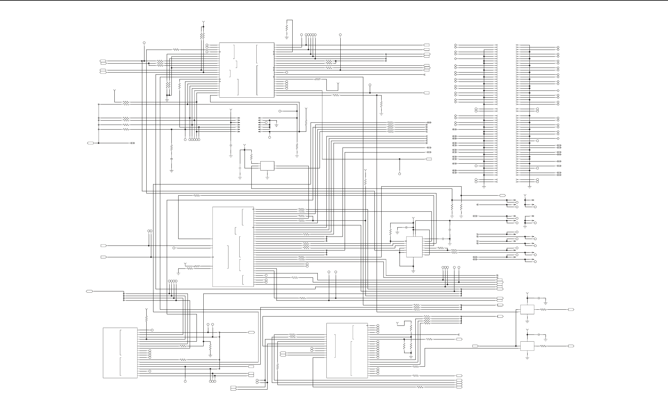
4-36 Controller Schematics (UHF)
I2C_TXOMAP_SDA
RESET_OUT_TXOMAP_N
RESET_IN_TXOMAP_N
I2C_TXOMAP_SCL
R1205M1
R1204M1
R1203M1
R1202M1
R1201M1
R1200M1
10K
0
0
0
0
49.9
1_875V
5
7
8
9
6
BOUNDARY_SCAN<9..0>
IO
OUT
OUT
IO
IN
TP1200M1
1
R1209M1
R1208M1
R1207M1 0
0
0
R1221M1
R1220M1
R1213M1
0
1K 1K
USB1_TXOMAP_VP USB1_TXOMAP_VP_
1_875V
RESET_IN_TXOMAP_N_U20
RESET_IN_TXOMAP_N_R12
TXOMAP_MPU_BOOT
RESET_OUT_TXOMAP_N_
TXOMAP_GPIO_1
NC
NC
NC
R1214M1
R1211M1
R1210M1 10K
10K
0
FPGA_EX_ADDR_2_
JTAG_TXOMAP_RTCK_
V18
R19
AA9
W13
Y5
AA17
J20
U20
V19
V16
W17
Y18
R12
P12
AA20
Y17
T18
V20
Y4
W18
Y19
AA19
V17
MCSI1_SYNC
SYS_CLK_IN
MPU_BOOT
CONF
GPIO_1
CAM_RSTZ
CAM_EXCLK
CAM_LCLK
CAM_VS
CAM_HS
CAM_OUTCLK
CAM_D_0
CAM_D_1
CAM_D_2
CAM_D_3
CAM_D_4
CAM_D_5
CAM_D_6
CAM_D_7
GPIO_18
GPIO_12
GPIO_15
MCBSP2_CLKR
MCBSP2_CLKX
MCBSP2_RSYNC
MCBSP2_XSYNC
MCBSP2_DOUT
MCBSP2_DIN
NEMU1
RTCK_NSBCAN
TCK
NTRST
TMS
TDO
TDI
NEMU0
SCL
SDA
GPIO_55
GPIO_26
RST_OUT
PWRON_RESET
MPU_RST
RESET_MODE
GPIO_7
MPUIO_1
JTAG
CAMERA
GPIO
RF BASEBAND &
MISC GPIO
RESET
I2C
U1000M1
OMAP1710
L19
K14
K15
K19
K18
J14
J19
J18
H19
L15
J15
Y15
M19
L18
N18
M20
R9
V7
Y6
P10
AA5
W6
W7
FPGA_EX_ADDR_0_
RF_RELAY_CONTROL_
TXOMAP_MCBSP2_CLKR
TXOMAP_EXT_CLK
SSI_TRIDENT_TX_
SSI_TRIDENT_RX_LOOPBK_
TX_PERSONALITY
PA_ENABLE_UNGATED_
NC
NC
NC
NC
NC
R1241M1
10K
1_875V
R1240M1
33.2
R1235M1
10K
1_875V
R1227M1
10K
DNI
DNI
DNI
DNI
DNI
DNI
DNI 1
3
5
7
9
11
13
NC
DNI
DNI
DNI
DNI
DNI
DNI
DNI 2
4
6
8
10
12
14
P1200M1P1200M1
P1200M1P1200M1
P1200M1P1200M1
P1200M1P1200M1
P1200M1P1200M1
P1200M1P1200M1
P1200M1P1200M1
TP1218M1
TP1216M1 1
1
JTAG_TXOMAP_EMU1_N
JTAG_TXOMAP_TRST_N
JTAG_TXOMAP_EMU0_N
1_875V
JTAG_TXOMAP_TMS
JTAG_TXOMAP_TDI
JTAG_TXOMAP_TDO
JTAG_TXOMAP_RTCK
JTAG_TXOMAP_TCK
IN
V_POS NC
NO
COM
GND
U1201M1
R1222M1
C1202M1
C1201M1
.1UF
.1UF
10K
TS5A3159
4
2
6
3
1
5 SSI_TXOMAP_DIN
1_875V
PLACED CLOSER TO THE CONNECTOR.
ALL JTAG TEST PADS MUST BE
TP1208M1
TP1207M1
TP1206M1
TP1205M1
TP1204M1
TP1203M1 1
1
1
1
1
1
R1212M1
C1200M1
DNP
100PF
DNP0
TP1230M1
TP1227M1
TP1226M1
TP1224M1
TP1223M1
TP1220M1
TP1219M1
1
1
1
1
1
1
1
R1274M1
10K
SSI_TRIDENT_FS
SSI_TRIDENT_TX
SSI_TRIDENT_CLK
R1244M1
R1243M1
R1242M1 0
0DNP
0
0
2
1
TP1231M1
1
RF_RELAY_CONTROL
AC_FAIL
GPIO_5
GPI_4
MIC_BUTTON_INT_N
SSI_TRIDENT<2..0>
GPI_1
GPIO_10
MAKO_USB_INT_N
R1272M1
10K
PA_ENABLE_UNGATED
IN
IN
OUT
IN
IN
IN
IN
IO
R1250M1
R1249M1
R1248M1
R1247M1
R1246M1 0
0
0
0
0
USB2_TXOMAP<2..0>
SSI_RXOMAP_DIN
SSI_RXOMAP_FSIN
RXOMAP_SYNC
SSI_RXOMAP_CLKIN
SSI_RXOMAP_DOUT
SSI_TXOMAP_MAKO_CLK
SSI_TXOMAP_MAKO_FS
SSI_TXOMAP_MAKO_DIN
SSI_TXOMAP_MAKO_DOUT
USB0_TXOMAP<2..0>
TP1232M1 1
GPIO_6
R1245M1
10K
1_875V
IN
CLK_FPGA_TXOMAP_12MHZ
ABACUS_SYNCB
I2C_TXOMAP_SDA
RESET_OUT_RXOMAP_N
RESET_IN_RXOMAP_N
SPIF_RXOMAP_MOSI
FPGA_EX_ADDR_0
RESET_OUT_TXOMAP_N
RESET_IN_TXOMAP_N
SSI_RXOMAP_DIN
SPIF_TXOMAP_MISO
SSI_CODEC12_CLK
SSI_TXOMAP_MAKO_CLK
SSI_CODEC12_FS
SSI_WBCODEC_CLK
DMCS
SSI_CODEC12_DOUT
SSI_RXOMAP_DOUT
SSI_CODEC12_DIN
SSI_TRIDENT_TX
SSI_TXOMAP_MAKO_FS
OPT_IRQ_N
FPGA_IRQ_N
FPGA_EX_ADDR_1
RCVR_ADDR_1
I2C_TXOMAP_SCL
SPIF_RXOMAP_MISO
SPIF_TXOMAP_NCS3
CLK_FPGA_RXOMAP_12MHZ
SPIF_RXOMAP_CLK
SPIF_RXOMAP_NCS
SSI_WBCODEC_FS
RCVR_ADDR_0
NC
NC
NC
NC
NC
R1268M1
R1265M1
C1205M1
1UF
10K 1.5K
TXOMAP_FPGA_RST
TXOMAP_USBBOOT_EN
RXOMAP_USBBOOT_EN
USB1_RXOMAP_VBUS
USB1_TXOMAP_VBUS
OUT
C1204M1
.1UF
DPOS
DNEG
VPU
GND
VREG
RCV
VP
VM
VBUS
OE_N
ENUMERATE
VCC
VO_VPO
FSE0_VMO
SUSPND
SPEED
MODE
U1200M1
R1251M1
C1203M1
.1UF
10K
ISP1105
14
7
9
1016
12
17
6
12
8
5
4
11 3
15
13
R1218M1 0 USB1_TXOMAP_VM
TP1202M1
TP1201M1
1
1
CLK_FPGA_TXOMAP_32_768KHZ
CLK_FPGA_TXOMAP_12MHZ
IN
IN
SPI_ENET_MOSI
SPI_ENET_CS_N
SPI_ENET_MISO
0
2
SPI_ENET_CLK
SPI_ENET<3..0>
3
1
IO
MMC1_CLK
MMC1_CLKIN
MMC1_CMD
MMC1_CMDDIR
MMC1_DATDIR0
MMC1_DATDIR1
MMC1_DATDIR2
MMC1_DATDIR3
MMC1_DAT0
MMC1_DAT1
MMC1_DAT2
MMC1_DAT3
MMC2_CLK
MMC2_CMD
MMC2_CMDDIR
MMC2_DATDIR0
MMC2_DATDIR1
MMC2_DAT0
MMC2_DAT1
MMC2_DAT2
MMC2_DAT3
U1000M1
OMAP1710
V11
M15
P11
P19
R11
V10
W10
W11
P20
P18
M14
R18
Y10
Y8
V9
W8
V8
W15
R10
V5
W19
OPTION CARD
INTF
MEMORY CARD
INTF
R1206M1
10K
1_875V
NC
SSI_CODEC12_DIN
SSI_TXOMAP_FSOUT
SPIF_TXOMAP_MOSI_
SSI_CODEC12_CLK
NC
NC
NC
NC
NC
R1216M1
R1215M1 0
0
TXOMAP_SYNC
SSI_CODEC12_DOUT_
FPGA_EX_ADDR_1_
SSI_CODEC12_FS
1
2
3
0
SSI_CODEC12_DOUT
R1275M1
10K
TP1211M1
TP1209M1
1
1
SSI_CODEC12<3..0> IO
GPIO_2
OPT_IRQ_N
MIC_PTT_N IN
IN
IN
TP1215M1
TP1214M1 1
1
TP1217M1
TP1213M1
TP1212M1
TP1210M1 1
1
1
1
GPIO_8
GPIO_9
IN
IN
TP1255M1
TP1254M1
TP1253M1
TP1252M1
1
1
1
1
TP1256M1
R1219M1
R1217M1
0
10K
1
P13
P14
Y2
W3
V13
AA13
CLK_TXOMAP_OSC1_OUT_TP
1_4V_TXOMAP_CORE
USB1_TXOMAP_VM_ GPIO_43
MCBSP1_BCLK
MCBSP1_SYNC
MCBSP1_DIN
MCBSP1_DOUT
USB0_TXEN
USB0_DAT
USB0_SE0
USB1_TXEN
USB1_DAT
USB1_SE0
USB2_TXEN
USB2_DAT
USB2_SE0
MPUIO_5
UART1_TX
UART1_RX
UART1_RTS
UART1_CTS
UART3_TX
UART3_RX
GPIO_11
GPIO_60
GPIO_16
GPIO_59
GPIO_5
GPIO_36
OSC1_IN
OSC1_OUT
CLK32K_IN
OSC32K_IN
OSC32K_OUT
SPI_DI
SPI_DO
SPI_CS3
SPI_CS2
SPI_CS1
SPI_CS0
GPIO_56
SPI_CLK
MCBSP1
SP1
OSCILLATOR
CRYSTAL
ONE WIRE
GCA/GPIO
UART
USB
GPIO
U1000M1
OMAP1710
N20
Y1
Y12
P3
V15
L3
M8
G21
H20
H18
H15
T20
U19
N14
N15
T19
P15
U18
W21
R14
AA15
V14
Y14
L14
M18
P9
R8
W4
W14
R13
W16
V6
W5
W9
NC
NC
NC
SSI_TXOMAP_DIN_
USB0_TXOMAP_TXEN
USB0_TXOMAP_DAT
USB0_TXOMAP_SE0
USB1_TXOMAP_TXEN_
UART1_TXOMAP_CTS
UART1_TXOMAP_TX_
SSI_TXOMAP_DOUT
SPIF_TXOMAP_NCS3_
SPIF_TXOMAP_MISO
SSI_TXOMAP_MAKO_DOUT_
USB1_TXOMAP_DAT_
SSI_TXOMAP_CLKOUT
TXOMAP_FPGA_RST_
USB1_TXOMAP_SE0_
USB1_TXOMAP_RCV_
USB2_TXOMAP_DAT
SPIF_TXOMAP_NCS1_
SPIF_TXOMAP_CLK_
UART1_TXOMAP_RTS
USB2_TXOMAP_SE0
USB2_TXOMAP_TXEN
R1231M1
R1230M1
R1229M1
R1228M1 33.2
0
0DNP
0
0
0
0
0
R1239M1
R1238M1
R1237M1
R1236M1
R1233M1
R1232M1 0
0
TP1222M1
TP1221M1
1
1
USB1_TXOMAP_SE0
USB1_TXOMAP_DAT
USB1_TXOMAP_TXEN
1
0
2
0
2
1
TP1229M1
TP1228M1
1
1
R1234M1
R1226M1
33.2
33.2
TXOMAP_SPARE1_
TXOMAP_SPARE2_
1_875V
USB1_TXOMAP_RCV
TP1237M1
TP1236M1
TP1235M1
TP1234M1
TP1233M1
1
1
1
1
1
R1267M1
R1266M1
R1264M1
1.5K
33.2
33.2
USB1_TXOMAP_DM_U1200
USB1_TXOMAP_DP_U1200
UART1_TXOMAP_TX
GPIO_7
TXOMAP_SPARE2
TXOMAP_SPARE1
GPIO_3
FPGA_EX_ADDR<2..0>
FPGA_IRQ_N
TXOMAP_SPARE3
SPIF_TXOMAP<3..0>
UART1_TXOMAP_RX
IO
IO
IN
IN
IO
OUT
IN
IN
2
1
0
3
SPIF_TXOMAP_CLK
SPIF_TXOMAP_NCS3
SPIF_TXOMAP_MOSI
SPI_CS_ADDR_3 3
FPGA_EX_ADDR_0 0
FPGA_EX_ADDR_2
FPGA_EX_ADDR_1
SPI_CS_ADDR_1
SPI_CS_ADDR_2
1
2
1
2
0
SPI_CS_ADDR_0 SPI_CS_ADDR<3..0> OUT
49.9
49.9
49.9
49.9 R1262M1
R1261M1
R1260M1
R1259M1
R1257M1
R1256M1
R1255M1 0
0
0
NC
NC
NC
NC
NC
NC
NC
NC
NC
NC
NC
NC
NC
NC
NC
DMCS_
EX_ENABLE_UNGATED_
SPI_CS_ADDR_3_
SPI_CS_ADDR_1_
SPI_CS_ADDR_2_
ETHERNET_ENABLE_
TXOMAP_SYNC_TRIG_OUT
ANALOG_MUX0
ANALOG_MUX1
DMCS
ETHERNET_ENABLE OUT
OUT
OUT
OUT
OUT
R1258M1
R1254M1
R1253M1
0
0
33.2
R1223M1
33.2
NC
NC
ANALOG_MUX2
ANALOG_MUX3
OUT
OUT
F18
D20
D19
E18
C21
G19
G18
F19
H14
E20
E19
R1225M1
R1224M1 0
0
TRIG_SYNC_TRIG_OUT_
SPI_CS_ADDR_0_
ANALOG_MUX1_
ANALOG_MUX0_
U1000M1
OMAP1710
LCD_PIXEL_10
LCD_PIXEL_11
LCD_PIXEL_12
LCD_PIXEL_13
LCD_PIXEL_14
KBC_5
LCD_PIXEL_15
KBR_4
KBR_0
KBR_1
KBR_2
KBR_3
KBC_0
KBC_1
KBC_2
KBC_3
KBC_4
LCD_PCLK
LCD_AC
LCD_VSYNC
LCD_HSYNC
LCD_RED0
LCD_BLUE0
SOSSI_TE
LCD_PIXEL_0
LCD_PIXEL_1
LCD_PIXEL_2
LCD_PIXEL_3
LCD_PIXEL_4
LCD_PIXEL_5
LCD_PIXEL_6
LCD_PIXEL_7
LCD_PIXEL_8
LCD_PIXEL_9
LCD CONTROL
LCD DATA
KEYPAD
B15
N19
C20
C15
D18
B21
C17
B17
G13
A17
C16
D15
C19
G14
H13
A20
B19
C18
D17
D16
N21
B18
G20
R1273M1
R1271M1
R1252M1 10K
DNP
10K
10K
TXOMAP_GP_BOOT_MODE
1_875V
ANTENNA_RELAY_
R1263M1
33.2
ANTENNA_RELAY
MAKO_INT_N
EX_ENABLE_UNGATED
OUT
3
1
2
FPGA_EX_DISABLE_N
IN
GND
INB
INA
VCC
OUTY
U1203M1
R1270M1
C1207M1
.1UF
0
NC7SZ08
4
5
EX_ENABLE
1_875V
OUT
GND
INB
INA
VCC
OUTY
U1202M1
R1269M1
C1206M1
.1UF
0
NC7SZ08
3
1
2
5
PA_ENABLE
1_875V
OUT
4
USB1_TXOMAP_DP
RS232_TXOMAP_TX
RS232_TXOMAP_RX
RS232_RXOMAP_TX
RS232_RXOMAP_RX
USB1_TXOMAP_DM
USB1_RXOMAP_DM
USB1_RXOMAP_DP
DNI
DNI
DNI
DNI
DNI
DNI
DNI
DNI
TP1251M1
TP1250M1
TP1249M1
TP1248M1
TP1247M1
TP1246M1
P1201M1
P1201M1
P1201M1
P1201M1
P1201M1
P1201M1
P1201M1
P1201M1
DNI
DNI
DNI
DNI
DNI
DNI
DNI
TP1245M1
TP1244M1
TP1243M1
TP1242M1
TP1241M1
TP1240M1
TP1239M1
TP1238M1
P1201M1
P1201M1
P1201M1
P1201M1
P1201M1
P1201M1
P1201M1
P1201M1 2
4
6
8
10
12
14
16
1
1
1
1
1
1
1_875V
DNI
1
3
5
7
9
11
13
15
1
1
1
1
1
1
1
1
J1204M1
J1204M1
J1204M1
J1204M1
J1204M1
J1204M1
J1204M1
J1204M1
J1204M1
J1204M1
J1204M1
J1204M1
J1204M1
J1204M1
J1204M1
J1204M1
J1204M1
J1204M1
J1204M1
J1204M1
J1204M1
J1204M1
J1204M1
J1204M1
J1204M1
J1204M1
J1204M1
J1204M1
J1204M1
J1204M1
J1204M1
J1204M1
J1204M1
J1204M1
J1204M1
J1204M1
J1204M1
J1204M1
J1204M1
J1204M1
J1204M1
J1204M1
J1204M1
J1204M1
J1204M1
J1204M1
J1204M1
J1204M1
J1204M1
J1204M1
J1204M1
J1204M1
J1204M1
J1204M1
J1204M1
J1204M1
J1204M1
J1204M1
J1203M1
J1203M1
J1203M1
J1203M1
J1203M1
J1203M1
J1203M1
J1203M1
J1203M1
J1203M1
J1203M1
J1203M1
J1203M1
J1203M1
J1203M1
J1203M1
J1203M1
J1203M1
J1203M1
J1203M1
J1203M1
J1203M1
J1203M1
J1203M1
J1203M1
J1203M1
J1203M1
J1203M1
J1203M1
J1203M1
J1203M1
J1203M1
J1203M1
J1203M1
J1203M1
J1203M1
J1203M1
J1203M1
J1203M1
J1203M1
J1203M1
J1203M1
J1203M1
J1203M1
J1203M1
J1203M1
J1203M1
J1203M1
J1203M1
J1203M1
J1203M1
J1203M1
J1203M1
J1203M1
J1203M1
J1203M1
J1203M1
J1203M1
G1
G2
A1
A2
A3
A4
A5
A6
A7
A8
A9
A10
A11
A12
A13
A14
A15
A16
A17
A18
A19
A20
A21
A22
A23
A24
A25
A26
A27
G1
G2
A1
A2
A3
A4
A5
A6
A7
A8
A9
A10
A11
A12
A13
A14
A15
A16
A17
A18
A19
A20
A21
A22
A23
A24
A25
A26
A27
NC
NC
NC
NC
NC
NC
SSI_RXOMAP_CLKIN
RXOMAP_SYNC
MAKO_INT_N
EX_ENABLE
SSI_TRIDENT_CLK
SSI_ABACUS_RX
SSI_ABACUS_FS
CLK_FPGA_TXOMAP_32_768KHZ
SPIF_RXOMAP_NCS3
RCVR_ADDR_2
CLK_FPGA_RXOMAP_32_768KHZ
SPIF_TXOMAP_CLK
SPI_CS_ADDR_2
SPI_CS_ADDR_1
SPI_CS_ADDR_3
SSI_TXOMAP_MAKO_DOUT
SSI_TXOMAP_MAKO_DIN
SSI_RXOMAP_FSIN
RF_RELAY_CONTROL
SSI_TRIDENT_FS
ANALOG_MUX1
AC_FAIL
MAKO_USB_INT_N
SPIF_TXOMAP_MOSI
ANALOG_MUX0
ANTENNA_RELAY
FPGA_EX_ADDR_2
SSI_WBCODEC_DIN
SSI_WBCODEC_DOUT
SSI_ABACUS_CLK
SPI_CS_ADDR_0
PA_ENABLE
B1
B2
B3
B4
B5
B6
B7
B8
B9
B10
B11
B12
B13
B14
B15
B16
B17
B18
B19
B20
B21
B22
B23
B24
B25
B26
B27
G3
G4
B1
B2
B3
B4
B5
B6
B7
B8
B9
B10
B11
B12
B13
B14
B15
B16
B17
B18
B19
B20
B21
B22
B23
B24
B25
B26
B27
G3
G4
Controller – Tx OMAP Schematic Diagram (Kit No. CLN8502)
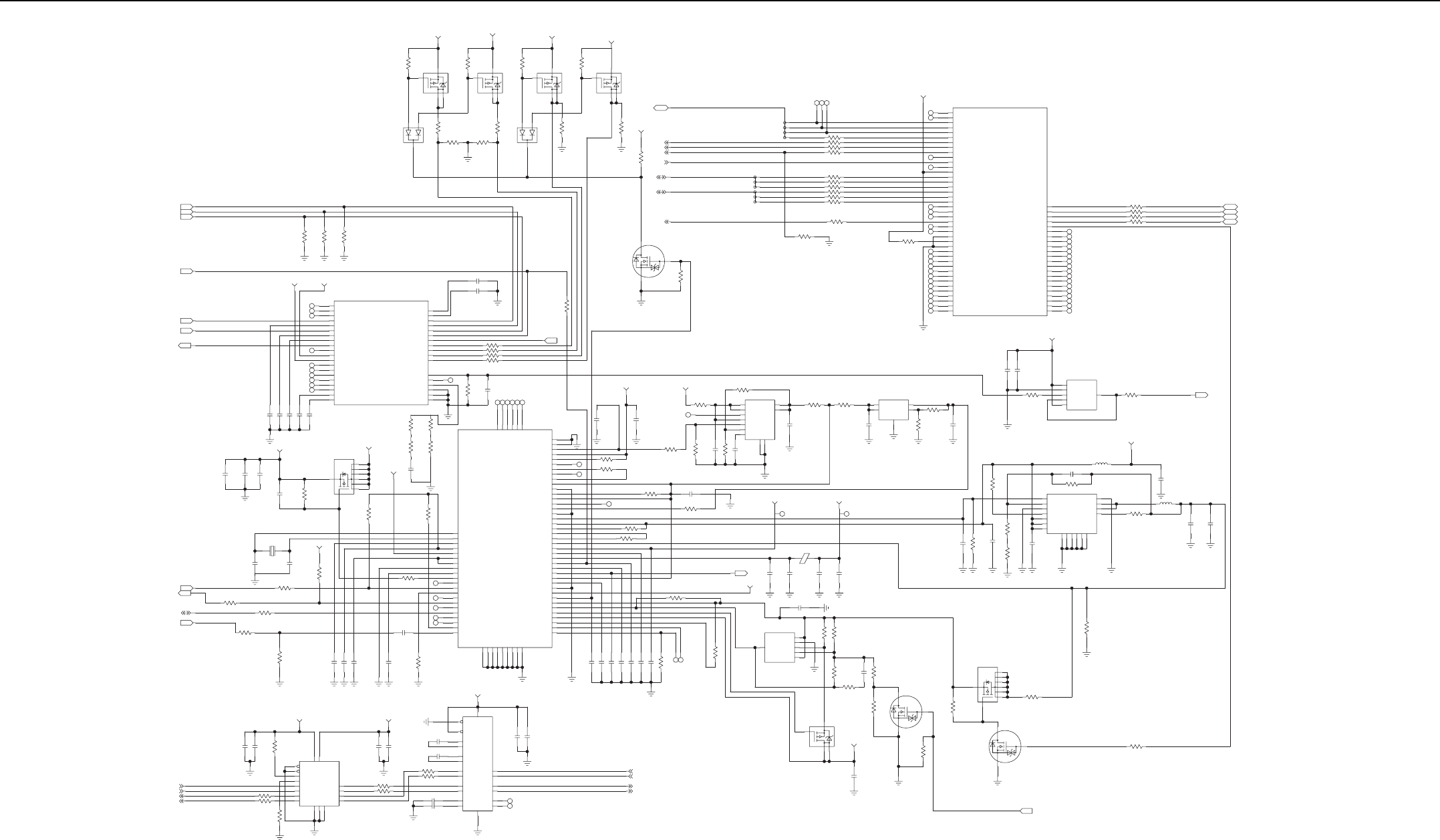
Controller Schematics (UHF) 4-37
OPTION2_ID
OPTION1_ID
WIRELINE_ID
IN
IN
IN
TXAUD_MIC_FLTR
TXAUD_MIC_DATA
PTEMP+
MAKO_CODEC_AUDIO_P
OUT
IN
IN
IN
R1415M1
R1414M1
R1411M1 10K
10K
10K
SW_9_3V 9_3V
NC
NC
NC
NC
NC
NC
NC
NC
NC
NC
B11
E3
J1
J2
G1
H1
K1
K2
F2
F1
L2
E1
G3
G2
A11
H2
H3
J3
H4
A4
C1412M1
C1411M1
C1410M1
C1408M1
C1407M1 .1UF
.1UF
.1UF
.1UF
.1UF
PA_BPLUS
PA_IN_M
PA_IN_P
INT_SPKR_P
INT_SPKR_M
EXT_SPKR_P
AD_TRIG
TX_RX
MIC_BIAS
EXT_SPKR_M
VREF
VCM2
VCM1
EXT_MIC_M
EXT_MIC_P
INT_MIC_M
INT_MIC_P
BPLUS
VC_OUT_M
VC_OUT_P
ADC_VREF
ATOD_0
ATOD_1
ATOD_2
ATOD_3
ATOD_4
ATOD_5
ATOD_6
ATOD_7
ATOD_8
PWR_CTRL
FE_TUNE2
VMES
VFUSE
TEST
SCAN_EN
FE_TUNE1
U1402M1
AT56H09
M12
N14
M13
L11
M14
L12
L13
K11
K12
K13
L3
M2
N1
C4
A3
E8
L10
MAKO_FE_TUNE1
R1431M1
R1430M1
R1429M1
R1428M1 0
0
0
0
MIC_BUTTON IN
R1435M1
C1425M1
C1424M1 100PF
100PF
10K
PGLDO3
V10_O
V10_I
V09_O
V07_O
V06_O
VBUS1_CMD
VBUS1_SENS
VBUS1
VBUS2
VBUS2_CMD
VBUS2_SENS
TCXO_IN
GND5
GND6
GND7
GND8
GND9
NC4
NC3
TCXO_SEL_16_24
NC2
XOUT
XIN
SW5_VDD
V04_O
V03_O
V02_O
V08_O
V08_I
V10_GND
GND2
GND3
GND4
NC5
SW1_DH
SW1_PHASE
SW1_VOUT
SW1_GND
SW1_VDDHV
SW1_VSEN_BUK
SW1_VSEN_BST
SW1_SUMCOMP_DL
PGLDO2
RESETX
GATED_32K_CLK
INT_X
HV_BG
FET_ENX
EMERG_PB
MECH_SW
SW_TYPE
IGN_X
VSAVE
SW2_GND
NC6
VBUS_SUPPLY
BAT_RTC
SW2_VOUT
SW2_LX
SW2_VCCS
SW2_VCC
SW5_VOUT
SW5_PHASE
SW5_SUMCOMP
SW5_VSENSE
SW5_VDDHV
SW1_VDD
NC1
BAT_7V5
BAT_3V6
REG_3V6
BAT_TYPE
XTAL32_OUT
XTAL32_IN
GND1
NC
NC
NC
NC
NC
NC
NC
R1427M1
C1426M1
750PF
100K
A1
A14
P1
P14
M5
B14
C3
A2
H13
H14
F14
G14
G13
G12
H12
J11
H11
L14
J14
J12
K14
J13
G11
E13
D13
F13
F12
E14
N4
P4
N5
P3
P6
K3
K4
L1
L9
J10
M6
H10
C14
E12
D12
C13
F11
B13
NC
NC
U1402M1
AT56H09
C1435M1
C1430M1
1UF
.1UF
R1438M1
R1437M10
4.75K
OUT1
OUT2
IN2
PG
BIAS
EN
FB
SS
CTGND
GND
IN1
NC
U1404M1
R1493M1
R1452M1
R1449M1
R1445M1
1K
0
3.74K
22.1K
TPS74701
4
5
8
1
2
3
7
5V
R1451M1
C1440M1
C1439M1 10UF
470PF
1.07K
11
6
3.6V
R1469M1
R1454M1
C1442M1
10UF
00
9
10
2.2V
IN
EN
GND
OUT
NR_FB
U1406M1
R1476M1
R1474M1 C1450M1
C1449M1
1UF 1UF
39.2K
33.2K
TPS73601
3
2
1
4
5R1482M1
C1454M1
C1453M1
.01UF .1UF
0
5V
ENABLE
V_NEG
V_POS
IN_NEG
VOUT
IN_POS
U1403M1
OPA363IDBV
5
4
3
2
6R1486M1
0
1MAKO_BP_RSSI OUT
5.4V
EN
FB
LBI
SYNC
VIN1
VINA
GND1
GND2
PGND2
AGND
LBO
SW1
PG
VIN2
CTGND
SW2
U1407M1
R1491M1
L1401M1
L1400M1
C1459M1
C1458M1
C1457M1
DNP
2.2UF
22UF
DNP
22UF
DNP
180NH
DNP
15UH
DNP
100K
DNP
DNP
TPS62110
6
13
14
15
SW_9_3V
PGND1
R1484M1
C1456M1 10PF DNP
475K
DNP
9
17
11
12
1
16
4
10
7
5
2
3
8
R1481M1 R1480M1
R1479M1
R1478M1
C1455M1
C1452M1
C1451M1 1UF
10UF
DNP
1UF DNP
100K
DNP
DNP
0
121K DNPDNP8.2K
MAKO_SW5_OUT
R1485M1
10K
R1483M1
DNP
0
Q1408M1
NTHS5441
DNP
1
2
3
6
7
8
R1477M1
4
5
100K
DNP
R1492M1
Q1409M1
DNP
2SK3541
3
1
2
DNP0
MAKO_USB_CONNECT_FET
MAKO_USB_CRNT_LIMIT
IN
R1475M1
R1472M1
Q1407M1
Q1406M1
C1447M1
4.7UF
DNP
SI8401DB
2
3
1
4
DNP
2SK3541
3
1
2
DNP
91K
10K
VBUS1
ENABLE
V_NEG
V_POS
IN_NEG
VOUT
IN_POS
U1405M1
R1466M1
R1455M1
C1444M1
0.1UF
DNP
.2
200
DNP
OPA363IDBV
DNP
5
4
3
2
6
1
MAKO_VBUS_SUPPLY
R1467M1
C1448M1
.1UF
DNP
DNP10K
R1471M1
R1470M1
DNP0
DNP
10K
E1400M1
C1446M1C1445M1C1443M1C1441M1
100PF 10UF 220PF .1UF
SW_9_3V
MAKO_FPGA_V9_DET OUT
TP1407M1
TP1406M1
R1499M1 0
1
1
MAKO_VBUS2_CMD
MAKO_VBUS2_SENS
MAKO_VBUS1_CMD
MAKO_VBUS1_SENS
R1446M1 0
R1444M1
C1437M1
C1436M1
C1434M1
C1433M1
C1432M1
C1431M1
C1429M1 1UF
2.2UF
2.2UF
2.2UF
2.2UF
2.2UF
2.2UF
10K
R1448M1
R1443M1 C1438M1 .1UF
0
0
TP1405M1
1
MAKO_V7_OUT
MAKO_V3_OUT
MAKO_V6_OUT
MAKO_SW5_VDD
MAKO_SW5_VDDHV_IN
MAKO_V4_OUT
R1498M1
R1441M1 22.1K
0
R1497M1
R1496M1
R1495M1
R1494M1
C1460M1
.01UF
49.9
49.9
1K
1K
9_3V
Q1400M1
NTHS5441
1
2
3
6
7
8
SW_9_3V
R1416M1
10K
4
5
C1406M1
C1402M1
C1400M1
10UF
.1UF
.01UF
9_3V
R1412M1
C1409M1
2.2UF
22.1K
R1422M1
10K
D2
D1
F3
B2
F4
E2
F5
G4
B4
D5
E4
D3
C5
B3
M1
D4
C2
A13
A12
C1
B1
NC
NC
NC
NC
NC
R1421M1
R1420M1
C1419M1
C1417M1
1000PF
100PF
0
4.75K
MAKO_HV_BG
CLK_MAKO_24M_
MAKO_REG_3V6
MAKO_VSAVE
R1408M1
C1415M1
C1414M1
C1413M1 .1UF
2.2UF
2.2UF
1K
Y1400M1
R1413M1
R1410M1
R1404M1
R1403M1
R1402M1
C1462M1
C1461M1
5.6PF 5.6PF
33.2
510
0
0
10K
32.768KHZ
MAKO
21
CLK_MAKO_24M_LVLSFT
MAKO_INT_N_
MAKO_FPGA_RST_DET_N_
MAKO_V2_1_875V
MAKO_MECH_SW_N
CLK_FPGA_MAKO_24_576MHZ
MAKO_INT_N
MAKO_FPGA_RST_DET_N
OUT
IN
IN
P5
M7
J4
G5
K9
L4
D14
H5
D9
RS232_RXOMAP_RX
RS232_TXOMAP_TX
RS232_TXOMAP_RX
RS232_RXOMAP_TX4
6
5
7
13
11
12
10
2
3
8
9
17
15
14
VCCB
VCCA
GND3
GND2
GND1
B1_2
B1_1
B2_2
B2_1
A2_2
A2_1
A1_2
A1_1
DIR2
DIR1
OE2
OE1
DNI
U1400M1
SN74AVC4T245
R1418M1
R1417M1
1
16
0
0
C1418M1
C1416M1
.1UF .01UF
3_3V
1_875V
R1407M1
C1405M1
C1403M1 .1UF
.01UF
10K
R1409M1
R1406M1
R1405M1 0
0
10K
UART1_TXOMAP_TX
UART1_RXOMAP_TX
UART1_RXOMAP_RX
UART1_TXOMAP_RX
R1424M1
R1423M1 0
0
C1423M1
C1422M1
C1421M1
C1420M1
4
2
6
5
1
15
10
20
13
12
7
3
.1UF
.1UF
.1UF
.1UF
VNEG
VPOS
NC2
NC1
R2IN
T2OUT
T1OUT
GND
VCC
T2IN
C1NEG
C1POS
T1IN
R2OUT
EN
SHDN
R1IN
C2POS
C2NEG
R1OUT
NC
NC
DNI
C1428M1
C1427M1
U1401M1
MAX3222E
18
11
14
16
9
17
8
19
.1UF .01UF
3_3V
SW_9_3V
TP1412M1
TP1411M1
11
MAKO_V4_2_775V
MAKO_V2_1_875V
V3_6_SW1_LDO
R1503M1
R1502M1 R1500M1 R1436M1
R1434M1
R1433M1
R1432M1
R1425M1
R1419M1
Q1404M1
Q1403M1
Q1402M1
D1401M1
D1400M1
MMBD6100
1
2
3
MMBD6100
1
2
3
SI8401DB
2
3
1
4
SI8401DB
2
3
1
4
SI8401DB
2
3
1
4
4
68.1K
10K 10K
100K
10K
100K
100K
100K
22.1K
14_2V 5V 1_875V
MAKO_VMON_FET_EN
3_3V
R1439M1
Q1405M1
SI8401DB
2
3
1
10K
5V
R1447M1
Q1401M1
2SK3541
3
2
100K
1
SSI_TXOMAP_MAKO_DOUT
SSI_TXOMAP_MAKO_FS
SSI_TXOMAP_MAKO_DIN
USB0_TXOMAP<2..0>
SSI_TXOMAP_MAKO_CLK
MAKO_USB_INT_N
USB2_TXOMAP<2..0>
R1442M1
100K
0
2
1
2
1
2
3
0
0
1
FPGA_MAKO_SPI<3..0>
IO
TP1410M1
TP1409M1
TP1408M1
1
1
1
R1459M1
R1458M1
R1457M1
R1456M1 0
0
0
0
SSI_MAKO_FS_
SSI_MAKO_TX_
USB2_MAKO_SE0_
USB2_MAKO_DAT_
USB2_MAKO_OE_
USB1_MAKO_SE0_
USB1_MAKO_DAT_
USB1_MAKO_OE_
SPIF_MAKO_DO_
SSI_MAKO_DCLK_
49.9
49.9
49.9
49.9
49.9
49.9
R1465M1
R1464M1
R1463M1
R1462M1
R1461M1
R1460M1
R1468M1
R1453M1
4.75K
33.2 MAKO_USB_INTX_
NC
NC
NC
NC
NC
NC
NC
NC
NC
NC
NC
NC
NC
NC
NC
NC
NC
NC
NC
NC
NC
NC
R1473M1
10K
MAKO_V2_1_875V
L5
A5
B5
C7
C12
E11
D10
B10
A6
L7
F10
C11
G10
D11
B12
A8
M3
P2
N2
N8
E6
D6
B6
C6
K6
J5
A10
E9
N3
C8
B8
D8
B9
A9
C9
C10
E7
D7
A7
B7
M4
U1402M1
AT56H09
USB_CONNECT
USB2_DM
USB1_DP
OPTA_SEL0
TXDO_BDI_5V
RXDIN_5V
RTS_FILLSEN_5V
CTS_CABLE_DET_5V
OPTA_SEL1
SB96_BUS_BUSY
SB96_BDO_KF_5V
ONE_WIRE_1
ONE_WIRE_2
ONE_WIRE_BATT
USB2_DPCTS_X
UART2_RXD_OD
UART2_TXD
APCO
RS232_USB_X
BOOT_NORM_X
CABLE_DET_3V
BUSY_OUT
BUSY_IN
RTS_FILLSEN_3V
RXDIN_ENC_3V
TXDO_BDI_ENC_3V
USB1_OE
TXDO_BDI_UP_3V
RXDIN_3V
USB_INTX
BBP_SYNC
BBP_CLK
ONE_WIRE_UP
SB96D_BDO_KF_3V
OPT_GPIO0
OPT_GPIO3
OPT_GPIO2
OPT_GPIO1
USB1_DAT_TXD
USB1_SE0
USB2_OE_RCV_RTS
USB2_DAT_VP
USB2_SE0_VM_RXD
VC_DCLK
SPI_DI
SPI_CS
SPI_CLK
LOGIC_VDD
UCM_SS
VC_RX
VC_TX3V
VC_TX
OPTION_INTX
SPI_DO
OPTA_SEL2
OPTA_SEL3
OPTB_SEL0
OPTB_SEL1
OPTB_SEL2
OPTB_SEL3
VC_FSYNC
USB1_DM
NC
NC
NC
NC
NC
NC
NC
NC
NC
NC
NC
NC
NC
NC
NC
NC
NC
P13
P9
M8
L8
P10
K7
M9
N10
P11
K8
P12
N11
M11
N12
N9
N13
M10
P7
N6
P8
N7
L6
USB2_MAKO_DM_
MAKO_USB_CONNECT
USB2_MAKO_DP_
USB1_MAKO_DP_
USB1_MAKO_DM_
R1490M1
R1489M1
R1488M1
R1487M1 26.7
26.7
26.7
26.7 USB2_MAKO_DM
USB1_MAKO_DM
USB2_MAKO_DP
USB1_MAKO_DP
IO
IO
IO
IO
Controller – MAKO Schematic Diagram (Kit No. CLN8502)
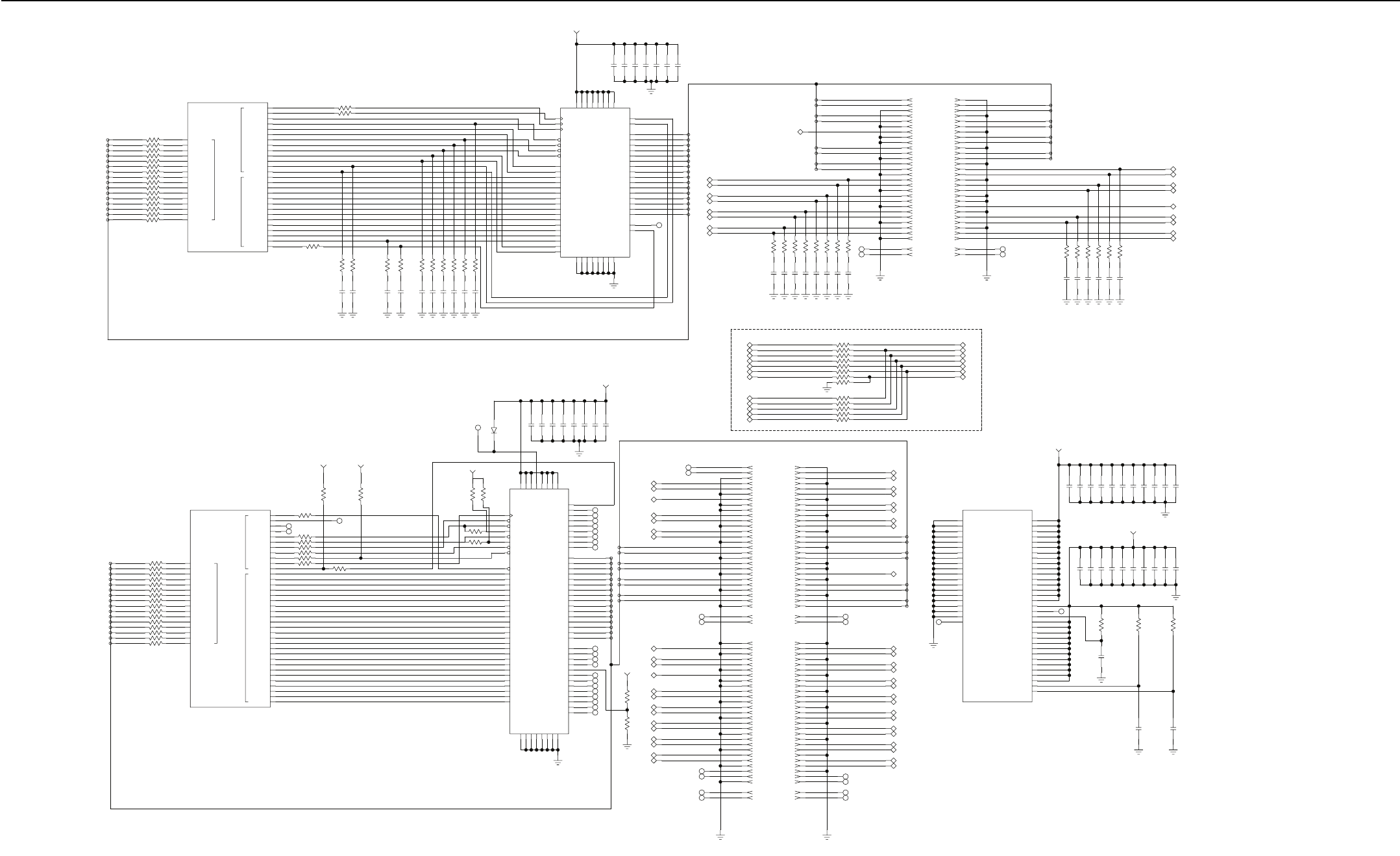
4-38 Controller Schematics (UHF)
R1615M1
R1614M1
R1613M1
R1612M1
R1611M1
R1610M1
R1609M1
R1608M1
R1607M1
R1606M1
R1605M1
R1604M1
R1603M1
R1602M1
R1601M1
R1600M1
11
3
10
7
6
0
1
2
4
5
8
9
13
12
14
15
10
10
10
10
10
10
10
10
10
10
10
10
10
10
10
10
D6
C6
D11
C13
C11
D13
D12
C12
C5
D7
D5
C7
C4
D8
C10
D14
SADD_3
SADD_4
SADD_5
SADD_6
SADD_7
SADD_8
SADD_9
SADD_10
SADD_11
SADD_12
SADD_13
SDATA_2
SDATA_1
SDATA_0
SDATA_15
SDCLKX
SDCLK
SDCLK_EN
NSWE
SBANK_0
SBANK_1
NSRAS
NSCAS
CS_SDRAM
NSDQMU
NSDQML
DSQ_H
DSQ_L
SDATA_14
SDATA_13
SDATA_12
SDATA_11
SDATA_10
SDATA_9
SDATA_8
SDATA_7
SDATA_3
SDATA_4
SDATA_5
SDATA_6
SADD_0
SADD_1
SADD_2
CONTROL
DATA
ADDRESS
U1001M1
OMAP1710
G8
C14
D4
B4
C8
D10
H7
H8
A2
B2
B8
H10
H9
H11
B6
A1
G10
B9
G12
G11
G9
B12
B3
C3
C9
H12
D9
R1661M1
R1660M1 0
0
DDR_RX_CLK_
DDR_RX_CLKN_
R1639M1 0DNP
DDR_RX_CLK
DDR_RX_CLKN
DDR_RX_CAS_N
DDR_RX_DQML
DDR_RX_DQSU
DDR_RX_ADDR_0
DDR_RX_ADDR_1
DDR_RX_ADDR_2
DDR_RX_ADDR_3
DDR_RX_ADDR_4
DDR_RX_ADDR_5
DDR_RX_ADDR_6
DDR_RX_ADDR_7
DDR_RX_ADDR_13
DDR_RX_ADDR_8
DDR_RX_ADDR_9
DDR_RX_ADDR_10
DDR_RX_ADDR_11
DDR_RX_ADDR_12
DDR_RX_CS_N
DDR_RX_DQMU
DDR_RX_BA1
DDR_RX_BA0
DDR_RX_CLK_EN
DDR_RX_RAS_N
DDR_RX_WE_N
DDR_RX_DQSL
DDR_RX_DATA<15..0>
R1686M1
R1670M1
R1669M1
R1668M1
R1667M1
R1666M1
R1665M1
R1664M1
R1663M1
R1662M1
C1661M1
C1646M1
C1645M1
C1644M1
C1643M1
C1642M1
C1641M1
C1640M1
C1639M1
C1638M1
1.1PF
1.1PF
4.7PF
DNP
4.7PF
DNP
4.7PF
DNP
4.7PF
4.7PF
4.7PF
4.7PF
4.7PF
49.9
49.9
DNP
49.9
DNP
49.9
DNP
49.9
49.9
49.9
49.9
49.9
49.9
C1614M1
C1613M1
C1612M1
C1611M1
C1610M1
C1609M1
C1608M1 .1UF
.1UF
.1UF
.1UF
.01UF
100PF
4.7UF
1_875V
J8
J9
J7
H2
H3
K7
K8
K2
K3
J1
J2
J3
H1
H8
H9
G8
G2
G3
G1
H7
F8
G9
F2
G7
A8
B7
D3
C2
C3
B2
B3
A2
B8
C7
C8
D7
D8
E7
E3
D2
E8
F3
F7
E2
NC
10
1
0
3
4
7
6
5
9
8
11
14
2
13
15
12
A1
F1
K1
A3
B9
C1
D9
E1
U1601M1
MT46H16M16LF
A9
F9
K9
A7
B1
C9
D1
E9
UDQS
DQ0
DQ2
DQ3
DQ4
DQ5
DQ6
DQ7
DQ8
DQ9
DQ11
DQ10
DQ13
DQ12
DQ14
DQ15
NC2
NC1
VSSQ5
VSSQ3
VSSQ4
BA0
BA1
A0
A2
A1
A3
A4
A5
A6
A7
A8
A10_AP
A9
A11
VSSQ1
VSSQ2
VSS3
VSS2
VSS1
A12
UDM
LDM
DQ1
VDD1
VDD2
VDD3
VDDQ1
VDDQ2
VDDQ3
VDDQ4
VDDQ5
LDQS
CLK
CLK*
EN_CS
RAS
CAS
EN_CLKE
WE
DDR_RX_ADDR_9
DDR_RX_ADDR_8
DDR_RX_ADDR_7
DDR_RX_BA1
DDR_RX_ADDR_6
DDR_RX_ADDR_3
DDR_RX_ADDR_2
DDR_RX_BA0
NC
NC
R1678M1
R1677M1
R1676M1
R1675M1
R1674M1
R1673M1
R1672M1
R1671M1
C1654M1
C1653M1
C1652M1
C1651M1
C1650M1
C1649M1
C1648M1
C1647M1
4.7PF
4.7PF
4.7PF
4.7PF
4.7PF
4.7PF
4.7PF
4.7PF
49.9
49.9
49.9
49.9
49.9
49.9
49.9
49.9
0
1
4
5
10
11
14
15
LA_RX_CLK_0
A1
A2
A3
A4
A5
A6
A7
A8
A9
A10
A11
A12
A13
A14
A15
A16
A17
A18
A19
A20
A21
A22
A23
A24
A25
A26
A27
G1
G2 J1600M1
J1600M1
J1600M1
J1600M1
J1600M1
J1600M1
J1600M1
J1600M1
J1600M1
J1600M1
J1600M1
J1600M1
J1600M1
J1600M1
J1600M1
J1600M1
J1600M1
J1600M1
J1600M1
J1600M1
J1600M1
J1600M1
J1600M1
J1600M1
J1600M1
J1600M1
J1600M1
J1600M1
J1600M1
J1600M1
J1600M1
J1600M1
J1600M1
J1600M1
J1600M1
J1600M1
J1600M1
J1600M1
J1600M1
J1600M1
J1600M1
J1600M1
J1600M1
J1600M1
J1600M1
J1600M1
J1600M1
J1600M1
J1600M1
J1600M1
J1600M1
J1600M1
J1600M1
J1600M1
J1600M1
J1600M1
J1600M1
J1600M1 B1
B2
B3
B4
B5
B6
B7
B8
B9
B10
B11
B12
B13
B14
B15
B16
B17
B18
B19
B20
B21
B22
B23
B24
B25
B26
B27
G3
G4
6
3
2
9
8
7
13
12
NC
NC
LA_RX_CLK_1
DDR_RX_DQML
DDR_RX_DQMU
DDR_RX_ADDR_5
DDR_RX_ADDR_4
DDR_RX_ADDR_1
DDR_RX_ADDR_0
DDR_RX_ADDR_10
DDR_RX_ADDR_11
R1684M1
R1683M1
R1682M1
R1681M1
R1680M1
R1679M1
C1660M1
C1659M1
C1658M1
C1657M1
C1656M1
C1655M1
4.7PF
4.7PF
4.7PF
4.7PF
4.7PF
4.7PF
49.9
49.9
49.9
49.9
49.9
49.9
FLASH_RX_DATA<15..0>
R1631M1
R1630M1
R1629M1
R1628M1
R1627M1
R1626M1
R1625M1
R1624M1
R1623M1
R1622M1
R1621M1
R1620M1
R1619M1
R1618M1
R1617M1
R1616M1
5
4
0
1
2
3
6
7
8
9
10
11
12
13
14
15
0
0
0
0
0
0
0
0
0
0
0
0
0
0
0
0
N4
N2
T3
P8
U1
U3
T4
V3
N7
P2
P4
P7
R2
R3
R4
T2
NFWP
FCLK
FRDY
FADD_1
FADD_2
FADD_3
FADD_4
FADD_5
FADD_6
FADD_7
FADD_8
FADD_9
FADD_10
FADD_11
FADD_12
FADD_13
FADD_14
FADD_15
FADD_16
FADD_17
FADD_18
FADD_19
FADD_20
FADD_21
FADD_22
FADD_23
FADD_24
FADD_25
FDATA_0
FDATA_1
FDATA_2
FDATA_3
FDATA_4
FDATA_5
FDATA_6
FDATA_7
FDATA_8
FDATA_9
FDATA_10
FDATA_11
FDATA_12
FDATA_13
FDATA_14
FDATA_15
NF_ADV
NFCS_0
NFCS_1
NFCS_2
NFCS_3
NFOE
NFRP
NFWE
DATA
CONTROL
ADDRESS
U1001M1
OMAP1710
R1640M1
R1632M1
26.7
10K
J8
G4
G3
G2
K8
H4
H3
K7
J2
J4
J3
D3
F2
L8
K4
K3
L7
E1
C1
E4
D2
F4
E3
J7
F3
N3
V2
L4
M7
M3
M4
N8
U4
W1
W2
V4
NC
NC
R1638M1
R1637M1
R1636M1
R1635M1
R1634M1
R1633M1
26.7
26.7
26.7
26.7
26.7
DNP
26.7
TP1600M1
1
R1641M1
0
DNP
R1685M1
10K
1_875V 1_875V
PN UPDATED IN BOM
TO 0180706J37
FLASH_RX_ADDR_7
FLASH_RX_ADDR_8
FLASH_RX_ADDR_9
FLASH_RX_ADDR_4
FLASH_RX_LE_N
FLASH_RX_CE_N
FLASH_RX_OE_N
FLASH_RX_RESET_N
FLASH_RX_WP_N
FLASH_RX_ADDR_15
FLASH_RX_ADDR_25
FLASH_RX_ADDR_24
FLASH_RX_ADDR_23
FLASH_RX_ADDR_22
FLASH_RX_ADDR_21
FLASH_RX_ADDR_19
FLASH_RX_ADDR_20
FLASH_RX_ADDR_18
FLASH_RX_ADDR_16
FLASH_RX_ADDR_17
FLASH_RX_ADDR_14
FLASH_RX_ADDR_13
FLASH_RX_ADDR_11
FLASH_RX_ADDR_12
FLASH_RX_ADDR_10
FLASH_RX_ADDR_6
FLASH_RX_ADDR_5
FLASH_RX_ADDR_2
FLASH_RX_ADDR_3
FLASH_RX_ADDR_1
FLASH_RX_CLK
FLASH_RX_WE_N
FLASH_RX_WAIT_N
R1688M1
R1687M1
R1643M1
R1642M1 0 DNP
DNP0
10K 10K
1_875V
G1
F1
E7
B8
C8
D8
F7
E8
F8
D2
B2
B3
E1
E6
B7
C7
C3
D3
D1
B1
C1
F2
E2
F6
D7
E5
C6
F4
E4
K1
J2
G8
H8
F5
TP1601M1
D1600M1
BAT54HT1G
1
VPP_FLASH_RXOMAP
1_875V
C1607M1
C1606M1
C1605M1
C1604M1
C1603M1
C1602M1
C1601M1
C1600M1 .1UF
.1UF
.1UF
.1UF
.1UF
.01UF
100PF
4.7UF
U1600M1
PF48F4000P0ZBQE
VCC3
VCC4
VCC2
VCC1
DU3
DU4
DU2
DU1
DU5
DQ0
DU8
DU7
DU6
DQ5
DQ3
DQ4
DQ2
DQ1
DQ10
DQ8
DQ9
DQ7
DQ6
DQ15
DQ13
DQ14
DQ12
DQ11
RFU4
RFU3
RFU2
RFU1
RFU8
RFU7
RFU6
RFU5
A25
RFU9
RFU12
RFU11
RFU10
VCCQ2
VCCQ3
VPP
VCCQ1
WAIT
VSS8
VSS7
VSS5
VSS6
CLK
F1_CE
F2_CE
WE
F1_OE
F2_OE
A0
A2
A1
A3
A4
A5
A7
A6
A9
A11
A10
A12
A13
A16
A15
A17
A19
A18
A20
A21
A22
A23
A24
VSS2
VSS3
VSS4
A8
A14
VSS1
EN_RST
EN_WP
ADV
B4
C4
L1
L2
L5
L6
L7
L8
NC
NC
NC
NC
NC
NC
NC
NC
NC
NC
NC
NC
NC
NC
NC
NC
NC
NC
NC
NC
E3
H2
H3
G4
J4
H5
G6
H6
J7
G3
H4
J5
G5
J6
H7
G2
J3
A1
A2
A7
A8
C2
K4
K5
K8
C5
D5
D6
F3
H1
J1
K2
K3
G7
M1
M2
M7
M8
B5
B6
K6
L4
J8
K7
L3
D4
10
1
3
0
2
4
5
6
8
12
13
14
15
7
11
9
12
8
6
2
3
7
9
13
R1690M1
R1689M1
DNP10K
10K
1_875V
FLASH_RX_ADDR_10
FLASH_RX_ADDR_23
FLASH_RX_ADDR_24
FLASH_RX_ADDR_25
FLASH_RX_ADDR_1
FLASH_RX_ADDR_11
FLASH_RX_ADDR_14
FLASH_RX_ADDR_4
FLASH_RX_ADDR_5
LA_RX_CLK_4
FLASH_RX_ADDR_22
FLASH_RX_ADDR_19
FLASH_RX_ADDR_18
FLASH_RX_ADDR_15
NC
NC
NC
NC
NC
NC
DDR_RX_CAS_N
DDR_RX_CS_N
DDR_RX_DQSU
LA_RX_CLK_2
DDR_RX_DQSL
FLASH_RX_WP_N
FLASH_RX_WE_N
NC
NC
A1
A2
A3
A4
A5
A6
A7
A8
A9
A10
A11
A12
A13
A14
A15
A16
A17
A18
A19
A20
A21
A22
A23
A24
A25
A26
A27
G1
G2
A1
A2
A3
A4
A5
A6
A7
A8
A9
A10
A11
A12
A13
A14
A15
A16
A17
A18
A19
A20
A21
A22
A23
A24
A25
A26
A27
G1
G2 J1602M1
J1602M1
J1602M1
J1602M1
J1602M1
J1602M1
J1602M1
J1602M1
J1602M1
J1602M1
J1602M1
J1602M1
J1602M1
J1602M1
J1602M1
J1602M1
J1602M1
J1602M1
J1602M1
J1602M1
J1602M1
J1602M1
J1602M1
J1602M1
J1602M1
J1602M1
J1602M1
J1602M1
J1602M1
J1602M1
J1602M1
J1602M1
J1602M1
J1602M1
J1602M1
J1602M1
J1602M1
J1602M1
J1602M1
J1602M1
J1602M1
J1602M1
J1602M1
J1602M1
J1602M1
J1602M1
J1602M1
J1602M1
J1602M1
J1602M1
J1602M1
J1602M1
J1602M1
J1602M1
J1602M1
J1602M1
J1602M1
J1602M1
J1601M1
J1601M1
J1601M1
J1601M1
J1601M1
J1601M1
J1601M1
J1601M1
J1601M1
J1601M1
J1601M1
J1601M1
J1601M1
J1601M1
J1601M1
J1601M1
J1601M1
J1601M1
J1601M1
J1601M1
J1601M1
J1601M1
J1601M1
J1601M1
J1601M1
J1601M1
J1601M1
J1601M1
J1601M1
J1601M1
J1601M1
J1601M1
J1601M1
J1601M1
J1601M1
J1601M1
J1601M1
J1601M1
J1601M1
J1601M1
J1601M1
J1601M1
J1601M1
J1601M1
J1601M1
J1601M1
J1601M1
J1601M1
J1601M1
J1601M1
J1601M1
J1601M1
J1601M1
J1601M1
J1601M1
J1601M1
J1601M1
J1601M1 B1
B2
B3
B4
B5
B6
B7
B8
B9
B10
B11
B12
B13
B14
B15
B16
B17
B18
B19
B20
B21
B22
B23
B24
B25
B26
B27
G3
G4
B1
B2
B3
B4
B5
B6
B7
B8
B9
B10
B11
B12
B13
B14
B15
B16
B17
B18
B19
B20
B21
B22
B23
B24
B25
B26
B27
G3
G4 NC
NC
NC
NC
NC
NC
FLASH_RX_ADDR_8
FLASH_RX_ADDR_9
FLASH_RX_WAIT_N
FLASH_RX_CE_N
FLASH_RX_LE_N
DDR_RX_RAS_N
DDR_RX_WE_N
FLASH_RX_ADDR_16
FLASH_RX_ADDR_21
DDR_RX_CLKN
DDR_RX_CLK
LA_RX_CLKN_5
FLASH_RX_ADDR_12
FLASH_RX_ADDR_13
FLASH_RX_ADDR_7
FLASH_RX_ADDR_6
FLASH_RX_ADDR_2
FLASH_RX_ADDR_3
DDR_RX_CLK_EN
FLASH_RX_CLK
FLASH_RX_ADDR_20
FLASH_RX_ADDR_17
LA_RX_CLK_3
FLASH_RX_OE_N
LA_RX_CLK_5
0
15
14
1
4
5
10
11
NC
E5
B5
AA21
Y13
AA7
Y3
AA1
U2
N1
K2
G1
B1
B7
A13
B16
A21
F20
K20
R21
W20
U1001M1
OMAP1710
1_875V
VDDSHV7
VDDSHV8
VDDSHV9
VSS_1
VSS_2
VSS_3
VSS_4
VSS_5
VSS_6
VSS_7
VSS_8
VSS_9
VSS_10
VSS_11
VSS_12
VSS_13
VSS_14
VSS_15
VSS_16
VSS_17
VSS_18
VSS_19
NC1
VDDSHV_RTC
VDD_RTC
VPP
VDD_DLL
VDD_1
VDD_2
VDD_3
VDD_4
VDD1_1
VDD2
VDD2_1
VDD2_2
VDD3_1
VDD3_2
VDD3_3
VDD3_4
VDDA
VDD4
VDDSHV1_1
VDDSHV1_2
VDDSHV2
VDDSHV3
VDDSHV4_1
VDDSHV4_2
VDDSHV4_3
VDDSHV4_4
VDDSHV5_1
VDDSHV5_2
VDDSHV5_3
VDDSHV6
VDD SUPPLY
GROUND
AA3
A9
A3
E2
B13
B20
J21
R20
J1
A15
Y20
Y9
M2
A11
W12
Y21
A19
E21
AA2
Y7
A5
A7
B10
B14
R1
H2
C2
AA11
Y16
L21
U21
V12
L1
NC
VDDA_RXOMAP_CORE
VDD4_RXOMAP_CORE
C1636M1
C1629M1
.1UF 1UF
R1659M1
R1658M1
C1622M1
.1UF
10 5.1
R1657M1
10
VDD_DLL_RXOMAP_CORE
1_4V_RXOMAP_CORE
C1637M1
C1635M1
C1633M1
C1631M1
C1628M1
C1626M1
C1624M1
C1621M1
C1619M1
C1617M1 100PF
.1UF
.1UF
100PF
.1UF
.1UF
.1UF
100PF
1UF
2.2UF C1662M1
C1634M1
C1632M1
C1630M1
C1627M1
C1625M1
C1623M1
C1620M1
C1618M1
C1616M1
C1615M1 100PF
.1UF
.1UF
100PF
.1UF
.1UF
.1UF
100PF
1UF
2.2UF
.1UF
FLASH_RX_CLK
FLASH_RX_OE_N
FLASH_RX_WE_N
FLASH_RX_LE_N
DDR_RX_RAS_N
DDR_RX_CS_N
DDR_RX_CAS_N
DDR_RX_WE_N
DDR_RX_CLK
DDR_RX_CLK_EN
DDR_RX_CLKN
FLASH_RX_CE_N
R1656M1
R1655M1
R1654M1
R1653M1
R1652M1
R1651M1
R1650M1
R1649M1
R1648M1
R1647M1
R1646M1
R1645M1
R1644M1 0
0
0
0
0
0
0
0
0
0
0
0
0
DNP
DNP
DNP
DNP
DNP
DNP
DNP
DNP
DNP
DNP
DNP
DNP
LOGIC ANALYZER CLK INPUT SELECT
LA_RX_CLK_1
LA_RX_CLK_0
LA_RX_CLK_2
LA_RX_CLKN_5
LA_RX_CLK_5
LA_RX_CLK_4
LA_RX_CLK_3
Controller – Rx OMAP Memory Schematic Diagram (Kit No. CLN8502)
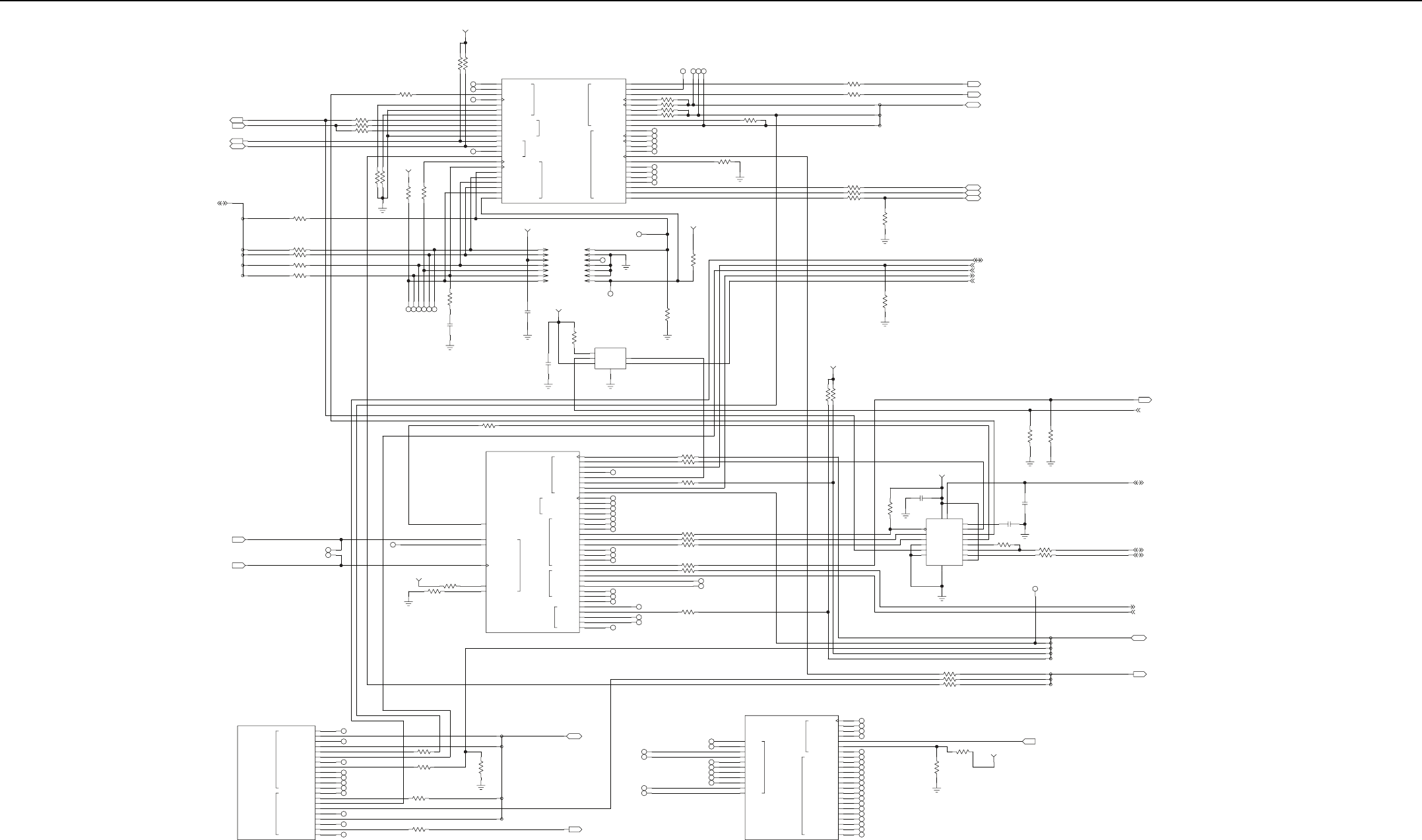
Controller Schematics (UHF) 4-39
1
RESET_OUT_RXOMAP_N
I2C_RXOMAP_SCL
RESET_IN_RXOMAP_N
I2C_RXOMAP_SDA
IN
OUT
OUT
IO
R1804M1
R1803M1
R1802M1
R1801M1
R1800M1 0
0
0
0
49.9
2
3
4
1
0
BOUNDARY_SCAN<9..0>
RESET_IN_RXOMAP_N_U20
RESET_OUT_RXOMAP_N_
RXOMAP_MPU_BOOT
RXOMAP_GPIO_1
RESET_IN_RXOMAP_N_R12
NC
NC
NC
R1821M1
R1820M1
R1810M1
R1807M1
R1806M1
R1805M1 0
0
0
0
1K 1K
USB1_RXOMAP_VP USB1_RXOMAP_VP_
1_875V
NC
R1814M1
R1811M1
R1809M1
R1808M1 10K
10K
10K
0
JTAG_RXOMAP_RTCK_
RCVR_ADDR_2_
1_875V
JTAG CONNECTOR
ALL TP CLOSER TO
TP1807M1
TP1806M1
TP1805M1
TP1804M1
TP1803M1
TP1802M1
R1818M1
C1800M1
100PF
DNP
DNP0
1
1
1
1
1
1
JTAG_RXOMAP_EMU0_N
JTAG_RXOMAP_RTCK
JTAG_RXOMAP_TDO
JTAG_RXOMAP_TMS
JTAG_RXOMAP_TDI
1_875V
JTAG_RXOMAP_TCK
R1823M1
C1802M1
C1801M1
.1UF
.1UF
10K
1_875V
IN
V_POS NC
NO
COM
GND
U1801M1
TS5A3159
4
2
6
3
1
5
NC
DNI
DNI
DNI
DNI
DNI
DNI
DNI
TP1808M1
2
4
6
8
10
12
14
1
JTAG_RXOMAP_EMU1_N
DNI
DNI
DNI
DNI
DNI
DNI
DNI
P1800M1
P1800M1 P1800M1
P1800M1 P1800M1
P1800M1 P1800M1
P1800M1 P1800M1
P1800M1 P1800M1
P1800M1 P1800M1
P1800M1
1
3
5
7
9
11
13
TP1813M1 1
JTAG_RXOMAP_TRST_N R1834M1
10K
1_875V
R1824M1
10K
V18
R19
AA9
W13
Y5
AA17
J20
U20
V19
V16
W17
Y18
R12
P12
AA20
Y17
T18
V20
Y4
W18
Y19
AA19
V17
MCSI1_SYNC
SYS_CLK_IN
MPU_BOOT
CONF
GPIO_1
CAM_RSTZ
CAM_EXCLK
CAM_LCLK
CAM_VS
CAM_HS
CAM_OUTCLK
CAM_D_0
CAM_D_1
CAM_D_2
CAM_D_3
CAM_D_4
CAM_D_5
CAM_D_6
CAM_D_7
GPIO_18
GPIO_12
GPIO_15
MCBSP2_CLKR
MCBSP2_CLKX
MCBSP2_RSYNC
MCBSP2_XSYNC
MCBSP2_DOUT
MCBSP2_DIN
NEMU1
RTCK_NSBCAN
TCK
NTRST
TMS
TDO
TDI
NEMU0
SCL
SDA
GPIO_55
GPIO_26
RST_OUT
PWRON_RESET
MPU_RST
RESET_MODE
GPIO_7
MPUIO_1
JTAG
CAMERA
GPIO
RF BASEBAND &
MISC GPIO
RESET
I2C
U1001M1
TP1823M1
TP1820M1
TP1819M1
TP1818M1
1
1
1
1
OMAP1710
RXOMAP_SYNC_OUT_
RX_ATTEN_
SSI_ABACUS_CLK
SSI_ABACUS_FS
SSI_ABACUS_RX
L19
K14
K15
K19
K18
J14
J19
J18
H19
L15
J15
Y15
M19
L18
N18
M20
R9
V7
Y6
P10
AA5
W6
W7 R1858M1
R1857M1
R1856M1
R1855M1 0
DNP
0
0
DNP
0
RXOMAP_EXT_CLK
SSI_ABACUS_TX_LOOPBACK_
NC
NC
NC
NC
NC
NC
NC
NC
NC
R1836M1
R1835M1
10K
0DNP
RCVR_ADDR_0_
RX_PERSONALITY
RXOMAP_SPARE1_
RXOMAP_SPARE3_
RXOMAP_SPARE2_
RXOMAP_SYNC_OUT
SSI_ABACUS<2..0>
RX_ATTEN OUT
OUT
IO
R1840M1
R1839M1 0
33.2
1
2
0
RXOMAP_SPARE1
RXOMAP_SPARE2
RXOMAP_SPARE3 IO
IO
IO
R1859M1
R1843M1
R1842M1
R1841M1 33.2
33.2
33.2
10K
SSI_RXOMAP_DIN
SSI_RXOMAP_DOUT
SSI_RXOMAP_FSIN
RXOMAP_SYNC
SSI_RXOMAP_CLKIN
R1860M1
1MEG
R1838M1
R1837M1 10K
10K
1_875V
USB1_RXOMAP_RCV
DPOS
DNEG
VPU
GND
VREG
RCV
VP
VM
VBUS
OE_N
ENUMERATE
VCC
VO_VPO
FSE0_VMO
SUSPND
SPEED
MODE
16
12
17
6
1
5
11
U1800M1
R1844M1
C1803M1
.1UF
10K
ISP1105
9
10
2
8
14
7
4
3
15
13
1_875V
TP1824M1
R1852M1
R1851M1
R1849M1
C1805M1
C1804M1
.1UF
1UF
1.5K 33.2
33.2
1
USB1_RXOMAP_DM
USB1_RXOMAP_DP
RXOMAP_USBBOOT_EN
USB1_RXOMAP_VBUS
RXOMAP_FPGA_RST OUT
R1853M1
R1850M1
10K 1.5K
UART1_RXOMAP_RX
RCVR_ADDR<2..0>
UART1_RXOMAP_TX
SPIF_RXOMAP<4..0> IO
OUT
0
1
3
1
2
2
4
0
SPIF_RXOMAP_NCS3
SPIF_RXOMAP_MOSI
SPIF_RXOMAP_CLK
RCVR_ADDR_0
RCVR_ADDR_1
RCVR_ADDR_2
SPIF_RXOMAP_NCS
R1848M1
R1847M1
R1846M1 0
0
0
R1854M1
R1845M1
10K
DNP
10K
RXOMAP_SYNC_IN
1_875V
RXOMAP_GP_BOOT_MODE IN
NC
NC
NC
NC
NC
NC
NC
NC
NC
NC
NC
NC
NC
NC
NC
NC
NC
NC
NC
NC
NC
LCD_PIXEL_10
LCD_PIXEL_11
LCD_PIXEL_12
LCD_PIXEL_13
LCD_PIXEL_14
KBC_5
LCD_PIXEL_15
KBR_4
KBR_0
KBR_1
KBR_2
KBR_3
KBC_0
KBC_1
KBC_2
KBC_3
KBC_4
LCD_PCLK
LCD_AC
LCD_VSYNC
LCD_HSYNC
LCD_RED0
LCD_BLUE0
SOSSI_TE
LCD_PIXEL_0
LCD_PIXEL_1
LCD_PIXEL_2
LCD_PIXEL_3
LCD_PIXEL_4
LCD_PIXEL_5
LCD_PIXEL_6
LCD_PIXEL_7
LCD_PIXEL_8
LCD_PIXEL_9
U1001M1
OMAP1710
LCD CONTROL
LCD DATA
KEYPAD
B15
N19
C20
C15
D18
B21
C17
B17
G13
A17
C16
D15
C19
G14
H13
A20
B19
C18
D17
D16
N21
B18
G20
F18
D20
D19
E18
C21
G19
G18
F19
H14
E20
E19
NC
NC
NC
NC
NC
NC
NC
TP1817M1
TP1816M1
TP1815M1
TP1814M1 1
1
1
1RXOMAP_E19_TP
RXOMAP_E20_TP
RXOMAP_E18_TP
RXOMAP_D19_TP
ABACUS_SYNCB OUT
MMC1_CLK
MMC1_CLKIN
MMC1_CMD
MMC1_CMDDIR
MMC1_DATDIR0
MMC1_DATDIR1
MMC1_DATDIR2
MMC1_DATDIR3
MMC1_DAT0
MMC1_DAT1
MMC1_DAT2
MMC1_DAT3
MMC2_CLK
MMC2_CMD
MMC2_CMDDIR
MMC2_DATDIR0
MMC2_DATDIR1
MMC2_DAT0
MMC2_DAT1
MMC2_DAT2
MMC2_DAT3
U1001M1
OMAP1710
OPTION CARD
INTF
MEMORY CARD
INTF
V11
M15
P11
P19
R11
V10
W10
W11
P20
P18
M14
R18
Y10
Y8
V9
W8
V8
W15
R10
V5
W19
NC
NC
NC
NC
NC
NC
NC
NC
NC
NC
NC
SSI_WBCODEC_DOUT_
SSI_WBCODEC_FS
ABACUS_SYNCB_
RCVR_ADDR_1_
SSI_WBCODEC_CLK
SSI_WBCODEC_DIN
SPIF_RXOMAP_MOSI_
EVENT1_
R1861M1
R1816M1
R1815M1
R1813M1
R1812M1
0
0
0
0
10K
0
SSI_WBCODEC_DOUT
1
2
3
SSI_CODEC_WB<3..0> IO
CLK_FPGA_RXOMAP_32_768KHZ
CLK_FPGA_RXOMAP_12MHZ
IN
IN
TP1801M1
TP1800M1 1
1TP1825M1
R1819M1
R1817M1
0
10K
P13
P14
Y2
W3
V13
AA13
CLK_RXOMAP_OSC1_OUT_TP
USB1_RXOMAP_VM_
1_4V_RXOMAP_CORE
GPIO_43
MCBSP1_BCLK
MCBSP1_SYNC
MCBSP1_DIN
MCBSP1_DOUT
USB0_TXEN
USB0_DAT
USB0_SE0
USB1_TXEN
USB1_DAT
USB1_SE0
USB2_TXEN
USB2_DAT
USB2_SE0
MPUIO_5
UART1_TX
UART1_RX
UART1_RTS
UART1_CTS
UART3_TX
UART3_RX
GPIO_11
GPIO_60
GPIO_16
GPIO_59
GPIO_5
GPIO_36
OSC1_IN
OSC1_OUT
CLK32K_IN
OSC32K_IN
OSC32K_OUT
SPI_DI
SPI_DO
SPI_CS3
SPI_CS2
SPI_CS1
SPI_CS0
GPIO_56
SPI_CLK
MCBSP1
SP1
OSCILLATOR
CRYSTAL
ONE WIRE
GCA/GPIO
GPIO
UART
U1001M1
OMAP1710
USB
R1822M1 0USB1_RXOMAP_VM
N20
Y1
Y12
P3
V15
L3
M8
G21
H20
H18
H15
T20
U19
N14
N15
T19
P15
U18
W21
R14
AA15
V14
Y14
L14
M18
P9
R8
W4
W14
R13
W16
V6
W5
W9
NC
NC
NC
NC
NC
NC
NC
NC
R1831M1
R1830M1
R1829M1
R1828M1
R1826M1
R1825M1 33.2
0
33.2
0
0
0
USB1_RXOMAP_RCV_
SSI_RXOMAP_DIN_
SPIF_RXOMAP_NCS3_
SPIF_RXOMAP_MISO
USB1_RXOMAP_TXEN
USB1_RXOMAP_DAT
USB1_RXOMAP_SE0
USB1_RXOMAP_SE0_
USB1_RXOMAP_DAT_
USB1_RXOMAP_TXEN_
SPIF_RXOMAP_CLK_
NC
NC
NC
NC
NC
NC
NC
TP1822M1
TP1821M1
TP1812M1
TP1811M1
R1833M1
R1832M1
0
0
1
1
1
1
1
RXOMAP_FPGA_RST_
UART1_RXOMAP_CTS
UART1_RXOMAP_TX_
UART1_RXOMAP_RTS
TP1809M1
R1827M1
33.2
Controller – Rx OMAP Schematic Diagram (Kit No. CLN8502)
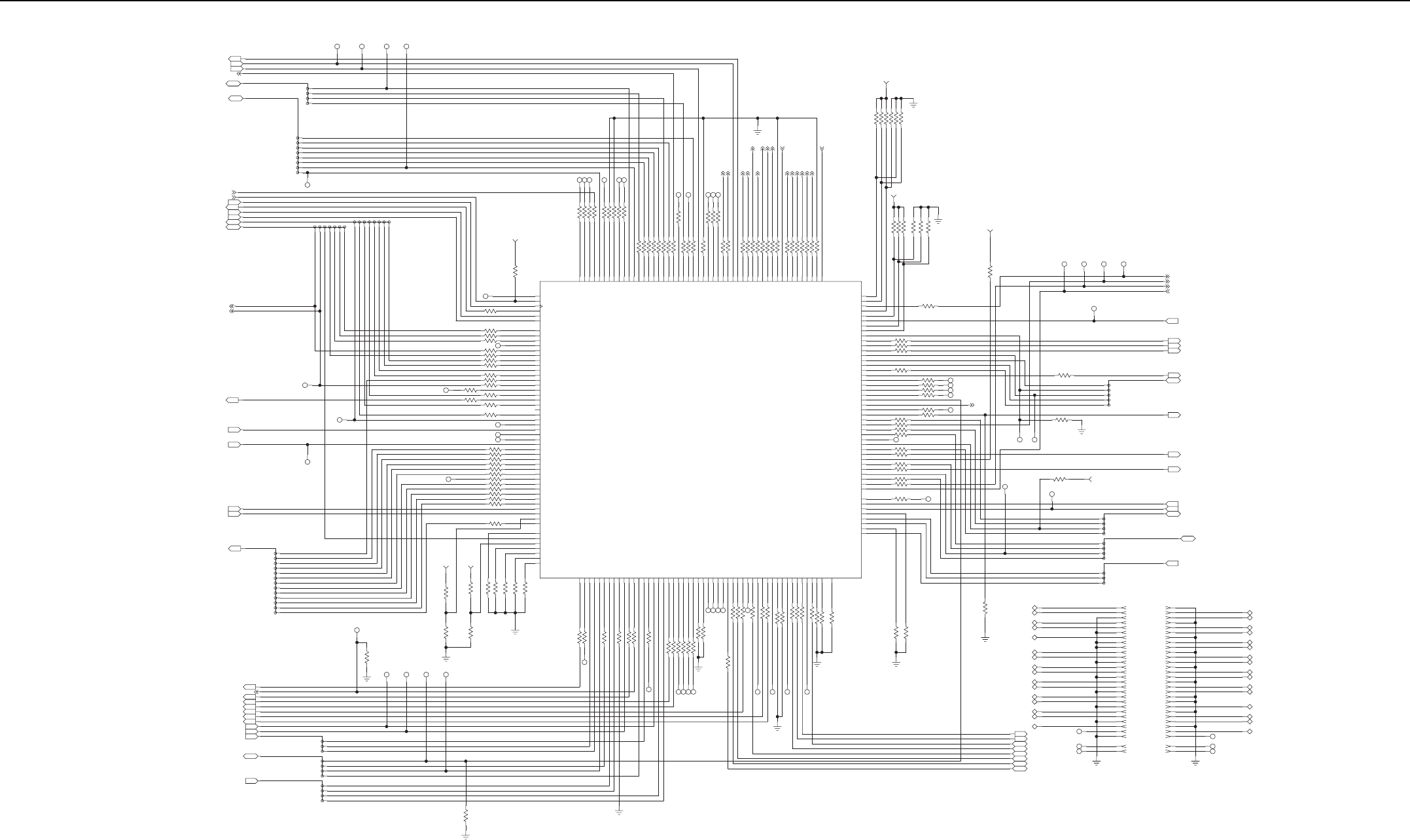
4-40 Controller Schematics (UHF)
TP2019M5
TP2016M5 TP2013M5TP2012M5
11
11
OUT
IN
IN
IO
IO
FPGA_MAKO_MECH_SW_N
FP_FPGA_RST_N
MAKO_FPGA_V9_DET
CLK_FPGA_WD_32_768KHZ
ABA_SPI<0..3>
RCVR_SPI<0..7> 2FPGA_ABA_SPI_CS_N
FPGA_ABA_SPI_MOSI
FPGA_ABA_SPI_CLK
ABA_FPGA_SPI_MISO
0
1
3
7
FPGA_RCVR_SPI_ADDR2
FPGA_RCVR_SPI_CLK
FPGA_RCVR_SPI_CS
RCVR_FPGA_SPI_MISO
FPGA_RCVR_SPI_MOSI
3
6
5
1
2
4
0
FPGA_RCVR_SPI_ADDR0
FPGA_RCVR_SPI_ADDR1
FPGA_RCVR_SPI_ADDR3_TP
TP2000M5
1
BP_FPGA_MISO_B
FPGA_SPI<0..6>
FPGA_TMS
FPGA_TDI
STA_FPGA<0..7>
FPGA_TDO
FPGA_TCK
FPGA_PROG_B
OUT
IN
IN
IN
IO
IO
FPGA_STA_REF_SRC_SEL
CLK_STA_FPGA_16_8MHZ
STA_FPGA_PH_DET_DN
STA_FPGA_COMP_IN
FPGA_STA_DAC_CS_N
FPGA_STA_DAC_CLK
FPGA_STA_DAC_MOSI
FPGA_EX_SPI_ADDR2
FPGA_EX_SPI_ADDR1
FPGA_EX_SPI_ADDR0
FPGA_EX_SPI_CS
EX_FPGA_MISO
FPGA_SPI_CLK
STA_FPGA_PH_DET_UP
FPGA_SPI_MOSI
5
2
4
3
7
0
2
0
3
5
4
6
1
6
1
TP2017M5
TP2015M5
TP2010M5 1
1
TEST_POINT
1
FP_LED<0..12>
FP_FPGA_EXT_REF
1_4V_ROMAP_PG
5V_MON
1_4V_TOMAP_PG
MAKO_USB_CRNT_LIMIT
OUT
OUT
IN
IN
IN
IN
TP2018M5
TEST_POINT
FPGA_FP_LED_TX2_R
FPGA_FP_LED_PWR_G
FPGA_FP_LED_RX1_R
FPGA_FP_LED_TX1_G
FPGA_FP_LED_STA_R
FPGA_FP_LED_TX2_G
FPGA_FP_LED_RX2_G
FPGA_FP_LED_RX2_R
9
6
5
2
1
FPGA_FP_LED_MODE
FPGA_FP_LED_PWR_R
FPGA_FP_LED_TX1_R
12
10
8
7
4
0
11
FPGA_FP_LED_STA_G
3FPGA_FP_LED_RX1_G
TP2023M5TP2022M5TP2021M5TP2020M5
R2151M5
1K
1111
1
FPGA_GPIO_(6)
FPGA_TXOMAP_SPI_IRQ_N
FPGA_GPIO_(4)
FPGA_MAIN_RESET_N
FPGA_GPIO_(7)
FPGA_GPIO_(3)
FPGA_GPIO_(2)
FPGA_EX_ADDR<2..0>
FPGA_GPIO_(5)
TXOMAP_FPGA_RST
MAKO_FPGA_RST_DET_N
IN
IN
OUT
OUT
OUT
OUT
OUT
OUT
IN
OUT
SPIF_TXOMAP<3..0>
SPI_CS_ADDR<3..0>
IN
IO
FPGA_EX_ADDR_0
SPI_CS_ADDR_1
SPI_CS_ADDR_0
SPI_CS_ADDR_3
SPIF_TXOMAP_NCS3
SPIF_TXOMAP_MOSI
SPIF_TXOMAP_MISO
SPIF_TXOMAP_CLK
FPGA_EX_ADDR_2
SPI_CS_ADDR_2
1FPGA_EX_ADDR_1
2
0
3
0
1
2
2
1
3
0
R2089M5
4.75K
DNI
R2038M5
R2037M5
R2035M5
R2034M5
R2006M5
R2005M5
R2001M5
R2000M5
R2004M5 4.75K
4.75K DNP
1K
4.75K
4.75K
4.75K
4.75K
4.75K
4.75K
3_3V
3_3V
R2033M5
R2032M5
R2031M5
R2030M5
R2029M5
R2028M5
R2027M5
R2026M5
R2025M5
R2024M5
R2023M5
R2022M5
R2021M5 0
0
0
0
0
0
0
0
0
0
0
0
0
TP2004M5
TP2003M5
TP2002M5 1
1
1
NC
TP2005M5
TP2001M5
R2036M5
R2020M5
R2019M5
R2018M5
R2017M5
R2016M5
R2015M5
R2014M5
R2013M5
R2012M5
R2011M5
R2010M5
R2009M5
R2008M5
R2007M5
R2003M5
R2002M5 0
0
33.2
33.2
33.2
33.2
49.9
33.2
33.2
33.2
33.2
0
33.2
33.2
33.2
33.2
4.75K
DNP
1
1
SPARE20
3_3V
T15
C13
D13
B14
B15
D11
C12
A13
A14
A12
B12
E10
D10
A11
C11
A10
B10
D9
C10
A9
C9
D8
C8
B8
A8
C7
A7
E7
F8
B6
A6
C6
D7
C5
A5
B4
A4
B3
A3
D5
C4
D6
D12
E6
F7
F9
F10
E9
A2
A15
B1
B16
B2
SUSPEND
IP_L25P_1_VREF_1
IO_L20P_2_D0_DIN_MISO
IO_L20N_2_CCLK
IO_L19P_2
IO_L19N_2
IO_L18P_2_D2
IO_L18N_2_D1
IO_L17P_2_INIT_B
IO_L17N_2_D3
IO_L16P_2
IO_L16N_2
IO_L24N_1_A25
IO_L23P_1_A22
IO_L23N_1_A23
IO_L22P_1_A20
IO_L22N_1_A21
IO_L20P_1_A18
IO_L20N_1_A19
IO_L19P_1_A16
IP_2_VREF_2_2
IP_2_VREF_2_1
IO_L10P_2_GCLK14
IO_L10N_2_GCLK15
IO_L09P_2_GCLK12
IO_L09N_2_GCLK13
IO_L08P_2_D5
IO_L08N_2_D4
IO_L07P_2
IO_L07N_2
IP_2_VREF_2_6
IP_2_VREF_2_5
IO_L12N_1_TRDY1_RHCLK3
IO_L11P_1_RHCLK0
IO_L15P_2_AWAKE
IO_L15N_2_DOUT
IO_L14P_2
IO_L14N_2_MOSI_CSI_B
IO_L13P_2
IO_L13N_2
IO_L12P_2_GCLK2
IO_L12N_2_GCLK3
IO_L11P_2_GCLK0
IO_L11N_2_GCLK1
IO_L05N_1_VREF_1
IO_L03P_1_A0
IO_L03N_1_A1
IO_L02P_1_LDC1
IO_L02N_1_LDC0
IO_L01P_1_HDC
IO_L01N_1_LDC2
IP_L25P_3
IO_L06P_2_D7
IO_L06N_2_D6
IP_2_VREF_2_4
IP_2_VREF_2_3
IO_L04P_2_VS1
IO_L04N_2_VS0
IO_L03P_2_RDWR_B
IO_L03N_2_VS2
IO_L02P_2_M2
IO_L02N_2_CSO_B
IO_L01P_2_M1
IO_L01N_2_M0
IO_L23N_3
IO_L22P_3
IP_L25N_1
IP_L21P_1_VREF_1
IP_L21N_1
IP_L13P_1
IP_L13N_1
IP_L09P_1_VREF_1
IP_L09N_1
IP_L04P_1
IP_L04N_1_VREF_1
IO_L24P_1_A24
IO_L16N_3
IO_L15P_3_TRDY2_LHCLK6
IO_L15N_3_LHCLK7
IO_L14P_3_LHCLK4
IO_L14N_3_LHCLK5
IO_L11P_3_LHCLK0
IO_L19N_1_A17
IO_L18P_1_A14
IP_2_2
IP_2_1
IO_L17N_1_A13
IO_L16P_1_A10
IO_L16N_1_A11
IO_L15P_1_IRDY1_RHCLK6
IO_L15N_1_RHCLK7
IO_L14P_1_RHCLK4
IO_L14N_1_RHCLK5
IO_L12P_1_RHCLK2
IO_L03N_3
IO_L02P_3
IO_L11N_1_RHCLK1
IO_L10P_1_A8
IO_L10N_1_A9
IO_L08P_1_A6
IO_L08N_1_A7
IO_L07P_1_A4
IO_L07N_1_A5
IO_L06P_1_A2
IO_L06N_1_A3
IO_L05P_1
IO_L20P_0_VREF_0
IO_L20N_0_PUDC_B
IO_L19P_0
IO_L19N_0
IO_L18P_0
IO_L18N_0
IO_L17P_0
IO_L17N_0
IP_L25N_3_VREF_3
IP_L21P_3
IO_L05P_2
IO_L05N_2
IP_L13N_3
IP_L06P_3
IP_L06N_3_VREF_3
IP_L04P_3
IP_L04N_3_VREF_3
IO_L24P_3
IO_L24N_3
IO_L23P_3
IO_L10P_0_GCLK6
IO_L10N_0_GCLK7
IO_L22N_3
IO_L20P_3
IO_L20N_3
IO_L19P_3
IO_L19N_3
IO_L18P_3
IO_L18N_3
IO_L17P_3
IO_L17N_3
IO_L16P_3_VREF_3
IO_L04P_0
IO_L04N_0
IO_L03P_0
IO_L03N_0
IO_L02P_0_VREF_0
IO_L02N_0
IO_L01P_0
IO_L01N_0
IO_L11N_3_LHCLK1
IO_L10P_3
IO_L18N_1_A15
IO_L17P_1_A12
IO_L09N_3
IO_L08P_3
IO_L08N_3_VREF_3
IO_L07P_3
IO_L07N_3
IO_L05P_3
IO_L05N_3
IO_L03P_3
IO_L15P_0
IO_L15N_0
IO_L02N_3
IO_L01P_3
IO_L01N_3
IP_0_VREF_0
IP_0_6
IP_0_5
IP_0_4
IP_0_3
IP_0_2
IP_0_1
IO_L09P_0_GCLK4
IO_L09N_0_GCLK5
IO_L08P_0
IO_L08N_0
IO_L07P_0
IO_L07N_0
IO_L06P_0
IO_L06N_0_VREF_0
IO_L05P_0
IO_L05N_0
IP_L21N_3
IP_L13P_3
IO_L14P_0
IO_L14N_0_VREF_0
IO_L13P_0
IO_L13N_0
IO_L12P_0_GCLK10
IO_L12N_0_GCLK11
IO_L11P_0_GCLK8
IO_L11N_0_GCLK9
IO_L10N_3
IO_L09P_3
PROG_B
TCK
TDI
TMS
DONE
TDO
IO_L16P_0
IO_L16N_0
IO_L12P_3_LHCLK2
IO_L12N_3_IRDY2_LHCLK3
U2000M5
XC3S200AN
FOR 800/900MHZ, PLACE R2004 AND DNP R2006
ADDITIONAL BOM CHANGES ON
POWER AND STATION REF SHEET
BOM CHANGE IS MANAGED VIA VARIANT
FOR UHF/VHF, PLACE R2006 AND DNP R2004
NC
NC
NC
NC
NC
R2145M5
R2128M5
R2114M5
4.75K 4.75K
4.75K
RXOMAP_SPARE1
FPGA_GPIO_(1)
TXOMAP_SPARE3
RXOMAP_SPARE3
RXOMAP_SPARE2
TXOMAP_SPARE1
TXOMAP_SPARE2
FPGA_GPIO_(0)
IO
OUT
OUT
IO
IO
IO
IO
IO
N14
N13
P15
R15
N16
P16
M14
M13
K13
L13
M16
M15
L16
L14
J13
J12
K14
K15
J16
K16
H14
J14
H16
H15
F16
G16
G14
H13
F15
E16
F14
G13
F13
E14
D15
D16
D14
E13
C15
C16
K12
K11
J11
J10
H11
H10
G11
G12
F11
F12
R16
NC
R2046M5
R2042M5
R2040M5 33.2
0
SPARE23
R2072M5
R2070M5
R2068M5
R2066M5
R2064M5
R2062M5
R2057M5
R2053M5
R2052M5
R2050M5
33.2
4.75K
0
0
0SPARE24
0
0
0
0
0
0
SPARE26
SPARE28
SPARE27
SPARE25
NC
NC
NC
NC
NC
TP2009M5
TP2008M5
TP2007M5
TP2006M5
R2088M5
R2085M5
R2083M5
R2082M5
R2081M5
R2075M5
R2073M5
4.75K
4.75K
0
0
0
0
33.2
1
1
1
1
FPGA_FLASH_TP_MISO
FPGA_FLASH_TP_MOSI
FPGA_FLASH_TP_SPI_CS_N
FPGA_FLASH_TP_SPI_CLK
TXOMAP_SPARE3_
R2095M5
R2093M5 0
0
R2113M5
R2112M5
R2111M5
R2109M5
R2106M5
R2104M5
R2102M5
R2099M5
R2098M5 4.75K
4.75K
33.2
0
0
33.2
4.75K
4.75K
4.75K
C1
C2
D3
D4
E1
D1
E2
E3
G4
F3
G1
F1
H4
G3
H5
H6
H1
G2
J3
H3
J1
J2
K1
K3
L2
L1
J6
J4
L3
K4
L4
M3
N1
M1
P1
N2
P2
R1
M4
N3
F4
E4
G5
G6
J7
H7
K6
K5
L6
L5
R2063M5
R2061M5
R2060M5
R2059M5
R2058M5
R2056M5
R2055M5
R2054M5
0
0
0
0
0
0
0
0
R2110M5
R2108M5
R2107M5
R2105M5
R2103M5
R2101M5
R2100M5
R2097M5
R2096M5
R2094M5
R2092M5
R2091M5
R2087M5
R2086M5
R2084M5 0
0
0
0
0
0
0
4.75K
0
0
0
0
0
0
4.75K
FPGA_WL1_LATCH_CS_N
FPGA_OP2_CS1_N
FPGA_WL2_LATCH_CS_N
FPGA_WL12_FSYNC
FPGA_WL34_FSYNC
FPGA_WIRELINE12_TXD
FPGA_OP2_CS3_N
FPGA_OP1_CS2_N
FPGA_OP2_CS2_N
FPGA_WL12_RXD
FPGA_OP1_CS1_N
FPGA_PA_ADDR1
FPGA_WL34_RXD
FPGA_PA_ADDR0
FPGA_OP1_CS3_N
FPGA_WIRELINE34_TXD
NC
NC
NC
NC
NC
NC
NC
NC
NC
NC
NC
R2080M5
R2079M5
R2078M5
R2077M5
R2076M5
R2074M5
R2071M5
R2069M5
R2067M5
R2065M5
R2051M5
R2049M5
R2048M5
R2047M5
R2045M5
R2044M5
R2043M5
R2041M5
R2039M5 0
0
0
0
0
4.75K
4.75K
0
0
0
33.2
0
33.2
4.75K
0
0
0
33.2
0
SPARE8
FPGA_WL_M_B_CLK
SPARE10
SPARE11
BP_FPGA_MISO_B_R
SPARE9
SPARE7
SPARE6
SPARE3
SPARE1
SPARE2
SPARE4
P4
N4
T2
R2
T3
R3
P5
N6
R5
T4
T6
T5
P6
N7
N8
P7
T7
R7
T8
P8
P9
N9
T9
R9
M10
N10
P10
T10
R11
T11
N11
P11
P12
T12
R13
T13
P13
N12
R14
T14
L7
L8
L9
L10
M7
M8
M11
N5
FOR MASTER SPI MODE:M0=1, M1=0,M2=0
DEFAULT IS M0=1, M1=1, M2=0
R2141M5
R2132M5
R2131M5
R2130M5
R2129M5
R2127M5 0
0
0DNP
0
DNP
0
0DNP
3_3V
FOR FAST READ MODE:VS0=1, VS1=1,VS2=1
DEFAULT IS VS0=1, VS1=0, VS2=1
3_3V
M1
M0
M2
R2154M5
R2153M5
R2148M5
R2144M5
R2143M5
R2142M5 0
0
0DNP
0
DNP
0
DNP
0
VS2
VS0
VS1
R2152M5
33.2
NC
NC
NC
NC
NC
TP2011M5
R2140M5
R2139M5
R2138M5
R2137M5
R2136M5
R2135M5
R2134M5
R2120M5
R2119M5
R2118M5
R2117M5
R2116M5
R2115M5 33.2
0
0
33.2
33.2
33.2
33.2
0
0
0
0
33.2
0
33.2
1
SPARE12
SPARE17
SPARE19
FPGA_RESET_RXOMAP_ALT_N
SPARE15
SPARE14
SPARE16
R2149M5
R2126M5
R2125M5
R2124M5
R2123M5
R2122M5
R2121M5
33.2
33.2
33.2
33.2
33.2
33.2
NC
R2147M5 0
R2146M5
DNP
4.75K
1_875V
HOLD PROG_B LOW WILL TURN ALL I/O TO HIGH-Z
ALLOW DIRECT PROGRAMMING TO SPI FLASH PINS.
TP2033M5TP2032M5TP2031M5TP2030M5
1111
FPGA_CCLK
FPGA_MISO
FPGA_MOSI
FPGA_CSO_B
TP2029M5
1
CLK_FPGA_RXOMAP_12MHZ
CLK_FPGA_TXOMAP_12MHZ
CLK_FPGA_RXOMAP_32_768KHZ
RXOMAP_FPGA_RST IN
OUT
OUT
OUT
R2133M5
DNP
33.2
SPIF_RXOMAP_NCS
SPIF_RXOMAP_MOSI
SPIF_RXOMAP_CLK
SPIF_RXOMAP_NCS3
SPIF_RXOMAP_MISO
CLK_FPGA_WBCODEC_12MHZ
SPIF_RXOMAP<4..0> IO
OUT
OUT
2
1
4
0
3
TP2028M5
TP2027M5
TP2026M5
TP2024M5
R2150M5
R2090M5
4.75K
4.75K
1
1
1
1
FPGA_EX_DISABLE_N
CLK_FPGA_MAKO_24_576MHZ
1_875V
CLK_FPGA_TXOMAP_32_768KHZ
IN
IO
IO
IN
IN
OUT
OUT
TOMAP_FPGA_WDRST_N
ROMAP_FPGA_WDRST_N
FPGA_MAKO_SPI<3..0>
SSI_CODEC12<3..0>
RCVR_ADDR<2..0>
FPGA_MAKO_SPI_MOSI
MAKO_FPGA_SPI_MISO
FPGA_MAKO_SPI_CLK
RCVR_ADDR_2
RCVR_ADDR_1
0
FPGA_MAKO_SPI_CS
3
2
1
2
RCVR_ADDR_0
1
0
3
0
2
1
SSI_CODEC12_FS
SSI_CODEC12_DOUT
SSI_CODEC12_CLK
SSI_CODEC12_DIN
FPGA_ABA_SPI_CLK
CLK_FPGA_MAKO_24_576MHZ
FPGA_CSO_B
FPGA_SPI_CLK
FPGA_MAKO_SPI_CLK
FPGA_MAKO_SPI_MOSI
FPGA_WL1_LATCH_CS_N
FPGA_WL34_FSYNC
FPGA_RCVR_SPI_ADDR0
FPGA_RCVR_SPI_MOSI
FPGA_WL12_RXD
FPGA_ABA_SPI_CS_N
RCVR_FPGA_SPI_MISO
FPGA_RCVR_SPI_CLK
FPGA_RCVR_SPI_CS
FPGA_WL2_LATCH_CS_N
NC
NC
NC
A1
A2
A3
A4
A5
A6
A7
A8
A9
A10
A11
A12
A13
A14
A15
A16
A17
A18
A19
A20
A21
A22
A23
A24
A25
A26
A27
G1
G2 J2000M5
J2000M5
J2000M5
J2000M5
J2000M5
J2000M5
J2000M5
J2000M5
J2000M5
J2000M5
J2000M5
J2000M5
J2000M5
J2000M5
J2000M5
J2000M5
J2000M5
J2000M5
J2000M5
J2000M5
J2000M5
J2000M5
J2000M5
J2000M5
J2000M5
J2000M5
J2000M5
J2000M5
J2000M5
J2000M5
J2000M5
J2000M5
J2000M5
J2000M5
J2000M5
J2000M5
J2000M5
J2000M5
J2000M5
J2000M5
J2000M5
J2000M5
J2000M5
J2000M5
J2000M5
J2000M5
J2000M5
J2000M5
J2000M5
J2000M5
J2000M5
J2000M5
J2000M5
J2000M5
J2000M5
J2000M5
J2000M5
J2000M5 B1
B2
B3
B4
B5
B6
B7
B8
B9
B10
B11
B12
B13
B14
B15
B16
B17
B18
B19
B20
B21
B22
B23
B24
B25
B26
B27
G3
G4
FPGA_WIRELINE12_TXD
FPGA_WIRELINE34_TXD
FPGA_CCLK
ABA_FPGA_SPI_MISO
FPGA_WL_M_B_CLK
FPGA_ABA_SPI_MOSI
FPGA_MISO
FPGA_MOSI
MAKO_FPGA_SPI_MISO
FPGA_WL34_RXD
FPGA_WL12_FSYNC
FPGA_RCVR_SPI_ADDR1
FPGA_MAKO_SPI_CS
FPGA_PA_ADDR1
FPGA_PA_ADDR0
FPGA_RCVR_SPI_ADDR2
NC
NC
NC
NC
Controller – FPGA Schematic Diagram (Kit No. CLN8502)
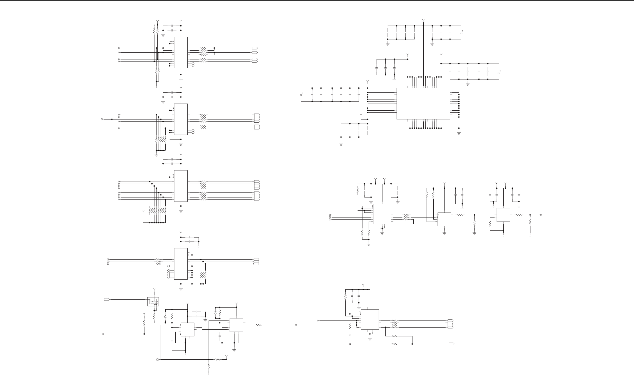
Controller Schematics (UHF) 4-41
7
FPGA_SPI_CLK
FPGA_WL2_LATCH_CS_N
FPGA_SPI_MOSI
FPGA_WL1_LATCH_CS_N
R2215M5
R2212M5 10K
10K
GND
Y0A0
A1
Y3
Y4
A5
A6
Y7
EN_OE1
EN_OE2
Y1
Y2A2
A3
A4
Y5
Y6
A7
VCC
2
4
6
8
11
13
15
17
1
19
C2201M5
C2200M5
0.1UF
.01UF
20
5V
3_3V
U2200M5
MC74HCT244
18
16
14
12
9
7
5
3
R2225M5
R2224M5
R2223M5
R2222M5
R2221M5
R2220M5
NC
NC
49.9
49.9
49.9
49.9
0
0
10
R2206M5
R2203M5 10K
10K
GND
Y0A0
A1
Y3
Y4
A5
A6
Y7
EN_OE1
EN_OE2
Y1
Y2A2
A3
A4
Y5
Y6
A7
VCC
NC
NC
R2232M5
R2231M5
R2230M5
R2229M5
R2228M5
R2227M5 0
0
0
0
0
0
18
16
14
12
9
7
5
3
FPGA_BP_WIRELINE_BCLK
FPGA_BP_WIRELINE12_FSYNC
FPGA_BP_WIRELINE12_RXD
FPGA_BP_WIRELINE34_RXD
FPGA_BP_WIRELINE_MCLK
FPGA_BP_WIRELINEL34_FSYNC
OUT
OUT
OUT
OUT
OUT
OUT
U2201M5
C2203M5
.01UF MC74HCT244
2
4
6
8
11
13
15
17
1
19
10 20
C2202M5
0.1UF
5V
R2218M5
R2216M5
R2213M5
R2207M5
R2204M5
10K
10K
10K
10K
10K
FPGA_WL12_RXD
FPGA_WL_M_B_CLK
FPGA_WL34_RXD
FPGA_WL34_FSYNC
FPGA_WL12_FSYNC
GND
Y0A0
A1
Y3
Y4
A5
A6
Y7
EN_OE1
EN_OE2
Y1
Y2A2
A3
A4
Y5
Y6
A7
VCC
U2202M5
R2240M5
R2239M5
R2238M5
R2237M5
R2236M5
R2235M5
R2234M5
R2233M5
C2205M5
.01UF
0
0
0
0
0
0
0
0
MC74HCT244
2
4
6
8
11
13
15
17
1
19
20
18
16
14
12
9
7
5
3
R2219M5
R2217M5
R2214M5
R2208M5
R2205M5
R2202M5
R2201M5
R2200M5
10
10K
10K
10K
10K
10K
10K
10K
10K
3_3V
FPGA_OP1_CS2_N
FPGA_OP2_CS3_N
FPGA_PA_ADDR0
FPGA_PA_ADDR1
FPGA_OP2_CS2_N
FPGA_OP1_CS1_N
FPGA_OP1_CS3_N
FPGA_OP2_CS1_N
NC
NC
NC
NC
NC
U2203M5
R2211M5
R2210M5
R2209M5 0
0
0
MC74LVX244
18
16
14
12
9
7
5
3
FPGA_WIRELINE12_TXD
FPGA_WIRELINE34_TXD
BP_FPGA_MISO_B
GND
Y0 A0
A1
Y3
Y4
A5
A6
Y7
EN_OE1
EN_OE2
Y1
Y2 A2
A3
A4
Y5
Y6
A7
VCC
R2242M5
R2241M5
R2226M5
C2207M5
C2206M5
0.1UF
.01UF
10K
10K
10K
DNP
2
4
6
8
11
13
15
17
1
19
10 20
3_3V
BP_FPGA_MISO
BP_FPGA_WIRELINE34_TXD
BP_FPGA_WIRELINE12_TXD
IN
IN
IN
FPGA_BP_OP2_CS1_N
FPGA_BP_PA_ADDR0
FPGA_BP_OP1_CS1_N
FPGA_BP_OP1_CS3_N
FPGA_BP_OP2_CS3_N
FPGA_BP_OP2_CS2_N
FPGA_BP_OP1_CS2_N
FPGA_BP_PA_ADDR1 OUT
OUT
OUT
OUT
OUT
OUT
OUT
OUT
C2204M5 0.1UF
5V
FPGA_BP_WL2_CS_N
FPGA_BP_MOSI
FPGA_BP_SPI_CLK
FPGA_BP_WL1_CS_N
OUT
OUT
OUT
OUT
Q2200M5
SI8401DB
2
3
1
4
BUFFERED_1_4V_ROMAP_PG
3_3V
IN
GND
VCC
Q*
Q
GND_CX
A
CX_RX
B
RESET
U2207M5
R2257M5 C2248M5
C2247M5 0.1UF
.01UF
475K
MC74HC4538A
4
5
2
8
1
6
7
3
3_3V
TP2200M5
C2246M5
10UF
TEST_POINT
1
16
R2270M5
R2269M5
D2200M5
BAS52
332
100K
3_3V
CLK_FPGA_WD_32_768KHZ
PLACE PULL UP TO ENABLE WATCH DOG.
PLACE PULL DOWN TO DISABLE WATCH DOG.
R2259M5
R2258M5
1K
DNP
1K
3_3V
GND
VCC
Q*
Q
GND_CX
A
CX_RX
B
RESET
U2207M5
R2260M5
D2201M5
C2249M5
.01UF
BAS52
1K
MC74HC4538A
12
11
14
8
15
10
9
13
16
3_3V
R2261M5
0FPGA_PROG_B
1_875V
C2225M5C2224M5C2223M5C2221M5
.01UF .01UF 0.1UF 0.1UF
C2231M5
C2228M5C2227M5C2226M5
100PF
50V 50V
100PF
16V
1UF 10UF
12
3_3V
C2235M5
C2234M5C2233M5
C2232M5C2230M5C2229M5
.01UF 0.1UF 0.1UF 100PF
50V
1UF
16V
10UF
1
2
VCCAUX4
VCCAUX3
VCCAUX2
VCCAUX1
VCCINT6
VCCINT5
VCCINT4
VCCINT3
GND25
GND26
GND27
GND28
GND18
GND19
GND20
GND21
GND22
GND12
GND13
GND14
GND15
VCCO_3_4
VCCO_1_2
VCCO_1_3
VCCO_1_4
VCCO_2_1
VCCO_0_2
GND7
VCCO_3_2
VCCO_3_3
GND1
GND2
VCCO_2_2
VCCO_2_3
VCCO_2_4
VCCO_3_1
GND16
GND17
GND8
GND9
GND10
GND11
GND3
GND4
GND6
VCCINT1
VCCINT2
GND23
GND24
VCCO_0_1
VCCO_0_3
VCCO_0_4
VCCO_1_1
GND5
U2000M5
XC3S200AN
B5
B9
B13
E8
E15
H12
J15
N15
M9
R4
R8
R12
D2
H2
J5
M2
K7
K9
L11
L15
M5
M12
P3
P14
R6
R10
T1
T16
A1
F6
G8
G10
G15
H9
J8
K2
A16
B7
B11
C3
C14
E5
E12
F2
E11
F5
L12
M6
G7
G9
H8
J9
K8
K10
1_2V_FPGA_CORE
C2218M5C2217M5C2215M5C2213M5
.01UF .01UF 100PF
50V 16V
1UF
3_3V
C2216M5C2214M5C2212M5
C2211M5C2210M5
C2209M5
C2208M5
10UF
12
16V
1UF 100PF
50V 50V
100PF .01UF .01UF .01UF
3_3V
C2222M5C2220M5
C2219M5
100PF
50V 0.1UF 0.1UF
FPGA EXTERNAL FLASH CIRCUIT
EXTERNAL FLASH CIRCUIT IS ONLY NEEDED
IF A NON XILINX 3AN FPGA IS USED.
VCCB
VCCA
GND3
GND2
GND1
B1_2
B1_1
B2_2
B2_1
A2_2
A2_1
A1_2
A1_1
DIR2
DIR1
OE2
OE1
R2247M5
R2246M5
10K
DNP DNP
10K
4
6
5
7
2
3
8
9
17
15
14
FPGA_CSO_B
FPGA_MOSI
FPGA_CCLK 13
11
12
10
1
16
U2204M5
R2250M5
R2249M5
R2248M5 DNP
0
DNP
0
0DNP
SN74AVC4T245
DNP
SI
CS
SCK
R2245M5 C2239M5
C2238M5
C2237M5
C2236M5
0.1UF DNP
.01UF DNP
0.1UF
DNP
.01UF
DNP
10K
DNP
1_875V 3_3V
R2252M5
R2251M5
10K DNP
10K DNP
3_3V
THIS RESISTOR IS NEEDED
MISO INPUT ON FPGA.
TO TERMINATED THE
SO
VCC
SCK
CS
GND
RESET
WP
SI
B
DIR
VCCA
VCCB
GND
A
U2206M5
U2205M5
R2268M5
R2256M5
R2255M5
R2254M5
R2253M5
0DNP
DNP
10K
0DNP
10K
10K
DNP
AT45DB041D
DNP
4
3
2
1
8
6
5
SN74AVC1T45
DNP
C1C2
B2
B1
A1
A2
SO FPGA_MISO
C2245M5
C2244M5
C2243M5
C2242M5
C2241M5
C2240M5
DNP
0.1UF .01UF
DNP
0.1UF
DNP
DNP.01UF
DNP
0.1UF
.01UF
DNP
3_3V1_875V
R2243M5
C2251M5
C2250M5
0.1UF
.01UF
10K
1_875V
VCCB
VCCA
GND3
GND2
GND1
B1_2
B1_1
B2_2
B2_1
A2_2
A2_1
A1_2
A1_1
DIR2
DIR1
OE2
OE1
R2244M5
10K
4
6
5
7
2
3
8
9
17
15
14
FPGA_MAIN_RESET_N
FPGA_RESET_RXOMAP_ALT_N
U2208M5
R2267M5
R2266M5
R2265M5
R2264M5
R2263M5
R2262M5 0
0
0
0
0
DNP
0
SN74AVC4T245
13
11
12
10
1
16
FPGA_RESET_TXOMAP_N
FPGA_EX_RESET_N
FPGA_WBCODEC_BP_RESET_N
FPGA_ENET_RX_RESET_N
FPGA_RESET_RXOMAP_N OUT
OUT
OUT
OUT
OUT
Controller – FPGA Logic Schematic Diagram (Kit No. CLN8502)
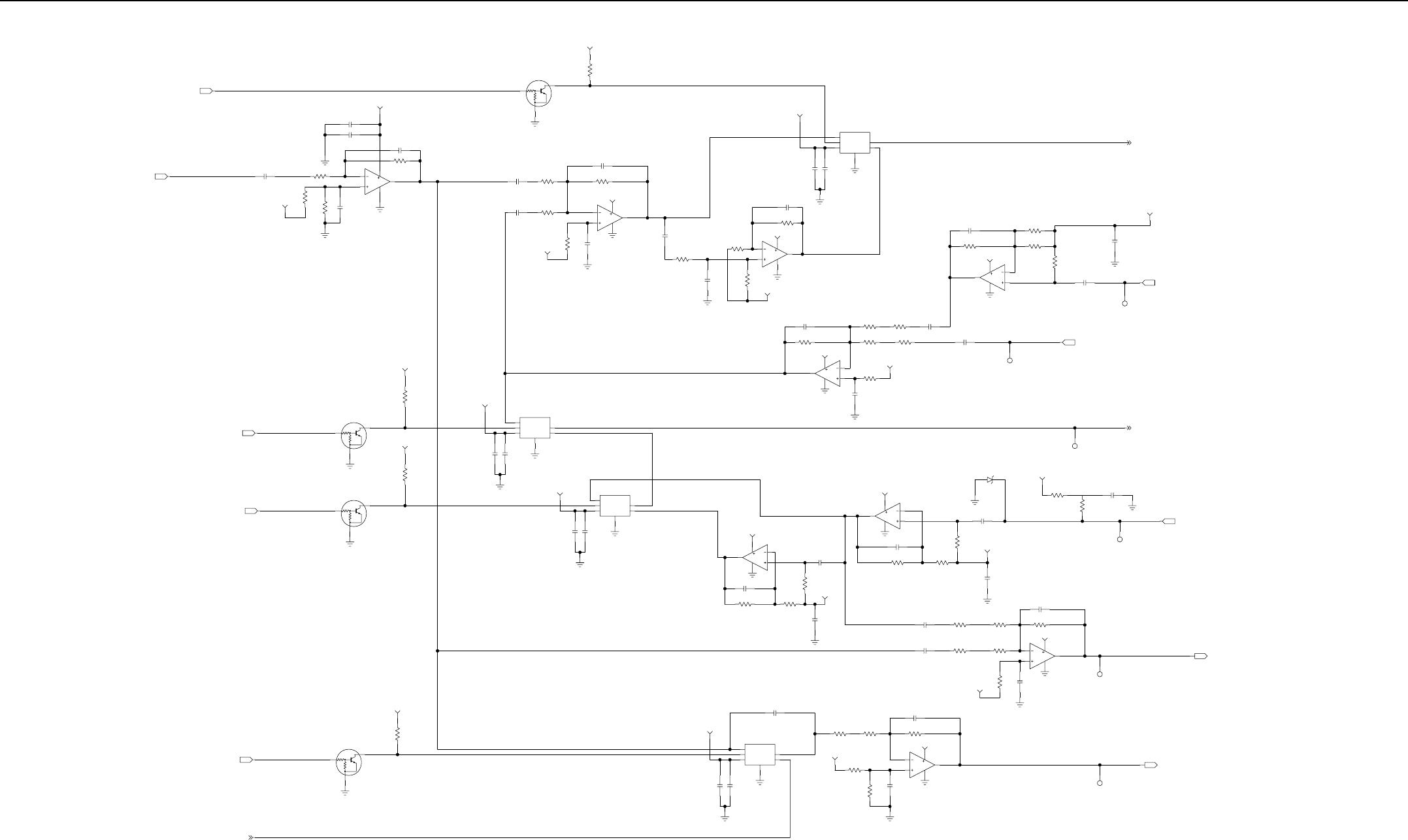
4-42 Controller Schematics (UHF)
ANALOG_MUX2
IN
NOTE 3
60% RSD
74MVRMS
MAKO
C2637M2
22UF
MAKO_CODEC_AUDIO_P
IN
U2604M2
R2892M2
R2845M2
R2844M2
R2843M2
C2638M2
C2602M2
C2601M2
C2600M2
25V
.01UF
.01UF
0.1UF
47PF
22.1K
33.2K
14K DNP
100K
TL3474A
2
3
1
411
2_5V
9_3V
60% RSD
221MVRMS
R2851M2
R2850M2
R2849M2
C2609M2
C2606M2
C2605M2
22UF
16V
22UF
16V
.01UF
25V
10K
10K
10K
2_5V
R2853M2
11.5K
411
9_3V
SUM
U2604M2
C2610M2
50V
470PF
TL3474A
6
5
7
60% RSD
254MVRMS
R2854M2
C2642M2
C2639M2
.15UF
1UF
10K
IN
V_POS NC
NO
COM
GND
U2800M2
U2608M2
R2894M2
R2893M2
R2857M2
C2620M2
C2617M2
C2615M2
47PF
0.1UF .01UF
100K
11.5K
12.4K
TS5A3159
2
6
1
5
TL3474A
9
10
8
411
2_5V
5VA
9_3V
SPKR_DE-EMPHASIS
10K
47K
R2852M2
Q2603M2
DTC114YKAF
2
3
1
10K
5VA
254MVRMS
60% RSD
4
3
SPKR_AUDIO_SW_OUT
2_5V
C2636M2
25V
.01UF
U2603M2
MC3320
13
14
4
11
9_3V
TX_AUDIO_PRE
R2883M2
R2881M2
R2880M2
R2876M2
C2629M2
47PF
105K
DNP
16.2K
DNP
14.3K
16.2K
60% RSD
80MVRMS
NOTE 1
TP2605M2
C2634M2
22UF
16V
1
TX_AUDIO_PRE
IN
TX_AUDIO
NOTE 1
80MVRMS
60% RSD
TP2600M2 1
TX_AUDIO IN
2113945A14
REPLACE C2627 WITH
4700PF 5%
TX_AUDIO
SUM
U2603M2
R2870M2
R2869M2
R2865M2
R2864M2
R2863M2
R2859M2 C2628M2
C2627M2
C2621M2
C2616M2
47PF
.01UF
25V
5%
560PF
22UF
16V
100K
0
34K
100K
6.81K
1.74K
MC3320
2
3
1
4
11
2_5V
9_3V
12
221MVRMS
60% RSD TX_AUDIO_BUF_OUT
IN
V_POS NC
NO
COM
GND
U2602M2
C2604M2
C2603M2
0.1UF .01UF
TS5A3159
4
2
6
3
1
5
5VA
IN
V_POS NC
NO
COM
GND
U2607M2
C2608M2
C2607M2
0.1UF .01UF
TS5A3159
4
2
6
3
1
5
5VA
ANALOG_MUX3
ANALOG_MUX0
IN
IN 10K
47K
10K
47K
R2848M2
R2847M2
Q2601M2
Q2600M2
DTC114YKAF
23
1
DTC114YKAF
23
1
10K
10K
5VA
5VA
PRE-EMPHASIS
221MVRMS
60% RSD
MIC
U2603M2
R2860M2
R2858M2
R2856M2
C2619M2
C2618M2
C2613M2
47PF
25V
.01UF
5%
3300PF
105K 47.5K
16.2K
MC3320 9
10
8
4
11
2_5V
9_3V
U2800M2
TL3474A
7
4
MIC_AUDIO_BUF_OUT
9_3V
6
5
11
VR2601M2
C2630M2
16V
.1UF
MMSZ5248BT1G
18V
12
NOTE 2
60% RSD
56MVRMS
TP2604M2
TP2601M2
R2885M2
R2884M2
C2635M2
16V
10UF
2.21K
604
1
1
MIC_AUDIO
9_3V
TXAUD_MIC
IN
FP_MIC_IN
R2873M2
R2872M2
C2631M2
25V
.01UF
34K
34K 2_5V
330MVRMS INTO 50K OHMS
60% RSD
RX_AUDIO
NOTE 1
U2604M2
TP2602M2 1
TL3474A
11
RX_AUDIO OUT
R2882M2
C2633M2
C2632M2
.01UF
25V
47PF
100K
9
10
8
4
9_3V
IN
V_POS NC
NO
COM
GND
U2605M2
C2614M2
C2612M2
C2611M2
DNP
0.1UF DNP
.01UF
22UF
16V
DNP
TS5A3159
4
2
6
3
1
5
5VA
U2604M2
R2867M2
R2866M2
R2862M2
R2861M2
C2622M2
25V
.01UF
5.11K
100K
61.9K
DNP
10K
TL3474A
13
12
411
2_5V
9_3V
AUX_RX_AUDIO
60% RSD
330MVRMS INTO 50K OHMS
R2879M2
R2878M2
R2877M2
R2875M2
R2874M2
R2871M2
C2626M2
C2625M2
C2624M2
47PF
.1UF
16V
22UF
100K
5.11K
5.11K
61.9K
61.9K
100K
14
2_5V
R2868M2
C2623M2
47PF
100K
TP2603M2 1
AUX_RX_AUDIO
OUT NOTE 1
221MVRMS
60% RSD
10K
47K
R2846M2
Q2602M2
DNP
DTC114YKAF
2
3
1
DNP
10K
ANALOG_MUX1
5VA
IN
WB_CODEC_RX
NOTE 1 : Backplane Circuitry Schematic Diagram (Kit No. CLN8502)
NOTE 2 : Front Panel Schematic Diagram (Kit No. CLN8502)
NOTE 3 : MAKO Schematic Diagram (Kit No. CLN8502)
Controller – Analog 1 Schematic Diagram (Kit No. CLN8502)
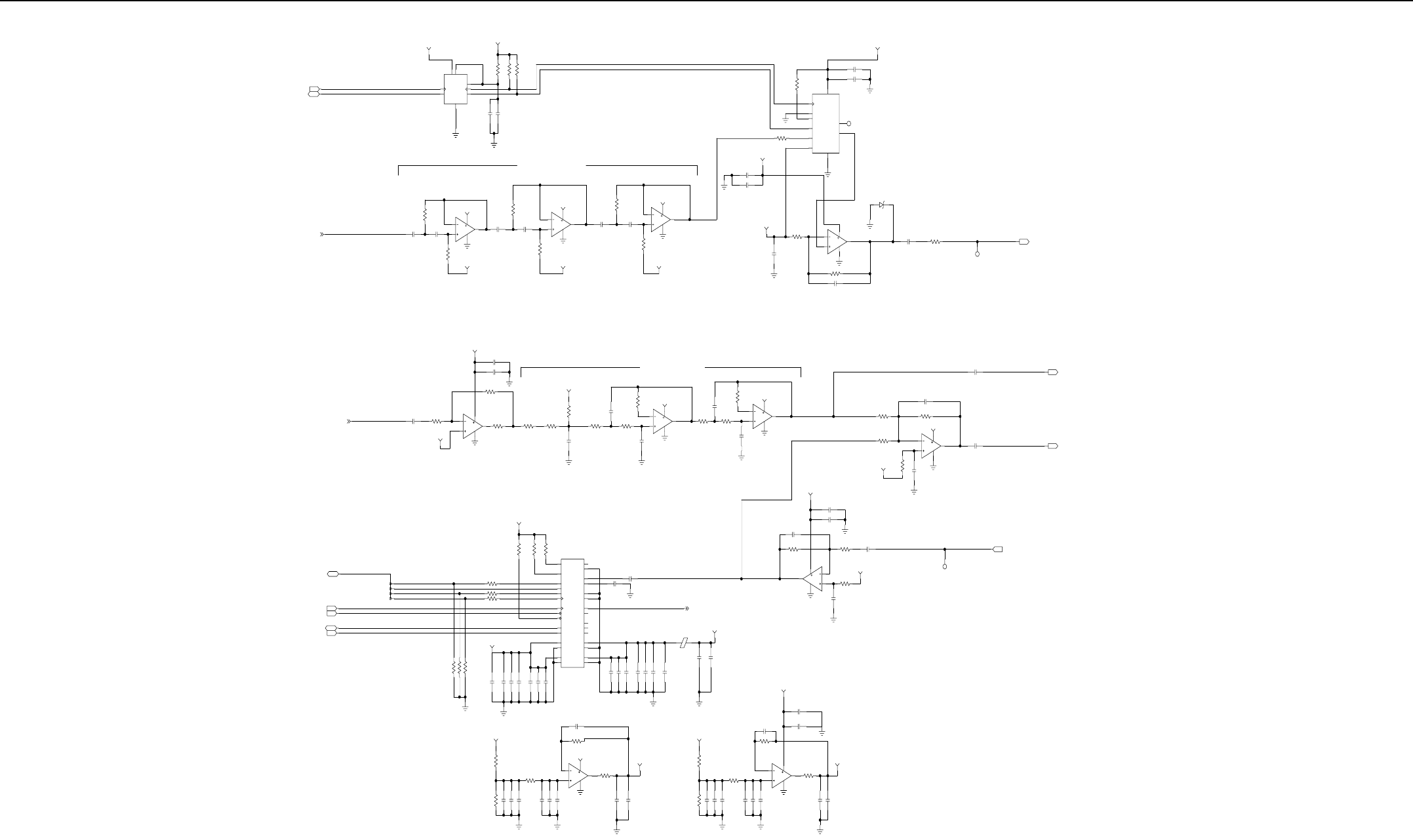
Controller Schematics (UHF) 4-43
1
I2C_TXOMAP_SCL
I2C_TXOMAP_SDA
IN
IO
SCL2
EN
GND VREF2
VREF1
SDA1
SCL1 SDA2
U2600M2
PCA9306
8
36
45
2
7
1_875V
R2813M2
R2812M2
R2810M2
C2805M2
C2801M2
0.1UF .01UF
200K
2.21K
2.21K
5VA
HIGH PASS FILTER
U2803M2
R2887M2
R2886M2
C2859M2
C2858M2
.15UF
.033UF
1.69K
5.36K
TL3474A
2
3
411
9_3V
2_5V
U2803M2
R2889M2
R2888M2
C2861M2
C2860M2
.15UF
.022UF
1.3K
38.3K
1
TL3474A
6
5
7
11
9_3V
2_5V
U2803M2
R2891M2
R2890M2
C2891M2
C2890M2
.068UF
.015UF
1K
287K
4
TL3474A
9
10
8
411
9_3V
2_5V
254MVRMS
60% RSD
SPKR_AUDIO_SW_OUT
255~50060
RWA (OHM)
NC
SDO_NC
W
VDD
DIS
AD0_CS*
GND
B
SDI_SDA
A
CLK_SCL U2601M2
R2834M2
C2893M2
C2851M2 0.1UF
.01UF
10K
AD5161
1
3
2
6
8
7
5
4
9
10
5VA
R2833M2
C2843M2
C2842M2
.01UF
0.1UF
0
9_3V
SPKR GAIN CONTROLLED
NOTE 2
SPKR_AUD
0~500MVRMS
60% RSD
BY SOFTWARE
VR2600M2
U2803M2
TP2801M2
R2855M2
R2838M2
R2832M2
C2854M2
C2853M2
C2844M2
.01UF
25V
470PF
1UF
10K
10K
22.1
1
TL3474A
13
12
14
4
11
MMSZ5248BT1G
18V
12
SPEAKER_AUDIO
2_5V
OUT
SPLATTER FILTER
LIMITER
221MVRMS
60% RSD
U2802M2
U2800M2
U2603M2
R2830M2
R2828M2
R2827M2
R2824M2
R2823M2
R2822M2
R2820M2
R2819M2
R2815M2
R2811M2
R2804M2
R2800M2
C2838M2
C2835M2
C2828M2
C2820M2
C2818M2
C2804M2
C2803M2
C2800M2
22UF
.01UF
0.1UF
.068UF
.015UF
3300PF
.047UF
4700PF
10K
100K
10
3.74K 34K
1.47K
6.81K
6.81K
26.7K
3.32K 3.32K
6.81K
MC3320
6
57
411
TL3474A
2
3
1
411
TL3474A
9
10
8
411
9_3V
4_65V
4_65V
9_3V
TXAUD_MIC
TXDATA_PL_DPL_BUF_OUT
9_3V
9_3V
NOTE 3
80MVRMS VOICE
60% RSD
C2856M2
1UF TXAUD_MIC_FLTR OUT
80MVRMS VOICE
60% RSD
16MVRMS DATA
NOTE 3
C2857M2
1UF TXAUD_MIC_TDATA OUT
MAKO_SUM
U2802M2
R2842M2
R2841M2
R2840M2
R2839M2
C2894M2
C2855M2
25V
.01UF
470PF
10K
49.9K
4.75K
10K
TL3474A
13
12
14
4
11
9_3V
4_65V
80MVRMS
60% RSD
NOTE 1
TP2800M2 1
TXDATA_PL_DPL
IN
R2837M2
R2836M2
C2852M2
C2850M2
C2641M2
C2640M2 .01UF
0.1UF
25V
.01UF
16V
22UF
47.5K
47.5K
4_65V
U2800M2
R2835M2
C2848M2
100PF
47.5K
TL3474A
13
12
14
4
11
TXDATA_PL_DPL
SOURCE
C2846M2
C2845M2
.01UF
0.1UF
9_3V
4_65V
U2802M2
R2896M2
R2831M2
C2892M2
C2849M2
C2847M2
.047UF
10V 16V
10UF
470PF
10K
0
TL3474A
6
5
7
411
R2829M2
R2826M2
R2825M2
C2841M2
C2840M2
C2839M2
C2837M2
C2836M2
C2833M2 22UF
16V
16V
22UF
10V0.1UF
22UF 16V
22UF
16V
10V
.047UF
33.2K
33.2K
10K
9_3V
SOURCE
U2802M2
R2895M2
R2821M2
R2816M2
R2809M2
R2808M2
C2862M2
C2822M2
C2819M2
C2817M2
C2816M2
C2814M2
C2811M2
C2809M2
C2807M2 22UF 16V
22UF 16V
0.1UF 10V
22UF 16V
22UF 16V
10V.047UF
.047UF
10V
10UF
16V
470PF
105K
39.2K
10K
10K
0
TL3474A
2
3
1
411
9_3V
9_3V
2_5V
I2C_RXOMAP_SCL
CLK_FPGA_WBCODEC_12MHZ
FPGA_WBCODEC_BP_RESET_N
I2C_RXOMAP_SDA
SSI_CODEC_WB<3..0>
2
SSI_WBCODEC_DIN
3
1
0
SSI_WBCODEC_DOUT
SSI_WBCODEC_FS
SSI_WBCODEC_CLK
IN
IO
IN
IN
IO
R2807M2
R2806M2
R2805M2 0DNP
DNP
0
DNP
0
R2803M2
R2802M2
R2801M2 10K
10K
10K
1_875V
6
5
29
30
4
3
2
1
7
25
8
24
26
28
27
C2815M2
C2813M2
C2812M2
C2810M2
C2808M2
C2806M2
C2802M2 DNP
DNP
DNP
DNP
DNP
DNP
DNP
10UF
1UF
0.1UF
.01UF
1UF
0.1UF
.01UF
BIAS
MICIN
INP1
INM1
INP2
INM2
OUTP1
OUTM1
OUTP2
OUTMV
OUTP3
AVDD
AVSS
DRVDD
DRVSS
M_S
DOUT
SCLK
MCLK
RESET
PWRDN
SDA
DVDD
DVSS
IOVDD
IOVSS
FSD
FS
DIN
SCL
17
16
21
11
12
22
20
23
19
18
9
14
10
13
15
U2606M2
R2818M2
R2817M2
R2814M2
DNP
1K
DNP
1K
1K
DNP TLV320AIC12
1_875V
C2826M2
C2823M2
DNP0.1UF
10V
1UF
16V
DNP
DNP
WB_CODEC_RX
E2600M2
C2834M2
C2832M2
C2831M2
C2830M2
C2829M2
C2827M2
C2825M2
C2824M2
C2821M2 .01UF
0.1UF
1UF
.01UF
0.1UF
1UF
10UF
DNP
DNP
DNP
DNP
DNP
DNP
DNP
DNP
.01UF
0.1UF
DNP
DNP
3_3V
NOTE 1 : Backplane Circuitry Schematic Diagram (Kit No. CLN8502)
NOTE 2 : Front Panel Schematic Diagram (Kit No. CLN8502)
NOTE 3 : MAKO Schematic Diagram (Kit No. CLN8502)
Controller – Analog 2 Schematic Diagram (Kit No. CLN8502)
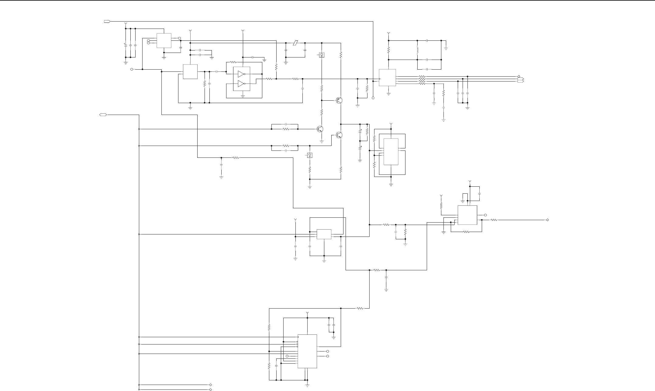
4-44 Controller Schematics (UHF)
3
OUTPUT
VREF
GND
NC2
NC1
VCONT
VCC
NC
NC
NC
DNI
DNI
DNI
DNI
DNI
TP2400M6
Y2401M6
C2432M6
C2400M6
C2401M6
C2433M6
15PF
150PF
0.1UF
330UF
12
16.8MHZ
OX2200013
7
5
6
4
3
12
TEST_POINT
1
12VA
2_775VA_PG
IN
Y2400M6
C2403M6
C2402M6 0.1UF
150PF
IVT5300B
16.8MHZ
2_775VA
VCONT
COMM_CASE
POS_VCC
OUT
R2400M6 C2434M6
C2404M6
.01UF
15PF
10K
2
4
1
DNI
TP2401M6
R2411M6
Q2400M6
C2418M6
R2416M6 1K
DNP
39PF
MMBT3906
32
100
TEST_POINT
1
DNI
U2400M6
R2409M6
R2403M6
C2412M6
C2406M6
R2406M6
475
0.1UF
56PF
DNP
0
0
NL27WZU04
A1
A2
VCC
GND
Y1
Y2
R2401M6
47.5K
1
3
25
6
4
R2413M6
E2400M6
D2401M6
C2413M6
C2408M6
.01UF 0.1UF MMBD6050LT1
2
31
150
Y0
Y1
Y2
Y3
GND
OE
CLKIN
VDD3_3V
U2402M6
CDCV304PWRG4
1
2
3
5
7
8
U2405M6
R2412M6
1
1K
MMBT3904
1
32
1
32
R2407M6
C2409M6 39PF
DNP
39.2K
R2410M6
R2408M6
D2400M6
C2410M6
DNP
39PF
MMBD6050LT1
2
31
3.92K
1.21K
IN2POS
IN2NEG
VCC_NEG
IN1NEG
IN1POS
VCC_POS
OUT1
OUT2
U2407M6
TS272
1
7
3_3VA
STA_REF_GAURD_BAND
U2406M6
R2419M6 R2418M6
R2417M6
R2414M6
C2420M6
C2419M6
.1UF
12
2.2UF
1
2
562
20K
10K10K
MMBT3904
2
3
6
5
48
3_3VA
FPGA_STA_PH_DET_UP
FPGA_STA_PH_DET_DN
1
0
STA_FPGA_<0..7>
IO
R2402M6
C2405M6
.022UF
1.74K
FPGA_STA_REF_SRC_SEL
3
FPGA_STA_DAC_CS_N
CLK_STA_FPGA_16_8MHZ
4FPGA_STA_DAC_DATA
STA_FPGA_COMP_IN
FPGA_STA_DAC_CLK
2
7
5
6
U2401M6
C2416M6
C2415M6
0.1UF
4.7UF
MAX5123
3_3VA
PDL
CS
VDD
DOUT
DIN
REFADJ
REF
AGND
DGND
OUT
SCLK
RSTVAL
FB
PD
UPO
CLR
NC
NC
NC
13
5
6
9
7
10
1
2
12
4
14
15
3
8
11
16
R2405M6
C2407M6 .033UF
10K
R2404M6
10K
IN
V_POS NC
NO
COM
GND
U2403M6
C2417M6
C2414M6
C2411M6
0.1UF 0.1UF 0.1UF
TS5A3159
4
2
6
3
1
5
2_775VA
R2420M6
C2421M6
82PF
10K
R2415M6
0
R2423M6
R2421M6
C2422M6
82PF
10K
1MEG
NC
POS_IN_A
OUT_B
NEG_IN_A OUT_A
NEG_IN_B
POS_IN_B
V_POS
V_NEG
U2404M6
R2431M6
R2430M6
R2428M6
C2431M6
0.1UF
10K
1MEG
33.2
LMV762
2
6
1
7
3
5
4
8
3_3VA
3_3VA
STA_FPGA_COMP_IN
R2427M6
R2426M6
R2425M6
R2424M6 49.9
49.9
49.9
49.9
R2422M6 L2400M6
C2425M6
C2424M6
C2423M6
0.1UF
0.1UF
100PF
1.5UH
0
DNP
3_3VA
46
R2429M6
C2430M6
C2429M6
C2428M6
C2427M6
C2426M6 10PF
DNP
0.1UF
DNP100PF
100PF DNP
DNP
100PF
DNP1K
CLK_RX_16_8_MHZ
CLK_EX_16_8MHZ
CLK_STA_FPGA_16_8MHZ
OUT
OUT
Controller – Station Reference Schematic Diagram (Kit No. CLN8502)
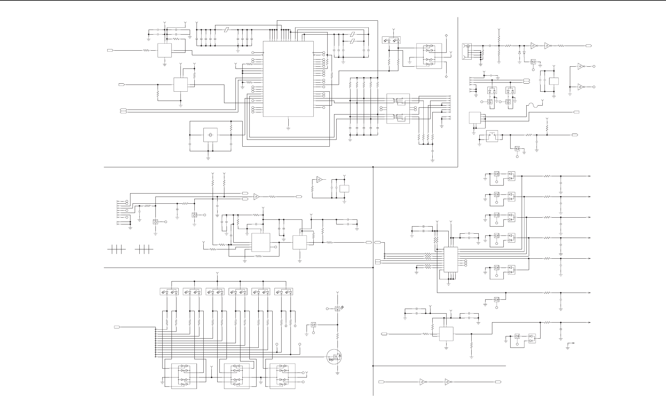
Controller Schematics (UHF) 4-45
=
5V
NC
NC
NC
R3053M7
E3041M7
C3056M7
C3052M7
C3051M7
C3049M7 .1UF
.1UF
.1UF
.1UF
12.4K
32
8
36
34
24
42
44
5
6
38
40
49
13
33
39
47
43
11
12
16
20
18
3_3V
SMSC_VDD33A
B
DIR
VCCA
VCCB
GND
A
U3020M7 R3015M7
R3000M7
C3040M7
C3037M7
C3035M7
C3032M7
C3030M7
C3024M7
C3023M7
C3017M7
C3016M7
.01UF
0.1UF
.01UF
0.1UF
.1UF
.1UF
.1UF
.1UF
.1UF
33.2
10K
SN74LVC1T45
34
5
2
1
6
3_3V
3_3V 1_875V
SMSC_RESET_N
IN
B
DIR
VCCA
VCCB
GND
U3025M7 R3021M7
R3001M7
10K
10K
SN74LVC1T45
34
5
2
1
6
1_875V
USB2_MAKO_DP
SMSC_VBUS_DET
USB2_MAKO_DM
ETHERNET_ENABLE
3_3V
IN
IO
IO
A
FPGA_ENET_RX_RESET_N
NC
NC
NC
NC
NC
NC
NC
R3054M7 12K
IN
GND1
GND
OUT
Y3038M7
25MHZ
NX5032SA
2
4
3
1
SMSC_XO
R3044M7
C3045M7
C3027M7
30PF 30PF
1MEG
SMSC_XI
COL_GPIO0
MDC_GPIO2
MDIO_GPIO1
CRS_GPIO3
TXD0_GPIO4_EEP_DISABLE
TXD1_GPIO5_RMT_WKP
TXD2_GPIO6_PORT_SWAP
TXD3_GPIO7_EEP_SIZE
TDO_NPHY_RST
NSPD_LED_GPIO10
NFDX_LED_GPIO8
NLNKA_LED_GPIO9
XO
EECS
NC
TXP
TXN
EEDO_AUTOMDIX_EN
EECLK_PWR_SEL
PHY_SEL
NTRST_RXD0
TEST1
EXRES
TEST2
TEST3
VSS
USBDP
USBDM
USBRBIAS
RXDV
TXEN
RXER
RXN
RXP
XI
EEDI
VBUS_DET
TCK_RXD1
TMS_RXD2
TDI_RXD3
RXCLK
PHY_INT
VDD18CORE_1
VDD18CORE_2
VDD18USBPLL
VDD18PLL
VDD33IO_5
VDD33IO_3
VDD33IO_4
VDD33IO_2
VDD33IO_1
VDD33A_2
VDD33A_3
VDD33A_1
TXCLK
RESET
VDD33A_4
21
50
10
17
4
7
9
15
25
35
48
51
52
SMSC_VDD18USBPLL
SMSC_VDD18PLL
SMSC_VDD18CORE
U3005M7
LAN9500I
46
45
29
30
31
22
23
14
26
27
28
1
41
37
56
55
54
53
2
3
19
NC
NC
NC
NC
NC
NC
NC
NC
NC
NC
NC
NC
NC
NC
NC
IO2
VN
IO1
VP
IO3
IO4
D3006M7
NUP4301
1
3
4
6
25
3_3V
D3070_LED_3 D3070_LED_1
ENET ACTIVITY
D3108M7
QT1222
2
3_3V
R3109M7
R3107M7
1
3
DNP
332
150
R3075M7
R3074M7
E3091M7
E3090M7
C3101M7
C3098M7
C3085M7
C3082M7
C3077M7 .1UF
.1UF
1UF
.022UF
.1UF
10K
10K
SMSC_NLNKA_LED
R3104M7
R3102M7
R3099M7
R3092M7
R3088M7 10
49.9
49.9
49.9
49.9
ENET_RXP
ENET_TXN
ENET_RXN
ENET_TXP
NC
NC
2
7
12
13
8
6
3
1
C3105M7
C3103M7
C3100M7
C3093M7
C3089M7 .022UF
15PF
15PF
15PF
15PF
R3115M7
R3112M7
R3111M7
R3110M7
C3116M7
1000PF
75
75
75
75
J3006M7
J3006M7
J3006M7
J3006M7
J3006M7
J3006M7
J3006M7
J3006M7
J3006M7
J3006M7
ENET
1
2
3
4
5
6
7
8
G1
G2
ENET_RXN_FP
ENET_RXP_FP
ENET_TXP_FP
ENET_TXN_FP
GND1
NC1
NC3
CT1
CT2
TD_NEG
RD_POS
RD_NEG
NC4
NC2
TD_POS
RX_NEG
GND2
RX_POS
TX_POS
TX_NEG
T3106M7
HX1188
NC
NC
15
10
4
5
9
11
14
16
BNC
J3008M7
CONN_J
C
G1
G2
G3
G4
SPEAKER
RESET
B2A2
NC
NC
NC NC
S2
S1
GND1
GND2
S3
S4
VCC
GND
NC
NC
DNI
VR3150M7
VR3142M7
VR3006M7
VR3000M7
U3000M7
U3000M7
U3000M7
U3000M7
U3000M7
R3160M7
R3158M7
R3157M7
R3153M7
R3134M7
R3003M7
R3002M7
J3010M7
F3000M7
D3013M7
D3012M7
C3159M7
C3156M7
C3154M7
C3141M7
S3011M7
SWITCH
1
2
3
4
.01UF
.01UF
1000PF
0.1UF
1
2
BAS52 BAS52
CONN_J
G1
G2
1
2
3
4
100
0
51
22.1
11.5K
11.5K
10K
MC74LVX14
12
MC74LVX14
34
MC74LVX14
56
MC74LVX14
13 12
MC74LVX14
714
MMBZ5231BLT1G
5.1V
2
1
MMBZ5231BLT1G
5.1V
2
3
1
MMBZ5231BLT1G
5.1V
2
31
5.1V
MMBZ5231BLT1G
2
31
3_3V
14_2V
3_3V
3_3V
SPEAKER_AUDIO
14V_SPKR
FP_FPGA_RST_N
5MHZ_BNC_IN OUT
OUT
IN
USB
J3009M7
J3009M7
J3009M7
J3009M7
J3009M7
J3009M7
D3007M7D3005M7
C3001M7
1000PF
BAV99LT1G
1
3
2
BAV99LT1G
3
16V
1.1A
1
2
3
4
G1
G2
3
VBUS1
USB1_MAKO_DM
USB1_MAKO_DP IO
IO
TEST_PORT
3
4
5
6
7
8
9
10
2
22
R3126M7
R3125M7
R3124M7
R3123M7
R3122M7
R3121M7
R3120M7
C3118M7
C3117M7 .01UF
0.1UF
0
0
0
10K
10K
10K
10K
1_875V
RXOMAP_SYNC_OUT
SSI_ABACUS_FS
2
0
1
SSI_ABACUS_CLK
SSI_ABACUS<2..0>
SSI_ABACUS_RX
TXOMAP_SYNC_TRIG_OUT
IN
IN
IO
VCCB2
VCCB1
VCCA
GND4
GND3
GND2
GND1
B8
B7
B6
B5
B3
A8
A7
A6
A5
A4
A3
A1
DIR B2
B1
A2 B4
OE
U3007M7
SN74LVC8T245
21
20
19
18
17
16
15
14
1
23
24
NC
NC
NC
11
12
13
G1
C3130M7
C3129M7.01UF
0.1UF
NC
NC
NC
NC
VR3138M7
VR3137M7
VR3136M7
VR3135M7
D3147M7
D3146M7
D3145M7
D3144M7
BAV99LT1G
1
3
2
BAV99LT1G
1
3
2
BAV99LT1G
1
3
2
BAV99LT1G
1
3
2
5.1V
MMBZ5231BLT1G
2
31
5.1V
MMBZ5231BLT1G
2
31
5.1V
MMBZ5231BLT1G
2
31
MMBZ5231BLT1G
5.1V
2
31
P3013M7
P3013M7
P3013M7
P3013M7
P3013M7
P3013M7
P3013M7
C3174M7
C3173M7
C3172M7
C3171M7
C3170M7
C3169M7
C3168M7
DNP
1000PF
1000PF
DNP
DNP
1000PF
1000PF
DNP
DNP
1000PF
1000PF
DNP
DNP
1000PF
SSI_ABACUS_CLK_FP
TXOMAP_SYNC_TRIG_OUT_FP
SSI_ABACUS_RX_FP
RXOMAP_SYNC_OUT_FP
SSI_ABACUS_FS_FP
BUF_EN_N
RXOMAP_SYNC_IN_FP
1
2
3
4
5
6
7
R3167M7
R3166M7
R3165M7
R3164M7
R3163M7
R3162M7
R3161M7
49.9
49.9
49.9
49.9
49.9
49.9
49.9
P3013M7
8
NC
VR3151M7
D3155M7
BAV99LT1G
1
2
MMBZ5231BLT1G
5.1V
2
31
RXOMAP_SYNC_IN_FP_FLT
3
NC
VR3140M7
5.1V
MMBZ5231BLT1G
2
3
1
NC
VR3139M7
D3148M7
BAV99LT1G
1
3
2
5.1V
MMBZ5231BLT1G
2
31
RXOMAP_SYNC_IN
OUT B
DIR
VCCA
VCCB
GND
A
U3127M7
R3133M7
R3128M7
R3119M7
C3132M7
C3131M7
C3114M7
C3113M7
.01UF
0.1UF
.01UF
0.1UF
33.2
10K
10K
SN74LVC1T45
34
5
2
1
6
1_875V
5V
U3000M7 U3000M7
MC74LVX14
98
MC74LVX14
11 10 BUFFERED_1_4V_ROMAP_PG
1_4V_ROMAP_PG_INVERTED
1_4V_ROMAP_PG OUT
IN
MICROPHONE
J3000M7
J3000M7
J3000M7
J3000M7
J3000M7
J3000M7
J3000M7
J3000M7
J3000M7
J3000M7 1
2
3
4
5
6
7
8
9
10
NC
NC
NC
NC
NC
VR3033M7
R3031M7
C3029M7
1000PF
475
MMBZ5231BLT1G
5.1V
2
3
1
MIC_PTT_FLT
NC
VR3019M7
MMBZ5231BLT1G
5.1V
2
3
R3018M7
C3014M7
1000PF
475
1
MIC GEOM DOES NOT
SEE DECODE TABLE BELOW
FOLLOW VENDOR PIN OUT
SCHEMATIC
1
VENDOR SPEC
5
44
3
2183
57876
26
POS_IN_A
OUT_B
NEG_IN_AOUT_A
NEG_IN_B
POS_IN_B
V_POS
V_NEG
NC
U3064M7
R3062M7
C3069M7
C3067M7 0.1UF
.01UF
365K
LMV762
2
6
1
7
3
5
R3060M7
R3057M7
R3047M7
R3042M7
C3061M7
C3050M7
C3046M7
C3000M7
0.1UF
0.1UF
.01UF
0.1UF
10K
10K
54.9K
10K
4
8
5V
5V
MIC_BUTTON_COMP_REF
C3002M7
1000PF
MIC_AUDIO
MIC_BUTTON OUT
OUT
R3066M7
R3059M7
4.75K 20K
5V 5V
U3087M7 R3080M7
33.2
NC7WZ17
34 MIC_PTT_N OUT
VCC
GND
U3087M7
U3087M7
R3004M7
C3084M7
C3083M7 .01UF
0.1UF
10K
NC7WZ17
16
NC7WZ17
25
1_875V
B
DIR
VCCA
VCCB
GND
A
U3073M7
R3086M7
R3081M7
R3071M7
C3097M7
C3096M7
.01UF
0.1UF
10K
10K
0
SN74LVC1T45
34
5
2
1
6
MIC_BUTTON_INT_N
1_875V
OUT
LED'S
FP_LED<0..12>
IN
8
12
9
11
6
3
1
2
0
7
5
10
4
1
3
1
3
1
3
1
3
1
3
1
3
IO2
VN
IO1
VP
IO3
IO4
D3009M7
NUP4301
1
3
4
6
25
3_3V
IO2
VN
IO1
VP
IO3
IO4
D3010M7
NUP4301
1
3
4
6
25
IO2
VN
IO1
VP
IO3
IO4
NC
NC
D3011M7
NUP4301
4
6
5
3_3V
1
3
2
POWER/STATUS TX STATUS 1
D3002M7D3001M7D3000M7
QT1222
2
QT1222
2
QT1222
2
RX STATUS 1 RX STATUS 2
TX STATUS 2 EXT_REF
D3070M7
D3004M7D3003M7
QT1222
2
QT1222
2
QT1222
2
3_3V
MODE
NC
NC
VR3007M7
TP3001M7
TP3000M7
R3079M7
R3072M7
R3068M7
R3065M7
R3063M7
R3058M7
R3055M7
R3048M7
R3043M7
R3039M7
R3034M7
R3028M7
R3026M7
Q3076M7
D3078M7
QSMR
21
3
2SK3541
3
1
2
332
150
332
150
332
150
332
150
332
150
332
150
332
TEST_POINT
1
TEST_POINT
1
DNP
MMBZ5231BLT1G
5.1V
2
31
5V
D3070_LED_1
D3070_LED_3
57
Controller – Front Panel Schematic Diagram (Kit No. CLN8502)
4-46 Controller Schematics (UHF)
2
ADJ
VIN
VOUT2
VOUT1
U3831M4
TP3829M4
R3832M4
R3830M4
C3834M4
C3828M4
10UF
35V
12
10UF
2.21K
1.21K
1
TLV1117
1
32
4
14_2V
TP3836M4
R3833M4
C3835M4
22UF
12
121
TEST_POINT
1
9_3V
GND1
GND2
ON_OFF
VIN
ADJ
VOUT
DNI
DNI
DNI
DNI
DNI
DNI
DNI
DNI
DNI
DNI
TP3899M4
R3887M4
Q3886M4
U3893M4
D3892M4
E3888M4
C3898M4
C3889M4
C3890M4
C3897M4
R3895M4
R3896M4
R3894M4
10.2K
1.5K
11K .1UF
.1UF
2.2UF
22UF
12
MBRM140T3
LM2941
1
3
6
2
45
DTC114YKAF
DNP
1K
DNP
TEST_POINT
1
14_2V
3_3VA
12VA
10K
47K
2
3
1
3_3V_PG
ADJ
VIN
VOUT2
VOUT1
U3838M4
TP3843M4
R3840M4
R3839M4
C3842M4
C3841M4
C3837M4
10UF
35V
12
10UF 22UF
12
1K
332
TEST_POINT
1
TLV1117
1
32
4
14_2V 5VA
DNI
R3891M4
0
RESET
GND
CT
SENSE
VDD
MR
U3809M4
TP3863M4
R3806M4
R3805M4
R3804M4
R3803M4
C3911M4
C3910M4
C3862M4
C3808M4
C3807M4
C3802M4
1000PF
.01UF
0.1UF
10UF
.015UF
100UF
1
2
43.2K
4.75K
68.1K
DNP
10K
1
TPS3808
4
3
15
6
5V
5V
TP3810M4 1
2
H7
G7
H5
F7
G6
G1
G2
G3
H1
H2
H3
VOUT1
VOUT2
VOUT3
VOUT8
VOUT4
VOUT5
VOUT6
VOUT7
VOUT9
VOUT11
VOUT10
VOUT12
PGOOD
AUX
BIAS
GND24
GND23
GND22
GND21
GND20
GND19
GND18
GND17
GND16
GND14
GND15
VIN1
VIN2
VIN5
VIN6
SHARE
GND13
GND12
GND11
GND10
GND9
GND8
GND7
GND6
GND4
GND5
GND3
RUN_SS
SYNC
RT
ADJ
GND2
GND1
VIN4
VIN3
U3874M4
LTM8023
A5
D1
D2
D3
D4
D5
D6
D7
E1
E2
E3
A6
E4
E5
E6
E7
F6
A7
B5
B6
B7
C5
C6
C7
NC
R3871M4 R3870M4
R3869M4
R3865M4
C3866M4 .47UF
39.2K
68.1K
357K
6.81K
F5
G5
H6
A1
C2
C3
C4
A2
A3
A4
B1
B2
B3
B4
C1
OUT
TP3878M4
R3876M4
C3877M4
100UF
6.3V
1
2
4.75K
TEST_POINT
1
1_875V
BSW_PG
NC
OUT1
OUT2
IN2
PG
BIAS
EN
FB
SS
CTGND
GND
IN1
U3906M4
R3905M4
R3904M44.53K
20K
TPS74701
4
11
5
8
6
1
2
9
10
3
7
R3902M4
C3903M4
C3901M4
10UF
470PF
1.5K
IN
R3900M4
10K
3_3V_PG
2_775VA_PG
5V
3_3VA
OUT
TP3908M4
C3907M4
10UF
TEST_POINT
1
2_775VA
4
5
8
1
2
3
7
OUT
IN
OUT1
OUT2
IN2
PG
BIAS
EN
FB
SS
CTGND
GND
IN1
U3801M4
TP3875M4
R3872M4
R3867M4
R3861M4
C3873M4
C3868M4
C3864M4
10UF
680PF
10UF
10K
1.1K
3.48K
TEST_POINT
1
TPS74801
9
10
3_3V_PG
BSW_PG
5V
3_3V
3_3V
11
6
OUT1
OUT2
IN2
PG
BIAS
EN
FB
SS
CTGND
GND
IN1
U3883M4
R3882M4
3.48K
TPS74701
4
5
8
1
2
3
7
5V
NC
R3880M4
C3881M4
470PF
1.1K
11
6
9
10
C3879M4
10UF
C3884M4
10UF
TP3885M4
TEST_POINT
1
3_3VA
IN BSW_PG
OUT
IN
R3909M4
10K
1_2V_PG
3_3V_PG
3_3V 5V
COUT IS PLACED ON FPGA PWR SYMBOL. SHEET 8.
REF DES: C2208
OUT1
OUT2
IN2
PG
BIAS
EN
FB
SS
CTGND
GND
IN1
U3826M4
TP3827M4
R3825M4
R3823M4 C3824M4
C3822M4
10UF
470PF
4.75K
2.37K
TEST_POINT
1
TPS74701
4
11
5
8
6
1
2
9
10
3
7
1_2V_FPGA_CORE
IN
OUT1
OUT2
IN2
PG
BIAS
EN
FB
SS
CTGND
GND
IN1
U3850M4
TP3852M4
R3849M4
R3847M4
R3844M4
C3851M4
C3848M4
C3846M4
C3845M4
10UF
1UF
560PF
10UF
10K
4.75K
3.48K
TEST_POINT
1
TPS74701
4
11
5
8
6
1
2
9
10
3
7
1_2V_PG
3_3V
1_4V_ROMAP_PG
5V
1_4V_RXOMAP_CORE
1_875V
OUT
IN
OUT1
OUT2
IN2
PG
BIAS
EN
FB
SS
CTGND
GND
IN1
U3800M4
R3858M4
R3853M4
10K
3.48K
TPS74701
11
6
5V
1_2V_PG
3_3V
1_4V_TOMAP_PG
1_875V
OUT
R3856M4
C3857M4
C3855M4
C3854M410UF
1UF
560PF
4.75K
4
5
8
1
2
9
10
3
7
TP3860M4
C3859M4
10UF
TEST_POINT
1
1_4V_TXOMAP_CORE
RESET
GND
CT
SENSE
VDD
MR
U3819M4
TP3821M4
R3820M4
R3816M4
R3814M4
R3813M4
R3812M4
C3815M4C3811M4
1000PF DNP
.047UF
43.2K
4.75K
68.1K
10K 10K
TEST_POINT
1
TPS3808
4
3
15
6
3_3V
C3818M4
C3817M4 .01UF
0.1UF
5V
5V_MON
OUT
Controller – Power Schematic Diagram (Kit No. CLN8502)
Controller Schematics (UHF) 4-47
R4005M4
R4004M4
R4003M4
R4002M4 10K
10K
10K
10K
FPGA_TDI
FPGA_TCK
FPGA_TDO
3_3V
FPGA_TMS
IN
OUT
OUT
OUT
1
1
1
1TP4010M4
TP4008M4
TP4007M4
TP4006M4
R4009M4
DNP
0
ASSET PROGRAMMER
DNP R4000 WHEN USING
JTAG CONNECTOR
NC
NC
NC
NC
DNI
DNI
DNI
DNI
DNI
DNI
DNI
DNI
DNI
DNI
DNI
DNI
DNI
DNI
TP4014M4
R4013M4
P4000M4
P4000M4
P4000M4
P4000M4
P4000M4
P4000M4
P4000M4
P4000M4
P4000M4
P4000M4
P4000M4
P4000M4
P4000M4
P4000M4
1
2
3
4
5
6
7
8
9
10
11
12
13
14
DNP
1K
1
3_3V
TP4012M4
1
OMAP_TDO_OUT
R4011M4
10K
TP4015M4
R4023M4
R4019M4
C4017M4
C4016M4 0.1UF
.01UF
4.75K 4.75K
DNP
1
BSCAN_LVLSFT_EN
TAP_TRST_N
3_3V
VCCB
VCCA
GND3
GND2
GND1
B1_2
B1_1
B2_2
B2_1
A2_2
A2_1
A1_2
A1_1
DIR2
DIR1
OE2
OE1
R4024M4
4.75K
4
6
5
7
2
3
8
9
17
15
14
13
11
12
10
1
16
U4001M4
R4032M4
R4031M4
R4030M4
0
0
0
SN74AVC4T245
TCK
TMS
TRST_N
C4029M4
C4028M4 0.1UF
.01UF
1_875V
TXOMAP_TDI
RXOMAP_TDO
TXOMAP_TDO_RXOMAP_TDI
OMAP_TMS
0
OMAP_TRST_N
OMAP_TCK
7
5
2
3
8
6
9
4
1
C4027M4
C4026M4 0.1UF
.01UF
3_3V
1_875V
R4022M4
C4021M4
C4020M4 0.1UF
.01UF
4.75K
B
DIR
VCCA
VCCB
GND
A
U4025M4
R4018M4
0
SN74AVC1T45
C1
C2
B2
B1
A1
A2
BOUNDARY_SCAN(9..0)
IO
Controller – JTAG Schematic Diagram (Kit No. CLN8502)
4-48 Controller Schematics (UHF)
14_2V 8V
10V_RX
10V_EX
5V
P3200M3
P3200M3
P3200M3
P3200M3
P3200M3
P3200M3
P3200M3
P3200M3
P3200M3
P3200M3
P3200M3
P3200M3
P3200M3
P3200M3
P3200M3
P3200M3
P3200M3
P3200M3
P3200M3
P3200M3
P3200M3
P3200M3
P3200M3
P3200M3
P3200M3
P3200M3
P3200M3
P3200M3
P3200M3
P3200M3
P3200M3
P3200M3
P3200M3
P3200M3
P3200M3
P3200M3
P3200M3
P3200M3
P3200M3
P3200M3
P3200M3
P3200M3
P3200M3
P3200M3
P3200M3
P3200M3
P3200M3
P3200M3
P3200M3
P3200M3
P3200M3
P3200M3
P3200M3
P3200M3
P3200M3
P3200M3
P3200M3
P3200M3
P3200M3
P3200M3
P3200M3
P3200M3
P3200M3
P3200M3
P3200M3
P3200M3
P3200M3
P3200M3
P3200M3
P3200M3
P3200M3
P3200M3
P3200M3
P3200M3
P3200M3
P3200M3
P3200M3
P3200M3
P3200M3
P3200M3
P3200M3
P3200M3
P3200M3
P3200M3
P3200M3
P3200M3
P3200M3
P3200M3
P3200M3
P3200M3
P3200M3
P3200M3
P3200M3
P3200M3
P3200M3
P3200M3
P3200M3
P3200M3
NC
NC
NC
NC
NC
NC
NC
NC
NC
NC
NC
NC
NC
NC
NC
NC
NC
NC
NC
NC
NC
NC
NC
NC
NC
NC
B25
B26
B27
B28
B29
B30
B31
B32
C1
C2
C3
C4
C5
C6
C7
C8
C9
C10
C11
C12
C13
C14
C15
C16
C17
C18
C19
C20
C21
C22
C23
C24
C25
C26
C27
C28
C29
C30
C31
C32
G1
G2
A1
A2
A3
A4
A5
A6
A7
A8
A9
A10
A11
A12
A13
A14
A15
A16
A17
A18
A19
A20
A21
A22
A23
A24
A25
A26
A27
A28
A29
A30
A31
A32
B1
B2
B3
B4
B5
B6
B7
B8
B9
B10
B11
B12
B13
B14
B15
B16
B17
B18
B19
B20
B21
B22
B23
B24
BP_WIRELINE12_FSYNC
BP_WIRELINE1_LATCH_CS_N
BP_PA_ENABLE
BP_GPIO_8
BP_GPIO_7
BP_GPIO_10
BP_RF_RELAY_CTL
BP_EXT_PTT_N
BP_CARRIER_DETECT
BP_OPTION2_ID
BP_ANTENNA_RELAY
BP_AC_FAIL
BP_AUX_RX_AUDIO
BP_RSSI
BP_TX_DATA
BP_GPI_1
BP_GPIO_5
BP_PA_ADDR1
BP_OPTION1_ID
BP_WIRELINE_ID
BP_MISO
BP_RESET_N
BP_OP1_CS2_N
BP_MOSI
BP_OP2_CS2_N
BP_OPT_IRQ_N
BP_OP2_CS3_N
BP_OP1_CS3_N
BP_WIRELINE2_LATCH_CS_N
BP_GPIO_9
BP_WIRELINE34_FSYNC
BP_WIRELINE12_TXD
BP_PA_ADDR0
BP_OP2_CS1_N
BP_OP1_CS1_N
BP_GPI_4
BP_PTEMP+
BP_GPIO_6
BP_TX_AUDIO_PRE
BP_WIRELINE_MCLK
BP_WIRELINE12_RXD
BP_WIRELINE34_TXD
BP_SPI_CLK
BP_WIRELINE_BCLK
BP_WIRELINE34_RXD
BP_GPIO_2
BP_GPIO_3
BP_RX_AUDIO
BP_TX_AUDIO
R3233M3
0DNP
SECURE BACKPLANE I/F
R3239M3
R3238M3
R3237M3
C3234M3
C3233M3
C3232M3
1000PF
1000PF
1000PF
475
475
475
BP_OP2_CS1_N
BP_OP2_CS3_N
FPGA_BP_OP2_CS2_N BP_OP2_CS2_N
FPGA_BP_OP2_CS1_N
FPGA_BP_OP2_CS3_N
IN
IN
IN
PA BACKPLANE I/F
R3236M3
R3235M3
C3231M3
C3230M3
1000PF
1000PF
475
475
BP_PA_ADDR0
FPGA_BP_PA_ADDR0
FPGA_BP_PA_ADDR1 BP_PA_ADDR1
IN
IN
NC
VR3206M3
MMBZ5231BLT1G
5.1V
2
3 1
AUX_RX_AUDIO
IN
NC
VR3205M3
R3232M3
R3228M3
R3227M3
C3226M3
C3225M3
1000PF
1000PF
475
1K
604
MMBZ15VDLT1
1
2
3
BP_TX_DATA
TXDATA_PL_DPL
BP_AUX_RX_AUDIO
OUT
NC
VR3204M3
R3226M3
C3224M3
1000PF
1K
5.1V
MMBZ5231BLT1G
2
31
RX_AUDIO BP_RX_AUDIO
IN
LOCAL AUDIO
NC
NC
VR3208M3
VR3203M3
R3248M3
R3247M3
R3231M3
R3225M3
C3238M3
C3223M3
1000PF
1000PF
475
604
475
604
MMBZ15VDLT1
1
2
3
MMBZ15VDLT1
1
2
TX_AUDIO_PRE
TX_AUDIO
BP_TX_AUDIO_PRE
BP_TX_AUDIO
OUT
OUT
BACKPLANE SPI BUS
R3221M3
R3219M3
R3214M3
R3213M3
L3201M3
L3200M3
C3219M3
C3218M3
C3213M3
22PF
22PF
22PF
1UH
1UH
475
26.7
475
100K
FPGA_BP_SPI_CLK
BP_MOSI
BP_FPGA_MISO
FPGA_BP_MOSI
BP_SPI_CLK
BP_MISO
OUT
IN
IN
OTHER OPTIONS (MAKO)
NC
NC
VR3202M3
VR3201M3
R3223M3
R3222M3
R3218M3
R3217M3
C3221M3
C3220M3
C3215M3
C3214M3
1000PF
1000PF
1000PF
1000PF
475
475
475
475
MMBZ5231BLT1G
5.1V
2
31
5.1V
MMBZ5231BLT1G
2
31
BP_RSSI
BP_OPTION2_ID
BP_PTEMP+
BP_OPTION1_ID
MAKO_BP_RSSI
OPTION2_ID
PTEMP+
OPTION1_ID
IN
OUT
OUT
OUT
WIRELINE BACKPLANE
R3244M3
R3243M3
R3204M3
R3202M3
R3201M3
R3200M3
C3210M3
C3202M3
C3201M3
C3200M3
470PF
470PF
470PF
470PF
100
100
100
100
0
0
BP_WIRELINE1_LATCH_CS_N
BP_WIRELINE12_TXD
BP_WIRELINE12_RXD
BP_WIRELINE34_RXD
FPGA_BP_WIRELINE12_RXD
BP_WIRELINE2_LATCH_CS_N
BP_WIRELINE_MCLK
BP_WIRELINE_BCLK
BP_FPGA_WIRELINE34_TXD
FPGA_BP_WIRELINE12_FSYNC
BP_WIRELINE34_FSYNC
BP_WIRELINE_ID
BP_FPGA_WIRELINE12_TXD
BP_WIRELINE34_TXD
BP_WIRELINE12_FSYNC
OUT
IN
IN
OUT
R3210M3
R3209M3
R3208M3
R3207M3
R3206M3
R3205M3
R3203M3
C3209M3
C3208M3
C3207M3
C3206M3
C3205M3
C3204M3
C3203M3
470PF
470PF
470PF
470PF
1000PF
1000PF
1000PF
100
100
100
100
475
475
475
FPGA_BP_WIRELINE34_RXD
FPGA_BP_WIRELINE_BCLK
FPGA_BP_WL2_CS_N
FPGA_BP_WIRELINE34_FSYNC
WIRELINE_ID
FPGA_BP_WIRELINE_MCLK
FPGA_BP_WL1_CS_N
OUT
IN
IN
IN
IN
IN
IN
3
Controller – Backplane Circuitry Schematic Diagram (Kit No. CLN8502)
Controller Schematics (UHF) 4-49
2
PB_GPIO AND GPI
10K
47K
R3470M3
R3466M3
R3418M3
R3412M3
Q3409M3
Q3406M3
MMBT3904
1
3
2
DTC114YKAF
2
3
1
1K
475
47.5K
33.2K
FPGA_GPIO_(4)
OMAP_GPIO_7
IN
OUT
10K
47K
VR3402M3
R3469M3
R3465M3
R3450M3
R3411M3
R3407M3
R3403M3
R3402M3
Q3411M3
Q3403M3
D3403M3
C3402M3
1000PF
BAS52
MMBT3904
1
3
2
DTC114YKAF
2
3
1
1K
1K
10K
475 0
47.5K
33.2K
MMBZ20VALT1G
3
1
2
1_875V
OMAP_GPIO_3
5V
FPGA_GPIO_(3)
BP_GPIO_3
1_875V
OMAP_GPI_4
OUT
IN
IN
OUT
10K
47K
Q3410M3
DTC114YKAF
2
3
1
FPGA_GPIO_(2)
VR3400M3
R3468M3
R3467M3
R3464M3
R3463M3
R3454M3
R3448M3
R3420M3
R3417M3
R3414M3
R3408M3
R3404M3
R3400M3
Q3408M3
Q3400M3
D3401M3
D3400M3
C3408M3
C3400M3
1000PF
1000PF
BAS52
BAS52
MMBT3904
1
3
2
MMBT3904
1
32
1K
10K
475
1K
10K
475
0
0
47.5K
47.5K
33.2K
33.2K
MMBZ20VALT1G
3
1
2
BP_GPI_1
OMAP_GPI_1
5V
5V
OMAP_GPIO_6
BP_GPIO_6
1_875V
1_875V
OUT
OUT
VR3401M3
R3475M3
R3471M3
R3449M3
R3409M3
R3405M3
R3401M3
Q3401M3
D3405M3
C3401M3
1000PF
BAS52
MMBT3904
1
32
1K
10K
475 0
47.5K
33.2K
MMBZ20VALT1G
3
1
2
BP_GPIO_2
5V
1_875V
OMAP_GPIO_2
OUT
10K
47K
Q3404M3
DTC114YKAF
2
3
1
FPGA_GPIO_(0)
IN
R3452M3
R3419M3
R3416M3
D3406M3
C3406M3
1000PF
BAS52
10K
475
0BP_GPIO_5
5V
R3476M3
R3472M3
R3413M3
Q3407M3
MMBT3904
1
3
2
1K
47.5K
33.2K
1_875V
OMAP_GPIO_5
OUT
VR3403M3
R3477M3
R3473M3
R3451M3
R3410M3
R3406M3
R3224M3
Q3402M3
D3407M3
D3404M3
C3403M3
1000PF
BAS52
BAS52
MMBT3904
1
32
1K
10K
475 0
47.5K
33.2K
MMBZ20VALT1G
3
BP_GPI_4
1_875V
5V
5V
OMAP_GPIO_8
OUT
R3246M3
C3227M3
1000PF
0BP_GPIO_8
R3478M3
R3474M3
R3230M3
R3229M3
10K
475
47.5K
33.2K
Q3200M3
MMBT3904
1
32
10K
47K
Q3201M3
DTC114YKAF
2
3
1
FPGA_GPIO_(5)
IN
10K
47K
R3453M3
R3415M3
Q3405M3
D3402M3
C3407M3
1000PF
BAS52
DTC114YKAF
2
3
1
10K
0BP_GPIO_7
5V
FPGA_GPIO_(1)
1_875V
IN
1
2
10K
47K
R3480M3
R3479M3
R3457M3
R3430M3
R3428M3
R3424M3
Q3415M3
Q3413M3
D3408M3
C3413M3
1000PF
BAS52
MMBT3904
1
32
DTC114YKAF
2
3
1
1K
10K
475
0
47.5K
33.2K
FPGA_GPIO_(7)
OMAP_GPIO_10
BP_GPIO_10
5V
1_875V
IN
OUT
10K
47K
R3482M3
R3481M3
R3423M3
Q3414M3
Q3412M3
MMBT3904
1
3
2
DTC114YKAF
2
3
1
1K
47.5K
33.2K
1_875V
OMAP_GPIO_9
FPGA_GPIO_(6)
IN
OUT
VR3408M3
R3456M3
R3429M3
R3427M3
D3409M3
C3412M3
1000PF
BAS52
10K
475 0
MMBZ20VALT1G
3
1
2
BP_GPIO_9
5V
R3438M3
R3437M3
R3436M3
C3422M3
C3421M3
C3420M3
1000PF
1000PF
1000PF
475
475
475
BP_OP1_CS1_N
BP_OP1_CS2_N
FPGA_BP_OP1_CS1_N
FPGA_BP_OP1_CS3_N
FPGA_BP_OP1_CS2_N
BP_OP1_CS3_N
IN
IN
IN
VCC
GND
U3400M3
C3415M3
C3414M3.01UF
0.1UF NC7WZ17
25
1_875V
U3400M3
R3458M3
R3447M3
R3441M3
C3431M3
1000PF
47.5K
475 0
NC7WZ17
34 BP_OPT_IRQ_N
5V
R3431M3
33.2
OPT_IRQ_N
OUT
R3426M3
R3425M3
0
0
BP_GPIO_3
BP_GPI_1
BP_CARRIER_DETECT
BP_EXT_PTT_N
R3245M3
C3222M3
1000PF
0BP_AC_FAIL
NC
VR3200M3
U3400M3
R3220M3
R3215M3
47.5K
475
NC7WZ17
16
MMBZ5231BLT1G
5.1V
2
3 1
5V
R3211M3
33.2
AC_FAIL
OUT
OTHER OPTIONS
10K
47K
10K
47K
R3462M3
R3461M3
R3460M3
R3459M3
Q3417M3
Q3416M3
DTC114YKAF
2
3
1
DTC114YKAF
2
3
1
33.2
33.2
4.75K
4.75K
FPGA_RX_MAIN_RST_N
EX_BUF_EN_N
FPGA_EX_MAIN_RST_N
FPGA_ENET_RX_RESET_N
FPGA_EX_RESET_N
RX_BUF_EN_N
3_3V
3_3V
IN
IN
R3432M3
33.2
PA_ENABLE
RF_RELAY_CONTROL
ANTENNA_RELAY
FPGA_WBCODEC_BP_RESET_N
IN
IN
IN
IN
10K
47K
R3483M3
R3234M3
Q3418M3
DTC114YKAF
2
3
1
10K
33.2
5V
1_4V_TOMAP_PG
IN
R3435M3
R3434M3
R3249M3 10K
10K
DNP
1
2
10K
DNP
1
2
BP_LVL_SHIFT_OE_N
3
4
5
6
7
8
9
10
2
22
VCCB2
VCCB1
VCCA
GND4
GND3
GND2
GND1
B8
B7
B6
B5
B3
A8
A7
A6
A5
A4
A3
A1
DIRB2
B1
A2B4
OE
U3403M3
SN74LVC8T245
21
20
19
18
17
16
15
14
11
12
13
G1
1
23
24
R3421M3
10K
DNP
FPGA_BP_MAIN_RST_N
1_875V
C3410M3
C3409M3
C3405M3
C3404M3.01UF
0.1UF
.01UF
0.1UF
1_875V 5V
B
DIR
VCCA
VCCB
GND
A
U3401M3
R3455M3
R3445M3
R3443M3
R3439M3
R3422M3
Q3419M3
D3410M3
C3429M3
C3426M3
C3425M3 .01UF
0.1UF
1000PF
BAS52
PZT651T1
1
2
4
3
10K
DNP
10K
4.75K
DNP
12
475
332
SN74LVC1T45
34
5
1
6
5V
BP_RESET_N
5V
VR3407M3
C3411M3
1000PF 18V
MMSZ5248BT1G
12
BP_ANTENNA_RELAY
R3446M3
R3444M3 C3430M3
1000PF
4.75K
DNP
12
475 BP_RF_RELAY_CTL
R3242M3
R3241M3 C3237M3
1000PF
DNP
4.75K
12
475 BP_PA_ENABLE
Controller – Trunking/Options Schematic Diagram (Kit No. CLN8502)
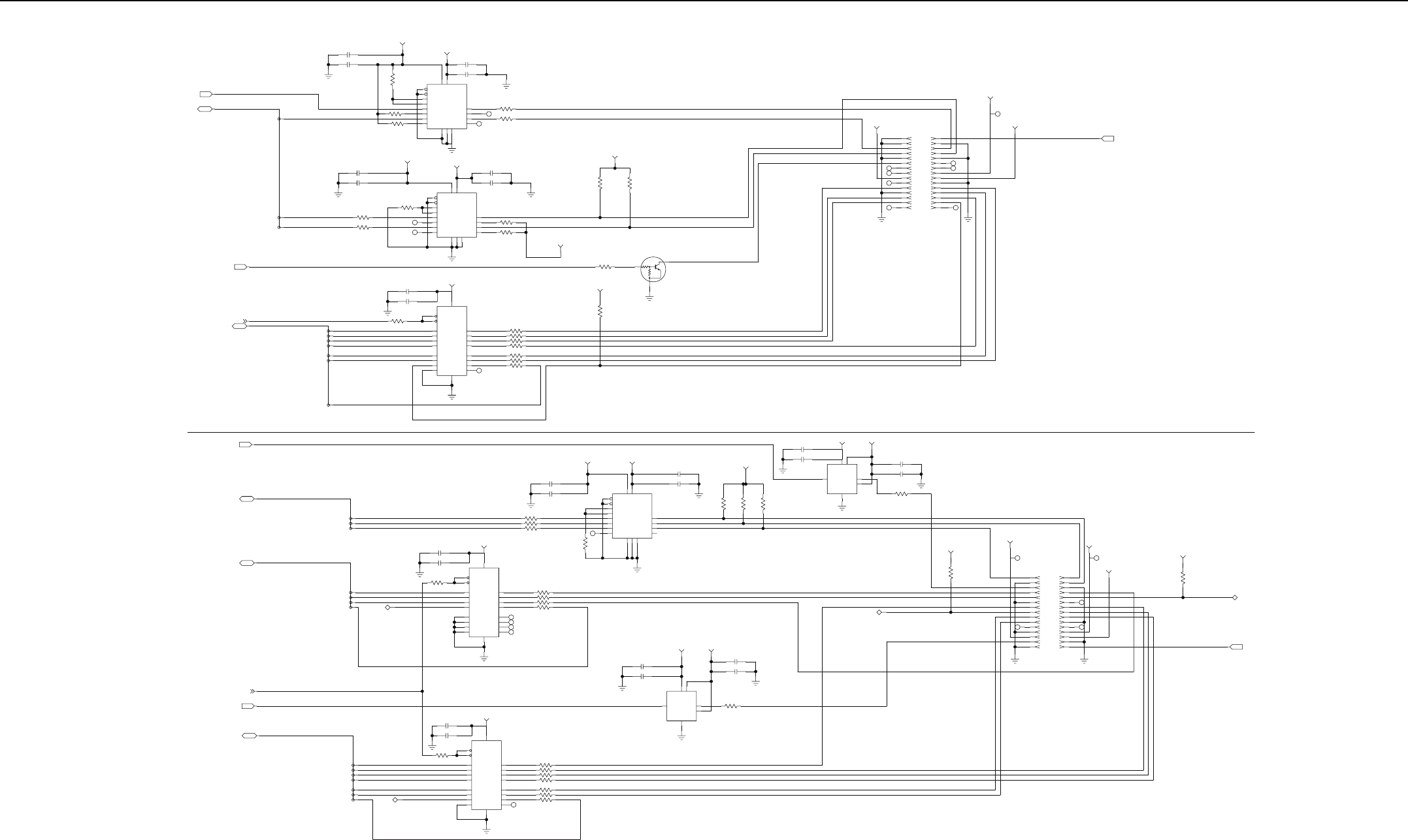
4-50 Controller Schematics (UHF)
DMCS
SSI_TRIDENT<2..0>
IN
IO
2SSI_TRIDENT_TXD
C3601M3
C3600M30.1UF
.01UF
MAKO_V4_2_775V
1_875V
R3601M3
0
SSI_TRIDENT_CLK
EX_ENABLE
SSI_TRIDENT_FS
1
0
IN
NC
NC
R3605M3
R3600M3
C3603M3
C3602M30.1UF
.01UF
49.9
4.75K
1_875V MAKO_V4_2_775V
VCCB
VCCA
GND3
GND2
GND1
B1_2
B1_1
B2_2
B2_1
A2_2
A2_1
A1_2
A1_1
DIR2
DIR1
OE2
OE1 U3602M3
C3609M3
C3608M30.1UF
.01UF
SN74AVC4T245
4
6
5
7
2
3
8
9
17
15
14
1
16
R3609M3
R3608M3 4.75K
4.75K
13
11
12
10
TXFS_EX
MAKO_V4_2_775V
TXCLK_EX
R3639M3
R3638M3
4.75K
DNP 4.75K
DNP
MAKO_V4_2_775V
VCCB
VCCA
GND3
GND2
GND1
B1_2
B1_1
B2_2
B2_1
A2_2
A2_1
A1_2
A1_1
DIR2
DIR1
OE2
OE1
NC
NC
R3607M3
R3606M3
R3604M3
R3603M3
R3602M3
4.75K
4.75K
4.75K
49.9
0
4
6
5
7
13
11
12
10
2
3
8
9
17
15
14
TXD_EX
DMCS_EX
U3600M3
C3607M3
C3606M30.1UF
.01UF
SN74AVC4T245
1
16
EXCITER CIRCUITRY
10K
47K
R3643M3
R3617M3
Q3600M3
DTC114YKAF
2
3
1
0
100K
3_3V
EX_BUF_EN_N
FPGA_SPI_<0..6>
IO
3
6
4
5
FPGA_EX_SPI_CS
FPGA_EX_SPI_ADDR1
EX_FPGA_MISO
1
0
FPGA_SPI_MOSI
2
FPGA_EX_SPI_ADDR2
FPGA_EX_SPI_ADDR0
FPGA_SPI_CLK
GND
Y0A0
A1
Y3
Y4
A5
A6
Y7
EN_OE1
EN_OE2
Y1
Y2A2
A3
A4
Y5
Y6
A7
VCC
NC
U3601M3
R3635M3
C3605M3
C3604M30.1UF
.01UF
0
MC74LVX244
2
4
6
8
11
13
15
17
1
19
10 20
18
16
14
12
9
7
5
3
3_3V
R3616M3
R3615M3
R3614M3
R3613M3
R3612M3
R3611M3
R3610M3
0
0
0
0
0
0
0
EX_CPLD_ADD_1
EX_CPLD_MOSI
EX_CPLD_CLK
EX_CPLD_ADD_0
EX_CPLD_CE
EX_CPLD_ADD_2
EX_CPLD_MISO
EX_ENABLE_N
TP3600M3
1
CLK_EX_16_8MHZ
14_2V
10V_EX
IN
NC
NC
NC
NC
NC NC
NC
J3600M3
J3600M3
J3600M3
J3600M3
J3600M3
J3600M3
J3600M3
J3600M3
J3600M3
J3600M3
J3600M3
J3600M3
J3600M3
J3600M3
J3600M3
A1
A2
A3
A4
A5
A6
A7
A8
A9
A10
A11
A12
A13
A14
A15
B1
B2
B3
B4
B5
B6
B7
B8
B9
B10
B11
B12
B13
B14
B15
8V
ABACUS_SYNCB
ABA_SPI_<0..3>
SSI_ABACUS<2..0>
IN
IO
IO
SSI_ABACUS_FS
SSI_ABACUS_RX
SSI_ABACUS_CLK
1
0
2
C3611M3
C3610M30.1UF
.01UF
GND
Y0A0
A1
Y3
Y4
A5
A6
Y7
EN_OE1
EN_OE2
Y1
Y2A2
A3
A4
Y5
Y6
A7
VCC
NC
NC
NC
NC
U3603M3
R3636M3
R3624M3
R3623M3
R3622M3
R3621M3
33.2
49.9
49.9
0
0
MC74LVX244
2
4
6
8
11
13
15
17
1
19
10 20
18
16
14
12
9
7
5
3
3_3V
ABA_DOUT
FPGA_ABA_SPI_MOSI
FPGA_ABA_SPI_CLK
FPGA_ABA_SPI_CS_N
1
3
0
2
ABA_FPGA_SPI_MISO
R3620M3
R3619M3
R3618M3
C3615M3
C3614M30.1UF
.01UF
0
0
0
3_3V1_875V
B
DIR
VCCA
VCCB
GND
U3607M3
R3634M3
C3625M3
C3624M3
C3623M3
C3622M30.1UF
.01UF
0.1UF
.01UF
33.2
SN74AVC1T45
C1 C2
B2
A1
A2
1_875V3_3V
A
B1
VCCB
VCCA
GND3
GND2
GND1
B1_2
B1_1
B2_2
B2_1
A2_2
A2_1
A1_2
A1_1
DIR2
DIR1
OE2
OE1
NC
U3605M3
R3642M3
R3641M3
R3640M3
R3632M3
C3619M3
C3618M3 0.1UF
.01UF
4.75K
100K
100K
100K
SN74AVC4T245
4
6
5
7
13
11
12
10
2
3
8
9
17
15
14
1
16
3_3V
ABA_CLK
ABA_DATA
ABA_FS
RECEIVER CIRCUITRY
R3645M3
100K
3_3V
CLK_RX_16_8MHZ
ABA_DOUT
IN
TP3602M3
1
ABA_PD
14_2V
8V
TP3601M3
1
10V_RX
RX_ATTEN_RX
RX_CPLD_CE
ABA_PC
ABA_PE
ABA_SYNCB
J3601M3
J3601M3
J3601M3
J3601M3
J3601M3
J3601M3
J3601M3
J3601M3
J3601M3
J3601M3
J3601M3
J3601M3
J3601M3
J3601M3
J3601M3 B1
B2
B3
B4
B5
B6
B7
B8
B9
B10
B11
B12
B13
B14
B15
NC NC
NC
A1
A2
A3
A4
A5
A6
A7
A8
A9
A10
A11
A12
A13
A14
A15
RX_CPLD_MOSI
RX_CPLD_ADD2
RX_CPLD_CLK
R3644M3
100K
3_3V
RX_CPLD_MISO
R3633M3
C3621M3
C3620M3 0.1UF
.01UF
0
3_3V 1_875V
B
DIR
VCCA
VCCB
GND
U3606M3
C3617M3
C3616M30.1UF
.01UF
SN74AVC1T45
C1 C2
B2
B1
A1
A2
A
18
16
14
12
9
7
5
3
33.2
33.2
33.2
33.2
33.2
33.2
0
NC
R3631M3
R3630M3
R3629M3
R3628M3
R3627M3
R3626M3
R3625M3
GND
Y0A0
A1
Y3
Y4
A5
A6
Y7
EN_OE1
EN_OE2
Y1
Y2A2
A3
A4
Y5
Y6
A7
VCC
U3604M3
MC74LVX244
10
R3637M3
C3613M3
C3612M30.1UF
.01UF
02
4
6
8
11
13
15
17
1
19
20
3_3V
RX_CPLD_MISO
6
4
3
5
2
0
1
FPGA_RCVR_SPI_ADDR0
FPGA_RCVR_SPI_ADDR1
FPGA_RCVR_SPI_ADDR2
FPGA_RCVR_SPI_MOSI
FPGA_RCVR_SPI_CLK
FPGA_RCVR_SPI_CS
RCVR_FPGA_SPI_MISO
RX_CPLD_ADD0
RX_CPLD_ADD1
RX_BUF_EN_N
RX_ATTEN
RCVR_SPI_<0..7>
IN
IO
Controller – Exciter and Receiver Schematic Diagram (Kit No. CLN8502)
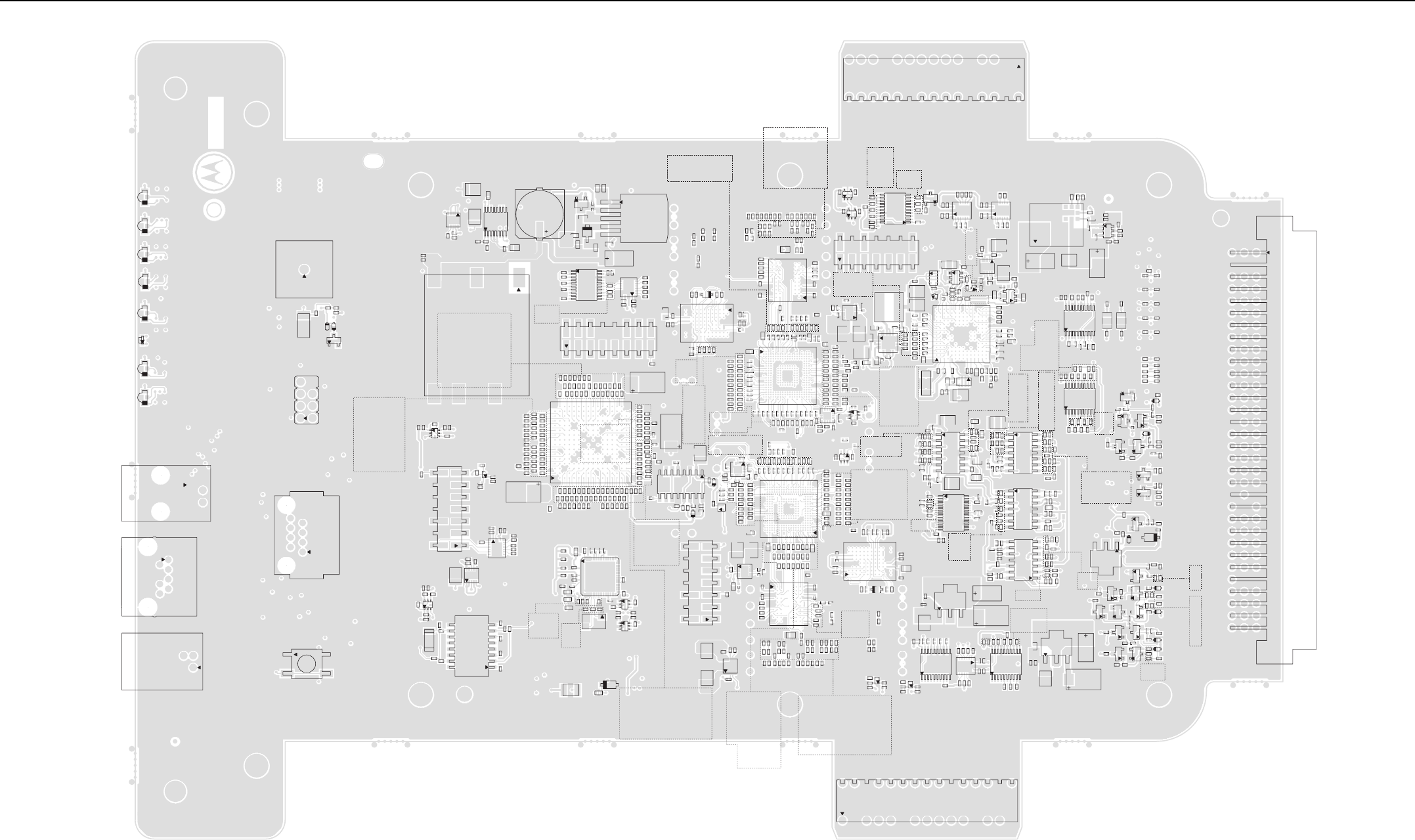
Controller PCB (UHF) 4-51
4.5 Controller PCB (UHF)
D3070M7
D3108M7
D3004M7
D3078M7
D3003M7
D3002M7
D3001M7
D3000M7
3
C
2008
J3009M7
J3000M7
J3010M7
G2
G1
4
G1
3
G2
10
6
54
7
82
3
9
3
2
4
2
S3011M7
3
4
2
J3006M7
28
G1 7G2
P3013M7
2
87
R3157M7
C3141M7
VR3142M7
D3012M7
R3134M7
R3158M7
R3002M7
J3008M7
D3013M7
G1
G2
3
G4
G3
2
C2401M6
C2400M6
Y2401M6
R3880M4
R2405M6
C3881M4 R3882M4
C3884M4
U3883M4
C3879M4
R2415M6
R2404M6
C2415M6
C2416M6
U2401M6
C2407M6
7
4
3
5
610
16
8
9C2432M6
R1424M1
C1423M1
C1421M1
C1420M1
U1401M1
C1422M1
C3890M4
E3888M4
D3892M4
C3889M4
Q3886M4
R1423M1
R1418M1
R1417M1
C1427M1
C1416M1
C1428M1
C1418M1
C3897M4
C3898M4
R3895M4
R3887M4
R3891M4
R3894M4
R3896M4
U1400M1
U3893M4
8
7
2
6
32
20 11
9
10
15
16
5
10
R3112M7
R3111M7
C3116M7
R3110M7
R3115M7
R3071M7
C3069M7
C3067M7
U3073M7
R3081M7 R3086M7
C3097M7
C3096M7
T3106M7
C3822M4 U3826M4
C3105M7
R3088M7
C3103M7
C3089M7
16 9
5
6
10
8
6
3
4
C3100M7
C3093M7
R4013M4
R3825M4 C3824M4
R4019M4
R3823M4
P4000M4
C4016M4
C4028M4
C4017M4
C4029M4
U4001M4
R4023M4
R4024M4
R4031M4
R4030M4
R4032M4
214
13
8
9
10
15
16
7
2
P3200M3
R3128M7
C3132M7
C3113M7
C3131M7
U3127M7 R3119M7
C3114M7
R2033M5 R2032M5
R2031M5
R2030M5
R2029M5
R2027M5
R2036M5
R2034M5
R2028M5
R2026M5
R2025M5 R2022M5
R2021M5
R2003M5
R2002M5
R2038M5
R2012M5 R2013M5
R2015M5
R2018M5
R2019M5
R2020M5
R2008M5
R2010M5 R2014M5
6
34
R2081M5
R2082M5
R2083M5
R2106M5
R2104M5
R2095M5
R2093M5
R2085M5
R2073M5
R2007M5 R2109M5
R2088M5
R2064M5
R2112M5
R2111M5
R2099M5
R2098M5
R1859M1
R2102M5
R2072M5
R2070M5
R2068M5
R2066M5
R2062M5
R2057M5
R2053M5
R2052M5
R2042M5
R2113M5
R2050M5
R2040M5
R2046M5
C4026M4
R4018M4
R4022M4
C4027M4
R2004M5
C4020M4
C4021M4
U4025M4
C2208M5
R2024M5
R2006M5
R2005M5
R2000M5
R2001M5
R2023M5
R2016M5
R2075M5
R2037M5
R2035M5
R2011M5
R2017M5
R2009M5
C2858M2
R2069M5 R2065M5
R2060M5 R2058M5
R2056M5
R2055M5
R2051M5
R2049M5
R2045M5
R2044M5
R2043M5 R2041M5
R2039M5
R2067M5
R2071M5
C2854M2
VR2600M2
R2131M5
R2108M5 R2105M5
R2103M5
R2101M5 R2100M5
R2096M5
R2094M5
R2092M5
R2086M5 R2080M5
R2078M5
R2077M5 R2076M5
R2079M5
R2129M5
R2141M5
R2130M5
C3016M7
C3017M7
C3037M7
U3020M7
R3075M7
R3015M7
3
C3051M7
C3045M7
C3085M7
E3090M7
R3104M7
R3102M7
C3049M7
R3053M7
R3054M7
E3091M7
R3099M7
R3092M7
C3024M7
C3023M7
C3027M7
C3082M7
C3101M7
R3000M7
R3044M7
Y3038M7
R3021M7
U3025M7
4
3
2
R3160M7
C3098M7
C3052M7
C3056M7
R3074M7
E3041M7 R2063M5
R2061M5
R2059M5
R2054M5
R2074M5
R2048M5
R2047M5
C3040M7
U3005M7
C3077M7
C3030M7
C3035M7
C3032M7
R2107M5
R2091M5
R2087M5
R2084M5
R2110M5
R2097M5
6
4
6
4
3
29
43
15
56
J3601M3
A15
B15
B1
J3600M3
B1
B15
A15
U2000M5
R2144M5
R2146M5
R2145M5
R2147M5
R2139M5
R2128M5
R2089M5
R2119M5
R2120M5
R2121M5
R2123M5 R2140M5
R2114M5
C2235M5
R2122M5
R2124M5
R2125M5
R2126M5
R2090M5
R2270M5
C2231M5
T1
T16
A1
A16
R2261M5
R2142M5
R2143M5
R2148M5
R2127M5
R2132M5
R2153M5
R2154M5
R2117M5
R2115M5
R2118M5
R2152M5
R2137M5
R2136M5
R2135M5
R2134M5
R2116M5
R2133M5
R2258M5
R2259M5
R2260M5
C2249M5
U2207M5
16
9
8
C2246M5
R1820M1
C1803M1
R1852M1
R2257M5
D2200M5
R1844M1
U1800M1
9
5
13
P1800M1
D2201M5
R3861M4
C3864M4
R3872M4
R3867M4
C3873M4
U3801M4
R1838M1
R1816M1
C2247M5
C2248M5
R2269M5
Q2200M5
R1849M1
R1853M1
C3868M4
10
13
4
3
2
5
6
214
R1672M1
R1673M1
R1676M1
C1649M1
R1664M1
R1665M1
R1674M1
R1675M1
R1679M1
R1680M1
R1681M1
C1640M1
C1648M1
C1650M1
C1651M1
C1652M1
C1655M1
C1656M1
C1614M1
U1601M1
R1612M1
R1607M1
R1606M1
R1605M1
R1604M1
R1611M1
R1613M1
C1612M1
R1608M1
R1603M1
R1602M1
R1601M1
R1600M1 R1657M1
R1610M1
R1614M1
R1609M1
R1615M1
C1622M1
C1616M1
C1617M1
C1618M1
C1628M1
R1677M1
R1678M1
C1653M1
R1662M1
R1663M1
R1682M1
R1683M1
R1684M1
C1638M1
C1639M1
C1654M1
C1657M1
C1658M1
C1659M1
C1660M1
C1662M1
C1635M1
C3622M3
C3623M3
R3634M3 R3633M3
C3624M3
U3607M3
R3844M4
C1801M1
C3846M4 C3845M4
R1671M1
R1666M1
C1641M1
C1642M1
C1647M1
R1648M1
R1649M1
R1650M1
R1651M1
C1609M1
R3847M4
R3849M4
R3909M4
C1611M1
C3848M4
U3850M4
C1632M1
C1637M1
C3851M4
5
6
10
R3631M3
R3630M3
R3629M3
R2876M2
C2629M2
R2883M2
R2856M2
C2613M2
C2636M2
R2858M2
R2860M2
U2603M2
R1644M1
R1645M1
R1646M1
R1647M1
R1670M1
R1686M1
C1613M1
C1608M1
C1646M1
C1661M1
R1689M1
R1690M1
C1600M1
C1610M1
C1601M1
R1667M1 R1668M1
C1643M1 C1644M1
R1669M1
R1656M1
R1655M1
D1600M1
U1600M1
C3620M3
C3621M3
C3617M3
C3616M3
C3625M3
U3606M3 C3610M3
R1654M1
R1653M1
C1605M1
C1607M1
C1604M1
C1603M1
R3645M3
R3624M3
R3623M3
R3622M3
R3636M3
C3611M3
R3621M3
U3603M3
U3838M4
R3839M4
R3840M4
C3841M4
C2832M2
C2834M2
R3640M3
R3641M3
R3642M3
C3619M3
C3618M3
R3619M3
R3618M3
R3632M3
R3620M3
C3614M3
C3615M3
U3605M3
R2880M2
R2881M2
C2618M2
7
14 8
10 15
8
916
72
3
10
20 11
2
4
M1
M8
A1
A8
C1645M1
R3637M3
R3644M3
R3628M3
R3627M3
R3626M3
R3625M3
U3831M4
R3833M4
R2859M2
R2863M2
R2864M2
C2616M2
C2627M2
C3613M3
C3612M3
C3837M4
C3842M4
3
2
4
U3604M3
C3834M4
R3830M4
R3832M4
C3828M4
C3835M4
10
20 11
R1044M1
C1010M1
R1047M1
R1046M1
R1062M1
R1063M1
C1009M1
C1057M1
C1058M1
C1059M1
R1077M1
R1078M1
R1081M1
R1082M1
R1083M1
R1084M1
C1038M1
C1039M1
C1053M1
C1054M1
C1060M1
R1064M1
R1086M1
C1040M1
C1061M1
C1014M1
R1065M1
R1072M1
R1073M1
R1074M1
R1075M1
R1076M1
R1079M1
R1080M1
C1041M1
C1048M1
C1049M1
C1050M1 C1051M1
C1052M1
C1055M1
C1056M1
C1042M1
R1071M1
C1047M1
C1405M1
R1833M1
R1406M1
R1405M1
R1409M1
R1407M1
C1403M1
C1007M1
R1070M1
C1046M1
R1067M1
R1068M1
C1043M1
C1044M1
R1045M1
R1066M1
P1201M1
R1850M1
R1043M1
C1004M1
C1002M1
C1003M1
C1005M1
C1006M1
R1042M1
R1087M1
R1088M1
U1002M1
A8
A1
15
16
M8
M1
2
R1031M1
R1030M1
R1029M1
R1026M1
R1023M1
R1085M1
R1038M1
R1027M1
R1024M1
R1020M1
R1022M1
U1003M1
R1053M1
R1069M1
C1045M1
R1056M1
R1052M1
R1054M1
D1000M1
C3607M3
R3608M3
R3638M3
R3639M3
U3600M3
R3606M3
R3607M3
C1206M1 C1207M1
R3612M3
R3611M3
R3610M3
R1269M1 R3643M3
C3604M3
C3605M3
U1202M1
R1270M1
U1203M1
R3616M3
R3615M3
R3635M3
U3601M3
R3614M3
R3617M3
C3608M3
Q3600M3
R3609M3
2
3
54
3
54
3
20
10
11
C3609M3
R1493M1
R3605M3
R3601M3
R3600M3
C3600M3
C3606M3
C3601M3
U3602M3
R3604M3
R3602M3
R3603M3
C3602M3
C3603M3
8
9
10
15
16
7
2
8
9
10
15
16
7
2
P1200M1
14
13
2
U3874M4
R3806M4
C3911M4
R3876M4
R3870M4
R3871M4
R3869M4
R3865M4
C3866M4
R3804M4
C3910M4
R3805M4
U3809M4
C3802M4
C3807M4
C3808M4
R3803M4
4
3
6
A7
H1
H7
R2230M5
R3213M3
R3214M3
L3201M3
L3200M3
C3219M3
C3218M3
R3209M3
R3204M3
C3208M3
C3210M3
R3243M3
R3202M3
R3200M3
C3205M3
C3202M3
C3200M3
C2204M5
C2202M5
C3877M4
R2236M5
R2235M5
R2234M5
R2233M5
R2231M5
R2219M5
R2217M5
R2216M5
R2214M5
R2213M5
R2208M5
R2207M5
R2204M5
C2205M5
R2232M5
U2201M5
R2229M5
R2228M5
R2227M5
R2218M5
C2203M5
C3862M4
R3206M3
10
20 11
R3233M3
D3409M3
C3421M3
C3420M3
C3233M3
C3231M3
C3230M3
U1001M1 AA1
A21
AA21
R1835M1
R1832M1
R1828M1
R1843M1
R1842M1
R1841M1
R1821M1
R1851M1
R1822M1
R1845M1
R1808M1
R1809M1
R1639M1
C1615M1
C1627M1
C1629M1
C1626M1
R1840M1
R1658M1
R1807M1
R1825M1
R2802M2
E2600M2
R2806M2
R2805M2
R2818M2
R2817M2
R2814M2
R2801M2
U2606M2
16
30
15
R3412M3
R3403M3
R3463M3
R3400M3
Q3403M3
Q3400M3
R3465M3 R3470M3
R3469M3
Q3405M3
R3466M3
VR3402M3
R3242M3
R3415M3
R3241M3
R3247M3
C3237M3
C3238M3
VR3208M3
R3248M3
Q3409M3
C3411M3
VR3407M3
R3245M3
R3425M3
R3210M3
C3209M3
R3217M3
C3215M3
C3214M3
3
2
3
2
2
32
3
2
3
R2240M5
R2239M5
R2238M5
R2237M5
R2205M5
R2202M5
R2201M5
R2200M5
U2202M5
R3414M3
Q3408M3
R3464M3
R3468M3
R3467M3
Q3406M3
D3410M3
R3422M3
R3455M3
Q3419M3
R3215M3
R3480M3
R3424M3
R3423M3
Q3413M3Q3412M3 R3481M3
Q3414M3
R3454M3
R3420M3
R3417M3
R3404M3
C3408M3
Q3411M3
D3400M3
D3401M3
R3450M3
R3448M3
R3411M3
R3408M3
R3407M3
C3402M3
C3400M3
VR3400M3
D3403M3
R3418M3
R3453M3
C3407M3
D3402M3
VR3200M3
R3220M3
C3222M3
VR3202M3
R3223M3
C3221M3
VR3201M3
R3430M3
R3428M3
C3413M3
C3412M3
VR3408M3
Q3415M3
D3408M3
R3429M3
R3456M3
R3236M3
R3427M3
R3436M3
R3437M3
R3238M3
R3235M3
32
3
2
32
3
3
2
3
2
2
3
22
42
32
3
2
32
3
3
10
20 11
32
R3479M3
R3218M3
R3457M3
R3613M3
R1632M1
C1634M1
R1633M1
R1620M1
R1619M1
R1617M1
R1618M1
R1616M1
R1627M1
C1623M1
C1633M1
C1631M1
C1625M1
R1659M1
C1636M1
R1634M1 R1631M1
R1629M1
R1637M1 R1640M1
R1839M1
R1626M1
R1256M1
R1643M1
R1642M1
R1652M1
R1687M1
R1688M1
R1635M1
R1630M1
R1625M1
R1624M1
R1622M1
R1623M1
R1621M1
R1628M1
R1638M1
R1636M1
R1823M1
R1275M1
C1602M1
C1606M1
R1641M1
R1257M1
R1246M1
R1239M1
R1238M1
R1233M1
R1229M1
R1208M1
R1237M1
R1217M1
R1216M1
R1213M1
R1251M1
R1219M1
C1021M1
C1015M1
U1000M1
R1209M1
C1203M1
R1214M1
C1024M1
R1242M1
C1019M1
R1041M1
R1035M1
R1028M1
R1243M1
R1274M1
C1023M1
C1030M1
C1031M1
C1025M1
C1017M1
R1059M1
C1036M1
AA21
A21
AA1
C1013M1
R1037M1
R1036M1
R1034M1
R1025M1
R1021M1
R1040M1
R1033M1
R1032M1
R1018M1
R1017M1
R1016M1
R1019M1
C1034M1
R1055M1 R1089M1
R1090M1
C1001M1
C1000M1
R1232M1
R1249M1
R1248M1R1215M1
R1058M1
R1220M1
C1029M1
C1020M1
R1228M1
R1268M1
R1259M1
R1244M1
R1236M1
R1225M1
R1224M1
R1241M1
R1210M1
R1247M1 R1230M1
C1026M1
C1027M1
R1263M1
R1240M1
R1223M1
C1202M1
U1201M1
R1265M1
R1227M1
R1207M1
R1015M1
R1012M1
R1011M1
R1009M1
R1007M1
R1001M1
R1000M1
R1253M1
R1254M1
R1006M1
R1049M1
R1048M1
C1008M1
R1051M1
R1050M1
C1012M1
R1039M1
R3856M4
R3858M4
C3857M4
R3853M4
C3855M4
U3800M4
L1401M1
10
5
6
R1014M1
R1010M1
R1008M1
R1005M1
C1011M1
R1013M1
R1003M1
R1002M1
R1057M1
C1028M1
C1022M1
C1018M1
C1016M1
C1033M1
R1260M1
R1262M1
R1261M1
C1032M1
C1037M1
C3859M4
C1455M1
C1457M1
C3854M4
R1491M1
R1004M1
C1035M1
C1440M1
R1472M1
R1466M1
R1445M1
R1449M1
C1439M1
R1452M1
U1404M1
U1406M1
R1454M1
R1469M1
C1449M1
C1442M1
10
5
6
R1475M1
R1471M1
C1448M1
R1451M1
Q1407M1
R1476M1
R1474M1
C1450M1
R1470M1
R1467M1
2
U1405M1
C1444M1
Q1408M1
R1446M1
R1499M1
R1455M1
4
6
3
85 4
R2865M2
C2621M2
R2869M2
R2870M2
R2800M2
R2811M2
R2819M2
R2804M2
R2815M2
C2640M2
C2641M2
R2882M2
R2879M2
R2878M2
C2632M2
C2633M2
R2867M2
R2866M2
C2622M2
C2624M2
R2861M2
R2871M2
R2892M2
R2843M2
C2601M2
C2602M2
C2638M2
C2600M2
R2844M2
R2845M2
R2857M2
C2615M2
R2854M2
R2893M2
C2850M2
C2848M2
R2894M2
R2837M2
R2835M2
C2642M2
R2877M2
C2625M2
R2875M2
R2874M2
R2862M2
C2857M2
R2868M2
C2631M2
C2623M2
R2823M2
R2822M2
R2873M2
R2872M2
C2804M2
C2803M2
R2824M2
U2800M2
R2853M2
R2851M2
R2850M2
C2609M2
C2610M2
U2604M2
C2637M2
R2836M2
R2896M2
U2802M2
C2849M2
R2807M2
R2803M2
R2820M2
C2823M2
C2826M2
C2835M2
C2838M2
R2830M2
R2849M2
R2839M2
R2842M2
R2828M2
R2841M2 C2894M2
C2855M2
R2840M2
C2856M2
8
14 8
14
7
7
8
14
7
R2827M2
C2837M2
R2826M2
R2831M2
R2808M2
C2845M2
C2847M2
C2841M2
R2825M2
R2821M2
C2811M2
C2819M2
C2817M2
R2809M2
R2829M2
C2846M2
C2892M2
R2816M2
C2862M2
Q1400M1
R1495M1
R1403M1R1408M1
C1408M1
C1407M1
C1419M1
C1432M1
R1497M1
C1460M1 R1494M1
R1496M1
C1434M1
C1436M1
C1437M1
R1490M1
R1488M1
R1489M1
R1487M1
R1435M1
R1414M1
R1411M1
C1431M1 C1433M1
R1415M1
8
5
4
P1
C1400M1
R1420M1
U1402M1
R1448M1
R1438M1
R2895M2
C2822M2
R1412M1
C1402M1
C1406M1
C1409M1
Y1400M1
C1461M1
C1462M1
R1498M1
P14
A14
32
R3482M3
R1410M1
R1465M1
R1483M1
C1459M1
C1458M1
R1404M1
R1422M1
C1414M1
R1462M1
R1464M1
R1459M1
R1456M1
R1457M1
R1468M1
R1477M1
Q1409M1
2
R1416M1
R1402M1
R1481M1
R1458M1
R1453M1
R1413M1
C1456M1
R1484M1
R1480M1
R1485M1
R1473M1
R1461M1
U1407M1
9
45
8
12
16
13
R1685M1
C1802M1
C1204M1
U1801M1
R1264M1
R1267M1
R1266M1
C1205M1
R1218M1
U1200M1
R1222M1
139
5
6
34
6
3
4
R1211M1
R1206M1
R1231M1
R1221M1
R1245M1
R1272M1
R1234M1
R1273M1
R1258M1
R3001M7
R1226M1
C1451M1
L1400M1
C1452M1
R1479M1
R1478M1
R1848M1
R1847M1
R1817M1
R1812M1
R1806M1
R1826M1
R1829M1
R1255M1
R1846M1
R1830M1
R1250M1
R1814M1
R1836M1
R1804M1
R1802M1
R1800M1
R1827M1
R1837M1
R1810M1
R1819M1
R1801M1
R1813M1
R1831M1
R1815M1
C1619M1
C1621M1
C1630M1
C1620M1
R1824M1
R1803M1
R1805M1
C1624M1
C1804M1
C1805M1
Controller PCB – Top View (PCB No. 8475374H02)
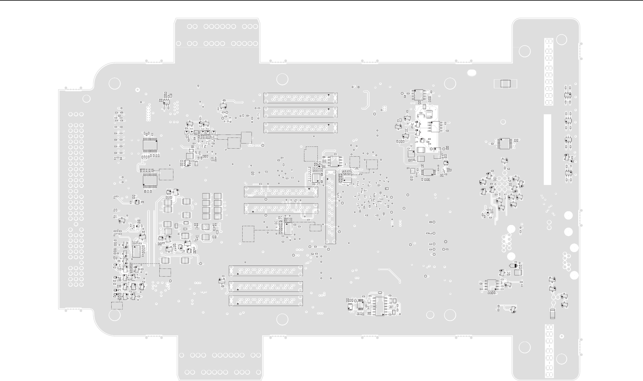
4-52 Controller PCB (UHF)
R3401M3
Q3401M3
R3471M3
R3475M3
TP1213M1
TP1230M1
R3449M3
R3409M3
R3416M3
R3405M3
C3401M3
VR3401M3
Q3404M3
D3405M3
D3406M3
R3451M3
R3452M3
R3419M3
R3410M3
R3406M3
C3406M3
C3403M3
VR3403M3
D3407M3
2
3
3
2
3
3
2
2
R3413M3
TP1220M1
TP1234M1
R3224M3
TP1215M1
TP1228M1
Q3407M3
Q3410M3
R3402M3
Q3402M3
R3472M3
R3477M3 TP1231M1
Q3200M3
TP2605M2
R3230M3
R3227M3
R3229M3
R3246M3
C3227M3
C3225M3
VR3205M3
R3232M3
Q3201M3
TP2800M2
D3404M3
R3426M3
R3226M3
R3225M3
C3224M3
C3223M3
R3231M3
TP2600M2
R3458M3
C3431M3
C3430M3
3
23
2
32
3
32
3
2
2
3
2
R3203M3
R3476M3
R3434M3
R3421M3
R3435M3
R3432M3
C3414M3
R3483M3
Q3418M3
TP1212M1
R3439M3
R3249M3
R3234M3
C3404M3
C3405M3
C3409M3
C3410M3
U3403M3
R3441M3
R3431M3
R3211M3
TP1223M1
U3400M3
C3415M3
TP2603M2
R3443M3
C3426M3
C3425M3
U3401M3
VR3204M3V
TP2602M2
R3447M3
R3446M3
R3228M3
R3222M3
C3226M3
C3220M3
VR3206M3
R3445M3
C3429M3
TP3601M3
32
11
12
13
14
24
2
23
6
34
32
32
R3444M3
Q2602M2
C2626M2
R2846M2
C2611M2
C2612M2
U2605M2
C2614M2
R2242M5
R2241M5
R2226M5
32
634
U2203M5
R2211M5
R2210M5
R2209M5
C2207M5
C2206M5
TP3810M4
TP3600M3
R3221M3
R3219M3
C3213M3
R3239M3
R3237M3
C3234M3
C3232M3
R3208M3
R3207M3
R3438M3
C3422M3
C3207M3
C3206M3
R3244M3
R3205M3
R3203M3
R3201M3
C3204M3
C3203M3
C3201M3
TP3602M3
10
20 11
C2200M5
R2223M5
R2222M5
R2221M5
R2220M5
R2212M5
C2201M5
U2200M5
R2225M5
R2224M5
R2206M5
R2203M5
R2215M5
10
20
11
R3820M4
R3816M4
U3819M4
R3813M4
C3818M4
C3811M4
R3814M4
R3812M4
C3815M4
C3817M4
4
6
3
J1600M1
J1601M1
J1602M1
TP1601M1
G1
G1
B1
G4
G1
B1
G4
B1
G4
G2
A27 G2
A27
B27 G3
A27 G2
B27 G3
B27 G3
TP3843M4
R2848M2
C2829M2 C2827M2
C2607M2
C2608M2
C2634M2
C2604M2
U2602M2
U2607M2
C2619M2
Q2601M2
C2800M2
TP2601M2
TP3836M4
C2628M2
R2847M2
R2852M2
C2603M2
C2617M2
U2608M2
Q2600M2
Q2603M2
C2620M2
R3473M3
R3474M3
R3478M3
6
3
4
6
34
6
4
3
2
32
3
C2808M2
C2810M2
C2812M2
C2830M2
C2802M2
C2831M2
R3461M3
R3459M3
Q3416M3
C2824M2
C2813M2
C2821M2
C2815M2
C2825M2
C2806M2
32
C2840M2
C2839M2
C2816M2
C2814M2
C2820M2
C2828M2
C2818M2
C2606M2
C2605M2
C2852M2
C2639M2
C2836M2
C2833M2
C2809M2
C2807M2
R3124M7
R3123M7
R3122M7
R3120M7
R3121M7
TP1809M1
R3125M7
R1857M1
R1858M1
TP1822M1
R1855M1
TP1825M1
TP1811M1
TP1812M1
TP1800M1
R1856M1
TP1805M1
TP1808M1
R1834M1
TP1803M1
TP1802M1
R1818M1
R1811M1
C1800M1
TP2013M5
R1861M1
TP3852M4
TP1817M1
R3126M7
R1854M1
C3129M7
TP1818M1
TP1814M1
TP1816M1
C3130M7
TP1824M1
TP1821M1
R1661M1
R1660M1
C3117M7
U3007M7
TP1600M1
TP1815M1
C3118M7
14
23
24
211
12
13
TP1813M1
TP1804M1
TP1806M1
TP1807M1
J2000M5
TP1801M1
TP1820M1 TP1823M1
J1204M1
J1203M1
TP1819M1
TP1202M1
B1
G1
G4
B27
G3
A27
G2
G3
G2
A27
B27
B1
G4
G1
A27
B27
G2
G3
B1 G4
G1
TP1255M1
TP1221M1
TP1222M1
R2150M5
R1860M1
TP1253M1
R1271M1
R1252M1
TP1237M1
TP1210M1
TP2010M5
R2151M5
R2244M5
R2262M5
R2263M5
R2264M5
C2250M5
C2251M5
R2265M5
R2266M5
R2267M5
R1460M1
TP1256M1
TP1000M1
R1463M1
TP1254M1
R1061M1
R1060M1
C1062M1
TP1252M1
TP1219M1
TP3860M4
8
9
10
15
16
7
2
R2243M5
R2253M5
R2268M5
C2240M5
R2251M5
U2208M5
R2254M5
R2255M5
R2256M5
C2241M5
C2242M5
C2243M5
C2244M5
C2245M5
U2206M5
TP1001M1
J1002M1
J1001M1
J1000M1
A27
B27
G3
G2
A27
B27
G3
G2
A27
B27
G3
G2
B1 G4
G1
B1 G4
G1
B1 G4
G1
D1401M1
R1447M1
R1433M1
R1500M1
Q1403M1
R1442M1
Q1401M1
D1400M1
R1502M1
Q1402M1
R1436M1
Q1406M1
4
3
2
3
2
2
4
3
4
32
3
4
32
2
4
32
2
Q1405M1
R1439M1
R1432M1
R1430M1
R1429M1
R1434M1
R1503M1
Q1404M1
R1431M1
R1444M1
TP1407M1
TP1406M1
C1447M1
C1426M1
R1482M1
R1427M1
C1413M1
C1410M1
C1411M1
C1417M1
E1400M1
R1437M1
R1492M1
R1443M1
R1441M1
C1446M1 C1441M1
C1425M1
C1424M1
C1438M1
C1435M1
C1429M1
TP1405M1
U1403M1
R1486M1
C1453M1
C1454M1
C1443M1
R1428M1
C1445M1
R1425M1
R1419M1
TP1214M1 TP1232M1
TP1411M1
R1421M1
C1412M1
C1415M1
C1430M1
TP1409M1
TP1408M1
TP1410M1
4
6
3
TP1207M1
R1235M1
R3460M3
Q3417M3
TP1224M1
TP1227M1
TP1412M1
R1202M1
R1201M1 TP1204M1
TP1206M1
R1204M1
R1203M1
C1201M1
TP1205M1
TP1218M1
TP1203M1
TP1216M1
R1200M1
R1205M1
TP1208M1
R3462M3
2
3C1200M1
R1212M1
U2803M2
C2890M2
R2832M2
C2844M2
R2891M2
U2601M2
C2891M2
R2890M2
R2833M2
U2600M2
TP3875M4
C2805M2
C2801M2
R2813M2
R2810M2
4
5
8
14 8
7
610
5
R2886M2
R2889M2
C2843M2
TP3863M4
C2859M2
R2888M2
C2861M2
C2860M2
C2842M2
R2834M2
R2838M2
C2893M2
C2851M2
C2853M2
R2812M2
R2887M2
TP1243M1
U2205M5
R2252M5
5
8
4
TP3899M4
TP3829M4
TP1247M1
TP1246M1
TP1238M1
TP1244M1
TP1250M1
TP1242M1
TP1248M1
TP1240M1
TP2021M5
TP1241M1
TP1251M1
TP1239M1
TP1245M1
TP1249M1
R2246M5
R2248M5
R2249M5
R2250M5
TP2018M5
C2236M5
C2237M5
C2238M5
C2239M5
TP2001M5
TP2007M5
TP2008M5
TP2009M5
TP1235M1
TP1229M1
TP1233M1
TP1236M1
TP2020M5
C2211M5
C2232M5
C2216M5
C2218M5
C2228M5
C2209M5
TP2019M5
C2226M5
C2222M5
C2213M5
C2233M5
C2227M5
TP2026M5
C2224M5
C2223M5
C2215M5
C2214M5
C2212M5
R2138M5
TP2022M5
TP2024M5
TP2028M5
C2225M5
R2149M5
TP2023M5
TP2031M5
TP2032M5
TP2029M5
TP1201M1
TP2011M5
TP1209M1
TP1211M1
R2245M5
R2247M5
U2204M5
TP2005M5
TP2033M5
TP1200M1
TP2027M5
TP2030M5
8
9
10
15
16
7
2
C2234M5
C2221M5
TP2006M5
C2210M5
TP3001M7
TP2016M5
TP3821M4
TP3000M7
TP1217M1
TP2017M5
TP2004M5
TP2015M5
C2217M5
C2219M5
C2230M5
C2220M5
TP2000M5
C2229M5
TP2002M5
TP2003M5
TP1226M1
TP2200M5
TP2012M5
32
TP4012M4
TP4014M4
R4011M4
TP3878M4
TP3827M4
TP4006M4
TP4008M4
R4002M4
R4005M4
TP4007M4
TP4010M4
R4004M4
R4003M4
TP4015M4
R4009M4
VR3006M7
D3007M7
C3001M7
D3005M7
VR3000M7
2
323
3232
R2884M2
R2885M2
R3018M7 C2635M2
C2630M2
VR2601M2
TP2604M2
R3047M7
VR3019M7 3
2
R3031M7
C3029M7
VR3150M7
C3014M7
VR3033M7
C3156M7
R3153M7
R3062M7
R3060M7
C3050M7
R3057M7
R3059M7
C3000M7
U3064M7
C3046M7
C3061M7
R3042M7
85
4
32
32
TP2801M2
R2855M2
R3079M7
Q3076M7
R3065M7
R3058M7
R3043M7
R3039M7
VR3007M7
R3063M7
D3011M7
R3055M7
R3048M7
D3010M7
R3034M7
D3009M7
R3026M7
R3028M7
F3000M7
2
3
2
3
64
64
3
6
4
3
R3068M7
R3109M7
R3072M7
D3006M7
R3107M7
6
4
3
8475374H02 REV B
C3159M7
C3154M7
U3000M7
VR3140M7
R3003M7
14 8
32
7
R3161M7
C3168M7
D3144M7
D3146M7
VR3135M7
VR3137M7
R3165M7
R3163M7
C3172M7
C3170M7 VR3139M7
D3148M7
C3173M7
R3004M7C3084M7
C3083M7 VR3136M7
R3080M7
R3162M7
C3169M7
D3147M7
D3145M7
R3164M7
R3167M7
C3174M7
C3171M7
D3155M7
R3166M7
R3133M7
R3066M7
C3002M7
U3087M7
VR3138M7
VR3151M7
32
32
32
2
32
32
3
2
32
3
3
2
2
32
32
3
R2427M6
R2429M6
C2427M6
C2426M6
R2416M6
R2409M6 C2412M6
C2418M6
R2403M6
R2406M6
C2406M6
C2433M6
C2434M6
U2400M6
R2401M6
TP3908M4
R2400M6
C2402M6
C2403M6
C2404M6
R2424M6
C2430M6
TP2400M6
C2405M6
R2402M6
C2411M6
6
34
4
R2419M6
R2418M6
R2425M6
C2429M6
U2402M6
Y2400M6
U2407M6
C2428M6
C2424M6
C2425M6
R2426M6
R2422M6
R3904M4
C2423M6
C3903M4
R3902M4
R3905M4
L2400M6
C3907M4
TP2401M6
R3900M4
C2417M6
U2403M6
C3901M4
U3906M4
C2414M6
Q2400M6
U2406M6
R2414M6
C2419M6
C2413M6
C2408M6
R2413M6
E2400M6
3
8
4
5
2
4
6
5
4
8
610
3
5
3
2
3
2
C2420M6
R2421M6
R2420M6
C2421M6
R2430M6
R2431M6
R2412M6
R2411M6
R2408M6
C2410M6
D2401M6
D2400M6
R2417M6
R2410M6
R2428M6
C2422M6
R2423M6
U2404M6
U2405M6
R2407M6
C2409M6
TP3885M4
C2431M6
32
5
8
4
32
32
Controller PCB – Bottom View (PCB No. 8475374H02)
Controller Parts List (UHF) 4-53
4.6 Controller Parts List (UHF)
Circuit Ref Motorola Part
No Description
*PC512F00W000
010000
MTR3000 FPGA
FIRMWARE
C1000M1 2113945Y02 CAP,FXD,.1UF,+10%,-
10%,16V-DC,0402,X7R,-
55DEG CMIN,125DEG
CMAX
C1001M1 2113945Y02 CAP,FXD,.1UF,+10%,-
10%,16V-DC,0402,X7R,-
55DEG CMIN,125DEG
CMAX
C1002M1 2113945Y02 CAP,FXD,.1UF,+10%,-
10%,16V-DC,0402,X7R,-
55DEG CMIN,125DEG
CMAX
C1003M1 2113945Y02 CAP,FXD,.1UF,+10%,-
10%,16V-DC,0402,X7R,-
55DEG CMIN,125DEG
CMAX
C1004M1 2113945Y02 CAP,FXD,.1UF,+10%,-
10%,16V-DC,0402,X7R,-
55DEG CMIN,125DEG
CMAX
C1005M1 2113945B02 CAP CER CHP 10,000PF
25V 10%
C1006M1 2113944A40 CAP CER CHP 100.0PF
50V 5%
C1007M1 2113956C35 CAP,FXD,4.7UF,+10%,-
10%,16V-DC,0805,X5R,-
55DEG CMIN,85DEG
CMAX
C1008M1 2113945Y02 CAP,FXD,.1UF,+10%,-
10%,16V-DC,0402,X7R,-
55DEG CMIN,125DEG
CMAX
C1009M1 2113945Y02 CAP,FXD,.1UF,+10%,-
10%,16V-DC,0402,X7R,-
55DEG CMIN,125DEG
CMAX
C1010M1 2113945Y02 CAP,FXD,.1UF,+10%,-
10%,16V-DC,0402,X7R,-
55DEG CMIN,125DEG
CMAX
C1011M1 2113945Y02 CAP,FXD,.1UF,+10%,-
10%,16V-DC,0402,X7R,-
55DEG CMIN,125DEG
CMAX
C1012M1 2113945B02 CAP CER CHP 10,000PF
25V 10%
C1013M1 2113944A40 CAP CER CHP 100.0PF
50V 5%
C1014M1 2113956C35 CAP,FXD,4.7UF,+10%,-
10%,16V-DC,0805,X5R,-
55DEG CMIN,85DEG
CMAX
C1015M1 2113944A40 CAP CER CHP 100.0PF
50V 5%
C1016M1 2113945Y02 CAP,FXD,.1UF,+10%,-
10%,16V-DC,0402,X7R,-
55DEG CMIN,125DEG
CMAX
C1017M1 2113944A40 CAP CER CHP 100.0PF
50V 5%
C1018M1 2113945Y02 CAP,FXD,.1UF,+10%,-
10%,16V-DC,0402,X7R,-
55DEG CMIN,125DEG
CMAX
C1019M1 2113945Y02 CAP,FXD,.1UF,+10%,-
10%,16V-DC,0402,X7R,-
55DEG CMIN,125DEG
CMAX
C1020M1 2113944A40 CAP CER CHP 100.0PF
50V 5%
C1021M1 2113945Y02 CAP,FXD,.1UF,+10%,-
10%,16V-DC,0402,X7R,-
55DEG CMIN,125DEG
CMAX
C1022M1 2113945Y02 CAP,FXD,.1UF,+10%,-
10%,16V-DC,0402,X7R,-
55DEG CMIN,125DEG
CMAX
C1023M1 2113945Y02 CAP,FXD,.1UF,+10%,-
10%,16V-DC,0402,X7R,-
55DEG CMIN,125DEG
CMAX
C1024M1 2113944A40 CAP CER CHP 100.0PF
50V 5%
Circuit Ref Motorola Part
No Description
C1025M1 2113945Y02 CAP,FXD,.1UF,+10%,-
10%,16V-DC,0402,X7R,-
55DEG CMIN,125DEG
CMAX
C1026M1 2113945Y02 CAP,FXD,.1UF,+10%,-
10%,16V-DC,0402,X7R,-
55DEG CMIN,125DEG
CMAX
C1027M1 2113945Y02 CAP,FXD,.1UF,+10%,-
10%,16V-DC,0402,X7R,-
55DEG CMIN,125DEG
CMAX
C1028M1 2113945Y02 CAP,FXD,.1UF,+10%,-
10%,16V-DC,0402,X7R,-
55DEG CMIN,125DEG
CMAX
C1029M1 2113945Y02 CAP,FXD,.1UF,+10%,-
10%,16V-DC,0402,X7R,-
55DEG CMIN,125DEG
CMAX
C1030M1 2113944A40 CAP CER CHP 100.0PF
50V 5%
C1031M1 2113945Y02 CAP,FXD,.1UF,+10%,-
10%,16V-DC,0402,X7R,-
55DEG CMIN,125DEG
CMAX
C1032M1 2113946S35 CAP CER CHP 1.0UF 16V
10%
C1033M1 2113944A40 CAP CER CHP 100.0PF
50V 5%
C1034M1 2113946D05 CAP,CHIP,2.2UF,+10%,-
10%,6.3V-DC,0603,X5R,-
55DEG CMIN,85DEG CMA
C1035M1 2113946S35 CAP CER CHP 1.0UF 16V
10%
C1036M1 2113946S35 CAP CER CHP 1.0UF 16V
10%
C1037M1 2113946D05 CAP,CHIP,2.2UF,+10%,-
10%,6.3V-DC,0603,X5R,-
55DEG CMIN,85DEG CMA
C1038M1 2113944A01 CAP CER CHP 1.1PF 50V
+/- 0.25PF
C1039M1 2113944A01 CAP CER CHP 1.1PF 50V
+/- 0.25PF
Circuit Ref Motorola Part
No Description
C1043M1 2113944A17 CAP CER CHP 4.7PF 50V
+/- 0.25PF
C1044M1 2113944A17 CAP CER CHP 4.7PF 50V
+/- 0.25PF
C1045M1 2113944A17 CAP CER CHP 4.7PF 50V
+/- 0.25PF
C1046M1 2113944A17 CAP CER CHP 4.7PF 50V
+/- 0.25PF
C1047M1 2113944A17 CAP CER CHP 4.7PF 50V
+/- 0.25PF
C1048M1 2113944A17 CAP CER CHP 4.7PF 50V
+/- 0.25PF
C1049M1 2113944A17 CAP CER CHP 4.7PF 50V
+/- 0.25PF
C1050M1 2113944A17 CAP CER CHP 4.7PF 50V
+/- 0.25PF
C1051M1 2113944A17 CAP CER CHP 4.7PF 50V
+/- 0.25PF
C1052M1 2113944A17 CAP CER CHP 4.7PF 50V
+/- 0.25PF
C1053M1 2113944A17 CAP CER CHP 4.7PF 50V
+/- 0.25PF
C1054M1 2113944A17 CAP CER CHP 4.7PF 50V
+/- 0.25PF
C1055M1 2113944A17 CAP CER CHP 4.7PF 50V
+/- 0.25PF
C1056M1 2113944A17 CAP CER CHP 4.7PF 50V
+/- 0.25PF
C1057M1 2113944A17 CAP CER CHP 4.7PF 50V
+/- 0.25PF
C1058M1 2113944A17 CAP CER CHP 4.7PF 50V
+/- 0.25PF
C1059M1 2113944A17 CAP CER CHP 4.7PF 50V
+/- 0.25PF
C1060M1 2113944A17 CAP CER CHP 4.7PF 50V
+/- 0.25PF
C1061M1 2113944A17 CAP CER CHP 4.7PF 50V
+/- 0.25PF
Circuit Ref Motorola Part
No Description
4-54 Controller Parts List (UHF)
C1062M1 2113945Y02 CAP,FXD,.1UF,+10%,-
10%,16V-DC,0402,X7R,-
55DEG CMIN,125DEG
CMAX
C1201M1 2113945Y02 CAP,FXD,.1UF,+10%,-
10%,16V-DC,0402,X7R,-
55DEG CMIN,125DEG
CMAX
C1202M1 2113945Y02 CAP,FXD,.1UF,+10%,-
10%,16V-DC,0402,X7R,-
55DEG CMIN,125DEG
CMAX
C1203M1 2113945Y02 CAP,FXD,.1UF,+10%,-
10%,16V-DC,0402,X7R,-
55DEG CMIN,125DEG
CMAX
C1204M1 2113945Y02 CAP,FXD,.1UF,+10%,-
10%,16V-DC,0402,X7R,-
55DEG CMIN,125DEG
CMAX
C1205M1 2113946S35 CAP CER CHP 1.0UF 16V
10%
C1206M1 2113945Y02 CAP,FXD,.1UF,+10%,-
10%,16V-DC,0402,X7R,-
55DEG CMIN,125DEG
CMAX
C1207M1 2113945Y02 CAP,FXD,.1UF,+10%,-
10%,16V-DC,0402,X7R,-
55DEG CMIN,125DEG
CMAX
C1400M1 2113956E91 CAP,FXD,10UF,+10%,-
10%,16V-DC,1210,X5R,-
55DEG CMIN,85DEG
CMAX,P
C1402M1 2113945Y02 CAP,FXD,.1UF,+10%,-
10%,16V-DC,0402,X7R,-
55DEG CMIN,125DEG
CMAX
C1403M1 2113945Y02 CAP,FXD,.1UF,+10%,-
10%,16V-DC,0402,X7R,-
55DEG CMIN,125DEG
CMAX
C1405M1 2113945B02 CAP CER CHP 10,000PF
25V 10%
C1406M1 2113945B02 CAP CER CHP 10,000PF
25V 10%
Circuit Ref Motorola Part
No Description
C1407M1 2113945Y02 CAP,FXD,.1UF,+10%,-
10%,16V-DC,0402,X7R,-
55DEG CMIN,125DEG
CMAX
C1408M1 2113945Y02 CAP,FXD,.1UF,+10%,-
10%,16V-DC,0402,X7R,-
55DEG CMIN,125DEG
CMAX
C1409M1 2113956B33 CAP,FXD,2.2UF,+10%,-
10%,16V-DC,0603,X5R,-
55DEG CMIN,85DEG
CMAX
C1410M1 2113945Y02 CAP,FXD,.1UF,+10%,-
10%,16V-DC,0402,X7R,-
55DEG CMIN,125DEG
CMAX
C1411M1 2113945Y02 CAP,FXD,.1UF,+10%,-
10%,16V-DC,0402,X7R,-
55DEG CMIN,125DEG
CMAX
C1412M1 2113945Y02 CAP,FXD,.1UF,+10%,-
10%,16V-DC,0402,X7R,-
55DEG CMIN,125DEG
CMAX
C1413M1 2113945Y02 CAP,FXD,.1UF,+10%,-
10%,16V-DC,0402,X7R,-
55DEG CMIN,125DEG
CMAX
C1414M1 2113946D05 CAP,CHIP,2.2UF,+10%,-
10%,6.3V-DC,0603,X5R,-
55DEG CMIN,85DEG CMA
C1415M1 2113946D05 CAP,CHIP,2.2UF,+10%,-
10%,6.3V-DC,0603,X5R,-
55DEG CMIN,85DEG CMA
C1416M1 2113945Y02 CAP,FXD,.1UF,+10%,-
10%,16V-DC,0402,X7R,-
55DEG CMIN,125DEG
CMAX
C1417M1 2113945A09 CAP CER CHP 1000PF
50V 10%
C1418M1 2113945B02 CAP CER CHP 10,000PF
25V 10%
C1419M1 2113944A40 CAP CER CHP 100.0PF
50V 5%
Circuit Ref Motorola Part
No Description
C1420M1 2113945Y02 CAP,FXD,.1UF,+10%,-
10%,16V-DC,0402,X7R,-
55DEG CMIN,125DEG
CMAX
C1421M1 2113945Y02 CAP,FXD,.1UF,+10%,-
10%,16V-DC,0402,X7R,-
55DEG CMIN,125DEG
CMAX
C1422M1 2113945Y02 CAP,FXD,.1UF,+10%,-
10%,16V-DC,0402,X7R,-
55DEG CMIN,125DEG
CMAX
C1423M1 2113945Y02 CAP,FXD,.1UF,+10%,-
10%,16V-DC,0402,X7R,-
55DEG CMIN,125DEG
CMAX
C1424M1 2113944A40 CAP CER CHP 100.0PF
50V 5%
C1425M1 2113944A40 CAP CER CHP 100.0PF
50V 5%
C1426M1 2113944F81 CAP,FXD,750PF,+5%,-
5%,50V-DC,0805,C0G,-
55DEG CMIN,125DEG
CMAX,P
C1427M1 2113945Y02 CAP,FXD,.1UF,+10%,-
10%,16V-DC,0402,X7R,-
55DEG CMIN,125DEG
CMAX
C1428M1 2113945B02 CAP CER CHP 10,000PF
25V 10%
C1429M1 2113946S35 CAP CER CHP 1.0UF 16V
10%
C1430M1 2113946S35 CAP CER CHP 1.0UF 16V
10%
C1431M1 2113946D05 CAP,CHIP,2.2UF,+10%,-
10%,6.3V-DC,0603,X5R,-
55DEG CMIN,85DEG CMA
C1432M1 2113946D05 CAP,CHIP,2.2UF,+10%,-
10%,6.3V-DC,0603,X5R,-
55DEG CMIN,85DEG CMA
C1433M1 2113946D05 CAP,CHIP,2.2UF,+10%,-
10%,6.3V-DC,0603,X5R,-
55DEG CMIN,85DEG CMA
Circuit Ref Motorola Part
No Description
C1434M1 2113946D05 CAP,CHIP,2.2UF,+10%,-
10%,6.3V-DC,0603,X5R,-
55DEG CMIN,85DEG CMA
C1435M1 2113945Y02 CAP,FXD,.1UF,+10%,-
10%,16V-DC,0402,X7R,-
55DEG CMIN,125DEG
CMAX
C1436M1 2113946D05 CAP,CHIP,2.2UF,+10%,-
10%,6.3V-DC,0603,X5R,-
55DEG CMIN,85DEG CMA
C1437M1 2113946D05 CAP,CHIP,2.2UF,+10%,-
10%,6.3V-DC,0603,X5R,-
55DEG CMIN,85DEG CMA
C1438M1 2113945Y02 CAP,FXD,.1UF,+10%,-
10%,16V-DC,0402,X7R,-
55DEG CMIN,125DEG
CMAX
C1439M1 2113946J03 CAP CER CHP 10.0UF
16V 10%
C1440M1 2113945A05 CAP CER CHP 470PF 50V
10%
C1441M1 2113944A40 CAP CER CHP 100.0PF
50V 5%
C1442M1 2113946J03 CAP CER CHP 10.0UF
16V 10%
C1443M1 2113956E91 CAP,FXD,10UF,+10%,-
10%,16V-DC,1210,X5R,-
55DEG CMIN,85DEG
CMAX,P
C1444M1 2113946B04 CAP CER CHP 0.10UF
10V 10%
C1445M1 2113944A44 CAP CER CHP 220.0 PF
50V 5%
C1446M1 2113945Y02 CAP,FXD,.1UF,+10%,-
10%,16V-DC,0402,X7R,-
55DEG CMIN,125DEG
CMAX
C1447M1 2113956C35 CAP,FXD,4.7UF,+10%,-
10%,16V-DC,0805,X5R,-
55DEG CMIN,85DEG
CMAX
C1449M1 2113946S35 CAP CER CHP 1.0UF 16V
10%
Circuit Ref Motorola Part
No Description
Controller Parts List (UHF) 4-55
C1450M1 2113946S35 CAP CER CHP 1.0UF 16V
10%
C1451M1 2113946S35 CAP CER CHP 1.0UF 16V
10%
C1453M1 2113945B02 CAP CER CHP 10,000PF
25V 10%
C1454M1 2113945Y02 CAP,FXD,.1UF,+10%,-
10%,16V-DC,0402,X7R,-
55DEG CMIN,125DEG
CMAX
C1460M1 2113945B02 CAP CER CHP 10,000PF
25V 10%
C1461M1 2113944A19 CAP CER CHP 5.6PF 50V
+/- 0.5PF
C1462M1 2113944A19 CAP CER CHP 5.6PF 50V
+/- 0.5PF
C1600M1 2113945Y02 CAP,FXD,.1UF,+10%,-
10%,16V-DC,0402,X7R,-
55DEG CMIN,125DEG
CMAX
C1601M1 2113945Y02 CAP,FXD,.1UF,+10%,-
10%,16V-DC,0402,X7R,-
55DEG CMIN,125DEG
CMAX
C1602M1 2113945Y02 CAP,FXD,.1UF,+10%,-
10%,16V-DC,0402,X7R,-
55DEG CMIN,125DEG
CMAX
C1603M1 2113945Y02 CAP,FXD,.1UF,+10%,-
10%,16V-DC,0402,X7R,-
55DEG CMIN,125DEG
CMAX
C1604M1 2113945Y02 CAP,FXD,.1UF,+10%,-
10%,16V-DC,0402,X7R,-
55DEG CMIN,125DEG
CMAX
C1605M1 2113945B02 CAP CER CHP 10,000PF
25V 10%
C1606M1 2113944A40 CAP CER CHP 100.0PF
50V 5%
C1607M1 2113956C35 CAP,FXD,4.7UF,+10%,-
10%,16V-DC,0805,X5R,-
55DEG CMIN,85DEG
CMAX
Circuit Ref Motorola Part
No Description
C1608M1 2113945Y02 CAP,FXD,.1UF,+10%,-
10%,16V-DC,0402,X7R,-
55DEG CMIN,125DEG
CMAX
C1609M1 2113945Y02 CAP,FXD,.1UF,+10%,-
10%,16V-DC,0402,X7R,-
55DEG CMIN,125DEG
CMAX
C1610M1 2113945Y02 CAP,FXD,.1UF,+10%,-
10%,16V-DC,0402,X7R,-
55DEG CMIN,125DEG
CMAX
C1611M1 2113945Y02 CAP,FXD,.1UF,+10%,-
10%,16V-DC,0402,X7R,-
55DEG CMIN,125DEG
CMAX
C1612M1 2113945B02 CAP CER CHP 10,000PF
25V 10%
C1613M1 2113944A40 CAP CER CHP 100.0PF
50V 5%
C1614M1 2113956C35 CAP,FXD,4.7UF,+10%,-
10%,16V-DC,0805,X5R,-
55DEG CMIN,85DEG
CMAX
C1615M1 2113944A40 CAP CER CHP 100.0PF
50V 5%
C1616M1 2113945Y02 CAP,FXD,.1UF,+10%,-
10%,16V-DC,0402,X7R,-
55DEG CMIN,125DEG
CMAX
C1617M1 2113944A40 CAP CER CHP 100.0PF
50V 5%
C1618M1 2113945Y02 CAP,FXD,.1UF,+10%,-
10%,16V-DC,0402,X7R,-
55DEG CMIN,125DEG
CMAX
C1619M1 2113945Y02 CAP,FXD,.1UF,+10%,-
10%,16V-DC,0402,X7R,-
55DEG CMIN,125DEG
CMAX
C1620M1 2113944A40 CAP CER CHP 100.0PF
50V 5%
Circuit Ref Motorola Part
No Description
C1621M1 2113945Y02 CAP,FXD,.1UF,+10%,-
10%,16V-DC,0402,X7R,-
55DEG CMIN,125DEG
CMAX
C1622M1 2113945Y02 CAP,FXD,.1UF,+10%,-
10%,16V-DC,0402,X7R,-
55DEG CMIN,125DEG
CMAX
C1623M1 2113945Y02 CAP,FXD,.1UF,+10%,-
10%,16V-DC,0402,X7R,-
55DEG CMIN,125DEG
CMAX
C1624M1 2113944A40 CAP CER CHP 100.0PF
50V 5%
C1625M1 2113945Y02 CAP,FXD,.1UF,+10%,-
10%,16V-DC,0402,X7R,-
55DEG CMIN,125DEG
CMAX
C1626M1 2113945Y02 CAP,FXD,.1UF,+10%,-
10%,16V-DC,0402,X7R,-
55DEG CMIN,125DEG
CMAX
C1627M1 2113945Y02 CAP,FXD,.1UF,+10%,-
10%,16V-DC,0402,X7R,-
55DEG CMIN,125DEG
CMAX
C1628M1 2113945Y02 CAP,FXD,.1UF,+10%,-
10%,16V-DC,0402,X7R,-
55DEG CMIN,125DEG
CMAX
C1629M1 2113945Y02 CAP,FXD,.1UF,+10%,-
10%,16V-DC,0402,X7R,-
55DEG CMIN,125DEG
CMAX
C1630M1 2113944A40 CAP CER CHP 100.0PF
50V 5%
C1631M1 2113945Y02 CAP,FXD,.1UF,+10%,-
10%,16V-DC,0402,X7R,-
55DEG CMIN,125DEG
CMAX
C1632M1 2113946S35 CAP CER CHP 1.0UF 16V
10%
C1633M1 2113944A40 CAP CER CHP 100.0PF
50V 5%
Circuit Ref Motorola Part
No Description
C1634M1 2113946D05 CAP,CHIP,2.2UF,+10%,-
10%,6.3V-DC,0603,X5R,-
55DEG CMIN,85DEG CMA
C1635M1 2113946S35 CAP CER CHP 1.0UF 16V
10%
C1636M1 2113946S35 CAP CER CHP 1.0UF 16V
10%
C1637M1 2113946D05 CAP,CHIP,2.2UF,+10%,-
10%,6.3V-DC,0603,X5R,-
55DEG CMIN,85DEG CMA
C1638M1 2113944A01 CAP CER CHP 1.1PF 50V
+/- 0.25PF
C1639M1 2113944A01 CAP CER CHP 1.1PF 50V
+/- 0.25PF
C1643M1 2113944A17 CAP CER CHP 4.7PF 50V
+/- 0.25PF
C1644M1 2113944A17 CAP CER CHP 4.7PF 50V
+/- 0.25PF
C1645M1 2113944A17 CAP CER CHP 4.7PF 50V
+/- 0.25PF
C1646M1 2113944A17 CAP CER CHP 4.7PF 50V
+/- 0.25PF
C1647M1 2113944A17 CAP CER CHP 4.7PF 50V
+/- 0.25PF
C1648M1 2113944A17 CAP CER CHP 4.7PF 50V
+/- 0.25PF
C1649M1 2113944A17 CAP CER CHP 4.7PF 50V
+/- 0.25PF
C1650M1 2113944A17 CAP CER CHP 4.7PF 50V
+/- 0.25PF
C1651M1 2113944A17 CAP CER CHP 4.7PF 50V
+/- 0.25PF
C1652M1 2113944A17 CAP CER CHP 4.7PF 50V
+/- 0.25PF
C1653M1 2113944A17 CAP CER CHP 4.7PF 50V
+/- 0.25PF
C1654M1 2113944A17 CAP CER CHP 4.7PF 50V
+/- 0.25PF
C1655M1 2113944A17 CAP CER CHP 4.7PF 50V
+/- 0.25PF
Circuit Ref Motorola Part
No Description

4-56 Controller Parts List (UHF)
C1656M1 2113944A17 CAP CER CHP 4.7PF 50V
+/- 0.25PF
C1657M1 2113944A17 CAP CER CHP 4.7PF 50V
+/- 0.25PF
C1658M1 2113944A17 CAP CER CHP 4.7PF 50V
+/- 0.25PF
C1659M1 2113944A17 CAP CER CHP 4.7PF 50V
+/- 0.25PF
C1660M1 2113944A17 CAP CER CHP 4.7PF 50V
+/- 0.25PF
C1661M1 2113944A17 CAP CER CHP 4.7PF 50V
+/- 0.25PF
C1662M1 2113945Y02 CAP,FXD,.1UF,+10%,-
10%,16V-DC,0402,X7R,-
55DEG CMIN,125DEG
CMAX
C1801M1 2113945Y02 CAP,FXD,.1UF,+10%,-
10%,16V-DC,0402,X7R,-
55DEG CMIN,125DEG
CMAX
C1802M1 2113945Y02 CAP,FXD,.1UF,+10%,-
10%,16V-DC,0402,X7R,-
55DEG CMIN,125DEG
CMAX
C1803M1 2113945Y02 CAP,FXD,.1UF,+10%,-
10%,16V-DC,0402,X7R,-
55DEG CMIN,125DEG
CMAX
C1804M1 2113945Y02 CAP,FXD,.1UF,+10%,-
10%,16V-DC,0402,X7R,-
55DEG CMIN,125DEG
CMAX
C1805M1 2113946S35 CAP CER CHP 1.0UF 16V
10%
C2200M5 2113946B04 CAP CER CHP 0.10UF
10V 10%
C2201M5 2113945B02 CAP CER CHP 10,000PF
25V 10%
C2202M5 2113946B04 CAP CER CHP 0.10UF
10V 10%
C2203M5 2113945B02 CAP CER CHP 10,000PF
25V 10%
Circuit Ref Motorola Part
No Description
C2204M5 2113946B04 CAP CER CHP 0.10UF
10V 10%
C2205M5 2113945B02 CAP CER CHP 10,000PF
25V 10%
C2206M5 2113946B04 CAP CER CHP 0.10UF
10V 10%
C2207M5 2113945B02 CAP CER CHP 10,000PF
25V 10%
C2208M5 2313960G32 CAP,FXD,10UF,+10%,-
10%,35V-DC,SM,-55DEG
CMIN,125DEG
CMAX,387MA
C2209M5 2113946S35 CAP CER CHP 1.0UF 16V
10%
C2210M5 2113944A40 CAP CER CHP 100.0PF
50V 5%
C2211M5 2113944A40 CAP CER CHP 100.0PF
50V 5%
C2212M5 2113945B02 CAP CER CHP 10,000PF
25V 10%
C2213M5 2113945B02 CAP CER CHP 10,000PF
25V 10%
C2214M5 2113945B02 CAP CER CHP 10,000PF
25V 10%
C2215M5 2113945B02 CAP CER CHP 10,000PF
25V 10%
C2216M5 2113945B02 CAP CER CHP 10,000PF
25V 10%
C2217M5 2113944A40 CAP CER CHP 100.0PF
50V 5%
C2218M5 2113946S35 CAP CER CHP 1.0UF 16V
10%
C2219M5 2113944A40 CAP CER CHP 100.0PF
50V 5%
C2220M5 2113946B04 CAP CER CHP 0.10UF
10V 10%
C2221M5 2113945B02 CAP CER CHP 10,000PF
25V 10%
C2222M5 2113946B04 CAP CER CHP 0.10UF
10V 10%
Circuit Ref Motorola Part
No Description
C2223M5 2113945B02 CAP CER CHP 10,000PF
25V 10%
C2224M5 2113946B04 CAP CER CHP 0.10UF
10V 10%
C2225M5 2113946B04 CAP CER CHP 0.10UF
10V 10%
C2226M5 2113944A40 CAP CER CHP 100.0PF
50V 5%
C2227M5 2113944A40 CAP CER CHP 100.0PF
50V 5%
C2228M5 2113946S35 CAP CER CHP 1.0UF 16V
10%
C2229M5 2113945B02 CAP CER CHP 10,000PF
25V 10%
C2230M5 2113946B04 CAP CER CHP 0.10UF
10V 10%
C2231M5 2313960G32 CAP,FXD,10UF,+10%,-
10%,35V-DC,SM,-55DEG
CMIN,125DEG
CMAX,387MA
C2232M5 2113946B04 CAP CER CHP 0.10UF
10V 10%
C2233M5 2113944A40 CAP CER CHP 100.0PF
50V 5%
C2234M5 2113946S35 CAP CER CHP 1.0UF 16V
10%
C2235M5 2313960G32 CAP,FXD,10UF,+10%,-
10%,35V-DC,SM,-55DEG
CMIN,125DEG
CMAX,387MA
C2246M5 2113946J03 CAP CER CHP 10.0UF
16V 10%
C2247M5 2113946B04 CAP CER CHP 0.10UF
10V 10%
C2248M5 2113945B02 CAP CER CHP 10,000PF
25V 10%
C2249M5 2113945B02 CAP CER CHP 10,000PF
25V 10%
C2250M5 2113946B04 CAP CER CHP 0.10UF
10V 10%
C2251M5 2113945B02 CAP CER CHP 10,000PF
25V 10%
Circuit Ref Motorola Part
No Description
C2402M6 2113946B04 CAP CER CHP 0.10UF
10V 10%
C2403M6 2113944A42 CAP CER CHP 150.0PF
50V 5%
C2404M6 2113945B02 CAP CER CHP 10,000PF
25V 10%
C2405M6 2113945B04 CAP,FXD,.022UF,+10%,-
10%,25V-DC,0402,X7R,-
55DEG CMIN,125DEG
CMA
C2406M6 2113946B04 CAP CER CHP 0.10UF
10V 10%
C2407M6 2113945D01 CAP CER CHP 33,000PF
25V 10%
C2408M6 2113945B02 CAP CER CHP 10,000PF
25V 10%
C2411M6 2113946B04 CAP CER CHP 0.10UF
10V 10%
C2413M6 2113946B04 CAP CER CHP 0.10UF
10V 10%
C2414M6 2113946B04 CAP CER CHP 0.10UF
10V 10%
C2415M6 2113946B04 CAP CER CHP 0.10UF
10V 10%
C2416M6 2113956C35 CAP,FXD,4.7UF,+10%,-
10%,16V-DC,0805,X5R,-
55DEG CMIN,85DEG
CMAX
C2417M6 2113946B04 CAP CER CHP 0.10UF
10V 10%
C2419M6 2313960A26 CAP,FXD,.1UF,+10%,-
10%,35V-DC,SM,-55DEG
CMIN,125DEG
CMAX,61MA,E
C2420M6 2313960C78 CAP,FXD,2.2UF,+10%,-
10%,20V-DC,SM,-55DEG
CMIN,125DEG
CMAX,156MA
C2421M6 2113944A38 CAP CER CHP 82.0PF
50V 5%
C2422M6 2113944A38 CAP CER CHP 82.0PF
50V 5%
Circuit Ref Motorola Part
No Description
Controller Parts List (UHF) 4-57
C2423M6 2113946B04 CAP CER CHP 0.10UF
10V 10%
C2424M6 2113946B04 CAP CER CHP 0.10UF
10V 10%
C2425M6 2113944A40 CAP CER CHP 100.0PF
50V 5%
C2426M6 2113944A25 CAP CER CHP 10.0PF
50V +/- 0.5PF
C2431M6 2113946B04 CAP CER CHP 0.10UF
10V 10%
C2434M6 2113944A27 CAP CER CHP 15.0PF
50V 5%
C2600M2 2113945B02 CAP CER CHP 10,000PF
25V 10%
C2601M2 2113945B02 CAP CER CHP 10,000PF
25V 10%
C2602M2 2113946B04 CAP CER CHP 0.10UF
10V 10%
C2603M2 2113946B04 CAP CER CHP 0.10UF
10V 10%
C2604M2 2113945B02 CAP CER CHP 10,000PF
25V 10%
C2605M2 2113946J04 CAP CER CHP 22.0UF
16V 10%
C2606M2 2113946J04 CAP CER CHP 22.0UF
16V 10%
C2607M2 2113946B04 CAP CER CHP 0.10UF
10V 10%
C2608M2 2113945B02 CAP CER CHP 10,000PF
25V 10%
C2609M2 2113945B02 CAP CER CHP 10,000PF
25V 10%
C2610M2 2113945A05 CAP CER CHP 470PF 50V
10%
C2613M2 2115153H49 CAP, CERAMIC, COG
C2614M2 2113946J04 CAP CER CHP 22.0UF
16V 10%
C2615M2 2115153H49 CAP, CERAMIC, COG
C2616M2 2115153H49 CAP, CERAMIC, COG
Circuit Ref Motorola Part
No Description
C2617M2 2113946B04 CAP CER CHP 0.10UF
10V 10%
C2618M2 2113945B02 CAP CER CHP 10,000PF
25V 10%
C2619M2 2113945L37 CAP,FXD,3300PF,+5%,-
5%,50V-DC,0603,X7R,-
55DEG CMIN,125DEG
CMAX
C2620M2 2113945B02 CAP CER CHP 10,000PF
25V 10%
C2621M2 2113945B02 CAP CER CHP 10,000PF
25V 10%
C2622M2 2113945B02 CAP CER CHP 10,000PF
25V 10%
C2623M2 2115153H49 CAP, CERAMIC, COG
C2624M2 2115153H49 CAP, CERAMIC, COG
C2625M2 2113945Y02 CAP,FXD,.1UF,+10%,-
10%,16V-DC,0402,X7R,-
55DEG CMIN,125DEG
CMAX
C2626M2 2113946J04 CAP CER CHP 22.0UF
16V 10%
C2627M2 2113945A14 CAP,FXD,4700PF,+5%,-
5%,50V-DC,0402,X7R,-
55DEG CMIN,125DEG
CMAX
C2628M2 2113946J04 CAP CER CHP 22.0UF
16V 10%
C2629M2 2115153H49 CAP, CERAMIC, COG
C2630M2 2113945Y02 CAP,FXD,.1UF,+10%,-
10%,16V-DC,0402,X7R,-
55DEG CMIN,125DEG
CMAX
C2631M2 2113945B02 CAP CER CHP 10,000PF
25V 10%
C2632M2 2113945B02 CAP CER CHP 10,000PF
25V 10%
C2633M2 2115153H49 CAP, CERAMIC, COG
C2634M2 2113946J04 CAP CER CHP 22.0UF
16V 10%
C2635M2 2113946J03 CAP CER CHP 10.0UF
16V 10%
Circuit Ref Motorola Part
No Description
C2636M2 2113945B02 CAP CER CHP 10,000PF
25V 10%
C2637M2 2113946J04 CAP CER CHP 22.0UF
16V 10%
C2638M2 2115153H49 CAP, CERAMIC, COG
C2639M2 2113945J21 CAP,FXD,.15UF,+5%,-
5%,50V-DC,1210,X7R,-
55DEG CMIN,125DEG
CMAX,P
C2640M2 2113945B02 CAP CER CHP 10,000PF
25V 10%
C2641M2 2113946B04 CAP CER CHP 0.10UF
10V 10%
C2642M2 2113946S35 CAP CER CHP 1.0UF 16V
10%
C2800M2 2113946J04 CAP CER CHP 22.0UF
16V 10%
C2801M2 2113946B04 CAP CER CHP 0.10UF
10V 10%
C2803M2 2113945B02 CAP CER CHP 10,000PF
25V 10%
C2804M2 2113946B04 CAP CER CHP 0.10UF
10V 10%
C2805M2 2113945B02 CAP CER CHP 10,000PF
25V 10%
C2807M2 2113946J04 CAP CER CHP 22.0UF
16V 10%
C2809M2 2113946J04 CAP CER CHP 22.0UF
16V 10%
C2811M2 2113946B04 CAP CER CHP 0.10UF
10V 10%
C2814M2 2113946J04 CAP CER CHP 22.0UF
16V 10%
C2816M2 2113946J04 CAP CER CHP 22.0UF
16V 10%
C2817M2 2113946B02 CAP CER CHP 0.047UF
10V 10,
C2818M2 21009275001 68000 PF CAPACITOR
C2819M2 2113946B02 CAP CER CHP 0.047UF
10V 10,
Circuit Ref Motorola Part
No Description
C2820M2 2113945G49 CAP,FXD,.015UF,+5%,-
5%,50V-DC,0805,X7R,-
55DEG CMIN,125DEG
CMAX
C2822M2 2113946J03 CAP CER CHP 10.0UF
16V 10%
C2828M2 2113945G33 CAP,FXD,3300PF,+5%,-
5%,50V-DC,0805,X7R,-
55DEG CMIN,125DEG
CMAX
C2833M2 2113946J04 CAP CER CHP 22.0UF
16V 10%
C2835M2 2113945G61 CAP,FXD,.047UF,+5%,-
5%,50V-DC,0805,X7R,-
55DEG CMIN,125DEG
CMAX
C2836M2 2113946J04 CAP CER CHP 22.0UF
16V 10%
C2837M2 2113946B04 CAP CER CHP 0.10UF
10V 10%
C2838M2 2113945G37 CAP,FXD,4700PF,+5%,-
5%,50V-DC,0805,X7R,-
55DEG CMIN,125DEG
CMAX
C2839M2 2113946J04 CAP CER CHP 22.0UF
16V 10%
C2840M2 2113946J04 CAP CER CHP 22.0UF
16V 10%
C2841M2 2113946B02 CAP CER CHP 0.047UF
10V 10,
C2842M2 2113945B02 CAP CER CHP 10,000PF
25V 10%
C2843M2 2113946B04 CAP CER CHP 0.10UF
10V 10%
C2844M2 2113945B02 CAP CER CHP 10,000PF
25V 10%
C2845M2 2113945B02 CAP CER CHP 10,000PF
25V 10%
C2846M2 2113946B04 CAP CER CHP 0.10UF
10V 10%
C2847M2 2113946B02 CAP CER CHP 0.047UF
10V 10,
Circuit Ref Motorola Part
No Description
4-58 Controller Parts List (UHF)
C2848M2 2113944A40 CAP CER CHP 100.0PF
50V 5%
C2849M2 2113946J03 CAP CER CHP 10.0UF
16V 10%
C2850M2 2113945B02 CAP CER CHP 10,000PF
25V 10%
C2851M2 2113946B04 CAP CER CHP 0.10UF
10V 10%
C2852M2 2113946J04 CAP CER CHP 22.0UF
16V 10%
C2853M2 2113945A05 CAP CER CHP 470PF 50V
10%
C2854M2 2113946S35 CAP CER CHP 1.0UF 16V
10%
C2855M2 2113945B02 CAP CER CHP 10,000PF
25V 10%
C2856M2 2113946S35 CAP CER CHP 1.0UF 16V
10%
C2857M2 2113946S35 CAP CER CHP 1.0UF 16V
10%
C2858M2 2113945J21 CAP,FXD,.15UF,+5%,-
5%,50V-DC,1210,X7R,-
55DEG CMIN,125DEG
CMAX,P
C2859M2 2113945G57 CAP,FXD,.033UF,+5%,-
5%,50V-DC,0805,X7R,-
55DEG CMIN,125DEG
CMAX
C2860M2 2113945G93 CAP,FXD,.15UF,+10%,-
10%,50V-DC,0805,X7R,-
55DEG CMIN,125DEG
CMAX
C2861M2 2113944F15 CAP,CHIP,.022UF,+5%,-
5%,50V-DC,0805,C0G,-
55DEG CMIN,125DEG
CMAX
C2862M2 2113945A05 CAP CER CHP 470PF 50V
10%
C2890M2 21009275001 68000 PF CAPACITOR
C2891M2 2113945G49 CAP,FXD,.015UF,+5%,-
5%,50V-DC,0805,X7R,-
55DEG CMIN,125DEG
CMAX
Circuit Ref Motorola Part
No Description
C2892M2 2113945A05 CAP CER CHP 470PF 50V
10%
C2893M2 2113945B02 CAP CER CHP 10,000PF
25V 10%
C2894M2 2113945A05 CAP CER CHP 470PF 50V
10%
C3000M7 2113946B04 CAP CER CHP 0.10UF
10V 10%
C3001M7 2188473T01 CAP,CER
CHIP,1000PF,10PF+/-
,2000V-DC,-55DEG
CMIN,125DEG CMAX
C3002M7 2113945A09 CAP CER CHP 1000PF
50V 10%
C3014M7 2113945A09 CAP CER CHP 1000PF
50V 10%
C3016M7 2113945B02 CAP CER CHP 10,000PF
25V 10%
C3017M7 2113946B04 CAP CER CHP 0.10UF
10V 10%
C3023M7 2113945B02 CAP CER CHP 10,000PF
25V 10%
C3024M7 2113946B04 CAP CER CHP 0.10UF
10V 10%
C3027M7 2115153H44 CAP, CERAMIC, COG
C3029M7 2113945A09 CAP CER CHP 1000PF
50V 10%
C3030M7 2113945Y02 CAP,FXD,.1UF,+10%,-
10%,16V-DC,0402,X7R,-
55DEG CMIN,125DEG
CMAX
C3032M7 2113945Y02 CAP,FXD,.1UF,+10%,-
10%,16V-DC,0402,X7R,-
55DEG CMIN,125DEG
CMAX
C3035M7 2113945Y02 CAP,FXD,.1UF,+10%,-
10%,16V-DC,0402,X7R,-
55DEG CMIN,125DEG
CMAX
C3037M7 2113945Y02 CAP,FXD,.1UF,+10%,-
10%,16V-DC,0402,X7R,-
55DEG CMIN,125DEG
CMAX
Circuit Ref Motorola Part
No Description
C3040M7 2113945Y02 CAP,FXD,.1UF,+10%,-
10%,16V-DC,0402,X7R,-
55DEG CMIN,125DEG
CMAX
C3045M7 2115153H44 CAP, CERAMIC, COG
C3046M7 2113946B04 CAP CER CHP 0.10UF
10V 10%
C3049M7 2113945Y02 CAP,FXD,.1UF,+10%,-
10%,16V-DC,0402,X7R,-
55DEG CMIN,125DEG
CMAX
C3050M7 2113945B02 CAP CER CHP 10,000PF
25V 10%
C3051M7 2113945Y02 CAP,FXD,.1UF,+10%,-
10%,16V-DC,0402,X7R,-
55DEG CMIN,125DEG
CMAX
C3052M7 2113945Y02 CAP,FXD,.1UF,+10%,-
10%,16V-DC,0402,X7R,-
55DEG CMIN,125DEG
CMAX
C3056M7 2113945Y02 CAP,FXD,.1UF,+10%,-
10%,16V-DC,0402,X7R,-
55DEG CMIN,125DEG
CMAX
C3061M7 2113946B04 CAP CER CHP 0.10UF
10V 10%
C3067M7 2113946B04 CAP CER CHP 0.10UF
10V 10%
C3069M7 2113945B02 CAP CER CHP 10,000PF
25V 10%
C3077M7 2113945Y02 CAP,FXD,.1UF,+10%,-
10%,16V-DC,0402,X7R,-
55DEG CMIN,125DEG
CMAX
C3082M7 2113945Y02 CAP,FXD,.1UF,+10%,-
10%,16V-DC,0402,X7R,-
55DEG CMIN,125DEG
CMAX
C3083M7 2113945B02 CAP CER CHP 10,000PF
25V 10%
C3084M7 2113946B04 CAP CER CHP 0.10UF
10V 10%
Circuit Ref Motorola Part
No Description
C3085M7 2113946S35 CAP CER CHP 1.0UF 16V
10%
C3089M7 2113945B04 CAP,FXD,.022UF,+10%,-
10%,25V-DC,0402,X7R,-
55DEG CMIN,125DEG
CMA
C3093M7 2113944A27 CAP CER CHP 15.0PF
50V 5%
C3096M7 2113945B02 CAP CER CHP 10,000PF
25V 10%
C3097M7 2113946B04 CAP CER CHP 0.10UF
10V 10%
C3098M7 2113945B04 CAP,FXD,.022UF,+10%,-
10%,25V-DC,0402,X7R,-
55DEG CMIN,125DEG
CMA
C3100M7 2113944A27 CAP CER CHP 15.0PF
50V 5%
C3101M7 2113945Y02 CAP,FXD,.1UF,+10%,-
10%,16V-DC,0402,X7R,-
55DEG CMIN,125DEG
CMAX
C3103M7 2113944A27 CAP CER CHP 15.0PF
50V 5%
C3105M7 2113944A27 CAP CER CHP 15.0PF
50V 5%
C3113M7 2113945B02 CAP CER CHP 10,000PF
25V 10%
C3114M7 2113946B04 CAP CER CHP 0.10UF
10V 10%
C3116M7 2188473T01 CAP,CER
CHIP,1000PF,10PF+/-
,2000V-DC,-55DEG
CMIN,125DEG CMAX
C3117M7 2113945B02 CAP CER CHP 10,000PF
25V 10%
C3118M7 2113946B04 CAP CER CHP 0.10UF
10V 10%
C3129M7 2113945B02 CAP CER CHP 10,000PF
25V 10%
C3130M7 2113946B04 CAP CER CHP 0.10UF
10V 10%
Circuit Ref Motorola Part
No Description

Controller Parts List (UHF) 4-59
C3131M7 2113945B02 CAP CER CHP 10,000PF
25V 10%
C3132M7 2113946B04 CAP CER CHP 0.10UF
10V 10%
C3141M7 2113945B02 CAP CER CHP 10,000PF
25V 10%
C3154M7 2113945B02 CAP CER CHP 10,000PF
25V 10%
C3156M7 2113945A09 CAP CER CHP 1000PF
50V 10%
C3159M7 2113946B04 CAP CER CHP 0.10UF
10V 10%
C3200M3 2113945A05 CAP CER CHP 470PF 50V
10%
C3201M3 2113945A05 CAP CER CHP 470PF 50V
10%
C3202M3 2113945A05 CAP CER CHP 470PF 50V
10%
C3203M3 2113945A05 CAP CER CHP 470PF 50V
10%
C3204M3 2113945A05 CAP CER CHP 470PF 50V
10%
C3205M3 2113945A05 CAP CER CHP 470PF 50V
10%
C3206M3 2113945A05 CAP CER CHP 470PF 50V
10%
C3207M3 2113945A09 CAP CER CHP 1000PF
50V 10%
C3208M3 2113945A09 CAP CER CHP 1000PF
50V 10%
C3209M3 2113945A09 CAP CER CHP 1000PF
50V 10%
C3210M3 2113945A05 CAP CER CHP 470PF 50V
10%
C3213M3 2113944A29 CAP CER CHP 22.0PF
50V 5%
C3214M3 2113945A09 CAP CER CHP 1000PF
50V 10%
C3215M3 2113945A09 CAP CER CHP 1000PF
50V 10%
Circuit Ref Motorola Part
No Description
C3218M3 2113944A29 CAP CER CHP 22.0PF
50V 5%
C3219M3 2113944A29 CAP CER CHP 22.0PF
50V 5%
C3220M3 2113945A09 CAP CER CHP 1000PF
50V 10%
C3221M3 2113945A09 CAP CER CHP 1000PF
50V 10%
C3222M3 2113945A09 CAP CER CHP 1000PF
50V 10%
C3223M3 2113945A09 CAP CER CHP 1000PF
50V 10%
C3224M3 2113945A09 CAP CER CHP 1000PF
50V 10%
C3225M3 2113945A09 CAP CER CHP 1000PF
50V 10%
C3226M3 2113945A09 CAP CER CHP 1000PF
50V 10%
C3227M3 2113945A09 CAP CER CHP 1000PF
50V 10%
C3230M3 2113945A09 CAP CER CHP 1000PF
50V 10%
C3231M3 2113945A09 CAP CER CHP 1000PF
50V 10%
C3232M3 2113945A09 CAP CER CHP 1000PF
50V 10%
C3233M3 2113945A09 CAP CER CHP 1000PF
50V 10%
C3234M3 2113945A09 CAP CER CHP 1000PF
50V 10%
C3237M3 2113945A09 CAP CER CHP 1000PF
50V 10%
C3238M3 2113945A09 CAP CER CHP 1000PF
50V 10%
C3400M3 2113945A09 CAP CER CHP 1000PF
50V 10%
C3401M3 2113945A09 CAP CER CHP 1000PF
50V 10%
C3402M3 2113945A09 CAP CER CHP 1000PF
50V 10%
Circuit Ref Motorola Part
No Description
C3403M3 2113945A09 CAP CER CHP 1000PF
50V 10%
C3404M3 2113945B02 CAP CER CHP 10,000PF
25V 10%
C3405M3 2113946B04 CAP CER CHP 0.10UF
10V 10%
C3406M3 2113945A09 CAP CER CHP 1000PF
50V 10%
C3407M3 2113945A09 CAP CER CHP 1000PF
50V 10%
C3408M3 2113945A09 CAP CER CHP 1000PF
50V 10%
C3409M3 2113945B02 CAP CER CHP 10,000PF
25V 10%
C3410M3 2113946B04 CAP CER CHP 0.10UF
10V 10%
C3411M3 2113945A09 CAP CER CHP 1000PF
50V 10%
C3412M3 2113945A09 CAP CER CHP 1000PF
50V 10%
C3413M3 2113945A09 CAP CER CHP 1000PF
50V 10%
C3414M3 2113945B02 CAP CER CHP 10,000PF
25V 10%
C3415M3 2113946B04 CAP CER CHP 0.10UF
10V 10%
C3420M3 2113945A09 CAP CER CHP 1000PF
50V 10%
C3421M3 2113945A09 CAP CER CHP 1000PF
50V 10%
C3422M3 2113945A09 CAP CER CHP 1000PF
50V 10%
C3425M3 2113945B02 CAP CER CHP 10,000PF
25V 10%
C3426M3 2113946B04 CAP CER CHP 0.10UF
10V 10%
C3429M3 2113945A09 CAP CER CHP 1000PF
50V 10%
C3430M3 2113945A09 CAP CER CHP 1000PF
50V 10%
Circuit Ref Motorola Part
No Description
C3431M3 2113945A09 CAP CER CHP 1000PF
50V 10%
C3600M3 2113946B04 CAP CER CHP 0.10UF
10V 10%
C3601M3 2113945B02 CAP CER CHP 10,000PF
25V 10%
C3602M3 2113946B04 CAP CER CHP 0.10UF
10V 10%
C3603M3 2113945B02 CAP CER CHP 10,000PF
25V 10%
C3604M3 2113946B04 CAP CER CHP 0.10UF
10V 10%
C3605M3 2113945B02 CAP CER CHP 10,000PF
25V 10%
C3606M3 2113946B04 CAP CER CHP 0.10UF
10V 10%
C3607M3 2113945B02 CAP CER CHP 10,000PF
25V 10%
C3608M3 2113946B04 CAP CER CHP 0.10UF
10V 10%
C3609M3 2113945B02 CAP CER CHP 10,000PF
25V 10%
C3610M3 2113946B04 CAP CER CHP 0.10UF
10V 10%
C3611M3 2113945B02 CAP CER CHP 10,000PF
25V 10%
C3612M3 2113946B04 CAP CER CHP 0.10UF
10V 10%
C3613M3 2113945B02 CAP CER CHP 10,000PF
25V 10%
C3614M3 2113946B04 CAP CER CHP 0.10UF
10V 10%
C3615M3 2113945B02 CAP CER CHP 10,000PF
25V 10%
C3616M3 2113946B04 CAP CER CHP 0.10UF
10V 10%
C3617M3 2113945B02 CAP CER CHP 10,000PF
25V 10%
C3618M3 2113946B04 CAP CER CHP 0.10UF
10V 10%
Circuit Ref Motorola Part
No Description
4-60 Controller Parts List (UHF)
C3619M3 2113945B02 CAP CER CHP 10,000PF
25V 10%
C3620M3 2113946B04 CAP CER CHP 0.10UF
10V 10%
C3621M3 2113945B02 CAP CER CHP 10,000PF
25V 10%
C3622M3 2113946B04 CAP CER CHP 0.10UF
10V 10%
C3623M3 2113945B02 CAP CER CHP 10,000PF
25V 10%
C3624M3 2113946B04 CAP CER CHP 0.10UF
10V 10%
C3625M3 2113945B02 CAP CER CHP 10,000PF
25V 10%
C3802M4 2113945A09 CAP CER CHP 1000PF
50V 10%
C3807M4 2113945B02 CAP CER CHP 10,000PF
25V 10%
C3808M4 2113946B04 CAP CER CHP 0.10UF
10V 10%
C3811M4 2113945A09 CAP CER CHP 1000PF
50V 10%
C3817M4 2113945B02 CAP CER CHP 10,000PF
25V 10%
C3818M4 2113946B04 CAP CER CHP 0.10UF
10V 10%
C3822M4 2113946J03 CAP CER CHP 10.0UF
16V 10%
C3824M4 2113945A05 CAP CER CHP 470PF 50V
10%
C3828M4 2313960G32 CAP,FXD,10UF,+10%,-
10%,35V-DC,SM,-55DEG
CMIN,125DEG
CMAX,387MA
C3834M4 2113946J03 CAP CER CHP 10.0UF
16V 10%
C3835M4 2314030F03 CAP,FXD,22UF,+10%,-
10%,16V-DC,SM,-55DEG
CMIN,125DEG
CMAX,561MA
Circuit Ref Motorola Part
No Description
C3837M4 2313960G32 CAP,FXD,10UF,+10%,-
10%,35V-DC,SM,-55DEG
CMIN,125DEG
CMAX,387MA
C3841M4 2113946J03 CAP CER CHP 10.0UF
16V 10%
C3842M4 2314030F03 CAP,FXD,22UF,+10%,-
10%,16V-DC,SM,-55DEG
CMIN,125DEG
CMAX,561MA
C3845M4 2113946J03 CAP CER CHP 10.0UF
16V 10%
C3846M4 2113946S35 CAP CER CHP 1.0UF 16V
10%
C3848M4 2113945A06 CAP CER CHP 560PF 50V
10%
C3851M4 2113946J03 CAP CER CHP 10.0UF
16V 10%
C3854M4 2113946J03 CAP CER CHP 10.0UF
16V 10%
C3855M4 2113946S35 CAP CER CHP 1.0UF 16V
10%
C3857M4 2113945A06 CAP CER CHP 560PF 50V
10%
C3859M4 2113946J03 CAP CER CHP 10.0UF
16V 10%
C3862M4 2113946J03 CAP CER CHP 10.0UF
16V 10%
C3864M4 2113946J03 CAP CER CHP 10.0UF
16V 10%
C3866M4 2113946C08 CAP,FXD,.47UF,+10%,-
10%,10V-DC,0603,X5R,-
55DEG CMIN,85DEG
CMAX
C3868M4 2113945A07 CAP CER CHP 680PF 50V
10%
C3873M4 2113946J03 CAP CER CHP 10.0UF
16V 10%
C3877M4 2382983Y07 CAP,TANT,100UF,20%,
6.3V,SM
C3879M4 2113946J03 CAP CER CHP 10.0UF
16V 10%
Circuit Ref Motorola Part
No Description
C3881M4 2113945A05 CAP CER CHP 470PF 50V
10%
C3884M4 2113946J03 CAP CER CHP 10.0UF
16V 10%
C3901M4 2113946J03 CAP CER CHP 10.0UF
16V 10%
C3903M4 2113945A05 CAP CER CHP 470PF 50V
10%
C3907M4 2113946J03 CAP CER CHP 10.0UF
16V 10%
C3910M4 2113946A01 CAP CER CHP 0.015UF
16V 10%
C3911M4 2382983Y07 CAP,TANT,100UF,20%,
6.3V,SM
C4016M4 2113946B04 CAP CER CHP 0.10UF
10V 10%
C4017M4 2113945B02 CAP CER CHP 10,000PF
25V 10%
C4020M4 2113946B04 CAP CER CHP 0.10UF
10V 10%
C4021M4 2113945B02 CAP CER CHP 10,000PF
25V 10%
C4026M4 2113946B04 CAP CER CHP 0.10UF
10V 10%
C4027M4 2113945B02 CAP CER CHP 10,000PF
25V 10%
C4028M4 2113946B04 CAP CER CHP 0.10UF
10V 10%
C4029M4 2113945B02 CAP CER CHP 10,000PF
25V 10%
D1000M1 4813978A25 SCHOTTKY 30V SOD-323
T&R PB FREE
D1400M1 4813978C02 PB FREE, NOT
COMPLETELY ENRICHED
D1401M1 4813978C02 PB FREE, NOT
COMPLETELY ENRICHED
D1600M1 4813978A25 SCHOTTKY 30V SOD-323
T&R PB FREE
D2200M5 4809924D29 DIODE, SCHOTTKY, LOW
LEAKAGE,SC79, SMD,
W18 COMPLIANT
Circuit Ref Motorola Part
No Description
D2201M5 4809924D29 DIODE, SCHOTTKY, LOW
LEAKAGE,SC79, SMD,
W18 COMPLIANT
D2400M6 4813978P10 DIODE,SWG,MMBD6050,
SM,SOT-
23,200MA,70V,.225W,PB-
FREE
D2401M6 4813978P10 DIODE,SWG,MMBD6050,
SM,SOT-
23,200MA,70V,.225W,PB-
FREE
D3000M7 4885062E01 LED RE/GRN
SIDELOOKER
D3001M7 4885062E01 LED RE/GRN
SIDELOOKER
D3002M7 4885062E01 LED RE/GRN
SIDELOOKER
D3003M7 4885062E01 LED RE/GRN
SIDELOOKER
D3004M7 4885062E01 LED RE/GRN
SIDELOOKER
D3005M7 4813978P05 DIODE ARRAY,SIGNL/
SWG,BAV99,SM,SOT-
23,215MA,70V,.225W,SHT
K,2,PB-
D3006M7 4813979B23 DIODE
ARRAY,SUPR,SM,TSOP6,
200MA,70V,8,PB-FREE
D3007M7 4813978P05 DIODE ARRAY,SIGNL/
SWG,BAV99,SM,SOT-
23,215MA,70V,.225W,SHT
K,2,PB-
D3009M7 4813979B23 DIODE
ARRAY,SUPR,SM,TSOP6,
200MA,70V,8,PB-FREE
D3010M7 4813979B23 DIODE
ARRAY,SUPR,SM,TSOP6,
200MA,70V,8,PB-FREE
D3011M7 4813979B23 DIODE
ARRAY,SUPR,SM,TSOP6,
200MA,70V,8,PB-FREE
D3012M7 4809924D29 DIODE, SCHOTTKY, LOW
LEAKAGE,SC79, SMD,
W18 COMPLIANT
Circuit Ref Motorola Part
No Description
Controller Parts List (UHF) 4-61
D3013M7 4809924D29 DIODE, SCHOTTKY, LOW
LEAKAGE,SC79, SMD,
W18 COMPLIANT
D3070M7 4885062E01 LED RE/GRN
SIDELOOKER
D3078M7 4885102C29 INDCTR,LED,BLUE,LED
SIDE FIRING
D3108M7 4885062E01 LED RE/GRN
SIDELOOKER
D3144M7 4813978P05 DIODE ARRAY,SIGNL/
SWG,BAV99,SM,SOT-
23,215MA,70V,.225W,SHT
K,2,PB-
D3145M7 4813978P05 DIODE ARRAY,SIGNL/
SWG,BAV99,SM,SOT-
23,215MA,70V,.225W,SHT
K,2,PB-
D3146M7 4813978P05 DIODE ARRAY,SIGNL/
SWG,BAV99,SM,SOT-
23,215MA,70V,.225W,SHT
K,2,PB-
D3147M7 4813978P05 DIODE ARRAY,SIGNL/
SWG,BAV99,SM,SOT-
23,215MA,70V,.225W,SHT
K,2,PB-
D3148M7 4813978P05 DIODE ARRAY,SIGNL/
SWG,BAV99,SM,SOT-
23,215MA,70V,.225W,SHT
K,2,PB-
D3155M7 4813978P05 DIODE ARRAY,SIGNL/
SWG,BAV99,SM,SOT-
23,215MA,70V,.225W,SHT
K,2,PB-
D3400M3 4809924D29 DIODE, SCHOTTKY, LOW
LEAKAGE,SC79, SMD,
W18 COMPLIANT
D3401M3 4809924D29 DIODE, SCHOTTKY, LOW
LEAKAGE,SC79, SMD,
W18 COMPLIANT
D3402M3 4809924D29 DIODE, SCHOTTKY, LOW
LEAKAGE,SC79, SMD,
W18 COMPLIANT
D3403M3 4809924D29 DIODE, SCHOTTKY, LOW
LEAKAGE,SC79, SMD,
W18 COMPLIANT
Circuit Ref Motorola Part
No Description
D3404M3 4809924D29 DIODE, SCHOTTKY, LOW
LEAKAGE,SC79, SMD,
W18 COMPLIANT
D3405M3 4809924D29 DIODE, SCHOTTKY, LOW
LEAKAGE,SC79, SMD,
W18 COMPLIANT
D3406M3 4809924D29 DIODE, SCHOTTKY, LOW
LEAKAGE,SC79, SMD,
W18 COMPLIANT
D3407M3 4809924D29 DIODE, SCHOTTKY, LOW
LEAKAGE,SC79, SMD,
W18 COMPLIANT
D3408M3 4809924D29 DIODE, SCHOTTKY, LOW
LEAKAGE,SC79, SMD,
W18 COMPLIANT
D3409M3 4809924D29 DIODE, SCHOTTKY, LOW
LEAKAGE,SC79, SMD,
W18 COMPLIANT
D3410M3 4809924D29 DIODE, SCHOTTKY, LOW
LEAKAGE,SC79, SMD,
W18 COMPLIANT
E1400M1 2485410Y02 MIN CHIP FERRITE BEAD
30Ω W18
E2400M6 2485449Y01 SURFACE MOUNT
FERRITE BEAD W18
E3041M7 7686949J15 FLTR,FERR,2A,SM,0603
E3090M7 7686949J15 FLTR,FERR,2A,SM,0603
E3091M7 7686949J15 FLTR,FERR,2A,SM,0603
F3000M7 6585677Y04 FUSE,RESET,PTC,1.1A,18
12
J3000M7 0915930H01 RJ-45, CAT5 SHIELDED,
ONE PORT
J3006M7 0975079B01 MODULAR
JACK,VERTICAL,
RJ45,W/LED'S
J3008M7 0982492W01 BNC CONN PCB
VERTICAL RECEPT
J3009M7 0989742V01 CONN USB,2
ROW,RCPT,4CONT,GLD,P
CB - THRU-HOLE,PB-
FREE
Circuit Ref Motorola Part
No Description
J3010M7 09009263001 Modular Jack,R/
A,Shld,4x4
J3600M3 09009147002 RECEPT 30 PIN RA
J3601M3 09009147002 RECEPT 30 PIN RA
L2400M6 2485364Y24 CHIP IND 1500 NH 5%
EPP
L3200M3 2414032D30 IDCTR,WW,1UH,5%,320M
A,2.8Ω,CER,28 Q,340MHZ
SRF,SM,LEAD-FR
L3201M3 2414032D30 IDCTR,WW,1UH,5%,320M
A,2.8Ω,CER,28 Q,340MHZ
SRF,SM,LEAD-FR
P3013M7 28009146005 HEADER 8
POSN,DOUBLE
ROW,VERTICAL
P3200M3 2886267Y04 PLUG, EUROCARD 96
PIN R A
PWB 8475374H02 MID-TIER CONV CONTRL
PCB
Q1400M1 4813970A62 XSTR,FET GP
PWR,MOSFET,P-
CH,ENHN,CF,-
20V,1.3W,PB-FREE
Q1401M1 4809579E77 FET, NCH MOS FET,
1.2MM X 1.2MM
PACKAGE, SMD, W18
COMPLIANT
Q1402M1 4805585Q23 XSTR,FET GEN PURP,PB-
FREE
Q1403M1 4805585Q23 XSTR,FET GEN PURP,PB-
FREE
Q1404M1 4805585Q23 XSTR,FET GEN PURP,PB-
FREE
Q1405M1 4805585Q23 XSTR,FET GEN PURP,PB-
FREE
Q2200M5 4805585Q23 XSTR,FET GEN PURP,PB-
FREE
Q2400M6 4813973A13 XSTR,GEN PURPOSE
SMALL
SIG,PNP,MMBT3906L,TO-
236,4, PB-FREE
Circuit Ref Motorola Part
No Description
Q2600M2 4815261H01 TRANSISTOR,BIP
GENERAL PURPOSE
SMALL NPN
Q2601M2 4815261H01 TRANSISTOR,BIP
GENERAL PURPOSE
SMALL NPN
Q2603M2 4815261H01 TRANSISTOR,BIP
GENERAL PURPOSE
SMALL NPN
Q3076M7 4809579E77 FET, NCH MOS FET,
1.2MM X 1.2MM
PACKAGE, SMD, W18
COMPLIANT
Q3200M3 4813973M07 XSTR,BIP GP
SS,NPN,T3904,SM,SOT-
23,SMT,40V,.225W,200MA
,300MHZ
Q3201M3 4815261H01 TRANSISTOR,BIP
GENERAL PURPOSE
SMALL NPN
Q3400M3 4813973M07 XSTR,BIP GP
SS,NPN,T3904,SM,SOT-
23,SMT,40V,.225W,200MA
,300MHZ
Q3401M3 4813973M07 XSTR,BIP GP
SS,NPN,T3904,SM,SOT-
23,SMT,40V,.225W,200MA
,300MHZ
Q3402M3 4813973M07 XSTR,BIP GP
SS,NPN,T3904,SM,SOT-
23,SMT,40V,.225W,200MA
,300MHZ
Q3403M3 4813973M07 XSTR,BIP GP
SS,NPN,T3904,SM,SOT-
23,SMT,40V,.225W,200MA
,300MHZ
Q3404M3 4815261H01 TRANSISTOR,BIP
GENERAL PURPOSE
SMALL NPN
Q3405M3 4815261H01 TRANSISTOR,BIP
GENERAL PURPOSE
SMALL NPN
Q3406M3 4813973M07 XSTR,BIP GP
SS,NPN,T3904,SM,SOT-
23,SMT,40V,.225W,200MA
,300MHZ
Circuit Ref Motorola Part
No Description
4-62 Controller Parts List (UHF)
Q3407M3 4813973M07 XSTR,BIP GP
SS,NPN,T3904,SM,SOT-
23,SMT,40V,.225W,200MA
,300MHZ
Q3408M3 4813973M07 XSTR,BIP GP
SS,NPN,T3904,SM,SOT-
23,SMT,40V,.225W,200MA
,300MHZ
Q3409M3 4815261H01 TRANSISTOR,BIP
GENERAL PURPOSE
SMALL NPN
Q3410M3 4815261H01 TRANSISTOR,BIP
GENERAL PURPOSE
SMALL NPN
Q3411M3 4815261H01 TRANSISTOR,BIP
GENERAL PURPOSE
SMALL NPN
Q3412M3 4813973M07 XSTR,BIP GP
SS,NPN,T3904,SM,SOT-
23,SMT,40V,.225W,200MA
,300MHZ
Q3413M3 4813973M07 XSTR,BIP GP
SS,NPN,T3904,SM,SOT-
23,SMT,40V,.225W,200MA
,300MHZ
Q3414M3 4815261H01 TRANSISTOR,BIP
GENERAL PURPOSE
SMALL NPN
Q3415M3 4815261H01 TRANSISTOR,BIP
GENERAL PURPOSE
SMALL NPN
Q3416M3 4815261H01 TRANSISTOR,BIP
GENERAL PURPOSE
SMALL NPN
Q3417M3 4815261H01 TRANSISTOR,BIP
GENERAL PURPOSE
SMALL NPN
Q3418M3 4815261H01 TRANSISTOR,BIP
GENERAL PURPOSE
SMALL NPN
Q3419M3 4813973B04 XSTR,BIP GP
SS,NPN,T651,SM,SOT-
223,SMT,60V,.8W,2A,75M
HZ,PB-FRE
Circuit Ref Motorola Part
No Description
Q3600M3 4815261H01 TRANSISTOR,BIP
GENERAL PURPOSE
SMALL NPN
R1000M1 0613952K01 CER CHIP RES 10.0Ω 1%
0402
R1001M1 0613952K01 CER CHIP RES 10.0Ω 1%
0402
R1002M1 0613952K01 CER CHIP RES 10.0Ω 1%
0402
R1003M1 0613952K01 CER CHIP RES 10.0Ω 1%
0402
R1004M1 0613952K01 CER CHIP RES 10.0Ω 1%
0402
R1005M1 0613952K01 CER CHIP RES 10.0Ω 1%
0402
R1006M1 0613952K01 CER CHIP RES 10.0Ω 1%
0402
R1007M1 0613952K01 CER CHIP RES 10.0Ω 1%
0402
R1008M1 0613952K01 CER CHIP RES 10.0Ω 1%
0402
R1009M1 0613952K01 CER CHIP RES 10.0Ω 1%
0402
R1010M1 0613952K01 CER CHIP RES 10.0Ω 1%
0402
R1011M1 0613952K01 CER CHIP RES 10.0Ω 1%
0402
R1012M1 0613952K01 CER CHIP RES 10.0Ω 1%
0402
R1013M1 0613952K01 CER CHIP RES 10.0Ω 1%
0402
R1014M1 0613952K01 CER CHIP RES 10.0Ω 1%
0402
R1015M1 0613952K01 CER CHIP RES 10.0Ω 1%
0402
R1016M1 0613952R66 CER CHIP RES 0.0 +/-
0.050Ω
R1017M1 0613952R66 CER CHIP RES 0.0 +/-
0.050Ω
R1018M1 0613952R66 CER CHIP RES 0.0 +/-
0.050Ω
Circuit Ref Motorola Part
No Description
R1019M1 0613952R66 CER CHIP RES 0.0 +/-
0.050Ω
R1020M1 0613952R66 CER CHIP RES 0.0 +/-
0.050Ω
R1021M1 0613952R66 CER CHIP RES 0.0 +/-
0.050Ω
R1022M1 0613952R66 CER CHIP RES 0.0 +/-
0.050Ω
R1023M1 0613952R66 CER CHIP RES 0.0 +/-
0.050Ω
R1024M1 0613952R66 CER CHIP RES 0.0 +/-
0.050Ω
R1025M1 0613952R66 CER CHIP RES 0.0 +/-
0.050Ω
R1026M1 0613952R66 CER CHIP RES 0.0 +/-
0.050Ω
R1027M1 0613952R66 CER CHIP RES 0.0 +/-
0.050Ω
R1028M1 0613952R66 CER CHIP RES 0.0 +/-
0.050Ω
R1029M1 0613952R66 CER CHIP RES 0.0 +/-
0.050Ω
R1030M1 0613952R66 CER CHIP RES 0.0 +/-
0.050Ω
R1031M1 0613952R66 CER CHIP RES 0.0 +/-
0.050Ω
R1032M1 0613952K42 CER CHIP RES 26.7Ω 1%
0402
R1033M1 0613952K42 CER CHIP RES 26.7Ω 1%
0402
R1034M1 0613952K42 CER CHIP RES 26.7Ω 1%
0402
R1035M1 0613952K42 CER CHIP RES 26.7Ω 1%
0402
R1036M1 0613952K42 CER CHIP RES 26.7Ω 1%
0402
R1038M1 0613952K42 CER CHIP RES 26.7Ω 1%
0402
R1040M1 0613952N01 CER CHIP RES 10.0KΩ 1
0402
Circuit Ref Motorola Part
No Description
R1051M1 0613952R66 CER CHIP RES 0.0 +/-
0.050Ω
R1057M1 0613952K01 CER CHIP RES 10.0Ω 1%
0402
R1058M1 0613952K01 CER CHIP RES 10.0Ω 1%
0402
R1059M1 0613952Q18 CER CHIP RES 5.1Ω 5%
0402
R1060M1 0613952R66 CER CHIP RES 0.0 +/-
0.050Ω
R1061M1 0613952R66 CER CHIP RES 0.0 +/-
0.050Ω
R1062M1 0613952K68 CER CHIP RES 49.9Ω 1%
0402
R1063M1 0613952K68 CER CHIP RES 49.9Ω 1%
0402
R1067M1 0613952K68 CER CHIP RES 49.9Ω 1%
0402
R1068M1 0613952K68 CER CHIP RES 49.9Ω 1%
0402
R1069M1 0613952K68 CER CHIP RES 49.9Ω 1%
0402
R1070M1 0613952K68 CER CHIP RES 49.9Ω 1%
0402
R1071M1 0613952K68 CER CHIP RES 49.9Ω 1%
0402
R1072M1 0613952K68 CER CHIP RES 49.9Ω 1%
0402
R1073M1 0613952K68 CER CHIP RES 49.9Ω 1%
0402
R1074M1 0613952K68 CER CHIP RES 49.9Ω 1%
0402
R1075M1 0613952K68 CER CHIP RES 49.9Ω 1%
0402
R1076M1 0613952K68 CER CHIP RES 49.9Ω 1%
0402
R1077M1 0613952K68 CER CHIP RES 49.9Ω 1%
0402
R1078M1 0613952K68 CER CHIP RES 49.9Ω 1%
0402
Circuit Ref Motorola Part
No Description

Controller Parts List (UHF) 4-63
R1079M1 0613952K68 CER CHIP RES 49.9Ω 1%
0402
R1080M1 0613952K68 CER CHIP RES 49.9Ω 1%
0402
R1081M1 0613952K68 CER CHIP RES 49.9Ω 1%
0402
R1082M1 0613952K68 CER CHIP RES 49.9Ω 1%
0402
R1083M1 0613952K68 CER CHIP RES 49.9Ω 1%
0402
R1084M1 0613952K68 CER CHIP RES 49.9Ω 1%
0402
R1085M1 0613952N01 CER CHIP RES 10.0KΩ 1
0402
R1086M1 0613952K68 CER CHIP RES 49.9Ω 1%
0402
R1087M1 0613952N01 CER CHIP RES 10.0KΩ
1% 0402
R1088M1 0613952N01 CER CHIP RES 10.0KΩ
1% 0402
R1090M1 0613952N01 CER CHIP RES 10.0KΩ
1% 0402
R1200M1 0613952N01 CER CHIP RES 10.0KΩ
1% 0402
R1201M1 0613952R66 CER CHIP RES 0.0 +/-
0.050Ω
R1202M1 0613952R66 CER CHIP RES 0.0 +/-
0.050Ω
R1203M1 0613952R66 CER CHIP RES 0.0 +/-
0.050Ω
R1204M1 0613952R66 CER CHIP RES 0.0 +/-
0.050Ω
R1205M1 0613952K68 CER CHIP RES 49.9Ω 1%
0402
R1206M1 0613952N01 CER CHIP RES 10.0KΩ
1% 0402
R1207M1 0613952R66 CER CHIP RES 0.0 +/-
0.050Ω
R1208M1 0613952R66 CER CHIP RES 0.0 +/-
0.050Ω
Circuit Ref Motorola Part
No Description
R1209M1 0613952R66 CER CHIP RES 0.0 +/-
0.050Ω
R1210M1 0613952N01 CER CHIP RES 10.0KΩ
1% 0402
R1211M1 0613952N01 CER CHIP RES 10.0KΩ
1% 0402
R1213M1 0613952R66 CER CHIP RES 0.0 +/-
0.050Ω
R1214M1 0613952R66 CER CHIP RES 0.0 +/-
0.050Ω
R1215M1 0613952R66 CER CHIP RES 0.0 +/-
0.050Ω
R1216M1 0613952R66 CER CHIP RES 0.0 +/-
0.050Ω
R1217M1 0613952R66 CER CHIP RES 0.0 +/-
0.050Ω
R1218M1 0613952R66 CER CHIP RES 0.0 +/-
0.050Ω
R1219M1 0613952N01 CER CHIP RES 10.0KΩ
1% 0402
R1220M1 0613952M01 CER CHIP RES 1000Ω 1%
0402
R1221M1 0613952M01 CER CHIP RES 1000Ω 1%
0402
R1222M1 0613952N01 CER CHIP RES 10.0KΩ
1% 0402
R1223M1 0613952K51 CER CHIP RES 33.2Ω 1%
0402
R1224M1 0613952R66 CER CHIP RES 0.0 +/-
0.050Ω
R1225M1 0613952R66 CER CHIP RES 0.0 +/-
0.050Ω
R1226M1 0613952K51 CER CHIP RES 33.2Ω 1%
0402
R1227M1 0613952N01 CER CHIP RES 10.0KΩ
1% 0402
R1228M1 0613952K51 CER CHIP RES 33.2Ω 1%
0402
R1229M1 0613952R66 CER CHIP RES 0.0 +/-
0.050Ω
Circuit Ref Motorola Part
No Description
R1231M1 0613952R66 CER CHIP RES 0.0 +/-
0.050Ω
R1232M1 0613952R66 CER CHIP RES 0.0 +/-
0.050Ω
R1233M1 0613952R66 CER CHIP RES 0.0 +/-
0.050Ω
R1234M1 0613952K51 CER CHIP RES 33.2Ω 1%
0402
R1235M1 0613952N01 CER CHIP RES 10.0KΩ
1% 0402
R1236M1 0613952R66 CER CHIP RES 0.0 +/-
0.050Ω
R1237M1 0613952R66 CER CHIP RES 0.0 +/-
0.050Ω
R1238M1 0613952R66 CER CHIP RES 0.0 +/-
0.050Ω
R1239M1 0613952R66 CER CHIP RES 0.0 +/-
0.050Ω
R1240M1 0613952K51 CER CHIP RES 33.2Ω 1%
0402
R1241M1 0613952N01 CER CHIP RES 10.0KΩ
1% 0402
R1242M1 0613952R66 CER CHIP RES 0.0 +/-
0.050Ω
R1244M1 0613952R66 CER CHIP RES 0.0 +/-
0.050Ω
R1245M1 0613952N01 CER CHIP RES 10.0KΩ
1% 0402
R1246M1 0613952R66 CER CHIP RES 0.0 +/-
0.050Ω
R1247M1 0613952R66 CER CHIP RES 0.0 +/-
0.050Ω
R1248M1 0613952R66 CER CHIP RES 0.0 +/-
0.050Ω
R1249M1 0613952R66 CER CHIP RES 0.0 +/-
0.050Ω
R1250M1 0613952R66 CER CHIP RES 0.0 +/-
0.050Ω
R1251M1 0613952N01 CER CHIP RES 10.0KΩ
1% 0402
Circuit Ref Motorola Part
No Description
R1253M1 0613952R66 CER CHIP RES 0.0 +/-
0.050Ω
R1254M1 0613952R66 CER CHIP RES 0.0 +/-
0.050Ω
R1255M1 0613952R66 CER CHIP RES 0.0 +/-
0.050Ω
R1256M1 0613952R66 CER CHIP RES 0.0 +/-
0.050Ω
R1257M1 0613952R66 CER CHIP RES 0.0 +/-
0.050Ω
R1258M1 0613952K51 CER CHIP RES 33.2Ω 1%
0402
R1259M1 0613952K68 CER CHIP RES 49.9Ω 1%
0402
R1260M1 0613952K68 CER CHIP RES 49.9Ω 1%
0402
R1261M1 0613952K68 CER CHIP RES 49.9Ω 1%
0402
R1262M1 0613952K68 CER CHIP RES 49.9Ω 1%
0402
R1263M1 0613952K51 CER CHIP RES 33.2Ω 1%
0402
R1264M1 0613952M18 CER CHIP RES 1500Ω 1%
0402
R1265M1 0613952N01 CER CHIP RES 10.0KΩ
1% 0402
R1266M1 0613952K51 CER CHIP RES 33.2Ω 1%
0402
R1267M1 0613952K51 CER CHIP RES 33.2Ω 1%
0402
R1268M1 0613952M18 CER CHIP RES 1500Ω 1%
0402
R1269M1 0613952R66 CER CHIP RES 0.0 +/-
0.050Ω
R1270M1 0613952R66 CER CHIP RES 0.0 +/-
0.050Ω
R1271M1 0613952N01 CER CHIP RES 10.0KΩ
1% 0402
R1272M1 0613952N01 CER CHIP RES 10.0KΩ
1% 0402
Circuit Ref Motorola Part
No Description

4-64 Controller Parts List (UHF)
R1273M1 0613952N01 CER CHIP RES 10.0KΩ
1% 0402
R1274M1 0613952N01 CER CHIP RES 10.0KΩ
1% 0402
R1275M1 0613952N01 CER CHIP RES 10.0KΩ
1% 0402
R1402M1 0613952K51 CER CHIP RES 33.2Ω 1%
0402
R1403M1 0613952Q66 CER CHIP RES 510Ω 5%
0402
R1404M1 0613952R66 CER CHIP RES 0.0 +/-
0.050Ω
R1405M1 0613952R66 CER CHIP RES 0.0 +/-
0.050Ω
R1406M1 0613952R66 CER CHIP RES 0.0 +/-
0.050Ω
R1407M1 0613952N01 CER CHIP RES 10.0KΩ
1% 0402
R1408M1 0613952M01 CER CHIP RES 1000Ω 1%
0402
R1409M1 0613952N01 CER CHIP RES 10.0KΩ
1% 0402
R1410M1 0613952R66 CER CHIP RES 0.0 +/-
0.050Ω
R1411M1 0613952N01 CER CHIP RES 10.0KΩ
1% 0402
R1412M1 0613952N34 CER CHIP RES 22.1KΩ
1% 0402
R1413M1 0613952N01 CER CHIP RES 10.0KΩ
1% 0402
R1414M1 0613952N01 CER CHIP RES 10.0KΩ
1% 0402
R1415M1 0613952N01 CER CHIP RES 10.0KΩ
1% 0402
R1416M1 0613952N01 CER CHIP RES 10.0KΩ
1% 0402
R1417M1 0613952R66 CER CHIP RES 0.0 +/-
0.050Ω
R1418M1 0613952R66 CER CHIP RES 0.0 +/-
0.050Ω
Circuit Ref Motorola Part
No Description
R1419M1 0613952N81 CER CHIP RES 68.1KΩ
1% 0402
R1420M1 0613952R66 CER CHIP RES 0.0 +/-
0.050Ω
R1421M1 0613952M66 CER CHIP RES 4750Ω 1%
0402
R1422M1 0613952N01 CER CHIP RES 10.0KΩ
1% 0402
R1423M1 0613952R66 CER CHIP RES 0.0 +/-
0.050Ω
R1424M1 0613952R66 CER CHIP RES 0.0 +/-
0.050Ω
R1425M1 0613952N01 CER CHIP RES 10.0KΩ
1% 0402
R1427M1 0613952P01 CER CHIP RES 100KΩ 1%
0402
R1428M1 0613952R66 CER CHIP RES 0.0 +/-
0.050Ω
R1429M1 0613952R66 CER CHIP RES 0.0 +/-
0.050Ω
R1430M1 0613952R66 CER CHIP RES 0.0 +/-
0.050Ω
R1431M1 0613952R66 CER CHIP RES 0.0 +/-
0.050Ω
R1432M1 0613952N01 CER CHIP RES 10.0KΩ
1% 0402
R1433M1 0613952P01 CER CHIP RES 100KΩ
1%0402
R1434M1 0613952N01 CER CHIP RES 10.0KΩ
1% 0402
R1435M1 0613952N01 CER CHIP RES 10.0KΩ
1% 0402
R1436M1 0613952P01 CER CHIP RES 100KΩ 1%
0402
R1437M1 0613952R66 CER CHIP RES 0.0 +/-
0.050Ω
R1438M1 0613952M66 CER CHIP RES 4750Ω 1%
0402
R1439M1 0613952N01 CER CHIP RES 10.0KΩ
1% 0402
Circuit Ref Motorola Part
No Description
R1441M1 0613952N34 CER CHIP RES 22.1KΩ
1% 0402
R1442M1 0613952P01 CER CHIP RES 100KΩ 1%
0402
R1443M1 0613952R66 CER CHIP RES 0.0 +/-
0.050Ω
R1444M1 0613952N01 CER CHIP RES 10.0KΩ
1% 0402
R1445M1 0613952M01 CER CHIP RES 1000Ω 1%
0402
R1446M1 0613952R66 CER CHIP RES 0.0 +/-
0.050Ω
R1447M1 0613952P01 CER CHIP RES 100KΩ 1%
0402
R1448M1 0613952R66 CER CHIP RES 0.0 +/-
0.050Ω
R1449M1 0613952R66 CER CHIP RES 0.0 +/-
0.050Ω
R1451M1 0613952M04 CER CHIP RES 1070Ω 1%
0402
R1452M1 0613952M56 CER CHIP RES 3740Ω 1%
0402
R1453M1 0613952M66 CER CHIP RES 4750Ω 1%
0402
R1454M1 0613952R66 CER CHIP RES 0.0 +/-
0.050Ω
R1456M1 0613952R66 CER CHIP RES 0.0 +/-
0.050Ω
R1457M1 0613952R66 CER CHIP RES 0.0 +/-
0.050Ω
R1458M1 0613952R66 CER CHIP RES 0.0 +/-
0.050Ω
R1459M1 0613952R66 CER CHIP RES 0.0 +/-
0.050Ω
R1460M1 0613952K68 CER CHIP RES 49.9Ω 1%
0402
R1461M1 0613952K68 CER CHIP RES 49.9Ω 1%
0402
R1462M1 0613952K68 CER CHIP RES 49.9Ω 1%
0402
Circuit Ref Motorola Part
No Description
R1463M1 0613952K68 CER CHIP RES 49.9Ω 1%
0402
R1464M1 0613952K68 CER CHIP RES 49.9Ω 1%
0402
R1465M1 0613952K68 CER CHIP RES 49.9Ω 1%
0402
R1468M1 0613952K51 CER CHIP RES 33.2Ω 1%
0402
R1469M1 0613952R66 CER CHIP RES 0.0 +/-
0.050Ω
R1473M1 0613952N01 CER CHIP RES 10.0KΩ
1% 0402
R1474M1 0613952N58 CER CHIP RES 39.2KΩ
1% 0402
R1475M1 0613952N01 CER CHIP RES 10.0KΩ
1% 0402
R1476M1 0613952N51 CER CHIP RES 33.2KΩ
1% 0402
R1482M1 0613952R66 CER CHIP RES 0.0 +/-
0.050Ω
R1485M1 0613952N01 CER CHIP RES 10.0KΩ 1
0402
R1486M1 0613952R66 CER CHIP RES 0.0 +/-
0.050Ω
R1487M1 0613952K42 CER CHIP RES 26.7Ω 1%
0402
R1488M1 0613952K42 CER CHIP RES 26.7Ω 1%
0402
R1489M1 0613952K42 CER CHIP RES 26.7Ω 1%
0402
R1490M1 0613952K42 CER CHIP RES 26.7Ω 1%
0402
R1493M1 0613952N34 CER CHIP RES 22.1KΩ 1
0402
R1494M1 0613952K68 CER CHIP RES 49.9Ω 1%
0402
R1495M1 0613952K68 CER CHIP RES 49.9Ω 1%
0402
R1496M1 0613952M01 CER CHIP RES 1000Ω 1%
0402
Circuit Ref Motorola Part
No Description

Controller Parts List (UHF) 4-65
R1497M1 0613952M01 CER CHIP RES 1000Ω 1%
0402
R1498M1 0613952R66 CER CHIP RES 0.0 +/-
0.050Ω
R1499M1 0613952R66 CER CHIP RES 0.0 +/-
0.050Ω
R1500M1 0613952P01 CER CHIP RES 100KΩ 1%
0402
R1502M1 0613952P01 CER CHIP RES 100KΩ 1%
0402
R1503M1 0613952N34 CER CHIP RES 22.1KΩ
1% 0402
R1600M1 0613952K01 CER CHIP RES 10.0Ω 1%
0402
R1601M1 0613952K01 CER CHIP RES 10.0Ω 1%
0402
R1602M1 0613952K01 CER CHIP RES 10.0Ω 1%
0402
R1603M1 0613952K01 CER CHIP RES 10.0Ω 1%
0402
R1604M1 0613952K01 CER CHIP RES 10.0Ω 1%
0402
R1605M1 0613952K01 CER CHIP RES 10.0Ω 1%
0402
R1606M1 0613952K01 CER CHIP RES 10.0Ω 1%
0402
R1607M1 0613952K01 CER CHIP RES 10.0Ω 1%
0402
R1608M1 0613952K01 CER CHIP RES 10.0Ω 1%
0402
R1609M1 0613952K01 CER CHIP RES 10.0Ω 1%
0402
R1610M1 0613952K01 CER CHIP RES 10.0Ω 1%
0402
R1611M1 0613952K01 CER CHIP RES 10.0Ω 1%
0402
R1612M1 0613952K01 CER CHIP RES 10.0Ω 1%
0402
R1613M1 0613952K01 CER CHIP RES 10.0Ω 1%
0402
Circuit Ref Motorola Part
No Description
R1614M1 0613952K01 CER CHIP RES 10.0Ω 1%
0402
R1615M1 0613952K01 CER CHIP RES 10.0Ω 1%
0402
R1616M1 0613952R66 CER CHIP RES 0.0 +/-
0.050Ω
R1617M1 0613952R66 CER CHIP RES 0.0 +/-
0.050Ω
R1618M1 0613952R66 CER CHIP RES 0.0 +/-
0.050Ω
R1619M1 0613952R66 CER CHIP RES 0.0 +/-
0.050Ω
R1620M1 0613952R66 CER CHIP RES 0.0 +/-
0.050Ω
R1621M1 0613952R66 CER CHIP RES 0.0 +/-
0.050Ω
R1622M1 0613952R66 CER CHIP RES 0.0 +/-
0.050Ω
R1623M1 0613952R66 CER CHIP RES 0.0 +/-
0.050Ω
R1624M1 0613952R66 CER CHIP RES 0.0 +/-
0.050Ω
R1625M1 0613952R66 CER CHIP RES 0.0 +/-
0.050Ω
R1626M1 0613952R66 CER CHIP RES 0.0 +/-
0.050Ω
R1627M1 0613952R66 CER CHIP RES 0.0 +/-
0.050Ω
R1628M1 0613952R66 CER CHIP RES 0.0 +/-
0.050Ω
R1629M1 0613952R66 CER CHIP RES 0.0 +/-
0.050Ω
R1630M1 0613952R66 CER CHIP RES 0.0 +/-
0.050Ω
R1631M1 0613952R66 CER CHIP RES 0.0 +/-
0.050Ω
R1632M1 0613952K42 CER CHIP RES 26.7Ω 1%
0402
R1633M1 0613952K42 CER CHIP RES 26.7Ω 1%
0402
Circuit Ref Motorola Part
No Description
R1634M1 0613952K42 CER CHIP RES 26.7Ω 1%
0402
R1635M1 0613952K42 CER CHIP RES 26.7Ω 1%
0402
R1636M1 0613952K42 CER CHIP RES 26.7Ω 1%
0402
R1638M1 0613952K42 CER CHIP RES 26.7Ω 1%
0402
R1640M1 0613952N01 CER CHIP RES 10.0KΩ
1% 0402
R1651M1 0613952R66 CER CHIP RES 0.0 +/-
0.050Ω
R1657M1 0613952K01 CER CHIP RES 10.0Ω 1%
0402
R1658M1 0613952K01 CER CHIP RES 10.0Ω 1%
0402
R1659M1 0613952Q18 CER CHIP RES 5.1Ω 5
0402
R1660M1 0613952R66 CER CHIP RES 0.0 +/-
0.050Ω
R1661M1 0613952R66 CER CHIP RES 0.0 +/-
0.050Ω
R1662M1 0613952K68 CER CHIP RES 49.9Ω 1%
0402
R1663M1 0613952K68 CER CHIP RES 49.9Ω 1%
0402
R1667M1 0613952K68 CER CHIP RES 49.9Ω 1%
0402
R1668M1 0613952K68 CER CHIP RES 49.9Ω 1%
0402
R1669M1 0613952K68 CER CHIP RES 49.9Ω 1%
0402
R1670M1 0613952K68 CER CHIP RES 49.9Ω 1%
0402
R1671M1 0613952K68 CER CHIP RES 49.9Ω 1%
0402
R1672M1 0613952K68 CER CHIP RES 49.9Ω 1%
0402
R1673M1 0613952K68 CER CHIP RES 49.9Ω 1%
0402
Circuit Ref Motorola Part
No Description
R1674M1 0613952K68 CER CHIP RES 49.9Ω 1%
0402
R1675M1 0613952K68 CER CHIP RES 49.9Ω 1%
0402
R1676M1 0613952K68 CER CHIP RES 49.9Ω 1%
0402
R1677M1 0613952K68 CER CHIP RES 49.9Ω 1%
0402
R1678M1 0613952K68 CER CHIP RES 49.9Ω 1%
0402
R1679M1 0613952K68 CER CHIP RES 49.9Ω 1%
0402
R1680M1 0613952K68 CER CHIP RES 49.9Ω 1%
0402
R1681M1 0613952K68 CER CHIP RES 49.9Ω 1%
0402
R1682M1 0613952K68 CER CHIP RES 49.9Ω 1%
0402
R1683M1 0613952K68 CER CHIP RES 49.9Ω 1%
0402
R1684M1 0613952K68 CER CHIP RES 49.9Ω 1%
0402
R1685M1 0613952N01 CER CHIP RES 10.0KΩ
1% 0402
R1686M1 0613952K68 CER CHIP RES 49.9Ω 1%
0402
R1687M1 0613952N01 CER CHIP RES 10.0KΩ
1% 0402
R1688M1 0613952N01 CER CHIP RES 10.0KΩ
1% 0402
R1690M1 0613952N01 CER CHIP RES 10.0KΩ
1% 0402
R1800M1 0613952R66 CER CHIP RES 0.0 +/-
0.050Ω
R1801M1 0613952R66 CER CHIP RES 0.0 +/-
0.050Ω
R1802M1 0613952R66 CER CHIP RES 0.0 +/-
0.050Ω
R1803M1 0613952R66 CER CHIP RES 0.0 +/-
0.050Ω
Circuit Ref Motorola Part
No Description

4-66 Controller Parts List (UHF)
R1804M1 0613952K68 CER CHIP RES 49.9Ω 1%
0402
R1805M1 0613952R66 CER CHIP RES 0.0 +/-
0.050Ω
R1806M1 0613952R66 CER CHIP RES 0.0 +/-
0.050Ω
R1807M1 0613952R66 CER CHIP RES 0.0 +/-
0.050Ω
R1808M1 0613952N01 CER CHIP RES 10.0KΩ
1%0402
R1809M1 0613952N01 CER CHIP RES 10.0KΩ
1% 0402
R1810M1 0613952R66 CER CHIP RES 0.0 +/-
0.050Ω
R1811M1 0613952N01 CER CHIP RES 10.0KΩ
1% 0402
R1812M1 0613952R66 CER CHIP RES 0.0 +/-
0.050Ω
R1813M1 0613952R66 CER CHIP RES 0.0 +/-
0.050Ω
R1814M1 0613952R66 CER CHIP RES 0.0 +/-
0.050Ω
R1815M1 0613952R66 CER CHIP RES 0.0 +/-
0.050Ω
R1816M1 0613952R66 CER CHIP RES 0.0 +/-
0.050Ω
R1817M1 0613952R66 CER CHIP RES 0.0 +/-
0.050Ω
R1819M1 0613952N01 CER CHIP RES 10.0KΩ
1% 0402
R1820M1 0613952M01 CER CHIP RES 1000Ω 1%
0402
R1821M1 0613952M01 CER CHIP RES 1000Ω 1%
0402
R1822M1 0613952R66 CER CHIP RES 0.0 +/-
0.050Ω
R1823M1 0613952N01 CER CHIP RES 10.0KΩ
1% 0402
R1824M1 0613952N01 CER CHIP RES 10.0KΩ
1% 0402
Circuit Ref Motorola Part
No Description
R1825M1 0613952K51 CER CHIP RES 33.2Ω 1%
0402
R1826M1 0613952R66 CER CHIP RES 0.0 +/-
0.050Ω
R1827M1 0613952K51 CER CHIP RES 33.2Ω 1%
0402
R1828M1 0613952K51 CER CHIP RES 33.2Ω 1%
0402
R1829M1 0613952R66 CER CHIP RES 0.0 +/-
0.050Ω
R1830M1 0613952R66 CER CHIP RES 0.0 +/-
0.050Ω
R1831M1 0613952R66 CER CHIP RES 0.0 +/-
0.050Ω
R1832M1 0613952R66 CER CHIP RES 0.0 +/-
0.050Ω
R1833M1 0613952R66 CER CHIP RES 0.0 +/-
0.050Ω
R1834M1 0613952N01 CER CHIP RES 10.0KΩ
1% 0402
R1835M1 0613952N01 CER CHIP RES 10.0KΩ
1% 0402
R1837M1 0613952N01 CER CHIP RES 10.0KΩ
1% 0402
R1838M1 0613952N01 CER CHIP RES 10.0KΩ
1% 0402
R1839M1 0613952R66 CER CHIP RES 0.0 +/-
0.050Ω
R1840M1 0613952K51 CER CHIP RES 33.2Ω 1%
0402
R1841M1 0613952K51 CER CHIP RES 33.2Ω 1%
0402
R1842M1 0613952K51 CER CHIP RES 33.2Ω 1%
0402
R1843M1 0613952K51 CER CHIP RES 33.2Ω 1%
0402
R1844M1 0613952N01 CER CHIP RES 10.0KΩ
1% 0402
R1846M1 0613952R66 CER CHIP RES 0.0 +/-
0.050Ω
Circuit Ref Motorola Part
No Description
R1847M1 0613952R66 CER CHIP RES 0.0 +/-
0.050Ω
R1848M1 0613952R66 CER CHIP RES 0.0 +/-
0.050Ω
R1849M1 0613952M18 CER CHIP RES 1500Ω 1%
0402
R1850M1 0613952N01 CER CHIP RES 10.0KΩ
1% 0402
R1851M1 0613952K51 CER CHIP RES 33.2Ω 1%
0402
R1852M1 0613952K51 CER CHIP RES 33.2Ω 1%
0402
R1853M1 0613952M18 CER CHIP RES 1500Ω 1%
0402
R1854M1 0613952N01 CER CHIP RES 10.0KΩ
1% 0402
R1855M1 0613952R66 CER CHIP RES 0.0 +/-
0.050Ω
R1857M1 0613952R66 CER CHIP RES 0.0 +/-
0.050Ω
R1859M1 0613952N01 CER CHIP RES 10.0KΩ
1% 0402
R1860M1 0613952P97 CER CHIP RES 1.0MΩ 1%
0402
R1861M1 0613952N01 CER CHIP RES 10.0KΩ
1% 0402
R2001M5 0613952M01 CER CHIP RES 1000Ω 1%
0402
R2002M5 0613952R66 CER CHIP RES 0.0 +/-
0.050Ω
R2003M5 0613952R66 CER CHIP RES 0.0 +/-
0.050Ω
R2005M5 0613952M66 CER CHIP RES 4750Ω 1%
0402
R2006M5 0613952M66 CER CHIP RES 4750Ω 1%
0402
R2007M5 0613952K51 CER CHIP RES 33.2Ω 1%
0402
R2008M5 0613952K51 CER CHIP RES 33.2Ω 1%
0402
Circuit Ref Motorola Part
No Description
R2009M5 0613952K51 CER CHIP RES 33.2Ω 1%
0402
R2010M5 0613952K51 CER CHIP RES 33.2Ω 1%
0402
R2011M5 0613952K68 CER CHIP RES 49.9Ω 1%
0402
R2012M5 0613952K51 CER CHIP RES 33.2Ω 1%
0402
R2013M5 0613952K51 CER CHIP RES 33.2Ω 1%
0402
R2014M5 0613952K51 CER CHIP RES 33.2Ω 1%
0402
R2015M5 0613952K51 CER CHIP RES 33.2Ω 1%
0402
R2016M5 0613952R66 CER CHIP RES 0.0 +/-
0.050Ω
R2017M5 0613952K51 CER CHIP RES 33.2Ω 1%
0402
R2018M5 0613952K51 CER CHIP RES 33.2Ω 1%
0402
R2019M5 0613952K51 CER CHIP RES 33.2Ω 1%
0402
R2020M5 0613952K51 CER CHIP RES 33.2Ω 1%
0402
R2021M5 0613952R66 CER CHIP RES 0.0 +/-
0.050Ω
R2022M5 0613952R66 CER CHIP RES 0.0 +/-
0.050Ω
R2023M5 0613952R66 CER CHIP RES 0.0 +/-
0.050Ω
R2024M5 0613952R66 CER CHIP RES 0.0 +/-
0.050Ω
R2025M5 0613952R66 CER CHIP RES 0.0 +/-
0.050Ω
R2026M5 0613952R66 CER CHIP RES 0.0 +/-
0.050Ω
R2027M5 0613952R66 CER CHIP RES 0.0 +/-
0.050Ω
R2028M5 0613952R66 CER CHIP RES 0.0 +/-
0.050Ω
Circuit Ref Motorola Part
No Description

Controller Parts List (UHF) 4-67
R2029M5 0613952R66 CER CHIP RES 0.0 +/-
0.050Ω
R2030M5 0613952R66 CER CHIP RES 0.0 +/-
0.050Ω
R2031M5 0613952R66 CER CHIP RES 0.0 +/-
0.050Ω
R2032M5 0613952R66 CER CHIP RES 0.0 +/-
0.050Ω
R2033M5 0613952R66 CER CHIP RES 0.0 +/-
0.050Ω
R2034M5 0613952M66 CER CHIP RES 4750Ω 1%
0402
R2035M5 0613952M66 CER CHIP RES 4750Ω 1%
0402
R2037M5 0613952M66 CER CHIP RES 4750Ω 1%
0402
R2038M5 0613952M66 CER CHIP RES 4750Ω 1%
0402
R2039M5 0613952R66 CER CHIP RES 0.0 +/-
0.050Ω
R2040M5 0613952K51 CER CHIP RES 33.2Ω 1%
0402
R2041M5 0613952R66 CER CHIP RES 0.0 +/-
0.050Ω
R2042M5 0613952R66 CER CHIP RES 0.0 +/-
0.050Ω
R2043M5 0613952R66 CER CHIP RES 0.0 +/-
0.050Ω
R2044M5 0613952R66 CER CHIP RES 0.0 +/-
0.050Ω
R2045M5 0613952R66 CER CHIP RES 0.0 +/-
0.050Ω
R2046M5 0613952K51 CER CHIP RES 33.2Ω 1%
0402
R2047M5 0613952M66 CER CHIP RES 4750Ω 1%
0402
R2048M5 0613952M66 CER CHIP RES 4750Ω 1%
0402
R2049M5 0613952R66 CER CHIP RES 0.0 +/-
0.050Ω
Circuit Ref Motorola Part
No Description
R2050M5 0613952M66 CER CHIP RES 4750Ω 1%
0402
R2051M5 0613952R66 CER CHIP RES 0.0 +/-
0.050Ω
R2052M5 0613952R66 CER CHIP RES 0.0 +/-
0.050Ω
R2053M5 0613952R66 CER CHIP RES 0.0 +/-
0.050Ω
R2054M5 0613952R66 CER CHIP RES 0.0 +/-
0.050Ω
R2055M5 0613952R66 CER CHIP RES 0.0 +/-
0.050Ω
R2056M5 0613952R66 CER CHIP RES 0.0 +/-
0.050Ω
R2057M5 0613952R66 CER CHIP RES 0.0 +/-
0.050Ω
R2058M5 0613952R66 CER CHIP RES 0.0 +/-
0.050Ω
R2059M5 0613952R66 CER CHIP RES 0.0 +/-
0.050Ω
R2060M5 0613952R66 CER CHIP RES 0.0 +/-
0.050Ω
R2061M5 0613952R66 CER CHIP RES 0.0 +/-
0.050Ω
R2062M5 0613952R66 CER CHIP RES 0.0 +/-
0.050Ω
R2063M5 0613952R66 CER CHIP RES 0.0 +/-
0.050Ω
R2064M5 0613952R66 CER CHIP RES 0.0 +/-
0.050Ω
R2065M5 0613952R66 CER CHIP RES 0.0 +/-
0.050Ω
R2066M5 0613952R66 CER CHIP RES 0.0 +/-
0.050Ω
R2067M5 0613952K51 CER CHIP RES 33.2Ω 1%
0402
R2068M5 0613952R66 CER CHIP RES 0.0 +/-
0.050Ω
R2069M5 0613952R66 CER CHIP RES 0.0 +/-
0.050Ω
Circuit Ref Motorola Part
No Description
R2070M5 0613952R66 CER CHIP RES 0.0 +/-
0.050Ω
R2071M5 0613952K51 CER CHIP RES 33.2Ω 1%
0402
R2072M5 0613952R66 CER CHIP RES 0.0 +/-
0.050Ω
R2073M5 0613952M66 CER CHIP RES 4750Ω 1%
0402
R2074M5 0613952M66 CER CHIP RES 4750Ω 1%
0402
R2075M5 0613952M66 CER CHIP RES 4750Ω 1%
0402
R2076M5 0613952R66 CER CHIP RES 0.0 +/-
0.050Ω
R2077M5 0613952R66 CER CHIP RES 0.0 +/-
0.050Ω
R2078M5 0613952R66 CER CHIP RES 0.0 +/-
0.050Ω
R2079M5 0613952K51 CER CHIP RES 33.2Ω 1%
0402
R2080M5 0613952R66 CER CHIP RES 0.0 +/-
0.050Ω
R2081M5 0613952R66 CER CHIP RES 0.0 +/-
0.050Ω
R2082M5 0613952R66 CER CHIP RES 0.0 +/-
0.050Ω
R2083M5 0613952R66 CER CHIP RES 0.0 +/-
0.050Ω
R2084M5 0613952R66 CER CHIP RES 0.0 +/-
0.050Ω
R2085M5 0613952R66 CER CHIP RES 0.0 +/-
0.050Ω
R2086M5 0613952R66 CER CHIP RES 0.0 +/-
0.050Ω
R2087M5 0613952R66 CER CHIP RES 0.0 +/-
0.050Ω
R2088M5 0613952K51 CER CHIP RES 33.2Ω 1%
0402
R2089M5 0613952M66 CER CHIP RES 4750Ω 1%
0402
Circuit Ref Motorola Part
No Description
R2090M5 0613952M66 CER CHIP RES 4750Ω 1%
0402
R2091M5 0613952R66 CER CHIP RES 0.0 +/-
0.050Ω
R2092M5 0613952R66 CER CHIP RES 0.0 +/-
0.050Ω
R2093M5 0613952R66 CER CHIP RES 0.0 +/-
0.050Ω
R2094M5 0613952R66 CER CHIP RES 0.0 +/-
0.050Ω
R2095M5 0613952R66 CER CHIP RES 0.0 +/-
0.050Ω
R2096M5 0613952R66 CER CHIP RES 0.0 +/-
0.050Ω
R2097M5 0613952M66 CER CHIP RES 4750Ω 1%
0402
R2098M5 0613952M66 CER CHIP RES 4750Ω 1%
0402
R2099M5 0613952M66 CER CHIP RES 4750Ω 1%
0402
R2100M5 0613952R66 CER CHIP RES 0.0 +/-
0.050Ω
R2101M5 0613952R66 CER CHIP RES 0.0 +/-
0.050Ω
R2102M5 0613952K51 CER CHIP RES 33.2Ω 1%
0402
R2103M5 0613952R66 CER CHIP RES 0.0 +/-
0.050Ω
R2104M5 0613952R66 CER CHIP RES 0.0 +/-
0.050Ω
R2105M5 0613952R66 CER CHIP RES 0.0 +/-
0.050Ω
R2106M5 0613952R66 CER CHIP RES 0.0 +/-
0.050Ω
R2107M5 0613952R66 CER CHIP RES 0.0 +/-
0.050Ω
R2108M5 0613952R66 CER CHIP RES 0.0 +/-
0.050Ω
R2109M5 0613952K51 CER CHIP RES 33.2Ω 1%
0402
Circuit Ref Motorola Part
No Description

4-68 Controller Parts List (UHF)
R2110M5 0613952M66 CER CHIP RES 4750Ω 1%
0402
R2111M5 0613952M66 CER CHIP RES 4750Ω 1%
0402
R2112M5 0613952M66 CER CHIP RES 4750Ω 1%
0402
R2113M5 0613952M66 CER CHIP RES 4750Ω 1%
0402
R2114M5 0613952M66 CER CHIP RES 4750Ω 1%
0402
R2115M5 0613952K51 CER CHIP RES 33.2Ω 1%
0402
R2116M5 0613952R66 CER CHIP RES 0.0 +/-
0.050Ω
R2117M5 0613952R66 CER CHIP RES 0.0 +/-
0.050Ω
R2118M5 0613952K51 CER CHIP RES 33.2Ω 1%
0402
R2119M5 0613952K51 CER CHIP RES 33.2Ω 1%
0402
R2120M5 0613952K51 CER CHIP RES 33.2Ω 1%
0402
R2121M5 0613952K51 CER CHIP RES 33.2Ω 1%
0402
R2122M5 0613952K51 CER CHIP RES 33.2Ω 1%
0402
R2123M5 0613952K51 CER CHIP RES 33.2Ω 1%
0402
R2124M5 0613952K51 CER CHIP RES 33.2Ω 1%
0402
R2125M5 0613952K51 CER CHIP RES 33.2Ω 1%
0402
R2126M5 0613952K51 CER CHIP RES 33.2Ω 1%
0402
R2127M5 0613952R66 CER CHIP RES 0.0 +/-
0.050Ω
R2128M5 0613952M66 CER CHIP RES 4750Ω 1%
0402
R2129M5 0613952R66 CER CHIP RES 0.0 +/-
0.050Ω
Circuit Ref Motorola Part
No Description
R2131M5 0613952R66 CER CHIP RES 0.0 +/-
0.050Ω
R2134M5 0613952R66 CER CHIP RES 0.0 +/-
0.050Ω
R2135M5 0613952R66 CER CHIP RES 0.0 +/-
0.050Ω
R2136M5 0613952R66 CER CHIP RES 0.0 +/-
0.050Ω
R2137M5 0613952R66 CER CHIP RES 0.0 +/-
0.050Ω
R2138M5 0613952K51 CER CHIP RES 33.2Ω 1%
0402
R2139M5 0613952R66 CER CHIP RES 0.0 +/-
0.050Ω
R2140M5 0613952K51 CER CHIP RES 33.2Ω 1%
0402
R2142M5 0613952R66 CER CHIP RES 0.0 +/-
0.050Ω
R2143M5 0613952R66 CER CHIP RES 0.0 +/-
0.050Ω
R2145M5 0613952M66 CER CHIP RES 4750Ω 1%
0402
R2147M5 0613952R66 CER CHIP RES 0.0 +/-
0.050Ω
R2148M5 0613952R66 CER CHIP RES 0.0 +/-
0.050Ω
R2149M5 0613952K51 CER CHIP RES 33.2Ω 1%
0402
R2150M5 0613952M66 CER CHIP RES 4750Ω 1%
0402
R2151M5 0613952M01 CER CHIP RES 1000Ω 1%
0402
R2152M5 0613952K51 CER CHIP RES 33.2Ω 1%
0402
R2200M5 0613952N01 CER CHIP RES 10.0KΩ
1% 0402
R2201M5 0613952N01 CER CHIP RES 10.0KΩ
1% 0402
R2202M5 0613952N01 CER CHIP RES 10.0KΩ
1% 0402
Circuit Ref Motorola Part
No Description
R2203M5 0613952N01 CER CHIP RES 10.0KΩ
1% 0402
R2204M5 0613952N01 CER CHIP RES 10.0KΩ
1% 0402
R2205M5 0613952N01 CER CHIP RES 10.0KΩ
1% 0402
R2206M5 0613952N01 CER CHIP RES 10.0KΩ
1% 0402
R2207M5 0613952N01 CER CHIP RES 10.0KΩ
1% 0402
R2208M5 0613952N01 CER CHIP RES 10.0KΩ
1% 0402
R2209M5 0613952R66 CER CHIP RES 0.0 +/-
0.050Ω
R2210M5 0613952R66 CER CHIP RES 0.0 +/-
0.050Ω
R2211M5 0613952R66 CER CHIP RES 0.0 +/-
0.050Ω
R2212M5 0613952N01 CER CHIP RES 10.0KΩ
1% 0402
R2213M5 0613952N01 CER CHIP RES 10.0KΩ
1% 0402
R2214M5 0613952N01 CER CHIP RES 10.0KΩ
1% 0402
R2215M5 0613952N01 CER CHIP RES 10.0KΩ
1% 0402
R2216M5 0613952N01 CER CHIP RES 10.0KΩ
1% 0402
R2217M5 0613952N01 CER CHIP RES 10.0KΩ
1% 0402
R2218M5 0613952N01 CER CHIP RES 10.0KΩ
1% 0402
R2219M5 0613952N01 CER CHIP RES 10.0KΩ
1% 0402
R2220M5 0613952K68 CER CHIP RES 49.9Ω 1%
0402
R2221M5 0613952K68 CER CHIP RES 49.9Ω 1%
0402
R2222M5 0613952K68 CER CHIP RES 49.9Ω 1%
0402
Circuit Ref Motorola Part
No Description
R2223M5 0613952K68 CER CHIP RES 49.9Ω 1%
0402
R2224M5 0613952R66 CER CHIP RES 0.0 +/-
0.050Ω
R2225M5 0613952R66 CER CHIP RES 0.0 +/-
0.050Ω
R2226M5 0613952N01 CER CHIP RES 10.0KΩ
1% 0402
R2227M5 0613952R66 CER CHIP RES 0.0 +/-
0.050Ω
R2228M5 0613952R66 CER CHIP RES 0.0 +/-
0.050Ω
R2229M5 0613952R66 CER CHIP RES 0.0 +/-
0.050Ω
R2230M5 0613952R66 CER CHIP RES 0.0 +/-
0.050Ω
R2231M5 0613952R66 CER CHIP RES 0.0 +/-
0.050Ω
R2232M5 0613952R66 CER CHIP RES 0.0 +/-
0.050Ω
R2233M5 0613952R66 CER CHIP RES 0.0 +/-
0.050Ω
R2234M5 0613952R66 CER CHIP RES 0.0 +/-
0.050Ω
R2235M5 0613952R66 CER CHIP RES 0.0 +/-
0.050Ω
R2236M5 0613952R66 CER CHIP RES 0.0 +/-
0.050Ω
R2237M5 0613952R66 CER CHIP RES 0.0 +/-
0.050Ω
R2238M5 0613952R66 CER CHIP RES 0.0 +/-
0.050Ω
R2239M5 0613952R66 CER CHIP RES 0.0 +/-
0.050Ω
R2240M5 0613952R66 CER CHIP RES 0.0 +/-
0.050Ω
R2241M5 0613952N01 CER CHIP RES 10.0KΩ
1% 0402
R2243M5 0613952N01 CER CHIP RES 10.0KΩ
1% 0402
Circuit Ref Motorola Part
No Description

Controller Parts List (UHF) 4-69
R2244M5 0613952N01 CER CHIP RES 10.0KΩ
1% 0402
R2256M5 0613952N01 CER CHIP RES 10.0KΩ
1% 0402
R2257M5 0613952P66 CER CHIP RES 475KΩ 1%
0402
R2259M5 0613952M01 CER CHIP RES 1000Ω 1%
0402
R2260M5 0613952M01 CER CHIP RES 1000Ω 1%
0402
R2261M5 0613952R66 CER CHIP RES 0.0 +/-
0.050Ω
R2262M5 0613952R66 CER CHIP RES 0.0 +/-
0.050Ω
R2263M5 0613952R66 CER CHIP RES 0.0 +/-
0.050Ω
R2264M5 0613952R66 CER CHIP RES 0.0 +/-
0.050Ω
R2265M5 0613952R66 CER CHIP RES 0.0 +/-
0.050Ω
R2266M5 0613952R66 CER CHIP RES 0.0 +/-
0.050Ω
R2269M5 0613952L51 CER CHIP RES 332Ω 1%
0402
R2270M5 0613952P01 CER CHIP RES 100KΩ 1%
0402
R2400M6 0613952N01 CER CHIP RES 10.0KΩ
1% 0402
R2401M6 0613952N66 CER CHIP RES 47.5KΩ
1% 0402
R2402M6 0613952M24 CER CHIP RES 1740Ω 1%
0402
R2403M6 0613952R66 CER CHIP RES 0.0 +/-
0.050Ω
R2404M6 0613952N01 CER CHIP RES 10.0KΩ
1% 0402
R2405M6 0613952N01 CER CHIP RES 10.0KΩ
1% 0402
R2407M6 0613952E58 CER CHIP RES 39.2KΩ
1% 0603
Circuit Ref Motorola Part
No Description
R2408M6 0613952D58 CER CHIP RES 3920Ω 1%
0603
R2409M6 0613952R66 CER CHIP RES 0.0 +/-
0.050Ω
R2410M6 0613952M09 CER CHIP RES 1210Ω 1%
0402
R2411M6 0613952L01 CER CHIP RES 100Ω 1%
0402
R2412M6 0613952M01 CER CHIP RES 1000Ω 1%
0402
R2413M6 0613952L18 CER CHIP RES 150Ω 1%
0402
R2414M6 0613952L73 CER CHIP RES 562Ω 1%
0402
R2415M6 0613952R66 CER CHIP RES 0.0 +/-
0.050Ω
R2417M6 0613952N30 CER CHIP RES 20.0KΩ
1% 0402
R2418M6 0613952N01 CER CHIP RES 10.0KΩ
1% 0402
R2419M6 0613952N01 CER CHIP RES 10.0KΩ
1% 0402
R2420M6 0613952N01 CER CHIP RES 10.0KΩ
1% 0402
R2421M6 0613958E01 CER CHIP RES 10.0KΩ
1% 0805
R2423M6 0613952P97 CER CHIP RES 1.0MΩ 1%
0402
R2424M6 0613952K68 CER CHIP RES 49.9Ω 1%
0402
R2425M6 0613952K68 CER CHIP RES 49.9Ω 1%
0402
R2426M6 0613952K68 CER CHIP RES 49.9Ω 1%
0402
R2427M6 0613952K68 CER CHIP RES 49.9Ω 1%
0402
R2428M6 0613952N01 CER CHIP RES 10.0KΩ
1% 0402
R2430M6 0613952P97 CER CHIP RES 1.0MΩ 1%
0402
Circuit Ref Motorola Part
No Description
R2431M6 0613952K51 CER CHIP RES 33.2Ω 1%
0402
R2800M2 0613952N01 CER CHIP RES 10.0KΩ
1% 0402
R2801M2 0613952N01 CER CHIP RES 10.0KΩ
1% 0402
R2802M2 0613952N01 CER CHIP RES 10.0KΩ
1% 0402
R2803M2 0613952N01 CER CHIP RES 10.0KΩ
1% 0402
R2804M2 0613952P01 CER CHIP RES 100KΩ 1%
0402
R2808M2 0613952P03 CER CHIP RES 105KΩ 1%
0402
R2809M2 0613952N58 CER CHIP RES 39.2KΩ
1% 0402
R2810M2 0613952P30 CER CHIP RES 200KΩ 1%
0402
R2811M2 0613952K01 CER CHIP RES 10.0Ω 1%
0402
R2812M2 0613952M34 CER CHIP RES 2210Ω 1%
0402
R2813M2 0613952M34 CER CHIP RES 2210Ω 1%
0402
R2815M2 0613952M56 CER CHIP RES 3740Ω 1%
0402
R2816M2 0613952N01 CER CHIP RES 10.0KΩ
1% 0402
R2819M2 0613952N52 CER CHIP RES 34.0KΩ
1% 0402
R2820M2 0613952M17 CER CHIP RES 1470Ω 1%
0402
R2821M2 0613952N01 CER CHIP RES 10.0KΩ
1% 0402
R2822M2 0613952M81 CER CHIP RES 6810Ω 1%
0402
R2823M2 0613952M81 CER CHIP RES 6810Ω 1%
0402
R2824M2 0613952N42 CER CHIP RES 26.7KΩ
1% 0402
Circuit Ref Motorola Part
No Description
R2825M2 0613952N51 CER CHIP RES 33.2KΩ
1% 0402
R2826M2 0613952N51 CER CHIP RES 33.2KΩ
1% 0402
R2827M2 0613952M51 CER CHIP RES 3320Ω 1%
0402
R2828M2 0613952M51 CER CHIP RES 3320Ω 1%
0402
R2829M2 0613952N01 CER CHIP RES 10.0KΩ
1% 0402
R2830M2 0613952M81 CER CHIP RES 6810Ω 1%
0402
R2831M2 0613952N01 CER CHIP RES 10.0KΩ
1% 0402
R2832M2 0613952N01 CER CHIP RES 10.0KΩ
1% 0402
R2833M2 0613952R66 CER CHIP RES 0.0 +/-
0.050Ω
R2834M2 0613952N01 CER CHIP RES 10.0KΩ
1% 0402
R2835M2 0613952N66 CER CHIP RES 47.5KΩ
1% 0402
R2836M2 0613952N66 CER CHIP RES 47.5KΩ
1% 0402
R2837M2 0613952N66 CER CHIP RES 47.5KΩ
1% 0402
R2838M2 0613952N01 CER CHIP RES 10.0KΩ
1% 0402
R2839M2 0613952N01 CER CHIP RES 10.0KΩ
1% 0402
R2840M2 0613952N68 CER CHIP RES 49.9KΩ
1% 0402
R2841M2 0613952M66 CER CHIP RES 4750Ω 1%
0402
R2842M2 0613952N01 CER CHIP RES 10.0KΩ
1% 0402
R2843M2 0613952N34 CER CHIP RES 22.1KΩ
1% 0402
R2844M2 0613952N51 CER CHIP RES 33.2KΩ
1% 0402
Circuit Ref Motorola Part
No Description

4-70 Controller Parts List (UHF)
R2847M2 0613952N01 CER CHIP RES 10.0KΩ
1% 0402
R2848M2 0613952N01 CER CHIP RES 10.0KΩ
1% 0402
R2849M2 0613952N01 CER CHIP RES 10.0KΩ
1% 0402
R2850M2 0613952N01 CER CHIP RES 10.0KΩ
1% 0402
R2851M2 0613952N01 CER CHIP RES 10.0KΩ
1% 0402
R2852M2 0613952N01 CER CHIP RES 10.0KΩ
1% 0402
R2853M2 0613952N07 CER CHIP RES 11.5KΩ
1% 0402
R2854M2 0613952N01 CER CHIP RES 10.0KΩ
1% 0402
R2855M2 0613952K34 CER CHIP RES 22.1Ω 1%
0402
R2856M2 0613952P03 CER CHIP RES 105KΩ 1%
0402
R2857M2 0613952P01 CER CHIP RES 100KΩ 1%
0402
R2858M2 0613952N66 CER CHIP RES 47.5KΩ
1% 0402
R2859M2 0613952P01 CER CHIP RES 100KΩ 1%
0402
R2860M2 0613952N21 CER CHIP RES 16.2KΩ
1% 0402
R2861M2 0613952M69 CER CHIP RES 5110Ω 1%
0402
R2862M2 0613952P01 CER CHIP RES 100KΩ 1%
0402
R2863M2 0613952R66 CER CHIP RES 0.0 +/-
0.050Ω
R2864M2 0613952N52 CER CHIP RES 34.0KΩ
1% 0402
R2865M2 0613952P01 CER CHIP RES 100KΩ 1%
0402
R2866M2 0613952N77 CER CHIP RES 61.9KΩ
1% 0402
Circuit Ref Motorola Part
No Description
R2868M2 0613952P01 CER CHIP RES 100KΩ 1%
0402
R2869M2 0613952M81 CER CHIP RES 6810Ω 1%
0402
R2870M2 0613952M24 CER CHIP RES 1740Ω 1%
0402
R2871M2 0613952P01 CER CHIP RES 100KΩ 1%
0402
R2872M2 0613952N52 CER CHIP RES 34.0KΩ
1% 0402
R2873M2 0613952N52 CER CHIP RES 34.0KΩ
1% 0402
R2874M2 0613952M69 CER CHIP RES 5110Ω 1%
0402
R2875M2 0613952M69 CER CHIP RES 5110Ω 1%
0402
R2876M2 0613952P03 CER CHIP RES 105KΩ 1%
0402
R2877M2 0613952N77 CER CHIP RES 61.9KΩ
1% 0402
R2878M2 0613952N77 CER CHIP RES 61.9KΩ
1% 0402
R2879M2 0613952P01 CER CHIP RES 100KΩ 1%
0402
R2882M2 0613952P01 CER CHIP RES 100KΩ 1%
0402
R2883M2 0613952N21 CER CHIP RES 16.2KΩ
1% 0402
R2884M2 0613952M34 CER CHIP RES 2210Ω 1%
0402
R2885M2 0613952L76 CER CHIP RES 604Ω 1%
0402
R2886M2 0613952M23 CER CHIP RES 1690Ω 1%
0402
R2887M2 0613952M71 CER CHIP RES 5360Ω 1%
0402
R2888M2 0613952M12 CER CHIP RES 1300Ω 1%
0402
R2889M2 0613952N57 CER CHIP RES 38.3KΩ
1% 0402
Circuit Ref Motorola Part
No Description
R2890M2 0613952M01 CER CHIP RES 1000Ω 1%
0402
R2891M2 0613952P45 CER CHIP RES 287KΩ 1%
0402
R2892M2 0613952P01 CER CHIP RES 100KΩ 1%
0402
R2893M2 0613952N07 CER CHIP RES 11.5KΩ
1% 0402
R2894M2 0613952N10 CER CHIP RES 12.4KΩ
1% 0402
R2895M2 0613952R66 CER CHIP RES 0.0 +/-
0.050Ω
R2896M2 0613952R66 CER CHIP RES 0.0 +/-
0.050Ω
R3000M7 0613952K51 CER CHIP RES 33.2Ω 1%
0402
R3001M7 0613952N01 CER CHIP RES 10.0KΩ
1% 0402
R3002M7 0613952L01 CER CHIP RES 100Ω 1%
0402
R3003M7 0613952R66 CER CHIP RES 0.0 +/-
0.050Ω
R3004M7 0613952N01 CER CHIP RES 10.0KΩ
1% 0402
R3015M7 0613952N01 CER CHIP RES 10.0KΩ
1% 0402
R3018M7 0613952L66 CER CHIP RES 475Ω 1%
0402
R3021M7 0613952N01 CER CHIP RES 10.0KΩ
1% 0402
R3026M7 0613952L51 CER CHIP RES 332Ω 1%
0402
R3028M7 0613952L18 CER CHIP RES 150Ω 1%
0402
R3031M7 0613952L66 CER CHIP RES 475Ω 1%
0402
R3034M7 0613952L51 CER CHIP RES 332Ω 1%
0402
R3039M7 0613952L18 CER CHIP RES 150Ω 1%
0402
Circuit Ref Motorola Part
No Description
R3042M7 0613952N01 CER CHIP RES 10.0KΩ
1% 0402
R3043M7 0613952L51 CER CHIP RES 332Ω 1%
0402
R3044M7 0613952P97 CER CHIP RES 1.0MΩ 1
0402
R3047M7 0613952N01 CER CHIP RES 10.0KΩ
1% 0402
R3048M7 0613952L18 CER CHIP RES 150Ω 1%
0402
R3053M7 0613952N10 CER CHIP RES 12.4KΩ
1% 0402
R3054M7 0613952Z55 RES,MF,12KΩ,1%,.0625W
,SM,0402,200PPM/
CEL,PB-FREE
R3055M7 0613952L51 CER CHIP RES 332Ω 1%
0402
R3057M7 0613952N72 CER CHIP RES 54.9KΩ
1% 0402
R3058M7 0613952L18 CER CHIP RES 150Ω 1%
0402
R3059M7 0613952M66 CER CHIP RES 4750Ω 1%
0402
R3060M7 0613952N01 CER CHIP RES 10.0KΩ
1% 0402
R3062M7 0613952P55 CER CHIP RES 365KΩ 1%
0402
R3063M7 0613952L51 CER CHIP RES 332Ω 1%
0402
R3065M7 0613952L18 CER CHIP RES 150Ω 1%
0402
R3066M7 0613952N30 CER CHIP RES 20.0KΩ
1% 0402
R3068M7 0613952L51 CER CHIP RES 332Ω 1%
0402
R3071M7 0613952N01 CER CHIP RES 10.0KΩ
1% 0402
R3072M7 0613952L18 CER CHIP RES 150Ω 1%
0402
R3074M7 0613952N01 CER CHIP RES 10.0KΩ
1% 0402
Circuit Ref Motorola Part
No Description
Controller Parts List (UHF) 4-71
R3075M7 0613952N01 CER CHIP RES 10.0KΩ
1% 0402
R3079M7 0613952L51 CER CHIP RES 332Ω 1%
0402
R3080M7 0613952K51 CER CHIP RES 33.2Ω 1%
0402
R3081M7 0613952N01 CER CHIP RES 10.0KΩ
1% 0402
R3086M7 0613952R66 CER CHIP RES 0.0 +/-
0.050Ω
R3088M7 0613952K01 CER CHIP RES 10.0Ω 1%
0402
R3092M7 0613952K68 CER CHIP RES 49.9Ω 1%
0402
R3099M7 0613952K68 CER CHIP RES 49.9Ω 1%
0402
R3102M7 0613952K68 CER CHIP RES 49.9Ω 1%
0402
R3104M7 0613952K68 CER CHIP RES 49.9Ω 1%
0402
R3109M7 0613952L18 CER CHIP RES 150Ω 1%
0402
R3110M7 0613952K85 CER CHIP RES 75.0Ω 1%
0402
R3111M7 0613952K85 CER CHIP RES 75.0Ω 1%
0402
R3112M7 0613952K85 CER CHIP RES 75.0Ω 1%
0402
R3115M7 0613952K85 CER CHIP RES 75.0Ω 1%
0402
R3119M7 0613952K51 CER CHIP RES 33.2Ω 1%
0402
R3120M7 0613952R66 CER CHIP RES 0.0 +/-
0.050Ω
R3121M7 0613952R66 CER CHIP RES 0.0 +/-
0.050Ω
R3122M7 0613952R66 CER CHIP RES 0.0 +/-
0.050Ω
R3123M7 0613952N01 CER CHIP RES 10.0KΩ
1% 0402
Circuit Ref Motorola Part
No Description
R3124M7 0613952N01 CER CHIP RES 10.0KΩ
1% 0402
R3125M7 0613952N01 CER CHIP RES 10.0KΩ
1% 0402
R3126M7 0613952N01 CER CHIP RES 10.0KΩ
1% 0402
R3128M7 0613952N01 CER CHIP RES 10.0KΩ
1% 0402
R3133M7 0613952N01 CER CHIP RES 10.0KΩ
1% 0402
R3134M7 0613959Q42 CER CHIP RESΩ 5% 2010
R3153M7 0613952K34 CER CHIP RES 22.1Ω 1%
0402
R3157M7 0613952N07 CER CHIP RES 11.5KΩ
1% 0402
R3158M7 0613952N07 CER CHIP RES 11.5KΩ
1% 0402
R3160M7 0613952N01 CER CHIP RES 10.0KΩ
1% 0402
R3161M7 0613952K68 CER CHIP RES 49.9Ω 1%
0402
R3162M7 0613952K68 CER CHIP RES 49.9Ω 1%
0402
R3163M7 0613952K68 CER CHIP RES 49.9Ω 1%
0402
R3164M7 0613952K68 CER CHIP RES 49.9Ω 1%
0402
R3165M7 0613952K68 CER CHIP RES 49.9Ω 1%
0402
R3166M7 0613952K68 CER CHIP RES 49.9Ω 1%
0402
R3167M7 0613952K68 CER CHIP RES 49.9Ω 1%
0402
R3200M3 0613952L01 CER CHIP RES 100Ω 1%
0402
R3201M3 0613952L01 CER CHIP RES 100Ω 1%
0402
R3202M3 0613952L01 CER CHIP RES 100Ω 1%
0402
Circuit Ref Motorola Part
No Description
R3203M3 0613952L01 CER CHIP RES 100Ω 1%
0402
R3204M3 0613952L01 CER CHIP RES 100Ω 1%
0402
R3205M3 0613952L01 CER CHIP RES 100Ω 1%
0402
R3206M3 0613952L01 CER CHIP RES 100Ω 1%
0402
R3207M3 0613952L01 CER CHIP RES 100Ω 1%
0402
R3208M3 0613952L66 CER CHIP RES 475Ω 1%
0402
R3209M3 0613952L66 CER CHIP RES 475Ω 1%
0402
R3210M3 0613952L66 CER CHIP RES 475Ω 1%
0402
R3211M3 0613952K51 CER CHIP RES 33.2Ω 1%
0402
R3213M3 0613952L66 CER CHIP RES 475Ω 1%
0402
R3214M3 0613952K42 CER CHIP RES 26.7Ω 1%
0402
R3215M3 0613952N66 CER CHIP RES 47.5KΩ
1% 0402
R3217M3 0613952L66 CER CHIP RES 475Ω 1%
0402
R3218M3 0613952L66 CER CHIP RES 475Ω 1%
0402
R3219M3 0613952L66 CER CHIP RES 475Ω 1%
0402
R3220M3 0613952L66 CER CHIP RES 475Ω 1%
0402
R3221M3 0613952P01 CER CHIP RES 100KΩ 1%
0402
R3222M3 0613952L66 CER CHIP RES 475Ω 1%
0402
R3223M3 0613952L66 CER CHIP RES 475Ω 1%
0402
R3224M3 0613952M01 CER CHIP RES 1000Ω 1%
0402
Circuit Ref Motorola Part
No Description
R3225M3 0613952L66 CER CHIP RES 475Ω 1%
0402
R3226M3 0613952M01 CER CHIP RES 1000Ω 1%
0402
R3227M3 0613952L66 CER CHIP RES 475Ω 1%
0402
R3228M3 0613952M01 CER CHIP RES 1000Ω 1%
0402
R3229M3 0613952N01 CER CHIP RES 10.0KΩ
1% 0402
R3230M3 0613952L66 CER CHIP RES 475Ω 1%
0402
R3231M3 0613952L76 CER CHIP RES 604Ω 1%
0402
R3232M3 0613952L76 CER CHIP RES 604Ω 1%
0402
R3234M3 0613952N01 CER CHIP RES 10.0KΩ
1% 0402
R3235M3 0613952L66 CER CHIP RES 475Ω 1%
0402
R3236M3 0613952L66 CER CHIP RES 475Ω 1%
0402
R3237M3 0613952L66 CER CHIP RES 475Ω 1%
0402
R3238M3 0613952L66 CER CHIP RES 475Ω 1%
0402
R3239M3 0613952L66 CER CHIP RES 475Ω 1%
0402
R3242M3 0613952L66 CER CHIP RES 475Ω 1%
0402
R3243M3 0613952R66 CER CHIP RES 0.0 +/-
0.050Ω
R3244M3 0613952R66 CER CHIP RES 0.0 +/-
0.050Ω
R3245M3 0613952R66 CER CHIP RES 0.0 +/-
0.050Ω
R3246M3 0613952R66 CER CHIP RES 0.0 +/-
0.050Ω
R3247M3 0613952L66 CER CHIP RES 475Ω 1%
0402
Circuit Ref Motorola Part
No Description

4-72 Controller Parts List (UHF)
R3248M3 0613952L76 CER CHIP RES 604Ω 1%
0402
R3249M3 0613952N01 CER CHIP RES 10.0KΩ
1% 0402
R3400M3 0613952M01 CER CHIP RES 1000Ω 1%
0402
R3401M3 0613952M01 CER CHIP RES 1000Ω 1%
0402
R3402M3 0613952M01 CER CHIP RES 1000Ω 1%
0402
R3403M3 0613952M01 CER CHIP RES 1000Ω 1%
0402
R3404M3 0613952N01 CER CHIP RES 10.0KΩ
1% 0402
R3405M3 0613952N01 CER CHIP RES 10.0KΩ
1% 0402
R3406M3 0613952N01 CER CHIP RES 10.0KΩ
1% 0402
R3407M3 0613952N01 CER CHIP RES 10.0KΩ
1% 0402
R3408M3 0613952L66 CER CHIP RES 475Ω 1%
0402
R3409M3 0613952L66 CER CHIP RES 475Ω 1%
0402
R3410M3 0613952L66 CER CHIP RES 475Ω 1%
0402
R3411M3 0613952L66 CER CHIP RES 475Ω 1%
0402
R3412M3 0613952M01 CER CHIP RES 1000Ω 1%
0402
R3413M3 0613952M01 CER CHIP RES 1000Ω 1%
0402
R3414M3 0613952M01 CER CHIP RES 1000Ω 1%
0402
R3415M3 0613952N01 CER CHIP RES 10.0KΩ
1% 0402
R3416M3 0613952N01 CER CHIP RES 10.0KΩ
1% 0402
R3417M3 0613952N01 CER CHIP RES 10.0KΩ
1% 0402
Circuit Ref Motorola Part
No Description
R3418M3 0613952L66 CER CHIP RES 475Ω 1%
0402
R3419M3 0613952L66 CER CHIP RES 475Ω 1%
0402
R3420M3 0613952L66 CER CHIP RES 475Ω 1%
0402
R3423M3 0613952M01 CER CHIP RES 1000Ω 1%
0402
R3424M3 0613952M01 CER CHIP RES 1000Ω 1%
0402
R3425M3 0613952R66 CER CHIP RES 0.0 +/-
0.050Ω
R3426M3 0613952R66 CER CHIP RES 0.0 +/-
0.050Ω
R3427M3 0613952N01 CER CHIP RES 10.0KΩ
1% 0402
R3428M3 0613952N01 CER CHIP RES 10.0KΩ
1% 0402
R3429M3 0613952L66 CER CHIP RES 475Ω 1%
0402
R3430M3 0613952L66 CER CHIP RES 475Ω 1%
0402
R3431M3 0613952K51 CER CHIP RES 33.2Ω 1%
0402
R3432M3 0613952K51 CER CHIP RES 33.2Ω 1%
0402
R3436M3 0613952L66 CER CHIP RES 475Ω 1%
0402
R3437M3 0613952L66 CER CHIP RES 475Ω 1%
0402
R3438M3 0613952L66 CER CHIP RES 475Ω 1%
0402
R3439M3 0613952N01 CER CHIP RES 10.0KΩ
1% 0402
R3441M3 0613952N66 CER CHIP RES 47.5KΩ
1% 0402
R3445M3 0613952L66 CER CHIP RES 475Ω 1%
0402
R3446M3 0613952L66 CER CHIP RES 475Ω 1%
0402
Circuit Ref Motorola Part
No Description
R3447M3 0613952L66 CER CHIP RES 475Ω 1%
0402
R3448M3 0613952R66 CER CHIP RES 0.0 +/-
0.050Ω
R3449M3 0613952R66 CER CHIP RES 0.0 +/-
0.050Ω
R3450M3 0613952R66 CER CHIP RES 0.0 +/-
0.050Ω
R3451M3 0613952R66 CER CHIP RES 0.0 +/-
0.050Ω
R3452M3 0613952R66 CER CHIP RES 0.0 +/-
0.050Ω
R3453M3 0613952R66 CER CHIP RES 0.0 +/-
0.050Ω
R3454M3 0613952R66 CER CHIP RES 0.0 +/-
0.050Ω
R3455M3 0613952L51 CER CHIP RES 332Ω 1%
0402
R3456M3 0613952R66 CER CHIP RES 0.0 +/-
0.050Ω
R3457M3 0613952R66 CER CHIP RES 0.0 +/-
0.050Ω
R3458M3 0613952R66 CER CHIP RES 0.0 +/-
0.050Ω
R3459M3 0613952K51 CER CHIP RES 33.2Ω 1%
0402
R3460M3 0613952K51 CER CHIP RES 33.2Ω 1%
0402
R3461M3 0613952M66 CER CHIP RES 4750Ω 1%
0402
R3462M3 0613952M66 CER CHIP RES 4750Ω 1%
0402
R3463M3 0613952N66 CER CHIP RES 47.5KΩ
1% 0402
R3464M3 0613952N66 CER CHIP RES 47.5KΩ
1% 0402
R3465M3 0613952N66 CER CHIP RES 47.5KΩ
1% 0402
R3466M3 0613952N66 CER CHIP RES 47.5KΩ
1% 0402
Circuit Ref Motorola Part
No Description
R3467M3 0613952N51 CER CHIP RES 33.2KΩ
1% 0402
R3468M3 0613952N51 CER CHIP RES 33.2KΩ
1% 0402
R3469M3 0613952N51 CER CHIP RES 33.2KΩ
1% 0402
R3470M3 0613952N51 CER CHIP RES 33.2KΩ
1% 0402
R3471M3 0613952N66 CER CHIP RES 47.5KΩ
1% 0402
R3472M3 0613952N66 CER CHIP RES 47.5KΩ
1% 0402
R3473M3 0613952N66 CER CHIP RES 47.5KΩ
1% 0402
R3474M3 0613952N66 CER CHIP RES 47.5KΩ
1% 0402
R3475M3 0613952N51 CER CHIP RES 33.2KΩ
1% 0402
R3476M3 0613952N51 CER CHIP RES 33.2KΩ
1% 0402
R3477M3 0613952N51 CER CHIP RES 33.2KΩ
1% 0402
R3478M3 0613952N51 CER CHIP RES 33.2KΩ
1% 0402
R3479M3 0613952N66 CER CHIP RES 47.5KΩ
1% 0402
R3480M3 0613952N51 CER CHIP RES 33.2KΩ
1% 0402
R3481M3 0613952N66 CER CHIP RES 47.5KΩ
1% 0402
R3482M3 0613952N51 CER CHIP RES 33.2KΩ
1% 0402
R3483M3 0613952K51 CER CHIP RES 33.2Ω 1%
0402
R3600M3 0613952K68 CER CHIP RES 49.9Ω 1%
0402
R3601M3 0613952R66 CER CHIP RES 0.0 +/-
0.050Ω
R3602M3 0613952M66 CER CHIP RES 4750Ω 1%
0402
Circuit Ref Motorola Part
No Description

Controller Parts List (UHF) 4-73
R3603M3 0613952M66 CER CHIP RES 4750Ω 1%
0402
R3604M3 0613952M66 CER CHIP RES 4750Ω 1%
0402
R3605M3 0613952M66 CER CHIP RES 4750Ω 1%
0402
R3606M3 0613952K68 CER CHIP RES 49.9Ω 1%
0402
R3607M3 0613952R66 CER CHIP RES 0.0 +/-
0.050Ω
R3608M3 0613952M66 CER CHIP RES 4750Ω 1%
0402
R3609M3 0613952M66 CER CHIP RES 4750Ω 1%
0402
R3610M3 0613952R66 CER CHIP RES 0.0 +/-
0.050Ω
R3611M3 0613952R66 CER CHIP RES 0.0 +/-
0.050Ω
R3612M3 0613952R66 CER CHIP RES 0.0 +/-
0.050Ω
R3613M3 0613952R66 CER CHIP RES 0.0 +/-
0.050Ω
R3614M3 0613952R66 CER CHIP RES 0.0 +/-
0.050Ω
R3615M3 0613952R66 CER CHIP RES 0.0 +/-
0.050Ω
R3616M3 0613952R66 CER CHIP RES 0.0 +/-
0.050Ω
R3617M3 0613952R66 CER CHIP RES 0.0 +/-
0.050Ω
R3618M3 0613952R66 CER CHIP RES 0.0 +/-
0.050Ω
R3619M3 0613952R66 CER CHIP RES 0.0 +/-
0.050Ω
R3620M3 0613952R66 CER CHIP RES 0.0 +/-
0.050Ω
R3621M3 0613952K51 CER CHIP RES 33.2Ω 1%
0402
R3622M3 0613952K68 CER CHIP RES 49.9Ω 1%
0402
Circuit Ref Motorola Part
No Description
R3623M3 0613952K68 CER CHIP RES 49.9Ω 1%
0402
R3624M3 0613952R66 CER CHIP RES 0.0 +/-
0.050Ω
R3625M3 0613952K51 CER CHIP RES 33.2Ω 1%
0402
R3626M3 0613952K51 CER CHIP RES 33.2Ω 1%
0402
R3627M3 0613952K51 CER CHIP RES 33.2Ω 1%
0402
R3628M3 0613952K51 CER CHIP RES 33.2Ω 1%
0402
R3629M3 0613952K51 CER CHIP RES 33.2Ω 1%
0402
R3630M3 0613952K51 CER CHIP RES 33.2Ω 1%
0402
R3631M3 0613952R66 CER CHIP RES 0.0 +/-
0.050Ω
R3632M3 0613952M66 CER CHIP RES 4750Ω 1%
0402
R3633M3 0613952R66 CER CHIP RES 0.0 +/-
0.050Ω
R3634M3 0613952K51 CER CHIP RES 33.2Ω 1%
0402
R3635M3 0613952R66 CER CHIP RES 0.0 +/-
0.050Ω
R3636M3 0613952R66 CER CHIP RES 0.0 +/-
0.050Ω
R3637M3 0613952R66 CER CHIP RES 0.0 +/-
0.050Ω
R3640M3 0613952P01 CER CHIP RES 100KΩ 1%
0402
R3641M3 0613952P01 CER CHIP RES 100KΩ 1%
0402
R3642M3 0613952P01 CER CHIP RES 100KΩ 1%
0402
R3643M3 0613952P01 CER CHIP RES 100KΩ 1%
0402
R3644M3 0613952P01 CER CHIP RES 100KΩ 1%
0402
Circuit Ref Motorola Part
No Description
R3645M3 0613952P01 CER CHIP RES 100KΩ 1%
0402
R3803M4 0613952N62 CER CHIP RES 43.2KΩ
1% 0402
R3804M4 0613952M66 CER CHIP RES 4750Ω 1%
0402
R3806M4 0613952N01 CER CHIP RES 10.0KΩ
1% 0402
R3812M4 0613952N62 CER CHIP RES 43.2KΩ
1% 0402
R3813M4 0613952M66 CER CHIP RES 4750Ω 1%
0402
R3814M4 0613952N81 CER CHIP RES 68.1KΩ
1% 0402
R3816M4 0613952N01 CER CHIP RES 10.0KΩ
1% 0402
R3820M4 0613952N01 CER CHIP RES 10.0KΩ 1
0402
R3823M4 0613952M66 CER CHIP RES 4750Ω 1%
0402
R3825M4 0613952M37 CER CHIP RES 2370Ω 1%
0402
R3830M4 0613952M34 CER CHIP RES 2210Ω 1%
0402
R3832M4 0613952M09 CER CHIP RES 1210Ω 1%
0402
R3833M4 0613952C09 CER CHIP RES 121Ω 1%
0603
R3839M4 0613952M01 CER CHIP RES 1000Ω 1%
0402
R3840M4 0613952L51 CER CHIP RES 332Ω 1%
0402
R3844M4 0613952N01 CER CHIP RES 10.0KΩ
1% 0402
R3847M4 0613952M66 CER CHIP RES 4750Ω 1%
0402
R3849M4 0613952M53 CER CHIP RES 3480Ω 1%
0402
R3853M4 0613952N01 CER CHIP RES 10.0KΩ
1% 0402
Circuit Ref Motorola Part
No Description
R3856M4 0613952M66 CER CHIP RES 4750Ω 1%
0402
R3858M4 0613952M53 CER CHIP RES 3480Ω 1%
0402
R3861M4 0613952N01 CER CHIP RES 10.0KΩ
1% 0402
R3865M4 0613952N58 CER CHIP RES 39.2KΩ
1% 0402
R3867M4 0613952M05 CER CHIP RES 1100Ω 1%
0402
R3869M4 0613952N81 CER CHIP RES 68.1KΩ
1% 0402
R3870M4 0613952P54 CER CHIP RES 357KΩ 1%
0402
R3871M4 0613952M81 CER CHIP RES 6810Ω 1%
0402
R3872M4 0613952M53 CER CHIP RES 3480Ω 1%
0402
R3876M4 0613952M66 CER CHIP RES 4750Ω 1%
0402
R3880M4 0613952M05 CER CHIP RES 1100Ω 1%
0402
R3882M4 0613952M53 CER CHIP RES 3480Ω 1%
0402
R3900M4 0613952N01 CER CHIP RES 10.0KΩ
1% 0402
R3902M4 0613952M18 CER CHIP RES 1500Ω 1%
0402
R3904M4 0613952M64 CER CHIP RES 4530Ω 1%
0402
R3905M4 0613952N30 CER CHIP RES 20.0KΩ
1% 0402
R3909M4 0613952N01 CER CHIP RES 10.0KΩ
1% 0402
R4002M4 0613952N01 CER CHIP RES 10.0KΩ
1% 0402
R4003M4 0613952N01 CER CHIP RES 10.0KΩ
1% 0402
R4004M4 0613952N01 CER CHIP RES 10.0KΩ
1% 0402
Circuit Ref Motorola Part
No Description
4-74 Controller Parts List (UHF)
R4005M4 0613952N01 CER CHIP RES 10.0KΩ
1% 0402
R4011M4 0613952N01 CER CHIP RES 10.0KΩ
1% 0402
R4018M4 0613952R66 CER CHIP RES 0.0 +/-
0.050Ω
R4019M4 0613952M66 CER CHIP RES 4750Ω 1%
0402
R4022M4 0613952M66 CER CHIP RES 4750Ω 1%
0402
R4024M4 0613952M66 CER CHIP RES 4750Ω 1%
0402
R4030M4 0613952R66 CER CHIP RES 0.0 +/-
0.050Ω
R4031M4 0613952R66 CER CHIP RES 0.0 +/-
0.050Ω
R4032M4 0613952R66 CER CHIP RES 0.0 +/-
0.050Ω
T3106M7 2489647C01 XFMR,1:1,SM,10BASE-
T_XFMR, ENET
TRANSFORMER, HALO,
TG110-SO
U1000M1 5102495J13 IC,MICROP,P1710ZZGE,B
GA,,,12MHZ,32BITS
U1001M1 5102495J13 IC,MICROP,P1710ZZGE,B
GA,,,12MHZ,32BITS
U1002M1 0180706J37 IC, FLASH,
PREPROGRAMMED
U1003M1 51012031001 32MB DIE SHRINK DDR
SDRAM IC
U1200M1 5187970L07 IC ADV USB
TRANSCEIVER 3.1X3.1
U1201M1 5171779H01 SPDT ANALOG SWITCH
U1202M1 5188540T01 IC,AND,NC7SZ08,1PER
PKG,SC70,SC70,PB-
FREE
U1203M1 5188540T01 IC,AND,NC7SZ08,1PER
PKG,SC70,SC70,PB-
FREE
U1402M1 5185143E77 IC, MAKO ASIC, CMOS
PWR MGMT
Circuit Ref Motorola Part
No Description
U1403M1 5171674H01 OP AMP
U1404M1 5114610F01 500MA LDO 0.8V TO 5.5V
INPUT/OUTPUT
U1406M1 5184790Y04 IC,400MA ADJ VREG
LDO,SOT23
U1600M1 0180706J37 IC, FLASH,
PREPROGRAMMED
U1601M1 51012031001 32MB DIE SHRINK DDR
SDRAM IC
U1800M1 5187970L07 IC ADV USB
TRANSCEIVER 3.1X3.1
U1801M1 5171779H01 SPDT ANALOG SWITCH
U2000M5 5114698D01 IC,FPGA,FTBGA256,SPA
RTAN 3AN FPGA
U2200M5 5114000C01 IC,BFR,8PER
PKG,74VHCT244,3ST,SM,
TSSOP20,PB-FREE
U2201M5 5114000C01 IC,BFR,8PER
PKG,74VHCT244,3ST,SM,
TSSOP20,PB-FREE
U2202M5 5114000C01 IC,BFR,8PER
PKG,74VHCT244,3ST,SM,
TSSOP20,PB-FREE
U2203M5 5114019M13 IC,BFR,8PER
PKG,74LVX244,LOW
VOLATGE,3ST,SM,TSSOP
20,PB-FREE
U2207M5 5114000M42 IC,MONOSTABLE
MULTIVIBRATOR,2PER
PKG,74HC4538,DUAL
PRECISION,SM
U2208M5 5185941F86 IC, 4- BIT BUS
TRANSCEIVER
U2400M6 5115001H02 NL27WZU04DFT2G
INVERTER (EPP)
U2401M6 5185096Y01 12-BIT DAC W OUTPUT
AMPLF W18
U2402M6 5184936Y01 CLOCK BUFFER
U2403M6 5171779H01 SPDT ANALOG SWITCH
U2404M6 5184937Y01 PRECISION
COMPARATOR
Circuit Ref Motorola Part
No Description
U2405M6 4813973M07 XSTR,BIP GP
SS,NPN,T3904,SM,SOT-
23,SMT,40V,.225W,200MA
,300MHZ
U2406M6 4813973M07 XSTR,BIP GP
SS,NPN,T3904,SM,SOT-
23,SMT,40V,.225W,200MA
,300MHZ
U2407M6 5185183Y01 HI PERF DUAL CMOS
OPAMP W18
U2600M2 5164852H47 IC, I2C LEVEL
TRANSLATOR
U2601M2 5115368H01 I2C AUDIO ATTENUATOR
U2602M2 5171779H01 SPDT ANALOG SWITCH
U2603M2 5114016A12 IC,OP AMP,4PER
PKG,LVOLT,SM,SO-
14,PB-FREE
U2604M2 5184334Y01 IC HIGH PERFORMANCE
SING SPLY
U2607M2 5171779H01 SPDT ANALOG SWITCH
U2608M2 5171779H01 SPDT ANALOG SWITCH
U2800M2 5184334Y01 IC HIGH PERFORMANCE
SING SPLY
U2802M2 5184334Y01 IC HIGH PERFORMANCE
SING SPLY
U2803M2 5184334Y01 IC HIGH PERFORMANCE
SING SPLY
U3000M7 5114019M05 IC,INVTR,SCHMITT,74LVX
14,6PER
PKG,SM,TSSOP14,PB-
FREE
U3005M7 51009265001 USB 2.0 TO 10/100 USB
CONTROLLER
U3007M7 5175422H01 8-BIT DUAL SUPPLY BUS
TXCVR
U3020M7 5189995T01 IC,XCVR,1PER
PKG,SN74LVC1T45DCKR
G4,LVCMOS,SOT-353/SC-
88A,SC70
Circuit Ref Motorola Part
No Description
U3025M7 5189995T01 IC,XCVR,1PER
PKG,SN74LVC1T45DCKR
G4,LVCMOS,SOT-353/SC-
88A,SC70
U3064M7 5184937Y01 PRECISION
COMPARATOR
U3073M7 5189995T01 IC,XCVR,1PER
PKG,SN74LVC1T45DCKR
G4,LVCMOS,SOT-353/SC-
88A,SC70
U3087M7 5109522E84 IC DUAL SCHMITT TRIG
MICRO PAK
U3127M7 5189995T01 IC,XCVR,1PER
PKG,SN74LVC1T45DCKR
G4,LVCMOS,SOT-353/SC-
88A,SC70
U3400M3 5109522E84 IC DUAL SCHMITT TRIG
MICRO PAK
U3401M3 5189995T01 IC,XCVR,1PER
PKG,SN74LVC1T45DCKR
G4,LVCMOS,SOT-353/SC-
88A,SC70
U3403M3 5175422H01 8-BIT DUAL SUPPLY BUS
TXCVR
U3600M3 5185941F86 IC, 4- BIT BUS
TRANSCEIVER
U3601M3 5114019M13 IC,BFR,8PER
PKG,74LVX244,LOW
VOLATGE,3ST,SM,TSSOP
20,PB-FREE
U3602M3 5185941F86 IC, 4- BIT BUS
TRANSCEIVER
U3603M3 5114019M13 IC,BFR,8PER
PKG,74LVX244,LOW
VOLATGE,3ST,SM,TSSOP
20,PB-FREE
U3604M3 5114019M13 IC,BFR,8PER
PKG,74LVX244,LOW
VOLATGE,3ST,SM,TSSOP
20,PB-FREE
U3605M3 5185941F86 IC, 4- BIT BUS
TRANSCEIVER
U3606M3 5115865H01 SINGLE-BIT BUS
TRANSCEIVER
Circuit Ref Motorola Part
No Description
Controller Parts List (UHF) 4-75
U3607M3 5115865H01 SINGLE-BIT BUS
TRANSCEIVER
U3800M4 5114610F01 500MA LDO 0.8V TO 5.5V
INPUT/OUTPUT
U3801M4 5171590Y73 IC,LNR V
REGLTR,ADJUSTABLE,1.
5A,SM,PB-FREE
U3809M4 5187904J03 IC,,,SOT-23,SOT-23,0PER
PKG,,LOW QUIESCENT
CURRENT,
PROGRAMMABLE
U3819M4 5187904J03 IC,,,SOT-23,SOT-23,0PER
PKG,,LOW QUIESCENT
CURRENT,
PROGRAMMABLE
U3826M4 5114610F01 500MA LDO 0.8V TO 5.5V
INPUT/OUTPUT
U3831M4 5188550D01 REGULATOR, T.I.,
TLV1117IDCY
U3838M4 5188550D01 REGULATOR, T.I.,
TLV1117IDCY
U3850M4 5114610F01 500MA LDO 0.8V TO 5.5V
INPUT/OUTPUT
U3874M4 5163316A09 IC SWITCHING
REGULATOR
U3883M4 5114610F01 500MA LDO 0.8V TO 5.5V
INPUT/OUTPUT
U3906M4 5114610F01 500MA LDO 0.8V TO 5.5V
INPUT/OUTPUT
U4001M4 5185941F86 IC, 4- BIT BUS
TRANSCEIVER
U4025M4 5115865H01 SINGLE-BIT BUS
TRANSCEIVER
VR2600M2 4813977C28 DIODE,ZEN,MMSZ5248,S
M,SOD-
123,18V,10MA,.5W,ZEN,P
B-FREE
VR2601M2 4813977C28 DIODE,ZEN,MMSZ5248,S
M,SOD-
123,18V,10MA,.5W,ZEN,P
B-FREE
Circuit Ref Motorola Part
No Description
VR3000M7 4813977M10 DIODE,ZEN,MBZ5231,SM,
SOT-
23,5.1V,10MA,.225W,ZEN,
PB-FREE
VR3006M7 4813977M10 DIODE,ZEN,MBZ5231,SM,
SOT-
23,5.1V,10MA,.225W,ZEN,
PB-FREE
VR3019M7 4813977M10 DIODE,ZEN,MBZ5231,SM,
SOT-
23,5.1V,10MA,.225W,ZEN,
PB-FREE
VR3033M7 4813977M10 DIODE,ZEN,MBZ5231,SM,
SOT-
23,5.1V,10MA,.225W,ZEN,
PB-FREE
VR3135M7 4813977M10 DIODE,ZEN,MBZ5231,SM,
SOT-
23,5.1V,10MA,.225W,ZEN,
PB-FREE
VR3136M7 4813977M10 DIODE,ZEN,MBZ5231,SM,
SOT-
23,5.1V,10MA,.225W,ZEN,
PB-FREE
VR3137M7 4813977M10 DIODE,ZEN,MBZ5231,SM,
SOT-
23,5.1V,10MA,.225W,ZEN,
PB-FREE
VR3138M7 4813977M10 DIODE,ZEN,MBZ5231,SM,
SOT-
23,5.1V,10MA,.225W,ZEN,
PB-FREE
VR3139M7 4813977M10 DIODE,ZEN,MBZ5231,SM,
SOT-
23,5.1V,10MA,.225W,ZEN,
PB-FREE
VR3140M7 4813977M10 DIODE,ZEN,MBZ5231,SM,
SOT-
23,5.1V,10MA,.225W,ZEN,
PB-FREE
VR3142M7 4813977M10 DIODE,ZEN,MBZ5231,SM,
SOT-
23,5.1V,10MA,.225W,ZEN,
PB-FREE
Circuit Ref Motorola Part
No Description
VR3150M7 4813977M10 DIODE,ZEN,MBZ5231,SM,
SOT-
23,5.1V,10MA,.225W,ZEN,
PB-FREE
VR3151M7 4813977M10 DIODE,ZEN,MBZ5231,SM,
SOT-
23,5.1V,10MA,.225W,ZEN,
PB-FREE
VR3200M3 4813977M10 DIODE,ZEN,MBZ5231,SM,
SOT-
23,5.1V,10MA,.225W,ZEN,
PB-FREE
VR3201M3 4813977M10 DIODE,ZEN,MBZ5231,SM,
SOT-
23,5.1V,10MA,.225W,ZEN,
PB-FREE
VR3202M3 4813977M10 DIODE,ZEN,MBZ5231,SM,
SOT-
23,5.1V,10MA,.225W,ZEN,
PB-FREE
VR3203M3 4813979C08 DIODE,SUPR,.225W,MMB
Z15,SM,SOT-23,ZEN,PB-
FREE
VR3204M3 4813977M10 DIODE,ZEN,MBZ5231,SM,
SOT-
23,5.1V,10MA,.225W,ZEN,
PB-FREE
VR3205M3 4813979C08 DIODE,SUPR,.225W,MMB
Z15,SM,SOT-23,ZEN,PB-
FREE
VR3206M3 4813977M10 DIODE,ZEN,MBZ5231,SM,
SOT-
23,5.1V,10MA,.225W,ZEN,
PB-FREE
VR3208M3 4813979C08 DIODE,SUPR,.225W,MMB
Z15,SM,SOT-23,ZEN,PB-
FREE
VR3400M3 4813977A48 DIODE
ARRAY,SUPR,SM,SOT-
23,17V,.225W,ZEN,2,PB-
FREE
VR3401M3 4813977A48 DIODE
ARRAY,SUPR,SM,SOT-
23,17V,.225W,ZEN,2,PB-
FREE
Circuit Ref Motorola Part
No Description
VR3402M3 4813977A48 DIODE
ARRAY,SUPR,SM,SOT-
23,17V,.225W,ZEN,2,PB-
FREE
VR3403M3 4813977A48 DIODE
ARRAY,SUPR,SM,SOT-
23,17V,.225W,ZEN,2,PB-
FREE
VR3407M3 4813977C28 DIODE,ZEN,MMSZ5248,S
M,SOD-
123,18V,10MA,.5W,ZEN,P
B-FREE
VR3408M3 4813977A48 DIODE
ARRAY,SUPR,SM,SOT-
23,17V,.225W,ZEN,2,PB-
FREE
Y1400M1 4809995L05 XTAL QUARTZ
32.768KHZ CC4V-T1
Y2400M6 5116032H01 CRYSTAL OSCILLATOR
Y3038M7 4884121Y01 XTAL,SMT 25MHZ,50PPM
Circuit Ref Motorola Part
No Description

4-76 Controller Parts List (UHF)
Notes
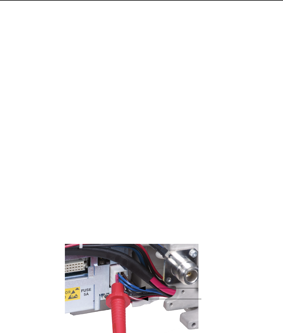
5-1
Chapter 5 MTR3000 Power Supply
5.1 Overview
This section provides an overview and probing of the Power Supply (PS) module’s output to isolate
fault.
For specifications of the PS, refer to the MOTOTRBOTM MTR3000 Base Station/Repeater Basic
Service Manual (68007024096).
5.2 Troubleshooting
5.2.1 Basic Voltage Check Procedure
This section is to illustrate measurement of the 28.6 VDC, 14.2 VDC, and 5.1 VDC sources if a
known good AC or DC source is applied to the Power Supply but there is no apparent activity from
the station.
To check the basic voltage for station failure, such as no power indicated to the station when the AC
and DC mains are connected, perform the following steps:
1. Turn on station power at source (e.g. AC or DC breaker).
2. Push a voltmeter probe into the power connector at the Backplane Interconnect Board or PA
adjacent to the indicated wires. Ensure enough of the probe tip is inserted to touch the metal
Pin inside the connector housing.
3. Touch the other voltmeter probe anywhere on the chassis (or either casting) to complete the
measurement circuit.
To measure the 14.2 VDC and 5.1 VDC, refer to Figure 5-1 For the pin-out, refer to Figure 5-2
Figure 5-1 Measuring 14.2 VDC and 5.1 VDC (other voltmeter probe to chassis)
14.2 VDC (either blue wire)
5.1 VDC (either red-white wire)
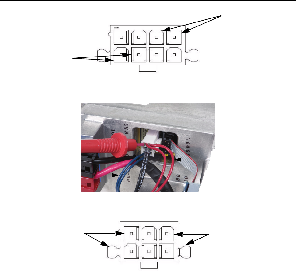
5-2 Troubleshooting
Figure 5-2 Pin-out of connector (measuring 14.2 VDC and 5.1 VDC)
To measure the 14.2 VDC and 28.6 VDC, refer to Figure 5-3 For the pin-out, refer to Figure 5-4
Figure 5-3 Measuring 14.2 VDC and 28.6 VDC (other voltmeter probe to chassis)
Figure 5-4 Pin-out of connector (measuring 14.2 VDC and 28.6 VDC)
If it is determined that the PSU is not functioning, the whole unit needs to be sent to the nearest
Motorola Repair Center to be replaced as it is not designed to be field serviceable.
14
14
58
1
4
3
6
28.6 VDC (either red wire)
14.2VDC (either blue wire)
14.2 VDC (blue wires) 28.6 VDC (red wires)
14.2 VDC (blue wires)
5.1 VDC (red-white wires)

6-1
Chapter 6 MTR3000 Receiver Module
6.1 Overview
Refer to Section 6.2, Section 6.3, Section 6.4 and Section 6.5 for the schematic diagrams, overlays,
and parts lists of the MTR3000 Receiver Module. A complete list of all parts is provided with the
parts ordered according to the schematic reference number.
For the Theory of Operation, Specifications, Block Diagrams and troubleshooting procedures of the
Receiver Module, refer to the MOTOTRBOTM MTR3000 Base Station/Repeater Basic Service
Manual (68007024096).

6-2 Overview
Notes
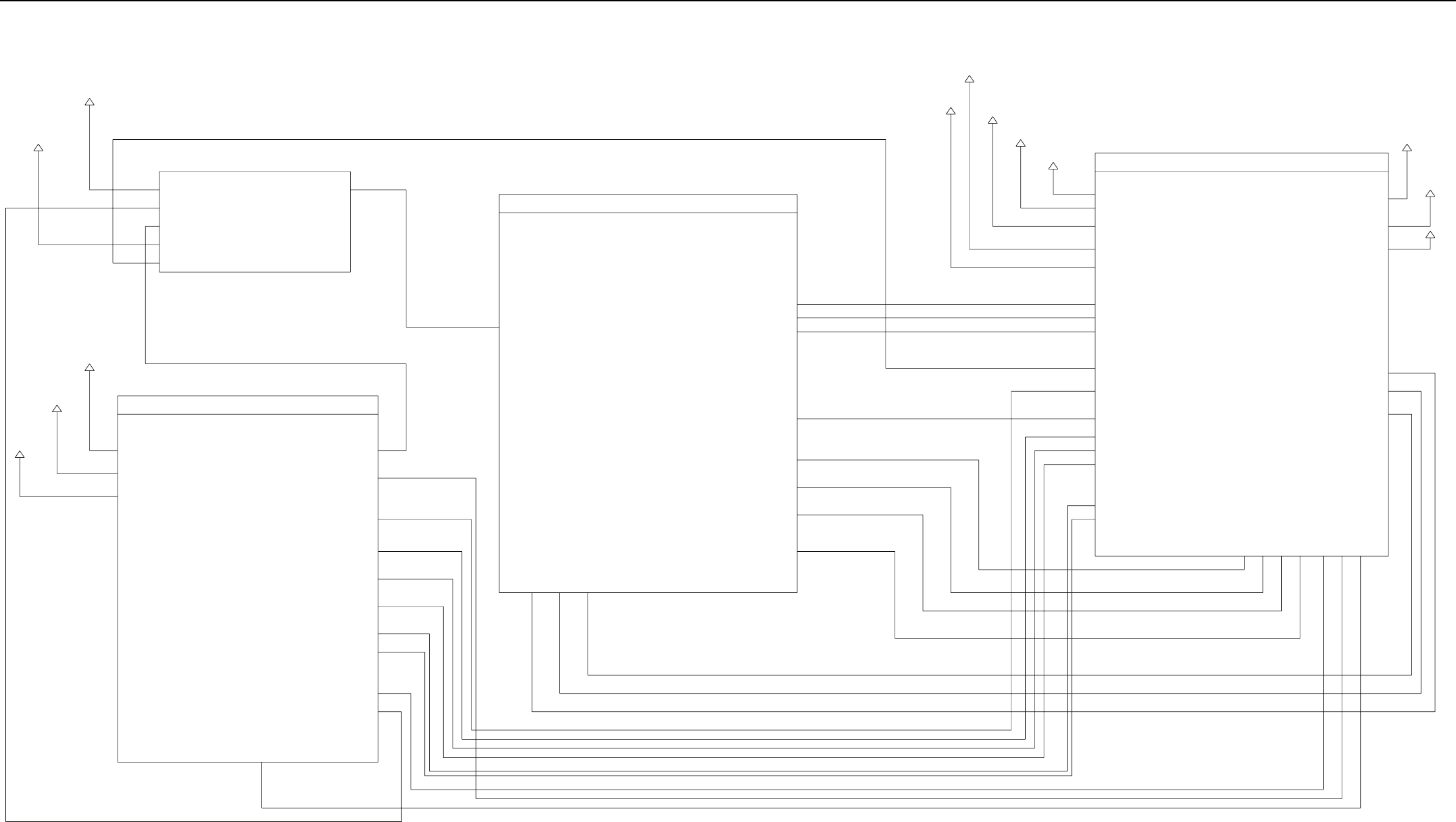
Receiver Schematics (UHF) 6-3
6.2 Receiver Schematics (UHF)
RX_V_CNTL
2.775V_RX
SYNTH_SPI_DR
SYNTH_SPI_DW
SYNTH_CLK_IN
SYNTH_CE_IN
REF_16.8MHZ_IN
INJ_MIXER_OUT
10V
TRI_RSTB_IN
RX_SLV_MON
RX_LOCK_DETECT
INJ_AMP_M1
12V_RX_SW
2.775V_RX
12V_RX_SW
10V_RX_SW
RX_FGU_1100
IN
IN
IN
BANDIT_RX_FGU
IN
OUT
OUT
IN
IN
OUT
IN
OUT
OUT
IN
RX_IF_IN
16.8MHZ_ABA_REF_IN
RX_ABA_DOUTB/MISO
RX_ABA_PC
RX_ABA_PD
RX_ABA_PE
ABACUS_CLK_M1_OUT
ABACUS_2LO_M1_OUT
RX_ABA_ODC
RX_ABA_DATA
RX_ABA_FS
RX_ABA_SYNCB
RX_BACKEND_PLL_1200
BANDIT_RX_BE_PLL
IN
IN
OUT
OUT
RX_FRONTEND_1000_1600
FINAL_IF
V_ATTN
5.0V_RX_SW
FE_V_CNTL
MIXER_LO_INPUT
12V_RX_SW
5.0V_RX
12V_RX_SW
BANDIT_RX_FE
IN
IN
IN
OUT
IN
OUT
OUT
OUT
10V_RX_SW
12V_RX_SW
5.0V_RX_SW
VCO_LD_M1_IN
RX_IF_ATTEN_OUT
SYNTH_CE_CPLD
ABA_DATA_IN
ABA_SYNCB_OUT
VCO_STL_M1_IN
ABA_PC_OUT
ABA_PD_OUT
ABA_PE_OUT
ABA_DOUTB/MISO_IN
TRI_RST_OUT
16.8MHZ_ABA_REF_OUT
ABACUS_CLK_M1_IN
ABACUS_2LO_M1_IN
8V
10V
14.2V
3.3V_RX
ABA_FS_IN
ABA_ODC_IN
2.775V_RX
16.8MHZ_SYN
INJ_FINAL_M1_IN
SPI_CLK_SYNTH
SPI_MOSI_SYNTH
SPI_MISO_SYNTH
RX_DIGITAL_1000
BANDIT_RX_DIGITAL
14.2V_RX
8.0V_RX
10.0V_RX
OUT
IN
IN
IN
IN
IN
12V_RX_SW
5.0V_RX
3.3V_RX
2.775V_RX
10V_RX_SW
OUT
IN
OUT
OUT
IN
IN
OUT
OUT
in
out
out
in
out
out
out
OUT
OUT
IN
IN
IN
OUT
OUT
OUT
Receiver – Main Schematic Diagram (Kit No. CRE4007)
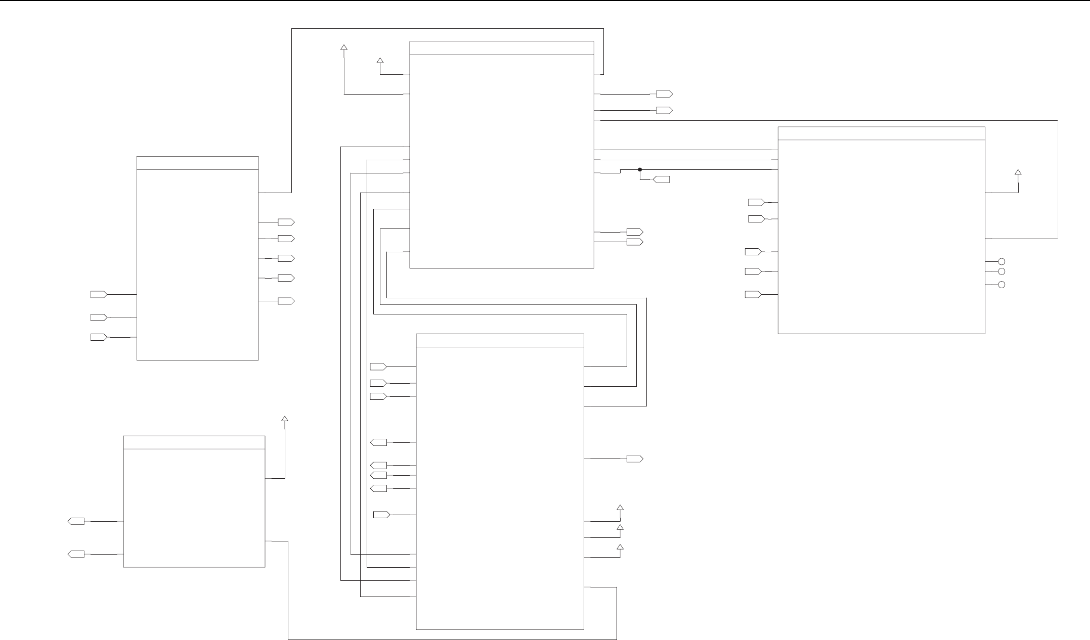
6-4 Receiver Schematics (UHF)
REF_16.8_IN
3.3V_16.8_BUFFER
16.8MHZ_ABACUS
16.8MHZ_SYN
OUT
OUT
RX_REF_BUFFER_2600
16.8MHZ_ABA_REF_OUT
16.8MHZ_SYN
OUT
BANDIT_REF_BUFFER_RX
OUT
2.775V_RX
3.3V_RX
5.0V_RX_SW
10V_RX_SW
12V_RX_SW
OUT
OUT
OUT
OUT
OUT
OUT
OUT
OUT
OUT
OUT
IN
IN
IN
IN
IN
IN
IN
8V
14.2V
10V
14.2V_RX
10.0V_RX
8.0V_RX
RX_STANDBY
10V_RX_SW
5.0V_RX_SW
3.3V_RX
2.775V_RX
12V_RX_SW
RX_REGULATORS_2200
RX_REGULATORS
3.3V_RX
IN
IN
10V_RX
RX_ATTEN
14.2V
8.0V
ABA_DOUTB/MISO
ABA_PE
ABA_FS
ABA_DATA
ABA_SYNCB
ABA_PD
ABA_PC
RX_CPLD_CE
ABA_ODC
RX_CPLD_CLK
RX_CPLD_MOSI
RX_CPLD_MISO
RX_CPLD_ADD_0
RX_CPLD_ADD_1
RX_CPLD_ADD_2
16.8_MHZ
RX_INTERCONNECT_2000
RX_INTERCONNECT
OUT
OUT
IN
IN
OUT
IN
OUT
OUT
OUT
OUT
IN
IN
ABA_SYNCB_OUT
ABA_DOUTB/MISO_IN
ABA_PC_OUT
ABA_PD_OUT
ABA_PE_OUT
ABA_FS_IN
ABA_DATA_IN
ABA_ODC_IN
IN
IN
IN
OUT
OUT
OUT
OUT
IN
8.0V_RX
10.0V_RX
14.2V_RX
RX_IF_ATTEN_OUT
OUT
IN
IN
IN
IN
IN
OUT
IN
IN
3.3V_RX
2.775V_RX
IN
IN
IN
IN
IN
IN
OUT
IN
IN
2.775V_RX
RX_STANDBY3_3V_CPLD
SPI_MISO_OUT_CPLD
SPI_MOSI_IN_CPLD
CPLD_ENABLE
ADDR1
ADDR2
ADDR0
SPI_CLK_CPLD
SYNTH_CE
TRIDENT_RST
SPI_MISO_IN_CPLD
SPI_CLK_OUT_CPLD
SPI_MOSI_OUT_CPLD
SPI_CLK_M
SPI_MOSI_M
METERING1_CE
RX_CPLD_3300
RX_CPLD
out
OUT
in
out
OUT
out
OUT
OUT
out
SYNTH_CE_CPLD
TRI_RST_OUT
OUT
OUT
IN
OUT
IN
IN
IN
in
IN
IN
ABACUS_CLK_M1_IN
SPI_MISO_SYNTH
ABACUS_2LO_M1_IN
VCO_LD_M1_IN
VCO_STL_M1_IN
INJ_FINAL_M1_IN
IN
IN
IN
IN
IN
IN
SPI_CLK_SYNTH
SPI_MOSI_SYNTH
OUT
OUT
NC
NC
NC
3.3V_RX
IN
IN
CE2_MT1
3_3_V_RX_METER
RX_RESERVED_4
RX_RESERVED_5
RX_RESERVED_6
SPI_MISO
SPI_MOSI
SPI_CLK
INJ_FINAL_M1
AB_2LO_M1
VCO_STL_M1
VCO_LD_M1
AB_CLK_M1
RX_METERING_2800
RX_METERING
Receiver – General Rx Digital Section Schematic Diagram (Kit No. CRE4007)
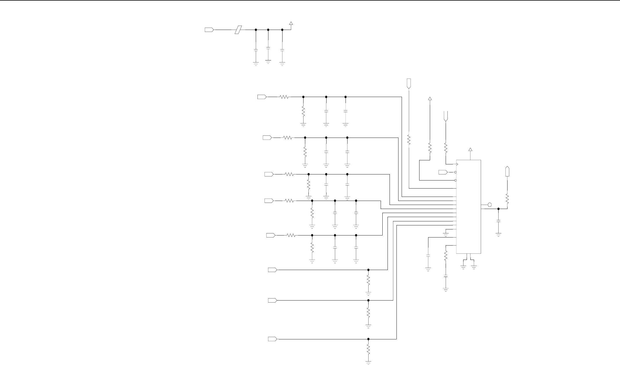
Receiver Schematics (UHF) 6-5
DNP
10UF .1UF
3_3_V_DIG_RX_METER
220PF
C2802
C2801
C2800
E2800
3_3_V_RX_METER
21
21
21
IN
20K
10K
R2802
R2801
AB_2LO_M1
AB_CLK_M1
IN
IN
220PF
.1UF
10K
R2800
C2804
C2803
21
21
15K
220PF
10K
10K
.1UF
3.32K
220PF
33.2K .1UF
10K
220PF
.1UF
R2805 C2808
C2807
R2804
R2808
R2807
R2806
C2810
C2809
R2803 C2806
C2805
VCO_LD_M1
VCO_STL_M1
INJ_FINAL_M1
21
IN
IN
IN
IN
3.9K .1UF
10K
10K
220PF
10K
R2812
R2811
R2810
R2809 C2812
C2811
RX_RESERVED_4
RX_RESERVED_6
RX_RESERVED_5
IN
IN
5.62
.015UF
4.7UF
R2817
C2813
C2814
14
13
CE2_MT1 IN
11
10
19
12
17
18
9
8
7
6
5
4
3
2
1
20
0
3_3_V_DIG_RX_METER
DNP
3_3_V_DIG_RX_METER
0
0
R2813
R2814 R2815
SPI_CLK
SPI_MOSI
IN
IN
NC
CH6
DIN
DOUT
SSTRB
DGND
AGND
VDD
CH7
CH5
CH4
CH3
CH2
CH1
CH0
SCLK
VREF
REFADJ
COM
CS
SHDN
MAX149
0
DNP
10PF
C2815
U2800
R2816
SPI_MISO
16
15
OUT
NOTE 1 : Rx CPLD Schematic Diagram (Kit No. CRE4007)
NOTE 2 : Rx Abacus Schematic Diagram (Kit No. CRE4007)
NOTE 3 : Trident Block Schematic Diagram (Kit No. CRE4007)
NOTE 4 : Rx Lo1 Injection Amp and Feedback Schematic Diagram (Kit No. CRE4007)
NOTE 2
NOTE 2
NOTE 4
NOTE 3
NOTE 3
NOTE 1
NOTE 1
NOTE 1
NOTE 1
Receiver – Rx Metering Schematic Diagram (Kit No. CRE4007)
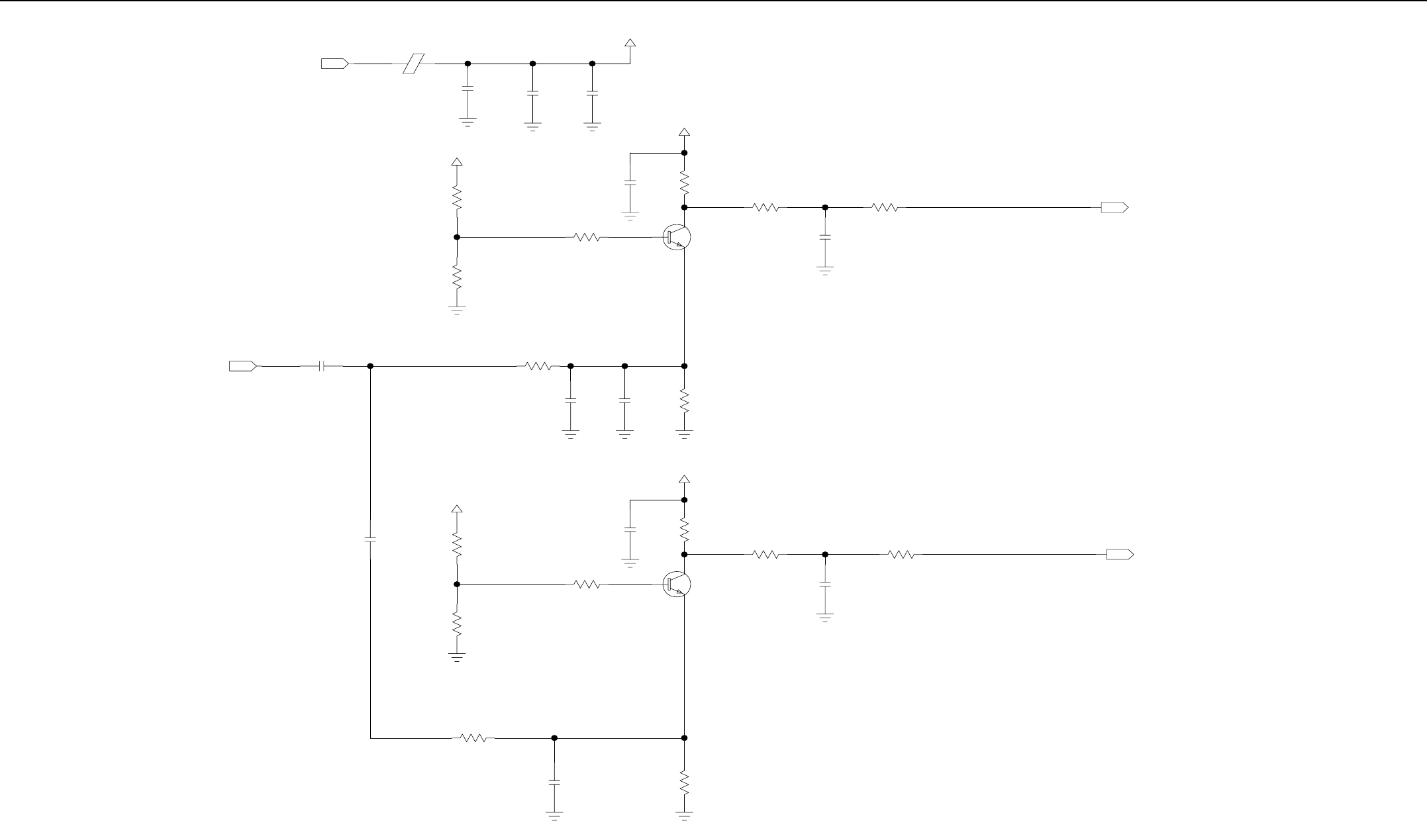
6-6 Receiver Schematics (UHF)
3.3V_16.8_BUFFERIN
SQAURE WAVE
1.3 VP-P
.1UF
C2610
REF_16.8_ININ0.8V
180PF 150
15PF
0
C2621 R2615
C2615
R2610
1.3V
3.3V_BUF
.1UF 2.67K
2.67K
475
R2623
R2651
R2622
C2613
1
0.9V
3.3V_BUF
.1UF 475
100
MMBT3904
R2627
R2625
C2618
Q2611
23
0.8V
150
15PF
0
R2626
C2616
R2620
DNP
10UF
220PF
RX_REF_BUFFER
.1UF
E2610
C2614
C2612
C2611
1.3V
0.9V
475
3.3V_BUF
3.3V_BUF
.1UF
C2617 R2616
3.3V_BUF
2.67K
MMBT3904
2.67K
475
100
R2614
Q2610
R2628
R2612
R2611
23
1
0
33PF
R2630
C2620
OUT
SQUARE WAVE
1.1 VP-P
16.8MHZ_SYN
SQUARE WAVE
1.1 VP-P
16.8MHZ_ABACUS
OUT
0
33PF
R2631
C2619
NOTE 1 : Control Board to Rx Interconnect Schematic Diagram (Kit No. CRE4007)
NOTE 2 : Rx Abacus Schematic Diagram (Kit No. CRE4007)
NOTE 3 : Trident Block Schematic Diagram (Kit No. CRE4007)
NOTE 1
NOTE 2
NOTE 3
Receiver – Rx 16.8MHz Ref Buffer Schematic Diagram (Kit No. CRE4007)
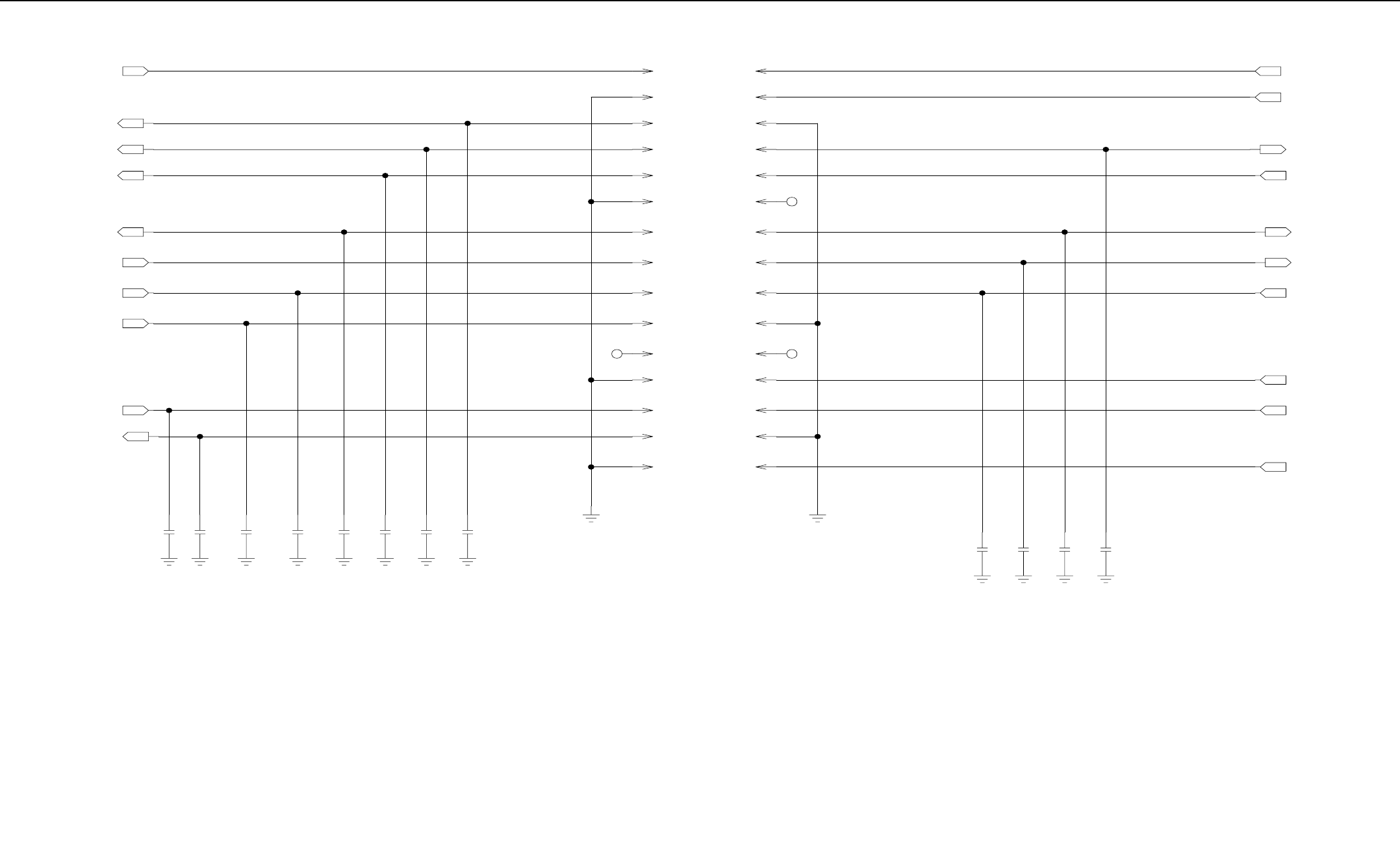
Receiver Schematics (UHF) 6-7
ABA_ODC
ABA_SYNCB
ABA_PE
ABA_PC
RX_CPLD_CE
10V_RX
RX_CPLD_ADD_0
RX_CPLD_ADD_1
RX_ATTEN
RX_CPLD_MISO
IN
IN
IN
OUT
OUT
OUT
OUT
IN
IN
OUT
DNP
DNP
DNP
DNP
DNP
DNP
DNP
DNP
.1UF
220PF
220PF
220PF
220PF
220PF
220PF
220PF
C2015
C2006
C2005
C2004
C2003
C2002
C2001
C2000
21
21
RX_INTERCONNECT
J2000
J2000J2000
J2000J2000
J2000
J2000J2000
J2000J2000
J2000J2000
J2000
J2000J2000
J2000J2000
J2000
J2000J2000
J2000
J2000
J2000J2000
29 30
2827
2625
23 24
2221
2019
1817
15 16
1413
1211
910
87
56
34
21
J2000
J2000
J2000
J2000
J2000
J2000
NC NC
NC
220PF
220PF
220PF
220PF DNP
DNP
DNP
DNPC2011
C2010
C2008
C2009
ABA_FS
14.2V
8.0V
ABA_DATA
ABA_PD
ABA_DOUTB/MISO
RX_CPLD_ADD_2
RX_CPLD_MOSI
RX_CPLD_CLK
16.8_MHZ
IN
IN
OUT
OUT
IN
IN
OUT
IN
IN
IN
NOTE 1 : Rx 16.8MHz Ref Buffer Schematic Diagram (Kit No. CRE4007)
NOTE 2 : Rx CPLD Schematic Diagram (Kit No. CRE4007)
NOTE 3 : Rx Abacus Schematic Diagram (Kit No. CRE4007)
NOTE 4 : Rx IF Attenuator Schematic Diagram (Kit No. CRE4007)
NOTE 3
NOTE 3
NOTE 3
NOTE 3
NOTE 2
NOTE 2
NOTE 2
NOTE 2
NOTE 4
NOTE 3
NOTE 3
NOTE 3
NOTE 3
NOTE 2
NOTE 2
NOTE 2
NOTE 1
Receiver – Control Board to Rx Interconnect Schematic Diagram (Kit No. CRE4007)
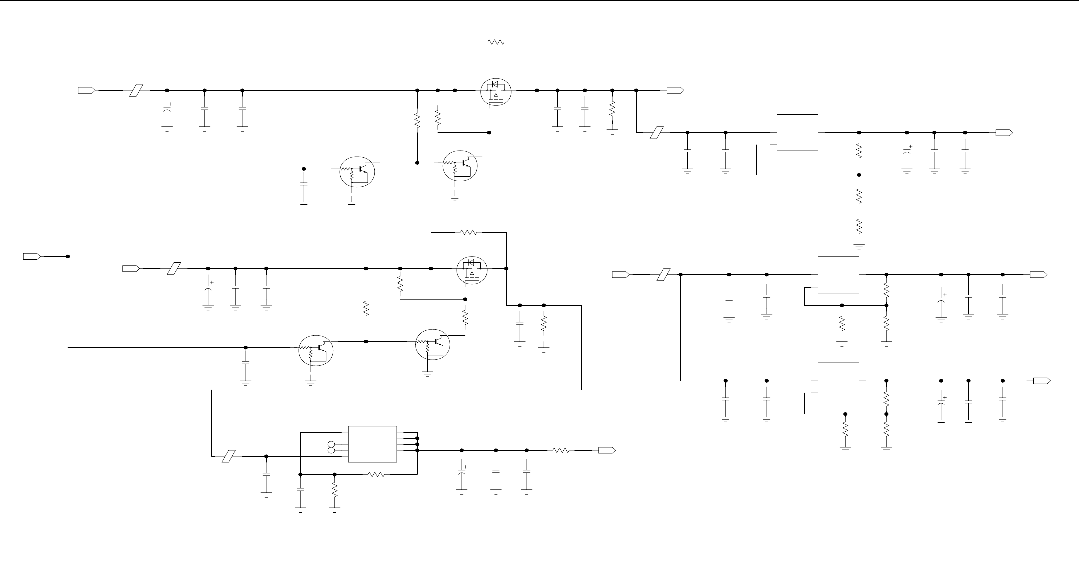
6-8 Receiver Schematics (UHF)
ENCHANCEMENT PCHAN
NORMALLY OFF
OUTIN
ADJUST
10K
47K
10K
47K
.1UF
MUN5214T1
220PF
10K
DNP
NTR1P02LT1
0
.01UF
LM317M
220PF
220PF
DNP
RX_REGULATORS
47UF
10K
MUN5214T1
220PF .1UF
10K
R2203 U2200
C2208
C2207
E2203
C2206
C2205
R2202
Q2200
Q2202
R2201
R2200
Q2201
C2211
C2202
C2201
C2200
E2200
10.0V_RX10V_RX_SW
3
1
2
1
3
2
3
1
2
3
1
21
OUT
IN
2
220PF
10
.1UF
280 10UF
825
C2203 C2210
C2209
R2206
R2205
R2204
5.0V_RX_SW
21
OUT
OUTIN
ADJUST
.1UF
DNP
1.1K
LM317M
270
430
220PF
R2217
U2201
C2226
C2225
E2204
R2216
R2215
8.0V_RX23
1
IN
.1UF 220PF
10UF
C2233 C2228
C2227
3.3V_RX
21
OUT
220PF
C2232
2.775V_RX
OUT
.1UF
C2235
10UF
C2231
21
OUTIN
ADJUST
280
DNP
1.1K 332
LM317M
R2221
U2202
R2220
R2219
23
1
220PF .1UF
C2230
C2229
0
220PF
.1UF
10UF
R2213
C2224
C2223
C2222
21
OUT
NC
NC
VOUT1
VOUT2
VOUT4
VOUT3
VIN
NC1
NC2
GND_ADJ
MC33269
U2203
7
6
3
2
4
8
5
1
1UF
.33UF
2.32K
270
DNP
R2212
R2211
C2220
E2202
C2221
12V_RX_SW
DEFAULT-LOW
ACTIVE-HIGH
14.2V_RX
RX_STANDBY
IN
IN
47UF
DNP
220PF.01UF
C2214C2213
C2212
21
10K
47K
MUN5214T1
220PF
Q2204
C2218
2
3
1
10K
10K
R2208
R2207
10K
47K
10K
MUN5214T1
R2210
Q2205
2
3
1
DNP
NTR1P02LT1
0
Q2203
R2209
2
1
3
.1UF 10K
R2214
C2217
E2201
NOTE 1 : Rx CPLD Schematic Diagram (Kit No. CRE4007)
NOTE 1
Receiver – Rx Voltage Regulators Schematic Diagram (Kit No. CRE4007)
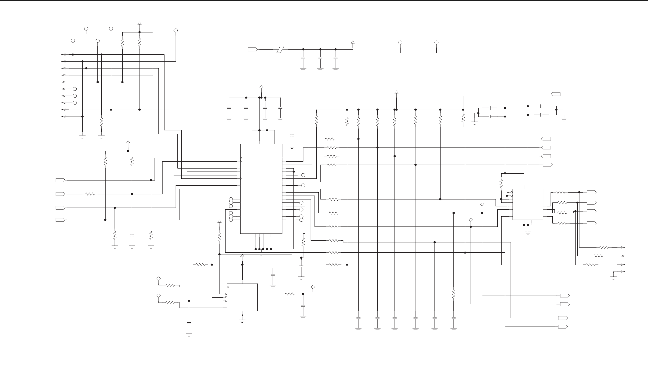
Receiver Schematics (UHF) 6-9
NOTE A:
FOR BANDIT ONLY, THE EVEN NUMBER OF ENABLE PINS ARE USED FOR CPLD
NOTE A
3_3V_CPLD_FILT
0
1K
4.75K
4.75K
R3303
R3305
R3301
R3300
SPI_MISO_IN_CPLD
SPI_CLK_CPLD
SPI_MOSI_IN_CPLD
CPLD_ENABLE
IN
IN
IN
IN
SPI_MOSI_M
10PF
SPI_CLK_M
0
0
R3328
C3318
R3330
SPI_MOSI_M
SPI_CLK_M
3_3V_CPLD_FILT
10K
4.75K
R3331
R3327
1K
DNP
10PF
1K
R3307
C3300
R3302
7
32
1
26
40
38
31
28
27
25
35
34
33
39
37
NC
NC
NC
NC
NC
NC
30
24
11
4
36
16
VCCINT1
VCCINT0
IO_A0
IO_A1
IO_A2
IO_A3
IO_A6
IO_A5
IO_A4
IO_A8
IO_A7
IO_A11
IO_A10
IO_A9
IO_B0
IO_A12
IO_B1
IO_B2
IO_B3
IO_B5
IO_B4
GNDINT1
GNDIO3
GNDINT0
VCCIO1
VCCIO0
GCLK1
TCK
TMS
TDI
OE1
GCLRN
IO_B7
IO_B6
IO_B8
IO_B10
IO_B9
IO_B12
IO_B11
GNDIO1
GNDIO2
GNDIO0
TDO
OE2_GCLK2
EPM3032ATI44
U3300
NC
NC
NC
NC
NC
NC
49.9
R3326
DNP
10PF
C3349
4.75K
R3350
PLACE 0.1UF CAP NEAR EACH SUPPLY PIN OF CPLD
3_3V_CPLD_FILT
.1UF
.1UF .1UF.1UF
RECEIVER_CPLD
C3304
C3303C3302C3301
29
9
41
17
23
22
21
20
19
18
15
14
13
12
10
8
6
5
44
43
42
3
2
33.2
33.2
33.2
33.2
33.2
33.2
33.2
49.9
49.9
49.9
R3390
R3391
R3392
R3314
R3312
R3311
R3310
R3309
R3308
R3332
4.75K
4.75K 4.75K
4.75K4.75K 4.75K
4.75K
R3322
R3318
R3317
R3334R3316R3315R3333
3_3V_CPLD_FILT
.01UF
.1UFC3345
C3346 .01UF
.1UFC3347
C3348
2.775V_RX
IN
ADDR2
ADDR1
METERING1_CE
ADDR0
OUT
IN
IN
IN
10
12
11
13
14
15
3
2
7
5
6
4
16
1
17
9
8
VCCB
VCCA
GND3
GND2
GND1
B1_2
B1_1
B2_2
B2_1
A2_2
A2_1
A1_2
A1_1
DIR2
DIR1
OE2
OE1
SN74AVC4T245
U3303
4.75K
R3345
SPI_CLK_M
SPI_MOSI_M
SYNTH_CE
SPI_MOSI_OUT_CPLD
TRIDENT_RST
SPI_CLK_OUT_CPLD
OUT
OUT
OUT
OUT
0
33.2
33.2
33.2
R3346
R3347
R3348
R3349
0
DNP
0DNP
DNP
DNP
0DNP
DNP
DNP
P3301
P3301
P3301
P3301
R3323
R3324
R3325
1
4
3
2
SPI_CLK_M
SPI_MOSI_M
RX_STANDBY
SPI_MISO_OUT_CPLD
OUT
OUT
OUT
OUT
PLACE SERIES RC ON FINAL DAISY-CHAINED SPI DEVICE
DNPDNPDNP
0
DNPDNP
10PF 10PF10PF 10PF 10PF 10PF
DNP
DNP
R3319
C3312
C3311C3310C3320C3309C3308
GND
WP
VCC
HOLD
SI
SOEN_CS
CLK_S
AT25640A
U3301
3
5
7
4
1
6
3_3V_CPLD_FILT
0.1UF
33.2
DNP
10PF
C3315
C3316
R3329
8
2
DNP
10PF
SPI_MISO_IN_CPLD
C3317
SPI_MISO_IN_CPLD
TEST_POINT
TP3302
1
2
3
4
5
6
7
8
9
10
NC
NC
NC
P3300
P3300
P3300
P3300
P3300
P3300
P3300
P3300
P3300
P3300
TEST_POINT
TEST_POINT
TP3303TP3301
TP3300
1
1
1
1
3_3V_CPLD_FILT
1K 1K
R3306
R3304
TEST_POINT
TEST_POINTTP3304
1
E3300
3_3V_CPLD IN
3_3V_CPLD_FILT
.1UF 220PF
10UF
C3307C3306C3305
TEST_POINTTEST_POINT
TP3306TP3305
1
1
NOTE 1 : Rx Metering Schematic Diagram (Kit No. CRE4007)
NOTE 2 : Control Board to Rx Interconnect Schematic Diagram (Kit No. CRE4007)
NOTE 3 : Rx Voltage Regulators Schematic Diagram (Kit No. CRE4007)
NOTE 4 : Trident Block Schematic Diagram (Kit No. CRE4007)
NOTE 2
NOTE 1
NOTE 4
NOTE 2
NOTE 2
NOTE 2
NOTE 2
NOTE 2
NOTE 1
NOTE 4
NOTE 4
NOTE 4
NOTE 4
NOTE 1
NOTE 1
NOTE 2
NOTE 3
Receiver – Rx CPLD Schematic Diagram (Kit No. CRE4007)
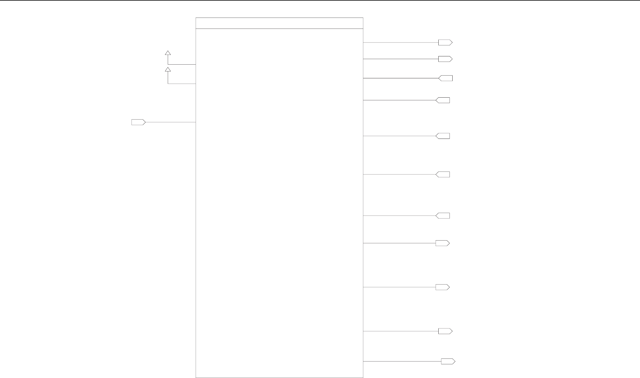
6-10 Receiver Schematics (UHF)
RX_ABA_SYNCB
RX_ABA_ODC
RX_ABA_FS
RX_ABA_DATA
RX_ABA_DOUTB/MISO
OUT
OUT
OUT
OUT
IN
IN
IN
IN
IN16.8MHZ_ABA_REF_IN
ABACUS_2LO_M1_OUT
ABACUS_CLK_M1_OUT
RX_ABA_PC
RX_ABA_PE
RX_ABA_PD
OUT
OUT
8.0V_RX
10.0V_RX
in
IN
IN
RX_IF_ININ
REF_16.8
AB_2LO_M1
AB_CLK_M1
ABA_CLK
ABA_CE
ABA_DATA
ABA_ODC
ABA_FS
ABA_DOUT
ABA_DOUTB/MISO
SYNC_B
8V_RX
10V_RX
RX_IF_IN
RX_BACKEND_2400
RX_BACKEND
OUT
in
in
in
in
in
out
out
out
out
out
Receiver – Rx Backend PLL Schematic Diagram (Kit No. CRE4007)
Receiver Schematics (UHF) 6-11
8V_RXINOUTIN
ADJUST
220PF .1UF
1.21K
DNP
220PF
430
270 .1UF10UF
LM317M
C2402
U2400
C2400 C2409C2406C2433
R2404
R2403
R2400
2
3
1
21
191
100K
22UF
1MEG
191
.1UF
10
R2422
R2423
C2401
E2400
R2406
R2405
R2401
C2403
10V_RX
21
IN
MMBTA13
Q2400
23
1
110
110
0
.1UF
22UF
R2413
C2410
C2407
R2407
R2408
21
REF_16.8
RX_IF_IN
ABA_DATA
ABA_CLK
ABA_CE
SYNC_B
IN
IN
IN
IN
IN
IN
IN
IN
IN
IN
IN
IN
IN
IN
ABA_CLKOUT
ABA_DOUTA
ABA_FS
RX_SL_LO2
RX_SL_CLK
PD
PC
PE
SYNCB
IF
3.3V
FREF
ANALOG_5V
ABA_DOUTB/MISO
RX_ABACUS_2500
RX1_ABACUSIII
OUT
OUT
OUT
OUT
OUT
OUT
AB_2LO_M1
AB_CLK_M1
ABA_ODC
ABA_DOUT
ABA_FS
ABA_DOUTB/MISO
OUT
OUT
OUT
OUT
OUT
OUT
Receiver – Rx Backend Schematic Diagram (Kit No. CRE4007)
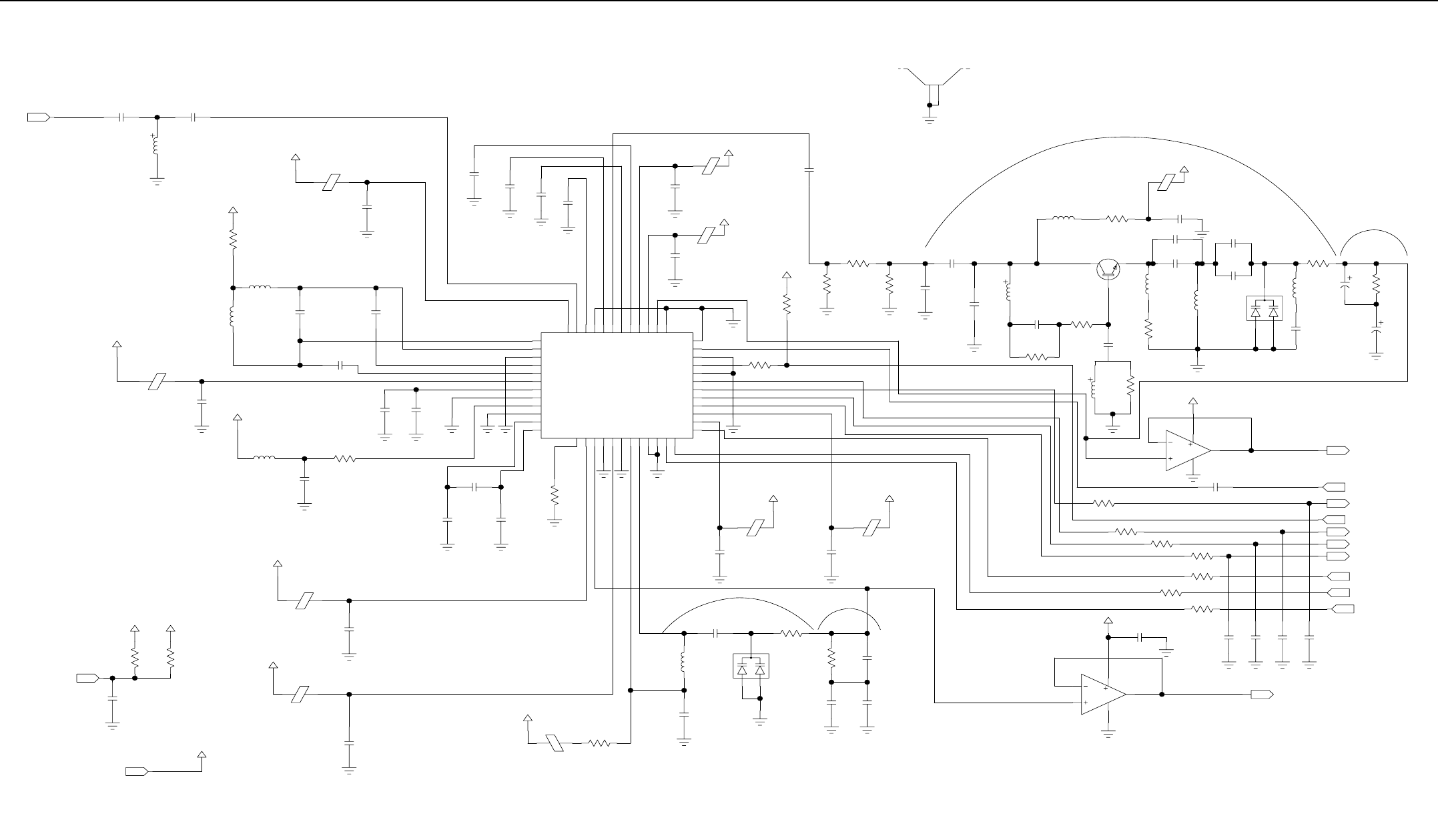
6-12 Receiver Schematics (UHF)
IF
IN
15PF
C2501
21
270NH
L2530
21
33PF
C2502
21
3.3V_ANALOG_M
49.9
R2532
21
1.5V
2.0V
100K
100PF
.01UF
100PF
C2516
R2534
C2519
C2514
21
21
21
3.3V_DIGITAL_M
3.3V_ANALOG_M
.047UF
4.7NH0
E2534
L2534
C2503
R2533
21
3.3V_ANALOG_M
0.1UF
E2533
C2506
3.3V_ANALOG_M
ANALOG_5V_M
3.3V_DIGITAL_M
0
0
0.1UF
R2531
R2530
C2500
ANALOG_5V
3.3V
21
21
IN
IN
3.3V_DIGITAL_M
0.1UF
0.1UF
C2504
E2535
C2505
3.3V_DIGITAL_M
10K
E2536 R2535
21
SAMPLE CLK SLV
2.0V TYPICAL
(0.8V TO 2.8V)
(18 MHZ)
CLOCK VCO TANK
1.9V
1SV228
100PF 2K
1.2UH 392
0.1UF
.33UF
0.1UF
.33UF
C2532
C2531
C2529
R2540
R2538
CR2531
C2525
C2523
L2535
3
2
21 2 1
1
3.3V_DIGITAL_M
0.1UF
3.3V_DIGITAL_M
0.1UF
C2528
E2538
C2524
E2537
14
17
13
24
23
15
21
16
22
18
19
20
11
12
6
9
1
2
5
4
3
10
7
8
CXVL
LOP
LON
CXVM
VDDL
VDDP
IOUTL
GNDP
RREF
VDDQ
IOUTC
GNDQ
VDDC
GNDC
CLKP
CLKN
GNDS1
GNDD
PC
PD
GNDL
FREF
GNDS2
SYNCB
GNDH
FS
DOUTB
DOUTA
CLKOUT
VDDH
VDDD
PE
MXOP
MXON
GNDF
IF2N
IF2P
VDDF
GCP
GCN
VDDA
GNDA
VREFP
VREFN
VDDI
IFIN
CXIF
GNDI
RX_ABACUS
AD9874
U2530
1.2V
3.3V
3.3V
1.5V
33.2
R2536
27
26
33
25
34
36
32
31
35
30
29
28
39
40
48
43
42
38
47
37
45
41
44
46
ANALOG_5V_M
0.1UF
C2521
E2539
21
3.3V_ANALOG_M
0.1UF
C2522
E2540
7.5PF 330NH
1SV228
3300PF 22UF
120NH
2.2UF 182
10K
C2561
R2563
C2557
R2559
C2555
L2548
CR2530
C2552
L2547
21
21
21
3
2
1
2.2UH
121
R2548
L2543
21
2121
15PF
DNP27PF
0.1UF
3PF
ANALOG_5V_M
C2547
E2541
C2554
C2553
C2546
21
BFQ67W
10
2.2UH
R2549
L2539
Q2530
23
1
15PF
C2542
21
ANALOG_5V_M
12NH
100
R2547
L2549
2
1
21
3
2
2.2V
MC33072
0.1UF
U2531
C2556
48
1
ANALOG_5V_M
0.1UF
C2551
MC33072
U2531
21
48
7
5
6
1.7V
RX_SL_CLK
OUT
10PF
10PF
10PF
10PF
C2580
C2581
C2582
C2583
49.9
33.2
49.9
33.2
33.2
49.9
33.2
R2596
R2597
R2595
R2581
R2580
R2582
R2583
ABA_DOUTB/MISO
FREF
PC
ABA_DOUTA
ABA_FS
SYNCB
PD
ABA_CLKOUT
PE
IN
OUT
OUT
OUT
IN
OUT
IN
OUT
IN
IN
RX_SL_LO2
3.2V
1.5V
3.2V
1.5V
0.7V
2200PF
56PF
100PF
150PF
10UH
10UH
100PF
C2509
C2510
L2532
L2533
C2508 C2513
C2512
21
21
21
21
21
1.0V
3.3V_ANALOG_M
0.1UF
C2517
E2532
1.9V
3.3V
1.9V
2.0V
.01UF
.01UF
0.1UF
1000PF
C2520
C2518
C2515
C2511
21
442
442
3.3V_DIGITAL_M
11.5
100K
R2541
R2542
R2539
R2537
21
3.6 DB
50 OHM 2.2PF
1.1PF
1.1PF
DNP
C2539
C2534
C2535
12NH
10K
470PF
R2545
C2541
L2538
21
21
21
475
R2546
0.1UF
RX_ABACUS
SHIELD
SH2500
C2527
2
1
2ND LO LOOP FILTER
VSL = 2.3V TYPICAL
(0.8V < VSL < 4.4V)
2ND LO VCO @ 75.6 MHZ
NOTE 1 : Rx Metering Schematic Diagram (Kit No. CRE4007)
NOTE 2 : Rx 16.8MHz Ref Buffer Schematic Diagram (Kit No. CRE4007)
NOTE 3 : Control Board to Rx Interconnect Schematic Diagram (Kit No. CRE4007)
NOTE 4 : Rx IF Attenuator Schematic Diagram (Kit No. CRE4007)
NOTE 4
NOTE 1
NOTE 2
NOTE 3
NOTE 3
NOTE 3
NOTE 3
NOTE 3
NOTE 1
Receiver – Rx Abacus Schematic Diagram (Kit No. CRE4007)
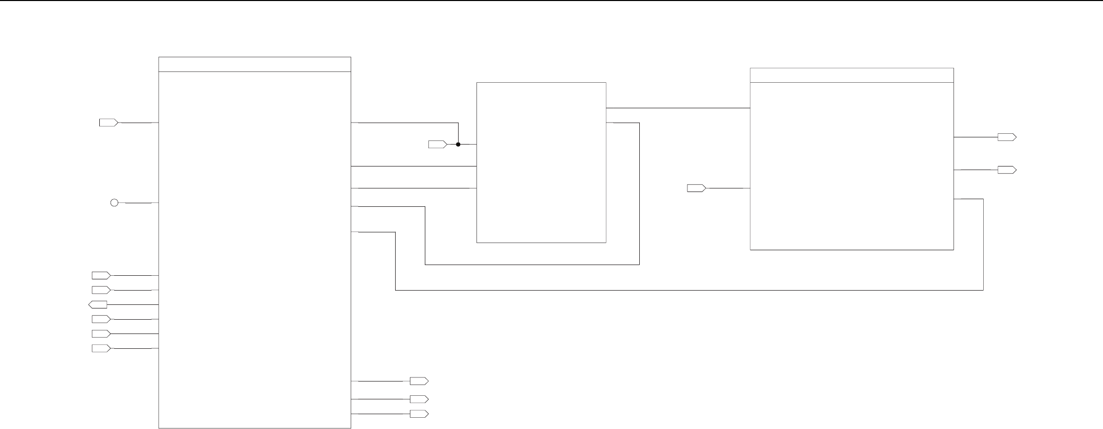
Receiver Schematics (UHF) 6-13
in
in
in
in
out
in
in
out
NC
SYNTH_CLK_IN
2.775V_RX
REF_16.8MHZ_IN
SYNTH_SPI_DW
SYNTH_CE_IN
TRI_RSTB_IN
SYNTH_SPI_DR
IN
IN
IN
IN
OUT
IN
IN
TRI_AUX_DAC
2.775V_RX
RX_LOCK_DETECT
RX_SLV_MON
LF_OUT
PRE_SCALER
SPARE_2
REF_16.8_MHZ
TRI_SPI_DW
TRI_SPI_CLK
VCO_SELECT
TRI_SPI_CEX
TRI_SPI_DR
TRI_RSTB
VCC_CP
12V_RX_SW
TRIDENT_BLOCK
3100
12V_RX_SWININ
in
out
OUT
OUT
in
out
IN
RX_V_CNTL
RX_LOCK_DETECT
RX_SLV_MON
OUT
OUT
OUT
VCC_CP
LO_OUT
VCO_SELECT
VCO_SLV
12V_VCO
RX_VCO_3200
3200
VCO_V5
OUT
OUT
OUT
INJ_MIXER_OUT
INJ_AMP_M1
VCO_FEEDBACK
INJ_AMP_M1
VCO_INJ_OUT
RX_INJ_AMP_FBK_2700
2700
BANDIT_INJ_AMP_FDBK
10V_RX
LO_IN
IN
IN
10V IN
OUT
OUT
Receiver – Rx Frequency Generation Unit (FGU) Schematic Diagram (Kit No. CRE4007)
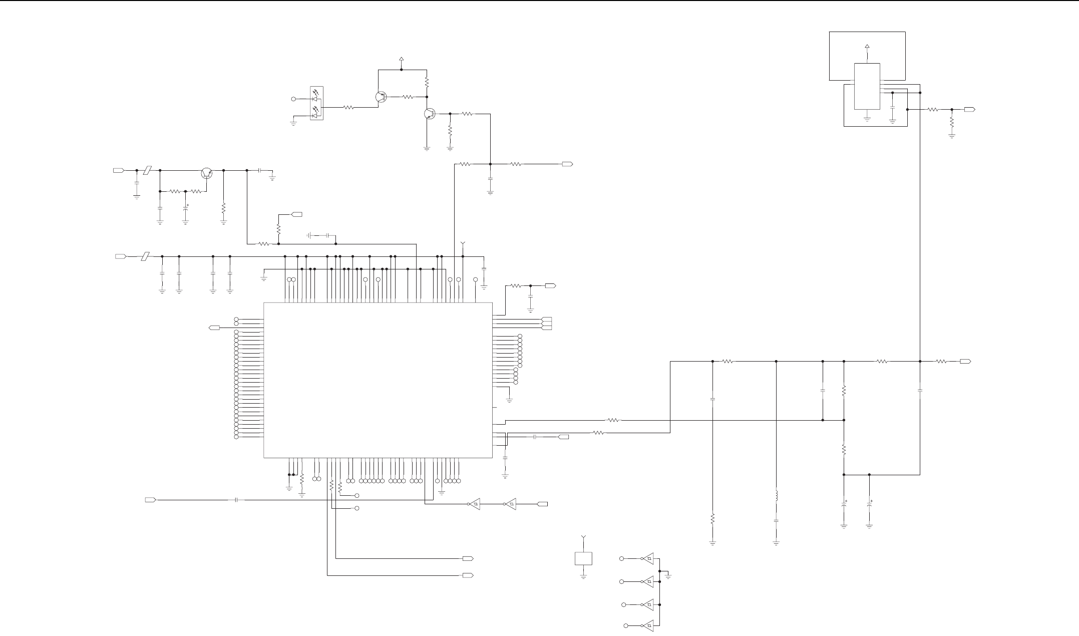
6-14 Receiver Schematics (UHF)
.01UF
10
DNP
DNP
.01UF
DNP
267
39PF
DNP
DNP
10K
DNP
330UF
DNP
DNPDNP
MMBT3904
C3171
Q3100
R3152
R3151
E3110
R3150
C3132
C3131
C3130
12V_RX_SW21
23
1
21
IN
DNP
.1UF
00
R3101
R3100
C3116
VCC_CP
21
IN
BOTTOM-SIDE EVALTOP-SIDE EVAL
DNP
220PF DNP
220PF
.1UF .1UF
C3100
C3111C3107
E3105
2.775V_RXIN
C3103
TRI_AUX_DAC OUT
L7
L8
J11
A10
F5
D2
D1
C2
C1
B6
A5
K7
G11
L6
K8
F8
J7
A3
A4
B5
J10
E2
E1
B1
B2
K6
D3
A6
C3
NC
NC
NC
NC
NC
NC
NC
NC
NC
NC
NC
NC
NC
NC
NC
NC
NC
NC
NC
NC
NC
NC
NC
NC
NC
NC
NC
NC
NC
NC
NC
NC
NC
NC
NC
.1UF
TRI_VCC
C3124
NC3
ESC_CPBIAS
ESC_CP
SF_BYP
REF_OSC_OUT
TXQ
NTXI
PHCLK
DEEPSLEEP
NC4
LVCC1
SDM_CLK_GEN_GND
RX_AGND2
SSI_GND
MAIN_GND
LGND1
VMULTI2
VMULTI1
SUB2
DMCS
TXFS
TXCLK
TXD
ESC_IN
MN_CP
SF_OUT
CLK_OUT
CLK_EMIT
M_PRSC
RXD
ESC_TEST
BP_Q
BP_QX
BP_I
QCAP
RSTB
SF_SPLY
EF_OUTP
EF_OUTM
INCR_DECR
NC5
REF_VCC
GPO2_TEST2
RX_EN_OUT
SUB3
AGC_DAC
FBQ
SDM_VREFP
SDM_VAG
REF_IN
NTXQ
TXI
HP_MOD_OUT
MN_CP_GND
SUB1
NC6
ASPI_CLK
SPI_CLK
RXQ
RXQX
SCAN_EN
ICAP
ACE2_GPO8
TEST1_LCKDET
CEX
SPI_DW
SPI_DR
RXACQ
RXCLK
RXFS
BP_IX
SCAN_IN
GPO4_TEST4
GPO1_TEST1
RX_AVCC2
ASPI_VCC
SDM_CLK_GEN_VCC
RX_AVCC1
SF_GND
SDM_REF_VCC
SSI_VCC
TCLK
CLK_CP
CLK_BASE
MN_ADAPT_CP
M_PRSCX
SENS
AUX_DAC
ESC_CP_GND
MN_CP_VCC
MAIN_VCC
ESC_CP_VCC
TX_VCC
CLK_VCC
ESC_VCC
TX_DAC_VCC
SDM_REF_GND
RX_AGND1
CLK_GND
NC1
DC_CAL_GPO5
RFSTEPA_GPO6
ESC_INX
ACE1_GPO7
SDM_VREFM
NC2
ASPI_GND
TX_GND
ESC_GND
TX_DAC_GND
ESCD2_OUT
ESCD2_OUTX
GPO3_TEST3
ASPI_DATA
RXIX
RXI
AGC_FLAG
AGC_REF
FBI
TEST2
RX_TRIDENT_BLOCK
TRIDENT BGA 121PIN
15H28
U3100
TM
F9
F11
F10
D10
D9
C11
E8
D11
E9
D7
K2
K1
H2
J2
L3
F7
D8
NC
NC
NC
NC
NC
NC
NC
NC
NC
NC
NC
NC
TRI_SPI_CLK
TRI_SPI_DW
TRI_SPI_CEX
IN
IN
IN
TRI_SPI_DR
OUT
DNP
10PF
C3172
33.2
R3172
H7
G7
H6
G6
E7
C4
B4
E11
E10
J4
C8
C9
A9
B9
B11
C7
A2
D4
B3
E4
J6
F1
F2
G4
G5
G8
G9
H3
H4
J1
L2
J3
K3
H9
J9
A8
B8
REF_16.8_MHZ IN
.022UF
C3101
NC
NC
NC
NC
NC
NC
NC
NC
NC
NC
NC
NC
NC
NC
NC
NC
NC
NC
NC
NC
H10
H11
F4
F6
K9
K4
J5
L4
H5
B10
C10
L5
K5
F3
E3
L11
L1
A11
A1
C5
E6
D5
E5
J8
H8
G10
L10
K10
K11
A7
B7
D6
C6
NC
NC
NC
NC
10K
DNP
10K
DNP
10K
R3102
R3173
R3113
MC74LVX14
U3103 U3103
TRI_RSTB
432 1 IN
VCO_SELECT
SPARE_2
OUT
OUT
NC
QT1222
DNP
DNP
51
D3180
R3180
2
3
1
DNP
DNP
MMBT3904
10K
DNP
MMBT3906
150K
DNP
DNP
150K
DNP
27K
2.775V_RX
R3182
Q3180
R3184
R3185
R3183
Q3181
R3181
23
1
23
1
100 0
.1UF
DNP
R3187
C3185
RX_LOCK_DETECT
OUT
.01UF
2.8K
C3102
R3103
0
0
R3130
R3129
PRE_SCALER
IN
220PF
220PF
C3127
C3126
G3
G2
H1
G1
L9
MC74LVX14
IN2POS
IN2NEG
VCC_NEG
IN1NEG
IN1POS
VCC_POS
OUT1
OUT2
12V_RX_SW
TS272
U3101
84
7
1
5
6
3
2
220PF
10K
0
C3120
R3147
R3146
RX_SLV_MON
OUT
0
R3134
LF_OUT
OUT
.12UF
C3105
22.1
348
R3104
R3105
.12UF
C3104
49.9
R3106
1UF 1UF
C3109
C3108
21
21
COILCRAFT 0805CS
3300PF
100NH
L3100
C3106
0
R3108
5
9
11
13
MC74LVX14
MC74LVX14
MC74LVX14
MC74LVX14
U3103
U3103
U3103
U3103
NC
NC
NC
NC 6
8
10
12
VCC
GND
MC74LVX14
TRI_VCC
U3103
147
NOTE 1 : Rx Metering Schematic Diagram (Kit No. CRE4007)
NOTE 2 : Rx 16.8MHz Ref Buffer Schematic Diagram (Kit No. CRE4007)
NOTE 3 : Rx CPLD Schematic Diagram (Kit No. CRE4007)
NOTE 4 : Rx Lo1 Injection Amp and Feedback Schematic Diagram (Kit No. CRE4007)
NOTE 5 : UHF VCO Schematic Diagram (Kit No. CRE4007)
NOTE 6 : Rx FE Tunable Filter Schematic Diagram (Kit No. CRE4007)
NOTE 6
NOTE 2
NOTE 5
NOTE 1
NOTE 3
NOTE 3
NOTE 3
NOTE 3
NOTE 4
NOTE 3
NOTE 5
NOTE 1
NOTE 5
Receiver – Trident Block Schematic Diagram (Kit No. CRE4007)
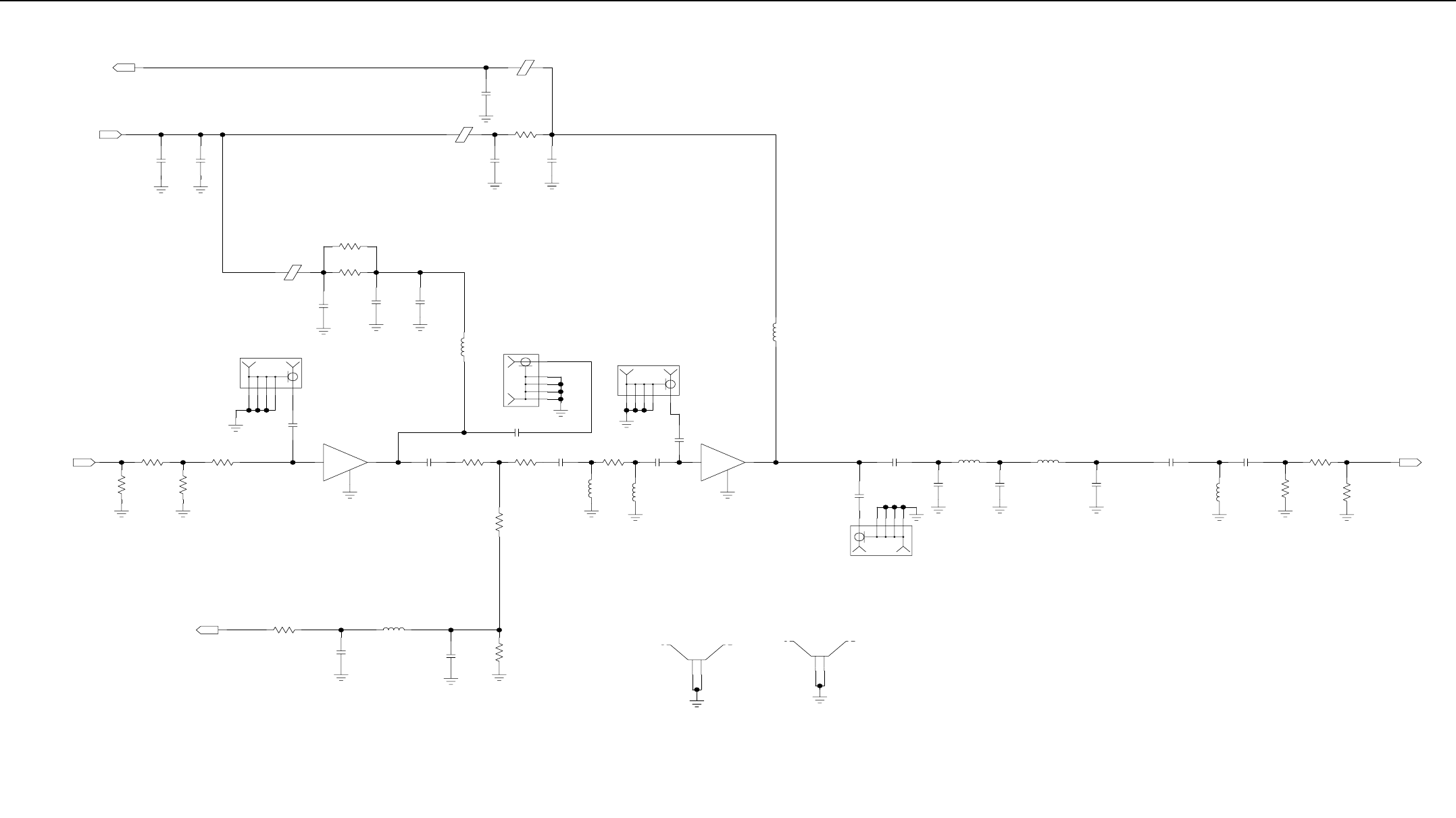
Receiver Schematics (UHF) 6-15
10V_RXIN
OUT
220PF .1UF
C2722 C2724
INJ_AMP_M1
4.3
220PF
.01UF
.1UF
E2701 R2711
C2711 C2712
E2702
C2725
~ 9.2V
DNP
CONN_J
P2702
1
2
3
4
5
1
3
5
2
4
5~9DBM @ UHF BAND
1DB PAD
~ 18DBM @ UHF BAND
G1
OUT
825
HMC479
825
220PF
DNP
DNP
5.62
CONN_J
0
U2700
C2718
R2717
R2718 R2719
P2700
R2713
LO_IN
12
2
13
IN
1
2
3
4
5
DNP
CONN_J
P2703
GAI N ~13.5DB @ UHF BAND
G1
OUT
AH101
U2701
2
3
IN
2.2DB PAD
39NH
220PF
0
16NH
220PF 220PF
DNP
220PF
150
5.62
DNP
5.62
DNP
18PF
L2708 L2709
R2705
C2720
C2719
C2708
C2709
R2703
R2704
R2706
C2710
1
~4.7V
220PF
220NH
.01UF
160
.1UF
160
C2702 C2703
L2700
C2704
R2712
E2700
R2710
12
1
2
-8.0 DBM
VCO_FEEDBACKOUT
18NH
9.1PF 68.1
9.1PF
267
R2708 L2701
R2707
C2707 C2706
IN
SHIELD SHIELD
SH2700 SH2701
1
2
1
2
DNP
CONN_J
P2704
~ 27DBM @ UHF BAND
16NH
10PF
5.6PF 0
DNP
0
DNP
0
15NH
220PF
220PF 15NH
DNP
4.7PF
6.8PF 6.8PF
C2721
C2713 C2717
L2703 L2704
C2714 C2716
C2715
R2715
R2714 R2716
C2723
L2705
VCO_INJ_OUT
1
2
3
4
5
OUT
470NH
L2702
12
NOTE 1 : Rx Metering Schematic Diagram (Kit No. CRE4007)
NOTE 2 : Trident Block Schematic Diagram (Kit No. CRE4007)
NOTE 3 : UHF VCO Schematic Diagram (Kit No. CRE4007)
NOTE 4 : Mixer Schematic Diagram (Kit No. CRE4007)
NOTE 1
NOTE 3
NOTE 2
NOTE 4
Receiver – Rx Lo1 Injection Amp and Feedback Schematic Diagram (Kit No. CRE4007)
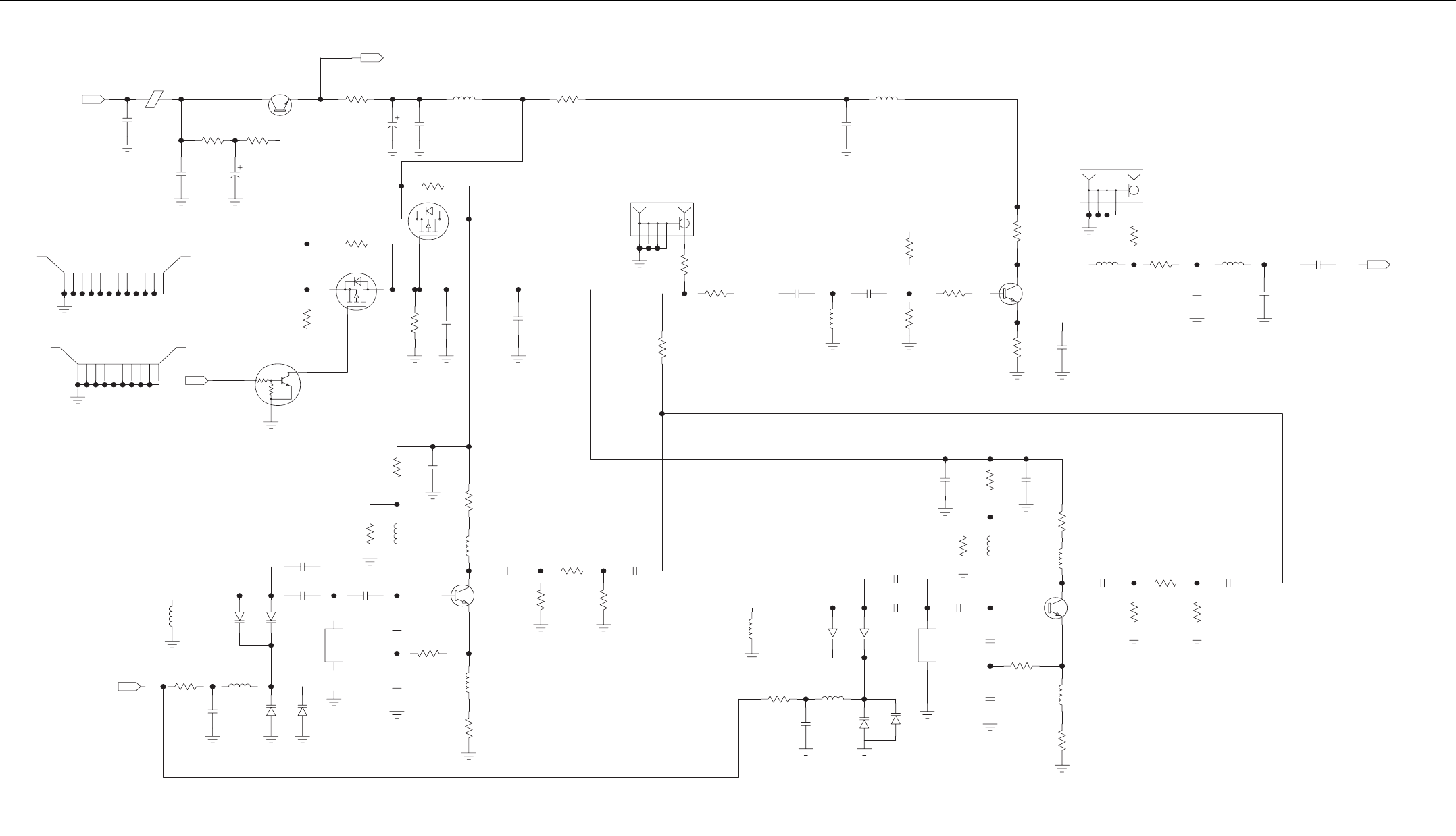
6-16 Receiver Schematics (UHF)
12V_VCOIN
493MHZ
SI8800SPQ0493YE
4.3PF
1SV229
1SV229
4.3PF
10
18NH
220PF
1SV229 1SV229
390NH
C3201
Y3200
CR3200
CR3203
CR3201
CR3202
R3200 L3200
L3201
C3200
C3202
VCO_SLV
21
21
21
21 21
IN
OUT IN
1.58K
3PF
390NH
220PF
100
390NH
1K
C3203
L3203
R3205
L3204
C3206
R3204
R3203
220PF
432
432
11.5
2.2PF
NE68519
Q3200
C3207 C3208
R3208
R3207
R3206
390NH
15
10PF
8.2PF
301
R3202
R3201
C3205
C3204
L3202
13
2
LOW RANGE VCO ENABLE - LOW
HIGH RANGE VCO ENABLED HIGH
LOW RANGE VCO ENABLED LOW
10
9
8
7
6
5
4
3
2
1
SHIELD
SHIELD
SH3200
SH3201
10
9
8
7
6
5
4
3
12
11
2
1
VCO_SELECT
1
IN
10K
47K
DNP0
MUN5214T1
10K
NTR1P02LT1
R3233
Q3205
Q3206
R3235
2
1
3
2
3
DNP
220PF
10K 220PF
C3233
C3232
R3234
P-CHAN ENHANCEMENT
NORMALLY OFF
10V
390NH
DNP0
RX_VCO
.01UF
NTR1P02LT1
R3232
Q3204
L3215
C3227
2
1
3
11.3V
220PF 267 10
34.8
MMBT3904
330UF
.01UF
R3229
C3228
Q3203
R3231
C3229
C3230
R3230
E3200
VCC_CP
OUT
47UF
C3226
21
0
R3228
DNP
0
0
0
R3236
R3219
R3218
21
301
100
.1UF
BFQ67W
200
3.32K
R3225 C3220
R3223
Q3202
R3224
R3221
220PF
2K
2.7PF
27NH
R3222
C3219
C3218
L3211
HIGH RANGE VCO ENABLE - HIGH
SI8800SPQ0527YE
527MHZ
3.9PF
1SV229
1SV229 1SV229
3.6PF
1K
220PF
1SV229
390NH
10
18NH
3PF
C3210
Y3201
CR3207
CR3204
C3209
R3209 L3205
CR3205
L3206
CR3206
C3211 C3212
R3214
21
21
21
21 21
OUT IN
NE68519
15
301
10PF
390NH
C3214
R3210
R3211
L3207
Q3201
13
DNP
220PF
8.2PF
2.7PF
390NH
100
220PF
390NH
1.58K
C3231
C3213
L3208
R3213 C3215
L3209
C3216
R3212
2
432
432
11.5 220PF
R3216
R3215
R3217
C3217
CONN_J
DNP
P3200
220PF
390NH
L3214
C3225
33NH0
0
DNP
3.3PF
3.3PF
18NH220PF
C3224
C3223
L3213
L3212 R3227
R3226
C3222
LO_OUT
OUT
DNP
CONN_J
P3201
NOTE 1 : Trident Block Schematic Diagram (Kit No. CRE4007)
NOTE 2 : Rx Lo1 Injection Amp and Feedback Schematic Diagram (Kit No. CRE4007)
NOTE 1
NOTE 1
NOTE 1
NOTE 2
Receiver – UHF VCO Schematic Diagram (Kit No. CRE4007)
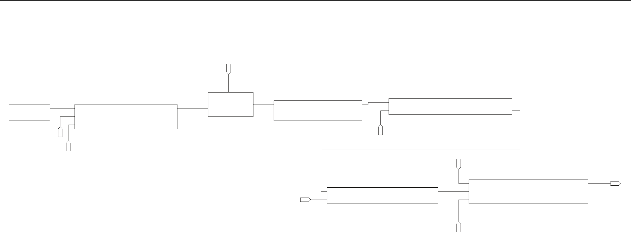
Receiver Schematics (UHF) 6-17
RX_TUNABLE_FILTER_1100
RX_LPF_1000
LPF_OUT
12V_LO1_FB
RF_OUT
V_CNTL
RF_IN
12V_RX_SW
FE_V_CNTL
IN
IN
TUNABLE_FILTER
LPF
RX_LNA_1200
LNA_INLNA_OUT
5V_LNA
5.0V_RX_SW
LNA
IN
RX_IMAGEFILTER_1300
IMG_FILTER
IMGFILT_OUT
IMGFILT_IN
RX_MIXER_1400
MIXER_LO_IN
LOWPASS_IN
MIXER_IF
MIXER_LO_INPUT
IN
MIXER
FINAL_IF
OUT
RX_IF_ATTENUATOR_1600
5V_IF_ATTN
IF_ATTN_IN
V_ATTN
IF_ATTN_OUT
IF_ATTEN
V_ATTN
5.0V_RX_SW
ININ
RX1_IF_OUT
RX_5VDC
RX1_IF_INIF_STRIP
RX_IF_STRIP_1500
5.0V_RX_SWIN
Receiver – Schematic Diagram (Kit No. CRE4007)
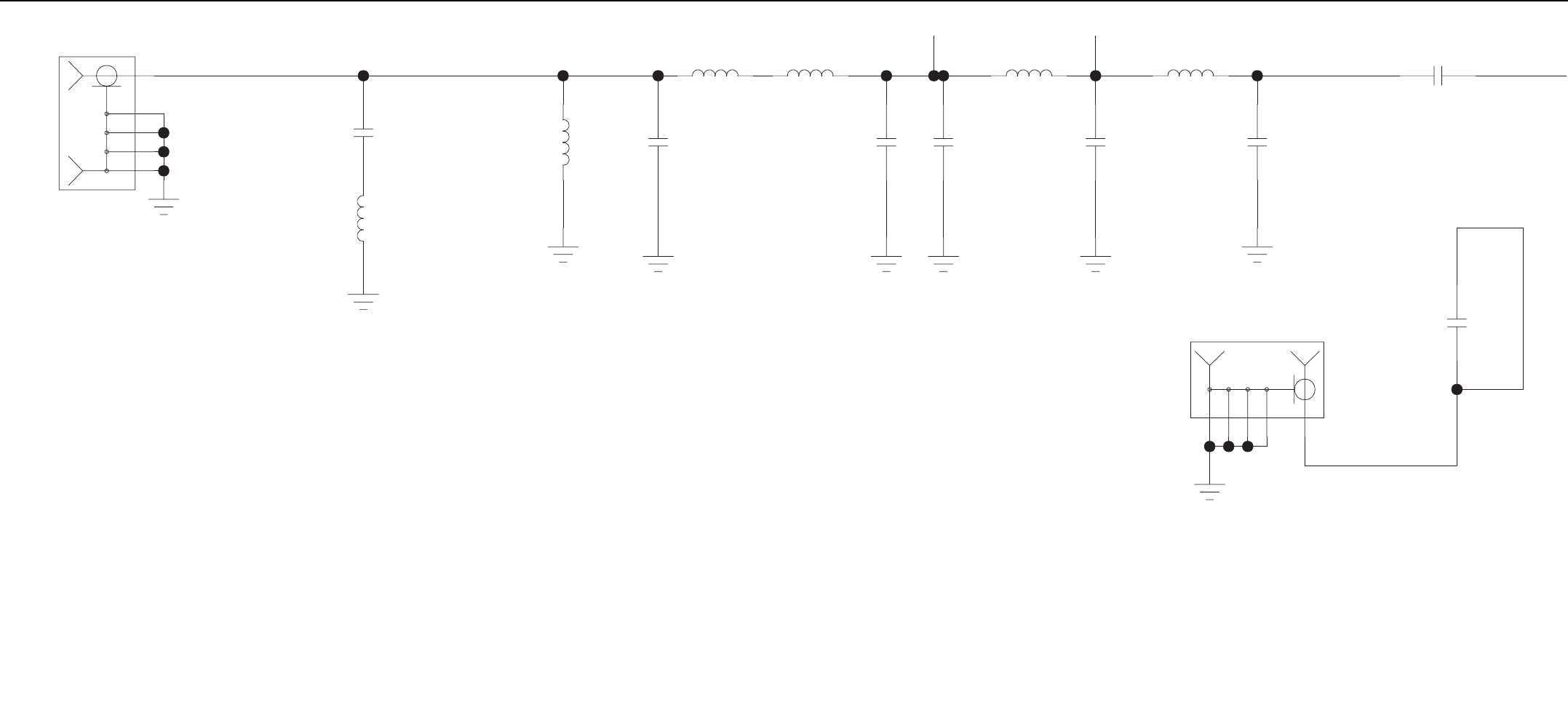
6-18 Receiver Schematics (UHF)
G4
G3
G2
G1
C
CONN_J
33PF
150NH
L1005
C1008
33NH
L1000
6.8NH
1.5PF
5.1PF
27NH
C1001
C1000
L1002L1001
2.4PF
C1002
27NH
2.4PF
4.7PF
C1005C1004
L1004 220PF
C1006
LPF_O
U
DNP
220PF
CONN_J
P1000 C1007
DNP
5
4
3
2
1
27NH
L1003
NOTE 1 : Rx FE Tunable Filter Schematic Diagram (Kit No. CRE4007)
Receiver – Rx Low Pass Filter Schematic Diagram (Kit No. CRE4007)
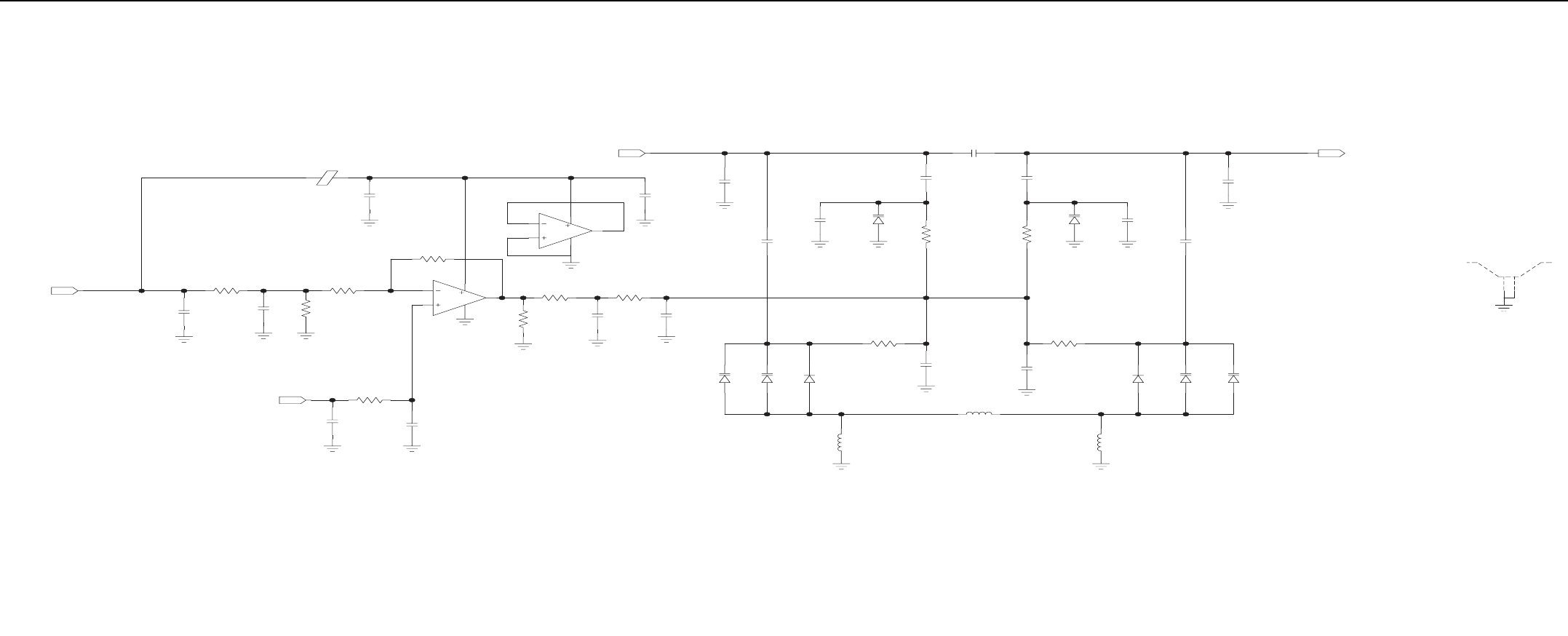
Receiver Schematics (UHF) 6-19
12V_LO1_FB
IN
20PF
2.7PF
DNP
C1111
C1112
RF_OUT
OUT
~ 1.8DB OF LOSS @ 437MHZ
51PF
51PF
47.5K
20PF
10PF 1SV279
.8PF
47.5K 1SV279
10PF
R1104
R1103 D1104
D1103
C1103
C1110
C1104
C1109
C1106
C1107
21
21
2.7PF
MC33202
.1UF
DNP
C1102
C1117
U1100
RF_IN
48
7
5
6
IN
220PF
C1116
E1100 12V
137K
20K
20K
R1106
R1111
R1107
1.1K
220PF
100PF
C1114 C1119 R1110
DNP
MC33202 4700PF
220K
20K
220PF
10K
R1109 C1121
R1108
U1100
R1100
C1100
48
1
3
2
91NH
220PF
DNP220PF
DNP
13NH
1SV280
1SV279 1SV279
47.5K
L1101
D1105
D1106 D1107
L1102
R1102
C1108
C1105
21
21
13NH
47.5K
L1100
R1101
1SV279
1SV279
1SV280D1102
D1101
D1100
21
21
SHIELD
SH1100
2
1
1K
220PF
.1UF
C1113
R1105
C1120
V_CNTL
IN
NOTE 1 : Trident Block Schematic Diagram (Kit No. CRE4007)
NOTE 2 : Rx Low Pass Filter Schematic Diagram (Kit No. CRE4007)
NOTE 3 : LNA Schematic Diagram (Kit No. CRE4007)
NOTE 1
NOTE 2 NOTE 3
Receiver – Rx FE Tunable Filter Schematic Diagram (Kit No. CRE4007)
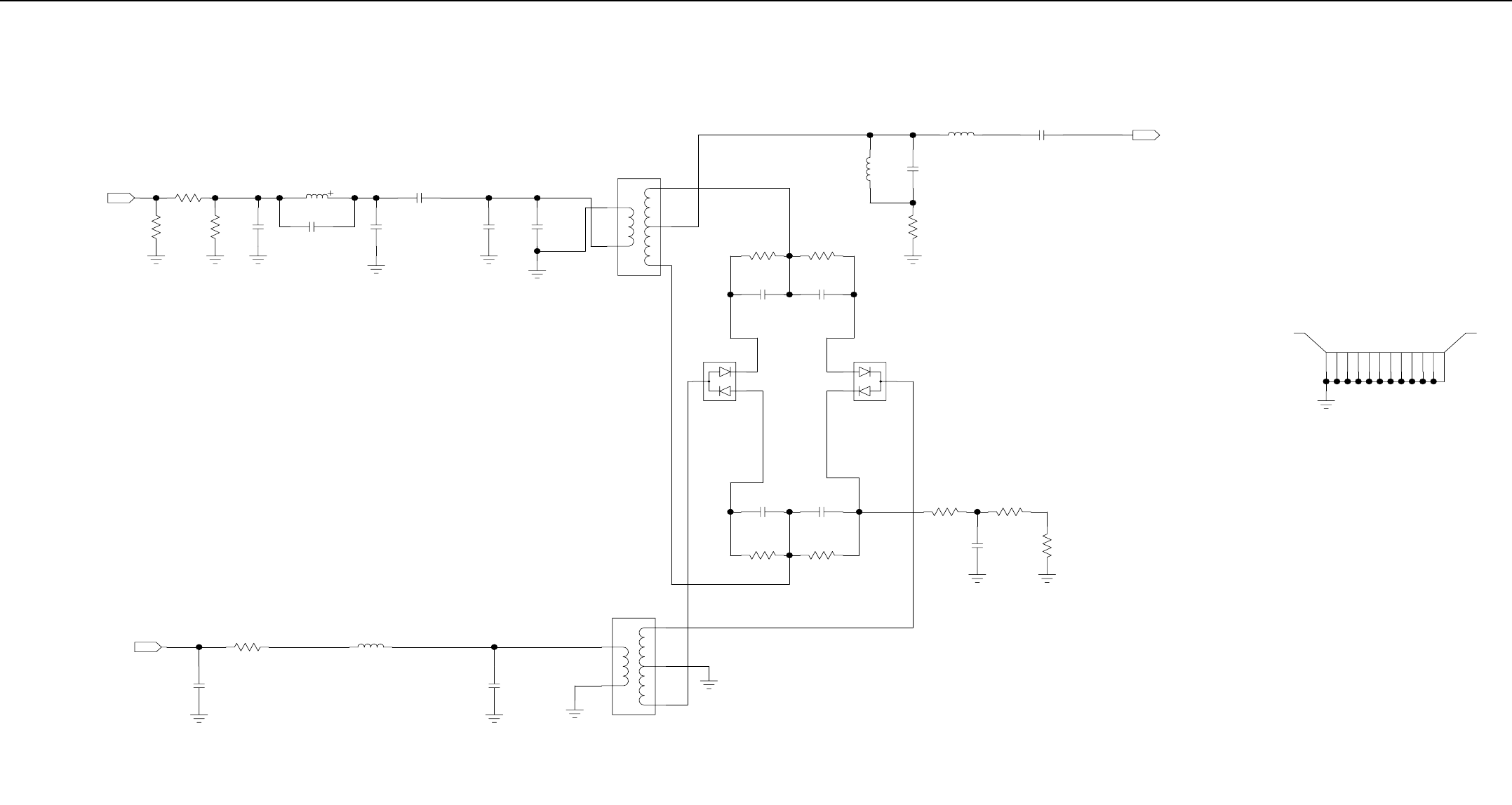
6-20 Receiver Schematics (UHF)
LOWPASS_ININ
9.1PF
6.8NH
DNP
3PF
DNP
221
221 5.6PF
5.6PF
XFMR
12PF
1.8PF
0
DNP
R1412
R1409 R1411 C1419
T1401
C1410
C1408
C1409
L1402
C1405
C1404
3
2
1
5
4
21
SMS3923
178
.01UF
178
.01UF
SMS3923
CR1401
CR1400
C1414
R1404
C1413
R1403
2
3
12
3
1
21
21
~ 6.5DB OF LOSS @ UHF BAND
82PF
68NH
47NH91PF
51
C1415
L1404
R1400
C1416
L1403
MIXER_IF
OUT
10
9
8
7
6
5
4
3
12
11
2
1
SHIELD
SH1401
0
470PF
1K3.3K
R1407
C1417
R1406
R1405
21
21212121
.01UF
178
178
.01UF
R1402
R1401
C1412
C1411
XFMR
T1400
3
2
1
5
4
2PF
C1403
4.7NH
L1401
5.6PF
0
C1400
R1410
IN
MIXER_LO_IN
NOTE 1 : Rx Lo1 Injection Amp and Feedback Schematic Diagram (Kit No. CRE4007)
NOTE 2 : IF Strip Schematic Diagram (Kit No. CRE4007)
NOTE 3 : Image Filter Schematic Diagram (Kit No. CRE4007)
NOTE 1
NOTE 3
NOTE 2
Receiver – Mixer Schematic Diagram (Kit No. CRE4007)
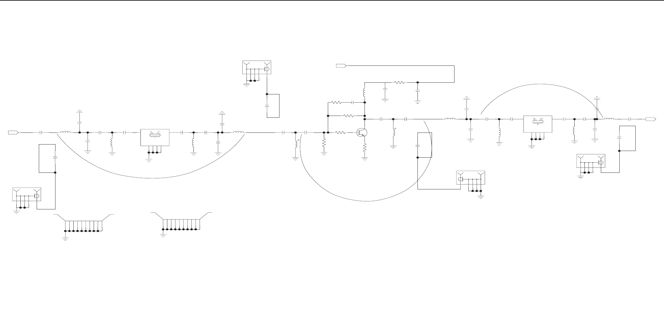
Receiver Schematics (UHF) 6-21
DNP
.01UF
CONN_J
DNP
P1500
C1530
5
4
3
2
1
.01UF 270NH
8.2PF
6.8PF
2.7PF 51PF
1UH
C1529
C1501
C1500
L1501
C1503
L1500 C1502
RX1_IF_IN
IN
GND1
OUT
GND3
GND2
GND4
IN
MM13114
1UH
270NH
8.2PF
2.7PF
6.8PF
12PF
U1500 C1504
L1502 C1506
C1505
C1507
L1503
41
6
5
3
2
DNP
.01UF
C1509
5
4
3
2
1
21
DNP
CONN_J
P1503
~ 2.8 DB OF INSERTION LOSS AT 73.35 MHZ
SHIELD
SHIELD
SH1500 SH1501
10
9
8
7
6
5
4
3
2
1
10
9
8
7
6
5
4
3
2
1
~ 13.6 DB OF GAIN AT 73.35 MHZ
GND1
OUT
GND3
GND2
GND4
IN
MM13114
1UH
51PF
8.2PF
270NH
12PF
270NH.01UF
DNP
.01UF
8.2PF
2.7PF
6.8PF
2.7PF
1UH
DNP
CONN_J
6.8PF
P1501
C1528
C1527
L1510
L1507
C1520
C1521
C1519
L1508
C1522 U1501 C1523
L1509 C1525
C1524
C1526
RX1_IF_OUT
5
4
3
2
1
41
6
5
3
2
OUT
2.7V
0.9V
.01UF
2.21K
12.1
825
182
.01UF
0.1UF 220PF
DNP
3.32K
BFQ67
47PF
0.1UF
220NH
470NH
10
C1515
C1512
R1503
R1504
R1500
R1501
U1502
R1502
L1506
C1516
C1513
L1505 C1514
C1517
R1505
12
23
1
21
21
21
21
21
0.15V
RX_5VDC
IN
.01UF
180NH
39PF
L1504
C1510
21
C1511
CONN_J
DNP
P1502
5
4
3
2
1
FINAL CIRCUIT HAS ~ 8 DB OF GAIN
~ 2.8 DB OF INSERTION LOSS AT 73.35 MHZ
NOTE 1 : Mixer Schematic Diagram (Kit No. CRE4007)
NOTE 2 : Rx IF Attenuator Schematic Diagram (Kit No. CRE4007)
NOTE 1
NOTE 2
Receiver – IF Strip Schematic Diagram (Kit No. CRE4007)
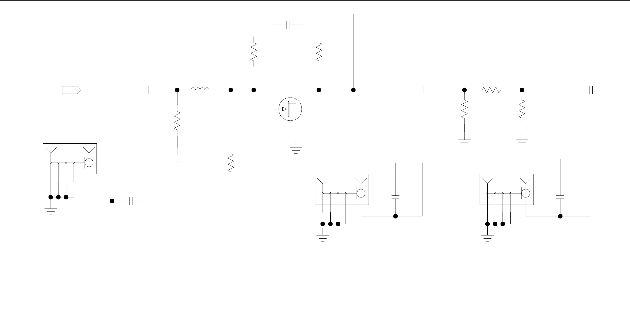
6-22 Receiver Schematics (UHF)
220PF
DNP
CONN_J
DNP
C1207
P1200
5
4
3
2
1
~ 18DB GAIN @ UHF BAND
30NH
220PF
10K
C1203 L1200
R1200
LNA_IN
IN
5.6
1PF
R1201
C1204
D
S
G
FH1
U1200
2
1
510
1000PF
510
R1203
R1202
3
1.5DB PAD
8.25
604 604
220PF R1232
R1230 R1231
C1206
220PF
DNP
CONN_J
DNP
C1208
P1201
5
4
3
2
1
CONN_J
DNP
P1230
DNP
220PF
C1231
5
4
3
2
1
220PF
C1230
NOTE 1 : Rx FE Tunable Filter Schematic Diagram (Kit No. CRE4007)
NOTE 2 : Image Filter Schematic Diagram (Kit No. CRE4007)
NOTE 1
Receiver – LNA Schematic Diagram (Kit No. CRE4007)
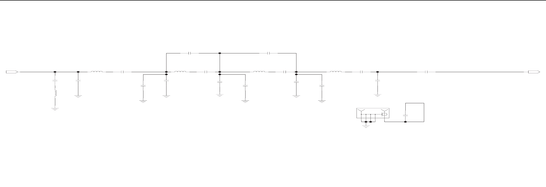
Receiver Schematics (UHF) 6-23
~ 1.5DB OF LOSS @ 437MHZ
10PF
5.1PF1.3PF
3.9PF
27NH10PF
5.1PF
3.9PF
18PF
7.5PF
27NH
8.2PF
47PF 6.2PF
22PF
27NH
100NH
3.6PF
220PF
27NH
C1306
C1311
C1303
C1315
C1312C1308
C1309
L1304 C1314
L1303 C1310
C1305
L1302
C1304
C1302
C1300
L1300
C1301
L1301
C1313
IMGFILT_INIMGFILT_OUT
OUT
IN
.5PF
C1307
5
4
3
2
1
CONN_J
DNP
P1300
220PF
DNP
C1316
NOTE 1 : Mixer Schematic Diagram (Kit No. CRE4007)
NOTE 2 : LNA Schematic Diagram (Kit No. CRE4007)
NOTE 1
NOTE 2
Receiver – Image Filter Schematic Diagram (Kit No. CRE4007)
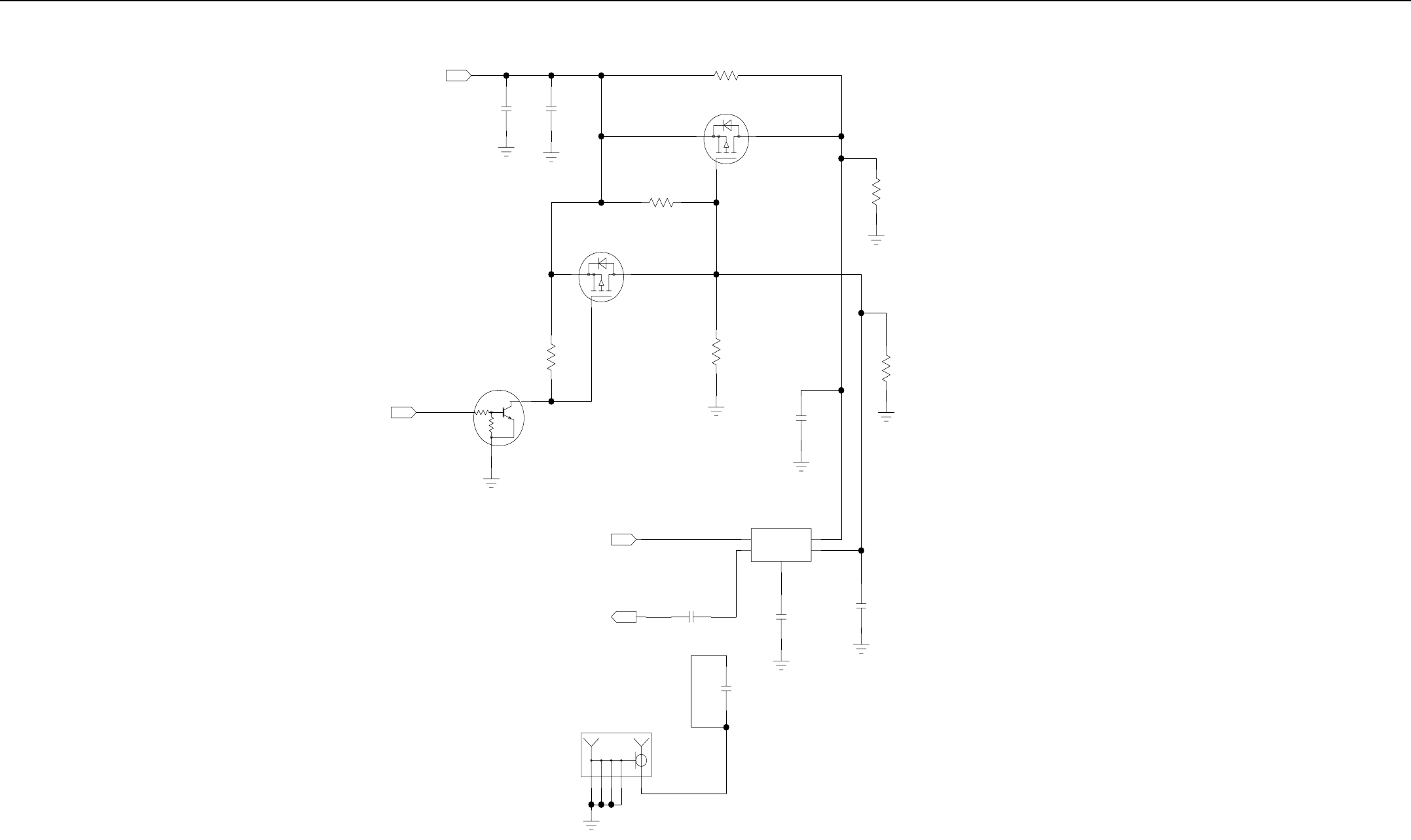
6-24 Receiver Schematics (UHF)
0.1UF 220PF
C1600 C1601
5V_IF_ATTN
IN
NTR1P02LT1
0
DNP
0
DNP
R1601
Q1602
R1600
2
1
3
NTR1P02LT1
Q1601
2
1
3
10K
47K
10K
MUN5214T1
Q1600
R1602
V_ATTN
2
3
1
IN
DNP
DNP
CONN_J
.01UF
C1602
P1600
5
4
3
2
1
.01UF
C1603
IF_ATTN_OUT
IF_ATTN_IN
OUT
INRFIO1
RFIO2
GND
V1
V2
0.1UF
AT267
.01UF
C1605
U1600
C1606
5
4
3
1
2
10K
0.1UF
10K
R1605
C1604
R1603
10K
R1604
NOTE 1 : Control Board to Rx Interconnect Schematic Diagram (Kit No. CRE4007)
NOTE 2 : Rx Abacus Schematic Diagram (Kit No. CRE4007)
NOTE 3 : IF Strip Schematic Diagram (Kit No. CRE4007)
NOTE 1
NOTE 2
NOTE 3
Receiver – Rx IF Attenuator Schematic Diagram (Kit No. CRE4007)
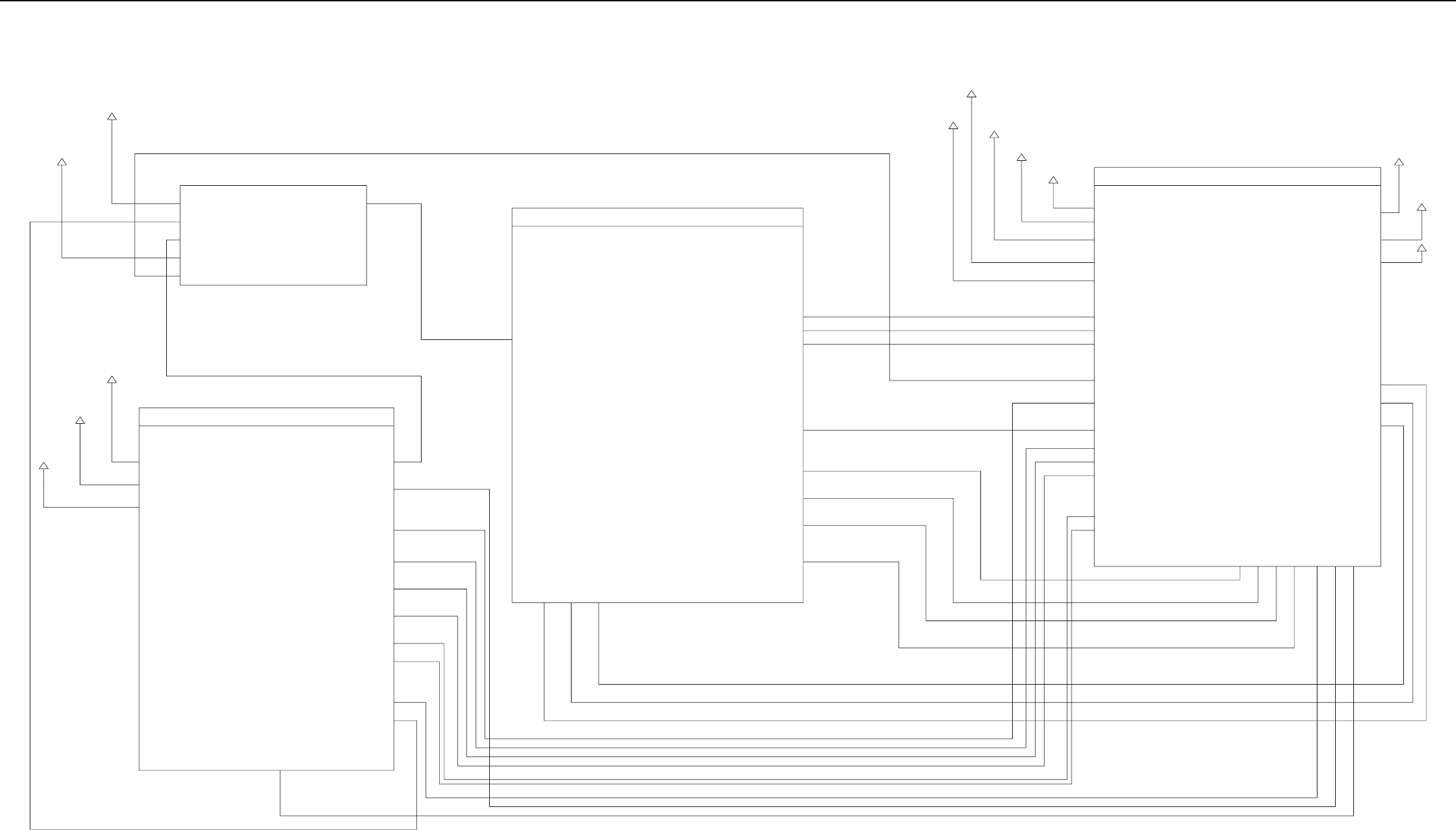
Receiver Schematics (UHF) 6-25
5.0V_RX
12V_RX_SW
RX_FRONTEND_1000_1600
FINAL_IF
V_ATTN
5.0V_RX_SW
FE_V_CNTL
MIXER_LO_INPUT
12V_RX_SW
2.775V_RX
12V_RX_SW
10V_RX_SW
IN
IN
IN
BANDIT_RX_FE
RX_V_CNTL
2.775V_RX
SYNTH_SPI_DR
SYNTH_SPI_DW
SYNTH_CLK_IN
SYNTH_CE_IN
INJ_MIXER_OUT
10V
TRI_RSTB_IN
RX_SLV_MON
RX_LOCK_DETECT
INJ_AMP_M1
12V_RX_SW
RX_FGU_1100
BANDIT_RX_FGU
REF_16.8MHZ_IN
IN
IN
OUT
OUT
IN
IN
OUT
OUT
OUT
IN
RX_IF_IN
16.8MHZ_ABA_REF_IN
RX_ABA_DOUTB/MISO
RX_ABA_PC
RX_ABA_PD
RX_ABA_PE
ABACUS_CLK_M1_OUT
ABACUS_2LO_M1_OUT
RX_ABA_ODC
RX_ABA_DATA
RX_ABA_FS
RX_ABA_SYNCB
IN
IN
IN
IN
IN
OUT
OUT
IN
OUT
OUT
OUT
OUT
RX_BACKEND_PLL_1200
BANDIT_RX_BE_PLL
10V_RX_SW
12V_RX_SW
5.0V_RX_SW
VCO_LD_M1_IN
RX_IF_ATTEN_OUT
SYNTH_CE_CPLD
ABA_DATA_IN
ABA_SYNCB_OUT
VCO_STL_M1_IN
ABA_PC_OUT
ABA_PD_OUT
ABA_PE_OUT
ABA_DOUTB/MISO_IN
TRI_RST_OUT
16.8MHZ_ABA_REF_OUT
ABACUS_CLK_M1_IN
ABACUS_2LO_M1_IN
8V
10V
14.2V
3.3V_RX
ABA_FS_IN
ABA_ODC_IN
2.775V_RX
16.8MHZ_SYN
INJ_FINAL_M1_IN
SPI_CLK_SYNTH
SPI_MOSI_SYNTH
SPI_MISO_SYNTH
RX_DIGITAL_1000
in
out
out
in
out
out
out
BANDIT_RX_DIGITAL
14.2V_RX
8.0V_RX
10.0V_RX
OUT
IN
IN
IN
IN
IN
2.775V_RX
12V_RX_SW
5.0V_RX
3.3V_RX
10V_RX_SW
OUT
IN
OUT
OUT
OUT
IN
IN
OUT
IN
IN
IN
OUT
OUT
OUT
OUT
OUT
Receiver – Main Schematic Diagram (Kit No. CRE4008)

6-26 Receiver Schematics (UHF)
REF_16.8_IN
3.3V_16.8_BUFFER
16.8MHZ_ABACUS
16.8MHZ_SYN
OUT
OUT
RX_REF_BUFFER_2600
16.8MHZ_ABA_REF_OUT
16.8MHZ_SYN
OUT
BANDIT_REF_BUFFER_RX
OUT
2.775V_RX
3.3V_RX
5.0V_RX_SW
10V_RX_SW
12V_RX_SW
OUT
OUT
OUT
OUT
OUT
OUT
OUT
OUT
OUT
OUT
IN
IN
IN
IN
IN
IN
IN
8V
14.2V
10V
14.2V_RX
10.0V_RX
8.0V_RX
RX_STANDBY
10V_RX_SW
5.0V_RX_SW
3.3V_RX
2.775V_RX
12V_RX_SW
RX_REGULATORS_2200
RX_REGULATORS
3.3V_RX
IN
IN
10V_RX
RX_ATTEN
14.2V
8.0V
ABA_DOUTB/MISO
ABA_PE
ABA_FS
ABA_DATA
ABA_SYNCB
ABA_PD
ABA_PC
RX_CPLD_CE
ABA_ODC
RX_CPLD_CLK
RX_CPLD_MOSI
RX_CPLD_MISO
RX_CPLD_ADD_0
RX_CPLD_ADD_1
RX_CPLD_ADD_2
16.8_MHZ
RX_INTERCONNECT_2000
RX_INTERCONNECT
OUT
OUT
IN
IN
OUT
IN
OUT
OUT
OUT
OUT
IN
IN
ABA_SYNCB_OUT
ABA_DOUTB/MISO_IN
ABA_PC_OUT
ABA_PD_OUT
ABA_PE_OUT
ABA_FS_IN
ABA_DATA_IN
ABA_ODC_IN
IN
IN
IN
OUT
OUT
OUT
OUT
IN
8.0V_RX
10.0V_RX
14.2V_RX
RX_IF_ATTEN_OUT
OUT
IN
IN
IN
IN
IN
OUT
IN
IN
3.3V_RX
2.775V_RX
IN
IN
IN
IN
IN
IN
OUT
IN
IN
2.775V_RX
RX_STANDBY3_3V_CPLD
SPI_MISO_OUT_CPLD
SPI_MOSI_IN_CPLD
CPLD_ENABLE
ADDR1
ADDR2
ADDR0
SPI_CLK_CPLD
SYNTH_CE
TRIDENT_RST
SPI_MISO_IN_CPLD
SPI_CLK_OUT_CPLD
SPI_MOSI_OUT_CPLD
SPI_CLK_M
SPI_MOSI_M
METERING1_CE
RX_CPLD_3300
RX_CPLD
out
OUT
in
out
OUT
out
OUT
OUT
out
SYNTH_CE_CPLD
TRI_RST_OUT
OUT
OUT
IN
OUT
IN
IN
IN
in
IN
IN
ABACUS_CLK_M1_IN
SPI_MISO_SYNTH
ABACUS_2LO_M1_IN
VCO_LD_M1_IN
VCO_STL_M1_IN
INJ_FINAL_M1_IN
IN
IN
IN
IN
IN
IN
SPI_CLK_SYNTH
SPI_MOSI_SYNTH
OUT
OUT
NC
NC
NC
3.3V_RX
IN
IN
CE2_MT1
3_3_V_RX_METER
RX_RESERVED_4
RX_RESERVED_5
RX_RESERVED_6
SPI_MISO
SPI_MOSI
SPI_CLK
INJ_FINAL_M1
AB_2LO_M1
VCO_STL_M1
VCO_LD_M1
AB_CLK_M1
RX_METERING_2800
RX_METERING
Receiver – General Rx Digital Section Schematic Diagram (Kit No. CRE4008)
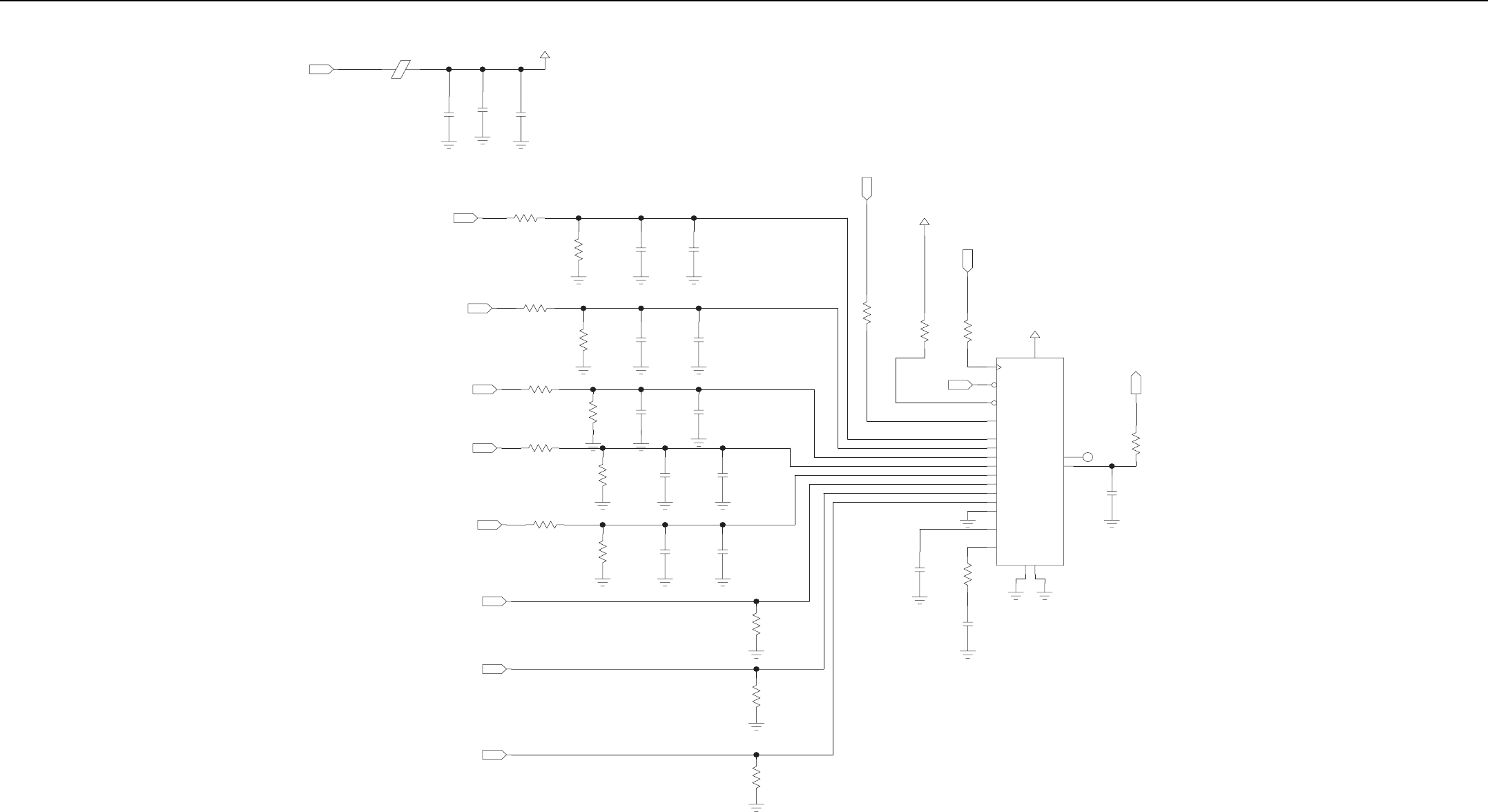
Receiver Schematics (UHF) 6-27
3_3_V_RX_METERIN
3_3_V_DIG_RX_METER
E2800
DNP
10UF .1UF
150PF
C2802
C2801
C2800
21
21
INJ_FINAL_M1
AB_CLK_M1
RX_RESERVED_5
RX_RESERVED_6
RX_RESERVED_4
VCO_STL_M1
VCO_LD_M1
AB_2LO_M1
IN
IN
IN
IN
IN
IN
IN
IN
3.9K
15K
.1UF
20K
10K
.1UF
10K
10K
10K
10K
.1UF
10K
3.32K .1UF
150PF
150PF
150PF
150PF
33.2K 150PF
.1UF
10K
10K
R2805 C2808
C2807
R2804
R2812
R2811
R2810
R2809 C2812
C2811
R2808
R2807
R2806
C2810
C2809
R2802
R2800
R2803 C2806
C2805
C2804
C2803
R2801
21
21
CH6
DIN
DOUT
SSTRB
DGND
AGND
VDD
CH7
CH5
CH4
CH3
CH2
CH1
CH0
SCLK
VREF
REFADJ
COM
CS
SHDN
MAX149
U2800
0
0
0
DNP
3_3_V_DIG_RX_METER
3_3_V_DIG_RX_METER
R2813
R2814 R2815
SPI_MOSI
SPI_CLK
CE2_MT1
11
20
10
19
12
17
18
9
8
7
6
5
4
3
2
1
IN
IN
IN
NC
0
10PF
DNP
C2815
R2816
SPI_MISO
16
15
OUT
5.62
.015UF
4.7UF
R2817
C2813
C2814
14
13
Receiver – Rx Metering Schematic Diagram (Kit No. CRE4008)
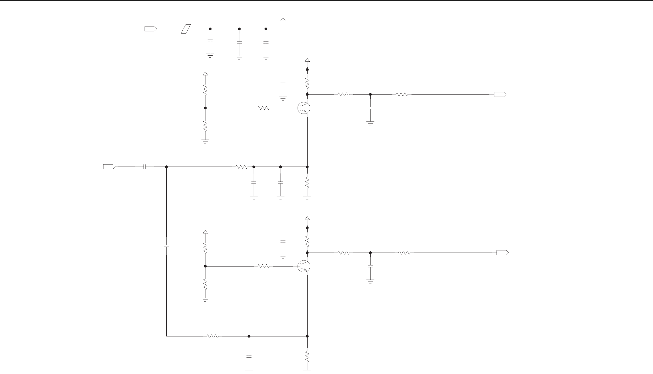
6-28 Receiver Schematics (UHF)
1.0 VP-P
1.3V
0.9V
SQUARE WAVE
475
33PF
100
MMBT3904
.1UF
0
3.3V_BUF
R2614
R2616
C2620
Q2610
C2617
R2628 R2630
16.8MHZ_SYN
1
3
2
OUT
DNP
10UF
150PF
RX_REF_BUFFER3.3V_BUF
475
.1UF
C2611 C2612
E2610
C2614
3.3V_16.8_BUFFERIN
2.67K
3.3V_BUF
2.67K
R2611
R2612
SQAURE WAVE
1.2 VP-P
.1UF
C2610
IN
REF_16.8_IN
.1UF
2.67K
2.67K
3.3V_BUF
C2613
R2622
R2651
0.8V
150
0
15PF
270PF
R2610
C2615 R2615
C2621
0.9V 100
475
3.3V_BUF
R2625
R2627
1.3V
33PF
.1UF
475
MMBT3904
R2623
Q2611
C2618
C2619
1
23
0.8V
0
15PF 150
R2620
C2616 R2626
0
R2631
1.0 VP-P
SQUARE WAVE
OUT 16.8MHZ_ABACUS
Receiver – Rx 16.8MHz Ref Buffer Schematic Diagram (Kit No. CRE4008)
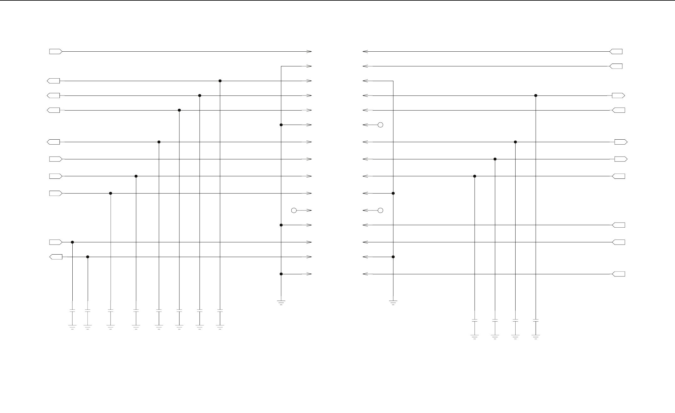
Receiver Schematics (UHF) 6-29
ABA_ODC
ABA_SYNCB
ABA_PE
ABA_PC
RX_CPLD_CE
10V_RX
RX_CPLD_ADD_0
RX_CPLD_ADD_1
RX_ATTEN
RX_CPLD_MISO
IN
IN
IN
OUT
OUT
OUT
OUT
IN
IN
OUT
NC NC
NC
RX_INTERCONNECT
J2000
J2000J2000
J2000J2000
J2000
J2000J2000
J2000J2000
J2000J2000
J2000
J2000J2000
J2000J2000
J2000
J2000J2000
J2000
J2000
J2000
J2000
29 30
2827
2625
23 24
2221
2019
1817
15 16
1413
1211
910
87
56
34
21
J2000
J2000
J2000
J2000
J2000
J2000
ABA_FS
14.2V
8.0V
ABA_DATA
ABA_PD
ABA_DOUTB/MISO
RX_CPLD_ADD_2
RX_CPLD_MOSI
RX_CPLD_CLK
16.8_MHZ
IN
IN
OUT
OUT
IN
IN
OUT
IN
IN
IN
150PF
150PF
150PF
150PF DNP
DNP
DNP
DNPC2011
C2010
C2008
C2009
150PF
150PF
150PF
150PF
150PF
150PF
150PF
.1UF DNP
DNP
DNP
DNP
DNP
DNP
DNP
DNP
C2015
C2006
C2005
C2004
C2003
C2002
C2001
C2000
21
Receiver – Control Board to Rx Interconnect Schematic Diagram (Kit No. CRE4008)
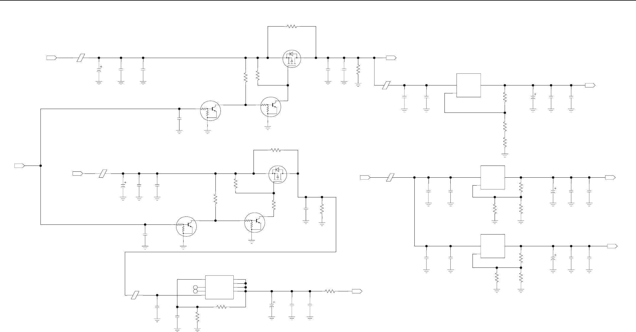
6-30 Receiver Schematics (UHF)
E2200
10.0V_RXIN
DNP
150PF47UF .01UF
C2202C2201C2200
21
10K
47K
150PF
MUN5214T1
Q2201
C2211
2
3
1
ACTIVE-HIGH
DEFAULT-LOW
150PF
DNP
47UF .01UF
C2214
C2213
C2212
E2201
14.2V_RX
21
IN
10K
47K
150PF
MUN5214T1
Q2204
C2218
2
3
1
10K
47K
MUN5214T1
10K
10K
R2208
Q2205
R2207
2
3
1
10K
NTR1P02LT1
Q2203
R2210
2
1
3
0
DNP
R2209
10K
47K
MUN5214T1
Q2202
2
3
1
NORMALLY OFF
ENCHANCEMENT PCHAN
10K
NTR1P02LT1
10K
Q2200
R2201
R2200
2
1
3
OUTIN
ADJUST
LM317M
RX_REGULATORS
U2200
10V_RX_SW
23
1
OUT
.1UF
150PF
C2208
C2207
E2203
10K
.1UF
150PF
R2203
C2206
C2205
DNP
0
R2202
RX_STANDBY
IN
NC
NC
VOUT1
VOUT2
VOUT4
VOUT3
VIN
NC1
NC2
GND_ADJ
DNP
1UF 2.32K
.33UF
270
MC33269
U2203
R2212
R2211
C2220
E2202
C2221
7
6
3
2
4
8
5
1
.1UF
0
10UF 150PF
R2213
C2224C2223C2222
12V_RX_SW
21
OUT
10K
.1UF
R2214
C2217
E2204
8.0V_RXINOUTIN
ADJUST
DNP
150PF
430
270
1.1K
.1UF10UF
LM317M
C2233 C2228C2227
R2217
U2201
R2216
R2215
3.3V_RX
21
23
1
OUT
150PF .1UF
C2226
C2225
OUTIN
ADJUST
LM317M
1.1K
.1UF
150PF
332
280
DNP
R2221
U2202
R2220
R2219
C2230
C2229
23
1
280
825
10
R2206
R2205
R2204
.1UF
10UF 150PF
C2203 C2210
C2209
5.0V_RX_SW
21
OUT
2.775V_RX
OUT
150PF
.1UF10UF
C2235 C2232C2231
21
Receiver – Rx Voltage Regulators Schematic Diagram (Kit No. CRE4008)
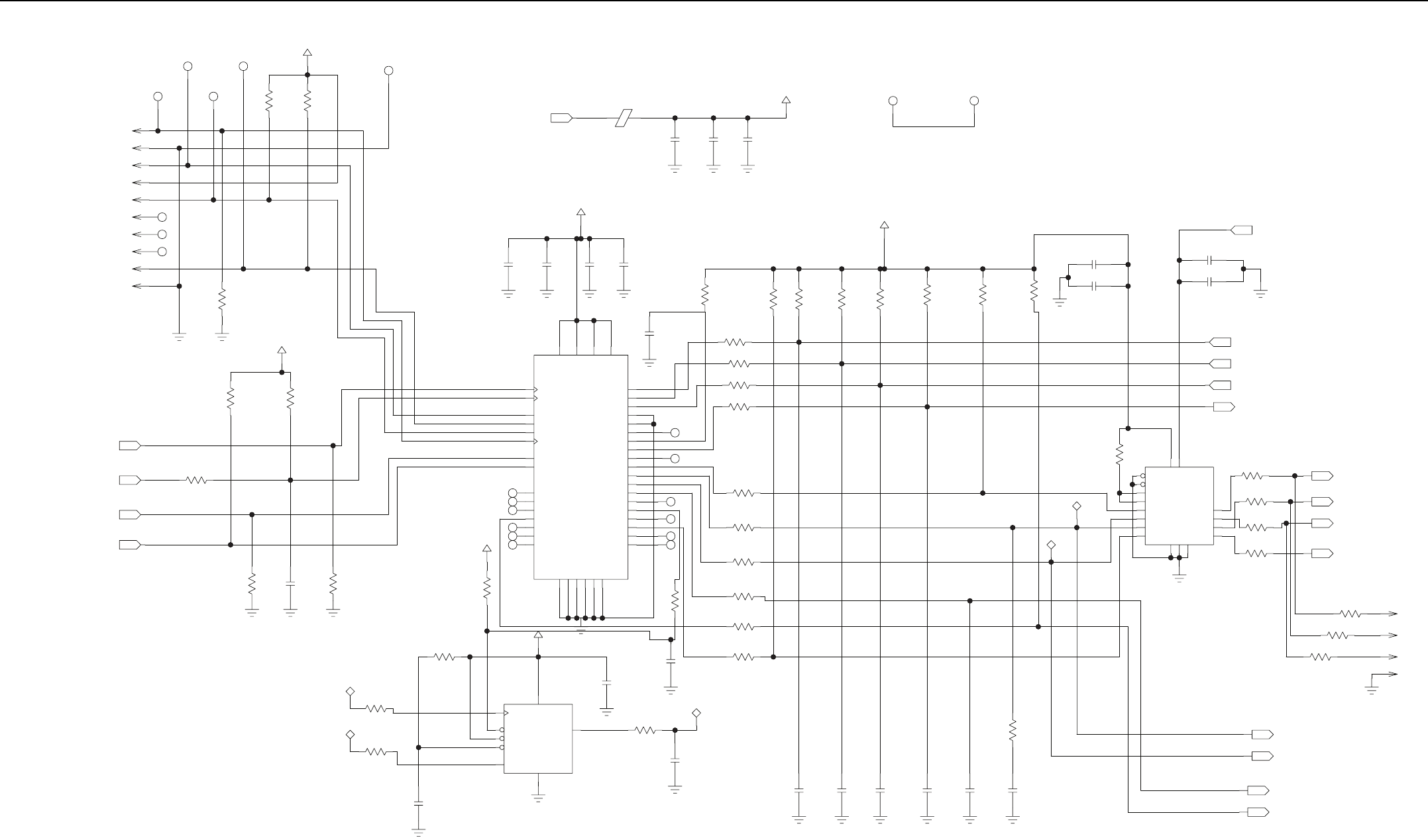
Receiver Schematics (UHF) 6-31
P3300
P3300
P3300
P3300
P3300
P3300
P3300
P3300
P3300
P3300
NC
NC
NC
1
2
3
4
5
6
7
8
9
10
3_3V_CPLD_FILT
1K 1K
TEST_POINT
TEST_POINT
TEST_POINT
R3306
R3304
TP3303
TP3301
TP3300
TEST_POINT
TP3302
1
1
1
1
TEST_POINT
TP3304
1
PLACE 0.1UF CAP NEAR EACH SUPPLY PIN OF CPLD
3_3V_CPLD IN
3_3V_CPLD_FILT
.1UF .1UF .1UF.1UF
C3304
C3303
C3302C3301
RECEIVER_CPLD
29
9
41
17
NC
NC
NC
NC
NC
NC
7
32
1
26
40
38
31
28
27
25
35
34
33
39
37
NOTE A
0
R3300
SPI_MOSI_IN_CPLD
CPLD_ENABLE
SPI_CLK_CPLD
SPI_MISO_IN_CPLD
IN
IN
IN
IN
4.75K 4.75K
3_3V_CPLD_FILT
R3305
R3301
1K
R3303
10PF
1K
DNP
1K
R3307
C3300
R3302
FOR BANDIT ONLY, THE EVEN NUMBER OF ENABLE PINS ARE USED FOR CPLD
NOTE A
3_3V_CPLD_FILT
4.75K
R3331
10K
R3327
SPI_MOSI_M
0
SPI_CLK_M
0
R3328
R3330
SPI_CLK_M
SPI_MOSI_M
10PF
C3318
GND
WP
VCC
HOLD
SI
SO
EN_CS
CLK_S
U3301
3
5
7
4
1
6
0.1UF
33.2
DNP
DNP
10PF
10PF
SPI_MISO_IN_CPLD
C3315
C3316
R3329
C3317
SPI_MISO_IN_CPLD
AT25640A
3_3V_CPLD_FILT
8
2
49.9
33.2
33.2
33.2
49.9
33.2
R3312
R3311
R3310
R3309
R3308
R3332
49.9
R3326
30
24
11
4
36
16
NC
NC
NC
NC
NC
NC
33.2
33.2
33.2
49.9
R3390
R3391
R3392
R3314
4.75K
4.75K
4.75K4.75K4.75K 4.75K
R3318R3317
R3334R3316R3315R3333
10PF
DNP
4.75K
3_3V_CPLD_FILT
R3350
C3349
.01UF
4.75K
.1UF
C3345
C3346
R3322
.01UF
.1UF
C3347
C3348
2.775V_RX
IN
ADDR0
ADDR2
ADDR1
METERING1_CE
OUT
IN
IN
IN
SYNTH_CE
SPI_MOSI_OUT_CPLD
TRIDENT_RST
SPI_CLK_OUT_CPLD
OUT
OUT
OUT
OUT
0
DNP
0DNP
DNP
DNP
0DNP
DNP
DNP
P3301
P3301
P3301
P3301
R3323
R3324
R3325
1
4
3
2
SPI_CLK_M
SPI_MOSI_M
RX_STANDBY
SPI_MISO_OUT_CPLD
OUT
OUT
OUT
OUT
33.2
33.2
33.2
0
R3346
R3347
R3348
R3349
VCCB
VCCA
GND3
GND2
GND1
B1_2
B1_1
B2_2
B2_1
A2_2
A2_1
A1_2
A1_1
DIR2
DIR1
OE2
OE1
SN74AVC4T245
U3303
17
9
8
10
12
11
13
14
15
3
2
7
5
6
4
4.75K
R3345
16
1
SPI_CLK_M
SPI_MOSI_M
DNP
0
R3319
PLACE SERIES RC ON FINAL DAISY-CHAINED SPI DEVICE
DNPDNPDNPDNPDNP
10PF 10PF
10PF 10PF 10PF 10PF
DNP
C3312
C3311
C3310
C3320
C3309
C3308
23
22
21
20
19
18
15
14
13
12
10
8
6
5
44
43
42
3
2
VCCINT1
VCCINT0
IO_A0
IO_A1
IO_A2
IO_A3
IO_A6
IO_A5
IO_A4
IO_A8
IO_A7
IO_A11
IO_A10
IO_A9
IO_B0
IO_A12
IO_B1
IO_B2
IO_B3
IO_B5
IO_B4
GNDINT1
GNDIO3
GNDINT0
VCCIO1
VCCIO0
GCLK1
TCK
TMS
TDI
OE1
GCLRN
IO_B7
IO_B6
IO_B8
IO_B10
IO_B9
IO_B12
IO_B11
GNDIO1
GNDIO2
GNDIO0
TDO
OE2_GCLK2
EPM3032ATI44
U3300
10UF .1UF
3_3V_CPLD_FILT
150PF
C3307C3306C3305
E3300
TEST_POINTTEST_POINT
TP3306TP3305
1
1
Receiver – Rx CPLD Schematic Diagram (Kit No. CRE4008)
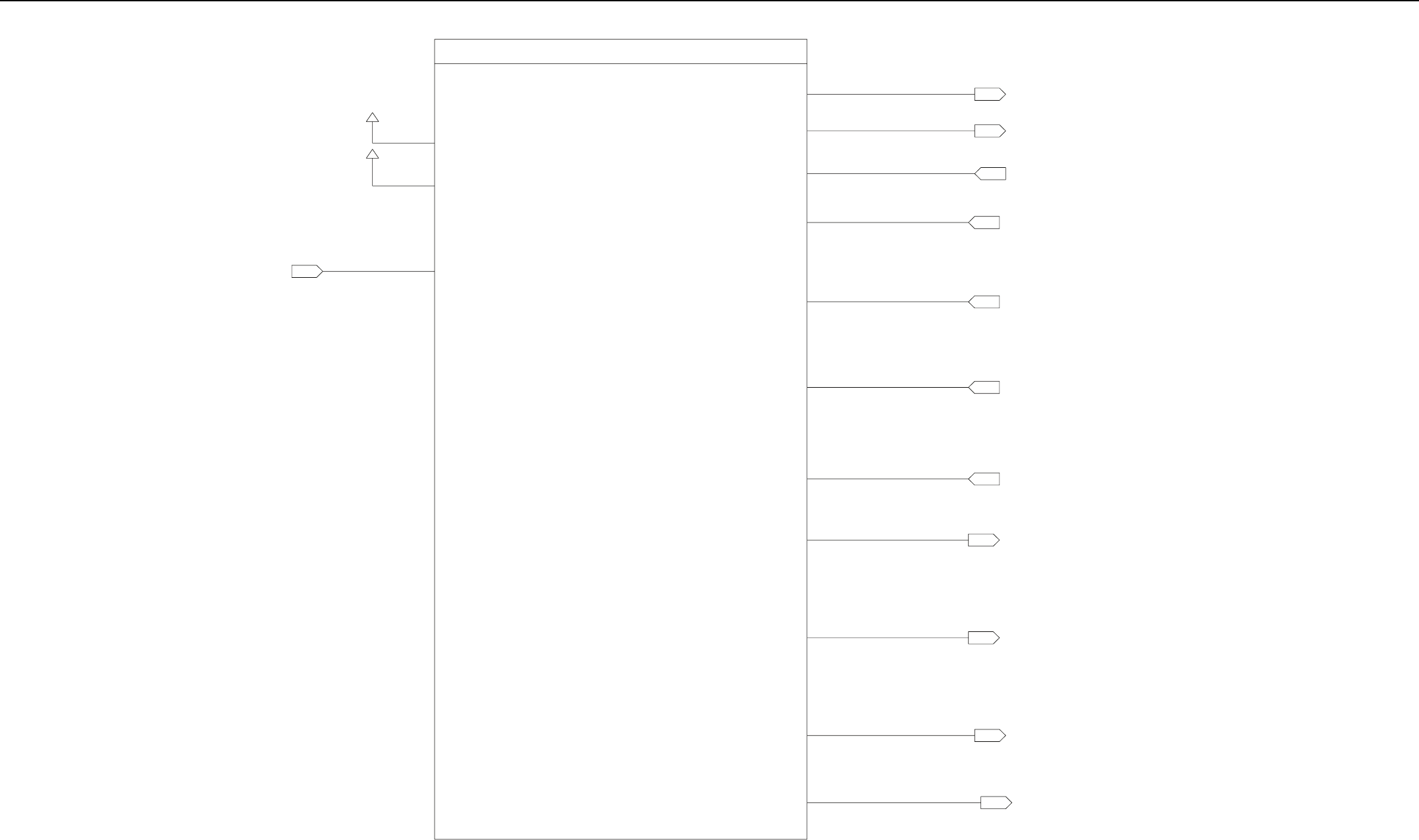
6-32 Receiver Schematics (UHF)
RX_BACKEND_2400
RX_BACKEND
REF_16.8
AB_2LO_M1
AB_CLK_M1
ABA_CLK
ABA_CE
ABA_DATA
ABA_ODC
ABA_FS
ABA_DOUT
ABA_DOUTB/MISO
SYNC_B
8V_RX
10V_RX
RX_IF_IN
in
IN
IN
8.0V_RX
10.0V_RX
RX_IF_ININ
RX_ABA_SYNCB
16.8MHZ_ABA_REF_IN
ABACUS_2LO_M1_OUT
ABACUS_CLK_M1_OUT
RX_ABA_PC
RX_ABA_PE
RX_ABA_PD
RX_ABA_ODC
RX_ABA_FS
RX_ABA_DATA
RX_ABA_DOUTB/MISO
IN
IN
IN
OUT
OUT
IN
OUT
OUT
OUT
OUT
IN
OUT
in
in
in
in
in
out
out
out
out
out
Receiver – Rx Backend PLL Schematic Diagram (Kit No. CRE4008)
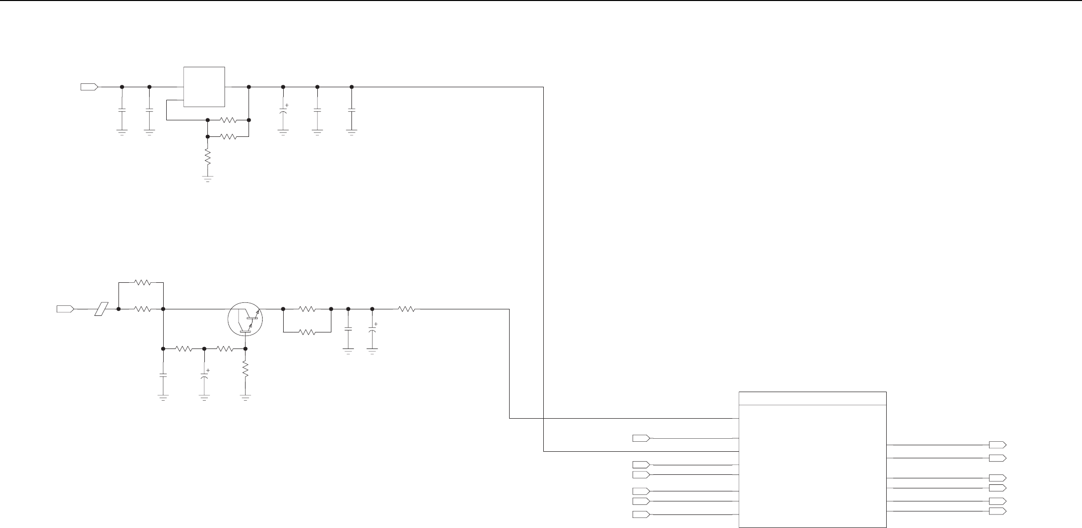
Receiver Schematics (UHF) 6-33
OUTIN
ADJUST
270
DNP
430
1.21K
150PF .1UF
LM317M
C2402
U2400
C2400 R2404
R2403
R2400
8V_RX23
1
IN
150PF
10UF .1UF
C2409
C2406
C2433
21
0
.1UF 22UF
R2413
C2410
C2407
21
110
110
100K
1MEG
22UF
.1UF
MMBTA13
10
C2401
R2407
R2408
Q2400
R2406
R2405
R2401
C2403
23
1
21
191
191
R2422
R2423
E2400
10V_RXIN
REF_16.8
RX_IF_IN
ABA_DATA
ABA_CLK
ABA_CE
SYNC_B
IN
IN
IN
IN
IN
IN
IN
IN
IN
IN
IN
IN
IN
IN
OUT
OUT
OUT
OUT
OUT
OUT
ABA_CLKOUT
ABA_DOUTA
ABA_FS
RX_SL_LO2
RX_SL_CLK
PD
PC
PE
SYNCB
IF
3.3V
FREF
ANALOG_5V
ABA_DOUTB/MISO
RX_ABACUS_2500
RX1_ABACUSIII
AB_2LO_M1
AB_CLK_M1
ABA_ODC
ABA_DOUT
ABA_FS
ABA_DOUTB/MISO
OUT
OUT
OUT
OUT
OUT
OUT
Receiver – Rx Backend Schematic Diagram (Kit No. CRE4008)
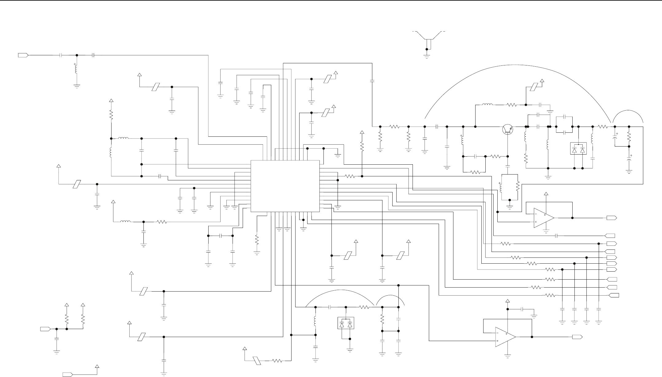
6-34 Receiver Schematics (UHF)
IF
IN
3.2V
1.5V
3.2V
1.5V
0.68V
100PF
3.3V_ANALOG_M
49.9
100PF
56PF
150PF
10UH
2200PF
10UH
C2513
R2532
L2532
L2533
C2508
C2510
C2512
C2509
21
21
21
21
21
21
3.3V_ANALOG_M
.047UF
4.7NH
3.3V_ANALOG_M
0.1UF
0
L2534
C2503
R2533
E2533
C2506
21
3.3V_DIGITAL_M
3.3V_DIGITAL_M
0.1UF
0.1UF
C2504
E2535
C2505
E2534
3.3V_ANALOG_M
ANALOG_5V_M
3.3V_DIGITAL_M
0
0
0.1UF
R2531
R2530
C2500
ANALOG_5V
3.3V
21
21
IN
IN
270NH
33PF
15PF
C2501
L2530
C2502
21
21
21
3.3V_ANALOG_M
0.1UF
C2517
E2532
1.9V
3.3V
1.9V
1.0V
2.0V
1000PF
0.1UF
.01UF
.01UF
C2520
C2518
C2515
C2511
21
3.3V_ANALOG_M
0.1UF
ANALOG_5V_M
0.1UF
C2522
E2540
C2521
E2539
21
442
3.3V_DIGITAL_M
100K
R2539
R2537
21
ANALOG_5V_M
0.1UF
MC33072
100
12NH
U2531
R2547
L2549
C2556
48
1
3
2
2
1
21
50 OHM
3.6 DB
442
1.1PF
12NH
DNP
11.5 2.2PF
475
10K
1.1PF
470PF
R2545
R2546
C2541
L2538
C2539
C2534
C2535
R2541
R2542
21
21
21
15PF
BFQ67W
C2542
Q2530
21
23
1
VSL = 2.3V TYPICAL
(0.8V < VSL < 4.4V)
2ND LO LOOP FILTER
120NH
7.5PF
1SV228
3300PF
182
22UF
2.2UF
330NH
10K
C2561
R2563
C2557
R2559
C2555
L2548
CR2530
C2552
L2547
21
21
21
2
1
21
10
2.2UH
27PF
DNP
0.1UF
3PF
ANALOG_5V_M
C2547
E2541
C2554
R2549
L2539
C2553
21
3
2ND LO VCO @ 75.6 MHZ
2.2UH
15PF
121
C2546
R2548
L2543
2121
SHIELD
RX_ABACUS
SH2500
2
1
0.1UF
C2527
PC
ABA_DOUTB/MISO
ABA_DOUTA
ABA_FS
SYNCB
RX_SL_LO2
PD
FREF
ABA_CLKOUT
PE
IN
OUT
OUT
OUT
IN
OUT
IN
OUT
IN
IN
2.2V
49.9
33.2
ANALOG_5V_M
49.9
33.2
0.1UF
33.2
49.9
33.2
R2596
R2597
R2595
R2581
R2580
R2582
R2583
C2551
1.7V
21
RX_SL_CLK
OUT
MC33072
U2531
48
7
5
6
10PF 10PF 10PF 10PF
C2580 C2581 C2582 C2583
1.9V
1.2UH
1SV228
392
0.1UF
.33UF
0.1UF
.33UF
C2532
C2531
C2529
R2540
CR2531
C2523
L2535
212 1
3
2
1
3.3V_DIGITAL_M
10K
E2536 R2535
21
2.0V TYPICAL
(0.8V TO 2.8V)
SAMPLE CLK SLV
(18 MHZ)
CLOCK VCO TANK
100PF 2K
R2538
C2525
0.1UF
3.3V_DIGITAL_M
C2528
E2538
3.3V_DIGITAL_M
0.1UF
C2524
E2537
33.2
R2536
1.5V
30
27
26
33
25
34
36
32
31
35
29
28
46
39
40
48
43
42
38
47
37
45
41
44
11
12
6
9
1
2
5
4
3
10
7
8
CXVL
LOP
LON
CXVM
VDDL
VDDP
IOUTL
GNDP
RREF
VDDQ
IOUTC
GNDQ
VDDC
GNDC
CLKP
CLKN
GNDS1
GNDD
PC
GNDL
FREF
GNDS2
SYNCB
GNDH
FS
DOUTB
DOUTA
CLKOUT
VDDH
VDDD
PE
MXOP
MXON
GNDF
IF2N
IF2P
VDDF
GCP
GCN
VDDA
GNDA
VREFP
VREFN
VDDI
IFIN
CXIF
GNDI
RX_ABACUS
AD9874
U2530
PD
1.2V
3.3V
3.3V
14
17
13
24
23
15
21
16
22
18
19
20
100K
R2534
21
2.0V 1.5V
.01UF
100PF 100PF
C2516
C2519
C2514
21
21
Receiver – Rx Abacus Schematic Diagram (Kit No. CRE4008)
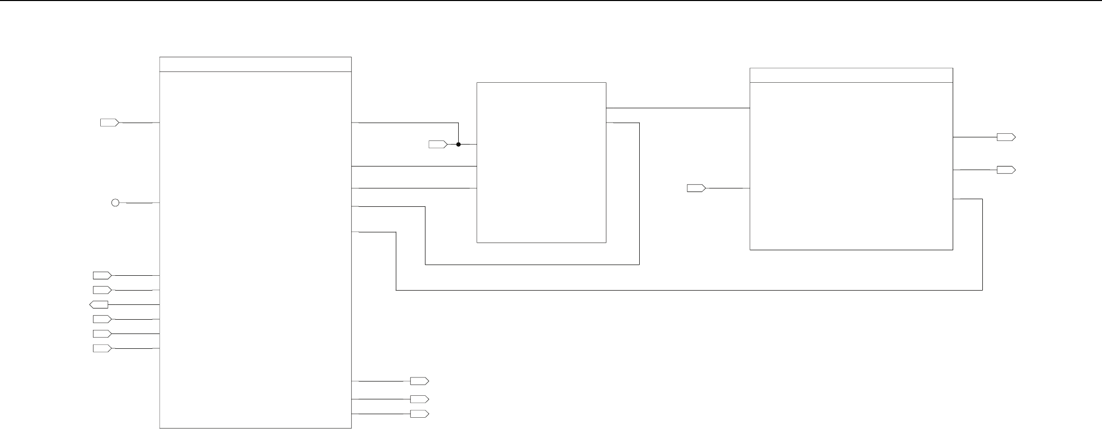
Receiver Schematics (UHF) 6-35
NC
IN
IN
IN
IN
OUT
IN
IN
in
in
in
in
out
in
in
out
SYNTH_CLK_IN
2.775V_RX
REF_16.8MHZ_IN
SYNTH_SPI_DW
SYNTH_CE_IN
TRI_RSTB_IN
SYNTH_SPI_DR
TRI_AUX_DAC
2.775V_RX
RX_LOCK_DETECT
RX_SLV_MON
LF_OUT
PRE_SCALER
SPARE_2
REF_16.8_MHZ
TRI_SPI_DW
TRI_SPI_CLK
VCO_SELECT
TRI_SPI_CEX
TRI_SPI_DR
TRI_RSTB
VCC_CP
12V_RX_SW
TRIDENT_BLOCK
3100
IN
12V_RX_SWIN
in
out
OUT
OUT
in
out
IN
RX_V_CNTL
RX_LOCK_DETECT
RX_SLV_MON
OUT
OUT
OUT
VCC_CP
LO_OUT
VCO_SELECT
VCO_SLV
12V_VCO
RX_VCO_3200
3200
VCO_V5
VCO_FEEDBACK
INJ_AMP_M1
10V_RX
LO_IN
VCO_INJ_OUT
IN
IN
RX_INJ_AMP_FBK_2700
2700
10V
BANDIT_INJ_AMP_FDBK
IN
OUT
OUT
OUT
INJ_MIXER_OUT
INJ_AMP_M1
OUT
OUT
Receiver – Rx Frequency Generation Unit (FGU) Schematic Diagram (Kit No. CRE4008)
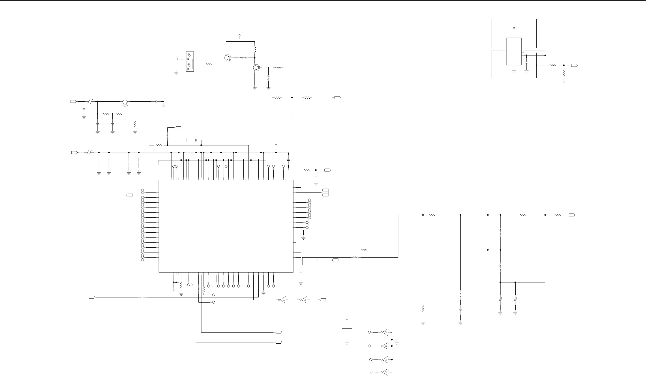
6-36 Receiver Schematics (UHF)
0
DNP
.1UF
0
R3101
R3100
C3116
VCC_CP
21
IN
DNP
.01UF
C3171
21
DNP
DNP
330UF 10K
DNP
267
DNP
DNP
10
MMBT3904
Q3100
R3152
R3151
R3150
C3132
23
1
21
DNP
DNP
39PF
.01UF
DNP
E3110
C3131
C3130
12V_RX_SWIN
TOP-SIDE EVAL BOTTOM-SIDE EVAL
E3105
2.775V_RXIN
.1UF
DNP
150PF
DNP
.1UF
150PF
C3100
C3111
C3107 C3103
TRI_AUX_DAC OUT
NC
2.775V_RX
MMBT3906
DNP
10K
DNP
DNP
DNP
27K
51
QT1222
DNP
R3182
Q3180
D3180
R3181
R3180
23
1
2
3
1
MMBT3904
DNP
Q3181
23
1
DNP
0
DNP
150K
150K
DNP
.1UF
100
R3187
R3184
C3185
R3185
R3183
RX_LOCK_DETECT
OUT
10K
0
R3147
R3146 RX_SLV_MON
OUT
IN2POS
IN2NEG
VCC_NEG
IN1NEG
IN1POS
VCC_POS
OUT1
OUT2
12V_RX_SW
TS272
U3101
8
4
220PF
C3120
7
1
5
6
3
2
.15UF
0
C3105
R3134
LF_OUT
OUT
348
22.1
R3104
R3105
64.9
R3106
.1UF
C3104
COILCRAFT 0805CS1UF
100NH
1UF
3300PF
C3109
C3108
L3100
C3106
21
21
2.94K
.01UF
C3102
R3103
0
R3108
MC74LVX14
MC74LVX14
MC74LVX14
MC74LVX14
U3103
U3103
U3103
U3103
65
89
10 11
12 13
VCC
GND
TRI_VCC
MC74LVX14
U3103
14
7
NC
NC
NC
NC
SPARE_2
VCO_SELECT
OUT
OUT
MC74LVX14MC74LVX14
0
0
150PF
150PF
U3103 U3103
R3130
R3129
C3127
C3126
PRE_SCALER
TRI_RSTB
4321
IN
IN
.022UF
C3101
REF_16.8_MHZ IN
NC
NC
NC
NC
NC
NC
NC
NC
NC
NC
NC
NC
NC
NC
NC
NC
NC
NC
NC
NC
NC
NC
NC
NC
NC
NC
NC
NC
L7
L8
J11
A10
F5
D2
D1
C2
C1
B6
A5
K7
G11
L6
K8
F8
J7
A3
A4
B5
J10
E2
E1
B1
B2
K6
D3
A6
C3
NC3
ESC_CPBIAS
ESC_CP
SF_BYP
REF_OSC_OUT
TXQ
NTXI
PHCLK
DEEPSLEEP
NC4
LVCC1
SDM_CLK_GEN_GND
RX_AGND2
SSI_GND
MAIN_GND
LGND1
VMULTI2
VMULTI1
SUB2
DMCS
TXFS
TXCLK
TXD
ESC_IN
MN_CP
SF_OUT
CLK_OUT
CLK_EMIT
M_PRSC
RXD
ESC_TEST
BP_Q
BP_QX
BP_I
QCAP
RSTB
SF_SPLY
EF_OUTP
EF_OUTM
INCR_DECR
NC5
REF_VCC
GPO2_TEST2
RX_EN_OUT
TM
SUB3
AGC_DAC
FBQ
SDM_VREFP
SDM_VAG
REF_IN
NTXQ
TXI
HP_MOD_OUT
MN_CP_GND
SUB1
NC6
ASPI_CLK
SPI_CLK
RXQ
RXQX
SCAN_EN
ICAP
ACE2_GPO8
TEST1_LCKDET
CEX
SPI_DW
SPI_DR
RXACQ
RXCLK
RXFS
BP_IX
SCAN_IN
GPO4_TEST4
GPO1_TEST1
RX_AVCC2
ASPI_VCC
SDM_CLK_GEN_VCC
RX_AVCC1
SF_GND
SDM_
REF_
VCC
SSI_VCC
TCLK
CLK_CP
CLK_BASE
MN_ADAPT_CP
M_PRSCX
SENS
AUX_DAC
ESC_CP_GND
MN_CP_VCC
MAIN_VCC
ESC_CP_VCC
TX_VCC
CLK_VCC
ESC_VCC
TX_DAC_VCC
SDM_REF_GND
RX_AGND1
CLK_GND
NC1
DC_CAL_GPO5
RFSTEPA_GPO6
ESC_INX
ACE1_GPO7
SDM_VREFM
NC2
ASPI_GND
TX_GND
ESC_GND
TX_DAC_GND
ESCD2_OUT
ESCD2_OUTX
GPO3_TEST3
ASPI_DATA
RXIX
RXI
AGC_FLAG
AGC_REF
FBI
TEST2
RX_TRIDENT_BLOCK
TRIDENT BGA 121PIN
15H28
U3100
H7
G7
H6
G6
E7
C4
B4
E11
E10
J4
C8
C9
A9
B9
B11
A2
D4
B3
E4
J6
F1
F2
G4
G5
G8
G9
H3
H4
J1
L2
J3
K3
H9
J9
A8
B8
NC
NC
NC
NC
NC
NC
NC
.1UF
C3124
C7
10PF
DNP
C3172
TRI_SPI_DR
TRI_SPI_CEX
TRI_SPI_DW
TRI_SPI_CLK
OUT
IN
IN
IN
33.2
R3172
NC
NC
NC
NC
NC
NC
NC
NC
NC
NC
NC
NC
F9
F11
F10
D10
D9
C11
E8
D11
E9
D7
K2
K1
H2
J2
L3
F7
D8
G3
G2
H1
G1
L9
NC
NC
NC
NC
NC
NC
NC
NC
NC
NC
NC
NC
NC
NC
NC
NC
NC
NC
NC
NC
NC
NC
NC
NC
DNP
10K DNP
10K
10K
R3102
R3173
R3113
H10
H11
F4
F6
K9
K4
J5
L4
H5
B10
C10
L5
K5
F3
E3
L11
L1
A11
A1
C5
E6
D5
E5
J8
H8
G10
L10
K10
K11
A7
B7
D6
C6
TRI_VCC
Receiver – Trident Block Schematic Diagram (Kit No. CRE4008)
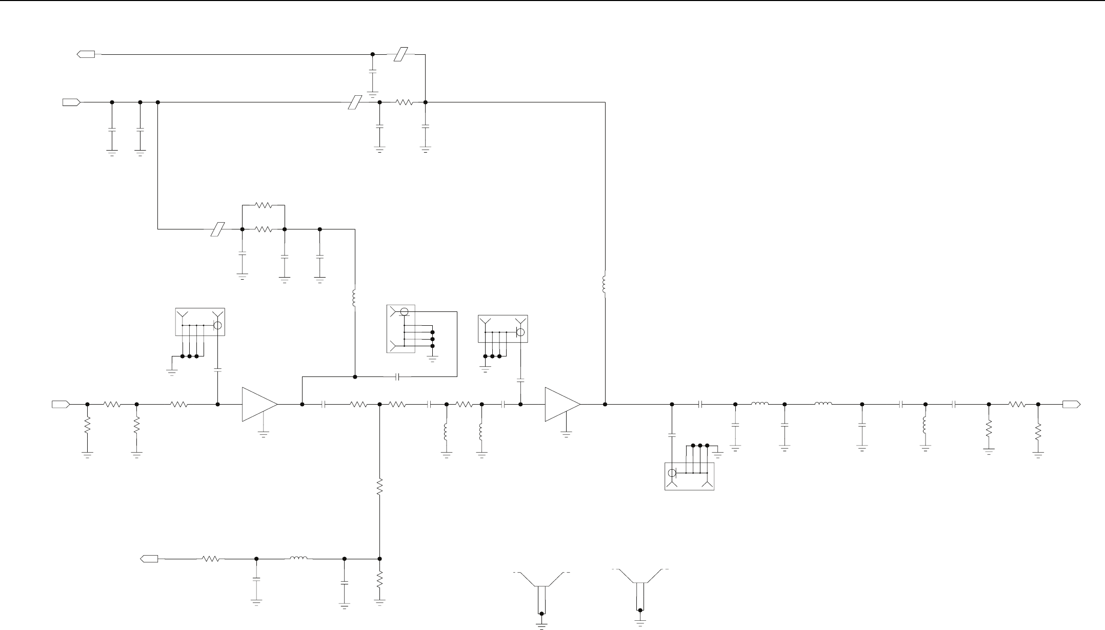
Receiver Schematics (UHF) 6-37
SHIELD
SHIELD
SH2701
SH2700
2
1
2
1
CONN_J
DNP
P2704
3.9PF 8.2PF
18NH
150PF
150PF
DNP
16NH
3.9PF
6.8PF 7.5PF
18NH
C2723
L2705
C2715 C2716
C2714
L2704
L2703 C2717
C2713
C2721
5
4
3
2
1
~ 27DBM @ UHF BAND
0
DNP
0
0
DNP
R2716
R2714
R2715 VCO_INJ_OUT
OUT
5
4
3
2
1
GAIN ~13.5DB @ UHF BAND
G1
INOUT
150PF
DNPAH101
DNP
CONN_J
C2720
P2703
U2701
31
2
5~9DBM @ UHF BAND
1DB PAD
~ 18DBM @ UHF BAND
G1
INOUT
825 825
5.62
HMC479
0
CONN_J
150PF
DNP
DNP
R2719
R2718
R2717 R2713
C2718
P2700
U2700
LO_IN
5
4
3
2
1
31
2
IN
2.2DB PAD
5.62
5.62
39NH
150PF
DNP
16NH
150PF
0
150
27PF
C2710
L2708
R2705
R2706
R2704
R2703
C2709
C2708
L2709
DNP
150PF
C2719
5
4
3
2
1
220NHDNP
CONN_J
P2702
L2700
21
~4.7V
150PF
.1UF .01UF
160
160
R2712
E2700
C2704
C2703
C2702
R2710
21
-8.0 DBM
VCO_FEEDBACKOUT
18NH
475
7.5PF
C2707
L2701
R2708
68.1
8.2PF
C2706 R2707
470NH
L2702
21
~9.2V
.01UF 150PF
4.3
.1UF
C2725
E2702
C2712
C2711
R2711
E2701
INJ_AMP_M1
150PF .1UF
C2724
C2722
10V_RXIN
OUT
Receiver – Rx Lo1 Injection Amp and Feedback Schematic Diagram (Kit No. CRE4008)
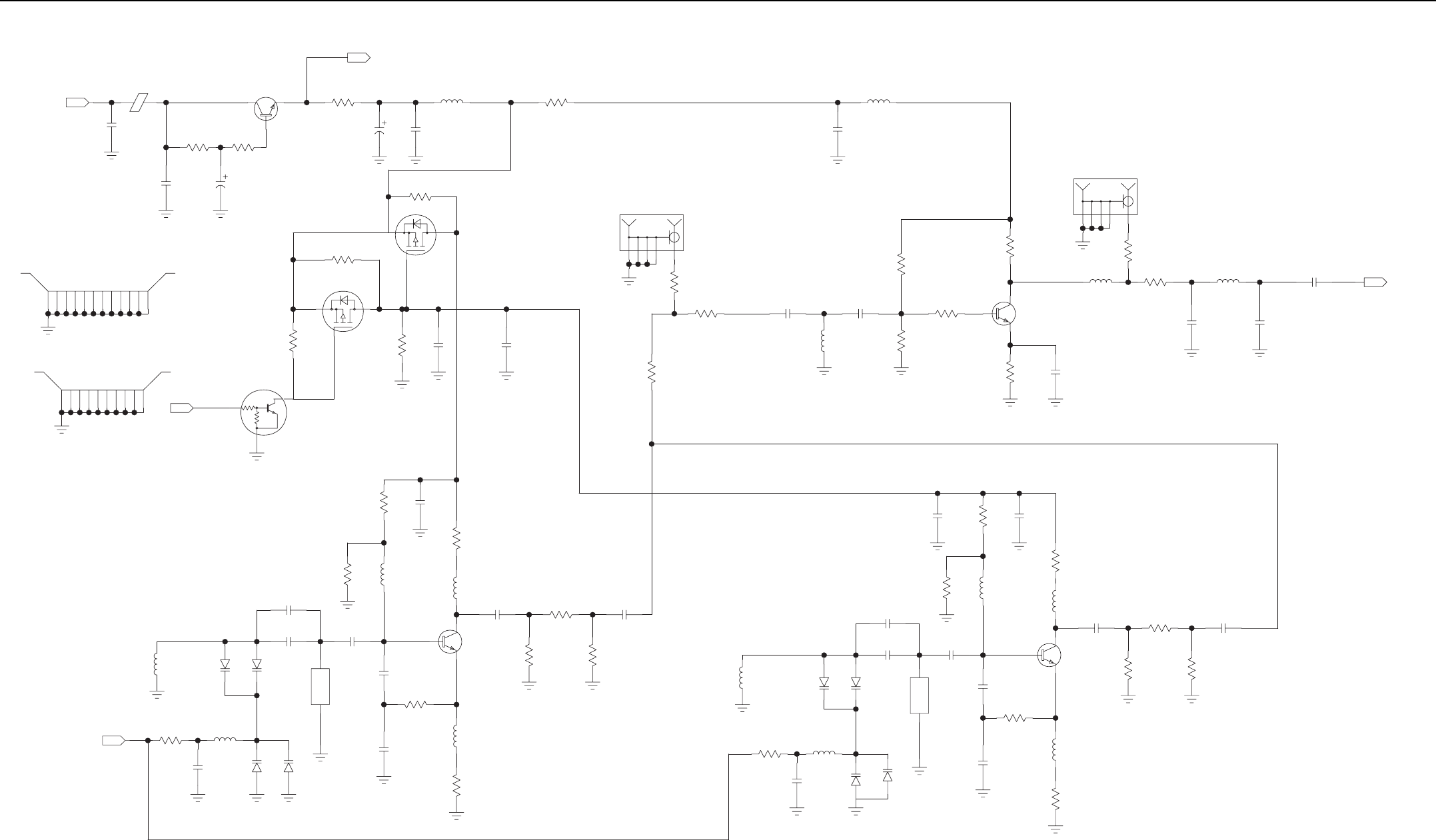
6-38 Receiver Schematics (UHF)
10
9
8
7
6
5
4
3
2
1
SHIELD
SH3201
VCO_SELECT
IN
LOW RANGE VCO ENABLED LOW
HIGH RANGE VCO ENABLED HIGH
10K
47K MUN5214T1
Q3206
2
3
1
10K
R3235
10
9
8
7
6
5
4
3
12
11
2
1
SHIELD
SH3200
150PF
.01UF 330UF
267 10
C3228
R3231
C3229
C3230
R3230
E3200
12V_VCOIN
11.3V
MMBT3904
Q3203
34.8
R3229
VCC_CP
OUT
10V
.01UF
47UF
RX_VCO
0
390NH
C3226
R3228
L3215
C3227
21
NORMALLY OFF
P-CHAN ENHANCEMENT
DNP
150PF
150PF
10K
0
DNP
DNP
0
NTR1P02LT1
NTR1P02LT1
C3232
C3233
R3232
R3233
R3234
Q3204
Q3205
2
1
3
2
1
3
CONN_J
DNP
P3200
DNP
0
0
R3219
R3218
0
R3236
21
DNP
.1UF
DNP
CONN_J
22NH
3.32K
200
100 0
2K
0
150PF
BFQ67W
27NH
3PF
301
R3222
P3201
L3212 R3227
R3226
R3225 C3220
C3219
C3218
L3211
R3223
Q3202
R3224
R3221
18NH150PF
6.2PF 6.2PF
C3224
C3223
L3213
C3222
LO_OUT
OUT
150PF
390NH
L3214
C3225
432
2.7PF
432
150PF
11.5
C3216
R3216
R3215
R3217
C3217
SI8800SPQ0579YE
579MHZ
1SV229
1SV229
15NH
Y3201
CR3204
L3206
CR3206
1
21
21
OUT IN
DNP
150PF
4.3PF
390NH
1K
150PF
2.7PF
2.2PF
100
1.58K
390NH
C3231
C3210
C3211 C3212
R3214 L3208
R3213 C3215
L3209
R3212
NE68519
Q3201
13
2
390NH
6.2PF
5.1PF
18.2
340
C3214
R3210
C3213
R3211
L3207
2
HIGH RANGE VCO ENABLE - HIGH
1SV229
10 390NH
150PF
1SV229
CR3207
C3209
R3209 L3205
CR3205
21
21
390NH
390NH
NE68519
1.58K
432
1K
150PF
150PF
100
2.7PF 11.5
432
L3203
R3205
Q3200
L3204
C3206
C3207 C3208
R3208
R3207
R3206
R3204
R3203
13
2
18.2
390NH
7.5PF
6.2PF
340
R3202
R3201
C3205
C3204
L3202
1SV229 1SV229
390NH
10
150PF CR3203
CR3201
R3200 L3200
C3200
VCO_SLV
21
21
IN
LOW RANGE VCO ENABLE - LOW
CAPACITOR
1SV229
1SV229
542MHZ
SI8800SPQ0542YE
3.3PF
4.7PF 2.7PF
18NH
C3201
Y3200
CR3200 CR3202
L3201
C3202 C3203
21
21
21
OUT IN
Receiver – UHF VCO Schematic Diagram (Kit No. CRE4008)
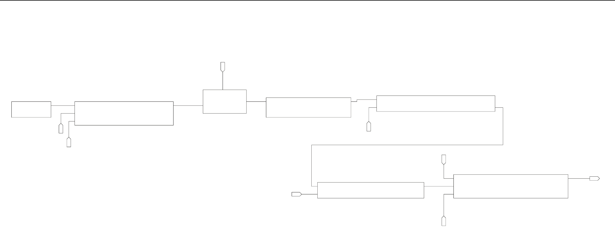
Receiver Schematics (UHF) 6-39
RX_MIXER_1400
MIXER_LO_IN
LOWPASS_IN
MIXER_IF
MIXER
RX_IMAGEFILTER_1300
IMGFILT_IN
MIXER_LO_INPUT
IMG_FILTER
IMGFILT_OUT
IN
RX_LNA_1200
LNA_IN
LNA_OUT
5V_LNA
LNA
5.0V_RX_SW
IN
RX_TUNABLE_FILTER_1100
12V_LO1_FB
RF_OUT
V_CNTL
RF_IN
TUNABLE_FILTER
RX_LPF_1000
LPF_OUT
12V_RX_SW
FE_V_CNTL
IN
IN
LPF
RX_IF_STRIP_1500
RX1_IF_OUT
RX_5VDC
RX1_IF_IN
5.0V_RX_SWIN
IF_STRIP
V_ATTN
IN
5.0V_RX_SW
IN
RX_IF_ATTENUATOR_1600
5V_IF_ATTN
IF_ATTN_IN
V_ATTN
IF_ATTN_OUT
IF_ATTEN
FINAL_IF
OUT
Receiver – Schematic Diagram (Kit No. CRE4008)
6-40 Receiver Schematics (UHF)
G4
G3
G2
G1
CONN_J
J1000
C
33PF
150NH
L1005
C1008
6.8NH
33NH 1.1PF 2.7PF 4.3PF 2.7PF5.6PF
22NH
C1005C1004C1002C1001C1000
L1002
L1001
L1000
~ 0.6DB OF LOSS @ 487MHZ
1.5PF
27NH
C1003
L1003
27NH
L1004
DNP
CONN_J
P1000
5
4
3
2
1
DNP
150PF
C1007
150PF
C1006
LPF_
O
Receiver – Rx Low Pass Filter Schematic Diagram (Kit No. CRE4008)
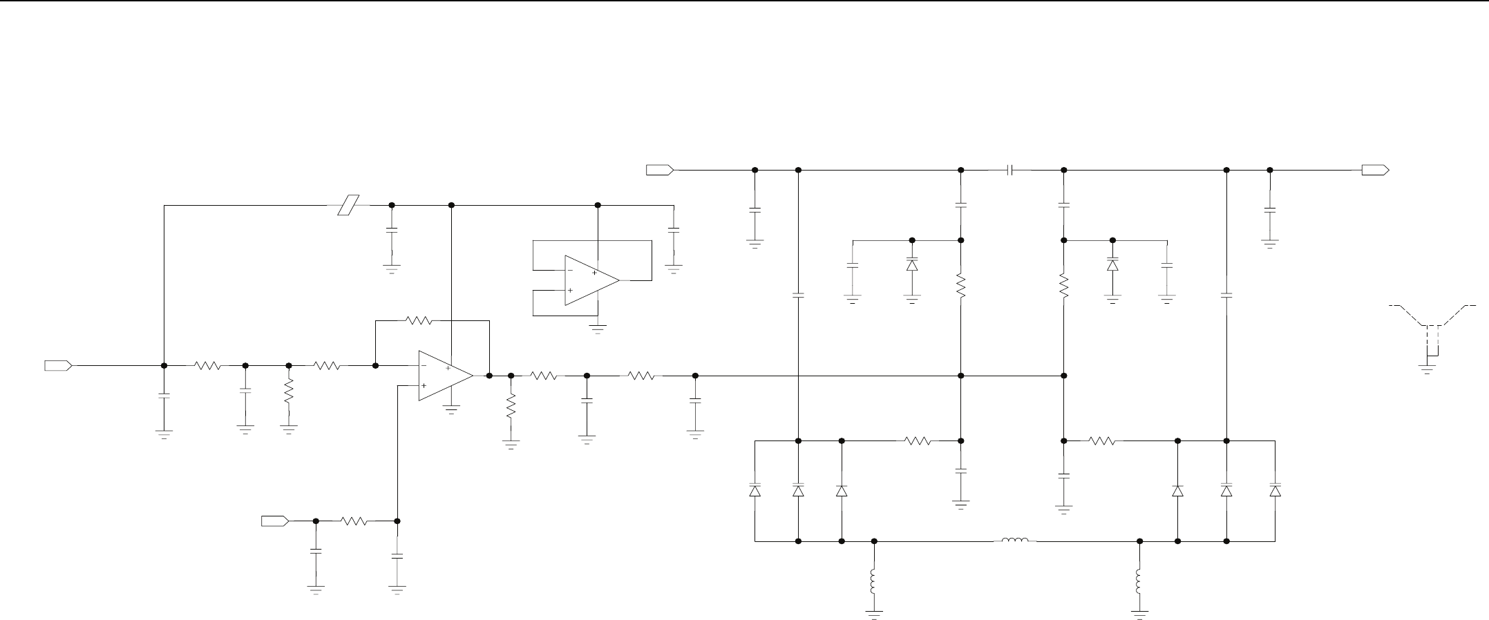
Receiver Schematics (UHF) 6-41
12V_LO1_FB
IN
1SV279
9.1PF
24PF
2.7PF
DNP
D1104
C1111
C1110
C1112
RF_OUT
OUT
~ 2.0DB OF LOSS @ 487MHZ
62PF
62PF
.8PF
C1109
C1106
C1107
21
47.5K
47.5K
1SV279
R1104
R1103
D1103
21
DNP
10PF
24PF
2.7PF
C1103
C1104
C1102
.1UF
C1117
RF_ININ
MC33202
U1100
48
7
5
6
137K
MC33202 150PF
10K
150PF
220K
20K
4700PF
DNP
R1111
R1100
C1121
R1108
R1109
U1100
C1116
E1100
C1100
12V
48
1
3
2
1.1K
20K
150PF
100PF
20K
R1107
R1110
C1119
R1106
C1114
150PF
1K
.1UF C1120
R1105
C1113
V_CNTL IN
SHIELD
SH1100
2
1
1SV280
1SV279
1SV279
D1105
D1106
D1107
21
21
DNP
150PF
47.5K
R1102
C1108
9NH
L1102
47.5K
1SV279
150PF
1SV279
1SV280
DNP
68NH
L1101
D1102
D1101
D1100
R1101
C1105
21
21
9NH
L1100
Receiver – Rx FE Tunable Filter Schematic Diagram (Kit No. CRE4008)
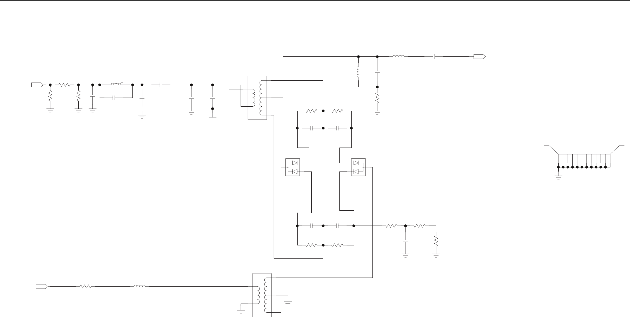
6-42 Receiver Schematics (UHF)
LOWPASS_ININ
2PF
221
DNP
5.6NH
3PF
9.1PF
DNP
0
221
XFMR
3.9PF
5.6PF
10PF
DNP
R1409 R1411
R1412
C1419
T1401
C1410
C1408
C1409
L1402
C1405
C1404
3
2
1
5
4
21
SMS3923
SMS3923
CR1401
CR1400
2
3
12
3
1
.01UF
150
150
.01UF
C1414
R1404
C1413
R1403
2121
~ 6.5DB OF LOSS @ UHF BAND
51
82PF
47NH91PF
68NH
C1415
L1404
R1400
C1416
L1403
MIXER_IF
OUT
10
9
8
7
6
5
4
3
12
11
2
1
SHIELD
SH1401
150
150
.01UF
.01UF
R1402
R1401
C1412
C1411
2121
XFMR
T1400
3
2
1
5
4
470PF 0
1K
3.3K
R1407
C1417
R1406
R1405
21
2121
MIXER_LO_ININ
03.3NH
R1410 L1401
Receiver – Mixer Schematic Diagram (Kit No. CRE4008)
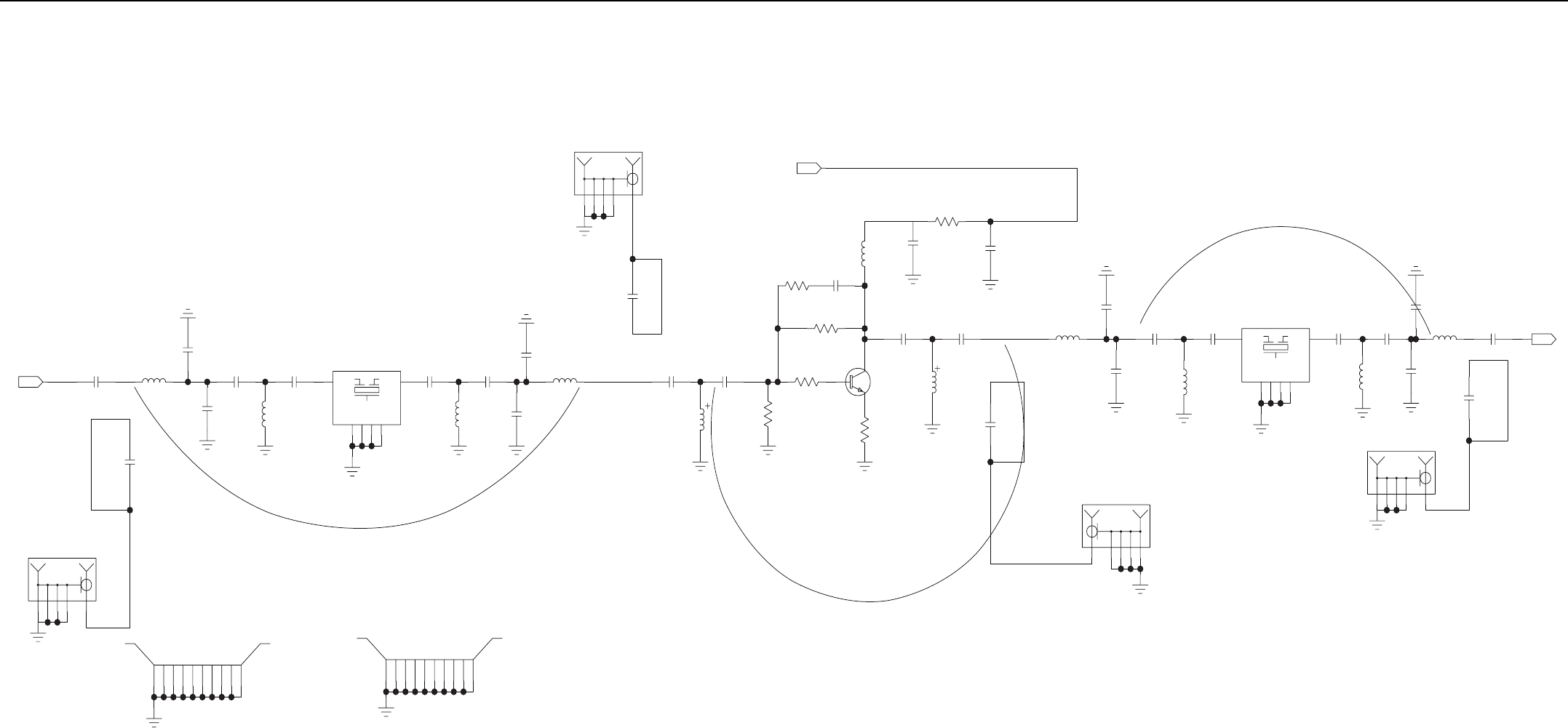
Receiver Schematics (UHF) 6-43
DNP
.01UF
CONN_J
DNP
P1500
C1530
5
4
3
2
1
SHIELD
SHIELD
SH1500 SH1501
10
9
8
7
6
5
4
3
2
1
10
9
8
7
6
5
4
3
2
1
~ 2.8 DB OF INSERTION LOSS AT 73.35 MHZ
~ 2.8 DB OF INSERTION LOSS AT 73.35 MHZ
~ 13.6 DB OF GAIN AT 73.35 MHZ FINAL CIRCUIT HAS ~ 8 DB OF GAIN
RX1_IF_IN
IN
51PF
.01UF 270NH
8.2PF
6.8PF
2.7PF
1UH
C1529
C1501
C1500
L1501
C1503
L1500 C1502
1
GND1
OUT
GND3
GND2
GND4
IN
MM13114
U1500
6
5
3
2
270NH
8.2PF
2.7PF
6.8PF
1UH
C1504
L1502 C1506
C1505
C1507
L1503
412PF
DNP
CONN_J
DNP
.01UF
P1503
C1509
5
4
3
2
1
21
DNP
CONN_J
P1502
5
4
3
2
1
2.7V
470NH
.01UF
.01UF
DNP
47PF
220NH
L1506
C1515 C1516
L1505
C1517
21
21
21
0.9V
0.15V
.01UF
2.21K
12.1
180NH
825
3.32K
39PF
BFQ67
0.1UF
10
R1504
R1500
R1501
C1512
R1503
U1502
R1502
L1504
C1510 C1511
21
23
1
21
21
0.1UF
182
C1513
R1505
RX_5VDC
21
IN
GND1
OUT
GND3
GND2
GND4
IN
MM13114
12PF
150PF
270NH
8.2PF
2.7PF
1UH
51PF
6.8PF
C1514
L1507
C1520
C1521
C1519
L1508
C1522 U1501 C1523
41
6
5
3
2
1UH 8.2PF
2.7PF
DNP
CONN_J
P1501
L1509 C1525
C1524
5
4
3
2
1
.01UF
270NH
6.8PF
C1527
L1510
C1526
RX1_IF_OUT
OUT
DNP
.01UF
C1528
Receiver – IF Strip Schematic Diagram (Kit No. CRE4008)
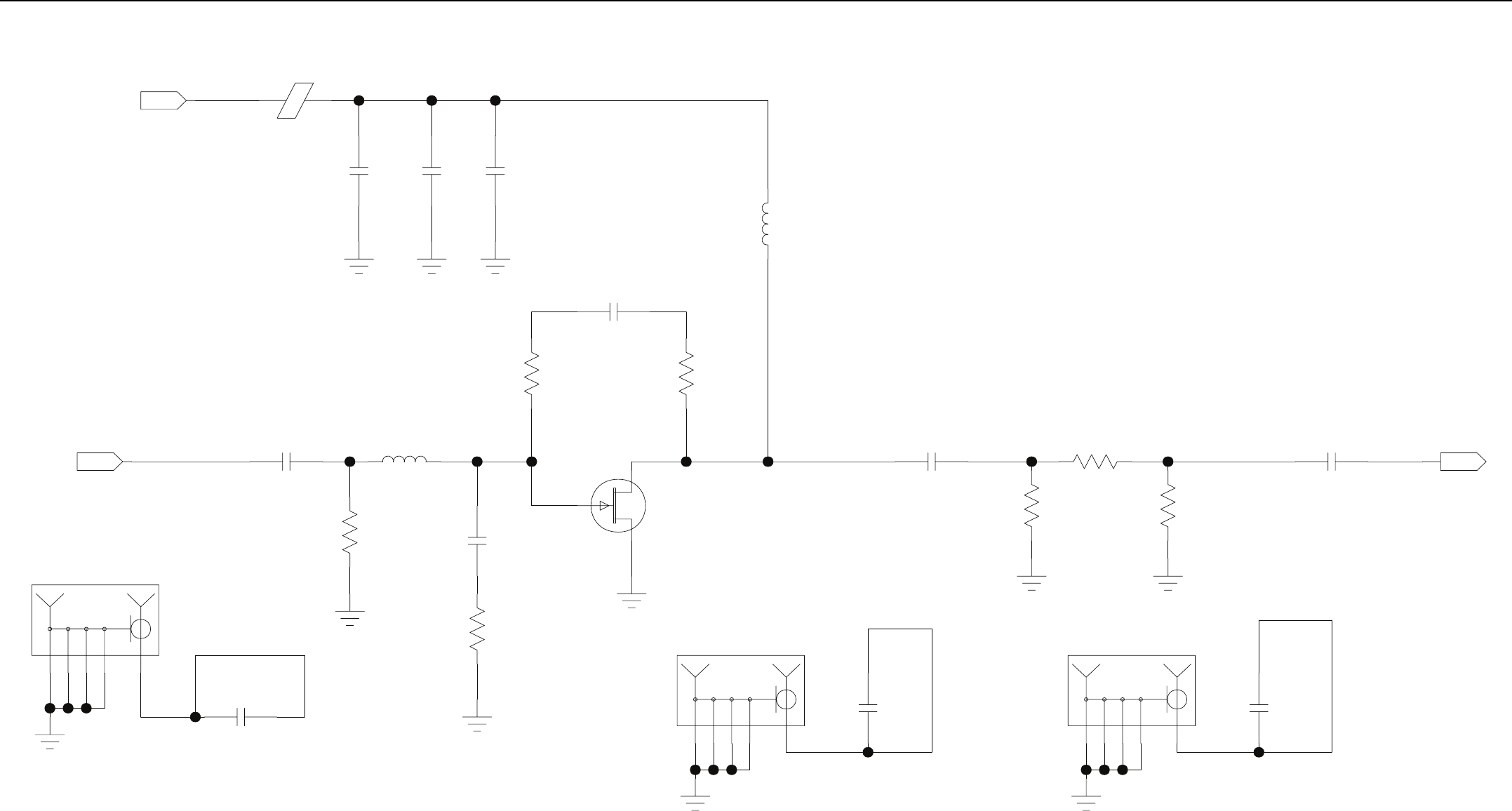
6-44 Receiver Schematics (UHF)
E1200
5V_LNA
IN
150PF.1UF.01UF
C1200 C1201 C1202
510 510
1000PF
C1205
R1203R1202
150NH
L1201
D
S
GFH1
1PF
5.6
U1200
C1204
R1201
3
2
1
~ 18DB GAIN @ UHF BAND
150PF 20NH
CONN_J
DNP
L1200
P1200
C1203
LNA_IN
5
4
3
2
1
IN
150PF
DNP
10K
C1207
R1200
DNP
150PF
CONN_J
DNP
C1208
P1201
5
4
3
2
1
CONN_J
150PF
DNP
DNP
C1231
P1230
5
4
3
2
1
1.82K
150PF
C1230
R1231
LNA_OUT
OUT
0.5DB PAD
2.74
1.82K
150PF R1232
R1230
C1206
Receiver – LNA Schematic Diagram (Kit No. CRE4008)
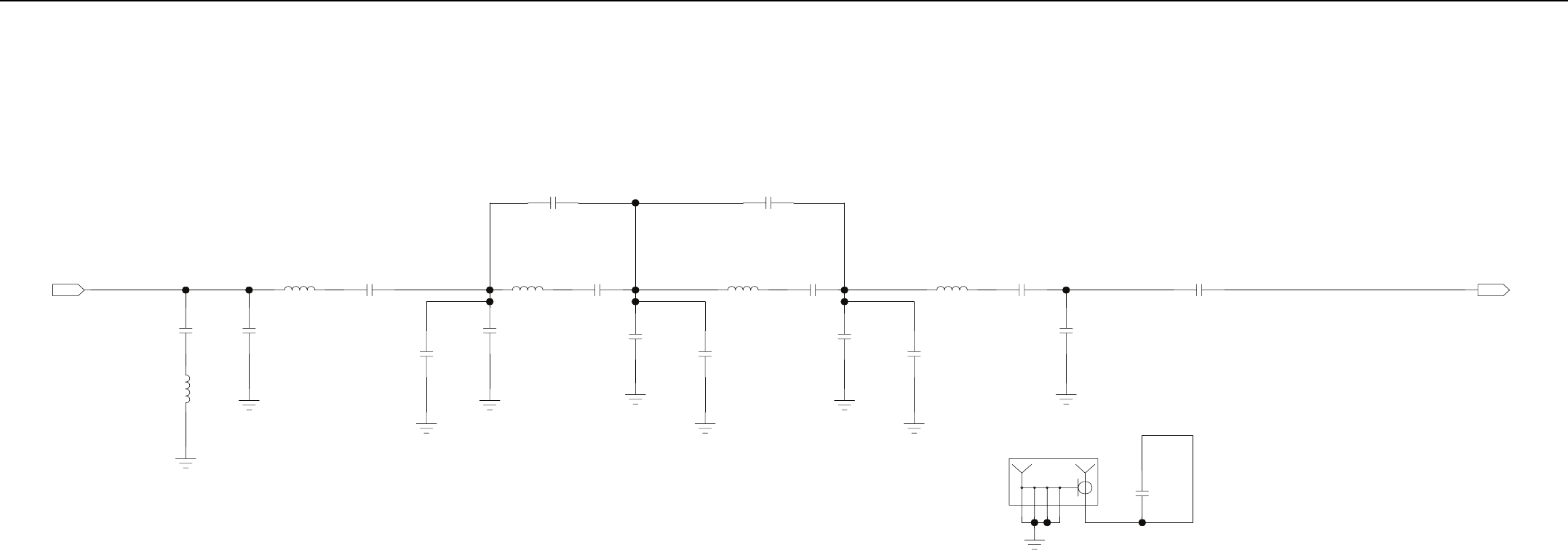
Receiver Schematics (UHF) 6-45
100NH
47PF 6.8PF
C1300
L1300
C1301
27NH
L1301
IMGFILT_IN
IN
18PF
C1302
4.7PF
1.3PF
C1303
C1304
~1.4DB OF LOSS @ 487MHZ
27NH10PF
3PF
C1305
L1302 C1306
.5PF
2.2PF
C1307
C1308
10PF
27NH
C1310
L1303
3PF
C1309
4.7PF
1.3PF
C1311
C1312
22PF
27NH
6.2PF
L1304 C1314
C1313
150PF
C1315
IMGFILT_OUT
OUT
CONN_J
DNP
P1300
5
4
3
2
1
150PF
DNP
C1316
Receiver – Image Filter Schematic Diagram (Kit No. CRE4008)
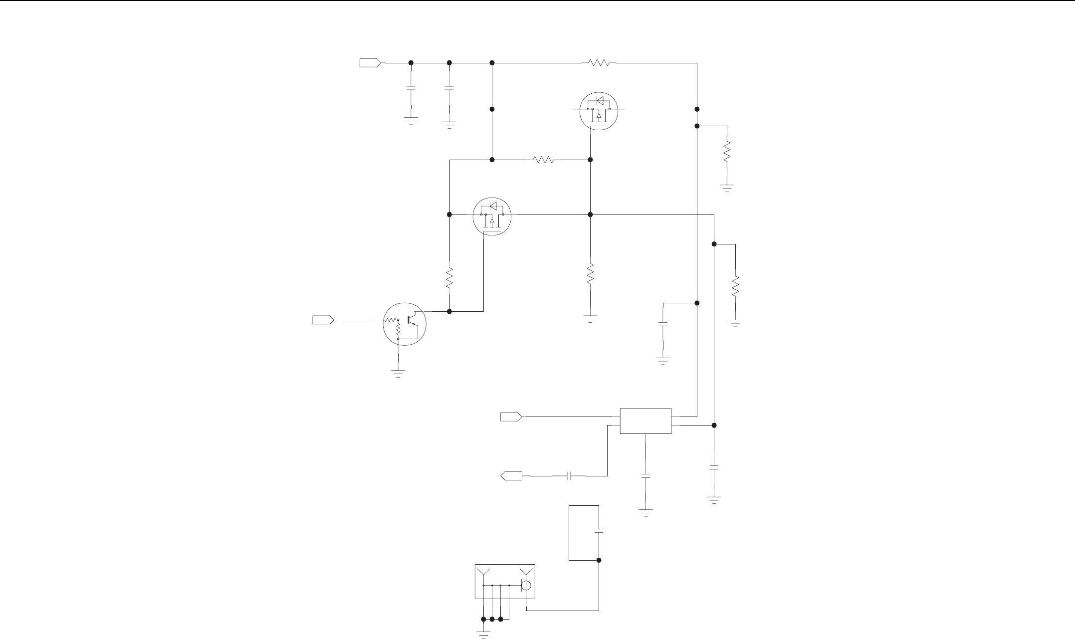
6-46 Receiver Schematics (UHF)
0.1UF 150PF
C1600 C1601
5V_IF_ATTN
IN
0
DNP
NTR1P02LT1
Q1602
R1600
2
1
3
NTR1P02LT1
Q1601
2
1
3
10K
47K
10K
MUN5214T1
Q1600
R1602
V_ATTN
2
3
1
IN
IF_ATTN_OUT
IF_ATTN_IN
OUT
IN
.01UF
CONN_J
DNP
DNP
C1602
P1600
5
4
3
2
1
.01UF
.01UF
0.1UF
C1605
C1606
C1603
RFIO1
RFIO2
GND
V1
V2
AT267
U1600
5
4
3
1
2
0.1UF
C1604
10K
R1603
10K
R1605
DNP
0
10K
R1604
R1601
Receiver – Rx IF Attenuator Schematic Diagram (Kit No. CRE4008)
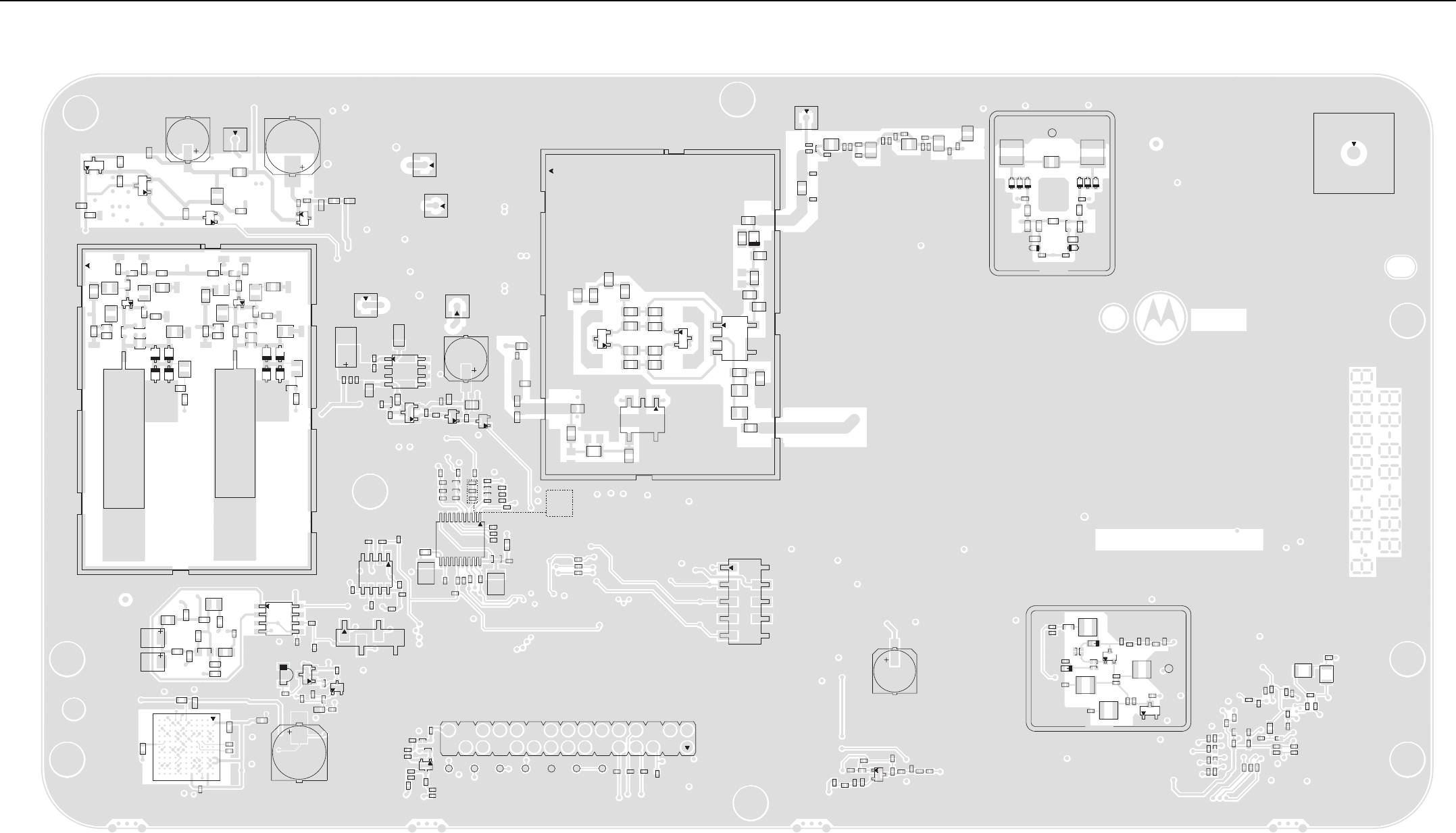
Receiver PCB (UHF) 6-47
6.3 Receiver PCB (UHF)
2
5
23
32
32
32
3
4
C3233
R3234
R3233
Q3204
R3232
Q3205
C3227
Q3206
L3215
R3235
C3226
R3229
R3228
P3201
Q3203
C3229
R3230
R3231
C3228
C3230
E3200
11
8
9
10
3
2
12
Y3200
C3203
C3206
R3204
R3205
R3203
L3203
L3204
Q3200
R3207
CR3201
CR3203
C3200
CR3202
CR3200
L3201
C3201
C3202
C3204
R3202
L3202
C3205
C3207
R3208
R3201
C3208
R3206
R3200
L3200
C3215
R3214
R3213
R3212
L3208
L3209
C3217
R3217
Y3201
CR3207
CR3206
C3213
C3210
C3211
C3212
R3211
L3207
C3214
C3216
Q3201
R3216
R3210
R3215
CR3205
C3209
R3209
CR3204
L3205
L3206
7
5
4
6
SH3200
5
4
53
4
2
23
P2702
P2700
32
58
32
L11
L1
A11
4
U3100
C3101
C3109
R3106
C3105
C3108
C3116
R3101
C3104
R3129
R3103
R3130
R3105
L3100
C3106
R3134
R3104
R3173
R3102
C3103
E3105
R3180
D3180
C3102
R3108
U3101
R3187
C3185
R3183
R3184
R3185
C3120
Q3180
R3181
R3147
R3146
C3132
Q3181
R3182
4
2
3
C3100
P3301
R3330
R3328
C3318
C3316
R3331
R3327
C3317
C2814
R2817
R3329
8
5
4
U3301
2
5
4
32
8
3
32
R2214
C2224
C2223
R2213
C2220
C2222
R2212
R2211
C2812
C2811
R2809
R2208
R2209
C2217
U2203
Q2203
E2202
C3172
C2813
C2815
R2816
R2813
R2815
R2808
C2808
C2810
C2807
C2809
R2807
R2805
Q2204
R2207
R2806
R2804
C2214
E2201
Q2205
C2213
R2210
C2212
C2800
C2802
C2801
E2800
R2814
R2811
C2806 C2804
C2805
C2803
R2801
R2803
R2802
R2800
R2810
R2716
R2715
R2714
C2723
L2705
R3392
R3390
R3391
11 20
10
U2800
R2812
23
4
5
2
3
45
P2703
C2221
P2704
2
32
29 30
R2616
R2630
C2620
C2615
C2621
Q2610
R2615
R2628
R2610
R2614
C2610
C2614
C2611
TP3303
TP3302
TP3301
TP3305
TP3304
J2000
C2011
C2004
TP3306
C2006
C2005
TP3300
9
10
2
P3300
3
2
C2613
R2620
R2622
C2616
Q2611
R2626
R2651
R2625
R2623 C2556
C2618
C2619
R2627
R2631
C2200
84009273002_B
32
32
C2555
L2543
R2548
C2541
C2542
C2554 L2538
L2549
R2547
R2545
R2546
L2539
E2541
R2549
SH2500
C2547
C2553
C2552
CR2530
L2548
C2539
C2535
C2534
C2546
Q2530
L2547
R2559
R2541
R2542
R2539
C2505
C2504
C2517 C2506
E2532
C2508
C2510
C2513
L2532
L2533
R2532
C2582
C2583
C2581
C2580
R2595
C2524
C2528
E2538
E2537
R2581
R2582
R2583
R2580
E2539
R2536
R2537
R2597
R2596
C2503
E2534
E2535
R2533
C2522 L2534
E2540
E2533
C2521
G3
G4
G2
G1
J1000
C2009
C1112
C1110
C1109
R1104
D1104
C1111
R1102
D1106
D1107
D1105
L1102
C1102
C1107
C1104
C1106
R1103
D1103
C1103
R1101
D1100
D1101
D1102
SH1100
L1101 L1100
45
2
3
R1412
R1409
R1411
C1314
C1313
C1315
C1316
L1304
P1300
L1303
C1309
C1308
C1312
C1310
C1311
C1307
C1305
C1304
C1306
C1302 C1303
L1302
C1301
C1300
L1300
L1301
10
5
4
3
2
4
3
32
12
5
3
2
6
3
11
7
8
54
9
R1410
C1400
R1407
C1403
L1401
R1402
R1404
CR1401
C1414
R1405
R1406
C1412
C1417
T1400
R1401
R1403
CR1400
C1413
C1411
SH1401
L1403
L1404
C1416
T1401
C1415
R1400
C1408
C1409
C1410
C1405
C1419
L1402
C1404
Receiver Board PCB – Top View (PCB No. 84009273002)
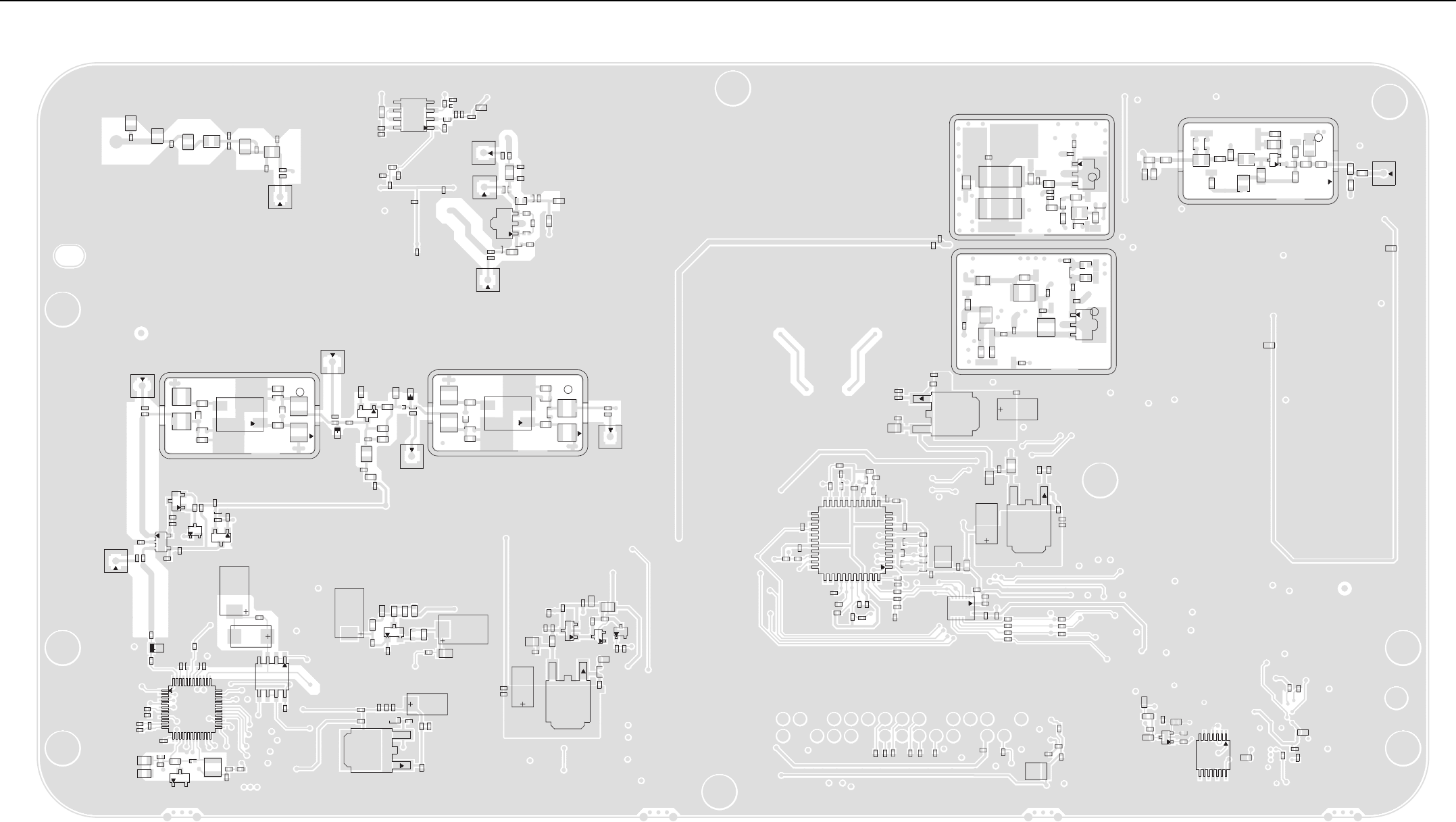
6-48 Receiver PCB (UHF)
P1000
C1006
C1007
C1003
C1005 C1004
C1000
C1001 C1002
L1005
L1000
L1001
L1004
L1003
L1002
C1008
3
4
2
5
85
4
2
5
3
4
C1230
P1201
R1106
C1231
C1114
C1100
P1230
R1111
R1107
R1110
C1119
R1105
C1120
C1113
C1105
R1109
R1100
C1121
R1108
C1108
E1100
U1100
C1117
C1116
3
3
4
2
5
R1203
C1205
E1200
R1202
R1201
C1202
C1201
C1200
R1230
R1231
C1203
C1207
C1204
U1200 R1200
L1200
L1201
C1206
C1208
R1232
23
4
5
P1200
76
96
5
4
2
3
4
2
C1521
C1522
L1508
C1519
C1520
L1507
SH1500
U1501
C1526
C1525
C1524
L1510
C1523
L1509
2
3
45
C1527
C1528
P1501
34
5
32
32
32
Q1602
R1603
C1600
R1604
C1604
Q1600
R1601
C1601
R1600
R1602
C1603
C1602
C1605
C1606
R1605
U1600
Q1601
3
4
2
5
P1600
5
4
32
13
25
37
8
C2551
U2531
R2563
C2523
E2536
R2535
C2557
C2561
CR2531
L2535
C2525
R2538
C2520
U2530
C2527 C2518
C2515
C2511
C2529
C2519
C2516 C2532
R2540
R2534
C2531
C2512
C2509
C2514
C2501 C2502
L2530
3
32
2
R2400
R2403
C2433
C2410
C2407
R2413
R2408
C2402
U2400
R2404
C2406
C2409
C2500
C2400
Q2400
R2406
R2407
R2401
C2401
E2400
R2423
R2422
R2530
R2531
R2405
C2403
3
32
32
32
R2206
R2205
C2218
C2211
Q2202
Q2201
R2200
R2201
R2204
C2202
E2200
C2201
C2205
C2206
C2207
C2208
Q2200
E2203
R2203
C2210
C2203
C2209
2
U2200
R2202
2
96
5
4
2
3
4
76
C1502
C1503
L1501
C1500
C1501
L1500
SH1501
U1500
C1505
C1506
C1507
L1503
C1504
L1502
2
3
45
32
45
2
3
C1510
C1514
P1503
C1509
L1505
R1502
R1503
C1511
L1504
R1500
R1501
C1513
R1505
C1516
C1515
C1512
L1506
C1517
U1502
R1504
P1502
2
3
45
C1530
P1500
C1529
8
7
14
32
C3107
C3111
R3113
C3126
C3124
R3172
C3127
U3103
C3171 Q3100
C3131
E3110
R3150 R3152
R3151
C3130
R3100
C2617
C2612
E2610
R2612
R2611
C2000
C2015
C2008
C2002
C2001
C2009
C2010
C2003
44 12
11
34
33 23
22
C3312
C3308
R3309
C3309
C3349
C3310
R3350
R3305
R3300
C3300
C3301
R3301
R3307
U3300
C3315
C3302
R3318
R3317
R3326
R3314
R3312
R3333
R3302
C3304
R3308
R3303
R3322
R3332
3
8
9
10 15
16
72
C3348
R3348
R3347
R3346
R3349
C3346
C3345
R3345
U2201
C3347
U3303
E3300
C3306
C3305
C2227
C3307
C3311
R3310
R3311
R3319
C3303
C3320
R3304
R3306
R3315
R3316
R3334
2
C2228
C2233
R2217
R2216
R2215
C2225
E2204
C2226
R3324
R3325
R3323
3
2
C2232
U2202
R2221
C2230
C2229
R2220
R2219
SH2701
C2235
C2231
C3232
C3231
23
4
5
P3200
R3219
R3218
R3236
2
9
3
4
2
76
C3218
C3219
R3221
R3223
L3211
R3222
SH3201
Q3202
R3224
L3214
R3225
L3212
C3220
C3225
L3213
C3222
C3223
R3226
R3227
C3224
R2719
R2718
R2717
3
C2707
R2708
L2701
R2704
R2707
C2719
C2708
L2700
U2700
C2706
R2706
R2703
C2718
R2713
C2704
R2710
R2712
C2703
C2702
SH2700
E2700
C2724
C2722
3
C2720
L2709
L2708
U2701
L2702
C2712
C2709
C2710
E2702
R2705
C2725
C2713
C2721
L2703
C2714
C2711
R2711
C2717
L2704
C2715
E2701
C2716
Receiver Board PCB – Bottom View (PCB No. 84009273002)
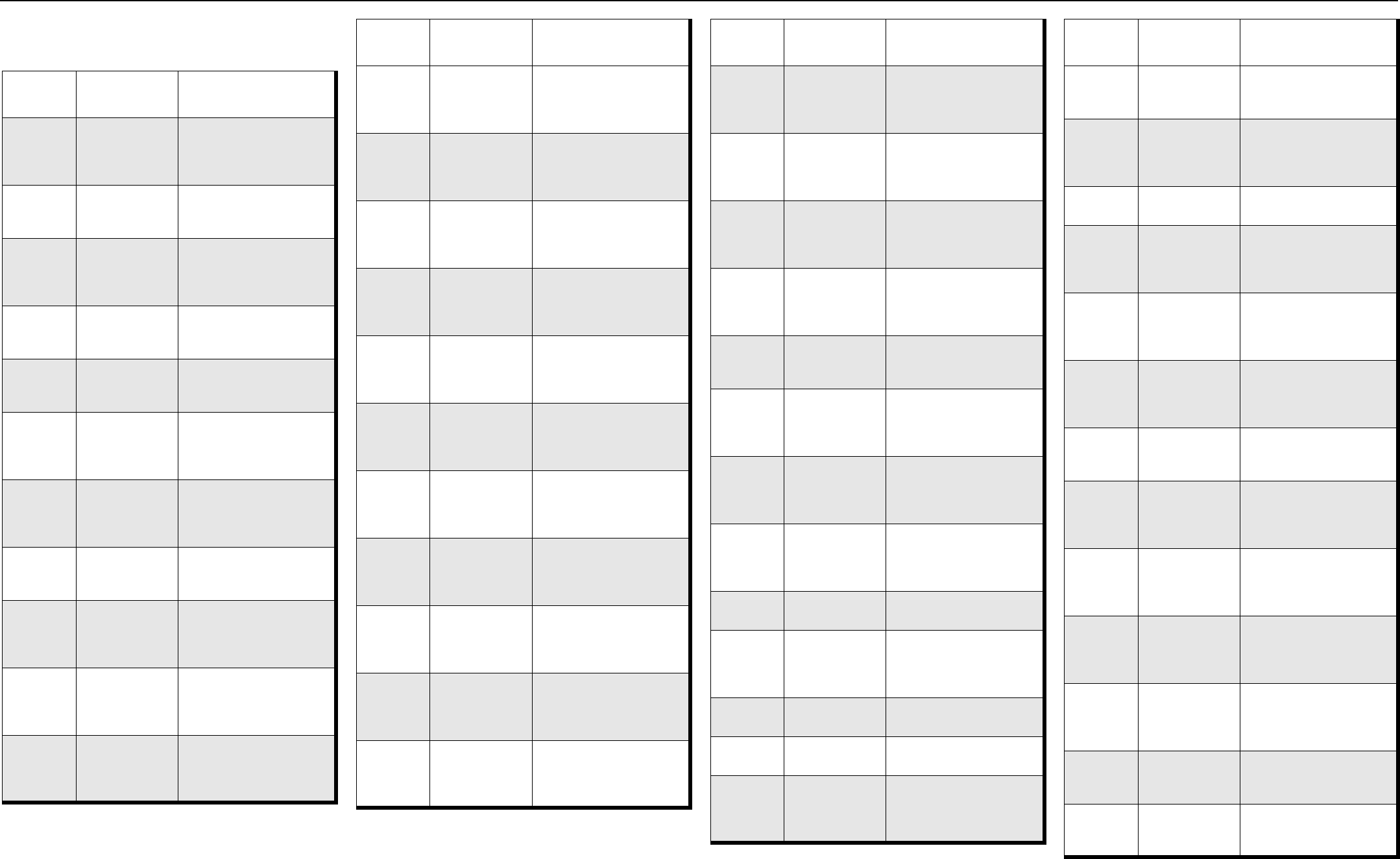
Receiver Parts List (UHF) – CRE4007 6-49
6.4 Receiver Parts List (UHF) –
CRE4007
Circuit
Ref
Motorola Part
No Description
C1000 2115153H20 CAP,FXD,5.1PF,.1PF+/-
,+2%,-2%,50V-
DC,0402,C0G,CAP,
CERAMIC, CO
C1001 2115153H07 CAP,FXD,1.5PF,.1PF+/-
,+6.67%,-6.67%,50V-
DC,0402,C0G
C1002 2115153H12 CAP,CERAMIC
CHIP,2.4PF,.1PF+/-,+.1%,-
.1%,50V-
DC,0402,C0G,CAP,
C1003 2115153H10 CAP,CER CHIP,2PF,.1PF+/
-,+.1%,-.1%,50V-
DC,0402,C0G
C1004 2115153H19 CAP,FXD,4.7PF,.1PF+/-
,+.1%,-.1%,50V-
DC,0402,C0G
C1005 2115153H12 CAP,CERAMIC
CHIP,2.4PF,.1PF+/-,+.1%,-
.1%,50V-
DC,0402,C0G,CAP,
C1006 2113944A44 CAP,CHIP,220PF,+5%,-
5%,50V-DC,0402,C0G,-
55DEG CMIN,125DEG
CMAX
C1008 2115153H45 CAP,CERAMIC
CHIP,33PF,+1%,-1%,50V-
DC,0402,C0G
C1103 2113951C39 CAP,FXD,20PF,+1%,-
1%,250V-DC,0603,C0G,-
55DEG CMIN,125DEG
CMAX,P
C1104 2113951C34 CAP,FXD,10PF,+1%,-
1%,250V-DC,0603,C0G,-
55DEG CMIN,125DEG
CMAX,P
C1106 2113951C49 CAP,FXD,51PF,+1%,-
1%,250V-DC,0603,C0G,-
55DEG CMIN,125DEG
CMAX,P
C1107 2113951C08 CAP,FXD,.8PF,.05PF+/-
,250V-DC,0603,C0G,-
55DEG CMIN,125DEG
CMAX
C1109 2113951C49 CAP,FXD,51PF,+1%,-
1%,250V-DC,0603,C0G,-
55DEG CMIN,125DEG
CMAX,P
C1110 2113951C34 CAP,FXD,10PF,+1%,-
1%,250V-DC,0603,C0G,-
55DEG CMIN,125DEG
CMAX,P
C1111 2113951C39 CAP,FXD,20PF,+1%,-
1%,250V-DC,0603,C0G,-
55DEG CMIN,125DEG
CMAX,P
C1113 2113946K02 CAP,CHIP,.1UF,+80%,-
20%,16V-DC,0402,Y5V,-
30DEG CMIN,85DEG
CMAX
C1114 2113944C45 CAP,CHIP,100PF,+5%,-
5%,50V-DC,0603,C0G,-
55DEG CMIN,125DEG
CMAX
C1116 2113944A44 CAP,CHIP,220PF,+5%,-
5%,50V-DC,0402,C0G,-
55DEG CMIN,125DEG
CMAX
C1117 2113946K02 CAP,CHIP,.1UF,+80%,-
20%,16V-DC,0402,Y5V,-
30DEG CMIN,85DEG
CMAX
C1119 2113944A44 CAP,CHIP,220PF,+5%,-
5%,50V-DC,0402,C0G,-
55DEG CMIN,125DEG
CMAX
C1120 2113944A44 CAP,CHIP,220PF,+5%,-
5%,50V-DC,0402,C0G,-
55DEG CMIN,125DEG
CMAX
C1121 2113944A44 CAP,CHIP,220PF,+5%,-
5%,50V-DC,0402,C0G,-
55DEG CMIN,125DEG
CMAX
Circuit
Ref
Motorola Part
No Description
C1200 2113945C02 CAP,CHIP,.01UF,+10%,-
10%,50V-DC,0603,X7R,-
55DEG CMIN,125DEG
CMA
C1201 2113946K02 CAP,CHIP,.1UF,+80%,-
20%,16V-DC,0402,Y5V,-
30DEG CMIN,85DEG
CMAX
C1202 2113944A44 CAP,CHIP,220PF,+5%,-
5%,50V-DC,0402,C0G,-
55DEG CMIN,125DEG
CMAX
C1203 2113944A44 CAP,CHIP,220PF,+5%,-
5%,50V-DC,0402,C0G,-
55DEG CMIN,125DEG
CMAX
C1204 2115153H03 CAP,CER CHIP,1PF,.1PF+/
-,+.1%,-.1%,50V-
DC,0402,C0G
C1205 2113944A52 CAP,CHIP,1000PF,+5%,-
5%,50V-DC,0402,C0G,-
55DEG CMIN,125DEG
CMAX
C1206 2113944A44 CAP,CHIP,220PF,+5%,-
5%,50V-DC,0402,C0G,-
55DEG CMIN,125DEG
CMAX
C1230 2113944A44 CAP,CHIP,220PF,+5%,-
5%,50V-DC,0402,C0G,-
55DEG CMIN,125DEG
CMAX
C1300 2115153H49 CAP,FXD,47PF,+1%,-
1%,50V-DC,0402,C0G
C1301 2115153H25 CAP,CERAMIC
CHIP,8.2PF,.1PF+/-,+.1%,-
.1%,50V-
DC,0402,C0G,CAP,
C1302 2115153H39 CAP,FXD,18PF,50V-
DC,0402,C0G
C1303 2115153H06 CAP,FXD,1.3PF,.1PF+/-
,50V-DC,0402,C0G
C1304 2115153H24 CAP,CER
CHIP,7.5PF,.1PF+/-,+.1%,-
.1%,50V-
DC,0402,C0G,CAP, CERA
Circuit
Ref
Motorola Part
No Description
C1305 2115153H17 CAP,FXD,3.9PF,.1PF+/-
,50V-DC,0402,C0G,CAP,
CERAMIC, COG
C1306 2115153H27 CAP,FXD,10PF,.1PF+/-
,+1%,-1%,50V-
DC,0402,C0G,CAP,
CERAMIC, COG
C1307 2185957Y47 CAP,.5PF,CAP,NP0,0.5 PF
+/-.05PF,200V,0402
C1308 2115153H20 CAP,FXD,5.1PF,.1PF+/-
,+2%,-2%,50V-
DC,0402,C0G,CAP,
CERAMIC, CO
C1309 2115153H16 CAP,CERAMIC
CHIP,3.6PF,.1PF+/-,+.1%,-
.1%,50V-
DC,0402,C0G,CAP,
C1310 2115153H27 CAP,FXD,10PF,.1PF+/-
,+1%,-1%,50V-
DC,0402,C0G,CAP,
CERAMIC, COG
C1311 2115153H17 CAP,FXD,3.9PF,.1PF+/-
,50V-DC,0402,C0G,CAP,
CERAMIC, COG
C1312 2115153H20 CAP,FXD,5.1PF,.1PF+/-
,+2%,-2%,50V-
DC,0402,C0G,CAP,
CERAMIC, CO
C1313 2115153H22 CAP,CERAMIC
CHIP,6.2PF,.1PF+/-,+.1%,-
.1%,50V-
DC,0402,C0G,CAP,
C1314 2115153H41 CAP,FXD,22PF,+1%,-
1%,50V-
DC,0402,C0G,CAP,
CERAMIC, COG
C1315 2113944A44 CAP,CHIP,220PF,+5%,-
5%,50V-DC,0402,C0G,-
55DEG CMIN,125DEG
CMAX
C1400 2113901A23 CAP,CHIP,5.6PF,.5PF+/-
,200V-DC,0805,-55DEG
CMIN,125DEG CMAX
C1403 2113901A11 CAP,CHIP,2PF,.25PF+/-
,200V-DC,0805,-55DEG
CMIN,125DEG CMAX
Circuit
Ref
Motorola Part
No Description

6-50 Receiver Parts List (UHF) – CRE4007
C1404 2113901A09 CAP,CHIP,1.8PF,.25PF+/-
,200V-DC,0805,-55DEG
CMIN,125DEG CMAX
C1405 2113901A28 CAP,CHIP,9.1PF,.5PF+/-
,200V-DC,0805,-55DEG
CMIN,125DEG CMAX
C1408 2113901A23 CAP,CHIP,5.6PF,.5PF+/-
,200V-DC,0805,-55DEG
CMIN,125DEG CMAX
C1409 2113901A31 CAP,CHIP,12PF,+5%,-
5%,200V-DC,0805,-55DEG
CMIN,125DEG CMAX
C1410 2113901A23 CAP,CHIP,5.6PF,.5PF+/-
,200V-DC,0805,-55DEG
CMIN,125DEG CMAX
C1411 2113945G45 CAP,FXD,.01UF,+5%,-
5%,50V-DC,0805,X7R,-
55DEG CMIN,125DEG
CMAX,P
C1412 2113945G45 CAP,FXD,.01UF,+5%,-
5%,50V-DC,0805,X7R,-
55DEG CMIN,125DEG
CMAX,P
C1413 2113945G45 CAP,FXD,.01UF,+5%,-
5%,50V-DC,0805,X7R,-
55DEG CMIN,125DEG
CMAX,P
C1414 2113945G45 CAP,FXD,.01UF,+5%,-
5%,50V-DC,0805,X7R,-
55DEG CMIN,125DEG
CMAX,P
C1415 2113901A56 CAP,CHIP,82PF,+5%,-
5%,200V-DC,0805,-55DEG
CMIN,125DEG CMAX
C1416 2113901A57 CAP,CHIP,91PF,+5%,-
5%,200V-DC,0805,-55DEG
CMIN,125DEG CMAX
C1417 2113944F05 CAP,CHIP,470PF,+5%,-
5%,50V-DC,0805,C0G,-
55DEG CMIN,125DEG
CMAX
C1500 2113951C30 CAP,FXD,6.8PF,.25PF+/-
,250V-DC,0603,C0G,-
55DEG CMIN,125DEG
CMA
Circuit
Ref
Motorola Part
No Description
C1501 2113951C32 CAP,FXD,8.2PF,.25PF+/-
,250V-DC,0603,C0G,-
55DEG CMIN,125DEG
CMA
C1502 2113951C20 CAP,FXD,2.7PF,.05PF+/-
,250V-DC,0603,C0G,-
55DEG CMIN,125DEG
CMA
C1503 2113951C49 CAP,FXD,51PF,+1%,-
1%,250V-DC,0603,C0G,-
55DEG CMIN,125DEG
CMAX,P
C1504 2113951C36 CAP,FXD,12PF,+1%,-
1%,250V-DC,0603,C0G,-
55DEG CMIN,125DEG
CMAX,P
C1505 2113951C20 CAP,FXD,2.7PF,.05PF+/-
,250V-DC,0603,C0G,-
55DEG CMIN,125DEG
CMA
C1506 2113951C32 CAP,FXD,8.2PF,.25PF+/-
,250V-DC,0603,C0G,-
55DEG CMIN,125DEG
CMA
C1507 2113951C30 CAP,FXD,6.8PF,.25PF+/-
,250V-DC,0603,C0G,-
55DEG CMIN,125DEG
CMA
C1510 2113944A32 CAP,CHIP,39PF,+5%,-
5%,50V-DC,0402,C0G,-
55DEG CMIN,125DEG
CMAX,P
C1511 2113945B02 CAP,CHIP,.01UF,+10%,-
10%,25V-DC,0402,X7R,-
55DEG CMIN,125DEG
CMA
C1512 2113946B04 CAP,CHIP,.1UF,+10%,-
10%,10V-DC,0402,X5R,-
55DEG CMIN,85DEG
CMAX
C1513 2113946B04 CAP,CHIP,.1UF,+10%,-
10%,10V-DC,0402,X5R,-
55DEG CMIN,85DEG
CMAX
Circuit
Ref
Motorola Part
No Description
C1514 2113944A44 CAP,CHIP,220PF,+5%,-
5%,50V-DC,0402,C0G,-
55DEG CMIN,125DEG
CMAX
C1515 2113945B02 CAP,CHIP,.01UF,+10%,-
10%,25V-DC,0402,X7R,-
55DEG CMIN,125DEG
CMA
C1516 2113944A33 CAP,CHIP,47PF,+5%,-
5%,50V-DC,0402,C0G,-
55DEG CMIN,125DEG
CMAX,P
C1519 2113951C30 CAP,FXD,6.8PF,.25PF+/-
,250V-DC,0603,C0G,-
55DEG CMIN,125DEG
CMA
C1520 2113951C32 CAP,FXD,8.2PF,.25PF+/-
,250V-DC,0603,C0G,-
55DEG CMIN,125DEG
CMA
C1521 2113951C20 CAP,FXD,2.7PF,.05PF+/-
,250V-DC,0603,C0G,-
55DEG CMIN,125DEG
CMA
C1522 2113951C36 CAP,FXD,12PF,+1%,-
1%,250V-DC,0603,C0G,-
55DEG CMIN,125DEG
CMAX,P
C1523 2113951C49 CAP,FXD,51PF,+1%,-
1%,250V-DC,0603,C0G,-
55DEG CMIN,125DEG
CMAX,P
C1524 2113951C20 CAP,FXD,2.7PF,.05PF+/-
,250V-DC,0603,C0G,-
55DEG CMIN,125DEG
CMA
C1525 2113951C32 CAP,FXD,8.2PF,.25PF+/-
,250V-DC,0603,C0G,-
55DEG CMIN,125DEG
CMA
C1526 2113951C30 CAP,FXD,6.8PF,.25PF+/-
,250V-DC,0603,C0G,-
55DEG CMIN,125DEG
CMA
Circuit
Ref
Motorola Part
No Description
C1527 2113945B02 CAP,CHIP,.01UF,+10%,-
10%,25V-DC,0402,X7R,-
55DEG CMIN,125DEG
CMA
C1529 2113945B02 CAP,CHIP,.01UF,+10%,-
10%,25V-DC,0402,X7R,-
55DEG CMIN,125DEG
CMA
C1600 2113946B04 CAP,CHIP,.1UF,+10%,-
10%,10V-DC,0402,X5R,-
55DEG CMIN,85DEG
CMAX
C1601 2113944A44 CAP,CHIP,220PF,+5%,-
5%,50V-DC,0402,C0G,-
55DEG CMIN,125DEG
CMAX
C1603 2113945B02 CAP,CHIP,.01UF,+10%,-
10%,25V-DC,0402,X7R,-
55DEG CMIN,125DEG
CMA
C1604 2113946B04 CAP,CHIP,.1UF,+10%,-
10%,10V-DC,0402,X5R,-
55DEG CMIN,85DEG
CMAX
C1605 2113946B04 CAP,CHIP,.1UF,+10%,-
10%,10V-DC,0402,X5R,-
55DEG CMIN,85DEG
CMAX
C1606 2113945B02 CAP,CHIP,.01UF,+10%,-
10%,25V-DC,0402,X7R,-
55DEG CMIN,125DEG
CMA
C2201 2113945C02 CAP,CHIP,.01UF,+10%,-
10%,50V-DC,0603,X7R,-
55DEG CMIN,125DEG
CMA
C2202 2113944A44 CAP,CHIP,220PF,+5%,-
5%,50V-DC,0402,C0G,-
55DEG CMIN,125DEG
CMAX
C2203 2113946K02 CAP,CHIP,.1UF,+80%,-
20%,16V-DC,0402,Y5V,-
30DEG CMIN,85DEG
CMAX
Circuit
Ref
Motorola Part
No Description

Receiver Parts List (UHF) – CRE4007 6-51
C2205 2113944A44 CAP,CHIP,220PF,+5%,-
5%,50V-DC,0402,C0G,-
55DEG CMIN,125DEG
CMAX
C2206 2113946K02 CAP,CHIP,.1UF,+80%,-
20%,16V-DC,0402,Y5V,-
30DEG CMIN,85DEG
CMAX
C2207 2113944A44 CAP,CHIP,220PF,+5%,-
5%,50V-DC,0402,C0G,-
55DEG CMIN,125DEG
CMAX
C2208 2113945G91 CAP,FXD,.1UF,+10%,-
10%,50V-DC,0805,X7R,-
55DEG CMIN,125DEG
CMAX
C2209 2313960F01 CAP,FXD,10UF,+10%,-
10%,16V-DC,SM,-55DEG
CMIN,125DEG
CMAX,247MA
C2210 2113944A44 CAP,CHIP,220PF,+5%,-
5%,50V-DC,0402,C0G,-
55DEG CMIN,125DEG
CMAX
C2211 2113944A44 CAP,CHIP,220PF,+5%,-
5%,50V-DC,0402,C0G,-
55DEG CMIN,125DEG
CMAX
C2213 2113945C02 CAP,CHIP,.01UF,+10%,-
10%,50V-DC,0603,X7R,-
55DEG CMIN,125DEG
CMA
C2214 2113944A44 CAP,CHIP,220PF,+5%,-
5%,50V-DC,0402,C0G,-
55DEG CMIN,125DEG
CMAX
C2217 2113945C31 CAP,FXD,.1UF,+10%,-
10%,50V-DC,0603,X7R,-
55DEG CMIN,125DEG
CMAX
C2218 2113944A44 CAP,CHIP,220PF,+5%,-
5%,50V-DC,0402,C0G,-
55DEG CMIN,125DEG
CMAX
Circuit
Ref
Motorola Part
No Description
C2220 2113945G96 CAP,FXD,.33UF,+10%,-
10%,50V-DC,0805,X7R,-
55DEG CMIN,125DEG
CMAX
C2222 2.31E+38 CAP,FXD,10UF,+10%,-
10%,35V-DC,SM,-55DEG
CMIN,125DEG
CMAX,262MA
C2223 2113946K02 CAP,CHIP,.1UF,+80%,-
20%,16V-DC,0402,Y5V,-
30DEG CMIN,85DEG
CMAX
C2224 2113944A44 CAP,CHIP,220PF,+5%,-
5%,50V-DC,0402,C0G,-
55DEG CMIN,125DEG
CMAX
C2225 2113944A44 CAP,CHIP,220PF,+5%,-
5%,50V-DC,0402,C0G,-
55DEG CMIN,125DEG
CMAX
C2226 2113945G91 CAP,FXD,.1UF,+10%,-
10%,50V-DC,0805,X7R,-
55DEG CMIN,125DEG
CMAX
C2227 2313960F01 CAP,FXD,10UF,+10%,-
10%,16V-DC,SM,-55DEG
CMIN,125DEG
CMAX,247MA
C2228 2113944A44 CAP,CHIP,220PF,+5%,-
5%,50V-DC,0402,C0G,-
55DEG CMIN,125DEG
CMAX
C2229 2113944A44 CAP,CHIP,220PF,+5%,-
5%,50V-DC,0402,C0G,-
55DEG CMIN,125DEG
CMAX
C2230 2113945G91 CAP,FXD,.1UF,+10%,-
10%,50V-DC,0805,X7R,-
55DEG CMIN,125DEG
CMAX
C2231 2313960F01 CAP,FXD,10UF,+10%,-
10%,16V-DC,SM,-55DEG
CMIN,125DEG
CMAX,247MA
Circuit
Ref
Motorola Part
No Description
C2232 2113944A44 CAP,CHIP,220PF,+5%,-
5%,50V-DC,0402,C0G,-
55DEG CMIN,125DEG
CMAX
C2233 2113946K02 CAP,CHIP,.1UF,+80%,-
20%,16V-DC,0402,Y5V,-
30DEG CMIN,85DEG
CMAX
C2235 2113946K02 CAP,CHIP,.1UF,+80%,-
20%,16V-DC,0402,Y5V,-
30DEG CMIN,85DEG
CMAX
C2400 2113945D04 CAP,CHIP,.1UF,+10%,-
10%,25V-DC,0603,X7R,-
55DEG CMIN,125DEG
CMAX
C2401 2113945D04 CAP,CHIP,.1UF,+10%,-
10%,25V-DC,0603,X7R,-
55DEG CMIN,125DEG
CMAX
C2402 2113944A44 CAP,CHIP,220PF,+5%,-
5%,50V-DC,0402,C0G,-
55DEG CMIN,125DEG
CMAX
C2403 2313960G78 CAP,FXD,22UF,+10%,-
10%,20V-DC,SM,-55DEG
CMIN,125DEG
CMAX,433MA
C2406 2113946K02 CAP,CHIP,.1UF,+80%,-
20%,16V-DC,0402,Y5V,-
30DEG CMIN,85DEG
CMAX
C2407 2113945G91 CAP,FXD,.1UF,+10%,-
10%,50V-DC,0805,X7R,-
55DEG CMIN,125DEG
CMAX
C2409 2113944A44 CAP,CHIP,220PF,+5%,-
5%,50V-DC,0402,C0G,-
55DEG CMIN,125DEG
CMAX
C2410 2313960G78 CAP,FXD,22UF,+10%,-
10%,20V-DC,SM,-55DEG
CMIN,125DEG
CMAX,433MA
Circuit
Ref
Motorola Part
No Description
C2433 2313960F01 CAP,FXD,10UF,+10%,-
10%,16V-DC,SM,-55DEG
CMIN,125DEG
CMAX,247MA
C2500 2113946B04 CAP,CHIP,.1UF,+10%,-
10%,10V-DC,0402,X5R,-
55DEG CMIN,85DEG
CMAX
C2501 2113944A27 CAP,CHIP,15PF,+5%,-
5%,50V-DC,0402,C0G,-
55DEG CMIN,125DEG
CMAX,P
C2502 2113944A31 CAP,CHIP,33PF,+5%,-
5%,50V-DC,0402,C0G,-
55DEG CMIN,125DEG
CMAX,P
C2503 2113946B02 CAP,CHIP,.047UF,+10%,-
10%,10V-DC,0402,X5R,-
55DEG CMIN,85DEG CMA
C2504 2113946B04 CAP,CHIP,.1UF,+10%,-
10%,10V-DC,0402,X5R,-
55DEG CMIN,85DEG
CMAX
C2505 2113946B04 CAP,CHIP,.1UF,+10%,-
10%,10V-DC,0402,X5R,-
55DEG CMIN,85DEG
CMAX
C2506 2113946B04 CAP,CHIP,.1UF,+10%,-
10%,10V-DC,0402,X5R,-
55DEG CMIN,85DEG
CMAX
C2508 2113944A42 CAP,CHIP,150PF,+5%,-
5%,50V-DC,0402,C0G,-
55DEG CMIN,125DEG
CMAX
C2509 2113944A34 CAP,CHIP,56PF,+5%,-
5%,50V-DC,0402,C0G,-
55DEG CMIN,125DEG
CMAX,P
C2510 2113944A40 CAP,CHIP,100PF,+5%,-
5%,50V-DC,0402,C0G,-
55DEG CMIN,125DEG
CMAX
C2511 2113945A09 CAP,CHIP,1000PF,+10%,-
10%,50V-DC,0402,X7R,-
55DEG CMIN,125DEG CM
Circuit
Ref
Motorola Part
No Description

6-52 Receiver Parts List (UHF) – CRE4007
C2512 2113945A11 CAP,CHIP,2200PF,+10%,-
10%,50V-DC,0402,X7R,-
55DEG CMIN,125DEG CM
C2513 2113944A40 CAP,CHIP,100PF,+5%,-
5%,50V-DC,0402,C0G,-
55DEG CMIN,125DEG
CMAX
C2514 2113944A40 CAP,CHIP,100PF,+5%,-
5%,50V-DC,0402,C0G,-
55DEG CMIN,125DEG
CMAX
C2515 2113946B04 CAP,CHIP,.1UF,+10%,-
10%,10V-DC,0402,X5R,-
55DEG CMIN,85DEG
CMAX
C2516 2113945B02 CAP,CHIP,.01UF,+10%,-
10%,25V-DC,0402,X7R,-
55DEG CMIN,125DEG
CMA
C2517 2113946B04 CAP,CHIP,.1UF,+10%,-
10%,10V-DC,0402,X5R,-
55DEG CMIN,85DEG
CMAX
C2518 2113945B02 CAP,CHIP,.01UF,+10%,-
10%,25V-DC,0402,X7R,-
55DEG CMIN,125DEG
CMA
C2519 2113944A40 CAP,CHIP,100PF,+5%,-
5%,50V-DC,0402,C0G,-
55DEG CMIN,125DEG
CMAX
C2520 2113945B02 CAP,CHIP,.01UF,+10%,-
10%,25V-DC,0402,X7R,-
55DEG CMIN,125DEG
CMA
C2521 2113946B04 CAP,CHIP,.1UF,+10%,-
10%,10V-DC,0402,X5R,-
55DEG CMIN,85DEG
CMAX
C2522 2113946B04 CAP,CHIP,.1UF,+10%,-
10%,10V-DC,0402,X5R,-
55DEG CMIN,85DEG
CMAX
C2523 2113946B04 CAP,CHIP,.1UF,+10%,-
10%,10V-DC,0402,X5R,-
55DEG CMIN,85DEG
CMAX
Circuit
Ref
Motorola Part
No Description
C2524 2113946B04 CAP,CHIP,.1UF,+10%,-
10%,10V-DC,0402,X5R,-
55DEG CMIN,85DEG
CMAX
C2525 2113944A40 CAP,CHIP,100PF,+5%,-
5%,50V-DC,0402,C0G,-
55DEG CMIN,125DEG
CMAX
C2527 2113946B04 CAP,CHIP,.1UF,+10%,-
10%,10V-DC,0402,X5R,-
55DEG CMIN,85DEG
CMAX
C2528 2113946B04 CAP,CHIP,.1UF,+10%,-
10%,10V-DC,0402,X5R,-
55DEG CMIN,85DEG
CMAX
C2529 2113945G96 CAP,FXD,.33UF,+10%,-
10%,50V-DC,0805,X7R,-
55DEG CMIN,125DEG
CMAX
C2531 2113945G96 CAP,FXD,.33UF,+10%,-
10%,50V-DC,0805,X7R,-
55DEG CMIN,125DEG
CMAX
C2532 2113946B04 CAP,CHIP,.1UF,+10%,-
10%,10V-DC,0402,X5R,-
55DEG CMIN,85DEG
CMAX
C2535 2113944A09 CAP,CHIP,2.2PF,.25PF+/-
,50V-DC,0402,C0G,-
55DEG CMIN,125DEG
CMA
C2539 2113944A01 CAP,CHIP,1.1PF,.25PF+/-
,50V-DC,0402,C0G,-
55DEG CMIN,125DEG
CMA
C2541 2113945A05 CAP,CHIP,470PF,+10%,-
10%,50V-DC,0402,X7R,-
55DEG CMIN,125DEG
CMA
C2542 2113944A27 CAP,CHIP,15PF,+5%,-
5%,50V-DC,0402,C0G,-
55DEG CMIN,125DEG
CMAX,P
Circuit
Ref
Motorola Part
No Description
C2546 2113944A27 CAP,CHIP,15PF,+5%,-
5%,50V-DC,0402,C0G,-
55DEG CMIN,125DEG
CMAX,P
C2551 2113946B04 CAP,CHIP,.1UF,+10%,-
10%,10V-DC,0402,X5R,-
55DEG CMIN,85DEG
CMAX
C2552 2113944A22 CAP,CHIP,7.5PF,.5PF+/-
,50V-DC,0402,C0G,-
55DEG CMIN,125DEG
CMAX
C2553 2113944A30 CAP,CHIP,27PF,+5%,-
5%,50V-DC,0402,C0G,-
55DEG CMIN,125DEG
CMAX,P
C2554 2113946B04 CAP,CHIP,.1UF,+10%,-
10%,10V-DC,0402,X5R,-
55DEG CMIN,85DEG
CMAX
C2555 2113945A12 CAP,CHIP,3300PF,+10%,-
10%,50V-DC,0402,X7R,-
55DEG CMIN,125DEG CM
C2556 2113946B04 CAP,CHIP,.1UF,+10%,-
10%,10V-DC,0402,X5R,-
55DEG CMIN,85DEG
CMAX
C2557 2.31E+34 CAP,FXD,2.2UF,+10%,-
10%,35V-DC,SM,-55DEG
CMIN,125DEG
CMAX,177MA
C2561 2313960G78 CAP,FXD,22UF,+10%,-
10%,20V-DC,SM,-55DEG
CMIN,125DEG
CMAX,433MA
C2580 2113944A25 CAP,CHIP,10PF,.5PF+/-
,50V-DC,0402,C0G,-
55DEG CMIN,125DEG
CMAX
C2581 2113944A25 CAP,CHIP,10PF,.5PF+/-
,50V-DC,0402,C0G,-
55DEG CMIN,125DEG
CMAX
C2582 2113944A25 CAP,CHIP,10PF,.5PF+/-
,50V-DC,0402,C0G,-
55DEG CMIN,125DEG
CMAX
Circuit
Ref
Motorola Part
No Description
C2583 2113944A25 CAP,CHIP,10PF,.5PF+/-
,50V-DC,0402,C0G,-
55DEG CMIN,125DEG
CMAX
C2610 2113946K02 CAP,CHIP,.1UF,+80%,-
20%,16V-DC,0402,Y5V,-
30DEG CMIN,85DEG
CMAX
C2611 2113944A44 CAP,CHIP,220PF,+5%,-
5%,50V-DC,0402,C0G,-
55DEG CMIN,125DEG
CMAX
C2613 2113946K02 CAP,CHIP,.1UF,+80%,-
20%,16V-DC,0402,Y5V,-
30DEG CMIN,85DEG
CMAX
C2614 2113946K02 CAP,CHIP,.1UF,+80%,-
20%,16V-DC,0402,Y5V,-
30DEG CMIN,85DEG
CMAX
C2615 2113944A27 CAP,CHIP,15PF,+5%,-
5%,50V-DC,0402,C0G,-
55DEG CMIN,125DEG
CMAX,P
C2616 2113944A27 CAP,CHIP,15PF,+5%,-
5%,50V-DC,0402,C0G,-
55DEG CMIN,125DEG
CMAX,P
C2617 2113946K02 CAP,CHIP,.1UF,+80%,-
20%,16V-DC,0402,Y5V,-
30DEG CMIN,85DEG
CMAX
C2618 2113946K02 CAP,CHIP,.1UF,+80%,-
20%,16V-DC,0402,Y5V,-
30DEG CMIN,85DEG
CMAX
C2619 2113944A31 CAP,CHIP,33PF,+5%,-
5%,50V-DC,0402,C0G,-
55DEG CMIN,125DEG
CMAX,P
C2620 2113944A31 CAP,CHIP,33PF,+5%,-
5%,50V-DC,0402,C0G,-
55DEG CMIN,125DEG
CMAX,P
Circuit
Ref
Motorola Part
No Description

Receiver Parts List (UHF) – CRE4007 6-53
C2621 2113944A43 CAP,CHIP,180PF,+5%,-
5%,50V-DC,0402,C0G,-
55DEG CMIN,125DEG
CMAX
C2702 2113946K02 CAP,CHIP,.1UF,+80%,-
20%,16V-DC,0402,Y5V,-
30DEG CMIN,85DEG
CMAX
C2703 2113945C02 CAP,CHIP,.01UF,+10%,-
10%,50V-DC,0603,X7R,-
55DEG CMIN,125DEG
CMA
C2704 2113944A44 CAP,CHIP,220PF,+5%,-
5%,50V-DC,0402,C0G,-
55DEG CMIN,125DEG
CMAX
C2706 2113951C33 CAP,FXD,9.1PF,.25PF+/-
,250V-DC,0603,C0G,-
55DEG CMIN,125DEG
CMA
C2707 2113951C33 CAP,FXD,9.1PF,.25PF+/-
,250V-DC,0603,C0G,-
55DEG CMIN,125DEG
CMA
C2708 2113944A44 CAP,CHIP,220PF,+5%,-
5%,50V-DC,0402,C0G,-
55DEG CMIN,125DEG
CMAX
C2709 2113944A44 CAP,CHIP,220PF,+5%,-
5%,50V-DC,0402,C0G,-
55DEG CMIN,125DEG
CMAX
C2710 2113944A28 CAP,CHIP,18PF,+5%,-
5%,50V-DC,0402,C0G,-
55DEG CMIN,125DEG
CMAX,P
C2711 2113945C02 CAP,CHIP,.01UF,+10%,-
10%,50V-DC,0603,X7R,-
55DEG CMIN,125DEG
CMA
C2712 2113944A44 CAP,CHIP,220PF,+5%,-
5%,50V-DC,0402,C0G,-
55DEG CMIN,125DEG
CMAX
Circuit
Ref
Motorola Part
No Description
C2713 2113944A44 CAP,CHIP,220PF,+5%,-
5%,50V-DC,0402,C0G,-
55DEG CMIN,125DEG
CMAX
C2714 2113951C28 CAP,FXD,5.6PF,.05PF+/-
,250V-DC,0603,C0G,-
55DEG CMIN,125DEG
CMA
C2715 2113951C34 CAP,FXD,10PF,+1%,-
1%,250V-DC,0603,C0G,-
55DEG CMIN,125DEG
CMAX,P
C2716 2113951C26 CAP,FXD,4.7PF,.05PF+/-
,250V-DC,0603,C0G,-
55DEG CMIN,125DEG
CMA
C2717 2115153H23 CAP,CER
CHIP,6.8PF,.1PF+/-,+.1%,-
.1%,50V-
DC,0402,C0G,CAP, CERA
C2722 2113944A44 CAP,CHIP,220PF,+5%,-
5%,50V-DC,0402,C0G,-
55DEG CMIN,125DEG
CMAX
C2723 2115153H23 CAP,CER
CHIP,6.8PF,.1PF+/-,+.1%,-
.1%,50V-
DC,0402,C0G,CAP, CERA
C2724 2113946K02 CAP,CHIP,.1UF,+80%,-
20%,16V-DC,0402,Y5V,-
30DEG CMIN,85DEG
CMAX
C2725 2113946K02 CAP,CHIP,.1UF,+80%,-
20%,16V-DC,0402,Y5V,-
30DEG CMIN,85DEG
CMAX
C2801 2113946K02 CAP,CHIP,.1UF,+80%,-
20%,16V-DC,0402,Y5V,-
30DEG CMIN,85DEG
CMAX
C2802 2113944A44 CAP,CHIP,220PF,+5%,-
5%,50V-DC,0402,C0G,-
55DEG CMIN,125DEG
CMAX
Circuit
Ref
Motorola Part
No Description
C2803 2113946K02 CAP,CHIP,.1UF,+80%,-
20%,16V-DC,0402,Y5V,-
30DEG CMIN,85DEG
CMAX
C2804 2113944A44 CAP,CHIP,220PF,+5%,-
5%,50V-DC,0402,C0G,-
55DEG CMIN,125DEG
CMAX
C2805 2113946K02 CAP,CHIP,.1UF,+80%,-
20%,16V-DC,0402,Y5V,-
30DEG CMIN,85DEG
CMAX
C2806 2113944A44 CAP,CHIP,220PF,+5%,-
5%,50V-DC,0402,C0G,-
55DEG CMIN,125DEG
CMAX
C2807 2113946K02 CAP,CHIP,.1UF,+80%,-
20%,16V-DC,0402,Y5V,-
30DEG CMIN,85DEG
CMAX
C2808 2113944A44 CAP,CHIP,220PF,+5%,-
5%,50V-DC,0402,C0G,-
55DEG CMIN,125DEG
CMAX
C2809 2113946K02 CAP,CHIP,.1UF,+80%,-
20%,16V-DC,0402,Y5V,-
30DEG CMIN,85DEG
CMAX
C2810 2113944A44 CAP,CHIP,220PF,+5%,-
5%,50V-DC,0402,C0G,-
55DEG CMIN,125DEG
CMAX
C2811 2113946K02 CAP,CHIP,.1UF,+80%,-
20%,16V-DC,0402,Y5V,-
30DEG CMIN,85DEG
CMAX
C2812 2113944A44 CAP,CHIP,220PF,+5%,-
5%,50V-DC,0402,C0G,-
55DEG CMIN,125DEG
CMAX
C2813 2113946A01 CAP,CHIP,.015UF,+10%,-
10%,16V-DC,0402,X5R,-
55DEG CMIN,85DEG CMA
C2814 2113946J02 CAP,CHIP,4.7UF,+10%,-
10%,16V-DC,1210,X5R,-
55DEG CMIN,85DEG
CMAX
Circuit
Ref
Motorola Part
No Description
C3101 2113945C04 CAP,CHIP,.022UF,+10%,-
10%,50V-DC,0603,X7R,-
55DEG CMIN,125DEG CM
C3102 2113945G78 CAP,FXD,.01UF,+10%,-
10%,50V-DC,0805,X7R,-
55DEG CMIN,125DEG
CMAX
C3104 2113945G92 CAP,FXD,.12UF,+10%,-
10%,50V-DC,0805,X7R,-
55DEG CMIN,125DEG
CMAX
C3105 2113945G92 CAP,FXD,.12UF,+10%,-
10%,50V-DC,0805,X7R,-
55DEG CMIN,125DEG
CMAX
C3106 2113945L37 CAP,FXD,3300PF,+5%,-
5%,50V-DC,0603,X7R,-
55DEG CMIN,125DEG
CMAX
C3107 2113944A44 CAP,CHIP,220PF,+5%,-
5%,50V-DC,0402,C0G,-
55DEG CMIN,125DEG
CMAX
C3108 2313960C26 CAP,FXD,1UF,+10%,-
10%,35V-DC,SM,-55DEG
CMIN,125DEG
CMAX,114MA,E
C3109 2313960C26 CAP,FXD,1UF,+10%,-
10%,35V-DC,SM,-55DEG
CMIN,125DEG
CMAX,114MA,E
C3111 2113945D04 CAP,CHIP,.1UF,+10%,-
10%,25V-DC,0603,X7R,-
55DEG CMIN,125DEG
CMAX
C3116 2113945D04 CAP,CHIP,.1UF,+10%,-
10%,25V-DC,0603,X7R,-
55DEG CMIN,125DEG
CMAX
C3120 2113944A44 CAP,CHIP,220PF,+5%,-
5%,50V-DC,0402,C0G,-
55DEG CMIN,125DEG
CMAX
C3124 2113945D04 CAP,CHIP,.1UF,+10%,-
10%,25V-DC,0603,X7R,-
55DEG CMIN,125DEG
CMAX
Circuit
Ref
Motorola Part
No Description

6-54 Receiver Parts List (UHF) – CRE4007
C3126 2113944A44 CAP,CHIP,220PF,+5%,-
5%,50V-DC,0402,C0G,-
55DEG CMIN,125DEG
CMAX
C3127 2113944A44 CAP,CHIP,220PF,+5%,-
5%,50V-DC,0402,C0G,-
55DEG CMIN,125DEG
CMAX
C3200 2113944C02 CAP,CHIP,220PF,+5%,-
5%,50V-DC,0603,C0G,-
55DEG CMIN,125DEG
CMAX
C3201 2113951C25 CAP,FXD,4.3PF,.05PF+/-
,250V-DC,0603,C0G,-
55DEG CMIN,125DEG
CMA
C3202 2113951C25 CAP,FXD,4.3PF,.05PF+/-
,250V-DC,0603,C0G,-
55DEG CMIN,125DEG
CMA
C3203 2113951C21 CAP,FXD,3PF,.05PF+/-
,250V-DC,0603,C0G,-
55DEG CMIN,125DEG
CMAX
C3204 2113951C32 CAP,FXD,8.2PF,.25PF+/-
,250V-DC,0603,C0G,-
55DEG CMIN,125DEG
CMA
C3205 2113951C34 CAP,FXD,10PF,+1%,-
1%,250V-DC,0603,C0G,-
55DEG CMIN,125DEG
CMAX,P
C3206 2113944C02 CAP,CHIP,220PF,+5%,-
5%,50V-DC,0603,C0G,-
55DEG CMIN,125DEG
CMAX
C3207 2113951C18 CAP,FXD,2.2PF,.05PF+/-
,250V-DC,0603,C0G,-
55DEG CMIN,125DEG
CMA
C3208 2113944C02 CAP,CHIP,220PF,+5%,-
5%,50V-DC,0603,C0G,-
55DEG CMIN,125DEG
CMAX
Circuit
Ref
Motorola Part
No Description
C3209 2113944C02 CAP,CHIP,220PF,+5%,-
5%,50V-DC,0603,C0G,-
55DEG CMIN,125DEG
CMAX
C3210 2113951C24 CAP,FXD,3.9PF,.05PF+/-
,250V-DC,0603,C0G,-
55DEG CMIN,125DEG
CMA
C3211 2113951C23 CAP,FXD,3.6PF,.05PF+/-
,250V-DC,0603,C0G,-
55DEG CMIN,125DEG
CMA
C3212 2113951C21 CAP,FXD,3PF,.05PF+/-
,250V-DC,0603,C0G,-
55DEG CMIN,125DEG
CMAX
C3213 2113951C32 CAP,FXD,8.2PF,.25PF+/-
,250V-DC,0603,C0G,-
55DEG CMIN,125DEG
CMA
C3214 2113951C34 CAP,FXD,10PF,+1%,-
1%,250V-DC,0603,C0G,-
55DEG CMIN,125DEG
CMAX,P
C3215 2113944C02 CAP,CHIP,220PF,+5%,-
5%,50V-DC,0603,C0G,-
55DEG CMIN,125DEG
CMAX
C3216 2113951C20 CAP,FXD,2.7PF,.05PF+/-
,250V-DC,0603,C0G,-
55DEG CMIN,125DEG
CMA
C3217 2113944C02 CAP,CHIP,220PF,+5%,-
5%,50V-DC,0603,C0G,-
55DEG CMIN,125DEG
CMAX
C3218 2113951C20 CAP,FXD,2.7PF,.05PF+/-
,250V-DC,0603,C0G,-
55DEG CMIN,125DEG
CMA
C3219 2113944C02 CAP,CHIP,220PF,+5%,-
5%,50V-DC,0603,C0G,-
55DEG CMIN,125DEG
CMAX
Circuit
Ref
Motorola Part
No Description
C3220 2113945D04 CAP,CHIP,.1UF,+10%,-
10%,25V-DC,0603,X7R,-
55DEG CMIN,125DEG
CMAX
C3222 2113951C22 CAP,FXD,3.3PF,.05PF+/-
,250V-DC,0603,C0G,-
55DEG CMIN,125DEG
CMA
C3223 2113951C22 CAP,FXD,3.3PF,.05PF+/-
,250V-DC,0603,C0G,-
55DEG CMIN,125DEG
CMA
C3224 2113944C02 CAP,CHIP,220PF,+5%,-
5%,50V-DC,0603,C0G,-
55DEG CMIN,125DEG
CMAX
C3225 2113944C02 CAP,CHIP,220PF,+5%,-
5%,50V-DC,0603,C0G,-
55DEG CMIN,125DEG
CMAX
C3226 2385170Y10 CAP,47UF,25V-DC,-
55DEG CMIN,105DEG
CMAX
C3227 2113945C02 CAP,CHIP,.01UF,+10%,-
10%,50V-DC,0603,X7R,-
55DEG CMIN,125DEG
CMA
C3228 2385170Y08 CAP,AL EL,330UF,25V-DC
C3229 2113945C02 CAP,CHIP,.01UF,+10%,-
10%,50V-DC,0603,X7R,-
55DEG CMIN,125DEG
CMA
C3230 2113944C02 CAP,CHIP,220PF,+5%,-
5%,50V-DC,0603,C0G,-
55DEG CMIN,125DEG
CMAX
C3232 2113944C02 CAP,CHIP,220PF,+5%,-
5%,50V-DC,0603,C0G,-
55DEG CMIN,125DEG
CMAX
C3301 2113946K02 CAP,CHIP,.1UF,+80%,-
20%,16V-DC,0402,Y5V,-
30DEG CMIN,85DEG
CMAX
Circuit
Ref
Motorola Part
No Description
C3302 2113946K02 CAP,CHIP,.1UF,+80%,-
20%,16V-DC,0402,Y5V,-
30DEG CMIN,85DEG
CMAX
C3303 2113946K02 CAP,CHIP,.1UF,+80%,-
20%,16V-DC,0402,Y5V,-
30DEG CMIN,85DEG
CMAX
C3304 2113946K02 CAP,CHIP,.1UF,+80%,-
20%,16V-DC,0402,Y5V,-
30DEG CMIN,85DEG
CMAX
C3306 2113946K02 CAP,CHIP,.1UF,+80%,-
20%,16V-DC,0402,Y5V,-
30DEG CMIN,85DEG
CMAX
C3307 2113944A44 CAP,CHIP,220PF,+5%,-
5%,50V-DC,0402,C0G,-
55DEG CMIN,125DEG
CMAX
C3316 2113946B04 CAP,CHIP,.1UF,+10%,-
10%,10V-DC,0402,X5R,-
55DEG CMIN,85DEG
CMAX
C3318 2113944A25 CAP,CHIP,10PF,.5PF+/-
,50V-DC,0402,C0G,-
55DEG CMIN,125DEG
CMAX
C3345 2113946K02 CAP,CHIP,.1UF,+80%,-
20%,16V-DC,0402,Y5V,-
30DEG CMIN,85DEG
CMAX
C3346 2113945B02 CAP,CHIP,.01UF,+10%,-
10%,25V-DC,0402,X7R,-
55DEG CMIN,125DEG
CMA
C3347 2113946K02 CAP,CHIP,.1UF,+80%,-
20%,16V-DC,0402,Y5V,-
30DEG CMIN,85DEG
CMAX
C3348 2113945B02 CAP,CHIP,.01UF,+10%,-
10%,25V-DC,0402,X7R,-
55DEG CMIN,125DEG
CMA
CR1400 48009262001 DIODE,SUR MT MXR
SHTK DIODE
Circuit
Ref
Motorola Part
No Description
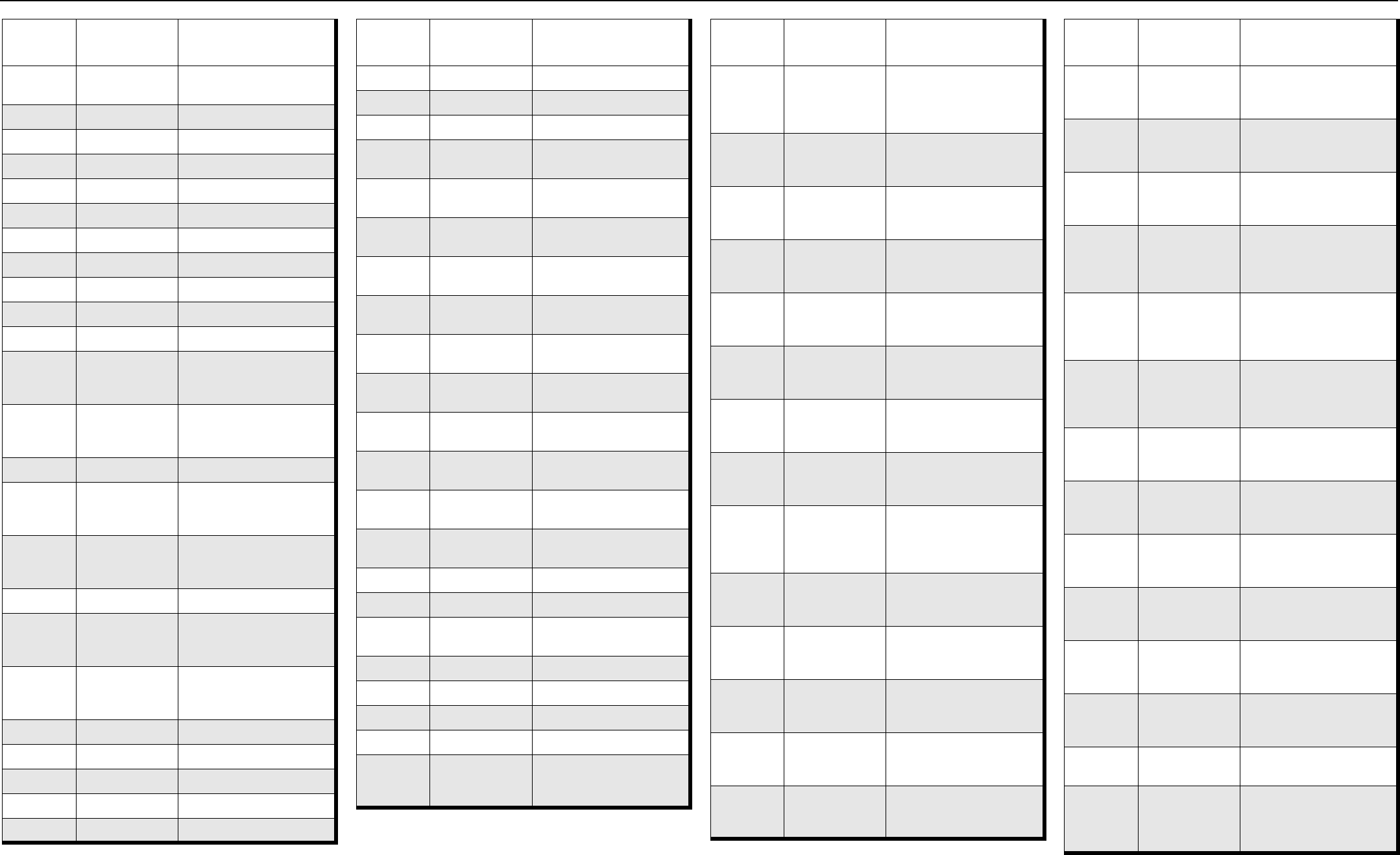
Receiver Parts List (UHF) – CRE4007 6-55
CR1401 48009262001 DIODE,SUR MT MXR
SHTK DIODE
CR2530 4885094Y01 DIODE,VCTR, 15V
CR2531 4885094Y01 DIODE,VCTR, 15V
CR3200 4885055Y01 DIODE,VCTR, 15V
CR3201 4885055Y01 DIODE,VCTR, 15V
CR3202 4885055Y01 DIODE,VCTR, 15V
CR3203 4885055Y01 DIODE,VCTR, 15V
CR3204 4885055Y01 DIODE,VCTR, 15V
CR3205 4885055Y01 DIODE,VCTR, 15V
CR3206 4885055Y01 DIODE,VCTR, 15V
CR3207 4885055Y01 DIODE,VCTR, 15V
D1100 4805656W87 DIODE,VCTR, @
15V,1SV279,SOD-523/SC-
79,SOD-523/SC-79
D1101 4805656W87 DIODE,VCTR, @
15V,1SV279,SOD-523/SC-
79,SOD-523/SC-79
D1102 4885095Y01 DIODE,VARACTOR,15V
D1103 4805656W87 DIODE,VCTR, @
15V,1SV279,SOD-523/SC-
79,SOD-523/SC-79
D1104 4805656W87 DIODE,VCTR, @
15V,1SV279,SOD-523/SC-
79,SOD-523/SC-79
D1105 4885095Y01 DIODE,VARACTOR,15V
D1106 4805656W87 DIODE,VCTR, @
15V,1SV279,SOD-523/SC-
79,SOD-523/SC-79
D1107 4805656W87 DIODE,VCTR, @
15V,1SV279,SOD-523/SC-
79,SOD-523/SC-79
E1100 2485410Y01 CHIP INDUCTOR
E1200 2485410Y01 CHIP INDUCTOR
E2200 2485410Y04 FLTR,FERR,1.5A,SM,0805
E2201 2485410Y04 FLTR,FERR,1.5A,SM,0805
E2202 2485410Y01 CHIP INDUCTOR
Circuit
Ref
Motorola Part
No Description
E2203 2485410Y01 CHIP INDUCTOR
E2204 2485410Y04 FLTR,FERR,1.5A,SM,0805
E2400 2485410Y01 CHIP INDUCTOR
E2532 2485449Y01 CHIP
INDUCTOR,FXD,FERR
E2533 2485449Y01 CHIP
INDUCTOR,FXD,FERR
E2534 2485449Y01 CHIP
INDUCTOR,FXD,FERR
E2535 2485449Y01 CHIP
INDUCTOR,FXD,FERR
E2536 2485449Y01 CHIP
INDUCTOR,FXD,FERR
E2537 2485449Y01 CHIP
INDUCTOR,FXD,FERR
E2538 2485449Y01 CHIP
INDUCTOR,FXD,FERR
E2539 2485449Y01 CHIP
INDUCTOR,FXD,FERR
E2540 2485449Y01 CHIP
INDUCTOR,FXD,FERR
E2541 2485449Y01 CHIP
INDUCTOR,FXD,FERR
E2610 2485449Y01 CHIP
INDUCTOR,FXD,FERR
E2700 2485410Y04 FLTR,FERR,1.5A,SM,0805
E2701 2485410Y04 FLTR,FERR,1.5A,SM,0805
E2702 2485449Y01 CHIP
INDUCTOR,FXD,FERR
E2800 2485410Y01 CHIP INDUCTOR
E3105 2485410Y01 CHIP INDUCTOR
E3200 2485410Y01 CHIP INDUCTOR
E3300 2485410Y01 CHIP INDUCTOR
J1000 0982492W01 RF
CONNECTOR,BNC,RCPT,
ST,PCMT
Circuit
Ref
Motorola Part
No Description
J2000 28009146002 CONN,HDR,2
ROW,M,30CONT,2.54MM,
GLD,ST,THRU HOLE,HDR
2 X 15 VER
L1000 2414015B10 IDCTR,FXD,33NH,2%,500
MA,.34Ω,CER,40
Q,1.3GHZ SRF,SM,0805,P
L1001 2414015B16 IDCTR,FXD,27NH,2%,500
MA,.25Ω,CER,55
Q,2.5GHZ SRF,SM,0805,P
L1002 2414032F21 IDCTR,WW,6.8NH,5%,600
MA,.11Ω,CER,50 Q,3GHZ
SRF,SM,PB-FREE
L1003 2414015B16 IDCTR,FXD,27NH,2%,500
MA,.25Ω,CER,55
Q,2.5GHZ SRF,SM,0805,P
L1004 2414015B16 IDCTR,FXD,27NH,2%,500
MA,.25Ω,CER,55
Q,2.5GHZ SRF,SM,0805,P
L1005 2414015B06 IDCTR,FXD,150NH,2%,40
0MA,.56Ω,CER,35
Q,780MHZ SRF,SM,0805
L1100 2471968L11 IDCTR,AW,13NH,2%,4A,.0
039Ω,AIR,5 TURNS,100
Q,3GHZ SRF,SM,1
L1101 524669-029-00 IDCTR,WW,91NH,2%,400
MA,.48Ω,CER,65
Q,1.33GHZ
SRF,SM,0805,L
L1102 2471968L11 IDCTR,AW,13NH,2%,4A,.0
039Ω,AIR,5 TURNS,100
Q,3GHZ SRF,SM,1
L1200 24012009005 IDCTR,WW,30NH,2%,600
MA,CER,PACKAGED,CHI
P IDCTR - 0603CT
L1201 2478057A28 IDCTR,WW,150NH,2%,390
MA,CER,PACKAGED,CHI
P IDCTR - 0603HP
L1300 2414015B04 IDCTR,FXD,100NH,2%,40
0MA,.46Ω,CER,40
Q,1250MHZ SRF,SM,0805
L1301 2414015B16 IDCTR,FXD,27NH,2%,500
MA,.25Ω,CER,55
Q,2.5GHZ SRF,SM,0805,P
Circuit
Ref
Motorola Part
No Description
L1302 2414015B16 IDCTR,FXD,27NH,2%,500
MA,.25Ω,CER,55
Q,2.5GHZ SRF,SM,0805,P
L1303 2414015B16 IDCTR,FXD,27NH,2%,500
MA,.25Ω,CER,55
Q,2.5GHZ SRF,SM,0805,P
L1304 2414015B16 IDCTR,FXD,27NH,2%,500
MA,.25Ω,CER,55
Q,2.5GHZ SRF,SM,0805,P
L1401 2486905Y23 CHIP
INDUCTOR,CHIP,4.7NH,4
%,750MA,CER,43
Q,SM,0805,IND CHI
L1402 2486905Y41 CHIP
INDUCTOR,CHIP,6.8NH,2.
94%,750MA,CER,43
Q,SM,0805,IND CHIP
L1403 2414032F30 IDCTR,WW,47NH,5%,500
MA,.31Ω,CER,40
Q,1.4GHZ SRF,SM,PB-
FRE
L1404 2414032F32 IDCTR,FXD,68NH,5%,500
MA,.38Ω,CER,40
Q,1.2GHZ SRF,SM,0805,P
L1500 2414015A09 IDCTR,FXD,270NH,2%,69
0MA,.91Ω,CER,28
Q,550MHZ SRF,SM,1008
L1501 2489917V05 IDCTR,RF,1UH,1%,370MA
,1.75Ω,290MHZ
SRF,SM,1008,PB FREE
L1502 2489917V05 IDCTR,RF,1UH,1%,370MA
,1.75Ω,290MHZ
SRF,SM,1008,PB FREE
L1503 2414015A09 IDCTR,FXD,270NH,2%,69
0MA,.91Ω,CER,28
Q,550MHZ SRF,SM,1008
L1504 2414017N27 IDCTR,CHIP,180NH,5%,15
0MA,2.7Ω,CER,11
Q,500MHZ SRF,SM,0603
L1505 2485364Y21 IDCTR,470NH, 5%, 0805,
SMT
L1506 2414017N28 IDCTR,CHIP,220NH,5%,15
0MA,3Ω,CER,11
Q,400MHZ
SRF,SM,0603,P
Circuit
Ref
Motorola Part
No Description
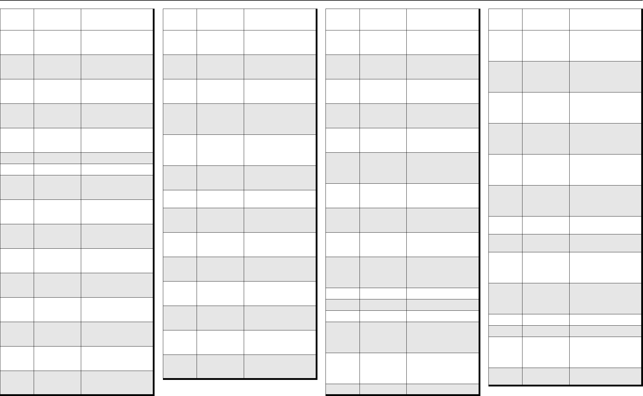
6-56 Receiver Parts List (UHF) – CRE4007
L1507 2414015A09 IDCTR,FXD,270NH,2%,69
0MA,.91Ω,CER,28
Q,550MHZ SRF,SM,1008
L1508 2489917V05 IDCTR,RF,1UH,1%,370MA
,1.75Ω,290MHZ
SRF,SM,1008,PB FREE
L1509 2489917V05 IDCTR,RF,1UH,1%,370MA
,1.75Ω,290MHZ
SRF,SM,1008,PB FREE
L1510 2414015A09 IDCTR,FXD,270NH,2%,69
0MA,.91Ω,CER,28
Q,550MHZ SRF,SM,1008
L2530 2414017K28 IDCTR,CHIP,270NH,5%,20
0MA,1.3Ω,CER,11
Q,270MHZ SRF,SM,0805
L2532 2485364Y25 IDCTR
L2533 2485364Y25 IDCTR
L2534 2414017H08 IDCTR,CHIP,4.7NH,300MA
,.16Ω,CER,10 Q,3GHZ
SRF,SM,0603,PB-
L2535 2414015A25 IDCTR,FXD,1.2UH,2%,440
MA,2Ω,CER,20 Q,200MHZ
SRF,SM,1008,PB
L2538 2414017N13 IDCTR,CHIP,12NH,5%,600
MA,.35Ω,CER,13 Q,2GHZ
SRF,SM,0603,PB
L2539 2414032B72 IDCTR,WW,2.2UH,5%,380
MA,2.8Ω,CER,20
Q,140MHZ SRF,SM,PB-FR
L2543 2414032B72 IDCTR,WW,2.2UH,5%,380
MA,2.8Ω,CER,20
Q,140MHZ SRF,SM,PB-FR
L2543 2414032B72 IDCTR,WW,2.2UH,5%,380
MA,2.8Ω,CER,20
Q,140MHZ SRF,SM,PB-FR
L2547 2414015A05 IDCTR,FXD,120NH,2%,80
0MA,.63Ω,CER,25
Q,900MHZ SRF,SM,1008
L2548 2414015A10 IDCTR,FXD,330NH,2%,66
0MA,1.05Ω,CER,30
Q,500MHZ SRF,SM,1008
L2549 2414017N13 IDCTR,CHIP,12NH,5%,600
MA,.35Ω,CER,13 Q,2GHZ
SRF,SM,0603,PB
Circuit
Ref
Motorola Part
No Description
L2700 2415429H43 IDCTR,WW,220NH,5%,300
MA,2.1Ω,CER,SM,0603,C
HIP
L2701 2414032F25 IDCTR,WW,18NH,5%,600
MA,.2Ω,CER,45 Q,2.4GHZ
SRF,SM,PB-FREE
L2702 2414032B61 IDCTR,WW,470NH,5%,600
MA,1.19Ω,CER,30
Q,425MHZ SRF,SM,PB-F
L2703 2414032F24 IDCTR,WW,15NH,5%,600
MA,.17Ω,CER,45
Q,2.5GHZ SRF,SM,PB-
FRE
L2704 2414032F24 IDCTR,WW,15NH,5%,600
MA,.17Ω,CER,45
Q,2.5GHZ SRF,SM,PB-
FRE
L2705 2415429H19 IDCTR,WW,16NH,5%,700
MA,CER,104KHZ
SRF,SM,0603,CHIP
L2708 2415429H28 IDCTR,WW,39NH,5%,600
MA,CER,SM,CHIP
L3100 2414032F34 IDCTR,WW,100NH,5%,400
MA,.46Ω,CER,40
Q,950MHZ SRF,SM,PB-FR
L3200 2414032F59 IDCTR,WW,390NH,5%,290
MA,1.5Ω,CER,48
Q,560MHZ SRF,SM,PB-FR
L3201 2414032F25 IDCTR,WW,18NH,5%,600
MA,.2Ω,CER,45 Q,2.4GHZ
SRF,SM,PB-FREE
L3202 2414032F59 IDCTR,WW,390NH,5%,290
MA,1.5Ω,CER,48
Q,560MHZ SRF,SM,PB-FR
L3203 2414032F59 IDCTR,WW,390NH,5%,290
MA,1.5Ω,CER,48
Q,560MHZ SRF,SM,PB-FR
L3204 2414032F59 IDCTR,WW,390NH,5%,290
MA,1.5Ω,CER,48
Q,560MHZ SRF,SM,PB-FR
L3205 2414032F59 IDCTR,WW,390NH,5%,290
MA,1.5Ω,CER,48
Q,560MHZ SRF,SM,PB-FR
Circuit
Ref
Motorola Part
No Description
L3206 2414032F25 IDCTR,WW,18NH,5%,600
MA,.2Ω,CER,45 Q,2.4GHZ
SRF,SM,PB-FREE
L3207 2414032F59 IDCTR,WW,390NH,5%,290
MA,1.5Ω,CER,48
Q,560MHZ SRF,SM,PB-FR
L3208 2414032F59 IDCTR,WW,390NH,5%,290
MA,1.5Ω,CER,48
Q,560MHZ SRF,SM,PB-FR
L3209 2414032F59 IDCTR,WW,390NH,5%,290
MA,1.5Ω,CER,48
Q,560MHZ SRF,SM,PB-FR
L3211 2414032F27 IDCTR,FXD,27NH,5%,500
MA,.25Ω,CER,45 Q,2GHZ
SRF,SM,0805,PB-
L3212 2414032F28 IDCTR,WW,33NH,5%,500
MA,.27Ω,CER,40
Q,1.8GHZ SRF,SM,PB-
FRE
L3213 2414032F25 IDCTR,WW,18NH,5%,600
MA,.2Ω,CER,45 Q,2.4GHZ
SRF,SM,PB-FREE
L3214 2414032F59 IDCTR,WW,390NH,5%,290
MA,1.5Ω,CER,48
Q,560MHZ SRF,SM,PB-FR
L3215 2414032F59 IDCTR,WW,390NH,5%,290
MA,1.5Ω,CER,48
Q,560MHZ SRF,SM,PB-FR
Q1600 4813973A34 XSTR,BIP GP
SS,NPN,SM,SC-
70,SMT,50V,.202W,100MA
,PB-FREE
Q1601 4885065Y01 XSTR,FET GP PWR
Q1602 4885065Y01 XSTR,FET GP PWR
Q2200 4885065Y01 XSTR,FET GP PWR
Q2201 4813973A34 XSTR,BIP GP
SS,NPN,SM,SC-
70,SMT,50V,.202W,100MA
,PB-FREE
Q2202 4813973A34 XSTR,BIP GP
SS,NPN,SM,SC-
70,SMT,50V,.202W,100MA
,PB-FREE
Q2203 4885065Y01 XSTR,FET GP PWR
Circuit
Ref
Motorola Part
No Description
Q2204 4813973A34 XSTR,BIP GP
SS,NPN,SM,SC-
70,SMT,50V,.202W,100MA
,PB-FREE
Q2205 4813973A34 XSTR,BIP GP
SS,NPN,SM,SC-
70,SMT,50V,.202W,100MA
,PB-FREE
Q2400 4813973A04 XSTR,BIP GP
SS,NPN,TA13,SM,SOT-
23,SMT,30V,.225W,300MA
,125MHZ,P
Q2530 4805218N63 XSTR,GEN PURPOSE
SMALL SIG,SOT-
323,BROADBAND AND
XSTR
Q2610 4813973A54 XSTR,BIP GP
SS,NPN,T3904,SM,SC-
70,SMT,40V,.15W,200MA,
300MHZ,PB
Q2611 4813973A54 XSTR,BIP GP
SS,NPN,T3904,SM,SC-
70,SMT,40V,.15W,200MA,
300MHZ,PB
Q3200 4885061Y01 XSTR,BIP RF SMALL
SIGNAL
Q3201 4885061Y01 XSTR,BIP RF SMALL
SIGNAL
Q3202 4805218N63 XSTR,GEN PURPOSE
SMALL SIG,SOT-
323,BROADBAND AND
XSTR
Q3203 4813973A54 XSTR,BIP GP
SS,NPN,T3904,SM,SC-
70,SMT,40V,.15W,200MA,
300MHZ,PB
Q3204 4885065Y01 XSTR,FET GP PWR
Q3205 4885065Y01 XSTR,FET GP PWR
Q3206 4813973A34 XSTR,BIP GP
SS,NPN,SM,SC-
70,SMT,50V,.202W,100MA
,PB-FREE
R1100 0613952R33 RES,MF,220000,5,.0625,S
M,0402,200,PB-FREE
Circuit
Ref
Motorola Part
No Description

Receiver Parts List (UHF) – CRE4007 6-57
R1101 0613952N66 RES,MF,47.5KΩ,1%,.0625
W,SM,0402,200PPM/
CEL,PB-FREE
R1102 0613952N66 RES,MF,47.5KΩ,1%,.0625
W,SM,0402,200PPM/
CEL,PB-FREE
R1103 0613952N66 RES,MF,47.5KΩ,1%,.0625
W,SM,0402,200PPM/
CEL,PB-FREE
R1104 0613952N66 RES,MF,47.5KΩ,1%,.0625
W,SM,0402,200PPM/
CEL,PB-FREE
R1105 0613952M01 RES,MF,1KΩ,1%,.0625W,
SM,0402,200PPM/
CEL,PB-FREE
R1106 0613952N30 RES,MF,20KΩ,1%,.0625W
,SM,0402,200PPM/
CEL,PB-FREE
R1107 0613952N30 RES,MF,20KΩ,1%,.0625W
,SM,0402,200PPM/
CEL,PB-FREE
R1108 0613952N30 RES,MF,20KΩ,1%,.0625W
,SM,0402,200PPM/
CEL,PB-FREE
R1109 0613952N01 RES,MF,10KΩ,1%,.0625W
,SM,0402,200PPM/
CEL,PB-FREE
R1110 0613952M05 RES,MF,1.1KΩ,1%,.0625
W,SM,0402,200PPM/
CEL,PB-FREE
R1111 0613952P14 RES,MF,137KΩ,1%,.0625
W,SM,0402,200PPM/
CEL,PB-FREE
R1200 0613952R01 RES,MF,10KΩ,5%,.0625W
,SM,0402,200PPM/
CEL,PB-FREE
R1201 0613952Q19 RES,MF,5.6Ω,5%,.0625W,
SM,0402,200PPM/
CEL,PB-FREE
R1202 0613952Q66 RES,MF,510Ω,5%,.0625W,
SM,0402,200PPM/
CEL,PB-FREE
Circuit
Ref
Motorola Part
No Description
R1203 0613952Q66 RES,MF,510Ω,5%,.0625W,
SM,0402,200PPM/
CEL,PB-FREE
R1230 0613952L76 RES,MF,604Ω,1%,.0625W,
SM,0402,200PPM/
CEL,PB-FREE
R1231 0613952L76 RES,MF,604Ω,1%,.0625W,
SM,0402,200PPM/
CEL,PB-FREE
R1232 0613958A89 RES,MF,8.25Ω,1%,.125W,
SM,0805,400PPM/
CEL,PB-FREE
R1400 0613958H42 RES,MF,51Ω,5%,.125W,S
M,0805,200PPM/CEL,PB-
FREE
R1401 0613958C25 RES,MF,178Ω,1%,.125W,S
M,0805,100PPM/CEL,PB-
FREE
R1402 0613958C25 RES,MF,178Ω,1%,.125W,S
M,0805,100PPM/CEL,PB-
FREE
R1403 0613958C25 RES,MF,178Ω,1%,.125W,S
M,0805,100PPM/CEL,PB-
FREE
R1404 0613958C25 RES,MF,178Ω,1%,.125W,S
M,0805,100PPM/CEL,PB-
FREE
R1405 0613958H85 RES,MF,3.3KΩ,5%,.125W,
SM,0805,200PPM/
CEL,PB-FREE
R1406 0613958H73 RES,MF,1KΩ,5%,.125W,S
M,0805,200PPM/CEL,PB-
FREE
R1407 0613958J74 RES,MF,0Ω,5%,.125W,SM,
0805,PB-FREE
R1410 0613958J74 RES,MF,0Ω,5%,.125W,SM,
0805,PB-FREE
R1412 0613958J74 RES,MF,0Ω,5%,.125W,SM,
0805,PB-FREE
R1500 0613952D34 RES,MF,2.21KΩ,1%,.1W,S
M,0603,100PPM/CEL,PB-
FREE
Circuit
Ref
Motorola Part
No Description
R1501 0613952B01 RES,MF,10Ω,1%,.1W,SM,0
603,100PPM/CEL,PB-
FREE
R1502 0613952D51 RES,MF,3.32KΩ,1%,.1W,S
M,0603,100PPM/CEL,PB-
FREE
R1503 0613952C89 RES,MF,825Ω,1%,.1W,SM,
0603,100PPM/CEL,PB-
FREE
R1504 0613952B09 RES,MF,12.1Ω,1%,.1W,SM
,0603,100PPM/CEL,PB-
FREE
R1505 0613952C26 RES,MF,182Ω,1%,.1W,SM,
0603,100PPM/CEL,PB-
FREE
R1602 0613952R01 RES,MF,10KΩ,5%,.0625W
,SM,0402,200PPM/
CEL,PB-FREE
R1603 0613952R01 RES,MF,10KΩ,5%,.0625W
,SM,0402,200PPM/
CEL,PB-FREE
R1604 0613952N01 RES,MF,10KΩ,1%,.0625W
,SM,0402,200PPM/
CEL,PB-FREE
R1605 0613952N01 RES,MF,10KΩ,1%,.0625W
,SM,0402,200PPM/
CEL,PB-FREE
R2200 0613952N01 RES,MF,10KΩ,1%,.0625W
,SM,0402,200PPM/
CEL,PB-FREE
R2201 0613952N01 RES,MF,10KΩ,1%,.0625W
,SM,0402,200PPM/
CEL,PB-FREE
R2203 0613952N01 RES,MF,10KΩ,1%,.0625W
,SM,0402,200PPM/
CEL,PB-FREE
R2204 0613952B01 RES,MF,10Ω,1%,.1W,SM,0
603,100PPM/CEL,PB-
FREE
R2205 0613952C89 RES,MF,825Ω,1%,.1W,SM,
0603,100PPM/CEL,PB-
FREE
Circuit
Ref
Motorola Part
No Description
R2206 0613952L44 RES,MF,280Ω,1%,.0625W,
SM,0402,200PPM/
CEL,PB-FREE
R2207 0613952N01 RES,MF,10KΩ,1%,.0625W
,SM,0402,200PPM/
CEL,PB-FREE
R2208 0613952N01 RES,MF,10KΩ,1%,.0625W
,SM,0402,200PPM/
CEL,PB-FREE
R2210 0613952N01 RES,MF,10KΩ,1%,.0625W
,SM,0402,200PPM/
CEL,PB-FREE
R2211 0613952M36 RES,MF,2.32KΩ,1%,.0625
W,SM,0402,200PPM/
CEL,PB-FREE
R2212 0613952Q59 RES,MF,270Ω,5%,.0625W,
SM,0402,200PPM/
CEL,PB-FREE
R2213 0613952R66 RES,MF,0Ω,5%,.0625W,S
M,0402,PB-FREE
R2214 0613952N01 RES,MF,10KΩ,1%,.0625W
,SM,0402,200PPM/
CEL,PB-FREE
R2216 0613952Q64 RES,MF,430Ω,5%,.0625W,
SM,0402,200PPM/
CEL,PB-FREE
R2217 0613952Q59 RES,MF,270Ω,5%,.0625W,
SM,0402,200PPM/
CEL,PB-FREE
R2220 0613952L51 RES,MF,332Ω,1%,.0625W,
SM,0402,200PPM/
CEL,PB-FREE
R2221 0613952L44 RES,MF,280Ω,1%,.0625W,
SM,0402,200PPM/
CEL,PB-FREE
R2400 0613952Q64 RES,MF,430Ω,5%,.0625W,
SM,0402,200PPM/
CEL,PB-FREE
R2401 0613952F01 RES,MF,100KΩ,1%,.1W,S
M,0603,100PPM/CEL,PB-
FREE
R2404 0613952Q59 RES,MF,270Ω,5%,.0625W,
SM,0402,200PPM/
CEL,PB-FREE
Circuit
Ref
Motorola Part
No Description
6-58 Receiver Parts List (UHF) – CRE4007
R2405 0613952K01 RES,MF,10Ω,1%,.0625W,S
M,0402,200PPM/CEL,PB-
FREE
R2406 0613952P97 RES,MF,1MΩ,1%,.0625W,
SM,0402,200PPM/
CEL,PB-FREE
R2407 0613952C05 RES,MF,110Ω,1%,.1W,SM,
0603,100PPM/CEL,PB-
FREE
R2408 0613952C05 RES,MF,110Ω,1%,.1W,SM,
0603,100PPM/CEL,PB-
FREE
R2413 0613952R66 RES,MF,0Ω,5%,.0625W,S
M,0402,PB-FREE
R2422 0613952C26 RES,MF,182Ω,1%,.1W,SM,
0603,100PPM/CEL,PB-
FREE
R2423 0613952C28 RES,MF,191Ω,1%,.1W,SM,
0603,100PPM/CEL,PB-
FREE
R2530 0613952R66 RES,MF,0Ω,5%,.0625W,S
M,0402,PB-FREE
R2531 0613952R66 RES,MF,0Ω,5%,.0625W,S
M,0402,PB-FREE
R2532 0613952K68 RES,MF,49.9Ω,1%,.0625W
,SM,0402,200PPM/
CEL,PB-FREE
R2533 0613952R66 RES,MF,0Ω,5%,.0625W,S
M,0402,PB-FREE
R2534 0613952P01 RES,MF,100KΩ,1%,.0625
W,SM,0402,200PPM/
CEL,PB-FREE
R2535 0613952N01 RES,MF,10KΩ,1%,.0625W
,SM,0402,200PPM/
CEL,PB-FREE
R2536 0613952K51 RES,MF,33.2Ω,1%,.0625W
,SM,0402,200PPM/
CEL,PB-FREE
R2537 0613952P01 RES,MF,100KΩ,1%,.0625
W,SM,0402,200PPM/
CEL,PB-FREE
R2538 0613952D30 RES,MF,2KΩ,1%,.1W,SM,
0603,100PPM/CEL,PB-
FREE
Circuit
Ref
Motorola Part
No Description
R2539 0613952L63 RES,MF,442Ω,1%,.0625W,
SM,0402,200PPM/
CEL,PB-FREE
R2540 0613952L58 RES,MF,392Ω,1%,.0625W,
SM,0402,200PPM/
CEL,PB-FREE
R2541 0613952K07 RES,MF,11.5Ω,1%,.0625W
,SM,0402,200PPM/
CEL,PB-FREE
R2542 0613952L63 RES,MF,442Ω,1%,.0625W,
SM,0402,200PPM/
CEL,PB-FREE
R2545 0613952N01 RES,MF,10KΩ,1%,.0625W
,SM,0402,200PPM/
CEL,PB-FREE
R2546 0613952L66 RES,MF,475Ω,1%,.0625W,
SM,0402,200PPM/
CEL,PB-FREE
R2547 0613952L01 RES,MF,100Ω,1%,.0625W,
SM,0402,200PPM/
CEL,PB-FREE
R2548 0613952L09 RES,MF,121Ω,1%,.0625W,
SM,0402,200PPM/
CEL,PB-FREE
R2549 0613952B01 RES,MF,10Ω,1%,.1W,SM,0
603,100PPM/CEL,PB-
FREE
R2559 0613952N01 RES,MF,10KΩ,1%,.0625W
,SM,0402,200PPM/
CEL,PB-FREE
R2563 0613952L26 RES,MF,182Ω,1%,.0625W,
SM,0402,200PPM/
CEL,PB-FREE
R2580 0613952K68 RES,MF,49.9Ω,1%,.0625W
,SM,0402,200PPM/
CEL,PB-FREE
R2581 0613952K51 RES,MF,33.2Ω,1%,.0625W
,SM,0402,200PPM/
CEL,PB-FREE
R2582 0613952K51 RES,MF,33.2Ω,1%,.0625W
,SM,0402,200PPM/
CEL,PB-FREE
Circuit
Ref
Motorola Part
No Description
R2583 0613952K51 RES,MF,33.2Ω,1%,.0625W
,SM,0402,200PPM/
CEL,PB-FREE
R2595 0613952K51 RES,MF,33.2Ω,1%,.0625W
,SM,0402,200PPM/
CEL,PB-FREE
R2596 0613952K68 RES,MF,49.9Ω,1%,.0625W
,SM,0402,200PPM/
CEL,PB-FREE
R2597 0613952K68 RES,MF,49.9Ω,1%,.0625W
,SM,0402,200PPM/
CEL,PB-FREE
R2610 0613952R66 RES,MF,0Ω,5%,.0625W,S
M,0402,PB-FREE
R2611 0613952M42 RES,MF,2.67KΩ,1%,0.062
5W,SM,0402,200PPM/
CEL,PB-FREE
R2612 0613952M42 RES,MF,2.67KΩ,1%,0.062
5W,SM,0402,200PPM/
CEL,PB-FREE
R2614 0613952L66 RES,MF,475Ω,1%,.0625W,
SM,0402,200PPM/
CEL,PB-FREE
R2615 0613952L18 RES,MF,150Ω,1%,.0625W,
SM,0402,200PPM/
CEL,PB-FREE
R2616 0613952L66 RES,MF,475Ω,1%,.0625W,
SM,0402,200PPM/
CEL,PB-FREE
R2620 0613952R66 RES,MF,0Ω,5%,.0625W,S
M,0402,PB-FREE
R2622 0613952M42 RES,MF,2.67KΩ,1%,0.062
5W,SM,0402,200PPM/
CEL,PB-FREE
R2623 0613952L66 RES,MF,475Ω,1%,.0625W,
SM,0402,200PPM/
CEL,PB-FREE
R2625 0613952L66 RES,MF,475Ω,1%,.0625W,
SM,0402,200PPM/
CEL,PB-FREE
R2626 0613952L18 RES,MF,150Ω,1%,.0625W,
SM,0402,200PPM/
CEL,PB-FREE
Circuit
Ref
Motorola Part
No Description
R2627 0613952L01 RES,MF,100Ω,1%,.0625W,
SM,0402,200PPM/
CEL,PB-FREE
R2628 0613952L01 RES,MF,100Ω,1%,.0625W,
SM,0402,200PPM/
CEL,PB-FREE
R2630 0613952R66 RES,MF,0Ω,5%,.0625W,S
M,0402,PB-FREE
R2631 0613952R66 RES,MF,0Ω,5%,.0625W,S
M,0402,PB-FREE
R2651 0613952M42 RES,MF,2.67KΩ,1%,0.062
5W,SM,0402,200PPM/
CEL,PB-FREE
R2703 0613952A73 RES,MF,5.62Ω,1%,.1W,SM
,0603,400PPM/CEL,PB-
FREE
R2704 0613952A73 RES,MF,5.62Ω,1%,.1W,SM
,0603,400PPM/CEL,PB-
FREE
R2705 0613952G67 RES,MF,0,1,.1,SM,0603,P
B-FREE
R2706 0613952C18 RES,MF,150Ω,1%,.1W,SM,
0603,100PPM/CEL,PB-
FREE
R2707 0613952B81 RES,MF,68.1Ω,1%,.1W,SM
,0603,100PPM/CEL,PB-
FREE
R2708 0613952C42 RES,MF,267Ω,1%,.1W,SM,
0603,100PPM/CEL,PB-
FREE
R2710 0613959Y54 RES,MF,160Ω,5%,1W,SM,
2512,100PPM/CEL,PB-
FREE
R2711 0613959G16 RES,MF,4.3Ω,5%,.33W,SM
,1210,400PPM/CEL,PB-
FREE
R2712 0613959Y54 RES,MF,160Ω,5%,1W,SM,
2512,100PPM/CEL,PB-
FREE
R2713 0613952R66 RES,MF,0Ω,5%,.0625W,S
M,0402,PB-FREE
R2715 0613952G67 RES,MF,0,1,.1,SM,0603,P
B-FREE
Circuit
Ref
Motorola Part
No Description
Receiver Parts List (UHF) – CRE4007 6-59
R2717 0613952A73 RES,MF,5.62Ω,1%,.1W,SM
,0603,400PPM/CEL,PB-
FREE
R2718 0613952C89 RES,MF,825Ω,1%,.1W,SM,
0603,100PPM/CEL,PB-
FREE
R2719 0613952C89 RES,MF,825Ω,1%,.1W,SM,
0603,100PPM/CEL,PB-
FREE
R2800 0613952N01 RES,MF,10KΩ,1%,.0625W
,SM,0402,200PPM/
CEL,PB-FREE
R2801 0613952N30 RES,MF,20KΩ,1%,.0625W
,SM,0402,200PPM/
CEL,PB-FREE
R2802 0613952N01 RES,MF,10KΩ,1%,.0625W
,SM,0402,200PPM/
CEL,PB-FREE
R2803 0613952N01 RES,MF,10KΩ,1%,.0625W
,SM,0402,200PPM/
CEL,PB-FREE
R2804 0613952N01 RES,MF,10KΩ,1%,.0625W
,SM,0402,200PPM/
CEL,PB-FREE
R2805 0613952M51 RES,MF,3.32KΩ,1%,0.062
5W,SM,0402,200PPM/
CEL,PB-FREE
R2806 0613952N01 RES,MF,10KΩ,1%,.0625W
,SM,0402,200PPM/
CEL,PB-FREE
R2807 0613952N51 RES,MF,33.2KΩ,1%,.0625
W,SM,0402,200PPM/
CEL,PB-FREE
R2808 0613952N18 RES,MF,15KΩ,1%,.0625W
,SM,0402,200PPM/
CEL,PB-FREE
R2809 0613952Z46 RES,MF,3.9KΩ,1%,.0625
W,SM,0402,200PPM/
CEL,PB-FREE
R2810 0613952N01 RES,MF,10KΩ,1%,.0625W
,SM,0402,200PPM/
CEL,PB-FREE
Circuit
Ref
Motorola Part
No Description
R2811 0613952N01 RES,MF,10KΩ,1%,.0625W
,SM,0402,200PPM/
CEL,PB-FREE
R2812 0613952N01 RES,MF,10KΩ,1%,.0625W
,SM,0402,200PPM/
CEL,PB-FREE
R2813 0613952R66 RES,MF,0Ω,5%,.0625W,S
M,0402,PB-FREE
R2815 0613952R66 RES,MF,0Ω,5%,.0625W,S
M,0402,PB-FREE
R2816 0613952R66 RES,MF,0Ω,5%,.0625W,S
M,0402,PB-FREE
R2817 0613952A73 RES,MF,5.62Ω,1%,.1W,SM
,0603,400PPM/CEL,PB-
FREE
R3101 0613952G67 RES,MF,0,1,.1,SM,0603,P
B-FREE
R3103 0613952D44 RES,MF,2.8KΩ,1%,.1W,S
M,0603,100PPM/CEL,PB-
FREE
R3104 0613952B34 RES,MF,22.1Ω,1%,.1W,SM
,0603,100PPM/CEL,PB-
FREE
R3105 0613952C53 RES,MF,348Ω,1%,.1W,SM,
0603,100PPM/CEL,PB-
FREE
R3106 0613952B68 RES,MF,49.9Ω,1%,.1W,SM
,0603,100PPM/CEL,PB-
FREE
R3108 0613952R66 RES,MF,0Ω,5%,.0625W,S
M,0402,PB-FREE
R3113 0613952N01 RES,MF,10KΩ,1%,.0625W
,SM,0402,200PPM/
CEL,PB-FREE
R3129 0613952G67 RES,MF,0,1,.1,SM,0603,P
B-FREE
R3130 0613952G67 RES,MF,0,1,.1,SM,0603,P
B-FREE
R3134 0613952G67 RES,MF,0,1,.1,SM,0603,P
B-FREE
R3146 0613952R66 RES,MF,0Ω,5%,.0625W,S
M,0402,PB-FREE
Circuit
Ref
Motorola Part
No Description
R3147 0613952R01 RES,MF,10KΩ,5%,.0625W
,SM,0402,200PPM/
CEL,PB-FREE
R3172 0613952K51 RES,MF,33.2Ω,1%,.0625W
,SM,0402,200PPM/
CEL,PB-FREE
R3185 0613952L01 RES,MF,100Ω,1%,.0625W,
SM,0402,200PPM/
CEL,PB-FREE
R3187 0613952R66 RES,MF,0Ω,5%,.0625W,S
M,0402,PB-FREE
R3200 0613952B01 RES,MF,10Ω,1%,.1W,SM,0
603,100PPM/CEL,PB-
FREE
R3201 0613952B18 RES,MF,15Ω,1%,.1W,SM,0
603,100PPM/CEL,PB-
FREE
R3202 0613958C47 RES,MF,301Ω,1%,.125W,S
M,0805,100PPM/CEL,PB-
FREE
R3203 0613958C01 RES,MF,100Ω,1%,.125W,S
M,0805,100PPM/CEL,PB-
FREE
R3204 0613952D20 RES,MF,1.58KΩ,1%,.1W,S
M,0603,100PPM/CEL,PB-
FREE
R3205 0613952D01 RES,MF,1KΩ,1%,.1W,SM,
0603,100PPM/CEL,PB-
FREE
R3206 0613952B07 RES,MF,11.5Ω,1%,.1W,SM
,0603,100PPM/CEL,PB-
FREE
R3207 0613952C62 RES,MF,432Ω,1%,.1W,SM,
0603,100PPM/CEL,PB-
FREE
R3208 0613952C62 RES,MF,432Ω,1%,.1W,SM,
0603,100PPM/CEL,PB-
FREE
R3209 0613952B01 RES,MF,10Ω,1%,.1W,SM,0
603,100PPM/CEL,PB-
FREE
R3210 0613952B18 RES,MF,15Ω,1%,.1W,SM,0
603,100PPM/CEL,PB-
FREE
Circuit
Ref
Motorola Part
No Description
R3211 0613958C47 RES,MF,301Ω,1%,.125W,S
M,0805,100PPM/CEL,PB-
FREE
R3212 0613958C01 RES,MF,100Ω,1%,.125W,S
M,0805,100PPM/CEL,PB-
FREE
R3213 0613952D20 RES,MF,1.58KΩ,1%,.1W,S
M,0603,100PPM/CEL,PB-
FREE
R3214 0613952D01 RES,MF,1KΩ,1%,.1W,SM,
0603,100PPM/CEL,PB-
FREE
R3215 0613952B07 RES,MF,11.5Ω,1%,.1W,SM
,0603,100PPM/CEL,PB-
FREE
R3216 0613952C62 RES,MF,432Ω,1%,.1W,SM,
0603,100PPM/CEL,PB-
FREE
R3217 0613952C62 RES,MF,432Ω,1%,.1W,SM,
0603,100PPM/CEL,PB-
FREE
R3219 0613952G67 RES,MF,0,1,.1,SM,0603,P
B-FREE
R3221 0613952D51 RES,MF,3.32KΩ,1%,.1W,S
M,0603,100PPM/CEL,PB-
FREE
R3222 0613952D30 RES,MF,2KΩ,1%,.1W,SM,
0603,100PPM/CEL,PB-
FREE
R3223 0613952C30 RES,MF,200Ω,1%,.1W,SM,
0603,100PPM/CEL,PB-
FREE
R3224 0613958C01 RES,MF,100Ω,1%,.125W,S
M,0805,100PPM/CEL,PB-
FREE
R3225 0613958C47 RES,MF,301Ω,1%,.125W,S
M,0805,100PPM/CEL,PB-
FREE
R3227 0613952G67 RES,MF,0,1,.1,SM,0603,P
B-FREE
R3228 0613952G67 RES,MF,0,1,.1,SM,0603,P
B-FREE
Circuit
Ref
Motorola Part
No Description

6-60 Receiver Parts List (UHF) – CRE4007
R3229 0613958B53 RES,MF,34.8Ω,1%,.125W,
SM,0805,100PPM/
CEL,PB-FREE
R3230 0613952L42 RES,MF,267Ω,1%,.0625W,
SM,0402,200PPM/
CEL,PB-FREE
R3231 0613952K01 RES,MF,10Ω,1%,.0625W,S
M,0402,200PPM/CEL,PB-
FREE
R3234 6139520 RES,MF,10KΩ,1%,.1W,SM
,0603,100PPM/CEL,PB-
FREE
R3235 6139520 RES,MF,10KΩ,1%,.1W,SM
,0603,100PPM/CEL,PB-
FREE
R3236 0613952G67 RES,MF,0,1,.1,SM,0603,P
B-FREE
R3300 0613952R66 RES,MF,0Ω,5%,.0625W,S
M,0402,PB-FREE
R3301 0613952M66 RES,MF,4.75KΩ,1%,.0625
W,SM,0402,200PPM/
CEL,PB-FREE
R3302 0613952M01 RES,MF,1KΩ,1%,.0625W,
SM,0402,200PPM/
CEL,PB-FREE
R3303 0613952M01 RES,MF,1KΩ,1%,.0625W,
SM,0402,200PPM/
CEL,PB-FREE
R3304 0613952M01 RES,MF,1KΩ,1%,.0625W,
SM,0402,200PPM/
CEL,PB-FREE
R3305 0613952M66 RES,MF,4.75KΩ,1%,.0625
W,SM,0402,200PPM/
CEL,PB-FREE
R3306 0613952M01 RES,MF,1KΩ,1%,.0625W,
SM,0402,200PPM/
CEL,PB-FREE
R3307 0613952M01 RES,MF,1KΩ,1%,.0625W,
SM,0402,200PPM/
CEL,PB-FREE
R3308 0613952K51 RES,MF,33.2Ω,1%,.0625W
,SM,0402,200PPM/
CEL,PB-FREE
Circuit
Ref
Motorola Part
No Description
R3309 0613952K68 RES,MF,49.9Ω,1%,.0625W
,SM,0402,200PPM/
CEL,PB-FREE
R3310 0613952K51 RES,MF,33.2Ω,1%,.0625W
,SM,0402,200PPM/
CEL,PB-FREE
R3311 0613952K51 RES,MF,33.2Ω,1%,.0625W
,SM,0402,200PPM/
CEL,PB-FREE
R3312 0613952K68 RES,MF,49.9Ω,1%,.0625W
,SM,0402,200PPM/
CEL,PB-FREE
R3314 0613952K68 RES,MF,49.9Ω,1%,.0625W
,SM,0402,200PPM/
CEL,PB-FREE
R3315 0613952M66 RES,MF,4.75KΩ,1%,.0625
W,SM,0402,200PPM/
CEL,PB-FREE
R3316 0613952M66 RES,MF,4.75KΩ,1%,.0625
W,SM,0402,200PPM/
CEL,PB-FREE
R3317 0613952M66 RES,MF,4.75KΩ,1%,.0625
W,SM,0402,200PPM/
CEL,PB-FREE
R3318 0613952M66 RES,MF,4.75KΩ,1%,.0625
W,SM,0402,200PPM/
CEL,PB-FREE
R3322 0613952M66 RES,MF,4.75KΩ,1%,.0625
W,SM,0402,200PPM/
CEL,PB-FREE
R3326 0613952K68 RES,MF,49.9Ω,1%,.0625W
,SM,0402,200PPM/
CEL,PB-FREE
R3327 0613952N01 RES,MF,10KΩ,1%,.0625W
,SM,0402,200PPM/
CEL,PB-FREE
R3328 0613952R66 RES,MF,0Ω,5%,.0625W,S
M,0402,PB-FREE
R3329 0613952K51 RES,MF,33.2Ω,1%,.0625W
,SM,0402,200PPM/
CEL,PB-FREE
R3330 0613952R66 RES,MF,0Ω,5%,.0625W,S
M,0402,PB-FREE
Circuit
Ref
Motorola Part
No Description
R3331 0613952M66 RES,MF,4.75KΩ,1%,.0625
W,SM,0402,200PPM/
CEL,PB-FREE
R3332 0613952K51 RES,MF,33.2Ω,1%,.0625W
,SM,0402,200PPM/
CEL,PB-FREE
R3333 0613952M66 RES,MF,4.75KΩ,1%,.0625
W,SM,0402,200PPM/
CEL,PB-FREE
R3334 0613952M66 RES,MF,4.75KΩ,1%,.0625
W,SM,0402,200PPM/
CEL,PB-FREE
R3345 0613952M66 RES,MF,4.75KΩ,1%,.0625
W,SM,0402,200PPM/
CEL,PB-FREE
R3346 0613952K51 RES,MF,33.2Ω,1%,.0625W
,SM,0402,200PPM/
CEL,PB-FREE
R3347 0613952K51 RES,MF,33.2Ω,1%,.0625W
,SM,0402,200PPM/
CEL,PB-FREE
R3348 0613952K51 RES,MF,33.2Ω,1%,.0625W
,SM,0402,200PPM/
CEL,PB-FREE
R3349 0613952R66 RES,MF,0Ω,5%,.0625W,S
M,0402,PB-FREE
R3350 0613952M66 RES,MF,4.75KΩ,1%,.0625
W,SM,0402,200PPM/
CEL,PB-FREE
R3390 0613952K51 RES,MF,33.2Ω,1%,.0625W
,SM,0402,200PPM/
CEL,PB-FREE
R3391 0613952K51 RES,MF,33.2Ω,1%,.0625W
,SM,0402,200PPM/
CEL,PB-FREE
R3392 0613952K51 RES,MF,33.2Ω,1%,.0625W
,SM,0402,200PPM/
CEL,PB-FREE
SH1100 2685297D02 SHLD,CVR,NI-AG,STOCK
FINISH,24.58MMLG,18.73
MMW,4.45MM,VCO
SH1401 1583004X05 SHLD,SHIELD, VCO
Circuit
Ref
Motorola Part
No Description
SH1500 2685668Y01 SHLD,CORRAL,NI-
AG,24MMLG,13MMW,3.28
MM
SH1501 2685668Y01 SHLD,CORRAL,NI-
AG,24MMLG,13MMW,3.28
MM
SH2500 2685297D02 SHLD,CVR,NI-AG,STOCK
FINISH,24.58MMLG,18.73
MMW,4.45MM,VCO
SH2700 2685297D02 SHLD,CVR,NI-AG,STOCK
FINISH,24.58MMLG,18.73
MMW,4.45MM,VCO
SH2701 2685297D02 SHLD,CVR,NI-AG,STOCK
FINISH,24.58MMLG,18.73
MMW,4.45MM,VCO
SH3200 1583004X05 SHLD,SHIELD, VCO
SH3201 2685668Y01 SHLD,CORRAL,NI-
AG,24MMLG,13MMW,3.28
MM
T1400 2585040Y01 XFMR,BALUN
T1401 2585040Y01 XFMR,BALUN
U1100 5114005M13 IC,OP AMP,2PER
PKG,LVOLT,SM,SOIC8,PB
-FREE
U1200 5185481Y01 XSTR
U1500 91012005001 FLTR,73.35MHZ
MAX,SM,73.35MHZ XTAL
FILTER, 3-POLE
U1501 91012005001 FLTR,73.35MHZ
MAX,SM,73.35MHZ XTAL
FILTER, 3-POLE
U1502 4805218N55 XSTR,BIP RF SMALL
SIGNAL,SLCN,NPN,BFQ6
7,SM,SOT-
23,SMT,10V,.3W,5
U1600 5185941F45 ATTEN,VAR,14.4DBMIN,1
5.6DBMAX,0-2000
MHZFREQ,50Ω,PCMT,SO
T-25
U2200 5114014A26 IC,LNR V
REGLTR,ADJUSTABLE,1.
2V TO
,37V,500MA,SM,DPAK,PB
-FREE
Circuit
Ref
Motorola Part
No Description

Receiver Parts List (UHF) – CRE4007 6-61
U2201 5114014A26 IC,LNR V
REGLTR,ADJUSTABLE,1.
2V TO
,37V,500MA,SM,DPAK,PB
-FREE
U2202 5114014A26 IC,LNR V
REGLTR,ADJUSTABLE,1.
2V TO
,37V,500MA,SM,DPAK,PB
-FREE
U2203 5114014A20 IC,LNR V
REGLTR,ADJUSTABLE,1.
35V TO
,10V,800MA,SM,SO-8,PB-
FREE
U2400 5114014A26 IC,LNR V
REGLTR,ADJUSTABLE,1.
2V TO
,37V,500MA,SM,DPAK,PB
-FREE
U2530 5185963A85 IC-ABACUS III-LP
U2531 5114005A19 IC,OP AMP,2PER PKG,HI-
SPD,SM,SO-8,SING SPLY,
PB-FREE
U2700 5171183H01 AMP MDL,GAIN BLCK
MMIC AMP
U2701 5185337Y01 AMP
U2800 5184998Y01 IC,LOW-
POWER,8CHANNEL,SERI
AL 10-BIT ADCS
U3100 5164015H28 IC,CUST,MULTI
PROTOCOL/BAND
TRANSCVR
IC,SM,BGA,TRIDENT,
INTEG
U3101 5185183Y01 IC,OP AMP,SO-8
U3103 5114019M05 IC,INVTR,SCHMITT,74LVX
14,6PER
PKG,SM,TSSOP14,PB-
FREE
U3300 5185130Y01 IC,PLD,TQFP
U3301 5184943Y01 IC,EEPROM,64
KB,SOIC,AT25640AN-
10SU-2.7
Circuit
Ref
Motorola Part
No Description
U3303 5185941F86 IC,XCVR,0PER
PKG,PQFP,PQFP16,IC, 4-
BIT BUS XCVR
Y3200 9171848H09 RESON,CER,SMD,13.95N
H,493MHZ
Y3201 9171848H10 RESON,CER,SMD,12.14N
H,527MHZ
Circuit
Ref
Motorola Part
No Description
6-62 Receiver Parts List (UHF) – CRE4008
6.5 Receiver Parts List (UHF) –
CRE4008
Circuit
Ref
Motorola
Part No Description
C1000 2115153H21 CAP,FXD,5.6PF,.1PF+/-,50V-
DC,0402,C0G,CAP, CERAMIC,
COG
C1001 2115153H04 CAP,CERAMIC
CHIP,1.1PF,.1PF+/-,+.1%,-
.1%,50V-DC,0402,C0G,CAP,
C1002 2115153H13 CAP,FXD,2.7PF,.1PF+/-,+3.7%,-
3.7%,50V-DC,0402,C0G,CAP,
CERAMIC
C1003 2115153H07 CAP,FXD,1.5PF,.1PF+/-,+6.67%,-
6.67%,50V-DC,0402,C0G
C1004 2115153H18 CAP,CER CHIP,4.3PF,.1PF+/-
,+.1%,-.1%,50V-
DC,0402,C0G,CAP, CERA
C1005 2115153H13 CAP,FXD,2.7PF,.1PF+/-,+3.7%,-
3.7%,50V-DC,0402,C0G,CAP,
CERAMIC
C1006 2113944A42 CAP,CHIP,150PF,+5%,-5%,50V-
DC,0402,C0G,-55DEG
CMIN,125DEG CMAX
C1008 2115153H45 CAP,CERAMIC CHIP,33PF,+1%,-
1%,50V-DC,0402,C0G
C1103 2113951C41 CAP,FXD,24PF,+1%,-1%,250V-
DC,0603,C0G,-55DEG
CMIN,125DEG CMAX,P
C1104 2113951C34 CAP,FXD,10PF,+1%,-1%,250V-
DC,0603,C0G,-55DEG
CMIN,125DEG CMAX,P
C1106 2113951C51 CAP,FXD,62PF,+1%,-1%,250V-
DC,0603,C0G,-55DEG
CMIN,125DEG CMAX,P
C1107 2113951C08 CAP,FXD,.8PF,.05PF+/-,250V-
DC,0603,C0G,-55DEG
CMIN,125DEG CMAX
C1109 2113951C51 CAP,FXD,62PF,+1%,-1%,250V-
DC,0603,C0G,-55DEG
CMIN,125DEG CMAX,P
C1110 2113951C33 CAP,FXD,9.1PF,.25PF+/-,250V-
DC,0603,C0G,-55DEG
CMIN,125DEG CMA
C1111 2113951C41 CAP,FXD,24PF,+1%,-1%,250V-
DC,0603,C0G,-55DEG
CMIN,125DEG CMAX,P
C1113 2113946K02 CAP,CHIP,.1UF,+80%,-20%,16V-
DC,0402,Y5V,-30DEG
CMIN,85DEG CMAX
C1114 2113944C45 CAP,CHIP,100PF,+5%,-5%,50V-
DC,0603,C0G,-55DEG
CMIN,125DEG CMAX
C1116 2113944A42 CAP,CHIP,150PF,+5%,-5%,50V-
DC,0402,C0G,-55DEG
CMIN,125DEG CMAX
C1117 2113946K02 CAP,CHIP,.1UF,+80%,-20%,16V-
DC,0402,Y5V,-30DEG
CMIN,85DEG CMAX
C1119 2113944A42 CAP,CHIP,150PF,+5%,-5%,50V-
DC,0402,C0G,-55DEG
CMIN,125DEG CMAX
C1120 2113944A42 CAP,CHIP,150PF,+5%,-5%,50V-
DC,0402,C0G,-55DEG
CMIN,125DEG CMAX
C1121 2113944A42 CAP,CHIP,150PF,+5%,-5%,50V-
DC,0402,C0G,-55DEG
CMIN,125DEG CMAX
C1200 2113945C02 CAP,CHIP,.01UF,+10%,-10%,50V-
DC,0603,X7R,-55DEG
CMIN,125DEG CMA
C1201 2113946K02 CAP,CHIP,.1UF,+80%,-20%,16V-
DC,0402,Y5V,-30DEG
CMIN,85DEG CMAX
C1202 2113944A42 CAP,CHIP,150PF,+5%,-5%,50V-
DC,0402,C0G,-55DEG
CMIN,125DEG CMAX
C1203 2113944A42 CAP,CHIP,150PF,+5%,-5%,50V-
DC,0402,C0G,-55DEG
CMIN,125DEG CMAX
C1204 2115153H03 CAP,CER CHIP,1PF,.1PF+/-
,+.1%,-.1%,50V-DC,0402,C0G
C1205 2113944A52 CAP,CHIP,1000PF,+5%,-5%,50V-
DC,0402,C0G,-55DEG
CMIN,125DEG CMAX
C1206 2113944A42 CAP,CHIP,150PF,+5%,-5%,50V-
DC,0402,C0G,-55DEG
CMIN,125DEG CMAX
Circuit
Ref
Motorola
Part No Description
C1230 2113944A42 CAP,CHIP,150PF,+5%,-5%,50V-
DC,0402,C0G,-55DEG
CMIN,125DEG CMAX
C1300 2115153H49 CAP,FXD,47PF,+1%,-1%,50V-
DC,0402,C0G
C1301 2115153H23 CAP,CER CHIP,6.8PF,.1PF+/-
,+.1%,-.1%,50V-
DC,0402,C0G,CAP, CERA
C1302 2115153H39 CAP,FXD,18PF,50V-
DC,0402,C0G
C1303 2115153H06 CAP,FXD,1.3PF,.1PF+/-,50V-
DC,0402,C0G
C1304 2115153H19 CAP,FXD,4.7PF,.1PF+/-,+.1%,-
.1%,50V-DC,0402,C0G
C1305 2115153H14 CAP,CERAMIC CHIP,3PF,.1PF+/-
,+.1%,-.1%,50V-
DC,0402,C0G,CAP, CE
C1306 2115153H27 CAP,FXD,10PF,.1PF+/-,+1%,-
1%,50V-DC,0402,C0G,CAP,
CERAMIC, COG
C1307 2185957Y47 CAP,.5PF,CAP,NP0,0.5 PF +/-
.05PF,200V,0402
C1308 2115153H11 CAP,FXD,2.2PF,.1PF+/-,+1%,-
1%,50V-DC,0402,C0G
C1309 2115153H14 CAP,CERAMIC CHIP,3PF,.1PF+/-
,+.1%,-.1%,50V-
DC,0402,C0G,CAP, CE
C1310 2115153H27 CAP,FXD,10PF,.1PF+/-,+1%,-
1%,50V-DC,0402,C0G,CAP,
CERAMIC, COG
C1311 2115153H06 CAP,FXD,1.3PF,.1PF+/-,50V-
DC,0402,C0G
C1312 2115153H19 CAP,FXD,4.7PF,.1PF+/-,+.1%,-
.1%,50V-DC,0402,C0G
C1313 2115153H22 CAP,CERAMIC
CHIP,6.2PF,.1PF+/-,+.1%,-
.1%,50V-DC,0402,C0G,CAP,
C1314 2115153H41 CAP,FXD,22PF,+1%,-1%,50V-
DC,0402,C0G,CAP, CERAMIC,
COG
C1315 2113944A42 CAP,CHIP,150PF,+5%,-5%,50V-
DC,0402,C0G,-55DEG
CMIN,125DEG CMAX
Circuit
Ref
Motorola
Part No Description
C1404 2113901A11 CAP,CHIP,2PF,.25PF+/-,200V-
DC,0805,-55DEG CMIN,125DEG
CMAX
C1405 2113901A28 CAP,CHIP,9.1PF,.5PF+/-,200V-
DC,0805,-55DEG CMIN,125DEG
CMAX
C1409 2113901A29 CAP,CHIP,10PF,.5PF+/-,200V-
DC,0805,-55DEG CMIN,125DEG
CMAX
C1410 2113901A19 CAP,CHIP,3.9PF,.25PF+/-,200V-
DC,0805,-55DEG CMIN,125DEG
CMAX
C1411 2113945G45 CAP,FXD,.01UF,+5%,-5%,50V-
DC,0805,X7R,-55DEG
CMIN,125DEG CMAX,P
C1412 2113945G45 CAP,FXD,.01UF,+5%,-5%,50V-
DC,0805,X7R,-55DEG
CMIN,125DEG CMAX,P
C1413 2113945G45 CAP,FXD,.01UF,+5%,-5%,50V-
DC,0805,X7R,-55DEG
CMIN,125DEG CMAX,P
C1414 2113945G45 CAP,FXD,.01UF,+5%,-5%,50V-
DC,0805,X7R,-55DEG
CMIN,125DEG CMAX,P
C1415 2113901A56 CAP,CHIP,82PF,+5%,-5%,200V-
DC,0805,-55DEG CMIN,125DEG
CMAX
C1416 2113901A57 CAP,CHIP,91PF,+5%,-5%,200V-
DC,0805,-55DEG CMIN,125DEG
CMAX
C1417 2113944F05 CAP,CHIP,470PF,+5%,-5%,50V-
DC,0805,C0G,-55DEG
CMIN,125DEG CMAX
C1419 2113901A16 CAP,CHIP,3PF,.25PF+/-,200V-
DC,0805,-55DEG CMIN,125DEG
CMAX
C1500 2113951C30 CAP,FXD,6.8PF,.25PF+/-,250V-
DC,0603,C0G,-55DEG
CMIN,125DEG CMA
C1501 2113951C32 CAP,FXD,8.2PF,.25PF+/-,250V-
DC,0603,C0G,-55DEG
CMIN,125DEG CMA
Circuit
Ref
Motorola
Part No Description

Receiver Parts List (UHF) – CRE4008 6-63
C1502 2113951C20 CAP,FXD,2.7PF,.05PF+/-,250V-
DC,0603,C0G,-55DEG
CMIN,125DEG CMA
C1503 2113951C49 CAP,FXD,51PF,+1%,-1%,250V-
DC,0603,C0G,-55DEG
CMIN,125DEG CMAX,P
C1504 2113951C36 CAP,FXD,12PF,+1%,-1%,250V-
DC,0603,C0G,-55DEG
CMIN,125DEG CMAX,P
C1505 2113951C20 CAP,FXD,2.7PF,.05PF+/-,250V-
DC,0603,C0G,-55DEG
CMIN,125DEG CMA
C1506 2113951C32 CAP,FXD,8.2PF,.25PF+/-,250V-
DC,0603,C0G,-55DEG
CMIN,125DEG CMA
C1507 2113951C30 CAP,FXD,6.8PF,.25PF+/-,250V-
DC,0603,C0G,-55DEG
CMIN,125DEG CMA
C1510 2113944A32 CAP,CHIP,39PF,+5%,-5%,50V-
DC,0402,C0G,-55DEG
CMIN,125DEG CMAX,P
C1511 2113945B02 CAP,CHIP,.01UF,+10%,-10%,25V-
DC,0402,X7R,-55DEG
CMIN,125DEG CMA
C1512 2113946B04 CAP,CHIP,.1UF,+10%,-10%,10V-
DC,0402,X5R,-55DEG
CMIN,85DEG CMAX
C1513 2113946B04 CAP,CHIP,.1UF,+10%,-10%,10V-
DC,0402,X5R,-55DEG
CMIN,85DEG CMAX
C1514 2113944A42 CAP,CHIP,150PF,+5%,-5%,50V-
DC,0402,C0G,-55DEG
CMIN,125DEG CMAX
C1515 2113945B02 CAP,CHIP,.01UF,+10%,-10%,25V-
DC,0402,X7R,-55DEG
CMIN,125DEG CMA
C1516 2113944A33 CAP,CHIP,47PF,+5%,-5%,50V-
DC,0402,C0G,-55DEG
CMIN,125DEG CMAX,P
C1519 2113951C30 CAP,FXD,6.8PF,.25PF+/-,250V-
DC,0603,C0G,-55DEG
CMIN,125DEG CMA
Circuit
Ref
Motorola
Part No Description
C1520 2113951C32 CAP,FXD,8.2PF,.25PF+/-,250V-
DC,0603,C0G,-55DEG
CMIN,125DEG CMA
C1521 2113951C20 CAP,FXD,2.7PF,.05PF+/-,250V-
DC,0603,C0G,-55DEG
CMIN,125DEG CMA
C1522 2113951C36 CAP,FXD,12PF,+1%,-1%,250V-
DC,0603,C0G,-55DEG
CMIN,125DEG CMAX,P
C1523 2113951C49 CAP,FXD,51PF,+1%,-1%,250V-
DC,0603,C0G,-55DEG
CMIN,125DEG CMAX,P
C1524 2113951C20 CAP,FXD,2.7PF,.05PF+/-,250V-
DC,0603,C0G,-55DEG
CMIN,125DEG CMA
C1525 2113951C32 CAP,FXD,8.2PF,.25PF+/-,250V-
DC,0603,C0G,-55DEG
CMIN,125DEG CMA
C1526 2113951C30 CAP,FXD,6.8PF,.25PF+/-,250V-
DC,0603,C0G,-55DEG
CMIN,125DEG CMA
C1527 2113945B02 CAP,CHIP,.01UF,+10%,-10%,25V-
DC,0402,X7R,-55DEG
CMIN,125DEG CMA
C1529 2113945B02 CAP,CHIP,.01UF,+10%,-10%,25V-
DC,0402,X7R,-55DEG
CMIN,125DEG CMA
C1600 2113946B04 CAP,CHIP,.1UF,+10%,-10%,10V-
DC,0402,X5R,-55DEG
CMIN,85DEG CMAX
C1601 2113944A42 CAP,CHIP,150PF,+5%,-5%,50V-
DC,0402,C0G,-55DEG
CMIN,125DEG CMAX
C1603 2113945B02 CAP,CHIP,.01UF,+10%,-10%,25V-
DC,0402,X7R,-55DEG
CMIN,125DEG CMA
C1604 2113946B04 CAP,CHIP,.1UF,+10%,-10%,10V-
DC,0402,X5R,-55DEG
CMIN,85DEG CMAX
C1605 2113946B04 CAP,CHIP,.1UF,+10%,-10%,10V-
DC,0402,X5R,-55DEG
CMIN,85DEG CMAX
Circuit
Ref
Motorola
Part No Description
C1606 2113945B02 CAP,CHIP,.01UF,+10%,-10%,25V-
DC,0402,X7R,-55DEG
CMIN,125DEG CMA
C2201 2113945C02 CAP,CHIP,.01UF,+10%,-10%,50V-
DC,0603,X7R,-55DEG
CMIN,125DEG CMA
C2202 2113944A42 CAP,CHIP,150PF,+5%,-5%,50V-
DC,0402,C0G,-55DEG
CMIN,125DEG CMAX
C2203 2113946K02 CAP,CHIP,.1UF,+80%,-20%,16V-
DC,0402,Y5V,-30DEG
CMIN,85DEG CMAX
C2205 2113944A42 CAP,CHIP,150PF,+5%,-5%,50V-
DC,0402,C0G,-55DEG
CMIN,125DEG CMAX
C2206 2113946K02 CAP,CHIP,.1UF,+80%,-20%,16V-
DC,0402,Y5V,-30DEG
CMIN,85DEG CMAX
C2207 2113944A42 CAP,CHIP,150PF,+5%,-5%,50V-
DC,0402,C0G,-55DEG
CMIN,125DEG CMAX
C2208 2113945G91 CAP,FXD,.1UF,+10%,-10%,50V-
DC,0805,X7R,-55DEG
CMIN,125DEG CMAX
C2209 2313960F01 CAP,FXD,10UF,+10%,-10%,16V-
DC,SM,-55DEG CMIN,125DEG
CMAX,247MA
C2210 2113944A42 CAP,CHIP,150PF,+5%,-5%,50V-
DC,0402,C0G,-55DEG
CMIN,125DEG CMAX
C2211 2113944A42 CAP,CHIP,150PF,+5%,-5%,50V-
DC,0402,C0G,-55DEG
CMIN,125DEG CMAX
C2213 2113945C02 CAP,CHIP,.01UF,+10%,-10%,50V-
DC,0603,X7R,-55DEG
CMIN,125DEG CMA
C2214 2113944A42 CAP,CHIP,150PF,+5%,-5%,50V-
DC,0402,C0G,-55DEG
CMIN,125DEG CMAX
C2217 2113945C31 CAP,FXD,.1UF,+10%,-10%,50V-
DC,0603,X7R,-55DEG
CMIN,125DEG CMAX
Circuit
Ref
Motorola
Part No Description
C2218 2113944A42 CAP,CHIP,150PF,+5%,-5%,50V-
DC,0402,C0G,-55DEG
CMIN,125DEG CMAX
C2220 2113945G96 CAP,FXD,.33UF,+10%,-10%,50V-
DC,0805,X7R,-55DEG
CMIN,125DEG CMAX
C2222 2313960E32 CAP,FXD,10UF,+10%,-10%,35V-
DC,SM,-55DEG CMIN,125DEG
CMAX,262MA
C2223 2113946K02 CAP,CHIP,.1UF,+80%,-20%,16V-
DC,0402,Y5V,-30DEG
CMIN,85DEG CMAX
C2224 2113944A42 CAP,CHIP,150PF,+5%,-5%,50V-
DC,0402,C0G,-55DEG
CMIN,125DEG CMAX
C2225 2113944A42 CAP,CHIP,150PF,+5%,-5%,50V-
DC,0402,C0G,-55DEG
CMIN,125DEG CMAX
C2226 2113945G91 CAP,FXD,.1UF,+10%,-10%,50V-
DC,0805,X7R,-55DEG
CMIN,125DEG CMAX
C2227 2313960F01 CAP,FXD,10UF,+10%,-10%,16V-
DC,SM,-55DEG CMIN,125DEG
CMAX,247MA
C2228 2113944A42 CAP,CHIP,150PF,+5%,-5%,50V-
DC,0402,C0G,-55DEG
CMIN,125DEG CMAX
C2229 2113944A42 CAP,CHIP,150PF,+5%,-5%,50V-
DC,0402,C0G,-55DEG
CMIN,125DEG CMAX
C2230 2113945G91 CAP,FXD,.1UF,+10%,-10%,50V-
DC,0805,X7R,-55DEG
CMIN,125DEG CMAX
C2231 2313960F01 CAP,FXD,10UF,+10%,-10%,16V-
DC,SM,-55DEG CMIN,125DEG
CMAX,247MA
C2232 2113944A42 CAP,CHIP,150PF,+5%,-5%,50V-
DC,0402,C0G,-55DEG
CMIN,125DEG CMAX
C2233 2113946K02 CAP,CHIP,.1UF,+80%,-20%,16V-
DC,0402,Y5V,-30DEG
CMIN,85DEG CMAX
Circuit
Ref
Motorola
Part No Description

6-64 Receiver Parts List (UHF) – CRE4008
C2235 2113946K02 CAP,CHIP,.1UF,+80%,-20%,16V-
DC,0402,Y5V,-30DEG
CMIN,85DEG CMAX
C2400 2113945D04 CAP,CHIP,.1UF,+10%,-10%,25V-
DC,0603,X7R,-55DEG
CMIN,125DEG CMAX
C2401 2113945D04 CAP,CHIP,.1UF,+10%,-10%,25V-
DC,0603,X7R,-55DEG
CMIN,125DEG CMAX
C2402 2113944A42 CAP,CHIP,150PF,+5%,-5%,50V-
DC,0402,C0G,-55DEG
CMIN,125DEG CMAX
C2403 2313960G78 CAP,FXD,22UF,+10%,-10%,20V-
DC,SM,-55DEG CMIN,125DEG
CMAX,433MA
C2406 2113946K02 CAP,CHIP,.1UF,+80%,-20%,16V-
DC,0402,Y5V,-30DEG
CMIN,85DEG CMAX
C2407 2113945G91 CAP,FXD,.1UF,+10%,-10%,50V-
DC,0805,X7R,-55DEG
CMIN,125DEG CMAX
C2409 2113944A42 CAP,CHIP,150PF,+5%,-5%,50V-
DC,0402,C0G,-55DEG
CMIN,125DEG CMAX
C2410 2313960G78 CAP,FXD,22UF,+10%,-10%,20V-
DC,SM,-55DEG CMIN,125DEG
CMAX,433MA
C2433 2313960F01 CAP,FXD,10UF,+10%,-10%,16V-
DC,SM,-55DEG CMIN,125DEG
CMAX,247MA
C2500 2113946B04 CAP,CHIP,.1UF,+10%,-10%,10V-
DC,0402,X5R,-55DEG
CMIN,85DEG CMAX
C2501 2113944A27 CAP,CHIP,15PF,+5%,-5%,50V-
DC,0402,C0G,-55DEG
CMIN,125DEG CMAX,P
C2502 2113944A31 CAP,CHIP,33PF,+5%,-5%,50V-
DC,0402,C0G,-55DEG
CMIN,125DEG CMAX,P
C2503 2113946B02 CAP,CHIP,.047UF,+10%,-
10%,10V-DC,0402,X5R,-55DEG
CMIN,85DEG CMA
Circuit
Ref
Motorola
Part No Description
C2504 2113946B04 CAP,CHIP,.1UF,+10%,-10%,10V-
DC,0402,X5R,-55DEG
CMIN,85DEG CMAX
C2505 2113946B04 CAP,CHIP,.1UF,+10%,-10%,10V-
DC,0402,X5R,-55DEG
CMIN,85DEG CMAX
C2506 2113946B04 CAP,CHIP,.1UF,+10%,-10%,10V-
DC,0402,X5R,-55DEG
CMIN,85DEG CMAX
C2508 2113944A42 CAP,CHIP,150PF,+5%,-5%,50V-
DC,0402,C0G,-55DEG
CMIN,125DEG CMAX
C2509 2113944A34 CAP,CHIP,56PF,+5%,-5%,50V-
DC,0402,C0G,-55DEG
CMIN,125DEG CMAX,P
C2510 2113944A40 CAP,CHIP,100PF,+5%,-5%,50V-
DC,0402,C0G,-55DEG
CMIN,125DEG CMAX
C2511 2113945A09 CAP,CHIP,1000PF,+10%,-
10%,50V-DC,0402,X7R,-55DEG
CMIN,125DEG CM
C2512 2113945A11 CAP,CHIP,2200PF,+10%,-
10%,50V-DC,0402,X7R,-55DEG
CMIN,125DEG CM
C2513 2113944A40 CAP,CHIP,100PF,+5%,-5%,50V-
DC,0402,C0G,-55DEG
CMIN,125DEG CMAX
C2514 2113944A40 CAP,CHIP,100PF,+5%,-5%,50V-
DC,0402,C0G,-55DEG
CMIN,125DEG CMAX
C2515 2113946B04 CAP,CHIP,.1UF,+10%,-10%,10V-
DC,0402,X5R,-55DEG
CMIN,85DEG CMAX
C2516 2113945B02 CAP,CHIP,.01UF,+10%,-10%,25V-
DC,0402,X7R,-55DEG
CMIN,125DEG CMA
C2517 2113946B04 CAP,CHIP,.1UF,+10%,-10%,10V-
DC,0402,X5R,-55DEG
CMIN,85DEG CMAX
C2518 2113945B02 CAP,CHIP,.01UF,+10%,-10%,25V-
DC,0402,X7R,-55DEG
CMIN,125DEG CMA
Circuit
Ref
Motorola
Part No Description
C2519 2113944A40 CAP,CHIP,100PF,+5%,-5%,50V-
DC,0402,C0G,-55DEG
CMIN,125DEG CMAX
C2520 2113945B02 CAP,CHIP,.01UF,+10%,-10%,25V-
DC,0402,X7R,-55DEG
CMIN,125DEG CMA
C2521 2113946B04 CAP,CHIP,.1UF,+10%,-10%,10V-
DC,0402,X5R,-55DEG
CMIN,85DEG CMAX
C2522 2113946B04 CAP,CHIP,.1UF,+10%,-10%,10V-
DC,0402,X5R,-55DEG
CMIN,85DEG CMAX
C2523 2113946B04 CAP,CHIP,.1UF,+10%,-10%,10V-
DC,0402,X5R,-55DEG
CMIN,85DEG CMAX
C2524 2113946B04 CAP,CHIP,.1UF,+10%,-10%,10V-
DC,0402,X5R,-55DEG
CMIN,85DEG CMAX
C2525 2113944A40 CAP,CHIP,100PF,+5%,-5%,50V-
DC,0402,C0G,-55DEG
CMIN,125DEG CMAX
C2527 2113946B04 CAP,CHIP,.1UF,+10%,-10%,10V-
DC,0402,X5R,-55DEG
CMIN,85DEG CMAX
C2528 2113946B04 CAP,CHIP,.1UF,+10%,-10%,10V-
DC,0402,X5R,-55DEG
CMIN,85DEG CMAX
C2529 2113945G96 CAP,FXD,.33UF,+10%,-10%,50V-
DC,0805,X7R,-55DEG
CMIN,125DEG CMAX
C2531 2113945G96 CAP,FXD,.33UF,+10%,-10%,50V-
DC,0805,X7R,-55DEG
CMIN,125DEG CMAX
C2532 2113946B04 CAP,CHIP,.1UF,+10%,-10%,10V-
DC,0402,X5R,-55DEG
CMIN,85DEG CMAX
C2535 2113944A09 CAP,CHIP,2.2PF,.25PF+/-,50V-
DC,0402,C0G,-55DEG
CMIN,125DEG CMA
C2539 2113944A01 CAP,CHIP,1.1PF,.25PF+/-,50V-
DC,0402,C0G,-55DEG
CMIN,125DEG CMA
Circuit
Ref
Motorola
Part No Description
C2541 2113945A05 CAP,CHIP,470PF,+10%,-
10%,50V-DC,0402,X7R,-55DEG
CMIN,125DEG CMA
C2542 2113944A27 CAP,CHIP,15PF,+5%,-5%,50V-
DC,0402,C0G,-55DEG
CMIN,125DEG CMAX,P
C2546 2113944A27 CAP,CHIP,15PF,+5%,-5%,50V-
DC,0402,C0G,-55DEG
CMIN,125DEG CMAX,P
C2551 2113946B04 CAP,CHIP,.1UF,+10%,-10%,10V-
DC,0402,X5R,-55DEG
CMIN,85DEG CMAX
C2552 2113944A22 CAP,CHIP,7.5PF,.5PF+/-,50V-
DC,0402,C0G,-55DEG
CMIN,125DEG CMAX
C2553 2113944A30 CAP,CHIP,27PF,+5%,-5%,50V-
DC,0402,C0G,-55DEG
CMIN,125DEG CMAX,P
C2554 2113946B04 CAP,CHIP,.1UF,+10%,-10%,10V-
DC,0402,X5R,-55DEG
CMIN,85DEG CMAX
C2555 2113945A12 CAP,CHIP,3300PF,+10%,-
10%,50V-DC,0402,X7R,-55DEG
CMIN,125DEG CM
C2556 2113946B04 CAP,CHIP,.1UF,+10%,-10%,10V-
DC,0402,X5R,-55DEG
CMIN,85DEG CMAX
C2557 2313960E28 CAP,FXD,2.2UF,+10%,-10%,35V-
DC,SM,-55DEG CMIN,125DEG
CMAX,177MA
C2561 2313960G78 CAP,FXD,22UF,+10%,-10%,20V-
DC,SM,-55DEG CMIN,125DEG
CMAX,433MA
C2580 2113944A25 CAP,CHIP,10PF,.5PF+/-,50V-
DC,0402,C0G,-55DEG
CMIN,125DEG CMAX
C2581 2113944A25 CAP,CHIP,10PF,.5PF+/-,50V-
DC,0402,C0G,-55DEG
CMIN,125DEG CMAX
C2582 2113944A25 CAP,CHIP,10PF,.5PF+/-,50V-
DC,0402,C0G,-55DEG
CMIN,125DEG CMAX
Circuit
Ref
Motorola
Part No Description

Receiver Parts List (UHF) – CRE4008 6-65
C2583 2113944A25 CAP,CHIP,10PF,.5PF+/-,50V-
DC,0402,C0G,-55DEG
CMIN,125DEG CMAX
C2610 2113946K02 CAP,CHIP,.1UF,+80%,-20%,16V-
DC,0402,Y5V,-30DEG
CMIN,85DEG CMAX
C2611 2113944A42 CAP,CHIP,150PF,+5%,-5%,50V-
DC,0402,C0G,-55DEG
CMIN,125DEG CMAX
C2613 2113946K02 CAP,CHIP,.1UF,+80%,-20%,16V-
DC,0402,Y5V,-30DEG
CMIN,85DEG CMAX
C2614 2113946K02 CAP,CHIP,.1UF,+80%,-20%,16V-
DC,0402,Y5V,-30DEG
CMIN,85DEG CMAX
C2615 2113944A27 CAP,CHIP,15PF,+5%,-5%,50V-
DC,0402,C0G,-55DEG
CMIN,125DEG CMAX,P
C2616 2113944A27 CAP,CHIP,15PF,+5%,-5%,50V-
DC,0402,C0G,-55DEG
CMIN,125DEG CMAX,P
C2617 2113946K02 CAP,CHIP,.1UF,+80%,-20%,16V-
DC,0402,Y5V,-30DEG
CMIN,85DEG CMAX
C2618 2113946K02 CAP,CHIP,.1UF,+80%,-20%,16V-
DC,0402,Y5V,-30DEG
CMIN,85DEG CMAX
C2619 2113944A31 CAP,CHIP,33PF,+5%,-5%,50V-
DC,0402,C0G,-55DEG
CMIN,125DEG CMAX,P
C2620 2113944A31 CAP,CHIP,33PF,+5%,-5%,50V-
DC,0402,C0G,-55DEG
CMIN,125DEG CMAX,P
C2621 2113944A45 CAP,CHIP,270PF,+5%,-5%,50V-
DC,0402,C0G,-55DEG
CMIN,125DEG CMAX
C2702 2113946K02 CAP,CHIP,.1UF,+80%,-20%,16V-
DC,0402,Y5V,-30DEG
CMIN,85DEG CMAX
C2703 2113945C02 CAP,CHIP,.01UF,+10%,-10%,50V-
DC,0603,X7R,-55DEG
CMIN,125DEG CMA
Circuit
Ref
Motorola
Part No Description
C2704 2113944A42 CAP,CHIP,150PF,+5%,-5%,50V-
DC,0402,C0G,-55DEG
CMIN,125DEG CMAX
C2706 2113951C32 CAP,FXD,8.2PF,.25PF+/-,250V-
DC,0603,C0G,-55DEG
CMIN,125DEG CMA
C2707 2113951C31 CAP,FXD,7.5PF,.25PF+/-,250V-
DC,0603,C0G,-55DEG
CMIN,125DEG CMA
C2708 2113944A42 CAP,CHIP,150PF,+5%,-5%,50V-
DC,0402,C0G,-55DEG
CMIN,125DEG CMAX
C2709 2113944A42 CAP,CHIP,150PF,+5%,-5%,50V-
DC,0402,C0G,-55DEG
CMIN,125DEG CMAX
C2710 2113944A30 CAP,CHIP,27PF,+5%,-5%,50V-
DC,0402,C0G,-55DEG
CMIN,125DEG CMAX,P
C2711 2113945C02 CAP,CHIP,.01UF,+10%,-10%,50V-
DC,0603,X7R,-55DEG
CMIN,125DEG CMA
C2712 2113944A42 CAP,CHIP,150PF,+5%,-5%,50V-
DC,0402,C0G,-55DEG
CMIN,125DEG CMAX
C2713 2113944A42 CAP,CHIP,150PF,+5%,-5%,50V-
DC,0402,C0G,-55DEG
CMIN,125DEG CMAX
C2714 2113951C24 CAP,FXD,3.9PF,.05PF+/-,250V-
DC,0603,C0G,-55DEG
CMIN,125DEG CMA
C2715 2113951C32 CAP,FXD,8.2PF,.25PF+/-,250V-
DC,0603,C0G,-55DEG
CMIN,125DEG CMA
C2716 2113951C24 CAP,FXD,3.9PF,.05PF+/-,250V-
DC,0603,C0G,-55DEG
CMIN,125DEG CMA
C2717 2115153H23 CAP,CER CHIP,6.8PF,.1PF+/-
,+.1%,-.1%,50V-
DC,0402,C0G,CAP, CERA
C2722 2113944A42 CAP,CHIP,150PF,+5%,-5%,50V-
DC,0402,C0G,-55DEG
CMIN,125DEG CMAX
Circuit
Ref
Motorola
Part No Description
C2723 2115153H24 CAP,CER CHIP,7.5PF,.1PF+/-
,+.1%,-.1%,50V-
DC,0402,C0G,CAP, CERA
C2724 2113946K02 CAP,CHIP,.1UF,+80%,-20%,16V-
DC,0402,Y5V,-30DEG
CMIN,85DEG CMAX
C2725 2113946K02 CAP,CHIP,.1UF,+80%,-20%,16V-
DC,0402,Y5V,-30DEG
CMIN,85DEG CMAX
C2801 2113946K02 CAP,CHIP,.1UF,+80%,-20%,16V-
DC,0402,Y5V,-30DEG
CMIN,85DEG CMAX
C2802 2113944A42 CAP,CHIP,150PF,+5%,-5%,50V-
DC,0402,C0G,-55DEG
CMIN,125DEG CMAX
C2803 2113946K02 CAP,CHIP,.1UF,+80%,-20%,16V-
DC,0402,Y5V,-30DEG
CMIN,85DEG CMAX
C2804 2113944A42 CAP,CHIP,150PF,+5%,-5%,50V-
DC,0402,C0G,-55DEG
CMIN,125DEG CMAX
C2805 2113946K02 CAP,CHIP,.1UF,+80%,-20%,16V-
DC,0402,Y5V,-30DEG
CMIN,85DEG CMAX
C2806 2113944A42 CAP,CHIP,150PF,+5%,-5%,50V-
DC,0402,C0G,-55DEG
CMIN,125DEG CMAX
C2807 2113946K02 CAP,CHIP,.1UF,+80%,-20%,16V-
DC,0402,Y5V,-30DEG
CMIN,85DEG CMAX
C2808 2113944A42 CAP,CHIP,150PF,+5%,-5%,50V-
DC,0402,C0G,-55DEG
CMIN,125DEG CMAX
C2809 2113946K02 CAP,CHIP,.1UF,+80%,-20%,16V-
DC,0402,Y5V,-30DEG
CMIN,85DEG CMAX
C2810 2113944A42 CAP,CHIP,150PF,+5%,-5%,50V-
DC,0402,C0G,-55DEG
CMIN,125DEG CMAX
C2811 2113946K02 CAP,CHIP,.1UF,+80%,-20%,16V-
DC,0402,Y5V,-30DEG
CMIN,85DEG CMAX
Circuit
Ref
Motorola
Part No Description
C2812 2113944A42 CAP,CHIP,150PF,+5%,-5%,50V-
DC,0402,C0G,-55DEG
CMIN,125DEG CMAX
C2813 2113946A01 CAP,CHIP,.015UF,+10%,-
10%,16V-DC,0402,X5R,-55DEG
CMIN,85DEG CMA
C2814 2113946J02 CAP,CHIP,4.7UF,+10%,-10%,16V-
DC,1210,X5R,-55DEG
CMIN,85DEG CMAX
C3101 2113945C04 CAP,CHIP,.022UF,+10%,-
10%,50V-DC,0603,X7R,-55DEG
CMIN,125DEG CM
C3102 2113945G78 CAP,FXD,.01UF,+10%,-10%,50V-
DC,0805,X7R,-55DEG
CMIN,125DEG CMAX
C3104 2113945G91 CAP,FXD,.1UF,+10%,-10%,50V-
DC,0805,X7R,-55DEG
CMIN,125DEG CMAX
C3105 2113945G93 CAP,FXD,.15UF,+10%,-10%,50V-
DC,0805,X7R,-55DEG
CMIN,125DEG CMAX
C3106 2113945L37 CAP,FXD,3300PF,+5%,-5%,50V-
DC,0603,X7R,-55DEG
CMIN,125DEG CMAX
C3107 2113944A42 CAP,CHIP,150PF,+5%,-5%,50V-
DC,0402,C0G,-55DEG
CMIN,125DEG CMAX
C3108 2313960C26 CAP,FXD,1UF,+10%,-10%,35V-
DC,SM,-55DEG CMIN,125DEG
CMAX,114MA,E
C3109 2313960C26 CAP,FXD,1UF,+10%,-10%,35V-
DC,SM,-55DEG CMIN,125DEG
CMAX,114MA,E
C3111 2113945D04 CAP,CHIP,.1UF,+10%,-10%,25V-
DC,0603,X7R,-55DEG
CMIN,125DEG CMAX
C3116 2113945D04 CAP,CHIP,.1UF,+10%,-10%,25V-
DC,0603,X7R,-55DEG
CMIN,125DEG CMAX
C3120 2113944A44 CAP,CHIP,220PF,+5%,-5%,50V-
DC,0402,C0G,-55DEG
CMIN,125DEG CMAX
Circuit
Ref
Motorola
Part No Description

6-66 Receiver Parts List (UHF) – CRE4008
C3124 2113945D04 CAP,CHIP,.1UF,+10%,-10%,25V-
DC,0603,X7R,-55DEG
CMIN,125DEG CMAX
C3126 2113944A42 CAP,CHIP,150PF,+5%,-5%,50V-
DC,0402,C0G,-55DEG
CMIN,125DEG CMAX
C3127 2113944A42 CAP,CHIP,150PF,+5%,-5%,50V-
DC,0402,C0G,-55DEG
CMIN,125DEG CMAX
C3200 2113944C47 CAP,CHIP,150PF,+5%,-5%,50V-
DC,0603,C0G,-55DEG
CMIN,125DEG CMAX
C3201 2113951C22 CAP,FXD,3.3PF,.05PF+/-,250V-
DC,0603,C0G,-55DEG
CMIN,125DEG CMA
C3202 2113951C26 CAP,FXD,4.7PF,.05PF+/-,250V-
DC,0603,C0G,-55DEG
CMIN,125DEG CMA
C3203 2113951C20 CAP,FXD,2.7PF,.05PF+/-,250V-
DC,0603,C0G,-55DEG
CMIN,125DEG CMA
C3204 2113951C29 CAP,FXD,6.2PF,.05PF+/-,250V-
DC,0603,C0G,-55DEG
CMIN,125DEG CMA
C3205 2113951C31 CAP,FXD,7.5PF,.25PF+/-,250V-
DC,0603,C0G,-55DEG
CMIN,125DEG CMA
C3206 2113944C47 CAP,CHIP,150PF,+5%,-5%,50V-
DC,0603,C0G,-55DEG
CMIN,125DEG CMAX
C3207 2113951C20 CAP,FXD,2.7PF,.05PF+/-,250V-
DC,0603,C0G,-55DEG
CMIN,125DEG CMA
C3208 2113944C47 CAP,CHIP,150PF,+5%,-5%,50V-
DC,0603,C0G,-55DEG
CMIN,125DEG CMAX
C3209 2113944C47 CAP,CHIP,150PF,+5%,-5%,50V-
DC,0603,C0G,-55DEG
CMIN,125DEG CMAX
C3210 2113951C18 CAP,FXD,2.2PF,.05PF+/-,250V-
DC,0603,C0G,-55DEG
CMIN,125DEG CMA
Circuit
Ref
Motorola
Part No Description
C3211 2113951C25 CAP,FXD,4.3PF,.05PF+/-,250V-
DC,0603,C0G,-55DEG
CMIN,125DEG CMA
C3212 2113951C20 CAP,FXD,2.7PF,.05PF+/-,250V-
DC,0603,C0G,-55DEG
CMIN,125DEG CMA
C3213 2113951C27 CAP,FXD,5.1PF,.05PF+/-,250V-
DC,0603,C0G,-55DEG
CMIN,125DEG CMA
C3214 2113951C29 CAP,FXD,6.2PF,.05PF+/-,250V-
DC,0603,C0G,-55DEG
CMIN,125DEG CMA
C3215 2113944C47 CAP,CHIP,150PF,+5%,-5%,50V-
DC,0603,C0G,-55DEG
CMIN,125DEG CMAX
C3216 2113951C20 CAP,FXD,2.7PF,.05PF+/-,250V-
DC,0603,C0G,-55DEG
CMIN,125DEG CMA
C3217 2113944C47 CAP,CHIP,150PF,+5%,-5%,50V-
DC,0603,C0G,-55DEG
CMIN,125DEG CMAX
C3218 2113951C21 CAP,FXD,3PF,.05PF+/-,250V-
DC,0603,C0G,-55DEG
CMIN,125DEG CMAX
C3219 2113944C47 CAP,CHIP,150PF,+5%,-5%,50V-
DC,0603,C0G,-55DEG
CMIN,125DEG CMAX
C3220 2113945D04 CAP,CHIP,.1UF,+10%,-10%,25V-
DC,0603,X7R,-55DEG
CMIN,125DEG CMAX
C3222 2113951C29 CAP,FXD,6.2PF,.05PF+/-,250V-
DC,0603,C0G,-55DEG
CMIN,125DEG CMA
C3223 2113951C29 CAP,FXD,6.2PF,.05PF+/-,250V-
DC,0603,C0G,-55DEG
CMIN,125DEG CMA
C3224 2113944C47 CAP,CHIP,150PF,+5%,-5%,50V-
DC,0603,C0G,-55DEG
CMIN,125DEG CMAX
C3225 2113944C47 CAP,CHIP,150PF,+5%,-5%,50V-
DC,0603,C0G,-55DEG
CMIN,125DEG CMAX
C3226 2385170Y10 CAP,47UF,25V-DC,-55DEG
CMIN,105DEG CMAX
Circuit
Ref
Motorola
Part No Description
C3227 2113945C02 CAP,CHIP,.01UF,+10%,-10%,50V-
DC,0603,X7R,-55DEG
CMIN,125DEG CMA
C3228 2385170Y08 CAP,AL EL,330UF,25V-DC
C3229 2113945C02 CAP,CHIP,.01UF,+10%,-10%,50V-
DC,0603,X7R,-55DEG
CMIN,125DEG CMA
C3230 2113944C47 CAP,CHIP,150PF,+5%,-5%,50V-
DC,0603,C0G,-55DEG
CMIN,125DEG CMAX
C3232 2113944C47 CAP,CHIP,150PF,+5%,-5%,50V-
DC,0603,C0G,-55DEG
CMIN,125DEG CMAX
C3301 2113946K02 CAP,CHIP,.1UF,+80%,-20%,16V-
DC,0402,Y5V,-30DEG
CMIN,85DEG CMAX
C3302 2113946K02 CAP,CHIP,.1UF,+80%,-20%,16V-
DC,0402,Y5V,-30DEG
CMIN,85DEG CMAX
C3303 2113946K02 CAP,CHIP,.1UF,+80%,-20%,16V-
DC,0402,Y5V,-30DEG
CMIN,85DEG CMAX
C3304 2113946K02 CAP,CHIP,.1UF,+80%,-20%,16V-
DC,0402,Y5V,-30DEG
CMIN,85DEG CMAX
C3306 2113946K02 CAP,CHIP,.1UF,+80%,-20%,16V-
DC,0402,Y5V,-30DEG
CMIN,85DEG CMAX
C3307 2113944A42 CAP,CHIP,150PF,+5%,-5%,50V-
DC,0402,C0G,-55DEG
CMIN,125DEG CMAX
C3316 2113946B04 CAP,CHIP,.1UF,+10%,-10%,10V-
DC,0402,X5R,-55DEG
CMIN,85DEG CMAX
C3318 2113944A25 CAP,CHIP,10PF,.5PF+/-,50V-
DC,0402,C0G,-55DEG
CMIN,125DEG CMAX
C3345 2113946K02 CAP,CHIP,.1UF,+80%,-20%,16V-
DC,0402,Y5V,-30DEG
CMIN,85DEG CMAX
C3346 2113945B02 CAP,CHIP,.01UF,+10%,-10%,25V-
DC,0402,X7R,-55DEG
CMIN,125DEG CMA
Circuit
Ref
Motorola
Part No Description
C3347 2113946K02 CAP,CHIP,.1UF,+80%,-20%,16V-
DC,0402,Y5V,-30DEG
CMIN,85DEG CMAX
C3348 2113945B02 CAP,CHIP,.01UF,+10%,-10%,25V-
DC,0402,X7R,-55DEG
CMIN,125DEG CMA
CR1400 48009262001 DIODE,SUR MT MXR SHTK
DIODE
CR1401 48009262001 DIODE,SUR MT MXR SHTK
DIODE
CR2530 4885094Y01 DIODE,VCTR, 15V
CR2531 4885094Y01 DIODE,VCTR, 15V
CR3200 4885055Y01 DIODE,VCTR, 15V
CR3201 4885055Y01 DIODE,VCTR, 15V
CR3202 4885055Y01 DIODE,VCTR, 15V
CR3203 4885055Y01 DIODE,VCTR, 15V
CR3204 4885055Y01 DIODE,VCTR, 15V
CR3205 4885055Y01 DIODE,VCTR, 15V
CR3206 4885055Y01 DIODE,VCTR, 15V
CR3207 4885055Y01 DIODE,VCTR, 15V
D1100 4805656W87 DIODE,VCTR, @
15V,1SV279,SOD-523/SC-
79,SOD-523/SC-79
D1101 4805656W87 DIODE,VCTR, @
15V,1SV279,SOD-523/SC-
79,SOD-523/SC-79
D1102 4885095Y01 DIODE,VARACTOR,15V
D1103 4805656W87 DIODE,VCTR, @
15V,1SV279,SOD-523/SC-
79,SOD-523/SC-79
D1104 4805656W87 DIODE,VCTR, @
15V,1SV279,SOD-523/SC-
79,SOD-523/SC-79
D1105 4885095Y01 DIODE,VARACTOR,15V
D1106 4805656W87 DIODE,VCTR, @
15V,1SV279,SOD-523/SC-
79,SOD-523/SC-79
Circuit
Ref
Motorola
Part No Description
Receiver Parts List (UHF) – CRE4008 6-67
D1107 4805656W87 DIODE,VCTR, @
15V,1SV279,SOD-523/SC-
79,SOD-523/SC-79
E1100 2485410Y01 CHIP INDUCTOR
E1200 2485410Y01 CHIP INDUCTOR
E2200 2485410Y04 FLTR,FERR,1.5A,SM,0805
E2201 2485410Y04 FLTR,FERR,1.5A,SM,0805
E2202 2485410Y01 CHIP INDUCTOR
E2203 2485410Y01 CHIP INDUCTOR
E2204 2485410Y04 FLTR,FERR,1.5A,SM,0805
E2400 2485410Y01 CHIP INDUCTOR
E2532 2485449Y01 CHIP INDUCTOR,FXD,FERR
E2533 2485449Y01 CHIP INDUCTOR,FXD,FERR
E2534 2485449Y01 CHIP INDUCTOR,FXD,FERR
E2535 2485449Y01 CHIP INDUCTOR,FXD,FERR
E2536 2485449Y01 CHIP INDUCTOR,FXD,FERR
E2537 2485449Y01 CHIP INDUCTOR,FXD,FERR
E2538 2485449Y01 CHIP INDUCTOR,FXD,FERR
E2539 2485449Y01 CHIP INDUCTOR,FXD,FERR
E2540 2485449Y01 CHIP INDUCTOR,FXD,FERR
E2541 2485449Y01 CHIP INDUCTOR,FXD,FERR
E2610 2485449Y01 CHIP INDUCTOR,FXD,FERR
E2700 2485410Y04 FLTR,FERR,1.5A,SM,0805
E2701 2485410Y04 FLTR,FERR,1.5A,SM,0805
E2702 2485449Y01 CHIP INDUCTOR,FXD,FERR
E2800 2485410Y01 CHIP INDUCTOR
E3105 2485410Y01 CHIP INDUCTOR
E3200 2485410Y01 CHIP INDUCTOR
E3300 2485410Y01 CHIP INDUCTOR
J1000 0982492W01 RF CONNEC-
TOR,BNC,RCPT,ST,PCMT
J2000 28009146002 CONN,HDR,2
ROW,M,30CONT,2.54MM,GLD,S
T,THRU HOLE,HDR 2 X 15 VER
Circuit
Ref
Motorola
Part No Description
L1000 2414015B10 IDCTR,FXD,33NH,2%,500MA,.34
Ω,CER,40 Q,1.3GHZ
SRF,SM,0805,P
L1001 2414015B15 IDCTR,FXD,22NH,2%,500MA,.22
Ω,CER,55 Q,2.6GHZ
SRF,SM,0805,P
L1002 2414032F21 IDCTR,WW,6.8NH,5%,600MA,.11
Ω,CER,50 Q,3GHZ SRF,SM,PB-
FREE
L1003 2414015B16 IDCTR,FXD,27NH,2%,500MA,.25
Ω,CER,55 Q,2.5GHZ
SRF,SM,0805,P
L1004 2414015B16 IDCTR,FXD,27NH,2%,500MA,.25
Ω,CER,55 Q,2.5GHZ
SRF,SM,0805,P
L1005 2414015B06 IDCTR,FXD,150NH,2%,400MA,.5
6Ω,CER,35 Q,780MHZ
SRF,SM,0805
L1100 2471968L10 IDCTR,AW,9NH,2%,4A,.0034Ω,A
IR,5 TURNS,120 Q,4GHZ
SRF,SM,9.
L1101 2414015B19 IDCTR,FXD,68NH,2%,500MA,.38
Ω,CER,60 Q,1.45GHZ
SRF,SM,0805
L1102 2471968L10 IDCTR,AW,9NH,2%,4A,.0034Ω,A
IR,5 TURNS,120 Q,4GHZ
SRF,SM,9.
L1200 24012009001 IDCTR,WW,20NH,2%,760MA,CE
R,PACKAGED,CHIP IDCTR -
0603CT
L1201 2478057A28 IDCTR,WW,150NH,2%,390MA,C
ER,PACKAGED,CHIP IDCTR -
0603HP
L1300 2414015B04 IDCTR,FXD,100NH,2%,400MA,.4
6Ω,CER,40 Q,1250MHZ
SRF,SM,0805
L1301 2414015B16 IDCTR,FXD,27NH,2%,500MA,.25
Ω,CER,55 Q,2.5GHZ
SRF,SM,0805,P
L1302 2414015B16 IDCTR,FXD,27NH,2%,500MA,.25
Ω,CER,55 Q,2.5GHZ
SRF,SM,0805,P
Circuit
Ref
Motorola
Part No Description
L1303 2414015B16 IDCTR,FXD,27NH,2%,500MA,.25
Ω,CER,55 Q,2.5GHZ
SRF,SM,0805,P
L1304 2414015B16 IDCTR,FXD,27NH,2%,500MA,.25
Ω,CER,55 Q,2.5GHZ
SRF,SM,0805,P
L1401 2486905Y21 CHIP INDUC-
TOR,CHIP,3.3NH,6.06%,1A,CER,
42 Q,SM,0805,IND CHIP 3
L1402 2486905Y42 HIP INDUC-
TOR,CHIP,5.6NH,3.57%,750MA,
CER,50 Q,SM,0805
L1403 2414032F30 IDCTR,WW,47NH,5%,500MA,.31
Ω,CER,40 Q,1.4GHZ
SRF,SM,PB-FRE
L1404 2414032F32 IDCTR,FXD,68NH,5%,500MA,.38
Ω,CER,40 Q,1.2GHZ
SRF,SM,0805,P
L1500 2414015A09 IDCTR,FXD,270NH,2%,690MA,.9
1Ω,CER,28 Q,550MHZ
SRF,SM,1008
L1501 2489917V05 IDCTR,RF,1UH,1%,370MA,1.75Ω
,290MHZ SRF,SM,1008,PB FREE
L1502 2489917V05 IDCTR,RF,1UH,1%,370MA,1.75Ω
,290MHZ SRF,SM,1008,PB FREE
L1503 2414015A09 IDCTR,FXD,270NH,2%,690MA,.9
1Ω,CER,28 Q,550MHZ
SRF,SM,1008
L1504 2414017N27 IDCTR,CHIP,180NH,5%,150MA,2
.7Ω,CER,11 Q,500MHZ
SRF,SM,0603
L1505 2485364Y21 IDCTR,470NH, 5%, 0805, SMT
L1506 2414017N28 IDCTR,CHIP,220NH,5%,150MA,3
Ω,CER,11 Q,400MHZ
SRF,SM,0603,P
L1507 2414015A09 IDCTR,FXD,270NH,2%,690MA,.9
1Ω,CER,28 Q,550MHZ
SRF,SM,1008
L1508 2489917V05 IDCTR,RF,1UH,1%,370MA,1.75Ω
,290MHZ SRF,SM,1008,PB FREE
L1509 2489917V05 IDCTR,RF,1UH,1%,370MA,1.75Ω
,290MHZ SRF,SM,1008,PB FREE
Circuit
Ref
Motorola
Part No Description
L1510 2414015A09 IDCTR,FXD,270NH,2%,690MA,.9
1Ω,CER,28 Q,550MHZ
SRF,SM,1008
L2530 2414017K28 IDCTR,CHIP,270NH,5%,200MA,1
.3Ω,CER,11 Q,270MHZ
SRF,SM,0805
L2532 2485364Y25 IDCTR
L2533 2485364Y25 IDCTR
L2534 2414017H08 IDCTR,CHIP,4.7NH,300MA,.16Ω,
CER,10 Q,3GHZ
SRF,SM,0603,PB-
L2535 2414015A25 IDCTR,FXD,1.2UH,2%,440MA,2
Ω,CER,20 Q,200MHZ
SRF,SM,1008,PB
L2538 2414017N13 IDCTR,CHIP,12NH,5%,600MA,.3
5Ω,CER,13 Q,2GHZ
SRF,SM,0603,PB
L2539 2414032B72 IDCTR,WW,2.2UH,5%,380MA,2.8
Ω,CER,20 Q,140MHZ
SRF,SM,PB-FR
L2543 2414032B72 IDCTR,WW,2.2UH,5%,380MA,2.8
Ω,CER,20 Q,140MHZ
SRF,SM,PB-FR
L2547 2414015A05 IDCTR,FXD,120NH,2%,800MA,.6
3Ω,CER,25 Q,900MHZ
SRF,SM,1008
L2548 2414015A10 IDCTR,FXD,330NH,2%,660MA,1.
05Ω,CER,30 Q,500MHZ
SRF,SM,1008
L2549 2414017N13 IDCTR,CHIP,12NH,5%,600MA,.3
5Ω,CER,13 Q,2GHZ
SRF,SM,0603,PB
L2700 2415429H43 IDCTR,WW,220NH,5%,300MA,2.
1Ω,CER,SM,0603,CHIP
L2701 2414032F25 IDCTR,WW,18NH,5%,600MA,.2Ω
,CER,45 Q,2.4GHZ SRF,SM,PB-
FREE
L2702 2414032B61 IDCTR,WW,470NH,5%,600MA,1.
19Ω,CER,30 Q,425MHZ
SRF,SM,PB-F
L2703 2414032F25 IDCTR,WW,18NH,5%,600MA,.2Ω
,CER,45 Q,2.4GHZ SRF,SM,PB-
FREE
Circuit
Ref
Motorola
Part No Description
6-68 Receiver Parts List (UHF) – CRE4008
L2704 2414032F25 IDCTR,WW,18NH,5%,600MA,.2Ω
,CER,45 Q,2.4GHZ SRF,SM,PB-
FREE
L2705 2415429H19 IDCTR,WW,16NH,5%,700MA,CE
R,104KHZ SRF,SM,0603,CHIP
L2708 2415429H28 IDCTR,WW,39NH,5%,600MA,CE
R,SM,CHIP
L3100 2414032F34 IDCTR,WW,100NH,5%,400MA,.4
6Ω,CER,40 Q,950MHZ
SRF,SM,PB-FR
L3200 2414032F59 IDCTR,WW,390NH,5%,290MA,1.
5Ω,CER,48 Q,560MHZ
SRF,SM,PB-FR
L3201 2414032F25 IDCTR,WW,18NH,5%,600MA,.2Ω
,CER,45 Q,2.4GHZ SRF,SM,PB-
FREE
L3202 2414032F59 IDCTR,WW,390NH,5%,290MA,1.
5Ω,CER,48 Q,560MHZ
SRF,SM,PB-FR
L3203 2414032F59 IDCTR,WW,390NH,5%,290MA,1.
5Ω,CER,48 Q,560MHZ
SRF,SM,PB-FR
L3204 2414032F59 IDCTR,WW,390NH,5%,290MA,1.
5Ω,CER,48 Q,560MHZ
SRF,SM,PB-FR
L3205 2414032F59 IDCTR,WW,390NH,5%,290MA,1.
5Ω,CER,48 Q,560MHZ
SRF,SM,PB-FR
L3206 2414032F24 IDCTR,WW,15NH,5%,600MA,.17
Ω,CER,45 Q,2.5GHZ
SRF,SM,PB-FRE
L3207 2414032F59 IDCTR,WW,390NH,5%,290MA,1.
5Ω,CER,48 Q,560MHZ
SRF,SM,PB-FR
L3208 2414032F59 IDCTR,WW,390NH,5%,290MA,1.
5Ω,CER,48 Q,560MHZ
SRF,SM,PB-FR
L3209 2414032F59 IDCTR,WW,390NH,5%,290MA,1.
5Ω,CER,48 Q,560MHZ
SRF,SM,PB-FR
L3211 2414032F27 IDCTR,FXD,27NH,5%,500MA,.25
Ω,CER,45 Q,2GHZ
SRF,SM,0805,PB-
Circuit
Ref
Motorola
Part No Description
L3212 2414032F26 IDCTR,WW,22NH,5%,500MA,.22
Ω,CER,45 Q,2.2GHZ
SRF,SM,PB-FRE
L3213 2414032F25 IDCTR,WW,18NH,5%,600MA,.2Ω
,CER,45 Q,2.4GHZ SRF,SM,PB-
FREE
L3214 2414032F59 IDCTR,WW,390NH,5%,290MA,1.
5Ω,CER,48 Q,560MHZ
SRF,SM,PB-FR
L3215 2414032F59 IDCTR,WW,390NH,5%,290MA,1.
5Ω,CER,48 Q,560MHZ
SRF,SM,PB-FR
Q1600 4813973A34 XSTR,BIP GP SS,NPN,SM,SC-
70,SMT,50V,.202W,100MA,PB-
FREE
Q1601 4885065Y01 XSTR,FET GP PWR
Q1602 4885065Y01 XSTR,FET GP PWR
Q2200 4885065Y01 XSTR,FET GP PWR
Q2201 4813973A34 XSTR,BIP GP SS,NPN,SM,SC-
70,SMT,50V,.202W,100MA,PB-
FREE
Q2202 4813973A34 XSTR,BIP GP SS,NPN,SM,SC-
70,SMT,50V,.202W,100MA,PB-
FREE
Q2203 4885065Y01 XSTR,FET GP PWR
Q2204 4813973A34 XSTR,BIP GP SS,NPN,SM,SC-
70,SMT,50V,.202W,100MA,PB-
FREE
Q2205 4813973A34 XSTR,BIP GP SS,NPN,SM,SC-
70,SMT,50V,.202W,100MA,PB-
FREE
Q2400 4813973A04 XSTR,BIP GP
SS,NPN,TA13,SM,SOT-
23,SMT,30V,.225W,300MA,125M
HZ,P
Q2530 4805218N63 XSTR,GEN PURPOSE SMALL
SIG,SOT-323,BROADBAND
AND XSTR
Q2610 4813973A54 XSTR,BIP GP
SS,NPN,T3904,SM,SC-
70,SMT,40V,.15W,200MA,300MH
Z,PB
Circuit
Ref
Motorola
Part No Description
Q2611 4813973A54 XSTR,BIP GP
SS,NPN,T3904,SM,SC-
70,SMT,40V,.15W,200MA,300MH
Z,PB
Q3200 4885061Y01 XSTR,BIP RF SMALL SIGNAL
Q3201 4885061Y01 XSTR,BIP RF SMALL SIGNAL
Q3202 4805218N63 XSTR,GEN PURPOSE SMALL
SIG,SOT-323,BROADBAND
AND XSTR
Q3203 4813973A54 XSTR,BIP GP
SS,NPN,T3904,SM,SC-
70,SMT,40V,.15W,200MA,300MH
Z,PB
Q3204 4885065Y01 XSTR,FET GP PWR
Q3205 4885065Y01 XSTR,FET GP PWR
Q3206 4813973A34 XSTR,BIP GP SS,NPN,SM,SC-
70,SMT,50V,.202W,100MA,PB-
FREE
R1100 0613952R33 RES,MF,220000,5,.0625,SM,0402
,200,PB-FREE
R1101 0613952N66 RES,MF,47.5KΩ,1%,.0625W,SM,
0402,200PPM/CEL,PB-FREE
R1102 0613952N66 RES,MF,47.5KΩ,1%,.0625W,SM,
0402,200PPM/CEL,PB-FREE
R1103 0613952N66 RES,MF,47.5KΩ,1%,.0625W,SM,
0402,200PPM/CEL,PB-FREE
R1104 0613952N66 RES,MF,47.5KΩ,1%,.0625W,SM,
0402,200PPM/CEL,PB-FREE
R1105 0613952M01 RES,MF,1KΩ,1%,.0625W,SM,040
2,200PPM/CEL,PB-FREE
R1106 0613952N30 RES,MF,20KΩ,1%,.0625W,SM,04
02,200PPM/CEL,PB-FREE
R1107 0613952N30 RES,MF,20KΩ,1%,.0625W,SM,04
02,200PPM/CEL,PB-FREE
R1108 0613952N30 RES,MF,20KΩ,1%,.0625W,SM,04
02,200PPM/CEL,PB-FREE
R1109 0613952N01 RES,MF,10KΩ,1%,.0625W,SM,04
02,200PPM/CEL,PB-FREE
R1110 0613952M05 RES,MF,1.1KΩ,1%,.0625W,SM,0
402,200PPM/CEL,PB-FREE
Circuit
Ref
Motorola
Part No Description
R1111 0613952P14 RES,MF,137KΩ,1%,.0625W,SM,0
402,200PPM/CEL,PB-FREE
R1200 0613952R01 RES,MF,10KΩ,5%,.0625W,SM,04
02,200PPM/CEL,PB-FREE
R1201 0613952Q19 RES,MF,5.6Ω,5%,.0625W,SM,04
02,200PPM/CEL,PB-FREE
R1202 0613952Q66 RES,MF,510Ω,5%,.0625W,SM,04
02,200PPM/CEL,PB-FREE
R1203 0613952Q66 RES,MF,510Ω,5%,.0625W,SM,04
02,200PPM/CEL,PB-FREE
R1230 0613952M26 RES,MF,1.82KΩ,1%,.0625W,SM,
0402,200PPM/CEL,PB-FREE
R1231 0613952M26 RES,MF,1.82KΩ,1%,.0625W,SM,
0402,200PPM/CEL,PB-FREE
R1232 0613958A43 RES,MF,2.74Ω,1%,.125W,SM,08
05,400PPM/CEL,PB-FREE
R1400 0613958H42 RES,MF,51Ω,5%,.125W,SM,0805
,200PPM/CEL,PB-FREE
R1401 0613958C18 RES,MF,150Ω,1%,.125W,SM,080
5,100PPM/CEL,PB-FREE
R1402 0613958C18 RES,MF,150Ω,1%,.125W,SM,080
5,100PPM/CEL,PB-FREE
R1403 0613958C18 RES,MF,150Ω,1%,.125W,SM,080
5,100PPM/CEL,PB-FREE
R1404 0613958C18 RES,MF,150Ω,1%,.125W,SM,080
5,100PPM/CEL,PB-FREE
R1405 0613958H85 RES,MF,3.3KΩ,5%,.125W,SM,08
05,200PPM/CEL,PB-FREE
R1406 0613958H73 RES,MF,1KΩ,5%,.125W,SM,0805
,200PPM/CEL,PB-FREE
R1407 0613958J74 RES,MF,0Ω,5%,.125W,SM,0805,
PB-FREE
R1410 0613958J74 RES,MF,0Ω,5%,.125W,SM,0805,
PB-FREE
R1412 0613958J74 RES,MF,0Ω,5%,.125W,SM,0805,
PB-FREE
R1500 0613952D34 RES,MF,2.21KΩ,1%,.1W,SM,060
3,100PPM/CEL,PB-FREE
R1501 0613952B01 RES,MF,10Ω,1%,.1W,SM,0603,1
00PPM/CEL,PB-FREE
Circuit
Ref
Motorola
Part No Description

Receiver Parts List (UHF) – CRE4008 6-69
R1502 0613952D51 RES,MF,3.32KΩ,1%,.1W,SM,060
3,100PPM/CEL,PB-FREE
R1503 0613952C89 RES,MF,825Ω,1%,.1W,SM,0603,
100PPM/CEL,PB-FREE
R1504 0613952B09 RES,MF,12.1Ω,1%,.1W,SM,0603,
100PPM/CEL,PB-FREE
R1505 0613952C26 RES,MF,182Ω,1%,.1W,SM,0603,
100PPM/CEL,PB-FREE
R1602 0613952R01 RES,MF,10KΩ,5%,.0625W,SM,04
02,200PPM/CEL,PB-FREE
R1603 0613952R01 RES,MF,10KΩ,5%,.0625W,SM,04
02,200PPM/CEL,PB-FREE
R1604 0613952N01 RES,MF,10KΩ,1%,.0625W,SM,04
02,200PPM/CEL,PB-FREE
R1605 0613952N01 RES,MF,10KΩ,1%,.0625W,SM,04
02,200PPM/CEL,PB-FREE
R2200 0613952N01 RES,MF,10KΩ,1%,.0625W,SM,04
02,200PPM/CEL,PB-FREE
R2201 0613952N01 RES,MF,10KΩ,1%,.0625W,SM,04
02,200PPM/CEL,PB-FREE
R2203 0613952N01 RES,MF,10KΩ,1%,.0625W,SM,04
02,200PPM/CEL,PB-FREE
R2204 0613952B01 RES,MF,10Ω,1%,.1W,SM,0603,1
00PPM/CEL,PB-FREE
R2205 0613952C89 RES,MF,825Ω,1%,.1W,SM,0603,
100PPM/CEL,PB-FREE
R2206 0613952L44 RES,MF,280Ω,1%,.0625W,SM,04
02,200PPM/CEL,PB-FREE
R2207 0613952N01 RES,MF,10KΩ,1%,.0625W,SM,04
02,200PPM/CEL,PB-FREE
R2208 0613952N01 RES,MF,10KΩ,1%,.0625W,SM,04
02,200PPM/CEL,PB-FREE
R2210 0613952N01 RES,MF,10KΩ,1%,.0625W,SM,04
02,200PPM/CEL,PB-FREE
R2211 0613952M36 RES,MF,2.32KΩ,1%,.0625W,SM,
0402,200PPM/CEL,PB-FREE
R2212 0613952Q59 RES,MF,270Ω,5%,.0625W,SM,04
02,200PPM/CEL,PB-FREE
R2213 0613952R66 RES,MF,0Ω,5%,.0625W,SM,0402
,PB-FREE
Circuit
Ref
Motorola
Part No Description
R2214 0613952N01 RES,MF,10KΩ,1%,.0625W,SM,04
02,200PPM/CEL,PB-FREE
R2216 0613952Q64 RES,MF,430Ω,5%,.0625W,SM,04
02,200PPM/CEL,PB-FREE
R2217 0613952Q59 RES,MF,270Ω,5%,.0625W,SM,04
02,200PPM/CEL,PB-FREE
R2220 0613952L51 RES,MF,332Ω,1%,.0625W,SM,04
02,200PPM/CEL,PB-FREE
R2221 0613952L44 RES,MF,280Ω,1%,.0625W,SM,04
02,200PPM/CEL,PB-FREE
R2400 0613952Q64 RES,MF,430Ω,5%,.0625W,SM,04
02,200PPM/CEL,PB-FREE
R2401 0613952F01 RES,MF,100KΩ,1%,.1W,SM,0603
,100PPM/CEL,PB-FREE
R2404 0613952Q59 RES,MF,270Ω,5%,.0625W,SM,04
02,200PPM/CEL,PB-FREE
R2405 0613952K01 RES,MF,10Ω,1%,.0625W,SM,040
2,200PPM/CEL,PB-FREE
R2406 0613952P97 RES,MF,1MΩ,1%,.0625W,SM,04
02,200PPM/CEL,PB-FREE
R2407 0613952C05 RES,MF,110Ω,1%,.1W,SM,0603,1
00PPM/CEL,PB-FREE
R2408 0613952C05 RES,MF,110Ω,1%,.1W,SM,0603,1
00PPM/CEL,PB-FREE
R2413 0613952R66 RES,MF,0Ω,5%,.0625W,SM,0402
,PB-FREE
R2422 0613952C28 RES,MF,191Ω,1%,.1W,SM,0603,
100PPM/CEL,PB-FREE
R2423 0613952C28 RES,MF,191Ω,1%,.1W,SM,0603,
100PPM/CEL,PB-FREE
R2530 0613952R66 RES,MF,0Ω,5%,.0625W,SM,0402
,PB-FREE
R2531 0613952R66 RES,MF,0Ω,5%,.0625W,SM,0402
,PB-FREE
R2532 0613952K68 RES,MF,49.9Ω,1%,.0625W,SM,0
402,200PPM/CEL,PB-FREE
R2533 0613952R66 RES,MF,0Ω,5%,.0625W,SM,0402
,PB-FREE
R2534 0613952P01 RES,MF,100KΩ,1%,.0625W,SM,0
402,200PPM/CEL,PB-FREE
Circuit
Ref
Motorola
Part No Description
R2535 0613952N01 RES,MF,10KΩ,1%,.0625W,SM,04
02,200PPM/CEL,PB-FREE
R2536 0613952K51 RES,MF,33.2Ω,1%,.0625W,SM,0
402,200PPM/CEL,PB-FREE
R2537 0613952P01 RES,MF,100KΩ,1%,.0625W,SM,0
402,200PPM/CEL,PB-FREE
R2538 0613952D30 RES,MF,2KΩ,1%,.1W,SM,0603,1
00PPM/CEL,PB-FREE
R2539 0613952L63 RES,MF,442Ω,1%,.0625W,SM,04
02,200PPM/CEL,PB-FREE
R2540 0613952L58 RES,MF,392Ω,1%,.0625W,SM,04
02,200PPM/CEL,PB-FREE
R2541 0613952K07 RES,MF,11.5Ω,1%,.0625W,SM,04
02,200PPM/CEL,PB-FREE
R2542 0613952L63 RES,MF,442Ω,1%,.0625W,SM,04
02,200PPM/CEL,PB-FREE
R2545 0613952N01 RES,MF,10KΩ,1%,.0625W,SM,04
02,200PPM/CEL,PB-FREE
R2546 0613952L66 RES,MF,475Ω,1%,.0625W,SM,04
02,200PPM/CEL,PB-FREE
R2547 0613952L01 RES,MF,100Ω,1%,.0625W,SM,04
02,200PPM/CEL,PB-FREE
R2548 0613952L09 RES,MF,121Ω,1%,.0625W,SM,04
02,200PPM/CEL,PB-FREE
R2549 0613952B01 RES,MF,10Ω,1%,.1W,SM,0603,1
00PPM/CEL,PB-FREE
R2559 0613952N01 RES,MF,10KΩ,1%,.0625W,SM,04
02,200PPM/CEL,PB-FREE
R2563 0613952L26 RES,MF,182Ω,1%,.0625W,SM,04
02,200PPM/CEL,PB-FREE
R2580 0613952K68 RES,MF,49.9Ω,1%,.0625W,SM,0
402,200PPM/CEL,PB-FREE
R2581 0613952K51 RES,MF,33.2Ω,1%,.0625W,SM,0
402,200PPM/CEL,PB-FREE
R2582 0613952K51 RES,MF,33.2Ω,1%,.0625W,SM,0
402,200PPM/CEL,PB-FREE
R2583 0613952K51 RES,MF,33.2Ω,1%,.0625W,SM,0
402,200PPM/CEL,PB-FREE
R2595 0613952K51 RES,MF,33.2Ω,1%,.0625W,SM,0
402,200PPM/CEL,PB-FREE
Circuit
Ref
Motorola
Part No Description
R2596 0613952K68 RES,MF,49.9Ω,1%,.0625W,SM,0
402,200PPM/CEL,PB-FREE
R2597 0613952K68 RES,MF,49.9Ω,1%,.0625W,SM,0
402,200PPM/CEL,PB-FREE
R2610 0613952R66 RES,MF,0Ω,5%,.0625W,SM,0402
,PB-FREE
R2611 0613952M42 RES,MF,2.67KΩ,1%,0.0625W,SM
,0402,200PPM/CEL,PB-FREE
R2612 0613952M42 RES,MF,2.67KΩ,1%,0.0625W,SM
,0402,200PPM/CEL,PB-FREE
R2614 0613952L66 RES,MF,475Ω,1%,.0625W,SM,04
02,200PPM/CEL,PB-FREE
R2615 0613952L18 RES,MF,150Ω,1%,.0625W,SM,04
02,200PPM/CEL,PB-FREE
R2616 0613952L66 RES,MF,475Ω,1%,.0625W,SM,04
02,200PPM/CEL,PB-FREE
R2620 0613952R66 RES,MF,0Ω,5%,.0625W,SM,0402
,PB-FREE
R2622 0613952M42 RES,MF,2.67KΩ,1%,0.0625W,SM
,0402,200PPM/CEL,PB-FREE
R2623 0613952L66 RES,MF,475Ω,1%,.0625W,SM,04
02,200PPM/CEL,PB-FREE
R2625 0613952L66 RES,MF,475Ω,1%,.0625W,SM,04
02,200PPM/CEL,PB-FREE
R2626 0613952L18 RES,MF,150Ω,1%,.0625W,SM,04
02,200PPM/CEL,PB-FREE
R2627 0613952L01 RES,MF,100Ω,1%,.0625W,SM,04
02,200PPM/CEL,PB-FREE
R2628 0613952L01 RES,MF,100Ω,1%,.0625W,SM,04
02,200PPM/CEL,PB-FREE
R2630 0613952R66 RES,MF,0Ω,5%,.0625W,SM,0402
,PB-FREE
R2631 0613952R66 RES,MF,0Ω,5%,.0625W,SM,0402
,PB-FREE
R2651 0613952M42 RES,MF,2.67KΩ,1%,0.0625W,SM
,0402,200PPM/CEL,PB-FREE
R2703 0613952A73 RES,MF,5.62Ω,1%,.1W,SM,0603,
400PPM/CEL,PB-FREE
R2703 0613952A73 RES,MF,5.62Ω,1%,.1W,SM,0603,
400PPM/CEL,PB-FREE
Circuit
Ref
Motorola
Part No Description

6-70 Receiver Parts List (UHF) – CRE4008
R2704 0613952A73 RES,MF,5.62Ω,1%,.1W,SM,0603,
400PPM/CEL,PB-FREE
R2704 0613952A73 RES,MF,5.62Ω,1%,.1W,SM,0603,
400PPM/CEL,PB-FREE
R2705 0613952G67 RES,MF,0,1,.1,SM,0603,PB-
FREE
R2706 0613952C18 RES,MF,150Ω,1%,.1W,SM,0603,
100PPM/CEL,PB-FREE
R2707 0613952B81 RES,MF,68.1Ω,1%,.1W,SM,0603,
100PPM/CEL,PB-FREE
R2708 0613952C66 RES,MF,475Ω,1%,.1W,SM,0603,
100PPM/CEL,PB-FREE
R2710 0613959Y54 RES,MF,160Ω,5%,1W,SM,2512,1
00PPM/CEL,PB-FREE
R2711 0613959G16 RES,MF,4.3Ω,5%,.33W,SM,1210,
400PPM/CEL,PB-FREE
R2712 0613959Y54 RES,MF,160Ω,5%,1W,SM,2512,1
00PPM/CEL,PB-FREE
R2713 0613952R66 RES,MF,0Ω,5%,.0625W,SM,0402
,PB-FREE
R2715 0613952G67 RES,MF,0,1,.1,SM,0603,PB-
FREE
R2717 0613952A73 RES,MF,5.62Ω,1%,.1W,SM,0603,
400PPM/CEL,PB-FREE
R2717 0613952A73 RES,MF,5.62Ω,1%,.1W,SM,0603,
400PPM/CEL,PB-FREE
R2718 0613952C89 RES,MF,825Ω,1%,.1W,SM,0603,
100PPM/CEL,PB-FREE
R2719 0613952C89 RES,MF,825Ω,1%,.1W,SM,0603,
100PPM/CEL,PB-FREE
R2800 0613952N01 RES,MF,10KΩ,1%,.0625W,SM,04
02,200PPM/CEL,PB-FREE
R2801 0613952N30 RES,MF,20KΩ,1%,.0625W,SM,04
02,200PPM/CEL,PB-FREE
R2802 0613952N01 RES,MF,10KΩ,1%,.0625W,SM,04
02,200PPM/CEL,PB-FREE
R2803 0613952N01 RES,MF,10KΩ,1%,.0625W,SM,04
02,200PPM/CEL,PB-FREE
R2804 0613952N01 RES,MF,10KΩ,1%,.0625W,SM,04
02,200PPM/CEL,PB-FREE
Circuit
Ref
Motorola
Part No Description
R2805 0613952M51 RES,MF,3.32KΩ,1%,0.0625W,SM
,0402,200PPM/CEL,PB-FREE
R2806 0613952N01 RES,MF,10KΩ,1%,.0625W,SM,04
02,200PPM/CEL,PB-FREE
R2807 0613952N51 RES,MF,33.2KΩ,1%,.0625W,SM,
0402,200PPM/CEL,PB-FREE
R2808 0613952N18 RES,MF,15KΩ,1%,.0625W,SM,04
02,200PPM/CEL,PB-FREE
R2809 0613952Z46 RES,MF,3.9KΩ,1%,.0625W,SM,0
402,200PPM/CEL,PB-FREE
R2810 0613952N01 RES,MF,10KΩ,1%,.0625W,SM,04
02,200PPM/CEL,PB-FREE
R2811 0613952N01 RES,MF,10KΩ,1%,.0625W,SM,04
02,200PPM/CEL,PB-FREE
R2812 0613952N01 RES,MF,10KΩ,1%,.0625W,SM,04
02,200PPM/CEL,PB-FREE
R2813 0613952R66 RES,MF,0Ω,5%,.0625W,SM,0402
,PB-FREE
R2815 0613952R66 RES,MF,0Ω,5%,.0625W,SM,0402
,PB-FREE
R2816 0613952R66 RES,MF,0Ω,5%,.0625W,SM,0402
,PB-FREE
R2817 0613952A73 RES,MF,5.62Ω,1%,.1W,SM,0603,
400PPM/CEL,PB-FREE
R2817 0613952A73 RES,MF,5.62Ω,1%,.1W,SM,0603,
400PPM/CEL,PB-FREE
R3101 0613952G67 RES,MF,0,1,.1,SM,0603,PB-
FREE
R3103 0613952D46 RES,MF,2.94KΩ,1%,.1W,SM,060
3,100PPM/CEL,PB-FREE
R3104 0613952B34 RES,MF,22.1Ω,1%,.1W,SM,0603,
100PPM/CEL,PB-FREE
R3105 0613952C53 RES,MF,348Ω,1%,.1W,SM,0603,
100PPM/CEL,PB-FREE
R3106 0613952B79 RES,MF,64.9Ω,1%,.1W,SM,0603,
100PPM/CEL,PB-FREE
R3108 0613952R66 RES,MF,0Ω,5%,.0625W,SM,0402
,PB-FREE
R3113 0613952N01 RES,MF,10KΩ,1%,.0625W,SM,04
02,200PPM/CEL,PB-FREE
Circuit
Ref
Motorola
Part No Description
R3129 0613952G67 RES,MF,0,1,.1,SM,0603,PB-
FREE
R3130 0613952G67 RES,MF,0,1,.1,SM,0603,PB-
FREE
R3134 0613952G67 RES,MF,0,1,.1,SM,0603,PB-
FREE
R3146 0613952R66 RES,MF,0Ω,5%,.0625W,SM,0402
,PB-FREE
R3147 0613952R01 RES,MF,10KΩ,5%,.0625W,SM,04
02,200PPM/CEL,PB-FREE
R3172 0613952K51 RES,MF,33.2Ω,1%,.0625W,SM,0
402,200PPM/CEL,PB-FREE
R3185 0613952L01 RES,MF,100Ω,1%,.0625W,SM,04
02,200PPM/CEL,PB-FREE
R3187 0613952R66 RES,MF,0Ω,5%,.0625W,SM,0402
,PB-FREE
R3200 0613952B01 RES,MF,10Ω,1%,.1W,SM,0603,1
00PPM/CEL,PB-FREE
R3201 0613952B26 RES,MF,18.2Ω,1%,.1W,SM,0603,
100PPM/CEL,PB-FREE
R3202 0613958C52 RES,MF,340Ω,1%,.125W,SM,080
5,100PPM/CEL,PB-FREE
R3203 0613958C01 RES,MF,100Ω,1%,.125W,SM,080
5,100PPM/CEL,PB-FREE
R3204 0613952D20 RES,MF,1.58KΩ,1%,.1W,SM,060
3,100PPM/CEL,PB-FREE
R3205 0613952D01 RES,MF,1KΩ,1%,.1W,SM,0603,1
00PPM/CEL,PB-FREE
R3206 0613952B07 RES,MF,11.5Ω,1%,.1W,SM,0603,
100PPM/CEL,PB-FREE
R3207 0613952C62 RES,MF,432Ω,1%,.1W,SM,0603,
100PPM/CEL,PB-FREE
R3208 0613952C62 RES,MF,432Ω,1%,.1W,SM,0603,
100PPM/CEL,PB-FREE
R3209 0613952B01 RES,MF,10Ω,1%,.1W,SM,0603,1
00PPM/CEL,PB-FREE
R3210 0613952B26 RES,MF,18.2Ω,1%,.1W,SM,0603,
100PPM/CEL,PB-FREE
R3211 0613958C52 RES,MF,340Ω,1%,.125W,SM,080
5,100PPM/CEL,PB-FREE
Circuit
Ref
Motorola
Part No Description
R3212 0613958C01 RES,MF,100Ω,1%,.125W,SM,080
5,100PPM/CEL,PB-FREE
R3213 0613952D20 RES,MF,1.58KΩ,1%,.1W,SM,060
3,100PPM/CEL,PB-FREE
R3214 0613952D01 RES,MF,1KΩ,1%,.1W,SM,0603,1
00PPM/CEL,PB-FREE
R3215 0613952B07 RES,MF,11.5Ω,1%,.1W,SM,0603,
100PPM/CEL,PB-FREE
R3216 0613952C62 RES,MF,432Ω,1%,.1W,SM,0603,
100PPM/CEL,PB-FREE
R3217 0613952C62 RES,MF,432Ω,1%,.1W,SM,0603,
100PPM/CEL,PB-FREE
R3219 0613952G67 RES,MF,0,1,.1,SM,0603,PB-
FREE
R3221 0613952D51 RES,MF,3.32KΩ,1%,.1W,SM,060
3,100PPM/CEL,PB-FREE
R3222 0613952D30 RES,MF,2KΩ,1%,.1W,SM,0603,1
00PPM/CEL,PB-FREE
R3223 0613952C30 RES,MF,200Ω,1%,.1W,SM,0603,
100PPM/CEL,PB-FREE
R3224 0613958C01 RES,MF,100Ω,1%,.125W,SM,080
5,100PPM/CEL,PB-FREE
R3225 0613958C47 RES,MF,301Ω,1%,.125W,SM,080
5,100PPM/CEL,PB-FREE
R3227 0613952G67 RES,MF,0,1,.1,SM,0603,PB-
FREE
R3228 0613952G67 RES,MF,0,1,.1,SM,0603,PB-
FREE
R3229 0613958B53 RES,MF,34.8Ω,1%,.125W,SM,08
05,100PPM/CEL,PB-FREE
R3230 0613952L42 RES,MF,267Ω,1%,.0625W,SM,04
02,200PPM/CEL,PB-FREE
R3231 0613952K01 RES,MF,10Ω,1%,.0625W,SM,040
2,200PPM/CEL,PB-FREE
R3234 6139520 RES,MF,10KΩ,1%,.1W,SM,0603,
100PPM/CEL,PB-FREE
R3235 6139520 RES,MF,10KΩ,1%,.1W,SM,0603,
100PPM/CEL,PB-FREE
R3236 0613952G67 RES,MF,0,1,.1,SM,0603,PB-
FREE
Circuit
Ref
Motorola
Part No Description
Receiver Parts List (UHF) – CRE4008 6-71
R3300 0613952R66 RES,MF,0Ω,5%,.0625W,SM,0402
,PB-FREE
R3301 0613952M66 RES,MF,4.75KΩ,1%,.0625W,SM,
0402,200PPM/CEL,PB-FREE
R3302 0613952M01 RES,MF,1KΩ,1%,.0625W,SM,040
2,200PPM/CEL,PB-FREE
R3303 0613952M01 RES,MF,1KΩ,1%,.0625W,SM,040
2,200PPM/CEL,PB-FREE
R3304 0613952M01 RES,MF,1KΩ,1%,.0625W,SM,040
2,200PPM/CEL,PB-FREE
R3305 0613952M66 RES,MF,4.75KΩ,1%,.0625W,SM,
0402,200PPM/CEL,PB-FREE
R3306 0613952M01 RES,MF,1KΩ,1%,.0625W,SM,040
2,200PPM/CEL,PB-FREE
R3307 0613952M01 RES,MF,1KΩ,1%,.0625W,SM,040
2,200PPM/CEL,PB-FREE
R3308 0613952K51 RES,MF,33.2Ω,1%,.0625W,SM,0
402,200PPM/CEL,PB-FREE
R3309 0613952K68 RES,MF,49.9Ω,1%,.0625W,SM,0
402,200PPM/CEL,PB-FREE
R3310 0613952K51 RES,MF,33.2Ω,1%,.0625W,SM,0
402,200PPM/CEL,PB-FREE
R3311 0613952K51 RES,MF,33.2Ω,1%,.0625W,SM,0
402,200PPM/CEL,PB-FREE
R3312 0613952K68 RES,MF,49.9Ω,1%,.0625W,SM,0
402,200PPM/CEL,PB-FREE
R3314 0613952K68 RES,MF,49.9Ω,1%,.0625W,SM,0
402,200PPM/CEL,PB-FREE
R3315 0613952M66 RES,MF,4.75KΩ,1%,.0625W,SM,
0402,200PPM/CEL,PB-FREE
R3316 0613952M66 RES,MF,4.75KΩ,1%,.0625W,SM,
0402,200PPM/CEL,PB-FREE
R3317 0613952M66 RES,MF,4.75KΩ,1%,.0625W,SM,
0402,200PPM/CEL,PB-FREE
R3318 0613952M66 RES,MF,4.75KΩ,1%,.0625W,SM,
0402,200PPM/CEL,PB-FREE
R3322 0613952M66 RES,MF,4.75KΩ,1%,.0625W,SM,
0402,200PPM/CEL,PB-FREE
R3326 0613952K68 RES,MF,49.9Ω,1%,.0625W,SM,0
402,200PPM/CEL,PB-FREE
Circuit
Ref
Motorola
Part No Description
R3327 0613952N01 RES,MF,10KΩ,1%,.0625W,SM,04
02,200PPM/CEL,PB-FREE
R3328 0613952R66 RES,MF,0Ω,5%,.0625W,SM,0402
,PB-FREE
R3329 0613952K51 RES,MF,33.2Ω,1%,.0625W,SM,0
402,200PPM/CEL,PB-FREE
R3330 0613952R66 RES,MF,0Ω,5%,.0625W,SM,0402
,PB-FREE
R3331 0613952M66 RES,MF,4.75KΩ,1%,.0625W,SM,
0402,200PPM/CEL,PB-FREE
R3332 0613952K51 RES,MF,33.2Ω,1%,.0625W,SM,0
402,200PPM/CEL,PB-FREE
R3333 0613952M66 RES,MF,4.75KΩ,1%,.0625W,SM,
0402,200PPM/CEL,PB-FREE
R3334 0613952M66 RES,MF,4.75KΩ,1%,.0625W,SM,
0402,200PPM/CEL,PB-FREE
R3345 0613952M66 RES,MF,4.75KΩ,1%,.0625W,SM,
0402,200PPM/CEL,PB-FREE
R3346 0613952K51 RES,MF,33.2Ω,1%,.0625W,SM,0
402,200PPM/CEL,PB-FREE
R3347 0613952K51 RES,MF,33.2Ω,1%,.0625W,SM,0
402,200PPM/CEL,PB-FREE
R3348 0613952K51 RES,MF,33.2Ω,1%,.0625W,SM,0
402,200PPM/CEL,PB-FREE
R3349 0613952R66 RES,MF,0Ω,5%,.0625W,SM,0402
,PB-FREE
R3350 0613952M66 RES,MF,4.75KΩ,1%,.0625W,SM,
0402,200PPM/CEL,PB-FREE
R3390 0613952K51 RES,MF,33.2Ω,1%,.0625W,SM,0
402,200PPM/CEL,PB-FREE
R3391 0613952K51 RES,MF,33.2Ω,1%,.0625W,SM,0
402,200PPM/CEL,PB-FREE
R3392 0613952K51 RES,MF,33.2Ω,1%,.0625W,SM,0
402,200PPM/CEL,PB-FREE
SH1100 2685297D02 SHLD,CVR,NI-AG,STOCK FIN-
ISH,24.58MMLG,18.73MMW,4.45
MM,VCO
SH1401 1583004X05 SHLD,SHIELD, VCO
SH1500 2685668Y01 SHLD,CORRAL,NI-
AG,24MMLG,13MMW,3.28MM
Circuit
Ref
Motorola
Part No Description
SH1501 2685668Y01 SHLD,CORRAL,NI-
AG,24MMLG,13MMW,3.28MM
SH2500 2685297D02 SHLD,CVR,NI-AG,STOCK FIN-
ISH,24.58MMLG,18.73MMW,4.45
MM,VCO
SH2700 2685297D02 SHLD,CVR,NI-AG,STOCK FIN-
ISH,24.58MMLG,18.73MMW,4.45
MM,VCO
SH2701 2685297D02 SHLD,CVR,NI-AG,STOCK FIN-
ISH,24.58MMLG,18.73MMW,4.45
MM,VCO
SH3200 1583004X05 SHLD,SHIELD, VCO
SH3201 2685668Y01 SHLD,CORRAL,NI-
AG,24MMLG,13MMW,3.28MM
T1400 2585040Y01 XFMR,BALUN
T1401 2585040Y01 XFMR,BALUN
U1100 5114005M13 IC,OP AMP,2PER
PKG,LVOLT,SM,SOIC8,PB-FREE
U1200 5185481Y01 XSTR
U1500 91012005001 FLTR,73.35MHZ
MAX,SM,73.35MHZ XTAL FIL-
TER, 3-POLE
U1501 91012005001 FLTR,73.35MHZ
MAX,SM,73.35MHZ XTAL FIL-
TER, 3-POLE
U1502 4805218N55 XSTR,BIP RF SMALL SIG-
NAL,SLCN,NPN,BFQ67,SM,SOT
-23,SMT,10V,.3W,5
U1600 5185941F45 ATTEN,VAR,14.4DBMIN,15.6DB
MAX,0-2000 MHZ-
FREQ,50Ω,PCMT,SOT-25
U2200 5114014A26 IC,LNR V REGLTR,ADJUST-
ABLE,1.2V TO
,37V,500MA,SM,DPAK,PB-FREE
U2201 5114014A26 IC,LNR V REGLTR,ADJUST-
ABLE,1.2V TO
,37V,500MA,SM,DPAK,PB-FREE
U2202 5114014A26 IC,LNR V REGLTR,ADJUST-
ABLE,1.2V TO
,37V,500MA,SM,DPAK,PB-FREE
Circuit
Ref
Motorola
Part No Description
U2203 5114014A20 IC,LNR V REGLTR,ADJUST-
ABLE,1.35V TO
,10V,800MA,SM,SO-8,PB-FREE
U2400 5114014A26 IC,LNR V REGLTR,ADJUST-
ABLE,1.2V TO
,37V,500MA,SM,DPAK,PB-FREE
U2530 5185963A85 IC-ABACUS III-LP
U2531 5114005A19 IC,OP AMP,2PER PKG,HI-
SPD,SM,SO-8,SING SPLY, PB-
FREE
U2700 5171183H01 AMP MDL,GAIN BLCK MMIC
AMP
U2701 5185337Y01 AMP
U2800 5184998Y01 IC,LOW-
POWER,8CHANNEL,SERIAL 10-
BIT ADCS
U3100 5164015H28 IC,CUST,MULTI PROTOCOL/
BAND TRANSCVR
IC,SM,BGA,TRIDENT, INTEG
U3101 5185183Y01 IC,OP AMP,SO-8
U3103 5114019M05 IC,INVTR,SCHMITT,74LVX14,6P
ER PKG,SM,TSSOP14,PB-FREE
U3300 5185130Y01 IC,PLD,TQFP
U3301 5184943Y01 IC,EEPROM,64
KB,SOIC,AT25640AN-10SU-2.7
U3303 5185941F86 IC,XCVR,0PER
PKG,PQFP,PQFP16,IC, 4- BIT
BUS XCVR
Y3200 9171848H11 RESON,CER,SMD,11.53NH,542
MHZ
Y3201 9171848H12 RESON,CER,SMD,10.90NH,579
MHZ
Circuit
Ref
Motorola
Part No Description

6-72 Receiver Parts List (UHF) – CRE4008
Notes

7-1
Chapter 7 MTR3000 Exciter Module
7.1 Overview
Refer to Section 7.2, Section 7.3, Section 7.4 and Section 7.5 for the schematic diagrams, overlays,
and parts lists of the MTR3000 Exciter Module. A complete list of all parts is provided with the parts
ordered according to the schematic reference number.
For the Theory of Operation, Specifications, Block Diagrams and troubleshooting procedures of the
Exciter Module, refer to the MOTOTRBOTM MTR3000 Base Station/Repeater Basic Service Manual
(68007024096).

7-2 Overview
Notes
Exciter Schematics (UHF) 7-3
7.2 Exciter Schematics (UHF)
EX_RF_IN
ASW
5V_EX
5V_EX
EXCITER_RF_4800
IN
EXCITER_RF
RF_OUT
IN
OUT
IN
G4
G3
G2
G1
CP4800
CONN_J
5V_EX10V_EX
2.775V_EX
IN
IN
IN
OUT
OUT
OUT
OUT
10V_EX
12V_VCO
5V_EX
FINAL_AMP
DRIVER_AMP
EX_ENABLE_IN
2.775V_EX
EX_SPI_SYNTH_MOSI
EX_SPI_SYNTH_CLK
EX_SPI_SYNTH_CE
EX_SPI_SYNTH_MISO
TRIDENT_RST
REF_16.8MHZ_SYNTH
EX_SLV_LD_SYNTH
EX_SLV_MON_SYNTH
EX_FS
EX_CLK
EXD
EX_DMCS
VCO_BUF_OUT
ASW
EX_PLL_4500-4799
EX_PLL
IN
OUT
OUT
IN
OUT
IN
IN
IN
IN
IN
OUT
IN
OUT
OUT
OUT
IN
OUT
OUT
OUT
IN
IN
OUT
IN
OUT
IN
OUT
DRIVER_AMP
FINAL_AMP
2.775V_EX
SYNTH_SPI_MISO
SYNTH_SPI_MOSI
16.8MHZ_OUT
SYNTH_SPI_CE
SYNTH_SPI_CLK
TRIDENT_RST
EX_SYNTH_LD
EX_SYNTH_SL
EX_FS
EX_CLK
EXD
EX_DMCS
3.3V_EX
12V_VCO
10V_EX_SWTCH
5V_EX
EX_ENABLE
EXCITER_DIGITAL_4000-4499
EXCITER_DIGITAL
OUT
OUT
OUT
OUT
OUT
IN
IN
12V_VCO
3.3V_EX
2.775V_EX
10V_EX
5V_EX
12V_VCO
Exciter – Main Schematic Diagram (Kit No. CTE4003)
7-4 Exciter Schematics (UHF)
2.775V_EX
EXD
EX_CLK
TRIDENT_RST
EX_SPI_SYNTH_MISO
EX_SPI_SYNTH_CE
EX_DMCS
EX_SPI_SYNTH_CLK
EX_SPI_SYNTH_MOSI
EX_FS
REF_16.8MHZ_SYNTH
EX_SLV_MON_SYNTH
EX_SLV_LD_SYNTH
IN
IN
IN
IN
IN
IN
IN
OUT
OUT
OUT
OUT
OUT
IN
OUT
IN
OUT
IN
IN
OUT
OUT
IN
IN
IN
IN
OUT
OUT
IN
NC
TRIDENT_BLOCK
4500
EXD
EXCLK
VCO_SELECT
TRI_RSTB
TRI_SPI_DR
TRI_SPI_CEX
LF_OUT
VCC_CP
DMCS
TRI_SPI_CLK
TRI_SPI_DW
PRE_SCALER
EXFS
REF_16.8_MHZ
EX_SLV_MON
EX_SLV_LD
SPARE_2
+2.775V
IN
INOUT
IN
IN
IN
OUT
12V_VCOIN
VCO_SELECT
VCO_SLV
12V_VCO
LO_OUT
4600
BANDIT_EX_VCO
DRIVER_AMP
VCO_BUF_OUT
ASW
FINAL_AMP
OUT
OUT
OUT
OUT
OUT
OUT
OUT
OUT
OUT
10V_EX
2.775V_EX
EX_ENABLE
DRIVER_AMP
FINAL_AMP
VBA_OUT
VBA_IN
5V_EX
VCO_FEEDBACK
10V_EX
IN
EX_ENABLE_IN
IN
5V_EX
IN
IN
OUT
IN
IN
IN
4700
EX_BUFF_AMP
ASW
Exciter – Frequency Generation Unit (FGU) Schematic Diagram (Kit No.CTE4003)
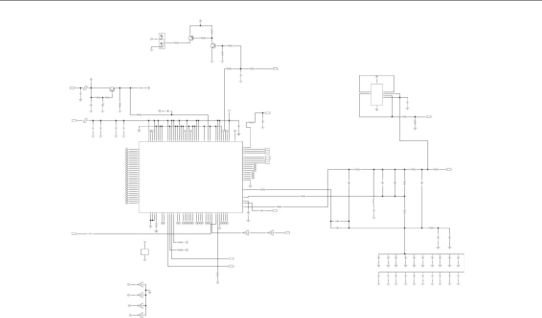
Exciter Schematics (UHF) 7-5
NC
R4502
R4503
R4504
2
3
1
D4500
R4500
21
R4501
23
1
Q4501
23
1
Q4500
R4505
C4500
R4506
150K
DNP
150K
100
27K
DNP
51
DNP
1000PF
DNP
QT1222
DNP
DNP
DNP
10K
MMBT3904
DNP
MMBT3906
DNP
2.775V_EX
EX_SLV_LD
0
OUT
BOTTOM-SIDE EVALTOP-SIDE EVAL
C4504
R4509
23
1
Q4503
R4508
R4507
21
C4503
E4500
C4502
C4501
C4508
C4509
R4510
C4505
C4507
C4506
E4501
TX_SYNTH_12VDC
10K
150PF
MMBT3904
.1UF
+2.775V
.1UF
150PF
DNP
0
VCC_CP
267
.01UF
150PF
.01UF
.1UF
DNP
330UF
10
IN
IN
NC
NC
NC
NC
NC
NC
NC
R4511 C4511
C4510
.1UF
0
TRI_SPI_DR
10PF
DNP
TRI_VCC
OUT
DMCS
EXD
TRI_SPI_DW
EXCLK
EXFS
TRI_SPI_CLK
TRI_SPI_CEX
OUT
OUT
IN
IN
IN
IN
IN
NC
NC
NC
NC
NC
NC
NC
NC
R4516
150
NC
NC
NC
NC
NC
NC
NC
NC
NC
NC
NC
NC
NC
NC
NC
NC
NC
NC
NC
NC
NC
NC
NC
NC
NC
NC
NC
NC
NC
L7
L8
J11
A10
F5
D2
D1
C2
C1
B6
A5
K7
G11
L6
K8
F8
J7
A3
A4
B5
J10
E2
E1
B1
B2
K6
D3
A6
C3
NC
NC
NC
NC 12 13
U4501
10 11
U4501
89
U4501
65
U4501
MC74LVX14
MC74LVX14
MC74LVX14
MC74LVX14
NC
NC
VCC
GND
14
7
U4501
R4514
R4513
MC74LVX14
10K
DNP
DNP
10K
TRI_VCC
C4512
.022UF
REF_16.8_MHZ IN
R4515
0
DNP
VCO_SELECT
SPARE_2
NC
OUT
OUT
NC
NC
NC
NC
NC
NC
NC
NC
NC
NC
NC
NC
NC
NC
NC
NC
NC
NC
NC
NC
NC
R4512
10K
H10
H11
F4
F6
K9
K4
J5
L4
H5
B10
C10
L5
K5
F3
E3
L11
L1
A11
A1
C5
E6
D5
E5
J8
H8
G10
L10
K10
K11
A7
B7
D6
C6
MURATA COG 1206 (BOTTOM SIDE)
0.1UF X 20
43
U4501
21
U4501
TRI_RSTB
MC74LVX14MC74LVX14
IN
R4518
C4514
C4513
0
150PF 150PF
PRE_SCALER
IN
R4517
0
H7
G7
H6
G6
E7
C4
B4
E11
E10
J4
C8
C9
A9
B9
B11
C7
A2
D4
B3
E4
J6
F1
F2
G4
G5
G8
G9
H3
H4
J1
L2
J3
K3
H9
J9
A8
B8
F9
F11
F10
D10
D9
C11
E8
D11
E9
D7
G3
G2
H1
G1
L9
K2
K1
H2
J2
L3
F7
D8
NC3
ESC_CPBIAS
ESC_CP
SF_BYP
REF_OSC_OUT
TXQ
NTXI
PHCLK
DEEPSLEEP
NC4
LVCC1
SDM_CLK_GEN_GND
RX_AGND2
SSI_GND
MAIN_GND
LGND1
VMULTI2
VMULTI1
SUB2
DMCS
TXFS
TXCLK
TXD
ESC_IN
MN_CP
SF_OUT
CLK_OUT
CLK_EMIT
M_PRSC
RXD
ESC_TEST
BP_Q
BP_QX
BP_I
QCAP
RSTB
SF_SPLY
EF_OUTP
EF_OUTM
INCR_DECR
NC5
REF_VCC
GPO2_TEST2
RX_EN_OUT
TM
SUB3
AGC_DAC
FBQ
SDM_VREFP
SDM_VAG
REF_IN
NTXQ
TXI
HP_MOD_OUT
MN_CP_GND
SUB1
NC6
ASPI_CLK
SPI_CLK
RXQ
RXQX
SCAN_EN
ICAP
ACE2_GPO8
TEST1_LCKDET
CEX
SPI_DW
SPI_DR
RXACQ
RXCLK
RXFS
BP_IX
SCAN_IN
GPO4_TEST4
GPO1_TEST1
RX_AVCC2
ASPI_VCC
SDM_CLK_GEN_VCC
RX_AVCC1
SF_GND
SDM_REF_VCC
SSI_VCC
TCLK
CLK_CP
CLK_BASE
MN_ADAPT_CP
M_PRSCX
SENS
AUX_DAC
ESC_CP_GND
MN_CP_VCC
MAIN_VCC
ESC_CP_VCC
TX_VCC
CLK_VCC
ESC_VCC
TX_DAC_VCC
SDM_REF_GND
RX_AGND1
CLK_GND
NC1
DC_CAL_GPO5
RFSTEPA_GPO6
ESC_INX
ACE1_GPO7
SDM_VREFM
NC2
ASPI_GND
TX_GND
ESC_GND
TX_DAC_GND
ESCD2_OUT
ESCD2_OUTX
GPO3_TEST3
ASPI_DATA
RXIX
RXI
AGC_FLAG
AGC_REF
FBI
TEST2
U4500
15H28
EXCITER_TRIDENT_BLOCK
TRIDENT BGA 121PIN
IN2POS
IN2NEG
VCC_NEG
IN1NEG
IN1POS
VCC_POS
OUT1
OUT2
5
6
3
2
U4502
TS272
TX_SYNTH_12VDC
84
7
1
C4570
R4525
R4524
8.25K
EX_SLV_MON
33.2K
220PF
OUT
NON-PIEZO
ATC_1210
6800PF NP0
21
C4516
C4515
DNP
.1UF
6800PF
ATC_200B
NON-PIEZO
C4519
R4519
549
.01UF ATC_200B
NON-PIEZO
COILCRAFT 0805CS
ATC_200B
NON-PIEZO
C4546
C4521
C4520
R4522
R4521
R4520
21
L4500
21
C4517
R4523
0
LF_OUT
51.1
487
0.033UF .033UF
.068UF
100NH
121
DNP
3300PF
OUT
AVX FILM CAPS
2 UF
R4526
C4523
C4522
DNP
1UF
DNP
1UF
0
DNP
0.1UF X 20
MURATA COG 1206
C4543 C4544 C4545C4542C4541C4538 C4539 C4540
C4537
C4536
C4533 C4534 C4535C4532C4531C4526 C4530C4529C4528
C4527
.1UF
.1UF .1UF .1UF
.1UF .1UF .1UF .1UF .1UF
.1UF .1UF
.1UF
.1UF .1UF.1UF
.1UF
.1UF
.1UF
.1UF.1UF
NOTE 1 : Metering Schematic Diagram (Kit No. CTE4003)
NOTE 2 : CPLD Schematic Diagram (Kit No. CTE4003)
NOTE 3 : Interconnect Schematic Diagram (Kit No. CTE4003)
NOTE 4 : Buffer Amplifier Schematic Diagram (Kit No. CTE4003)
NOTE 5 : UHF VCO Schematic Diagram (Kit No. CTE4003)
NOTE 6 : 16.8MHz Ref Buffer Schematic Diagram (Kit No. CTE4003)
NOTE 1
NOTE 6
NOTE 2
NOTE 1
NOTE 5
NOTE 2
NOTE 3
NOTE 4
NOTE 2
NOTE 5
Exciter – Trident Block Schematic Diagram (Kit No. CTE4003)
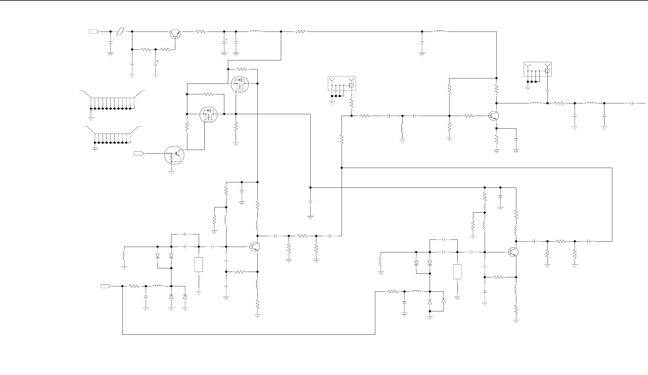
7-6 Exciter Schematics (UHF)
OUT IN
C4632
21
Y4600
L4601
R4600
R4608
C4608
R4606
R4607
R4603
C4607
L4604
13
2Q4600
C4606
R4604
L4603
R4605
C4603
L4602
R4602
R4601
C4604
C4605
C4601
C4602
21
CR4602
21
CR4600
21
CR4603
21
CR4601
L4600
C4600
29.4
182
182
32.4
419MHZ
8.2PF
301
100PF
100
390NH
1SV232
1SV232
1SV232
24NH
DNP
1SV232
220PF
220PF
10
1.58K
VCO_SLV
1K
DNP
390NH
NE68519
220PF
390NH
15PF
3PF
390NH
SI8800SPQ0419YE
2.2PF
6.8PF
7.5PF
IN
10
9
8
7
6
5
4
3
2
1
10
9
8
7
6
5
4
3
12
11
2
1
SH4600
SH4601
SHIELD
SHIELD
LOW RANGE VCO ENABLED LOW
HIGH RANGE VCO ENABLED HIGH
10K
47K
R4635
2
3
1
Q4606
MUN5214T1
VCO_SELECT
10K
IN
C4630
E4600
220PF
12V_VCO
IN
NORMALLY OFF
P-CHAN ENHANCEMENT
R4630
C4629
2
1
3
Q4604
R4628
23
1
Q4603
R4632
R4634
R4633
R4631
21
C4628
2
1
3
Q4605
330UF
.01UF
10
EXCITER_VCO
NTR1P02LT1
0DNP
0DNP
0
267
MMBT3904
10K
NTR1P02LT1
C4627
R4629
21
C4626
47UF .01UF
34.8 10V
L4615
390NH
LOWHIGH
R4619
R4618
5
4
3
2
1
P4600
DNP
DNP
0
0
CONN_J
21
R4636
C4619
C4618
L4611
0
27NH
220PF
6.2PF
R4621
R4623
R4622
3.32K
2K
200
R4624
C4620
23
1Q4602
R4625
.1UF
BFQ67W
301
100
C4624
L4613
R4627
L4612
C4623
C4622
4.7PF 4.7PF
220PF
24NH
22NH0
C4631
5
4
3
2
1
P4601
DNP
DNP
220PF
CONN_J
L4614
C4625
390NH
220PF
C4617
R4617
R4615
R4616
C4616
R4612
C4615
L4609
13
2Q4601
R4613
L4608
R4614
C4612
L4607
R4610
R4611
C4613
C4614
220PF
100
100PF
390NH
5.6PF
221
3PF
1.58K
301
390NH
5.6PF
221
26.7
12PF
390NH
NE68519
23.7
1K
OUT IN
21
Y4601
C4610
C4611
21
CR4606
21
CR4604
L4605
21
CR4607
21
CR4605
C4609
R4609
L4606
1SV232
1.8PF
DNP
1SV232
1SV232
390NH
10
220PF
DNP
22NH
1SV232
SI8800SPQ0417.5YE
417.5MHZ
6.2PF
NOTE 1 : Trident Block Schematic Diagram (Kit No. CTE4003)
NOTE 2 : Buffer Amplifier Schematic Diagram (Kit No. CTE4003)
NOTE 1
NOTE 1
Exciter – UHF VCO Schematic Diagram (Kit No. CTE4003)
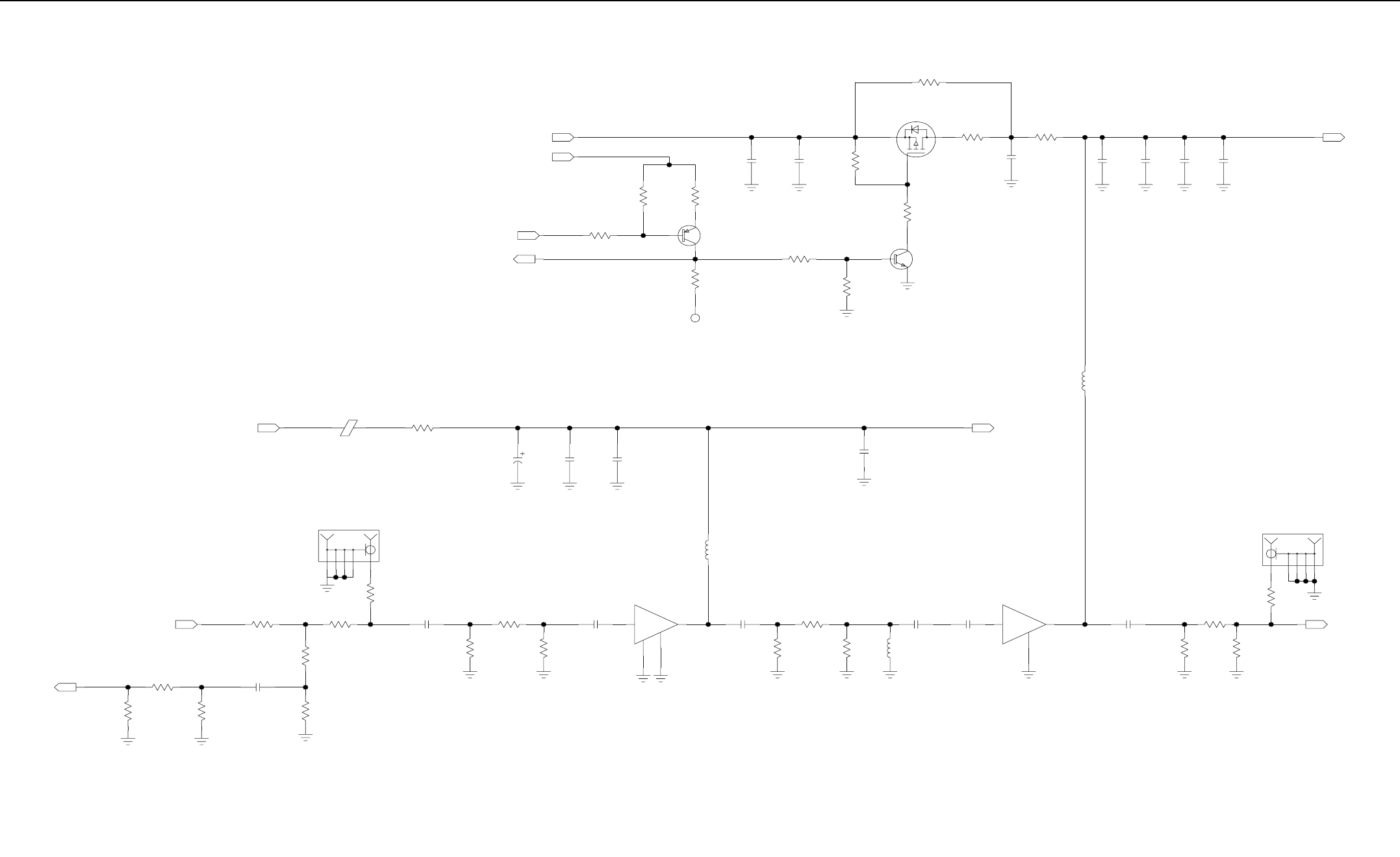
Exciter Schematics (UHF) 7-7
R4706
R4705
R4704
C4700
R4703
R4702
R4700 R4701
150
220PF
0
VCO_FEEDBACK
1.21 1.21
205
DNP
VBA_IN
DNP
0
0
OUT
IN
R4707
5
4
3
2
1
P4700
DNP
0
DNP
CONN_J
G1
OUTIN3
U4701
C4705
R4715 R4717
R4716
R4719
5
4
3
2
1
P4701
HMC479
121
220PF
DNP
VBA_OUT
30.1
121
DNP
CONN_J
0
OUT
C4719
21
C4704
1
2
11PF
220PF
7DB PAD
L4702
R4712 R4714
C4703 R4713
22NH
130
220PF 44.2
130
2 DB PAD
G1
G0
OUT
IN
R4708 R4710
C4701
R4709
C4702
3
1
4
2
U4700
21
L4700
390NH
AG30286
392
220PF
220PF
10
392
5V_EX IN
E4700 R4720
22.1
21
C4706 C4707 C4708
.1UF 220PF
DNP
10UF
FOR VERIFICATION
ADDED TESTPOINTTP4700
TEST_POINT
DNP
1
R4726
3
1K
DNP
R4723
R4724
2
1Q4702
R4725
10K
MMBT3906
18.2K
0
IN
IN
10V_EX
2.775V_EX
EX_ENABLE
ASW
IN
OUT
C4718
DRIVER_AMP
.01UF
OUT
L4701
150NH
R4727
R4728
23
1Q4701
MMBT3904
33.2K
10K
R4729
10K
R4721
2
1
3
Q4700
NTR1P02LT1
10K
21
C4711
C4712
220PF .1UF
DNP
R4730
R4722
C4713
R4731
.1UF
0
0
82
DNP
DNPC4717C4714 C4715 C4716
1000PF
FINAL_AMP
.1UF .01UF
220PF
OUT
EXCITER_VCO_BUFFER
NOTE 1 : Trident Block Schematic Diagram (Kit No. CTE4003)
NOTE 2 : UHF VCO Schematic Diagram (Kit No. CTE4003)
NOTE 3 : Switch Schematic Diagram (Kit No. CTE4003)
NOTE 4 : Metering Schematic Diagram (Kit No. CTE4003)
NOTE 5 : Interconnect Schematic Diagram (Kit No. CTE4003)
NOTE 4
NOTE 3NOTE 2
NOTE 1
NOTE 5
NOTE 3
NOTE 4
Exciter – Buffer Amplifier Schematic Diagram (Kit No. CTE4003)

7-8 Exciter Schematics (UHF)
+5V
RF_INRF_OUT
ASW
4800
TX_SWITCH
ASW
IN
EX_RF_IN
5V_EX
IN
IN
IN
IN
IN
OUT RF_OUT
OUT
Exciter – RF Section Schematic Diagram (Kit No. CTE4003)
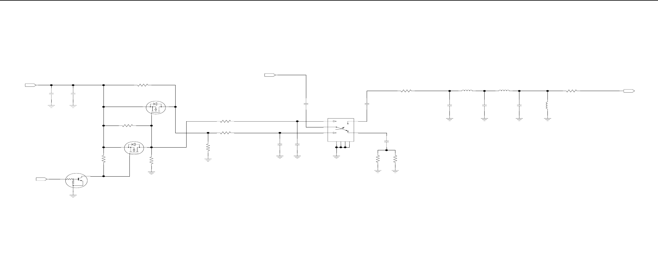
Exciter Schematics (UHF) 7-9
C4800 C4801
.1UF
+5V
220PF
IN
10K
47K
R4802
R4800
R4801
2
3
1
Q4800
2
1
3
Q4801
MUN5214T1
ASW
10K
DNP
0
NTR1P02LT1
10K
IN
R4808
2
1
3
Q4802
DNP
0
NTR1P02LT1
R4810
R4803
R4809
10K
0
0
GND4
GND3
GND1
J1
V2
J2
GND2
V1
J3
21
C4803
21
C4802
21
C4805
21
C4804
2
1
5
8
3
9
7
6
4
U4800
220PF
220PF
AS186302
270PF 270PF
RF_ININ
C4809
L4801 R4805
L4802
C4808
L4800
C4807
47NH
8.2PF 6.2PF
0
3.6PF
18NH
18NH
R4804
0
R4807R4806
C4811
100 100
270PF
RF_OUT
OUT
NOTE 1 : Exciter – Buffer Amplifier Schematic Diagram (Kit No. CTE4003)
NOTE 1
NOTE 1
Exciter – Switch Schematic Diagram (Kit No. CTE4003)
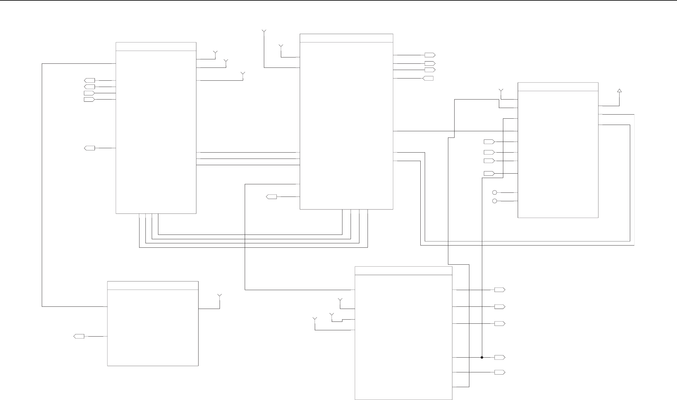
7-10 Exciter Schematics (UHF)
16.8MHZ_OUT
IN
OUT
OUT
REF_16.8_IN3.3V_16.8_BUFFER
16.8MHZ_SYN
IN
EX_REF_BUFFER_4100
3.3V_EX
BANDIT_REF_BUFFER
IN
IN
IN
IN
14.2V
8V
10V
EX_STANDBY
10V_EX_SWTCH
5V_EX
3.3V_EX
2.775V_EX
12V_VCO
8V
10V
14.2V
8V_EX
EX_REGULATORS
OUT
OUT
OUT
OUT
OUT
OUT
10V_EX_SWTCH
5V_EX
3.3V_EX
2.775V_EX
12V_VCO
OUT
OUT
OUT
OUT
OUT
EX_CPLD_CE
EX_CPLD_MISO
EX_CPLD_MOSI
EX_CPLD_CLK
14.2V
8V
16.8MHZ_REF
EX_CPLD_ADD_2
EX_CPLD_ADD_1
EX_CPLD_ADD_0
SSI_DATA
DMCS
TXFS
TXCLK
EX_ENABLE
10V
EX_INTERCONNECT_4200
EX_INTERCONNECT
EX_ENABLE
OUT
OUT
IN
OUT
OUT
EX_DMCS
EXD
IN
EX_FS
EX_CLK
OUT
IN
IN
OUT
OUT
IN
OUT
OUT
OUT
IN
IN
OUT
IN
OUT
OUT
8V
14.2V
10V
OUT
IN
OUT
IN
IN
IN
IN
3.3V_EX
2.775V_EX
OUT
TRIDENT_RST
CPLD_ENABLE
SPI_MISO_OUT_CPLD
SPI_MOSI_IN_CPLD
SPI_CLK_CPLD
EX_STANDBY
TRIDENT_RST
3_3V_CPLD
ADDR0
ADDR1
ADDR2
SPI_CLK_OUT_CPLD
SPI_MOSI_OUT_CPLD
SYNTH_CE
SPI_MISO_IN_CPLD
METERING_CE
2.775V_EX
SPI_MOSI_M
SPI_CLK_M
EX_CPLD_4400
PLA_DIGITIAL_INTERFACE
IN
IN
IN
OUT
OUT
OUT
IN
OUT
OUT
OUT
OUT
SYNTH_SPI_CE
SYNTH_SPI_MISO
SYNTH_SPI_MOSI
SYNTH_SPI_CLK
IN
OUT
OUT
OUT
IN
IN
IN
IN
IN
IN
IN
IN
IN
IN
NC
NC
3.3V_EX
DRIVER_AMP
EX_SYNTH_SL
EX_SYNTH_LD
FINAL_AMP IN
IN
IN
IN
SPI_MISO
EX_RESERVED_5
METERING_CE
DRIVER_AMP
FINAL_AMP
EX_RESERVED_6
3.3V_EX
8V_EX
10V_EX
VCO_LD_M1
VCO_STL_M1
SPI_CLK
SPI_MOSI
SYNTH_SPI_MISO
IN
OUT
IN
EX_METERING_4000
EX_METERING
Exciter – Digital Section Schematic Diagram (Kit No. CTE4003)
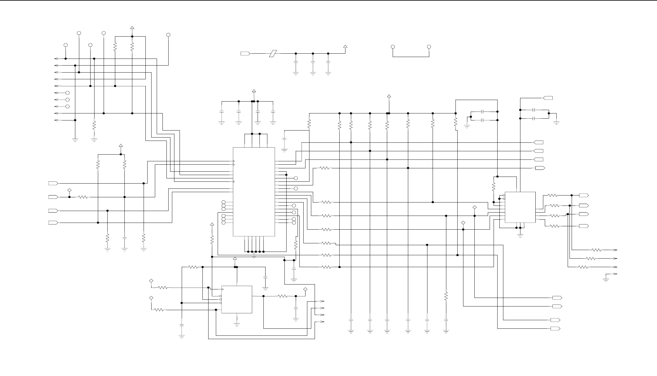
Exciter Schematics (UHF) 7-11
NC
NC
NC
1
P4400
2
P4400
3
P4400
4
P4400
5
P4400
6
P4400
7
P4400
8
P4400
9
P4400
10
P4400
DNP
DNP
DNP
DNP
DNP
DNP
DNP
DNP
DNP
DNP
1
TP4403
TP4401
TP4402
R4406 R4407
3_3V_CPLD_FILT
TEST_POINT
TEST_POINT
1K 1K
TEST_POINT
1
TP4400
1
1
TEST_POINT
1
TP4404
TEST_POINT
3_3V_CPLD IN
PLACE 0.1UF CAP NEAR EACH SUPPLY PIN OF CPLD
3_3V_CPLD_FILT
C4407
C4406C4405
E4400
3_3V_CPLD_FILT
.01UF .1UF 220PF
C4404C4403C4402C4401
.1UF
.1UF.1UF .1UF
EXCITER_CPLD
R4414 R4421R4420
R4419
R4418R4417R4416R4415
4.75K 4.75K
4.75K4.75K4.75K 4.75K
4.75K4.75K
3_3V_CPLD_FILT
21
C4420
21
C4419
.1UF
.01UF
C4422
C4421
.1UF
.01UF
2.775V_EX
IN
ADDR2
ADDR1
ADDR0
METERING_CE
IN
IN
IN
OUT
SYNTH_CE
SPI_CLK_OUT_CPLD
SPI_MOSI_OUT_CPLD
TRIDENT_RST
OUT
OUT
OUT
OUT
R4434
R4433
R4432
R4431
0
0
0
0
10
12
11
13
VCCB
VCCA
GND3
GND2
GND1
B1_2
B1_1
B2_2
B2_1
A2_2
A2_1
A1_2
A1_1
DIR2
DIR1
OE2
OE1
R4430
16
1
14
15
17
9
8
3
2
7
5
6
4
U4402
4.75K
SN74AVC4T245
SPI_MOSI
SPI_CLK
P4402
P4402
P4402
P4402
DNP
DNP
DNP
DNP
2
3
4
1
21
R4437
21
R4436
21
R4435
0
DNP
0DNP
DNP0
SPI_CLK_M
SPI_MOSI_M
SPI_MISO_OUT_CPLD
EX_STANDBY
OUT
OUT
OUT
OUT
1
TP4406
1
TP4405
TEST_POINT TEST_POINT
R4405
R4403
R4401
3_3V_CPLD_FILT
4.75K
1K
4.75K
R4400
0
SPI_MISO
SPI_CLK_CPLD
SPI_MOSI_IN_CPLD
CPLD_ENABLE
SPI_MISO_IN_CPLD
IN
IN
IN
IN
R4413
R4410
R4404
R4408
C4408
R4409
C4400
R4402
3_3V_CPLD_FILT
10K
49.9
SPI_MOSI
10PF
49.9
10PF
1K DNP4.75K
1K
SPI_CLK
NC
NC
NC
NC
NC
NC
7
32
1
26
40
38
31
28
27
25
35
34
33
39
37
29
9
41
17
C4418
DNP
10PF
R4422
33.2
NC
NC
NC
NC
NC
NC
C4410
10PF
DNP
R4423
R4424
R4425
R4426
R4427
R4428
33.2
49.9
33.2
33.2
49.9
33.2
R4412
33.2
30
24
11
4
36
16
23
22
21
20
19
18
15
14
13
12
10
8
6
5
44
43
42
3
2
VCCINT1
VCCINT0
IO_A0
IO_A1
IO_A2
IO_A3
IO_A6
IO_A5
IO_A4
IO_A8
IO_A7
IO_A11
IO_A10
IO_A9
IO_B0
IO_A12
IO_B1
IO_B2
IO_B3
IO_B5
IO_B4
GNDINT1
GNDIO3
GNDINT0
VCCIO1
VCCIO0
GCLK1
TCK
TMS
TDI
OE1
GCLRN
IO_B7
IO_B6
IO_B8
IO_B10
IO_B9
IO_B12
IO_B11
GNDIO1
GNDIO2
GNDIO0
TDO
OE2_GCLK2
U4400
EPM3032ATI44
GND
WP
VCC
HOLD
SI
SO
EN_CS
CLK_S
C4409
U4401
AT25640A
0.1UF
3
8
2
5
7
4
1
6
C4411
R4411
33.2
10PF
DNP
SPI_MISO
3_3V_CPLD_FILT
P4401
P4401
P4401
P4401
DNP
DNP
DNP
DNP
1
2
3
4
PLACE SERIES RC ON FINAL DAISY-CHAINED SPI DEVICE
C4417C4416C4415C4414C4413C4412
DNP
10PF
DNPDNP
10PF 10PF
DNP
10PF
DNP
10PF 10PF
DNP
R4429
0
DNP
NOTE 1 : Interconnect Schematic Diagram (Kit No. CTE4003)
NOTE 2 : Trident Block Schematic Diagram (Kit No. CTE4003)
NOTE 3 : Metering Schematic Diagram (Kit No. CTE4003)
NOTE 4 : Regulators Schematic Diagram (Kit No. CTE4003)
NOTE 1
NOTE 2
NOTE 3
NOTE 1
NOTE 1
NOTE 1
NOTE 1
NOTE 1
NOTE 3
NOTE 2
NOTE 2
NOTE 2
NOTE 2
NOTE 3
NOTE 3
NOTE 1
NOTE 4
Exciter – CPLD Schematic Diagram (Kit No. CTE4003)
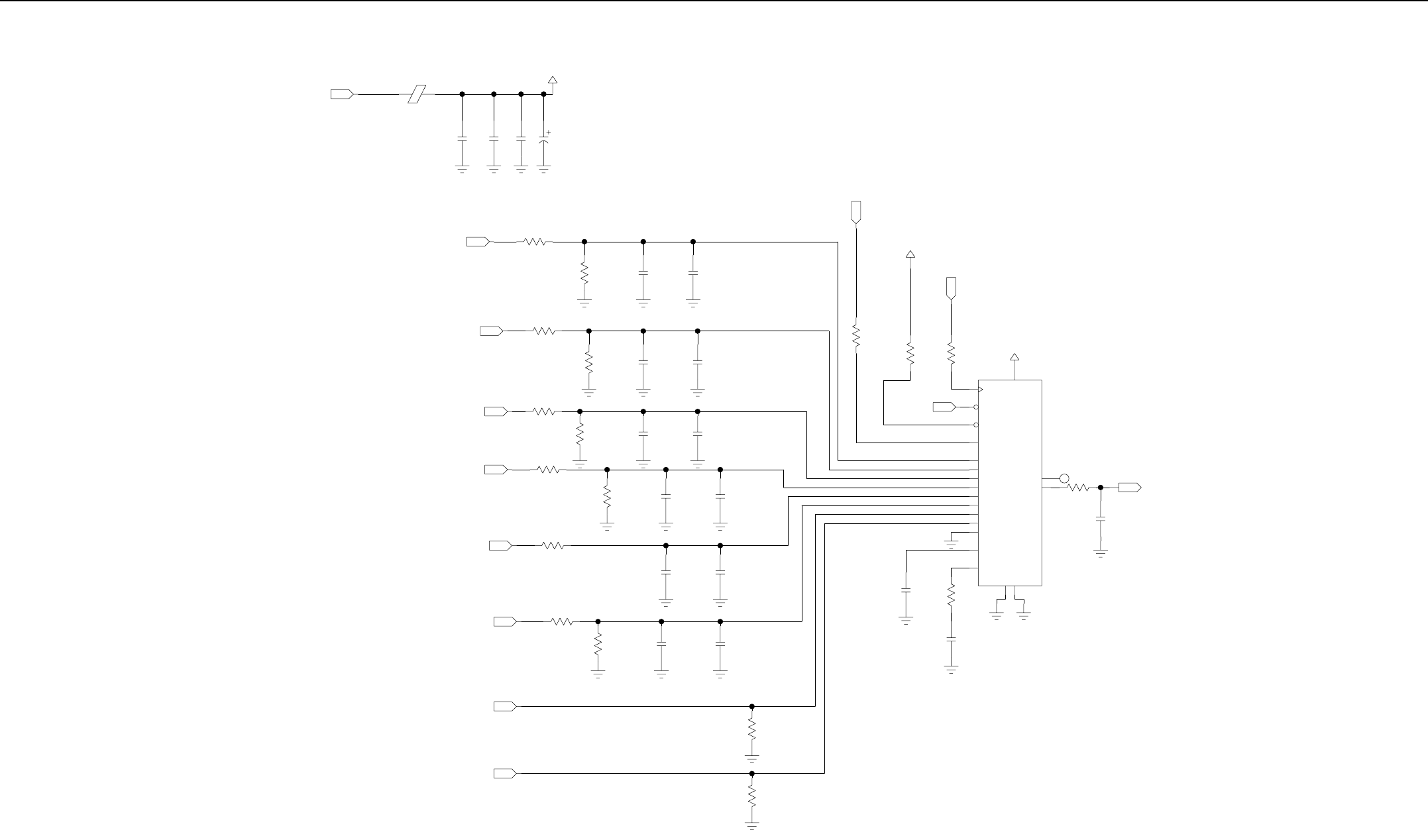
7-12 Exciter Schematics (UHF)
21
C4018
E4000
C4002
C4001
C4000
.01UF .1UF DNP
EXCITER_METERING
220PF
3_3_V_DIG_EX_METER
10UF
3.3V_EX IN
EX_RESERVED_6
EX_RESERVED_5
FINAL_AMP
DRIVER_AMP
VCO_LD_M1
VCO_STL_M1
IN
IN
IN
IN
IN
IN
R4011
R4010
R4005
R4004
R4003
R4001
C4014
C4013
R4008
R4006
R4002
R4000
C4004
C4003
C4006
C4005
C4008
C4007
C4010
C4012
C4009
C4011
R4007
3.6K
8V_EX
220PF
10K
10K .1UF
10K
10K
10K
10K
.1UF 220PF
2.67K .1UF 220PF
33.2K
10V_EX
220PF
0
.1UF
.1UF 220PF
.1UF
220PF
IN
IN
10K
R4012
R4013
10K
10K
R4018
14
13
C4016
C4015
5.62
.015UF
4.7UF
METERING_CE
IN
R4016
R4015
R4014
3_3_V_DIG_EX_METER
0
SPI_MOSI
DNP
0
33.2
SPI_CLK
3_3_V_DIG_EX_METER
IN
IN
11
10
19
12
17
18
9
8
7
6
5
4
3
2
1
NC
C4017
R4017
20
16
15 SPI_MISO
10PF
0
DNP
OUT
CH6
DIN
DOUT
SSTRB
DGND
AGND
VDD
CH7
CH5
CH4
CH3
CH2
CH1
CH0
SCLK
VREF
REFADJ
COM
SHDN
U4000
MAX149
CS
NOTE 1 : Trident Block Schematic Diagram (Kit No. CTE4003)
NOTE 2 : Buffer Amplifier Schematic Diagram (Kit No. CTE4003)
NOTE 3 : CPLD Schematic Diagram (Kit No. CTE4003)
NOTE 2
NOTE 1
NOTE 1
NOTE 2
NOTE 3
NOTE 3
NOTE 3
NOTE 3
Exciter – Metering Schematic Diagram (Kit No. CTE4003)
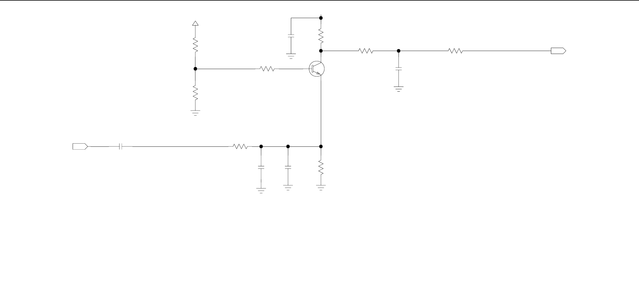
Exciter Schematics (UHF) 7-13
C4103
REF_16.8_IN
.1UF
IN
R4103
2.67K
21
R4102
3
.
3V
_
BUF
2.67K
0.8V
C4107
21
R4101
21
C4104
R4100
180PF 150
15PF
0
1.3V
C4105
R4104
475
.1UF
0.9V
R4106
21
R4105
23
1Q4100
MMBT3904
249
475 R4107
C4106
0
33PF
16.8MHZ_SYN
OUT
NOTE 1 : Trident Block Schematic Diagram (Kit No. CTE4003)
NOTE 2 : Interconnect Schematic Diagram (Kit No. CTE4003)
NOTE 1
NOTE 2
Exciter – 16.8MHz Ref Buffer Schematic Diagram (Kit No. CTE4003)
7-14 Exciter Schematics (UHF)
ACTIVE LOW
8V
EX_CPLD_CE
EX_CPLD_ADD_0
EX_CPLD_CLK
TXFS
EX_ENABLE
SSI_DATA
OUT
OUT
OUT
OUT
IN
IN
OUT
R4203
R4202
R4200 R4201
0
49.9
0
0
C4201 C4200
DNP10PF
10PF
C4205C4203 C4204
C4206
DNP
DNP
DNP
220PF
DNP
220PF 220PF
220PF P4200
P4200
P4200
P4200
P4200
P4200
P4200
P4200
P4200
P4200
P4200
P4200
P4200
P4200
P4200
NC
NC
29
27
25
23
21
19
17
NC
NC 15
13
11
9
7
5
3
1
EXCITER_INTERCONNECT
P4200
P4200
P4200
P4200
P4200
P4200
P4200
P4200
P4200
P4200
P4200
P4200
P4200
P4200
P4200
R4205
R4204
6
4
2
0
0
30
28
26
24
22
20
18
16
14
12
10
8
NC
NC
NC
C4202
DNP
10PF
C4209 C4210 C4211 C4212
220PF
DNP220PF
DNP
220PF
DNPDNP
220PF
C4207 C4208
DNP
DNP
220PF
220PF
EX_CPLD_MOSI
EX_CPLD_MISO
EX_CPLD_ADD_1
10V
14.2V
EX_CPLD_ADD_2
OUT
OUT
OUT
IN
IN
IN
R4207
R4206
49.9
16.8MHZ_REF
0
DMCS
TXCLK
OUT
IN
OUT
NOTE 1 : Trident Block Schematic Diagram (Kit No. CTE4003)
NOTE 2 : Buffer Amplifier Schematic Diagram (Kit No. CTE4003)
NOTE 3 : CPLD Schematic Diagram (Kit No. CTE4003)
NOTE 4 : 16.8MHz Ref Buffer Schematic Diagram (Kit No. CTE4003)
NOTE 1
NOTE 1
NOTE 2
NOTE 3
NOTE 3
NOTE 3
NOTE 4
NOTE 1
NOTE 1
NOTE 3
NOTE 3
NOTE 3
NOTE 3
Exciter – Interconnect Schematic Diagram (Kit No. CTE4003)
Exciter Schematics (UHF) 7-15
R4319
C4316
C4315
21
C4314
10UF .1UF
0
12V_VCO
220PF
OUT
VOUT1
VOUT2
VOUT4
VOUT3
VIN
NC1
NC2
GND_ADJ
NC
NC 4
8
5
1
U4303
MC33269
R4318
R4317 R4316
C4313
7
6
3
2
DNP
270
1UF 2.32K
0
R4331
R4308
R4315
C4312
R4307
R4306
280
.1UF
10K
0
825
10
OUTIN
ADJUST
R4330
R4301
2
3
1
U4300
C4304
2
1
3
Q4302
R4305
NTR1P02LT1
1UF
EXCITER_REGULATORS
10K
10K
LM317M
0
10K
47K
2
3
1
Q4301
21
R4304
21
21
R4302
21
C4301
.01UF
4.75K
MUN5214T1
220PF
0
R4303
C4302
0
21
21
C4300
47UF
DNP
10K
47K
3
Q4300
MUN5214T1
2
1
EX_STANDBY IN
R4300
E4300 0
10V IN
R4309
R4310
C4307
C4306
21
C4305
10UF .1UF 220PF
DNP
68.1
0
10V_EX_SWTCH
5V_EX
OUT
OUT
10K
47K
R4312
2
3
1
Q4303
R4313
C4310
C4309
220PF.01UF
MUN5214T1
0
10K
C4311
R4314
2
1
3
Q4304
.1UF
10K
NTR1P02LT1
21
C4308
R4311
E4301
DNP
47UF
0
14.2V IN
R4321
21
R4324
R4323
430
0
0
OUT
IN
ADJUST
R4322
23
1
U4301
LM317M
270
21
C4322
10UF
R4325
C4324
C4323
3.3V_EX
0
.1UF 220PF
OUT
R4320
C4319
C4318
21
C4317
E4302
DNP
47UF .01UF 220PF
0
8V IN
C4321
.1UF
OUT
IN
ADJUST
R4328
R4327 R4326
2
U4302
280
332
LM317M
0
3
1
21
C4325
10UF
R4329
C4327
C4326
220PF
0
2.775V_EX
.1UF
OUT
8V_EX
OUT
NOTE 1 : CPLD Schematic Diagram (Kit No. CTE4003)
NOTE 1
Exciter – Regulators Schematic Diagram (Kit No. CTE4003)
7-16 Exciter Schematics (UHF)
EX_RF_IN
ASW
5V_EX
RF_OUT
5V_EX
EXCITER_RF_4800
IN
EXCITER_RF
G4
G3
G2
G1
C
P4800
OUT
CONN_J
2.775V_EX
IN
IN
IN
OUTIN
INOUT
12V_VCO
5V_EX10V_EX
10V_EX
12V_VCO
5V_EX
EX_ENABLE_IN
2.775V_EX
EX_SPI_SYNTH_MOSI
EX_SPI_SYNTH_CLK
EX_SPI_SYNTH_CE
EX_SPI_SYNTH_MISO
TRIDENT_RST
REF_16.8MHZ_SYNTH
EX_SLV_LD_SYNTH
EX_SLV_MON_SYNTH
EX_FS
EX_CLK
EXD
EX_DMCS
VCO_BUF_OUT
ASW
EX_PLL_4500-4799
EX_PLL
FINAL_AMP
DRIVER_AMP
OUT
OUT
IN
OUT
OUT
OUT
OUT
IN
OUT
OUT
IN
OUT
OUT
IN
IN
IN
IN
IN
OUT
IN
OUT
IN
IN
OUT
IN
OUT
IN
OUT
DRIVER_AMP
FINAL_AMP
2.775V_EX
SYNTH_SPI_MISO
SYNTH_SPI_MOSI
16.8MHZ_OUT
SYNTH_SPI_CE
SYNTH_SPI_CLK
TRIDENT_RST
EX_SYNTH_LD
EX_SYNTH_SL
EX_FS
EX_CLK
EXD
EX_DMCS
3.3V_EX
12V_VCO
10V_EX_SWTCH
5V_EX
EX_ENABLE
EXCITER_DIGITAL_4000-4499
EXCITER_DIGITAL
OUT
OUT
OUT
OUT
OUT
IN
IN
12V_VCO
3.3V_EX
2.775V_EX
10V_EX
5V_EX
Exciter – Main Schematic Diagram (Kit No. CTE4004)
Exciter Schematics (UHF) 7-17
NC
NC
NC
IN
IN
3.3V_RX
RX_RESERVED_6
RX_RESERVED_5
RX_RESERVED_4
3_3_V_RX_METER
CE2_MT1
RX_METERING_2800
RX_METERING
SPI_MISO
SPI_MOSI
SPI_CLK
INJ_FINAL_M1
AB_2LO_M1
VCO_STL_M1
VCO_LD_M1
AB_CLK_M1
IN
IN
IN
IN
in
IN
IN
OUT
ABACUS_2LO_M1_IN
SPI_MISO_SYNTH
ABACUS_CLK_M1_IN
INJ_FINAL_M1_IN
VCO_STL_M1_IN
SPI_MOSI_SYNTH
SPI_CLK_SYNTH
VCO_LD_M1_IN
IN
IN
IN
IN
IN
IN
OUT
OUT
OUT
out
out
out
OUT
OUT
OUT
in
out
SYNTH_CE_CPLD
TRI_RST_OUT
OUT
OUT
2.775V_RX
RX_STANDBY3_3V_CPLD
SPI_MISO_OUT_CPLD
SPI_MOSI_IN_CPLD
CPLD_ENABLE
ADDR1
ADDR2
ADDR0
SPI_CLK_CPLD
SYNTH_CE
TRIDENT_RST
SPI_MISO_IN_CPLD
SPI_CLK_OUT_CPLD
SPI_MOSI_OUT_CPLD
SPI_CLK_M
SPI_MOSI_M
METERING1_CE
RX_CPLD_3300
RX_CPLD
2.775V_RX
3.3V_RX
IN
IN
IN
IN
IN
IN
OUT
IN
IN
12V_RX_SW
10V_RX_SW
3.3V_RX
2.775V_RX
5.0V_RX_SW
OUT
OUT
OUT
OUT
OUT
IN
OUT
OUT
OUT
OUT
OUT
14.2V_RX
10.0V_RX
8.0V_RX
RX_STANDBY
10V_RX_SW
5.0V_RX_SW
3.3V_RX
2.775V_RX
12V_RX_SW
RX_REGULATORS_2200
RX_REGULATORS
IN
IN
IN
8V
14.2V
10V
IN
IN
IN
3.3V_RX
RX_REF_BUFFER_2600
BANDIT_REF_BUFFER_RX
REF_16.8_IN
3.3V_16.8_BUFFER
16.8MHZ_ABACUS
16.8MHZ_SYN
OUT
OUT
16.8MHZ_SYN
16.8MHZ_ABA_REF_OUT
OUT
OUT
IN
IN
ABA_FS_IN
ABA_PC_OUT
ABA_PD_OUT
ABA_PE_OUT
ABA_SYNCB_OUT
ABA_DOUTB/MISO_IN
ABA_DATA_IN
ABA_ODC_IN
IN
IN
IN
OUT
OUT
OUT
OUT
IN
OUT
IN
IN
OUT
IN
OUT
OUT
OUT
OUT
OUT
IN
IN
ABA_DOUTB/MISO
ABA_PE
ABA_FS
ABA_DATA
ABA_SYNCB
ABA_PD
ABA_PC
RX_CPLD_CE
ABA_ODC
RX_CPLD_CLK
RX_CPLD_MOSI
RX_CPLD_MISO
RX_INTERCONNECT_2000
RX_INTERCONNECT
10V_RX
RX_ATTEN
14.2V
8.0V
RX_CPLD_ADD_0
RX_CPLD_ADD_1
RX_CPLD_ADD_2
16.8_MHZ IN
IN
IN
IN
IN
OUT
IN
IN
14.2V_RX
10.0V_RX
8.0V_RX
RX_IF_ATTEN_OUT
OUT
Exciter – Frequency Generation Unit (FGU) Schematic Diagram (Kit No. CTE4004)
7-18 Exciter Schematics (UHF)
NC
NC
NC
NC 12 13
U4501
10 11
U4501
89
U4501
65
U4501
MC74LVX14
MC74LVX14
MC74LVX14
MC74LVX14
VCC
GND
147
U4501
TRI_VCC
MC74LVX14
C4512
REF_16.8_MHZ
.022UF
IN
NC
NC
NC
NC
NC
NC
NC
NC
NC
NC
NC
NC
NC
NC
NC
NC
NC
NC
NC
NC
NC
NC
R4515
SPARE_2
VCO_SELECT
DNP
0
OUT
OUT
NC
NC
R4514
R4513
10K
DNP
DNP
10K
R4512
H10
H11
F4
F6
K9
K4
J5
L4
H5
B10
C10
L5
K5
F3
E3
L11
L1
A11
A1
C5
E6
D5
E5
J8
H8
G10
L10
K10
K11
A7
B7
D6
C6
10K
NC
NC
NC
NC
NC
NC
NC
NC
NC
NC
NC
NC
NC
NC
NC
NC
NC
NC
NC
NC
NC
NC
NC
NC
NC
NC
NC
NC
NC
L7
L8
J11
A10
F5
D2
D1
C2
C1
B6
A5
K7
G11
L6
K8
F8
J7
A3
A4
B5
J10
E2
E1
B1
B2
K6
D3
A6
C3
NC3
ESC_CPBIAS
ESC_CP
SF_BYP
REF_OSC_OUT
TXQ
NTXI
PHCLK
DEEPSLEEP
NC4
LVCC1
SDM_CLK_GEN_GND
RX_AGND2
SSI_GND
MAIN_GND
LGND1
VMULTI2
VMULTI1
SUB2
DMCS
TXFS
TXCLK
TXD
ESC_IN
MN_CP
SF_OUT
CLK_OUT
CLK_EMIT
M_PRSC
RXD
ESC_TEST
BP_Q
BP_QX
BP_I
QCAP
RSTB
SF_SPLY
EF_OUTP
EF_OUTM
INCR_DECR
NC5
REF_VCC
GPO2_TEST2
RX_EN_OUT
TM
SUB3
AGC_DAC
FBQ
SDM_VREFP
SDM_VAG
REF_IN
NTXQ
TXI
HP_MOD_OUT
MN_CP_GND
SUB1
NC6
ASPI_CLK
SPI_CLK
RXQ
RXQX
SCAN_EN
ICAP
ACE2_GPO8
TEST1_LCKDET
CEX
SPI_DW
SPI_DR
RXACQ
RXCLK
RXFS
BP_IX
SCAN_IN
GPO4_TEST4
GPO1_TEST1
RX_AVCC2
ASPI_VCC
SDM_CLK_GEN_VCC
RX_AVCC1
SF_GND
SDM_REF_VCC
SSI_VCC
TCLK
CLK_CP
CLK_BASE
MN_ADAPT_CP
M_PRSCX
SENS
AUX_DAC
ESC_CP_GND
MN_CP_VCC
MAIN_VCC
ESC_CP_VCC
TX_VCC
CLK_VCC
ESC_VCC
TX_DAC_VCC
SDM_REF_GND
RX_AGND1
CLK_GND
NC1
DC_CAL_GPO5
RFSTEPA_GPO6
ESC_INX
ACE1_GPO7
SDM_VREFM
NC2
ASPI_GND
TX_GND
ESC_GND
TX_DAC_GND
ESCD2_OUT
ESCD2_OUTX
GPO3_TEST3
ASPI_DATA
RXIX
RXI
AGC_FLAG
AGC_REF
FBI
TEST2
U4500
TRIDENT BGA 121PIN
EXCITER_TRIDENT_BLOCK
5164015H28
15H28
H7
G7
H6
G6
E7
C4
B4
E11
E10
J4
C8
C9
A9
B9
B11
C7
A2
D4
B3
E4
J6
F1
F2
G4
G5
G8
G9
H3
H4
J1
L2
J3
K3
H9
J9
A8
B8
F9
F11
F10
D10
D9
C11
E8
D11
E9
D7
K2
K1
H2
J2
L3
F7
D8
NC
NC
NC
NC
NC
NC
NC
NC
TRI_SPI_CEX
TRI_SPI_CLK
EXFS
EXCLK
TRI_SPI_DW
EXD
DMCS
OUT
OUT
IN
IN
IN
IN
IN
0.1UF X 20
MURATA COG 1206 (BOTTOM SIDE)
43
U4501
21
U4501
MC74LVX14 MC74LVX14
TRI_RSTB
IN
R4518
R4517
R4516
C4514
C4513
G3
G2
H1
G1
L9
0
PRE_SCALER
150PF
150PF
0
150
IN6800PF NP0
ATC_1210
NON-PIEZO
21
C4516
C4515
6800PF
.1UF
DNP
NON-PIEZO
ATC_200B
COILCRAFT 0805CS
C4546
C4519
R4522
21
L4500
21
C4517
R4519
3300PF
DNP
100NH
.01UF
549
0.033UF
140
NON-PIEZO
ATC_200B
NON-PIEZO
ATC_200B
C4521
C4520
R4521
R4520
R4523
523
LF_OUT
.033UF
51.1 0
.068UF
OUT
AVX FILM CAPS
2 UF
R4526
C4523
C4522
DNP
0
1UF
DNP
1UF
DNP
C4533 C4534 C4535C4532C4531C4526 C4530C4529
C4528
C4527
.1UF .1UF .1UF.1UF .1UF
.1UF .1UF .1UF
.1UF
.1UF
MURATA COG 1206
0.1UF X 20
C4543 C4544 C4545C4542C4541C4538 C4539 C4540
C4537
C4536
.1UF .1UF
.1UF
.1UF .1UF
.1UF
.1UF.1UF.1UF.1UF
NC
NC
NC
NC
NC
NC
NC
R4511 C4511
R4510
C4505
C4510
TRI_VCC
DNP
10PF
TRI_SPI_DR
0
0
.1UF
.1UF
OUT
C4508 C4509C4507C4506
DNP
.1UF150PF
DNP
150PF .1UF
TOP-SIDE EVAL BOTTOM-SIDE EVAL
E4501
+2.775V IN
R4509
23
1
Q4503
R4508
R4507
21
C4503
E4500
C4502
C4501
VCC_CP
150PF
TX_SYNTH_12VDC
10
330UF
.01UF
267
MMBT3904
10K
IN
C4504
.01UF
NC
R4502
R4503
R4504
2
3
1
D4500
R4500
21
R4501
23
1
Q4501
2
3
1
Q4500
R4505
C4500
R4506
2.775V_EX
DNP
MMBT3906
DNP
MMBT3904
10K
DNP
DNP
DNP
QT1222
DNP
1000PF
DNP
DNP
51
150K
DNP
27K
100
150K
EX_SLV_LD
0
OUT
IN2POS
IN2NEG
VCC_NEG
IN1NEG
IN1POS
VCC_POS
OUT1
OUT2
8
4
7
1
5
6
3
2
U4502
TX_SYNTH_12VDC
TS272
C4570
R4524
220PF
33.2K
R4525
EX_SLV_MON
8.25K
OUT
Exciter – Trident Block Schematic Diagram (Kit No. CTE4004)
Exciter Schematics (UHF) 7-19
L4613
C4623
C4622
C4624
R4627
L4612
18NH
6.8PF
0
LO_OUT
220PF
6.8PF
22NH
OUT
C4631
5
4
3
2
1
P4601
DNP
220PF
CONN_J
DNP
R4622
C4618
21
R4636
R4624
R4621
R4623
23
1
R4625
C4619
L4611
R4619
R4618
5
4
3
2
1
P4600
0
DNP
200
1.65K
27NH
3.32K
0
3.9PF 220PF
CONN_J
DNP
0301
100
C4630
E4600
R4630
C4629
R4631
21
C4628
10
220PF
12V_VCO
.01UF 330UF
267
IN
10V
SH4600
C4627
R4628
L4615
R4629
23
1
Q4603
21
C4626
EXCITER_VCO
34.8
SHIELD
390NH
.01UF
MMBT3904
0
47UF
P-CHAN ENHANCEMENT
NORMALLY OFF
10K
47K
2
1
3
Q4604
R4632
R4634
R4633
2
1
3
Q4605
R4635
2
3
1
Q4606
10K
DNP
MUN5214T1
NTR1P02LT1
DNP
0
10K
0
NTR1P02LT1
IN
10
9
8
7
6
5
4
3
2
1
SH4601
SHIELD
HIGH RANGE VCO ENABLED HIGH
LOW RANGE VCO ENABLED LOW
VCO_SELECT
OUT IN
R4608
R4607
R4606
R4601
C4607
2
Y4600
C4605
C4608
R4603
L4604
13
2
Q4600
L4602
R4602
C4604
221
221
15
SI8800SPQ0468.5YE
NE68519
468.5MHZ
12PF
15
10PF
390NH
100
390NH
301
100PF
4.7PF
R4604
R4605
1
C4601
C4603
C4602
L4601
R4600
C4606
L4603
21
CR4602
2
1
CR4600
21
CR4603
21
CR4601
L4600
C4600
3.3PF
4.7PF
4.3PF
390NH
390NH
1.21K
220PF
1K
1SV232
1SV232
VCO_SLV
24NH
DNP
DNP
10
220PF 1SV232 1SV232
IN
10
9
8
7
6
5
4
3
12
11
2
1
L4614
C4625
390NH
220PF
LOW
OUT IN
21
Y4601
R4614
R4610
L4606
C4614
C4613
C4612
C4611
C4610
L4607
R4611
21
CR4606
21
CR4604
L4605
21
CR4607
21
CR4605
C4609
R4609
505.5MHZ
33NH
1SV232
SI8800SPQ05055YE
1.21K
2.2PF
15
220PF
DNP
390NH
DNP
10
1SV232
301
1SV232
1SV232
390NH
4.7PF
10PF
8.2PF
3.6PF
HIGH
C4620
Q4602
BFQ67W
.1UF
R4616
R4615
R4613
C4616
R4612
C4615
L4609
13
2Q4601
L4608
15
1K
390NH
191
390NH
100
NE68519
220PF
4.7PF
R4617
C4617
191
100PF
Exciter – UHF VCO Schematic Diagram (Kit No. CTE4004)
7-20 Exciter Schematics (UHF)
VCO_FEEDBACK
OUT
7DB PAD2 DB PAD
G1
OUT
IN
G1
G0
OUTIN
C4719
L4702
R4706
R4705 C4700
R4703
R4702
R4700 R4701
R4707
5
4
3
2
1
P4700
R4708 R4710 R4712 R4714
C4701 R4709 C4702
31
4
2
U4700
C4703
21
L4700
R4713
21
C4704
31
2
U4701
390NH
44.2
130
392
10
CONN_J
0
DNP
0
0
DNP
VBA_IN
205
220PF
220PF
HMC479
1.21
130
220PF
220PF
392
DNP
AG30286
1.21
220PF
150
9.1PF
18NH
IN
R4704
DNP
0
E4700 R4720
22.1
5V_EX IN
21
C4706 C4707 C4708
10UF
DNP220PF
.1UF
C4718
.01UF
DRIVER_AMP
OUT
L4701
150NH
R4723
R4724
18.2K
10K
ASW
EX_ENABLE
10V_EX
IN
OUT
IN
IN
2
3
1
Q4702
R4725
2.775V_EX
0
MMBT3906
C4717
C4714 C4715 C4716
220PF .01UF
.1UF 1000PF
R4727
21
C4711
C4712
R4728
23
1Q4701
R4721
R4729
2
1
3
Q4700
R4730
R4722
C4713
R4731
DNP
DNP
.1UF
220PF
DNP
EXCITER_VCO_BUFFER
10K
82
10K
0
10K
33.2K
0
NTR1P02LT1
.1UF
MMBT3904
ADDED TESTPOINT
FOR VERIFICATION
1
TP4700
R4726
DNP
DNP
TEST_POINT
1K
FINAL_AMP
OUT
R4719
5
4
3
2
1
P4701
0
CONN_J
DNP
DNP
VBA_OUT
OUT
5 DB PAD
C4705
R4715 R4717
R4716
30.1
121 121
220PF
Exciter – Buffer Amplifier Schematic Diagram (Kit No. CTE4004)

Exciter Schematics (UHF) 7-21
+5V
RF_INRF_OUT
ASW
OUT
ASW
IN
EX_RF_INRF_OUT
5V_EX
IN
IN
OUT
IN
IN
IN
4800
TX_SWITCH
Exciter – RF Section Schematic Diagram (Kit No. CTE4004)
7-22 Exciter Schematics (UHF)
C4800 C4801
.1UF
+5V
220PF
IN
10K
47K
R4808
R4802
R4800
R4801
2
3
1
Q4800
2
1
3
Q4801
2
1
3
Q4802
MUN5214T1
ASW
10K
DNP
0
DNP
0
NTR1P02LT1
10K
NTR1P02LT1
IN
GND4
GND3
GND1
J1
V2
J2
GND2
V1
J3
C4809
L4801 R4805
L4802C4808
L4800
C4807
R4804
21
C4805
21
C4804
2
1
5
8
3
9
7
6
4
U4800
6.8PF6.2PF1.5PF
0
27NH
15NH
RF_OUT
AS186302
270PF
0
270PF
18NH
OUT
21
C4803
21
C4802
220PF
220PF
R4810
R4803
R4809
10K
0
0
RF_ININ
R4807
C4811
100
270PF
R4806
100
Exciter – Switch Schematic Diagram (Kit No. CTE4004)
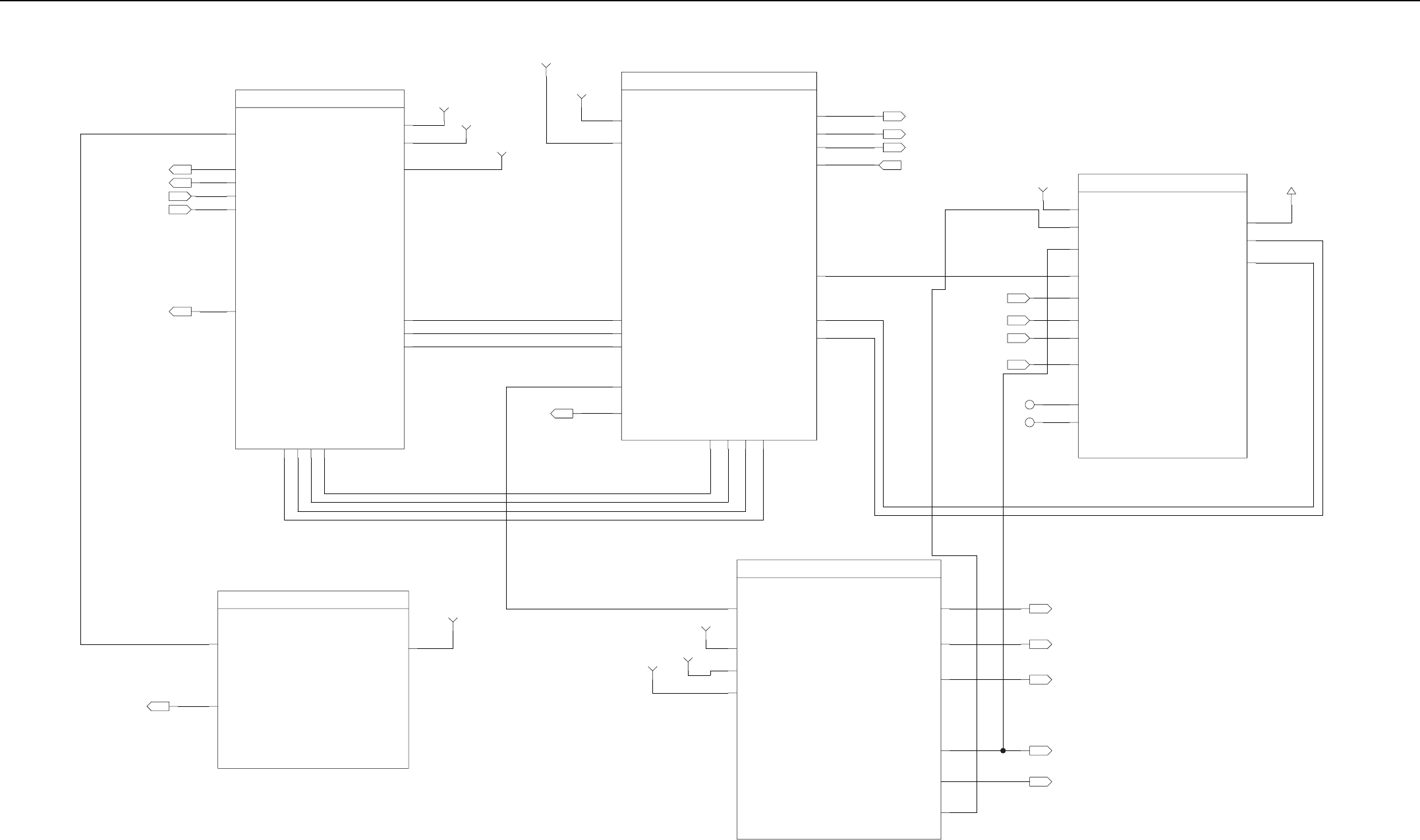
Exciter Schematics (UHF) 7-23
EX_CLK
EX_FS
EXD
EX_DMCS
EX_ENABLE
OUT
IN
IN
OUT
OUT
IN
OUT
OUT
OUT
IN
IN
OUT
OUT
16.8MHZ_OUT OUT
EX_CPLD_CE
EX_CPLD_MISO
EX_CPLD_MOSI
EX_CPLD_CLK
14.2V
16.8MHZ_REF
EX_CPLD_ADD_2
EX_CPLD_ADD_1
EX_CPLD_ADD_0
SSI_DATA
DMCS
TXFS
TXCLK
EX_ENABLE
10V
EX_INTERCONNECT_4200
EX_INTERCONNECT
OUT
OUT
OUT
IN
OUT
OUT
OUT
TRIDENT_RST
IN
IN
IN
OUT
OUT
OUT
8V
2.775V_EX
10V
14.2V
8V
ININ
IN
IN
IN
3.3V_EX
REF_16.8_IN3.3V_16.8_BUFFER
16.8MHZ_SYN
3.3V_EX
EX_REF_BUFFER_4100
IN
BANDIT_REF_BUFFER
10V
8V
14.2V
EX_STANDBY
10V_EX_SWTCH
5V_EX
3.3V_EX
2.775V_EX
12V_VCO
8V
10V
14.2V
8V_EX
OUT
INOUT
OUT
OUT
OUT
IN
IN
IN
OUT
EX_REGULATORS
12V_VCO
2.775V_EX
3.3V_EX
5V_EX
10V_EX_SWTCH
OUT
OUT
OUT
OUT
OUT
CPLD_ENABLE
SPI_MISO_OUT_CPLD
SPI_MOSI_IN_CPLD
SPI_CLK_CPLD
EX_STANDBY
TRIDENT_RST
3_3V_CPLD
ADDR0
ADDR1
ADDR2
SPI_CLK_OUT_CPLD
SPI_MOSI_OUT_CPLD
SYNTH_CE
SPI_MISO_IN_CPLD
METERING_CE
2.775V_EX
SPI_MOSI_M
SPI_CLK_M
EX_CPLD_4400
PLA_DIGITIAL_INTERFACE
OUT
IN
IN
IN
OUT
OUT
OUT
OUT
IN
OUT
OUT
SYNTH_SPI_MISO
SYNTH_SPI_CE
SYNTH_SPI_CLK
SYNTH_SPI_MOSI
IN
OUT
OUT
OUT
NC
NC
3.3V_EX
IN
FINAL_AMP
IN
IN
IN
EX_SYNTH_LD
EX_SYNTH_SL
DRIVER_AMP
IN
IN
IN
IN
IN
IN
IN
IN
IN
IN
SYNTH_SPI_MISO
IN
OUT
IN
EX_METERING
SPI_MISO
EX_RESERVED_5
METERING_CE
DRIVER_AMP
FINAL_AMP
EX_RESERVED_6
3.3V_EX
8V_EX
10V_EX
VCO_LD_M1
VCO_STL_M1
SPI_CLK
SPI_MOSI
EX_METERING_4000
Exciter – Digital Section Schematic Diagram (Kit No. CTE4004)
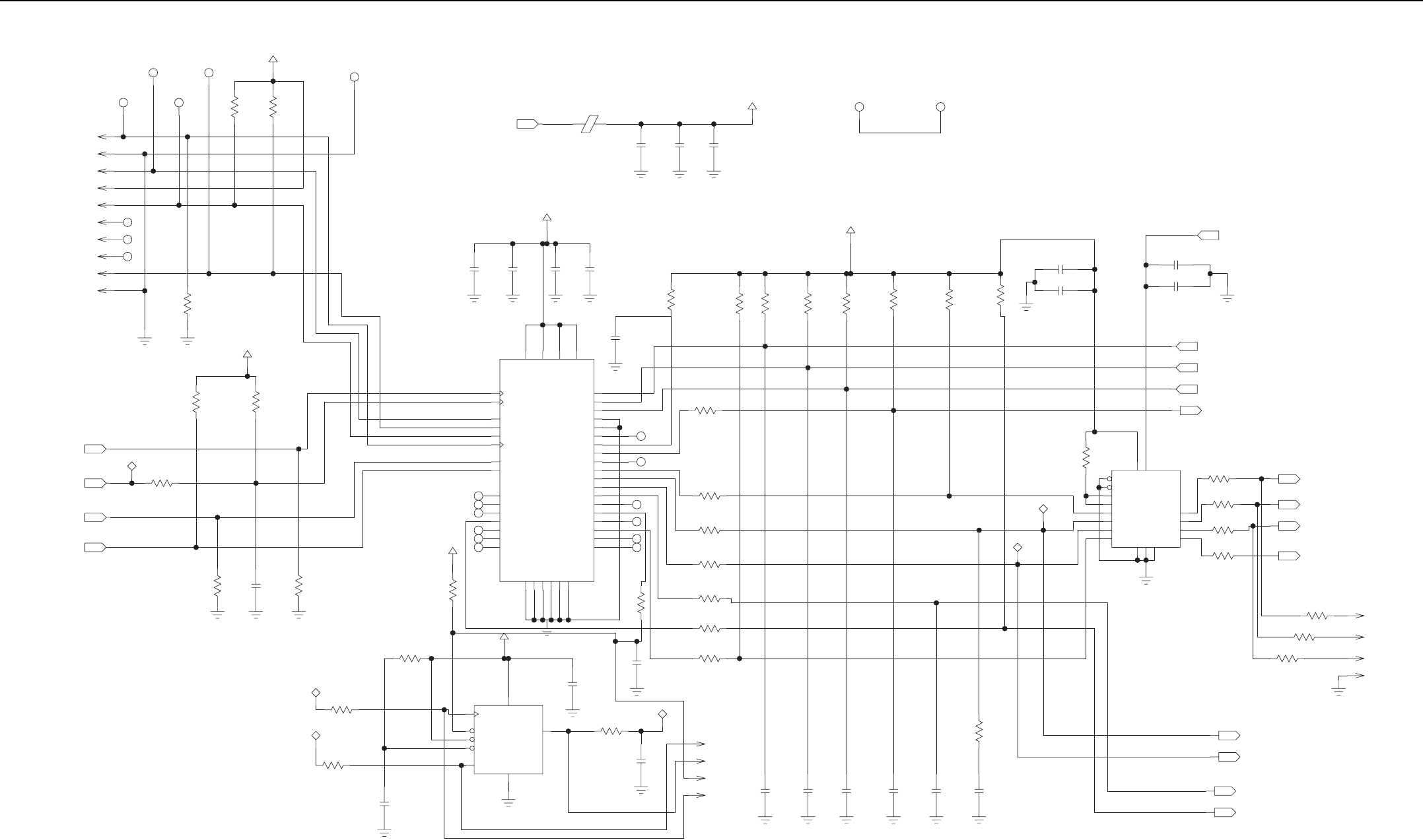
7-24 Exciter Schematics (UHF)
NC
NC
NC
1
P4400
2
P4400
3
P4400
4
P4400
5
P4400
6
P4400
7
P4400
8
P4400
9
P4400
10
P4400
DNP
DNP
DNP
DNP
DNP
DNP
DNP
DNP
DNP
DNP
1
TP4403
1
TP4400
1
TP4401
1
TP4402
R4406 R4407
3_3V_CPLD_FILT
TEST_POINT
TEST_POINT
1K 1K
TEST_POINT
TEST_POINT
1
TP4404
TEST_POINT
PLACE 0.1UF CAP NEAR EACH SUPPLY PIN OF CPLD
C4407
C4406
C4405
E4400
3_3V_CPLD_FILT
3_3V_CPLD_FILT
3_3V_CPLD
.01UF .1UF 220PF
IN
C4418
R4414 R4421
R4420R4419R4418R4417R4416R4415
C4404C4403C4402C4401
4.75K 4.75K
4.75K
.1UF
4.75K
4.75K 4.75K
4.75K
.1UF.1UF
4.75K
DNP
.1UF
10PF
21
C4420
21
C4419
.1UF
.01UF
C4422
C4421
.1UF
.01UF
2.775V_EX
IN
ADDR2
ADDR1
ADDR0
METERING_CE
IN
IN
IN
OUT
SYNTH_CE
SPI_CLK_OUT_CPLD
SPI_MOSI_OUT_CPLD
TRIDENT_RST
OUT
OUT
OUT
OUT
VCCB
VCCA
GND3
GND2
GND1
B1_2
B1_1
B2_2
B2_1
A2_2
A2_1
A1_2
A1_1
DIR2
DIR1
OE2
OE1
R4434
R4433
R4432
R4431
R4430
16
1
14
15
17
9
8
3
2
7
5
6
4
U4402
0
0
4.75K
SPI_MOSI
0
SPI_CLK SN74AVC4T245
0
10
12
11
13
P4402
P4402
P4402
P4402
DNP
DNP
DNP
DNP
2
3
4
1
21
R4437
21
R4436
21
R4435
0
DNP
0DNP
DNP
0
SPI_CLK_M
SPI_MOSI_M
SPI_MISO_OUT_CPLD
EX_STANDBY
OUT
OUT
OUT
OUT
3_3V_CPLD_FILT
1
TP4406
1
TP4405
TEST_POINT TEST_POINT
PLACE SERIES RC ON FINAL DAISY-CHAINED SPI DEVICE
R4429
C4417
C4416C4415C4414C4413C4412
DNP
10PF
0
DNPDNP
10PF 10PF
DNP
10PF
DNP
10PF
DNP
10PF
DNP
P4401
P4401
P4401
P4401
DNP
DNP
DNP
DNP
1
2
3
4
GND
WP
VCC
HOLD
SI
SO
EN_CS
CLK_S
3
8
5
7
1
6
U4401
AT25640A
2
C4410
C4409
C4411
R4411
33.2
10PF
10PF
DNP
DNP
SPI_MISO
0.1UF
3_3V_CPLD_FILT
R4423
R4424
R4425
R4426
R4427
R4428
33.2
49.9
33.2
33.2
49.9
33.2
R4422
33.2
EXCITER_CPLD
29
9
41
17
7
32
1
26
40
38
31
28
27
25
35
34
33
39
37
NC
NC
NC
NC
NC
NC
30
24
11
4
36
16
R4413
R4410
3_3V_CPLD_FILT
10K
4.75K
R4404
C4400
R4402
10PF
1K
DNP
1K
R4408
R4409
49.9
SPI_MOSI
49.9
SPI_CLK
C4408
10PF
R4400
SPI_MOSI_IN_CPLD
CPLD_ENABLE
0
SPI_MISO
SPI_CLK_CPLD
SPI_MISO_IN_CPLD
IN
IN
IN
IN
R4403
R4401
4.75K
4.75K
R4405
3_3V_CPLD_FILT
1K
4
NC
NC
NC
NC
NC
NC
R4412
33.2
23
22
21
20
19
18
15
14
13
12
10
8
6
5
44
43
42
3
2
VCCINT1
VCCINT0
IO_A0
IO_A1
IO_A2
IO_A3
IO_A6
IO_A5
IO_A4
IO_A8
IO_A7
IO_A11
IO_A10
IO_A9
IO_B0
IO_A12
IO_B1
IO_B2
IO_B3
IO_B5
IO_B4
GNDINT1
GNDIO3
GNDINT0
VCCIO1
VCCIO0
GCLK1
TCK
TMS
TDI
OE1
GCLRN
IO_B7
IO_B6
IO_B8
IO_B10
IO_B9
IO_B12
IO_B11
GNDIO1
GNDIO2
GNDIO0
TDO
OE2_GCLK2
U4400
EPM3032ATI44
Exciter – CPLD Schematic Diagram (Kit No. CTE4004)
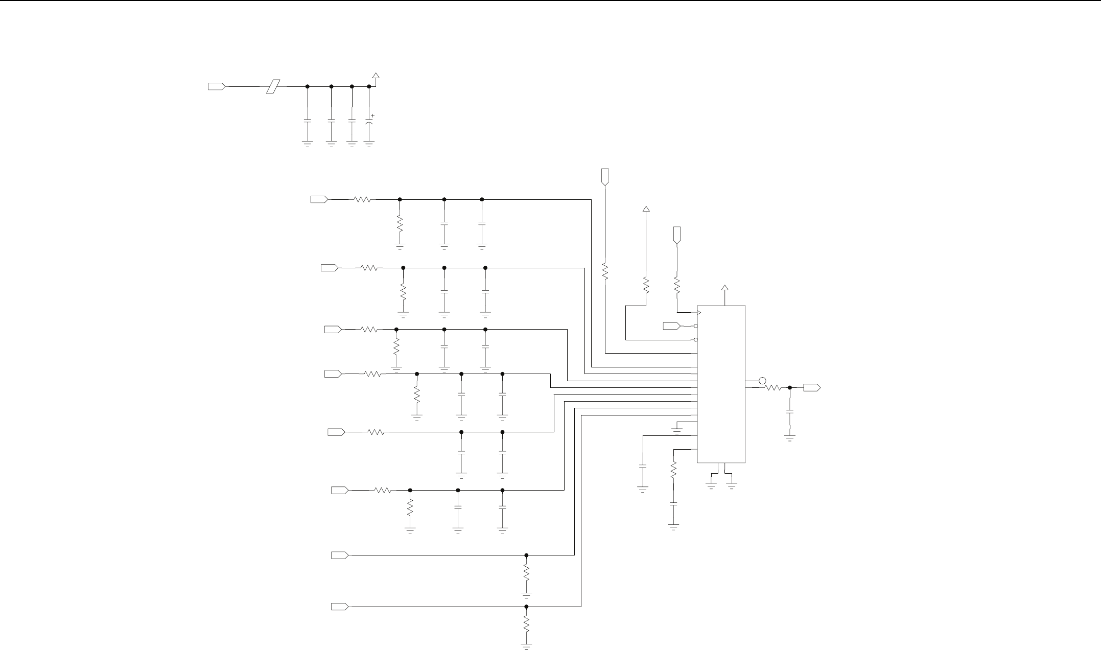
Exciter Schematics (UHF) 7-25
21
C4018
E4000
C4002
C4001
C4000
EXCITER_METERING
DNP
10UF
3_3_V_DIG_EX_METER
3.3V_EX
.01UF .1UF 220PF
IN
R4012
R4013
10K
10K
R4011
R4010
C4014C4013
FINAL_AMP
10K
10K
VCO_STL_M1
.1UF 220PF
EX_RESERVED_5
EX_RESERVED_6
8V_EX
DRIVER_AMP
VCO_LD_M1
10V_EX
R4005
R4004
R4003
R4001
R4008
R4006
R4002
R4000
C4004
C4003
C4006
C4005
C4008
C4007
C4010
C4012
C4009
C4011
R4007
3.6K
10K
220PF
10K
10K .1UF
10K
10K
.1UF 220PF
2.67K .1UF 220PF
33.2K
0
.1UF
.1UF
220PF
220PF
IN
IN
IN
IN
IN
IN
IN
IN
11
10
19
12
17
18
9
8
7
6
5
4
3
2
1
CH6
DIN
DOUT
SSTRB
DGND
AGND
VDD
CH7
CH5
CH4
CH3
CH2
CH1
CH0
SCLK
VREF
REFADJ
COM
CS
SHDN
U4000
MAX149
R4016
R4015
R4014
20
0
SPI_MOSI
DNP
0
33.2
SPI_CLK
3_3_V_DIG_EX_METER
METERING_CE
3_3_V_DIG_EX_METER
IN
IN
IN
NC
C4017
R4017
16
15
10PF
0
DNP
SPI_MISO
OUT
R4018
14
13
C4016
C4015
.015UF 5.62
4.7UF
Exciter – Metering Schematic Diagram (Kit No. CTE4004)
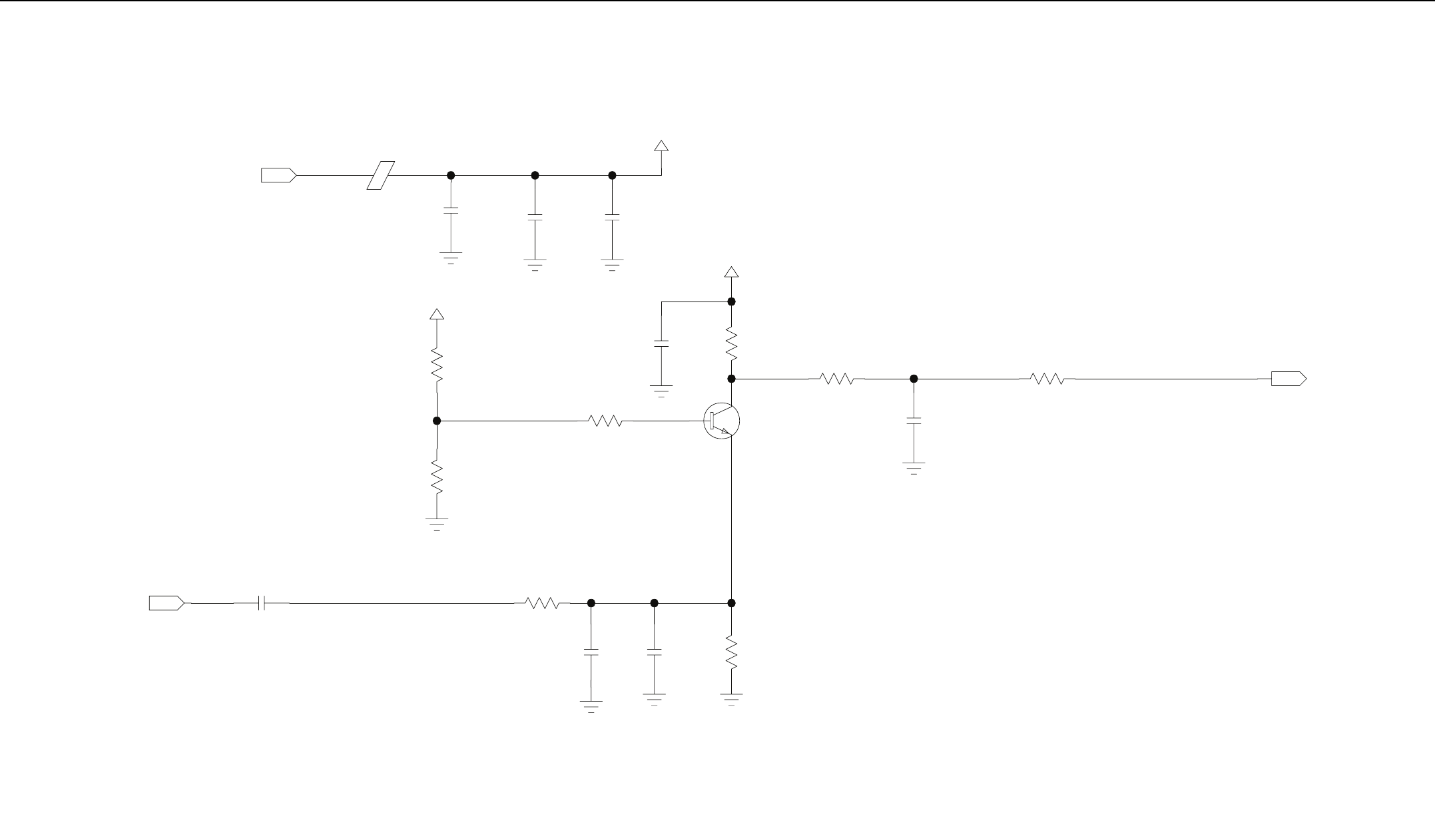
7-26 Exciter Schematics (UHF)
C4103
REF_16.8_IN
.1UF
IN
R4103
21
R4102
3.3V_BUF
2.67K
2.67K
0.8V
1.3V
0.9V
C4107
C4105 R4105
R4104
23
1Q4100
21
R4101
21
C4104
R4100
475
180PF
MMBT3904
150
475
.1UF
15PF
0
R4107
C4106
R4106
21
3.3V_BUF
0
249
33PF
16.8MHZ_SYN
OUT
21
C4102
C4101
21
C4100
E4100
3.3V_BUF
220PF .01UF .1UF
EXCITER_REF_BUFFER
IN
3.3V_16.8_BUFFER
Exciter – 16.8MHz Ref Buffer Schematic Diagram (Kit No. CTE4004)
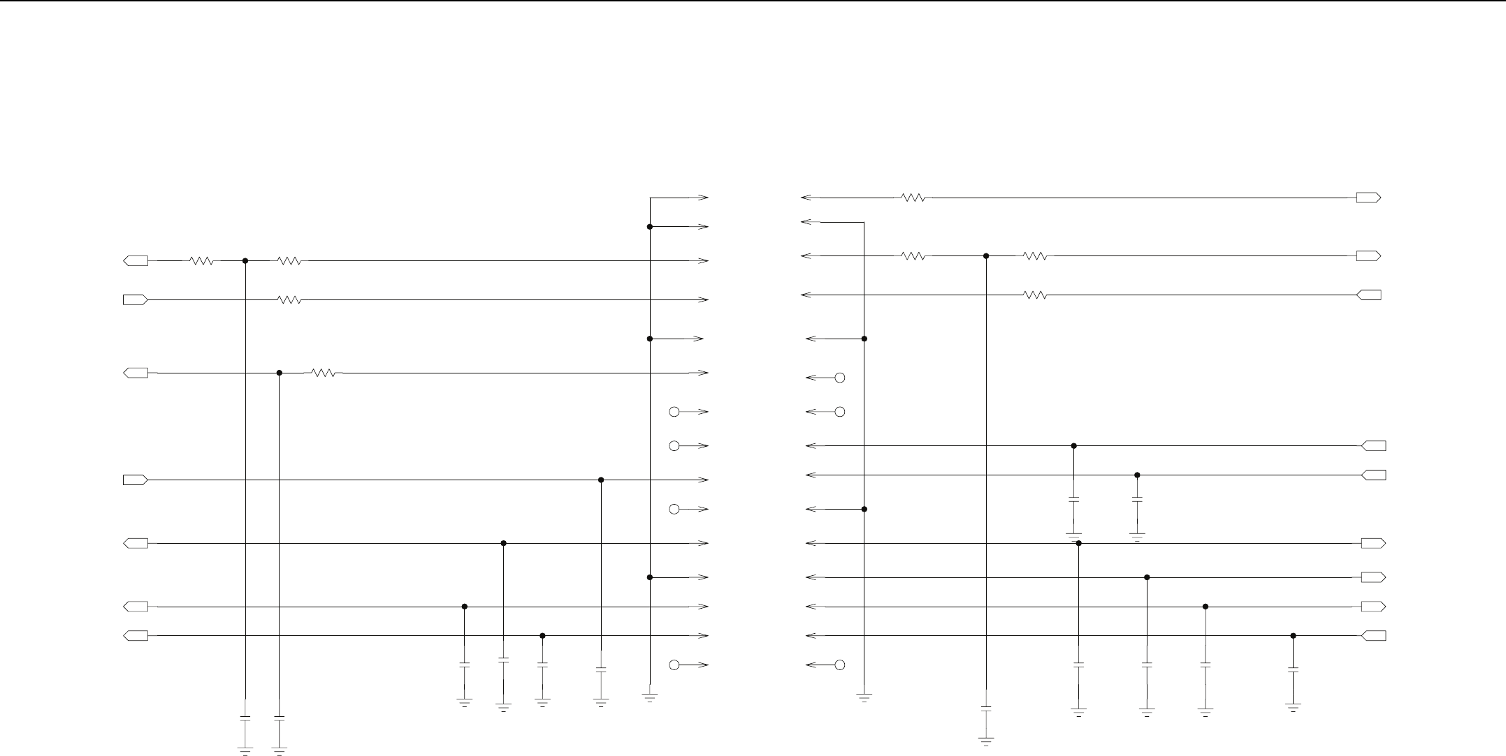
Exciter Schematics (UHF) 7-27
ACTIVE LOW
8V
EX_CPLD_CE
EX_CPLD_ADD_0
EX_CPLD_CLK
TXFS
EX_ENABLE
SSI_DATA
OUT
OUT
OUT
OUT
IN
IN
OUT
R4203
R4202
R4200 R4201
0
49.9
0
0
C4201
C4200
DNP10PF
10PF
C4205
C4203 C4204 C4206
DNPDNP
DNP
220PF
DNP
220PF 220PF
220PF P4200
P4200
P4200
P4200
P4200
P4200
P4200
P4200
P4200
P4200
P4200
P4200
P4200
P4200
P4200
P4200
P4200
P4200
P4200
P4200
P4200
P4200
P4200
P4200
P4200
P4200
P4200
P4200
P4200
P4200
EXCITER_INTERCONNECT
29
27
25
23
21
19
17
15
13
11
9
7
5
3
1
NC
NC
NC
NC
R4205
R4204
0
0
30
28
26
24
22
20
18
16
14
12
10
8
6
4
2
NC
NC
NC C4209 C4210 C4211 C4212
C4202
220PF
DNP
DNP
10PF
220PF
DNP
220PF
DNPDNP
220PF
C4207 C4208
DNPDNP
220PF220PF
EX_CPLD_MOSI
EX_CPLD_MISO
EX_CPLD_ADD_1
10V
14.2V
EX_CPLD_ADD_2
OUT
OUT
OUT
IN
IN
IN
R4207
R4206
49.9
0
16.8MHZ_REF
DMCS
TXCLK
OUT
IN
OUT
Exciter – Interconnect Schematic Diagram (Kit No. CTE4004)
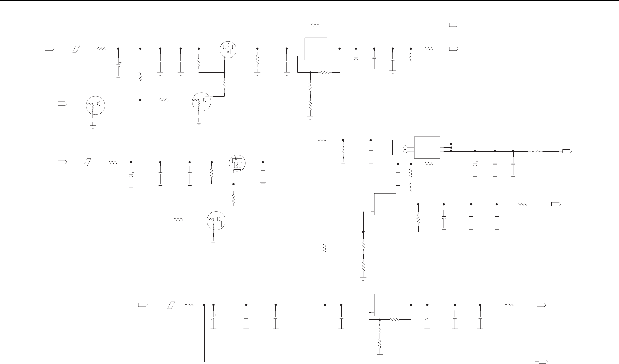
7-28 Exciter Schematics (UHF)
VOUT1
VOUT2
VOUT4
VOUT3
VIN
NC1
NC2
GND_ADJ
NC
NC 7
6
3
2
4
8
5
1
U4303
MC33269
R4331
R4318
R4315
R4317
R4316
C4313
C4312
DNP
.1UF
10K
0
270
1UF 2.32K
0
OUTIN
ADJUST
R4321
21
R4324
R4323
23
1
U4301
430
LM317M
0
0
10K
47K
R4312
2
3
1
Q4303
R4313
C4311
R4314
2
1
3
Q4304
C4310
C4309
21
C4308
R4311
E4301
.1UF
220PF
.01UF
DNP
10K
NTR1P02LT1
47UF
0
MUN5214T1
0
14.2V
10K
IN
10K
47K
2
3
1
Q4300
MUN5214T1
EX_STANDBY IN
R4300
21
C4302
21
R4302
21
C4301
21
C4300
E4300
.01UF
4.75K
220PF
0
10V
47UF
DNP
IN
21
R4305
10K
10K
47K
2
3
1
Q4301
21
R4304
R4303
2
1
3
Q4302
NTR1P02LT1
EXCITER_REGULATORS
MUN5214T1 0
0
R4330
R4308
R4307
C4304
1UF
10K
825
10
OUTIN
ADJUST
R4301
R4306
23
1
U4300
280
LM317M
0
R4309
R4310
C4307
C4306
21
C4305
10UF .1UF 220PF DNP
68.1
10V_EX_SWTCH
5V_EX
0
OUT
OUT
R4319
C4316
C4315
21
C4314
10UF .1UF
0
220PF
12V_VCO
OUT
3.3V_EX
OUT
R4322
R4325
C4324
C4323
21
C4322
10UF
270
0
.1UF 220PF
C4319
C4318
C4317
DNP
47UF .01UF 220PF
R4320
21
E4302
0
8V IN
C4321
.1UF
OUTIN
ADJUST
R4328
R4327 R4326
R4329
C4327
C4326
21
C4325
2
3
1
U4302
280
332
220PF
LM317M
10UF
0
2.775V_EX
0
.1UF
OUT
8V_EX
OUT
Exciter – Regulators Schematic Diagram (Kit No. CTE4004)
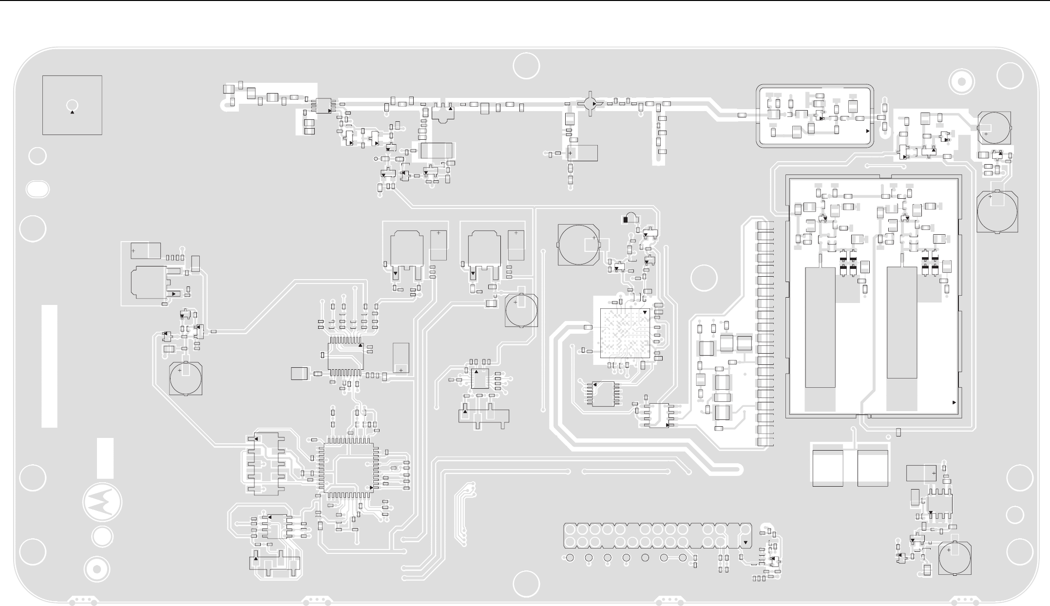
Exciter PCB (UHF) 7-29
7.3 Exciter PCB (UHF)
P4800
G1
G2
G4
G3
R4805
C4809
L4802
C4807
C4808
L4800
L4801
C4811
R4806
R4807
U4800
C4805
R4804
R4800
C4802 C4803
Q4802
R4802
R4803 R4808
R4809
R4810
C4804
Q4800
R4726
TP4700
C4801
Q4801 R4719
R4801
C4800
R4717
R4716
C4715
C4716
C4717
C4714
L4701
U4701
C4705
R4715
C4704
C4719
R4714
L4702
R4713
R4712
2
32
3
3
85
3
2
4
R4723
R4724
R4725
Q4702
R4727
C4711
Q4700
Q4701
R4728
R4729
R4721
R4010
R4011
R4731
R4730
R4722
C4713
C4712
3232
3
2
C4503
Q4503
R4507
E4500
R4503
R4504
R4506
Q4501
R4509
C4500
C4501
R4502
R4500 Q4500
R4501
D4500
2
32
3
32
R4508
C4511
R4511
C4512
U4501
R4207
R4200
R4512
C4514
C4513
U4500
R4524
U4502
C4570
R4525
C4508
R4206
R4202
R4514
C4507
C4509
C4506
E4501
R4505
R4513
C4504
R4510
C4505
C4502
C4510
4
8
7
14
L11
L1
8
5
A11
E4300
Q4300
R4306
C4307
U4300
C4305
C4306
C4300
C4301
C4302
R4300
Q4302
Q4301
R4307
R4301
R4304
R4303
R4305
R4302
C4304
R4308
R4310
R4330
R4309
3
2
2
2
3
32
3
P4401
C4408
C4410
R4411
R4410
R4413
U4401
C4411
P4400
E4400
R4408
R4409
C4409 C4407
C4406
C4405
C4404
R4427
R4405
R4421
R4412
R4428
R4415
2
3
5
4
10
9
8
2
4
R4400
R4403 C4400
C4401
R4404
R4402
R4401
R4424
U4400
C4416
R4426
R4425
C4403
C4413
C4412
C4414
R4407
R4418
R4406
R4417
R4416
34
33
23
22
44
11
12
C4016
R4018
R4015
C4013
C4014
C4402
R4422
R4423
R4420
R4419
C4015
C4017
R4016
R4014
R4017
U4000
C4011
C4009
C4007
C4005
C4012
C4010
C4006
R4007
R4008
R4006
R4002
R4003
C4415
C4418
R4414
C4001
C4002
C4000
E4000
R4013
R4012
C4003
C4004
R4001
R4000
C4018
11
10
20
C4008
R4322
R4323
R4324
C4318
C4323
C4319
C4324
R4321
R4325
C4322
U4301
R4327
R4326
E4302
R4320
C4326
C4327
R4328
R4329
C4321
C4325
U4302
C4317
3
2
3
2
C4417
R4435
R4429
R4430
C4419
P4402
U4402 R4437
R4436
R4434
R4433
R4432
C4422
C4421
C4420
R4431
16
8
7
2
2
3
4
9
10
15
R4005
C4706
E4700
R4720
R4004
C4708
C4707
L4700
C4718
C4703
R4709
C4702
R4710
U4700
R4706
C4700
R4704
R4705
R4707
R4703
R4702
C4701
R4700
R4708
34
R4701
R4636
R4618
R4619
Q4604
Q4605
R4633
R4635
R4632
R4628
L4615
R4634
Q4606
C4627
C4628
E4600
Q4603
R4629
C4630
C4629
C4626
R4631
R4630
3223
32
3
2
L4613
C4625
C4623
R4624
R4627
L4614
L4612
SH4601
C4622
C4631
Q4602
R4621
R4623
R4622
C4619
R4625
C4620
L4611
C4618
6
9
32
4
2
7
C4624
TP4403
TP4401
TP4406
TP4404
C4200
R4203
TP4405
C4202
C4201
R4205
R4201
R4204
E4100
C4102
C4105
C4103
C4100
C4101
Q4100
R4100 R4105
C4106
C4104
C4107
R4101
R4106
R4107
R4103
R4102
3
2
2
3029
TP4402
TP4400
R4104
P4200
L4500
C4517
R4519
R4518
R4523
R4521 C4521
C4520
C4546
R4522
R4520
C4515
C4519
R4517
R4516
C4526
C4527
C4528
C4529
C4530
C4531
C4532
C4533
C4534
C4535
C4516
C4536
C4537
C4538
C4539
C4540
C4541
C4542
C4543
C4544
C4545
Q4303
R4311
Q4304
R4312 R4314
R4313
C4311
C4309
C4313
R4316
R4317
R4318
C4314
E4301
C4308
C4310
R4315
R4331
C4312
U4303
C4316
R4319
C4315
3
2
8
4
32
5
C4523 C4522
C4632
SH4600 12
10
11
R4605
R4604
L4603
C4606 R4603
L4604
CR4600
R4601
C4605
C4601
C4602
C4603
C4604
R4602
R4607
R4606
R4608
L4602
C4607
C4608
Q4600
R4613
R4614
L4601
C4615 R4612
L4609
C4617
CR4607
CR4606
R4610
L4608 C4614
C4613
C4610
C4611
R4616
R4615
R4617
L4607
C4616
Q4601
CR4605
R4609 L4605
C4609
CR4604
L4606
R4611
3
4
5
8
7
6
Y4600
CR4601
CR4603
CR4602
R4600
L4600
C4600
Y4601
C4612
2
9
84009272002_B
C2009
Exciter Board PCB – Top View (PCB No. 84009272002)
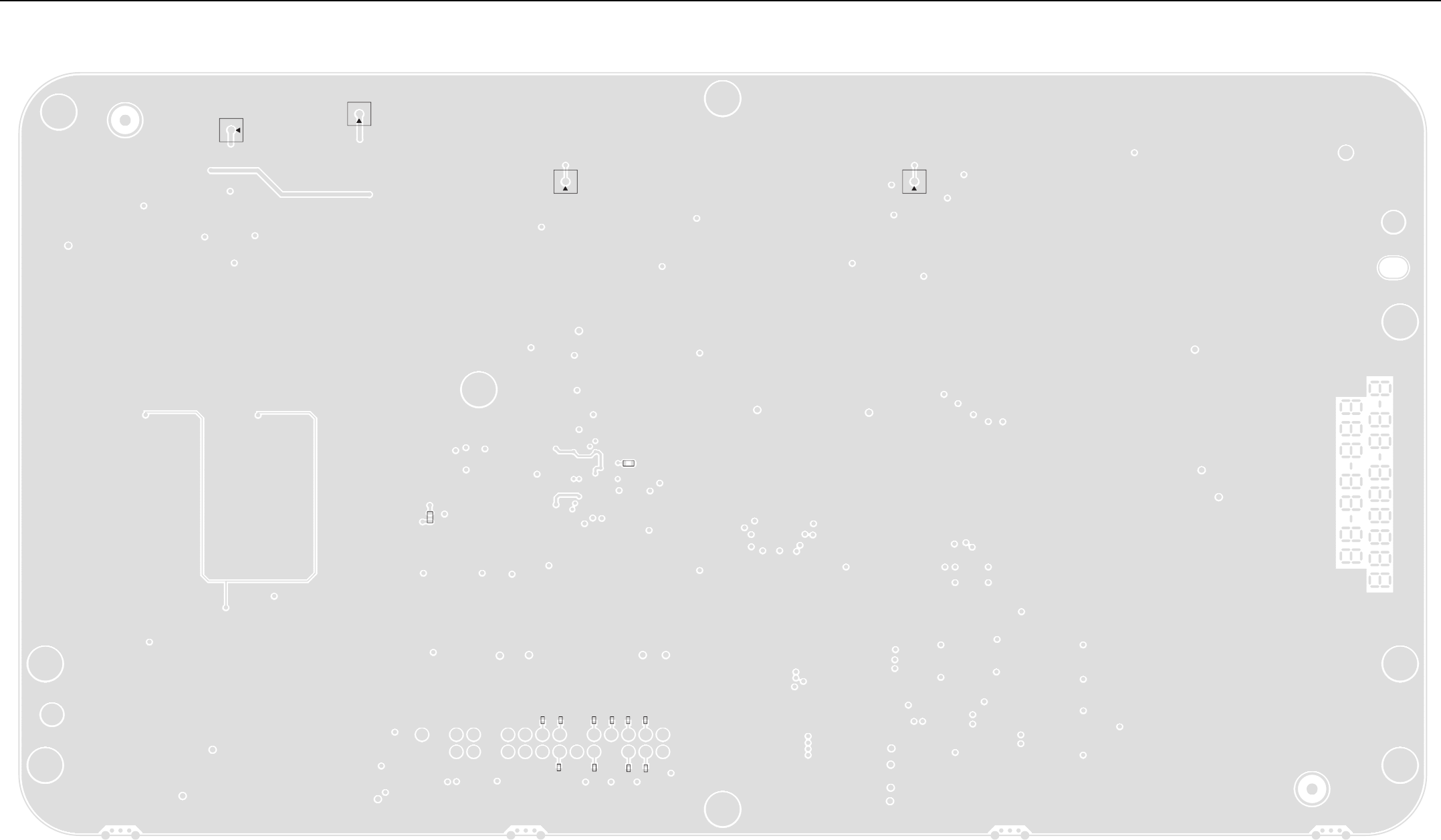
7-30 Exciter PCB (UHF)
P4701
C4205
C4212
C4203
C4204
C4209
C4210
C4211
R4515
C4206
C4207
C4208
P4700
R4526
P4601
P4600
23
4
5
23
4
5
23
4
5
23
4
5
Exciter Board PCB – Bottom View (PCB No. 84009272002)(
Exciter Parts List (UHF) – CTE4003 7-31
7.4 Exciter Parts List (UHF) –
CTE4003
Circuit
Ref
Motorola Part
No Description
*1085674C03 PASTE/NC-SMQ230
* 2683006X02 COVER, TX VCO SHIELD
*84009272002 MTR3000 EXCITER
C4000 2113945B02 CAP CER CHP 10,000PF
25V 10%
C4001 2113946K02 CAP CER CHP 0.10UF
16V
C4002 2113944A44 CAP CER CHP 220.0 PF
50V 5%
C4003 2113946K02 CAP CER CHP 0.10UF
16V
C4004 2113944A44 CAP CER CHP 220.0 PF
50V 5%
C4005 2113946K02 CAP CER CHP 0.10UF
16V
C4006 2113944A44 CAP CER CHP 220.0 PF
50V 5%
C4007 2113946K02 CAP CER CHP 0.10UF
16V
C4008 2113944A44 CAP CER CHP 220.0 PF
50V 5%
C4009 2113946K02 CAP CER CHP 0.10UF
16V
C4010 2113944A44 CAP CER CHP 220.0 PF
50V 5%
C4011 2113946K02 CAP CER CHP 0.10UF
16V
C4012 2113944A44 CAP CER CHP 220.0 PF
50V 5%
C4013 2113946K02 CAP CER CHP 0.10UF
16V
C4014 2113944A44 CAP CER CHP 220.0 PF
50V 5%
C4015 2113946A01 CAP CER CHP 0.015UF
16V 10%
C4016 2113946J02 CAP CER CHP 4.7UF 16V
10%
C4100 2113944A44 CAP CER CHP 220.0 PF
50V 5%
C4101 2113945B02 CAP CER CHP 10,000PF
25V 10%
C4102 2113946K02 CAP CER CHP 0.10UF
16V
C4103 2113946K02 CAP CER CHP 0.10UF
16V
C4104 2113944A27 CAP CER CHP 15.0PF
50V 5%
C4105 2113946K02 CAP CER CHP 0.10UF
16V
C4106 2113944A31 CAP CER CHP 33.0PF
50V 5%
C4107 2113944A43 CAP CER CHP 180.0PF
50V 5%
C4200 2113944A25 CAP CER CHP 10.0PF
50V +/- 0.5PF
C4301 2113945B02 CAP CER CHP 10,000PF
25V 10%
C4302 2113944A44 CAP CER CHP 220.0 PF
50V 5%
C4304 2113955D01 CAP,FXD,1UF,+10%,-
10%,100V-DC,1206,X7R,-
55DEG CMIN,125DEG
CMAX
C4305 2313960F01 CAP,FXD,10UF,+10%,-
10%,16V-DC,SM,-55DEG
CMIN,125DEG
CMAX,247MA
C4306 2113946K02 CAP CER CHP 0.10UF
16V
C4307 2113944A44 CAP CER CHP 220.0 PF
50V 5%
C4309 2113945C02 CAP CER CHP 10,000PF
50V 10%
C4310 2113944A44 CAP CER CHP 220.0 PF
50V 5%
C4311 2113945C31 CAP,FXD,.1UF,+10%,-
10%,50V-DC,0603,X7R,-
55DEG CMIN,125DEG
CMAX
Circuit
Ref
Motorola Part
No Description
C4312 2113945C31 CAP,FXD,.1UF,+10%,-
10%,50V-DC,0603,X7R,-
55DEG CMIN,125DEG
CMAX
C4314 2313960E32 CAP,FXD,10UF,+10%,-
10%,35V-DC,SM,-55DEG
CMIN,125DEG
CMAX,262MA
C4315 2113945C31 CAP,FXD,.1UF,+10%,-
10%,50V-DC,0603,X7R,-
55DEG CMIN,125DEG
CMAX
C4316 2113944A44 CAP CER CHP 220.0 PF
50V 5%
C4318 2113945B02 CAP CER CHP 10,000PF
25V 10%
C4319 2113944A44 CAP CER CHP 220.0 PF
50V 5%
C4321 2113945D04 CAP CER CHP 100,000PF
25V 10%
C4322 2313960F01 CAP,FXD,10UF,+10%,-
10%,16V-DC,SM,-55DEG
CMIN,125DEG
CMAX,247MA
C4323 2113946K02 CAP CER CHP 0.10UF
16V
C4324 2113944A44 CAP CER CHP 220.0 PF
50V 5%
C4325 2313960F01 CAP,FXD,10UF,+10%,-
10%,16V-DC,SM,-55DEG
CMIN,125DEG
CMAX,247MA
C4326 2113946K02 CAP CER CHP 0.10UF
16V
C4327 2113944A44 CAP CER CHP 220.0 PF
50V 5%
C4401 2113946K02 CAP CER CHP 0.10UF
16V
C4402 2113946K02 CAP CER CHP 0.10UF
16V
C4403 2113946K02 CAP CER CHP 0.10UF
16V
Circuit
Ref
Motorola Part
No Description
C4404 2113946K02 CAP CER CHP 0.10UF
16V
C4405 2113945B02 CAP CER CHP 10,000PF
25V 10%
C4406 2113946K02 CAP CER CHP 0.10UF
16V
C4407 2113944A44 CAP CER CHP 220.0 PF
50V 5%
C4408 2113944A25 CAP CER CHP 10.0PF
50V +/- 0.5PF
C4409 2113946B04 CAP CER CHP 0.10UF
10V 10%
C4419 2113946K02 CAP CER CHP 0.10UF
16V
C4420 2113945B02 CAP CER CHP 10,000PF
25V 10%
C4421 2113946K02 CAP CER CHP 0.10UF
16V
C4422 2113945B02 CAP CER CHP 10,000PF
25V 10%
C4501 2113944A42 CAP CER CHP 150.0PF
50V 5%
C4502 2113945C02 CAP CER CHP 10,000PF
50V 10%
C4503 2385170Y08 CAP AL LYTIC 330UF 25V
20% PB-FREE
C4504 2113945B02 CAP CER CHP 10,000PF
25V 10%
C4505 2113945D04 CAP CER CHP 100,000PF
25V 10%
C4506 2113944A42 CAP CER CHP 150.0PF
50V 5%
C4507 2113945D04 CAP CER CHP 100,000PF
25V 10%
C4510 2113945D04 CAP CER CHP 100,000PF
25V 10%
C4512 2113945C04 CAP CER CHP 22,000PF
50V 10%
C4513 2113944A42 CAP CER CHP 150.0PF
50V 5%
Circuit
Ref
Motorola Part
No Description
7-32 Exciter Parts List (UHF) – CTE4003
C4514 2113944A42 CAP CER CHP 150.0PF
50V 5%
C4515 21012013006 CHIP CAPACITOR -
1210NPO - 6800PF
C4517 2113945L37 CAP,FXD,3300PF,+5%,-
5%,50V-DC,0603,X7R,-
55DEG CMIN,125DEG
CMAX
C4519 21012012001 CHIP CAPACITOR -
ATC200B SERIES
C4520 21012012008 CHIP CAPACITOR -
ATC200B - 33000PF
C4521 21012012013 CHIP CAPACITOR -
ATC200B - 68000PF
C4526 21012016001 CHIP CAPACITOR -1206
C0G -0.1UF
C4527 21012016001 CHIP CAPACITOR -1206
C0G -0.1UF
C4528 21012016001 CHIP CAPACITOR -1206
C0G -0.1UF
C4529 21012016001 CHIP CAPACITOR -1206
C0G -0.1UF
C4530 21012016001 CHIP CAPACITOR -1206
C0G -0.1UF
C4531 21012016001 CHIP CAPACITOR -1206
C0G -0.1UF
C4532 21012016001 CHIP CAPACITOR -1206
C0G -0.1UF
C4533 21012016001 CHIP CAPACITOR -1206
C0G -0.1UF
C4534 21012016001 CHIP CAPACITOR -1206
C0G -0.1UF
C4535 21012016001 CHIP CAPACITOR -1206
C0G -0.1UF
C4536 21012016001 CHIP CAPACITOR -1206
C0G -0.1UF
C4537 21012016001 CHIP CAPACITOR -1206
C0G -0.1UF
C4538 21012016001 CHIP CAPACITOR -1206
C0G -0.1UF
Circuit
Ref
Motorola Part
No Description
C4539 21012016001 CHIP CAPACITOR -1206
C0G -0.1UF
C4540 21012016001 CHIP CAPACITOR -1206
C0G -0.1UF
C4541 21012016001 CHIP CAPACITOR -1206
C0G -0.1UF
C4542 21012016001 CHIP CAPACITOR -1206
C0G -0.1UF
C4543 21012016001 CHIP CAPACITOR -1206
C0G -0.1UF
C4544 21012016001 CHIP CAPACITOR -1206
C0G -0.1UF
C4545 21012016001 CHIP CAPACITOR -1206
C0G -0.1UF
C4570 2113944A44 CAP CER CHP 220.0 PF
50V 5%
C4600 2113944C02 CAP CER CHP 220.0PF
50V 5%
C4601 2113951C30 CAP,FXD,6.8PF,.25PF+/-
,250V-DC,0603,C0G,-
55DEG CMIN,125DEG
CMA
C4602 2113951C18 CAP,FXD,2.2PF,.05PF+/-
,250V-DC,0603,C0G,-
55DEG CMIN,125DEG
CMA
C4603 2113951C31 CAP,FXD,7.5PF,.25PF+/-
,250V-DC,0603,C0G,-
55DEG CMIN,125DEG
CMA
C4604 2113951C37 CAP,FXD,15PF,+1%,-
1%,250V-DC,0603,C0G,-
55DEG CMIN,125DEG
CMAX,P
C4605 2113951C32 CAP,FXD,8.2PF,.25PF+/-
,250V-DC,0603,C0G,-
55DEG CMIN,125DEG
CMA
C4606 2113944C02 CAP CER CHP 220.0PF
50V 5%
C4607 2113951C21 CAP,FXD,3PF,.05PF+/-
,250V-DC,0603,C0G,-
55DEG CMIN,125DEG
CMAX
Circuit
Ref
Motorola Part
No Description
C4608 2113944C45 CAP CER CHP 100.0PF
50V 5%
C4609 2113944C02 CAP CER CHP 220.0PF
50V 5%
C4610 2113951C29 CAP,FXD,6.2PF,.05PF+/-
,250V-DC,0603,C0G,-
55DEG CMIN,125DEG
CMA
C4611 2113951C16 CAP,FXD,1.8PF,.05PF+/-
,250V-DC,0603,C0G,-
55DEG CMIN,125DEG
CMA
C4612 2113951C28 CAP,FXD,5.6PF,.05PF+/-
,250V-DC,0603,C0G,-
55DEG CMIN,125DEG
CMA
C4613 2113951C36 CAP,FXD,12PF,+1%,-
1%,250V-DC,0603,C0G,-
55DEG CMIN,125DEG
CMAX,P
C4614 2113951C28 CAP,FXD,5.6PF,.05PF+/-
,250V-DC,0603,C0G,-
55DEG CMIN,125DEG
CMA
C4615 2113944C02 CAP CER CHP 220.0PF
50V 5%
C4616 2113951C21 CAP,FXD,3PF,.05PF+/-
,250V-DC,0603,C0G,-
55DEG CMIN,125DEG
CMAX
C4617 2113944C45 CAP CER CHP 100.0PF
50V 5%
C4618 2113951C29 CAP,FXD,6.2PF,.05PF+/-
,250V-DC,0603,C0G,-
55DEG CMIN,125DEG
CMA
C4619 2113944C02 CAP CER CHP 220.0PF
50V 5%
C4620 2113945D04 CAP CER CHP 100,000PF
25V 10%
C4622 2113951C26 CAP,FXD,4.7PF,.05PF+/-
,250V-DC,0603,C0G,-
55DEG CMIN,125DEG
CMA
Circuit
Ref
Motorola Part
No Description
C4623 2113951C26 CAP,FXD,4.7PF,.05PF+/-
,250V-DC,0603,C0G,-
55DEG CMIN,125DEG
CMA
C4624 2113944C02 CAP CER CHP 220.0PF
50V 5%
C4625 2113944C02 CAP CER CHP 220.0PF
50V 5%
C4626 2385170Y10 CAP AL LYTIC 47UF 25V
20% PB-FREE
C4627 2113945C02 CAP CER CHP 10,000PF
50V 10%
C4628 2385170Y08 CAP AL LYTIC 330UF 25V
20% PB-FREE
C4629 2113945C02 CAP CER CHP 10,000PF
50V 10%
C4630 2113944C02 CAP CER CHP 220.0PF
50V 5%
C4632 2113944C02 CAP CER CHP 220.0PF
50V 5%
C4700 2113944A44 CAP CER CHP 220.0 PF
50V 5%
C4701 2113944A44 CAP CER CHP 220.0 PF
50V 5%
C4702 2113944A44 CAP CER CHP 220.0 PF
50V 5%
C4703 2113944A44 CAP CER CHP 220.0 PF
50V 5%
C4704 2113944A44 CAP CER CHP 220.0 PF
50V 5%
C4705 2113944A44 CAP CER CHP 220.0 PF
50V 5%
C4707 2113946K02 CAP CER CHP 0.10UF
16V
C4708 2113944A44 CAP CER CHP 220.0 PF
50V 5%
C4711 2113944A44 CAP CER CHP 220.0 PF
50V 5%
C4714 2113945C31 CAP,FXD,.1UF,+10%,-
10%,50V-DC,0603,X7R,-
55DEG CMIN,125DEG
CMAX
Circuit
Ref
Motorola Part
No Description

Exciter Parts List (UHF) – CTE4003 7-33
C4715 2113944A52 CAP CER CHP 1000.0 PF
50V 5%
C4716 2113944A44 CAP CER CHP 220.0 PF
50V 5%
C4717 2113945C02 CAP CER CHP 10,000PF
50V 10%
C4718 2113945C02 CAP CER CHP 10,000PF
50V 10%
C4719 2113951C35 CAP,FXD,11PF,+1%,-
1%,250V-DC,0603,C0G,-
55DEG CMIN,125DEG
CMAX,P
C4800 2113945D04 CAP CER CHP 100,000PF
25V 10%
C4801 2113944A44 CAP CER CHP 220.0 PF
50V 5%
C4802 2113944A44 CAP CER CHP 220.0 PF
50V 5%
C4803 2113944A44 CAP CER CHP 220.0 PF
50V 5%
C4804 2113944A45 CAP CER CHP 270.0 PF
50V 5%
C4805 2113944A45 CAP CER CHP 270.0 PF
50V 5%
C4807 2113944C19 CAP CER CHP 3.6PF 50V
+/- 0.25PF
C4808 2113944C28 CAP CER CHP 8.2PF 50V
+/- 0.5PF
C4809 2113944C25 CAP CER CHP 6.2PF 50V
+/- 0.5PF
C4811 2113944A45 CAP CER CHP 270.0 PF
50V 5%
CR4602 4815072H01 DIODE VARACTOR
CR4603 4815072H01 DIODE VARACTOR
CR4604 4815072H01 DIODE VARACTOR
CR4605 4815072H01 DIODE VARACTOR
E4000 2485410Y01 MIN CHIP FERRITE BEAD
E4100 2485449Y01 SURFACE MOUNT
FERRITE BEAD W18
Circuit
Ref
Motorola Part
No Description
E4300 2485410Y04 MIN CHIP FERRITE BEAD
330ΩS W18
E4301 2485410Y04 MIN CHIP FERRITE BEAD
330ΩS W18
E4302 2485410Y04 MIN CHIP FERRITE BEAD
330ΩS W18
E4400 2485410Y01 MIN CHIP FERRITE BEAD
E4500 2485410Y01 MIN CHIP FERRITE BEAD
E4501 2485410Y01 MIN CHIP FERRITE BEAD
E4600 2485410Y01 MIN CHIP FERRITE BEAD
E4700 2485410Y01 MIN CHIP FERRITE BEAD
L4500 2414032F34 IDCTR,WW,100NH,5%,400
MA,.46Ω,CER,40
Q,950MHZ SRF,SM,PB-FR
L4600 2414032F59 IDCTR,WW,390NH,5%,290
MA,1.5Ω,CER,48
Q,560MHZ SRF,SM,PB-FR
L4601 2414032F50 IDCTR,WW,24NH,5%,500
MA,.24Ω,CER,45 Q,2GHZ
SRF,SM,PB-FREE
L4602 2414032F59 IDCTR,WW,390NH,5%,290
MA,1.5Ω,CER,48
Q,560MHZ SRF,SM,PB-FR
L4603 2414032F59 IDCTR,WW,390NH,5%,290
MA,1.5Ω,CER,48
Q,560MHZ SRF,SM,PB-FR
L4604 2414032F59 IDCTR,WW,390NH,5%,290
MA,1.5Ω,CER,48
Q,560MHZ SRF,SM,PB-FR
L4605 2414032F59 IDCTR,WW,390NH,5%,290
MA,1.5Ω,CER,48
Q,560MHZ SRF,SM,PB-FR
L4606 2414032F26 IDCTR,WW,22NH,5%,500
MA,.22Ω,CER,45
Q,2.2GHZ SRF,SM,PB-
FRE
L4607 2414032F59 IDCTR,WW,390NH,5%,290
MA,1.5Ω,CER,48
Q,560MHZ SRF,SM,PB-FR
L4608 2414032F59 IDCTR,WW,390NH,5%,290
MA,1.5Ω,CER,48
Q,560MHZ SRF,SM,PB-FR
Circuit
Ref
Motorola Part
No Description
L4609 2414032F59 IDCTR,WW,390NH,5%,290
MA,1.5Ω,CER,48
Q,560MHZ SRF,SM,PB-FR
L4611 2414032F27 IDCTR,FXD,27NH,5%,500
MA,.25Ω,CER,45 Q,2GHZ
SRF,SM,0805,PB-
L4612 2414032F26 IDCTR,WW,22NH,5%,500
MA,.22Ω,CER,45
Q,2.2GHZ SRF,SM,PB-
FRE
L4613 2414032F50 IDCTR,WW,24NH,5%,500
MA,.24Ω,CER,45 Q,2GHZ
SRF,SM,PB-FREE
L4614 2414032F59 IDCTR,WW,390NH,5%,290
MA,1.5Ω,CER,48
Q,560MHZ SRF,SM,PB-FR
L4615 2414032F59 IDCTR,WW,390NH,5%,290
MA,1.5Ω,CER,48
Q,560MHZ SRF,SM,PB-FR
L4700 2414032F59 IDCTR,WW,390NH,5%,290
MA,1.5Ω,CER,48
Q,560MHZ SRF,SM,PB-FR
L4701 2416540H35 CHIP INDUCTOR
L4702 2414015B15 IDCTR,FXD,22NH,2%,500
MA,.22Ω,CER,55
Q,2.6GHZ SRF,SM,0805,P
L4800 2414015B17 IDCTR,FXD,18NH,2%,600
MA,.2Ω,CER,50 Q,3.3GHZ
SRF,SM,0805,PB
L4801 2414015B17 IDCTR,FXD,18NH,2%,600
MA,.2Ω,CER,50 Q,3.3GHZ
SRF,SM,0805,PB
L4802 2414015B12 IDCTR,FXD,47NH,2%,500
MA,.34Ω,CER,40
Q,1.3GHZ SRF,SM,0805,P
P4200 28009146002 HEADER 2 X 15
VERTICAL
P4800 0982492W01 BNC CONN PCB
VERTICAL RECEPT
Q4100 4813973A54 XSTR,BIP GP
SS,NPN,T3904,SM,SC-
70,SMT,40V,.15W,200MA,
300MHZ,PB
Circuit
Ref
Motorola Part
No Description
Q4300 4813973A34 XSTR,BIP GP
SS,NPN,SM,SC-
70,SMT,50V,.202W,100MA
,PB-FREE
Q4301 4813973A34 XSTR,BIP GP
SS,NPN,SM,SC-
70,SMT,50V,.202W,100MA
,PB-FREE
Q4302 4885065Y01 POWER MOSFET 1.3A,
20V PB-FREE
Q4303 4813973A34 XSTR,BIP GP
SS,NPN,SM,SC-
70,SMT,50V,.202W,100MA
,PB-FREE
Q4304 4885065Y01 POWER MOSFET 1.3A,
20V PB-FREE
Q4503 4813973A54 XSTR,BIP GP
SS,NPN,T3904,SM,SC-
70,SMT,40V,.15W,200MA,
300MHZ,PB
Q4600 4885061Y01 XSTR NPN 6V 30UA
12GHZ PB-FREE
Q4601 4885061Y01 XSTR NPN 6V 30UA
12GHZ PB-FREE
Q4602 4805218N63 RF TRANS SOT 323
BFQ67W
Q4603 4813973A54 XSTR,BIP GP
SS,NPN,T3904,SM,SC-
70,SMT,40V,.15W,200MA,
300MHZ,PB
Q4604 4885065Y01 POWER MOSFET 1.3A,
20V PB-FREE
Q4605 4885065Y01 POWER MOSFET 1.3A,
20V PB-FREE
Q4606 4813973A34 XSTR,BIP GP
SS,NPN,SM,SC-
70,SMT,50V,.202W,100MA
,PB-FREE
Q4700 4885065Y01 POWER MOSFET 1.3A,
20V PB-FREE
Q4701 4813973A54 XSTR,BIP GP
SS,NPN,T3904,SM,SC-
70,SMT,40V,.15W,200MA,
300MHZ,PB
Circuit
Ref
Motorola Part
No Description
7-34 Exciter Parts List (UHF) – CTE4003
Q4702 4813973A13 XSTR,GEN PURPOSE
SMALL
SIG,PNP,MMBT3906L,TO-
236,4, PB-FREE
Q4800 4813973A34 XSTR,BIP GP
SS,NPN,SM,SC-
70,SMT,50V,.202W,100MA
,PB-FREE
Q4801 4885065Y01 POWER MOSFET 1.3A,
20V PB-FREE
Q4802 4885065Y01 POWER MOSFET 1.3A,
20V PB-FREE
R4000 0613952N01 CER CHIP RES 10.0KΩ 1
0402
R4001 0613952Q86 CER CHIP RES 3600Ω 5
0402
R4002 0613952N01 CER CHIP RES 10.0KΩ 1
0402
R4003 0613952M42 CER CHIP RES 2670Ω 1%
0402
R4004 0613952N01 CER CHIP RES 10.0KΩ 1
0402
R4005 0613952N01 CER CHIP RES 10.0KΩ 1
0402
R4006 0613952N01 CER CHIP RES 10.0KΩ 1
0402
R4007 0613952N51 CER CHIP RES 33.2KΩ 1
0402
R4008 0613952R66 CER CHIP RES 0.0 +/-
0.050Ω
R4010 0613952N01 CER CHIP RES 10.0KΩ 1
0402
R4011 0613952N01 CER CHIP RES 10.0KΩ 1
0402
R4012 0613952N01 CER CHIP RES 10.0KΩ 1
0402
R4013 0613952N01 CER CHIP RES 10.0KΩ 1
0402
R4014 0613952R66 CER CHIP RES 0.0 +/-
0.050Ω
R4016 0613952K51 CER CHIP RES 33.2Ω 1%
0402
Circuit
Ref
Motorola Part
No Description
R4017 0613952R66 CER CHIP RES 0.0 +/-
0.050Ω
R4018 0613952A73 CER CHIP RES 5.62Ω 1%
0603
R4100 0613952R66 CER CHIP RES 0.0 +/-
0.050Ω
R4101 0613952L18 CER CHIP RES 150Ω 1%
0402
R4102 0613952M42 CER CHIP RES 2670Ω 1%
0402
R4103 0613952M42 CER CHIP RES 2670Ω 1%
0402
R4104 0613952L66 CER CHIP RES 475Ω 1%
0402
R4105 0613952L66 CER CHIP RES 475Ω 1%
0402
R4106 0613952L39 CER CHIP RES 249Ω 1
0402
R4107 0613952R66 CER CHIP RES 0.0 +/-
0.050Ω
R4200 0613952R66 CER CHIP RES 0.0 +/-
0.050Ω
R4201 0613952R66 CER CHIP RES 0.0 +/-
0.050Ω
R4202 0613952K68 CER CHIP RES 49.9Ω 1%
0402
R4203 0613952R66 CER CHIP RES 0.0 +/-
0.050Ω
R4204 0613952R66 CER CHIP RES 0.0 +/-
0.050Ω
R4205 0613952R66 CER CHIP RES 0.0 +/-
0.050Ω
R4206 0613952R66 CER CHIP RES 0.0 +/-
0.050Ω
R4207 0613952K68 CER CHIP RES 49.9Ω 1%
0402
R4300 0613952R66 CER CHIP RES 0.0 +/-
0.050Ω
R4301 0613952R66 CER CHIP RES 0.0 +/-
0.050Ω
Circuit
Ref
Motorola Part
No Description
R4302 0613952M66 CER CHIP RES 4750Ω 1%
0402
R4303 0613952R66 CER CHIP RES 0.0 +/-
0.050Ω
R4304 0613952R66 CER CHIP RES 0.0 +/-
0.050Ω
R4305 0613952N01 CER CHIP RES 10.0KΩ 1
0402
R4306 0613952L44 CER CHIP RES 280Ω 1
0402
R4307 0613952L89 CER CHIP RES 825Ω 1%
0402
R4308 0613952K01 CER CHIP RES 10.0Ω 1%
0402
R4310 0613952R66 CER CHIP RES 0.0 +/-
0.050Ω
R4311 0613952R66 CER CHIP RES 0.0 +/-
0.050Ω
R4312 0613952R66 CER CHIP RES 0.0 +/-
0.050Ω
R4313 0613952N01 CER CHIP RES 10.0KΩ 1
0402
R4314 0613952N01 CER CHIP RES 10.0KΩ 1
0402
R4315 0613952R66 CER CHIP RES 0.0 +/-
0.050Ω
R4316 0613952Q59 CER CHIP RES 270Ω 5
0402
R4317 0613952M36 CER CHIP RES 2320Ω 1
0402
R4318 0613952R66 CER CHIP RES 0.0 +/-
0.050Ω
R4319 0613952R66 CER CHIP RES 0.0 +/-
0.050Ω
R4320 0613952R66 CER CHIP RES 0.0 +/-
0.050Ω
R4321 0613952R66 CER CHIP RES 0.0 +/-
0.050Ω
R4322 0613952Q59 CER CHIP RES 270Ω 5
0402
Circuit
Ref
Motorola Part
No Description
R4323 0613952Q64 CER CHIP RES 430Ω 5
0402
R4324 0613952R66 CER CHIP RES 0.0 +/-
0.050Ω
R4325 0613952R66 CER CHIP RES 0.0 +/-
0.050Ω
R4326 0613952L44 CER CHIP RES 280Ω 1
0402
R4327 0613952C51 CER CHIP RES 332Ω 1%
0603
R4328 0613952R66 CER CHIP RES 0.0 +/-
0.050Ω
R4329 0613952R66 CER CHIP RES 0.0 +/-
0.050Ω
R4330 0613952N01 CER CHIP RES 10.0KΩ 1
0402
R4331 0613952N01 CER CHIP RES 10.0KΩ 1
0402
R4400 0613952R66 CER CHIP RES 0.0 +/-
0.050Ω
R4401 0613952M66 CER CHIP RES 4750Ω 1%
0402
R4402 0613952M01 CER CHIP RES 1000Ω 1%
0402
R4403 0613952M66 CER CHIP RES 4750Ω 1%
0402
R4404 0613952M01 CER CHIP RES 1000Ω 1%
0402
R4405 0613952M01 CER CHIP RES 1000Ω 1%
0402
R4406 0613952M01 CER CHIP RES 1000Ω 1%
0402
R4407 0613952M01 CER CHIP RES 1000Ω 1%
0402
R4408 0613952K68 CER CHIP RES 49.9Ω 1%
0402
R4409 0613952K68 CER CHIP RES 49.9Ω 1%
0402
R4410 0613952N01 CER CHIP RES 10.0KΩ 1
0402
Circuit
Ref
Motorola Part
No Description

Exciter Parts List (UHF) – CTE4003 7-35
R4411 0613952K51 CER CHIP RES 33.2Ω 1%
0402
R4412 0613952K51 CER CHIP RES 33.2Ω 1%
0402
R4413 0613952M66 CER CHIP RES 4750Ω 1%
0402
R4414 0613952M66 CER CHIP RES 4750Ω 1%
0402
R4415 0613952M66 CER CHIP RES 4750Ω 1%
0402
R4416 0613952M66 CER CHIP RES 4750Ω 1%
0402
R4417 0613952M66 CER CHIP RES 4750Ω 1%
0402
R4418 0613952M66 CER CHIP RES 4750Ω 1%
0402
R4419 0613952M66 CER CHIP RES 4750Ω 1%
0402
R4420 0613952M66 CER CHIP RES 4750Ω 1%
0402
R4421 0613952M66 CER CHIP RES 4750Ω 1%
0402
R4422 0613952K51 CER CHIP RES 33.2Ω 1%
0402
R4423 0613952K51 CER CHIP RES 33.2Ω 1%
0402
R4424 0613952K68 CER CHIP RES 49.9Ω 1%
0402
R4425 0613952K68 CER CHIP RES 49.9Ω 1%
0402
R4426 0613952K51 CER CHIP RES 33.2Ω 1%
0402
R4427 0613952K51 CER CHIP RES 33.2Ω 1%
0402
R4428 0613952K51 CER CHIP RES 33.2Ω 1%
0402
R4430 0613952M66 CER CHIP RES 4750Ω 1%
0402
R4431 0613952R66 CER CHIP RES 0.0 +/-
0.050Ω
Circuit
Ref
Motorola Part
No Description
R4432 0613952R66 CER CHIP RES 0.0 +/-
0.050Ω
R4433 0613952R66 CER CHIP RES 0.0 +/-
0.050Ω
R4434 0613952R66 CER CHIP RES 0.0 +/-
0.050Ω
R4505 0613952L01 CER CHIP RES 100Ω 1%
0402
R4506 0613952R66 CER CHIP RES 0.0 +/-
0.050Ω
R4507 0613952L42 CER CHIP RES 267Ω 1%
0402
R4508 0613952K01 CER CHIP RES 10.0Ω 1%
0402
R4509 0613952N01 CER CHIP RES 10.0KΩ 1
0402
R4510 0613952G67 CER CHIP RES 0.0 +/-
0.050Ω
R4511 0613952R66 CER CHIP RES 0.0 +/-
0.050Ω
R4512 0613952N01 CER CHIP RES 10.0KΩ 1
0402
R4516 0613952C18 CER CHIP RES 150Ω 1%
0603
R4517 0613952G67 CER CHIP RES 0.0 +/-
0.050Ω
R4518 0613952G67 CER CHIP RES 0.0 +/-
0.050Ω
R4519 0613952C72 CER CHIP RES 549Ω 1
0603
R4520 0613952C67 CER CHIP RES 487Ω 1
0603
R4521 0613952B69 CER CHIP RES 51.1Ω 1%
0603
R4522 0613952C09 CER CHIP RES 121Ω 1%
0603
R4523 0613952G67 CER CHIP RES 0.0 +/-
0.050Ω
R4524 0613952N51 CER CHIP RES 33.2KΩ 1
0402
Circuit
Ref
Motorola Part
No Description
R4525 0613952M89 CER CHIP RES 8250Ω 1%
0402
R4600 0613952B01 CER CHIP RES 10.0Ω 1%
0603
R4601 0613952B46 CER CHIP RES 29.4Ω 1%
0603
R4602 0613958C47 CER CHIP RES 301Ω 1%
0805
R4603 0613958C01 CER CHIP RES 100Ω 1%
0805
R4604 0613952D20 CER CHIP RES 1580Ω 1
0603
R4605 0613952D01 CER CHIP RES 1000Ω 1%
0603
R4606 0613952B50 CER CHIP RES 32.4Ω 1%
0603
R4607 0613952C26 CER CHIP RES 182Ω 1%
0603
R4608 0613952C26 CER CHIP RES 182Ω 1%
0603
R4609 0613952B01 CER CHIP RES 10.0Ω 1%
0603
R4610 0613952B42 CER CHIP RES 26.7Ω 1%
0603
R4611 0613958C47 CER CHIP RES 301Ω 1%
0805
R4612 0613958C01 CER CHIP RES 100Ω 1%
0805
R4613 0613952D20 CER CHIP RES 1580Ω 1
0603
R4614 0613952D01 CER CHIP RES 1000Ω 1%
0603
R4615 0613952B37 CER CHIP RES 23.7Ω 1%
0603
R4616 0613952C34 CER CHIP RES 221Ω 1%
0603
R4617 0613952C34 CER CHIP RES 221Ω 1%
0603
R4619 0613952G67 CER CHIP RES 0.0 +/-
0.050Ω
Circuit
Ref
Motorola Part
No Description
R4621 0613952D51 CER CHIP RES 3320Ω 1%
0603
R4622 0613952D30 CER CHIP RES 2000Ω 1%
0603
R4623 0613952C30 CER CHIP RES 200Ω 1%
0603
R4624 0613958C01 CER CHIP RES 100Ω 1%
0805
R4625 0613958C47 CER CHIP RES 301Ω 1%
0805
R4627 0613952G67 CER CHIP RES 0.0 +/-
0.050Ω
R4628 0613952G67 CER CHIP RES 0.0 +/-
0.050Ω
R4629 0613958B53 CER CHIP RES 34.8Ω 1%
0805
R4630 0613952L42 CER CHIP RES 267Ω 1%
0402
R4631 0613952K01 CER CHIP RES 10.0Ω 1%
0402
R4634 0613952E01 CER CHIP RES 10.0KΩ
1% 0603
R4635 0613952E01 CER CHIP RES 10.0KΩ
1% 0603
R4636 0613952G67 CER CHIP RES 0.0 +/-
0.050Ω
R4700 0613952A09 CER CHIP RES 1.21Ω 1
R4701 0613952A09 CER CHIP RES 1.21Ω 1
R4702 0613952C31 CER CHIP RES 205Ω 1%
0603
R4703 0613952C18 CER CHIP RES 150Ω 1%
0603
R4705 0613952G67 CER CHIP RES 0.0 +/-
0.050Ω
R4708 0613952L58 CER CHIP RES 392Ω 1%
0402
R4709 0613952K01 CER CHIP RES 10.0Ω 1%
0402
R4710 0613952L58 CER CHIP RES 392Ω 1%
0402
Circuit
Ref
Motorola Part
No Description

7-36 Exciter Parts List (UHF) – CTE4003
R4712 0613952C12 CER CHIP RES 130Ω 1%
0603
R4713 0613952B63 CER CHIP RES 44.2Ω 1%
0603
R4714 0613952C12 CER CHIP RES 130Ω 1%
0603
R4715 0613952C09 CER CHIP RES 121Ω 1%
0603
R4716 0613952B47 CER CHIP RES 30.1Ω 1%
0603
R4717 0613952C09 CER CHIP RES 121Ω 1%
0603
R4720 0613952B34 CER CHIP RES 22.1Ω 1%
0603
R4721 0613952N01 CER CHIP RES 10.0KΩ 1
0402
R4723 0613952E26 CER CHIP RES 18.2KΩ 1
0603
R4724 0613952N01 CER CHIP RES 10.0KΩ 1
0402
R4725 0613952R66 CER CHIP RES 0.0 +/-
0.050Ω
R4727 0613952E01 CER CHIP RES 10.0KΩ
1% 0603
R4728 0613952E51 CER CHIP RES 33.2KΩ 1
0603
R4729 0613952N01 CER CHIP RES 10.0KΩ 1
0402
R4730 0613952R66 CER CHIP RES 0.0 +/-
0.050Ω
R4731 0613959Y47 CER CHIP RESΩ 5% 2512
R4800 0613952N01 CER CHIP RES 10.0KΩ 1
0402
R4801 0613952N01 CER CHIP RES 10.0KΩ 1
0402
R4803 0613952R66 CER CHIP RES 0.0 +/-
0.050Ω
R4804 0613952G67 CER CHIP RES 0.0 +/-
0.050Ω
Circuit
Ref
Motorola Part
No Description
R4805 0613952G67 CER CHIP RES 0.0 +/-
0.050Ω
R4806 0613958C01 CER CHIP RES 100Ω 1%
0805
R4807 0613958C01 CER CHIP RES 100Ω 1%
0805
R4809 0613952R66 CER CHIP RES 0.0 +/-
0.050Ω
R4810 0613952N01 CER CHIP RES 10.0KΩ 1
0402
SH4600 1583004X05 SHIELD, VCO
SH4601 2685668Y01 SHIELD, XCVR RX IF
FILTER
U4000 5184998Y01 IC ADC 10BIT 8CHNNL
LOPWR 149
U4300 5114014A26 IC,LNR V
REGLTR,ADJUSTABLE,1.
2V TO
37V,500MA,SM,DPAK,PB-
FREE
U4301 5114014A26 IC,LNR V
REGLTR,ADJUSTABLE,1.
2V TO
37V,500MA,SM,DPAK,PB-
FREE
U4302 5114014A26 IC,LNR V
REGLTR,ADJUSTABLE,1.
2V TO
37V,500MA,SM,DPAK,PB-
FREE
U4303 5114014A20 IC,LNR V
REGLTR,ADJUSTABLE,1.
35V TO
10V,800MA,SM,SO-8,PB-
FREE
U4400 5185130Y01 CPLD EPM3032AT144
W18 CMPLNT
U4401 5184943Y01 64KB SERIAL EEPROM
8192X8
U4402 5185941F86 IC, 4- BIT BUS
TRANSCEIVER
U4500 5164015H28 IC,TRIDENT,INTEG
SYNTH,RX/TX BSBND
Circuit
Ref
Motorola Part
No Description
U4501 5114019M05 IC,INVTR,SCHMITT,74LVX
14,6PER
PKG,SM,TSSOP14,PB-
FREE
U4502 5185183Y01 HI PERF DUAL CMOS
OPAMP W18
U4700 5185106Y01 INGAP HBT GAIN BLOCK
W18
U4701 5171183H01 GAIN BLOCK MMIC
AMPLIFIER
U4800 5185145Y01 SPDT NON-REFLECTIVE
SWITCH W18
Y4600 9171848H05 TABBED CERAMIC
RESONATOR
Y4601 9171848H06 TABBED CERAMIC
RESONATOR
Circuit
Ref
Motorola Part
No Description

Exciter Parts List (UHF) – CTE4004 7-37
7.5 Exciter Parts List (UHF) –
CTE4004
Circuit
Ref
Motorola Part
No Description
*1085674C03 PASTE/NC-SMQ230
* 2683006X02 COVER, TX VCO SHIELD
*84009272002 MTR3000 EXCITER
C4000 2113945B02 CAP CER CHP 10,000PF
25V 10%
C4001 2113946K02 CAP CER CHP 0.10UF
16V
C4002 2113944A44 CAP CER CHP 220.0 PF
50V 5%
C4003 2113946K02 CAP CER CHP 0.10UF
16V
C4004 2113944A44 CAP CER CHP 220.0 PF
50V 5%
C4005 2113946K02 CAP CER CHP 0.10UF
16V
C4006 2113944A44 CAP CER CHP 220.0 PF
50V 5%
C4007 2113946K02 CAP CER CHP 0.10UF
16V
C4008 2113944A44 CAP CER CHP 220.0 PF
50V 5%
C4009 2113946K02 CAP CER CHP 0.10UF
16V
C4010 2113944A44 CAP CER CHP 220.0 PF
50V 5%
C4011 2113946K02 CAP CER CHP 0.10UF
16V
C4012 2113944A44 CAP CER CHP 220.0 PF
50V 5%
C4013 2113946K02 CAP CER CHP 0.10UF
16V
C4014 2113944A44 CAP CER CHP 220.0 PF
50V 5%
C4015 2113946A01 CAP CER CHP 0.015UF
16V 10%
C4016 2113946J02 CAP CER CHP 4.7UF 16V
10%
C4100 2113944A44 CAP CER CHP 220.0 PF
50V 5%
C4101 2113945B02 CAP CER CHP 10,000PF
25V 10%
C4102 2113946K02 CAP CER CHP 0.10UF
16V
C4103 2113946K02 CAP CER CHP 0.10UF
16V
C4104 2113944A27 CAP CER CHP 15.0PF
50V 5%
C4105 2113946K02 CAP CER CHP 0.10UF
16V
C4106 2113944A31 CAP CER CHP 33.0PF
50V 5%
C4107 2113944A43 CAP CER CHP 180.0PF
50V 5%
C4200 2113944A25 CAP CER CHP 10.0PF
50V +/- 0.5PF
C4301 2113945B02 CAP CER CHP 10,000PF
25V 10%
C4302 2113944A44 CAP CER CHP 220.0 PF
50V 5%
C4304 2113955D01 CAP,FXD,1UF,+10%,-
10%,100V-DC,1206,X7R,-
55DEG CMIN,125DEG
CMAX
C4305 2313960F01 CAP,FXD,10UF,+10%,-
10%,16V-DC,SM,-55DEG
CMIN,125DEG
CMAX,247MA
C4306 2113946K02 CAP CER CHP 0.10UF
16V
C4307 2113944A44 CAP CER CHP 220.0 PF
50V 5%
C4309 2113945C02 CAP CER CHP 10,000PF
50V 10%
C4310 2113944A44 CAP CER CHP 220.0 PF
50V 5%
C4311 2113945C31 CAP,FXD,.1UF,+10%,-
10%,50V-DC,0603,X7R,-
55DEG CMIN,125DEG
CMAX
Circuit
Ref
Motorola Part
No Description
C4312 2113945C31 CAP,FXD,.1UF,+10%,-
10%,50V-DC,0603,X7R,-
55DEG CMIN,125DEG
CMAX
C4314 2313960E32 CAP,FXD,10UF,+10%,-
10%,35V-DC,SM,-55DEG
CMIN,125DEG
CMAX,262MA
C4315 2113945C31 CAP,FXD,.1UF,+10%,-
10%,50V-DC,0603,X7R,-
55DEG CMIN,125DEG
CMAX
C4316 2113944A44 CAP CER CHP 220.0 PF
50V 5%
C4318 2113945B02 CAP CER CHP 10,000PF
25V 10%
C4319 2113944A44 CAP CER CHP 220.0 PF
50V 5%
C4321 2113945D04 CAP CER CHP 100,000PF
25V 10%
C4322 2313960F01 CAP,FXD,10UF,+10%,-
10%,16V-DC,SM,-55DEG
CMIN,125DEG
CMAX,247MA
C4323 2113946K02 CAP CER CHP 0.10UF
16V
C4324 2113944A44 CAP CER CHP 220.0 PF
50V 5%
C4325 2313960F01 CAP,FXD,10UF,+10%,-
10%,16V-DC,SM,-55DEG
CMIN,125DEG
CMAX,247MA
C4326 2113946K02 CAP CER CHP 0.10UF
16V
C4327 2113944A44 CAP CER CHP 220.0 PF
50V 5%
C4401 2113946K02 CAP CER CHP 0.10UF
16V
C4402 2113946K02 CAP CER CHP 0.10UF
16V
C4403 2113946K02 CAP CER CHP 0.10UF
16V
Circuit
Ref
Motorola Part
No Description
C4404 2113946K02 CAP CER CHP 0.10UF
16V
C4405 2113945B02 CAP CER CHP 10,000PF
25V 10%
C4406 2113946K02 CAP CER CHP 0.10UF
16V
C4407 2113944A44 CAP CER CHP 220.0 PF
50V 5%
C4408 2113944A25 CAP CER CHP 10.0PF
50V +/- 0.5PF
C4409 2113946B04 CAP CER CHP 0.10UF
10V 10%
C4419 2113946K02 CAP CER CHP 0.10UF
16V
C4420 2113945B02 CAP CER CHP 10,000PF
25V 10%
C4421 2113946K02 CAP CER CHP 0.10UF
16V
C4422 2113945B02 CAP CER CHP 10,000PF
25V 10%
C4501 2113944A42 CAP CER CHP 150.0PF
50V 5%
C4502 2113945C02 CAP CER CHP 10,000PF
50V 10%
C4503 2385170Y08 CAP AL LYTIC 330UF 25V
20% PB-FREE
C4504 2113945B02 CAP CER CHP 10,000PF
25V 10%
C4505 2113945D04 CAP CER CHP 100,000PF
25V 10%
C4506 2113944A42 CAP CER CHP 150.0PF
50V 5%
C4507 2113945D04 CAP CER CHP 100,000PF
25V 10%
C4510 2113945D04 CAP CER CHP 100,000PF
25V 10%
C4512 2113945C04 CAP CER CHP 22,000PF
50V 10%
C4513 2113944A42 CAP CER CHP 150.0PF
50V 5%
Circuit
Ref
Motorola Part
No Description

7-38 Exciter Parts List (UHF) – CTE4004
C4514 2113944A42 CAP CER CHP 150.0PF
50V 5%
C4515 21012013006 CHIP CAPACITOR -
1210NPO - 6800PF
C4517 2113945L37 CAP,FXD,3300PF,+5%,-
5%,50V-DC,0603,X7R,-
55DEG CMIN,125DEG
CMAX
C4519 21012012001 CHIP CAPACITOR -
ATC200B SERIES
C4520 21012012008 CHIP CAPACITOR -
ATC200B - 33000PF
C4521 21012012013 CHIP CAPACITOR -
ATC200B - 68000PF
C4526 21012016001 CHIP CAPACITOR -1206
C0G -0.1UF
C4527 21012016001 CHIP CAPACITOR -1206
C0G -0.1UF
C4528 21012016001 CHIP CAPACITOR -1206
C0G -0.1UF
C4529 21012016001 CHIP CAPACITOR -1206
C0G -0.1UF
C4530 21012016001 CHIP CAPACITOR -1206
C0G -0.1UF
C4531 21012016001 CHIP CAPACITOR -1206
C0G -0.1UF
C4532 21012016001 CHIP CAPACITOR -1206
C0G -0.1UF
C4533 21012016001 CHIP CAPACITOR -1206
C0G -0.1UF
C4534 21012016001 CHIP CAPACITOR -1206
C0G -0.1UF
C4535 21012016001 CHIP CAPACITOR -1206
C0G -0.1UF
C4536 21012016001 CHIP CAPACITOR -1206
C0G -0.1UF
C4537 21012016001 CHIP CAPACITOR -1206
C0G -0.1UF
C4538 21012016001 CHIP CAPACITOR -1206
C0G -0.1UF
Circuit
Ref
Motorola Part
No Description
C4539 21012016001 CHIP CAPACITOR -1206
C0G -0.1UF
C4540 21012016001 CHIP CAPACITOR -1206
C0G -0.1UF
C4541 21012016001 CHIP CAPACITOR -1206
C0G -0.1UF
C4542 21012016001 CHIP CAPACITOR -1206
C0G -0.1UF
C4543 21012016001 CHIP CAPACITOR -1206
C0G -0.1UF
C4544 21012016001 CHIP CAPACITOR -1206
C0G -0.1UF
C4545 21012016001 CHIP CAPACITOR -1206
C0G -0.1UF
C4570 2113944A44 CAP CER CHP 220.0 PF
50V 5%
C4600 2113944C02 CAP CER CHP 220.0PF
50V 5%
C4601 2113951C22 CAP,FXD,3.3PF,.05PF+/-
,250V-DC,0603,C0G,-
55DEG CMIN,125DEG
CMA
C4602 2113951C26 CAP,FXD,4.7PF,.05PF+/-
,250V-DC,0603,C0G,-
55DEG CMIN,125DEG
CMA
C4603 2113951C25 CAP,FXD,4.3PF,.05PF+/-
,250V-DC,0603,C0G,-
55DEG CMIN,125DEG
CMA
C4604 2113951C36 CAP,FXD,12PF,+1%,-
1%,250V-DC,0603,C0G,-
55DEG CMIN,125DEG
CMAX,P
C4605 2113951C34 CAP,FXD,10PF,+1%,-
1%,250V-DC,0603,C0G,-
55DEG CMIN,125DEG
CMAX,P
C4606 2113944C02 CAP CER CHP 220.0PF
50V 5%
C4607 2113951C26 CAP,FXD,4.7PF,.05PF+/-
,250V-DC,0603,C0G,-
55DEG CMIN,125DEG
CMA
Circuit
Ref
Motorola Part
No Description
C4608 2113944C45 CAP CER CHP 100.0PF
50V 5%
C4609 2113944C02 CAP CER CHP 220.0PF
50V 5%
C4610 2113951C18 CAP,FXD,2.2PF,.05PF+/-
,250V-DC,0603,C0G,-
55DEG CMIN,125DEG
CMA
C4611 2113951C26 CAP,FXD,4.7PF,.05PF+/-
,250V-DC,0603,C0G,-
55DEG CMIN,125DEG
CMA
C4612 2113951C23 CAP,FXD,3.6PF,.05PF+/-
,250V-DC,0603,C0G,-
55DEG CMIN,125DEG
CMA
C4613 2113951C34 CAP,FXD,10PF,+1%,-
1%,250V-DC,0603,C0G,-
55DEG CMIN,125DEG
CMAX,P
C4614 2113951C32 CAP,FXD,8.2PF,.25PF+/-
,250V-DC,0603,C0G,-
55DEG CMIN,125DEG
CMA
C4615 2113944C02 CAP CER CHP 220.0PF
50V 5%
C4616 2113951C26 CAP,FXD,4.7PF,.05PF+/-
,250V-DC,0603,C0G,-
55DEG CMIN,125DEG
CMA
C4617 2113944C45 CAP CER CHP 100.0PF
50V 5%
C4618 2113951C24 CAP,FXD,3.9PF,.05PF+/-
,250V-DC,0603,C0G,-
55DEG CMIN,125DEG
CMA
C4619 2113944C02 CAP CER CHP 220.0PF
50V 5%
C4620 2113945D04 CAP CER CHP 100,000PF
25V 10%
C4622 2113951C30 CAP,FXD,6.8PF,.25PF+/-
,250V-DC,0603,C0G,-
55DEG CMIN,125DEG
CMA
Circuit
Ref
Motorola Part
No Description
C4623 2113951C30 CAP,FXD,6.8PF,.25PF+/-
,250V-DC,0603,C0G,-
55DEG CMIN,125DEG
CMA
C4624 2113944C02 CAP CER CHP 220.0PF
50V 5%
C4625 2113944C02 CAP CER CHP 220.0PF
50V 5%
C4626 2385170Y10 CAP AL LYTIC 47UF 25V
20% PB-FREE
C4627 2113945C02 CAP CER CHP 10,000PF
50V 10%
C4628 2385170Y08 CAP AL LYTIC 330UF 25V
20% PB-FREE
C4629 2113945C02 CAP CER CHP 10,000PF
50V 10%
C4630 2113944C02 CAP CER CHP 220.0PF
50V 5%
C4632 2113944C02 CAP CER CHP 220.0PF
50V 5%
C4700 2113944A44 CAP CER CHP 220.0 PF
50V 5%
C4701 2113944A44 CAP CER CHP 220.0 PF
50V 5%
C4702 2113944A44 CAP CER CHP 220.0 PF
50V 5%
C4703 2113944A44 CAP CER CHP 220.0 PF
50V 5%
C4704 2113944A44 CAP CER CHP 220.0 PF
50V 5%
C4705 2113944A44 CAP CER CHP 220.0 PF
50V 5%
C4707 2113946K02 CAP CER CHP 0.10UF
16V
C4708 2113944A44 CAP CER CHP 220.0 PF
50V 5%
C4711 2113944A44 CAP CER CHP 220.0 PF
50V 5%
C4714 2113945C31 CAP,FXD,.1UF,+10%,-
10%,50V-DC,0603,X7R,-
55DEG CMIN,125DEG
CMAX
Circuit
Ref
Motorola Part
No Description
Exciter Parts List (UHF) – CTE4004 7-39
C4715 2113944A52 CAP CER CHP 1000.0 PF
50V 5%
C4716 2113944A44 CAP CER CHP 220.0 PF
50V 5%
C4717 2113945C02 CAP CER CHP 10,000PF
50V 10%
C4718 2113945C02 CAP CER CHP 10,000PF
50V 10%
C4719 2113951C33 CAP,FXD,9.1PF,.25PF+/-
,250V-DC,0603,C0G,-
55DEG CMIN,125DEG
CMA
C4800 2113945D04 CAP CER CHP 100,000PF
25V 10%
C4801 2113944A44 CAP CER CHP 220.0 PF
50V 5%
C4802 2113944A44 CAP CER CHP 220.0 PF
50V 5%
C4803 2113944A44 CAP CER CHP 220.0 PF
50V 5%
C4804 2113944A45 CAP CER CHP 270.0 PF
50V 5%
C4805 2113944A45 CAP CER CHP 270.0 PF
50V 5%
C4807 2113944C10 CAP CER CHP 1.5PF 50V
+/- 0.25PF
C4808 2113944C25 CAP CER CHP 6.2PF 50V
+/- 0.5PF
C4809 2113944C26 CAP CER CHP 6.8PF 50V
+/- 0.5PF
C4811 2113944A45 CAP CER CHP 270.0 PF
50V 5%
CR4602 4815072H01 DIODE VARACTOR
CR4603 4815072H01 DIODE VARACTOR
CR4604 4815072H01 DIODE VARACTOR
CR4605 4815072H01 DIODE VARACTOR
E4000 2485410Y01 MIN CHIP FERRITE BEAD
E4100 2485449Y01 SURFACE MOUNT FER-
RITE BEAD W18
Circuit
Ref
Motorola Part
No Description
E4300 2485410Y04 MIN CHIP FERRITE BEAD
330ΩS W18
E4301 2485410Y04 MIN CHIP FERRITE BEAD
330ΩS W18
E4302 2485410Y04 MIN CHIP FERRITE BEAD
330ΩS W18
E4400 2485410Y01 MIN CHIP FERRITE BEAD
E4500 2485410Y01 MIN CHIP FERRITE BEAD
E4501 2485410Y01 MIN CHIP FERRITE BEAD
E4600 2485410Y01 MIN CHIP FERRITE BEAD
E4700 2485410Y01 MIN CHIP FERRITE BEAD
L4500 2414032F34 IDCTR,WW,100NH,5%,400
MA,.46Ω,CER,40
Q,950MHZ SRF,SM,PB-FR
L4600 2414032F59 IDCTR,WW,390NH,5%,290
MA,1.5Ω,CER,48
Q,560MHZ SRF,SM,PB-FR
L4601 2414032F50 IDCTR,WW,24NH,5%,500
MA,.24Ω,CER,45 Q,2GHZ
SRF,SM,PB-FREE
L4602 2414032F59 IDCTR,WW,390NH,5%,290
MA,1.5Ω,CER,48
Q,560MHZ SRF,SM,PB-FR
L4603 2414032F59 IDCTR,WW,390NH,5%,290
MA,1.5Ω,CER,48
Q,560MHZ SRF,SM,PB-FR
L4604 2414032F59 IDCTR,WW,390NH,5%,290
MA,1.5Ω,CER,48
Q,560MHZ SRF,SM,PB-FR
L4605 2414032F59 IDCTR,WW,390NH,5%,290
MA,1.5Ω,CER,48
Q,560MHZ SRF,SM,PB-FR
L4606 2414032F28 IDCTR,WW,33NH,5%,500
MA,.27Ω,CER,40
Q,1.8GHZ SRF,SM,PB-
FRE
L4607 2414032F59 IDCTR,WW,390NH,5%,290
MA,1.5Ω,CER,48
Q,560MHZ SRF,SM,PB-FR
L4608 2414032F59 IDCTR,WW,390NH,5%,290
MA,1.5Ω,CER,48
Q,560MHZ SRF,SM,PB-FR
Circuit
Ref
Motorola Part
No Description
L4609 2414032F59 IDCTR,WW,390NH,5%,290
MA,1.5Ω,CER,48
Q,560MHZ SRF,SM,PB-FR
L4611 2414032F27 IDCTR,FXD,27NH,5%,500
MA,.25Ω,CER,45 Q,2GHZ
SRF,SM,0805,PB-
L4612 2414032F26 IDCTR,WW,22NH,5%,500
MA,.22Ω,CER,45
Q,2.2GHZ SRF,SM,PB-
FRE
L4613 2414032F25 IDCTR,WW,18NH,5%,600
MA,.2Ω,CER,45 Q,2.4GHZ
SRF,SM,PB-FREE
L4614 2414032F59 IDCTR,WW,390NH,5%,290
MA,1.5Ω,CER,48
Q,560MHZ SRF,SM,PB-FR
L4615 2414032F59 IDCTR,WW,390NH,5%,290
MA,1.5Ω,CER,48
Q,560MHZ SRF,SM,PB-FR
L4700 2414032F59 IDCTR,WW,390NH,5%,290
MA,1.5Ω,CER,48
Q,560MHZ SRF,SM,PB-FR
L4701 2416540H35 CHIP INDUCTOR
L4702 2414015B17 IDCTR,FXD,18NH,2%,600
MA,.2Ω,CER,50 Q,3.3GHZ
SRF,SM,0805,PB
L4800 2414015B24 IDCTR,FXD,15NH,2%,600
MA,.17Ω,CER,50
Q,3.4GHZ SRF,SM,0805,P
L4801 2414015B17 IDCTR,FXD,18NH,2%,600
MA,.2Ω,CER,50 Q,3.3GHZ
SRF,SM,0805,PB
L4802 2414015B16 IDCTR,FXD,27NH,2%,500
MA,.25Ω,CER,55
Q,2.5GHZ SRF,SM,0805,P
P4200 28009146002 HEADER 2 X 15 VERTI-
CAL
P4800 0982492W01 BNC CONN PCB VERTI-
CAL RECEPT
Q4100 4813973A54 XSTR,BIP GP
SS,NPN,T3904,SM,SC-
70,SMT,40V,.15W,200MA,
300MHZ,PB
Circuit
Ref
Motorola Part
No Description
Q4300 4813973A34 XSTR,BIP GP
SS,NPN,SM,SC-
70,SMT,50V,.202W,100MA
,PB-FREE
Q4301 4813973A34 XSTR,BIP GP
SS,NPN,SM,SC-
70,SMT,50V,.202W,100MA
,PB-FREE
Q4302 4885065Y01 POWER MOSFET 1.3A,
20V PB-FREE
Q4303 4813973A34 XSTR,BIP GP
SS,NPN,SM,SC-
70,SMT,50V,.202W,100MA
,PB-FREE
Q4304 4885065Y01 POWER MOSFET 1.3A,
20V PB-FREE
Q4503 4813973A54 XSTR,BIP GP
SS,NPN,T3904,SM,SC-
70,SMT,40V,.15W,200MA,
300MHZ,PB
Q4600 4885061Y01 XSTR NPN 6V 30UA
12GHZ PB-FREE
Q4601 4885061Y01 XSTR NPN 6V 30UA
12GHZ PB-FREE
Q4602 4805218N63 RF TRANS SOT 323
BFQ67W
Q4603 4813973A54 XSTR,BIP GP
SS,NPN,T3904,SM,SC-
70,SMT,40V,.15W,200MA,
300MHZ,PB
Q4604 4885065Y01 POWER MOSFET 1.3A,
20V PB-FREE
Q4605 4885065Y01 POWER MOSFET 1.3A,
20V PB-FREE
Q4606 4813973A34 XSTR,BIP GP
SS,NPN,SM,SC-
70,SMT,50V,.202W,100MA
,PB-FREE
Q4700 4885065Y01 POWER MOSFET 1.3A,
20V PB-FREE
Q4701 4813973A54 XSTR,BIP GP
SS,NPN,T3904,SM,SC-
70,SMT,40V,.15W,200MA,
300MHZ,PB
Circuit
Ref
Motorola Part
No Description

7-40 Exciter Parts List (UHF) – CTE4004
Q4702 4813973A13 XSTR,GEN PURPOSE
SMALL
SIG,PNP,MMBT3906L,TO-
236,4, PB-FREE
Q4800 4813973A34 XSTR,BIP GP
SS,NPN,SM,SC-
70,SMT,50V,.202W,100MA
,PB-FREE
Q4801 4885065Y01 POWER MOSFET 1.3A,
20V PB-FREE
Q4802 4885065Y01 POWER MOSFET 1.3A,
20V PB-FREE
R4000 0613952N01 CER CHIP RES 10.0KΩ 1
0402
R4001 0613952Q86 CER CHIP RES 3600Ω 5
0402
R4002 0613952N01 CER CHIP RES 10.0KΩ 1
0402
R4003 0613952M42 CER CHIP RES 2670Ω 1%
0402
R4004 0613952N01 CER CHIP RES 10.0KΩ 1
0402
R4005 0613952N01 CER CHIP RES 10.0KΩ 1
0402
R4006 0613952N01 CER CHIP RES 10.0KΩ 1
0402
R4007 0613952N51 CER CHIP RES 33.2KΩ 1
0402
R4008 0613952R66 CER CHIP RES 0.0 +/-
0.050Ω
R4010 0613952N01 CER CHIP RES 10.0KΩ 1
0402
R4011 0613952N01 CER CHIP RES 10.0KΩ 1
0402
R4012 0613952N01 CER CHIP RES 10.0KΩ 1
0402
R4013 0613952N01 CER CHIP RES 10.0KΩ 1
0402
R4014 0613952R66 CER CHIP RES 0.0 +/-
0.050Ω
R4016 0613952K51 CER CHIP RES 33.2Ω 1%
0402
Circuit
Ref
Motorola Part
No Description
R4017 0613952R66 CER CHIP RES 0.0 +/-
0.050Ω
R4018 0613952A73 CER CHIP RES 5.62Ω 1%
0603
R4100 0613952R66 CER CHIP RES 0.0 +/-
0.050Ω
R4101 0613952L18 CER CHIP RES 150Ω 1%
0402
R4102 0613952M42 CER CHIP RES 2670Ω 1%
0402
R4103 0613952M42 CER CHIP RES 2670Ω 1%
0402
R4104 0613952L66 CER CHIP RES 475Ω 1%
0402
R4105 0613952L66 CER CHIP RES 475Ω 1%
0402
R4106 0613952L39 CER CHIP RES 249Ω 1
0402
R4107 0613952R66 CER CHIP RES 0.0 +/-
0.050Ω
R4200 0613952R66 CER CHIP RES 0.0 +/-
0.050Ω
R4201 0613952R66 CER CHIP RES 0.0 +/-
0.050Ω
R4202 0613952K68 CER CHIP RES 49.9Ω 1%
0402
R4203 0613952R66 CER CHIP RES 0.0 +/-
0.050Ω
R4204 0613952R66 CER CHIP RES 0.0 +/-
0.050Ω
R4205 0613952R66 CER CHIP RES 0.0 +/-
0.050Ω
R4206 0613952R66 CER CHIP RES 0.0 +/-
0.050Ω
R4207 0613952K68 CER CHIP RES 49.9Ω 1%
0402
R4300 0613952R66 CER CHIP RES 0.0 +/-
0.050Ω
R4301 0613952R66 CER CHIP RES 0.0 +/-
0.050Ω
Circuit
Ref
Motorola Part
No Description
R4302 0613952M66 CER CHIP RES 4750Ω 1%
0402
R4303 0613952R66 CER CHIP RES 0.0 +/-
0.050Ω
R4304 0613952R66 CER CHIP RES 0.0 +/-
0.050Ω
R4305 0613952N01 CER CHIP RES 10.0KΩ 1
0402
R4306 0613952L44 CER CHIP RES 280Ω 1
0402
R4307 0613952L89 CER CHIP RES 825Ω 1%
0402
R4308 0613952K01 CER CHIP RES 10.0Ω 1%
0402
R4310 0613952R66 CER CHIP RES 0.0 +/-
0.050Ω
R4311 0613952R66 CER CHIP RES 0.0 +/-
0.050Ω
R4312 0613952R66 CER CHIP RES 0.0 +/-
0.050Ω
R4313 0613952N01 CER CHIP RES 10.0KΩ 1
0402
R4314 0613952N01 CER CHIP RES 10.0KΩ 1
0402
R4315 0613952R66 CER CHIP RES 0.0 +/-
0.050Ω
R4316 0613952Q59 CER CHIP RES 270Ω 5
0402
R4317 0613952M36 CER CHIP RES 2320Ω 1
0402
R4318 0613952R66 CER CHIP RES 0.0 +/-
0.050Ω
R4319 0613952R66 CER CHIP RES 0.0 +/-
0.050Ω
R4320 0613952R66 CER CHIP RES 0.0 +/-
0.050Ω
R4321 0613952R66 CER CHIP RES 0.0 +/-
0.050Ω
R4322 0613952Q59 CER CHIP RES 270Ω 5
0402
Circuit
Ref
Motorola Part
No Description
R4323 0613952Q64 CER CHIP RES 430Ω 5
0402
R4324 0613952R66 CER CHIP RES 0.0 +/-
0.050Ω
R4325 0613952R66 CER CHIP RES 0.0 +/-
0.050Ω
R4326 0613952L44 CER CHIP RES 280Ω 1
0402
R4327 0613952C51 CER CHIP RES 332Ω 1%
0603
R4328 0613952R66 CER CHIP RES 0.0 +/-
0.050Ω
R4329 0613952R66 CER CHIP RES 0.0 +/-
0.050Ω
R4330 0613952N01 CER CHIP RES 10.0KΩ 1
0402
R4331 0613952N01 CER CHIP RES 10.0KΩ 1
0402
R4400 0613952R66 CER CHIP RES 0.0 +/-
0.050Ω
R4401 0613952M66 CER CHIP RES 4750Ω 1%
0402
R4402 0613952M01 CER CHIP RES 1000Ω 1%
0402
R4403 0613952M66 CER CHIP RES 4750Ω 1%
0402
R4404 0613952M01 CER CHIP RES 1000Ω 1%
0402
R4405 0613952M01 CER CHIP RES 1000Ω 1%
0402
R4406 0613952M01 CER CHIP RES 1000Ω 1%
0402
R4407 0613952M01 CER CHIP RES 1000Ω 1%
0402
R4408 0613952K68 CER CHIP RES 49.9Ω 1%
0402
R4409 0613952K68 CER CHIP RES 49.9Ω 1%
0402
R4410 0613952N01 CER CHIP RES 10.0KΩ 1
0402
Circuit
Ref
Motorola Part
No Description
Exciter Parts List (UHF) – CTE4004 7-41
R4411 0613952K51 CER CHIP RES 33.2Ω 1%
0402
R4412 0613952K51 CER CHIP RES 33.2Ω 1%
0402
R4413 0613952M66 CER CHIP RES 4750Ω 1%
0402
R4414 0613952M66 CER CHIP RES 4750Ω 1%
0402
R4415 0613952M66 CER CHIP RES 4750Ω 1%
0402
R4416 0613952M66 CER CHIP RES 4750Ω 1%
0402
R4417 0613952M66 CER CHIP RES 4750Ω 1%
0402
R4418 0613952M66 CER CHIP RES 4750Ω 1%
0402
R4419 0613952M66 CER CHIP RES 4750Ω 1%
0402
R4420 0613952M66 CER CHIP RES 4750Ω 1%
0402
R4421 0613952M66 CER CHIP RES 4750Ω 1%
0402
R4422 0613952K51 CER CHIP RES 33.2Ω 1%
0402
R4423 0613952K51 CER CHIP RES 33.2Ω 1%
0402
R4424 0613952K68 CER CHIP RES 49.9Ω 1%
0402
R4425 0613952K68 CER CHIP RES 49.9Ω 1%
0402
R4426 0613952K51 CER CHIP RES 33.2Ω 1%
0402
R4427 0613952K51 CER CHIP RES 33.2Ω 1%
0402
R4428 0613952K51 CER CHIP RES 33.2Ω 1%
0402
R4430 0613952M66 CER CHIP RES 4750Ω 1%
0402
R4431 0613952R66 CER CHIP RES 0.0 +/-
0.050Ω
Circuit
Ref
Motorola Part
No Description
R4432 0613952R66 CER CHIP RES 0.0 +/-
0.050Ω
R4433 0613952R66 CER CHIP RES 0.0 +/-
0.050Ω
R4434 0613952R66 CER CHIP RES 0.0 +/-
0.050Ω
R4505 0613952L01 CER CHIP RES 100Ω 1%
0402
R4506 0613952R66 CER CHIP RES 0.0 +/-
0.050Ω
R4507 0613952L42 CER CHIP RES 267Ω 1%
0402
R4508 0613952K01 CER CHIP RES 10.0Ω 1%
0402
R4509 0613952N01 CER CHIP RES 10.0KΩ 1
0402
R4510 0613952G67 CER CHIP RES 0.0 +/-
0.050Ω
R4511 0613952R66 CER CHIP RES 0.0 +/-
0.050Ω
R4512 0613952N01 CER CHIP RES 10.0KΩ 1
0402
R4516 0613952C18 CER CHIP RES 150Ω 1%
0603
R4517 0613952G67 CER CHIP RES 0.0 +/-
0.050Ω
R4518 0613952G67 CER CHIP RES 0.0 +/-
0.050Ω
R4519 0613952C72 CER CHIP RES 549Ω 1
0603
R4520 0613952C70 CER CHIP RES 523Ω 1
0603
R4521 0613952B69 CER CHIP RES 51.1Ω 1%
0603
R4522 0613952C15 CER CHIP RES 140Ω 1%
0603
R4523 0613952G67 CER CHIP RES 0.0 +/-
0.050Ω
R4524 0613952N51 CER CHIP RES 33.2KΩ 1
0402
Circuit
Ref
Motorola Part
No Description
R4525 0613952M89 CER CHIP RES 8250Ω 1%
0402
R4600 0613952B01 CER CHIP RES 10.0Ω 1%
0603
R4601 0613952B18 CER CHIP RES 15.0Ω 1%
0603
R4602 0613958C47 CER CHIP RES 301Ω 1%
0805
R4603 0613958C01 CER CHIP RES 100Ω 1%
0805
R4604 0613952D01 CER CHIP RES 1000Ω 1%
0603
R4605 0613952D09 CER CHIP RES 1210Ω 1%
0603
R4606 0613952B18 CER CHIP RES 15.0Ω 1%
0603
R4607 0613952C34 CER CHIP RES 221Ω 1%
0603
R4608 0613952C34 CER CHIP RES 221Ω 1%
0603
R4609 0613952B01 CER CHIP RES 10.0Ω 1%
0603
R4610 0613952B18 CER CHIP RES 15.0Ω 1%
0603
R4611 0613958C47 CER CHIP RES 301Ω 1%
0805
R4612 0613958C01 CER CHIP RES 100Ω 1%
0805
R4613 0613952D01 CER CHIP RES 1000Ω 1%
0603
R4614 0613952D09 CER CHIP RES 1210Ω 1%
0603
R4615 0613952B18 CER CHIP RES 15.0Ω 1%
0603
R4616 0613952C28 CER CHIP RES 191Ω 1%
0603
R4617 0613952C28 CER CHIP RES 191Ω 1%
0603
R4619 0613952G67 CER CHIP RES 0.0 +/-
0.050Ω
Circuit
Ref
Motorola Part
No Description
R4621 0613952D51 CER CHIP RES 3320Ω 1%
0603
R4622 0613952D22 CER CHIP RES 1650Ω 1
0603
R4623 0613952C30 CER CHIP RES 200Ω 1%
0603
R4624 0613958C01 CER CHIP RES 100Ω 1%
0805
R4625 0613958C47 CER CHIP RES 301Ω 1%
0805
R4627 0613952G67 CER CHIP RES 0.0 +/-
0.050Ω
R4628 0613952G67 CER CHIP RES 0.0 +/-
0.050Ω
R4629 0613958B53 CER CHIP RES 34.8Ω 1%
0805
R4630 0613952L42 CER CHIP RES 267Ω 1%
0402
R4631 0613952K01 CER CHIP RES 10.0Ω 1%
0402
R4634 0613952E01 CER CHIP RES 10.0KΩ
1% 0603
R4635 0613952E01 CER CHIP RES 10.0KΩ
1% 0603
R4636 0613952G67 CER CHIP RES 0.0 +/-
0.050Ω
R4700 0613952A09 CER CHIP RES 1.21Ω 1
R4701 0613952A09 CER CHIP RES 1.21Ω 1
R4702 0613952C31 CER CHIP RES 205Ω 1%
0603
R4703 0613952C18 CER CHIP RES 150Ω 1%
0603
R4705 0613952G67 CER CHIP RES 0.0 +/-
0.050Ω
R4708 0613952L58 CER CHIP RES 392Ω 1%
0402
R4709 0613952K01 CER CHIP RES 10.0Ω 1%
0402
R4710 0613952L58 CER CHIP RES 392Ω 1%
0402
Circuit
Ref
Motorola Part
No Description
7-42 Exciter Parts List (UHF) – CTE4004
R4712 0613952C12 CER CHIP RES 130Ω 1%
0603
R4713 0613952B63 CER CHIP RES 44.2Ω 1%
0603
R4714 0613952C12 CER CHIP RES 130Ω 1%
0603
R4715 0613952C09 CER CHIP RES 121Ω 1%
0603
R4716 0613952B47 CER CHIP RES 30.1Ω 1%
0603
R4717 0613952C09 CER CHIP RES 121Ω 1%
0603
R4720 0613952B34 CER CHIP RES 22.1Ω 1%
0603
R4721 0613952N01 CER CHIP RES 10.0KΩ 1
0402
R4723 0613952E26 CER CHIP RES 18.2KΩ 1
0603
R4724 0613952N01 CER CHIP RES 10.0KΩ 1
0402
R4725 0613952R66 CER CHIP RES 0.0 +/-
0.050Ω
R4727 0613952E01 CER CHIP RES 10.0KΩ
1% 0603
R4728 0613952E51 CER CHIP RES 33.2KΩ 1
0603
R4729 0613952N01 CER CHIP RES 10.0KΩ 1
0402
R4730 0613952R66 CER CHIP RES 0.0 +/-
0.050Ω
R4731 0613959Y47 CER CHIP RESΩ 5% 2512
R4800 0613952N01 CER CHIP RES 10.0KΩ 1
0402
R4801 0613952N01 CER CHIP RES 10.0KΩ 1
0402
R4803 0613952R66 CER CHIP RES 0.0 +/-
0.050Ω
R4804 0613952G67 CER CHIP RES 0.0 +/-
0.050Ω
Circuit
Ref
Motorola Part
No Description
R4805 0613952G67 CER CHIP RES 0.0 +/-
0.050Ω
R4806 0613958C01 CER CHIP RES 100Ω 1%
0805
R4807 0613958C01 CER CHIP RES 100Ω 1%
0805
R4809 0613952R66 CER CHIP RES 0.0 +/-
0.050Ω
R4810 0613952N01 CER CHIP RES 10.0KΩ 1
0402
SH4600 1583004X05 SHIELD, VCO
SH4601 2685668Y01 SHIELD, XCVR RX IF FIL-
TER
U4000 5184998Y01 IC ADC 10BIT 8CHNNL
LOPWR 149
U4300 5114014A26 IC,LNR V
REGLTR,ADJUST-
ABLE,1.2V TO
37V,500MA,SM,DPAK,PB-
FREE
U4301 5114014A26 IC,LNR V
REGLTR,ADJUST-
ABLE,1.2V TO
37V,500MA,SM,DPAK,PB-
FREE
U4302 5114014A26 IC,LNR V
REGLTR,ADJUST-
ABLE,1.2V TO
37V,500MA,SM,DPAK,PB-
FREE
U4303 5114014A20 IC,LNR V
REGLTR,ADJUST-
ABLE,1.35V TO
10V,800MA,SM,SO-8,PB-
FREE
U4400 5185130Y01 CPLD EPM3032AT144
W18 CMPLNT
U4401 5184943Y01 64KB SERIAL EEPROM
8192X8
U4402 5185941F86 IC, 4- BIT BUS TRANS-
CEIVER
U4500 5164015H28 IC,TRIDENT,INTEG
SYNTH,RX/TX BSBND
Circuit
Ref
Motorola Part
No Description
U4501 5114019M05 IC,INVTR,SCHMITT,74LVX
14,6PER
PKG,SM,TSSOP14,PB-
FREE
U4502 5185183Y01 HI PERF DUAL CMOS
OPAMP W18
U4700 5185106Y01 INGAP HBT GAIN BLOCK
W18
U4701 5171183H01 GAIN BLOCK MMIC
AMPLIFIER
U4800 5185145Y01 SPDT NON-REFLECTIVE
SWITCH W18
Y4600 9171848H07 TABBED CERAMIC RES-
ONATOR
Y4601 9171848H08 TABBED CERAMIC RES-
ONATOR
Circuit
Ref
Motorola Part
No Description

A-1
Appendix A EMEA Warranty, Service and Technical
Support
A.1 Warranty and Service Support
Motorola offers long term support for its products. This support includes full exchange and/or repair
of the product during the warranty period, and service/repair or spare parts support out of warranty.
Any "return for exchange" or "return for repair" by an authorized Motorola Dealer must be
accompanied by a Warranty Claim Form. Warranty Claim Forms are obtained by contacting an
Authorized Motorola Dealer.
A.1.1 Warranty Period and Return Instructions
The terms and conditions of warranty are defined fully in the Motorola Dealer or Distributor or
Reseller contract. These conditions may change from time to time and the following notes are for
guidance purposes only.
In instances where the product is covered under a "return for replacement" or "return for repair"
warranty, a check of the product should be performed prior to shipping the unit back to Motorola.
This is to ensure that the product has been correctly programmed or has not been subjected to
damage outside the terms of the warranty.
Prior to shipping any radio back to the appropriate Motorola warranty depot, please contact
Customer Resources (Please see page A-3). All returns must be accompanied by a Warranty Claim
Form, available from your Customer Services representative. Products should be shipped back in
the original packaging, or correctly packaged to ensure no damage occurs in transit.
A.1.2 After Warranty Period
After the Warranty period, Motorola continues to support its products in two ways.
1. Motorola's Managed Technical Services (MTS) offers a repair service to both end users and
dealers at competitive prices.
2. MTS supplies individual parts and modules that can be purchased by dealers who are
technically capable of performing fault analysis and repair.

A-2 EMEA Warranty, Service and Technical Support: European Radio Support Centre (ERSC)
A.2 European Radio Support Centre (ERSC)
The ERSC Customer Information Desk is available through the following service numbers:
Austria: 08 00 29 75 41 Italy: 80 08 77 387
Belgium: 08 00 72 471 Luxemburg: 08 00 23 27
Denmark: 80 88 05 72 Netherlands: 08 00 22 45 13
Finland: 08 00 11 49 910 Norway: 80 01 11 15
France: 08 00 90 30 90 Portugal: 08 00 84 95 70
Germany: 08 00 18 75 240 Spain: 90 09 84 902
Greece: 00 80 04 91 29 020 Sweden: 02 07 94 307
UK : 08 00 96 90 95 Switzerland: 08 00 55 30 82
Ireland: 18 00 55 50 21 Iceland: 80 08 147
Or dial the European Repair and Service Centre:
Tel: +49 30 6686 1555
Please use these numbers for repair enquiries only.
A.3 Piece Parts
Some replacement parts, spare parts, and/or product information can be ordered directly.
If a complete Motorola part number is assigned to the part, it is available from Motorola Radio
Products and Solutions Organization (RPSO). If no part number is assigned, the part is not normally
available from Motorola. If the part number is appended with an asterisk, the part is serviceable by
Motorola Depot only. If a parts list is not included, this generally means that no user-serviceable
parts are available for that kit or assembly.
Orders for replacement parts, kits and assemblies should be placed directly on Motorola's local
distribution/dealer organisation or via Motorola Online at: http://www.motorola.com/emeaonline
* The Radio Products and Solutions Organization (RPSO) was formerly known as the Radio
Products Services Division (RPSD) and/or the Accessories and Aftermarket Division (AAD).

EMEA Warranty, Service and Technical Support: Technical Support A-3
A.4 Technical Support
Motorola Product Services is available to assist the dealer/distributors in resolving any malfunctions
which may be encountered.
North Europe - Stephen Woodrow Central and East Europe - Siggy Punzenberger
Telephone: +44 (0) 1256 488 082 Telephone: +49 (0) 6128 70 2342
Fax: +44 01256 488 080 Fax: +49 (0) 6128 95 1096
Email: CSW066@motorola.com Email: TFG003@email.mot.com
Russia and Belarus - Andrey Nagornykh Germany - Customer Connect Team
Telephone: +7 495 787 8910 Telephone: +49 (0) 30 6686 1539
Fax: +7 495 785 0185 Fax: +49 (0) 30 6686 1916
Email: MWCB47@email.mot.com Email: cgiss.emea@europe.mot.com
Middle East and Africa - Wayne Holmes Italy - Ugo Gentile
Telephone: +49 (0)6126 957 6237 Telephone: +39 0 2822 0325
Fax: +49 (0)6126 957 6826 Fax: +39 0 2822 0334
Email: wayne.holmes@motorola.com Email: C13864@email.mot.com
France - Armand Roy France - Laurent Irrmann
Telephone: +33 1 6935 7868 Telephone: +33 1 6935 7866
Fax: +33 1 6935 7808 Fax: +33 1 6935 7808
Email: armand.roy@motorola.com Email: laurent.irrmann@motorola.com
A.5 Further Assistance From Motorola
You can also contact the Customer Help Desk through the following web address.
http://www.motorola.com/governmentandenterprise/contactus

Notes
A-4 EMEA Warranty, Service and Technical Support: Further Assistance From Motorola
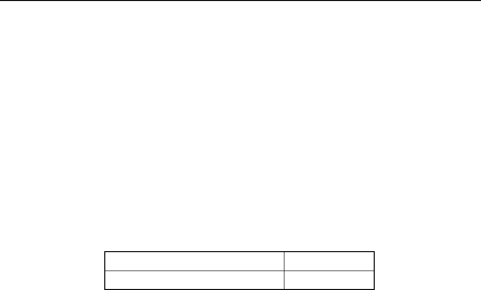
B-1
Appendix B LACR Replacement Parts Ordering and
Motorola Service Centers
B.1 Commercial Warranty
Limited Warranty
MOTOROLA COMMUNICATION PRODUCTS
I. What This Warranty Covers And For How Long
MOTOROLA INC. (“MOTOROLA”) warrants the MOTOROLA manufactured Communication
Products listed below (“Product”) against material defects in material and workmanship under normal
use and service for the period of time from the date of purchase as scheduled below:
Motorola will at its option and at no charge either repair the defective Product (with new or
reconditioned parts), replace it (with a new or reconditioned Product), or refund the purchase price of
the defective Product during the warranty period provided it is returned before the expiration of the
warranty period and in accordance with the terms of this warranty. Replaced Product, parts or boards
are warranted for the balance of the original applicable warranty period. All replaced Product, parts
of boards shall become the property of MOTOROLA.
This express limited warranty is extended by MOTOROLA to the original end user purchasing the
Product for commercial, industrial or governmental use only and is not assignable or transferable to
any other party. This is the complete warranty for the Product manufactured by MOTOROLA.
MOTOROLA assumes no obligations or liability for additions or modifications to this warranty unless
made in writing and signed by an officer of MOTOROLA. Unless made in a separate agreement
between MOTOROLA and the original purchaser, MOTOROLA does not warrant the installation,
maintenance or service of the Product.
MOTOROLA is not responsible in any way for any ancillary equipment not furnished by MOTOROLA
which is attached to or used in connection with the Product, or for operation of the Product with any
ancillary equipment, and all such equipment is expressly excluded from this warranty. Because each
system which may use the Product is unique, MOTOROLA disclaims liability for range, coverage, or
operation of the system in part or as a whole under this warranty.
Base Station/Repeater Two (2) Years
Product Accessories One (1) Year

B-2 LACR Replacement Parts Ordering and Motorola Service Centers: Limited Warranty
II. General Provisions
This warranty sets forth the full extent of MOTOROLA'S responsibilities regarding the Product.
Repair, replacement or refund of the purchase price, at MOTOROLA'S option, is the exclusive
remedy. THIS WARRANTY IS THE COMPLETE WARRANTY FOR THE PRODUCT AND IS GIVEN
IN LIEU OF ALL OTHER WARRANTIES. MOTOROLA DISCLAIMS ALL OTHER WARRANTIES OR
CONDITIONS, EXPRESS OR IMPLIED, INCLUDING WITHOUT LIMITATION, IMPLIED
WARRANTIES OF MERCHANTABILITY AND FITNESS FOR A PARTICULAR PURPOSE. IN NO
EVENT SHALL MOTOROLA BE LIABLE FOR DAMAGES IN EXCESS OF THE PURCHASE PRICE
OF THE PRODUCT, FOR ANY COMMERCIAL LOSS; INCONVIENCE; LOSS OF USE, TIME,
DATA, GOOD WILL, REVENUES, PROFITS OR SAVINGS; OR OTHER SPECIAL, INCIDENTAL,
INDIRECT, OR CONSEQUENTIAL DAMAGES IN ANY WAY RELATED TO OR ARISING FROM
THE SALE OR USE OF THE PRODUCT.
III. How To Get Warranty Service
You must provide proof of purchase (bearing the date of purchase and Product item serial number)
in order to receive warranty service and deliver or send the Product item, transportation and
insurance prepaid, to an authorized warranty service location before the expiration of the warranty
period. Warranty service will be provided by Motorola through one of its authorized warranty service
locations. If you first contact the company which sold you the Product, it can facilitate your obtaining
warranty service. You can also open a Contact Us case on Motorola Online
(http://www.motorola.com/businessonline).
IV. What This Warranty Does Not Cover
This warranty does not cover:
A. Defects or damage resulting from use of the Product in other than its normal customary or
authorized manner.
B. Defects or damage from misuse, accident, liquid, lightning, neglect or act of God.
C. Defects or damage from testing, maintenance, installation, alteration, modification, or
adjustment not provided or authorized in writing by MOTOROLA.
D. Breakage or damage to antennas unless caused directly by defects in material or
workmanship.
E. A Product subjected to unauthorized Product modifications, disassemblies or repairs
(including, without limitation, the addition to the Product of non-Motorola supplied equipment)
which adversely affect performance of the Product or interfere with Motorola's normal
warranty inspection and testing of the Product to verify any warranty claim.
F. Product which has had the serial number removed or made illegible.
G. Freight costs to ship the product to the repair depot.
H. Batteries (because they carry their own separate limited warranty) or consumables.
I. Customer’s failure to comply with all applicable industry and OSHA standards.
J. A Product which, due to illegal or unauthorized alteration of the software/firmware in the
Product, does not function in accordance with MOTOROLA’s published specifications or the
FCC type acceptance labeling in effect for the Product at the time the Product was initially
distributed from MOTOROLA.
K. Scratches or other cosmetic damage to Product surfaces that does not affect the operation of
the Product.
L. Normal and customary wear and tear.

LACR Replacement Parts Ordering and Motorola Service Centers: Replacement Parts Ordering B-3
V. Governing Law
This Warranty is governed by the laws of the State of Illinois, USA.
B.2 Replacement Parts Ordering
B.2.1 Basic Ordering Information
When ordering replacement parts or equipment information, the complete identification number
should be included. This applies to all components, kits, and chassis. If the component part number
is not known, the order should include the number of the chassis or kit of which it is a part, and
sufficient description of the desired component to identify it.
B.2.2 Motorola Online
Motorola Online users can access our online catalog at http://www.motorola.com/businessonline
To register for online access:
• Have your Motorola Customer number available.
• Please go to http://www.motorola.com/businessonline and click on “Sign Up Now.”
• Complete form and submit it.
• Contact your BDM to complete set-up and it will be done within 24 to 48 hours.
B.3 Motorola Service Centers
B.3.1 Servicing Information
If a unit requires further complete testing, knowledge and/or details of component level
troubleshooting or service than is customarily performed at the basic level, please send the radio to
a Motorola Service Center as listed below.
B.3.2 Motorola de México, S.A.
Bosques de Alisos 125
Col. Bosques de las Lomas CP 05120
México D.F.
México
Tel: (5) 257-6700
B.3.3 Motorola de Colombia, Ltd.
Carrera 7 No. 71-52
Bogota - Colombia
Tel: (571) 376-6990

B-4 LACR Replacement Parts Ordering and Motorola Service Centers: Motorola Service Centers
Notes

C-1
Appendix C NAG Replacement Parts Ordering and
Motorola Service Centers
C.1 Commercial Warranty
Limited Warranty
MOTOROLA COMMUNICATION PRODUCTS
I. What This Warranty Covers And For How Long
MOTOROLA INC. (“MOTOROLA”) warrants the MOTOROLA manufactured Communication
Products listed below (“Product”) against material defects in material and workmanship under normal
use and service for the period of time from the date of purchase as scheduled below:
Motorola will at its option and at no charge either repair the defective Product (with new or
reconditioned parts), replace it (with a new or reconditioned Product), or refund the purchase price of
the defective Product during the warranty period provided it is returned before the expiration of the
warranty period and in accordance with the terms of this warranty. Replaced Product, parts or boards
are warranted for the balance of the original applicable warranty period. All replaced Product, parts
of boards shall become the property of MOTOROLA.
This express limited warranty is extended by MOTOROLA to the original end user purchasing the
Product for commercial, industrial or governmental use only and is not assignable or transferable to
any other party. This is the complete warranty for the Product manufactured by MOTOROLA.
MOTOROLA assumes no obligations or liability for additions or modifications to this warranty unless
made in writing and signed by an officer of MOTOROLA. Unless made in a separate agreement
between MOTOROLA and the original purchaser, MOTOROLA does not warrant the installation,
maintenance or service of the Product.
MOTOROLA is not responsible in any way for any ancillary equipment not furnished by MOTOROLA
which is attached to or used in connection with the Product, or for operation of the Product with any
ancillary equipment, and all such equipment is expressly excluded from this warranty. Because each
system which may use the Product is unique, MOTOROLA disclaims liability for range, coverage, or
operation of the system in part or as a whole under this warranty.
Base Station/Repeater Two (2) Years
Product Accessories One (1) Year

C-2 NAG Replacement Parts Ordering and Motorola Service Centers: Limited Warranty
II. General Provisions
This warranty sets forth the full extent of MOTOROLA'S responsibilities regarding the Product.
Repair, replacement or refund of the purchase price, at MOTOROLA'S option, is the exclusive
remedy. THIS WARRANTY IS THE COMPLETE WARRANTY FOR THE PRODUCT AND IS GIVEN
IN LIEU OF ALL OTHER WARRANTIES. MOTOROLA DISCLAIMS ALL OTHER WARRANTIES OR
CONDITIONS, EXPRESS OR IMPLIED, INCLUDING WITHOUT LIMITATION, IMPLIED
WARRANTIES OF MERCHANTABILITY AND FITNESS FOR A PARTICULAR PURPOSE. IN NO
EVENT SHALL MOTOROLA BE LIABLE FOR DAMAGES IN EXCESS OF THE PURCHASE PRICE
OF THE PRODUCT, FOR ANY COMMERCIAL LOSS; INCONVIENCE; LOSS OF USE, TIME,
DATA, GOOD WILL, REVENUES, PROFITS OR SAVINGS; OR OTHER SPECIAL, INCIDENTAL,
INDIRECT, OR CONSEQUENTIAL DAMAGES IN ANY WAY RELATED TO OR ARISING FROM
THE SALE OR USE OF THE PRODUCT.
III. How To Get Warranty Service
You must provide proof of purchase (bearing the date of purchase and Product item serial number)
in order to receive warranty service and deliver or send the Product item, transportation and
insurance prepaid, to an authorized warranty service location before the expiration of the warranty
period. Warranty service will be provided by Motorola through one of its authorized warranty service
locations. If you first contact the company which sold you the Product, it can facilitate your obtaining
warranty service. You can also open a Contact Us case on Motorola Online
(http://www.motorola.com/businessonline).
IV. What This Warranty Does Not Cover
This warranty does not cover:
A. Defects or damage resulting from use of the Product in other than its normal customary or
authorized manner.
B. Defects or damage from misuse, accident, liquid, lightning, neglect or act of God.
C. Defects or damage from testing, maintenance, installation, alteration, modification, or
adjustment not provided or authorized in writing by MOTOROLA.
D. Breakage or damage to antennas unless caused directly by defects in material or
workmanship.
E. A Product subjected to unauthorized Product modifications, disassemblies or repairs
(including, without limitation, the addition to the Product of non-Motorola supplied equipment)
which adversely affect performance of the Product or interfere with Motorola's normal
warranty inspection and testing of the Product to verify any warranty claim.
F. Product which has had the serial number removed or made illegible.
G. Freight costs to ship the product to the repair depot.
H. Batteries (because they carry their own separate limited warranty) or consumables.
I. Customer’s failure to comply with all applicable industry and OSHA standards.
J. A Product which, due to illegal or unauthorized alteration of the software/firmware in the
Product, does not function in accordance with MOTOROLA’s published specifications or the
FCC type acceptance labeling in effect for the Product at the time the Product was initially
distributed from MOTOROLA.
K. Scratches or other cosmetic damage to Product surfaces that does not affect the operation of
the Product.
L. Normal and customary wear and tear.

NAG Replacement Parts Ordering and Motorola Service Centers: Replacement Parts Ordering C-3
V. Governing Law
This Warranty is governed by the laws of the State of Illinois, USA.
C.2 Replacement Parts Ordering
C.2.1 Basic Ordering Information
When ordering replacement parts or equipment information, the complete identification number
should be included. This applies to all components, kits, and chassis. If the component part number
is not known, the order should include the number of the chassis or kit of which it is a part, and
sufficient description of the desired component to identify it.
C.2.2 Motorola Online
Motorola Online users can access our online catalog at
http://motorola.com/businessonline
To register for online access, please call 1-800-422-4210 (for U.S. and Canada Service Centers
only). International customers can obtain assistance at http://motorola.com/businessonline
C.2.3 Mail Orders
Mail orders are only accepted by the US Federal Government Markets Division (USFGMD).
Motorola
7031 Columbia Gateway Drive
3rd Floor - Order Processing
Columbia, MD 21046
U.S.A.
C.2.4 Telephone Orders
Radio Products and Solutions Organization*
(United States and Canada)
7:00 AM to 7:00 PM (Central Standard Time)
Monday through Friday (Chicago, U.S.A.)
1-800-422-4210
1-847-538-8023 (United States and Canada)
U.S. Federal Government Markets Division (USFGMD)
1-877-873-4668
8:30 AM to 5:00 PM (Eastern Standard Time)
C.2.5 Fax Orders
Radio Products and Solutions Organization*
(United States and Canada)
1-800-622-6210
1-847-576-3023 (United States and Canada)
USFGMD
(Federal Government Orders)
1-800-526-8641 (For Parts and Equipment Purchase Orders)

C-4 NAG Replacement Parts Ordering and Motorola Service Centers: Motorola Service Centers
C.2.6 Parts Identification
Radio Products and Solutions Organization*
(United States and Canada)
1-800-422-4210
C.2.7 Product Customer Service
Radio Products and Solutions Organization (United States and Canada)
1-800-927-2744
* The Radio Products and Solutions Organization (RPSO) was formerly known as the Radio
Products Services Division (RPSD) and/or the Accessories and Aftermarket Division (AAD).
C.3 Motorola Service Centers
C.3.1 Servicing Information
If a unit requires further complete testing, knowledge and/or details of component level
troubleshooting or service than is customarily performed at the basic level, please send the repeater
to a Motorola Service Center as listed below.
C.3.2 Motorola Service Center
45D Butterfield Trail
El Paso, TX 79906
Tel: 1-800-227-6772
C.3.3 Motorola Federal Technical Center
4395 Nicole Drive
Lanham, MD 20706
Tel: 1-800-969-6680
Fax: 1-800-784-4133
C.3.4 Motorola Canadian Technical Logistics Center
Motorola Canada Ltd.
8133 Warden Avenue
Markham, Ontario, L6G 1B3
Tel: 1-800-543-3222
Fax: 1-888-331-9872 or 1-905-948-5970

Glossary-1
Glossary of Terms and Acronyms Glossary
This glossary contains an alphabetical listing of terms and their definitions that are applicable to
portable and mobile subscriber radio products. All terms do not necessarily apply to all radios, and
some terms are merely generic in nature.
Term Definition
AGC Automatic Gain Control
Alert tone Audio signal produced by the station, providing feedback to the user.
Analog Refers to a continuously variable signal or a circuit or device designed to
handle such signals.
ASIC Application Specific Integrated Circuit
AUX Auxiliary
Band Frequencies allowed for a specific purpose.
CCI Control Channel Indicate
CDCSS Continuous Digital-Controlled Squelch Systems (DPL)
CTCSS Continuous Tone-Controlled Squelch Systems (PL)
CIT Central Interconnect Terminal. Used to provide telephone interconnect
capability in a trunked station.
CIU Console Interface Unit. Interface between operator console and station to
provide encryption/decryption functions.
Clear Channel modulation type in which voice information is transmitted over the
channel using analog modulation.
Code detect Traditional term used to indicate that a 12kbps CVSD signal is being received
on the RF channel.
Conventional Term used for standard non-trunked radio system (usually using TRC/DC
console).
CPI Console Priority Interface - option allowing console control of a trunked station.
CPS Customer Programming Software: Software with a graphical user interface
containing the feature set of a radio.
DDM Dual Device Module
Default A pre-defined set of parameters.
Digital Refers to data that is stored or transmitted as a sequence of discrete symbols
from a finite set; most commonly this means binary data represented using
electronic or electromagnetic signals.
DPL Digital Private Line (See PL)

Glossary-2
DSP Digital Signal Processor, microprocessor specifically designed to perform
digital signal processing algorithms.
DVP Digital Voice Protection, or Digital Voice Privacy, applies to the Vulcan
encryption algorithm and the Motorola product in which it is sold.
EIA Electronic Industries Association
E/M Telephone circuit signalling lines (Ear/Mouth, Ernie/Mary)
EOM End-Of-Message, 6 kHz signal transmitted at the end of a 12 kbps CVSD signal
that is used by the receiving unit for fast muting of the speaker audio for
squelch tail elimination.
ESD Electro Static Discharge
ETS European Telecommunications Standards
EU European Union
Failsoft Trunked station mode entered when central controller fails
FCC Federal Communications Commission.
FFSK Fast FSK
FM Frequency Modulation
Frequency Number of times a complete electromagnetic-wave cycle occurs in a fixed unit
of time (usually one second).
FRU Field Replaceable Unit
FSK Frequency Shift Keying
GPI General Purpose Input
GPO General Purpose Output
HLGT High Level Guard Tone
IC Integrated Circuit, An assembly of interconnected components on a small
semiconductor chip, usually made of silicon. One chip can contain millions o
microscopic components and perform many functions.
IF intermediate frequency
I/O Input or Output
IRB Inbound Recovery Board used with the Trunking Controller
IRQ Interrupt Request.
kHz kilohertz: One thousand cycles per second. Used especially as a
radio-frequency unit.
LCD Liquid-Crystal Display: An LCD uses two sheets of polarizing material with a
liquid-crystal solution between them. An electric current passed through the
liquid causes the crystals to align so that light cannot pass through them.
Term Definition

Glossary-3
LED Light Emitting Diode: An electronic device that lights up when electricity is
passed through it.
LLGT Low Level Guard Tone
MAN_CS Manual Channel Select.
MDC Motorola Data Communications. 1200 or 4800 baud data signalling scheme.
MHz Megahertz: One million cycles per second. Used especially as a
radio-frequency unit.
MISO Master In, Slave Out.
MON Monitor.
MOSI Master Out, Slave In.
MRTI Microprocessor Radio-Telephone Interconnect; a Motorola system that
provides a repeater connection to the telephone network (The MRTI allows the
radio to access the telephone network when the proper access code is
received).
MSK Minimum Shift Keying
OSW Outbound Signalling Word, data packet transmitted on the outbound Trunking
control channel by the central controller that contains call assignment
information for the subscriber.
PA Power Amplifier that transmits final RF signal to transmit antenna
Paging One-way communication that alerts the Receiver to retrieve a message.
PC Board Printed Circuit Board. Also referred to as a PCB.
PFC Power Factor Correction
PL Private-Line tone squelch; a continuous subaudible tone that is transmitted
along with the carrier (A radio that has PL on the receive frequency will require
both the presence of carrier and the correct PL tone before it will unmute). Also,
if there is PL on the transmit frequency, all transmissions by the radio will be
modulated with the PL tone. Modulation will be continuous.
PLL Phase locked loop; a circuit in which an oscillator is kept in phase with a
reference, usually after passing through a frequency divider.
Programming Cable A cable that allows the CPS to communicate directly with the radio using
RS232.
PSTN Public Switched Telephone Network
PTT Push-to-talk; the switch located on the left side of the radio which, when
pressed causes the radio to transmit.
RA/RT Remote Access/Remote Transmit
RAC Repeater Access Control
Term Definition

Glossary-4
RdStat Receiver Data Status
Receiver Electronic device that amplifies RF signals. A Receiver separates the audio
signal from the RF carrier, amplifies it, and converts it back to the original
sound waves.
Repeater Remote transmit/receive facility that retransmits received signals in order to
improve communications range and coverage.
RF Radio Frequency, The portion of the electromagnetic spectrum between audio
sound and infrared light (approximately 10 kHz to 10 GHz).
RSS Radio Service Software; the software application used to program and service
the station.
RSSI Received Signal Strength Indicator; a dc voltage proportional to the received
RF signal strength.
Rx Receive.
SCM Station Control Module; station controller.
Signal An electrically transmitted electromagnetic wave.
SINAD Acronym for the ratio of signal plus noise plus distortion and noise plus
distortion.
SMR Schaumburg Manual Revision
Smart Repeater Trunking system in which channel control is distributed among several
repeaters.
Spectra-TAC Analog Total Area Coverage voting comparator used to select wide area
receivers.
Spectrum Frequency range within which radiation has specific characteristics.
SPI Serial Peripheral Interface (clock and data lines); simple synchronous serial
interface for data transfer between processors and peripheral ICs.
Squelch Muting of audio circuits when received signal levels fall below a pre-determined
value. With carrier squelch, all channel activity that exceeds the radio’s preset
squelch level can be heard.
SRAM Static RAM, memory chip used for scratchpad memory.
TCC Trunking Central Controller; main control unit of the trunked dispatch system;
handles ISW and OSW messages to and from radios in the field (See ISW and
OSW).
TOC Turn Off Code; alternating binary pattern used by DPL signalling to provide fast
muting of the receiving radio.
TOT Time-out Timer: A timer that limits the length of a transmission.
TPL Tone Private Line.
Term Definition

Glossary-5
Transceiver Transmitter-Receiver. A device that both transmits and receives analog or
digital signals. Also abbreviated as XCVR.
Transmitter Electronic equipment that generates and amplifies an RF carrier signal,
modulates the signal, and then radiates it into space.
TRC Tone Remote Control
Trunking Radio control system which permits efficient frequency utilization and
enhanced control features.
Tx Transmit.
Type II Trunking Motorola trunking system which provides extended features.
UHF Ultra High Frequency
USB Universal Serial Bus: An external bus standard that supports data transfer
rates of 12 Mbps.
Voltage-Controlled Oscillator; an oscillator whereby the frequency of oscillation
can be varied by changing a control voltage.
VHF Very High Frequency
VIP Vehicle Interface Port.
VOX Voice Operated Switch; Used with MRTI.
VSWR Voltage Standing Wave Ratio.
WCI Wildcard Input
WCO Wildcard Output
WFI Word Frame Interrupt; used to synchronize trunking data messages in a Smart
Repeater system.
Wide Area Wide area systems allow expanded radio coverage by using multiple receivers
and/or transmitters.
WL Wireline
WL Rx Wireline Receive; information from station RF Receiver sent to wireline
equipment.
WL Tx Wireline Transmit; information from wireline equipment sent to station RF
transmitter.
XPR Refers to Digital Professional Repeater model names in the MOTOTRBO
Professional Digital Two-Way Radio System.
Term Definition
MTR3000.book Page 0 Monday, October 5, 2009 11:13 AM