MVME147 Single Board Computer Data Sheet MVME147_Brochure Brochure
MVME147_Brochure MVME147_Brochure
User Manual: MVME147_Brochure
Open the PDF directly: View PDF ![]() .
.
Page Count: 4
Datasheet
MVME147
Single-Board
Computer
■16, 25, or 33.33 MHz MC68030 enhanced 32-bit
microprocessor
■16, 25, or 33.33 MHz MC68882 floating-point co-
processor
■4, 8, 16, or 32MB of shared DRAM, with
programmable parity
■4K x 8 SRAM and time-of-day clock with battery
backup
■Four 28/32-pin ROM/PROM/EPROM/EEPROM
sockets, 16 bits wide
■A32/D32 VMEbus master/slave interface with
system controller function
■Four EIA-232-D serial communications ports
■Centronics compatible printer port
■Two 16-bit timers and watchdog timer
■SCSI bus interface with DMA
■Ethernet transceiver interface
■4-level requester, 7-level interrupter, and 7-level
interrupt handler for VMEbus
■On-board debugger and diagnostic firmware
VMEbus single-board computer that eliminates the need for additional backplane
modules
The MVME147 series is a family of VMEbus single-board computers. The on-board
resources and peripheral controllers eliminate the need for additional modules in the
VMEbus backplane thus reducing costs and freeing up valuable bus slots for additional
functions.
The MVME147 series features an MC68030 enhanced 32-bit microprocessor. The
MC68030 was the first general-purpose microprocessor with on-chip cache memory
for both instructions and data, which increases the processor’s efficiency by 20 to 40
percent. The MC68030 features a complete memory management unit (MMU) that
provides the software protection and virtual memory functions critical to many
applications.
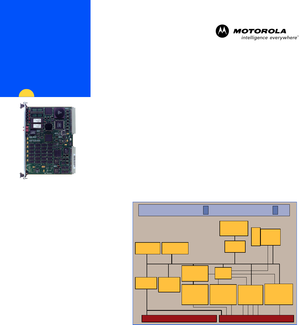
Front Panel
DRAM
4 to 32MB
Array w/parity
GCC
ASIC
EPROM
4 Sockets
2 Banks
Ethernet
Transceiver
AM7990
VMEbus
Interface
MC68030
MPU
P2
MC68882
FPC
P1
Centronics
Compatible
Parallel I/O
Port
PCC
FPGA
NVRAM
RTC
MK48T18
SNAPHAT
Battery
Serial
Controller
85C30
(two)
Serial
Interface
Adapter
LXT901
SCSI
Interface
Adapter
33C93B
2MVME147
MVME147 Details
Transition Module
An optional MVME712M transition module is available
to support the use of standard I/O connections for the
MVME147 series. This module takes the I/O connections
for the peripherals on board the MVME147 series from
the P2 connection of the module to a transition module
that has industry-standard connections.
Development Software
Development software for the MVME147 series includes
the on-board debugger/monitor firmware and driver
packages for the UNIX SYSTEM V/68 and VMEexec
environments. Debugger/monitor firmware is included
on the board.
Software Support
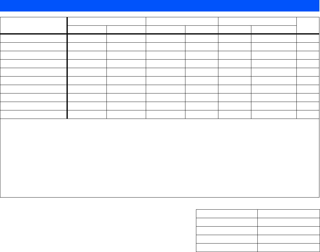
MVME147 DETAILS
Access Sequence 16 MHz 25 MHz 33.33 MHz Notes
Read Cycles Write Cycles Read Cycles Write Cycles Read Cycles Write Cycles
MPU to Local DRAM
No Parity 4444441, 2
Delayed Parity N/A N/A 4 4 4 4 1, 2
Parity N/A N/A 5 4 5 4 1, 2
MPU to Local ROM 9 9 13 13 16 16 1, 3
VMEbus to Local DRAM 13, 813 ns 11, 688 ns 13, 520 ns 11, 440 ns 13, 390 ns 11, 330 ns 4, 5
MPU to Global RAM
VMEbus Master 6 + A 6 + A 9 + A 9 + A 12 + A 12 + A 5, 6
System Controller/Not Master 11 + B 11 + B 17 + B 17 + B 22 + B 22 + B 5, 7
Not System Controller/Not Master 9 + C 9 + C 15 + C 15 + C 19 + C 19 + C 5, 8
Notes:
1. No arbitration overhead.
2. Except RMW cycles where the MVME147 is required to obtain VMEbus mastership before RMW cycle can be started.
3. Device access time must be 200 ns or less.
4. DS0*/DS1* asserted DTACK* asserted.
5. Typical values. Actual values may be greater or less depending on the state of the slave device.
6. A = ta/T cycles.
7. B = (ta + tr)/T cycles.
8. C = (ta + tg)/T cycles.
ta = DS0*/DS1* to the assertion of DTACK* (slave access time).
tr = BRx* low to BBSY high and AS* high (bus requested and granted).
tg = BRx* low to BGINx* low and AS* high (bus requested and granted).
T = MPU clock period, 16 MHz = 62.5 ns, 25 MHz = 40 ns, 33.33 MHz = 30 ns
Integrated Systems, Inc.: pSOS+
Lynx Real-Time Systems, Inc.: LynxOS
Microware Systems Corporation: OS-9
Microtec Research, Inc.: VRTX-32
Wind River Systems, Inc.: VxWorks

MVME147 3
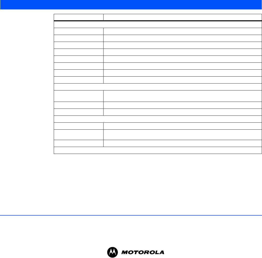
Specifications
Processor
Memory
VMEbus ANSI/VITA 1-1994 VME64 (IEEE STD 1014)
Ethernet
SCSI Bus
Clock/Timers
Serial Ports
Power Requirements
Hardware Support
Board Size
Demonstrated MTBF
(based on a sample of eight boards in accelerated stress environment)
Environmental
Electromagnetic Compatibility (EMC)
Intended for use in systems meeting the following regulations:
This product was tested in a representative system to the following
standards:
SPECIFICATIONS
Microprocessor: MC68030
Co-processor: MC68882
Clock Frequency: 16, 25 or 33.33 MHz
Main Memory: Dynamic RAM
Capacity: 4, 8, 16, or 32MB
Single Cycle
Accesses:
Four read/four write
Read Burst Mode - no
parity:
4-2-2-2
Read Burst Mode -
parity:
5-3-3-3
Write Burst Mode: 4-2-2-2
Parity: Yes, programmable (parity not available
on MVME147-010A)
EPROM: 16-bit, 32-pin DIP
# of Sockets (max.
capacity):
Four (1M x 8)
Capacity: 4MB
DTB Master: A16–A32; D08–D32
DTB Slave: A16–A32; D08–D32, UAT
Arbiter: RR/PRI
Interrupt Handler: IRQ 1–7
Interrupt Generator: Any 1 of 7
System Controller: Yes, jumperable
Location Monitor: Four, LMA32
Controller: AM7990
Local bus DMA: Yes
Connector: Routed to P2
Controller: 33C93B
Local Bus DMA: Yes
Asynchronous (8-bit
mode):
1.5MB/s
Synchronous (8-bit
mode):
4.0MB/s
Connector: Routed to P2
TOD Clock Device: M48T18; 4KB NVRAM (available for user
applications)
Timers/Counters: Two 16-bit, one watchdog
Controller: 85C30
Number of ports: Four
Configuration: EIA-232 DTE
Async Baud Rate, b/s
max.:
19.2K
Sync Baud Rate, b/s
max.:
19.2K
Connector: Routed to P2
Typical Maximum
+5V ± 5.0%: 3.5 A 5.0 A
+12V ± 10.0%: — 1.0 A (with off-board
LAN transceiver)
–12V ± 10.0%: 100 mA —
Multiprocessor
Hardware Support:
Four mailbox interrupts, RMW, shared
RAM
Debug/Monitor
(included):
MVME147BUG
Transition Module
(optional):
MVME712M
Height: 233.4 mm (9.187 in.)
Depth: 160.0 mm (6.299 in.)
Front Panel Height: 261.8 mm (10.3 in.)
Width: 19.8 mm (0.8 in.)
Mean: 190,509 hours
95% Confidence: 107,681 hours
Operating Nonoperating
Temperature: 0° C to +55° C,
forced air cooling
–40° C to +85° C
Humidity (NC): 5% to 90% 5% to 90%
Vibration: 2 Gs RMS,
20–2000 Hz random
6 Gs RMS,
20–2000 Hz random
U.S.: FCC Part 15, Subpart B, Class A (non-residential)
Canada: ICES-003, Class A (non-residential)
CE Mark per European EMC Directive 89/336/EEC with
Amendments; Emissions: EN55022 Class B; Immunity: EN55024
www.motorola.com/computer
Motorola Computer Group
Regional Offices
NORTH AMERICA: Tempe, AZ 800-759-1107 or 602-438-5720
EUROPE: Loughborough, UK +44 1509 634300
EAST MEDITERRANEAN: Tel Aviv, Israel +972 3 568 4388
ASIA: Shanghai, China +86 21 5292 5693
PACIFIC RIM: Tokyo, Japan +81 3 5424 3101
ASIA/PACIFIC: Hong Kong +852 2966 3210
Ordering Information
ORDERING INFORMATION
Part Number Description
All modules include four serial ports and one parallel port.
MVME147-010A 16 MHz, 4MB DRAM, no parity, SCSI
MVME147-011A 25 MHz, 4MB DRAM, Ethernet and SCSI
MVME147-012A 25 MHz, 8MB DRAM, Ethernet and SCSI
MVME147-013A 25 MHz, 16MB DRAM, Ethernet and SCSI
MVME147-014A 25 MHz, 32MB DRAM, Ethernet and SCSI
MVME147-022A 33.33 MHz, 8MB DRAM, Ethernet and SCSI
MVME147-023A 33.33 MHz, 16MB DRAM, Ethernet and SCSI
MVME147-024A 33.33 MHz, 32MB DRAM, Ethernet and SCSI
Related Products
MVME712M Four DB-25 female serial port connectors, Centronics parallel port connector, DB-15 Ethernet connector, SCSI
connector, and P2 adapter
MVME712P2 Adapter module from VME backplane to cabling for transition modules
MVME147FWnn Object of the debugger/monitor where nn=software version; requires software license
Documentation
VME147A/IH MVME147 Installation and Use Manual
V147BUGA1/UM and
V147BUGA2/UM
147Bug User’s Manual, Volumes 1 and 2
VME712MA/IH MVME712 Transition Module Installation and Use
Documentation is available for online viewing and ordering at http://www.motorola.com/computer/literature
MOTOROLA and the Stylized M Logo are registered in the U.S. Patent and Trademark Office. All other product or
service names are the property of their respective owners.
This datasheet identifies products, their specifications, and their characteristics, which may be suitable for certain
applications. It does not constitute an offer to sell or a commitment of present or future availability, and should not be
relied upon to state the terms and conditions, including warranties and disclaimers thereof, on which Motorola may
sell products. A prospective buyer should exercise its own independent judgement to confirm the suitability of the
products for particular applications. Motorola reserves the right to make changes, without notice, to any products or
information herein which will, in its sole discretion, improve reliability, function, or design. Motorola does not assume
any liability arising out of the application or use of any product or circuit described herein; neither does it convey any
license under its patent or other intellectual property rights or under others. This disclaimer extends to any prospective
buyer, and it includes Motorola’s licensee, licensee’s transferees, and licensee’s customers and users. Availability of
some of the products and services described herein may be restricted in some locations.
MV147-D5 02/03 © 2003, 2001, 1996 Motorola, Inc. All rights reserved.
