MVME167 Single Board Computer User's Manual MVME167_d3_Users_Manual D3 Users
MVME167_d3_Users_Manual manual pdf -FilePursuit
MVME167_d3_Users_Manual MVME167_d3_Users_Manual
User Manual: MVME167_d3_Users_Manual
Open the PDF directly: View PDF ![]() .
.
Page Count: 82
- GENERAL INFORMATION
- Introduction
- Model Designations
- Features
- Specifications
- General Description
- Equipment Required
- Related Documentation
- Support Information
- Manual Terminology
- HARDWARE PREPARATION AND INSTALLATION
- Introduction
- Unpacking Instructions
- Hardware Preparation
- Installation Instructions
- OPERATING INSTRUCTIONS
- Introduction
- Controls and Indicators
- Memory Maps
- Software Initialization
- FUNCTIONAL DESCRIPTION
- Introduction
- MVME167 Functional Description
- EIA-232-D INTERCONNECTIONS
- Introduction
- Levels of Implementation

MVME167
Single Board Computer
User’s Manual
Character User Interface:

vii
Contents
CHAPTER 1 GENERAL INFORMATION
Introduction................................................................................................................1-1
Model Designations ...................................................................................................1-1
Features......................................................................................................................1-2
Specifications.............................................................................................................1-3
Cooling Requirements ........................................................................................1-3
FCC Compliance.................................................................................................1-4
General Description ...................................................................................................1-5
Equipment Required ..................................................................................................1-6
Related Documentation..............................................................................................1-7
Support Information...................................................................................................1-8
Manual Terminology..................................................................................................1-9
CHAPTER 2 HARDWARE PREPARATION AND INSTALLATION
Introduction................................................................................................................2-1
Unpacking Instructions ..............................................................................................2-1
Hardware Preparation ................................................................................................2-1
General Purpose Readable Jumpers on Header J1..............................................2-2
System Controller Header J2..............................................................................2-2
Serial Port 4 Clock Configuration Select Headers J6 and J7..............................2-4
SRAM Backup Power Source Select Header J8.................................................2-5
Installation Instructions..............................................................................................2-6
MVME167 Module Installation..........................................................................2-6
System Considerations........................................................................................2-7
CHAPTER 3 OPERATING INSTRUCTIONS
Introduction................................................................................................................3-1
Controls and Indicators..............................................................................................3-1
ABORT Switch S1..............................................................................................3-1
RESET Switch S2...............................................................................................3-1
Front Panel Indicators (DS1 - DS4)....................................................................3-2
Memory Maps............................................................................................................3-3
Local Bus Memory Map.....................................................................................3-3

viii
Normal Address Range ...............................................................................3-3
Detailed I/O Memory Maps ............................................................................3-6
BBRAM,TOD Clock Memory Map .............................................................3-26
Interrupt Acknowledge Map .........................................................................3-28
VMEbus Memory Map ........................................................................................3-29
VMEbus Accesses to the Local Bus .............................................................3-29
VMEbus Short I/O Memory Map .................................................................3-29
Software Initialization .................................................................................................3-30
Multi-MPU Programming Considerations ...........................................................3-30
Local Reset Operation..........................................................................................3-30
CHAPTER 4 FUNCTIONAL DESCRIPTION
Introduction ...................................................................................................................4-1
MVME167 Functional Description...............................................................................4-1
Data Bus Structure..................................................................................................4-1
MC68040 MPU......................................................................................................4-2
EPROM ..................................................................................................................4-2
SRAM.....................................................................................................................4-2
Onboard DRAM.....................................................................................................4-3
Battery Backed Up RAM and Clock......................................................................4-4
VMEbus Interface ..................................................................................................4-4
I/O Interfaces..........................................................................................................4-5
Serial Port Interface.........................................................................................4-5
Parallel Port Interface......................................................................................4-6
Ethernet Interface............................................................................................4-6
SCSI Interface.................................................................................................4-7
SCSI Termination............................................................................................4-7
Local Resources .....................................................................................................4-7
Programmable Tick Timers.............................................................................4-7
Watchdog Timer..............................................................................................4-8
Software-Programmable Hardware Interrupts ................................................4-8
Local Bus Timeout..........................................................................................4-8
Timing Performance...............................................................................................4-8
Local Bus to DRAM Cycle Times..................................................................4-8
ROM Cycle Times ..........................................................................................4-9
SCSI Transfers ................................................................................................4-9
LAN DMA Transfers......................................................................................4-9
Remote Status and Control...................................................................................4-10

ix
APPENDIX A EIA-232-D INTERCONNECTIONS
Introduction.................................................................................................................. A-1
Levels of Implementation ............................................................................................ A-3
Signal Adaptations................................................................................................ A-3
Sample Configurations ......................................................................................... A-4
Proper Grounding ................................................................................................. A-6

x

xi
List of Figures
Figure 2-1. MVME167 Switches, Headers, Connectors, Fuses, and LEDs ..............2-3
Figure 4-1. MVME167 Main Module Block Diagram............................................4-11
Figure 4-2. Parity DRAM Mezzanine Module Block Diagram...............................4-12
Figure 4-3. ECC DRAM Mezzanine Module Block Diagram ................................4-13
Figure A-1. Middle-of-the-Road EIA-232-D Configuration....................................A-4
Figure A-2. Minimum EIA-232-D Connection ........................................................A-5

xii

xiii
List of Tables
Table 1-1. MVME167 Model Designations...............................................................1-1
Table 1-2. MVME167 Specifications ........................................................................1-4
Table 3-1. Local Bus Memory Map...........................................................................3-4
Table 3-2. Local I/O Devices Memory Map..............................................................3-5
Table 3-3. VMEchip2 Memory Map (Sheet 1 of 3)...................................................3-8
Table 3-4. PCCchip2 Memory Map.........................................................................3-14
Table 3-5. Printer Memory Map ..............................................................................3-16
Table 3-6. MEMC040 Internal Register Memory Map ...........................................3-17
Table 3-7. MCECC Internal Register Memory Map................................................3-17
Table 3-8. Cirrus Logic CD2401 Serial Port Memory Map ....................................3-19
Table 3-9. 82596CA Ethernet LAN Memory Map..................................................3-23
Table 3-10. 53C710 SCSI Memory Map .................................................................3-24
Table 3-11. MK48T08 BBRAM,TOD Clock Memory Map ...................................3-25
Table 3-12. BBRAM Configuration Area Memory Map.........................................3-25
Table 3-13. TOD Clock Memory Map.....................................................................3-26
Table A-1. EIA-232-D Interconnections...................................................................A-2

xiv
MVME167/D31-1
1
GENERAL INFORMATION
Introduction
This manual provides general information, preparation for use and installation
instructions, operating instructions, and functional description for the MVME167
series of Single Board Computers (referred to as the MVME167 throughout this
manual).
Model Designations
The MVME167 is available in several models, which are listed in Table 1-1.
MVME167 Model Designations on page 1-1.
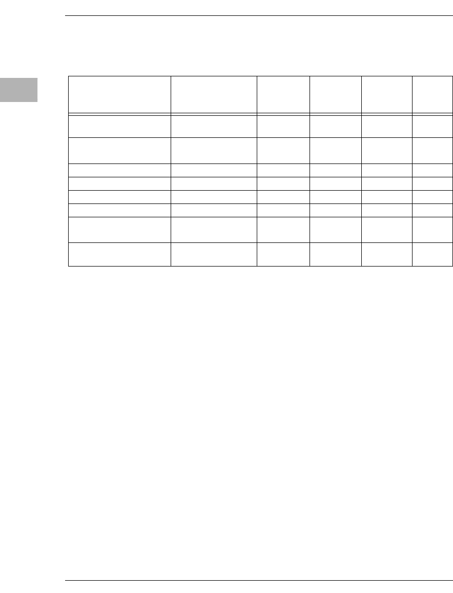
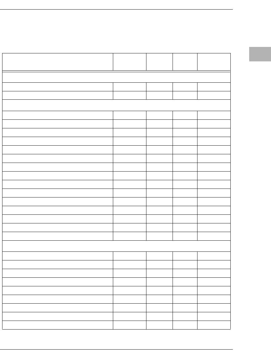
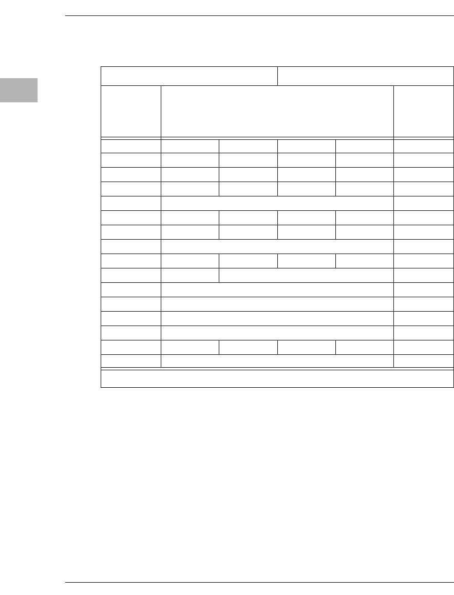
Table 1-1. MVME167 Model Designations
Model Number Speed Major Differences
MVME167-001B (was MVME167-01 or -001A) 25 MHz 4MB Onboard Parity DRAM
MVME167-002B (was MVME167-02 or -002A) 25 MHz 8MB Onboard Parity DRAM
MVME167-003B (was MVME167-03 or -003A) 25 MHz 16MB Onboard Parity DRAM
MVME167-004B (was MVME167-04 or -004A) 25 MHz 32MB Onboard Parity DRAM
MVME167-031B (was MVME167-31 or -031A) 33 MHz 4MB Onboard ECC DRAM
MVME167-032B (was MVME167-32 or -032A) 33 MHz 8MB Onboard ECC DRAM
MVME167-033B (was MVME167-33 or -033A) 33 MHz 16MB Onboard ECC DRAM
MVME167-034B (was MVME167-34 or -034A) 33 MHz 32MB Onboard ECC DRAM
MVME167-035B (was MVME167-035A) 33 MHz 64MB Onboard ECC DRAM
MVME167-036B (was MVME167-036A) 33 MHz 128MB Onboard ECC DRAM

General Information
1-2 MVME167 Single Board Computer User’s Manual
1
Features
Features of the MVME167 are listed below.
❏MC68040 Microprocessor at 25 MHz (-00X models), or 33 MHz
(-03X models)
❏4/8/16/32/64MB of 32-bit DRAM with parity protection
or 4/8/16/32/64/128/256MB of DRAM with ECC protection
❏Four 44-pin PLCC ROM sockets (organized as two banks of 32 bits)
❏128KB SRAM (with optional battery backup)
❏Status LEDs for FAIL, STAT, RUN, SCON, LAN, +12V (LAN power), SCSI,
and VME.
❏8K by 8 RAM and time of day clock with battery backup
❏RESET and ABORT switches
❏Four 32-bit tick timers for periodic interrupts
❏Watchdog timer
❏Eight software interrupts
❏I/O
– SCSI Bus interface with DMA
– Four serial ports with EIA-232-D buffers with DMA
– Centronics printer port
– Ethernet transceiver interface with DMA
❏VMEbus interface
– VMEbus system controller functions
– VMEbus interface to local bus (A24/A32,
D8/D16/D32 (D8/D16/D32/D64BLT) (BLT = Block Transfer)
– Local bus to VMEbus interface (A16/A24/A32, D8/D16/D32)
– VMEbus interrupter
– VMEbus interrupt handler
– Global CSR for interprocessor communications
– DMA for fast local memory - VMEbus transfers (A16/A24/A32,
D16/D32 (D16/D32/D64BLT)

Specifications
MVME167/D3 1-3
1
Specifications
General specifications for the MVME167 are listed in Table 1-2. MVME167
Specifications on page 1-4.
The following sections detail cooling requirements and FCC compliance.
Cooling Requirements
The Motorola MVME167 VMEmodule is specified, designed, and tested to operate
reliably with an incoming air temperature range from 0° to 55° C
(32° to 131° F) with forced air cooling at a velocity typically achievable by using a 100
CFM axial fan. Temperature qualification is performed in a standard Motorola
VMEsystem chassis. Twenty-five watt load boards are inserted in two card slots, one
on each side, adjacent to the board under test, to simulate a high power density system
configuration. An assembly of three axial fans, rated at 100 CFM per fan, is placed
directly under the VME card cage. The incoming air temperature is measured between
the fan assembly and the card cage, where the incoming airstream first encounters the
module under test. Test software is executed as the module is subjected to ambient
temperature variations. Case temperatures of critical, high power density integrated
circuits are monitored to ensure component vendors specifications are not exceeded.
While the exact amount of airflow required for cooling depends on the ambient air
temperature and the type, number, and location of boards and other heat sources,
adequate cooling can usually be achieved with 10 CFM and 490 LFM flowing over the
module. Less airflow is required to cool the module in environments having lower
maximum ambients. Under more favorable thermal conditions, it may be possible to
operate the module reliably at higher than 55° C with increased airflow. It is important
to note that there are several factors, in addition to the rated CFM of the air mover,
which determine the actual volume and speed of air flowing over a module.
General Information
1-4 MVME167 Single Board Computer User’s Manual
1
FCC Compliance
The MVME167 was tested in an FCC-compliant chassis, and meets the requirements
for Class A equipment. FCC compliance was achieved under the following conditions:
1. Shielded cables on all external I/O ports.
2. Cable shields connected to earth ground via metal shell connectors bonded to a
conductive module front panel.
3. Conductive chassis rails connected to earth ground. This provides the path for
connecting shields to earth ground.
4. Front panel screws properly tightened.
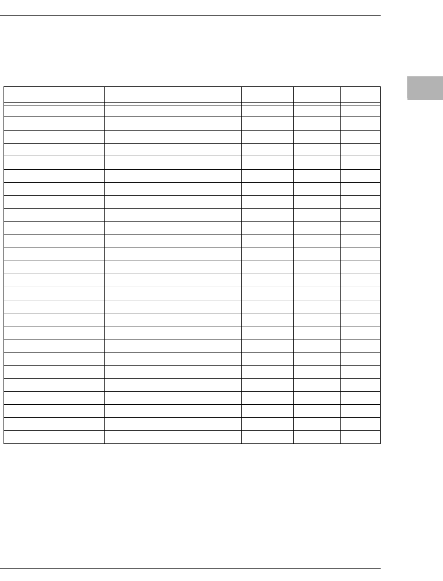
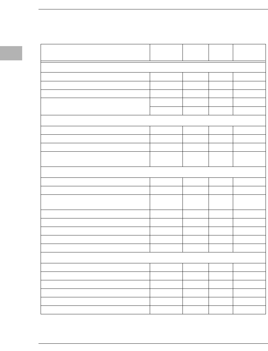
Table 1-2. MVME167 Specifications
Characteristics Specifications
Power requirements
(with all four EPROM
sockets populated and
excluding external
LAN transceiver)
+5 Vdc (± 5%), 3.5 A (typical), 4.5 A (max.)
(at 25 MHz, with 32MB parity DRAM);
5.0 A (typical), 6.5 A (max.)
(at 33 MHz, with 128MB ECC DRAM)
+12 Vdc (± 5%), 100 mA (max.)
(1.0 A (max.) with offboard LAN
transceiver)
-12 Vdc (± 5%), 100 mA (max.)
Operating temperature (refer to
Cooling Requirements section)
0° to 55° C at point of entry of forced air
(approximately 490 LFM)
Storage temperature -40° to +85° C
Relative humidity 5% to 90% (non-condensing)
Physical dimensions
PC board with mezzanine module
only
Height
Depth
Thickness
PC boards with connectors and front
panel
Height
Depth
Thickness
Double-high VMEboard
9.187 inches (233.35 mm)
6.299 inches (160.00 mm)
0.662 inches (16.77 mm)
10.309 inches (261.85 mm)
7.4 inches (188 mm)
0.80 inches (20.32 mm)

General Description
MVME167/D3 1-5
1
For minimum RF emissions, it is essential that the conditions above be implemented;
failure to do so could compromise the FCC compliance of the equipment containing
the module.
General Description
The MVME167 is a double-high VMEmodule based on the MC68040 microprocessor.
The MVME167 has 4/8/16/32/64 MB of parity-protected DRAM or
4/8/16/32/64/128/256 MB of ECC-protected DRAM, 8KB of static RAM and time of
day clock (with battery backup), Ethernet transceiver interface, four serial ports with
EIA-232-D interface, four tick timers, watchdog timer, four ROM sockets, SCSI bus
interface with DMA, Centronics printer port, A16/A24/A32/D8/D16/D32/D64
VMEbus master/slave interface, 128KB of static RAM (with optional battery backup),
and VMEbus system controller.
The I/O on the MVME167 is connected to the VMEbus P2 connector. The main board
is connected through a P2 transition board and cables to the transition boards. The
MVME167 supports the transition boards MVME712-12, MVME712-13,
MVME712M, MVME712A, MVME712AM, and MVME712B (referred to in this
manual as MVME712X, unless separately specified). The MVME712X transition
boards provide configuration headers and provide industry standard connectors for the
I/O devices.
The VMEbus interface is provided by an ASIC called the VMEchip2. The VMEchip2
includes two tick timers, a watchdog timer, programmable map decoders for the master
and slave interfaces, and a VMEbus to/from local bus DMA controller, a VMEbus
to/from local bus non-DMA programmed access interface, a VMEbus interrupter, a
VMEbus system controller, a VMEbus interrupt handler, and a VMEbus requester.
Processor-to-VMEbus transfers can be D8, D16, or D32. VMEchip2 DMA transfers to
the VMEbus, however, can be D16, D32, D16/BLT, D32/BLT, or D64/MBLT.
The PCCchip2 ASIC provides two tick timers and the interface to the LAN chip, SCSI
chip, serial port chip, printer port, and BBRAM.
The MEMC040 memory controller ASIC provides the programmable interface for the
parity-protected DRAM mezzanine board.
The MCECC memory controller ASIC provides the programmable interface for the
ECC-protected DRAM mezzanine board.

General Information
1-6 MVME167 Single Board Computer User’s Manual
1
Equipment Required
The following equipment is required to make a complete system using the MVME167:
❏Terminal
❏Disk drives and controllers
❏Transition module MVME712-12, MVME712-13, MVME712M, MVME712A,
MVME712AM, or MVME712B, and connecting cables and P2 adapter
❏Operating system
The MVME167Bug debug monitor firmware (167Bug) is provided in two of the four
EPROM sockets on the MVME167 main module. It provides over 50 debug,
up/downline load, and disk bootstrap load commands, as well as a full set of onboard
diagnostics and a one-line assembler/disassembler. 167Bug includes a user interface
which accepts commands from the system console terminal. 167Bug can also operate
in a System Mode, which includes choices from a service menu. Refer to the
MVME167Bug Debugging Package User’s Manual and the Debugging Package for
Motorola 68K CISC CPUs User’s Manual for details.
The MVME712X series of transition modules provide the interface between the
MVME167 module and peripheral devices. They connect the MVME167 to
EIA-232-D serial devices, Centronics-compatible parallel devices, SCSI devices, and
Ethernet devices. The MVME712X series work with cables and a P2 adapter.
Software available for the MVME167 includes SYSTEM V/68 and real-time operating
systems, programming languages, and other tools and applications. Contact your local
Motorola sales office for more details.
Related Documentation
MVME167/D3 1-7
1
Related Documentation
The following publications are applicable to the MVME167 and may provide
additional helpful information. If not shipped with this product, they may be purchased
by contacting your local Motorola sales office. Non-Motorola documents may be
purchased from the sources listed.
Note Although not shown in the above list, each Motorola Computer
Group manual publication number is suffixed with characters
which represent the revision level of the document, such as
"/D2" (the second revision of a manual); a supplement bears the
same number as a manual but has a suffix such as "/D2A1" (the
first supplement to the second edition of the manual).
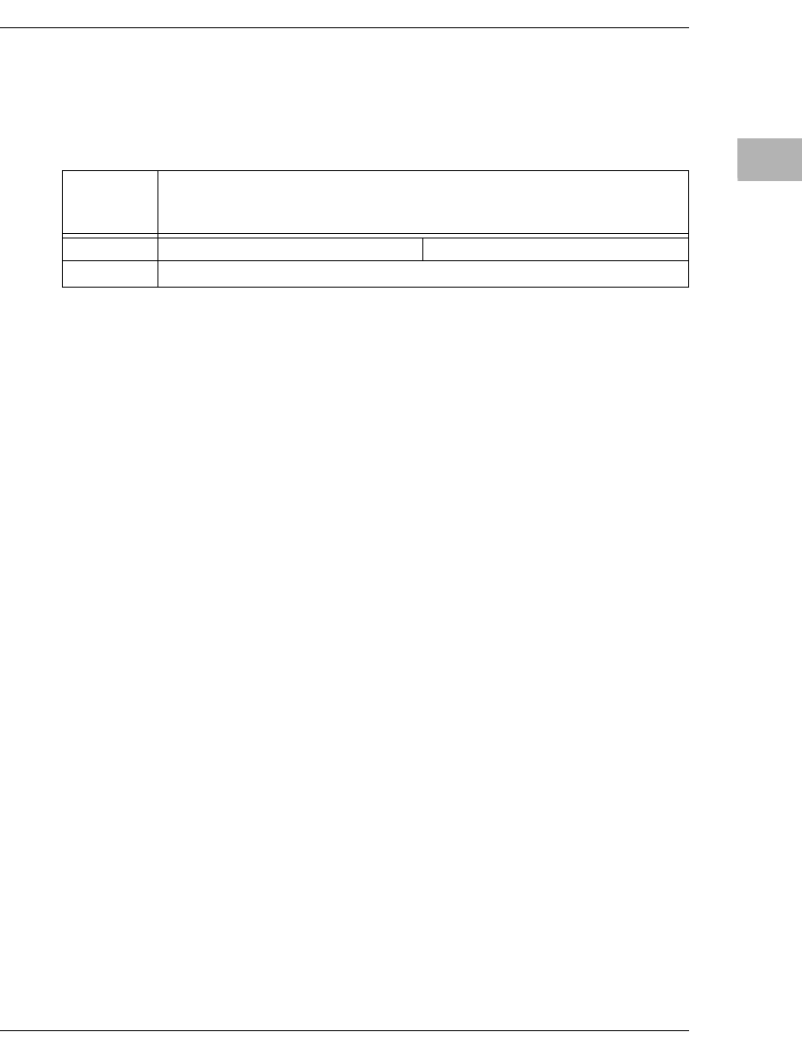
Document Title Motorola
Publication
Number
MVME167 Single Board Computer Support Information
(Refer to Support Information on page 1-8)
SIMVME167
MVME167Bug Debugging Package User’s Manual MVME167BUG
Debugging Package for Motorola 68K CISC CPUs User’s Manual 68KBUG
Single Board Computers SCSI Software User’s Manual SBCSCSI
MVME166/MVME167/MVME187 Single Board Computers
Programmer’s Reference Guide
MVME187PG
MVME712M Transition Module and P2 Adapter Board User’s
Manual
MVME712M
MVME712-12, MVME712-13, MVME712A, MVME712AM, and
MVME712B Transition Module and LCP2 Adapter Board User’s
Manual
MVME712A
M68040 Microprocessor User’s Manual M68040UM

General Information
1-8 MVME167 Single Board Computer User’s Manual
1
The following publications are available from the sources indicated.
Versatile Backplane Bus: VMEbus, ANSI/IEEE Std 1014-1987, The Institute of
Electrical and Electronics Engineers, Inc., 345 East 47th Street, New York, NY 10017
(VMEbus Specification). This is also available as Microprocessor system bus for 1 to
4 byte data, IEC 821 BUS, Bureau Central de la Commission Electrotechnique
Internationale; 3, rue de Varembé, Geneva, Switzerland.
ANSI Small Computer System Interface-2 (SCSI-2), Draft Document X3.131-198X,
Revision 10c; Global Engineering Documents, P.O. Box 19539, Irvine, CA 92714.
CL-CD2400/2401 Four-Channel Multi-Protocol Communications Controller Data
Sheet, order number 542400-003; Cirrus Logic, Inc., 3100 West Warren Ave.,
Fremont, CA 94538.
82596CA Local Area Network Coprocessor Data Sheet, order number 290218; and
82596 User’s Manual, order number 296853; Intel Corporation, Literature Sales, P.O.
Box 58130, Santa Clara, CA 95052-8130.
NCR 53C710 SCSI I/O Processor Data Manual, order number NCR53C710DM; and
NCR 53C710 SCSI I/O Processor Programmer’s Guide, order number
NCR53C710PG; NCR Corporation, Microelectronics Products Division, Colorado
Springs, CO.
MK48T08(B) Timekeeper TM and 8Kx8 Zeropower TM RAM data sheet in Static
RAMs Databook, order number DBSRAM71; SGS-THOMPSON Microelectronics
Group; North & South American Marketing Headquarters, 1000 East Bell Road,
Phoenix, AZ 85022-2699.
Support Information
The SIMVME167 manual contains the connector interconnect signal information,
parts lists, and the schematics for the MVME167.
This manual may be obtained free of charge by contacting your local Motorola sales
office.

Manual Terminology
MVME167/D3 1-9
1
Manual Terminology
Throughout this manual, a convention is used which precedes data and address
parameters by a character identifying the numeric format as follows:
Unless otherwise specified, all address references are in hexadecimal.
An asterisk (*) following the signal name for signals which are level significant
denotes that the signal is true or valid when the signal is low.
An asterisk (*) following the signal name for signals which are edge significant
denotes that the actions initiated by that signal occur on high to low transition.
In this manual, assertion and negation are used to specify forcing a signal to a
particular state. In particular, assertion and assert refer to a signal that is active or true;
negation an negate indicate a signal that is inactive or false. These terms are used
independently of the voltage level (high or low) that they represent.
Data and address sizes are defined as follows:
❏A byte is eight bits, numbered 0 through 7, with bit 0 being the least significant.
❏A word is 16 bits, numbered 0 through 15, with bit 0 being the least significant.
❏A longword is 32 bits, numbered 0 through 31, with bit 0 being the least
significant.
$ dollar specifies a hexadecimal character
% percent specifies a binary number
& ampersand specifies a decimal number

General Information
1-10 MVME167 Single Board Computer User’s Manual
1
MVME167/D32-1
2
HARDWARE PREPARATION
AND INSTALLATION
Introduction
This chapter provides unpacking instructions, hardware preparation, and installation
instructions for the MVME167. The MVME712X transition module hardware
preparation is provided in separate manuals. Refer to Related Documentation in
Chapter 1.
Unpacking Instructions
Note
If the shipping carton is damaged upon receipt, request carrier’s
agent be present during unpacking and inspection of equipment.
Unpack equipment from shipping carton. Refer to packing list and verify that all items
are present. Save packing material for storing and reshipping of equipment.
Caution
Avoid touching areas of integrated circuitry; static discharge
can damage circuits.
Hardware Preparation
To select the desired configuration and ensure proper operation of the MVME167,
certain option modifications may be necessary before installation. The MVME167
provides software control for most of these options. Some options can not be done in
software, so are done by jumpers on headers. Most other modifications are done by
setting bits in control registers after the MVME167 has been installed in a system. (The
MVME167 registers are described in Chapter 4, and/or in the
MVME166/MVME167/MVME187 Single Board Computers Programmer’s Reference
Guide as listed in Related Documentation in Chapter 1.)
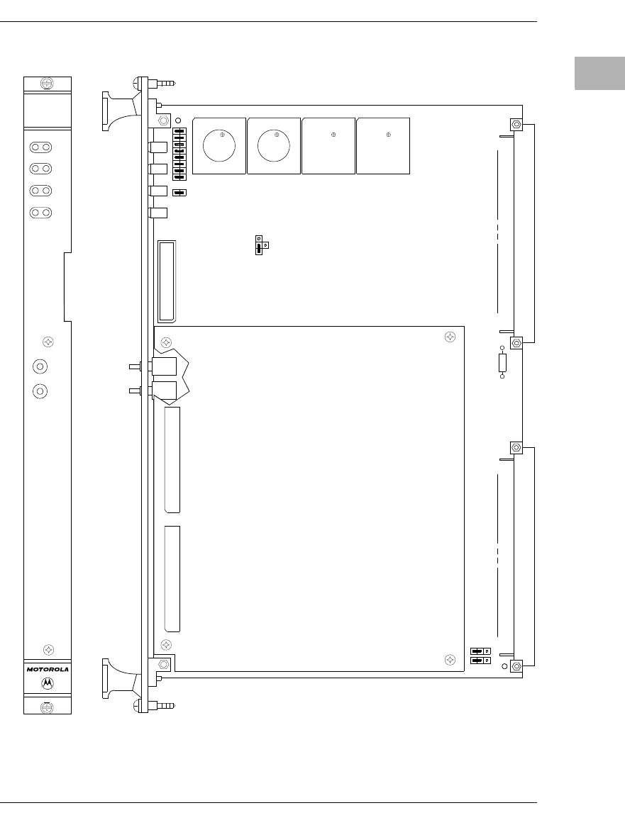
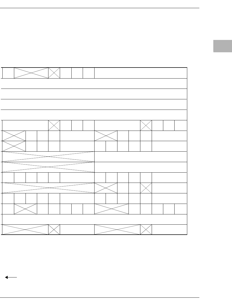
The location of the switches, jumper headers, connectors, and LED indicators on the
MVME167 is illustrated in Figure 2-1. The MVME167 has been factory tested and is
shipped with the factory jumper settings described in the following sections. The
MVME167 operates with its required and factory-installed Debug Monitor,
MVME167Bug (167Bug), with these factory jumper settings.
Settings can be made for:
❏General purpose readable register (J1)
Hardware Preparation and Installation
2-2 MVME167 Single Board Computer User’s Manual
2❏System controller select (J2)
❏Serial port 4 clock configuration select (J6 and J7)
❏SRAM backup power source select (J8) (optional)
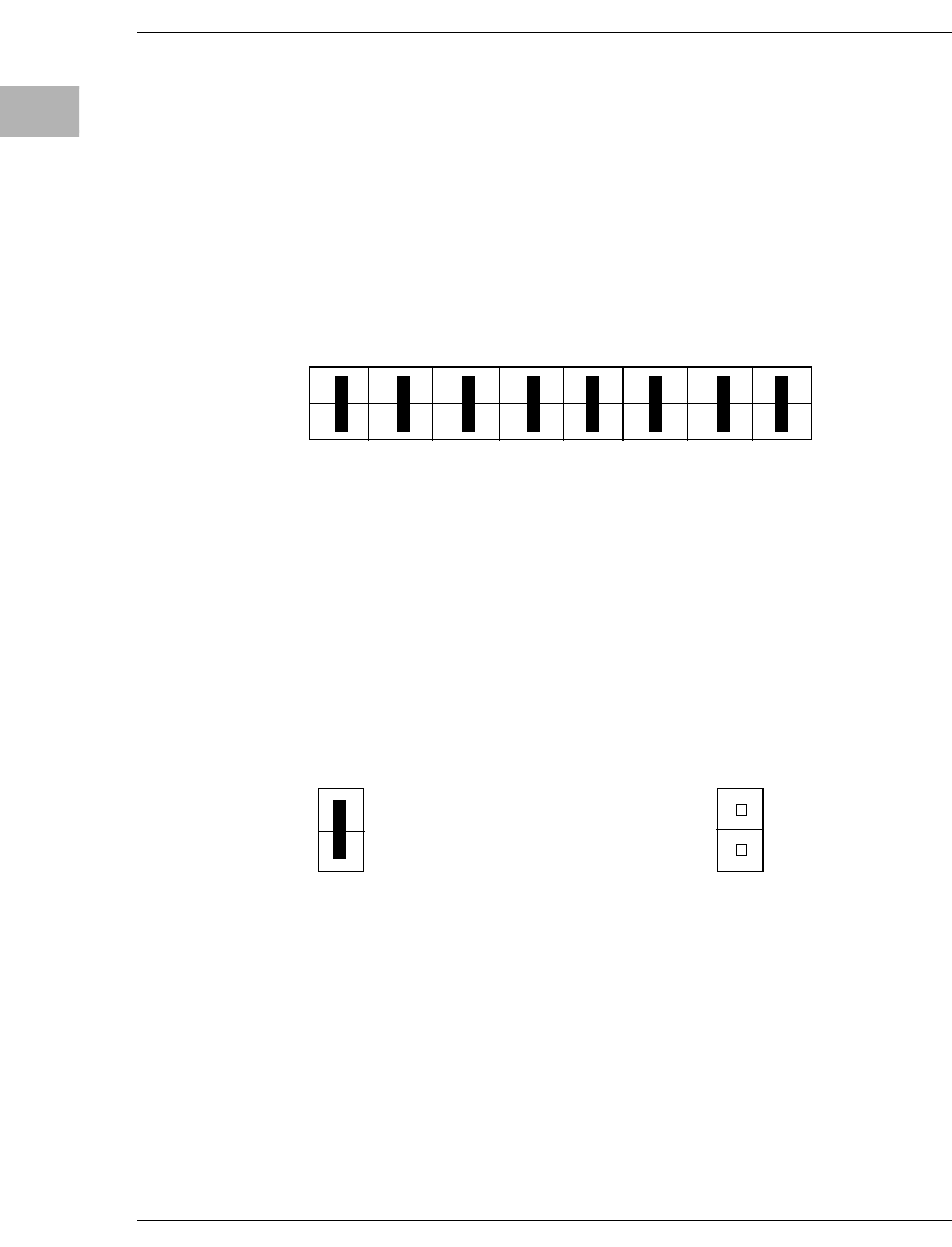
General Purpose Readable Jumpers on Header J1
Each MVME167 may be configured with readable jumpers. These jumpers can be read
as a register (at $FFF40088) in the VMEchip2 LCSR. The bit values are read as a one
when the jumper is off, and as a zero when the jumper is on.
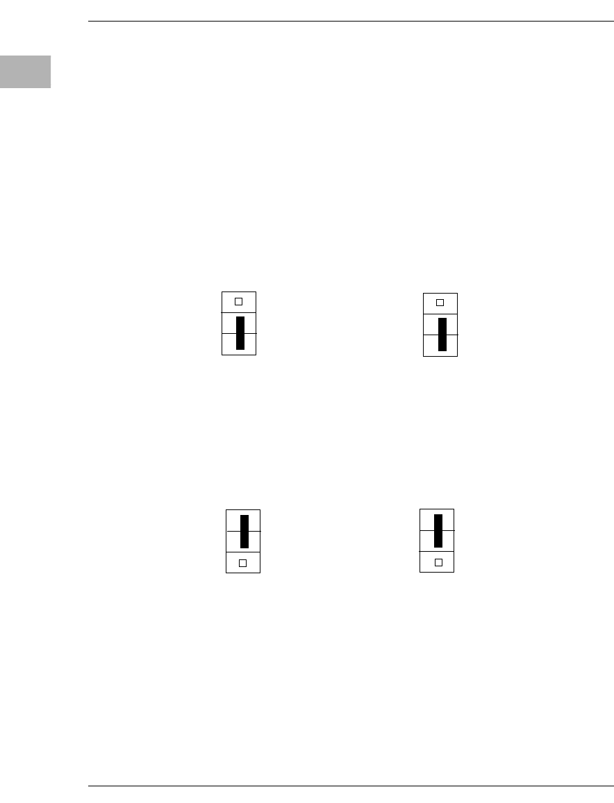
System Controller Header J2
The MVME167 can be VMEbus system controller. The system controller function is
enabled/disabled by jumpers on header J2. When the MVME167 is system controller,
the SCON LED is turned on. The VMEchip2 may be configured as a system controller
as follows.
J1
2
1
16
15
GP10 GP11 GP12 GP13 GP14 GP15 GP16 GP17
All Zeros (Factory Configuration)
J2
1
System Controller
(Factory Configuration)
2
J2
Not System Controller
1
2
Hardware Preparation
MVME167/D3 2-3
2
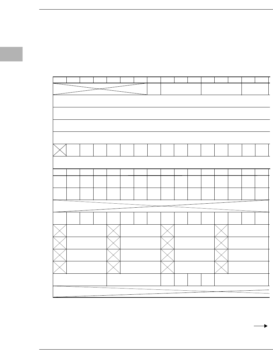
Figure 2-1. MVME167 Switches, Headers, Connectors, Fuses, and LEDs
S1 S2
P1
A1
B1
C1
A32
B32
C32
1379 9404
MVME
167
PRIMARY SIDE
P2
A32
B32
C32
A1
B1
C1
19
20 J3
DS1
1
2
HALTFAIL
RUN SCON
LAN
SCSI VME
ABORT
RESET
J2
F2
J8
1
162
115
+12V
XU4
SKT
39
40
1
2
29
28
6718
17
XU3
SKT
39
40
1
29
28
6718
17
XU2
39
40
1
29
28
6718
17
XU1
39
40
1
29
28
6718
17
11
33
J6 J7
COMPONENTS ARE REMOVED FOR CLARITY
60
59 2
1
J4 60
59 2
1
J5
MEZZANINE BOARD
DS2
DS3
DS4
2
2
2
1
2
J1
23
4
(OPTIONAL)
Hardware Preparation and Installation
2-4 MVME167 Single Board Computer User’s Manual
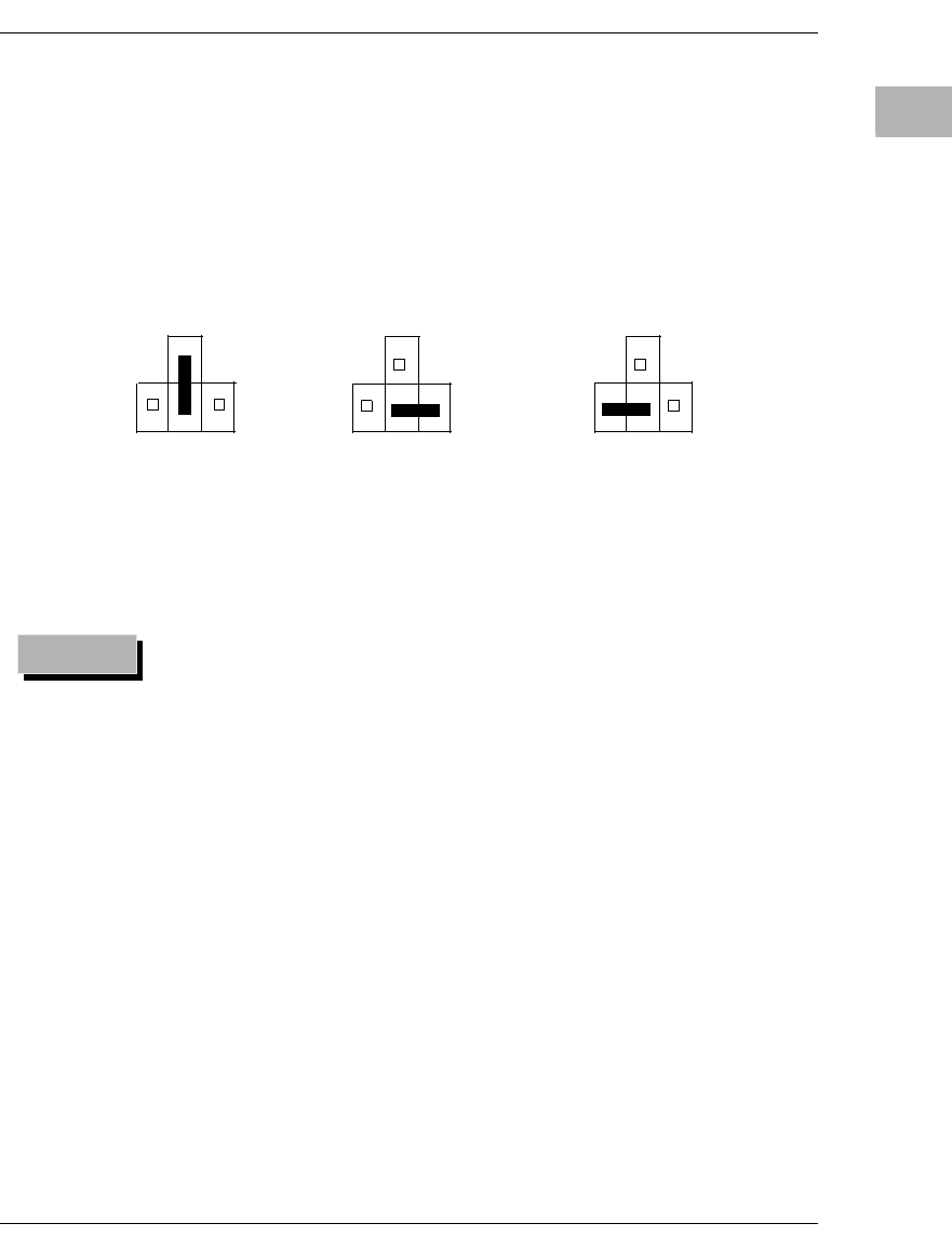
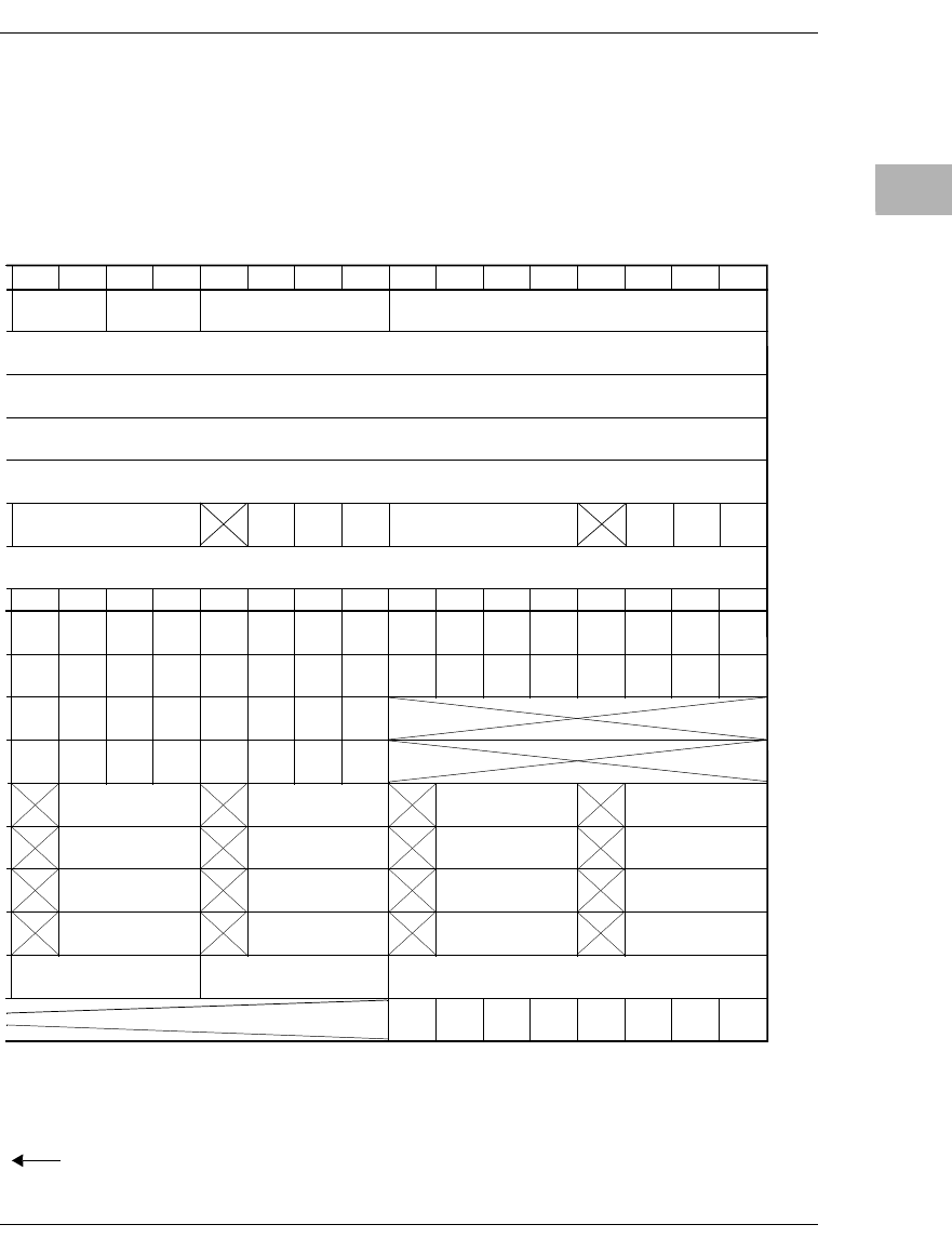
2Serial Port 4 Clock Configuration Select Headers J6 and J7
Serial port 4 can be configured to use clock signals provided by the RTXC4 and
TRXC4 signal lines. Headers J6 and J7 on the MVME167 configure serial port 4 to
drive or receive RTXC4 and TRXC4, respectively. Factory configuration is with port
4 set to receive both signals.
The remaining configuration of the clock lines is accomplished using the Serial Port 4
Clock Configuration Select header on the MVME712M transition module. Refer to the
MVME712M Transition Module and MVME147P2 Adapter Board User’s Manual for
configuration of that header
Receive RTXC4
J7
1
3
J6
1
3
Receive TRXC4
(Factory Configurations)
Drive RTXC4
J7
1
3
J6
Drive TRXC4
1
3
Hardware Preparation
MVME167/D3 2-5
2
SRAM Backup Power Source Select Header J8
Header J8 is an optional header that is used to select the power source used to back up
the SRAM on the MVME167, if the optional battery and circuitry is present.
Caution Do not remove all jumpers from J8. This may disable the
SRAM.
If your board contains the optional header J8, but the optional
battery is removed, jumpers must be installed on J8 between
pins 2 and 4, as shown in the Backup Power Disabled drawing
above.
J8
4
13
VMEbus +5V STBY
(Factory Configuration, when
Optional Battery Is Present)
Optional Battery
J8J8
2
4
13 2
4
13 2
Backup Power Disabled

Hardware Preparation and Installation
2-6 MVME167 Single Board Computer User’s Manual
2Installation Instructions
The following sections discuss installation of the MVME167 into a VME chassis, and
system considerations. Ensure that EPROM devices are installed as needed. Factory
configuration is with two EPROMs installed for the MVME167Bug debug monitor, in
sockets XU1 and XU2. Ensure that all header jumpers are configured as desired.
MVME167 Module Installation
Now that the MVME167 module is ready for installation, proceed as follows:
1. Turn all equipment power OFF and disconnect power cable from ac power source.
Caution
Inserting or removing modules while power is applied could
result in damage to module components. WARNING
!
WARNING DANGEROUS VOLTAGES, CAPABLE OF CAUSING
DEATH, ARE PRESENT IN THIS EQUIPMENT. USE
EXTREME CAUTION WHEN HANDLING, TESTING, AND
ADJUSTING.
2. Remove chassis cover as instructed in the equipment user’s manual.
3. Remove the filler panel(s) from the appropriate card slot(s) at the front and rear of
the chassis (if the chassis has a rear card cage). The MVME167 module requires
power from both P1 and P2. It may be installed in any double-height unused card
slot, if it is not configured as system controller. If the MVME167 is configured as
system controller, it must be installed in the leftmost card slot (slot 1) to correctly
initiate the bus-grant daisy-chain and to have proper operation of the
IACK-daisy-chain driver. The MVME167 is to be installed in the front of the
chassis and the MVME712X is to be installed in the front or the rear of the chassis.
Other modules in the system may have to be moved to allow space for the
MVME712M which has a double-wide front panel.
4. Carefully slide the MVME167 module into the card slot. Be sure the module is
seated properly into the P1 and P2 connectors on the backplane. Do not damage
or bend connector pins. Fasten the module in the chassis with screws provided,
making good contact with the transverse mounting rails to minimize RFI
emissions.
5. Remove IACK and BG jumpers from the header on the chassis backplane for the
card slot the MVME167 is installed in.

Installation Instructions
MVME167/D3 2-7
2
6. Connect the P2 Adapter Board and specified cable(s) to the MVME167 at P2 on
the backplane at the MVME167 slot, to mate with (optional) terminals or other
peripherals at the EIA-232-D serial ports, parallel port, SCSI ports, and LAN
Ethernet port. Refer to the manuals listed in Related Documentation in Chapter 1
for information on installing the P2 Adapter Board and the MVME712X transition
module(s). (Some connection diagrams are in the
MVME166/MVME167/MVME187 Single Board Computers Programmer’s
Reference Guide.) Some cable(s) are not provided with the MVME712X
module(s), and therefore are made or provided by the user. (Motorola
recommends using shielded cables for all connections to peripherals to minimize
radiation.) Connect the peripherals to the cable(s). Detailed information on the
EIA-232-D signals supported is found in Appendix A.
7. Install any other required VMEmodules in the system.
8. Replace the chassis cover.
9. Connect power cable to ac power source and turn equipment power ON.
System Considerations
The MVME167 needs to draw power from both P1 and P2 of the VMEbus backplane.
P2 is also used for the upper 16 bits of data for 32-bit transfers, and for the upper 8
address lines for extended addressing mode. The MVME167 may not operate properly
without its main board connected to P1 and P2 of the VMEbus backplane.
Whether the MVME167 operates as a VMEbus master or as a VMEbus slave, it is
configured for 32 bits of address and for 32 bits of data (A32/D32). However, it
handles A16 or A24 devices in the address ranges indicated in Chapter 3. D8 and/or
D16 devices in the system must be handled by the MC68040 software. Refer to the
memory maps in Chapter 3.
The MVME167 contains shared onboard DRAM whose base address is
software-selectable. Both the onboard processor and offboard VMEbus devices see
this local DRAM at base physical address $00000000, as programmed by the
MVME167Bug firmware. This may be changed, by software, to any other base
address. Refer to the MVME166/MVME167/MVME187 Single Board Computers
Programmer’s Reference Guide for details.
If the MVME167 tries to access offboard resources in a nonexistent location, and is not
system controller, and if the system does not have a global bus timeout, the MVME167
waits forever for the VMEbus cycle to complete. This would cause the system to hang
up. There is only one situation in which the system might lack this global bus timeout:
the MVME167 is not the system controller, and there is no global bus timeout
elsewhere in the system.

Hardware Preparation and Installation
2-8 MVME167 Single Board Computer User’s Manual
2Multiple MVME167 modules may be configured into a single VME card cage. In
general, hardware multiprocessor features are supported.
Other MPUs on the VMEbus can interrupt, disable, communicate with and determine
the operational status of the processor(s). One register of the GCSR set includes four
bits which function as location monitors to allow one MVME167 processor to
broadcast a signal to other MVME167 processors, if any. All eight registers are
accessible from any local processor as well as from the VMEbus.
The MVME167 provides +12 Vdc power to the Ethernet LAN transceiver interface
through a 1 amp fuse F2 located on the MVME167 module. The +12V LED lights
when +12 Vdc is available. The fuse is socketed, and located near diode CR1. If the
Ethernet transceiver fails to operate, check the fuse. When using the MVME712M
module, the yellow LED (DS1) on the MVME712M front panel lights when LAN
power is available, indicating that the fuse is good.
The MVME167 provides SCSI terminator power through a 1 amp fuse F1 located on
the P2 Adapter Board. The fuse is socketed. If the fuse is blown, the SCSI devices may
not operate or may function erratically. When the P2 Adapter Board is used with an
MVME712M and the SCSI bus is connected to the MVME712M, the green LED
(DS2) on the MVME712M front panel lights when there is SCSI terminator power. If
the LED flickers during SCSI bus operation, the fuse should be checked.

MVME167/D33-1
3
OPERATING
INSTRUCTIONS
Introduction
This chapter provides necessary information to use the MVME167 module in a system
configuration. This includes controls and indicators, memory maps, and software
initialization of the module.
Controls and Indicators
The MVME167 module has ABORT and RESET switches; and FAIL, STAT, RUN,
SCON, LAN,+12V (LAN power), SCSI, and VME indicators; all located on the front
panel of the module.
ABORT Switch S1
When enabled by software, the front panel ABORT switch generates an interrupt at a
user-programmable level. It is normally used to abort program execution and return to
the 167Bug debugger firmware located in the MVME167 EPROMs.
The ABORT switch interrupter in the VMEchip2 is an edge-sensitive interrupter
connected to the ABORT switch. This interrupter is filtered to remove switch bounce.
RESET Switch S2
The front panel RESET switch resets all onboard devices, and drives SYSRESET* if
the board is system controller. The RESET switch may be disabled by software.
The VMEchip2 includes both a global and a local reset driver. When the chip operates
as the VMEbus system controller, the reset driver provides a global system reset by
asserting the VMEbus signal SYSRESET*. A SYSRESET* may be generated by the
RESET switch, a power up reset, a watchdog timeout, or by a control bit in the LCSR.
SYSRESET* remains asserted for at least 200 msec, as required by the VMEbus
specification.
Similarly, the VMEchip2 provides an input signal and a control bit to initiate a local
reset operation. By setting a control bit, software can maintain a board in a reset state,
disabling a faulty board from participating in normal system operation. The local reset
driver is enabled even when the VMEchip2 is not the system controller. A local reset
may be generated by the RESET switch, a power up reset, a watchdog timeout, a
VMEbus SYSRESET*, or a control bit in the GCSR.
Front Panel Indicators (DS1 - DS4)
There are eight LEDs on the MVME167 front panel: FAIL, STAT, RUN, SCON,
LAN, +12V (LAN power), SCSI, and VME.

Operating Instructions
3-2 MVME167 Single Board Computer User’s Manual
3
❏The red FAIL LED (part of DS1) lights when the BRDFAIL signal line is active.
❏The MC68040 status lines are decoded, on the MVME167, to drive the yellow
STAT (status) LED (part of DS1). In this case, a halt condition from the processor
lights the LED.
❏The green RUN LED (part of DS2) lights when the local bus TIP* signal line is
low. This indicates one of the local bus masters is executing a local bus cycle.
❏The green SCON LED (part of DS2) lights when the VMEchip2 in the MVME167
is the VMEbus system controller.
❏The green LAN LED (part of DS3) lights when the LAN chip is local bus master.
❏The MVME167 supplies +12V power to the Ethernet transceiver interface
through a fuse. The green +12V (LAN power) LED (part of DS3) lights when
power is available to the transceiver interface.
❏The green SCSI LED (part of DS4) lights when the SCSI chip is local bus master.
❏The green VME LED (part of DS4) lights when the board is using the VMEbus
(VMEbus AS* is asserted by the VMEchip2) or when the board is accessed by the
VMEbus (VMEchip2 is the local bus master).

Memory Maps
MVME167/D3 3-3
3
Memory Maps
There are two points of view for memory maps: 1) the mapping of all resources as
viewed by local bus masters (local bus memory map), and 2) the mapping of onboard
resources as viewed by VMEbus Masters (VMEbus memory map).
Local Bus Memory Map
The local bus memory map is split into different address spaces by the transfer type
(TT) signals. The local resources respond to the normal access and interrupt
acknowledge codes.
Normal Address Range
The memory map of devices that respond to the normal address range is shown in the
following tables. The normal address range is defined by the Transfer Type (TT)
signals on the local bus. On the MVME167, Transfer Types 0, 1, and 2 define the
normal address range.
Table 3-1. Local Bus Memory Map, is the entire map from $00000000 to $FFFFFFFF.
Many areas of the map are user-programmable, and suggested uses are shown in the
table. The cache inhibit function is programmable in the MMUs. The onboard I/O
space must be marked cache inhibit and serialized in its page table.
Table 3-2. Local I/O Devices Memory Map on page 3-5 further defines the map for the
local I/O devices.
Operating Instructions
3-4 MVME167 Single Board Computer User’s Manual
3
NOTES: 1. Onboard EPROM appears at $00000000 - $003FFFFF following a local bus
reset. The EPROM appears at 0 until the ROM0 bit is cleared in the VMEchip2.
The ROM0 bit is located at address $FFF40030 bit 20. The EPROM must be
disabled at 0 before the DRAM is enabled. The VMEchip2 and DRAM map
decoders are disabled by a local bus reset.
2. This area is user-programmable. The suggested use is shown in the table. The
DRAM decoder is programmed in the MEMC040 or MCECC chip, and the
local-to-VMEbus decoders are programmed in the VMEchip2.
3. Size is approximate.
4.Cache inhibit depends on devices in area mapped.
5. This area is not decoded. If these locations are accessed and the local bus timer
is enabled, the cycle times out and is terminated by a TEA signal.
Table 3-1. Local Bus Memory Map
Address Range Devices Accessed Port Size Size Software
Cache
Inhibit Notes
$00000000 - DRAMSIZE User Programmable
(Onboard DRAM)
D32 DRAMSIZE N 1, 2
DRAMSIZE - $FF7FFFFF User Programmable
(VMEbus)
D32/D16 3GB ? 3, 4
$FF800000 - $FFBFFFFF ROM D32 4MB N 1
$FFC00000 - $FFDFFFFF reserved -- 2MB -- 5
$FFE00000 - $FFE1FFFF SRAM D32 128KB N --
$FFE20000 - $FFEFFFFF SRAM (repeated) D32 896KB N --
$FFF00000 - $FFFEFFFF Local I/O Devices
(Refer to next table)
D32-D8 1MB Y 3
$FFFF0000 - $FFFFFFFF User Programmable
(VMEbus A16)
D32/D16 64KB ? 2, 4
Memory Maps
MVME167/D3 3-5
3
The following table focuses on the Local I/O Devices portion of the local bus Main
Memory Map.9.
NOTES: 1. For a complete description of the register bits, refer to the data sheet for the
specific chip. For a more detailed memory map refer to the following detailed
peripheral device memory maps.
2. On the MVME167 this area does not return an acknowledge signal. If the local
bus timer is enabled, the access times out and is terminated by a TEA signal.
Table 3-2. Local I/O Devices Memory Map
Address Range Devices Accessed Port Size Size Notes
$FFF00000 - $FFF3FFFF reserved -- 256KB 5
$FFF40000 - $FFF400FF VMEchip2 (LCSR) D32 256B 1,4
$FFF40100 - $FFF401FF VMEchip2 (GCSR) D32-D8 256B 1,4
$FFF40200 - $FFF40FFF reserved -- 3.5KB 5,7
$FFF41000 - $FFF41FFF reserved -- 4KB 5
$FFF42000 - $FFF42FFF PCCchip2 D32-D8 4KB 1
$FFF43000 - $FFF430FF MEMC040/MCECC #1 D8 256B 1
$FFF43100 - $FFF431FF MEMC040/MCECC #2 D8 256B 1
$FFF43200 - $FFF43FFF MEMC040s/MCECCs (repeated) -- 3.5KB 1,7
$FFF44000 - $FFF44FFF reserved -- 4KB 5
$FFF45000 - $FFF451FF CD2401 (Serial Comm. Cont.) D16-D8 512B 1,9
$FFF45200 - $FFF45DFF reserved -- 3KB 7,9
$FFF45E00 - $FFF45FFF reserved -- 512B 1,9
$FFF46000 - $FFF46FFF 82596CA (LAN) D32 4KB 1,8
$FFF47000 - $FFF47FFF 53C710 (SCSI) D32/D8 4KB 1
$FFF48000 - $FFF4FFFF reserved -- 32KB 5
$FFF50000 - $FFF6FFFF reserved -- 128KB 5
$FFF70000 - $FFF76FFF reserved -- 28KB 6
$FFF77000 - $FFF77FFF reserved -- 4KB 2
$FFF78000 - $FFF7EFFF reserved -- 28KB 6
$FFF7F000 - $FFF7FFFF reserved -- 4KB 2
$FFF80000 - $FFF9FFFF reserved -- 128KB 6
$FFFA0000 - $FFFBFFFF reserved -- 128KB 5
$FFFC0000 - $FFFCFFFF MK48T08 (BBRAM, TOD Clock) D32-D8 64KB 1
$FFFD0000 - $FFFDFFFF reserved -- 64KB 5
$FFFE0000 - $FFFEFFFF reserved -- 64KB 2

Operating Instructions
3-6 MVME167 Single Board Computer User’s Manual
3
3. Byte reads should be used to read the interrupt vector. These locations do not
respond when an interrupt is not pending. If the local bus timer is enabled, the
access times out and is terminated by a TEA signal.
4. Writes to the LCSR in the VMEchip2 must be 32 bits. LCSR writes of 8 or 16
bits terminate with a TEA signal. Writes to the GCSR may be 8, 16 or 32 bits.
Reads to the LCSR and GCSR may be 8, 16 or 32 bits.
5. This area does not return an acknowledge signal. If the local bus timer is enabled,
the access times out and is terminated by a TEA signal.
6. This area does return an acknowledge signal.
7. Size is approximate.
8. Port commands to the 82596CA must be written as two 16-bit writes: upper word
first and lower word second.
9. The CD2401 appears repeatedly from $FFF45200 to $FFF45FFF on the
MVME167. If the local bus timer is enabled, the access times out and is
terminated by a TEA signal.
Detailed I/O Memory Maps
Tables 3-3 through 3-13 give the detailed memory maps for:
Note: Manufacturers’ errata sheets for the various chips are available by contacting
your local Motorola sales representative. A non-disclosure agreement may be required.
3-3 VMEchip2 3-9 82596CA Ethernet chip
3-4 PCCchip2 3-10 53C710 SCSI chip
3-5 Printer 3-11 MK48T08 BBRAM/TOD clock
3-6 MEMC040 memory controller chip 3-12 BBRAM configuration area
3-7 MCECC memory controller chip 3-13 TOD clock
3-8 CD2401 serial chip

Memory Maps
MVME167/D3 3-7
3
This page intentionally left blank.
Operating Instructions
3-8 MVME167 Single Board Computer User’s Manual
3
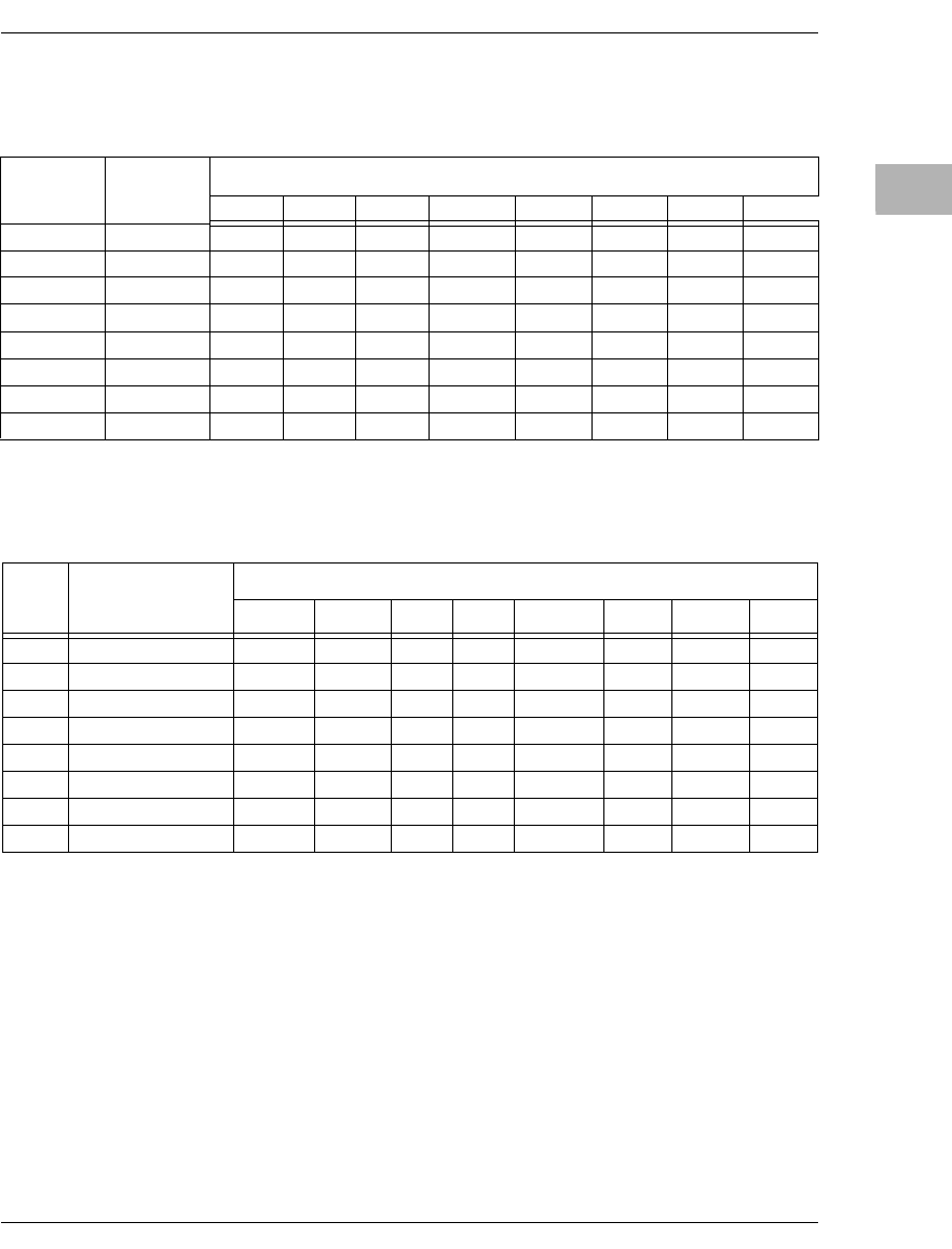
Table 3-3. VMEchip2 Memory Map (Sheet 1 of 3)
DMA TB
SNP MODE
ROM
ZERO SRAM
SPEED
ADDER
2
SLAVE ENDING ADDRESS 1
SLAVE ENDING ADDRESS 2
SLAVE ADDRESS TRANSLATION ADDRESS 1
SLAVE ADDRESS TRANSLATION ADDRESS 2
BLK
D64
SNP
2
WP
2
SUP
2
USR
2
A32
2
A24
2
BLK
2
PRGM
2
DATA
2
2
MASTER ENDING ADDRESS 1
MASTER ENDING ADDRESS 2
MASTER ENDING ADDRESS 3
MASTER ENDING ADDRESS 4
MASTER ADDRESS TRANSLATION ADDRESS 4
VMEchip2 LCSR Base Address = $FFF40000
OFFSET:
16171819202122232425262728293031
16171819202122232425262728293031
16171819202122232425262728293031
MAST
D16
EN
MAST
WP
EN
MAST
D16
EN
MAST
WP
EN MASTER AM 3MASTER AM 4
GCSR GROUP SELECT GCSR
BOARD SELECT
MAST
4
EN
MAST
3
EN
MAST
2
EN
MAST
1
EN
TICK
2/1 TICK
IRQ 1
EN
CLR
IRQ IRQ
STAT VMEBUS
INTERRUPT
LEVEL VMEBUS INTERRUPT VECTOR
0
4
8
C
10
14
18
1C
20
24
28
2C
30
34
38
3C
40
44
48
WAIT
RMW
DMA CONTROLLER
DMA CONTROLLER
DMA CONTROLLER
DMA CONTROLLER
This sheet continues on facing page.
Memory Maps
MVME167/D3 3-9
3
ARB
ROBN MAST
DHB MAST
DWB MST
FAIR MST
RWD MASTER
VMEBUS DMA
HALT DMA
EN DMA
TBL DMA
FAIR DM
RELM DMA
VMEBUS
ADDER
1
MAST
WP
EN
MAST
WP
EN
MAST
D16
EN
MAST
D16
EN
SNP
1
WP
1
SUP
1
USR
1
A32
1
A24
1
BLK
1
PRGM
1
DATA
1
BLK
D64
1
MASTER STARTING ADDRESS 1
MASTER STARTING ADDRESS 2
MASTER STARTING ADDRESS 3
MASTER STARTING ADDRESS 4
MASTER ADDRESS TRANSLATION SELECT 4
SLAVE STARTING ADDRESS 1
SLAVE STARTING ADDRESS 2
SLAVE ADDRESS TRANSLATION SELECT 1
SLAVE ADDRESS TRANSLATION SELECT 2
0123456789101112131415
0123456789101112131415
IO2
EN IO2
WP
EN
IO2
S/U IO2
P/D IO1
EN IO1
D16
EN
IO1
WP
EN
IO1
S/U
0123456789101112131415
MASTER AM 2 MASTER AM 1
ROM
SIZE
ROM BANK B
SPEED
ROM BANK A
SPEED
DMA
TBL
INT
DMA LB
SNP MODE DMA
INC
VME
DMA
INC
LB
DMA
D64
BLK
DMA
BLK DMA
AM
5
DMA
AM
4
DMA
WRT DMA
D16 DMA
AM
3
DMA
AM
2
DMA
AM
1
DMA
AM
0
DMA TABLE
INTERRUPT COUNT
MPU
CLR
STAT
MPU
LBE
ERR
MPU
LPE
ERR
MPU
LOB
ERR
MPU
LTO
ERR
DMA
LBE
ERR
DMA
LPE
ERR
DMA
LOB
ERR
DMA
LTO
ERR
DMA
TBL
ERR
DMA
VME
ERR
DMA
DONE
LOCAL BUS ADDRESS COUNTER
VMEBUS ADDRESS COUNTER
BYTE COUNTER
TABLE ADDRESS COUNTER
1360 9403
This sheet begins on facing page.
Operating Instructions
3-10 MVME167 Single Board Computer User’s Manual
3
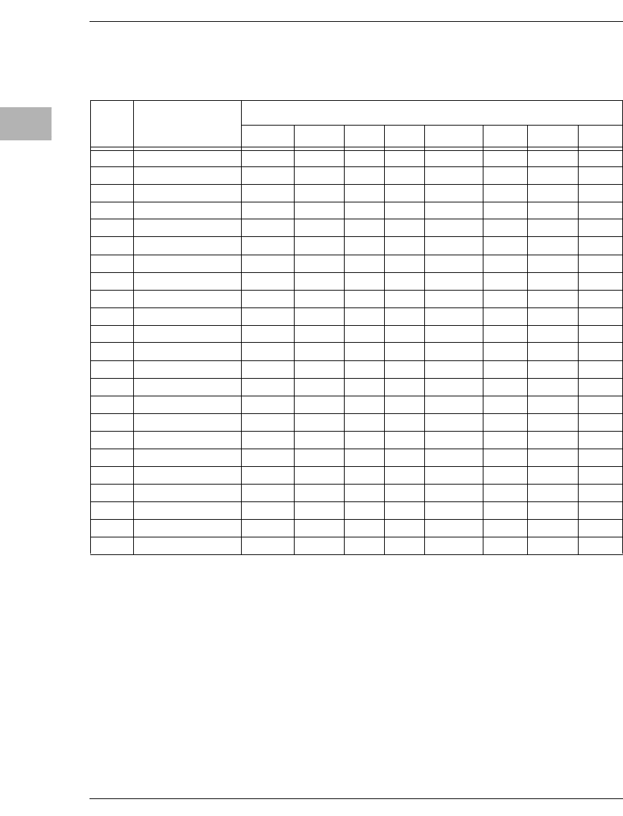
Table 3-3. VMEchip2 Memory Map (Sheet 2 of 3)
EN
IRQ
31
EN
IRQ
30
EN
IRQ
29
EN
IRQ
28
EN
IRQ
27
EN
IRQ
26
EN
IRQ
25
EN
IRQ
24
EN
IRQ
23
EN
IRQ
22
EN
IRQ
21
EN
IRQ
20
EN
IRQ
19
EN
IRQ
18
EN
IRQ
17
EN
IRQ
16
CLR
IRQ
31
CLR
IRQ
30
CLR
IRQ
29
CLR
IRQ
28
CLR
IRQ
27
CLR
IRQ
26
CLR
IRQ
25
CLR
IRQ
24
CLR
IRQ
23
CLR
IRQ
22
CLR
IRQ
21
CLR
IRQ
20
CLR
IRQ
19
CLR
IRQ
18
CLR
IRQ
17
CLR
IRQ
16
AC FAIL
IRQ LEVEL
VMEchip2 LCSR Base Address = $FFF40000
OFFSET:
16171819202122232425262728293031
68
6C
70
74
78
7C
80
84
88
8C
AC
FAIL
IRQ
AB
IRQ SYS
FAIL
IRQ
MWP
BERR
IRQ
PE
IRQ IRQ1E
IRQ TIC2
IRQ TIC1
IRQ VME
IACK
IRQ
DMA
IRQ SIG3
IRQ SIG2
IRQ SIG1
IRQ SIG0
IRQ LM1
IRQ LM0
IRQ
ABORT
IRQ LEVEL
SYS FAIL
IRQ LEVEL
MST WP ERROR
IRQ LEVEL
VME IACK
IRQ LEVEL
DMA
IRQ LEVEL
SIG 3
IRQ LEVEL
SIG 2
IRQ LEVEL
SW7
IRQ LEVEL
SW6
IRQ LEVEL
SW5
IRQ LEVEL
SW4
IRQ LEVEL
SPARE
IRQ LEVEL
VME IRQ 7
IRQ LEVEL
VME IRQ 6
IRQ LEVEL
VME IRQ 5
IRQ LEVEL
VECTOR BASE
REGISTER 0
VECTOR BASE
REGISTER 1
MST
IRQ
EN
SYS
FAIL
LEVEL
AC
FAIL
LEVEL
ABORT
LEVEL GPIOEN
16171819202122232425262728293031
ARB
BGTO
EN
DMA
TIME OFF
DMA
TIME ON
VME
GLOBAL
TIMER
SYS
FAIL
SCON BRD
FAIL
STAT
PURS
STAT CLR
PURS
STAT
BRD
FAIL
OUT
RST
SW
EN
SYS
RST WD
CLR
TO
WD
CLR
CNT
WD
TO
STAT
TO
BF
EN
WD
SRST
LRST
WD
RST
EN
WD
EN
PRE
4C
50
54
58
5C
60
64
TICK TIMER 1
TICK TIMER 1
TICK TIMER 2
TICK TIMER 2
This sheet continues on facing page.
Memory Maps
MVME167/D3 3-11
3
0123456789101112131415
VME
ACCESS
TIMER
LOCAL
BUS
TIMER
WD
TIME OUT
SELECT
PRESCALER
CLOCK ADJUST
TIC
EN
1
COC
EN
1
CLR
OVF
1
TIC
EN
2
COC
EN
2
CLR
OVF
2
OVERFLOW
COUNTER 1
OVERFLOW
COUNTER 2
SCALER
1361 9403
COMPARE REGISTER
COUNTER
COPARE REGISTER
COUNTER
EN
IRQ
15
EN
IRQ
14
EN
IRQ
13
EN
IRQ
12
EN
IRQ
11
EN
IRQ
10
EN
IRQ
9
EN
IRQ
8
EN
IRQ
7
EN
IRQ
6
EN
IRQ
5
EN
IRQ
4
EN
IRQ
3
EN
IRQ
2
EN
IRQ
1
EN
IRQ
0
CLR
IRQ
15
CLR
IRQ
14
CLR
IRQ
13
CLR
IRQ
12
CLR
IRQ
11
CLR
IRQ
10
CLR
IRQ
9
CLR
IRQ
8
SET
IRQ
15
SET
IRQ
14
SET
IRQ
13
SET
IRQ
12
SET
IRQ
11
SET
IRQ
10
SET
IRQ
9
SET
IRQ
8
SW7
IRQ SW6
IRQ SW5
IRQ SW4
IRQ SW3
IRQ SW2
IRQ SW1
IRQ SW0
IRQ SPARE VME
IRQ7 VME
IRQ6 VME
IRQ5 VME
IRQ4 VME
IRQ3 VME
IRQ2 VME
IRQ1
0123456789101112131415
GPIOO
P ERROR
IRQ LEVEL
IRQ1E
IRQ LEVEL
TIC TIMER 2
IRQ LEVEL
TIC TIMER 1
IRQ LEVEL
SW3
IRQ LEVEL
SW2
IRQ LEVEL
SW1
IRQ LEVEL
SW0
IRQ LEVEL
VME IRQ 4
IRQ LEVEL
VMEB IRQ 3
IRQ LEVEL
VME IRQ 2
IRQ LEVEL
VME IRQ 1
IRQ LEVEL
SIG 1
IRQ LEVEL
SIG 0
IRQ LEVEL
LM 1
IRQ LEVEL
LM 0
IRQ LEVEL
GPIOI GPI
MP
IRQ
EN
REV
EROM
NO
EL
BBSY
DIS
SRAM
DIS
MST
DIS
BSYT
EN
INT
DIS
BGN
This sheet begins on facing page.

Operating Instructions
3-12 MVME167 Single Board Computer User’s Manual
3
This page intentionally left blank.
Memory Maps
MVME167/D3 3-13
3
Table 3-3. VMEchip2 Memory Map (Sheet 3 of 3)
VMEchip2 GCSR Base Address = $FFF40100
Offsets
VME-
bus Local
Bus
15 14 13 12 11 10 9 8 7 6 5 4 3 2 1 0
00 CHIP REVISION CHIP ID
24
LM3 LM2 LM1 LM0 SIG3 SIG2 SIG1 SIG0 RST ISF BF SCON SYSFL XXX
48 GENERAL PURPOSE CONTROL AND STATUS REGISTER 0
6C GENERAL PURPOSE CONTROL AND STATUS REGISTER 1
810 GENERAL PURPOSE CONTROL AND STATUS REGISTER 2
A14 GENERAL PURPOSE CONTROL AND STATUS REGISTER 3
C18 GENERAL PURPOSE CONTROL AND STATUS REGISTER 4
E1C GENERAL PURPOSE CONTROL AND STATUS REGISTER 5
Operating Instructions
3-14 MVME167 Single Board Computer User’s Manual
3
Table 3-4. PCCchip2 Memory Map
PRTR
FLT
PLTY
PRTR
FLT
E/L*
PRTR
FLT
INT
PRTR
FLT
IEN
PRTR
FLT
ICLR
PRTR FAULT
IRQ LEVEL
PRTR
ACK
PLTY
PRTR
ACK
E/L*
PRTR
ACK
INT
PRTR
ACK
IEN
PRTR
ACK
ICLR
SCC
RTRY
ERR
PCCchip2 Base Address = $FFF42000
OFFSET:
00
04
08
0C
10
14
18
1C
20
24
28
2C
30
34
38
3C
PRTR ACK
IRQ LEVEL
GPI
PLTY
D16D23D24D31
CHIP ID CHIP REVISION
TIC TIMER 1
TIC TIMER 1
TIC TIMER 2
TIC TIMER 2
PRESCALER COUNT REGISTER PRESCALER CLOCK ADJUST
GPI
E/L* GPI
INT GPI
IEN GPI
ICLR GPI
IRQ LEVEL GPI GPOE GPO
SCC
PAR
ERR
SCC
EXT
ERR
SCC
LTO
ERR
SCC
SCLR SCC
MDM
ERR
SCC
MDM
IEN
SCC
MDM
AVEC
SCC MODEM
IRQ LEVEL
SCC TRANSMIT PIACK
LAN
PAR
ERR
LAN
EXT
ERR
LAN
LTO
ERR
LAN
SCLR
SCSI
PAR
ERR
SCSI
EXT
ERR
SCSI
LTO
ERR
SCSI
SCLR
PRTR
BSY
PLTY
PRTR
BSY
E/L*
PRTR
BSY
INT
PRTR
BSY
IEN
PRTR
BSY
ICLR
PRTR BSY
IRQ LEVEL
CHIP SPEED
SCC PROVIDES ITS OWN VECTORS
This sheet continues on facing page.
Memory Maps
MVME167/D3 3-15
3
INTERRUPT
MASK LEVEL
INTERRUPT
IPL LEVEL
TIC TIMER 2
IRQ LEVEL
SCC TRANSMIT
IRQ LEVEL
CLR
OVF
1
COC
EN
1
TIC
EN
1
CPU
040 MSTR
INT
EN
FAST
BRAM
OVERFLOW
COUNTER 2
TIC TIMER 1
IRQ LEVEL
SCC RECEIVE
IRQ LEVEL
SCC RECEIVE PIACK
LAN
INT
PLTY
TIC2
INT
CLR
OVF
2
D15 D7D8 D0
VECTOR BASE REGISTER
DRO
COMPARE REGISTER
COUNTER REGISTER
COMPARE REGISTER
COUNTER REGISTER
OVERFLOW
COUNTER 1
COC
EN
2
TIC
EN
2
TIC2
IEN
TIC2
ICLR
TIC1
INT
TIC1
IEN
TIC1
ICLR
SCC
TX
IRQ
SCC
TX
IEN
SCC
TX
AVEC
SCC
SC1
SCC
SC0
SCC
RX
IRQ
SCC
RX
IEN
SCC
RX
AVEC
SCC MODEM PIACK
LAN
INT
E/L*
LAN
INT
LAN
IEN
LAN
ICLR
LAN INT
IRQ LEVEL
PRTR
SEL
PLTY
PRTR
SEL
E/L*
PRTR
SEL
INT
PRTR
SEL
IEN
PRTR
SEL
ICLR
PRTR
ANY
INT
PRTR
ACK PRTR
FLT PRTR
SEL PRTR
PE PRTR
BSY
PRTR SEL
IRQ LEVEL
PRINTER DATA
LAN
SC1
LAN
SC0
LAN
ERR
INT
LAN
ERR
IEN
LAN
ERR
ICLR
LAN ERR
IRQ LEVEL
SCSI
IRQ
SCSI
IEN
SCSI INT
IRQ LEVEL
PRTR PE
IRQ LEVEL
PRTR
PE
PLTY
PRTR
PE
E/L*
PRTR
PE
INT
PRTR
PE
IEN
PRTR
PE
ICLR
PRTR
DAT
ENBL
PRTR
INP PRTR
STB
PRTR
FAST
ASTB
PRTR
MAN
STB
1362 9403
This sheet begins on facing page.
Operating Instructions
3-16 MVME167 Single Board Computer User’s Manual
3
Table 3-5. Printer Memory Map
Printer ACK Interrupt Control Register $FFF42030
Printer FAULT Interrupt Control Register $FFF42031
Printer SEL Interrupt Control Register $FFF42032
Printer PE Interrupt Control Register $FFF42033
Printer BUSY Interrupt Control Register $FFF42034
Printer Input Status Register $FFF42036
Printer Port Control Register $FFF42037
Printer Data Register 16 bits $FFF4203A
BIT3130292827262524
NAME PLTY E/L* INT IEN ICLR IL2 IL1 IL0
BIT2322212019181716
NAME PLTY E/L* INT IEN ICLR IL2 IL1 IL0
BIT151413121110 9 8
NAME PLTY E/L* INT IEN ICLR IL2 IL1 IL0
BIT76543210
NAME PLTY E/L* INT IEN ICLR IL2 IL1 IL0
BIT3130292827262524
NAME PLTY E/L* INT IEN ICLR IL2 IL1 IL0
BIT151413121110 9 8
NAME PLTY ACK FLT SEL PE BSY
BIT76543210
NAME DOEN INP STB FAST MAN
BIT 15-0
NAME PD15 - PD0
Memory Maps
MVME167/D3 3-17
3
Table 3-6. MEMC040 Internal Register Memory Map
2nd
MEMC040 1st
MEMC040 Data Bits
D31 D30 D29 D28 D27 D26 D25 D24
$FFF43100 $FFF43000 CID7 CID6 CID5 CID4 CID3 CID2 CID1 CID0
$FFF43104 $FFF43004 REV7 REV6 REV5 REV4 REV3 REV2 REV1 REV0
$FFF43108 $FFF43008 FSTRD EXTPEN WPB* MSIZ2 MSIZ1 MSIZ0
$FFF4310C $FFF4300C STS7 STS6 STS5 STS4 STS3 STS2 STS1 STS0
$FFF43110 $FFF43010 OUT7 OUT6 OUT5 OUT4 OUT3 OUT2 OUT1 OUT0
$FFF43114 $FFF43014 BAD31 BAD30 BAD29 BAD28 BAD27 BAD26 BAD25 BAD24
$FFF43118 $FFF43018 BAD23 BAD22 DMCTL SWAIT WWP PARINT PAREN RAMEN
$FFF4311C $FFF4301C BCK7 BCK6 BCK5 BCK4 BCK3 BCK2 BCK1 BCK0
Table 3-7. MCECC Internal Register Memory Map
MCECC Base Address = $FFF43000 (1st); $FFF43100 (2nd)
Register
Offset Register
Name
Register Bit Names
D31 D30 D29 D28 D27 D26 D25 D24
$00 CHIP ID CID7 CID5 CID5 CID4 CID3 CID2 CID1 CID0
$04 CHIP REVISION REV7 REV6 REV5 REV4 REV3 REV2 REV1 REV0
$08 MEMORY CONFIG 0 0 FSTRD 1 0 MSIZ2 MSIZ1 MSIZ0
$0C DUMMY 0 0 0 0 0 0 0 0 0
$10 DUMMY 1 0 0 0 0 0 0 0 0
$14 BASE ADDRESS BAD31 BAD30 BAD29 BAD28 BAD27 BAD26 BAD25 BAD24
$18 DRAM CONTROL BAD23 BAD22 RWB5 SWAIT RWB3 NCEIEN NCEBEN RAMEN
$1C BCLK FREQUENCY BCK7 BCK6 BCK5 BCK4 BCK3 BCK2 BCK1 BCK0
Operating Instructions
3-18 MVME167 Single Board Computer User’s Manual
3
$20 DATA CONTROL 0 0 DERC ZFILL RWCKB 0 0 0
$24 SCRUB CONTROL RACODE RADATA HITDIS SCRB SCRBEN 0 SBEIEN IDIS
$28 SCRUB PERIOD SBPD15 SBPD14 SBPD13 SBPD12 SBPD11 SBPD10 SBPD9 SBPD8
$2C SCRUB PERIOD SBPD7 SBPD6 SBPD5 SBPD4 SBPD3 SBPD2 SBPD1 SBPD0
$30 CHIP PRESCALE CPS7 CPS6 CPS5 CPS4 CPS3 CPS2 CPS1 CPS0
$34 SCRUB TIME ON/OFF SRDIS 0 STON2 STON1 STON0 STOFF2 STOFF1 STOFF0
$38 SCRUB PRESCALE 0 0 SPS21 SPS20 SPS19 SPS18 SPS17 SPS16
$3C SCRUB PRESCALE SPS15 SPS14 SPS13 SPS12 SPS11 SPS10 SPS9 SPS8
$40 SCRUB PRESCALE SPS7 SPS6 SPS5 SPS4 SPS3 SPS2 SPS1 SPS0
$44 SCRUB TIMER ST15 ST14 ST3 ST12 ST11 ST10 ST9 ST8
$48 SCRUB TIMER ST7 ST6 ST5 ST4 ST3 ST2 ST1 ST0
$4C SCRUB ADDR CNTR 0 0 0 0 0 SAC26 SAC25 SAC24
$50 SCRUB ADDR CNTR SAC23 SAC22 SAC21 SAC20 SAC19 SAC18 SAC17 SAC16
$54 SCRUB ADDR CNTR SAC15 SAC14 SAC13 SAC12 SAC11 SAC10 SAC9 SAC8
$58 SCRUB ADDR CNTR SAC7 SAC6 SAC5 SAC4 0 0 0 0
$5C ERROR LOGGER ERRLOG ERD ESCRB ERA EALT 0 MBE SBE
$60 ERROR ADDRESS EA31 EA30E EA29 EA28 EA27 EA26 EA25 EA24
$64 ERROR ADDRESS EA23 EA22 EA21 EA20 EA19 EA18 EA17 EA16
$68 ERROR ADDRESS EA15 EA14 EA13 EA12 EA11 EA10 EA9 EA8
$6C ERROR ADDRESS EA7 EA6 EA5 EA4 0 0 0 0
$70 ERROR SYNDROME S7 S6 S5 S4 S3 S2 S1 S0
$74 DEFAULTS1 WRHDIS STATCOL FSTRD SELI1 SELI0 RSIZ2 RSIZ1 RSIZ0
$78 DEFAULTS2 FRC_OPN XY_FLIP REFDIS TVECT NOCACHE RESST2 RESST1 RESST0
Table 3-7. MCECC Internal Register Memory Map (Continued)
MCECC Base Address = $FFF43000 (1st); $FFF43100 (2nd)
Register
Offset Register
Name
Register Bit Names
D31 D30 D29 D28 D27 D26 D25 D24
Memory Maps
MVME167/D3 3-19
3
Table 3-8. Cirrus Logic CD2401 Serial Port Memory Map
Base Address = $FFF45000
Register Description Register
Name Offsets Size Access
Global Registers
Global Firmware Revision Code Register GFRCR 81 B R
Channel Access Register CAR EE B R/W
Option Registers
Channel Mode Register CMR 1B B R/W
Channel Option Register 1 COR1 10 B R/W
Channel Option Register 2 COR2 17 B R/W
Channel Option Register 3 COR3 16 B R/W
Channel Option Register 4 COR4 15 B R/W
Channel Option Register 5 COR5 14 B R/W
Channel Option Register 6 COR6 18 B R/W
Channel Option Register 7 COR7 07 B R/W
Special Character Register 1 SCHR1 1F B R/W Async
Special Character Register 2 SCHR2 1E B R/W Async
Special Character Register 3 SCHR3 1D B R/W Async
Special Character Register 4 SCHR4 1C B R/W Async
Special Character Range low SCRl 23 B R/W Async
Special Character Range high SCRh 22 B R/W Async
LNext Character LNXT 2E B R/W Async
Bit Rate and Clock Option Registers
Receive Frame Address Register1 RFAR1 1F B R/W Sync
Receive Frame Address Register2 RFAR2 1E B R/W Sync
Receive Frame Address Register3 RFAR3 1D B R/W Sync
Receive Frame Address Register4 RFAR4 1C B R/W Sync
CRC Polynomial Select Register CPSR D6 B R/W Sync
Receive Baud Rate Period Register RBPR CB B R/W
Receive Clock Option Register RCOR C8 B R/W
Transmit Baud Rate Period Register TBPR C3 B R/W
Transmit Clock Option Register TCOR C0 B R/W
Operating Instructions
3-20 MVME167 Single Board Computer User’s Manual
3
Channel Command and Status Registers
Channel Command Register CCR 13 B R/W
Special Transmit Command Register STCR 12 B R/W
Channel Status Register CSR 1A B R
Modem Signal Value Registers MSVR-RTS DE B R/W
MSVR-DTR DF B R/W
Interrupt Registers
Local Interrupt Vector Register LIVR 09 B R/W
Interrupt Enable Register IER 11 B R/W
Local Interrupting Channel Register LICR 26 B R/W
Stack Register STK E2 B R
Receive Interrupt Registers
Receive Priority Interrupt Level Register RPILR E1 B R/W
Receive Interrupt Register RIR ED B R
Receive Interrupt Status Register RISR 88 W
(NOTE)
R/W
Receive Interrupt Status Register low RISRl 89 B R
Receive Interrupt Status Register high RISRh 88 B R
Receive FIFO Output Count RFOC 30 B R
Receive Data Register RDR F8 B R
Receive End Of Interrupt Register REOIR 84 B W
Transmit Interrupt Registers
Transmit Priority Interrupt Level Register TPILR E0 B R/W
Transmit Interrupt Register TIR EC B R
Transmit Interrupt Status Register TISR 8A B R
Transmit FIFO Transfer Count TFTC 80 B R
Transmit Data Register TDR F8 B W
Transmit End Of Interrupt Register TEOIR 85 B W
Table 3-8. Cirrus Logic CD2401 Serial Port Memory Map (Continued)
Base Address = $FFF45000
Register Description Register
Name Offsets Size Access

Memory Maps
MVME167/D3 3-21
3
Modem Interrupt Registers
Modem Priority Interrupt Level Register MPILR E3 B R/W
Modem Interrupt Register MIR EF B R
Modem (/Timer) Interrupt Status Register MISR 8B B R
Modem End Of Interrupt Register MEOIR 86 B W
DMA Registers
DMA Mode Register (write only) DMR F6 B W
Bus Error Retry Count BERCNT 8E B R/W
DMA Buffer Status DMABSTS 19 B R
DMA Receive Registers
A Receive Buffer Address Lower ARBADRL 42 W R/W
A Receive Buffer Address Upper ARBADRU 40 W R/W
B Receive Buffer Address Lower BRBADRL 46 W R/W
B Receive Buffer Address Upper BRBADRU 44 W R/W
A Receive Buffer Byte Count ARBCNT 4A W R/W
B Receive Buffer Byte Count BRBCNT 48 W R/W
A Receive Buffer Status ARBSTS 4F B R/W
B Receive Buffer Status BRBSTS 4E B R/W
Receive Current Buffer Address Lower RCBADRL 3E W R
Receive Current Buffer Address Upper RCBADRU 3C W R
DMA Transmit Registers
A Transmit Buffer Address Lower ATBADRL 52 W R/W
A Transmit Buffer Address Upper ATBADRU 50 W R/W
B Transmit Buffer Address Lower BTBADRL 56 W R/W
B Transmit Buffer Address Upper BTBADRU 54 W R/W
A Transmit Buffer Byte Count ATBCNT 5A W R/W
B Transmit Buffer Byte Count BTBCNT 58 W R/W
A Transmit Buffer Status ATBSTS 5F B R/W
B Transmit Buffer Status BTBSTS 5E B R/W
Transmit Current Buffer Address Lower TCBADRL 3A W R
Transmit Current Buffer Address Upper TCBADRU 38 W R
Table 3-8. Cirrus Logic CD2401 Serial Port Memory Map (Continued)
Base Address = $FFF45000
Register Description Register
Name Offsets Size Access
Operating Instructions
3-22 MVME167 Single Board Computer User’s Manual
3
NOTE: This is a 16-bit register.
Timer Registers
Timer Period Register TPR DA B R/W
Receive Time-out Period Register RTPR 24 W R/W Async
Receive Time-out Period Regis low RTPRl 25 B R/W Async
Receive Time-out Period Register high RTPRh 24 B R/W Async
General Timer 1 GT1 2A W R Sync
General Timer 1 low GT1l 2B B R Sync
General Timer 1 high GT1h 2A B R Sync
General Timer 2 GT2 29 B R Sync
Transmit Timer Register TTR 29 B R Async
Table 3-8. Cirrus Logic CD2401 Serial Port Memory Map (Continued)
Base Address = $FFF45000
Register Description Register
Name Offsets Size Access
Memory Maps
MVME167/D3 3-23
3
NOTES: 1. Refer to the MPU Port and MPU Channel Attention registers in the
MVME166/MVME167/MVME187 Single Board Computers Programmer’s
Reference Guide.
2. After resetting, you must write the System Configuration Pointer to the command
registers before writing to the MPU Channel Attention register. Writes to the
System Configuration Pointer must be upper word first, lower word second.
Table 3-9. 82596CA Ethernet LAN Memory Map
82596CA Ethernet LAN Directly Accessible Registers
Data Bits
Address D31 D16 D15 D0
$FFF46000 Upper Command Word Lower Command Word
$FFF46004 MPU Channel Attention (CA)
Operating Instructions
3-24 MVME167 Single Board Computer User’s Manual
3
Table 3-10. 53C710 SCSI Memory Map
53C710 Register Address Map Base Address is $FFF47000
Big Endian
Mode
SCRIPTs
Mode and
Little Endian
Mode
00 SIEN SDID SCNTL1 SCNTL0 00
04 SOCL SODL SXFER SCID 04
08 SBCL SBDL SIDL SFBR 08
0C SSTAT2 SSTAT1 SSTAT0 DSTAT 0C
10 DSA 10
14 CTEST3 CTEST2 CTEST1 CTEST0 14
18 CTEST7 CTEST6 CTEST5 CTEST4 18
1C TEMP 1C
20 LCRC CTEST8 ISTAT DFIFO 20
24 DCMD DBC 24
28 DNAD 28
2C DSP 2C
30 DSPS 30
34 SCRATCH 34
38 DCNTL DWT DIEN DMODE 38
3C ADDER 3C
NOTE: Accesses may be 8-bit or 32-bit, but not 16-bit.
Memory Maps
MVME167/D3 3-25
3
Table 3-11. MK48T08 BBRAM,TOD Clock Memory Map
Address Range Description Size (Bytes)
$FFFC00 00 - $FFFC 0FFF User Area 4096
$FFFC1000 - $FFFC10FF Networking Area 256
$FFFC110 0 - $F FFC16F7 Ope rat ing S ystem Are a 1528
$FFFC16 F8 - $F FFC1EF7 Deb ugger Area 2048
$FFFC1EF8 - $FFFC1FF7 Configuration Area 256
$FFFC1FF8 - $FFFC1FFF TOD Clock 8
Table 3-12. BBRAM Configuration Area Memory Map
Address Range Description Size (Bytes)
$FFFC1EF8 - $FFFC1EFB Version 4
$FFFC1EFC - $FFFC1F07 Serial Number 12
$FFFC1F08 - $FFFC1F17 Board ID 16
$FFFC1F18 - $FFFC1F27 PWA 16
$FFFC1F28 - $FFFC1F2B Speed 4
$FFFC1F2C - $FFFC1F31 Ethernet Address 6
$FFFC1F32 - $FFFC1F33 Reserved 2
$FFFC1F34 - $FFFC1F35 SCSI ID 2
$FFFC1F36 - $FFFC1F3D System ID 8
$FFFC1F3E - $FFFC1F45 Mezz. Board 1 PWB 8
$FFFC1F46 - $FFFC1F4D Mezz. Board 1 Serial Number 8
$FFFC1F4E - $FFFC1F55 Mezz. Board 2 PWB 8
$FFFC1F56 - $FFFC1F5D Mezz. Board 2 Serial Number 8
$FFFC1F5E - $FFFC1FF6 Reserved 153
$FFFC1FF7 Checksum 1
Operating Instructions
3-26 MVME167 Single Board Computer User’s Manual
3
NOTES: W = Write Bit R = Read Bit S = Signbit
ST = Stop Bit FT = Frequency Test x = Unused
BBRAM,TOD Clock Memory Map
The MK48T08 BBRAM (also called Non-Volatile RAM or NVRAM) is divided into
six areas as shown in Table 3-11. MK48T08 BBRAM,TOD Clock Memory Map on page
3-25. The first five areas are defined by software, while the sixth area, the time-of-day
(TOD) clock, is defined by the chip hardware. The first area is reserved for user data.
The second area is used by Motorola networking software. The third area is used by
the SYSTEM V/68 operating system. The fourth area is used by the MVME167 board
debugger (MVME167Bug). The fifth area, detailed in Table 3-12. BBRAM
Configuration Area Memory Map on page 3-25, is the configuration area. The sixth
area, the TOD clock, detailed in Table 3-13. TOD Clock Memory Map on page 3-26,
is defined by the chip hardware.
The data structure of the configuration bytes starts at $FFFC1EF8 and is as follows.
struct brdi_cnfg {
char version[4];
char serial[12];
char id[16];
char pwa[16];
char speed[4];
char ethernet_adr[6];
char fill[2];
char lscsiid[2];
char sysid[8];
char brd1_pwb[8];
char brd1_serial[8];
Table 3-13. TOD Clock Memory Map
Data Bits
Address D7D6D5D4D3D2D1D0 Function
$FFFC1FF8 W R S -- -- -- -- -- CONTROL 00
$FFFC1FF9 ST -- -- -- -- -- -- -- SECONDS 00
$FFFC1FFAx--------------MINUTES00
$FFFC1FFB x x -- -- -- -- -- -- HOUR 00
$FFFC1FFC x FT x x x -- -- -- DAY 01
$FFFC1FFD x x -- -- -- -- -- -- DATE 01
$FFFC1FFE x x x -- -- -- -- -- MONTH 01
$FFFC1FFF----------------YEAR 00

Memory Maps
MVME167/D3 3-27
3
char brd2_pwb[8];
char brd2_serial[8];
char reserved[153];
char cksum[1];
}
The fields are defined as follows:
1. Four bytes are reserved for the revision or version of this structure. This revision
is stored in ASCII format, with the first two bytes being the major version
numbers and the last two bytes being the minor version numbers. For example, if
the version of this structure is 1.0, this field contains:
0100
2. Twelve bytes are reserved for the serial number of the board in ASCII format. For
example, this field could contain:
000000470476
3. Sixteen bytes are reserved for the board ID in ASCII format. For example, for a
16 MB, 25 MHz MVME167 board, this field contains:
MVME167-003B
(The 12 characters are followed by four blanks.)
4. Sixteen bytes are reserved for the printed wiring assembly (PWA) number
assigned to this board in ASCII format. This includes the 01-W prefix. This is for
the main logic board if more than one board is required for a set. Additional boards
in a set are defined by a structure for that set. For example, for a 16 MB, 25 MHz
MVME167 board at revision A, the PWA field contains:
01-W3899B03A
(The 12 characters are followed by four blanks.)
5. Four bytes contain the speed of the board in MHz. The first two bytes are the
whole number of MHz and the second two bytes are fractions of MHz. For
example, for a 25.00 MHz board, this field contains:
2500
6. Six bytes are reserved for the Ethernet address. The address is stored in
hexadecimal format. (Refer to the detailed description in Chapter 4.) If the board
does not support Ethernet, this field is filled with zeros.
7. These two bytes are reserved.
8. Two bytes are reserved for the local SCSI ID. The SCSI ID is stored in ASCII
format.
9. Eight bytes are reserved for the systems serial ID, for boards 1used in a system.

Operating Instructions
3-28 MVME167 Single Board Computer User’s Manual
3
10. Eight bytes are reserved for the printed wiring board (PWB) number assigned to
the first mezzanine board in ASCII format. This does not include the 01-W prefix.
For example, for a 16MB parity mezzanine at revision E, the PWB field contains:
3690B03E
11. Eight bytes are reserved for the serial number assigned to the first mezzanine
board in ASCII format.
12. Eight bytes are reserved for the printed wiring board (PWB) number assigned to
the optional second mezzanine board in ASCII format.
13. Eight bytes are reserved for the serial number assigned to the optional second
mezzanine board in ASCII format.
14. Growth space (153 bytes) is reserved. This pads the structure to an even 256 bytes.
System-specific items, such as size of system side, and systems side version, may
go here.
15. The final one byte of the area is reserved for a checksum (as defined in the
MVME167Bug Debugging Package User’s Manual and the Debugging Package
for Motorola 68K CISC CPUs User’s Manual) for security and data integrity of
the configuration area of the NVRAM. This data is stored in hexadecimal format.
Interrupt Acknowledge Map
The local bus distinguishes interrupt acknowledge cycles from other cycles by placing
the binary value %11 on TT1-TT0. It also specifies the level that is being
acknowledged using TM2-TM0. The interrupt handler selects which device within that
level is being acknowledged.
On the MVME187, a read anywhere from location $FFFE0004 through $FFFE001C
causes an interrupt acknowledge cycle at the specified level. This does not do so on the
MVME167. Refer to the PCCchip2 information in the
MVME166/MVME167/MVME187 Single Board Computers Programmer’s Reference
Guide for information on reading the current interrupt level and setting the interrupt
mask.
VMEbus Memory Map
This section describes the mapping of local resources as viewed by VMEbus masters.
VMEbus Accesses to the Local Bus
The VMEchip2 includes a user-programmable map decoder for the VMEbus to local
bus interface. The map decoder allows you to program the starting and ending address
and the modifiers the MVME167 responds to.

Memory Maps
MVME167/D3 3-29
3
VMEbus Short I/O Memory Map
The VMEchip2 includes a user-programmable map decoder for the GCSR. The GCSR
map decoder allows you to program the starting address of the GCSR in the VMEbus
short I/O space.

Operating Instructions
3-30 MVME167 Single Board Computer User’s Manual
3
Software Initialization
Most functions that have been done with switches or jumpers on other modules are
done by setting control registers on the MVME167. At powerup or reset, the EPROMs
that contain the 167Bug debugging package set up the default values of many of these
registers.
Specific programming details may be determined by study of the MC68040
Microprocessor User’s Manual. Then check the details of all the MVME167 onboard
registers as given in the MVME166/MVME167/MVME187 Single Board Computers
Programmer’s Reference Guide.
Multi-MPU Programming Considerations
Good programming practice dictates that only one MPU at a time have control of the
MVME167 control registers.
Of particular note are:
registers that modify the address map;
registers that require two cycles to access; and
VMEbus interrupt request registers.
Local Reset Operation
Local reset (LRST) is a subset of system reset (SRST). Local reset can be generated
five ways: expiration of the watchdog timer, pressing the front panel RESET switch (if
the system controller function is disabled), by asserting a bit in the board control
register in the GCSR, by SYSRESET*, or by powerup reset.
Note
The GCSR allows a VMEbus master to reset the local bus. This
feature is very dangerous and should be used with caution. The
local reset feature is a partial system reset, not a complete
system reset such as powerup reset or SYSRESET*. When the
local bus reset signal is asserted, a local bus cycle may be
aborted. The VMEchip2 is connected to both the local bus and
the VMEbus and if the aborted cycle is bound for the VMEbus,
erratic operation may result. Communications between the local
processor and a VMEbus master should use interrupts or
mailbox locations; reset should not be used in normal
communications. Reset should be used only when the local
processor is halted or the local bus is hung and reset is the last
resort.
Any VMEbus access to the MVME167 while it is in the reset state is ignored. If a
global bus timer is enabled, a bus error is generated.

MVME167/D34-1
4
FUNCTIONAL
DESCRIPTION
Introduction
This chapter provides a block diagram level description for the MVME167 module.
The functional description provides an overview of the module, followed by a detailed
description of several blocks of the module. The block diagram of the MVME167 is
shown in Figure 4-1. MVME167 Main Module Block Diagram on page 4-10. The block
diagram of the parity DRAM mezzanine module of the MVME167 is shown as Figure
4-2. Parity DRAM Mezzanine Module Block Diagram on page 4-11. The block
diagram of the ECC DRAM mezzanine module of the MVME167 is shown as Figure
4-2. Parity DRAM Mezzanine Module Block Diagram on page 4-11.
Descriptions of the other blocks of the MVME167, including programmable registers
in the ASICs and peripheral chips, are given in the MVME166/MVME167/MVME187
Single Board Computers Programmer’s Reference Guide. Refer to it for the rest of the
functional description of the MVME167 module.
MVME167 Functional Description
The MVME167 is a high functionality VMEbus single board computer designed
around the MC68040 chip. It has 4/8/16/32/64/128/256MB of dynamic RAM, a SCSI
mass storage interface, four serial ports, a printer port, and an Ethernet transceiver
interface.
Data Bus Structure
The local data bus on the MVME167 is a 32-bit synchronous bus that is based on the
MC68040 bus, and supports burst transfers and snooping. The various local bus master
and slave devices use the local bus to communicate. The local bus is arbitrated by
priority type arbiter and the priority of the local bus masters from highest to lowest is:
82596CA LAN, CD2401 serial (through the PCCchip2), 53C710 SCSI, VMEbus, and
MPU. In the general case, any master can access any slave; however, not all
combinations pass the common sense test. Refer to the
MVME166/MVME167/MVME187 Single Board Computers Programmer’s Reference
Guide and to the user’s guide for each device to determine its port size, data bus
connection, and any restrictions that apply when accessing the device.

Functional Description
4-2 MVME167 Single Board Computer User’s Manual
4
MC68040 MPU
The MC68040 processor is used on the MVME167. The MC68040 has on-chip
instruction and data caches and a floating point processor. Refer to the MC68040 user’s
manual for more information.
EPROM
There are four 44-pin PLCC/CLCC EPROM sockets for 27C102JK or 27C202JK type
EPROMs. They are organized as two 32-bit wide banks that support 8-, 16-, and 32-bit
read accesses. The EPROMs are mapped to local bus address 0 following a local bus
reset. This allows the MC68040 to access the stack pointer and execution address
following a reset. The EPROMs are controlled by the VMEchip2. The map decoder,
access time, and when they appear at address 0 is programmable. For more detail, refer
to the VMEchip2 in the MVME166/MVME167/MVME187 Single Board Computers
Programmer’s Reference Guide.
SRAM
The boards include 128KB of 32-bit wide static RAM that supports 8-, 16-, and 32-bit
wide accesses. The SRAM allows the debugger to operate and limited diagnostics to
be executed without the DRAM mezzanine. The SRAM is controlled by the
VMEchip2, and the access time is programmable. Refer to the VMEchip2 in the
MVME166/MVME167/MVME187 Single Board Computers Programmer’s Reference
Guide for more detail. The boards are populated with 100 ns SRAMs.
SRAM battery backup is optionally available on the MVME167. The battery backup
function is provided by a Dallas DS1210S. Only one backup power source is supported
on the MVME167.
Each time the MVME167 is powered, the DS1210S checks power source and if the
voltage of the backup source is less than two volts, the second memory cycle is
blocked. This allows software to provide an early warning to avoid data loss. Because
the DS1210S may block the second access, the software should do at least two accesses
before relying on the data.
Optionally, the MVME167 provides jumpers that allow the power source of the
DS1210S to be connected to the VMEbus +5 V STDBY pin or the onboard battery.
The optional power source SRAM is a socketed Sanyo CR2430 battery. A small
capacitor is provided to allow the battery to be quickly replaced without data loss.
The lifetime of the battery is very dependent on the ambient temperature of the board
and the power-on duty cycle. The FB1225 and CR2430 lithium batteries should
provide at least two years of backup time with the board powered off and the board at

MVME167 Functional Description
MVME167/D3 4-3
4
40° C. If the power-on duty cycle is 50% (the board is powered on half of the time),
the battery lifetime is four years. At lower ambient temperatures the backup time is
greatly extended and may approach the shelf life of the battery.
When a board is stored, if the battery is present, it should be disconnected to prolong
battery life. This is especially important at high ambient temperatures. MVME167
boards with battery backup are shipped with the batteries disconnected.
The power leads from the battery are exposed on the solder side of the board, therefore
the board should not be placed on a conductive surface or stored in a conductive bag
unless the battery is removed.
!
WARNING
Lithium batteries incorporate inflammable materials such as
lithium and organic solvents. If lithium batteries are mistreated
or handled incorrectly, they may burst open and ignite, possibly
resulting in injury and/or fire. When dealing with lithium
batteries, carefully follow the precautions listed below in order
to prevent accidents.
❏Do not short circuit.
❏Do not disassemble, deform, or apply excessive pressure.
❏Do not heat or incinerate.
❏Do not apply solder directly.
❏Do not use different models, or new and old batteries together.
❏Do not charge.
❏Always check proper polarity.
To remove the battery from the module, carefully pull the battery from the socket.
Onboard DRAM
The MVME167 onboard DRAM is located on a mezzanine board. The mezzanine
boards are available in different sizes and with parity protection or ECC protection.
Mezzanine board sizes are 4, 8, 16, or 32MB (parity), or 4, 8, 16, 32, 64, or 128MB
(ECC); two mezzanine boards may be stacked to provide 256MB of onboard RAM.
The main board and a single mezzanine board together take one slot. The stacked
configuration requires two VMEboard slots. Motorola software does support mixed
parity and ECC memory boards on the same main board. The DRAM is four-way
interleaved to efficiently support cache burst cycles. The parity mezzanines are only
supported on 25 MHz main boards.

Functional Description
4-4 MVME167 Single Board Computer User’s Manual
4
The DRAM map decoder can be programmed to accommodate different base
address(es) and sizes of mezzanine boards. The onboard DRAM is disabled by a local
bus reset and must be programmed before the DRAM can be accessed. Refer to the
MEMC040 or the MCECC in the MVME166/MVME167/MVME187 Single Board
Computers Programmer’s Reference Guide for detailed programming information.
Most DRAM devices require some number of access cycles before the DRAMs are
fully operational. Normally this requirement is met by the onboard refresh circuitry
and normal DRAM initialization. However, software should insure a minimum of 10
initialization cycles are performed to each bank of RAM.
Battery Backed Up RAM and Clock
The MK48T08 RAM and clock chip is used on the MVME167. This chip provides a
time of day clock, oscillator, crystal, power fail detection, memory write protection,
8KB of RAM, and a battery in one 28-pin package. The clock provides seconds,
minutes, hours, day, date, month, and year in BCD 24-hour format. Corrections for
28-, 29- (leap year), and 30-day months are automatically made. No interrupts are
generated by the clock. The MK48T08 is an 8 bit device; however, the interface
provided by the PCCchip2 supports 8-, 16-, and 32-bit accesses to the MK48T08.
Refer to the PCCchip2 in the MVME166/MVME167/MVME187 Single Board
Computers Programmer’s Reference Guide and to the MK48T08 data sheet for
detailed programming information.
VMEbus Interface
The local bus to VMEbus interface, the VMEbus to local bus interface, and the
local-VMEbus DMA controller functions on the MVME167 are provided by the
VMEchip2. The VMEchip2 can also provide the VMEbus system controller functions.
Refer to the VMEchip2 in the MVME166/MVME167/MVME187 Single Board
Computers Programmer’s Reference Guide for detailed programming information.
I/O Interfaces
The MVME167 provides onboard I/O for many system applications. The I/O functions
include serial ports, printer port, Ethernet transceiver interface, and SCSI mass storage
interface.
Serial Port Interface
The CD2401 serial controller chip (SCC) is used to implement the four serial ports.
The serial ports support the standard baud rates (110 to 38.4K baud). The four serial
ports are different functionally because of the limited number of pins on the P2 I/O
connector. Serial port 1 is a minimum function asynchronous port. It uses RXD, CTS,
TXD, and RTS. Serial ports 2 and 3 are full function asynchronous ports. They use
RXD, CTS, DCD, TXD, RTS, and DTR. Serial port 4 is a full function asynchronous

MVME167 Functional Description
MVME167/D3 4-5
4
or synchronous port. It can operate at synchronous bit rates up to 64 k bits per second.
It uses RXD, CTS, DCD, TXD, RTS, and DTR. It also interfaces to the synchronous
clock signal lines. Refer to the MVME166/MVME167/MVME187 Single Board
Computers Programmer’s Reference Guide for drawings of the serial port interface
connections.
All four serial ports use EIA-232-D drivers and receivers located on the main board,
and all the signal lines are routed to the I/O connector. The configuration headers are
located on the main board and the MVME712X transition board. An external I/O
transition board such as the MVME712X should be used to convert the I/O connector
pinout to industry-standard connectors.
Note
The MVME167 board hardware ties the DTR signal from the
CD2401 to the pin labeled RTS at connector P2. Likewise, RTS
from the CD2401 is tied to DTR on P2. Therefore, when
programming the CD2401, assert DTR when you want RTS,
and RTS when you want DTR.
The interface provided by the PCCchip2 allows the 16-bit CD2401 to appear at
contiguous addresses; however, accesses to the CD2401 must be 8 or 16 bits. 32-bit
accesses are not permitted. Refer to the CD2401 data sheet and to the PCCchip2 in the
MVME166/MVME167/MVME187 Single Board Computers Programmer’s Reference
Guide for detailed programming information.
The CD2401 supports DMA operations to local memory. Because the CD2401 does
not support a retry operation necessary to break VMEbus lockup conditions, the
CD2401 DMA controllers should not be programmed to access the VMEbus. The
hardware does not restrict the CD2401 to onboard DRAM.
Parallel Port Interface
The PCCchip2 provides an 8-bit bidirectional parallel port. All eight bits of the port
must be either inputs or outputs (no individual selection). In addition to the 8 bits of
data, there are two control pins and five status pins. Each of the status pins can generate
an interrupt to the MPU in any of the following programmable conditions: high level,
low level, high-to-low transition, or low-to-high transition. This port may be used as a
Centronics-compatible parallel printer port or as a general parallel I/O port.
When used as a parallel printer port, the five status pins function as: Printer
Acknowledge (ACK), Printer Fault (FAULT*), Printer Busy (BSY), Printer Select
(SELECT), and Printer Paper Error (PE); while the control pins act as Printer Strobe
(STROBE*), and Input Prime (INP*).

Functional Description
4-6 MVME167 Single Board Computer User’s Manual
4
The PCCchip2 provides an auto-strobe feature similar to that of the MVME147 PCC.
In auto-strobe mode, after a write to the Printer Data Register, the PCCchip2
automatically asserts the STROBE* pin for a selected time specified by the Printer Fast
Strobe control bit. In manual mode, the Printer Strobe control bit directly controls the
state of the STROBE* pin.
Refer to the MVME166/MVME167/MVME187 Single Board Computers
Programmer’s Reference Guide for drawings of the printer port interface connections.
Ethernet Interface
The 82596CA is used to implement the Ethernet transceiver interface. The 82596CA
accesses local RAM using DMA operations to perform its normal functions. Because
the 82596CA has small internal buffers and the VMEbus has an undefined latency
period, buffer overrun may occur if the DMA is programmed to access the VMEbus.
Therefore, the 82596CA should not be programmed to access the VMEbus.
Every MVME167 is assigned an Ethernet Station Address. The address is
$08003E2XXXXX where XXXXX is the unique 5-nibble number assigned to the
board (i.e., every MVME167 has a different value for XXXXX).
Each module has an Ethernet Station Address displayed on a label attached to the
VMEbus P2 connector. In addition, the six bytes including the Ethernet address are
stored in the configuration area of the BBRAM. That is, 08003E2XXXXX is stored in
the BBRAM. At an address of $FFFC1F2C, the upper four bytes (08003E2X) can be
read. At an address of $FFFC1F30, the lower two bytes (XXXX) can be read. Refer to
the BBRAM, TOD Clock memory map description in Chapter 3. The MVME167
debugger has the capability to retrieve or set the Ethernet address.
If the data in the BBRAM is lost, the user should use the number on the VMEbus P2
connector label to restore it.
The Ethernet transceiver interface is located on the MVME167 main module, and the
industry standard connector is located on the MVME712X transition module.
Support functions for the 82596CA are provided by the PCCchip2. Refer to the
82596CA user’s guide and to the MVME166/MVME167/MVME187 Single Board
Computers Programmer’s Reference Guide for detailed programming information.
SCSI Interface
The MVME167 provides for mass storage subsystems through the industry-standard
SCSI bus. These subsystems may include hard and floppy disk drives, streaming tape
drives, and other mass storage devices. The SCSI interface is implemented using the
NCR 53C710 SCSI I/O controller.

MVME167 Functional Description
MVME167/D3 4-7
4
Support functions for the 53C710 are provided by the PCCchip2. Refer to the 53C710
user’s guide and to the MVME166/MVME167/MVME187 Single Board Computers
Programmer’s Reference Guide for detailed programming information.
SCSI Termination
The system configurer must ensure that the SCSI bus is properly terminated at both
ends. On the MVME167, sockets are provided for the terminators on the P2 transition
board. If the SCSI bus ends at the P2 transition board, then termination resistors must
be installed on the P2 transition board. +5V power to the SCSI bus TERM power line
and termination resistors is provided through a fuse located on the P2 transition board.
Local Resources
The MVME167 includes many resources for the local processor. These include tick
timers, software programmable hardware interrupts, watchdog timer, and local bus
timeout.
Programmable Tick Timers
Four 32-bit programmable tick timers with 1 µs resolution are provided, two in the
VMEchip2 and two in the PCCchip2. The tick timers can be programmed to generate
periodic interrupts to the processor. Refer to the VMEchip2 and PCCchip2 in the
MVME166/MVME167/MVME187 Single Board Computers Programmer’s Reference
Guide for detailed programming information.
Watchdog Timer
A watchdog timer function is provided in the VMEchip2. When the watchdog timer is
enabled, it must be reset by software within the programmed time or it times out. The
watchdog timer can be programmed to generate a SYSRESET signal, local reset
signal, or board fail signal if it times out. Refer to the VMEchip2 in the
MVME166/MVME167/MVME187 Single Board Computers Programmer’s Reference
Guide for detailed programming information.
Software-Programmable Hardware Interrupts
Eight software-programmable hardware interrupts are provided by the VMEchip2.
These interrupts allow software to create a hardware interrupt. Refer to the VMEchip2
in the MVME166/MVME167/MVME187 Single Board Computers Programmer’s
Reference Guide for detailed programming information.
Local Bus Timeout
The MVME167 provides a timeout function for the local bus. When the timer is
enabled and a local bus access times out, a Transfer Error Acknowledge (TEA) signal
is sent to the local bus master. The timeout value is selectable by software for 8 µsec,
64 µsec, 256 µsec, or infinite. The local bus timer does not operate during VMEbus

Functional Description
4-8 MVME167 Single Board Computer User’s Manual
4
bound cycles. VMEbus bound cycles are timed by the VMEbus access timer and the
VMEbus global timer. Refer to the VMEchip2 in the
MVME166/MVME167/MVME187 Single Board Computers Programmer’s Reference
Guide for detailed programming information.
Timing Performance
This section provides the performance information for the MVME167. Various
MVME167s are designed to operate at 25 MHz or 33 MHz.
Local Bus to DRAM Cycle Times
The PCCchip2 and VMEchip2 have the same local bus interface timing as the
MC68040, therefore the following cycle times also apply to the PCCchip2 and the
VMEchip2. Read accesses to onboard DRAM require 4 bus clock cycles with parity
checking off. With parity checking on and the bus error reported in the current cycle,
5 bus clock cycles are required. Write accesses to onboard DRAM require 2 bus clock
cycles.
Burst read accesses require 7 (4-1-1-1) bus clock cycles with parity check off. With
parity checking on and the bus error reported in the current cycle, 8 (5-1-1-1) bus clock
cycles are required. Burst write cycles require 5 (2-1-1-1) bus clock cycles.
The parity DRAM is organized as four banks; this requires the use of 256K by 4 chips
for the data portion of the RAM and 256K by 4 chips with the write-per-bit option for
the parity bits. The use of four banks allows X-1-1-1 bursts with parity on.
ROM Cycle Times
The ROM cycle time is programmable from 4 to 11 bus clock cycles. The data
transfers are 32 bits wide. Refer to the MVME166/MVME167/MVME187 Single Board
Computers Programmer’s Reference Guide.
SCSI Transfers
The MVME167 includes a SCSI mass storage bus interface with DMA controller. The
SCSI DMA controller uses a FIFO buffer to interface the 8-bit SCSI bus to the 32-bit
local bus. The FIFO buffer allows the SCSI DMA controller to efficiently transfer data
to the local bus in four longword bursts. This reduces local bus usage by the SCSI
device.
The first longword transfer of a burst, with snooping disabled, takes four bus clocks
with parity off and five bus clocks with parity on. Each of the remaining three transfers
requires one bus clock.
The transfer rate of the DMA controller is 44 MB/sec at 25 MHz with parity off.
Assuming a continuous transfer rate of 5 MB/sec on the SCSI bus, 12% of the local
bus bandwidth is used by transfers from the SCSI bus.

MVME167 Functional Description
MVME167/D3 4-9
4
LAN DMA Transfers
The MVME167 includes a LAN interface with DMA controller. The LAN DMA
controller uses a FIFO buffer to interface the serial LAN bus to the 32-bit local bus.
The FIFO buffer allows the LAN DMA controller to efficiently transfer data to the
local bus.
The 82596CA does not execute MC68040 compatible burst cycles, therefore the LAN
DMA controller does not use burst transfers. Parity DRAM write cycles require 3
clock cycles, and read cycles require 5 clock cycles with parity off and 6 clock cycles
with parity on.
The transfer rate of the LAN DMA controller is 20 MB/sec at 25 MHz with parity off.
Assuming a continuous transfer rate of 1 MB/sec on the LAN bus, 5% of the local bus
bandwidth is used by transfers from the LAN bus.
Remote Status and Control
The remote status and control connector, J3, is a 20-pin connector located behind the
front panel of the MVME167. It provides system designers the flexibility to access
critical indicator and reset functions. This allows a system designer to construct a
RESET/LED panel that can be located remotely from the MVME167.
In addition to the LED and RESET switch access, this connector also includes two
general purpose TTL-level I/O pins and one general purpose interrupt pin which can
also function as a trigger input. This interrupt pin is level programmable.
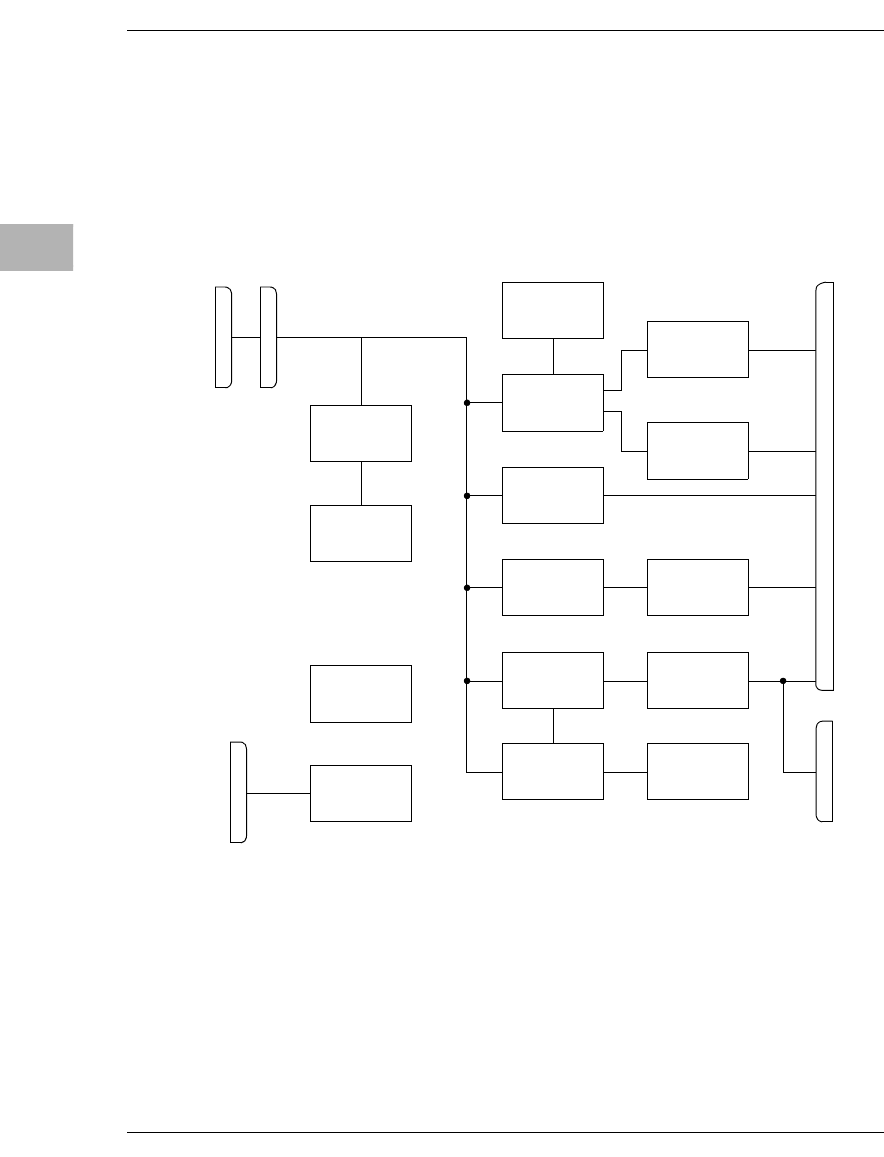
Functional Description
4-10 MVME167 Single Board Computer User’s Manual
4
Figure 4-1. MVME167 Main Module Block Diagram
MEZZANINE
PRINTER
PCCCHIP2
SCSI INTERFACE
IPL COMBINER
SERIAL
VME
1473 9405
REMOTE
RESET/ABORT/LEDS
LEDS AND
SWITCHES
CLOCKS
GENERATOR
J4, J5
SHEET 7
SHEET 28
SHEET 10
SHEET 9
P4, P5
SHEET 8
J3
SHEET 20
SHEET 21
SHEET 18
LANCE
SHEET 19
SERIAL PORT
SHEETS 24-26
PRINTER PORTS
SHEET 22
SIA
SHEET 20
BATTERY/BACKUP
SHEET 28
SRAMS AND
SHEETS 16-17
EPROMS
VME BUFFERS
SHEETS 13-15
VMECHIP2
SHEET 12
MC68040 MPU
SHEET 27
SCSI
LAN
VME
P2
SHEET 6
P1
SHEET 5
BBRAM AND TOD
SHEET 23
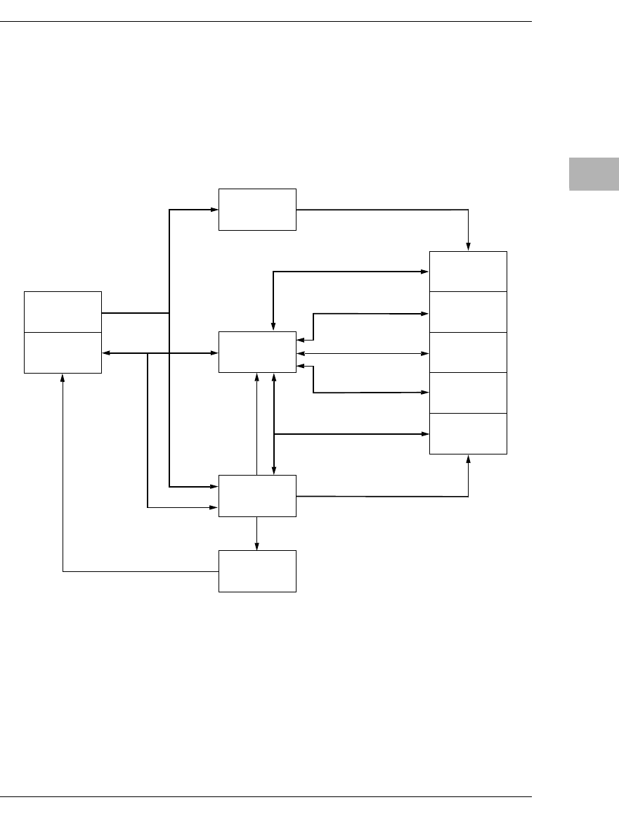
MVME167 Functional Description
MVME167/D3 4-11
4
Figure 4-2. Parity DRAM Mezzanine Module Block Diagram
PARITY MEMORY
SHEET 12
MEMORY ARRAY
BANK A
SHEET 8
CONNECTOR
SHEET 5
DATA MUX
SHEET 13, 14
ADDRESS BUS
MULTIPLEXED ADDRESS
MEMORY ARRAY
BANK B
SHEET 9
MEMORY ARRAY
BANK C
SHEET 10
MEMORY ARRAY
BANK D
SHEET 11
ADDRESS MUX
SHEET 7
10887.00 9401
TIMING CONTROL
SHEET 6
ACKNOWLEDGE
SHEET 15
CONNECTORS
SHEET 4
DATA BUS
CONTROL
RDA BUS
RDB BUS
RDC BUS
RDD BUS
PARITY DATA
DRAM STROBES
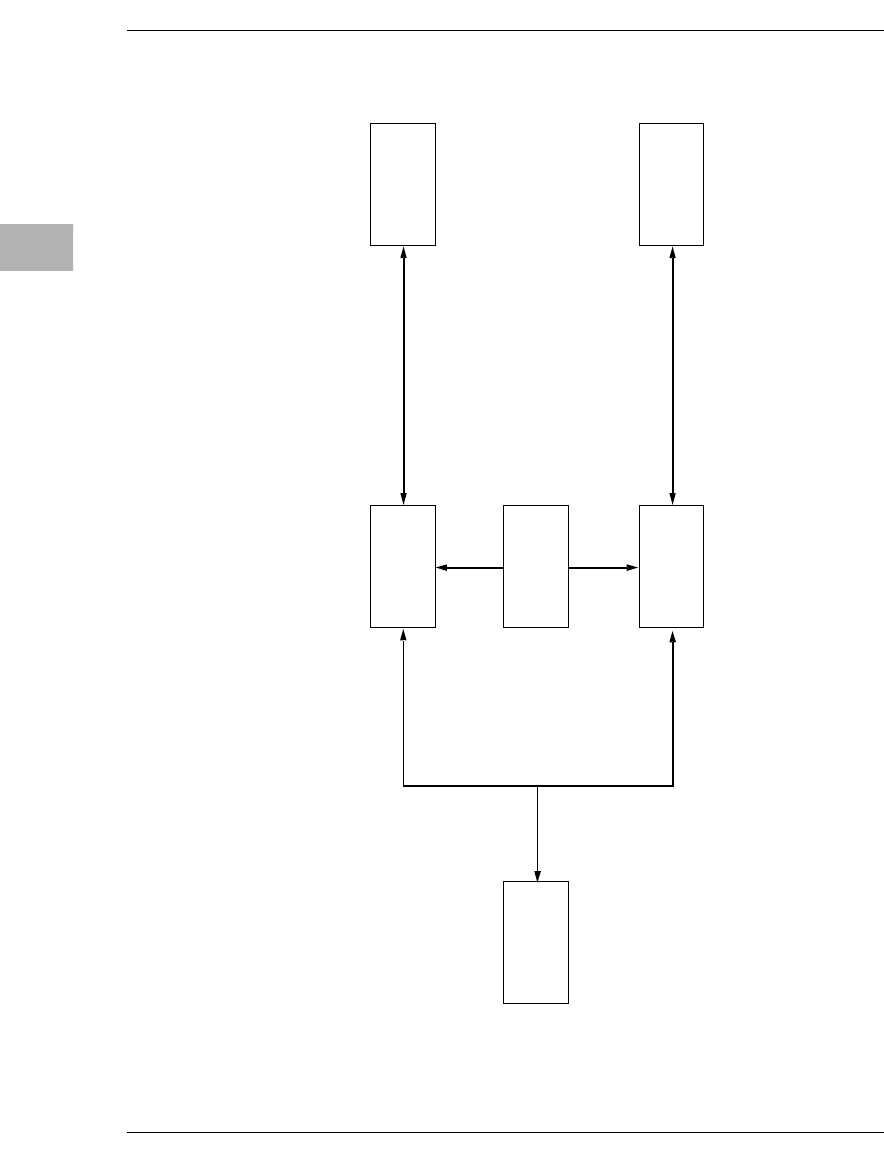
Functional Description
4-12 MVME167 Single Board Computer User’s Manual
4
Figure 4-3. ECC DRAM Mezzanine Module Block Diagram
TIMING_CONTROL,
ADDDRESS MUX,
LOWER DATA MUX
SHEET 7
UPPER DRAM ARRAY
BLOCKS 0 AND 1
SHEET 13,14
LOWER DRAM ARRAY
BLOCKS 0 AND 1
SHEET 11, 12
CONNECTORS
SHEET 4, 5
BOARD DEFAULTS
SHEET 6
TIMING_CONTROL,
ADDRESS MUX,
UPPER DATA MUX
SHEET 8
DRAM ADDR, CNTRL, LOWER DATA
040 LOCAL BUS
DRAM ADDR, CNTRL, UPPER DATA040 ADDR, CNTRL, U DATA
040 ADDR, CNTRL, L DATA
10885.00 9401

MVME167/D3A-1
A
EIA-232-D
INTERCONNECTIONS
Introduction
The EIA-232-D standard is the most widely used terminal/computer and
terminal/modem interface, and yet it is not fully understood. This may be because not
all the lines are clearly defined, and many users do not see the need to follow the
standard in their applications. Many times designers think only of their own
equipment, but the state of the art is computer-to-computer or computer-to-modem
operation. A system should easily connect to any other.
The EIA-232-D standard was originally developed by the Bell System to connect
terminals via modems. Several handshaking lines were included for that purpose.
Although handshaking is unnecessary in many applications, the lines themselves
remain part of many designs because they facilitate troubleshooting.
Table A-1 lists the standard EIA-232-D interconnections. To interpret this information
correctly, remember that EIA-232-D was intended to connect a terminal to a modem.
When computers are connected to each other without modems, one of them must be
configured as a terminal (data terminal equipment: DTE) and the other as a modem
(data circuit-terminating equipment: DCE). Since computers are normally configured
to work with terminals, they are said to be configured as a modem in most cases.
Signal levels must lie between +3 and +15 volts for a high level, and between
-3 and -15 volts for a low level. Connecting units in parallel may produce out-of-range
voltages and is contrary to EIA-232-D specifications.

EIA-232-D Interconnections
A-2 MVME167 Single Board Computer User’s Manual
A
NOTES: 1. A high EIA-232-D signal level is +3 to +15 volts. A low level is -3 to -15 volts.
Connecting units in parallel may produce out-of-range voltages and is contrary
to specifications.
Table A-1. EIA-232-D Interconnections
Pin Number Signal Mnemonic Signal Name and Description
01 Not used.
02 TxD TRANSMIT DATA. Data to be transmitted; input to the modem from the
terminal.
03 RxD RECEIVE DATA. Data which is demodulated from the receive line; output
from the modem to the terminal.
04 RTS REQUEST TO SEND. Input to the modem from the terminal when required
to transmit a message. With RTS off, the modem carrier remains off. When
RTS is turned on, the modem immediately turns on the carrier.
05 CTS CLEAR TO SEND. Output from the modem to the terminal to indicate that
message transmission can begin. When a modem is used, CTS follows the
off-to-on transition of RTS after a time delay.
06 DSR DATA SET READY. Output from the modem to the terminal to indicate that
the modem is ready to transmit data.
07 SIG-GND SIGNAL GROUND. Common return line for all signals at the modem
interface.
08 DCD DATA CARRIER DETECT. Output from the modem to the terminal to
indicate that a valid carrier is being received.
09-14 Not used.
15 TxC TRANSMIT CLOCK (DCE). Output from the modem to the terminal; clocks
data from the terminal to the modem.
16 Not used.
17 RxC RECEIVE CLOCK. Output from the modem to the terminal; clocks data
from the modem to the terminal.
18, 19 Not used.
20 DTR DATA TERMINAL READY. Input to the modem from the terminal;
indicates that the terminal is ready to send or receive data.
21 Not used.
22 RI RING INDICATOR. Output from the modem to the terminal; indicates to the
terminal that an incoming call is present. The terminal causes the modem to
answer the phone by carrying DTR true while RI is active.
23 Not used.
24 TxC TRANSMIT CLOCK (DTE). Input to modem from terminal; same function
as TxC on pin 15.
25 BSY BUSY. Input to modem from terminal. A positive EIA signal applied to this
pin causes the modem to go off-hook and make the associated phone busy.

Levels of Implementation
MVME167/D3 A-3
A
2. The EIA-232-D interface is intended to connect a terminal to a modem. When
computers are connected without modems, one must be configured as a modem
and the other as a terminal.
Levels of Implementation
There are several levels of conformance that may be appropriate for typical EIA-232-
D interconnections. The bare minimum requirement is the two data lines and a ground.
The full implementation of EIA-232-D requires 12 lines; it accommodates automatic
dialing, automatic answering, and synchronous transmission. A middle-of-the-road
approach is illustrated in Figure A-1.
Signal Adaptations
One set of handshaking signals frequently implemented are RTS and CTS. CTS is used
in many systems to inhibit transmission until the signal is high. In the modem
application, RTS is turned around and returned as CTS after 150 microseconds. RTS
is programmable in some systems to work with the older type 202 modem (half
duplex). CTS is used in some systems to provide flow control to avoid buffer overflow.
This is not possible if modems are used. It is usually necessary to make CTS high by
connecting it to RTS or to some source of +12 volts such as the resistors shown in
Figure A-1. CTS is also frequently jumpered to an MC1488 gate which has its inputs
grounded (the gate is provided for this purpose).
Another signal used in many systems is DCD. The original purpose of this signal was
to tell the system that the carrier tone from the distant modem was being received. This
signal is frequently used by the software to display a message like CARRIER NOT
PRESENT to help the user to diagnose failure to communicate. Obviously, if the system
is designed properly to use this signal and is not connected to a modem, the signal must
be provided by a pullup resistor or gate as described above (see Figure A- 1).
Many modems expect a DTR high signal and issue a DSR. These signals are used by
software to help prompt the operator about possible causes of trouble. The DTR signal
is sometimes used to disconnect the phone circuit in preparation for another automatic
call. It is necessary to provide these signals in order to talk to all possible modems (see
Figure A-1).
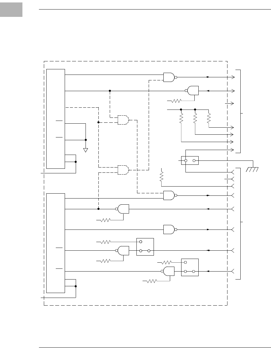
EIA-232-D Interconnections
A-4 MVME167 Single Board Computer User’s Manual
A
Sample Configurations
Figure A-1 is a good minimum configuration that almost always works. If the CTS and
DCD signals are not received from the modem, the jumpers can be moved to
artificially provide the needed signal.
Figure A-1. Middle-of-the-Road EIA-232-D Configuration
3
TXD
RXD
RTS
CTS
DCD
TXC
RXC
-12V
TXD
RXD
RTS
CTS
DCD
TXC
RXC
OPTIONAL
HARDWARE
TRANSPARENT
MODE
LOGIC
470Ω
39kΩ
39kΩ
39kΩ
470Ω
39kΩ
-12V
2
1
5
6
8
7
7
1
20
2
3
4
5
6
CHASSIS GND
CONNECTOR
TO
TERMINAL
CONNECTOR
TO
MODEM
OR
HOST
SYSTEM
RXD
TXD
NC
CTS
DSR
DCD
SIG GND
DTR
TXD
RXD
RTS
CTS
DCD
-12V
+12V
-12V +12V
+12V GND
+12V
SIG GND
NC
cb181 9210
470Ω
6850
6850
LS08
LS08
470Ω470Ω470Ω
MODULE
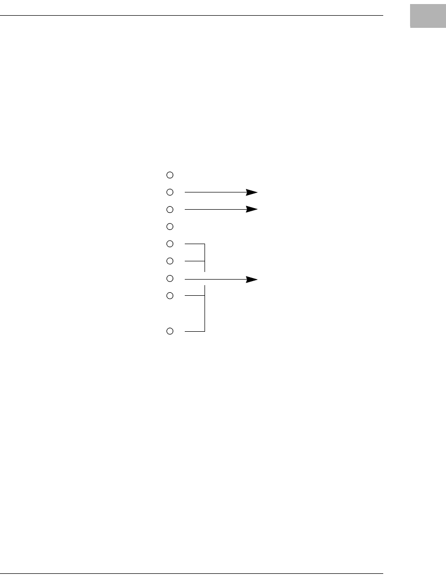
Levels of Implementation
MVME167/D3 A-5
A
Figure A-2 shows a way of wiring an EIA-232-D connector to enable a computer to
connect to a basic terminal with only three lines. This is feasible because most
terminals have a DTR signal that is ON, and which can be used to pull up the CTS,
DCD and DSR signals. Two of these connectors wired back-to-back can be used. In
this implementation, however, diagnostic messages that might otherwise be generated
do not occur because all the handshaking is bypassed. In addition, the TX and RX lines
may have to be crossed since TX from a terminal is outgoing but the TX line on a
modem is an incoming signal.
Figure A-2. Minimum EIA-232-D Connection
GND 1
TxD 2
RxD 3
GND 7
RTS 4
CTS 5
DSR 6
DCD 8
EIA-232-D CONNECTOR
DTR 20
....

EIA-232-D Interconnections
A-6 MVME167 Single Board Computer User’s Manual
A
Proper Grounding
Another subject to consider is the use of ground pins. There are two pins labeled GND.
Pin 7 is the SIGNAL GROUND and must be connected to the distant device to
complete the circuit. Pin 1 is the CHASSIS GROUND, but it must be used with care.
The chassis is connected to the power ground through the green wire in the power cord
and must be connected to the chassis to be in compliance with the electrical code.
The problem is that when units are connected to different electrical outlets, there may
be several volts of difference in ground potential. If pin 1 of each device is
interconnected with the others via cable, several amperes of current could result. This
condition may not only be dangerous for the small wires in a typical cable, but may
also produce electrical noise that causes errors in data transmission. That is why Figure
A-1 shows no connection for pin 1. Normally, pin 7 should only be connected to the
CHASSIS GROUND at one point; if several terminals are used with one computer, the
logical place for that point is at the computer. The terminals should not have a
connection between the logic ground return and the chassis.

MVME167/D3IN-1
Index
When using this index, keep in mind that a page number indicates only where
referenced material begins. It may extend to the page or pages following the page
referenced.
Numerics
167Bug (see debug monitor and
MVME167Bug) 1-6, 2-2, 2-6, 3-1,
3-30
53C710 (see SCSI Controller) 4-7
53C710 SCSI memory map 3-24
82596CA (see Ethernet and LAN) 4-6
82596CA Ethernet LAN memory map
3-23
A
ABORT switch interrupter 3-1
ABORT switch S1 3-1
adapter board (see P2 adapter board) 1-5,
2-7
ambient air temperature 1-3
assembler/disassembler 1-6
assertion 1-9
B
Battery Backed Up RAM (BBRAM) and
Clock (see MK48T08 and
NVRAM) 4-4
battery backup 4-2
battery handling and disposal 4-3
battery lifetime 4-3
BBRAM (see Battery Backed Up RAM,
MK48T08, and NVRAM) 3-26,
4-4
BBRAM configuration area memory map
3-25
BBRAM,TOD Clock memory map 3-26
BG (bus grant) 2-7
big endian mode 3-24
binary number 1-9
block diagram
ECC DRAM mezzanine module 4-13
MVME167 main module 4-11
parity DRAM mezzanine module
4-12
board ID 3-27
board serial number 3-27
board speed 3-28
bus error 3-30
bus grant (BG) 2-7
byte 1-9
C
cables (see also shielded cables) 2-7
CD2401 (see SCC and Serial Controller
Chip) 4-5
CFM (cubic feet per minute) 1-3
chassis ground A-6
checksum 3-28
Cirrus Logic CD2401 serial port memory
map 3-19
conductive chassis rails 1-4
configuration area 3-26
controls and indicators 3-1
cooling requirements 1-3
CR2430 4-2
cubic feet per minute (CFM) 1-3
cycle times 4-8
local bus to DRAM 4-8
ROM 4-9

Index
IN-2 MVME167 Single Board Computer User’s Manual
I
N
D
E
X
D
data bus structure 4-1
data circuit-terminating equipment
(DCE) A-1
data terminal equipment (DTE) A-1
DCE (data circuit-terminating equip-
ment) A-1
debug monitor (see 167Bug and
MVME167Bug) 2-2, 2-6, 3-1, 3-30
debugging package 1-7, 3-30
decimal number 1-9
default values
registers 3-30
detailed I/O memory maps 3-6
diagnostics 1-6
DMA 4-5, 4-6
DRAM (dynamic RAM) 4-3
DRAM base address 2-7
DS1 - DS4 3-2
DS1210S 4-2
DTE (data terminal equipment) A-1
dynamic RAM (DRAM) 4-3
E
ECC (error checking and correction)
DRAM mezzanine module block
diagram 4-13
EIA-232-D 4-5
EIA-232-D interconnections A-1, A-2
EIA-232-D standard A-1
EPROM sockets 1-6
EPROM(s) 2-6, 3-4, 3-30, 4-2
equipment required 1-6
errata sheets, chip 3-6
Ethernet (see 82596CA and LAN) 2-8, 4-6
Ethernet address 3-27, 3-28
Ethernet interface 4-6
Ethernet station address 4-6
Ethernet transceiver interface 4-6
extended addressing 2-7
F
factory jumper settings 2-2
FCC compliance 1-4
features 1-2
forced air cooling 1-3
front panel 3-1
front panel indicators (DS1- DS4) 3-2
functional description 4-1
fuse F1 2-8
fuse F2 2-8
G
GCSR (Global Control and Status Regis-
ters) (see VMEchip2 GCSR) 2-8,
3-30
GCSR board control register 3-30
general description 1-5
general information 1-1
general purpose readable jumpers on
header J1 2-2
global bus timeout 2-8
Global Control and Status Registers (GC-
SR) (see VMEchip2 GCSR) 2-8,
3-30
grounding A-6
H
half duplex A-3
handshaking A-1, A-3
hardware interrupts
software-programmable 4-8
hardware preparation 2-1
hardware preparation and installation
2-1
hexadecimal character 1-9
I
I/O interfaces 4-5
IACK (interrupt acknowledge) 2-7
installation instructions 2-6
interrupt acknowledge (IACK) 2-7
interrupt acknowledge map 3-28

MVME167/D3 IN-3
I
N
D
E
X
interrupts 4-8
introduction 1-1, 2-1, 3-1, 4-1, A-1
J
J1 2-2
J2 2-2
J3 4-10
J6 2-4
J7 2-4
J8 2-5
jumpers 2-1
L
LAN (see 82596CA and Ethernet) 4-6
LAN DMA transfers 4-9
LAN FIFO buffer 4-9
LAN transceiver 2-8
LCSR (Local Control and Status Regis-
ters) (see VMEchip2 LCSR) 2-2
LEDs 3-2
levels of implementation A-3
LFM (linear feet per minute) 1-3
linear feet per minute (LFM) 1-3
little endian mode 3-24
Local Area Network (see LAN) 4-6
local bus 4-8
local bus access 4-8
local bus memory map 3-3, 3-4
local bus timeout 4-8
local bus to DRAM cycle times 4-8
Local Control and Status Registers
(LCSR) (see VMEchip2 LCSR)
2-2
local I/O devices memory map 3-5
local reset (LRST) 3-1, 3-30
local reset operation 3-30
local resources 4-7
local SCSI ID 3-28
location monitors 2-8
longword 1-9
LRST (local reset) 3-1, 3-30
M
manual terminology 1-9
map decoders 3-29
MC68040 MPU 4-2
MCECC 1-5
MCECC internal register memory map
3-17
MEMC040 1-5
MEMC040 internal register memory map
3-17
memory maps 3-3
53C710 SCSI 3-24
82596CA Ethernet LAN 3-23
BBRAM configuration area 3-25
BBRAM, TOD Clock 3-26
Cirrus Logic CD2401 serial port 3-19
detailed I/O 3-6
interrupt acknowledge 3-28
local bus 3-3
local I/O devices 3-5
MCECC internal register 3-17
MEMC040 internal register 3-17
MK48T08 BBRAM, TOD Clock 3-25
PCCchip2 3-14
printer 3-16
TOD clock 3-26
VMEbus 3-29
VMEbus short I/O 3-29
VMEchip2 3-8
mezzanine module
ECC DRAM 4-13
parity DRAM 4-12
middle-of-the-road EIA-232-D configu-
ration A-4
minimum EIA-232-D connection A-5
MK48T08 (see Battery Backed Up RAM,
BBRAM, and NVRAM) 4-4
MK48T08 BBRAM,TOD Clock memory
map 3-25
model designations 1-1
modem(s) A-1

Index
IN-4 MVME167 Single Board Computer User’s Manual
I
N
D
E
X
multi-MPU programming consider-
ations 3-30
MVME167 functional description 4-1
MVME167 main module block diagram
4-11
MVME167 model designations 1-1
MVME167 module installation 2-6
MVME167 specifications 1-4
MVME167 switches, headers, connec-
tors, fuses, and LEDs 2-3
MVME167Bug (see 167Bug and debug
monitor) 1-6, 2-2, 2-6, 3-1, 3-30
MVME167Bug debug monitor 1-6
MVME167Bug debugging package 1-7
MVME712-12 1-5
MVME712-13 1-5
MVME712A 1-5
MVME712AM 1-5
MVME712B 1-5
MVME712M 1-5, 2-6, 2-8
MVME712X 1-6, 2-6, 4-5
N
negation 1-9
Non-Volatile RAM (NVRAM) (see Bat-
tery Backed Up RAM, BBRAM,
and MK48T08) 3-26, 4-4
normal address range 3-3
NVRAM (Non-Volatile RAM) (see Bat-
tery Backed Up RAM, BBRAM,
and MK48T08) 3-26, 4-4
O
onboard DRAM 4-3
operating instructions 3-1
operating systems 1-6
P
P2 adapter board 1-5, 2-7, 2-8
parallel port interface 4-6
parallel printer port 4-6
parity DRAM mezzanine module block
diagram 4-12
PCCchip2 1-5
PCCchip2 memory map 3-14
printer interface 4-6
printer memory map 3-16
printer port 4-6
programmable hardware interrupts 4-8
programmable tick timers 4-7
proper grounding A-6
R
registers 3-30
default values 3-30
related documentation 1-7
remote status and control J3 4-10
RESET switch S2 3-1, 3-30
RF emissions 1-5
RFI 2-7
ROM cycle times 4-9
RTXC4 (Receive Transmit Clock 4) 2-4
S
S1 3-1
S2 3-1, 3-30
sample configurations A-4
SCC (Serial Controller Chip) (see
CD2401) 4-5
SCSI Controller (see 53C710) 4-7
SCSI FIFO buffer 4-9
SCSI ID (see local SCSI ID) 3-28
SCSI interface 4-7
SCSI specification 1-8
SCSI termination 4-7
SCSI terminator power 2-8
SCSI transfers 4-9
Serial Controller Chip (SCC) (see
CD2401) 4-5
serial port 4 2-4
serial port 4 clock configuration select
headers J6 and J7 2-4
serial port interface 4-5

MVME167/D3 IN-5
I
N
D
E
X
shielded cables (see also cables) 1-4, 2-7
signal adaptations A-3
signal ground A-6
signal levels A-1
signals
transfer type (TT) 3-3
software initialization 3-30
software-programmable hardware inter-
rupts 4-8
specifications 1-3
SRAM (static RAM) 4-2
SRAM backup power source select head-
er J8 2-5
SRAM battery backup 4-2
SRST (system reset) 3-1, 3-30
static RAM (SRAM) 4-2
support information 1-8
SYSRESET* (see system reset) 3-1, 3-30
system considerations 2-7
system console terminal 1-6
system controller 2-2
system controller function 2-2, 3-30
system controller header J2 2-2
system mode 1-6
system reset (SRST) 3-30
system reset (SRST) (see SYSRESET*) 3-1
SYSTEM V/68 1-6
systems serial ID 3-28
T
terminal(s) A-1
terminology 1-9
tick timers 4-7
timeout 4-8
global bus 2-8
local bus 4-8
timers 4-7
timing performance 4-8
TOD clock memory map 3-26
transfer type (TT) signals 3-3
transition modules 1-5, 4-5
transparent mode A-4
TRXC4 (Transmit Receive Clock 4) 2-4
TT (transfer type) signals 3-3
U
unpacking instructions 2-1
V
VMEbus 3-29
VMEbus accesses to the local bus 3-29
VMEbus interface 4-4
VMEbus memory map 3-29
VMEbus short I/O memory map 3-29
VMEbus specification 1-8
VMEchip2 1-5
VMEchip2 GCSR (Global Control and
Status Registers) 2-8
VMEchip2 LCSR (Local Control and Sta-
tus Registers) 2-2
VMEchip2 memory map 3-8
W
warnings 4-3
watchdog timer 3-30, 4-8
word 1-9

Index
IN-6 MVME167 Single Board Computer User’s Manual
I
N
D
E
X
