Manual V1.0
Manual%20V1.0
User Manual:
Open the PDF directly: View PDF ![]() .
.
Page Count: 17

1
User Manual of MLP simulator (+NeuroSim) V1.0
Developers: Pai-Yu Chen and Xiaochen Peng
PI: Prof. Shimeng Yu, Arizona State University
Index
1. Introduction ........................................................................................................................................... 1
2. System Requirements (Linux) .............................................................................................................. 2
3. Installation and Usage (Linux) .............................................................................................................. 2
4. Device Level: Extraction of Synaptic Device Characteristics .............................................................. 3
4.1 Non-ideal Analog eNVM Device Properties ............................................................................... 3
4.2 Fitting by MATLAB script (nonlinear_fit.m) ............................................................................. 4
5. Circuit Level: Synaptic Cores and Array Architectures ....................................................................... 7
5.1 Crossbar Array Architecture ........................................................................................................ 7
5.2 Pseudo-crossbar Array Architecture ............................................................................................ 8
5.3 Array Peripheral Circuits ............................................................................................................. 9
6. Algorithm Level: Multilayer Perceptron (MLP) Neural Network Architecture ................................. 12
7. How to run MLP simulator (+NeuroSim) ........................................................................................... 14
1. Introduction
MLP simulator (+NeuroSim) is developed in C++ to emulate the online learning/offline classification
scenario with MNIST handwritten dataset in a 2-layer multilayer perceptron (MLP) neural network based
on emerging non-volatile memory (eNVM) array architectures. The eNVM in this simulator refers to a
special subset of resistive memory devices that can tune the conductance into multilevel states with voltage
stimulus. NeuroSim is a circuit-level macro model for benchmarking neuro-inspired architectures in terms
of circuit-level performance metrics, such as chip area, latency, dynamic energy and leakage power.
Without NeuroSim, MLP simulator can be regarded as a standalone functional simulator that is able to
evaluate the learning accuracy and the circuit-level performance (but only for the synapse array) during
learning. With NeuroSim, MLP simulator (+NeuroSim) becomes an integrated framework with hierarchical
organization from the device level (transistor and analog eNVM device properties) to the circuit level
(analog eNVM array architectures with periphery circuit modules) and then to the algorithm level (neural
network topology), enabling trace-based and cycle-accurate evaluation on the learning accuracy as well as
the circuit-level performance metrics at the run-time of learning.
In this released version 1.0, the target users are device engineers who wish to quickly estimate the system-
level performance with his/her own analog synaptic device data. The users are expected to have the weight

2
update characteristics (conductance vs. # pulse) ready in hand. Device-level parameters such as number of
levels, weight update nonlinearity, device-to-device variation, and cycle-to-cycle variations, could be
extracted using the MATLAB script that is provided. At the circuit level, a few design options are available,
such as the array architecture being true crossbar or pseudo crossbar with 1T1R. At the algorithm level, a
simple 2-layer MLP neural network is provided for evaluation, thus only limited options are available to
the users to modify, such as the size of each layer and the size of weight matrices.
2. System Requirements (Linux)
The tool is expected to run in Linux with required system dependencies installed. These include GCC, GNU
make, GNU C libraries (glibc). We have tested the compatibility of the tool with a few different Linux
environments, such as (1) Red Hat 5.11 (Tikanga), gcc v4.7.2, glibc 2.5, (2) Red Hat 7.3 (Maipo), gcc
v4.8.5, glibc v2.1.7, (3) Ubuntu 16.04, gcc v5.4.0, glibc v2.23, and they are all workable.
※ The tool may not run correctly (stuck forever) if compiled with gcc 4.5 or below, because some C++11
features are not well supported.
3. Installation and Usage (Linux)
Step 1: Get the tool from GitHub
git clone https://github.com/neurosim/MLP_NeuroSim.git
Step 2: Extract MNIST_data.zip to it’s current directory
unzip MNIST_data.zip
Step 3: Compile the codes
make
Summary of the useful commands is provided below. It is recommended to execute these commands under
the tool’s directory.
Command
Description
make
Compile the codes and build the “main” program
make clean
Clean up the directory by removing the object files and the “main” executable
./main
Run simulation (after make)
make run
Run simulation (after make), and the results will be saved to a log file (filename
appended with the current time info). This command does not work if “stdbuf” is not
found.
※ The simulation uses OpenMP for multithreading, and it will use up all the CPU cores by default.
3
4. Device Level: Extraction of Synaptic Device Characteristics
4.1 Non-ideal Analog eNVM Device Properties
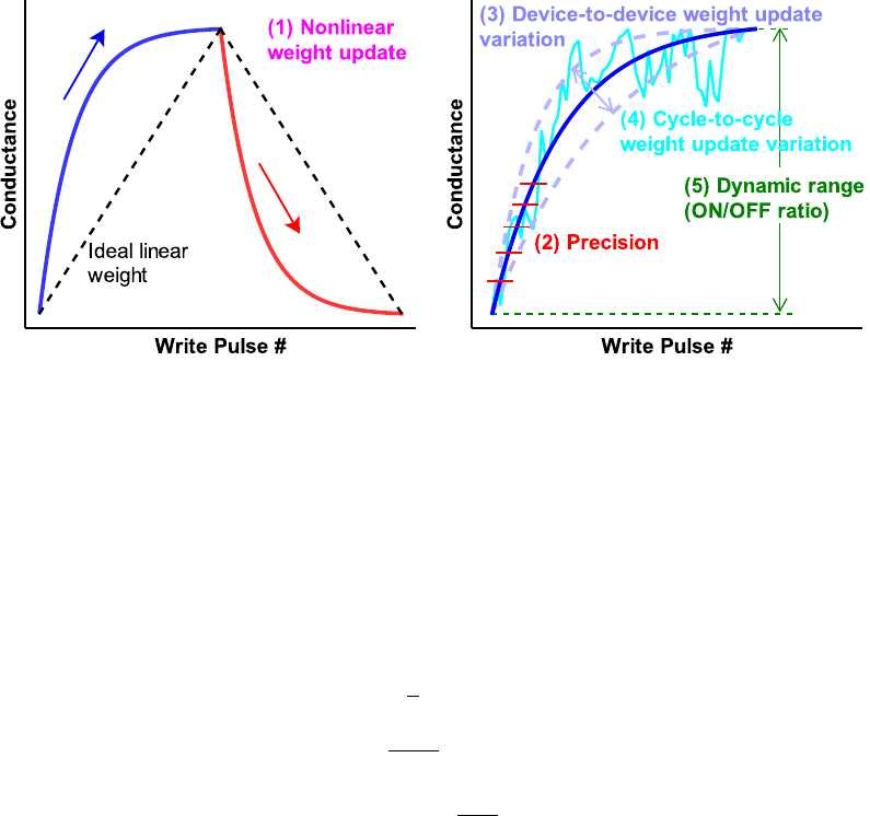
As shown in Fig. 1, the framework considers the following non-ideal analog eNVM device properties:
Fig. 1 Summary of non-ideal analog eNVM device properties.
1) Nonlinear weight update
Ideally, the amount of weight increase (or long-term potentiation, LTP) and weight decrease (or long-term
depression, LTD) should be linearly proportional to the number of write pulses. However, the realistic
devices reported in literature do not follow such ideal trajectory, where the conductance typically changes
rapidly at the beginning stages of LTP and LTD and then gradually saturates. We have built a device
behavioral model to capture nonlinear weight update behavior, where the conductance change with number
of pulses (P) is described with the following equations:
GLTP=B 1-e-P
A+Gmin
(1)
GLTD=-B 1-eP-Pmax
A+Gmax
(2)
B=(Gmax-Gmin)/(1-e
-Pmax
A)
(3)
GLTP and GLTD are the conductance for LTP and LTD, respectively. Gmax, Gmin, and Pmax are directly
extracted from the experimental data, which represents the maximum conductance, minimum conductance
and the maximum pulse number required to switch the device between the minimum and maximum
conductance states. A is the parameter that controls the nonlinear behavior of weight update. A can be
positive (blue) or negative (red). In Fig. 1, the A of LTP and LTD has the same magnitude but different
signs. B is simply a function of A that fits the functions within the range of Gmax, Gmin, and Pmax. All these
parameters can be different in LTP and LTD in the fitting by the MATLAB script. However, for simplicity,
the simulator currently uses the smaller value of Gmax and the larger value of Gmin in LTP and LTD.
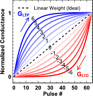
Using Eq. (1)-(3), a set of nonlinear weight increase (blue) and weight decrease (red) behavior can be
obtained by adjusting A as shown in Fig. 2, where each nonlinear curve is labeled with a nonlinearity value
from +6 to -6. It can be proved that Eq. (1) and (2) are equivalent with a different sign of A, thus we will
just use Eq. (1) to calculate both nonlinear LTP and LTD weight update. Different than Fig. 1, all LTD
4
curves are mirrored and shifted horizontally to make sure the curve starting from the pulse number 0 for
simpler formulization.
Fig. 2 Analog eNVM device behavioral model of the nonlinear weight update with the nonlinearity
labeled from -6 to 6.
2) Limited precision
The precision of an analog eNVM device is determined by the number of conductance states it has, which
is Pmax in Eq. (1)-(3).
3) Device-to-device weight update variation
The effect of device-to-device weight update variation can be analyzed by introducing the variation into
the nonlinearity baseline. This variation is defined as the nonlinearity baseline’s standard deviation (σ)
respect to 1 step of the 6 steps in Fig. 2.
4) Cycle-to-cycle weight update variation
The Cycle-to-cycle weight update variation is referred to as the variation in conductance change at every
programming pulse. This variation (σ) is expressed in terms of the percentage of entire conductance range.
5) Dynamic range (ON/OFF ratio)
Ideally, the weight values are represented by a normalized conductance of analog eNVM devices with the
range from 0 to 1. However, the minimum conductance can be regarded as 0 only when the ratio between
the maximum and minimum conductance (ON/OFF ratio) approaches infinity. With limited ON/OFF ratio,
the cells with weight=0 still have leakage.
4.2 Fitting by MATLAB script (nonlinear_fit.m)
In this section, we will fit the experimental weight update data and extract the device parameters that will
be used in the simulator. We have developed a MATLAB script nonlinear_fit.m to do such a task, where
it has been set up for fitting Ag:a-Si devices in the following reference as an example.
S. H. Jo, T. Chang, I. Ebong, B. B. Bhadviya, P. Mazumder, and W. Lu, “Nanoscale memristor device as
synapse in neuromorphic systems,” Nano Lett., vol. 10, no. 4, pp. 1297–1301, 2010.
5
Before the fitting, the user has to make sure the experimental weight update data are pre-processed in a
format that is similar to Fig. 2. Namely, the LTD data should be mirrored horizontally and both LTP and
LTD data should start from the pulse number 0 so that the data can be fit by Eq. (1)-(3). The user can look
at the pre-processed data of Ag:a-Si devices as an example in the MATLAB script.
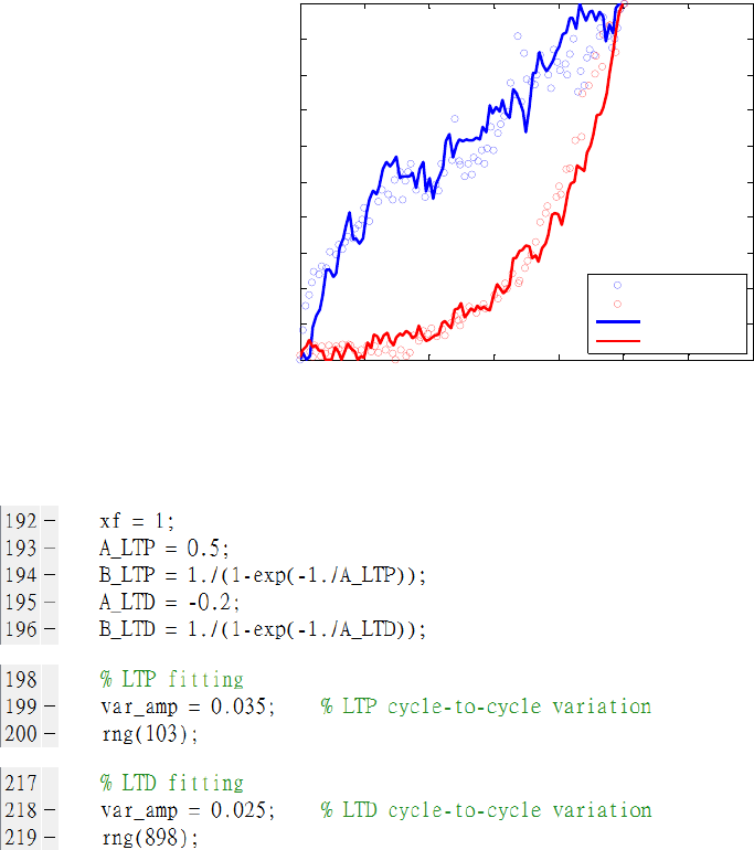
The shape of nonlinear weight update curves can look very different with the same A but different Pmax and
Gmin, because A has to be scaled according to different Pmax. First, we normalize Pmax to be 1 by default
definition, then we can tune the normalized A and the cycle-to-cycle weight update variation for both LTP
and LTD in the generated Figure 1 (normalized conductance vs. normalized number of pulses) to find the
best fit, as shown in Fig. 3. A good procedure is that the user first finds out a reasonable normalized A for
LTP and LTD curves without variation (by setting the variation in LTP and LTD to zero), and then try to
fit the LTP and LTD data with good variation values and pseudorandom seeds (for example, rng(103) and
rng(898) in script). In the script, the A values are defined as A_LTP and A_LTD, and Pmax is defined as xf
which is set to be 1. These parameters are shown in Fig. 4. It should be noted that the device-to-device
weight update variation is not considered in this script.
Fig. 3 Fitting of Ag:a-Si weight update data with normalized A in the plot of normalized conductance vs.
normalized number of pulses.
Fig. 4 Code snippet of parameters in nonlinear_fit.m
0 0.2 0.4 0.6 0.8 1 1.2 1.4
0
0.1
0.2
0.3
0.4
0.5
0.6
0.7
0.8
0.9
1
Normalized Pulse #
Normalized Conductance
Exp data (LTP)
Exp data (LTD)
Fit (LTP)
Fit (LTD)

6
After the fitting is done, the user can look up the magnitude of the normalized A value to figure out its
corresponding nonlinearity label. We provide the information of one-to-one mapping of the nonlinearity
label values to the normalized A values in the file Nonlinearity-NormA.htm. The nonlinearity label value
is from 0 to 9 with a step of 0.01, which is precise enough. If the normalized A value is negative, the
nonlinearity label value will also simply be negative. In the example of Ag:a-Si, the fitted normalized A
values are 0.5 and -0.2, and we can figure out their corresponding nonlinearities are 2.40 and -4.88 for LTP
and LTD, respectively, as shown in Table 1. In the last section, MLP simulator (+NeuroSim) will take these
two values as eNVM cell parameters.
Nonlinearity
Norm.
A
Nonlinearity
Norm.
A
Nonlinearity
Norm.
A
Nonlinearity
Norm.
A
Nonlinearity
Norm.
A
2.31
0.5207
2.38
0.5038
2.45
0.4879
4.84
0.2030
4.91
0.1983
2.32
0.5183
2.39
0.5015
2.46
0.4856
4.85
0.2023
4.92
0.1976
2.33
0.5158
2.40
0.4992
…
…
4.86
0.2016
4.93
0.1970
2.34
0.5134
2.41
0.4969
…
…
4.87
0.2010
4.94
0.1963
2.35
0.5110
2.42
0.4946
…
…
4.88
0.2003
4.95
0.1957
2.36
0.5086
2.43
0.4932
4.82
0.2044
4.89
0.1996
4.96
0.1950
2.37
0.5062
2.44
0.4901
4.83
0.2037
4.90
0.1990
4.97
0.1944
Table 1 Snippet of Nonlinearity-NormA.htm
7
5. Circuit Level: Synaptic Cores and Array Architectures
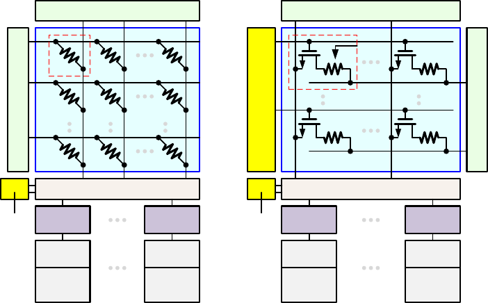
In this framework, we consider two synaptic cores of 2-layer MLP in the evaluation for circuit-level metrics
such as area, latency, energy, etc. A synaptic core is a computation unit that is specifically designed for
weighted sum and weight update. It consists of the synaptic array and array periphery. In the simulator, a
synaptic core can be instantiated from SubArray class in SubArray.cpp. In this released version, there are
two available design options for the synaptic core. One is based on the crossbar array architecture, and other
one is based on the pseudo-crossbar array architecture, as shown in Fig. 5. The details of both architectures
and their peripheral circuits are introduced below.
Fig. 5 Synaptic cores based on (a) crossbar and (b) pseudo-crossbar array architectures
5.1 Crossbar Array Architecture
The crossbar array structure has the most compact and simplest array structure for eNVM devices to form
a weight matrix, where each eNVM device is located at the cross point of a word line (WL) and a bit line
(BL). The crossbar array structure can achieve a high integration density of 4F2/cell (F is the lithography
feature size). If the input vector is encoded by read voltage signals, the weighted sum operation (matrix-
vector multiplication) can be performed in a parallel fashion with the crossbar array. However, as there is
no isolation between cells, it is necessary to apply some voltage (smaller than the programming voltage,
e.g. V/2) at all the unselected rows and columns to prevent the write disturbance on unselected cells during
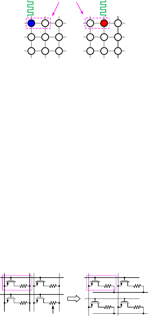
weight update. The voltage bias schemes for weight update is shown in Fig. 6. In addition, a two-terminal
threshold switching selector device is desired to minimize the write disturbance and sneak path problem.
In our model, a simple I-V nonlinearity (NL) in Cell.cpp is used to define the effect of selector or built-in
self-selection. As the weight increase and decrease need different programming voltage polarities, the
weight update process requires 2 steps with different voltage bias schemes. In weight update, the selected
cells will be on the same row, and programming pulses or biases (if no update) are provided from the BL,
allowing the selected cells to be tuned differently in parallel. To perform weight update for the entire array,
a row-by-row operation is necessary. Ideally, the entire row is selected at a time to ensure the maximum
parallelism. In the simulator, the crossbar array architecture can be designated by setting cmosAccess=false
in RealDevice class of Cell.cpp.
Mux
Read
Circuit
WL Switch Matrix
BL Switch Matrix
Read
Circuit
Adder
Shift
Register
Adder
Shift
Register
WL
BL
Synapse
Mux
Decoder
Crossbar Array
Crossbar WL Decoder
SL BL
WL
Mux
Read
Circuit
BL Switch Matrix
SL Switch Matrix
Read
Circuit
Synapse
eNVM
Pseudo-crossbar Array
Adder
Shift
Register
Adder
Shift
Register
Mux
Decoder
(b)(a)
8
Fig. 6 Voltage bias scheme in the write operation of crossbar array. Two separate phases for weight
increase and decrease are required. In this example, the left cell of the selected cells will be updated in
phase 1, while the right one will be updated in phase 2.
5.2 Pseudo-crossbar Array Architecture
Another common design solution to the write disturbance and sneak path problem is to add a cell selection
transistor in series with the eNVM device, forming the one-transistor one-resistor (1T1R) array architecture,
as shown in Fig. 7(a). The WL controls the gate of the transistor, which can be viewed as a switch for the
cell. The source line (SL) connects to the source of the transistor. The eNVM cell’s top electrode connects
to the BL, while its bottom electrode connects to the drain of the transistor through a contact via. In such
case, the cell area of 1T1R array is then determined by the transistor size, which is typically >6F2 depending
on the maximum current required to be delivered into the eNVM cell. Larger current needs larger transistor
gate width/length (W/L). However, conventional 1T1R array is not able to perform the parallel weighted
sum operation. To solve this problem, we modify the conventional 1T1R array by rotating the BLs by 90o,
which is known as the pseudo-crossbar array architecture, as shown in Fig. 7(b). In weighted sum operation,
all the transistors will be transparent when all WLs are turned on. Thus, the input vector voltages are
provided to the BLs, and the weighted sum currents are read out through SLs in parallel. The weight update
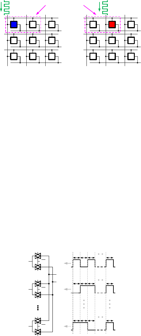
operation in pseudo-crossbar array is similar to that in crossbar array, as shown in Fig. 8. As the unselected
WLs can turn off the transistors on unselected rows, no voltage bias is required for these unselected BLs
thus pseudo-crossbar array can have save a lot of weight update energy compared to the crossbar array. In
the simulator, the pseudo-crossbar array architecture can be designated by setting cmosAccess=true in
RealDevice class of Cell.cpp.
Fig. 7 Transformation from (a) conventional 1T1R array to (b) pseudo-crossbar array by 90o rotation of
BL to enable weighted sum operation.
VW/2
VW/2
VW/2
VW
VW/2
VW/2
VW/2
0
VW0 0VW
VW/2 VW/2
Selected cells
Weight increase
(phase 1) Weight decrease
(phase 2)
WL
BL
WL
BL
SL BL
WL Cell
Conventional 1T1R array
eNVM
BL
WL Cell
Pseudo-crossbar array
SL
(a) (b)
9
Fig. 8 Voltage bias scheme in the write operation of pseudo-crossbar array. Two separate phases for
weight increase and decrease are required. In this example, the left cell of the selected cells will be
updated in phase 1, while the right one will be updated in phase 2.
5.3 Array Peripheral Circuits
The periphery circuit modules used in both eNVM crossbar and pseudo-crossbar synaptic cores in Fig. 5
are described below:
1) Switch matrix
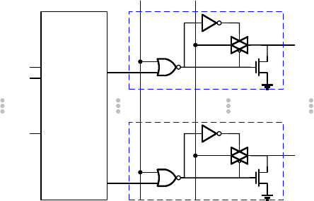
Switch matrixes are used for fully parallel voltage input to the array rows or columns. Fig. 9(a) shows the
BL switch matrix for example. It consists of transmission gates that are connected to all the BLs, with
control signals (B1 to Bn) of the transmission gates stored in the registers (not shown here). In the weighted
sum operation, the input vector signal is loaded to B1 to Bn, which decide the BLs to be connected to either
the read voltage or ground. In this way, the read voltage that is applied at the input of transmission gates
can pass to the BLs and the weighted sums are read out through SLs in parallel. If the input vector is not 1
bit, it should be encoded using multiple clock cycles, as shown in Fig. 9(b). The reason why we do not use
analog voltage to represent the input vector precision is the I-V nonlinearity of eNVM cell, which will cause
the weighted sum distortion or inaccuracy. In the simulator, all the switch matrixes (slSwitchMatrix,
blSwitchMatrix and wlSwitchMatrix) are instantiated from SwitchMatrix class in SwitchMatrix.cpp.
Fig. 9 (a) Transmission gates of the BL switch matrix in the weighted sum operation. A vector of control
signals (B1 to Bn) from the registers (not shown here) decide the BLs to be connected to either a voltage
source or ground. (b) Control signals in a bit stream to represent the precision of the input vector.
SL
WL
VWL
0
0
0
0
VW0
SL
WL
VWL
00
0
0
0
0
0VW
VW
VW
VW0
Weight increase (phase 1)
Selected cells
BL BL
Weight decrease (phase 2)
B1
B1
B1
BL1
VREAD
GND
B2
B2
B2
BL2
Bn
Bn
Bn
BLn
≈ ≈
Digitized Input Vector
V
0
V
0
≈
V
0
B1[0] B1[k-1]B1[1] B1[2]
B2[0] B2[1] B2[2] B2[k-1]
Bn[0] Bn[1] Bn[2] Bn[k-1]
(a) (b)
10
2) Crossbar WL decoder
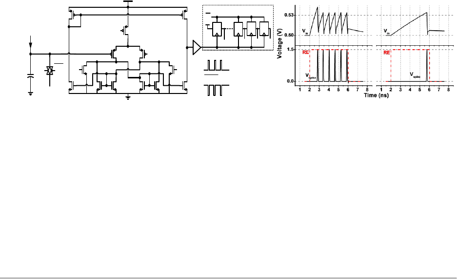
The crossbar WL decoder is modified from the traditional WL decoder. It has an additional feature to
activate all the WLs for making all the transistors transparent for weighted sum. The crossbar WL decoder
is constructed by attaching the follower circuits to every output row of the traditional decoder, as shown in
Fig. 10. If ALLOPEN=1, the crossbar WL decoder will activate all the WLs no matter what input address
is given, otherwise it will function as a traditional WL decoder. In the simulator, the crossbar WL decoder
contains a traditional decoder (wlDecoder) instantiated from RowDecoder class in RowDecoder.cpp and
a collection of follower circuits (wlDecoderOutput) instantiated from WLDecoderOutput class in
WLDecoderOutput.cpp.
Fig. 10 Circuit diagram of the crossbar WL decoder. Follower circuit is attached to every row of the
decoder to enable activation of all WLs when ALLOPEN=1.
3) Multiplexer (Mux) and Mux decoder
The Multiplexer (Mux) is used for sharing the read periphery circuits among synaptic array columns,
because the array cell size is much smaller than the size of read periphery circuits and it will not be area-
efficient to put all the read periphery circuits underneath the array. However, sharing the read periphery
circuits among synaptic array columns inevitably increases the latency of weighted sum as time
multiplexing is needed, which is controlled by the Mux decoder. In the simulator, the Mux (mux) is
instantiated from Mux class in Mux.cpp and the Mux decoder (muxDecoder) is instantiated from
RowDecoder class in RowDecoder.cpp.
4) Analog-to-digital read circuit
To convert these analog weighted sum currents to digital outputs, we use the read circuit in the following
reference to employ the principle of the integrate-and-fire neuron model, as shown in Fig. 11(a). The read
circuit integrates the weighted sum current on the finite capacitance of the array column. Once the voltage
charges up above a certain threshold, the read circuit fires an output pulse and the capacitance is discharged
back. The simulated waveform of integrated input voltage and the digital output spikes of the read circuit
is shown in Fig. 11(b). The number of output spikes is proportional to the weight sum current. The precision
required for this analog-to-digital conversion (ADC) determines the pulse width in each bit of the input
vector. In the simulator, a collection of read circuits (readCircuit) is instantiated from ReadCircuit class
in ReadCircuit.cpp.
WL[0]
ALLOPEN VIN
WL[2n-1]
n:2n
Decoder
ADDR[0]
ADDR[1]
ADDR[n-1]
Follower
11
D. Kadetotad, Z. Xu, A. Mohanty, P.-Y. Chen, B. Lin, J. Ye, S. Vrudhula, S. Yu, Y. Cao, J.-S. Seo, “Parallel
architecture with resistive crosspoint array for dictionary learning acceleration,” IEEE J. Emerg. Sel. Topics
Circuits Syst. (JETCAS), vol. 5, no. 2, pp. 194-204, 2015.
Fig. 11 (a) Design of a read circuit that employs the principle of the integrate-and-fire neuron model. (b)
Simulated waveform of integrated input voltage and the digital output spikes of the read circuit.
5) Adder and shift register
The adder and shift register pair at the bottom of synaptic core performs shift and add of the weighted sum
result at each input vector bit cycle (B1 to Bn in Fig. 9(b)) to get the final weighted sum. The bit-width of
the adder and shift register needs to be further extended depending on the precision of input vector. If the
values in the input vector are only 1 bit, then the adder and shift register pair is not required. In the simulator,
a collection of the adder and shift register pairs (ShiftAdd) is instantiated from ShiftAdd class in
ShiftAdd.cpp, where ShiftAdd further contains a collection of adders (adder) instantiated from Adder
class in Adder.cpp and a collection of registers (dff) instantiated from DFF class in DFF.cpp.
Vreset
Vspike
Ir,i (or IZ,j)
(0 – 8 μA) D Q
RD Q
R
8-bit spike counter
Q[5]
Q[7]
RE
Q[0]
Ccol
(Crow)
D Q
RD Q
R
Q[6] Q[7]
Vin
Vspike
Vspike
Vp
Vp
Vp
Vspike
(b)(a)
I=5.75µA I=1µA
12
6. Algorithm Level: Multilayer Perceptron (MLP) Neural Network
Architecture
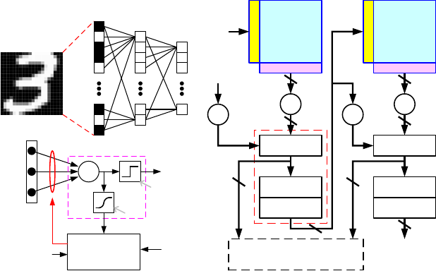
At the algorithm level, we provide a simple 2-layer multilayer perceptron (MLP) neural network for
performance benchmark. As shown in Fig. 12(a), the network consists of an input layer, hidden layer and
output layer (the input layer is not included when counting the number of layers). MLP is a fully connected
neural network, where each neuron node in one layer connects to every neuron node in the following layer.
The connection between two neuron nodes is through a synapse with its strength representing the weight,
where WIH and WHO are the weight matrix between input and hidden layer and between hidden and output
layer, respectively. For the input image data, we post-processed the MNIST handwritten digits by cropping
the edges of each image (making it 20×20 pixels). For the favor of hardware implementation, we also
convert the images to black and white data in the simulator to reduce the design complexity of input
encoding. By default, the network topology is 400(input layer)-100(hidden layer)-10(output layer). 400
neurons of input layer correspond to the 20×20 MNIST image, and 10 neurons of output layer correspond
to 10 classes of digits. The users could change the network topology as needed. However, a new learning
rate may be required to optimize the learning accuracy.
The learning applications that the network can implement in this simulator include the online learning and
offline training with classification only. In online learning, the simulator emulates hardware to train the
network with images randomly picked from the training dataset (60k images) and classify the testing dataset
(10k images). In offline training with classification only, the network is pre-trained by software, and the
MLP simulator only emulates hardware to classify the testing dataset. The training data file is
patch60000_train.txt and its label file (the correct answers of the training data) is label60000_train.txt.
The testing data file is patch10000_test.txt and its label file (the correct answers of the testing data) is
label60000_train.txt.
The training process consists of two key operations, the feed forward (FF) and back propagation (BP). In
feed forward, the input data are fed from the input layer and they will travel in a forward direction to the
output layer via a series of weighted sum operation and neuron activation function along the way. The feed
forward result at the output layer will then be compared with its correct answer (the label) to calculate its
prediction error (the deviation). In back propagation, this error is propagated backward from the output
layer to adjust the weights of each layer in a way that the prediction error is minimized. In this simulator,
we use stochastic gradient decent method to update the weights in the back propagation. Different than the
traditional gradient decent, the back propagation is performed after the feed forward of every image rather
than that of the entire image dataset. On the other hand, the testing (classification) process only has the feed
forward operation to make predictions. The weights in this process will not be changed.
Fig. 12(b) shows a schematic of a neuron node, which encapsulates the principles discussed above. The
neuron takes the weighted sum result from its inward synapses and pass it through a 1-bit low-precision
activation function. In this way, the offline classification, which is purely feed forward, can be realized in
1 bit. However, the computation on the back propagation of weight update generally needs higher precision
to update the small errors, thus a high-precision activation function for the back propagation is still
necessary.
Fig. 12(c) shows the circuit block diagram for hardware implementation of this 2-layer MLP neural network.
The weighted sum operation is performed using the synaptic cores. However, the weights used in a regular
synaptic array can only represent positive values (WH=0~1), while the weights in algorithm can be either
positive or negative values (WA=-1~1). The algorithm’s weighted sum is then expressed as
13
WAV
=2WH-JV
=2WHV-JV
(4)
where V is the input vector and J is the matrix of all ones that has the same dimension as WA and WH. In Eq.
(4), WHV is the weighted sum output from the synaptic core. Therefore, we squeeze WA from (-1~1) to the
range of WH (0~1): i.e. -1 is mapped to 0, 0 is mapped to 0.5, and 1 is mapped to 1. To reconstruct WAV, we
have to perform a two-step read from the array: first, we read out WHV, and then multiply WHV by 2 using
a 1-bit left-shift, and then subtract JV (basically the sum of vector) from WHV through the adder at the
periphery. The MSB (sign bit in 2’s complement notation) of the adder output will be the 1-bit output of
the low-precision activation function. It should be noted that we only consider the main sub-circuit modules
for the neuron periphery at current stage of this simulator, and the hardware for BP error calculation as well
as the detailed control logics will be included in the future release.
Fig. 12 (a) The 2-layer MLP neural network. (b) Schematic of a neuron node. (c) Circuit block diagram
for hardware implementation of the 2-layer MLP network.
In the back propagation phase, the weight update values (ΔW) will be translated to the number of LTP or
LTD write pulses (Fig. 12(b)) and applied to the synaptic array following the voltage bias scheme in Fig. 6
or Fig. 8. To reduce the hardware design complexity, we assume that all the selected cells in each write
batch have to wait for the full number of write pulse cycles regardless of their ΔW. For example, if the
device has 64 conductance levels, then it needs to go through the whole 64 write pulse cycles even when
its ΔW=0. For this naïve weight update scheme, the total weight update latency of a synaptic array can be
straightforwardly calculated as (number of conductance states) × (number of write batches in an array row)
× (number of array rows). The second term, number of write batches, is related to numWriteColMuxed in
Param.cpp, which will be introduced later in the next section.
20x20 Cropped
Handwritten Digits
Black & White
Data
400 Input
Elements 100 Hidden
Neurons 10 Output
Neurons
WIH WHO
∑
Neuron
W
Computation
of weight
update
FF
output
BP
errors
Low-precision
Activation Function
ΔW
Values
from
previous
layer
(a)
(b)
Adders
Mux
Registers
Synaptic
Core
(WIH)
Input vector
Adders
Mux
Registers
Synaptic
Core
(WHO)
+
-+
vector
Weight update with other
hardware control logics
MSB
∑ ×2×2
Predicted
result
MSB
∑
-
Neuron
Periphery
(c)
High-precision
Activation Function
Neuron nodes at
previous layer
14
7. How to run MLP simulator (+NeuroSim)
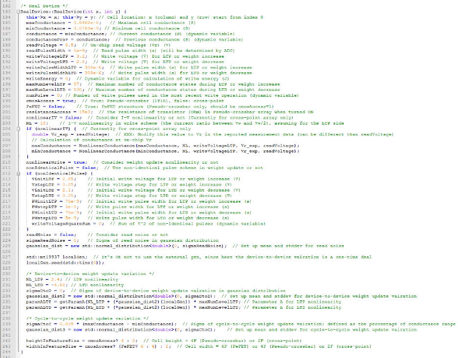
Before running the simulator, the device-level and array-level parameters that the user may wish to modify
are in RealDevice class of Cell.cpp, as shown in Fig. 13. The default values are for the Ag:Si example.
Fig. 13 Code snippet of RealDevice class in Cell.cpp
where maxConductance and minConductance are defined as 1/Ron and 1/Roff respectively, readVoltage
and readPulseWidth are on-chip read voltage (V) and read pulse width (s). The specified value of
readPulseWidth does not matter because it will be modified later by the read circuit module when it
calculates the required pulse width for each integration cycle based on the ADC precision.
writeVoltageLTP and writePulseWidthLTP are the write voltage (V) and the write pulse width (s) during
LTP or weight increase. writeVoltageLTD and writePulseWidthLTD are also defined in the same way.
maxNumLevelLTP and maxNumLevelLTD mean the maximum number of write pulse for LTP and LTD
of the real device, which represents the precision. Besides, NL_LTP and NL_LTD represent the
nonlinearity values for LTP and LTD, and sigmaDtoD and sigmaCtoC represent the device-to-device and
cycle-to-cycle weight update variation, respectively. Currently the simulator only takes one value of the
cycle-to-cycle weight update variation for sigmaCtoC. It is encouraged that the user selects the larger one
in LTP and LTD for conservative estimation. In the example of Ag:a-Si, NL_LTP and NL_LTD are set to
15
2.40 and -4.88, which are obtained from the MATLAB fitting results. The cycle-to-cycle weight update
variation is set to be 0.035 as the maximum variation of LTP and LTD is 3.5%.
Also, cmosAccess is used to choose the cell structure, or synaptic core type in other words.
cmosAccess=true means the pseudo-crossbar (1T1R) array, while cmosAccess=false means the true
crossbar array. If the cell is 1T1R, we need to define resistanceAccess, which is the turn-on resistance
value of the transistor in 1T1R array. The FeFET option for the ferroelectric FET is not released yet, thus
the default configuration is FeFET=false. If the cell is crossbar, I-V nonlinearity NL can be specified as
the current ratio between write voltage and half write voltage considering if a selector is added. The
nonIdenticalPulse option is for non-identical write pulse scheme where the write pulse amplitude or width
linearly increases or decreases with the pulse number. VinitLTP, VstepLTP, VinitLTD, VstepLTD,
PWinitLTP, PWstepLTP, PWinitLTD and PWstepLTD are essential parameters that need to be defined
by the users when nonIdenticalPulse=true.
16
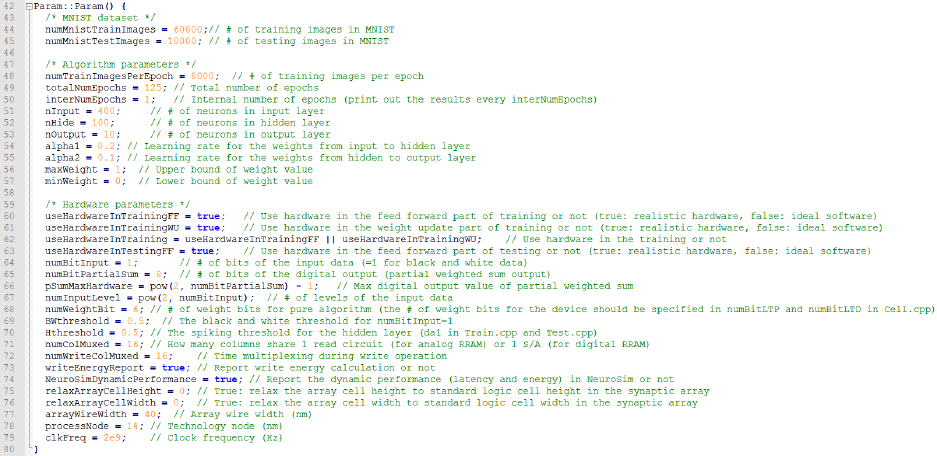
In the file Param.cpp, there are also network-level parameters that the user may wish to modify, as shown
in Fig. 14.
Fig. 14 Code snippet of Param.cpp
where numMnistTrainImages and numMnistTestImages are the number of images in MNIST during
training and testing respectively, numTrainImagesPerEpoch means the number of training images per
epoch, while interNumEpochs represents the internal number of epochs within each printed epoch shown
on the screen. In addition, nInput, nHide and nOutput are the number of neurons in input, hidden and
output layers in the 2-layer MLP neural network, respectively.
The first four hardware parameters determine the learning configuration, which can be the following cases:
1. Online learning in hardware: useHardwareInTrainingFF, useHardwareInTrainingWU and
useHardwareInTestingFF are all true
2. Offline learning in software and then classification only in hardware: useHardwareInTrainingFF and
useHardwareInTrainingWU are false, while useHardwareInTestingFF is true
3. Pure learning in software: useHardwareInTrainingFF, useHardwareInTrainingWU and
useHardwareInTestingFF are all false
For other hardware parameters, numBitInput means the number of bits of the input data. The hardware
architecture design in this released version only allows numBitInput=1 (black and white data), which
should not be changed. numBitPartialSum represents the number of bits in the digital output (partial
weighted sum output) of read circuit (ADC) at the periphery of the synaptic array. numWeightBit means
the number of weight bits for pure algorithm without consideration of hardware, and numColMuxed means
the number of columns of the synaptic array sharing one read circuit in the array. Time-multiplexing is
required if numColMuxed is greater than 1. For example, the total weighted sum latency will be increased
by roughly 16 times if numColMuxed=16. In the weight update, there might also be limited throughput
for the weight update information to be provided from outside. In this case, time-multiplexing is
implemented by setting numWriteColMuxed. For example, numWriteColMuxed=16 means updating
every row will need roughly 16 weight update operations.
17
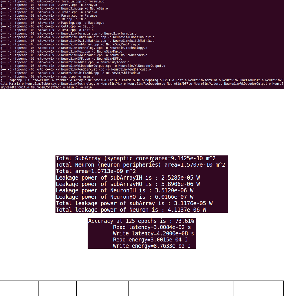
Basically, the parameters for running the simulator are all included in the file Cell.cpp and Param.cpp.
Whenever any change is made in the files, the codes has to be recompiled by using make command as
stated in Usage (Linux) section. If the compilation is successful, the following screenshot of Fig. 15 can
be expected:
Fig. 15 Output of make
Then, use ./main or make run to run the program. For both commands, the program will print out the
results at every epoch during the simulation. Compared to ./main, make run can save the results to a
log file with filename appended with the current time info, as shown in Fig. 16. With the default value of
totalNumEpochs=125 and numTrainImagesPerEpoch=8000 for a total 1 million MNIST images, the
simulation will approximately take about 40 mins with an Intel i7 CPU and 32 GB RAM.
Fig. 16 Output of the simulation
At the end of simulation, it is expected to have similar results for the Ag:a-Si example in Table 2:
Accuracy
Area (m2)
Read Latency (s)
Write Latency (s)
Read Energy (J)
Write Energy (J)
73.61%
1.0713e-9
3.0084e-2
4.2000e8
3.0015e-4
8.76e-2
Table 2 Final results of learning accuracy and circuit-level performance
For the accuracy of pure software learning as the reference, the users could change the learning modes in
Param.cpp as discussed above, and it is 96~97% for a network topology 400-100-10.