North_Star_Z80A_Processor_Board_ZPB A_Rev_2_1977 North Star Z80A Processor Board ZPB A Rev 2 1977
North_Star_Z80A_Processor_Board_ZPB-A_Rev_2_1977 North_Star_Z80A_Processor_Board_ZPB-A_Rev_2_1977
User Manual: North_Star_Z80A_Processor_Board_ZPB-A_Rev_2_1977
Open the PDF directly: View PDF ![]() .
.
Page Count: 35

/
NORTH
STAR
*
COMPUTERS,
INc.
2547 Ninth Street · Be
rk
el
ey,
Ca
li
fornia
94
710 •
(4
15) 549-0
85
8
I
North
Star
Z80A. PROCESSOR
BOARD
ZPB-A
/
Contents
Cautions
• . . . . . • • . . . . . . . 2
Introduction
.
.........•
3
Limited
Warranty
. . . . • • • . . . .
..
4
Out
of
Warranty
Repair
. . . . . . . • 4
ZBP-A
Parts
List
. • . . • . . . • . .
.•
5
PROM
Opt
i
on
Parts
List
. . . . . . . .
•.
6
A~sembly
I
n
form~tion
.
..
•
.....
7
Figure
lA:
Component
Identification
.
10
ZPBAssembly
. .
..
•.•.•...•
11
ZBP
Board
Checkout
.
..•..
..
15
PROM
Option
Assembly
and
Checkout
. . 20
Con
f
iguration
Options
. . 4
•••••••
21
The
o
ry
of
Operation
. . . . . . . . . 24
Append
i x
1:
Pulse
Signal
Detection
.•..
28
Appendix
2:
S-100
Bus
Signals
....•.
29
Assembly
Figures
. . . • . . . . .
30
Schematic
Drawings
. . . .
.•
. .
..
31
Copyright
1977,
North
Star
Co
m
puters,
I
nc.
REVISION 2

CAUTIONS
1.
Correct
this
document
from
the
errata
sheets,
if
any,
before
doing
anything
else.
2.
Building
this
product
from
a
kit
is
a
complex,
demanding
project.
It
should
not
be
attempted
without
prior
kit
building
experience.
3.
Do
NOT
insert
or
remove
the
ZPB
from
the
computer
while
the
power
is
turned
on.
Note
that
the
power
is
not
completely
off
until
the
capacitors
have
discharged,
several
seconds
after
turning
of
the
power
switch.
.
4.
Do
NOT
insert
or
remove
IC's
from
the
board
while
the
power
is
turned
on.
5.
Be
sure
each
5
volt
regulator
is
generating
5
volt
output
voltage
before
installing
any
IC's.
6.
Be
careful
to
insert
all
IC's
in
correct
positions
and
with
correct
orientation.
Be
sure
all
IC
pins
are
correctly
inserted
into
the
socket
holes
and
are
not
bent
under
the
IC
and
are
not
outside
the
socket.
7.
Carefully
observe
the
anti-static
handling
procedure
for
the
static
sensitive
devices
(these
are
the
Z80A
and
the
2708
PROM
in
the
PROM
option).
The
procedure
is
described
in
the
Assembly
Information
section
of
this
manual.
North
Star
Z80A
PROCESSOR
BOARD
2

INTRODUCTION
The
North
Star
Computers
Z80A
Processor
Board
(ZPB)
provides
Z80
microprocessor
capability
on
the
S-100
bus.
The
use
of
the
Z80A
chip
allows
full
speed
4MHz
operation
as
a
standard
feature.
The
ZPB
can
be
used
in
any
standard
S-100
bus
computer
and
will
operate
in
conjunction
with
nearly
all
other
S-100
bus
boards.
However,
the
ZPB
has
been
specifically
designed
to
integrate
into.
the
North
Star
Computers
HORIZON
computer
system.
In
addition
to
the
Z80A
microprocessor
and
support
logic
to
interface
to
the
standard
S-100
bus,
the
ZPB
contains
the
following
features
and
options:
1.
AUTO-JUMP
feature
that
will
cause
an
automatic
jump
to
any
address
at
power-on
or
reset.
2.
VECTORED
INTERRUPTS.
ZPB
logic
will
respond
to
eight
levels
of
interrupt
requests,
determine
the
highest
priority
request
pending
and
generate
the
appropriate
RST
instruction.
The
logic
may
be
disabled
to
allow
the
function
to
be
performed
on
another
board.
3.
FRONT
PANEL
INTERFACE
for
direct
connection
to
IMSAI
and
other
similar
front
panels.
40
ADDRESS
MIRROR
feature
to
simulate
the
input/output
characteristics
of
the
8080
mieroprocesso[.
This
feature
maintains
compatibility
with
some
S-100
bus
peripheral
boards.
Address
mirroring
may
be
disabled
to
allow
use
of
the
more
powerful
Z80
protocol.
5.
PROM
OPTION. lK
of
2708
type
erasable
PROM
can
be
'added
to
the
ZPB.
This
allows
configuration
of
systems
that
requ1re
resident
monitor
and
bootstrap
programs.
If
you
have
purchased
the
ZPB
as
a
kit,
firyt
skim
this
entire
manual.
Before
beginning
assembly,
careful~y
read
the
Assembly
Information
section.
Whether
you
purchased
the
ZPB
as
a
kit
or
assembled,
read
the
Configuration
section
before
attempting
to
use
the
ZPB.
Note
that
a
Z80
Technical
Manual
has
been
included
to
fully
describe
the
operation
of
the
Z80A.
3
North
Star
Z80A
PROCESSOR
BOARD

LIMITED
WARRANTY
North
Star
Computers,
Inc.
warrants
the
electrical
and
mechanical
parts
and
workmanship
of
this
product
to
be
free
of
defects
for
a
period
of
90
days
from
date
of
purchase.
If
such
defects
occur,
North
Star
Computers,
Inc.
will
repair
the
defect
at
no
cost
to
the
purchaser.
This
warranty
does
not
extend
to
defects
resulting
from
improper
use
or
assembly
by
purchaser,
nor
does
it
cover
transportation
to
the
factory.
Also,
the
warranty
is
invalid
if
all
instructions
included
in
the
accompanying
documentation
are
not
carefully
followed.
Should
a
unit
returned
for
warranty
repair
be deemed
by
North
Star
Computers,
Inc.
to
be
defective
due
to
purchaser's
action,
then
a
repair
charge
not
to
exceed
$30
without
purchaser's
consent
will
be
assessed.
ANY
UNIT
OR
PART
RETURNED
FOR
WARRANTY
REPAIR
MUST
BE
ACCOMPANIED
BY
A
COpy
OF
THE
ORIGINAL
SALES
RECEIPT.
This
warranty
applies
to
units
located
outside
the
United
S~ates
of
America
only
if
all
costs
and
arrangements
for
transportation
of
the
product
to
and
from
the
factory
are
borne
entirely
by
the
customer.
This
warranty
is
made
in
lieu
of
all
other
warranties,
expressed
or
implied,
and
is
limited
to
the
repair
or
replacement
of
the
product.
No
warranty,
expressed
or
implied,
is
extended
concerning
the
completeness,
correctness,
or
suitability
of
the
North
Star
equipment
for
any
particular
application.
There
are
no
warranties
which
extend
beyond
those
expressly
stated
herein.
OUT·OF
WARRANTY
REPAIR
If
your
unit
is
out
of
warranty
and
you
are
unsuccessful
at
diagnosing
or
repairing
the
problem,
out-of-warranty
service
may
be
arranged
with
a
local
dealer
or
other
experienced
local
computer
technician.
Alternatively,
any
North
Star
products
may
be
shipped
PREPAID
to
the
North
Star
address
with
a
clear
written
description
of
the
problem.
Include
as
many
details
as
possible
about
the
problem
and
about
your
system
configuration.
Your
unit
will
be
returned,
C.O.D.,
within
30
days
after
receipt
by
North
Star.
Out-of-warranty
repair
service
is
billed
at
the
rate
of
$25.00
per
hour.
If
you
wish
to
place
an
upper
limit
on
the
amount
of
time
spent
on
your
unit,
mention
this
in
the
written
description.
North
Star
Z80A
PROCESSOR
BOARD
4

ZPB-A
PARTS
LIST
1 ZPB
Manual
1
Z80
Technical
Manual
1 ZPB
printed
circuit
board,
5"
x
Ie"
1
40-pin
IC
socket
7
20-pin
IC
sockets
14
l6-pin
IC
sockets
14
14-pin
IC
sockets
1
16-pin
DIP
header
1
lN4l48
diode
2 5
volt
regulators,
7805
or
340T-5
2
heat
sinks,
6107B-14
I
crystal,
8MHz
2
6-32x3/B"
machine
screws
2
#6
lock
washers
2
6-32
nuts
Integrated
Circuits
3
74LS00
1
74LS132
2
74LS02
1
74LS148
1
74LS03
'J
74LS175
..J
2
74LS04
7
74LS241
J
74LS08
2
74LS257
1
74LS14
1
7404
1
74LS32
<
74367
1
74LS74
1
8T97
2
74LS75
1 Z80A
Resistors
1
100
ohm
(brown-black-brown)
1
330
ohm
(orange-orange-brown)
2
470
ohm
(yellow-violet-brown)
11
lK
ohm
(brown-black~red)
I
10K
ohm
(brown-black-orange)
4
lK
ohm
networks,
Part
No.
l0-9-l-R1K
1
2.2K
ohm
network,
Part
No.
10-9-l-R2.2K
Capacitors
I
1
19
2
1 .
1
5
33pf
470pf
.047uf
6.8uf
39uf
100uf
dipped
mica
(may
be
marked
"330J03")
dipped
mica
ceramic
disc
dipped
tantalum
dipped
tantalum
electrolytic
North
Star
Z80A PROCESSOR
BOARD
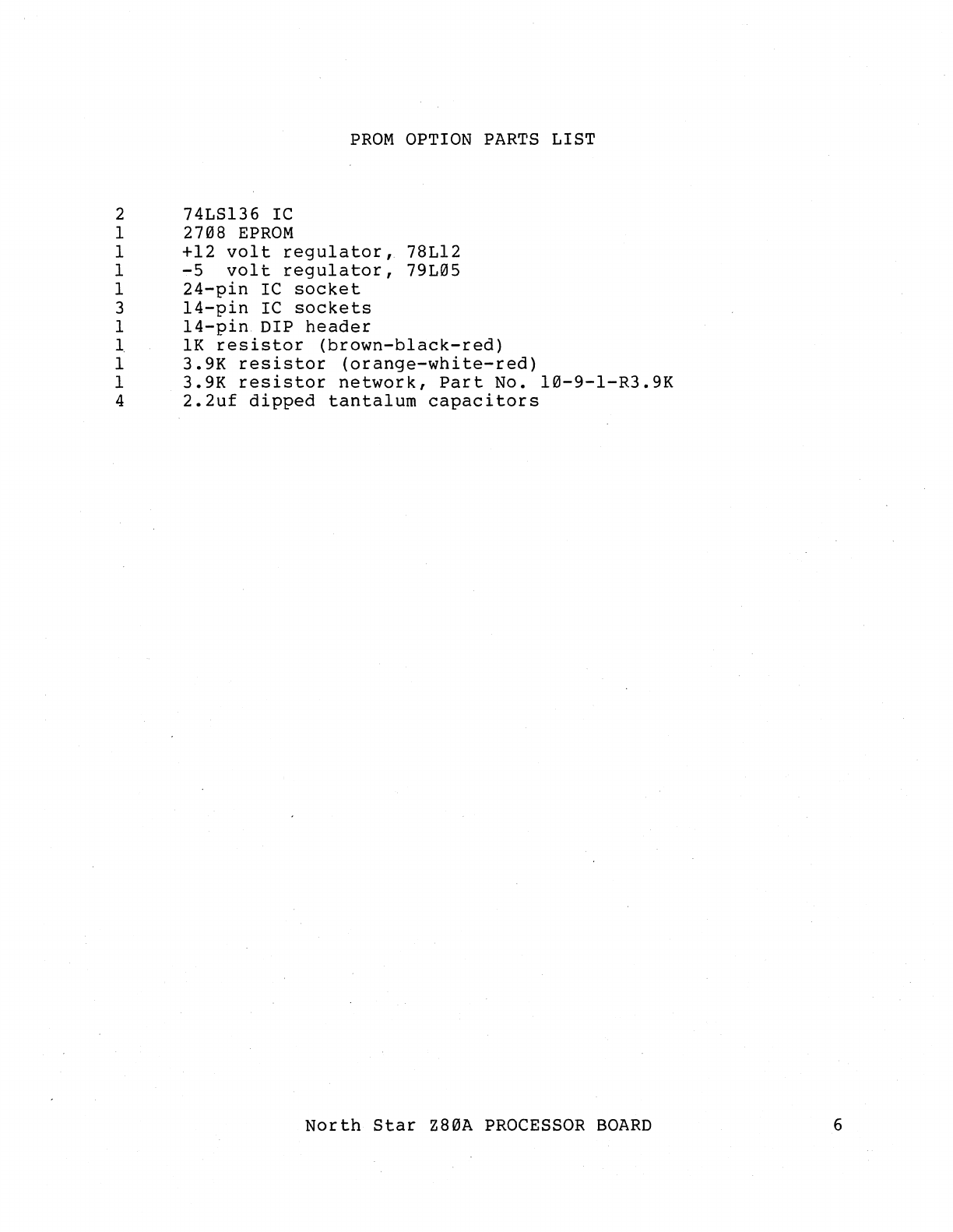
PROM
OPTION
PARTS
LIST
2
74LS136
IC
1
2708
EPROM
1
+12
volt
regulator,
78L12
1
-5
volt
regulator,
79L05
1
24-pin
IC
socket
3
14-pin
IC
sockets
1
14-pin
DIP
header
1
lK
resistor
(brown-black-red)
1
3.9K
resistor
(orange-white-red)
1
3.9K
resistor
network,
Part
No.
10-9-1-R3.9K
4
2.2uf
dipped
tantalum
capacitors
North
Star
Z80A
PROCESSOR
BOARD
6

ASSEMBLY
INFORMATION
Read
completely
through
each
section
before
beginning
the
first
instruction
step
of
that
section.
Perform
all
operations
in
the
sequence
indicated.
Read
each
step
entirely,
including
any
notes
that
accompany
the
step,
before
beginning
to
follow
the
step.
WORK
AREA
AND
TOOLS
Start
with
a
clean,
well-lit
and
well-ventilated
area
to
work.
The
area
should
be
large
enough
to
accommodate
the
kit,
tools,
parts
and
assembly
instructions~
Suggested
tools
are:
screwdrivers,
needle-nose
pliers,
diagonal
cutters,
soldering
iron,
solder,
and
masking
tape.
A number
of
tests
will
require
using
a
YOM
(ohmmeter-voltmeter),
or
VTVM.
Also
highly
desirable,
but
not
necessary,
are
an
IC
inserter,
a
screw-holding
screwdriver,
an
oscilloscope
or
logic
probe,
and
an
extender
card.
[Note
that
if
you do
not
have
an
oscilloscope
or
logic
probe,
waveforms
can
be
detected
by
one
of
the
procedures
described
in
Appendix
1.]
SOLDERING
TIPS
For
best
results
use
a
15
to
25
watt
soldering
iron
or
an
iron
with
a
temperature
controlled
tip
(approximately
700
degrees).
The
tip
should
be no
wider
than
the
solder
pads
on
the
printed
circuit
board.
Use
only
a
fine
gauge
rosin
core
solder
(60/40
or
63/37).
Do
NOT
use
acid
core
solder
as
this
can
severely
damage
a
printed
circuit
board.
When
soldering,
keep
the
soldering
iron
tip
on
the
pad
just
long
enough
for
the
solder
to
completely
flow.
If
the
solder
does
not
draw
up
the
wire
then
more
solder
is
required.
Do
not
use
so
much
solder
that
it
overflows
the:
pad.
i~
a
solidified
joint
is
not
sn1ny,
1L
may
be
a
cold
solder
joint
and
should
be
remelted.
The
soldering
iron
tip
should
be
cleaned
frequently
by
wiping
on a damp
sponge
When
you
have
completed
assembly
of
a
board,
inspect
it
for
unintended
solder
connections
or
"bridges",
as
well
as
unsoldered
leads.
After
soldering,
it
is
recommended
that
the
rosin
flux
be
removed
from
the
board
using
flux
remover,
FREON
or
paint-thinner
type
solvent.
This
will
make
looking
for
soldering
problems
easier
and
give
the
board
a
clean,
professional
appearance.
IC
SOCKET
INSTALLATION
Integrated
circuit
(IC)
sockets
can
be
installed
by
first
inserting
them
into
the
printed
circuit
board,
then
placing
another
flat
board
over
the
IC
sockets
and
finally'
turning
over
this
sandwich.
Be
sure
that
each
IC
socket
is
inserted
into
the
proper
location
and
is
oriented
such
that
pin
1
of
the
socket
corresponds
to
the
pin
1
indication
on
the
PC
board
layout
legend.
(Refer
to
figure
IA
to
identify
pin
I on
an
IC
socket.)
To
solder
IC
sockets,
first
solder
just
two
opposite
corner
pins
7
North
Star
Z80A
PROCESSOR
BOARD

for
all
sockets
being
installed.
Then
remelt
the
corner
connections
while
applying
pressure
down on
the
board.
This
will
remove
any
gaps
'that
may
be
present
between
the
IC
sockets
and
the
PC
board.
Finally,
solder
the
remaining
pins
of
the
IC
sockets.
DIP
HEADER
SOLDERING
When
making
jumper
connections
on
a DIP
header,
solder
resistor
or
capacitor
lead
snippings
between
the
leads
to
be
connected.
When
more
than
two
pins
are
to
be
connected
together,
bend
a
sIngle
wire
so
that
it
routes
to
each
pin,
and
solder
each
pin
once.
Insert
the
header
in
an
IC
socket
on a
PC
board
to
hold
it
during
soldering.
Overheating
the
pins
with
t~e
soldering
iron
will
melt
the
plastic
of
the
header.
If
there
are
multiple
jumpers
on
a
header,
make
sure
that
no
unintended
connections
are
made by
carefully
routing
the
jumpers,
or
by
insulating
each
jumper
with
some
wire
insulation.
RESISTOR
AND
CAPACITOR
INSTALLATION
To
install
resistors
or
capacitors,
first
make
right
angle
bends
in
the
leads
to
fit
the
PC
board
hole
spacing.
(Some
capacitor
leads
are
already
appropriately
spaced
and
do
not
need
bending.)
Then
insert
the
leads
as
far
as
possible
through
the
correct
.
holes
in
the
PC
board
and
spread
the
leads
slightly
on
the
solder
side
of
the
board
to
keep
the
part
in
place.
After
a
grou~
of
resistors
or
capacitors
has
been
inserted,
then
solder
the
leadS
on
the
solder
side
of
the
board
and
snip
off
the
excess
leads
as
close
to
the
board
as
possible.
Use
caution
to
avoid
eye
injury
from
flying
bits
of
wire.
Save
the
lead
clippings
for
later
use
in
making
jumper
connections.
PRINTED
CIRCUIT
BOARD
LAYOUT
The
white
component
layout
legend
is
printed
on
the
component
side
of
a
printed
circuit
(PC)
boar~.
All
components
are
inserted
from
this
side
(component
side)
and
soldered
on
the
other
side
(solder
side).
Locations
on
the
PC
board
are
identified
by
two-character
codes
as
marked
on
the
board:
a
digit
followed
by
a
letter
indicating
the
horizontal
and
vertical
coordinates
of
the
location.
Note
that
in
North
Star
kits,
IC's
can
be
found
on
styrene
pads
in
positions
corresponding
to
their
intended
locations
on
the
PC
board.
Pin
nrimbering
conventions
for
the
S-l~~
edge
pins
are
as
follows:'
When
viewing
the
component
side
of
the
board
(with
the
pin
edge
facing
down),
pins
1,2,
•••
,
5~
range
from
left
to
right.
When
viewing
the
solder
side
of
the
board,
pins
l~~,
99,
•••
, 51
range
from
left
to
right.
North
Star
Z8~A
PROCESSOR
BOARD
8

MaS
INTEGRATED CIRCUIT
HANDLING
Some
North
Star
PC
boards
use
some
MaS-type
IC's.
These
parts
are
identified
as
such
in
the
instructions.
MaS
devices
can
be
damaged
by
static
electricity
discharge,
so
special
handling
is
necessary
to
protect
them.
Handle
MaS
devices
as
little
as
possible
and
avoid
touching
the
pins.
Place
the
conductive
foam
or
tube
which
contains
the
MaS
device
onto
the
PC
board
before
removing
the
device
from
the
foam
or
tube.
Also,
be
sure
both
hands
are
touching
the
foam
or
tube
when
the
device
is
removed
from
the
foam
or
tube.
Once
a
MaS
device
has
been
installed
in
a
PC
board,
handle
the
.board
as
little
as
possible.
Of
course,
never
insert
or
remove
any
IC
while
power
is
applied
to
the
board,
and
never
remove
or
insert
a
PC
board
while
power
is
applied
to
the
motherboard.
9
North
Star
Z80A PROCESSOR
BOARD

c::=======~~
100
MFD
)J::=======:3
positive (+) lead
\};...
.
Axial Lead
Electrolytic Capacitor
========(€]DDD[:)~======~
Transistor and
Regulator (To-92)
Resistor
Quick-Connect
Lug
Integrated Circuit (lC)
Ceramic
Disc
Capacitor·
Ii'
-
Dipped
Mylar
Capacitor
I C Socket
Dipped
Mica
Capacitor
Figure
1A.
Identification
and
orientation
of
components.
Resistor Network
Dipped
Tantalum
Capacitor
positive
(+) lead
DIP
Header

ZPB
ASSEMBLY
Before
beginning
assembly
of
the
ZPB,
first
check
that
you
have
all
the
parts
listed
in
the
parts
list.
Note
tha
t
in
the
f01lowing
instructions,
"le
ft"
and
"r
ight"
refer
to
those
directions
when
viewing
the
component
side
of
the
PC
board
with
the
100-pin
edge
facing
down.
Using
an
ohmmeter,
check
for
open
circuits
between
the
pair
of
solder
pads
for
each
of
the
following
seven
capacitor
locations:
C22,
C23,
C25,C26,
C27, C28,
and
C29.
If
any
shorts
are
found,
locat~
and
correct
the
problem
or
return
the
PC
board
for
repla'cement.
Insert
and
solder
the
40-pin
IC
socket
at
location
3C,
following
the
procedure
given
in
the
Assembly
Information
section.
Insert
and
solder
the
seven
20-pin
IC
sockets
with
correct
orientation.
Insert
and
solder
a
16-pin
IC
socket
at
location
IG.
Note
that
this
socket
has
reverse
orientation
from
all
the
others,
with
pin
I
in
the
upper
right
corner.
ZS.
Insert
and
solder
the
remaining
thirteen
16-pin
sockets
with
correct
orientation.
t';;"2\
~
zs.
11
Insert
and
solder
the
fourteen
14-pin
sockets
with
correct
orientation.
Do
not
install
sockets
in
locations
5C,
5D,
and
5E
(inside
dashed
line)
unless
you
are
assembling
the
PROM
option
at
this
time.
Insert
and
solder
the
five
single-in-line
(SIP)
resistor
networks
labeled
RNI,
RN2, RN4, RN5,
and
RN6
on
the
layout
legend.
RN6
is
a
2.2K
ohm
network
and
the
remaining
four
are
IK
ohm
networks.
RN3
is
part
of
the
PROM
option.
Orient
each
SIP
so
the
end
marked
with
a "I"
(sometimes
this
end
has
a
beveled
corner)
corresponds
to
the
end
marked
with
a
dot
on
the
layout
legend.
Insert
and
solder
the
following
sixteen
resistors.
Refer
to
the
Assembly
Information
section
for
resistor
installation
procedures.
Resistor
Value
Color-code
Location
(~
Rl
470
ohm
yellow-violet-brown
IF
North
Star
Z80A PROCESSOR
BOARD

~~
R2
470
ohm
yellow-violet-brown
IF
R3
IK
ohm
brown-black-red
2E
(V'j
RS
IK ohm
brown~black-red
SG-
(~
R6
IK ohm
brown-black-red
4F
(
R7
330
ohm
orange-orange-brown
4C
(v)
R8
IK
ohm
brown-black-red
6B
(~R9
IK
ohm
brown-black-red
6B
(.
RII
IK
ohm
brown-black-red
4G
(1
Rl2
IK
ohm
brown-black-red
7C·
(Vr
R13.
lK
ohm
brown-black-red
7A
(~
Rl4
IK
ohm
brown-black-red
7A
( RIS lK
ohm
brown-black-red
8F
(v)
Rl6
10K
ohm
brown-black-orange
8G
(
V(
Rl7
100
ohm
brown-black-brown
8G
(v
R18
lK
ohm
brown-black-red
8G
~
Insert
and
solder
the
lN4l48
diode
at
location
8G. The
end
of
the
diode
marked
with
a
band
is
the
cathode
end
and
should
be
oriented
toward
the
top
of
the
board.
/ZrD
Insert
and
solder
the
l0flh:lf.
electrolytic
cap~cito.r
(C29)
~
located
near
8A. The
posltlve
end
(marked
wlth
a "+"
or
a
red
dot)
should
be
oriented
toward
the
right
as
indicated
on
the
layout
legend.
Some
capacitors
mark
the
negative
end
with
a
"-"
instead
of
the
positive
end.
I .
~.l.
Insert
and
solder
the
39uf
tantalum
capacitor
(C2l)
near
~
location
7G.
Be
sure
to
orient
the
capacitor
so
that
the
lead
marked
with
a "+"
is
inserted
through
the
hole
marked
with
a
"+".
~.
Insert
and
solder
the
two
6.8uf
tantalum
capacitors
(C22
and
~C23)
at
locations
8F
and
8G.
Be
sure
to
orient
the
'capacitors
so
that
the
lead
marked
with
a "+"
is
inserted
through
the
hole
marked
with~a
"+".
G.l:V
Insert
and
solder
the
470pf
dipped
mica
capacitor
(Cl)
at
location
IF.
Some
470pf
capacitors
are
marked
"47lJO".
@~Inser~
and
solder
the
33pf
dil?ped'
mica
capacitor
(CS)
at
.
locatlon
2F.
Some
33pf
capacltors
are
marked
"330J03".
<iI0rnsert
and
solder
the
nineteen
ceramic
disc
bypass
capacitors
in
locations
marked
with
an
asterisk
on
the
layout
legend.
rZl~.Insert
and
solder
the
8MHz
crystal
at
location
IF.
Make
~
right
angle
bends
in
the
two
leads
so
the
crystal
will
lie
parallel
with
the
PC
board.
To
hold
the
crystal
package
in
place,
use
a
piece
of
snipped
resistor
lead
to
solder
the
top
of
the
crystal
package
to
the
corresponding
hole
in
the
board.
A
little
space
should
be
left
between
the
cryst~l
and
the
PC
board
to
avoid
the
possibility.of
shorts.
North
Star
Z80A
PROCESSOR
BOARD
12

.
NOTE:
The
BMHz
crystal
is
used
for
4MHz
operation
of
the
processor.
If
2MHz
operation
is
desired,
then
a
4MHz
crystal
(not
supplied)
should
be
used.
See
the
Configuration
section
for
details
•.
Recheck
the
circuiis
between
the
capacitor
leads
as
in
step
Zl
and
make
sure
they
are
still
open
circuits.
Note
that
the
capacitors'which
have
been
installed
may
cause
the
ohmmeter
needle
to
jump when
first
contact
is
made
but
the
indication
should
rapidly
return
to
a
high
resistance.
(~
Insert
and
so~der
the
tWO.5-volt
regulators
(03
and
Q4).
\J
These
parts
will
be
marked
"7805"
or
"340T-5".
Bend down
the
three
leads
of
the
regulator
90
degrees
so
that
the
leads
go
into
the
correct
holes
while
the
machine
screw
holes
line
up.
Install
the
heat
sink
and
regulator
so
that
the
following
sequence
results
from
bottom
to
top:
6-32
machine
screw
head,
PC
board,
heat
sink,
regulator,
lock
washer,
and
nut.
Finally,
make
sure
the
leads
do
not
touch
each
other
or
the
heat
sinks
and
then
tighten
the
machine
screw
and
solder
the
regulator
leads.
NOTE:
Heat
sink
grease
may
be
used
though
it
is
not
generally
needed.
Tightening
the
bolts
too
tight
can
crack
the
PC
board.
e C
/,..
"'1.-:; !.
Cf1
( c
?.
'!>::.
~,O
'-
V
Z19.
with
the
computer
power
off,
plug
the
partially
assembled
board
into
the
motherboard.
Then
turn
on
the
power.
with
a
DC
volt
meter
check
that
both
regulators
are
generating
5
volts
output.
These
voltages
can
be
measured
across
the
pins
of
C22
and
C23.
wait
a few
minutes
and
measure
again.
The
regulators
should
not
get
very
hot
in
this
configuration~
However,
with
all
parts
installed
it
is
normal
for
the
regulator
to
feel
quite
hot
to
the
touch.
Remember
to
turn
off
the
power
before
removing
the
board.
Construct
a
16-pin
DIP
header
with
jumpers
set
up
for
a
starting
address
of
EB00
hex.
This
is
the
standard
HORIZON
starting
address.
If
some
other
starting
address
is
desired,
change
the
header
after
completing
the
checkout
instructions.
See
figure
lZ
for
the
details
of
the
header
configuration.
Refer
to
the
Assembly
Information
section
for
header
construction
procedures.
Plug
the
completed
header
into
location
2E
(the
POJ
ADDRESS
socket)
with
the
correct
orientation.
/
---,,!>"""t-
2.
...
5,
DCj
G
'1,..
~
-;.
.)
I
00
Insert
the
33
integrated
circuits
(all
exce?t
the
z80A
chip).
Be
sure
that
all
IC's
have
pin
1
oriented
to
the
bottom
left
corner.
Do
not
insert
any
IC's
inside
the
area
for
the
PROM
option
(outlined
with
a
dashed
line).
SVO
/J'YltV
TOT r
fJJ!O
-z..-1?O!
Recheck
the
regulator
output
voltages
as
in
step
Zl9.
13
North
Star
Z80A
PROCESSOR
BOARD

Z23
•.
Remove
the
PC
board
from
the
computer
and
then
plug
in
the
Z80A
chip
with
correct
orientation.
Refer
to
the
Assembly
Information
section
for
MOS
device
handling
procedures.
Z24.
Inspect
the
board
in
a
good
light
to
insure
that:
A.
all
solder
joints
are
good,
i.e.
there
are
no
bridges
of
solder
beween
adjacent
solder
joints,
no
unsoldered
joints,
and
no
cold
solder
joints
indicated
by
a
dull
finish
on
the
solder.
B.
all
IC
pins
are
in
the
IC
socket
holes,
not
outside
the
socket
and
not
folded
under
the
chip.
Pins
folded
under
can
often
be
detected
by
sighting
down. a row
of
chips
to
see
if
there
is
any
blockage
of
light
under
the
chips.
C.
all
parts
are
installed
in
the
correct
locations
with
the
correct
orientation.
The
ZPB
is
now
completely
assembled.
Proceed
to
the
RAM
Board
Checkout
section.
North
Star
Z80A
PROCESSOR
BOARD
14

RAM
BOARD
CHECKOUT
The
following
checkout
procedure
should
be
followed
for
a
newly
assembled
board.
It
can
also
be
used
to
diagnose
problems
in
previously
operational
boards.
This
checkout
procedure
assumes
that
no
other
board
besides
the
ZPB
is
plugged
into
the
S-100
bus.
This
makes
it
possible
to
get
the
ZPB
operational
even
if
no
other
board
in
the
system
is
yet
working.
This
procedure
assumes
only
that
the
correct
unregulated
voltages
have
been
applied
to
the
bus,
that
the
computer
has
a
reset
switch,
and
that
the
bus
lines
are
not
shorted
to
each
other.
The
following
terms
are
used
in
specifying
expected
test
results.
GND
LOW
HIGH
+5V
AC
ground,
0
volts
DC
logic
zero,
0-.7
volts,
normally
about
.3
volts
logic
one,
2.4-5.0
volts,
normally
about
3
volts
+5
volts
from
power
supply
Signal
with
pulses
(as
opposed
to
DC
signal)
When
referring
to
the
name
of
a
signal
from
the
schematic
drawings,
if
the
signal
is
identified
with
a
bar
over
its
name
then
the
name
of
the
signal
is
followed
by
a
slash
(e.g.,
STORE/)
in
the
checkout
instructions.
When
describing
an
AC
pulse,
the
notation
(±W,P)
refers
to
a
positive
or
negative
pulse
with
a
width
of
Wand
a
period
of
P.
For
example,
a
positive
pulse
of
width
125
nanoseconds
appearing
every
25
microseconds
would
be
represented
as
(+125ns,25us).
See
Appendix
1
for
details
on
how
to
detect
pulse
signals.
The
abbreviation
MB
before
a
pin
number
indicates
a
bus
pin
on
the
motherboard.
If
an
oscilloscope
will
be
used
to
test
the
board,
a
"scope
ground"
may
be
installed
by
soldering
a
"bridge"
of
jumper
wire
between
the
two
PC
board
holes
that
connect
edge
connector
pins
50
and
100
near
location
2A.
Note
that
either
of
the
two
regulator
machine
screws
can
also
be
used
for
ground
test
points.
~
Check
for
correct
clock
signals
on
the
ZPB
as
follows:
15
A.
Install
a
jumper
wire
at
PE
(near
location
4G)
if
the
PE
trace
was
has
been
cut.
B. Remove
the
lW
jumper
(near
location
6G)
if
it
was
previously
installed.
North
Star
Z80A
PROCESSOR
BOARD

c
•.
Install
a
jumper
wire
at
MW
(near
location
6A)
if
the
MW
trace
has
been
cut.
D.
with
the
computer
power
off,
install
only
the
ZPB
in
the
computer
motherboard.
E.
Turn
on
the
compu~er
power
and
check
for
the
following
signals.
Note
that'all
timing
signals~iven
below
assume
the
ZPB
is
configuredfRr
standard
4MHz
operation.
",
Signal
Location
Description
t
:fl~)
~
I-\.v,n-
{ qq'1
'bt-t
(91.
v-PHI
Z80
pin
6
AC,
(+125ns,250ns)
......
VPHI 2
MB
pin
24
AC,
(+
125ns,
25
0ns')
V;;HI 1
MB
pin
25
AC,
(+62ns,250ns)
\ \
q"1
W
\
2MH
Z
CLOCK/
MB
pin
49
AC,
(-250ns,500ns)
~"
If
any
of
these
are
wrong,
trace
back
to
the
crystal
to
determine
the
cause.
C1v~
This
step
will
check
the
reset
logic.
Use
the
same
setup
as
the
previous
step
and
check
the
following
signals
while
alternately
depressing
and
releasing
the
computer
reset
switch.
Switch Switch
Signal
Location
Depressed
Released
RESET/
I/MB
pin
75
LOW
HIGH
V7G
pin
6
HIGH
LOW
RST/ y'5G
pin
6
LOW
HIGH
POC/
","'MB
pin
99
LOW
HIGH
Check
the
auto-jump
logic
as
follows:
A.
Leave
the
board
configured
as
in
the
previous
step.
B.
Turn
off
the
computer
power
and
remove
the
ZPB
from
the
computer.
Temporarily
connect
the
PRDY
signal
to
ground
by
soldering
a
piece
of
jumper
wire
beween
7F
pin
5
and
7F
pin
7
on
the
solder
side
of
the
ZPB.
C.
Install
only
the
ZPB
in
the
computer
'motherboard
and
then
turn
on
the
power
and
depress
and
release
the
reset
switch.
The
processor
should
pause
immediately
after
performing
the
auto-jump
sequence
and
just
before
executing
the
first
instruction
at
the
auto-jump
address.
Sheck
that
the
SMI
signal
at
motherboard
pin
44
is
HIGH.~
D.
Assuming
the
jump
address
specified
on
the
header
at
location
E2
is
E800,
then
E800
should
be
on
the
motherboard
address
lines.
HIGH
signals
should
be
observed
on
the
following,
motherboard
pins:
North
Star
Z80A
PROCESSOR
BOARD
16

../
/'
./
V
pins
32,
85, 86,
and
87.
LOW
signals
should
be
observed
on
the
following
motherboard
pins:
I
v v V'"
Vv"
v'
v
V'/
"/'
.
pins
29,
30, 31,
33,
34,
37,
79,
80,
81, 83,
and
84
The
processor
should·
have
executed
a
single
instruction
(JMP
E800)
and
then
gone
into
a
wait
state
during
the
instruction
fetch
at
that
address.
The
Theory
of
Operation
section
describes
the
auto-jump
sequence.
If
SMI
is
high
but
the
address
is
wrong,
check
the
data
paths
through
the
POJ
header
and
multiplexors.
If
SMI
is
LOW,
skip
to
the
next
step
to
see
if
the
processor
can
execute
instructions
at
all.
If
SMI
has
an
AC
signal,
check
the
wait
logic
from
PRDY
to
WAIT/.
C4.
This
step
checks
out
the
Z80A
while
executing
a
one
instruction
program.
17
A.
With
the
power
off,
remove
the
jumper
from
PRDY
to
ground
from
the
ZPB.
B.
Turn
on
the
power
and
then
depress
and
release
the
reset
switch.
The
Z80
should
be
executing
an
RST
7
instruction
repeatedly.
Observe
that
all
the
data
input
(01)
lines
are
HIGH
by
checking
the
following
motherboard
pins:
.
t/./
/
~..
~(if
/
plns
41,
42,
43,91,
93, 94,
and 95
C.
If
you
have
an
oscilloscope,
then
check
that
the
signals
ZD0-ZD7
are
HIGH
during
Ml
at
the
Z80A
chip
pins:
/
pins
14,
15, 12,
8,
7,
9,
10,
and
13
~0
~!.-'-.
D.
Check
that
the
following
motherboard
address
lines
are
AC
signals:
v'
t/
V
pins
29-34,
37,
and
79-87.
E. The
RST
7
instruction
causes
a
subroutine
call
to
location
0038
hex,
thus
the
stack
address
stored
will
be
0039 hex
(stored
as
alternating
00
byte
and
39
hex
byte).
Thus,
observing
the
data
output
bus
(DO),
the
following
motherboard
bus
pins
should
always
be
LOW:
~!
\ Du,utcJ
(,...
tZ(;r~,)E::~:-;':
pins
35,
40,
88,
and
90.
and
the
following
motherboard
bus
pins
should
have
AC
signals:
pins
36,
38,
39,
and
89
North
Star
Z80A
PROCESSOR
BOARD

North
Star
Computers,
Inc.
2547
Ninth
Street
Berkeley,
California
94710
Gentlemen:
September
9,
1978
I
am
resonding
to
your
request
for
information
regarding
possible
errors
in
the
Horizon
documentation.
I'm
sure
it's
redundant
but
here
goes
anyway:
ZPB-A
board
checkout
procedure,
page
17,
par.
C4-E
is
no
longer
valid
due
to
the
addition
of
the
DO
bus
pull-up,
RN6.
These
lines
wi.ll
go
hi.gh
when
ever
the
DO-EN
line
disables
IC's
1
Band
1A
giving
an
AC
indication
during
the
test.
Incidently,
my
Horizon
I
kit
webt
together
beautifully
and
so
far,
seems
to
be
working
like
a
champ!

//f)
Check
for
the
following
signals
at
the
Z80
chip:
L,)f
Signal
PHI
Ml/
INT/
NMI/
WAIT/
RST/
Vcc
ground
Location
pin
6
pin
27
pin
16
pin
17
pin
24
pin
26
pin
11
pin
29
Description
AC,
(+125ns,250ns)
AC,
(-;,,500ns,2750ns)
HIGH
./
HIGH
HIGH
HIGH
+5V
GND
~The
following
signals
should
be
observed
.on
the
motherboard
bus
lines:
Signal
XRDY
VI0/
VII/
VI2/
VI3/
VI4/
VI5/
VI6/
VI7/
NMI/
STAT-DSBL/
CC-DSBL/
ADDR-DSBL/
DO-DSBL/
PHLDA
PWAIT
PINTE
SMI
SOUT
SINP
SMEMR
SHLTA
SSW-DSBL/
PMREQ/
PRFSH/
MWRITE
RUN
PINT/
PHOLD/
PSYNC
PWR/
PDBIN
SWO/
Location
pin
3
pin
~.
pin
§
pin
6
pin
~
pin
8
pin
,9
pin
3.13
pin
.11
pin
,12
pin
·18
. '
Pln
19
pin
,22
pin.·23
pin
.:26
pin~
27
pin
28
pin
44
pin-45
pin
t46
pin- 47
pin
.48
pin
r53
pin
65
pin
6
..
6
pin
6j3
pin"7l
pin-73
pin~
74
pin
76
pin
17
pin
78
pin
97
Description
HIGH
HIGH
HIGH
HIGH
HIGH
HIGH
HIGH
HIGH
HIGH
HIGH
HIGH
HIGH
HIGH
HIGH
LOW
LOW
HIGH
AC,
(+500ns,2750ns)
LOW
LOW
AC,
(+375ns,2750.ns)
LOW
HIGH
AC,
4-pulses
every
2750ns
AC,
(-475ns,2750ns)
AC,
(+250ns
twice,2750ns)
HIGH
HIGH
HIGH
AC,
3
+pulses
every
275f3ns
AC,
(-250ns
twice,
2750ns)
Z\C,
(+360ns,2750ns)
A~,
(-250ns
twice,
2750ns)
North
Star
Z80A
PROCESSOR
BOARD
18

If
these
checkout
steps
have
been
successful,
then
the
ZPB
has
successfully
done
an
auto-jump
and
executed
a
simple
program.
Therefore,
most
of
the
circuits
on
the
ZPB
have
been
tested.
The
ZPB
should
now
have
its
configuration
options
set.
Be
sure
to
remove
all
special
jumpers
added
during
the
checkout.
It
is
then
ready
to
be
used
in
conjunction
with
the
other
boards
in
the
computer
system.
If
the
PROM
option
is
being
used,
install
it
at
this
time.
Diagnosis
of
a·
problem
in
a
previously
operational
board
will
usually
be
successful
using
the
following
procedure:
1.
Determine
that
the
ZPB
is
in
fact
the
board
that
has
the
problem
by
attempting
to
use
it
in
another
computer.
2.
Check
that
the
regulator
outputs
are
correct.
Then,
in
an
orderly
fashion
begin
replacing
IC's
in
the
ZPB
with
known
good
parts
until
the
problem
disappears.
If
a
board
that
was
working
has
not
been
subjected
to
any
abnormal
abuse
then
an
IC
failure
will
be
the
cause
of
the
problem
in
nearly
every
case.
3.
If
the
board
is
still
failing
then
the
problem
may
be
a
result
of
any
of
the
following
less
likely
conditions:
dirty
edge
connector
contacts,
bad
parts
other
than
the
IC's,
bad
connection
in
an
IC
socket,
or
introduction
of
a
short
or
open
in
the
traces
on
the
board.
19
NorthStar
Z80A
PROCESSOR
BOARD

PROM
OPTION
ASSEMBLY
AND
CHECKOUT
Before
assembling
the
PROM
option,
the
rest
of
the
ZPB
should
be
completely
assembled
and
checked-out.
Pl.
Insert
and
solder
the
24-pin
IC
socket
at
location
4E
with
the
correct
orientation.
P2.
Insert
and
solder
the
three
14-pin
IC
sockets
with
correct
orientation.
P3.
Insert
and
solder
the
resistor
network
RN3
at
location
40
so
that
pin
1
(or
the
beveled
corner)
corresponds
to
the
dot
on
the
layout
legend.
P4.
Insert
and
solder
R4
(3.9K,
orange-white-red)
at
location
3E
and
R10
(lK,
brown-blak-red)
at
location
5C.
P5.
Insert
and
solder
the
+12
volt
regulator
(~arked
~78L12~)
at
location
01
(near
location
8B).
Also
insert
and
solder
the
-5
volt
regulator
(marked
"79L05")
at
locatibn
02
(near
location
8B).
The
regulators
should
be
oriented
so
that
the
flat
sides
of
the
parts
face
the
direction
indicated
on
the
layout
legend.
P6.
Insert
and
solder
the
four
2.2uf
tantalum
capacitors
(C25,
C26, C27,
and
C28)
at
location
8B
oriented
so
that
the
leads
marked
with
a
"+"
correspond
to
the
holes
marked
with
a .,+"
on
the
layout
legend.
P7.
Using
the
14-pin
DIP
header
and
some
lead
snippings
construct
a
header
to
determine
the
PROM
location
in
memory.
Refer
to
the
Configuration
section
(step
J8)
for
details.
Plug
the
completed
header
into
location
5E
with
correct
orientation.
P8.
Enable
the
PROM
option
by
cutting
the
"PE"
trace
between
locations
3G
and
4G.
P9.
Insert
the
3
integrated
circuits
as
indicated
on
the
layout
legend
with
correct
orientation.
When
inserting
the
PROM
observe
the
MOS
device
handling
precautions
given
in
the
Assembly
Information
section.
P10.
The
PROM
option
can
now
be
checked
out
by
reading
the
contents
of
the
PROM
using
a
monitor
program
or
control
panel.
Note,
however,
that
control
panels
which
display
the
01
bus
(e.g.,
Altair)
will
not
display
the
PROM
contents.
North
Star
Z80A PROCESSOR
BOARD
20

CONFIGURATION
OPTIONS
There
are
a number
of
configuration
options
possible
on
the
ZPB
that
are
specified
by
wIrIng
jumpers
on
the
board.
The
desired
configuration
should
be
wired
according
to
the
following
instructions
before
the
board
is
used.
Jl.
Signal
grounding.
Backplane
pins
20
and
70
may
be
optionally
connected
to
ground.
These
connections
can
be
made by
installing
the
jumpers
labeled
"EC20/1
and
"EC70/1,
respectively,
located
at
6A.
These
connections
should
be
made
unless
these
grounds
would
interfere
with
the
operation
of
other
boards
on
the
bus.
Grounding
these
pins
will
reduce
backplane
noise
and
thus
provide
more
reliable
performance.
Both
pins
should
be
grounded
with
a
HORIZON.
Pin
20
should
not
be
grounded
for
use
with
the
IMSAI.
Neither
pin
should
be
grounded
on
an
Altair.
J2.
Memory
wait
states.
The
"lW"
jumper
to
the
right
of
location
7G,
if
connected,
forces
at
least
one
wait
state
on
every
memory
or
I/O
reference
made by
the
processor.
(If
a memory
board
specifies
one
or
more
wait
states,
then
that
number
of
wait
states
will
be
used
for
references
to
that
board.)
The
jumper
should
be
installed
if
memory
in
the
system
is
not
fast
enough
to
run
with
zero
wait
states
at
4MHz
(about
300ns
or
faster)
and
the
memory'
itself
cannot
be
configured
to
have
one
wait
state.
If
you
are
not
sure
your
memories
are
this
fast,
connect
the
jumper
to
get
the
system
running
and
experiment
later.
The
North
Star
16K
RAM
Board
does
not
require
any
wait
states.
J3.
Processor
speed.
Normally
the
processor
runs
at
4MHz.
However,
provision
has
been
made
to
run
at
2MHz.
To
achieve
2MHz
operation,
replace
the
8MHz
crystal
at
location
IF
with
a
4MHz
crystal
(not
supplied).
Then
cut
the
"4"
trace
above
location
6F
and
install
the
"2"
jumper
instead.
This
keeps
the
clock
on
backplane
pin
49
at
2MHz
as
required
by
some
S-
11313
bus
boards.
J4.
Address
mirroring.
As
required
by
some
S-100
bus
boards,
the
ZPB
simulates
an
8080
during
IN
and
OUT
instructions
by
driving
the
port
address
onto
both
8-bit
halves
of
the
address
bus.
To
disable
this
feature
and
take
advantage
of
the
greater
flexiblility
of
the
Z80,
cut
the
"AM"
(address
mirror)
trace
to
the
left
of
location
7F
and
install
the
"NM"
(no
mirror)
jumper
instead.
J5.
Control
panel.
The
ZPB
normally
generates
the
MWRITE
signal
to
backplane
pin
68.
If
the
ZPB
is
used
in
systems
with
control
panels
or
other
boards
that
generate
MWRITE,
then
the
"MW/I
trace
below
location
6B
should
be
cut.
Leave
the
trace
in
place
for
use
in
the
HORIZON.
Cut
the
trace
when
used
with
an
Altair
or
IMSAI.
21
North
Star
Z80A
PROCESSOR
BOARD

J6
•.
Vectored
interrupts.
The
ZPB
is
supplied
with
logic
to
respond
to
an
interrupt
request
on
the
vectored
interrupt
request
liries
VI0-VI7
by
generating
the
indicated
RST
instruction.
This
logic
may
be
disabled
by
installing
the
"ID"
jumper
above
location
7E.
This
will
allow
some
other
board
to
respond
to
interrupt
conditions.
J7.
PROM
option.
If
the
PROM
option
is
installed,
then
the
"PE"
trace
to
the
left
of
16cation
3G
must
be
cut
to
en~ble
the
on-board
PROM.
J8.
PROM
Address
Selection.
The
lK
bytes
of
on-board
PROM
can
be
selected
to
reside
in
any
of
sixty-four
lK
regions
of
the
Z80
address
space.
The
address
selection
logic
compares
the
six
high
order
address
bits
(A10-A15)
from'
the
Z80
against
the
six
bits
specified
with
jumper
wires
on
the
header
at
location
5E.
Pins
8-13
correspond
to
the
six
address
bits
A10-A15,
respectively.
All
bits
that
should
match
a
"zero"
bit
should
have
their
corresponding
pins
connected
to
pin
1
or
pin
2
with
jumper
wires.
All
bits
that
should
match
a
"one"
bit
should
have
their
corresponding
pins
connected
to
pin
6
or
pin
7
with
jumper
wires.
Figure
IP
shows
the
jumper
pin
assignments
and
some
examples.
J9.
Auto-Jump
Address
Selection.
Any
of
the
64K
different
addresses
may
be
specified
as
the
auto-jump
address
with
jumper
wires
on
the
16
pin
header
at
location
2E.
The
eight
pins
9-16
on
the
header
correspond
to
pairs
of
address
bits
according
to
the
following
table.
Pin
Low
Addr
Bit
High
Addr
Bit
9 0 8
10
1 9
11
2
10
12
3
11
13
4
12
14
5
13
15
6
14
16
7
15
The
address
bit
pins
9-16
should
each
be
connected
to
one
of
the
pins
1-8
according
to
the
following
table:
Connect
to
pin
1
or
2
if
both
the
high
nrder
and
low
order
address
bits
of
the
pair
are
"ones".
Connect
to
pin
3
or
4
if
the
high
order
address
bit
is
a
"one"
and
the
low
order
address
bit
is
a
"zero".
Connect
to
pin
5
or
6
if
the
high
order
address
bit
is
a
"zero"
and
the
low
order
address
bit
is
a
"one".
North
Star
Z80A PROCESSOR
BOARD
22

23
Connect
to
pin
7
or
8
if
both
the
high
order
and
low
order
address
bits
of
the
pair
are
"zeros".
For
example,
if
bit
9
of
the
jump
address
is
a
"one"
and
bit
1
is
a
"zero"
then
pin
10
should
be
connected
to
pin
3
or
pin
4.
If
jump
address
bit
15
is
a
"zero"
and
bit
7
is
a
"zero"
then
pin
16
should
be
connected
to
pin
7
or
pin
8.
Figure
lZ
shows
the
jumper
pin
assignments
and
some
examples.
North
Star
Z80A PROCESSOR
BOARD

THEORY
OF
OPERATION
Z80A
AND
CONTROL
CIRCUITS
The
primary
function
of
the
ZPB
is
to
interface
the
Z80A
processor
to
the
S-100
bus
with
its
control
lines.
The
following
'list
gives
the
S-L00
control
signals
along
with
pertinent
comments
about
their
use
and
derivation.
A
slaah
at
the
end
of
a
name
indicates
that
the
signal
is
active
low
(negative
logic).
Pin
Signal
22
19
23
68
78
26
74
73
28
65
12
99
72
ADDR-DSBL/
CC-DSBL/
DO-DSBL/
MWRITE
PDBIN
PHLDA
PHOLD/
PINT!
PINTE/
PMREQ/
PNMI
POC/
PRDY
Description
Disables
the
address
line
drivers
onto
the
S-100
bus
when
true.
Disables
drivers
for
PSYNC,
PDBIN,
PWAIT,
PWR,
PMREQ,
and
PRFSH
when
true.
Disables
the
data
output
bus
(DO)
drivers
when
true.
,
True
during
a memory
write
operation
of
the
Z80.
This
signal
should
be
disconnected
if
the
ZPB
is
used
in
a
system
where
MWRITE
is
generated
on
the
control
panel
board
or
some
other.board.
Indicates.
that
the
Z80
is
reading
the
DI-;-:'bus
during
a memory
read,
input,
or
interrupt
ackno~ledge
operation4
The
hold
acknowledge
response
by
the
Z80
to
a
hold
req~est
(PHOLD).
Indicates
that
the
Z80
execution
is
suspended
and
that
a
DMA
bus
operation
may
begin.
Used
to
request
the
Z80
to
sus.pend
activity
and
allow
direct
memory
access
by
a
peripheral
d'evice.
Interrupt
request
line
to
the
Z80
from
the
on-
board
vectored
interrupt
logic
or
from
some
other
board.
This
signal
("interrupts
enabled"
on
8080
systems)
is
normally
true
tiut
goes
false
momentarily
during
interrupt
acknowledge
sequences
thus
providing
an
edge
to
latch
the
VI
lines
for
boards
such
as
the
IMSAI
PIC-8.
Memory
cycle
request
signal
from
the
Z80.
Non-maskable
interrupt
request
to
Z80.
System
reset
synchronized
to
the
Z80
clock.
True
when
the
RESET
switch
is
depressed
or
momentarily
when
power
first
comes
on.
When
false,
causes
the
Z80
to
WAIT.
Usually
generated
by memory
boards
to'
extend
memory
cycles
for
slow
access
time
memories.
See
'also
XRDY.
North
Star
Z80A
PROCESSOR
BOARD
24

75 PRESET/
66 PRFSH/
76
PSYNC
27
PWAIT
77
PWR/
71
RUN
48
SHLTA
46 SINP
96
SINTA
47
SMEMR
44
SMI
45
SOUT
21
SS
98
SSTACK
53
SSW-DSBL
18 STA-DSBL/
97
SWO
03
XRDY
DATA
BUS
connected
to
the
reset
switch.
Dynamic memory
refresh
signal
generated
by
the
Z80.
This
signal
is
true
between
memory
and/or
IO
cycles
of
the
Z80.
Usually
one
clock
cycle
wide
(sometimes
two).
Usually
used
by
wait
state
counters
on memory
boards.
True
when
the
Z80
is
in
the
wait
state
caused
by
PRDY
or
XRDY.
Timing"
sign~l
generated
during
memory
write
and
output
operations
which
indicates
that
valid
data
is
on
the
DO
bus.
Signal
generated
by
a
control
panel
to
indicate
the
processor
should
be
in
run
mode
True
if
theZ80
is
executing
a
halt
instruction.
True
during
an
input
operation.
True
during
an
interrupt
qcknowledge
operation.
True
during
a memory
read
operation~
True
during
the
i~struGtion
opcode
fetch
portion
of
each
instruction
cycle
of
the
Z80.
For
instructions
with
two
opcode
bytes,
this
signal
is
true
twi~e.
,_;.~.
True
durlpg
output
operatlons.
Generated
by
a
control
panel
to
indicate
that
the
Z80
should
be
in
run
mode
during
a
single
step
operation.
Always
false.
On
8080
systems
indicates
that
a
stack
reference
cycle
is
in
progress.
DisablesDI
bus
receivers
and"
enables
CP
bus
receivers.
Used
during
input
of
sense
"switches
from
a
control
panel.
Disables
drivers
for
SMEMR,
SWO,
SINP,
SHLTA,
SMl,
SOUT,
and
SINTA.
True
when
the
Z80
is
sending
data
out
on
the
DO
bus.
Causes
the
Z80
to
enter
~ait
mode when
false.
Usually
generated
by
a
control
panel
to
cause
a
control
panel
stop.
There
has
been
some
conflict
of
use
between
this
signal
and
PRDY
so
care
should
be
taken
to
guarantee
that
drivers
on
this
line
from
different
boards
cannot
be
simultaneously
active.
NOTE:
This
and
the
following
sections
will
be
more
meaningful
if
the
schematic
drawings
are
referenced
while
they
are
read.
The
capitalized
signal
names
refer
to
names
used
in
the
drawings.
The
Z80
data
bus
(ZD0-ZD7)
is
the
8
data
bits
directly
connected
to
the
Z80
processor.
The
data
bus
from
the
control
panel
(CP0-
CP7)
is
gated
onto
the
ZD
bus
by
the
CPIN-EN
signal
during
control
panel
operations.
The
S-100
data
input
bus
(DI0-DI7)
is
25
North
Star
Z80A
PROCESSOR
BOARD
)

gated
onto
the
ZD
bus
by
the
DI-EN
signal
during
Z80
read
operations
(RD-D)
except
on-board
PROM
reads
and
during
interrupt
operations
(XINTA).
The
ZD
bus
is
gated
onto
the
control
panel
bus
whenever
a
control
panel
operation
is
not
in
progress.
The
ZD
bus
is
gated
onto
the
S-100
data
output
bus
(D00-D07)'
b'y DO-EN
during
memory
write
and
output
operations
of
the
Z80.
The
data
from
the
on-board
PROM
is
gated
onto
the
ZD
bus
directly
by
the
PROM-EN
signal
during
on-board
PROM
read
operations.
ADDRESS
BUS
The
sixteen
address
lines
from
the
Z80
(ZA0-ZA15)
are
connected
through
drivers
to
the
S-100
address
bus
(A0-A15)
except
during
input/output
operations.
In
this
latter
case"if
the
address
mirroring
feature
is
enabled
then
the
low
order
8
address
bits
from
the
Z80
are
gated
onto
both
the
top
and
bottom
8
blts
of
the
S~100
address
bus.
This
feature
allows
simulation
of
8080
I/O
operations
for
systems
that
include
S-100
boards
that
take
advantage
of
this
8080
characteristic
•.
VECTORED
INTERRUPTS
The
on-board
vectored
interrupt
capability
provides
for
a
priority
response
to
8
interrupt
levels.
Whenever
the
Z80
generates
an
interrupt
acknowledge
condition
(INTA),
the
state
of
the
eight
interrupt
request
lines
(VI0-VI7)
is
latched
(8B,
8C)
and
the
latch
outputs
are
fed
to
a
priority
encoder
(8D).
The
~hree
encoder
outputs
indicate
the
highest
priority
pending
interrupt
re~uest.
These
lines
are
merged
with
"1"
bits
at
the
multiplexors
(2D,
IE)
to
provide
the
correct
RST
instruction
on
the
Z80
data
bus
(ZD0-ZD7)
when
the
multiplexor
is
enabled
by
MX-
EN.
The
INT-RQ
signal
out
of
the
encoder
indicates
that
at
least
,one
interrupt
request
level
is
pending
and
causes
an
interrupt
request
to
the
Z80
if
on-board
interrupts
are
enabled
(OBIE).
AUTO-JUMP
The
auto-jump
feature
causes
an
automatic
jump
to
a
jumper-wire-
specified
address
(2E)
upon
power-on
or
reset.
The
register
at
4G
is
configured
to
be
a
four
state
counter.
The
restart
condition
(RST)
resets
the
register
and
each
successive
read
cycle
(RD)
causes
the
register
to
shift
to
the
next
state
until
the
auto-jump
sequence
is
done
in
the
fourth
state
(AUJ-DONE).
The
first
three
states
cause
the
three
bytes
of
an
unconditional
jump
instruction
to
the
specified
address
to
be
multiplexed
(IE,
2D)
onto
the
Z80
data
bus
(ZD0-ZD7).
The
AUJ-DONE
signal
disables
the
auto-jump
feature
until
the
next
restart
condition
reinitiates
the
entire
sequence.
The
AUJS
signal
causes
the
two
address
bytes
to
be
selected
by
the
multiplexors
(IE,
2D)
during
the
second
and
third
states.
The
jump
opcode
is
generated
during
the
first
state
as
a
special
case
of
the
interrupt
logic
which
generates
a JMP
instruction
rather
than
an
RST.
North
Star
Z80A PROCESSOR
BOARD
26

The
auto-jump
feature
can
be
disabled
by
removing
the
74LSl75
chip
from
location
4G.
ON-BOARD
PROM
OPTION
The
ZPB
has
provision
for
one
on-board
2708
type
EPROM.
The
PROM
address
can
be
specified
by
jumper
wire
selection
(5E)
to
start
on
any
lK
address
boundary.
The
address
comparison
to
test
for
on-board
PROM
addresses
is
performed
by
the
exclusive-or
gates
(5C,
5D)
The
PROM
is
enabled
(PROM-EN)
if
the
high
order
6
address
bits
compare
during
a
memory
read
operation.
A
wait.
state
is
provided
for
the
PROM
so
that
the
r~st
of
memory
may
run
at
full
speed.
27
North
Star
Z80A PROCESSOR
BOARD

APPENDIX
1.
PULSE
SIGNAL
DETECTION
Some
steps
in
the
checkout
procedure
will
require
test
equipment
capable
of
distinguishing
a
signal
containing
pulses
from
a
DC
signal.
Anyone
of
the
following
will
suffice.
1.
Use
of
an
oscilloscope
is
best
since
the
shape
and
frequency
of
the
pulses
can
also
be
determined.
2.
Use a
logic
probe
that
detects
pulses.
3.
If
the
ZPB
is
being
assembled
for
use
with
a
HORIZON,
then
use
a
counter
on
the
motherboard
to
divide
the
frequencies
down
to
the
audio
range
and
then
play
the
result
through
a
hi-fi
amplifier.
To
do
this,
remove
the
74LS161
at
location
7D
on
the
motherboard.
Then
attach
the
test
probe
wire
to
jumper
2D
pin
16
(this
is
the
input
to
the
divider).
Next,
take
the
output
of
the
divider
at
jumper
10A
pin
11
and
connect
to
the
AUX
input
of
the
audio
amplifier.
Finally,
connect
the
AUX
input
ground
on
the
audio
amplifier
to
signal
ground
on
the
motherboard.
This
arrangement
will
divide
high
frequency
signals
by 4096
and
thus
put
the
resulting
signal
in
the
audible
range.
Thus
a 4
MHz
signal
will
be
heard
as
a
tone
one
octave
higher
than
a
2MHz
signal.
4.
Construct
the
"probe"
shown
in
figure
lC
on
a
piece
of
cardboard
or
perf-board.
This
probe
converts
high
frequency
signals
to
DC
signals.
The
voltage
of
the
resulting
DC
signal
will
be
proportional
to
the
duty
factor
of
the
tested
wave
form.
North
Star
Z80A
PROCESSOR
BOARD
28

APPENDIX
2.
S-100
BUS
SIGNALS
PIN
# SIGNAL
PIN
# SIGNAL
1 +8
VOLTS
51
+8
VOLTS
2
+16
VOLTS
52
-16
VOLTS
3
XRDY
53 SSW-DSBL/
4
VI0/
54
EXT-CLR/
5
VII/
55
6
VI2/
56
7
VI3/
57
8
VI4/
58
9
VIS/
59
10
VI6/
60
11
VI7/
61
GROUND
(optional)
12
62
13
63
14
64
15
65 PMREQ/
16
66
PRFSH/
17
67
PHANTOM
18
STA-DSBL/ 68
MWRITE
19
CC-DSBL/
69
PSI
20
GROUND
(optional)
70
GROUND
(optional)
21 SS 71
RUN
22
ADDR-DSBL/ 72
PRDY
23 DO-DSBL/ 73
PINT/
24 PHI 2 74 PHOLD/
25 PHI 1 75
PRESET/
26
PHLDA
76
PSYNC
27
PWAIT
77
PWR/
28 PINTE 78 PDBIN
29
AS,
79
A0
30
A4
80
Al
31 AJ: 81 A2·
32
AIS
82
A6'
33
A12
83
A7'
34
A9
84
A8
.
3~
001
85
A13
36
00,0 86 A14
37
A10
87
All
DO"l...
38
004
88
~
39
DOS
89 D03
40
D06
90
D07
41
012
91
DI4
42
013
92
DIS
43
017
93
DI6
44
SM1
94
DI1
45
SOUT
95
010
46
SINP
I
96
SINTA
47
SMEMR
97
SWO
48
SHLTA
98
SSTACK
49
2MHZ
CLOCK/
99
POC/
50
GROUND
100
GROUND
29
North
Star
Z80A PROCESSOR
BOARD

SOURCE
OF
ONES
IN
80TH
BYTES
~======jfr;:~
SOLJRCf:
OF
ONES.
IN
HI
BYT E I
..
.
-=======:f:l
ZEROES
IN
LO
BYTE
5
SOURCE
OF
ZEROES
IN
HI
BYTE?
"~=====::::J
BIT
7
ilT
,
SIT
S
BIT
+
BIT
3
81
T
2-
BIT
I
BIT
q>
i:iATED
TO
DATA BUs
DURINg
.AUJ
SEG/UE:NCE
SOURC.E
OF
ONES
IN
LO
8YT
E I
ZEROES
IN
BOTH
BYTES
-======:::::JQ!;L'='-g
o
o
o
o
o
o
o
FtP¢C
FI~()RE
I
Z:
AUJ
(POJ)
ADDRESS
HEADER
(LOCATiON
2.E))
WITH
THREE
EXAMPLES.
LOGIC.
LEVEL
WHICH
_=======~
MATCHES ZEROES
1..0",C.
I..EVEL
WHICH
MATCHES
ONES
o o
BITI5"j
BIT
14
BIT
13
81
T
IZ
Blr
II
BI
r
14>
o o
FROM
CPU
~
ZAIS"
ZAI4
ZAI3
ZAI2.
ZAII
zAIIP
MATCH
o
o
o
c
o
5C,D
o
f:,C,URE I
P:
PROM
ADDRESS
HEADER
(LOCATION
5E)J
WITH
THREE
EXAMPLES.
I'
--
-
--
------- -
-,
I
"-
I
f-
a
I
1.2.K
47tiJpF IN4148 1 I
I 1
I
L~MI+B
.4)Hf'FT
I
DC
2.2K
I I -VOI..T
~
L
__
I
METER
--
-
---
--
--
--
_oJ
ZPB
SIGNAL
(,ROUND
F,c,
VRE I
c.
:
A.C.
S\G.NAL
DETEC.TOR
North
Star
Z80A PROCESSOR
BOARD
PROM
SELEC.T
"
30

4C
SHT2 J I NT -RQ
~,
OBlE
W R
p-"=-
___
-'
~ALT
~'--------~
R D 1>-""'-
____
-1
©
1'177.)
NORTH
SrAR
COMPvTeR~,
INC..
YJ!~+I--WR
z
80
A
PROCE
S50R
USER
MAY
CUT"
SWO
-
<51l
ZPB-A2
SHT
IOF4

Vee
I
>_-.l!'--_~
D
55
2.1
RUN
BC
G
~
'I
13
8B
Co
413
\.\
\
'--
_____
OBI
E
..-
______
....:I.<l7ENCODE1Reo
IS"
nrr-Ro,
j..-O
..-
____
~,
LSI48
,)iT
I .
COS
1
(I'/e)
.-I-----Ld
i
~Zb_="'-------,
AI
7
eD
QUAD
D
'k
5"
b
~
AVJQI
D
AVJGl2. 0
13
D
~
SH"
I
·R~T
~\
~
\
zPt
LSI
75'
46,
R c
>-="L-_CP7
>-,7,--_
C
P6
..........
5'--_
c.P~
t--
.,g
ltJ
.to
C'1
'"
-e-
Q.,
a.
a..
0.
a..
Q.
Cl..
Q.
f",)
V
\oJ
(J
'U
(j
u 0
CONTROL
PANEL
CONN
aCToR
I~
'----
-----'-1
--
~
2.
)
J:NTA
'3
~"
. /I . )(J:NTA
(NC
0iiYE.
-"'-
"u
~vA.C
2.,
HI'·
MPAR
'l~
~
______
~~
~-
ZDr
HI
5 A
LSZ57
~
~
_____
-,,,~
! Y
Z.
Db
, A
3 a
k--+4~
____
~2~A
\-
r--
__
~~3~B
ZD4
":>!!=--_
ZD7
AUJS
MX-EN
G,VAb
2""
L-----4-I
~.
MPXR.
12
\,l..
r-----,!.;I
lj's
y.'
z.p
3
z.
A
L5.2,57
+L
.-----.l.l
BY'
1.
J)
Z.
S
"
ZP3
,>=,--_
CP3
CP3.:...l:::""'_-+-..=.1
zoz
zel
1.p~
')..!l!.-_
1.02
1.1>2
>-t::I:--
z e I zel
ZDP
Dr-EN
MR~'
3---
S"T 1
GD
PROM-EN
PROM-5E
L
13
L I -
~HT""
I
3~
~~~---------~==~--C~N-EN
--,
'-~
ZSOA
PROCESSOR
ZPS"-'-A2
DATA,
INTERRlIPTS. , PDJ
SHT
20F
4

NAME:
@\)
NM
CD
2.
lW
ID
fJlW
PE
(Ec:2'0
~)
IoRQ
SHT!
~
IOC,
GG.
GF
G,F
76
7E
GA
'l-GJ
~A
SA
JUMPER
SUMMARY
puRPoSE
ADDRES MIRRoR
I.
<;ELECT
ONE
MO
M
1,,1<01<.
(Z80
MODI:)
J
1Mlh.
c.PU
(BMHz
XTAL)
?
SE""c:r
ONE'
2 MHz
CPU
(4MHzXTAL) )
PROVIDES
ON~
WAIT
STATE
DISABLES
ON-
BO~RD
INTERRUPT
LO"'~C.
CUT
IF
CONTRoL
PANE-L
SOURC.E.!;
MWRITE
CUT
TO
ENABLE
ON-
BOARD
PROM
ADD'L
GND
FOR
NOIS,E"
RE
D vc.
TlON
»--------':2'-1
..
"32.P-=3'-->--
____
---...-+_--!:.1i<:t'7~
l'~M"
I
7F
12.
o
10
ALL
ZA',
FRI)M
SHT I
RIB
IK
ADDR-OSBL
22:/-----4-----1
~--
"ECZO"
~I
+BV
UNREq
1
8 B
STANDARD
GROIJNDS
l
"'''>ON''
,,,"",,
v~~
TO
LEFT
F--r-----r-----
H
~L
F
OF
BOA
I<!
D
CI2.J
J3,
J+;
IS)".)
11;/S,11,w,Z't
~_~R3Vv-_
HI
r=--->-----_+_----I--
Vee.
TO
RI~H'
C'2.)
5.)+J
6
...
7)
8J
9)
JOJ
1/
HALF OF BOARD
ZA6
ZA4
ZA2.
ZM
2.A?
z.~::;
A7
>-,'-=:;2..---<@l
A5
>-'1C1.+
___
-<Zq
A3
1.
A 3
4"
",>-'-"/4'--
___
cJT1
~2fJ/'
-.........:::.!
V
ZAl
ZAb
ZA4
zAZ
ZAO
AI
>-,1,,-8---~CJ80
A4
>-q'----~:::JB2.
?
6
A2.
>-=-----<81
A
Z80A
PROCESSOR
BOARD
ZPB-A2
SHT
ADDRESS
DRIVERS.
POWER REc,VLATOI,\S
©
1~77.
NORT/,
STAR
COMPUTERS"
TNC.
3
of
4-

zAIS"
ZAlf
ZAI3
FROM
SHT
I
ZAI2.
ZA
1/
ZAf(~
+16v
UNREC,
HI
,-
___
---'5"'-//l~C.
6
13
,IP
z..
14
13
12
II
14
9 8
PROM
ADDRE"SS
JUMPER
5£
I~
~
~~--------------~-~
~/6
V VNR£C7
5'>---------------~~~
Ve<-
Vee..
1
RN3
3.QK
ZA"I
1024,8
2..3
PROM
2AS
2.7
iPs
ZA7
ZA(, " YD!)"'" I j
.3
Vee.
ON
2.4-
G,ND
O.v
12-
FROM
ZAS
5HT
Vss
0<1
21
I ZA4
ZA3
ZA2- 4E
ZAI
zM>
I~
2.2
T
C25
TANT-&
17
16
/s-
14-
13
II
J~
'1
16
PROM
-
&N
----
__
-'-'--'--.1--
___
---'
SflT
2.
VDD
VaB
?;D7
ZD6
ZD!>-
ZD4
ZD3
ZD2-
ZD
1
ZDtP
Vee.
R
liP
IK
Vee.
i
"Pe"
r~
5f.lT
I
Z80A
PROCESSO R
PROM
OPTION
PROM-
SEL"
SHT
1,2-
PROM-
SEL
Sf.lT
2.
ZPB-A2
