OSD335x Ref. Design Lesson 1 V2
OSD335x-Reference-Design-Tutorial OSD335x-Reference-Design-Tutorial of /octavosystems.com/wp-content/uploads/2017/08
User Manual: OSD335x-Ref.-Design-Lesson-1-V2 of /octavosystems.com/wp-content/uploads/2018/01
Open the PDF directly: View PDF ![]() .
.
Page Count: 89
OSD335x Tutorial Series
Rev.2 1/2/2018
Octavo Systems LLC
Copyright 2017
Introduction to the OSD335x Reference Design Tutorial Series
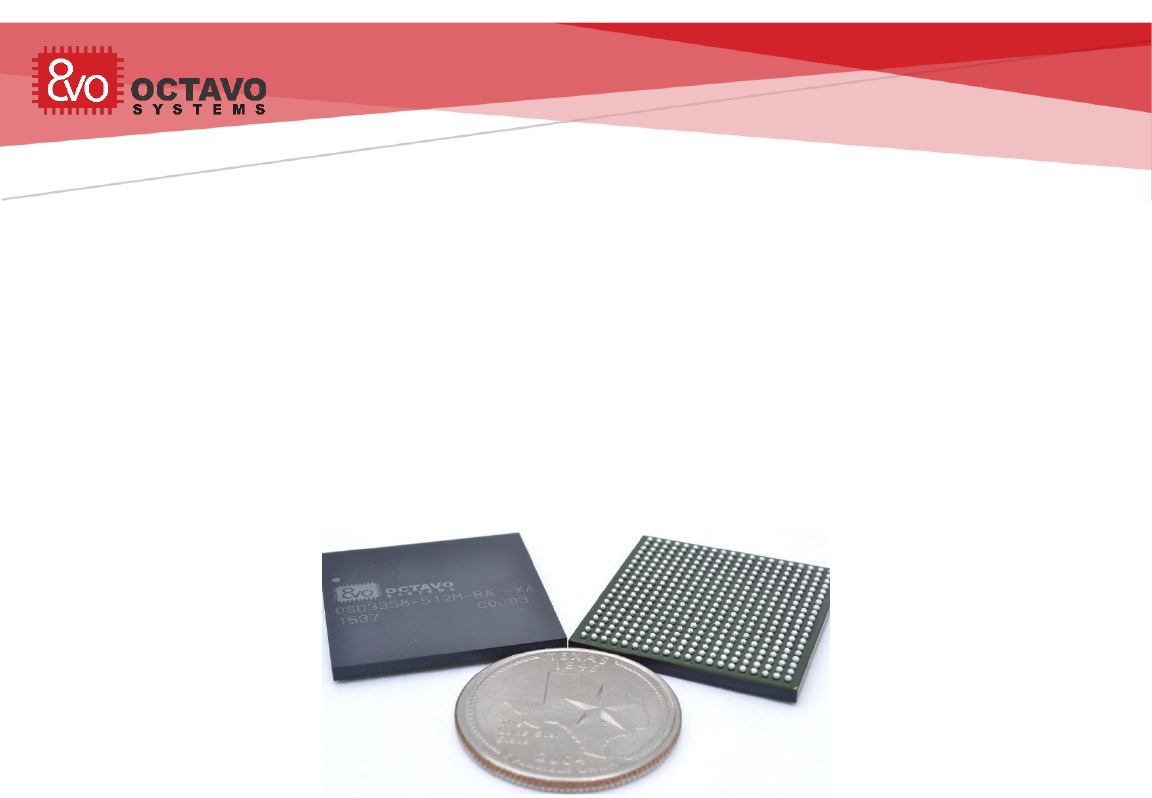
The OSD335x family of System-In-Package (SiP) devices serve as a solid foundation to
build advanced embedded systems quickly with reduced time to market. These SiPs
tightly integrate Texas Instrument (TI)’s AM335x ARM® Cortex® A8 CPU, TPS65217C
Power Management IC (PMIC), TL5209 LDO, up to 1GB of DDR3 and all associated
passives. All this is contained in a US quarter sized package as shown in Figure 1.
At Octavo Systems, we are committed to simplifying your design as much as possible
so that you can quickly start designing and building your dream products. With this
intent in mind, we have developed the OSD335x Reference Design Tutorial Series
which will walk you through the OSD335x design process in a systematic manner.
Figure 1 OSD335x in comparison with US quarter
The tutorial series is broken down into several lessons. Each lesson will address a
specific concept and build upon the concepts of previous lessons. Each lesson will
conclude with a Printed Circuit Board (PCB) which would implement and verify all the
concepts taught. We begin with the basics and then take you through advanced
concepts.
Let’s look at what each lesson talks about:
Lesson 1: You will learn how to build the bare minimum circuitry required to boot the
OSD335x without an operating system and all the concepts related to it.
Lesson 2: You will learn how to build the minimum circuitry required to Boot Linux on
the OSD335x and all the concepts related to it.
Further lessons will be coming soon.

2
OSD335x Tutorial Series
Rev.2 1/2/2018
Octavo Systems LLC
Copyright 2017
Table of Contents
1 Before You Begin ............................................................................. 6
1.1 Fundamentals of the OSD335x ......................................................... 6
1.2 Lesson organization ...................................................................... 7
1.3 Pre-requisites ............................................................................. 8
2 Introduction to Bare Minimum Circuitry to Boot OSD335x.............................. 9
2.1 Introduction .............................................................................. 9
2.2 CAD Environment Setup ............................................................... 10
2.2.1 Library Setup ...................................................................... 10
2.2.2 Schematic setup ................................................................... 10
2.2.3 Layout (Board) Setup: ............................................................ 11
2.3 OSD3358-512M-BAS pin distribution ................................................. 13
3 OSD335x Power Inputs and Outputs ..................................................... 14
3.1 Introduction ............................................................................ 14
3.2 Power Input ............................................................................. 14
3.2.1 VIN_AC .............................................................................. 14
3.2.2 VIN_USB ............................................................................ 15
3.2.3 VIN_BAT ............................................................................ 15
3.3 Input Power Schematics .............................................................. 16
3.4 Input Power Layout .................................................................... 17
3.5 Power output ........................................................................... 18
3.6 Test points on internal power rails .................................................. 19
3.7 Schematics for power output pins and test points on internal power rails ... 20
3.8 Layout for test points on internal power rails ..................................... 20
3.9 Analog reference input and ground ................................................. 21
4 OSD335x Ground Connections ............................................................ 23
4.1 Introduction ............................................................................ 23
4.2 Ground Connections ................................................................... 23
4.3 Ground pour layout discussion: ...................................................... 23
4.4 Power and Ground Planes ............................................................ 26

3
OSD335x Tutorial Series
Rev.2 1/2/2018
Octavo Systems LLC
Copyright 2017
5 OSD335x Power Management ............................................................. 29
5.1 Introduction ............................................................................ 29
5.2 I2C interface ............................................................................ 29
5.3 PMIC control and status ............................................................... 31
5.4 Power button ........................................................................... 34
5.5 Power indicator LED ................................................................... 36
6 OSD335x Clamping Circuit ................................................................. 38
6.1 Introduction ............................................................................ 38
6.2 AM335x Power-Down Requirements ................................................. 38
6.3 Clamping circuit ........................................................................ 39
6.3.1 Phase 1 – AM335x in normal operation / just before power down
(Clamping circuit in standby): ............................................................ 40
6.3.2 Phase 2 – AM335x power down sequence begins (Clamping circuit actively
maintaining the voltage difference between the two power rails): ................ 41
6.3.3 Phase 3 - End of AM335x power down sequence (Clamping circuit back to
standby): .................................................................................... 43
7 OSD335x ESD Protection ................................................................... 46
7.1 Introduction ............................................................................ 46
7.2 ESD protection ......................................................................... 46
8 OSD335x Reset Circuitry ................................................................... 49
8.1 Introduction ............................................................................ 49
8.2 Reset Types ............................................................................. 49
8.2.1 Cold reset .......................................................................... 49
8.2.2 Warm reset ........................................................................ 49
8.3 Reset external connections........................................................... 51
9 OSD335x Clock Circuitry ................................................................... 55
9.1 Introduction ............................................................................ 55
9.2 The OSD335x OSC0 and OSC1 ........................................................ 55
9.3 Layout guidelines ...................................................................... 59
9.4 RTC_KALDO_ENN ....................................................................... 60
10 OSD335x Peripheral Circuitry ............................................................. 62
10.1 Introduction .......................................................................... 62

4
OSD335x Tutorial Series
Rev.2 1/2/2018
Octavo Systems LLC
Copyright 2017
10.2 JTAG ................................................................................... 62
10.3 Boot configuration .................................................................. 64
10.4 Buttons and LEDs .................................................................... 66
10.5 Peripheral header ................................................................... 68
10.6 Finalizing the silkscreen ............................................................ 69
10.7 Expected outcome .................................................................. 70
10.8 PCB order process ................................................................... 72
11 OSD335x Bare Minimum Board Boot Process ............................................ 73
11.1 Introduction .......................................................................... 73
11.2 The Board (PCB) ..................................................................... 73
11.3 Basic board bring-up ................................................................ 73
11.3.1 Tests before board power-up ................................................... 73
11.3.2 Possible problems after board power-up ...................................... 75
11.3.3 Tests after power-up ............................................................. 75
11.4 Setting up software environment (for Windows 7,8 and 10 OS) .............. 77
11.4.1 Installing Code Composer Studio ............................................... 77
11.4.2 Installing StarterWare ............................................................ 78
11.4.3 Debugger ........................................................................... 78
11.5 Demo Apps ............................................................................ 79
11.5.1 Demo App 1: LED Dimmer ....................................................... 79
11.5.2 Running Demo app 1 .............................................................. 79
11.5.3 Demo App 2: Motion Detector ................................................... 88
11.5.4 Running Demo app 2 .............................................................. 88

5
OSD335x Tutorial Series
Rev.2 1/2/2018
Octavo Systems LLC
Copyright 2017
Revision History
Revision Number
Revision Date
Changes
Author
1
8/6/2017
Initial Release
Eshtaartha Basu
2
1/2/2018
LED series resistors (R10, R32 and
R33) updated from 4.7k to 1k, Open -
drain buffer TRM reference added to
Reset Article
Eshtaartha Basu
6
OSD335x Tutorial Series
Rev.2 1/2/2018
Octavo Systems LLC
Copyright 2017
1 Before You Begin
1.1 Fundamentals of the OSD335x
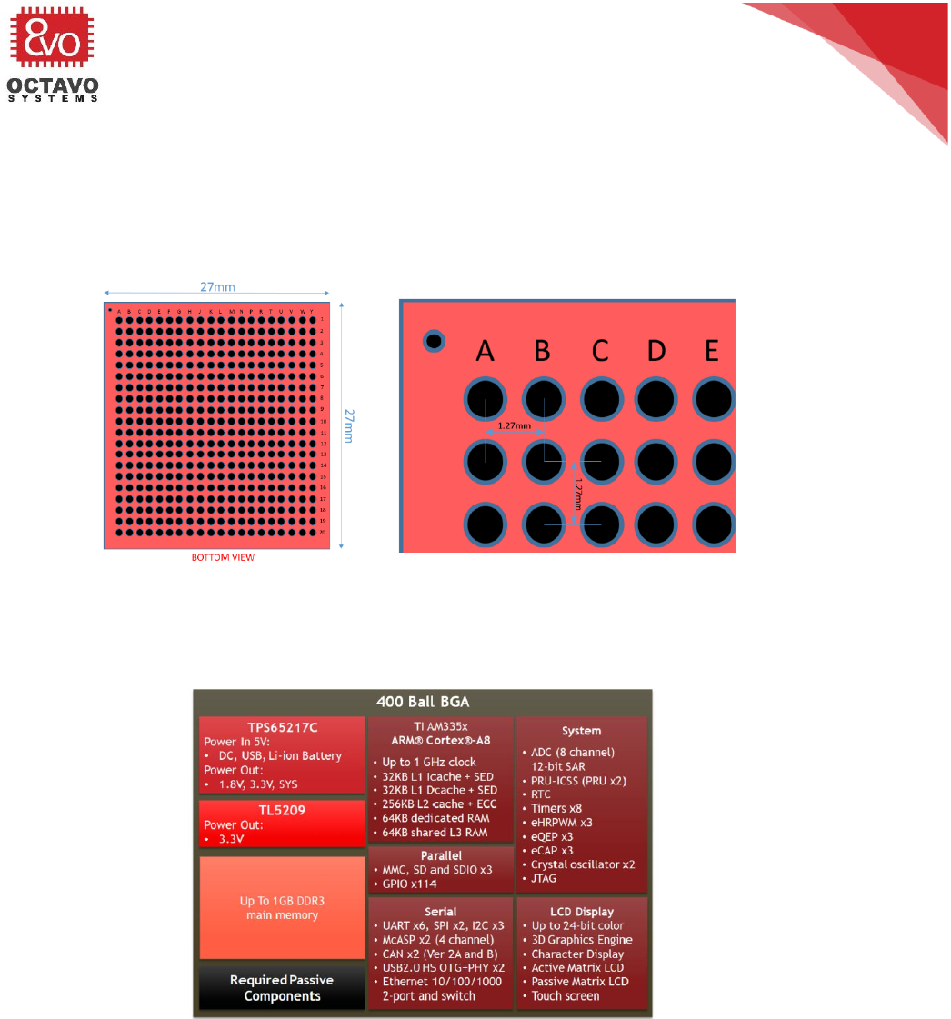
There are many parts within the OSD335x family. We will be focusing on the OSD3358-
512M-BAS in this series. Therefore, all references to the OSD335x hereafter imply
OSD3358-512M-BAS.
Figure 2 OSD335x BGA package
The OSD335x comes in a 27mm x 27mm Ball Grid Array (BGA) package with 400 balls
and 1.27mm ball pitch as shown in Figure 2.
Figure 3 OSD335x Functional Diagram
It consists of four main components as shown in Figure 3. They are:
o Sitara® AM335x ARM® Cortex® A8 processor from TI - is the heart of the
OSD335x.
o TPS65217 Power Management IC (PMIC) from TI - manages power distribution to
various parts of the OSD335x and provides power to external devices.
7
OSD335x Tutorial Series
Rev.2 1/2/2018
Octavo Systems LLC
Copyright 2017
o TL5209 Low Drop Out (LDO) regulator from TI - provides dedicated 3.3V rail to
power external components of the OSD335x.
o Up to 1GB of DDR3 - is the main memory of the OSD335x.
All of the peripheral interfaces of the AM335x (except the DDR interface) are brought
out to pins on the OSD335x. See the OSD335x datasheet for more information on the
pinout.
1.2 Lesson organization
Each lesson will consist of an Introduction section which describes the objective of
the lesson followed by a series of articles, each of which will walk you through the
design methodology. The lesson will conclude with an Expected outcome section
which describes how the outcome of that lesson will look.
Furthermore, each lesson may have several Perks and Caveats. The Perks will give
additional information about the topic in discussion and the Caveats will warn you
about conditions or situations which require more attention. The Perks and Caveats
look like this:
Before starting lesson 1, we strongly encourage you to go through the OSD335x
datasheet which can be found here.

8
OSD335x Tutorial Series
Rev.2 1/2/2018
Octavo Systems LLC
Copyright 2017
1.3 Pre-requisites
We will be using Autodesk Eagle for schematics and layout. Hence, we assume that
you are familiar with Eagle schematics and layout. If not, please learn about them
first. The following website is one of the many websites that can help you:
To learn more about schematics: https://learn.sparkfun.com/tutorials/using-eagle-
schematic
To learn more about layout: https://learn.sparkfun.com/tutorials/using-eagle-board-
layout

OSD335x Tutorial Series
Rev.2 1/2/2018
Octavo Systems LLC
Copyright 2017
2 Introduction to Bare Minimum Circuitry to Boot OSD335x
2.1 Introduction
The objective of this lesson is to help you become familiar with the bare minimum
setup required to boot the OSD335x and getting it ready to execute software. This
lesson will consist of a series of articles which will walk you through every step of the
design process. We start from specifications and guide you through every step till
debugging the manufactured Printed Circuit Board (PCB). The lesson will conclude
with a PCB that verifies the design by putting together everything that was taught.
Figure 4 OSD335x Lesson 1 Block Diagram
To boot the OSD335x in its minimal configuration, we will need:
o Power circuitry
o Clock circuitry
o Reset circuitry
o Debugging/Programming interface (JTAG interface)
To make our design more functional, we will add a couple of buttons, LEDs and a
peripheral header to allow us to better test our completed design.

10
OSD335x Tutorial Series
Rev.2 1/2/2018
Octavo Systems LLC
Copyright 2017
A block diagram of this setup is shown in Figure 4. We will discuss each of these
concerns in separate articles to have a better depth of understanding of each topic.
2.2 CAD Environment Setup
Before proceeding with the articles, let’s understand the Autodesk Eagle design
environment we will be using.
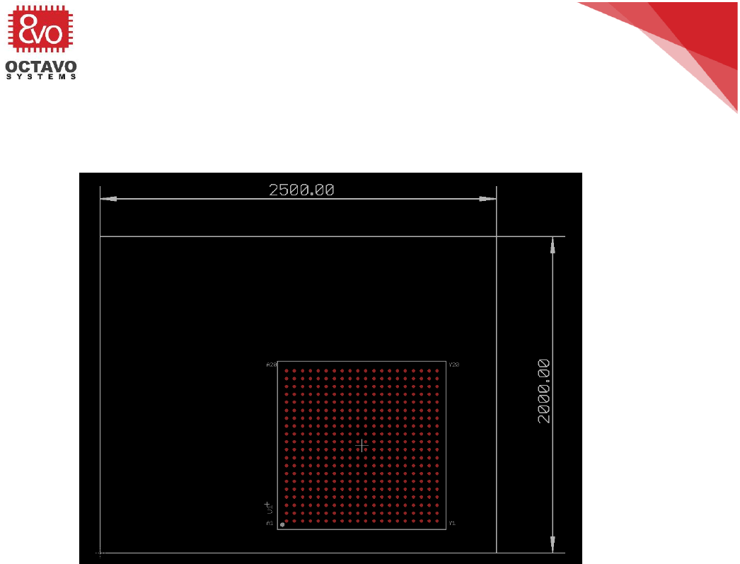
For this design, we are going to create a PCB with the following parameters:
o Board Size: 2500mil x 2000mil (2.5inch x 2inch)
o Number of layers: 4 layers.
o Trace width: 6mil (approx. 0.15mm). Since power traces generally carry more
current, we will be using larger traces (at least 15mil or 0.4mm) for them.
o Trace spacing: 6mil.
o Minimum drill and via size: 12mil (approx. 0.30mm) drill and 24mil (approx.
0.60mm) finished via diameter (i.e., 6 mil annular ring).
Using these standard rules will help us reduce manufacturing cost. For your design,
you are free to select the appropriate rules for your manufacturer and components
that suit your design.
All design files for this lesson can be downloaded here.
2.2.1 Library Setup
Octavo Systems provides an Eagle library, OSD3358_BAS_RefDesignParts.lbr, that
contains the schematic symbol and footprint for the device. This reference library can
be downloaded here.
o It is good practice to create your own Eagle Library for each design and copy all
parts used in the design into it. For this design, we have created the library
OSD3358_BAS_RefDesignParts.lbr.
o Setup the Eagle library path to the location of the Octavo Systems library file
and copy the device OSD3358-512M-BAS into your new library.
2.2.2 Schematic setup
o Open a new schematic file and name it appropriately.
o Make sure to use the OSD3358_BAS_RefDesignParts.lbr library in the
schematics.
o From the library, add the OSD3358-512M-BAS symbols to the schematic as
shown in Figure 5. The OSD3358-512M-BAS symbol will easily fit into A3 size
sheets. In the design files, all four A3 sheets are consolidated into a single

11
OSD335x Tutorial Series
Rev.2 1/2/2018
Octavo Systems LLC
Copyright 2017
Eagle sheet so that we can use the free version of the tool while still allowing
the schematics to be easily viewable while printing.
Figure 5 OSD335x symbol arrangement on schematic
2.2.3 Layout (Board) Setup:
o The layer stack up is shown in Figure 6. We’ll be using Top and Bottom layers
for signal routing. Route2 layer acts as power plane (We will be connecting it
to an appropriate power output pin of the OSD335x later). Route15 layer acts
as ground plane.

OSD335x Tutorial Series
Rev.2 1/2/2018
Octavo Systems LLC
Copyright 2017
3 OSD335x Power Inputs and Outputs
3.1 Introduction
When it comes to booting a device, power circuitry is the first thing that comes to
mind. To have stable and predictable operation from any electronic device, we need
to make sure the power circuitry is well designed and is able to meet the power
requirements of the device under normal as well as extreme operating conditions.
The Power Circuitry is a complex topic, so we have split the discussion into five parts.
They are:
• Power Inputs and Outputs: This article will focus on input and output power
considerations for the OSD335x.
• Ground Connections: This article will focus on ground connections and
important layout pour considerations for the OSD335x.
• Power Management: This article will focus on topics related to control and
management of power for the OSD335x.
• Clamping Circuit: This article will focus on clamping circuit which can be used
to prevent certain power down issues that may arise with the OSD335x.
• ESD Protection: This article will focus on steps needed to provide Electro
Static Discharge (ESD) protection to the OSD335x based Printed Circuit Boards
(PCB).
This article is the first part of the OSD335x Reference Design Lesson 1 Power circuitry
articles. We recommend you to read other parts of power circuitry article as well
which are available further ahead in this article. As we discuss the power circuitry,
we will build the schematic and layout the corresponding traces. All the components
used in this article can be found in the provided library. The components will be
introduced after relevant discussion as we proceed with the article.
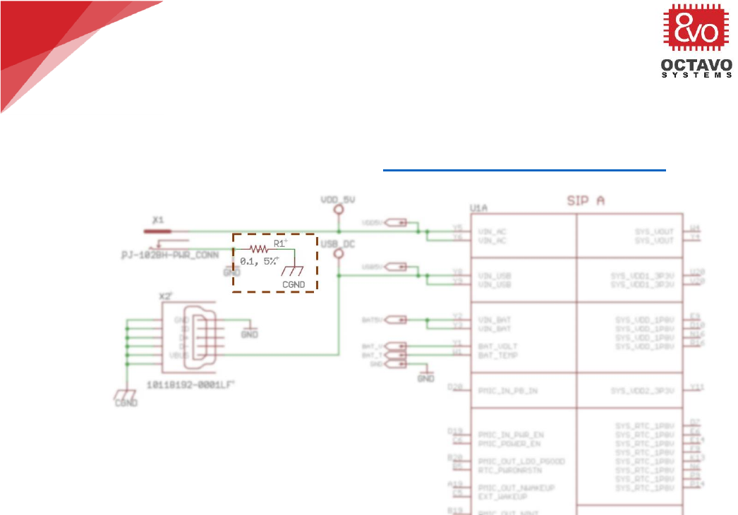
3.2 Power Input
The OSD335x can be powered from 5V DC power supply (generally sourced from an AC
adapter), from a standard USB port (5V) or using a standard single cell (1S) Li-Ion/Li-
Polymer (LiPo) battery.
3.2.1 VIN_AC
While this port is called VIN_AC, it is a DC power input generally powered from a 5V
AC adapter. By default, this input has 2A current limit and can be used as primary
power input. For our design, we will use a DC barrel connector to source this input
since DC barrel connectors are used by many other electronic devices and adapters

15
OSD335x Tutorial Series
Rev.2 1/2/2018
Octavo Systems LLC
Copyright 2017
compatible with this type of connector are easily available. The DC barrel connector
device we’re using can be found under the name PJ-102B_POWER_CON in the
provided library. Let’s connect this pin directly to the input pins Y5 and Y6 of the
OSD335x.
3.2.2 VIN_USB
This input of the OSD335x can be powered from the VBUS line of the USB client
connector at 5V. By default, the input current limit of this pin is 500mA which is also
the standard output current limit for a USB 2.0 host port. However, through software
configuration of the power management IC (PMIC) inside the OSD335x, the current
limit can be raised to 1.3A.
The USB client connector used in this design can be found under the name 10118192-
0001LF in the provided library. The VBUS pin of this connector should be connected
to the pins Y8 and Y9 on the OSD335x.
3.2.3 VIN_BAT
VIN_BAT pin can act as either a battery input or output. It acts as a battery input
when the OSD335x is running on battery power. It acts as a battery output when the
OSD335x is charging the connected battery (more information on charging given in the
below perk). This input should be powered by a single cell (1S) Li-Ion or Li-polymer
battery with voltage range of 2.75V to 5.5V.
In this lesson, we will primarily use VIN_AC and VIN_USB to source power to the
OSD335x. How-ever, in the future we may want to use a (1S) Li-ion or Li-Polymer
battery to power our design. Hence, we will add thru-hole test points for battery
Caveat:
While it is ok for us to connect the DC barrel connector directly to the OSD335x for
this minimal design, you should add appropriate power input protection, such a
ferrite beads, diodes and fuses, based on the needs of your application.
Caveat:
Depending on your application, 500mA input current may not be sufficient. If you
plan to increase the input current limit of this input through software, make sure
the USB host can source the required additional current. For example, USB 3.0 host
port can supply up to 0.9A output current at 5V.

16
OSD335x Tutorial Series
Rev.2 1/2/2018
Octavo Systems LLC
Copyright 2017
power inputs so that we can connect a battery later if necessary. Thru-hole test
points can be found under the name TESTPAD/W_HOLE_1X1 in the provided library.
3.3 Input Power Schematics
Based on the description above, let’s update our schematics with all the input power
connections as shown in Figure 9 (Updates made to the schematics are shown using
dotted lines).
Caveat:
The OSD335x does not use VIN_BAT as an input event to power up the device from
OFF state or SLEEP state. More information about this can be found under section
9.3.1.1 in the TPS65217 datasheet.
Perk:
The OSD335x is also capable of charging Li-ion and Li-Po batteries using its built in
linear charger. It has dedicated pins to monitor battery voltage (BAT_VOLT) and
monitor battery temperature (BAT_TEMP). The VIN_BAT pin provides battery
output while charging. Battery charging is managed by the TPS65217 PMIC present
inside the OSD335x. More information about battery charging can be found in the
TPS65217x Datasheet.
17
OSD335x Tutorial Series
Rev.2 1/2/2018
Octavo Systems LLC
Copyright 2017
Figure 9 Power input connections
It is a good idea to add test points to all the input power rails so that we can easily
test the voltages during debug. For this design, we have used thru-hole test points for
all the input power rails. But, for your design, feel free to use surface test pads to
save board area.
Supply pins are also added to input power rails so that we can see where these
voltages are used elsewhere on the schematic.
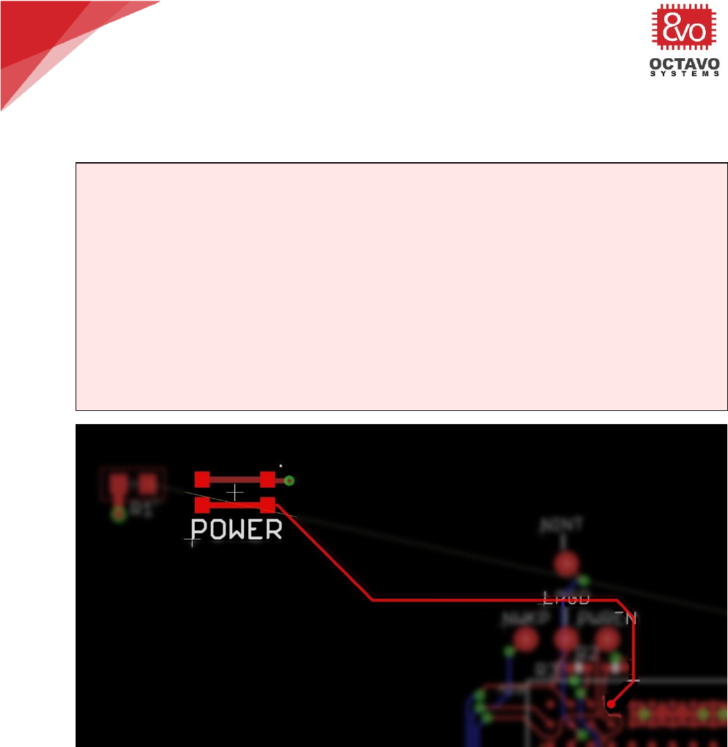
The reason behind the presence of resistor R1 is explained under the ESD (Electro
Static Discharge) protection chapter (chapter 6) of this document.
3.4 Input Power Layout
Now that we have completed the schematics for power input, let’s begin the layout. As
per the guidelines in the introduction article, we will use 6mil (approx. 0.15mm)
traces for signals and at least 15mil (approx. 0.40mm) traces for power traces and
connect them to the OSD335x power pins using pours so that there is good connection
to the BGA balls. While we could use pours for the entire power connection, in this
design we do not have any peripherals with high current draw so we can use traces to
make layout easier. The layout is shown in Figure 10.
18
OSD335x Tutorial Series
Rev.2 1/2/2018
Octavo Systems LLC
Copyright 2017
Figure 10 Power input layout
The components are placed and routed in a specific manner to accommodate future
components and to facilitate easy routing as we go ahead with the articles.
3.5 Power output
The PMIC and LDO inside the OSD335x generate many different power outputs. Some
of the outputs are only for internal use within the System in Package (SiP). However,
others provide power that can be used by the systems external to the SiP. Please go
through the power app note before budgeting power for your design. The maximum
power output of each of these pins can be found in the OSD335x datasheet. The
following power outputs can be used for external devices:
o SYS_VOUT: Shared supply sourced by the PMIC. This rail also supplies power to the
AM335x, DDR3 and TL5209 LDO inside the SiP. This output is not regulated. It merely
reflects the voltage of the input power source that is being used to power the PMIC.
Therefore, when using a battery, it is necessary to make sure that any components
that use the SYS_VOUT power output can operate on a voltage between 3V and 5V
since the PMIC will switch to a different power input when charging the battery.
o SYS_VDD1_3P3V: Dedicated 3.3V supply rail for external circuitry. Powered by the
TL5209 LDO and enabled by LDO4 of the PMIC. This power output will be connected
to the power plane of our layout.

19
OSD335x Tutorial Series
Rev.2 1/2/2018
Octavo Systems LLC
Copyright 2017
o SYS_VDD2_3P3V: Dedicated 3.3V supply for external circuitry directly supplied by
LDO2 of the PMIC.
o SYS_RTC_1P8V: 1.8V output powered by LDO1 of the PMIC. It is also used internally
to power the RTC of the AM335x.
o SYS_VDD_1P8V: 1.8V output powered by LDO3 of the PMIC.
o SYS_ADC_1P8V: 1.8V output powered by LDO3 of the PMIC and filtered for analog
applications. It supplies power to the AM335x ADC. It can also be used to power
external analog circuitry.
It is a good idea to add supply pins and test points to all the power output pins as
shown in Figure 11 so that we can probe the voltages during debug and board bring-
up.
3.6 Test points on internal power rails
The OSD335x provides external access to critical internal power rails. These pins
should be used for testing/monitoring purposes only. They shouldn’t be used to
power external circuitry. Test points need to be added to these power rails so that
internal voltages can be looked up in case of power-up issues. You can use either
thru-hole test points or test pads, whichever makes your routing easier. For this
design, we will be using thru-hole test points.
The OSD335x pins that provide access to internal power rails are VDDSHV_3P3V,
VDDS_DDR, VDD_MPU, VDD_CORE and VDDS_PLL.
Perk:
If you’re curious about how the internal power rails are used within the SiP,
you can find more information below:
o VDDSHV_3P3V: Dedicated 3.3VDC to power the AM335x I/O. It is supplied by
the TPS65217 LDO4.
o VDDS_DDR: Dedicated 1.5VDC supply to power the AM335x DDR3 interface and
DDR3 device.
o VDD_MPU: Dedicated 1.1VDC supply to power the AM335x MPU domain.
o VDD_CORE: Dedicated 1.1VDC supply to power the AM335x CORE domain.
o VDDS_PLL: Filtered 1.8VDC to supply power to the AM335x PLLs and oscillators.
You can also refer Texas Instruments (TI) Power Hookup Application Note for in depth
information.
20
OSD335x Tutorial Series
Rev.2 1/2/2018
Octavo Systems LLC
Copyright 2017
3.7 Schematics for power output pins and test points on internal power rails
Figure 11 OSD335x schematic for test points on internal power rails and power output pins
Let’s add test points and supply pins suitably as shown in Figure 11 (Updates made to
the schematics are shown using dotted lines). Thru-hole test points can be found
under the device name TESTPAD/W_HOLE_1X1 in the provided library.
3.8 Layout for test points on internal power rails
Figure 12 OSD335x layout for power output pins and test points on internal power rails

21
OSD335x Tutorial Series
Rev.2 1/2/2018
Octavo Systems LLC
Copyright 2017
The test points were placed and routed to accommodate future components and
facilitate easy routing as shown in Figure 12.
3.9 Analog reference input and ground
Figure 13 Schematic for Analog Reference input and Ground
The OSD335x has an Analog-to-Digital Converter (ADC) interface that can be used for
things like monitoring voltages and interfacing with analog sensors. To use the ADCs,
the Analog Power and Ground must be connected appropriately. The interface can
tolerate inputs up to 1.8V depending on the analog voltage reference VREFP.
Internally, the OSD335x connects the VREFN pin of the AM335x to analog ground, so
the range of ADC is analog ground to VREFP. Generally, VREFP is connected to
SYS_ADC_1P8V but it can be set to a lower voltage using a voltage divider.
Since the voltage reference, VREFP, needs to be a clean as possible, we want to put a
resistor footprint between VREFP and the power connection. This gives the option of
putting a resistor or ferrite bead in at a latter place if we need to suppress noise.
Also, we want to put bypass capacitors between VREFP and analog ground to help
suppress noise. These connections can be seen in Figure 13 (Updates made to the
schematics are shown using dotted lines).
If you do not need to use the ADC interface in your application, then VREFP should be
shorted with AGND.
Layout for Analog Connections can be made as shown in Figure 14.
22
OSD335x Tutorial Series
Rev.2 1/2/2018
Octavo Systems LLC
Copyright 2017
Figure 14 Layout for Analog Connections
*****
OSD335x Tutorial Series
Rev.2 1/2/2018
Octavo Systems LLC
Copyright 2017
4 OSD335x Ground Connections
4.1 Introduction
This article is the second part of the OSD335x Reference Design Lesson1 Power
circuitry articles. It will focus on ground connections and pours required for reliable
performance from the OSD335x. As we discuss the power circuitry, we will build the
schematic and layout the corresponding traces.
4.2 Ground Connections
Figure 15 OSD335x Ground connections
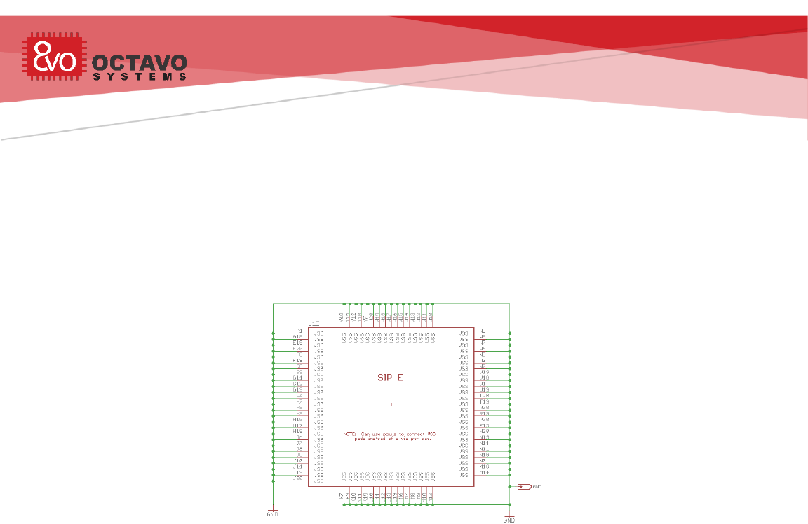
The OSD335x has several ground pins. All the pins on the SIP E symbol should be
grounded, as shown above in Figure 15, even though they are connected together
within the SiP. This is to make sure all components within the OSD335x are uniformly
grounded and ensure the shortest return current paths for all the components inside
the OSD335x. For our reference design, a thru-hole test point was added to help us
measure voltage during bring-up.
It is good to have test points to ground on the design for testing during bring-up, but
it is not necessary as long as there is access to ground somewhere in the design. In
compact designs, you can use surface test points to save space.
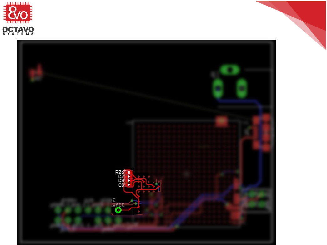
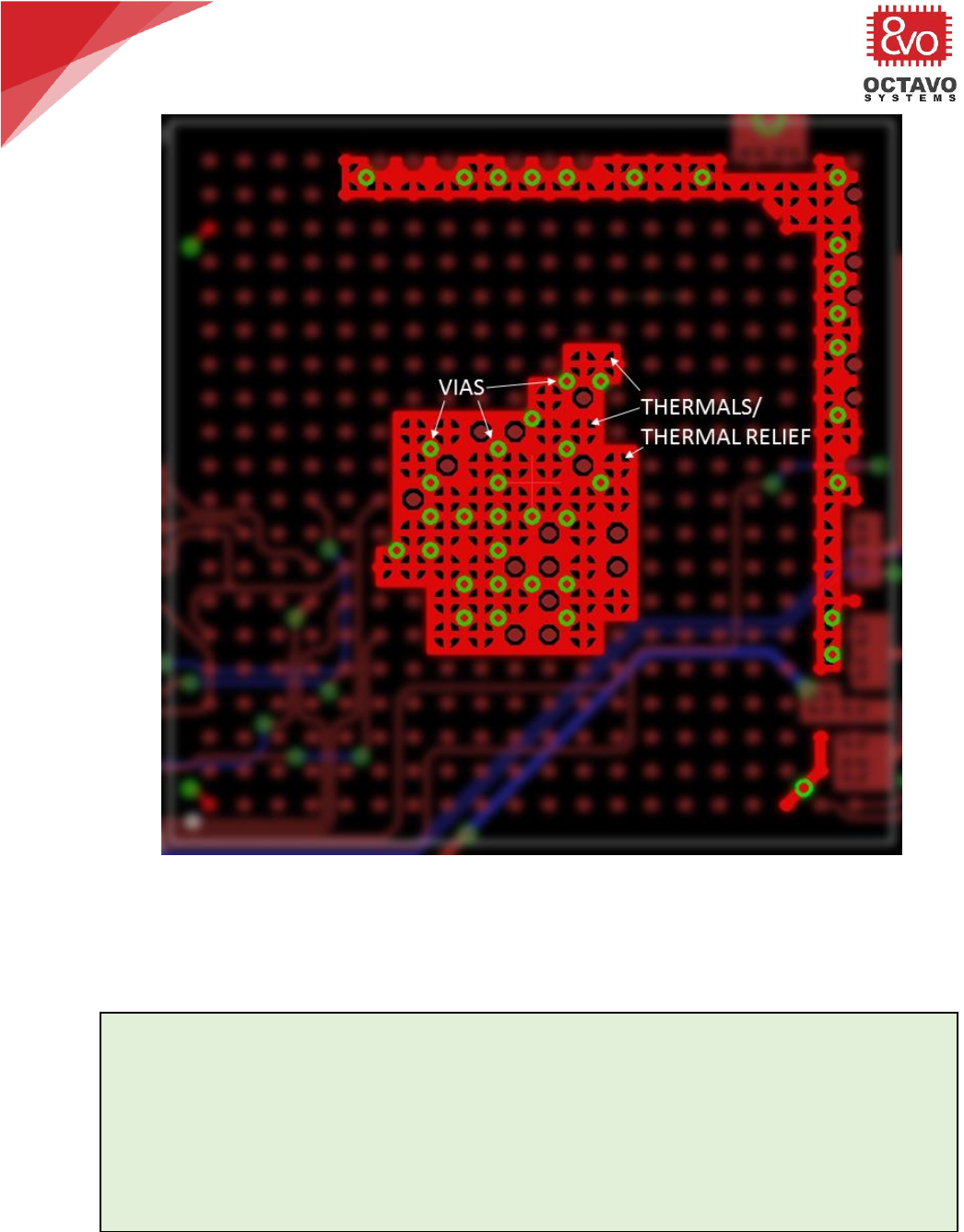
4.3 Ground pour layout discussion:
When grounding the OSD335x, you are free to use one via for each ground pin.
However, vias occupy a lot of routable space and a lot of vias can cause routing
problems (this does not necessarily apply to blind and buried vias since they occupy
much less route-able board area). Routable space can be saved by instead using
ground pours and minimizing the number of ground vias. For this design, since the
ground pins are clustered in two areas, we have placed two copper pours on the top
layer for ground. Then we have at least one via per two ground pins so there is a good
connection to the ground plane. When using copper pours, the following things should
be considered:

24
OSD335x Tutorial Series
Rev.2 1/2/2018
Octavo Systems LLC
Copyright 2017
o Have at least one via for every two to four ground pins.
o Vias should be placed wisely keeping current return path also in mind.
o Care should be taken not to flood the entire area below the BGA of the
OSD335x with a ground pour. If the area of the ground pour is large, it may sink
too much heat from the BGA and may result in bad solder joints during reflow.
Similarly, make sure thermals are used for the pours to prevent the pours from
sinking too much heat and causing bad solder joints.
Perk:
A ground pour is nothing but a copper pour connected to GND or GND plane of the
PCB. More information about copper pours can be found here.
25
OSD335x Tutorial Series
Rev.2 1/2/2018
Octavo Systems LLC
Copyright 2017
Figure 16 OSD335x Ground Pour
As shown in Figure 16, we have used two ground pours for this design to minimize the
size of each pour. Each pour uses thermals (thermal relief) and there are plenty of
vias to ensure good connection to ground.
Perk:
A thermal (thermal relief) in PCB jargon refers to a particular way in which a pad
is connected to a pour/plane to make good electrical connection but poor thermal
connection. Copper is a good conductor of heat. Hence, if good thermal
connection were to be made, the plane/pour would draw all the heat away from
the pad leading to a bad solder joint. More information about thermals and their
uses can be found here.

26
OSD335x Tutorial Series
Rev.2 1/2/2018
Octavo Systems LLC
Copyright 2017
4.4 Power and Ground Planes
As we already stated, our design uses a 4 layer PCB. The top and the bottom layers
are used for signal routing whereas the layer beneath the top layer is used as a power
plane and the layer below the power plane is used as a ground plane. Use of power
and ground planes that are closely spaced to each other reduces crosstalk and
interference between the top and bottom signal layers.
Most of the components in this design will operate on 3.3V. Hence, we will be
connecting SYS_VDD_3P3V to the power plane. The power plane will help those
components directly receive power through a via with minimal resistance since the
power plane is spread across the board.
The ground plane is used to connect all components to a common ground reference. It
will:
o provide a low resistance return path for currents to reduce noise.
o will prevent current loops.
o will act as EMI shield protecting the PCB from external noise and prevent
radiation of high frequency noise from the PCB.
o provide uniform impedance plane for traces carrying high frequency signals
with high fidelity against reflections.
Power and Ground planes can be created in the layout by drawing one complete
polygon along the edge of the board in layer 2 and connecting it to SYS_VDD_3P3V and
drawing the other complete polygon in Layer 15 and connecting it to GND using the
NAME tool of Eagle. The POWER and GND polygons are shown in Figure 17. When the
RATSNEST button is pressed on the layout, the power and ground planes occupy the
entire area of the board as shown in Figure 18 and Figure 19.

27
OSD335x Tutorial Series
Rev.2 1/2/2018
Octavo Systems LLC
Copyright 2017
Figure 17 Power and Ground plane polygons
Figure 18 Power Plane
28
OSD335x Tutorial Series
Rev.2 1/2/2018
Octavo Systems LLC
Copyright 2017
Figure 19 Ground Plane
****
OSD335x Tutorial Series
Rev.2 1/2/2018
Octavo Systems LLC
Copyright 2017
5 OSD335x Power Management
5.1 Introduction
This article is the third part of the OSD335x Reference Design Lesson1 Power circuitry
articles. It will mainly focus on topics related to control and management of power
for the OSD335x. As we discuss the power circuitry, we will build the schematics and
layout the corresponding traces.
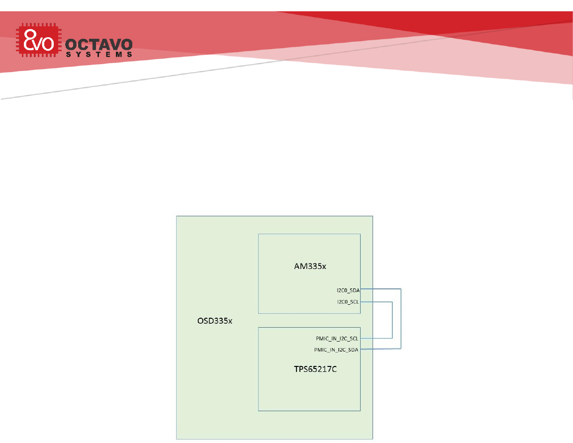
5.2 I2C interface
Figure 20 OSD335x I2C connections
For most designs, the AM335x processor communicates with the TPS65217C PMIC
through the I2C0 interface. The I2C lines for both the processor and the PMIC are
brought out to the BGA balls of the OSD335x to give flexibility in how things are
connected. Almost always, the I2C0 pins of the AM335x and the I2C pins of the
TPS65217C PMIC are connected externally to enable I2C communication between the
processor and PMIC. The I2C pins that need to be connected are placed close to each
other on the OSD335x schematic symbol to facilitate easy connection. The necessary
connections are shown in Figure 20 block diagram.
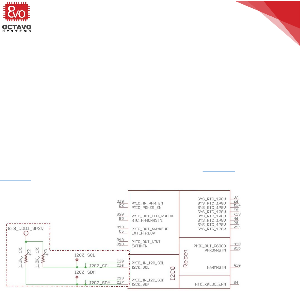
The I2C0 pins of the AM335x processor have internal 4.7K ohm pullup resistors. This is
sufficient if nothing else is connected to the I2C0 bus. In the case that other
components are connected to the I2C0 bus, it is good practice to put additional
external pull-up resistors. This allows the strength of the pull-ups on the I2C0 bus to
be set based on the other bus components. For this design, given we are connecting
30
OSD335x Tutorial Series
Rev.2 1/2/2018
Octavo Systems LLC
Copyright 2017
to some unknown components, we are going to use 1.5k ohm external pull-ups whose
value can be adjusted later if necessary.
Most of the functionality of the TPS65217C PMIC can be controlled and various
parameters can be set using the I2C interface. Some of the features that can be
controlled are:
o Battery charger voltage.
o Charge safety timer control.
o Buck and Boost converter output voltage.
o LDO output voltage.
o Power up and power down sequences.
o Over current and over temperature thresholds.
Details about the I2C interface and its usage can be found in the TPS65217x
datasheet.
Figure 21 Schematic for OSD335x I2C connections
Let’s make I2C connections on the schematic as shown in Figure 21 (Updates made to
the schematics are shown using dotted lines).
31
OSD335x Tutorial Series
Rev.2 1/2/2018
Octavo Systems LLC
Copyright 2017
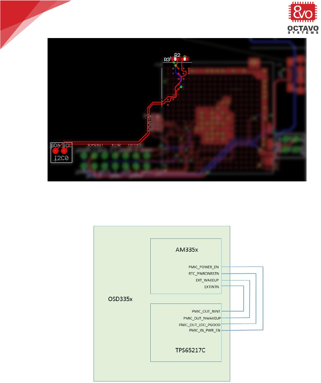
Figure 22 Layout for I2C connections
The highlighted routes in Figure 22 represent the I2C connections in the layout.
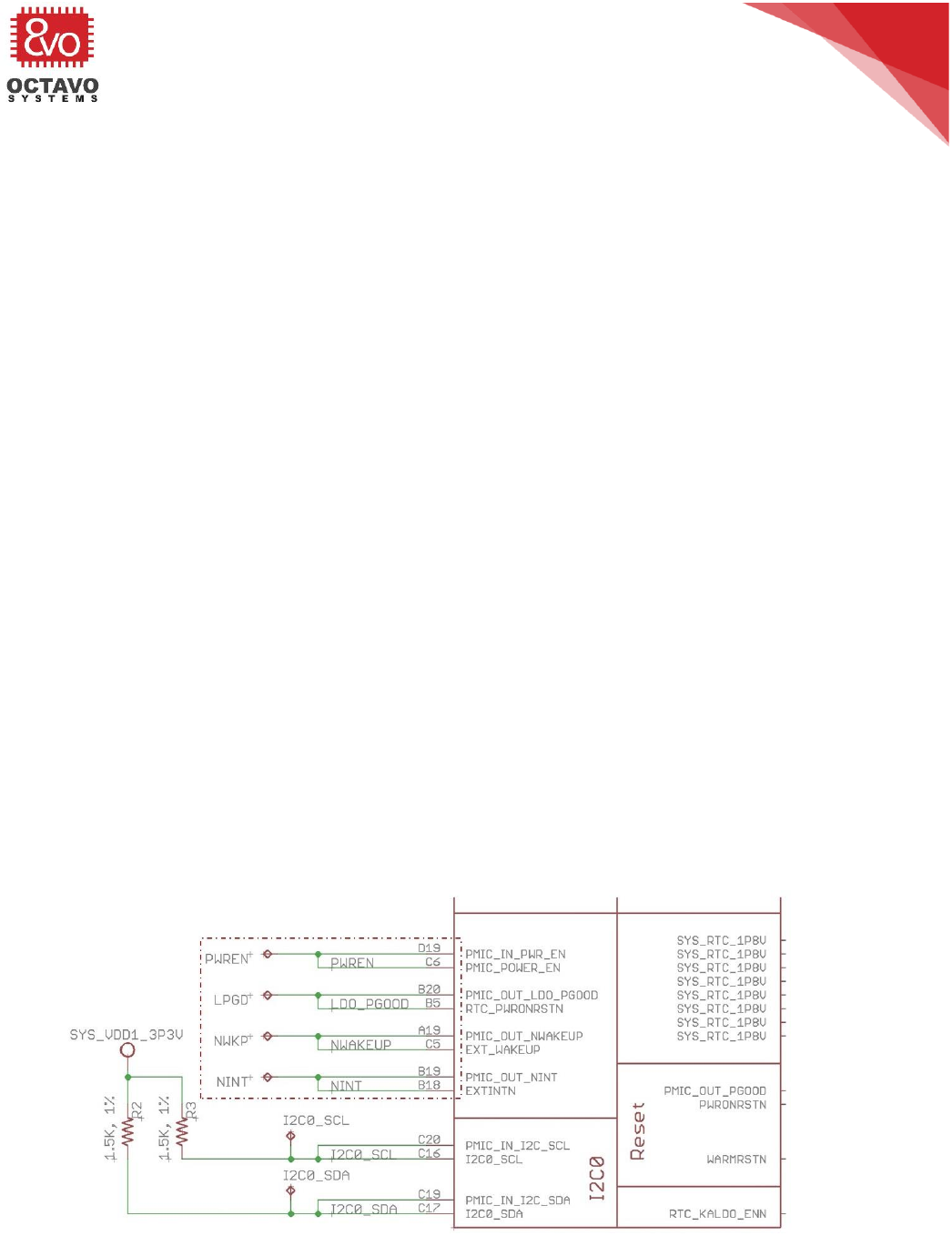
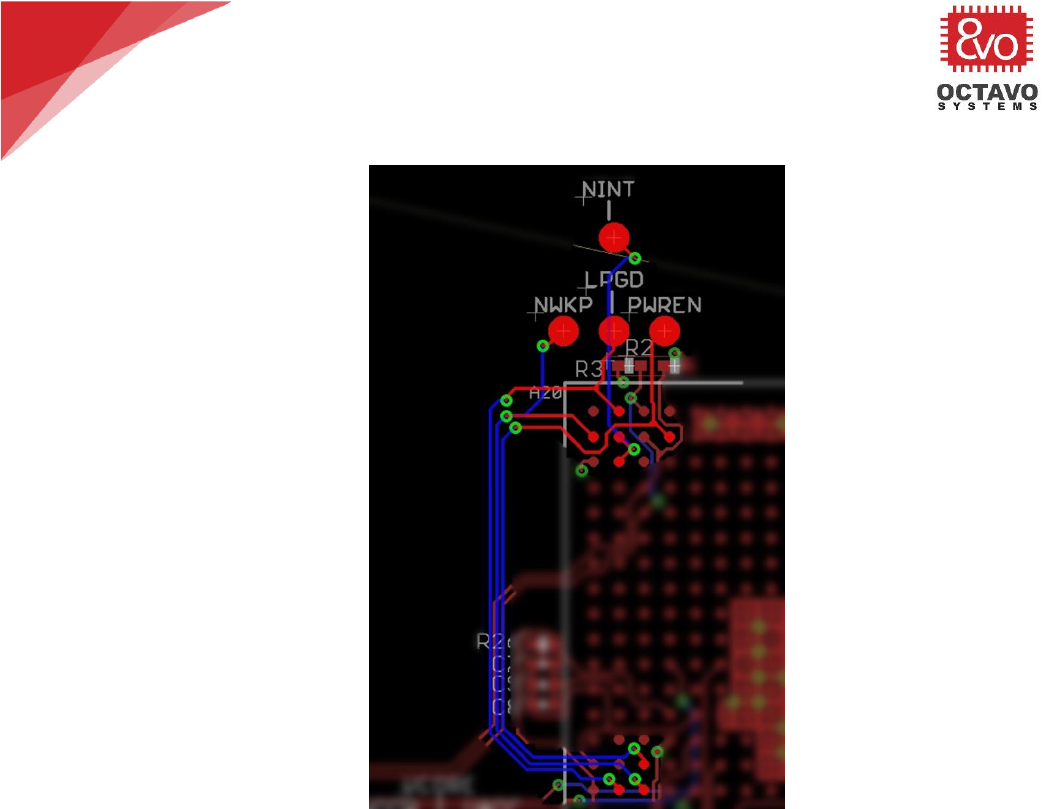
5.3 PMIC control and status
Figure 23 External connections required between AM335x processor and TPS65217C PMIC
Besides the I2C connections, there are a few more signals that must be connected
between the processor and PMIC for the OSD335x to function correctly. Figure 23
32
OSD335x Tutorial Series
Rev.2 1/2/2018
Octavo Systems LLC
Copyright 2017
shows the external signal connections that we must make to allow the AM335x and
the TPS65217C PMIC to coordinate their operations. These signals were brought out of
the OSD335x so that the user can have more control over power sequencing if
necessary. The description of these signals are:
o PMIC_POWER_EN: This pin is used by the AM335x to control the power
up sequence of the PMIC.
o PMIC_IN_PWR_EN: Enable input for buck converters and LDOs on the
PMIC. Pulling this pin high will start the power up sequence.
o RTC_PWRONRSTN: Independent Power On Reset Pin of the AM335x RTC.
o PMIC_OUT_LDO_PGOOD: LDO power good output. This pin goes high
when both LDO1 and LDO2 output voltages are within regulation and
goes low when either one of them are out of regulation.
o EXT_WAKEUP: Dedicated input pin of the AM335x for external wake up
events.
o PMIC_OUT_NWAKEUP: Signal to host to indicate a power on event
(active low)
o EXTINTN: External interrupt input of the AM335x.
o PMIC_OUT_NINT: Interrupt output (active low) of the PMIC.
For this design, we do not need any additional control of the power
sequencing, so we can directly connect the pins. However, let’s add test
points so that we can probe these signals during bring-up. Let’s make the
necessary connections on the schematic as shown in Figure 24 (Updates made
to the schematics are shown using dotted lines).
34
OSD335x Tutorial Series
Rev.2 1/2/2018
Octavo Systems LLC
Copyright 2017
5.4 Power button
The TPS65217C PMIC inside the OSD335x has an active low reset input which is
brought out through the PMIC_IN_PB_IN pin of the OSD335x and can be connected to a
push button. This input has a 50ms deglitch time and an internal pull-up resistor to an
always-on supply. The power button has the following functions:
o The PMIC is powered up from OFF or SLEEP mode upon detecting a falling
edge on PMIC_IN_PB_IN.
o PMIC is power cycled/reset when PMIC_IN_PB_IN is held low for more than 8
s. All rails will be shut down by the sequencer and all register values are
reset to their default values. Rails not controlled by the sequencer are shut
down immediately. The device remains in this state for as long as this pin is
held low. However, the device will remain in RESET state for a minimum of
1 second before it returns to ACTIVE state.
o If the PMIC_IN_PB_IN pin is kept low for an extended amount of time, the
device will continue to cycle between ACTIVE and RESET state, entering
RESET every 8 seconds.
Figure 26 OSD335x Power Button
Perk:
You can find more information about power button and PMIC modes at:
http://www.ti.com/product/TPS65217/datasheet/detailed-
description#SLVSB641234
http://www.ti.com/product/TPS65217/datasheet/detailed-
description#SLVSB643180
35
OSD335x Tutorial Series
Rev.2 1/2/2018
Octavo Systems LLC
Copyright 2017
The schematic is developed as shown in Figure 26 (Updates made to the schematics are
shown using dotted lines). The power button we’re using can be found under the device
name KMR231GLFS in the given library.
Figure 27 Power button layout
The highlighted routes in Figure 27 represent the power button connections in the
layout.
Caveat:
Long-pressing the power button on some boards will power off the system instead
of power cycling it. This state can be caused when the TPS65217C PMIC shuts off
SYS_5V at the start of the power down sequence, which often causes some
regulated supplies to shut down before the PMIC intends to shut them off, resulting
in a PMIC fault hence taking the system to off-state instead of going through with
the power-cycle.
On a board like Beaglebone Black (which uses the TPS65217C PMIC), without
external connections and with HDMI framer disabled, power consumption during the
power off sequence may be low enough to prevent a PMIC fault, hence long-
pressing the power button will then power-cycle the system as it was intended.
36
OSD335x Tutorial Series
Rev.2 1/2/2018
Octavo Systems LLC
Copyright 2017
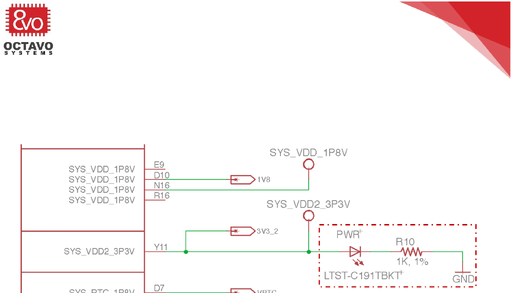
5.5 Power indicator LED
For this design, we want to have an LED to indicate that power is on. Since
SYS_VDD2_3P3V can only supply 150mA externally, we used this power output to
indicate power is on as shown in Figure 28 (Updates made to the schematics are
shown using dotted lines).
Figure 28 Schematic for OSD335x Power LED

OSD335x Tutorial Series
Rev.2 1/2/2018
Octavo Systems LLC
Copyright 2017
6 OSD335x Clamping Circuit
6.1 Introduction
This article is the fourth part of the OSD335x Reference Design Lesson1 Power
circuitry discussion. It will focus on a clamping circuit which may be needed by your
application. A clamping circuit is a type of circuit that maintains the voltage level of
an input with respect to another input. As we discuss the clamping circuit, we will
build the schematic and layout the corresponding traces.
6.2 AM335x Power-Down Requirements
The AM335x datasheet requires that the voltage difference between the power rails
VDDS (1.8V) and VDDSHVx [1-6] (3.3V) of the AM335x processor be less than 2V during
the entire power-down sequence (More information about this can be found under Use
of a Clamping Circuit for Simultaneous Ramp Down section of this user guide). The
VDDS power input of the AM335x processor is connected within the OSD335x to the
SYS_RTC_1P8V power rail and the VDDSHVx [1-6] power inputs are connected within
the OSD335x to the VDDSHV_3P3V power rail. The voltage difference between these
two power rails could exceed 2V if VDDSHV_3P3V rail remains high, possibly because
of large output capacitance or no load being present on the output, while the
SYS_RTC_1P8V rail ramps down quickly, as if it were fully loaded.
If you cannot guarantee that the voltage difference between the two voltage rails
(SYS_RTC_1P8V and VDDSHV_3P3V) of the OSD335x will be less than 2V during the
entire power down sequence in your design, then you will need a clamping circuit.
39
OSD335x Tutorial Series
Rev.2 1/2/2018
Octavo Systems LLC
Copyright 2017
6.3 Clamping circuit
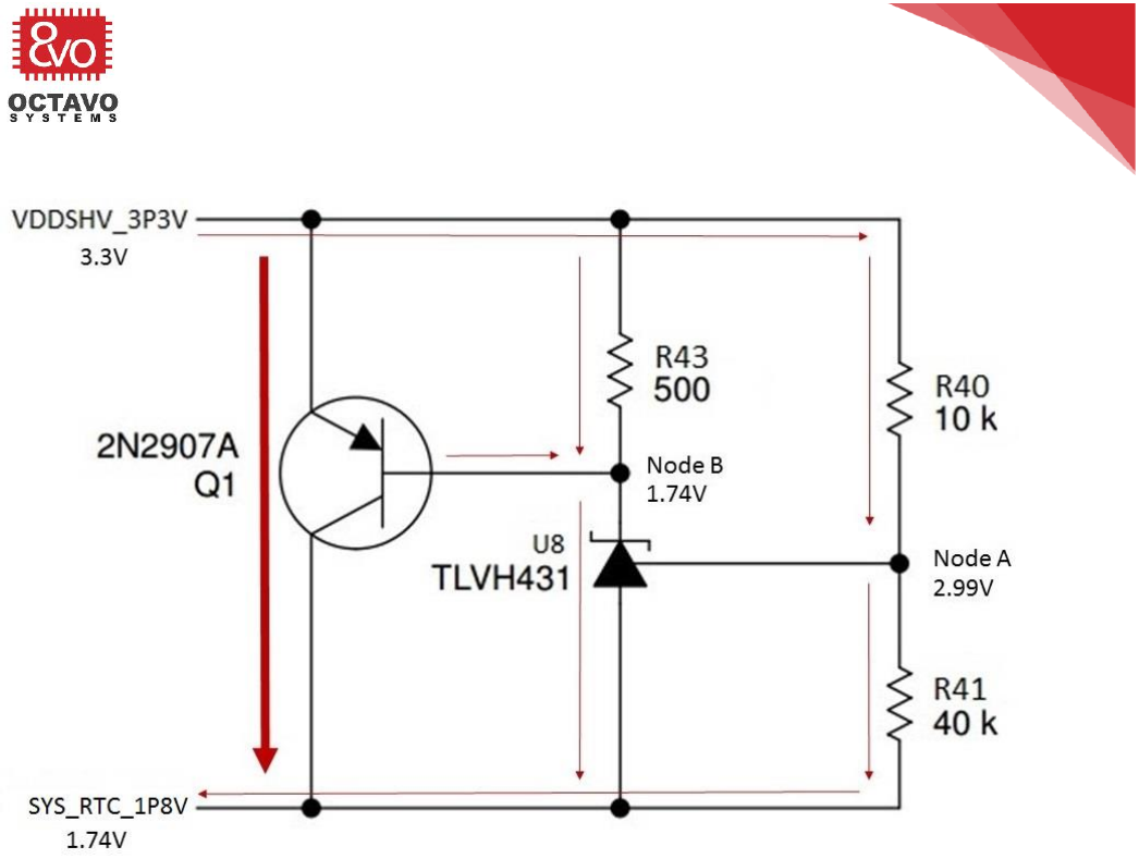
Figure 30 Clamping circuit
The clamping circuit (shown in Figure 30) will make sure that the voltage difference
between the given two voltage rails (VDDSHV_3P3V and SYS_RTC_1P8V) is less than
2V. Its operation will be discussed in three phases.
You need to keep the following assumptions in mind before analyzing the operation of
clamping circuit:
o It is assumed that, once the power down sequence of the AM335x begins, the
voltage rail VDDSHV_3P3V remains high due to a large output capacitance or no
load and the voltage rail SYS_RTC_1P8V ramps down relatively quickly due to a
full load.
o It is also assumed that, the voltage rail, VDDSHV_3P3V, will be able to source
enough current to pull up the voltage of SYS_RTC_1P8V rail whenever
necessary.
We recommend you to read the datasheets of the shunt regulator TLVH431 and
2N2907A transistor before trying to understand the operation of clamping circuit.
Few quick tips about TLVH431 and 2N2907A essential to understand the operation of
clamping circuit:
o The shunt regulator, TLVH431, will be OFF (acts as open switch) whenever the
voltage at its reference input connected to node A (in Figure 30) is less than
1.24V. It will turn ON (act as closed switch) whenever voltage at its reference
input (node A) is greater than 1.24V.
o The PNP transistor, 2N2907A, will allow current to flow from its emitter
terminal to the collector terminal when the voltage difference between its
40
OSD335x Tutorial Series
Rev.2 1/2/2018
Octavo Systems LLC
Copyright 2017
base terminal and emitter terminal is greater than or equal to 0.4V. In other
words, it acts like a closed switch when the voltage difference between node B
and the VDDSHV_3P3V rail is greater than 0.4V and acts like an open switch
when the voltage difference between node B
and the VDDSHV_3P3V rail is less than 0.4V.
For the circuit analysis below, we will assume that TLVH431 will be in the OFF state
whenever the reference input of the TLVH431 is at 1.24V.
6.3.1 Phase 1 – AM335x in normal operation / just before power down (Clamping
circuit in standby):
Figure 31 Clamping circuit (Phase 1)
The clamping circuit will operate in this phase when both the voltage rails are at
nominal voltages (i.e., VDDSHV_3P3V is at 3.3V and SYS_RTC_1P8V is at 1.8V) as
shown in Figure 31.
The voltage divider circuit consisting of resistors R40 and R41 provides the reference
voltage for U8 (TLVH431) at node A. In this phase of operation, node A will be at 3V
relative to ground. But, node A will be at 1.2V (3V – 1.8V) with respect to
SYS_RTC_1P8V voltage rail. As a result, U8 will turn OFF (will not sink current from
node B) and voltage at node B will remain at 3.3V. Hence, Q1 (2N2907A) will turn
OFF.
41
OSD335x Tutorial Series
Rev.2 1/2/2018
Octavo Systems LLC
Copyright 2017
6.3.2 Phase 2 – AM335x power down sequence begins (Clamping circuit actively
maintaining the voltage difference between the two power rails):
The clamping circuit will operate in this phase when the voltage difference between
its two power rails, VDDSHV_3P3V and SYS_RTC_1P8V, is greater than or equal to
1.55V. Let’s discuss the two possible cases:
6.3.2.1 Case 1: Voltage difference between VDDSHV_3P3V and SYS_RTC_1P8V is equal to
1.55V
Figure 32 Clamping circuit (Phase 2, Case 1)
Let’s understand case 1 through an example. For this example, let’s assume
VDDSHV_3P3V is at 3.3V and SYS_RTC_1P8V is at 1.75V as shown in Figure 32 (Fixing
the voltage will help us understand the circuit better). Now, the voltage difference
between the two power rails is 1.55V (3.3V – 1.75V = 1.55V).
When SYS_RTC_1P8V is at 1.75V, the voltage at node A will be 2.99V (i.e., 2.99V-
1.75V = 1.24V with respect to SYS_RTC_1P8V rail). As a result, U8 (TLVH431) turns
OFF and will not sink current from node B. Therefore, node B will be at 3.29V and the
voltage difference between the base and emitter of transistor Q1 will be less than
0.4V. Hence, Q1 will turn OFF. This is similar to Phase 1 where both U8 and Q1 are
off.
42
OSD335x Tutorial Series
Rev.2 1/2/2018
Octavo Systems LLC
Copyright 2017
6.3.2.2 Case 2: Voltage difference between VDDSHV_3P3V and SYS_RTC_1P8V is greater than
1.55V
Figure 33 Clamping circuit (Phase 2, Case 2)
Now, let’s understand the behavior of clamping circuit when the voltage difference
between its two power rails is greater than 1.55V. Let’s assume VDDSHV_3P3V is at
3.3V and SYS_RTC_1P8V is at 1.74V as shown in Figure 33 (Fixing the voltage will help
us understand the circuit better). Hence, the voltage difference between the two
power rails becomes 1.56V (3.3V – 1.74V = 1.56V).
When SYS_RTC_1P8V is at 1.74V, the voltage at node A will be 2.99V (i.e., 2.99V-
1.74V = 1.25V with respect to SYS_RTC_1P8V rail). As a result, U8 (TLVH431) turns ON
and sinks current from node B. This will lower the voltage at node B to 1.74V and the
voltage difference between the base and emitter of Q1 will exceed 0.4V. Hence, Q1
will turn ON and current begins to flow from VDDSHV_3P3V rail to SYS_RTC_1P8V rail.
This will increase the voltage of SYS_RTC_1P8V rail to 1.75V. The voltage at node A
with respect to ground will now become 1.24V (2.99V – 1.75V = 1.24V) and U8 will
turn OFF. So, Q1 will turn OFF and current flow from VDDSHV_3P3V to SYS_RTC_1P8V
will cease.
This cycle continues until one or both of the voltage rails drop down to 0V at the end
of the power down sequence. Now, this is an idealized analysis so in the real

43
OSD335x Tutorial Series
Rev.2 1/2/2018
Octavo Systems LLC
Copyright 2017
operation there will be some overshoot and undershoot but based on the voltage
ripple should be less than ±5%.
6.3.3 Phase 3 - End of AM335x power down sequence (Clamping circuit back to
standby):
Figure 34 Clamping circuit (Phase 3)
The clamping circuit will operate in this phase when the AM335x is almost at the end
of its power down sequence and after SYS_RTC_1P8V drops down to 0V while
VDDSHV_3P3V is still at 1.55V as shown in Figure 34.
When SYS_RTC_1P8V is at 0V, the voltage at node A will be 1.24V. As a result, U8
(TLVH431) turns OFF and will not sink current from node B. This will lower the voltage
at node B and the voltage difference between the base and emitter of Q1 will be less
than 0.4V. Hence, Q1 will turn OFF. This is similar to Phase 1 where both U8 and Q1
are off.
The operation of clamping circuit and its three phases can be better understood with
the help of a voltage vs time graph as shown in Figure 35.
Phase 1: The clamping circuit will be in standby and Q1 is OFF.
Phase 2: Initially, the clamping circuit will turn ON when the voltage difference
between the given two power rails increases to 1.56V (shown at the beginning of
44
OSD335x Tutorial Series
Rev.2 1/2/2018
Octavo Systems LLC
Copyright 2017
Phase 2 in Figure 35). After this, the clamping circuit will actively maintain the
voltage difference between VDDSHV_3P3V and SYS_RTC_1P8V at approximately 1.55V.
Phase 3: The clamping circuit will go back to standby mode since SYS_RTC_1P8V will
drop down to 0V while VDDSHV_3P3V is at 1.55V and the difference between the two
voltage rails is 1.55V.
Figure 35 Clamping circuit voltage curves
Let’s build the schematic of the clamping circuit as shown in Figure 36.
Figure 36 Schematic for OSD335x Clamping Circuit
45
OSD335x Tutorial Series
Rev.2 1/2/2018
Octavo Systems LLC
Copyright 2017
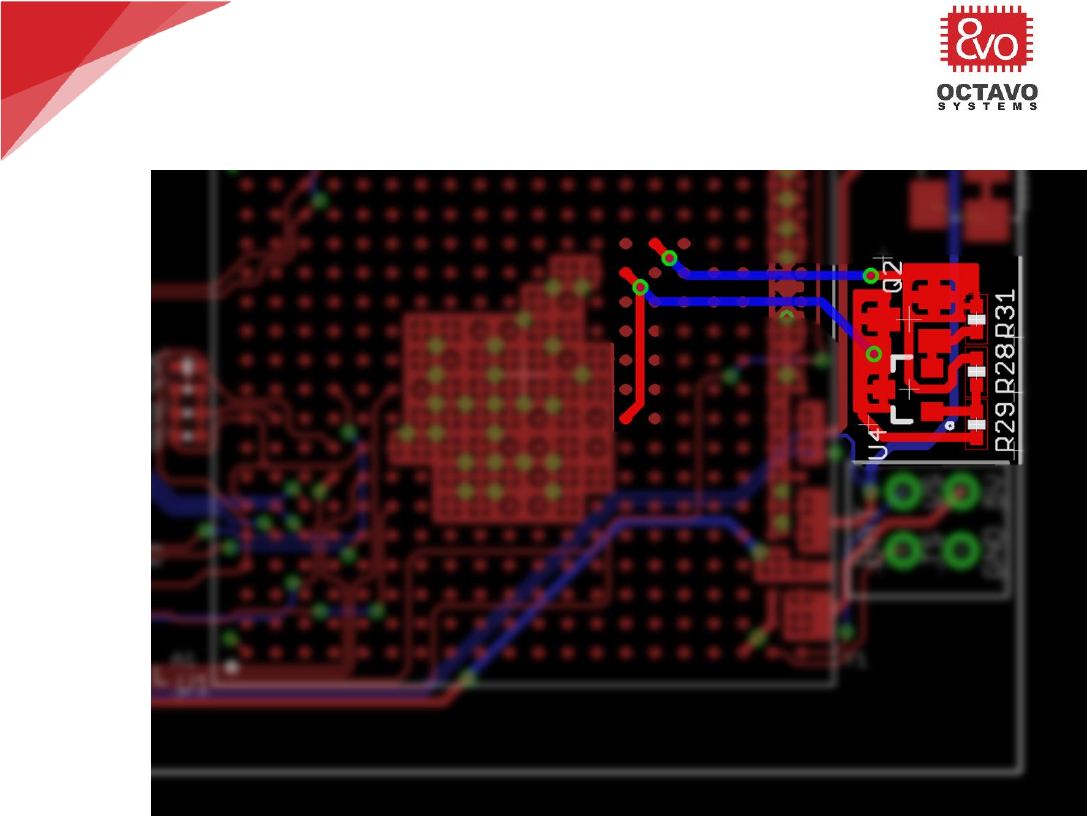
Connections in layout are made as shown in Figure 37.
Figure 37 OSD335x Clamping Circuit layout with pour
For this design, we used copper pours as well as 15 mil traces so that there is good
electrical as well as thermal connections.
Since we only wanted to put components on a single side of the board for this design,
the power outputs were routed to the clamping circuit as shown in Figure 37.
However, if placing components on the back side of the board, clamping circuit can
go directly under the power connections.
*****

OSD335x Tutorial Series
Rev.2 1/2/2018
Octavo Systems LLC
Copyright 2017
7 OSD335x ESD Protection
7.1 Introduction
Electrostatic discharge (ESD) is the flow of a static electric charge from one object to
another when two charged objects come into contact. Familiar examples of ESD
include the shock we receive when we walk across a carpet and touch a metal door
knob and the static electricity we feel after drying clothes in a clothes dryer. This
flow of static charge involves build-up of a very high voltage (around 10KV) for a very
short duration of time. Generally, a Printed Circuit Board (PCB) receives an ESD strike
whenever a person (whose skin is statically charged) touches it. Most electronic
components (without internal ESD protection) get damaged since they cannot
withstand such high voltage. Hence, ESD protection for a PCB is essential to protect
all the components on it.
This article is the fifth part of the OSD335x Reference Design Lesson1 Power Circuitry
Discussion. It will focus on providing ESD protection to a PCB with the OSD335x and
other components on it. As we discuss the ESD protection circuitry, we will build the
schematics and layout the corresponding traces.
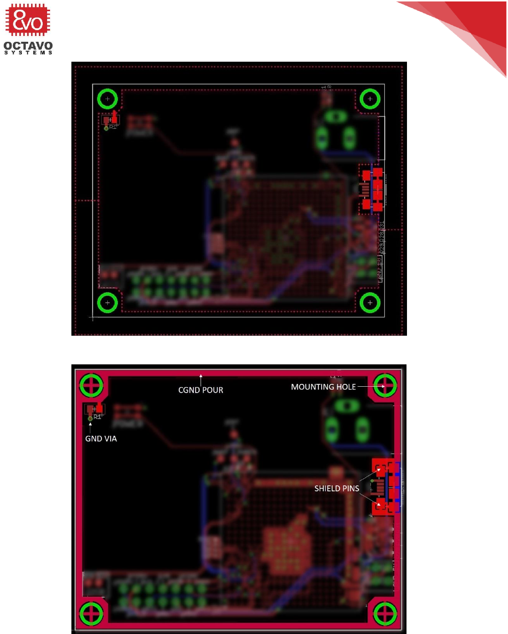
7.2 ESD protection
In order to protect the board from ESD strikes which can result from a person touching
the PCB, we have created a ground ring, CGND, that runs along the edge of the PCB
on both the top and bottom layers. The ground ring connects all of the mounting holes
(annotated in Figure 41) and shield pins (annotated in Figure 41) of metal connectors,
such as USB connectors. These components are most susceptible to ESD strikes. An
ESD strike has a very high voltage (around 10KV), but relatively little charge (low
energy). Therefore, we can use a couple of different methods to help dissipate the
energy from an ESD strike.
First, we can make use of the mounting holes as shown in Figure 38. Four mounting
holes are placed at the corners of the PCB for mechanical attachments to the board.
Generally, PCBs are bolted through the mounting holes to metal cases that are
externally grounded. As a result, when an ESD strike occurs, the charge safely flows
through the mounting holes to the bolts and finally to external ground.
Figure 38 Mounting holes connected to CGND
47
OSD335x Tutorial Series
Rev.2 1/2/2018
Octavo Systems LLC
Copyright 2017
Second, since a PCB may not be mounted and not have a path to external ground, we
can add circuitry to dissipate the energy through the ground (GND) plane. Therefore,
CGND is connected to the GND plane of the PCB through a 0.1 ohm resistor (R1) as
shown in Figure 39 (This picture is from OSD335x Power Inputs and Outputs article).
Figure 39 ESD energy dissipation
This will make sure any ESD strike can be safely dissipated into the GND plane. The
0.1 ohm resistor should have a higher wattage (0.125W or larger) to make sure there
are no thermal issues (damage to the resistor due to power flow that exceeds its
rating). Alternately, a 0.1uF capacitor and 100K Ohm resistor in parallel can be used
to connect CGND to the GND plane (In this design, we have opted for the single
resistor approach to dissipate energy since it is more economical).
The CGND polygon pour for ESD protection should form a complete ring along the
edge of the board and must be well connected to the shield pins of the connectors.
The CGND polygon pour must be present on both sides of the board. For this design,
we will use a pour of at least 50 mils as shown in Figure 40 and Figure 41.
48
OSD335x Tutorial Series
Rev.2 1/2/2018
Octavo Systems LLC
Copyright 2017
Figure 40 OSD335x mounting holes with CGND pour outline for ESD protection
Figure 41 OSD335x mounting holes with CGND pour for ESD protection
*****

OSD335x Tutorial Series
Rev.2 1/2/2018
Octavo Systems LLC
Copyright 2017
8 OSD335x Reset Circuitry
8.1 Introduction
This article will help you understand the OSD335x Reset Circuitry design methodology.
A Reset circuit/pin is typically used to help a microprocessor reinitialize itself and
resume its normal operation whenever it runs into condition which is undesirable for
the current activity and when all other recovery mechanisms fail. It is also used
during power-up to make sure the microprocessor and all its modules start their
operation from a known state.
8.2 Reset Types
Before we jump into the OSD335x specifics, let’s look at the type of reset inputs
typically provided by Texas Instruments (TI). TI generally provides two types of
resets: Cold Reset and Warm Reset. Let’s look at the properties of both these reset
types:
8.2.1 Cold reset
o It affects all the logic within the given entity (sub-system, module or macro-
cell).
o It is non blockable (This signal cannot be interrupted or blocked using software
or any other internal module. Once this signal is triggered, the device
immediately performs all the necessary operations irrespective of its state).
o A cold reset takes place during device power-up and power domain power-up.
o Cold reset is synonymous with Power-On-Reset.
8.2.2 Warm reset
o It is a partial reset which doesn’t affect all the logic within the given entity.
o It is used to reduce Reset recovery time (Time required to resume normal
operation after application of reset signal).
In general, a reset signal is asserted during device startup to make sure the device
begins operation from a known initial state each time it is powered up. This signal is
applied until the power supplies are stable and the device can begin normal
operation. A reset signal is also applied during device operation when the
microprocessor runs into an error condition which is undesirable for the current
activity and all other error recovery mechanisms fail.
The OSD335x provides three reset inputs PWRONRSTN, WARMRSTN and
RTC_PWRONRSTN which are directly connected to the AM335x processor reset inputs
of the same name. Let’s look at each of them in more detail:

50
OSD335x Tutorial Series
Rev.2 1/2/2018
Octavo Systems LLC
Copyright 2017
8.2.2.1 PWRONRSTN
o It is a cold reset.
o It needs to be driven low during device power-up until all the input power
lines have ramped up and are stable.
o It is non blockable (PWRONRSTN signal cannot be interrupted or blocked
using software or any other internal module. Once this signal is triggered,
the device immediately performs all the necessary operations irrespective
of its state).
o Entire system is affected except RTC (Real Time Clock) module.
o SYSBOOT (boot configuration) pins are latched when reset is de-asserted.
8.2.2.2 WARMRSTN
o It is a warm reset.
o It can be blocked by EMAC (Ethernet Media Access Controller) switch.
o PLLs are not affected.
o Most debug logic subsystems are not affected. This allows us to maintain
debug session even after warm reset event.
o SYSBOOT pins are not latched with warm reset.
o Some PRCM (Power, Reset and Clock Management) and control module
registers are warm reset insensitive.
o Warm reset assumes power supply and clock is stable from assertion
through de-assertion.
8.2.2.3 RTC_PWRONRSTN
o Dedicated Power-On-Reset input for the RTC module.
o RTC module is not affected by device Power-On-Reset (PWRONRSTN).
Similarly, RTC_PWRONRSTN will not have any effect on the rest of the
device.
51
OSD335x Tutorial Series
Rev.2 1/2/2018
Octavo Systems LLC
Copyright 2017
8.3 Reset external connections
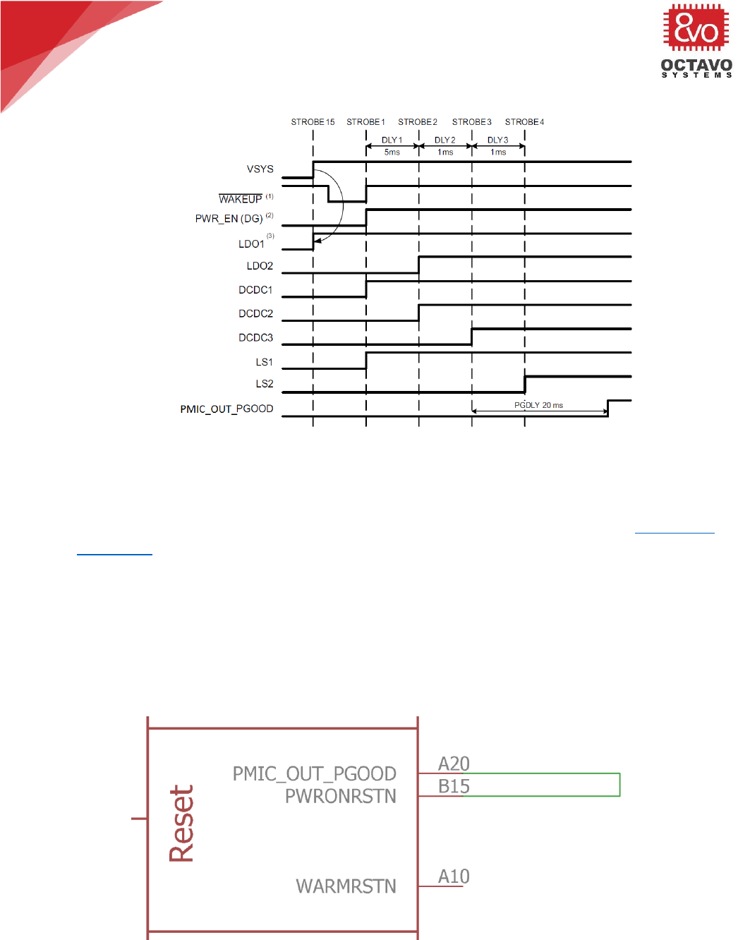
Figure 42 TPS65217 PMIC Power-Up Sequence (PMIC_OUT_PGOOD/PGOOD behavior during power-up)
During power-up, voltages on the input power rails of the AM335x processor will be
ramping up as shown in Figure 42 (More information about Power-Up sequence of
various power rails can be found in Power-Up Sequencing section of the TPS65217x
datasheet). The PWRONRSTN pin should be driven low until all the power rails have
ramped up and are stable. The PMIC_OUT_PGOOD pin will be maintained low when
power rails are ramping up or when the power on any of the power rails is below the
required value. It will go high only when the power on all power rails are stable as
shown in Figure 42. Hence, the PWRONRSTN pin needs to be driven by the
PMIC_OUT_PGOOD pin. Both the PWRONRSTN and the PMIC_OUT_PGOOD signals are
brought out of the OSD335x and they need to be connected externally as shown in
Figure 43.
Figure 43 PWRONRSTN and PMIC_OUT_PGOOD connection

52
OSD335x Tutorial Series
Rev.2 1/2/2018
Octavo Systems LLC
Copyright 2017
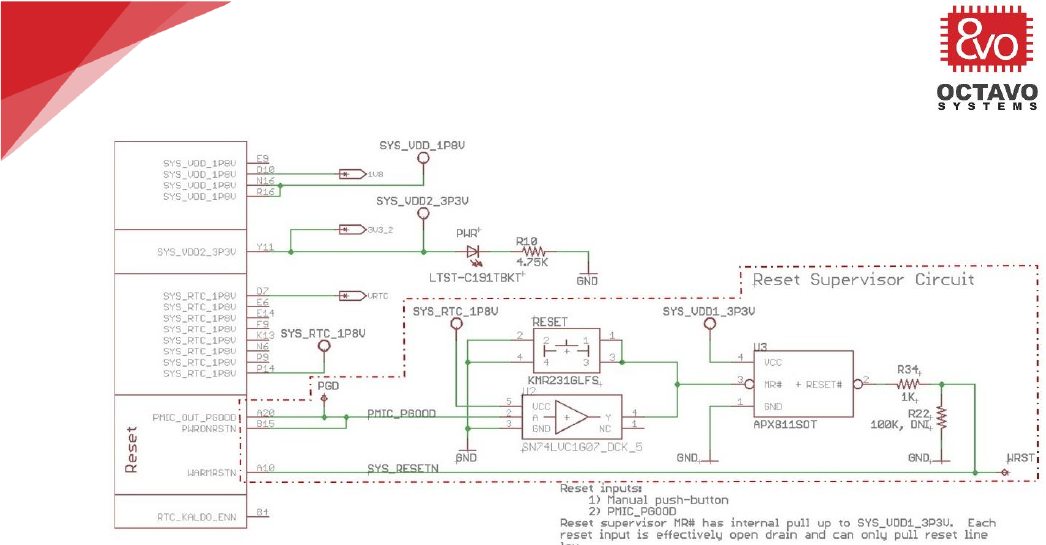
As described in the PORz Sequence section of the AM335x TRM, for the WARMRSTN
pin (nRESETIN_OUT) to maintain a valid low state until the supplies are ramped, it
should also be driven by PMIC_OUT_PGOOD. However, due to I/O voltage differences
(PMIC_OUT_PGOOD and PWRONRSTN pins operate at 1.8V while the WARMRSTN pin
operates at 3.3V) and the need for independent reset control, WARMRSTN should be
driven by PMIC_OUT_PGOOD thru an open-drain buffer (SN74LVC1G07). For more
information on the requirement of open-drain buffer, see section 8.1.7.3.2 PORz
Sequence (page 1236) of the AM335x TRM (Rev. P).
To manually reset the OSD335x in the case of a software or hardware error condition,
we will also add a push button as a reset source for WARMRSTN. Push buttons are
susceptible to ground bounce which may lead to multiple resets or partial resets. To
overcome this problem, a reset supervisor circuit can be used. The APX811 is an
efficient and cost effective solution which allows us to consolidate the reset sources
for WARMRSTN and drive the signal cleanly. The entire reset supervisor circuit can be
seen in Figure 44.
Perk:
A supervisor circuit (with manual reset input) has two specific functions. It asserts
a reset signal for a fixed period of time whenever the:
• supply voltage falls below a preset voltage.
• the manual reset input is asserted. (it may care of input button de-bouncing
also)
You can find more information about APX811’s operation by going through its
datasheet here.
53
OSD335x Tutorial Series
Rev.2 1/2/2018
Octavo Systems LLC
Copyright 2017
Figure 44 Reset button and buffer with APX811 supervisor circuit
The connections are made as shown in Figure 44 (Schematic updates are shown using
dotted lines).
Let’s go layout corresponding traces to complete the reset circuit design process as
shown in Figure 45.
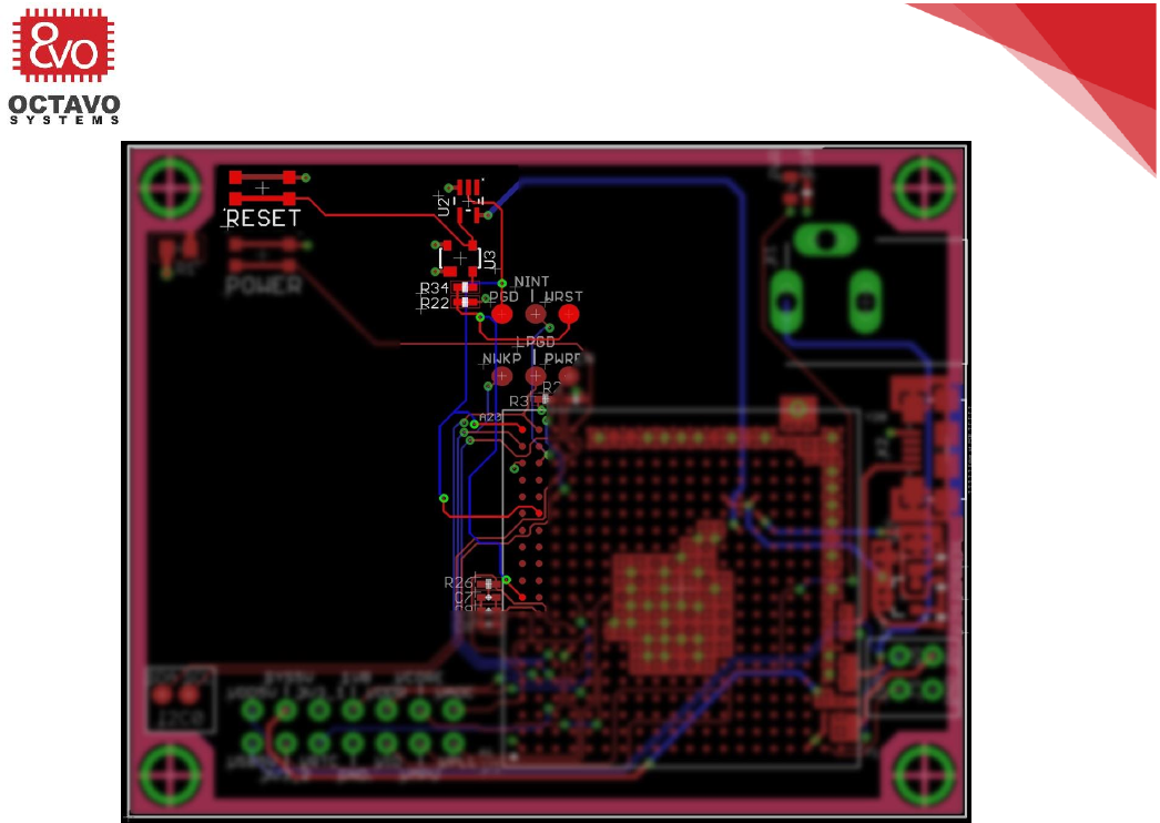
54
OSD335x Tutorial Series
Rev.2 1/2/2018
Octavo Systems LLC
Copyright 2017
Figure 45 Reset circuitry layout
The components are placed in a specific manner in to accommodate future
components and facilitate easy routing.
*****
OSD335x Tutorial Series
Rev.2 1/2/2018
Octavo Systems LLC
Copyright 2017
9 OSD335x Clock Circuitry
9.1 Introduction
A clock is essential for the operation of any microprocessor. Therefore, proper design
of the clock circuit is pivotal to achieve reliable operation. This article will help you
understand the OSD335x Clock Circuitry design methodology.
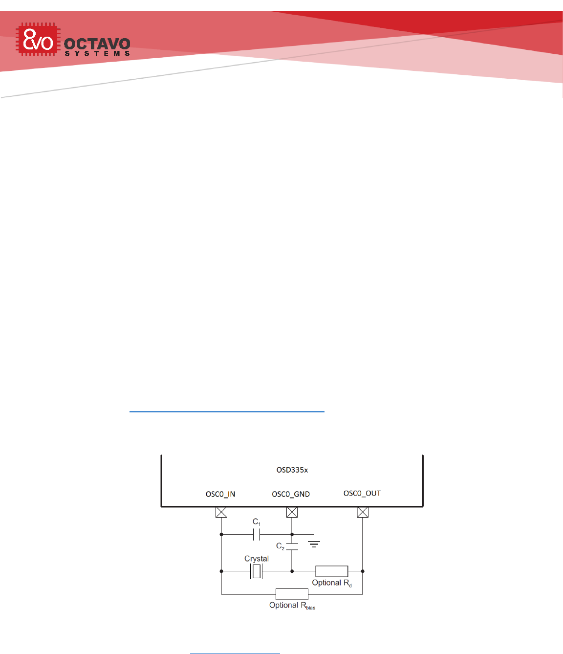
9.2 The OSD335x OSC0 and OSC1
The OSD335x has two clock inputs. They are:
OSC0: This is the High Frequency Oscillator Input. This clock source is also called the
Master Oscillator. It operates at either 19.2MHz, 24MHz ,25 MHz or 26MHz. This clock
source provides reference for all non-RTC functions. The OSC0_IN, OSC0_OUT and
OSC0_GND pins are used for this clock input.
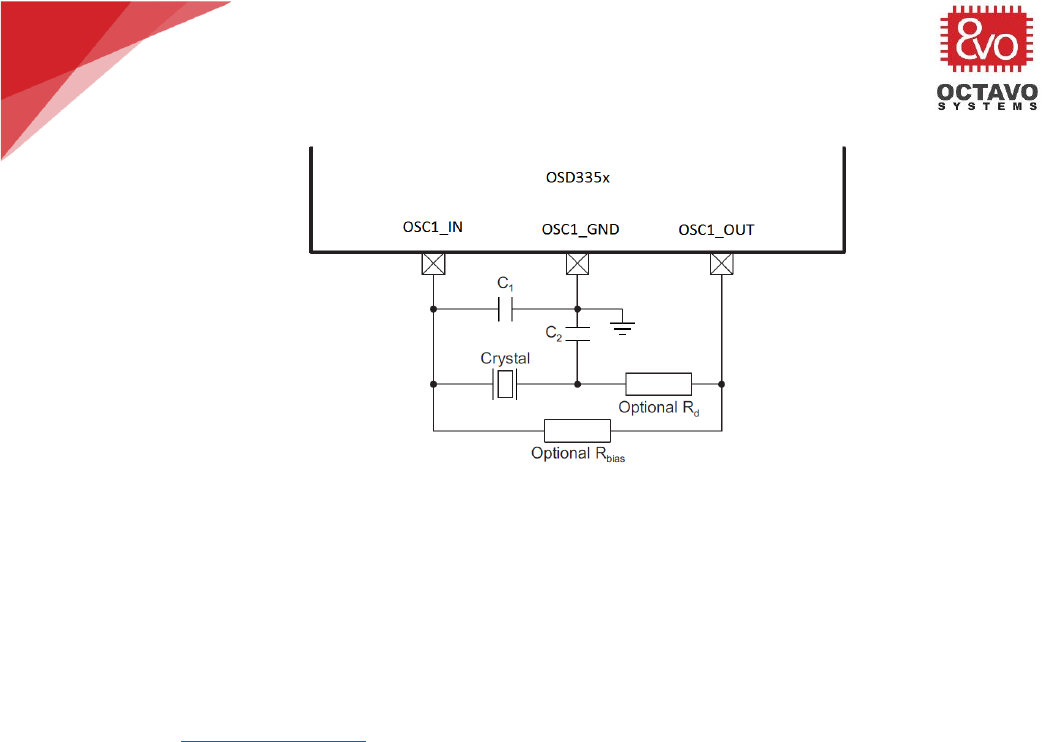
OSC1: This is the Low Frequency Oscillator Input. This clock source provides a reference clock for
the Real Time Clock (RTC) and operates at 32.768kHz. The OSC1_IN, OSC1_OUT and OSC1_GND
pins are used for this clock input.
OSC1 is disabled by default when power is applied. This clock input is optional and is
not required if the RTC (Real Time Clock) module is configured to receive clock from
internal 32kHz RC oscillator or if the RTC modules is not needed at all.
For more information on clock sub-systems, you can refer the Clock Management
section of the AM335x Technical Reference Manual.
The crystal oscillator circuit for OSC0 is shown in Figure 46.
Figure 46 Crystal Oscillator circuit for OSC0
o According to the AM335x datasheet, resistors Rbias and Rd are optional. For the
reference design, we added the footprint for Rbias to give us the flexibility to add a
resistor to the circuit if the default configuration (i.e., just C1 and C2 are connected)

56
OSD335x Tutorial Series
Rev.2 1/2/2018
Octavo Systems LLC
Copyright 2017
did not provide the desired crystal performance. Additionally, Rbias’s footprint can
be left unpopulated if it is not needed since it is in parallel with OSC0_IN and
OSC0_OUT pins.
However, Rd is in series with the crystal and the OSC0_OUT pin, so it must always be
populated even if it is not needed, which adds cost to the design. We decided not to
add the footprint for Rd since we didn’t think we needed it and it makes the layout
cleaner.
For the reference design, we were happy with the performance of the crystal when
we just used a 1 MOhm resistor for Rbias. You will have to decide how to handle Rbias
and Rd based on your design and your crystal.
o C1 and C2 represent the total capacitance of the respective PCB trace, load
capacitor, and other components (excluding the crystal) connected to each crystal
terminal. The value of capacitors C1 and C2 should be selected to provide the total
load capacitance, CL, specified by the crystal manufacturer. The total load
capacitance is CL = [(C1 × C2) / (C1 + C2)] + Cshunt, where Cshunt is the crystal shunt
capacitance (C0) specified by the crystal manufacturer. As long as the layout
guidelines are followed, we can assume that the capacitance of the PCB
trace and other components is small and can be ignored in the calculation
of C1 and C2.
o For recommended crystal circuit component values for OSC0, check OSC0 Crystal
Circuit Requirements table in the AM335x datasheet.
o The AM335x supports either 19.2MHz, 24MHz,25MHz or 26MHz clock input for
OSC0. However, the software we will be using in future lessons assumes a 24MHz
input clock. Hence, we will be using 24MHz crystal oscillator 7A-24.000MAAJ-T from
TXC for OSC0. Based on the above mentioned guidelines for capacitor selection, we
will be using 18pF capacitors for both C1 and C2 for our OSC0 design.
Caveat:
The choice of OSC0 clock frequency will affect the boot-configuration pull down/pull-up
resistor setup. See the SYSBOOT Configuration Pins section of the AM335x Technical
Reference Manual for more information about boot configuration resistor setup.
57
OSD335x Tutorial Series
Rev.2 1/2/2018
Octavo Systems LLC
Copyright 2017
Figure 47 Crystal Oscillator circuit for OSC1
o The crystal oscillator circuit for OSC1 is shown in Figure 47 and is the same as the
oscillator circuit for OSC0. For the reference design, we do not need either Rbias or Rd
since OSC1 has an internal resistor. However, as discussed above, we have placed a
footprint for Rbias but not for Rd to give us the flexibility to adjust the crystal
performance without increasing the design cost. For recommended crystal circuit
component values for OSC1, check OSC1 Crystal Circuit Requirements table in the
AM335x datasheet.
OSC1 circuit operates in the same way as OSC0 circuit.
o The AM335x only supports a 32.768kHz clock input for OSC1 input. Therefore, we will be
using the 32.768kHz crystal oscillator ABS07-32.768KHZ-T from Abracon LLC for OSC1
design. Based on the guidelines above for capacitor selection, we will be using 18pF
capacitors for both C1 and C2 for our OSC1 design.
58
OSD335x Tutorial Series
Rev.2 1/2/2018
Octavo Systems LLC
Copyright 2017
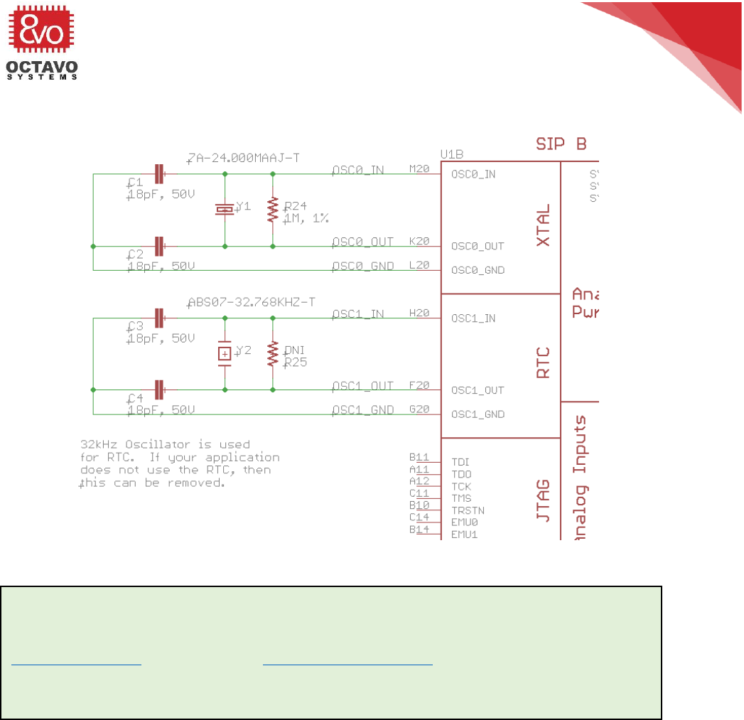
Now let’s add OSC0 and OSC1 circuits into our schematics as shown in Figure 48.
Figure 48 OSD335x Clock circuitry schematic
Perk:
OSC0 and OSC1 clock inputs can also be sourced from digital oscillator chips like
SIT8008BCE7-18E (for OSC0) and ASDK2-32.768KHZ-LRT (for OSC1). Use of digital
oscillators will significantly reduce the complexity of the circuit but does add cost.
A discussion on digital oscillator chip is beyond the scope of this article.

59
OSD335x Tutorial Series
Rev.2 1/2/2018
Octavo Systems LLC
Copyright 2017
9.3 Layout guidelines
Here are the guidelines we used for crystal oscillator layout in this design:
o The crystal oscillator is sensitive to noise from other signals. Other digital activities on
the board may also distort the small amplitude sine wave from the crystal oscillator.
Therefore, care should be taken when placing components or routing signals near the
oscillator circuit to avoid capacitive coupling.
o The crystal oscillator circuit components should be placed close to the OSD335x.
o For the OSD335x, each oscillator has an oscillator ground. This should be used
as the ground reference for the oscillator.
o Try not to route any other signal under the oscillator circuit wherever possible.
o If routing signals under the oscillators, then try to make sure that the signal
traces cross at right angles vs running parallel to oscillator traces to minimize
coupling.
o Avoid right angle traces.
o Avoid vias for clock signals if possible. If not possible, then make sure that
there is enough keep out in the inner planes to not cause excessive noise on
inner plane layers.
o The length of clock signal traces should be matched as much as possible.
Let’s layout the traces for OSC0 and OSC1 as shown in Figure 49.
60
OSD335x Tutorial Series
Rev.2 1/2/2018
Octavo Systems LLC
Copyright 2017
Figure 49 OSD335x OSC0 and OSC1 layout
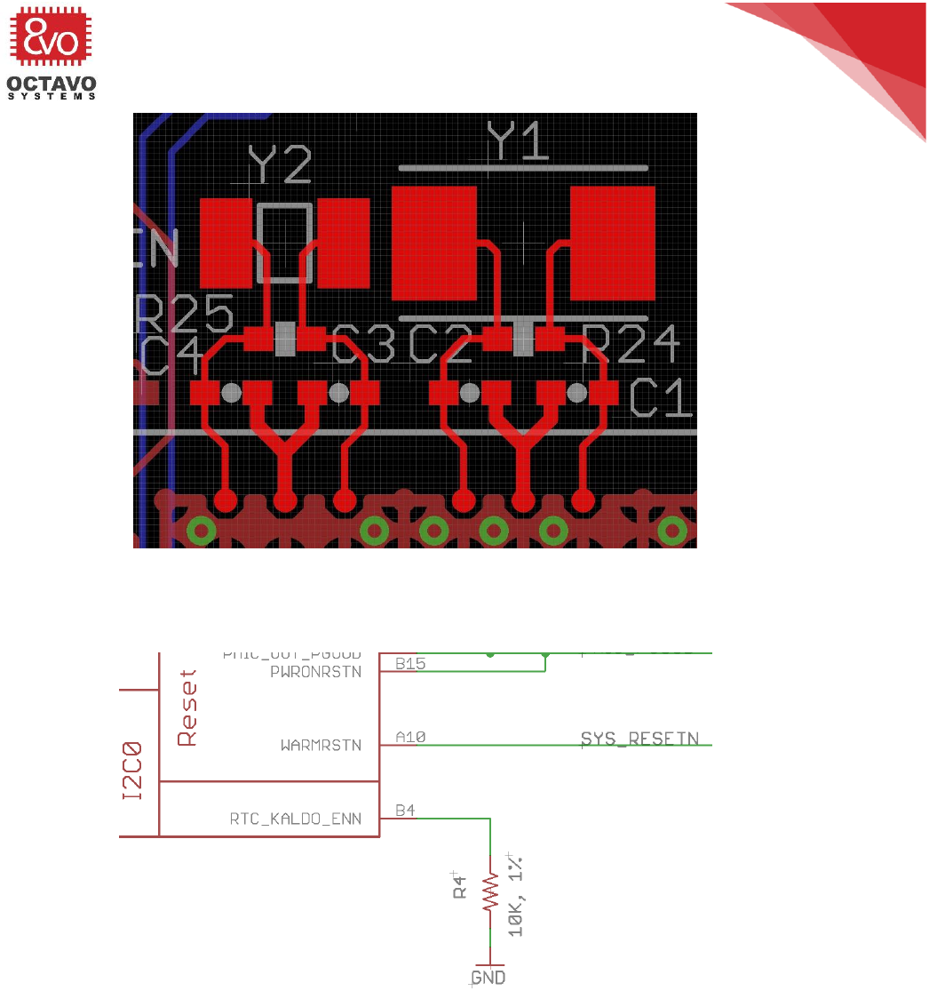
9.4 RTC_KALDO_ENN
Figure 50 Grounding RTC_KALDO_ENN pin
The AM335x processor inside the OSD335x consists of an RTC (Real Time Clock) with
the potential to support an RTC-Only mode. However, the OSD335x DOES NOT support
RTC-Only mode because we have used the C version of TPS65217 which does not
support RTC-Only power mode. Although RTC-Only mode is not available, we would
like to enable and use RTC digital core along with other modules of the processor to
keep track of time.
61
OSD335x Tutorial Series
Rev.2 1/2/2018
Octavo Systems LLC
Copyright 2017
The RTC digital core has an internal RTC LDO which can supply power to it.
CAP_VDD_RTC (the supply pin for the RTC core) gets power from the internal RTC LDO
if the RTC_KALDO_ENn (active low) pin is pulled low as shown in Figure 50. If
RTC_KALDO_ENn is pulled high, the internal RTC LDO will be disabled and
CAP_VDD_RTC will have to be connected to VDD_CORE to power the RTC core
externally.
Figure 51 OSD335x clock circuitry layout
On completion of clock circuitry layout, the board should look like Figure 51 (assuming the
board is also populated with power and reset circuitry from previous articles).
*****
OSD335x Tutorial Series
Rev.2 1/2/2018
Octavo Systems LLC
Copyright 2017
10 OSD335x Peripheral Circuitry
10.1 Introduction
Now that the power, reset and clocks are all connected, we need to add the ability to
program the OSD335x to make our design useful. To program the OSD335x, we are
going to use the JTAG connection to the processor (later lessons will look at other
boot devices). To enable us to do some fun things with our design, we will add a
couple of general purpose LEDs, switches, and a multipurpose peripheral header. The
header will allow us to connect daughter boards to extend functionality.
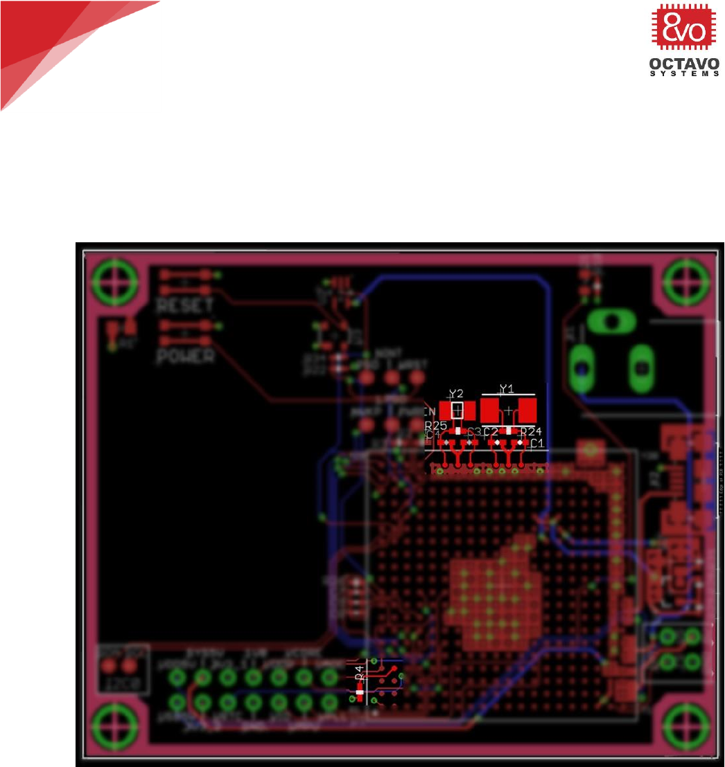
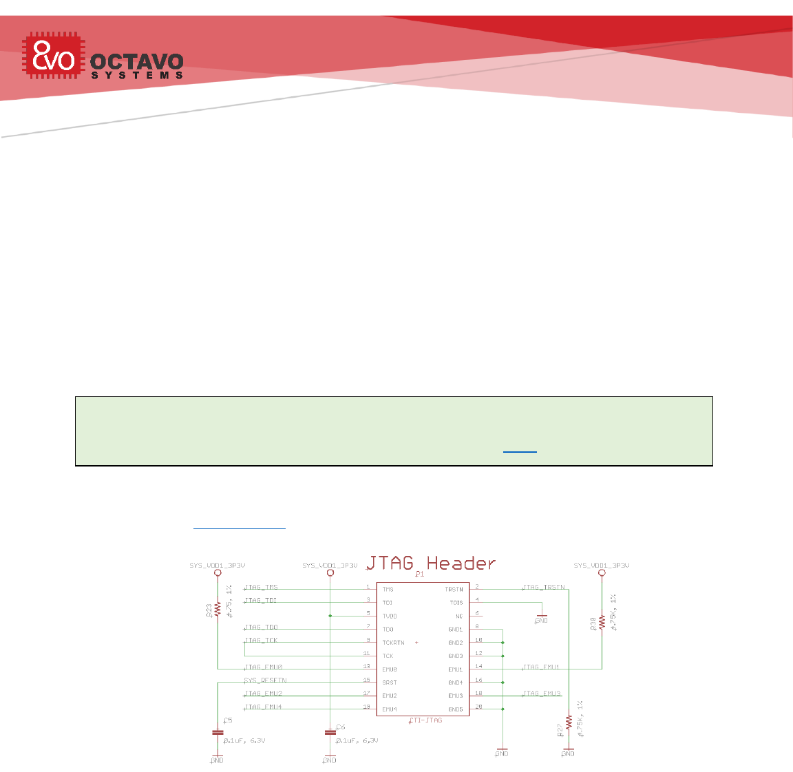
10.2 JTAG
For this design, we do not include any non-volatile storage to allow us to boot and run
an OS by default. Therefore, all programs will need to be loaded via the JTAG
interface.
The JTAG circuit can be built on the schematic as shown in Figure 52. This uses a
standard 20-pin connector and supports most JTAG debuggers. The JTAG header can
be found in the given library under the device name CTI-JTAG.
Figure 52 JTAG schematics
The JTAG connections can be made in the layout as shown in Figure 53.
Perk:
More information about JTAG interface can be found at here.

63
OSD335x Tutorial Series
Rev.2 1/2/2018
Octavo Systems LLC
Copyright 2017
Figure 53 JTAG layout
64
OSD335x Tutorial Series
Rev.2 1/2/2018
Octavo Systems LLC
Copyright 2017
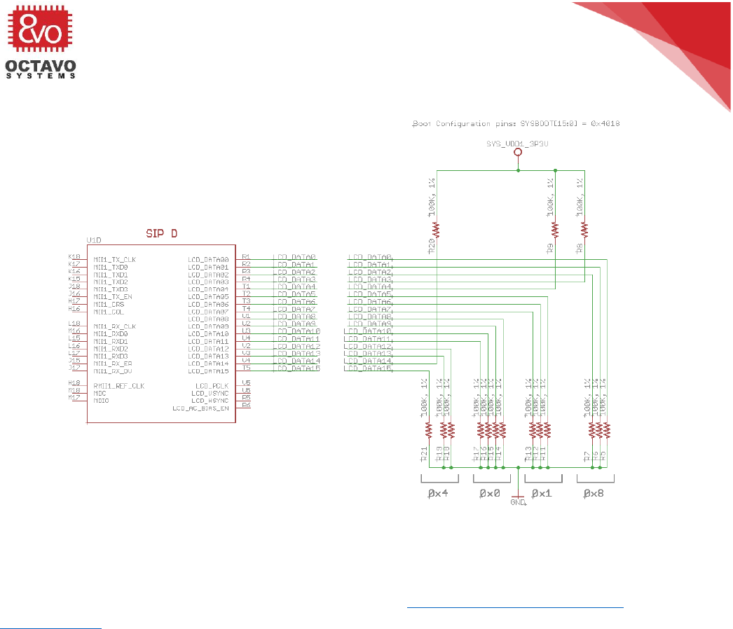
10.3 Boot configuration
Figure 54 Boot configuration schematic
LCD_DATA0 to LCD_DATA15 pins are multiplexed with the SYSBOOT boot configuration
pins of the OSD335x. More information about the function of each of these pins can be
found in SYSBOOT Configuration Pins section of the AM335x Technical Reference
Manual (TRM). SYSBOOT[0] corresponds to LCD_DATA0 while SYSBOOT[15] corresponds
to LCD_DATA15.
Using the boot configuration pins for this design, we will:
o Set clock frequency to 24MHz.
o Disable CLKOUT1 output through XDMA_EVENT_INTR0 since this pin will only
be used for JTAG emulation.
o Set the boot sequence to SPI0 -> MMC0 -> USB0 -> UART0
By default, if no valid boot images are found during the boot sequence, then JTAG
can take control of the processor to allow software to be loaded.
To achieve this, we need to set SYSBOOT[15:0] = 0x4018. We can build the schematic
for the boot configuration as shown in Figure 54.
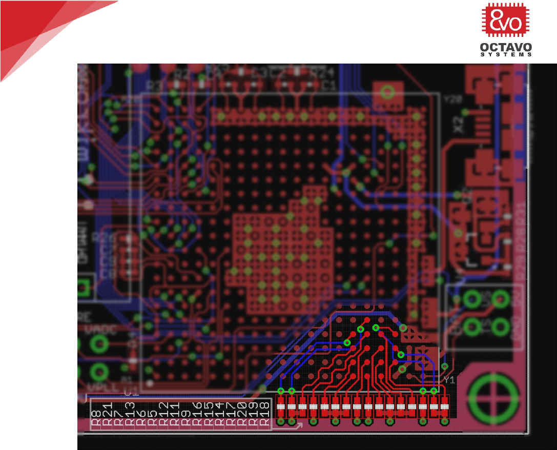
66
OSD335x Tutorial Series
Rev.2 1/2/2018
Octavo Systems LLC
Copyright 2017
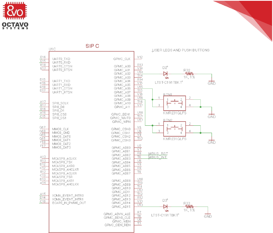
10.4 Buttons and LEDs
Figure 56 User LEDs and user buttons
For this design, we will add two push buttons and two LEDs. The buttons can be
connected to GPIOs GPMC_A06 and GPMC_A09. These two pins were chosen to make
routing easier. There was no de-bounce circuitry added to the buttons so any de-
bouncing must be done in software.
Also, let’s add two LEDs, one to GPIO GPMC_A02 and the other to a PWM capable
GPIO GPMC_AD15 so that we can exploit the PWM capability of the OSD335x. The
schematic for these connections is shown in Figure 56.
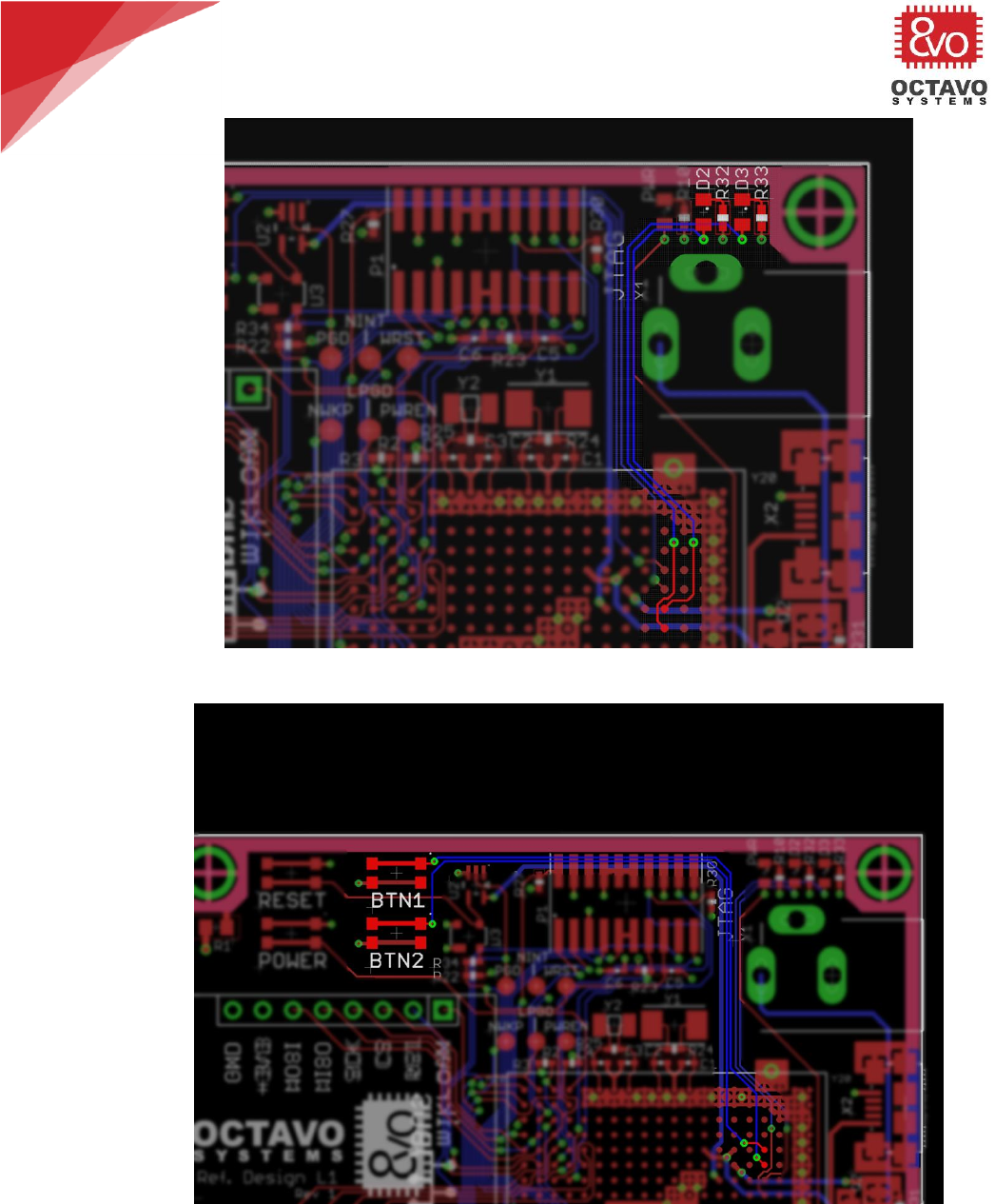
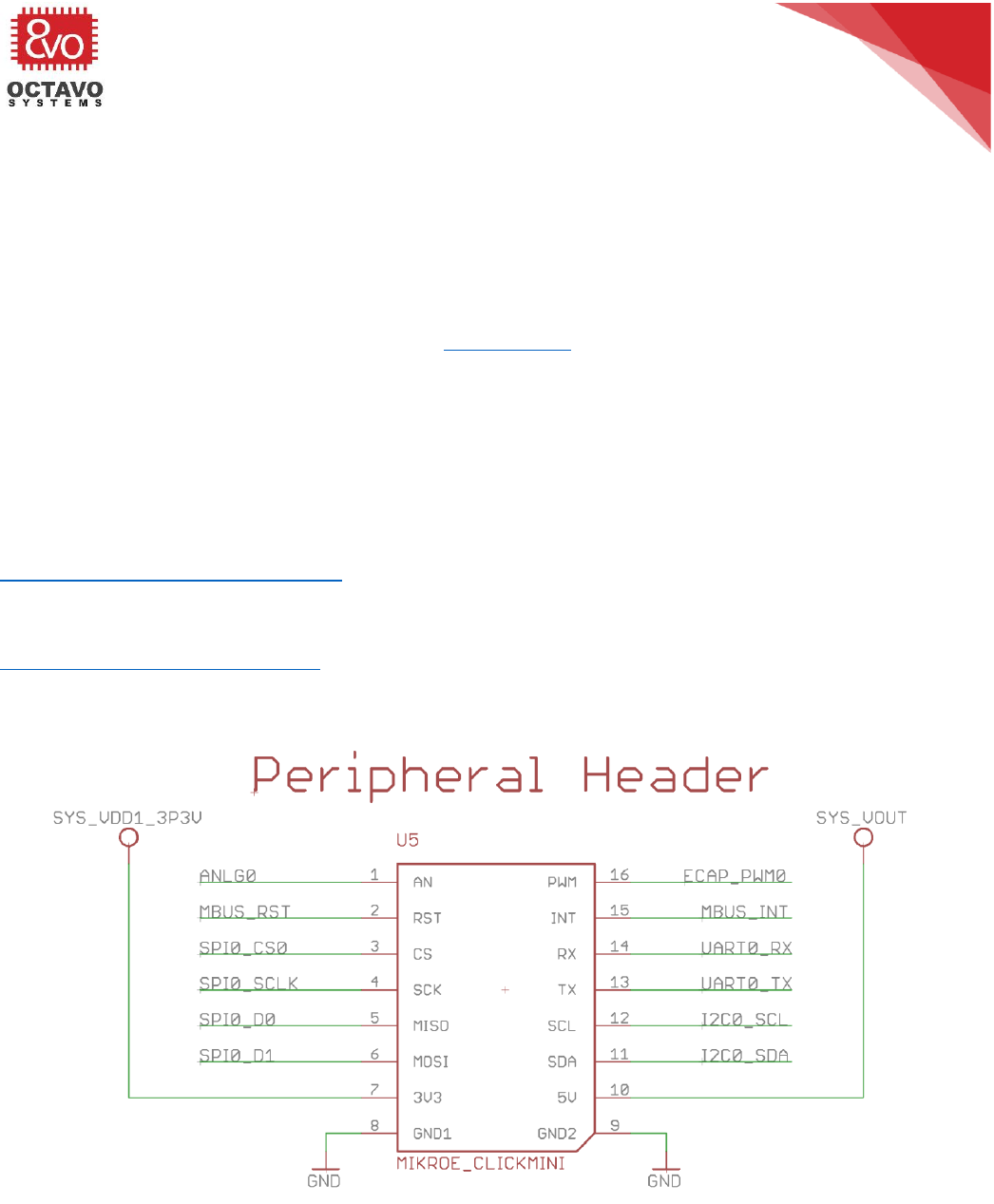
68
OSD335x Tutorial Series
Rev.2 1/2/2018
Octavo Systems LLC
Copyright 2017
10.5 Peripheral header
The OSD335x supports several serial communication protocols like UART, SPI and I2C.
These protocols can be used to communicate with and control external devices.
We can map these signals to a standard peripheral header to provide expandability
and additional functionality.
The peripheral header we’re using consists of a pair of 1x8 female headers with pin
configuration as shown in Figure 59. In the given library, the peripheral header can be
found under the device name MIKROE_CLICKMINI (MIKROE_CLICK). This
configuration is compatible with mikroBus® Click Board™. Click Boards are daughter
boards with a single IC, module or circuit that brings specific functionality to a target
main board. Hundreds of click boards are available with various types of sensors,
transceivers and functionality.
More description about mikroBus socket and Click boards can be found at:
https://www.mikroe.com/mikrobus/
You can browse through available click boards at:
https://shop.mikroe.com/click.
The peripheral header schematic is given below:
Figure 59 Peripheral header schematic
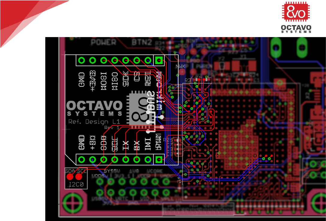
69
OSD335x Tutorial Series
Rev.2 1/2/2018
Octavo Systems LLC
Copyright 2017
Figure 60 Peripheral header layout
The footprint for peripheral header is shown in Figure 60 and the connections are
highlighted.
10.6 Finalizing the silkscreen
Silkscreen on a PCB is used to identify components, test points, warning symbols,
certification symbols, company logos, PCB name and revision, and any other text that
is necessary to document the functionality of the board. During the placement and
routing phases of the board design, you should not really worry about the silkscreen.
However, now that we have completed placement and routing of all the components
on the PCB, we need to make sure that the silkscreen is readable. We need to make
sure:
o All the component designators are placed appropriately next to their
corresponding components.
o Pin 1 is marked for necessary components. This includes all ICs, connectors
and polarized capacitors.
o There is no silkscreen over any component pads. This can lead to bad solder
joints.
o The font size of the component designators is as large as possible given the
space constraints of the board so that the text is readable.
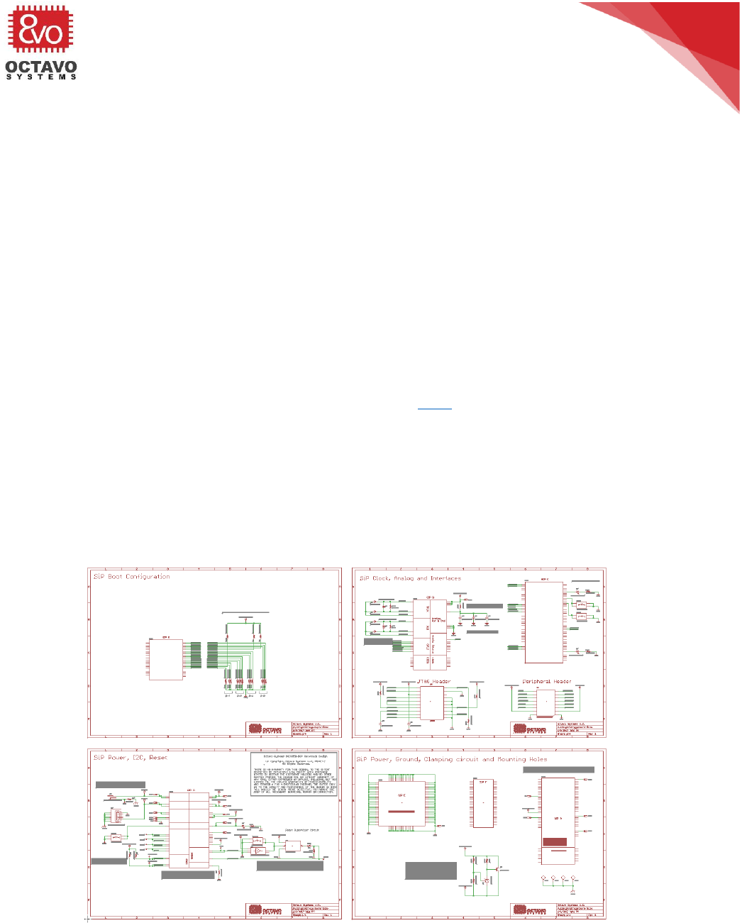
70
OSD335x Tutorial Series
Rev.2 1/2/2018
Octavo Systems LLC
Copyright 2017
o Try to not place silkscreen over vias. Silkscreen has a hard time adhering to
the annular ring of a via which can make the text difficult to read.
When designing a board, the actual size of the text can be deceiving since the view in
the design tool is generally many times larger than the actual board. The minimum
font size you should use is 24mils with 8% ratio. Depending on your eyes, a font size of
32mils with an 8% ratio is readable without magnification. This is a good size for
passive designators, though in general bigger is better. You can also increase the ratio
of the text to make the line width thicker. This can help make the text more readable
but only up to a point. However, once you get larger fonts (over 50mils), you should
use larger ratios (12% or greater) to make the text more readable. It is recommended
that once you are done with updating the silkscreen, print out the silkscreen layers to
check their readability.
You can also import a picture of your logo into Eagle and add it into your layout. You
can learn more about the procedure to import images here. For our design, we have
added Octavo Systems logo along with the lesson name and revision number as shown
in Figure 62, Figure 63 and Figure 64.
10.7 Expected outcome
Now that we have completed building the schematic and layout, the complete
schematic should look similar to Figure 61 and complete layout should look similar to
Figure 62, Figure 63 and Figure 64.
Figure 61 Lesson 1 complete schematic
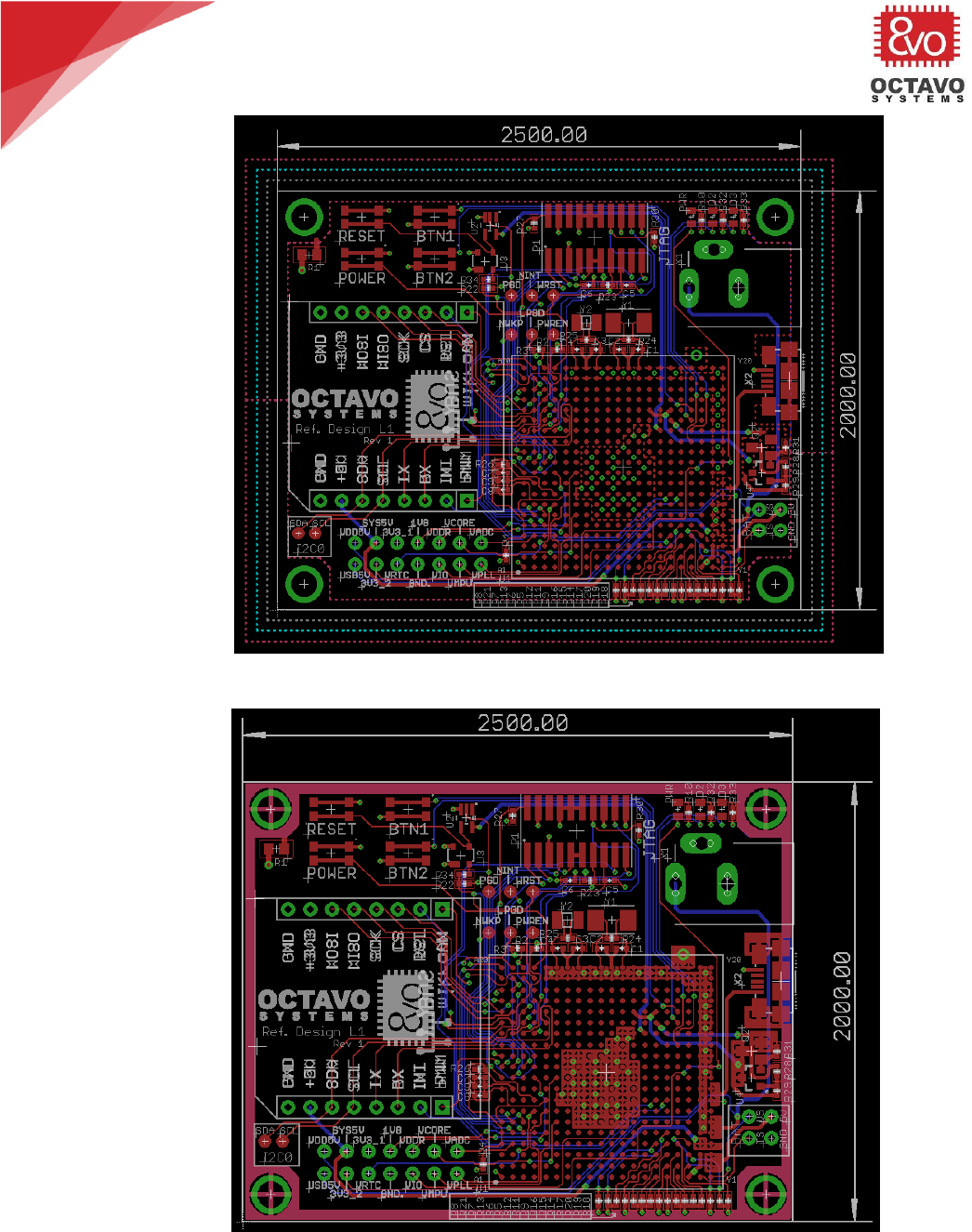
71
OSD335x Tutorial Series
Rev.2 1/2/2018
Octavo Systems LLC
Copyright 2017
Figure 62 Lesson 1 complete layout with pour outlines
Figure 63 Lesson 1 complete layout with pour
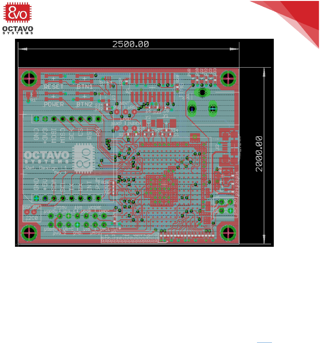
72
OSD335x Tutorial Series
Rev.2 1/2/2018
Octavo Systems LLC
Copyright 2017
Figure 64 Lesson 1 complete layout with all layers turned on
10.8 PCB order process
The PCB order process begins with Bill Of Material (BOM) generation. EAGLE is capable
of maintaining manufacturer and part number for each component so the schematic
can be the controlled document for manufacturing information. The BOM.ulp can be
used to output this data in an easily readable format. Once BOM is generated, the
components can be purchased.
The next step is gerber file generation for PCB manufacturing. More information on
gerber file generation, gerber verification and order placement can be found here.
*****
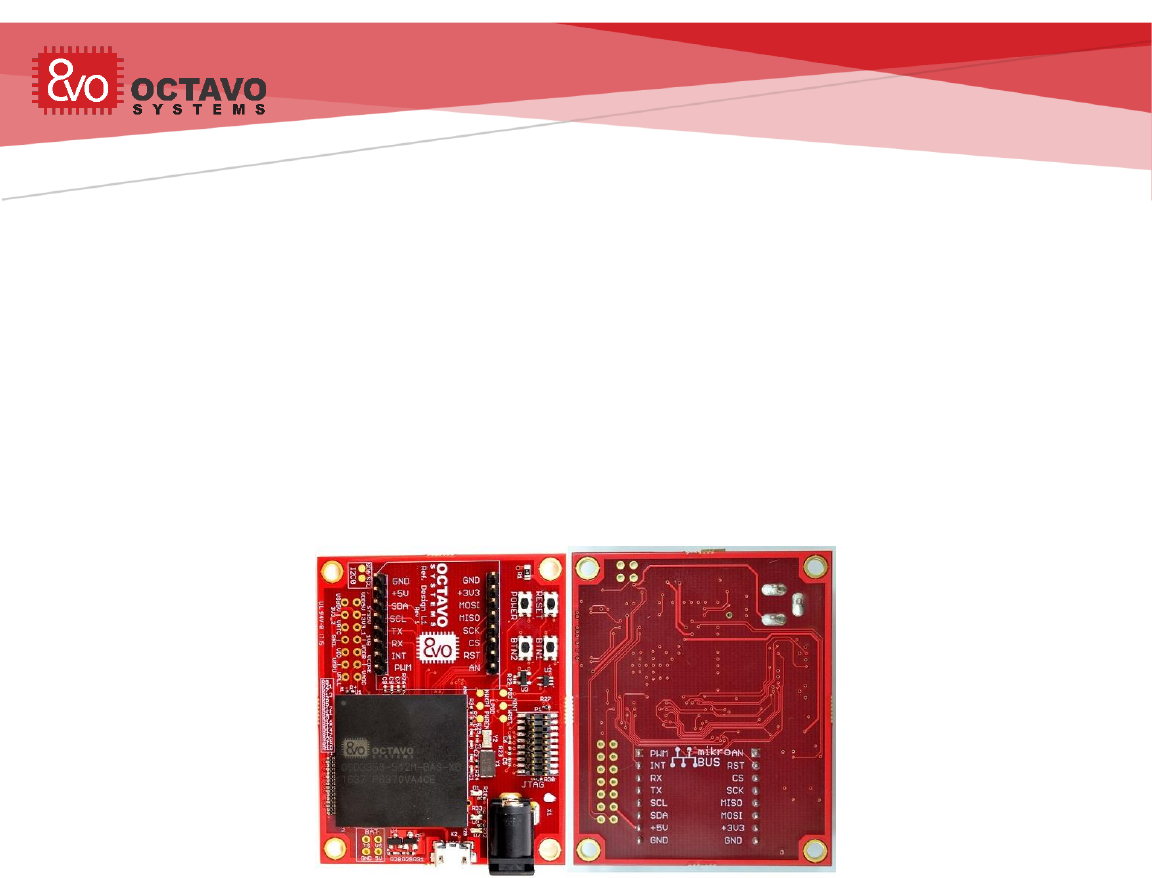
OSD335x Tutorial Series
Rev.2 1/2/2018
Octavo Systems LLC
Copyright 2017
11 OSD335x Bare Minimum Board Boot Process
11.1 Introduction
This document will take you through the bring-up process of the Printed Circuit Board
(PCB) developed as part of the OSD335x Reference Design Lesson 1.
We begin with bringing-up the newly manufactured board (PCB) to make sure it is
functional followed by the necessary software environment setup. We conclude with
the demo apps to verify the overall functionality of the board.
11.2 The Board (PCB)
The board built as part of previous articles of this lesson should look similar to Figure
65 (Assuming you chose Red color for solder mask and white color for silk screen):
Figure 65 OSD335x Bare Minimum Board
11.3 Basic board bring-up
This section describes the various tests that need to be done during the board bring-
up process.
11.3.1 Tests before board power-up
The newly manufactured PCB should be examined before powering it up for the first
time to prevent damage to the board.
o Use a Digital Multi Meter (DMM) to make sure there are no shorts
(resistance<=100ohms) between:
- Power input pins and ground.
- Power output pins and ground.
- Between power inputs and power outputs - This is where all the test
points can be very helpful.
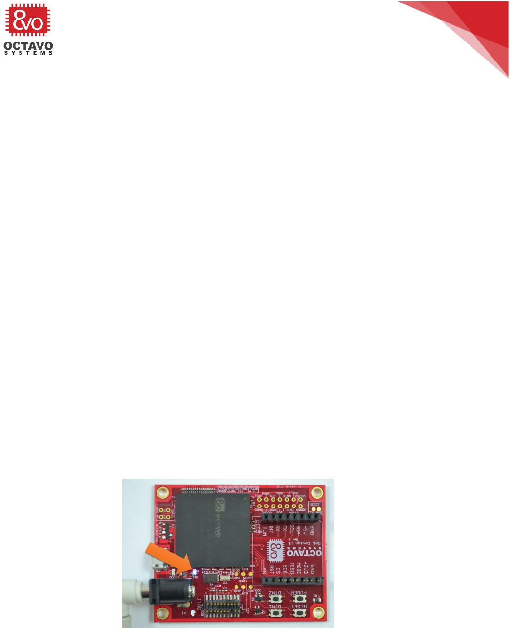
74
OSD335x Tutorial Series
Rev.2 1/2/2018
Octavo Systems LLC
Copyright 2017
- If there are any shorts, try to locate the source of the short. This can be
done by:
▪ Examining schematics and layout.
▪ In many cases, the only way to isolate shorts is to remove
components connected to the short one by one until the short is
resolved.
▪ Once you have discovered the source of the problem, you can try
to modify the board to fix the issue. This can involve cutting
traces or re-wiring components. Unfortunately, sometimes boards
cannot be fixed and the design must be re-spun (i.e., schematics
and layout updated and boards re-manufactured). If you have to
re-spin a board, please make sure to update the revision code on
the board.
o Use a DMM to check the resistance between:
- All power inputs, power outputs and ground.
- Between power planes and ground.
- In any case, if the resistance is less than 100ohms, you need to be very
careful during power-up to make sure no components have issues.
o Check if the correct components are used by reading the marking on the devices.
o Check if the orientations of the components are correct.
After performing all the above tests, we can power up the board using the DC barrel
jack. If everything goes well, you should see the power LED PWR light up as shown in
Figure 66.
Figure 66 PWR LED after successful power up

75
OSD335x Tutorial Series
Rev.2 1/2/2018
Octavo Systems LLC
Copyright 2017
11.3.2 Possible problems after board power-up
Once the board is powered up, if you observe sparking, overheating or smoke from
any of the components, TURN OFF POWER TO THE BOARD IMMEDIATELY to avoid
further damage to the board and prevent a possible fire hazard. For any component
that failed, please make sure:
o The symbol pinout of the component in schematic matches with its datasheet
pinout. Please make sure that you have the latest version of the datasheet
since documentation can be updated / corrected between the time of symbol
creation and board manufacture.
o The footprint of the component on PCB matches with the footprint specified on
its datasheet.
o The symbol to footprint pin mapping is correct.
o All the components are supplying power within their specified output current
limits. For example, if you notice that the voltage of one of the power outputs
of the SiP, let’s say, SYS_VDD1_3P3V, is low (less than 3.3V), there is a
possibility that too much current is being drawn from it. Make sure the current
output of SYS_VDD1_3P3V is within its maximum value to restore its output
voltage to 3.3V.
o If possible, try to solve the problem by manually cutting suitable traces on the
PCB/making connections using a thin wire. If the problem cannot be solved
using these methods, you will have to re-spin the board.
11.3.3 Tests after power-up
If the power LED is lit and you don’t observe any smoke, sparking or heating issues
then we can consider it a successful power-up. But, this does not mean the board is
fully functional. We can test for functionality by running demo apps. Before running
the demo apps:
o Check the following voltage levels using the available test points/pads:
Perk:
More information about using Digital Multi Meters can be found here.
Caveat:
Boards should only be powered up for the first time in a good work environment
with proper safety equipment like fire extinguisher, non-flammable ESD
workbench, safety glasses, fume extractor (to remove soldering smoke) etc. Please
make sure your work environment is proper before doing any board bring-up work.

76
OSD335x Tutorial Series
Rev.2 1/2/2018
Octavo Systems LLC
Copyright 2017
- Verify if VIN_AC is at 5V (assuming you’re using DC barrel connector for
power input).
- Verify if SYS_VOUT is at 5V (assuming you’re using a 5V power input).
- Verify if SYS_VDD1_3P3V is at 3.3V.
- Verify if SYS_RTC_1P8V is at 1.8.
- Verify if the test pad PGD (PMIC_OUT_PGOOD) is at 1.8V and WRST
(WARMRSTN) is at 3.3V to make sure the OSD335x is not being held in reset.
If any of the above voltages are not at the desired level, please use the test
points/test pads with an oscilloscope and DMM to find out which component(s)
is responsible for the erroneous voltage. One thing to be aware of is that the
voltage on a power rail or signal pin can drop if the load is trying to draw more
current than the source can provide.
If you’ve made it this far through the article and if everything looks good on
your board, pat yourself on the back. Good job! Now you’re ready to run some
code!
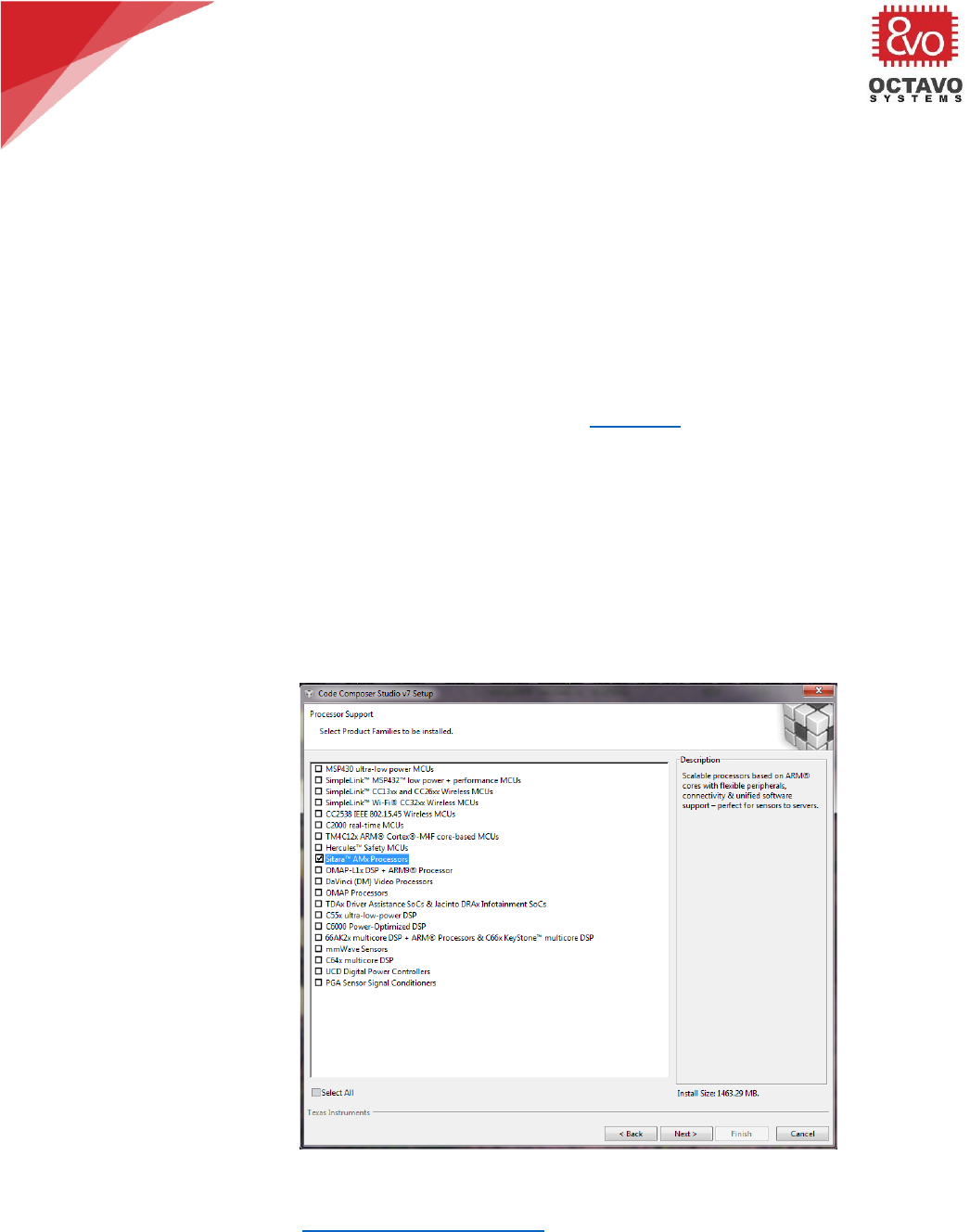
77
OSD335x Tutorial Series
Rev.2 1/2/2018
Octavo Systems LLC
Copyright 2017
11.4 Setting up software environment (for Windows 7,8 and 10 OS)
11.4.1 Installing Code Composer Studio
For our design, we will use the Code Composer Studio (CCS) Integrated Development
Environment (IDE) to compile, debug and load programs to the OSD335x. The OSD335x
uses the AM335x processor from Texas Instruments (TI). Therefore, for the AM335x,
we will use the IDE developed and supported by TI. You can use third party IDEs and
compilers if necessary.
Steps to install Code Composer Studio:
o You can download the CCS 7.2.0.00013 (which was the latest version at the
time of writing this article) installer from this page. The below mentioned
steps are for the offline installer. All the demo apps have been tested on CCS
7.2.0.00013 and CCS 6.2.0.00050. You may use CCS 6.2.0.00050 if you face
compatibility issues with CCS 7.2.0.00013.
o Midway through the installation process, the installer will ask you to Select
Product Families to be installed. Choose Sitara as shown in Figure 67 and
click next (if you plan to use CCS for other TI processors, you should select to
install those now; else you will have to completely re-install CCS if you need to
add support for other processors).
Figure 67 CCS Product family selection
o We are using XDS100v2 debug probe. Therefore, we will choose XDS under
debug probes, as shown in Figure 68 and hit next. If you are using a different
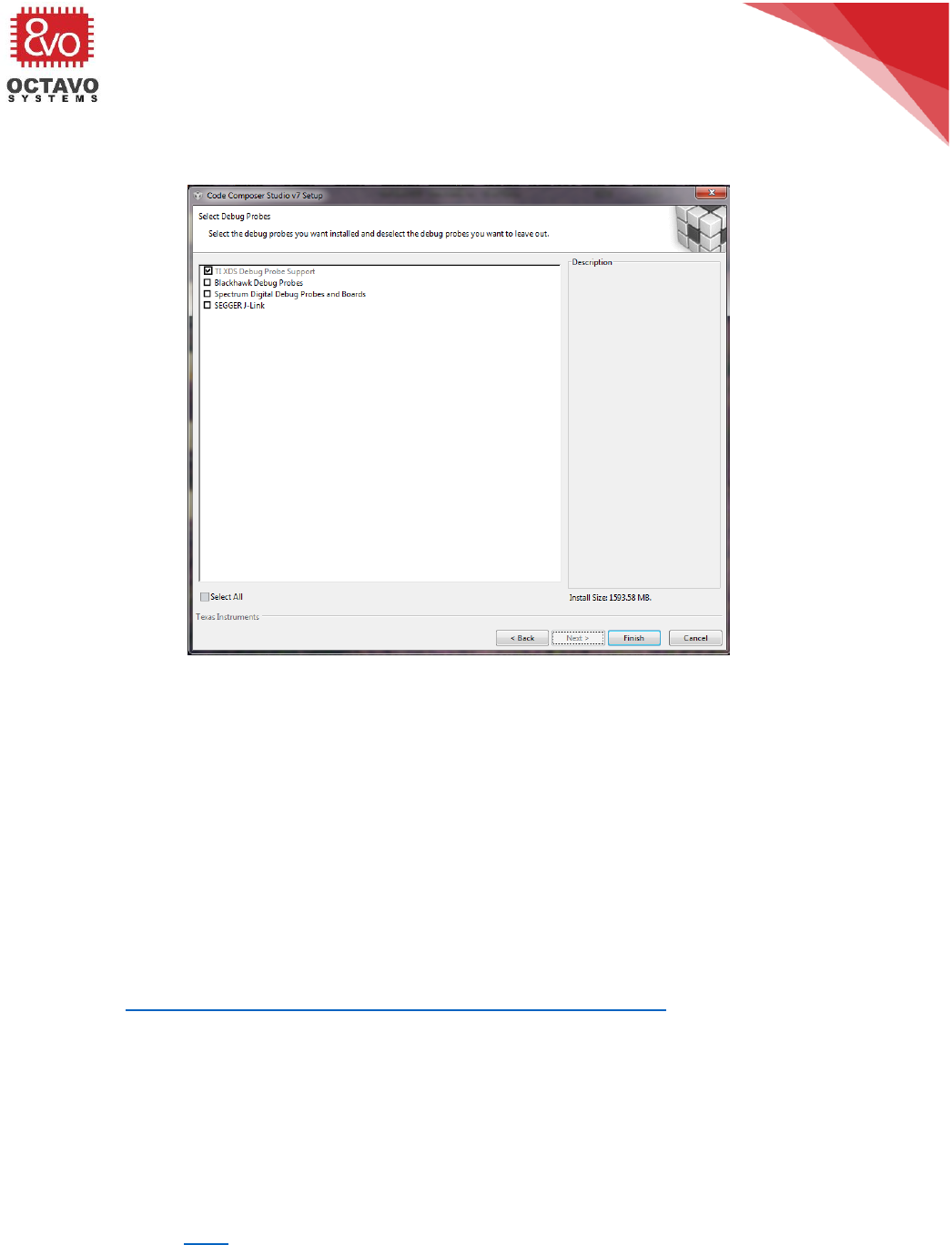
78
OSD335x Tutorial Series
Rev.2 1/2/2018
Octavo Systems LLC
Copyright 2017
debugger, please select and install those instead. Follow the onscreen
instructions to complete the installation.
Figure 68 CCS debug probe selection
11.4.2 Installing StarterWare
StarterWare is a free software development package that provides bare metal
(non-OS) platform support for ARM and DSP TI processors. StarterWare includes
Device Abstraction Layer (DAL) libraries and example applications that
demonstrate the capabilities of the peripherals on the TI processors. StarterWare
also provides pre-built binaries for quick evaluations on the target. To keep things
simple and to avoid using an OS like Linux, we will be using Starterware platform
for this lesson. Linux will be introduced in the next lesson.
To install StarterWare:
o Go to http://processors.wiki.ti.com/index.php/StarterWare.
o Download StarterWare 02.00.01.01 for the AM335x (TI Account Login required.
You can download the software only if TI approves it).
o Install StarterWare 02.00.01.01 using on screen instructions.
11.4.3 Debugger
To load the program to the OSD335x, we need a debugger. We have tested the Demo
Apps using XDS100v2 from Spectrum Digital (shown in Figure 69). You are free to use
other debuggers if you have them. We have only validated operation on the XDS100v2
which you can get here.
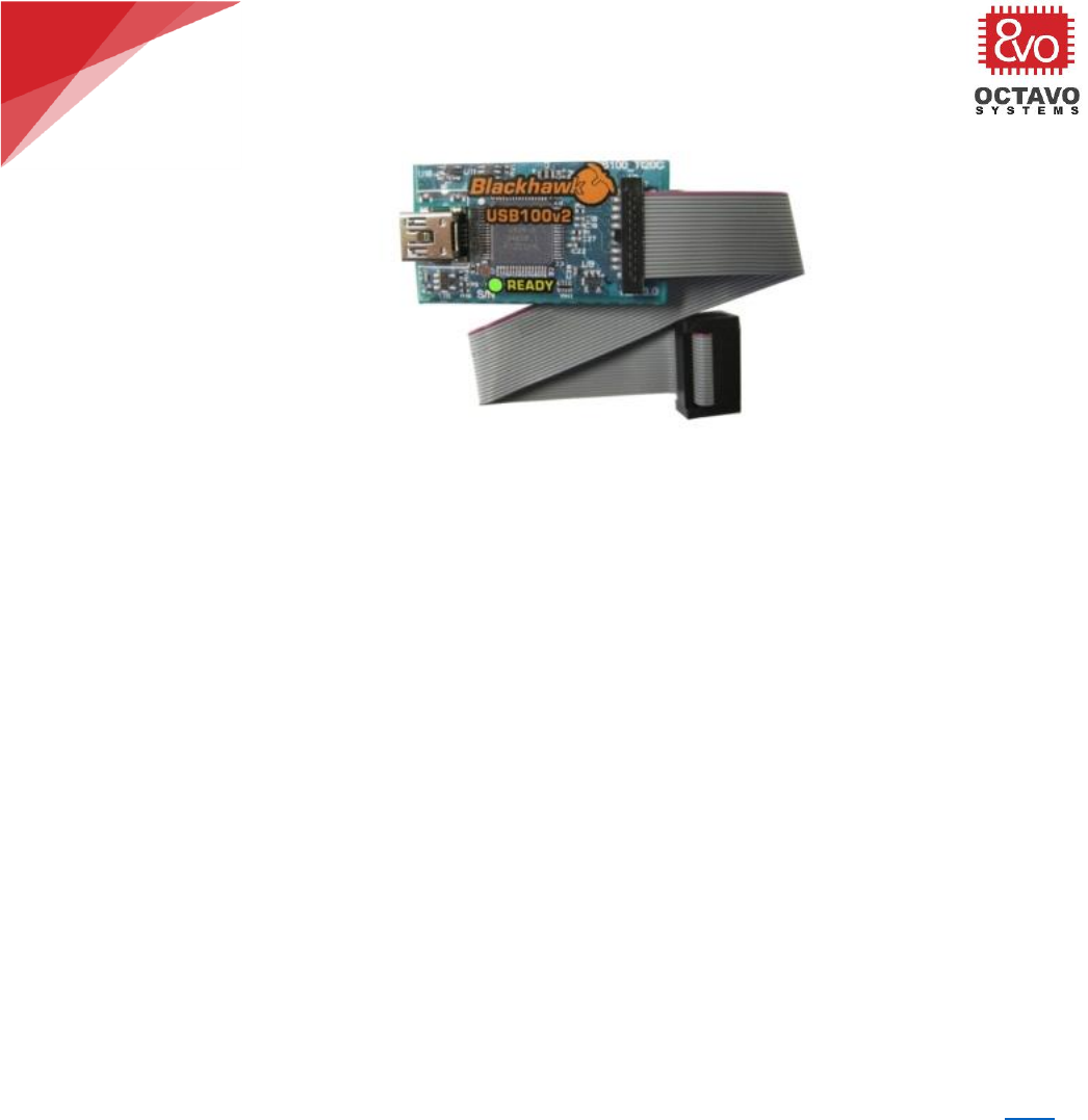
79
OSD335x Tutorial Series
Rev.2 1/2/2018
Octavo Systems LLC
Copyright 2017
Figure 69 XDS100v2 Debugger
11.5 Demo Apps
11.5.1 Demo App 1: LED Dimmer
The objective of this app is to demonstrate the use of the GPIO and EHRPWM
peripherals within the OSD335x.
The Demo App 1 generates a hardware PWM signal on the EHRPWM1A(GPIO1_18) pin
which is connected to LED D2 on the board and a software PWM signal on the
GPIO1_15 pin which is connected to LED D3 on the board. The brightness of each of
these LEDs will be controlled by their respective PWM duty cycles and will be set to
the maximum value (i.e., always on) in the beginning.
The duty cycle of the hardware PWM signal for LED D2 will be controlled by button
BTN1. When the button is first pressed and held, the duty cycle will slowly decrease,
which will cause the LED to dim. This will continue until the minimum duty cycle is
reached, and the LED will be off. If you continue to press the button, the duty cycle
will then increase, which will cause the LED to brighten back up to the maximum duty
cycle. This process repeats itself as long as BTN1 is pressed. The duty cycle of the
software PWM signal for LED D3 will be controlled by button BTN2. The behavior of
the PWM duty cycle controlled by BTN 2 is same as that of BTN1.
All the CCS design files required for Demo App 1 and Demo App 2 can be found here.
11.5.2 Running Demo app 1
o Open CCS.
o Create a new CCS Project (In Project Explorer, right click > New >CCS Project)
o Name the project as RefDesL1Demo1. Configure the project as shown in Figure
70 and hit Finish.
Target: AM3358.
Connection: Texas Instruments XDS100v2 USB Debug probe.
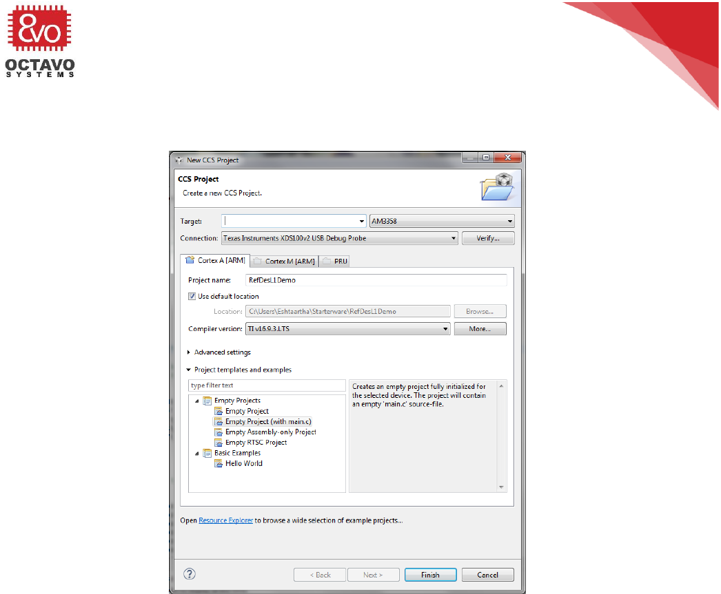
80
OSD335x Tutorial Series
Rev.2 1/2/2018
Octavo Systems LLC
Copyright 2017
Compiler version: TI v16.9.3.LTS or higher.
Project template: Empty Project (with main.c).
Figure 70 Demo App 1 project settings
The compiler will need access to many different Starterware folders and
libraries in order to compile our code. Add the following paths to the ARM
Compiler’s Include Options as shown in Figure 71 (To find Compiler Include
Options, right click on Project Name in Project Explorer > Properties > CCS
Build > ARM Compiler > Include Options. The below paths are given assuming
you have installed Starterware at C:\ti. If not, alter the path suitably):
- C:\ti\AM335X_StarterWare_02_00_01_01\include
- C:\ti\AM335X_StarterWare_02_00_01_01\include\armv7a
- C:\ti\AM335X_StarterWare_02_00_01_01\include\armv7a\am335x
- C:\ti\AM335X_StarterWare_02_00_01_01\include\hw
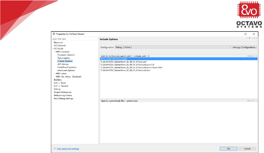
81
OSD335x Tutorial Series
Rev.2 1/2/2018
Octavo Systems LLC
Copyright 2017
Figure 71 Compiler Include Paths
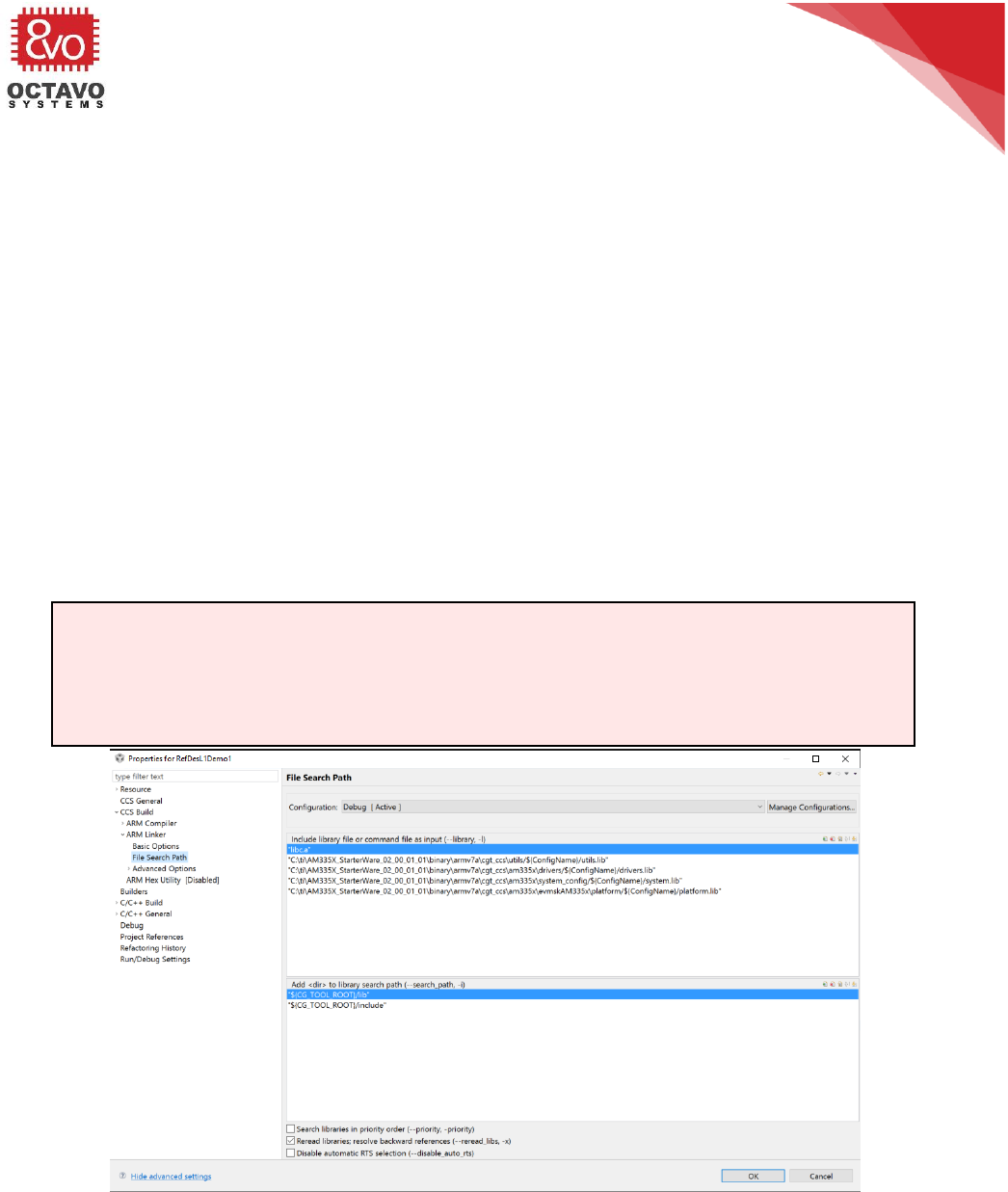
82
OSD335x Tutorial Series
Rev.2 1/2/2018
Octavo Systems LLC
Copyright 2017
The linker will need access to many different Starterware folders and libraries
in order to build our code. Add the following paths to the ARM Linker’s File
Search Path as shown in Figure 72 (To find Linker File Search Path, right click
on Project Name in Project Explorer > Properties > CCS Build > ARM Linker >
File Search Path. The below paths are given assuming you have installed
Starterware at C:\ti.If not, alter the path suitably):
- C:\ti\AM335X_StarterWare_02_00_01_01\binary\armv7a\cgt_ccs\utils/${Con
figName}\utils.lib
- C:\ti\AM335X_StarterWare_02_00_01_01\binary\armv7a\cgt_ccs\am335x\dri
vers/${ConfigName}\drivers.lib
- C:\ti\AM335X_StarterWare_02_00_01_01\binary\armv7a\cgt_ccs\am335x\sys
tem_config/${ConfigName}\system.lib
- C:\ti\AM335X_StarterWare_02_00_01_01\binary\armv7a\cgt_ccs\am335x\ev
mskAM335x\platform/${ConfigName}\platform.lib
Figure 72 Linker Search Paths
Caveat:
Make sure you use forward slash (/) with the project macro ${ConfigName} as
/${ConfigName} in the paths above. Otherwise, CCS will not resolve
${ConfigName} into its value.
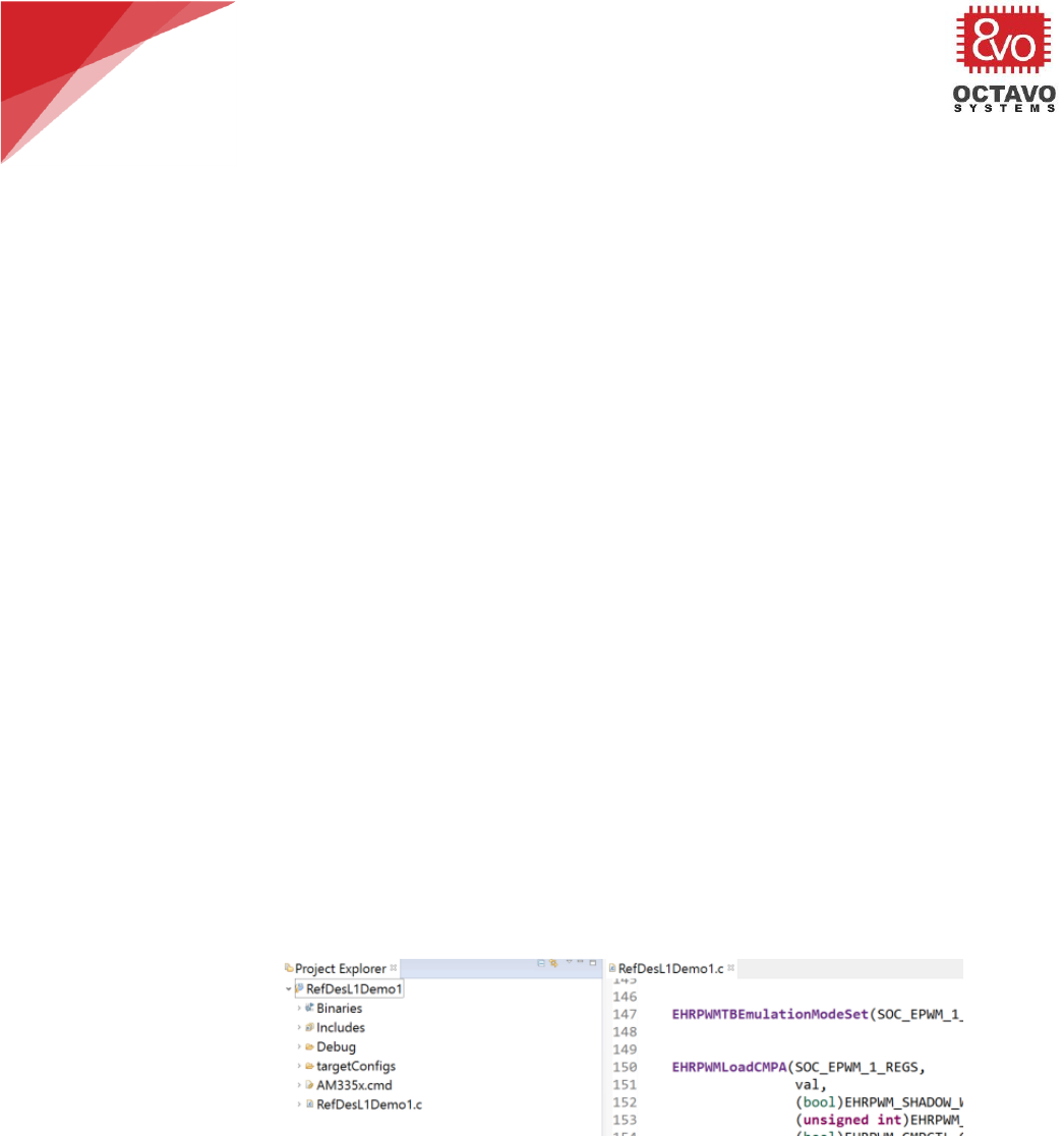
83
OSD335x Tutorial Series
Rev.2 1/2/2018
Octavo Systems LLC
Copyright 2017
o Delete main.c from your project. Download RefDesL1Demo1.c from and add it
to the project.
o The default linker command file, AM335x.cmd and the given startup code file,
init.asm that CCS provides are not suitable for our demo apps because of the
following reasons:
- The default linker command file uses the default startup code which sets
the processor to User Mode before calling main() function. But, the
processor needs to be in Privilege Mode/System Mode to be able to write
to GPIO control module registers for the GPIO or EHRPWM registers as part
of our demo projects.
- The given startup code file, init.asm, is configured to operate using
external DDR3 with 4KB of stack assigned for interrupt requests. While the
DDR3 memory exists in the OSD335x, we do not have the DDR initialization
code in the demo program and therefore need to run the program using only
the AM335x internal memory. Given that we are using internal memory, we
will have to reduce interrupt request stack size to 256B.
To solve the above problems, Octavo Systems provides two files:
AM335x.cmd and init.asm, which make CCS use custom startup code before
calling main() function. The custom startup code sets the processor to
System Mode before calling main() function. It also reduces the interrupt
request stack size to 256B.
Delete the default AM335x.cmd file under your project files and replace it
with the modified AM335x.cmd file (provided as part of CCS design files.
Link given above) as shown in Figure 73.
Figure 73 CCS Project Explorer
Import system_config project from (folder path is given assuming you have
installed Starterware at C:\ti, otherwise adjust the path accordingly):
C:\ti\AM335X_StarterWare_02_00_01_01\build\armv7a\cgt_ccs\am335x
Delete the default init.asm file under this project and replace it with the
modified init.asm file (can be downloaded from the link above) as shown in
Figure 74. Build the project using the build button as shown in Figure 75.
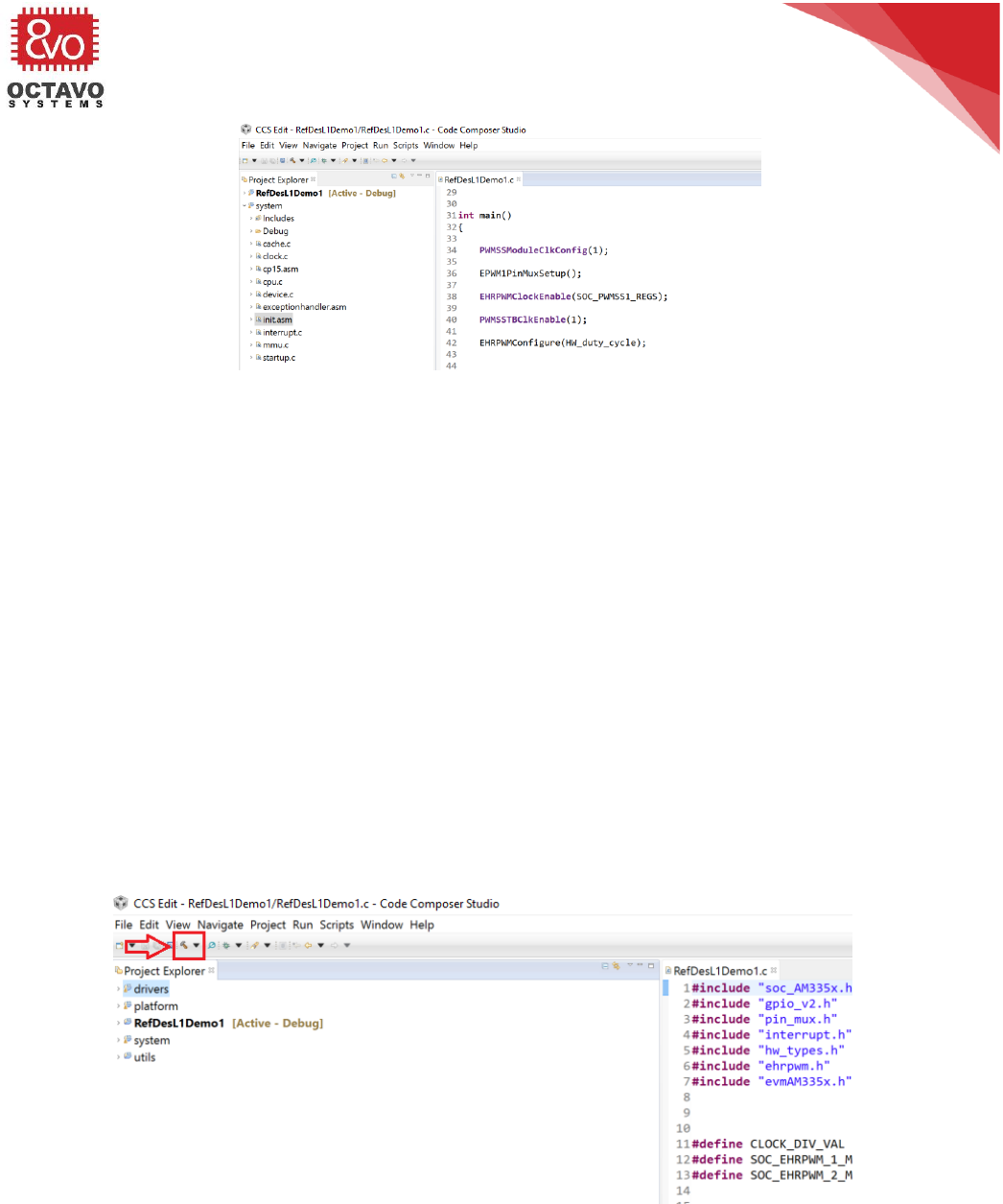
84
OSD335x Tutorial Series
Rev.2 1/2/2018
Octavo Systems LLC
Copyright 2017
Figure 74 Adding custom init.asm file
o Before we can run the demo app, we need to build 3 libraries: utils.lib,
drivers.lib, and platform.lib. We will be using many APIs from these libraries
in our demo apps. To build the libraries, you need to (folder paths are given
assuming you have installed Starterware at C:\ti, otherwise adjust the path
accordingly):
- Import utils project from
C:\ti\AM335X_StarterWare_02_00_01_01\build\armv7a\cgt_ccs
- Import platform project from
C:\ti\AM335X_StarterWare_02_00_01_01\build\armv7a\cgt_ccs\am335x\evm
skAM335x
- Import drivers project from
C:\ti\AM335X_StarterWare_02_00_01_01\build\armv7a\cgt_ccs\am335x
- Build each of the above projects by selecting the project and hitting the
build button as shown in Figure 75.
Figure 75 CCS Build button

85
OSD335x Tutorial Series
Rev.2 1/2/2018
Octavo Systems LLC
Copyright 2017
o Now we are ready to build Demo App 1. Select RefDesL1Demo1 project and
build it. If you have followed all the instructions given above, it should build
without errors.
o Connect the debugger to your computer.
o Connect the 20 pin JTAG connector of the debugger to the JTAG header on the
board.
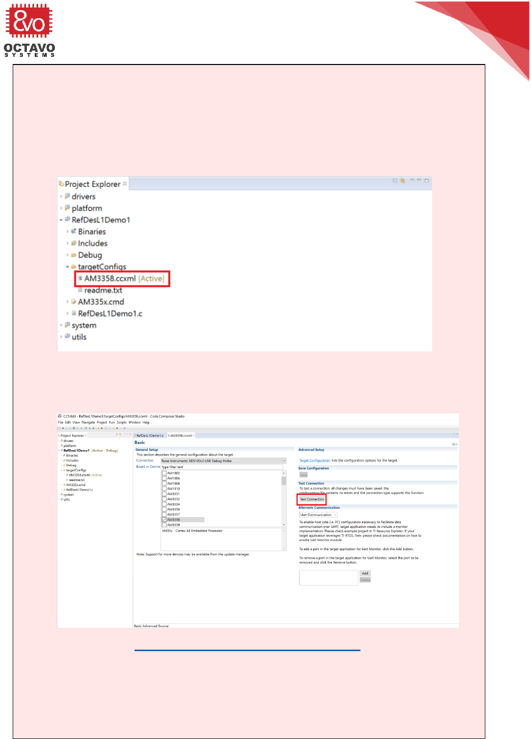
86
OSD335x Tutorial Series
Rev.2 1/2/2018
Octavo Systems LLC
Copyright 2017
o Power up the board.
Caveat:
Before you try to load the demo apps through the JTAG debugger, you need to
make sure the JTAG connection is setup properly and there are no connection
issues. To check the JTAG connection, follow the steps below:
o In the drop down menu of your project folder, open targetConfigs drop
down menu and then open AM3358.ccxml file as shown below.
o Click on Test Connection button to test the JTAG connectivity as shown
below. CCS will perform a series of tests and you should receive the JTAG
DR Integrity scan-test has succeeded message or something similar at the
end of the testing process.
You can use the TI’s Debugging JTAG Connectivity Problems wiki page to resolve
any errors, if any. Probe the clock signals and use an oscilloscope to make sure
OSC0 is operating at 24MHz and OSC1 is operating at 32.768KHz if JTAG
connectivity test fails repeatedly.
You can continue with Demo App debug process once the JTAG connection is
successfully verified.
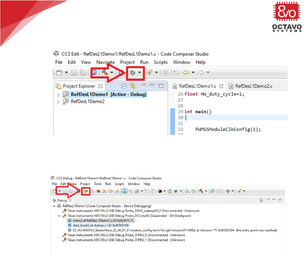
87
OSD335x Tutorial Series
Rev.2 1/2/2018
Octavo Systems LLC
Copyright 2017
o Press the Debug button as shown in Figure 76.
Figure 76 CCS Debug button
o Once the program gets loaded, you should see the below screen (Figure 77). Hit
the Resume button to run the program on the board.
Figure 77 CCS Run button
o Verify the functionality of Demo app 1 by pressing the user buttons BTN1 and
BTN2 and observing the brightness of user LEDs D2 and D3 as shown in Figure
78.

88
OSD335x Tutorial Series
Rev.2 1/2/2018
Octavo Systems LLC
Copyright 2017
Figure 78 Demo App 1 in action
11.5.3 Demo App 2: Motion Detector
The objective of this app is to demonstrate the use of peripheral header with the
OSD335x.
This project uses the MOTION click board
(https://shop.mikroe.com/click/sensors/motion). It can be directly plugged into the
peripheral header. The MOTION click board detects motion of living bodies. It picks up
the IR radiation emitted by living bodies using its PIR sensor. Whenever a motion is
detected, it sends an interrupt to the OSD335x using the INT pin of peripheral header.
The OSD335x detects this interrupt and alternatively blinks LED D2 and LED D3 to
indicate motion detection.
11.5.4 Running Demo app 2
The procedure to run demo app 2 is exactly same as that of demo app 1 except that
you have to use RefDesL1Demo2.c from instead of RefDesL1Demo1.c. Figure 79
shows Demo App 2 in action.
Perk:
Generally, most errors that arise are due to compiler or linker path problems.
Please pay extra attention while setting these paths.
Code Composer Studio does a good job in pointing out errors. Whenever there is an
error, please go through the error message carefully. This will help you isolate the
problem quickly so that it can be fixed.

89
OSD335x Tutorial Series
Rev.2 1/2/2018
Octavo Systems LLC
Copyright 2017
Figure 79 Demo App 2 in action
****
