OV10640_IG_AN OV10640 Implementation Guide AN 1.1 Neusoft
OV10640_Implementation_Guide_AN_1.1_Neusoft
User Manual:
Open the PDF directly: View PDF ![]() .
.
Page Count: 45
- table of contents
- list of figures
- list of tables
- 1 integration time
- 2 gain
- 3 ADC range and minimum gain
- 4 PLL and frame timing
- 5 image format and output
- 5.1 image format
- 5.2 interface and maximum frame rates
- 5.2.1 DVP interface
- table 5-6 maximum frame rates supported via MIPI interface
- figure 5-7 3x12b linear raw output timing
- figure 5-8 2x11b linear raw output timing
- figure 5-9 16b log raw output timing option 1
- figure 5-10 16b log raw output timing option 2
- figure 5-11 20b linear combined raw output timing option 1
- figure 5-12 20b linear combined raw output timing option 2
- figure 5-13 12b PWL combined raw output timing
- 5.2.2 MIPI interface
- 5.2.1 DVP interface
- 6 embedded row
- 7 backend processor ISP consideration
- revision history
application note
IMPLEMENTATION GUIDE
1/2.56 color CMOS 1.3 megapixel (1280 x 1080) high dynamic range (HDR)
high definition (HD) image sensor
OV10640
1

color CMOS 1.3 megapixel (1280x1080) high dynamic range (HDR) high definition image sensor
OV10640
00Copyright © 2015 OmniVision Technologies, Inc. All rights reserved.
This document is provided “as is” with no warranties whatsoever, including any warranty of merchantability,
non-infringement, fitness for any particular purpose, or any warranty otherwise arising out of any proposal, specification,
or sample.
OmniVision Technologies, Inc. and all its affiliates disclaim all liability, including liability for infringement of any proprietary
rights, relating to the use of information in this document. No license, expressed or implied, by estoppel or otherwise, to
any intellectual property rights is granted herein.
The information contained in this document is considered proprietary to OmniVision Technologies, Inc. and all its
affiliates. This information may be distributed to individuals or organizations authorized by OmniVision Technologies, Inc.
to receive said information. Individuals and/or organizations are not allowed to re-distribute said information.
Trademark Information
OmniVision and the OmniVision logo are registered trademarks of OmniVision Technologies, Inc.
All other trademarks used herein are the property of their respective owners.
To learn more about OmniVision Technologies, visit www.ovt.com.
OmniVision Technologies is publicly traded on NASDAQ under the symbol OVTI.
color CMOS 1.3 megapixel (1280x1080) high dynamic range (HDR) high definition image sensor
application note
IMPLEMENTATION GUIDE
version 1.1
april 2015
2

04.22.2015 IMPLEMENTATION GUIDE proprietary to OmniVision Technologies
i
00table of contents
1 integration time 1-1
2 gain 2-1
3 ADC range and minimum gain 3-1
4 PLL and frame timing 4-1
5 image format and output 5-1
5.1 image format 5-1
5.1.1 3x12b linear raw 5-1
5.1.2 2x11b PWL raw 5-1
5.1.3 16b log domain combined raw 5-4
5.1.4 20b linear combined raw 5-7
5.1.5 12b PWL combined raw 5-9
5.2 interface and maximum frame rates 5-10
5.2.1 DVP interface 5-10
5.2.2 MIPI interface 5-14
6 embedded row 6-1
7 backend processor ISP consideration 7-1
7.1 AEC/AGC and dynamic range control 7-1
7.1.1 collect statistics 7-1
7.1.2 calculate exposure and gain 7-1
7.2 AWB 7-2
7.2.1 WB gain of L, S and VS channels 7-2
7.2.2 3x12b or 2x11b format 7-3
7.2.3 combined raw format 7-3
7.3 defect pixel correction 7-4
3

color CMOS 1.3 megapixel (1280x1080) high dynamic range (HDR) high definition image sensor
OV10640
proprietary to OmniVision Technologies IMPLEMENTATION GUIDE version 1.1
4
04.22.2015 IMPLEMENTATION GUIDE proprietary to OmniVision Technologies
iii
00list of figures
figure 1-1 L, S, and VS exposure and readout timing diagram 1-1
figure 3-1 ADC and BLC diagram 3-1
figure 3-2 signal range, ADC range, and minimum gain 3-1
figure 4-1 PLL block diagram 4-1
figure 4-2 frame timing 4-2
figure 4-3 readout area and output image size 4-3
figure 5-1 RAW12 to RAW10 compression curve 5-2
figure 5-2 36b to 22b mapping 5-2
figure 5-3 pseudo color plot of combination weight 5-5
figure 5-4 linear combined data 5-6
figure 5-5 L/S/VS when normalization is ON 5-7
figure 5-6 L/S/VS when normalization is OFF 5-8
figure 5-7 3x12b linear raw output timing 5-11
figure 5-8 2x11b linear raw output timing 5-11
figure 5-9 16b log raw output timing option 1 5-12
figure 5-10 16b log raw output timing option 2 5-12
figure 5-11 20b linear combined raw output timing option 1 5-13
figure 5-12 20b linear combined raw output timing option 2 5-13
figure 5-13 12b PWL combined raw output timing 5-14
figure 5-14 3x12b MIPI output packet diagram 5-14
figure 5-15 2x11b MIPI output packet diagram 5-15
figure 5-16 16b MIPI output packet diagram 5-15
figure 5-17 20b MIPI output packet diagram 5-15
figure 5-18 20b MIPI output packet diagram 5-16
figure 7-1 linear combined data 7-3
5

color CMOS 1.3 megapixel (1280x1080) high dynamic range (HDR) high definition image sensor
OV10640
proprietary to OmniVision Technologies IMPLEMENTATION GUIDE version 1.1
6

04.22.2015 IMPLEMENTATION GUIDE proprietary to OmniVision Technologies
v
00list of tables
table 1-1 exposure time control registers 1-1
table 2-1 exposure time control registers 2-1
table 5-1 3x12b key settings 5-1
table 5-2 2x11b key settings 5-3
table 5-3 16b log raw key settings 5-6
table 5-4 20b linear combined raw key settings 5-8
table 5-5 12b PWL combined raw key settings 5-9
table 5-6 maximum frame rates supported via MIPI interface 5-10
7

color CMOS 1.3 megapixel (1280x1080) high dynamic range (HDR) high definition image sensor
OV10640
proprietary to OmniVision Technologies IMPLEMENTATION GUIDE version 1.1
8
04.22.2015 IMPLEMENTATION GUIDE proprietary to OmniVision Technologies
1-1
1 integration time
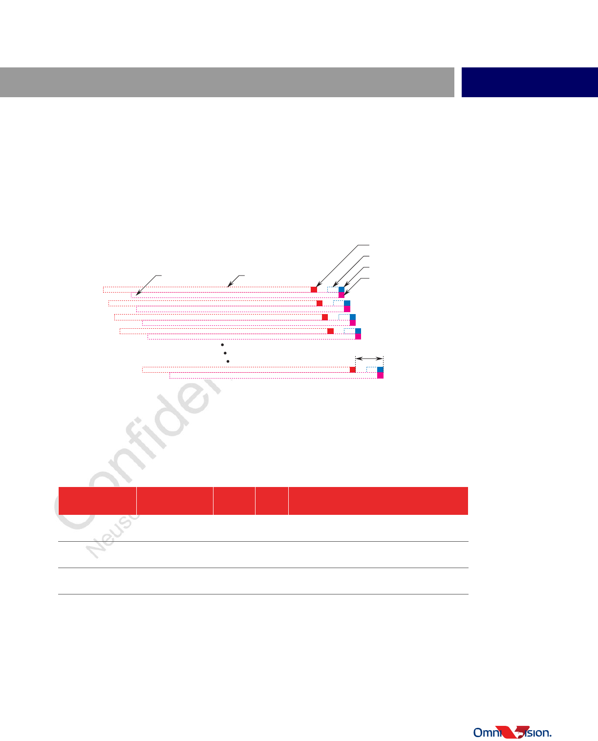
The OV10640 supports quasi-simultaneous captures of long (L) and short (S) integration time using two photodiodes per
pixel, and an optional staggered capture of very short (VS) integration time, as shown in figure 1-1. The readout of L and
S channels is always 4 row periods apart even when the VS capture is not used.
figure 1-1 L, S, and VS exposure and readout timing diagram
The integration time of L and S channels is in unit of row period, and the maximum is VTS -6 where VTS is the frame
period in unit of row period. The precision of the integration time for VS capture is 1/32 row period. The maximum
integration time of the VS channel is 3.95 row periods, the minimum integration time of the VS channel is 0.5 row periods.
table 1-1 lists the integration time control registers of each capture.
table 1-1 exposure time control registers
address
register name
default
value
R/W
description
{0x30E6, 0x30E7} EXPO_L 0x0040 RW Long Channel (L) Exposure Time in Units of
Row Periods
{0x30E8, 0x30E9} EXPO_S 0x0040 RW Short Channel (S) Exposure Time in Units of
Row Periods
0x30EA EXPO_VS 0x20 RW Very Short Channel (VS) Exposure Time in
Units of Row Periods
S integration S readout
VS readout
VS integration
L readout
L integration
4 tROW
10640_IG_1_1
9

color CMOS 1.3 megapixel (1280x1080) high dynamic range (HDR) high definition image sensor
OV10640
proprietary to OmniVision Technologies IMPLEMENTATION GUIDE version 1.1
10
04.22.2015 IMPLEMENTATION GUIDE proprietary to OmniVision Technologies
2-1
2gain
The gain of L, S and VS can be applied independently. The OV10640 supports 1x, 2x, 4x and 8x analog gain, and fine
digital gain. The conversion gain controlled by register 0x30EB[6] (for L) and 0x30EB[7] (for VS) is superior to the
subsequent gain stages because it is applied at the very beginning of the signal path. It should be applied prior to other
gain stages whenever possible. This gain stage is not available for S channel though. table 2-1 summarizes the gain
registers and the formula.
table 2-1 exposure time control registers
address
register name
default
value
R/W
description
0x30EB CG_AGAIN 0x00 RW
Bit[7]: VS channel conversion gain (CG)
0: Low CG
1: High CG
Bit[6]: L channel conversion gain (CG)
0: Low CG
1: High CG
Bit[5:4]: VS channel analog gain, equal to
20x30EB[5:4]
Bit[3:2]: S channel analog gain, equal to
20x30EB[3:2]
Bit[1:0]: L channel analog gain, equal to
20x30EB[1:0]
{0x30EC, 0x30ED} DGAIN_L 0x00100 RW L Channel Digital Gain, equal to
{0x30EC, 0x30ED} / 0x100
{0x30EE, 0x30EF} DGAIN_S 0x00100 RW S Channel Digital Gain, equal to
{0x30EE, 0x30EF} / 0x100
{0x30F0, 0x30F1} DGAIN_VS 0x00100 RW VS Channel Digital Gain, equal to
{0x30F0, 0x30F1} / 0x100
11

color CMOS 1.3 megapixel (1280x1080) high dynamic range (HDR) high definition image sensor
OV10640
proprietary to OmniVision Technologies IMPLEMENTATION GUIDE version 1.1
12
04.22.2015 IMPLEMENTATION GUIDE proprietary to OmniVision Technologies
3-1
3 ADC range and minimum gain
The OV10640 implements a high precision low noise 12-bit ADC per column. The ADC range is maximized to leave room
for dark current, and thus, is greater than pixel full well capacity (FWC), so a minimum gain must be applied to ensure
that bright objects can always saturate and the pixel response is linear before saturation.
As shown in figure 3-1, the optical black pixel value is subtracted from the normal pixel in the black level calibration
(BLC) block to keep black level consistent over temperature.
figure 3-1 ADC and BLC diagram
The black pixel's output value, y_Black, is not always 0 due to dark current. figure 3-2 shows the black pixel value and
the highest value of a normal pixel at different temperature and analog gain. A minimum (digital) gain must be applied
after BLC to compensate the ADC range eaten by dark current.
figure 3-2 signal range, ADC range, and minimum gain
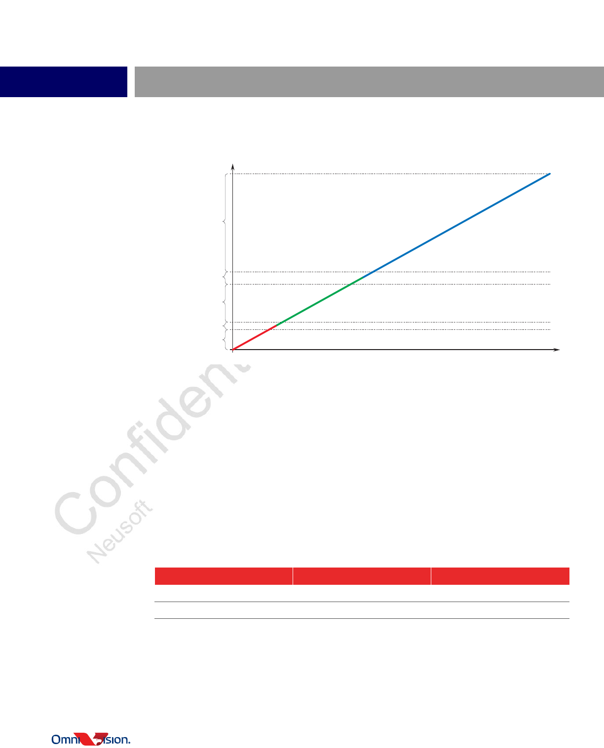
The minimum digital gain to stretch the remaining signal range to full ADC range is:
where CBLC is the black level pedestal, CADC is the ADC pedestal, yBlack is the black pixel output. yBlack is equal to dark
current multiplied by analog gain.
normal
pixel
black
pixel
ADC
analog
gain
BLC
+
-
10640_IG_3_1
1x analog high analog
pixel FWC
ADC range
black pixel
normal pixel
mid temp
high temp
0
212 - 1
low temp
dig gain in
saturation
10640_IG_3_2
g
ain =
_________________________________________________
_
4095 – (y + C )
Black ADC
4095 – C
BLC
dig_min
13

color CMOS 1.3 megapixel (1280x1080) high dynamic range (HDR) high definition image sensor
OV10640
proprietary to OmniVision Technologies IMPLEMENTATION GUIDE version 1.1
where gainana is analog gain and yDark is dark current. Dark current increases exponentially with temperature and linearly
with exposure time. yBlack of L, S and VS channels can be read back from register {0x30D6, 0x30D7}, {0x30D8, 0x30D9}
and {0x30DA, 0x30DB}, respectively.
These registers are unsigned values. However, when yBlack is small, the calculation of yBlack may overflow and result in
a big number (e.g., 0xFFE). In this case, the real yBlack can be calculated by subtracting 4096 from the register value.
For example, 0xFFE means yBlack of -2. The dark current can be read back to distinguish real high yBlack from the
overflowed value. When dark current is small, a big register value means yBlack is negative. The dark current of L, S and
VS channels can be read back from registers {0x30D0, 0x30D1}, {0x30D2, 0x30D3}, and {0x30D4, 0x30D5},
respectively.
The ADC pedestal value, CADC, is also a function of analog gain. Please use following pedestal values to calculate the
minimum digital gain (may change in the final setting). These values include the potential increase of yBlack before the
next gain and exposure adjustment due to temperature change.
With minimum digital gain calculated following the above procedure, the max output of a normal pixel may be still less
than 4095, so extra gain, preferably analog gain, is required. This gain can be calculated by the following formula:
where yWhite is the maximum value of normal pixel at 1x analog gain (i.e., the pixel FWC). For the OV10640, yWhite is 3500
for L and VS, and 1600 for S. Please keep in mind that fractional analog gain is not supported and analog gain must be
1x, 2x, 4x or 8x.
y = gain x y
Black Darkana
y
= register {0x30D6, 0x30D7}
y
= register {0x30D8, 0x30D9}
y
= register {0x30DA, 0x30DB}
Black_L
Black_S
Black_VS
126,
312,
560,
1056,
when gain = 1
when gain = 2
when gain = 4
when gain = 8
ana
ana
ana
ana
ADC
C =
{
g
ain =
_________________________________________________
_
y
x
gain
White dig_min
4095 – C
BLC
extra_min
14

04.22.2015 IMPLEMENTATION GUIDE proprietary to OmniVision Technologies
3-3
In extremely strong illumination (e.g., the Sun or reflection from car body), the pixel reset level will drop quickly before
the correlated double sampling (CDS) can result in a low readout value. This is known as black sun issue. The OV10640
has a built-in anti-Black Sun function. A minimum 1.35x digital gain is required for this circuit to operate properly. If the
minimal digital gain calculated earlier is lower than 1.35x, the minimum gain must be set to 1.35x. Very short channel
has the same minimum gain as long channel and short channel gain is 3x.
15

color CMOS 1.3 megapixel (1280x1080) high dynamic range (HDR) high definition image sensor
OV10640
proprietary to OmniVision Technologies IMPLEMENTATION GUIDE version 1.1
16
04.22.2015 IMPLEMENTATION GUIDE proprietary to OmniVision Technologies
4-1
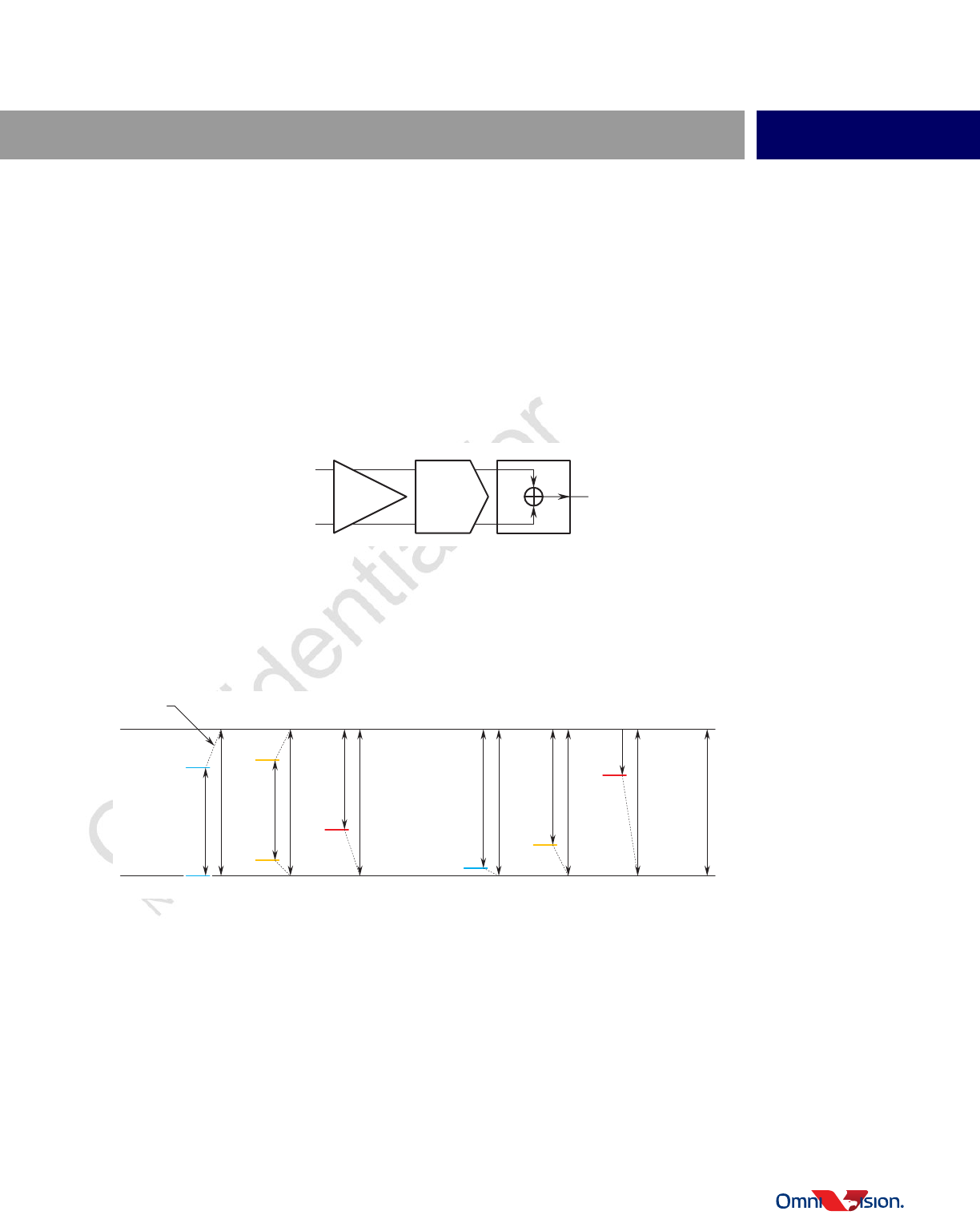
4 PLL and frame timing
The OV10640 implements two phase lock loops (PLLs) to generate clocks. PLL1 generates a system clock for all internal
blocks. PLL2 is used mainly to generate a clock for the output interface. EMC issue is usually related to the interface.
Decoupling the interface clock PLL from the system clock PLL allows adjustment of the interface clock speed while
keeping the frame rate unchanged.
The frequency range of the PLL reference clock is 3~27MHz. The input clock frequency range is 6~27MHz. Though it is
possible to slow down XVCLK to 3MHz with a pre-divider of 1, the maximum SCCB speed decreases with XVCLK, so it is
figure 4-1 PLL block diagram
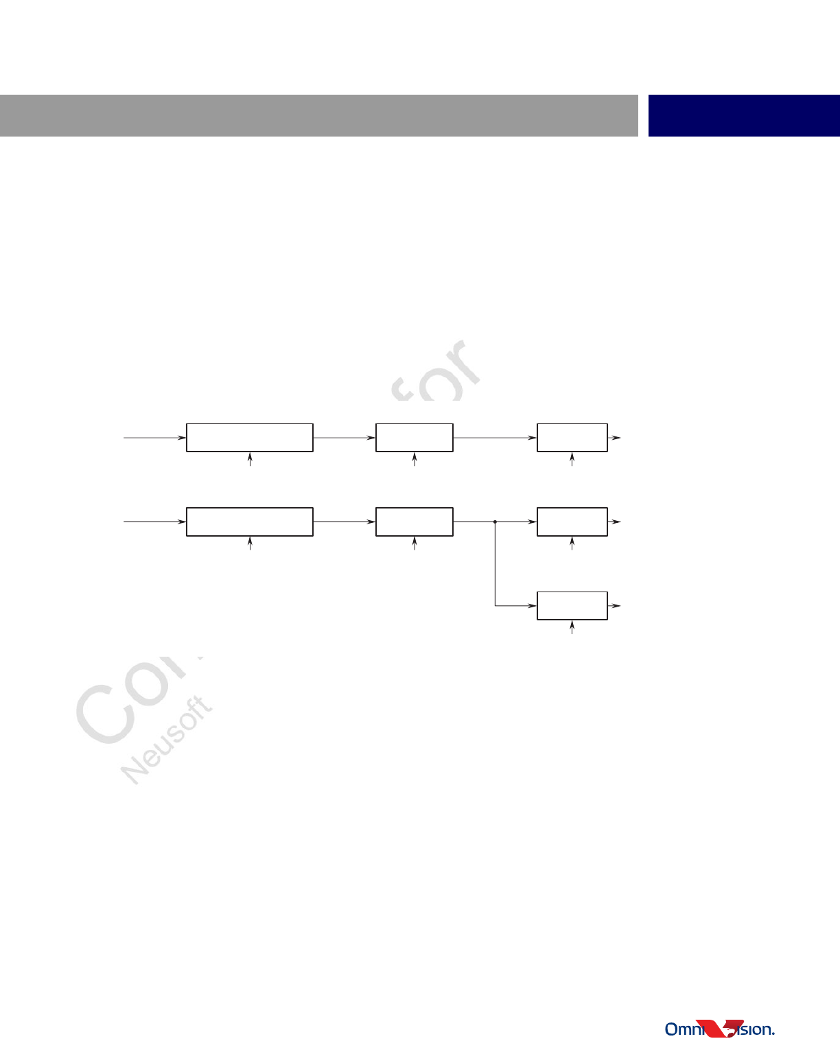
Frame timing is generated from the system clock. The row length (or horizontal total size) is set by registers {0x3080,
0x3081} in unit of system clock period. The frame length (or vertical total size) is set by registers {0x3082, 0x3083} in
unit of row period. The image width and height are set by registers {0x307C, 0x307D} and {0x307E, 0x307F},
respectively. figure 4-2 shows a diagram for frame timing.
pre divider
/1, /1.5, /2, /3, /4, /5, /6, /7
0x3000[2:0]
PLL multiplier
1 to 128
0x3001[7:0]
post divider
1 to 16
0x3002[3:0]
XVLCK
PLL 1
6 ~ 27 MHz 3 ~ 27 MHz 200 ~ 800 MHz SCLK
pre divider
/1, /1.5, /2, /3, /4, /5, /6, /7
0x3004[2:0]
PLL multiplier
1 to 128
0x3005[7:0]
post divider
1 to 16
0x3006[3:0]
XVLCK
note SCLK/PCLK 33 ~ 118 MHz
PLL 2
6 ~ 27 MHz 3 ~ 27 MHz 200 ~ 800 MHz PCLK
MIPI divider
1 or 2
0x3007[1]
MIPI/
LVDS
clock
10640_IG_4_1
17
color CMOS 1.3 megapixel (1280x1080) high dynamic range (HDR) high definition image sensor
OV10640
proprietary to OmniVision Technologies IMPLEMENTATION GUIDE version 1.1
figure 4-2 frame timing
The frame rate can be calculated from the system clock frequency, row length and frame length.
The maximum frame rate is 60 fps at full resolution.
The minimum horizontal blanking period is limited by the read out circuit speed and is dependent on the system clock
period. During vertical blanking period, the sensor needs to finish black level calibration (BLC) etc., so a minimum
number of blanking rows is also required.
To minimize rolling shutter effect, it is recommended to keep the row period at minimum value. The reference setting
provided usually sets the horizontal blanking period to minimum already.
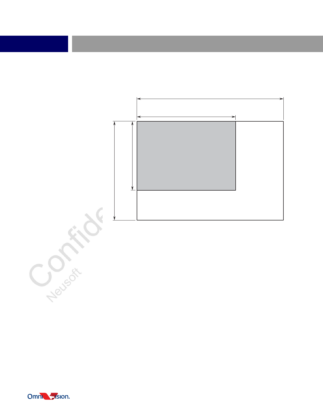
The OV10640 has a pixel array of 1288 columns by 1088 rows. The output window size is programmable from 256 to
1288 columns in steps of 4 (8 in sub-sampling mode), and 20 to 1088 rows in steps of 2 (4 in sub-sampling mode). The
window must start at an even row and column and end at odd row and column. The starting column is set by crop_h_start
(registers {0x3074, 0x3075}), and the starting row is set by crop_v_start (registers {0x3076, 0x3077}). The number of
columns read out is set by crop_h_end - crop_h_start+1 and the number of rows read out is set by crop_v_end -
vertical blanking
horizontal blanking
DVP_output_size
{0x307C, 0x307D}
active image
output period
horizontal_total_size
{0x3080, 0x3081}
DVP_output_size
{0x307E, 0x307F}
vertical_total_size
{0x3082, 0x3083}
10640_IG_4_2
_________________________________________________
_
n x n
row_length_CLK frame_length_row
f
sys_clock_Hz
n =
frame_rate_fps
18
04.22.2015 IMPLEMENTATION GUIDE proprietary to OmniVision Technologies
4-3
crop_v_start +1. The readout window size is usually slightly bigger than the display image size. The extra border pixels
are used by the Image Signal Processor (ISP) and trimmed out before it is output to display.
Refer to the OV10640 Preliminary Specification for additional readout control (e.g., mirror and flip, etc.).
figure 4-3 readout area and output image size
sensor core horizontal size
crop_h_start crop_h_end
horizontal full size: 1288
sensor core vertical size
crop_v_startcrop_v_end
vertical full size: 1088
10640_IG_4_3
19

color CMOS 1.3 megapixel (1280x1080) high dynamic range (HDR) high definition image sensor
OV10640
proprietary to OmniVision Technologies IMPLEMENTATION GUIDE version 1.1
20
04.22.2015 IMPLEMENTATION GUIDE proprietary to OmniVision Technologies
5-1
5 image format and output
5.1 image format
The OV10640 can output Bayer raw data of one exposure channel only through the MIPI interface or pixel interleaved
fashion through the DVP interface, or the raw data combining three exposure channels, or the raw data combining two
exposure channels. The OV10640 does not have line buffers to support line interleaved output (with different virtual
channels. It is always pixel interleaved (MIPI, LVDS, and DVP). The single channel output is not useful for real application
and is only used for some debug purposes.
5.1.1 3x12b linear raw
In this mode, the OV10640 outputs 12-bit L, S and VS channel Bayer raw data. The backend processor can collect the
statistics of each exposure channel and use it to control exposure, gain, white balance, lens shading correction, defect
pixel correction, HDR combination, tone mapping, de-mosaic, color correction, gamma correction, sharpness and
de-noise, etc. Optionally, the sensor can perform defect pixel correction, lens shading correction, and apply white
balance (WB) gain.
table 5-1 shows the settings to set up this format.
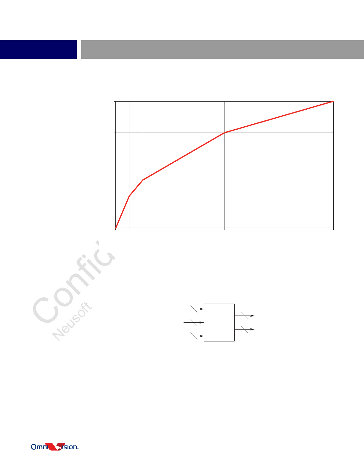
5.1.2 2x11b PWL raw
The ratio from L and VS is usually large. For any pixel, either the L channel data is saturated, or the VS channel data is
nearly black, so there is no need to send out both L and VS channel data. 2x11b format is defined with this in mind to
save output data bandwidth. S is between L and VS, so S is always output together with either L or VS.
In this mode, the L, S and VS channel firstly compressed to 10 bit from 12 bit by a 4-piece piece-wise linear (PWL) curve
defined by following formula and illustrated in figure 5-1.
table 5-1 3x12b key settings
register DVP MIPI
0x3119 0x40 0x50
0x3127[0] 1’b0 1’b0
+ 128,
+ 256,
+ 512,
y < 256
in_12b
y > 2048
in_12b
y ,
in_12b
out_10b
y =
{
y
2
in_12b
256 < y < 512
in_12b
512 < y < 2048
in_12b
8
y
in_12b
4
y
in_12b
21
color CMOS 1.3 megapixel (1280x1080) high dynamic range (HDR) high definition image sensor
OV10640
proprietary to OmniVision Technologies IMPLEMENTATION GUIDE version 1.1
figure 5-1 RAW12 to RAW10 compression curve
To identify whether the data is L or VS, an extra bit is output with the 10-bit data. The mapping of 3x12b to 2x11b is
illustrated in figure 5-2.
figure 5-2 36b to 22b mapping
0
512
256
2048
4096
0
384
256
768
1023
10640_IG_5_1
12
12
12
L
S
11
11
A
32b to 22b
mapping B
VS
10640_IG_5_2
{
A
[9:0] = PWL (L[11:0]),
PWL (VS[11:0]), |A[10] = 0
|A[10] = 1
B
[9:0] = PWL (S[11:0])
B
[10]: reserved
12_10
12_10
12_10
22
04.22.2015 IMPLEMENTATION GUIDE proprietary to OmniVision Technologies
5-3
The backend processor can recover L and VS using following formula:
table 5-2 shows the settings to set up this format. When register bit 0x3119[3] is set to 0, the sensor outputs L channel
data (PWL12_10(L[11:0])) instead of L/VS (A[10:0]).
table 5-2 2x11b key settings
register DVP MIPI
0x3119 0x49 0x59
0x3127[0] 1’b0 1’b0
y ,
2 x (y – 128),
4 x (y – 256),
8 x (y – 512),
y < 256
256 < y < 384
384 < y < 768
y > 768
in_10b
in_10b
in_10b
in_10b
in_10b
in_10b
in_10b
in_10b
out_12b
y =
{
23

color CMOS 1.3 megapixel (1280x1080) high dynamic range (HDR) high definition image sensor
OV10640
proprietary to OmniVision Technologies IMPLEMENTATION GUIDE version 1.1
5.1.3 16b log domain combined raw
The OV10640 can combine L, S and VS channels together and output combined raw. The combination takes place either
between L and S, or between S and VS. The weighting is based on a 2D lookup table defined by registers
0x3136~0x3145. The threshold values at which the weight is defined are programmable by registers 0x3133~0x3155.
There are two options:
• when register bit 0x31BE[0] is 1’b1, the combination occurs on the original 12 bits of data and max threshold should
be 2^12
• when register bit 0x31BE[0] is 1’b0, the combination occurs on the original 10 bits of data (2 LSBs are lost) and max
threshold should be 2^10
The following is the formula for the threshold and weight:
L
w (0, 0) = reg 0x3136/0x80
SL
w (0, 0) = 1 – w
L_Thre0L
w (y , 0) = reg 0x3137/0x80
reg 0x3133[7:4]+2
L_Thre0
y = 2
reg 0x3134[7:4]+2
L_Thre1
y = 2
reg 0x3135[7:4]+2
L_Thre2
y = 2
reg 0x3133[3:0]+2
L_Thre0
y = 2
reg 0x3134[3:0]+2
L_Thre1
y = 2
reg 0x3135[3:0]+2
L_Thre2
y = 2
w (y , 0) = reg 0x3138/0x80
L_Thre1L
w (y , 0) = reg 0x3139/0x80
L_Thre2L
w (0, y ) = reg 0x3139/0x80
S_Thre0L
w (0, y ) = reg 0x313E/0x80
S_Thre1L
w (0, y ) = reg 0x3142/0x80
S_Thre2L
w (y , y ) = reg 0x313B/0x80
S_Thre0L_Thre0L
w (y , y ) = reg 0x313C/0x80
S_Thre0L_Thre1L
w (y , y ) = reg 0x313D/0x80
S_Thre0L_Thre2L
w (y , y ) = reg 0x313F/0x80
S_Thre1L_Thre0L
w (y , y ) = reg 0x3140/0x80
S_Thre1L_Thre1L
w (y , y ) = reg 0x3141/0x80
S_Thre1L_Thre2L
w (y , y ) = reg 0x3143/0x80
S_Thre2L_Thre0L
w (y , y ) = reg 0x3144/0x80
S_Thre2L_Thre1L
w (y , y ) = reg 0x3145/0x80
S_Thre2L_Thre2L
24
04.22.2015 IMPLEMENTATION GUIDE proprietary to OmniVision Technologies
5-5
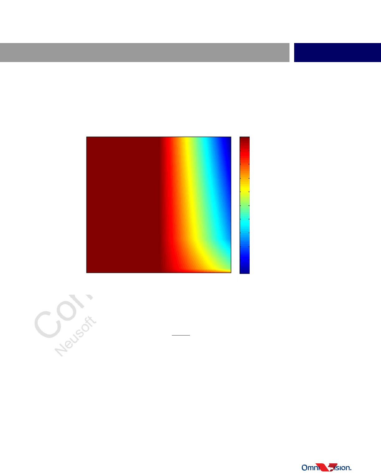
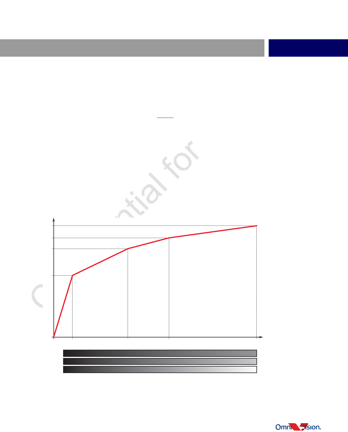
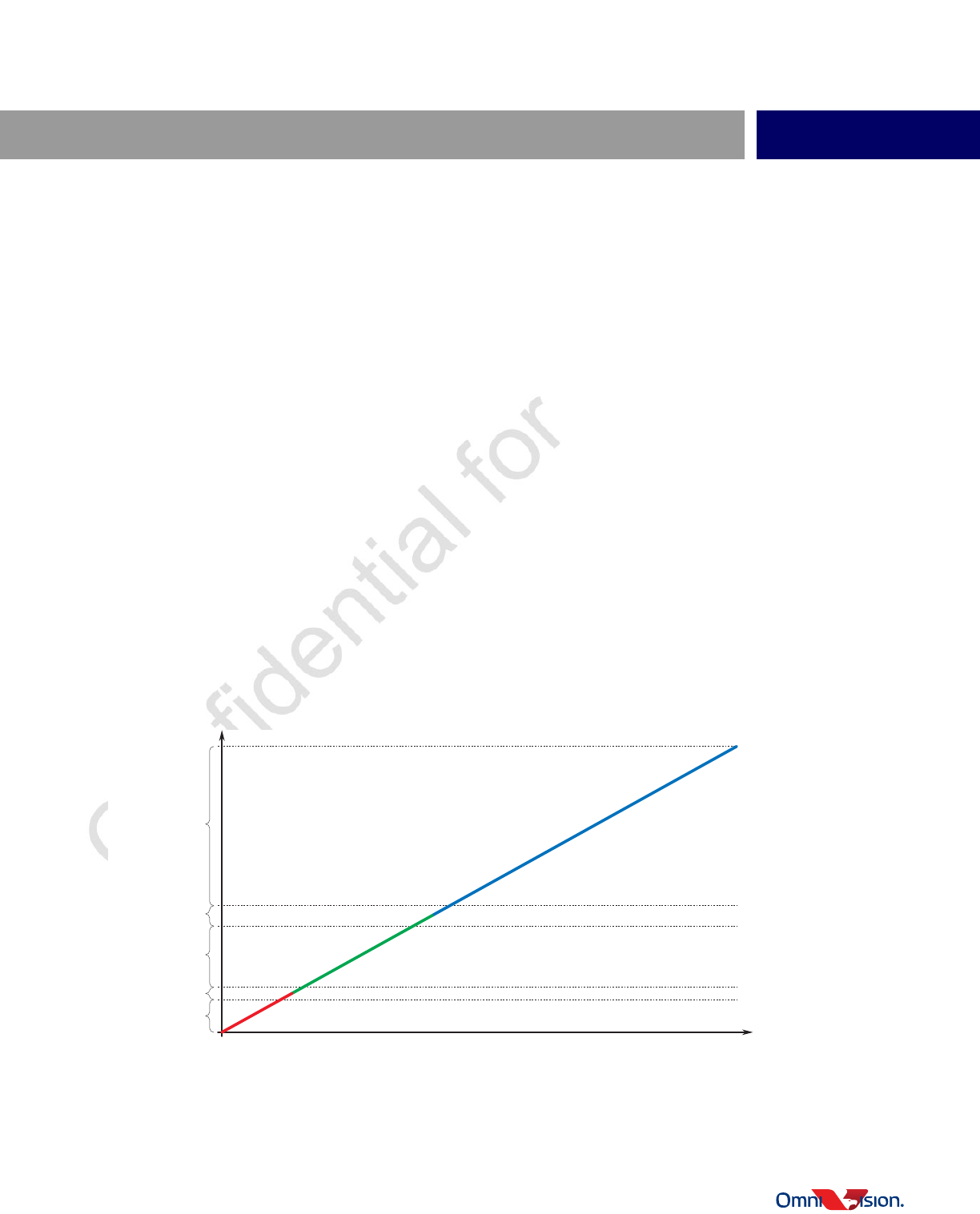
figure 5-3 illustrates the default combination weight. The same lookup table is used for L/S combination and S/VS
combination. The horizontal and vertical axis of the drawing is the maximum color component of the long and short
exposure channels of each pixel.
figure 5-3 pseudo color plot of combination weight
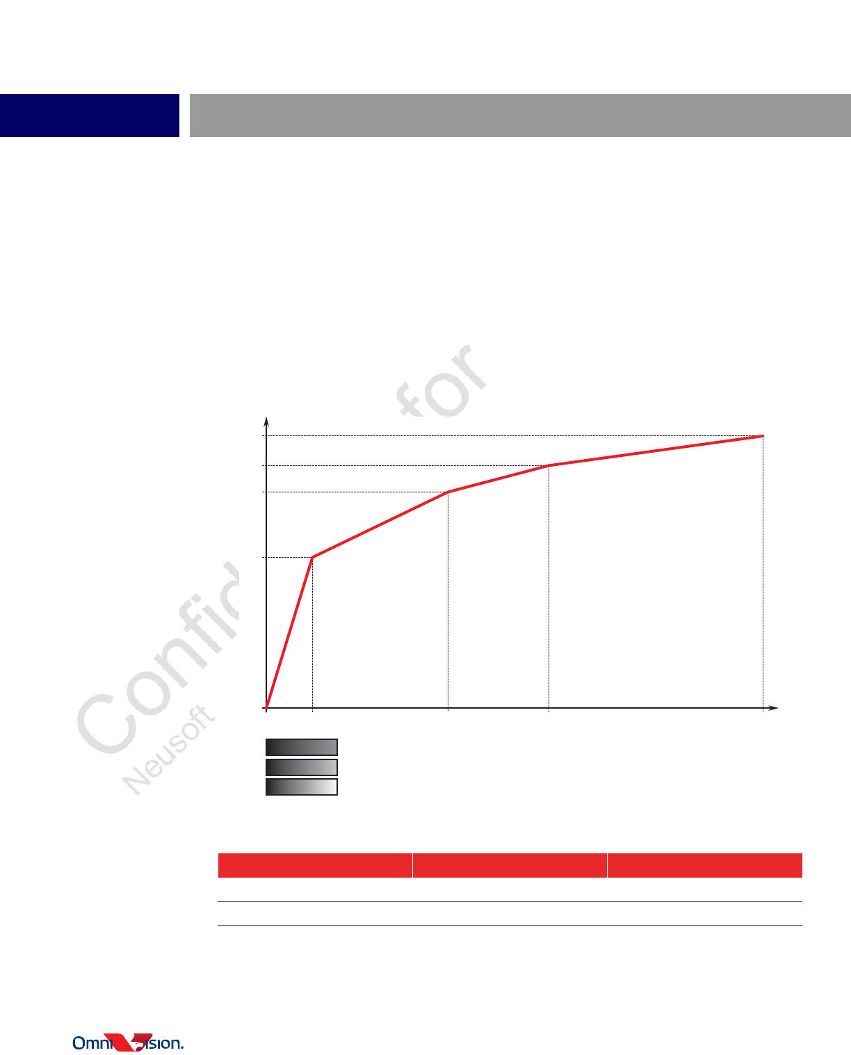
The image combination is done in log domain and the sensor can output the 16-bit combined raw data. The formula to
convert the data back to linear domain is:
This 16-bit data is not normalized, meaning the maximum value is dependent on the exposure ratio between L and VS.
The exposure ratio has to be limited in order to limit the bit depth of linear data converted from this combined data.
The statistics of L, S and VS channels, which is useful for AEC/AGC/AWB, cannot be simply taken from the log raw data.
After converting it back to linear data, it is possible to collect the statistics of L, S and VS channels between the
combination knee points since the backend processor knows the exposure ratio (and thus, the knee points), as shown
in figure 5-4. Because the combination weight is based on the maximum color component of each pixel, the data range
of each exposure channel shown in this diagram is not true for every pixel, so the statistics are not very accurate, but
should be reasonably good for AEC/AGC/AWB control after excluding the values around the knee points.
1
0.9
0.8
0.7
0.6
0.5
0.4
0.3
0.2
0.1
0
0
0
yS_Thre0
2048
yS_Thre1
4095
yS_Thre2
4095
yL_Thre2
4095
yL_Thre0
(32)
yL_Thre1
(256)
yS (or yVS)
yL (or yS)
Linear_20b
y = 2 + 1
y
2048
Log_16b
25
color CMOS 1.3 megapixel (1280x1080) high dynamic range (HDR) high definition image sensor
OV10640
proprietary to OmniVision Technologies IMPLEMENTATION GUIDE version 1.1
figure 5-4 linear combined data
The combined 16-bit log raw contains all the information and requires a lower bandwidth than 3x12b and 2x11b.
However, it requires a pixel-wise calculation to convert it back to linear data.
Any processing applied on an individual exposure channel (e.g., the compensation on S channel to match the spectral
response with L and VS) can be done only before the combination in sensor only. For example, the sensor can apply a
pre-WB gain and a pre-color correction matrix (CCM) on S channel before the combination to compensate the spectral
difference between S and L/VS channels. Applying a pre-WB gain on S channel is done because its blue channel
response is relatively stronger than its red channel response as compared to L and VS channels. The pre-CCM is done
to further match the S channel color to L and VS channels. Because pre-CCM must be applied on white balanced data,
it is not possible to apply it when the white balance gain is applied in the backend processor. The pre-CCM is usually
close to the unit matrix. It is recommended for the customer to evaluate whether the color without this correction is
acceptable.
table 5-3 16b log raw key settings
register DVP MIPI
0x3119 0x43 0x53
0x3127[0] 1’b1 1’b1
illumination
VS
βS + (1-β)VS
S
αL + (1-α)S
L
combined data
10640_IG_5_4
26
04.22.2015 IMPLEMENTATION GUIDE proprietary to OmniVision Technologies
5-7
5.1.4 20b linear combined raw
The sensor can also convert the 16-bit log raw to 20-bit linear raw. This requires a higher bandwidth, but eliminates the
need for conversion in the backend processor. The formula of the conversion is as shown below:
All other limitations of the 16b log raw apply to 20b linear raw as well. When converting data from 16 bits log to 20 bits
linear, please pay attention to the normalization feature. After combination, there is an option which can normalize the
data or not. If enabled, normalization (register bit 0x328A[1] = 1’b0), 20b linear raw data is MSB aligned; else, it is LSB
aligned. If normalization is off, there is data overflow when the total ratio is larger than 1024x (register bit 0x31BE[0] is
1’b0) or 256x (register bit 0x31BE[0] is 1’b1).
5.1.4.1 normalization ON
Suppose L/S/VS ratio is 1, L=S=VS. So, valid combination data only occupies the lower 12 bits in 20b linear raw
range. After PWL, L, S, and VS saturation levels do not change and are always 4095.
figure 5-5 L/S/VS when normalization is ON
Linear_20b
y = 2 + 1
y
2048
Log_16b
211 214 216 220
27
212
long
short
very short
10640_IG_5_5
27
color CMOS 1.3 megapixel (1280x1080) high dynamic range (HDR) high definition image sensor
OV10640
proprietary to OmniVision Technologies IMPLEMENTATION GUIDE version 1.1
There is a difference between how the OV10640 (rev 1D) sensor and OV10640 (rev 1E) sensor handles
normalization. For the OV10640 (rev 1D) sensor, the user should manually set the max log value (registers {0x31BF,
0x31C0}, such as a value of 20480 + (L/VS-1) * 2048. If the user does not want to set the max log value manually,
the user can set it as 0x9FFF and the sensor will always output 20 bits of data which will be LSB aligned. For the
OV10640 (rev 1E) sensor, the sensor can automatically update the max log value if the auto calculation feature is
set (register bit 0x328A[4] = 1’b1 and register bit 0x328A[0] = 1’b0).
5.1.4.2 normalization OFF
Suppose L/S/VS ratio is 1, L=S=VS. So, valid combined data only occupies the lower 12 bits in 20b linear raw range.
After PWL, L, S, and VS saturation levels change from 4095 to 640.
figure 5-6 L/S/VS when normalization is OFF
table 5-4 20b linear combined raw key settings
register DVP MIPI
0x3119 0x42 0x52
0x3127[0] 1’b1 1’b1
211 214 216 220
27
212
long
short
very short 10640_IG_5_6
28
04.22.2015 IMPLEMENTATION GUIDE proprietary to OmniVision Technologies
5-9
5.1.5 12b PWL combined raw
To save bandwidth, the 20-bit linear raw can be compressed to 12-bit by a 4-piece PWL curve as shown below:
The 12-bit raw can be converted back to 20-bit raw using following formula in the backend processor.
table 5-5 shows the settings to set up this format.
table 5-5 12b PWL combined raw key settings
register DVP MIPI
0x3119 0x44 0x54
0x3127[0] 1’b1 1’b1
+ 384,
,
+ 1152,
+ 2048,
y < 2048
in_12b
y > 65536
in_12b
out_12b
y =
{
y
16
in_20b
y
4
in_20b
2048 < y < 16384
in_12b
16384 < y < 65536
in_12b
512
y
in_20b
64
y
in_20b
4 x y ,
16 x (y – 384),
64 x (y – 1152),
512 x (y – 2048),
y < 512
512 < y < 1408
1408 < y < 2176
y > 2176
in_12b
in_12b
in_12b
in_12b
in_12b
in_12b
in_12b
in_12b
out_12b
y =
{
29
color CMOS 1.3 megapixel (1280x1080) high dynamic range (HDR) high definition image sensor
OV10640
proprietary to OmniVision Technologies IMPLEMENTATION GUIDE version 1.1
5.2 interface and maximum frame rates
The OV10640 can output all image formats via the digital video port (DVP) and the mobile industry processor interface
(MIPI).
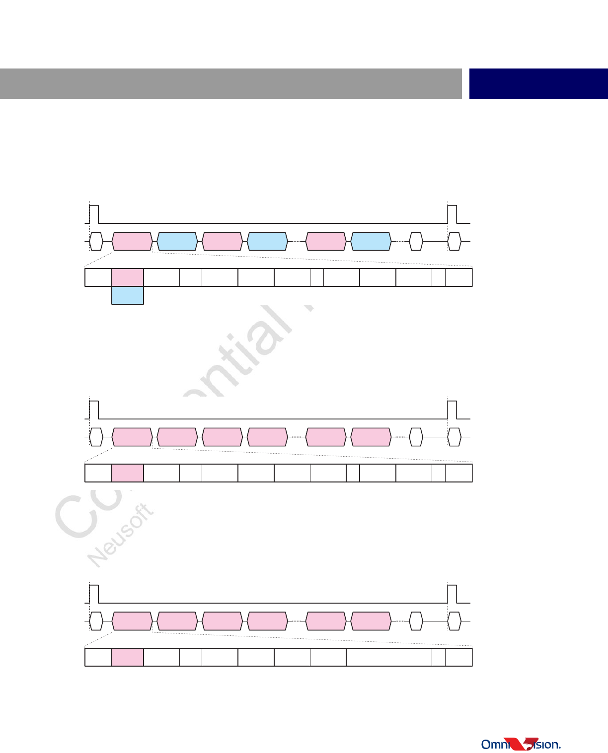
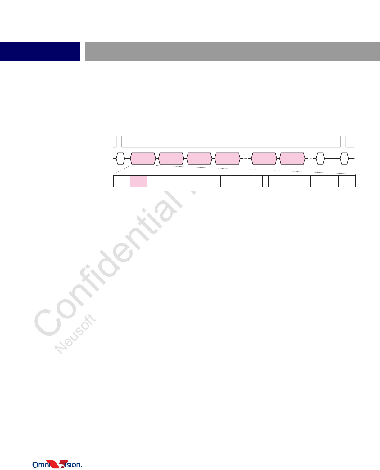
5.2.1 DVP interface
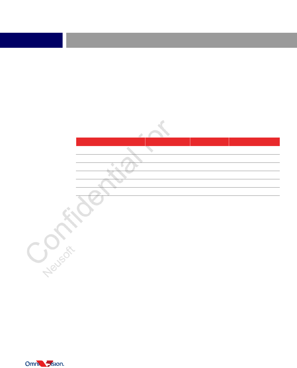
The OV10640 DVP bus is 12-bit wide and the pixel clock can run up to 118 MHz. This bandwidth limits the maximum
frame rate of each format. table 5-6 lists the maximum frame rate that can be achieved via DVP interface.
In DVP mode, the video stream outputs in pixel-interleaving fashion. figure 5-7 ~ figure 5-13 show the output timing of
3x12b, 2x11b, 16b, 20b and 12b, respectively.
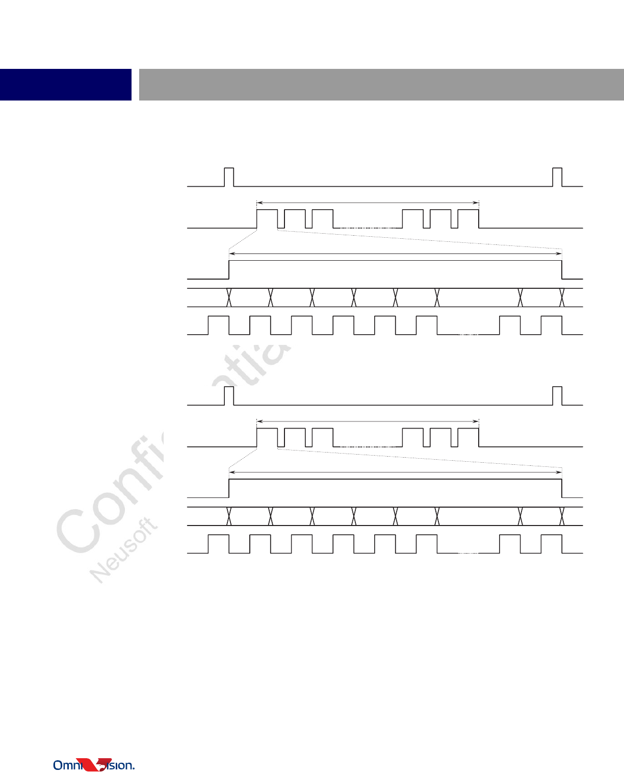
For 16b data format, timing option 1 enables transmitting 16-bit data through the eight most significant data lines. With
timing option 2, the 12 most significant bits are transmitted in the first clock cycle and the rest of the bits are transferred
in the second clock cycle, which requires specific data packing in the backend processor. Similarly, two options are
provided for 20b data format. These options are selected by register bit 0x3123[3], where a value of 0 means option 1
and a value of 1 means option 2.
table 5-6 maximum frame rates supported via MIPI interface
format resolution PCLK max frame rate
3x12b linear raw 1288 x 1088 100 Mbpsa
a. 5 pF maximum loading
22 fps
3x12b linear raw 1288 x 968 118 Mbpsb
b. 20 pF maximum loading
30 fps
2x11b PWL raw 1288 x 1088 100 Mbps 30 fps
16b log combined raw 1288 x 1088 100 Mbps 30 fps
20b linear combined raw 1288 x 1088 100 Mbps 30 fps
12 PWL combined raw 1288 x 1088 100 Mbps 30 fps
30

04.22.2015 IMPLEMENTATION GUIDE proprietary to OmniVision Technologies
5-11
figure 5-7 3x12b linear raw output timing
figure 5-8 2x11b linear raw output timing
VSYNC
HREF
HREF
D[11:0]
PCLK
height
3x width
PwidthL[11:0]P2L[11:0] ...
P2VS[11:0]P2S[11:0]P1L[11:0]P1VS[11:0]P1S[11:0]
10640_IG_5_7
VSYNC
HREF
HREF
D[10:0]
PCLK
height
2x width
P
width
L_VS[10:0]
P3L_VS[10:0] ...
P3S[10:0]P2L_VS[10:0]P2S[10:0]P1L_VS[10:0]P1S[10:0]
10640_IG_5_8
31
color CMOS 1.3 megapixel (1280x1080) high dynamic range (HDR) high definition image sensor
OV10640
proprietary to OmniVision Technologies IMPLEMENTATION GUIDE version 1.1
figure 5-9 16b log raw output timing option 1
figure 5-10 16b log raw output timing option 2
VSYNC
HREF
HREF
D[11:0]
PCLK
height
2x width
{Pwidth[7:0],
Pwidth[3:0]}
{P3[7:0],
P3[3:0]} ...
{P3[15:8],
P3[7:4]}
{P2[7:0],
P2[3:0]}
{P2[15:8],
P2[7:4]}
{P1[7:0],
P1[3:0]}
{P1[15:8],
P1[7:4]}
10640_IG_5_9
VSYNC
HREF
HREF
D[11:0]
PCLK
height
2x width
{Pwidth[3:0],
Pwidth[7:0]}
{P3[3:0],
P3[7:0]} ...
P3[15:4]
{P2[3:0],
P2[7:0]}
P2[15:4]
{P1[3:0],
P1[7:0]}
P1[15:4]
10640_IG_5_10
32
04.22.2015 IMPLEMENTATION GUIDE proprietary to OmniVision Technologies
5-13
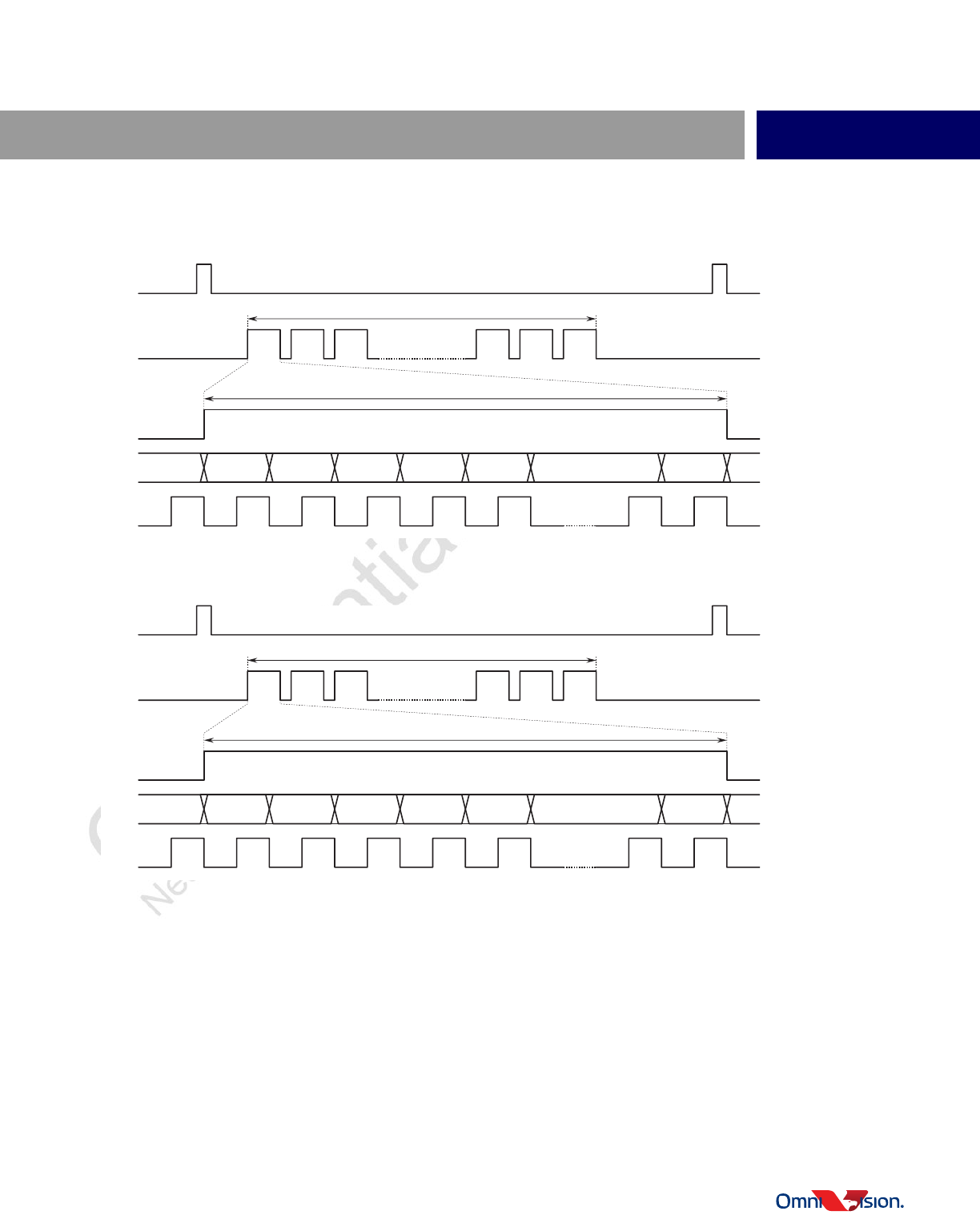
figure 5-11 20b linear combined raw output timing option 1
figure 5-12 20b linear combined raw output timing option 2
VSYNC
HREF
HREF
D[11:0]
PCLK
height
2x width
{Pwidth[9:0],
2'bxx}
{P3[9:0],
2'bxx} ...
{P3[19:10],
P3[9:8]}
{P2[9:0],
2'bxx}
{P2[19:10],
P2[9:8]}
{P1[9:0],
2'bxx}
{P1[19:10],
P1[9:8]}
10640_IG_5_11
VSYNC
HREF
HREF
D[11:0]
PCLK
height
2x width
{Pwidth[7:0],
4'bxxxx}
{P3[7:0],
4'bxxxx} ...
P3[19:8]
{P2[7:0],
4'bxxxx}
P2[19:8]
{P1[7:0],
4'bxxxx}
P1[19:8]
10640_IG_5_12
33
color CMOS 1.3 megapixel (1280x1080) high dynamic range (HDR) high definition image sensor
OV10640
proprietary to OmniVision Technologies IMPLEMENTATION GUIDE version 1.1
figure 5-13 12b PWL combined raw output timing
5.2.2 MIPI interface
The OV10640 supports up to four data lanes. The maximum data rate is 800 Mbps per lane and the total bandwidth is
about 3.2Gbps, which is enough to output full resolution at 60 fps for any data format.
In MIPI mode, L, S and VS are sent out via different virtual channels, so they are output in line-interleaving fashion.
5.2.2.1 3x12b linear raw format
L, S and VS are sent out via virtual channel 0, 1 and 2, respectively. For each exposure channel, every 2 pixels are
packed into 3 bytes. figure 5-14 illustrates the MIPI output packet.
figure 5-14 3x12b MIPI output packet diagram
VSYNC
HREF
HREF
D[11:0]
PCLK
height
width
Pwidth[11:0]P6[11:0] ...
P5[11:0]P4[11:0]P3[11:0]P2[11:0]P1[11:0]
10640_IG_5_13
VSYNC
MIPI row 0
long
row 0
short
row 0
VS
row n
long
row n
short
row n
VS FE FSFS
sync
8'hB8
data ID
8'h2C
WC
1.5x width ECC P1[11:4] P2[11:4] {P2[3:0],
P1[3:0]} ... ...
Pn[11:4] Pn+1[11:4] {Pn[3:0],
Pn+1[3:0]}
packet
footer
data ID
8'h6C
data ID
8'hAC 10640_IG_5_14
34
04.22.2015 IMPLEMENTATION GUIDE proprietary to OmniVision Technologies
5-15
5.2.2.2 2x11b PWL raw format
The 11b data is extended to 12b with MSB set to 0 and then sent out following CSI-2 raw12 format.
figure 5-15 2x11b MIPI output packet diagram
5.2.2.3 16b log combined raw format
16b log combined raw is sent out following CSI-2 raw8 format. Every pixel is packed into 2 bytes. figure 5-16
illustrates the MIPI output packet.
figure 5-16 16b MIPI output packet diagram
5.2.2.4 20b linear combined raw format
20b linear combined raw is sent out following CSI-2 raw 10 format. Every 2 pixels are packed into 5 bytes.
figure 5-17 illustrates the MIPI output packet.
figure 5-17 20b MIPI output packet diagram
VSYNC
MIPI row 0
long or VS
row 0
short
row 1
long or VS
row 1
short
row n
long or VS
row n
short FE FSFS
sync
8'hB8
data ID
8'h2C
WC
1.5x width ECC {0,
P1[10:4]}
{0,
P2[11:4]}
{P2[3:0],
P1[3:0]} ... ...
{0,
Pn[11:4]}
{0,
Pn+1[11:4]}
{Pn[3:0],
Pn+1[3:0]}
packet
footer
data ID
8'h6C 10640_IG_5_15
VSYNC
MIPI row 0 row 1 row 2 row 3 row n row n+1 FE FSFS
sync
8'hB8
data ID
8'h2A
WC
2x width ECC P1[15:8] P1[7:0] P2[15:8] ... ...
P2[7:0] Pn[15:8] Pn[7:0] packet
footer
10640_IG_5_16
VSYNC
MIPI row 0 row 1 row 2 row 3 row n row n+1 FE FSFS
sync
8'hB8
data ID
8'h2B
WC
2.5x width ECC P1[19:12] P1[9:2] P2[19:12] ...
P2[9:2] {P2[1:0], P2[11:10],
P1[1:0], P1[11:10]}
packet
footer
10640_IG_5_17
35
color CMOS 1.3 megapixel (1280x1080) high dynamic range (HDR) high definition image sensor
OV10640
proprietary to OmniVision Technologies IMPLEMENTATION GUIDE version 1.1
5.2.2.5 12b PWL combined raw format
20b linear combined raw is sent out following CSI-2 raw 10 format. Every 2 pixels are packed into 5 bytes.
figure 5-18 illustrates the MIPI output packet.
figure 5-18 20b MIPI output packet diagram
VSYNC
MIPI row 0 row 1 row 2 row 3 row n row n+1 FE FSFS
sync
8'hB8
data ID
8'h2C
WC
1.5x width ECC P1[11:4] P2[11:4] P2[19:12] ......
{P2[3:0],
P1[3:0]} Pn[11:4] Pn+1[11:4] {Pn[3:0],
Pn+1[3:0]}
packet
footer
10640_IG_5_18
36

04.22.2015 IMPLEMENTATION GUIDE proprietary to OmniVision Technologies
6-1
6 embedded row
Embedded row is used to send register values and internal statistics to the backend processor. It is strongly
recommended for the backend processor to get the information from the sensor through an embedded row instead of
the SCCB. When the OV10640 interfaces with the backend processor via a pair of SerDes and LVDS links, the SCCB is
supported by the LVDS link back channel, so it is slower to read registers through the SCCB. The other benefit is that
the information is synchronous with the video frame, which is very critical for any control loop (e.g., AEC/AGC).
The OV10640 can output four embedded rows - two top rows before video frame and two bottom rows after video frame.
The top embedded rows are enabled by register bit 0x3091[2], and the bottom rows are enabled by register bit 0x3091[3].
The top embedded rows are usually used to transfer information known before the video frame (e.g., the exposure, gain,
black row average, image size, etc.). The bottom embedded rows are usually used to transfer statistic information which
is available only after the video frame finishes.
The register list of each embedded row is programmable by specifying the start and end address of the registers. The
OV10640 register address is continuous to allow easy programming of embedded rows. The following is an example.
; Top embedded rows register address range
60 3030 30 ; start address is 0x3000
60 3031 00
60 3032 35 ; end register address is 0x3500
60 3033 00
; Bottom embedded rows register address range
60 3034 40 ; start address is 0x4000
60 3035 00
60 3036 42 ; end register address is 0x4200
60 3037 00
Each register value is tagged by 0xDA. The register value and tag are MSB aligned in 10-bit (used for in MIPI interface
for 20b format) or 12-bit data format. In 2x11b and 3x12b image format, the register value with its tag is repeated two
and three times, respectively, as if each register is a pixel.
37

color CMOS 1.3 megapixel (1280x1080) high dynamic range (HDR) high definition image sensor
OV10640
proprietary to OmniVision Technologies IMPLEMENTATION GUIDE version 1.1
38

04.22.2015 IMPLEMENTATION GUIDE proprietary to OmniVision Technologies
7-1
7 backend processor ISP consideration
7.1 AEC/AGC and dynamic range control
The OV10640 extends the dynamic range by the ratio of exposure between captures, so exposure control of each
capture is the key for dynamic range. It is highly recommended to adjust the exposure of each capture based on the
histogram of three captures together. Simple average-based AEC/AGC will not cover the scene dynamic range very well
in some cases.
7.1.1 collect statistics
3x12b is the format without any information loss so the backend processor can collect the statistics data it requires to
control the exposure and gain. The drawback is that the bandwidth requirement is high, so the MIPI interface is
recommended. For the DVP interface, the maximum frame rate of 3x12b is 30fps at a resolution of 1280x960.
If interface bandwidth is the bottleneck of the system, the second recommended format is 2x11b format. The bandwidth
requirement of 2x11b is 1/3 less than 3x12b format. Though some information is lost in 2x11b compression, the loss is
below shot noise so the image quality is very close to 3x12b format. The backend processor can recover all three
captures for each pixel and get the statistics.
For 2x11b format, the backend processor should use L or VS throughout its pipeline for each pixel. It should not derive
VS from L when L becomes saturated somewhere in the pipeline after amplified by any digital gain. The reason is that
VS and L are not correlated to each other for a moving object or an object with varying intensity, so the VS value derived
from L will be different to the VS read out from the pixel. In a smooth area, if some pixels come from the VS capture and
some other pixels are derived from L capture, the difference between derived VS and the real VS capture will make
noticeable artifacts.
As mentioned, the interface bandwidth is greatly reduced for combined raw formats and the pixel wise computation
requirement is also much less. However, it is difficult to collect the statistics for each exposure channel accurately. The
statistics of each exposure channel can be extracted from their data range accordingly, but the result is not as accurate
as 3x12b or 2x11b format.
7.1.2 calculate exposure and gain
The pixel response is proportional to the product of exposure time and gain. The first step is to calculate the product of
the new exposure and gain for L, S and VS channels from their current image level, the target image level, and their
current exposure and gain.
39

color CMOS 1.3 megapixel (1280x1080) high dynamic range (HDR) high definition image sensor
OV10640
proprietary to OmniVision Technologies IMPLEMENTATION GUIDE version 1.1
Calculating exposure and gain from their product is not trivial. A certain amount of digital gain and possibly a minimum
analog gain must be applied. Refer to section 3, ADC range and minimum gain and the following formula:
Please keep in mind that yBlack is a function of exposure time and analog gain and the new minimum gains must be based
on the new exposure and analog gain. The normalized dark current (per row period at 1x analog gain) can be calculated
from current yBlack divided by current analog gain and current exposure time. Then, multiply this normalized dark current
by the new exposure time, new analog gain to get the new yBlack. If the digital gain is less than 1.35x, it has to be set to
1.35x for the anti-Black Sun function to work properly.
Because dark current increases exponentially with temperature, high analog gain at high temperature may lead to too
high yBlack and only leave a very small ADC range for photon current. In this case, the signal-to-noise ratio (SNR) is poor
due to a small signal. It is recommended to keep yBlack below 1/3 of the full ADC range whenever possible. This can be
done by applying the proper analog and digital gain. yBlack is a function of analog gain but does not change with digital
gain. At cold temperature, dark current is low so yBlack is still low even with high analog gain. When temperature
increases, analog gain must be controlled to not make yBlack too high. In summary, analog gain is preferred at cold or
nominal temperature, but not at high temperature.
7.2 AWB
7.2.1 WB gain of L, S and VS channels
Unlike exposure and gain, the WB gain of three exposure channels is very similar. In fact, the L and VS are from the
same photo diode, so their gain should be the same. The S channel is from a different photo diode with slightly different
spectral response, so its WB gain is slightly different to L and VS channel. Based on experimental data, it is
recommended to calculate S channel WB gain from L/VS channel by a fixed ratio as below.
where CR is recommended to be 1.xx, and CB is recommended to be 0.yy.
The OV10640 will apply AWB gain on the image data with BLC offset so the user must change AWB offset at the same
time AWB gain is changed.
gain =
__________________________________________________
4095 – (y + C )
Black ADC
4095 – C
BLC
dig_min
gain =
__________________________________________________
y x gain
White dig_min
4095 – C
BLC
extra_min
y = gain x y
Black Darkana
R = R x C
B = B x C
Gain_S
Gain_S
Gain_L&VS
Gain_L&VS
R
B
A
WB = (AWB – 1) x BLC x 25
6
offset Gain target
40
04.22.2015 IMPLEMENTATION GUIDE proprietary to OmniVision Technologies
7-3
7.2.2 3x12b or 2x11b format
For these two formats, it is recommended to get the WB gain of L and VS channel from L channel statistics according to
the AWB algorithm, and then using the above formula to calculate WB gain for S channel.
The WB gain can be applied in the backend processor, or in the sensor depending on the image processing pipeline.
The sensor WB gain registers of L, S and VS are listed below. Keep these gains at 1x if the WB gain is applied in the
backend processor.
7.2.3 combined raw format
If the AWB algorithm allows applying WB gain in the sensor (i.e., it can calculate the new WB gain from the combined
raw data with WB gain applied), it is very straightforward to apply the WB gain in the sensor. Refer to the sensor WB gain
registers listed in the last section.
If the WB gain must be applied in backend processor, it is recommended to apply above CR and CB gain on S channel
in the sensor, so the backend processor can apply the WB gain on the combined data. To keep the gain no less than 1
(otherwise, it causes a saturation issue and color artifact), the blue channel gain is set to 1, and blue and green channel
gain is multiplied by 1/CB. This is equivalent to a global digital gain of 1/CB on S channel. It is recommended to consider
this into the dynamic range control.
Referring to figure 7-1 showing a graph of the combined data versus illumination, it is recommended to collect the WB
statistics data from the data range of L channel or L and S channels. The VS data is usually too bright and the number
of pixels is usually small, so it is better to ignore them for AWB. Also, try to exclude the combination value of L and S,
because the L of some pixels may be saturated and the linearity is not very good.
figure 7-1 linear combined data
illumination
VS
βS + (1-β)VS
S
αL + (1-α)S
L
combined data
10640_IG_7_1
41

color CMOS 1.3 megapixel (1280x1080) high dynamic range (HDR) high definition image sensor
OV10640
proprietary to OmniVision Technologies IMPLEMENTATION GUIDE version 1.1
7.3 defect pixel correction
The OV10640 supports dynamic defect pixel correction. This algorithm, however, is optimized for a white balanced input
image. If the WB gain is applied by the backend processor and defect pixel correction is done by the OV10640, the defect
correction will causes color artifacts at high contrast edges (e.g., thin black line on a bright background, or a bright line
on a black background). It is recommended to do defect pixel correction with the backend processor if the WB gain is
applied by the backend processor.
42

04.22.2015 IMPLEMENTATION GUIDE proprietary to OmniVision Technologies
rev-1
revision history
version 1.0 09.03.2014
• initial release
version 1.1 04.22.2015
• at the bottom of page 3-2, changed sentence " For the OV10640, yWhite is 3500 for L and VS, and
2048 for VS (may change for final production version)." to " For the OV10640, yWhite is 3500 for L
and VS, and 1600 for S."
• in chapter 3, changed the last two sentences from "A minimum 1.4x digital gain is required for this
circuit to operate properly. If the minimal digital gain calculated earlier is lower than 1.4x, the
minimum gain must be set to 1.4x." to "A minimum 1.35x digital gain is required for this circuit to
operate properly. If the minimal digital gain calculated earlier is lower than 1.35x, the minimum gain
must be set to 1.35x." and added "Very short channel has the same minimum gain as long channel
and short channel gain is 3x."
• in chapter 4, changed second sentence after figure 4-2 to "The maximum frame rate is 60 fps at full
resolution." and removed next two sentences
• in section 5.1, deleted ", or all three channels in line interleaved fashion" from first sentence and
added "The OV10640 does not have line buffers to support line interleaved output (with different
virtual channels. It is always pixel interleaved (MIPI, LVDS, and DVP)."
• in section 5.1.3, added "There are two options: when register bit 0x31BE[0] is 1’b1, the combination
occurs on the original 12 bits of data and max threshold should be 2^12 and when register bit
0x31BE[0] is 1’b0, the combination occurs on the original 10 bits of data (2 LSBs are lost) and max
threshold should be 2^10"
• in section 5.1.4, added "When converting data from 16 bits log to 20 bits linear, please pay attention
to the normalization feature. After combination, there is an option which can normalize the data or
not. If enabled, normalization (register bit 0x328A[1] = 1’b0), 20b linear raw data is MSB aligned;
else, it is LSB aligned. If normalization is off, there is data overflow when the total ratio is larger than
1024x (register bit 0x31BE[0] is 1’b0) or 256x (register bit 0x31BE[0] is 1’b1). to second paragraph
• in section 5.1.4, added subsections 5.1.4.1 and 5.1.4.2 including figures 5-5 and 5-6
• in section 7.1.2, changed last sentence of third paragraph to "If the digital gain is less than 1.35x, it
has to be set to 1.35x for the anti-Black Sun function to work properly."
43

color CMOS 1.3 megapixel (1280x1080) high dynamic range (HDR) high definition image sensor
OV10640
proprietary to OmniVision Technologies IMPLEMENTATION GUIDE version 1.1
44

defining the future of digital imaging™
website: www.ovt.com
OmniVision Technologies, Inc.
UNITED STATES
4275 Burton Drive
Santa Clara, CA 95054
tel: +1 408 567 3000
fax: +1 408 567 3001
email: sales@ovt.com
UNITED KINGDOM
Hook, Hampshire +44 1256 744 610
GERMANY
Munich +49 89 63 81 99 88
INDIA
Bangalore +91 80 4112 8966
CHINA
Beijing + 86 10 6580 1690
Shanghai + 86 21 6175 9888
+86 21 5774 9288
Shenzhen + 86 755 8384 9733
JAPAN
Yokohama +81 45 478 7977
Osaka +81 6 4964 2606
KOREA
Seoul + 82 2 3472 3769
SINGAPORE +65 6933 1933
TAIWAN
Taipei +886 2 2657 9800
Hsin-chu +886 3 5656688
45
