P2110B Datasheet V1.3
User Manual:
Open the PDF directly: View PDF ![]() .
.
Page Count: 11
P2110B
915 MHz RF Pow
erharvester
REV A
–
201
6
/
11
© 201
www.powercastco.com
DESCRIPTION
The Powercast P2110B
Powerharvester
an RF energy harvesting device that converts
RF to DC.
Housed in a compact
package, the P2110B
receiver provides RF
energy harvesting and power management
for battery-free, micro-
power devices. The
P2110B
converts RF energy to DC and stores
it in a capacitor. When a charge threshold on
the capacitor is achieved, the
P2110B
the voltage to the set output voltage level
and enables the voltage output. When the
charge on the capacitor declines to the low
voltage threshold the voltage output is
turned off.
A microprocessor can be used to
optimize the power usage from the P211
and obtain other data from the component
for improving overall system operation.
FEATURES
High conversion efficiency
Converts low-
level RF signals enabling
long range applications
Regulated voltage output up to 5.
Up to 50mA output current
Received
signal strength indicator
No external RF components required
Internally matched to 50 ohms
Wide RF operating range
Operation down to -12
dBm input
Externally resettable for
microprocessor
control
Industrial temperature range
RoHS compliant
Powercast products and technology are covered by one or more of the following patents and other patents pending:
6,289,237 | 6,615,074 | 6,856,291 | 7,027,311 | 7,057,514 | 7,639,994 | 7,643,312 | 7,812,771 | 7,844,306 | 7,868,482 | 7,898
erharvester
® Receiver
© 201
6
Powercast Corporation, All rights reserved.
www.powercastco.com
/ contact@powercastco.com
Powerharvester
is
an RF energy harvesting device that converts
Housed in a compact
SMD
receiver provides RF
energy harvesting and power management
power devices. The
converts RF energy to DC and stores
it in a capacitor. When a charge threshold on
P2110B
boosts
the voltage to the set output voltage level
and enables the voltage output. When the
charge on the capacitor declines to the low
voltage threshold the voltage output is
A microprocessor can be used to
optimize the power usage from the P211
0B
and obtain other data from the component
for improving overall system operation.
level RF signals enabling
Regulated voltage output up to 5.
5V
signal strength indicator
No external RF components required
–
Internally matched to 50 ohms
dBm input
power
microprocessor
Industrial temperature range
APPLICATIONS
Battery-
free wireless sensors
- Industrial Monitoring
- Smart Grid
- Defense
- Building automation
- Oil & Gas
Battery recharging
-Coin cells
-Thin-film cells
Low power electronics
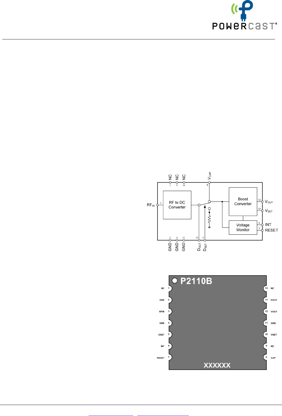
FUNCTIONAL BLOCK DIAGRAM
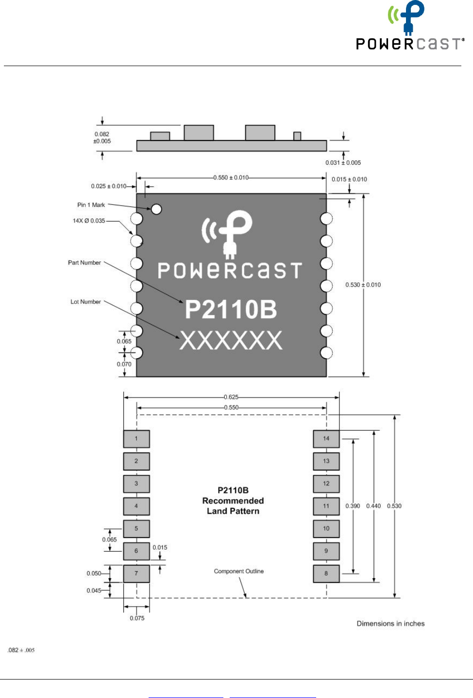
PIN CONFIGURATION
Powercast products and technology are covered by one or more of the following patents and other patents pending:
6,289,237 | 6,615,074 | 6,856,291 | 7,027,311 | 7,057,514 | 7,639,994 | 7,643,312 | 7,812,771 | 7,844,306 | 7,868,482 | 7,898
,105
| 7,925,308 | 8,159,090
8,432,062 | 8,461,817 | 8,621,245
TOP VIEW
+1 (412) 455
-
5800
P a g e 1
free wireless sensors
FUNCTIONAL BLOCK DIAGRAM
Powercast products and technology are covered by one or more of the following patents and other patents pending:
| 7,925,308 | 8,159,090
| 8,380,255
TOP VIEW
P2110B
915 MHz RF Powerharvester® Receiver
REV A
–
201
6
/
11
© 201
6
Powercast Corporation, All rights reserved.
www.powercastco.com / contact@powercastco.com
+1 (412) 455
-
5800
P a g e 2
ABSOLUTE MAXIMUM RATINGS
TA = 25°C, unless otherwise noted.
Parameter Rating Unit
RF Input Power 23 dBm
RFIN to GND 0 V
DSET to GND 6 V
RESET to GND 6 V
VCAP to GND 2.3 V
VOUT to GND 6 V
VOUT Current 100 mA
Operating Temperature Range -40 to 85 °C
Storage Temperature Range -40 to 140 °C
ESD CAUTION
This is an ESD (electrostatic discharge) sensitive device. Proper ESD
precautions should be taken to avoid degradation or damage to the
component.
PIN FUNCTIONAL DESCRIPTIONS
Pin
Label
Function
1
NC
No Connection.
2
GND
RF Ground. Connect to analog ground plane.
3
RF
IN
RF Input. Connect
to 50Ω antenna through a 50Ω transmission line. Add
a DC block if antenna is a DC short.
4
GND
RF Ground. Connect to analog ground plane.
5
D
SET
Digital Input. Set to enable measurement of harvested power. If this
function is not desired leave NC.
6
INT
Digital Output. Indicates that voltage is present at V
OUT
.
7
RESET
Digital Input. Set to disable V
OUT
. If this function is not desired leave NC.
8
V
CAP
Connect to an external capacitor for energy storage.
9
NC
No Connection.
10
V
SET
Output
Voltage Adjustment. Sets the output voltage by connecting a
resistor to V
OUT
or GND. Leave NC for 3.3V.
11
GND
DC Ground. Connect to analog ground plane.
12
V
OUT
DC Output. Connect to external device. The output is preset to 3.3V but
can be adjusted with an external resistor.
13
D
OUT
Analog Output. Provides an analog voltage level corresponding to the
harvested power.
14
NC
No Connection.
Exceeding the
absolute maximum
ratings may cause
permanent
damage to the
device.
P2110B
915 MHz RF Powerharvester® Receiver
REV A
–
201
6
/
11
© 201
6
Powercast Corporation, All rights reserved.
www.powercastco.com / contact@powercastco.com
+1 (412) 455
-
5800
P a g e 3
SPECIFICATIONS
TA = 25°C, RFIN = 915MHz unless otherwise noted.
Parameter Symbol Condition
Min
Typ Max Unit
RF Characteristics
1
Input Power
Frequency
RFIN
-12
902
10
928
dBm
MHz
DC Characteristics
Output Voltage
Output Current
VCAP Maximum
VCAP Minimum
Signal Strength
Boost Efficiency
Maximum INT Current
VOUT
IOUT
VMAX
VMIN
DOUT
RFIN = 0dBm
IOUT = 20mA
2.0
3.3
1.25
1.02
275
85
0.1
5.5
50
V
mA
V
V
mV
%
mA
Digital Characteristics
RESET Input High
DSET Input High
INT Output High
1.8
VMIN
1
VMAX
V
V
V
Timing Characteristics
DSET Delay
RESET Delay
RESET Pulse Width
20
50
6.6
s
s
ns
1See typical performance graphs for operation at other frequencies or power levels.
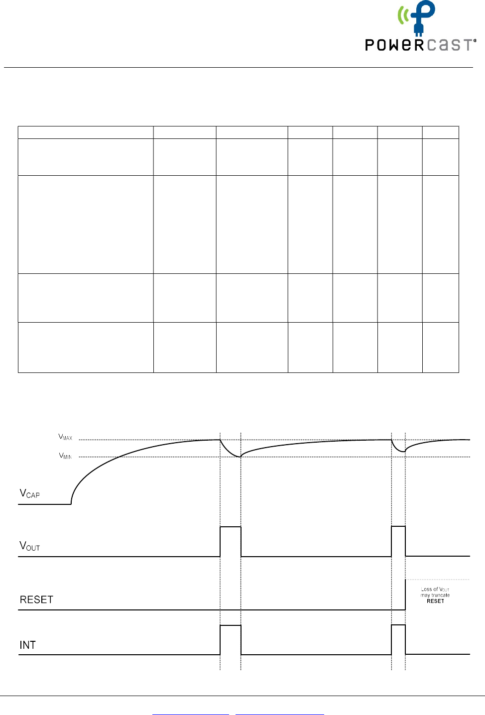
TIMING DIAGRAM

P2110B
915 MHz RF Powerharvester® Receiver
REV A
–
201
6
/
11
© 201
6
Powercast Corporation, All rights reserved.
www.powercastco.com / contact@powercastco.com
+1 (412) 455
-
5800
P a g e 4
FUNCTIONAL DESCRIPTION
RF INPUT (RFIN)
The RF input is an unbalanced input from
the antenna. Any standard or custom
50antenna may be used with the
receiver. The P2110B has been optimized
for operation in the 902-928MHz band but
will operate outside this band with reduced
efficiency. Contact Powercast for custom
frequency requirements.
The RF input must be isolated from ground.
For antennas that are a DC short, a high-Q
DC blocking capacitor should be added in
series with the antenna.
STORAGE CAPACITOR SELECTION (VCAP)
The P2110B requires an external storage
capacitor connected at VCAP. The value of
the capacitor will determine the amount of
energy available from the VOUT pin. The
capacitor should have a leakage current as
small as possible. It is recommended that
the leakage current of the capacitor be less
than 1μA at 1.2V. The capacitor ESR should
be 200mor less.
Smaller capacitors will charge more quickly
but will result in shorter operation cycles.
Larger capacitors will charge more slowly,
but will provide for longer operation cycles.
The minimum required capacitor value can
be estimated using the following equation.
= 15
Where,
- Output voltage
- Average output current
- On-time of the output voltage
When using the RESET function, the size of
the capacitor is less important. A larger
capacitor can be used to facilitate
intermittent functions that require more
energy. The RESET will control the amount
of energy removed from the capacitor
during operation which will minimize the
required recharge time. It should be noted
that when RESET is used, a larger capacitor
will not affect charge time during operation,
but it will require more time to initially
charge from a completely discharged state.
The voltage on the VCAP pin under normal
operation will vary between approximately
1.25V and 1.02V. If the harvested energy
becomes too large, the voltage on the
capacitor will be internally clamped to
protect low voltage supercapacitors.
Clamping will begin at approximately 1.8V
and will limit the voltage to less than 2.3V
at the maximum rated input power.
RSSI OPERATION (DOUT, DSET)
The RSSI functionality allows the sampling
of the received signal to provide an
indication of the amount of energy being
harvested. When DSET is driven high the
harvested DC power will be directed to an
internal sense resistor, and the
corresponding voltage will be provided to
the DOUT pin. The voltage on the DOUT pin can
be read after a 50μs settling time.
When the RSSI functionality is being used,
the harvested DC power is not being stored.

P2110B
915 MHz RF Powerharvester® Receiver
REV A
–
201
6
/
11
© 201
6
Powercast Corporation, All rights reserved.
www.powercastco.com / contact@powercastco.com
+1 (412) 455
-
5800
P a g e 5
If the RSSI functionality is not used, DOUT
and DSET should be left unconnected. DSET is
internally pulled down.
DATA RETRIEVAL (DOUT, DSET)
Using DOUT and DSET it is possible to collect
data from the RF transmitter that is
supplying power to the P2110B. As
discussed above, with DSET high, DOUT will
provide a voltage across R3 that can be read
by an ADC. However, the voltage on DOUT
will also follow the power level of the RF
field as the power level changes. If the RF
field is being provided by a transmitter that
is also communicating by modulating its
amplitude, such as the Powercast TX91501-
3W-ID Powercaster® transmitter, the data
can be read by the P2110B. The voltage
level will need gained up using operation
amplifiers and supplied to a device that can
read the data pattern supplied by the
transmitter.
RESET
The RESET function allows the voltage from
VOUT to be turned off before the storage
capacitor reaches the lower threshold, VMIN,
thereby saving energy and improving the
recharge time back to the activation
threshold, VMAX. The RESET function can be
implemented by a microcontroller. When
the function of the microcontroller is
completed, driving RESET high will disable
the voltage from VOUT. Care should be taken
to ensure that the microcontroller,
especially during power-on, does not
inadvertently drive RESET high. This will
immediately shutdown the output voltage.
If the RESET functionality is not used, RESET
should be left unconnected. RESET in
internally pulled down
INTERRUPT (INT)
The interrupt function provides a digital
indication that voltage (or current) is
present at the VOUT pin. INT can be used in
more sophisticated systems that contain
other storage elements and can be used as
an external interrupt to bring a device such
as microcontroller out of a deep sleep
mode. The digital high level of the INT pin
will be between VMIN and VMAX. The INT pin
can provide a maximum of 0.1mA of
current.
If the INT functionality is not used, INT
should be left unconnected.
SETTING THE OUTPUT VOLTAGE (VOUT)
The DC output voltage from the P2110 is
preset to 3.3V. However, it can be adjusted
by adding an external resistor to increase or
decrease the output voltage using the
following equations. ( = 10)
To decrease the output voltage, place a
resistor calculated by the following
equation from VSET to VOUT. The voltage
can be set to a minimum of 2.0V.
= 1 (
− 1.21)
(3.32 − )
P2110B
915 MHz RF Powerharvester® Receiver
REV A
–
201
6
/
11
© 201
6
Powercast Corporation, All rights reserved.
www.powercastco.com / contact@powercastco.com
+1 (412) 455
-
5800
P a g e 6
To increase the output voltage, place a
resistor calculated by the following
equation from VSET to GND. The voltage
can be set to a maximum of 5.5V.
= 1.21
( − 3.32)
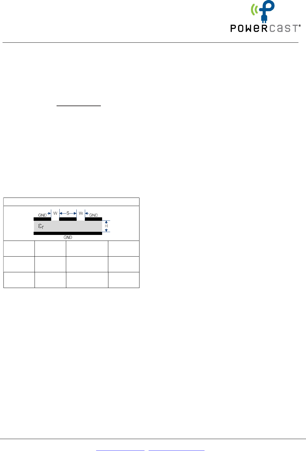
LAYOUT CONSIDERATIONS
The RFIN feed line should be designed as a
50Ω trace and should be as short as
possible to minimize feed line losses. The
following table provides recommended
dimensions for 50Ω feed lines (CPWG) for
different circuit board configurations.
PCB Side View
Material Thickness
(H)
Trace Width
(S)
Spacing
(W)
FR4
(ε
r
= 4.2)
62 50 9
FR4
(ε
r
= 4.2)
31 50 20
*All dimensions are in mils.
The GND pins on each side of the RFIN pin
should be connected to the PCB ground
plane through a via located next to the pads
under the receiver.
When setting the output voltage, the
resistor connected to the VSET pin should
be as close as possible to the pin. No
external capacitance should be added to
this pin.
The DOUT pin can contain low-level analog
voltage signals. If a long trace is connected
to this pin, additional filtering capacitance
next to the A/D converter may be required.
Additional capacitance on this pin will
increase the DSET delay time.
The trace from VCAP to the storage
capacitor should be as short as possible and
have a width of greater than 20mils to
minimize the series resistance of the trace.
P2110B
915 MHz RF Pow
erharvester
REV A
–
201
6
/
11
© 201
www.powercastco.com
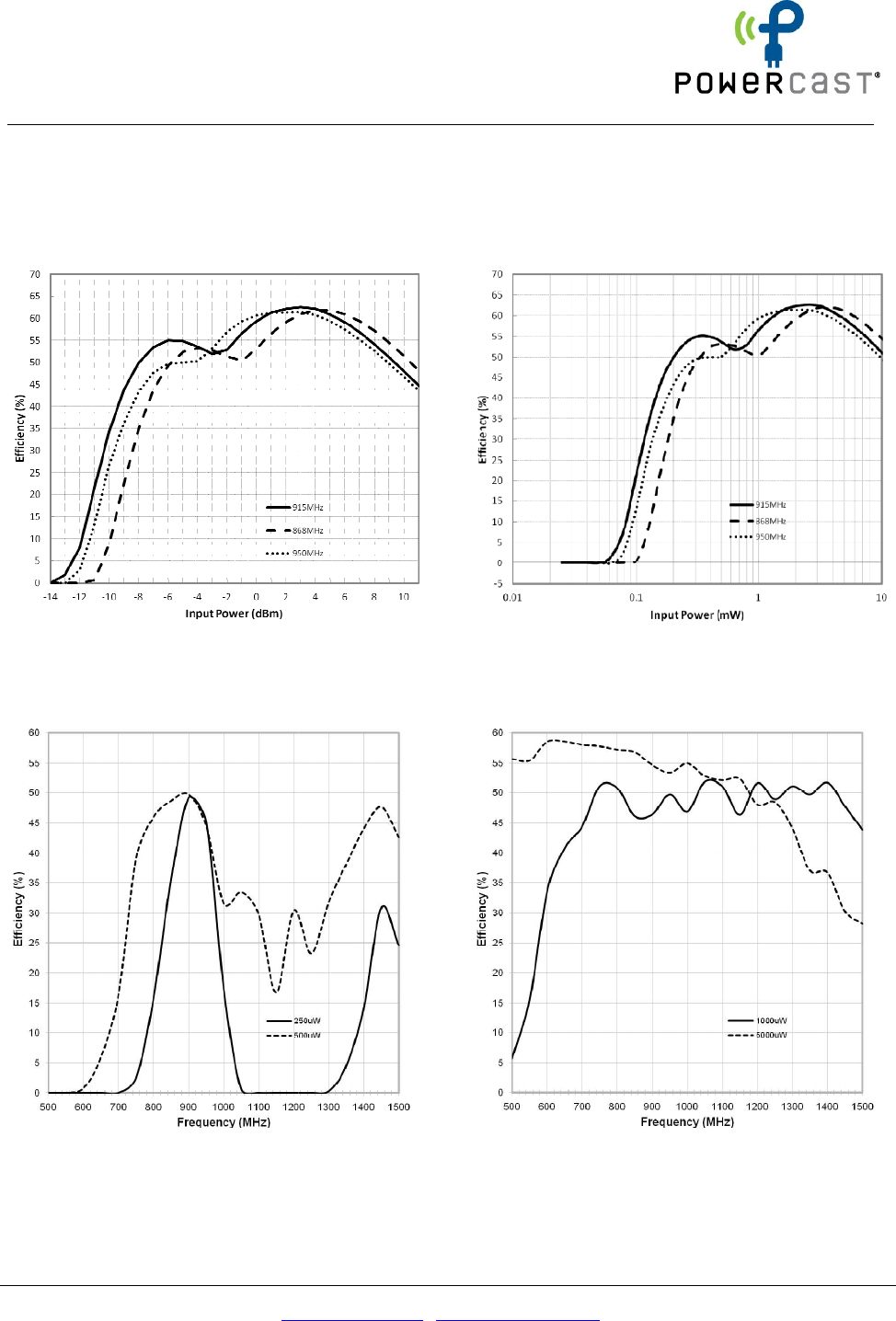
TYPICAL
PERFORMANCE GRAPHS
Powerharvester Efficiency
vs. RFIN (dBm)
Powerharvester Efficiency
vs. Frequency
erharvester
® Receiver
© 201
6
Powercast Corporation, All rights reserved.
www.powercastco.com
/ contact@powercastco.com
PERFORMANCE GRAPHS
TA = 25°C, VOUT = 3.3V, VCAP
= 1.2V, unless otherwise noted
Powerharvester Efficiency
Powerharvester Efficiency
Powerharvester Efficiency
vs. RFIN
(mW)
Powerharvester Efficiency
vs. Frequency
+1 (412) 455
-
5800
P a g e 7
= 1.2V, unless otherwise noted
Powerharvester Efficiency
(mW)
Powerharvester Efficiency
vs. Frequency
P2110B
915 MHz RF Powerharvester® Receiver
REV A
–
201
6
/
11
© 201
6
Powercast Corporation, All rights reserved.
www.powercastco.com / contact@powercastco.com
+1 (412) 455
-
5800
P a g e 8
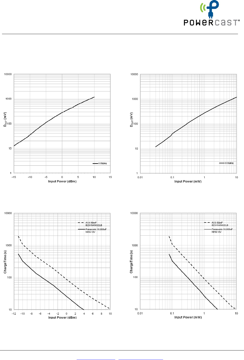
TYPICAL PERFORMANCE GRAPHS TA = 25°C, VOUT = 3.3V, VCAP = 1.2V, unless otherwise noted
Received Signal Strength Indicator
vs. RFIN (dBm)
Initial CAP Charge Time to First
Activation vs. RFIN (dBm)
Received Signal Strength Indicator
vs. RFIN (mW)
Initial CAP Charge Time to First
Activation vs. RFIN (mW)
P2110B
915 MHz RF Powerharvester® Receiver
REV A
–
201
6
/
11
© 201
6
Powercast Corporation, All rights reserved.
www.powercastco.com / contact@powercastco.com
+1 (412) 455
-
5800
P a g e 9
Manual Specifications

P2110B
915 MHz RF Powerharvester® Receiver
REV A
–
201
6
/
11
© 201
6
Powercast Corporation, All rights reserved.
www.powercastco.com / contact@powercastco.com
+1 (412) 455
-
5800
P a g e 10
P2110 MODULE SERIES
MODULE STATUS FUNCTIONAL DIFFERENCES
P2110 End-of-life N/A
P2110B Replaced P2110 Increased RF-to-DC conversion
efficiency
V
SET
resistor values modified

P2110B
915 MHz RF Powerharvester® Receiver
REV A
–
201
6
/
11
© 201
6
Powercast Corporation, All rights reserved.
www.powercastco.com / contact@powercastco.com
+1 (412) 455
-
5800
P a g e 11
IMPORTANT NOTICE
Information furnished by Powercast Corporation (Powercast) is believed to be accurate and
reliable. However, no responsibility is assumed by Powercast for its use, nor for any
infringements of patents or other rights of third parties that may result from its use.
Specifications are subject to change without notice.
No license is granted by implication or otherwise under any patent or patent rights of
Powercast. Trademarks and registered trademarks are the property of their respective owners.
POWERCAST PRODUCTS (INCLUDING HARDWARE AND/OR SOFTWARE) ARE NOT DESIGNED OR
INTENDED TO BE FAIL-SAFE, FAULT TOLERANT OR FOR USE IN ANY APPLICATION THAT COULD
LEAD TO DEATH, PERSONAL INJURY OR SEVERE PROPERTY OR ENVIRONMENTAL DAMAGE
(INDIVIDUALLY AND COLLECTIVELY, “CRITICAL APPLICATIONS”), SUCH AS LIFE-SUPPORT OR
SAFETY DEVICES OR SYSTEMS, CLASS III MEDICAL DEVICES, NUCLEAR FACILITIES, APPLICATIONS
THAT AFFECT CONTROL OF A VEHICLE OR AIRCRAFT, APPLICATIONS RELATED TO THE
DEPLOYMENT OF AIRBAGS, OR ANY OTHER CRITICAL APPLICATIONS. CUSTOMER AGREES, PRIOR
TO USING OR DISTRIBUTING ANY SYSTEMS THAT INCORPORATE POWERCAST PRODUCTS, TO
THOROUGHLY TEST THE SAME FOR SAFETY PURPOSES. CUSTOMER ASSUMES THE SOLE RISK
AND LIABILITY OF ANY USE OF POWERCAST PRODUCTS IN CRITICAL APPLICATIONS, SUBJECT
ONLY TO APPLICABLE LAWS AND REGULATIONS GOVERNING LIMITATIONS ON PRODUCT
LIABILITY.
Powercast warrants its products in accordance with Powercast’s standard warranty available at
www.powercastco.com.
