Radio Shack Hardware Manual PC 1 Service 19xx Tandy Text
User Manual: manual pdf -FilePursuit
Open the PDF directly: View PDF ![]() .
.
Page Count: 40
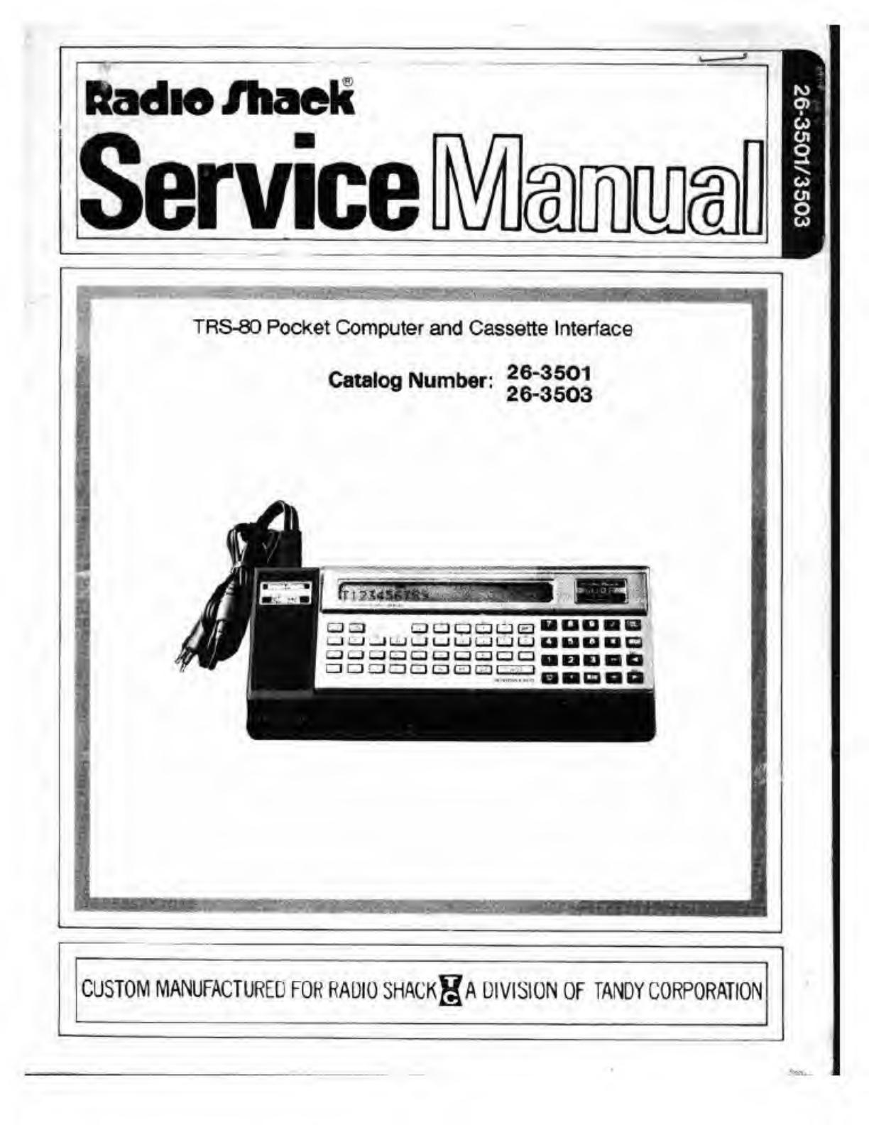
TRS-80 Pocket Computer and Cassette Interface
Catalog Number: fJJJOJ
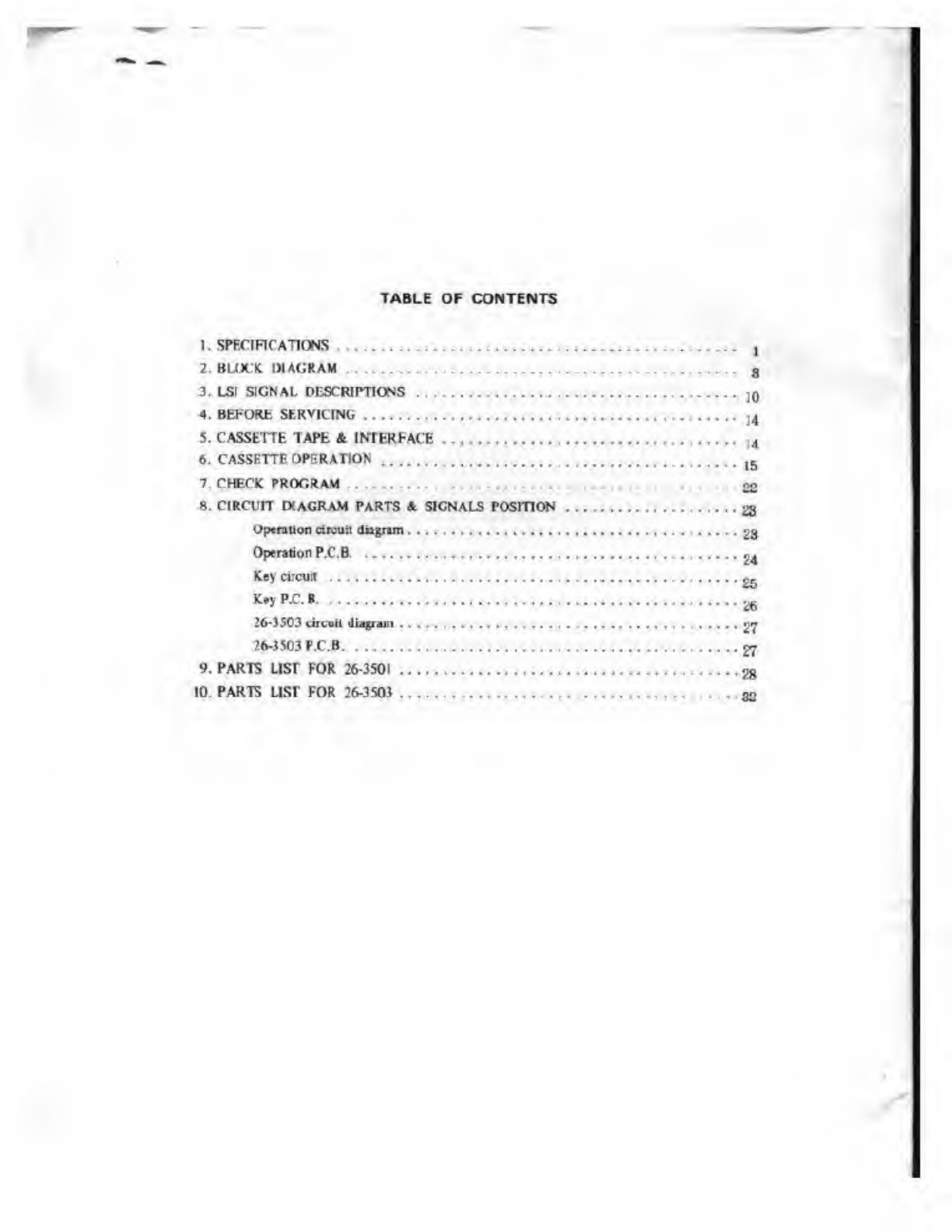
TABLE OF CONTENTS
1. SPECIFICATIONS l
2. BLOCK DIAGRAM 3
3. LSI SIGNAL DESCRIPTIONS jq
A. BEFORE SERVICING ]4
5. CASSETTE TAPE &INTERFACE 14
6. CASSETTE OPERATION I5
7CHFCK PROGRAM 22
8. CIRCUIT DIAGRAM PARTS 4SIGNALS POSITION 28
Operation circuit diagram 23
Operation P.C.B 24
Key i<i I „.
Key P.C. B^
26-3503 uicoil <iiagi<un 27
26-3503 P.C.B g?
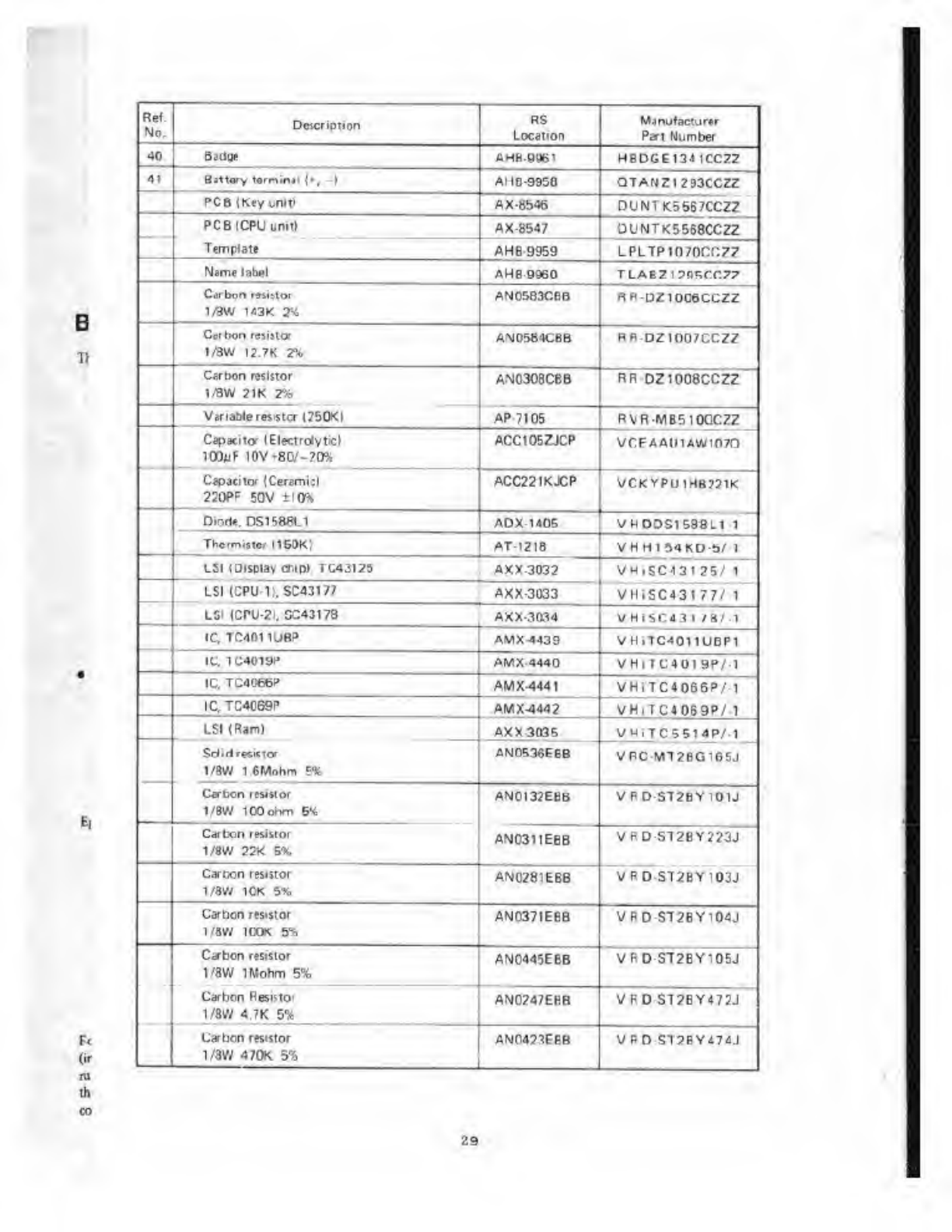
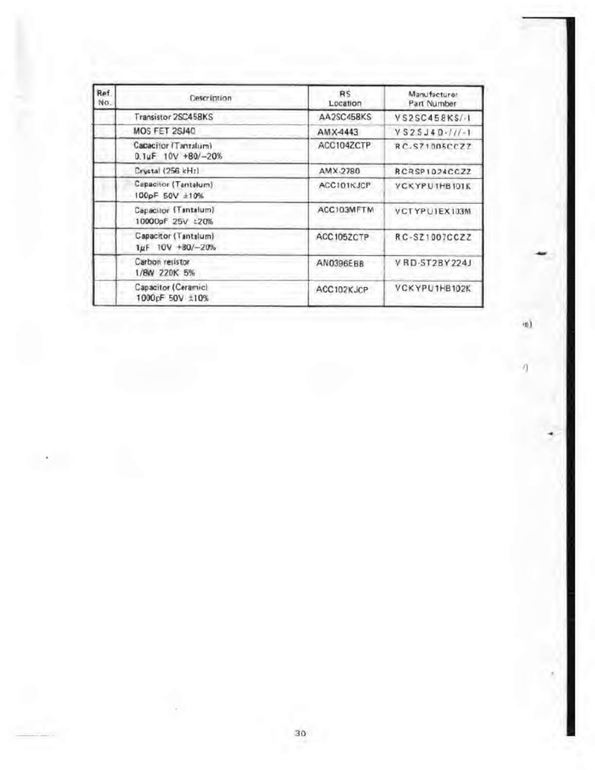
9. PARTS LISr FOR 26-3501 28
10. PARTS USr FOR 76-.1501 gg
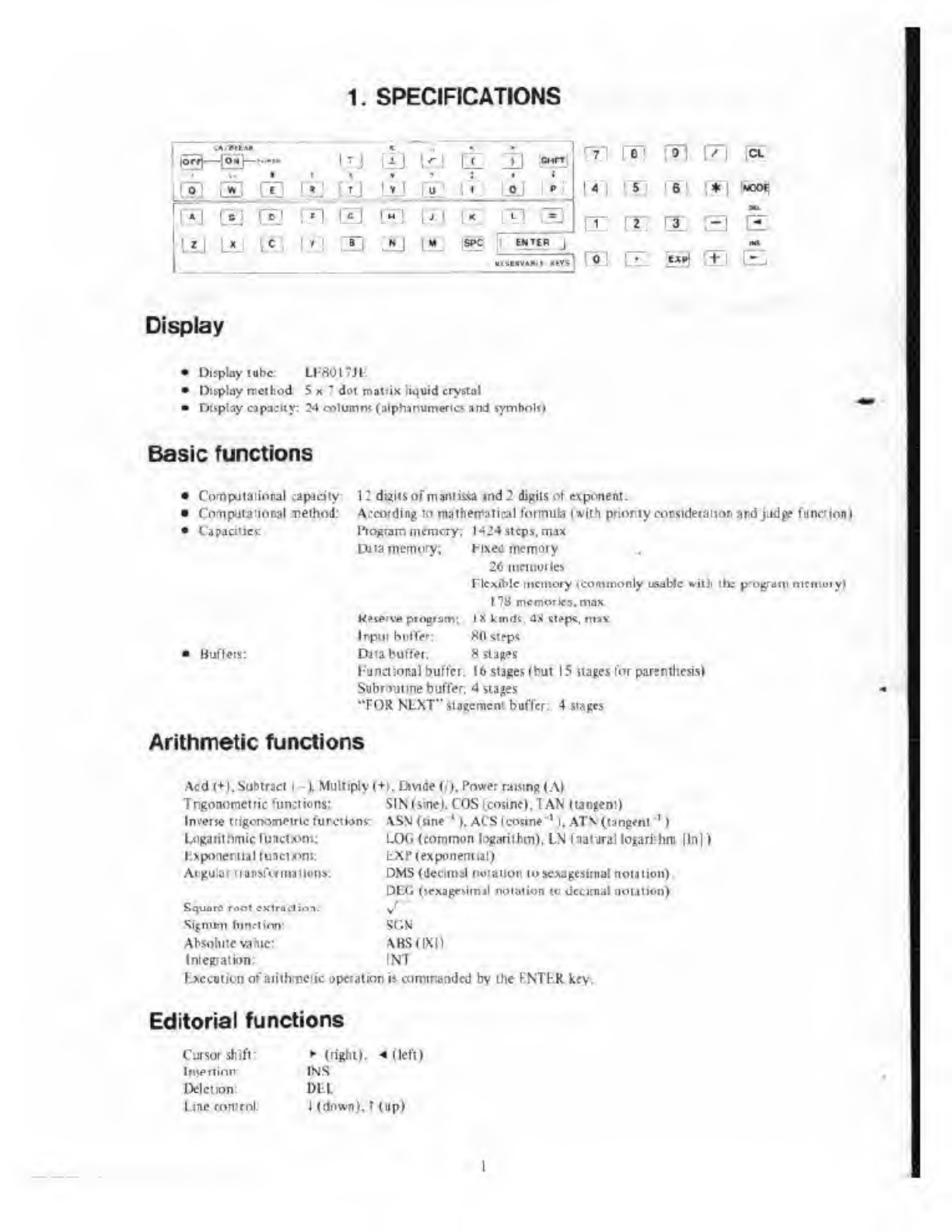
1. SPECIFICATIONS
ca ®l;J E3 Ld CEl 3ssl
hm[f] [vi rj (i Loj >
iee ra SGH 11I . 5
l«J L*J ta LX3 Xi JLI [-_ 6pc fNUH i
KMMVWIt ->YS <
7m m m ia
I4"i ss' *: «^
(T ej ce 3E
ra cr i«j is e
Display
•Display tube: LI-80I7JI.
•Display method 5» "dot matrix liquid crystal
•Display capacity: 24 columm (alphanumeric; and tymboh)
Basic functions
Computational rapid ty
Comptiia:ional method:
Capacities:
12dt^ifsof mantissa ind 2 digits of exponent.
According lo maiheirntiral formula (with priority consideration arid judge function)
Buffers:
M24 steps, max
Fixed memory
20 nxmoilei
Flexible memory ^commonly usable »it!i ire prog
178 memories, max
I£ktniti. as ttepc, miv
SO steps
8stages
l-'uncliona) buffer. 16 stages (but 15 napes fur parenthesis)
Subroutine buffer; 4stages
"FOR NLXT" statement buffer: 4stages
1'iogram memory;
Data memory;
W^pw program;
Inpui buffer:
Data buffer.
mi iiinnot y
Arithmetic functions
Acd (*). Subtract [-% Multiply (+), Divide (,<). Power raising (A)
Tngonometric functions:
Inverse trigonometric fur.ctlonr
Logarithmic fuactom:
hxponenial tunciom:
Ar&uiar transformations:
S-quotO r..'! ;\tr.i ,1 ni.
Slgniim fnnrtlnn:
Absolut evalue:
Integration:
SIN (sine). COS (cosine). TAN (tangent)
ASN (line '). ACS (cosine'1
). AT\ (tangent '
)
LOG (common logarithm). LN (natural logarr.hni |ln|
)
\i\? (exponential)
DMS (decimal notation to sexagesimal notation).
DEG (lexageMiinl notation tu decimal nuiation)
J
SCN
rVBS(|X0
INT
Kxccoticn of arithmetic operation is commanded by ilie ENTKR key.
Editorial functions
Cursor shift:
lmetlinn:
Deletion:
Line control:
(right). <(left)
INS
DEL
I(down). T(up)
Programming language
BASIC (Beginner's All p«pose Symbolic Initruction Code)
Power source
Battery; Four MR44 <m«rcury ba«eri*s)
Ra<t*ry liiV J00 hours
Power conJump ion: 0.01 1
W
Automaitc powei shutofl: About 6rainules
Miscellaneous
Data protection: Program memory, dau mcmaiy. re$er*e program memory
Peripheral unit: Audio OMMtte unit (recording/Tending (if rfi* prrgram Trmory. dali mentnry and MMf*t
program memory)
Optional 26-3503 (audio cauei ic interface)
PhyMcal iimenaora: 17S(W) x70(D) x44(11) mm <6.8<W) x 2.7(D) x1.7(H) inches)
Weight: Afprox. I70g(0.37 lbs) ... 26-3501
Aceiox. 240b (0.5J lbO (with batUri**) _. 2G-3S03
For torapttfr frttili of optratna ttw TRS-80 Pockt Computer, rrfii to fh« Qwntr't Minunt.
s
z
iit
ao£
£5 2bs,b**j <
6
y>
nz
^ct* :h-ih
h-.h
i
.
*"S12 T.
il
VII
1<k H
CV-IV
KtHI-iniU
ri<
<3=±
.-_— ,. ...
B*ae
><
S5
I'
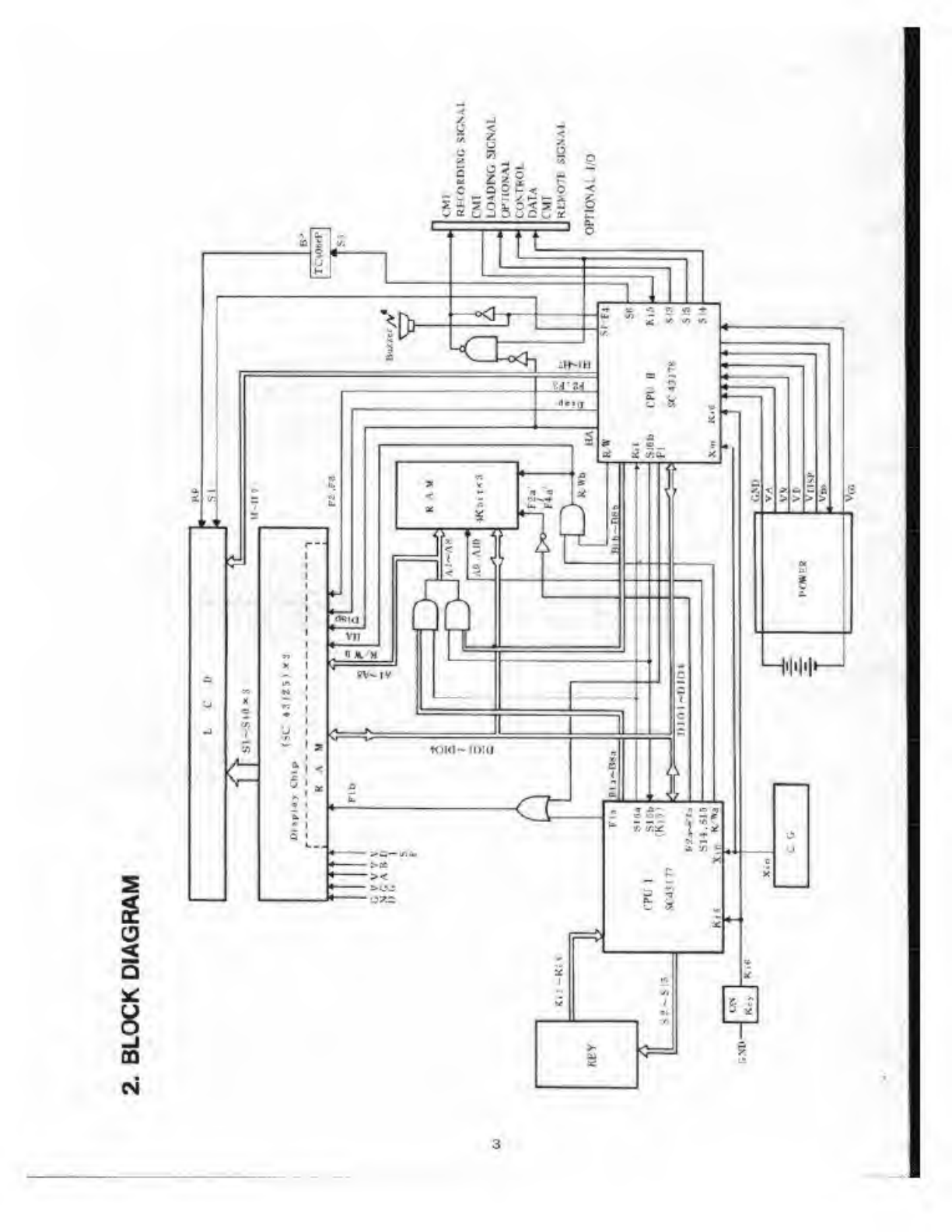
System configuration (see the s/stem block diagram)
The system consists of (he following components:
1. CPUI(SC43I77)« I
2. CPUU(SC43l7S)x I
3. 4K-bltRAM(rOM4)*x3)
4. Display chip (SC43I23 «3. with Duilt-in RAN)
5. 2ANDga(e<TC4011UrJP*l)
6. 2AMJ20H(K4yivUCx I)
7. lnvwter(TC4069BPx I)
S. Quard Analog Switch Miiltiplover (TCdOAtBP)
o. ITD(34-di8it FhMdot LCD)
10. Key
11. Crystal (CSB2560)
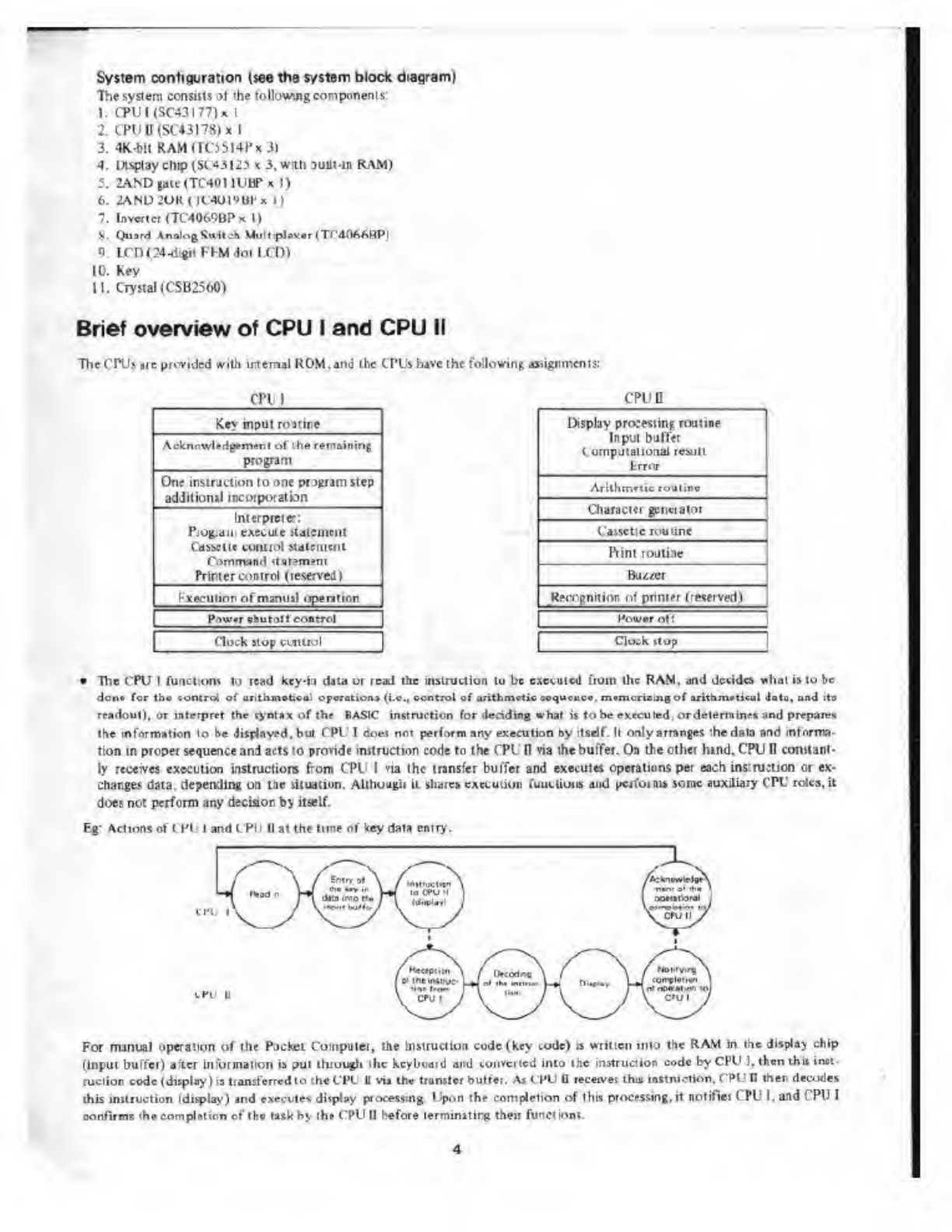
Brief overview of CPU Iand CPU II
The CPUs are provided with internal ROM. and the CPUs have ihe following assignments
CPU I
Key input rostine
Acknowledgement of the remaining
program
One instruction to one program step
additional incoiporatton
Interpreter:
Pio&aiii execute italciiuul
CdSSCtlt tuillfol MdUlUClil
Cummand ilateimnt
Pointer control (leserved)
v-irii'i lit mrinutl opentnn
Piw.resumt control
Clouk Hup centred
CPU
Display proceHing routine
Input buffer
Cunipuiaiional result
trr'T
Ai >Uim>tit H'jlirc
Character geritiatoi
(arctic routine
Print tontine
Qj,uei
Rprngnitlor: nf printer (reserved)
I'oiver "t I
Clojk nop
•The CPU Iiu.ii;;i, ia read key-ii data ur read (tie instruction to be execute*] fiom the RAM, and decides what is to be
don* (or Iho loiuitl of aritlunebco': operation* (i.e., control of arithmetic sequence, memorieingof arithmetical Jots, and its
-i I '.or interpret the cyntnx of the BASIC instruction for deciding what is to be executed, or determine* and prepare*
the information lo be displayed, but CPU" Idoei not perfiwm any execution By itself. Il only arranges ihedata and inlorma-
tlon in proper sequence and acts to provide instruction codelo the fPL II via the buffer. On Uteothet hind. CPU Dconstant-
ly receives execution instructions from CPU Ivia the transfer buffer and executes operations pei each infraction or ex-
changes data, depending on the situation. Although it shares eA«.uiio>! fum-lions and tieifoiai* some auxiliary CPU rolcs.it
does net perform any decision by itself.
Eg- Actions of CPU Iand tPU Uat the lime of key data entry.
irt
kvv u
For ni ui'. il operation of ihe Pocket Computet, the uislructlon code (key code) awritten (mo the RAM in the display chip
(Input buffer) after Information is put through the kcybwitd and converted into the instruction code by CPU I, then this inst-
ruction code (display! is transferred to thoCPt-111 vis the transfer butler. As CPU Disceivei this inctmciion. CPU II ther decodes
this imtmction <display) and executes dlisplay processing Upon the completion of this processing, it notitlei CPU I, and CPU I
confirms the completion of the vak hy ihe CPU 11 before lermimtirg their function!.
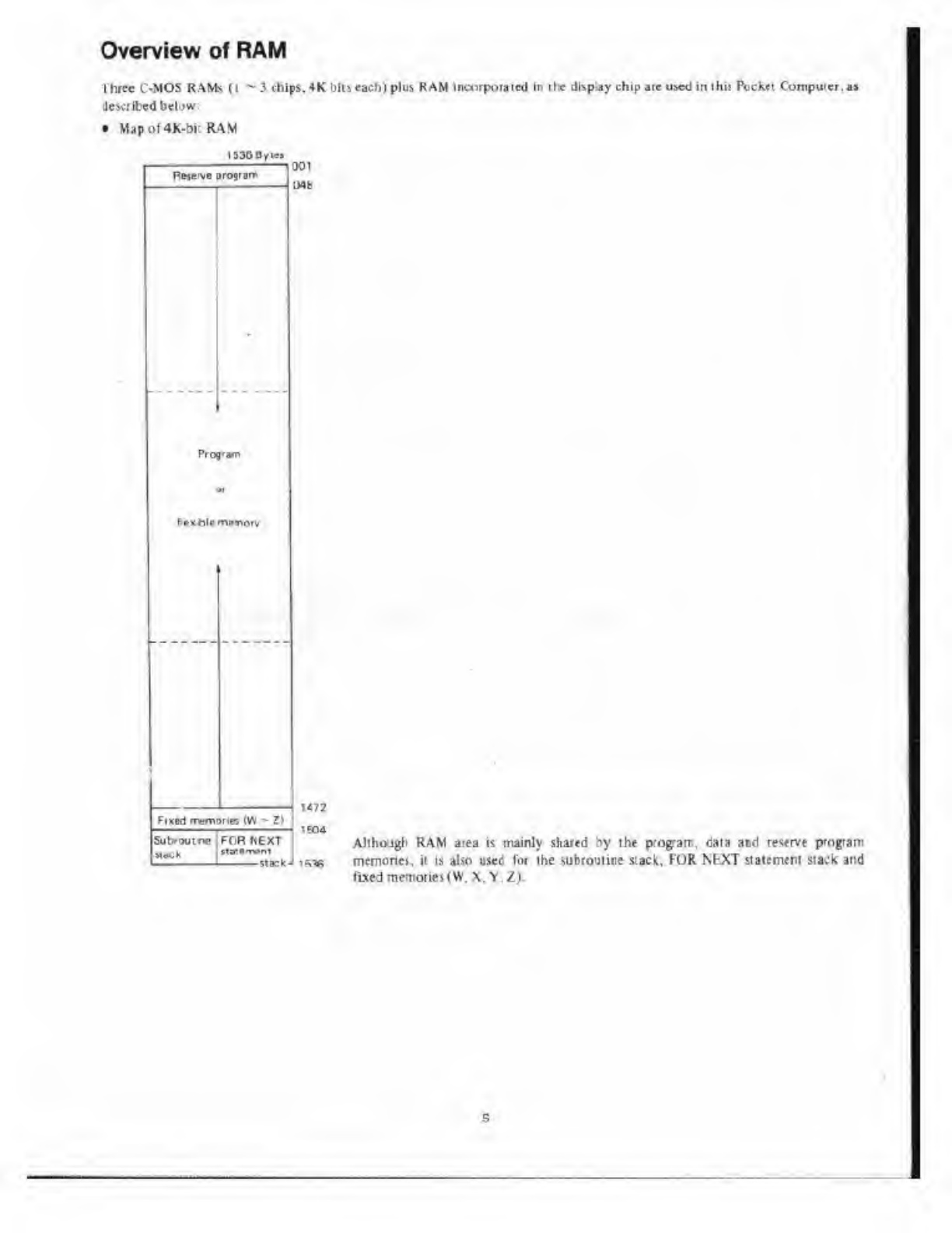
Overview of RAM
Three C-MOS RAMs (I —3 chips. 4K bin each) plus RAM Incorporated In the display chip aie used in ihii Pticket Computet, ai
described below:
•Mapol4K-bf. RAM
103OD/ie>
Rtnnn orostor*
Prog'am
tipihlpmowflfv
001
IMfi
1«7?
Fined mmonei <¥Y -£i
b*oume
HiKli
^04
Aithojgrt RAM aiea is mainly shar*d by ihe prog-air., daia and reserve program
FOR KEXT
q-.-k. isgg memories. i( is also usee I'm the subroutine sack. FOR NhXT staiemert slack and
fixed memories (W. X. Y.Z).
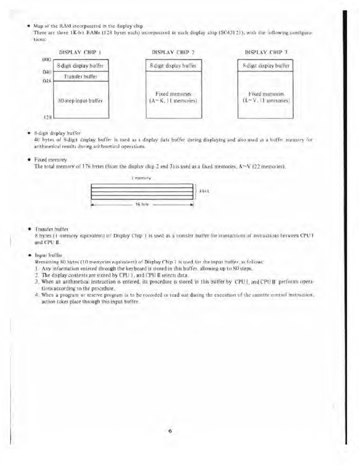
Map of the KAK1 incorporated xi Ihc Jispluy chip
Tl.cic are lincc IK-Ii.t KAMs (12S bytes each) incorporated in each display chip (SC431 25). willi the following condguio-
t.cns:
DISPLAY CHIP 1
IJOIJ
two
(MS
I2S
8-digil display buffet
Trarufci btffc:
fiO-step input buffe
DISPLAY (HIP 3
8-digit display buffer
Fixed memories
(A—K. 1 1 memories]
DISPLAY CHIP 3
Sdijui display buffet
Fixed memories
(L— V. 1 1 memories''
8-digtt display buffer
4€ byln of 8-digt display buffer is used as Jdisplay data buffer during displaying and also used as abuffet iretrwry for
arithmetical result, during arithmetical operations.
Fixed memory
The loial memory of 176 bvies (fiorr the display chip 2and 31 is used asa fixed memories. A—V (22 memories).
1r-iemcy
•I '
IfefllH
Itanster buffer
oliyies (I memory equivalent ior f>spl;ty Chip 1is used as atransfer buffer for transactions of instruction*, let ween CPU I
and CPU B.
Input buffer
Rem lining HO Syt>s (1(1 me-iioi-ipt e-yiivilent) nf Display Chip Ikuserl I'm the inroil buffet as follow*:
IAny information tnlered through the keyboard is stored in this buffet, allowing up to HO steps.
2. Be dispJayconieiis are stored by CPU 1. and CPU Dselecii data.
3. When an arithmetical instruction is emered. its piocedute is stored in ibis suffer by CPU I. and CPU II performs open*
lions according to the procedure.
4
.
When aprogram or reserve program is to be recorded or read out during the execution nf the tassctlc control nstruction.
action tikes place through this input buffer.
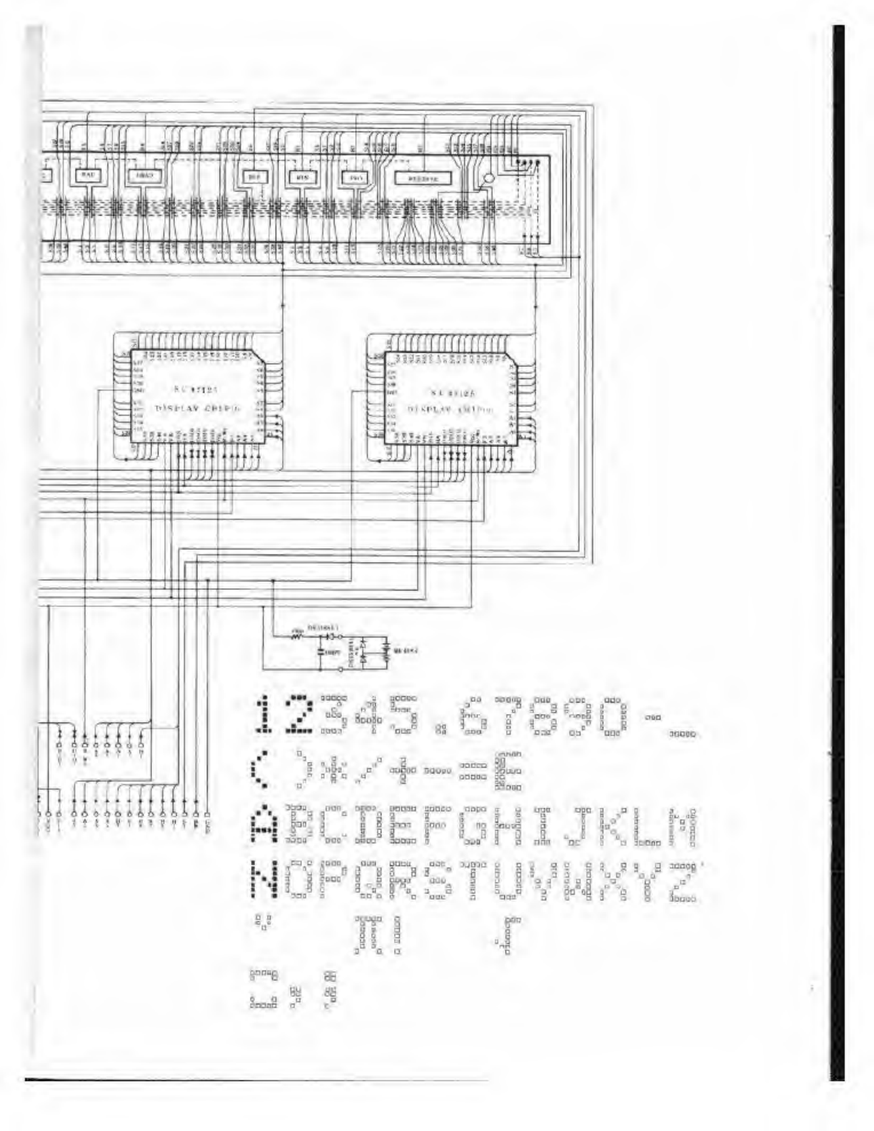
Overview of Display
The coniems til fhr itaptoy AS indicated by CPU Iis reoeiwd by CPU II via ih* input buffer ind are ccnvericd into respective
cliaric*«l etides. ihey arc transferred to the display buffer in the Diiplay (hip lluuugh the adjiess data bus.
*Designation of 'he display i-n
IJie rolkwitigsiru.'tureii observed in the display buffer mthe Display Chip.
*/
A« K? WA*
1
\
F
1
1
1
F
1
(1 1 II
)
p
Aifcli e>i
JfCOCPt
\
Tlu-.c arc 8*40 *320 bill (40 tyies) of area in the display
buffer in Ifce Display Chip.
hg: tiitiplay numerical "4"
il- 114 ii> tit 113 'VI 111
XOI) 1
xI
I.0
III
HiidPiV bat*—
|in n[ i) rm
loijniog |i
SI "' nnnin
ss "'DOilD
»»Din«n
M+ BDD1D
"'
Sll "SDDDID
SI7 H7Qaa«D
sis SI S2 S3 S4 S5
'S33
•-'
T
IHOI
11104 1)102 MO* 1H02
A5- A5-0
The numeral "4" (to be displayed by CPU II) is cotiTcrtcd into He lele.am character code and earned (hrouah on the address
data bus. hirst, the segnwni Si isvkned with the address A8-AI "OOOOOOCO" to store iheday DNM-DIOI '1000" in the
display butler (see above illustration). To store the second 4biis of thedaia. only A5 in the address in turned *l "in mike ihe
addieis "OUQJOUOO" io store daia "tOOT. In ihe same manner, address "OOOOtXlOl" is sefected for storing the Prst 4-bit data
"Oioo" for icgmcm 52 and ihe second 4-bttdaia 'OOQi"issioted with the addies "1X101001)1".
Timing Signal* for Displaying "4'
MSP
HA
HI
H2
H3
114
Hi
116
H?
imi-
ruiJiruuinjinjinjiiiJinjinj
jt_zz£:
~u m—ar
—i_n
—
i-l
l,M'
"VIHU*
U
LT n
JT_r
_TLr
_r
SI XMWA. v//$/r
*^-^* ^r^r
HA: Ucek frequency for me counter. mis signal It counted and decoded to perToim iynchiorUzation wliJi UK common
Mgndl.Hl-HV.geneiaicdliom CPU D.
DSIP: Wiih high level wf lhi» itgnal.pioc*siinft of display operation ii indicated (RAM data designated by HI ~- 118 is »*m out on
Sl~S40).
The dam MOtcd in the displa) buffet beamed through Si ~S40 (illustrated ibuve)tobc fed to the LCD. (lb indicate "4" un
thf <!i*pl*y. IW and lit »rr cnpgfH tor Si .lllitivl Wfor S?. etc ,tlm.ugh Rn -S40.)
Overview of Power supply
l}i>;i
MHHX*
%.1
'iX
cpun
GNU
ovpisp
RtlitonMiwr i«np«»iLue*iiO VOISP
*0' -V
The liquid crystal reference voltage VDISP is generated by the above circuity lo avoid bluncd ehaiaden cr contrast varia-
tion* that might cegnde display performance (which would be caused by aslight voltage variation hthe liquid crystal
referencevollaff- VDISP}.
a. VDD is generated mCPU II. referenced to VGG.
b. The gate voltage of MOS FET i& controlled by the 230K!2 put 10 regular the vullage foi VDISP. The FhorniMur \i provided
to compensate foi lemptvawre variaiion.
C. Ref*ren« voltage VDlSPit aiviicc by resistor combinations to provide VA, VM and VB-
VIlKPr In<u vnliag* fcw Rmnmnn tignaUtH' —117) fiv II'D
VA: llim vuli age for segment signals(SI-S40t
VM: Inlerrrediilevollage fur common and *gment signals
VB: Law voltage lor segment signals.
NOTE: VA, VM and VBbejune pulses, with jii amplitude of several TOllS, due to the influence nf the LSI.
Adjustment ot relerence voltage VDISP
VDISP had been precisely adjusted to -3,74V at an ambient temperature of 2GrOand -4.29V
al If it is necessary lo rcacjusi the voltage after servicing rhc LCD or changing some
components, he sure to look it ihe Display from a30sangle (from vertical) while adjusting
1he pot.
VA
VM
v»
VDISP
Hyo poiiiion
3. LSI SIGNAL DESCRIPTIONS
SC43177 (CPU I)
Pin No. Signal name IntOui De&flptftM
i
3
4
F4a
F3a
Fla
Oul
Out
Out
Out
Chip Enable signal (RAM3 Mlect signal
)
Chip Enable signal (RAM2 *•!«« signal)
Chip Enable signal (RAMI select signal)
Chip tnable signal (Display chip 1select ligrial
usage)
During display: Low **
Dining icad-iu: turns moiiicntaiily high
.lor input buffer and Irmsfer buffer
bVr.f; In Source voltage 1""voliage of baiteivl
7v,l( .In
8Xin In Basic clock (pulse signal, 256kH? 1
9
10
TESTI
test: Connected it. GND
11 RESET In All Reset Switch input
Normally high but turns low when the All Kesri Switch bpreyed.
12 RjWa Oui RAM Data Read/Wiitc signal
During disptoy* High
Pickings key causes it to morr*.«nlari}y 5.1 low -^
13
14
15
16
DIOl
DI02
DI03
DI03
In' Oul
In- Out
In' Out
In.' Out
l>ila HtR Ifor address detignation of the input buffer am
Ditnlav Phio 1 ,
1irmsfer buffer mRAM and
During dismay: High \\\\\ \\
During read-in Low •» \_\_\_V_i_\_\_
17
18
19
20
2)
22
23
24
D7a
B6a
B3a
Ma
B3a
B2a
Bla
Out
Out
Out
Oui
Oui
Oul
Out
Oui
Addtess Bus (for address designation of the input buffer ind r
and Display Chip 1).
fanslet buffer in RAM
Morient arv erncrationOnling display __ _
Dining icad-m 'Trnuini
1L
rnrn-
30 GND In Source voltage (0V)
40 51 Ga Oui Busy signal to CPU ll (High during execution in CPU t)
During display: Low
During toad in: tutiu itiuiticnliiiily lugli
41
42
Sn
Si
Out
On Kay Strobe signal. RAM Addrcts signal
Key Stfrtbo signal. RAM Address signal
10
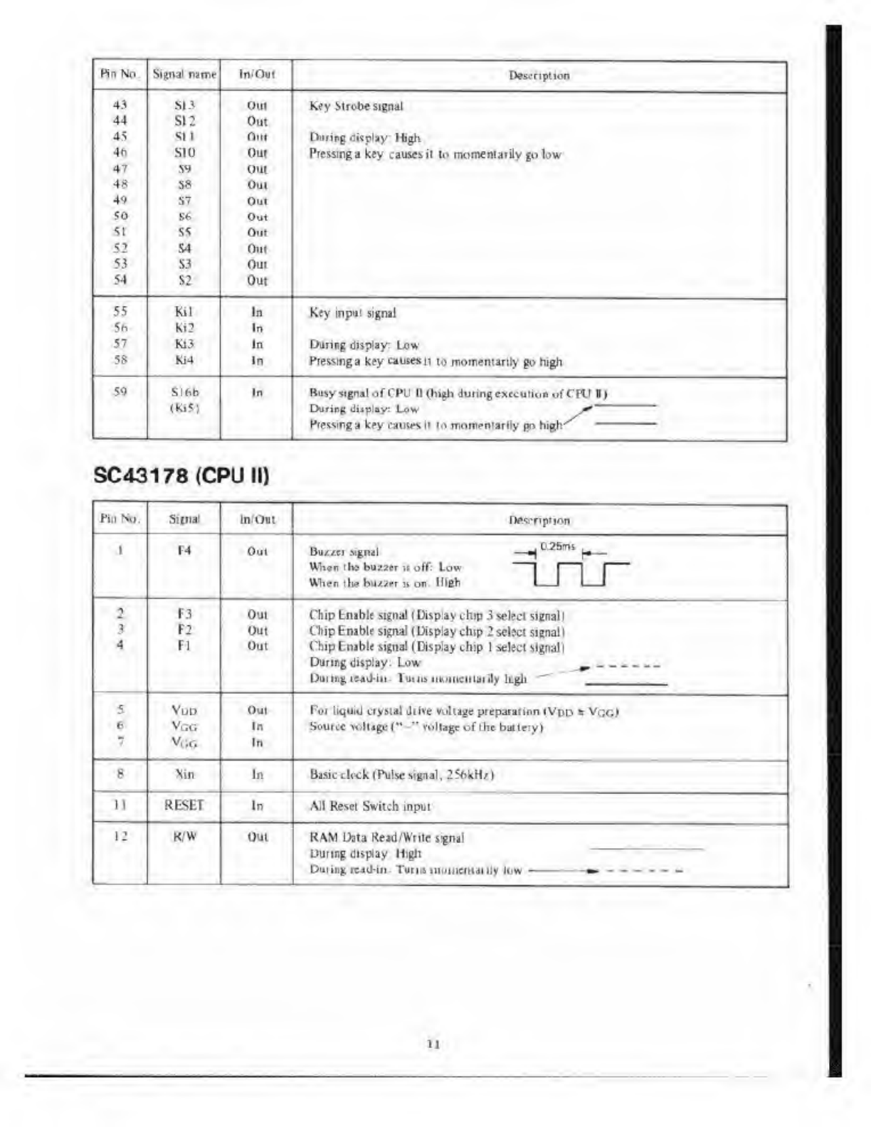
HdNo. Signal pjiw In' Out Description
43 SI 3Out Key Strobe -LiM.il
44 SI 2Out
4S SI 1Out Dining display High
46 SIO Out Pressing akey causes it to momentarily go low
47 59 Out
48 58 Out
49 S7 Out
SO 56 Oul
51 S5 Out
52 S4 Out
53 S3 Out
54 S2 Out
55 kil In Key input signal
56 Ki2 In
57 K13 In Owing display: Low
58 KM In Pressing akey causes nto momentarily go high
5<) SI 6b
(KiS)
In Busy signal of CPU 11 (high during execution t>f CPU H>
During dijpUy: Low J*
SC43178(CPUII)
Pin No. Siinal Ini'Out Description
1P4 Out Bu/.«i signal —
^
C25rni f^_
Whert tha buzicr it off: Low 1I-""
1[~
~
".Tier ih* bWBW iv on High '
1I—
J
2
4
F3
F2
Fl
Oul
Out
Out
Chip fcnible signal 1Display chip 3 select sienall
ChipEmble signal) Display chip 2select signal I
Chip Enable signal (Display chip 1aelecl signal)
During display: Low ___.-- -_
Duung tend-in Tmm tikiniciilai ily h-gh
5
6
7
Vc,c.
V,;r.
Out
In
In
Foi liquid crystal drive vullige preparation i.Vdd *Vc;c>
Source wluge(**-" voltage of Ihe battery)
eXin In Basic click (Pulse signal. 256kHz)
li RESEr In All Reset Switch input
12 WW Oul RAM Data Read/Write signal
During display High
Dining read-in- Turn* iiiuiiicitiailly luw **
1
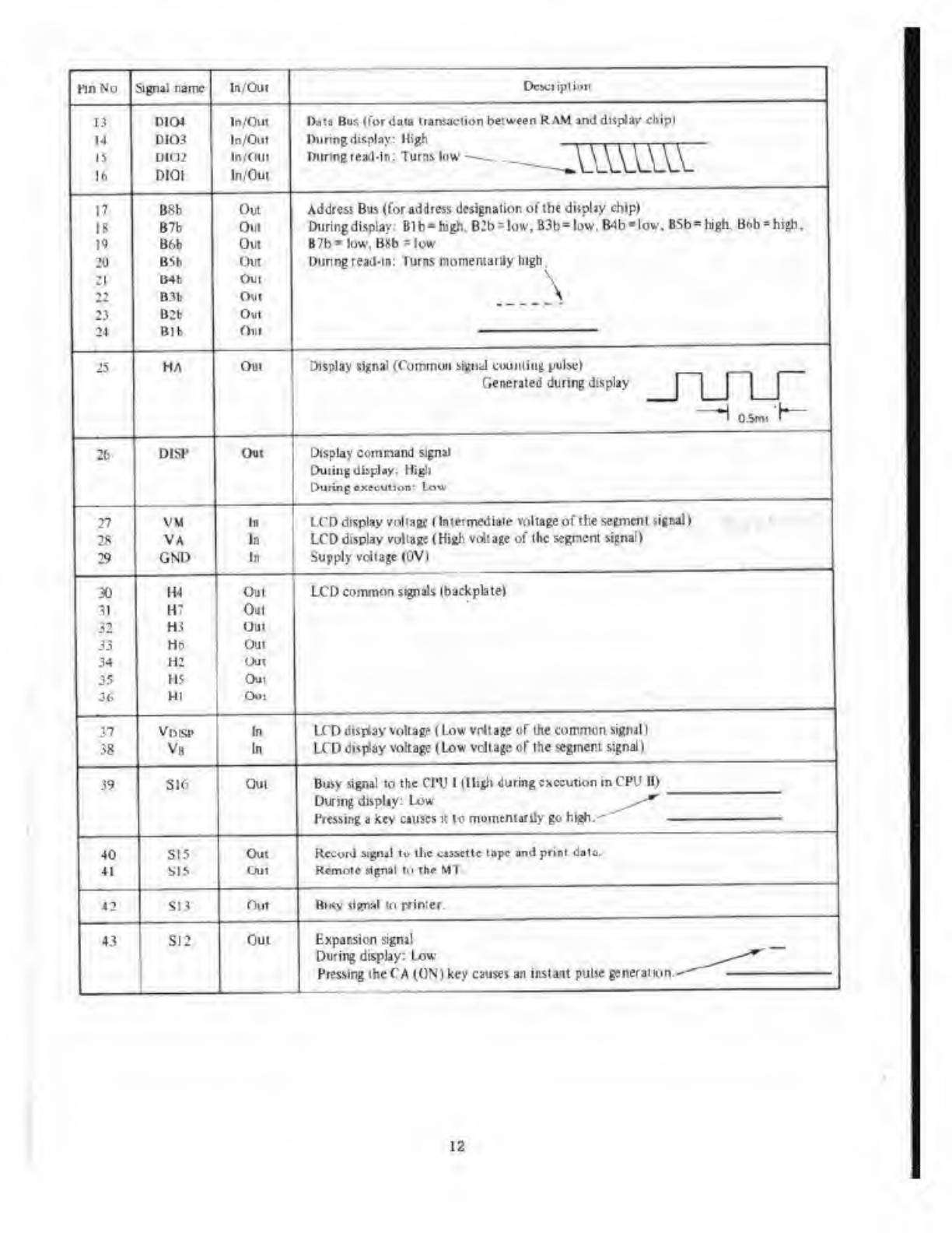
nnNo 1Signal name In/Oiu DwtfjpttWi
14
lb
men
DI03
OIOZ
DIOt
In/Out
In/Out
In/Out
In/Out
l>.ita Bus (for data transaction between RAM and display ehipl
Dunne iea.Hn. Turns low -_^_^ \\\\\\\\
I?
IE
19
20
21
22
23
24
B8b
B7b
B6b
BSb
D4t
B3b
B2b
Bib
Out
Out
On!
Oui
Out
Oui
Out
Oil!
Address Bus (for address designaiion of the display chip!
Duringdisplay Blb» high. B2b Mow, B3b=bw. B4b-lov. BSb=high B6b =hieh.
B7b«low. BSb=low
l>urtng read-In: Turns momentarily high
25 HA Oui Display sijna'(fommiui signal couniiug pulser
Generated during display
*i 05m r
26 MSP Oui Display command signal
Dining display- High
During execution: Low
27
IB
29
VM
VA
GND
In
In
In
LCD display vnhagff (Intermediate voltage of the segmeni lignal)
LCD display voltage (High voltage of the segment signal)
Supply voltage (OVl
30
^1
32
33
34
35
36
144
H?
Hi
Ht>
H2
115
HI
Out
Oui
Oui
Out
Out
Out
OU!
LCD common signals (backplate)
3?
38
Vmsp
Vb
In
In
LCD display voltage ILow vrltage of ihe common signal)
LCD display voltage (Low vdiage of ihe segment signal)
39 510 Out Busy signal to the CIV 1(Ilijh during execution in CPU II)
During display: Low _^**^
40
41
S15
SI b
Out
Out
RcuoiJ signal tw the cassette tape and prinl idala.
Remote signal to the MT.
42 SI 3 Otit RiKy tibial i" r*inier.
43 ., Out Expansion signal
During display: Low ^^—-*"
12
PinNu Signa name In 'Out Description
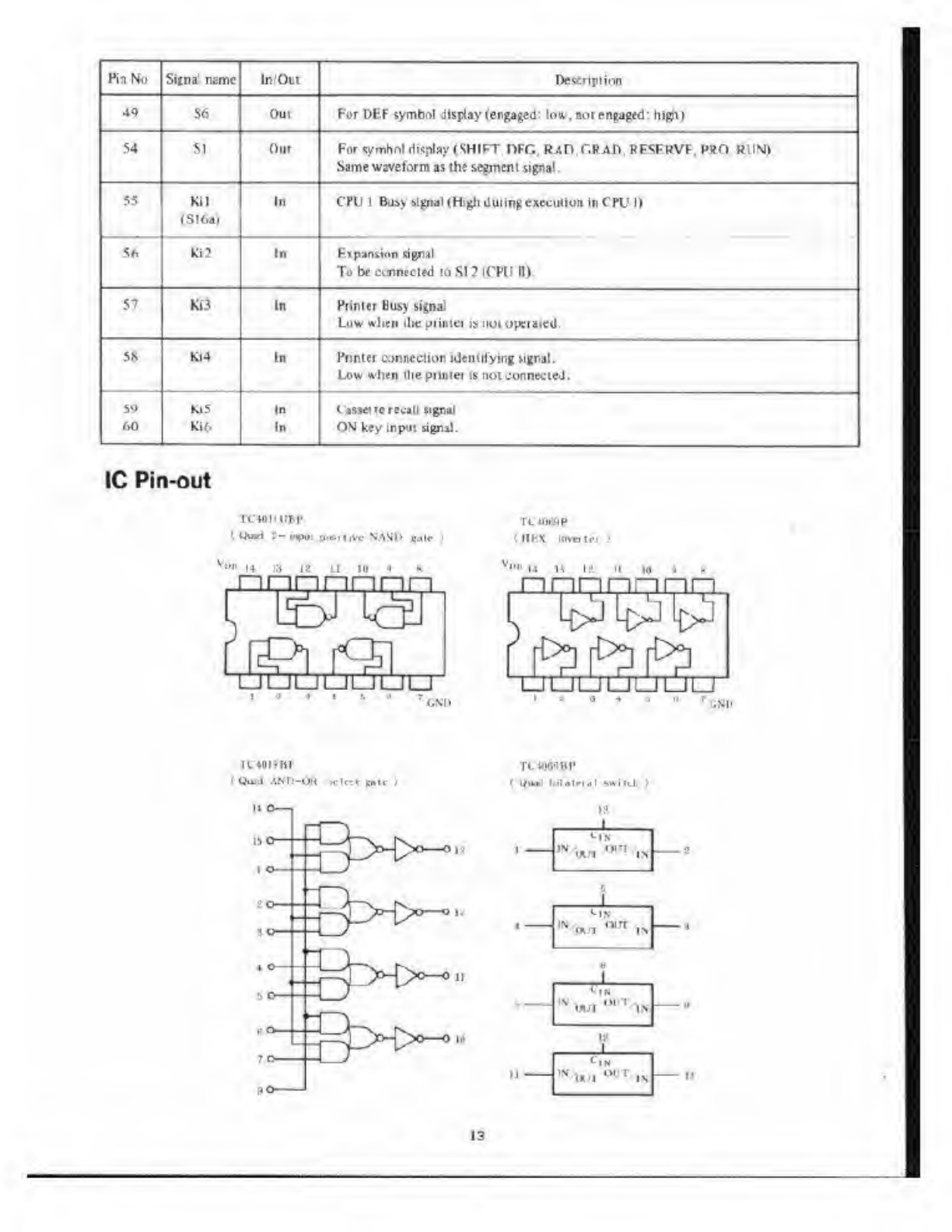
49 S6 Out Fot DEF symbol display (engaged" low, aoi engaged: lilgfi)
54 SI Out Fnrtymhnl display (SHIFT DFC., KaUCVAD, P.FSFKVF, PKO RUN)
Same waveform as the segment signal
.
55 Kit
(SI 6a)
In CPU 1BusysfgnaHHighuuiingexecutiujiinCPUl)
56 Ki? In F.ipantion signal
To b* cimrwcifd to SI 2(CPU 11).
57 H3 in Primer Busy signal
LuW A'litll lIlC i^lilllCI i> IIVH opcuttil
58 Ki4 In Puntei connection identifying iignal.
Low when ihe pimtei is not connected.
59
60
hi 5
Ki6
In
In
(asset to recall signal
OM key input signal.
IC Pin-out
ic-toiiuBr
HJu*t i-«npui p-tsmvo NASI* iwlr )
|< in ip
1lltS mvn id )
'""14 13 18 II ID JK
nnnnnnn
lay k^J
,fPl„r^1„,
uul1iljul!ju
I*A'CM)
',('' 14 HI? tl io >
nnnnnnn
c>
:
UUUUlJUU(iNI'
n:*umn'
'Quiii AMD-Oft Klcti wit >
THOBflBP
(tfiwi </il«lridl »*ilili >
zS>^~
IN '«n °"1in
l%*qui *» in
MbUt™ 'I.N
c,„
13
4. BEFORE SERVICING
Disassembly procedure
1
.
Remove 2screws (i) and Iscrews (b).
1From (he sere* sule. leparate the upper cabinet item
the lower cabinet (they are latched togeihei at ihiee
points, A, Band C).
Repot ring procodure
].The bii'-i' of lK« at jihiwetic ftintod board will be
exposed after the removal of the lower cabinet. You
can check the arithmetic printed board from the back.
2. Replacement ol the CPU 11 is possible.
3. If the key primed board is to be checked, the arith-
metic piiiilcd buaid lies to be bent at aright angle
alter removing the screws )d) anc (el. Inspection ol
the CPU 1bpossible if the bizzrr Is removed after
lemming sciew(c).
4. The hey printed bontd can be dismounted by removing 9gcrrws (f> and 1screws <$> Tale care as you remove rtie printed
board, so y«.iilonl *plll iIn* he/ lops.
LkcI
Replacement of the LSI
1
.
Only «very fine soldering pencil should be used tot replacing the LSI.
2. Be sure to first remove the key primed board fiotn the uppei cabinet. If the LSI on the key primed boird is to be removed,
if the LSI sremoved while the key ptlnted board Is on the upper cibinci. there is apoistbUity of deforming the key
rubber with Ute heal of the wittering pencil.
?. Bcsurc tocut each pinof the defeciive K. a-
Measuring current consumption
tVwer source volnge 4.72V
Cuitem consumption:
After pressing the (IN key Under ftSQuA
After pressing the OFF key: Under 12(iA
5. CASSETTE TAPE &INTERFACE
For details of operation and connection, refer to -Jie Owner's Manual for the TRS-80 Pocket Computer
.
Notes on suitable recorders
While Radio Slack's CTK-SOA is the intended cassette Recorder, oiheri can b* used The following totes
1. Cassettes oi upciMecl tjpci can te used.
2. Mic input jack must lia« an oipui impedance of IK or leas, wiih asensitivity level ofat least -tmV.
3. Eaiphone output must Hjvb an output impedance of IOK or less and an outpu: level nf 1volt or more.
4. Allowable distortion is -1 %%. *ith frequency response from ?to 4k H?
wy Im> hclpl'ii
14
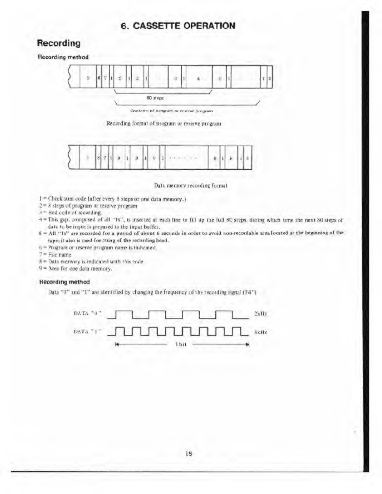
Recording
Recording method
6. CASSETTE OPERATION
cm
Recording formal of pi opam or reserve program
/
Data memory recording formal
1=Check sum code (after every ssteps or one data memory. I
2"8 steps of program or reserve program
3~fcnd code of recording.
4Tim gap. composed of all "Is", is inserted ai each line to (ill up Hie lull 80 steps, during which time the next SO steps of
data to be Input is peered in ll<c input buffet.
5-All *' Is" sre recorded for aperiod of about 6wCondf in order lo avoid non-record able area located at the beginning of the
tap« lit alto ii uwd for cuing of the recording head.
6=Program or reserve program nam* is frwlfcaied
7= File name
R=Data memory is mriicaied with r-iK rorle
9Area for one data memory.
Kecording method
Data "0" ind "1" are identified by changing The. frequency of the recording signal (F4"»
pata »_r :kiic
PATA JIkM/
lbi
15
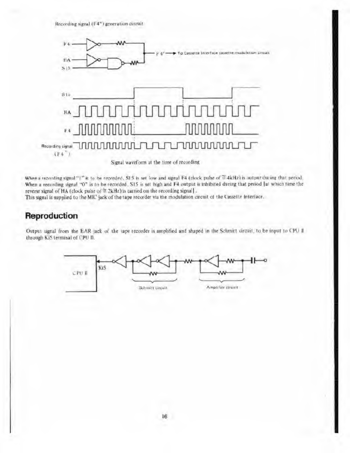
Recording Mgrul IF4" )^ncralion circuit
f.- 4" »to CfliMiM Ininlacc utwttc mafclmon cucun
SlJ
HA
F4
jULfiiLTLriJiJirLrLrirLnnr
juuuifiniuui JUUUUUUUl
Reco.d.9^.."uinjijiriiijui^^
(F**>
Signal waveform at the tin* of recording
Whan awording *leml"r*k 1« h# recorded. SI 5kvet low and «8n»i F4 (clock pulse of -4kH/lis .iiiiput du-ini thai period.
When arecording ligral "0" is in be recorded. SIS is set high and K4 output is inhibited during that peiiod Uwhich time the
reverse sinnal of HA (clock pulse .»:' =2kHz) is carried on lite recording signal |
.
This signilh supplied to the MIC jack of !he tape recorder via the modulation circuit oJ the Cassette Interface.
Reproduction
Output signal from the EAR jack of the tape recorder is amplified and shaped mthe Schmitt circuit, to be input to CPU II
through Ki5 terminal ot CPU II.
CPU II
MS wwv-
h^>
Jl! M'U C»CV>T Arvpli'icr circuit
16

Remote control
The Cassette In let fate will coltrci the RKMOTE Jack automatically (or record, playback and verify commands.
O.M7pF .V7 «Ki«
rl
KIMOTI- O
(SU)
*feG
(iMI>
1'ne U'-452XPisa mono-siablemultmbraUHHo perform tiiggei and resel fraction! from the sirgle chip).
"A" outputs apulse which KitepenrifM rtn thp limp ointtaiH OfCR a' the tailing edge of the mput ctgnil, and "ti" outputs a
pulw which udependent on the tine constant of CR at the ruing edge of ihe input signal- The relay operates ON and OH-
accut ding to the curie nt flow 10 ihe coil, and bauivatfil when "A" bactive and deactivated when "B*' KtCUW.
Startup ol >,< .,.,-tt- .r"---"
su
/—
Tmmtool ion ul ihc c<»cirt jj-rdin.i
QA
\Activa'ian of the relay
i:«ictt* to itort runnng)
QR "LT
\Oeaetivacior ot the telev
(cassette to nopruonir-q)
17
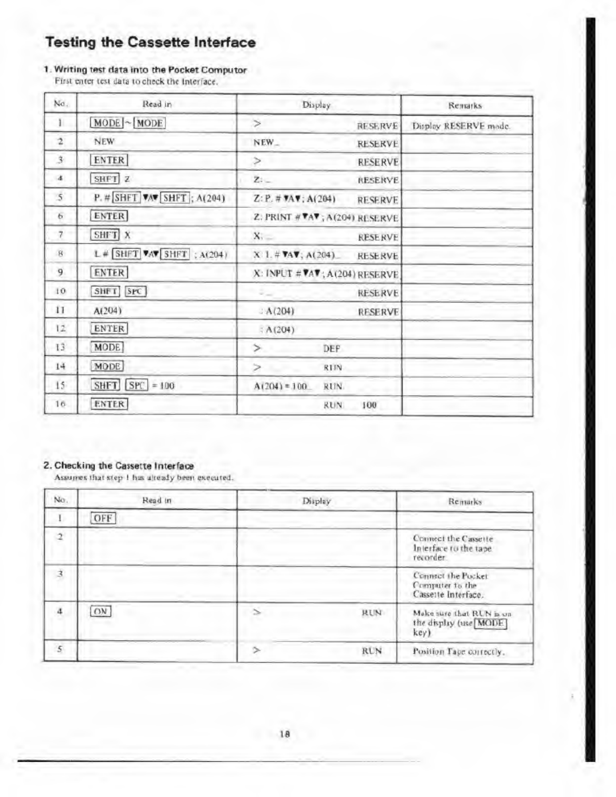
Testing the Cassette Interface
1Writing. '«t data into the Pocket Computor
Firn enter tesi flats 10 check tlu Inter fact,
No. Read in Display Remarks
^^^^"^
1ImodeHmodeI ^RESERVE Dhplcy RF-SF.RVF m.ide
2NEW NEW_ RESERVE
3ENTER >RESERVE
41shftI 2Z; _RESERVE
5P. »LSHFTJ?A» SHFT ;A<204> Z:P. tf»AT;A(204t RESERVE
6ir>Tl-K| Z; PRINT *TAT ;A(204) RfcSCRVE
71SHFTI XX. RESERVE —
8L#|SHFTi?AT|SHFT| ;A(204> X: 1. 3TAT; A(204)_ RESERVE
9int(k) X: INPUT =?AT;A(204) RESERVE
10 Sill 11|SK |RESERVE
I] AI204) :A(204| RESERVE
12 bNItK :A(204)
13 MODFJ ::.(->
14 MODEl >KlIN
15 SHFTl ISPi! =100 A(?041=lflO_ RUM
16 ENTER IKlIN 1U0
2. Checking the Cassette Interface
Amuires ihat iiep Ihut already been executed.
No. Read in Di iploy Remarks
1OFF
**
•Connect tiicCwseUc
Interface to the lape
recorder
3Connect the Pocket
Computer In the
Cassette Inurface.
4[TUT] 5* RUN Mako suic that RL'N »un
th# dKphy (u«fMfH»F|
ke/) '
5>RL'N Pimtijn Tjuc coiieciy.
16
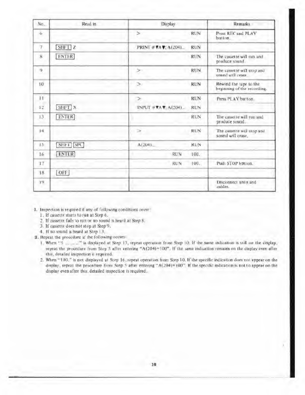
Nu. Read in Display Remarks
6>RUN Pr«a» RHC aad PLAY
huimn.
7
'
PRIN1 *TAT;AI2(W|_ RUN
1SHMJ Z
HRUN nie casseliewill run ami
produce *ouid
|KNThR|
9>RUN The usiclic wi'l slop and
tnnnd mill ct%tt.
10
•
>RUN Ke*'ind (tie tape to the
beginning .>f tht recording.
11
12
>
INPUT #TAT;A(204)
r: n
RUN
Press Pl.AYbuuon.
1SHFT 1X
13 IENTER |RUN '11 if L&aetlc wi'l iuii and
produce sound.
14 >RUN The GUMIWW0 siopanO
sound will case.
15 1Mtl-I l|SK] AUU4> RUN
16 IHNTtR| R\ \mo.
17 RUN 100. Push STOPbouon.
18 fOFFl
19 Disconnect ani:sand
castes.
I. Inspection is reqnii-'td if any of following conditions occur*
1. lfcassettestm!torunatStep6.
2. If cassette fails to run or no jouml is heard at Step 8.
3. If cassette does not stop at SicpO.
4. If no sound sheard at Step 13.
U. Repeal the procedure it" ihc following occur*:
1
.
When "5 "»displayed at Step 13, repeat operation fnim Step 10. If ihe saine indication is Mill on the display.
repeat Ihe procedure frum Step 5 after emetine. "A(204)=100". If ihc tame indkatixn remains on Ike display even after
this .detailed inspection ii required.
2. When 'MOO.' is not displayed at Step 16, repeal operation from Step 10. If the specific Mfotlon doe* Ml appear on the
display, repeal ihe procedlM front Step 5after entering "Af204l= 100". If the specific indication is not to ippe-ar on the
display even after this, detailed inspection Is required.
10
Repairing the Cassette Interface
P'(W)f»m
1
U.1
1N T
t> ri
#i) •
ii ii
:PAU5E1
|A(201) 1
Us? ibe following procedures ioe>v»luaie the Cassette Ititertaie
No. Read in Displjv
Plug Tape rwuiuVi
ReaMika
lak| cKtM
OTI PLAY MX STOP
1tonnei't lompuier io
Interlace.
i|off|)
2[ON] >HUN o o Uelermine recording
loca'.iiin oi> the tape.
3>RUN o o OooMake sure liul 111; upe
docs not run.
4
'
CS.TA RUN ooCSjSHKTlf
A
sRUN oooooTHa lap* ttirtc tnnin
jnJ u'cording tound will
be heard.
IfcNItP 1
h>RUN ooo o Hie Miutiil will cext.it and
tlie upe will stop wlteu
">*' is displayed.
7>RUN o o RewjiJ lupe to tic begin-
ning!)! ihc ICUHUDK.
K>KL'N o o o o
9CLO.? (SHFTlTA Cl.O/fA RUN oo o
iU 1trVI!-K |RUN o o ooine display ccnietiis will
disappear, 'apt will s'.an
aid .oiinl will be pro-
duced.
11 >RUN oo o Sound and tape \>ill Mop
when">"isdispaycd.
12 RUN
13 lOFFl
1
0= Cunneciedor activated
2G
|NOTES]
1. Check the Com puw.il th* cassette tape keeps running in Step 3,fab to run in Step S.ot the tape does nor slop in Slep 6.
2. Check the recording circiii! of the Interface ifno recording sound is audible at Step S.
J. Kr» sound ft audible a> Step ID, playback anoihei recorded tape to check il sound isiuciblr with that tape If tound is not
audible with that tape, check the reproducing circuit of the Intetface. If sound is audible with the jecond tape, check
ihe lecordinR circuit of the Interface.
No.
|
Read in Display Ketnaiks
1
s
RUN RUN_ RUN
Dim
No tap* recorder motion.
z
i
IbtSIcK l^-1KU I*
RUN
kbcokdor soufiu is auuimc.
Reco'dinff sound ceases and "10." is displayed foi about 1second.
iRUN
»5and 12 pins ot
TCXSJHBP lor t>«ii water t
)
1(1111 1
._.-.. 1- In J. A. In A* J.ln <X .!_ „__
<l' diiuiptia——h*—^"—"p ——f—"|" incDiaim
'<«ord«ig 'ina.ipjjy reco-ding Indnplav recording indHDlav
•Stcrmnalol Ihe inlor
»10BinolTC4528an
«1 ••rn-mal i* f*io >»I«y
A;tiw»tion ot tht riliv
(cs»cite top* io start tunning)
-»fU- Imsecmm j
L>eact^3tK"> oi in« r*iav
(gasaeiio Ldpe lu tiw)
Cassette ONjOFF conitol must be pioperly executed when the above signals ate observed during cxeiutwn of program.
21
7. CHECK PROGRAM
READ IN l> 1S P LAY
12 3 t 5 17-s10 II 1! 13 i1* .. 1' 17 islie •
1Xw\
2
3
^»
i : 1 i i i
IALL RESET)
8/8 lENTERl 5515 555551
—
l.-
—*—
*
1modbI
f>
.^^^^~ —"i-
i•rk1N1»() K, w
1F•ISHF7I (1 h[SHU ;ENTfeRl
82JS1IFTI 2ISHFTJ P•2Tz'r
L*
l—iu
1,SMK1| SISHET1 IKNTHRI 2
3
:z
ne
T
E
rk
1—1—
1
p
i11
IN11'
s' T'^
82
8BEE P 8[entek|
]MODfc! '-
1T
10 GRAdIeNTErI ..»
11 [Shi- i| Isi'tl u14'1 (fcNlfc-fcl ii i47
12
18
1iMOIH-i --
|SHFT| 7S
14 'NOUH'SHFTliSPCl ii I47
1i | ,
1:, 1CLI RAD [ENTER) J5 i i
IS r1f-r :- 1i.k (i
( 1 V
K
I|L_
I:lENTER, S
18 [Enter' -.
ie {OFF]
20
*11
—
ii
si
11
32
23
24
26
en
i>7
2fi
29
30 1I
'i
''
as
S3
34
8fi
11'111
36
87
ax
1i i
.10
it 1
40
SVMBOI. laavtt
)|;i|is|z3 USHFT Dill RAD GfAH DEF JrUK TRO WbQU> play'rec stw RBCn
j J J
^ft1
''.-.
iE• 1
f^Ot
<G> O
(Ul oO
Co)
o_";.
oo
'. J
<io
o*_*
(O) o o
''
OG1
1
oi~
'vj
"
oO o
.
!
I'*
1
32
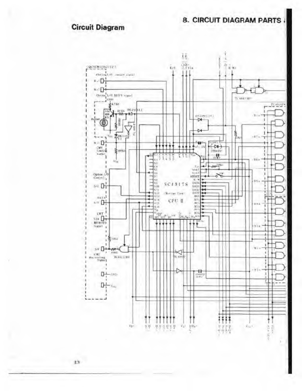
Circuit Diagram
8. CIRCUIT DIAGRAM PARTS i
I"J
- -
CHE-
Hie i.?Fi
'Of
or
I'liirl"! BUSV >l«v!
»» Or
lvt
<n EK
M-min
I
!>*
cm '"""
*»ai4liM, Ki>; i«.
>i11*
.
ss
$11 mil'
SIB <B->ll.ir> Pivwl I'HH
til HHt,
!S cpu DII.
ft .
(ii Ufa
•.|w *» I* "»
TTTT
'
t>-
ifir (!:
FKL i..i
o
ZIo
:0-
...-!. :0
:
fl—
r
vB-?v gyggyij **' V" VV V V
ii ni» ii
23

SSIGNALS POSITION
Via f
:-Mi
.IDI f
11 LIS ~I
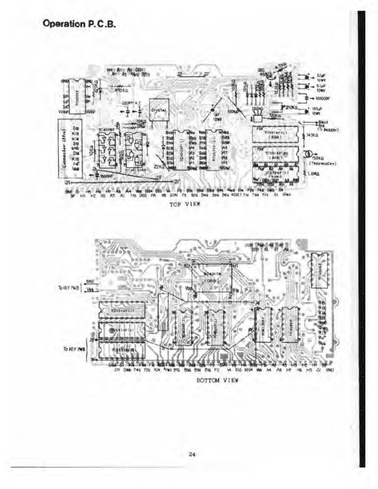
Operation P. C.B.
«•<---'->©
m
**3 «tb MO!
w§
J* 1
o*f
«X)U
fi*y
—
-
So
1KI9
JWD
1SM
1KH
K*OMF
•i"->.\
U*L
±-»iwoo«
n
<*«0
ilOOWir B
fSOKQ
'herniate*'}
j, _—.jr
9NB5- *H«r**6*«*ttW«M6* nw*&*toam**t*FnH*9*bfii
IP Hi HZ H) AS AI mWW*ilAi ri MBH IM M> «*' >ni Mmi it **»*
TOP VIE*
&tfr»WB
To KEY
*»• to
J
.. /J
1*
ID 5i» Ml fim mVm era
!/«1 •'
^.^
BM PW PC «lit NO* MMA6 MHb HJ AI W
BOTTCM VIE*
24
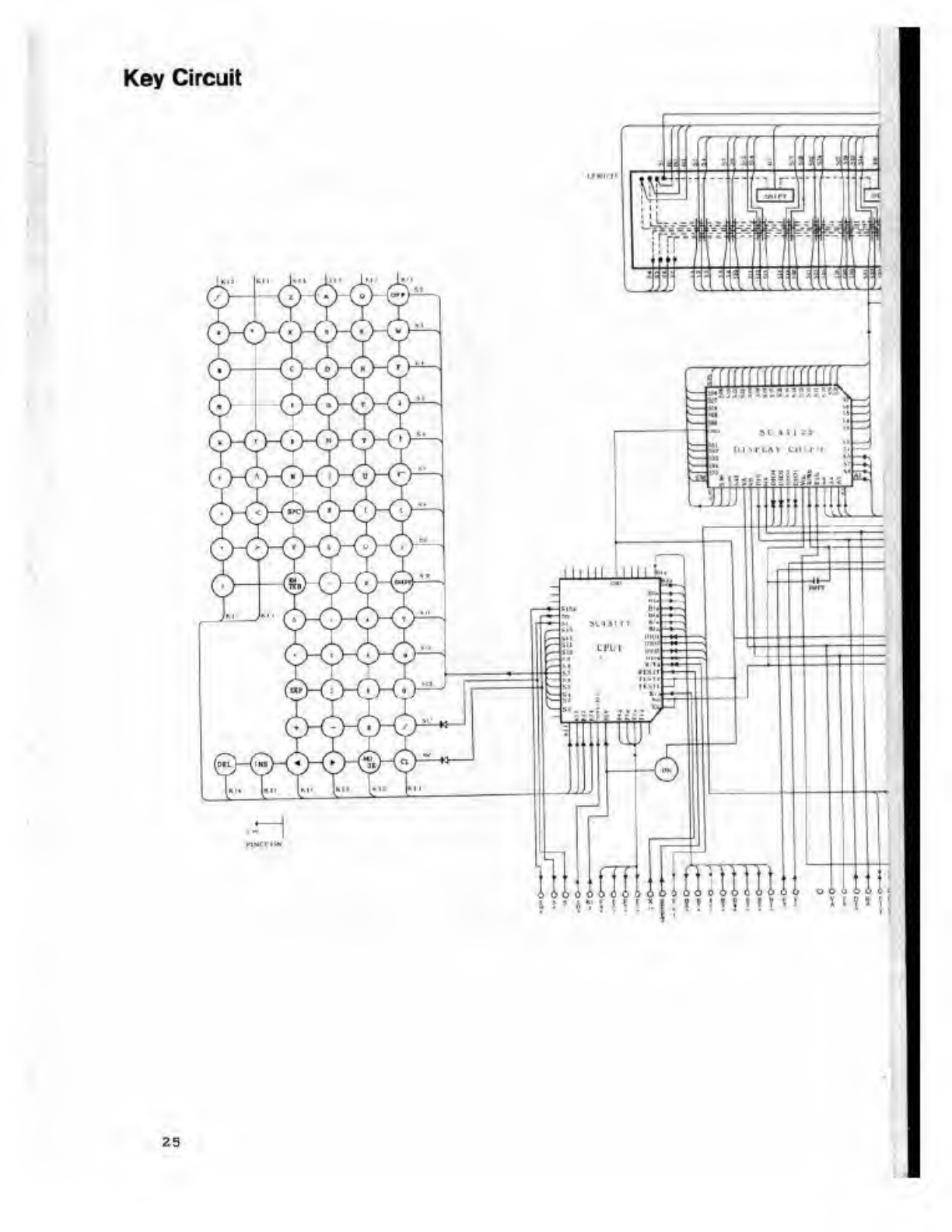
Key Circuit
sunn
\i |M'l.ftl ill :!'i| ••
23
&&6& & O O I
iftinmiu -fl 8
H^D
= 3 -
In I3"a 9CJBB 8
••1aflOM
:•! 23D ;1"<•" -
gn
3Q331!
33
ai
3
S2
DO cccp
00. 00 D
sua
iPP
""'""I s
.liB s
Q a t
ioa a c
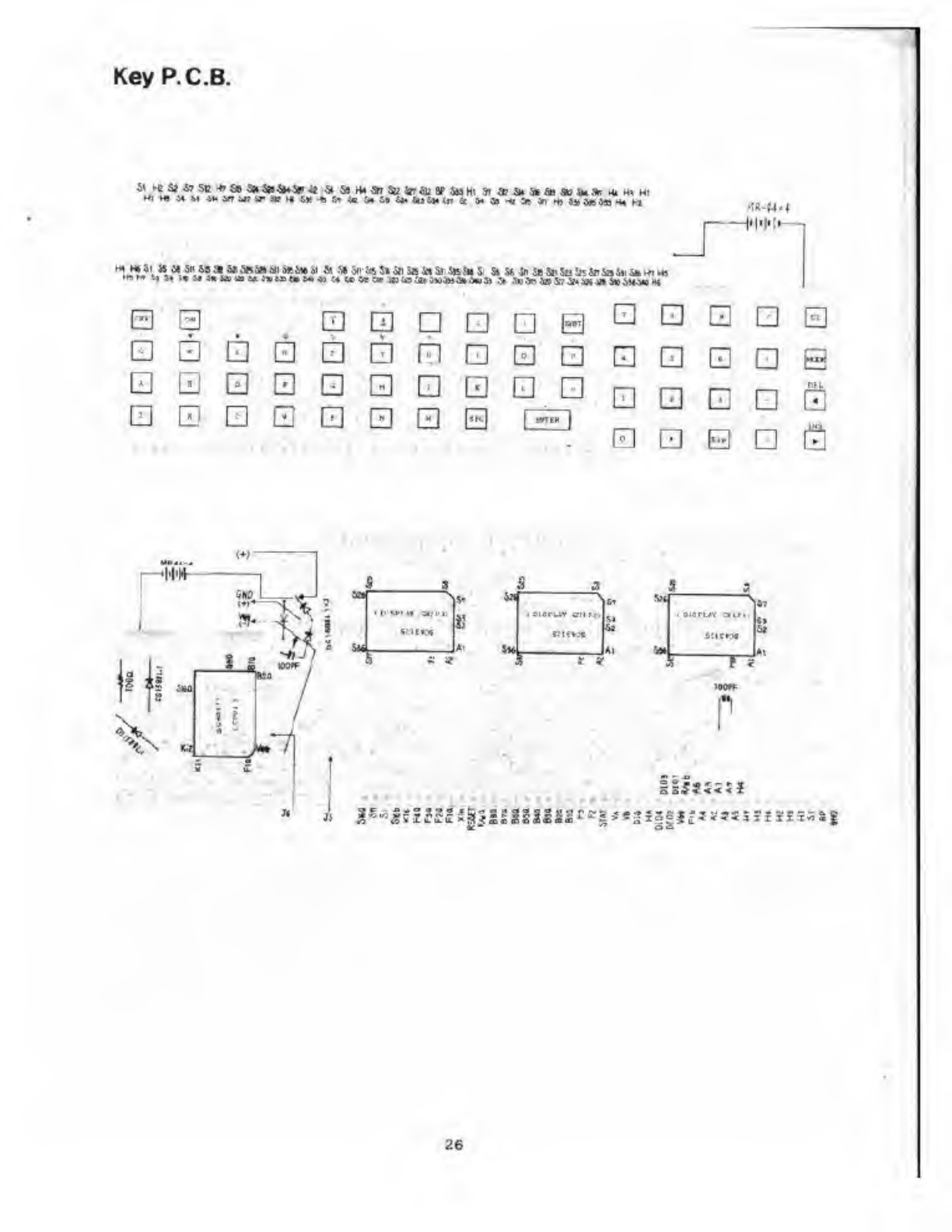
KeyP.C.B.
Ml WM M 4u IB W? *»* *S* •« S. J* &. &BS* l4< ->• (nJ» &&-V U} to •» Z% &> *B ** *l
S3 QDDH
EQQQEJE1F1QE1Q
QEQQD
EQQQQ
~*t ry fR-U-l
B
D-
Enit,
B
HDa
#ft
(+>
op 3S
w
•MH 1* loci;
-*
iDicrui sit rn
nio.i
E?
B
*i i*
ID'gFLAY .3 1(1
SEIOOt
MP
m
P
.-
26
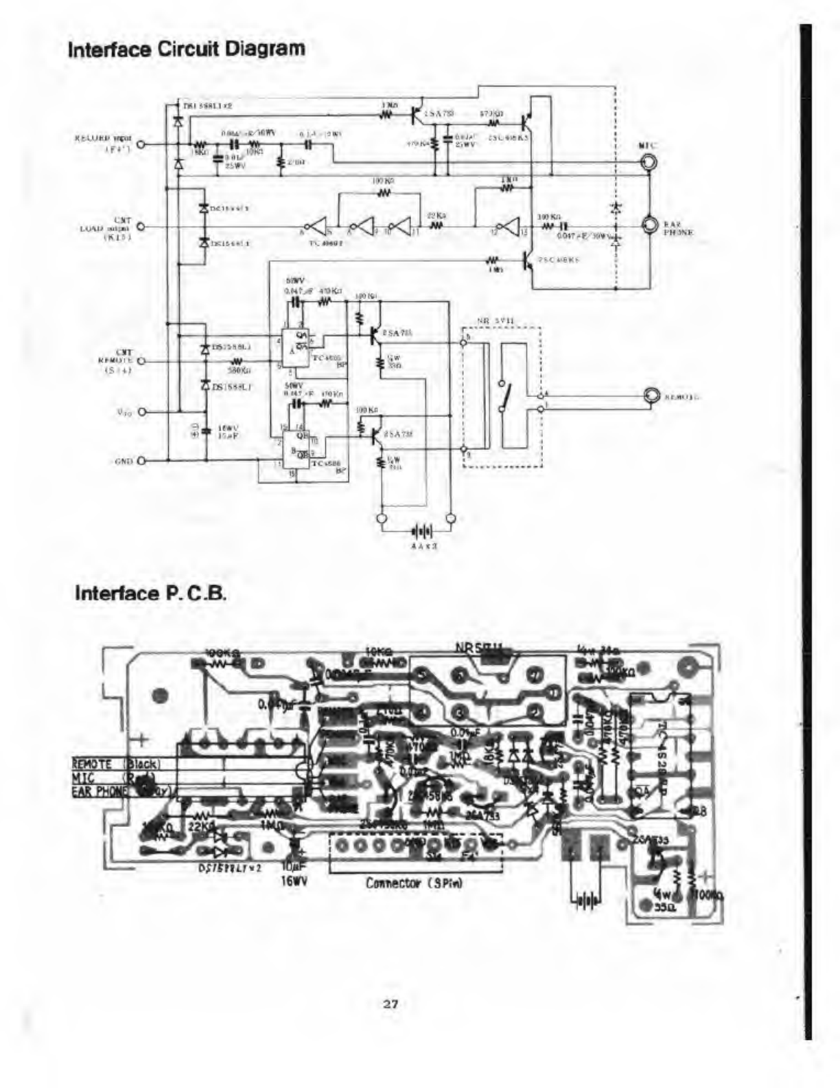
Interface Circuit Diagram
KtUJM> "»ul _
IPl'l U
1H10)
can O
Interface P.C.B.
27
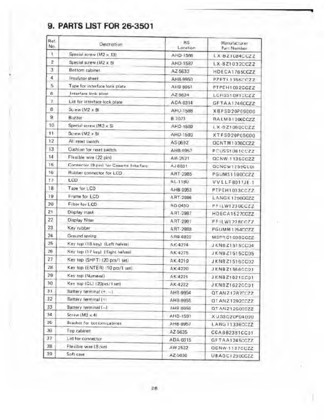
9. PARTS LIST FOR 26-3501
Ret
Nr> Description RS
Location
Manufacturer
Pa'i Number
1Special sc*e«v (M2 *131 AHD15S5 Lx-H*;iU84UtJZZ
2Special screw (M2X aAH13-I587 LX 3Z1032CCZZ
3Bottom cablet AZ-5633 HDECA1765CCZZ
4InsuUto' sheet AHB-9P,!V)
i
P7FTI 135SCCZ2
5T^ne for interface loclc plats Ana 90S1 PTPEH1C0 2CCZZ
A1Morfsnt lor*4< plme AZ5634 LCH351091CCZZ
7Lid tor interface lock plate ADA-0314 GFTAA1?46CCZZ
3t'c«(M2 < 9) AHLMS8B XBPSD2OP09OOO
9BlJ2?tt B7073 RALMaiOOBCCZZ
10 Special «r»iw (M2 x5) AHD-1689 LX-BZ10SOCCZ2
11 Scnr*)M2 x5) AHO-1690 XTPSD20P05000
12 All reset twitch AS-U692 QCNTM1036CCZZ
13
14
IB
Cushion 'or reset switch \HR '-<'>- PCUSS10S1CCZZ
Flexible wire (22 on) AtAi.2621 QCNW 1136CCZZ
Conrwcicr 18pi-.J 'o'Caw«tt« Interface AJ0031 QCNCW WD3CC0I
to Rubber connector tot LCD ART-2985 PGUM51190CCZZ
VVLLF8017JE 1
17
'8
19
LCD AL1180
Tape for LCD AHB9953 PTPEH1033CCZZ
Frame tor LCD ART2986 LANGK1290CCZZ
20 Filter lor LCD AQO430 PPILWI230CCZZ
«Display niask ART-2987 HDECA1527CCZZ
22
23
Display ftL'r ART-2991 PFiLwi??acr:77
Key rubber \h~ ?<ms PGUMM1264CCZZ
Mcnnct oooccsz
2d Ground sonno
—-" —*
ana 6623
25
26
Key lop 08 key) (Left n»lvesl AK-4274 JKNBZ1515CC04
Key top (1 7key) (Right lidlvo) AK-4276 JKNBZ1515CC05
27 Key ioplSHFT)<2CpcVl sell AK4219 JKNBZ1516CC02
zh Kay lop (ENTER) HO pcs/1 set) AK-4220 JKNBZl r*6C0CM
29 Kwy top (Njmeial) AK-4221 JKNBZ1621CC01
30
31
32
Key iop(CL! <20pcS/1setI AK4222 JKNBZ1622CCQ1
Salter/ terminal (-*, —
]
AHB-9954 0TAN2l?R7^r7Z
Battery terminal!*! AHB-9955 QTANZ1292CCZZ
33 Battery terminal (-) AMBQ0S6 OT ANZI250CCZZ
<4 So»w(M2 x4) AHD-1G91 XUSSOZCP040QO
36 fliockci fot boinmcaMnct AHB-9957 LANU11336CCZZ
36 1op cabinet AZ-5635 CCA3B2381CC01
3? Lid tor connector ADA0315 GFTAA124SCCZZ
38
39
Flexible vnre(Bnin) AW 2522 QCNW 1137CCZZ
Soft esse AZ-5036 UBAGC1230CCZZ
28
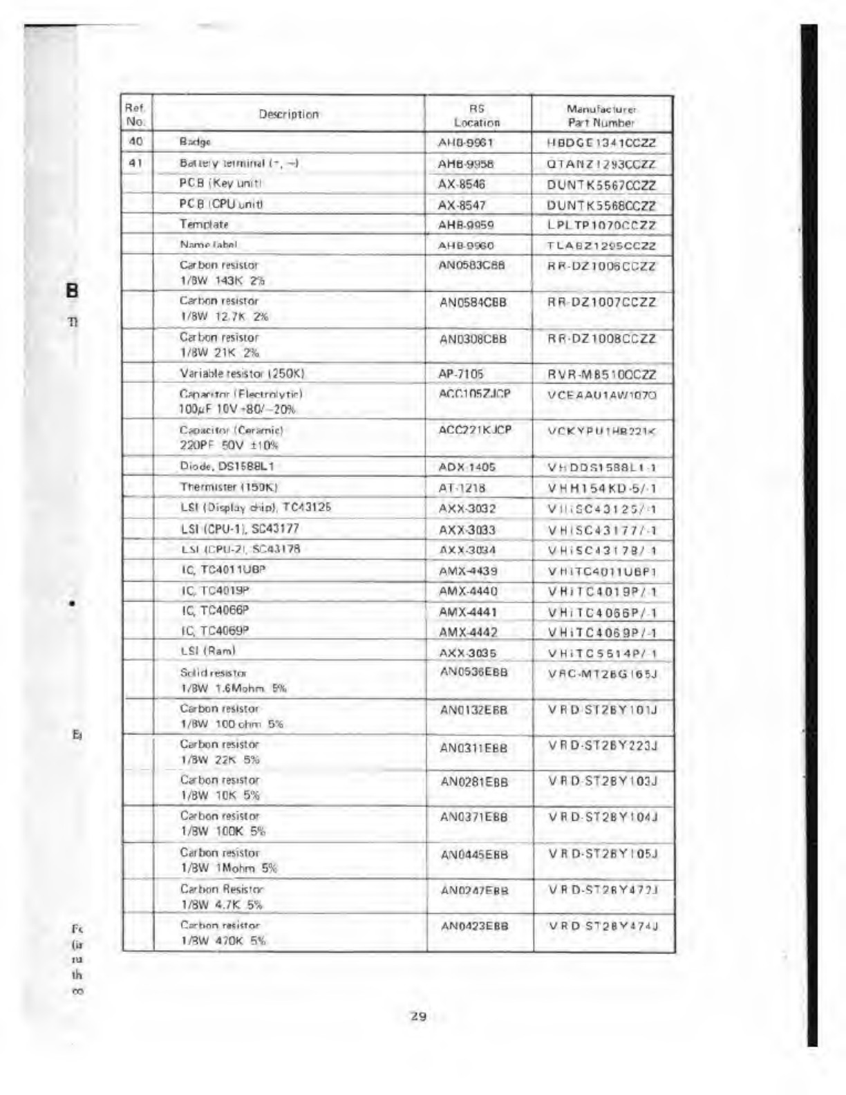
B
Fc
ru
ih
No. [Description RS
Location
Menufoe lure'
P»t Number
40 Bad90 Al 10-9961 HBDCE1341CC2Z
41 Bcuey urmlnil (-, -1 AHB-9958 QTANZI293CCZZ
PCB (Key unit) AX 8546 DUNTK5567CCZZ
PC B (CPU unitl AX-8547 DUNTK5568CCZZ
Template AHB-OQ5Q LPLTP1070CC7?
Nam* lahnl AHB99G0 TLAB21205CCZZ
Cstxm resistor
1/BW 143K Zh
AN0583CBa RR-DZ10Q6CCZZ
Carben resislor
I/8W 12. 7K 2*
AN0584C6B RRDZ10D7CCZZ
Ca bon resistor
1/8W 21 K2%
AN03Q8CfiB RRDZ100BCCZZ
Variable resistor 125010 AP-710S RVR-MB5100CZZ
C*p*-itnr (Flertrnlytir)
lOO^F 10V -807-20%
Arnnszjcp VCEAAU1AW107O
Co.iokv (CerCTtit)
220PP 50V itO*
ACC271KJCP vr*YPLnMB?31<
Diode. DS1688L1 AOX 1405 VHDOS158BL11
Trie miner iisok) AT-1218 VHH154KD-5/1
LSI (Display thiol TC/312S AXX3032 V1liSC431 25/1
LSI (CPU-1). SC43177 AX> 3033 VHISC43I 77/1
LSI tCPU-71. Sr.4.tl7n AXX-3034 VHJSC431 78/ 1
IC, TC401 1UBP AMX-4439 VHiTC4Q11UBPl
IC TC4019P flMX-4440 VHiTC40»9P/ 1
IC, TC4066P AMX-4441
AMX-4442
VHi 1C4056P/ 1
IC, TC4069P VHiTC4069PM
LSI (Ram) AX> 3C3^ VHiTC5514PM
Sdidresatoi
1/8W I.6M9I1P1 6%
ANCS36EBB VBC-MT26G I65J
Carbon resistoi
1/3W 100 ohm 5*
AN0I32E6B VRD ST2BY101J
Carbon resistor
1/BW 22K 5% AN0311E6B VRD ST2BY223J
Cabon resistor
1/BW 1CK 5% AN0281EBB VRD ST2BYI03J
Carbon resistor
1/BW 1G0K 5%
AN0371EBB VRD ST2BY104J
Carbon resistor
I/8W 1Mohm 594
AN0445EBB VRO-ST28YI05J
Cation Resistor
1/8W 4.7K 5%
AN07A7EBB VRD-ST2RY477J
Carbon rtsitlor
1/SW 470K 5*6
AN0423E8B VRD ST2BY*7*J
29
B
Fc
(if
m
th
CO
Rel.
No. Deicripiion RS
1OC^on
Manufacturer
Part Number
40 Badge flMh.yyei HBDGE134 1CC2Z
41 BatWy Wrniml 4>, -I AHB-9958 QTANZ1293CCZZ
PCB(Keytmt» AX -8546 DUNTK5567CCZZ
PCBICPUunit) AX-8547 OUNTK5558CCZZ
Template AHB-9959 LPLTP1070CC77
Name label AHB9960 TLABZ13fl«;rf:77
Carbon resistor AN0583CBB RP-DZ1006CCZZ
Carbon reiiitor
1/BW 12.7K 2%
AM0&84CBB RR-DZI007CCZZ
Carbon resistor
1/BW 21K 2% AN03O8CBB RR-DZ1008CCZZ
VariaWeresislcr (250X1 AP7105 RVR-MB510QCZZ
^~
Capacita (Electrolvticl
IDOyf IOV-8lV-2(Bi
ACC105ZJCP VCEAA1I1AW107O
Capacitor {Cersmicl
2;op= 50V ro-.
ACC221KJCP VCKVPU1HB221K
Diode. DS1588L1 ADX1405 VHDDS1588L1 1
Thc-mistct I160K) AT-1218 VHHISaRD-SM
LSI (Display OltW TC43I2S AXX-3032 VHiSC*3125/ 1
LSI tCPU-1). SC43177
1^1 Jnni 111 PTAMTO
AXX-3033 VHJSC43177/ 1
Lol lul U-^l, jO*»JI /O
IC, TC401 1UB&
AXX-3034
AMX-4439
VHtSC43 1/8/-1
VH.TC4011UBP1
IC, 1040191* AMX-444Q VHiTC401 9P/-1
IC. TC4066P
l
AMX-4441 VHJ7C4066P/-1
IC. TC4069P AMX-4442 VHiTC40S9P/-l
LSI (Ram) AX X3035 VMJTC5514P/1
Sdirl resit Tor
I/8W 16Mohm 9fe
AN0536EBB VRC-MT26G165J
.« „
Carbon resltlor
1/BW lOOo-vn 6%
AN0132EBB VPDST2BY101J
Carbon resistor
1/BW 22K S% AN031IE6B VPD S12BY223J
Caroon resistor
1/8W 10K 5% AN 0281 EBB VRDST2BY103J
Carbon resistor
1/8W ICOK 5%
AN0371EBB VRO ST2BY104J
Carbon resistor
1/8W IMohm 5% AN0445EBB VRD-S72BY105J
Carbon Resiitot
1/8W 4.7K 5*
AN0247EBB VRD ST2BY472J
Carbon resistor
1/8W 470K 5%
AN0423EBB VPO-ST?BY474J
29
Rpf
v- Description RS Manufacture-
Location Part Number
Transistor 2SC4S8KS AA2SC458KS VS2SC458KS/I
MOS FET 2SJ40 AMX-4443 VS2SJ4 0-///-1
Cacaciiot (T;m&Jurnt
O.laF 10V +80/-2O%
ACC104ZCTP RC.?7inOBCCZZ
Crvti4l (256 kH-| AMX.2780 RC^SPI0?4CC7Z
Capacitor (Tantalum)
lOOpF 50V ilOW
ACClOIKJCP VCKYPU1HB10IK
Capacitor {Tantalum)
lOOOOpF 25V :20%
ACC103MFTM VCTYPU1EX103M
Capacitor (Tintiiuml
1/tF 10V +8Q/-2Q*.
ACC105ZCTP RC-SZ1Q07CCZZ
Carbon resistor
1/8W 220K 5% AN0396EBB VRD-ST2BV224J
Capacitor (Cframicl
lOOOpF 50V il(Wt
ACC102KJCP VCKYPU1HB102K
-)
30
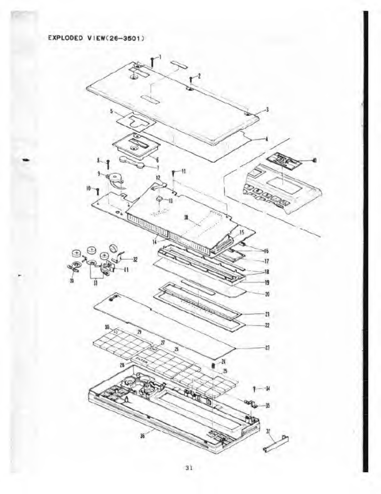
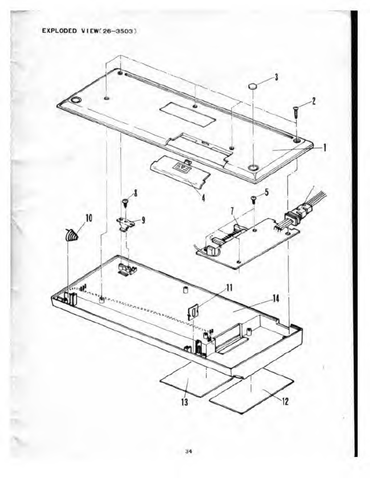
EXPLODED VIEWC 26-3501)
r«*,
31
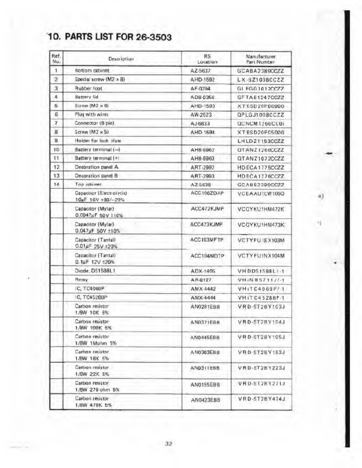
10. PARTS LIST FOR 26-3503
Ret.
No. Dctuitxivii RS
Location
Wan:ifartu'er
Pari Number
1Bottom cabinet AZ5637 GCABA2389CCZZ
2Special screw (M2 >8) AHD-159? LX-BZ1038CCZZ
3Rubber foot AF-0?<U fil Ffif. 101 7C.C77
4Battary lid ADB036C GFTAB1247CC2Z
5Screw (M2 x01 AMD- 1593 XTC3D20PGCO0O
6Plug with wire* AW-2523 QPLGJ1008CCZZ
7Connector (9 pin) AJ-HM3 qcncmuwcuqi
aScriwlM2x5» AHD 1594 XTBSD20P0500O
9HoU«» *b< lock Dlaie LHLOZ1 153CCZZ
10 Battery letmlnaH-J AHB-9962
AHB-9963
QTANZ1266CCZZ
QTANZ1072CCZZ
1
1
12
13
Battery termmaH+!
Decoration panel AART-2992 HDECA1775CCZZ
Oecoratiori panel BAR1 -P993 HDfCA177€CC7?
14 fop pohnei A25G39 GCABB2300CCZZ
Capacitor (Electrolytic)
10»P iGv+ao7-2o%
ACC106ZDAP VCEAAUICW 106G
Capacitor (Mylar)
O.C047,mF 50V 110%
ACC4/2KJMP VCQYKU1HM472K
Capacitor (MylaO
0.047iiF 50V +10%
ACC473KJMP VCQYKU1HM473K
Capacitor (Tantill
0.01/*F 25V ±20%
ACC103MFTP VCTYPU1EX103M
Capacitor (Tinuil
O.lMF 12V J20*
ACC104MD1P VCTYPUINXICMM
D,ode.D$1588L1 ADX-1405 VHDDS1589L1 1
Relay AB-8127 VH.N R57 11 //-I
IC,TC4069P AM X-4 442 VHiTC4069P,' 1
(C, TC4G26BP AMX4444 VMiTC4528BP-1
Carbon iesi si >
1/8W 10K 6%
AN0281EBB VROST2BY103J
Carbon resistor
1/8W lOOK 5*
AN0371EB8 VRD-ST2BY104J
1
Carbon remittor
1/8W 1Mohm 5%
AN0445E8B VH D-ST2BY105J
Carbon remittor
1/SW 1BK 5%
AN0303EBB VRD ST2BY183J
i
Carbon iciiitoi
1/BW 22K 6%
-
AN03HEBB VRD-5T2BY223J
CaiDon resistor
1/6W 270 ohm 6* AN0155EBB VRD-ST2BY271J
Carbon resistor
l/BW 470K b% AN0423EBB VRD-ST2BY474J
*)
32
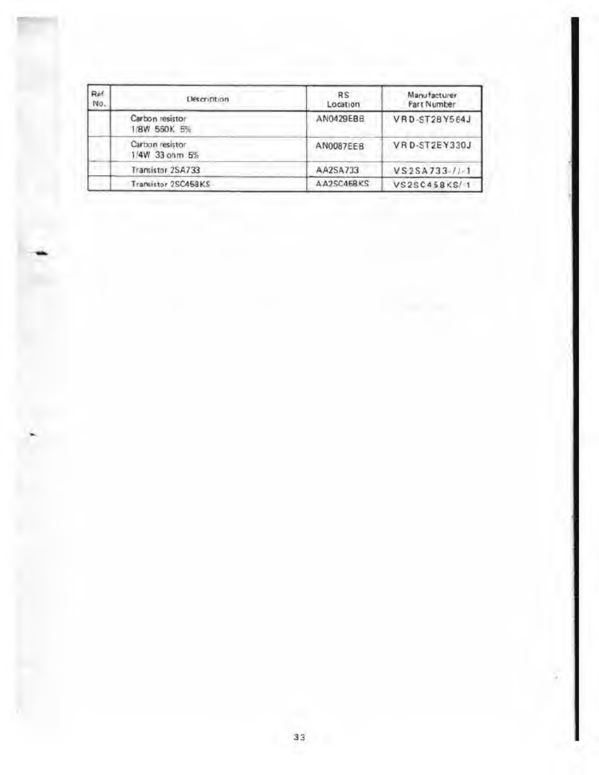
Re'
NO. Description RS
Location
Manjfaclurei
Part Number
Carton resistor
1«VI 550K 5%
ANCM29EB9 VRD-ST2BY564J
Carton resistor
l.'4W 33 oft m5%
AN0Q87EEB VRD-ST2EY330J
Transiitor 2SA733 AA2SA733 VS2SA733-/M
T.arwiitor 7SC453KS AA2SC458KS VS2SC458KSM
33
EXPLODED VIEWr 26-3503;
34
