Radio Shack Hardware Manual PC 6 Service 19xx Tandy Text
User Manual: manual pdf -FilePursuit
Open the PDF directly: View PDF ![]() .
.
Page Count: 27
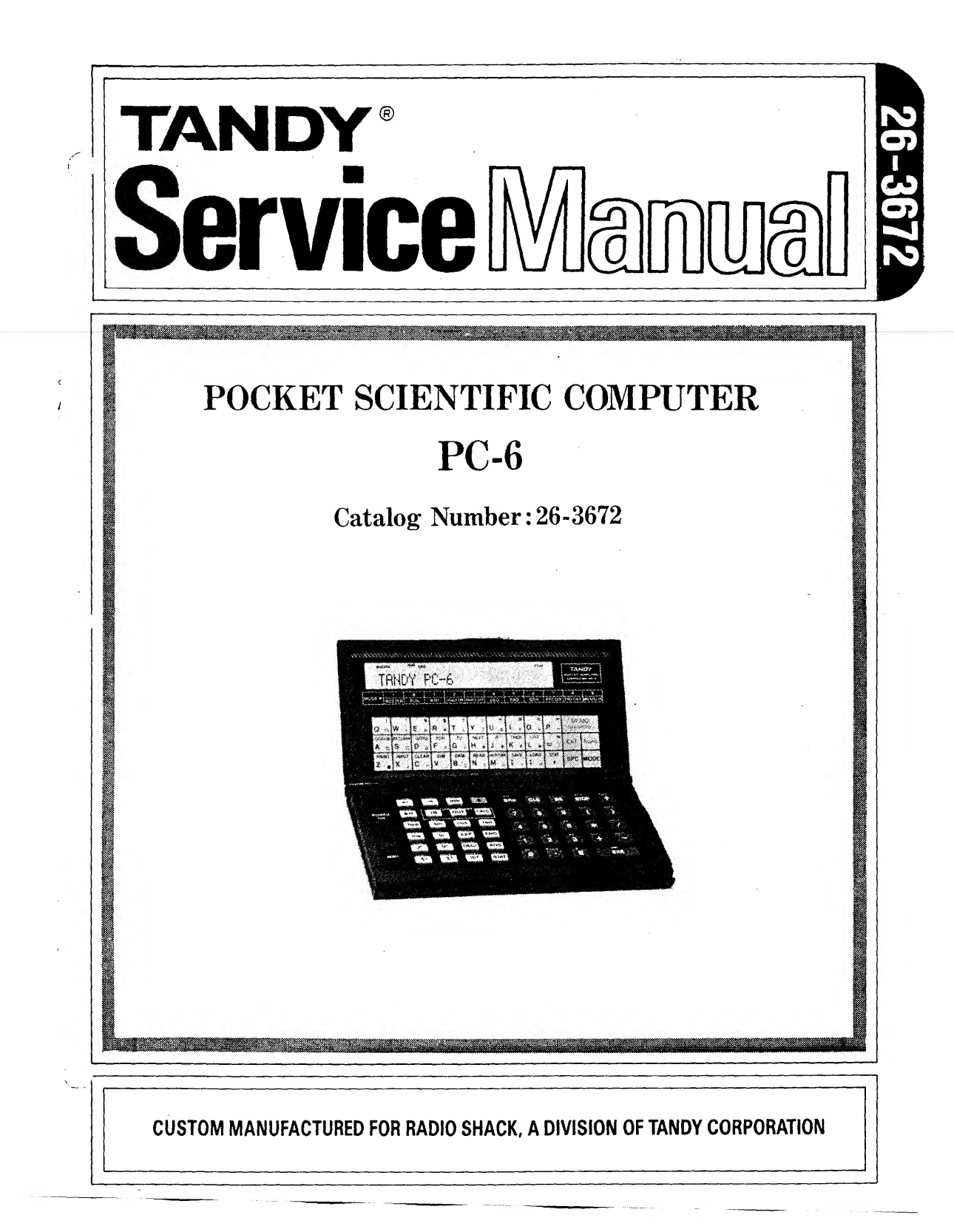
Catalog Number: 26-3672
CUSTOM MANUFACTURED FOR RADIO SHACK, ADIVISION OF TANDY CORPORATION
CONTENTS
PAGE
SPECIFICATIONS 3
How To Open Upper Case ..3
THEORY OF OPERATION 4
Block Diagram 4
LSI 5
Ram Map 5
Buzzer Control Circuit 6
Interrupt Circuit 6
Keyboard 6
Power Supply 7
LSI (Pin Functions) 8
DISPLAY 9
TROUBLESHOOTING GUIDE 10
Test Programs 11
Operation Check 14
PCB ASSEMBLY VIEWS 19
PARTS LIST 20
Electrical Parts 20
Mechanical Parts 21
EXPLODED VIEW/DISASSEMBLY INSTRUCTIONS 23
SCHEMATIC DIAGRAM 24
Main Block m24
Keyboard .25
Display 26
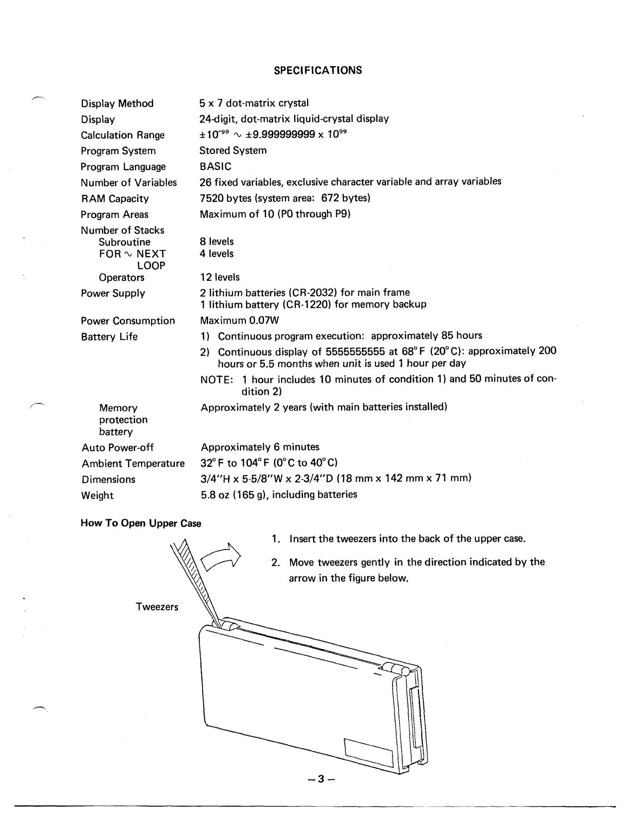
SPECIFICATIONS
Display Method
Display
Calculation Range
Program System
Program Language
Number of Variables
RAM Capacity
Program Areas
Number of Stacks
Subroutine
FOR-v NEXT
LOOP
Operators
Power Supply
Power Consumption
Battery Life
Memory
protection
battery
Auto Power-off
Ambient Temperature
Dimensions
Weight
5x7 dot-matrix crystal
24-digit, dot-matrix liquid-crystal display
±10" -v ±9.999999999 x10"
Stored System
BASIC
26 fixed variables, exclusive character variable and array variables
7520 bytes (system area: 672 bytes)
Maximum of 10 (P0 through P9)
8levels
4levels
12 levels
2lithium batteries (CR-2032) for main frame
1lithium battery (CR-1220) for memory backup
Maximum 0.07W
1) Continuous program execution: approximately 85 hours
2) Continuous display of 5555555555 at 68° F(20°C): approximately 200
hours or 5.5 months when unit is used 1hour per day
NOTE: 1hour includes 10 minutes of condition 1) and 50 minutes of con-
dition 2)
Approximately 2years (with main batteries installed)
Approximately 6minutes
32°Fto104°F (0°Cto40°C)
3/4"H x5-5/8"W x2-3/4"D (18 mm x142 mm x71 mm)
5.8 oz (165 g), including batteries
How To Open Upper Case
Tweezers
1
.
Insert the tweezers into the back of the upper case.
2. Move tweezers gently in the direction indicated by the
arrow in the figure below.
3-
THEORY OF OPERATION
Block Diagram
ayva12, d7^cl12
b7M)12, 67^12
07^012, R(rvR14
DOT-MATRIX DISPLAY
5x7 dots, 24 digits
77
KEYBOARD
Ks2'VKs10
ts: JI7S
CPU IC2
HD61747B25
aTva6, d1^d6
bl^be, el'Vee
Km1^Km12
CPU IC1 A
HD61747B20\r
D1-D8,OP,CE,C1,C2
KEYBOARD
I—\GATE ARRAY
)IC4
—/MB64H193
/\RAM IC3
\/HM6264ALFP
AD0-AD12
CS3-CS6
IO0-IO7
OPTIONS 7\26-3671
26-3651
CMT 26-3652
26-3671
ii
26-3652
NOTE: Only one of 2options can be connected at atime.
-4
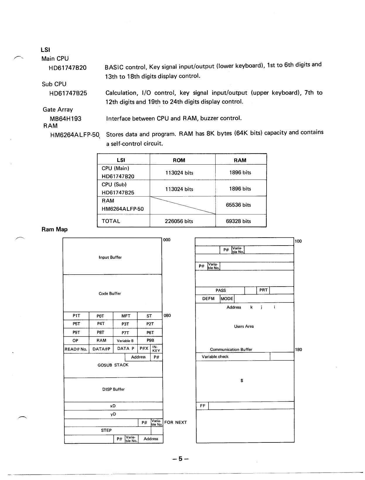
LSI
Main CPU
HD61747B20
Sub CPU
HD61747B25
BASIC control, Key signal input/output (lower keyboard), 1st to 6th digits and
13th to 18th digits display control.
Calculation, I/O control, key signal input/output (upper keyboard), 7th to
12th digits and 19th to 24th digits display control.
Gate Array
MB64H193 Interface between CPU and RAM, buzzer control.
RAM
HM6264ALFP-50, Stores data and program. RAM has 8K bytes (64K bits) capacity and contains
aself-control circuit.
Ram Map
LSI ROM RAM
CPU (Main)
HD61747B20 113024 bits 1896 bits
CPU (Sub)
HD61747B25 113024 bits 1896 bits
RAM
HM6264ALFP-50 65536 bits
TOTAL 226056 bits 69328 bits
Input Buffer
Code Buffer
P1T POT MFT ST
P5T P4T P3T P2T
P9T P8T P7T P6T
OP RAM Variable BP9B
READ#No. DATA#P DATA PP#X IN-
KEY
Address P#
GOSUB STAC K
DISP Buffer
xD
YD
P# Varia-
ble No.
STEP
P# Varia-
ble No. Address
000
080
P# ble No
P# Varia-
ble No.
PASS
DEFM MODE
PRT
Address kj
Users Area
Communication Buffer
Variable check
FOR NEXT
FF
100
180
-5-
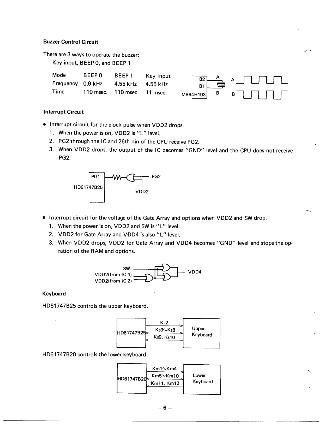
Buzzer Control Circuit
There are 3ways to operate the buzzer:
Key input, BEEP 0, and BEEP 1
Mode BEEPO BEEP 1Key Input
Frequency 0.9 kHz 4.55 kHz 4.55 kHz
Time 110 msec. 110 msec. 11msec.
B2
B1
MB64H193 BB-uinr
Interrupt Circuit
•Interrupt circuit for the clock pulse when VDD2 drops.
1
.
When the power is on, VDD2 is "L" level.
2. PG2 through the IC and 26th pin of the CPU receive PG2.
3. When VDD2 drops, the output of the IC becomes "GND" level and the CPU does not receive
PG2.
PG1
HD61747B25
-J^Kk PG2
VDD2
Interrupt circuit for the voltage of the Gate Array and options when VDD2 and SW drop.
1. When the power is on, VDD2 and SW is "L" level.
2. VDD2 for Gate Array and VOD4 is also "L" level.
3. When VDD2 drops, VDD2 for Gate Array and VDD4 becomes "GND" level and stops the op-
ration of the RAM and options.
SW
VDD2(fromlC4)
VDD2(fromlC2)
Keyboard
HD61747B25 controls the upper keyboard.
VDD4
HD61747B25*
HD61747B20 controls the lower keyboard.
HD61747B20^
Ks2
Ks3^Ks8
Ks9, KslO
Km1^Km4
Km5^Km10
Km11, Km12
Upper
Keyboard
Lower
Keyboard
Power Supply
VSS1 Power supply voltage for TC4071BF.
VRAM Memory used to keep the voltage for the RAM.
VKV5 LCD drive voltages. Voltage is generated by connecting the external resistor to VDD2.
VDD1 Power supply for the CPU, RAM and options.
VDD2 Stays VDD1 at power-on. Goes to GND at power-off or APO (auto power-off).
-7-
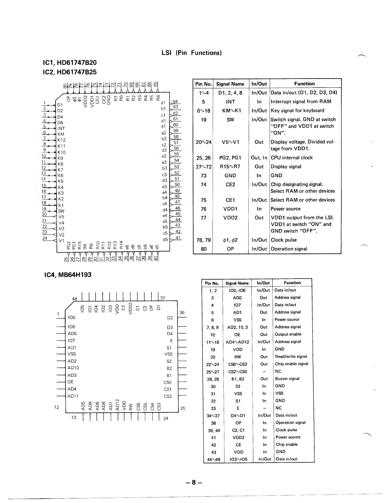
LSI (Pin Functions)
IC1,HD61747B20
IC2, HD61747B25
!is|S|K{SiiS}S{Sls|dg|SjS|:
11 ] i11 11AAAAA
7_
10
1_U_
12
13
14
15
16
17
19
20
21
22
23
24 -<
D1
D2
D4
D8
INT
KM
K12
K11
K10
K9
K8
K7
K6
K5
K4
K3
K2
K1
SW
V5
V4
V3
V2
VI
cm r- ,_ (mq r^ o
^.^ Q O LU UJ2 CC CC
>
r- CN CO ^t LD CD
CC DC CC CC CC DC
CN <- LD
(J d^CO OT
q_ q_ DC CC CC
O*- CN CO <*
DC CC DC DC CC
a1
b1
cl
d1
e1
a2
b2
c2
d2
e2
a3
b3
c3
d3
e3
a4
b4
c4
d4
e4
a5
b5
c5
d5
LD cd r-. CO
Cslj CNJ CM ICN
iMsWalsIsWfiWslsl
,64
63
,62
,
61
,60
59
58
57
,56
,55
^54
,53
,52
r51
r50
349
48
47
,46
:45
r44
_43
42
41
Pin No. Signal Name In/Out Function
Tv4 01,2,4,8 In/Out Data in/out (D1, D2, D3, D4)
5INT In Interrupt signal from RAM
6^18 KM'VKI In/Out Key signal for keyboard
19 SW In/Out Switch signal. GND at switch
"OFF" and VDD1 at switch
"ON".
2CV24 V5M/1 Out Display voltage. Divided vol-
tage from VDD1.
25,26 PG2, PG1 Out, In CPU internal clock
27V72 R15'\>R7 Out Display signal
73 GND In GND
74 CE2 In/Out Chip designating signal.
Select RAM or other devices
75 CE1 In/Out Select RAM or other devices
76 VDD1 In Power source
77 VDD2 Out VDD1 output from the LSI.
VDD1 at switch "ON" and
GND switch "OFF".
78,79 01,02 In/Out Clock pulse
80 OP In/Out Operation signal
IC4, MB64H193
48 37
•^cncoCiujq<-cncl
12
OO O O O QU
_ _ _ >uU O Q
IO0
106
ADO
107
AD1
VSS
AD2
AD10
AD3
OE
AD4
AD11
D2
D3
D4
E
SI
VSS
S2
B2
B1
CS0
CS1
CS2
ID O) ©00
QQO Q
< < < <
Q
>CC
CD LD -3" CO
CO CO CO CO
OOOCJ
13 24
36
25
Pin No. Signal Name In/Out Function
1, 2IO0, I06 In/Out Data in/out
3ADO Out Address signal
4I07 In/Out Data in/out
5AD1 Out Address signal
6VSS In Power source
7,8,9 AD2, 10,3 Out Address signal
10 OE Out Output enable
11M8 AD4'VAD12 In/Out Address signal
19 VDD In GND
20 RW Out Read/write signal
22^24 CS6^CS3 Out Chip enable signal
25^27 CS2^CS0 -NC
28,29 81, B2 Out Buzzer signal
30 S2 In GND
31 VSS In VSS
32 S1 In GND
33 E-NC
34^37 D4MD1 In/Out Data in/out
38 OP In Operation signal
39,40 C2,C1 In Clock pulse
41 VDD2 In Power source
42 CE In Chip enable
43 VDD In GND
44^48 103^105 In/Out Data in/out -
-8-
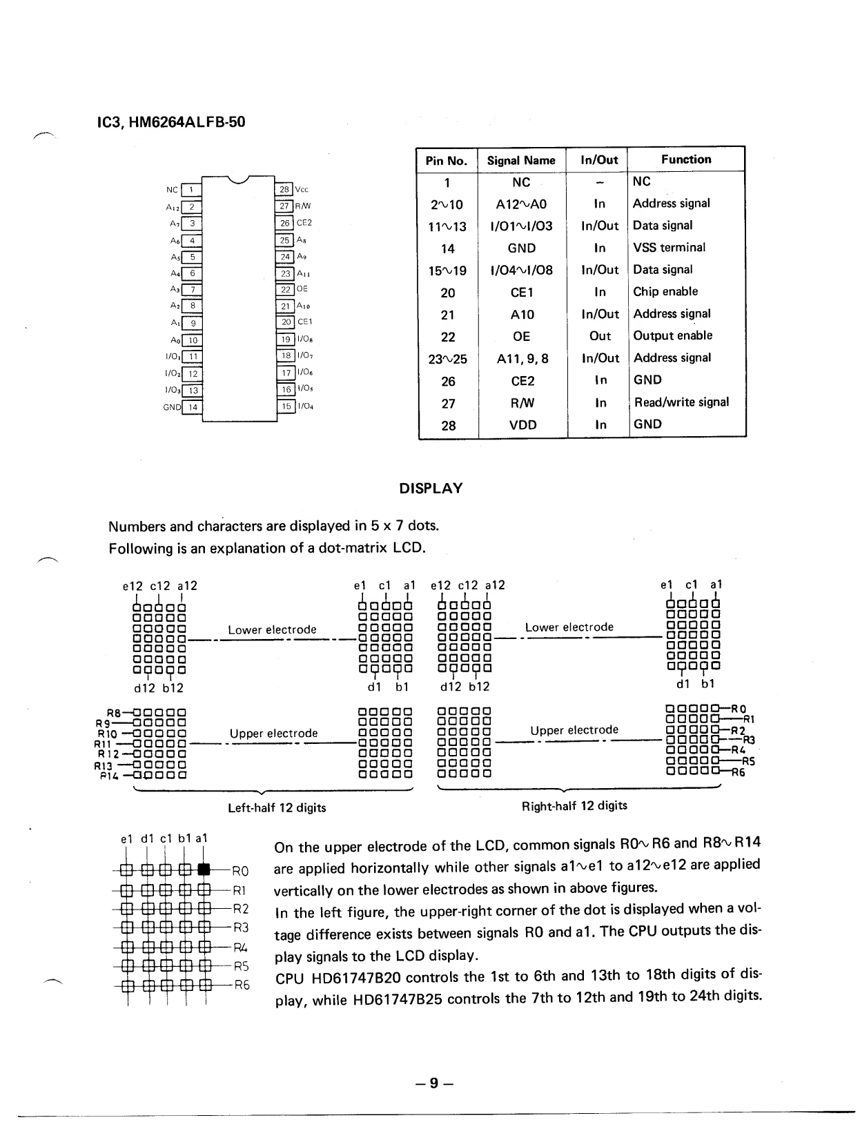
IC3, HM6264ALFB-50
NC |1
Ai2 [X
A7|3
A6r~4
A5|5
A4|6
A3|~T
A218
_9
Aq|Tq
l/Oi| 11
i/o 2Q7
!/0 3[T3
gnd|
'
I14
28 |Vcc
27 |R/W
~26]cE2
25 |A8
24 |A9
23] An
22~[OE
21~[Aiq
~2o"|CE1
TFJi/Os
Tili/07
TT]i/06
jF]l/04
Pin No. Signal Name In/Out Function
1NC -NC
2M0 A12^A0 In Address signal
11M3 I/01M/03 In/Out Data signal
14 GND In VSS terminal
15^19 1/04^1/08 In/Out Data signal
20 CE1 In Chip enable
21 A10 In/Out Address signal
22 OE Out Output enable
23^25 A11,9,8 In/Out Address signal
26 CE2 In GND
27 R/W In Read/write signal
28 VDD In GND
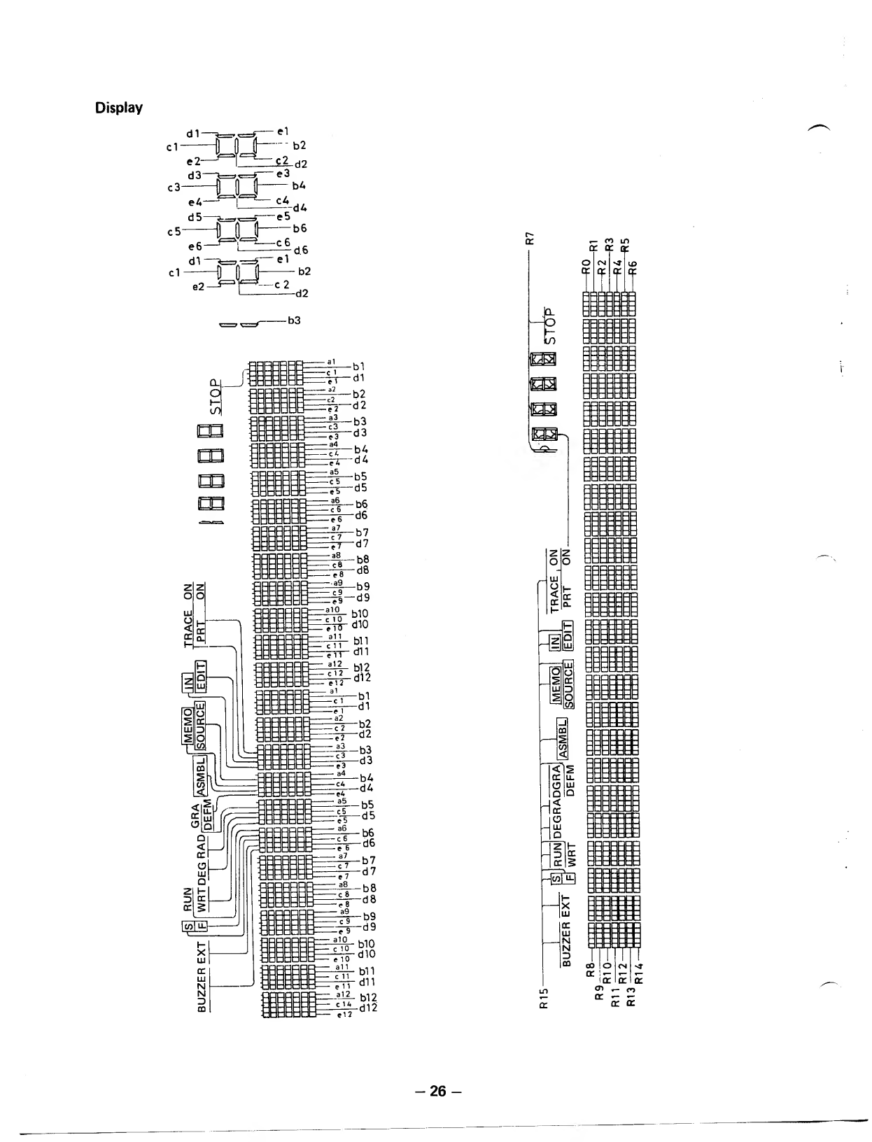
DISPLAY
Numbers and characters are displayed in 5x7dots.
Following is an explanation of adot-matrix LCD.
e12 c12 a12
QODOQ
oaaaa
aaoaa
aaaoQ
—
oaaaa
aaaaa
acpacpa
d12 b12
R8—aaaaa
R9 —aaaaa
Rio —aaaaa
R11 —aaaaa—
r12 —aaaaa
R13 —aaaaa
pu. —aoaaa
Lower electrode
Upper electrode
e1 da1
aaaaa
aaaaa
aaaaa
-aaaaa
aaaaa
aaaaa
acparpa
d1 b1
aaaaa
aaaaa
aaaaa
-aaaaa
aaaaa
aaaaa
aaaaa
e12 c12 a12
iaaao
aaaaa
aaaaa
aaaaa
—
aaaaa
aaaaa
atpacpa
d12 b12
aaaaa
aaaaa
aaaaa
aaaaa-
aaaaa
aaaaa
aaaaa
Lower electrode
Upper electrode
e1 da1
rJiaAai
aaaaa
aaaaa
-aaaaa
aaaaa
aaaaa
atpacpa
d1 b1
aaaaa—ro
aaaaa
—
ri
aaaaa—R2
-aaaaa—R3
aaaaa—rl
aaaaa
—
rs
aaaaa—ns
Left-half 12 digits Right-half 12 digits
e1 dl cl bl a1
MHH3-B
£3-E3-G-E3-B
£3~EH3-E3-B
T
-RO
-RI
-R2
-R3
-R4
-R5
-R6
On the upper electrode of the LCD, common signals RCKR6 and RB'vRM
are applied horizontally while other signals a1^e1 to a12^e12 are applied
vertically on the lower electrodes as shown in above figures.
In the left figure, the upper-right corner of the dot is displayed when avol-
tage difference exists between signals RO and a1. The CPU outputs the dis-
play signals to the LCD display.
CPU HD61747B20 controls the 1st to 6th and 13th to 18th digits of dis-
play, while HD61747B25 controls the 7th to 12th and 19th to 24th digits.
-9-
TROUBLESHOOTING GUIDE
Symptom
No display at all.
Acertain segment(s)
cannot be displayed.
Acertain button does not
function.
Cause
Weak batteris
Poor battery contact
Peeled heat seal
Broken heat seal
LCD(CA51-TS)
LSI (HD61747B)
Calculation impossible.
Peeled heat seal
Broken heat seal
LCD (CA51-TS)
LSI (HD61747B)
LSI (HD61747B)
Poor key contact
Broken PC line
Peeled heat seal
LSI (HD61747B)
Solution
Replace the batteries.
Clean the battery and contact spring.
Lift the battery spring.
Replace the heat seal.
Replace the heat seal.
Replace the LCD.
Replace the LSI.
Replace the heat seal.
Replace the heat seal.
Replace the LCD.
Replace the LSI.
Replace the LSI.
Celan the contact pad on the PCB and the
key contact rubber.
Connect the PC line.
Replace the heat seal.
Replace the LSI.
-10-
Test Program
Notes:
1
.
After typing in the programs below, save the programs to acassette tape for future use.
2. Memory and printer check programs cannot be executed at the same time because of alimited
memory capacity.
Memory check program
Ready P0
LIST
10
20
25
30
40
50
60
70
80
CLEAR
C=904
DEFM C
FOR B=l TO C
D(B)=B
NEXT B
$="ABCDEFGHIJKL
MNOPQRSTUVWXYZ"
BEEP 1: BEEP 1
PRINT "INPUT OK
90 GOTO #1
PI
A=0
A=A+1
FOR B=l TO C
IF D(B)#B THEN
100
NEXT B
IF $="ABCDEFGHI
JKLMNOPQRSTUVWX
YZ" THEN 100
IF A=5 THEN 110
PRINT A; :GOTO
7
PRINT "CHECK* *N
G**"; :BEEP 1:
BEEP 0: GOTO 111
PRINT "A=";A;
PRINT "CHECK**0
K**" ;:BEEP 1:
BEEP 1
PRINT "A=";A;
:
END
Ready
LIST
5.
7
10
20
30
40
50
60
100
101
110
111
Printer check program
Ready PI
LIST
10 MODE 7
20 PRINT "**PC-
6CHECK**
30 PRINT "ABCDEFGH
IJKLMNOPQRSTUVW
XYZ";
40 PRINT "abcdefgh
ijklmnopqrstuvw
xyz" ;
50 PRINT "0.123456
789";
60 PRINT "%' @¥[] &+-
4<->-0 o*x ^**** :: *'°
-EfiUY<5 n
;
70 PRINT "!#$?\<<>
>^t () */+- £^»;
80 FOR A=l TO 28
90 PRINT "8";
100 NEXT A
110 PRINT "
END-
120 MODE 8
-11 -
Program SAVE, LOAD and MEMORY
System:
PC6 +
26-3651
or PC-5
cable
(26-3671)
+CMT
Operation:
(1) PW ,
(2) CMT
SW ON
PLAY MODE
LOAD
(3) SEXE LOAD
END BUZZER RUN DEG
Ready P0
(4) PW SW OFF
(5) PW SW ON
(6) S
Take out the 26-3651 +CMT
BUZZER RUN DEG
Ready P0
BUZZER RUN DEG DEFM
INPUT OK* (Buzzer sound)
BUZZER RUN DEG DEFM
INPUT OK*1
BUZZER RUN DEG DEFM
INPUT OK* 12
BUZZER RUN DEG DEFM
INPUT OK* 123
BUZZER RUN DEG DEFM
INPUT OK* 12 34
BUZZER RUN DEG DEFM
INPUT OK* 1234CHECK**OK**A=5 (Buzzer sound) OK
BUZZER RUN DEG DEFM
INPUT OK* CHECK**NG**A=1 (Buzzer sound) NG
(7) IBRK
-12-
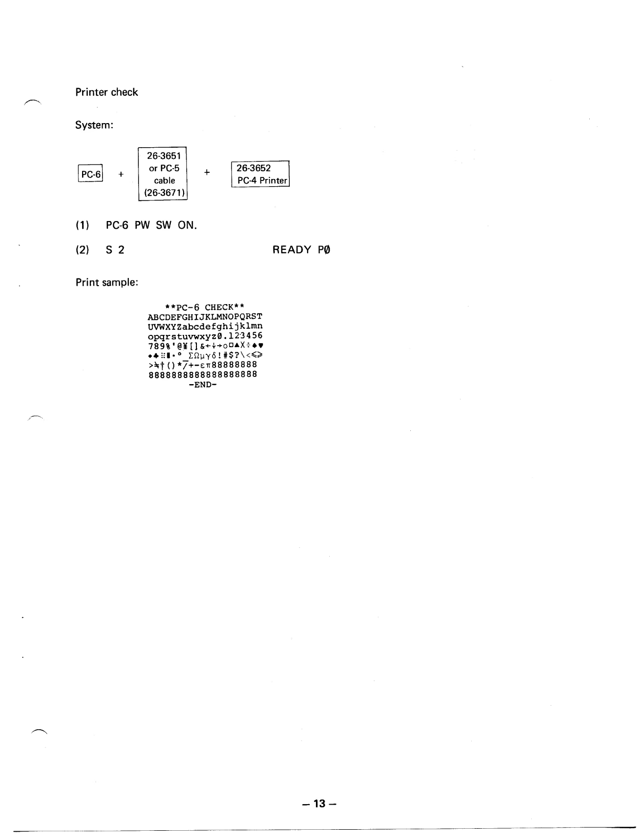
Printer check
System:
26-3651
or PC-5
cable
(26-3671)
+
PC-6 +26-3652
PC-4 Printer
(1) PC-6 F
(2) S2
>W SW N.
RE/
Print sample:
**PC-6 CHECK**
ABCDEFGHIJKLMNOPQRST
UVWXYZabcdefghijklmn
opqrstuvwxyz0. 123456
789% ,@¥[]&^+ooaXt**
>M ()*/+-£TT88888888
8888888888888888888
-END-
-13-
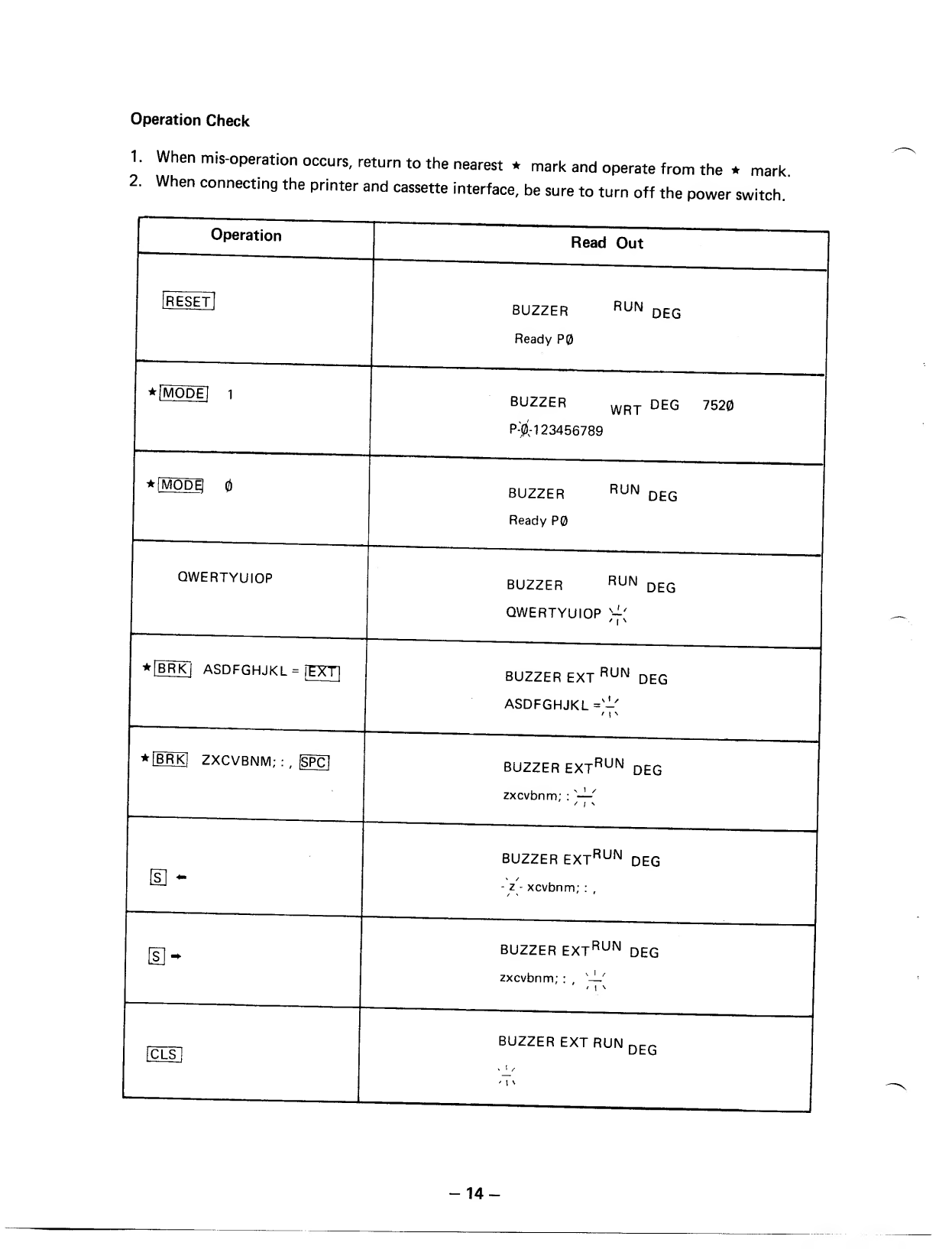
Operation Check
1. When mis-operation occurs, return to the nearest* mark and operate from the *mark
2. When connecting the printer and cassette interface, be sure to turn off the power switch.
Operation Read Out
BUZZER RUN DEG
Ready P0
(RESET
BUZZER WRJ DEG 7520
P^: 123456789
*|MODEj 1
BUZZER RUN DEG
Ready P0
*|MODEl
QWERTYUIOP BUZZER RUN DEG
QWERTYUIOP )~[
*FbRK] ASDFGHJKL- [EXT] BUZZER EXT RUN DEG
ASDFGHJKL =-'
*[BRK] ZXCVBNM;:, (SPCl BUZZER EXT RUN DEG
zxcvbnm; :—'
[s> BUZZER EXTRUN DEG
-z-xcvbnm; :,
®- BUZZER EXT RUN DEG
zxcvbnm; :,"-L'
BUZZER EXTRUN DEG
't\
|CLSJ
-14-
Operation
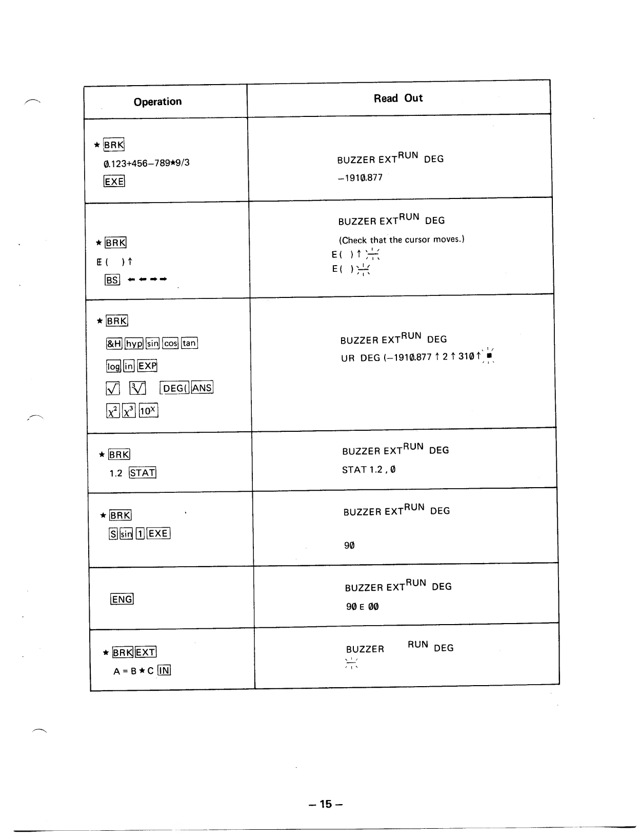
•iBRKl
0.123+456-789*9/3
•BRK
E( )t
•BRK
|&F^ [hypl[sinl[cosl [tan
tog)[in|[EXP
5j [Vj 1deg(1 |ans
x2x310*
•BRK
1.2 STAT
•BRIO
ISllsinlllllEXEl
ENG
•IbrkIIextI
a=b*c[jn]
Read Out
BUZZER EXT RUN DEG
-1910.877
BUZZER EXTRUN DEG
(Check that the cursor moves.
e( )t;-r{
BUZZER EXTRUN DEG
UR DEG (-1910.877 t2t310f
BUZZER EXT RUISi DEG
STAT 1.2,0
BUZZER EXT RUN DEG
90
BUZZER EXTRUN DEG
90 E00
BUZZER RUN DEG
15-
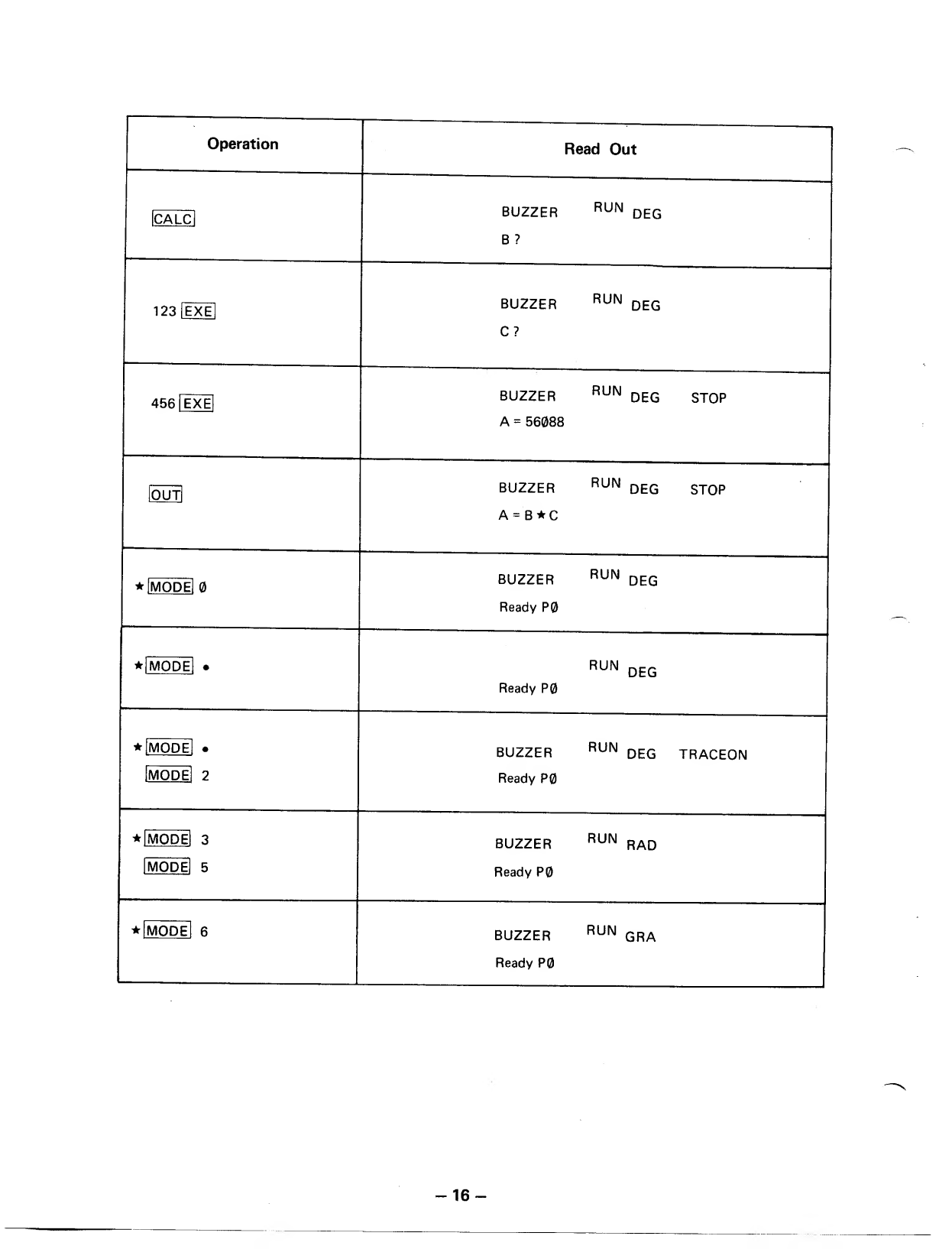
Operation
ICALCl
123 EXE
456 EXE
WJT
•ImodeI o
•WIODE •
•IMODEl •
iMODEl 2
•IMODEl 3
iMODEl 5
•MODE] 6
Read Out
BUZZER
B?
RUN DEG
BUZZER RUN DEG
C?
BUZZER RUN DEG STOP
A=56088
BUZZER RUN DEG STOP
A=B*C
BUZZER RUN DEG
Ready P0
RUN DEG
Ready P0
BUZZER
Ready P0
RUN DEG TRACEON
BUZZER RUN RAD
Ready P0
BUZZER RUN GRA
Ready P0
16
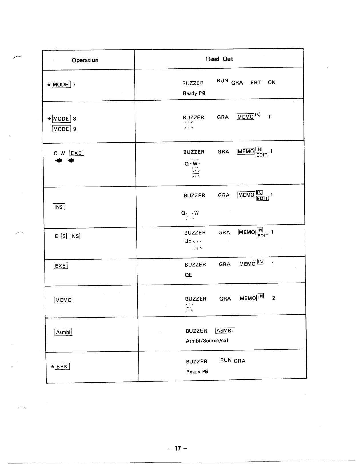
Operation Read Out
BUZZER RUN GRA PRT ON
Ready P0
•MODE 7
iitKiT
•MODE 8BUZZER GRA |MEMO|^ 1
•1"^
(MODE 9
QW|EXE| BUZZER GRA IMEMOI™^ 1
Q-W-
s1^
INS
BUZZER GRA iMEMOl^^ 1
E|SI||NS| BUZZER GRA [MEMOl^^ y
QE m/
|EXE| BUZZER GRA |MEMO|^ 1
QE
BUZZER GRA iMEMOl^ 2
/1^
|MEMO|
Asmbl BUZZER |ASMBL1
Asmbl /Source /ca1
BUZZER RUN GRA
Ready P0
•BRK
-17
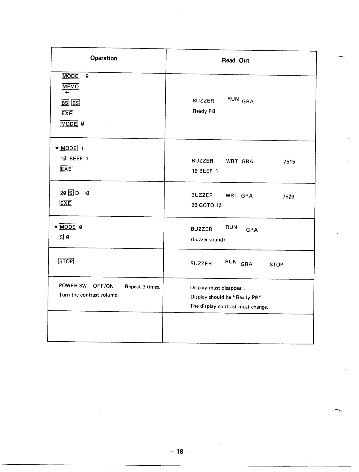
Operation
IMODE1 9
IMEMOI
[is] [bsI
1EXE1
JMODEl
•iMODEl 1
10 BEEP 1
EXE
20[|]D 10
IEXEI
•IMODEl
[Sj
ISTOPI
POWER SW OFF/ON Repeat 3times.
Turn the contrast volume.
Read Out
BUZZER RUN GRA
Ready P0
BUZZER WRT GRA
10 BEEP 1
BUZZER WRT GRA
20 GOTO 10
BUZZER RUN GRA
(buzzer sound)
7515
7509
BUZZER RUN GRA STOP
Display must disappear.
Display should be "Ready P0."
The display contrast must change.
-18-
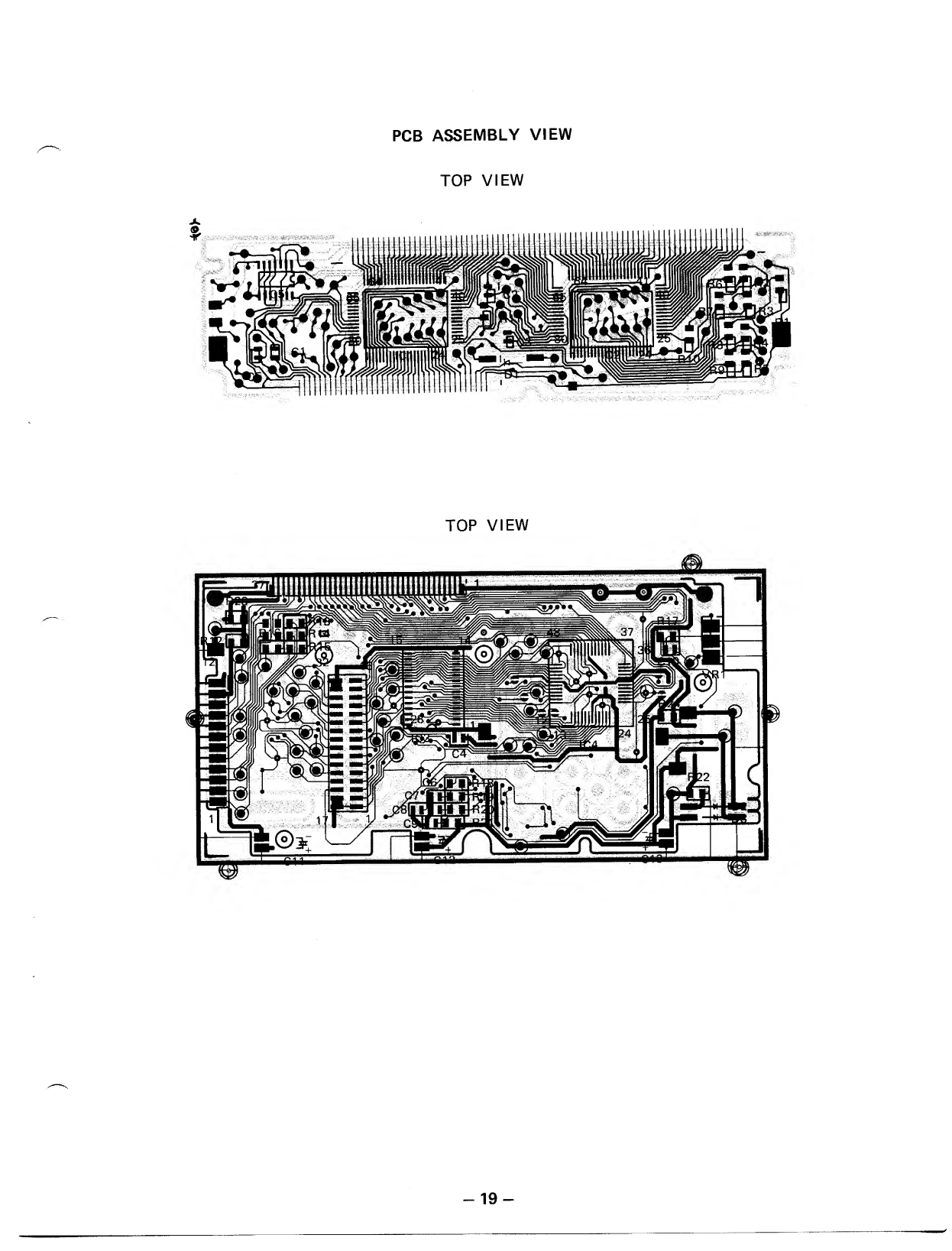
PCB ASSEMBLY VIEW
TOP VIEW
TOP VIEW
-19-
PARTS LIST
Electrical Parts
Ref. No. Description RSPart No. Mfr's Part No.
CAPACITORS
CTVC4 Chip, Ceramic, 100pF, 25V, ±5%, CM21CH101J25V ACF-1466 28907311
C5^C10 Chip, Ceramic, O.ljuF, 15V, +100%, CM21YV104P15V ACF-7347 71032167
C11,C12 Electrolytic, 22juF, 10V, ±20%, CE04C-1 A220MS7 CE-226MCBA 28047223
C13 Electrolytic, 100juF, 10V, ±20%, CE04C-1A1 01 MS CE-107MCBA 28041047
ICs
IC1 LSI, CPU, HD61747B20 MX-7273 20018364
IC2 LSI, CPU, HD61747B25 MX-7274 20018801
IC3 LSI, RAM, HM6264ALFP-50 MX-7275 20011149
IC4 LSI, MB64H193 MX-7276 20030453
IC5 IC, TC4071BF MX-4245 21004359
PRIN-FED CIRCUIT BOARD ASSEMBLIES
PC1 Assembly, PCB-G707-1 82636701
PC2 Assembly, PCB-G707-2 82636702
RESISTORS
RT\/R9 Chip, Ruthenium, 3.3 Kohm, 1/8W, ±5%, CR32-108-332J-T-TP ND-0230EBN 27930620
R10 Chip, Ruthenium, 12 Kohm, 1/8W, ±5%, CR32-108-123J-T-TP ND-0288EBN 27930638
R11 Chip, Ruthenium, 68 Kohm, 1/8W, ±2%, CR32-108-683G-T-TP ND-0354CBN 27904530
R12 Chip, Ruthenium, 220 ohm, 1/8W, ±10%, CR32-1 08-221 K-T-TP ND-0149FBN 27904734
R13^R16 Chip, Ruthenium, 3.9 Kohm, 1/8W, ±5%, CR32-108-392J-T-TP ND-0237EBN 27903835
R17^R21 Chip, Ruthenium, 10 Kohm, 1/8W, ±2%, CR32-108-103G-T-TP ND-0281CBN 27930603
R22 Chip, Ruthenium, 22 Kohm, 1/8W, ±5%, CR32-108-223J-T-TP ND-0311EBN 27903740
R23 Chip, Ruthenium, 2.2 Mohm, 1/8W, ±5%, CR32-108-225J-T-TP ND-0454EBN 27904761
R24 Chip, Ruthenium, 100 ohm, 1/8W, ±10%, CR32-108-101 K-T-TP ND-0132FBN 27904629
MISCELLANEOUS
D1^D3 Diode, 1S1 588, silicon DX-0273 23003031
VR1 Volume, for contrast, 20 Kohm, EVL-AHAA00B24 AP-7004 27709486
-20-
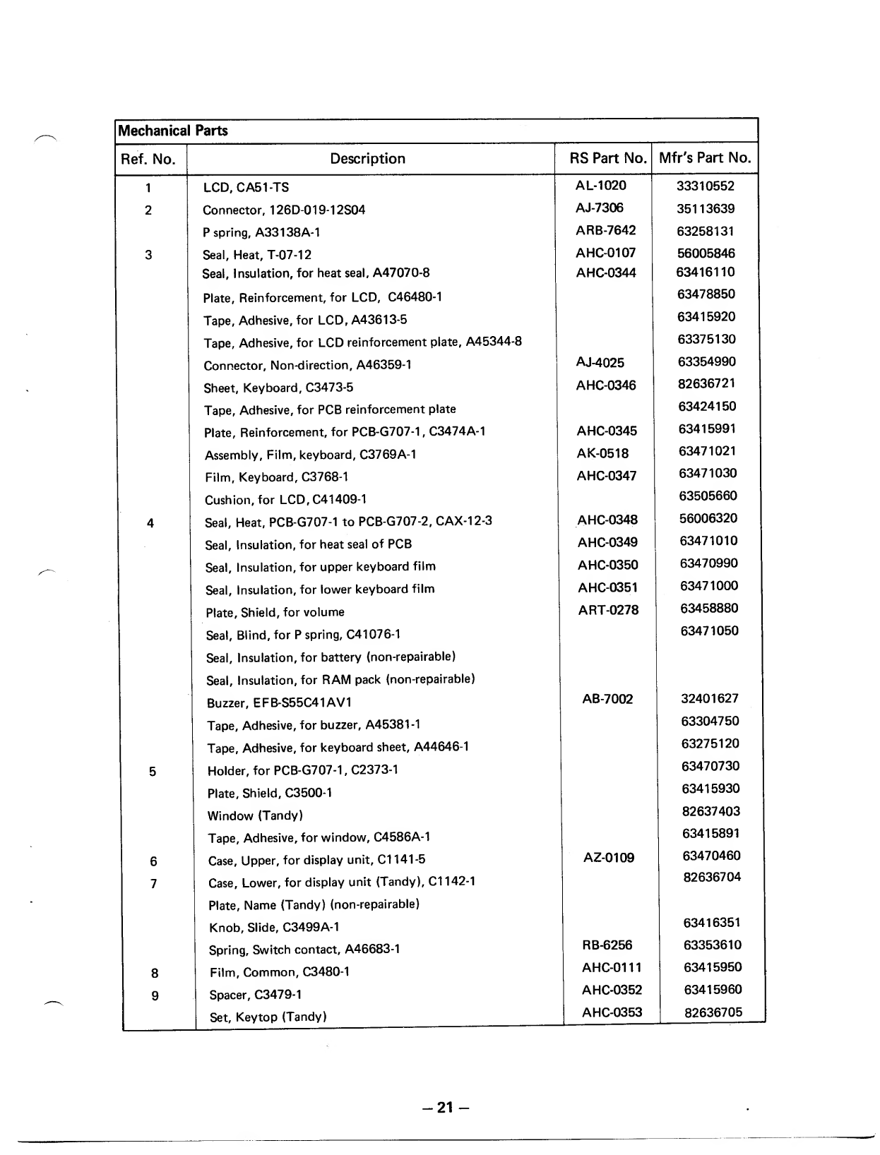
Mechanical Parts
Ret. No. Description RS Part No. Mfr's Part No.
8
9
LCD,CA51-TS
Connector, 126D-019-12S04
Pspring, A33138A-1
Seal, Heat, T-07-12
Seal, Insulation, for heat seal, A47070-8
Plate, Reinforcement, for LCD, C46480-1
Tape, Adhesive, for LCD, A43613-5
Tape, Adhesive, for LCD reinforcement plate, A45344-8
Connector, Non-direction, A46359-1
Sheet, Keyboard, C3473-5
Tape, Adhesive, for PCB reinforcement plate
Plate, Reinforcement, for PCB-G707-1 ,C3474A-1
Assembly, Film, keyboard, C3769A-1
Film, Keyboard, C3768-1
Cushion, for LCD,C41409-1
Seal, Heat, PCB-G7Q7-1 to PCB-G707-2, CAX-12-3
Seal, Insulation, for heat seal of PCB
Seal, Insulation, for upper keyboard film
Seal, Insulation, for lower keyboard film
Plate, Shield, for volume
Seal, Blind, for Pspring, C41 076-1
Seal, Insulation, for battery (non-repairable)
Seal, Insulation, for RAM pack (non-repairable)
Buzzer, EFB-S55C41AV1
Tape, Adhesive, for buzzer, A45381-1
Tape, Adhesive, for keyboard sheet, A44646-1
Holder, for PCB-G707-1, C2373-1
Plate, Shield, C3500-1
Window (Tandy)
Tape, Adhesive, for window, C4586A-1
Case, Upper, for display unit, C1 141-5
Case, Lower, for display unit (Tandy), C1 142-1
Plate, Name (Tandy) (non-repairable)
Knob, Slide, C3499A-1
Spring, Switch contact, A46683-1
Film, Common, C3480-1
Spacer, C3479-1
Set, Keytop (Tandy)
AL-1020
AJ-7306
ARB-7642
AHC-0107
AHC-0344
AJ-4025
AHC-0346
AHC-0345
AK-0518
AHC-0347
AHC-0348
AHC-0349
AHC-0350
AHC-0351
ART-0278
AB-7002
AZ-0109
RB-6256
AHC-0111
AHC-0352
AHC-0353
33310552
35113639
63258131
56005846
63416110
63478850
63415920
63375130
63354990
82636721
63424150
63415991
63471021
63471030
63505660
56006320
63471010
63470990
63471000
63458880
63471050
32401627
63304750
63275120
63470730
63415930
82637403
63415891
63470460
82636704
63416351
63353610
63415950
63415960
82636705
-21-
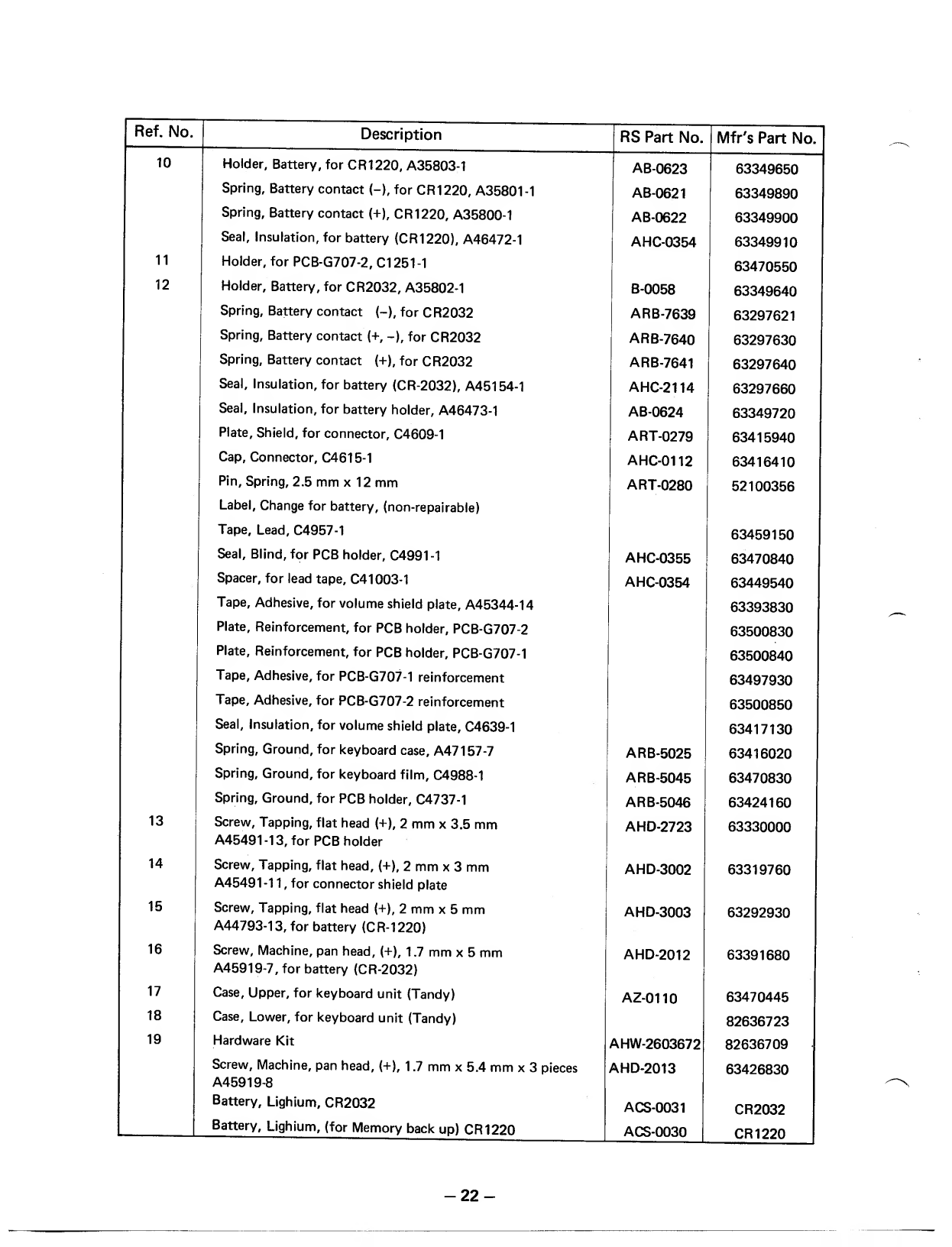
Ref. No. Description
10
11
12
13
14
15
16
17
18
19
Holder, Battery, for CR1220, A35803-1
Spring, Battery contact (-), for CR1220, A35801-1
Spring, Battery contact (+), CR1220, A35800-1
Seal, Insulation, for battery (CR1220), A46472-1
Holder, for PCB-G707-2, C1251-1
Holder, Battery, for CR2032, A35802-1
Spring, Battery contact (-), for CR2032
Spring, Battery contact (+, -), for CR2032
Spring, Battery contact (+), for CR2032
Seal, Insulation, for battery (CR-2032), A45154-1
Seal, Insulation, for battery holder, A46473-1
Plate, Shield, for connector, C4609-1
Cap, Connector, C4615-1
Pin, Spring, 2.5 mm x12 mm
Label, Change for battery, (non-repairable)
Tape, Lead, C4957-1
Seal, Blind, for PCB holder, C4991 -1
Spacer, for lead tape, C41 003-1
Tape, Adhesive, for volume shield plate, A45344-14
Plate, Reinforcement, for PCB holder, PCB-G707-2
Plate, Reinforcement, for PCB holder, PCB-G707-1
Tape, Adhesive, for PCB-G707-1 reinforcement
Tape, Adhesive, for PCB-G707-2 reinforcement
Seal, Insulation, for volume shield plate, C4639-1
Spring, Ground, for keyboard case, A47 157-7
Spring, Ground, for keyboard film, C4988-1
Spring, Ground, for PCB holder, C4737-1
Screw, Tapping, flat head (+), 2mm x3.5 mm
A45491 -1 3, for PCB holder
Screw, Tapping, flat head, (+), 2mm x3mm
A45491-1 1,for connector shield plate
Screw, Tapping, flat head (+), 2mm x5mm
A44793-1 3, for battery (CR-1220)
Screw, Machine, pan head, (+), 1.7 mm x 5 mm
A45919-7, for battery (CR-2032)
Case, Upper, for keyboard unit (Tandy)
Case, Lower, for keyboard unit (Tandy)
Hardware Kit
Screw, Machine, pan head, (+), 1.7 mm x5.4 mm x3pieces
A45919-8
Battery, Lighium, CR2032
Battery, Lighium, (for Memory back up) CR1220
RS Part No.
AB-0623
AB-0621
AB-0622
AHC-0354
B-0058
ARB-7639
ARB-7640
ARB-7641
AHC-2114
AB-0624
ART-0279
AHC-0112
ART-0280
AHC-0355
AHC-0354
ARB-5025
ARB-5045
ARB-5046
AHD-2723
AHD-3002
Mfr's Part No.
63349650
63349890
63349900
63349910
63470550
63349640
63297621
63297630
63297640
63297660
63349720
63415940
63416410
52100356
63459150
63470840
63449540
63393830
63500830
63500840
63497930
63500850
63417130
63416020
63470830
63424160
63330000
63319760
AHD-3003 63292930
AHD-2012 63391680
AZ-0110 63470445
82636723
AHW-2603672 82636709
AHD-2013 63426830
ACS-0031 CR2032
ACS-0030 CR1220
-22-
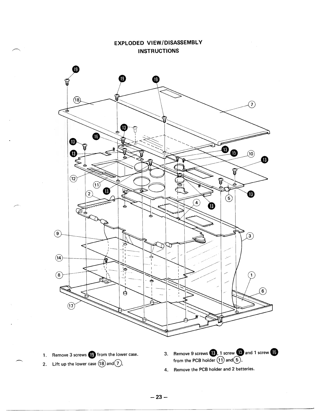
EXPLODED VIEW/DISASSEMBLY
INSTRUCTIONS
1
.
Remove 3screws ^from the lower case.
2. Lift up the lower case @and(Y).
3. Remove 9screws $, 1screw Oand 1screw ©
from the PCB holder (fj) and(5).
4. Remove the PCB holder and 2batteries.
-23-
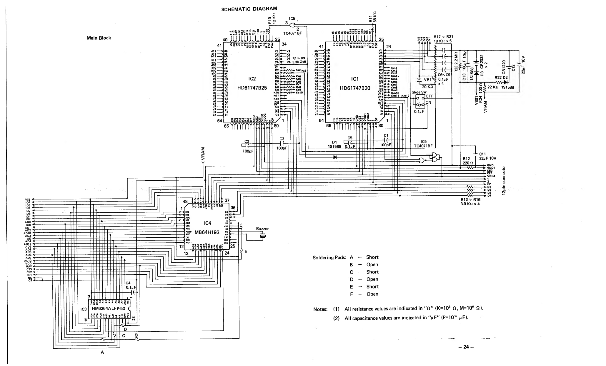
SCHEMATIC DIAGRAM
CJ
1C5
3^1
><£
Main Block 40 1IJlllllJllllIil25
41
b11-
•10-
d10-
c10-
blO-
ilO-
•9-
d9-
c9-
b9-
•8-
b8-
•8-
•7-
d7-
64
cocectctr <to.o.
IC2
HD61747B25
K4
*-*VW*- K»2 k,3
65
oNraa
toto*oo*T-or>.ZujuiQO &
OC EC CC 0C 0C OC (C OC OO»•- NO
ffffVfff
2
TC4071BF
24
I—vi
f—V2
*—V3
t—V4 R1^R9
«—V5 3.3Knx9
**VSAA*K«4
K5 *-WW*»Kj5
K6 *-fr>/VV-»Kt6
K7 <-^w\^»Ki7
K8 «_»*W^K»8
K9 «-*W^ K*9
kio #-*'s/\Nfc*> k«io
K12
KM
INT
08
D4
D2
01
TfTTTTTT
C2
<
>
100pF
103 <-
105 <-
102 "*-
106 *-
101 *-
107 -*-
ADO <-
108 <-
AD1
AD2 **-
AD10 *-
AD3 *-
0£ <-
ADA *-
AD11 <~
AD5 <-
A09 <-
AD6 <-
AD8<-
CS1 -*
NC *
IC3 HM6264ALFP-50
i|||5|8js58i|j
«
m
~t tit t
12
80
C3
100pF
5SaSououuoa
IC4 £
vss
MB64H193 »
13
SSSSSSosSSSS
yyyyuu lyyyvjy
36
ummmml 25
OCBCOCCCOC
IC1
HD61747B20
K4
KS
K6
K7
K8
K9
KIO
K11
K12
KM
INT
D8
D4
24
-Kml
*Km2
"Km3
•Kn>4.
*Km5
*Km6
"Km7
"Km8
Km9
*Km10
*Km11 Km12
6MUUllUM[m 80
C5
D1 L
1SI 588 0.1m F
-if-
C1
100pF
*.. R17^ R21
10 Kn x5
^VR1
20 Kn
Slide SW
O.VF
IC5
TC4071BF
*&i
R22D2
-AAAr>M
:22Kn 1S1588
R12
220 n
±C11
22jiF10V
—*.cei
—>VDD4
-^1
-* 2
->-OP
—>D1
R13^ R16
3.9 Kn x4
U
25
24
-<V
Buzzer
_JT
Soldering Pads: A-Short
B—Open
C-Short
D—Open
E-Short
F—Open
Notes: (1) Ail resistance values are indicated in "n" (K=103a, M=106a)
(2) Ail capacitance values are indicated in '>F" (P=10~6pF).
-24
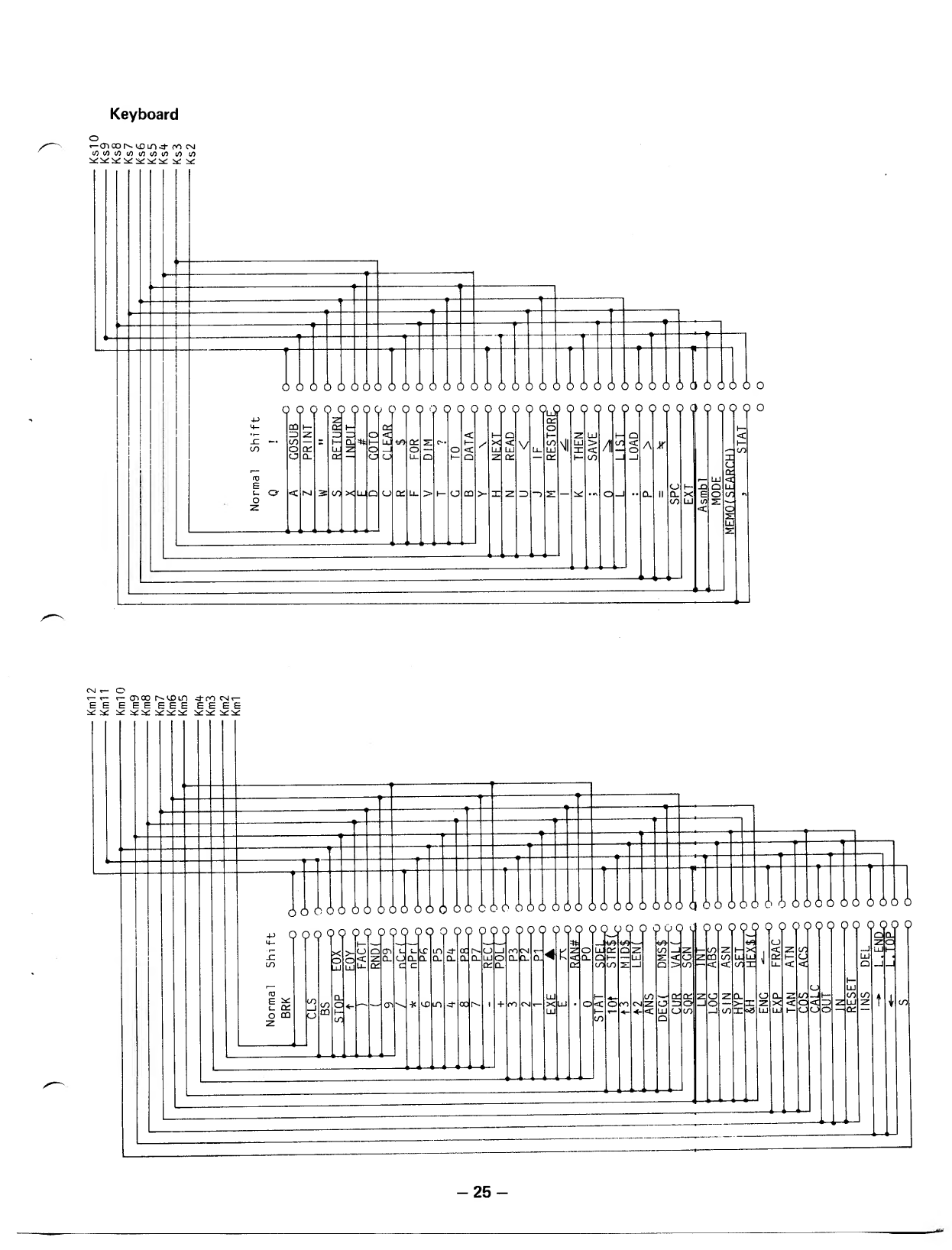
Keyboard
WW (0 (fl (fl (fl ifl 10 LO
000006606000000660000600066000666060
000 00 00000000000000 00 99999999999999
CO
(0
E
o
oJ=tti—
oVAJT
E E EEEEEE EEEE
1—
1
.— .•
'
«,
I
—
.—j
—
<
1
—
<
—i
1
1
—
I,
c
-E
CO
(0
E^
t_ a:
CQ
z
—
1
>
—
>c
1—
1
)(
pc
CO
_j
O
pc;
CO
CQ
pc
X
LU
CL
C
h-
cr
>d
)C
>-
LU
<-
pc;
1—
<
Lu
!) d
pc
C£
pc
CTi
(X
—
i
pc
CJ
c
}—
)I
)c
CL
C
pc
cc
a
) c
1
p<j
CL
)d
pc
a.
pc
cc
00
!> <!
pc
CL
td
pc
LU
QC
1
—
1
^c
pc
1j
CL
+
—
<—
>d
pc
00
CL
pc
Cl
pc
Cl
)c
)c
4
LU
X
LU
pc;
LU
pc
<
!) c
pc
CL
O
—
<
i)c
pc
_j
LL
CO
1—
<
1—
CO
—
«—
)(!
)J.
0;
h-
CO
s
1—
<
K
no
1—
1
)I
LU
CSI
:> d
PK
CO
<
>—
1
pc
<**
CO
LU
O
pc;
_j
<
>
d
»
—
—
1
\i
>c
z
CO
CO
*—
C
—
z
pc
CO
CQ
<
O
O
_J
\—
)d
pc
Z
CO
<
z
CO
»—
1
;d
pc
H
la-
CO
D_
>-
X
1
—
1C
pc
X
LU
X
X
•
—
—
<
?s
-z.
LU
pC
<
b_
Cl
X
LU
1—
.
;6
p
ZC
t— t
<<
ZLL
<<:
1-1
»—•
—
«
Ad
9c
O-J
D<
JO
—
,
pc
•—
1
—
)I
)C
F—
<
pc
(—
LU
CO
LU
QC
—
1
5C
pC
LU
CO
z.
)6
>9
QC
LUH
t
A6
L
D
J
f<s>
-25-
Display
-b3
r
^3
-26-
RADIO SHACK, ADIVISION OF TANDY CORPORATION
U.S.A.: FORT WORTH, TEXAS 76102
CANADA: BARRIE, ONTARIO L4M 4W5
TANDY CORPORATION
AUSTRALIA BELBIUM FRANCE O.
91 KURRAIONB AVENUE RUE DES PIEOS O'AIOUETTE. 39 BP 147-95022 BILSTON ROAO WEDNESBURY
MOUNT ORUin, N.S.W.2770 5140 NANINNE(NAMUR) CERGT PONTOISE CEOEX WEST MIDLANDS WS 107 IN
7A6 PRINTED IN JAPAN
