ILR 01 CoverXX Xls PCX250
User Manual: PCX250
Open the PDF directly: View PDF ![]() .
.
Page Count: 60
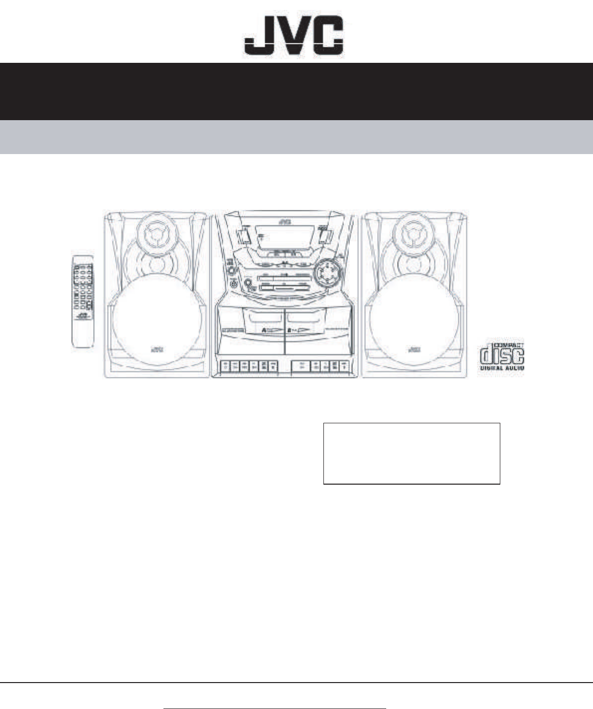
PC-X250
Contents
Safety precaution ------------------ 2 Block/Wiring Diagram ------------------ 25
Disassembly method -------------- 4 Circuit Diagram -------------------------- 27
Adjustment method ---------------- 6 PCB drawing ----------------------------- 29
TOC read ---------------------------- 10 Assembly ---------------------------------- 32
Major IC Description -------------- 11 Packing ------------------------------------ 42
No. 28001
Oct. 2001
COPYRIGHT © 2001 VICTOR COMPANY OF JAPAN,LTD (By JCA)
SERVICE MANUAL
CD PORTABLE COMPONENT SYSTEM
PC-X250
Area Suffix
J ---- USA
C ---- Canada
Unit No
SP-PCX250 Unit No
SP-PCX250
Unit No
CA-PCX250
PC-X250
1. This design of this product contains special hardware and many circuits and components specially for
safety purposes. For continued protection, no changes should be made ti the original design unless
authorised in writing by the manufacturer. Replacement parts must be identical to those used in the
original circuits. Services should be performed by qualified personel only.
2. Alterations of the design or circuitry of the product should not be made. Any design alterations of the
product should not be made. Any design alterations or additions will void the manufacturer's warranty
and will further relieve the manufacturer of responsibility for personal injury or property damage
resulting therefrom.
3. Many eletrical and mechanical parts in the products have special safety-related characteristics.
These characteristics are often not evident from visual inspection nor can the protection afforded by
them necessarily be obtain by using replaement components rated for higher voltage, the Parts
List of Service manual. Electrical components having such features ate identified by the shading on the
schematics and by ( ! ) on the parts List in the Service Manual. The use of a substitute
repalcement which does not have the same safety characteristics as the recommended replacement
parts shown in the Parts List of Service manual may create shock, fire, or other hazards.
4. The leads in the products are routed and dressed with ties, clamps, tubing's, barriers and the like to
be separated from live parts, high temperatures parts, moving parts and/or sharp edges for the
prevention of electric shcok and fire hazard. When service is required, the original leat routing and
dress should be observed, and it should be confirmed that they have been returned to normal, after
re-assembling.
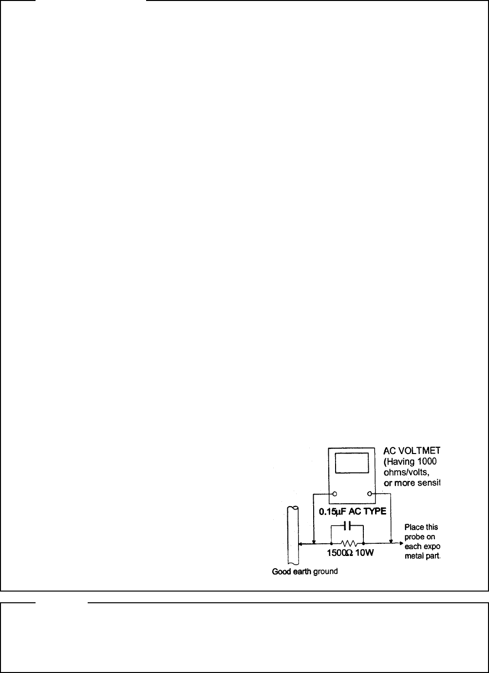
5. Leakage current check (Electrical Shock hazard testing)
After re-assembling the product, always perform an isolation check on the exposed metap Parts of the
product (antenna terminals, knobs, metal cabinet, screw heads, headphone jack, control shafts, etc.)
to be sure the product is safe to operate without danger of electrical shock.
Do not use a line isloation transformer during this check.
Plug the AC line cord directly into the AC outlet. Using a "Leakage Current Tester", measure the
leakage current from each ecposed metal parts of the cabinet, particularly and exposed metal
part having a return path to the chassis, to a known good earth ground. Any leakage current must
not exceed 0.5mA AC (r.m.s.)
Alternate check method
Plug the AC line cord directly into the AC outlet. Use an AC voltmeter having, 1,000 ohms per
volt or more sensitvity in the following manner. Connect a 1,500 ohm 10W resistor paralleled by a
0.15uF AC-type capacitor between an exposed
metal part and a known good earth ground.
Measure the AC voltage across the resistor with
the AC voltmeter.
Move the resistor connection to each exposed
metal part, particularly and exposed metal part
having a return path to te chassis and
measure the AC voltage across the resistor. Now,
reverse the plug in the AC outlet and repeat
each measurement. Voltage measured Any must
not exceed 0.75 V AC (r.m.s.). This corresponds
to 0.5 mA AC (r.m.s.).
1. This equipment has been designed and manufactured to meet international safety standards.
2. It is the legal responsibility of the repairer to ensure that these safety standards are maintained.
3. repairs must be made in accordance with the relevant safety standards.
4. It is essential that safety critical components are replaced by approved parts.
5. It mains voltage selector is provided, check setting for local voltage.
CAUTION
Burrs formed during moulding may be left over on some parts of the chassis. Therefore,
pay attention to such burrs in the case of performing repair of this system.
Safety Precautions
Warning
1 - 2
PC-X250
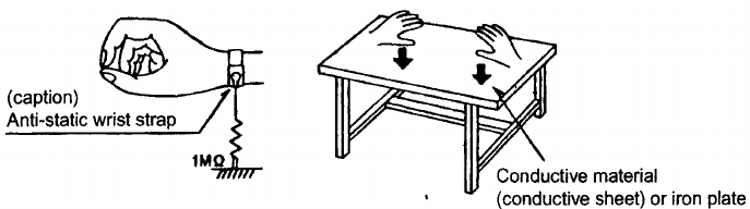
Preventing static electricity
Electrostatic discharge (ESD), which occurs when static electricity stored in the body, fabric, etc. is discharged,
can destroy the laser diode in the traverse unit (optical pcikup). Take care to prevent this when performing repairs.
1.1. Grounding to prevent damage by static electricity
Static electricity in the work area can destroy the optical pickup (laser diode) in devicessuch as DVD players.
Be careful to use proper grounding in the area where repairs are being performed.
1.1.1. Gound the workbench
1.
Ground the workbench by laying conductive material (such as a conductive sheet) or an iron plate over
it before placing the traverse unit (optical pickup) on it.
1.1.2. Ground yourself
1.
Use an anti-static wrist starp to release and static electricity built up in your body.
1.1.3. Handling the optical pcikup
1.
In order to maintain quality during transport and before installation, both sides of the laser diode on the
replacement optical pickup are storted. After replacement, return the shorted parts to their original condition.
(Refer to the text.)
2.
Do not use a tester to check the condition of the laserdiode in the optical pickup. The tester's internal power
source can easily destory the laser diode.
1.2. Handling the traverse unit (optical pickup)
1.
Do not subject the traverse unit (optical pcikup) to strong shocks, as it is a sensitive, complex unit.
2.
Cut off the shorted part of the flexible cable using nippers, etc. after replacing the optical pickup. For specific
details, refer to the replacement procdeure in the text. Remove the anti-static pin when replacing the traverse
unit. Be careful not to take too long a time when attaching itto the connector.
3.
Handle the flexible cable carefully as it may break when subjected to strong force.
4.
It is not possible to adjust the semi-fixed resistor that adjusts the laser power. Do not return it.
1 - 3
PC-X250
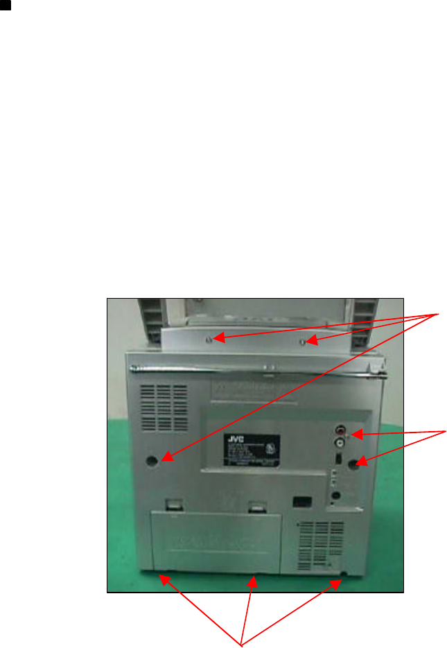
Disassembly method
Removing the rear panel
1.
From behind the body, remove the Five screws
A
retaining the rear panel.
2.
Then remove the Two screws
B
retaining the bottom of rear panel.
3.
Take out the rear panel from the body.
Note:
Be careful of the FM antenna white wire, it is connection with the tuner PCB up side.
You can directly take out from the tuner PCB.
When you re-assembly the product, plug the FM antenna white wire into the Tuner PCB's
"FM ANT" position.
Screw A.
Screw A.
Screw B.
1 - 4
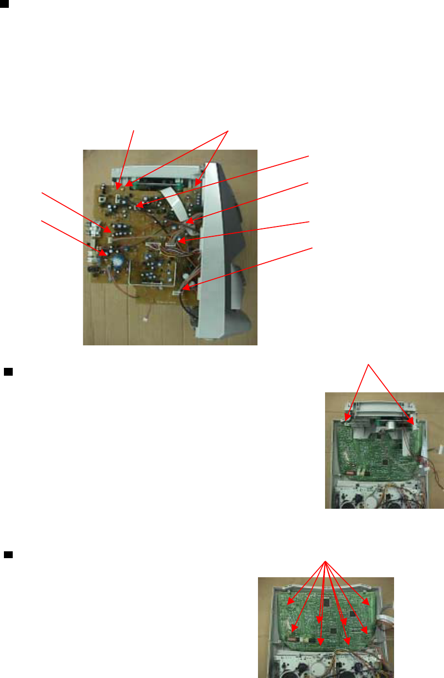
Removing the Audio Board
1.Open & remove the rear panel
2. Remove the Connector CN201, CN202, CN203, CN405, CN502, CN801
& CN301 on the Audio Board.
3. Remove the two Screws C retaining the Audio Board.
CN202 Screw C
CN201
CN502
CN203
CN801 CN405
CN301
Screw D
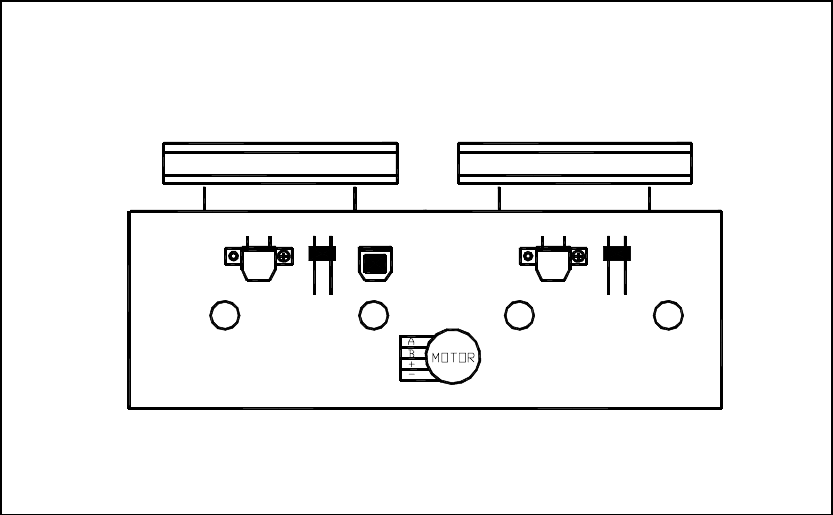
Removing the CD Mechanism
1 Open & remove the rear panel
2 Remove the Audio PCB
3 Remove the Two Screws D retaining the CD Tray Backet.
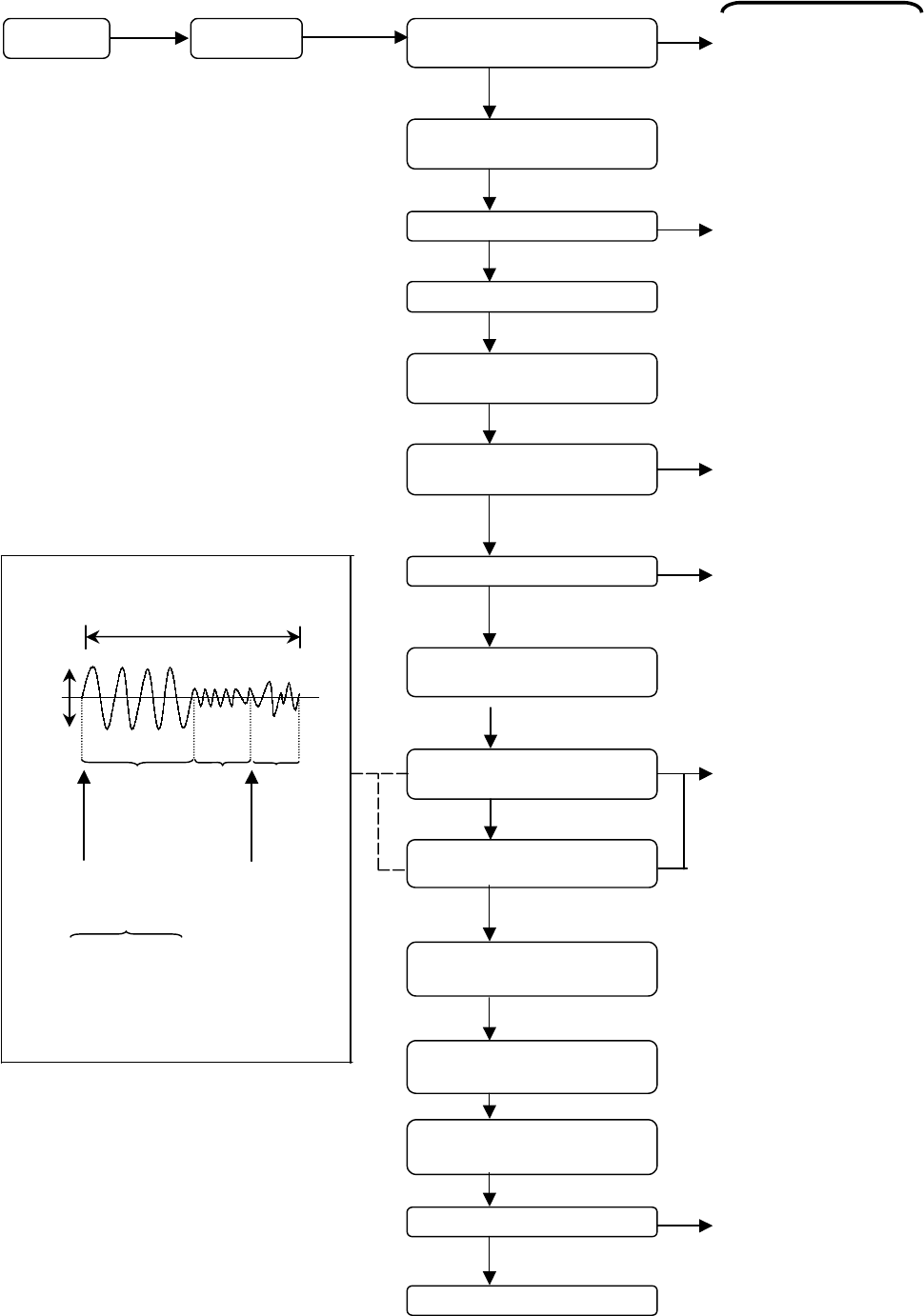
Removing the Tuner PCB Screw E
1 Open & remove the rear panel.
2 Remove the Audio PCB.
3 Remove CD mechanism.
4 Remove the Eight Screws E retaining
on the Tuner Board.
PC-X250
1 - 5

Ad
j
ustment method
Measurement instruments required for Tuner section
adjustment
1Low frequency oscillator Voltage applied to tuner ---------- +B:DC 4.9V
This oscillator should have a capacity to output VT:DC 12V
0dBs to 600 at an oscillation frequency of Reference measurement ----- 26.1mV(0.28V)/3
50Hz-20KHz output
Input positions ----- AM : Standard loop antenna
2Electronic voltmeter FM : TP1 (hot) and TP2 (GND)
3Distortion meter
4Frequency counter Standard measurement position of volume
5Wow & flutter meter
6Test tape Bass ----------------------------------------------------- Off
TCC-112 : Tape speed and running unevenness (3KHz) Active hoper bass pro ------------------------ Off
TCC-140 : Reference level (1KHz) Up and down adjustment of volume ----- Vol : 23
TCC-182A : Head angle (8KHz) , playback frequency
characteristics (1KHz) and dubbing frequency Precautions for measurement
characteristics (125Hz and 8KHz) 1 Apply 30PF and 33 Kohm to the IF sweeper output
Because of frequency - mixed tape with 63 , 1 , 10 and side and 0.082UF and 100 Kohm in series to the
14KHz (250nWb/m -24dB) , use this tape together sweeper input side .
with a filter . 2 The IF sweeper output level should be made as
7Black tape low as possible within the adjustable range .
TYPE I : AC - 225 3 Since the IF sweeper is a fixed device , there is no
TYPE II : AC - 514 need to adjust this sweeper .
8Torque gauge : For play and back tension 4 Since a ceramic oscillator is used , there is no need
FWD(TW2111A) , REV(TW2121a) and FF/REW(TW2231A) to perform any MIX adjustment .
5 Since a fixed coil is used , there is no need to
Measurement conditions adjust the FM tracking .
6 The input and output earth systems are separated .
Power supply voltage ---------------- AC 120V (60Hz) In case of simultaneously measuring the voltage in
Reference output -------------- Speaker : 0.866V/3 both of the input and output systems with an
Headphone : 0.245V/32 electronic voltmeter for two channels , therefore , the
Reference frequency and ----- 1KHz , AUX : 450~500mV earth should be connected particularly carefully .
input level 7 In the case of BTL connection amp. , the minus
Input for confirming recording and ------- AUX : -28dBs terminal of speaker is not for earthing . Therefore , be
playback characteristics sure not to connect any other earth terminal to this
Measurement output terminal ---------- Speaker J3002 terminal . This system is of an BTL system .
* Load resistance --------------------------- 3 8 For connecting a dummy resistor when measuring
the output , use the wire with a greater code size .
Radio Input signal 9 Whenever any mixed tape is used , use the band
pass filter (DV-12V)
AM frequency -------------------------------- 400Hz
AM modulation ---------------------------------- 30%
FM frequency --------------------------------- 1 KHz
FM frequency deviation ------------------------ 22.5KHz
PC-X250
1 - 6
TAPE DECK ADJUSTMENTS
1 HEAD AZIMUTH ADJUSTMET
( 1 ) Load the test tape TCC-182A 8KHz for azimuth
adjustment.
( 2 ) Press the PLAY button.
( 3 ) Use a cross-tip screwdriver to turn the screw for azimuth
adjustment so that the left and right output are maximized
( 4 ) Press the STOP button
( 5 ) After completion of the adjustment. Use thread lock(TB-1401B)
to secure the azimuth-adjustment screw.
2 AC BIAS FREQUENCY ADJUSTMENTS
( 1 ) Connect frequency counter to CN202(BS);
( 2 ) R/P swith in recording state;
( 3 ) Adjusting T801 use a plastic screwdriver, AC bias frepuency ;61kHz +/- 1kHz..
3 TAPE SPEED ADJUSTMENT
( 1 ) Insert the test tape(MTT-111N,3,000 HZ)
( 2 ) Press the PLAY button.
( 3 ) Use a flat-tip screwdriver to turn the VR 501.
Adjust VR501 so that the frequency counter
become 3,000Hz
TAPE HEAD AND SPEED ADJUSTMENT DIAGRAM
CASS DECK
A DECK B DECK
A
P HEAD
L. SW
A
L. SW
E HEAD
P/R HEAD
PC-X250
1 - 7

Tape recorder section
Measurement Standard Adjusting]
conditions Values positions
Confirmation Test tape 1 Playback the test tape TCC-182A (8KHz) Maximum Adjust the head
of head angle :TA-182A(8KHz) 2 With the recording & playback mechanism, output azimuth screw
Measurement output adjust the head azimuth screw so that the only when the
terminal left and right output levers become head has been
:Speaker terminal maximum, After adjustment, lock the head changed
Sperker R azimuth at least by half turn.
(Load resistance:3 )
:Headphone terminal
Confirmation Test tape Adjust VR501 so that the frequrncy counter Tape speed VR501
of tape speed :TCC-112(3000Hz) reading becomes 3,010Hz +/-15Hz when of deck
playing back the test tape TCC-112 (3000Hz) with :3,010Hz
Measurement output playback and recording mechanism after +/-15Hz
terninal ending forward winding if the taoe.
:Headphone terminal
Reference Values for Confirmation Items
Measurement Standard Adjusting]
conditions Values positions
Wow & flutter Test tape When the test tape TCC-112 (3000Hz) has been 0.25% or
:TCC-112(3000Hz) played back with the recording and playback less
mecganism at the beginning of forward (WRMS)
Measurement outut winding, the frequency counter reading of
terminal wow & flutter should be 0.25% or less
:Headphone terminal (WRMS).
Items Measrrnment methed
ITEMS Measrrnment methed
PC-X250
1 - 8

Electrical Performance
Measurement Standard Adjusting
conditions Values positions
Adjustment of Mode:Forward or 1 With the recording and playback
recording bias reverse mode mechanism, load thd test tapes
current Recording mode TDK-60 , and set the mechanism to the recording 4.5 A
(Reference Test tape and pausing condition in advance . +/-0.5 A
Value) TDK-60
Measurement output 2 After connecting 100 in series to the
termial recorder head, measure the bias current
:Both recording and with a valve voltmeter at both of the
headphone terminals terminals
Adjustment of Reference frequency 1 with the recording and playback Output
recording and :1KHz and 8KHz mechanism, load the test tapes (TDK-60) deviation
playback (REF.:-20dB) and set the mechanism to the between
frequency Test tape recording and pausing condition in 1KHz and
characteristics TDK-60 advance 8KHz
Measurement input 2 While repetitively inputting the reference :-1dB +/-2dB
terminal frequency signal of 1KHz and 10KHz from
:OSC IN OSC IN, record and playback the tape.
Reference Values for Electrical Function Confirmation Items
Measurement Standard Adjusting
conditions Values positions
Recording Forward or reverse 1 While changing over to and form BIAS 1 61KHz
bias Test tape and 2, confirm that the frequency is +/-1KHz
frequency TDK-60 changed
Measurement 2 With the recording and playback
terminal : BIAS TP on mechanism, load the test tape.
P.C. board (TDK-60 ) , and set the
mechanism to the recording and pausing
condition in advance.
3 Confirm that the BIAS TP frequency on the
P.C. board is 61KHz +/-1KHz
ITEMS Measrrnment methed
Items Measrrnment methed
PC-X250
1 - 9
Flow of functional operation until TOC read
Check Point
Check that the voltage at the pin
16 of IC903 is OV (a moument)?
Check that the voltage at the
pin64 of IC901 + side is + 5V?
Confirm that the Focus error
s-cuve signal at the pin16 of
IC901 is approx.2V p-p
Tracking error waveform at TOC reading Confirm that the signal from
pin27 IC901 is 0V as a
accelerated pulse during
approx.400ms
Confirm the waveform of
the Tracking error signal
at the pin15 of IC901 (R975)
(See fig-1)
Confirm the eys-pattern
at the lead of TP1
Power ON Power Key Slider turns REST
SW ON.
Automatic tuning
of TE offset
Laser ON
Detection of disc
Automatic tuning of
Focus offset
Automatic measurement of
Focus A-curve amplitude
Disc is rotated
Focus servo ON
(Tracking servo ON)
Automatic measurement of
Tracking error amplitude
Automatic tuning of
Tracking error balance
Automatic tuning of
Focus error balance
Automatic tuning of
Focus error gain
Automatic tuning of
Tracking error gain
TOC reading
Play a disc
Approx 3sec
pin 15 of
IC901(TO)
Tracking
servo
off status
Tracking
servo
on status
Disc to be
braked to
stop
TOC reading
finishes
Disc status
to rotate
Automatic measurement
of TO amplitude and
automatic tuning of
TO balance
500mV/div, 2mS/div Fig.1
VREF
Approx
1.8V
PC-X250
1 - 10
RAM: Data memory
ROM: Program memory
DP: Data pointer register
BNK: Bank register
APG: RAM page flags
AC: Accumulator
ALU: Arithmetic and logic unit
B: B register
OPG: ROM page flag
PC: Program counter
IR: Instruction register
STS1: Status register 1
STS2: Status register 2
STS3: Status register 3
STS4: Status register 4
STS5: Status register 5
PLA: Segment data and strobe programmable logic
array
WAIT.C:Waiting time counter
Description of major ICs
LC587008
PC-X250
1 - 11
System Block Diagram for the LC587008, LC587006 and LC587004

LC72131 Block Diagram
PC-X250
1 - 12
LC72131 Pin Functions
Pin No.
Symbol (MFP pin Nos. are Type Functions Circuit configuration
in parentheses.)
XIN
XOUT
FMIN
AMIN
CE
CL
DI
DO
VDD
1 (1)
22 (20)
16 (14)
15 (13)
3 (2)
5 (4)
4 (3)
6 (5)
17 (15)
Xtal OSC
Local oscillator
signal input
Local oscillator
signal input
Chip enable
Clock
Data input
Data output
Power supply
¥ Crystal resonator connection
(4.5/7.2 MHz)
¥ FMIN is selected when the serial data input DVS bit is
set to 1.
¥ The input frequency range is from 10 to 160 MHz.
¥ The input signal passes through the internal divide-by-
two prescaler and is input to the swallow counter.
¥ The divisor can be in the range 272 to 65535. However,
since the signal has passed through the divide-by-two
prescaler, the actual divisor is twice the set value.
¥ AMIN is selected when the serial data input DVS bit is
set to 0.
¥ When the serial data input SNS bit is set to 1:
Ñ The input frequency range is 2 to 40 MHz.
Ñ The signal is directly input to the swallow counter.
Ñ The divisor can be in the range 272 to 65535, and
the divisor used will be the value set.
¥ When the serial data input SNS bit is set to 0:
Ñ The input frequency range is 0.5 to 10 MHz.
Ñ The signal is directly input to a 12-bit programmable
divider.
Ñ The divisor can be in the range 4 to 4095, and the
divisor used will be the value set.
Set this pin high when inputting (DI) or outputting (DO)
serial data.
¥ Used as the synchronization clock when inputting (DI) or
outputting (DO) serial data.
¥ Inputs serial data transferred from the controller to the
LC72131.
¥ Outputs serial data transferred from the LC72131 to the
controller.
The content of the output data is determined by the
serial data DOC0 to DOC2.
¥ The LC72131 power supply pin (VDD = 4.5 to 5.5 V)
¥ The power on reset circuit operates when power is first
applied.
PC-X250
1 - 13
LC72131 Pin Functions
Pin No.
Symbol (MFP pin Nos. are Type Functions Circuit configuration
in parentheses.)
VSS
BO1
BO2
BO3
BO4
IO1
IO2
PD
AIN
AOUT
IFIN
21 (19)
7 (6)
8 (7)
9 (8)
10 (9)
11 (10)
13 (12)
18 (16)
19 (17)
20 (18)
12 (11)
Ground
Output port
I/O port
Charge pump
output
LPF amplifier
transistor
IF counter
¥ The LC72131 ground Ñ
¥ Dedicated output pins
¥ The output states are determined by BO1 to BO4 bits in
the serial data.
Data: 0 = open, 1 = low
¥ A time base signal (8 Hz) can be output from the BO1
pin. (When the serial data TBC bit is set to 1.)
¥ Care is required when using the BO1 pin, since it has a
higher on impedance that the other output ports (pins
BO2 to BO4).
¥ All output ports are set to the open state following a
power on reset.
¥ I/O dual-use pins
¥ The direction (input or output) is determined by bits IOC1
and IOC2 in the serial data.
Data: 0 = input port, 1 = output port
¥ When specified for use as input ports:
The state of the input pin is transmitted to the controller
over the DO pin.
Input state: low = 0 data value
high = 1 data value
¥ When specified for use as output ports:
The output states are determined by the IO1 and IO2
bits in the serial data.
Data: 0 = open, 1 = low
¥ These pins function as input pins following a power on
reset.
¥ PLL charge pump output
When the frequency generated by dividing the local
oscillator frequency by N is higher than the reference
frequency, a high level is output from the PD pin.
Similarly, when that frequency is lower, a low level is
output. The PD pin goes to the high impedance state
when the frequencies match.
¥ The n-channel MOS transistor used for the PLL active
low-pass filter.
¥ Accepts an input in the frequency range 0.4 to 12 MHz.
¥ The input signal is directly transmitted to the IF counter.
¥ The result is output starting the MSB of the IF counter
using the DO pin.
¥ Four measurement periods are supported: 4, 8, 32, and
64 ms.
1 - 14
PC-X250
Pin No. Pin Description Notes
¥ Connection to the 0.5 ´VDD voltage generator circuit used as the
analog signal ground.
Applications must connect a capacitor of about 10 µF between this pin
and VSS to exclude power supply ripple.
28 Vref
¥ Chip enable
Data is written to the internal latch when this pin goes from high to low.
The internal analog switches operate at this point. Data transfer is
enabled when this pin is high.
2CE
¥ Serial data and clock inputs used for IC control.
1
30
DI
CL
¥ Ground3 VSS
¥ Power supply29 VDD
LC75342 Pin Functions.
¥ Electronic volume and tone control testing
This pin must be tied to VSS during normal operation.
4VSS
¥ Unused.
These pins must be left open or connected to VSS during normal
operation.
15
16
27
NC
PC-X250
1 - 15
DI 1 30 CL
CE 2 29 VDD
VSS 3 28 VREF
TEST 4 27 NC
LOUT 5 26 ROUT
LBASS2 6 25 RBASS2
LBASS1 7 24 RBASS1
LTRE 8 23 RTRE
LIN 9 22 RIN
LSELO 10 21 RSELO
L4 11 20 R4
L3 12 19 R3
L2 13 18 R2
L1 14 17 R1
NC 15 16 NC
TOP VIEW
LC75342
LC75342 Pin Assignment
1 - 16
PC-X250
LC75342 Pin Functions
Pin No. Pin Description Notes
¥ Input signal connections
14
13
12
11
17
18
19
20
L1
L2
L3
L4
R1
R2
R3
R4
¥ Connections for the resistors and capacitors that form the bass band
filters.
7
6
24
25
LBASS1
LBASS2
RBASS1
RBASS2
¥ Input selector outputs
10
21
LSEL0
RSEL0
¥ Volume and equalizer outputs
5
26
LOUT
ROUT
8
23
LTRE
RTRE ¥ Connections for the capacitors that form the treble band filters.
9
22
LIN
RIN ¥ Volume control and equalizer input
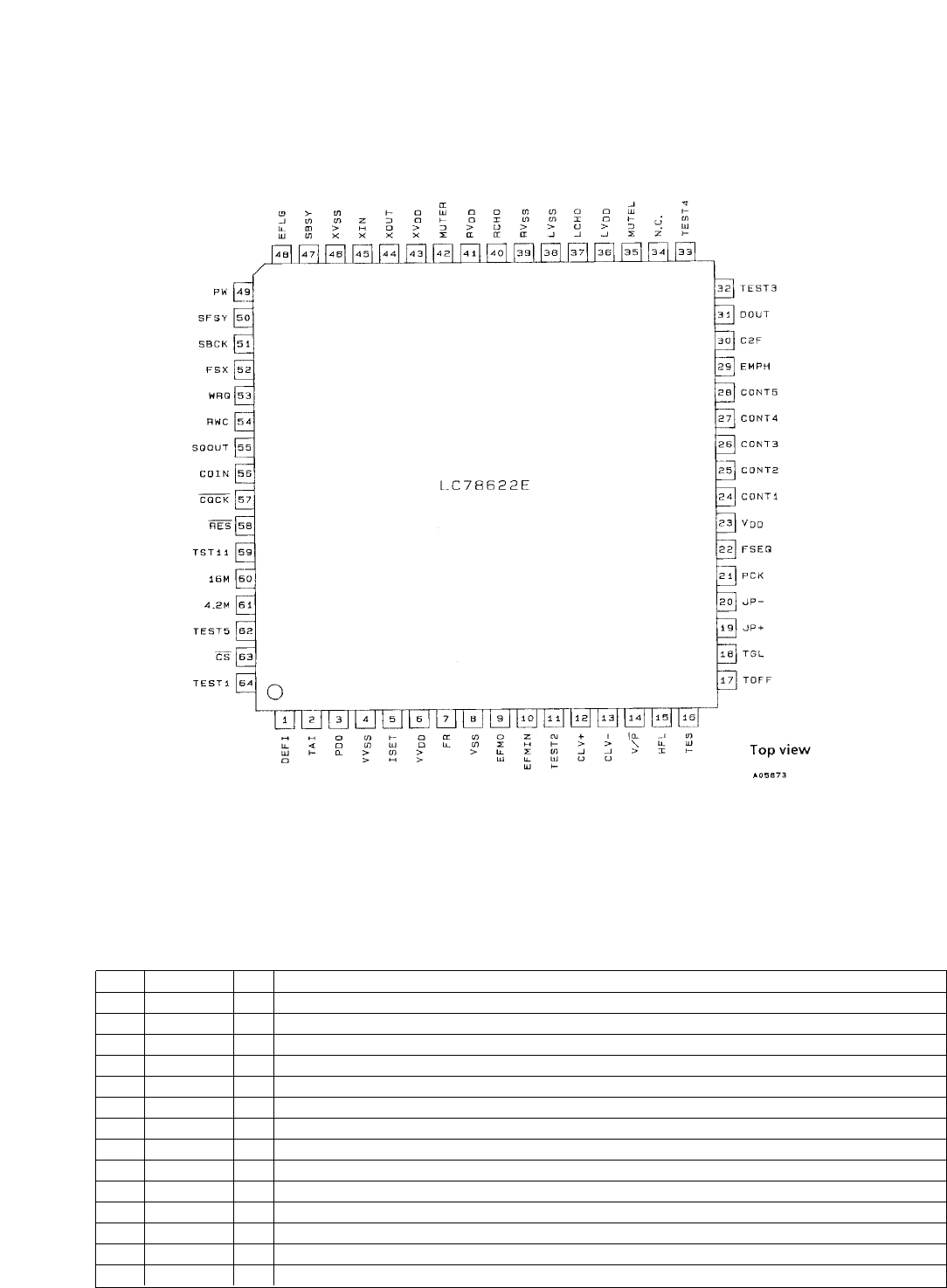
LC78622 Pin Function
Note: The same potential must be supplied to all power supply pins, i.e., VDD, VVDD, LVDD, RVDD, and XVDD.
Pin No. Symbol I/O Function
51 SBCK I Subcode readout clock input. This is a Schmitt input. (Must be connected to 0 V when unused.)
52 FSX O Output for the 7.35 kHz synchronization signal divided from the crystal oscillator
53 WRQ O Subcode Q output standby output
54 RWC I Read/write control input. This is a Schmitt input.
55 SQOUT O Subcode Q output
56 COIN I Command input from the control microprocessor
57 CQCK I Input for both the command input clock and the subcode readout clock. This is a Schmitt input.
58 RES I Chip reset input. This pin must be set low briefly after power is first applied.
59 TST11 O Test output. Leave open. (Normally outputs a low level.)
60 16M O 16.9344 MHz output.
61 4.2M O 4.2336 MHz output
62 TEST5 I Test input. A pull-down resistor is built in. Must be connected to 0 V.
63 CS I Chip select input. A pull-down resistor is built in. Must be connected to 0 V if not controlled.
64 TEST1 I Test input. No pull-down resistor. Must be connected to 0 V.
LC78622 Pin Assignment
PC-X250
1 - 17
Pin No. Symbol I/O Function
1 DEFI I Defect detection signal (DEF) input. (Must be connected to 0 V when unused.)
2 TAI I Test input. A pull-down resistor is built in. Must be connected to 0 V.
3 PDO O External VCO control phase comparator output
4 VVSS ÐPLL pins Internal VCO ground. Must be connected to 0 V.
5 ISET AI PDO output current adjustment resistor connection
6 VVDD ÐInternal VCO power supply
7 FR AI VCO frequency range adjustment
8 VSS Ð Digital system ground. Must be connected to 0 V.
9 EFMO O Slice level control EFM signal output
10 EFMIN I EFM signal input
11 TEST2 I Test input. A pull-down resistor is built in. Must be connected to 0 V.
12 CLV+ODisc motor control output.
13 CLVÐO Three-value output is also possible when specified by microprocessor command.
14 V/P O Rough servo/phase control automatic switching monitor output. Outputs a high level during rough servo and a low level
during phase control.
15 HFL I Track detection signal input. This is a Schmitt input.
16 TES I Tracking error signal input. This is a Schmitt input.
17 TOFF O Tracking off output
18 TGL O Tracking gain switching output. Increase the gain when low.
19 JP+OTrack jump output.
20 JPÐO Three-value output is also possible when specified by microprocessor command.
21 PCK O EFM data playback clock monitor. Outputs 4.3218 MHz when the phase is locked.
22 FSEQ O Synchronization signal detection output. Outputs a high level when the synchronization signal detected from the EFM
signal and the internally generated synchronization signal agree.
23 VDD ÐDigital system power supply.
24 CONT1 I/O General-purpose I/O pin 1
25 CONT2 I/O General-purpose I/O pin 2 Controlled by serial data commands from the microprocessor. Any of these that are unused
26 CONT3 I/O General-purpose I/O pin 3 must be either set up as input ports and connected to 0 V, or set up as output ports and
27 CONT4 I/O General-purpose I/O pin 4 left open.
28 CONT5 I/O General-purpose I/O pin 5
29 EMPH O De-emphasis monitor pin. A high level indicates playback of a de-emphasis disk.
30 C2F O C2 flag output
31 DOUT O Digital output. (EIAJ format)
32 TEST3 I Test input. A pull-down resistor is built in. Must be connected to 0 V.
33 TEST4 I Test input. A pull-down resistor is built in. Must be connected to 0 V.
34 N.C. Ð Unused. Must be left open.
35 MUTEL O Left channel mute output
36 LVDD ÐLeft channel Left channel power supply
37 LCHO O one-bit D/A converter Left channel output
38 LVSS Ð Left channel ground. Must be connected to 0 V.
39 RVSS Ð Right channel ground. Must be connected to 0 V.
40 RCHO O Right channel Right channel output
41 RVDD Ðone-bit D/A converter Right channel power supply
42 MUTER O Right channel mute output
43 XVDD ÐCrystal oscillator power supply.
44 XOUT OConnections for a 16.9344 crystal oscillator element
45 XIN I
46 XVSS Ð Crystal oscillator ground. Must be connected to 0 V.
47 SBSY O Subcode block synchronization signal output
48 EFLG O C1, C2, single and double error correction monitor pin
49 PW O Subcode P, Q, R, S, T, U, V and W output
50 SFSY O Subcode frame synchronization signal output. This signal falls when the subcodes are in the standby state.
LC78622 Pin Functions
PC-X250
1 - 18
1
2
4
3
LA6541D Pin Assignment
PC-X250
1 - 19
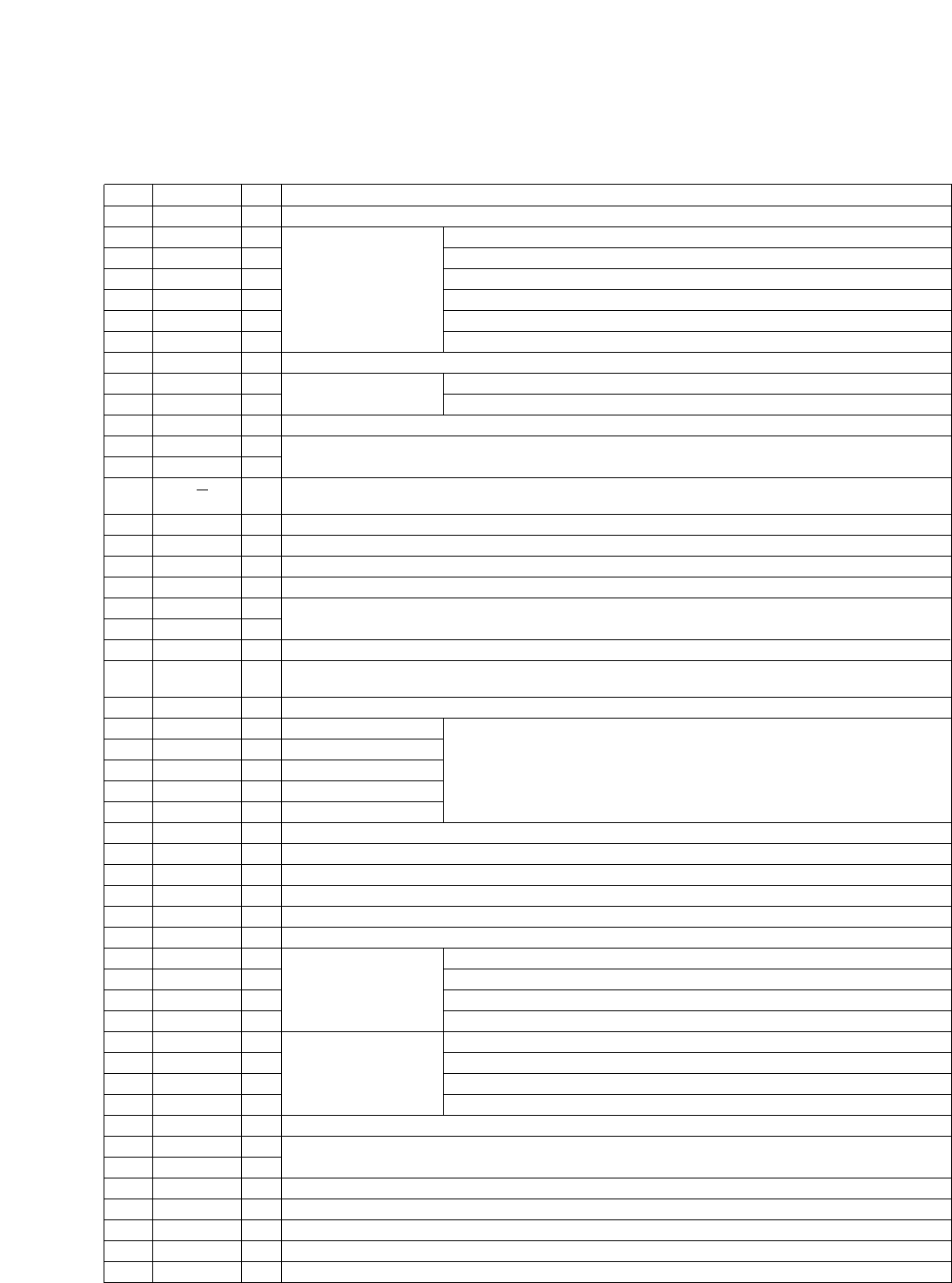
Level Shift Level Shift
Level Shift Level Shift
Regulator

Pin No. Pin Name Description (Function)
1V
CC Power supply (shorted with pin 30)
2 Mute ON/OFF control for all BTL AMP outputs
3V
IN1 BTL AMP 1 input
4 VG1 BTL AMP 1 input (for gain control)
5V
O
1 BTL AMP 1 output (non-inverting side)
6V
O
2 BTL AMP 1 output (inverting side)
7 GND GND (minimum electric potential)
8 GND GND (minimum electric potential)
9 GND GND (minimum electric potential)
10 VO3 BTL AMP 2 output (inverting side)
11 VO4 BTL AMP 2 output (non-inverting side)
12 VG2 BTL AMP 2 input (for gain control)
13 VIN2 BTL AMP 2 input
14 REG OUT Connection for collector of external transistor (PNP); 5 V supply output
15 REG IN Connection for base of external transistor (PNP)
16 RES Reset output
17 CDReset output delay time setting (with capacitor)
18 VIN3 BTL AMP 3 input
19 VG3 BTL AMP 3 input (for gain control)
20 VO5 BTL AMP 3 output (non-inverting side)
21 VO6 BTL AMP 3 output (inverting side)
22 GND GND (minimum electric potential)
23 GND GND (minimum electric potential)
24 GND GND (minimum electric potential)
25 VO7 BTL AMP 4 output (inverting side)
26 VO8 BTL AMP 4 output (non-inverting side)
27 VG4 BTL AMP 4 input (for gain control)
28 VIN4 BTL AMP 4 input
29 VREF Reference voltage input for level shift circuit
30 VCC Power supply (shorted with pin 1)
LA6541D Pin Functions
PC-X250
1 - 20
Microcontroller
INTERFACE
LA9241M Equivalent Circuit Block Diagram
PC-X250
1 - 21

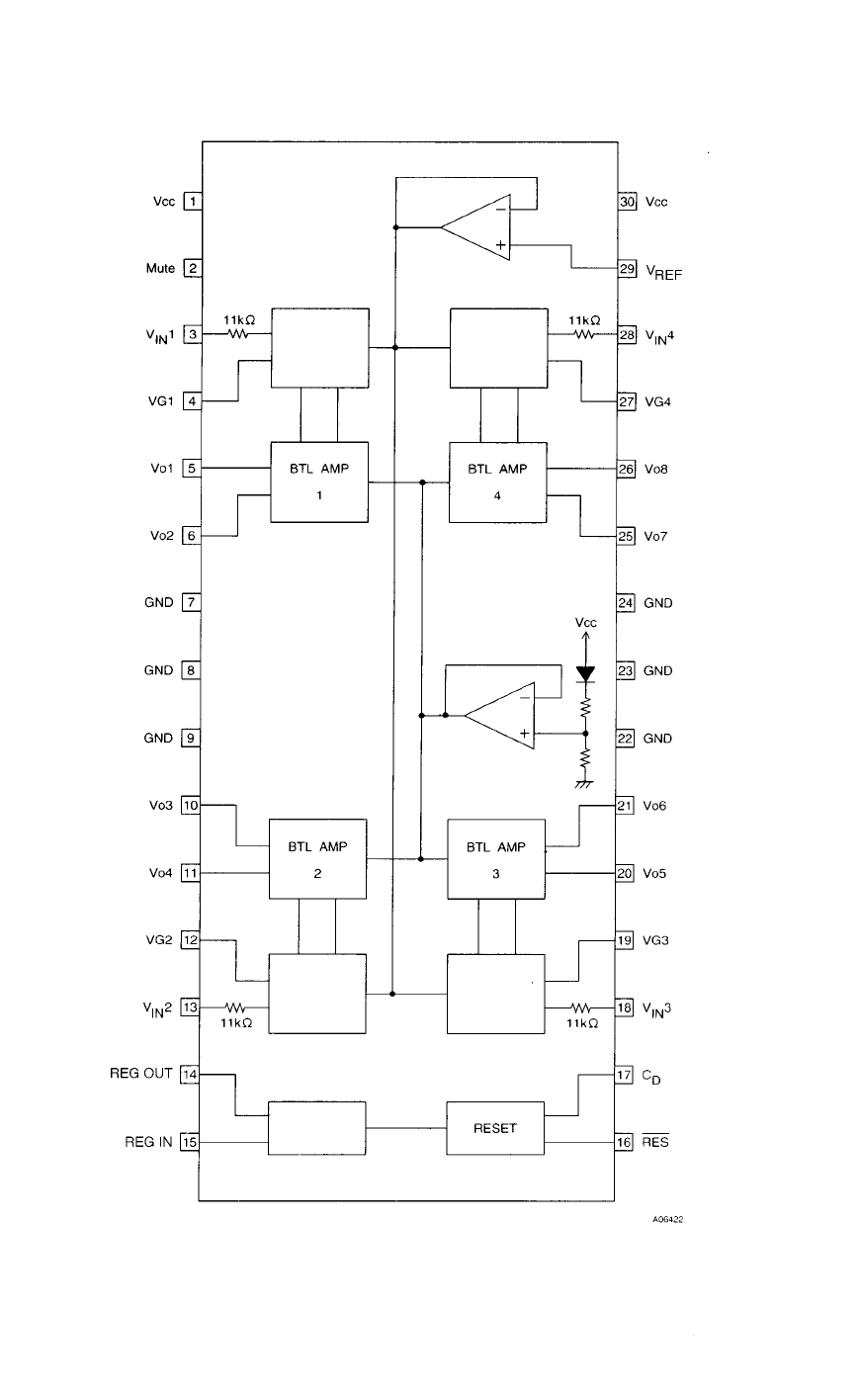
Pin
No. Symbol Contents
1 FIN2 Pickup photodiode connection pin. Added to FIN1 pin to generate the RF signal, subtracted from FIN1 pin to generate
the FE signal.
2 FIN1 Pickup photodiode connection pin.
3 E Pickup photodiode connection pin. Subtracted from F pin to generate the TE signal.
4 F Pickup photodiode connection pin.
5 TB TE signal DC component input pin.
6TE
?
Pin which connects the TE signal gain setting resistor between this pin and TE pin.
7 TE TE signal output pin.
8 TESI TES (Track Error Sense) comparator input pin. The TE signal is input through a bandpass filter.
9 SCI Shock detection input pin.
10 TH Tracking gain time constant setting pin.
11 TA TA amplifier output pin.
12 TD
?
Pin for configuring the tracking phase compensation constant between the TD and VR pins.
13 TD Tracking phase compensation setting pin.
14 JP Tracking jump signal (kick pulse) amplitude setting pin.
15 TO Tracking control signal output pin.
16 FD Focusing control signal output pin.
17 FD
?
Pin for configuring the focusing phase compensation constant between the FD and FA pins.
18 FA Pin for configuring the focusing phase compensation constant between the FD
?
and FA
?
pins.
19 FA
?
Pin for configuring the focusing phase compensation constant between the FA and FE pins.
20 FE FE signal output pin.
21 FE
?
Pin which connects the FE signal gain setting resistor between this pin and FE pin.
22 AGND Analog signal GND.
23 NC No connection
24 SP CV
+
and CV
?
pins input signal single-end output.
25 SPG 12-cm spindle mode gain setting resistor connection pin.
26 SP
?
Spindle phase compensation constant connection pin, along with the SPD pin.
27 SPD Spindle control signal output pin.
28 SLEQ Sled phase compensation constant connection pin.
29 SLD Sled control signal output pin.
30 SL
?
Input pin for sled movement signal from microprocessor.
31 SL
+
Input pin for sled movement signal from microprocessor.
32 JP
?
Input pin for tracking jump signal from DSP.
33 JP
+
Input pin for tracking jump signal from DSP.
34 TGL Input pin for tracking gain control signal from DSP. Gain is low when TGL is high.
35 TOFF Input pin for tracking off control signal from DSP. Tracking servo is off when TOFF is high.
36 TES Output pin for TES signal to DSP.
37 HFL The High Frequency Level is used to determine whether the main beam is positioned over a bit or over the mirrored
surface.
38 SLOF Sled servo off control input pin
39 CV
?
Input pin for CLV error signal from DSP.
40 CV
+
Input pin for CLV error signal from DSP.
41 RFSM RF output pin.
42 RFS
?
RF gain setting and EFM signal 3T compensation constant setting pin, along with the RFSM pin.
43 SLC Slice Level Control is an output pin that controls the data slice level used by the DSP for the RF waveform.
44 SLI Input pin used by DSP for controlling the data slice level.
45 DGND Digital system GND pin.
46 FSC Focus search smoothing capacitor output pin.
47 TBC Tracking Balance Control; EF balance adjustment variable range setting pin
48 NC No connection
49 DEF Disc defect detection output pin.
50 CLK Reference clock input pin. 4.23 MHz signal from the DSP is input.
51 CL Microprocessor command clock input pin.
Pin
No. Symbol Contents
52 DAT Microprocessor command data input pin.
53 CE Microprocessor command chip enable input pin.
54 DRF RF level detection output (Detect RF).
55 FSS Focus Search Select; focus search mode (±search/+search vs. the reference voltage) switching pin
56 VCC2 Servo system and digital system VCC pin.
57 REFI By-pass capacitor connection pin for reference voltage.
58 VR Reference voltage output pin.
59 LF2 Disc defect detection time constant setting pin.
60 PH1 RF signal peak hold capacitor connection pin.
61 BH1 RF signal bottom hold capacitor connection pin.
62 LDD APC circuit output pin.
63 LDS APC circuit input pin.
64 VCC1 RF system VCC pin.
LA9241 Pin Functions
PC-X250
1 - 22
PC-X250
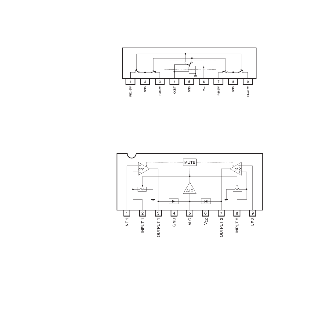
BA3126 Block Diagram
BA3308 Block Diagram
1 - 23
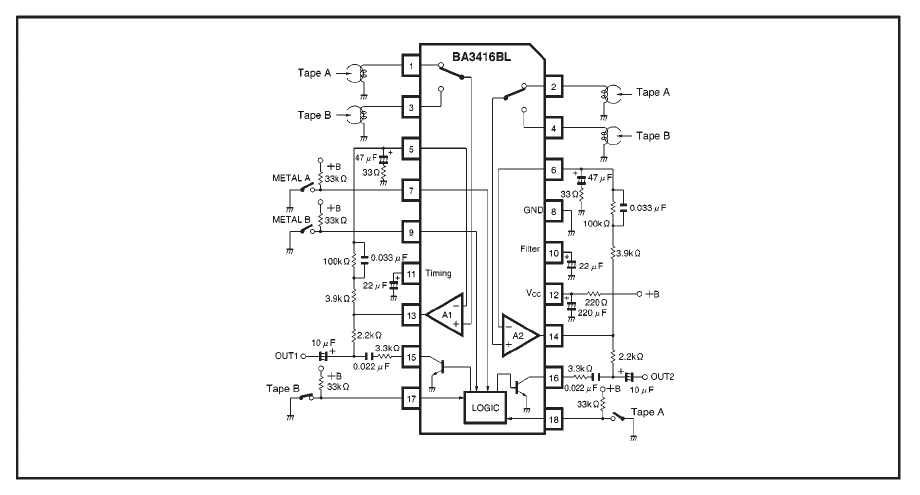
BA3416BL Block Diagram
PC-X250
1 - 24
PC-X250
1 - 25
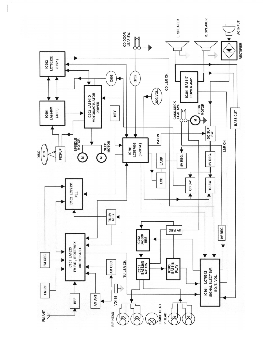
Block Diagram
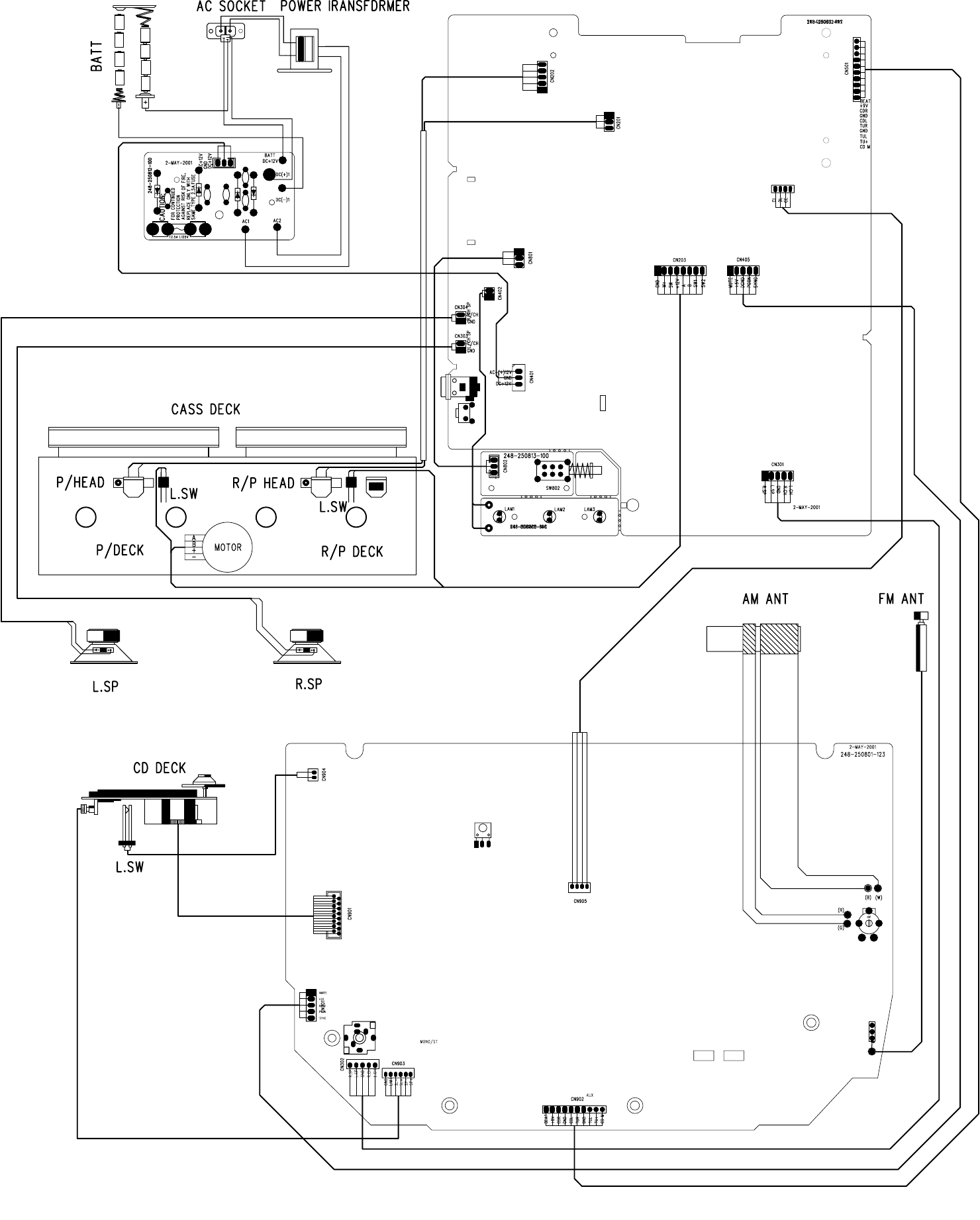
Wiring Diagram
PC-X250
1 - 26
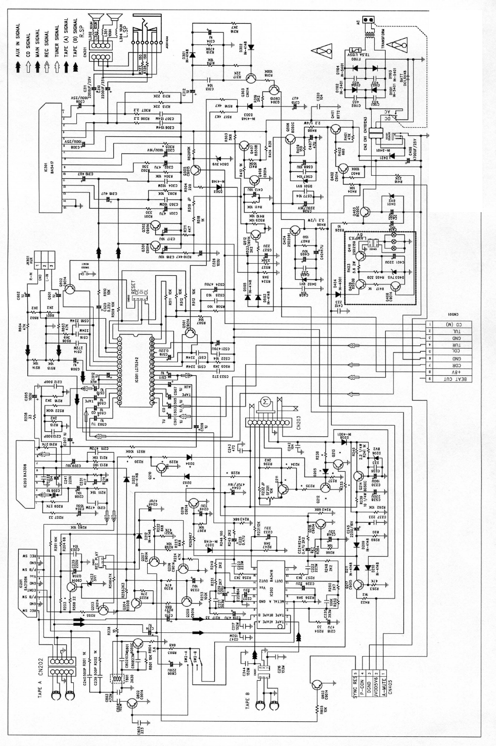
Circuit Diagram -1 PC-X250
1 - 27
1 - 28
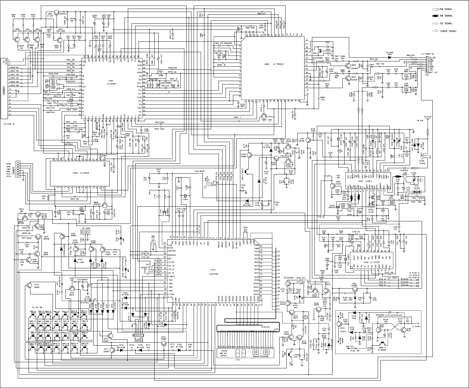
Circuit Diagram -2
PC-X250
PC-X250
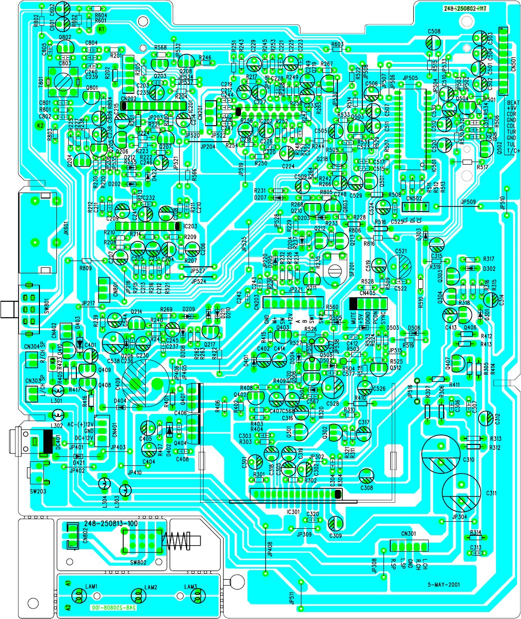
PCB Layout-1
1 - 29
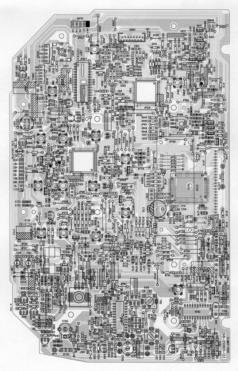
PCB Layout-2
PC-X250
1 - 30

PC-X250
1 - 31
PCB Layout-3
PC-X250
1 - 32
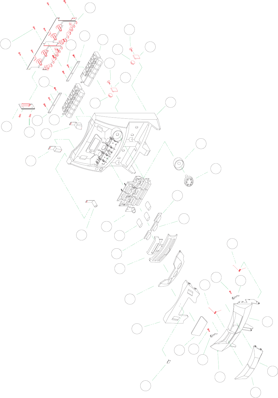
Assembly- 1
S8
34
S6
32
S5
33
S7
26
25
29
30
24
S3
31
28
S4
27
23
22
15
14
18
17
21
20
19
16
13
12
07
S1
05
08
11
10
09
S2
06
03
02
01
04

!ITEM Q'TY
01 525-073030-011 RIGHT CASS DOOR LENS 1
02 525-072030-011 LEFT CASS DOOR LENS 1
03 525-0030S3-012 LEFT CASS DOOR 1
04 525-0130S3-012 RIGHT CASS DOOR 1
05 766-250000-000 LEFT CASS DOOR SPRING 1
06 525-029300-000 LEFT CASS TAPE BRACKET 1
07 766-250000-000 RIGHT CASS DOOR SPRING 1
08 525-029300-000 RIGHT CASS TAPE BRACKET 1
09 525-080400-013 CD DISPLAY LENS 1
10 500-810200-011 "JVC" NAME PLATE 1
11 525-045430-013 DISPLAY PANEL 1
12 525-0453S3-011 CONTROL PLATE 1
13 525-045817-011 FUNCTION PLATE 1
14 525-0074S3-000 VOLUME KNOB 1
15 525-090427-000 VOLUME KNOB RING 1
16 525-078827-011 RADIO KNOB LENS 1
17 525-078327-011 CD KNOB LENS 1
18 525-078027-011 TAPE KNOB LENS 1
19 525-080800-000 REFLECTION LENS 3
20 525-0500S3-013 CD CONTROL KNOB 12pcs/KIT
21 525-0072S3-000 SUPER BASS KNOB 1
22 525-0010S3-012 FRONT CABINET 1
23 539-121200-000 LEFT CASS DOOR GEAR HOLDER 1
24 539-121100-000 LEFT CASS DOOR GEAR 1
25 525-0102S3-012 LEFT CASS KNOB 5pcs/KIT
26 463-380000-000 LEFT CASS KNOB PLATE 1
27 539-121200-000 RIGHT CASS DOOR GEAR HOLDER 1
28 539-121100-000 RIGHT CASS DOOR GEAR 1
29 525-0085S3-000 EQ KNOB 1
30 525-0510S3-000 POWER CONTROL KNOB 1
31 525-0108S3-012 RIGHT CASS KNOB 6pcs/KIT
32 463-380000-000 RIGHT CASS KNOB PLATE 1
33 248-250813-000 RECORDING BOARD 1
34 156-255609-254 CASS DECK 1
S1 238-120060-602 SCREW 2 X 6 PB 1 FIX RIGHT TAPE BRACKET
S2 238-120060-602 SCREW 2 X 6 PB 1 FIX LEFT TAPE BRACKET
S3 238-130080-632 SCREW 3 X 8 PWB 1 FIX LEFT CASS DOOR GEAR
S4 238-130080-632 SCREW 3 X 8 PWB 1 FIX RIGHT CASS DOOR GEAR
S5 238-130060-602 SCREW 3 X 6 PB 3 FIX LEFT CASS DOOR PLATE
S6 238-130060-602 SCREW 3 X 6 PB 3 FIX RIGHT CASS DOOR PLATE
S7 238-220050-903 SCREW 2 X 5 MC 2 FIX THE RECORDING BOARD
S8 238-130100-602 SCREW 3 X 10 PB 6 FIX CASS DECK
PARTS NUMBER PARTS NAME DESCRIPTION/LOCALITY
PC-X250
1 - 33
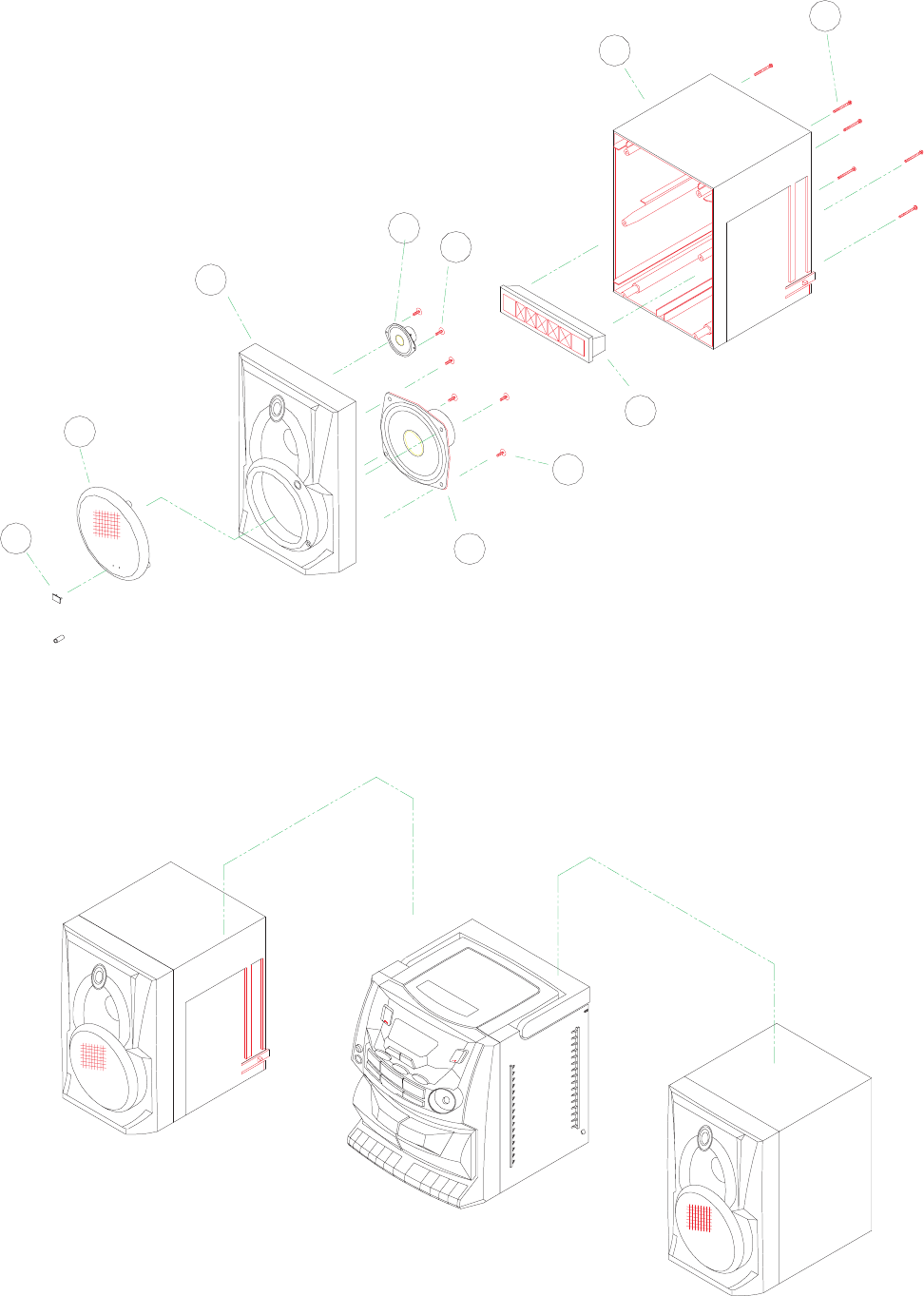
Assembly- 1
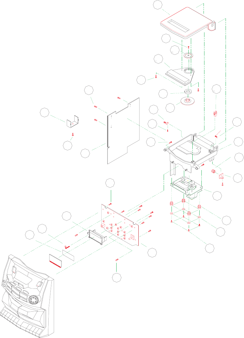
Assembly- 2
PC-X250
1 - 34
20
S9
19
18
12
S8
17
16
15
S7
S4
S6
14
S5
13
11
10
09
08
07
06
05
S3
S2
03
02
01
S1
04

!ITEM Q'TY
01 466-756350-050 PVC BACK LIGHT PLATE 1
02 206-106938-000 REMOTE RECEIVER 1
03 525-031064-000 CD DISPLAY BRACKET 1
04 248-250802-117 AUDIO BOARD 1
05 453-030100-050 METAL WASHER 4
06 458-328840-220 RUBBER SILICON 4
07 356-110300-091 CD DECK 1
08 539-121200-000 CD DOOR GEAR HOLDER 1
09 539-121100-000 CD DOOR GEAR 1
10 525-0470S3-000 CD TRAY 1
11 479-328800-000 CD DOOR SPRING 1
12 846-209000-000 CD DOOR LOCK 1
13 248-250801-123 TUNER BOARD 1
14 408-146395-150 HEAT SINK 1
15 217-200035-050 LEAF SWITCH 1
16 500-291942-501 CD CHUCK (M) 1
17 473-300160-500 CD MAGNET RING 1
18 525-080330-011 CD DOOR LENS 1
19 500-100000-000 CD CHUCK (A) 1
20 525-0490S3-014 CD DOOR 1
S1 238-130150-602 SCREW 3 x 15 PB 2 FROM AUDIO BOARD TO CD TRAY
S2 238-130080-602 SCREW 3 x 8 PB 8 FIX THE AUDIO BOARD
S3 238-126080-632 SCREW 2.6 X 8 PWB 4 FIX THE CD DECK
S4 238-130100-602 SCREW 3 x 10 PB 2 FROM CD TRAY TO FRONT CABINET
S5 238-230086-202 SCREW 3 X 8 BB ( HARD ) 1 FIX HEAT SINK
S6 238-130080-602 SCREW 3 X 8 PB 3 FIX THE MAIN BOARD
S7 238-120060-602 SCREW 2 X 6 PB ( BLACK ) 1 FIX CD LEAF SWITCH
S8 238-130082-102 SCREW 3 X 8 KB ( BLACK ) 2 FIX CD DOOR LENS
S9 238-220060-202 SCREW 2 X 6 BB 1 FIX CD CHUCK A
PARTS NAME DESCRIPTION/LOCALITYPART NO.
PC-X250
1 - 35
Assembly- 2
13
11
06
07
12
09
10
08
S5
S4
05
04
S3
03
S1
01
02
S2
PC-X250
1 - 36
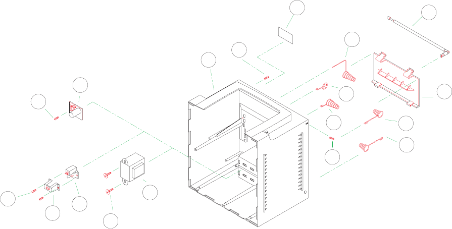
Assembly- 3

!ITEM PART NO. Q'TY
!01 158-000117-622 AC SOCKET 1
!02 500-025100-000 AC SOCKET COVER 1
!03 152-112560-225 POWER TRANSFORMER 1
04 248-250812-100 RECTIFIER BOARD 1
05 525-0020S3-012 BACK CABINET 1
06 763-250000-000 BATTERY SPRING ( +/-- ) 1
07 764-701300-000 BATTERY SPRING ( +) 1
08 765-901000-000 BATTERY SPRING ( -- ) 1
09 763-455000-000 BATTERY SPRING ( +/-- ) 1
10 763-331800-000 BATTERY SPRING ( +/-- ) 1
11 525-0040S3-000 BATTERY DOOR 1
12 466-756350-050 1 COVER THE VOLTAGE SELECTOR HOLE
13 155-420026-238 RADIO ANTENNA 1
S1 238-130200-632 SCREW 3 X 20 PWB 2 FIX POWER TRANSFORMER
S2 238-128120-602 SCREW 2.8 X 12 PB 2 FIX AC SOCKET COVER
S3 238-130080-602 SCREW 3 X 8 PB 1 FIX RECTIFIER BOARD
S4 238-128120-602 SCREW 3 X 10 PB 1 FIX AUX JACK
S5 238-130100-203 SCREW 3 X 10 BM ( BLACK ) 1 FIX RADIO ANTENNA
PVC PLATE FOR VOLTAGE
SELECTOR HOLE
PARTS NAME DESCRIPTION/LOCALITY
PC-X250
1 - 37
Assembly- 3
PC-X250
1 - 38
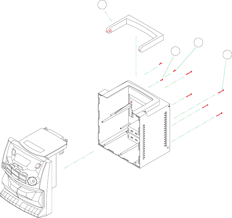
Assembly- 4
01
S2
S3
S1

!ITEM PART NO. Q'TY
1 525-0050S3-000 HANDLE 1
S1 238-130250-602 SCREW 3 X 25 PB 5 FROM FRONT CASINET TO BACK CABINET
S2 238-130100-602 SCREW 3 X 10 PB 1 FIX THE AUX JACK
S3 238-128120-602 SCREW 2 X 5 MC 2 FIX THE RECORDING BOARD
PARTS NAME DESCRIPTION/LOCALITY
PC-X250
1 - 39
Assembly- 4
PC-X250
1 - 40
Assembly- 5
Assembly- 6
S1
07
S2
04
03
06
S3
05
02
01

FOR RIGHT SPEAKER BOX ASSEMBLY
!ITEM Q'TY
01 500-810200-011 "JVC" NAME PLATE 1
02 525-040000-000 SPEAKER NET HOLDER 1
03 525-0410S3-010 SPEAKER BOX PANEL 1
04 154-178450-329 LOUD SPEAKER 1
05 154-508380-609 SPEAKER 1
06 525-026900-000 SPEAKER CORD HOLDER 1
07 525-0390S3-008 RIGHT SPEAKER BOX BACK 1
S1 238-130300-602 SCREW 3 X 30 PB 6
S2 238-130080-632 SCREW 3 X 8 PWB 2 FIX THE SPEAKER
S3 238-130080-632 SCREW 3 X 8 PWB 4
FOR LEFT SPEAKER BOX ASSEMBLY
ITEM Q'TY
01 500-810200-011 "JVC" NAME PLATE 1
02 525-040000-000 SPEAKER NET HOLDER 1
03 525-0410S3-010 SPEAKER BOX PANEL 1
04 154-508380-609 SPEAKER 1
05 154-178450-329 LOUD SPEAKER 1
06 525-026900-000 SPEAKER CORD HOLDER 1
07 525-0390S3-002 LEFT SPEAKER BOX BACK 1
S1 238-130300-602 SCREW 3 X 30 PB 6
S2 238-130080-632 SCREW 3 X 8 PWB 4 FIX THE SPEAKER
S3 238-130080-632 SCREW 3 X 8 PWB 2
PART NO. PARTS NAME DESCRIPTION/LOCALITY
FROM SPEAKER PANEL TO SPEAKER BOX BACK
FIX THE LOUD SPEAKER
PART NO. PARTS NAME DESCRIPTION/LOCALITY
FROM SPEAKER PANEL TO SPEAKER BOX BACK
FIX THE LOUD SPEAKER
PC-X250
1 - 41
Assembly- 5
PC-X250
1-42
P.2
P.1
P.4
P.6
P.5
P.3
P.7
P.8
P.9
P.10 P.11
P.12 P.13
P.14
P.15
P.16
P.17
P.18
P.19
P.20
P.22
P.21
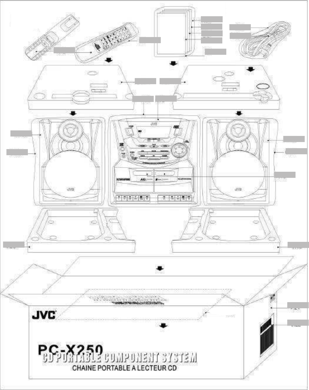
Packing
Item Part's Name Parts No.
P.1 Poly Bag
P.2 Remote Control Unit
P.6 Safety Instruction Sheet 602-900276-000
P.7 Poly Bag 676-070100-040
P.8 Poly Bag 676-040130-040
P.9 Power Cord Set 151-117117-612
P.10 Poly Form, Top Left
P.11 Poly Form, Top Right
P.12 Poly Bag 676-215240-040
P.13 Main Unit -
P.14 Speaker Unit, Left AS00-25002
P.15 Poly Bag 676-180240-040
P.16 Speaker Unit, Right AS00-25008
P.17 Poly Bag 676-180240-040
POP Label-Left 629-080097-000
POP Label-Right 629-080096-000
P.19 Poly Form, Bottom Right
P.20 Poly Form, Bottom Left
P.21 Gift Box 891-250102-010
P.22 Bar Code Label 612-080131-000
RC27-100S3-011
602-700337-000
P.18
601-250000-010
602-700388-001
P.3 Instruction Manual
P.4 Warranty Card
875-351000-000
P.5 Registration card
875-351000-000
PC-X250
1 - 43
Packing List

PC-X250
VICTOR COMPANY OF JAPAN, LIMITED. (By JCA)
AUDIO & COMMUNICATION BUSINESS DIVISION (By JCA)
PERSONAL & MOBILE NETWORK BUSINESS UNIT. 10-1, 1 Chome, Ohwatari-machi, Maebashi-city, 371-8543, Japan. (By JCA)
No. 28001

PARTS LIST
* All printed circuit boards and its assemblies are not available as service parts.
- Contents -
Electrical Parts List (Tuner circuit pcb)
Electrical Parts List (Audio circuit pcb)
Electrical Parts List (Rectifier circuit pcb)
Electrical Parts List (Tape recording circuit pcb)
Electrical Parts List (Display lighting circuit pcb)
[ PC-X250 ]
2 - 2
2 - 9
2 - 14
2 - 15
2 - 16
Area suffix
J ------------------------------- USA
C -------------------------- Canada
PC-X250
2 - 1

Tuner pcb
Part No. Materials Qty Position/ECN
199-741005-000 GOLD CAP DX-5R5H104 0.1 F/5.5V 1 PCS
201-000330-185 RESISTOR 3.3 OHM +-5% 1/8W 1 PCS J216
201-001000-185 RESISTOR 10 OHM +-5% 1/8W 2 PCS R75,R89
201-002200-185 RESISTOR 22 OHM +-5% 1/8W 1 PCS R902
201-011000-185 RESISTOR 100 OHM +-5% 1/8W 16 PCS R310,R702,R970,R971,R703,R704,R705,R706,R708,R709,R710,R711,
R712,R723,R724,R725
201-013300-185 RESISTOR 330 OHM +-5% 1/8W 4 PCS R201,R208,R931,R20
201-014700-185 RESISTOR 470 OHM +-5% 1/8W 2 PCS R950,R716
201-016800-185 RESISTOR 680 OHM +-5% 1/8W 2 PCS R932,R939
201-021000-185 RESISTOR 1 KOHM +-5% 1/8W 13 PCS R106,R119,R120,R121,R123,R125,R26,R30,R1,R920,R930,R402,R1043
201-021200-185 RESISTOR 1.2 KOHM +-5% 1/8W 2 PCS R103,R941
201-021500-185 RESISTOR 1.5 KOHM +-5% 1/8W 3 PCS R2,R11,R915
201-022200-185 RESISTOR 2.2 KOHM +-5% 1/8W 10 PCS R57,R520,R521,R19,R719,R720,R741,R905,R910,R11
201-023300-185 RESISTOR 3.3 KOHM +-5% 1/8W 3 PCS R11,R946,R949
201-023900-185 RESISTOR 3.9 KOHM +-5% 1/8W 2 PCS R945,R948
201-024700-185 RESISTOR 4.7 KOHM +-5% 1/8W 12 PCS R147,R148,R21,R933,R934,R938,R2,R5,R9,R945,R956,R730,R741
201-025100-185 RESISTOR 5.1 KOHM +-5% 1/8W 2 PCS R112,R113
201-025600-185 RESISTOR 5.6 KOHM +-5% 1/8W 2 PCS R12,R17
201-026800-185 RESISTOR 6.8 KOHM +-5% 1/8W 4 PCS R951,R904,R923,R926
201-028200-185 RESISTOR 8.2 KOHM +-5% 1/8W 5 PCS R49,R34,R916,R944,R947
201-031000-185 RESISTOR 10 KOHM +-5% 1/8W 22 PCS R115,R126,R131,R133,R952,R954,R961,R965,R58,R1,R6,R22,R24,R27,R28,
R29,R32,R33,R917,R922,R927,R3
201-031500-185 RESISTOR 15 KOHM +-5% 1/8W 22 PCS R4,R5,R7,R8,R38,R46,R47,R48,R713,R714,R727,R728,R729,R734,R735,
R908,R913,R928,R96,R77,R92,R40
201-032200-185 RESISTOR 22 KOHM +-5% 1/8W 3 PCS R912,R929,R985
201-032700-185 RESISTOR 27 KOHM +-5% 1/8W 2 PCS R35,R911
201-033300-185 RESISTOR 33 KOHM +-5% 1/8W 5 PCS R108,R10,R14,R918,R974
201-034700-185 RESISTOR 47 KOHM +-5% 1/8W 9 PCS R3,R4,R6,R7,R8,R9,R13,R18,R715
201-035600-185 RESISTOR 56 KOHM +-5% 1/8W 4 PCS R137,R919,R921,R940
201-036800-185 RESISTOR 68 KOHM +-5% 1/8W 2 PCS R907,R914
201-041000-185 RESISTOR 100 KOHM +-5% 1/8W 5 PCS R101,R102,R134,R906,R942
201-041500-185 RESISTOR 150 KOHM +-5% 1/8W 1 PCS R903
201-042200-185 RESISTOR 220 KOHM +-5% 1/8W 3 PCS R104,R924,R925
201-042700-185 RESISTOR 270 KOHM +-5% 1/8W 1 PCS R25
201-051000-185 RESISTOR 1 MOHM +-5% 1/8W 2 PCS R945,R948
202-100505-505 G CERAMIC CAP 5 PF/50V SL +-5% 1 PCS C920
202-101805-505 G CERAMIC CAP 18 PF/50V SL 1 PCS C140
202-103005-505 H CERAMIC CAP 30 PF/50V SL 6 PCS C105,C106,C138,C139,C713,C714
202-103305-505 H CERAMIC CAP 33 PF/50V SL 2 PCS C950,C951
202-104705-505 H CERAMIC CAP 47 PF/50V SL 1 PCS C114
PC-X250
2 - 2
Tuner pcb
202-211005-101 G CERAMIC CAP 100 PF/50V B(X7R 5 PCS C111,C112,C113,C916,C952
202-213005-101 G CERAMIC CAP 300 PF/50V B(X7R 1 PCS C121
202-213305-101 G CERAMIC CAP 330 PF/50V B(X7R 2 PCS C904,C942
202-221005-101 G CERAMIC CAP 0.001 UF/50V B 8 PCS C125,C133,C136,C910,C943,C948,C949,C983
202-422201-202 G CERAMIC CAP 0.0022 UF/16V X 1 PCS C921
202-422701-101 G CERAMIC CAP 0.0027 UF/16V X 1 PCS C132
202-423301-202 G CERAMIC CAP 0.0033 UF/16V X 3 PCS C907,C914,C919
202-500305-505 G CERAMIC CAP 3 PF/50V NPO 2 PCS C126,C127
202-500335-505 G CERAMIC CAP 3.3 PF/50V NPO 2 PCS C707,C708
202-500505-505 G CERAMIC CAP 5 PF/50V NPO 1 PCS C120
202-501505-101 G CERAMIC CAP 15 PF/50V NPO 1 PCS C134
202-501505-505 G CERAMIC CAP 15 PF/50V NPO 1 PCS C922
202-631002-802 G CERAMIC CAP 0.01 UF/25V F 7 PCS C110,C116,C119,C926,C972,C980,C998
202-631502-802 G CERAMIC CAP 0.015 UF/25V F 1 PCS C912
202-631802-802 G CERAMIC CAP 0.018 UF/25V F 3 PCS C141,C142,C913
202-632002-802 G CERAMIC CAP 0.020 UF/25V F 1 PCS C122
202-632202-802 G CERAMIC CAP 0.022 UF/25V F 2 PCS C103,C118
202-633302-802 G CERAMIC CAP 0.033 UF/25V F 4 PCS C902,C903,C905,C923
202-634702-802 G CERAMIC CAP 0.047 UF/25V F 3 PCS C908,C927,C930
202-641002-802 G CERAMIC CAP 0.1 UF/25V F(Y5V 18 PCS C107,C108,C135,C137,C143,C144,C706,C709,C710,C711,C911,C932,C944,
C968,C970,C984,C985,C986
202-641502-802 G CERAMIC CAP 0.15 UF/25V F(Y5 2 PCS C901,C909
203-041050-202 ELECT CAP 0.1 UF/50V +-20% 1 PCS C130
203-042250-202 ELECT CAP 0.22 UF/50V +-20% 1 PCS C931
203-051050-202 ELECT CAP 1 UF/50V +-20% 1 PCS C712
203-053350-202 ELECT CAP 3.3 UF/50V +-20% 1 PCS C145
203-054750-202 ELECT CAP 4.7 UF/50V +-20% 3 PCS C145,C701,C935
203-061025-212 ELECT CAP 10 UF/25V +-20% 7 PCS C18,C963,C965,C915,C901,C905,C963
203-062210-202 ELECT CAP 22 UF/10V +-20% 1 PCS C933
203-064710-202 ELECT CAP 47 UF/10V +-20% 2 PCS C6,C146
203-072210-202 ELECT CAP 220 UF/10V +-20% 3 PCS C1,C27,C967
203-074710-202 ELECT CAP 470 UF/10V +-20% 1 PCS C969
203-081010-202 ELECT CAP 1000 UF/10V +-20% 1 PCS C971
206-100201-000 DIODE VCD/SVC201 NSX1900 2 PCS VD101,VD102
206-100348-000 G DIODE VCD/SVC348 PC-X250 1 PCS D115
206-104148-000 DIODE IN-4148 38.39.4630.63. 20 PCS D1,D2,D3,D5,D7,D101,D102,D701,D702,D703,D709,D711,D713,D715,
D716,D717,D718,D719,D901,D902
206-106938-000 DIODE RPM-6938-V4 (ROHM) AM20
9
1 PCS
206-200056-102 ZENER 5.6V 1/2W CD82/CD978/CH 1 PCS D102
207-003330-000 TRANSISTOR 2SC-3330U CD9788/ 3 PCS Q104,Q903,Q904
207-003399-000 E TRANSISTOR C3399 PC-X250 6 PCS Q6,Q702,Q705,Q706,Q707,Q708
207-008550-020 TRANSISTOR 8550B/C #38/39/4630 2 PCS Q918,Q919
PC-X250
2 - 3
Tuner pcb
207-009014-030 TRANSISTOR 9014C #38/39/4630/ 10 PCS Q1,Q2,Q3,Q4,Q8,Q9,Q11,Q12,Q723,Q921
207-009018-080 TRANSISTOR 9018-H 38/39/63/731 1 PCS Q15
207-190764-040 TRANSISTOR 2SB-764-D CD85.97 1 PCS Q909
207-191317-913 TRANSISTOR 2SA-1317-S-AC CD84
.
1 PCS Q901
207-191346-130 TRANSISTOR 2SA-1346-AC CD84.8
5
2 PCS Q902,Q34
207-191936-913 TRANSISTOR 2SD-1936-S-AC CD84 4 PCS Q1,Q2,Q3,Q4
208-010720-118 CERAMIC FILTER 10.7 MCI-A 2PIN 1 PCS CF104
208-010730-018 CERAMIC FILTER 10.7 MHz 3 PINS 2 PCS CF101,CF102
208-045030-000 CERAMIC FILTER 450 KHz 3 PINS 1 PCS CF106
209-181612-010 I.F.T. OSC 1A612R RED 10 mm MW 1 PCS T101
209-252070-010 I.F.T. IF 2070 YELLOW 10 mm 1 PCS T103
210-001823-000 I.C. SANYO LA-1823-ESIA CD9938 1 PCS IC101
210-006541-004 I.C. SANYO LA-6541D CD72.76.83 1 PCS IC903
210-009241-013 I.C. SANYO LA-9241M CD7588/PC- 1 PCS IC901
210-072131-000 I.C. SANYO LC-72131D AMR211/31 1 PCS IC1
210-078622-005 I.C. SANYO LC-78622E CD72.82. 1 PCS IC902
210-587008-000 G I.C. SANYO LC-587008 PC-X250 1 PCS IC701
212-065025-100 AM COIL 65:25T WIRE 4 x 100mm 1 PCS L6
213-035035-070 FM COIL 3.5T 3.5 x 0.7 mm 1 PCS L105
213-035045-070 FM COIL 3.5T 4.5 x 0.7 mm 1 PCS L104
216-000010-018 TRIMMER 10 PF RED 2 PCS CT102,CT103
217-060650-450 TACT SWITCH H=5mm W=6x6mm 15 PCS SW1-SW11,SW13-SW16
217-200035-050 LEAF SWITCH LS-N35 #CD8488/ 1 PCS
220-207634-241 G LCD DISPLAY 76x34 mm 24 PINS 1 PCS LCD701
222-010070-000 FERRITE BAR 10 x 70 mm 1 PCS
226-002600-000 CHOKE COIL 26 uH x2 , COMMON 1 PCS L1
226-010000-000 CHOKE COIL 100 uH #38.7017.801 1 PCS L2
227-060505-000 LED ROUND TYPE FLAT HEAD 3 PCS D1,D4,D6
229-016934-000 CRYSTAL 16.9344 MHz #AMR209. 1 PCS X901
229-040000-000 G CRYSTAL 4 MHz PC-X250 1 PCS X701
229-045000-000 CRYSTAL 4.5 MHz 1 PCS X105
229-327680-200 CRYSTAL 32.768KHz 20PPM HOOR
A
1 PCS X702
232-160190-310 FFC HEADER 16 PINS 1.0mm V 1 PCS CN901
233-020200-020 HEADER 2 PINS "JST" 2.0mm V 1 PCS CN904
233-030200-020 HEADER 3 PINS "JST" 2.0mm V 1 PCS CN702
233-040200-025 HEADER 4 PINS "JST" 2.5mm V 1 PCS CN701
233-050200-025 HEADER 5 PINS "JST" 2.5mm V 1 PCS CN302
233-060200-020 HEADER 6 PINS "JST" 2.0 mm V 1 PCS CN903
237-260080-055 JUMPER WIRE #26 80 mm YELLO
W
1 PCS TUNER BD. C TO D
237-260100-058 JUMPER WIRE #26 100 mm ORANG 1 PCS TUNER BD. E TO F
237-260150-021 JUMPER WIRE #26 150 mm BLUE 1 PCS TUNER BD. A TO B
238-120060-102 SCREW ST 2 x 6 mm KB BLACK 5 PCS CD DOOR LENS
PC-X250
2 - 4
Tuner pcb
238-120060-602 SCREW ST 2 x 6 mm PB BLACK 1 PCS LEAF SW.
238-126080-632 SCREW ST 2.6 x 8 mm PWB 4 PCS CD DECK
238-130080-602 SCREW ST 3 x 8 mm PB 10 PCS CONTROL BD.
238-130080-632 SCREW ST 3 x 8 mm PWB 1 PCS CD DOOR GEAR
248-250801-123 G P.C.B. PC-X250 TUNER BD. 1 PCS
270-121524-122 ROTARY ENCODER EC12E24204F2 1 PCS VR501
356-110300-091 E CD DECK MECHANISM (SANYO)
D
1 PCS
401-101032-000 ANTENNA BAR HOLDER (8012) 801
2
2 PCS
453-030100-050 METAL WASHER 3x10x0.5mm 4 PCS
458-328840-220 RUBBER SILICON(BLACK) HARDN
E
4 PCS
473-300160-500 CD MAGNET RING 30x16X5mm CD
8
1 PCS
479-328800-000 SPRING FOR CD DOOR 1 PCS
500-100000-000 CD CHUCK A (FOR SONY&SANYO
C
1 PCS
500-291942-501 CD CHUCK M (FOR SANYO DA11) 1 PCS
500-991110-000 CD MEDHANISM COVER (FOR SAN
Y
1 PCS
525-031064-000 DISPLAY BRACKET PC-X250 1 PCS
539-121100-000 GEAR FOR CASS DOOR 3918 1 PCS
539-121200-000 GEAR HOLER FOR CASS DOOR 39
1
1 PCS
846-209000-000 CD DOOR LOCK AMR-209M/V3/340 1 PCS
201-000330-185 RESISTOR 3.3 OHM +-5% 1/8W 1 PCS J216
201-001000-185 RESISTOR 10 OHM +-5% 1/8W 2 PCS R75,R89
201-002200-185 RESISTOR 22 OHM +-5% 1/8W 1 PCS R902
201-011000-185 RESISTOR 100 OHM +-5% 1/8W 16 PCS R310,R702,R970,R971,R703,R704,R705,R706,R708,R709,R710,R711,R712,
R723,R724,R725
201-013300-185 RESISTOR 330 OHM +-5% 1/8W 4 PCS R201,R208,R931,R20
201-014700-185 RESISTOR 470 OHM +-5% 1/8W 2 PCS R950,R716
201-016800-185 RESISTOR 680 OHM +-5% 1/8W 2 PCS R932,R939
201-021000-185 RESISTOR 1 KOHM +-5% 1/8W 13 PCS R106,R119,R120,R121,R123,R125,R26,R30,R1,R920,R930,R402,R1043
201-021200-185 RESISTOR 1.2 KOHM +-5% 1/8W 2 PCS R103,R941
201-021500-185 RESISTOR 1.5 KOHM +-5% 1/8W 3 PCS R2,R11,R915
201-022200-185 RESISTOR 2.2 KOHM +-5% 1/8W 10 PCS R57,R520,R521,R19,R719,R720,R741,R905,R910,R11
201-023300-185 RESISTOR 3.3 KOHM +-5% 1/8W 3 PCS R11,R946,R949
201-023900-185 RESISTOR 3.9 KOHM +-5% 1/8W 2 PCS R945,R948
201-024700-185 RESISTOR 4.7 KOHM +-5% 1/8W 12 PCS R147,R148,R21,R933,R934,R938,R2,R5,R9,R945,R956,R730,R741
201-025100-185 RESISTOR 5.1 KOHM +-5% 1/8W 2 PCS R112,R113
201-025600-185 RESISTOR 5.6 KOHM +-5% 1/8W 2 PCS R12,R17
201-026800-185 RESISTOR 6.8 KOHM +-5% 1/8W 4 PCS R951,R904,R923,R926
201-028200-185 RESISTOR 8.2 KOHM +-5% 1/8W 5 PCS R49,R34,R916,R944,R947
201-031000-185 RESISTOR 10 KOHM +-5% 1/8W 22 PCS R115,R126,R131,R133,R952,R954,R961,R965,R58,R1,R6,R22,R24,R27,
R28,R29,R32,R33,R917,R922,R927,R3
201-031500-185 RESISTOR 15 KOHM +-5% 1/8W 22 PCS R4,R5,R7,R8,R38,R46,R47,R48,R713,R714,R727,R728,R729,R734,R735,
PC-X250
2 - 5
Tuner pcb
R908,R913,R928,R96,R77,R92,R40
201-032200-185 RESISTOR 22 KOHM +-5% 1/8W 3 PCS R912,R929,R985
201-032700-185 RESISTOR 27 KOHM +-5% 1/8W 2 PCS R35,R911
201-033300-185 RESISTOR 33 KOHM +-5% 1/8W 5 PCS R108,R10,R14,R918,R974
201-034700-185 RESISTOR 47 KOHM +-5% 1/8W 9 PCS R3,R4,R6,R7,R8,R9,R13,R18,R715
201-035600-185 RESISTOR 56 KOHM +-5% 1/8W 4 PCS R137,R919,R921,R940
201-036800-185 RESISTOR 68 KOHM +-5% 1/8W 2 PCS R907,R914
201-041000-185 RESISTOR 100 KOHM +-5% 1/8W 5 PCS R101,R102,R134,R906,R942
201-041500-185 RESISTOR 150 KOHM +-5% 1/8W 1 PCS R903
201-042200-185 RESISTOR 220 KOHM +-5% 1/8W 3 PCS R104,R924,R925
201-042700-185 RESISTOR 270 KOHM +-5% 1/8W 1 PCS R25
201-051000-185 RESISTOR 1 MOHM +-5% 1/8W 2 PCS R945,R948
202-100505-505 G CERAMIC CAP 5 PF/50V SL +-5% 1 PCS C920
202-101805-505 G CERAMIC CAP 18 PF/50V SL 1 PCS C140
202-103005-505 H CERAMIC CAP 30 PF/50V SL 6 PCS C105,C106,C138,C139,C713,C714
202-103305-505 H CERAMIC CAP 33 PF/50V SL 2 PCS C950,C951
202-104705-505 H CERAMIC CAP 47 PF/50V SL 1 PCS C114
202-211005-101 G CERAMIC CAP 100 PF/50V B(X7R 5 PCS C111,C112,C113,C916,C952
202-213005-101 G CERAMIC CAP 300 PF/50V B(X7R 1 PCS C121
202-213305-101 G CERAMIC CAP 330 PF/50V B(X7R 2 PCS C904,C942
202-221005-101 G CERAMIC CAP 0.001 UF/50V B 8 PCS C125,C133,C136,C910,C943,C948,C949,C983
202-422201-202 G CERAMIC CAP 0.0022 UF/16V X 1 PCS C921
202-422701-101 G CERAMIC CAP 0.0027 UF/16V X 1 PCS C132
202-423301-202 G CERAMIC CAP 0.0033 UF/16V X 3 PCS C907,C914,C919
202-500305-505 G CERAMIC CAP 3 PF/50V NPO 2 PCS C126,C127
202-500335-505 G CERAMIC CAP 3.3 PF/50V NPO 2 PCS C707,C708
202-500505-505 G CERAMIC CAP 5 PF/50V NPO 1 PCS C120
202-501505-505 G CERAMIC CAP 15 PF/50V NPO 2 PCS C922
202-631002-802 G CERAMIC CAP 0.01 UF/25V F 7 PCS C110,C116,C119,C926,C972,C980,C998
202-631502-802 G CERAMIC CAP 0.015 UF/25V F 1 PCS C912
202-631802-802 G CERAMIC CAP 0.018 UF/25V F 3 PCS C141,C142,C913
202-632002-802 G CERAMIC CAP 0.020 UF/25V F 1 PCS C122
202-632202-802 G CERAMIC CAP 0.022 UF/25V F 2 PCS C103,C118
202-633302-802 G CERAMIC CAP 0.033 UF/25V F 4 PCS C902,C903,C905,C923
202-634702-802 G CERAMIC CAP 0.047 UF/25V F 3 PCS C908,C927,C930
202-641002-802 G CERAMIC CAP 0.1 UF/25V F(Y5V 18 PCS C107,C108,C135,C137,C143,C144,C706,C709,C710,C711,C911,C932,C944,
C968,C970,C984,C985,C986
202-641502-802 G CERAMIC CAP 0.15 UF/25V F(Y5 2 PCS C901,C909
203-041050-202 ELECT CAP 0.1 UF/50V +-20% 1 PCS C130
203-042250-202 ELECT CAP 0.22 UF/50V +-20% 1 PCS C931
203-051050-202 ELECT CAP 1 UF/50V +-20% 1 PCS C712
203-053350-202 ELECT CAP 3.3 UF/50V +-20% 1 PCS C145
PC-X250
2 - 6
Tuner pcb
203-054750-202 ELECT CAP 4.7 UF/50V +-20% 3 PCS C145,C701,C935
203-061025-212 ELECT CAP 10 UF/25V +-20% 7 PCS C18,C963,C965,C915,C901,C905,C963
203-062210-202 ELECT CAP 22 UF/10V +-20% 1 PCS C933
203-064710-202 ELECT CAP 47 UF/10V +-20% 2 PCS C6,C146
203-072210-202 ELECT CAP 220 UF/10V +-20% 3 PCS C1,C27,C967
203-074710-202 ELECT CAP 470 UF/10V +-20% 1 PCS C969
203-081010-202 ELECT CAP 1000 UF/10V +-20% 1 PCS C971
206-100201-000 DIODE VCD/SVC201 NSX1900 2 PCS VD101,VD102
206-100348-000 G DIODE VCD/SVC348 PC-X250 1 PCS D115
206-104148-000 DIODE IN-4148 38.39.4630.63. 20 PCS D1,D2,D3,D5,D7,D101,D102,D701,D702,D703,D709,D711,D713,D715,
D716,D717,D718,D719,D901,D902
206-106938-000 DIODE RPM-6938-V4 (ROHM) AM20
9
1 PCS
206-200056-102 ZENER 5.6V 1/2W CD82/CD978/CH 1 PCS D102
207-003330-000 TRANSISTOR 2SC-3330U CD9788/ 3 PCS Q104,Q903,Q904
207-003399-000 E TRANSISTOR C3399 PC-X250 6 PCS Q6,Q702,Q705,Q706,Q707,Q708
207-008550-020 TRANSISTOR 8550B/C #38/39/4630 2 PCS Q918,Q919
207-009014-030 TRANSISTOR 9014C #38/39/4630/ 10 PCS Q1,Q2,Q3,Q4,Q8,Q9,Q11,Q12,Q723,Q921
207-009018-080 TRANSISTOR 9018-H 38/39/63/731 1 PCS Q15
207-190764-040 TRANSISTOR 2SB-764-D CD85.97 1 PCS Q909
207-191317-913 TRANSISTOR 2SA-1317-S-AC CD84
.
1 PCS Q901
207-191346-130 TRANSISTOR 2SA-1346-AC CD84.8
5
2 PCS Q902,Q34
207-191936-913 TRANSISTOR 2SD-1936-S-AC CD84 4 PCS Q1,Q2,Q3,Q4
208-010720-118 CERAMIC FILTER 10.7 MCI-A 2PIN 1 PCS CF104
208-010730-018 CERAMIC FILTER 10.7 MHz 3 PINS 2 PCS CF101,CF102
208-045030-000 CERAMIC FILTER 450 KHz 3 PINS 1 PCS CF106
209-181612-010 I.F.T. OSC 1A612R RED 10 mm MW 1 PCS T101
209-252070-010 I.F.T. IF 2070 YELLOW 10 mm 1 PCS T103
210-001823-000 I.C. SANYO LA-1823-ESIA CD9938 1 PCS IC101
210-006541-004 I.C. SANYO LA-6541D CD72.76.83 1 PCS IC903
210-009241-013 I.C. SANYO LA-9241M CD7588/PC- 1 PCS IC901
210-072131-000 I.C. SANYO LC-72131D AMR211/31 1 PCS IC1
210-078622-005 I.C. SANYO LC-78622E CD72.82. 1 PCS IC902
210-587008-000 G I.C. SANYO LC-587008 PC-X250 1 PCS IC701
212-065025-100 AM COIL 65:25T WIRE 4 x 100mm 1 PCS L6
213-035035-070 FM COIL 3.5T 3.5 x 0.7 mm 1 PCS L105
213-035045-070 FM COIL 3.5T 4.5 x 0.7 mm 1 PCS L104
216-000010-018 TRIMMER 10 PF RED 2 PCS CT102,CT103
217-060650-450 TACT SWITCH H=5mm W=6x6mm 15 PCS SW1-SW11,SW13-SW16
217-200035-050 LEAF SWITCH LS-N35 #CD8488/ 1 PCS
220-207634-241 G LCD DISPLAY 76x34 mm 24 PINS 1 PCS LCD701
222-010070-000 FERRITE BAR 10 x 70 mm 1 PCS
226-002600-000 CHOKE COIL 26 uH x2 , COMMON 1 PCS L1
PC-X250
2 - 7
Tuner pcb
226-010000-000 CHOKE COIL 100 uH #38.7017.801 1 PCS L2
227-060505-000 LED ROUND TYPE FLAT HEAD 3 PCS D1,D4,D6
229-016934-000 CRYSTAL 16.9344 MHz #AMR209. 1 PCS X901
229-040000-000 G CRYSTAL 4 MHz PC-X250 1 PCS X701
229-045000-000 CRYSTAL 4.5 MHz 1 PCS X105
229-327680-200 CRYSTAL 32.768KHz 20PPM HOOR
A
1 PCS X702
232-160190-310 FFC HEADER 16 PINS 1.0mm V 1 PCS CN901
233-020200-020 HEADER 2 PINS "JST" 2.0mm V 1 PCS CN904
233-030200-020 HEADER 3 PINS "JST" 2.0mm V 1 PCS CN702
233-040200-025 HEADER 4 PINS "JST" 2.5mm V 1 PCS CN701
233-050200-025 HEADER 5 PINS "JST" 2.5mm V 1 PCS CN302
233-060200-020 HEADER 6 PINS "JST" 2.0 mm V 1 PCS CN903
237-260080-055 JUMPER WIRE #26 80 mm YELLO
W
1 PCS TUNER BD. C TO D
237-260100-058 JUMPER WIRE #26 100 mm ORANG 1 PCS TUNER BD. E TO F
237-260150-021 JUMPER WIRE #26 150 mm BLUE 1 PCS TUNER BD. A TO B
238-120060-102 SCREW ST 2 x 6 mm KB BLACK 5 PCS CD DOOR LENS
238-120060-602 SCREW ST 2 x 6 mm PB BLACK 1 PCS LEAF SW.
238-126080-632 SCREW ST 2.6 x 8 mm PWB 4 PCS CD DECK
238-130080-602 SCREW ST 3 x 8 mm PB 10 PCS CONTROL BD.
238-130080-632 SCREW ST 3 x 8 mm PWB 1 PCS CD DOOR GEAR
248-250801-123 G P.C.B. PC-X250 TUNER BD. 1 PCS
270-121524-122 ROTARY ENCODER EC12E24204F2 1 PCS VR501
356-110300-091 E CD DECK MECHANISM (SANYO)
D
1 PCS
401-101032-000 ANTENNA BAR HOLDER (8012) 801
2
2 PCS
453-030100-050 METAL WASHER 3x10x0.5mm 4 PCS
458-328840-220 RUBBER SILICON(BLACK) HARDN
E
4 PCS
473-300160-500 CD MAGNET RING 30x16X5mm CD
8
1 PCS
479-328800-000 SPRING FOR CD DOOR 1 PCS
500-100000-000 CD CHUCK A (FOR SONY&SANYO
C
1 PCS
500-291942-501 CD CHUCK M (FOR SANYO DA11) 1 PCS
500-991110-000 CD MEDHANISM COVER (FOR SAN
Y
1 PCS
525-031064-000 DISPLAY BRACKET PC-X250 1 PCS
539-121100-000 GEAR FOR CASS DOOR 3918 1 PCS
539-121200-000 GEAR HOLER FOR CASS DOOR 39
1
1 PCS
846-209000-000 CD DOOR LOCK AMR-209M/V3/340 1 PCS
PC-X250
2 - 8

Audio pcb
Part No. Materials Qty Position
201-000220-125 RESISTOR 2.2 OHM +-5% 1/2W 2 PCS R240,R406
201-000220-145 RESISTOR 2.2 OHM +-5% 1/4W 1 PCS R408
201-000220-185 RESISTOR 2.2 OHM +-5% 1/8W 2 PCS R306,R307
201-000560-185 RESISTOR 5.6 OHM +-5% 1/8W 1 PCS R804
201-001000-145 RESISTOR 10 OHM +-5% 1/4W 1 PCS R239
201-002200-185 RESISTOR 22 OHM +-5% 1/8W 1 PCS R568
201-003300-185 RESISTOR 33 OHM +-5% 1/8W 5 PCS R207,R208,R217,R238,R254
201-008200-185 RESISTOR 82 OHM +-5% 1/8W 1 PCS R414
201-011000-185 RESISTOR 100 OHM +-5% 1/8W 4 PCS R204,R221,R246,R508
201-011500-185 RESISTOR 150 OHM +-5% 1/8W 3 PCS R407,R409,R412
201-012200-145 RESISTOR 220 OHM +-5% 1/4W 2 PCS R301,R302
201-012200-185 RESISTOR 220 OHM +-5% 1/8W 1 PCS R213
201-013300-185 RESISTOR 330 OHM +-5% 1/8W 1 PCS R405
201-015600-185 RESISTOR 560 OHM +-5% 1/8W 1 PCS R402
201-016800-185 RESISTOR 680 OHM +-5% 1/8W 1 PCS ZD201
201-021000-185 RESISTOR 1 KOHM +-5% 1/8W 5 PCS R201,R202,R221,R223,R241
201-022200-185 RESISTOR 2.2 KOHM +-5% 1/8W 11 PCS R215,R235,R244,R245,R248,R249,R250,R251,R253,R316,R319
201-022700-185 RESISTOR 2.7 KOHM +-5% 1/8W 1 PCS R316
201-023300-185 RESISTOR 3.3 KOHM +-5% 1/8W 3 PCS R247,R257,R258
201-023900-185 RESISTOR 3.9 KOHM +-5% 1/8W 2 PCS R505,R506
201-024700-185 RESISTOR 4.7 KOHM +-5% 1/8W 6 PCS R220,R311,R516,R569,R570,R571
201-025600-185 RESISTOR 5.6 KOHM +-5% 1/8W 3 PCS R247,R256,R803
201-031000-185 RESISTOR 10 KOHM +-5% 1/8W 16 PCS R303,R304,R320,R321,R404,R410,R507,R509,R510,R571,R511,R512,
R513,R801,R802,R805
201-031200-185 RESISTOR 12 KOHM +-5% 1/8W 5 PCS R11,R227,R312,R313,R2105
201-031500-185 RESISTOR 15 KOHM +-5% 1/8W 2 PCS R211,R212
201-032200-185 RESISTOR 22 KOHM +-5% 1/8W 3 PCS R259,R317,R569
201-032700-185 RESISTOR 27 KOHM +-5% 1/8W 1 PCS R225
201-034700-185 RESISTOR 47 KOHM +-5% 1/8W 10 PCS R234,R235,R209,R210,R565,R566,R562,R228,R401,R230
201-036800-185 RESISTOR 68 KOHM +-5% 1/8W 2 PCS R242,R243
201-038200-185 RESISTOR 82 KOHM +-5% 1/8W 2 PCS R501,R521
201-041000-185 RESISTOR 100 KOHM +-5% 1/8
W
8 PCS R221,R236,R252,R253,R403,R413,R561,R564
201-041500-185 RESISTOR 150 KOHM +-5% 1/8
W
1 PCS R237
201-044700-185 RESISTOR 470 KOHM +-5% 1/8
W
1 PCS R315
201-051000-185 RESISTOR 1 MOHM +-5% 1/8W 1 PCS R214
202-215005-101 H CERAMIC CAP 500 PF/50V B(X
7
4 PCS C212,C213,C239,C240
202-221005-101 G CERAMIC CAP 0.001 UF/50V B 3 PCS C303,C304,C804
202-421501-202 G CERAMIC CAP 0.0015 UF/16V
X
4 PCS C216,C217,C244,C247
202-422701-202 G CERAMIC CAP 0.0027 UF/16V
X
2 PCS C514,C523
202-424701-202 G CERAMIC CAP 0.0047 UF/16V
X
3 PCS C210,C211,C803
PC-X250
2 - 9
Audio pcb
202-631002-802 G CERAMIC CAP 0.01 UF/25V F 1 PCS C802
202-632202-802 G CERAMIC CAP 0.022 UF/25V F 6 PCS C203,C222,C223,C234,C406,C805
202-633902-802 G CERAMIC CAP 0.039 UF/25V F 2 PCS C220,C221
202-641002-802 G CERAMIC CAP 0.1 UF/25V F(Y
5
10 PCS C228,C232,C315,C408,C515,C516,C517,C518,C522,C1
202-641502-802 G CERAMIC CAP 0.15 UF/25V F(
Y
2 PCS C306,C307
203-044750-202 ELECT CAP 0.47 UF/50V +-20% 2 PCS C224,C225
203-051050-202 ELECT CAP 1 UF/50V +-20% 18 PCS C204,C206,C207,C208,C209,C236,C312,C314,C314,C501,C502,
C503,C505,C506,C509,C510,C511,C512
203-052250-202 ELECT CAP 2.2 UF/50V +-20% 1 PCS C231
203-054725-202 ELECT CAP 4.7 UF/25V +-20% 4 PCS C316,C317,C502,C519
203-061016-202 ELECT CAP 10 UF/16V +-20% 7 PCS C238,C576,C412,C14,C568,C214,C215
203-062216-202 ELECT CAP 22 UF/16V +-20% 4 PCS C226,C227,C233,C523
203-064725-202 ELECT CAP 47 UF/25V +-20% 11 PCS C301,C302,C305,C402,C407,C315,C544,C404,C243,C237,C242
203-071010-202 ELECT CAP 100 UF/10V +-20% 6 PCS C218,C219,C230,C226,C227,C241
203-071016-202 ELECT CAP 100 UF/16V +-20% 4 PCS C308,C309,C229,C538
203-072216-202 ELECT CAP 220 UF/16V +-20% 3 PCS C2,C401,C806
203-074710-202 ELECT CAP 470 UF/10V +-20% 2 PCS C521,C524
203-081016-202 ELECT CAP 1000 UF/16V +-20% 2 PCS C310,C311
203-083325-202 ELECT CAP 3300 UF/25V +-20% 1 PCS C409
204-021099-101 MYLAR CAP 0.001 UF/100V +-10
%
3 PCS C303,C304,C804
204-021599-101 MYLAR CAP 0.0015 UF/100V +-1
0
4 PCS C216,C217
204-024799-101 MYLAR CAP 0.0047 UF/100V +-1
0
3 PCS C210,C803
204-031099-101 MYLAR CAP 0.01 UF/100V +-10% 1 PCS C802
204-032299-101 MYLAR CAP 0.022 UF/100V +-10
%
3 PCS C222,C223,C801
204-033950-101 MYLAR CAP 0.039 UF/50V +-10% 2 PCS C220,C221
204-041599-101 MYLAR CAP 0.15 UF/100V +-10% 2 PCS C306,C307
206-104148-000 DIODE IN-4148 38.39.4630.63. 5 PCS D203,D205,D301,D302,D303
206-200043-102 ZENER 4.3V 1/2W CH818RC 1 PCS D423
206-200056-102 ZENER 5.6V 1/2W CD82/CD978/
C
2 PCS D401,D422
206-200082-102 ZENER 8.2V 1/2W #CD32.42.72.7
6
1 PCS D206
206-200091-102 ZENER 9.1V 1/2W CD3508 2 PCS D1,D402
206-304001-000 RECTIFIER IN-4001 38.39.63.70. 1 PCS D421
207-000772-250 TRANSISTOR B772-Y SKC-V3 1 PCS Q401
207-008050-030 TRANSISTOR 8050C/D #38/39/63
/
4 PCS Q214,Q403,Q506,Q801
207-008550-020 TRANSISTOR 8550B/C #38/39/46
3
4 PCS Q204,Q211,Q407,Q409
207-009014-030 TRANSISTOR 9014C #38/39/4630
/
20 PCS Q303,Q406,Q203,Q402,Q208,Q408,Q301,Q302,Q205,Q802,Q206,Q207,
Q208,Q511,Q510,Q501,Q502,Q212,Q512,Q803
207-009015-030 TRANSISTOR 9015C #38/39/4630
/
1 PCS Q304
207-182061-500 TRANSISTOR 2SD-2061E #AMR2
0
1 PCS Q404
207-182159-050 TRANSISTOR 2SD-2159E 8017/C
D
1 PCS Q410
209-223630-010 I.F.T. AC BIAS 3630 BLACK 10m
m
1 PCS T801
210-003126-014 G I.C. ROHM BA3126N PC-X250 1 PCS IC201
PC-X250
2 - 10
Audio pcb
210-003308-000 I.C. ROHM BA-3308 #39/63/73/79 1 PCS IC203
210-003416-022 I.C. ROHM BA-3416BL 63/73/8025 1 PCS IC202
210-005417-000 I.C. ROHM BA-5417 AMR209/M90 1 PCS IC301
210-075342-000 G I.C. SANYO LC75342 PC-X250 1 PCS IC501
215-800500-000 SEMI-FIXED FRB-085-500 OHM / 1 PCS SF201
218-622400-900 PUSH SWITCH PS-22E03 2P2T
W
1 PCS SW201
233-030200-025 HEADER 3 PINS "JST" 2.5mm V 1 PCS CN201
233-040200-020 HEADER 4 PINS "JST" 2.0mm V 1 PCS CN502
233-050200-025 HEADER 5 PINS "JST" 2.5mm V 2 PCS CN202,CN405
233-080200-025 HEADER 8 PINS "JST" 2.5mm V 2 PCS CN203,CN501
240-004000-000 DC JACK DC-400 1 PCS DC401
241-000252-638 G RCA JACK MSP-252V-04 NI PC
-
1 PCS JK301
248-250802-117 G P.C.B. PC-X250 AUDIO BD. 1 PCS
201-000220-125 RESISTOR 2.2 OHM +-5% 1/2W 2 PCS R240,R406
201-000220-145 RESISTOR 2.2 OHM +-5% 1/4W 1 PCS R408
201-000220-185 RESISTOR 2.2 OHM +-5% 1/8W 2 PCS R306,R307
201-000560-185 RESISTOR 5.6 OHM +-5% 1/8W 1 PCS R804
201-001000-145 RESISTOR 10 OHM +-5% 1/4W 1 PCS R239
201-002200-185 RESISTOR 22 OHM +-5% 1/8W 1 PCS R568
201-003300-185 RESISTOR 33 OHM +-5% 1/8W 5 PCS R207,R208,R217,R238,R254
201-008200-185 RESISTOR 82 OHM +-5% 1/8W 1 PCS R414
201-011000-185 RESISTOR 100 OHM +-5% 1/8W 4 PCS R204,R221,R246,R508
201-011500-185 RESISTOR 150 OHM +-5% 1/8W 3 PCS R407,R409,R412
201-012200-145 RESISTOR 220 OHM +-5% 1/4W 2 PCS R301,R302
201-012200-185 RESISTOR 220 OHM +-5% 1/8W 1 PCS R213
201-013300-185 RESISTOR 330 OHM +-5% 1/8W 1 PCS R405
201-015600-185 RESISTOR 560 OHM +-5% 1/8W 1 PCS R402
201-016800-185 RESISTOR 680 OHM +-5% 1/8W 1 PCS ZD201
201-021000-185 RESISTOR 1 KOHM +-5% 1/8W 5 PCS R201,R202,R221,R223,R241
201-022200-185 RESISTOR 2.2 KOHM +-5% 1/8W 11 PCS R215,R235,R244,R245,R248,R249,R250,R251,R253,R316,R319
201-022700-185 RESISTOR 2.7 KOHM +-5% 1/8W 1 PCS R316
201-023300-185 RESISTOR 3.3 KOHM +-5% 1/8W 3 PCS R247,R257,R258
201-023900-185 RESISTOR 3.9 KOHM +-5% 1/8W 2 PCS R505,R506
201-024700-185 RESISTOR 4.7 KOHM +-5% 1/8W 6 PCS R220,R311,R516,R569,R570,R571
201-025600-185 RESISTOR 5.6 KOHM +-5% 1/8W 3 PCS R247,R256,R803
201-031000-185 RESISTOR 10 KOHM +-5% 1/8W 16 PCS R303,R304,R320,R321,R404,R410,R507,R509,R510,R571,R511,R512,
R513,R801,R802,R805
201-031200-185 RESISTOR 12 KOHM +-5% 1/8W 5 PCS R11,R227,R312,R313,R2105
201-031500-185 RESISTOR 15 KOHM +-5% 1/8W 2 PCS R211,R212
201-032200-185 RESISTOR 22 KOHM +-5% 1/8W 3 PCS R259,R317,R569
201-032700-185 RESISTOR 27 KOHM +-5% 1/8W 1 PCS R225
201-034700-185 RESISTOR 47 KOHM +-5% 1/8W 10 PCS R234,R235,R209,R210,R565,R566,R562,R228,R401,R230
PC-X250
2 - 11
Audio pcb
201-036800-185 RESISTOR 68 KOHM +-5% 1/8W 2 PCS R242,R243
201-038200-185 RESISTOR 82 KOHM +-5% 1/8W 2 PCS R501,R521
201-041000-185 RESISTOR 100 KOHM +-5% 1/8
W
8 PCS R221,R236,R252,R253,R403,R413,R561,R564
201-041500-185 RESISTOR 150 KOHM +-5% 1/8
W
1 PCS R237
201-044700-185 RESISTOR 470 KOHM +-5% 1/8
W
1 PCS R315
201-051000-185 RESISTOR 1 MOHM +-5% 1/8W 1 PCS R214
202-215005-101 H CERAMIC CAP 500 PF/50V B(X
7
4 PCS C212,C213,C239,C240
202-221005-101 G CERAMIC CAP 0.001 UF/50V B 3 PCS C303,C304,C804
202-421501-202 G CERAMIC CAP 0.0015 UF/16V
X
4 PCS C216,C217,C244,C247
202-422701-202 G CERAMIC CAP 0.0027 UF/16V
X
2 PCS C514,C523
202-424701-202 G CERAMIC CAP 0.0047 UF/16V
X
3 PCS C210,C211,C803
202-631002-802 G CERAMIC CAP 0.01 UF/25V F 1 PCS C802
202-632202-802 G CERAMIC CAP 0.022 UF/25V F 6 PCS C203,C222,C223,C234,C406,C805
202-633902-802 G CERAMIC CAP 0.039 UF/25V F 2 PCS C220,C221
202-641002-802 G CERAMIC CAP 0.1 UF/25V F(Y
5
10 PCS C228,C232,C315,C408,C515,C516,C517,C518,C522,C1
202-641502-802 G CERAMIC CAP 0.15 UF/25V F(
Y
2 PCS C306,C307
203-044750-202 ELECT CAP 0.47 UF/50V +-20% 2 PCS C224,C225
203-051050-202 ELECT CAP 1 UF/50V +-20% 18 PCS C204,C206,C207,C208,C209,C236,C312,C314,C314,C501,C502,C503,
C505,C506,C509,C510,C511,C512
203-052250-202 ELECT CAP 2.2 UF/50V +-20% 1 PCS C231
203-054725-202 ELECT CAP 4.7 UF/25V +-20% 4 PCS C316,C317,C502,C519
203-061016-202 ELECT CAP 10 UF/16V +-20% 7 PCS C238,C576,C412,C14,C568,C214,C215
203-062216-202 ELECT CAP 22 UF/16V +-20% 4 PCS C226,C227,C233,C523
203-064725-202 ELECT CAP 47 UF/25V +-20% 11 PCS C301,C302,C305,C402,C407,C315,C544,C404,C243,C237,C242
203-071010-202 ELECT CAP 100 UF/10V +-20% 6 PCS C218,C219,C230,C226,C227,C241
203-071016-202 ELECT CAP 100 UF/16V +-20% 4 PCS C308,C309,C229,C538
203-072216-202 ELECT CAP 220 UF/16V +-20% 3 PCS C2,C401,C806
203-074710-202 ELECT CAP 470 UF/10V +-20% 2 PCS C521,C524
203-081016-202 ELECT CAP 1000 UF/16V +-20% 2 PCS C310,C311
203-083325-202 ELECT CAP 3300 UF/25V +-20% 1 PCS C409
204-021099-101 MYLAR CAP 0.001 UF/100V +-10
%
3 PCS C303,C304,C804
204-021599-101 MYLAR CAP 0.0015 UF/100V +-1
0
4 PCS C216,C217
204-024799-101 MYLAR CAP 0.0047 UF/100V +-1
0
3 PCS C210,C803
204-031099-101 MYLAR CAP 0.01 UF/100V +-10% 1 PCS C802
204-032299-101 MYLAR CAP 0.022 UF/100V +-10
%
3 PCS C222,C223,C801
204-033950-101 MYLAR CAP 0.039 UF/50V +-10% 2 PCS C220,C221
204-041599-101 MYLAR CAP 0.15 UF/100V +-10% 2 PCS C306,C307
206-104148-000 DIODE IN-4148 38.39.4630.63. 5 PCS D203,D205,D301,D302,D303
206-200043-102 ZENER 4.3V 1/2W CH818RC 1 PCS D423
206-200056-102 ZENER 5.6V 1/2W CD82/CD978/
C
2 PCS D401,D422
206-200082-102 ZENER 8.2V 1/2W #CD32.42.72.7
6
1 PCS D206
206-200091-102 ZENER 9.1V 1/2W CD3508 2 PCS D1,D402
PC-X250
2 -12
Audio pcb
206-304001-000 RECTIFIER IN-4001 38.39.63.70. 1 PCS D421
207-000772-250 TRANSISTOR B772-Y SKC-V3 1 PCS Q401
207-008050-030 TRANSISTOR 8050C/D #38/39/63
/
4 PCS Q214,Q403,Q506,Q801
207-008550-020 TRANSISTOR 8550B/C #38/39/46
3
4 PCS Q204,Q211,Q407,Q409
207-009014-030 TRANSISTOR 9014C #38/39/4630
/
20 PCS Q303,Q406,Q203,Q402,Q208,Q408,Q301,Q302,Q205,Q802,Q206,Q207,
Q208,Q511,Q510,Q501,Q502,Q212,Q512,Q803
207-009015-030 TRANSISTOR 9015C #38/39/4630
/
1 PCS Q304
207-182061-500 TRANSISTOR 2SD-2061E #AMR2
0
1 PCS Q404
207-182159-050 TRANSISTOR 2SD-2159E 8017/C
D
1 PCS Q410
209-223630-010 I.F.T. AC BIAS 3630 BLACK 10m
m
1 PCS T801
210-003126-014 G I.C. ROHM BA3126N PC-X250 1 PCS IC201
210-003308-000 I.C. ROHM BA-3308 #39/63/73/79 1 PCS IC203
210-003416-022 I.C. ROHM BA-3416BL 63/73/8025 1 PCS IC202
210-005417-000 I.C. ROHM BA-5417 AMR209/M90 1 PCS IC301
210-075342-000 G I.C. SANYO LC75342 PC-X250 1 PCS IC501
215-800500-000 SEMI-FIXED FRB-085-500 OHM / 1 PCS SF201
218-622400-900 PUSH SWITCH PS-22E03 2P2T
W
1 PCS SW201
233-030200-025 HEADER 3 PINS "JST" 2.5mm V 1 PCS CN201
233-040200-020 HEADER 4 PINS "JST" 2.0mm V 1 PCS CN502
233-050200-025 HEADER 5 PINS "JST" 2.5mm V 2 PCS CN202,CN405
233-080200-025 HEADER 8 PINS "JST" 2.5mm V 2 PCS CN203,CN501
240-004000-000 DC JACK DC-400 1 PCS DC401
241-000252-638 G RCA JACK MSP-252V-04 NI PC
-
1 PCS JK301
248-250802-117 G P.C.B. PC-X250 AUDIO BD. 1 PCS
PC-X250
2 - 13

Rectifier pcb
Part No. Materials Qty Position
202-634002-802 A CERAMIC CAP 0.040 UF/25V F 4 PCS C1101-C1104
206-305401-000 RECTIFIER IN-5401 #AMR209.309L 4 PCS D1101-D1104
231-220005-125 GLASS TUBE FUSE 2A 125V TSP 1 PCS
233-020200-025 HEADER 2 PINS "JST" 2.5mm V 1 PCS CN1101
248-250812-100 G P.C.B. PC-X250 RECTIFIER BD. 1 PCS
406-050090-000 FUSE HOLDER 5 x 9 mm MW1010K 2 PCS
PC-X250
2 - 14

Recording pcb
Part No. Material Qty Position
218-085085-180 PUSH SWITCH PS-8.5x8.5-180G 1 PCS SW802
233-030200-025 HEADER 3 PINS "JST" 2.5mm V 2 PCS CN801,CN802
248-250813-100 G P.C.B. PC-X250 RECORDING BD. 1 PCS
PC-X250
2 - 15

Lighting pcb
Part No. Assembly/B.O.M. Qty Position
227-020302-86
0
LIGHT BULB 8V 60 mA DIA=3 mm 3 PCS LAMP701,LAMP702,LAMP703
248-250808-10
0
G P.C.B. PC-X250 LIGHT BD. 1 PCS
402-030070-02
1
LIGHT BULB COVER 3 mm (BLUE 3 PCS LAMP701,LAMP702,LAMP703
PC-X250
2 - 16
