Software Developer’s Guide For PGA411 Q1 SW
User Manual:
Open the PDF directly: View PDF ![]() .
.
Page Count: 24
- Software Developer’s Guide for PGA411-Q1
- 1 Introduction to High-Level Software Flow
- 2 main.c File
- 3 PGA411-Q1 Driver File pga411.c and pga411.h
- 4 HAL Hardware Layer (C2000 Specific)—hal.c and hal.h (32 bit)
- 5 Acknowledgments
- Important Notice

1
SLAA708–July 2016
Submit Documentation Feedback Copyright © 2016, Texas Instruments Incorporated
Software Developer’s Guide for PGA411-Q1
C2000 is a trademark of Texas instruments.
All other trademarks are the property of their respective owners.
Application Report
SLAA708–July 2016
Software Developer’s Guide for PGA411-Q1
Ankur Verma................................................................................................... Mixed Signal Automotive
ABSTRACT
The objective of this guide is to explain high-level software flow for platform development with the
PGA411-Q1 device.
This report starts with a high-level overview of the software development flow, describing various functions
and abstractions. Then, the report then describes three layers which are: the main program loop, the
PGA411-Q1 specific functions, and the hardware abstraction layer that can be adapted to any controller
while keeping everything else as it is. The example software is based on a 32-bit C2000™ microcontroller.
Contents
1 Introduction to High-Level Software Flow ................................................................................ 2
2main.c File .................................................................................................................... 2
3 PGA411-Q1 Driver File pga411.c and pga411.h ........................................................................ 5
3.1 PGA411-Q1 CRC Calculation Function.......................................................................... 5
3.2 PGA411-Q1 Initialization Function................................................................................ 6
3.3 Default Configuration Function.................................................................................... 7
3.4 SPI Communication Function ..................................................................................... 8
3.5 SPI Read Function.................................................................................................. 8
3.6 SPI Write Function.................................................................................................. 9
3.7 SPI Read All Function.............................................................................................. 9
3.8 PGA411 Change State Function ................................................................................ 10
3.9 Device Unlock Function .......................................................................................... 10
3.10 EEPROM Unlock Function....................................................................................... 10
4 HAL Hardware Layer (C2000 Specific)—hal.c and hal.h (32 bit) .................................................... 11
4.1 PGA411-Q1 GPIO Initialization.................................................................................. 11
4.2 PGA411-Q1 SPI Initialization .................................................................................... 14
4.3 SPI Transmit and Receive Function ............................................................................ 15
4.4 Digital Parallel Output............................................................................................. 15
4.5 UART Initialization................................................................................................. 16
4.6 Reading Angle and Velocity ..................................................................................... 18
4.7 GPIO Configuration (Input and Output) ........................................................................ 19
4.8 System Initialization............................................................................................... 22
5 Acknowledgments.......................................................................................................... 23
List of Figures
1 Software Flowchart .......................................................................................................... 2
2 Software Sequence Flowchart ............................................................................................. 3
3 Initialization Sequence ...................................................................................................... 6
4 Default Configuration Sequence........................................................................................... 7
5 PGA411-Q1 SPI Response Frames ...................................................................................... 8
6 Block Diagram Showing High-Level Connection of TIDA-00796 .................................................... 11
7 ORD Timing Characteristics .............................................................................................. 16
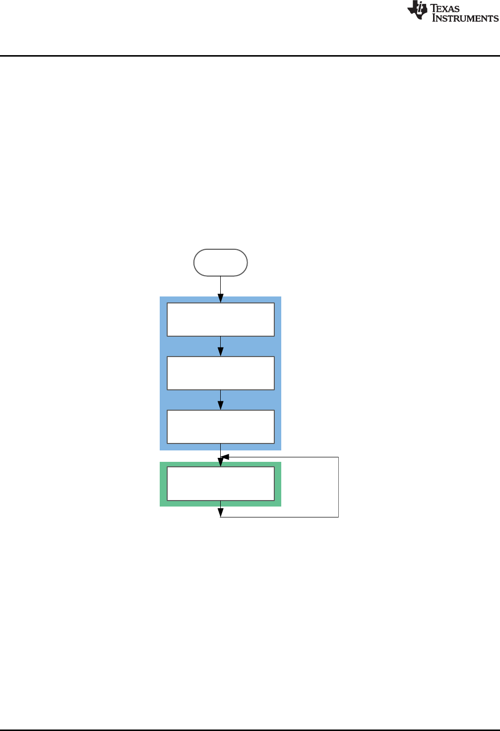
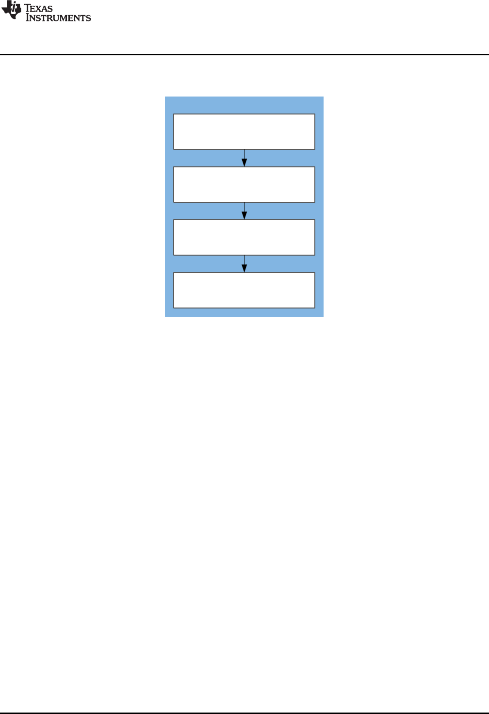
System Reset
MCU Initialization
PGA411-Q1 Initialization
PGA411-Q1 Configuration
Read Angle and Velocity
Introduction to High-Level Software Flow
www.ti.com
2SLAA708–July 2016
Submit Documentation Feedback
Copyright © 2016, Texas Instruments Incorporated
Software Developer’s Guide for PGA411-Q1
1 Introduction to High-Level Software Flow
Figure 1 shows the high-level overview of the software flow.
There are three main components of the software flow.
1. The main.c file
2. The pga411.c file
3. The hal.c file
The hal.c file must be modified depending on the controller used in the application.
The main.c program loop implements the routine shown in Figure 1 for reading angle and velocity from the
PGA411-Q1 device. The PGA411-Q1 related functions are called from the pga411.c file and the C2000
related code and functions are called from the hal.c file which is described in this guide. The functions are
defined in the hal.h and pga411.h header files. The code used for the following explanation is based on
the TIDA-00796 PGA411-Q1 files (refer to Automotive Resolver-to-Digital Converter Reference Design for
Safety Application).
Figure 1. Software Flowchart
2main.c File
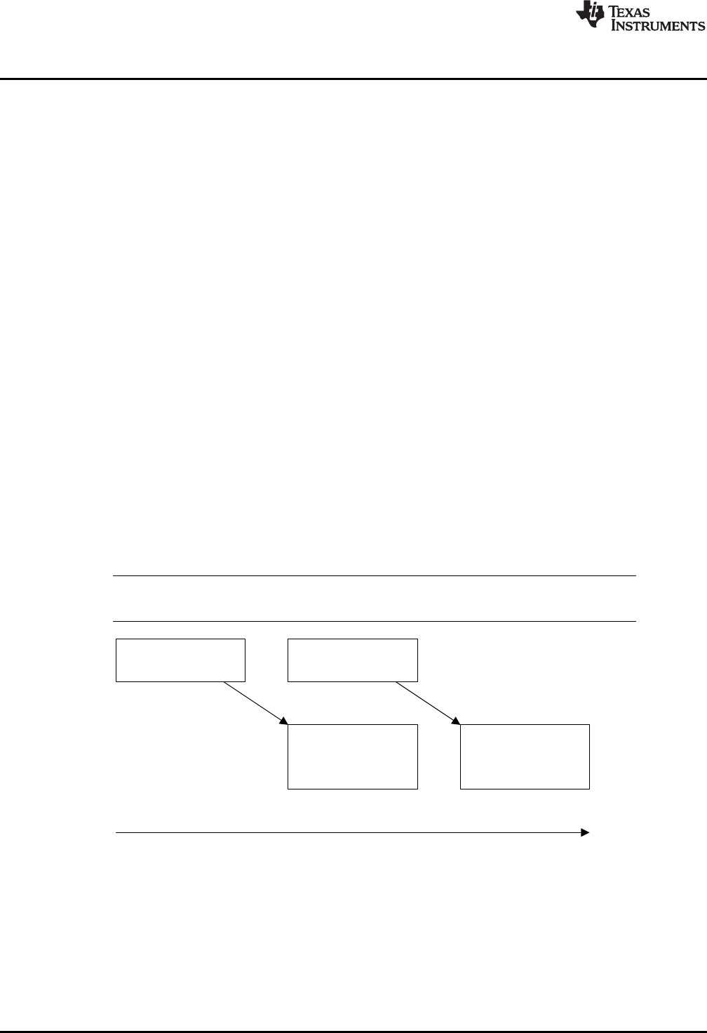
Figure 1 shows the high level software chart. Figure 2 shows the flow chart for the sequence of software
actions that are followed and how these actions are mapped to the software functions.
The functions starting with PGA411, such as pga411_DefaultCfg(), are called from the pga411.c file that is
described in Section 3. The functions starting with hal, such as hal_ToggleLED(), are called from the hal.c
that is described in Section 4.
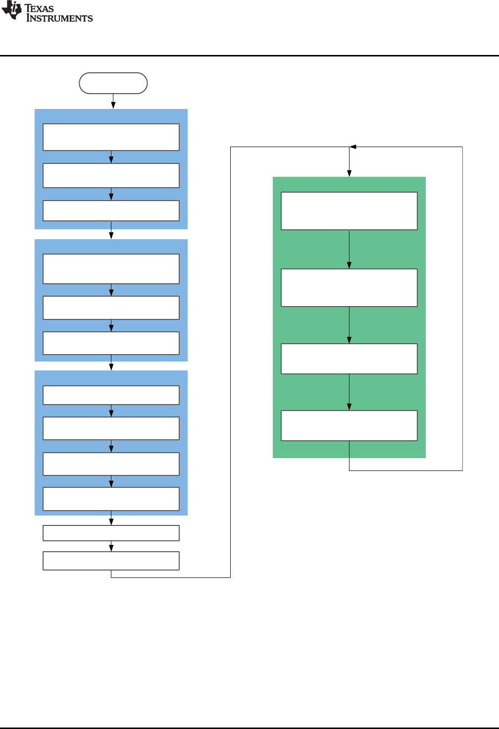
SYSTEM RESET
Unlock the PGA411-Q1 Registers
pga411_DeviceUnlock()(5)
Pga411_DefaultCfg()
Write Application-Specific Configuration to
PGA411-Q1 registers
Go to DIAGNOSTIC State
pga411_State(DIAG)(5)
Go to NORMAL State
pga411_State(NORM)(6)
Clear Faults if any
pga411_FaultReset()(4)
Deglitch Time When the Exciter Enables
Initialize Microcontroller-Related Clocks
hal_InitSysCtrl();(1)
GPIO and LED Control
hal_InitGPIO();(2)
Set Microcontroller UART 115200
hal_InitUART();(3)
MCU Initialization
PGA411-Q1 Related
GPIO Pins Initialization
hal_InitPgaGPIO()(4)
SPI Initialization
hal_InitSPI()(4)
PGA411-Q1 Reset Using GPIO
pga411_Reset()(4)
Pga411_Init()
Read Angle
pga411_ReadReg(DEV_STAT5)(6)
Calculate(7)
Read Velocity
pga411_ReadReg(DEV_STAT6)(6)
System Action
While(1) loop
www.ti.com
main.c File
3
SLAA708–July 2016
Submit Documentation Feedback Copyright © 2016, Texas Instruments Incorporated
Software Developer’s Guide for PGA411-Q1
(1) See Section 4.8.
(2) See Section 4.7.
(3) See Section 4.5.
(4) See Section 3.2.
(5) See Section 3.3.
(6) See Section 3.8.
(7) See Section 4.6.
Figure 2. Software Sequence Flowchart

main.c File
www.ti.com
4SLAA708–July 2016
Submit Documentation Feedback
Copyright © 2016, Texas Instruments Incorporated
Software Developer’s Guide for PGA411-Q1
NOTE: The functions starting with PGA411-Q1, such as pga411_DefaultCfg(), are called from the
pga411.c file that is described in Section 3 and are required for PGA411-Q1.
The functions starting with hal, such as hal_ToggleLED(), are called from the hal.c that is
described in Section 4 and are required for the controller only.
int main(void)
{
/* copy fast codes from FLASH to RAM if running from FLASH */
#ifndef DEBUG
memcpy(&RamfuncsRunStart, &RamfuncsLoadStart, (Uint32)&RamfuncsLoadSize);
#endif
hal_InitSysCtrl(); /* inits clock domains, PLL */
hal_InitGPIO(); /* practically default config + LED */
hal_InitUART(); /* inits UART 115200 8N1 */
pga411_Init(); /* inits PGA411 driver */
pga411_DefaultCfg(); /* default config defined in "pga411_regs" */
HAL_DELAY_US(10000); /* 10 ms deglitch period when the exciter enables */
pga411_FaultReset(); /* clear faults if any */
/* endless loop */
while (1)
{
HAL_DELAY_US(100000); /* 100 ms delay */
hal_ToggleLED(); /* LED on the controlSTIC is blinking periodically */
/* VT100 */
hal_PutsUART(VT100_CLRSCR); /* clear entire screen */
hal_PutsUART(VT100_GOHOME); /* more cursor to upper left corner */
/* read angle and print */
main_GetAngleAndPrint();
/* read velocity and print */
main_GetVeloAndPrint();
}
#pragma diag_suppress 112 /* to get rid of warning that code is unreachable */
return 0;
#pragma diag_default 112 /* restore error level */
}
www.ti.com
PGA411-Q1 Driver File pga411.c and pga411.h
5
SLAA708–July 2016
Submit Documentation Feedback Copyright © 2016, Texas Instruments Incorporated
Software Developer’s Guide for PGA411-Q1
3 PGA411-Q1 Driver File pga411.c and pga411.h
3.1 PGA411-Q1 CRC Calculation Function
This CRC calculation routine is designed for a 32-bit C2000 little endian controller. Verify the output of the
routine with the examples listed in Table 1 or see the PGA411-Q1 Resolver Sensor Interface data sheet.
The SPI uses the 24 most significant bits (MSBs) of the SPI frame to generate a CRC value or to check
for SPI CRC errors. The polynomial in Equation 1 is applied for CRC calculation on both the master and
slave SPI frames.
SPI_CRC6 = X6+ X4+ X3+ X + 1 (1)
The operation occurs one bit at a time and begins with the MSB. The initial seed value is 0x3F.
NOTE: The input of the function corresponds to a complete 32 bit frame but only top 24 bits are
used for the calculation.
Table 1. SPI CRC Examples
24-BIT SPI FRAME CRC-6
0xAE0000 0x11
0x950055 0x22
0x855555 0x29
0x0D2FFE 0x0D
0x85FFFF 0x38
/* CRC6 calculation - optimized for PGA411 */
Uint16 pga411_crc2(Uint32 datin)
{
Uint16 byte_idx, bit_idx, crc = (CRC_INITSEED << 2);
/* byte by byte starting from most significant (3-2-1) */
for (byte_idx = CRC_BYTECOUNT; byte_idx >= 1; byte_idx--)
{
/* XOR-in new byte from left to right */
crc ^= ((datin >> (byte_idx << 3)) & 0x000000FF);
/* bit by bit for each byte */
for (bit_idx = 0; bit_idx < 8; bit_idx++)
{
crc = crc << 1 ^ (crc & 0x80 ? (CRC_POLYNOM << 2) : 0);
}
}
return (crc >> 2 & CRC_INITSEED); /*restore two bit offset */
}
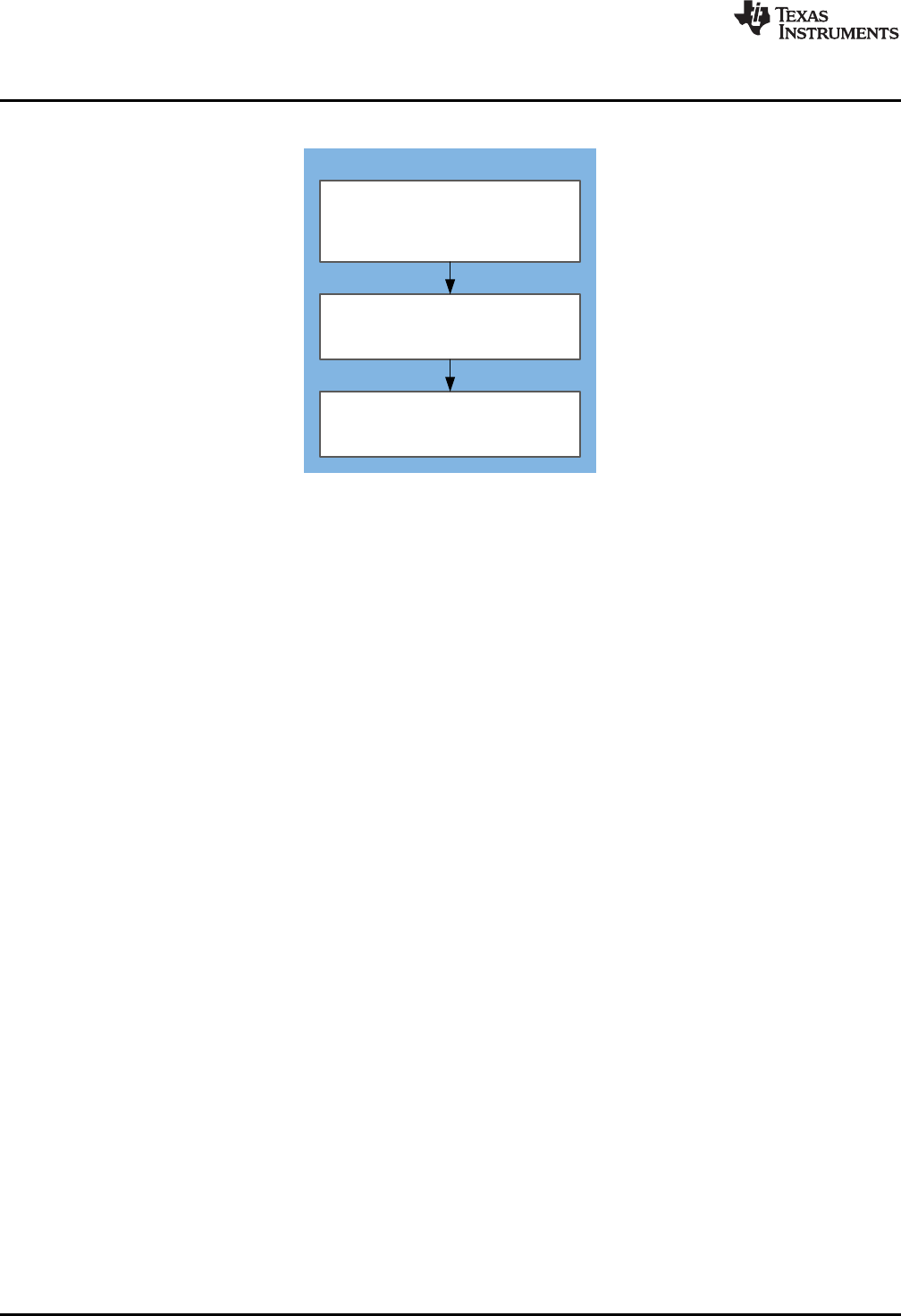
PGA411-Q1 Related
GPIO Pins Initialization
hal_InitPgaGPIO()
SPI Initialization
hal_InitSPI()
PGA411-Q1 Reset Using GPIO
pga411_Reset()
Pga411_Init()
PGA411-Q1 Driver File pga411.c and pga411.h
www.ti.com
6SLAA708–July 2016
Submit Documentation Feedback
Copyright © 2016, Texas Instruments Incorporated
Software Developer’s Guide for PGA411-Q1
3.2 PGA411-Q1 Initialization Function
Figure 3. Initialization Sequence
The following function and routines enable SPI communication that calls the functions defined in
Section 4.
/* Initialization PGA411-Q1 related hardware */
void pga411_Init(void)
{
hal_InitPgaGPIO(); /* init GPIO */
hal_InitSPI(); /* init SPI periphery */
pga411_Reset(); /* perform PGA411 reset */
}
/* Perform PGA411-Q1 reset using GPIO */
void pga411_Reset(void)
{
HAL_PGA_RESET_N_LOW; /* RESET_N low */
HAL_DELAY_US(500); /* hold in reset for 500us */
HAL_PGA_RESET_N_HIGH; /* release from reset */
HAL_DELAY_US(10000); /* wait at least 10 ms*/
}
/* Perform PGA411-Q1 FAULT reset using GPIO */
void pga411_FaultReset(void)
{
HAL_PGA_FAULTRES_LOW; /* assert FAULTRES low - open collector */
HAL_DELAY_US(1000); /* hold in the state for 1ms */
HAL_PGA_FAULTRES_HIZ; /* return back to high-z*/
}
Unlock the PGA411-Q1 Registers
pga411_DeviceUnlock()
Pga411_DefaultCfg()
Write Application-Specific Default
Configuration
Go to DIAGNOSTIC State
pga411_State(DIAG)
Go to NORMAL State
pga411_State(NORM)
www.ti.com
PGA411-Q1 Driver File pga411.c and pga411.h
7
SLAA708–July 2016
Submit Documentation Feedback Copyright © 2016, Texas Instruments Incorporated
Software Developer’s Guide for PGA411-Q1
3.3 Default Configuration Function
This function writes the default configuration into the PGA411-Q1 device.
Figure 4. Default Configuration Sequence
/* Write default configuration to PGA */
void pga411_DefaultCfg(void)
{
int i;
/* go to diagnostic state */
pga411_State(DIAG);
/* unlock registers */
pga411_DeviceUnlock();
/* first 12 registers to default */
/* note: for some u need to unlocked them first ! */
for (i = 0; i < 12; i++)
{
pga411_XmitSPI(WRITE, i, pga411_regs[i].def_val);
}
/* go to normal state */
pga411_State(NORMAL);
}
SPI Read Command 1
Response from PGA41x
for Read Command 1
SPI Read Command 2
Response from
PGA41x for Read
Command 2
Time
PGA411-Q1 Driver File pga411.c and pga411.h
www.ti.com
8SLAA708–July 2016
Submit Documentation Feedback
Copyright © 2016, Texas Instruments Incorporated
Software Developer’s Guide for PGA411-Q1
3.4 SPI Communication Function
The following function is for SPI communication that calls the functions defined in Section 4. Depending on
the dir parameter, the appropriate SPI address is selected.
/* Xmit data to PGA over SPI, for reg use defined macros */
pga411_spi_frame_t pga411_XmitSPI(Uint16 dir, Uint16 reg, Uint16 wdata)
{
pga411_spi_frame_t out, in;
/* do we read data ? */
if (dir == READ) { out.addr = pga411_regs[reg].read_add; } /* read address */
/* or write data ? */
else { out.addr = pga411_regs[reg].write_add; } /* write address */
/* compose the rest of the frame */
out.dataout = wdata; /* real data (W) or dummy data (R) */
out.reserved = 0x00; /* always zero */
out.mcrc = pga411_crc2(out.frame); /* calculate TX CRC */
in.frame = hal_Xmit4BSPI(out.frame);
/* check RX CRC */
if (pga411_crc2(in.frame) != in.scrc)
{
hal_assert(); /* if error -> terminate */
}
return (in);
}
3.5 SPI Read Function
The following function is for a SPI read. The response from SPI frame Nreports the angle captured by SPI
frame N – 1.
NOTE: Upon receiving a SPI read of the angle or velocity data, the PGA411-Q1 device goes
through 1 to 2 clock cycles to load the angle or velocity data into the SPI to send out.
Figure 5. PGA411-Q1 SPI Response Frames
/* Read data from defined register */
Uint16 pga411_ReadReg(Uint16 reg)
{
/* first read returns whatever */
pga411_XmitSPI(READ, reg, SPI_DUMMY);
/* second read returns requested data */
return (pga411_XmitSPI(READ, reg, SPI_DUMMY).datain);
}

www.ti.com
PGA411-Q1 Driver File pga411.c and pga411.h
9
SLAA708–July 2016
Submit Documentation Feedback Copyright © 2016, Texas Instruments Incorporated
Software Developer’s Guide for PGA411-Q1
3.6 SPI Write Function
The following function is for a SPI write.
/* Write data to defined register */
void pga411_WriteReg(Uint16 reg, Uint16 data)
{
/* here we just making it nice, can be macro too */
pga411_XmitSPI(WRITE, reg, data);
}
3.7 SPI Read All Function
The following function is for a SPI read all.
/* Read all registers from PGA */
void pga411_ReadAll(void)
{
int i;
Uint16 rx_data;
/* register by register (27+1) */
/* PGA411 always returns previous read register value */
/* thats why 28 reads are needed (first read returns whatever data) */
for (i = 0; i < PGA411_REG_COUNT + 1; i++)
{
rx_data = pga411_XmitSPI(READ, i, SPI_DUMMY).datain;
/*boolean trick - save data if not first cycle */
if (i)
{
pga411_regs[i - 1].real_val = rx_data;
}
}
}

PGA411-Q1 Driver File pga411.c and pga411.h
www.ti.com
10 SLAA708–July 2016
Submit Documentation Feedback
Copyright © 2016, Texas Instruments Incorporated
Software Developer’s Guide for PGA411-Q1
3.8 PGA411 Change State Function
This function changes between the DIAGNOSTIC and NORMAL states based on the state parameter
(defined by enum).
enum {READ, WRITE}; /* Enmus selects SPI operation */
enum {DIAG, NORMAL}; /* Operational states of PGA */
/* Change state diagnostic/normal */
void pga411_State(Uint16 state)
{
Uint16 temp;
/* Enter Diagnostic state */
if (state == DIAG)
{
/* read content of DEV_CONTROL3 register */
temp = pga411_ReadReg(DEV_CONTROL3);
temp |= 0x0004; /* set bit SPIDIAG */
pga411_WriteReg(DEV_CONTROL3, temp); /* finish R-M-W */
}
/* Go back to normal state */
else
{
/* read content of DEV_CONTROL1 register */
temp = pga411_ReadReg(DEV_CONTROL1);
temp |= 0x0001; /* set bit DIAGEXIT */
pga411_WriteReg(DEV_CONTROL1, temp); /* finish R-M-W */
}
}
3.9 Device Unlock Function
NOTE: To access the DEV_CONTROL1 and DEV_CONTROL2 registers, a predefined device
unlock sequence must be applied to the DEV_UNLK_CTRL1 register in the following order:
1. Write 0x000F to DEV_UNLK_CTRL1
2. Write 0x0055 to DEV_UNLK_CTRL1
3. Write 0x00AA to DEV_UNLK_CTRL1
4. Write 0x00F0 to DEV_UNLK_CTRL1
/* Device unlock (must be in diagnostic state) */
void pga411_DeviceUnlock(void)
{
pga411_WriteReg(DEV_UNLK_CTRL1, 0x000F);
pga411_WriteReg(DEV_UNLK_CTRL1, 0x0055);
pga411_WriteReg(DEV_UNLK_CTRL1, 0x00AA);
pga411_WriteReg(DEV_UNLK_CTRL1, 0x00F0);
}
3.10 EEPROM Unlock Function
NOTE: To access the DEV_EE_CTRL1, a predefined EEPROM unlock sequence must be applied to
the DEV_EE_CTRL4 register in the following order:
1. Write 0x000F to DEV_EE_CTRL4
2. Write 0x0055 to DEV_EE_CTRL4
3. Write 0x00AA to DEV_EE_CTRL4
4. Write 0x00F0 to DEV_EE_CTRL4
/* EEPROM unlock (must be in diagnostic state) */
void pga411_EEPROMUnlock(void)
DC-DC
Sheet 2
7 - 42 V to 5 V
LDO
Sheet 2
5 V to 3.3 V
STATUS LED
Sheet 2
PWR. GOOD, FAULT
EXT. SUPPLY
Sheet 2
7 - 42 V
CONNECTOR
SYSTEM CONNECTOR
Vusb
5 V
J1
3.3 V
5 V
Sheet 2
(SPI, LOGIC, Vusb)
Sheet 2
5 V
3.3 V
FAULT
PGA411-Q1
Sheet 3
PARALEL INTERFACE HEADER
Sheet 2
(ORD[0..13], OMODE, INHB, VA0, VA1)
4 14
SPI (4)
8
EXC
SIN
COS
Sheet 3
RESOLVER CONNECTOR
EXC+
EXC-
SIN+
SIN-
COS+
COS-
FAULTRES
S1
Sheet 2
Copyright © 2016, Texas Instruments Incorporated
www.ti.com
HAL Hardware Layer (C2000 Specific)—hal.c and hal.h (32 bit)
11
SLAA708–July 2016
Submit Documentation Feedback Copyright © 2016, Texas Instruments Incorporated
Software Developer’s Guide for PGA411-Q1
{
pga411_WriteReg(DEV_EE_CTRL4, 0x000F);
pga411_WriteReg(DEV_EE_CTRL4, 0x0055);
pga411_WriteReg(DEV_EE_CTRL4, 0x00AA);
pga411_WriteReg(DEV_EE_CTRL4, 0x00F0);
}
4 HAL Hardware Layer (C2000 Specific)—hal.c and hal.h (32 bit)
This layer can be adapted for different hardware platforms and architectures. For example when the
methods to access the GPIO registers must be changed and updated. The following example is for the
TMS320F28069M device which is a 32-bit microcontroller with 16-bit registers.
4.1 PGA411-Q1 GPIO Initialization
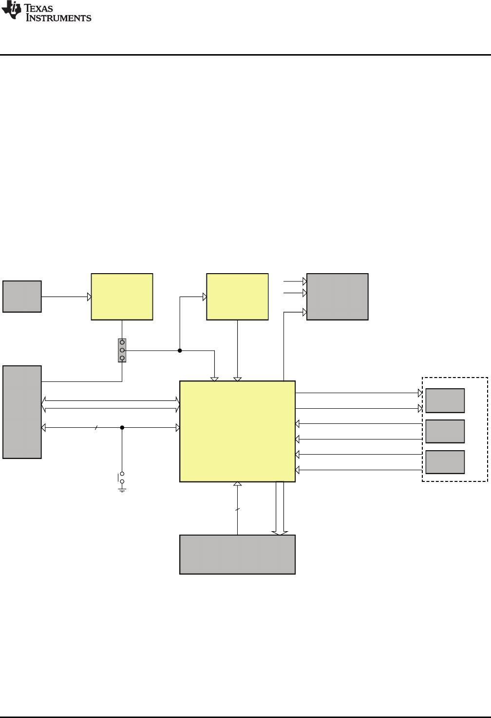
The primary function of this routine is to configure the GPIO of the PGA411-Q1 device for this specific
application. The commands that follow are based on the configuration used in the TIDA-00796 schematic.
The pins that are connected to the PGA411-Q1 device and used in this application will be configured as
either an input or output in the routine that follows.
Figure 6. Block Diagram Showing High-Level Connection of TIDA-00796
HAL Hardware Layer (C2000 Specific)—hal.c and hal.h (32 bit)
www.ti.com
12 SLAA708–July 2016
Submit Documentation Feedback
Copyright © 2016, Texas Instruments Incorporated
Software Developer’s Guide for PGA411-Q1
(1) Additional pins will be needed for parallel output interface.
Table 2. Table Showing Relevant Pins of PGA411-Q1
PIN LOGIC INPUT
OR OUTPUT DESCRIPTION
NAME NO.
AMODE 28 Input Accelerated mode select
BMODE0 5 Input Resolution select, input low is 10-bit mode, input high is 12-bit mode
ECLKSEL 3 Input Clock select input
FAULT 16 Output Fault-detection signal output (open drain structure)
FAULTRES 14 Input Fault reset input (faults are reset when this pin is LOW)
INHB 13 Input Inhibit function and output data hold
NCS 17 Input Chip select for the serial peripheral interface (SPI)
NRESET 12 Input Reset input
OMODE 29 Input Data output format select
ORD0 57 Output Data output, 0 for parallel angle and velocity. Encoder output U
ORD1 56 Output Data output, 1 for parallel angle and velocity. Encoder output V
ORD10 47 Output Data output, 10 for parallel angle and velocity
ORD11 46 Output Data output, 11 for parallel angle and velocity
ORD12 45 Output Optional pin (data output, 12 for parallel angle and velocity - unused)
ORDCLK 44 Output ORD Clock
ORD2 55 Output Data output select 2 for parallel angle and velocity. Encoder output W
ORD3 54 Output Data output select 3 for parallel angle and velocity. Encoder output U1
ORD4 53 Output Data output select 4 for parallel angle and velocity. Encoder output V1
ORD5 52 Output Data output select 5 for parallel angle and velocity. Encoder output W1
ORD6 51 Output Data output select 6 for parallel angle and velocity. Encoder output A
ORD7 50 Output Data output select 7 for parallel angle and velocity. Encoder output B
ORD8 49 Output Data output select 8 for parallel angle and velocity. Encoder output Z
ORD9 48 Output Data output select 9 for parallel angle and velocity
OUTA 1 Output Incremental encoder, output A
OUTB 2 Output Incremental encoder, output B
OUTZ 64 Output Incremental encoder, output Z
PRD 15 Output Data parity output. The PRD pin can be routed to the parallel interface header.
SCLK 18 Input SPI clock
SDI 19 Input SPI data input
SDO 20 Output SPI data output
VA0 31 Input Data output select 0 for angle and velocity
VA1 32 Input Data output select 1 for angle and velocity
Table 3. Piccolo F28069 controlStick Pinout (C2000 GPIOs that must be Initialized(1))
ABCD
1 ADC-A6 / COMP3(+VE) ADC-A2 / COMP1(+VE) ADC-A0 3V3
2 ADC-A4 / COMP2 (+VE) ADC-B1 EPWM-4B / GPIO-07 Tz1 / GPIO-12
3 SCL-A / GPIO-33 ADC-B6 / COMP3 (-VE) EPWM-4A / GPIO-06 ADC-A1
4 SDA-A / GPIO-32 ADC-B0 EPWM-3B / GPIO-05 5V0 (Disabled by Default)
5 EPWM-1A / GPIO-00 ADC-B4 / COMP2 (-VE) EPWM-3A / GPIO-04 SPISOMI-A / GPIO-17
6 EPWM-1B / GPIO-01 ADC-A5 EPWM-2B / GPIO-03 SPISIMO-A / GPIO-16
7 SPISTE-A / GPIO-19 ADC-B2 / COMP1 (-VE) EPWM-2A / GPIO-02 GND
8 SPICLK-A / GPIO-18 GPIO-34 / (LED) PWM1A-DAC (Filtered) GND

www.ti.com
HAL Hardware Layer (C2000 Specific)—hal.c and hal.h (32 bit)
13
SLAA708–July 2016
Submit Documentation Feedback Copyright © 2016, Texas Instruments Incorporated
Software Developer’s Guide for PGA411-Q1
/* PGA411-Q1 GPIO configuration */
void hal_InitPgaGPIO(void)
{
/* note: for better portability we configure all pins again */
asm(" EALLOW"); /* Enable EALLOW protected register access */
/* FAULTRES, negative logic */
GpioCtrlRegs.GPBMUX1.bit.GPIO33 = 0; /* 0=GPIO 1=COMP2OUT 2=rsvd
3=COMP3OUT */
GpioCtrlRegs.GPBPUD.bit.GPIO33 = 1; /* pull up disabled (external) */
GpioCtrlRegs.GPBQSEL1.bit.GPIO33 = 0; /* no qualification */
GpioCtrlRegs.GPBDIR.bit.GPIO33 = 0; /* input by default - output collector */
GpioDataRegs.GPBSET.bit.GPIO33 = 1; /* default value 1, ignored anyway */
/* OUTA - however GPIO only, no QEP at control stick pinout */
GpioCtrlRegs.GPBMUX1.bit.GPIO32 = 0; /* 0=GPIO 1=COMP2OUT 2=rsvd
3=COMP3OUT */
GpioCtrlRegs.GPBPUD.bit.GPIO32 = 1; /* pull up disabled driven by PGA */
GpioCtrlRegs.GPBQSEL1.bit.GPIO32 = 0; /* no qualification */
GpioCtrlRegs.GPBDIR.bit.GPIO32 = 0; /* input by default */
GpioDataRegs.GPBSET.bit.GPIO32 = 1; /* default value 1, ignored anyway */
/* OUTB - however GPIO only, no QEP at control stick pinout */
GpioCtrlRegs.GPAMUX1.bit.GPIO0 = 0; /* 0=GPIO 1=COMP2OUT 2=rsvd
3=COMP3OUT */
GpioCtrlRegs.GPAPUD.bit.GPIO0 = 1; /* pull up disabled driven by PGA */
GpioCtrlRegs.GPAQSEL1.bit.GPIO0 = 0; /* no qualification */
GpioCtrlRegs.GPADIR.bit.GPIO0 = 0; /* input by default */
GpioDataRegs.GPASET.bit.GPIO0 = 1; /* default value 1, ignored anyway */
/* OUTZ - however GPIO only, no QEP at control stick pinout */
GpioCtrlRegs.GPAMUX1.bit.GPIO1 = 0; /* 0=GPIO 1=COMP2OUT 2=rsvd
3=COMP3OUT */
GpioCtrlRegs.GPAPUD.bit.GPIO1 = 1; /* pull up disabled driven by PGA */
GpioCtrlRegs.GPAQSEL1.bit.GPIO1 = 0; /* no qualification */
GpioCtrlRegs.GPADIR.bit.GPIO1 = 0; /* input by default */
GpioDataRegs.GPASET.bit.GPIO1 = 1; /* default value 1, ignored anyway */
/* BMODE0 - low = 10b resolution, high = 12b resolution */
GpioCtrlRegs.GPAMUX1.bit.GPIO7 = 0; /* 0=GPIO 1=COMP2OUT 2=rsvd
3=COMP3OUT */
GpioCtrlRegs.GPAPUD.bit.GPIO7 = 1; /* pull up disabled */
GpioCtrlRegs.GPAQSEL1.bit.GPIO7 = 0; /* no qualification */
GpioCtrlRegs.GPADIR.bit.GPIO7 = 1; /* output by default */
GpioDataRegs.GPASET.bit.GPIO7 = 1; /* default 12b resolution */
/* EXTCLKIN - external clock for PGA411 >> NOT SUPPORTED YET << */
GpioCtrlRegs.GPAMUX1.bit.GPIO6 = 0; /* 0=GPIO 1=COMP2OUT 2=rsvd
3=COMP3OUT */
GpioCtrlRegs.GPAPUD.bit.GPIO6 = 1; /* pull up disabled */
GpioCtrlRegs.GPAQSEL1.bit.GPIO6 = 0; /* no qualification */
GpioCtrlRegs.GPADIR.bit.GPIO6 = 1; /* output by default */
GpioDataRegs.GPACLEAR.bit.GPIO6 = 1; /* keep low */
/* AMODE - accelerated mode */
GpioCtrlRegs.GPAMUX1.bit.GPIO5 = 0; /* 0=GPIO 1=COMP2OUT 2=rsvd
3=COMP3OUT */
GpioCtrlRegs.GPAPUD.bit.GPIO5 = 1; /* pull up disabled */
GpioCtrlRegs.GPAQSEL1.bit.GPIO5 = 0; /* no qualification */
GpioCtrlRegs.GPADIR.bit.GPIO5 = 1; /* output by default */
GpioDataRegs.GPACLEAR.bit.GPIO5 = 1; /* accelerated mode disabled by default */
/* FAULT - fault detection, active = high - Z */
GpioCtrlRegs.GPAMUX1.bit.GPIO4 = 0; /* 0=GPIO 1=COMP2OUT 2=rsvd
3=COMP3OUT */
GpioCtrlRegs.GPAPUD.bit.GPIO4 = 1; /* pull up disabled - external pull up */
GpioCtrlRegs.GPAQSEL1.bit.GPIO4 = 0; /* no qualification */
GpioCtrlRegs.GPADIR.bit.GPIO4 = 0; /* input by default */
GpioDataRegs.GPASET.bit.GPIO4 = 1; /* default value 1, ignored anyway */
/* PRD - data parity output */
GpioCtrlRegs.GPAMUX1.bit.GPIO3 = 0; /* 0=GPIO 1=COMP2OUT 2=rsvd
3=COMP3OUT */
GpioCtrlRegs.GPAPUD.bit.GPIO3 = 1; /* pull up disabled - driven by PGA */
GpioCtrlRegs.GPAQSEL1.bit.GPIO3 = 0; /* no qualification */

HAL Hardware Layer (C2000 Specific)—hal.c and hal.h (32 bit)
www.ti.com
14 SLAA708–July 2016
Submit Documentation Feedback
Copyright © 2016, Texas Instruments Incorporated
Software Developer’s Guide for PGA411-Q1
GpioCtrlRegs.GPADIR.bit.GPIO3 = 0; /* input by default */
GpioDataRegs.GPASET.bit.GPIO3 = 1; /* default value 1, ignored anyway */
/* RESET_N - resets PGA, active low */
GpioCtrlRegs.GPAMUX1.bit.GPIO2 = 0; /* 0=GPIO 1=COMP2OUT 2=rsvd
3=COMP3OUT */
GpioCtrlRegs.GPAPUD.bit.GPIO2 = 1; /* pull up disabled */
GpioCtrlRegs.GPAQSEL1.bit.GPIO2 = 0; /* no qualification */
GpioCtrlRegs.GPADIR.bit.GPIO2 = 1; /* output by default */
GpioDataRegs.GPASET.bit.GPIO2 = 1; /* device's running by default */
/* ECLKSEL - switches between internal/external clock >> NOT SUPPORTED YET << */
GpioCtrlRegs.GPAMUX1.bit.GPIO12 = 0; /* 0=GPIO 1=COMP2OUT 2=rsvd
3=COMP3OUT */
GpioCtrlRegs.GPAPUD.bit.GPIO12 = 1; /* pull up disabled */
GpioCtrlRegs.GPAQSEL1.bit.GPIO12 = 0; /* no qualification */
GpioCtrlRegs.GPADIR.bit.GPIO12 = 1; /* output by default */
GpioDataRegs.GPACLEAR.bit.GPIO12 = 1; /* internal oscillator by default */
asm(" EDIS"); /* Disable EALLOW protected register access */
}
4.2 PGA411-Q1 SPI Initialization
The primary function of this routine is to initialize the SPI of the PGA411-Q1 device. Table 3 shows the
high level connection of the PGA411-Q1 device with the C2000 microcontroller.
/* SPI init */
void hal_InitSPI(void)
{
asm(" EALLOW"); /* Enable EALLOW protected register access */
/* enable peripheral clock */
SysCtrlRegs.PCLKCR0.bit.SPIAENCLK = 1; /* SPI-A */
/* init GPIOs */
GpioCtrlRegs.GPAPUD.bit.GPIO16 = 0; /* Enable pull-up on GPIO16 (SPISIMOA) */
GpioCtrlRegs.GPAPUD.bit.GPIO17 = 0; /* Enable pull-up on GPIO17 (SPISOMIA) */
GpioCtrlRegs.GPAPUD.bit.GPIO18 = 0; /* Enable pull-up on GPIO18 (SPICLKA) */
GpioCtrlRegs.GPAPUD.bit.GPIO19 = 0; /* Enable pull-up on GPIO19 (SPISTEA) */
GpioCtrlRegs.GPAQSEL2.bit.GPIO16 = 3; /* Asynch input GPIO16 (SPISIMOA) */
GpioCtrlRegs.GPAQSEL2.bit.GPIO17 = 3; /* Asynch input GPIO17 (SPISOMIA) */
GpioCtrlRegs.GPAQSEL2.bit.GPIO18 = 3; /* Asynch input GPIO18 (SPICLKA) */
GpioCtrlRegs.GPAQSEL2.bit.GPIO19 = 3; /* Asynch input GPIO19 (SPISTEA) */
GpioCtrlRegs.GPAMUX2.bit.GPIO16 = 1; /* 0=GPIO 1=SPISIMOA 2=rsvd 3=TZ2
*/
GpioCtrlRegs.GPAMUX2.bit.GPIO17 = 1; /* 0=GPIO 1=SPISOMIA 2=rsvd 3=TZ3
*/
GpioCtrlRegs.GPAMUX2.bit.GPIO18 = 1; /* 0=GPIO 1=SPICLKA 2=SCITXDB
3=XCLKOUT */
GpioCtrlRegs.GPAMUX2.bit.GPIO19 = 1; /* 0=GPIO/XCLKIN 1=SPISTEA 2=SCIRXDB
3=ECAP1 */
/* Initialize SPI periphery */
SpiaRegs.SPICCR.bit.SPISWRESET = 0; /* Reset SPI and hold */
SpiaRegs.SPICCR.all = 0x0007; /* Loopback off 8-bit character, Clock Polarity 0 */
SpiaRegs.SPICTL.all = 0x0006; /* master, xmit enable */
SpiaRegs.SPIBRR = 0x0009; /* SYSCLK = 80Mhz = LSPCLK, baud rate = LSPCLK/(SPIBRR+1) = 8 MHz */
SpiaRegs.SPISTS.all = 0x0000; /* reset all status information */
SpiaRegs.SPIPRI.bit.FREE = 1; /* priority control settings - free run */
SpiaRegs.SPICCR.bit.SPISWRESET = 1; /* Release from SPI reset */
/* reset both fifos */
SpiaRegs.SPIFFTX.bit.TXFIFO = 0;
SpiaRegs.SPIFFRX.bit.RXFIFORESET = 0; /*and keep them in reset during configuration */
/* configure fifos */
SpiaRegs.SPIFFTX.all = 0xC004; /* Enable FIFO's, do not use interrupts */
SpiaRegs.SPIFFRX.all = 0x0004; /* Set RX FIFO, do not use interrupts */
SpiaRegs.SPIFFCT.all = 0x0000; /* no delay between FIFO and TXBUF */
/* releasing fifos from reset */
SpiaRegs.SPIFFTX.bit.TXFIFO = 1;
SpiaRegs.SPIFFRX.bit.RXFIFORESET = 1; /* OK */

www.ti.com
HAL Hardware Layer (C2000 Specific)—hal.c and hal.h (32 bit)
15
SLAA708–July 2016
Submit Documentation Feedback Copyright © 2016, Texas Instruments Incorporated
Software Developer’s Guide for PGA411-Q1
/* error checking, fifo pointers should be zero */
if ((SpiaRegs.SPIFFTX.bit.TXFFST != 0) || (SpiaRegs.SPIFFRX.bit.RXFFST != 0)) { hal_assert();
}
asm(" EDIS"); /* Disable EALLOW protected register access */
}
/* Exchanges 4 Bytes via SPI, blocks until finished, 32b architecture = no pointer */
4.3 SPI Transmit and Receive Function
Uint32 hal_Xmit4BSPI(Uint32 frame)
{
Uint32 rxval = 0x00000000; /* incoming data */
/* empty RX and TX 4B FIFOs */
SpiaRegs.SPIFFTX.bit.TXFIFO = 0; /* reset FIFOs */
SpiaRegs.SPIFFRX.bit.RXFIFORESET = 0;
asm(" NOP"); /* probably not needed */
asm(" NOP"); /* probably not needed */
SpiaRegs.SPIFFTX.bit.TXFIFO = 1;
SpiaRegs.SPIFFRX.bit.RXFIFORESET = 1; /* release from reset */
/* quick & dirty ! */
SPIA_PUSH(frame >> 24); /* first byte (from most significant) */
SPIA_PUSH(frame >> 16);
SPIA_PUSH(frame >> 8);
SPIA_PUSH(frame); /* last byte */
NOTE: The SPI is an 8-bit transfer which is why 4 bytes are transferred one by one starting with the
most significant byte.
/* wait until the transmission is finished */
while (SpiaRegs.SPIFFRX.bit.RXFFST < 4) {EMPTY_LOOP};
/* get data from RX FIFO */
rxval = SPIA_POP; /* first byte (from the most significant) */
rxval = ((rxval << 8) | SPIA_POP);
rxval = ((rxval << 8) | SPIA_POP);
rxval = ((rxval << 8) | SPIA_POP); /* last byte */
/* NCS must remain high at least 200ns */
HAL_DELAY_US(1);
return (rxval);
}
4.4 Digital Parallel Output
The digital parallel output is the default data interface of the PGA411-Q1 output. To enable the parallel
output interface, se the OMODE pin high (VIO). The device is configured in the encoder-emulated output
mode (described as follows) when the OMODE pin is set low (DGND).
The digital parallel output provides an update to the angle or velocity sample value every 100 ns at the
ORD[11:0] pins which can be expressed as a 10-Msps output-update rate.
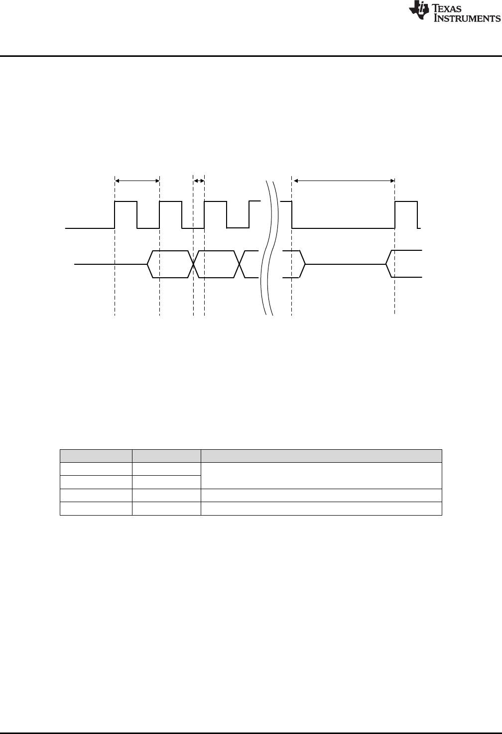
ORDCLK
ORD[12:0]
25 ns Clock off because of low inhibit
pin, or disabled tracking loop
f6 f7
100 ns
...
HAL Hardware Layer (C2000 Specific)—hal.c and hal.h (32 bit)
www.ti.com
16 SLAA708–July 2016
Submit Documentation Feedback
Copyright © 2016, Texas Instruments Incorporated
Software Developer’s Guide for PGA411-Q1
When the parallel output interface is enabled, the angle and velocity data is read from the ORD11 (MSB)
to ORD0 (LSB) pins. The digital data at the parallel output is in 2s complement format. While this format is
not important for the angle output because the value is always positive, the velocity output can be either
positive or negative depending on the direction of the resolver rotation. In the case the resolver sensor
rotation is clockwise (CW) and the value of the digital parallel-output velocity is positive. If the resolver
sensor rotation is counter-clockwise (CCW), the output value is negative. In the case where the device is
used in 10-bit mode (BMODE0 is low) the ORD10 and ORD11 pins are low (zeros) for a positive angle or
velocity output or high (ones) for a negative velocity.
Figure 7. ORD Timing Characteristics
While the OMODE selection pin switches the ORD[11:0] pins between the parallel data output and the
emulated encoder output, the VA0 and VA1 pins enable and disable the ORD[11:0] pins while also
selecting the output parameter. Setting the ORD[11:0] pins in a high impedance (Hi-Z) state allows for
systems to use multiple PGA411-Q1 devices controlled by a single MCU. See the PGA411-Q1 data sheet
for an example of multiple PGA411-Q1 devices controlled by a single MCU.
Table 4 lists the VA0 and VA1 pin configurations.
Table 4. ORD[11:0] Output Selection
VA0 VA1 FUNCTION
0 0 ORD[11:0] set to Hi-Z
1 1
0 1 Angle output at ORD[11:0]
1 0 Velocity output at ORD[11:0]
The INHB pin controls the update of the data output for the PGA411-Q1 device. When the INHB pin is
high (VIO), the output data is sampled at the ORD[11:0] pins as soon as the data is available. When the
INHB pin is set low (DGND), the data output at theORD[11:0] pins is held at the last sampled output. In a
synchronous data-transfer system sampling the data at the output of the PGA411-Q1 device on every
clock period is possible by applying a clock signal at the INHB input with a frequency lower than 10 MHz.
TI recommends the following sequence to read angle outputs on parallel interface (this code was not
implemented as part of the TIDA-00796 reference design, refer to the following sequence for an example):
1. Take INHB pin to High (PGA411-Q1 updates the output if the Inhibit is high)
2. Wait until ORDCLK is high
3. Read the ORD[12:0] outputs.
4.5 UART Initialization
The primary function of this routine is to initialize the UART. This configuration helps the
TMS320F28069M device on the control stick communicate over the USB with the computer through a
UART-to-USB serial converter.

www.ti.com
HAL Hardware Layer (C2000 Specific)—hal.c and hal.h (32 bit)
17
SLAA708–July 2016
Submit Documentation Feedback Copyright © 2016, Texas Instruments Incorporated
Software Developer’s Guide for PGA411-Q1
/* UART init */
void hal_InitUART(void)
{
asm(" EALLOW"); /* Enable EALLOW protected register access */
/* enable peripheral clock */
SysCtrlRegs.PCLKCR0.bit.SCIAENCLK = 1; /* SCI-A */
/* init GPIOs */
GpioCtrlRegs.GPAPUD.bit.GPIO28 = 0; /* Enable pull-up for GPIO28 (SCIRXDA) */
GpioCtrlRegs.GPAPUD.bit.GPIO29 = 0; /* Enable pull-up for GPIO29 (SCITXDA) */
GpioCtrlRegs.GPAMUX2.bit.GPIO28 = 1; /* 0=GPIO 1=SCIRXDA 2=SDAA 3=TZ2
*/
GpioCtrlRegs.GPAMUX2.bit.GPIO29 = 1; /* 0=GPIO 1=SCITXDA 2=SCLA 3=TZ3
*/
GpioCtrlRegs.GPAQSEL2.bit.GPIO28 = 3; /* Asynch input GPIO28 (SCIRXDA) */
/* serial port settings */
SciaRegs.SCICCR.all = 0x0007; /* 8N1, no loopback, async, idle-line protocol */
SciaRegs.SCICTL1.all = 0x0003; /* enable TX, RX, internal SCICLK, Disable RX ERR, SLEEP,
TXWAKE */
SciaRegs.SCIHBAUD = 0x0000; /* 115200 baud @LSPCLK = 80MHz (80 MHz SYSCLK). */
SciaRegs.SCILBAUD = 0x0055;
SciaRegs.SCICTL1.all = 0x0023; /* Relinquish SCI from Reset */
asm(" EDIS"); /* Disable EALLOW protected register access */
}
/* UART send character */
void hal_PutcUART(unsigned char c)
{
while (SciaRegs.SCICTL2.bit.TXRDY == 0) {EMPTY_LOOP}
SciaRegs.SCITXBUF = c;
}
/* UART send string */
void hal_PutsUART(char * s)
{
while (*s) { hal_PutcUART(*s++); }
}
/* set LED on the control stick */
void hal_SetLED(void)
{
GpioDataRegs.GPBCLEAR.bit.GPIO34 = 1; /* GPIO34 pin is set to 0 (turn LED on) */
}
/* clear LED on the control stick */
void hal_ClearLED(void)
{
GpioDataRegs.GPBSET.bit.GPIO34 = 1; /* GPIO34 pin is set to 1 (turn LED off) */
}
/* toggle LED on the control stick */
void hal_ToggleLED(void)
{
GpioDataRegs.GPBTOGGLE.bit.GPIO34 = 1; /* GPIO34 pin is toggle */
}
/* pseudo assert */
void hal_assert(void)
{
__asm(" ESTOP0"); /* stops emulation at this point */
while (ENDLESS); /* just in case */
}

clk 25
¦ 25'[
(RPM) 60 2
u
- u
clk 21
¦ 25'[
(RPM) 60 2
u
- u
12
ORDx
(degrees) 360 2
M u
10
ORDx
(degrees) 360 2
M u
HAL Hardware Layer (C2000 Specific)—hal.c and hal.h (32 bit)
www.ti.com
18 SLAA708–July 2016
Submit Documentation Feedback
Copyright © 2016, Texas Instruments Incorporated
Software Developer’s Guide for PGA411-Q1
4.6 Reading Angle and Velocity
The angle and velocity data are also available in the register memory space and can be polled through the
SPI. The corresponding locations are the bits in the DEV_STAT5 register for angle data value and the bits
in the DEV_STAT6 register for velocity data value.
Use the following equations to convert the PGA411-Q1 parallel output or SPI data into meaningful angle
and velocity values:
• 10-bit angle:
(2)
• 12-bit angle:
(3)
• 10-bit velocity:
where
• where ƒclk is the device clock frequency (typically 20 MHz) (4)
• 12-bit velocity
(5)
4.6.1 Angle Calculation Example
The following code snippet reads angle data from the PGA411-Q1 device, calculates the corresponding
angle and prints the result over a serial port to the host system.
The provided example uses Texas Instruments' IQmathLib library
(processors.wiki.ti.com/index.php/IQmath_Library_for_C28x). An alternate approach uses the traditional
float or fixed point (Q number format) arithmetic. The final approach should be considered based on the
hardware architecture.
/* angle calculation for the PGA411 using IQmathLib library */
/* _iq19 stores -4096 to 4095.999998093 with 0.000001907 resolution */
{
Uint16 angle_raw; /* raw data from the PGA411 register */
_iq angle; /* IQ math angle */
/* read data from the PGA411 */
angle_raw = pga411_ReadReg(DEV_STAT5);
angle_raw &= 0x1FFF; /* preserve only ORDANGLE bits */
/* multiply minimal step (LSB) by ORDANGLE value */
angle = _IQ19mpy(_IQ19(360.0/4096), _IQ19(angle_raw)); /* 12b example */
/* convert IQ variable to string */
_IQ19toa(outbuf, "%4.5f", angle);
/* print-out the buffer */
hal_PutsUART(outbuf);
}
4.6.2 Velocity Calculation Example
Similarly to the angle calculation example, the next code snippet reads velocity data from the PGA411-Q1
device, calculates velocity and prints the result over a serial port.

www.ti.com
HAL Hardware Layer (C2000 Specific)—hal.c and hal.h (32 bit)
19
SLAA708–July 2016
Submit Documentation Feedback Copyright © 2016, Texas Instruments Incorporated
Software Developer’s Guide for PGA411-Q1
The velocity calculation is more complex than the angle calculation. Velocity data (10 or 12 bit) from the
PGA411-Q1 are stored in 2's-complement format. However, because of different word size, the data must
be first converted. This conversion occurs as follows:
Step 1. Check the sign (bit 11).
Step 2. Convert to the positive integer.
Step 3. Preserve only the ORDVELOCITY bits.
Step 4. Cast to float format.
Step 5. Multiply by –1 if the sign is negative
The IQmathLib library is used for the final velocity calculation and string conversion. The final
implementation should consider target architecture, especially float and negative integer data
representation.
/* velocity calculation for the PGA411 using IQmathLib library */
/* _iq14 stores -131072 to 131071.999938965 with 0.000061035 resolution */
{
Int16 velocity_raw; /* raw data from the PGA411 register */
float velocity_float; /* temp for 2nd complement to float conversion */
_iq velocity; /* IQ math velocity */
/* read data from the PGA411 */
velocity_raw = pga411_ReadReg(DEV_STAT6);
/* convert 2nd complement to float */
if(velocity_raw & 0x0800) /* negative number ? */
{
/* convert to positive number first */
velocity_float = (((~velocity_raw) +1) & 0x07FF);
velocity_float *= -1; /* and make it negative */
}
else
{
/* positive number, preserve only needed bits */
velocity_float = (velocity_raw & 0x07FF);
}
velocity = _IQ14mpy(_IQ14(60*20000000/33554432),_IQ14(velocity_float + 1)); /* 12b
example */
/* convert IQ variable to string */
_IQ14toa(outbuf, "%7.5f", velocity);
/* print-out the buffer */
hal_PutsUART(outbuf);
}
4.7 GPIO Configuration (Input and Output)
The primary function of this routine is to configure the GPIO of the TMS320F28069 device used on the
control stick (www.ti.com/product/TMS320F28069M/toolssoftware).
At the system reset, all the GPIOs are set as the input. Later, in the program, the GPIOs are reconfigured
for a specific application (see Section 4.1).
/* Input - output configuration (ControlSTICK compatible) */
void hal_InitGPIO(void)
{
asm(" EALLOW"); /* Enable EALLOW protected register access */
/* Group A pins */
GpioCtrlRegs.GPACTRL.all = 0x00000000; /* QUALPRD = SYSCLKOUT for all group A GPIO */
GpioCtrlRegs.GPAQSEL1.all = 0x00000000; /* No qualification for all group A GPIO 0-15 */
GpioCtrlRegs.GPAQSEL2.all = 0x00000000; /* No qualification for all group A GPIO 16-31 */
GpioCtrlRegs.GPADIR.all = 0x00000000; /* All group A GPIO are inputs */
GpioCtrlRegs.GPAPUD.all = 0x00000000; /* all pullups enabled GPIO 0-31 */
/* */

HAL Hardware Layer (C2000 Specific)—hal.c and hal.h (32 bit)
www.ti.com
20 SLAA708–July 2016
Submit Documentation Feedback
Copyright © 2016, Texas Instruments Incorporated
Software Developer’s Guide for PGA411-Q1
GpioCtrlRegs.GPAMUX1.bit.GPIO0 = 0; /* 0=GPIO 1=EPWM1A 2=rsvd
3=rsvd */
GpioCtrlRegs.GPAMUX1.bit.GPIO1 = 0; /* 0=GPIO 1=EPWM1B 2=rsvd
3=COMP1OUT */
GpioCtrlRegs.GPAMUX1.bit.GPIO2 = 0; /* 0=GPIO 1=EPWM2A 2=rsvd
3=rsvd */
GpioCtrlRegs.GPAMUX1.bit.GPIO3 = 0; /* 0=GPIO 1=EPWM2B 2=SPISOMIA
3=COMP2OUT */
GpioCtrlRegs.GPAMUX1.bit.GPIO4 = 0; /* 0=GPIO 1=EPWM3A 2=rsvd
3=rsvd */
GpioCtrlRegs.GPAMUX1.bit.GPIO5 = 0; /* 0=GPIO 1=EPWM3B 2=SPISIMOA
3=ECAP1 */
GpioCtrlRegs.GPAMUX1.bit.GPIO6 = 0; /* 0=GPIO 1=EPWM4A 2=EPWMSYNCI
3=EPWMSYNCO */
GpioCtrlRegs.GPAMUX1.bit.GPIO7 = 0; /* 0=GPIO 1=EPWM4B 2=SCIRXDA
3=ECAP2 */
GpioCtrlRegs.GPAMUX1.bit.GPIO8 = 0; /* 0=GPIO 1=EPWM5A 2=rsvd
3=ADCSOCAO */
GpioCtrlRegs.GPAMUX1.bit.GPIO9 = 0; /* 0=GPIO 1=EPWM5B 2=SCITXDB
3=ECAP3 */
GpioCtrlRegs.GPAMUX1.bit.GPIO10 = 0; /* 0=GPIO 1=EPWM6A 2=rsvd
3=ADCSOCBO */
GpioCtrlRegs.GPAMUX1.bit.GPIO11 = 0; /* 0=GPIO 1=EPWM6B 2=SCIRXDB
3=ECAP1 */
GpioCtrlRegs.GPAMUX1.bit.GPIO12 = 0; /* 0=GPIO 1=TZ1 2=SCITXDA
3=SPISIMOB */
GpioCtrlRegs.GPAMUX1.bit.GPIO13 = 0; /* 0=GPIO 1=TZ2 2=rsvd
3=SPISOMIB */
GpioCtrlRegs.GPAMUX1.bit.GPIO14 = 0; /* 0=GPIO 1=TZ3 2=SCITXDB
3=SPICLKB */
GpioCtrlRegs.GPAMUX1.bit.GPIO15 = 0; /* 0=GPIO 1=ECAP2 2=SCIRXDB
3=SPISTEB */
GpioCtrlRegs.GPAMUX2.bit.GPIO16 = 0; /* 0=GPIO 1=SPISIMOA 2=rsvd
3=TZ2 */
GpioCtrlRegs.GPAMUX2.bit.GPIO17 = 0; /* 0=GPIO 1=SPISOMIA 2=rsvd
3=TZ3 */
GpioCtrlRegs.GPAMUX2.bit.GPIO18 = 0; /* 0=GPIO 1=SPICLKA 2=SCITXDB
3=XCLKOUT */
GpioCtrlRegs.GPAMUX2.bit.GPIO19 = 0; /* 0=GPIO/XCLKIN 1=SPISTEA 2=SCIRXDB
3=ECAP1 */
GpioCtrlRegs.GPAMUX2.bit.GPIO20 = 0; /* 0=GPIO 1=EQEP1A 2=MDXA
3=COMP1OUT */
GpioCtrlRegs.GPAMUX2.bit.GPIO21 = 0; /* 0=GPIO 1=EQEP1B 2=MDRA
3=COMP2OUT */
GpioCtrlRegs.GPAMUX2.bit.GPIO22 = 0; /* 0=GPIO 1=EQEP1S 2=MCLKXA
3=SCITXDB */
GpioCtrlRegs.GPAMUX2.bit.GPIO23 = 0; /* 0=GPIO 1=EQEP1I 2=MFSXA
3=SCIRXDB */
GpioCtrlRegs.GPAMUX2.bit.GPIO24 = 0; /* 0=GPIO 1=ECAP1 2=EQEP2A
3=SPISIMOB */
GpioCtrlRegs.GPAMUX2.bit.GPIO25 = 0; /* 0=GPIO 1=ECAP2 2=EQEP2B
3=SPISOMIB */
GpioCtrlRegs.GPAMUX2.bit.GPIO26 = 0; /* 0=GPIO 1=ECAP3 2=EQEP2I
3=SPICLKB */
GpioCtrlRegs.GPAMUX2.bit.GPIO27 = 0; /* 0=GPIO 1=HRCAP2 2=EQEP2S
3=SPISTEB */
GpioCtrlRegs.GPAMUX2.bit.GPIO28 = 0; /* 0=GPIO 1=SCIRXDA 2=SDAA
3=TZ2 */
GpioCtrlRegs.GPAMUX2.bit.GPIO29 = 0; /* 0=GPIO 1=SCITXDA 2=SCLA
3=TZ3 */
GpioCtrlRegs.GPAMUX2.bit.GPIO30 = 0; /* 0=GPIO 1=CANRXA 2=EQEP2I
3=EPWM7A */
GpioCtrlRegs.GPAMUX2.bit.GPIO31 = 0; /* 0=GPIO 1=CANTXA 2=EQEP2S
3=EPWM8A */
/* Group B pins */
GpioCtrlRegs.GPBCTRL.all = 0x00000000; /* QUALPRD = SYSCLKOUT for all group B GPIO */

www.ti.com
HAL Hardware Layer (C2000 Specific)—hal.c and hal.h (32 bit)
21
SLAA708–July 2016
Submit Documentation Feedback Copyright © 2016, Texas Instruments Incorporated
Software Developer’s Guide for PGA411-Q1
GpioCtrlRegs.GPBQSEL1.all = 0x00000000; /* No qualification for all group B GPIO 32-44 */
GpioCtrlRegs.GPBQSEL2.all = 0x00000000; /* No qualification for all group B GPIO 50-58 */
GpioCtrlRegs.GPBDIR.all = 0x00000000; /* All group B GPIO are inputs */
GpioCtrlRegs.GPBPUD.all = 0x00000000; /* All group B pullups enabled */
/* */
GpioCtrlRegs.GPBMUX1.bit.GPIO32 = 0; /* 0=GPIO 1=SDAA 2=EPWMSYNCI
3=ADCSOCAO */
GpioCtrlRegs.GPBMUX1.bit.GPIO33 = 0; /* 0=GPIO 1=SCLA 2=EPWMSYNCO
3=ADCSOCBO */
GpioCtrlRegs.GPBMUX1.bit.GPIO34 = 0; /* 0=GPIO 1=COMP2OUT 2=rsvd
3=COMP3OUT */
GpioCtrlRegs.GPBMUX1.bit.GPIO35 = 0; /* 0=GPIO (TDI) 1=rsvd 2=rsvd
3=rsvd */
GpioCtrlRegs.GPBMUX1.bit.GPIO36 = 0; /* 0=GPIO (TMS) 1=rsvd 2=rsvd
3=rsvd */
GpioCtrlRegs.GPBMUX1.bit.GPIO37 = 0; /* 0=GPIO (TDO) 1=rsvd 2=rsvd
3=rsvd */
GpioCtrlRegs.GPBMUX1.bit.GPIO38 = 0; /* 0=GPIO/XCLKIN (TCK) 1=rsvd 2=rsvd
3=rsvd */
GpioCtrlRegs.GPBMUX1.bit.GPIO39 = 0; /* 0=GPIO 1=rsvd 2=rsvd
3=rsvd */
GpioCtrlRegs.GPBMUX1.bit.GPIO40 = 0; /* 0=GPIO 1=EPWM7A 2=SCITXDB
3=rsvd */
GpioCtrlRegs.GPBMUX1.bit.GPIO41 = 0; /* 0=GPIO 1=EPWM7B 2=SCIRXDB
3=rsvd */
GpioCtrlRegs.GPBMUX1.bit.GPIO42 = 0; /* 0=GPIO 1=EPWM8A 2=TZ1
3=COMP1OUT */
GpioCtrlRegs.GPBMUX1.bit.GPIO43 = 0; /* 0=GPIO 1=EPWM8B 2=TZ2
3=COMP2OUT */
GpioCtrlRegs.GPBMUX1.bit.GPIO44 = 0; /* 0=GPIO 1=MFSRA 2=SCIRXDB
3=EPWM7B */
GpioCtrlRegs.GPBMUX2.bit.GPIO50 = 0; /* 0=GPIO 1=EQEP1A 2=MDXA
3=TZ1 */
GpioCtrlRegs.GPBMUX2.bit.GPIO51 = 0; /* 0=GPIO 1=EQEP1B 2=MDRA
3=TZ2 */
GpioCtrlRegs.GPBMUX2.bit.GPIO52 = 0; /* 0=GPIO 1=EQEP1S 2=MCLKXA
3=TZ3 */
GpioCtrlRegs.GPBMUX2.bit.GPIO53 = 0; /* 0=GPIO 1=EQEP1I 2=MFSXA
3=rsvd */
GpioCtrlRegs.GPBMUX2.bit.GPIO54 = 0; /* 0=GPIO 1=SPISIMOA 2=EQEP2A
3=HRCAP1 */
GpioCtrlRegs.GPBMUX2.bit.GPIO55 = 0; /* 0=GPIO 1=SPISOMIA 2=EQEP2B
3=HRCAP2 */
GpioCtrlRegs.GPBMUX2.bit.GPIO56 = 0; /* 0=GPIO 1=SPICLKA 2=EQEP2I
3=HRCAP3 */
GpioCtrlRegs.GPBMUX2.bit.GPIO57 = 0; /* 0=GPIO 1=SPISTEA 2=EQEP2S
3=HRCAP4 */
GpioCtrlRegs.GPBMUX2.bit.GPIO58 = 0; /* 0=GPIO 1=MCLKRA 2=SCITXDB
3=EPWM7A */
/* Analog I/O Mux pins */
GpioCtrlRegs.AIOMUX1.bit.AIO2 = 0; /* 0,1=AIO2 2,3=ADCINA2/COMP1A */
GpioCtrlRegs.AIOMUX1.bit.AIO4 = 0; /* 0,1=AIO4 2,3=ADCINA4/COMP2A */
GpioCtrlRegs.AIOMUX1.bit.AIO6 = 0; /* 0,1=AIO6 2,3=ADCINA6/COMP3A */
GpioCtrlRegs.AIOMUX1.bit.AIO10 = 0; /* 0,1=AIO10 2,3=ADCINB2/COMP1B */
GpioCtrlRegs.AIOMUX1.bit.AIO12 = 0; /* 0,1=AIO12 2,3=ADCINB4/COMP2B */
GpioCtrlRegs.AIOMUX1.bit.AIO14 = 0; /* 0,1=AIO14 2,3=ADCINB6/COMP3B */
GpioCtrlRegs.AIODIR.bit.AIO2 = 0; /* AIO2 is an input (when selected as digital
function) */
GpioCtrlRegs.AIODIR.bit.AIO4 = 0; /* AIO4 is an input (when selected as digital
function) */
GpioCtrlRegs.AIODIR.bit.AIO6 = 0; /* AIO6 is an input (when selected as digital
function) */
GpioCtrlRegs.AIODIR.bit.AIO10 = 0; /* AIO10 is an input (when selected as digital
function) */
GpioCtrlRegs.AIODIR.bit.AIO12 = 0; /* AIO12 is an input (when selected as digital
function) */

HAL Hardware Layer (C2000 Specific)—hal.c and hal.h (32 bit)
www.ti.com
22 SLAA708–July 2016
Submit Documentation Feedback
Copyright © 2016, Texas Instruments Incorporated
Software Developer’s Guide for PGA411-Q1
GpioCtrlRegs.AIODIR.bit.AIO14 = 0; /* AIO14 is an input (when selected as digital
function) */
/* External interrupt selection */
GpioIntRegs.GPIOXINT1SEL.all = 0x0000; /* GPIO0 is XINT1 source */
GpioIntRegs.GPIOXINT2SEL.all = 0x0000; /* GPIO0 is XINT2 source */
GpioIntRegs.GPIOXINT3SEL.all = 0x0000; /* GPIO0 is XINT3 source */
XIntruptRegs.XINT1CR.all = 0x0000; /* XINT1 disabled */
XIntruptRegs.XINT2CR.all = 0x0000; /* XINT2 disabled */
XIntruptRegs.XINT3CR.all = 0x0000; /* XINT3 disabled */
/* Low-power mode selection */
GpioIntRegs.GPIOLPMSEL.all = 0x00000000; /* No pin selected for HALT and STANBY wakeup
(reset default) */
/************************/
/* APPLICATION SPECIFIC */
/************************/
/* LED on control stick, negative logic */
GpioCtrlRegs.GPBDIR.bit.GPIO34 = 1; /* GPIO34 is an output (connected to LED on F28069
ControlSTICK) */
GpioDataRegs.GPBSET.bit.GPIO34 = 1; /* LED is off now */
asm(" EDIS"); /* Disable EALLOW protected register access */
}
4.8 System Initialization
The primary function of this routine is to initialize the TMS320F28069M microcontroller. This routine must
be adapted for other controllers.
/* System clock & control init */
void hal_InitSysCtrl(void)
{
volatile Uint16 iVol;
/* WDT must be disabled */
hal_DisableWDT();
/* IMPORTANT - compact minimalistic code reused & modified from F2806x_SysCtrl.c */
asm(" EALLOW"); /* Enable EALLOW protected register access */
/* get out ADC calibration data data */
SysCtrlRegs.PCLKCR0.bit.ADCENCLK = 1; /* Enable ADC peripheral clock */
(*Device_cal)();
SysCtrlRegs.PCLKCR0.bit.ADCENCLK = 0; /* Return ADC clock to original state */
/* INTOSC1 (10 MHz) as a source */
SysCtrlRegs.CLKCTL.bit.INTOSC1OFF = 0;
SysCtrlRegs.CLKCTL.bit.OSCCLKSRCSEL = 0; /* Clk Src = INTOSC1 */
SysCtrlRegs.CLKCTL.bit.XCLKINOFF = 1; /* Turn off XCLKIN */
SysCtrlRegs.CLKCTL.bit.XTALOSCOFF = 1; /* Turn off XTALOSC */
SysCtrlRegs.CLKCTL.bit.INTOSC2OFF = 1; /* Turn off INTOSC2 */
/* Make sure the PLL is not running in limp mode */
if (SysCtrlRegs.PLLSTS.bit.MCLKSTS != 0)
{
/* Failure detected, PLL in limp mode */
hal_assert();
}
/* DIVSEL MUST be 0 before PLLCR can be changed from
0x0000. It is set to 0 by an external reset XRSn
This puts us in 1/4 */
if (SysCtrlRegs.PLLSTS.bit.DIVSEL != 0)
{
SysCtrlRegs.PLLSTS.bit.DIVSEL = 0;
}
/* Change the PLLCR only when different */
if (SysCtrlRegs.PLLCR.bit.DIV != DSP28_PLLCR)
{
/* Before setting PLLCR turn off missing clock detect logic */
SysCtrlRegs.PLLSTS.bit.MCLKOFF = 1;

www.ti.com
Acknowledgments
23
SLAA708–July 2016
Submit Documentation Feedback Copyright © 2016, Texas Instruments Incorporated
Software Developer’s Guide for PGA411-Q1
SysCtrlRegs.PLLCR.bit.DIV = DSP28_PLLCR;
/* wait until PLL is locked */
while (SysCtrlRegs.PLLSTS.bit.PLLLOCKS != 1) {EMPTY_LOOP};
/* clear missing clk detection */
SysCtrlRegs.PLLSTS.bit.MCLKOFF = 0;
}
/* If switching to 1/2 */
if ((DSP28_DIVSEL == 1) || (DSP28_DIVSEL == 2))
{
SysCtrlRegs.PLLSTS.bit.DIVSEL = DSP28_DIVSEL;
}
/* If switching to 1/1
* First go to 1/2 and let the power settle
* The time required will depend on the system, this is only an example
* Then switch to 1/1 */
if (DSP28_DIVSEL == 3)
{
SysCtrlRegs.PLLSTS.bit.DIVSEL = 2;
HAL_DELAY_US(50L);
SysCtrlRegs.PLLSTS.bit.DIVSEL = 3;
}
/* Low speed oscillator = XCLKOUT/1 = 80 MHz */
SysCtrlRegs.LOSPCP.all = 0x0000; /* low speed has no chance ! :-) */
asm(" EDIS"); /* Disable EALLOW protected register access */
}
5 Acknowledgments
The author of this application report, Ankur Verma, would like to acknowledge and thank Jiri Panacek and
Lee Shanley for their help with the creation of this document.

IMPORTANT NOTICE
Texas Instruments Incorporated and its subsidiaries (TI) reserve the right to make corrections, enhancements, improvements and other
changes to its semiconductor products and services per JESD46, latest issue, and to discontinue any product or service per JESD48, latest
issue. Buyers should obtain the latest relevant information before placing orders and should verify that such information is current and
complete. All semiconductor products (also referred to herein as “components”) are sold subject to TI’s terms and conditions of sale
supplied at the time of order acknowledgment.
TI warrants performance of its components to the specifications applicable at the time of sale, in accordance with the warranty in TI’s terms
and conditions of sale of semiconductor products. Testing and other quality control techniques are used to the extent TI deems necessary
to support this warranty. Except where mandated by applicable law, testing of all parameters of each component is not necessarily
performed.
TI assumes no liability for applications assistance or the design of Buyers’ products. Buyers are responsible for their products and
applications using TI components. To minimize the risks associated with Buyers’ products and applications, Buyers should provide
adequate design and operating safeguards.
TI does not warrant or represent that any license, either express or implied, is granted under any patent right, copyright, mask work right, or
other intellectual property right relating to any combination, machine, or process in which TI components or services are used. Information
published by TI regarding third-party products or services does not constitute a license to use such products or services or a warranty or
endorsement thereof. Use of such information may require a license from a third party under the patents or other intellectual property of the
third party, or a license from TI under the patents or other intellectual property of TI.
Reproduction of significant portions of TI information in TI data books or data sheets is permissible only if reproduction is without alteration
and is accompanied by all associated warranties, conditions, limitations, and notices. TI is not responsible or liable for such altered
documentation. Information of third parties may be subject to additional restrictions.
Resale of TI components or services with statements different from or beyond the parameters stated by TI for that component or service
voids all express and any implied warranties for the associated TI component or service and is an unfair and deceptive business practice.
TI is not responsible or liable for any such statements.
Buyer acknowledges and agrees that it is solely responsible for compliance with all legal, regulatory and safety-related requirements
concerning its products, and any use of TI components in its applications, notwithstanding any applications-related information or support
that may be provided by TI. Buyer represents and agrees that it has all the necessary expertise to create and implement safeguards which
anticipate dangerous consequences of failures, monitor failures and their consequences, lessen the likelihood of failures that might cause
harm and take appropriate remedial actions. Buyer will fully indemnify TI and its representatives against any damages arising out of the use
of any TI components in safety-critical applications.
In some cases, TI components may be promoted specifically to facilitate safety-related applications. With such components, TI’s goal is to
help enable customers to design and create their own end-product solutions that meet applicable functional safety standards and
requirements. Nonetheless, such components are subject to these terms.
No TI components are authorized for use in FDA Class III (or similar life-critical medical equipment) unless authorized officers of the parties
have executed a special agreement specifically governing such use.
Only those TI components which TI has specifically designated as military grade or “enhanced plastic” are designed and intended for use in
military/aerospace applications or environments. Buyer acknowledges and agrees that any military or aerospace use of TI components
which have not been so designated is solely at the Buyer's risk, and that Buyer is solely responsible for compliance with all legal and
regulatory requirements in connection with such use.
TI has specifically designated certain components as meeting ISO/TS16949 requirements, mainly for automotive use. In any case of use of
non-designated products, TI will not be responsible for any failure to meet ISO/TS16949.
Products Applications
Audio www.ti.com/audio Automotive and Transportation www.ti.com/automotive
Amplifiers amplifier.ti.com Communications and Telecom www.ti.com/communications
Data Converters dataconverter.ti.com Computers and Peripherals www.ti.com/computers
DLP® Products www.dlp.com Consumer Electronics www.ti.com/consumer-apps
DSP dsp.ti.com Energy and Lighting www.ti.com/energy
Clocks and Timers www.ti.com/clocks Industrial www.ti.com/industrial
Interface interface.ti.com Medical www.ti.com/medical
Logic logic.ti.com Security www.ti.com/security
Power Mgmt power.ti.com Space, Avionics and Defense www.ti.com/space-avionics-defense
Microcontrollers microcontroller.ti.com Video and Imaging www.ti.com/video
RFID www.ti-rfid.com
OMAP Applications Processors www.ti.com/omap TI E2E Community e2e.ti.com
Wireless Connectivity www.ti.com/wirelessconnectivity
Mailing Address: Texas Instruments, Post Office Box 655303, Dallas, Texas 75265
Copyright © 2016, Texas Instruments Incorporated
