Ph2679_32 PH2761
User Manual: PH2761
Open the PDF directly: View PDF ![]() .
.
Page Count: 14
PH-2761C
- 1 -
Service Manual
Published by Service Dept.
Printed in Japan
Clarion Co., Ltd.
50 Kamitoda, Toda-shi, Saitama 335-8511 Japan
Service Dept.: 5-66 Azuma , Kitamoto-shi, Saitama 364-0007 Japan
Tel: +81-48-541-2335 / 2432 FAX: +81-48-541-2703
298-6423-00 Jan.2007
ORIGINAL SERVICE MANUAL
This additional service manual is designed to be used to-
gether with the original manual.
Original model Manual No.
PH-2761C-F PH-2761C-A 298-6303-00
PH-2761C-G PH-2761C-B
PH-2761C-H PH-2761C-C
PH-2761C-I PH-2761C-D
PH-2761C-J PH-2761C-E
PH-2761C-K PH-2761C-D
DIFFERENT POINT
CD mechanism and some parts were changed from the
original model(PH-2761C-A/B/C/D/E).
PH-2761C-A/B/C/D/E PH-2761C-F/G/H/I/J/K
CD mechanism 929-0292-80 929-5000-80
Model
Model
Model
Model
Model
HONDA Automobile Genuine
AM/FM Radio CD Stereo
(Pre-AMP Type)
PH-2761C-G
PH-2761C-F
PH-2761C-H
( Genuine No. 39100-SVA-A11 )
( ID No. 4PC0 / ID Label: HM-H )
( Genuine No. 39100-SVA-A11 )
( ID No. 4PC0 / ID Label: HM-B )
( Genuine No. 39100-SVA-C11 )
( ID No. 4PC1 / ID Label: HN-B )
PH-2761C-I
( Genuine No. 39100-SVB-A11 )
( ID No. 4TC0 / ID Label: HP )
PH-2761C-J
( Genuine No. 39100-SVB-C11)
( ID No. 4TC1 / ID Label: HQ )
Model PH-2761C-K
( Genuine No. 39100-SNA-K51 )
( ID No. 4TC6 / ID Label: TL-B )
PH-2761C-F
PH-2761C - 2 -
The laser is focused on the disc reflection surface through the
lens of the optical pickup. When checking that the laser opti-
cal diode lights up, keep your eyes more than 30cms away
from the lens. Prolonged viewing of the laser within 30cms
may damage your eyesight.
11. Cautions in handling the optical pickup
The laser diode of the optical pickup can be damaged by elec-
trostatic charge caused by your clothes and body. Make sure
to avoid electrostatic charges on your clothes or body, or dis-
charge static electricity before handling the optical pickup.
11-1. Laser diode
The laser diode terminals are shorted for transportation in or-
der to prevent electrostatic damage. After replacement, open
the shorted circuit. When removing the pickup from the mecha-
nism, short the terminals by soldering them to prevent this
damage.
11-2. Actuator
The actuator has a powerful magnetic circuit. If a magnetic
material is put close to it. Its characteristics will change. En-
sure that no foreign substances enter through the ventilation
slots in the cover.
11-3. Cleaning the lens
Dust on the optical lens affects performance.
To clean the lens, apply a small amount of isopropyl alcohol to
lens paper and wipe the lens gently.
To engineers in charge of repair or
inspection of our products.
Before repair or inspection, make sure to follow the
instructions so that customers and Engineers in charge
of repair or inspection can avoid suffering any risk or
injury.
1. Use specified parts.
The system uses parts with special safety features against fire
and voltage. Use only parts with equivalent characteristics
when replacing them.
The use of unspecified parts shall be regarded as remodeling
for which we shall not be liable. The onus of product liability
(PL) shall not be our responsibility in cases where an accident
or failure is as a result of unspecified parts being used.
2. Place the parts and wiring back in their original positions after
replacement or re-wiring.
For proper circuit construction, use of insulation tubes, bond-
ing, gaps to PWB, etc, is involved. The wiring connection and
routing to the PWB are specially planned using clamps to keep
away from heated and high voltage parts. Ensure that they are
placed back in their original positions after repair or inspec-
tion.
If extended damage is caused due to negligence during re-
pair, the legal responsibility shall be with the repairing com-
pany.
3. Check for safety after repair.
Check that the screws, parts and wires are put back securely
in their original position after repair. Ensure for safety reasons
there is no possibility of secondary ploblems around the re-
paired spots.
If extended damage is caused due to negligence of repair, the
legal responsibility shall be with the repairing company.
4. Caution in removal and making wiring connection to the parts
for the automobile.
Disconnect the battery terminal after turning the ignition key
off. If wrong wiring connections are made with the battery con-
nected, a short circuit and/or fire may occur. If extensive dam-
age is caused due to negligence of repair, the legal responsi-
bility shall be with the repairing company.
5. Cautions in soldering
Please do not spread liquid flux in soldering.
Please do not wash the soldering point after soldering.
6. Cautions in soldering for chip capacitors
Please solder the chip capacitors after pre-heating for replace-
ment because they are very weak to heat.
Please do not heat the chip capacitors with a soldering iron
directly.
7. Cautions in handling for chip parts.
Do not reuse removed chips even when no abnormality is ob-
served in their appearance. Always replace them with new
ones. (The chip parts include resistors, capacitors, diodes, tran-
sistors, etc).
Please make an operation test after replacement.
8. Cautions in handling flexible PWB
Before working with a soldering iron, make sure that the iron
tip temperature is around 270 . Take care not to apply the
iron tip repeatedly(more than three times)to the same patterns.
Also take care not to apply the tip with force.
9. Turn the unit OFF during disassembly and parts replacement.
Recheck all work before you apply power to the unit.
10. Cautions in checking that the optical pickup lights up.
ADJUSTMENT
Clock accuracy
1.Connect the frequency counter with CLK-TP directly by
using 10:1 probes.
2.Set the frequency counter to not "FREQUENCY" but "PE-
RIOD".
3.Set GATE TIME to 10S.
4.Adjust TC701 so that the reading is 30.5184 to 30.5186
micro seconds.

PH-2761C
- 3 -
EXPLANATION OF IC
052-3197-21 uPD703272YGC324-8EAA System Contoller
Terminal Description
pin 1: A Vref 0 : - : Reference voltage for the internal ADC.
pin 2: A VSS : - : Negative voltage supply for analog section.
pin 3: ANC CHK : O : This pin outputs H on testing.
pin 4: ANC OFF : O : This pin outputs H without ANC-connec-
tion.
pin 5: A Vref 1 : - : Reference voltage for the internal DAC.
pin 6: DSP RESET : O : Reset signal output to the DSP IC.
pin 7: DSP INIT :IN : The initial finished signal input from the
Radio-Audio-DSP.
pin 8: FLMDO : O : Connect to the ground to standard motion.
pin 9: VDD : - : Positive voltage supply.
pin 10: REG C : - : The capacitor connection.
pin 11: VSS : - : Negative voltage supply.
pin 12: X 1 : - : The crystal connection.
pin 13: X 2 : - : The crystal connection.
pin 14: RESET : IN : Reset signal input.
pin 15: XT 1 : - : Crystal connection.
pin 16: XT 2 : - : Crystal connection.
pin 17: RDBS DATA :IN: RDBS data input.
pin 18: BU DET :IN : Backup detection signal input.
pin 19: ACC DET :IN: ACC detection signal input.
pin 20: RDBS CLCK :IN: RDBS clock input.
pin 21: SPEED PULSE :IN: The speed pulse input.
pin 22: TUNE DATA : O : I2C data output for BUS Tuner.
pin 23: TUNE CLK : O : I2C clock output for BUS Tuner.
pin 24: CATS KEY :IN: The treasure key signal input for CATS.
pin 25: FLASH TX : O : The serial data output for the flash mem-
ory.
pin 26: FLASH RX :IN : The serial data input for the flash memo-
ry.
pin 27: ILL PWM :IN : The illumination PWM input.
pin 28: CMS 1 :IN: The keyless entry setting terminal.
pin 29: CMS 2 :IN: The keyless entry setting terminal.
pin 30: LCD Bk Light : O : LCD back light ON signal output.
pin 31: GA-NET TX : O : The serial data output for GA-NET.
pin 32: GA-NET RX :IN : The serial data input for GA-NET.
pin 33: E VSS : - : Ground.
pin 34: E VDD : - : Positive voltage supply.
pin 35: K-LINE TX : O : K-LINE data output.
pin 36: K-LINE RX : IN: K-LINE data input.
pin 37: LCD BL PULSE : O : LCD back light control-pulse output.
pin 38: ILL PWM : O : The brightness control signal output for
the illumination.
pin 39: LCD CE 1 : O : Chip enable signal output to LCD driver.
pin 40: LCD DI :IN: The srial data input from the LCD driver.
pin 41: LCD DO : O : The srial data output to the LCD driver.
pin 42: LCD CLK : O : The clock pulse output to the LCD driver.
pin 43: DSP DATA : O : Serial data output to the digital signal pro-
cessor.
pin 44: DSP CLK : O : The clock pulse output to DSP.
pin 45: LCD CE 2 : O : Chip enable signal output to LCD driver.
pin 46: LCD RESET : O : Reset pulse output to LCD.
pin 47: VR A IN :IN: The pulse signal input from the rotary
encoder.
pin 48: VR B IN :IN: The pulse signal input from the rotary
encoder.
pin 49: TN A IN :IN: The pulse signal input from the rotary
encoder.
pin 50: TN B IN :IN: The pulse signal input from the rotary
encoder.
pin 51: CATS IND : O : CATS indicator control signal output.
pin 52: CD 1.5V : O : 1.5V power supply control signal output.
pin 53: MP3 DI :IN: MP3 serial data input.
pin 54: MP3 DO : O : MP3 serial data output.
pin 55: MP3 CLCK : O : MP3 clock output.
pin 56: ILL DET :IN : Illumination ON signal input.
pin 57: EJECT SW :IN : Eject switch signal input.
pin 58: SBSY :IN: Sub code block synchronous signal detec-
tion input.
pin 59: LD MUTE : O : Muting signal output to the CD mecha-
nism.
pin 60: LD CONT : O : Loading control signal output.
pin 61: TR A :IN: Photo sensor signal input from the CD
mechanism.
pin 62: TR B :IN: Photo sensor signal input from the CD
mechanism.
pin 63: CHU SW :IN: CD disc chucking signal input.
pin 64: S STOP :IN: Inside limit signal input from the CD mech-
anism.
pin 65: BUS 0 :I/O: CD IC Data input / output.
pin 66: BUS 1 :I/O: CD IC Data input / output.
pin 67: BUS 2 :I/O: CD IC Data input / output.
pin 68: BUS 3 :I/O: CD IC Data input / output.
pin 69: B VSS : - : Ground for the bus interface section.
pin 70: B VDD : - : Positive voltage supply for the bus inter-
face section.
pin 71: CD RESET : O : The reset pulse output to the CD IC.
pin 72: CCE : O : The chip enable signal output.
pin 73: BUC CLOCK : O : CD IC clock pulse output.
pin 74: MP3 RAM STB : O : MP3 RAM standby output.
pin 75: MP3 REQ : IN: MP3 request input.
pin 76: NU : - : Not in use.
pin 77: MP3 RESET : O : MP3 reset output.
pin 78: MP3 STB : O : MP3 standby output.
pin 79: MP3 CS : O : MP3 chip selection signal output.
pin 80: MP3 LP : O : MP3 latch pulse output.
pin 81: MP3 ACK :IN : MP3 acknowledge input.
pin 82: EEP ROM CE : O : The chip enable signal output to the EEP-
ROM.
pin 83: EEP ROM CLK : O : The clock pulse output to the EEP-ROM.
pin 84: EEP ROM DI :IN: The serial data input from the EEP-ROM.
pin 85: EEP ROM DO : O : The serial data output to the EEP-ROM.
pin 86: CD 8V : O : 8V power supply control signal output.
pin 87: CD 3.3V : O : 3.3V power supply control signal output.
pin 88: DSP 3.3V : O : 3.3V power supply control signal output.
pin 89: SYS ON : O : System ON signal output.
pin 90: TUNER ON : O : The tuner ON signal output.
pin 91: REM 5V : O : Power ON signal output to the 5V and
3.3V supply circuit.
pin 92: POWER STB : O : The standby signal output to Power IC.
pin 93: POWER MUTE : O : The mute signal output to Power IC.
pin 94: POWER DIAGI :IN : The diagnosis signal input from Power IC.
pin 95: AUX DET :IN: AUX detection signal input.
pin 96: ANC DET :IN: ANC detection signal input.
pin 97: HFT MUTE :IN : HFT level-detection for mute.
pin 98: PAS MUTE :IN : PAS level-detection for mute.
pin 99: TEL MUTE :IN : Telephone mute command input.
pin100: ST REMO :IN : Steering wheel remote control detection.
PH-2761C - 4 -
NO. PART NO. DESCRIPTION Q'TY
NO. PART NO. DESCRIPTION Q'TY
EXPLODED VIEW / PARTS LIST
Escutcheon section
1 940-8109-14 ES-ASSY (PH2761CF) 1
940-8109-54 ES-ASSY (PH2761CG)
940-8109-64 ES-ASSY (PH2761CH)
940-8109-74 ES-ASSY (PH2761CI)
940-8109-84 ES-ASSY (PH2761CJ)
940-8152-40 ES-ASSY (PH2761CK)
5 379-1373-43 LCD (PH2761CF/G/H) 1
379-1339-42 LCD (PH2761CI/J/K)
29 347-7841-51 PROTECTOR 1
30 290-0016-01 LABE (HM-B) (PH2761CF) 1
290-0016-08 LABEL(HM-H) (PH2761CG)
290-0016-02 LABEL(HN-B) (PH2761CH)
290-0016-03 LABEL(HP) (PH2761CI)
290-0016-04 LABEL(HQ) (PH2761CJ)
290-0016-19 LABEL(TL-B) (PH2761CK)
Main section
4 310-1817-02 UPPER CASE 1
8 345-8581-03 GASKET 2
10 816-4028-50 FLAT WIRE 1
16 345-8720-00 GASKET 2
17 714-2603-8B MACHINE SCREW(M2.6x3) 2
19 929-5000-80 CD-MECH-MODULE 1
21 286-6685-11 SETPLATE (PH2761CF) 1
286-6685-13 SETPLATE (PH2761CG)
286-6685-14 SETPLATE (PH2761CH)
286-6685-17 SETPLATE (PH2761CI)
286-6685-18 SETPLATE (PH2761CJ)
286-6685-28 SETPLATE (PH2761CK)
22 ----------- SOCKET CVR(Unused) 1
31 074-1237-79 OUTLET SOCKET(MECH) 1
* Other parts are the same as the original model. Please refer to page 10 of the original service manual.
* Other parts are the same as the original model. Plaease refer to page 11 of the original service manual.
1
30
8
116
NOTE)
ES color code LCD color
PH-2761C-F(M-B) NH608L BLUE
PH-2761C-G(HM-H) YR334L BLUE
PH-2761C-H(HN-B) NH608L BLUE
PH-2761C-I(HP) NH608L AMBER
PH-2761C-J(HQ) NH608L AMBER
PH-2761C-K(TL-B) NH608L AMBER
- 5 - PH-2761C
C
24
25
26
27
28
29
30
31
32
33343536373839404142434445464748
49
50
51
52
53
54
55
56
57
C
C
C
C208
C210
IC201
IC201
: Changed point
* Please refer to ELECTRICAL PARTS LIST about the changed parts.
* Other circuits are the same as the original model.
Please refer to the original service manual [page21-25].
0.1
0.1
C232 0.1
C231 0.1
IC205
MSM51V17400D
-60TS-K
TC94A34FG
MP3
-RSTBY
MP3
-REQ
DQ1
DQ2
DQ3
DQ4
N.C.
18
19
20
21
22
SBSY 17DATA
DSP-CD
SFSY
SPDIF
VDD
CLCK
N.C.
N.C.
N.C.
/WE
DQ1
DQ2
DQ3
DQ4
/WE
/RAS
/CAS
/0E
/RAS
/CAS
/0E
REQ
N.C.
16151413
LRCKIA
BCKIA
SDIO
LRCKO
1211
BCKO
SDOO
GS-1-DATA
GS-1-CL
GS-1-W
N.C.
N.C.
VDDM
SRMSTB
VDDT
AD10
AD9
AD8
AD7
AD6
AD5
A10R
A9
A8
A7
A6
A5
AD4
AD3
AD2
AD1
A4
A3
A2
A1
AD0
A0
VSS
VDD
CKO/PO13/AD16
123456
VCC
DQ1
DQ2
/WE
/RAS
N.C.
789101112
242322212019181716151413
A10R
A0
A1
A2
A3
VCC
< CD+3.3V > < GND >
< GND > < REM+5V >
VSS
DQ4
DQ3
/CAS
/OE
A9
A8
A7
A6
A5
A4
VSS
VDDX
MP3/WMA DECODER
AUDIO-CPU
81
82
80 IC703
uPD70F3273YGC-8EA
R806
33K R811 10K
(ASSY CODE ID)
PH-2761CF
PH-2761CG
PH-2761CH
PH-2761CI
PH-2761CJ
PH-2761CK
R811
Used
Used
Used
Used
Unused
Unused
R812
Used
Used
Unused
Unused
Used
Used
R813
Unused
Unused
Used
Unused
Used
Unused
R814
Unused
Unused
Unused
Used
Unused
Used
A
B
C
D
MP3-ACK
MP3-LP
E2P-CE
C
C
C
12 13 14 15 16
C712 X701
TC701
C711
X702
R729
18p
C736
4p
18p
160K
X-IN
X-OUT
RESET
XT1-IN
XT2-OUT
C
1
8
D714
R794
D712
IC705 R791
R795
R796
MA111
82 1/4W
MA111
NJM2903V
0.1
C722
1K
1K
10K
< GND >
VCC
C
C
C
C463
L416
R455
C462
C464
C465
C466
330 6.3V
10
0.1
0.1
220
10V
0.1
DSP3.3V-OUT
C
C400 1000p
J201
(To CD mech)
1
MBOV
SFSY
CLCK
CD-VDD
IPF
DATA SFSY
CLCK
DATA
SFSY
GS1-SBSY
CLCK
DATA
BCK
LRCK
AOUT
R812 10K
R813 10K
R814 10K
CLK-TP
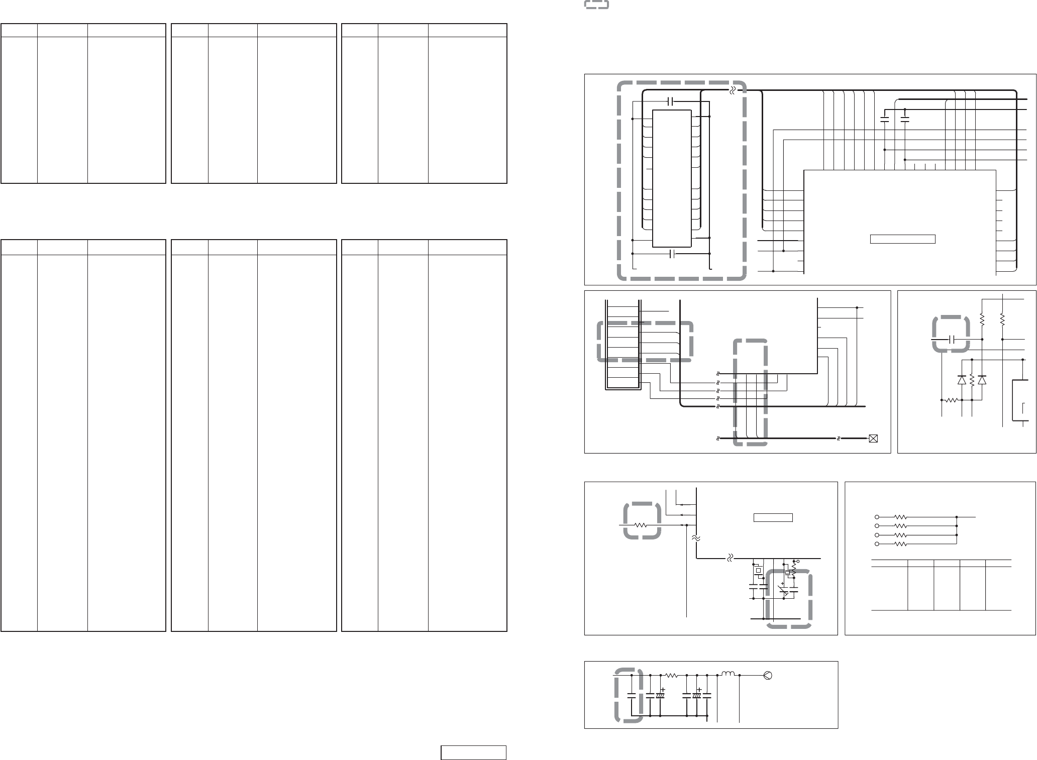
CIRCUIT DIAGRAM
Main PWB section(B1) 3/5
Main PWB section(B1) 4/5
Main PWB section(B1) 2/5
ELECTRICAL PARTS LIST
Main PWB section(B1)
REF No. PART No. DESCRIPTION REF No. PART No. DESCRIPTION REF No. PART No. DESCRIPTION
C212 043-0554-90 25V 10uF
C215 163-1073-15 6.3V 100uF
C217 119-3331-15 1/10W 33k ohm
C221 163-4763-15 6.3V 47uF
C222 163-4763-15 6.3V 47uF
C226 043-0554-90 25V 10uF
C227 043-0554-90 25V 10uF
C228 163-1073-15 6.3V 100uF
C231 168-1042-78 16V 0.1uF
C232 168-1042-78 16V 0.1uF
C400 168-1022-55 1000pF K
C467 ----------- (Unused)
C502 163-2263-15 6.3V 22uF
C564 163-1073-35 16V 100uF
* Other parts are the same as the original model. Please refer to page 14 of the original service manual.
C714 ----------- (Unused)
C722 168-1042-78 16V 0.1uF
C734 ----------- (Unused)
C736 166-4096-50 4pF CH
IC201 051-6711-20 TC94A34FG-004
IC205 051-9318-00 MSM51V17400D-
60TS-K
IC506 051-3057-90 BA4558RFV
IC701 051-5423-38 BD6329G-TR
IC703 052-3197-21 uPD703272YGC324-
8EAA
IC705 051-3408-90 BA2903FV
J201 074-1237-79 SOCKET(29P)
R745 ----------- (Unused)
R806 119-3331-15 1/10W 33k ohm
R811 119-1031-15 1/10W 10k ohm
(PH2761CF/G/H/I)
R812 119-1031-15 1/10W 10k ohm
(PH2761CF/G/J/K)
R813 119-1031-15 1/10W 10k ohm
(PH2761CH/J)
R814 119-1031-15 1/10W 10k ohm
(PH2761CI/K)
TC701 004-1583-51 10pF WHT
X702 061-3506-80 32.768MHz
PWB 039-2882-00 PWB(WITHOUT
COMPONENTS)
REF No. PART No. DESCRIPTION REF No. PART No. DESCRIPTION REF No. PART No. DESCRIPTION
Switch PWB section(B2)
C112 ----------- (Unused)
C113 ----------- (Unused)
D101 001-7100-90 NESB017-EE2-
KLP7*17.5
(PH2761CF/G/H)
001-7100-92 NESB017-ED2-
KLP2LP3*17
(PH2761CI/J/K)
D102 001-7100-90 NESB017-EE2-
KLP7*17.5
(PH2761CF/G/H)
001-7100-92 NESB017-ED2-
KLP2LP3*17
(PH2761CI/J/K)
D103 001-7100-90 NESB017-EE2-
KLP7*17.5
(PH2761CF/G/H)
001-7100-92 NESB017-ED2-
KLP2LP3*17
(PH2761CI/J/K)
D104 001-7100-90 NESB017-EE2-
KLP7*17.5
(PH2761CF/G/H)
001-7100-92 NESB017-ED2-
KLP2LP3*17
(PH2761CI/J/K)
D105 001-7100-90 NESB017-EE2-
KLP7*17.5
(PH2761CF/G/H)
001-7100-92 NESB017-ED2-
KLP2LP3*17
(PH2761CI/J/K)
D106 001-7100-90 NESB017-EE2-
KLP7*17.5
(PH2761CF/G/H)
001-7100-92 NESB017-ED2-
KLP2LP3*17
(PH2761CI/J/K)
D107 001-7100-90 NESB017-EE2-
KLP7*17.5
(PH2761CF/G/H)
001-7100-92 NESB017-ED2-
KLP2LP3*17
(PH2761CI/J/K)
D108 001-7100-90 NESB017-EE2-
KLP7*17.5
(PH2761CF/G/H)
001-7100-92 NESB017-ED2-
KLP2LP3*17
(PH2761CI/J/K)
D109 001-7100-90 NESB017-EE2-
KLP7*17.5
(PH2761CF/G/H)
001-7100-92 NESB017-ED2-
KLP2LP3*17
(PH2761CI/J/K)
D110 001-7100-90 NESB017-EE2-
KLP7*17.5
(PH2761CF/G/H)
001-7100-92 NESB017-ED2-
KLP2LP3*17
(PH2761CI/J/K)
D111 001-7100-90 NESB017-EE2-
KLP7*17.5
(PH2761CF/G/H)
001-7100-92 NESB017-ED2-
KLP2LP3*17
(PH2761CI/J/K)
D112 001-7100-90 NESB017-EE2-
KLP7*17.5
(PH2761CF/G/H)
001-7100-92 NESB017-ED2-
KLP2LP3*17
(PH2761CI/J/K)
D220 ----------- (Unused)
D221 ----------- (Unused)
LCD101 379-1373-43 LCD(INDICATOR)
(PH2761CF/G/H)
379-1339-42 LCD(INDICATOR)
(PH2761CI/J/K)
Q205 ----------- (Unused)
Q206 ----------- (Unused)
R105 116-2711-15 1/4W 270 ohm
(PH2761CF/G/H)
116-2211-15 1/4W 220 ohm
(PH2761CI/J/K)
R106 116-2711-15 1/4W 270 ohm
(PH2761CF/G/H)
116-2211-15 1/4W 220 ohm
(PH2761CI/J/K)
R107 116-2711-15 1/4W 270 ohm
(PH2761CF/G/H)
116-2211-15 1/4W 220 ohm
(PH2761CI/J/K)
R108 116-2711-15 1/4W 270 ohm
(PH2761CF/G/H)
116-2211-15 1/4W 220 ohm
(PH2761CI/J/K)
R109 116-2711-15 1/4W 270 ohm
(PH2761CF/G/H)
116-2211-15 1/4W 220 ohm
(PH2761CI/J/K)
R110 116-2711-15 1/4W 270 ohm
(PH2761CF/G/H)
116-2211-15 1/4W 220 ohm
(PH2761CI/J/K)
R111 ----------- (Unused)
PWB 039-2973-00 PWB(WITHOUT
COMPONENTS)
* Other parts are the same as the original model. Please refer to page 16 of the original service manual.
- 6 - PH-2761C
PRINTED WIRING BOARD
Main PWB section(B1) 1/2
IC Q
Main PWB(B1)
SOLDER SIDE
1617 789101112
AC
13 891113
10 12 14
56
247
12345678910
11121314151617181920
123
131415
456
R482
C103
C105
C107
C108
C109 C110
C111
C218
R105
R302
C209
R204
C208
C210
D105
R213
R210
R484
C701
R301
R304
C446
D106
R303
C231
C408
R405
C409
L404
R464
R429
R425
R426
C440
L409
C447
R708
C453
C451
C452
C450
C454
R738
L413
L416
C462
C464
IC403
C484
C481
R477
C483
C232
R476
C449
Q403
C498
R705
C499
L414
C486
C596
C599
R709
C549
C552
C551
C557
C558
C559
C560
C563
R762
C703
R702
R737
R732
C702
Q701
R769
C720
R779
R786
D712
L706
Q108
R910
IC705
1
C905
C721
Q101
D104
C302
D302
R751
D503
R740
R797
D718
D713
D714
R798
D903
R754
R114
C216
R775
R109
J702(NC)
C480
R402
R211
IC704
C550
D303
C597
L405
L401
C433
C466
L407
L408
C458
C459
Q109
Q103
R119
C708
R917
R106
R776
R715
C418
IC205
112
24 13
R736
D904
D504
L102
R108
R112
R717
R741
R113 Q105
IC506
Q107
R783
C214
R814(CI/CK)
R813(CH/CJ)
R812(CF/CG/CJ/CK)
R811(CF/CG/CH/CI)
R205
Q104
R706
R704
C212
L201
R707
C494
C301
R404
R743
C716
R802
R742
R701
R718
Q915
R483
R401
C416
C417
R406
R427
R421
C436
R408
C415
R407
R467
C448
R449
R118
C910
R455
C598
C477
R463
C485
R466
R481
C482 C479
R470
R471
C487
C488 R480R462
R465
D301
C478
R777
Q301
C437
C217
R120
R799
IC701
R763
R716
R723
R735
R720
R721
R722
R725
R703
D702
R724
R726
R727
R728
Q702
Q916
C706 C707
R800
R731
R110
R111
R801
R755
R750
R760
R752
R753
R772
R758
R759
R757
R739
R791
IC902
L412
R765
R795
R778
D711
R787
R788R789
R790
R785
C723
R793
R796
R805
C224
Q110
R485
R918
R919
R920
C226
C381
R486
R487
R488
R489
C382
C383
C384
R403
R719
C227
C491
R792
IC403
Q403
Q701
Q108
IC705
Q101
IC704 Q109
Q103
IC205
Q105
IC506
Q107
Q104
Q915
Q301
IC701
Q702
Q916
IC902
Q110
1
1
1
1
17
14 8
1
Caution:
COMPONENT SIDE: Parts on the component side seen
from the component side are indicated.
SOLDER SIDE: Parts on the solder side seen
from the solder side are indicated.
CLK TP CLK TP
C613
R616 C612
R620
R619
R617
R615
R624
C614
C611
R623
R622
R626
R636
R621
R637 C622
R639
R640 R646
R644
C621
1
1
1
1
R618
R645
C619
R643
R625
R642
C620
R635
R641
R638
IC601
IC603
IC602
IC604
IC601
IC603
IC602
IC604
- 7 - PH-2761C
Main PWB section(B1) 2/2
ICQ
14
85
14
85
Main PWB(B1)
COMPONENT SIDE
8
9
10
11
12
13
14
BUS GND
GND-SHIELD
ILL-C
R+
R-
L+
L-
1
2
3
4
5
6
7
+B
+B
SYSTEM ACC
ILL
BUS+
BUS-
MAIN GND
A
B
C
ANT IN
GND
SWD +B
8
9
10
11
12
13
14
RR+
FR+
FL+
RL+
ILL+
K-LINE
NC(TEL-MUTE)
15
16
17
SECURITY
ACC
VSP
1
2
3
4
5
6
7
MAIN GND
RR-
FR-
FL-
RL-
ILL-
+B
8
9
10
11
12
13
14
AUX SIG GND
NC
(NAVI SH GND)
NC(NAVI GND)
NC(HFT MUTE)
NC(TELM SIG+)
NC(HFT ICON2)
NC(PAS MUTE)
15
16
17
18
19
20
SW +B
AUX DET
AUX R-CH
AUX L-CH
NC(NAVI R-CH)
NC(NAVI L-CH)
1
2
3
4
5
6
7
NC
(TELM SH GND)
NC(TELM SIG-)
NC(HFT ICON1)
REMOTE
REMOTE GND
AUX GND
AUX SH GND
11123 13 14 15
16 17
456
123 13 14 15 456
789 101112
16 17
789 101112
A
C
CA
3891113
13891113
101214 56247
101214 56247
2345678910
12345678910
11 12 13 14 15 16 17 18 19 20
11 12 13 14 15 16 17 18 19 20
B
External Device Connector(20P) GA-NET Connector(14P) Main Connector(17P) ANT Connector
To J201 of SW PWB-B(page 8)
CTo J101 of CD PWB(page M6)
Flat Wire
(816-4028-50) D
117
1
VCC
1100 76
26 50
25
75
51
124
29 1
1
16 17 32
64 49 48
33
1144 109
37 72
36
108
73
C101
R913
D804
C104 C106
Q106
C202
C203 C204
C205
C206
C207
C211
C213
R451
C219
C225
R311
C221C222
C220
R308
R116
Q712
Q711
R928
R578
TM201
C402C411
C403 C404 C405
C406
C407
C423
C410
C414
C419
C420
C421
C422
R101
IC202
C425
C426
C427
C428
C429
C430
C431
C432
C424
C434
C435
C497
C438
C441
C442
C443
C444
C461
C460
C445
C463
C465
C911
C473 C475 C472
C303
R909
R929
C548
J101
R215
C503
X701
C722
C500
C564
TC701
C709
C704
L705
C725
C705
C736
C713
C547
C718
R924
D102
Q102
D103
C115
L703
L702
C727
IC401
C803
D902
C902
IC203
C912
C496
R744
D201
Q205
C904
TP404
D502
D505
C493
Q803
Q913
R794
Q904
R307
D805
D806
C102
IC201
IC404
L101
C228
IC204
1
1
1
L203
IC706
C715
Q517
L202
L402
L403
L406
L410
L411
IC703
L704
L701
R784
Q921
J302
R921
Q204
C113
R122
TP403
R572
R306
Q914
Q203
C710
Q912
Q908
C903
R102
C112
C474
X201
R121
R923
R115
R914
C401
C914
C907 C909
C201
R202
R203
R209 R501
R214
TH101
IC301
R305
Q521
X401
C735
C901
C906
Q906
R936
R935
C729
D101
C504
L415
C412
C726
BL101
R412
R413
R415
R416
P701
R806
D701
C400
R439
R440
R441
R442
R444
R445
R446
R448
C502
R454
R458
R459
R460
R461
Q522
Q907
R912
Q901
Q922
D708
R925
R926
R201
R117
IC702
R927
Q909
D501
R579
R107
R710
R711
R713
R714
R712
R730
R733
D719
C215
R746
R747
R748
R749
SUP101
R761
R764 R766C719
T501
TM901 TM102
C724
R729
TM101
ANT101
TM501
TM701
D901
TH501
R903
C711
Q902
R803
R804
R905R901
R808
R904
R911 R577
R902
R907
R734
C413
Q905
R212
R916
R915
C913
C223
Q516
J301
X702
C495
C439
C712
Q106
Q712
IC202
Q102
IC401
IC203
Q205
Q803
Q913
Q904
IC201
IC404
IC204
IC706
Q517
IC703
Q921
Q204
Q914
Q203
Q912
Q908
IC301
Q521
Q906
Q522
Q907
Q901
Q922
IC702
Q909
Q902
Q905
Q516
Q711
- 8 - PH-2761C
Switch PWB-A(B2) section Switch PWB-B(B2) section
Switch PWB-A(B2)
COMPONENT SIDE SOLDER SIDE
IC
Q
112
120
120
6041
21
40
80
61
6041
21
40
80
61
114
To J202 of SW PWB-B
Flat wire
(816-4013-51)
B
To J203 of SW PWB-B
Flat wire
(816-4014-51)
A
C102
C103
R123
IC201
R112
C107
R114
R109
Q201
R202
J204
IC202
J205
C111
R208
C104
R106
C105
R110
C101
R113 C106
R116
C108
R104
R121
R122
Q202
R108
R207
R105 R107
TM101
D104
LCD101
D107
TM102
D105 D106 D109 D110 D111 D112
D108
D101 D103D102
COMPONENT SIDE Switch PWB-B(B2) SOLDER SIDE
IC
Q
114
1
112
23
224
To P701 of
Main PWB
(page 7)
C
To J205 of
SW PWB-A
B
To J204 of
SW PWB-A
A
R203
R204
IC203
J203 J202
D201
J201
R201
PL111
PL112
C109
D214
D202
C121
D119
D118
C122
D209
PL103 PL104
D213
S119
S102
D206
S103 S104
S111 D211
S109
S106
D207
S107 S108
S112
S116
S114 S115
S117
S113
PL109 PL105 PL110 PL108
S101
S118
PL101
S105
C110
PL107
PL102
S110
D212
PL106
D210
D204
D216
D208
D222
D215
D203
D303
D205
1
929-5000-80
- M1 -
Service Manual
Published by Service Dept.
Printed in Japan
Clarion Co., Ltd.
50 Kamitoda, Toda-shi, Saitama 335-8511 Japan
Service Dept.: 5-66 Azuma , Kitamoto-shi, Saitama 364-0007 Japan
Tel: +81-48-541-2335 / 2432 FAX: +81-48-541-2703
Model
CD mechanism
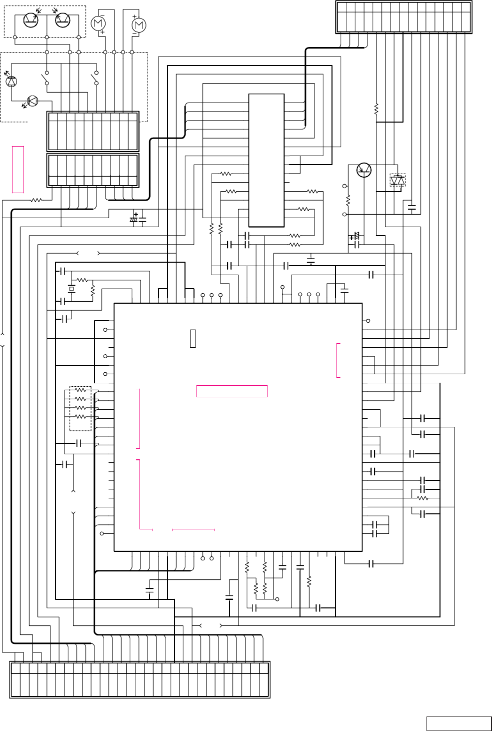
BLOCK DIAGRAM
J101
SLED / LOADING
MOTOR
SPINDLE MOTOR
RF-AMP
SERVO PROCESSOR
IC2
TC94A15FG
MOTOR DRIVER
IC1
BA5825FP
IF-VDD
8.0V
AOUT
SFSY
SBSY
/RST
BUS0
BUS1
BUS2
BUS3
BUCK
/CCE
DATA
LDMUT
LDCONT
SW / DET
3.3V
PICK UP UNIT
LASER
DETECTOR
A,B,C,E,F
FOCUS
TRACKING COIL
S2 LIMIT
SWITCH
CHUCKING
SWITCH
Q1,2 PHOTO
TR A,B
D1,2 LED A,B
S1
CLCK
BCK
LRCK
MBOV
IPF
8V
CD-VDD
3.3V
5.0V
929-5000-80
929-5000-80 - M2 -
H4
H5
G6
H6
H7
A5
A1
A2
A3
A4
G2
G3
B2
A8
A8
I1
M1
K3
K4
C1
A2
A3
G9
G8
G11
G5
G14
G6
3
4
75
74
76
5
11
7
9
12
31
32
33
34
35
36
13
14
15
16
17
37
38
39
40
18
19
29 20
21
22
30
23
24
25
26
28
43
44
45
46 47
65
48
48
50
53
51
67
63
64
54
55
56
57
59
60
61
62
70
68
71
72
73
69
1
2
59
46
I1
I2
D2
D1
H6
H7
K1
K2
C3
H5
H4
22
29
H6
B1
H1
H2
H3
G13
D1
52
D2
G12
H2
H1
H3
65
A4
A5
E2
G2
G14
G5
G1
G3
E1
G4
M1
G9
G8
G11
C5
C2
G1
I2
C1
66 66
49
49
H6
C5
C2
C3
K1
K2
K3
K4
G12
G4
A1
G13
B1
B2
69
E1
E2
41
6
8
10
42 27
58
1
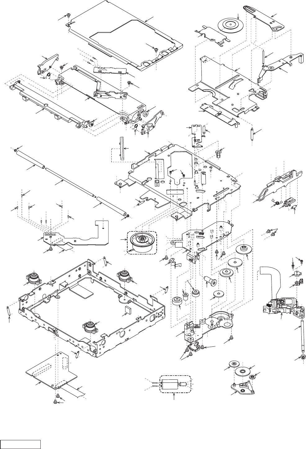
EXPLODED VIEW / PARTS LIST

929-5000-80
- M3 -
NO. PART NO. DESCRIPTION Q'TYNO. PART NO. DESCRIPTION Q'TY
1 ----------- SENSOR PWB 1
2 ----------- MAIN PWB 1
3 SMA-182-100 SPINDLE MOTOR-ASSY 1
4 SMA-183-100 SLED MOTOR-ASSY 1
5 345-5476-20 CUSHION RUBBER 1
6 620-1023-23 CLAMPER PLATE 1
7 620-1026-21 SPRING PLATE 1
8 620-1596-23 CLAMPER LINK 1
9 620-1598-22 UPPER CHASSIS 1
10 620-1752-20 SENSOR ARM 1
11 620-1753-20 ID-LOCK PLATE 1
12 620-1754-20 LOWER CHASSIS 1
13 621-0608-21 SECOND GEAR 1
14 621-0609-20 BASE GEAR 1
15 621-0610-20 IDLE GEAR A 1
16 621-0611-20 IDLE GEAR B 1
17 621-0612-21 ROLLER GEAR A 1
18 621-0620-20 THREAD GEAR A 1
19 621-0621-20 THREAD GEAR B 1
20 621-0623-23 LS-HOLDER 1
21 621-0624-22 GUIDE RAIL 1
22 621-0711-20 LOADING ROLLER 2
23 621-0718-21 ROLLER GUIDE 1
24 621-0719-20 ROLLER GEAR B 1
25 621-0720-20 ROLLER GEAR C 1
26 621-0721-20 ROLLER GEAR D 1
27 621-0728-20 STOPPER LINK 1
28 621-1719-20 IDLE CASE 1
29 621-1726-20 ROLLER SLEEVE 2
30 621-1729-20 SH-BASE 1
31 621-1742-20 UPPER GUIDE 1
32 621-1743-20 SHIFT LEVER 1
33 621-1744-20 RACK 1
34 621-1745-20 LOCK ARM L 1
35 621-1746-20 LOCK ARM R 1
36 621-1747-20 GEAR COVER 1
37 621-1748-20 POWER GEAR A 1
38 621-1749-20 POWER GEAR B 1
39 621-1750-20 POWER GEAR C 1
40 621-1751-20 POWER GEAR D 1
41 621-1752-20 DISC STOPPER 1
42 621-1753-20 CLAMPER RING 1
43 621-1754-20 GEAR BASE 1
44 622-1571-21 ROLLER SHAFT 1
45 624-0020-00 LEAD SCREW 1
46 629-0086-20 DAMPER F 2
47 629-0087-20 DAMPER R 1
48 716-1507-01 SCREW(M2x3) 3
49 716-1670-01 SCREW(M2x4) 4
50 716-1733-01 SCREW(M1.7x2.3) 2
51 716-3469-01 SCREW(1.7x4) 2
52 716-3473-01 SCREW(M2x3) 1
53 716-3551-00 SCREW(M1.4x2.5) 2
54 750-3467-21 SHIFT SPRING 1
55 750-3468-20 RACK SPRING 1
56 750-3469-20 CLAMPER SPRING 1
57 750-3470-20 ID-LOCK SPRING 1
58 750-3471-20 SENSOR SPRING 1
59 750-3472-21 DR-SPRING F 2
60 750-3473-20 DR-SPRING RA 1
61 750-3474-20 DR-SPRING RB 1
62 750-3475-21 DR-SPRING C 1
63 750-6797-20 ROLLER SPRING L 1
64 750-6798-20 ROLLER SPRING R 1
65 714-2003-8B SCREW(M2x3) 2
66 780-2025-00 SCREW(M2x2.5) 3
67 781-1730-00 SCREW(M1.7x3) 1
68 803-4906-60 VINYL-COAT-WIRE(ORG) 1
69 816-2542-01 FLAT WIRE 1
70 816-2590-00 VINYL-COAT-WIRE(GRN) 1
71 816-2591-00 VINYL-COAT-WIRE(YEL) 1
72 816-2592-00 VINYL-COAT-WIRE(BLUE) 1
73 816-2593-00 VINYL-COAT-WIRE(PUR) 1
74 966-1722-20 SH-RACK-ASSY 1
75 966-1743-21 DRIVE-PLT-ASSY 1
76 969-0071-30 PICKUP-ASSY 1
929-5000-80 - M4 -
REF No. PART No. DESCRIPTION REF No. PART No. DESCRIPTION REF No. PART No. DESCRIPTION
REF No. PART No. DESCRIPTION REF No. PART No. DESCRIPTION REF No. PART No. DESCRIPTION
ELECTRICAL PARTS LIST
CD PWB(BM1) section
C1 168-1042-78 16V 0.1uF
C2 163-1073-35 16V 100uF
C4 178-1052-78 1uF
C5 042-0560-85 6.3V 100uF
C6 178-1052-78 1uF
C8 178-1052-78 1uF
C10 168-1042-78 16V 0.1uF
C11 168-1042-78 16V 0.1uF
C12 045-4701-50 47pF
C13 046-1532-78 0.015uF
C14 168-1042-78 16V 0.1uF
C15 046-1032-78 0.015uF
C17 046-4722-58 4700pF
C18 046-1522-58 1500pF
C19 168-1042-78 16V 0.1uF
C20 168-1042-78 16V 0.1uF
C21 046-6812-58 680pF
C22 168-1042-78 16V 0.1uF
C23 046-1532-78 0.015uF
C24 168-1042-78 16V 0.1uF
C25 045-6801-50 68pF
C26 168-1042-78 16V 0.1uF
C27 046-3332-78 0.033uF
C29 046-6822-58 6800pF
C30 168-1042-78 16V 0.1uF
C31 046-4712-58 470pF
C32 046-4712-58 470pF
C33 168-1042-78 16V 0.1uF
C34 168-4732-78 16V 0.047uF
C35 168-4732-78 16V 0.047uF
C36 045-1007-50 10pF
C37 045-1007-50 10pF
C38 168-1042-78 16V 0.1uF
C39 046-5622-58 5600pF
C40 168-1042-78 16V 0.1uF
CCT1 050-0140-63 1/32W 47k ohm x4J
D1 001-0367-91 1SS226
IC1 051-6079-90 BA5830FPG
IC2 051-6399-00 TC94A15F
J101 074-1228-79 29P
J201 074-1138-65 15P
J301 074-1138-60 10P
Q1 131-1188-50 2SB1188PQR
R1 117-6811-15 1/8W 680 ohm
R2 117-1001-15 1/8W 10 ohm
R3 033-2211-15 1/10W 220 ohm
R5 033-0000-05 1/10W 0 ohm
R6 033-5621-15 1/10W 5.6k ohm
R7 033-4731-15 1/10W 47k ohm
R8 033-3341-15 1/10W 330k ohm
R9 033-2231-15 1/10W 22k ohm
R10 033-2231-15 1/10W 22k ohm
R11 033-2731-15 1/10W 27k ohm
R12 033-4731-15 1/10W 47k ohm
R13 033-2731-15 1/10W 27k ohm
R14 033-1531-15 1/10W 15k ohm
R15 033-2731-15 1/10W 27k ohm
R16 033-8231-15 1/10W 82k ohm
R17 033-2731-15 1/10W 27k ohm
R18 033-8231-15 1/10W 82k ohm
R19 033-1051-15 1/10W 1M ohm
R20 119-2221-15 1/10W 2.2k ohm
X2 061-3534-90 16.92MHz
PWB 039-2741-20 PWB(WITHOUT
COMPONENT)
Sensor PWB(BM2) section
D1 001-7058-90 AN1105W-RR
D2 001-7058-90 AN1105W-RR
J1 074-1138-60 10P
Q1 060-4015-91 PS1192HB
Q2 060-4015-91 PS1192HB
S1 013-7414-50 CHUCKING
S2 013-7413-50 LIMIT
PWB 039-2675-20 PWB(WITHOUT
COMPONENT)
929-5000-80
- M5 -
٨
٨
٨
٨
٨
٨
٨
٨
٨
٨
٨
٨
٨
٨
٨
٨
٨
٨
٨
٨
٨
٨
٨
٨
٨
٨
٨
٨
٨
٨
٨
٨
٨
٨
٨
٨
٨
٨
٨
٨
٨
٨
٨
٨
٨
٨
٨
٨
٨
٨
٨٨
٨
٨
٨
٨
٨
٨
٨
٨
٨
٨
٨
٨٨
٨
٨
٨
٨
٨
٨
٨
٨
٨
٨
٨٨
٨٨
٨
٨
٨٨
٨
٨
٨
٨
٨
٨
٨
٨
٨
٨
٨
٨
٨٨٨
٨
٨
٨٨
٨
٨
٨
٨
٨
٨
٨
٨
٨
٨
٨
٨
CCT1
47KX4
1
2
3
4
5
6
7
8
9
10
1
2
3
4
5
6
7
8
9
10
11
12
13
14
15
16
17
18
19
20
21
22
23
24
25
26
27
28
29
SENSOR-A
SENSOR-B
SBOK
IPF
CLCK
VDD3
VSS3
DATA
SFSY
SBSY
ARSEL
AWRC
PVDD3
PDO
TMAXS
LPFN
LPFO
PVREF
VCOF
VCOREF
DTCN
DTCP
PVSS3
TMAX
SLCO
RFRPI
RFI
RFEQO
AVDD3
RESIN
VRO
VMDIR
TESTR
AGCI
RFDCI
RFO
PNSEL
EQSET
RVDD3
MDI
FNI2
FNI1
FPI1
TNI
RFZI
AVSS3
RFRP
RFDC
FEI
SBAD
TEI
TEZI
AVDD3
FOO
TRO
VREF
FMO
DMO
MONIT
FGIN
VSS3
TESIN
XVSS3
XI
XO
DVSS3
RO
DVDD3
DVR
LO
DVSS3
ZDET
VSS5
BUS0
BUS1
BUS2
BUS3
BUCK
VDD5
IO0B
IO1B
IO2B
IO3B
EMPH
BCK
AOUT
LRCK
DOUT
XVDD3
VDD3
RVSS3
SL-
SL+
SP-
SP+
SSTOP
CHU
TR-B
TR-A
GND
FCS(+)
1
2
3
4
5
6
7
8
9
10
11
12
13
15
14
FCS(-)
TRK(-)
TRK(+)
F
VC
VCC
LD
GND
VR
PD
B
A
E
C
8V
8V
TR-B
TR-A
CHU-SW
SBSY
BUCK
BUS3
BUS2
BUS1
GND
BUS0
/CCE
/RESET
P-GND
P-GND
SSTOP
INVSEL
LDO
FPI2
TPI
/CCE
/RST
To pick up
To J201 of Main PWB
CLV:L
LED+
LCONT
LDMUT
fc=13.5KHz
IO0A
IO1A
IO2A
IO3A
AOUT
LRCK
BCK
SFSY
MBOV
IPF
CD-VDD
IF-VDD
DATA
CLCK
VO2+
VO2-
VO1+
PwVCC
PwGND
MUTE
PrGND
REG
OPIN2
OPOUT2
OPIN1
OPOUT1
REG-B
VO-
VO3+
VO3-
VO4+
PwVCC2
PwGND
VO4-
CNT
LDIN
OPOUTSL
OPINSL-
OPOUT3
OPIN3
BIAS
PrVCC
SL-
SL+
SP-
SP+
PHOTO-B
PHOTO-A
GND
LED+
1
2
3
4
5
6
7
8
9
10
CHUCK-SW
LIMIT-SW
J201
R2
C11
C13
C15
R3
C17
C18
C19 C20
C21
C22
C25
C26
C27
C29
C31
C33
C38
C39
R6
R7
R8
R9
R10
R13
R15
TP18
TP19
R5
C6
R12
X2
C10
C14
R16
R18
R17
R19
R20
D1
Q1
C4
C5
C30
R11
C35
IC1
C34 C32
C1
C2
R1
D2
D1
S1
S2
Q2
Q1
J1
J301
J101
C36
C37
C12
C40
R14
IC2 C8
C23
C24
10
0.1
0.015
0.01
220
4700p
1500p
0.1 0.1
680p
0.1
68p
0.1
0.033
6800p
470p
0.1
0.1
5600p
5.6K
47K
330K
22K
22K
27K
27K
LD-
LD+
FTE
0
1
47K
16.92M
0.1
0.1
82K
82K
27K
1M
2.2K
1SS226TE85L
2SB1188
1
100
6.3V
0.1
27K
0.047
BA5830FP
0.047 470p
0.1
100
16V
680
AN1105W-RR
AN1105W-RR
SPVG22
SPVG12
PS1192HB
PS1192HB
SP+
SP-
SL+
SL-
GND
10p
10p
47p
0.1
15K
TC94A15FG 1
0.015
0.1
A-3.3V
8V
D-3.3V
IF-VDD
TR-A
CHU
SSTOP
TR-A
CHU
SSTOP
BUS0
BUS1
BUS2
BUS3
/CCE
BUCK
SP+
SP-
SL+
SL-
F-
T+
F+
T-
TR-B TR-B
/RST
LRCK
BCK
AOUT
F-
F+
T-
T+
SBSY
/RST
/CCE
BUCK
BUS3
BUS2
BUS1
BUS0
IPF
MBOV
CLCK
DATA
SFSY
BCK
LRCK
AOUT
SL-
SL+
SP+
SP-
IPF
MBOV
CLCK
DATA
SFSY
SBSY
C
C
C
C
C
C
C
C
C
C
C
C
C
C
C
C
C
C
C
C
1 2 3 4 5 6 7 8 9101112131415161718192021222324
31
32
33
34
35
36
37
38
39
40
565758596061626364
25
41
42
43
44
45
46
47
48
49
50
6566676869707172737475
81
82
83
84
85
86
87
88
89
90
91
92
93
94
95
96
97
98
99
100 26
27
28
29
30
80
79
78
77
76
5152535455
C
C
C
C
C
C
C
C
C
C
C
C
C
12345678910 11 12 13 14
21
27
28 22
23
24
25
26 15
16
17
18
19
20
0V
0V
8V
1.7V 0.8V
1.7V
1.4V
1.7V
1.7V
1.7V
3.3V
0V
3.3V
0V
0V
1.7V
0V
3.3V
0V
0V
3.3V
0V
1.8V
1.7V
1.7V
1.7V
1.7V
3.3V
1.7V
1.7V
1.7V
2.0 TO 2.8V
0V
1.7 TO 2.0V
0V
0.2V
2.4V
3.3V
0.6 TO 1.8V
1.1 TO 2.4V
1.6V
1.5V
1.7V
1.5V
3.3V
TO 2.3V
RF-AMP AND
DIGITAL SERVO PROCESSOR
1.7V
0V
0V
3.3V
1.8 TO 2.2V
3.3V
3.3V
1.7V
0V
0.19V
0.15V
1.7V
1.8V1.7V
0V
0V
8V
3.8V
3.8V
3.8V
4.0V
3.6V
4.0V
3.6V 4.0V
8V
0V
1.8V
1.7V
1.6V
1.7V
1.7V
7.9V
DRIVER WITH
REG. CONTROLLER
3.3V
3.3V or 5V
0/IF-VDD
0/IF-VDD 3.3V
3.3V
0/IF-VDD
0/IF-VDD
0/IF-VDD
0/IF-VDD
3.3V or 5V
1.8V
0.6 TO 1.8V
1.3
TO 2.2V
0.6 TO 1.8V
1.0 TO 2.3V
1.0
1.8 TO 2.2V
CIRCUIT DIAGRAM
CD PWB(BM1) section
Sensor PWB(BM2) section
929-5000-80 - M6 -
PRINTED WIRING BOARD
CD PWB(BM1) section
Sensor PWB(BM2) section
CD PWB (BM1)
CD PWB (BM1)
Sensor PWB-B
(BM2)
GRN(-)
FLAT WIRE
(816-2542-01)
PICK UP-ASSY
(969-0071-30)
SPINDLE MOTOR-ASSY
With LEAD
(SMA-182-100)
SLED MOTOR-ASSY
(SMA-183-100)
ORG(+)
RED(+)
BLK(-)
To J201 of Main PWB
GRN
ORG
BLK
RED
BLU
PUR
YEL
PUR
YEL
BLU
Sensor PWB-A
(BM2)
IC Q
MARKING
+
+
COMPONENT SIDE
SOLDER SIDE
Caution:
COMPONENT SIDE: Parts on the component side seen
from the component side are indicated.
SOLDER SIDE: Parts on the solder side seen
from the solder side are indicated.
Q
