PIC32 FRM Section 9. Watchdog Timer And Power Up Family Reference Manual, Sect. 09
User Manual:
Open the PDF directly: View PDF ![]() .
.
Page Count: 16
- Section 9. Watchdog Timer and Power-up Timer
- 9.1 Introduction
- 9.2 Watchdog Timer and Power-up Timer Control Registers
- 9.3 Operation
- 9.4 Interrupt and Reset Generation
- 9.5 I/O Pins
- 9.6 Operation in Debug and Power-Saving Modes
- 9.7 Effects of Various Resets
- 9.8 Related Application Notes
- 9.9 Revision History

© 2007-2011 Microchip Technology Inc. DS61114F-page 9-1
Watchdog Timer and
Power-up Timer
9
Section 9. Watchdog Timer and Power-up Timer
HIGHLIGHTS
This section of the manual contains the following major topics:
9.1 Introduction................................................................................................................9-2
9.2 Watchdog Timer and Power-up Timer Control Registers ..........................................9-3
9.3 Operation...................................................................................................................9-6
9.4 Interrupt and Reset Generation ............................................................................... 9-10
9.5 I/O Pins....................................................................................................................9-12
9.6 Operation in Debug and Power-Saving Modes ....................................................... 9-12
9.7 Effects of Various Resets.........................................................................................9-12
9.8 Related Application Notes .......................................................................................9-13
9.9 Revision History....................................................................................................... 9-14
PIC32 Family Reference Manual
DS61114F-page 9-2 © 2007-2011 Microchip Technology Inc.
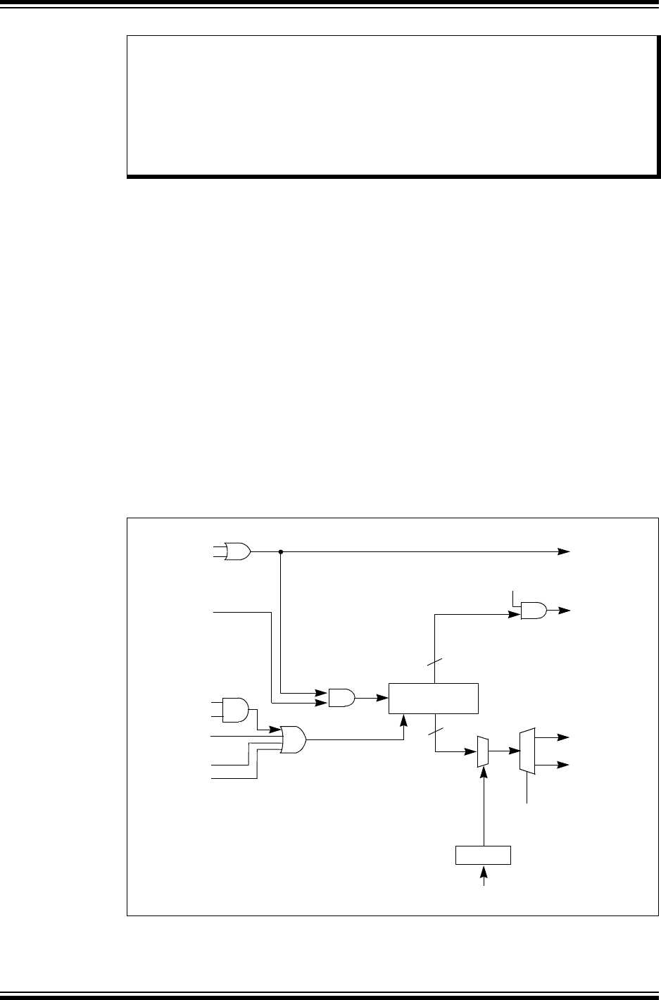
9.1 INTRODUCTION
The PIC32 Watchdog Timer (WDT) and Power-up Timer (PWRT) modules are described in this
section. Refer to Figure 9-1 for a block diagram of the WDT and PWRT.
The WDT, when enabled, operates from the internal Low-Power RC (LPRC) Oscillator clock
source. The WDT can be used to detect system software malfunctions by resetting the device if
the WDT is not cleared periodically in software. The WDT can be configured in Windowed mode
or non-Windowed mode. Various WDT time-out periods can be selected using the WDT
postscaler. The WDT can also be used to wake the device from Sleep or Idle mode.
The PWRT, when enabled, holds the device in Reset for a 64 millisecond period after the normal
Power-on Reset (POR) start-up period is complete. This allows additional time for the Primary
Oscillator (POSC) clock source and the power supply to stabilize. Like the WDT, the PWRT also
uses the LPRC as its clock source. For more information, refer to Figure 9-1.
Following are some of the key features of the WDT and PWRT modules:
• Configuration or software controlled
• User-configurable time-out period
• Can wake the device from Sleep or Idle
Figure 9-1: Watchdog Timer and Power-up Timer Block Diagram
Note: This family reference manual section is meant to serve as a complement to device
data sheets. Depending on the device variant, this manual section may not apply to
all PIC32 devices.
Please consult the note at the beginning of the “Power-Saving Features” and
“Special Features” chapters in the current device data sheet to check whether this
document supports the device you are using.
Device data sheets and family reference manual sections are available for
download from the Microchip Worldwide Web site at: http://www.microchip.com
Wake
WDTCLR = 1
WDT Enable
LPRC
Power Save
25-bit Counter
PWRT Enable
WDT Enable LPRC
WDT Counter Reset
Control
Oscillator
25 Device Reset
NMI (Wake-up)
PWRT
PWRT Enable
WDTPS<4:0> (DEVCFG1<20:16>)
Clock
Decoder
1
1:64 Output
0
1
WDT Enable
Reset Event

© 2007-2011 Microchip Technology Inc. DS61114F-page 9-3
Section 9. Watchdog Timer and Power-up Timer
Watchdog Timer and
Power-up Timer
9
9.2 WATCHDOG TIMER AND POWER-UP TIMER CONTROL REGISTERS
The WDT and PWRT modules consist of the following Special Function Registers (SFRs):
•WDTCON: Watchdog Timer Control Register
•RCON: Resets Control Register
The following table provides a brief summary of the related WDT module and PWRT module
registers. Corresponding registers appear after the summary, followed by a detailed description
of each register.
Table 9-1: Watchdog Timer and Power-up Timer SFR Summary
Name Bit
31/23/15/7 Bit
30/22/14/6 Bit
29/21/13/5 Bit
28/20/12/4 Bit
27/19/11/3 Bit
26/18/10/2 Bit
25/17/9/1 Bit
24/16/8/0
WDTCON(1,2,3) 31:24 — — — — — — — —
23:16 — — — — — — — —
15:8 ON — — — — — — —
7:0 — SWDTPS<4:0> WDTWINEN WDTCLR
RCON(1,2,3) 31:24 — — — — — — — —
23:16 — — — — — — — —
15:8 — — — — — — CM(4) VREGS(4)
7:0 EXTR(4) SWR(4) — WDTO SLEEP IDLE BOR(4) POR(4)
Legend: — = unimplemented, read as ‘0’.
Note 1: This register has an associated Clear register at an offset of 0x4 bytes. These registers have the same name with CLR
appended to the end of the register name (e.g., WDTCONCLR). Writing a ‘1’ to any bit position in the Clear register will
clear valid bits in the associated register. Reads from the Clear register should be ignored.
2: This register has an associated Set register at an offset of 0x8 bytes. These registers have the same name with SET
appended to the end of the register name (e.g., WDTCONSET). Writing a ‘1’ to any bit position in the Set register will
set valid bits in the associated register. Reads from the Set register should be ignored.
3: This register has an associated Invert register at an offset of 0xC bytes. These registers have the same name with INV
appended to the end of the register name (e.g., WDTCONINV). Writing a ‘1’ to any bit position in the Invert register will
invert valid bits in the associated register. Reads from the Invert register should be ignored.
4: These bits are not associated with the WDT or PWRT modules. For complete register details, see Register 7-1:
“RCON: Resets Control Register” in Section 6. “Resets” (DS61118) of the “PIC32 Family Reference Manual”.

PIC32 Family Reference Manual
DS61114F-page 9-4 © 2007-2011 Microchip Technology Inc.
Register 9-1: WDTCON: Watchdog Timer Control Register
Bit
Range Bit
31/23/15/7 Bit
30/22/14/6 Bit
29/21/13/5 Bit
28/20/12/4 Bit
27/19/11/3 Bit
26/18/10/2 Bit
25/17/9/1 Bit
24/16/8/0
31:24 U-0 U-0 U-0 U-0 U-0 U-0 U-0 U-0
— — — — — — — —
23:16 U-0 U-0 U-0 U-0 U-0 U-0 U-0 U-0
— — — — — — — —
15:8 R/W-0 U-0 U-0 U-0 U-0 U-0 U-0 U-0
ON(1,2) — — — — — — —
7:0 U-0 R-y R-y R-y R-y R-y R/W-0 R/W-0
— SWDTPS<4:0> WDTWINEN WDTCLR
Legend: y = Value from Configuration bit on POR
R = Readable bit W = Writable bit U = Unimplemented bit, read as ‘0’
-n = Value at POR ‘1’ = Bit is set ‘0’ = Bit is cleared x = Bit is unknown
bit 31-16 Unimplemented: Read as ‘0’
bit 15 ON: Watchdog Timer Enable bit(1,2)
1 = Enables the Watchdog Timer if it is not enabled by the device configuration
0 = Disable the Watchdog Timer if it was enabled in software
bit 14-7 Unimplemented: Read as ‘0’
bit 6-2 SWDTPS<4:0>: Shadow Copy of Watchdog Timer Postscaler Value from Device Configuration bits
On reset, these bits are set to the values of the WDTPS<4:0> Configuration bits.
bit 1 WDTWINEN: Watchdog Timer Window Enable bit
1 = Enable windowed Watchdog Timer
0 = Disable windowed Watchdog Timer
bit 0 WDTCLR: Watchdog Timer Reset bit
1 = Writing a ‘1’ will clear the WDT
0 = Software cannot force this bit to a ‘0’
Note 1: A read of this bit will result in a ‘1’ if the WDT is enabled by the device configuration or by software.
2: When using the 1:1 PBCLK divisor, the user’s software should not read or write the peripheral’s SFRs in
the SYSCLK cycle immediately following the instruction that clears the module’s ON bit.

© 2007-2011 Microchip Technology Inc. DS61114F-page 9-5
Section 9. Watchdog Timer and Power-up Timer
Watchdog Timer and
Power-up Timer
9
Register 9-2: RCON: Resets Control Register
Bit
Range Bit
31/23/15/7 Bit
30/22/14/6 Bit
29/21/13/5 Bit
28/20/12/4 Bit
27/19/11/3 Bit
26/18/10/2 Bit
25/17/9/1 Bit
24/16/8/0
31:24 U-0 U-0 U-0 U-0 U-0 U-0 U-0 U-0
— — — — — — — —
23:16 U-0 U-0 U-0 U-0 U-0 U-0 U-0 U-0
— — — — — — — —
15:8 U-0 U-0 U-0 U-0 U-0 U-0 R/W-0 R.W-0
— — — — — — CM(1) VREGS(1)
7:0 R/W-0 R/W-0 U-0 R/W-0 R/W-0 R/W-0 R/W-1 R/W-1
EXTR(1) SWR(1) —WDTOSLEEPIDLEBOR(1) POR(1)
Legend:
R = Readable bit W = Writable bit U = Unimplemented bit, read as ‘0’
-n = Value at POR ‘1’ = Bit is set ‘0’ = Bit is cleared x = Bit is unknown
bit 4 WDTO: Watchdog Time-out bit
1 = A Watchdog Timer time-out has occurred since either the device was powered up or the WDTO
bit was last cleared by software
0 = A Watchdog Timer time-out has not occurred since either the WDTO bit was cleared by software
or the device was reset
bit 3 SLEEP: Sleep Event bit
1 = The device was in Sleep since either the device was powered up or the SLEEP bit was last
cleared by software
0 = The device was not in Sleep since either the SLEEP bit was cleared by software or the device
was reset
bit 2 IDLE: Idle Event bit
1 = The device has been in Idle mode since either the device was powered up or the IDLE bit was
last cleared by software
0 = The device has not been in Idle mode since either the IDLE bit was cleared by software or the
device was reset
Note 1: These bits are not associated with the WDT or PWRT modules. For complete register details, see
Register 7-1: “RCON: Resets Control Register” in Section 6. “Resets” (DS61118) of the “PIC32
Family Reference Manual”.

PIC32 Family Reference Manual
DS61114F-page 9-6 © 2007-2011 Microchip Technology Inc.
9.3 OPERATION
If enabled, the WDT will increment until it overflows or “times out”. A WDT time-out will force a
device Reset, except during Sleep or Idle modes. To prevent a WDT time-out Reset, the user
application must periodically clear the WDT by setting the WDTCLR bit (WDTCON<0>).
The WDT module uses the LPRC Oscillator for reliability.
9.3.1 Modes of Operation
The WDT has two modes of operation: Windowed and Programmable Windowed.
The Programmable Windowed mode can be enabled by setting the Watchdog Window
Enable (WDTWINEN) bit (WDTCON<1>). In Programmable Windowed mode, software can
clear the WDT only when the counter is in its final window before a period match occurs.
There are four window size options. This window is active when the timer counter is greater
than a predetermined value for each option. Any attempts to clear the WDT when the win-
dow is not active will cause a device Reset. In Windowed mode, software can clear the WDT
anytime before the period match occurs.
9.3.2 Enabling and Disabling the WDT
The WDT is enabled or disabled by the device configuration or controlled through software by
writing to the WDTCON register (Register 9-1).
9.3.3 Device Configuration Controlled WDT
If the FWDTEN Configuration bit is set, the WDT is always enabled. The ON control bit
(WDTCON<15>) will reflect this by reading a ‘1’. In this mode, the ON bit cannot be cleared in
software. The FWDTWINEN and FWDTEN Configuration bits will not be cleared by any form of
reset. To disable the WDT, the configuration must be rewritten to the device.
The FWDTWINEN Configuration bit can be used to enable or disable the Programmable
Windowed mode. The window size for the WDT Windowed mode can be configured using the
FWDTWINSZ Configuration bits.
9.3.4 Software Controlled WDT
If the FWDTEN Configuration bit is a ‘0’, the WDT module can be enabled or disabled (the default
condition) by software. In this mode, the ON bit (WDTCON<15>) reflects the status of the WDT
under software control. A ‘1’ indicates the WDT module is enabled and a ‘0’ indicates it is
disabled. If the FWDTWINEN Configuration bit is a ‘0’, the WDT Programmable Windowed mode
can be enabled or disabled by software. The Programmable Windowed mode can be configured
using the WDTWINEN bit (WDTCON<2>). A ‘1’ indicates that Programmable Windowed mode
is enabled and ‘0’ indicates it is disabled. The window sizes can be configured by setting the
FWDTWINSZ configuration bits only, and cannot be set in software.
The WDT is enabled in software by setting the WDT ON control bit. The ON control bit is cleared
on any device Reset. The bit is not cleared upon a wake from Sleep or exit from Idle mode. The
software WDT option allows the user to enable the WDT for critical code segments and disable
the WDT during noncritical segments for maximum power savings. This bit can also be used to
disable the WDT while the device is awake to eliminate the need for WDT servicing, and then
re-enable it before the device is put into Idle or Sleep to wake the device at a later time.
Example 9-1 shows the WDT initialization and servicing sample.
Example 9-1: Sample WDT Initialization and Servicing
Note: The LPRC Oscillator is enabled whenever the WDT is enabled.
Note: The WDT is enabled by default on an unprogrammed device.
//This code fragment assumes the WDT was not enabled by the device configuration
// The Postscaler value must be set with the device configuration
WDTCONSET = 0x8000; // Turn on the WDT
main
{WDTCONSET = 0x01; // Service the WDT
... User code goes here ...
}

© 2007-2011 Microchip Technology Inc. DS61114F-page 9-7
Section 9. Watchdog Timer and Power-up Timer
Watchdog Timer and
Power-up Timer
9
9.3.4.1 WATCHDOG TIMER PROGRAMMABLE WINDOW
The window size is determined by the Configuration bits, FWDTWINSZ and WDTPS. In the
Programmable Windowed mode (WDTWINEN = 1), the WDT should be cleared based on the
setting of the Window Size Configuration bits (FWDTWINSZ<1:0>) (see Figure 9-3). These bit
settings are:
•11 = WDT window is 25% of the WDT period
•10 = WDT window is 37.5% of the WDT period
•01 = WDT window is 50% of the WDT period
•00 = WDT window is 75% of the WDT period
If the WDT is cleared before the allowed window, a system Reset is immediately generated.
The Windowed mode is useful for resetting the device during unexpected quick or slow execution
of a critical portion of the code.
Figure 9-2: Windowed WDT
Figure 9-3: Programmable Windowed WDT
9.3.5 WDT Operation in Power-Saving Modes
The WDT, if enabled, will continue operation in Sleep or Idle modes. The WDT module may be
used to wake the device from Sleep or Idle mode. When the WDT times out in a power-saving
mode, a Non-Maskable Interrupt (NMI) is generated and the WDTO bit (RCON<4>) is set. The
NMI vectors execution to the CPU start-up address, but does not reset registers or peripherals.
If the device was in Sleep, the SLEEP status bit (RCON<3>) will also be set. If the device was in
Idle, the IDLE status bit (RCON<2>) will also be set. These bits allow the start-up code to
determine the cause of the wake-up.
9.3.6 Time Delays on Wake
There will be a time delay between the WDT event in Sleep and the beginning of code execution.
The duration of this delay consists of the start-up time for the oscillator in use and the power-up
timer delay, if it is enabled.
Unlike a wake-up from Sleep mode, there are no time delays associated with wake-up from Idle
mode. The system clock is running during Idle mode; therefore, no start-up delays are required
at wake-up.
Watchdog Time-out Period
(TWTO)
Allowed Window
(0.25 x TWTO)
Disallowed Window
Watchdog Time-out Period
(TWTO)
Allowed Window
Disallowed Window (WDTWIN<1:0> x TWTO)
Note: The programmable windowed WDT feature is available on selected devices.
Refer to the specific device data sheet for availability of this feature.

PIC32 Family Reference Manual
DS61114F-page 9-8 © 2007-2011 Microchip Technology Inc.
9.3.7 Resetting the WDT
The WDT is cleared by any of the following:
• On any device Reset
•By a WDTCONSET = 0x01 or equivalent instruction during normal execution
• Execution of a DEBUG command
• Exiting from Idle or Sleep due to an interrupt
9.3.8 WDT Period Selection
The WDT clock source is the internal LPRC Oscillator, which has a nominal frequency of 32 kHz.
This creates a nominal time-out period for the WDT (TWDT) of 1 millisecond when no postscaler
is used.
9.3.9 WDT Postscalers
The WDT has a 5-bit postscaler to create a wide variety of time-out periods. This postscaler
provides 1:1 through 1:1048576 divider ratios (see Table 9-2). Time-out periods that range
between 1 ms and 1048.576 seconds (nominal) can be achieved using the postscaler.
The postscaler settings are selected using the WDTPS<4:0> Configuration bits in the DEVCFG1
register. The time-out period of the WDT is calculated as follows:
Equation 9-1: WDT Time-out Period Calculation
Note: The WDT is not reset when the device enters a power-saving mode. The WDT mod-
ule should be serviced prior to entering a power-saving mode.
Note: The WDT module time-out period is directly related to the frequency of the LPRC
Oscillator. The frequency of the LPRC Oscillator will vary as a function of device
operating voltage and temperature. Please refer to the specific device data sheet
for LPRC clock frequency specifications.
WDT Period = 1 ms • 2 Prescaler

© 2007-2011 Microchip Technology Inc. DS61114F-page 9-9
Section 9. Watchdog Timer and Power-up Timer
Watchdog Timer and
Power-up Timer
9
Table 9-2: WDT Time-out Period versus Postscaler Settings(1,2)
WDTPS<4:0> Postscaler Ratio Time-out Period
(Windowed Mode)
Time-out Period
(Programmable
Windowed mode)(3)
00000 1:1 1 ms 0.75 ms
00001 1:2 2 ms 1.5 ms
00010 1:4 4 ms 3 ms
00011 1:8 8 ms 6 ms
00100 1:16 16 ms 12 ms
00101 1:32 32 ms 24 ms
00110 1:64 64 ms 48 ms
00111 1:128 128 ms 96 ms
01000 1:256 256 ms 192 ms
01001 1:512 512 ms 384 ms
01010 1:1024 1.024s 0.768s
01011 1:2048 2.048s 1.536s
01100 1:4096 4.096s 3.072s
01101 1:8192 8.192s 6.144s
01110 1:16384 16.384s 12.228s
01111 1:32768 32.768s 24.576s
10000 1:65536 65.536s 49.152s
10001 1:131072 131.072s 98.304s
10010 1:262144 262.144s 196.608s
10011 1:524288 524.288s 393.216s
10100 1:1045876 1048.576s 786.432s
Note 1: All other combinations will result in operation as if the prescaler was set to ‘10100’.
2: The periods listed are based on a 32 kHz (nominal) input clock.
3: In this case, FWDTWINSZ = 00. The WDT window is 75% of the selected WDT period.

PIC32 Family Reference Manual
DS61114F-page 9-10 © 2007-2011 Microchip Technology Inc.
9.4 INTERRUPT AND RESET GENERATION
The WDT will cause an NMI or a device Reset when it expires. The power-saving mode of the
device determines which event occurs. The PWRT does not generate interrupts or resets.
9.4.1 Watchdog Timer Reset
When the WDT module expires and the device is not in Sleep or Idle mode, a device Reset is
generated. The CPU code execution jumps to the device reset vector and the registers and
peripherals are forced to their reset values.
To detect a WDT Reset, the WDTO bit (RCON<4>), SLEEP bit (RCON<3>) and IDLE bit
(RCON<2>) must be tested. If the WDTO bit is a ‘1’, the event was due to a WDT time-out. The
SLEEP and IDLE bits can then be tested to determine if the WDT event occurred while the device
was awake or if it was in Sleep or Idle.
9.4.2 Watchdog Timer NMI
When the WDT module expires in Sleep or Idle, a NMI is generated. The NMI causes the CPU
code execution to jump to the device reset vector. Although the NMI shares the same vector as
a device Reset, registers and peripherals are not reset.
To detect a wake from a power-saving mode by the WDT, the WDTO bit (RCON<4>), SLEEP bit
(RCON<3>) and IDLE bit (RCON<2>) must be tested. If the WDTO bit is a ‘1’, the event was
caused by a WDT time-out. The SLEEP and IDLE bits can then be tested to determine if the WDT
event occurred in Sleep or Idle modes.
To cause a WDT time-out in Sleep mode to act like an interrupt, a return from interrupt instruction
(RETFIE) may be used in the start-up code after the event was determined to be a WDT
wake-up. This will cause code execution to continue with the opcode following the WAIT
instruction that put the device into the power-saving mode (see Example 9-2).
Example 9-2: Sample Code to Determine the Cause of a WDT Event
// sample code to determine the cause of a WDT event
// Unlock the OSCCON register
SYSKEY = 0x12345678; //write invalid key to force lock
SYSKEY = 0xAA996655; //write Key1 to SYSKEY
SYSKEY = 0x556699AA; //write Key2 to SYSKEY
// OSCCON is now unlocked
OSCCONSET = 0x10; // set power save mode to Sleep
// Alternate relock code in ‘C’
SYSREG = 0x33333333;
// OSCCON is relocked
WDTCONSET = 0x8000; //Enable WDT
while (1)
{... user code ...
WDTCONSET = 0x01; // service the WDT
asm volatile ( “wait” ); // put device into selected power-saving mode
// code execution will resume here after wake
... user code ...
}
// The following code fragment is at the top of the device start-up code
if (( RCON & 0x18 ) == 0x18)
{// The WDT caused a wake from sleep
asm volatile ( “eret” ); // return from interrupt
}
if (( RCON & 0x14 ) == 0x14)
{// The WDT caused a wake from idle
asm volatile ( “eret” ); // return from interrupt
}
if (( RCON & 0x10 ) == 0x10)
{// WDT timed out (device may have been awake or may have been in Sleep/Idle mode)
}

© 2007-2011 Microchip Technology Inc. DS61114F-page 9-11
Section 9. Watchdog Timer and Power-up Timer
Watchdog Timer and
Power-up Timer
9
9.4.3 Determining Device Status When a WDT Event Has Occurred
To detect a WDT Reset, the WDTO bit (RCON<4>), SLEEP bit (RCON<3>), and IDLE bit
(RCON<2>) must be tested. If the WDTO bit is a ‘1’, the event was due to a WDT time-out. The
SLEEP and IDLE bits can then be tested to determine whether the WDT event occurred while
the device was awake or if it was in Sleep or Idle mode. The user should clear the WDTO, SLEEP,
and IDLE bits in the Interrupt Service Routine (ISR) to allow software to correctly determine the
source of a subsequent WDT event.
9.4.4 Wake From a Power-Saving Mode By a non-WDT Event
When the device is awakened from a power-saving mode by an interrupt, the WDT is cleared.
Practically, this extends the time until the next WDT generated device Reset occurs, so that an
unintended WDT event does not occur too soon after the interrupt that woke the device.

PIC32 Family Reference Manual
DS61114F-page 9-12 © 2007-2011 Microchip Technology Inc.
9.5 I/O PINS
The PWRT is disabled when the internal voltage regulator is enabled. A device without an
internal voltage regulator will always have the PWRT enabled. A device with an internal voltage
regulator will enable the PWRT when the VREG pin is tied to ground (to disable the regulator).
9.6 OPERATION IN DEBUG AND POWER-SAVING MODES
9.6.1 WDT Operation in Power-Saving Modes
The WDT can be used to wake the device from Sleep or Idle modes. The WDT continues to
operate in power-saving modes. A time-out can then be used to wake the device. This allows the
device to remain in Sleep mode until the WDT expires or another interrupt wakes the device.
If the device does not re-enter Sleep or Idle mode following a wake-up, the WDT must be
disabled or periodically serviced to prevent a device Reset.
9.6.2 WDT Operation in Sleep Mode
The WDT, if enabled, will continue operation in Sleep mode. The WDT may be used to wake the
device from Sleep mode. When the WDT times out in Sleep, a NMI is generated and the WDTO
bit (RCON<4>) is set. The NMI vectors execution to the CPU start-up address, but does not reset
registers or peripherals. The Sleep status bit (RCON<3>) will be set indicating the device was in
Sleep mode. These bits allow the start-up code to determine the cause of the wake-up.
9.6.3 WDT Operation in Idle Mode
The WDT, if enabled, will continue operation in Idle mode. The WDT may be used to wake the
device from Idle mode. When the WDT times out in Idle, a NMI is generated and the WDTO bit
(RCON<4>) is set. The NMI vectors execution to the CPU start-up address, but does not reset
registers or peripherals. The IDLE status bit (RCON<2>) will be set indicating the device was in
Idle mode. These bits allow the start-up code to determine the cause of the wake-up.
9.6.4 Time Delays During Wake-up
The delay between a WDT time-out and the beginning of code execution depends on the
power-saving mode.
There will be a time delay between the WDT event in Sleep mode and the beginning of code
execution. The duration of this delay consists of the start-up time for the oscillator in use and the
PWRT delay, if it is enabled.
Unlike a wake-up from Sleep mode, there are no time delays associated with wake-up from Idle
mode. The system clock is running during Idle mode; therefore, no start-up delays are required
at wake-up.
9.6.5 WDT Operation in Debug Mode
The WDT is always suspended in Debug mode, and therefore does not time-out.
9.7 EFFECTS OF VARIOUS RESETS
Any form of device Reset will clear the WDT. The reset will return the WDTCON register to the
default value and the WDT will be disabled unless it is enabled by the device configuration.
Note: After a device Reset, the WDT ON bit (WDTCON<15>) will reflect the state of the
FWDTEN bit (DEVCFG1<23>).

© 2007-2011 Microchip Technology Inc. DS61114F-page 9-13
Section 9. Watchdog Timer and Power-up Timer
Watchdog Timer and
Power-up Timer
9
9.8 RELATED APPLICATION NOTES
This section lists application notes that are related to this section of the manual. These
application notes may not be written specifically for the PIC32 device family, but the concepts are
pertinent and could be used with modification and possible limitations. The current application
notes related to the Watchdog Timer and Power-up Timer module are:
Title Application Note #
No related application notes at this time. N/A
Note: Visit the Microchip web site (www.microchip.com) for additional application notes
and code examples for the PIC32 family of devices.

PIC32 Family Reference Manual
DS61114F-page 9-14 © 2007-2011 Microchip Technology Inc.
9.9 REVISION HISTORY
Revision A (October 2007)
This is the initial released version of this document.
Revision B (October 2007)
Updated document to remove Confidential status.
Revision C (April 2008)
Revised status to Preliminary; Revised U-0 to r-x.
Revision D (June 2008)
Revised Registers 29-1, bit 14; Revised Registers 29-26, 29-27, Footnote; Revised Examples
29-1 and 29-9; Change Reserved bits from “Maintain as” to “Write”; Added Note to ON bit
(RTCCON Register).
Revision E (November 2010)
This revision includes the following updates:
• Added information to 9.3.7 “Resetting the WDT”, which states that the Watchdog Timer
can be cleared by executing a DEBUG command
• Added a Note at the beginning of the section, which provides information on complemen-
tary documentation
• Added a Note regarding the shaded bit names in Register 9-2
• Added Notes describing the Clear, Set and Invert registers associated with the WDTCON
and RCON registers in Table 9-1
• Revised Register 9-1 and Register 9-2
• The following registers were removed:
- RCONCLR, RCONSET, RCONINV
- WDTCONCLR, WDTCONSET, WDTCONINV
- DEVCFG1
• Updated the FWDTPS bit as WDTPS bit throughout the document
• Minor changes to the text and formatting have been incorporated throughout the document
Revision F (July 2011)
This revision includes the following updates:
• Added the WDTWINEN bit to the SFR summary table and the Watchdog Timer Control
Register (see Table 9-1 and Register 9-1)
• Updated the reset value definition for the SWDTPS<4:0> bits in the Watchdog Timer
Control Register (see Register 9-1)
• Removed the Notes describing the Clear, Set and Invert register from the WDTCON and
RCON registers (see Register 9-1 and Register 9-2)
• Updated Note 1 in the RCON register (see Register 9-2)
• Updated 9.3 “Operation” to clarify the windowed modes of operation
• Added 9.3.1 “Modes of Operation”, which introduces information on windowed modes of
operation
• Updated 9.3.2 “Enabling and Disabling the WDT” and 9.3.3 “Device Configuration
Controlled WDT” with information on windowed modes of operation
• Added 9.3.4.1 “Watchdog Timer Programmable Window” with information on configuring
Windowed mode
• Added a new column, Time-out Period (Programmable Windowed mode), to the WDT
Time-out Period versus Postscaler Settings (see Table 9-2)
• Removed 9.8 “Design Tips”
• Modifications to register formatting and minor text updates have been incorporated
throughout the document

© 2007-2011 Microchip Technology Inc. DS61114F-page 9-15
Information contained in this publication regarding device
applications and the like is provided only for your convenience
and may be superseded by updates. It is your responsibility to
ensure that your application meets with your specifications.
MICROCHIP MAKES NO REPRESENTATIONS OR
WARRANTIES OF ANY KIND WHETHER EXPRESS OR
IMPLIED, WRITTEN OR ORAL, STATUTORY OR
OTHERWISE, RELATED TO THE INFORMATION,
INCLUDING BUT NOT LIMITED TO ITS CONDITION,
QUALITY, PERFORMANCE, MERCHANTABILITY OR
FITNESS FOR PURPOSE. Microchip disclaims all liability
arising from this information and its use. Use of Microchip
devices in life support and/or safety applications is entirely at
the buyer’s risk, and the buyer agrees to defend, indemnify and
hold harmless Microchip from any and all damages, claims,
suits, or expenses resulting from such use. No licenses are
conveyed, implicitly or otherwise, under any Microchip
intellectual property rights.
Trademarks
The Microchip name and logo, the Microchip logo, dsPIC,
KEELOQ, KEELOQ logo, MPLAB, PIC, PICmicro, PICSTART,
PIC32 logo, rfPIC and UNI/O are registered trademarks of
Microchip Technology Incorporated in the U.S.A. and other
countries.
FilterLab, Hampshire, HI-TECH C, Linear Active Thermistor,
MXDEV, MXLAB, SEEVAL and The Embedded Control
Solutions Company are registered trademarks of Microchip
Technology Incorporated in the U.S.A.
Analog-for-the-Digital Age, Application Maestro, chipKIT,
chipKIT logo, CodeGuard, dsPICDEM, dsPICDEM.net,
dsPICworks, dsSPEAK, ECAN, ECONOMONITOR,
FanSense, HI-TIDE, In-Circuit Serial Programming, ICSP,
Mindi, MiWi, MPASM, MPLAB Certified logo, MPLIB,
MPLINK, mTouch, Omniscient Code Generation, PICC,
PICC-18, PICDEM, PICDEM.net, PICkit, PICtail, REAL ICE,
rfLAB, Select Mode, Total Endurance, TSHARC,
UniWinDriver, WiperLock and ZENA are trademarks of
Microchip Technology Incorporated in the U.S.A. and other
countries.
SQTP is a service mark of Microchip Technology Incorporated
in the U.S.A.
All other trademarks mentioned herein are property of their
respective companies.
© 2007-2011, Microchip Technology Incorporated, Printed in
the U.S.A., All Rights Reserved.
Printed on recycled paper.
ISBN: 978-1-61341-404-0
Note the following details of the code protection feature on Microchip devices:
• Microchip products meet the specification contained in their particular Microchip Data Sheet.
• Microchip believes that its family of products is one of the most secure families of its kind on the market today, when used in the
intended manner and under normal conditions.
• There are dishonest and possibly illegal methods used to breach the code protection feature. All of these methods, to our
knowledge, require using the Microchip products in a manner outside the operating specifications contained in Microchip’s Data
Sheets. Most likely, the person doing so is engaged in theft of intellectual property.
• Microchip is willing to work with the customer who is concerned about the integrity of their code.
• Neither Microchip nor any other semiconductor manufacturer can guarantee the security of their code. Code protection does not
mean that we are guaranteeing the product as “unbreakable.”
Code protection is constantly evolving. We at Microchip are committed to continuously improving the code protection features of our
products. Attempts to break Microchip’s code protection feature may be a violation of the Digital Millennium Copyright Act. If such acts
allow unauthorized access to your software or other copyrighted work, you may have a right to sue for relief under that Act.
Microchip received ISO/TS-16949:2009 certification for its worldwide
headquarters, design and wafer fabrication facilities in Chandler and
Tempe, Arizona; Gresham, Oregon and design centers in California
and India. The Company’s quality system processes and procedures
are for its PIC® MCUs and dsPIC® DSCs, KEELOQ® code hopping
devices, Serial EEPROMs, microperipherals, nonvolatile memory and
analog products. In addition, Microchip’s quality system for the design
and manufacture of development systems is ISO 9001:2000 certified.

DS61114F-page 9-16 © 2007-2011 Microchip Technology Inc.
AMERICAS
Corporate Office
2355 West Chandler Blvd.
Chandler, AZ 85224-6199
Tel: 480-792-7200
Fax: 480-792-7277
Technical Support:
http://www.microchip.com/
support
Web Address:
www.microchip.com
Atlanta
Duluth, GA
Tel: 678-957-9614
Fax: 678-957-1455
Boston
Westborough, MA
Tel: 774-760-0087
Fax: 774-760-0088
Chicago
Itasca, IL
Tel: 630-285-0071
Fax: 630-285-0075
Cleveland
Independence, OH
Tel: 216-447-0464
Fax: 216-447-0643
Dallas
Addison, TX
Tel: 972-818-7423
Fax: 972-818-2924
Detroit
Farmington Hills, MI
Tel: 248-538-2250
Fax: 248-538-2260
Indianapolis
Noblesville, IN
Tel: 317-773-8323
Fax: 317-773-5453
Los Angeles
Mission Viejo, CA
Tel: 949-462-9523
Fax: 949-462-9608
Santa Clara
Santa Clara, CA
Tel: 408-961-6444
Fax: 408-961-6445
Toronto
Mississauga, Ontario,
Canada
Tel: 905-673-0699
Fax: 905-673-6509
ASIA/PACIFIC
Asia Pacific Office
Suites 3707-14, 37th Floor
Tower 6, The Gateway
Harbour City, Kowloon
Hong Kong
Tel: 852-2401-1200
Fax: 852-2401-3431
Australia - Sydney
Tel: 61-2-9868-6733
Fax: 61-2-9868-6755
China - Beijing
Tel: 86-10-8569-7000
Fax: 86-10-8528-2104
China - Chengdu
Tel: 86-28-8665-5511
Fax: 86-28-8665-7889
China - Chongqing
Tel: 86-23-8980-9588
Fax: 86-23-8980-9500
China - Hangzhou
Tel: 86-571-2819-3180
Fax: 86-571-2819-3189
China - Hong Kong SAR
Tel: 852-2401-1200
Fax: 852-2401-3431
China - Nanjing
Tel: 86-25-8473-2460
Fax: 86-25-8473-2470
China - Qingdao
Tel: 86-532-8502-7355
Fax: 86-532-8502-7205
China - Shanghai
Tel: 86-21-5407-5533
Fax: 86-21-5407-5066
China - Shenyang
Tel: 86-24-2334-2829
Fax: 86-24-2334-2393
China - Shenzhen
Tel: 86-755-8203-2660
Fax: 86-755-8203-1760
China - Wuhan
Tel: 86-27-5980-5300
Fax: 86-27-5980-5118
China - Xian
Tel: 86-29-8833-7252
Fax: 86-29-8833-7256
China - Xiamen
Tel: 86-592-2388138
Fax: 86-592-2388130
China - Zhuhai
Tel: 86-756-3210040
Fax: 86-756-3210049
ASIA/PACIFIC
India - Bangalore
Tel: 91-80-3090-4444
Fax: 91-80-3090-4123
India - New Delhi
Tel: 91-11-4160-8631
Fax: 91-11-4160-8632
India - Pune
Tel: 91-20-2566-1512
Fax: 91-20-2566-1513
Japan - Yokohama
Tel: 81-45-471- 6166
Fax: 81-45-471-6122
Korea - Daegu
Tel: 82-53-744-4301
Fax: 82-53-744-4302
Korea - Seoul
Tel: 82-2-554-7200
Fax: 82-2-558-5932 or
82-2-558-5934
Malaysia - Kuala Lumpur
Tel: 60-3-6201-9857
Fax: 60-3-6201-9859
Malaysia - Penang
Tel: 60-4-227-8870
Fax: 60-4-227-4068
Philippines - Manila
Tel: 63-2-634-9065
Fax: 63-2-634-9069
Singapore
Tel: 65-6334-8870
Fax: 65-6334-8850
Taiwan - Hsin Chu
Tel: 886-3-6578-300
Fax: 886-3-6578-370
Taiwan - Kaohsiung
Tel: 886-7-213-7830
Fax: 886-7-330-9305
Taiwan - Taipei
Tel: 886-2-2500-6610
Fax: 886-2-2508-0102
Thailand - Bangkok
Tel: 66-2-694-1351
Fax: 66-2-694-1350
EUROPE
Austria - Wels
Tel: 43-7242-2244-39
Fax: 43-7242-2244-393
Denmark - Copenhagen
Tel: 45-4450-2828
Fax: 45-4485-2829
France - Paris
Tel: 33-1-69-53-63-20
Fax: 33-1-69-30-90-79
Germany - Munich
Tel: 49-89-627-144-0
Fax: 49-89-627-144-44
Italy - Milan
Tel: 39-0331-742611
Fax: 39-0331-466781
Netherlands - Drunen
Tel: 31-416-690399
Fax: 31-416-690340
Spain - Madrid
Tel: 34-91-708-08-90
Fax: 34-91-708-08-91
UK - Wokingham
Tel: 44-118-921-5869
Fax: 44-118-921-5820
Worldwide Sales and Service
05/02/11
