PIC32MX FRM Section 19. Comparator PIC32 Family Reference Manual, Sect. 19
User Manual:
Open the PDF directly: View PDF ![]() .
.
Page Count: 18

© 2010 Microchip Technology Inc. DS61110E-page 19-1
Comparator
19
Section 19. Comparator
HIGHLIGHTS
This section of the manual contains the following major topics:
19.1 Introduction.............................................................................................................. 19-2
19.2 Comparator Control Registers ................................................................................. 19-3
19.3 Comparator Operation............................................................................................. 19-7
19.4 Interrupts................................................................................................................ 19-11
19.5 Operation in Power-Saving and Debug Modes ..................................................... 19-13
19.6 Effects of a Reset .................................................................................................. 19-13
19.7 Related Application Notes ..................................................................................... 19-14
19.8 Revision History..................................................................................................... 19-15
PIC32MX Family Reference Manual
DS61110E-page 19-2 © 2010 Microchip Technology Inc.
19.1 INTRODUCTION
The PIC32MX family Analog Comparator module contains one or more comparator(s) that can
be configured in a variety of ways.
Following are some of the key features of this module:
• Selectable inputs available include:
- Analog inputs multiplexed with I/O pins
- On-Chip Internal Absolute Voltage Reference (IVREF)
- Comparator Voltage Reference (CVREF)
• Outputs can be inverted
• Selectable interrupt generation
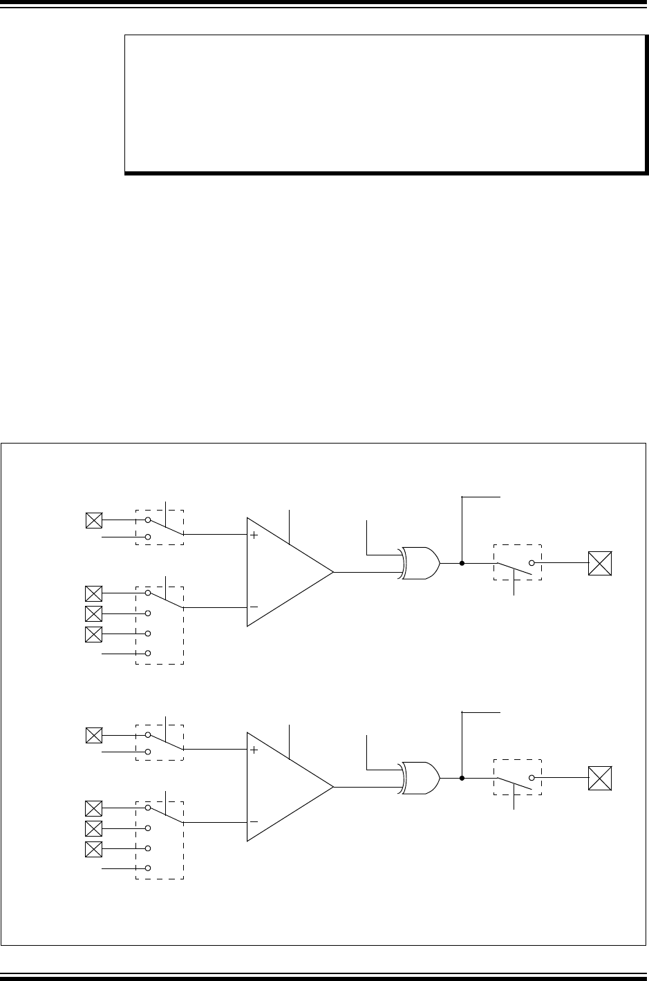
A block diagram of the comparator module is illustrated in Figure 19-1.
Figure 19-1: Comparator Block Diagram
Note: This family reference manual section is meant to serve as a complement to device
data sheets. Depending on the device variant, this manual section may not apply to
all PIC32MX devices.
Please consult the note at the beginning of the “Comparator” chapter in the current
device data sheet to check whether this document supports the device you are
using.
Device data sheets and family reference manual sections are available for
download from the Microchip Worldwide Web site at: http://www.microchip.com
C1
CVREF(2)
C1IN+(1)
C1IN+
C1IN-
C1OUT
COUT (CM1CON)
CREF
CCH<1:0>
CPOL
COE
ON
C2IN+
IVREF(2)
C1OUT (CMSTAT)
C2
CVREF(2)
C2IN+
C2IN+
C2IN-
C2OUT
COUT (CM2CON)
CREF
CPOL
COE
ON
C1IN+
IVREF(2)
C2OUT (CMSTAT)
Comparator 2
Comparator 1
CCH<1:0>
Note 1: On devices with a USB module, and when the module is enabled, this pin is controlled by the USB module,
and therefore, is not available as a comparator input.
2: Internally connected.
© 2010 Microchip Technology Inc. DS61110E-page 19-3
Section 19. Comparator
Comparator
19
19.2 COMPARATOR CONTROL REGISTERS
A Comparator module consists of the following Special Function Registers (SFRs):
•CMxCON: Comparator Control Register(1,2,3)
•CMSTAT: Comparator Status Register(1,2,3)
The following table provides a brief summary of all Comparator-related registers. Corresponding
registers appear after the summary, followed by a detailed description of each register.
Note: Each PIC32MX device variant may have one or more Comparator modules. An ‘x’
used in the names of pins, control/status bits and registers denotes the particular
module. Refer to the specific device data sheet for more information.
Table 19-1: Comparator SFRs Summary
Name Bit
31/23/15/7
Bit
30/22/14/6
Bit
29/21/13/5
Bit
28/20/12/4
Bit
27/19/11/3
Bit
26/18/10/2
Bit
25/17/9/1
Bit
24/16/8/0
CMxCON(1,2,3) 31:24 ————————
23:16 ————————
15:8 ON COE CPOL ————COUT
7:0 EVPOL<1:0> — CREF —— CCH<1:0>
CMSTAT(1,2,3) 31:24 ————————
23:16 ————————
15:8 — FRZ SIDL —————
7:0 —————— C2OUT C1OUT
Legend: — = unimplemented, read as ‘0’.
Note 1: This register has an associated Clear register at an offset of 0x4 bytes. These registers have the same name with CLR
appended to the end of the register name (e.g., CMxCONCLR). Writing a ‘1’ to any bit position in the Clear register will
clear valid bits in the associated register. Reads from the Clear register should be ignored.
2: This register has an associated Set register at an offset of 0x8 bytes. These registers have the same name with SET
appended to the end of the register name (e.g., CMxCONSET). Writing a ‘1’ to any bit position in the Set register will set
valid bits in the associated register. Reads from the Set register should be ignored.
3: This register has an associated Invert register at an offset of 0xC bytes. These registers have the same name with INV
appended to the end of the register name (e.g., CMxCONINV). Writing a ‘1’ to any bit position in the Invert register will
invert valid bits in the associated register. Reads from the Invert register should be ignored.

PIC32MX Family Reference Manual
DS61110E-page 19-4 © 2010 Microchip Technology Inc.
Register 19-1: CMxCON: Comparator Control Register(1,2,3)
U-0 U-0 U-0 U-0 U-0 U-0 U-0 U-0
— — — — — — — —
bit 31 bit 24
U-0 U-0 U-0 U-0 U-0 U-0 U-0 U-0
— — — — — — — —
bit 23 bit 16
R/W-0 R/W-0 R/W-0 U-0 U-0 U-0 U-0 R-0
ON COE CPOL — — — —COUT
bit 15 bit 8
R/W-1 R/W-1 U-0 R/W-0 U-0 U-0 R/W-1 R/W-1
EVPOL<1:0> —CREF—— CCH<1:0>
bit 7 bit 0
Legend:
R = Readable bit W = Writable bit P = Programmable bit r = Reserved bit
U = Unimplemented bit -n = Bit Value at POR: (‘0’, ‘1’, x = Unknown)
bit 31-16 Unimplemented: Read as ‘0’
bit 15 ON: Comparator ON bit
1 = Module is enabled. Setting this bit does not affect the other bits in this register
0 = Module is disabled and does not consume current. Clearing this bit does not affect the other bits
in this register
Note: When using the 1:1 PBCLK divisor, the user’s software should not read/write the
peripheral’s SFRs in the SYSCLK cycle immediately following the instruction that clears the
module’s ON bit.
bit 14 COE: Comparator Output Enable bit
1 = Comparator output is driven on the output CxOUT pin
0 = Comparator output is not driven on the output CxOUT pin
bit 13 CPOL: Comparator Output Inversion bit
1 = Output is inverted
0 = Output is not inverted
Note: Setting this bit will invert the signal to the comparator interrupt generator as well. This will
result in an interrupt being generated on the opposite edge from the one selected by
EVPOL<1:0>.
bit 12-9 Unimplemented: Read as ‘0’
Note 1: This register has an associated Clear register (CMxCONCLR) at an offset of 0x4 bytes. Writing a ‘1’ to any
bit position in the Clear register will clear valid bits in the associated register. Reads from the Clear register
should be ignored.
2: This register has an associated Set register (CMxCONSET) at an offset of 0x8 bytes. Writing a ‘1’ to any
bit position in the Set register will set valid bits in the associated register. Reads from the Set register
should be ignored.
3: This register has an associated Invert register (CMxCONINV) at an offset of 0xC bytes. Writing a ‘1’ to any
bit position in the Invert register will invert valid bits in the associated register. Reads from the Invert
register should be ignored.
4: For x=1/y=2 or x=2/y=1.

© 2010 Microchip Technology Inc. DS61110E-page 19-5
Section 19. Comparator
Comparator
19
bit 8 COUT: Comparator Output bit
1 = Output of the Comparator is a ‘1’
0 = Output of the Comparator is a ‘0’
bit 7-6 EVPOL<1:0>: Interrupt Event Polarity Select bits
11 = Comparator interrupt is generated on a low-to-high or high-to-low transition of the comparator
output
10 = Comparator interrupt is generated on a high-to-low transition of the comparator output
01 = Comparator interrupt is generated on a low-to-high transition of the comparator output
00 = Comparator interrupt generation is disabled
bit 5 Unimplemented: Read as ‘0’
bit 4 CREF: Comparator Positive Input Configure bit
1 = Comparator non-inverting input is connected to the internal CVREF
0 = Comparator non-inverting input is connected to the CXIN+ pin
bit 3-2 Unimplemented: Read as ‘0’
bit 1-0 CCH<1:0>: Comparator Negative Input Select bits for Comparator
11 = Comparator inverting input is connected to the IVREF
10 = Comparator inverting input is connected to the CyIN+ pin(4)
01 = Comparator inverting input is connected to the CxIN+ pin(4)
00 = Comparator inverting input is connected to the CxIN- pin(4)
Register 19-1: CMxCON: Comparator Control Register(1,2,3) (Continued)
Note 1: This register has an associated Clear register (CMxCONCLR) at an offset of 0x4 bytes. Writing a ‘1’ to any
bit position in the Clear register will clear valid bits in the associated register. Reads from the Clear register
should be ignored.
2: This register has an associated Set register (CMxCONSET) at an offset of 0x8 bytes. Writing a ‘1’ to any
bit position in the Set register will set valid bits in the associated register. Reads from the Set register
should be ignored.
3: This register has an associated Invert register (CMxCONINV) at an offset of 0xC bytes. Writing a ‘1’ to any
bit position in the Invert register will invert valid bits in the associated register. Reads from the Invert
register should be ignored.
4: For x=1/y=2 or x=2/y=1.

PIC32MX Family Reference Manual
DS61110E-page 19-6 © 2010 Microchip Technology Inc.
Register 19-2: CMSTAT: Comparator Status Register(1,2,3)
U-0 U-0 U-0 U-0 U-0 U-0 U-0 U-0
— — — — — — — —
bit 31 bit 24
U-0 U-0 U-0 U-0 U-0 U-0 U-0 U-0
— — — — — — — —
bit 23 bit 16
U-0 R/W-0 R/W-0 U-0 U-0 U-0 U-0 U-0
— FRZ SIDL — — — — —
bit 15 bit 8
U-0 U-0 U-0 U-0 U-0 U-0 R-0 R-0
— — — — — — C2OUT C1OUT
bit 7 bit 0
Legend:
R = Readable bit W = Writable bit P = Programmable bit r = Reserved bit
U = Unimplemented bit -n = Bit Value at POR: (‘0’, ‘1’, x = Unknown)
bit 31-15 Unimplemented: Read as ‘0’
bit 14 FRZ: Freeze Control bit
1 = Freeze operation when CPU enters Debug Exception mode
0 = Continue operation when CPU enters Debug Exception mode
Note: FRZ is writable in Debug Exception mode only. It always reads ‘0’ in Normal mode.
bit 13 SIDL: Stop in IDLE Control bit
1 = All Comparator modules are disabled in IDLE mode
0 = All Comparator modules continue to operate in the IDLE mode
bit 12-2 Unimplemented: Read as ‘0’
bit 1 C2OUT: Comparator Output bit
1 = Output of Comparator 2 is a ‘1’
0 = Output of Comparator 2 is a ‘0’
bit 0 C1OUT: Comparator Output bit
1 = Output of Comparator 1 is a ‘1’
0 = Output of Comparator 1 is a ‘0’
Note 1: This register has an associated Clear register (CMSTATCLR) at an offset of 0x4 bytes. Writing a ‘1’ to any
bit position in the Clear register will clear valid bits in the associated register. Reads from the Clear register
should be ignored.
2: This register has an associated Set register (CMSTATSET) at an offset of 0x8 bytes. Writing a ‘1’ to any bit
position in the Set register will set valid bits in the associated register. Reads from the Set register should
be ignored.
3: This register has an associated Invert register (CMSTATINV) at an offset of 0xC bytes. Writing a ‘1’ to any
bit position in the Invert register will invert valid bits in the associated register. Reads from the Invert
register should be ignored.
© 2010 Microchip Technology Inc. DS61110E-page 19-7
Section 19. Comparator
Comparator
19
19.3 COMPARATOR OPERATION
19.3.1 Comparator Configuration
The Comparator module has a flexible input and output configuration to allow the module to be
tailored to the needs of the application. The PIC32MX family Comparator module has individual
control over the enable, output inversion, output on I/O pin and input selections. The VIN+ pin of
each comparator can select from an input pin or the CVREF. The VIN- input of the Comparator
module can select from one of three input pins or the IVREF. In addition, the Comparator module
has two individual comparator event generation control bits. These control bits can be used for
detecting when the output of an individual comparator changes to a desired state or changes
states.
If the comparator mode is changed, the comparator output level may not be valid for the specified
mode change delay (refer to the specific device data sheet for more information).
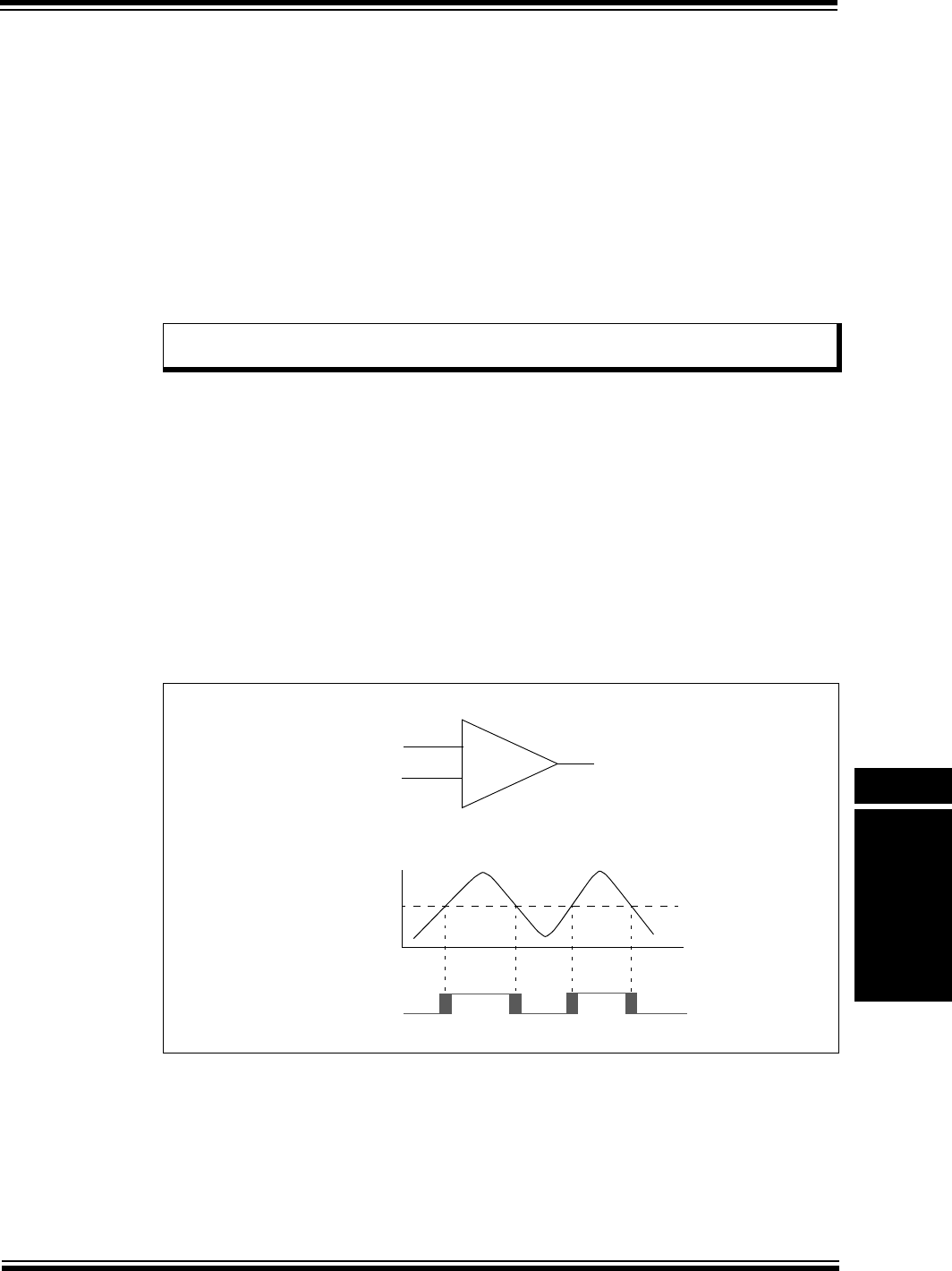
A single comparator is illustrated in the upper portion of Figure 19-2. The lower portion repre-
sents the relationship between the analog input levels and the digital output. When the analog
input at VIN+ is less than the analog input at VIN-, the output of the comparator is a digital low
level. When the analog input at VIN+ is greater than the analog input VIN-, the output of the com-
parator is a digital high level. The shaded areas of the output of the comparator in the lower por-
tion of Figure 19-2 illustrates the uncertainty that is due to input offsets and the response time of
the comparator.
19.3.2 Comparator Inputs
Depending on the comparator operating mode, the inputs to the comparators may be from two
input pins or a combination of an input pin and one of two internal voltage references. The analog
signal present at VIN- is compared to the signal at VIN+ and the digital output of the comparator
is set or cleared according to the result of the comparison, as illustrated in Figure 19-2.
Figure 19-2: Single Comparator
19.3.2.1 EXTERNAL REFERENCE SIGNAL
An external voltage reference may be used with the comparator by using the output of the reference
as an input to the comparator. Refer to the specific device data sheet for input voltage limits.
Note: Comparator interrupts should be disabled during a comparator mode change;
otherwise, a false interrupt may be generated.
–
+
VIN+
VIN-
Output
Output
VIN-
VIN+

PIC32MX Family Reference Manual
DS61110E-page 19-8 © 2010 Microchip Technology Inc.
19.3.2.2 INTERNAL REFERENCE SIGNALS
The CVREF module and the IVREF can be used as inputs to the comparator, as illustrated in
Figure 19-1. The CVREF provides a user-selectable voltage for use as a comparator reference.
For more information on this module, refer to Section 20. “Comparator Voltage Reference”
(DS61109) in the “PIC32MX Family Reference Manual”. The IVREF has a fixed 1.2V output that
does not change with the device supply voltage. Refer to the specific device data sheet for details
and accuracy of this reference.
19.3.3 Comparator Response Time
Response time is the minimum amount of time that elapses from the moment a change is made
in the input voltage of a comparator to the moment the output reflects the new level. If the internal
reference is changed, the maximum delay of the internal voltage reference must be considered,
when using the comparator outputs. Otherwise, the maximum delay of the comparators should
be used. For more information, refer to the specific device data sheet.
19.3.4 Comparator Outputs
The comparator output is read through the CMSTAT register and the COUT bit (CM2CON<8> or
CM1CON<8>). This bit is read-only. The comparator output may also be directed to an I/O pin
via the CxOUT bit; however, the COUT bit is still valid when the signal is routed to a pin. For the
comparator output to be available on the CxOUT pin, the associated TRIS bit for the output pin
must be configured as an output. When the COUT signal is routed to a pin the signal is the
unsynchronized output of the comparator.
The output of the comparator has a degree of uncertainty. The uncertainty of each of the
comparators is related to the input offset voltage and the response time, as stated in the
specifications. The lower portion of Figure 19-2 provides a graphical representation of this
uncertainty.
The comparator output bit, COUT, provides the latched sampled value of the comparator’s output
when the register was read. There are two common methods used to detect a change in the
comparator output:
• Software polling
• Interrupt generation
19.3.4.1 SOFTWARE POLLING METHOD OF COMPARATOR EVENT
DETECTION
Software polling of COUT is performed by periodically reading the COUT bit. This allows the
output to be read at uniform time intervals. A change in the comparator output is not detected
until the next read of the COUT bit. If the input signal changes at a rate faster than the polling, a
brief change in output may not be detected.
19.3.4.2 INTERRUPT GENERATION METHOD OF COMPARATOR EVENT
DETECTION
Interrupt generation is the other method for detecting a change in the comparator output. The
Comparator module can be configured to generate an interrupt when the COUT bit changes.
An interrupt will be generated when the comparator’s output changes (subject to the interrupt
priorities). This method responds more rapidly to changes than the software polling method;
however, rapidly changing signals will cause an equally large number of interrupts. This can
cause interrupt loading and potentially undetected interrupts due to new interrupts being
generated while the previous interrupt is still being serviced or even before the interrupt can be
serviced. If the input signal changes rapidly, reading the COUT bit in the Interrupt Service
Routine (ISR) may yield a different result than the one that generated the Interrupt. This is due
to the COUT bit representing the value of the comparator output when the bit was read and not
the value that caused the interrupt.
Comparator output and interrupt generation is illustrated in Figure 19-4.
© 2010 Microchip Technology Inc. DS61110E-page 19-9
Section 19. Comparator
Comparator
19
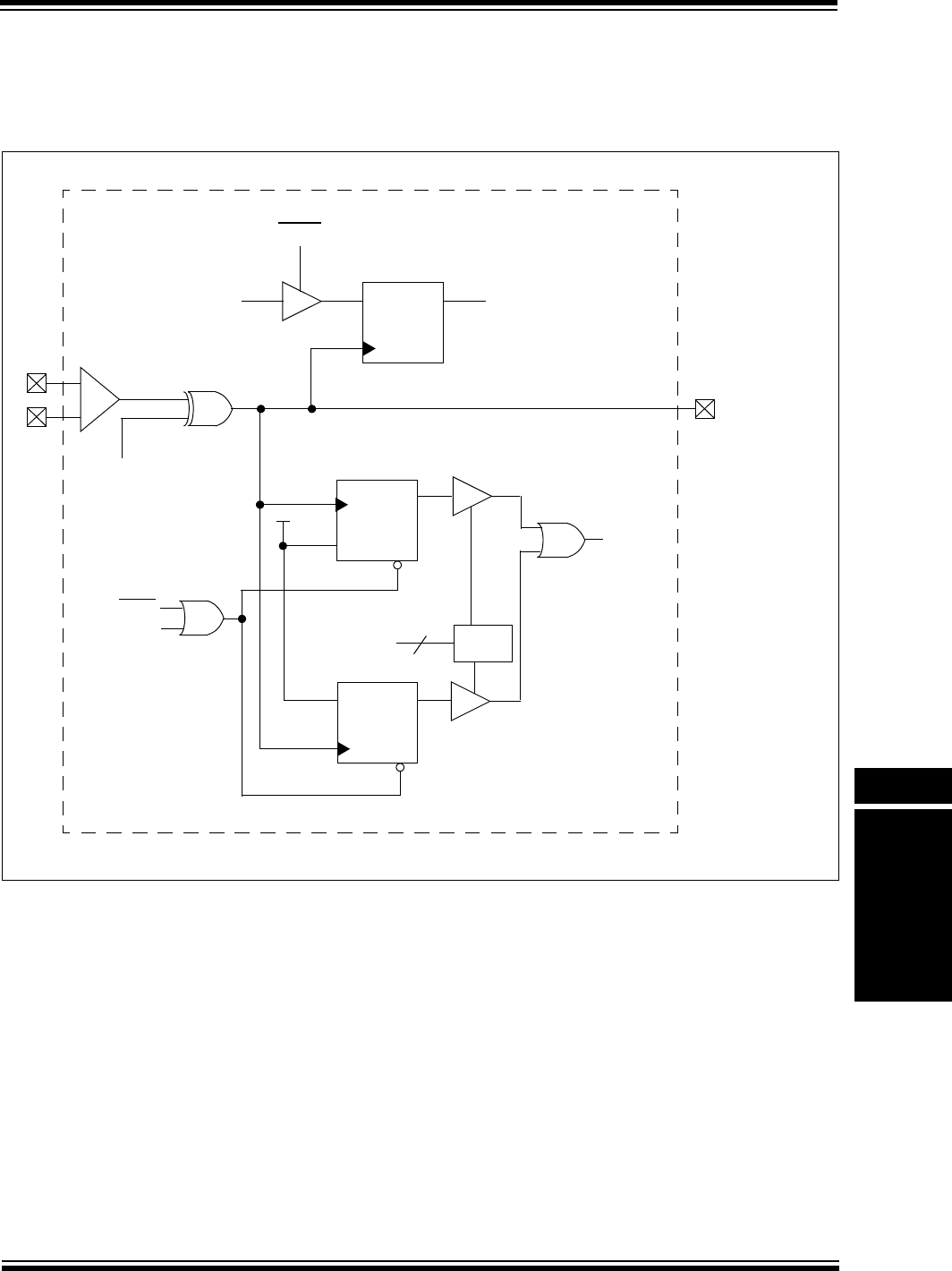
19.3.4.3 CHANGING THE POLARITY OF COMPARATOR OUTPUTS
The polarity of the comparator outputs can be changed using the CPOL bit (CMxCON<13>).
CPOL appears below the comparator Cx on the left side of Figure 19-3.
Figure 19-3: Comparator Output Block Diagram
D
Q
CL
To Cx O U T pin
To Interrupt
CPOL
DQ
CL CL
–
+
D
Q
CL
Freeze
PBCLK CxOUT (CMSTAT)
COUT (CMxCON)
EVPOL
2
Decoder
Reset
Interrupt ACK
CL
C
X
Controller
PIC32MX Family Reference Manual
DS61110E-page 19-10 © 2010 Microchip Technology Inc.
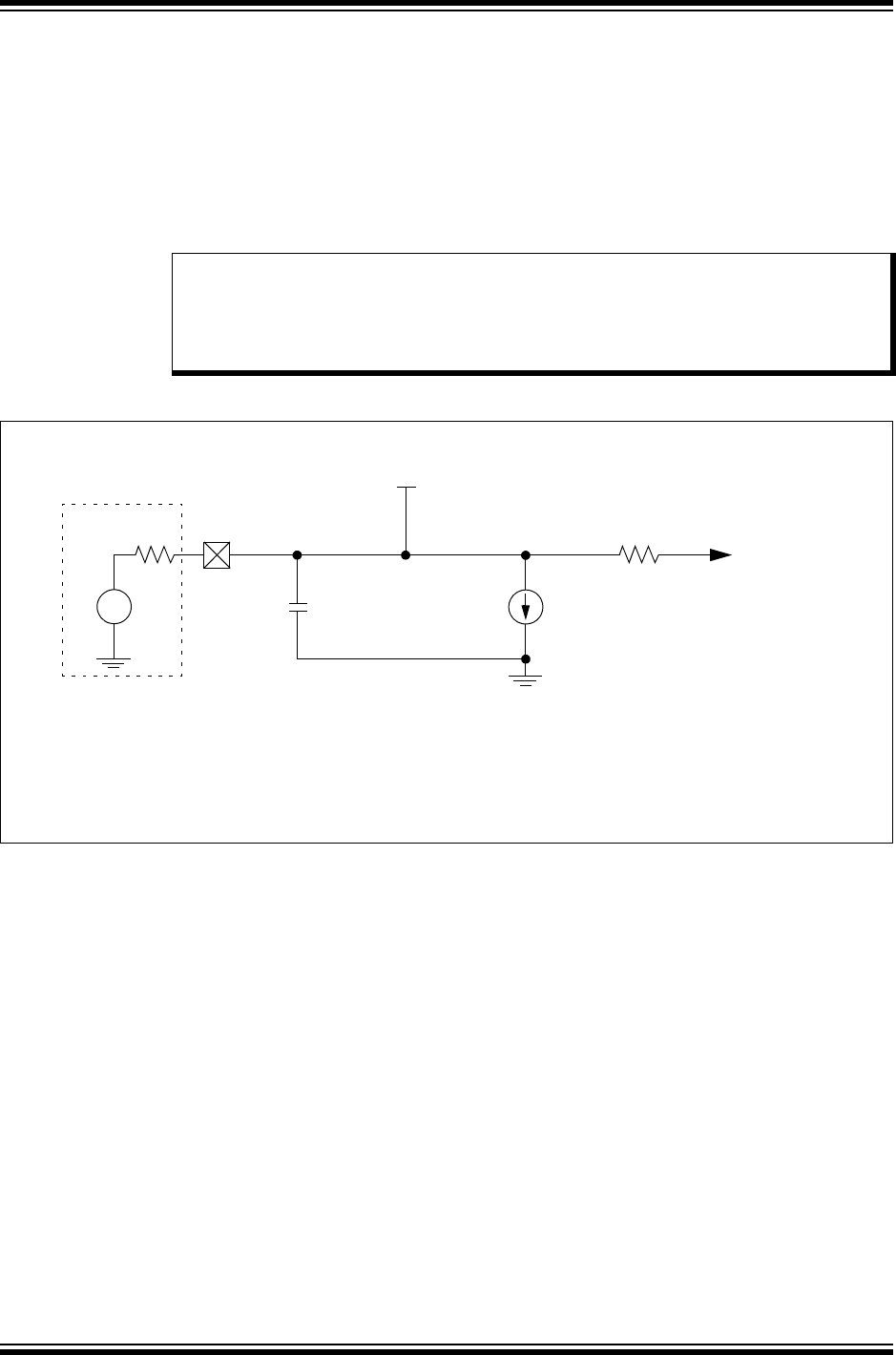
19.3.5 Analog Input Connection Considerations
A simplified circuit for an analog input is illustrated in Figure 19-4. A maximum source imped-
ance of 10 kΩ is recommended for the analog sources. Any external component connected to
an analog input pin, such as a capacitor or a Zener diode, should have very little leakage cur-
rent. Refer to the specific device data sheet for input voltage limits. If a pin is to be shared by
two or more analog inputs that are to be used simultaneously, the loading effects of all the mod-
ules involved must be taken into consideration. This loading may reduce the accuracy of one
or more of the modules connected to the common pin. This may also require a lower source
impedance than is stated for a single module with exclusive use of a pin in Analog mode.
Figure 19-4: Comparator Analog Input Model
Note: When reading the PORT register, all pins configured as analog inputs will read as a
‘0’. Pins configured as digital inputs will convert an analog input according to the
Schmitt Trigger input specification.
Analog levels on any pin defined as a digital input may cause the input buffer to
consume more current than is specified.
VA
RS < 10k
AIN
CPIN
5 pF
VDD
RIC
ILEAKAGE
±500 nA
VSS
Comparator
Input
Legend: CPIN = Input Capacitance
ILEAKAGE = Leakage Current at the pin due to various junctions
RIC = Interconnect Resistance
RS = Source Impedance
VA = Analog Voltage

© 2010 Microchip Technology Inc. DS61110E-page 19-11
Section 19. Comparator
Comparator
19
19.4 INTERRUPTS
Each of the available comparators has a dedicated interrupt bit, CMPxIF (IFS1<3> or IFS1<4>),
and a corresponding interrupt enable/mask bit, CMPxIE (IEC1<3> or IEC1<4>). These bits are
used to determine the source of an interrupt and to enable or disable an individual interrupt
source. The priority level of each of the channels can also be set independently of the other
channels.
The CMPxIF bit is set when the CMPx channel detects a predefined match condition that is
defined as an event generating an interrupt. The CMPxIF bit will then be set without regard to the
state of the corresponding CMPxIE bit. The CMPxIF bit can be polled by software if desired.
The CMPxIE bit controls the interrupt generation. If the CMPxIE bit is set, the CPU will be
interrupted whenever a comparator interrupt event occurs and the corresponding CMPxIF bit will
be set (subject to the priority and subpriority as outlined below).
It is the responsibility of the user’s software routine that services a particular interrupt, to clear
the appropriate interrupt flag bit before the service routine is complete.
The priority of each comparator channel can be set independently through the CMPxIP<2:0>
bits. This priority defines the priority group to which the interrupt source will be assigned. The
priority groups range from a value of 7 (the highest priority), to a value of 0 (which does not
generate an interrupt). An interrupt being serviced will be preempted by an interrupt in a higher
priority group.
The subpriority bits allow setting the priority of an interrupt source within a priority group. The
values of the subpriority bit OCxIS<1:0> range from 3 (the highest priority), to 0 (the lowest
priority). An interrupt within the same priority group but having a higher subpriority value will
preempt a lower subpriority interrupt that is in progress.
The priority group and subpriority bits allow more than one interrupt source to share the same
priority and subpriority. If simultaneous interrupts occur in this configuration, the natural order of
the interrupt sources within a priority/subgroup pair determine the interrupt generated. The
natural priority is based on the vector numbers of the interrupt sources. The lower the vector
number, the higher the natural priority of the interrupt. Any interrupts that were overridden by
natural order will then generate their respective interrupts based on priority, subpriority, and
natural order, after the interrupt flag for the current interrupt is cleared.
After an enabled interrupt is generated, the CPU will jump to the vector assigned to that interrupt.
The vector number for the interrupt is the same as the natural order number. The CPU will then
begin executing code at the vector address. The user’s code at this vector address should per-
form any application-specific operations required, such as reloading the duty cycle, clear the
interrupt flag CMPxIF, and then exit. For more information on interrupts, refer to the vector
address table details in Section 8. “Interrupts” (DS61108).

PIC32MX Family Reference Manual
DS61110E-page 19-12 © 2010 Microchip Technology Inc.
Example 19-1: Comparator Initialization with Interrupts Enabled Code Example
Example 19-2: Comparator ISR Code Example
// Configure both comparators to generate an interrupt on any
// output transition
CM1CON = 0xC0D0; // Initialize Comparator 1
// Comparator enabled, output enabled, interrupt on any output
// change, inputs: CVref, C1IN-
CM2CON = 0xA0C2; // Initialize Comparator 2
// Comparator enabled, output enabled, interrupt on any output
// change, inputs: C2IN+, C1IN+
// Enable interrupts for Comparator modules and set priorities
// Set priority to 7 and subpriority to 3
IPC7SET = 0x00000700; // Set CMP1 interrupt subpriority
IFS1CLR = 0x00000008; // Clear the CMP1 interrupt flag
IEC1SET = 0x00000008; // Enable CMP1 interrupt
IPC7SET = 0x00070000; // Set CMP2 interrupt sub priority
IFS1CLR = 0x000000010; // Clear the CMP2 interrupt flag
IEC1SET = 0x000000010; // Enable CMP2 interrupt
// Insert user code here
void__ISR(_COMPARATOR_2_VECTOR, ipl4)Cmp2_IntHandler(void)
{
// Insert user code here
IFS1CLR = 0x00000010; // Clear the CMP2 interrupt flag
}
void__ISR(_COMPARATOR_1_VECTOR, ipl4)Cmp1_IntHandler(void)
{
// Insert code user here
IFS1CLR = 0x00000008; // Clear the CMP1 interrupt flag
}

© 2010 Microchip Technology Inc. DS61110E-page 19-13
Section 19. Comparator
Comparator
19
19.5 OPERATION IN POWER-SAVING AND DEBUG MODES
19.5.1 Comparator Operation During Idle Mode
When a comparator is active and the device is placed in Idle mode, the comparator remains
active and interrupts are generated (if enabled); if SIDL = 1 (CMSTAT<13>), the comparators are
disabled in Idle mode.
19.5.2 Comparator Operation During Sleep Mode
When a comparator is active and the device is placed in Sleep mode, the comparator remains
active and the interrupt is functional (if enabled). This interrupt will wake up the device from Sleep
mode (when enabled). Each operational comparator will consume additional current, as shown
in the comparator specifications. To minimize power consumption while in Sleep mode, turn off
the comparators: ON = 0 (CMxCON<15>), prior to entering Sleep mode. If the device wakes up
from Sleep mode, the contents of the CMxCON register are not affected. For additional
information on Sleep mode, refer to Section 10. “Power-Saving Modes” (DS61130).
19.5.3 Comparator Operation in Debug Mode
The FRZ bit (CMSTAT<14>) determines whether the Comparator module will run or stop while
the CPU is executing debug exception code (i.e., application is halted) in Debug mode. When
FRZ = 0, the Comparator module continues to run even when application is halted in Debug
mode. When FRZ = 1 and application is halted in Debug mode, the module will freeze its
operations and make no changes to the state of the Comparator module. The module will resume
its operation after the CPU resumes execution.
19.6 EFFECTS OF A RESET
All Resets force the CMxCON registers to its Reset state, causing the comparator modules to be
turned off (CMxCON<15> = 0). However, the input pins multiplexed with analog input sources
are configured as analog inputs by default on device Reset. The I/O configuration for these pins
is determined by the setting the AD1PCFG register.
Note: The FRZ bit is readable and writable only when the CPU is executing in Debug
Exception mode. In all other modes, the FRZ bit reads as ‘0’. If the FRZ bit is
changed during Debug mode, the new value does not take effect until the current
Debug Exception mode is exited and re-entered. During the Debug Exception
mode, the FRZ bit reads the state of the peripheral when entering Debug mode.

PIC32MX Family Reference Manual
DS61110E-page 19-14 © 2010 Microchip Technology Inc.
19.7 RELATED APPLICATION NOTES
This section lists application notes that are related to this section of the manual. These
application notes may not be written specifically for the PIC32MX device family, but the concepts
are pertinent and could be used with modification and possible limitations. The current
application notes related to the Comparator module are:
Title Application Note #
No related application notes at this time N/A
Note: Please visit the Microchip web site (www.microchip.com) for additional application
notes and code examples for the PIC32MX family of devices.

© 2010 Microchip Technology Inc. DS61110E-page 19-15
Section 19. Comparator
Comparator
19
19.8 REVISION HISTORY
Revision A (October 2007)
This is the initial released version of this document.
Revision B (October 2007)
Updated document to remove Confidential status.
Revision C (April 2008)
Revised status to Preliminary; Revised U-0 to r-x.
Revision D (May 2008)
Revised Figure 19-1; Revised Registers 19-1, 19-5, 19-13, 19-14, 19-15; Revised Example 19-2;
Revised Section 19.5, pin names; Change Reserved bits from “Maintain as” to “Write”; Added
Note to ON bit (CM1CON/CM2CON Registers).
Revision E (November 2010)
This revision includes the following updates:
• Notes:
- Added a note at the beginning of the section, which provides information on
complementary documentation.
• Updated all Reserved bits as Unimplemented bits in Register 19-1 and Register 19-2.
• Changed Figure 19-1.
• Removed CMxCON and CMSTAT registers along with their corresponding CLR, SET and
INV registers and added the following Note in Table 19-1
- All registers in this table have corresponding CLR, SET and INV registers at their
virtual addresses, plus offset of 0X04, 0X08 and 0X0C respectively.
• Removed IFS1, IEC1, IPC1 registers and their corresponding CLR, SET and INV registers.
• Removed Table 19-2 from 19.4 “Interrupts”.
• Removed section 19.5 “I/O Pin Control”.
• Minor changes to the text and formatting have been incorporated throughout the document.

PIC32MX Family Reference Manual
DS61110E-page 19-16 © 2010 Microchip Technology Inc.
NOTES:

© 2010 Microchip Technology Inc. DS61110E-page 19-17
Information contained in this publication regarding device
applications and the like is provided only for your convenience
and may be superseded by updates. It is your responsibility to
ensure that your application meets with your specifications.
MICROCHIP MAKES NO REPRESENTATIONS OR
WARRANTIES OF ANY KIND WHETHER EXPRESS OR
IMPLIED, WRITTEN OR ORAL, STATUTORY OR
OTHERWISE, RELATED TO THE INFORMATION,
INCLUDING BUT NOT LIMITED TO ITS CONDITION,
QUALITY, PERFORMANCE, MERCHANTABILITY OR
FITNESS FOR PURPOSE. Microchip disclaims all liability
arising from this information and its use. Use of Microchip
devices in life support and/or safety applications is entirely at
the buyer’s risk, and the buyer agrees to defend, indemnify and
hold harmless Microchip from any and all damages, claims,
suits, or expenses resulting from such use. No licenses are
conveyed, implicitly or otherwise, under any Microchip
intellectual property rights.
Trademarks
The Microchip name and logo, the Microchip logo, dsPIC,
KEELOQ, KEELOQ logo, MPLAB, PIC, PICmicro, PICSTART,
PIC32 logo, rfPIC and UNI/O are registered trademarks of
Microchip Technology Incorporated in the U.S.A. and other
countries.
FilterLab, Hampshire, HI-TECH C, Linear Active Thermistor,
MXDEV, MXLAB, SEEVAL and The Embedded Control
Solutions Company are registered trademarks of Microchip
Technology Incorporated in the U.S.A.
Analog-for-the-Digital Age, Application Maestro, CodeGuard,
dsPICDEM, dsPICDEM.net, dsPICworks, dsSPEAK, ECAN,
ECONOMONITOR, FanSense, HI-TIDE, In-Circuit Serial
Programming, ICSP, Mindi, MiWi, MPASM, MPLAB Certified
logo, MPLIB, MPLINK, mTouch, Omniscient Code
Generation, PICC, PICC-18, PICDEM, PICDEM.net, PICkit,
PICtail, REAL ICE, rfLAB, Select Mode, Total Endurance,
TSHARC, UniWinDriver, WiperLock and ZENA are
trademarks of Microchip Technology Incorporated in the
U.S.A. and other countries.
SQTP is a service mark of Microchip Technology Incorporated
in the U.S.A.
All other trademarks mentioned herein are property of their
respective companies.
© 2010, Microchip Technology Incorporated, Printed in the
U.S.A., All Rights Reserved.
Printed on recycled paper.
ISBN: 978-1-60932-654-8
Note the following details of the code protection feature on Microchip devices:
• Microchip products meet the specification contained in their particular Microchip Data Sheet.
• Microchip believes that its family of products is one of the most secure families of its kind on the market today, when used in the
intended manner and under normal conditions.
• There are dishonest and possibly illegal methods used to breach the code protection feature. All of these methods, to our
knowledge, require using the Microchip products in a manner outside the operating specifications contained in Microchip’s Data
Sheets. Most likely, the person doing so is engaged in theft of intellectual property.
• Microchip is willing to work with the customer who is concerned about the integrity of their code.
• Neither Microchip nor any other semiconductor manufacturer can guarantee the security of their code. Code protection does not
mean that we are guaranteeing the product as “unbreakable.”
Code protection is constantly evolving. We at Microchip are committed to continuously improving the code protection features of our
products. Attempts to break Microchip’s code protection feature may be a violation of the Digital Millennium Copyright Act. If such acts
allow unauthorized access to your software or other copyrighted work, you may have a right to sue for relief under that Act.
Microchip received ISO/TS-16949:2002 certification for its worldwide
headquarters, design and wafer fabrication facilities in Chandler and
Tempe, Arizona; Gresham, Oregon and design centers in California
and India. The Company’s quality system processes and procedures
are for its PIC® MCUs and dsPIC® DSCs, KEELOQ® code hopping
devices, Serial EEPROMs, microperipherals, nonvolatile memory and
analog products. In addition, Microchip’s quality system for the design
and manufacture of development systems is ISO 9001:2000 certified.

DS61110E-page 19-18 © 2010 Microchip Technology Inc.
AMERICAS
Corporate Office
2355 West Chandler Blvd.
Chandler, AZ 85224-6199
Tel: 480-792-7200
Fax: 480-792-7277
Technical Support:
http://support.microchip.com
Web Address:
www.microchip.com
Atlanta
Duluth, GA
Tel: 678-957-9614
Fax: 678-957-1455
Boston
Westborough, MA
Tel: 774-760-0087
Fax: 774-760-0088
Chicago
Itasca, IL
Tel: 630-285-0071
Fax: 630-285-0075
Cleveland
Independence, OH
Tel: 216-447-0464
Fax: 216-447-0643
Dallas
Addison, TX
Tel: 972-818-7423
Fax: 972-818-2924
Detroit
Farmington Hills, MI
Tel: 248-538-2250
Fax: 248-538-2260
Kokomo
Kokomo, IN
Tel: 765-864-8360
Fax: 765-864-8387
Los Angeles
Mission Viejo, CA
Tel: 949-462-9523
Fax: 949-462-9608
Santa Clara
Santa Clara, CA
Tel: 408-961-6444
Fax: 408-961-6445
Toronto
Mississauga, Ontario,
Canada
Tel: 905-673-0699
Fax: 905-673-6509
ASIA/PACIFIC
Asia Pacific Office
Suites 3707-14, 37th Floor
Tower 6, The Gateway
Harbour City, Kowloon
Hong Kong
Tel: 852-2401-1200
Fax: 852-2401-3431
Australia - Sydney
Tel: 61-2-9868-6733
Fax: 61-2-9868-6755
China - Beijing
Tel: 86-10-8528-2100
Fax: 86-10-8528-2104
China - Chengdu
Tel: 86-28-8665-5511
Fax: 86-28-8665-7889
China - Chongqing
Tel: 86-23-8980-9588
Fax: 86-23-8980-9500
China - Hong Kong SAR
Tel: 852-2401-1200
Fax: 852-2401-3431
China - Nanjing
Tel: 86-25-8473-2460
Fax: 86-25-8473-2470
China - Qingdao
Tel: 86-532-8502-7355
Fax: 86-532-8502-7205
China - Shanghai
Tel: 86-21-5407-5533
Fax: 86-21-5407-5066
China - Shenyang
Tel: 86-24-2334-2829
Fax: 86-24-2334-2393
China - Shenzhen
Tel: 86-755-8203-2660
Fax: 86-755-8203-1760
China - Wuhan
Tel: 86-27-5980-5300
Fax: 86-27-5980-5118
China - Xian
Tel: 86-29-8833-7252
Fax: 86-29-8833-7256
China - Xiamen
Tel: 86-592-2388138
Fax: 86-592-2388130
China - Zhuhai
Tel: 86-756-3210040
Fax: 86-756-3210049
ASIA/PACIFIC
India - Bangalore
Tel: 91-80-3090-4444
Fax: 91-80-3090-4123
India - New Delhi
Tel: 91-11-4160-8631
Fax: 91-11-4160-8632
India - Pune
Tel: 91-20-2566-1512
Fax: 91-20-2566-1513
Japan - Yokohama
Tel: 81-45-471- 6166
Fax: 81-45-471-6122
Korea - Daegu
Tel: 82-53-744-4301
Fax: 82-53-744-4302
Korea - Seoul
Tel: 82-2-554-7200
Fax: 82-2-558-5932 or
82-2-558-5934
Malaysia - Kuala Lumpur
Tel: 60-3-6201-9857
Fax: 60-3-6201-9859
Malaysia - Penang
Tel: 60-4-227-8870
Fax: 60-4-227-4068
Philippines - Manila
Tel: 63-2-634-9065
Fax: 63-2-634-9069
Singapore
Tel: 65-6334-8870
Fax: 65-6334-8850
Taiwan - Hsin Chu
Tel: 886-3-6578-300
Fax: 886-3-6578-370
Taiwan - Kaohsiung
Tel: 886-7-213-7830
Fax: 886-7-330-9305
Taiwan - Taipei
Tel: 886-2-2500-6610
Fax: 886-2-2508-0102
Thailand - Bangkok
Tel: 66-2-694-1351
Fax: 66-2-694-1350
EUROPE
Austria - Wels
Tel: 43-7242-2244-39
Fax: 43-7242-2244-393
Denmark - Copenhagen
Tel: 45-4450-2828
Fax: 45-4485-2829
France - Paris
Tel: 33-1-69-53-63-20
Fax: 33-1-69-30-90-79
Germany - Munich
Tel: 49-89-627-144-0
Fax: 49-89-627-144-44
Italy - Milan
Tel: 39-0331-742611
Fax: 39-0331-466781
Netherlands - Drunen
Tel: 31-416-690399
Fax: 31-416-690340
Spain - Madrid
Tel: 34-91-708-08-90
Fax: 34-91-708-08-91
UK - Wokingham
Tel: 44-118-921-5869
Fax: 44-118-921-5820
Worldwide Sales and Service
08/04/10
