PS 10
User Manual: PS-10
Open the PDF directly: View PDF ![]() .
.
Page Count: 12
SILICON
GENERAL
APPLICATION NOTES -SG1525A/SG1526/SG1527A
LINEAR
INTEGRATEO
CIRCUITS
PS-IO
POWER SUPPLY CIRCUITS HEAD
FOR
SIMPLICITY
BY
INTEGRATION
Stan Dendinger
Manager, Advanced Product Development
Silicon General, Inc.
SUMMARY
The benefits obtained from switching power supplies have be-
come universally recognized by power systems engineers in the
past several years. However, there has been a simultaneous
realization that, too frequently, gains
in
efficiency and reductions
in weight have been accompanied by an escalating component
count and a decrease in reliability and predictability of perform-
ance. To effectively solve these problems, integrated circuit
manufacturers have recently designed new products specifically
for switchers. These devices offer the proven advantages of
monolithic technology: compactness, accuracy, reproducibility,
higher performance through reduction of parasitics, and the
economies
of
mass production.
This paper reviews the circuit simplifications made possible by
these specialized devices, as typified by the first practical switch-
ing regulator control chip, the SG1524 Pulse Width Modulator,
and later by other circuits such as the
ZN1
066, the TL494A, and
the
MC3420. A second potential area of power supply simplifica-
tion is the interface between the control circuit and the high power
switching transistors. Two specialized driver circuits, the SG1627
and the SG1629 are described which provide high-level turn-on
and turn-off signals for efficient switching. Finally, some second
and third generation pulse width modulator designs will be dis-
cussed. These later devices, designated the SG1525/27 series
and the SG 1526, offer even higher levels of control function
integration compared to earlier designs. The SG1526 in particular
integrates a number of protective control features which substan-
tially increase the reliability
of
the power semiconductors in "real
world" switching power supplies.
HISTORICAL PERSPECTIVE
A basic pulse width modulated switching power supply requires
only four control elements: a precision reference voltage, a ramp
oscillator, an error
amplifier, and a differential voltage comparator.
January 1990
Each of these elements has been available in integrated circuit
form for years, with the well-established benefits
of
reduced
physical size, greater reliability, and increased performance. In
light
of
this background, the development
of
a single monolithic
circuit for switching power supply control appears to be a logical
progression.
One
of
the first devices available to power supply designers was
the SG1524 Pulse Width Modulator from Silicon General. This
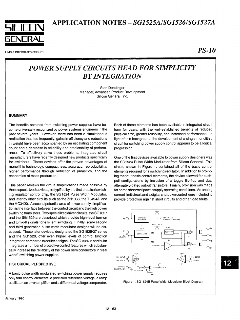
circuit, shown in Figure
1,
contained all of the basic control
elements required for a switching regulator.
In
addition to provid-
ing the four basic control elements, the device allowed for push-
pull configurations by inclusion
of
a toggle flip-flop and dual
alternately-gated output transistors. Finally, provision was made
for some abnormal power
supply operating conditions. An analog
current limit circuit and a digital shutdown control were included to
provide protection against short circuits and other load faults.
+5VTOALL
INTERNAL
CIRCUITRY
Figure
1.
SG1524B Pulse Width Modulator Block Diagram
"
12-63
..
APPLICATION NOTES -SG1525A/SG1526/SG1527A
Despite this level of complexity, the device was easy to under-
stand and was quite flexible. As a result, since its introduction in
1976, the SG1524 has been very widely accepted within the
power supply industry, finding its way into a majority of new
designs, including exotic applications in communications satel-
lites and the space shuttle program.
POWER DRIVER INTEGRATION -SG1627
As experience was gained in applying the SG1524, it became
apparent that there was a gap between output power capabilities
of the control integrated circuit and the drive levels required by the
power semiconductors.
Two
areas were identified within most
supply configurations where specialized driver functions could be
successfully implemented with monolithic technology.
An
Integrated
Source/Sink
Driver
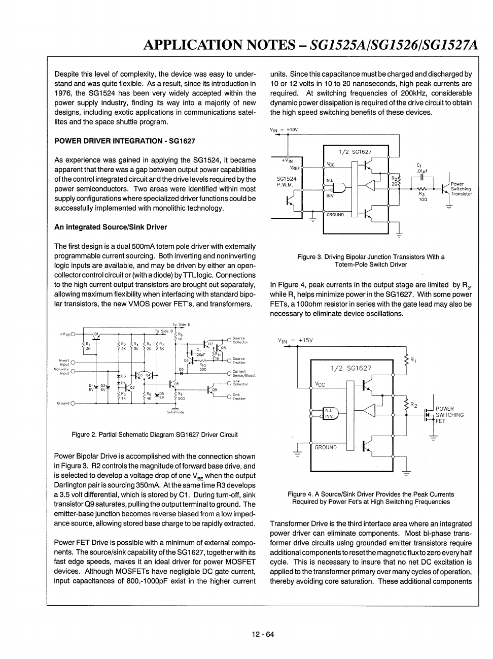
The first design is a
dual500mA
totem pole driver with externally
programmable current sourcing. Both inverting and noninverting
logic inputs are available, and may be driven by either an open-
collector control circuit or (with a diode) by
TTL
logic. Connections
to the high current output transistors are brought out separately,
allowing maximum flexibility when interfacing with standard bipo-
lar transistors, the new VMOS power FET's, and transformers.
+Vcc
I~V;~:
0----1--+--1--+
NOI1I~~UYt
0----1-,---1
01
02
6V 6V
To
SideS
R,
1K
Source
Collector
+-*--<-------o~~~rs~)soost
Sink
Collector
SInk
Emitter
Figure
2.
Partial
Schematic
Diagram
SG1627
Driver
Circuit
Power Bipolar Drive is accomplished with the connection shown
in Figure 3.
R2
controls the magnitude of forward base drive, and
is selected to develop a voltage drop
of
one V
BE
when the output
Darlington pair is sourcing 350mA. At the same time
R3
develops
a 3.5 volt differential, which is stored by C1. During turn-off, sink
transistor
09
saturates, pulling the outputterminal to ground. The
emitter-base junction becomes reverse biased from a low imped-
ance source, allowing stored base charge to be rapidly extracted.
Power FET Drive is possible with a minimum of external compo-
nents. The source/sink capability
ofthe
SG1627, together with its
fast edge speeds, makes it an ideal driver for power MOSFET
devices. Although MOSFETs have negligible DC gate current,
input capacitances
of
800,-1000pF exist in the higher current
units. Since this capacitance must be charged and discharged by
10 or 12 volts in 10
to
20 nanoseconds, high peak currents are
required. At switching frequencies
of
200kHz, considerable
dynamic power dissipation is required
ofthe
drive circuit to obtain
the high speed switching benefits
of
these devices.
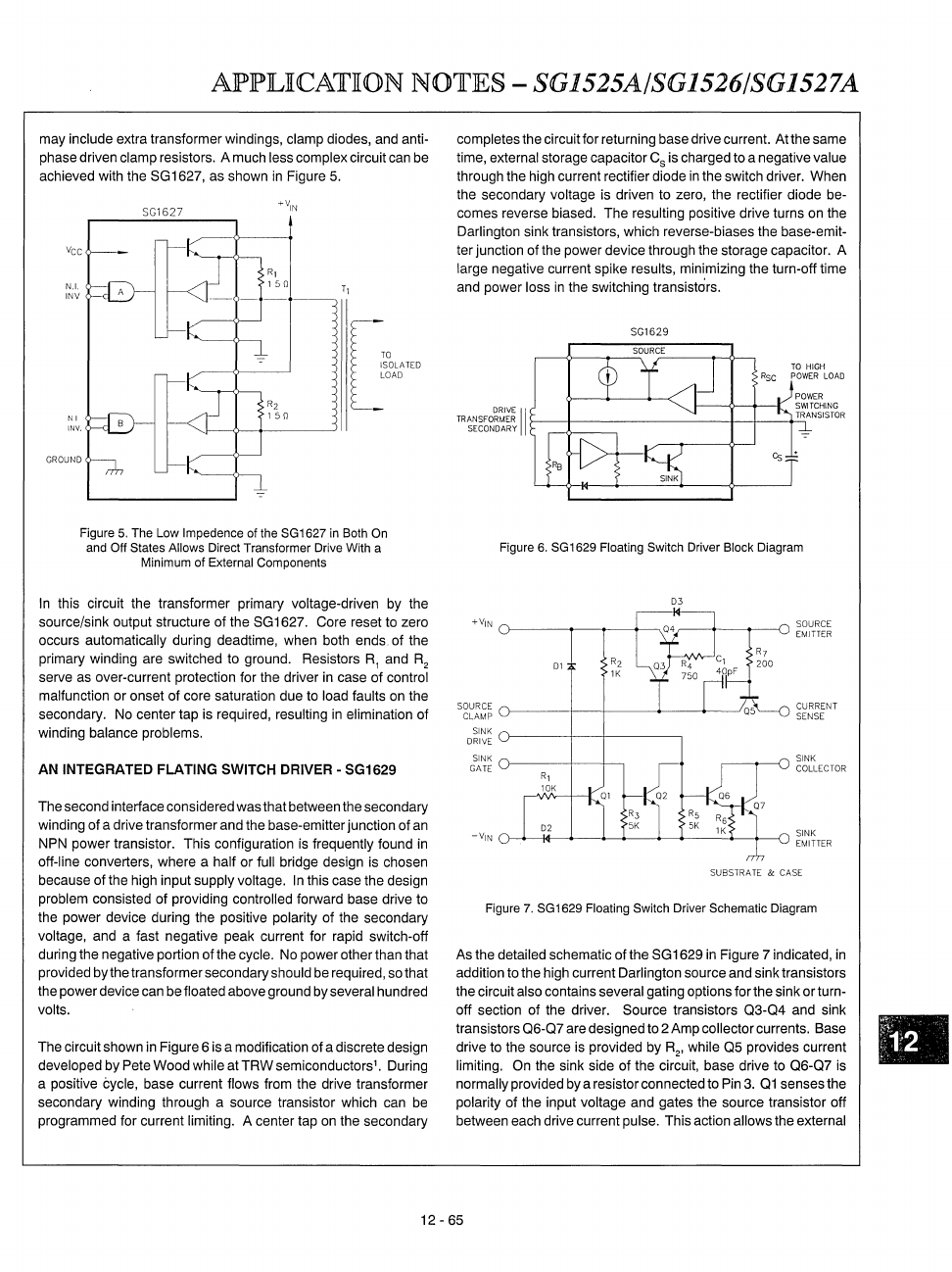
Figure
3.
Driving
Bipolar Junction Transistors
With
a
Totem-Pole Switch Driver
In
Figure 4, peak currents in the output stage are limited by R2,
while
R,
helps minimize power in the SG1627. With some power
FETs, a 1000hm resistor in series with the gate lead may also be
necessary to eliminate device oscillations.
VIN =
+15V
1/2
SG1627
,-----<>---1
J
POWER
'0-----¢-~O-_l~
~WITCHING
i
ET
Figure
4.
A Source/Sink Driver Provides the
Peak
Currents
Required
by
Power
Fet's
at
High
Switching Frequencies
Transformer Drive is the third interface area where an integrated
power driver can eliminate components. Most bi-phase trans-
former drive circuits using grounded emitter transistors require
additional components
to
resetthe magnetic flux to zero every half
cycle. This is necessary
to
insure that no net DC excitation is
applied to the transformer primary over many cycles of operation,
thereby avoiding core saturation. These additional components
12 -64
APPLICATION NOTES -SG1525A/SG1526/SG1527A
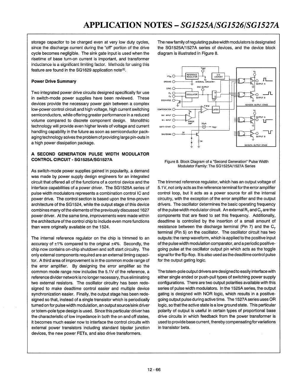
may include extra transformer windings, clamp diodes, and anti-
phase driven clamp resistors. A much less complex circuit can be
achieved with the SG1627, as shown
in
Figure
5.
N.I.
INV L
ro
ISOLATED
LOAD
INV.
GROUND
Figure
5.
The Low Impedence of the SG1627 in Both On
and Off States Allows Direct Transformer Drive With a
Minimum of External Components
In
this circuit the transformer primary voltage-driven by the
source/sink output structure of the SG1627. Core reset to zero
occurs automatically during deadtime, when both ends of the
primary winding are switched to ground. Resistors
R,
and R,
serve as over-current protection for the driver
in
case of control
malfunction or onset of core saturation due to load faults on the
secondary. No center tap is required, resulting
in
elimination of
winding balance problems.
AN INTEGRATED FLATING SWITCH DRIVER -SG1629
The second interface considered was that between the secondary
winding of a drive transformer and the base-emitter junction of an
NPN power transistor. This configuration
is
frequently found
in
off-line converters, where a half or full bridge design is chosen
because of the high input supply voltage.
In
this case the design
problem consisted of providing controlled forward base drive to
the power device during the positive polarity of the secondary
voltage, and a fast negative peak current for rapid switch-off
during the negative portion
ofthe
cycle. No power other than that
provided by the transformer secondary should be required, so that
the power device can be floated above ground by several hundred
volts.
The circuit shown
in
Figure 6
is
a modification of a discrete design
developed by Pete Wood while at
TRW
semiconductors'. During
a positive cycle, base current flows from the drive transformer
secondary winding through a source transistor which can be
programmed for current limiting. A center tap on the secondary
completes the circuitfor returning base drive current.
Atthe
same
time, external storage capacitor Cs is charged to a negative value
through the high current rectifier diode
in
the switch driver. When
the secondary voltage is driven to zero, the rectifier diode be-
comes reverse biased. The resulting positive drive turns on the
Darlington sink transistors, which reverse-biases the base-emit-
ter junction of the power device through the storage capacitor. A
large negative current spike results, minimizing the turn-off time
and power loss
in
the switching transistors.
SG1629
POWER
SWITCHING
TRANSFO~~~~
II
r-_+
_________
-+_t--_+'lTRANSISTOR
SECONDARY
Figure
6.
SG1629 Floating Switch Driver Block Diagram
+VIN
('r----.---.---+~
01
R2
1K
03
D~II~~
('r----+---+-----~
~~~~
lr----r--r-,
CURRENT
SENSE
SUBSTRA
TE
& CASE
Figure
7.
SG1629 Floating Switch Driver Schematic Diagram
As the detailed schematic of the SG1629
in
Figure 7 indicated,
in
addition to the high current Darlington source and sink transistors
the circuit also contains several gating options
forthe
sink orturn-
off section of the driver. Source transistors Q3-Q4 and sink
transistors Q6-Q7 are designed to
2Amp
collector currents. Base
drive to the source is provided by R" while Q5 provides current
limiting. On the sink side of the circuit, base drive to Q6-Q7
is
normally provided
by
a resistor connected to Pin
3.
Ql
senses the
polarity of the input voltage and gates the source transistor off
between each drive current pulse. This action allows the external
12 -65
APPLICATION NOTES -SG1525A/SG1526/SG1527A
storage capacitor to
be
charged
even
at
very
low
duty
cycles,
since
the
discharge current
during
the "off'
portion
of
the drive
cycle
becomes
negligible.
The
sink
gate
input
is
used
when
the
risetime
of
base
turn-on current
is
important,
and
transformer
inductance
is
a significant limiting
factor.
Methods
for
using
this
feature
are
found
in
the
SG1629
application
note(2).
Power Drive Summary
Two
integrated power
drive
circuits
designed
specifically for
use
in
switch-mode power
supplies
have
been
reviewed.
These
devices
provide the necessary
power
gain
between
a
complex
low-power control circuit
and
high
voltage,
high
current switching
semiconductors, while offering greater performance
in
a
reduced
volume
compared
to
discrete
component
design.
Monolithic
technology will provide
even
higher
levels of voltage
and
current
handling capability
in
the
future
as
soon
as
semiconductor
pack-
aging
technology solves the
problem
of
providing
large pin-outs
in
a
high
power
dissipation
package.
A
SECOND
GENERATION
PULSE
WIDTH
MODULATOR
CONTROL CIRCUIT· SG1525A/SG1527 A
As
switch-mode power
supplies
gained
in
popularity, a
demand
was
made
by
power supply
design
engineers for
an
integrated
circuit that offered
all
of the functions of a
control
device
and
the
interface capabilities of a
power
driver.
The
SG1525A series of
pulse
width
modulators
represents
a
combination
control
IC
and
power
drive.
The
control
section
is
based
upon
the time-proven
architecture of the
SG1524,
while
the output
stage
of this device
combines
many
of
the
elements
ofthe previously discussed
1627
power
driver.
At the
same
time,
improvements
were
made
within
the architecture of
the
control
chip
to
include
even
more
functions
than
were
originally available
on
the
1524.
The
internal reference
regulator
on
the
chip
is
trimmed
to
an
accuracy of
±1
%
compared
to the original
±4%.
Secondly,
the
chip
now
contains
on-Chip
shutdown
and
soft start circuitry.
The
only external components
required
are
an
external timing capaci-
tor.
A
third
area
of
improvement
is
in
the
common
mode
range
of
the error amplifier.
By
deSigning
the error amplifier
so
the
common
mode
range
now
includes the
5.1
V of the
reference,
a
reference divider network
is
no
longer
necessary,
thus eliminating
two
external resistors.
The
oscillator
Circuitry
has
been
rede-
signed to
make
deadtime
control
easier
and
multiple device
synchronization easier.
Finally,
the
output
stage
has
been
rede-
signed
so
that,
instead
of
a
single
transistor
which
is
periodically
turned
on
for
pulse
width
modulation,
an
output source/sink driver
or
totem-pole
type
design
is
used.
Since
this particular driver
has
the characteristic of
low
impedance
in
both
the
on
and
off
states,
it
becomes
much
easier
now
to interface
the
control
circuits
with
external power transistors
including
standard
bipolar junction
devices, the
new
power
FETs,
and
also
drive transformers.
The
new
family of regulating
pulse
width
modulators
is
designated
the
SG1525N1527A series of devices,
and
the
device
block
diagram
is
illustrated
in
Figure
8.
"
c'u--....... I
Figure
8.
Block
Diagram
of a
"Second
Generation"
Pulse
Width
Modulator
Family:
The
SG1525N1527A Series
The
trimmed
reference
regulator,
which.has
an
output voltage of
5.1
V,
not only
acts
as
the
reference
terminal
for
the
error amplifier
control
loop,
but it acts
as
a
power
source
for
all
the
internal
circuitry,
with
the exception of
the
error amplifier
and
the output
drivers.
The
oscillator determines the
basic
operating
frequency
ofthe
pulse
width
modulator circuil.
An
external
RT
and
CT
are
the
components
that
are
fixed
to
set this
frequency.
Additionally,
deadtime
is
controlled
by
the insertion of a
small
amount of
resistance
between
the discharge
terminal
(Pin
7)
and
the CT
terminal
(Pin
5)
on
the oscillator.
The
oscillator circuit has
two
outputs:
the
ramp
waveform,
which
is
applied
to
the
positive input
ofthe
pulse
width
modulation
comparator,
and
a periodic positive-
going
pulse
at
the
oscillator output
pin
which
acts
as
the
toggle
signal
forthe flip-flop. It
is
also
used
as
the
deadtime
control
pulse
for
the
output
gating
logic.
The
totem-pole output drivers
are
designed
to easily interface
with
either single
ended
or
push-pull
types of
switching
power
supply
configurations. There
are
two
output polarities available
with
this
series of
pulse
width
modulators.
In
the
1525A
series,
the output
gating
is
designed
with
NOR
logic,
which
results
in
a positive-
going
output
pulse
during active
time.
The
1527
A
series
uses
OR
logic,
so
that the
active
state
is
a low
ground
state.
This
particular
polarity of output
is
useful
in
certain
types
of proportional
base
drive circuits
in
which
feedback
from
the
power
transformer
is
used
to
provide
base
current, thereby
compensating
for variations
in
transistor
beta.
12
-
66
APPLICATION NOTES -SG1525A/SG1526/SG1527A
Soft Start Circuit
The equivalent ofthe SG1525N1527 A soft start circuitry
is
shown
in
Figure
9.
An
external capacitor CSOFTSTART provides the timing
element for
the
soft start
cycle.
This capacitor is
charged
via a
50microamp current source internal
to
the
chip.
The
P.W.M.
comparator
has
two
inverting
inputs,
and
the more negative ofthe
two voltages determines
the
duty cycle.
During
undervoltage
conditions
on
the
V'N
line, current
is
forced through the
two
diodes
in
01 's
base
circuil. A voltage of approximately
FBE
appears
across 01 's emitter resistor, resulting
in
a collector current of
approximately
100pA.
Since the charging current available is only
50pA,
the soft start capacitor is held
in
a discharged
state.
Because the voltage at
pin
8
is
0,
the
PWM
comparator ignores
the
signal
from
the error amplifier,
and
zero
duty cycle
is
obtained.
When
the
controller supply
rises
to
8 volts the discharge current
is
turned
offc,and
the
voltage
on
pin
8
rise
linearly, resulting
in
gradually increasing duty
cycle.
Eventually the capacitor
charges
up
very close to
the
reference voltage
and
the
duty cycle
is
controlled
by
the error amplifier. Ifthevoltage
on
the
shutdown
pin
is raised above ±1.5 volts the capacitor is slowly discharged althe
same
rate
it
is
normally charged.
2'"
Figure 9. SG1525N1527 A Softstart Circuit
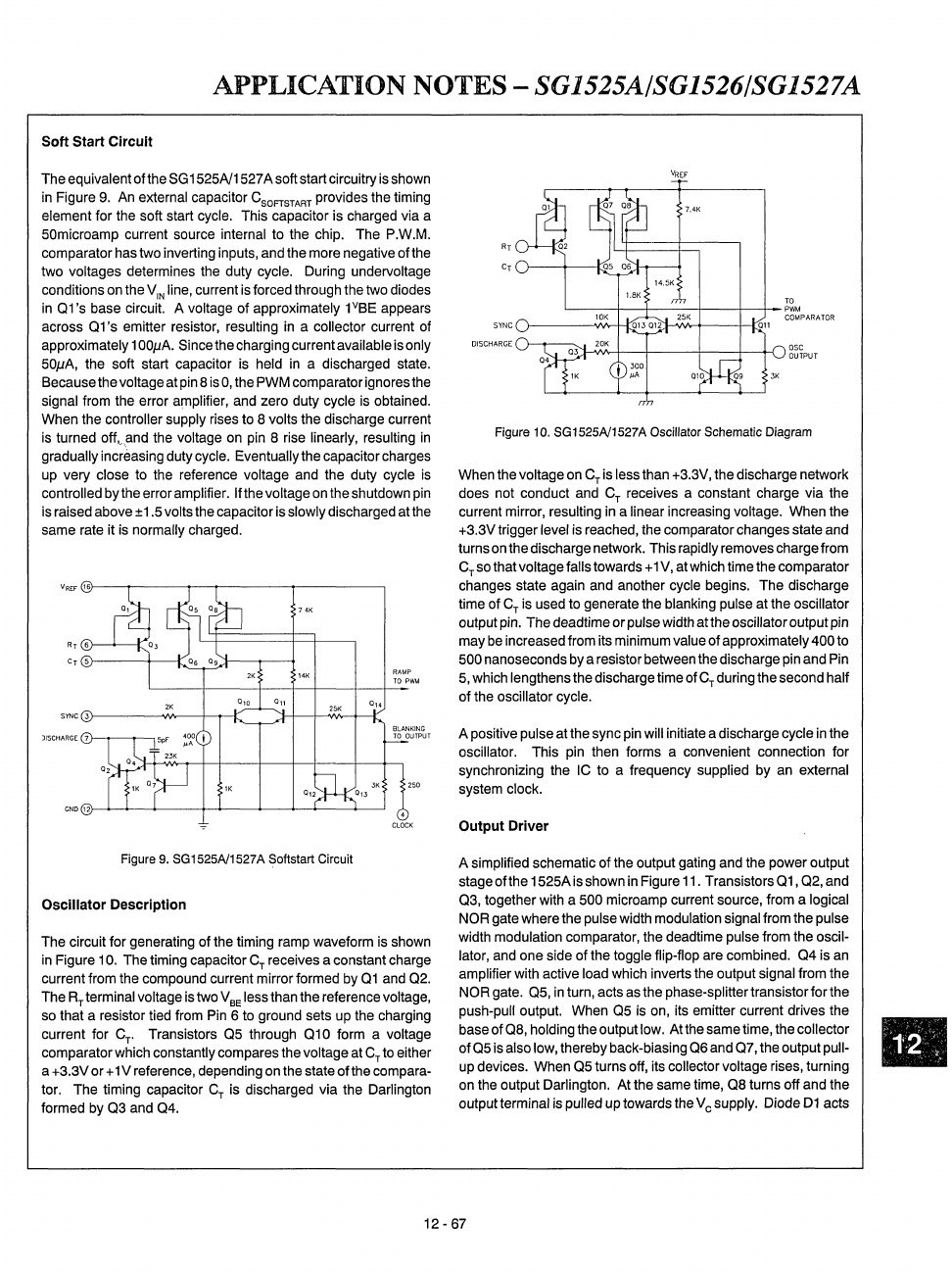
Oscillator Description
Q"
RAUP
BLANKING
TO
OUTPUT
CLOCK
The circuit for generating of
the
timing
ramp
waveform is
shown
in
Figure
10.
The
timing capacitor CT receives a constant
charge
current from
the
compound
current mirror formed
by
01
and
02.
The
RT
terminal voltage is two V
BE
less
than
the reference voltage,
so
that a resistor
tied
from
Pin
6
to
ground sets
up
the
charging
current for
CT'
Transistors
05
through
010
form
a voltage
comparator
which
constantly compares
the
voltage
at
CT
to
either
a +3.3V or + 1 V reference, depending
on
the
state ofthe
compara-
tor.
The timing capacitor CT
is
discharged via the Darlington
formed
by
03
and
04.
R,
C,
SYNC
DISCHARGE
7.4K
TO
L-
____
~~----~---+--+_p~
tl-'Nr+----l-1:<:Ol1
3K
COMPARATOR
OSC
OUTPUT
Figure 10.
SG1525N1527A
OSCillator Schematic Diagram
When
the voltage
on
Cr
is less than
+3.3V,
the discharge network
does
not
conduct
and
CT receives a constant charge via
the
current mirror, resulting
in
a linear increasing
Voltage.
When
the
+3.3V trigger level is reached,
the
comparator changes state
and
turns
on
the discharge network. This rapidly removes charge
from
CT
so
that voltage falls towards + 1
V,
at
which
time the comparator
changes
state
again
and
another
cycle
begins. The discharge
time of CT
is
used
to generate the
blanking
pulse
at the oscillator
output
pin.
The deadtime or pulse
width
althe oscillator output
pin
may
be
increased
from
its
minimum
value
of approximately 400
to
500
nanoseconds
by
a resistor
between
the
discharge
pin
and
Pin
5,
which
lengthens the discharge time of
Cr
during the second half
of the oscillator cycle.
A positive pulse at the sync
pin
will initiate a discharge cycle
in
the
oscillator. This
pin
then forms a convenient connection for
synchronizing the
IC
to a frequency supplied
by
an
external
system clock.
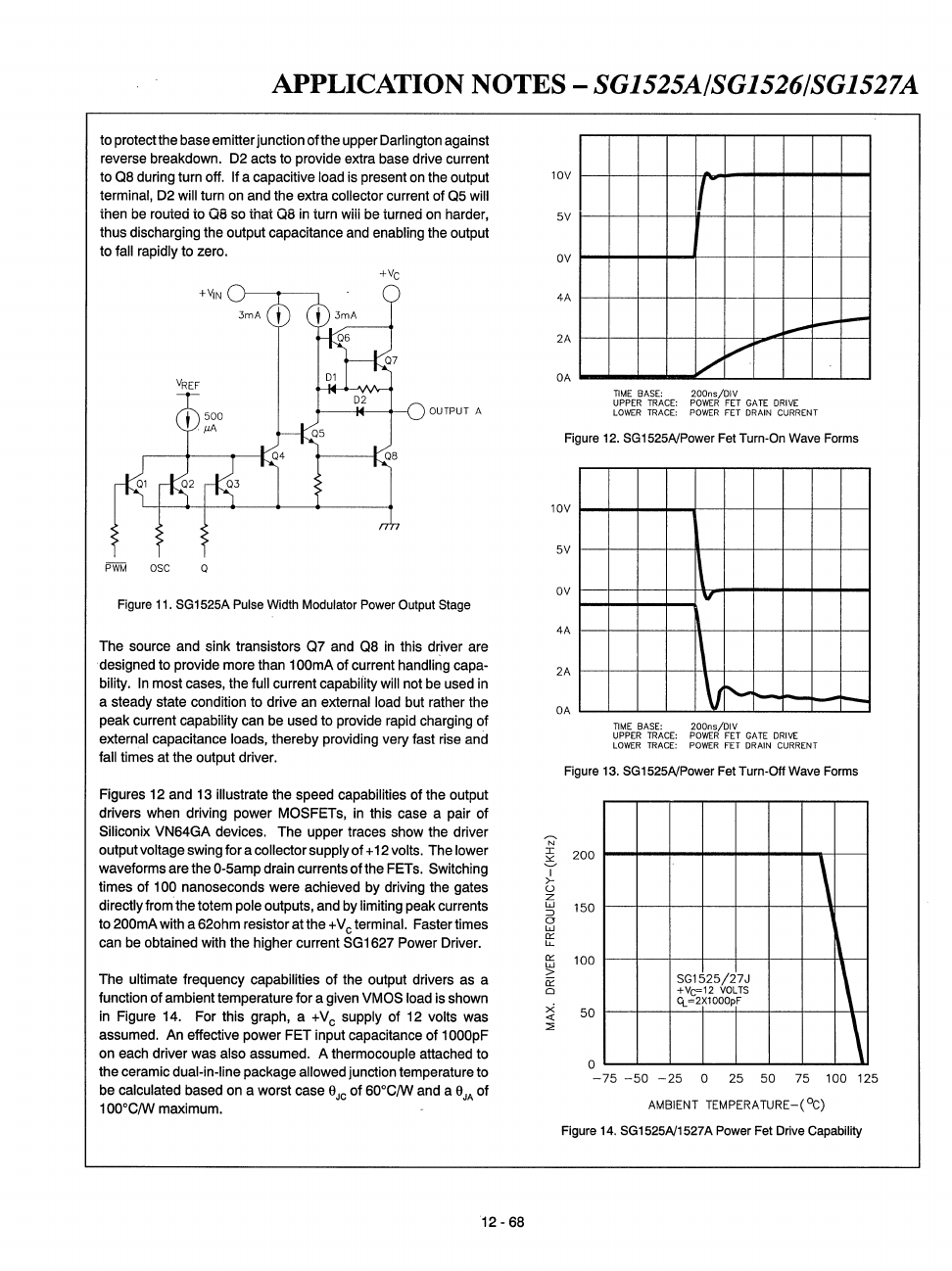
Output Driver
A simplified schematic of the output gating
and
the
power output
stage ofthe 1525A is
shown
in
Figure
11.
Transistors 01 , 02,
and
03, together
with
a
500
microamp current source, from a logical
NOR
gate where the
pulse
width modulation signal from the pulse
width modulation comparator, the deadtime
pulse
from
the oscil-
lator,
and
one
side of the toggle flip-flop
are
combined.
04
is
an
amplifier with active load
which
inverts
the
output signal from the
NOR
gate.
05,
in
turn,
acts
as
the phase-splittertransistorforthe
push-pull outpul.
When
05
is
on,
its emitter current drives the
base
of 08, holding the output
low.
Althe
same
time,
the collector
of
05
is also
low,
thereby back-biasing
06
and
07, the output pull-
up
devices.
When
05
turns off,
its
collector voltage
rises,
turning
on
the
output Darlington.
At
the
same
time,
08
turns off
and
the
output terminal
is
pulled
up
towards
the
V c supply. Diode
01
acts
12-
67
•
APPLICATION NOTES -SG1525A/SG1526/SG1527A
to
protect the
base
emitter junction ofthe upper Darlington against
reverse breakdown.
D2
acts to provide extra
base
drive current
to
08
during turn
off.
If a capacitive load is present
on
the output
10V
I
terminal,
D2
will turn
on
and
the extra collector current of
05
will
then
be
routed
to
08
so
that
08
in
turn
will
be
turned
on
harder,
5V
thus discharging
the
output capacitance
and
enabling
the
output
to fall rapidly
to
zero.
ov
+vc
H'IN
'm'Q)
~
4A
~
I"""'"
-
06
2A
"
07
1/
;'00
D1
OA
D2
TIME
BASE:
200ns/DIV
UPPER
TRACE:
POWER
FET
GATE
DRIVE
OUTPUT
A
LOWER
TRACE:
POWER
FET DRAIN CURRENT
./lA
l-~5
Figure
12.
SG1525NPower
Fet
Turn-On
Wave
Forms
l-
~2~3
14
rfB
01
10V
n'n
5V
PWM
osc
0 \
ov
v
Figure
11.
SG1525A
Pulse
Width
Modulator
Power
Output
Stage
4A
The
source
and
sink transistors
07
and
08
in
this driver are
designed
to
provide more than 1
OOmA
of current handling capa-
2A
bility.
In
most
cases,
the full current capabiiity
will
not
be
used
in
"
a steady state condition to drive
an
external
load
but
rather the
OA
peak current capability
can
be
used
to
provide
rapid
charging
of
TIME
BASE:
200ns/DIV
external capacitance loads, thereby providing very fast
rise
and
UPPER
TIRACE:
POWER
FET
GA
TIE
DRIVE
LOWER
TRACE:
POWER
FET DRAIN CURRENT
fall times at the output driver.
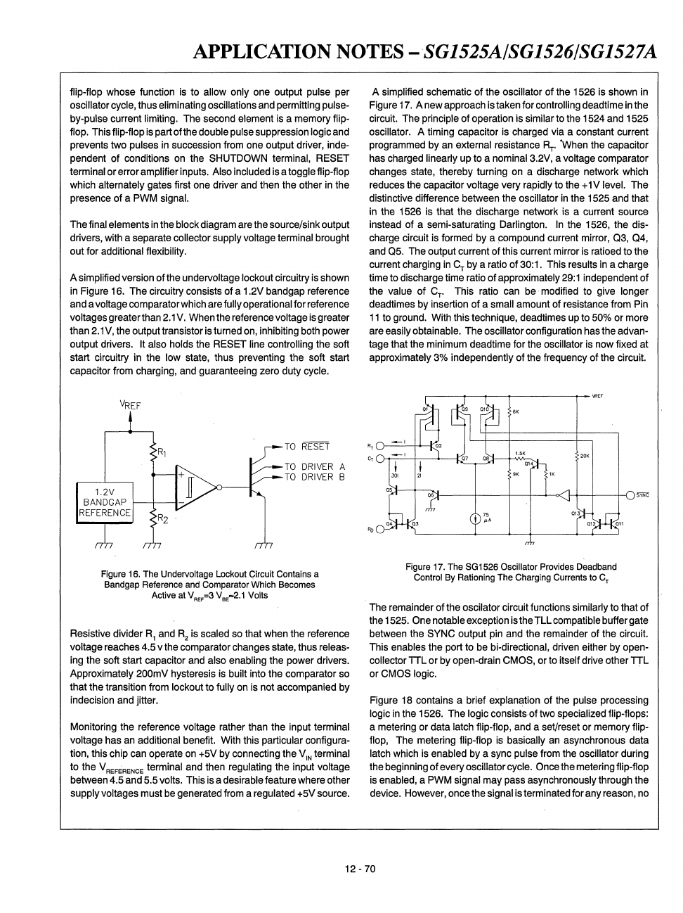
Figure
13.
SG1525NPower
Fe!
Turn-Off
Wave
Forms
Figures
12
and
13
illustrate the
speed
capabilities of the output
drivers
when
driving power
MOSFETs,
in
this
case
a pair of
Siliconix VN64GA devices. The upper traces
show
the driver
N'
output voltage swing for a collector supply of +
12
volts. The lower I
200
'"
waveforms are the 0-5amp drain currents of the
FETs.
Switching r J
times of
100
nanoseconds were achieved
by
driving the gates u
directly
from
the totem
pole
outputs,
and
by
limiting
peak
currents z
w
150
::J
to
200mA with a
620hm
resistor atthe
+V
c terminal. Fastertimes a
w
0::
can
be
obtained
with
the
higher current SG1627 Power
Driver.
"-
0::
100
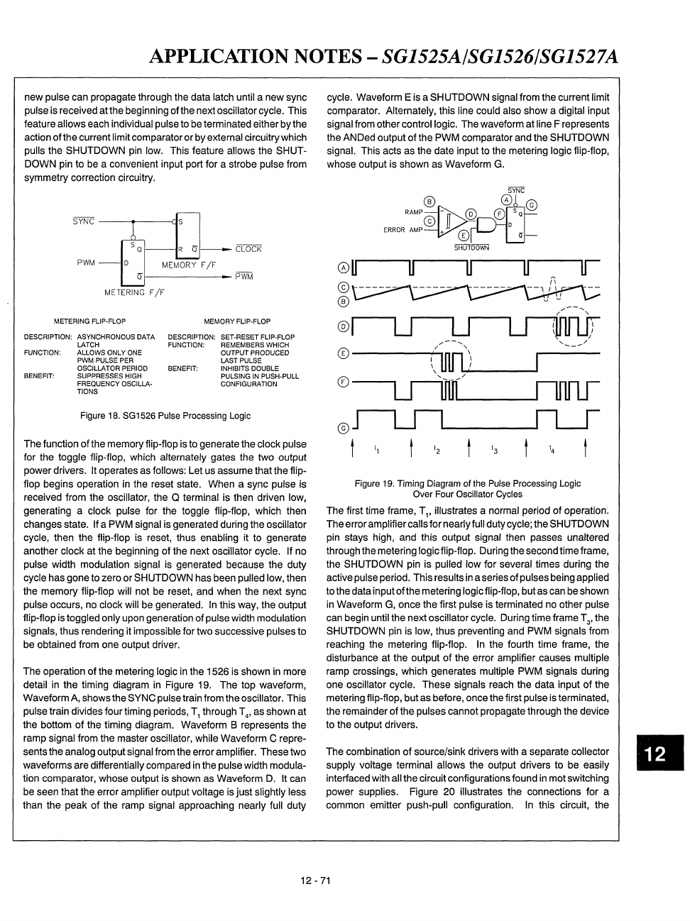
The ultimate frequency capabilities of the output drivers
as
a
~
SG1525/27J
a::
function of ambient temperature for a
given
VMOS
load
is
shown
D
+Vc=12
VOLTS
x
CL
=2X1000pF
in
Figure
14.
For this graph, a
+Vc
supply of
12
volts
was
«
50
\
assumed.
An
effective power FET input capacitance of 1000pF
::;;
on
each
driver was also assumed. A thermocouple attached to a
the ceramic dual-in-line package allowed junction temperature
to
-75 -50 -25
a
25
50
75
100 125
be
calculated
based
on
a worst
case
6
JC
of 60°CIW
and
a 6
JA
of
AMBIENT
TEMPERATURE-("c)
1
OO°CIW
maximum.
Figure
14.
SG1525N1527A
Power
Fe!
Drive
Capability
12
-
68

APPLICATION NOTES -SG1525A/SG1526/SG1527A
For ambient temperatures below 90°C, the maximum frequency
allowable is determined by the maximum possible oscillator
frequency of 400kHz. Above 90°C operating frequency and
dynamic power dissipation must be reduced to keep the junction
temperature from exceeding + 150°C. Different supply voltages,
capacitive loads, and heat sinking will result in other temperature
limits.
It will be noticed in comparing the block diagram
ofthe
SG1525A/
1527 A family to that
ofthe
SG1524 thatthere is no provision made
directly for current limiting on the 1525A/1527A. The reason for
this is that this chip is designed to interface with a new output
supervisory circuit, the SG1543. This device has an extra
comparator with adjustable offset which can be used for providing
the current limit function in conjunction with the SG1525A/1527 A.
Additionally, this particular chip has the capability for providing
under and overvoltage protection for the remainder
of
the power
supply.
A THIRD GENERATION SWITCHING POWER SUPPLY CON-
TROL
CIRCUIT -SG1526
• Supply operation to 40 volts
• Reference trimmed to ±1%
• Sawtooth oscillator with dead band control
• PWM comparator with hysteresis
• Undervoltage lockout
• Programmable soft start
• Wide error amp common mode range
• Wide current limit common mode range
• Two modes of digital current limiting
• Double pulse suppression logic
• Single pulse metering logic
• Symmetry correction capability
• TTL/CMOS compatible logic
• Dual 100mA source/sink output drivers
Table
1.
Desirable Features of a High-Performance
Pulse Width Modulator
An ideal circuit for switching power supplies should include not
only the elements necessary for normal pulse modulation opera-
tion, but also the full range
of
abnormal operations. Ideally, the
circuit should contain as many protective features as possible for
the power semiconductors. If a table
of
parameters were con-
structed for such device, it would look much like that shown in
Table
1.
Analysis ofthefeatures in the table would show that most
of the new features are control related and are therefore ideally
suited for inclusion in an integrated circuit, where a great deal
of
complexity can be easily compressed into a very small area. Just
such a device has been designed by Silicon General, and the
block diagram of that device is shown in Figure 15.
As can be seen, the four basic elements ofthe pulse modulator are
present: a reference regulator, error amplifier, sawtooth oscillator,
and a pulse width modulation comparator. Of particular interest
are some new features in the block diagram: an undervoltage
lockout, soft start circuitry, digital current limit comparator and
digital signal processing logic between the pulse width modulation
comparator and the output power drivers.
Figure 15. SG1526 High Performance Pulse Width
Modulator Block Diagram
The operation of the circuit is as follows: An on-Chip regulator
trimmed to 1 % is both reference voltage forthe error amplifier, and
also the stabilized power source for all the internal circuitry, with
the exception
of
the error amplifier, the current limit comparator,
and the output drivers.
The sawtooth oscillator is programmed for a specific frequency
and dead band by values of RT, CT and
RD.
The resulting ramp
waveform is applied to one side
of
the pulse width modulation
comparator, which has been designed with a very small amount
of
hysteresis to prevent oscillations at the' comparison point. The
other terminal
of
the PWM comparator is connected to the output
of
an error amplifier which has been designed with a common
mode range that includes both ground and the
5V
reference.
Also associated with the amplifier is on-Chip soft start circuitry.
This soft start circuitry is controlled not only by an external RESET
terminal, but also by the undervoltage lockout Circuitry. If the
reference voltage should be less than the
5V
required for normal
linear operation of the control circuitry, the RESET terminal in the
soft start is held low by the undervoltage lockout, thus preventing
the soft start capacitor from charging. At the same time, the power
output drivers of the device are inhibited. thus making it impos-
sible for spurious output pulses to occur during undervoltage
conditions.
The digital output of the pulse width modulation comparator is
ANDed with the output
of
the current limit comparator. This
provides very fast response
to
overcurrent conditions. The
current limit comparator has a fixed input offset
of
100mV plus a
slight hysteresis
of
20mV
to
eliminate indecision at
the
threshold
pOint.
The PWM signal from the AND gate is followed by three
levels
of
pulse processing logic. It first passes through a metering
12 -69
•
APPLICATION NOTES -SG1525A/SG1526/SG1527A
flip-flop
whose
function
is
to
allow
only
one
output
pulse
per
oscillator
cycle,
thus
eliminating oscillations
and
permitting
pulse-
by-pulse current limiting.
The
second
element
is
a
memory
flip-
flop.
This
flip-flop
is
part
ofthe
double
pulse
suppression logic
and
prevents
two
pulses
in
succession
from
one
output
driver,
inde-
pendent of conditions
on
the
SHUTDOWN
terminal,
RESET
terminal
or
error amplifier
inputs.
Also
included
is
a toggle flip-flop
which
alternately
gates
first
one
driver
and
then
the
other
in
the
presence of a
PWM
signal.
The
final
elements
in
the
block
diagram
are
the source/sink output
drivers,
with
a
separate
collector supply voltage terminal brought
out for additional flexibility.
A simplified version ofthe undeNoltage lockout circuitry
is
shown
in
Figure
16.
The
circuitry
consists
of
a
1.2V
bandgap
reference
and
a voltage comparator
which
are
fully operational for
reference
voltages greater
than
2.1
V.
When
the
reference
voltage
is
greater
than
2.1
V,
the
output transistor
is
turned
on,
inhibiting
both
power
output drivers. It
also
holds
the
RESET
line
controlling the soft
start circuitry
in
the
low
state,
thus preventing the soft start
capacitor
from
charging,
and
guaranteeing
zero
duty
cycle.
R1
TO
RESET
TO
DRIVER
A
TO
DRIVER
B
1.2V
BANDGAP
REFERENCE
RZ
Figure
16.
The
Undervoltage
Lockout
Circuit Contains a
Bandgap Reference
and
Comparator
Which
Becomes
Active at V
REF
=3
V.e"'2.1
Votts
Resistive
divider
Rl
and
R2
is
scaled
so
that
when
the reference
voltage
reaches
4.5
v
the
comparator
changes
state,
thus
releas-
ing
the soft start
capaCitor
and
also
enabling
the
power
drivers.
Approximately 200mV hysteresis
is
built
into
the comparator
so
that the transition
from
lockout to fully
on
is
not accompanied
by
indecision
and
jitter.
Monitoring
the
reference voltage rather
than
the input terminal
voltage has
an
additional benefit.
With
this
particular configura-
tion,
this
chip
can
operate
on
+5V
by
connecting the
VIN
terminal
to
the V REFERENCE terminal
and
then
regulating the input voltage
between
4.5
and
5.5
volts.
This
is
a desirable feature
where
other
supply voltages
must
be
generated
from
a
regulated
+5V
source.
A simplified schematic of the oscillator of the
1526
is
shown
in
Figure
17.
A
new
approach
is
taken for controlling deadtime
in
the
circuit.
The
principle of operation
is
similar
to
the
1524
and
1525
oscillator. A timing capacitor
is
charged
via
a constant current
programmed
by
an
external
resistance
1\.
'When
the
capacitor
has
charged
linearly
up
to
a nominaI3.2V, a voltage comparator
changes
state,
thereby turning
on
a discharge network
which
reduces
the
capaCitor
voltage very rapidly
to
the
+ 1 V
level.
The
distinctive difference
between
the oscillator
in
the
1525
and
that
in
the
1526
is
that the discharge
network
is
a current source
instead
of a semi-saturating
Darlington.
In
the
1526,
the
dis-
charge
circuit
is
formed
by
a
pompound
current
mirror,
03, 04,
and
05.
The
output current of this current mirror
is
ratioed
to
the
current
charging
in
CT
by
a ratio of
30:
1.
This
results
in
a charge
time
to
discharge time ratio of approximately
29:
1 independent of
the
value
of Cr This
ratio
can
be·
modified
to
give
longer
deadtimes
by
insertion of a small amount of
resistance
from
Pin
11
to
ground.
With
this
technique,
deadtimes
up
to
50%
or
more
are
easily obtainable.
The
oscillator configuration
has
the
advan-
tage
that the
minimum
deadtime for the oscillator
is
now
fixed
at
approximately
3%
independently of the frequency of the circuit.
"r
Or
Figure
17.
The
SG1526 Oscillator
Provides
Deadband
Control
By
Rationing
The
Charging
Currents to CT
""'"
The
remainder
of the oscilator circuit functions similarly to that of
the
1525.
One
notable exception
is
the
TLL
compatible
buffer gate
between
the
SYNC
output
pin
and
the
remainder
of
the
circuit.
This
enables
the port
to
be
bi-directional,
driven
either by open-
collector TTL
or
by
open-drain
CMOS,
or
to
itself
drive
other TTL
or
CMOS
logic.
Figure
18
contains
a brief explanation
of
the
pulse
processing
logic
in
the
1526.
The
logic consists-of
two
specialized flip-flops:
a
metering
or
data
latch
flip-flop,
and
a set/reset
or
memory
flip-
flop,
The
metering flip-flop
is
basically
an
asynchronous data
latch
which
is
enabled
by
a
sync
pulse
from
the
oscillator
during
the
beginning
of every oscillator
cycle.
Once
the
metering
flip-flop
is
enabled,
a
PWM
signal
may
pass
asynchronously through the
device.
However,
once
the signal
is
terminated
for
any
reason,
no
12-70
APPLICATION NOTES -SG1525A/SG1526/SG1527A
new pulse can propagate through the data latch until a new sync
pulse is received
atthe
beginning
ofthe
next oscillator cycle. This
feature allows each individual pulse to be terminated either by the
action
ofthe
current limit comparator or by external circuitry which
pulls the SHUTDOWN pin low. This feature allows the SHUT-
DOWN pin to be a convenient input port for a strobe pulse from
symmetry correction circuitry.
SYNC
--~---c:1
R
Ci
PWM
MEMORY
F
IF
~~-------PWM
METERING
F
IF
METERING FLlp·FLOP
DESCRIPTION: ASYNCHRONOUS DATA
LATCH
FUNCTION: ALLOWS ONLY
ONE
PWM
PULSE
PER
OSCILLATOR PERIOD
BENEFIT: SUPPRESSES HIGH
FREQUENCY OSCILLA·
TIONS
MEMORY FLlp·FLOP
DESCRIPTION: SET·RESET FLlp·FLOP
FUNCTION: REMEMBERS WHICH
OUTPUT PRODUCED
LAST
PULSE
BENEFIT: INHIBITS DOUBLE
PULSING
IN
PUSH·PULL
CONFIGURATION
Figure
18.
SG1526
Pulse
Processing
Logic
The function
of
the memory flip-flop is to generate the clock pulse
for the toggle flip-flop, which alternately gates the two output
power drivers. It operates as follows: Let us assume that the flip-
flop begins operation in the reset state. When a sync pulse is
received from the oscillator, the Q terminal is then driven low,
generating a clock pulse for the toggle flip-flop, which then
changes state. If a PWM Signal is generated during the oscillator
cycle, then the flip-flop is reset, thus enabling it to generate
another clock at the beginning of the next oscillator cycle. If no
pulse width modulation signal is generated because the duty
cycle has gone to zero or SHUTDOWN has been pulled low, then
the memory flip-flop will not be reset, and when the next sync
pulse occurs, no clock will be generated.
In
this way, the output
flip-flop is toggled only upon generation
of
pulse width modulation
signals, thus rendering it impossible for two successive pulses to
be obtained from one output driver.
The operation
of
the metering logic in the 1526 is shown in more
detail in the timing diagram in Figure 19. The top waveform,
Waveform A, shows the SYNC pulse train from the oscillator. This
pulse train divides four timing periods, T, through T4, as shown at
the bottom
of
the timing diagram. Waveform B represents the
ramp signal from the master oscillator, while Waveform C repre-
sents the analog output signal from the error amplifier. These two
waveforms are differentially compared in the pulse width modula-
tion comparator, whose output is shown as Waveform
D.
It can
be seen that the error amplifier output voltage is just slightly less
than the peak
of
the ramp signal approaching nearly full duty
cycle. Waveform E is a SHUTDOWN signal from the current limit
comparator. Alternately, this line could also show a digital input
signal from other control logic. The waveform at line F represents
the ANDed output
of
the PWM comparator and the SHUTDOWN
signal. This acts as the date input to the metering logic flip-flop,
whose output is shown as Waveform G.
0U
U U U
II
@
®
®
.....
--
.....
® / ,
\
tnn
i
\ .
CD
......
__
.-"
@ I
'2
'3
'4
Figure
19.
Timing
Diagram
of
the
Pulse
Processing
Logic
Over
Four
Oscillator
Cycles
The first time frame,
T"
illustrates a normal period
of
operation~
The error amplifier calls for nearly full duty cycle; the SHUTDOWN
pin stays high, and this output signal then passes unaltered
through the metering logic flip-flop. During the second time frame,
the SHUTDOWN pin is pulled low for several times during the
active pulse period. This results in a series
of
pulses being applied
to the data input
ofthe
metering logic flip-flop, but as can be shown
in Waveform G, once the first pulse is terminated no other pulse
can begin until the next oscillator cycle. During time frame Ta, the
SHUTDOWN pin is low, thus preventing and PWM signals from
reaching the metering flip-flop.
In
the fourth time frame, the
disturbance at the output
of
the error amplifier causes multiple
ramp crossings, which generates multiple PWM signals during
one oscillator cycle. These Signals reach the data input
of
the
metering flip-flop, but as before, once the first pulse is terminated,
the remainder of the pulses cannot propagate through the device
to the output drivers.
The combination
of
source/sink drivers with a separate collector
supply voltage terminal allows the output drivers to be easily
interfaced with all
the
circuit configurations found in mot switching
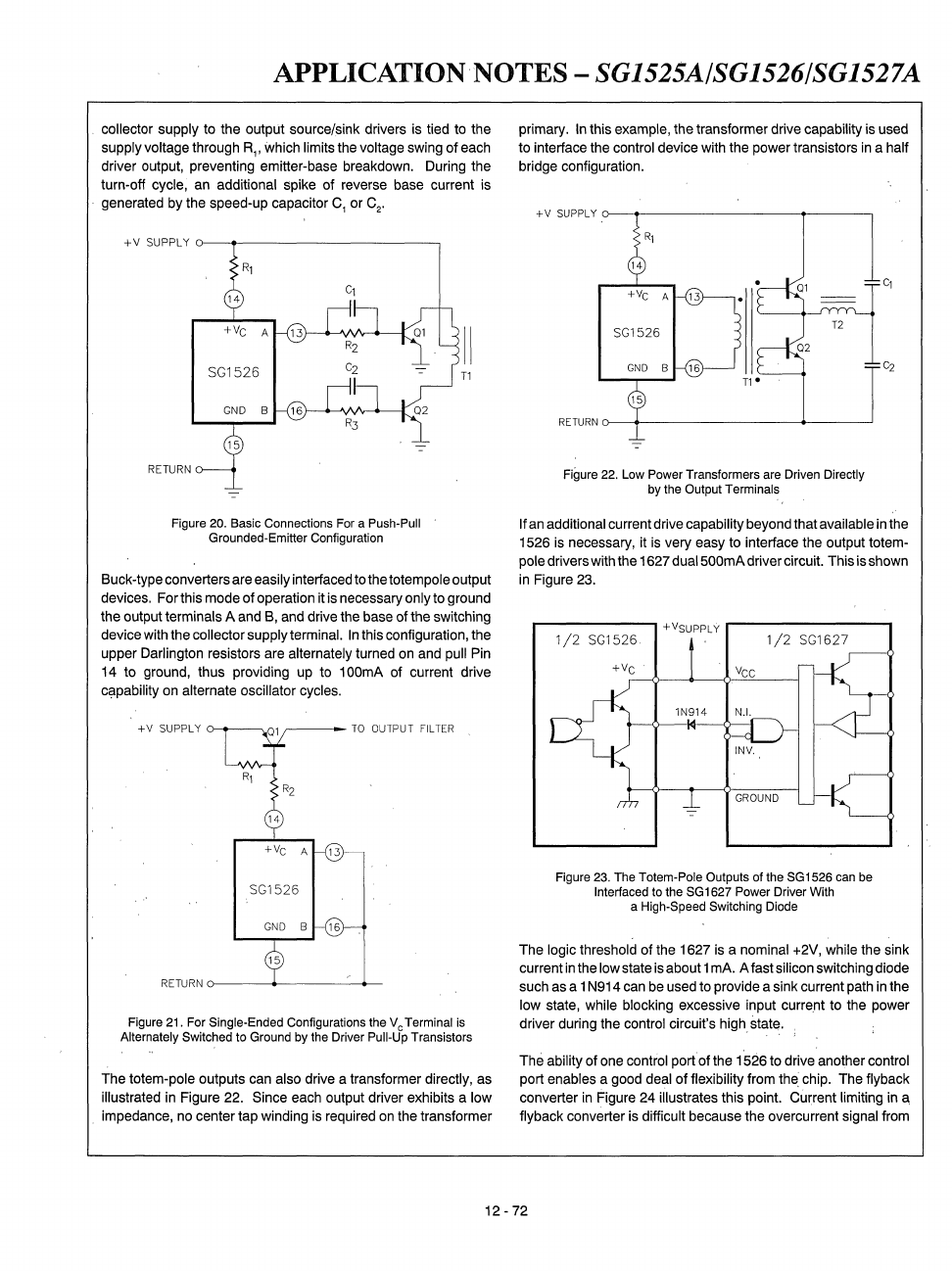
power supplies. Figure 20 illustrates the connections for a
common emitter push-pull configuration.
In
this circuit, the
12 -
71
•
APPLICATION NOTES -SG1525A/SG1526/SG1527A
collector supply to the output source/sink drivers is tied to the
supply voltage through
R"
iNhich limits the voltage swing
of
each
driver output, preventing emitter-base breakdown. During the
turn-off cycle, an additional spike
of
reverse base current is
. generated by the speed-up capacitor C, or C2•
+v
SUPPLY
0---.---------------,
RETURN
Figure 20. Basic Connections For a Push-Pull
Grounded-Emiller Configuration
II
T1
Buck-type converters are easily interfaced to the totem pole output
devices. Forthis mode
of
operation it is necessary only to ground
the output terminals A and
B,
and drive the base of the switching
device with the collector supply terminal.
In
this configuration, the
upper Darlington resistors are alternately turned on and pull Pin
14
to
ground, thus providing up to 100mA of current drive
c?pability on alternate oscillator cycles.
+V
SUPPLY
u-~---.
RETURN
o-------<>------+_
Figure 21. For Single-Ended Configurations the
Vc
Terminal
is
Alternately Switched to Ground by the Driver Pull-Up Transistors
The totem-pole outputs can also drive a transformer directly, as
illustrated in Figure 22. Since each output driver exhibits a low
impedance, no center tap winding is required on the transformer
primary. In this example, the transformer drive capability is used
to interface the control device with the power transistors in a half
bridge configuration.
+V
SUPPLY
o--t----------1>-------,
RETURNo--~-----------<~--~
Figure 22. Low Power Transformers are Driven Directly
by the Output Terminals
C,
If an additional current drive capability beyond that available in the
1526 is necessary, it is very easy to interface the output totem-
pole drivers with the 1627
dual500mA
driver circuit. This is shown
in Figure 23.
r---------,
+VSUPPLY
r----------,
1/2
1/2
SG1627
Figure 23. The Totem-Pole Outputs of the SG1526 can be
Interfaced to the SG1627 Power Driver With
a High-Speed Switching Diode
The logic threshold
of
the 1627 is a nominal +2V, while the sink
current in the
low state is about 1 mA. A fast silicon switching diode
such as a 1 N914 can be used to provide a sink current path in the
low state, while blocking excessive input curre.nt to the power
driver during the control circuit's
high
state.
The ability of one control port
of
the 1526
to
drive another control
port enables a good deal
of
flexibility from
the:
chip. The flyback
converter in Figure 24 illustrates this pOint.
Cu~rent
limiting in
~
flyback converter is difficult because the overcurrent signal from
12
-72
APPLICATION NOTES -SG1525A/SG1526/SG1527A
the current sense resistor is always out
of
phase with the conduc-
tion of the principle power transistor.
In
this circuit, the output of
the current limit comparator in the 1526 is used to re-trigger the
soft start circuitry. By choosing the value
ofthe
soft start capacitor
so that the recovery time of the soft start circuitry is of the order of
one or two cycles, it is possible to provide current limiting with a
minimal number
of
external components. This same technique
can be used in a push-pull converter where
it
is desirable for the
pulse width modulation signal to be turned off for multiple oscilla-
tor cycles rather than for a single cycle. This allows overstressed
output semiconductors a cool-off period before returning to nor-
mal operation.
+VSUPPLY
0---------.,.-----------,
SG1526
+c.s.
-c.s.
R2
RETURN
o-~~
____
--4
________
_+_-1
Figure
24.
Using
the
SG1526
in
a
Flyback
Converter
With
Current
Limiting
T1
II
CONCLUSION
Several integrated circuits designed specifically for switch-mode
power supply control have been described. A brief review has
been made of past approaches to the integration of switching
power supply control and driver circuitry. A description
of
a newly
available family of control/driver integrated circuits, the SG1525/
1527 series, has been given. Finally, a sketch of a future high
performance controller circuit, the SG1526, has been drawn.
The future of integrated circuits for switching power supplies
clearly involves greater complexity in the control circuitry to
account for all possible modes
of
supply operation. The benefits
for the power supply designer will be greater performance and
reliability from switchers with reduced component count and
greater overall manufacturing economies.
REFERENCES
1.
Peter
N.
Wood, "Design
of
a 5 Volt 1000 Watt Power
Supply,"
TRW
Power Semiconductors Application Note
122A, February, 1976.
2. Robert
A.
Mammano, "Power Switch Drivers: New IC
Interface Building Blocks for Switched-Mode Convert-
ers," Powercon 5 Proceedings, May, 1978.
12-73
II

12
-74
