PYNQ Z2 User Manual V1
PYNQ-Z2_manual
User Manual:
Open the PDF directly: View PDF ![]() .
.
Page Count: 31
PYNQ-Z2 Reference Manual v1.0
17 May 2018


Contents
1 PYNQ-Z2 features ...................................................................................................... 4
2 Board files and XDC constraints file .......................................................................... 6
3 Power .......................................................................................................................... 7
4 Boot mode selection .................................................................................................... 8
5 Clock Sources ............................................................................................................. 9
6 DRAM....................................................................................................................... 10
7 Quad SPI Flash ......................................................................................................... 11
8 USB Host .................................................................................................................. 12
9 ADAU1761 Audio Codec ......................................................................................... 13
10 MicroSD .................................................................................................................. 14
11 Ethernet PHY .......................................................................................................... 15
12 MicroUSB Port ....................................................................................................... 17
13 HDMI ports ............................................................................................................. 18
14 LEDs, Buttons, Switches ........................................................................................ 20
15 Board reset signals .................................................................................................. 22
16 Pmod Ports .............................................................................................................. 23
17 Arduino Shield Connector ...................................................................................... 25
18 Raspberry Pi Header ............................................................................................... 30
19 References ............................................................................................................... 31

1 PYNQ-Z2 features
• ZYNQ XC7Z020-1CLG400C
o 650MHz ARM® Cortex®-A9 dual-core processor
o Programmable logic
▪ 13,300 logic slices, each with four 6-input LUTs and 8 flip-
flops
▪ 630 KB block RAM
▪ 220 DSP slices
▪ On-chip Xilinx analog-to-digital converter (XADC)
o Programmable from JTAG, Quad-SPI flash, and MicroSD card
• Memory and storage
o 512MB DDR3 with 16-bit bus @ 1050Mbps
o 16MB Quad-SPI Flash with factory programmed 48-bit globally
unique EUI-48/64™ compatible identifier
o MicroSD slot
• Power
o USB or 7V-15V external power regulator
• USB and Ethernet
o Gigabit Ethernet PHY
o Micro USB-JTAG Programming circuitry
o Micro USB-UART bridge
o USB 2.0 OTG PHY (supports host only)
• Audio and Video
o 2x HDMI ports (input and output)
o 24bit I2S DAC with 3.5mm TRRS jack
o Line-in with 3.5mm jack
• Switches, Push-buttons and LEDs
o 4 push-buttons
o 2 slide switches
o 4 LEDs
o 2 RGB LEDs
• Expansion Connectors
o 2xPmod ports
▪ 16 Total FPGA I/O (8 pins on Pmod A are shared with
Raspberry Pi connector)
o Arduino Shield compatible connector


2 Board files and XDC constraints file
Board files containing the Zynq PS configuration for the PYNQ-Z2 can be
downloaded from the TUL website:
http://www.tul.com.tw/download/pynq-z2.zip
The board files can be used with Vivado to automatically configure the PS when
creating new Zynq designs for the board.
A master XDC constraints file which contains pin constraints for the PYNQ-Z2 is
also available from the TUL website:
http://www.tul.com.tw/download/pynq-z2_v1.0.xdc.zip
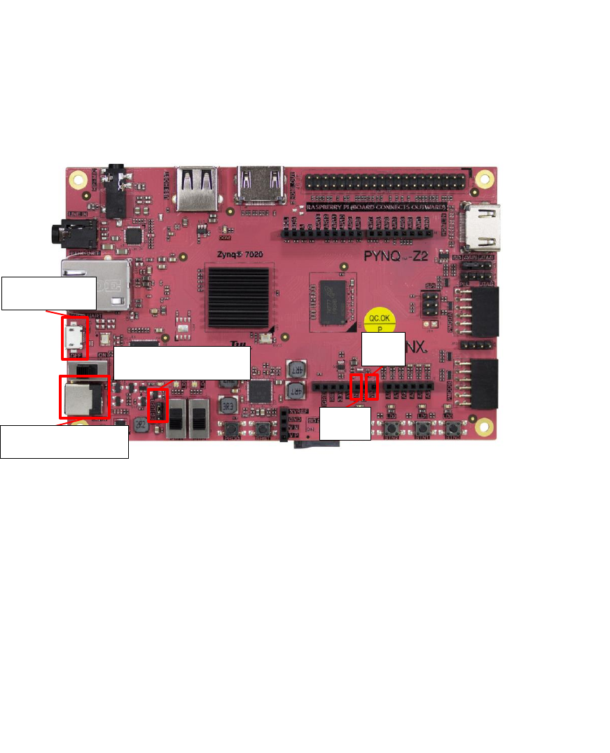
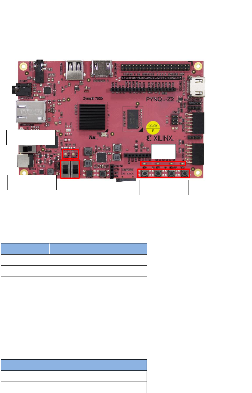
3 Power
The PYNQ-Z2 can be powered from the Micro-USB port (J8), an external power
supply, or a battery. The power source is selected by setting jumper J9 (near SW1) to
USB or REG (External power REGulator/Battery).
The MicroUSB port connects to a standard USB port and should provide enough
power for most designs. More demanding applications may require more power than
the USB port can provide.
When more power is required, an external power regulator (coax, center-positive
2.1mm internal-diameter plug) can be connected to the power jack (DC1). The board
supports 7VDC to 15VDC (12V recommended). Suitable supplies can be purchased
from the TUL website.
A battery can also be used to power the PYNQ-Z2 by attaching the positive terminal
to the “VIN” pin on the Arduino J7 connector (with jumper J9 set to REG). The
negative terminal can be connected to one of the pins labeled GND on J7.
Vi
n
Gnd
DC1 power
jack
J9 Power Jumper
Micro-
USB
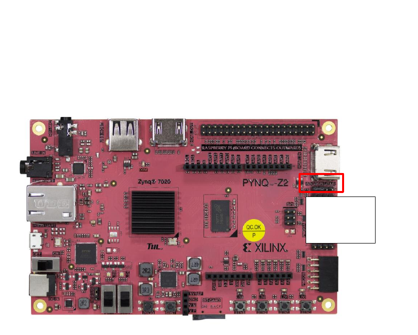
4 Boot mode selection
The PYNQ-Z2 supports MicroSD, Quad SPI Flash, and JTAG boot modes. The boot
mode is selected using the Mode jumper (JP1). TO select the boot mode, move the
jumper to the appropriate position as indicated by the label on the board.
Boot mode
jumper JP1
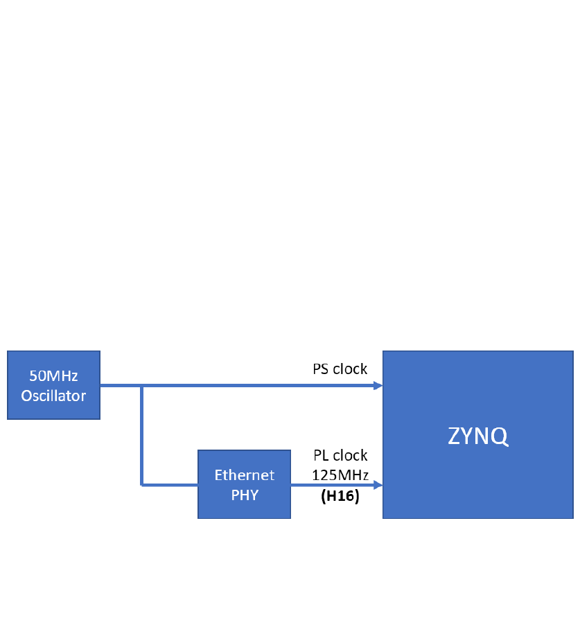
5 Clock Sources
The PYNQ-Z2 provides a 50 MHz clock to the Zynq PS_CLK input, which is used to
generate the clocks for each of the PS subsystems. The 50 MHz input allows the
processor to operate at a maximum frequency of 650 MHz.
The PYNQ-Z2 also has an external 125 MHz reference clock connected to pin H16 of
the PL. The external reference clock allows the PL to be used independently of the
PS.
Figure 6.1 outlines the clocking scheme used on the PYNQ-Z2. Note that the
reference clock output from the Ethernet PHY is used as the 125 MHz reference clock
to the PL. When the PHYRSTB signal is driven low, the Ethernet PHY (U5) is held in
reset disabling the CLK125.
For a full description of the capabilities of the Zynq PL clocking resources, refer to
the “7 Series FPGAs Clocking Resources User Guide” available from Xilinx.

6 DRAM
The PYNQ-Z2 includes a Micron 256Mx16 DDR3 memory (MT41K512M16HA-
125:A) creating a single rank, 16-bit wide interface with a total capacity of 512MB.
The DDR3 is connected to the hard memory controller in the Processor Subsystem
(PS).
The PS incorporates an AXI memory port interface, a DDR controller, the associated
PHY, and a dedicated I/O bank. DDR3 memory interface supports speeds of up to
525 MHz/1050 Mbps on the PYNQ-Z2 board.
For best DDR3 performance, DRAM training is enabled for write leveling, read gate,
and read data eye options in the PS Configuration Tool in the Xilinx tools. Training is
done dynamically by the controller to account for board delays, process variations and
thermal drift.
The PYNQ-Z2 board files (see section 2) contain the configuration for the DRAM
controller which includes optimum starting values for the training process taking into
account PCB and trace delays (propagation delays) for the memory signals board
delays are specified for each of the byte groups. These parameters are board-specific
and were calculated from the PCB trace length reports. The DQS to CLK Delay and
Board Delay values are calculated specific to the PYNQ-Z2 memory interface PCB
design.
7 Quad SPI Flash
The PYNQ-Z2 features a Spansion S25FL128S Quad SPI serial NOR flash.
• 16 MB
• x1, x2, and x4 support
• Bus speeds up to 104 MHz, supporting Zynq configuration rates @ 100 MHz
In Quad SPI mode, this translates to 400Mbs
• Powered from 3.3V
The Multi-I/O SPI Flash memory can be used to initialize and boot the PS subsystem
as well as configure the PL subsystem, or as non-volatile code and data storage.
The SPI Flash connects to the Zynq-7000 SoC and supports the Quad SPI interface.
This requires connection to MIO[1:6,8] as outlined in the Zynq datasheet.
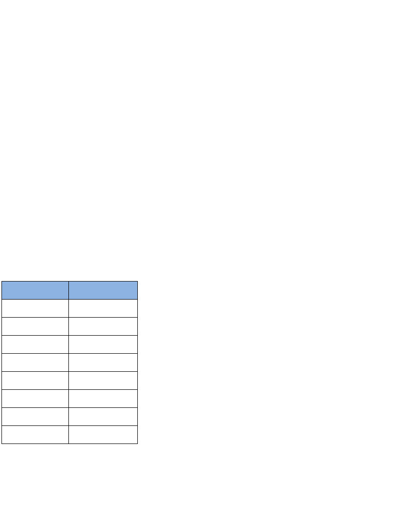
MIO Pin
Name
1
CS
2
DQ0
3
DQ1
4
DQ2
5
DQ3
6
SCLK
7
VCFG0
8
SLCK FB
Table 1 SPI Flash MIO pin mapping
Quad-SPI feedback mode is used, thus qspi_sclk_fb_out/MIO[8] is left to freely
toggle and is connected only to a 20K pull-up resistor to 3.3V. This allows a Quad
SPI clock frequency greater than FQSPICLK2
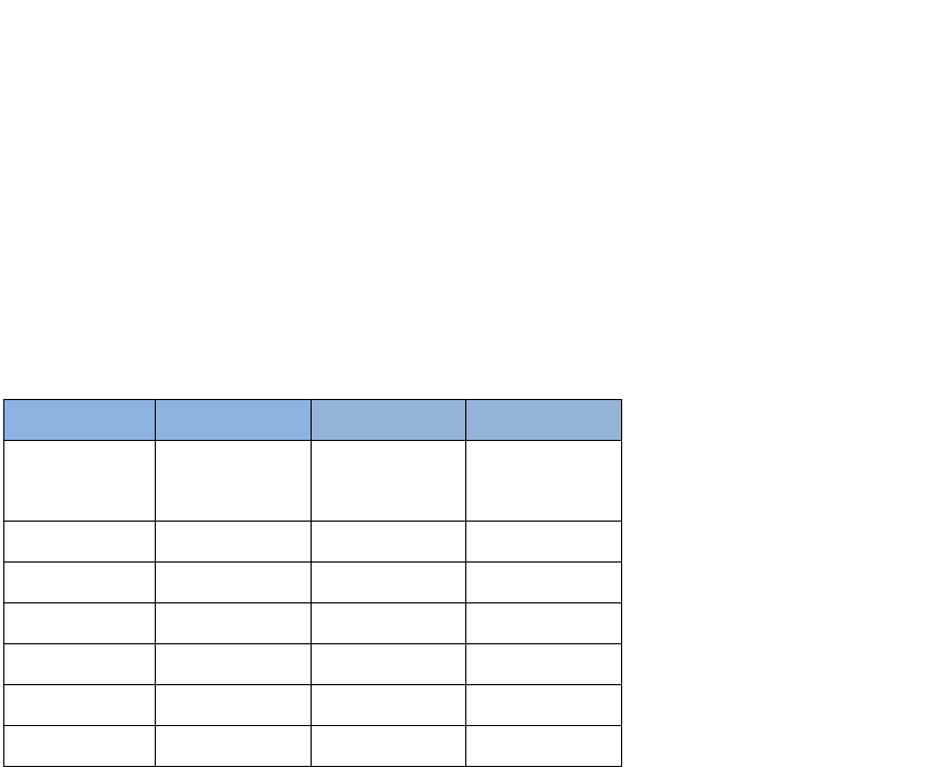
8 USB Host
The PYNQ-Z2 includes a TI TUSB1210 USB 2.0 PHY with an 8-bit ULPI interface
connected to the Zynq PS USB 0 controller (MIO[28-39]). The PHY features a HS-
USB Physical Front-End supporting speeds of up to 480Mbs. The USB interface is
configured to act as an embedded host. USB OTG and USB device modes are not
supported.
One of the Zynq PS USB controllers can be connected to the appropriate MIO pins to
control the USB port.
MIO Pin
Name
MIO Pin
Name
11
USB Over
Current
34
DATA2
28
DATA4
35
DATA3
29
DIR
36
CLK
30
STP
37
DATA5
31
NXT
38
DATA6
32
DATA0
39
DATA7
33
DATA1
46
RESETN
Table 2 USB MIO pin mapping

9 ADAU1761 Audio Codec
The PYNQ-Z2 has an Analog Devices ADAU1761 audio codec. It allows for stereo
48KHz record and playback. Sample rates from 8KHz to 96KHz are supported.
Additionally, the ADAU1761 provides digital volume control. The Codec can be
configured using Analog Devices SigmaStudio™ for optimizing audio for specific
acoustics, numerous filters, algorithms and enhancements. Analog Devices provides
Linux drivers for this device.
http://www.analog.com/en/content/cu_over_sigmastudio_graphical_dev_tool_overvie
w/fca.html
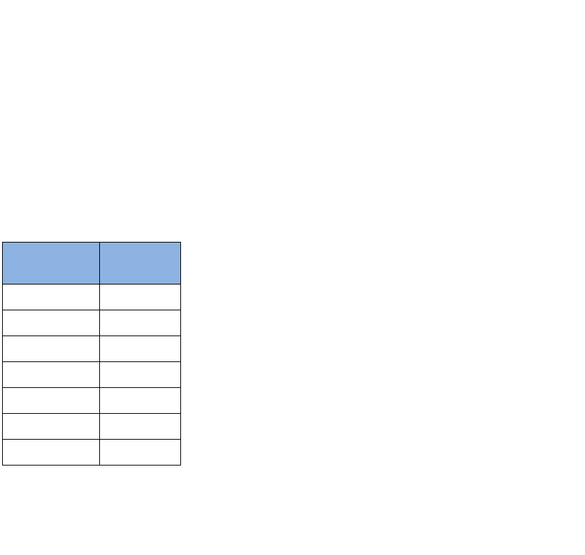
10 MicroSD
The PYNQ-Z2 has a MicroSD slot (SD1). An SD card can be used to boot the board,
or for applications that require non-volatile external memory storage. The PS IOP
controller SDIO 0 is wired to this port via MIO[40-47]. The pinout can be seen in
Table 7.1. The peripheral controller supports SDIO host mode with 1-bit and 4-bit SD
transfer modes. SPI mode is not supported.
The Zynq PS UART control can be connected to the appropriate MIO pins to control
the MicroSD port.
MIO Pin
Name
40
CCLK
41
CMD
42
D0
43
D1
44
D2
45
D3
47
CD
Table 3 SD MIO pin mapping
The maximum clock frequency is 50 MHz which supports both low-speed and high-
speed cards. A Class 4 MicroSD card or better is recommended.
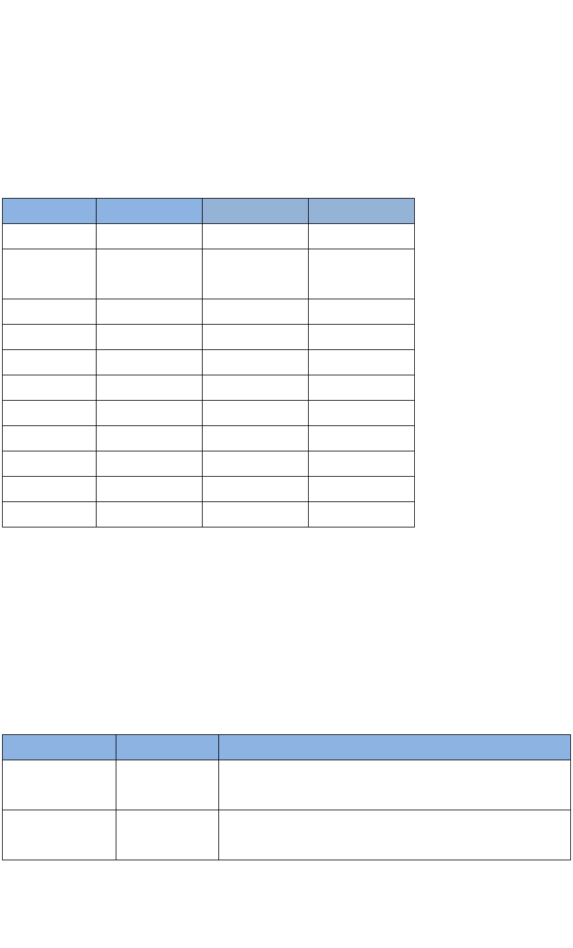
11 Ethernet PHY
The PYNQ-Z2 has a Realtek RTL8211E-VL PHY supporting 10/100/1000 Ethernet.
The PHY is connected to the Zynq RGMII controller. The auxiliary interrupt (INTB)
and reset (PHYRSTB) signals connect to MIO pins MIO10 and MIO9, respectively.
One of the Zynq PS Ethernet controllers can be connected to the appropriate MIO
pins to control the Ethernet port.
MIO Pin
Name
MIO Pin
Name
9
Ethernet Reset
25
RXD2
10
Ethernet
Interrupt
26
RXD3
16
TXCK
27
RXCTL
17
TXD0
23
RXD0
18
TXD1
24
RXD1
19
TXD2
25
RXD2
20
TXD3
26
RXD3
21
TXCTL
27
RXCTL
22
RXCK
52
MDC
23
RXD0
53
MDIO
24
RXD1
Table 4 Ethernet MIO pin mapping
The Zynq does not need to be configured for the PHY to establish a connection. After
power-up the PHY starts with Auto Negotiation enabled, advertising 10/100/1000 link
speeds and full duplex. The PHY will automatically establishes a link if there is an
Ethernet-capable partner connected.
There are two status LEDs on the RJ-45 connector that indicate traffic activity and
link status. Table 9.1 shows the default behavior.
LED
Color
Description
Link LED
(Right)
Green
- Blinking: Transmitting or Receiving
Act LED (Left)
Yellow
- Blinking: There is activity on this port.
- Off: No link is established.
Table 5 Ethernet status LEDs
Although the default power-up configuration of the PHY might be enough in most
applications, the MDIO bus is available to manage the interface. The RTL8211E-VL

is assigned the 5-bit address 00001 on the MDIO bus. With simple register read and
write commands, status information can be read out and the configuration can be
changed. The Realtek PHY follows an industry-standard register map for basic
configuration.
The PHY is clocked from the same 50 MHz oscillator that clocks the Zynq PS.
MAC address
A one-time-programmable (OTP) region of the Quad-SPI flash has been factory
programmed with a 48-bit globally unique EUI-48/64™ compatible identifier. The
OTP address range [0x20;0x25] contains the identifier with the first byte in
transmission byte order being at the lowest address. Refer to the Flash memory
datasheet for information on how to access the OTP regions. When using the PYNQ
framework, Ethernet is automatically handled in the boot-loader, and the Linux
system is automatically configured to use this unique MAC address.
12 MicroUSB Port
The PYNQ-Z2 includes an FTDI FT2232HL USB-UART bridge (attached to
connector J8 PROG UART) that supports USB-JTAG, USB-UART. The PYNQ-Z2
can also be powered from the MicroUSB port. The USB_UART allows PC
applications to communicate with the board using standard COM port commands (or
the tty interface in Linux and MacOS). The Zynq PS UART 0 controller is used to
connect to the UART device.
One of the Zynq PS UART controllers can be connected to the appropriate MIO pins
to control the UART port.
MIO Pin
Name
14
UART Input
15
UART
Output
Table 6 UART MIO pin mapping
Driver
The driver for the USB_UART should be automatically installed when the board is
connected to a computer using Windows 7 or later operating system, and recent
versions of Linux and MacOS.
13 HDMI ports
The PYNQ-Z2 contains two unbuffered HDMI ports connected directly to the PL.
The board labels indicate one HDMI port as input and the other port as output, but as
both ports are connected to PL pins, the designer can choose to use each of these ports
as input or output. Both ports use HDMI type-A receptacles with the data and clock
signals terminated and connected directly to the Zynq PL.
The 19-pin HDMI connectors include three differential data channels, one differential
clock channel five GND connections, a one-wire Consumer Electronics Control
(CEC) bus, a two-wire Display Data Channel (DDC) bus, a Hot Plug Detect (HPD)
signal, a 5V signal capable of delivering up to 50mA, and one reserved (RES) pin. All
non-power signals are connected to the Zynq PL with the exception of RES.
Pin/Signal
J11 (source) J18
J10 (sink)
Description
FPGA pin
Description
FPGA pin
D[2]_P, D[2]_N
Data output
J18, H18
Data input
N20, P20
D[1]_P, D[1]_N
Data output
K19, J19
Data input
T20, U20
D[0]_P, D[0]_N
Data output
K17, K18
Data input
V20, W20
CLK_P, CLK_N
Clock output
L16, L17
Clock input
N18, P19
CEC
Consumer
Electronics
Control
bidirectional
G15
Consumer
Electronics
Control
bidirectional
H17
SCL, SDA
DDC bidirectional
B9,B13
DDC
bidirectional
U14, U15
HPD/HPA
Hot-plug detect
input (inverted)
R19
Hot-plug assert
output
T19
Table 7 HDMI pin descriptions and PL pin locations

The Zynq PS I2C controller can be connected to the appropriate MIO pins to control
the I2C interface to the HDMI controller.
MIO Pin
Name
50
HDMI_TX_S
CL
51
HDMI_TX_S
DA
Table 8 HDMI I2C MIO pin mapping
14 LEDs, Buttons, Switches
The PYNQ-Z2 board includes 2 tri-color LEDs, 2 dipswitches, 4 push buttons, and 4
individual LEDs connected to the PL.
Push-buttons
The four push buttons generate a logic high on the corresponding PL pin when
pressed.
Signal Name
PL PIN
BTN0
D19
BTN1
D20
BTN2
L20
BTN3
L19
Table 9 Push Button PL pin mapping
Switches
When the switches are closed (in the “up” position) they generate a logic high on the
corresponding PL pins.
Signal Name
PL PIN
SW0
M20
SW1
M19
Table 10 Dip switch PL pin mapping
Tri-color
LEDs
DIP Switches
LED
s
Buttons
LEDs
The four individual LEDs are anode-connected to the Zynq PL via 330-ohm resistors.
Applying logic high to the appropriate pins will turn on the LEDs.
Signal Name
PL PIN
LED0
R14
LED1
P14
LED2
N16
LED3
M14
Table 11 LED PL pin mapping
The board also includes LEDs indicating board power, PL programming “done”, and
status for USB and Ethernet.
Tri color LEDs
Each of the 2 tri-color LEDs consists of three internal Reg, Blue Green LEDs. The
input signals to the internal RGB LEDs are driven by the Zynq PL through a
transistor, which inverts the signals.
Signal Name
PL PIN
LD4 Blue
L15
LD4 Red
N15
LD4 Green
G17
LD5 Blue
G14
LD5 Red
M15
LD5 Green
L14
Table 12 LED PL pin mapping
The tri-color LEDs are high intensity. It is recommended to use pulse-width
modulation (PWM) when driving the tri-color LEDs nd to aid driving the tri-color
LEDs with more than a 50% duty cycle. Using PWM also allows the LED to support
a wide range of colors by adjusting the duty cycle of each color.

15 Board reset signals
SRST is the external system reset. It resets the Zynq device without disturbing the
debug environment. System reset erases all memory content within the PS,
including the OCM. The PL is also cleared during a system reset. System reset does
not cause the boot mode strapping pins to be re-sampled.
The SRST button also causes the CK_RST signal to toggle in order to trigger a reset
on any attached shields.
The Zynq PS supports external power-on reset, a master reset of the whole chip. The
TPS65400 power regulator drives a PGOOD signal to hold the system in reset until all
power supplies are valid.
The PROG push switch, labeled PROG, enables Zynq PROG_B. This resets the PL
and causes DONE to be de-asserted. The PL will remain unconfigured until it is
reprogrammed by the processor or via JTAG.
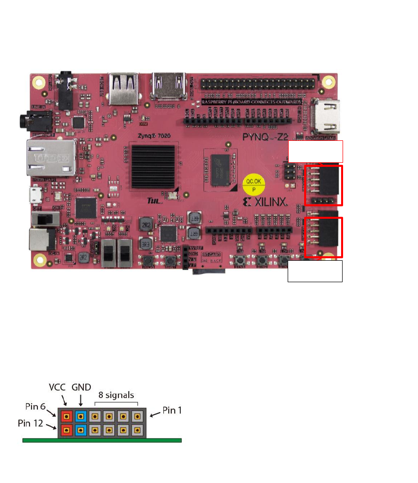
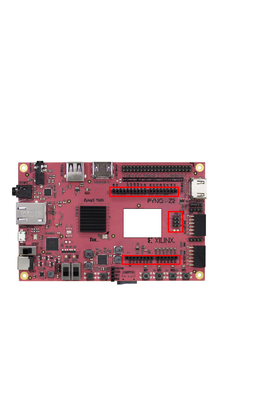
16 Pmod Ports
There are 2 Pmod ports on the PYNQ-Z2, labelled A and B.
Pmod ports are 2×6, right-angle, 100-mil spaced female connectors that mate with
standard 2×6 pin headers. Each 12-pin Pmod port provides two 3.3V VCC signals
(pins 6 and 12), two Ground signals (pins 5 and 11), and eight logic signals, as shown
in Figure 16.1.
The VCC and Ground pins can deliver up to 1A of current.
Pmod B
Pmod
A
PMODA
Signal Name
Description
Pin Number
ZYNQ PIN
JA1_P
I/O
1
Y18
JA1_N
I/O
2
Y19
JA2_P
I/O
3
Y16
JA2_N
I/O
4
Y17
GND
GND
5
N/C
3V3
POWER
6
N/C
JA3_P
I/O
7
U18
JA3_N
I/O
8
U19
JA4_P
I/O
9
W18
JA4_N
I/O
10
W19
GND
GND
11
N/C
3V3
POWER
12
N/C
Table 13 Pmod A pin description and PL pin assignments
* Pmod A pins are shared with the Raspberry Pi header
PMODB
Signal Name
Description
Pin Number
ZYNQ PIN
JB1_P
I/O
1
W14
JB1_N
I/O
2
Y14
JB2_P
I/O
3
T11
JB2_N
I/O
4
T10
GND
GND
5
N/C
3V3
POWER
6
N/C
JB3_P
I/O
7
V16
JB3_N
I/O
8
W156
JB4_P
I/O
9
V12
JB4_N
I/O
10
W13
GND
GND
11
N/C
3V3
POWER
12
N/C
Table 14 Pmod B pin description and PL pin assignments
17 Arduino Shield Connector
The Arduino shield connector has 26 pins connected to the Zynq PL. The pins can be
used as GPIO. Compatible Arduino shields can be connected to the PYNQ-Z2 board
via this header to extended functionality. Note that as the Arduino header is connected
to the PL, a design with appropriate controllers must be loaded before the Arduino
header can be used. Six of the Arduino pins (labeled A0-A5) can also be used as
single-ended analog inputs with an input range of 0V-3.3V, and another six (labeled
AR0-AR13) can be used as differential analog inputs.
Note: The PYNQ-Z2 is not compatible with shields that output 5V digital or
analog signals. Driving pins on the PYNQ-Z2 shield connector above 5V may
cause damage to the Zynq.
Shield
Digital I/O
The pins connected directly to the Zynq PL can be used as general-purpose
inputs/outputs. These pins include the pins labelled I2C (SCL, SDA), SPI (SS, SCL,
MISO, MOSI), and general purpose I/O pins. There are 200 Ohm series resistors
between the FPGA and the digital I/O pins to help provide protection against
accidental short circuits. The absolute maximum and recommended operating
voltages for these pins are outlined in the table below.
Arduino
Header
Absolute
Minimum
Voltage
Recommended
Minimum Operating
Voltage
Recommended
Maximum Operating
Voltage
Absolute
Maximum Voltage
Powered
-0.4V
-0.2V
3.4V
3.75V
Unpowered
-0.4V
N/A
N/A
0.55V
Table 15 Arduino header digital pin voltages
For more information on the electrical characteristics of the pins connected to the
Zynq PL, please see the Zynq-7000 datasheet from Xilinx.
Arduino J3 pins
Signal Name
Description
Pin Number
ZYNQ PIN
AR8
I/O
1
V17
AR9
I/O
2
V18
AR10
I/O
3
T16
AR11
I/O
4
R17
AR12
I/O
5
P18
AR13
I/O
6
N17
GND
GND
7
N/C
A
I/O
8
Y13
AR_SDA
SDA
9
P16
AR_SCL
SCL
10
P15
Table 16 Arduino J3 header PL pin assignments
Arduino J4 pins
Signal Name
Description
Pin Number
ZYNQ PIN
AR0
I/O
1
T14
AR1
I/O
2
U12
AR2
I/O
3
U13
AR3
I/O
4
V13
AR4
I/O
5
V15
AR5
I/O
6
T15
AR6
I/O
7
R16
AR7
I/O
8
U17
Table 17 Arduino J4 header PL pin assignments
Arduino J7 pins
Signal Name
Description
Pin Number
ZYNQ PIN
VU_CK
POWER
1
N/C
GND
GND
2
N/C
GND
GND
3
N/C
5V5
POWER
4
N/C
3V3
POWER
5
N/C
AR_RST
RST
6
PS_MIO12_500
3V3
POWER
7
N/C
N/C
N/C
8
N/C
Table 18 Arduino J7 header pin descriptions and connections
Arduino SPI pins
Signal Name
Description
Pin Number
ZYNQ PIN
AR_MISO
MISO
1
W15
3V3
POWER
2
N/C
AR_SCK
SCK
3
H15
AR_MOSI
MOSI
4
T12
AR_SS
SS
5
F16
GND
GND
6
N/C
Table 19 Arduino SPI header pin descriptions and PL pin assignments
Shield Analog I/O (Arduino J1)
The pins labeled A0-A5 and V_P/V_N are used as analog inputs to the XADC
module of the Zynq. The Zynq expects that the inputs range from 0-1 V. On the pins
labeled A0-A5 we use an external circuit to scale down the input voltage from 3.3V.
Signal Name
Description
Pin Number
ZYNQ PIN
A5
I/O
1
U10
A4
I/O
2
T5
A3
I/O
3
V11
A2
I/O
4
W11
A1
I/O
5
Y12
A0
I/O
6
Y11
Table 20 Arduino J1 header analog pin descriptions and PL pin assignments
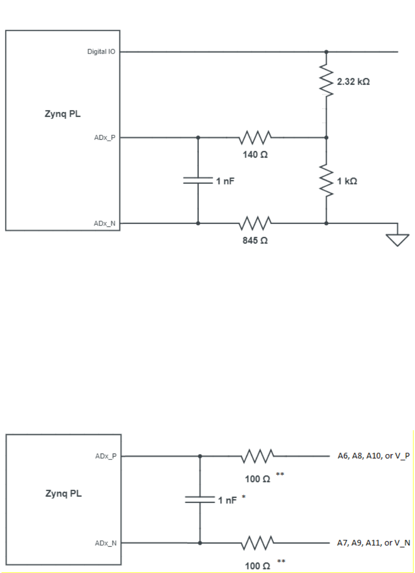
Figure 1 Single-Ended Analog Inputs
This circuit allows the XADC module to accurately measure any voltage between 0V
and 3.3V (relative to the PYNQ-Z2's GND) that is applied to any of these pins.
If you wish to use the pins labeled A0-A5 as Digital inputs or outputs, they are also
connected directly to the Zynq PL before the resistor divider circuit.
The pins labeled V_P and V_N are connected to the VP_0 and VN_0 dedicated
analog inputs of the FPGA. This pair of pins can also be used as a differential analog
input with voltage between 0-1V, but they cannot be used as Digital I/O.
Figure 2 Differential Analog Inputs
* Note that the 1nF capacitor is only loaded for V_P/VN
** For V_P/V_N, 140 Ohm resisters are used.
For more information on the XADC, see the Xilinx document titled “7 Series FPGAs
and Zynq-7000 SoC XADC Dual 12-Bit 1 MSPS Analog-to-Digital Converter”.
XADC header J5
Signal Name
Description
Pin Number
ZYNQ PIN
XADC_V_P
POWER
1
VP_0
XADC_V_N
GND
2
VN_0
XADCGND
GND
3
N/C
XADCVREF
POWER
4
N/C
Table 21 J5 header XADC pin descriptions and PL pin assignments
J5
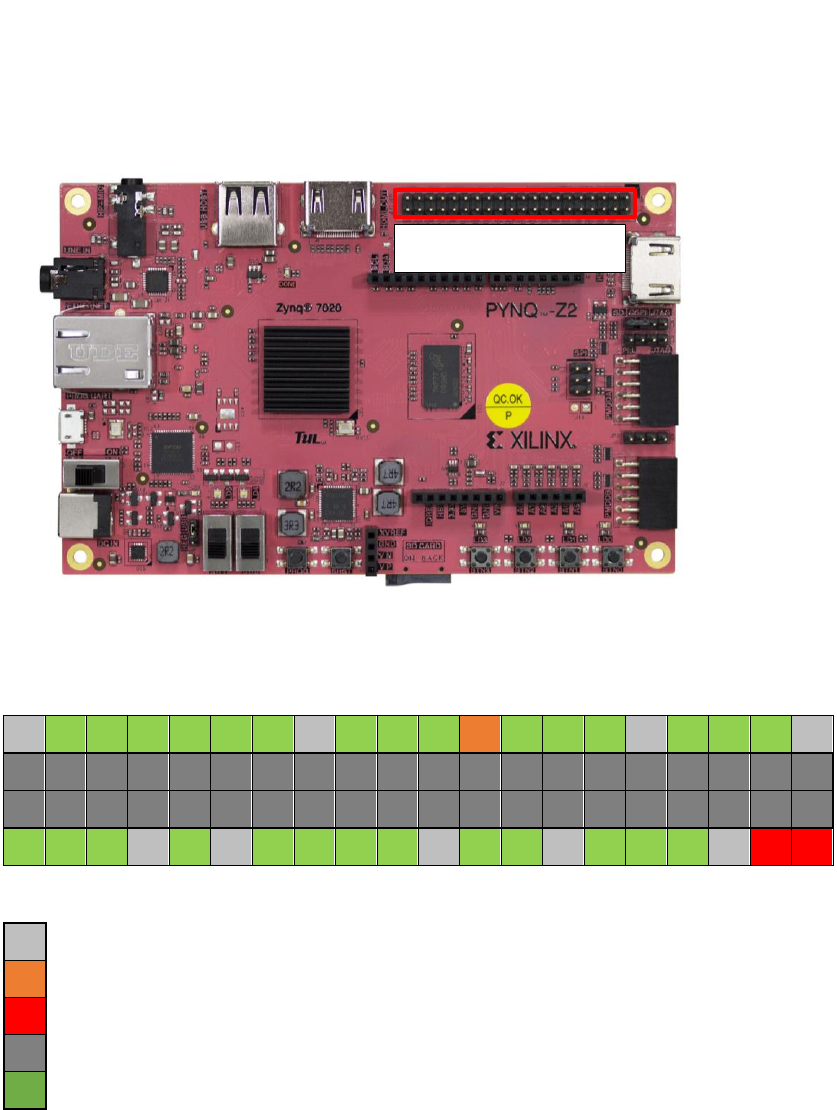
18 Raspberry Pi Header
The PYNQ-Z2 has a 40-pin Raspberry Pi connector with 28 pins connected to the
Zynq device.
These pins can be used as GPIO, or to connect a standard Raspberry Pi peripheral.
G
W9
Y8
W8
Y7
Y6
Y16
G
W10
V10
V8
V
U8
V7
U7
G
V6
W19
W18
G
39
37
35
33
31
29
27
25
23
21
19
17
15
13
11
9
7
5
3
1
40
38
36
34
32
30
28
26
24
22
20
18
16
14
12
10
8
6
4
2
Y9
A20
B19
G
B20
G
Y17
F20
F19
U19
G
U18
W6
G
C20
Y19
Y18
G
V
V
G
Ground
V
3.3V
V
5V
…
Raspberry Pi header pin number
…
Zynq Pin
Table 22 Raspberry Pi header pin layout and Zynq PL pin assignments
Raspberry Pi header

19 References
PYNQ-Z2 schematics:
http://www.tul.com.tw/download/TUL_PYNQ%20Schematic_R12.pdf
UG585 Zynq TRM
https://www.xilinx.com/support/documentation/user_guides/ug585-Zynq-7000-
TRM.pdf
UG472 7 Series FPGAs Clocking Resources User Guide
https://www.xilinx.com/support/documentation/user_guides/ug472_7Series_Clocking
.pdf
