PZMR2T
User Manual: PZMR2T
Open the PDF directly: View PDF ![]() .
.
Page Count: 146 [warning: Documents this large are best viewed by clicking the View PDF Link!]

PZ-MR2T
PZ-43MR2U
PZ-50MR2U
SERVICE MANUAL
S12F4PZ50MR2U
In the interests of user-safety (Required by safety regulations in some countries) the set should be restored
to its original condition and only parts identical to those specified should be used.
MODELS
PZ-MR2T
PZ-43MR2U
PZ-50MR2U
CONTENTS
Page
PLASMA DISPLAY TV
(AVC SYSTEM)
»IMPORTANT SERVICE SAFETY PRECAUTION ..... 2
»SPECIFICATIONS................................................ 4
»OPERATION MANUAL ........................................ 5
»DIMENSIONS .................................................... 13
»REMOVING OF MAJOR PARTS ....................... 14
»ADJUSTMENT PROCEDURES......................... 16
»DESCRIPTION OF MAJOR IC FUNCTIONS .... 22
»TROUBLE SHOOTING TABLE .......................... 49
»PRINTED WIRING BOARD BLOCK DIAGRAM .. 56
»SYSTEM BLOCK DIAGRAM ............................. 58
Page
»SIGNAL FLOW BLOCK DIAGRAM .................... 60
»DC/DC CONVERTER BLOCK DIAGRAM ......... 62
»POWER BLOCK DIAGRAM............................... 64
»PC I/F BLOCK DIAGRAM .................................. 66
»OVERALL WIRING DIAGRAM ........................... 68
»DESCRIPTION OF SCHEMATIC DIAGRAM ..... 72
»WAVEFORMS .................................................... 73
»SCHEMATIC DIAGRAM..................................... 74
»PRINTED WIRING BOARD ASSEMBLIES...... 114
»PARTS LIST ..................................................... 121
»PACKING OF THE SET ................................... 145
SHARP CORPORATION This document has been published to be used for
after sales service only.
The contents are subject to change without notice.
2
PZ-MR2T
PZ-43MR2U
PZ-50MR2U
SAFETY NOTICE
Many electrical and mechanical parts in Plasma Display
television have special safety-related characteristics.
These characteristics are often not evident from visual
inspection, nor can protection afforded by them be
necessarily increased by using replacement components
rated for higher voltage, wattage, etc.
Replacement parts which have these special safety
characteristics are identified in this manual; electrical
components having such features are identified by “ å”
and shaded areas in the
Replacement Parts List
and
Schematic Diagrams
.
For continued protection, replacement parts must be
identical to those used in the original circuit.
The use of a substitute replacement parts which do not
have the same safety characteristics as the factory
recommended replacement parts shown in this service
manual, may create shock, fire or other hazards.
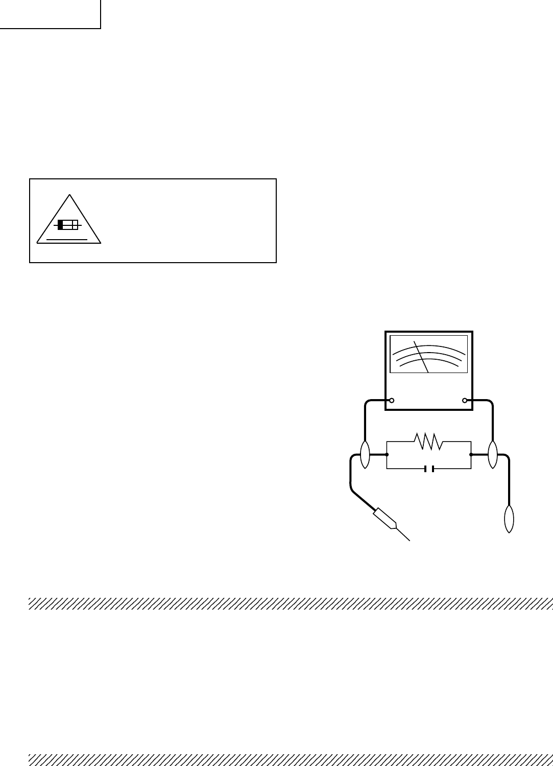
CAUTION: FOR CONTINUED
PROTECTION AGAINST A RISK
OF FIRE REPLACE ONLY WITH
SAME TYPE FUSE. F701 (T2A,
250V), F702 (T2A, 250V), F1702
(T4AL, 250V) FUSE.
WARNING
1. For continued safety, no modification of any circuit
should be attempted.
2. Disconnect AC power before servicing.
BEFORE RETURNING THE RECEIVER
(Fire & Shock Hazard)
Before returning the receiver to the user, perform
the following safety checks:
1. Inspect all lead dress to make certain that leads are
not pinched, and check that hardware is not lodged
between the chassis and other metal parts in the
receiver.
2. Inspect all protective devices such as non-metallic
control knobs, insulation materials, cabinet backs,
adjustment and compartment covers or shields,
isolation resistor-capacitor networks, mechanical
insulators, etc.
3. To be sure that no shock hazard exists, check for
leakage current in the following manner.
»Plug the AC cord directly into a 110~240 volt AC outlet,
and connect the DC power cable into the receiver's
DC jack. (Do not use an isolation transformer for this
test).
»Using two clip leads, connect a 1.5k ohm, 10 watt
resistor paralleled by a 0.15µF capacitor in series
with all exposed metal cabinet parts and a known
earth ground, such as electrical conduit or electrical
ground connected to an earth ground.
»Use an AC voltmeter having with 5000 ohm per volt,
or higher, sensitivity or measure the AC voltage drop
across the resisor.
»Connect the resistor connection to all exposed metal
parts having a return to the chassis (antenna, metal
cabinet, screw heads, knobs and control shafts,
escutcheon, etc.) and measure the AC voltage drop
across the resistor.
All checks must be repeated with the AC cord plug
connection reversed. (If necessary, a nonpolarized
adaptor plug must be used only for the purpose of
completing these checks.)
Any reading of 35V peak (this corresponds to 0.7
milliamp. peak AC.) or more is excessive and
indicates a potential shock hazard which must be
corrected before returning the monitor to the owner.
TO EXPOSED
METAL PARTS CONNECT TO
KNOWN EARTH
GROUND
IMPORTANT SERVICE SAFETY PRECAUTION
ËService work should be perfomed only by qualified service technicians who are thor-
oughly familiar with all safety checks and the servicing guidelines which follow:
A V
DVM
AC SCALE
1.5k ohm
10W
0.15 µF
TEST PROBE
3
PZ-MR2T
PZ-43MR2U
PZ-50MR2U
DVM
AC SCALE
1.5k ohm
10W
0.15 µF
TEST PROBE
PRECAUTION: POUR LA PROTECTION
CONTINUE CONTRE LES RISQUES
D'INCENDIE, REMPLACER LE FUSIBLE
PAR UN FUSIBLE DE MEME TYPE F701
(T2A, 250V), F702 (T2A, 250V), F1702
(T4AL, 250V).
AVIS POUR LA SECURITE
De nombreuses pièces, électriques et mécaniques, dans
les téléviseurs présentent des caractéristiques spéciales
relatives à la sécurité, qui ne sont souvent pas évidentes
à vue. Le degré de protection ne peut pas être
nécessairement augmentée en utilisant des pièces de
remplacement étalonnées pour haute tension,
puissance, etc.
Les pièces de remplacement qui présentent ces
caractéristiques sont identifiées dans ce manuel; les
pièces électriques qui présentent ces particularités sont
PRECAUTIONS A PRENDRE LORS DE LA REPARATION
ËNe peut effectuer la réparation qu' un technicien spécialisé qui s'est parfaitement
accoutumé à toute vérification de sécurité et aux conseils suivants.
identifiées par la marque " å " et hachurées dans la
liste des pièces de remplacement et les diagrammes
schématiques.
Pour assurer la protection, ces pièces doivent être
identiques à celles utilisées dans le circuit d'origine.
L'utilisation de pièces qui n'ont pas les mêmes
caractéristiques que les pièces recommandées par
l'usine, indiquées dans ce manuel, peut provoquer des
électrocutions, incendies, radiations X ou autres
accidents.
AVERTISSEMENT
1. N'entreprendre aucune modification de tout circuit.
C'est dangereux.
2. Débrancher le récepteur avant toute réparation.
VERIFICATIONS CONTRE L'INCEN-DIE ET
LE CHOC ELECTRIQUE
Avant de rendre le récepteur à l'utilisateur, effectuer
les vérifications suivantes.
1. Inspecter tous les faisceaux de câbles pour s'assurer
que les fils ne soient pas pincés ou qu'un outil ne soit
pas placé entre le châssis et les autres pièces
métalliques du récepteur.
2. Inspecter tous les dispositifs de protection comme les
boutons de commande non-métalliques, les isolants,
le dos du coffret, les couvercles ou blindages de réglage
et de compartiment, les réseaux de résistance-
capacité, les isolateurs mécaniques, etc.
3. S'assurer qu'il n'y ait pas de danger d'électrocution en
vérifiant la fuite de courant, de la facon suivante:
•Brancher le cordon d'alimentation directem-ent à une
prise de courant de 110-240V. (Ne pas utiliser de
transformateur d'isolation pour cet essai).
•A l'aide de deux fils à pinces, brancher une résistance
de 1.5 kΩ 10 watts en parallèle avec un condensateur
de 0,15µF en série avec toutes les pièces métalliques
exposées du coffret et une terre connue comme une
conduite électrique ou une prise de terre branchée à
la terre.
•Utiliser un voltmètre CA d'une sensibilité d'au moins
5000Ω/V pour mesurer la chute de tension en travers
de la résistance.
•Toucher avec la sonde d'essai les pièces métalliques
exposées qui présentent une voie de retour au châssis
(antenne, coffret métallique, tête des vis, arbres de
commande et des boutons, écusson, etc.) et mesurer
la chute de tension CA en-travers de la résistance.
Toutes les vérifications doivent être refaites après avoir
inversé la fiche du cordon d'alimentation. (Si nécessaire,
une prise d'adpatation non polarisée peut être utilisée
dans le but de terminer ces vérifications.)
Tous les courants mesurés ne doivent pas dépasser
0,5 mA.
Dans le cas contraire, il y a une possibilité de choc
électrique qui doit être supprimée avant de rendre le
récepteur au client.
A V
AUX PIECES
METALLIQUES
EXPOSEES
BRANCHER A UNE
TERRE CONNUE
0.15µF
SONDE D'ESSAI
DVM
ECHELLE CA
4
PZ-MR2T
PZ-43MR2U
PZ-50MR2U
Specifications
Item AVC System, Model: PZ-50MR2U, PZ-43MR2U, PZ-MR2T
Color System American TV standard NTSC system
TV
Function PLL full synchronous detection, PLL digital synthesizer system
VHF/UHF VHF 2–13ch, UHF 14–69ch
CATV 1–125ch
Audio multiplex BTSC system
Terminals S-VIDEO in, AV in, COMPONENT in
INPUT 2 S-VIDEO in, AV in
INPUT 3 S-VIDEO in, AV in, COMPONENT in, RGB in
Antenna 75 UNBAL, F Type for VHF/UHF/CATV in
INPUT 4 S-VIDEO, AV in
PC INPUT 15 Pin mini D-Sub, Audio in
Monitor Out Terminal S-VIDEO out, AV out, Audio (Variable, Fixed)
Power Requirement AC 110–240 V, 50/60 Hz, 40 W (0.6 W Standby)
Dimensions 16 15/16 (W) 2 25/32 (H) 13 (D) inch (430 (W), 70 (H), 330 (D) mm)
Weight 9.7 lbs(4.4 kg)
Accessories Power Cord, Remote control unit, Two AA size batteries, System Cable,
Operation manual
Cercuit type
Tuner
Rear INPUT 1
Front
Rear
• Design and specifications are subject to change without notice.
Other Features
OSD Language English/French/Spanish
Picture & Picture, Still image, Dual Tuner System

5
PZ-MR2T
PZ-43MR2U
PZ-50MR2U
Operation Manual
DISPLAY OUTPUT-2
RS-232C
AC INPUT
110V - 24OV
DISPLAY OUTPUT-1
YP
B
P
R
S-VIDEO VIDEO R-AUDIO-L
COMPONENT
INPUT 1
INPUT 2
YP
B
P
R
S-VIDEO
COMPONENT
VIDEO R-AUDIO-L
INPUT 3
HD INPUT
MONITOR OUTPUT
ANT/CABLE 75OUT
ANT-A ANT-B
USE FOR HDTV SIGNALS ONLY.
NOT INTENDED FOR USE WITH
COMPUTERS
Front view
CLEAR button*
POWER button INPUT 4 terminal (S-VIDEO)
INPUT 4 terminal (VIDEO)
PC INPUT terminal (AUDIO) INPUT 4 terminals (AUDIO)
PC INPUT terminal (ANALOG RGB)
AVC System
Rear view
INPUT 1 COMPONENT
terminals (Y, PB, PR)
INPUT 3 COMPONENT
video terminals
(Y, PB, PR)
MONITOR OUTPUT
terminal (S-VIDEO)
DISPLAY OUTPUT-2 terminal
DISPLAY OUTPUT-1
terminal
AC INPUT terminal
after RS-232C terminal
MONITOR
OUTPUT
terminal (VIDEO)
MONITOR OUTPUT
terminals (AUDIO L/R)
Antenna input
terminal (A)
Antenna input
terminal (B)
Antenna output
terminal
HD
INPUT
terminal
INPUT 3 terminal
(S-VIDEO)
INPUT 3 terminal
(VIDEO)
INPUT 3 terminals
(AUDIO L/R)
INPUT 1 terminal
(S-VIDEO)
INPUT 1 terminal
(VIDEO)
INPUT 1 terminals
(AUDIO L/R)
INPUT 2 terminal
(S-VIDEO)
INPUT 2 terminal
(VIDEO)
INPUT 2 terminals
(AUDIO L/R)
Door knob
How to open the door.
STANDBY/ON indicator
*If you’re having problems operating the AVC System and want to return to normal screen, even when it stays
on (the indicator lights green), press CLEAR on the AVC System. Pressing CLEAR resets the System as
shown below.
• AV MODE resets to STANDARD
• TV channel returns to initial channel setting(Air:2ch, Cable:1 or 2ch)
• Twin picture resets to normal
• Audio setting initializes
• SRS resets to Off.
• Image position initializes
• Pressing CLEAR will not work if the System is in standby mode (indicator lights red).
• Pressing CLEAR will not delete channel preset or secret number
you know your secret number. See Page for initialising factory preset values when you have forgotten your secret
number.
USE FOR HDTV SIGNALS ONLY.
NOT INTENDED FOR USE WITH
COMPUTERS
. See Page for initialising factory preset settings when

6
PZ-MR2T
PZ-43MR2U
PZ-50MR2U
Remote control unit
•When using the remote control unit, point it at the Plasma
Display TV(Panel Unit).
TV
ANT-A/B
INPUT
SURROUND
FRONT
TWIN
MODE
AV
POWER
MTS CC
PICTURE
SELECT
SUB TWIN CH
FREEZE
MODE
VOL CH
MUTE
MENU TV/SAT/DVD
FAVORITE CH
RECEIVER
DTV/DVD TOP
SOURCE DTV/SAT
DTV/SAT
VCR REC
ABCD
RETURN
MENU
POWER
SET/
ENTER
MENU
GUIDE
INPUT VOL– VOL+
INFO
VIEW
SLEEP LEARN
EDIT/
ENT
FLASHBACK
DISPLAY
INPUT
TV VCRCBL
/SAT
/DTV
DVD
/LD
123
456
789
100
0
POWER
16
17
18
19
20
21
22
24
23
3
2
1
4
5
6
7
8
9
10
11
12 13 14
15
Set the mode switch to TV.
1TV POWER: Switch the Plasma Display TV power on or
off.
2 FRONT SURROUND: Set SRS and FOCUS Sound
System mode.
3 AV MODE:Select an audio or video setting.
(AV mode: ST ANDARD, DYNAMIC,
MOVIE, GAME, USER.
PC mode: ST ANDARD, USER.)
4 VIEW MODE: Select the scr een size.
5 DISPLAY:Display the channel information.
6 SLEEP:Set the SLEEP timer.
7 FLASHBACK: Return to the previous channel or input
external mode.
8VOL : Set the volume.
9 MENU:Display the menu screen.
10 MENU RETURN: Return to the previous menu screen.
11 : Select a desired item on the setting screen.
12 ANT-A/B: Select the antenna. (A, B)
13 INPUT: Select an input sour ce of the Plasma Display
TV. (TV, INPUT 1, INPUT 2, INPUT 3, INPUT 4,
PC)
14 :When pressed all buttons on the remote control unit
will light. The lighting will turn off if no operations
are performed within about 5 seconds. This button
is used for performing operations in dark places.
15 MTS: Select the MTS/SAP.
16 CC: Display captions during closed-caption source.
17 TWIN CH buttons
TWIN PICTURE:Set the twin picture mode.
Press again to return to normal
screen.
FREEZE: Set the still image. Press again to return to
normal screen.
SELECT: Select the active screen.
SUB INPUT: Select an input sour ce of sub screen.
TWIN CH : Select the channel of sub screen.
18 0 – 9: Set the channel.
19 100 ENT: Select the three digit mode. Execute a
command of the channel.
20 CH : Select the channel.
21 MUTE: Mute the sound.
22 SET/ENTER: Execute a command.
23 FAVORITE CH
A, B, C, D: Select any of four preset channels. (See
page for details to set the FAVORITE CH.)
While watching you can toggle the set channels by
pressing A, B, C and D.
24 LED for transmission confirmation
Mode switch
+
–

7
PZ-MR2T
PZ-43MR2U
PZ-50MR2U
Preparation
Red
Black
Black Red
DISPLAY OUTPUT-2
RS-232C
AC INPUT
110V - 24OV
DISPLAY OUTPUT-1
YP
B
P
R
S-VIDEO VIDEO R-AUDIO-L
COMPONENT
INPUT 1
INPUT 2
YP
B
P
R
S-VIDEO
COMPONENT
VIDEO R-AUDIO-L
INPUT 3
HD INPUT
MONITOR OUTPUT
ANT/CABLE 75OUT
ANT-A ANT-B
System cable
AVC System (rear view)
Power cord
Plasma Display TV (Panel Unit) (rear view)
Power cord
System cable
(bottom view)
(GRAY)
(WHITE)
(GRAY) (WHITE)
Connecting the system
1. Connecting the system cable, the power cord and the speaker cables to the Plasma Display TV (Panel
Unit)
2. Connecting the system cable and the power cord to the AVC System
• TO PREVENT RISK OF ELECTRIC SHOCK, DO NOT TOUCH UN-INSULATED PARTS OF ANY CABLES WITH THE
POWER CORD CONNECTED.
Speaker cables
(GRAY GRAY with white stripe)
Speaker cable Speaker cable
As you apply pressure to this part,
insert the speaker cable. It is
important to match polarity when
connecting the speaker cables to the
terminals.
Insert the speaker cable
Lift up the snap clip.
Insert the wire into
the hole of the
connector.
Lower the snap clip
to grip the wire in
place.
•Two speaker cables of different lengths are supplied. As
shown in the diagram, connect the longer speaker cable
to the left speaker and the shorter to the right.

8
PZ-MR2T
PZ-43MR2U
PZ-50MR2U
preparation
As viewed from the rear of the display.
How to route cables
A system cable clamp and five speaker cable clamps are included with the system for cable management. Follow the
diagram below for correct cable management.
System cable
Wedge the power cord and the
system cable into the groove on the
stand.
Power cord
Speaker cable
Stick the speaker cable clamps
( – ) to the surface as shown.
System cable clamp
Speaker cable clamp
Speaker cable clamp
System cable
System cable clamp

9
PZ-MR2T
PZ-43MR2U
PZ-50MR2U
preparation
++
_
_
Using the remote control unit
Use the remote control unit by pointing it towards the remote sensor window.
Objects between the remote control unit and sensor window may prevent proper
operation.
Cautions regarding remote control unit
•Do not expose the remote control unit to shock. In addition, do not expose the
remote control unit to liquids, and do not place in an area with high humidity.
•Do not install or place the remote control unit under direct sunlight. The heat
may cause deformation of the unit.
•The remote control unit may not work properly if the remote sensor window of
the Plasma Display TV(Panel Unit) is under direct sunlight or strong lighting.
In such case, change the angle of the lighting or Plasma Display TV(Panel
Unit), or operate the remote control unit closer to the remote sensor window.
Inserting the batteries
If the remote control unit fails to operate Plasma Display TV functions, replace
the batteries in the remote control unit.
1Open the battery cover. 2Insert batteries (two AA size
batteries, supplied with product).
•Place batteries with their terminals
corresponding to the ( ) and ( )
indicators in the battery compartment.
3Close the battery cover.
Cautions regarding batteries
Improper use of batteries can result in chemical leakage or explosion. Be sure to follow the instructions below.
•Do not use manganese batteries. When you replace the batteries, use alkaline ones.
•Place the batteries with their terminals corresponding to the ( ) and ( ) indicators.
•Do not mix batteries of different types. Different types of batteries have different characteristics.
•Do not mix old and new batteries. Mixing old and new batteries can shorten the life of new batteries or cause
chemical leakage in old batteries.
•Remove batteries as soon as they have worn out. Chemicals that leak from batteries can cause a rash. If you
find any chemical leakage, wipe thoroughly with a cloth.
•The batteries supplied with this product may have a shorter life expectancy due to storage conditions.
•If you used the remote control unit for an extended period of time, remove the batteries from it.
•WHEN DISPOSING OF USED BATTERIES, PLEASE COMPLY WITH GOVERNMENTAL REGULATIONS OR
ENVIRONMENTAL PROTECTION GUIDELINES THAT APPLY IN YOUR COUNTRY OR AREA.

10
PZ-MR2T
PZ-43MR2U
PZ-50MR2U
Using external equipment
DISPLAY OUTPUT-2
RS-232C
AC INPUT
110V - 24OV
DISPLAY OUTPUT-1
YP
B
P
R
S-VIDEO VIDEO R-AUDIO-L
COMPONENT
INPUT 1
INPUT 2
YP
B
P
R
S-VIDEO
COMPONENT
VIDEO R-AUDIO-L
INPUT 3
HD INPUT
MONITOR OUTPUT
ANT/CABLE 75OUT
ANT-A ANT-B
DVD player
AVC System
(rear view)
AVC System
(front view)
AV Receiver
(Built-in Tuner Amp) VCR
Digital tuner
Game console/
Camcorder
Computer
You can connect many types of external equipment to your Plasma Display TV, like a DVD player, VCR, Digital
tuner, computer, game console and camcorder. To view external source images, select the input source from
INPUT on the remote control unit or on the Plasma Display TV(Panel Unit).
•To protect all equipment, always turn off the AVC System before connecting to a DVD player, VCR, Digital tuner,
computer, game console, camcorder or other external equipment.
•Please refer to the relevant operation manual (DVD player, computer, etc.) carefully before making connections.
S-VIDEO
S-VIDEO
S-VIDEO
AV
S-VIDEO
AV
AV
AV
Y/P
B
/P
R
Y/P
B
/P
R
RGB
PC-AUDIO
ANALOG RGB
AV
S-VIDEO
11
PZ-MR2T
PZ-43MR2U
PZ-50MR2U
Appendix
RS-232C port specifications
Return codeCommand 4-digits Parameter 4-digits
Computer Control of the Plasma Display TV (Panel Unit)
• When a program is set, the display can be controlled from the computer using the RS-232C terminal.
The input signal (computer/video) can be selected, the volume can be adjusted and various other adjustments
and settings can be made, enabling automatic programmed playing.
•
Attach an RS-232C cable cross-type (commercially available) to the supplied Din-D/sub RS-232C for the
connections.
• This operation system should be used by a person who is accustomed to using computers.
Communication conditions
Set the RS-232C communications settings on the computer to match the display's communications conditions.
The display's communications settings are as follows:
Baud rate:
Parity bit:
Data length:
Stop bit:
Flow control:
9,600 bps
8 bits
None
1 bit
None
Command format
Communication procedure
Send the control commands from the computer via the RS-232C connector.
The display operates according to the received command and sends a response message to the computer.
Do not send multiple commands at the same time. Wait until the computer receives the OK response before
sending the next command.
Eight ASCII codes CR
Command 4-digits:Command. The text of four characters.
Parameter 4-digits:Parameter 0 – 9, x, blank, ?
Parameter
Input the parameter values, aligning left, and fill with blank(s) for the remainder. (Be sure that four values are input for the
parameter.)
When the input parameter is not within an adjustable range, “ERR” returns. (Refer to “Response code format”.)
No problem to input any numerical value for “x” on the table.
When “?” is input for some commands, the present setting value responds.
C1 C2 C3 C4 P1 P2 P3 P4
0055
100
30
0009
0
????
?
–
12
PZ-MR2T
PZ-43MR2U
PZ-50MR2U
Appendix
Command table
•About the command except being indicated here, it is outside the guarantee range of operation.
CONTROL ITEM COMMAND
PARAMETER
CONTROL CONTENTS
POWER SETTING It shifts to standby.
It input-switches by the toggle. (It is the same as an input change key)
It input-switches to TV. (A channel remains as it is. (Last memory))
It input-switches to INPUT1~INPUT4.
It input-switches to PC.
An input change is also included.
Although it can choose now, it is toggle operation in inside.
Although it can choose now, it is toggle operation in inside.
(Toggle)
Input terminal number (1–4)
AUTO
AV-Y/C
COMPONENT
AUTO
AV-Y/C
COMPONENT
RGB
(Toggle)
STANDARD
DYNAMIC
MOVIE
GAME
USER
Volume (0–60)
AV mode. (±15)
PC mode. (±90)
AV mode. (±30)
PC mode. (±60)
Only PC mode. (±90)
Only PC mode. (±20)
(Toggle) [AV]
Toggle operation.
An input change is included if it is not TV display.
In Air, 2–69ch is effective.
In Cable, 1–125ch is effective.
If it is not TV display, it will input-switch to TV.
If it is not TV display, it will input-switch to TV.
Change toggle operation of tuner A/B.
Toggle operation of a closed caption.
(Toggle)
Side Bar [AV]
S.Stretch [AV]
Zoom [AV]
Stretch [AV]
Normal [PC]
Full [PC]
Dot by Dot [PC]
Dot by Dot (W) [PC]
(Toggle)
OFF
SRS
FOCUS
FOCUS
+
SRS
One screen
Twin screens
The channel number of TV
The channel number of TV 1
The channel number of TV 1
(Toggle)
(Toggle)
OFF
CC1
CC2
T1
T2
(1~125)
AUTO
POWR
ITGD
ITVD
IAVD
IPCD
INP1
INP3
INPUT SELECTION A TOGGLE
INPUT SELECTION B
AV MODE SELECTION
VOLUME
POSITION
WIDEMODE
SRS
TWIN PICTURE
CHANNEL
ANT-A/B
CC
DIRECT
CH UP
CH DOWN
CHANNEL
H-POSITIONH-POSITION
V-POSITION
CLOCK
PHASE
INPUT 1
INPUT 3
AVMD
VOLM
HPOS
VPOS
CLCK
PHSE
SRSS
TWI N
DCCH
CHUP
CHDW
ANTS
CLCP
WIDE
0
x
0
*
x
0
0
1
2
3
1
2
0
*
*
*
*
*
0
0
*
x
x
x
0
1
2
3
4
5
1
1
2
3
4
0
1
2
3
4
5
6
7
8
*
*
1
2
3
4
5
*
_
_
_
_
_
_
_
_
_
_
_
_
_
_
_
_
_
_
_
_
_
_
_
_
_
*
*
*
*
*
*
*
_
_
_
_
_
_
_
_
_
_
_
_
_
_
_
_
_
_
*
_
_
_
_
_
_
_
_
_
_
_
_
_
_
_
_
_
_
_
_
_
_
_
_
_
*
*
*
*
*
*
_
_
_
_
_
_
_
_
_
_
_
_
_
_
_
_
_
_
_
_
_
_
_
_
_
_
_
_
_
_
_
_
_
_
_
_
_
_
_
_
_
_
_
_
_
_
_
_
_
_
_
_
_
_
_
_
_
_
_
_
_
_
_
_
_
_
_
_
_
_
TV
INPUT1-4
PC
•If an underbar (_) appears in the parameter column, enter a space.
•If an asterisk (*) appears, enter a value in the range indicated in brackets under CONTROL CONTENTS.
•As long as that from which the parameter ( ) in the table is a numerical value, it may write anything.
Return code (0DH)
Response code format
Normal response
Problem response (communication error or incorrect command)
Return code (0DH)
OK
ERR
+
–

13
PZ-MR2T
PZ-43MR2U
PZ-50MR2U
Dimensions
(Unit: mm)

14
PZ-MR2T
PZ-43MR2U
PZ-50MR2U
REMOVING OF MAJOR PARTS
1. Remove the six lock screws from the back of the top cabinet. Slide the top cabinet backward and detach it.
2. Remove the three lock screws from the front panel. Undo the three hooks at the top and the four hooks at the
bottom, and detach the front panel.
3. Remove the two hexagonal shafts from the front shield. Undo the four hooks on both sides and detach the
front shield.
4. Remove the three lock screws from the front unit and detach this unit.
5. Remove the one lock screw from the LED unit and detach this unit.
6. Remove the PC I/F unit and SR unit assemblies.
6-1. Remove the two hexagonal shafts each from the system cable (white) terminal and the RS-232C terminal,
both on the PC I/F unit.
6-2. Remove two lock screws from the system cable (gray) terminal also on the SR unit.
6-3. Remove the two lock screws from the PC I/F unit bracket.
6-4. Remove the four lock screws from the PC I/F unit and SR unit assemblies. Take out these assemblies.
6-5. Remove the three lock screws from the brackets of the PC I/F unit and SR unit assemblies. Detach the
shield.
6-6. Remove the six lock screws from the PC I/F unit. Detach this unit from the bracket.
6-7. Remove the two lock screws from the SR unit. Detach this unit from the bracket.
7. Remove the seven lock screws from the main unit and detach this unit.
AV Unit
6-1
9-1
Main Unit
Front Unit
Power Unit
LED Unit
SR Unit
PC I/F Unit
EMC Unit
Bottom cabinet
1
7
Top cabinet
6-1
8-3 8-1
8-2
6-5
6-4
8-4
9-2
10
6-7
5
2
6-6
4
2
3
3

15
PZ-MR2T
PZ-43MR2U
PZ-50MR2U
8. Remove the AV unit.
8-1. Remove the coaxial cable from the antenna terminal.
8-2. Remove the three lock screws from the antenna terminals
8-3. Remove the six lock screws from the AV unit.
8-4. Remove the six lock screws from the AV unit and detach this unit.
9. Remove the EMC unit assemblies.
9-1. Remove the two lock screws from the EMC unit bracket.
9-2. Remove the two lock screws from the EMC unit and detach this unit.
10. Remove the three lock screws from the power unit and detach this unit.

16
PZ-MR2T
PZ-43MR2U
PZ-50MR2U
ADJUSTMENT PROCEDURES
ËË
ËË
ËProcedure for turning ON the power
1. Connecting the system
(1) Using the system cable, interconnect the plasma display and the AVC system.
(2) Connect the plasma display to the AC power source.
(3) Connect the AVC System to the AC power source.
2. Procedure for turning ON the power
(1) Turn ON the AC power switch located on the plasma display.
The power indicator on the plasma display will start blinking in red.
(When the AC power switch on the AVC System is not ON, the power indicator on the plasma display always
blinks in red.)
(2) Turn ON the power switch located on the AVC System.
The power indicator on the AVC System will be illuminated in green. Simultaneously, the power indicator on the
plasma display will change from blinking in red to illumination in green. Now the system has started up.
(3) If the power indicators on the AVC System and on the plasma display are both illuminated in red, press the
power key located on the remote controller and the power button located on the plasma display. The power
indicators on the plasma display and on the AVC System will change from red to green. Now the system has
started up.
ËË
ËË
ËProcedure for upgrading the AVC System software
(1)With the power being OFF, open the top cabinet of the AVC System and then set the slide switch from the
NORMAL position to the WRITE position by inserting an insulated stick into the cutout located between the
WHITE port on the rear of the shield case for the PC I/F unit and the RS-232C port. (Or the software may be
upgraded by calling the process adjustment mode and using CENTER PROG UPDATE on the process
adjustment menu screen. This is discussed later.)
(2)Connect a program-installed PC to the AVC system using the RS-232C cross cable. (For the details of the
program, see Appendix.)
(3) Open the MS-DOS window on the PC and then go to the directory in which the software is installed.
(4) Start up the system to which the AVC System and plasma display have been connected.
(5) Run “vup.bat (tentative name)” at the MS-DOS prompt. The software will be upgraded.
(6) Load the file “civic_XXXXa.bhx main.bhx osd.bhx (tentative name)”.
It will take a couple of minutes until the file has been loaded. Never turn OFF the power or operate the system
during this rewriting period.
(7) After the file has been loaded, turn OFF the plasma display and the AVC System, and then return the slide
switch in the above step (1) back from the WRITE position to the NORMAL position. Now the software has been
upgraded.
ËË
ËË
ËProcedure for adjusting each part of the AVC System
1. The adjustments were made to the best settings at factory. If any setting deviates or if any readjustment is
regarded as necessary when any part has been replaced, perform the following steps.
2. Any parameter that has been changed in the process adjustment mode is stored on the memory. If any
readjustment is required, write down the current value before changing it.
3. Use a stable AC power source.
4. If the program is upgraded, it will take approximately 1 minute for the EEPROM to be initialized before any
video appears. Therefore, you will need to wait for this time period. Do not turn OFF the power or operate the
system during the period.
5. If the program is rewritten, preferably write down the parameters that have been changed within the process
adjustment (see “OSD menu and parameters displayed at manual adjustment”), initialize the EEPROM, and
then reenter the recorded values.

17
PZ-MR2T
PZ-43MR2U
PZ-50MR2U
ËË
ËË
ËEntering a special mode
1. Entering the process adjustment mode
With the system being ON, turn OFF the main power of the plasma display. Next holding down the INPUT SELECT
and CH UP buttons on the plasma display itself, turn ON the main power again. Now the adjustment mode screen
shows up.
2. Adjustments in the adjustment process mode
[Steps]
Make adjustments using the process adjustment mode buttons, listed below.
[Description]
Following the items displayed on the process adjustment menu screen, adjust the settings given in their
adjustment tables.
3. Procedure for making factory settings
[Steps]
In the process adjustment mode, move the cursor to the line “INDUSTRY INIT” onscreen. Turn ON with the VOL
key and press the SET/ENTER key.
(Within the adjustment process, the channel settings remain unchanged. Once you exit the process adjustment
mode, the channel settings entered in the delivery adjustment mode become valid.)
[Description]
The user’s adjustment parameters and others will be set to the default values. Keep in mind that the channel
settings will also be initialized.
ËË
ËË
ËExiting the process adjustment mode
To exit the process adjustment mode, turn off the AVC System power.
ËË
ËË
ËOSD menu and parameters displayed at manual adjustment
»The default values may slightly differ depending upon the program version to be rewritten.
»The settings are not initialized to the default values by merely rewriting the program. (See the paragraph for
Procedure for adjusting each part of the AVC System.)
(1) Descriptions of special buttons in process adjustment mode
(All on the remote controller)
Cursor UP key : Returns to the previous page.
Cursor DOWN key : Proceeds to the next page.
Vol UP key : Increases the adjusted value by 1.
Vol DOWN key : Decreases the adjusted value by 1.
Cursor RIGHT key : Increases the adjusted value by 10.
Cursor LEFT key : Decreases the adjusted value by 10.
CH UP key : Moves up the cursor.
CH DOWN key : Moves down the cursor.
(2) Process adjustment menu table
The items displayed on the menu screen must be written down before replacing the EEPROM at the AVC
System side.
ËË
ËË
ËProcedure for replacing the PC I/F unit
Before replacing the PC I/F unit, write down the items displayed on each menu screen of the adjustment process.
If the I/F unit is completely broken and the above items cannot be jotted down in advance, follow the instructions
in “Adjustment procedures and items” and make all adjustments.

18
PZ-MR2T
PZ-43MR2U
PZ-50MR2U
(2) Organization of process adjustment screen
The example of a display
Parameter display
Ë+B Adj3.3V
Ë+B Adj2.5V
ËSUB N358 Y
ËSUB N358 COLOR GAIN
ËSUB N358 TINT
ËN358 Y CONTRAST
ËN358 COLOR GAIN
ËMAIN CR GAIN N358
ËN358 TINT
ËMAIN CONTRAST 15K
ËMAIN SUB BRIGHT 15K
ËCOMP 15K Y CONTRAST
ËCOMP 15K COLOR GAIN
ËMAIN CR GAIN COMP 15K
ËCOMP HDTV CONTRAST
ËCOMP HDTV SUB BRIGHT
ËPEAK ACL SW
Setting range
0 ~ 255
0 ~ 255
0~ 63
0~ 63
0~ 63
0~ 63
0~ 63
0 ~ 255
0~ 63
0~ 63
0~ 15
0~ 63
0~ 63
0 ~ 255
0~ 63
0~ 63
OFF/ON
Description
3.3 V adjustment
2.2 V adjustment
Sub N358 Y level adiustment
Sub N358 color gain adjustment
Sub N358 tint adjustment
Main N358 Y contrast adjustment
Main N358 color gain adjustment
Main N358 Cr level adjustment
Main N358 Tint adjustment
Main Contrast adjustment (15k)
Main sub bright adjustment (15k)
COMP 15k Y level adjustment
COMP 15k Color gain adjustment
COMP 15k Cr level adjustment
COMP HDTV contrast level adjustment
COMP HDTV black level adjustment
The values for the above parameters should be written down before the EEPROM is replaced on
the AVC System.
Ë+Badj3.3V
Ë+Badj2.5V
KEY WRITE
INDUSTRY INIT
CENTER Version
OSD version
CVIC Version
MONITOR version
PANEL Version
FLASH version
MONITOR Model
MODEL select MAIN
MODEL select AV
Model Select MONITOR
STANDBY TYPE
128
024
OFF
OFF
MR MAIN E 2001/11/14A
MR OSD 2001/09/06A
W2001/10/02 17.28 X2001/10/02 V2001/09/12 09.12
F6 91xx
-00
-01
11
2
1
Page Input Source Distinguish Signal HDCP
1/16 INPUT1 No SIG HDCP:ON

19
PZ-MR2T
PZ-43MR2U
PZ-50MR2U
ËË
ËË
ËProcedures before and after replacing the PC I/F unit
1) Before replacing the PC I/F unit, write down the values for the parameters listed on the 2nd and 3rd pages of
the Adjustment Process A screen.
If the values for the parameters cannot be written down because the PC I/F unit is completely broken or for any
other reason, make all the adjustments in accordance with the paragraph for Adjustment procedure and
parameters, rather than the following procedures. (End)
Set the parameters listed on the 2nd and 3rd pages of the Adjustment Process A screen to the values you have
written down.
ËË
ËË
ËAdjustment parameters
1) Analog adjustment
(1) Prior adjustment for AVC system chassis
(2) N358 signal adjustment
1 Process adjustment
mode
Adjustment item Description Adjustment procedure
2 AVC center 3.3V
adjustment
3 AVC center 2.5V
adjustment
1 Setup
Adjustment item Description Adjustment procedure
2 Tuner level adjustment
1.0Vp-p
3 MAIN N358 Y
CONTRAST
adjustment
0.7Vp-p
4 MAIN N358 COLOR
GAIN adjustment
5 MAIN N358 TINT
adjustment
0.3Vp-p
Smoothed
Call the process adjustment mode.
Adjust output voltage of DC/DC 3.3 V line to
3.25 ±0.01 V.
Adjust output voltage of DC/DC 2.5 V line to
2.6 ±0.01 V.
1. Receive the SPLIT FIELD color bar signal.
white 100%, 75% color bar, modulation
1. Adjust the V-LEVEL (R1121) control so that the tuner output
(TP1101) on the AV PWB (DUNTKA616) should be
1.0 ±0.02 Vp-p.
2. Adjust the V-LEVEL (R1219) control so that the tuner output
(TP1201) on the AV PWB (DUNTKA616) should be
1.0 ±0.02 Vp-p.
1. Adjust TB1274_MAIN output (pin (1) of P801)
to 0.7 ±0.01 Vp-p.
1. Adjust TB1274_MAIN output (pin (3) of P801) so that the
level shown below should be 0.3 ±0.01 Vp-p.
1. Adjust TB1274_MAIN output (pin (3) of P801) so that the
waveform should become as shown below.
Connect DC voltmeter to
TP1702.
Connect DC voltmeter to
TP1701.
»MAIN side
»SUB side
20
PZ-MR2T
PZ-43MR2U
PZ-50MR2U
6 MAIN N358 Cr level
adjustment
Adjustment item Description Adjustment procedure
7 MAIN N358
CONTRAST
adjustment
8 SUB N358 Y LEVEL
adjustment
9 SUB N358 COLOR
GAIN adjustment
0.3Vp-p
0.9Vp-p
0.68Vp-p
(3) Component 15 kHz signal adjustment
1 Setup
Adjustment item Description Adjustment procedure
2 COMPONENT
15 kHz Y level adjustment
3 COMPONENT
15 kHz COLOR GAIN
adjustment
4 COMPONENT
15 kHz Cr level
adjustment
0.7Vp-p
0.7Vp-p
Peak ACL: OFF
Check DC Tran 01
Press the TWIN PICTURE
key.
1. Adjust TB1274_MAIN output (pin (5) of P801) so that the
level shown below should be 0.3 ±0.01 Vp-p.
1. Turn off the PEAK ACL control. Adjust the output (TP815) of
IC810 to have 1.1 Vp-p from the pedestal level.
Adjusted value: 1.1 ±0.02 V
1. Select the special TWIN PICTURE settings for adjustment
(so that the same video source is reflected on MAIN/SUB).
1. Adjust TB1274_SUB output (TP806) to 0.9 ±0.02 Vp-p.
1. Adjust TB1274_SUB output (TP805) so that the level shown
below should be 0.68 ±0.01 Vp-p.
1. Select the component 15 kHz source (100% white color bar
signal).
1. Adjust TB1274_MAIN output (pin (1) of P801)
to 0.7 ±0.01 Vp-p.
1. Adjust TB1274_MAIN output (pin (3) of P801) so that the
level shown below should be 0.7 ±0.01 Vp-p.
1. Adjust TB1274_MAIN output (pin (5) of P801) so that the
level shown below should be 0.7 ±0.01 Vp-p.

21
PZ-MR2T
PZ-43MR2U
PZ-50MR2U
(4) Component HDTV signal adjustment
1 Setup
Adjustment item Description Adjustment procedure
2 COMPONENT
HDTV CONTRAST
adjustment
1. Select the component HDTV source (100% white color bar
signal).
1. Turn off the PEAK ACL control. Adjust the output (TP815) of
IC810 to have 1.1 ±0.02 Vp-p from the pedestal level.
Peak ACL: OFF
2. Factory settings
1 INDUSTRY INIT
Adjustment item Description Adjustment procedure
Check the PEAK ACL is "ON" and DC Tran is "00".
Press the Delivery Setup key on the remote controller. Or position
the cursor on the INDUSTRY INIT line, set the line to ON with
the VOL key, and then press the ENTER key. The adjustment is
finished when the line turns OFF.
Then turn off the AC power supply of the AVC System. (Be careful not to use the power switches of the remote controller and
panel unit.)
TP1101
SC1102J1104SC1101J1103
IC1401
AV SWITCH
IC1301
AV SWITCH
IC1102 P1301
CONNECTOR
SC1502
CONNECTOR
SC1501
CONNECTOR
P1502
CONNECTOR
P1702
CONNECTOR
P1703
CONNECTOR
SC1401
CONNECTOR
SC1503
CONNECTOR
SC1504
CONNECTOR
SC1402
CONNECTOR
P2503
CONNECTOR P2501
CONNECTOR
P2502
CONNECTOR
SC1103
TU1102 U/V TUNER
TU1101 U/V TUNER
TP1701
TP806
TP805
TP815
TP1201
R1219
R1121
TP1702
P801
IC1602
CCD
IC1601
V-CHIP
IC1603
V-CHIP
IC2501
MULTI SOUND
IC802
SUB VIDEO CHROMA
IC1901
PLD IC402
SUB COMB FILTER
IC403
CONTROL
IC604
SYNC SEPARATE
P1901
PROGRAMMING
CONNECTOR
IC803
RGB DECODER
IC7002
MEMORY
IC801
MAIN VIDEO CHROMA
IC7001
Y/C SEPERATE
IC1502
DAC
IC1502
DAC
L1708
L1718
L1710
T1701
L1711

22
PZ-MR2T
PZ-43MR2U
PZ-50MR2U
ÆDescription of Main ICs
»»
»»
»IC1301 (CXA2069Q)
This IC is a 7-input, 3-output selector.
The video signals other than those for the PC and components, which have been input from each input connector
and the tuner, and all the audio signals are sent to the IC1301 and then selected.
The video signals sent to the IC1301 are then input to the YC separation circuits, IC7001 (main) and IC402 (sub).
The audio signals are input to the PC I/F Unit via IC2501 (sound processor).
»»
»»
»IC1401 (MM1519XQ)
This IC is a 4-input, 3-output video selector for component input.
The VIDEO-1/3 Y/Pb/Pr signals, RGB component input and TV signal are input to the IC1401. The output signals
go to the main, sub, and component channels.
»»
»»
»IC2501 (IX3370CE)
This IC is used to decode audio signals.
It serves as both the S-IF decoder and the selector for the input audio data.
»»
»»
»IC801/IC802 (TB1274AF)
This IC is intended for color TV brightness, chroma demodulation and sync processing.
It receives the main and sub brightness signals and color signals from IC7001 (main) and IC402 (sub) in the
preceding stage, and gives out color difference signals.
»»
»»
»IC803 (CXA2101Q)
With a high-performance picture correction circuit incorporated, this IC consists of a base band video signal
processing section for color difference input and a video switch (including HV sync signal processing).
Input selection is performed by INPUT-SEL (IIC BUS). The Y/Pb/Pr signals of Y/Cb/Cr/HD and their respective HV
sync signals are input to each line.
As the multi-scanning compliance range, a horizontal scanning frequency of 15-60 kHz can be input.
»»
»»
»IC1901 (IXA194WJ)
This IC is FPGA for the synchronizing system.
It creates sand castle pulses for IC803 and generates horizontal blanking signals.
»»
»»
»IC604 (TA1318AF)
This IC synchronizes TV component signals.
The IC604 incorporates the necessary functions for measuring the frequency of input signals and synchronous
replay into a single chip, and is applicable for horizontal synchronous replay (15.75, 31.5, 33.75, and 45 kHz) and
vertical synchronous replay (525I, 525P, 625I, 750P, 1125I, 1125P, PAL 100 Hz, and NTSC 120 Hz).
»»
»»
»IC7001 (PD64082)
Through 3-dimensional NTSC signal processing, the PD64082 performs high-precision Y/C separation for main
video signals sent from the IC1301.
In combination with a 4Mbit EDO (Hyper Page Mode) DRAM, this IC forms 3-dimensional Y/C separation and
YNR/CNR system.
»»
»»
»IC402 (CXD2093Q)
This IC is a comb filter in the applicable field. Being a single high-precision Y/C chip, the 3-line comb filter performs
the Y/C separation of the sub channel video signals that have been output from IC1301.
»»
»»
»IC804/IC810 (IX3473CE)
The IC804 is a 6.7 MHz low-pass filter, incorporating a 6 dB amplifier, for the sub screen.
The IC810, on the other hand, is a 6.7 MHz low-pass filter, also incorporating a 6 dB amplifier, for the main screen
(for SDTV).
»»
»»
»IC811 (IX3474CE)
This IC is a 30 MHz low-pass filter, incorporating a 6 dB amplifier, for the main screen (for HDTV).
DESCRIPTION OF MAJOR IC FUNCTIONS

23
PZ-MR2T
PZ-43MR2U
PZ-50MR2U
»»
»»
»IC1701 (FA3675CE)
This IC is designed to control the 6-channel PWM switching regulator.
With 5 step-up switching regulator lines incorporated, the IC converts +10V to +2.5V, +3.3V and +5.8V.
Also with a step-down switching regulator line incorporated, the IC converts +10V to +6.0V, -5.0V, +12V and +35V.
The lines are individually turned on and off.
»»
»»
»IC1602 (Z86129S)
The Z86129S is built in the TV decoder circuit and serves to process the vertical blanking interval (VBI) data that
has come from the video signal field of the data corresponding to the transmission format defined by EIA-608.
The data flowing along Line 21 is composed of the data of some multiplexed data channels.
Field 1 has 4 data channels: 2 caption channels and 2 text channels.
Field 2 has 5 additional data channels: 2 caption channels, 2 text channels and expansion data service (XDS)
channel. On any of these 9 data channels, the data transmitted can be recovered and displayed.
»»
»»
»IC1601/IC1603 (Z86230S)
The Z86230S functions for the process expansion data service (XDS) in Field 2 during the vertical blanking
interval (VBI).
The XDS data is processed in order to specify the Program Blocking (PB) signal or recovered XDS data packets.
The on-chip XDS filter in the Z86230S enables to recover the XDS data packets only for programming.
The Z86230S is compatible with monitors (Picture-In-Picture) for violence blocking and other XDS data service.

24
PZ-MR2T
PZ-43MR2U
PZ-50MR2U
ÆDescription of Functions of Main ICs on PC I/F Unit
»»
»»
»IC4 (CXA3506R)
This IC is an A/D converter that incorporates a 3-channel, 8-bit, 120 MSPS amplifier and PLL. It is used for the
video signals input to the I/F board on the main channel in the 1-screen and 2-screen modes, and also for the
video signals input from the front for the PC.
The video signals (analog RGB) from the CN6 are input to IN1 of IC4.
For the PC, the video signals (analog RGB) from CN8 are input to IN2 of IC4.
The input video signals are converted into digital signals and then sent to IC25.
»»
»»
»IC310 (TLC5733A)
This IC is a 3-channel, 8-bit, 20 MSPS A/D converter.
It is used for the sub-channel of the video signals input to the PC I/F Unit in the 2-screen mode.
The video signals (analog Y, Cb, Cr) from CN6 are input to IC310.
The video signals input to this IC are converted into digital signals and then sent to IC25.
»»
»»
»IC25 (IX3434CE)
This IC performs the I/P conversion and scaling to match the digitalized video with the output resolution, and also
the data conversion.
It has two input lines, V0 and V1. The V0 line is used to process the RGB, composite, and skirt signals input to the
480i and 580i components for the sub-channel in the 2-screen mode. The V1 line is used to process all the signals
as well as V1 for the main channel in the 1-screen and 2-screen modes.
The IC25 detects what resolution is input from the input synchronizing signal; creates H synchronization in
accordance with the frequency division ratio; creates the clamp signal in accordance with the input synchronizing
signal; and performs the data matrix conversion.
The video signals input to this IC is sent to IC413.
»»
»»
»IC413 (SiL168)
This IC is a panel link transmitter.
It converts the 8-bit RGB video data output from IC25 into the differential TMDS signals and then digitally transmits
the converted signals to the monitor.
The TMDS signals are transmitted at the frequency 10 times higher than the clock frequency.
»»
»»
»IC1 (IX3270CE)
This IC is a 1-chip RISC microprocessor.
It performs communication with the monitor and operates the system.
The IC1 also controls each IC in the AVC System and partially manages the power source.
»»
»»
»IC405 (uPD4721)
This IC is an RS-232 line driver receiver conforming to the EIA/TIA-232-E standard.
The IC405, when connected to a PC, allows for externally controlling the system.
It is also applicable for upgrading IC1.

25
PZ-MR2T
PZ-43MR2U
PZ-50MR2U
»The information shown in the list is basic information and may not correspond exactly to that shown in the schematic diagrams.
ËVHiCXA2069Q-1 (ASSY: IC1301)
»S2-Compatible, 7-Input/3-Ouput AV Switch
»Block Diagram

26
PZ-MR2T
PZ-43MR2U
PZ-50MR2U
63
1
8
15
22
30
60
3
10
17
24
49
5
12
19
26
51
62, 2
9, 16
23, 29
59, 64
4, 11
18, 25
31, 61
53
41
44
56
39
58
47
37
52
43
38
54
45
40
6
13
20
27
7
14
21
28
32
33
34
36
55
46
48
50
»Pin Function
Pin No. Pin Name I/O Pin Function
TV
V1
V2
V3
V4
V5
V6
Y1
Y2
Y3
Y4
YIN1
C1
C2
C3
C4
CIN1
LTV, LV1
LV2, LV3
LV4, LV5
LV6, RTV
RV1, RV2
RV3, RV4
RV5, RV6
VOUT1
VOUT3
V/YOUT2
YOUT1
YOUT3
COUT1
COUT2
COUT3
LOUT1
LOUT2
LOUT3
ROUT1
ROUT2
ROUT3
S2-1
S2-2
S2-3
S2-4
S-1
S-2
S-3
S-4
ADR
SCL
SDA
DC OUT
TRAP1
TRAP2
MUTE
BIAS
I
I
I
I
I
I
I
I
I
I
I
I
I
I
I
I
I
I
I
I
I
I
I
I
O
O
O
O
O
O
O
O
O
O
O
O
O
O
I
I
I
I
I
I
I
I
I
I
I
O
I
I
I
I
Video signal input.
Composite video signal input
Y/C-separated signal input terminal for luminance signal input.
YIN1 to feed in the Y/C-separated signal of VOUT1 output.
Y/C-separated signal input terminal for chrominance signal input.
CIN1 to feed in the Y/C-separated signal of VOUT1 output.
Audio signal input terminal.
Video signal output terminal for composite video signal output.
Video signal output terminal for selection between composite video signal output and
luminance signal output by I2C Bus control.
Video signal output terminal for luminance signal output.
Video signal output terminal for chrominance signal output.
Audio signal output terminal.
Used to detect C signal-superimposed, S2-compatible DC level. 4:3 video signal when
below 1.3V. 4:3 letterbox signal when between 1.3V and 2.5V. 16:9 image squeeze
signal when above 2.5V. To be pulled down to GDN at 100KΩ to produce 4:3 video
signal when open.
Used to switch between composite video and S signals. Detection results to be written
in status register. S signal when below 3.5V. Composite video signal when above 3.5V.
To be pulled up to 5V at 100KΩ to produce composite video signal when open.
Used to select I2C Bus slave address. 90H when below 1.5V. 92H when above 2.5V.
90H also when the terminal is open.
I2C Bus signal input terminal.
I2C Bus signal input terminal.
Used to feed out S2-compatible DC level to be superimposed on COUT3 output. DC to
be superimposed by connecting to COUT3 output via a capacitor. Control to be made
by I2C Bus. S2-specified output impedance of 10 ±3KΩ to be realized by adding an
external resistance of 4.7KΩ.
Subcarrier trap circuit to be connected.
Audio signal output mute terminal. Mute off when below 1.3V. Mute on when above
2.5V. Mute off when the terminal is open.
Internal reference bias (Vcc/2) terminal. To be connected to GND with a capacitor in
between.
27
PZ-MR2T
PZ-43MR2U
PZ-50MR2U
ËVHiMM1519XQ-1(IC1401)
»Component Input Video Switch
»Block Diagram

28
PZ-MR2T
PZ-43MR2U
PZ-50MR2U
1
2
3
11
12
13
21
22
23
4, 14, 39, 45, 52,
58
51
5
15
53
59
24
6, 8, 16, 18, 33,
35, 37, 41, 43, 47,
49, 54, 56, 60, 62
7
9
17
19
55
57
61
63
10
20
32
64
25
26
27
28
29
30
31
34
36
38
40
42
44
46
48
50
»Pin Function
Pin No. Pin Name I/O Pin Function
VIDEO 1-L1
VIDEO 1-L2
VIDEO 1-L3
VIDEO 2-L1
VIDEO 2-L2
VIDEO 2-L3
VIDEO 3-L1
VIDEO 3-L2
VIDEO 3-L3
VCC
AVCC
VIDEO 2-Y
VIDEO 3-Y
TUNER-Y
VIDEO 1-Y
DGND
GND
VIDEO 2-Pb
VIDEO 2-Pr
VIDEO 3-Pb
VIDEO 3-Pr
TUNER-Pb
TUNER-Pr
VIDEO 1-Pb
VIDEO 1-Pr
VIDEO 2-SW
VIDEO 3-SW
MONO-SW
VIDEO 1-SW
ADDRESS
SDA
SCL
DVCC
L3 OUT
L2 OUT
L1 OUT
Pr OUT 3
Pb OUT 3
Y OUT 3
Pr OUT 2
Pb OUT 2
Y OUT 2
Pr OUT 1
Pb OUT 1
Y OUT 1
I
I
I
I
I
I
I
I
I
—
—
I
I
I
I
—
—
I
I
I
I
I
I
I
I
I
I
I
I
I
I/O
I
—
O
O
O
O
O
O
O
O
O
O
O
O
Line input of D-terminal
Analog power supply (9V)
Y-signal input
GND
Pb, Pr signal input
Switch line of D-terminal
Slave address select pin
Data input of I2C bus
Clock input of I2C bus
Digital power supply (5V)
Line output for monitor
Video signal output
29
PZ-MR2T
PZ-43MR2U
PZ-50MR2U
ËRH-iX3370CEN1 (ASSY: IC2501)
»Multi Standard Sound Processor
»Block Diagram

30
PZ-MR2T
PZ-43MR2U
PZ-50MR2U
1
2
3
4
5
6
7
8
9
10
11, 12, 13
14, 15, 16
17
18, 19, 20
21
22, 23
24
25
26
27
28
29
30
31, 32
33
34
35
36
37
38
39
40
41, 42
43, 44
45
46
47
48
49
50
51
52
53
54
55
56
57
58
59
60
61, 62
63, 64
65, 66
67
68
69
70
71
72
73
74
75, 76
77
78
79
80
»Pin Function
Pin No. Pin Name I/O Pin Function
NC
I2C_CL
I2C_DA
I2S_CL
I2S_WS
I2S_DA_OUT
I2S_DA_IN1
ADR_DA
ADR_WS
ADR_CL
DVSUP
DVSS
I2S_DA_IN2
NC
RESETQ
NC
DACA_R
DACA_L
VREF2
DACM_R
DACM_L
NC
DACM_SUB
NC
SC2_OUT_R
SC2_OUT_L
VREF1
SC1_OUT_R
SC1_OUT_L
CAPL_A
AHVSUP
CAPL_M
NC
AHVSS
AGNDC
NC
SC4_IN_L
SC4_IN_R
ASG4
SC3_IN_L
SC3_IN_R
ASG2
SC2_IN_L
SC2_IN_R
ASG1
SC1_IN_L
SC1_IN_R
VREFTOP
NC
MONO_IN
AVSS
NC
AVSUP
ANA_IN1+
ANA_IN-
ANA_IN2+
TESTEN
XTAL_IN
XTAL_OUT
TP
AUD_CL_OUT
NC
D_CTR_I/O_1
D_CTR_I/O_0
ADR_SEL
STANDBYQ
—
I/O
I/O
I/O
I/O
O
I
O
O
O
—
—
I
—
I
—
O
O
—
O
O
—
O
—
O
O
—
O
O
—
—
—
—
—
—
—
I
I
—
I
I
—
I
I
—
I
I
—
—
I
—
—
—
I
I
I
I
I
O
—
O
—
I/O
I/O
I
I
Not connected
I2C clock
I2C data
I2S clock
I2S word strobe
I2S data output
I2S1 data input
ADR data output
ADR word strobe
ADR clock
Digital power supply 5V
Digital ground
I2S2-data input
Not connected
Power-on-reset
Not connected
Headphone out, right
Headphone out, left
Reference ground 2
Loudspeaker out, right
Loudspeaker out, left
Not connected
Subwoofer output
Not connected
SCART 2 output, right
SCART 2 output, left
Reference ground 1
SCART 1 output, right
SCART 1 output, left
Volume capacitor AUX
Analog power supply 8V
Volume capacitor MAIN
Not connected
Analog ground
Analog reference voltage
Not connected
SCART 4 input, left
SCART 4 input, right
Analog Shield Ground 4
SCART 3 input, left
SCART 3 input, right
Analog Shield Ground 2
SCART 2 input, left
SCART 2 input, right
Analog Shield Ground 1
SCART 1 input, left
SCART 1 input, right
Reference voltage IF A/D converter
Not connected
Mono input
Analog ground
Not connected
Analog power supply 5V
IF input 1
IF common(can be left vacant, only if IF input 1 is also not in use)
IF input 2(can be left vacant, only if IF input 1 is also not in use)
Test pin
Crystal oscillator
Test pin
Audio clock output (18.432MHz)
Not connected
D_CTR_I/O_1
D_CTR_I/O_0
I2C Bus address select
Stand-by (low-active)
31
PZ-MR2T
PZ-43MR2U
PZ-50MR2U
ËVHiTB1274AF-1Q (ASSY: IC801, IC802)
»VIDEO/CHROMA Processor
»Block Diagram

32
PZ-MR2T
PZ-43MR2U
PZ-50MR2U
1
2
3
4
5
6
7
8
9
10
11
12
13
14
15
16
17
18
19
20
21
22
23
24
25
26
27
28
29
30
31
32
33
34
35
36
37
38
39
40
41
42
43
44
45
46
47
48
»Pin Function
Pin No. Pin Name I/O Pin Function
CVBS1/Y1-IN
SYNC-IN
CVBS-OUT
VS
COMB Y-IN
D-VDD
COMB C-IN
D-GND
HS
SCP
Yvi-IN
SYNC-VCC
SCL
SDA
YS3
(RGB1-in)
SYNC-GND
Cr1-IN
Cb1-IN
Y1-IN
CLP-FIL
Y-OUT
Cb-OUT
Cr-OUT
YS1
(YVbC2-IN)
B1-IN
G1-IN
R1-IN
Y/C-GND
Cr2-IN
Cb2-IN
Y2-IN
Y/C-VCC
B2-IN
G2-IN
R2-IN
YS2/YM
(RGB2-IN)
FIL.
X’TAL
C3-IN
APC-FIL
CVBS3/Y3-IN
ADDRESS
C2-IN
CVBS2/Y2-IN
COMB SYS
Fsc-OUT
AFC-FIL
C1-IN
I
I
O
O
I
—
I
—
O
O
O
—
I
I/O
I
—
I
I
I
—
O
O
O
I
I
I
I
—
I
I
I
—
I
I
I
I
—
—
I
—
I
I
I
I
O
O
—
I
CVBS1 or Y1-IN signal input.
Sync signal input.
CVBS or Y+C signal output terminal.
Counted-down vertical sync signal output.
Input of Y signal coming from comb filter. Open when not used.
DDS/BUS/V-CD/H-CD block power supply. DC5V (standard).
Input of C signal coming from comb filter. Open when not used.
DDS/BUS/V-CD/H-CD block grounding terminal.
H-AFC-processed horizontal sync signal output.
Sand Castle Pulse output. Clamping pulse and horizontal blanking pulse outputs.
Output of sync input Y signal selected with Video-SW.
SYNC/HVCO block power supply. DC5V (standard).
I2C BUS SCL terminal.
I2C BUS SDA terminal.
Selector switch for main signal and RGB1 input signal. YS3 input effective only when
“RGB1-ENB” is set at “enable” in bus setting.
SYNC/HVCO block grounding terminal.
Y1/Cb1/Cr1 signal input.
Y clamp filter to be connected.
Y/Cb/Cr signal output.
Selector switch for main signal and Y/Cr/Cb2 input signal.
RGB1 signal input. This input is selected at YS3 or I2C BUS.
Y/C/Text/Video-SW/1HDL block grounding terminal.
Y2/Cb2/Cr2 signal input. This input is selected at YS1.
Open when not used.
Y/C/Text/Video-SW/1HDL block power supply. DC5V (standard)
RGB2 signal input. This input is selected at YS2.
Open when not used.
Selector switch for main signal and RGB2 input signal.
Connected to Y/C-VCC terminal.
16.2MHz crystal oscillator to be connected.
Chroma signal input. Open when not used.
Chroma demodulation filter to be connected.
CVBS3 or Y3 signal input. Open when not used.
Slave address to be preset.
Chroma signal input. Open when not used.
CVBS2 or Y2 signal input. Open when not used.
Received color system judgment result to be output from this pin and pin 46.
Subcarrier output.
AFC detection filter to be connected.
Chroma signal input. Open when not used.
33
PZ-MR2T
PZ-43MR2U
PZ-50MR2U
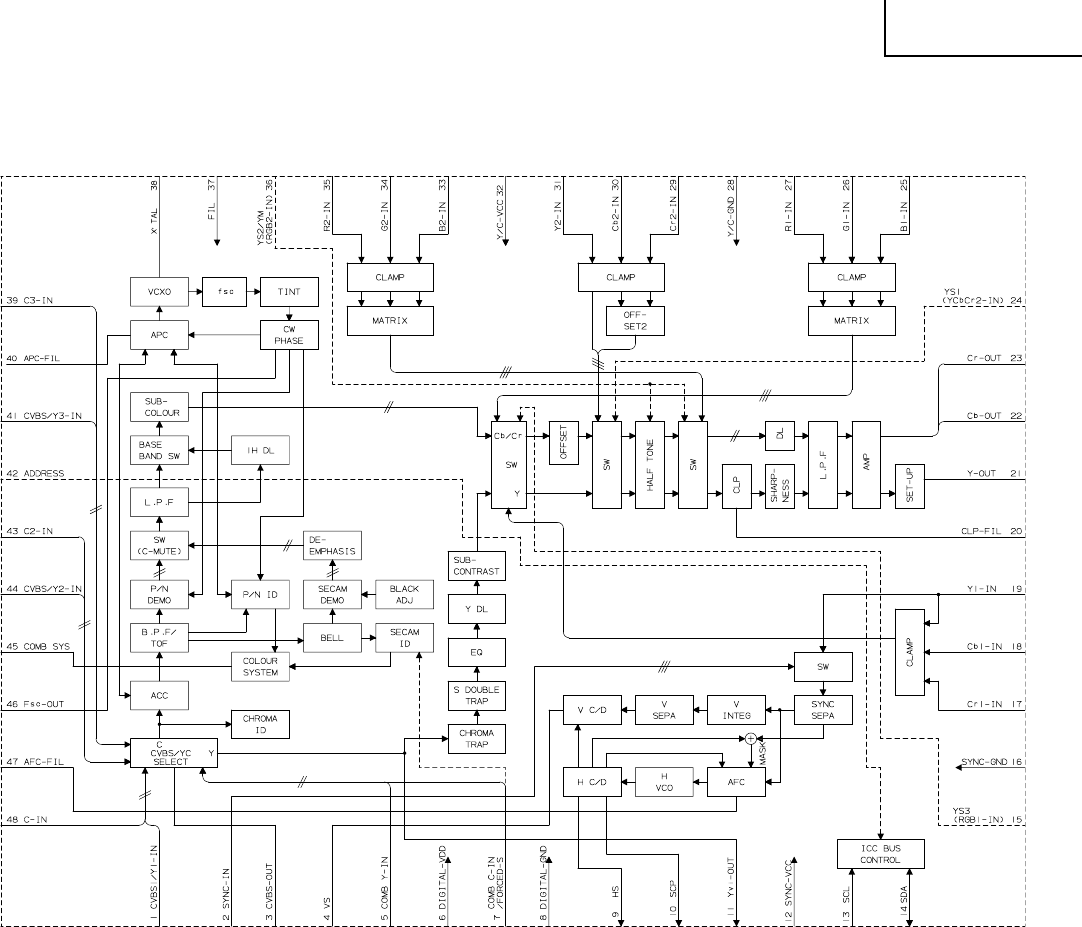
ËVHICXA2101Q-1 (ASSY: IC803)
»Baseband Video Signal Processor
»Block Diagram
1
2
3
4
5
6
7
8
9
10
11
12
13
14
15
16
17
»Pin Function
Pin No. Pin Name I/O Pin Function
IN2-H
IN2-V
IN2-1
IN2-2
IN2-3
Vcc-MAT
IN3-H
IN3-V
IN3-1
IN3-2
IN3-3
GND-MAT
IN4-H
IN4-V
IN4-1
IN4-2
IN4-3
I
I
I
I
I
—
I
I
I
I
I
—
I
I
I
I
I
IN2-H : Independent horizontal sync signal input terminal.
IN2-V : Independent vertical sync signal input terminal.
IN2 line signal input terminal.
Selector line and sync processor line power terminal.
IN3-H : Independent horizontal sync signal input terminal.
IN3-V : Independent vertical sync signal input terminal.
IN3 line signal input terminal.
Selector line and sync processor line grounding terminal.
IN4-H : Independent horizontal sync signal input terminal.
IN4-V : Independent vertical sync signal input terminal.
IN4 line signal input terminal.

34
PZ-MR2T
PZ-43MR2U
PZ-50MR2U
18
19
20
21
22
23
24
25
26
27
28
29
30
31
32
33
34
35
37
39
36
38
40
41
42
43
44
45
46
47
48
49
50
51
52
53
54
55
56
57
58
59
60
61
62
63
64
65
66
67
68
69
70
71
72
73
74
75
76
77
78
79
80
»Pin Function
Pin No. Pin Name I/O Pin Function
V-PH
IN5-H
IN5-V
IN5-1
IN5-2
IN5-3
H-PH
YG-OUT
YG-IN
IREF-SYNC
VS-OUT
HS-OUT
Vcc-OUT
SCP-IN
VTIM-IN
HP-IN
GND-OUT
R-OUT
G-OUT
B-OUT
R-SH
G-SH
B-SH
IK-IN
PABL-FIL
ABL-FIL
ABL-IN
YS/YM-1
LR1-IN
LG1-IN
LB1-IN
YS/YM-2
LR2-IN
LG2-IN
LB2-IN
ADDRESS
DPIC-C
SCL
SDA
DPIC-MUTE
CLP-C
VM-OUT
VM/SHP/COL-OFF
YCBCR-SW
ECR-IN
ECB-IN
EY-IN
V1-IN
H1-IN
CR1-IN
CB1-IN
Y1-IN
GND-SIG
IREF-YC
Vcc-SIG
SELCR-IN
SELCB-IN
SELY-IN
SELY-OUT
SELCB-OUT
SELCR-OUT
SELH-OUT
SELV-OUT
I
I
I
I
I
O
I
O
O
O
I
I
I
O
O
O
O
I
I
I
I
I
I
I
I
I
I
I
I
O
I
I
I
I
I
I
I
I
I
—
—
I
I
I
O
O
O
O
O
Vsync peak holding capacitor connection terminal.
IN5-H : Independent horizontal sync signal input terminal.
IN5-V : Independent vertical sync signal input terminal.
IN5 line signal input terminal.
Hsync peak holding capacitor connection terminal.
Sync separation composite video signal output terminal.
Sync separation composite video signal input terminal.
Reference current setting terminal (about 4.6V)
Used to select between IN1-line HV and IN2/IN5-line selector output HV by I2C BUS
“YCBCR/MAT” and feed out the signal in positive polarity.
RGB line power terminal.
Sand-Castle-Pulse input terminal.
V timing pulse input terminal.
H pulse input terminal.
RGB line grounding terminal.
RGB signal output terminal.
Output to be made at 2.6Vp-p with 100IRE white input.
RGB AKB sample-and-hold terminal.
Reference pulse to return to this terminal.
Peak ABL peak holding terminal.
Used to form LPF for ABL control signal.
ABL control signal input terminal.
YM1/YS1 control input terminal. Input level to be of 3 values.
VM turning-off function also available when YM and YS have reached their specified values.
Analog RGB1 signal input terminal.
YM2/YS2 control input terminal. Input level to be of 3 values.
VM turning-off function also available when YM and YS have reached their specified values.
Analog RGB2 signal input terminal.
I2C BUS slave address setting terminal.
Capacitor to be connected for grounding in order to detect the black signal in dynamic
picture (black stretching).
I2C BUS standard SCL (Serial Clock) input terminal.
I2C BUS standard SDA (Serial Data) input terminal.
Used to control MUTE of dynamic picture (black stretching).
Y line clamp capacitor connection terminal.
VM output terminal to feed out Y signal’s differential waveform in positive polarity.
Used to turn off VMÅASHARPNESS and COLOUR. Input level to be 3 values
Used to switch between INT and EXT SW input signals. External input terminal to be
selected at High level.
External Y, Cb, and Cr input terminals.
IN1-line HV input terminal. Positive-polarity input.
IN1-line Y, Cb, and Cr input terminals.
Y color difference signal processor grounding terminal.
Reference current setting terminal (mainly for Y color difference signal processing line).
Y color difference signal processor power terminal.
Used to feed in selector outputs Y, Cb, and Cr through clamp capacitor.
IN2- thru IN5-line selector output terminals.
Used to feed out Y-, Cb-, and Cr-converted signals.
IN2 thru IN5 selector HV output terminals.

35
PZ-MR2T
PZ-43MR2U
PZ-50MR2U
ËRH-iXA194WJZZ (ASSY: IC1901)
»PLD (Programmable Logic Device)
»Pin Function
1
2
3
4
5
6
7
8
9
10
11
12
13
14
15
16
17
18
19
20
21
22
23
24
25
26
27
28
29
30
31
32
33
34
35
36
37
38
39
40
41
42
43
44
Pin No. Pin Name I/O Pin Function
TDI
VD1
SP_HD
GND
SP_VD
SP_CP
TMS
HD3
VCC
VD3
GND
MODEA
MODEB
MODEC
SELA
GND
VCC
SELO
HD2
VD2
HDS
VDS
US_VD
GND
US_HD
TCK
TEXT_VD
TEXT_HD
VCC
GND
PL_BLK
TDO
PLCP
PL_HD
PL_VD
GND
GCLK1
OE1
GCLRn
OE2/GCLK2
VCC
CNR_CP
CNR_HBLK
HD1
I/O
I/O
I/O
—
I/O
I/O
I/O
I/O
—
I/O
—
I/O
I/O
I/O
I/O
—
—
I/O
I/O
I/O
I/O
I/O
I/O
—
I/O
I/O
I/O
I/O
—
—
I/O
I/O
I/O
I/O
I/O
—
I
I
I
I
—
I/O
I/O
I/O
Ground
Power supply (3.3V)
Ground
Ground
Power supply (3.3V)
Ground
Power supply (3.3V)
Ground
Ground
External clock input. 16MHz
Power supply (3.3V)
36
PZ-MR2T
PZ-43MR2U
PZ-50MR2U
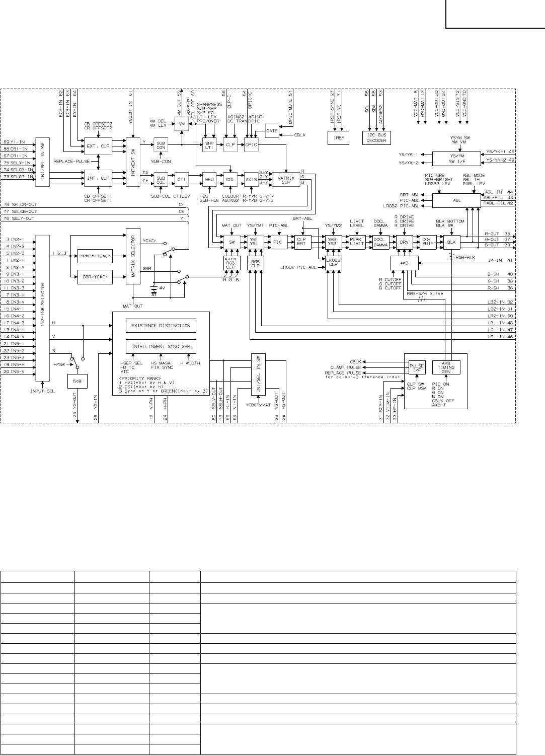
ËVHiTA1318AF-1 (ASSY: IC604)
»Sync Processor
»Block Diagram

37
PZ-MR2T
PZ-43MR2U
PZ-50MR2U
3
1
11
4
2
10
5
6
7
8
20
9
24
12
13
15
14
16
17
18
21
19
22
23
»Pin Function
Pin No. Pin Name I/O Pin Function
HD1-IN
HD2-IN
HD3-IN
VD1-IN
VD2-IN
VD3-IN
ANALOG GND
AFC FILTER
HVCO
VCC
DAC1
(V. SYNC output)
DAC2
(H/C. SYNC output)
DAC3
CP-OUT
HD1-OUT
HD2-OUT
DIGITAL GND
SDA
SCL
ADDRESS SW
SYNC1-IN
SYNC2-IN
VD1-OUT
VD2-OUT
I
I
I
I
I
I
—
—
—
—
O
O
O
O
O
O
—
I/O
I
I
I
I
O
O
Input the horizontal synchronizing signal.
It’s polarity corresponds to both positive and negative.
Input from this pin does not be synchronized internally.
Input the horizontal vertical signal.
It’s polarity corresponds to both positive and negative.
Input from this pin does not be synchronized internally.
The GND pin for analog circuit block.
Connect the filter for horizontal AFC. The frequency of the horizontal output is varied
by the volyage at this pin.
Connect the ceramic oscillator for horizontal oscillator.
The VCC pin. (9.0V)
DAC1 output pin. When TEST mode, VD or vertical sync signal to frequency counter
circuit is output.
DAC2 output pin. When TEST mode, HD or composite sync signal to frequency
counter circuit is output.
DAC3 output pin. This pin is open-collector system. When TEST mode, test pilses for
the shipping is output.
Clamp pulse output pin. CP mode at synchronization circuit is output.
HD output pin. This pin is open-collector system.
HD1/HD2 does not be synchronizing and they are output from this pin.
It’s polarity is switched by BUS write function.
The GND pin for logic circuit block.
The SDA pin for I”C BUS.
The SCL pin for I”C BUS.
Slave address switch.
Input a signal to separate sync signal.
VD output pin. This pin is open-collector system.
VD1/VD2 does not be synchronizing and they are output from this pin.
It’s polarity is switched by BUS write function.

38
PZ-MR2T
PZ-43MR2U
PZ-50MR2U
ËVHiPD64082/-1S (ASSY: IC7001)
»Y/C Separate IC
»Block Diagram

39
PZ-MR2T
PZ-43MR2U
PZ-50MR2U
1, 40, 55, 80
45, 64, 100
98
99
2-9
10
11
12
13-28
29
30
31
32
33-36
37
38
39
41-44
46
47
48
49
50
51
52
53
54
56
57
58
59
60
61
62
63
65-74
75
76
77
78
79
81
82
83
84
85
86
87
88
89
90
91
92
93
94
95
96
97
»Pin Function
Pin No. Pin Name I/O Pin Function
DGND
DVDD
MRAS
MA8
MA7-MA0
MCAS
MWE
MOE
MIO15-MIO0
DGND
XI
XO
DVDD
HO3-HO0
HWCK
HRCK
HRST
HI3-HI0
AVDD
FSCO
AGND
AGND
FSCI
CPLL
RPLL
AVDD
CKMD
CLK8
RSTB
SLA0
SCL
SDA
ST0
ST1
NSTD
DYCO0-DYCO9
ALTF
CSI
TEST
LINE
KIL
AVDD
CBPC
ACO
AYO
CBPY
AGND
AGND
AYI
VCLY
VRBY
VRTY
AVDD
AVDD
VRTC
VRBC
ACI
AGND
—
—
O
O
O
O
O
O
I/O
—
I
O
—
O
O
O
O
I
—
—
—
—
—
—
I
—
I
O/I
I
I
I
I/O
O
O
O
I/O
O
I
I
I
I
—
O
O
O
O
—
—
I
O
O
O
—
—
O
O
I
—
Digital section grounding.
Digital section power.
External EDO memory RAS output.
External EDO memory address output.
External EDO memory address output.
External EDO memory CAS output.
External EDO memory WE output.
External EDO memory OE output.
External EDO memory data input/output.
fsc generator digital section grounding.
fsc generator reference clock input.
fsc generator reference clock reverse output.
fsc generator digital section power.
External field memory data output.
External field memory write clock output.
External field memory read clock output.
External field memory reset signal output.
External field memory input.
fsc generator DAC power.
fsc generator fsc output.
fsc generator DAC grounding.
8fsc-PLL grounding.
8fsc-PLL fsc input.
8fsc-PLL filter output.
Test input.
8fsc-PLL power.
CLK8 test mode select (L: Usual, H: Test mode).
8fsc clock output (8fsc clock input at CLK8 test mode).
System reset input (Active Low).
(Active-Low reset pulse input from outside)
PC bus slave address select input (L: B8/B9h, H: BA/BBh).
PC bus clock input (To be connected to system’s SCL line).
PC bus clock input/output (To be connected to system’s SDA line).
nternal signal monitor output.
Internal signal monitor output.
Non-standard detection monitor output.
(L: Judged standard, H: Judged non-standard)
EXADINS=0: Digital Y/C signal alternate output.
EXADINS=1: External Y-ADC data input.
(Non-used lower bits to be connected to GND with resistor in between)
EXADINS=0: Digital Y/C signal alternate flag output (L: Y, H: C).
EXADINS=1: External Y-ADC 4fsc clock output.
Composite sync input (Active Low).
IC select test terminal (L: Usual operation, H: Test mode). (Connected to GND)
Forced line-to-line process select input (L: Usual operation, H: Forced line-to-line
processing).
External killer input (L: Usual operation, H: Forced Y/C separation stop).
Y-DAC, C-DAC power.
C-DAC phase compensation output.
C-DAC analog C signal output.
Y-DAC analog Y signal output.
Y-DAC phase compensation output.
Y-DAC, C-DAC grounding.
Y-ADC grounding.
Y-ADC analog composite signal/Y signal input.
Y-ADC clamp potential output.
Y-ADC bottom reference voltage output.
Y-ADC top reference voltage output.
Y-ADC power.
C-ADC power.
C-ADC top reference voltage output.
C-ADC bottom reference voltage output.
C-ADC analog C signal input.
C-ADC grounding.

40
PZ-MR2T
PZ-43MR2U
PZ-50MR2U
ËVHiCXD2093Q-1 (ASSY: IC402)
»Digital Comb Filter
»Block Diagram

41
PZ-MR2T
PZ-43MR2U
PZ-50MR2U
1
2
3
4
5
6
7
8
9
10
11
12
13
14
15, 28
32, 33, 35,
16, 27, 34
18, 23-26, 29, 36
17
19
20
21
22
30
31
37
38
39
40
41
42
43
44
45
46
47
48
»Pin Function
Pin No. Pin Name I/O Pin Function
CLPO
ADIN
RB
ADVS
ADVD
RT
ACO
DAVD
AYO
DAVS
VG
VRF
IRF
VB
TEST
TEST
DVDD
DVSS
MOD2
MOD1
VEH3
VEH2
VEH1
APCN
TRAP
FIN
CKSL
PLSL
MCKO
ADCK
CPO
PLVS
VCV
PLVD
CLVD
CLPEN
CLVS
O
I
O
—
—
O
O
—
O
—
O
I
O
O
I
I
—
—
I
I
I
I
I
I
I
I
I
I
O
I
O
—
I
—
—
I
—
Built-in clamp circuit current output terminal. To be connected to ADIN when built-in
clamp is used.
Comb filter analog input (A/D converter) terminal.
A/D converter reference bottom voltage. (standard 0.52V)
A/D converter analog grounding terminal.
A/D converter analog power terminal. (5.0V)
A/D converter reference top voltage. (standard 2.6V)
Analog chroma signal output terminal. Resistance to be added between this pin and
GND (DAVS) for obtaining the output.
D/A converter analog power terminal. (5.0V)
Analog luminance signal output terminal. Resistance to be added between this pin and
GND (DAVS) for obtaining the output.
D/A converter analog grounding terminal.
D/A converter terminal.
Y,C ch D/A converter output full-scale setting terminal.
x16 resistance to be connected against D/A converter output resistance “R”.
D/A converter terminal.
Test terminal. Usually fixed at Low.
Test terminal. Usually open or fixed at Low.
Digital power terminal. (5.0V)
Digital grounding terminal.
Y/C separation mode setting terminal.
MOD2 MOD1
L L Most suitable process
H L BPF separation mode
Vertical contour enhancement setting terminal.
VEH3 VEH2 VEH1: Presettable in 8 steps from LLL(Off) to HHH(Max).
Horizontal aperture correction circuit setting terminal. L: off, H: on
Trap filter circuit setting terminal. L: off, H: on
Clock input terminal. Burst lock (4fsc) to be fed in with built-in PLL system. Burst-
locked 4fsc signal to be fed in when PLL is not used.
PLL control terminal.
L : PLL not used. FIN input clock (4fsc) to be fed in.
H : PLL used. VCO oscillator output’s 4fsc clock to be fed in.
FIN input fsc to be selected. L: fsc input, H: 2fsc input.
Either at L or H when 4fsc is fed in PLL (without built-in PLL).
Clock (4fsc) output terminal.
A/D converter clock input terminal. To be connected to MCKO.
PLL phase comparator output terminal. Open when PLL is not used.
PLL analog grounding terminal.
VCO control voltage input terminal. To be connected to PLVS when PLL is not used.
PLL analog power terminal. (5.0V)
Clamp D/A converter analog power terminal. (5.0V)
Clamp circuit enable terminal. L: Clamp on, H: Clamp off
Clamp D/A converter analog grounding terminal.
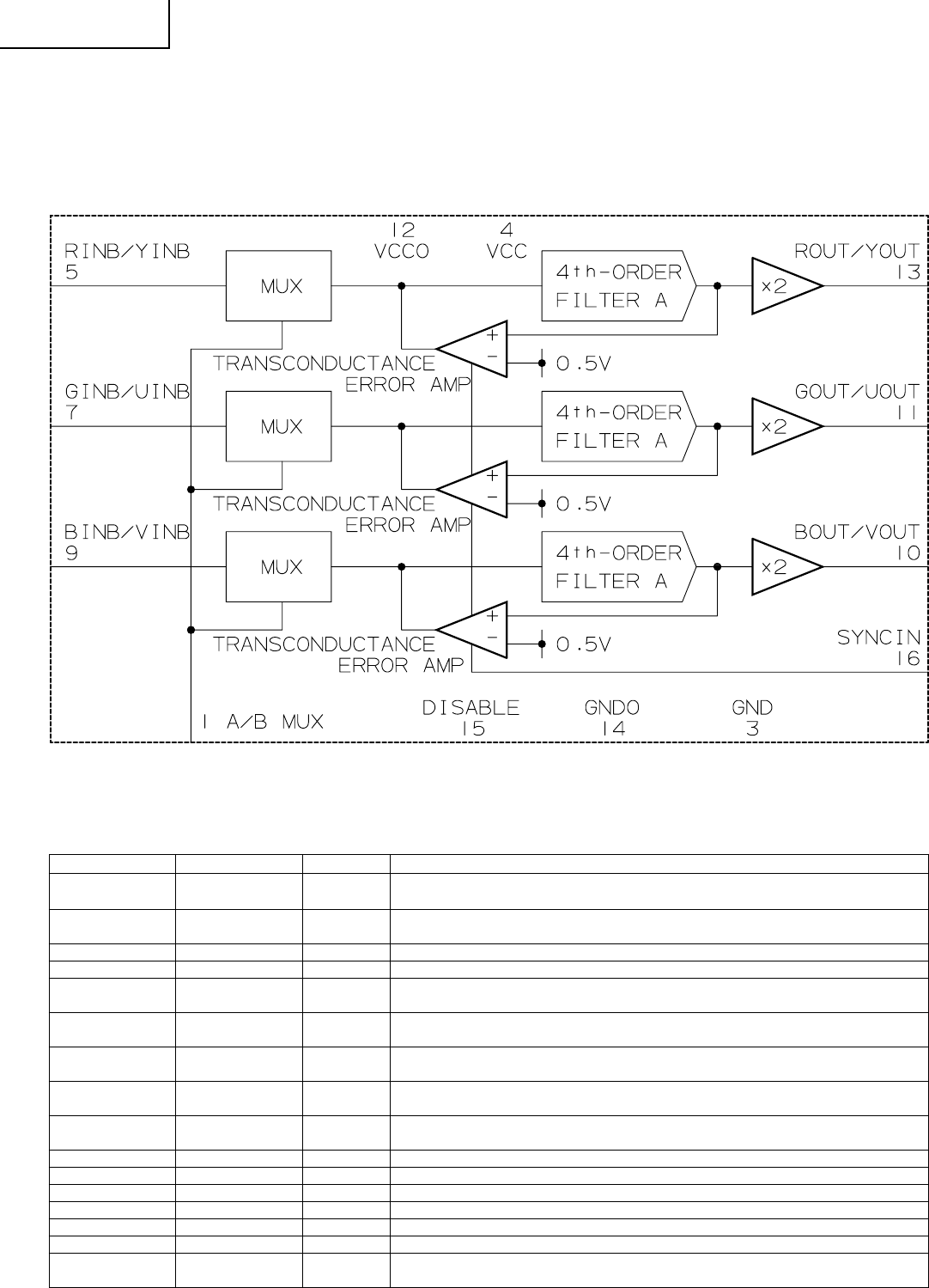
42
PZ-MR2T
PZ-43MR2U
PZ-50MR2U
1
2
3
4
5
6
7
8
9
10
11
12
13
14
15
16
»Pin Function
Pin No. Pin Name I/O Pin Function
A/B MUX
RINA/YINA
GND
VCC
RINB/YINB
GINA/UINA
GINB/UINB
BINA/VINA
BINB/VINB
BOUT
GOUT
VCCO
ROUT
GNDO
DISABLE
SYNC IN
—
I
—
—
I
I
I
I
I
O
O
—
O
—
I
I
Logic input pin to select between Bank <A> and Bank <B> video inputs.
This pin is internally pulled high.
Unfiltered analog R- or Y-channel input for Bank <A>, Sync must be provided at SYNC
IN pin.
Analog ground.
Analog 5V supply.
Unfiltered analog R or Y-channel input for Bank <B>, Sync must be provided at SYNC
IN pin.
Unfiltered analog G or U-channel input for Bank <A>, Sync must be provided at SYNC
IN pin.
Unfiltered analog G or U-channel input for Bank <B>, Sync must be provided at SYNC
IN pin.
Unfiltered analog B or V-channel input for Bank <A>, Sync must be provided at SYNC
IN pin.
Unfiltered analog B or V-channel input for Bank <B>, Sync must be provided at SYNC
IN pin.
Analog B or V-channel output.
Analog G or U-channel output.
5V power supply for output buffers.
Analog R or Y-channel output.
Analog ground.
Disable/Enable pin. Turns the chip off when logic high. Internally pulled low.
Input for an external H-sync logic signal for filter channels. CMOS level input. Active
High.
ËRH-iX3473CEZZ (ASSY: IC804, IC810)
ËRH-iX3474CEZZ (ASSY: IC811)
»Monolithic Video Filter
* RH-iX3473CEZZ is 6.7MHz at Cut-off frequency.
* RH-iX3474CEZZ is 30MHz at Cut-off frequency.
»Block Diagram
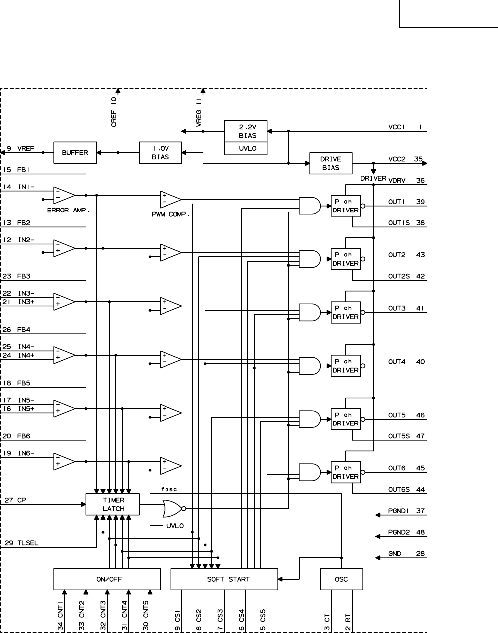
43
PZ-MR2T
PZ-43MR2U
PZ-50MR2U
ËVHiFA3675F/-1 (ASSY: IC1701)
»6-channel DC-DC Converter IC
»Block Diagram

44
PZ-MR2T
PZ-43MR2U
PZ-50MR2U
1
2
3
4
5
6
7
8
9
10
11
12
13
14
15
16
17
18
19
20
21
22
23
24
25
26
27
28
29
30
31
32
33
34
35
36
37
38
39
40
41
42
43
44
45
46
47
48
»Pin Function
Pin No. Pin Name I/O Pin Function
VCC1
RT
CT
CS3
CS5
CS4
CS1
CS2
VREF
CREF
VREG
IN2-
FB2
IN1-
FB1
IN5+
IN5-
FB5
IN6-
FB6
IN3+
IN3-
FB3
IN4+
IN4-
FB4
CP
GND
TLSEL
CNT5
CNT4
CNT2
CNT3
CNT1
VCC2
VDRV
PGND1
OUT1S
OUT1
OUT4
OUT3
OUT2S
OUT2
OUT6S
OUT6
OUT5
OUT5S
PGND2
—
—
—
—
—
—
—
—
O
O
O
I
O
I
O
I
I
O
I
O
I
I
O
I
I
O
I
—
I
I
I
I
I
I
—
O
—
O
O
O
O
O
O
O
O
O
O
—
Power supply for control circuit.
Oscillator timing resistor.
Oscillator timing capacitor.
Soft start for Ch.3 & Ch.4.
Soft start for Ch.6.
Soft start for Ch.5.
Soft start for Ch.1
Soft start for Ch.2.
Reference voltage output.
Capacitor for reference voltage output.
Regulated for voltage output.
Ch.2 inverting input to error amplifier.
Ch.2 output of error amplifier.
Ch.1 inverting input to error amplifier.
Ch.1 output of error amplifier.
Ch.5 non-inverting input to error amplifier.
Ch.5 inverting input to error amplifier.
Ch.5 output of error amplifier.
Ch.6 inverting input to error amplifier.
Ch.6 output of error amplifier.
Ch.3 non-inverting input to error amplifier.
Ch.3 inverting input to error amplifier.
Ch.3 output of error amplifier.
Ch.4 non-inverting input to error amplifier.
Ch.4 inverting input to error amplifier.
Ch.4 output of error amplifier.
Timing capacitor for timer latch delay.
Ground.
Ch.3 & Ch.4 timer latch selection(Low:disable).
Ch.6 ON/OFF function.
Ch.5 ON/OFF function.
Ch.2 ON/OFF function.
Ch.3 & Ch.4 ON/OFF function.
Ch.1 ON/OFF function.
Power supply for output stage.
Bias for logic circuit of output.
Power ground.
Ch.1 source electrode of output stage.
Ch.1 output(for Pch-MOSFET)
Ch.4 output(for Pch-MOSFET)
Ch.3 output(for Pch-MOSFET)
Ch.2 source electrode of output stage.
Ch.2 output(for Pch-MOSFET)
Ch.6 source electrode of output stage.
Ch.6 output(for Pch-MOSFET)
Ch.5 output(for Pch-MOSFET)
Ch.5 source electrode of output stage.
Power ground.
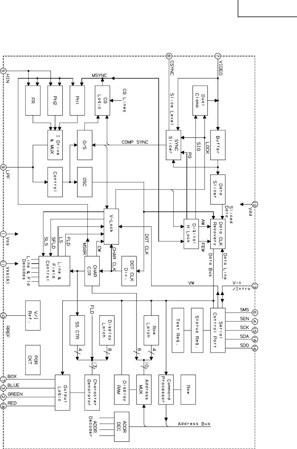
45
PZ-MR2T
PZ-43MR2U
PZ-50MR2U
ËVHiZ86129S+-1Y (ASSY: IC1602)
»NTSC Line21 Decoder IC
»Block Diagram

46
PZ-MR2T
PZ-43MR2U
PZ-50MR2U
1
2
3
4
5
6
7
8
9
10
11
12
13
14
15
16
17
18
»Pin Function
Pin No. Pin Name I/O Pin Function
Vss
GREEN
BLUE
SEN
HIN
SMS
VIDEO
CSYNC
LPF
RREF
Vss(A)
Vdd
Vin/INTRO
SDA
SCK
SDO
BOX
RED
—
O
0
I
I
I
I
O
O
I
—
—
I/O
I/O
I
O
O
O
Power Supply GND.
Video Output
Video Output
Serial Enable
Horizontal In
Serial Mode Select
Composite Video
Composite Sync
Loop Filter
Resistor Reference
Power Supply (Analog) GND.
Power Supply
Vertical In/Interrupt Out
Serial Data
Serial Clock
Serial Data Out
OSD Timing Signal
Video Output
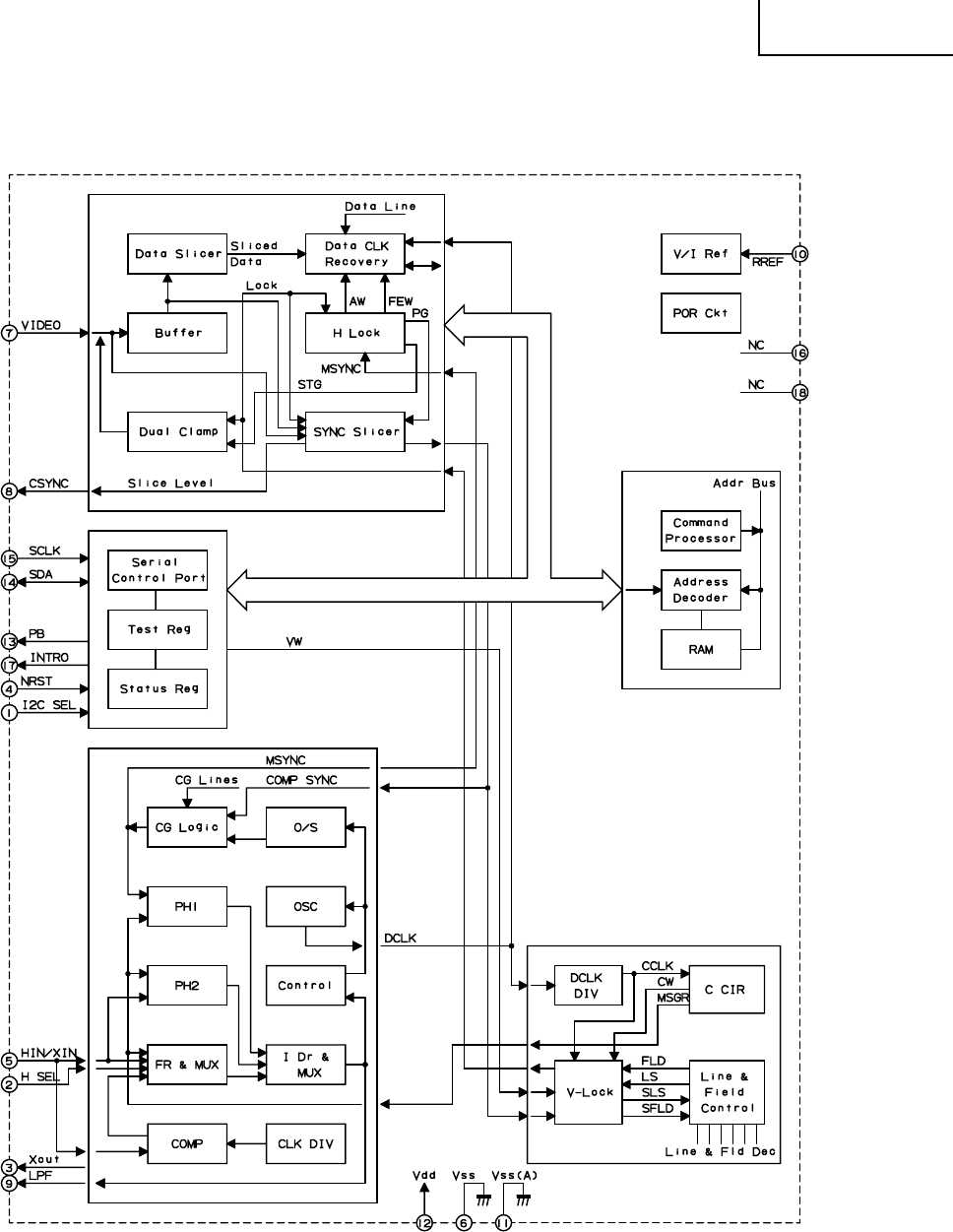
47
PZ-MR2T
PZ-43MR2U
PZ-50MR2U
ËVHiZ86230S+-1Y (ASSY: IC1601, IC1603)
»NTSC Line21 Decoder IC
»Block Diagram

48
PZ-MR2T
PZ-43MR2U
PZ-50MR2U
1
2
3
4
5
6
7
8
9
10
11
12
13
14
15
16
17
18
»Pin Function
Pin No. Pin Name I/O Pin Function
IICSEL
H SEL
Xout
NRST
HIN/XIN
Vss
VIDEO
CSYNC
LPF
RREF
Vss (A)
Vdd
PB
SDA
SCLK
NC
INTRO
NC
I
I
0
I
I
—
I
O
O
I
—
—
O
I/O
I
—
O
—
IIC Adderss Select
HIN/XIN Select
XTAL Output
RESET
Horizontal In/XTAL In
Power Supply (Digital) GND.
Composite Video
Composite Sync
Loop Filter
Resistor Reference
Power Supply (Analog) GND.
Power Supply +5V
Program Blocking
Serial Data
Serial Clock
No Connect
Interrupt Output
No Connect
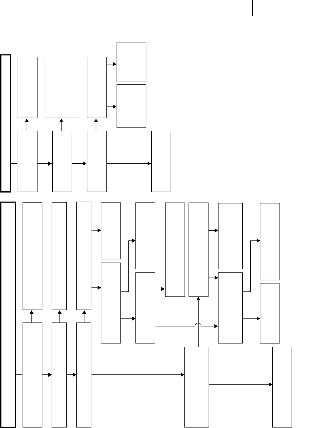
49
PZ-MR2T
PZ-43MR2U
PZ-50MR2U
TROUBLE SHOOTING TABLE
Power-on failure (Front LED indicator stays off.)
NO
YES
Is the power cable
connector properly
connected with the set?
Reinsert the power cable
connector and turn on the
power again.
NO
YES
Are F701 and F702 intact
in place?
Replace F701 or F702 and
turn on the power again. If
the fuse blows out again,
replace VA701, Q701, Q703
and IC702 and check the
performance again.
NO
YES
Does the BACK5V line
function?
Check the BACK5V line. Is
there any defective part or
short-circuit?
Check the set's wire
harnesses, FFCs and other
parts for their connections.
YES
Repair the defective
part or short-circuit.
Check the
performance again.
NO
Check IC702,
T702, PC703 and
their peripheral
circuits.
Power switch on, but no power
(Front LED indicator does not change from red to green, but remains in red.)
NO
YES
Are the MDR and DVI cable connectors (white
and gray) properly connected with the PDP
and the set as well?
NO
YES
YES
YES
Is the impedance of the M+10V line
as specified? (Measure the resistance
between F1702 and GND.)
NO
NO
YES
Are there voltage
fluctuations along the OVP
line (pin (12) of P1502)?
NO
Check the M+10V line as well
as its circuit parts.
YES
Are the DC/DC converter output
lines and MOS-FET (Q1712,
Q1716, Q1726 and Q1718) as
specified?
NO
Chekc the D_POW and
B+2.5V_POW lines (pins (6)
and (7) of IC1503).
YES NO
Check the DC/DC converter output
lines and replace the MOS-FET
(Q1712, Q1716, Q1726 and Q1718).
NO
YES
Is the PS_ON terminal (pin (1) of CN703) at HI
(3.5V)?
Check the internal parts of the power
unit (Q703, Q704, Q708, Q709, D717,
D710 and D711).
Are the D_POW and B+2.5V_POW
settings (pins (30), (32), (33) and (34)
of IC1701) at HI?
NO
YES
Do the +5V line (pin (10) of P1703),
+2.5V line (pins (5) and (6) of P1702),
and +3.3V line (pin (8) of P1702) all
function?
Check the set's wire harnesses,
FFCs and other parts for their
connections.
Replace IC1701.
Check the PS_ON line.
Is the M+10V line as specified?
Is the PDP's power switch on?
Reinsert the connectors, and turn on the
power again.
Turn on the PDP's power switch.

50
PZ-MR2T
PZ-43MR2U
PZ-50MR2U
TROUBLE SHOOTING TABLE
No sound
No sound from speaker
NO
YES
Does output icon denote speaker when
operating audio volume control?
NO
NO
Does output icon denote lineout when
operating audio volume control?
YES
Is audio output available at each
related pin of IC2501
(MULTI SOUND PROCESSOR)
normal ?
IC2501 Pins (36) and (37) (SC1 OUT L/R)
YES
Check Q2505, 2504 (Buffer) and
their peripheral circuits.
YES
Check PC I/F Unit and its peripheral
circuits.
No audio output (INPUT 1/2/3)
YES
Is audio output available at each
related pin of IC2501
(MULTI SOUND PROCESSOR)
normal?
IC2501 Pins (37) and (36)
(SC1 OUT L/R)
YES
Check the circuit between
pins (37)/(36) of IC2501 and
pins (5)/(14) of J1103 (INPUT1),
pins (2)/(11) of J1103 (INPUT2), and
pins (5)/(14) of J1104 (INPUT3),
as well as audio mute circuit.
Check the circuit between
pins (37)/(36) of IC2501 and
pins (10)/(13) of J3401 (INPUT4),
as well as audio mute circuit.
Check the circuit between
pins (34)/(33) of IC2501 and
pins (2)/(11) of J1104 (Monitor audio
output), as well as audio mute circuit.
NO
Is tuner audio input available at each
related pin of IC2501
(MULTI SOUND PROCESSOR) normal?
IC2501 Pin (67) (SOUND S-IF1)
IC2501 Pin (69) (SOUND S-IF2)
NO
NO
Is audio output available at each related pin of
IC1301 (AV SWITCH) normal?
IC1301 Pins (52) and (54)(MAIN L/R)
IC1301 Pins (43) and (45)(SUB L/R)
IC1301 Pins (38) and (40)(MONITOR OUT L/R)
NO
No audio output (INPUT4)
YES
Is audio output available at each
related pin of IC2501
(MULTI SOUND PROCESSOR)
normal?
IC2501 Pins (37) and (36)
(SC1 OUT L/R)
YES
No monitor audio output
YES
Is audio output available at each
related pin of IC2501
(MULTI SOUND PROCESSOR)
normal?
IC2501 Pins (34) and (33)
(SC2 OUT L/R)
YES
Check the plasma display section.
On TV reception On external input / PC input
Check IC2501 (MULTI SOUND PROCESSOR) and its peripheral circuits.
Check B.P.F. of SIF1 and SIF2 respectively.
Check U/V tuner (TU1101, TU1102) and peripherals.
Is each audio input circuit between J3401 (PC
INPUT/AUDIO) and pins (29)/(31) of IC1301
normal?
Check IC1301 and peripherals.
NO
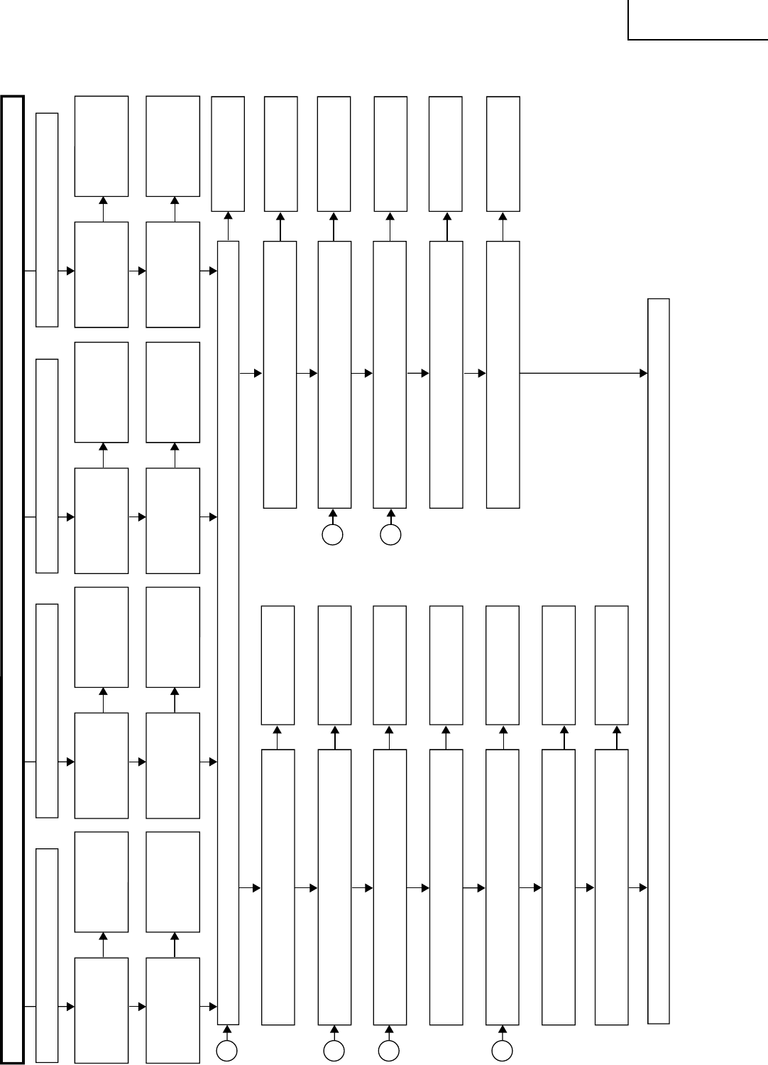
51
PZ-MR2T
PZ-43MR2U
PZ-50MR2U
TROUBLE SHOOTING TABLE (Continued)
No picture (1)
NO Check IC1301 and its
peripheral circuits.
Are there MAIN-R/G/B signal inputs at pins (5), (7) and
(9) of IC810 (6.7MHz L.P.F.), respectively?
YES
YES
NO Check IC810 and its
peripheral circuits.
Are there MAIN-R/G/B signal outputs at pins (13), (11)
and (10) of IC810, respectively?
NO Check between
IC803 and IC810.
YES
NO Check the line between
IC7001 and IC801.
YES
YES YES
Are there MAIN-Y and MAIN-C signal inputs at pins (1)
and (48) of IC801 (MAIN VIDEO CHROMA) respectively?
NO Check the line between
IC402 and IC802.
Are there SUB-Y and SUB-C signal input at pin (44) and
(1) of IC802 (SUB VIDEO CHROMA), respectively?
YES
NO Check IC801 and its
peripheral circuits.
YES
Are there MAIN-Component-Y/Cb/Cr signal outputs
at pins (21), (22) and (23) of IC801, respectively?
NO Check IC802 and its
peripheral circuits.
Are there SUB-Y/Cb/Cr signal outputs at pins (21),
(22) and (23) of IC802, respectively?
NO Check IC7001 and its
peripheral circuits.
Is there video signal input at pin (88) of IC7001 (Y/C
Spearate)?
NO Check IC402 and its
peripheral circuits.
Is there video signal at pins (2) and (1) of IC402
(Sub Comb Filter)?
YES
NO Check the line between
IC801 and IC803.
YES
Are there MAIN-
Component-
Y/Cb/Cr signal inputs at pins
(69), (68) and (67) of IC803 (RGB DECODER), respectively?
NO Check the line between
IC802 and IC810.
Are there
SUB-Y/Cb/Cr
signal inputs at pins (5), (9)
and (7) of IC810 (6.7MHz L.P.F.), respectively?
YES
NO Check IC803 and its
peripheral circuits.
YES
YES
Are there MAIN-R/G/B signal outputs at pins (35),
(37) and (39) of IC803, respectively?
NO Check IC810 and its
peripheral circuits.
Are there SUB-R/G/B signal outputs at pins (13),
(11) and (10) of IC810, respectively?
YES
No external input <INPUT1>
NO
Is "INPUT1" selected
on the Input Select
menu screen?
Select "INPUT1" on
the menu screen.
YES
NO
Is there AV signal
input at pin (1) of
IC1301 (AV
SWITCH)?
Check the line
between pin (23) of
J1003 and pin (1) of
IC1301.
YES
No external input <INPUT2>
NO
Is "INPUT2" selected
on the Input Select
menu screen?
Select "INPUT2" on
the menu screen.
YES
NO
Is there AV signal
input at pin (8) of
IC1301 (AV
SWITCH)?
Check the line
between pin (20) of
J1003 and pin (8)
of IC1301.
YES
No external input <INPUT3>
NO
Is "INPUT3" selected
on the Input Select
menu screen?
Select "INPUT3" on
the menu screen.
YES
NO
Is there AV signal
input at pin (15) of
IC1301 (AV
SWITCH)?
Check the line
between pin (23) of
J1104 and pin (15)
of IC1301.
YES
No external input <INPUT4>
NO
Is "INPUT4" selected
on the Input Select
menu screen?
Select "INPUT4" on
the menu screen.
YES
NO
Is there AV signal
input at pin (22) of
IC1301 (AV
SWITCH)?
Check the line
between pin (7) of
J3401 and pin (22)
of IC1301.
Are there MAIN and SUB video signal outputs at pins (56) and (44) of IC1301, respectively?
Check the PC I/F unit.
<MAIN system> <SUB system>
C
A
D
F
B
E
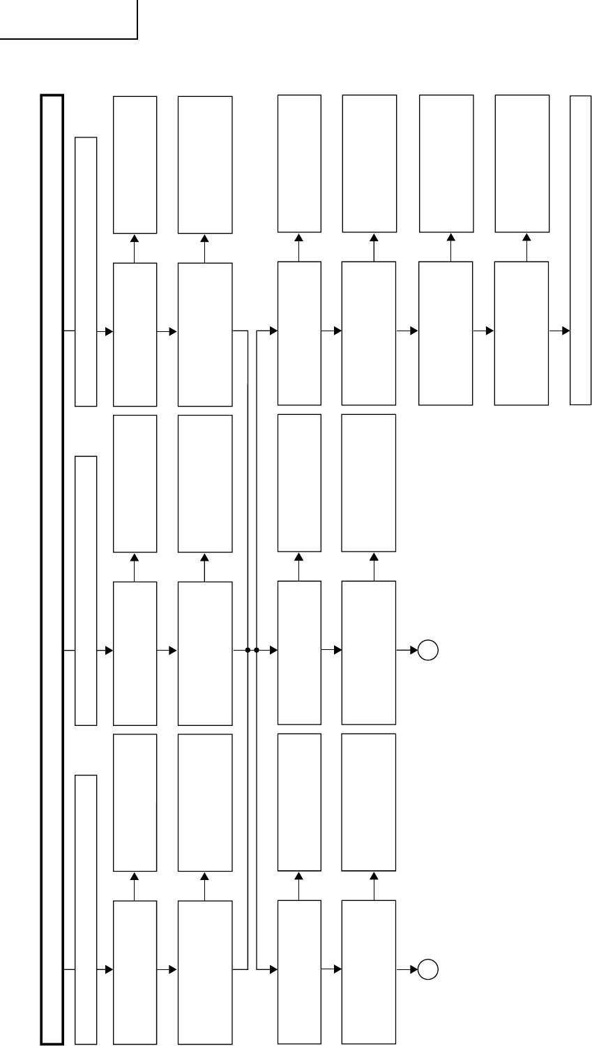
52
PZ-MR2T
PZ-43MR2U
PZ-50MR2U
TROUBLE SHOOTING TABLE (Continued)
No picture (2)
YES
NO
YES
NO
YES
No external input picture (INPUT3 RGB)
Is "RGB" of "INPUT3"
selected on Input Select
menu screen?
Select "RGB" of
"INPUT3" on menu
selection screen.
Is RGB signal input
available at pins (15), (17)
and (19) of IC1401 (AV
SWITCH)?
Check the circuit between
pins (1)/(2)/(3) of SC1103
and pins (15)/(17)/(19) of
IC1401.
Is COMPONET/RGB signal
output available at pins (38),
(36) and (34) on IC1401?
Check IC1401 and its
peripheral circuits.
Is COMPONET/RGB signal
input available at pins (6), (5)
and (4) of IC803 (RGB
DECODER), respectively?
Check the circuit between
pins (38)/(36)/(34) of
IC1401 and pins (6)/(5)/(4)
of IC803.
YES
YES
NO
YES
NO
YES
Are there MAIN-R/G/B signal
inputs at pins (5), (7) and (9)
of IC811 (30MHz L.P.F.),
respectively?
Check IC811 and
its peripheral
circuits.
Check the line
between IC803
and IC811.
Are there MAIN-R/G/B
signal outputs at pins (13),
(11) and (10) of IC811,
respectively?
<MAIN> <SUB> <HDTV>
Check the PC I/F unit.
NO
YES
NO
No external input picture (INPUT1 COMPONENT)
Is "COMPONENT" of
"INPUT1" selected on
Input Select menu screen?
Select "COMPONENT"
of "INPUT1" on menu
selection screen.
Is COMPONENT signal
input available at pins (59),
(61) and (63) on IC1401 (AV
SWITCH)?
Check the circuit between
pins (26)/(17) and (8) of
JC1103 and pins (59)/(61)/
(63) of IC1401.
NO
YES
NO
NO
YES
NO
No external input picture (INPUT3 COMPONENT)
Is "COMPONENT"of
"INPUT3" selected on
Input Select menu screen?
Select "COMPONENT"of
"INPUT3" on menu
selection screen.
Is component signal input
available at pins (5), (7) and
(9) of IC1401 (AV
SWITCH)?
Check the circuit between
pins (26)/(17)/(8) of J1104
and pins (5)/(7)/(9) of
IC1401.
E
YES
NO
YES
Is COMPONENT signal
output available at pins (44),
(42) and (40) of IC1401?
Check IC1401 and its
peripheral circuits.
NO
Is component signal input
available at pins (19), (18) and
(17) of IC802 (SUB VIDEO
CHROMA), respectively?
Check the circuit between
pins (44)/(42)/(40) of
IC1401 and pins
(19)/(18)/(17) of IC803.
NO
YES
NO
D
YES
NO
YES
Is COMPONENT signal
output available at pins (50),
(48) and (46) on IC1401?
Check IC1401 and its
peripheral circuits.
NO
Is COMPONENT signal input
available at pins (19), (18) and
(17) of IC801 (MAIN VIDEO
CHROMA), respectively ?
Check the circuit between
pins (50)/(48)/(46) of
IC1401 and (19)/(18)/(17)
of IC801.
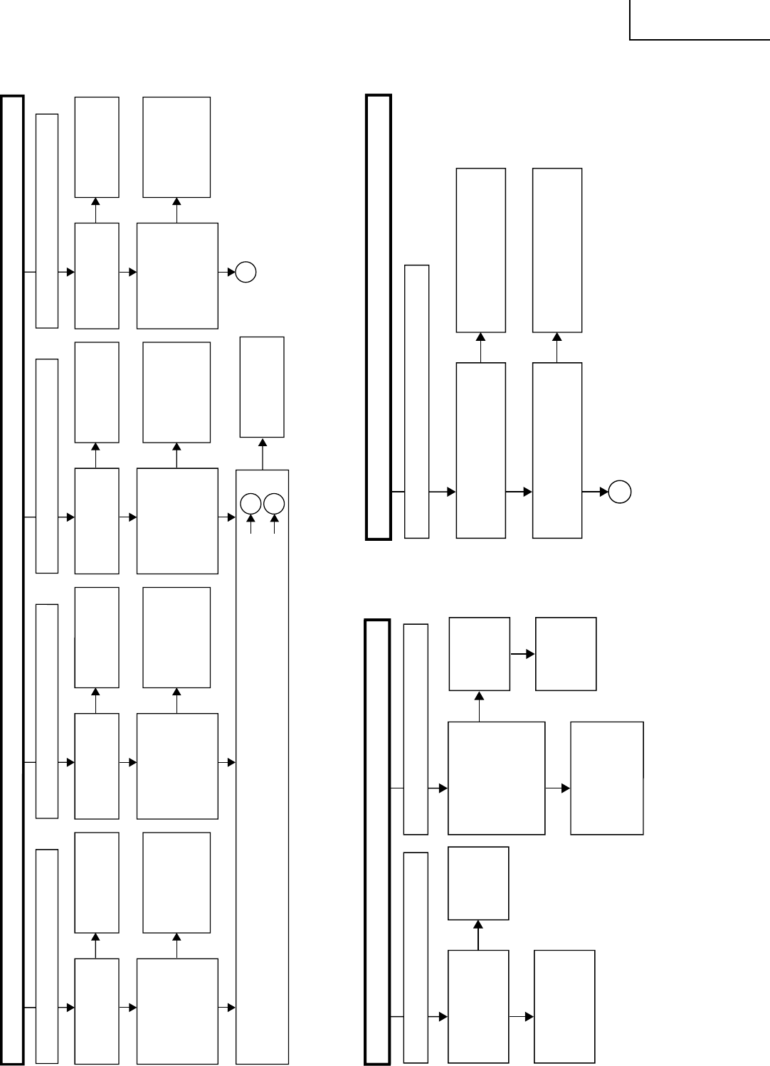
53
PZ-MR2T
PZ-43MR2U
PZ-50MR2U
TROUBLE SHOOTING TABLE (Continued)
C
NO
A
B
Is MAIN-Y signal output available at pin (56) and MAIN-C signal output at pin (58) of IC1301, respectively?
Is SUB-Y signal output available at pin (44) and SUB-C signal output at pin (47) of IC1301, respectively?
Is Y signal input
available at pin (3)
and C signal input at
pin (5) of IC1301 (AV
SWITCH),
respectively?
No picture (3)
YES
No external input picture (INPUT1 S-IN)
NO
Is "INPUT1" selected
on Input Select menu
screen?
Select "INPUT1" on
menu selection
screen.
YES
NO
Check the circuit
between pins
(9)/(10) of SC1101
and pins (3)/(5) of
IC1301.
Is Y signal input
available at pin (10)
and C signal input at
pin (12) of IC1301
(AV SWITCH),
respectively?
YES
No external input picture (INPUT2 S-IN)
NO
Is "INPUT2" selected
on Input Select menu
screen?
Select "INPUT2" on
menu selection
screen.
YES
NO
Check the circuit
between pins
(3)/(4) of SC1101
and pins (10)/(12)
of IC1301.
Is Y signal input
available at pin (17)
and C signal input at
pin (19) of IC1301
(AV SWITCH),
respectively?
YES
No external input picture (INPUT3 S-IN)
NO
Is "INPUT3" selected
on Input Select menu
screen?
Select "INPUT3" on
menu selection
screen.
YES
NO
Check the circuit
between pins
(2)/(1) of SC1102
and pins (9)/(10)
of IC1301.
Is Y signal input
available at pin (24)
and C signal input at
pin (26) of IC1301
(AV SWITCH),
respectively?
YES
No external input picture (INPUT4 S-IN)
NO
Is "INPUT4" selected
on Input Select menu
screen?
Select "INPUT4" on
menu selection
screen.
YES
NO
Check the circuit
between pins
(2)/(1) of J3401
and pins (24)/(26)
of IC1301.
Check IC1301 and
its peripheral
circuits.
No picture (4)
NO NO
Is Y signal output
available at pin (39)
and C signal output
at pin (37) of IC1301
(AV SWITCH),
respectively?
YES
YES
YES
Check the circuit
between pin (41) of
IC1301 and pin (20)
of J1104. Check the circuit
between pins
(39)/(37) of IC1301
and pins (3)/(4) of
SC1102.
Confirm
input signal
is S-INPUT.
No monitor picture (AV-OUT) No monitor picture (S-OUT)
Check
IC1301 and
its peripheral
circuits.
Check
IC1301 and
its peripheral
circuits.
Is video signal
output available at
pin (41) of IC1301
(AV SWITCH)?
YES
YES
YES
No picture (5)
NO
No TV picture
Is video output available at pin
(19) of TU1101 and TU1102
(U/V tuner)?
Check U/V tuner and
its peripheral circuits.
NO
Is video input signal available
at pins (63) and (60) of
IC1301?
Check the circuit between pin
(19) of TUNER and pins
(63)/(60) of IC1301.
C
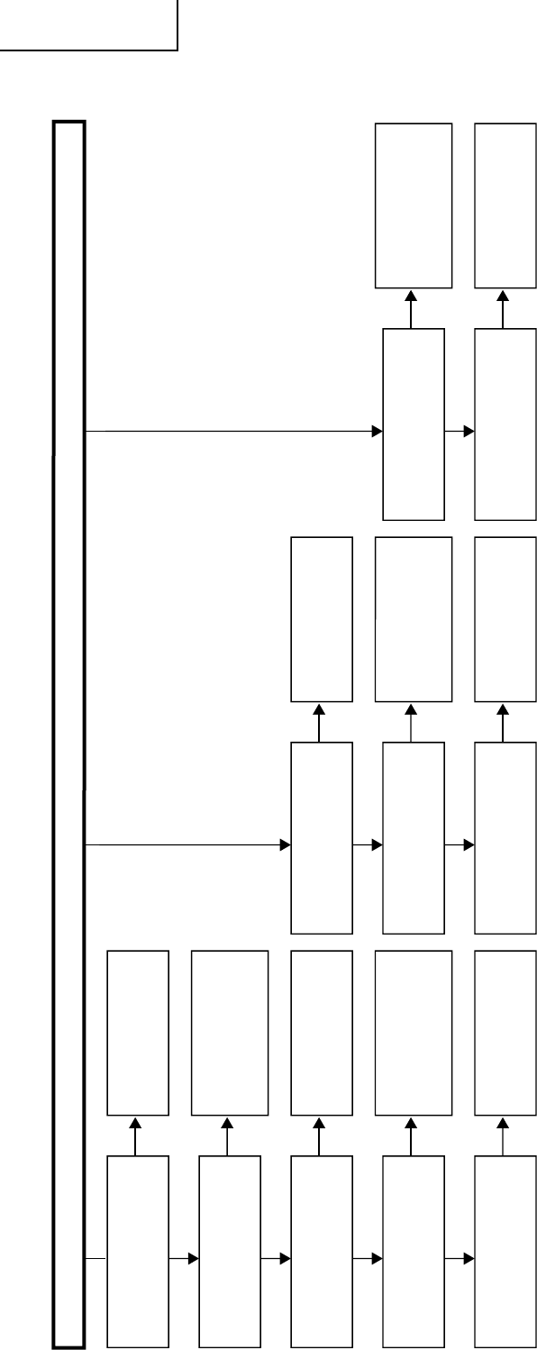
54
PZ-MR2T
PZ-43MR2U
PZ-50MR2U
TROUBLE SHOOTING TABLE (Continued)
Synchronization failure
NO
YES
Is VDM/HDM output available
at pins (28) and (29) of IC803
(RGB DECODER)?
Check IC803 and its
peripheral circuits.
NO
YES
Is HI/VI IN input available at
pins (66) and (65) of
IC803?
Check the circuit
between pins (35)/(34)
of IC1901 and pins
(66)/(65) of IC803.
NO
YES
Is PL-HD/VD output
available at pins (34) and
(35) of IC1901 (PLD)?
Check IC1901 and its
peripheral circuits.
NO
YES
Is HDS/VDS output
available at pins (21) and
(22) on IC1901 (PLD)?
Check IC1901 and its
peripheral circuits.
NO
YES
Is HD1/VD1 input available
at pins (44) and (2) of
IC1901?
Check the circuit
between pins (4)/(9) of
IC801 and pins (2)/(44)
of IC1901.
NO
YES
Is VD2/HD2 input available
at pins (20) and (19) of
IC1901?
Check the circuit
between pins (4)/(9) of
IC802 and pins
(20)/(19) of IC1901.
NO
YES
Is SP-VD/HD input available
at pins (5) and (40) of
IC1901?
Check the circuit
between pins (28)/(16)
of IC604 and pins
(5)/(40) of IC1901.
NO Check IC801 and its
peripheral circuits.
NO
Is HD2/VDM2 output available
at pins (9) and (4) of IC802
(SUB VIDEO CHROMA)?
Check IC802 and its
peripheral circuits.
NO
Is SP-HD/VD output
available at pins (16) and
(28) of IC604 (SYNC SEP)?
Check IC604 and its
peripheral circuits.
MAIN
SUB
HDTV
Is HD1/VD1 output available
at pins (9) and (4) of IC801
(MAIN VIDEO CHROMA)?

55
PZ-MR2T
PZ-43MR2U
PZ-50MR2U
Æ PC I/F Unit TROUBLESHOOTING
No picture
NO
YES
No TV, video and component picture
Is input at pins (124),
(133) and (139) of IC4
normal?
Check CN6 and its
peripheral circuits.
NO
YES
Are TL207, TL208 and
TL211 normal? Check CN6 and its
peripheral circuits.
NO
YES
Is digital output section of
IC4 normal?
Check IC4 and its
peripheral circuits.
NO
YES
Is digital output section
of IC310 normal? Check IC310 and its
peripheral circuits.
NO
YES
Is digital output of IC25
normal? Check IC25 and its
peripheral circuits.
No PC picture
YES
Is signal at pins (21), (22), (24), (25), (27), (28), (30) and (31)
of IC413? (The signal is of high frequency (a little less than
1GHz). Pay due attention to it during observation.)
Connecting cable or
monitor is problem.
NO
PC I/F Unit (CPCi-
0056CE) internal problem
is likely.
No MAIN picture on single screen and dual screen. No SUB picture on dual screen NO
YES
Is input at pins (126),
(136) and (141) of IC4
normal?
Check CN8 and its
peripheral circuits.
NO
YES
Is digital output section
of IC4 normal?
Check IC4 and its
peripheral circuits.
NO
YES
Is digital output of IC25
normal?
Check IC25 and its
peripheral circuits.

56
PZ-MR2T
PZ-43MR2U
PZ-50MR2U
654321
A
B
C
D
E
F
G
H
PRINTED WIRING BOARD BLOCK DIAGRAM-1/2
»PC I/F Unit
»AV Unit
CN1
CONNECTOR
CN
CONNECTOR
CN6
CONNECTOR
IC25
CIVIC
IC1
CPU
IC310
VIDEO SUB
A/D CONV
IC4
VIDEO MAIN/PC
A/D CONV
IC413
PANEL LINK
IC319
SDRAM
IC320
SDRAM
CN9
CONNECTOR
CN8
CONNECTOR
IC7
REG.
IC8
REG.
CN5
RS-232C
CN3
DISPLAY OUT-1
IC405
RS-323 RECIVER
PANEL LINK
OUTPUT
CIRCUIT
RS-232C LIN
E
DRIVER I/F
CIRCUIT
VIDEO IN A/D
CONVERTER
CIRCUIT
POWER REG.
CIRCUIT
PC R,G,B INPUT
CIRCUIT
CPU CIRCUIT
VIDEO PROCESSOR
CIRCUIT
CPCI-0056CE■
TU1102 U/V TUNER
IC1603
V-CHIP
IC1601
V-CHIP
IC2501
MULTI SOUND
P2502
CONNECTOR
IC1301
AV SWITCH
P1301
CONNECTOR
SC1401
CONNECTOR
SC1402
CONNECTOR
P2503
CONNECTOR P2501
CONNECTOR
IC1401
AV SWITCH
J1103
INPUT1 AV TERMINAL
INPUT2 AV TERMINAL
INPUT1 CONPONENT TERMINAL
V-CHIP CIRCU
IT
COMP. AV SWITCH CIRCUIT
ANALOG AV SWITCH CIRCUIT
TU1101 U/V TUNER
J1104
INPUT3 AV TERMINAL
INPUT3 CONPONENT TERMINAL
MONITER OUT AV TERMINAL
SC1101
INPUT1, INPUT2
S-VIDEO TERMINAL
SC1103
INPUT4
RGB TERMINAL
SC1102
INPUT3, MONITER OUT
S-VIDEO TERMINAL
IC1602
CCD
IC1102
CONTROL

57
PZ-MR2T
PZ-43MR2U
PZ-50MR2U
654321
A
B
C
D
E
F
G
H
PRINTED WIRING BOARD BLOCK DIAGRAM-2/2
»MAIN Unit
DC/DC CONVERTER CIRCUIT
P1703
CONNECTOR
IC1502
DAC
IC801
MAIN VIDEO CHROMA
IC604
SYNC SEPARATE
IC803
RGB DECODER
P1502
CONNECTOR
P1901
PROGRAMMING
CONNECTOR
P1702
CONNECTOR
SC1502
CONNECTOR
IC403
CONTROL
IC802
SUB VIDEO CHROMA SC1503
CONNECTOR
IC402
SUB COMB FILTER
IC1901
PLD
SC1504
CONNECTOR
POWER SUPPLY
IC7001
Y/C SEPARATE
L1711
L1708
L1718
L1710
T1701
IC7002
MEMORY
SC1501
CONNECTOR

58
87109654321
A
B
C
D
E
F
G
H
PZ-MR2T
PZ-43MR2U
PZ-50MR2U
SYSTEM BLOCK DIAGRAM
IC1301
ANT1
TU1101(C6h)
TU1102(C0h)
IN
IN
OUT
S
V
R
L
Y
Pb
Pr
VIDEO1
VIDEO2
SIF
SIF
C1-PLUG
C3-PLUG
CH3
ANT2
CH3
CH3
CXA2069Q(90h)
TV
R/L-TV
S1
V1
R/L1
S2 Y/VOUT1
V2 COUT1
R/L2 R/L 1
S3
V3 Y/VOUT 2
R/L3 COUT2
S4 R/L 2
V4
R/L4 Y/VOUT 3
V5 COUT3
R/L5 R/L 3
V6
R/L6
AV SWITCH
S
V
R
L
S
V
R
L
Y
Pb
Pr
VIDEO3
RGB
H/V
MM1519XQ(94h)
YPbPrTV
YPbPr1 OUT1
YPbPr2 OUT2
YPbPr3 OUT3
LOUT1
IC1401 CH
COMPONENT
AV SWITCH
3
MONITOR OUT
S
V
R
L
Y MUTE
VIDEO4
S
V
R
L
PC
R/ L
D1
D2
D3
D4 V1PLUG
D5 V2PLUG
D6 V3PLUG
D7 V4PLUG
IC1102
I/O EXPANDD
62320(74h)M
CH3
DI/O EXPAND
M62320(74h)
CH1
L MUTE ABL
from TUNER
It is destination distinction at H/L of 2bit.
POWER LED CONTROL
or
D0 IN1
D1 LED-R
D2 D_POW
D3 +2.5POW
D4 IN3
D5 LED-G
D6 DACRST
D7 SMPOW
IC1503
It goes into process mode by dropping on GND.
AFT-1/ 2
AGC-1/2
ACL_SIG
I2C-CH1
I2C-CH2
I2C-CH3
SMPOW
L-MUTE
PSEL-1/2
TBUS
IN1
IN3
OUT1
ACL-SW
MRDY
SRESET
TV-COL1
TV-COL2
SC1502
P
C
NJM2233BM
IN1
IN2 OUT
CTL
IC2504
NJM2233BM
IN1
IN2 OUT
CTL
IC2505
AnalogSW(MAIN)
AnalogSW(SUB)
CH3
CH3
CH1
Z86129(28h)
VIDEO RGB
HD BOX
IC1602
Z86230(28h)
VIDEO
IC1601
Z86230(2Ah)
VIDEO
IC1603
C.C
V-CHIP(SUB)
V-CHIP(MAIN)
IC2501
SOUND
PROCESSOR
CH3
MSP3440(80h)
ANT1
ANT2 DACM
DACA
SC1
SC2 SC1
SC3 SC2
SC4
I/O1
I/O2
SPR_CLI
SPL_DAI
P2502
TO SR UNIT
(TO PDP)
SRESET
3D Y/C
FRAME MEMORY
CH3
uPD64082(B8H)
AYI AYO
ACI ACO
IC7001
4Mbit EDO
IC7002
LOWE
R
CXD2093Q
ADIN AY
O
ACO
IC402
D0 MODE2
D1 DVss
D2
D3 DVss
D4
D5 APCN
D6 TRAP
D7 DVss
IC403
I/O EXPANDD
M62320(78h)
CH3
3Line COM

59
1716 1918151413121110
PZ-MR2T
PZ-43MR2U
PZ-50MR2U
or
AFT-1/ 2
AGC-1/2
ACL_SIG
I2C-CH1
I2C-CH2
I2C-CH3
SMPOW
L-MUTE
PSEL-1/2
TBUS
IN1
IN3
OUT1
ACL-SW
MRDY
SRESET
TV-COL1
TV-COL2
SC1502
PC I/F UNIT
TC7W53
IN0 OUT
IN1
CNT
IC1504
AnalogSW
IC15
A1 CR-MAIN
A2 CR-SUB
A3 +B2.5
A4 +BADJ2
A5 REFADJ
A6
A7
A8 CB-GAIN
RESET
CH
DAC EXPAN D
M62393(92h)
1
IX-3289CE
Y/V IN VBLK
H/ V
IC7200
V-BLK GEN. AutoWide
D
Y/C
ME
MEMORY
CH3
6
4082(B8H)
AYO
ACO
IC
7001
it
EDO
2
LOWER LUMINANCE CNR
SIG. PROCESSO R
(SUB )
CH3
IC801
TB1274AF(88h)
CVBS/Y1 YOUT
C1
CVBS/Y2 CbOUT
C2
CVBS/Y3 CrOUT
C3 H/V
YS2/YM
YCbCr1
YCbCr2
RGB1
RGB2
LEVEL ADJ.
LEVEL ADJ.
CR-MAIN
CB-GAIN
SIG. PROCESSO R
(MAIN)
CH3
CXD2093Q
ADIN AYO
ACO
IC402
D0 MODE2
D1 DVss
D2
D3 DVss
D4
D5 APCN
D6 TRAP
D7 DVss
IC403
I/O EXPANDD
M62320(78h)
CH3
3Line COM
TB1274AF(8Ah)
CVBS/Y1
C1 YOUT
CVBS/Y2 CbOUT
C2 CrOUT
CVBS/Y3
C3 H/V
COMB_Y
COMB_C
YCbCr1
RGB1
RGB2
IC802
IC803
SIG. PROCESSO R
CH3
CXA2101Q(84h)
YCbCr1
H/V1
YCbCr2
H/V2 ROU T
YCbCr3 GOUT
H/V3 BOU T
YCbCr4
H/V4
YCbCr5 H/V
H/V5
YS/YM1
RGB1
RGB2
SCP
ABL FIL
ML6426-1
RGB INA
RGB INB RGB
A/B MUX
SYNC
IC810
ML6426-1
RGB INA
RGB INB RGB
A/B MUX
SYNC
IC811
SC1501
LPF6.7M(MAIN)
LPF30M(MAIN)
IC1901
ML6426-1
RGB INA
RGB INB RGB
A/B MUX
SYNC
IC804
MAIN R
MAIN G
MAIN B
MAIN H
MAIN V
SUB Y
SUB Cb
SUB Cr
SUB H
SUB V
PC I/F UNIT
LPF6.7M(SUB)
EPM3064-10
SP_H/V/CLP PL_H/V
HD/VD1 PL_BLK/CLP
HD/VD2 HD/VD3
US_H/V CNR_CLP/BLK
AW_VBLK TEXT_H/V
HDS/VDS
D0 MODEC
D1 MODEB
D2 MODEA
D3 SEL_A
D4 SEL_OE
D5 MFIL_SEL
D6
D7
IC1902
H-BLK GEN. PLD
I/O EXPAND
M62320(7Bh)
RGB H/V
CLR-SW
P3401
+5 VBK
+12V
-5V(A)
+3.3V(D)
+2.5VCV
+5V(A)
+5V(D)
P1702
PC I/F UNTI
PC I/F UNIT
+2.5VCV
+3.3V(D)
+6V
IC1701
PS-ON
+5VBK
+10V
P1502
BACK UP
+2.5POW
POWER UNIT
DC/DC
B35V
D6V
-5 V
+12VA
T1701
+5V(A)
IC1709
+12V
IC1713
DC/DC
REG
REG
TA1318(D8h)
HD/VD1
HD/VD2 HD/VD 1
HD/VD3 HD/VD 2
SYNC1 CP
SYNC2
IC604
+5V(A )
IC1708
+5V(A )
IC1710
+5V(D )
IC1711
+5V(A
IC1712
+8V
IC1706
+9V(A
IC1704
REG
REG
REG
REG
REG
REG
SYNC. SEP.
CH3
)
)
CH3

60
87109654321
A
B
C
D
E
F
G
H
PZ-MR2T
PZ-43MR2U
PZ-50MR2U
SIGNAL FLOW BLOCK DIAGRAM
1
2
3
18
19
4
5

61
1716 1918151413121110
PZ-MR2T
PZ-43MR2U
PZ-50MR2U
19
20
21
22
17
23
24
25
14
15
16
11
12
13
9
10
8
6
7
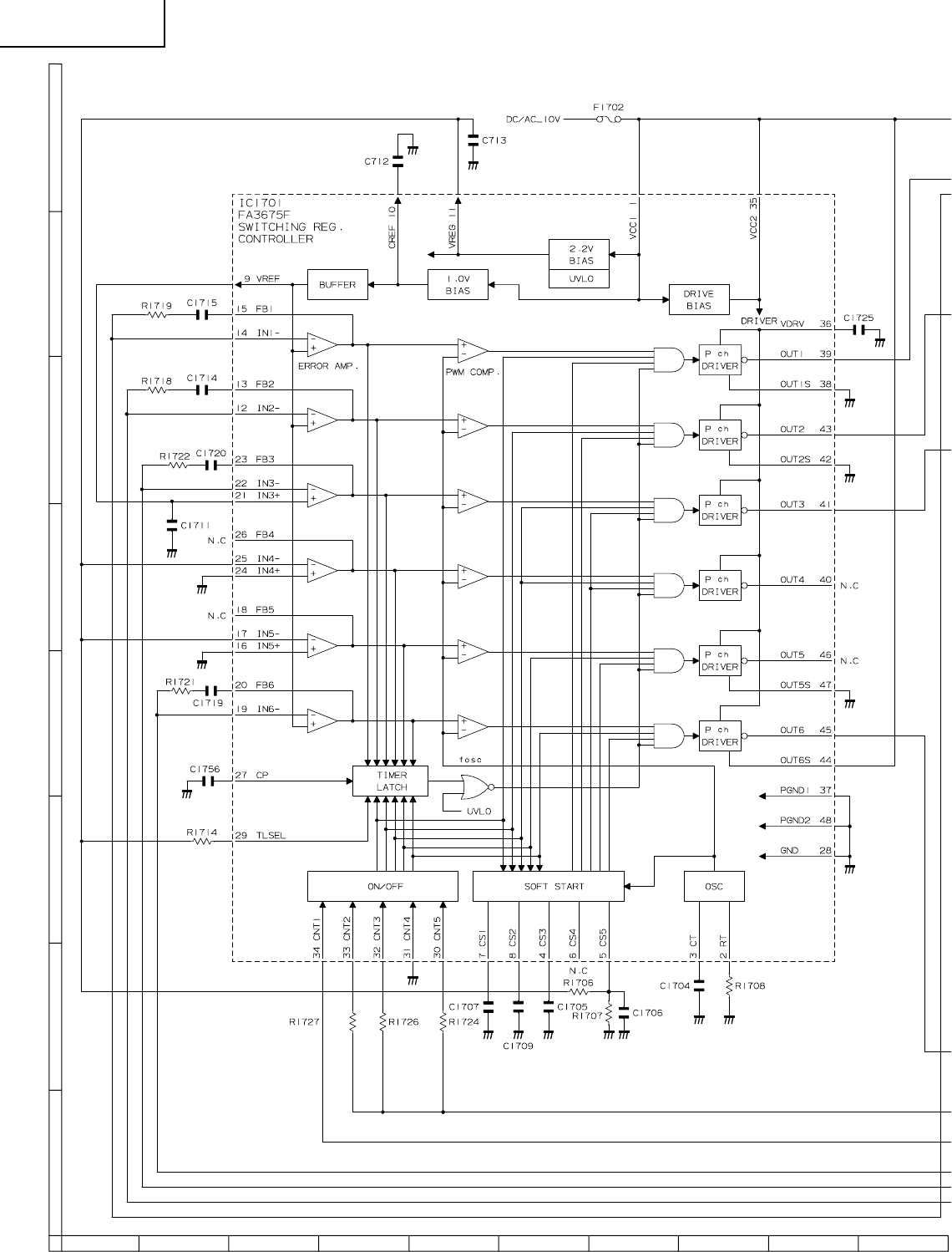
62
87109654321
A
B
C
D
E
F
G
H
PZ-MR2T
PZ-43MR2U
PZ-50MR2U
DC/DC CONVERTER BLOCK DIAGRAM

63
1716 1918151413121110
PZ-MR2T
PZ-43MR2U
PZ-50MR2U

64
87109654321
A
B
C
D
E
F
G
H
PZ-MR2T
PZ-43MR2U
PZ-50MR2U
POWER BLOCK DIAGRAM

65
1716 1918151413121110
PZ-MR2T
PZ-43MR2U
PZ-50MR2U

66
87109654321
A
B
C
D
E
F
G
H
PZ-MR2T
PZ-43MR2U
PZ-50MR2U
V0
A/D
Amp
PLL
IC4
CXA3506R
I2C=CH2
5V->3.3V Reg
IC8 PQ20VZ11
X5
79.794MHz
DO_VS YNC
DO_HS YNC
LCLK(79.79 4MH
z
X4
25MHz
E
A
T
I
CVIC
IC25
V1
A/D
IC310
TLC5733A
12V->5VReg
IC7 PQ05TZ11
PC_ C3
HV SEL
OV0 _H
V1
PLL
IC328
TLC2933IPW
12V->9V R eg
IC415 BA09FP
OV0_CLP
DO_HD ISP
-RESET_C1
-
RST_P LL
-C1_I NT
CPCI-00 56CE
-CS2
-WAIT _C1
V0
Sync
Sel
IC411
74LCX157
1B
2B
4B
1A
2A
4A
-A /+B
1Y
2Y
4Y
CN8
7
9
10
PC _H
PC_V
PC_C
CN6
18
17
29,3
0
MAIN _H
D
MAIN_VD
5
1
3
PC_R
RIN2
GIN2
BIN2
PC _G
PC_B
RIN1
GIN1
BIN1
25,2
6
21,2
2
MAI N_
B
MAI N_
G
MAI N_
R
ROUT
GOUT
BOUT
SYNCIN1
SYNCIN2
HOLD
CLPIN
DIVOUT
1/2C LK
XPOWERSAVE
RA[7..0]
RB[7..0]
GA[7..0]
GB[7..0]
BA[7..0]
BB[7..0]
AIN
BIN
CIN
RT
RB
3.27V
1.17V
AO[8..1]
BO[8..1]
CO[8..1]
EXTCLP
CLK
-OE
FIN-A
FIN-B
PFDINH
VCOOUT
13,1
4
9,10
5,6
SUB _Y
SUB_ Cb
SUB_ Cr
SUB_ HD
2
1
SUB _VD
About 60MHz
12pin TO CONNECTOR PWB
SDRAM
512Kx128bitx4 BANK
8
V0_HSYNC
V0_VSYNC
V0_CSYNC
OV0_V
V0_HSYNR
OV0_HSYNR
V0_PDEN
OV0_PDEN
V0_CLP
OV0_CLP
V0_HSYNC2
V0_VDCLK_I
OV0_HSC2
OVCLK(Max60MHz)
V0_RA[7..0]
V0_RB[7..0]
V0_GA[7..0]
V0_GB[7..0]
V0_BA[7..0]
V0_BB[7..0]
8
8
8
8
8
XPW R_SV
V1_GA[7..0]
V1_BA[7..0]
V1_RA[7..0]
8
8
8
OV1_VCKO
(≒15M Hz) V1_VDCLK_O
OV1_CLP V1_CLP
SAD C_OE
V1_HSYNR
V1_HSYNF
V1_PDEN
OV1_HSNR
OV1_HSNF
OV1_PDEN
V1_HSYNC
V1_VSYNC
V1_VDCLK_I
OV1 _H
OV1_V
OV1_VCLK
SDRAM BUS
D:128,A:11,BA:2,Ctrl:13
SDCLK=100MHz
DO_RA[9..2]
DO_GA[9..2]
DO_BA[9..2]
DO_HSYNC
DO_VSYNC
DO_HDISP
DCLKMCK_REF
8
8
8
LCLK
CKIO(24MHz)
BINT
BCLK
XBCS
BWAIT
XRESET
PLL_S
BD,BA CPU BUS
D
F
F
2
M
LH2
8
D
R
MS
ACL_S IG
12 CLR_ SW
WP
RX
D
TX
D
RX
D
TX
D
X6
25.175MHz
FPC 30pin TO MAIN PWB
CXA3506R
VCO
WHISKER
CORRECTIO
N CIRCUIT
IC423, IC424
VIDEO SIGNAL
PEAK DETECTION
V1 ADC
RT, RB SETTING
CIRCUIT
IC319-322
HY57V653220BTC-7 4 PCS.
PC I/F BLOCK DIAGRAM
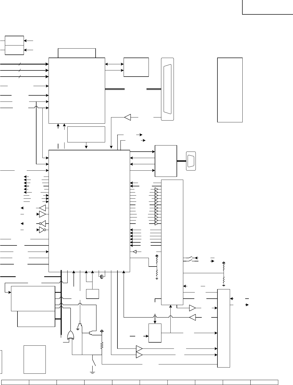
67
1716 1918151413121110
PZ-MR2T
PZ-43MR2U
PZ-50MR2U
X5
79.794MHz
DO_VS YNC
DO_HS YNC
LCLK(79.79 4MHz)
EEPROM
IC3
AT24C128N
I
2
C=CH3
TMDS(4ch)
PanelLink
HDCP
Transmitter
IC413
SiI168
I
2
C=CH1
CPU
IC1
SH7709
I
2
C PORT
CH1 Do:PTB4,Di:PTG5,Clk:PTB5
CH2 Do:PTC1,Di:PTF2,Clk:PTC2
CH3 Do:PTA6,Di:PTG6,Clk:PTA7
CH4 Do:PTD0,Di:PTG4,Clk:PTA4
5V->3.3V R eg
IC412 PQ1R33
DO_HD ISP
EEPROM
IC414
M24C32
X3
1.8432MHz
-RESET_C1
-
RST_P LL
-C1_I NT
XPWR_SV
-CS2
-WAIT _C1
8
8
8
D[23..16]
D[15..8]
D[7..0]
HSYNC
VSYNC
DE
IDCK+
EDGE
RST
TX
MDA
MCK
PTB3
PTA1
MON_DET
-RST _PL
PTC5
HVSEL PTA0
PTD7
PTE6
SEL _CD
SAD C_OE
CAR D_RST
PXOE
THER MO
B SREQ
CKIO(24MHz)
IRQ4
IRQ3
PTB7
PTC7
AN7
PTE6
CKIO
IRQ0
CS2
WAIT
PTD2
PTD5
CPU BUS D:16,A:26
D[15..0],A[25..0]
SCK1
SCK2
EXTAL
XTAL
RESETP
CN3
DVI
RS232C
Driver&
Reciever
IC405
uPD4721G
TXD2
RXD2
CTS2
RTS2
CN7
FPC 50pin (TO MAIN PWB)
I2C=CH1,2,3, SERIAL=CH1
IRQ1 4
SSYSTEM
PC_V
10
IO_STB
CN1
15pin
SERIAL=CH0
PTB6
PTE7
FLASH_W
SRST 4
5
23
1CSEN1
2
CSEN2
14
1235
9SENCE
SMPOW
7
AN2
6CCKM
S1 15FWMODEN
PTD1
PTF0
FLAS HWP
PTE1
FST ATUS
FLWP
FLASH
2Mx16bit
IC27
LH28F320S3NS
-C S0
DRAM 1Mx16bit
IC28
MSM51V18165D
PTD6
16
HOTPLUG
ACL_S IG44
5PTG2 KOUTEI
CLR_ SW PTD4
DAC_DATA
PTJ4 13
16PTJ5 DAC_CLK 8PTE3 ACL_SW 25PTE2 RES_OUT3
PTE1 3
SRESET
PTG1 15
AW_ DATA
PTC4 1
TV_COL2
PTC0 2
TV_COL1
PTB2 26
HPMUTE
1
PTB0 24
LMUTE
PTJ7 14
SH_ON
PTA5 18
AWC S_R
PTA3 17
AWC S_W
48AN0 AG C1
AN1 47
AG C2 50
49
AN4
AN3 AF T1
AF T2 20
19
AN6
AN5 PSE L1
PSE L2
6
WP
STS
VPP
A20
A20
CN9
1:VD+5
3:VA+5
5,6:VD+2.5
8:VD+3.3
10:V-5
12:VA+12
13:VD+5BK
X1
6MHz
TXD1
RXD1
TXD0
RXD0
RXD 1_T
TXD 1_T
RXD0_M
TXD0_M
RXD 1_T
TXD 1_T
8
9
42
41 RXD 1_T
TXD 1_T
R1077R1078
R1105R1106
PTC6
X6
25.175MHz VGA_OE
WXGA_OE
VGA_ OE
WXGA_OE
CE2A
CKE
RESET CIRCUIT
+2.5V IC19 PST623XW
+3.3V IC2 PST600IW
I
2
C=CH1
(TO MONITOR)
13pin (TO MAIN PWB)
POWER CONNECTOR
CN5
RS232C
SERIAL=CH2
INTERNAL 72MHz
EXTERNAL 24MHz
SERIAL CONNECTION FOR
CE01 ONLY
(R1081, R1080)
CVIC INTERNAL SUPPLY VOLTAGE
SELECTOR
R1077 MOUNTED: VD+2.5V=2.5V
R1078 MOUNTED: VD+2.5V=1.8V
CVIC INTERNAL SUPPLY VOLTAGE
MONITOR
R1105 MOUNTED: VD+2.5V=2.5V
R1106 MOUNTED: VD+2.5V=1.8V
PC
DDC
DETECT
FLASH WRITE AT FWMODEN=LOW
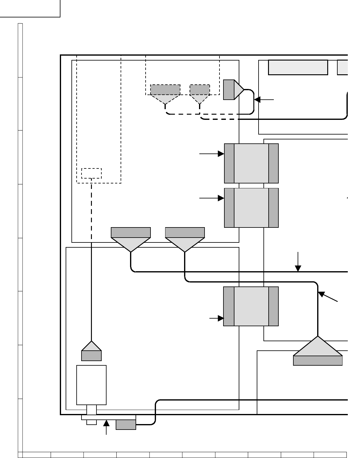
68
87109654321
A
B
C
D
E
F
G
H
PZ-MR2T
PZ-43MR2U
PZ-50MR2U
OVERALL WIRING DIAGRAM-1/2
CN9 CN8
POWER UNIT
FRO
NT
PC I/F UNIT
P3401
CN703
CN702
CN6 CN7
CN1
SC1502
SC1501
P1502
QC
NW
QCN
W
QCN
W
QCNW-6077CEZZ
QCNW-6080CEZZ
QCNW-
6083CEZZ
QCNW-
6084CEZZ
LED UNIT P3001
QCNW-6078CEZ
Z
SR UNIT
P6000 P6001

69
1716 1918151413121110
PZ-MR2T
PZ-43MR2U
PZ-50MR2U
FRONT UNIT
MAIN UNIT
AV UNIT
TUNER
P
3401 P3402
P1703
SC1503
SC1401
P1301
P2501
P2503
SC1402
SC1504
P1702
QCNW-6073CEZZ
QCNW-A280WJZZ
QCNW-6082CEZZ
QCNW-6079CEZZ
QCNW-6076CEZZ
QCNW-6074CEZZ
QCNW-6081CEZZ
80
CEZZ
60
78CEZZ
P2502
TUNER
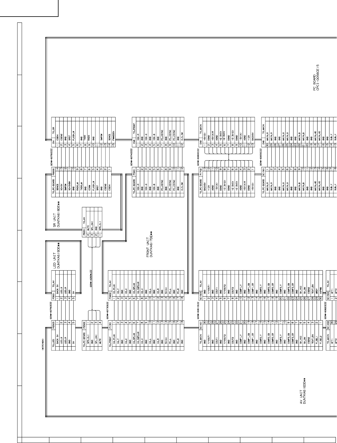
70
87109654321
A
B
C
D
E
F
G
H
PZ-MR2T
PZ-43MR2U
PZ-50MR2U
OVERALL WIRING DIAGRAM-2/2
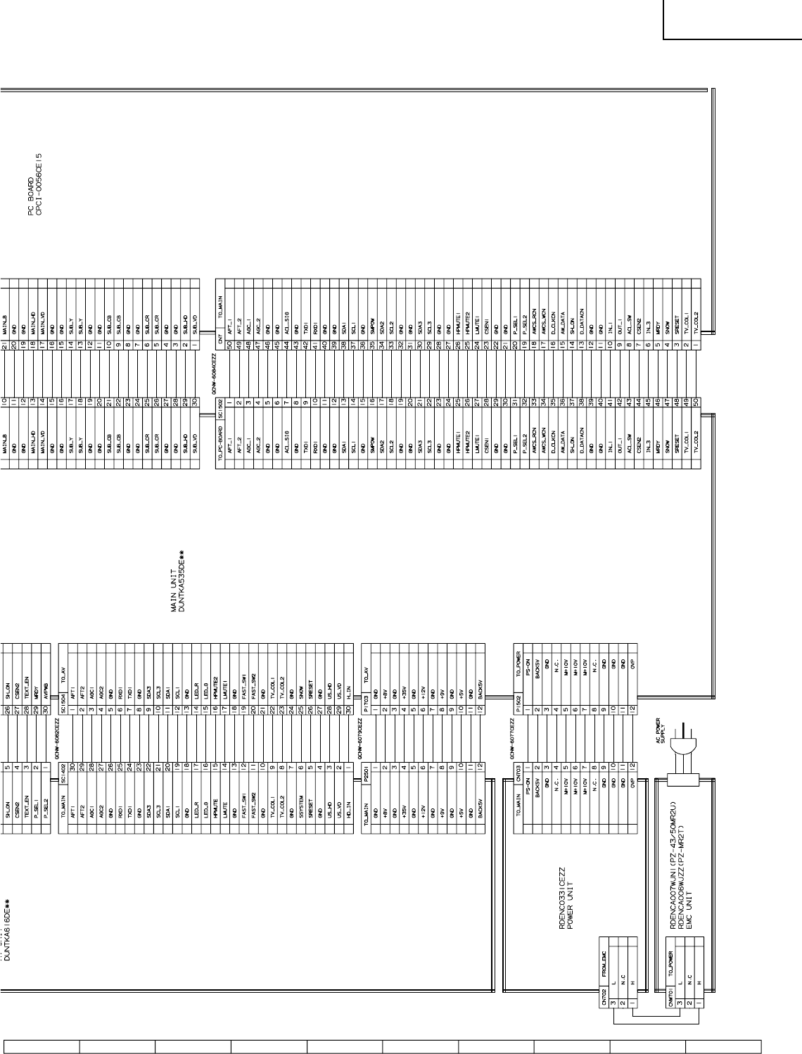
71
1716 1918151413121110
PZ-MR2T
PZ-43MR2U
PZ-50MR2U

72
PZ-MR2T
PZ-43MR2U
PZ-50MR2U
DESCRIPTION OF SCHEMATIC DIAGRAM
VOLTAGE MEASUREMENT CONDITION:
1. When the exclusive-use AC adapter is used, the color
bar signal of color bar generator for service is input to
get the normal screen. When the audio is minimized,
the voltage value is measured with the 20 kΩ/V tester.
WAVEFORM MEASUREMENT CONDITION:
1. When the exclusive-use AC adapter is used, the color
density, lightness and color hue are set to the center
position, and the signal of color bar generator for service
is observed to get waveform.
2. indicates waveform check points (See chart,
waveforms are measured from point indicated to
chassis ground.)
INDICATION OF RESISTOR & CAPACITOR:
RESISTOR
1. The unit of resistance “Ω” is omitted.
(K=kΩ=1000 Ω, M=MΩ).
2. All resistors are ± 5%, unless otherwise noted.
(J= ± 5%, F= ± 1%, D= ± 0.5%)
3. All resistors are Carbon type, unless otherwise noted.
C: Solid W: Cement
S: Oxide Film T: Special
N: Metal Coating
CAUTION:
This circuit diagram is original one, therefore there may be a
slight difference from yours.
IMPORTANT SAFETY NOTICE:
PARTS MARKED WITH “
å
”
( )ARE
IMPORTANT FOR MAINTAINING THE SAFETY OF
THE SET. BE SURE TO REPLACE THESE PARTS
WITH SPECIFIED ONES FOR MAINTAINING THE
SAFETY AND PERFORMANCE OF THE SET.
CAPACITOR
1. All capacitors are mF, unless otherwise noted.
(P=pF=mmF).
2. All capacitors are Ceramic type, unless otherwise
noted.
(ML) : Mylar (TA) : Tantalum
(PF) : Polypro Film (ST) : Styrol

73
PZ-MR2T
PZ-43MR2U
PZ-50MR2U
WAVEFORMS
1
IC1301 63-pin
V: 200mV/div H: 10µsec/div
2
IC1301 60-pin
V: 200mV/div H: 10µsec/div
3
IC1301 56-pin
V: 500mV/div H: 10µsec/div
4
TP7004
V: 200mV/div H: 10µsec/div
5
TP7003
V: 200mV/div H: 10µsec/div
6
TP812
V: 200mV/div H: 10µsec/div
7
TP603
V: 200mV/div H: 10µsec/div
8
P801 1-pin
V: 100mV/div H: 10µsec/div
9
P801 3-pin
V: 100mV/div H: 10µsec/div
0
P801 5-pin
V: 100mV/div H: 10µsec/div
q
TP809
V: 200mV/div H: 10µsec/div
w
TP808
V: 200mV/div H: 10µsec/div
e
TP807
V: 200mV/div H: 10µsec/div
r
IC810 13-pin
V: 200mV/div H: 10µsec/div
t
IC810 11-pin
V: 200mV/div H: 10µsec/div
y
IC810 10-pin
V: 200mV/div H: 10µsec/div
u
IC803 31-pin
V: 1V/div H: 10µsec/div
i
IC1301 44-pin
V: 500mV/div H: 10µsec/div
o
TP410
V: 500mV/div H: 10µsec/div
p
IC802 21-pin
V: 200mV/div H: 10µsec/div
a
IC802 22-pin
V: 200mV/div H: 10µsec/div
s
IC802 23-pin
V: 200mV/div H: 10µsec/div
d
IC804 13-pin
V: 500mV/div H: 10µsec/div
f
IC804 11-pin
V: 500mV/div H: 10µsec/div
g
IC804 10-pin
V: 500mV/div H: 10µsec/div

74
87109654321
A
B
C
D
E
F
G
H
PZ-MR2T
PZ-43MR2U
PZ-50MR2U
Ë MAIN UNIT-1/7

75
1716 1918151413121110
PZ-MR2T
PZ-43MR2U
PZ-50MR2U

76
87109654321
A
B
C
D
E
F
G
H
PZ-MR2T
PZ-43MR2U
PZ-50MR2U
Ë MAIN UNIT-2/7
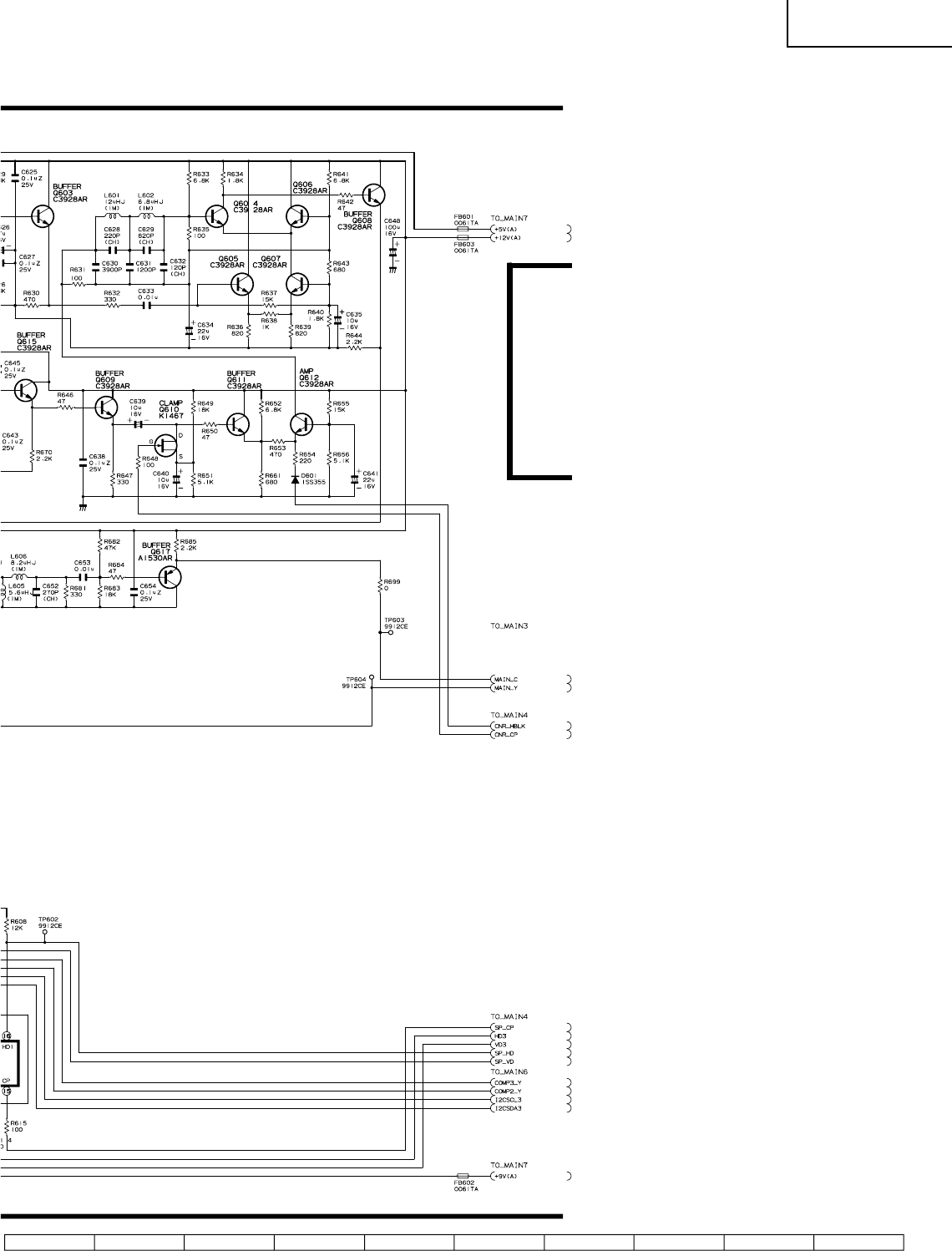
77
1716 1918151413121110
PZ-MR2T
PZ-43MR2U
PZ-50MR2U

78
87109654321
A
B
C
D
E
F
G
H
PZ-MR2T
PZ-43MR2U
PZ-50MR2U
Ë MAIN UNIT-3/7
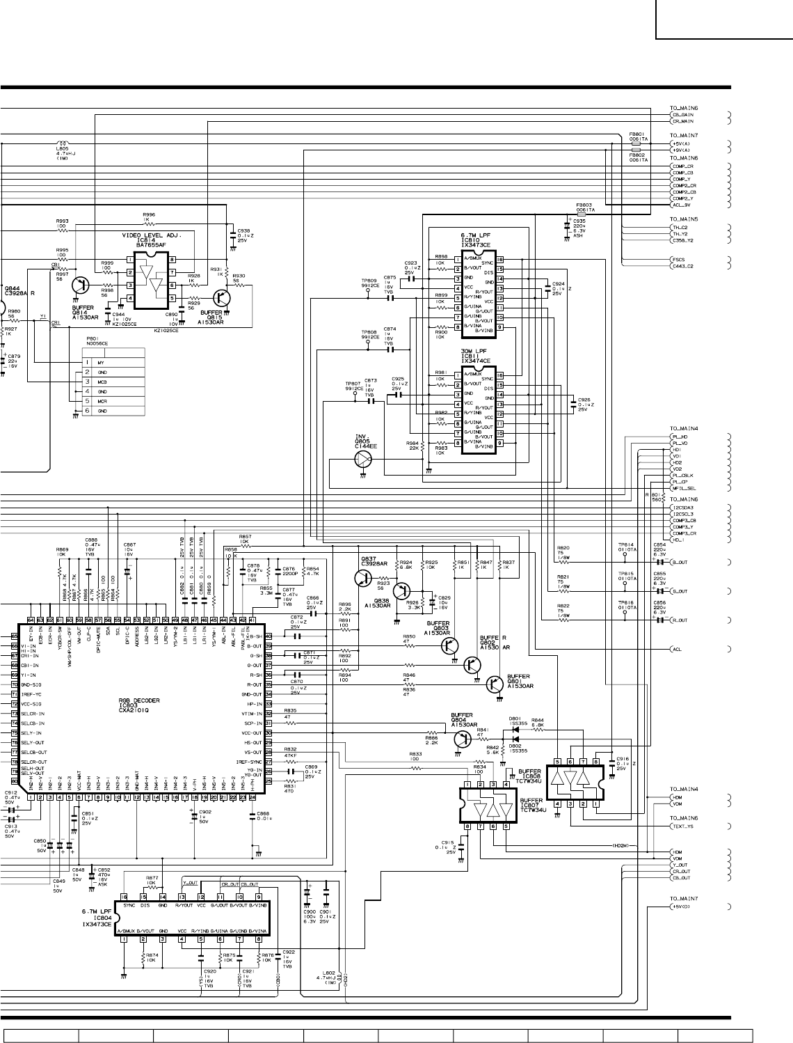
79
1716 1918151413121110
PZ-MR2T
PZ-43MR2U
PZ-50MR2U

80
87109654321
A
B
C
D
E
F
G
H
PZ-MR2T
PZ-43MR2U
PZ-50MR2U
Ë MAIN UNIT-4/7
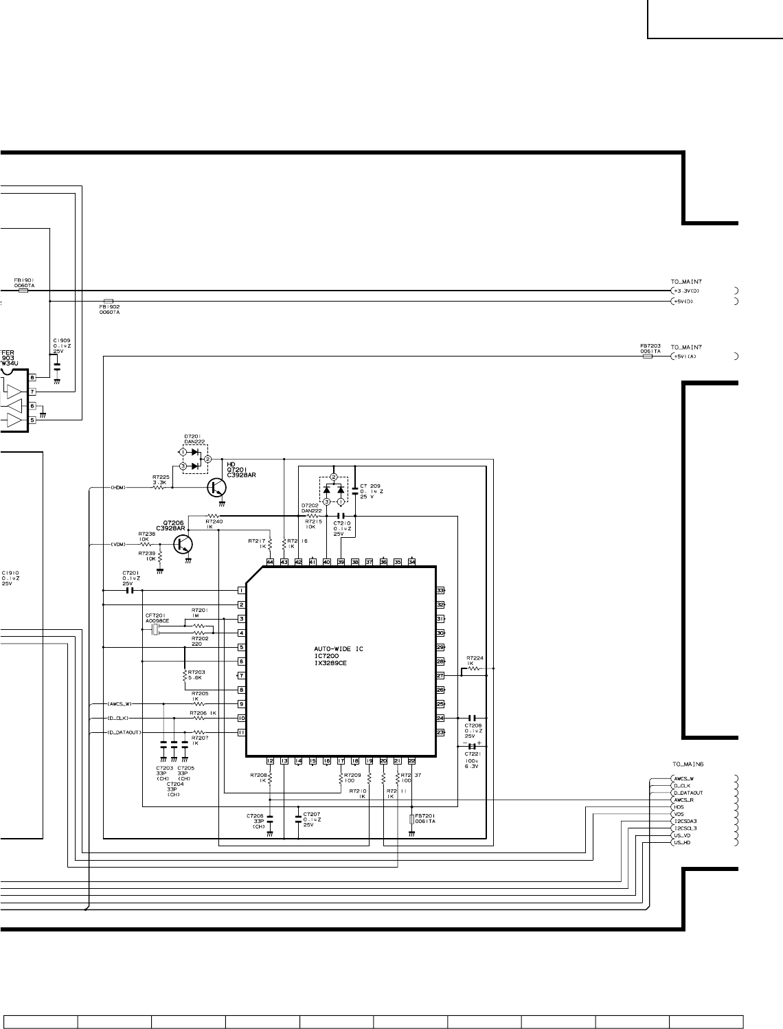
81
1716 1918151413121110
PZ-MR2T
PZ-43MR2U
PZ-50MR2U

82
87109654321
A
B
C
D
E
F
G
H
PZ-MR2T
PZ-43MR2U
PZ-50MR2U
Ë MAIN UNIT-5/7
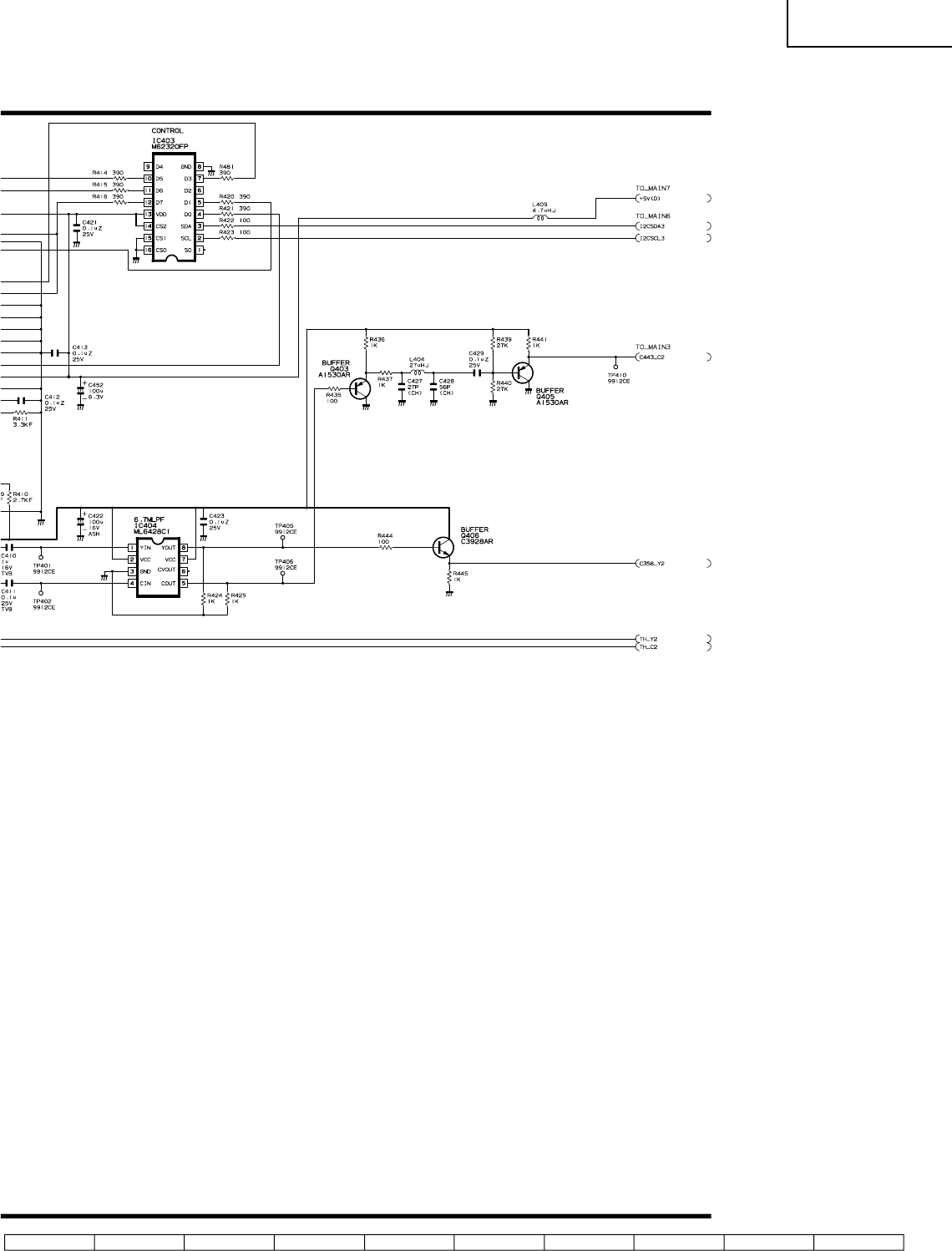
83
1716 1918151413121110
PZ-MR2T
PZ-43MR2U
PZ-50MR2U

84
87109654321
A
B
C
D
E
F
G
H
PZ-MR2T
PZ-43MR2U
PZ-50MR2U
Ë MAIN UNIT-6/7
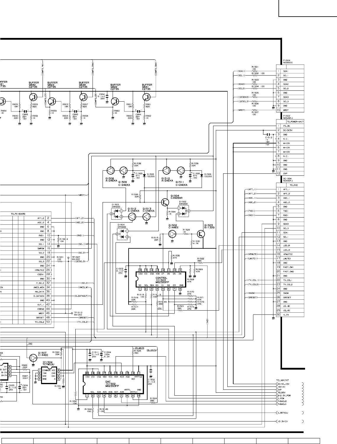
85
1716 1918151413121110
PZ-MR2T
PZ-43MR2U
PZ-50MR2U

86
87109654321
A
B
C
D
E
F
G
H
PZ-MR2T
PZ-43MR2U
PZ-50MR2U
Ë MAIN UNIT-7/7
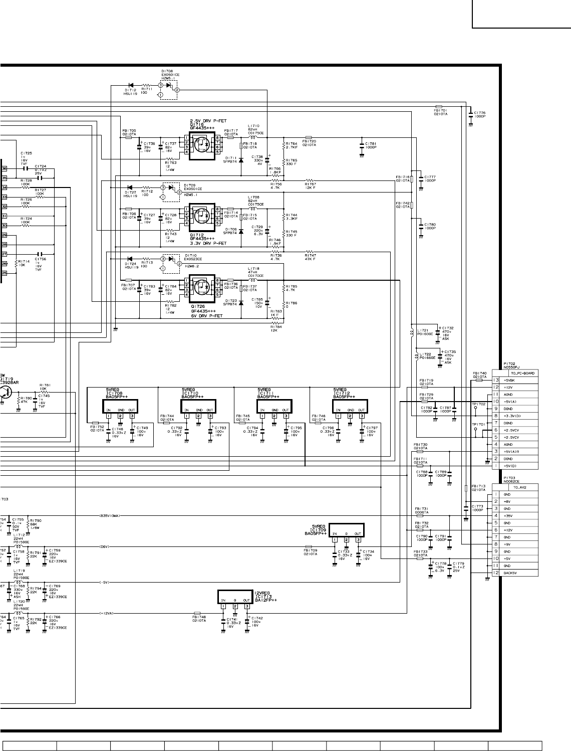
87
1716 1918151413121110
PZ-MR2T
PZ-43MR2U
PZ-50MR2U
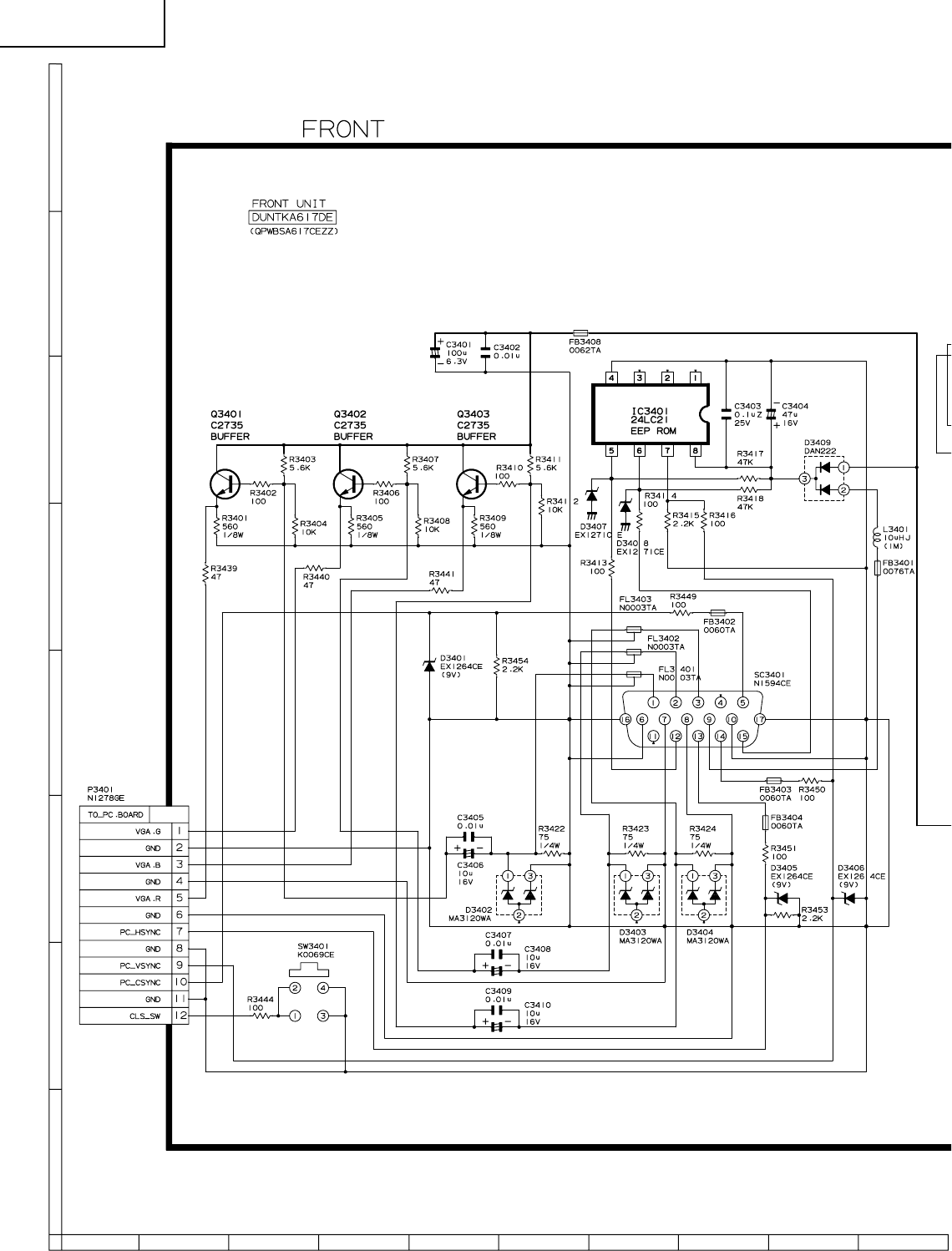
88
87109654321
A
B
C
D
E
F
G
H
PZ-MR2T
PZ-43MR2U
PZ-50MR2U
Ë FRONT UNIT
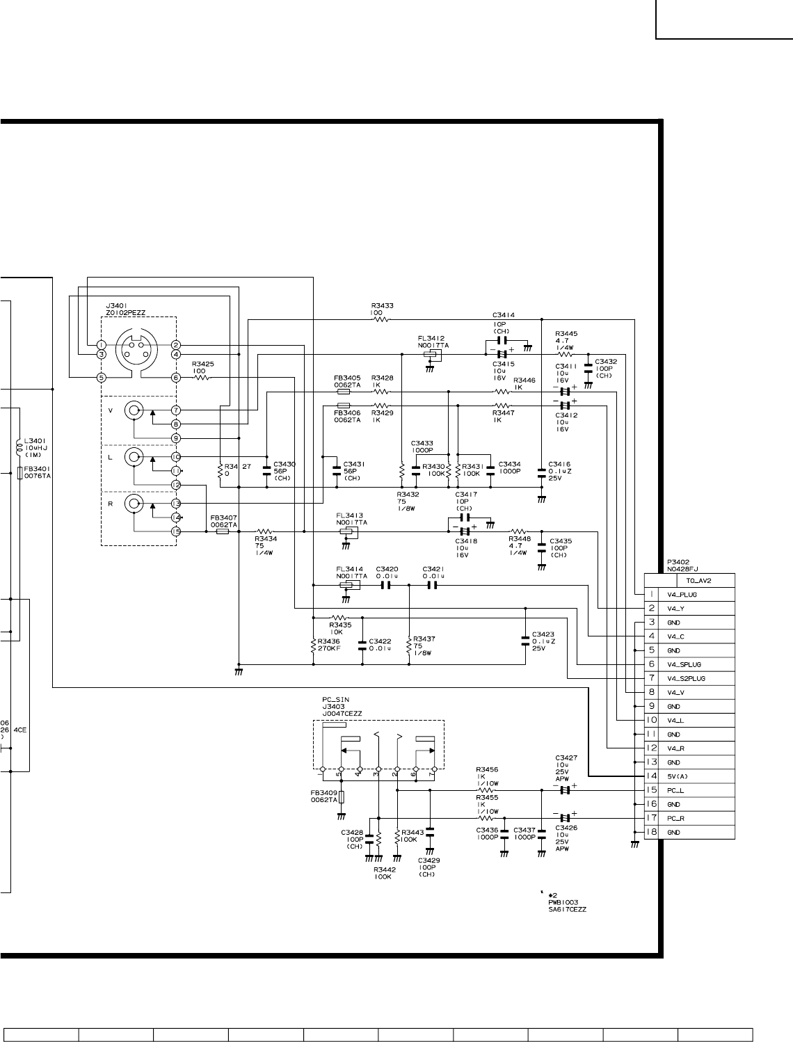
89
1716 1918151413121110
PZ-MR2T
PZ-43MR2U
PZ-50MR2U
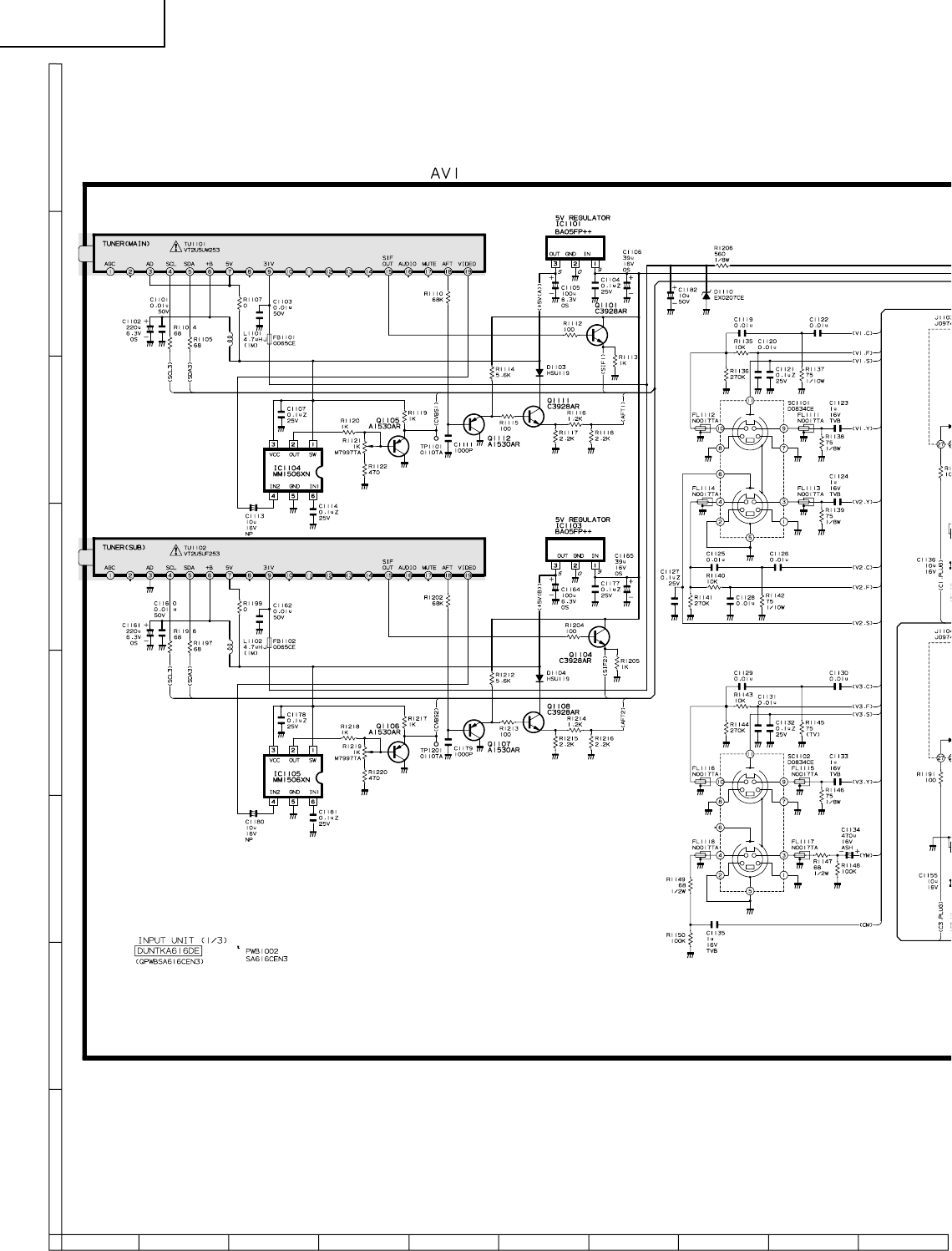
90
87109654321
A
B
C
D
E
F
G
H
PZ-MR2T
PZ-43MR2U
PZ-50MR2U
Ë AV UNIT-1/3
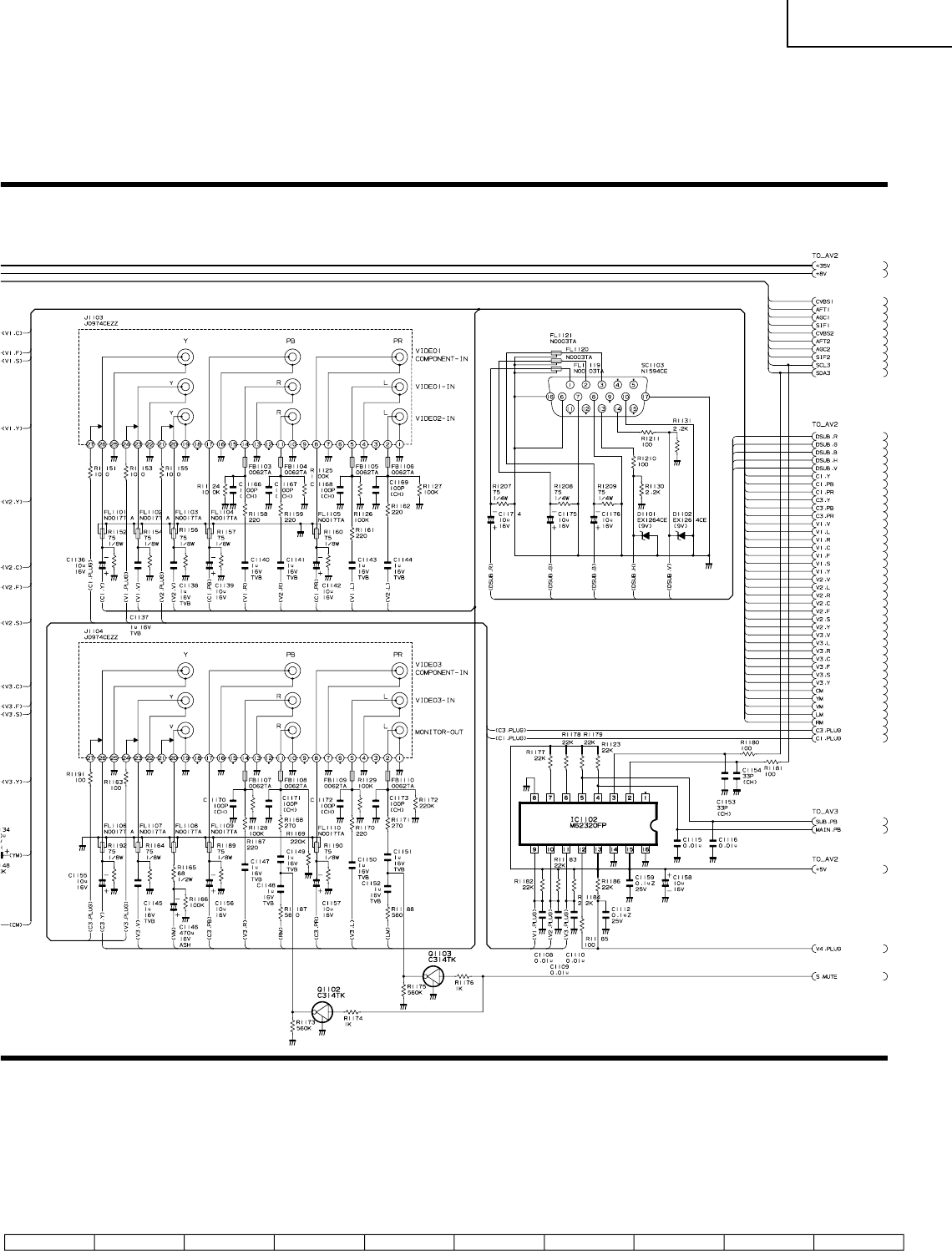
91
1716 1918151413121110
PZ-MR2T
PZ-43MR2U
PZ-50MR2U
92
87109654321
A
B
C
D
E
F
G
H
PZ-MR2T
PZ-43MR2U
PZ-50MR2U
Ë AV UNIT-2/3
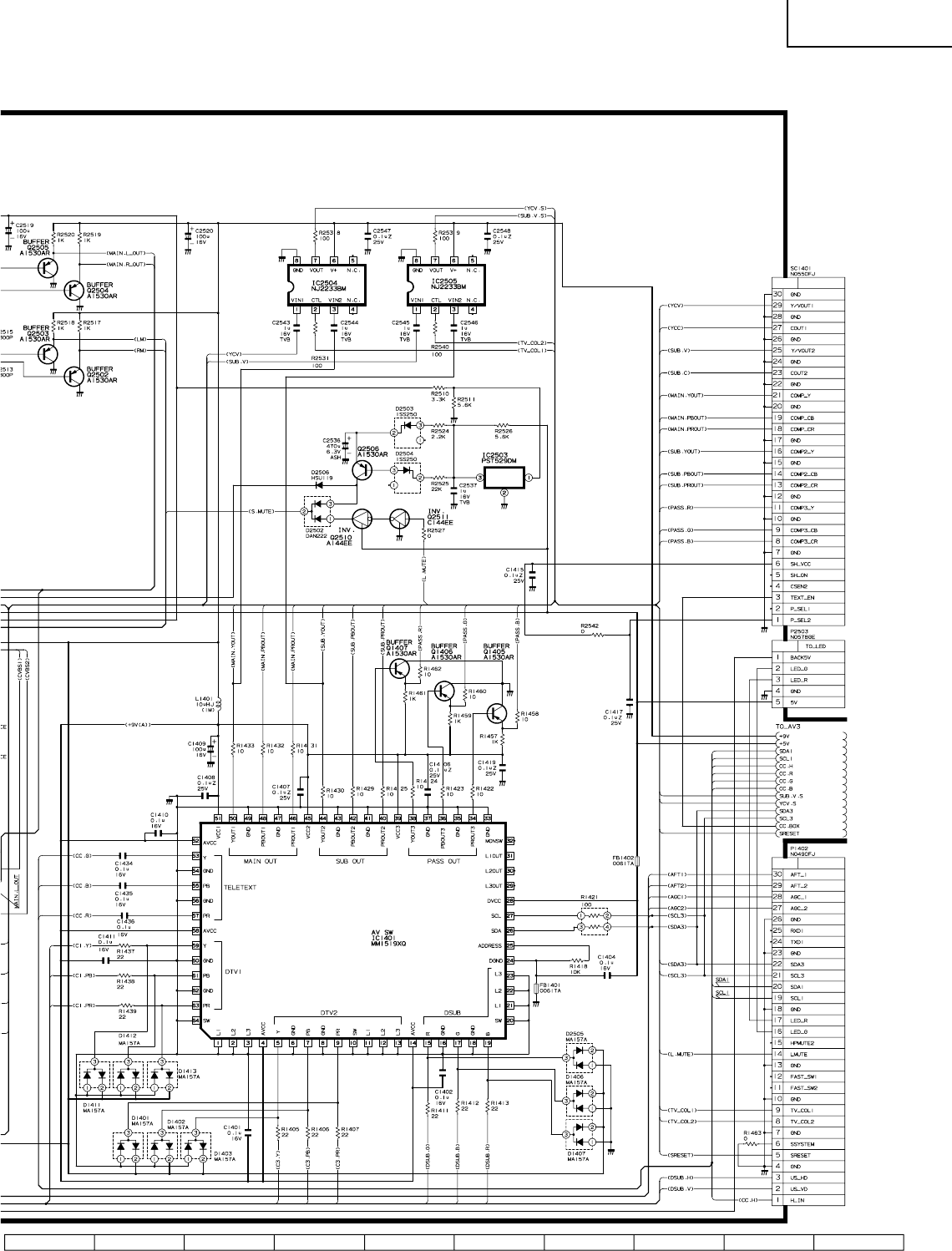
93
1716 1918151413121110
PZ-MR2T
PZ-43MR2U
PZ-50MR2U
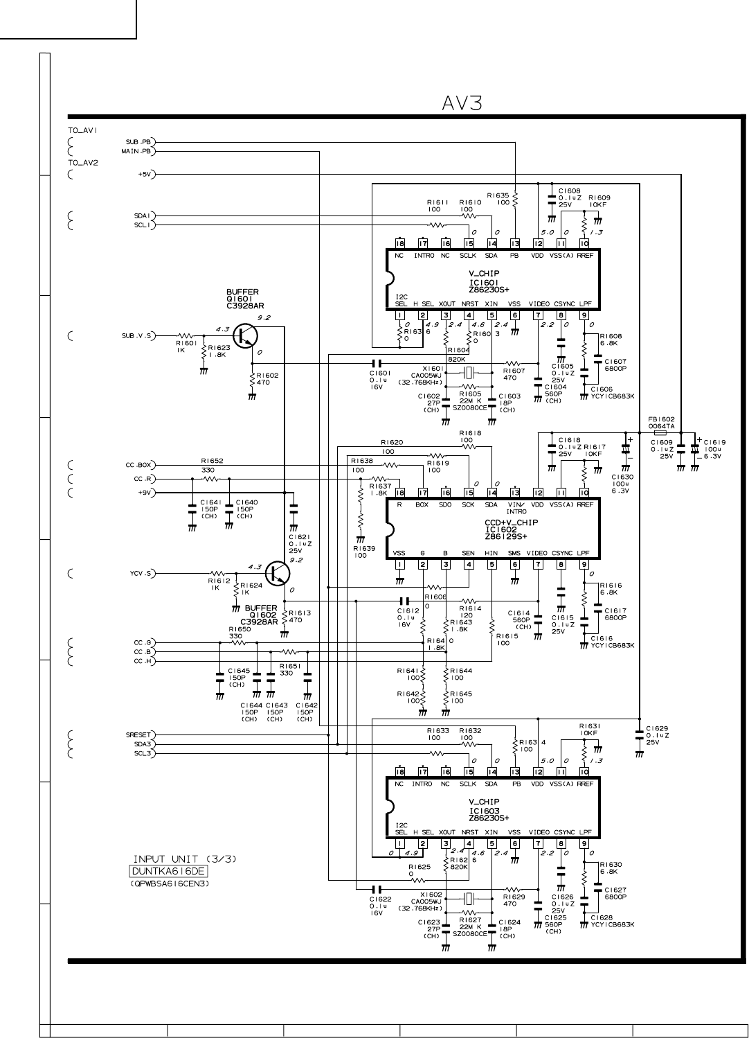
94
654321
A
B
C
D
E
F
G
H
PZ-MR2T
PZ-43MR2U
PZ-50MR2U
Ë AV UNIT-3/3

95
654321
A
B
C
D
E
F
G
H
PZ-MR2T
PZ-43MR2U
PZ-50MR2U
Ë LED Unit

96
87109654321
A
B
C
D
E
F
G
H
PZ-MR2T
PZ-43MR2U
PZ-50MR2U
Ë SR Unit

97
1716 1918151413121110
PZ-MR2T
PZ-43MR2U
PZ-50MR2U
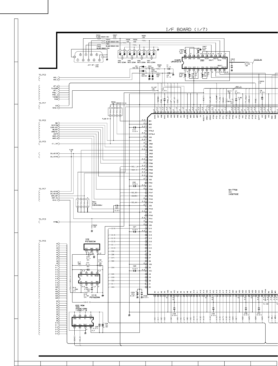
98
87109654321
A
B
C
D
E
F
G
H
PZ-MR2T
PZ-43MR2U
PZ-50MR2U
Ë PC I/F Unit-1/7
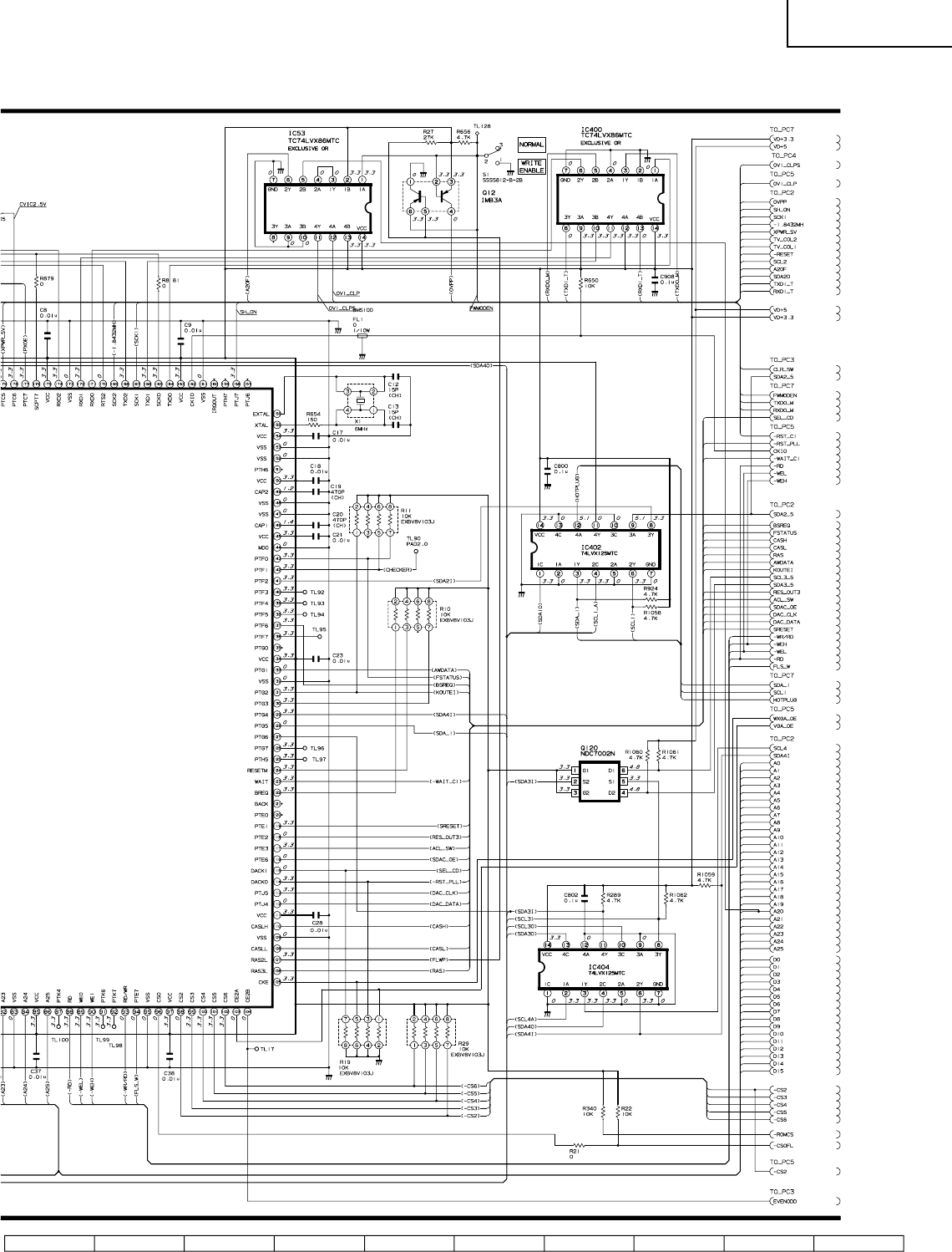
99
1716 1918151413121110
PZ-MR2T
PZ-43MR2U
PZ-50MR2U
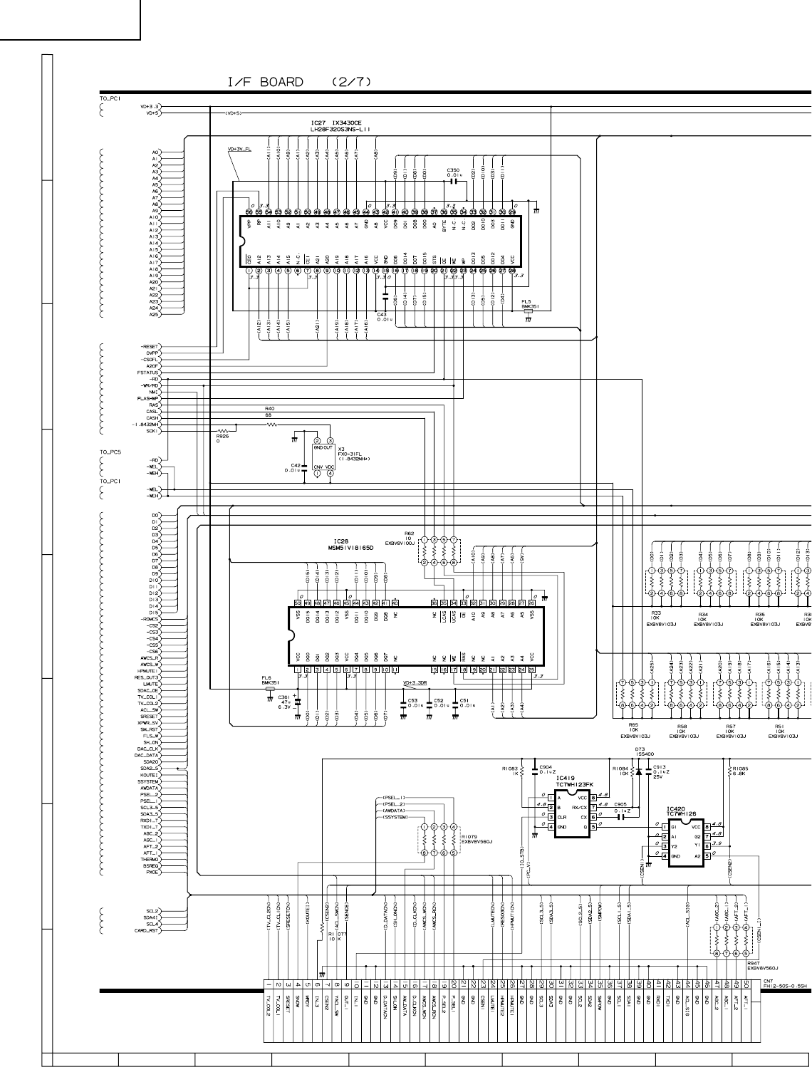
100
87109654321
A
B
C
D
E
F
G
H
PZ-MR2T
PZ-43MR2U
PZ-50MR2U
Ë PC I/F Unit-2/7
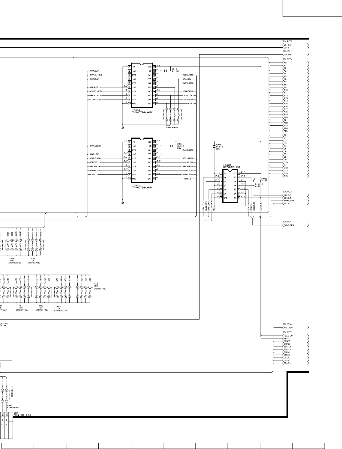
101
1716 1918151413121110
PZ-MR2T
PZ-43MR2U
PZ-50MR2U

102
87109654321
A
B
C
D
E
F
G
H
PZ-MR2T
PZ-43MR2U
PZ-50MR2U
Ë PC I/F Unit-3/7

103
1716 1918151413121110
PZ-MR2T
PZ-43MR2U
PZ-50MR2U

104
87109654321
A
B
C
D
E
F
G
H
PZ-MR2T
PZ-43MR2U
PZ-50MR2U
Ë PC I/F Unit-4/7
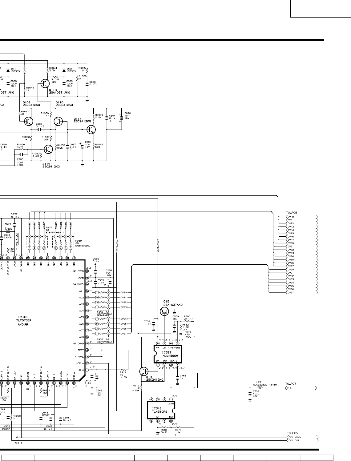
105
1716 1918151413121110
PZ-MR2T
PZ-43MR2U
PZ-50MR2U
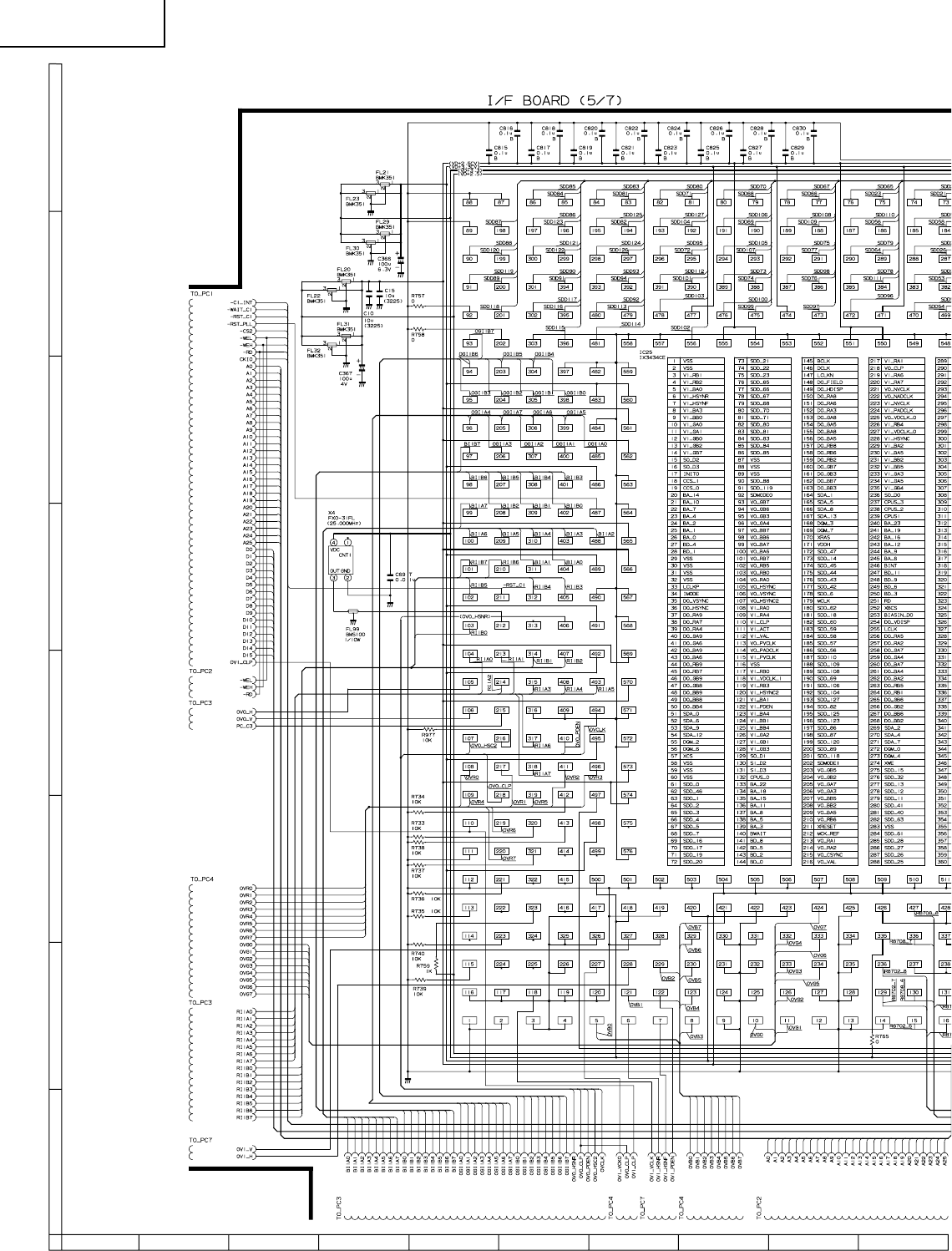
106
87109654321
A
B
C
D
E
F
G
H
PZ-MR2T
PZ-43MR2U
PZ-50MR2U
Ë PC I/F Unit-5/7
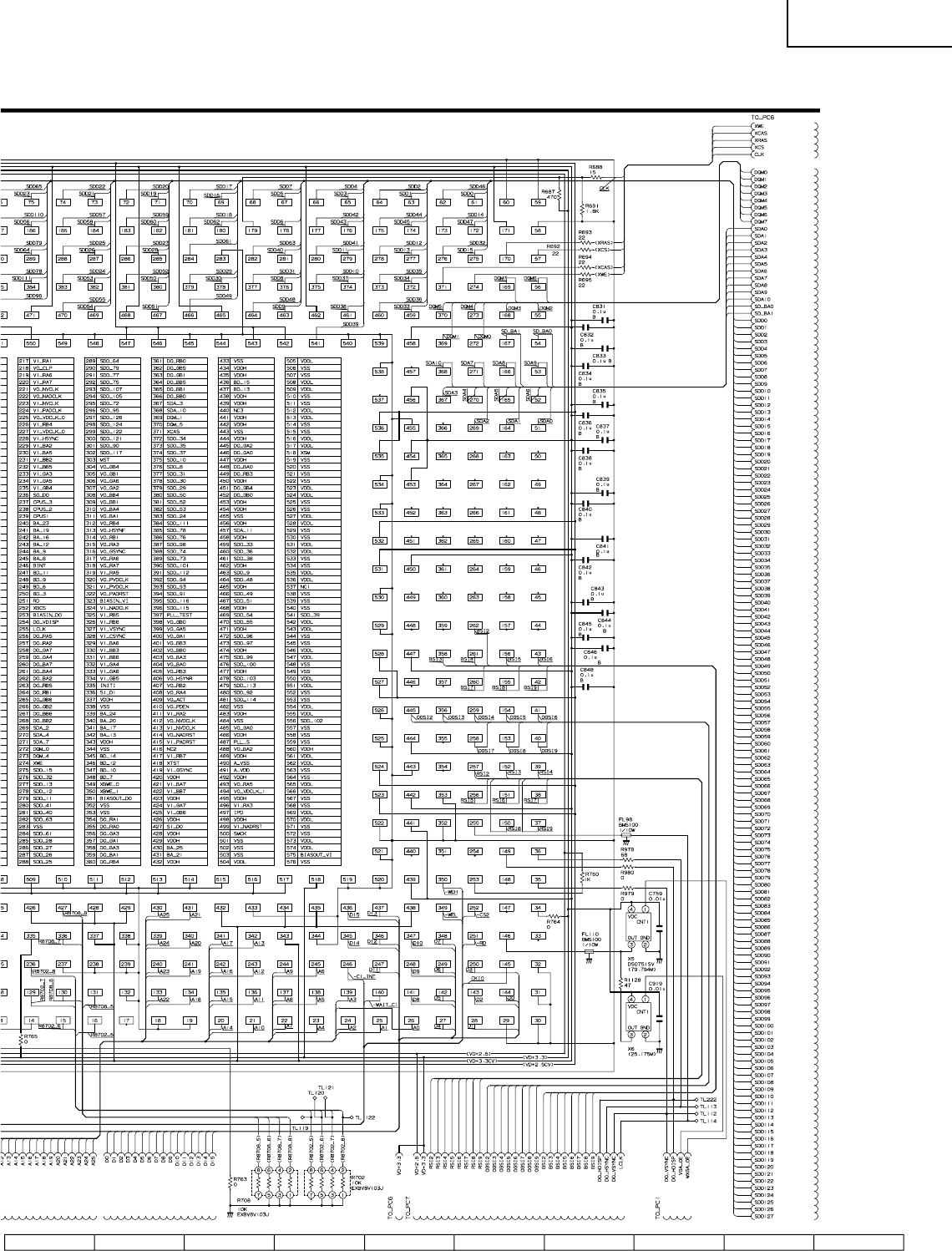
107
1716 1918151413121110
PZ-MR2T
PZ-43MR2U
PZ-50MR2U

108
87109654321
A
B
C
D
E
F
G
H
PZ-MR2T
PZ-43MR2U
PZ-50MR2U
Ë PC I/F Unit-6/7

109
1716 1918151413121110
PZ-MR2T
PZ-43MR2U
PZ-50MR2U

110
87109654321
A
B
C
D
E
F
G
H
PZ-MR2T
PZ-43MR2U
PZ-50MR2U
Ë PC I/F Unit-7/7

111
1716 1918151413121110
PZ-MR2T
PZ-43MR2U
PZ-50MR2U
112
87109654321
A
B
C
D
E
F
G
H
PZ-MR2T
PZ-43MR2U
PZ-50MR2U
Ë POWER and EMC Unit

113
1716 1918151413121110
PZ-MR2T
PZ-43MR2U
PZ-50MR2U

114
654321
A
B
C
D
E
F
G
H
PZ-MR2T
PZ-43MR2U
PZ-50MR2U
PRINTED WIRING BOARD DIAGRAM
MAIN Unit (A-Side)

115
654321
A
B
C
D
E
F
G
H
PZ-MR2T
PZ-43MR2U
PZ-50MR2U
MAIN Unit (B-Side)
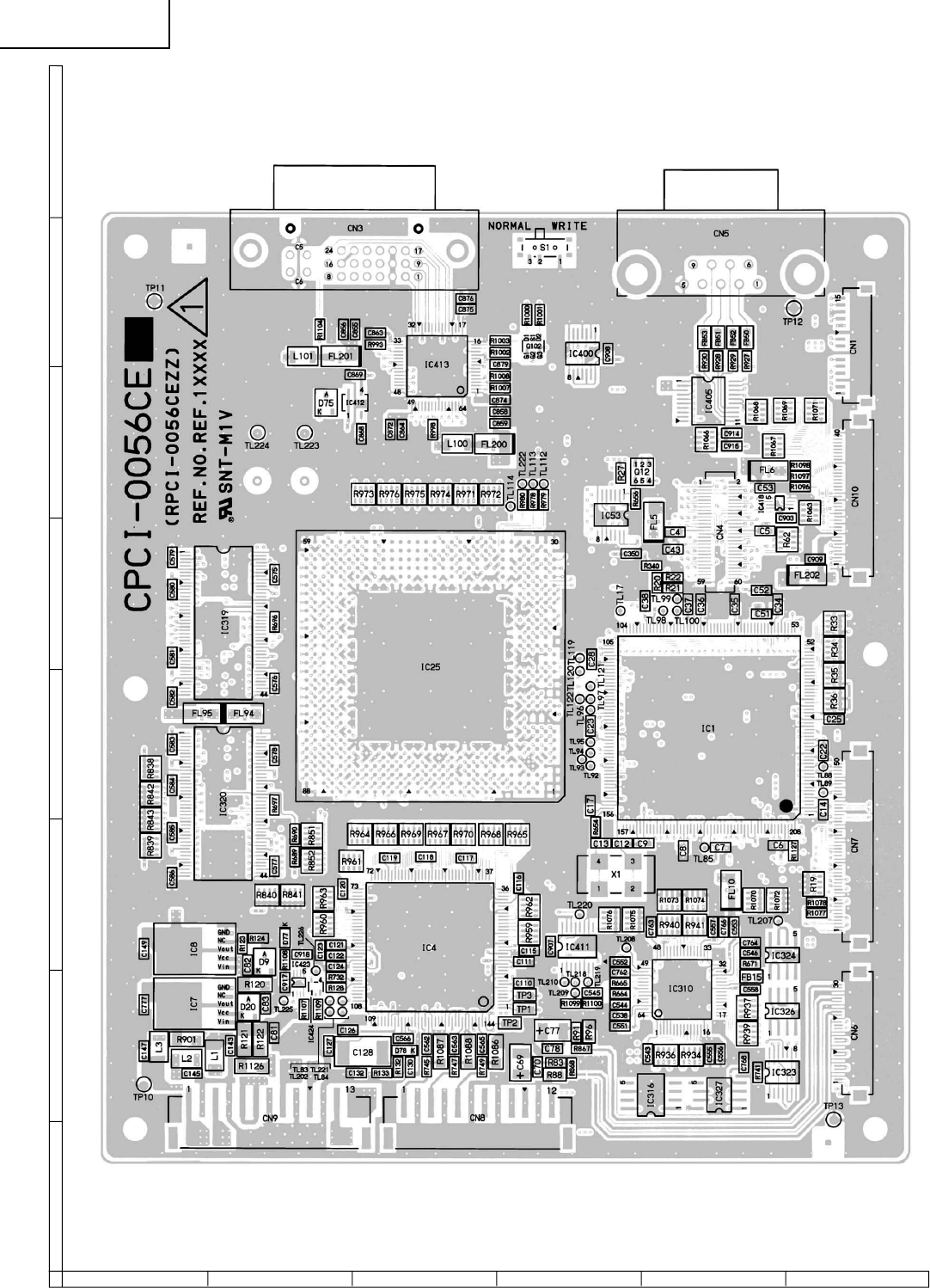
116
654321
A
B
C
D
E
F
G
H
PZ-MR2T
PZ-43MR2U
PZ-50MR2U
PC I/F Unit (A-Side)
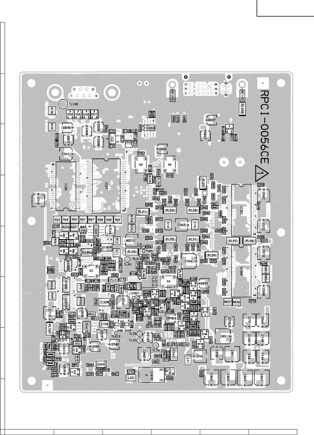
117
654321
A
B
C
D
E
F
G
H
PZ-MR2T
PZ-43MR2U
PZ-50MR2U
PC I/F Unit (B-Side)
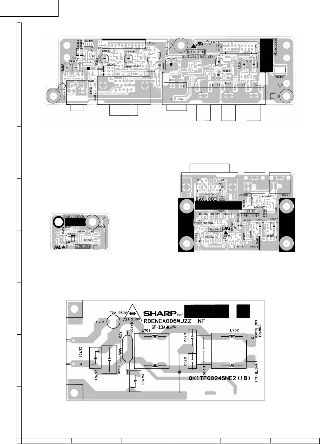
118
654321
A
B
C
D
E
F
G
H
PZ-MR2T
PZ-43MR2U
PZ-50MR2U
FRONT Unit (Component Side)
SR Unit (Component Side)LED Unit (Component Side)
EMC Unit (Component Side)
(PZ-MR2T)

119
654321
A
B
C
D
E
F
G
H
PZ-MR2T
PZ-43MR2U
PZ-50MR2U
EMC Unit (Component Side)
(PZ-43MR2U, PZ-50MR2U)
POWER Unit (Component Side)

120
654321
A
B
C
D
E
F
G
H
PZ-MR2T
PZ-43MR2U
PZ-50MR2U
AV Unit (Component Side)

Ref. No. Part No. ★Description Code Ref. No. Part No. ★Description Code
121
PZ-MR2T
PZ-43MR2U
PZ-50MR2U
PZ-43MR2U
DUNTKA535FE10 – MAIN Unit —
DUNTKA616DE03 – AV Unit —
DUNTKA617DE03 – FRONT Unit —
DUNTKA618DE03 – SR Unit —
DUNTKA619DE03 – LED Unit —
RDENCA007WJN1 – EMC Unit —
RDENC0331CEZZ – POWER Unit —
CPCi-0056CE15 – PC I/F Unit —
PZ-50MR2U
DUNTKA535FE08 – MAIN Unit —
DUNTKA616DE02 – AV Unit —
DUNTKA617DE02 – FRONT Unit —
DUNTKA618DE02 – SR Unit —
DUNTKA619DE02 – LED Unit —
RDENCA007WJN1 – EMC Unit —
RDENC0331CEZZ – POWER Unit —
CPCi-0056CE15 – PC I/F Unit —
PZ-MR2T
DUNTKA535FE16 – MAIN Unit —
DUNTKA616DE04 – AV Unit —
DUNTKA617DE04 – FRONT Unit —
DUNTKA618DE04 – SR Unit —
DUNTKA619DE04 – LED Unit —
RDENCA006WJZZ – EMC Unit —
RDENC0331CEZZ – POWER Unit —
CPCi-0056CE15 – PC I/F Unit —
PRINTED WIRING BOARD ASSEMBLIES
(NOT REPLACEMENT ITEM)
INTEGRATED CIRCUITS
IC402 VHiCXD2093Q-1Q J CXD2093Q AU
IC403 VHiM62320FP-1 J M62320FP AK
IC404 VHiML6428C1-1Y J Ml6428 AP
IC604 VHiTA1318AF-1Y J TA1318AF AS
IC801 VHiTB1274AF-1Q J TB1274AF AY
IC802 VHiTB1274AF-1Q J TB1274AF AY
IC803 VHiCXA2101Q-1 J CXA2101AQ-Tl BE
IC804 RH-iX3473CEZZ J Ml6426CS-1 AW
IC807 VHiTC7W34U/-1Y J TC7W34FU AE
IC808 VHiTC7W34U/-1Y J TC7W34FU AE
IC810 RH-iX3473CEZZ J Ml6426CS-1 AW
IC811 RH-iX3474CEZZ J Ml6426CS-4 AW
IC812 VHiNJM353M/-1 J NJM353M AG
IC814 VHiBA7655AF-1 J BA7655AF AG
IC1502 VHiM62393FP-1 J M62393FP AK
IC1503 VHiM62320FP-1 J M62320FP AK
IC1504 VHiTC7W53U/-1 J TC7W53FU AF
IC1701 VHiFA3675F/-1 J FA3675F AR
IC1704 VHiBA09T/FP-1 J BA09FP-E2 AG
IC1706 VHiBA08FP++-1Y J BA08FP AF
IC1708 VHiBA05FP++-1Y J BA05FP AF
IC1709 VHiBA05FP++-1Y J BA05FP AF
IC1710 VHiBA05FP++-1Y J BA05FP AF
IC1711 VHiBA05FP++-1Y J BA05FP AF
IC1712 VHiBA05FP++-1Y J BA05FP AF
IC1713 VHiBA12FP++-1Y J BA12FP-E2 AF
IC1901 RH-iXA194WJZZQ J I.C. AU
IC1902 VHiM62320FP-1 J M62320FP AK
IC1903 VHiTC7W34U/-1Y J TC7W34FU AE
IC7001 VHiPD64082/-1 J UPD64082GF-3BA BC
IC7002 RH-iX3152CEZZ J MSM514265C50JS AT
IC7003 VHiML6428C1-1Y J ML6428 AP
IC7004 VHiBA033FP/-1 J BA033FP-E2 AG
IC7005 VHiPST600iM-1 J PST600IMT AE
IC7200 RH-iX3289CEZZ J IX3289CE AQ
★ MARK: SPARE PARTS-DELIVERY SECTION
' MARK: X-RAY RELATED PARTS
★ MARQUE: SECTION LIVRAISON DES PIECES DERECHANGE
' MARQUE: PIECES RELATIVE AUX RAYONS X
PARTS LIST
PARTS REPLACEMENT
Replacement parts which have these special safety characteristics iden-
tified in this manual ; electrical components having such features are
identified by å and shaded areas in the Replacement Parts Lists and
Schematic Diagrams. The use of a substitute replacement part which
does no have the same safety characteristic as the factory recom-
mended replacement parts shown in this service manual may create
shock, fire or other hazards.
"HOW TO ORDER REPLACEMENT PARTS"
To have your order filled promptly and correctly, please furnish the fol-
lowing informations.
1. MODEL NUMBER 2. REF. NO.
3. PART NO. 4. DESCRIPTION
in USA: Contact your nearest SHARP Parts Distributor to order. For
location of SHARP Parts Distributor, Please call Toll-Free; 1-
800-BE-SHARP
LISTE DES PIECES
CHANGE DES PIECES
Les pi`eces de rechange qui pr élelesentent ces caract éleristiques sp
éleciales de s élecurit éle, sont identifi élees dans ce manuel : les pi`eces
élelectriques qui pr élesentent ces particularit éles, sont rep éler élee
par la marque å et sont hachur élees dans les listes de pi`eces et dans
les diagrammes sch élematiques.
La substitution d'une pi`ece de rechange par une autre qui ne pr éLesente
pas les m éoemes caract éLeristiques de s élecurit éle que la pi`ece
recommand élee parl'usine et dans ce manuel de service, peut provoquer
une éLelectrocution, un incendie ou toutautre sinistre.
"COMMENT COMMANDER LES PIECES DE RECHANGE"
Pour que votre commande soit rapidement et correctement remplie,
veuillez fournir les renseignements suivants.
1. NUMERO DU MODELE 2. NO. DE REF
3. NO. DE PIECE 4. DESCRIPTION
in CANADA: Contact SHARP Electronics of Canada Limited
Phone (416) 890-2100
Ref. No. Part No. ★Description Code Ref. No. Part No. ★Description Code
DUNTKA535FE10 (PZ-43MR2U)
DUNTKA535FE08 (PZ-50MR2U)
DUNTKA535FE16 (PZ-MR2T)
MAIN UNIT

Ref. No. Part No. ★Description Code Ref. No. Part No. ★Description Code
122
PZ-MR2T
PZ-43MR2U
PZ-50MR2U
TRANSISTORS
Q403 VS2SA1530AR-1 J 2SA1530AR AB
Q405 VS2SA1530AR-1 J 2SA1530AR AB
Q406 VS2SC3928AR-1 J 2SC3928AR AB
Q407 VS2SC3928AR-1 J 2SC3928AR AB
Q408 VS2SC3928AR-1 J 2SC3928AR AB
Q424 VS2SA1530AR-1 J 2SA1530AR AB
Q425 VS2SA1530AR-1 J 2SA1530AR AB
Q601 VS2SC3928AR-1 J 2SC3928AR AB
Q602 VS2SC3928AR-1 J 2SC3928AR AB
Q603 VS2SC3928AR-1 J 2SC3928AR AB
Q604 VS2SC3928AR-1 J 2SC3928AR AB
Q605 VS2SC3928AR-1 J 2SC3928AR AB
Q606 VS2SC3928AR-1 J 2SC3928AR AB
Q607 VS2SC3928AR-1 J 2SC3928AR AB
Q608 VS2SC3928AR-1 J 2SC3928AR AB
Q609 VS2SC3928AR-1 J 2SC3928AR AB
Q610 VS2SK1467//-1 J 2SK1467 AE
Q611 VS2SC3928AR-1 J 2SC3928AR AB
Q612 VS2SC3928AR-1 J 2SC3928AR AB
Q613 VS2SC3928AR-1 J 2SC3928AR AB
Q614 VS2SC3928AR-1 J 2SC3928AR AB
Q615 VS2SC3928AR-1 J 2SC3928AR AB
Q616 VS2SC3928AR-1 J 2SC3928AR AB
Q617 VS2SA1530AR-1 J 2SA1530AR AB
Q801 VS2SA1530AR-1 J 2SA1530AR AB
Q802 VS2SA1530AR-1 J 2SA1530AR AB
Q803 VS2SA1530AR-1 J 2SA1530AR AB
Q804 VS2SA1530AR-1 J 2SA1530AR AB
Q805 VSDTC144EE/-1 J DTC144EE AA
Q807 VS2SC3928AR-1 J 2SC3928AR AB
Q808 VS2SA1530AR-1 J 2SA1530AR AB
Q809 VS2SC3928AR-1 J 2SC3928AR AB
Q810 VS2SA1530AR-1 J 2SA1530AR AB
Q811 VS2SA1530AR-1 J 2SA1530AR AB
Q812 VS2SA1530AR-1 J 2SA1530AR AB
Q813 VSDTC124EKA-1 J DTC124EKA AB
Q814 VS2SA1530AR-1 J 2SA1530AR AB
Q815 VS2SA1530AR-1 J 2SA1530AR AB
Q818 VS2SA1530AR-1 J 2SA1530AR AB
Q819 VS2SA1530AR-1 J 2SA1530AR AB
Q820 VS2SA1530AR-1 J 2SA1530AR AB
Q821 VS2SC2735//1E J 2SC2735 AC
Q822 VS2SC2735//1E J 2SC2735 AC
Q823 VS2SC2735//1E J 2SC2735 AC
Q824 VS2SA1530AR-1 J 2SA1530AR AB
Q825 VS2SA1530AR-1 J 2SA1530AR AB
Q826 VS2SA1530AR-1 J 2SA1530AR AB
Q827 VS2SA1530AR-1 J 2SA1530AR AB
Q828 VS2SA1530AR-1 J 2SA1530AR AB
Q830 VS2SC3928AR-1 J 2SC3928AR AB
Q837 VS2SC3928AR-1 J 2SC3928AR AB
Q838 VS2SA1530AR-1 J 2SA1530AR AB
Q839 VS2SC2735//1E J 2SC2735 AC
Q840 VS2SC2735//1E J 2SC2735 AC
Q841 VS2SC2735//1E J 2SC2735 AC
Q842 VS2SC3928AR-1 J 2SC3928AR AB
Q843 VS2SC3928AR-1 J 2SC3928AR AB
Q844 VS2SC3928AR-1 J 2SC3928AR AB
Q1502 VSDTC144EE/-1 J DTC144EE AA
Q1503 VS2SB1132Q/-1 J 2SB1132Q AC
Q1504 VS2SC3928AR-1 J 2SC3928AR AB
Q1507 VSDTC144EE/-1 J DTC144EE AA
Q1508 VSDTA124EKA-1 J DTA124EKA AB
Q1509 VSDTC124EKA-1 J DTC124EKA AB
Q1510 VSDTA124EKA-1 J DTA124EKA AB
Q1511 VSDTC124EKA-1 J DTC124EKA AB
Q1512 VSDTA124EKA-1 J DTA124EKA AB
Q1513 VSDTC124EKA-1 J DTC124EKA AB
Q1701 VSDTC114EE/-1 J DTC114EE AB
Q1708 VSDTC114EE/-1 J DTC114EE AB
Q1710 VSFMMT718//-1 J FMMT718 AE
Q1712 VSGF4435+++-1Y J GF4435+++ AF
Q1716 VSGF4435+++-1Y J GF4435+++ AF
Q1718 VS2SK2503//-1 J 2SK2503 AE
Q1719 VS2SC3928AR-1 J 2SC3928AR AB
Q1726 VSGF4435+++-1Y J GF4435+++ AF
Q7001 VS2SA1530AR-1 J 2SA1530AR AB
Q7002 VS2SC3928AR-1 J 2SC3928AR AB
Q7003 VS2SA1530AR-1 J 2SA1530AR AB
Q7004 VS2SC3928AR-1 J 2SC3928AR AB
Q7005 VS2SA1530AR-1 J 2SA1530AR AB
Q7006 VS2SA1530AR-1 J 2SA1530AR AB
Q7007 VS2SA1530AR-1 J 2SA1530AR AB
Q7008 VS2SA1530AR-1 J 2SA1530AR AB
Q7009 VS2SA1530AR-1 J 2SA1530AR AB
Q7010 VS2SA1530AR-1 J 2SA1530AR AB
Q7201 VS2SC3928AR-1 J 2SC3928AR AB
Q7206 VS2SC3928AR-1 J 2SC3928AR AB
DIODES
D601 VHD1SS355//-1 J Diode AB
D801 VHD1SS355//-1 J Diode AB
D802 VHD1SS355//-1 J Diode AB
D1502 VHDDAN222//-1 J Diode AA
D1503 VHDDAN222//-1 J Diode AA
D1504 VHDDAN222//-1 J Diode AA
D1505 VHD1SS355//-1 J Diode AB
D1506 VHD1SS355//-1 J Diode AB
D1701 VHDHSU119//-1 J Diode AB
D1702 VHDHSU119//-1 J Diode AB
D1706 VHDSFPB74//2E J Diode AD
D1708 RH-EX0501CEZZY J Zener Diode AB
D1709 RH-EX0501CEZZY J Zener Diode AB
D1710 RH-EX0523CEZZ J Zener Diode AB
D1711 VHDSFPB74//2E J Diode AD
D1712 VHDHSU119//-1 J Diode AB
D1713 VHDHSU119//-1 J Diode AB
D1715 VHDSFPB56//2E J Diode AC
D1716 VHD1SS250//1E J Diode AB
D1717 VHDSFPB76//2E J Diode AD
D1719 VHDSFPB76//2E J Diode AD
D1720 VHDSFPB76//2E J Diode AD
D1723 VHDSFPB74//2E J Diode AD
D1724 VHDHSU119//-1 J Diode AB
D1727 VHDHSU119//-1 J Diode AB
D7201 VHDDAN222//-1 J Diode AA
D7202 VHDDAN222//-1 J Diode AA
PACKAGED CIRCUITS
X601 RFiLA0034CEZZ J Filter AD
X801 RCRSB0244CEZZ J Crystal AH
X802 RCRSB0244CEZZ J Crystal AH
X1901 RCRSZ0093CEZZY J Crystal AM
X7001 RCRSC0026CEZZY J Crystal AG
FILTERS AND COILS
CF7201 RFiLA0098CEZZ J Ceramic Filter AD
FL7001 RFiLN0097GEZZ J Filter AF
FL7002 RFiLN0097GEZZ J Filter AF
FL7003 RFiLN0079GEZZ J Filter AC
FL7004 RFiLN0079GEZZ J Filter AC
L401 VP-1M4R7J1R2N J Peaking 4.7µH AB
L404 VP-1M270J3R8N J Peaking 27µH AC
L407 VP-1M220J2R9N J Peaking 22µH AC
L409 VP-1M4R7J1R2N J Peaking 4.7µH AB
L601 VP-1M120J1R9N J Peaking 12µH AC
L602 VP-1M6R8J1R4N J Peaking 6.8µH AC
L603 VP-1M470J5R4N J Peaking 47µH AC
L604 VP-1M6R8J1R4N J Peaking 6.8µH AC
L605 VP-1M5R6J1R2NY J Peaking 5.6µH AB
L606 VP-1M8R2J1R5N J Peaking 8.2µH AC
L801 VP-1M4R7J1R2N J Peaking 4.7µH AB
L802 VP-1M4R7J1R2N J Peaking 4.7µH AB
L803 VP-1M4R7J1R2N J Peaking 4.7µH AB
DUNTKA535FE10 (PZ-43MR2U)
DUNTKA535FE08 (PZ-50MR2U)
DUNTKA535FE16 (PZ-MR2T)
MAIN UNIT (Continued)

Ref. No. Part No. ★Description Code Ref. No. Part No. ★Description Code
123
PZ-MR2T
PZ-43MR2U
PZ-50MR2U
DUNTKA535FE10 (PZ-43MR2U)
DUNTKA535FE08 (PZ-50MR2U)
DUNTKA535FE16 (PZ-MR2T)
MAIN UNIT (Continued)
L804 VP-1M4R7J1R2N J Peaking 4.7µH AB
L805 VP-1M4R7J1R2N J Peaking 4.7µH AB
L806 VP-1M4R7J1R2N J Peaking 4.7µH AB
L807 VP-1M4R7J1R2N J Peaking 4.7µH AB
L1708 RCiLC0175CEZZY J Coil AG
L1710 RCiLC0175CEZZY J Coil AG
L1711 RCiLC0130CEZZ J Coil AG
L1712 RCiLP0159GEZZ J Coil AD
L1718 RCiLC0170CEZZY J Coil AG
L1719 RCiLP0159GEZZ J Coil AD
L1720 RCiLP0159GEZZ J Coil AD
L1721 RCiLP0160GEZZ J Coil AD
L1722 RCiLP0166GEZZY J Coil AF
L7001 VP-1M4R7J1R2N J Peaking 4.7µH AB
L7002 VP-1M220J2R9N J Peaking 22µH AC
L7003 VP-1M220J2R9N J Peaking 22µH AC
TRANSFORMER
T1701 RTRNZ0802CEZZY J Transformer AM
CAPACITORS
[El. …Electrolytic]
C403 VCEAPF0JW226M J 22 6.3V EL. AB
C404 VCKYCY1EF104Z J 0.1 25V Ceramic AA
C405 VCKYCY1EF104Z J 0.1 25V Ceramic AA
C406 VCKYCY1EF104Z J 0.1 25V Ceramic AA
C407 VCKYCY1EF104Z J 0.1 25V Ceramic AA
C408 VCKYCY1EF104Z J 0.1 25V Ceramic AA
C409 VCKYCY1EF104Z J 0.1 25V Ceramic AA
C410 VCKYTV1CB105K J 1.0 16V Ceramic AC
C411 VCKYTV1EB104K J 0.1 25V Ceramic AB
C412 VCKYCY1EF104Z J 0.1 25V Ceramic AA
C413 VCKYCY1EF104Z J 0.1 25V Ceramic AA
C414 VCKYCY1EF104Z J 0.1 25V Ceramic AA
C415 VCKYCY1EF104Z J 0.1 25V Ceramic AA
C416 VCEAPF0JN107M J 100 6.3V EL. AD
C417 VCKYCY1HB102K J 1000p 50V Ceramic AA
C418 VCKYCY1HF223Z J 0.022 50V Ceramic AB
C419 VCKYCY1EF104Z J 0.1 25V Ceramic AA
C420 VCKYCY1EF104Z J 0.1 25V Ceramic AA
C421 VCKYCY1EF104Z J 0.1 25V Ceramic AA
C422 VCEAPW1CN107M J 100 16V EL. AE
C423 VCKYCY1EF104Z J 0.1 25V Ceramic AA
C427 VCCCCY1HH270J J 27p 50V Ceramic AA
C428 VCCCCY1HH560J J 56p 50V Ceramic AA
C429 VCKYCY1EF104Z J 0.1 25V Ceramic AA
C452 VCEAPF0JN107M J 100 6.3V EL. AD
C460 VCCCCY1HH270J J 27p 50V Ceramic AA
C461 VCCCCY1HH100D J 10p 50V Ceramic AA
C462 VCCCCY1HH100D J 10p 50V Ceramic AA
C466 VCEAPW1CN107M J 100 16V EL. AE
C467 VCKYCY1EF104Z J 0.1 25V Ceramic AA
C468 VCKYCY1EF104Z J 0.1 25V Ceramic AA
C614 VCEAPF1HN105M J 1.0 50V EL. AD
C615 VCKYCY1HB103K J 0.01 50V Ceramic AA
C616 VCEAPF1HW105M J 1.0 50V EL. AB
C617 VCKYCY1EF104Z J 0.1 25V Ceramic AA
C618 RC-EZ0538CEZZ J 330 16V EL. AE
C620 VCEASH0JN227MY J 220 6.3V EL. AC
C622 VCKYCY1HB103K J 0.01 50V Ceramic AA
C623 VCKYCY1EF104Z J 0.1 25V Ceramic AA
C624 VCEAPF1CW476M J 47 16V EL. AC
C625 VCKYCY1EF104Z J 0.1 25V Ceramic AA
C626 VCEAPF1CW476M J 47 16V EL. AC
C627 VCKYCY1EF104Z J 0.1 25V Ceramic AA
C628 VCCCCY1HH221J J 220p 50V Ceramic AA
C629 VCCCCY1HH821JY J 820p 50V Ceramic AB
C630 VCKYCY1HB392K J 3900p 50V Ceramic AA
C631 VCKYCY1HB122K J 1200p 50V Ceramic AA
C632 VCCCCY1HH121J J 120p 50V Ceramic AA
C633 VCKYCY1HB103K J 0.01 50V Ceramic AA
C634 VCEAPF1CW226M J 22 16V EL. AB
C635 VCEAPF1CW106M J 10 16V EL. AB
C636 VCKYCY1EF104Z J 0.1 25V Ceramic AA
C638 VCKYCY1EF104Z J 0.1 25V Ceramic AA
C639 VCEAPF1CW106M J 10 16V EL. AB
C640 VCEAPF1CW106M J 10 16V EL. AB
C641 VCEAPF1CW226M J 22 16V EL. AB
C642 VCKYCY1EF104Z J 0.1 25V Ceramic AA
C643 VCKYCY1EF104Z J 0.1 25V Ceramic AA
C644 VCEAPF1CW476M J 47 16V EL. AC
C645 VCKYCY1EF104Z J 0.1 25V Ceramic AA
C646 VCEAPF1HW475M J 4.7 50V EL. AB
C647 VCEAPF1AW336M J 33 10V EL. AC
C648 VCEAPF1CW107M J 100 16V EL. AD
C649 VCKYCY1EF104Z J 0.1 25V Ceramic AA
C650 VCCCCY1HH151J J 150p 50V Ceramic AA
C651 VCCCCY1HH121J J 120p 50V Ceramic AA
C652 VCCCCY1HH271J J 270p 50V Ceramic AA
C653 VCKYCY1HB103K J 0.01 50V Ceramic AA
C654 VCKYCY1EF104Z J 0.1 25V Ceramic AA
C801 VCKYTV1EB104K J 0.1 25V Ceramic AB
C802 VCKYCY1EF104Z J 0.1 25V Ceramic AA
C803 VCKYCY1HB103K J 0.01 50V Ceramic AA
C804 VCEAPF0JN107M J 100 6.3V EL. AD
C805 VCKYCY1HB103K J 0.01 50V Ceramic AA
C807 VCKYTV1EB104K J 0.1 25V Ceramic AB
C808 VCKYTV1EB104K J 0.1 25V Ceramic AB
C809 VCKYTV1EB104K J 0.1 25V Ceramic AB
C810 VCEAPF1EN475M J 4.7 25V EL. AC
C811 VCKYTV1EB104K J 0.1 25V Ceramic AB
C812 VCKYTV1EB104K J 0.1 25V Ceramic AB
C813 VCKYTV1EB104K J 0.1 25V Ceramic AB
C814 VCKYCY1HB103K J 0.01 50V Ceramic AA
C815 VCAAPF0JJ107MY J 100 6.3V EL. AF
C816 VCCCCY1HH9R0D J 9.0p 50V Ceramic AA
C817 VCKYCY1HB103K J 0.01 50V Ceramic AA
C818 VCEAPF1HN474M J 0.47 50V EL. AD
C819 VCEAPF1HN225M J 2.2 50V EL. AD
C820 VCKYCY1EB223K J 0.022 25V Ceramic AA
C821 VCKYCY1HB103K J 0.01 50V Ceramic AA
C822 VCKYTV1EB104K J 0.1 25V Ceramic AB
C823 VCKYCY1EF104Z J 0.1 25V Ceramic AA
C824 VCKYTV1EB104K J 0.1 25V Ceramic AB
C825 VCKYCY1HB103K J 0.01 50V Ceramic AA
C826 VCEAPF0JN107M J 100 6.3V EL. AD
C827 VCKYCY1HB103K J 0.01 50V Ceramic AA
C828 VCKYCY1HB103K J 0.01 50V Ceramic AA
C829 VCEAPF1CN106M J 10 16V EL. AD
C830 VCKYTV1EB104K J 0.1 25V Ceramic AB
C831 VCKYTV1EB104K J 0.1 25V Ceramic AB
C832 VCKYTV1EB104K J 0.1 25V Ceramic AB
C833 VCEAPF1EN475M J 4.7 25V EL. AC
C834 VCKYTV1EB104K J 0.1 25V Ceramic AB
C835 VCKYTV1EB104K J 0.1 25V Ceramic AB
C836 VCKYTV1EB104K J 0.1 25V Ceramic AB
C837 VCAAPF0JJ107MY J 100 6.3V EL. AF
C838 VCKYCY1HB103K J 0.01 50V Ceramic AA
C839 VCCCCY1HH9R0D J 9.0p 50V Ceramic AA
C840 VCKYCY1HB103K J 0.01 50V Ceramic AA
C841 VCEAPF1HN474M J 0.47 50V EL. AD
C842 VCKYCY1EF104Z J 0.1 25V Ceramic AA
C845 VCEAPF1HN225M J 2.2 50V EL. AD
C846 VCKYCY1EB223K J 0.022 25V Ceramic AA
C847 VCKYCY1HB103K J 0.01 50V Ceramic AA
C848 VCEAPF1HN105M J 1.0 50V EL. AD
C849 VCEAPF1HN105M J 1.0 50V EL. AD
C850 VCEAPF1HN105M J 1.0 50V EL. AD
C851 VCKYCY1EF104Z J 0.1 25V Ceramic AA
C852 VCEASK1CN477MY J 470 16V EL. AD
C854 VCEAPF0JW227MY J 220 6.3V EL. AD
C855 VCEAPF0JW227MY J 220 6.3V EL. AD
C856 VCEAPF0JW227MY J 220 6.3V EL. AD
C861 VCKYCY1EF104Z J 0.1 25V Ceramic AA
C866 VCKYCY1EF104Z J 0.1 25V Ceramic AA

Ref. No. Part No. ★Description Code Ref. No. Part No. ★Description Code
124
PZ-MR2T
PZ-43MR2U
PZ-50MR2U
C868 VCKYCY1HB103K J 0.01 50V Ceramic AA
C869 VCKYCY1EF104Z J 0.1 25V Ceramic AA
C870 VCKYCY1EF104Z J 0.1 25V Ceramic AA
C871 VCKYCY1EF104Z J 0.1 25V Ceramic AA
C872 VCKYCY1EF104Z J 0.1 25V Ceramic AA
C873 VCKYTV1CB105K J 1.0 16V Ceramic AC
C874 VCKYTV1CB105K J 1.0 16V Ceramic AC
C875 VCKYTV1CB105K J 1.0 16V Ceramic AC
C876 VCKYCY1HB222K J 2200p 50V Ceramic AA
C877 VCKYTV1CB474K J 0.47 16V Ceramic AC
C878 VCKYTV1CB474K J 0.47 16V Ceramic AC
C879 VCEAPF1CN226M J 22 16V EL. AD
C880 VCKYTV1EB104K J 0.1 25V Ceramic AB
C881 VCKYTV1EB104K J 0.1 25V Ceramic AB
C882 VCKYTV1EB104K J 0.1 25V Ceramic AB
C883 VCEAPF1CW226M J 22 16V EL. AB
C884 VCEAPF1CW226M J 22 16V EL. AB
C885 VCEAPF1CW226M J 22 16V EL. AB
C886 VCCCCY1HH390J J 39p 50V Ceramic AA
C887 VCEAPF1CN106M J 10 16V EL. AD
C888 VCKYTV1CB474K J 0.47 16V Ceramic AC
C890 RC-KZ1025CEZZ J 1.0 10V Ceramic AB
C891 VCEAPF0JN476M J 47 6.3V EL. AD
C892 VCKYTV1EB104K J 0.1 25V Ceramic AB
C893 VCKYTV1EB104K J 0.1 25V Ceramic AB
C894 VCKYTV1EB104K J 0.1 25V Ceramic AB
C895 VCKYTV1EB104K J 0.1 25V Ceramic AB
C896 VCKYTV1EB104K J 0.1 25V Ceramic AB
C897 VCKYTV1EB104K J 0.1 25V Ceramic AB
C898 VCKYCY1EF104Z J 0.1 25V Ceramic AA
C899 VCEAPF0JN476M J 47 6.3V EL. AD
C900 VCEAPF0JN107M J 100 6.3V EL. AD
C901 VCKYCY1EF104Z J 0.1 25V Ceramic AA
C902 VCEAPF1HN105M J 1.0 50V EL. AD
C903 VCKYCY1EF104Z J 0.1 25V Ceramic AA
C912 VCEAPF1HN474M J 0.47 50V EL. AD
C913 VCEAPF1HN474M J 0.47 50V EL. AD
C914 VCAAPF1CJ396MY J 39 16V EL. AF
C915 VCKYCY1EF104Z J 0.1 25V Ceramic AA
C916 VCKYCY1EF104Z J 0.1 25V Ceramic AA
C917 VCKYTV1EB104K J 0.1 25V Ceramic AB
C918 VCKYTV1EB104K J 0.1 25V Ceramic AB
C919 VCKYTV1EB104K J 0.1 25V Ceramic AB
C920 VCKYTV1CB105K J 1.0 16V Ceramic AC
C921 VCKYTV1CB105K J 1.0 16V Ceramic AC
C922 VCKYTV1CB105K J 1.0 16V Ceramic AC
C923 VCKYCY1EF104Z J 0.1 25V Ceramic AA
C924 VCKYCY1EF104Z J 0.1 25V Ceramic AA
C925 VCKYCY1EF104Z J 0.1 25V Ceramic AA
C926 VCKYCY1EF104Z J 0.1 25V Ceramic AA
C927 VCKYCY1EF104Z J 0.1 25V Ceramic AA
C928 VCEAPF1CN476M J 47 16V EL. AD
C929 VCEAPF1CN476M J 47 16V EL. AD
C930 VCKYCY1EF104Z J 0.1 25V Ceramic AA
C931 VCEAPF1CN106M J 10 16V EL. AD
C932 VCEAPF1CN106M J 10 16V EL. AD
C933 VCKYCY1EF104Z J 0.1 25V Ceramic AA
C934 VCEAPF1CN226M J 22 16V EL. AD
C935 VCEASH0JN227MY J 220 6.3V EL. AC
C936 VCEAPF1CN106M J 10 16V EL. AD
C937 VCEAPF1CN106M J 10 16V EL. AD
C938 VCKYCY1EF104Z J 0.1 25V Ceramic AA
C944 RC-KZ1025CEZZ J 1.0 10V Ceramic AB
C950 VCKYCY1EF104Z J 0.1 25V Ceramic AA
C951 VCKYCY1EF104Z J 0.1 25V Ceramic AA
C952 VCKYCY1EF104Z J 0.1 25V Ceramic AA
C953 VCKYCY1EF104Z J 0.1 25V Ceramic AA
C954 VCKYCY1EF104Z J 0.1 25V Ceramic AA
C1502 VCKYCY1EF104Z J 0.1 25V Ceramic AA
C1503 VCKYCY1EF104Z J 0.1 25V Ceramic AA
C1504 VCEAPF0JN107M J 100 6.3V EL. AD
C1505 VCEAPF1CW476M J 47 16V EL. AC
C1506 VCEAPF1CW476M J 47 16V EL. AC
C1511 VCKYCY1EF104Z J 0.1 25V Ceramic AA
C1512 VCKYTV1CF105Z J 1.0 16V Ceramic AB
C1701 VCEASH1CN337MY J 330 16V EL. AE
C1702 VCEAPF1CW226M J 22 16V EL. AB
C1703 VCKYCY1EF104Z J 0.1 25V Ceramic AA
C1704 VCCCCY1HH101J J 100p 50V Ceramic AA
C1705 VCKYCY1CF474Z J 0.47 16V Ceramic AB
C1706 VCKYTV1CF105Z J 1.0 16V Ceramic AB
C1707 VCKYTV1CF224Z J 0.22 16V Ceramic AB
C1709 VCKYCY1EF104Z J 0.1 25V Ceramic AA
C1711 VCKYTV1CF104Z J 0.1 16V Ceramic AA
C1712 VCKYCY1HB103K J 0.01 50V Ceramic AA
C1713 VCKYTV1CB105K J 1.0 16V Ceramic AC
C1714 VCKYCY1HB222K J 2200p 50V Ceramic AA
C1715 VCKYCY1HB222K J 2200p 50V Ceramic AA
C1717 VCKYCY1CF334Z J 0.33 16V Ceramic AA
C1718 VCEAPF1CN107M J 100 16V EL. AD
C1719 VCKYCY1HB222K J 2200p 50V Ceramic AA
C1720 VCKYCY1HB222K J 2200p 50V Ceramic AA
C1721 VCKYCY1CF334Z J 0.33 16V Ceramic AA
C1722 VCEAPF1CN107M J 100 16V EL. AD
C1724 VCKYCY1EF104Z J 0.1 25V Ceramic AA
C1725 VCKYTV1CF105Z J 1.0 16V Ceramic AB
C1727 VCAAPF1CJ396MY J 39 16V EL. AF
C1728 VCAAPF1CJ826MY J 82 16V EL. AG
C1729 VCAAPF0JJ227MY J 220 6.3V EL. AG
C1731 VCKYCY1EF104Z J 0.1 25V Ceramic AA
C1732 VCEASK1CN477MY J 470 16V EL. AD
C1733 VCKYCY1CF334Z J 0.33 16V Ceramic AA
C1734 VCEAPF1CN107M J 100 16V EL. AD
C1735 VCEASK1CN477MY J 470 16V EL. AD
C1736 VCAAPF1CJ396M J 39 16V EL. AF
C1737 VCAAPF1CJ826MY J 82 16V EL. AG
C1738 VCAAPF0GJ337M J 330 4.0V EL. AG
C1740 VCKYCY1HB102K J 1000p 50V Ceramic AA
C1741 VCKYCY1CF334Z J 0.33 16V Ceramic AA
C1742 VCEAPF1CN107M J 100 16V EL. AD
C1743 VCKYCY1HB102K J 1000p 50V Ceramic AA
C1744 VCKYCY1HB102K J 1000p 50V Ceramic AA
C1745 VCKYTV1CF105Z J 1.0 16V Ceramic AB
C1746 VCKYCY1HB102K J 1000p 50V Ceramic AA
C1748 VCKYCY1CF334Z J 0.33 16V Ceramic AA
C1749 VCEAPF1CN107M J 100 16V EL. AD
C1750 VCEASH1CN337MY J 330 16V EL. AE
C1751 VCKYCY1HB562K J 5600p 50V Ceramic AA
C1752 VCAAPF1CJ826MY J 82 16V EL. AG
C1753 VCKYCY1HB562K J 5600p 50V Ceramic AA
C1754 VCEASH1HN107MY J 100 50V EL. AD
C1755 VCKYTV1HF104Z J 0.1 50V Ceramic AA
C1756 VCKYTV1CF105Z J 1.0 16V Ceramic AB
C1757 VCEASH1CN337MY J 330 16V EL. AE
C1758 VCKYTV1CF105Z J 1.0 16V Ceramic AB
C1759 RC-EZ1339CEZZ J 220 16V EL. AD
C1764 VCEASH1CN337MY J 330 16V EL. AE
C1765 VCKYTV1CF105Z J 1.0 16V Ceramic AB
C1766 RC-EZ1339CEZZ J 220 16V EL. AD
C1767 VCKYTV1CF105Z J 1.0 16V Ceramic AB
C1768 VCEASH1CN337MY J 330 16V EL. AE
C1769 RC-EZ1339CEZZ J 220 16V EL. AD
C1770 VCKYCY1HB102K J 1000p 50V Ceramic AA
C1771 VCKYCY1HB102K J 1000p 50V Ceramic AA
C1772 VCKYCY1HB102K J 1000p 50V Ceramic AA
C1773 VCKYCY1HB102K J 1000p 50V Ceramic AA
C1774 VCEASK1CN477MY J 470 16V EL. AD
C1775 VCEASK1CN337MY J 330 16V EL. AD
C1776 VCKYCY1HB102K J 1000p 50V Ceramic AA
C1777 VCKYCY1HB102K J 1000p 50V Ceramic AA
C1778 VCEAPF0JW107M J 100 6.3V EL. AC
C1779 VCKYCY1EF104Z J 0.1 25V Ceramic AA
C1780 VCKYCY1HB102K J 1000p 50V Ceramic AA
C1781 VCKYCY1HB102K J 1000p 50V Ceramic AA
C1782 VCKYCY1HB102K J 1000p 50V Ceramic AA
DUNTKA535FE10 (PZ-43MR2U)
DUNTKA535FE08 (PZ-50MR2U)
DUNTKA535FE16 (PZ-MR2T)
MAIN UNIT (Continued)

Ref. No. Part No. ★Description Code Ref. No. Part No. ★Description Code
125
PZ-MR2T
PZ-43MR2U
PZ-50MR2U
C1783 VCAAPF1CJ396MY J 39 16V EL. AF
C1784 VCAAPF1CJ826M J 82 16V EL. AG
C1785 VCAAPF1AJ157MY J 150 10V EL. AG
C1787 VCKYCY1HB102K J 1000p 50V Ceramic AA
C1788 VCKYCY1HB102K J 1000p 50V Ceramic AA
C1789 VCKYCY1HB102K J 1000p 50V Ceramic AA
C1790 VCKYCY1HB102K J 1000p 50V Ceramic AA
C1791 VCKYCY1HB102K J 1000p 50V Ceramic AA
C1792 VCKYCY1CF334Z J 0.33 16V Ceramic AA
C1793 VCEAPF1CN107M J 100 16V EL. AD
C1794 VCKYCY1CF334Z J 0.33 16V Ceramic AA
C1795 VCEAPF1CN107M J 100 16V EL. AD
C1796 VCKYCY1CF334Z J 0.33 16V Ceramic AA
C1797 VCEAPF1CN107M J 100 16V EL. AD
C1798 VCKYCY1HB102K J 1000p 50V Ceramic AA
C1901 VCEAPF0JW107M J 100 6.3V EL. AC
C1902 VCKYCY1EF104Z J 0.1 25V Ceramic AA
C1903 VCKYCY1EF104Z J 0.1 25V Ceramic AA
C1904 VCKYCY1EF104Z J 0.1 25V Ceramic AA
C1905 VCKYCY1EF104Z J 0.1 25V Ceramic AA
C1906 VCKYCY1EF104Z J 0.1 25V Ceramic AA
C1907 VCKYCY1EF104Z J 0.1 25V Ceramic AA
C1908 VCEAPF0JW107M J 100 6.3V EL. AC
C1909 VCKYCY1EF104Z J 0.1 25V Ceramic AA
C1910 VCKYCY1EF104Z J 0.1 25V Ceramic AA
C1911 VCKYCY1EF104Z J 0.1 25V Ceramic AA
C7001 VCCCCY1HH220J J 22p 50V Ceramic AA
C7002 VCCCCY1HH220J J 22p 50V Ceramic AA
C7003 VCKYCY1EF104Z J 0.1 25V Ceramic AA
C7004 VCKYCY1EF104Z J 0.1 25V Ceramic AA
C7005 VCKYCY1EF104Z J 0.1 25V Ceramic AA
C7006 VCKYCY1EF104Z J 0.1 25V Ceramic AA
C7007 VCCCCY1HH391J J 390p 50V Ceramic AA
C7008 VCKYCY1EF104Z J 0.1 25V Ceramic AA
C7009 VCEAPF1CN106M J 10 16V EL. AD
C7010 VCKYCY1EF104Z J 0.1 25V Ceramic AA
C7011 VCKYCY1EF104Z J 0.1 25V Ceramic AA
C7012 VCEAPF1HN474M J 0.47 50V EL. AD
C7013 VCKYCY1HB103K J 0.01 50V Ceramic AA
C7014 VCKYCY1EF104Z J 0.1 25V Ceramic AA
C7015 VCCCCY1HH471J J 470p 50V Ceramic AA
C7016 VCEAPF1HN334M J 0.33 50V EL. AC
C7017 VCKYCY1EF104Z J 0.1 25V Ceramic AA
C7018 VCKYCY1EF104Z J 0.1 25V Ceramic AA
C7019 VCKYCY1EF104Z J 0.1 25V Ceramic AA
C7020 VCKYCY1EF104Z J 0.1 25V Ceramic AA
C7021 VCEAPF1CN106M J 10 16V EL. AD
C7022 VCKYCY1EF104Z J 0.1 25V Ceramic AA
C7023 VCCCCY1HH101J J 100p 50V Ceramic AA
C7024 VCE9PF1HW105M J 1.0 50V EL.(N.P) AC
C7025 VCKYCY1EF104Z J 0.1 25V Ceramic AA
C7026 VCKYCY1EF104Z J 0.1 25V Ceramic AA
C7027 VCKYCY1EF104Z J 0.1 25V Ceramic AA
C7028 VCKYCY1EF104Z J 0.1 25V Ceramic AA
C7029 VCKYCY1EF104Z J 0.1 25V Ceramic AA
C7030 VCKYCY1EF104Z J 0.1 25V Ceramic AA
C7031 VCKYCY1EF104Z J 0.1 25V Ceramic AA
C7032 VCKYCY1EF104Z J 0.1 25V Ceramic AA
C7033 VCKYCY1EF104Z J 0.1 25V Ceramic AA
C7034 VCCCCY1HH1R0C J 1.0p 50V Ceramic AA
C7035 VCKYTV1CB105K J 1.0 16V Ceramic AC
C7036 VCKYTV1CB105K J 1.0 16V Ceramic AC
C7037 VCKYCY1EF104Z J 0.1 25V Ceramic AA
C7038 VCAAPF0JJ107MY J 100 6.3V EL. AF
C7041 VCKYCY1EF104Z J 0.1 25V Ceramic AA
C7042 VCEAPF1CN476M J 47 16V EL. AD
C7043 VCCCCY1HH100D J 10p 50V Ceramic AA
C7044 VCCCCY1HH270J J 27p 50V Ceramic AA
C7045 VCCCCY1HH100D J 10p 50V Ceramic AA
C7046 VCCCCY1HH100D J 10p 50V Ceramic AA
C7047 VCCCCY1HH270J J 27p 50V Ceramic AA
C7048 VCCCCY1HH100D J 10p 50V Ceramic AA
C7049 VCKYCY1HB103K J 0.01 50V Ceramic AA
C7050 VCKYCY1HB103K J 0.01 50V Ceramic AA
C7051 VCEAPF0JN107M J 100 6.3V EL. AD
C7052 RC-EZ0416CEZZ J 330 6.3V EL. AD
C7053 VCEAPF0JN107M J 100 6.3V EL. AD
C7054 VCEAPF0JN107M J 100 6.3V EL. AD
C7055 VCKYCY1EF104Z J 0.1 25V Ceramic AA
C7057 VCEAPF0JN107M J 100 6.3V EL. AD
C7058 VCKYCY1EF104Z J 0.1 25V Ceramic AA
C7201 VCKYCY1EF104Z J 0.1 25V Ceramic AA
C7203 VCCCCY1HH330J J 33p 50V Ceramic AA
C7204 VCCCCY1HH330J J 33p 50V Ceramic AA
C7205 VCCCCY1HH330J J 33p 50V Ceramic AA
C7206 VCCCCY1HH330J J 33p 50V Ceramic AA
C7207 VCKYCY1EF104Z J 0.1 25V Ceramic AA
C7208 VCKYCY1EF104Z J 0.1 25V Ceramic AA
C7209 VCKYCY1EF104Z J 0.1 25V Ceramic AA
C7210 VCKYCY1EF104Z J 0.1 25V Ceramic AA
C7221 VCEAPF0JW107M J 100 6.3V EL. AC
RESISTORS
[M-Ox. …Metal Oxide]
R403 VRS-CY1JF471F J 470 1/16W M-Ox. AA
R405 VRS-CY1JF221F J 220 1/16W M-Ox. AA
R406 VRS-CY1JF391F J 390 1/16W M-Ox. AA
R409 VRS-CY1JF102F J 1.0k 1/16W M-Ox. AA
R410 VRS-CY1JF272F J 2.7k 1/16W M-Ox. AA
R411 VRS-CY1JF332F J 3.3k 1/16W M-Ox. AA
R412 VRS-CY1JF561J J 560 1/16W M-Ox. AA
R413 VRS-CY1JF563J J 56k 1/16W M-Ox. AA
R414 VRS-CY1JF391J J 390 1/16W M-Ox. AA
R415 VRS-CY1JF391J J 390 1/16W M-Ox. AA
R416 VRS-CY1JF391J J 390 1/16W M-Ox. AA
R420 VRS-CY1JF391J J 390 1/16W M-Ox. AA
R421 VRS-CY1JF391J J 390 1/16W M-Ox. AA
R422 VRS-CY1JF101J J 100 1/16W M-Ox. AA
R423 VRS-CY1JF101J J 100 1/16W M-Ox. AA
R424 VRS-CY1JF102J J 1.0k 1/16W M-Ox. AA
R425 VRS-CY1JF102J J 1.0k 1/16W M-Ox. AA
R435 VRS-CY1JF101J J 100 1/16W M-Ox. AA
R436 VRS-CY1JF102J J 1.0k 1/16W M-Ox. AA
R437 VRS-CY1JF102J J 1.0k 1/16W M-Ox. AA
R439 VRS-CY1JF273J J 27k 1/16W M-Ox. AA
R440 VRS-CY1JF273J J 27k 1/16W M-Ox. AA
R441 VRS-CY1JF102J J 1.0k 1/16W M-Ox. AA
R444 VRS-CY1JF101J J 100 1/16W M-Ox. AA
R445 VRS-CY1JF102J J 1.0k 1/16W M-Ox. AA
R446 VRS-CY1JF331J J 330 1/16W M-Ox. AA
R447 VRS-CY1JF361J J 360 1/16W M-Ox. AA
R448 VRS-CY1JF101J J 100 1/16W M-Ox. AA
R449 VRS-CY1JF102J J 1.0k 1/16W M-Ox. AA
R450 VRS-CY1JF331J J 330 1/16W M-Ox. AA
R451 VRS-CY1JF331J J 330 1/16W M-Ox. AA
R452 VRS-CY1JF101J J 100 1/16W M-Ox. AA
R453 VRS-CY1JF102J J 1.0k 1/16W M-Ox. AA
R454 VRS-CY1JF331J J 330 1/16W M-Ox. AA
R455 VRS-CY1JF391J J 390 1/16W M-Ox. AA
R459 VRS-CY1JF561J J 560 1/16W M-Ox. AA
R481 VRS-CY1JF391J J 390 1/16W M-Ox. AA
R528 VRS-CY1JF222J J 2.2k 1/16W M-Ox. AA
R529 VRS-CY1JF911J J 910 1/16W M-Ox. AA
R530 VRS-CY1JF102J J 1.0k 1/16W M-Ox. AA
R531 VRS-CY1JF102J J 1.0k 1/16W M-Ox. AA
R536 VRS-CY1JF332J J 3.3k 1/16W M-Ox. AA
R607 VRS-CY1JF123J J 12k 1/16W M-Ox. AA
R608 VRS-CY1JF123J J 12k 1/16W M-Ox. AA
R609 VRS-CY1JF101J J 100 1/16W M-Ox. AA
R610 VRS-CY1JF101J J 100 1/16W M-Ox. AA
R611 VRS-CY1JF682J J 6.8k 1/16W M-Ox. AA
R612 VRS-CY1JF391J J 390 1/16W M-Ox. AA
R613 VRS-CY1JF101J J 100 1/16W M-Ox. AA
R614 VRS-CY1JF101J J 100 1/16W M-Ox. AA
R615 VRS-CY1JF101J J 100 1/16W M-Ox. AA
DUNTKA535FE10 (PZ-43MR2U)
DUNTKA535FE08 (PZ-50MR2U)
DUNTKA535FE16 (PZ-MR2T)
MAIN UNIT (Continued)

Ref. No. Part No. ★Description Code Ref. No. Part No. ★Description Code
126
PZ-MR2T
PZ-43MR2U
PZ-50MR2U
R620 VRS-CY1JF332J J 3.3k 1/16W M-Ox. AA
R621 VRS-CY1JF470J J 47 1/16W M-Ox. AA
R622 VRS-CY1JF332J J 3.3k 1/16W M-Ox. AA
R623 VRS-CY1JF331J J 330 1/16W M-Ox. AA
R624 VRS-CY1JF471F J 470 1/16W M-Ox. AA
R625 VRS-CY1JF122J J 1.2k 1/16W M-Ox. AA
R626 VRS-CY1JF332J J 3.3k 1/16W M-Ox. AA
R627 VRS-CY1JF102J J 1.0k 1/16W M-Ox. AA
R628 VRS-CY1JF470J J 47 1/16W M-Ox. AA
R629 VRS-CY1JF332J J 3.3k 1/16W M-Ox. AA
R630 VRS-CY1JF471J J 470 1/16W M-Ox. AA
R631 VRS-CY1JF101J J 100 1/16W M-Ox. AA
R632 VRS-CY1JF331J J 330 1/16W M-Ox. AA
R633 VRS-CY1JF682J J 6.8k 1/16W M-Ox. AA
R634 VRS-CY1JF182J J 1.8k 1/16W M-Ox. AA
R635 VRS-CY1JF101J J 100 1/16W M-Ox. AA
R636 VRS-CY1JF821J J 820 1/16W M-Ox. AA
R637 VRS-CY1JF153J J 15k 1/16W M-Ox. AA
R638 VRS-CY1JF102J J 1.0k 1/16W M-Ox. AA
R639 VRS-CY1JF821J J 820 1/16W M-Ox. AA
R640 VRS-CY1JF182J J 1.8k 1/16W M-Ox. AA
R641 VRS-CY1JF682J J 6.8k 1/16W M-Ox. AA
R642 VRS-CY1JF470J J 47 1/16W M-Ox. AA
R643 VRS-CY1JF681J J 680 1/16W M-Ox. AA
R644 VRS-CY1JF222J J 2.2k 1/16W M-Ox. AA
R646 VRS-CY1JF470J J 47 1/16W M-Ox. AA
R647 VRS-CY1JF331J J 330 1/16W M-Ox. AA
R648 VRS-CY1JF101J J 100 1/16W M-Ox. AA
R649 VRS-CY1JF183J J 18k 1/16W M-Ox. AA
R650 VRS-CY1JF470J J 47 1/16W M-Ox. AA
R651 VRS-CY1JF512J J 5.1k 1/16W M-Ox. AA
R652 VRS-CY1JF682J J 6.8k 1/16W M-Ox. AA
R653 VRS-CY1JF471J J 470 1/16W M-Ox. AA
R654 VRS-CY1JF221J J 220 1/16W M-Ox. AA
R655 VRS-CY1JF153J J 15k 1/16W M-Ox. AA
R656 VRS-CY1JF512J J 5.1k 1/16W M-Ox. AA
R658 VRS-CY1JF470J J 47 1/16W M-Ox. AA
R659 VRS-CY1JF122J J 1.2k 1/16W M-Ox. AA
R661 VRS-CY1JF681J J 680 1/16W M-Ox. AA
R664 VRS-CY1JF301F J 300 1/16W M-Ox. AA
R665 VRS-CY1JF122J J 1.2k 1/16W M-Ox. AA
R666 VRS-CY1JF821J J 820 1/16W M-Ox. AA
R667 VRS-CY1JF470J J 47 1/16W M-Ox. AA
R668 VRS-CY1JF332J J 3.3k 1/16W M-Ox. AA
R669 VRS-CY1JF222J J 2.2k 1/16W M-Ox. AA
R670 VRS-CY1JF222J J 2.2k 1/16W M-Ox. AA
R671 VRS-CY1JF000J J 0 1/16W M-Ox. AA
R672 VRS-CY1JF000J J 0 1/16W M-Ox. AA
R675 VRS-CY1JF333J J 33k 1/16W M-Ox. AA
R676 VRS-CY1JF223J J 22k 1/16W M-Ox. AA
R677 VRS-CY1JF470J J 47 1/16W M-Ox. AA
R678 VRS-CY1JF222J J 2.2k 1/16W M-Ox. AA
R679 VRS-CY1JF471J J 470 1/16W M-Ox. AA
R680 VRS-CY1JF103J J 10k 1/16W M-Ox. AA
R681 VRS-CY1JF331J J 330 1/16W M-Ox. AA
R682 VRS-CY1JF473J J 47k 1/16W M-Ox. AA
R683 VRS-CY1JF183J J 18k 1/16W M-Ox. AA
R684 VRS-CY1JF470J J 47 1/16W M-Ox. AA
R685 VRS-CY1JF222J J 2.2k 1/16W M-Ox. AA
R699 VRS-CY1JF000J J 0 1/16W M-Ox. AA
R800 VRS-CY1JF000J J 0 1/16W M-Ox. AA
R801 VRS-CY1JF561J J 560 1/16W M-Ox. AA
R802 VRS-CY1JF101J J 100 1/16W M-Ox. AA
R803 VRS-CY1JF101J J 100 1/16W M-Ox. AA
R805 VRS-CY1JF273J J 27k 1/16W M-Ox. AA
R807 VRS-CY1JF392J J 3.9k 1/16W M-Ox. AA
R808 VRS-CY1JF101J J 100 1/16W M-Ox. AA
R809 VRS-CY1JF101J J 100 1/16W M-Ox. AA
R811 VRS-CY1JF273J J 27k 1/16W M-Ox. AA
R812 VRS-CY1JF101J J 100 1/16W M-Ox. AA
R813 VRS-CY1JF392J J 3.9k 1/16W M-Ox. AA
R816 VRS-CY1JF103J J 10k 1/16W M-Ox. AA
R817 VRS-CY1JF103J J 10k 1/16W M-Ox. AA
R818 VRS-CY1JF103J J 10k 1/16W M-Ox. AA
R819 VRS-CY1JF103J J 10k 1/16W M-Ox. AA
R820 VRS-TQ2BD750J J 75 1/8W M-Ox. AA
R821 VRS-TQ2BD750J J 75 1/8W M-Ox. AA
R822 VRS-TQ2BD750J J 75 1/8W M-Ox. AA
R830 VRS-CY1JF681J J 680 1/16W M-Ox. AA
R831 VRS-CY1JF471J J 470 1/16W M-Ox. AA
R832 VRS-CY1JF473F J 47k 1/16W M-Ox. AA
R833 VRS-CY1JF101J J 100 1/16W M-Ox. AA
R834 VRS-CY1JF101J J 100 1/16W M-Ox. AA
R835 VRS-CY1JF470J J 47 1/16W M-Ox. AA
R836 VRS-CY1JF470J J 47 1/16W M-Ox. AA
R837 VRS-CY1JF102J J 1.0k 1/16W M-Ox. AA
R841 VRS-CY1JF470J J 47 1/16W M-Ox. AA
R842 VRS-CY1JF562J J 5.6k 1/16W M-Ox. AA
R844 VRS-CY1JF682J J 6.8k 1/16W M-Ox. AA
R846 VRS-CY1JF470J J 47 1/16W M-Ox. AA
R847 VRS-CY1JF102J J 1.0k 1/16W M-Ox. AA
R850 VRS-CY1JF470J J 47 1/16W M-Ox. AA
R851 VRS-CY1JF102J J 1.0k 1/16W M-Ox. AA
R854 VRS-CY1JF472J J 4.7k 1/16W M-Ox. AA
R855 VRS-CY1JF335J J 3.3M 1/16W M-Ox. AA
R856 VRS-CY1JF102J J 1.0k 1/16W M-Ox. AA
R857 VRS-CY1JF103J J 10k 1/16W M-Ox. AA
R858 VRS-CY1JF103J J 10k 1/16W M-Ox. AA
R859 VRS-CY1JF000J J 0 1/16W M-Ox. AA
R864 VRS-CY1JF101J J 100 1/16W M-Ox. AA
R865 VRS-CY1JF101J J 100 1/16W M-Ox. AA
R866 VRS-CY1JF472J J 4.7k 1/16W M-Ox. AA
R867 VRS-CY1JF472J J 4.7k 1/16W M-Ox. AA
R868 VRS-CY1JF472J J 4.7k 1/16W M-Ox. AA
R869 VRS-CY1JF103J J 10k 1/16W M-Ox. AA
R873 VRS-CY1JF223F J 22k 1/16W M-Ox. AA
R874 VRS-CY1JF103J J 10k 1/16W M-Ox. AA
R875 VRS-CY1JF103J J 10k 1/16W M-Ox. AA
R876 VRS-CY1JF103J J 10k 1/16W M-Ox. AA
R877 VRS-CY1JF103J J 10k 1/16W M-Ox. AA
R886 VRS-CY1JF222J J 2.2k 1/16W M-Ox. AA
R891 VRS-CY1JF101J J 100 1/16W M-Ox. AA
R892 VRS-CY1JF101J J 100 1/16W M-Ox. AA
R894 VRS-CY1JF101J J 100 1/16W M-Ox. AA
R896 VRS-CY1JF222J J 2.2k 1/16W M-Ox. AA
R898 VRS-CY1JF103J J 10k 1/16W M-Ox. AA
R899 VRS-CY1JF103J J 10k 1/16W M-Ox. AA
R900 VRS-CY1JF103J J 10k 1/16W M-Ox. AA
R901 VRS-CY1JF183J J 18k 1/16W M-Ox. AA
R902 VRS-CY1JF223J J 22k 1/16W M-Ox. AA
R903 VRS-CY1JF183J J 18k 1/16W M-Ox. AA
R904 VRS-CY1JF223J J 22k 1/16W M-Ox. AA
R905 VRS-CY1JF183J J 18k 1/16W M-Ox. AA
R906 VRS-CY1JF223J J 22k 1/16W M-Ox. AA
R907 VRS-CY1JF560J J 56 1/16W M-Ox. AA
R908 VRS-TQ2BD151J J 150 1/8W M-Ox. AA
R909 VRS-CY1JF471J J 470 1/16W M-Ox. AA
R910 VRS-CY1JF181J J 180 1/16W M-Ox. AA
R911 VRS-CY1JF471J J 470 1/16W M-Ox. AA
R912 VRS-CY1JF432J J 4.3k 1/16W M-Ox. AA
R913 VRS-TQ2BD151J J 150 1/8W M-Ox. AA
R914 VRS-CY1JF152J J 1.5k 1/16W M-Ox. AA
R915 VRS-CY1JF560J J 56 1/16W M-Ox. AA
R923 VRS-CY1JF560J J 56 1/16W M-Ox. AA
R924 VRS-CY1JF682J J 6.8k 1/16W M-Ox. AA
R925 VRS-CY1JF103J J 10k 1/16W M-Ox. AA
R926 VRS-CY1JF332J J 3.3k 1/16W M-Ox. AA
R927 VRS-CY1JF102J J 1.0k 1/16W M-Ox. AA
R928 VRS-CY1JF102J J 1.0k 1/16W M-Ox. AA
R929 VRS-CY1JF560J J 56 1/16W M-Ox. AA
R930 VRS-CY1JF560J J 56 1/16W M-Ox. AA
R931 VRS-CY1JF102J J 1.0k 1/16W M-Ox. AA
R932 VRS-CY1JF101J J 100 1/16W M-Ox. AA
R933 VRS-CY1JF102J J 1.0k 1/16W M-Ox. AA
R934 VRS-CY1JF102J J 1.0k 1/16W M-Ox. AA
DUNTKA535FE10 (PZ-43MR2U)
DUNTKA535FE08 (PZ-50MR2U)
DUNTKA535FE16 (PZ-MR2T)
MAIN UNIT (Continued)

Ref. No. Part No. ★Description Code Ref. No. Part No. ★Description Code
127
PZ-MR2T
PZ-43MR2U
PZ-50MR2U
R935 VRS-CY1JF821J J 820 1/16W M-Ox. AA
R936 VRS-CY1JF102J J 1.0k 1/16W M-Ox. AA
R937 VRS-CY1JF101J J 100 1/16W M-Ox. AA
R938 VRS-CY1JF102J J 1.0k 1/16W M-Ox. AA
R939 VRS-CY1JF821J J 820 1/16W M-Ox. AA
R940 VRS-CY1JF102J J 1.0k 1/16W M-Ox. AA
R941 VRS-CY1JF102J J 1.0k 1/16W M-Ox. AA
R942 VRS-CY1JF102J J 1.0k 1/16W M-Ox. AA
R943 VRS-CY1JF821J J 820 1/16W M-Ox. AA
R944 VRS-CY1JF102J J 1.0k 1/16W M-Ox. AA
R945 VRS-CY1JF821J J 820 1/16W M-Ox. AA
R946 VRS-CY1JF102J J 1.0k 1/16W M-Ox. AA
R947 VRS-CY1JF102J J 1.0k 1/16W M-Ox. AA
R948 VRS-CY1JF102J J 1.0k 1/16W M-Ox. AA
R949 VRS-CY1JF821J J 820 1/16W M-Ox. AA
R950 VRS-CY1JF102J J 1.0k 1/16W M-Ox. AA
R951 VRS-CY1JF821J J 820 1/16W M-Ox. AA
R952 VRS-CY1JF102J J 1.0k 1/16W M-Ox. AA
R953 VRS-CY1JF102J J 1.0k 1/16W M-Ox. AA
R954 VRS-CY1JF102J J 1.0k 1/16W M-Ox. AA
R955 VRS-CY1JF821J J 820 1/16W M-Ox. AA
R956 VRS-CY1JF102J J 1.0k 1/16W M-Ox. AA
R957 VRS-CY1JF821J J 820 1/16W M-Ox. AA
R958 VRS-CY1JF102J J 1.0k 1/16W M-Ox. AA
R959 VRS-CY1JF102J J 1.0k 1/16W M-Ox. AA
R960 VRS-CY1JF102J J 1.0k 1/16W M-Ox. AA
R961 VRS-CY1JF821J J 820 1/16W M-Ox. AA
R962 VRS-CY1JF102J J 1.0k 1/16W M-Ox. AA
R963 VRS-CY1JF470J J 47 1/16W M-Ox. AA
R964 VRS-CY1JF472J J 4.7k 1/16W M-Ox. AA
R965 VRS-CY1JF470J J 47 1/16W M-Ox. AA
R966 VRS-CY1JF472J J 4.7k 1/16W M-Ox. AA
R967 VRS-CY1JF223J J 22k 1/16W M-Ox. AA
R968 VRS-CY1JF472J J 4.7k 1/16W M-Ox. AA
R969 VRS-CY1JF470J J 47 1/16W M-Ox. AA
R970 VRS-CY1JF113F J 11k 1/16W M-Ox. AA
R971 VRS-CY1JF682F J 6.8k 1/16W M-Ox. AA
R972 VRS-CY1JF152F J 1.5k 1/16W M-Ox. AA
R973 VRS-CY1JF470J J 47 1/16W M-Ox. AA
R974 VRS-CY1JF105J J 1.0M 1/16W M-Ox. AA
R975 VRS-CY1JF472J J 4.7k 1/16W M-Ox. AA
R976 VRS-CY1JF472J J 4.7k 1/16W M-Ox. AA
R977 VRS-CY1JF103J J 10k 1/16W M-Ox. AA
R978 VRS-CY1JF822J J 8.2k 1/16W M-Ox. AA
R979 VRS-CY1JF333F J 33k 1/16W M-Ox. AA
R980 VRS-CY1JF560J J 56 1/16W M-Ox. AA
R981 VRS-CY1JF103J J 10k 1/16W M-Ox. AA
R982 VRS-CY1JF103J J 10k 1/16W M-Ox. AA
R983 VRS-CY1JF103J J 10k 1/16W M-Ox. AA
R984 VRS-CY1JF223J J 22k 1/16W M-Ox. AA
R987 VRS-CY1JF331F J 330 1/16W M-Ox. AA
R988 VRS-CY1JF102F J 1.0k 1/16W M-Ox. AA
R989 VRS-CY1JF121F J 120 1/16W M-Ox. AA
R990 VRS-CY1JF393F J 39k 1/16W M-Ox. AA
R991 VRS-CY1JF470J J 47 1/16W M-Ox. AA
R992 VRS-CY1JF101J J 100 1/16W M-Ox. AA
R993 VRS-CY1JF101J J 100 1/16W M-Ox. AA
R994 VRS-CY1JF101J J 100 1/16W M-Ox. AA
R995 VRS-CY1JF101J J 100 1/16W M-Ox. AA
R996 VRS-CY1JF102J J 1.0k 1/16W M-Ox. AA
R997 VRS-CY1JF560J J 56 1/16W M-Ox. AA
R998 VRS-CY1JF560J J 56 1/16W M-Ox. AA
R999 VRS-CY1JF101J J 100 1/16W M-Ox. AA
R1501 VRS-CY1JF101J J 100 1/16W M-Ox. AA
R1502 VRS-CY1JF101J J 100 1/16W M-Ox. AA
R1503 VRS-CY1JF101J J 100 1/16W M-Ox. AA
R1504 VRS-CY1JF101J J 100 1/16W M-Ox. AA
R1505 VRS-CY1JF101J J 100 1/16W M-Ox. AA
R1506 VRS-CY1JF101J J 100 1/16W M-Ox. AA
R1507 VRS-CY1JF101J J 100 1/16W M-Ox. AA
R1515 VRS-CY1JF223J J 22k 1/16W M-Ox. AA
R1516 VRS-CY1JF223J J 22k 1/16W M-Ox. AA
R1517 VRS-CY1JF223J J 22k 1/16W M-Ox. AA
R1518 VRS-CY1JF101J J 100 1/16W M-Ox. AA
R1519 VRS-CY1JF101J J 100 1/16W M-Ox. AA
R1521 VRS-CY1JF391J J 390 1/16W M-Ox. AA
R1522 VRS-CY1JF391J J 390 1/16W M-Ox. AA
R1524 VRS-CY1JF391J J 390 1/16W M-Ox. AA
R1525 VRS-CY1JF391J J 390 1/16W M-Ox. AA
R1529 VRS-CY1JF102J J 1.0k 1/16W M-Ox. AA
R1530 VRS-CY1JF472J J 4.7k 1/16W M-Ox. AA
R1531 VRS-CY1JF101J J 100 1/16W M-Ox. AA
R1533 VRS-CY1JF101J J 100 1/16W M-Ox. AA
R1534 VRS-CY1JF101J J 100 1/16W M-Ox. AA
R1535 VRS-CY1JF473J J 47k 1/16W M-Ox. AA
R1538 VRS-CY1JF223J J 22k 1/16W M-Ox. AA
R1539 VRS-CY1JF223J J 22k 1/16W M-Ox. AA
R1544 VRS-CY1JF101J J 100 1/16W M-Ox. AA
R1545 VRS-CY1JF101J J 100 1/16W M-Ox. AA
R1550 VRS-CY1JF223J J 22k 1/16W M-Ox. AA
R1551 VRS-CY1JF102J J 1.0k 1/16W M-Ox. AA
R1564 VRS-CY1JF103J J 10k 1/16W M-Ox. AA
R1565 VRS-CY1JF391J J 390 1/16W M-Ox. AA
R1567 VRS-CY1JF102J J 1.0k 1/16W M-Ox. AA
R1568 VRS-CY1JF473J J 47k 1/16W M-Ox. AA
R1569 VRS-CY1JF473J J 47k 1/16W M-Ox. AA
R1570 VRS-CY1JF473J J 47k 1/16W M-Ox. AA
R1571 VRS-CY1JF473J J 47k 1/16W M-Ox. AA
R1572 VRS-CY1JF473J J 47k 1/16W M-Ox. AA
R1573 VRS-CY1JF473J J 47k 1/16W M-Ox. AA
R1594 VRS-CY1JF102J J 1.0k 1/16W M-Ox. AA
R1596 VRS-CY1JF223J J 22k 1/16W M-Ox. AA
R1701 VRS-CY1JF683J J 68k 1/16W M-Ox. AA
R1702 VRS-CY1JF272J J 2.7k 1/16W M-Ox. AA
R1706 VRS-CY1JF333J J 33k 1/16W M-Ox. AA
R1707 VRS-CY1JF273J J 27k 1/16W M-Ox. AA
R1708 VRS-CY1JF393J J 39k 1/16W M-Ox. AA
R1709 VRS-TW2ED100J J 10 1/4W M-Ox. AA
R1711 VRS-CY1JF101J J 100 1/16W M-Ox. AA
R1712 VRS-CY1JF101J J 100 1/16W M-Ox. AA
R1713 VRS-CY1JF101J J 100 1/16W M-Ox. AA
R1714 VRS-CY1JF103J J 10k 1/16W M-Ox. AA
R1718 VRS-CY1JF104J J 100k 1/16W M-Ox. AA
R1719 VRS-CY1JF104J J 100k 1/16W M-Ox. AA
R1721 VRS-CY1JF104J J 100k 1/16W M-Ox. AA
R1722 VRS-CY1JF104J J 100k 1/16W M-Ox. AA
R1724 VRS-CY1JF104J J 100k 1/16W M-Ox. AA
R1726 VRS-CY1JF104J J 100k 1/16W M-Ox. AA
R1727 VRS-CY1JF104J J 100k 1/16W M-Ox. AA
R1728 VRS-CY1JF104J J 100k 1/16W M-Ox. AA
R1736 VRS-CY1JF472J J 4.7k 1/16W M-Ox. AA
R1743 VRS-TW2ED120J J 12 1/4W M-Ox. AB
R1744 VRS-CY1JF332F J 3.3k 1/16W M-Ox. AA
R1745 VRS-CY1JF331F J 330 1/16W M-Ox. AA
R1746 VRS-CY1JF152F J 1.5k 1/16W M-Ox. AA
R1747 VRS-CY1JF473F J 47k 1/16W M-Ox. AA
R1751 VRS-TW2ED471J J 470 1/4W M-Ox. AA
R1753 VRS-CY1JF103J J 10k 1/16W M-Ox. AA
R1756 VRS-CY1JF472J J 4.7k 1/16W M-Ox. AA
R1763 VRS-TW2ED120J J 12 1/4W M-Ox. AB
R1764 VRS-CY1JF272F J 2.7k 1/16W M-Ox. AA
R1765 VRS-CY1JF331F J 330 1/16W M-Ox. AA
R1766 VRS-CY1JF182F J 1.8k 1/16W M-Ox. AA
R1767 VRS-CY1JF123F J 12k 1/16W M-Ox. AA
R1774 VRS-CY1JF223J J 22k 1/16W M-Ox. AA
R1775 VRS-CY1JF102F J 1.0k 1/16W M-Ox. AA
R1776 VRS-CY1JF561F J 560 1/16W M-Ox. AA
R1777 VRS-CY1JF303F J 30k 1/16W M-Ox. AA
R1778 VRS-CY1JF472F J 4.7k 1/16W M-Ox. AA
R1779 VRS-CY1JF393F J 39k 1/16W M-Ox. AA
R1780 VRS-CY1JF473J J 47k 1/16W M-Ox. AA
R1781 VRS-CY1JF103J J 10k 1/16W M-Ox. AA
R1782 VRS-TW2ED120J J 12 1/4W M-Ox. AB
R1783 VRS-CY1JF102F J 1.0k 1/16W M-Ox. AA
R1784 VRS-CY1JF123J J 12k 1/16W M-Ox. AA
DUNTKA535FE10 (PZ-43MR2U)
DUNTKA535FE08 (PZ-50MR2U)
DUNTKA535FE16 (PZ-MR2T)
MAIN UNIT (Continued)

Ref. No. Part No. ★Description Code Ref. No. Part No. ★Description Code
128
PZ-MR2T
PZ-43MR2U
PZ-50MR2U
R1785 VRS-CY1JF472J J 4.7k 1/16W M-Ox. AA
R1786 VRS-CY1JF000J J 0 1/16W M-Ox. AA
R1788 VRS-CR3AD821J J 820 1W M-Ox. AC
R1790 VRS-TQ2BD683J J 68k 1/8W M-Ox. AA
R1791 VRS-CY1JF223J J 22k 1/16W M-Ox. AA
R1792 VRS-CY1JF223J J 22k 1/16W M-Ox. AA
R1794 VRS-CY1JF223J J 22k 1/16W M-Ox. AA
R1901 VRS-CY1JF223J J 22k 1/16W M-Ox. AA
R1902 VRS-CY1JF223J J 22k 1/16W M-Ox. AA
R1905 VRS-CY1JF101J J 100 1/16W M-Ox. AA
R1906 VRS-CY1JF101J J 100 1/16W M-Ox. AA
R1907 VRS-CY1JF101J J 100 1/16W M-Ox. AA
R1911 VRS-CY1JF000J J 0 1/16W M-Ox. AA
R1913 VRS-CY1JF223J J 22k 1/16W M-Ox. AA
R1915 VRS-CY1JF223J J 22k 1/16W M-Ox. AA
R1916 VRS-CY1JF101J J 100 1/16W M-Ox. AA
R1917 VRS-CY1JF101J J 100 1/16W M-Ox. AA
R1920 VRS-CY1JF102J J 1.0k 1/16W M-Ox. AA
R1921 VRS-CY1JF102J J 1.0k 1/16W M-Ox. AA
R1922 VRS-CY1JF102J J 1.0k 1/16W M-Ox. AA
R1923 VRS-CY1JF102J J 1.0k 1/16W M-Ox. AA
R1926 VRS-CY1JF103J J 10k 1/16W M-Ox. AA
R1927 VRS-CY1JF103J J 10k 1/16W M-Ox. AA
R1928 VRS-CY1JF103J J 10k 1/16W M-Ox. AA
R1929 VRS-CY1JF103J J 10k 1/16W M-Ox. AA
R1930 VRS-CY1JF103J J 10k 1/16W M-Ox. AA
R1931 VRS-CY1JF101J J 100 1/16W M-Ox. AA
R1932 VRS-CY1JF101J J 100 1/16W M-Ox. AA
R1933 VRS-CY1JF101J J 100 1/16W M-Ox. AA
R1934 VRS-CY1JF101J J 100 1/16W M-Ox. AA
R1935 VRS-CY1JF101J J 100 1/16W M-Ox. AA
R1936 VRS-CY1JF101J J 100 1/16W M-Ox. AA
R1937 VRS-CY1JF101J J 100 1/16W M-Ox. AA
R1938 VRS-CY1JF101J J 100 1/16W M-Ox. AA
R1941 VRS-CY1JF101J J 100 1/16W M-Ox. AA
R1942 VRS-CY1JF101J J 100 1/16W M-Ox. AA
R1943 VRS-CY1JF101J J 100 1/16W M-Ox. AA
R1944 VRS-CY1JF101J J 100 1/16W M-Ox. AA
R7001 VRS-CY1JF471J J 470 1/16W M-Ox. AA
R7002 VRS-CY1JF471J J 470 1/16W M-Ox. AA
R7003 VRS-CY1JF102J J 1.0k 1/16W M-Ox. AA
R7004 VRS-CY1JF333J J 33k 1/16W M-Ox. AA
R7005 VRS-CY1JF271J J 270 1/16W M-Ox. AA
R7006 VRS-CY1JF271J J 270 1/16W M-Ox. AA
R7007 VRS-CY1JF182J J 1.8k 1/16W M-Ox. AA
R7008 VRS-CY1JF182J J 1.8k 1/16W M-Ox. AA
R7009 VRS-CY1JF472J J 4.7k 1/16W M-Ox. AA
R7010 VRS-CY1JF471J J 470 1/16W M-Ox. AA
R7011 VRS-CY1JF102J J 1.0k 1/16W M-Ox. AA
R7012 VRS-CY1JF222J J 2.2k 1/16W M-Ox. AA
R7013 VRS-CY1JF473J J 47k 1/16W M-Ox. AA
R7014 VRS-CY1JF224J J 220k 1/16W M-Ox. AA
R7015 VRS-CY1JF221J J 220 1/16W M-Ox. AA
R7016 VRS-TQ2BD000J J 0 1/8W M-Ox. AA
R7017 VRS-CY1JF101J J 100 1/16W M-Ox. AA
R7018 VRS-CY1JF104J J 100k 1/16W M-Ox. AA
R7019 VRS-CY1JF104J J 100k 1/16W M-Ox. AA
R7020 VRS-CY1JF104J J 100k 1/16W M-Ox. AA
R7021 VRS-CY1JF104J J 100k 1/16W M-Ox. AA
R7023 VRS-CY1JF102J J 1.0k 1/16W M-Ox. AA
R7027 VRS-CY1JF000J J 0 1/16W M-Ox. AA
R7028 VRS-CY1JF102J J 1.0k 1/16W M-Ox. AA
R7031 VRS-CY1JF102J J 1.0k 1/16W M-Ox. AA
R7034 VRS-CY1JF102J J 1.0k 1/16W M-Ox. AA
R7035 VRS-CY1JF102J J 1.0k 1/16W M-Ox. AA
R7036 VRS-CY1JF102J J 1.0k 1/16W M-Ox. AA
R7037 VRS-CY1JF911J J 910 1/16W M-Ox. AA
R7038 VRS-CY1JF152J J 1.5k 1/16W M-Ox. AA
R7039 VRS-CY1JF152J J 1.5k 1/16W M-Ox. AA
R7040 VRS-CY1JF222J J 2.2k 1/16W M-Ox. AA
R7041 VRS-CY1JF102J J 1.0k 1/16W M-Ox. AA
R7042 VRS-CY1JF911J J 910 1/16W M-Ox. AA
R7043 VRS-CY1JF152J J 1.5k 1/16W M-Ox. AA
R7044 VRS-CY1JF152J J 1.5k 1/16W M-Ox. AA
R7045 VRS-TX2HF2R2J J 2.2 1/2W M-Ox. AB
R7046 VRS-TX2HF2R2J J 2.2 1/2W M-Ox. AB
R7049 VRS-CY1JF470J J 47 1/16W M-Ox. AA
R7050 VRS-CY1JF621J J 620 1/16W M-Ox. AA
R7201 VRS-CY1JF105J J 1.0M 1/16W M-Ox. AA
R7202 VRS-CY1JF221J J 220 1/16W M-Ox. AA
R7203 VRS-CY1JF562J J 5.6k 1/16W M-Ox. AA
R7205 VRS-CY1JF102J J 1.0k 1/16W M-Ox. AA
R7206 VRS-CY1JF102J J 1.0k 1/16W M-Ox. AA
R7207 VRS-CY1JF102J J 1.0k 1/16W M-Ox. AA
R7208 VRS-CY1JF102J J 1.0k 1/16W M-Ox. AA
R7209 VRS-CY1JF101J J 100 1/16W M-Ox. AA
R7210 VRS-CY1JF102J J 1.0k 1/16W M-Ox. AA
R7211 VRS-CY1JF102J J 1.0k 1/16W M-Ox. AA
R7215 VRS-CY1JF103J J 10k 1/16W M-Ox. AA
R7216 VRS-CY1JF102J J 1.0k 1/16W M-Ox. AA
R7217 VRS-CY1JF102J J 1.0k 1/16W M-Ox. AA
R7224 VRS-CY1JF102J J 1.0k 1/16W M-Ox. AA
R7225 VRS-CY1JF332J J 3.3k 1/16W M-Ox. AA
R7237 VRS-CY1JF101J J 100 1/16W M-Ox. AA
R7238 VRS-CY1JF103J J 10k 1/16W M-Ox. AA
R7239 VRS-CY1JF103J J 10k 1/16W M-Ox. AA
R7240 VRS-CY1JF102J J 1.0k 1/16W M-Ox. AA
MISCELLANEOUS PARTS
åF1702 QFS-D0011CEZZ J Fuse T4AL/250V AE
FB401 RBLN-0061TAZZ J Ferrite Bead AD
FB601 RBLN-0061TAZZ J Ferrite Bead AD
FB602 RBLN-0061TAZZ J Ferrite Bead AD
FB603 RBLN-0061TAZZ J Ferrite Bead AD
FB801 RBLN-0061TAZZ J Ferrite Bead AD
FB802 RBLN-0061TAZZ J Ferrite Bead AD
FB803 RBLN-0061TAZZ J Ferrite Bead AD
FB1701 RBLN-0210TAZZ J Ferrite Bead AB
FB1702 RBLN-0210TAZZ J Ferrite Bead AB
FB1703 RBLN-0210TAZZ J Ferrite Bead AB
FB1704 RBLN-0210TAZZ J Ferrite Bead AB
FB1705 RBLN-0210TAZZ J Ferrite Bead AB
FB1706 RBLN-0210TAZZ J Ferrite Bead AB
FB1707 RBLN-0210TAZZ J Ferrite Bead AB
FB1709 RBLN-0210TAZZ J Ferrite Bead AB
FB1710 RBLN-0210TAZZ J Ferrite Bead AB
FB1711 RBLN-0210TAZZ J Ferrite Bead AB
FB1712 RBLN-0210TAZZ J Ferrite Bead AB
FB1713 RBLN-0210TAZZ J Ferrite Bead AB
FB1714 RBLN-0210TAZZ J Ferrite Bead AB
FB1715 RBLN-0210TAZZ J Ferrite Bead AB
FB1716 RBLN-0210TAZZ J Ferrite Bead AB
FB1717 RBLN-0210TAZZ J Ferrite Bead AB
FB1718 RBLN-0210TAZZ J Ferrite Bead AB
FB1719 RBLN-0210TAZZ J Ferrite Bead AB
FB1720 RBLN-0210TAZZ J Ferrite Bead AB
FB1721 RBLN-0210TAZZ J Ferrite Bead AB
FB1722 RBLN-0210TAZZ J Ferrite Bead AB
FB1723 RBLN-0210TAZZ J Ferrite Bead AB
FB1724 RBLN-0051TAZZ J Ferrite Bead AC
FB1725 RBLN-0210TAZZ J Ferrite Bead AB
FB1727 RBLN-0210TAZZ J Ferrite Bead AB
FB1728 RBLN-0210TAZZ J Ferrite Bead AB
FB1729 RBLN-0210TAZZ J Ferrite Bead AB
FB1730 RBLN-0210TAZZ J Ferrite Bead AB
FB1731 RBLN-0006TAZZ J Ferrite Bead AB
FB1732 RBLN-0210TAZZ J Ferrite Bead AB
FB1733 RBLN-0210TAZZ J Ferrite Bead AB
FB1734 RBLN-0210TAZZ J Ferrite Bead AB
FB1735 RBLN-0210TAZZ J Ferrite Bead AB
FB1736 RBLN-0210TAZZ J Ferrite Bead AB
FB1737 RBLN-0210TAZZ J Ferrite Bead AB
FB1740 RBLN-0210TAZZ J Ferrite Bead AB
FB1741 RBLN-0210TAZZ J Ferrite Bead AB
FB1742 RBLN-0210TAZZ J Ferrite Bead AB
DUNTKA535FE10 (PZ-43MR2U)
DUNTKA535FE08 (PZ-50MR2U)
DUNTKA535FE16 (PZ-MR2T)
MAIN UNIT (Continued)

Ref. No. Part No. ★Description Code Ref. No. Part No. ★Description Code
129
PZ-MR2T
PZ-43MR2U
PZ-50MR2U
DUNTKA535FE10 (PZ-43MR2U)
DUNTKA535FE08 (PZ-50MR2U)
DUNTKA535FE16 (PZ-MR2T)
MAIN UNIT (Continued)
FB1744 RBLN-0210TAZZ J Ferrite Bead AB
FB1745 RBLN-0210TAZZ J Ferrite Bead AB
FB1746 RBLN-0210TAZZ J Ferrite Bead AB
FB1747 RBLN-0210TAZZ J Ferrite Bead AB
FB1748 RBLN-0210TAZZ J Ferrite Bead AB
FB1749 RBLN-0210TAZZ J Ferrite Bead AB
FB1750 RBLN-0210TAZZ J Ferrite Bead AB
FB1751 RBLN-0210TAZZ J Ferrite Bead AB
FB1752 RBLN-0210TAZZ J Ferrite Bead AB
FB1901 RBLN-0060TAZZ J Ferrite Bead AB
FB1902 RBLN-0060TAZZ J Ferrite Bead AB
FB7001 RBLN-0061TAZZ J Ferrite Bead AD
FB7002 RBLN-0061TAZZ J Ferrite Bead AD
FB7003 RBLN-0061TAZZ J Ferrite Bead AD
FB7004 RBLN-0059CEZZ J Ferrite Bead AB
FB7005 RBLN-0059CEZZ J Ferrite Bead AB
FB7006 RBLN-0059CEZZ J Ferrite Bead AB
FB7007 RBLN-0059CEZZ J Ferrite Bead AB
FB7008 RBLN-0061TAZZ J Ferrite Bead AD
FB7201 RBLN-0061TAZZ J Ferrite Bead AD
FB7203 RBLN-0061TAZZ J Ferrite Bead AD
FH1703 QFSHD1002CEZZ J Fuse Holder AA
FH1704 QFSHD1002CEZZ J Fuse Holder AA
P801 QPLGN0056CEZZY J Plug 6-Pin AD
P1502 QPLGN0549FJZZY J Plug 12-Pin AE
P1504 QPLGN0060CEZZY J Plug 10-Pin AE
P1702 QPLGN0550FJZZY J Plug 13-Pin AF
P1703 QPLGN0062CEZZY J Plug 12-Pin AE
P1901 QPLGN1094CEZZ J Plug 10-Pin AF
SC1501 QSOCN0490FJZZ J Socket 30-Pin AF
SC1502 QSOCN0464FJZZ J Socket 50-Pin AH
SC1503 QSOCN0550FJZZ J Socket 30-Pin AF
SC1504 QSOCN0490FJZZ J Socket 30-Pin AF
QCNW-6077CEZZ J Connecting Cord AH
DUNTKA616DE03 (PZ-43MR2U)
DUNTKA616DE02 (PZ-50MR2U)
DUNTKA616DE04 (PZ-MR2T)
AV UNIT
TUNERS
TU1101 VTUVT2U5UW253 J Tuner BB
TU1102 VTUVT2U5UF253 J Tuner BB
INTEGRATED CIRCUITS
IC1101 VHiBA05FP++-1Y J BA05FP AF
IC1102 VHiM62320FP-1 J M62320FP AK
IC1103 VHiBA05FP++-1Y J BA05FP AF
IC1104 VHiMM1506XN-1 J MM1506XNRE AE
IC1105 VHiMM1506XN-1 J MM1506XNRE AE
IC1301 VHiCXA2069Q-1 J CXA2069Q AR
IC1401 VHiMM1519XQ-1 J MM1519XG AW
IC1601 VHiZ86230S+-1Y J Z8623012SSC AV
IC1602 VHiZ86129S+-1 J Z8612912SSC BA
IC1603 VHiZ86230S+-1Y J Z8623012SSC AV
IC2501 RH-iX3370CEN1Q J MSP3440G-QA-B8 AY
IC2503 VHiPST529DM-1 J PST529DMT AE
IC2504 VHiNJ2233BM-1 J NJM2233BM AE
IC2505 VHiNJ2233BM-1 J NJM2233BM AE
TRANSISTORS
Q1101 VS2SC3928AR-1 J 2SC3928AR AB
Q1102 VSDTC314TK/-1 J DTC314TK AC
Q1103 VSDTC314TK/-1 J DTC314TK AC
Q1104 VS2SC3928AR-1 J 2SC3928AR AB
Q1105 VS2SA1530AR-1 J 2SA1530AR AB
Q1106 VS2SA1530AR-1 J 2SA1530AR AB
Q1107 VS2SA1530AR-1 J 2SA1530AR AB
Q1108 VS2SC3928AR-1 J 2SC3928AR AB
Q1111 VS2SC3928AR-1 J 2SC3928AR AB
Q1112 VS2SA1530AR-1 J 2SA1530AR AB
Q1401 VS2SC3928AR-1 J 2SC3928AR AB
Q1402 VS2SC3928AR-1 J 2SC3928AR AB
Q1403 VS2SC3928AR-1 J 2SC3928AR AB
Q1405 VS2SA1530AR-1 J 2SA1530AR AB
Q1406 VS2SA1530AR-1 J 2SA1530AR AB
Q1407 VS2SA1530AR-1 J 2SA1530AR AB
Q1581 VS2SA1298Y/-1 J 2SA1298Y AB
Q1582 VSDTC144TE/-1 J DTC144TE AB
Q1601 VS2SC3928AR-1 J 2SC3928AR AB
Q1602 VS2SC3928AR-1 J 2SC3928AR AB
Q2502 VS2SA1530AR-1 J 2SA1530AR AB
Q2503 VS2SA1530AR-1 J 2SA1530AR AB
Q2504 VS2SA1530AR-1 J 2SA1530AR AB
Q2505 VS2SA1530AR-1 J 2SA1530AR AB
Q2506 VS2SA1530AR-1 J 2SA1530AR AB
Q2510 VSDTA144EE/-1 J DTA144EE AA
Q2511 VSDTC144EE/-1 J DTC144EE AA
DIODES
D1101 RH-EX1264CEZZ J Zener Diode AB
D1102 RH-EX1264CEZZ J Zener Diode AB
D1103 VHDHSU119//-1 J Diode AB
D1104 VHDHSU119//-1 J Diode AB
D1110 RH-EX0207CEZZ J Zener Diode AA
D1301 RH-EX1264CEZZ J Zener Diode AB
D1302 RH-EX1264CEZZ J Zener Diode AB
D1303 RH-EX1264CEZZ J Zener Diode AB
D1304 RH-EX1264CEZZ J Zener Diode AB
D1305 RH-EX1264CEZZ J Zener Diode AB
D1306 RH-EX1264CEZZ J Zener Diode AB
D1307 RH-EX1264CEZZ J Zener Diode AB
D1308 RH-EX1264CEZZ J Zener Diode AB
D1309 RH-EX1264CEZZ J Zener Diode AB
D1310 RH-EX1264CEZZ J Zener Diode AB
D1311 RH-EX1264CEZZ J Zener Diode AB
D1312 RH-EX1264CEZZ J Zener Diode AB
D1313 RH-EX1264CEZZ J Zener Diode AB
D1401 VHDMA157A//-1 J Diode AC

Ref. No. Part No. ★Description Code Ref. No. Part No. ★Description Code
130
PZ-MR2T
PZ-43MR2U
PZ-50MR2U
DUNTKA616DE03 (PZ-43MR2U)
DUNTKA616DE02 (PZ-50MR2U)
DUNTKA616DE04 (PZ-MR2T)
AV UNIT (Continued)
C1113 VCE9PF1CW106M J 10 16V EL.(N.P) AC
C1114 VCKYCY1EF104Z J 0.1 25V Ceramic AA
C1115 VCKYCY1HB103K J 0.01 50V Ceramic AA
C1116 VCKYCY1HB103K J 0.01 50V Ceramic AA
C1119 VCKYCY1HB103K J 0.01 50V Ceramic AA
C1120 VCKYCY1HB103K J 0.01 50V Ceramic AA
C1121 VCKYCY1EF104Z J 0.1 25V Ceramic AA
C1122 VCKYCY1HB103K J 0.01 50V Ceramic AA
C1123 VCKYTV1CB105K J 1.0 16V Ceramic AC
C1124 VCKYTV1CB105K J 1.0 16V Ceramic AC
C1125 VCKYCY1HB103K J 0.01 50V Ceramic AA
C1126 VCKYCY1HB103K J 0.01 50V Ceramic AA
C1127 VCKYCY1EF104Z J 0.1 25V Ceramic AA
C1128 VCKYCY1HB103K J 0.01 50V Ceramic AA
C1129 VCKYCY1HB103K J 0.01 50V Ceramic AA
C1130 VCKYCY1HB103K J 0.01 50V Ceramic AA
C1131 VCKYCY1HB103K J 0.01 50V Ceramic AA
C1132 VCKYCY1EF104Z J 0.1 25V Ceramic AA
C1133 VCKYTV1CB105K J 1.0 16V Ceramic AC
C1134 VCEAPW1CN477M J 470 16V EL. AE
C1135 VCKYTV1CB105K J 1.0 16V Ceramic AC
C1136 VCEAPF1CW106M J 10 16V EL. AB
C1137 VCKYTV1CB105K J 1.0 16V Ceramic AC
C1138 VCKYTV1CB105K J 1.0 16V Ceramic AC
C1139 VCEAPF1CW106M J 10 16V EL. AB
C1140 VCKYTV1CB105K J 1.0 16V Ceramic AC
C1141 VCKYTV1CB105K J 1.0 16V Ceramic AC
C1142 VCEAPF1CW106M J 10 16V EL. AB
C1143 VCKYTV1CB105K J 1.0 16V Ceramic AC
C1144 VCKYTV1CB105K J 1.0 16V Ceramic AC
C1145 VCKYTV1CB105K J 1.0 16V Ceramic AC
C1146 VCEAPW1CN477M J 470 16V EL. AE
C1147 VCKYTV1CB105K J 1.0 16V Ceramic AC
C1148 VCKYTV1CB105K J 1.0 16V Ceramic AC
C1149 VCKYTV1CB105K J 1.0 16V Ceramic AC
C1150 VCKYTV1CB105K J 1.0 16V Ceramic AC
C1151 VCKYTV1CB105K J 1.0 16V Ceramic AC
C1152 VCKYTV1CB105K J 1.0 16V Ceramic AC
C1153 VCCCCY1HH330J J 33p 50V Ceramic AA
C1154 VCCCCY1HH330J J 33p 50V Ceramic AA
C1155 VCEAPF1CW106M J 10 16V EL. AB
C1156 VCEAPF1CW106M J 10 16V EL. AB
C1157 VCEAPF1CW106M J 10 16V EL. AB
C1158 VCEAPF1CW106M J 10 16V EL. AB
C1159 VCKYCY1EF104Z J 0.1 25V Ceramic AA
C1160 VCKYCY1HB103K J 0.01 50V Ceramic AA
C1161 VCAAPF0JJ227MY J 220 6.3V EL. AG
C1162 VCKYCY1HB103K J 0.01 50V Ceramic AA
C1164 VCAAPF0JJ107MY J 100 6.3V EL. AF
C1165 VCAAPF1CJ396MY J 39 16V EL. AF
C1166 VCCCCY1HH101J J 100p 50V Ceramic AA
C1167 VCCCCY1HH101J J 100p 50V Ceramic AA
C1168 VCCCCY1HH101J J 100p 50V Ceramic AA
C1169 VCCCCY1HH101J J 100p 50V Ceramic AA
C1170 VCCCCY1HH101J J 100p 50V Ceramic AA
C1171 VCCCCY1HH101J J 100p 50V Ceramic AA
C1172 VCCCCY1HH101J J 100p 50V Ceramic AA
C1173 VCCCCY1HH101J J 100p 50V Ceramic AA
C1174 VCEAPF1CN106M J 10 16V EL. AD
C1175 VCEAPF1CN106M J 10 16V EL. AD
C1176 VCEAPF1CN106M J 10 16V EL. AD
C1177 VCKYCY1EF104Z J 0.1 25V Ceramic AA
C1178 VCKYCY1EF104Z J 0.1 25V Ceramic AA
C1179 VCKYCY1HB102K J 1000p 50V Ceramic AA
C1180 VCE9PF1CW106M J 10 16V EL.(N.P) AC
C1181 VCKYCY1EF104Z J 0.1 25V Ceramic AA
C1182 VCEAPF1HW106M J 10 50V EL. AB
C1301 VCKYCY1HB471K J 470p 50V Ceramic AA
C1302 VCKYCY1HB471K J 470p 50V Ceramic AA
C1303 VCKYCY1HB471K J 470p 50V Ceramic AA
C1304 VCKYCY1HB471K J 470p 50V Ceramic AA
C1305 VCKYCY1HB471K J 470p 50V Ceramic AA
C1306 VCKYCY1HB471K J 470p 50V Ceramic AA
C1307 VCKYCY1HB471K J 470p 50V Ceramic AA
C1308 VCKYCY1HB471K J 470p 50V Ceramic AA
D1402 VHDMA157A//-1 J Diode AC
D1403 VHDMA157A//-1 J Diode AC
D1406 VHDMA157A//-1 J Diode AC
D1407 VHDMA157A//-1 J Diode AC
D1411 VHDMA157A//-1 J Diode AC
D1412 VHDMA157A//-1 J Diode AC
D1413 VHDMA157A//-1 J Diode AC
D1581 VHDHSU119//-1 J Diode AB
D1582 VHDHSU119//-1 J Diode AB
D1583 VHDHSU119//-1 J Diode AB
D2502 VHDDAN222//-1 J Diode AA
D2503 VHD1SS250//1E J Diode AB
D2504 VHD1SS250//1E J Diode AB
D2505 VHDMA157A//-1 J Diode AC
D2506 VHDHSU119//-1 J Diode AB
PACKAGED CIRCUITS
X1601 RCRSCA005WJZZY J Crystal AF
X1602 RCRSCA005WJZZY J Crystal AF
X2501 RCRSB0250GEZZ J Crystal AG
FILTERS AND COILS
FL1101 RFiLN0017TAZZ J Filter AC
FL1102 RFiLN0017TAZZ J Filter AC
FL1103 RFiLN0017TAZZ J Filter AC
FL1104 RFiLN0017TAZZ J Filter AC
FL1105 RFiLN0017TAZZ J Filter AC
FL1106 RFiLN0017TAZZ J Filter AC
FL1107 RFiLN0017TAZZ J Filter AC
FL1108 RFiLN0017TAZZ J Filter AC
FL1109 RFiLN0017TAZZ J Filter AC
FL1110 RFiLN0017TAZZ J Filter AC
FL1111 RFiLN0017TAZZ J Filter AC
FL1112 RFiLN0017TAZZ J Filter AC
FL1113 RFiLN0017TAZZ J Filter AC
FL1114 RFiLN0017TAZZ J Filter AC
FL1115 RFiLN0017TAZZ J Filter AC
FL1116 RFiLN0017TAZZ J Filter AC
FL1117 RFiLN0017TAZZ J Filter AC
FL1118 RFiLN0017TAZZ J Filter AC
FL1119 RFiLN0003TAZZ J Filter AD
FL1120 RFiLN0003TAZZ J Filter AD
FL1121 RFiLN0003TAZZ J Filter AD
L1101 VP-1M4R7J1R2N J Peaking 4.7µH AB
L1102 VP-1M4R7J1R2N J Peaking 4.7µH AB
L1401 VP-1M100J1R6N J Peaking 10µH AC
L2501 VP-1M101J7R7N J Peaking 100µH AC
L2502 VP-1M4R7J1R2N J Peaking 4.7µH AB
L2503 VP-1M101J7R7N J Peaking 100µH AC
L2504 VP-1M4R7J1R2N J Peaking 4.7µH AB
CONTROLS
R1121 RVR-M7997TAZZ J 1k (B) V-Level AC
R1219 RVR-M7997TAZZ J 1k (B) V-Level AC
CAPACITORS
[El. …Electrolytic]
C1101 VCKYCY1HB103K J 0.01 50V Ceramic AA
C1102 VCAAPF0JJ227MY J 220 6.3V EL. AG
C1103 VCKYCY1HB103K J 0.01 50V Ceramic AA
C1104 VCKYCY1EF104Z J 0.1 25V Ceramic AA
C1105 VCAAPF0JJ107MY J 100 6.3V EL. AF
C1106 VCAAPF1CJ396MY J 39 16V EL. AF
C1107 VCKYCY1EF104Z J 0.1 25V Ceramic AA
C1108 VCKYCY1HB103K J 0.01 50V Ceramic AA
C1109 VCKYCY1HB103K J 0.01 50V Ceramic AA
C1110 VCKYCY1HB103K J 0.01 50V Ceramic AA
C1111 VCKYCY1HB102K J 1000p 50V Ceramic AA
C1112 VCKYCY1EF104Z J 0.1 25V Ceramic AA

Ref. No. Part No. ★Description Code Ref. No. Part No. ★Description Code
131
PZ-MR2T
PZ-43MR2U
PZ-50MR2U
C1309 VCKYCY1EF104Z J 0.1 25V Ceramic AA
C1310 VCKYCY1EF104Z J 0.1 25V Ceramic AA
C1311 VCEAPF1CW226M J 22 16V EL. AB
C1312 VCE9PF1AW106M J 10 10V EL.(N.P) AE
C1313 VCKYCY1HB102K J 1000p 50V Ceramic AA
C1314 VCKYCY1HB102K J 1000p 50V Ceramic AA
C1316 VCKYTV1CB105K J 1.0 16V Ceramic AC
C1320 VCCCCY1HH101J J 100p 50V Ceramic AA
C1321 VCCCCY1HH101J J 100p 50V Ceramic AA
C1322 VCKYCY1HB471K J 470p 50V Ceramic AA
C1323 VCKYCY1HB471K J 470p 50V Ceramic AA
C1324 VCCCCY1HH101J J 100p 50V Ceramic AA
C1325 VCCCCY1HH101J J 100p 50V Ceramic AA
C1326 VCCCCY1HH101J J 100p 50V Ceramic AA
C1327 VCCCCY1HH101J J 100p 50V Ceramic AA
C1328 VCKYCY1EF104Z J 0.1 25V Ceramic AA
C1401 VCKYCY1CB104K J 0.1 16V Ceramic AB
C1402 VCKYCY1CB104K J 0.1 16V Ceramic AB
C1404 VCKYCY1CB104K J 0.1 16V Ceramic AB
C1406 VCKYCY1EF104Z J 0.1 25V Ceramic AA
C1407 VCKYCY1EF104Z J 0.1 25V Ceramic AA
C1408 VCKYCY1EF104Z J 0.1 25V Ceramic AA
C1409 VCEAPF1CW107M J 100 16V EL. AD
C1410 VCKYCY1CB104K J 0.1 16V Ceramic AB
C1411 VCKYCY1CB104K J 0.1 16V Ceramic AB
C1412 VCKYTV1CB105K J 1.0 16V Ceramic AC
C1413 VCKYTV1CB105K J 1.0 16V Ceramic AC
C1415 VCKYCY1EF104Z J 0.1 25V Ceramic AA
C1417 VCKYCY1EF104Z J 0.1 25V Ceramic AA
C1419 VCKYCY1EF104Z J 0.1 25V Ceramic AA
C1420 VCKYTV1CB105K J 1.0 16V Ceramic AC
C1421 VCKYTV1CB105K J 1.0 16V Ceramic AC
C1422 VCEAPF1CW107M J 100 16V EL. AD
C1434 VCKYCY1CB104K J 0.1 16V Ceramic AB
C1435 VCKYCY1CB104K J 0.1 16V Ceramic AB
C1436 VCKYCY1CB104K J 0.1 16V Ceramic AB
C1581 VCEAPF1CW226M J 22 16V EL. AB
C1601 VCKYCY1CB104K J 0.1 16V Ceramic AB
C1602 VCCCCY1HH270J J 27p 50V Ceramic AA
C1603 VCCCCY1HH180J J 18p 50V Ceramic AA
C1604 VCCCCY1HH561J J 560p 50V Ceramic AB
C1605 VCKYCY1EF104Z J 0.1 25V Ceramic AA
C1606 VCKYCY1CB683K J 0.068 16V Ceramic AC
C1607 VCKYCY1HB682K J 6800p 50V Ceramic AA
C1608 VCKYCY1EF104Z J 0.1 25V Ceramic AA
C1609 VCKYCY1EF104Z J 0.1 25V Ceramic AA
C1612 VCKYCY1CB104K J 0.1 16V Ceramic AB
C1614 VCCCCY1HH561J J 560p 50V Ceramic AB
C1615 VCKYCY1EF104Z J 0.1 25V Ceramic AA
C1616 VCKYCY1CB683K J 0.068 16V Ceramic AC
C1617 VCKYCY1HB682K J 6800p 50V Ceramic AA
C1618 VCKYCY1EF104Z J 0.1 25V Ceramic AA
C1619 VCEAPF0JW107M J 100 6.3V EL. AC
C1621 VCKYCY1EF104Z J 0.1 25V Ceramic AA
C1622 VCKYCY1CB104K J 0.1 16V Ceramic AB
C1623 VCCCCY1HH270J J 27p 50V Ceramic AA
C1624 VCCCCY1HH180J J 18p 50V Ceramic AA
C1625 VCCCCY1HH561J J 560p 50V Ceramic AB
C1626 VCKYCY1EF104Z J 0.1 25V Ceramic AA
C1627 VCKYCY1HB682K J 6800p 50V Ceramic AA
C1628 VCKYCY1CB683K J 0.068 16V Ceramic AC
C1629 VCKYCY1EF104Z J 0.1 25V Ceramic AA
C1630 VCEAPF0JW107M J 100 6.3V EL. AC
C1640 VCCCCY1HH151J J 150p 50V Ceramic AA
C1641 VCCCCY1HH151J J 150p 50V Ceramic AA
C1642 VCCCCY1HH151J J 150p 50V Ceramic AA
C1643 VCCCCY1HH151J J 150p 50V Ceramic AA
C1644 VCCCCY1HH151J J 150p 50V Ceramic AA
C1645 VCCCCY1HH151J J 150p 50V Ceramic AA
C2501 VCKYCY1EF104Z J 0.1 25V Ceramic AA
C2502 VCEAPF0JW107M J 100 6.3V EL. AC
C2503 VCKYCY1EF104Z J 0.1 25V Ceramic AA
C2512 VCKYCY1HB332K J 3300p 50V Ceramic AA
C2513 VCKYCY1HB332K J 3300p 50V Ceramic AA
C2514 VCKYCY1HB332K J 3300p 50V Ceramic AA
C2515 VCKYCY1HB332K J 3300p 50V Ceramic AA
C2516 VCEAPF1CW106M J 10 16V EL. AB
C2517 VCEAPF1CW106M J 10 16V EL. AB
C2518 VCKYCY1EF104Z J 0.1 25V Ceramic AA
C2519 VCEAPF1CW107M J 100 16V EL. AD
C2520 VCEAPF1CW107M J 100 16V EL. AD
C2521 VCEAPF1HW335M J 3.3 50V EL. AB
C2522 VCKYCY1EF104Z J 0.1 25V Ceramic AA
C2523 VCKYTV1CB105K J 1.0 16V Ceramic AC
C2524 VCKYTV1CB105K J 1.0 16V Ceramic AC
C2525 VCKYTV1CB105K J 1.0 16V Ceramic AC
C2526 VCKYTV1CB105K J 1.0 16V Ceramic AC
C2527 VCKYCY1EF104Z J 0.1 25V Ceramic AA
C2528 VCEAPF1CW106M J 10 16V EL. AB
C2529 VCKYTV1CB105K J 1.0 16V Ceramic AC
C2530 VCEAPF0JW107M J 100 6.3V EL. AC
C2531 VCCCCY1HH560J J 56p 50V Ceramic AA
C2532 VCKYCY1HB103K J 0.01 50V Ceramic AA
C2533 VCCCCY1HH560J J 56p 50V Ceramic AA
C2534 VCCCCY1HH5R0C J 5.0p 50V Ceramic AA
C2535 VCCCCY1HH5R0C J 5.0p 50V Ceramic AA
C2536 VCEASH0JN477MY J 470 6.3V EL. AD
C2537 VCKYTV1CB105K J 1.0 16V Ceramic AC
C2538 VCKYTV1CB105K J 1.0 16V Ceramic AC
C2539 VCKYTV1CB105K J 1.0 16V Ceramic AC
C2543 VCKYTV1CB105K J 1.0 16V Ceramic AC
C2544 VCKYTV1CB105K J 1.0 16V Ceramic AC
C2545 VCKYTV1CB105K J 1.0 16V Ceramic AC
C2546 VCKYTV1CB105K J 1.0 16V Ceramic AC
C2547 VCKYCY1EF104Z J 0.1 25V Ceramic AA
C2548 VCKYCY1EF104Z J 0.1 25V Ceramic AA
C2553 VCKYCY1HB103K J 0.01 50V Ceramic AA
C2554 VCKYCY1HB103K J 0.01 50V Ceramic AA
RESISTORS
[M-Ox. …Metal Oxide]
R1104 VRS-CY1JF680J J 68 1/16W M-Ox. AA
R1105 VRS-CY1JF680J J 68 1/16W M-Ox. AA
R1107 VRS-CY1JF000J J 0 1/16W M-Ox. AA
R1110 VRS-CY1JF683J J 68k 1/16W M-Ox. AA
R1112 VRS-CY1JF101J J 100 1/16W M-Ox. AA
R1113 VRS-CY1JF102J J 1.0k 1/16W M-Ox. AA
R1114 VRS-CY1JF562J J 5.6k 1/16W M-Ox. AA
R1115 VRS-CY1JF101J J 100 1/16W M-Ox. AA
R1116 VRS-CY1JF122J J 1.2k 1/16W M-Ox. AA
R1117 VRS-CY1JF222J J 2.2k 1/16W M-Ox. AA
R1118 VRS-CY1JF222J J 2.2k 1/16W M-Ox. AA
R1119 VRS-CY1JF102J J 1.0k 1/16W M-Ox. AA
R1120 VRS-CY1JF102J J 1.0k 1/16W M-Ox. AA
R1122 VRS-CY1JF471J J 470 1/16W M-Ox. AA
R1123 VRS-CY1JF223J J 22k 1/16W M-Ox. AA
R1124 VRS-CY1JF104J J 100k 1/16W M-Ox. AA
R1125 VRS-CY1JF104J J 100k 1/16W M-Ox. AA
R1126 VRS-CY1JF104J J 100k 1/16W M-Ox. AA
R1127 VRS-CY1JF104J J 100k 1/16W M-Ox. AA
R1128 VRS-CY1JF104J J 100k 1/16W M-Ox. AA
R1129 VRS-CY1JF104J J 100k 1/16W M-Ox. AA
R1130 VRS-CY1JF222J J 2.2k 1/16W M-Ox. AA
R1131 VRS-CY1JF222J J 2.2k 1/16W M-Ox. AA
R1135 VRS-CY1JF103J J 10k 1/16W M-Ox. AA
R1136 VRS-CY1JF274J J 270k 1/16W M-Ox. AA
R1137 VRS-TV1JD750J J 75 1/10W M-Ox. AA
R1138 VRS-TQ2BD750J J 75 1/8W M-Ox. AA
R1139 VRS-TQ2BD750J J 75 1/8W M-Ox. AA
R1140 VRS-CY1JF103J J 10k 1/16W M-Ox. AA
R1141 VRS-CY1JF274J J 270k 1/16W M-Ox. AA
R1142 VRS-TV1JD750J J 75 1/10W M-Ox. AA
R1143 VRS-CY1JF103J J 10k 1/16W M-Ox. AA
R1144 VRS-CY1JF274J J 270k 1/16W M-Ox. AA
R1145 VRS-TV1JD750J J 75 1/10W M-Ox. AA
DUNTKA616DE03 (PZ-43MR2U)
DUNTKA616DE02 (PZ-50MR2U)
DUNTKA616DE04 (PZ-MR2T)
AV UNIT (Continued)

Ref. No. Part No. ★Description Code Ref. No. Part No. ★Description Code
132
PZ-MR2T
PZ-43MR2U
PZ-50MR2U
R1146 VRS-TQ2BD750J J 75 1/8W M-Ox. AA
R1147 VRS-TX2HF680J J 68 1/2W M-Ox. AA
R1148 VRS-CY1JF104J J 100k 1/16W M-Ox. AA
R1149 VRS-TX2HF680J J 68 1/2W M-Ox. AA
R1150 VRS-CY1JF104J J 100k 1/16W M-Ox. AA
R1151 VRS-CY1JF101J J 100 1/16W M-Ox. AA
R1152 VRS-TQ2BD750J J 75 1/8W M-Ox. AA
R1153 VRS-CY1JF101J J 100 1/16W M-Ox. AA
R1154 VRS-TQ2BD750J J 75 1/8W M-Ox. AA
R1155 VRS-CY1JF101J J 100 1/16W M-Ox. AA
R1156 VRS-TQ2BD750J J 75 1/8W M-Ox. AA
R1157 VRS-TQ2BD750J J 75 1/8W M-Ox. AA
R1158 VRS-CY1JF221J J 220 1/16W M-Ox. AA
R1159 VRS-CY1JF221J J 220 1/16W M-Ox. AA
R1160 VRS-TQ2BD750J J 75 1/8W M-Ox. AA
R1161 VRS-CY1JF221J J 220 1/16W M-Ox. AA
R1162 VRS-CY1JF221J J 220 1/16W M-Ox. AA
R1163 VRS-CY1JF101J J 100 1/16W M-Ox. AA
R1164 VRS-TQ2BD750J J 75 1/8W M-Ox. AA
R1165 VRS-TX2HF680J J 68 1/2W M-Ox. AA
R1166 VRS-CY1JF104J J 100k 1/16W M-Ox. AA
R1167 VRS-CY1JF221J J 220 1/16W M-Ox. AA
R1168 VRS-CY1JF271J J 270 1/16W M-Ox. AA
R1169 VRS-CY1JF224J J 220k 1/16W M-Ox. AA
R1170 VRS-CY1JF221J J 220 1/16W M-Ox. AA
R1171 VRS-CY1JF271J J 270 1/16W M-Ox. AA
R1172 VRS-CY1JF224J J 220k 1/16W M-Ox. AA
R1173 VRS-CY1JF564J J 560k 1/16W M-Ox. AA
R1174 VRS-CY1JF102J J 1.0k 1/16W M-Ox. AA
R1175 VRS-CY1JF564J J 560k 1/16W M-Ox. AA
R1176 VRS-CY1JF102J J 1.0k 1/16W M-Ox. AA
R1177 VRS-CY1JF223J J 22k 1/16W M-Ox. AA
R1178 VRS-CY1JF223J J 22k 1/16W M-Ox. AA
R1179 VRS-CY1JF223J J 22k 1/16W M-Ox. AA
R1180 VRS-CY1JF101J J 100 1/16W M-Ox. AA
R1181 VRS-CY1JF101J J 100 1/16W M-Ox. AA
R1182 VRS-CY1JF223J J 22k 1/16W M-Ox. AA
R1183 VRS-CY1JF223J J 22k 1/16W M-Ox. AA
R1184 VRS-CY1JF223J J 22k 1/16W M-Ox. AA
R1185 VRS-CY1JF101J J 100 1/16W M-Ox. AA
R1186 VRS-CY1JF223J J 22k 1/16W M-Ox. AA
R1187 VRS-CY1JF561J J 560 1/16W M-Ox. AA
R1188 VRS-CY1JF561J J 560 1/16W M-Ox. AA
R1189 VRS-TQ2BD750J J 75 1/8W M-Ox. AA
R1190 VRS-TQ2BD750J J 75 1/8W M-Ox. AA
R1191 VRS-CY1JF101J J 100 1/16W M-Ox. AA
R1192 VRS-TQ2BD750J J 75 1/8W M-Ox. AA
R1196 VRS-CY1JF680J J 68 1/16W M-Ox. AA
R1197 VRS-CY1JF680J J 68 1/16W M-Ox. AA
R1199 VRS-CY1JF000J J 0 1/16W M-Ox. AA
R1202 VRS-CY1JF683J J 68k 1/16W M-Ox. AA
R1204 VRS-CY1JF101J J 100 1/16W M-Ox. AA
R1205 VRS-CY1JF102J J 1.0k 1/16W M-Ox. AA
R1206 VRS-TQ2BD561J J 560 1/8W M-Ox. AA
R1207 VRS-TW2ED750J J 75 1/4W M-Ox. AA
R1208 VRS-TW2ED750J J 75 1/4W M-Ox. AA
R1209 VRS-TW2ED750J J 75 1/4W M-Ox. AA
R1210 VRS-CY1JF101J J 100 1/16W M-Ox. AA
R1211 VRS-CY1JF101J J 100 1/16W M-Ox. AA
R1212 VRS-CY1JF562J J 5.6k 1/16W M-Ox. AA
R1213 VRS-CY1JF101J J 100 1/16W M-Ox. AA
R1214 VRS-CY1JF122J J 1.2k 1/16W M-Ox. AA
R1215 VRS-CY1JF222J J 2.2k 1/16W M-Ox. AA
R1216 VRS-CY1JF222J J 2.2k 1/16W M-Ox. AA
R1217 VRS-CY1JF102J J 1.0k 1/16W M-Ox. AA
R1218 VRS-CY1JF102J J 1.0k 1/16W M-Ox. AA
R1220 VRS-CY1JF471J J 470 1/16W M-Ox. AA
R1301 VRS-CY1JF101J J 100 1/16W M-Ox. AA
R1302 VRS-CY1JF682J J 6.8k 1/16W M-Ox. AA
R1303 VRS-CY1JF101J J 100 1/16W M-Ox. AA
R1304 VRS-CY1JF682J J 6.8k 1/16W M-Ox. AA
R1305 VRS-CY1JF101J J 100 1/16W M-Ox. AA
R1306 VRS-CY1JF101J J 100 1/16W M-Ox. AA
R1307 VRS-CY1JF101J J 100 1/16W M-Ox. AA
R1308 VRS-CY1JF101J J 100 1/16W M-Ox. AA
R1309 VRS-CY1JF682J J 6.8k 1/16W M-Ox. AA
R1310 VRS-CY1JF101J J 100 1/16W M-Ox. AA
R1311 VRS-CY1JF682J J 6.8k 1/16W M-Ox. AA
R1312 VRS-CY1JF101J J 100 1/16W M-Ox. AA
R1313 VRS-CY1JF101J J 100 1/16W M-Ox. AA
R1314 VRS-CY1JF682J J 6.8k 1/16W M-Ox. AA
R1315 VRS-CY1JF101J J 100 1/16W M-Ox. AA
R1316 VRS-CY1JF682J J 6.8k 1/16W M-Ox. AA
R1317 VRS-CY1JF101J J 100 1/16W M-Ox. AA
R1318 VRS-CY1JF101J J 100 1/16W M-Ox. AA
R1319 VRS-CY1JF101J J 100 1/16W M-Ox. AA
R1320 VRS-CY1JF682J J 6.8k 1/16W M-Ox. AA
R1321 VRS-CY1JF101J J 100 1/16W M-Ox. AA
R1322 VRS-CY1JF682J J 6.8k 1/16W M-Ox. AA
R1323 VRS-CY1JF101J J 100 1/16W M-Ox. AA
R1324 VRS-CY1JF102J J 1.0k 1/16W M-Ox. AA
R1325 VRS-CY1JF102J J 1.0k 1/16W M-Ox. AA
R1326 VRS-CY1JF682J J 6.8k 1/16W M-Ox. AA
R1327 VRS-CY1JF682J J 6.8k 1/16W M-Ox. AA
R1328 VRS-TW2ED221J J 220 1/4W M-Ox. AA
R1329 VRS-TW2ED221J J 220 1/4W M-Ox. AA
R1330 VRS-TW2ED221J J 220 1/4W M-Ox. AA
R1331 VRS-CY1JF101J J 100 1/16W M-Ox. AA
R1332 VRS-CY1JF101J J 100 1/16W M-Ox. AA
R1334 VRS-CY1JF561J J 560 1/16W M-Ox. AA
R1335 VRS-CY1JF101J J 100 1/16W M-Ox. AA
R1336 VRS-CY1JF101J J 100 1/16W M-Ox. AA
R1337 VRS-CY1JF000J J 0 1/16W M-Ox. AA
R1338 VRS-CY1JF101J J 100 1/16W M-Ox. AA
R1339 VRS-CY1JF000J J 0 1/16W M-Ox. AA
R1340 VRS-CY1JF101J J 100 1/16W M-Ox. AA
R1341 VRS-CY1JF000J J 0 1/16W M-Ox. AA
R1342 VRS-CY1JF000J J 0 1/16W M-Ox. AA
R1343 VRS-CY1JF101J J 100 1/16W M-Ox. AA
R1344 VRS-CY1JF000J J 0 1/16W M-Ox. AA
R1345 VRS-CY1JF000J J 0 1/16W M-Ox. AA
R1348 VRS-CY1JF101J J 100 1/16W M-Ox. AA
R1349 VRS-CY1JF101J J 100 1/16W M-Ox. AA
R1350 VRS-CY1JF101J J 100 1/16W M-Ox. AA
R1354 VRS-CY1JF102J J 1.0k 1/16W M-Ox. AA
R1405 VRS-CY1JF220J J 22 1/16W M-Ox. AA
R1406 VRS-CY1JF220J J 22 1/16W M-Ox. AA
R1407 VRS-CY1JF220J J 22 1/16W M-Ox. AA
R1408 VRS-CY1JF101J J 100 1/16W M-Ox. AA
R1409 VRS-CY1JF101J J 100 1/16W M-Ox. AA
R1411 VRS-CY1JF220J J 22 1/16W M-Ox. AA
R1412 VRS-CY1JF220J J 22 1/16W M-Ox. AA
R1413 VRS-CY1JF220J J 22 1/16W M-Ox. AA
R1418 VRS-CY1JF103J J 10k 1/16W M-Ox. AA
R1421 VRS-CA1JF101J J 100 1/16W M-Ox. AA
R1422 VRS-CY1JF100J J 10 1/16W M-Ox. AA
R1423 VRS-CY1JF100J J 10 1/16W M-Ox. AA
R1424 VRS-CY1JF100J J 10 1/16W M-Ox. AA
R1425 VRS-CY1JF100J J 10 1/16W M-Ox. AA
R1429 VRS-CY1JF100J J 10 1/16W M-Ox. AA
R1430 VRS-CY1JF100J J 10 1/16W M-Ox. AA
R1431 VRS-CY1JF100J J 10 1/16W M-Ox. AA
R1432 VRS-CY1JF100J J 10 1/16W M-Ox. AA
R1433 VRS-CY1JF100J J 10 1/16W M-Ox. AA
R1437 VRS-CY1JF220J J 22 1/16W M-Ox. AA
R1438 VRS-CY1JF220J J 22 1/16W M-Ox. AA
R1439 VRS-CY1JF220J J 22 1/16W M-Ox. AA
R1443 VRS-CY1JF101J J 100 1/16W M-Ox. AA
R1444 VRS-CY1JF101J J 100 1/16W M-Ox. AA
R1445 VRS-CY1JF101J J 100 1/16W M-Ox. AA
R1446 VRS-CY1JF101J J 100 1/16W M-Ox. AA
R1457 VRS-CY1JF102J J 1.0k 1/16W M-Ox. AA
R1458 VRS-CY1JF100J J 10 1/16W M-Ox. AA
R1459 VRS-CY1JF102J J 1.0k 1/16W M-Ox. AA
R1460 VRS-CY1JF100J J 10 1/16W M-Ox. AA
DUNTKA616DE03 (PZ-43MR2U)
DUNTKA616DE02 (PZ-50MR2U)
DUNTKA616DE04 (PZ-MR2T)
AV UNIT (Continued)

Ref. No. Part No. ★Description Code Ref. No. Part No. ★Description Code
133
PZ-MR2T
PZ-43MR2U
PZ-50MR2U
R1461 VRS-CY1JF102J J 1.0k 1/16W M-Ox. AA
R1462 VRS-CY1JF100J J 10 1/16W M-Ox. AA
R1463 VRS-CY1JF000J J 0 1/16W M-Ox. AA
R1581 VRS-CR3AD330J J 33 1W M-Ox. AC
R1582 VRS-CY1JF103J J 10k 1/16W M-Ox. AA
R1583 VRS-CY1JF561J J 560 1/16W M-Ox. AA
R1584 VRS-CY1JF102J J 1.0k 1/16W M-Ox. AA
R1601 VRS-CY1JF102J J 1.0k 1/16W M-Ox. AA
R1602 VRS-CY1JF471J J 470 1/16W M-Ox. AA
R1603 VRS-CY1JF000J J 0 1/16W M-Ox. AA
R1604 VRS-CY1JF824J J 820k 1/16W M-Ox. AA
R1605 RR-SZ0080CEZZ J 2.2M 1/8W M-Ox. AA
R1606 VRS-CY1JF000J J 0 1/16W M-Ox. AA
R1607 VRS-CY1JF471J J 470 1/16W M-Ox. AA
R1608 VRS-CY1JF682J J 6.8k 1/16W M-Ox. AA
R1609 VRS-CY1JF103F J 10k 1/16W M-Ox. AA
R1610 VRS-CY1JF101J J 100 1/16W M-Ox. AA
R1611 VRS-CY1JF101J J 100 1/16W M-Ox. AA
R1612 VRS-CY1JF102J J 1.0k 1/16W M-Ox. AA
R1613 VRS-CY1JF471J J 470 1/16W M-Ox. AA
R1614 VRS-CY1JF121J J 120 1/16W M-Ox. AA
R1615 VRS-CY1JF101J J 100 1/16W M-Ox. AA
R1616 VRS-CY1JF682J J 6.8k 1/16W M-Ox. AA
R1617 VRS-CY1JF103F J 10k 1/16W M-Ox. AA
R1618 VRS-CY1JF101J J 100 1/16W M-Ox. AA
R1619 VRS-CY1JF101J J 100 1/16W M-Ox. AA
R1620 VRS-CY1JF101J J 100 1/16W M-Ox. AA
R1623 VRS-CY1JF182J J 1.8k 1/16W M-Ox. AA
R1624 VRS-CY1JF102J J 1.0k 1/16W M-Ox. AA
R1625 VRS-CY1JF000J J 0 1/16W M-Ox. AA
R1626 VRS-CY1JF824J J 820k 1/16W M-Ox. AA
R1627 RR-SZ0080CEZZ J 2.2M 1/8W M-Ox. AA
R1629 VRS-CY1JF471J J 470 1/16W M-Ox. AA
R1630 VRS-CY1JF682J J 6.8k 1/16W M-Ox. AA
R1631 VRS-CY1JF103F J 10k 1/16W M-Ox. AA
R1632 VRS-CY1JF101J J 100 1/16W M-Ox. AA
R1633 VRS-CY1JF101J J 100 1/16W M-Ox. AA
R1634 VRS-CY1JF101J J 100 1/16W M-Ox. AA
R1635 VRS-CY1JF101J J 100 1/16W M-Ox. AA
R1636 VRS-CY1JF000J J 0 1/16W M-Ox. AA
R1637 VRS-CY1JF182J J 1.8k 1/16W M-Ox. AA
R1638 VRS-CY1JF101J J 100 1/16W M-Ox. AA
R1639 VRS-CY1JF101J J 100 1/16W M-Ox. AA
R1640 VRS-CY1JF182J J 1.8k 1/16W M-Ox. AA
R1641 VRS-CY1JF101J J 100 1/16W M-Ox. AA
R1642 VRS-CY1JF101J J 100 1/16W M-Ox. AA
R1643 VRS-CY1JF182J J 1.8k 1/16W M-Ox. AA
R1644 VRS-CY1JF101J J 100 1/16W M-Ox. AA
R1645 VRS-CY1JF101J J 100 1/16W M-Ox. AA
R1650 VRS-CY1JF331J J 330 1/16W M-Ox. AA
R1651 VRS-CY1JF331J J 330 1/16W M-Ox. AA
R1652 VRS-CY1JF331J J 330 1/16W M-Ox. AA
R2501 VRS-CA1JF101J J 100 1/16W M-Ox. AA
R2502 VRS-CY1JF223J J 22k 1/16W M-Ox. AA
R2503 VRS-CY1JF223J J 22k 1/16W M-Ox. AA
R2505 VRS-CY1JF102J J 1.0k 1/16W M-Ox. AA
R2510 VRS-CY1JF332J J 3.3k 1/16W M-Ox. AA
R2511 VRS-CY1JF562J J 5.6k 1/16W M-Ox. AA
R2513 VRS-CY1JF102J J 1.0k 1/16W M-Ox. AA
R2514 VRS-CY1JF102J J 1.0k 1/16W M-Ox. AA
R2515 VRS-CY1JF102J J 1.0k 1/16W M-Ox. AA
R2516 VRS-CY1JF102J J 1.0k 1/16W M-Ox. AA
R2517 VRS-CY1JF102J J 1.0k 1/16W M-Ox. AA
R2518 VRS-CY1JF102J J 1.0k 1/16W M-Ox. AA
R2519 VRS-CY1JF102J J 1.0k 1/16W M-Ox. AA
R2520 VRS-CY1JF102J J 1.0k 1/16W M-Ox. AA
R2521 VRS-CA1JF101J J 100 1/16W M-Ox. AA
R2522 VRS-CA1JF101J J 100 1/16W M-Ox. AA
R2523 VRS-CY1JF105J J 1.0M 1/16W M-Ox. AA
R2524 VRS-CY1JF222J J 2.2k 1/16W M-Ox. AA
R2525 VRS-CY1JF223J J 22k 1/16W M-Ox. AA
R2526 VRS-CY1JF562J J 5.6k 1/16W M-Ox. AA
R2527 VRS-CY1JF000J J 0 1/16W M-Ox. AA
R2528 VRS-CA1JF101J J 100 1/16W M-Ox. AA
R2531 VRS-CY1JF101J J 100 1/16W M-Ox. AA
R2534 VRS-CY1JF101J J 100 1/16W M-Ox. AA
R2535 VRS-CY1JF220J J 22 1/16W M-Ox. AA
R2537 VRS-CY1JF220J J 22 1/16W M-Ox. AA
R2538 VRS-CY1JF101J J 100 1/16W M-Ox. AA
R2539 VRS-CY1JF101J J 100 1/16W M-Ox. AA
R2540 VRS-CY1JF101J J 100 1/16W M-Ox. AA
R2542 VRS-CY1JF000J J 0 1/16W M-Ox. AA
R2555 VRS-CY1JF102J J 1.0k 1/16W M-Ox. AA
R2556 VRS-CY1JF102J J 1.0k 1/16W M-Ox. AA
MISCELLANEOUS PARTS
FB1101 RBLN-0065CEZZ J Ferrite Bead AB
FB1102 RBLN-0065CEZZ J Ferrite Bead AB
FB1103 RBLN-0062TAZZ J Ferrite Bead AB
FB1104 RBLN-0062TAZZ J Ferrite Bead AB
FB1105 RBLN-0062TAZZ J Ferrite Bead AB
FB1106 RBLN-0062TAZZ J Ferrite Bead AB
FB1107 RBLN-0062TAZZ J Ferrite Bead AB
FB1108 RBLN-0062TAZZ J Ferrite Bead AB
FB1109 RBLN-0062TAZZ J Ferrite Bead AB
FB1110 RBLN-0062TAZZ J Ferrite Bead AB
FB1401 RBLN-0061TAZZ J Ferrite Bead AD
FB1402 RBLN-0061TAZZ J Ferrite Bead AD
FB1602 RBLN-0064TAZZ J Ferrite Bead AC
FB2501 RBLN-0051TAZZ J Ferrite Bead AC
FB2502 RBLN-0060TAZZ J Ferrite Bead AB
FB2503 RBLN-0051TAZZ J Ferrite Bead AC
FB2504 RBLN-0051TAZZ J Ferrite Bead AC
FB2505 RBLN-0051TAZZ J Ferrite Bead AC
FB2506 RBLN-0051TAZZ J Ferrite Bead AC
FB2507 RBLN-0051TAZZ J Ferrite Bead AC
J1103 QTANJ0974CEZZ J Video 1/2,Compo 1IN AK
J1104 QTANJ0974CEZZ J Video 3,Compo 3IN,Monitor AK
P1301 QPLGN0428FJZZ J Plug 18-Pin AD
P1402 QSOCN0490FJZZ J Socket 30-Pin AF
P2501 QPLGN0062CEZZY J Plug 12-Pin AE
P2502 QPLGN0478GEZZ J Plug 4-Pin AB
P2503 QPLGN0578GEZZ J Plug 5-Pin AB
SC1101 QSOCD0834CEZZ J INPUT 1/2 terminal AH
(S-VIDEO)
SC1102 QSOCD0834CEZZ J INPUT 3/MONITOR AH
OUTPUT terminal
(S-VIDEO)
SC1103 QSOCN1594CEZZ J HC INPUT terminal AK
SC1401 QSOCN0550FJZZY J Socket 30-Pin AF
QCNW-6073CEZZ J Connecting Cord AP
QCNW-6079CEZZ J Connecting Cord AL
DUNTKA616DE03 (PZ-43MR2U)
DUNTKA616DE02 (PZ-50MR2U)
DUNTKA616DE04 (PZ-MR2T)
AV UNIT (Continued)

Ref. No. Part No. ★Description Code Ref. No. Part No. ★Description Code
134
PZ-MR2T
PZ-43MR2U
PZ-50MR2U
R3404 VRS-CY1JF103J J 10k 1/16W M-Ox. AA
R3405 VRS-TQ2BD561J J 560 1/8W M-Ox. AA
R3406 VRS-CY1JF101J J 100 1/16W M-Ox. AA
R3407 VRS-CY1JF562J J 5.6k 1/16W M-Ox. AA
R3408 VRS-CY1JF103J J 10k 1/16W M-Ox. AA
R3409 VRS-TQ2BD561J J 560 1/8W M-Ox. AA
R3410 VRS-CY1JF101J J 100 1/16W M-Ox. AA
R3411 VRS-CY1JF562J J 5.6k 1/16W M-Ox. AA
R3412 VRS-CY1JF103J J 10k 1/16W M-Ox. AA
R3413 VRS-CY1JF101J J 100 1/16W M-Ox. AA
R3414 VRS-CY1JF101J J 100 1/16W M-Ox. AA
R3415 VRS-CY1JF222J J 2.2k 1/16W M-Ox. AA
R3416 VRS-CY1JF101J J 100 1/16W M-Ox. AA
R3417 VRS-CY1JF473J J 47k 1/16W M-Ox. AA
R3418 VRS-CY1JF473J J 47k 1/16W M-Ox. AA
R3422 VRS-TW2ED750J J 75 1/4W M-Ox. AA
R3423 VRS-TW2ED750J J 75 1/4W M-Ox. AA
R3424 VRS-TW2ED750J J 75 1/4W M-Ox. AA
R3425 VRS-CY1JF101J J 100 1/16W M-Ox. AA
R3427 VRS-CY1JF000J J 0 1/16W M-Ox. AA
R3428 VRS-CY1JF102J J 1.0k 1/16W M-Ox. AA
R3429 VRS-CY1JF102J J 1.0k 1/16W M-Ox. AA
R3430 VRS-CY1JF104J J 100k 1/16W M-Ox. AA
R3431 VRS-CY1JF104J J 100k 1/16W M-Ox. AA
R3432 VRS-TQ2BD750J J 75 1/8W M-Ox. AA
R3433 VRS-CY1JF101J J 100 1/16W M-Ox. AA
R3434 VRS-TW2ED750J J 75 1/4W M-Ox. AA
R3435 VRS-CY1JF103J J 10k 1/16W M-Ox. AA
R3436 VRS-CY1JF274F J 270k 1/16W M-Ox. AA
R3437 VRS-TQ2BD750J J 75 1/8W M-Ox. AA
R3439 VRS-CY1JF470J J 47 1/16W M-Ox. AA
R3440 VRS-CY1JF470J J 47 1/16W M-Ox. AA
R3441 VRS-CY1JF470J J 47 1/16W M-Ox. AA
R3442 VRS-CY1JF104J J 100k 1/16W M-Ox. AA
R3443 VRS-CY1JF104J J 100k 1/16W M-Ox. AA
R3444 VRS-CY1JF101J J 100 1/16W M-Ox. AA
R3445 VRS-TW2ED4R7J J 4.7 1/4W M-Ox. AA
R3446 VRS-CY1JF102J J 1.0k 1/16W M-Ox. AA
R3447 VRS-CY1JF102J J 1.0k 1/16W M-Ox. AA
R3448 VRS-TW2ED4R7J J 4.7 1/4W M-Ox. AA
R3449 VRS-CY1JF101J J 100 1/16W M-Ox. AA
R3450 VRS-CY1JF101J J 100 1/16W M-Ox. AA
R3451 VRS-CY1JF101J J 100 1/16W M-Ox. AA
R3453 VRS-CY1JF222J J 2.2k 1/16W M-Ox. AA
R3454 VRS-CY1JF222J J 2.2k 1/16W M-Ox. AA
R3455 VRS-TV1JD102J J 1.0k 1/16W M-Ox. AA
R3456 VRS-TV1JD102J J 1.0k 1/16W M-Ox. AA
SWITCH
SW3401 QSW-K0069CEZZ J Clear AB
MISCELLANEOUS PARTS
FB3401 RBLN-0076TAZZ J Ferrite Bead AC
FB3402 RBLN-0060TAZZ J Ferrite Bead AB
FB3403 RBLN-0060TAZZ J Ferrite Bead AB
FB3404 RBLN-0060TAZZ J Ferrite Bead AB
FB3405 RBLN-0062TAZZ J Ferrite Bead AB
FB3406 RBLN-0062TAZZ J Ferrite Bead AB
FB3407 RBLN-0062TAZZ J Ferrite Bead AB
FB3408 RBLN-0062TAZZ J Ferrite Bead AB
FB3409 RBLN-0062TAZZ J Ferrite Bead AB
J3401 QJAKZ0102PEZZ J INPUT 4 terminals AH
J3403 QJAKJ0047CEZZ J PC INPUT terminal AD
P3401 QPLGN1278GEZZ J Plug 12-Pin AC
P3402 QPLGN0428FJZZ J Plug 18-Pin AD
SC3401 QSOCN1594CEZZ J PC INPUT terminal AK
(ANALOG RGB)
DUNTKA617DE03 (PZ-43MR2U)
DUNTKA617DE02 (PZ-50MR2U)
DUNTKA617DE04 (PZ-MR2T)
FRONT UNIT
INTEGRATED CIRCUIT
IC3401 VHi24LC21//-1 J 24LC21T AN
TRANSISTORS
Q3401 VS2SC2735//1E J 2SC2735 AC
Q3402 VS2SC2735//1E J 2SC2735 AC
Q3403 VS2SC2735//1E J 2SC2735 AC
DIODES
D3401 RH-EX1264CEZZ J Zener Diode AB
D3402 VHDMA3120WA-1 J Diode AK
D3403 VHDMA3120WA-1 J Diode AK
D3404 VHDMA3120WA-1 J Diode AK
D3405 RH-EX1264CEZZ J Zener Diode AB
D3406 RH-EX1264CEZZ J Zener Diode AB
D3407 RH-EX1271CEZZ J Zener Diode AB
D3408 RH-EX1271CEZZ J Zener Diode AB
D3409 VHDDAN222//-1 J Diode AA
FILTERS AND COIL
FL3401 RFiLN0003TAZZ J Filter AD
FL3402 RFiLN0003TAZZ J Filter AD
FL3403 RFiLN0003TAZZ J Filter AD
FL3412 RFiLN0017TAZZ J Filter AC
FL3413 RFiLN0017TAZZ J Filter AC
FL3414 RFiLN0017TAZZ J Filter AC
L3401 VP-1M100J1R6N J Peaking 10µH AC
CAPACITORS
[El. …Electrolytic]
C3401 VCEAPF0JW107M J 100 6.3V EL. AC
C3402 VCKYCY1HB103K J 0.01 50V Ceramic AA
C3403 VCKYCY1EF104Z J 0.1 25V Ceramic AA
C3404 VCEAPF1CW476M J 47 16V EL. AC
C3405 VCKYCY1HB103K J 0.01 50V Ceramic AA
C3406 VCEAPF1CN106M J 10 16V EL. AD
C3407 VCKYCY1HB103K J 0.01 50V Ceramic AA
C3408 VCEAPF1CN106M J 10 16V EL. AD
C3409 VCKYCY1HB103K J 0.01 50V Ceramic AA
C3410 VCEAPF1CN106M J 10 16V EL. AD
C3411 VCEAPF1CN106M J 10 16V EL. AD
C3412 VCEAPF1CN106M J 10 16V EL. AD
C3414 VCCCCY1HH100D J 10p 50V Ceramic AA
C3415 VCEAPF1CN106M J 10 16V EL. AD
C3416 VCKYCY1EF104Z J 0.1 25V Ceramic AA
C3417 VCCCCY1HH100D J 10p 50V Ceramic AA
C3418 VCEAPF1CN106M J 10 16V EL. AD
C3420 VCKYCY1HB103K J 0.01 50V Ceramic AA
C3421 VCKYCY1HB103K J 0.01 50V Ceramic AA
C3422 VCKYCY1HB103K J 0.01 50V Ceramic AA
C3423 VCKYCY1EF104Z J 0.1 25V Ceramic AA
C3426 VCEAPW1EN106M J 10 25V EL. AD
C3427 VCEAPW1EN106M J 10 25V EL. AD
C3428 VCCCCY1HH101J J 100p 50V Ceramic AA
C3429 VCCCCY1HH101J J 100p 50V Ceramic AA
C3430 VCCCCY1HH560J J 56p 50V Ceramic AA
C3431 VCCCCY1HH560J J 56p 50V Ceramic AA
C3432 VCCCCY1HH101J J 100p 50V Ceramic AA
C3433 VCKYCY1HB102K J 1000p 50V Ceramic AA
C3434 VCKYCY1HB102K J 1000p 50V Ceramic AA
C3435 VCCCCY1HH101J J 100p 50V Ceramic AA
C3436 VCKYCY1HB102K J 1000p 50V Ceramic AA
C3437 VCKYCY1HB102K J 1000p 50V Ceramic AA
RESISTORS
[M-Ox. …Metal Oxide]
R3401 VRS-TQ2BD561J J 560 1/8W M-Ox. AA
R3402 VRS-CY1JF101J J 100 1/16W M-Ox. AA
R3403 VRS-CY1JF562J J 5.6k 1/16W M-Ox. AA

Ref. No. Part No. ★Description Code Ref. No. Part No. ★Description Code
135
PZ-MR2T
PZ-43MR2U
PZ-50MR2U
DUNTKA618DE03 (PZ-43MR2U)
DUNTKA618DE02 (PZ-50MR2U)
DUNTKA618DE04 (PZ-MR2T)
SR UNIT
DUNTKA619DE03 (PZ-43MR2U)
DUNTKA619DE02 (PZ-50MR2U)
DUNTKA619DE04 (PZ-MR2T)
LED UNIT
TRANSISTORS
Q6005 VSDTC314TK/-1 J DTC314TK AC
Q6006 VSDTC314TK/-1 J DTC314TK AC
Q6007 VS2SA1530AR-1 J 2SA1530AR AB
Q6008 VS2SC3928AR-1 J 2SC3928AR AB
DIODES
D6000 VHDMA157A//-1 J Diode AC
D6001 VHDMA157A//-1 J Diode AC
D6002 RH-EX1264CEZZ J Zener Diode AB
D6003 RH-EX1264CEZZ J Zener Diode AB
D6004 VHDMA157A//-1 J Diode AC
D6006 VHDMA157A//-1 J Diode AC
D6007 VHDMA157A//-1 J Diode AC
D6011 RH-EX1264CEZZ J Zener Diode AB
D6012 RH-EX1264CEZZ J Zener Diode AB
D6013 VHDMA157A//-1 J Diode AC
D6014 VHDMA157A//-1 J Diode AC
D6015 RH-EX1232CEZZ J Zener Diode AB
CAPACITORS
[El. …Electrolytic]
C6000 VCEAPF1CW106M J 10 16V EL. AB
C6001 VCEAPF1CW106M J 10 16V EL. AB
C6002 VCKYCY1EF104Z J 0.1 25V Ceramic AA
C6003 VCKYCY1AF105Z J 1.0 10V Ceramic AC
C6004 VCKYCY1AF105Z J 1.0 10V Ceramic AC
RESISTORS
[M-Ox. …Metal Oxide]
R6000 VRS-CY1JF560J J 56 1/16W M-Ox. AA
R6001 VRS-CY1JF560J J 56 1/16W M-Ox. AA
R6002 VRS-CY1JF560J J 56 1/16W M-Ox. AA
R6003 VRS-CY1JF473J J 47k 1/16W M-Ox. AA
R6004 VRS-CY1JF560J J 56 1/16W M-Ox. AA
R6005 VRS-CY1JF560J J 56 1/16W M-Ox. AA
R6006 VRS-CY1JF102J J 1.0k 1/16W M-Ox. AA
R6007 VRS-CY1JF560J J 56 1/16W M-Ox. AA
R6011 VRS-CY1JF471J J 470 1/16W M-Ox. AA
R6012 VRS-CY1JF471J J 470 1/16W M-Ox. AA
R6013 VRS-TQ2BD000J J 0 1/8W M-Ox. AA
R6014 VRS-TQ2BD000J J 0 1/8W M-Ox. AA
R6020 VRS-CY1JF472J J 4.7k 1/16W M-Ox. AA
R6030 VRS-CY1JF104J J 100k 1/16W M-Ox. AA
R6031 VRS-CY1JF104J J 100k 1/16W M-Ox. AA
R6032 VRS-CY1JF102J J 1.0k 1/16W M-Ox. AA
R6033 VRS-CY1JF102J J 1.0k 1/16W M-Ox. AA
R6036 VRS-CY1JF223J J 22k 1/16W M-Ox. AA
R6037 VRS-CY1JF103J J 10k 1/16W M-Ox. AA
R6038 VRS-CY1JF103J J 10k 1/16W M-Ox. AA
R6039 VRS-CY1JF681J J 680 1/16W M-Ox. AA
R6040 VRS-CY1JF105J J 1.0M 1/16W M-Ox. AA
MISCELLANEOUS PARTS
FB6000 RBLN-0060TAZZ J Ferrite Bead AB
FB6001 RBLN-0060TAZZ J Ferrite Bead AB
FB6002 RBLN-0060TAZZ J Ferrite Bead AB
P6000 QPLGN1474TAZZY J Plug 14-Pin AE
P6001 QPLGN0480GEZZ J Plug 4-Pin AB
SC6000 QSOCZ2015CEZZ J Socket 15-Pin D-Sub AG
QCNW-A280WJZZ J Connecting Cord AH
TRANSISTORS
Q3001 VS2SC3928AR-1 J 2SC3928AR AB
Q3002 VS2SC3928AR-1 J 2SC3928AR AB
Q3003 VSDTC144EE/-1 J DTC144EE AA
Q3004 VSDTC144EE/-1 J DTC144EE AA
Q3005 VSDTC144EE/-1 J DTC144EE AA
DIODE
D3001 RH-PX0421CEZZ J STAND BY/ON indicator AD
RESISTORS
[M-Ox. …Metal Oxide]
R3001 VRS-CY1JF471J J 470 1/16W M-Ox. AA
R3002 VRS-CY1JF223J J 22k 1/16W M-Ox. AA
R3003 VRS-CY1JF104J J 100k 1/16W M-Ox. AA
R3004 VRS-CY1JF182J J 1.8k 1/16W M-Ox. AA
R3005 VRS-CY1JF103J J 10k 1/16W M-Ox. AA
R3006 VRS-CY1JF103J J 10k 1/16W M-Ox. AA
R3007 VRS-CY1JF103J J 10k 1/16W M-Ox. AA
R3008 VRS-CY1JF103J J 10k 1/16W M-Ox. AA
R3010 VRS-CY1JF103J J 10k 1/16W M-Ox. AA
R3011 VRS-CY1JF000J J 0 1/16W M-Ox. AA
R3012 VRS-CY1JF000J J 0 1/16W M-Ox. AA
MISCELLANEOUS PARTS
P3001 QPLGN0564TAZZ J Plug 5-Pin AC
QCNW-6076CEZZ J Connecting Cord AG

Ref. No. Part No. ★Description Code Ref. No. Part No. ★Description Code
136
PZ-MR2T
PZ-43MR2U
PZ-50MR2U
RDENCA007WJN1 (PZ-43/50MR2U)
RDENCA006WJZZ (PZ-MR2T)
EMC UNIT
RDENC0331CEZZ
POWER UNIT
DIODE
åVA710 VHVNV470D10-C J Varistor AE
or
VHVENC471D10S
FILTERS
åL701 RCiLZ1230SNEZ J Filter AG
åL702 RCiLZ1230SNEZ J Filter AG
CAPACITORS
åC701 RC-M2E224RESC J 0.22 275V Film AE
or
RC-M2E224ETSC
åC702 RCDE0910R102S J 1000p 250V Ceramic AD
åC703 RCDE0910R102S J 1000p 250V Ceramic AD
åC735 RC-M2E224RESC J 0.22 275V Film AE
or
RC-M2E224ETSC
RESISTOR
åR701 VRD-HT2HY394J J 390k 1/2W Carbon AA
åR742 RR-RCR50+565J J 5.6M 1/2W Carbon
(PZ-43/50MR2U)
MISCELLANEOUS PARTS
åF701 QFS-A1129SNEZ J Fuse T2A 250V TR-5 AF
åCN701 QSOCA1012SNEZ J Socket, 3-pin AK
INTEGRATED CIRCUITS
IC701 VHiNJM2375AD1 J NJM2375AD AL
IC702 VHiTNY264P/-1 J TNY264P AN
IC703 VHiTA76431S15 J TA76431 AF
TRANSISTORS
Q701 VS2SK2662//-1 J 2SK2662 AH
Q702 VS2SC1741AS-1 J 2SC1741AS AC
Q703 VS2SK2700//-1 J 2SK2700 AM
Q704 VS2SC1741AS-1 J 2SC1741AS AC
Q705 VSDTD113ZS/-1 J DTD113ZS AD
Q706 VSDTC124ESA-1 J DTC124ESA AC
Q707 VSDTA124XSA-1 J DTA124XSA AC
Q708 VSDTC124ESA-1 J DTC124ESA AC
Q709 VSDTA114ESA-1 J DTA114ESA AC
DIODES
D701 VHDD3SB60//-1 J Diode AH
D702 VHD5JL2CZ47-1 J Diode AM
D703 VHD1SS270ATE1 J Diode AB
D704 VHD1SS270ATE1 J Diode AB
D705 VHEHZS18-3/-1 J Zener Diode AB
D706 VHD1SS270ATE1 J Diode AB
D707 VHD05NH45//-1 J Diode AD
D708 VHD05NH45//-1 J Diode AD
D709 VHDAG01////-1 J Diode AE
D710 VHDFMB26L//-1 J Diode AH
D711 VHEHZS12A3/-1 J Zener Diode AB
D713 VHDRK39LFC3-1 J Diode AF
D714 VHD1SS270ATE1 J 1SS270A AB
D715 VHEHZS3CLL/-1 J Zener Diode AD
D716 VHEHZS6C2//-1 J Zener Diode AB
D717 VHD1SS270ATE1 J Diode AB
PACKAGED CIRCUITS
åPC701 VHPPC123FY2-1 J Photo Coupler PC123FY AF
åPC702 VHPPC123FY2-1 J Photo Coupler PC123FY AF
åPC703 VHPPC123FY2-1 J Photo Coupler PC123FY AF
åPC704 VHPPC123FY2-1 J Photo Coupler PC123FY AF
FILTERS AND COILS
L703 RCiLC1239SNEZ J Coil AQ
L704 RCiLC1249SNEZ J Coil AG
L705 RCiLC1250SNEZ J Coil AE
TRANSFORMERS
åT701 RTRNP1219SNEZ J Transformer AS
åT702 RTRNP1220SNEZ J Transformer AQ
TH701 VHS8D2-10LD-1 J Power Thermistor AE
TH702 VHS8D2-10LD-1 J Power Thermistor AE
CAPACITORS
[EL.··· Electrolytic]
åC704 RC-M2E103RESC J 0.01 275V Film AE
åC705 RCDE0910R102S J 1000p 250V Ceramic AD
C706 RC-M2G824MDSC J 0.82 400V Film AG
C707 RCDE0707R221S J 220p 2kV Ceramic AD
C708 RC-E2W566KMMZ J 56 450V EL. AM
C709 RCDD350BC103K J 0.01 50V Ceramic AB
C710 RC-E1V107SNPW J 100 35V EL. AD
C711 RC-DD312F474Z J 0.47 12V Ceramic AD
C713 RCDE0707R221S J 220p 2kV Ceramic AD
C714 RCDE0707R221S J 220p 2kV Ceramic AD
C715 RCDD407SR104K J 0.1 16V Ceramic AC
C716 RCDD407SR104K J 0.1 16V Ceramic AC
C717 RCDD107-B472K J 4700p 50V Ceramic AB
C718 RCDD350BC103K J 0.01 50V Ceramic AB
C719 RC-E2G226KMXZ J 22 400V EL. AH
C720 RCDE0705SL101 J 100p 2kV Ceramic AD
C721 RCDD407SR104K J 0.1 16V Ceramic AC

Ref. No. Part No. ★Description Code Ref. No. Part No. ★Description Code
137
PZ-MR2T
PZ-43MR2U
PZ-50MR2U
C722 RC-E1H226SNPJ J 22 50V EL. AC
C723 RC-E1E477SNPW J 470 25V EL. AF
C724 RC-E1E477SNPW J 470 25V EL. AF
C725 RC-E1E477SNPW J 470 25V EL. AF
C726 RCDD407SR104K J 0.1 16V Ceramic AC
C727 RC-E1E477SNPW J 470 25V EL. AF
C728 RC-E1A227SNPW J 220 10V EL. AD
C729 RC-E1A227SNPW J 220 10V EL. AD
C730 RCDD407SR104K J 0.1 16V Ceramic AC
C731 RCDD407SR473K J 0.047 50V Ceramic AB
C732 RC-E1H105SNPR J 1 50V EL. AC
C733 RCDD106-B222K J 2200p 50V Ceramic AB
RESISTORS
[M-Ox.··· Metal Oxide]
R702 VRD-HT2EY105J J 1M 1/4W Carbon AA
R703 VRD-HT2EY105J J 1M 1/4W Carbon AA
R704 VRD-HT2EY223J J 22k 1/4W Carbon AA
R705 VRD-HT2EY100J J 10 1/4W Carbon AA
R706 RR-HRNMR15J2C J 0.15 2W M-Ox. AD
R707 VRD-HT2EY824J J 820k 1/4W Carbon AA
R708 VRD-HT2EY754J J 750k 1/4W Carbon AA
R709 VRD-HT2EY000J J 0 1/4W Carbon AA
R710 VRD-HT2EY153J J 15k 1/4W Carbon AA
R711 VRD-HT2EY561J J 560 1/4W Carbon AA
R712 VRD-HT2EY102J J 1k 1/4W Carbon AA
R713 VRD-HT2EY103J J 10k 1/4W Carbon AA
R714 VRS-RE3DA101J J 100 2W M-Ox. AC
R715 VRD-HT2HY274J J 270k 1/2W Carbon AA
R716 VRD-HT2HY274J J 270k 1/2W Carbon AA
R717 VRD-HT2EY183J J 18k 1/4W Carbon AA
R718 VRD-HT2EY562J J 5.6k 1/4W Carbon AA
R719 RR-HRSM3R0J3C J 3 3W M-Ox. AD
R720 VRD-HT2EY152J J 1.5k 1/4W Carbon AA
R721 VRD-HT2HY221J J 220 1/2W Carbon AA
R722 VRD-HT2EY680J J 68 1/4W Carbon AA
R723 VRD-HT2EY101J J 100 1/4W Carbon AA
R724 VRD-HT2EY471J J 470 1/4W Carbon AA
R725 VRD-HT2EY102J J 1k 1/4W Carbon AA
R726 VRD-HT2EY122J J 1.2k 1/4W Carbon AA
R727 VRD-HT2HY152J J 1.5k 1/2W Carbon AA
R728 VRD-HT2EY100J J 10 1/4W Carbon AA
R729 VRD-HT2EY101J J 100 1/4W Carbon AA
R730 VRD-HT2EY221J J 220 1/4W Carbon AA
R731 VRD-HT2EY102J J 1k 1/4W Carbon AA
R732 VRD-HT2EY103J J 10k 1/4W Carbon AA
R733 VRNHT2EK3601F J 3.6k 1/4W Carbon AB
R734 VRNHT2EK1500F J 150 1/4W Carbon AB
R735 VRNHT2EY1001F J 1k 1/4W Carbon AB
R736 VRD-HT2EY102J J 1k 1/4W Carbon AA
R737 VRD-HT2EY222J J 2.2k 1/4W Carbon AA
R738 VRD-HT2EY222J J 2.2k 1/4W Carbon AA
R739 VRD-HT2EY562J J 5.6k 1/4W Carbon AA
R740 VRD-HT2EY513J J 51k 1/4W Carbon AA
SWITCH
åSW701 QSW-P0591CEZZ J Switch AQ
MISCELLANEOUS PARTS
FB701 RCORF1011SNEZ J Ferrite Bead AC
FB702 RCORF1011SNEZ J Ferrite Bead AC
åRL701 RRLYD1010SNEZ J Relay AP
åF702 QFS-A1129SNEZ J Fuse T2A 250V TR-5 AF
CN702 QCNCM1003SNEZ J Connector, 3-pin AD
CN703 QCNCM1766SNEZ J Connector, 12-pin AD
PRDAF1085SNEZ J Heat Sink AQ
PRDAF1073SNEZ J Heat Sink AK
INTEGRATED CIRCUITS
IC2 9DK001-15061 J PST600IM AL
IC3 9DK001-11020 J AT24C128N-10SC-1.8 AS
IC4 9DK001-15079 J CXA3506R BN
IC7 9DK001-15038 J PQ05TZ11 AR
IC8 9DK001-15071 J PQ20VZ11 AL
IC19 9DK001-15060 J PST623XW AP
IC27 RH-iX3430CEZZ J LH28F320S3NS-L11 BK
IC28 9DK001-11027 J MSM51V181865F-60TS-K AX
IC53 9DK001-12079 J 74LVX86MTC AG
IC310 9DK001-15082 J TLC5733A BC
IC316 9DK001-15053 J TL431CPS AL
IC319 9DK001-11024 J HY57V653220BTC-7 BN
IC320 9DK001-11024 J HY57V653220BTC-7 BN
IC321 9DK001-11024 J HY57V653220BTC-7 BN
IC322 9DK001-11024 J HY57V653220BTC-7 BN
IC327 9DK001-15084 J NJM4560M AK
IC328 9DK001-15054 J TLC2933IPW AX
IC400 9DK001-12079 J 74LVX86MTC AG
IC402 9DK001-12105 J 74LVX125MTC AK
IC404 9DK001-12105 J 74LVX125MTC AK
IC405 9DK001-15107 J uPD4721G AS
IC408 9DK001-12085 J HD74HCT244T AL
or
9DK001-12086 74VHCT244AMTC AL
IC410 9DK001-12085 J HD74HCT244T AL
or
9DK001-12086 74VHCT244AMTC AL
IC411 9DK001-12103 J 74LCX157MTC AK
IC412 9DK001-15093 J PQ1R33 AP
IC415 9DK001-15109 J BA09FP AN
IC419 9DK001-12102 J TC7WH123FK AM
IC420 9DK001-12096 J TC7WH126FK AM
IC422 9DK001-12070 J HD74HCT125T AL
IC423 9DK001-12102 J TC7WH123FK AM
IC424 9DK001-12106 J NC7S08P5 AG
Note: When exchanging the following parts, it becomes unit
replacement correspondence.
IC1 RH-iX3270CEZZ J HD6417709 BH
IC25 RH-iX3434CZZZQ J CViC BW
IC413 9DK001-15106 J SiI168 BK
IC414 9DK001-11026 J M24C32-WMN6 AT
TRANSISTORS
Q12 9DK001-20025 J IMB3A AE
Q13 9DK001-20011 J 2SC2412KQ AE
Q15 9DK001-20012 J 2SA1037AKQ AE
Q102 9DK001-20036 J NDC7002N AL
Q103 9DK001-20011 J 2SC2412KQ AE
Q104 9DK001-20011 J 2SC2412KQ AE
Q105 9DK001-20011 J 2SC2412KQ AE
Q107 9DK001-20011 J 2SC2412KQ AE
Q108 9DK001-20011 J 2SC2412KQ AE
Q109 9DK001-20011 J 2SC2412KQ AE
Q110 9DK001-20011 J 2SC2412KQ AE
Q111 9DK001-20012 J 2SA1037AKQ AE
Q112 9DK001-20012 J 2SA1037AKQ AE
Q113 9DK001-20012 J 2SA1037AKQ AE
Q114 9DK001-20011 J 2SC2412KQ AE
Q117 9DK001-20011 J 2SC2412KQ AE
Q118 9DK001-20011 J 2SC2412KQ AE
Q119 9DK001-20011 J 2SC2412KQ AE
Q120 9DK001-20036 J NDC7002N AL
DIODES
D9 9DK001-30018 J Diode 1SS187 AD
D20 9DK001-30018 J Diode 1SS187 AD
D50 9DK001-30001 J Diode 1SS193 AC
D51 9DK001-30001 J Diode 1SS193 AC
D52 9DK001-30001 J Diode 1SS193 AC
D53 9DK001-30001 J Diode 1SS193 AC
RDENC0331CEZZ
POWER UNIT (Continued) CPCi-0056CE15
PC I/F UNIT

Ref. No. Part No. ★Description Code Ref. No. Part No. ★Description Code
138
PZ-MR2T
PZ-43MR2U
PZ-50MR2U
C22 9DK001-42096 J 0.01 50V Ceramic AC
C23 9DK001-42096 J 0.01 50V Ceramic AC
C24 9DK001-40077 J 10 16V EL. AF
C25 9DK001-42096 J 0.01 50V Ceramic AC
C26 9DK001-42096 J 0.01 50V Ceramic AC
C27 9DK001-42096 J 0.01 50V Ceramic AC
C28 9DK001-42096 J 0.01 50V Ceramic AC
C29 9DK001-42096 J 0.01 50V Ceramic AC
C30 9DK001-42105 J 0.047 50V Ceramic AC
C31 9DK001-42094 J 0.1 25V Ceramic AC
C32 9DK001-42094 J 0.1 25V Ceramic AC
C33 9DK001-42094 J 0.1 25V Ceramic AC
C34 9DK001-42096 J 0.01 50V Ceramic AC
C35 9DK001-42096 J 0.01 50V Ceramic AC
C36 9DK001-42096 J 0.01 50V Ceramic AC
C37 9DK001-42096 J 0.01 50V Ceramic AC
C38 9DK001-42096 J 0.01 50V Ceramic AC
C42 9DK001-42096 J 0.01 50V Ceramic AC
C43 9DK001-42096 J 0.01 50V Ceramic AC
C51 9DK001-42096 J 0.01 50V Ceramic AC
C52 9DK001-42096 J 0.01 50V Ceramic AC
C53 9DK001-42096 J 0.01 50V Ceramic AC
C62 9DK001-42094 J 0.1 25V Ceramic AC
C70 9DK001-42094 J 0.1 25V Ceramic AC
C78 9DK001-42094 J 0.1 25V Ceramic AC
C79 9DK001-40089 J 47 6.3V EL. AE
C80 9DK001-40079 J 47 16V EL. AG
C81 9DK001-42096 J 0.01 50V Ceramic AC
C82 9DK001-42096 J 0.01 50V Ceramic AC
C83 9DK001-42096 J 0.01 50V Ceramic AC
C84 9DK001-40089 J 47 6.3V EL. AE
C96 9DK001-40089 J 47 6.3V EL. AE
C110 9DK001-42094 J 0.1 25V Ceramic AC
C111 9DK001-42094 J 0.1 25V Ceramic AC
C112 9DK001-42094 J 0.1 25V Ceramic AC
C113 9DK001-42111 J 1 10V Ceramic AB
C114 9DK001-42094 J 0.1 25V Ceramic AC
C115 9DK001-42094 J 0.1 25V Ceramic AC
C116 9DK001-42094 J 0.1 25V Ceramic AC
C117 9DK001-42094 J 0.1 25V Ceramic AC
C118 9DK001-42094 J 0.1 25V Ceramic AC
C119 9DK001-42094 J 0.1 25V Ceramic AC
C120 9DK001-42094 J 0.1 25V Ceramic AC
C121 9DK001-42094 J 0.1 25V Ceramic AC
C122 9DK001-42111 J 1 10V Ceramic AB
C123 9DK001-42094 J 0.1 25V Ceramic AC
C124 9DK001-42094 J 0.1 25V Ceramic AC
C125 9DK001-42094 J 0.1 25V Ceramic AC
C126 9DK001-42094 J 0.1 25V Ceramic AC
C127 9DK001-42099 J 100p 50V Ceramic AC
C128 9DK001-42149 J 0.33 16V Film AM
C130 9DK001-42099 J 100p 50V Ceramic AC
C131 9DK001-42094 J 0.1 25V Ceramic AC
C132 9DK001-42094 J 0.1 25V Ceramic AC
C133 9DK001-42094 J 0.1 25V Ceramic AC
C134 9DK001-42094 J 0.1 25V Ceramic AC
C135 9DK001-42094 J 0.1 25V Ceramic AC
C136 9DK001-42094 J 0.1 25V Ceramic AC
C137 9DK001-42094 J 0.1 25V Ceramic AC
C138 9DK001-42094 J 0.1 25V Ceramic AC
C143 9DK001-42096 J 0.01 50V Ceramic AC
C144 9DK001-40089 J 47 6.3V EL. AE
C145 9DK001-42096 J 0.01 50V Ceramic AC
C146 9DK001-40089 J 47 6.3V EL. AE
C147 9DK001-42096 J 0.01 50V Ceramic AC
C148 9DK001-40089 J 47 6.3V EL. AE
C149 9DK001-42096 J 0.01 50V Ceramic AC
C350 9DK001-42096 J 0.01 50V Ceramic AC
C361 9DK001-40089 J 47 6.3V EL. AE
C366 9DK001-40080 J 100 6.3V EL. AF
C367 9DK001-40091 J 100 4V EL. AF
C531 9DK001-40089 J 47 6.3V EL. AE
C532 9DK001-42096 J 0.01 50V Ceramic AC
C537 9DK001-40077 J 10 16V EL. AF
C538 9DK001-42094 J 0.1 25V Ceramic AC
D54 9DK001-30022 J Diode MA3120WA AG
D55 9DK001-30022 J Diode MA3120WA AG
D56 9DK001-30022 J Diode MA3120WA AG
D57 9DK001-30022 J Diode MA3120WA AG
D70 9DK001-30020 J Diode 1SS355 AD
D71 9DK001-30020 J Diode 1SS355 AD
D72 9DK001-30020 J Diode 1SS355 AD
D73 9DK001-30021 J Diode 1SS400 AE
D75 9DK001-30018 J Diode 1SS187 AD
D76 9DK001-30018 J Diode 1SS187 AD
D77 9DK001-30021 J Diode 1SS400 AE
PACKAGED CIRCUITS
X1 9DK001-80012 J Crystal, 6MHz AN
X3 9DK001-80011 J Crystal, FXO-31FL AS
(1.8432MHz)
X4 9DK001-80018 J Crystal, FXO-31FL AV
(25MHz)
X5 9DK001-80029 J Crystal, DS07515V AV
(79.794MHz)
X6 9DK001-80031 J Crystal, 25.175MHz AT
FILTERS AND COILS
FL5 9DK001-81020 J Filter BMK351 AG
FL6 9DK001-81020 J Filter BMK351 AG
FL10 9DK001-81020 J Filter BMK351 AG
FL20 9DK001-81020 J Filter BMK351 AG
FL21 9DK001-81020 J Filter BMK351 AG
FL22 9DK001-81020 J Filter BMK351 AG
FL23 9DK001-81020 J Filter BMK351 AG
FL29 9DK001-81020 J Filter BMK351 AG
FL30 9DK001-81020 J Filter BMK351 AG
FL31 9DK001-81020 J Filter BMK351 AG
FL32 9DK001-81020 J Filter BMK351 AG
FL94 9DK001-81020 J Filter BMK351 AG
FL95 9DK001-81020 J Filter BMK351 AG
FL96 9DK001-81020 J Filter BMK351 AG
FL97 9DK001-81020 J Filter BMK351 AG
FL200 9DK001-81020 J Filter BMK351 AG
FL201 9DK001-81020 J Filter BMK351 AG
FL204 9DK001-81020 J Filter BMK351 AG
L1 9DK001-81052 J
Inductor NLC322522T-3R3M
AG
L2 9DK001-81052 J
Inductor NLC322522T-3R3M
AG
L3 9DK001-81052 J
Inductor NLC322522T-3R3M
AG
L4 9DK001-81052 J
Inductor NLC322522T-3R3M
AG
L22 9DK001-81052 J
Inductor NLC322522T-3R3M
AG
L100 9DK001-81052 J
Inductor NLC322522T-3R3M
AG
L101 9DK001-81052 J
Inductor NLC322522T-3R3M
AG
CAPACITORS
[EL.··· Electrolytic]
C1 9DK001-42094 J 0.1 25V Ceramic AC
C2 9DK001-42094 J 0.1 25V Ceramic AC
C6 9DK001-42096 J 0.01 50V Ceramic AC
C7 9DK001-42096 J 0.01 50V Ceramic AC
C8 9DK001-42096 J 0.01 50V Ceramic AC
C9 9DK001-42096 J 0.01 50V Ceramic AC
C10 9DK001-42131 J 10 10V Ceramic AE
or
9DK001-42118 10 25V Ceramic AL
C12 9DK001-42103 J 15p 50V Ceramic AC
C13 9DK001-42103 J 15p 50V Ceramic AC
C14 9DK001-42096 J 0.01 50V Ceramic AC
C15 9DK001-42131 J 10 10V Ceramic AE
or
9DK001-42118 10 25V Ceramic AL
C17 9DK001-42096 J 0.01 50V Ceramic AC
C18 9DK001-42096 J 0.01 50V Ceramic AC
C19 9DK001-42104 J 470p 50V Ceramic AC
C20 9DK001-42104 J 470p 50V Ceramic AC
C21 9DK001-42096 J 0.01 50V Ceramic AC
CPCi-0056CE15
PC I/F UNIT

Ref. No. Part No. ★Description Code Ref. No. Part No. ★Description Code
139
PZ-MR2T
PZ-43MR2U
PZ-50MR2U
C542 9DK001-40077 J 10 16V EL. AF
C543 9DK001-42094 J 0.1 25V Ceramic AC
C544 9DK001-42102 J 2200p 50V Ceramic AC
C545 9DK001-42102 J 2200p 50V Ceramic AC
C546 9DK001-42102 J 2200p 50V Ceramic AC
C550 9DK001-40077 J 10 16V EL. AF
C551 9DK001-42094 J 0.1 25V Ceramic AC
C552 9DK001-42094 J 0.1 25V Ceramic AC
C553 9DK001-42094 J 0.1 25V Ceramic AC
C554 9DK001-40077 J 10 16V EL. AF
C555 9DK001-42094 J 0.1 25V Ceramic AC
C556 9DK001-42094 J 0.1 25V Ceramic AC
C557 9DK001-42094 J 0.1 25V Ceramic AC
C558 9DK001-42094 J 0.1 25V Ceramic AC
C559 9DK001-42131 J 10 10V Ceramic AE
or
9DK001-42118 10 25V Ceramic AL
C562 9DK001-42094 J 0.1 25V Ceramic AC
C563 9DK001-42094 J 0.1 25V Ceramic AC
C564 9DK001-40106 J 33 6.3V OS AR
C565 9DK001-42094 J 0.1 25V Ceramic AC
C566 9DK001-42123 J 330p 50V Ceramic AC
C573 9DK001-40089 J 47 6.3V EL. AE
C574 9DK001-40089 J 47 6.3V EL. AE
C575 9DK001-42096 J 0.01 50V Ceramic AC
C576 9DK001-42096 J 0.01 50V Ceramic AC
C577 9DK001-42096 J 0.01 50V Ceramic AC
C578 9DK001-42096 J 0.01 50V Ceramic AC
C579 9DK001-42096 J 0.01 50V Ceramic AC
C580 9DK001-42096 J 0.01 50V Ceramic AC
C581 9DK001-42096 J 0.01 50V Ceramic AC
C582 9DK001-42096 J 0.01 50V Ceramic AC
C583 9DK001-42096 J 0.01 50V Ceramic AC
C584 9DK001-42096 J 0.01 50V Ceramic AC
C585 9DK001-42096 J 0.01 50V Ceramic AC
C586 9DK001-42096 J 0.01 50V Ceramic AC
C587 9DK001-40089 J 47 6.3V EL. AE
C588 9DK001-40089 J 47 6.3V EL. AE
C589 9DK001-42096 J 0.01 50V Ceramic AC
C590 9DK001-42096 J 0.01 50V Ceramic AC
C591 9DK001-42096 J 0.01 50V Ceramic AC
C592 9DK001-42096 J 0.01 50V Ceramic AC
C593 9DK001-42096 J 0.01 50V Ceramic AC
C594 9DK001-42096 J 0.01 50V Ceramic AC
C595 9DK001-42096 J 0.01 50V Ceramic AC
C596 9DK001-42096 J 0.01 50V Ceramic AC
C597 9DK001-42096 J 0.01 50V Ceramic AC
C598 9DK001-42096 J 0.01 50V Ceramic AC
C599 9DK001-42096 J 0.01 50V Ceramic AC
C600 9DK001-42096 J 0.01 50V Ceramic AC
C697 9DK001-42096 J 0.01 50V Ceramic AC
C698 9DK001-42152 J 0.47 16V Ceramic AC
C700 9DK001-42152 J 0.47 16V Ceramic AC
C702 9DK001-42152 J 0.47 16V Ceramic AC
C704 9DK001-42111 J 1 10V Ceramic AB
C705 9DK001-42145 J 0.1 16V Film AK
C706 9DK001-42096 J 0.01 50V Ceramic AC
C715 9DK001-42096 J 0.01 50V Ceramic AC
C716 9DK001-42096 J 0.01 50V Ceramic AC
C717 9DK001-42096 J 0.01 50V Ceramic AC
C741 9DK001-40089 J 47 6.3V EL. AE
C757 9DK001-42113 J 4.7 10V Ceramic AB
C759 9DK001-42096 J 0.01 50V Ceramic AC
C762 9DK001-42094 J 0.1 25V Ceramic AC
C763 9DK001-42094 J 0.1 25V Ceramic AC
C764 9DK001-42094 J 0.1 25V Ceramic AC
C766 9DK001-42094 J 0.1 25V Ceramic AC
C767 9DK001-40104 J 6.8 10V OS AP
C768 9DK001-42111 J 1 10V Ceramic AB
C769 9DK001-42113 J 4.7 10V Ceramic AB
C776 9DK001-40104 J 6.8 10V OS AP
C777 9DK001-42094 J 0.1 25V Ceramic AC
C800 9DK001-42094 J 0.1 25V Ceramic AC
C802 9DK001-42094 J 0.1 25V Ceramic AC
C803 9DK001-42094 J 0.1 25V Ceramic AC
C804 9DK001-40103 J 2.2 50V EL. AE
C805 9DK001-40103 J 2.2 50V EL. AE
C806 9DK001-40103 J 2.2 50V EL. AE
C807 9DK001-40103 J 2.2 50V EL. AE
C808 9DK001-40103 J 2.2 50V EL. AE
C813 9DK001-42094 J 0.1 25V Ceramic AC
C814 9DK001-42094 J 0.1 25V Ceramic AC
C815 9DK001-42094 J 0.1 25V Ceramic AC
C816 9DK001-42094 J 0.1 25V Ceramic AC
C817 9DK001-42094 J 0.1 25V Ceramic AC
C818 9DK001-42094 J 0.1 25V Ceramic AC
C819 9DK001-42094 J 0.1 25V Ceramic AC
C820 9DK001-42094 J 0.1 25V Ceramic AC
C821 9DK001-42094 J 0.1 25V Ceramic AC
C822 9DK001-42094 J 0.1 25V Ceramic AC
C823 9DK001-42094 J 0.1 25V Ceramic AC
C824 9DK001-42094 J 0.1 25V Ceramic AC
C825 9DK001-42094 J 0.1 25V Ceramic AC
C826 9DK001-42094 J 0.1 25V Ceramic AC
C827 9DK001-42094 J 0.1 25V Ceramic AC
C828 9DK001-42094 J 0.1 25V Ceramic AC
C829 9DK001-42094 J 0.1 25V Ceramic AC
C830 9DK001-42094 J 0.1 25V Ceramic AC
C831 9DK001-42094 J 0.1 25V Ceramic AC
C832 9DK001-42094 J 0.1 25V Ceramic AC
C833 9DK001-42094 J 0.1 25V Ceramic AC
C834 9DK001-42094 J 0.1 25V Ceramic AC
C835 9DK001-42094 J 0.1 25V Ceramic AC
C836 9DK001-42094 J 0.1 25V Ceramic AC
C837 9DK001-42094 J 0.1 25V Ceramic AC
C838 9DK001-42094 J 0.1 25V Ceramic AC
C839 9DK001-42094 J 0.1 25V Ceramic AC
C840 9DK001-42094 J 0.1 25V Ceramic AC
C841 9DK001-42094 J 0.1 25V Ceramic AC
C842 9DK001-42094 J 0.1 25V Ceramic AC
C843 9DK001-42094 J 0.1 25V Ceramic AC
C844 9DK001-42094 J 0.1 25V Ceramic AC
C845 9DK001-42094 J 0.1 25V Ceramic AC
C846 9DK001-42094 J 0.1 25V Ceramic AC
C847 9DK001-40080 J 100 6.3V EL. AF
C848 9DK001-42094 J 0.1 25V Ceramic AC
C849 9DK001-40080 J 100 6.3V EL. AF
C850 9DK001-40092 J 220 4V EL. AF
C851 9DK001-40080 J 100 6.3V EL. AF
C852 9DK001-40089 J 47 6.3V EL. AE
C853 9DK001-42096 J 0.01 50V Ceramic AC
C854 9DK001-40079 J 47 16V EL. AG
C855 9DK001-42133 J 82p 50V Ceramic AC
C856 9DK001-42094 J 0.1 25V Ceramic AC
C857 9DK001-40077 J 10 16V EL. AF
C858 9DK001-42133 J 82p 50V Ceramic AC
C859 9DK001-42094 J 0.1 25V Ceramic AC
C860 9DK001-40077 J 10 16V EL. AF
C863 9DK001-42133 J 82p 50V Ceramic AC
C864 9DK001-42133 J 82p 50V Ceramic AC
C865 9DK001-42133 J 82p 50V Ceramic AC
C867 9DK001-40077 J 10 16V EL. AF
C868 9DK001-42094 J 0.1 25V Ceramic AC
C869 9DK001-42094 J 0.1 25V Ceramic AC
C870 9DK001-42133 J 82p 50V Ceramic AC
C872 9DK001-42094 J 0.1 25V Ceramic AC
C874 9DK001-42133 J 82p 50V Ceramic AC
C875 9DK001-42133 J 82p 50V Ceramic AC
C876 9DK001-42094 J 0.1 25V Ceramic AC
C878 9DK001-42094 J 0.1 25V Ceramic AC
C879 9DK001-42133 J 82p 50V Ceramic AC
C880 9DK001-42152 J 0.47 16V Ceramic AC
C881 9DK001-42094 J 0.1 25V Ceramic AC
C882 9DK001-40078 J 22 16V EL. AF
C883 9DK001-42094 J 0.1 25V Ceramic AC
C884 9DK001-42094 J 0.1 25V Ceramic AC
CPCi-0056CE15
PC I/F UNIT

Ref. No. Part No. ★Description Code Ref. No. Part No. ★Description Code
140
PZ-MR2T
PZ-43MR2U
PZ-50MR2U
C885 9DK001-42094 J 0.1 25V Ceramic AC
C886 9DK001-42152 J 0.47 16V Ceramic AC
C887 9DK001-42151 J 120p 50V Ceramic AC
C888 9DK001-42151 J 120p 50V Ceramic AC
C889 9DK001-42151 J 120p 50V Ceramic AC
C890 9DK001-40077 J 10 16V EL. AF
C891 9DK001-40077 J 10 16V EL. AF
C894 9DK001-42094 J 0.1 25V Ceramic AC
C895 9DK001-42094 J 0.1 25V Ceramic AC
C896 9DK001-42094 J 0.1 25V Ceramic AC
C897 9DK001-42094 J 0.1 25V Ceramic AC
C898 9DK001-42099 J 100p 50V Ceramic AC
C899 9DK001-42099 J 100p 50V Ceramic AC
C900 9DK001-42099 J 100p 50V Ceramic AC
C904 9DK001-42094 J 0.1 25V Ceramic AC
C905 9DK001-42094 J 0.1 25V Ceramic AC
C907 9DK001-42094 J 0.1 25V Ceramic AC
C908 9DK001-42096 J 0.01 50V Ceramic AC
C913 9DK001-42094 J 0.1 25V Ceramic AC
C916 9DK001-42094 J 0.1 25V Ceramic AC
C917 9DK001-42096 J 0.01 50V Ceramic AC
C918 9DK001-42096 J 0.01 50V Ceramic AC
RESISTORS
R10 9DK001-51030 J 10k 1/16W
Resistor Array
AD
R11 9DK001-51030 J 10k 1/16W
Resistor Array
AD
R16 9DK001-50198 J
1.69k
1.16W Chip1608 AB
R17 9DK001-50210 J 33k 1/16W Chip1608 AA
R18 9DK001-50199 J
2.15k
1/16W Chip1608 AB
R19 9DK001-51030 J 10k 1/16W
Resistor Array
AD
R21 9DK001-50149 J 0 1/16W Chip1608 AB
R22 9DK001-50185 J 10k 1/16W Chip1608 AA
R27 9DK001-50209 J 27k 1/16W Chip1608 AA
R29 9DK001-51030 J 10k 1/16W
Resistor Array
AD
R33 9DK001-51030 J 10k 1/16W
Resistor Array
AD
R34 9DK001-51030 J 10k 1/16W
Resistor Array
AD
R35 9DK001-51030 J 10k 1/16W
Resistor Array
AD
R36 9DK001-51030 J 10k 1/16W
Resistor Array
AD
R40 9DK001-50163 J 68 1/16W Chip1608 AA
R43 9DK001-51030 J 10k 1/16W
Resistor Array
AD
R44 9DK001-51030 J 10k 1/16W
Resistor Array
AD
R50 9DK001-51030 J 10k 1/16W
Resistor Array
AD
R51 9DK001-51030 J 10k 1/16W
Resistor Array
AD
R57 9DK001-51030 J 10k 1/16W
Resistor Array
AD
R58 9DK001-51030 J 10k 1/16W
Resistor Array
AD
R62 9DK001-51029 J 10 1/16W
Resistor Array
AD
R65 9DK001-51030 J 10k 1/16W
Resistor Array
AD
R75 9DK001-50149 J 0 1/16W Chip1608 AB
R80 9DK001-50103 J 270 1/10W Chip2125 AB
R83 9DK001-50149 J 0 1/16W Chip1608 AB
R88 9DK001-50103 J 270 1/10W Chip2125 AB
R91 9DK001-50149 J 0 1/16W Chip1608 AB
R96 9DK001-50103 J 270 1/10W Chip2125 AB
R121 9DK001-50065 J 47 1/4W Chip3216 AF
R122 9DK001-50065 J 47 1/4W Chip3216 AF
R123 9DK001-50256 J 1.6k 1/16W Chip1608 AB
R124 9DK001-50237 J 1.0k 1/16W Chip1608 AA
R128 9DK001-50150 J 10 1/16W Chip1608 AA
R132 9DK001-50156 J 3.3k 1/16W Chip1608 AB
R133 9DK001-50155 J 3k 1/16W Chip1608 AB
R138 9DK001-50149 J 0 1/16W Chip1608 AB
R140 9DK001-50149 J 0 1/16W Chip1608 AB
R289 9DK001-50183 J 4.7k 1/16W Chip1608 AA
R340 9DK001-50185 J 10k 1/16W Chip1608 AA
R650 9DK001-50185 J 10k 1/16W Chip1608 AA
R651 9DK001-51037 J 6.8k 1/16W
Resistor Array
AD
R652 9DK001-51030 J 10k 1/16W
Resistor Array
AD
R654 9DK001-50204 J 150 1/16W Chip1608 AA
R656 9DK001-50183 J 4.7k 1/16W Chip1608 AA
R664 9DK001-50259 J 15k 1/16W Chip1608 AA
R665 9DK001-50259 J 15k 1/16W Chip1608 AA
R671 9DK001-50259 J 15k 1/16W Chip1608 AA
R677 9DK001-50173 J 470 1/16W Chip1608 AA
R678 9DK001-50254 J 1.2k 1/16W Chip1608 AB
R680 9DK001-50155 J 3k 1/16W Chip1608 AB
R681 9DK001-50155 J 3k 1/16W Chip1608 AB
R682 9DK001-50254 J 1.2k 1/16W Chip1608 AB
R687 9DK001-50173 J 470 1/16W Chip1608 AA
R688 9DK001-50201 J 15 1/16W Chip1608 AA
R689 9DK001-50173 J 470 1/16W Chip1608 AA
R690 9DK001-50205 J 1.8k 1/16W Chip1608 AA
R691 9DK001-50205 J 1.8k 1/16W Chip1608 AA
R692 9DK001-50159 J 22 1/16W Chip1608 AA
R693 9DK001-50159 J 22 1/16W Chip1608 AA
R694 9DK001-50159 J 22 1/16W Chip1608 AA
R695 9DK001-50159 J 22 1/16W Chip1608 AA
R696 9DK001-50185 J 10k 1/16W Chip1608 AA
R697 9DK001-50185 J 10k 1/16W Chip1608 AA
R698 9DK001-50185 J 10k 1/16W Chip1608 AA
R699 9DK001-50185 J 10k 1/16W Chip1608 AA
R702 9DK001-51030 J 10k 1/16W
Resistor Array
AD
R708 9DK001-51030 J 10k 1/16W
Resistor Array
AD
R730 9DK001-50175 J 680 1/16W Chip1608 AA
R731 9DK001-50271 J 620 1/16W Chip1608 AA
R733 9DK001-50185 J 10k 1/16W Chip1608 AA
R734 9DK001-50185 J 10k 1/16W Chip1608 AA
R735 9DK001-50185 J 10k 1/16W Chip1608 AA
R736 9DK001-50185 J 10k 1/16W Chip1608 AA
R737 9DK001-50185 J 10k 1/16W Chip1608 AA
R738 9DK001-50185 J 10k 1/16W Chip1608 AA
R739 9DK001-50185 J 10k 1/16W Chip1608 AA
R740 9DK001-50185 J 10k 1/16W Chip1608 AA
R742 9DK001-50149 J 0 1/16W Chip1608 AB
R743 9DK001-50205 J 1.8k 1/16W Chip1608 AA
R745 9DK001-50149 J 0 1/16W Chip1608 AB
R747 9DK001-50149 J 0 1/16W Chip1608 AB
R749 9DK001-50149 J 0 1/16W Chip1608 AB
R757 9DK001-50149 J 0 1/16W Chip1608 AB
R758 9DK001-50149 J 0 1/16W Chip1608 AB
R758 9DK001-50185 J 10k 1/16W Chip1608 AA
R759 9DK001-50177 J 1k 1/16W Chip1608 AA
R760 9DK001-50177 J 1k 1/16W Chip1608 AA
R763 9DK001-50149 J 0 1/16W Chip1608 AB
R764 9DK001-50149 J 0 1/16W Chip1608 AB
R765 9DK001-50149 J 0 1/16W Chip1608 AB
R867 9DK001-50217 J 510 1/16W Chip1608 AA
R868 9DK001-50217 J 510 1/16W Chip1608 AA
R869 9DK001-50217 J 510 1/16W Chip1608 AA
R876 9DK001-50149 J 0 1/16W Chip1608 AB
R877 9DK001-50185 J 10k 1/16W Chip1608 AA
R879 9DK001-50149 J 0 1/16W Chip1608 AB
R881 9DK001-50149 J 0 1/16W Chip1608 AB
R883 9DK001-50149 J 0 1/16W Chip1608 AB
R885 9DK001-50149 J 0 1/16W Chip1608 AB
R887 9DK001-50149 J 0 1/16W Chip1608 AB
R901 9DK001-50113 J 0 1/4W Chip3216 AB
R911 9DK001-50121 J 10 1/10W Chip2125 AB
R912 9DK001-50121 J 10 1/10W Chip2125 AB
R920 9DK001-50165 J 100 1/16W Chip1608 AA
R921 9DK001-50165 J 100 1/16W Chip1608 AA
R922 9DK001-50185 J 10k 1/16W Chip1608 AA
R924 9DK001-50183 J 4.7k 1/16W Chip1608 AA
R925 9DK001-50183 J 4.7k 1/16W Chip1608 AA
R926 9DK001-50149 J 0 1/16W Chip1608 AB
R927 9DK001-50165 J 100 1/16W Chip1608 AA
R928 9DK001-50165 J 100 1/16W Chip1608 AA
R929 9DK001-50165 J 100 1/16W Chip1608 AA
R930 9DK001-50165 J 100 1/16W Chip1608 AA
R934 9DK001-51040 J 68 1/16W
Resistor Array
AD
R936 9DK001-51040 J 68 1/16W
Resistor Array
AD
R937 9DK001-51040 J 68 1/16W
Resistor Array
AD
R939 9DK001-51040 J 68 1/16W
Resistor Array
AD
R940 9DK001-51040 J 68 1/16W
Resistor Array
AD
R941 9DK001-51040 J 68 1/16W
Resistor Array
AD
R947 9DK001-51039 J 56 1/16W
Resistor Array
AD
R951 9DK001-51037 J 6.8k 1/16W
Resistor Array
AD
CPCi-0056CE15
PC I/F UNIT

Ref. No. Part No. ★Description Code Ref. No. Part No. ★Description Code
141
PZ-MR2T
PZ-43MR2U
PZ-50MR2U
R959 9DK001-51040 J 68 1/16W
Resistor Array
AD
R960 9DK001-51040 J 68 1/16W
Resistor Array
AD
R961 9DK001-51040 J 68 1/16W
Resistor Array
AD
R962 9DK001-51040 J 68 1/16W
Resistor Array
AD
R963 9DK001-51040 J 68 1/16W
Resistor Array
AD
R964 9DK001-51040 J 68 1/16W
Resistor Array
AD
R965 9DK001-51040 J 68 1/16W
Resistor Array
AD
R966 9DK001-51040 J 68 1/16W
Resistor Array
AD
R967 9DK001-51040 J 68 1/16W
Resistor Array
AD
R968 9DK001-51040 J 68 1/16W
Resistor Array
AD
R969 9DK001-51040 J 68 1/16W
Resistor Array
AD
R970 9DK001-51040 J 68 1/16W
Resistor Array
AD
R971 9DK001-51042 J 33 1/16W
Resistor Array
AD
R972 9DK001-51042 J 33 1/16W
Resistor Array
AD
R973 9DK001-51042 J 33 1/16W
Resistor Array
AD
R974 9DK001-51042 J 33 1/16W
Resistor Array
AD
R975 9DK001-51042 J 33 1/16W
Resistor Array
AD
R976 9DK001-51042 J 33 1/16W
Resistor Array
AD
R977 9DK001-50185 J 10k 1/16W Chip1608 AA
R978 9DK001-50163 J 68 1/16W Chip1608 AA
R979 9DK001-50149 J 0 1/16W Chip1608 AB
R980 9DK001-50149 J 0 1/16W Chip1608 AB
R993 9DK001-50149 J 0 1/16W Chip1608 AB
R998 9DK001-50149 J 0 1/16W Chip1608 AB
R999 9DK001-50217 J 510 1/16W Chip1608 AA
R1000 9DK001-50183 J 4.7k 1/16W Chip1608 AA
R1001 9DK001-50183 J 4.7k 1/16W Chip1608 AA
R1002 9DK001-50165 J 100 1/16W Chip1608 AA
R1003 9DK001-50165 J 100 1/16W Chip1608 AA
R1004 9DK001-50177 J 1k 1/16W Chip1608 AA
R1005 9DK001-50177 J 1k 1/16W Chip1608 AA
R1006 9DK001-50179 J 2.2k 1/16W Chip1608 AA
R1007 9DK001-50177 J 1k 1/16W Chip1608 AA
R1008 9DK001-50177 J 1k 1/16W Chip1608 AA
R1009 9DK001-50179 J 2.2k 1/16W Chip1608 AA
R1011 9DK001-50210 J 33k 1/16W Chip1608 AA
R1012 9DK001-50177 J 1k 1/16W Chip1608 AA
R1013 9DK001-50161 J 47 1/16W Chip1608 AA
R1015 9DK001-50161 J 47 1/16W Chip1608 AA
R1017 9DK001-50161 J 47 1/16W Chip1608 AA
R1019 9DK001-50179 J 2.2k 1/16W Chip1608 AA
R1022 9DK001-50181 J 3.3k 1/16W Chip1608 AA
R1023 9DK001-50181 J 3.3k 1/16W Chip1608 AA
R1024 9DK001-50181 J 3.3k 1/16W Chip1608 AA
R1025 9DK001-50149 J 0 1/16W Chip1608 AB
R1026 9DK001-50169 J 220 1/16W Chip1608 AA
R1027 9DK001-50169 J 220 1/16W Chip1608 AA
R1028 9DK001-50169 J 220 1/16W Chip1608 AA
R1029 9DK001-50190 J 1M 1/16W Chip1608 AA
R1030 9DK001-50177 J 1k 1/16W Chip1608 AA
R1031 9DK001-50186 J 22k 1/16W Chip1608 AA
R1032 9DK001-50212 J 100k 1/16W Chip1608 AA
R1033 9DK001-50177 J 1k 1/16W Chip1608 AA
R1034 9DK001-50177 J 1k 1/16W Chip1608 AA
R1035 9DK001-50212 J 100k 1/16W Chip1608 AA
R1036 9DK001-50177 J 1k 1/16W Chip1608 AA
R1037 9DK001-50186 J 22k 1/16W Chip1608 AA
R1038 9DK001-50212 J 100k 1/16W Chip1608 AA
R1042 9DK001-50177 J 1k 1/16W Chip1608 AA
R1043 9DK001-50177 J 1k 1/16W Chip1608 AA
R1044 9DK001-50177 J 1k 1/16W Chip1608 AA
R1045 9DK001-50174 J 560 1/16W Chip1608 AA
R1048 9DK001-50161 J 47 1/16W Chip1608 AA
R1049 9DK001-50161 J 47 1/16W Chip1608 AA
R1050 9DK001-50161 J 47 1/16W Chip1608 AA
R1051 9DK001-50183 J 4.7k 1/16W Chip1608 AA
R1052 9DK001-50183 J 4.7k 1/16W Chip1608 AA
R1053 9DK001-50183 J 4.7k 1/16W Chip1608 AA
R1054 9DK001-50183 J 4.7k 1/16W Chip1608 AA
R1055 9DK001-50183 J 4.7k 1/16W Chip1608 AA
R1056 9DK001-50183 J 4.7k 1/16W Chip1608 AA
R1058 9DK001-50183 J 4.7k 1/16W Chip1608 AA
R1059 9DK001-50183 J 4.7k 1/16W Chip1608 AA
R1060 9DK001-50183 J 4.7k 1/16W Chip1608 AA
R1061 9DK001-50183 J 4.7k 1/16W Chip1608 AA
R1062 9DK001-50183 J 4.7k 1/16W Chip1608 AA
R1077 9DK001-50207 J 6.8k 1/16W Chip1608 AA
R1079 9DK001-51039 J 56 1/16W
Resistor Array
AD
R1082 9DK001-50159 J 22 1/16W Chip1608 AA
R1083 9DK001-50177 J 1k 1/16W Chip1608 AA
R1084 9DK001-50185 J 10k 1/16W Chip1608 AA
R1085 9DK001-50207 J 6.8k 1/16W Chip1608 AA
R1089 9DK001-50165 J 100 1/16W Chip1608 AA
R1099 9DK001-50149 J 0 1/16W Chip1608 AB
R1101 9DK001-51039 J 56 1/16W
Resistor Array
AD
R1102 9DK001-51039 J 56 1/16W
Resistor Array
AD
R1104 9DK001-50165 J 100 1/16W Chip1608 AA
R1105 9DK001-50185 J 10k 1/16W Chip1608 AA
R1107 9DK001-50177 J 1k 1/16W Chip1608 AA
R1108 9DK001-50214 J 16k 1/16W Chip1608 AB
R1110 9DK001-50183 J 4.7k 1/16W Chip1608 AA
R1120 9DK001-50149 J 0 1/16W Chip1608 AB
R1121 9DK001-50149 J 0 1/16W Chip1608 AB
R1122 9DK001-50149 J 0 1/16W Chip1608 AB
R1123 9DK001-50149 J 0 1/16W Chip1608 AB
R1124 9DK001-50149 J 0 1/16W Chip1608 AB
R1125 9DK001-50149 J 0 1/16W Chip1608 AB
R1126 9DK001-50088 J 10 1/4W Chip3216 AB
R1127 9DK001-50185 J 10k 1/16W Chip1608 AA
R1128 9DK001-50161 J 47 1/16W Chip1608 AA
FB15 9DK001-50110 J 0 1/10W Chip2125 AB
FB18 9DK001-50110 J 0 1/10W Chip2125 AB
FB19 9DK001-50110 J 0 1/10W Chip2125 AB
FL1 9DK001-50110 J 0 1/10W Chip2125 AB
FL98 9DK001-50080 J 33 1/10W Chip2125 AB
FL99 9DK001-50110 J 0 1/10W Chip2125 AB
FL102 9DK001-50110 J 0 1/10W Chip2125 AB
FL110 9DK001-50110 J 0 1/10W Chip2125 AB
SWITCH
S1 9DK001-70012 J Switch Slide AL
MISCELLANEOUS PARTS
FB50 9DK001-81060 J Ferrite Bead Chip2125 AF
FB51 9DK001-81060 J Ferrite Bead Chip2125 AF
FB52 9DK001-81060 J Ferrite Bead Chip2125 AF
FB53 9DK001-81060 J Ferrite Bead Chip2125 AF
CN1 9DK001-60074 J Connector, 15-pin AL
CN3 9DK001-60053 J Connector, 29-pin AZ
CN5 9DK001-60066 J Connector, JEY-9P-1A3F AT
CN6 9DK001-60067 J Connector, 30-pin AK
CN7 9DK001-60058 J Connector, 50-pin AS
CN8 9DK001-60070 J Connector, 12-pin AH
CN9 9DK001-60071 J Connector, 13-pin AH
CPCi-0056CE15
PC I/F UNIT
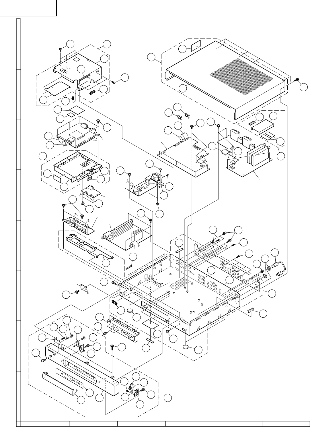
142
PZ-MR2T
PZ-43MR2U
PZ-50MR2U
654321
A
B
C
D
E
F
G
H
CABINET AND MECHANICAL PARTS
Main Unit
AV Unit
Front Unit
Power Unit
LED Unit
SR Unit
PC I/F Unit
EMC Unit
28
10
10
30 23
1-3
1-6
4-1
1-1
1
19
27
15 16 6
31
4
27
18
6-2 6-1
6-3
17
8
26
27
26
3-3
5-1
5-2
5-3 5-4
14
25
24
12
34
27
5
3-1
3
3-2
3-4
26
27
27
1-4
27 13
35
32
33
19
29
2-13
31
2
1-2
1-7
27
21
1-5
1-2
7
1-8
2-12
2-8
2-11
2-9
2-14
2-4 2-1
2-5
2-6
2-10
2-13
2-7
2-2
2-8
2-13
2-13
2-3
9
22
4-2
10
11

Ref. No. Part No. ★Description Code Ref. No. Part No. ★Description Code
143
PZ-MR2T
PZ-43MR2U
PZ-50MR2U
CABINET PARTS
1 CCABA3103CE03 J Bottom Cabinet Ass’y BG
(PZ-43MR2U)
1 CCABA3103CE02 J Bottom Cabinet Ass’y BF
(PZ-50MR2U)
1 CCABA3103CE04 J Bottom Cabinet Ass’y
(PZ-MR2T)
1-1
Not Available
– Bottom Cabinet —
1-2 GLEGG9017CE00 J Rubber Leg, x4 AC
1-3 HiNDP5935CESA J Indication Panel AH
1-4 LANGT9035CEFW J PWB Fixing Angle AM
1-5 LHLDW1021GE00 J Holder AB
1-6 QEARZA007WJZZ J Gascket AG
1-7 TLABM4317CEZZ J Model Label AG
(PZ-43MR2U)
1-7 TLABM4316CEZZ J Model Label AG
(PZ-50MR2U)
1-7 TLABM4326CEZZ J Model Label
(PZ-MR2T)
1-8 XBPSD30P06R00 J Screw, x3 AB
2 CWAKP1476CE01 J Front Cabinet Ass’y AZ
2-1
Not Available
– Front Cabinet —
2-2 GCOVA2034CEZZ J LED Cover AF
2-3 GDORF3027CEKA J Door AL
2-4 HiNDP5841CESA J Indication Panel AF
2-5 JBTN-2074CEKA J Power Button AE
2-6 LANGF9660CEFW J Fixing Metal AE
2-7 LHLDZ2178CEZZ J Button Holder AE
2-8 LHLDZ2179CEZZ J Damper Holder, x2 AD
2-9 LHLDZ2180CEZZ J Damper Holder AD
2-10 MSPRC0210CEFW J Power Button Spring AB
2-11 MSPRD0089CEFW J Spring AC
2-12 PDMPF1007TAZZ J Damper AF
2-13 XEBSD30P10000 J Screw, x4 AA
2-14 XJBSD20P05000 J Screw, x1 AA
3 CSLDM4688CE01 J Shield Ass’y AT
3-1
Not Available
– Shield —
3-2 LHLDW1021GE00 J Holder AB
3-3 PRDAR1567CEFW J Heat Sink AM
3-4 PSPAH0720CEZZ J Spacer AD
4 CCABB3079CE01 J Top Cabinet Ass’y BB
(PZ-43MR2U, PZ-50MR2U)
4-1
Not Available
– Top Cabinet —
(PZ-43MR2U, PZ-50MR2U)
4-1 GCABB3079CESA J Top Cabinet (PZ-MR2T) BB
4-2 TCAUHA001WJZZ J Caution Label AE
5 CANGT9033CE01 J PWB Angle Ass’y AV
5-1
Not Available
– PWB Angle —
5-2 LHLDW1021GE00 J Wire Holder AB
5-3 PSLDM0152CEZZ J Shield AA
5-4 PSPAH0721CEZZ J Spacer
6 CANGTA001WJ01 J Angle Cover Ass’y AR
6-1
Not Available
– Angle Cover —
6-2 PMLT-A001WJZZ J Spacer AE
6-3 QEARZA010WJZZ J Earth Angle AK
7 LHLDW1009CEZZ J Wire Holder, x3 AA
8 LHLDW1060CEZZ J Wire Holder, x1 AB
9 LX-BZ3434CEFN J Screw, x2 AB
10 NSFTZ0134CEFW J Shaft, x8 AD
11 PSLDM4692CEFW J Front Shield AL
12 QCNW-6074CEZZ J Connecting Cord AK
(FRONT - PC I/F)
13 QCNW-6078CEZZ J Connecting Cord AM
(SR - PC I/F)
14 QCNW-6080CEZZ J Connecting Cord AL
(MAIN - PC I/F)
15 QCNW-6081CEZZ J Connecting Cord AD
(MAIN - AV)
16 QCNW-6082CEZZ J Connecting Cord AC
(MAIN - AV)
17 QCNW-6083CEZZ J FFC Cable AD
(MAIN - PC I/F)
18 QCNW-6084CEZZ J FFC Cable AD
(MAIN - PC I/F)
19 QEARZ0056CEFW J Earth Spring, x6 AC
20 GCOVH9308CEZZ J Cover AA
21 TLABN0425CEZZ J Serial No. Label AG
(PZ-43MR2U, PZ-50MR2U)
22 QCNW-A342WJZZ Coaxial Cable AL
23 LX-NZ3047GEZZ J Nut, x3 AA
24 PSPAZ0464CEKZ J Spacer AB
25 PSPAZ0465CEKZ J Spacer AB
26 XBBSN30P06000 J Screw, x7 AA
27 XBPSD30P06JS0 J Screw, x30 AA
28 XBPSN30P06000 J Screw, x4 AA
29 XBSSD30P06000 J Screw, x1 AA
30 XEBSF30P08000 J Screw, x4 AA
31 XJPSN30P08XS0 J Screw, x8 AA
32 LANGK3000SNEZ J AC Inlet Angle AL
33 XBSSF30P06000 J Screw, x2 AA
34 XBPBN40P06K00 J Screw AB
35 LX-BZ1001SENZ J Screw, x2 AB

Ref. No. Part No. ★Description Code Ref. No. Part No. ★Description Code
144
PZ-MR2T
PZ-43MR2U
PZ-50MR2U
åQACCDA007WJPZ AC Cord AP
QCNW-6117CEZZ J System Cable BP
RRMCG1678CESA J Remote Control Unit BP
TiNS-7584CEZZ J Operation Manual AU
(PZ-43MR2U, PZ-50MR2U)
TiNS-7656CEZZ J Operation Manual
(PZ-MR2T)
SUPPLIED ACCESSORIES
SPAKF0515CEZZ – Packing Material —
SPAKC5671CEZZ – Packing Case —
(PZ-43MR2U)
SPAKC5670CEZZ – Packing Case —
(PZ-50MR2U)
SPAKC5687CEZZ – Packing Case —
(PZ-MR2T)
SPAKXA001CEZZ – Buffer Material —
(PZ-43M2U, PZ-50MR2U)
SPAKXA033WJZZ – Buffer Material —
(PZ-MR2T)
SSAKA0170CEZZ – Polyethylene Bag —
SSAKH0173CEZZ – Polyethylene Bag —
TLABK0001TAZZ – No. Label —
PACKING PARTS
(NOT REPLACEMENT ITEM)
QCNW-6099CEZZ J Connector, 30-pin AD
(PC I/F-MAIN)
QCNW-6100CEZZ J Connector, 50-pin AE
(PC I/F-MAIN)
QCNW-6101CEZZ J Connector, 4-pin AP
(SR-AV)
QCNW-6102CEZZ J Connector, 13-pin AL
(PC I/F-FRONT)
QCNW-6103CEZZ J Connector, 12-pin AV
(PC I/F-MAIN)
SERVICE JIGS
(Use for servicing)
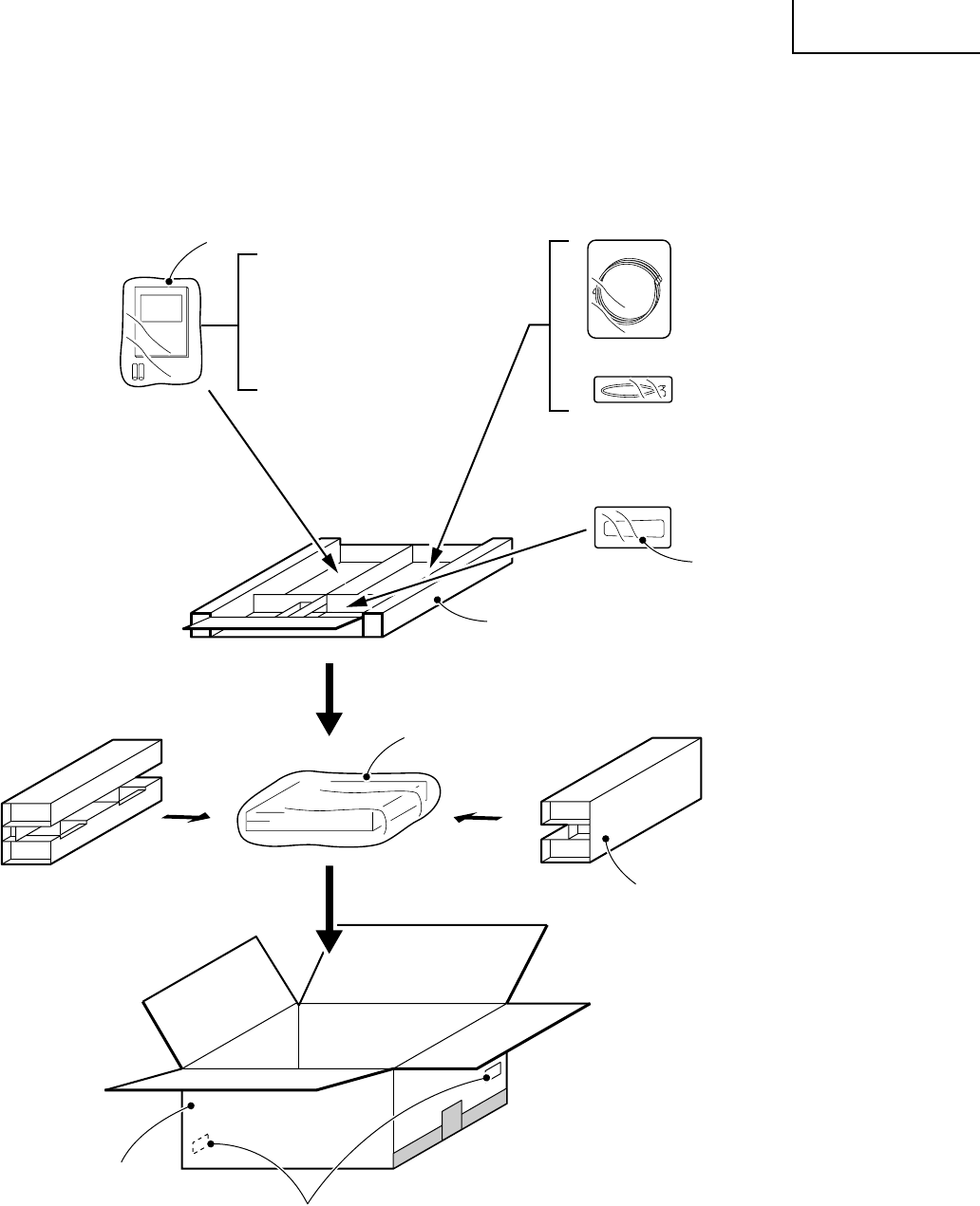
145
PZ-MR2T
PZ-43MR2U
PZ-50MR2U
PACKING OF THE SET
Packing Case
(SPAKC5671CEZZ)
(PZ-43MR2U)
(SPAKC5670CEZZ)
(PZ-50MR2U)
(SPAKC5687CEZZ)
(PZ-MR2T)
No. Label
(TLABK0001TAZZ)
Remote Control Unit
(RRMCG1678CESA)
Buffer Material
(SPAKXA001CEZZ)
(PZ-43MR2U, PZ-50MR2U)
(SPAKXA033WJZZ)
(PZ-MR2T)
Packing Material
(SPAKF0515CEZZ)
Polyethylene Bag
(SSAKH0173CEZZ)
Polyethylene Bag
(SSAKA0170CEZZ)
FRONT
Operation Manual
(TiNS-7584CEZZ)
(PZ-43MR2U, PZ-50MR2U)
(TiNS-7656CEZZ)
(PZ-MR2T)
Batteries AC Cord
(QACCDA007WJPZ)
System Cable
(QCNW-6117CEZZ)

146
PZ-MR2T
PZ-43MR2U
PZ-50MR2U
COPYRIGHT © 2002 BY SHARP CORPORATION
ALL RIGHTS RESERVED.
No part of this publication may be reproduced,
stored in a retrieval system, or transmitted in
any form or by any means, electronic, mechanical,
photocopying, recording, or otherwise, without
prior written permission of the publisher.
SHARP CORPORATION
AV Systems Group
Quality & Reliability Control Center
Yaita, Tochigi 329-2193, Japan
D JAPAN P JAPAN TQ1292-S
Apr. 2002 Printed in Japan
SY. KG
