CRT3238 GM 5000T Pioneer Service Manual
User Manual: GM-5000T
Open the PDF directly: View PDF ![]() .
.
Page Count: 23

PIONEER CORPORATION 4-1, Meguro 1-Chome, Meguro-ku, Tokyo 153-8654, Japan
PIONEER ELECTRONICS (USA) INC. P.O.Box 1760, Long Beach, CA 90801-1760 U.S.A.
PIONEER EUROPE NV Haven 1087 Keetberglaan 1, 9120 Melsele, Belgium
PIONEER ELECTRONICS ASIACENTRE PTE.LTD. 253 Alexandra Road, #04-01, Singapore 159936
C PIONEER CORPORATION 2004 K-ZZB. MAR. 2004 Printed in Japan
ORDER NO.
CRT3238
BRIDGEABLE POWER AMPLIFIER
GM-5000TX1R/EW
Service
Manual
GM-5000T/X1R/EW
GM-5000TX1R/UC
For details, refer to "Important symbols for good services".
GM-5000TX1R/ES
2
1234
1234
F
E
D
C
B
A
GM-5000T/X1R/EW
[ Important symbols for good services ]
In this manual, the symbols shown-below indicate that adjustments, settings or cleaning should be made securely.
When you find the procedures bearing any of the symbols, be sure to fulfill them:
2. Adjustments
To keep the original performances of the product, optimum adjustments or specification confirmation is indispensable.
In accordance with the procedures or instructions described in this manual, adjustments should be performed.
3. Cleaning
For optical pickups, tape-deck heads, lenses and mirrors used in projection monitors, and other parts requiring cleaning,
proper cleaning should be performed to restore their performances.
5. Lubricants, glues, and replacement parts
Appropriately applying grease or glue can maintain the product performances. But improper lubrication or applying
glue may lead to failures or troubles in the product. By following the instructions in this manual, be sure to apply the
prescribed grease or glue to proper portions by the appropriate amount.For replacement parts or tools, the prescribed
ones should be used.
4. Shipping mode and shipping screws
To protect the product from damages or failures that may be caused during transit, the shipping mode should be set or
the shipping screws should be installed before shipping out in accordance with this manual, if necessary.
1. Product safety
You should conform to the regulations governing the product (safety, radio and noise, and other regulations), and
should keep the safety during servicing by following the safety instructions described in this manual.
SAFETY INFORMATION
UC model
CAUTION
This service manual is intended for qualified service technicians; it is not meant for the casual do-it-yourselfer.
Qualified technicians have the necessary test equipment and tools, and have been trained to properly and safely repair
complex products such as those covered by this manual.
Improperly performed repairs can adversely affect the safety and reliability of the product and may void the warranty.
If you are not qualified to perform the repair of this product properly and safely, you should not risk trying to do so
and refer the repair to a qualified service technician.
WARNING
This product contains lead in solder and certain electrical parts contain chemicals which are known to the state of
California to cause cancer, birth defects or other reproductive harm.
Health & Safety Code Section 25249.6 - Proposition 65
- Service Precaution
You should conform to the regulations governing the product
(safety, radio and noise, and other regulations), and should keep
the safety during servicing by following the safety instructions
described in this manual.

3
5678
F
E
D
C
B
A
5678
GM-5000T/X1R/EW
CONTENTS
SAFETY INFORMATION............................................2
1. SPECIFICATIONS.......................................................3
2. EXPLODED VIEWS AND PARTS LIST ......................4
2.1 PACKING..............................................................4
2.2 EXTERIOR............................................................6
3. SCHEMATIC DIAGRAM.............................................8
3.1 OVERALL CONNECTION DIAGRAM(GUIDE PAGE) .....8
4. PCB CONNECTION DIAGRAM................................14
4.1 AMP UNIT..........................................................14
5. ELECTRICAL PARTS LIST........................................18
6. ADJUSTMENT.........................................................20
7. GENERAL INFORMATION.......................................21
7.1 DIAGNOSIS .......................................................21
7.1.1 DISASSEMBLY.........................................21
7.1.2 CONNECTOR FUNCTION DESCRIPTION ......22
8. OPERATIONS...........................................................23
1. SPECIFICATIONS
Power source .......................................................................................................... 14.4 V DC (10.8 — 15.1 V allowable)
Grounding system .......................................................................................................................................... Negative type
Backup current .............................................................................................................................................. 5.1 mA or less
Current consumption .................................................................................................... 25.0 A (at continuous power, 4 Ω)
Average current drawn* ........................................................................................................ 9.6 A (4 Ωfor two channels)
17.3 A (4 Ωfor one channel)
Fuse ........................................................................................................................................................................ 25 A ×2
Dimensions ...................................................................................................................... 300 (W) ×61 (H) ×324 (D) mm
Weight .................................................................................................................... 5.5 kg (Leads for wiring not included)
Maximum power output .................................................................................................................. 250 W ×2 / 760 W ×1
Continuous power output ...................................................................... 175 W ×2 / 530 W ×1 (DIN45324, +B=14.4 V)
Load impedance .......................................................................................................................... 4 Ω(2 — 8 Ωallowable)
(Bridge connection: 4 — 8 Ωallowable)
Frequency response .......................................................................................................... 10 — 50,000 Hz (+0 dB, –1 dB)
Signal-to-noise ratio .................................................................................................................... 100 dB (IEC-A network)
Distortion ........................................................................................................................................ 0.008 % (10 W, 1 kHz)
Separation ...................................................................................................................................................... 65 dB (1 kHz)
Low pass filter .............................................................................................................................. Cut off frequency: 80 Hz
Cut off slope: –12 dB/oct
Maximum input level/impedance .................................................................................. RCA: 6.5 V/22 kΩ(0.2 — 6.5 V)
Note:
•Specifications and the design are subject to possible modification without notice due to improvements.
*Average current drawn
•The average current drawn is nearly the maximum current drawn by this unit when an audio signal is input. Use this value when
working out total current drawn by multiple power amplifiers.
4
1234
1234
F
E
D
C
B
A
GM-5000T/X1R/EW
2. EXPLODED VIEWS AND PARTS LIST
2.1 PACKING
5
5678
F
E
D
C
B
A
5678
GM-5000T/X1R/EW
Part No.
Mark No. Description GM-5000T/X1R/EW GM-5000T/X1R/UC GM-5000T/X1R/ES
1Screw Assy HEA0058 HEA0058 HEA0058
2 Screw BYC40P180FZK BYC40P180FZK BYC40P180FZK
3Polyethylene Bag HEG0011 HEG0011 HEG0011
4Polyethylene Bag HEG0022 HEG0022 HEG0022
5Carton HHG0433 HHG0433 HHG0433
6Contain Box HHL0433 HHL0433 HHL0433
7Protector HHP0249 HHP0249 HHP0249
8Protector HHP0251 HHP0251 HHP0251
9-1 Owner’s Manual HRD0260 HRD0259 HRD0261
9-2 Owner’s Manual Not used Not used HRD0262
*9-3 Warranty Card HRY1157 ARY1048 Not used
-PACKING SECTION PARTS LIST
NOTE:
-Parts marked by “*” are generally unavailable because they are not in our Master Spare Parts List.
-Screws adjacent to ∇mark on the product are used for disassembly.
-For the applying amount of lubricants or glue, follow the instructions in this manual.
( In the case of no amount instructions, apply as you think it appropriate.)
-Owner's Manual
Part No. Language
HRD0259 English, French
HRD0260 English, Spanish, German, French, Italian, Dutch
HRD0261 English, Spanish
HRD0262 Arabic, Portuguese(B)
A
6
1234
1234
F
E
D
C
B
A
GM-5000T/X1R/EW
2.2 EXTERIOR

7
5678
F
E
D
C
B
A
5678
GM-5000T/X1R/EW
1Screw BBZ30P050FTC
2Screw BBZ30P060FTC
3Screw BBZ30P080FTC
4Screw BBZ30P120FTC
5Screw BSZ30P050FTC
6Screw(M3x8) HBA0011
7Screw(M3) HBA0028
8Stud HLA0021
9Case HNB0135
10 Panel HNB0256
11 Panel HNB0260
12 Holder HNC0080
13 Clip HNC0189
14 Spacer HNM0006
15 Insulator HNM0193
16 Screw BMZ30P050FTC
17 Insulator HNM0195
18 Heat Sink HNR0279
19 Spacer HNV0016
20 Fuse(25A) HEK0025
21 Amp Unit(EW) HWH0237
Amp Unit(UC) HWH0238
Amp Unit(ES) HWH0239
22 Pin Jack(CN851) HKB0002
23 Terminal(CN853) HKE0020
24 Terminal(CN854) HKE0021
25 Terminal(CN855) HKE0021
26 Terminal(CN850) HKF0001
27 Buss Bar HNC0043
28 Holder HNC0082
29 Screw PPZ30P100SAD
30 Light Pipe Unit HXA0322
31 Screw PPZ30P120FZK
32 Screw BSZ30P050FZK
33 Holder HNC0202
34 Insulator HNM0193
35 FET(Q905,Q906,Q911-Q914) IRF1010N
Mark No. Description Part No.
-EXTERIOR SECTION PARTS LIST
A-aA-a A-b A-b
A-aA-a A-b A-b
A-b A-b
A-a A-a
Large size
SCH diagram
Guide page
Detailed page
Note: When ordering service parts, be sure to refer to " EXPLODED VIEWS AND PARTS LIST" or
"ELECTRICAL PARTS LIST". A-a
A
1
2
4
3
8
1234
1234
F
E
D
C
B
A
GM-5000T/X1R/EW
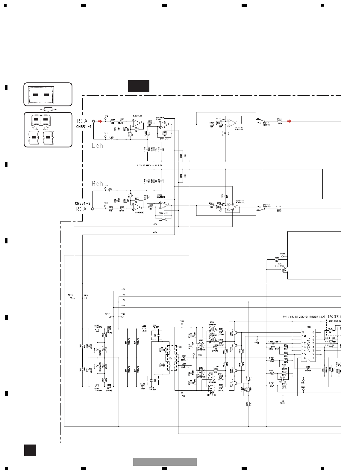
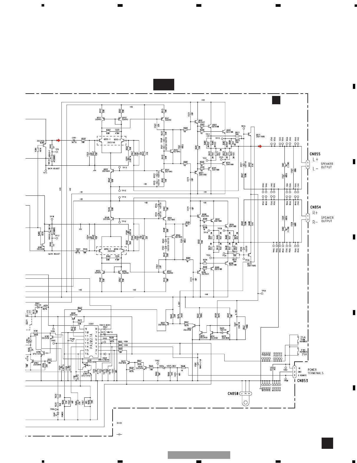
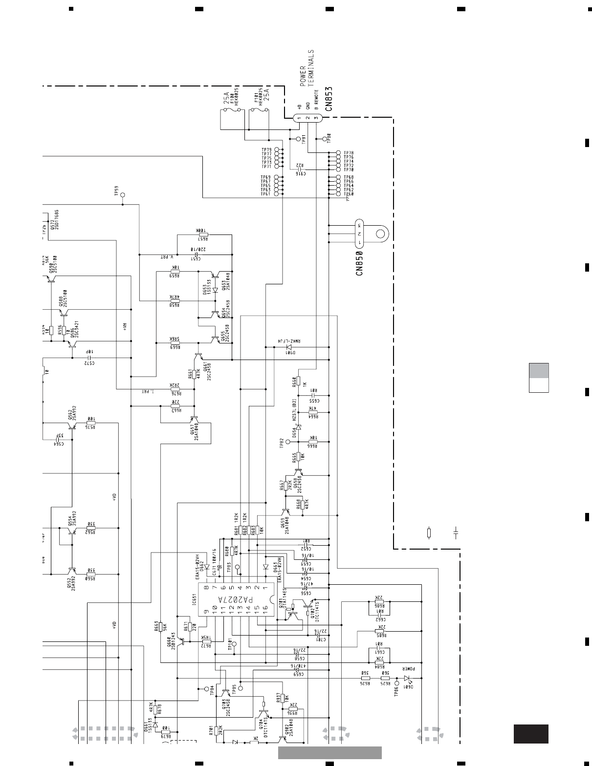
3. SCHEMATIC DIAGRAM
3.1 OVERALL CONNECTION DIAGRAM (GUIDE PAGE)
9
5678
F
E
D
C
B
A
5678
GM-5000T/X1R/EW
A-b
A-a A-b
A-a A-b
A-b
A-a
A
1
2
5
4
3
1
2
5
4
3
AM4661PBC
Decimal points for resistor
and capacitor fixed values
are expressed as :
2.2 2R2
0.022 R022
←
←
The > mark found on some component parts indicates
the importance of the safety factor of the part.
Therefore, when replacing, be sure to use parts of
identical designation.
Symbol indicates a resistor.
No differentiation is made between chip resistors and
discrete resistors.
NOTE :
Symbol indicates a capacitor.
No differentiation is made between chip capacitors and
discrete capacitors.
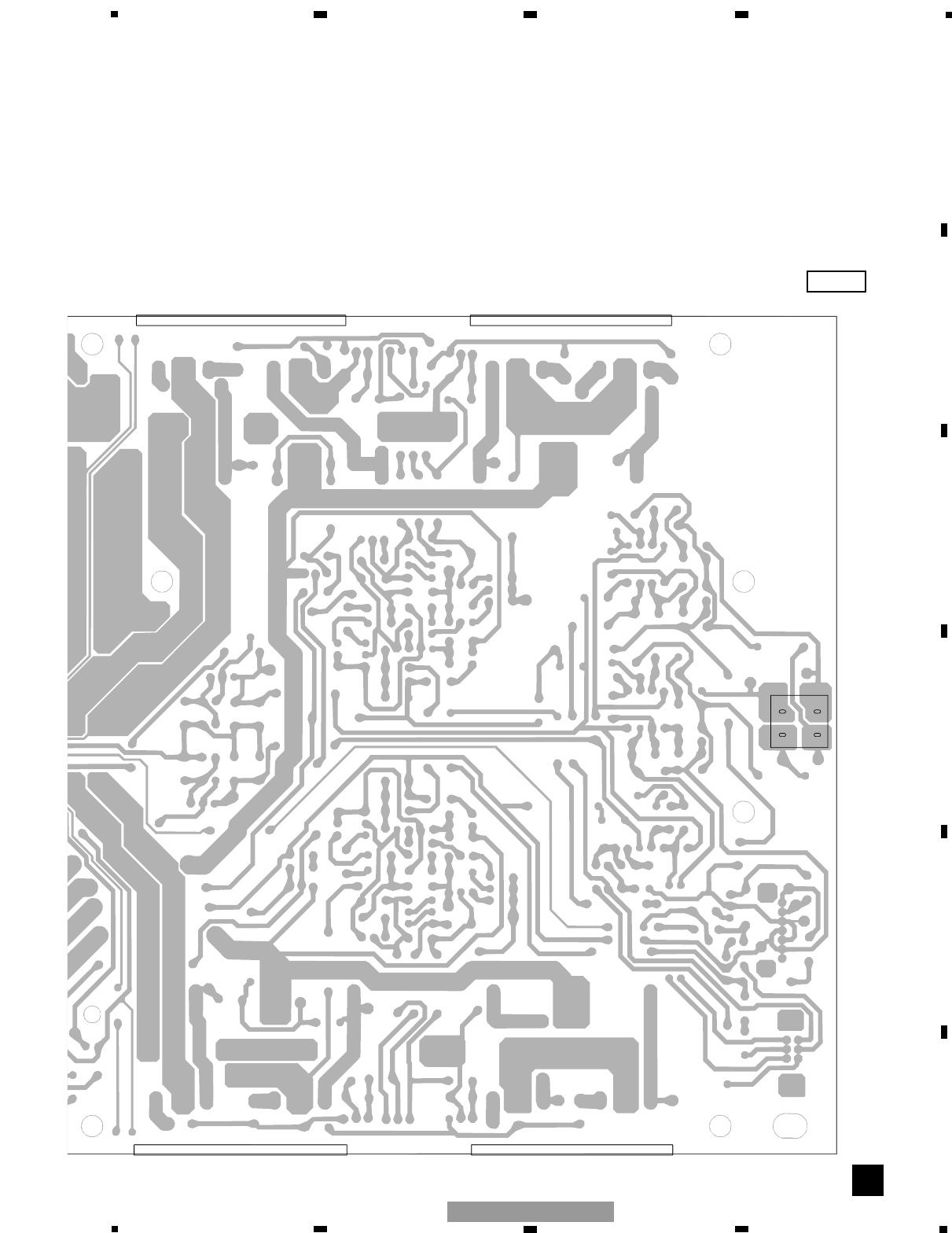
AAMP UNIT
>
>


13
5678
F
E
D
C
B
A
5678
GM-5000T/X1R/EW
A-a A-b
A-b
567
AM4661PBC
Decimal points for resistor
and capacitor fixed values
are expressed as :
2.2 2R2
0.022 R022
←
←
The > mark found on some component parts indicates
the importance of the safety factor of the part.
Therefore, when replacing, be sure to use parts of
identical designation.
Symbol indicates a resistor.
No differentiation is made between chip resistors and
discrete resistors.
NOTE :
Symbol indicates a capacitor.
No differentiation is made between chip capacitors and
discrete capacitors.
>
>
Capacitor
Connector
P.C.Board Chip Part
A
AAMP UNIT
SIDE B
SIDE A
NOTE FOR PCB DIAGRAMS
1.The parts mounted on this PCB
include all necessary parts for
several destination.
For further information for
respective destinations, be sure
to check with the schematic dia-
gram.
2.Viewpoint of PCB diagrams
L ch R ch
1
2
3
4
RCA
LPF
14
1234
1234
F
E
D
C
B
A
GM-5000T/X1R/EW
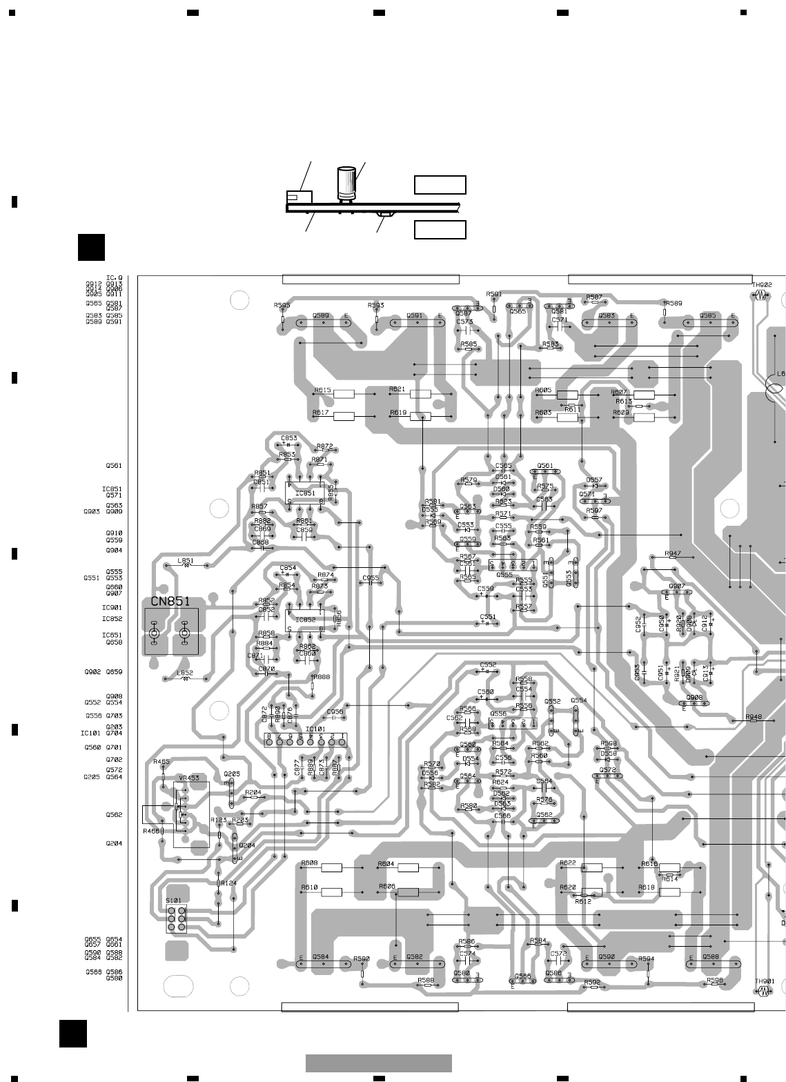
4. PCB CONNECTION DIAGRAM
4.1 AMP UNIT


18
1234
1234
F
E
D
C
B
A
GM-5000T/X1R/EW
Unit Number : HWH0237(EW)
Unit Number : HWH0238(UC)
Unit Number : HWH0239(ES)
Unit Name : Amp Unit
MISCELLANEOUS
IC 101 IC NJM4558L
IC 651 IC PA2027A
IC 851 IC NJM2068D
IC 852 IC NJM2068D
IC 901 IC UPC494C
Q 203 Transistor DTA124ES
Q 204 Transistor 2SC2458
Q 205 Transistor 2SC2458
Q 551 Transistor 2SA992
Q 552 Transistor 2SA992
Q 553 Transistor 2SA992
Q 554 Transistor 2SA992
Q 555 Transistor 2SC5168
Q 556 Transistor 2SC5168
Q 559 Transistor 2SC1845
Q 560 Transistor 2SC1845
Q 561 Transistor 2SA992
Q 562 Transistor 2SA992
Q 563 Transistor 2SC1845
Q 564 Transistor 2SC1845
Q 565 Transistor 2SC1845
Q 566 Transistor 2SC1845
Q 571 Transistor 2SD1768S
Q 572 Transistor 2SD1768S
Q 580 Transistor 2SA1358
Q 581 Transistor 2SC3421
Q 582 Transistor 2SA1908
Q 583 Transistor 2SC5100
Q 584 Transistor 2SA1908
Q 585 Transistor 2SC5100
Q 586 Transistor 2SC3421
Q 587 Transistor 2SA1358
Q 588 Transistor 2SC5100
Q 589 Transistor 2SA1908
Q 590 Transistor 2SC5100
Q 591 Transistor 2SA1908
Q 653 Transistor 2SA1048
Q 654 Transistor 2SC2458
Q 655 Transistor 2SC2458
Q 657 Transistor 2SA1048
Q 658 Transistor 2SC2458
Q 659 Transistor 2SA1048
Q 660 Transistor 2SB1243
Q 661 Transistor 2SC2458
Q 701 Transistor DTA114ES
Q 702 Transistor DTC114TS
Q 703 Transistor 2SC2458
Q 704 Transistor DTC114TS
Q 902 Transistor 2SA1048
Q 903 Transistor 2SB1277
Q 904 Transistor 2SB1277
Q 905 FET IRF1010N
Q 906 FET IRF1010N
Q 907 Transistor 2SD1864
Q 908 Transistor 2SB1243
Q 909 Transistor 2SD1919
Q 910 Transistor 2SD1919
Q 911 FET IRF1010N
Q 912 FET IRF1010N
Q 913 FET IRF1010N
Q 914 FET IRF1010N
D 553 Diode 1SS133
D 554 Diode 1SS133
D 555 Diode 1SS133
D 556 Diode 1SS133
D 557 Diode 1SS133
D 558 Diode 1SS133
D 560 Diode 1SS133
D 561 Diode 1SS133
D 562 Diode 1SS133
D 563 Diode 1SS133
D 601 LED AM4661PBC
D 653 Diode 1SS133
D 654 Diode HZS7L(B2)
D 658 Diode 1SS133
D 659 Diode 1SS133
D 661 Diode 1SS133
D 662 Diode ERA15-02VH
D 663 Diode ERA15-02VH
D 701 Diode 1SS133
D 901 Diode RM4Z-LFJ4
D 907 Diode FML22S
D 908 Diode HZS16L(1)
D 909 Diode HZS16L(1)
D 910 Diode FML22R
L 602 Choke Coil 75µH HTH0021
L 603 Choke Coil 75µH HTH0021
L 851 Ferri-Inductor CTF1007
L 852 Ferri-Inductor CTF1007
T 901 Transformer HTT0035
TH 901 Thermistor HCX0002
TH 902 Thermistor HCX0002
TH 903 Thermistor HCX0001
S 101 Switch(LPF) HSH0004
S 901 Switch(BFC)(EW,ES) HSH-156
VR 453 Volume HCS0003
F 100 Fuse (25A) HEK0025
F 101 Fuse (25A) HEK0025
5. ELECTRICAL PARTS LIST
NOTE:
-Parts whose parts numbers are omitted are subject to being not supplied.
-The part numbers shown below indicate chip components.
Chip Resistor
RS1/_S___J,RS1/__S___J
Chip Capacitor (except for CQS.....)
CKS....., CCS....., CSZS.....
=====Circuit Symbol and No.===Part Name Part No.
--- ------ ------------------------------------------ ------------------------- =====Circuit Symbol and No.===Part Name Part No.
--- ------ ------------------------------------------ -------------------------
A

19
5678
F
E
D
C
B
A
5678
GM-5000T/X1R/EW
RESISTORS
R 123 RD1/4PU222J
R 124 RD1/4PU222J
R 203 RD1/4PU472J
R 204 RD1/4PU472J
R 465 RD1/4PU470J
R 466 RD1/4PU470J
R 555 RD1/4PU103J
R 556 RD1/4PU103J
R 557 RD1/4PU433J
R 558 RD1/4PU433J
R 559 RD1/4PU331J
R 560 RD1/4PU331J
R 561 RD1/4PU331J
R 562 RD1/4PU331J
R 563 RD1/4PU681J
R 564 RD1/4PU681J
R 565 RD1/4PU361J
R 566 RD1/4PU361J
R 567 RD1/4PU433J
R 568 RD1/4PU433J
R 569 RD1/4PU681J
R 570 RD1/4PU681J
R 571 RD1/4PU223J
R 572 RD1/4PU223J
R 575 RD1/4PU101J
R 576 RD1/4PU101J
R 579 RD1/4PU681J
R 580 RD1/4PU681J
R 581 RD1/4PU181J
R 582 RD1/4PU181J
R 583 RD1/4PU100J
R 584 RD1/4PU100J
R 585 RD1/4PU100J
R 586 RD1/4PU100J
R 587 RD1/4PU100J
R 588 RD1/4PU100J
R 589 RD1/4PU100J
R 590 RD1/4PU100J
R 591 RD1/4PU221J
R 592 RD1/4PU221J
R 593 RD1/4PU100J
R 594 RD1/4PU100J
R 595 RD1/4PU100J
R 596 RD1/4PU100J
R 597 RD1/4PU564J
R 598 RD1/4PU564J
R 599 RD1/4PU473J
R 600 RD1/4PU473J
R 601 RS1/2PMF100J
R 602 RS1/2PMF100J
R 603 0.22ΩHCN0001
R 604 0.22ΩHCN0001
R 605 0.22ΩHCN0001
R 606 0.22ΩHCN0001
R 607 0.22ΩHCN0001
R 608 0.22ΩHCN0001
R 609 0.22ΩHCN0001
R 610 0.22ΩHCN0001
R 611 RD1/4PU563J
R 612 RD1/4PU563J
R 613 RD1/4PU563J
R 614 RD1/4PU563J
R 615 0.22ΩHCN0001
R 616 0.22ΩHCN0001
R 617 0.22ΩHCN0001
R 618 0.22ΩHCN0001
R 619 0.22ΩHCN0001
R 620 0.22ΩHCN0001
R 621 0.22ΩHCN0001
R 622 0.22ΩHCN0001
R 623 RD1/4PU561J
R 624 RD1/4PU561J
R 625 RD1/4PU361J
R 626 RD1/4PU361J
R 657 RD1/4PU104J
R 658 RD1/4PU472J
R 659 RD1/4PU103J
R 660 RD1/4PU102J
R 661 RD1/4PU472J
R 662 RD1/4PU221J
R 663 RD1/4PU563J
R 664 RD1/4PU473J
R 665 RD1/4PU103J
R 666 RD1/4PU103J
R 667 RD1/4PU222J
R 668 RD1/4PU472J
R 669 RD1/4PU562J
R 671 RD1/4PU221J
R 672 RD1/4PU152J
R 676 RD1/4PU222J
R 678 RD1/4PU472J
R 679 RD1/4PU101J
R 680 RD1/4PU472J
R 681 RD1/4PU122J
R 682 RD1/4PU122J
R 683 RD1/4PU103J
R 684 RD1/4PU223J
R 685 RD1/4PU223J
R 686 RD1/4PU223J
R 701 RD1/4PU222J
R 851 RD1/4PU471J
R 852 RD1/4PU471J
R 853 RD1/4PU223J
R 854 RD1/4PU223J
R 855 RN1/4PC1002D
R 856 RN1/4PC1002D
R 857 RN1/4PC1002D
R 858 RN1/4PC1002D
R 861 RN1/4PC1002D
R 862 RN1/4PC1002D
R 871 RD1/4PU102J
R 872 RD1/4PU202J
R 873 RD1/4PU102J
R 874 RD1/4PU202J
R 882 RN1/4PC1002D
R 884 RN1/4PC1002D
R 887 RD1/4PU103J
R 888 RD1/4PU103J
R 889 RD1/4PU103J
R 890 RD1/4PU103J
R 907 RD1/4PU473J
R 910 RD1/4PU153J
R 911 RD1/4PU102J
R 912 RD1/4PU272J
R 913 RD1/4PU472J
R 914 RD1/4PU472J
R 915 RD1/4PU472J
R 916 RD1/4PU332J
R 917 RD1/4PU332J
R 918 RS1/2PMF220J
=====Circuit Symbol and No.===Part Name Part No.
--- ------ ------------------------------------------ ------------------------- =====Circuit Symbol and No.===Part Name Part No.
--- ------ ------------------------------------------ -------------------------

20
1234
1234
F
E
D
C
B
A
GM-5000T/X1R/EW
R 919 RS1/2PMF220J
R 920 RD1/4PU472J
R 921 RD1/4PU472J
R 922 RD1/4PU472J
R 923 RD1/4PU472J
R 924 RS1/2PMF121J
R 925 RS1/2PMF121J
R 926 (EW,ES) RD1/4PU105J
R 928 RS1/2PMF121J
R 929 RS1/2PMF121J
R 932 RD1/4PU104J
R 933 RS1/2PMF121J
R 934 RS1/2PMF121J
R 935 RD1/4PU202J
R 936 RD1/4PU223J
R 937 RD1/4PU103J
R 938 RD1/4PU272J
R 939 RD1/4PU272J
R 947 RS1/2PMF560J
R 948 RS1/2PMF560J
R 949 RD1/4PU113J
R 950 RD1/4PU101J
R 951 RD1/4PU513J
R 952 RS1/2PMF220J
R 999 RD1/4PU103J
CAPACITORS
C 551 CEAT100M16
C 552 CEAT100M16
C 553 CCPUSL680J50
C 554 CCPUSL680J50
C 555 CQMA471J50
C 556 CQMA471J50
C 559 CEAT221M10
C 560 CEAT221M10
C 561 CCPUCH150J50
C 562 CCPUCH150J50
C 563 CCPUSL330J50
C 564 CCPUSL330J50
C 565 CFTNA223J50
C 566 CFTNA223J50
C 567 CFTNA333J50
C 568 CFTNA333J50
C 569 CQMA102J50
C 570 CQMA102J50
C 571 CCPUCH100J50
C 572 CCPUCH100J50
C 573 CCPUCH100J50
C 574 CCPUCH100J50
C 651 220µF/10V HCH0012
C 652 CFTNA103J50
C 653 CEAT100M16
C 654 CEAT100M16
C 655 CFTNA103J50
C 656 CEAT470M16
C 658 CEAT220M16
C 659 CEAT471M16
C 661 CFTNA103J50
C 662 CFTNA103J50
C 671 CEAT101M16
C 701 CEAT220M16
C 851 CKPUYB471K50
C 852 CKPUYB471K50
C 853 CEAT100M16
C 854 CEAT100M16
C 859 CCPUSL470J50
C 860 CCPUSL470J50
C 868 CFTNA223J50
C 869 CCPUSL470J50
C 870 CFTNA223J50
C 871 CCPUSL470J50
C 872 CFTNA274J50
C 873 CFTNA274J50
C 876 CFTNA154J50
C 877 CFTNA154J50
C 902 CEAT221M10
C 903 CEAT2R2M50
C 904 CEAT101M16
C 905 CQMA472J50
C 906 CQMA472J50
C 907 3300µF/16V HCH0005
C 908 2200µF/50V HCH0007
C 909 2200µF/50V HCH0007
C 910 2200µF/50V HCH0007
C 911 2200µF/50V HCH0007
C 912 CEAT470M16
C 913 CEAT470M16
C 915 CQMA102J50
C 916 CFTNA224J50
C 920 CFTNA564J50
C 932 CEAT470M16
C 949 3300µF/16V HCH0005
C 950 CEAT470M16
C 951 CEAT470M16
C 952 CQMA102J50
C 953 CQMA102J50
C 954 CQMA102J50
C 955 CFTNA103J50
C 956 CFTNA103J50
=====Circuit Symbol and No.===Part Name Part No.
--- ------ ------------------------------------------ ------------------------- =====Circuit Symbol and No.===Part Name Part No.
--- ------ ------------------------------------------ -------------------------
6. ADJUSTMENT
There is no information to be shown in this chapter.
21
5678
F
E
D
C
B
A
5678
GM-5000T/X1R/EW
1
1
- Removing the Case (Fig.1)
- Removing the Amp Unit (Fig.2)
Remove the three screws.
Remove the six screws and then
remove the Panel.
Fig.1
Fig.2
Case
2Remove the screw.
3Remove the six screws and then
remove the Panel.
2Remove the eight screws and then remove
the Case.
11
1
22
2
2
2
2
2
2
4Remove the three screws.
5Remove the fourteen screws.
6Remove the twelve screws and then
remove the Amp Unit.
1
1
1
1
1
1
2
3
3
3
3
4
4
4
5
6
666
6
66
6
6 6
Panel
Panel
Amp Unit
6
5
33
6
7. GENERAL INFORMATION
7.1 DIAGNOSIS
7.1.1 DISASSEMBLY
22
1234
1234
F
E
D
C
B
A
GM-5000T/X1R/EW
7.1.2 CONNECTOR FUNCTION DESCRIPTION
23
5678
F
E
D
C
B
A
5678
GM-5000T/X1R/EW
8. OPERATIONS
EW, ES models
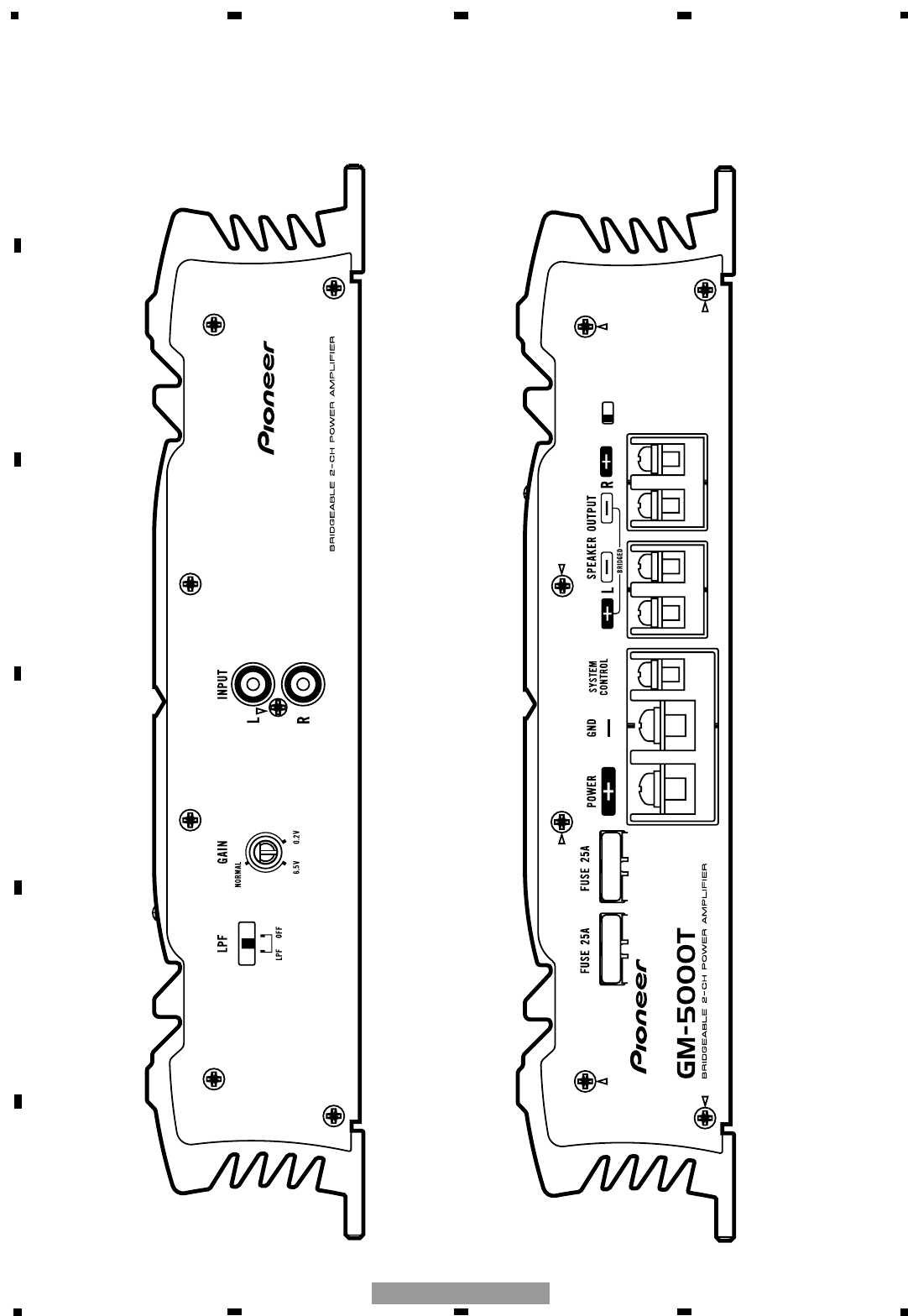
Gain Control
If the sound level is too low, even when
the volume of the car stereo used along
with this power amplifier is turned up,
turn gain control on the front of the
power amplifier clockwise. If the sound
distorts when the volume is turned up,
turn the gain control counter-clockwise.
• When using with an RCA equipped car
stereo (standard output of 500 mV), set to
the NORMAL position. When using with
an RCA equipped Pioneer car stereo with
max. output of 4 V or more, adjust level to
match the car stereo output level.
Power Indicator
The power indicator lights when the
power is switched on.
LPF (Low-Pass Filter) Select Switch
Set the LPF select switch as follows according to the type of speaker that is connected to the
speaker output connector and the car stereo system:
LPF Select Audio frequency range Speaker Remarks
Switch to be output Type
LPF (left) Very Low Frequency range Subwoofer Connect a subwoofer.
OFF (right) Full range Full range
BFC (Beat Frequency Control) Switch
If you hear a beat while listening to an
MW/LW broadcast with your car stereo,
change the BFC switch using a small stan-
dard tip screwdriver.
