Datasheet QMC5883L 1.0
User Manual: QMC5883L-Datasheet-1.0
Open the PDF directly: View PDF ![]() .
.
Page Count: 19
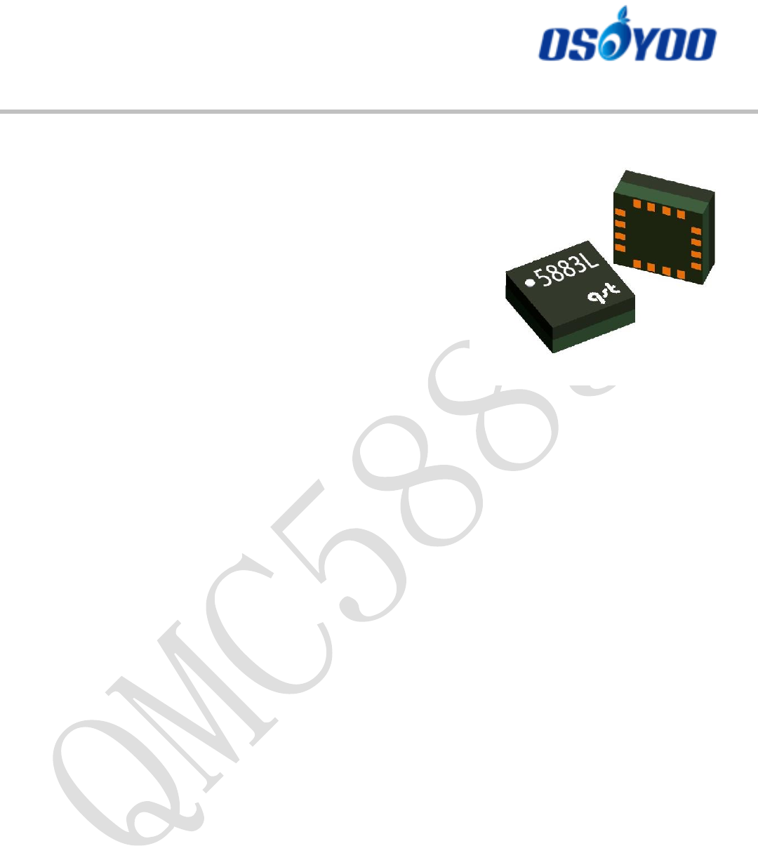
3-Axis Magnetic Sensor
QMC5883L
The QMC5883L is a multi-chip three-axis magnetic sensor. This
surface -mount, small sized chip has integrated magnetic sensors with
signal condition ASIC, targeted for high precision applications such as
compassing, navigation and gaming in drone, robot, mobile and
personal hand-held devices.
The QMC5883L is based on our state-of-the-art, high resolution,
magneto-resistive technology licensed from Honeywell AMR technology.
Along with custom-designed 16-bit ADC ASIC, it offers the advantages of
low noise, high accuracy, low power consumption, offset cancellation and
temperature compensation. QMC5883L enables 1° to 2° compass
heading accuracy. The I²C serial bus allows for easy interface.
The QMC5883L is in a 3x3x0.9mm3 surface mount 16-pin land grid
array (LGA) package.
FEATURES BENEFIT
3-Axis Magneto-Resistive Sensors in a 3x3x0.9 mm3
Land Grid Array Package (LGA), guaranteed
to operate over an extended temperature range of
-40 °C to +85 °C.
Small Size for Highly Integrated Products. Signals Have
Been Digitized And Calibrated.
16 Bit ADC With Low Noise AMR Sensors Achieves
2 Milli-Gauss Field Resolution
Enables 1° To 2° Degree Compass Heading Accuracy ,
Allows for Navigation and LBS Applications
Wide Magnetic Field Range (±8 Gauss)
Maximizes Sensor’s Full Dynamic Range and Resolution
Temperature Compensated Data Output and
Temperature Output
Automatically Maintains Sensor’s Sensitivity Under Wide
Operating Temperature Range
I2C Interface with Standard and Fast Modes.
High-Speed Interfaces for Fast Data Communications.
Maximum 200Hz Data Output Rate
Wide Range Operation Voltage (2.16V To 3.6V) and
Low Power Consumption (75A)
Compatible with Battery Powered Applications
Lead Free Package Construction
RoHS Compliance
Software And Algorithm Support Available
Compassing Heading, Hard Iron, Soft Iron, and Auto
Calibration Libraries Available
QMC5883L
2
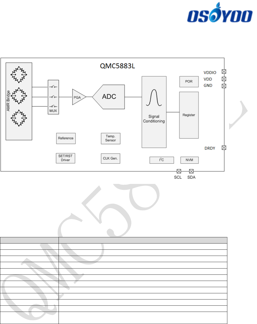
1 INTERNAL SCHEMATIC DIAGRAM
1.1 Internal Schematic Diagram
Figure 1. Block Diagram
Table 1. Block Function
Block
Function
AMR Bridge
3 axis magnetic sensor
MUX
Multiplexer for sensor channels
PGA
Programmable gain amplifier for sensor signals
ADC
16 bit Analog-to-Digital converter
Signal Conditioning
Digital blocks for magnetic signal calibration and compensation
I2C
Interface logic data I/O
NVM
Non-Volatile memory for calibrated parameters
SET/RST Driver
Internal driver to initialize magnetic sensor
Reference
Voltage/Current reference for internal biasing
Clock Gen.
Internal oscillator for internal operation
POR
Power on reset
Temperature Sensor
Temperature sensor for internal sensitivity /offset compensation, and
temperature output

3
2 SPECIFICATIONS AND I/O CHARACTERISTICS
2.1 Product Specifications
Table 2. Specifications (* Tested and specified at 25°C except stated otherwise.)
Parameter
Conditions
Min
Typ
Max
Unit
Supply Voltage
VDD
2.16
3.6
V
I/O Voltage
VDDIO
1.65
3.6
V
Standby Current
Total Current on VDD and
VDDIO
3
μA
Continuous Mode
Current
Low/Hig
h Power
Mode
(OSR=6
4 or 512)
ODR = 10Hz
75/100
μA
ODR = 50Hz
150/250
μA
ODR = 100Hz
250/450
μA
ODR = 200Hz
450/850
μA
Peak Current in
Active State
Peak Current on VDD and
VDDIO During
Measurement
2.6
mA
Sensor Field
Range
Full Scale
-8
+8
Gauss
Dynamic Output
Field Range
Programmable with 2
options
±2
±8
Gauss
Sensitivity [1]
Field Range = ±2G
12000
LSB/G
Field Range = ±8G
3000
LSB/G
Linearity
(Best fit linear
curve)
Field Range = ±2G
0.1
%FS
Hysteresis
All Ranges
0.3
%FS
Cross Axis
Sensitivity
Cross field = 1 Gauss,
Happlied = ±2 Gauss
0.1
%/G
Offset
±10
mG
Sensitivity
Tempco
Ta = -40℃~85℃
±0.05
%/℃
Temperature
Sensor Sensitivity
Ta = -40℃~85℃
100
LSB/℃
Digital Resolution
Change with Gain
0.1
1.0
mGauss
Field Resolution
Standard deviation 100
Data, FS ±2G
2
mGauss
Output Data Rate
Programmable.
10Hz/50Hz/100Hz/200Hz
10
200
Samples
/sec
X-Y-Z
Orthogonality
Sensitivity Directions
90±1
degree
Operating
Temperature
-40
85
℃
ESD
HB Model
2000
V
Charge Device Model
750
Note [1]: Sensitivity is calibrated at zero field, it is slightly decreased at high fields.
QMC5883L
4
2.2 Absolute Maximum Ratings
Table 3. Absolute Maximum Ratings (Tested at 25°C except stated otherwise.)
Parameter
MIN.
MAX.
Units
VDDIO
-0.3
5.4
V
VDD
-0.3
5.4
V
Storage Temperature
-40
125
℃
Exposed to Magnetic Field (all directions)
50000
Gauss
Reflow Classification
MSL 3, 260 C Peak Temperature
2.3 I/O Characteristics
Table 4. I/O Characteristics
Parameter
Symbol
Pin Condition
Min.
TYP.
Max.
Unit
Voltage Input
High Level 1
VIH1
SDA, SCL
0.7*VD
DIO
VDDIO+
0.3
V
Voltage Input
Low Level 1
VIL1
SDA, SCL
-0.3
0.3*VD
DIO
V
Voltage Output
High Level
VOH
INT Output Current
≥-100uA
0.8*VD
DIO
V
Voltage Output
Low Level
VOL
INT, SDA Output Current
≤100uA(INT)
Output Current
≤1mA (SDA)
0.2*VD
DIO
V
3 PACKAGE PIN CONFIGURATIONS
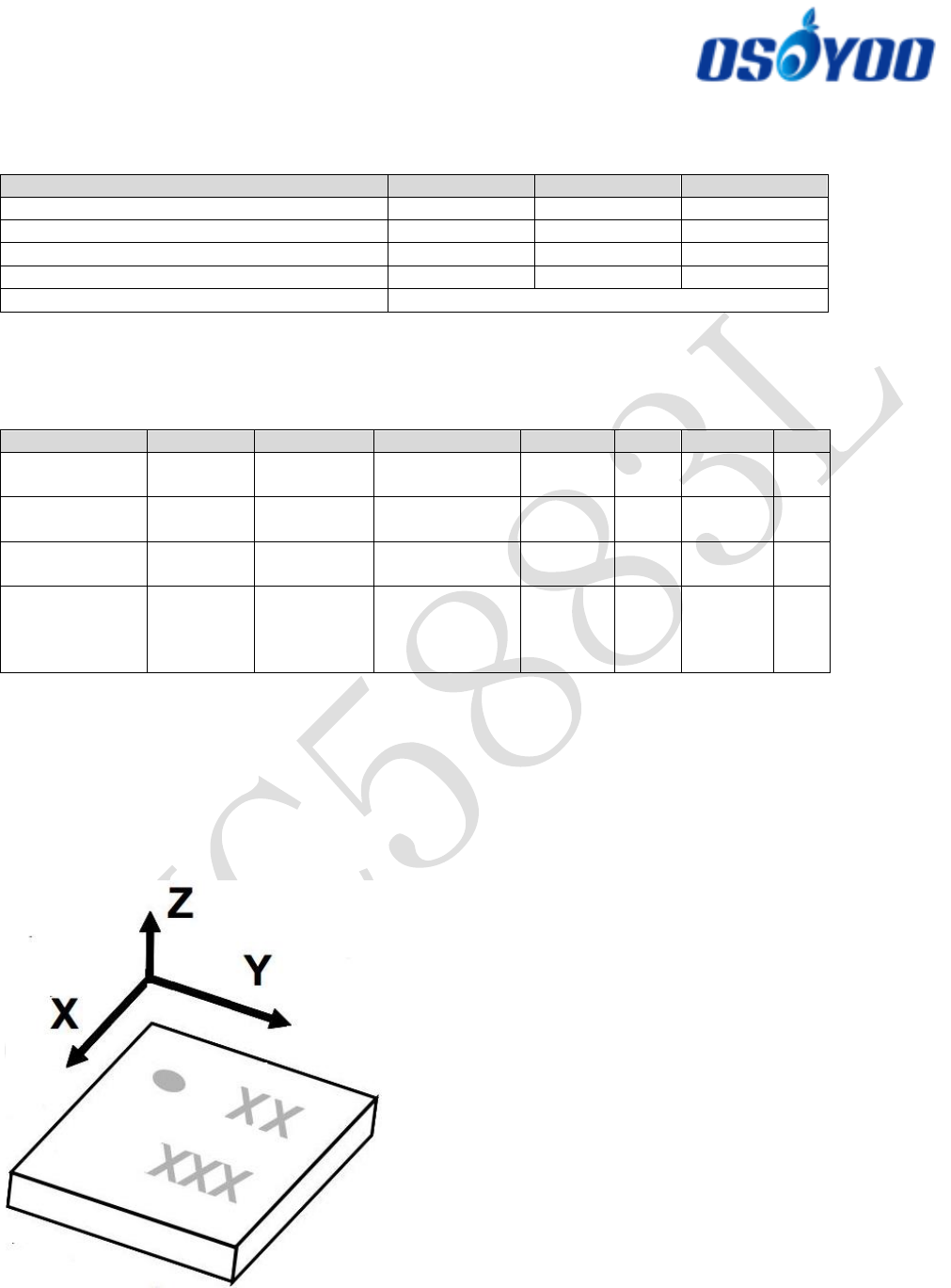
3.1 Package 3-D View
Arrow indicates direction of magnetic field that generates a positive output reading in normal measurement
configuration.
Figure 2. Package 3-D View
<QMC5883L>
5
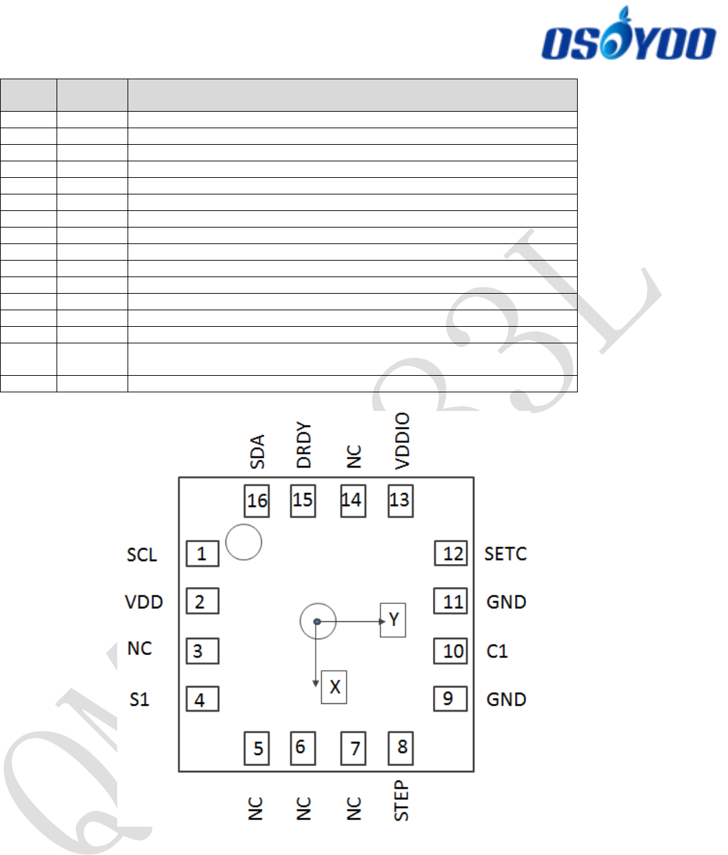
Table 5. Pin Configurations
PIN
No.
PIN
NAME
Function
1
SCL
Serial Clock – I2C Master/Slave Clock
2
VDD
Power Supply (2.16V to 3.6V)
3
NC
Not to be Connected
4
S1
Tie to VDDIO
5
NC
Not to be Connected
6
NC
Not to be Connected
7
NC
Not to be Connected
8
SETP
Set/Reset Strap Positive – S/R Capacitor (C2) Connection
9
GND
Supply Ground
10
C1
Reservoir Capacitor (C1) Connection
11
GND
Supply Ground
12
SETC
S/R Capacitor (C2) Connection – Driver Side
13
VDDIO
IO Power Supply (1.71V to VDD)
14
NC
Not to be Connected
15
DRDY
Data Ready, Interrupt Pin. Default low. Data ready high until data
register is read.
16
SDA
Serial Data – I2C Master/Slave Data
TOP VIEW ( looking through )
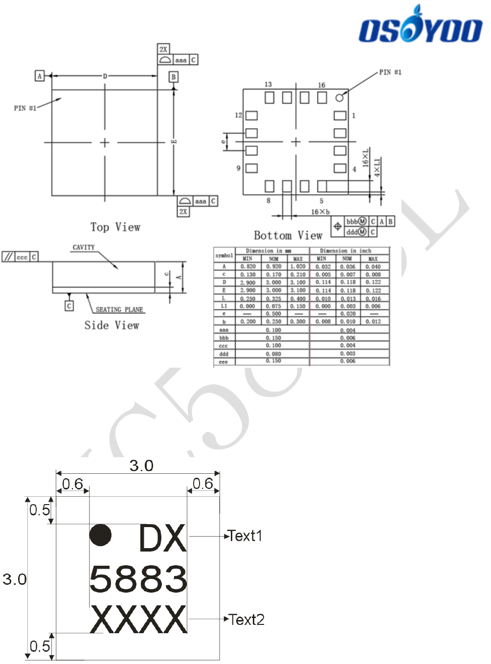
3.2 Package Outlines
3.2.1 Package Type
LGA (Land Grid Array)
3.2.2 Package Size:
3mm (Length)*3mm (Width)*0.9mm (Height)
QMC5883L
6
Figure 3. Package Size
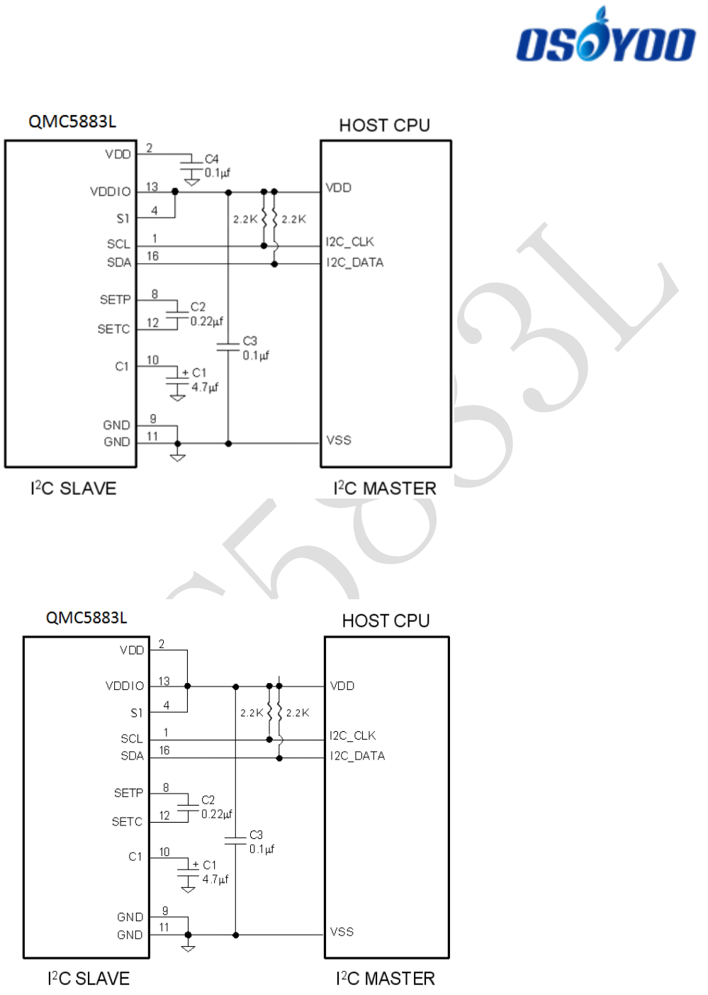
3.2.3 Marking:
Tracking code:
Text1: D Fixed code, X System generated for Customer type 9th bit
Text2: System generated for front 2 of Customer Batch number
Figure 4. Chip Marking
7
4 EXTERNAL CONNECTION
4.1 Dual Supply Connection
Figure 5. Dual Supply Connection
4.2 Single Supply connection
Figure 6. Single Supply Connection
2.16V to 3.6V
1.71V to VDD
2.16V to 3.6V
QMC5883L
8
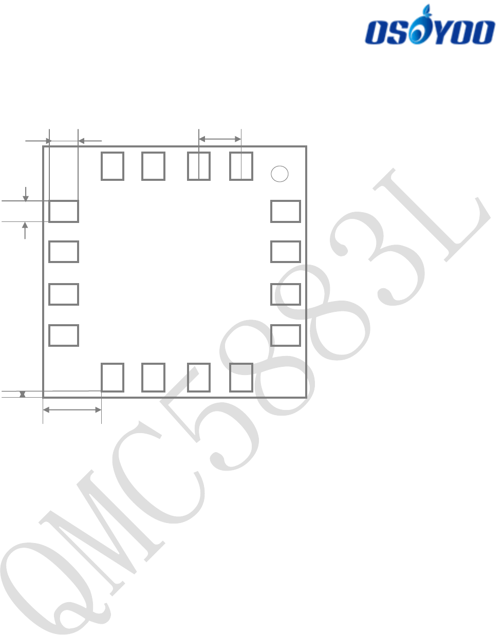
4.3 Mounting Considerations
The following is the recommend printed circuit board (PCB) footprint for the QMC5883L. Due to the fine pitch of
the pads, the footprint should be properly centered in the PCB.
Figure 7. QMC5883L PCB footprint
4.4 Layout Considerations
Besides keeping all components that may contain ferrous materials (nickel, etc.) away from the sensor on both
sides of the PCB, it is also recommended that there is no conducting copper line under/near the sensor in any of
the PCB layers.
4.4.1 Solder Paste
A 4 mil stencil and 100% paste coverage is recommended for the electrical contact pads.
4.4.2 Reflow Assembly
This device is classified as MSL 3 with 260C peak reflow temperature. As specified by JEDEC, parts with an
MSL 3 rating require baking prior to soldering, if the part is not kept in a continuously dry (< 10% RH) environment
before assembly. Reference IPC/JEDEC standard J-STD-033 for additional information.
No special reflow profile is required for QMC5883L, which is compatible with lead eutectic and lead-free solder
paste reflow profiles. We recommends adopting solder paste manufacturer’s guidelines. Hand soldering is not
recommended.
4.4.3 External Capacitors
The external capacitors C1 should be ceramic type with low ESR characteristics. The exact ESR value is not
critical, but values less than 200 milli-ohms are recommended. Reservoir capacitor C1 is nominally 4.7 µF in
capacitance. Low ESR characteristics may not be in many small SMT ceramic capacitors (0402), so be prepared
to up-size the capacitors to gain low ESR characteristics.
0.325
0.25
0.5
0.625
0.075

9
5 BASIC DEVICE OPERATION
5.1 Anisotropic Magneto-Resistive Sensors
The QMC5883L magneto-resistive sensor circuit consists of tri-axial sensors and application specific support
circuits to measure magnetic fields. With a DC power supply is applied to the sensor two terminals, the sensor
converts any incident magnetic field in the sensitive axis directions to a differential voltage output. The ASIC then
amplifies and processes the signal to have a digital output.
The device has an offset cancellation function to eliminate sensor and ASIC offsets. It also applies a self-aligned
magnetic field to restore magnetic state before each measurement to ensure high accuracy. Because of these
features, the QMC5883L doesn’t need to calibrate every time in most of application situations. It may need to be
calibrated once in a new system or a system changes a new battery.
5.2 Power Management
There are two power supply pins to the device. VDD provides power for all the internal analog and digital
functional blocks. VDDIO provides power for digital I/O and logic. It is possible to work with VDDIO equal to VDD,
the single supply mode, or with VDDIO lower than VDD, the dual supply mode.
The device should turn-on both power pins in order to operate properly. When the device is powered on, all
registers are reset by POR, then the device transits to the standby mode and waits for further commends.
Table 6 provides references for four power states. Transitions between power state 2 and power state 3 are
prohibited, due to leakage current concerns.
Table 6: Power States
Power State
VDD
VDDIO
Power State description
1
0V
0V
Device Off, No Power Consumption
2
0V
1.65v~3.6v
Device Off, Unpredictable Leakage Current on VDD
due to Floating Node.
3
2.16v~3.6v
0
Device Off, Same Current as Standby Mode
4
2.16v~3.6v
1.65v~3.6v
Device On, Normal Operation Mode, Enters Standby
Mode after POR
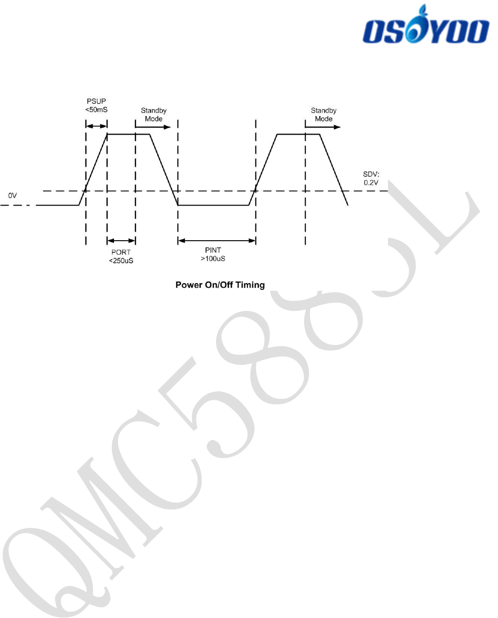
5.3 Power On/Off Time
After the device is powered on, some time periods are required for the device fully functional. The external power
supply requires a time period for voltage to ramp up (PSUP), it is typically 50 milli-second. However it isn’t
controlled by the device. The Power –On –Reset time period (PORT) includes time to reset all the logics, load
values in NVM to proper registers, enter the standby mode and get ready for analogy measurements. The power
on/off time related to the device is in Table 7.
Table 7. Time Required for Power On/Off
Parameter
Symbol
Condition
Min.
Typ.
Max.
Unit
POR
Completion
Time
PORT
Time Period After VDD and
VDDIO at Operating Voltage
to Ready for I2C Commend
and Analogy Measurement.
350
uS
Power off
Voltage
SDV
Voltage that Device Considers
to be Power Down.
0.2
V
Power on
Interval
PINT
Time Period Required for
Voltage Lower Than SDV to
Enable Next POR
100
uS
QMC5883L
10
Figure 8. Power On/Off Timing
5.4 Communication Bus Interface I2C and Its Addresses
This device will be connected to a serial interface bus as a slave device under the control of a master device,
such as the processor. Control of this device is carried out via I²C.
This device is compliant with I²C -Bus Specification, document number: 9398 393 40011. As an I²C compatible
device, this device has a 7-bit serial address and supports I²C protocols. This device supports standard and fast
speed modes, 100kHz and 400kHz, respectively. External pull-up resistors are required to support all these
modes.
The default I2C address is 0D: 0001101
If other I2C address options are required, please contact factory..
5.5 Internal Clock
The device has an internal clock for internal digital logic functions and timing management. This clock is not
available to external usage.
5.6 Temperature Compensation
Temperature compensation of the measured magnetic data is enabled by default at the factory. Temperature
measured by the built-in temperature sensor will be used to compensate the magnetic sensor’s sensitivity
changes due to temperatures. The compensated magnetic sensor data is placed in the Output Data Registers
automatically.
5.7 Temperature Output
QMC5883L has a built-in temperature sensor, it can provide temperature reading for other applications. The
output is placed in Temperature Output Registers (07H and 08H). The temperature is calibrated for its sensitivity.
11
6 MODES OF OPERATION
6.1 Modes Transition
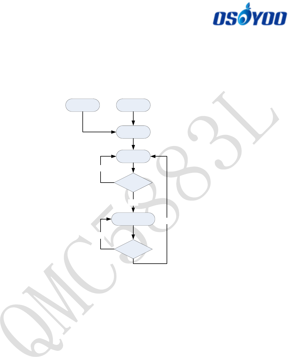
The device has two different operational modes, controlled by register (09H), mode bits. The main purpose of
these modes is for power management. The modes can be transited from one to the other, as shown below,
through I2C commends of changing mode bits. The default mode is Standby.
POR
OTP Load
Standby
Continuous Mode
Mode
Change?
Mode
Change?
Soft Reset
NO
NO
YES
YES
Soft Reset could be set at any
time and then chip
automatically transits to
standby mode
The system automatically
transits to standby mode after
power on reset or soft reset.
Figure 9. Modes Transition
6.2 Description of Modes
6.2.1 Continuous-Measurement Mode
During the continuous-measurement mode (mode bits= 01), the magnetic sensor continuously makes
measurements and places measured data in data output registers. The field range (or sensitivity) and data output
rate registers are also located in the control register (09H), they should be set up properly for your applications in
the continuous-measurement mode.
For example, if the application requires output date rate 50Hz, the ODR bit in control register (09H) should be 01.
If the field range is +/-8 Gauss, the RNG =01.
The over sample rate is optional for you to use. The default is OSR=00, if your application has enough resolution
and need low power consumption, you may reduce OSR to a lower number, such as OSR=10 (128) or OSR =11
(64).
In the continuous-measurement mode, the magnetic sensor data are automatically compensated for offset and
temperature effects. The gains are calibrated in the factory.
6.2.1.1 Normal Read Sequence
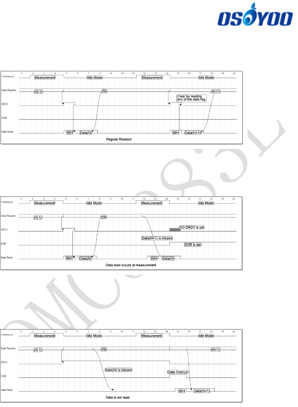
Complete magnetometer data read-out can be done as follow steps.
Check DRDY pin or by polling DRDY bit in Register 06H
Read DRDY bit in Register 06H (if polling, it’s unnecessary)
QMC5883L
12
DRDY: Data ready (“1”) or Not (“0”).
DOR: Any data has been missed (“1”) or not (“0”)
Read measured data, if any of the six data register is accessed, DRDY and DOR turn to “0”.
Data protection, if any of the six data register is accessed, data protection starts. During Data protection
period, data register cannot be updated until the last bits 05H (ZOUT [15:8]) have been read.
Figure 10. Normal Read Sequence
6.2.1.2 Data Read Sequence Occurs at Measurement
During measurement, it’s possible to read data register which keep the previous measured data. Therefore, no
interrupt (DRDY bit) will be set if data reading occurs at the middle of measurement.
Figure 11 Data Read Sequence at Measurement
6.2.1.3 Data Not Read
If Nth data is skipped, the current data will be flushed by next coming data. In this case, interrupt (DRDY bit)
keeps high until data is read. DOR bit is set to “1” which indicates a set of measurement data has been lost. DOR
bit turns to “0” once 06H is accessed in next data read operation
Figure 12. Sequence When Data Not Read
13
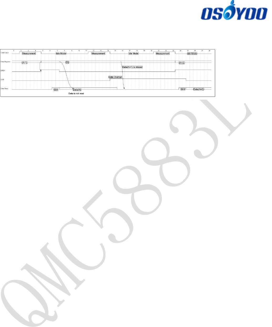
6.2.1.4 Data Locks Until Next Measurement Ends
Data lock is activated once any of the data register is accessed. If 05H (data unlock) is not accessed until next
measurements ends, current data blocks next data to update data register. In this case, DOR bit is also set to “1”
until 06H is accessed in next data read.
Figure 13. Sequence When Data Locks
6.2.1.5 Interrupt
An interrupt is generated on DRDY pin each time that magnetic field is measured. The interrupt can be disabled
by set 0AH[0] = 1.
6.2.2 Standby Mode
Standby mode is the default state of QMC5883L upon POR and soft reset, only few function blocks are activated
in this mode, which keeps power consumption as low as possible. In this state, register values are hold on by an
ultra-low power LDO, I2C interface can be woken up by reading or writing any registers. There is no
magnetometer measurement in the Standby mode. Internal clocking is also halted.
7 Application Examples
7.1 Continuous Mode Setup Example
Write Register 0BH by 0x01 (Define Set/Reset period)
Write Register 09H by 0x1D (Define OSR = 512, Full Scale Range = 8 Gauss, ODR = 200Hz, set continuous
measurement mode)
7.2 Measurement Example
Check status register 06H[0] ,”1” means ready.
Read data register 00H ~ 05H.
7.3 Standby Example
Write Register 09H by 0x00
7.4 Soft Reset Example
Write Register 0AH by 0x80
QMC5883L
14
8 I2C COMMUNICATION PROTOCOL
8.1 I2C Timings
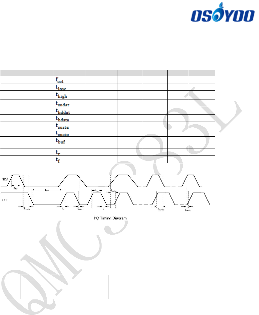
Below table and graph describe the I2C communication protocol times
Table 9. I2C Timings
Parameter
Symbol
Condition
Min.
Typ.
Max.
Unit
SCL Clock
0
400
kHz
SCL Low Period
1
μS
SCL High Period
1
μS
SDA Setup Time
0.1
μS
SDA Hold Time
0
0.9
μS
Start Hold Time
0.6
μS
Start Setup Time
0.6
μS
Stop Setup Time
0.6
μS
New Transmission
Time
1.3
μS
Rise Time
μS
Fall Time
μS
Figure 14. I2C Timing Diagram
8.2 I2C R/W Operation
8.2.1 Abbreviation
Table 10. Abbreviation
SACK
Acknowledged by slave
MACK
Acknowledged by master
NACK
Not acknowledged by master
RW
Read/Write
8.2.2 Start/Stop/Ack
START: Data transmission begins with a high to transition on SDA while SCL is held high. Once I2C transmission
starts, the bus is considered busy.
STOP: STOP condition is a low to high transition on SDA line while SCL is held high.
ACK: Each byte of data transferred must be acknowledged. The transmitter must release the SDA line during the
acknowledge pulse while the receiver mush then pull the SDA line low so that it remains stable low during the
high period of the acknowledge clock cycle.
NACK: If the receiver doesn’t pull down the SDA line during the high period of the acknowledge clock cycle, it’s
recognized as NACK by the transmitter.
15
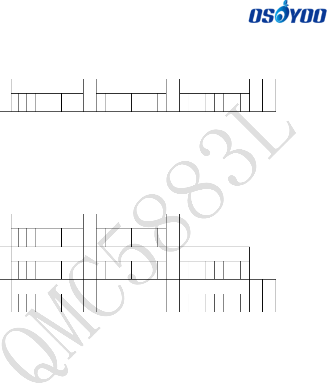
8.2.3 I2C Write
I2C write sequence begins with start condition generated by master followed by 7 bits slave address and a write
bit (R/W=0). The slave sends an acknowledge bit (ACK=0) and releases the bus. The master sends the one byte
register address. The slave again acknowledges the transmission and waits for 8 bits data which shall be written
to the specified register address. After the slave acknowledges the data byte, the master generates a stop signal
and terminates the writing protocol.
Table 11. I2C Write
START
Slave Address
R
W
SACK
Register Address
(0x09)
SACK
Data
(0x01)
SACK
STOP
0
0
0
1
1
0
1
0
0
0
0
0
1
0
0
1
0
0
0
0
0
0
0
1
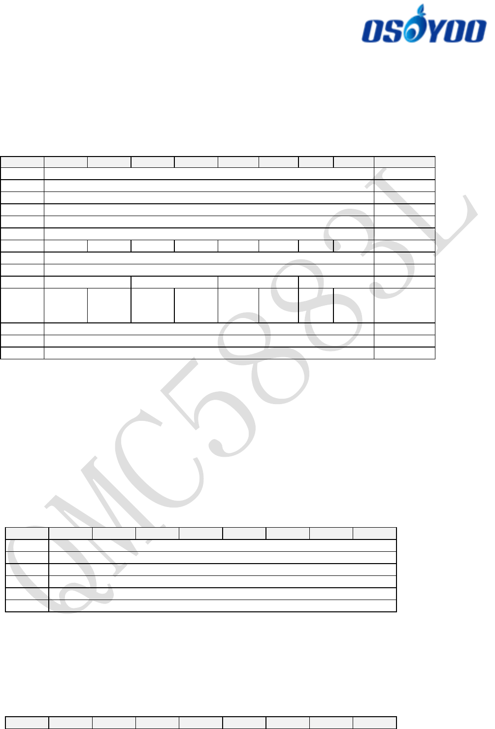
8.2.4 I2C Read
I2C write sequence consists of a one-byte I2C write phase followed by the I2C read phase. A start condition must
be generated between two phase. The I2C write phase addresses the slave and sends the register address to be
read. After slave acknowledges the transmission, the master generates again a start condition and sends the
slave address together with a read bit (R/W=1). Then master releases the bus and waits for the data bytes to be
read out from slave. After each data byte the master has to generate an acknowledge bit (ACK = 0) to enable
further data transfer. A NACK from the master stops the data being transferred from the slave. The slave releases
the bus so that the master can generate a STOP condition and terminate the transmission.
The register address is automatically incremented and more than one byte can be sequentially read out. Once a
new data read transmission starts, the start address will be set to the register address specified in the current I2C
write command.
Table 12. I2C Read
START
Slave Address
R
W
SACK
Register Address
(0x00)
SACK
0
0
0
1
1
0
1
0
0
0
0
0
0
0
0
0
START
Slave Address
R
W
SACK
Data
(0x00)
MACK
Data
(0x01)
0
0
0
1
1
0
1
1
0
0
0
0
0
0
0
0
0
0
0
0
0
0
0
1
MACK
Data
(0x02)
MACK
…………………………
…….
MACK
Data
(0x07)
NACK
STOP
0
0
0
0
0
0
1
0
…………………………
…….
0
0
0
0
0
1
1
1
8.2.5 I2C Pointer Roll-over
QMC5883L has an embedded I2C pointer roll-over function which can improve the data transmission efficiency.
The I2C data pointer will automatically roll between 00H ~ 06H if I2C read begins at any position among 00H~06H.
This function is enabled by set 0AH[6] = 01H.
QMC5883L
16
9 REGISTERS
9.1 Register Map
The table below provides a list of the 8-bit registers embedded in the device and their respective function and
addresses
Table 13. Register Map
Addr.
7
6
5
4
3
2
1
0
Access
00H
Data Output X LSB Register XOUT[7:0]
Read only
01H
Data Output X MSB Register XOUT[15:8]
Read only
02H
Data Output Y LSB Register YOUT[7:0]
Read only
03H
Data Output Y MSB Register YOUT[15:8]
Read only
04H
Data Output Z LSB Register ZOUT[7:0]
Read only
05H
Data Output Z MSB Register ZOUT[15:8]
Read only
06H
DOR
OVL
DRDY
Read only
07H
TOUT[7:0]
Read only
08H
TOUT[15:8]
Read only
09H
OSR[1:0]
RNG[1:0]
ODR[1:0]
MODE[1:0]
Read/Write
0AH
SOFT_
RST
ROL_P
NT
INT_E
NB
R/W, Read
only on
blanks
0BH
SET/RESET Period FBR [7:0]
Read/Write
0CH
Reserved
Read only
0DH
Chip ID
Read only
9.2 Register Definition
9.2.1 Output Data Register
Registers 00H ~ 05H store the measurement data from each axis magnetic sensor in continuous-measurement.
In the continuous measurement mode, the output data is refreshed periodically based on the data update rate
ODR setup in control registers 1. The data stays the same, regardless of reading status through I2C, until new
data replaces them. Each axis has 16 bit data width in 2’s complement, i.e., MSB of 01H/03H/05H indicates the
sign of each axis. The output data of each channel saturates at -32768 and 32767.
Table 14. Output Data Register
Addr.
7
6
5
4
3
2
1
0
00H
Data Output X LSB Register XOUT[7:0]
01H
Data Output X MSB Register XOUT[15:8]
02H
Data Output Y LSB Register YOUT[7:0]
03H
Data Output Y MSB Register YOUT[15:8]
04H
Data Output Z LSB Register ZOUT[7:0]
05H
Data Output Z MSB Register ZOUT[15:8]
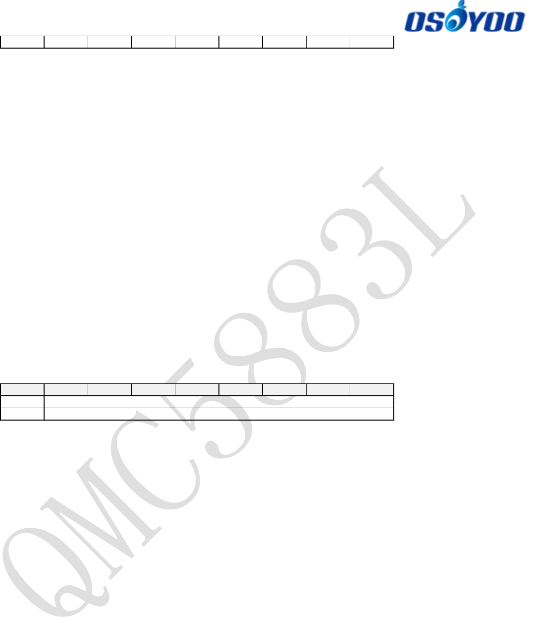
9.2.2 Status Register
There are two status registers located in address 06H and 0CH.
Register 06H has three bits indicating for status flags, the rest are reserved for factory use. The status registers
are read only bits.
Table 15. Status Register 1
Addr.
7
6
5
4
3
2
1
0
17
06H
DOR
OVL
DRDY
Data Ready Register (DRDY), it is set when all three axis data is ready, and loaded to the output data registers in
the continuous measurement mode. It is reset to “0” by reading any data register (00H~05H) through I2C
commends
DRDY: “0”: no new data, “1”: new data is ready
Overflow flag (OVL) is set to “1” if any data of three axis magnetic sensor channels is out of range. The output
data of each axis saturates at -32768 and 32767, if any of the axis exceeds this range, OVL flag is set to “1”. This
flag is reset to “0” if next measurement goes back to the range of (-32768, 32767), otherwise, it keeps as “1”.
OVL: “0”: normal, “1”: data overflow
Data Skip (DOR) bit is set to “1” if all the channels of output data registers are skipped in reading in the
continuous-measurement mode. It is reset to “0” by reading any data register (00H~05H) through I2C
DOR: “0”: normal, “1”: data skipped for reading
9.2.3 Temperature Data Registers
Registers 07H-08H store temperature sensor output data. 16 bits temperature sensor output is in 2’s complement.
Temperature sensor gain is factory-calibrated, but its offset has not been compensated, only relative temperature
value is accurate. The temperature coefficient is about 100 LSB/℃
Table 17. Temperature Sensor Output
Addr.
7
6
5
4
3
2
1
0
07H
TOUT[7:0]
08H
TOUT[15:8]
9.2.4 Control Registers
Two 8-bits registers are used to control the device configurations.
Control register 1 is located in address 09H, it sets the operational modes (MODE). output data update rate
(ODR), magnetic field measurement range or sensitivity of the sensors (RNG) and over sampling rate (OSR).
Control register 2 is located in address 0AH. It controls Interrupt Pin enabling (INT_ENB), Point roll over function
enabling(POL_PNT) and soft reset (SOFT_RST).
Two bits of MODE registers can transfer mode of operations in the device, the two modes are Standby, and
Continuous measurements. The default mode after Power-on-Reset (POR) is standby. There is no any restriction
in the transferring between the modes.
Output data rate is controlled by ODR registers. Four data update frequencies can be selected: 10Hz, 50Hz,
100Hz and 200Hz. For most of compassing applications, we recommend 10 Hz for low power consumption. For
gaming, the high update rate such as 100Hz or 200Hz can be used.
Field ranges of the magnetic sensor can be selected through the register RNG. The full scale field range is
determined by the application environments. For magnetic clear environment, low field range such as +/- 2gauss
can be used. The field range goes hand in hand with the sensitivity of the magnetic sensor. The lowest field range
has the highest sensitivity, therefore, higher resolution.
Over sample Rate (OSR) registers are used to control bandwidth of an internal digital filter. Larger OSR value
leads to smaller filter bandwidth, less in-band noise and higher power consumption. It could be used to reach a
good balance between noise and power. Four over sample ratio can be selected, 64, 128, 256 or 512.
QMC5883L
18
Table 18. Control Register 1
Addr
7
6
5
4
3
2
1
0
09H
OSR[1:0]
RNG[1:0]
ODR[1:0]
MODE[1:0]
Reg.
Definition
00
01
10
11
Mode
Mode Control
Standby
Continuous
Reserve
Reserve
ODR
Output Data Rate
10Hz
50Hz
100Hz
200Hz
RNG
Full Scale
2G
8G
Reserve
Reserve
OSR
Over Sample
Ratio
512
256
128
64
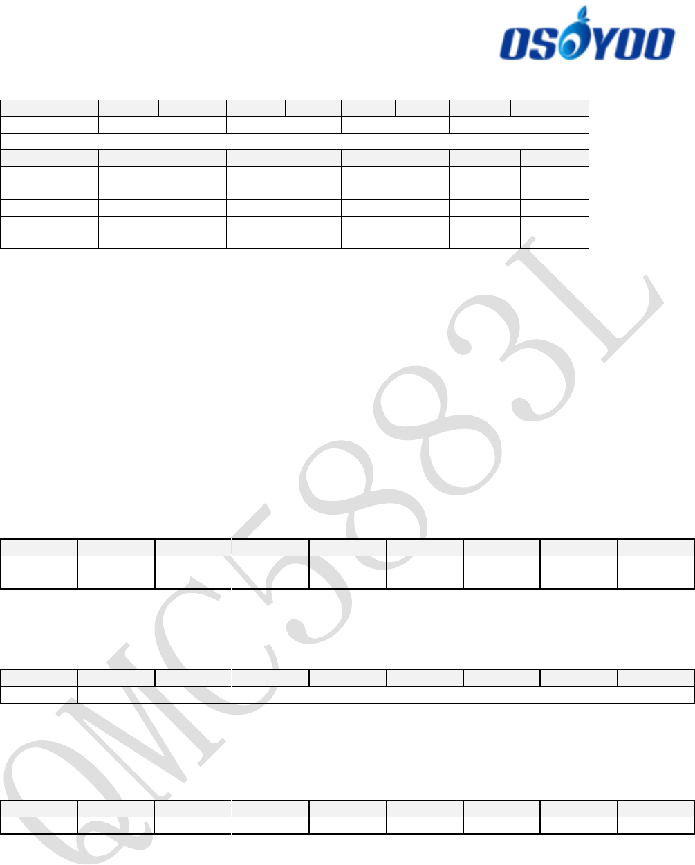
Interrupt enabling is controlled by register INT_ENB in control register 2. Once the interrupt is enabled, it will flag
when new data is in Data Output Registers.
INT_ENB: “0”: enable interrupt PIN, “1”: disable interrupt PIN
Pointer roll-over function is controlled by ROL_PNT register. When the point roll-over function is enabled, the I2C
data pointer automatically rolls between 00H ~ 06H, if I2C read begins at any address among 00H~06H.
ROL_PNT: “0”: Normal, “1”: Enable pointer roll-over function
Soft Reset can be done by changing the register SOFT_RST to set. Soft reset can be invoked at any time of any
mode. For example, if soft reset occurs at the middle of continuous mode reading, QMC5883L immediately
switches to standby mode due to mode register is reset to “00” in default.
SOFT_RST: “0”: Normal “1”: Soft reset, restore default value of all registers.
Table 19. Control Register 2
Addr.
7
6
5
4
3
2
1
0
0AH
SOFT_R
ST
ROL_PN
T
INT_ENB
9.2.5 SET/RESET Period Register
SET/RESET Period is controlled by FBR [7:0]. It is recommended that the register 0BH is written by 0x01.
Table 20. SET/RESET Period Register
Addr.
7
6
5
4
3
2
1
0
0BH
SET/RESET Period FBR [7:0]
9.2.6 Chip ID Register
This register is chip identification register. It returns 0xFF.
Table 21. Chip ID Register
Addr.
7
6
5
4
3
2
1
0
0DH
1
1
1
1
1
1
1
1
1D=0001 1101
12=0001 0010
19
ORDERING INFORMATION
Ordering Number
Temperature Range
Package
Packaging
QMC5883L-TR
-40℃~85℃
LGA-16
Tape and Reel: 3k pieces/reel
.
-
.
vership@foxmail.com