QM_Cyclone10_10CL006开发板 用户手册(Quartus17.0使用) V02 QMTECH Cyclone10 10CL006 User Manual (Quartus17.0)
User Manual:
Open the PDF directly: View PDF ![]() .
.
Page Count: 27
QM_CYCLONE10_10CL006 Development Board-User Manual(Quartus 17.0)
QM_CYCLONE10_10CL006 DB
USER MANUAL(QUARTUS 17.0)
Preface
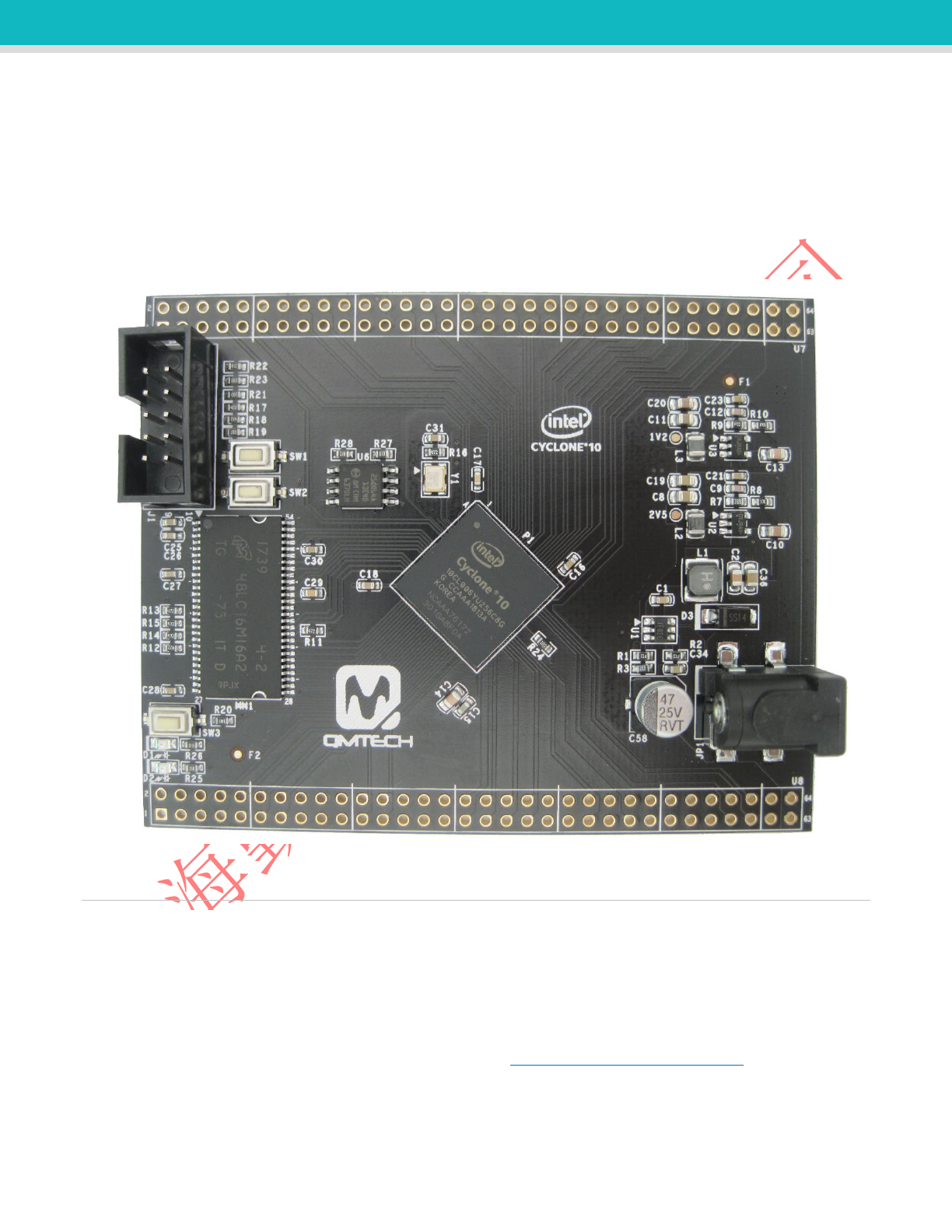
The QMTech® Cyclone 10 Core Board uses Intel® (Altera) 10CL006 device to demonstrate the
industry's lowest system cost and power, along with performance levels that make the device
family ideal for differentiating your high-volume applications. All Intel® Cyclone® 10 LP FPGAs
require only two core power supplies for operation, simplifying your power distribution network and
saving you board costs, board space, and design time. The flexibility of the Intel® Cyclone® 10 LP
FPGA enables you to design in a smaller, lower cost device, lowering your total system costs.
Users could visit QMTECH official website from here: http://www.chinaqmtech.com/

QM_CYCLONE10_10CL006 DB User Manual-V01
Table of Contents
1. QUARTUS PRIME 17.0 INSTALLATION ................................................. 3
2. FPGA PROJECT COMPILE, *.SOF DOWNLOAD AND *.JIC PROGRAM ... 7
2.1 CREATE NEW PROJECT ................................................................ 7
2.2 COMPILE THE PROJECT .............................................................. 12
2.3 PIN ASSIGNMENT .................................................................... 13
2.4 DOWNLOAD *.SOF INTO FPGA ................................................... 15
2.5 PROGRAM *.JIC INTO SPI FLASH .................................................. 18
3. SIGNALTAP II LOGIC ANALYZER......................................................... 22
4. REFERENCE........................................................................................ 26
5. REVISION .......................................................................................... 27
QM_CYCLONE10_10CL006 DB User Manual-V01
1. Quartus Prime 17.0 Installation
The revolutionary Intel® Quartus® Prime Design Software includes everything you need to design for
Intel® FPGAs, SoCs, and CPLDs from design entry and synthesis to optimization, verification, and
simulation. Dramatically increased capabilities on devices with multi-million logic elements are providing
designers with the ideal platform to meet next-generation design opportunities.
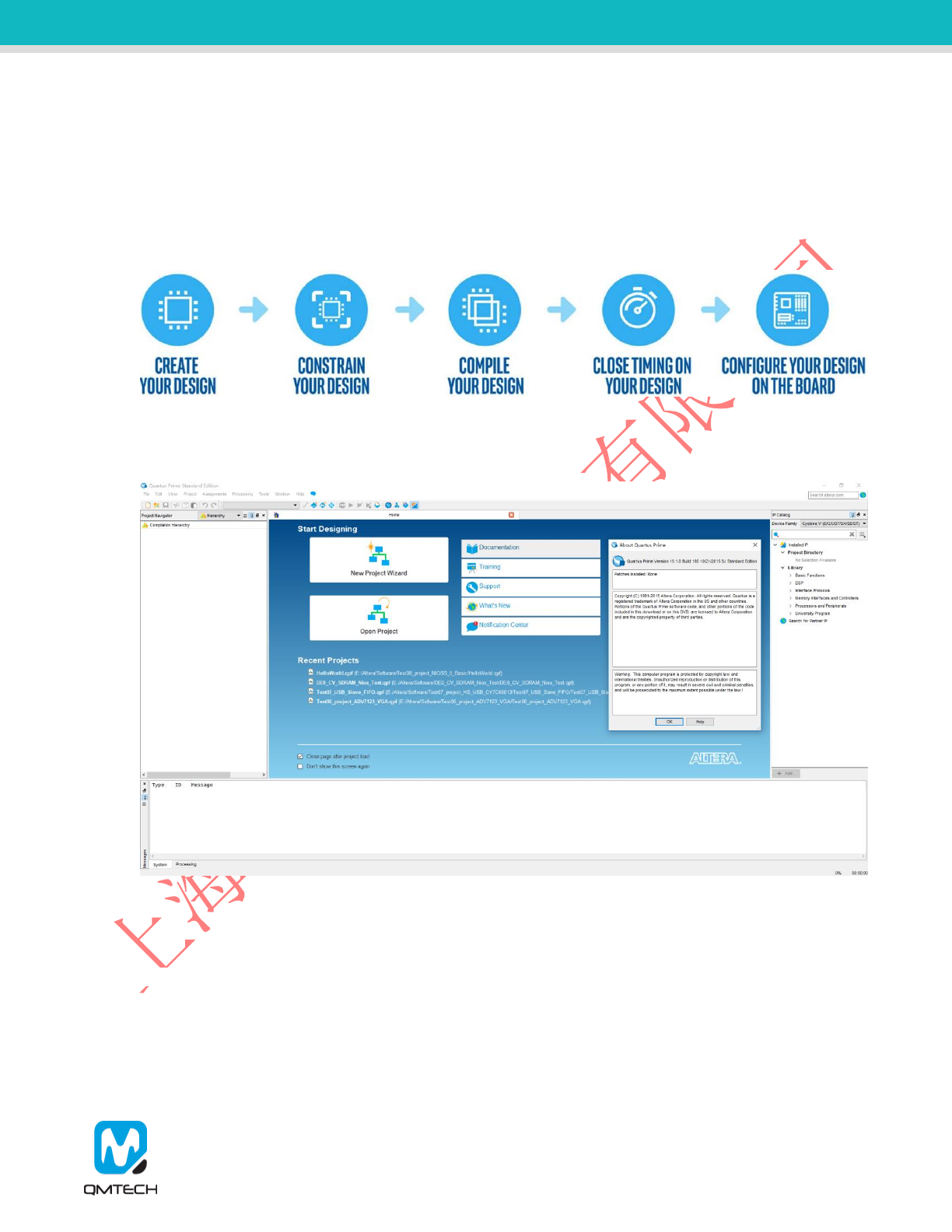
The Intel® Quartus® Prime Software design flow comprises of the following high-level steps:
The Quartus Prime software version 17.0 supports the following device families: Stratix IV, Stratix V, Arria
II, Arria V, Arria V GZ, Arria 10, Cyclone 10 LP, Cyclone IV, Cyclone V, MAX II, MAX V, and MAX 10
FPGA. Below image shows the startup UI of Quartus II Prime 17.0:
Figure 1-1. Quartus II Prime 17.0
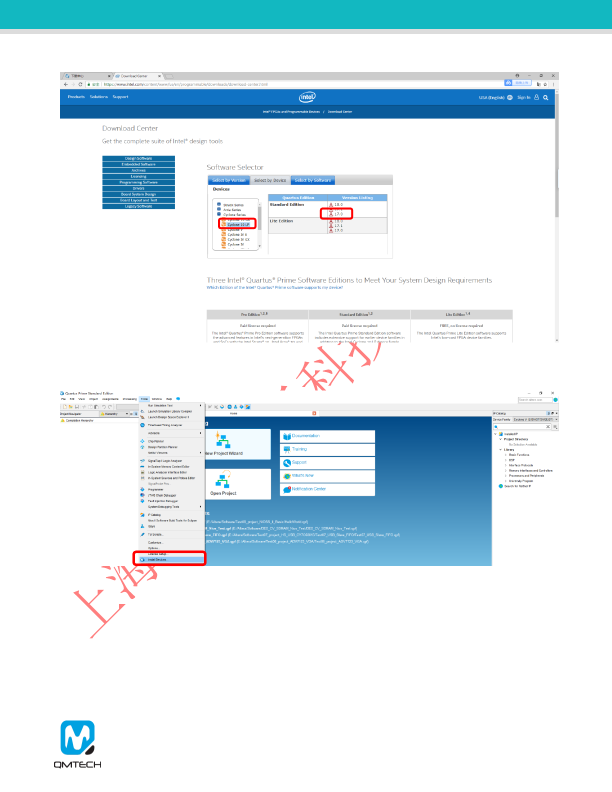
After the Quartus II Prime 17.0 is correctly installed, users still need to install the device package from
Intel official website. Below lists the download center address:
https://www.intel.com/content/www/us/en/programmable/downloads/download-center.html
In the Intel Download Center website, select the tab of ‘ Select by Device’ and then all the available
device packages will be listed as below image. The device used in this user manual is Cyclone10 LP
series and the detailed chip part number is 10CL006YU256C8G, so please download the device package
for Quartus II 17.0: cyclone10lp-17.0.0.595.qdz.
QM_CYCLONE10_10CL006 DB User Manual-V01
Figure 1-2. Download Device Package
Open Quartus II 17.0, Click Tools Install Device and then select the downloaded device package:
Figure 1-3. Install Device Package
QM_CYCLONE10_10CL006 DB User Manual-V01
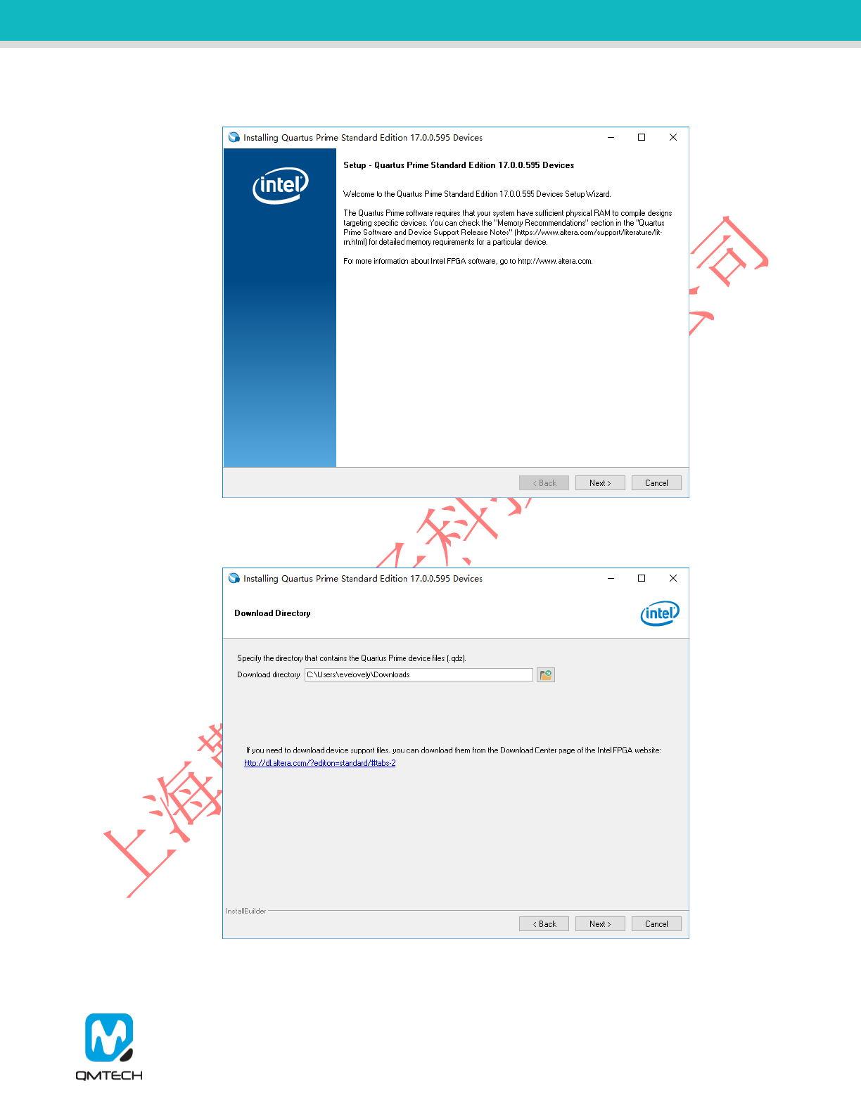
Below window will pop up and click Next:
Figure 1-4. Install Device Package
Choose the Download Directory where contains the cyclone10lp-17.0.0.595.qdz file:
Figure 1-5. Choose Device Package
QM_CYCLONE10_10CL006 DB User Manual-V01
Choose the device package needs to be installed and click Next:
Figure 1-6. Install the Device Package
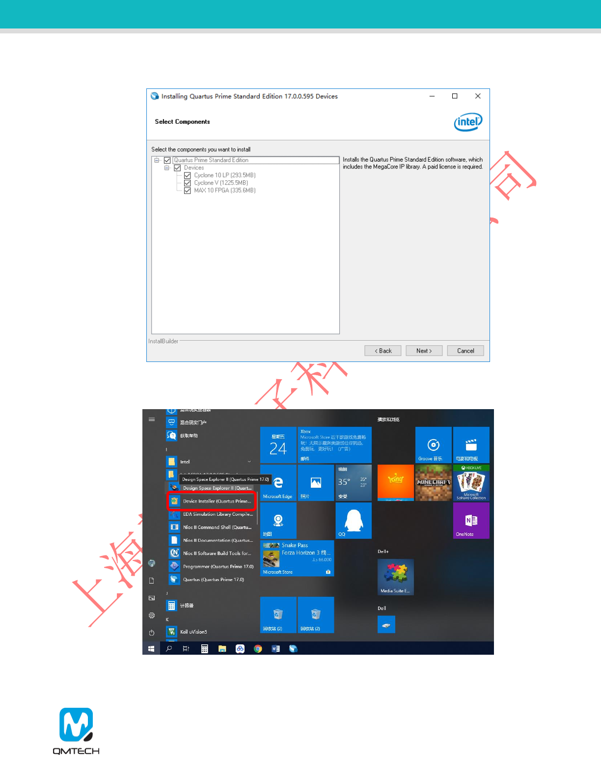
User could also install the device package by using Quartus II Prime 17.0 Device Installer directly:
Figure 1-7. Device Installer
QM_CYCLONE10_10CL006 DB User Manual-V01
2. FPGA Project Compile, *.sof Download and *.jic Program
2.1 Create New Project
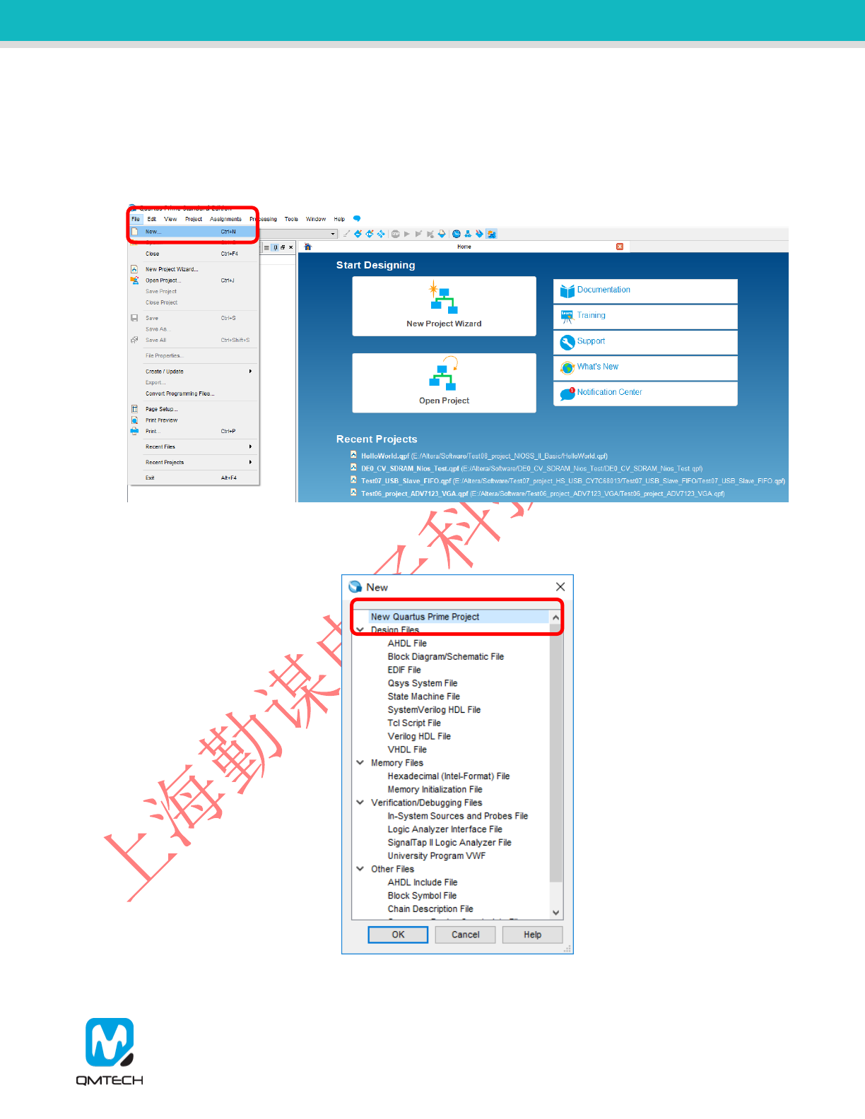
Click【File】【New Project Wizard…】 to create a new project:
Figure 2-1. Create New Project
Choose【New Quartus Prime Project】:
Figure 2-2. New Quartus Prime Project

QM_CYCLONE10_10CL006 DB User Manual-V01
In below【New Project Wizard】page, choose Next:
Figure 2-3. New Project Wizard
Set the target working folder below 【What is the working directory for this project?】. Set the new project
name below 【What is the name of this project?】. And finally set the example project name:
Test01_Project_LED shown as below.
Figure 2-4. Set Working Directory and Project Name
QM_CYCLONE10_10CL006 DB User Manual-V01
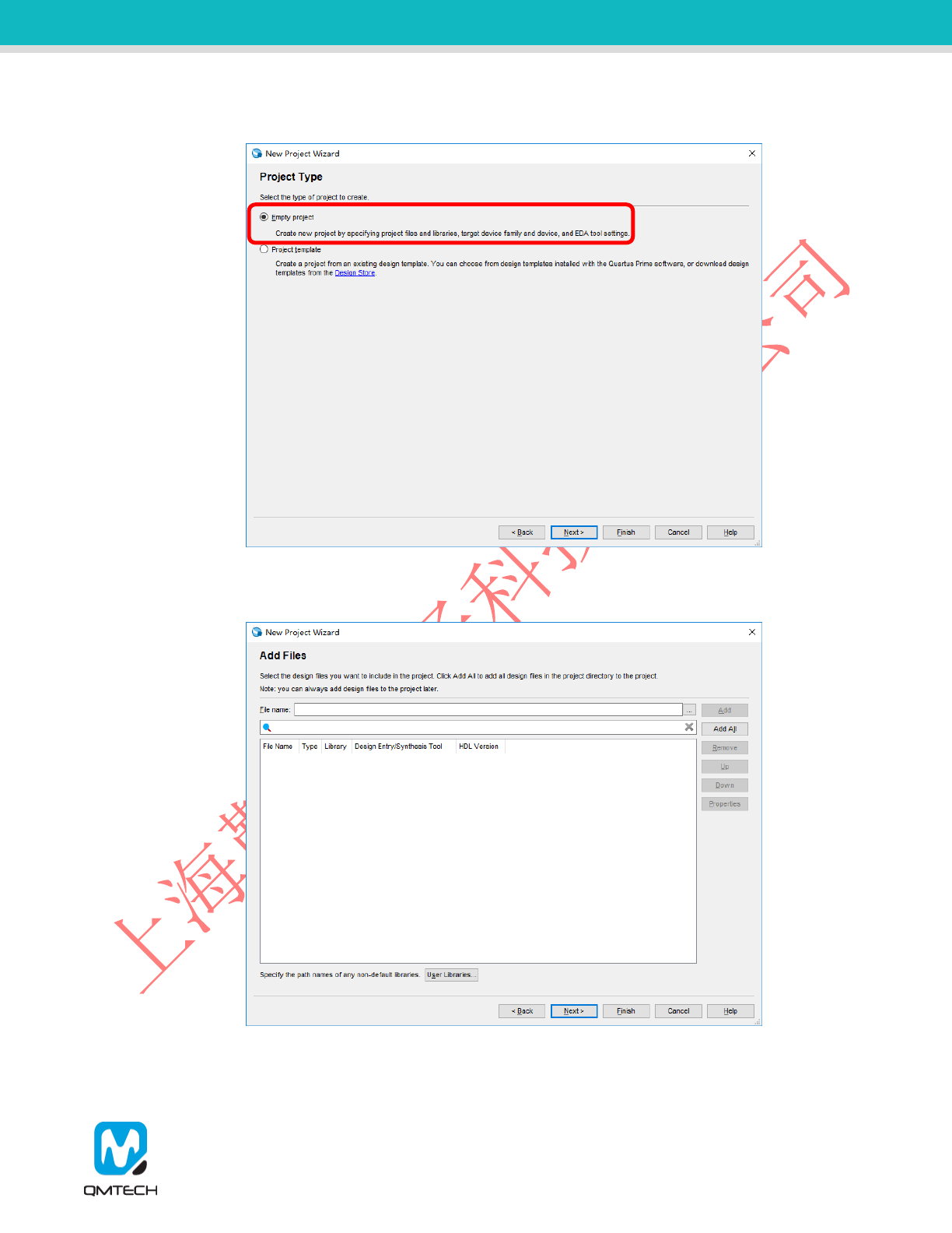
Select【Empty Project】and then click Next:
Figure 2-5. Create Empty Project
If user already has some source code, please add all these necessary files in this step:
Figure 2-6. Add Source Code
QM_CYCLONE10_10CL006 DB User Manual-V01
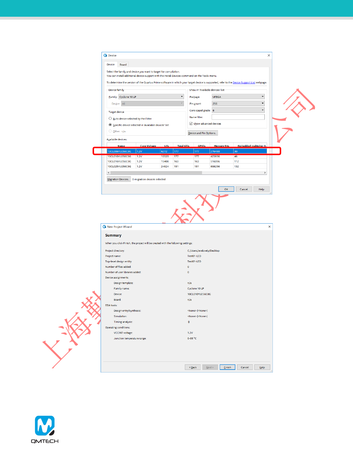
Choose the FPGA Chip number: 10CL006YU256C8G
Figure 2-7. Select Device
Summary page will be shown and click【Finish】if there’s nothing needs to be changed:
Figure 2-8. Project Summary Page
QM_CYCLONE10_10CL006 DB User Manual-V01
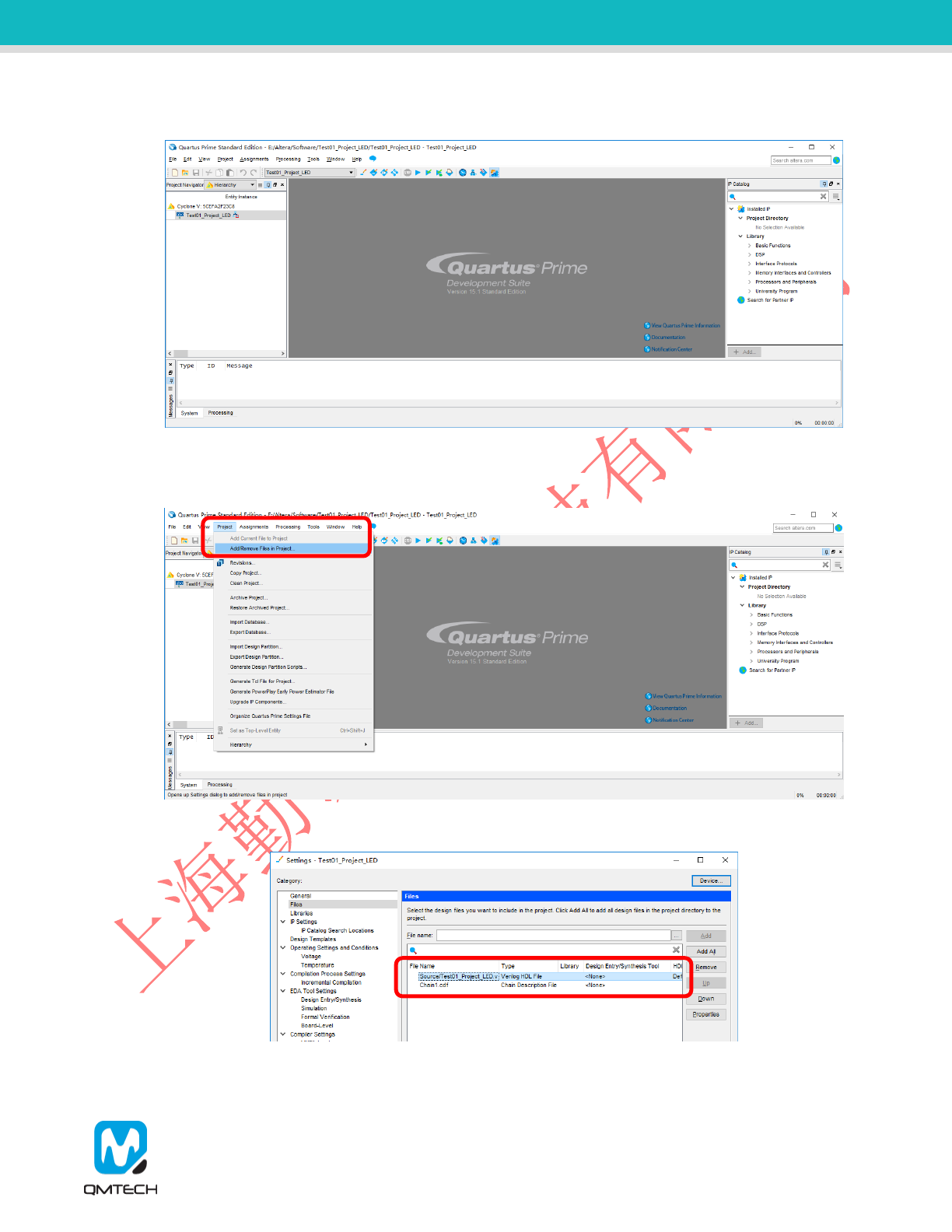
After the Empty Project created, below image will be shown:
Table 2-1. Empty Project
Users may add example source file Test01_Project_LED.v into this Empty Project shown as below:
Table 2-2. Add Source File
Table 2-3. Add Source File
QM_CYCLONE10_10CL006 DB User Manual-V01
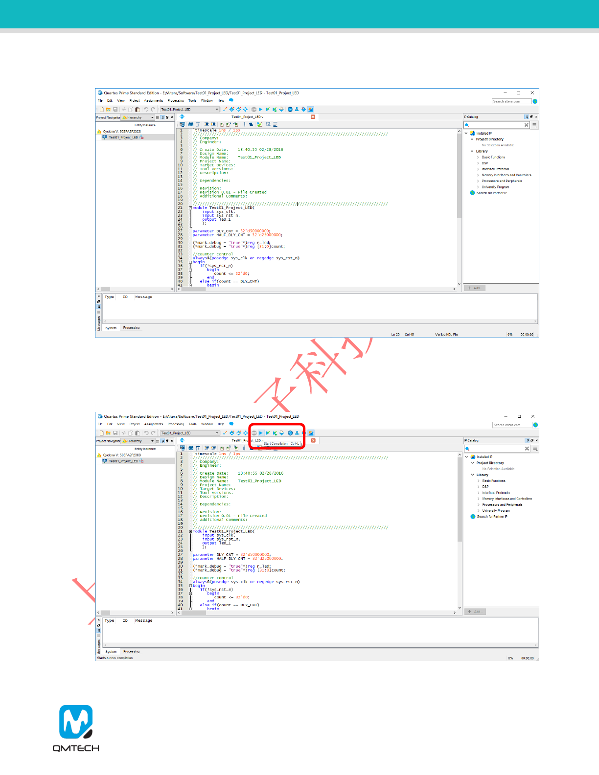
After the newly added source file loaded into project, user can view the source code shown as below:
Figure 2-9. View of Source Code
2.2 Compile the Project
Users could use the button【Start Compilation – Ctrl + L】shown in below image to compile the project:
Figure 2-10. Compilation
QM_CYCLONE10_10CL006 DB User Manual-V01
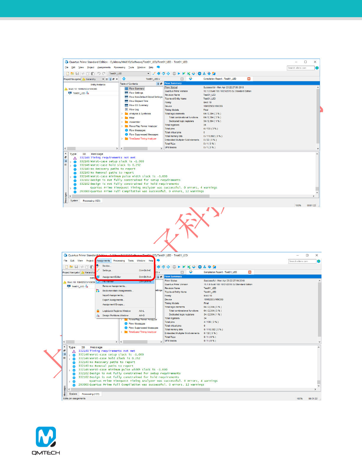
There will be compilation report after the compile finished, in which shows the info like logical element
resource usage, how many PLLs are used, etc. Below image shows an example Compilation Report:
Figure 2-11. Compilation Report
2.3 PIN Assignment
There are several ways to assign the Pins for the example project. Method 1: Choose【Assignment】
【Pin Planner】:
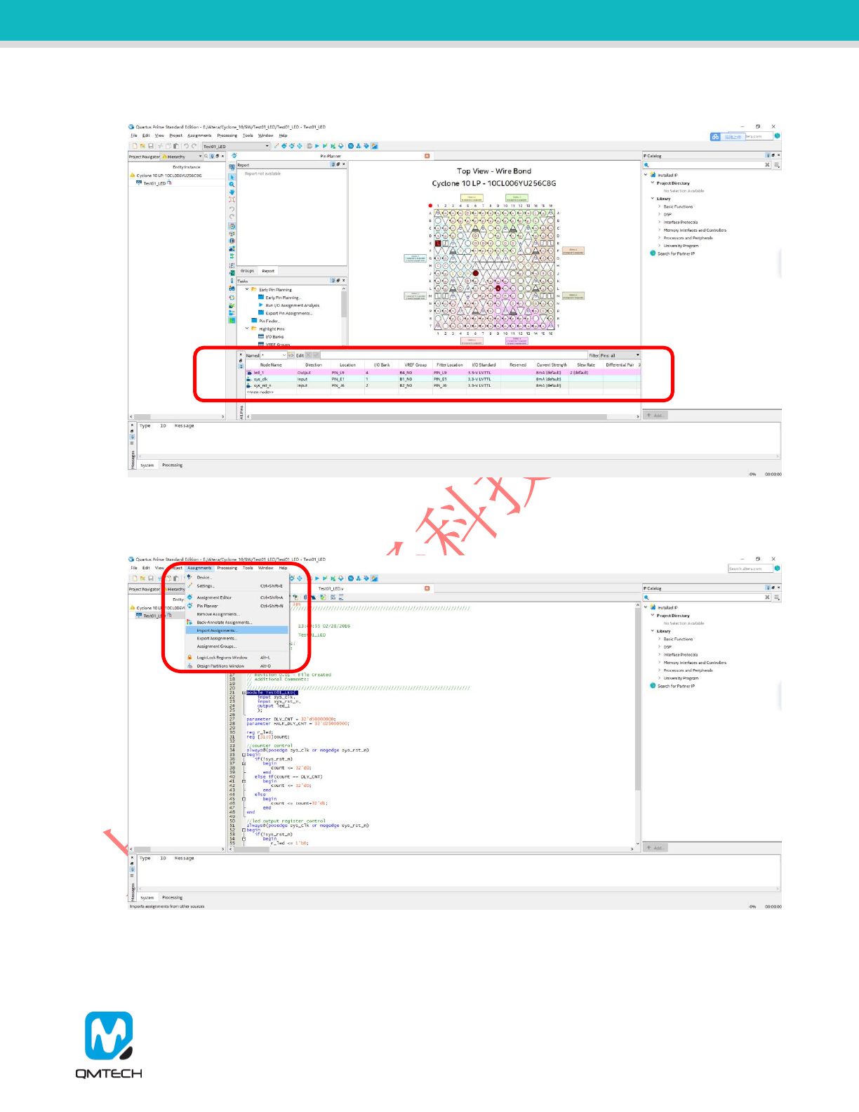
Figure 2-12. Pin Planner
QM_CYCLONE10_10CL006 DB User Manual-V01
Below image shows PIN settings for this test example:
Figure 2-13. PIN Assignment
Method 2: Prepare a *.csv file from other project, then use【Assignment】 【Import Assignment】to
import the existing *.csv file to allocate the Pin assignment:
Figure 2-14. Import Assignment
QM_CYCLONE10_10CL006 DB User Manual-V01
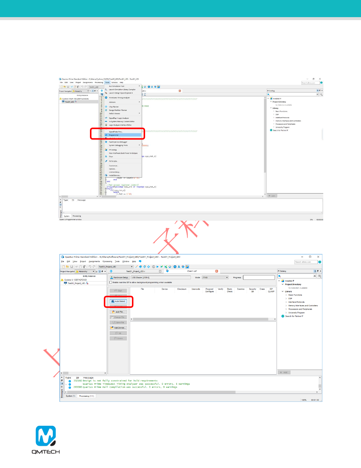
2.4 Download *.sof into FPGA
After the test example correctly compiled, the Quartus will generate a *.sof file which could be directly
loaded into FPGA to check whether implemented functions perform as expected. User could use
【Tools】【Programmer】to start a new download:
Figure 2-15. Programmer
Make sure the USB Blaster’s cable are correctly connected to FPGA’s JTAG port before using
Programmer to download *.sof file. Then click【Auto Detect】to check the hardware setup is okay or not:
Figure 2-16. JTAG Setup
QM_CYCLONE10_10CL006 DB User Manual-V01
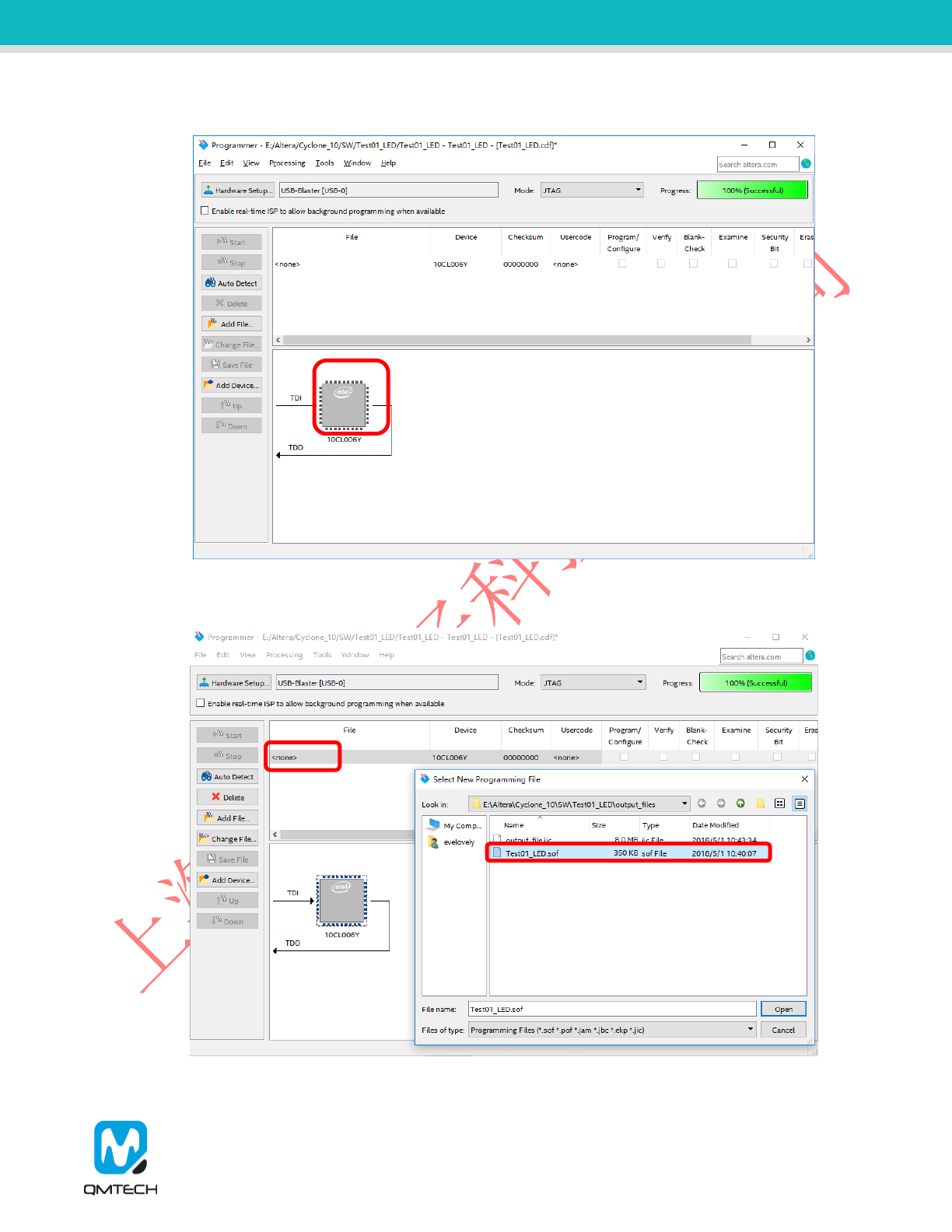
Below image shows the FPGA has been detected by the Programmer:
Figure 2-17. Detect FPGA
Users click【None】column to choose the *.sof file to be loaded into FPGA.
Figure 2-18. Choose *.sof File

QM_CYCLONE10_10CL006 DB User Manual-V01
Then toggle【Program/Configure】 and click the【Start】button to start a new program:
Figure 2-19. Program *.sof
If the *.sof file is correctly programed, the Progress bar will show info like: 100%(Successful). Then users
could check whether the LEDs on FPGA board blinking or not.
Figure 2-20. Program Successful
QM_CYCLONE10_10CL006 DB User Manual-V01
2.5 Program *.jic into SPI Flash
QM_CYCLONE10_10CL006 core board has mounted an external SPI Flash with 8MB capacity. The
hardware design chooses Active Serial x 1 method to make the FPGA could boot up from external SPI
Flash after power on. In this section, it describes how to program eternal SPI Flash through JTAG port.
The SPI Flash is non-volatile device which means the programmed *.jic file will never lose its content after
power down.
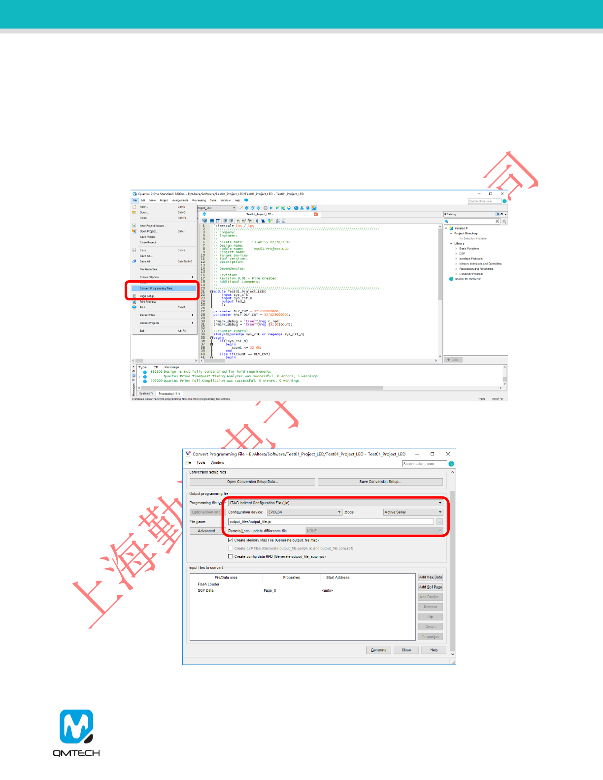
The SPI Flash programing file *.jic is converted by *.sof file described in previous chapter. So make sure
*.sof could be correctly running on FPGA before performing below steps. Step1: choose the Quartus II
Prime 15.1file convert tool by click【File】 【Convert Programming File】:
Figure 2-21. Convert Programming File Tool
Change the settings following below figure: choose EPCQ64, generated file name output_file.jic, etc.
Figure 2-22. Configure Convert Programming File Tool
QM_CYCLONE10_10CL006 DB User Manual-V01
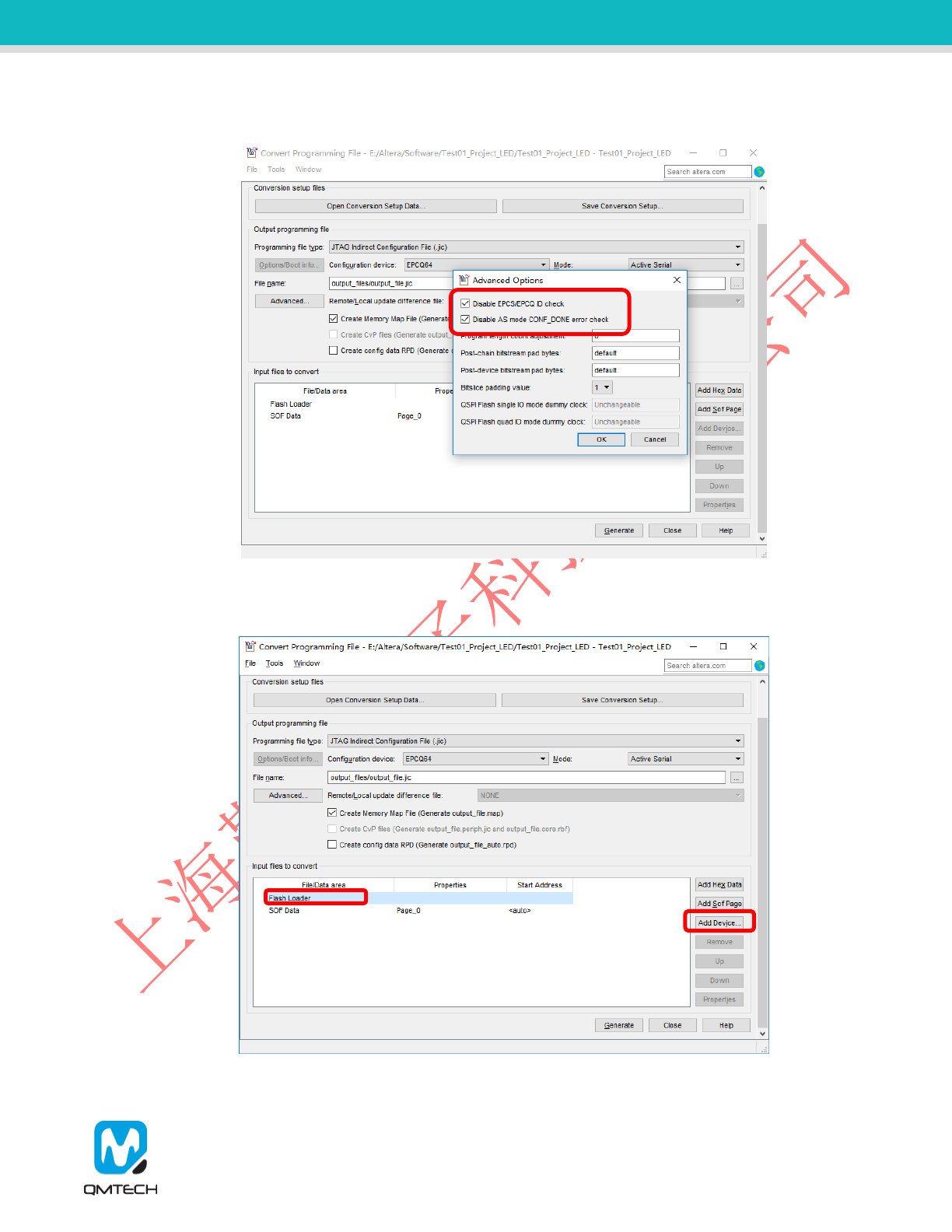
Click the【Advanced…】 option, and set these below two options in the red rectangle in Disable status:
Figure 2-23. Advanced Options
Select【Flash Loader】and then click【Add Device】 button:
Figure 2-24. Flash Loader
QM_CYCLONE10_10CL006 DB User Manual-V01
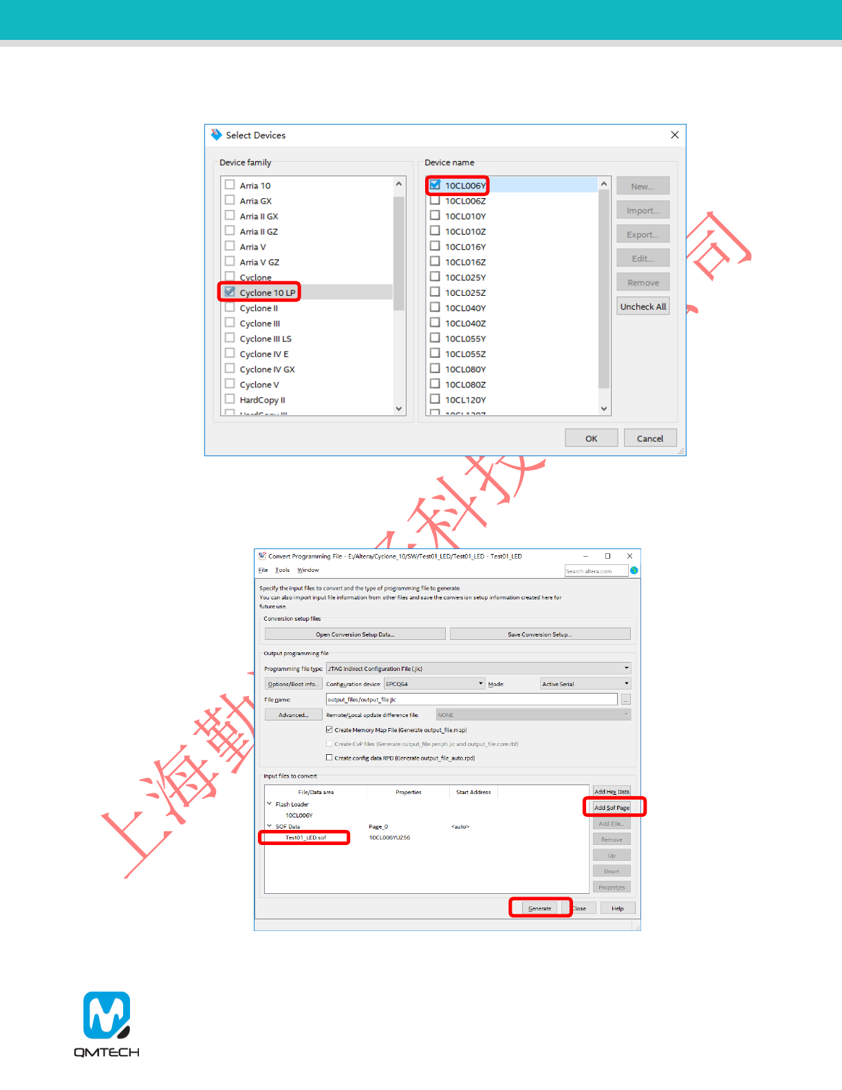
Choose the target Flash Loader device: 10CL006Y:
Figure 2-25. Flash Loader for 10CL006Y
Select【SOF Data】 and then choose【Add File…】 to add the verified *.sof file. And then click
【Generate】to generate the output_file.jic file:
Figure 2-26. Generate *.jic File

QM_CYCLONE10_10CL006 DB User Manual-V01
After the output_file.jic correctly generated, run the【Tools】【Programmer】. And then click【Add
File…】to choose the output_file.jic.
Figure 2-27. Choose *jic File
Toggle【Program/Configure】and then click【Start】button to program the external SPI Flash. Program
status will be shown in the【Progress】bar. After the *.jic correctly programmed, user may repower on
the board to check whether the FPGA could boot from external SPI Flash.
Figure 2-28. Program *.jic
QM_CYCLONE10_10CL006 DB User Manual-V01
3. SignalTap II Logic Analyzer
The SignalTap II Embedded Logic Analyzer is a system-level debugging tool that captures and displays
signals in circuits designed for implementation in Intel’s FPGAs. The user is expected to have access to a
computer that has Quartus II 17.0 software installed. The detailed example in this chapter was obtained
using Quartus II version 17.0, but newer versions of the software can also be used.
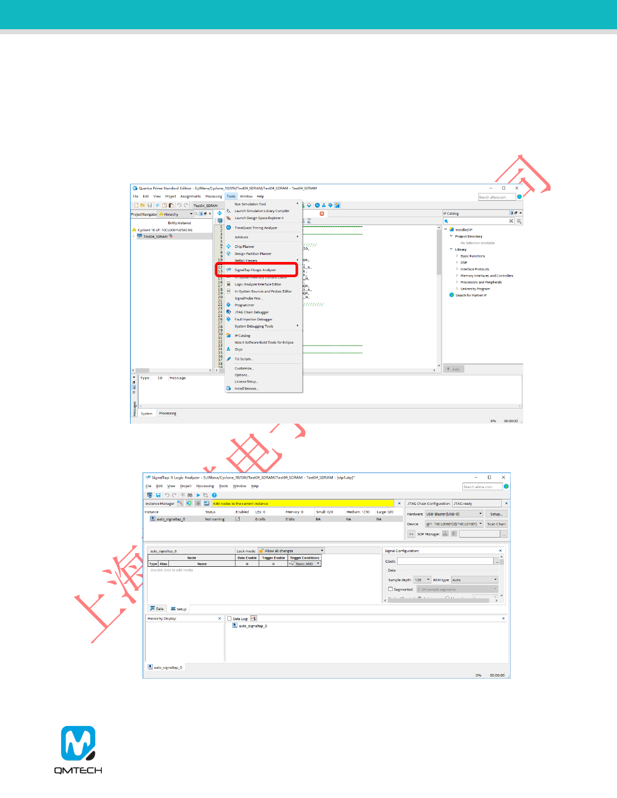
After successfully compiling the Test04_SDRAM project and setting pin assignments, select SignalTap II
Logic Analyzer from the tools dropdown menu (as shown below). Ensure the JTAG programmer (USB
Byte Blaster) is connected between the board and the computer.
Figure 3-1. Open SignalTap II Logic Analyzer
Below image shows the UI of the SignalTap II:
Figure 3-2. SignalTap II Logic Analyzer UI
QM_CYCLONE10_10CL006 DB User Manual-V01
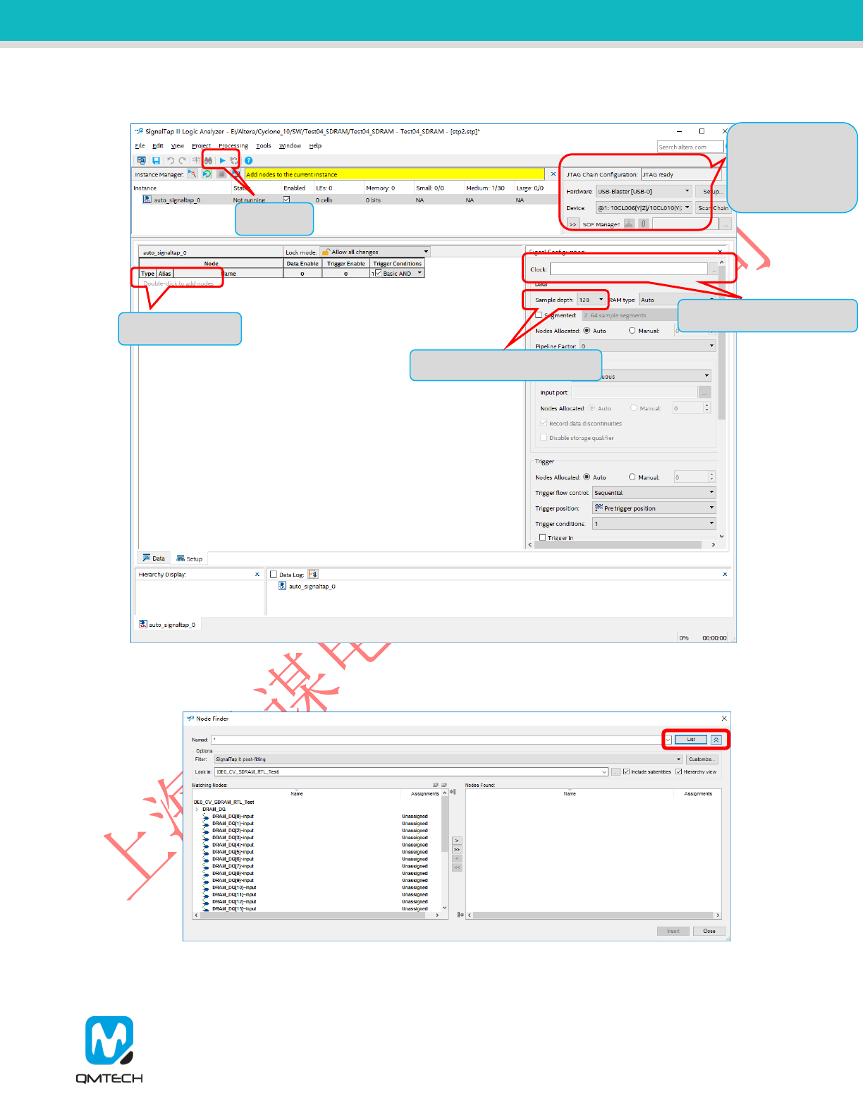
Below image shows the settings of the Test04_SDRAM example project:
Figure 3-3. SignalTap II Logic Analyzer Main Window
Double click the 【Node】column shown in the above image. Below window will pop up and user clicks
the【List】button to add the signals need to be monitored:
Figure 3-4. Set Capturing Signals
JTAG
Configuration,
Device Setup,
Download *.sof
Signal Sampling Clock
Capture Data Buffer Size
Monitor Signals
Compile
QM_CYCLONE10_10CL006 DB User Manual-V01
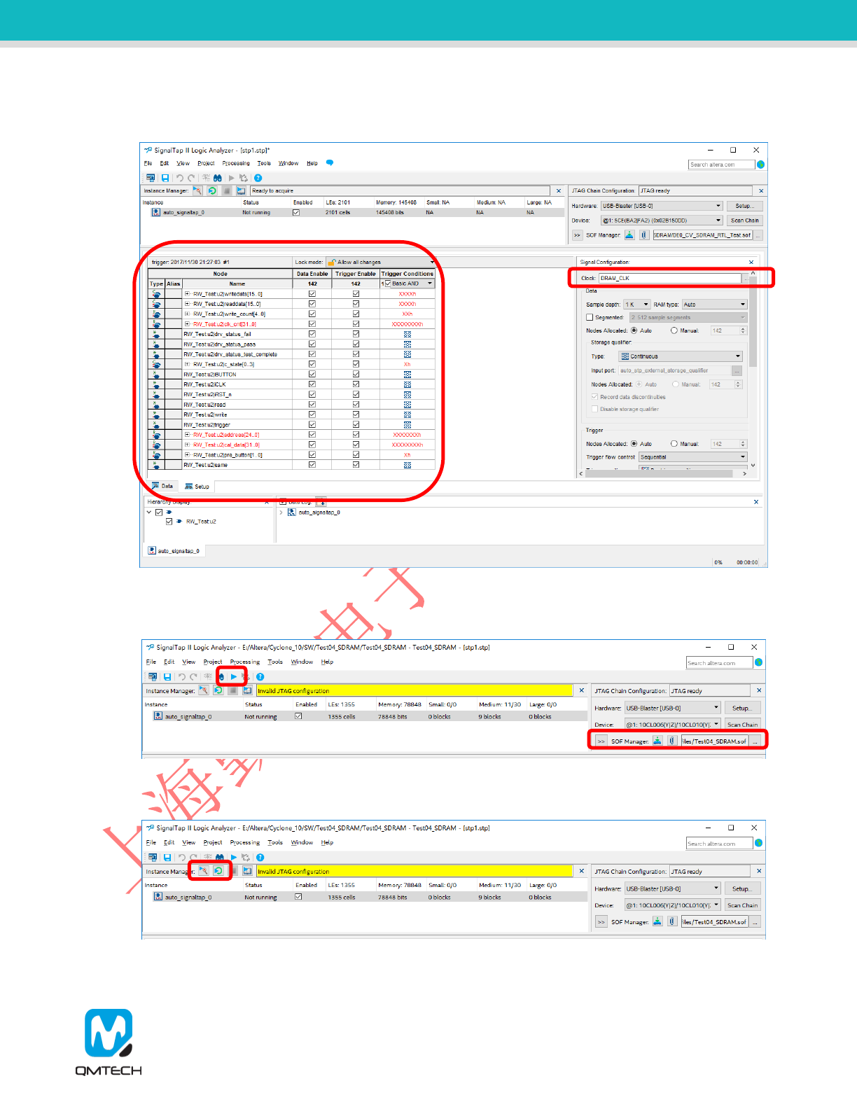
All the signals added in the above step will be displayed in the【setup】page. Please also select the
signal sampling clock【DRAM_CLK】:
Figure 3-5. Sampling Signals and Clocks
User needs to click the 【Compile】 button shown in the below image to recompile the whole project. Then
user may download the newly compiled *.sof into FPGA.
Figure 3-6. Compile the SignalTap II Project
User could click the button【AutoRun Analysis】or button 【Run Analysis】to start the waveform capture:
Figure 3-7. Start Capture

QM_CYCLONE10_10CL006 DB User Manual-V01
Below two images show the SDRAM data write and SDRAM data read:
Figure 3-8. Waveform for Writing Data into SDRAM
Figure 3-9. Waveform for Reading Data from SDRAM

QM_CYCLONE10_10CL006 DB User Manual-V01
4. Reference
[1] 10cl006-sdram-v01.pdf
[2] c10lp-51002.pdf
[3] c10lp-51003.pdf
[4] pcg-01021.pdf
[5] cyclone-10-lp-product-table.pdf
[6] an800.pdf
[7] aib-01029.pdf

QM_CYCLONE10_10CL006 DB User Manual-V01
5. Revision
Doc. Rev.
Date
Comments
0.1
30/12/2018
Initial Version.
1.0
11/01/2019
Formal Release.
