QM_XC6SLX16_SDRAM Core Board User Manual QM XC6SLX16 SDRAM
User Manual:
Open the PDF directly: View PDF ![]() .
.
Page Count: 13
- 1. Introduction
- 2. Getting Started
- 2.1 Install Development Tools
- 2.2 QM_XC6SLX16_SDRAM Hardware Design
- 2.2.1 QM_XC6SLX16_SDRAM Power Supply
- 2.2.2 QM_XC6SLX16_SDRAM SPI Boot
- 2.2.3 QM_XC6SLX16_SDRAM Memory
- 2.2.4 QM_XC6SLX16_SDRAM System Clock
- 2.2.5 QM_XC6SLX16 Extension IO
- 2.2.1 QM_XC6SLX16_SDRAM 3.3V Power Supply
- 2.2.2 QM_XC6SLX16_SDRAM JTAG Port
- 2.2.3 QM_XC6SLX16_SDRAM User LED
- 2.2.4 QM_XC6SLX16_SDRAM User Key
- 3. Reference
- 4. Revision
QM_XC6SLX16_SDRAM Core Board User Manual V01
QM_XC6SLX16_SDRAM CORE BOARD
USER MANUAL
Preface
The QMTech® XC6SLX16 SDRAM core board uses Xilinx’s Spartan®-6 XC6SLX16-2FTG256C device to
demonstrate industry leading connectivity features such as high logic-to-pin ratios, small form-factor
packaging, MicroBlaze™ soft processor, 800Mb/s DDR3 support, and a diverse number of supported I/O
protocols. Built on 45nm technology, the devices are ideally suited for advanced bridging applications found
in automotive infotainment, consumer, and industrial automation.
QM_XC6SLX16_SDRAM Core Board User Manual V01
Table of Contents
1. INTRODUCTION ............................................................................... 3
1.1 DOCUMENT SCOPE ....................................................................... 3
1.2 KIT OVERVIEW ............................................................................. 3
2. GETTING STARTED ........................................................................... 4
2.1 INSTALL DEVELOPMENT TOOLS ........................................................ 5
2.2 QM_XC6SLX16_SDRAM HARDWARE DESIGN ................................ 6
2.2.1 QM_XC6SLX16_SDRAM Power Supply ......................... 6
2.2.2 QM_XC6SLX16_SDRAM SPI Boot ................................. 7
2.2.3 QM_XC6SLX16_SDRAM Memory ................................. 8
2.2.4 QM_XC6SLX16_SDRAM System Clock ......................... 8
2.2.5 QM_XC6SLX16 Extension IO ........................................ 9
2.2.1 QM_XC6SLX16_SDRAM 3.3V Power Supply .............. 10
2.2.2 QM_XC6SLX16_SDRAM JTAG Port ............................. 10
2.2.3 QM_XC6SLX16_SDRAM User LED .............................. 10
2.2.4 QM_XC6SLX16_SDRAM User Key .............................. 11
3. REFERENCE .................................................................................... 12
4. REVISION ....................................................................................... 13
QM_XC6SLX16_SDRAM Core Board User Manual V01
1. Introduction
1.1 Document Scope
This demo user manual introduces the QM_XC6SLX16_SDRAM core board and describes how to setup
the core board running with application software Xilinx ISE 14.7. Users may employee the on board rich
logic resource FPGA XC6SLX16-2FTG256C and large SDRAM memory MT48LC16M16 to implement
various applications. The core board also has 108 non-multiplexed FPGA IOs for extending customized
modules, such as UART module, CMOS/CCD camera module, LCD/HDMI/VGA display module etc.
1.2 Kit Overview
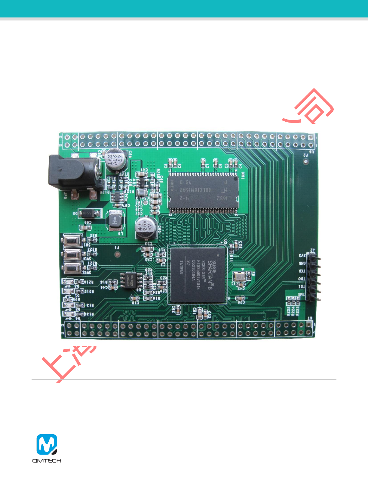
Below section lists the parameters of the QM_XC6SLX16_SDRAM core board:
On-Board FPGA: XC6SLX16-2FTG256C;
On-Board FPGA external crystal frequency: 50MHz;
XC6SLX16-2FTG256C has rich block RAM resource up to 576Kb;
XC6SLX16-2FTG256C has 14,579 logic cells;
On-Board M25P80 SPI Flash,1M bytes for user configuration code;
On-Board 32MB Micron SDRAM,MT48LC16M16A2-75;
On-Board 3.3V power supply for FPGA by using MP2359 wide input range DC/DC;
XC6SLX16 development board has two 64p, 2.54mm pitch headers for extending user IOs. All IOs
are precisely designed with length matching;
XC6SLX16 development board has 3 user switches;
XC6SLX16 development board has 4 user LEDs;
XC6SLX16 development board has JTAG interface, by using 6p, 2.54mm pitch header;
XC6SLX16 development board PCB size is: 6.7cm x 8.4cm;
Default power source for board is: 1A@5V DC, the DC header type: DC-050, 5.5mmx2.1mm;
Figure 1-1. QM_XC6SLX16_SDRAM Core Board Overview
QM_XC6SLX16_SDRAM Core Board User Manual V01
2. Getting Started
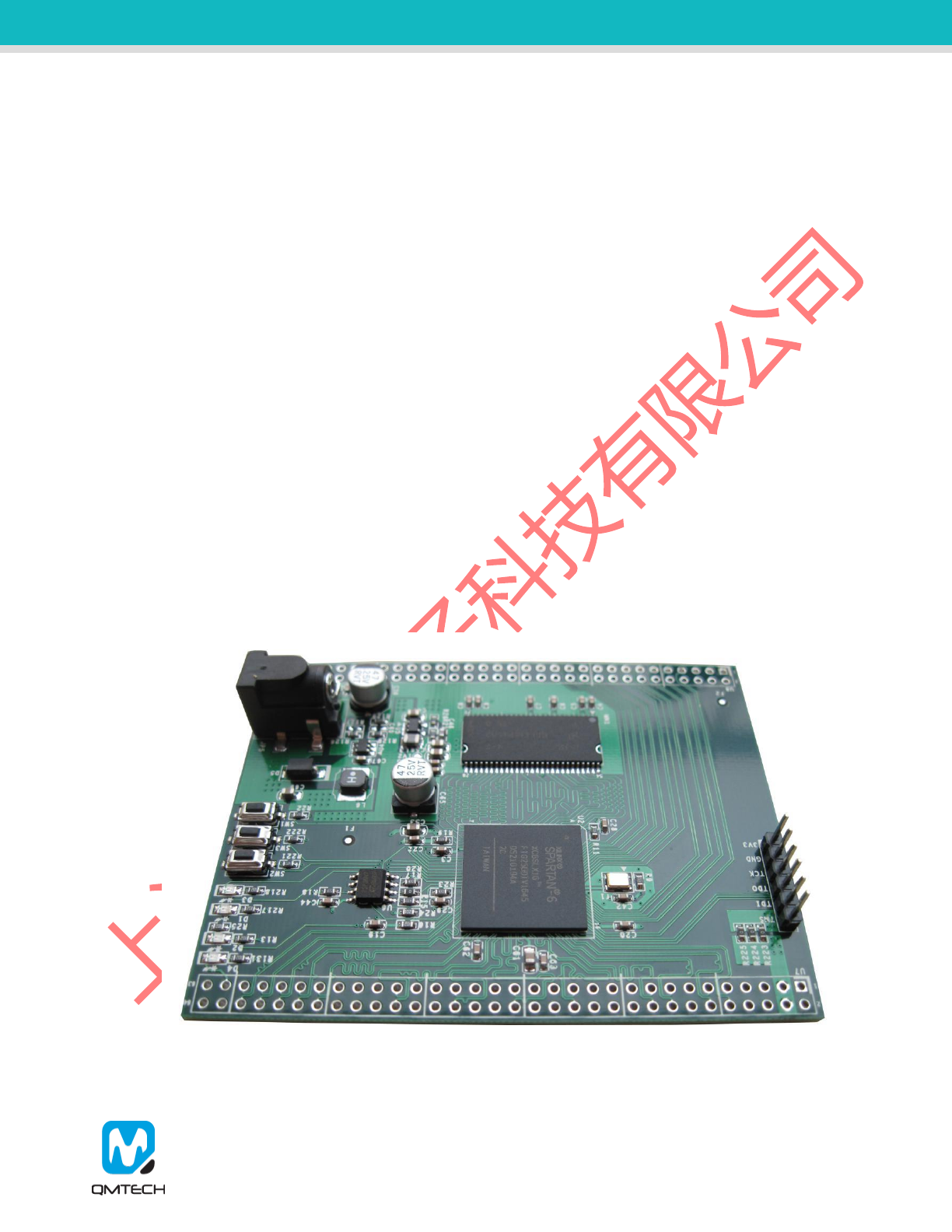
The QM_XC6SLX16_SDRAM core board includes below item:
Figure 2-1. QM_XC6SLX16_SDRAM Top View
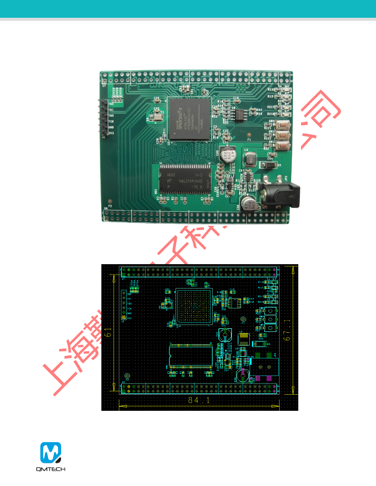
Below image shows the dimension of the QM_XC6SLX16_SDRAM core board: 6.7cm x 8.4cm. The unit
in below is millimeter(mm).
Figure 2-2. QM_XC6SLX16_SDRAM Core Board Dimension
QM_XC6SLX16_SDRAM Core Board User Manual V01
2.1 Install Development Tools
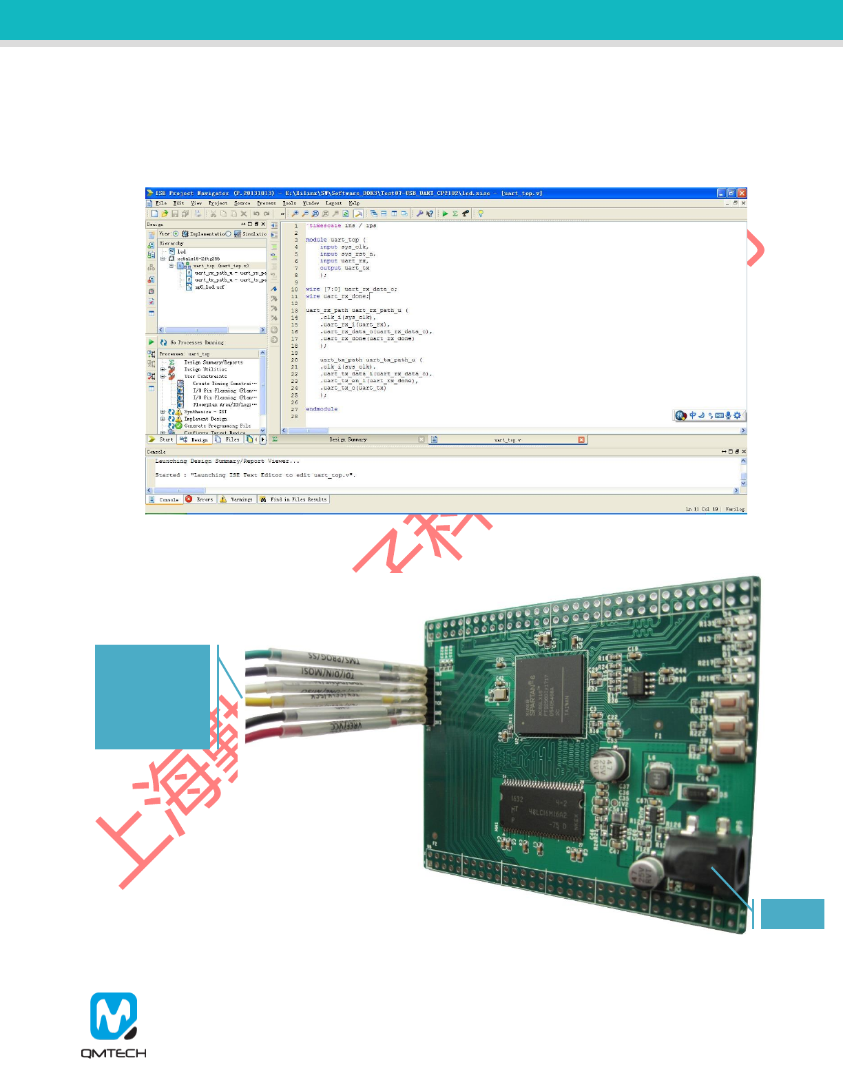
The QM_XC6SLX16_SDRAM core board tool chain consists of Xilinx ISE 14.7, Xilinx USB platform cable,
XC6SLX16 core board and 5V DC power supply. Below image shows the Xilinx ISE14.7 development
environment which could be downloaded from Xilinx office website:
Figure 2-3. ISE 14.7
Below image shows the JTAG connection between Xilinx USB platform cable and XC6SLX16 core board:
Figure 2-4. JTAG Connection and Power Supply
TMS (Green)
TDI (Purple)
TDO (White)
TCK (Yellow)
GND (Black)
VREF (Red)
5V DC
QM_XC6SLX16_SDRAM Core Board User Manual V01
2.2 QM_XC6SLX16_SDRAM Hardware Design
2.2.1 QM_XC6SLX16_SDRAM Power Supply
The core board needs 5V DC input as power supply which could be directly injected from power header or the 64P
female header U7/U8. Users may refer to the hardware schematic for the detailed design. The on board LED D4
indicates the 3.3V supply, it will be turned on when the 5V power supply is active. In default status, all the FPGA banks
IO power level is 3.3V because bank power supply is 3.3V. However, BANK1 IO’s power level could be changed
according to detailed custom requirement. There’re three 0 ohm resisters could be removed:R223/R224/R225, and
instead the BANK1’s power supply could be injected from 64P female header U7. Detailed design refer to hardware
schematic.
Note: FPGA core supply 1.2V is regulated by On-Semi DC/DC chip NCP1529 which could output maximum 1A
current.
Figure 2-5. Power Supply for the FPGA
C22
100NF
C20
100NF
C19
100NF
1V2
C35
10V
4.7uF
C37
100NF
C36
100NF
3V3
1V2
3V3
VCCO_1
C61
10V
4.7uF
C62
100NF
C63
100NF
3V3
3V3
VCCO_1
Spartan-6_XC6SLX16_FTG256
U2F
GND_0 A1
GND_1 A16
GND_2 B11
GND_3 B7
GND_4 D13
GND_5 D4
GND_6 E9
GND_7 G15
GND_8 G2
GND_9 G8
GND_10 H12
GND_11 H7
GND_12 H9
GND_13 J5
GND_14 J8
GND_15 K7
GND_16 K9
GND_17 L15
GND_18 L2
GND_19 M8
GND_20 N13
GND_21 P3
GND_22 R10
GND_23 R6
GND_24 T1
GND_25 T16
VCCAUX_0 E5
VCCAUX_1 F11
VCCAUX_2 F8
VCCAUX_3 G10
VCCAUX_4 H6
VCCAUX_5 J10
VCCAUX_6 L6
VCCAUX_7 L9
VCCINT_0 G7
VCCINT_1 G9
VCCINT_2 H10
VCCINT_3 H8
VCCINT_4 J7
VCCINT_5 J9
VCCINT_6 K10
VCCINT_7 K8
VCCO_0_0 B13
VCCO_0_1 B4
VCCO_0_2 B9
VCCO_0_3 D10
VCCO_0_4 D7
VCCO_1_0 D15
VCCO_1_1 G13
VCCO_1_2 J15
VCCO_1_3 K13
VCCO_1_4 N15
VCCO_1_5 R13
VCCO_2_0 N10
VCCO_2_1 N7
VCCO_2_2 R4
VCCO_2_3 R8
VCCO_3_0 D2
VCCO_3_1 G4
VCCO_3_2 J2
VCCO_3_3 K4
VCCO_3_4 N2
C53
10V
4.7uF
C28
100NF C29
100NF
QM_XC6SLX16_SDRAM Core Board User Manual V01
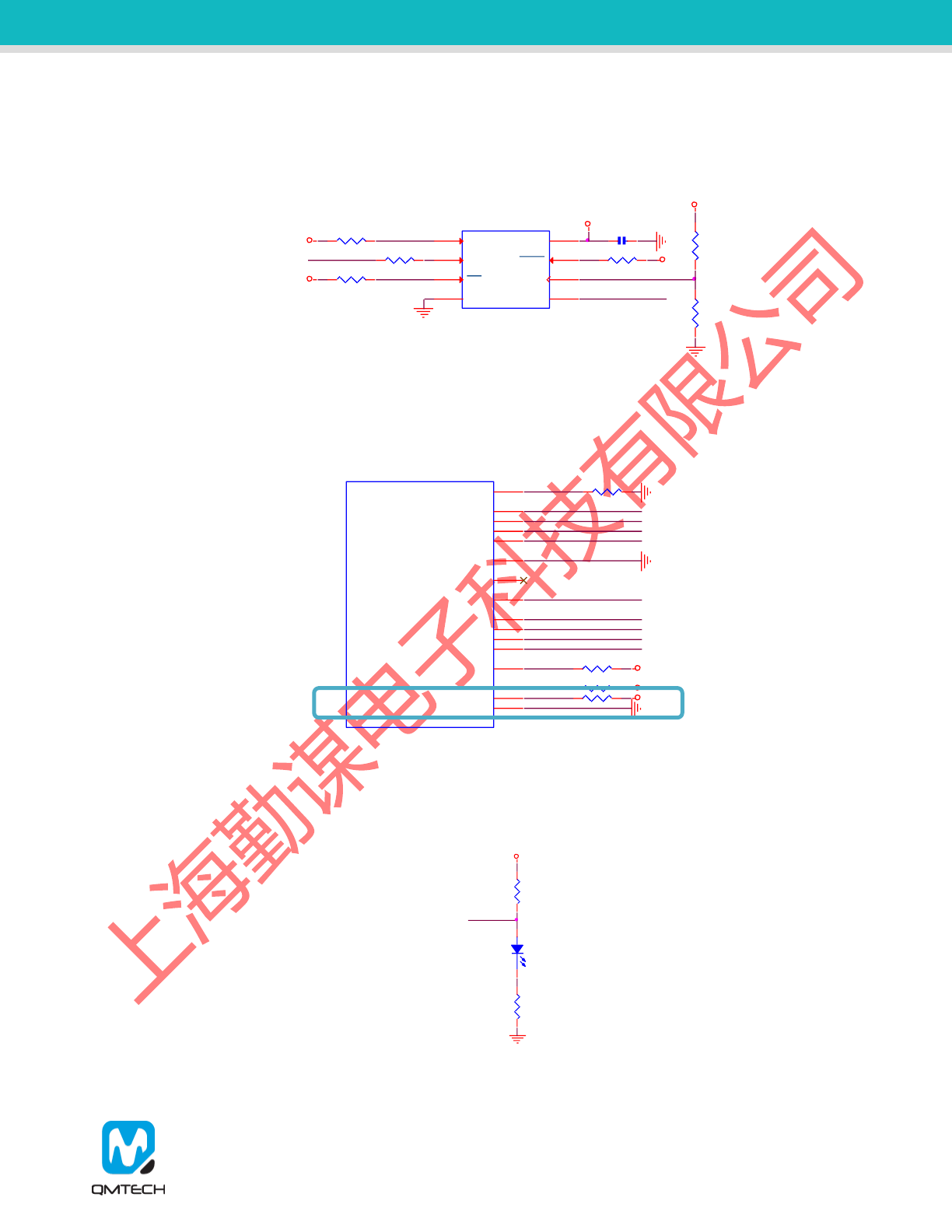
2.2.2 QM_XC6SLX16_SDRAM SPI Boot
In default, QM_XC6SLX16 boots from external SPI Flash, detailed hardware design is shown in below figure.
The SPI flash is using M25P80 manufactured by Micron, with 8Mbit memory storage.
Figure 2-6. SPI Flash
The FPGA boot sequence setting M0:M1 is configured as 1:0 which indicates FPGA will boot from SPI Flash
after power on.
Figure 2-7. M0:M1 Hardware Settings
The LED D2 will be turned on after the FPGA successfully loading configuration file from SPI Flash during
power on stage. In this case, LED D2 could be used as FPGA loading status indicator.
Figure 2-8. FPGA_DONE Status Indicator
U6
M25P80
nCE
1
HOLD 7
SO
2
VSS
4SI 5
SCK 6
WP
3
VDD 8
R154.7K
3V3 FPGA_CSO_B
R17 0R
FPGA_MISO
FPGA_MOSI
FPGA_CCLK
3V3 R204.7K
R16
1K
3V3
R18 4.7K 3V3
R24
1K
3V3
C44 100NF
R11 4.7K
3V3
PROG_BR22 4.7K
FPGA_DONE
3V3
R19 4.7K
FPGA_CSO_B
TCK
TDO
TMS
TDI
FPGA_MISO
FPGA_MOSI
FPGA_CCLK
Spartan-6_XC6SLX16_FTG256
U2E
IO_L1P_HSWAPEN_0 C4
TCK C14
TDI C12
TMS A15
TDO E14
SUSPEND P14
CMPCS_B_2 L11
DONE_2 P13
IO_L1P_CCLK_2 R11
IO_L1N_M0_CMPMISO_2 T11
IO_L3P_D0_DIN_MISO_MISO1_2 P10
IO_L3N_MOSI_CSI_B_MISO0_2 T10
IO_L13P_M1_2 N11
IO_L65P_INIT_B_2 R3
IO_L65N_CSO_B_2 T3
PROGRAM_B_2 T2
3V3
R23 4.7K
R13
1K
D2
Red
1
2
3V3
R25
1K
FPGA_DONE
QM_XC6SLX16_SDRAM Core Board User Manual V01
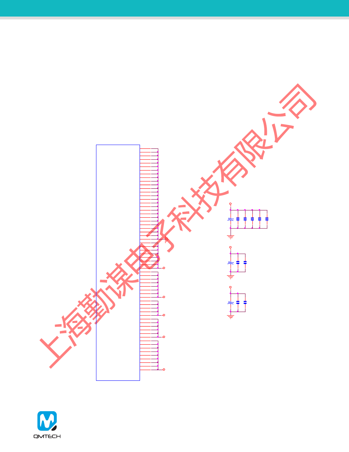
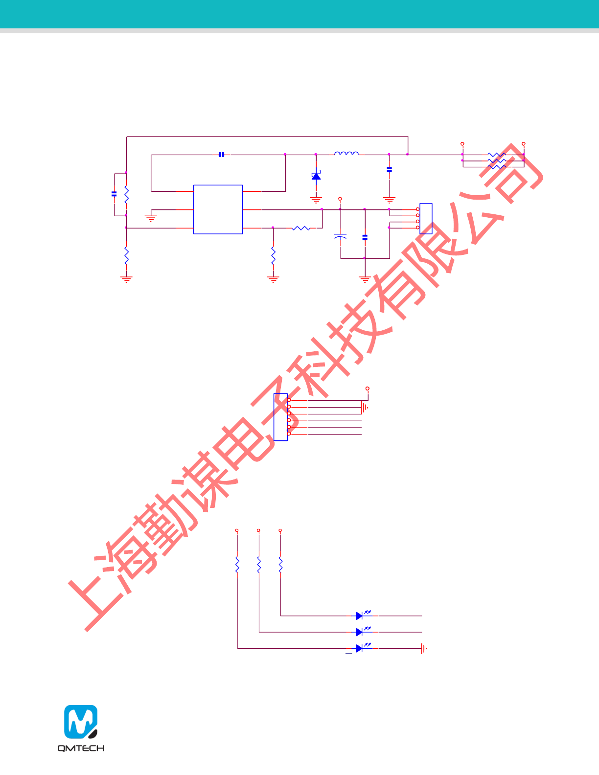
2.2.3 QM_XC6SLX16_SDRAM Memory
QM_XC6SLX16 has on board 16bit width data bus, 32MB memory size SDRAM MT48LC16M16 provided by
Micron. Below image shows the detailed hardware design:
Figure 2-9. SDRAM
2.2.4 QM_XC6SLX16_SDRAM System Clock
FPGA chip XC6SLX16-2FTG256C has system clock frequency 50MHz which is directly provided by external
crystal. The crystal is designed with high accuracy and stability with low temperature drift 10ppm/°c. Below
image shows the detailed hardware design:
Figure 2-10. 50MHz System Clock
C8
100NF
C4
100NF C6
100NF
C7
100NF
C5
100NF C9
100NF
MT48LC16M16A2
MN1
A0
23
A1
24
A2
25
A3
26
A4
29
A5
30
A6
31
A7
32
A8
33
A9
34
A10
22
BA0
20
A12
36
DQ0 2
DQ1 4
DQ2 5
DQ3 7
DQ4 8
DQ5 10
DQ6 11
DQ7 13
DQ8 42
DQ9 44
DQ10 45
DQ11 47
DQ12 48
DQ13 50
DQ14 51
DQ15 53
VDD 1
VSS 28
VSS 41
VDDQ 3
VDD 27
N.C
40
CLK
38
CKE
37
DQML
15
DQMH
39
CAS
17
RAS
18
WE
16
CS
19
VDDQ 9
VDDQ 43
VDDQ 49
VSSQ 6
VSSQ 12
VSSQ 46
VSSQ 52
VDD 14
VSS 54
A11
35
BA1
21
C3
100NF
3V3
256 Mbit s
DQML
A8
A9
A14
CAS
SD_NCS0
A13
A6
A11
A12
DQMH
SDCLK0
A1
A4
SDWE
A3
A7
RAS
SDCKE0
A5
A2
A0
A10
D2
D4
D15
D9
D14
D5
D12
D10
D8
D7
D6
D0
D3
D11
D13
D1
C42
100NF
50 MHz
VDD
VSS OUT
OE
Y1
SG-8002JC-50.0000M-PCB
41
32 SYS_CLK
R9 4.7K
3V3
QM_XC6SLX16_SDRAM Core Board User Manual V01
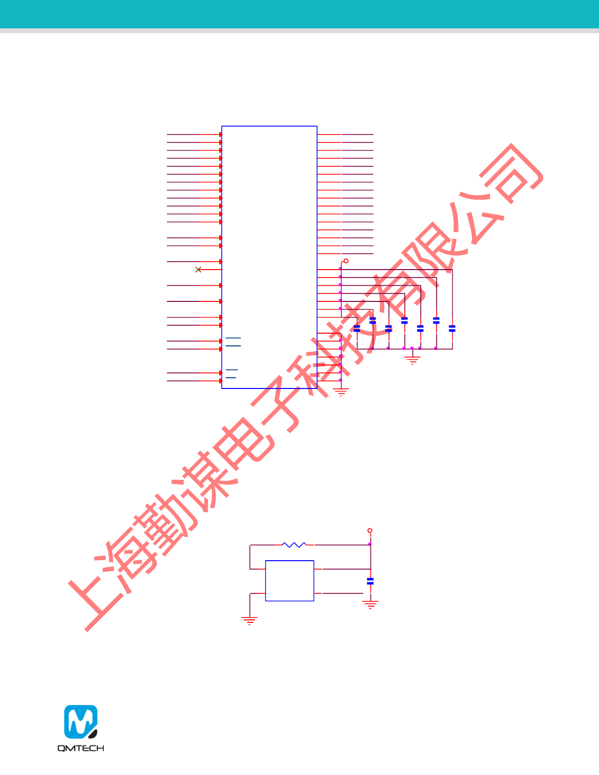
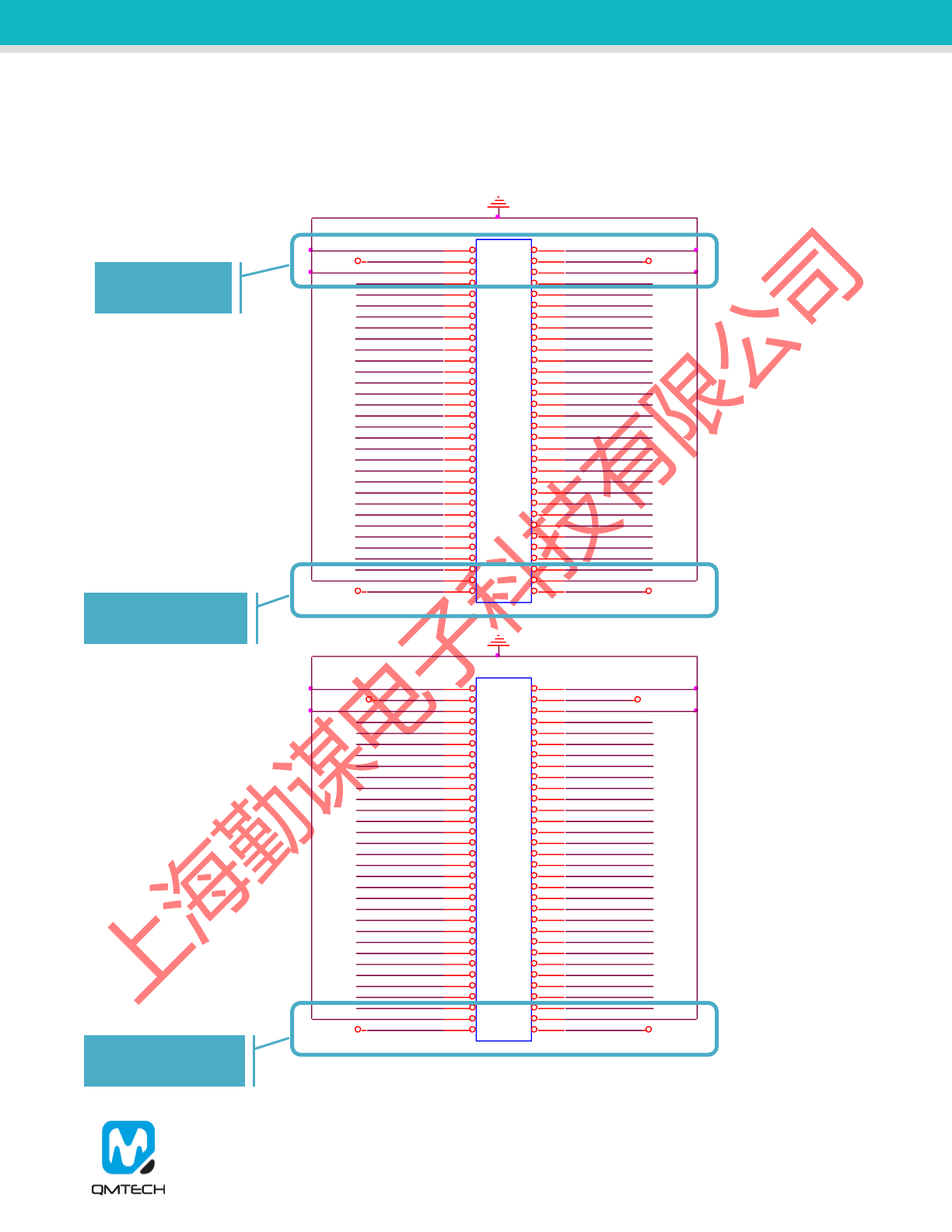
2.2.5 QM_XC6SLX16 Extension IO
The core board has two 64P 2.54mm pitch female headers which are used for extending user modules,
such as ADC/DAC module, audio/video module, ethernet module, etc.
Figure 2-11. Extension IO
VCCO_1 VCCO_1
5V_IN5V_IN
BANK1_B15
BANK1_E12
BANK1_K11
BANK1_L16
BANK1_K15
BANK1_D14
BANK1_C15
BANK1_P15
BANK1_L12
BANK1_M13
BANK1_N14
BANK1_M15
BANK1_F15
BANK1_E15
BANK1_T12
BANK1_T13
BANK1_R14
BANK1_R15
BANK1_G12
BANK1_H15
BANK1_G16
BANK1_F14
BANK1_G11
BANK1_K14
BANK1_J11
BANK1_J14
BANK1_H13
BANK1_F16
BANK1_E16
BANK1_D16
BANK1_C16
BANK1_B16
BANK1_E13
BANK1_H11
BANK1_H16
BANK1_G14
BANK1_F13
BANK1_F12
BANK1_K16
BANK1_J13
BANK1_J12
BANK1_J16
BANK1_H14
BANK1_L13
BANK1_M14
BANK1_N16
BANK1_M16
BANK1_K12
BANK1_L14
BANK1_R12
BANK1_T14
BANK1_T15
BANK1_R16
BANK1_P16
U7
HDR_32X2
1 2
3 4
5 6
7 8
910
11 12
13 14
15 16
17 18
19 20
21 22
23 24
25 26
27 28
29 30
31 32
33 34
35 36
37 38
39 40
41 42
43 44
45 46
47 48
49 50
51 52
53 54
55 56
57 58
59 60
61 62
63 64
U8
HDR_32X2
1 2
3 4
5 6
7 8
910
11 12
13 14
15 16
17 18
19 20
21 22
23 24
25 26
27 28
29 30
31 32
33 34
35 36
37 38
39 40
41 42
43 44
45 46
47 48
49 50
51 52
53 54
55 56
57 58
59 60
61 62
63 64
5V_IN 5V_IN
3V3 3V3
BANK0_IO_B14BANK0_IO_A14
BANK0_IO_C13 BANK0_IO_A13
BANK0_IO_A9
BANK0_IO_A11
BANK0_IO_A12
BANK0_IO_A8
BANK0_IO_A5
BANK0_IO_A6
BANK0_IO_A7
BANK0_IO_F10
BANK0_IO_C10
BANK0_IO_A4
BANK0_IO_D9
BANK2_IO_M6
BANK0_IO_C6
BANK0_IO_E6
BANK0_IO_D8
BANK0_IO_C9
BANK0_IO_B10
BANK0_IO_C11
BANK0_IO_B12
BANK0_IO_B8
BANK0_IO_B5
BANK0_IO_B6
BANK0_IO_C7
BANK0_IO_F9
BANK0_IO_E11
BANK0_IO_E10
BANK0_IO_C8
BANK2_IO_P4
BANK0_IO_D6
BANK0_IO_F7
BANK0_IO_E7
BANK2_IO_L7
BANK2_IO_P6
BANK2_IO_N6
BANK2_IO_N5
BANK2_IO_T4
BANK2_IO_M9
BANK2_IO_T7
BANK2_IO_R5
BANK2_IO_N8
BANK2_IO_M7
BANK2_IO_P5
BANK2_IO_P9
BANK2_IO_M10
BANK2_IO_N9
BANK2_IO_T6
BANK2_IO_T5
BANK2_IO_P12 BANK2_IO_M11
BANK2_IO_P11
BANK1 Voltage
Supply Pins.
Connected to 5V_IN
power header.
Connected to 5V_IN
power header.
QM_XC6SLX16_SDRAM Core Board User Manual V01
2.2.1 QM_XC6SLX16_SDRAM 3.3V Power Supply
The core board’s 3.3V power supply is using high efficiency DC/DC chip MP2359 provided by MPS Inc. The
MP2359 supports wide voltage input range from 4.5V to 24V. In normal use case, 5V DC power supply is
suggested to be applied on the board. Below image shows the MP2359 hardware design:
Figure 2-12. MP2359 Hardware Design
2.2.2 QM_XC6SLX16_SDRAM JTAG Port
The on board JTAG port uses 6P 2.54mm pitch header which could be easily connected to Xilinx USB platform
cable. Below image shows the hardware design of the JTAG port:
Figure 2-13. JTAG Port
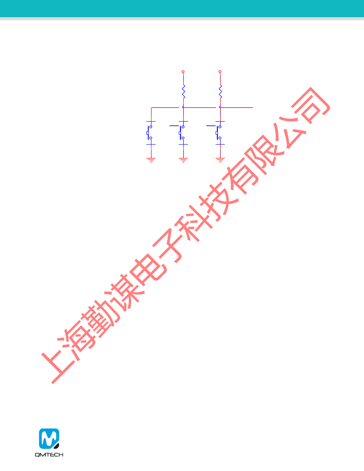
2.2.3 QM_XC6SLX16_SDRAM User LED
Below image shows two user LEDs and 3.3V power supply indicator:
Figure 2-14. LEDs
REGULATED
C67 10nF
5V ONLY
+C58
47uF
R126
100K
R127
DNP
D5
IN5819
12
L6
3.3uH
R128
100K
R129
33K
C60
DNP
C68
100nF
U4
MP2359
BST
1
GND
2
FB
3EN 4
VIN 5
SW 6
JP5
Power_Header_SMT
1
2
3
4
3V3
5V_IN
C69
4.7uF
VCCO_1
R223 0R
R224 0R
R225 0R
J2
JTAG
1
2
3
4
5
6
TCK
TMS
TDI
TDO
3V3
D1
1 2
R217
1K
D4
1 2
R131
1K
D3
1 2
R218
1K
3V33V33V3
BANK2_IO_T9
BANK2_IO_R9
QM_XC6SLX16_SDRAM Core Board User Manual V01
2.2.4 QM_XC6SLX16_SDRAM User Key
Below image shows the PROGRAM_B key and two user keys:
Figure 2-15. Keys
SW1
1
2
PROG_B
SW2
1
2
BANK2_IO_T8
R221
4.7K
BANK2_IO_R7
SW3
1
2
R222
4.7K
3V33V3

QM_XC6SLX16_SDRAM Core Board User Manual V01
3. Reference
[1] ug380-Configuration.pdf
[2] ug385-Package.pdf
[3] ug394-Power Managment.pdf
[4] M25P80.pdf
[5] LPC-Link-II_Rev_C.pdf
[6] QM_XC6SLX16.pdf
QM_XC6SLX16_SDRAM Core Board User Manual V01
4. Revision
Doc. Rev.
Date
Comments
0.1
05/10/2017
Initial Version.
1.0
05/14/2017
V1.0 Formal Release.
