幻灯片 1 Quectel LTE Module Thermal Design Guide V1.0
Quectel_LTE_Module_Thermal_Design_Guide_V1.0
Quectel_LTE_Module_Thermal_Design_Guide_V1.0
Quectel_LTE_Module_Thermal_Design_Guide_V1.0
Quectel_LTE_Module_Thermal_Design_Guide_V1.0
Quectel_LTE_Module_Thermal_Design_Guide_V1.0
User Manual:
Open the PDF directly: View PDF ![]() .
.
Page Count: 31

© Quectel Wireless Solutions Co., Ltd. All rights reserved
Thermal Design Guide
Quectel LTE Module
September, 2018

@ Quectel Wireless Solutions | September, 2018 | Page 2 Rev.: V1.0 | Status: Released
General Overview
Design Guidelines
Test Example

@ Quectel Wireless Solutions | September, 2018 | Page 3 Rev.: V1.0 | Status: Released
General Overview
This document mainly introduces the thermal considerations for the design of application devices
incorporating the following Quectel LTE modules:
•LTE Module Series
ECxx: includes EC25/EC21/EC20 R2.0/EC20 R2.1 modules NOTE
EG9x: includes EG91/EG95 modules
EM05 module
•LTE-A Module Series
Ex06: includes EP06/EG06/EM06 modules
•Automotive Module Series
AG35 module
NOTE: EC2x includes LCC modules, Mini PCIe modules and Mini PCIe-C modules.

@ Quectel Wireless Solutions | September, 2018 | Page 4 Rev.: V1.0 | Status: Released
Why Need Thermal Design?
•The module’s internal electronic circuits will generate more and more heat, due to the increasing demand of high-speed
communication and embedded applications.
•Complex workspaces, which is more and more common to see, require modules to have high heat dissipation performance.
•Heat accumulation of modules gives rise to the risk of damage on devices.
May cause burning sensations on skin/result in high surface temperature.
Some ICs may not work properly.
•Users may undergo limited device performance due to thermal mitigation algorithms.
•The module will disconnect from network automatically if the device temperature is higher than the absolute maximum
temperature.
•The module offers high performance when the internal baseband (BB) chip stays below 105℃. If the peak temperature of the
BB chip reaches or exceeds 105℃, the module will not be able to provide high-performance as usual (may offer decreased RF
output power, limited data rate, etc.). Therefore, the modules are recommended to optimize thermal design so as to keep the
peak temperature of BB chip lower than 105℃. AT+QTEMP command can be executed to get the peak temperature of BB
chip. The first return value of AT+QTEMP indicates the peak temperature of BB chip.
Proper thermal design significantly extends the high performance operating time without taking the risk of device failure
which affects user experience adversely.

@ Quectel Wireless Solutions | September, 2018 | Page 5 Rev.: V1.0 | Status: Released
General Overview
Design Guidelines
Test Example
@ Quectel Wireless Solutions | September, 2018 | Page 6 Rev.: V1.0 | Status: Released
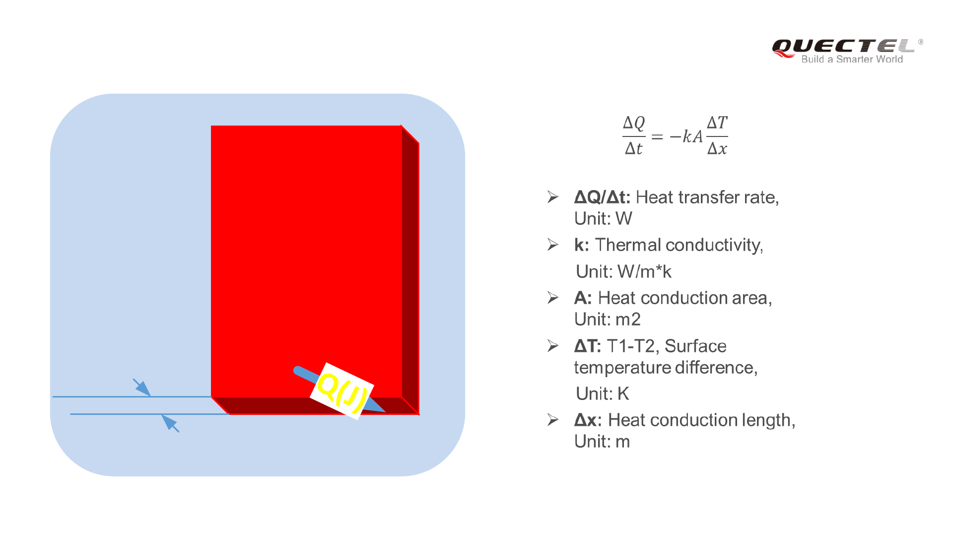
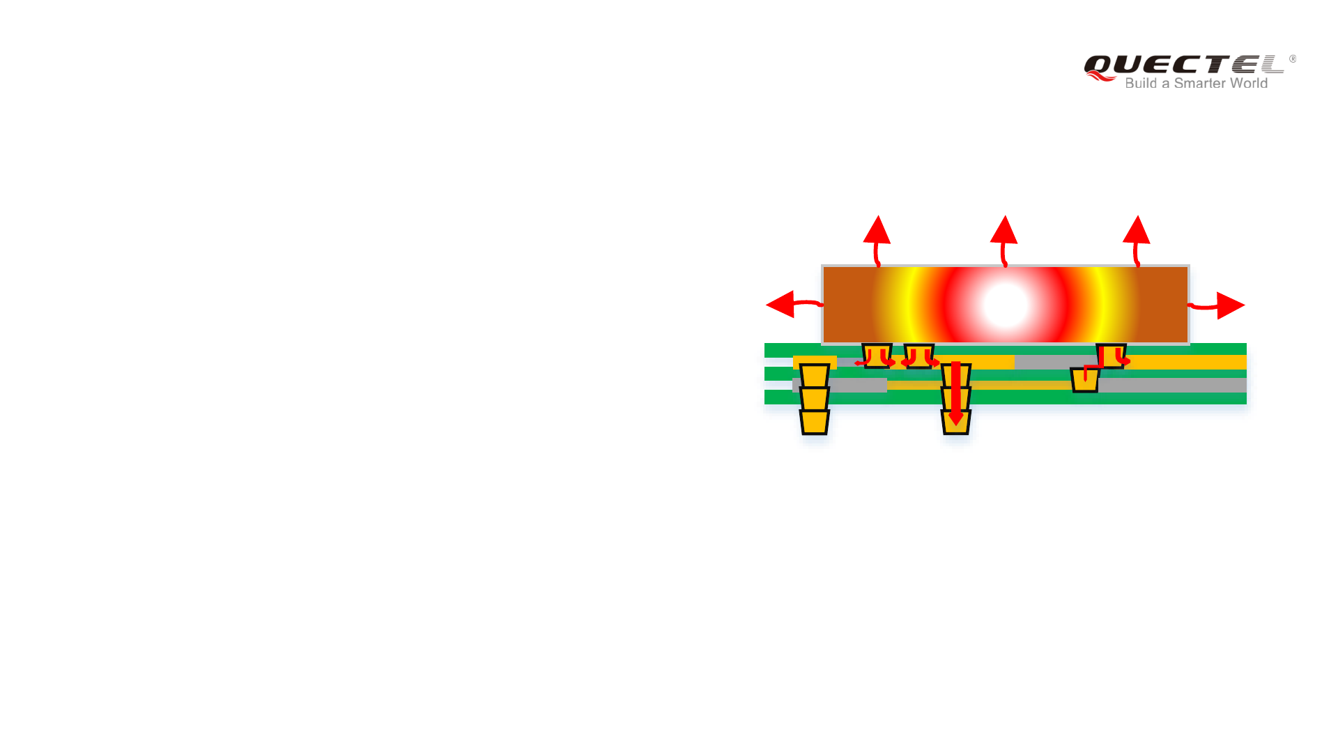
Thermal Concept 1
A(m2)
Δx(m) T1(K)
T2(K)
k(W/m*k)

@ Quectel Wireless Solutions | September, 2018 | Page 7 Rev.: V1.0 | Status: Released
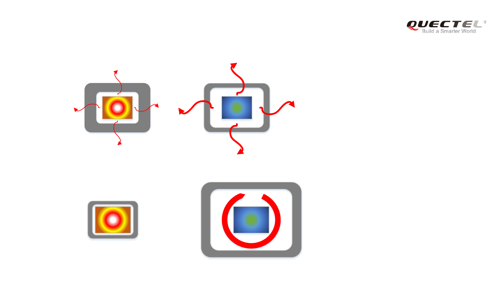
Thermal Concept 2
•Materials with higher thermal conductivity (k) transfer heat better.
Graphite (in-plane): k > 370 W/m*K
Aluminum: k = 205 W/m*K
Magnesium: k = 156 W/m*K
Plastic: k = 0.2 W/m*K
Air: k = 0.024 W/m*K
•Housing/enclosures with larger surface area (A) dissipate heat better.
Heat sink dissipates the heat by increasing the surface area in contact with the cooling fluid around
the module, such as air.
The PCB ground plane’s thickness and width (cross-sectional surface area), number of layers, and
vias are critical parameters for IC to reduce its peak temperature by spreading heat energy.
•The smaller distance between the cooling system and heat source is preferred.
@ Quectel Wireless Solutions | September, 2018 | Page 8 Rev.: V1.0 | Status: Released
Structure Design 1
•Select walls with thinner thickness because of smaller thermal resistance.
•Try to expand the internal space as much as possible for better convection.
GoodWorse
Worse Good

@ Quectel Wireless Solutions | September, 2018 | Page 9 Rev.: V1.0 | Status: Released
Structure Design 2
•Reserve enough space to add a heat sink on the top of the module as well as the opposite side of the
PCB area where the module is mounted.
•If the internal space is small, it is recommended to add a thermal pad with high thermal conductivity
between the module and the housing/enclosure.
•Do not install any battery or other components that may generate heat both at the top and bottom of the
module.

@ Quectel Wireless Solutions | September, 2018 | Page 10 Rev.: V1.0 | Status: Released
Heat Sink Design
•If the housing/enclosure is made up of aluminum alloy, it is recommended to integrate the heat sink with
the housing/enclosure.
•If the housing/enclosure is made up of plastic, it is recommended to design an independent heat sink
whose heat dissipation surface should be outside the housing/enclosure.
•Increase the number of heat sink fins as many as possible.
@ Quectel Wireless Solutions | September, 2018 | Page 11 Rev.: V1.0 | Status: Released
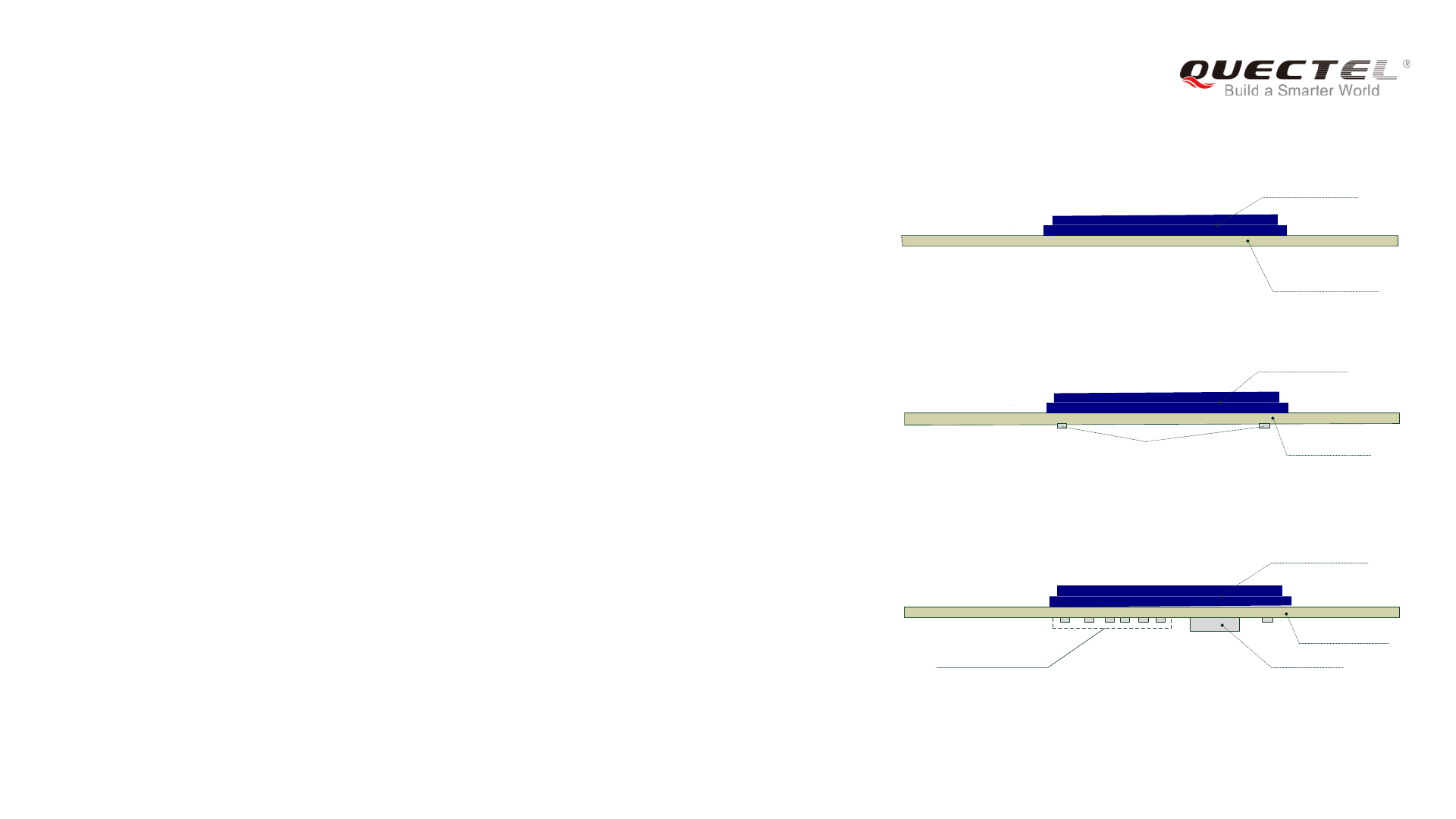
Thermal Pad Design 1
•Selection:
Select thermal pads with high thermal conductivity (k > 3 W/m*k).
•Heat conduction area:
It is recommended to select thermal pads with almost the same size with the module’s shielding cover.
Take AG35 module with size of 32.5mm×37mm as an example, its preferred thermal pad size is about
32.5mm×37.0mm.
Module’s shielding cover
Thermal Pad
32.5mm x 37.0mm
@ Quectel Wireless Solutions | September, 2018 | Page 12 Rev.: V1.0 | Status: Released
Thermal Pad Design 2
•Thermal pad thickness:
The thermal pad thickness is recommended to be 0.5mm greater than the distance between the module’s top/bottom
side and the heat sink (or housing/enclosure). The maximum thickness is recommended to be 3mm.
•Thermal pad position:
Cooling system on top side of the module: the thermal pad is used between the module’s shielding cover and the heat
sink (or housing/enclosure).
Cooling system on bottom side of the module: the thermal pad is used between the PCB area on opposite side of
which the module is mounted and the heat sink, or directly between the module’s bottom side and the PCB.
•Example:
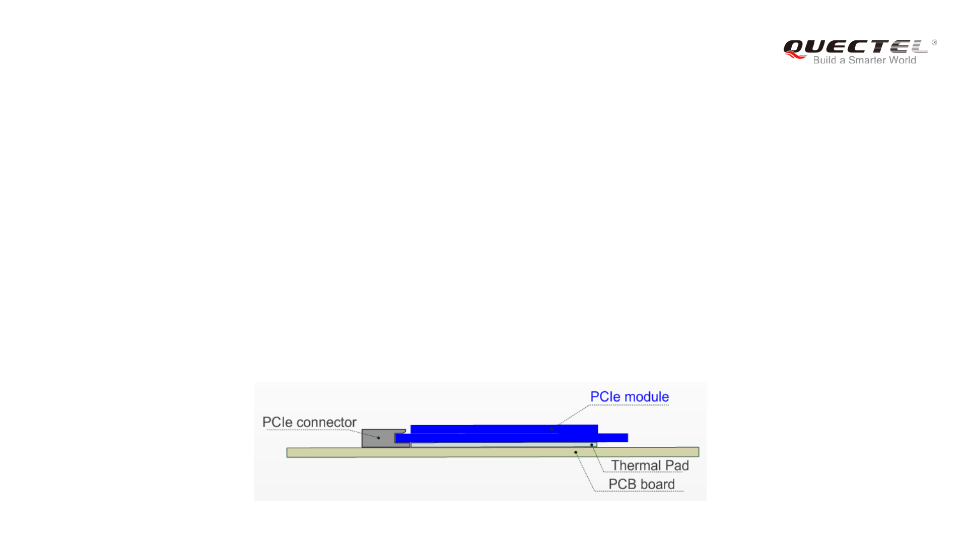
Taking Mini PCIe module as an example, the thermal pad is placed between the module’s bottom side and the PCB. In
such case, please do not apply solder mask on the connection area so as to ensure better heat dissipation
performance. The solder mask size should be almost the same as the bottom size of the module.
@ Quectel Wireless Solutions | September, 2018 | Page 13 Rev.: V1.0 | Status: Released
PCB Design 1
•Larger PCB size is beneficial for components placement and has the better performance for heat
dissipation
•Keep the module away from the ARM, audio amplifier, and other components that may generate heat.
•Keep the module away from the heat sensitive elements such as the TCXO/XO.
Module
TCXO/XO
Heat sensitive
element
Module
Audio
Amplifier
ModuleARM
Module
Other Hot
Components
@ Quectel Wireless Solutions | September, 2018 | Page 14 Rev.: V1.0 | Status: Released
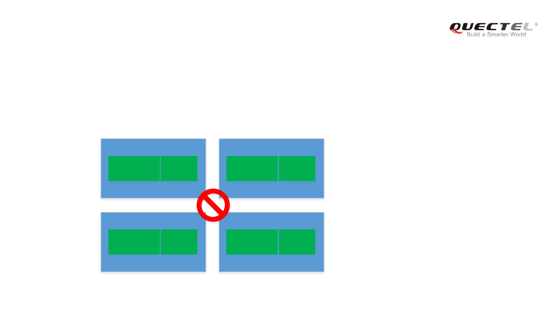
PCB Design 2
•Best design:
To facilitate adding of the heat sink when necessary, please do not
place components on the opposite side of the PCB area where the
module is mounted, and do not place components on both the PCB top
and bottom areas where the PCIe module is installed.
•Good design:
Place only some passive components with small packages, such as
resistors, capacitors, and inductors, on the opposite side of the PCB
area where the module is mounted, and leave a large blank area for
adding the cooling system.
•Bad design:
Placed many components with large packages and even heat sources
on the opposite side of the PCB area where the module is mounted.
PCB board
Many capacitors
and resistors
LTE module
Heat IC
Bad
PCB board
Few capacitors or resistors
LTE module
Good
PCB board
LTE module
Best
@ Quectel Wireless Solutions | September, 2018 | Page 15 Rev.: V1.0 | Status: Released
PCB Design 3
•Add layers as many as possible and increase the copper area at each layer.
•Increase the size of the GND plane as much as possible.
•Do not design GND pads of the module into thermal relief pads.
•Fill empty layers with copper wherever possible.
•Increase the power supply plane using thick/wide traces as many as possible.
•Try to keep the copper plane as a whole.
Worse Good
Copper Dielectric
@ Quectel Wireless Solutions | September, 2018 | Page 16 Rev.: V1.0 | Status: Released
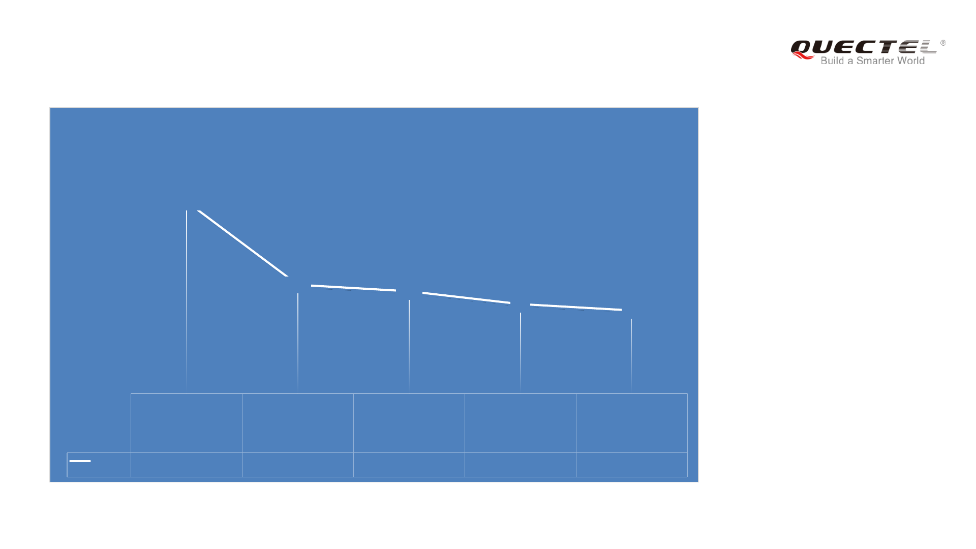
PCB Design 4
•Flotherm V12.0
•PCB Size:
90mm×150mm×1.6mm
2 layers PCB, L1
filled with GND
4 layers PCB,
L1/L3 filled with
GND, and 10 GND
vias used.
4 layers PCB,
L1/L3 filled with
GND, and 20 GND
vias used.
6 layers PCB,
L1/L3/5 filled with
GND, and 5 GND
vias used.
6 layers PCB,
L1/L3/5 filled with
GND, and 10 GND
vias used.
BB(℃)115 102 101 99 98
115
102 101 99 98
Temperature (℃)
Simulation: The Effect of PCB Layers and GND Vias
to Heat Dissipation
@ Quectel Wireless Solutions | September, 2018 | Page 17 Rev.: V1.0 | Status: Released
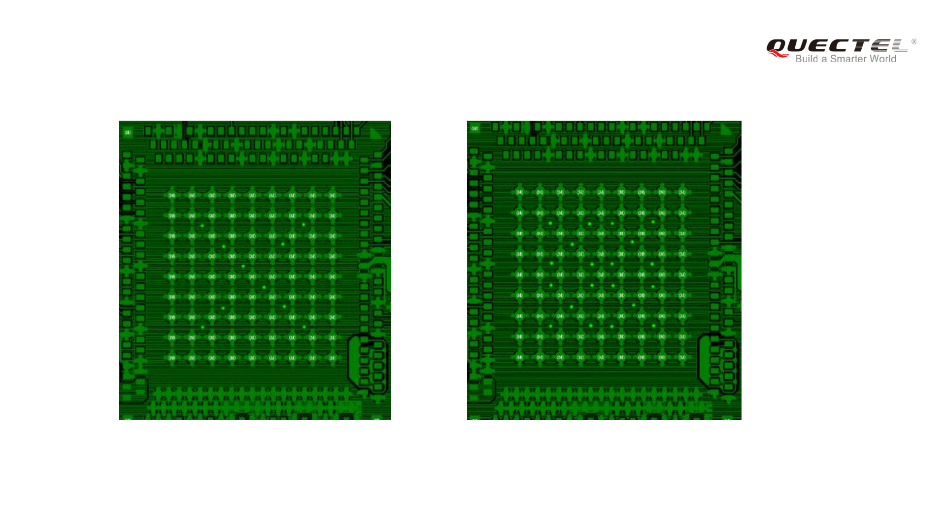
10 Through Holes 20 Through Holes
PCB Design 4 –Through Holes
@ Quectel Wireless Solutions | September, 2018 | Page 18 Rev.: V1.0 | Status: Released
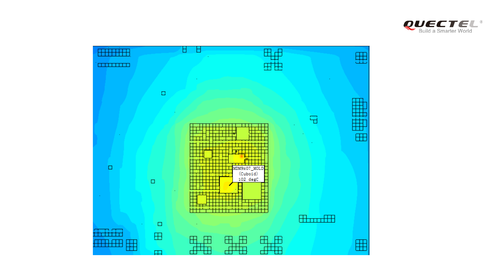
PCB Design 4 –Thermal Image
@ Quectel Wireless Solutions | September, 2018 | Page 19 Rev.: V1.0 | Status: Released
PCB Design 5
PCB Size: 90mm*150mm*1.6mm PCB Size: 90mm*75mm*1.6mm
BB Chip Temperature (℃)103 110
103
110
98
100
102
104
106
108
110
112
Temperature (℃)
Simulation: The Effect of PCB Size to Heat
Dissipation
•Flotherm V12.0
•PCB:
90mm×150mm×1.6mm, 6 layers
90mm×75mm×1.6mm, 6 layers
@ Quectel Wireless Solutions | September, 2018 | Page 20 Rev.: V1.0 | Status: Released
•Vias design:
a) Add adequate vias under and near the module.
b) Connect the vias to a large GND plane for better heat
dissipation.
c) Large vias are better than small vias.
d) Through holes are better than buried vias and blind vias.
e) Stacked vias are better than staggered vias.
•About solder mask:
Do not apply solder mask on the PCB area where the module is
mounted or installed to provide better heat dissipation
performance.
Module
Stacked vias
Staggered vias
PCB Design 6
@ Quectel Wireless Solutions | September, 2018 | Page 21 Rev.: V1.0 | Status: Released
Heat Dissipation Diagram
•Aluminum alloy shell and
recommended cooling system design
of LCC/LGA module
Heatsink
Aluminium alloy shell
Shielding Cover
Heat Source
Customer PCB Board Module
Thermal Pad
Shielding Cover
Heat Source
Customer PCB Board
Heatsink
Aluminium alloy shell
Module
Thermal Pad
Thermal Pad
Better
Good
@ Quectel Wireless Solutions | September, 2018 | Page 22 Rev.: V1.0 | Status: Released
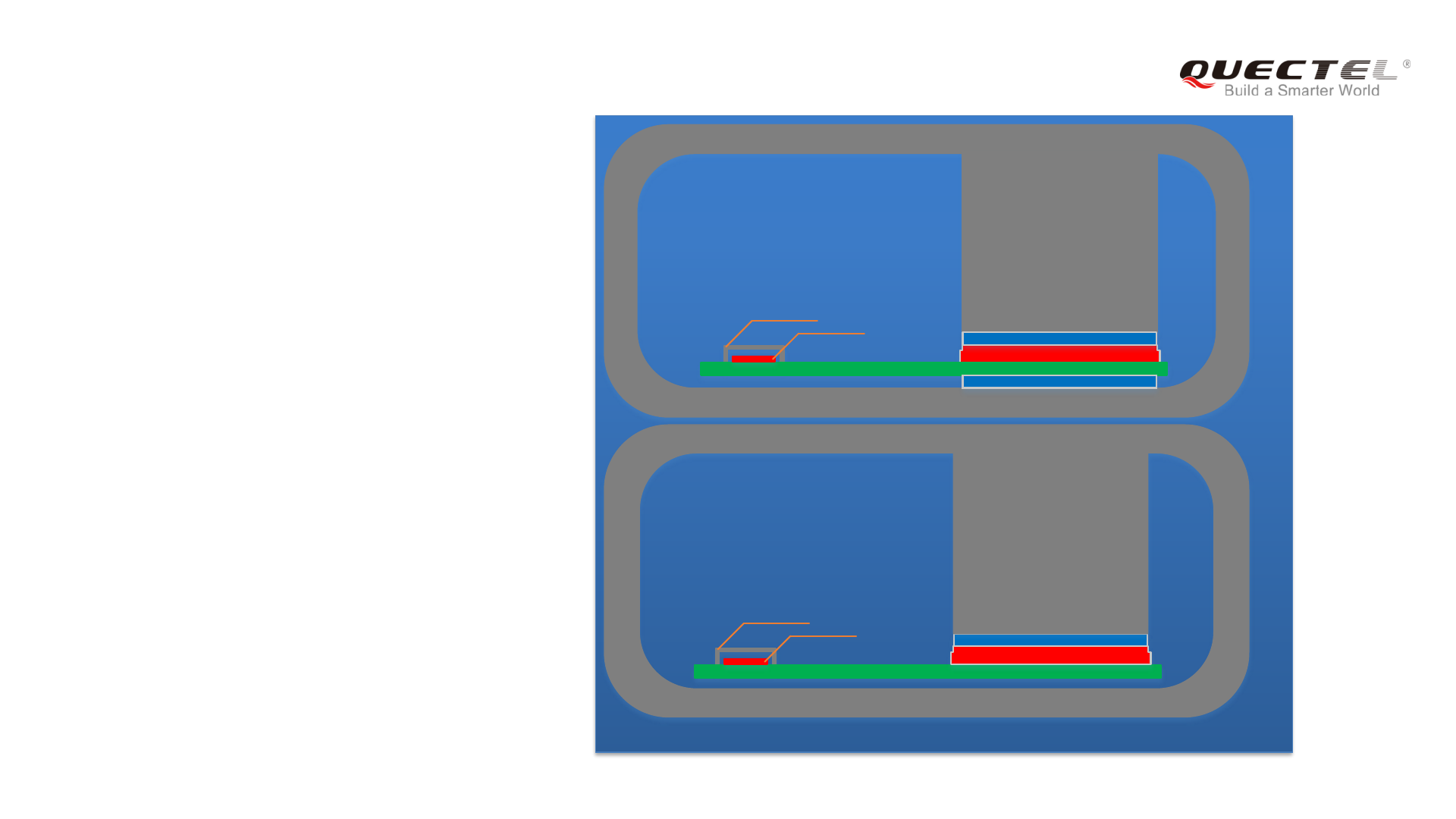
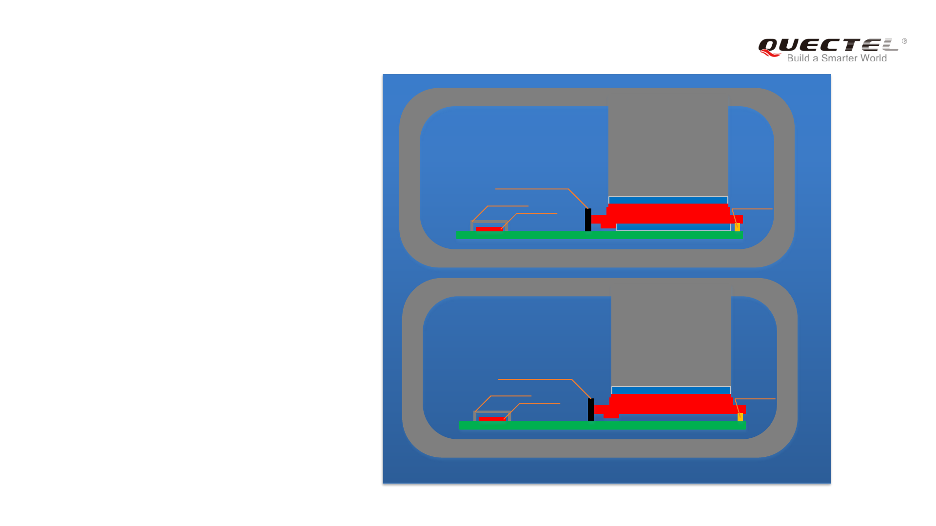
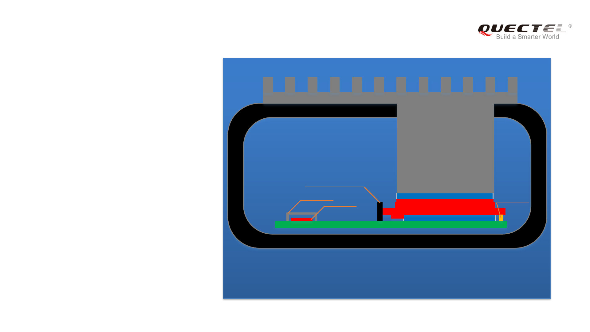
•Aluminum alloy shell and
recommended cooling system design
of Mini PCIe module
Shielding Cover
Heat Source
Customer PCB Board
Heatsink
Aluminium alloy shell
Thermal Pad
MINI PCIE Connector
Upholder
Thermal Pad
MINI PCIE Module
Shielding Cover
Heat Source
Customer PCB Board
Heatsink
Aluminium alloy shell
Thermal Pad
MINI PCIE Connector
Upholder
MINI PCIE Module
Better
Good
Heat Dissipation Diagram
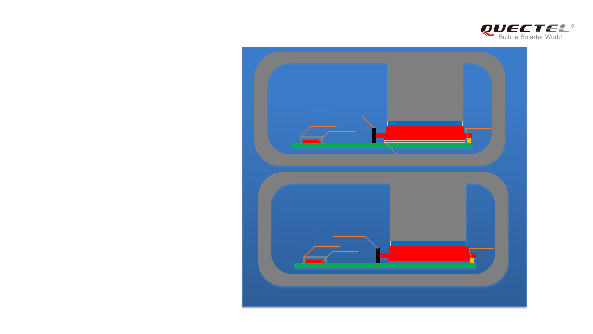
@ Quectel Wireless Solutions | September, 2018 | Page 23 Rev.: V1.0 | Status: Released
Heat Dissipation Diagram
•Aluminum alloy shell and
recommended cooling system design
of Mini PCIe-C or M.2 module Better
Good
Shielding Cover
Heat Source
Customer PCB Board
Heatsink
Aluminium alloy shell
Thermal Pad
MINI PCIE-C Module
Thermal Pad
MINI PCIE Connector
Upholder
Shielding Cover
Heat Source
Customer PCB Board
Heatsink
Aluminium alloy shell
Thermal Pad
MINI PCIE-C Module
MINI PCIE Connector
Upholder
Mini PCIe-C/M.2 Module
Mini PCIe-C/M.2 Module
@ Quectel Wireless Solutions | September, 2018 | Page 24 Rev.: V1.0 | Status: Released
Heat Dissipation Diagram
•Plastic shell and recommended
cooling system design of
LCC/LGA module
Shielding Cover
Heat Source
Customer PCB Board
Plastic shell
Module
Thermal Pad
Heatsink
@ Quectel Wireless Solutions | September, 2018 | Page 25 Rev.: V1.0 | Status: Released
•Plastic shell and recommended
cooling system design of
Mini PCIe module
Shielding Cover
Heat Source
Customer PCB Board
Plastic shell
Heatsink
Thermal Pad
MINI PCIE Module
Thermal Pad
Upholder
MINI PCIE Connector
Heat Dissipation Diagram
@ Quectel Wireless Solutions | September, 2018 | Page 26 Rev.: V1.0 | Status: Released
•Plastic shell and recommended
cooling system design of
Mini PCIe-C or M.2 module
Shielding Cover
Heat Source
Customer PCB Board
Plastic shell
Heatsink
Thermal Pad
MINI PCIE-C Module
Thermal Pad
Upholder
MINI PCIE Connector
Heat Dissipation Diagram
Mini PCIe-C/M.2 Module

@ Quectel Wireless Solutions | September, 2018 | Page 27 Rev.: V1.0 | Status: Released
General Overview
Design Guidelines
Test Example
@ Quectel Wireless Solutions | September, 2018 | Page 28 Rev.: V1.0 | Status: Released
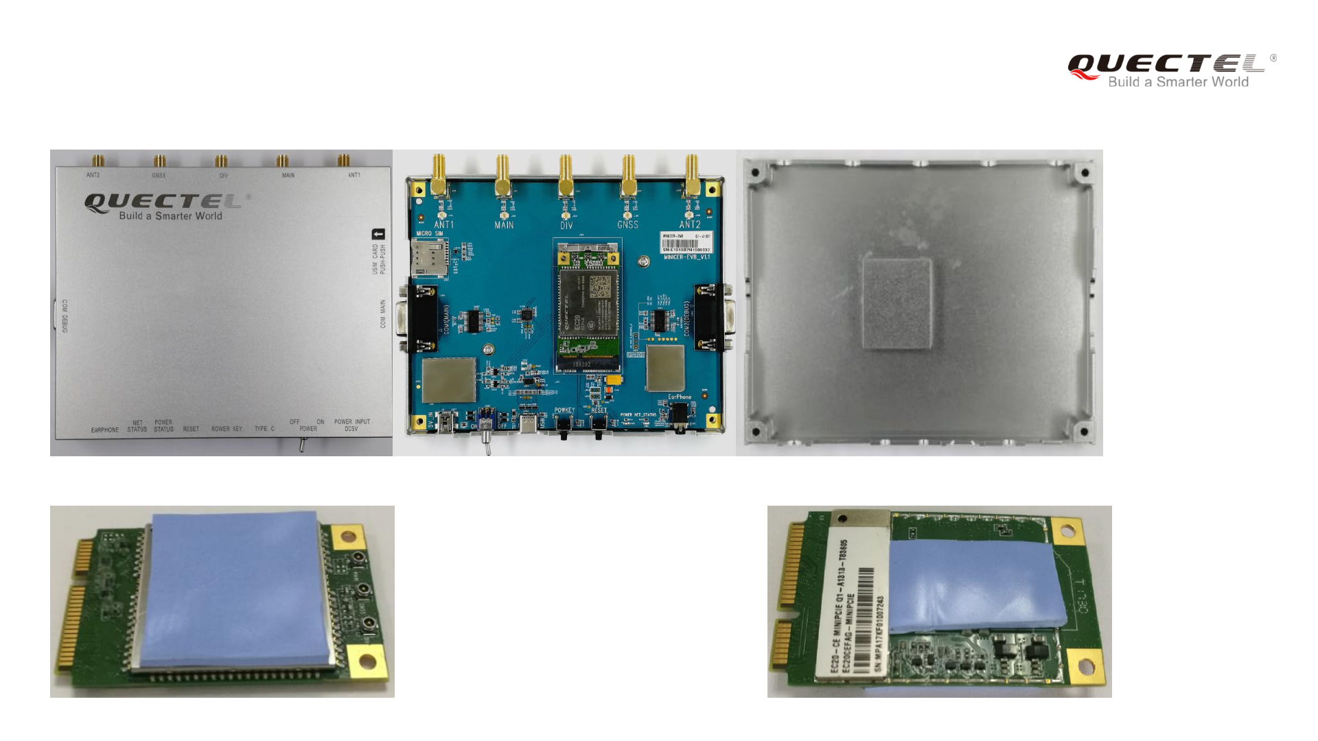
Test Environment
Aluminum Alloy Shell Heat SinkMini PCIe Module
Thermal Pad on the Top Side Thermal Pad on the Bottom Side

@ Quectel Wireless Solutions | September, 2018 | Page 29 Rev.: V1.0 | Status: Released
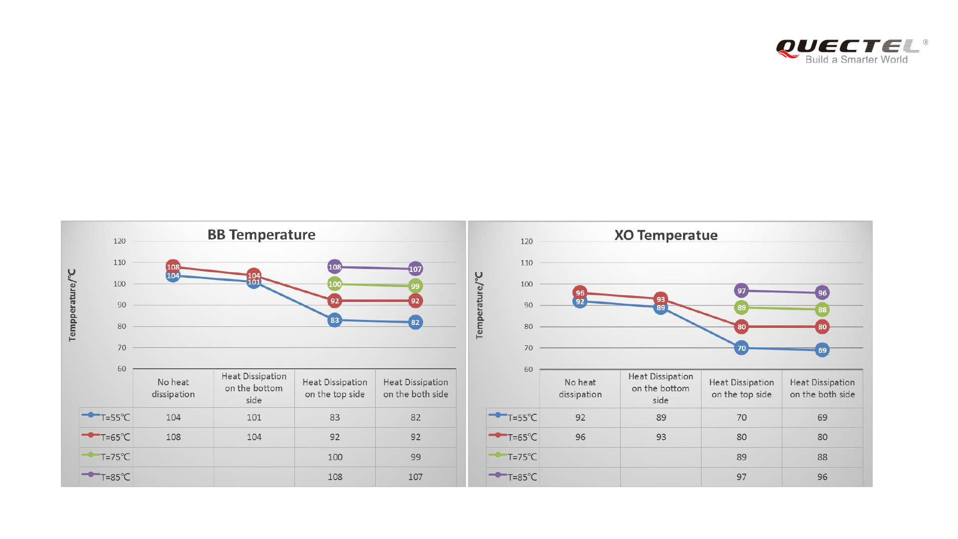
Test Condition
•Power the EVB by 5V DC power supply
•Connect the main antenna of the Mini PCIe module to CMW500 through RF cable
•Set the max power, max data rate, and UDP transfer mode
•Set different test temperatures, such as 55℃, 65℃, 75℃, and 85℃
•Use AT+QTEMP command to get the current temperature every 10s
@ Quectel Wireless Solutions | September, 2018 | Page 30 Rev.: V1.0 | Status: Released
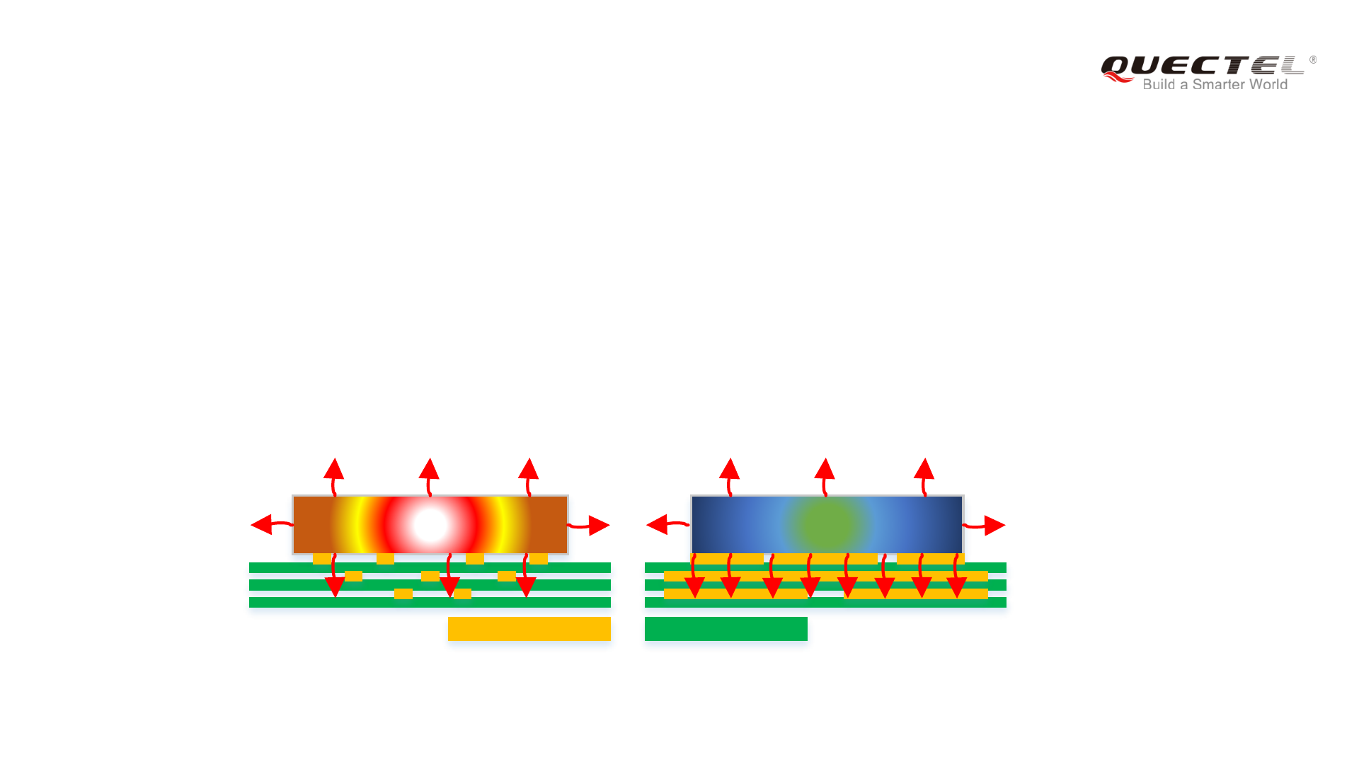
Test Results
•The Best Solution: Cooling system available on both sides of Mini PCIe module
It can lower the BB temperature by 8℃@T=85℃, and lower the XO temperature by 9℃@T=85℃.
•Good Solution: Cooling system on the top side of Mini PCIe module
It can lower the BB temperature by 7℃@T=85℃, and lower the XO temperature by 8℃@T=85℃.

© Quectel Wireless Solutions Co., Ltd. All rights reserved
7th Floor, Hongye Building, No.1801 Hongmei Road, Xuhui District,
Shanghai 200233, China
Tel: +86-21-5108 6236 Email: info@quectel.com
Website: www.quectel.com
Thank you!
www.quectel.com
https://www.linkedin.com/company/quectel-wireless-solutions
https://twitter.com/Quectel_IoT
https://www.facebook.com/quectelwireless
