RADEON Instinct MI25 Data Sheet
User Manual: RADEON-Instinct-MI25 DataSheet
Open the PDF directly: View PDF ![]() .
.
Page Count: 3
THE WORLD’S FASTEST TRAINING ACCELERATOR
FOR MACHINE INTELLIGENCE AND DEEP LEARNING1
The Radeon Instinct™ MI25 accelerator, designed with the most
advanced Next-Gen “Vega” GPU architecture, is the ultimate
training accelerator for large scale machine intelligence and
deep learning, along with being an optimized open compute
workhorse for single-precision HPC-class system workloads.
The MI25 delivers leadership in FP16 and FP32 performance in
a passively-cooled single GPU server card with 24.6 TFLOPS of
FP16 and 12.3 TFLOPS of FP32 peak performance through its 64
compute units with 4,096 stream processors.1
The Radeon Instinct MI25’s powerful compute engine and
advanced memory architecture, combined with AMD’s ROCm
open software platform and ecosystem, provides a powerful,
exible heterogeneous compute solution that allows datacenter
designers to meet the challenges of a new era of compute and
Machine Intelligence.
The Next Era of Compute and Machine Intelligence
Highlights
• Industry Leading Performance for Deep Learning1
• Next-Gen “Vega” Architecture
• Advanced Memory Engine
• Large BAR Support for Multi-GPU Peer to Peer
• ROCm Open Software Platform for Rack Scale
• Optimized MIOpen Libraries for Deep Learning
• MxGPU Hardware Virtualization
Key Features
GPU Architecture: AMD “Vega10”
Stream Processors: 4,096
GPU Memory: 16GB HBM2
Memory Bandwidth: Up to 484 GB/s
Performance:
Half-Precision (FP16) 24.6 TFLOPS
Single-Precision (FP32) 12.3 TFLOPS
Double-Precision (FP64) 768 GFLOPS
ECC: Yes3
MxGPU Capability: Yes
Board Form Factor: Full-Height, Duel-Slot
Length: 10.5”
Thermal Solution: Passively Cooled
Standard Max Power: 300W TDP
AMD’s Radeon Instinct™ MI25, combined with
the ROCm open software platform and MIOpen
libraries, delivers superior performance per
watt for deep learning training deployments in
the datacenter.2
OS Support: Linux® 64-bit
ROCm Software Platform: Yes
Programing Environment:
ISO C++, OpenCL™, CUDA (via AMD’s HIP conversion tool)
and Python5 (via Anaconda’s NUMBA)
For more information, visit: Radeon.com/Instinct
Bus Interface: PCIe® Gen 3 x16
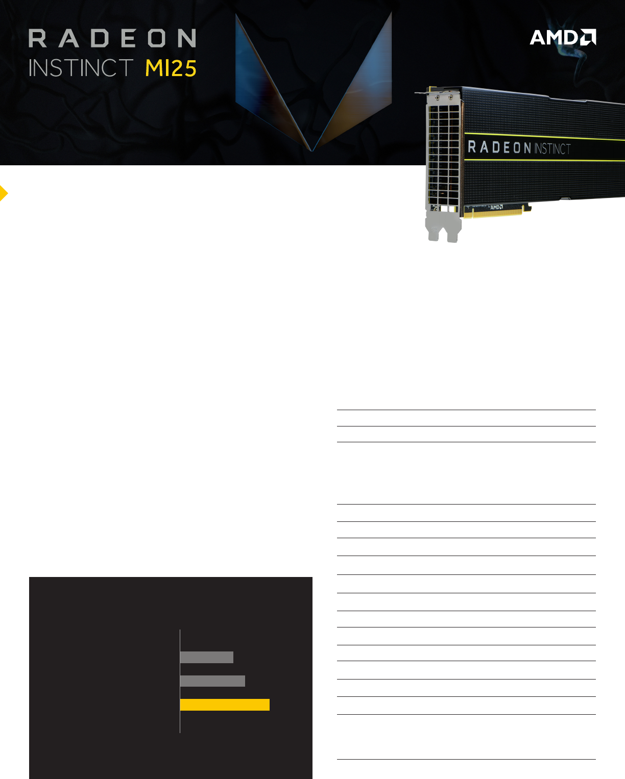
Superior Performance Per Watt
Nvidia Tesla P100-SMX2
Nvidia Tesla P100-16
71
75
Peak FP16 GFLOPS/Watt
Radeon Instinct MI25 82
Warranty: Three Year Limited4
Note: “Vega 10” is an internal codename only
NEXT-GEN “VEGA” ARCHITECTURE WITH THE
WORLD’S MOST ADVANCED MEMORY ARCHITECTURE
World’s most advanced GPU compute engine
and memory architecture built with cutting-
edge 14nm FinFET process, purpose-built
to handle big data sets and a diverse range of
computational workloads.
The Radeon Instinct MI25 accelerator brings in a new era of compute for the datacenter with its
Next-Gen “Vega” architecture delivering superior compute performance via its powerful parallel
compute engine and Next-Gen programmable geometry pipeline improving processing eciencies,
while delivering 2x peak throughput-per-clock over previous Radeon architectures.6 The Radeon
Instinct MI25 provides increased performance density, while decreasing energy consumption per
operation making it the perfect solution for today’s demanding workloads in the datacenter.
The Radeon Instinct MI25 design is a passively-
cooled accelerator design for large-scale server
deployments.
The Radeon Instinct MI25 accelerator has
advanced out-of-band manageability circuitry
for simplied GPU monitoring in large scale
systems. The MI25’s manageability capabilities
provide accessibility via I2C, regardless of
what state the GPU is in, providing advanced
monitoring of a range of static and dynamic
GPU information using PMCI compliant data
structures including board part detail, serial
numbers, GPU temperature, power and other
information.
NEXT-GEN “VEGA”
ARCHITECTURE
PASSIVELY
COOLED
REMOTE MANAGEABILITY
CAPABILITIES
Combined with AMD’s state of the art Innity
Memory Engine with a newly designed High
Bandwidth Cache (HBC) and controller, the
MI25 GPU has 16GB of latest HBM2 ECC3 GPU
memory with 484 GB/s of memory bandwidth.
HBM2: ULTRA-HIGH
MEMORY BANDWIDTH
LEADERSHIP IN FP16 & FP32 PERFORMANCE1
AMD’s ROCm platform provides a scalable,
fully open source software platform optimized
for large-scale heterogeneous system
deployments with an open source headless
Linux driver, HCC compiler, rich runtime based
on HSA, tools and libraries.
ROCm OPEN SOFTWARE
PLATFORM
Design support for AMD’s MxGPU SR-IOV
hardware virtualization technology, the
Radeon Instinct MI25 provides a VDI solution
with dedicated user GPU resources, data
security and version control. Plus, a cost
eective licensing model with no additional
hardware licensing fees, and a simplied native
driver model ensuring operating system and
application compatibility.
MxGPU SR-IOV HARDWARE
VIRTUALIZATION
©2017 Advanced Micro Devices, Inc. All rights reserved. AMD, the AMD arrow logo, Radeon, and combinations thereof, are trademarks of Advanced Micro Devices, Inc.
All other product names are for reference only and may be trademarks of their respective owners. “Vega” and “Vega 10” are internal architecture code names and not products.
For more information, visit:
Radeon.com/Instinct
ROCm.github.io
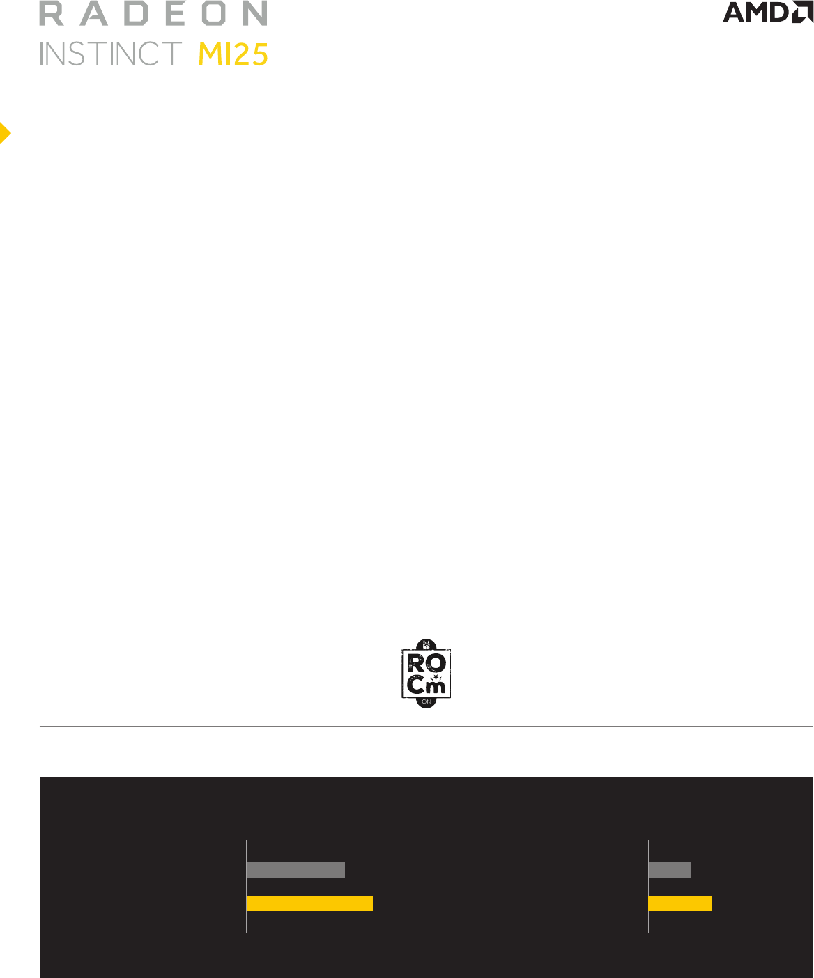
Up to 1.3x More FP16 TFLOPS Up to 1.3x More FP32 TFLOPS
Nvidia Tesla P100-16
Radeon Instinct MI25
18.7
24.5
Peak FP16 TFLOPS
Nvidia Tesla P100-16
Radeon Instinct MI25
9.3
12.3
Peak FP32 TFLOPS

1. Measurements conducted by AMD Performance Labs as of June 2, 2017 on the Radeon Instinct™ MI25 “Vega” architecture based accelerator.
Results are estimates only and may vary. Performance may vary based on use of latest drivers. PC/system manufacturers may vary congurations
yielding dierent results. The results calculated for Radeon Instinct MI25 resulted in 24.6 TFLOPS peak half precision (FP16) and 12.3 TFLOPS peak
single precision (FP32) oating-point performance.
AMD TFLOPS calculations conducted with the following equation: FLOPS calculations are performed by taking the engine clock from the highest
DPM state and multiplying it by xx CUs per GPU. Then, multiplying that number by xx stream processors, which exist in each CU. Then, that number
is multiplied by 2 FLOPS per clock for FP32. To calculate TFLOPS for FP16, 4 FLOPS per clock were used. The FP64 TFLOPS rate is calculated using
1/16th rate.
External results on the NVidia Tesla P100-16 (16GB card) GPU Accelerator resulted in 18.7 TFLOPS peak half precision (FP16) and 9.3 TFLOPS peak
single precision (FP32) oating-point performance.
Results found at: https://images.nvidia.com/content/tesla/pdf/nvidia-tesla-p100-PCIe-datasheet.pdf.
External results on the NVidia Tesla P100-SXM2 GPU Accelerator resulted in 21.2 TFLOPS peak half precision (FP16) and 10.6 TFLOPS peak single
precision (FP32) oating-point performance.
Results found at: http://www.nvidia.com/object/tesla-p100.html
AMD has not independently tested or veried external/third party results/data and bears no responsibility for any errors or omissions therein. RIV-1
2. Measurements conducted by AMD Performance Labs as of June 2, 2017 on the Radeon Instinct™ MI25 “Vega” architecture based accelerator.
Results are estimates only and may vary. Performance may vary based on use of latest drivers. PC/system manufacturers may vary congurations
yielding dierent results.
The results calculated for Radeon Instinct MI25 resulted in 82 GFLOPS/watt peak half precision (FP16) or 41 GFLOPS/watt peak single precision
(FP32) oating-point performance.
AMD GFLOPS per watt calculations conducted with the following equation: FLOPS calculations are performed by taking the engine clock from
the highest DPM state and multiplying it by xx CUs per GPU. Then, multiplying that number by xx stream processors, which exist in each CU. Then,
that number is multiplied by 2 FLOPS per clock for FP32. To calculate TFLOPS for FP16, 4 FLOPS per clock were used. The FP64 TFLOPS rate
is calculated using 1/16th rate. Once the TFLOPs are calculated, the number is divided by the xxx watts TDP power and multiplied by 1,000 to
determine the GFLOPS per watt.
Calculations conducted by AMD Performance Labs as of June 2, 2017 on the NVidia Tesla P100-16 (16GB card) GPU Accelerator to determine
GFLOPS/watt by dividing TFLOPS results by 250 watts TDP resulted in 75 GFLOPS per watt peak half precision (FP16) and 37 GFLOPS per watt peak
single precision (FP32) oating-point performance.
Sources: https://images.nvidia.com/content/tesla/pdf/nvidia-tesla-p100-PCIe-datasheet.pdf
Calculations conducted by AMD Performance Labs as of June 2, 2017 on the NVidia Tesla P100-SXM2 GPU Accelerator to determine GFLOPS/
watt by dividing TFLOPS results by 300 watts TDP resulted in 71 GFLOPS per watt peak half precision (FP16) and 35 GFLOPS per watt peak single
precision (FP32) oating-point performance.
Sources:
http://www.nvidia.com/object/tesla-p100.html
AMD has not independently tested or veried external/third party results/data and bears no responsibility for any errors or omissions therein. RIV-4
3. ECC support is limited to the HBM2 memory and ECC protection is not provided for internal GPU structures.
4. The Radeon Instinct GPU accelerator products come with a three year limited warranty. Please visit www.AMD.com/warranty for details on the
specic graphics products purchased. Toll-free phone service available in the U.S. and Canada only, email access is global.
5. Support for Python is planned, but still under development.
6. Data based on AMD Engineering design of Vega. Radeon R9 Fury X has 4 geometry engines and a peak of 4 polygons per clock.
Vega is designed to handle up to 11 polygons per clock with 4 geometry engines. This represents an increase of 2.6x. VG-3
FOOTNOTES
