RDA1846编程指南 RDA1846S Programming Guide 1.2
User Manual:
Open the PDF directly: View PDF ![]() .
.
Page Count: 25
- Document overview
- Doc. A: Interface
- Doc. B: Programming guide
- 1. Setting RF Frequency
- 2. Reference Clock
- 3. Setting Tx and Rx
- 4. Deep Sleep
- 5. TX Voice Channel Select
- 6. TX PA_bias output Voltage
- 7. Subaudio
- 8. SQ
- 9. VOX
- 10. DTMF
- 11. Tx FM Deviation
- 12. Rx Voice Volume
- 13. TX and RX code
- 14. GPIO
- 15. INT
- 16. Filter
- 17. Only read register
- 18. Flag
- 19. PLL Lock Detection
- 20. LDO
- 21. Initial process
- 22. Register introduction
- Change List
- Disclaimer

RDA1846S
The information contained herein is the exclusive property of RDA and shall not be distributed, reproduced, or disclosed in whole or in
part without prior written permission of RDA. 1
RDA1846S Programming Guide

RDA1846S
The information contained herein is the exclusive property of RDA and shall not be distributed, reproduced, or disclosed in whole or in
part without prior written permission of RDA. 2
Contents
Document overview ............................................................................................................................................. 4
Doc. A: Interface.................................................................................................................................................. 5
1. I2C Interface ............................................................................................................... 5
2 Three- wire SPI interface......................................................................................... 7
Doc. B: Programming guide................................................................................................................................. 9
1. Setting RF Frequency............................................................................................... 9
2. Reference Clock........................................................................................................ 9
3. Setting Tx and Rx...................................................................................................... 9
4. Deep Sleep............................................................................................................... 10
5. TX Voice Channel Select......................................................................................... 10
6. TX PA_bias output Voltage......................................................................................11
7. Subaudio...................................................................................................................11
8. SQ ............................................................................................................................. 12
9. VOX........................................................................................................................... 13
10. DTMF ...................................................................................................................... 13
11. Tx FM Deviation..................................................................................................... 16
12. Rx Voice Volume.................................................................................................... 16
13. TX and RX code..................................................................................................... 16
14. GPIO ....................................................................................................................... 16
15. INT........................................................................................................................... 17

RDA1846S
The information contained herein is the exclusive property of RDA and shall not be distributed, reproduced, or disclosed in whole or in
part without prior written permission of RDA. 3
16. Filter........................................................................................................................ 18
17. Only read register ................................................................................................. 19
18. Flag......................................................................................................................... 19
19. PLL Lock Detection............................................................................................... 19
20. LDO......................................................................................................................... 20
21. Initial process........................................................................................................ 20
22. Register introduction............................................................................................ 20
Change List ........................................................................................................................................................ 24
Disclaimer .......................................................................................................................................................... 25

RDA1846S
The information contained herein is the exclusive property of RDA and shall not be distributed, reproduced, or disclosed in whole or in
part without prior written permission of RDA. 4
Document overview
This programming guide has been restructured from previous revisions for clarity. This contains two
documents for interface and programmer separately. Interface document contains I2C interface and 3 wire SPI
interface .Programmer document contains a complete programming guide for using any interface.
RDA1846S
Doc. A: Interface
RDA1846S each register write is 24-bit long, including a r/ wbit,7-bit register address , and 16-bit data (MSB
is the first bit).
R/W A[6:0] D[15:0]
Note
If register address is more than 7FH, first write 0x0001 to 7FH, and then write value to the address
subtracted by 80H. Finally write 0x0000 to 7FH
Example: writing 85H register address is 0x001F .
Move 7FH 0x0001;
Move 05H 0x001F; 05H=85H-80H
Move 7FH 0x0000;
1. I2C Interface
RDA1846S enable software programming through I2C interface. Software controls chip working states, For
example: Txon or Rxon operation, and reads status register to get operation result through I2C interface.
It includes two pins: SCLK and SDIO.
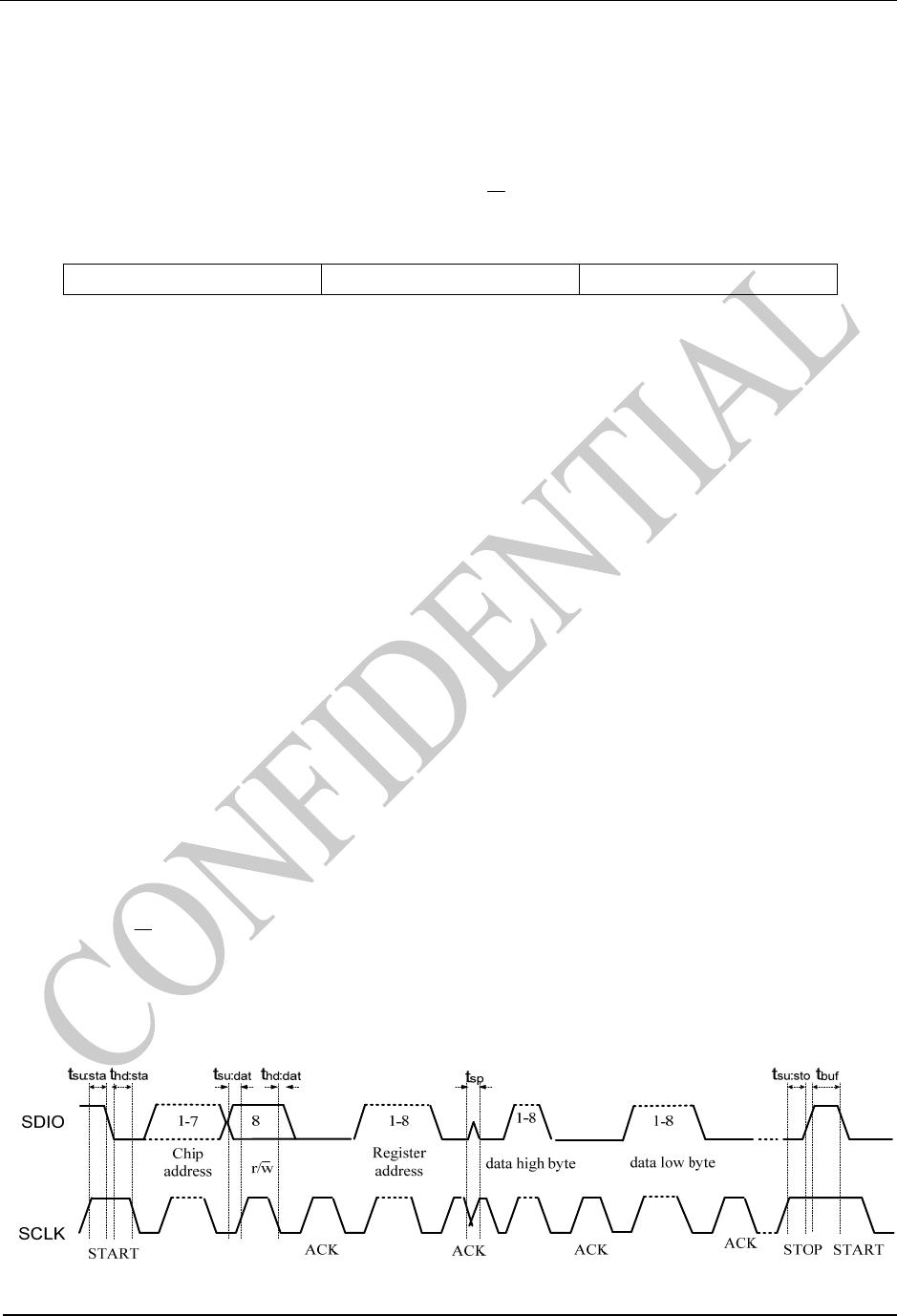
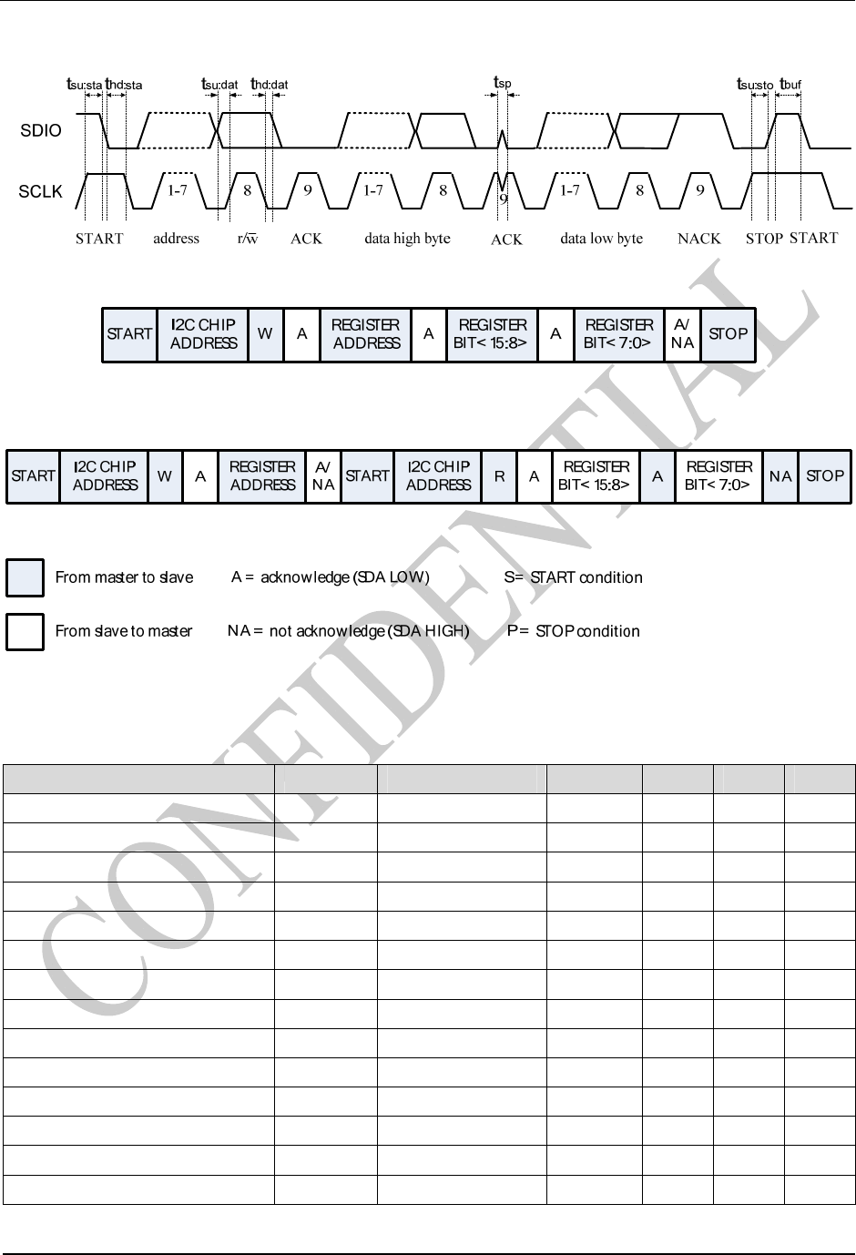
A I2C interface transfer begins with START condition, a command byte and data bytes, each byte has a
followed ACK (or NACK) bit, and ends with STOP condition. The command byte includes a 7-bit chip
address and a r/ wbit. The 7-bit chip address is 7’b0101110 when SEN is high, or is 7’1110001 when SEN is
low.The ACK ( or NACK) is always sent out by receiver. When in write transfer, data bytes is written out
from MCU, and when in read transfer, data bytes is read out from RDA1846S.
Figure 1. I2C Interface Write Timing Diagram
The information contained herein is the exclusive property of RDA and shall not be distributed, reproduced, or disclosed in whole or in
part without prior written permission of RDA. 5
RDA1846S
Figure 2. I2C Interface Read Timing Diagram
Figure 3 I2C Interface Write Combined Format
Figure 4 I2C Interface Read Combined Format
Table 2. I2C Timing Characteristics
PARAMETER SYMBOL TEST CONDITION MIN TYP MAX UNIT
SCLK Frequency fscl 0 - 400 KHz
SCLK High Time thigh 0.6 - -
s
SCLK Low Time tlow 1.3 - -
s
Setup Time for START Condition tsu:sta 0.6 - -
s
Hold Time for START Condition thd:sta 0.6 - -
s
Setup Time for STOP Condition tsu:sto 0.6 - -
s
SDIO Input to SCLK↑ Setup tsu:dat 100 - - ns
SDIO Input to SCLK↓ Hold thd:dat 0 - 900 ns
STOP to START Time tbuf 1.3 - -
s
SDIO Output Fall Time tf:out 20+0.1Cb- 250 ns
SDIO Input, SCLK Rise/Fall Time tr:in / tf:in 20+0.1Cb- 300 ns
Input Spike Suppression tsp - - 50 ns
SCLK, SDIO Capacitive Loading Cb - - 50 pF
Digital Input Pin Capacitance 5 pF
The information contained herein is the exclusive property of RDA and shall not be distributed, reproduced, or disclosed in whole or in
part without prior written permission of RDA. 6
RDA1846S
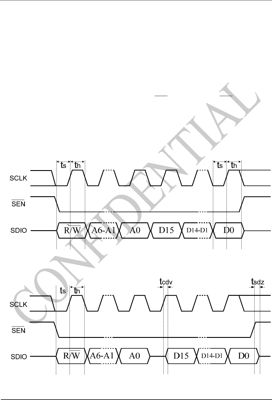
2 Three- wire SPI interface
RDA1846S enable software programming through three-wire(SPI) interface. Software controls chip working
states, For example: Txon or Rxon operation, and reads status register to get operation result through
three-wire interface.
Three-wire interface is slave interface. It includes three pins: SEN , SCLK and SDIO. SEN and SCLK are
input pins , SDIO are bi-direction pins.
RDA1846S samples command byte and data at posedge of SCLK.The turn around cycle between command
byte from MCU and data from RDA1846S is a half cycle. RDA1846S samples command byte at posedge of
SCLK, and output data also at posedge of SCLK.
Figure5. Three-wire Interface Write Timing Diagram
Figure6. Three-wire Interface Read Timing Diagram
The information contained herein is the exclusive property of RDA and shall not be distributed, reproduced, or disclosed in whole or in
part without prior written permission of RDA. 7
RDA1846S
Table 2. Three-wire Timing Characteristics
PARAMETER SYMBOL TEST CONDITION MIN TYP MAX UNIT
SCLK Cycle Time tCLK 35 ns
SCLK Rise Time tR 50 ns
SCLK Fall Time tF 50 ns
SCLK High Time tHI 10 ns
SCLK Low Time tLO 10 ns
SDIO Input, SEN to SCLK↑ Setup ts 10 - - ns
SDIO Input, to SCLK↑ Hold th 10 - - ns
SCLK↑ to SDIO Output Valid tcdv Read 2 - 10 ns
SEN↑ to SDIO Output High Z tsdz Read 2 - 10 ns
Digital Input Pin Capacitance 5 pF
The information contained herein is the exclusive property of RDA and shall not be distributed, reproduced, or disclosed in whole or in
part without prior written permission of RDA. 8
RDA1846S
The information contained herein is the exclusive property of RDA and shall not be distributed, reproduced, or disclosed in whole or in
part without prior written permission of RDA. 9
Doc. B: Programming guide
1. Setting RF Frequency
Bit Name Function
29H[13:0] freq<29:16> Freq high value (unit 1khz/16)
2aH[15:0] freq<15:0> Freq low value (unit 1khz/16)
Default frequency is 409.7500MHz
Freq<29:0>= Binary (Freq(MHz)*16000)
For example: frequency is 409.75MHz, Freq<29:0>=409.75*16000=6556000=0x640960,so write 29H [15:0]
=0x64 and 2aH [15:0] =0x0960.
2. Reference Clock
RDA1846S takes 12.8 MHz,13MHz,25.6M Hz and 26MHz crystals as its master reference clock. .
Bit Name Function
30H[14] xtal_mode 1: 26MHz/13MHz
0: 25.6MHz/12.8MHz
04H[0] clk_mode 1: 12.8MHz /13MHz
0: 25.6MHz /26MHz
For example: 12.8MHz crystal
04H[0]= clk_mode =1
30H[14]= clk_mode =0
13MHz crystal
04H[0]= clk_mode =1
30H[14]= clk_mode =1
26MHz crystal
04H[0]= clk_mode =0
30H[14]= clk_mode =1
3. Setting Tx and Rx
Bit Name Function
30H[13] filter_band_sel Analog filter band select
1 = 25khz band mode
RDA1846S
The information contained herein is the exclusive property of RDA and shall not be distributed, reproduced, or disclosed in whole or in
part without prior written permission of RDA. 10
0 = 12.5khz band mode
30H[12] band_mode Dsp band mode select
1 = 25khz band mode
0 = 12.5khz band mode
30H[6] tx_on 1 = on
0 = off
30H[5] rx_on 1 = on
0 = off
4. Deep Sleep
Bit Name Function
30H[2] pdn_reg The same as pdn pin
1 = power_on
0 = power_down
While Normal mode, pdn_reg and PDN pin must be high at the same time. Only one of pdn_reg and PDN pin
is low , which can turn into deep sleep.
For example: Sleep programming sequence:
setting 30H[6:5]=00 : shut down Tx or Rx
setting PDN pin is Low or 30H[2]=0 ; enter into deep sleep state
delay period of sleep time : in sleep state
setting PDN pin is High or 30H[2]=1 ; exit sleep state
delay 10ms
Setting 30H[6]or 30H[5]=1 :open Tx or Rx
5. TX Voice Channel Select
Bit Name Function
3aH[14:12] voice_sel<1:0> 000= Tx nothing
001= Tx signal from frequency of tone1
010=Tx signal from frequency of tone2
011= Tx signal from frequency of tone1 and tone2
100= Tx signal from microphone
other= reserved
RDA1846S
The information contained herein is the exclusive property of RDA and shall not be distributed, reproduced, or disclosed in whole or in
part without prior written permission of RDA. 11
6. TX PA_bias output Voltage
RDA1846S Pa_bias pin output voltage can be controlled by 0aH [5:0].
Bit Name Function
0aH [5:0] pabias_voltage<5:0> 000000: 1.04V
000001:1.05V
000010:1.07V
000100: 1.10V
001000: 1.22V
010000: 1.52V
100000: 2.14V
111111 :3.28V
7. Subaudio
Bit Name Function
4aH[15:0] ctcss1_freq<15:0> ctcss1 frequency for tx and tx
Ctcss1 freq = ctcss_freq(Hz)*100
Default value is 100Hz
It must be set to 134.4Hz when use standard cdcss
mode
4dH[15:0] ctcss2_freq<15:0> ctcss2 frequency for tx and rx
Ctcss2 freq = ctcss_freq(Hz)*100
Default value is 100Hz
4bH[7:0]
4cH[15:0]
4bH[7:0]=cdcss_code<23:16>
4cH[15:0]=cdcss_code<15:0>
cdcss bit for tx and rx
When use cdcss, this register must be set both in rx
and tx state
For example: When tx or rx Cdcss023
4bH=0x0076 and 4cH=0x3813
4eH[15:14] shift_sel<1:0> shift phase for tx and rx tail elimination
00= no phase shift,
01=120 degree phase shift,
10=180 degree phase shift,
11=240 degree phase shift.
4eH[10:9] ctcss/cdcss_sel<1:0> Select Ctcss/Cdcss mode for tx
11=ctcss with 1846S
10=cdcss with 1846S
01=ctcss/cdcss from GPIO0
RDA1846S
The information contained herein is the exclusive property of RDA and shall not be distributed, reproduced, or disclosed in whole or in
part without prior written permission of RDA. 12
00= not Tx ctcss/cdcss
4eH[8:6] cdcss_sel<2:0> Select cdcss mode for tx/rx
4eH[8]=1 invert cdcss ;
=0 not invert cdcss
4eH[7]=1 should be 1
4eH[6]=1 24bit cdcss;
=0 23bit cdcss
3aH[5] ctcss/cdcss_out_sel Select Ctcss/Cdcss mode for rx
1: output ctcss/cdcss wave to GPIO0
0: output ctcss/cdcss compared result to GPIO0
3aH[4:0]
ctcss/cdcss _dten<4:0> Select Ctcss/Cdcss detect mode for rx
3aH[4]=1 detect phase shift
3aH[3]=1 detect ctcss2 frequency
3aH[2]=1 detect invert cdcss
3aH[1]=1 detect normal cdcss
3aH[0]=1 detect ctcss1 frequency
5bH[15:8] ctcss_threshold_in<7:0> detect ctcss1 and ctcss2 match_threshold
5bH[7:0] ctcss_threshold_out<7:0> detect ctcss1 and ctcss2 unmatch_ threshold
Note:
5bH setting refer to the ctcss threshold of the
‘RDA1846S _register_table’
30H[11] tail_elim_en 1 = on, enable 1846S tail elimination function
0 = off disable 1846S tail elimination function
8. SQ
Bit Name Function
30H[3] sq_on 1 = on, enable 1846S auto sq function
0 = off
3aH[10:6] sq_dten<4:0> sq condition enable
3aH[6]=1 rssi detect enable
=0 rssi detect disable
3aH[7] =1 noise detect enable
=0 noise detect disable
3aH[8]=1 rssi&noise(block) enable
=0 rssi&noise(block) disable
3aH[9]=1 adjacent channel, detect enable
=0 adjacent channel,detect disable
3aH[0]=1 fm modu signal detect enable
RDA1846S
The information contained herein is the exclusive property of RDA and shall not be distributed, reproduced, or disclosed in whole or in
part without prior written permission of RDA. 13
=0 fm modu signal detect disable
49H[13:7] th_h_sq<6:0>
Sq open threshlod
Sq detect high th, rssi_cmp will be 1 when
rssi>th_h_sq, unit 1dB
49H[13:7]=Binary (137+ Sq open threshlod)
49H[6:0] th_l_sq<6:0>
Sq detect low th, rssi_cmp will be 0 when
rssi<th_l_sq && time delay meet, unit 1 dB
49H[6:0]=Binary (137+ Sq shut threshlod)
3aH[11] sq_out_sel =1 output of gpio6=sq_cmp & sub_audio_cmp;
=0 output of gpio6= sq_cmp .
For example: Sq open threshold=-120dBm and Sq shut threshold=-122dBm
So 49H[13:7]= Binary (137+(-120))=0010001,
49H[6:0] = Binary (137+(-122))=0001111,
49H[15:0]=00 0010001 0001111=0x088F
9. VOX
Bit Name Function
30H[4] vox_on 1 = on, enable 1846S Vox detect
0 = off, disable 1846S Vox detect
64H[13:7] th_h_vox<6:0> Vox open threshold
64H[6:0] th_l_vox<6:0> Vox Shut threshold
Note:
64H setting refer to the vox of the ‘RDA1846S
_register_table’
10. DTMF
Bit Name Function
3aH[14:12] voice_sel<1:0> 011= Tx signal from frequency of tone1 and tone2
79H[15] dtmf_direct 0= dtmf
1= single tone
79H[14] dtmf_tx 0= tx dtmf
1= tx single tone
7aH[15] dtmf_en 1=enable dtmf
0=disable dtmf
7aH[14] single_tone 1=enable single tone
0=disable single tone
7bH[11:6] dtmf_time0<5:0> Time interval for dtmf idle state
Time = dtmf_time0*2.5ms
RDA1846S
The information contained herein is the exclusive property of RDA and shall not be distributed, reproduced, or disclosed in whole or in
part without prior written permission of RDA. 14
7bH[5:0] dtmf_time1<5:0> Time interval for dual tone transmission
Time = dtmf_time1*2.5ms
35H[15:0] tone1_freq<15:0> =tone1 frequency(Hz)*10
36H[15:0] tone2_freq<15:0> =tone2 frequency(Hz)*10
7eH[5] dtmf_idle only for tx
1= dtmf code request for tx
0= dtmf code idle
7eH [4] dtmf_sample only for Rx
1= dtmf code ready for read
0= dtmf code not ready for read
67H[15:0] dtmf_c0<15:0> 697Hz
=0x0628 12.8MHz and 25.6MHz
=0x0628 13MHz and 26MHz
68H[15:0] dtmf_c1<15:0> 770Hz
=0x059F 12.8MHz and 25.6MHz
=0x05e5 13M and 26MHz
69H[15:0] dtmf_c2<15:0> 852 Hz
=0x0555 12.8MHz and 25.6MHz
=0x0555 13MHz and 26MHz
6aH[15:0] dtmf_c3 <15:0> 941 Hz
= 0x04B8 12.8MHz and 25.6MHz
= 0x04B8 13MHz and 26MHz
6bH[15:0] dtmf_c4 <15:0> 1209 Hz
=0x029F 12.8MHz and 25.6MHz
=0x02FE 13MHz and 26MHz
6cH[15:0] dtmf_c5<15:0> 1336 Hz
=0x01DD 12.8MHz and 25.6MHz
=0x01DD 13MHz and 26MHz
6dH[15:0] dtmf_c6<15:0> 1477 Hz
=0x00B1 12.8MHz and 25.6MHz
=0x00B1 13MHz and 26MHz
6eH[15:0] dtmf_c7<11:0> 1633 Hz
=0x0F81 12.8MHz and 25.6MHz
=0x0F81 13MHz and 26MHz
6fH[15:0] dtmf_c0_2nd_harm<15:0> =0x017A 12.8MHz and 25.6MHz
=0x017A 13MHz and 26MHz
70H[15:0] dtmf_c1_2nd_harm<150> =0x004C 12.8MHz and 25.6MHz
=0x004C 13MHz and 26MHz
71H[15:0] dtmf_c2_2nd_harm<15:0> =0x0EB8 12.8MHz and 25.6MHz
=0x0F1C 13MHz and 26MHz
72H[15:0] dtmf_c3_2nd_harm<15:0> =0x0D91 12.8MHz and 25.6MHz
RDA1846S
The information contained herein is the exclusive property of RDA and shall not be distributed, reproduced, or disclosed in whole or in
part without prior written permission of RDA. 15
=0x0D91 13MHz and 26MHz
73H[15:0] dtmf_c4_2nd_harm<15:0> =0x09F9 12.8MHz and 25.6MHz
=0x0A3E 13MHz and 26MHz
74H[15:0] dtmf_c5_2nd_harm<15:0> =0x08DE 12.8MHz and 25.6MHz
=0x090E 13MHz and 26MHz
75H[15:0] dtmf_c6_2nd_harm<15:0> =0x081F 12.8MHz and 25.6MHz
=0x0833 13MHz and 26MHz
76H[15:0] dtmf_c7_2nd_harm<15:0> =0x0810 12.8MHz and 25.6MHz
=0x0806 13MHz and 26MHz
7eH [3:0] dtmf_code<3:0> Dtmf code out
Usually, F0~F7 is selected as 697, 770, 852, 941,
1209, 1336, 1477, 1633 Hz (default)
F4 F5 F6 F7
F0 1 2 3 A
F1 4 5 6 B
F2 7 8 9 C
F3 E(*) 0 F(#) D
Note:
DTMF setting refer to the DTMF of the ‘RDA1846S _register_table’
Run the code in Matlab for calculate dtmf_code:
Coef means dtmf_coef_0~7
Coef 2means dtmf_coef_0~7_2nd_harm
close all
clear all
% Frequency tones of the telephone pad (Hz)
f = [697 770 852 941 1209 1336 1477 1633]
Fs = 6.4e6/1024 % 12.8M and 25.6M crystal or Fs = 6.5e6/1024 % 123M and 26M crystal
N = 127;
LEN = 10;
k = floor(f/Fs*N+0.5); % Indices of the DFT
coef = round(2*cos(2*pi*k/N)*2^LEN)/2^LEN;
disp('COEF');
coef*2^LEN
dec2bin(coef*2^LEN,12)
% 2nd harmonious
k2 = floor(2*f/Fs*N+0.5); % Indices of the DFT
RDA1846S
The information contained herein is the exclusive property of RDA and shall not be distributed, reproduced, or disclosed in whole or in
part without prior written permission of RDA. 16
coef2 = round(2*cos(2*pi*k2/N)*2^LEN)/2^LEN;
disp('COEF_2nd_harm');
coef2*2^LEN
11. Tx FM Deviation
Bit Name Function
0aH[10:6] pga_gain<4:0> Voice analog gain.
41H[6:0] voice_gain_tx<6:0> Voice digital gain.
44H[11:8] gain_tx<3:0> Voice digital gain after tx ADC down sample
59H [15:6] xmitter_dev<9:0> Ctcss/cdcss + voice dev setting
59H [5:0] c_dev<5:0> Ctcss/cdcss dev setting
Adjusting 59H [15:6] ( xmitter_dev) can change Tx FM deviation of voice and subaudio.
Adjusting 59H [5:0] ( c_dev) can only change Tx FM deviation of CTCSS and CDCSS.
Note:
Please refer to the deviation of the ‘RDA1846S _register_table’
12. Rx Voice Volume
Bit Name Function
44H[7:4] dac_vgain_<3:0> Analog DAC gain
44H[3:0] volume<3:0> Digital Voice gain
Adjusting 44H [3:0] and 44H [7:4] can change Rx voice range.
Please refer to volume of ‘RDA1846S_register_table’.
13. TX and RX code
14. GPIO
Register 1fh.
Bit Name Function
15:14 gpio7<1:0> 00 =hi-z
01 = vox
10 = low
11 = high
13:12 gpio6<1:0> 00 =hi-z
RDA1846S
The information contained herein is the exclusive property of RDA and shall not be distributed, reproduced, or disclosed in whole or in
part without prior written permission of RDA. 17
01 = sq,
sq&ctcss/cdcss,when sq_out_sel=1
10 = low
11 = high
11:10 gpio5<1:0> 00 =hi-z
01 = txon_rf
10 = low
11 = high
9:8 gpio4<1:0> 00 =hi-z
01 = rxon_rf
10 = low
11 = high
7:6 gpio3<1:0> 00 =hi-z
01 =dtmf_flag/code_flag
10 = low
11 = high
5:4 gpio2<1:0> 00 =hi-z
01 = int
10 = low
11 = high
3:2 gpio1<1:0> 00 =hi-z
01 = code_out/code_in
10 = low
11 = high
1:0 gpio0<1:0> 00 =hi-z
01 = css_out/css_in/css_cmp
10 = low
11 = high
15. INT
Register 2dh.
16’ b0000_0000_0000_0000
Bit Name Function
15:12 others <3:0> 000000
11 code_flag_int 1=enable
0=disable
10 other 0
9 sub_audio_compared_flag_int 1=enable
0=disable
RDA1846S
The information contained herein is the exclusive property of RDA and shall not be distributed, reproduced, or disclosed in whole or in
part without prior written permission of RDA. 18
8 rxon_rf _int 1=enable
0=disable
7 txon_rf_int 1=enable
0=disable
6 dtmf_idle int 1=enable
0=disable
5:3 others 000
2 sq_flag_int 1=enable
0=disable
1 other 0
0 vox_int 1=enable
0=disable
Note
Only one INT mode can be chosen at one time.
16. Filter
Register 58h.
Bit Name Function
15:14 others 10
13 rssi_lpfil_bw 1=bypass
0=normal
12 vox_lowpass_filter_bypass 1=bypass
0= normal
11 vox_highpass_filter_bypass 1=bypass
0= normal
10:8 others 100
7 pre/de-emph_bypass 1=bypass
0= normal
6 voice_highpass_filter_bypass 1=bypass
0= normal
5 voice_lowpass_filter_bypass 1=bypass
0= normal
4 ctcss_lowpass_filter_bypass 1=bypass
0= normal
3 ctcss_highpass_filter_bypass 1=bypass
0= normal
2:1 others 10
0 ctcss_lpfil_bw 1=250Hz BW
0=110Hz BW
RDA1846S
The information contained herein is the exclusive property of RDA and shall not be distributed, reproduced, or disclosed in whole or in
part without prior written permission of RDA. 19
17. Only read register
Bit Name Function
1bH[15:8] rssi_db<7:0]> Received RF signal strength ,unit 1dB
1bH[7:0] noise_db<7:0]> Received noise signal strength ,unit 1dB
1aH [15:8] vox_db<7:0> Tx path digital signal strength, unit 0.5dB
1aH [7:0] mic_db<7:0> Mic signal strength, unit 0.5dB
18. Flag
Register 1ch.
Bit Name Function
15:10 Others 00000
9 ctcss1_cmp ctcss1 compared result.
8 ctcss2_cmp ctcss2 compared result.
7 cdcss1_cmp cdcss positive code compared result
6 cdcss2_cmp cdcss negative code compared result.
5 invert_det Ctcss phase shift result
4:3 ctcss_shift<1:0> 00=0 degree phase shift,
01=120 degree phase shift
10=180 degree phase shift
11=240 degree phase shift
2 ctcss/cdcss_cmp ctcss/cdcss compared result
1 vox_cmp vox compared result.
0 sq_cmp Sq compare result.
19. PLL Lock Detection
Bit Name Function
24H[15] pll_lock_det_sel 1=disable pll lock detection function
If PLL unlock, RDA146S will not shutdown RF
signal.
0=enable pll lock detection function.
If PLL unlock, RDA146S will shutdown RF signal
24H[14:13] reset_pll_lock_delay<1:0> 00=10us
01=20us
RDA1846S
The information contained herein is the exclusive property of RDA and shall not be distributed, reproduced, or disclosed in whole or in
part without prior written permission of RDA. 20
10=30us
11=40us
0dH [15] pll_lock_det_flag Read only
0=Pll unlock
1=Pll lock
20. LDO
Bit Name Function
08H[14] ldo_master_bypass 1=bypass all LDOs inside RDA1846S.
Note: Setting RDA1846S in VHF band , 08H[14]
must be 0.
0=normal
09H [9:7] ldo_dig_vbit<2:0> If 08H[14]=0,control LDO Vout for digital.
When supply voltage for RDA1846S is 3.30V
100=2.20V
101=2.40V
110=2.80V
111=3.30V
21. Initial process
Refer to the ‘RDA1846S _register_table’
22. Register introduction
Register 00h. default value=0x1846
Bit Name Function
15:0 Chip_ID<15:0> Chip ID
Register 01h. default value=0x003F
Bit Name Function
15:0 mr_id<15:0> Metal revison ID
Register 30h. default value=0x0000
Bit Name Function
15 other
RDA1846S
The information contained herein is the exclusive property of RDA and shall not be distributed, reproduced, or disclosed in whole or in
part without prior written permission of RDA. 21
14 xtal_mode 1: 26MHz/13MHz
0: 25.6MHz/12.8MHz
13 filter_band_sel Analog filter band select
1 = 25khz band mode
0 = 12.5khz band mode
12 band_mode_sel Dsp band mode select
1 = 25khz band mode
0 = 12.5khz band mode
11 tail_elim_en 1 = on, enable 1846S tail elimination function
0 = off disable 1846S tail elimination function
10 direct_reg 1=enable direct_reg
0=disable direct_reg
9:8 others
7 mute 1 = mute when rxno
0 = no mute
6 tx_on 1 = on
0 = off
5 rx_on 1 = on
0 = off
4 vox_on 1 = on, enable 1846S Vox detect
0 = off, disable 1846S Vox detect
3 sq_on 1 = on, then chip auto sq
0 = off
2 pdn_reg The same as pdn pin
1 = enable
0 = disable
1 chip_cal_en 1 = cal enable
0 = cal disable
0 soft_reset 1 = reset, then all the registers are reset to default
value
0 = normal
Register 03h. default value=0x2B51
Bit Name Function
15:14 others
12 tx_adc_reset_dr 1=enable direct reg
0=disable direct reg
11 tx_adc_reset_reg 1=enable reset adc
0=disable reset adc
10:9 others
Register 04h. default value=0x0FD1
RDA1846S
Bit Name Function
15:1 others
0 clk_mode 1: 12.8MHz /13MHz
0: 25.6MHz /26MHz
Register 08h. default value=0x02A0
Register 09h. default value=0x03C2
Bit Name Function
15 other
14 ldo_master_bypass 1=bypass all LDOs inside RDA1846S.
Note: Setting RDA1846S in VHF band , 08H[14]
must be 0.
0=normal
13:0 others
Bit Name Function
15:10 others
9:7 ldo_dig_vbit<2:0> If 08H[14]=0,control LDO Vout for digital.
6:0 others
Register 0ah. default value=0x7C20
Bit Name Function
15 other
14:11 padrv_ibit<3:0> output of RF power control
10:6 pga_gain<4:0> voice analog gain.
5:0 pabias_voltage<5:0> pabiase_pin output voltage control
Register 15h. default value=0x1100
Bit Name Function
15:13 others
12:9 tuning_bit<3:0> Tuning IF filter center frequency and bw
8:0 others
Register 24h. default value=0x0001
Bit Name Function
15 pll_lock_det_sel 1: bypass pll lock det function
14:13 reset_pll_lock_delay<1:0>
12:8 others
7 dsp_resetn_dr 1=enable direct reg
0=disable direct reg
6 dsp_resetn_reg 1=enable reset dsp
0=disable reset dsp
5:0 others
Register 29h. default value=0x2486
The information contained herein is the exclusive property of RDA and shall not be distributed, reproduced, or disclosed in whole or in
part without prior written permission of RDA. 22
RDA1846S
The information contained herein is the exclusive property of RDA and shall not be distributed, reproduced, or disclosed in whole or in
part without prior written permission of RDA. 23
Bit Name Function
15:14 others
13:0 freq<29:16> Freq high value (unit 1khz/16)
Register 2ah. default value=0x 3A84
Bit Name Function
15:0 freq<15:0> Freq low value (unit 1khz/16)
Register 32h. default value=0x 7497
Bit Name Function
15:12 others
11:6 agc_target_pwr[5:0] AGC target power, unit 2dB
5:0 others
Register 3ah. default value=0x40C3
Bit Name Function
15 code_out_sel 1: output code sample signal via GPIO3
0: output dtmf_sample/dtmf_idle signal via GPIO3
14:12 voice_sel<1:0> voice path select
11 sq_out_sel =1 output of gpio6=sq_cmp & sub_audio_cmp;
=0 output of gpio6= sq_cmp .
10:6 sq_dten<4:0> sq condition enable
5 ctcss/cdcss_out_sel Select Ctcss/Cdcss mode for rx
4:0 ctcss/cdcss _dten<4:0> Select Ctcss/Cdcss detect mode for rx
Register 41h. default value=0x4006
Bit Name Function
15:7 others
6:0 voice_gain_tx<6:0> Voice digital gain.
Register 44h. default value=0x00FF
Bit Name Function
15:12 others
11:8 gain_tx<3:0> Voice digital gain after tx ADC down sample
7:4 dac_vgain_<3:0> Analog DAC gain
3:0 volume<3:0> Digital Voice gain
Register 4eh. default value=0x20C2
Bit Name Function
15:14 shift_sel<1:0> shift phase for tx and rx tail elimination
13:11 others
10:9 ctcss/cdcss_sel<1:0> Select Ctcss/Cdcss mode for tx
8:6 cdcss_sel<2:0> Select cdcss mode for tx
5:0 others
RDA1846S
The information contained herein is the exclusive property of RDA and shall not be distributed, reproduced, or disclosed in whole or in
part without prior written permission of RDA. 24
Change List
Rev Date Author Change Description
0.1 2010-8-22 Liu Ge Original draft
0.2 2010-10-8 Liu Ge Modify 0x4E

RDA1846S
Disclaimer
The information provided here is believed to be reliable; RDA Microelectronics assumes no liability for
inaccuracies and omissions. RDA Microelectronics assumes no liability for the use of this information and all
such information should entirely be at the user’s own risk. Specifications described and contained here are
subjected to change without notice for the purpose of improving the design and performance. All of the
information described herein shall only be used for sole purpose of development work of RDA1846S, no right
or license is implied or granted except for the above mentioned purpose. RDA Microelectronics does not
authorize or warrant any RDA products for use in the life support devices or systems.
Copyright@2006 RDA Microelectronics Inc. All rights reserved
For technical questions and additional information about RDA Microelectronics Inc.:
Website: www.rdamicro.com
Mailbox: info@rdamicro.com
RDA Microelectronics (Shanghai), Inc. RDA Microelectronics (Beijing), Inc.
Tel: +86-21-50271108 Tel: +86-10-63635360
Fax: +86-21-50271099 Fax: +86-10-82612663
The information contained herein is the exclusive property of RDA and shall not be distributed, reproduced, or disclosed in whole or in
part without prior written permission of RDA. 25
