RM VZ950T RMVZ950
User Manual: RMVZ950
Open the PDF directly: View PDF ![]() .
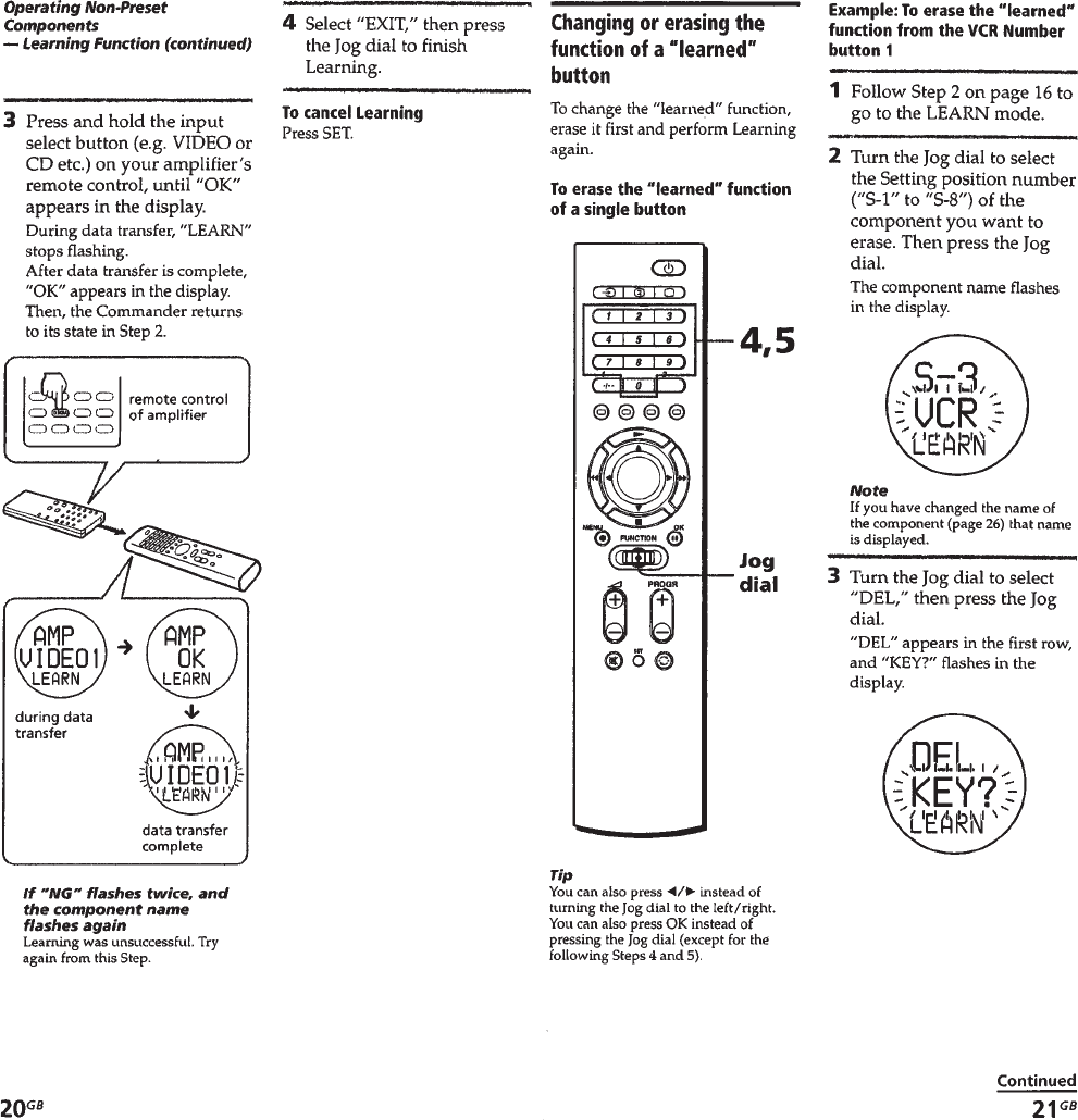
.
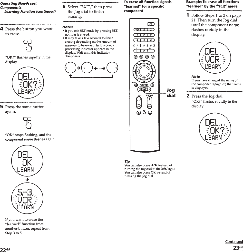
Page Count: 35
SERVICE MANUAL
Ver 1.0 2000. 08
REMOTE COMMANDER
AEP Model
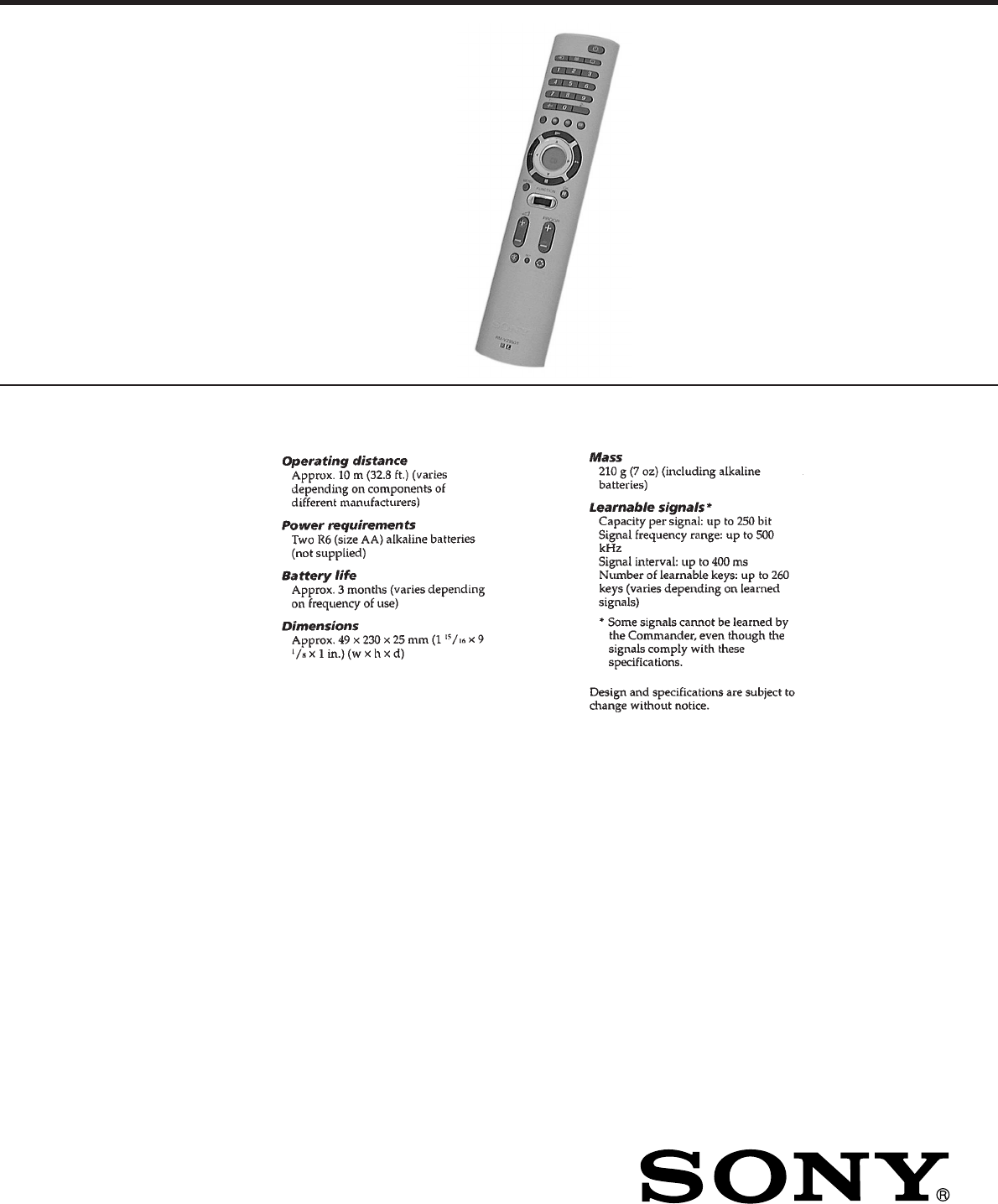
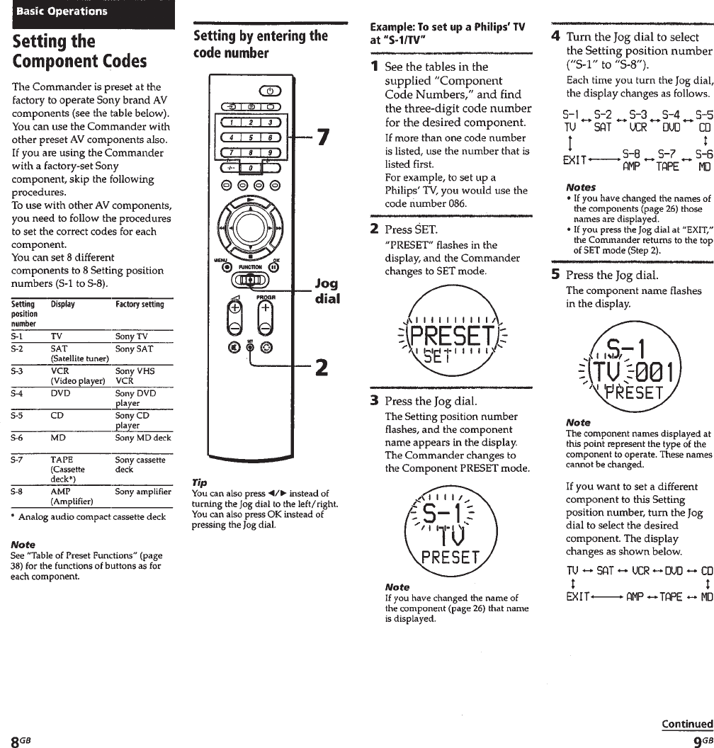
SPECIFICATIONS
RM-VZ950T
– 2 –
TABLE OF CONTENTS
1. GENERAL
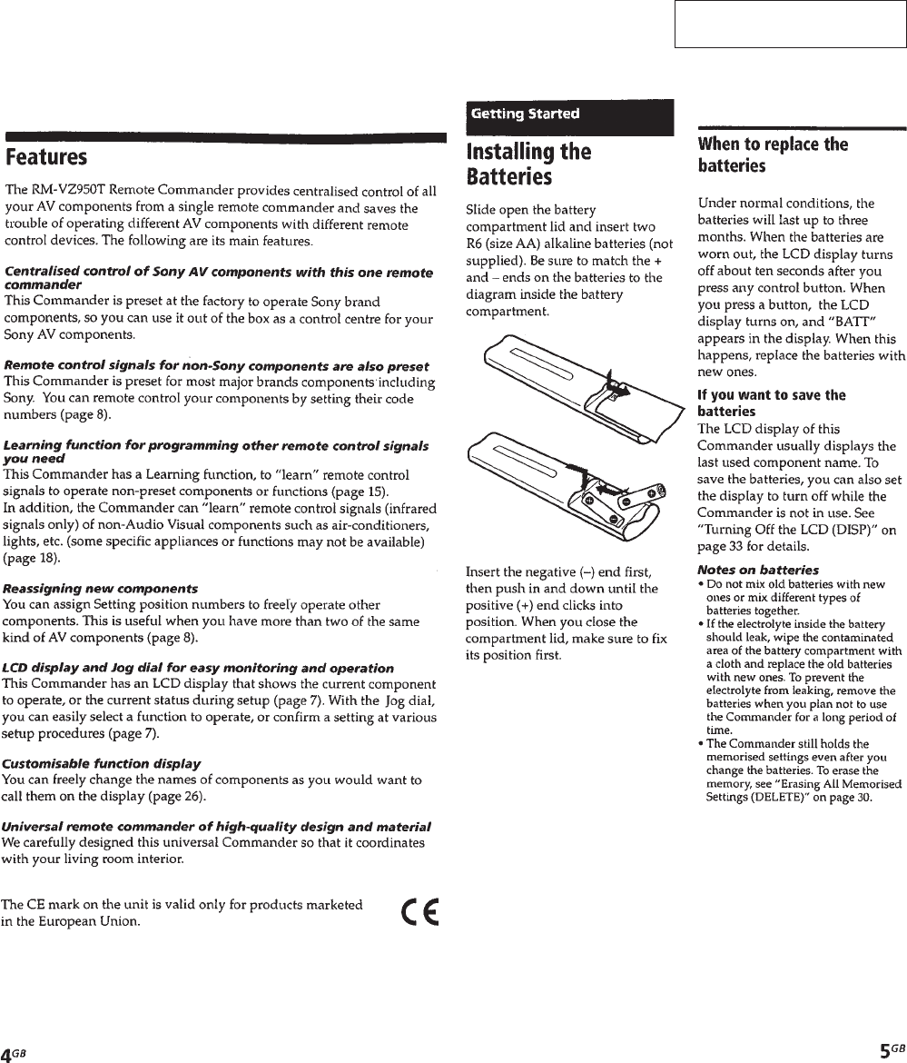
Getting Started ................................................................ 3
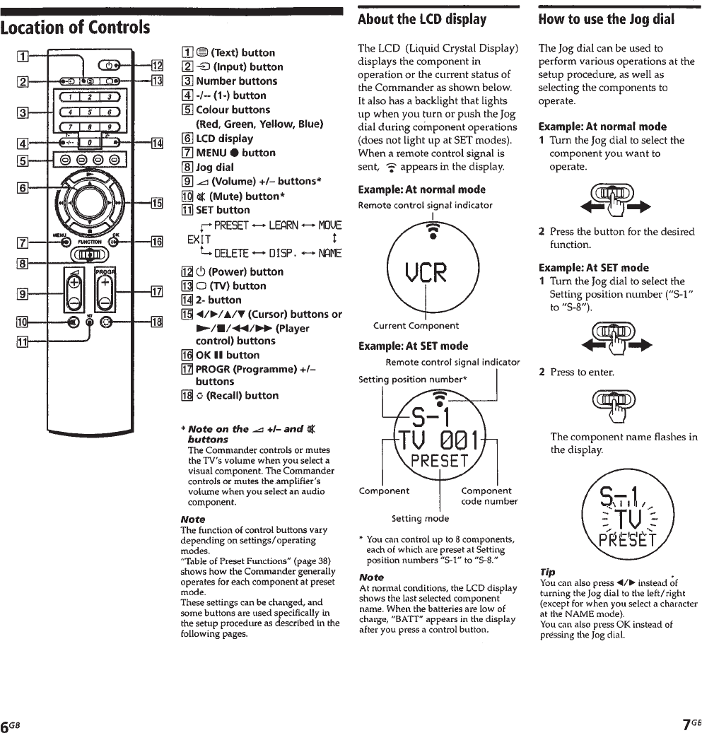
Location of Controls ....................................................... 4
Basic Operations ............................................................. 5
Advanced Features .......................................................... 13
Additional Information ................................................... 18
Appendix ......................................................................... 19
2. DISASSEMBLY
2-1. Case (Lower) ................................................................... 21
2-2. Remote Control Board .................................................... 21
2-3. Case, Inner....................................................................... 22
3. TEST MODE.............................................................. 23
4. DIAGRAMS
4-1. Block Diagram ................................................................ 27
4-2. Printed Wiring Boards..................................................... 29
4-3. Schematic Diagram ......................................................... 31
4-4. IC Pin Function Description ........................................... 35
5. EXPLODED VIEW ................................................... 36
6. ELECTRICAL PARTS LIST ............................... 37
Notes on chip component replacement
• Never reuse a disconnected chip component.
• Notice that the minus side of a tantalum capacitor may be dam-
aged by heat.
– 3 –
SECTION 1
GENERAL This section is extracted from
instruction manual.
– 4 –
– 5 –

– 6 –
– 7 –
– 8 –
– 9 –
– 10 –
– 11 –
– 12 –
– 13 –
– 14 –
– 15 –
– 16 –
– 17 –

– 18 –
– 19 –
– 20 –
– 21 –
2-1. CASE (LOWER)
2-2. REMOTE CONTROL BOARD
Note: Follow the disassembly procedure in the numerical order given.
SECTION 2
DISASSEMBLY
• This set can be disassemble in the order shown below.
Set Case (Lower) Remote Control Board Case, Inne
r
2
two hexagon socket bolts
(2.6
×
5)
4
three claws
3
two screws
(P2
×
6)
4
two claws
4
three claws
5
case (lower)
1
Remote the
battery case lid
in the direction
of arrow
A
.
A
1
filter
2
Rotate two brackets
to remove.
4
Remove the remote control boar
d
in the direction of arrow
A
.
3
wire
A
– 22 –
2-3. CASE, INNER
NOTE ON MOUNTING THE RUBBER FOOT
4
thirty-one
switches
Note on mounting the switches
1. Mount each switch, meeting its bosses
with respective guides.
2. Mount each switch to original position,
as its shape is different each other.
2
two screws
(P2
×
4)
3
jog board
1
key, rubber
5
cover, LCD
6
escutcheon, jog
7
Pull out the inner case.
1
Pull the knob
of rubber foot.
2
After mounting, cut off
the knob of rubber foot.
– 23 –
SECTION 3
TEST MODE
[GENERAL]
The test mode of this set consists of six test items including BATT
test, LCD test, KEY test, LEARN test, MEMORY test, and
MEMORY ERASE test and further each test item comprises sev-
eral check items.
[Setting/Releasing Test Mode]
Setting the test mode:
Push the [SET] key while pushing the [MENU ] key. The “BATT
TEST” will be displayed, when the test mode is set.
Releasing the test mode:
If the specified key is not pushed for more than 60 seconds while
the set is waiting for key input for the test item selection, or if the
test item “EXIT TEST” is selected.
[Test Item Selection]
1. Operation key
In the test mode, operate the jog dial and [SET] key.
2. Operating method
(1) Progress operation
Pushing the jog, progress the check items in order.
(2) Next test operation
• Clicking the left jog button at the check item selection causes
the “NEXT TEST” to be displayed for confirmation. (“NEXT
TEST” is displayed on LCD with “NEXT” blinking)
• Pushing the jog with the “NEXT TEST” on LCD causes the
next test item of current test to be displayed for selection.
• Clicking the right jog button with the “NEXT TEST” on LCD
causes the set to return to the check item before the “NEXT
TEST” display.
• Clicking the left jog button with the “NEXT TEST” on LCD is
ignored.
(3) Skip operation
• Clicking the right jog button while the set is waiting for key
input causes the “SKIP” to be displayed for confirmation.
(“SKIP” is blinking on the LCD)
• Pushing the jog with the “SKIP” on LCD allows the set to pro-
ceed to the next check item of current item.
• Clicking the right jog button with the “SKIP” on LCD causes
the set to return to the check item before the “SKIP” display.
• Clicking the left jog button with the “SKIP” on LCD is ignored.
The skip operation at the last check item for each item causes
the next test item to be displayed for selection.
(4) Others
If no key is pushed for more than 60 seconds while the set is wait-
ing for the check item selection of current test item, the next test
item is displayed.
3. Test item selection display list
• Test items
(1) BATT test selection display: “BATT TEST” is displayed (with
“BATT” blinking)
(2) LCD test selection display: “LCD TEST” is displayed (with
“LCD” blinking)
(3) KEY test selection display: “KEY TEST” is displayed (with
“KEY” blinking)
(4) LEARN test selection display: “LEARN TEST” is displayed
(with “LEARN” blinking)
(5) MEMORY test selection display: “MEMORY TEST” is dis-
played (with “MEMORY” blinking)
(6) MEMORY ERASE test selection display: “DEL MEMORY”
is displayed (with “DEL” blinking)
(7) EXIT test selection display: “EXIT TEST” is displayed (with
“EXIT” blinking)
• (1) is displayed immediately after the test mode is set.
Each time the right jog button is clicked, the display varies in
order of (1) → (2) → (3) → (4) → (5) → (6) → (7) → (1) → and
so on. Also, the display varies in the reverse direction when the
left jog button is clicked.
• Pushing the jog at any display causes the displayed test mode to
be activated.
• The test item selection screen will appear, if any test item fin-
ished, or the test mode was released in the next test. At this
time, the LCD will display the next test item of currently se-
lected test item. However, any test item can be selected there
through the jog operation.
[Test Mode Items]
1. BATT test
(1) Battery voltage check:
Whether the battery voltage is below or over 2.5 V is checked.
“BATT CHECK LOW” is displayed if the battery voltage is below
2.5 V, or “BATT CHECK GOOD” is displayed if over 2.5 V The
battery voltage is checked at 0.5 second interval until the jog is
pushed, and LCD display is updated. Proceed to (2) if the jog is
pushed
(2) DC/DC stop check:
DC/DC is stopped whichever the battery voltage is below or over
2.5 V The set waits for either key input or jog operation. When
either the key or jog is operated, DC/DC starts, and after LCD
initial setting, the BATT test is conducted, and then the “LCD
TEST” is displayed for selection.
z
– 24 –
2. LCD test
LCD display: Explanatory notes
(1) Transmission mark blinking check:
Only the “ ” is displayed for 0.5 sec and hidden for 0.5 sec
repeatedly. Proceed to (2) if the jog is pushed.
(2) First line, horizontal one-row dots vertical scanning check:
The transmission mark is cleared, and horizontal one-row dots of
2 to 5 digit characters on the first line are displayed from the top
row to the bottom row, every 0.3 sec for each row. This is repeated
until the jog is pushed. Proceed to (3) if the jog is pushed.
(3) Second line, horizontal one-row dots vertical scanning check:
The display of the first line is cleared, and the similar to (2) check
is made to the 1 to 6 digit characters on the second line. Proceed to
(4) if the jog is pushed.
(4) Third line, horizontal one-row dots vertical scanning check:
The display of the second line is cleared, and the similar to (2)
check is made to the 1 to 6 digit characters on the third line. Pro-
ceed to (5) if the jog is pushed.
(5) First digit character, vertical one-column dots horizontal
scanning check:
The display of the third line is cleared, and horizontal one-column
dots of 2, 3 digit characters on the first digit are displayed from
the left to the right, every 0.3 sec for each column. This is repeated
until the jog is pushed. Proceed to (6) if the jog is pushed.
(6) Second digit character, vertical one-column dots horizontal
scanning check:
The display of the first digit is cleared, and the similar to (5) check
is made to the 1 to 3 line characters on the second digit. Proceed to
(7) if the jog is pushed.
(7) Third digit character, vertical one-column dots horizontal
scanning check:
The display of the second digit is cleared, and the similar to (5)
check is made to the 1 to 3 line characters on the third digit. Pro-
ceed to (8) if the jog is pushed.
(8) Fourth digit character, vertical one-column dots horizontal
scanning check:
The display of the third digit is cleared, and the similar to (5) check
is made to the 1 to 3 line characters on the fourth digit. Proceed to
(9) if the jog is pushed.
(9) Fifth digit character, vertical one-column dots horizontal
scanning check:
The display of the fourth digit is cleared, and the similar to (5)
check is made to the 1 to 3 line characters on the fifth digit. Pro-
ceed to (10) if the jog is pushed.
(10) Sixth digit character, vertical one-column dots horizontal
scanning check:
The display of the fifth digit is cleared, and the similar to (5) check
is made to the 2, 3 line characters on the sixth digit. Proceed to
(11) if the jog is pushed.
(11) Backlight blinking check:
The backlight turns on for 0.5 sec when “BACK LIGHT ON” is
displayed, and it turns off for 0.5 sec when “BACK LIGHT OFF”
is displayed. This is repeated until the jog is pushed. When the jog
is pushed, the backlight turns off, the LCD test finishes, and the
“KEY TEST” is displayed for selection.
3. KEY test
When a key other than that specified on the LCD was pushed, or
when multiple keys were pushed, “KEY CHECK NG??” is dis-
played for one second, and then the LCD returns to the screen
displayed last.
(1) 1 key check:
The set waits for the input of 1 key when “push POWER key”
is displayed. When 1 key is pushed, the initially preset TV
POWER key data code is outputted from the REM (output of 3
frames), and the set proceeds to (2).
(2) t key check:
The set waits for the input of t key when “push INPUT key” is
displayed. When the t key is pushed, the set proceeds to (3).
(3) / key check:
The set waits for the input of / key when “push TEXT key” is
displayed. When the / key is pushed, the set proceeds to (4).
(4) a key check:
The set waits for the input of a key when “push TV key” is
displayed. When the a key is pushed, the set proceeds to (5).
(5) [1] key check:
The set waits for the input of [1] key when “push 1 key” is dis-
played. When the [1] key is pushed, the set proceeds to (6).
(6) [2] key check:
The set waits for the input of [2] key when “push 2 key” is dis-
played. When the [2] key is pushed, the set proceeds to (7).
(7) [3] key check:
The set waits for the input of [3] key when “push 3 key” is dis-
played. When the [3] key is pushed, the set proceeds to (8).
(8) [4] key check:
The set waits for the input of [4] key when “push 4 key” is dis-
played. When the [4] key is pushed, the set proceeds to (9).
(9) [5] key check:
The set waits for the input of [5] key when “push 5 key” is dis-
played. When the [5] key is pushed, the set proceeds to (10).
(10) [6] key check:
The set waits for the input of [6] key when “push 6 key” is dis-
played. When the [6] key is pushed, the set proceeds to (11).
(11) [7] key check:
The set waits for the input of [7] key when “push 7 key” is dis-
played. When the [7] key is pushed, the set proceeds to (12).
(12) [8] key check:
The set waits for the input of [8] key when “push 8 key” is dis-
played. When the [8] key is pushed, the set proceeds to (13).
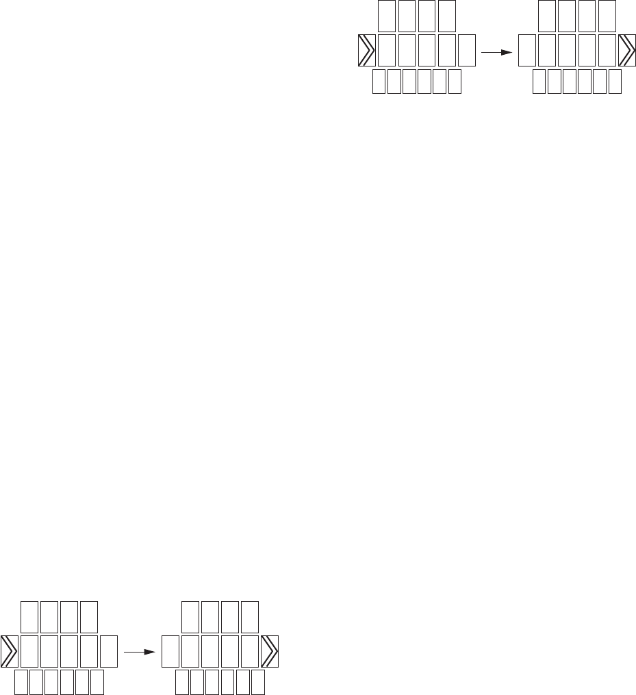
Second
digit Fourth
digit Sixt
h
digit
Third
digit
First
digit
Second line
First line
Third line
Fifth
digit

– 25 –
(13) [9] key check:
The set waits for the input of [9] key when “push 9 key” is dis-
played. When the [9] key is pushed, the set proceeds to (14).
(14) [1- -/--] key check:
The set waits for the input of [1- -/--] key when “push -/— key” is
displayed. When the [1- -/--] key is pushed, the set proceeds to
(15).
(15) [0] key check:
The set waits for the input of [0] key when “push 0 key” is dis-
played. When the [0] key is pushed, the set proceeds to (16).
(16) [2-] key check:
The set waits for the input of [2-] key when “push 2- key” is dis-
played. When the [2-] key is pushed, the set proceeds to (17).
(17) [ $RED%] key check:
The set waits for the input of [ $RED%] key when “push RED key”
is displayed. When the [ $RED%] key is pushed, the set proceeds
to (18).
(18) [ $GREEN%] key check:
The set waits for the input of [ $GREEN%] key when “push GREEN
key” is displayed. When the [ $GREEN%] key is pushed, the set
proceeds to (19).
(19) [ $YELLOW%] key check:
The set waits for the input of [ $YELLOW%] key when “push
YELLOW key” is displayed. When the [ $YELLOW%] key is
pushed, the set proceeds to (20).
(20) [ $BLUE%] key check:
The set waits for the input of [ $BLUE%] key when “push BLUE
key” is displayed. When the [ $BLUE%] key is pushed, the set
proceeds to (21).
(21) N v key check:
The set waits for the input of N vkey when “push UP key” is
displayed. When the N vkey is pushed, the set proceeds to (22).
(22) m b key check:
The set waits for the input of m bkey when “push ← key” is
displayed. When the m bkey is pushed, the set proceeds to
(23).
(23) M B key check:
The set waits for the input of M Bkey when “push → key” is
displayed. When the M Bkey is pushed, the set proceeds to
(24).
(24) x V key check:
The set waits for the input of x Vkey when “push DOWN key”
is displayed. When the x Vkey is pushed, the set proceeds to
(25).
(25) [MENU ] key check:
The set waits for the input of [MENU ] key when “push MENU
key” is displayed. When the [MENU ] key is pushed, the set
proceeds to (26).
(26) [OK ] key check:
The set waits for the input of [OK ] key when “push OK key” is
displayed. When the [OK ] key is pushed, the set proceeds to
(27).
(27) [ +] key check:
The set waits for the input of [ +] key when “push VOL + key”
is displayed. When the [ +] key is pushed, the set proceeds to
(28).
(28) [ --] key check:
The set waits for the input of [ --] key when “push VOL - key”
is displayed. When the [ --] key is pushed, the set proceeds to
(29).
(29) % key check:
The set waits for the input of %key when “push MUTE key” is
displayed. When the %key is pushed, the set proceeds to (30).
(30) [PROGR +] key check:
The set waits for the input of [PROGR +] key when “push CH +
key” is displayed. When the [PROGR +] key is pushed, the set
proceeds to (31).
(31) [PROGR --] key check:
The set waits for the input of [PROGR --] key when “push CH -
key” is displayed. When the [PROGR --] key is pushed, the set
proceeds to (32).
(32) key check:
The set waits for the input of key when “push RECALL key” is
displayed. When the key is pushed, the set proceeds to (33).
(33) Jog right check:
The set waits for the jog right turn when “turn RIGHT JOG” is
displayed. When the jog is turned to the right, the set proceeds to
(34). (In this item, “SKIP” is disabled)
(34) Jog left check:
The set waits for the jog left turn when “turn LEFT JOG” is dis-
played. When the jog is turned to the left, the Key test finishes and
the “LEARN TEST” is displayed for selection. (In this item,
“NEXT TEST” is disabled)
4. LEARN test
The learn function is tested. Infrared data are sent from other re-
mote commander to the photodetector for the learn function to
test if the learn function operates normally, and the learned data
are outputted through infrared when the jog is pushed. Check if
the learning data are identical to the infrared output data using an
external device. (For the test, use the exclusive checker in the fac-
tory, and the product in the field)
(1) Infrared input check:
The set waits for the input of infrared data (PDT) when “input
LEARN” is displayed on the LCD. If infrared data input is abnor-
mal, “NG input LEARN” is displayed on the LCD. “input
LEARN”is again displayed when the jog is pushed. If infrared
data input is normal, “GOOD input LEARN” is displayed on the
LCD. The set proceeds to (2) when the jog is pushed.
(2) Learned data output check:
The learned data are outputted by the amount of 3 frames from the
REM. Then, the Learn test finished, and the set proceeds to the
MEMORY test.
x
x
x
x
x
x
x
x
x
x
x
x
z
z
z
X
X
X
2
2
2
2
2
2
– 26 –
5. MEMORY test
• For the EEPROM, the memory occupation display, writing er-
ror history display, error test, and data erasing are carried out.
• For the writing error history display, whether the data writing
error occurred since the EEPROM was erased last is displayed.
• For the error test, the data are written to all areas, and then
whether all data are correct is checked and the result is displayed.
• After the error test finished, the data in all areas of EEPROM
are erased and all settings are initialized.
(1) EEPROM memory occupation display
How many percents of all memory areas are occupied with the
learned data is displayed in steps of 10%. When no data is stored,
0% is displayed, or otherwise, the unit place is rounded up. The
set proceeds to (2) when the jog is pushed.
(2) EEPROM writing error history display
In actual, each time the writing error occurred in the EEPROM,
the error flag turns on. “MISSED MEMORY” is displayed on the
LCD if the error flag is present, or “NO MISSED MEMORY” is
displayed if not present. The set proceeds to (3) when the jog is
pushed.
(3) EEPROM error test
(a) Memory writing confirmation display
“WRITE MEMORY” and “push SETkey MEMORY”
are alternately displayed on the LCD every second. The
set proceeds to (b) if the SET key is pushed.
(b) Memory data writing (-1)
The lower 8-bit values of the memory addresses are
written to all areas.
If an error occurred during data writing, the set goes to
(g) with the error flag turned on, or if no error occurs,
the set proceeds to (c).
(c) Memory data check (-1)
All bytes are read for checking.
If an error occurred during data check, the set goes to
(g) with the error flag turned on, or if no error occurs,
the set proceeds to (d).
(d) Memory data writing (-2)
The inverted lower 8-bit values of the memory addresses
are written to all areas.
If an error occurred during data writing, the set goes to
(g) with the error flag turned on, or if no error occurs,
the set proceeds to (e).
(e) Memory data check (-2)
All bytes are read for checking. If an error occurred dur-
ing data check, the set goes to (g) with the error flag
turned on, or if no error occurs, the set proceeds to (f).
(f) Memory erasing
All bytes are erased to return all settings to initial state.
If an error occurred, the set goes to (g) with the error
flag turned on, or if no error occurs, the set proceeds to
(g).
For the LCD display of (b) to (f), see below.
(g) Memory check result display
“TEST GOOD MEMORY” is displayed on the LCD if
the error flag is not present, or “TEST ERROR
MEMORY” is displayed if the error flag is present. Push
the jog, and the MEMORY test finishes and the
“MEMORY ERASE” is displayed for selection.
6. MEMORY ERASE
(1) Memory erasing
(a) Memory erasing confirmation display
“DELETE MEMORY” and “push SETkey MEMORY”
are alternately displayed on the LCD every second. The
set proceeds to (b) if the SET key is pushed.
(b) All bytes in the EEPROM are erased to return all set-
tings to initial state.
During this operation if an error occurred, the set goes
to (c) with the error flag turned on, or if no error occurs,
the set proceeds to (c) with the error flag not turned on.
For the LCD display of (a) and (b), see below.
(c) Memory erasing result display
“DEL GOOD MEMORY” is displayed on the LCD if
the error flag is not present, or “DEL NG MEMORY” is
displayed if the error flag is present. Push the jog, and
the MEMORY ERASE test finishes and the test items
are displayed for selection.
TTES
MEMORY
TTES
MEMORY
DEL
MEMORY
DEL
MEMORY
RM-VZ950T
– 27 – – 28 –
SECTION 4
DIAGRAMS
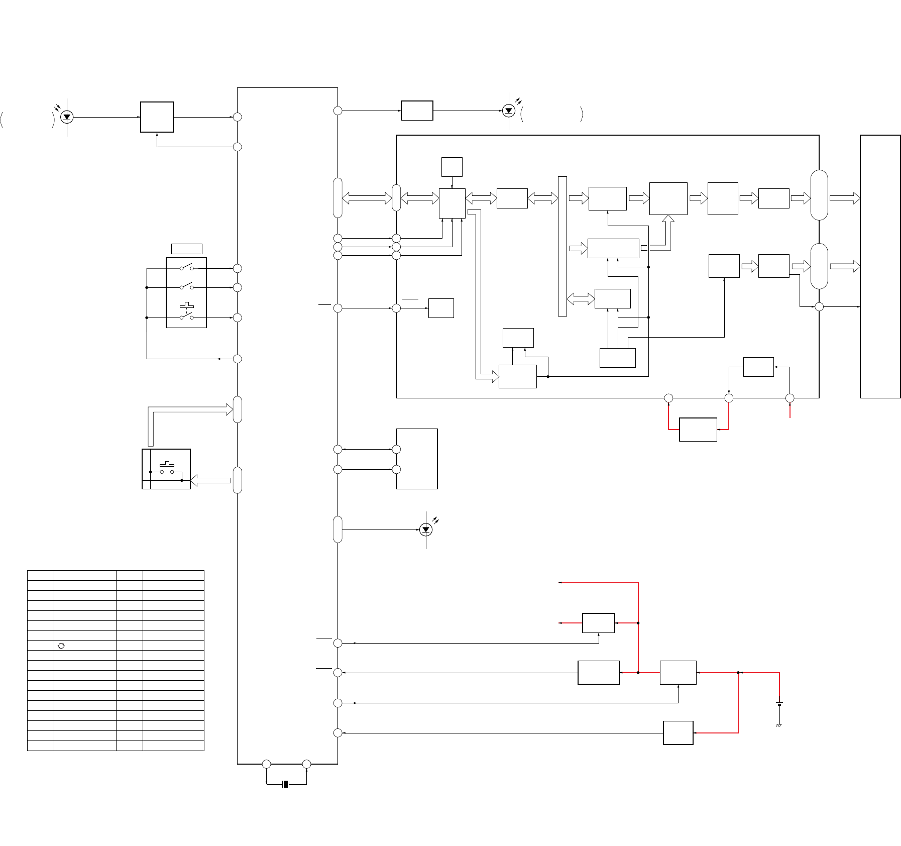
4-1. BLOCK DIAGRAM
61
27
63
64
65
58
44
8
9
10
40
41
42
6 39
16 5
18
5
60
31
66
70
6
76 – 80, 1 – 3
43 – 50
DB0 – DB7
19 – 2552 – 57
36 – 39
69
30 32 37
26
11 – 17,
19 – 25, 51 – 57
C1 – C7,
C9 – C15, C17 – C23
S1 – S15,
S21 – S25, S41 – S50
1 – 8, 59 – 73,
79 – 83, 99, 100
D1
REMOTE CONTROL
SIGNAL RECEIVER
PDT
PCNT
JDT1
JDT2
JDT3
JST
REM
RS
RW
E
LRST
SDA
SCL
DB0 – DB7
FUNCTION
SW1
KDT1 – KDT7KST1 – KST7
SYSTEM
CONTROLLER
IC1
BL1 – BL4
KEY MATRIX
S11 – 17, S21 – 23,
S25 – 27, S31 – 35,
S41 – 46, S52, S53,
S55 – 57, S62 – 65
05
Ref No.
S11
S12
S13
S14
S15
S16
S17
S21
S22
S23
S25
S26
S27
S31
S32
S33
S34
PANEL DESIGNATION
1
3
9
x (BLUE)
M B
PROGR –
a
6
2 –
OK X
PROGR +
SET
/
2
8
x (YELLOW)
PANEL DESIGNATION
N v
t
5
0
x (GREEN)
x V
2 +
4
1 – -/--
MENU z
2 –
%
1
7
x (RED)
m b
Ref No.
S35
S41
S42
S43
S44
S45
S46
S52
S53
S55
S56
S57
S62
S63
S64
S65
LPOW
RESET
CE
VDET
X1
X2
X1
5MHz
B+ SWITCH
Q2
RESET SIGNAL
GENERATOR
IC7
DC/DC
CONVERTER
IC5
VOLTAGE
DETECT
IC6
SYSTEM CONTROLLER (IC1),
EEPROM (IC3), LED B+
LCD B+
LIQUID CRYSTAL DISPLAY
DRIVER (IC2) B+
DRY BATTERY
SIZE “AA”
(IEC DESIGNATION R6)
2PCS. 3V
D5 – 8
(LCD BACK LIGHT)
SDA
SCL
EEPROM
IC3
BUSY
FLAG
DATA
REGISTER
SEGMENT
DRIVER
BOOSTER
CIRCUIT
ADDRESS
COUNTER
RESET
CIRCUIT
IN/OUT
BUFFER
INSTRUCTION
REGISTER
& DECODER
CHARACTOR
GENERATOR
CIRCUIT
SHIFT
REGISTER
CIRCUIT
COMMON
DRIVER
PARALLEL/
SERIAL
CONVERTER
CIRCUIT
SHIFT
REGISTER
& LATCH
CIRCUIT
TIMING
GENERATOR
DISPLAY
DATA RAM
CURSOR BLINK
CONTROL CIRCUIT
RESET
E
R/W
RS
LIQUID CRYSTAL
DISPLAY DRIVER
IC2
–5V
REGULATOR
IC8
LCD B+
V5
V5OUT
VCI
CMK1
LCD1
LIQUID
CRYSTAL
DISPLAY
LED DRIVE
Q1
D3, 4
REMOTE CONTROL
SIGNAL TRANSMITTER
BUFFER,
WAVEFORM
SHAPING
IC4
RM-VZ950T
– 29 – – 30 –
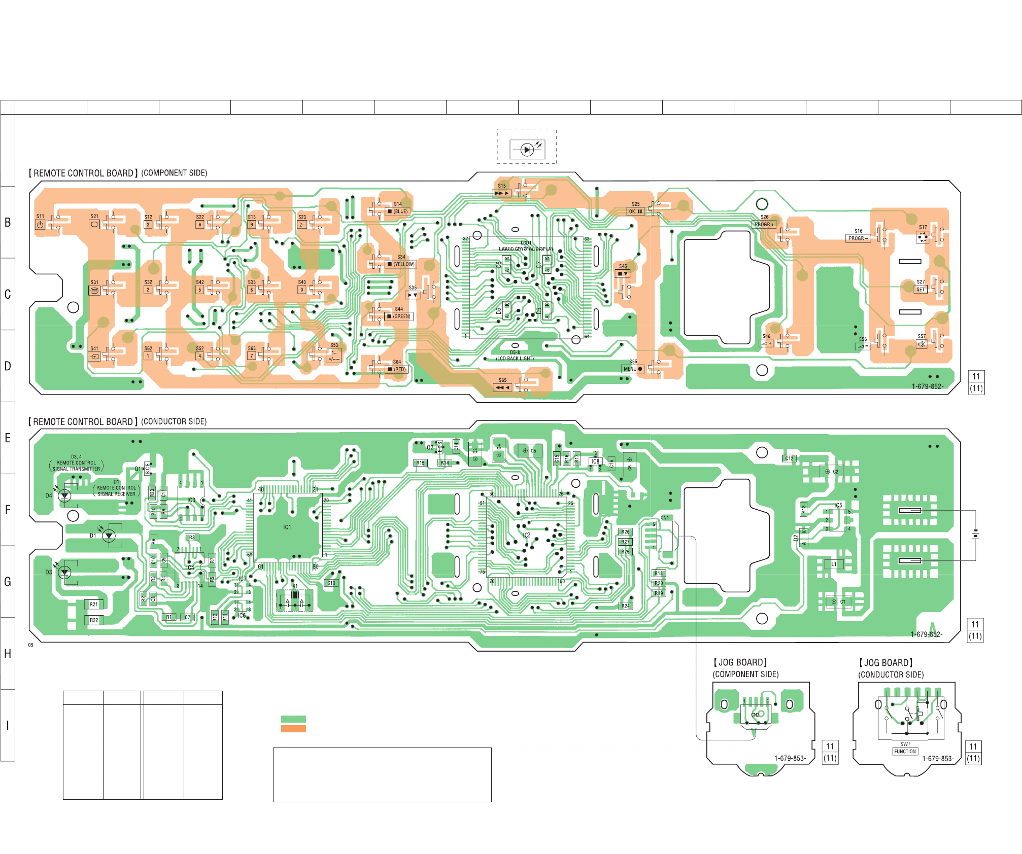
4-2. PRINTED WIRING BOARDS
D5-8
)
DRY
B
ATTERY
SIZE “AA”
(
IEC DESIGNATION R6
)
2P
CS
. 3
V
123 4 5 6 7 8 9 10 11 12 13 14
A
Note on Printed Wiring Boards:
•Y: parts extracted from the conductor side.
•z: Through hole.
•f: internal component.
• : Pattern from the side which enables seeing.
• : Carbon pattern.
(The other layers' patterns are not indicated.)
Caution:
Pattern face side: Parts on the pattern face side seen from
(Conductor Side) the pattern face are indicated.
Parts face side: Parts on the parts face side seen from
(Component Side) the parts face are indicated.
IC2 G-8
IC3 F-3
IC4 G-3
IC5 F-12
IC6 G-4
IC7 G-4
IC8 E-9
Q1 E-2
Q2 E-6
Ref. No. Location
Ref. No. Location
D1 F-2
D2 F-11
D3 G-1
D4 F-1
D5 C-8
D6 C-7
D7 C-8
D8 C-7
IC1 F-4
• Semiconductor Location
RM-VZ950T
WAVEFORM
SHAPING
,
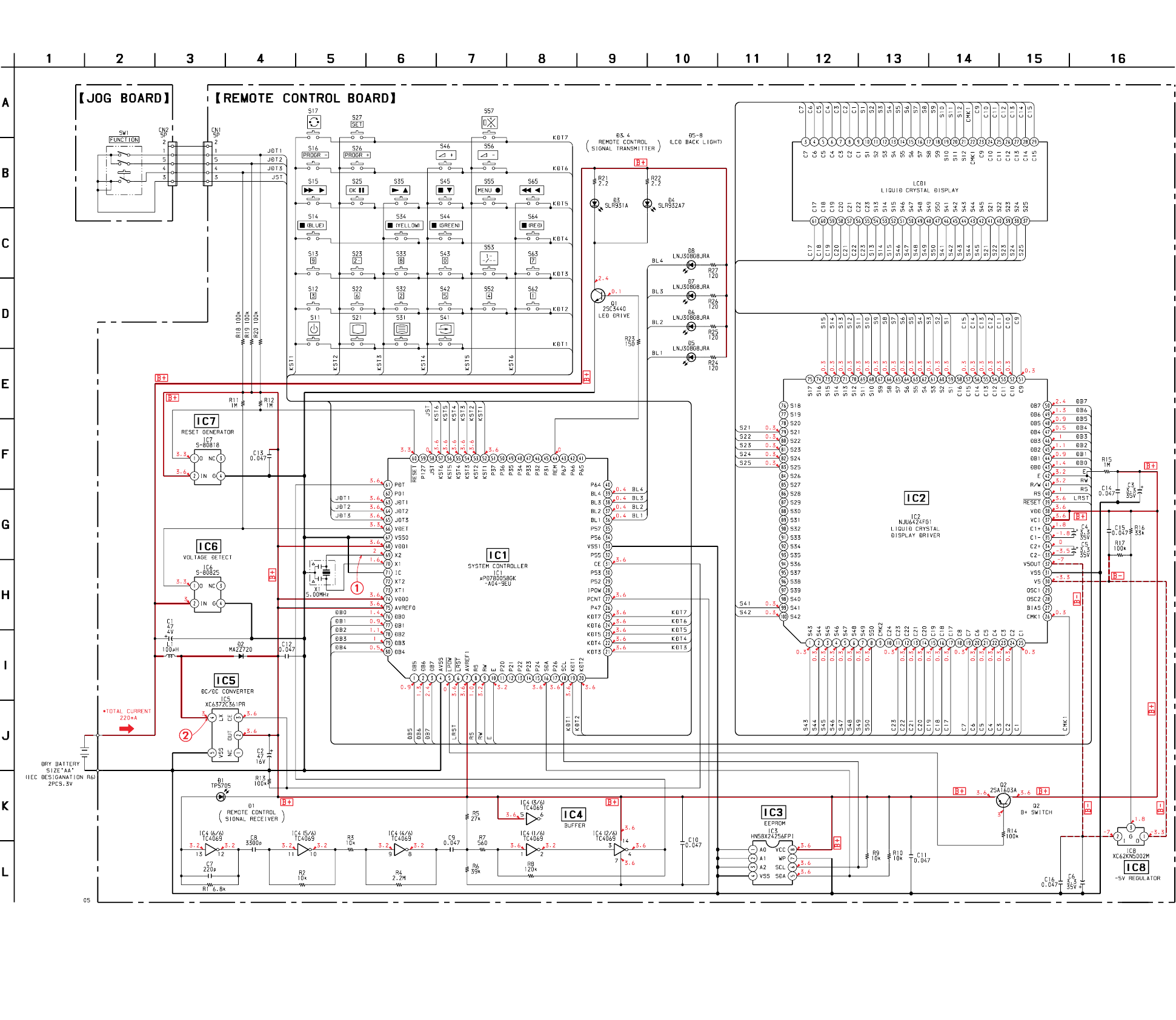
4-3. SCHEMATIC DIAGRAM • See page 33 for Waveforms. • See page 34 for IC Block Diagrams.
– 31 – – 32 –
Note on Schematic Diagram:
• All capacitors are in µF unless otherwise noted. pF: µµF
50 WV or less are not indicated except for electrolytics
and tantalums.
• All resistors are in Ω and 1/4 W or less unless otherwise
specified.
•f: internal component.
•C: panel designation.
•U: B+ Line.
•V: B– Line.
• Power voltage is dc 3 V and fed with regulated dc power
supply from battery terminal.
• Voltages and waveforms are dc with respect to ground
under no-signal conditions.
• Voltages are taken with a VOM (Input impedance 10 MΩ).
Voltage variations may be noted due to normal produc-
tion tolerances.
• Waveforms are taken with a oscilloscope.
Voltage variations may be noted due to normal produc-
tion tolerances.
• Circled numbers refer to waveforms.
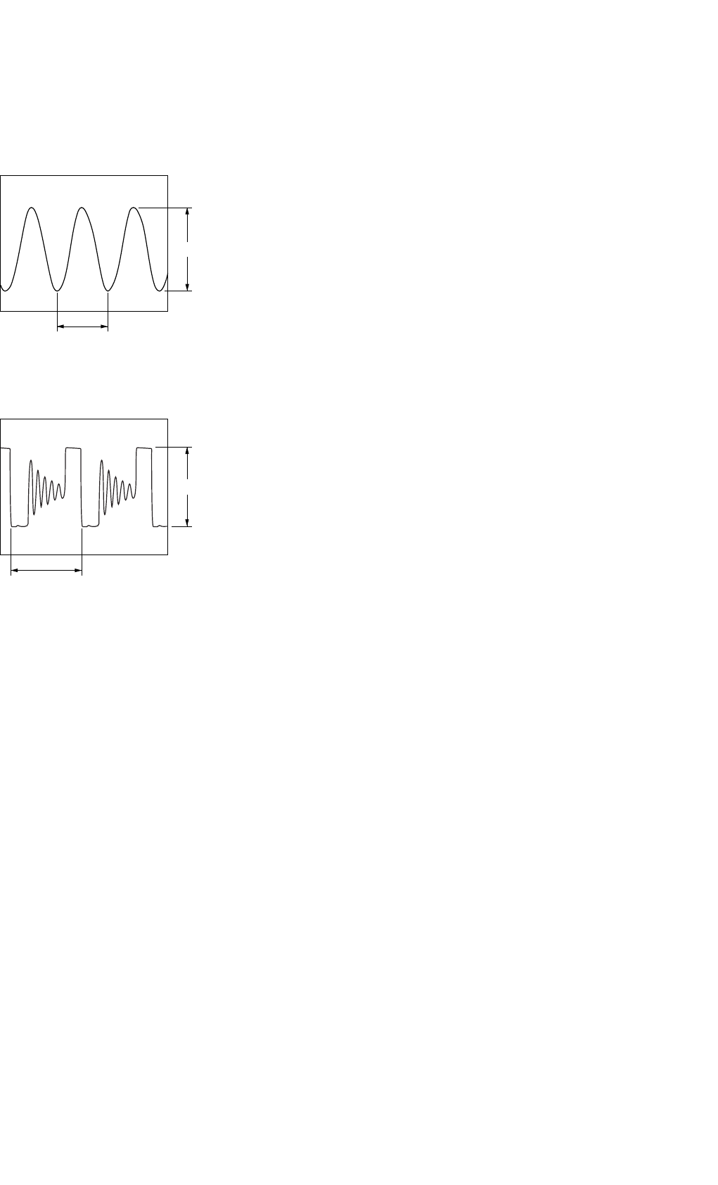
– 33 – – 34 –
• Waveforms
– REMOTE CONTROL Board –
1IC1 yl (X2)
1V/DIV, 50 ns/DIV
2IC5 4 (LX)
1V/DIV, 5 µs/DIV
3.9 Vp-p
200 ns
4.6 Vp-p
11.4
µ
s
• IC Block Diagrams
IC2 NJU6424FG1-T
1
2
3
4
5
6
7
8
9
10
11
12
13
14
15
16
17
18
19
20
21
22
23
24
25
58
57
56
55
54
53
52
51
72
71
70
69
68
67
66
65
75
74
73
64
63
62
61
60
59
SEGMENT
SIGNAL
DRIVER
50BIT
LATCH
CIRCUIT
CHARACTOR
GENERATOR
9600BIT
CHARACTOR
GENERATOR
32 X 5BIT
50BIT
SHIFT
REGISTER
TIMING
GENERATOR
CIRCUIT
PARALLEL/SERIAL
CONVERTER
CIRCUIT
COMMON
SIGNAL
DRIVER
26BIT
SHIFT
REGISTER
CURSOR
BLINK
CONTROL
CIRCUIT
DATA
REGISTER
DISPLAY DATA RAM
30 X 8BITS
26
BIAS
CIRCUIT
CR OSCILLATOR
CIRCUIT
BOOSTER
CIRCUIT
27
RESET
CIRCUIT
39 40 41 42 43 44 45 46 47 48 49 50
28
100 99 98 97 96 95 94 93 92 91 90 89 88 87 86 85 84 83 82 81 80 79 78 77 76
29 30 31 3833 3432 35 36 37
ADDRESS
COUNTER
INSTRUCTION
DECODER
INSTRUCTION
REGISTER
BUSY
FLAG
IN/OUT BUFFER
SEG43
SEG44
SEG45
SEG46
SEG47
SEG48
SEG49
SEG50
COMMK2
COM24
COM23
COM22
COM21
COM20
COM19
COM18
COM17
COM8
COM7
COM6
COM5
COM4
COM3
COM2
COM1
C
OMMK1
BIAS
RESET
RS
R/W
E
DB0
DB1
DB2
DB3
DB4
DB5
DB6
DB7
OSC2
OSC1
V5
VSS
C2–
C2+
V5OUT
C1–
C1+
VCI
VDD
COM16
COM15
COM14
COM13
COM12
COM11
COM10
COM9
SEG17
SEG16
SEG15
SEG14
SEG13
SEG12
SEG11
SEG10
SEG9
SEG8
SEG7
SEG6
SEG5
SEG4
SEG3
SEG2
SEG1
SEG4
2
SEG41
SEG4
0
SEG3
9
SEG3
8
SEG3
7
SEG3
6
SEG3
5
SEG3
4
SEG3
3
SEG3
2
SEG31
SEG3
0
SEG2
9
SEG2
8
SEG2
7
SEG2
6
SEG2
5
SEG2
4
SEG2
3
SEG2
2
SEG21
SEG2
0
SEG1
9
SEG1
8
IC5 XC6372C361PR-T
NC
VOUT
CE
VSS
LX
2
1
3
4
5
VLX
LIMITER
PWM/PFM
CONTROL
OSC 100kHz
BUFFER
PHASE
COMPARATOR
REFERENCE
VOLTAGE
CHIP
ENABLE
SLOW
START
+
–
VDD

– 35 –
4-4. IC PIN FUNCTION DESCRIPTION
• MAIN BOARD IC1 µPD780058GK-A04-9EU (SYSTEM CONTROLLER)
Pin No. Pin Name I/O Description
1 to 3 DB5 to DB7 I/O Two-way data bus with the liquid crystal display driver (IC2)
4 AVSS — Ground terminal (for A/D converter)
5 LPOW O Power on/off control signal output for the liquid crystal display driver (IC2) “L”: power on
6 LRST O Reset signal output to the liquid crystal display driver (IC2) “L”: reset
7 AVREF1 I Reference voltage input terminal (for A/D converter)
8RSO
Register selection signal output to the liquid crystal display driver (IC2)
9RWO
Data read/write selection signal output to the liquid crystal display driver (IC2)
“L”: data write, “H”: data read
10 E O Data enable signal output to the liquid crystal display driver (IC2)
11 to 15 P20 to P24 — Not used (open)
16 SDA I/O Two-way data bus with the EEPROM (IC3)
17 P26 — Not used (open)
18 SCL O Serial data transfer clock signal output to the EEPROM (IC2)
19 to 25 KDT1 to KDT7 I Key data input from the key matrix “L” input when key pressing
26 P47 — Not used (open)
27 PCNT O Learning control signal output to the TC4069 (IC4)
28 IPOW O Not used (open)
29, 30 P52, P53 — Not used (open)
31 CE O Power on/off control signal output supply to the DC/DC converter (IC5) “H”: power on
32 P55 — Not used (open)
33 VSS1 — Ground terminal
34, 35 P56, P57 — Not used (open)
36 to 39 BL1 to BL4 — LED drive signal output of the liquid crystal display back light (D5 to D8) “L”: LED on
40 to 43 P64 to P67 — Not used (open)
44 REM O LED drive signal output of the remote control signal transmitter (D3, D4) “H”: LED on
45 to 51 P31 to P37 — Not used (open)
52 to 57 KST1 to KST6 O Key scan output to the key matrix “L” output when key waiting
58 JST O Jog scan output to the rotary encoder (SW1)
59 P127 — Not used (open)
60 RESET I System reset signal input from the reset signal generator (IC7) “L”: reset
For several hundreds msec. after the power supply rises, “L” is input, then it changes to “H”
61 PDT I Learning data input from the TC4069 (IC4)
62 P01 — Not used (open)
63 JDT1 I Jog dial pulse input of the rotary encoder (SW1) (A phase input)
64 JDT2 I Jog dial pulse input of the rotary encoder (SW1) (B phase input)
65 JDT3 I Push switch input of the rotary encoder (SW1)
66 VDET I Voltage detection signal input terminal
67 VSS0 — Ground terminal
68 VDD1 — Power supply terminal (+3.6V)
69 X2 O Main system clock output terminal (5 MHz)
70 X1 I Main system clock input terminal (5 MHz)
71 IC — Internal connection terminal (connected to ground)
72 XT2 O Sub system clock output terminal Not used (open)
73 XT1 I Sub system clock input terminal Not used (open)
74 VDD0 — Power supply terminal (+3.6V)
75 AVREF0 I Reference voltage input terminal (for A/D converter)
76 to 80 DB0 to DB4 I/O Two-way data bus with the liquid crystal display driver (IC2)
– 36 –
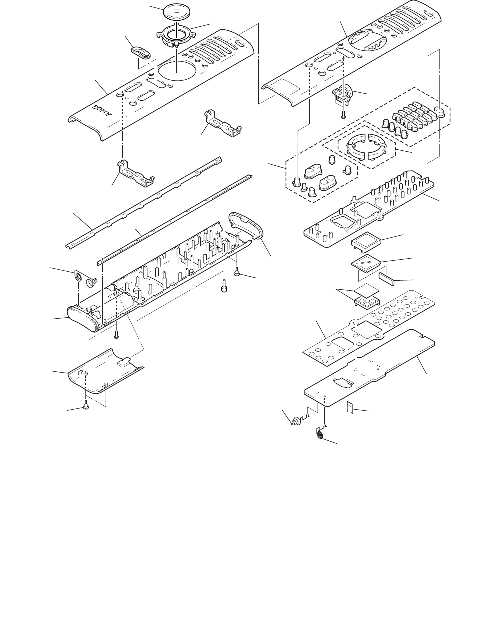
SECTION 5
EXPLODED VIEW
• Items marked “*” are not stocked since they
are seldom required for routine service. Some
delay should be anticipated when ordering
these items.
• The mechanical parts with no reference num-
ber in the exploded views are not supplied.
• Accessories and packing materials are given
in the last of the electrical parts list.
NOTE:
• -XX and -X mean standardized parts, so they
may have some difference from the original
one.
• Color Indication of Appearance Parts
Example:
KNOB, BALANCE (WHITE) . . . (RED)
↑↑
Parts Color Cabinet's Color
Ref. No. Part No. Description Remark Ref. No. Part No. Description Remark
1 3-220-687-01 FOOT, RUBBER
2 3-220-680-01 LID, BATTERY CASE
3 3-220-683-01 CASE (LOWER)
4 3-220-686-01 TERMINAL (C), BATTERY
*5 3-220-677-01 EDGE, SIDE
6 3-220-679-01 BUTTON (B)
7 3-220-681-01 CASE (TOP)
*8 3-220-672-01 ESCUTCHEON, JOG
9 3-220-691-01 PANEL, LCD
10 3-220-692-01 COVER, LCD
*11 3-220-682-01 CASE, INNER
12 A-4541-208-A JOG BOARD, COMPLETE
*13 3-220-675-01 KEY, RUBBER
14 3-220-689-01 TERMINAL, ZEBRA
*15 1-679-852-11 REMOTE CONTROL BOARD
16 9-885-008-54 WIRE
17 3-220-684-01 TERMINAL (A), BATTERY
18 3-220-685-01 TERMINAL (B), BATTERY
19 3-220-676-01 FILTER
*20 3-220-674-01 DOOM, POLY
21 3-220-678-01 BUTTON (A)
LCD1 9-885-008-47 DISPLAY PANEL, LIQUID CRYSTAL
#1 7-685-104-14 SCREW +P 2X6 TYPE2 NON-SLIT
#2 7-621-996-05 BOLT, HEXAGON SOCKET 2.6X5
#3 7-685-102-19 SCREW +P 2X4 NON-SLIT TYPE 2
not
supplied
not
supplied
LCD1
#1
1
2
3
4
5
not
supplied
not
supplied
7
8
9
10 11
12
6
5
#2
#3
21
19
1
13
14
20
15
16
17
18

– 37 –
SECTION 6
ELECTRICAL PARTS LIST
Ref. No. Part No. Description Remark Ref. No. Part No. Description Remark
JOG
REMOTE CONTROL
A-4541-208-A JOG BOARD, COMPLETE
********************
< CONNECTOR >
CN2 9-885-008-53 CONNECTOR 5P
< JOG ENCODER >
SW1 1-473-406-11 ENCODER, ED JOG (FUNCTION)
**************************************************************
*1-679-852-11 REMOTE CONTROL BOARD
**********************
3-220-684-01 TERMINAL (A), BATTERY
3-220-685-01 TERMINAL (B), BATTERY
3-220-689-01 TERMIAL, ZEBRA
< CAPACITOR >
C1 1-126-607-21 ELECT CHIP 47uF 20% 4V
C2 1-126-204-21 ELECT CHIP 47uF 20% 16V
C3 1-128-008-21 ELECT CHIP 3.3uF 20% 35V
C4 1-128-008-21 ELECT CHIP 3.3uF 20% 35V
C5 1-128-008-21 ELECT CHIP 3.3uF 20% 35V
C6 1-128-008-21 ELECT CHIP 3.3uF 20% 35V
C7 1-164-230-11 CERAMIC CHIP 220PF 5% 50V
C8 1-162-967-11 CERAMIC CHIP 0.0033uF 10% 50V
C9 1-164-361-11 CERAMIC CHIP 0.047uF 16V
C10 1-164-361-11 CERAMIC CHIP 0.047uF 16V
C11 1-164-361-11 CERAMIC CHIP 0.047uF 16V
C12 1-164-361-11 CERAMIC CHIP 0.047uF 16V
C13 1-164-361-11 CERAMIC CHIP 0.047uF 16V
C14 1-164-361-11 CERAMIC CHIP 0.047uF 16V
C15 1-164-361-11 CERAMIC CHIP 0.047uF 16V
C16 1-164-361-11 CERAMIC CHIP 0.047uF 16V
< CONNECTOR >
CN1 9-885-008-53 CONNECTOR 5P
< DIODE >
D1 9-885-008-55 DIODE TPS705 (HATA)
(REMOTE CONTROL SIGNAL RECEIVER)
D2 8-719-076-88 DIODE MA2Z720001S0
D3 1-807-851-11 LED SLR-931A
(REMOTE CONTROL SIGNAL TRANSMITTER)
D4 8-719-053-06 LED SLR-932A-7
(REMOTE CONTROL SIGNAL TRANSMITTER)
D5 8-719-058-69 LED LNJ308G8JRA (LCD BACK LIGHT)
D6 8-719-058-69 LED LNJ308G8JRA (LCD BACK LIGHT)
D7 8-719-058-69 LED LNJ308G8JRA (LCD BACK LIGHT)
D8 8-719-058-69 LED LNJ308G8JRA (LCD BACK LIGHT)
< IC >
IC1 8-759-699-74 IC uPD780058GK-A04-9EU
IC2 9-885-008-48 IC NJU6424FG1-T
IC3 9-885-008-49 IC HN58X24256FPI-T
IC4 8-759-530-29 IC TC4069UBFT (EL, N)
IC5 9-885-008-50 IC XC6372C361PR-T
IC6 8-759-479-03 IC S-80825ANNP-EDN-T2
IC7 8-759-665-49 IC S-80818ANNP-EDF-T2
IC8 9-885-008-51 IC XC62KN5002MR-T
< COIL >
L1 1-412-032-11 INDUCTOR CHIP 100uH
< TRANSISTOR >
Q1 8-729-047-62 TRANSISTOR 2SC3440-T12-1F
Q2 9-885-008-52 TRANSISTOR 2SA1603A-T
< RESISTOR >
R1 1-218-867-11 METAL CHIP 6.8K 5% 1/16W
R2 1-216-833-11 METAL CHIP 10K 5% 1/16W
R3 1-216-833-11 METAL CHIP 10K 5% 1/16W
R4 1-216-861-11 METAL CHIP 2.2M 5% 1/16W
R5 1-218-726-11 METAL CHIP 27K 5% 1/16W
R6 1-216-840-11 METAL CHIP 39K 5% 1/16W
R7 1-216-818-11 METAL CHIP 560 5% 1/16W
R8 1-216-846-11 METAL CHIP 120K 5% 1/16W
R9 1-216-833-11 METAL CHIP 10K 5% 1/16W
R10 1-216-833-11 METAL CHIP 10K 5% 1/16W
R11 1-216-857-11 METAL CHIP 1M 5% 1/16W
R12 1-216-857-11 METAL CHIP 1M 5% 1/16W
R13 1-216-845-11 METAL CHIP 100K 5% 1/16W
R14 1-216-845-11 METAL CHIP 100K 5% 1/16W
R15 1-216-857-11 METAL CHIP 1M 5% 1/16W
R16 1-216-839-11 METAL CHIP 33K 5% 1/16W
R17 1-216-845-11 METAL CHIP 100K 5% 1/16W
R18 1-216-845-11 METAL CHIP 100K 5% 1/16W
NOTE:
• Due to standardization, replacements in the
parts list may be different from the parts speci-
fied in the diagrams or the components used
on the set.
• -XX and -X mean standardized parts, so they
may have some difference from the original
one.
• RESISTORS
All resistors are in ohms.
METAL: Metal-film resistor.
METAL OXIDE: Metal oxide-film resistor.
F: nonflammable
• Items marked “*” are not stocked since they
are seldom required for routine service.
Some delay should be anticipated when order-
ing these items.
• SEMICONDUCTORS
In each case, u: µ, for example:
uA. . : µA. . uPA. . : µPA. .
uPB. . : µPB. . uPC. . : µPC. .
uPD. . : µPD. .
• CAPACITORS
uF: µF
• COILS
uH: µH
When indicating parts by reference
number, please include the board.

– 38 –
Ref. No. Part No. Description Remark Ref. No. Part No. Description Remark
R19 1-216-845-11 METAL CHIP 100K 5% 1/16W
R20 1-216-845-11 METAL CHIP 100K 5% 1/16W
R21 1-216-134-91 METAL CHIP 2.2 5% 1/8W
R22 1-216-134-91 METAL CHIP 2.2 5% 1/8W
R23 1-216-811-11 METAL CHIP 150 5% 1/16W
R24 1-216-810-11 METAL CHIP 120 5% 1/16W
R25 1-216-810-11 METAL CHIP 120 5% 1/16W
R26 1-216-810-21 METAL CHIP 120 5% 1/16W
R27 1-216-810-11 METAL CHIP 120 5% 1/16W
< VIBRATOR >
X1 1-767-452-11 VIBRATOR, CERAMIC (5MHz)
**************************************************************
MISCELLANEOUS
***************
16 9-885-008-54 WIRE
LCD1 9-885-008-47 DISPLAY PANEL, LIQUID CRYSTAL
**************************************************************
ACCESSORIES & PACKING MATERIALS
********************************
3-223-637-11 MANUAL, INSTRUCTION (ENGLISH, GERMAN)
3-223-637-21 MANUAL, INSTRUCTION (FRENCH, ITALIAN)
3-223-637-31 MANUAL, INSTRUCTION (DUTCH, SWEDISH)
3-223-637-41 MANUAL, INSTRUCTION
(SPANISH, PORTUGUESE)
3-223-638-11 MANUAL, INSTRUCTION (for PRESET)
(ENGLISH, FRENCH, GERMAN, SPANISH,
DUTCH, SWEDISH, ITALIAN, PORTUGUESE)
REMOTE CONTROL
RM-VZ950T
Sony Corporation
Audio Entertainment Group
9-927-994-11 2000H0538-1
Printed in Japan C 2000. 8
Published by General Engineering Dept.
