R&S/R&S FSP Series Service R&S
User Manual: R&S/R&S FSP Series Service
Open the PDF directly: View PDF ![]() .
.
Page Count: 207 [warning: Documents this large are best viewed by clicking the View PDF Link!]
- Tabbed Divider Overview
- Index
- Performance Test
- Test Instructions
- Measurement Equipment and Accessories
- Performance Test FSP
- Performance Test Option TV and RF Trigger: FSP-B6
- Performance Test Option Tracking Generator - FSP-B9
- Performance Test Option WCDMA Demodulation Hardware - FSP-B15
- Performance Test Option Electronic Attenuator- FSP-B25
- Performance Test Report FSP
- Performance Test Report Option FSP-B6
- Performance Test Report Option FSP-B9
- Performance Test Report Option FSP-B15
- Performance Test Report Option FSP-B25
- Adjustment
- Repair
- Instrument Design and Function Description
- Module Replacement
- Overview of the Modules
- Performing a Cold Boot
- Replacing the Front Module Controller A90
- Replacing the Lithium Battery on the Front Module Controller
- Replacing Hard Disk A60
- Replacing Flash Disk A60 (Option FSP-B20)
- Replacing the LCD and DC/AC Converter in the Front Module
- Replacing the Keyboard Membrane or Mat on the Front Module
- Replacing the Labelling Panel on the Front Module
- Replacing the Floppy Disk Drive A30
- Replacing the Power Supply A20
- Replacing the Fan
- Replacing the RF Input Connector (Cable W1)
- Replacing the Motherboard A10
- Replacing the Module RF Attenuator A40
- Replacing the Key/Probe Module A80 and Vol./Phone Board A191 (Option FSP-B3)
- Replacing the RF Frontend A100
- Replacing the Detector A120 or A140 (Option FSP-B70)
- Replacing the IF Filter A130
- Replacing the MW Converter Unit A160
- Replacing AF Demodulator A190 (Option FSP-B3)
- Replacing the OCXO A200 (Option FSP-B4)
- Replacing Trigger A230 (Option FSP-B6)
- Replacing the Tracking Generator A170 (Option FSP-B9)
- Replacing the External Generator Control A210 (Option FSP-B10)
- Replacing Wideband Calibrator A190 (Option FSP-B15)
- Replacing the LAN Adapter (Option FSP-B16)
- Replacing the Electronic Attenuator A50 (Option FSP-B25)
- Replacing the DC/DC Converter (Option FSP-B30)
- Replacing the Battery Charger Module (Option FSP-B31/32)
- Replacing the Batteries (Option FSP-B31/32)
- Troubleshooting
- Software Update / Installing Options
- Documents

1164.4556.82-01- 1
Test and Measurement
Division
Service Manual Instrument
SPECTRUM ANALYZER
R&S
FSP3
1164.4391.03
R&S
FSP7
1164.4391.07
R&S
FSP13
1164.4391.13
R&S
FSP30
1164.4391.30/.39
R&S
FSP40
1164.4391.40
Printed in the Federal
Republic of Germany
Dear Customer,
throughout this operating manual, the abbreviation FSP is used for your Spectrum Analyzer R&S FSP.
R&S® is a registered trademark of Rohde & Schwarz GmbH & Co. KG
Trade names are trademarks of the owners

FSP Tabbed Divider Overview
1164.4556.82REE-1
Tabbed Divider Overview
Index
Safety Instructions
Certificate of Quality
Spare Parts Express Service
List of R&S Representatives
Contents of Manuals for Spectrum Analyzer FSP
Service and Repair
Tabbed Divider
1 Chapter 1: Performance Test
2 Chapter 2: Adjustment
3 Chapter 3: Repair
4 Chapter 4: Firmware Update / Installation of Options
5 Chapter 5: Documents

FSP Index
1164.4556.82 I.1 E-1
Index
A
Adjustment .....................................................................2.1
frequency accuracy ..................................................2.6
Frequency response correction ................................2.8
functions...................................................................2.2
level accuracy ..........................................................2.4
level of the calibration signal.....................................2.2
manual .....................................................................2.3
Measuring equipment and Accessories ....................2.3
module data..............................................................2.8
reference frequency..................................................2.2
Akku Pack
replacement............................................................3.67
Audio demodulator
function.....................................................................3.8
replacement............................................................3.57
B
Bandwidth
Check.......................................................................1.8
check level accuracy ................................................1.7
Battery
replacement............................................................3.19
...............................................................................3.67
Battery Charger
replacement............................................................3.66
Battery pack
function.....................................................................3.9
...............................................................................3.67
Block circuit
description................................................................3.1
diagram ...........................................................5.5, 5.17
Boot-Problems
Troubleshooting......................................................3.70
C
Check
RF Trigger (B6) ......................................................1.20
TV Trigger (B6).......................................................1.20
Checking Comb Line Level B15)...................................1.25
D
DC Power supply
function.....................................................................3.9
DC/DC-Konverter..........................................................3.65
Detector
error message ........................................................3.75
function.....................................................................3.7
Display Linearity
Check.....................................................................1.13
Documents .....................................................................5.1
E
Electronic Attenuator
Check.....................................................................1.34
function.....................................................................3.2
replacement............................................................3.64
Error message
DETECTOR Access failed!.....................................3.75
LOUNL ...................................................................3.90
External generator control
function.................................................................... 3.9
External Generator Control
replacement........................................................... 3.61
F
Fanreplacement........................................................... 3.31
FFT bandwidth
check....................................................................... 1.7
FFT bandwith
function.................................................................... 3.8
Firmware update............................................................ 4.1
Flash Disk
replacement........................................................... 3.23
Floppy disk drive
replacement........................................................... 3.29
Frequency accuracy
adjustment ............................................................... 2.6
Check ...................................................................... 1.3
Frequency response
Check .................................................................... 1.10
correction................................................................. 2.8
Front module controller
function.................................................................. 3.10
replacement........................................................... 3.16
Front panel................................................................... 3.10
Frontend
function.................................................................... 3.3
replacement........................................................... 3.38
Troubleshooting..................................................... 3.90
Function description....................................................... 3.1
H
Hard disk
replacement........................................................... 3.22
I
IF Filter
function.................................................................... 3.5
replacement........................................................... 3.40
IF Gain
Check .................................................................... 1.16
function.................................................................... 3.5
IF image frequency rejection
Check ...................................................................... 1.4
function.................................................................... 3.3
IF rejection
check....................................................................... 1.5
Immunity to interference
Check ...................................................................... 1.3
Instrument design........................................................... 3.1
K
Key/Probe
function.................................................................. 3.11
replacement........................................................... 3.36
Keyboard
function.................................................................. 3.10
replacement........................................................... 3.26

Index FSP
1164.4556.82 I.2 E-1
L
LAN interface
function.....................................................................3.9
LAN-Interface
replacement............................................................3.63
LC-Display....................................................................3.10
Level accuracy
adjustment................................................................2.4
Check.....................................................................1.10
Lithium battery
replacement............................................................3.19
M
Manuel adjustment .........................................................2.3
Measurement Equipment
Performance Test.....................................................1.1
Measuring equipment
adjustment................................................................2.3
troubleshooting.......................................................3.68
Mechanical Drawings......................................................5.5
Microwave converter
function.....................................................................3.4
replacement............................................................3.41
Module replacement .....................................................3.12
AF-Demodulator .....................................................3.57
Battery....................................................................3.19
Detectorboard A120 ...............................................3.39
Electronic Attenuator ..............................................3.64
External Generator Control.....................................3.61
Fan.........................................................................3.31
flash disk................................................................3.23
Floppy disk drive ....................................................3.29
Front module controller A90 ...................................3.16
hard disk.................................................................3.22
IF-Filter A130..........................................................3.40
Key/Probe ..............................................................3.36
Keyboard................................................................3.26
Labelling panel .......................................................3.28
LAN-Interface .........................................................3.63
Motherboard A10....................................................3.33
MW Converter Unit A160........................................3.41
OCXO.....................................................................3.58
Power supply..........................................................3.30
RF Attenuator.........................................................3.35
RF Frontend ...........................................................3.38
RF input connector (cable W1) ...............................3.32
Switching mat.........................................................3.26
Switching membrane..............................................3.26
Tracking Generator.................................................3.60
Trigger....................................................................3.59
Vol./Phone board....................................................3.36
Wideband calibrator.......................................3.61, 3.63
Modules overview.........................................................3.14
Motherboard
function...................................................................3.11
replacement............................................................3.33
N
Noise display
Check.......................................................................1.9
Nonlinearities
Check.......................................................................1.6
O
OCXO
function.....................................................................3.6
replacement............................................................3.58
Option
FSP-B10
function.............................................................. 3.9
replacement..................................................... 3.61
FSP-B15
replacement............................................ 3.61, 3.63
FSP-B16
function.............................................................. 3.9
3.63
FSP-B25
function.............................................................. 3.2
replacement..................................................... 3.64
FSP-B3
function.............................................................. 3.8
replacement..................................................... 3.57
FSP-B30
function.............................................................. 3.9
FSP-B31
replacement............................................ 3.66, 3.67
replacement..................................................... 3.67
3.67
FSP-B31/32
function.............................................................. 3.9
FSP-B4
function.............................................................. 3.6
replacement..................................................... 3.58
FSP-B6
function.............................................................. 3.8
replacement..................................................... 3.59
FSP-B9
function.............................................................. 3.9
installation ......................................................... 4.3
list...................................................................... 4.3
FSP-B32
replacement..................................................... 3.67
replacement............................................ 3.66, 3.67
P
Password....................................................................... 2.2
Performance Test........................................................... 1.1
Bandwidth................................................................ 1.8
Display Linearity .................................................... 1.13
Electronic Attenuator (B25).................................... 1.34
Frequency accuracy................................................. 1.3
Frequency response .............................................. 1.10
Frequency Response with Elec. Attenuator (B25).. 1.30
Frequency Response with Preamplifier (B25) ........ 1.27
IF image frequency rejection.................................... 1.4
IF rejection............................................................... 1.5
IF-Gain Switching .................................................. 1.16
Immunity to interference........................................... 1.3
Level accuracy....................................................... 1.10
Level accuracy Bandw. Switch. ............................... 1.7
Level accuracy with Electr. Attenuator (B25).......... 1.30
Level accuracy with Preamplifier (B25).................. 1.27
Noise display ........................................................... 1.9
Noise Display with Preamplifier (B25).................... 1.26
Nonlinearities........................................................... 1.6
Nonlinearities with Electronic Attenuator (B25) ...... 1.32
Phase Noise .......................................................... 1.18
Reference accuracy................................................. 1.3
Reference Level Switching..................................... 1.16
Report FSP............................................................ 1.35
Report Option FSP-B15......................................... 1.51
Report Option FSP-B25......................................... 1.52
Report Option FSP-B6........................................... 1.49
Report Option FSP-B9........................................... 1.50
RF Attenuator ........................................................ 1.15
RF Attenuator (with Option B25)............................ 1.33
Shape factor ............................................................ 1.8

FSP Index
1164.4556.82 I.3 E-1
TG Frequency Response (B9)................................1.21
TG-Amplitude Modulation (B9) ...............................1.23
TG-Frequency Modulation (B9)...............................1.24
TG-I/Q Modulation (B9)...........................................1.22
TG-Output Level (B9) .............................................1.21
Third Order Intercept ................................................1.6
Third Order Intercept w. Elec. Attenuator (B25)......1.32
Phase Noise
Check.....................................................................1.18
Power cables..................................................................5.3
Power supply
function...................................................................3.11
replacement............................................................3.30
Preamplifier
function.....................................................................3.2
Probe power connector.................................................3.37
R
Reference frequency
Check.......................................................................1.3
function.....................................................................3.6
Reference Level Switching
Check.....................................................................1.16
Refurbished Modules......................................................5.2
Repair.............................................................................3.1
Replacement
module ...................................................................3.12
RF Attenuator
Check.....................................................................1.15
Check (with Option B25).........................................1.33
function.....................................................................3.2
replacement............................................................3.35
S
Service menu..................................................................2.1
Shape factor
Check.......................................................................1.8
Shipping
Instrument ................................................................5.1
Module .....................................................................5.1
Softkey
CAL SIGNAL POWER..............................................2.2
ENTER PASSWORD ...............................................2.2
FIRMWARE UPDATE.............................................. 4.1
REF FREQUENCY .................................................. 2.2
RESTORE FIRMWARE........................................... 4.1
SAVE CHANGES .................................................... 2.2
SELFTEST RESULTS ........................................... 3.78
SERVICE................................................................. 2.1
Software update............................................................. 4.1
Spare parts
electrical parts................................................. 5.5, 5.17
list of all parts........................................................... 5.7
Ordering................................................................... 5.2
Refurbished Modules............................................... 5.2
Switch-on problems...................................................... 3.69
T
Third Order Intercept
check....................................................................... 1.6
check (with Elec. Attenuator) ................................. 1.32
Tracking generator......................................................... 3.9
function.................................................................... 3.9
Trigger
replacement........................................................... 3.59
Troubleshooting ........................................................... 3.68
Frontend ................................................................ 3.90
loading module-EEPROMs .................................... 3.76
Local oscillator....................................................... 3.90
problems with boot process ................................... 3.70
Selftest .................................................................. 3.78
switch-on problems................................................ 3.69
TV and RF trigger........................................................... 3.8
function.................................................................... 3.8
V
Video bandwidth ............................................................ 3.8
Vol./Phones
function.................................................................. 3.11
replacement........................................................... 3.36
W
Wideband calibrator
replacement.................................................. 3.61, 3.63
Safety Instructions
1129.9055.12 Sheet 17
This unit has been designed and tested in accordance with the EC Certificate of Conformity and has left the
manufacturer’s plant in a condition fully complying with safety standards.
To maintain this condition and to ensure safe operation, the user must observe all instructions and warnings
given in this operating manual.
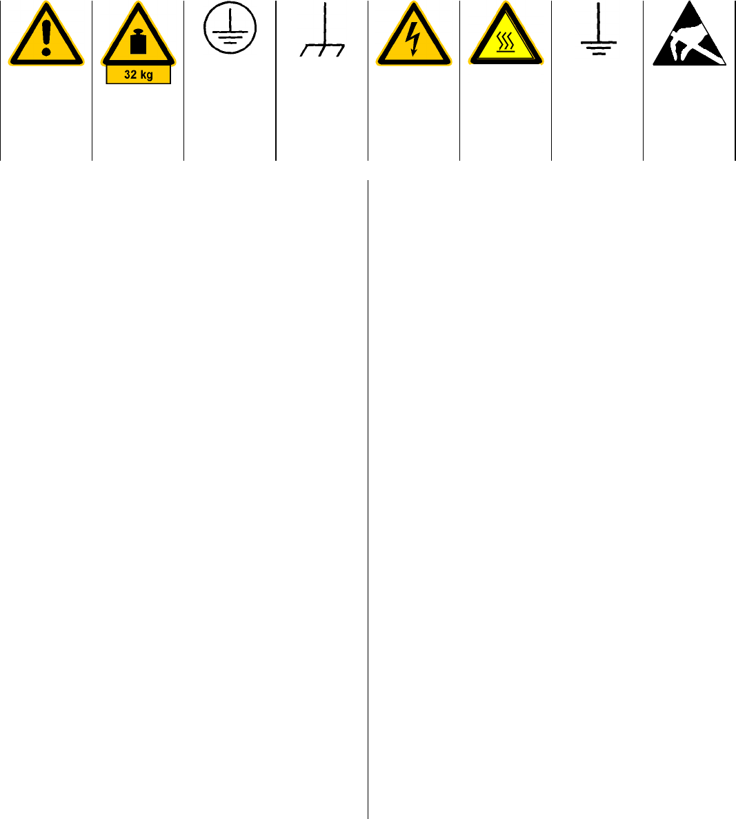
Safety-related symbols used on equipment and documentation from R&S:
Observe
operating
instructions
Weight
indication for
units >18 kg
PE terminal Ground
terminal Danger!
Shock hazard
Warning!
Hot surfaces Ground Attention!
Electrostatic
sensitive de-
vices require
special care
1. The unit may be used only in the operating con-
ditions and positions specified by the manufac-
turer. Unless otherwise agreed, the following
applies to R&S products:
IP degree of protection 2X, pollution severity 2
overvoltage category 2, only for indoor use, al-
titude max. 2000 m.
The unit may be operated only from supply net-
works fused with max. 16 A.
Unless specified otherwise in the data sheet, a
tolerance of 10% shall apply to the nominal
voltage and of 5% to the nominal frequency.
2. For measurements in circuits with voltages Vrms
> 30 V, suitable measures should be taken to
avoid any hazards.
(using, for example, appropriate measuring
equipment, fusing, current limiting, electrical
separation, insulation).
3. If the unit is to be permanently wired, the PE
terminal of the unit must first be connected to
the PE conductor on site before any other con-
nections are made. Installation and cabling of
the unit to be performed only by qualified techni-
cal personnel.
4. For permanently installed units without built-in
fuses, circuit breakers or similar protective de-
vices, the supply circuit must be fused such as
to provide suitable protection for the users and
equipment.
5. Prior to switching on the unit, it must be ensured
that the nominal voltage set on the unit matches
the nominal voltage of the AC supply network.
If a different voltage is to be set, the power fuse
of the unit may have to be changed accordingly.
6. Units of protection class I with disconnectible
AC supply cable and appliance connector may
be operated only from a power socket with
earthing contact and with the PE conductor con-
nected.
7. It is not permissible to interrupt the PE conduc-
tor intentionally, neither in the incoming cable
nor on the unit itself as this may cause the unit
to become electrically hazardous.
Any extension lines or multiple socket outlets
used must be checked for compliance with rele-
vant safety standards at regular intervals.
8. If the unit has no power switch for disconnection
from the AC supply, the plug of the connecting
cable is regarded as the disconnecting device.
In such cases it must be ensured that the power
plug is easily reachable and accessible at all
times (length of connecting cable approx. 2 m).
Functional or electronic switches are not suit-
able for providing disconnection from the AC
supply.
If units without power switches are integrated in
racks or systems, a disconnecting device must
be provided at system level.
9. Applicable local or national safety regulations
and rules for the prevention of accidents must
be observed in all work performed.
Prior to performing any work on the unit or
opening the unit, the latter must be discon-
nected from the supply network.
Any adjustments, replacements of parts, main-
tenance or repair may be carried out only by
authorized R&S technical personnel.
Only original parts may be used for replacing
parts relevant to safety (eg power switches,
power transformers, fuses). A safety test must
be performed after each replacement of parts
relevant to safety.
(visual inspection, PE conductor test, insulation-
resistance, leakage-current measurement, func-
tional test).
continued overleaf

Safety Instructions
1129.9055.12 Sheet 18
10. Ensure that the connections with information
technology equipment comply with IEC950 /
EN60950.
11. Lithium batteries must not be exposed to high
temperatures or fire.
Keep batteries away from children.
If the battery is replaced improperly, there is
danger of explosion. Only replace the battery by
R&S type (see spare part list).
Lithium batteries are suitable for environmen-
tally-friendly disposal or specialized recycling.
Dispose them into appropriate containers, only.
Do not short-circuit the battery.
12. Equipment returned or sent in for repair must be
packed in the original packing or in packing with
electrostatic and mechanical protection.
13. Electrostatics via the connectors may dam-
age the equipment. For the safe handling and
operation of the equipment, appropriate
measures against electrostatics should be im-
plemented.
14. The outside of the instrument is suitably
cleaned using a soft, lint-free dustcloth. Never
use solvents such as thinners, acetone and
similar things, as they may damage the front
panel labeling or plastic parts.
15. Any additional safety instructions given in this
manual are also to be observed.
Safety Instructions
1093.4820.82 SI E-1
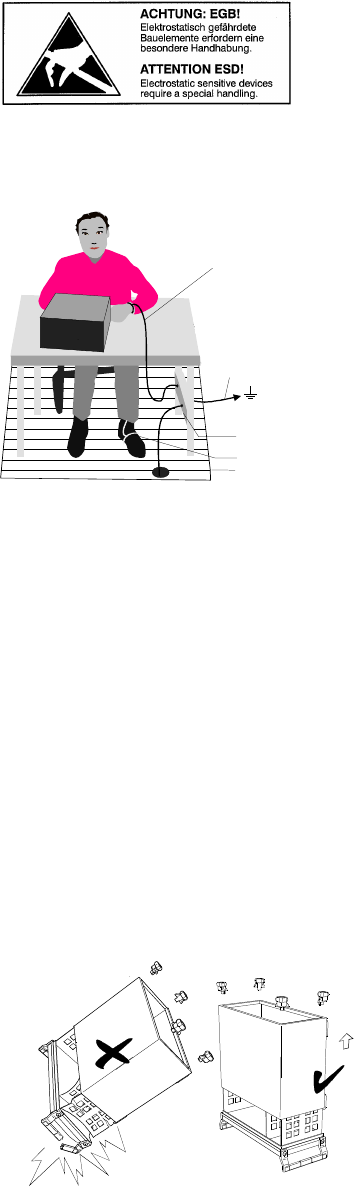
The instrument contains components which are hazardous to electrostatic exposure and which are marked by the
following symbol:
• To avoid damage of electronic components, the operational site must be protected against electrostatic di-
scharge (ESD).
Wrist strap with cord
Building ground
Floor mat
Ground connection
of operational site
Heel strap
The following two methods of ESD protection may be used together
or separately:
• Wrist strap with cord to ground connection
• Conductive floor mat and heel strap combination
The batteries used in the instrument are high-power lithium cells with a life utility of approx. 5 years. If you do not
handle them properly, there is a danger of explosion. Therefore, observe the following safety instructions:
• Avoid short-circuit and loading of the battery
• Do not expose lithium batteries to high temperature or fire.
• Do not open used batteries
• Keep batteries away from children.
• Replace battery only by R&S type battery (R&S ordering number 0565.1687.00)
• Make sure to connect the battery to the appropriate terminals when replacing
• Lithium batteries are suitable for environmentally-friendly disposal or specialized recycling. Dispose them into
appropriate containers, only.
• Put the instrument on the front handles before loosing the
rear feet and the tube to avoid damage of the instrument.
• When mounting the tube take care not to damage or pull off
cables.

1007.9016
Spare Parts Express Service
Phone: +49 89 4129 - 12465
Fax: +49 89 41 29 - 13306
E-mail:werner.breidling@rsd.rohde-schwarz.com
In case of urgent spare parts requirements for this Rohde &
Schwarz unit, please contact our spare parts express
service.
Outside business hours, please leave us a message or
send a fax or e-mail. We shall contact you promptly.

FSP Manuals
1164.4556.82 0.1 E-1
Contents of Manuals for Spectrum Analyzer FSP
Service Manual - Instrument
The service manual - instrument informs on how to check compliance with rated specifications, on
instrument function, repair, troubleshooting and fault elimination. It contains all information required
for repairing the FSP by the replacement of modules.
The service manual comprises four chapters and an annex (chapter 5) containing the FSP circuit docu-
mentation:
Chapter 1 provides all the information necessary to check FSP for compliance with rated
specifications. The required test equipment is included, too.
Chapter 2 describes the manual adjustment of the calibration source and of the frequency
accuracy as well as the automatic adjustment of individual module data following
module replacement.
Chapter 3 describes the design of FSP as well as simple measures for repair and fault
diagnosis, in particular, the replacement of modules.
Chapter 4 contains information on the extension and modification of FSP by installing
instrument software and retrofitting options.
Chapter 5 describes the shipping of the instrument and ordering of spare parts and contains
spare parts lists and exploded views of FSP.
Operating Manual
In the operating manual for FSP you will find information about the technical specifications of FSP,
the controls and connectors on the front and rear panel, necessary steps for putting the instrument
into operation, the basic operating concept, manual and remote control.
For introduction typical measurement tasks are explained in detail using the functions of the user in-
terface and program examples.
The operating manual further provides hints on preventive maintenance and fault
diagnosis by means of warnings and error messages output by the unit.

Service and Repair FSP
1164.4556.820.2E-1
Service and Repair
Please contact your Rohde & Schwarz support center or our spare parts express service if you need
service or repair of your equipment or to order spare parts and modules.
The list of the Rohde & Schwarz representatives and the address of our spare parts express service are
provided at the beginning of this service manual.
We require the following information in order to answer your inquiry fast and correctly and to decide
whether the warranty still applies for your instrument:
• Instrument model
• Serial number
• Firmware version
• Detailed error description in case of repair
• Contact partner for checkbacks
Rohde & Schwarz offers the following calibrations:
• Calibration on R&S-type test systems. The calibration documentation meets the requirements of
the quality management system ISO 9000.
• Calibration at an R&S calibration center approved by the German Calibration Service (DKD).
The calibration documentation consists of the DKD calibration certificate.
Refer to Chapter 5 for a detailed description on shipping of the instrument and ordering of spare parts.

FSP Contents - Performance Test
1166.4556.82 I-1.1 E-1
Contents - Chapter 1 "Performance Test"
1 Performance Test................................................................................................ 1.1
Test Instructions.............................................................................................................................. 1.1
Measurement Equipment and Accessories................................................................................... 1.1
Performance Test FSP..................................................................................................................... 1.3
Checking Reference Frequency Accuracy .............................................................................. 1.3
Checking Immunity to Interference.......................................................................................... 1.3
1st IF Image Frequency Rejection ................................................................................ 1.4
2nd IF Image Frequency Rejection ............................................................................... 1.4
3rd IF Image Frequency Rejection................................................................................ 1.4
1st IF Rejection ............................................................................................................. 1.5
2nd IF Rejection ............................................................................................................ 1.5
Checking Nonlinearities........................................................................................................... 1.6
Third Order Intercept Point............................................................................................ 1.6
Checking IF Filters................................................................................................................... 1.7
Checking Bandwidth Switching Level Accuracy............................................................ 1.7
Checking Bandwidth...................................................................................................... 1.8
Checking Shape Factor................................................................................................. 1.8
Checking Noise Display........................................................................................................... 1.9
Checking Level Accuracy and Frequency Response ............................................................ 1.10
Checking Display Linearity..................................................................................................... 1.13
Checking RF Attenuator ........................................................................................................ 1.15
Checking Reference Level Switching (IF Gain)..................................................................... 1.16
Checking Phase Noise .......................................................................................................... 1.18
Performance Test Option TV and RF Trigger: FSP-B6 .............................................................. 1.20
Checking RF Trigger .............................................................................................................1.20
Checking TV Trigger.............................................................................................................. 1.20
Performance Test Option Tracking Generator - FSP-B9 ........................................................... 1.21
Checking Output Level .......................................................................................................... 1.21
Checking Frequency Response ............................................................................................ 1.21
Checking Modulation .............................................................................................................1.22
Checking I/Q Modulation............................................................................................. 1.22
Checking Amplitude Modulation.................................................................................. 1.23
Checking Frequency Modulation................................................................................. 1.24
Performance Test Option WCDMA Demodulation Hardware - FSP-B15.................................. 1.25
Checking Comb Line Level.................................................................................................... 1.25
Performance Test Option Electronic Attenuator- FSP-B25 ....................................................... 1.26
Checking Noise Display with Preamplifier (B25) ................................................................... 1.26
Checking Level Accuracy and Frequency Response with Preamplifier ................................ 1.27
Checking Frequency Response with Electronic Attenuator................................................... 1.30
Checking Nonlinearities with Electronic Attenuator ............................................................... 1.32
Third Order Intercept................................................................................................... 1.32
Checking RF Attenuator (with Option B25) ........................................................................... 1.33
Checking Electronic Attenuator Accuracy ............................................................................. 1.34
Performance Test Report FSP...................................................................................................... 1.35

Contents - Performance Test FSP
1166.4556.82 I-1.2 E-3
Performance Test Report Option FSP-B6 ................................................................................... 1.49
Performance Test Report Option FSP-B9 ................................................................................... 1.50
Performance Test Report Option FSP-B15 ................................................................................. 1.51
Performance Test Report Option FSP-B25 ................................................................................. 1.52

FSP Measurement Equipment
1166.4556.82 1.1 E-1
1 Performance Test
Test Instructions
• The rated specifications of the analyzer are tested after a warm-up time of at least 15 minutes and
overall calibration. Only in this case can compliance with the specified data be ensured. Start of
overall adjustment: [CAL : CAL TOTAL]
• Unless specified otherwise, all measurements will be performed with external reference frequency.
• Values specified in the following sections are not ensured. Only the technical specifications of the
data sheet are binding.
• The values specified in the data sheet are the ensured limits. Due to measurement errors, these
limits must be extended by the tolerance of the measurement equipment used in this performance
test.
• Inputs for settings during measurements are shown as follows:
[<KEY>] Press a key on the front panel, e.g. [SPAN] .
[<SOFTKEY>] Press a softkey, e.g. [MARKER -> PEAK].
[<nn unit>] Enter a value and terminate by entering the unit, e.g. [12 kHz] .
Successive entries are separated by [:], e.g. [ BW : RES BW MANUAL : 3 kHz ] .
Measurement Equipment and Accessories
Item Type of
equipment Specifications recommended Equipment
recommended R&S Order
No. Use
1 Frequency
counter Accuracy < 1x10⁻⁹,
Frequency range up to 10 MHz Advantest
R5361B
with option 23
Frequency accuracy of
reference oscillator
2 Signal generator FSP 3: 10 MHz to 10 GHz
FSP 7: 10 MHz to 10 GHz
FSP 13: 10 MHz to 13.6 GHz
FSP 30: 10 MHz to 30 GHz
FSP 40: 1 MHz to 40 GHz
SMP02
SMP02
SMP02
SMP04
SMP04
1035.5005.02
1035.5005.02
1035.5005.02
1035.5005.04
1035.5005.04
Immunity to interference
Third order intercept
Frequency response
3 Signal generator Phase noise at 498 MHz:
< -100 dBc/Hz @ 100 Hz
< -115 dBc/Hz @ 1 kHz
< -127 dBc/Hz @ 10 kHz
< -130 dBc/Hz @ 100 kHz
< -142 dBc/Hz @ 1 MHz
SMHU 0835.8011.52 Calibration source 128
MHz
2nd order harmonic dist.
Third order intercept
IF filters
Frequency response
Display linearity
RF attenuator
Reference level switching
Phase noise
RF trigger
4 Signal generator FSP 07: 10 MHz to 7 GHz
FSP 13: 10 MHz to 13.6 GHz
FSP 30: 10 MHz to 30 GHz
SMP02
SMP02
SMP04
SMP04
1035.5005.02 Third order intercept
1035.5005.02
1035.5005.04
1035.5005.04

Measurement Equipment FSP
1166.4556.82 1.2 E-1
Item Type of
equipment Specifications recommended Equipment
recommended R&S Order
No. Use
5 3 dB coupler
(power combiner) Decoupling > 12 dB
FSP 03: 10 MHz to 3 GHz
FSP 07: 10 MHz to 7 GHz
FSP 13: 10 MHz to 13.6 GHz
FSP 30: 10 MHz to 30 GHz
FSP 40: 10 MHz to 40 GHz
Third order intercept
6 6 dB divider
(power divider) Level imbalance
1 MHz to 1 GHz ≤ 0.1 dB
1 GHz to 7 GHz ≤ 0.2 dB
7 GHz to 13.6 GHz ≤ 0.3 dB
13.6 GHz to 40 GHz ≤ 0.4 dB
FSP 03: 10 MHz to 3 GHz
FSP 07: 10 MHz to 7 GHz
FSP 13: 10 MHz to 13.6 GHz
FSP 30: 10 MHz to 30 GHz
FSP 40: 10 MHz to 40 GHz
Frequency response
750 Ω termination FSP 03: to 3 GHz
FSP 07: to 7 GHz
FSP 13: to 13.6 GHz
FSP 30: to 30 GHz
FSP 40: to 40 GHz
RNA
RNA
Wiltron 28S50
Wiltron 28K50
Wiltron 28K50
0272.4510.50
0272.4510.50 Noise display
8 Power meter NRVD 0857.8008.02 Frequency response
9 Power sensor 1 MHz to 3 GHz
RSS ≤ 0.8%
Meter noise ≤ 20 pW
NRV-Z4 0828.3618.02 Frequency response
10 Power sensor RSS referenced to indic. power:
1 MHz to 1 GHz ≤1.5 %
1 GHz to 7 GHz ≤2 %
7 GHz to 13.6 GHz ≤3.5 %
13.6 GHz to 30 GHz ≤ 4 %
FSP 03: 10 MHz to 3 GHz
FSP 07: 10 MHz to 7 GHz
FSP 13: 10 MHz to 13.6 GHz
FSP 30: 10 MHz to 30 GHz
FSP 40: 10 MHz to 40 GHz
NRV-Z4
NRV-Z2
NRV-Z2
NRV-Z55'
NRV-Z55
0828.3218.02
0828.3218.02
0828.3218.02
1081.2005.02
1081.2005.02
Frequency response
11 Step attenuator Variable attenuation
0 dB to 100 dB, 1 dB steps
Attenuation accuracy
< 0.1 dB (f = 128 MHz)
RSP 0831.3515.02 Reference level switching
display linearity
RF attenuator
12 Attenuator (2 x) Fixed attenuation 10 dB
FSP 03: 10 MHz to 3 GHz
FSP 07: 10 MHz to 7 GHz
FSP 13: 10 MHz to 13.6 GHz
FSP 30: 10 MHz to 30 GHz
FSP 40: 10 MHz to 40 GHz
DNF
DNF
Wiltron 43KB-10
Wiltron 43KC-10
Wiltron 43KC-10
0272.4210.50
0272.4210.50
Third order intercept
14 N cable Attenuation < 0.2 dB to 3 GHz TG output level
15 Spectrum
analyzer Frequency range to 3 GHz FSP 3 1093.4495.03 TG modulation
16 Arbitrary
waveform
generator
Frequency range to 10 MHz
2 sinusoidal signals with 90 deg.
phase difference
ADS TG modulation
17 Voltmeter DC and AC voltages URE TG modulation
18 TV signal source Checking the TV trigger

FSP Performance Test
1166.4556.82 1.3 E-1
Performance Test FSP
Checking Reference Frequency Accuracy
Test equipment: Frequency counter (refer to "Measurement Equipment", item 1):
Accuracy < 1x10⁻⁹
Frequency range up to 10 MHz
Test setup: Ø Connect frequency counter to 10 MHz reference output of the FSP
(rear panel).
FSP settings: - [SETUP : REFERENCE INT / EXT ]
Ø Toggle to internal reference (INT).
Measurement: Ø Measure frequency with frequency counter.
Nominal frequency:
Model without OCXO (option FSP-B4)..................10 MHz ± 10 Hz
.. Model with OCXO (option FSP-B4) ......................10 MHz ± 1 Hz
Note: The frequency of the reference oscillator can be adjusted by means of
a service function (refer to chapter "Adjustment").
Checking Immunity to Interference
Test equipment: Signal generator (refer to "Measurement Equipment", item 2):
Frequency range FSP 3: 10 MHz to 10 GHz
FSP 7: 10 MHz to 10 GHz
FSP 13: 10 MHz to 13.6 GHz
FSP 30: 10 MHz to 30 GHz
FSP 40: 10 MHz to 40 GHz
Maximum level ≥ -10 dBm
Test setup: Ø Connect RF output of the signal generator to RF input.
Signal generator settings: Level: Adjust the output level of signal generator for an RF input
level of -10 dBm.
FSP settings: - [ PRESET ]
- [ AMPT : RF ATTEN MANUAL : 0 dB ]
- [ AMPT : REF LEVEL : -30 dBm ]
- [ SPAN : 100 kHz ]
- [ BW : RES BW MANUAL : 3 kHz ]

Performance Test FSP
1166.4556.82 1.4 E-1
1st IF Image Frequency Rejection
Additional signal generator
settings: - Frequency fin + 6952.8 MHz
Additional FSP settings: - [ FREQ : CENTER : {fin} ]
Refer to "Performance Test Report" table for values of fin.
Measurement: Ø Set marker to peak of signal:
[ MKR Þ
ÞÞ
Þ : PEAK ]
Evaluation: The image frequency rejection is the difference between the output
level of the signal generator and the level reading of marker 1 (Ldis):
Image frequency rejection = -10 dBm – Ldis
2nd IF Image Frequency Rejection
Additional signal generator
settings: - Frequency fin + 808.8 MHz
Additional FSP settings: - [ FREQ : CENTER : {fin} ]
Refer to "Performance Test Report" table for values of fin.
Measurement: Ø Set marker to peak of signal:
[ MKR Þ
ÞÞ
Þ : PEAK ]
Evaluation: The image frequency rejection is the difference between the output
level of the signal generator and the level reading of marker 1 (Ldis):
Image frequency rejection = –10 dBm – Ldis
3rd IF Image Frequency Rejection
Additional signal generator
settings: - Frequency fin + 40.8 MHz
Additional FSP settings: - [ FREQ : CENTER : {fin} ]
Refer to "Performance Test Report" table for values of fin.
Measurement: Ø Set marker to peak of signal:
[ MKR Þ
ÞÞ
Þ : PEAK ]
Evaluation: The image frequency rejection is the difference between the output
level of the signal generator and the level reading of marker 1 (Ldis):
Image frequency rejection = –10 dBm – Ldis

FSP Performance Test
1166.4556.82 1.5 E-1
1st IF Rejection
Additional signal generator
settings: - Frequency 3476.4 MHz
Additional FSP settings: - [ FREQ : CENTER : {fin} ]
Refer to "Performance Test Report" table for values of fin.
Measurement: Ø Set marker to peak of signal:
- [ MKR Þ
ÞÞ
Þ : PEAK ]
Evaluation: The IF rejection is the difference between the output level of the signal
generator and the level reading of marker 1 (Ldis):
IF rejection = –10 dBm – Ldis
2nd IF Rejection
Additional signal generator
settings: - Frequency 404.4 MHz
Additional FSP settings: - [ FREQ : CENTER : {fin} ]
Refer to "Performance Test Report" table for values of fin.
Measurement: Ø Set marker to peak of signal:
- [ MKR Þ
ÞÞ
Þ : PEAK ]
Evaluation: The IF rejection is the difference between the output level of the signal
generator and the level reading of marker 1 (Ldis):
IF rejection = –10 dBm – Ldis

Performance Test FSP
1166.4556.82 1.6 E-1
Checking Nonlinearities
Third Order Intercept Point
Test equipment: - 2 signal generators
FSP 3: Refer to "Measurement Equipment", items 2 & 3.
FSP 7/13/30/40: Refer to "Measurement Equipment", items 2 & 4.
Frequency range:
FSP 3: 10 MHz to 3 GHz
FSP 7: 10 MHz to 7 GHz
FSP 13: 10 MHz to 13.6 GHz
FSP 30: 10 MHz to 30 GHz
FSP 40: 10 MHz to 40 GHz
Maximum level ≥ 0 dBm
- 2 attenuators (refer to "Measurement Equipment", item 12)
Attenuation aATT = 10 dB
Frequency range
FSP 3: 10 MHz to 3 GHz
FSP 7: 10 MHz to 7 GHz
FSP 13: 10 MHz to 13.6 GHz
FSP 30: 10 MHz to 30 GHz
FSP 40: 10 MHz to 40 GHz
- 3 dB coupler (refer to "Measurement Equipment", item 5)
Frequency range
FSP 3: 10 MHz to 3 GHz
FSP 7: 10 MHz to 7 GHz
FSP 13: 10 MHz to 13.6 GHz
FSP 30: 10 MHz to 30 GHz
FSP 40: 10 MHz to 40 GHz
Decoupling > 12 dB
Test setup: Ø Connect RF outputs of the signal generators via 10 dB attenuators
to the inputs of the 3 dB coupler.
Ø Connect output of the 3 dB coupler to RF input of the FSP.
Signal generator settings
(both generators): - Frequency: Generator 1 fg1 = fin − 50 kHz
Generator 2 fg2 = fin + 50 kHz
Refer to "Performance Test Report" table for values of fin.
Ø Adjust the output level of signal generators for an input level at the
FSP of -20 dBm.
FSP settings: - [ PRESET ]
- [ AMPT : RF ATTEN MANUAL : 0 dB ]
- [ AMPT : -10 dBm ]
- [ SPAN : 500 kHz ]
- [ BW : RES BW MANUAL : 3 kHz ]
- [ FREQ : CENTER : {fin} ]
Refer to "Performance Test Report" table for values of fin.
Measurement: Ø [ MKR FCTN : TOI ]
Evaluation: The third order intercept point (TOI) referenced to the input signal is
displayed in the marker field by the reading [TOI].

FSP Performance Test
1166.4556.82 1.7 E-1
Checking IF Filters
Test equipment: Signal generator (refer to "Measurement Equipment", item 3):
Frequency 128 MHz
Level ≥ 0 dBm
Test setup: Ø Connect RF output of the signal generator to RF input of the FSP.
Checking Bandwidth Switching Level Accuracy
Reference measurement (RBW 10 kHz)
Signal generator settings: - Frequency: 128 MHz
- Level: -30 dBm
FSP settings: - [ PRESET ]
- [ AMPT : -20 dBm ]
- [ AMPT : RF ATTEN MANUAL : 10 dB ]
- [ FREQ : CENTER : 128 MHz ]
- [ SPAN : 5 kHz ]
- [ TRACE : DETECTOR : RMS ]
- [ BW : RBW MANUAL : 10 : kHz ]
Reference measurement: Ø Set marker to peak of signal:
- [ MKR Þ
ÞÞ
Þ : PEAK ]
Ø Set reference to peak of signal:
- [ MKR : REFERENCE FIXED ]
Checking level accuracy
FSP settings: - [ SPAN : {0.5 x RBW} ]
- [ BW : RBW MANUAL : {RBW} : ENTER]
Note: To check the FFT filter, the resolution bandwidth has to be set manually
to FFT mode.
- [ BW : BW MODE : FFT ]
Measurement: Ø Set marker to peak of signal:
- [ MKR Þ
ÞÞ
Þ : PEAK ]
Evaluation: The level difference is displayed in the marker field by the reading
´Delta [T1 FXD] {xxx} dB´.

Performance Test FSP
1166.4556.82 1.8 E-1
Checking Bandwidth
Signal generator settings: - Frequency: 128 MHz
- Level: -10 dBm
FSP settings: - [ PRESET ]
- [ AMPT : RF ATTEN MANUAL : 10 dB ]
- [ AMPT : 0 dBm ]
- [ FREQ : CENTER : 128 MHz ]
- [ BW : COUPLING RATIO : SPAN/RBW MANUAL : 3 : ENTER ]
Ø Determine 3 dB bandwidth:
- [ MKR FCTN : N DB DOWN : 3 dB ]
- [ SPAN : {3 x RBW} ]
Refer to "Performance Test Report" table for values of RBW.
Note: To check the 10 MHz filter, the resolution bandwidth has to be set
manually to 10 MHz. All other bandwidths will be set automatically by
changing the span.
- [ BW : RES BW MANUAL : 10 MHz ]
Measurement: - [ MKR Þ
ÞÞ
Þ : PEAK ]
The 3 dB bandwidth is displayed by the reading ´BW {bandwidth}´.
Checking Shape Factor
Note: To check the shape factor, you need to know the values of the 3 dB bandwidth . Please check
these values before performing this measurement.
Signal generator settings: - Frequency: 128 MHz
- Level: 0 dBm
FSP settings: - [ PRESET ]
- [ AMPT : RF ATTEN MANUAL : 10 dB ]
- [ AMPT : 0 dBm ]
- [ FREQ : CENTER : 128 MHz ]
- [ BW : COUPLING RATIO : SPAN/RBW MANUAL : 20 ENTER ]
- [ BW : COUPLING RATIO : RBW/VBW NOISE [10] ]
- [ MKR FCTN : N DB DOWN : 60 dB ]
- [ SPAN : {20 x RBW} ]
Refer to "Performance Test Report" table for values of RBW.
Note: To check the 10 MHz filter, the resolution bandwidth has to be set
manually to 10 MHz. All other bandwidths will be set automatically by
changing the span.
- [ BW : RES BW MANUAL : 10 MHz ]
Measurement: - [ MKR Þ
ÞÞ
Þ : PEAK ]
The 60 dB bandwidth is displayed by the reading ´BW {bandwidth}´.
Evaluation: The shape factor is calculated by BW (60 dB) / BW (3 dB).

FSP Performance Test
1166.4556.82 1.9 E-1
Checking Noise Display
Test equipment: 50 Ω termination (refer to "Measurement Equipment", item 7)
Frequency range FSP 3: to 3 GHz
FSP 7: to 7 GHz
FSP 13: to 13.6 GHz
FSP 30: to 30 GHz
FSP 40: to 40 GHz
Test setup: Ø Terminate the RF input of the FSP with 50 Ω.
FSP settings: - [ PRESET ]
- [ AMPT : RF ATTEN MANUAL : 0 dB ]
- [ SPAN : 0 Hz ]
- [ BW: RES BW MANUAL : 10 Hz ]
- [ BW : VIDEO BW MANUAL : 1 Hz ]
- [ BW : SWEEP TIME MANUAL : 0.1 s ]
- [ TRACE 1 : AVERAGE ]
- [ TRACE 1 : SWEEP COUNT : 30 ENTER ]
- [ AMPT : {RefLev} ]
- [ FREQ : CENTER : {fn} ]
Refer to table below for values of RefLev.
Refer to "Performance Test Report" table for values of fn.
Measurement: Ø Set marker to peak:
- [ MKR Þ
ÞÞ
Þ : PEAK ]
Evaluation: The noise level is displayed by the level reading of marker 1.
Frequency < 10 kHz < 100 kHz < 1 MHz < 10 MHz > 10 kHz
RefLev -10 dBm -20 dBm -30 dBm -60 dBm -60 dBm

Performance Test FSP
1166.4556.82 1.10 E-1
Checking Level Accuracy and Frequency Response
Test equipment: - Signal generator:
FSP 3: Refer to "Measurement Equipment", item 3.
FSP 7/13/30: Refer to "Measurement Equipment", items 3 & 4.
Frequency range FSP 3: 1 MHz to 3 GHz
FSP 7: 1 MHz to 7 GHz
FSP 13: 1 MHz to 13.6 GHz
FSP 30: 1 MHz to 30 GHz
FSP 40: 1 MHz to 40 GHz
Maximum level ≥ 0 dBm
- Power meter (refer to "Measurement Equipment", item 8)
- Power sensor:
FSP 3: Refer to "Measurement Equipment", item 9.
FSP 7/13/30: Refer to "Measurement Equipment", items 9 & 10.
Frequency range FSP 3: 1 MHz to 3 GHz
FSP 7: 1 MHz to 7 GHz
FSP 13: 1 MHz to 13.6 GHz
FSP 30: 1 MHz to 30 GHz
FSP 40: 1 MHz to 40 GHz
Maximum power Pmax ≥ 100 µW
RSS referenced to indicated power
1 MHz to 1 GHz ≤ 1.5 %
1 GHz to 7 GHz ≤ 2 %
7 GHz to 13.6 GHz ≤ 3.5 %
13.6 GHz to 40 GHz ≤ 4 %
Impedance Z = 50 Ω
- 6 dB divider (refer to "Measurement Equipment", item 6)
Frequency range FSP 3: 1 MHz to 3 GHz
FSP 7: 1 MHz to 7 GHz
FSP 13: 1 MHz to 13.6 GHz
FSP 30: 1 MHz to 30 GHz
FSP 40: 1 MHz to 40 GHz
Level imbalance1) 1 MHz to 1 GHz ≤ 0.1 dB
1 GHz to 7 GHz ≤ 0.2 dB
7 GHz to 13.6 GHz ≤ 0.3 dB
13 GHz to 40 GHz ≤ 0.4 dB
1) If a power divider with higher level imbalance is used, correction
of the measured frequency response is recommended.

FSP Performance Test
1166.4556.82 1.11 E-1
Determining the level accuracy at 128 MHz
Test setup: Ø Connect power sensor (item 9) to the power meter and execute
function ´ZERO´ when there is no signal applied to the power
sensor.
Ø Connect power sensor to RF output of signal generator.
Signal generator settings: - Frequency 128 MHz
- Level -30 dBm
Measurement: Ø Determine output power of the signal generator with the power
meter.
Ø Connect RF output of the signal generator to RF input of the FSP.
FSP settings: - [ PRESET ]
- [ AMPT : RF ATTEN MANUAL : 10 dB ]
- [ AMPT : -20 dBm ]
- [ SPAN : 30 kHz ]
- [ BW : RES BW MANUAL : 10 kHz ]
- [ TRACE : DETECTOR : RMS ]
- [ FREQ : CENTER : 128 MHz ]
Ø Set marker to peak of signal:
- [ MKR Þ
ÞÞ
Þ : PEAK ]
Evaluation: The difference between the signal levels measured with the power
meter and the FSP (level reading of marker 1) reflects the absolute
level accuracy of the FSP. It can be calculated as follows:
Level accuracy128MHz = LFSP - Lpowermeter

Performance Test FSP
1166.4556.82 1.12 E-1
Checking frequency response
Test setup: Ø Connect RF output of signal generator to input of divider.
Ø Connect output 1 of divider to power sensor / power meter.
Ø Connect output 2 of divider to RF input of the FSP.
Signal generator settings: - Level 0 dBm
- Frequency 128 MHz
FSP settings: - [ PRESET ]
- [ AMPT : RF ATTEN MANUAL : 10 dB ]
- [ AMPT : 0 dBm ]
- [ SPAN : 100 kHz ]
- [ BW : RES BW MANUAL : 10 kHz ]
- [ TRACE : DETECTOR : RMS ]
- [ FREQ : CENTER : 128 MHz ]
Reference measurement: Ø Determine signal level Lpowermeter .
Ø Set marker to peak of signal:
- [ MKR Þ
ÞÞ
Þ : PEAK ]
The signal level LFSP is displayed by the level reading of marker 1.
Ref128MHz = LFSP - Lpowermeter
Measurement
Signal generator settings: - Frequency ffresp
Refer to "Performance Test Report" table for values of ffresp.
Power meter settings: Determine signal level Lpowermeter. To achieve higher accuracy,
compensating for the frequency response of the power sensor is
recommended.
FSP settings: - [ FREQ : CENTER : {ffresp} ]
Refer to "Performance Test Report" table for values of ffresp.
Ø - Set marker to peak of signal:
- [ MKR Þ
ÞÞ
Þ : PEAK ]
The signal level LFSP is displayed by the level reading of marker 1.
Evaluation: The frequency response can be calculated as follows:
Frequency response = LFSP - Lpowermeter - Ref128 MHz

FSP Performance Test
1166.4556.82 1.13 E-1
Checking Display Linearity
Test equipment: - Signal generator (refer to "Measurement Equipment", item 3)
Frequency 128 MHz
Maximum level ≥ 10 dBm
- Step attenuator (refer to "Measurement Equipment", item 11)
Frequency 128 MHz
Attenuation 0 to 100 dB in 1 dB steps
Attenuation accuracy < 0.1 dB
Test setup: Ø Connect RF output of the signal generator to RF input of the
step attenuator.
Ø Connect RF output of the step attenuator to RF input of the FSP.
Signal generator settings: - Frequency 128 MHz
- Level +10 dBm
Step attenuator settings: Attenuation 20 dB
FSP settings: - [ PRESET ]
- [ AMPT : RF ATTEN MANUAL : 10 dB ]
- [ AMPT : 0 dBm ]
- [ FREQ :CENTER : 128 MHz ]
- [ SPAN : 0 Hz ]
- [ TRACE : DETECTOR : RMS ]
1st measurement:
- [ BW : RES BW MANUAL : 300 Hz ]
2nd measurement:
- [ BW : RES BW MANUAL : 300 kHz ]
Reference measurement: Ø Set marker to peak of signal:
- [ MKR Þ
ÞÞ
Þ : PEAK ]
Ø Set reference to peak of signal:
- [ MKR : REFERENCE FIXED ]
Measurement
Step attenuator settings: Attenuation {aATT}
Refer to "Performance Test Report" table for values of aATT.
Evaluation: The difference between the level of the input signal of the FSP and the
reference (about 10 dB below the reference level) is displayed in the
marker field by the reading ´Delta [T1 FXD]´.

Performance Test FSP
1166.4556.82 1.14 E-1
Alternative measurement
FSP settings: - [ PRESET ]
- [ AMPT : RF ATTEN MANUAL : 10 dB ]
- [ AMPT : 0 dBm ]
- [ FREQ : CENTER : 128 MHz ]
- [ SPAN : 0 Hz ]
- [ TRACE : DETECTOR : AV ]
- [ SWEEP: SWEEP TIME MANUAL: xx ms]
Depending on the attenuation aATT of the step attenuator, the sweep
time is set as follows:
aATT Sweep time xx
aATT ≤ 50 dB 200 ms
50 dB < aATT ≤ 70 dB 600 ms
aATT > 70 dB 2000 ms
[MEAS: TIME DOM POWER: MEAN]
Note: The trace averaged across all test points is used for
better averaging of the test results.
1st measurement:
- [ BW : RES BW MANUAL : 300 Hz ]
2nd measurement:
- [ BW : RES BW MANUAL : 300 kHz ]
Reference measurement: Read the test result for the reference measurement (mean value in the
marker output field).
Use the measured mean value as the reference:
Ø [ MEAS : TIME DOM POWER: {right side menu}: Power Rel
Set Reference]
Measurement
Step attenuator settings: Attenuation {aATT}
Refer to "Performance Test Report" table for values of aATT.
Evaluation: The difference between the level of the input signal of the FSP and the
reference (approx. 10 dB below the reference level) is displayed in the
marker field by the reading ´Power [T1]´.

FSP Performance Test
1166.4556.82 1.15 E-1
Checking RF Attenuator
Test equipment: - Signal generator (refer to "Measurement Equipment", item 3)
Frequency 128 MHz
Maximum level ≥ 0 dBm
- Step attenuator (refer to "Measurement Equipment", item 11)
Frequency 128 MHz
Attenuation 0 to 80 dB in 10 dB steps
Attenuation accuracy < 0.1 dB
Test setup: Ø Connect RF output of the signal generator to RF input of the step
attenuator.
Ø Connect RF output of the step attenuator to RF input of the FSP.
Signal generator settings: - Frequency 128 MHz
- Level 0 dBm
Step attenuator settings: Attenuation 70 dB
FSP settings: - [ PRESET ]
- [ FREQ : CENTER : 128 MHz ]
- [ SPAN : 500 Hz ]
- [ BW : RES BW MANUAL : 1 kHz ]
- [ TRACE : DETECTOR : RMS ]
- [ BW : VIDEO BW MANUAL : 100 Hz ]
- [ AMPT : RF ATTEN MANUAL : 10 dB ]
- [ AMPT : -30 dBm ]
Reference measurement: Ø Set marker to peak of signal:
- [ MKR Þ
ÞÞ
Þ : PEAK ]
Ø Set reference to peak of signal:
- [ MKR : REFERENCE FIXED ]
Measurement
Step attenuator settings: Attenuation { 80 dB - aFSP }
Refer to table below for values of aATT.
FSP settings: - [ AMPT : RF ATTEN MANUAL : { aFSP } ]
- [ AMPT : {-40 dBm + aFSP } dBm ]
- [ MKR Þ
ÞÞ
Þ : PEAK ]
Refer to table below for values of a FSP , a ATT and reference level.
Evaluation: The difference between the level of the input signal of the FSP and the
reference (at 10 dB RF attenuation) is displayed in the marker field by
the reading ´Delta [T1 FXD]´.
aATT 80 dB 70 dB 60 dB 50 dB 40 dB 30 dB 20 dB 10 dB
aFSP 0 dB 10 dB 20 dB 30 dB 40 dB 50 dB 60 dB 70 dB
Reference level -40 dBm -30 dBm -20 dBm -10 dBm 0 dBm +10 dBm +20 dBm +30 dBm

Performance Test FSP
1166.4556.82 1.16 E-1
Checking Reference Level Switching (IF Gain)
Test principle: The IF gain of the FSP can be switched from 0 to 50 dB by changing
the reference level at fixed RF attenuation. To prevent the IF gain
accuracy from being confused with the log amplifier accuracy, it is
determined by comparison using an external precision attenuator.
Test equipment: - Signal generator (refer to "Measurement Equipment", item 3)
Frequency 128 MHz
Maximum level ≥ -10 dBm
- Step attenuator (refer to "Measurement Equipment", item 11)
Frequency 128 MHz
Attenuation 0 to 60 dB in 1 dB steps
Attenuation accuracy < 0.1 dB
Test setup: Ø Connect RF output of the signal generator to RF input of the step
attenuator.
Ø Connect RF output of the step attenuator to RF input of the FSP.
Signal generator settings: - Frequency 128 MHz
- Level -10 dBm
Step attenuator settings: Attenuation 20 dB
FSP settings: - [ PRESET ]
- [ FREQ : CENTER : 128 MHz ]
- [ SPAN : 2 kHz ]
- [ BW : RES BW MANUAL : 1 kHz ]
- [ BW : VIDEO BW MANUAL : 100 Hz ]
- [ TRACE : DETECTOR : RMS ]
- [ AMPT : RF ATTEN MANUAL : 10 dB ]
- [ AMPT : -10 dBm ]
Reference measurement: Ø Set marker to peak of signal:
- [ MKR Þ
ÞÞ
Þ : PEAK ]
Ø Set reference to peak of signal:
- [ MKR : REFERENCE FIXED ]

FSP Performance Test
1166.4556.82 1.17 E-1
Measurement
Step attenuator settings: Attenuation {aATT}
Refer to table below for values of aATT.
FSP settings: - [ AMPT : {reference level} dBm ]
Refer to table below for values of reference level.
- [ MKR Þ
ÞÞ
Þ : PEAK ]
Evaluation: The difference between the level of the input signal of the FSP and the
reference (at 10 dB IF gain) is displayed in the marker field by the
reading ´Delta [T1 FXD]´.
10 dB gain steps:
aATT 10 dB 20 dB 30 dB 40 dB 50 dB 60 dB
Reference level 0 dBm -10 dBm -20 dBm -30 dBm -40 dBm -50 dBm
1 dB gain steps:
aATT 20 dB 21 dB 22 dB 23 dB 24 dB 25 dB 26 dB 27 dB 28 dB 29 dB
Reference level -10 dBm -11 dBm -12 dBm -13 dBm -14 dBm -15 dBm -16 dBm -17 dBm -18 dBm -19 dBm

Performance Test FSP
1166.4556.82 1.18 E-1
Checking Phase Noise
Test equipment: Signal generator (refer to "Measurement Equipment", item 3)
Frequency 498 MHz
Level ≥ 0 dBm
Phase noise at 498 MHz: < -100 dBc/Hz @ 100 Hz
< -115 dBc/Hz @ 1 kHz
< -127 dBc/Hz @ 10 kHz
< -130 dBc/Hz @ 100 kHz
< -142 dBc/Hz @ 1 MHz
Test setup: Ø Connect RF output of the signal generator to RF input of the FSP.
Ø Connect signal generator EXT REF output to the EXT REF input of
the FSP.
Signal generator settings: - Frequency 498 MHz
- Level 0 dBm
FSP settings: - [ PRESET ]
- [ FREQ : CENTER : 498 MHz ]
- [ AMPT : 0 dBm ]
- [ AMPT : RF ATTEN MANUAL : 10 dB ]
- [ SPAN : {span} ]
Depending on offset, refer to table below for values of span.
- [ BW : COUPLING RATIO : RBW/VBW NOISE[10] ]
- [ BW : RBW MANUAL : {RBW} ]
Depending on offset, refer to table below for values of RBW.
- [ TRACE 1 : AVERAGE ]
- [ SWEEP : SWEEP COUNT : 20 : ENTER ]
Ø Activate phase noise marker:
- [MKR FCTN: PHASE NOISE ]
- [ FREQ : CENTER : {498 MHz + offset} ]
Refer to table below for values of offset.
- [ AMPT : {reference level} ]
Depending on offset, refer to table below for values of reference
level.
- [ AMPT : RF ATTEN MANUAL : {a FSP} ]
Depending on offset, refer to table below for values of a FSP.
FSP Performance Test
1166.4556.82 1.19 E-1
Ø Set phase noise marker
[ MKR : MARKER 2 : {offset} ]
Refer to table below for values of offset.
Note: Do not measure on a spurious signal.
Evaluation: The phase noise is displayed in the marker field by the reading
´Delta 2 [T1 PHN]´.
Phase noise measurement settings
Offset Span RBW Reference level aFSP
100 Hz 20 Hz 10 Hz 0 dBm 10 dB
1 kHz 200 Hz 100 Hz 0 dBm 10 dB
10 kHz 2 kHz 300 Hz -10 dBm 10 dB
100 kHz 10 kHz 3 kHz -20 dBm 0 dB
1 MHz 100 kHz 30 kHz -20 dBm 0 dB
Note: To obtain a precise measurement of the phase noise at high offsets, the level used at the
FSP input is 20 dB higher than the reference level. To reduce the measurement time, the
phase noise is measured with a small span around the frequency offset. This prevents the
FSP from being overloaded.

Performance Test FSP
1166.4556.82 1.20 E-1
Performance Test Option TV and RF Trigger: FSP-B6
Checking RF Trigger
Test equipment: - Signal generator (refer to "Measurement Equipment", item 3)
Frequency 128 MHz
Test setup: Ø Connect test output of the signal generator to RF input of the FSP.
Signal generator settings: - Frequency 128 MHz
- Level - {LGEN}
- Modulation AM, 90%, 100 Hz
FSP settings: - [PRESET]
- [AMPT: 0 dBm]
- [AMPT: RF ATTEN MANUAL : 10 dB ]
- [FREQ: CENTER : 128 MHz ]
- [SPAN: ZERO ]
- [TRIG: RF POWER : {LTRG} ]
- [SWEEP: SWEEPTIME MANUAL : 10 ms ]
- [MARKER: 0 s ]
Measurement: Set marker to sweep start:
- [ MKR : 0 s ]
Set trigger level LTRG and generator level LGEN (LGEN = LTRG). Check
trigger threshold using the marker.
Refer to "Performance Test Report" table for values of LTRG.
Checking TV Trigger
Test equipment: - TV signal source (e.g. TV antenna)
Test setup: Ø Connect the TV signal source to the RF input of the FSP.
FSP settings: - [PRESET]
- [AMPT: RF ATTEN MANUAL : 0 dB ]
- [AMPT: {LTV} ]
- [FREQ: CENTER : {fTV} ]
- [SPAN: ZERO ]
- [SWEEP: SWEEP TIME MANUAL: 128 µ
µµ
µs ]
- [TRIG: NEXT: TV TRIG SETTINGS: HOR SYNC ]
- [AMPT: RANGE LINEAR ]
The frequency fTV is the vision carrier frequency of the TV signal.
The level LTV is the vision carrier level.
Evaluation: Test lines 17 and 18 are displayed on the screen of the FSP.
Note: A CCVS monitor can be connected to the CCVS IN/OUT
connector for checking the TV picture.

FSP Performance Test
1166.4556.82 1.21 E-1
Performance Test Option Tracking Generator - FSP-B9
Checking Output Level
Test equipment: - N cable (refer to "Measurement Equipment", item 14)
Frequency up to 3 GHz
Maximum attenuation < 0.2 dB
Test setup: Ø Connect tracking generator output to RF input of the FSP.
FSP settings: - [ PRESET ]
- [ MODE NETWORK ]
- [ FREQ : CENTER : 128 MHz ]
- [ SPAN : 0 Hz ]
- [ BW : RES BW MANUAL : 1 kHz ]
- [ AMPT : RF ATTEN MANUAL : 10 dB ]
- [ AMPT : -0 dBm ]
- [ NETWORK : SOURCE POWER {level}]
{level} : 0 dBm; -5 dBm; -10 dBm; -15 dBm; -20 dBm; -25 dBm
Measurement: Set marker to peak:
- [ MKR Þ
ÞÞ
Þ : PEAK ]
Checking Frequency Response
Test equipment: - N cable (refer to "Measurement Equipment", item 14)
Frequency up to 3 GHz
Maximum attenuation < 0.2 dB
Test setup: Connect tracking generator output to RF input of the FSP.
FSP settings: - [ PRESET ]
- [ NETWORK ]
- [ BW : RES BW MANUAL : 1 kHz ]
- [ AMPT : RF ATTEN MANUAL : 10 dB ]
- [ AMPT : 0 dBm ]
- [ BW : RES BW MANUAL : 1 kHz ]
- [ SWT : MANUAL : 2 s ]
Range 1:
- [ FREQ : START : 9 kHz ]
- [ FREQ : STOP : 100 kHz ]
Range 2:
- [ FREQ : START : 100 kHz ]
- [ FREQ : STOP : 1 MHz ]
Range 3:
- [ FREQ : START : 1 MHz ]
- [ FREQ : STOP : 2 GHz ]
Range 4:
- [ FREQ : START : 2 GHz ]
- [ FREQ : STOP : 3 GHz ]
- [ NETWORK : SOURCE POWER {level}]
Values for {level} : 0 dBm; -10 dBm; -20 dBm

Performance Test FSP
1166.4556.82 1.22 E-1
Measurement: Set marker to peak:
- [ MKR Þ
ÞÞ
Þ : PEAK ]
Set marker to minimum value:
- [ MKR Þ
ÞÞ
Þ : MIN PEAK ]
Checking Modulation
Checking I/Q Modulation
Test equipment: - ADS (refer to "Measurement Equipment", item 16)
- Spectrum Analyzer (refer to "Measurement Equipment", item 15)
- 2 Voltmeters (refer to "Measurement Equipment", item 17)
- 2 BNC T pieces
Test setup: Ø Apply the I and Q outputs of ADS to the I and Q inputs of the
analyzer. Check the ADS voltages in parallel via T pieces.
Ø Connect spectrum analyzer to the TG output.
ADS settings: Ø Set DC voltage (offset) to 0 mV ± 3 mV
AC voltage: V(pp) = 1 V ± 10 mV
Frequency: 200 kHz
Phase (I/Q) = 90 degrees
Spectrum analyzer settings: - [ FREQUENCY : 1 GHz ]
- [ SPAN : 1 MHz ]
- [ REF : REF LEVEL : 0 dBm ]
FSP settings: - [ FREQUENCY : 1 GHz ]
- [ SPAN : 0 MHz ]
- [ REF : REF LEVEL : 0 dBm ]
- [ NETWORK : SOURCE POWER 0 dBm
- [ MODULATION EXT I/Q]
Measurement of residual
carrier:
Ø Switch off I and Q channels on ADS.
Voltmeter display: DC voltage < 3 mV
AC voltage < 3 mV
Set marker to peak:
- [ MKR Þ
ÞÞ
Þ : PEAK ]
Read measured value on spectrum analyzer (marker peak).
Measurement of impairments
(imbalance of I and Q path):
Ø Switch on I and Q channels on ADS.
Measure carrier amplitude at 1 GHz and lines at 1 GHz + 200 kHz
and 1 GHz – 200 kHz.

FSP Performance Test
1166.4556.82 1.23 E-1
Checking Amplitude Modulation
Test equipment: - ADS (refer to "Measurement Equipment", item 16)
- Spectrum analyzer (refer to "Measurement Equipment", item 15)
- 2 voltmeters (refer to "Measurement Equipment", item 17)
- 2 BNC T pieces
Test setup: Ø Apply the I and Q outputs of ADS to the I and Q inputs of the
analyzer. Check the ADS voltages in parallel via T pieces.
Ø Connect spectrum analyzer to the TG output.
ADS settings: Ø AC voltage: V(pp) = 1 V ± 10 mV
Frequency: 1 MHz
Spectrum analyzer settings: - [ FREQUENCY : 1 GHz ]
- [ SPAN : 10 MHz ]
- [ REF : REF LEVEL : 0 dBm ]
FSP settings: - [ FREQUENCY : 1 GHz ]
- [ SPAN : 0 MHz ]
- [ REF : REF LEVEL : 0 dBm ]
- [ NETWORK : SOURCE POWER 0 dBm
- [ MODULATION EXT AM]
Measurement: Ø Determine the level spacing between the carrier signal at 1 GHz
and the modulation lines at 1 GHz ± 1 MHz.

Performance Test FSP
1166.4556.82 1.24 E-1
Checking Frequency Modulation
Test equipment: - ADS (refer to "Measurement Equipment", item 16)
- Spectrum analyzer (refer to "Measurement Equipment", item 15)
- 2 voltmeters (refer to "Measurement Equipment", item 17)
- 2 BNC T pieces
Test setup: Ø Apply the I and Q outputs of ADS to the I and Q inputs of the
analyzer. Check the ADS voltages in parallel via T pieces.
Ø Connect spectrum analyzer to the TG output.
ADS settings: Ø AC voltage: V(pp) = 100 mV ± 10 mV
Frequency: 100 kHz
Spectrum analyzer settings: - [ FREQUENCY : 1 GHz ]
- [ SPAN : 100 MHz ]
- [ BW : 1 MHz ]
- [ REF : REF LEVEL : 0 dBm ]
FSP settings: - [ FREQUENCY : 1 GHz ]
- [ SPAN : 0 MHz ]
- [ REF : REF LEVEL : 0 dBm ]
- [ NETWORK : SOURCE POWER 0 dBm
- [ MODULATION EXT FM]
Measurement: Determination of the peak spacing = 2 x DEVIATION

FSP Performance Test
1166.4556.82 1.25 E-1
Performance Test Option WCDMA Demodulation Hardware -
FSP-B15
Checking Comb Line Level
FSP settings: - [ PRESET ]
- [ SETUP : SERVICE : NEXT : CAL GEN COMB 62,5 kHz]
- [ FREQ : CENTER : 40,0625 MHz ]
- [ SPAN : 100 kHz ]
- [ AMPT : - 40 dBm ]
- [ AMPT : RF ATTEN MANUAL : 10 dB ]
- [ TRACE : AVERAGE ]
- [ SWEEP : SWEEP COUNT : 20 ENTER ]
Measurement: Ø Set marker to peak:
- [ MKR Þ
ÞÞ
Þ : PEAK ]
- [ FREQ : CENTER : 50,0625 MHz ]
- [ MKR Þ
ÞÞ
Þ : PEAK ]
The signal level LFSP is displayed by the level reading of marker 1.

Performance Test FSP
1166.4556.82 1.26 E-1
Performance Test Option Electronic Attenuator- FSP-B25
Checking Noise Display with Preamplifier (B25)
Test equipment: 50 Ω termination (refer to "Measurement Equipment", item 7)
Frequency range: FSP 3 to 3 GHz
FSP 7 to 7 GHz
Test setup: Ø Terminate the RF input of the FSP with 50 Ω.
FSP settings: - [ PRESET ]
- [ AMPT : RF ATTEN MANUAL : 0 dB ]
- [ SPAN : 0 Hz ]
- [ BW : RES BW MANUAL : 10 Hz ]
- [ BW : VIDEO BW MANUAL : 1 Hz ]
- [ BW : SWEEP TIME MANUAL : 0.1 s ]
- [ TRACE 1 : AVERAGE ]
- [ TRACE 1 : SWEEP COUNT : 30 ENTER ]
- [ AMPT : - 80 dBm ]
- [ SETUP : PREAMP ON ]
- [ FREQ : CENTER : {fn} ]
Measurement: Ø Set marker to peak:
- [ MKR Þ
ÞÞ
Þ : PEAK ]
Evaluation: The noise level is displayed by the level reading of marker 1.

FSP Performance Test
1166.4556.82 1.27 E-1
Checking Level Accuracy and Frequency Response with
Preamplifier
Test equipment: - Signal generator :
FSP 3: Refer to "Measurement Equipment", item 3.
FSP 7: Refer to "Measurement Equipment", items 3 & 4.
Frequency range:
FSP 3: 10 MHz to 3 GHz
FSP 7: 10 MHz to 7 GHz
Maximum level ≥ 0 dBm
- Power meter (refer to "Measurement Equipment", item 8)
- Power sensor:
FSP 3: Refer to "Measurement Equipment", item 9.
FSP 7 0: Refer to "Measurement Equipment", items 9 & 10.
Frequency range:
FSP 3: 10 MHz to 3 GHz
FSP 7: 10 MHz to 7 GHz
maximum power Pmax ≥ 100 µW
RSS referenced to indicated power
1 MHz to 1 GHz ≤ 1.5 %
1 GHz to 7 GHz ≤ 2 %
impedance Z = 50 Ω
- 6 dB divider (refer to "Measurement Equipment", item 6)
Frequency range:
FSP 3: 10 MHz to 3 GHz
FSP 7: 10 MHz to 7 GHz
Level imbalance1) 1 MHz to 1 GHz ≤ 0.1 dB
1 GHz to 7 GHz ≤ 0.2 dB
1) If a power divider with higher level imbalance is used, correction
of the measured frequency response is recommended.

Performance Test FSP
1166.4556.82 1.28 E-1
Determining the level accuracy at 128 MHz
Test setup: Ø Connect power sensor (item 9) to the power meter and execute
function ´ZERO´ when there is no signal applied to the power
sensor.
Ø Connect power sensor to RF output of signal generator.
Signal generator settings: - Frequency 128 MHz
- Level -30 dBm
Measurement: Ø determine output power of the signal generator with the power
meter.
Ø Connect RF output of the signal generator to RF input of the FSP.
FSP settings: - [ PRESET ]
- [ AMPT : RF ATTEN MANUAL : 10 dB ]
- [ AMPT : -20 dBm ]
- [ SETUP : PREAMP ON ]
- [ SPAN : 10 kHz ]
- [ BW : RES BW MANUAL : 10 kHz ]
- [ TRACE : DETECTOR : RMS ]
- [ FREQ : CENTER : 128 MHz ]
Set marker to peak of signal:
- [ MKR Þ
ÞÞ
Þ : PEAK ]
Evaluation: The difference between the signal levels measured with the power
meter and the FSP (level reading of marker 1) reflects the absolute
level accuracy of the FSP. It can be calculated as follows:
Level accuracy128MHz = LFSP - Lpowermeter

FSP Performance Test
1166.4556.82 1.29 E-1
Checking frequency response
Test setup: Ø Connect RF output of the signal generator to input of the divider.
Ø Connect output 1 of the divider to the power sensor / power meter.
Ø Connect output 2 of the divider to RF input of the FSP.
Signal generator settings: - Level 0 dBm
- Frequency 128 MHz
FSP settings: - [ PRESET ]
- [ AMPT : RF ATTEN MANUAL : 30 dB ]
- [ AMPT : 0 dBm ]
- [ SETUP : PREAMP ON ]
- [ SPAN : 100 kHz ]
- [ BW : RES BW MANUAL : 10 kHz ]
- [ TRACE : DETECTOR : RMS ]
- [ FREQ : CENTER : 128 MHz ]
Reference measurement: Ø Determine signal level Lpowermeter.
Ø Set marker to peak of signal:
- [ MKR Þ
ÞÞ
Þ : PEAK ]
The signal level LFSP is displayed by the level reading of marker 1.
Ref128MHz = LFSP - Lpowermeter
Measurement
Signal generator settings: - Frequency ffresp
Refer to "Performance Test Report" table for values of ffresp.
Power meter settings: Determine signal level Lpowermeter. To achieve higher accuracy,
compensating for the frequency response of the power sensor is
recommended.
FSP settings: - [ FREQ : CENTER : {ffresp} ]
Refer to "Performance Test Report" table for values of ffresp.
Set marker to peak of signal:
- [ MKR Þ
ÞÞ
Þ : PEAK ]
The signal level LFSP is displayed by the level reading of marker 1.
Evaluation: The frequency response can be calculated as follows:
Frequency response = LFSP - Lpowermeter - Ref128 MHz

Performance Test FSP
1166.4556.82 1.30 E-1
Checking Frequency Response with Electronic Attenuator
Test equipment: - Signal generator :
FSP 3: Refer to "Measurement Equipment", item 3.
FSP 7: Refer to "Measurement Equipment", items 3 & 4.
Frequency range:
FSP 3: 10 MHz to 3 GHz
FSP 7: 10 MHz to 7 GHz
Maximum level ≥ 0 dBm
- Power meter (refer to "Measurement Equipment", item 8)
- Power sensor:
FSP 3: Refer to "Measurement Equipment", item 9.
FSP 7 0: Refer to "Measurement Equipment", items 9 & 10.
Frequency range:
FSP 3: 10 MHz to 3 GHz
FSP 7: 10 MHz to 7 GHz
Maximum power Pmax ≥ 100 µW
RSS referenced to indicated power:
1 MHz to 1 GHz ≤ 1.5 %
1 GHz to 7 GHz ≤ 2 %
Impedance Z = 50 Ω
- 6 dB divider (refer to "Measurement Equipment", item 6)
Frequency range:
FSP 3: 10 MHz to 3 GHz
FSP 7: 10 MHz to 7 GHz
Level imbalance1) 1 MHz to 1 GHz ≤ 0.1 dB
1 GHz to 7 GHz ≤ 0.2 dB
1) If a power divider with higher level imbalance is used, correction
of the measured frequency response is recommended.

FSP Performance Test
1166.4556.82 1.31 E-1
Test setup: Ø Connect RF output of the signal generator to input of the divider.
Ø Connect output 1 of the divider to the power sensor / power meter.
Ø Connect output 2 of the divider to RF input of the FSP.
Signal generator settings: - Level 0 dBm
- Frequency 128 MHz
FSP settings: - [ PRESET ]
- [ AMPT : RF ATTEN MANUAL : 10 dB ]
- [ AMPT : NEXT : ELEC ATTEN MANUAL : {EATT} : dB ]
- [ AMPT : 0 dBm ]
- [ SPAN : 100 kHz ]
- [ BW : RES BW MANUAL : 10 kHz ]
- [ TRACE : DETECTOR : RMS ]
- [ FREQ : CENTER : 128 MHz ]
Refer to "Performance Test Report" table for values of EATT.
Reference measurement: Ø Determine signal level Lpowermeter .
Ø Set marker to peak of signal:
- [ MKR Þ
ÞÞ
Þ : PEAK ]
The signal level LFSP is displayed by the level reading of marker 1.
Ref128MHz = LFSP - Lpowermeter
Measurement
Signal generator settings: - Frequency ffresp
Refer to "Performance Test Report" table for values of ffresp.
Power meter settings: Determine signal level Lpowermeter. To achieve higher accuracy,
compensating for the frequency response of the power sensor is
recommended.
FSP settings: - [ FREQ : CENTER : {ffresp} ]
Refer to "Performance Test Report" table for values of ffresp.
Set marker to peak of signal:
- [ MKR Þ
ÞÞ
Þ : PEAK ]
The signal level LFSP is displayed by the level reading of marker 1.
Evaluation: The frequency response can be calculated as follows:
Frequency response = LFSP - Lpowermeter - Ref128 MHz

Performance Test FSP
1166.4556.82 1.32 E-1
Checking Nonlinearities with Electronic Attenuator
Third Order Intercept
Test equipment: - 2 signal generators
FSP 3: Refer to "Measurement Equipment", items 2 & 3.
FSP 7: Refer to "Measurement Equipment", items 2 & 4.
Frequency range:
FSP 3: 10 MHz to 3 GHz
FSP 7: 10 MHz to 7 GHz
Maximum level ≥ 0 dBm
- 2 attenuators (refer to "Measurement Equipment", item 12)
Attenuation aATT = 10 dB
Frequency range:
FSP 3: 10 MHz to 3 GHz
FSP 7: 10 MHz to 7 GHz
- 3 dB coupler (refer to "Measurement Equipment", item 5)
Frequency range:
FSP 3: 10 MHz to 3 GHz
FSP 7: 10 MHz to 7 GHz
Decoupling > 12 dB
Test setup: Ø Connect RF outputs of the signal generators via 10 dB attenuators
to the inputs of the 3 dB coupler.
Ø Connect output of the 3 dB coupler to RF input of the FSP.
Signal generator settings
(both generators): - Frequency: generator 1 fg1 = fin − 50 kHz
generator 2 fg2 = fin + 50 kHz
Refer to "Performance Test Report" table for values of fin.
Ø Adjust the output level of signal generators for an input level at the
FSP of -20 dBm.
FSP settings: - [ PRESET ]
- [ AMPT : RF ATTEN MANUAL : 0 dB ]
- [ AMPT : NEXT : ELEC ATTEN MANUAL : 0 dB]
- [ AMPT : -10 dBm ]
- [ SPAN : 500 kHz ]
- [ BW : RES BW MANUAL : 3 kHz ]
- [ FREQ : CENTER : {fin} ]
Refer to "Performance Test Report" table for values of fin.
Measurement: Ø [ MKR FCTN : TOI ]
Evaluation: The third order intercept point (T.O.I) referenced to the input signal is
displayed in the marker field by the reading [TOI].

FSP Performance Test
1166.4556.82 1.33 E-1
Checking RF Attenuator (with Option B25)
Test equipment: - Signal generator (refer to "Measurement Equipment", item 3)
Frequency 128 MHz
Maximum level ≥ 10 dBm
- Step attenuator (refer to "Measurement Equipment", item 11)
Frequency 128 MHz
Attenuation 0 to 80 dB in 5 dB steps
Attenuation accuracy < 0.1 dB
Test setup: Ø Connect RF output of the signal generator to RF input of the step
attenuator.
Ø Connect RF output of the step attenuator to RF input of the FSP.
Signal generator settings: - Frequency 128 MHz
- Level 10 dBm
Step attenuator settings: Attenuation 70 dB
FSP settings: - [ PRESET ]
- [ FREQ : CENTER : 128 MHz ]
- [ SPAN : 500 Hz ]
- [ BW : RES BW MANUAL : 1 kHz ]
- [ TRACE : DETECTOR : RMS ]
- [ BW : VIDEO BW MANUAL : 100 Hz ]
- [ AMPT : RF ATTEN MANUAL : 10 dB ]
- [ AMPT : -35 dBm ]
Reference measurement: Ø Set marker to peak of signal:
- [ MKR Þ
ÞÞ
Þ : PEAK ]
Ø Set reference to peak of signal:
- [ MKR : REFERENCE FIXED ]
Measurement
Step attenuator settings: Attenuation { 80 dB - aFSP }
Refer to table below for values of aATT.
FSP settings: - [ AMPT : RF ATTEN MANUAL : {aFSP} ]
- [ AMPT : {-45 dBm + aFSP } dBm ]
- [ MKR Þ
ÞÞ
Þ : PEAK ]
Refer to table below for values of a FSP , a ATT and reference level.
Evaluation: The difference between the level of the input signal of the FSP and the
reference (at 10 dB RF-Attenuation) is displayed in the marker field by
the reading ´Delta [T1 FXD]´.
aATT in dB 80 75 70 65 60 55 50 45 40 35 30 25 20 15 10 5
aFSP in dB 0 5 10 15 20 25 30 35 40 45 50 55 60 65 70 75
Ref. level
in dBm -45 -40 -35 -30 -25 -20 -15 -10 -5 0 5 10 15 20 25 30

Performance Test FSP
1166.4556.82 1.34 E-1
Checking Electronic Attenuator Accuracy
Test equipment: - Signal generator (refer to "Measurement Equipment", item 3)
Frequency 128 MHz
Maximum level ≥ 0 dBm
- Step attenuator (refer to "Measurement Equipment", item 11)
Frequency 128 MHz
Attenuation 0 to 40 dB in 5 dB steps
Attenuation accuracy < 0.1 dB
Test setup: Ø Connect RF output of the signal generator to RF input of the step
attenuator.
Ø Connect RF output of the step attenuator to RF input of the FSP.
Signal generator settings: - Frequency 128 MHz
- Level 0 dBm
Step attenuator settings: Attenuation 40 dB
FSP settings: - [ PRESET ]
- [ FREQ : CENTER : 128 MHz ]
- [ SPAN : 500 Hz ]
- [ BW : RES BW MANUAL : 1 kHz ]
- [ TRACE : DETECTOR : RMS ]
- [ BW : VIDEO BW MANUAL : 100 Hz ]
- [ AMPT : RF ATTEN MANUAL : 10 dB ]
- [ AMPT : - 30 dBm ]
Reference measurement: Ø Set marker to peak of signal:
- [ MKR Þ
ÞÞ
Þ : PEAK ]
Ø Set reference to peak of signal:
- [ MKR : REFERENCE FIXED ]
Measurement
Step attenuator settings: Attenuation { 40 dB - aFSP }
Refer to table below for values of aATT.
FSP settings: - [ AMPT : NEXT : ELEC ATTEN MANUAL : {aFSP} ]
- [ AMPT : {-30 dBm + aFSP } dBm ]
- [ MKR Þ
ÞÞ
Þ : PEAK ]
Refer to table below for values of a FSP , a ATT and reference level.
Evaluation: The difference between the level of the input signal of the FSP and the
reference (at 10 dB RF-Attenuation) is displayed in the marker field by
the reading ´Delta [T1 FXD]´.
aATT 40 dB 35 dB 20 dB 25 dB 20 dB 15 dB 10 dB
aFSP 0 dB 5 dB 10 dB 15 dB 20 dB 25 dB 30 dB
Reference level -30 dBm -25 dBm -20 dBm -15 dBm -10 dBm -5 dBm 0 dBm

FSP Performance Test Report
1166.4556.82 1.35 E-1
Performance Test Report FSP
Table 1-1 Performance Test Report
ROHDE & SCHWARZ Performance Test Report Spectrum Analyzer FSP Version 27-Jul-00
Model (FSP-3/7/13/30/40):
Order number: 1093.4495.
Serial number:
Test person:
Date:
Signature:
Characteristic Included in Min. value Actual value Max. value Unit Tolerance
Frequency accuracy
Reference oscillator
Model w/o Opt. B4
Model with Opt. B4
Page 1.3
9.99999
9.999999
________
________
10.00001
10.000001
MHz
MHz
Image frequency
rejection, 1st IF, fin
11 MHz
100 MHz
1701 MHz
2999 MHz
Page 1.4
70
70
70
70
________
________
________
________
-
-
-
-
dB
dB
dB
dB

Performance Test Report FSP
1166.4556.82 1.36 E-1
Characteristic Included in Min. value Actual value Max. value Unit Tolerance
Image frequency
rejection, 2nd IF, fin
FSP 3 / 7 / 13 / 30 / 40:
100 MHz
FSP 7:
3100 MHz
5000 MHz
6999 MHz
FSP 13 / 30 / 40:
10100 MHz
13100 MHz
FSP 30 / 40:
20100 MHz
29100 MHz
FSP 40:
30100 MHz
39100 MHz
Page 1.4
70
70
70
70
70
70
70
70
70
70
________
________
________
________
________
________
________
________
________
________
-
-
-
-
-
-
-
-
-
-
dB
dB
dB
dB
dB
dB
dB
dB
dB
dB
Image frequency
rejection 3rd IF, fin
FSP 3 / 7 / 13 / 30/ 40:
100 MHz
FSP 7/ 13 / 30/ 40:
3100 MHz
Page 1.4
70
70
________
________
-
-
-
dB
dB
1st IF rejection
fin
11 MHz
100 MHz
1701 MHz
2990 MHz
Page 1.5
70
70
70
70
________
________
________
________
-
-
-
-
dB
dB
dB
dB
2nd IF rejection
fin
100 MHz
Page 1.5
70 ________ - dB

FSP Performance Test Report
1166.4556.82 1.37 E-1
Characteristic Included in Min. value Actual value Max. value Unit Tolerance
3rd order
intercept point, fin
FSP 3 / 7 / 13 / 30/ 40:
28 MHz
106 MHz
261 MHz
640 MHz
1000 MHz
1700 MHz
2500 MHz
2990 MHz
FSP 7 / 13 / 30/ 40:
3100 MHz
5000 MHz
6999 MHz
FSP 13 / 30/ 40:
7100 MHz
10000 MHz
13000 MHz
FSP 30:
15100 MHz
20000 MHz
26000 MHz
FSP 40:
15100 MHz
20000 MHz
26000 MHz
35000 MHz
39900 MHz
Page 1.6
5
5
7
7
7
7
7
7
10
10
10
10
10
10
10
10
8
10
10
10
10
10
________
________
________
________
________
________
________
________
________
________
________
________
________
________
________
________
________
________
________
________
________
________
-
-
-
-
-
-
-
-
-
-
-
-
-
-
-
-
-
-
-
-
-
-
dBm
dBm
dBm
dBm
dBm
dBm
dBm
dBm
dBm
dBm
dBm
dBm
dBm
dBm
dBm
dBm
dBm
dBm
dBm
dBm,
dBm,
dBm

Performance Test Report FSP
1166.4556.82 1.38 E-1
Characteristic Included in Min. value Actual value Max. value Unit Tolerance
IF bandwidth switch.
Level accuracy
100 Hz
300 Hz
1 kHz
3 kHz
10 kHz
30 kHz
100 kHz
300 kHz
1 MHz
3 MHz
10 MHz
Page 1.7
-0.1
-0.1
-0.1
-0.1
-
-0.1
-0.1
-0.2
-0.2
-0.2
-0.2
________
________
________
________
Reference
________
________
________
________
________
________
+0.1
+0.1
+0.1
+0.1
-
+0.1
+0.1
+0.2
+0.2
+0.2
+0.2
dB
dB
dB
dB
dB
dB
dB
dB
dB
dB
FFT bandwidth
Level accuracy
1 Hz
3 Hz
10 Hz
30 Hz
100 Hz
300 Hz
1 kHz
3 kHz
Page 1.7
-0.2
-0.2
-0.2
-0.2
-0.2
-0.2
-0.2
-0.2
________
________
________
________
________
________
________
________
+0.2
+0.2
+0.2
+0.2
+0.2
+0.2
+0.2
+0.2
dB
dB
dB
dB
dB
dB
dB
dB
IF bandwidth
Bandwidth
100 Hz
300 Hz
1 kHz
3 kHz
10 kHz
30 kHz
100 kHz
300 kHz
1 MHz
3 MHz
10 MHz
Page 1.8
97 Hz
291
970
2.91
9.7
29.1
90
270
900
2.7
7
________
________
________
________
________
________
________
________
________
________
________
103
309
1030
3.09
10.3
30.9
110
330
1100
3.3
11
Hz
Hz
Hz
kHz
kHz
kHz
kHz
kHz
kHz
MHz
MHz

FSP Performance Test Report
1166.4556.82 1.39 E-1
Characteristic Included in Min. value Actual value Max. value Unit Tolerance
IF Bandwidth
Shape factor
100 Hz
300 Hz
1 kHz
3 kHz
10 kHz
30 kHz
100 kHz
300 kHz
1 MHz
3 MHz
10 MHz
Page 1.8
-
-
-
-
-
-
-
-
-
-
-
________
________
________
________
________
________
________
________
________
________
________
5
5
5
5
5
5
15
15
15
15
6
-
-
-
-
-
-
-
-
-
-
-
Noise display
fnoise:
9 kHz
95 kHz
999 kHz
Page 1.9
-
-
-
________
________
________
-95
-100
-120
dBm
dBm
dBm
Noise display
FSP 3: fnoise
10.99 MHz
19.99 MHz
49.99 MHz
99.99 MHz
199.9 MHz
499.9 MHz
999.9 MHz
1499 MHz
1999 MHz
2499 MHz
2999 MHz
Page 1.9
-
-
-
-
-
-
-
-
-
-
-
________
________
________
________
________
________
________
________
________
________
________
-142
-142
-142
-142
-142
-142
-142
-140
-140
-140
-140
dBm
dBm
dBm
dBm
dBm
dBm
dBm
dBm
dBm
dBm
dBm

Performance Test Report FSP
1166.4556.82 1.40 E-1
Characteristic Included in Min. value Actual value Max. value Unit Tolerance
Noise display
FSP 7 / 13 / 30/40: fnoise
10.99 MHz
19.99 MHz
49.99 MHz
99.99 MHz
199.9 MHz
499.9 MHz
999.9 MHz
1499 MHz
1999 MHz
2499 MHz
2999 MHz
Page 1.9
-
-
-
-
-
-
-
-
-
-
-
________
________
________
________
________
________
________
________
________
________
________
-140
-140
-140
-140
-140
-140
-140
-138
-138
-138
-138
dBm
dBm
dBm
dBm
dBm
dBm
dBm
dBm
dBm
dBm
dBm
Noise display
FSP 7: fnoise
3099 MHz
3499 MHz
3999 MHz
4499 MHz
4999 MHz
5499 MHz
5999 MHz
6499 MHz
6999 MHz
Page 1.9
-
-
-
-
-
-
-
-
-
________
________
________
________
________
________
________
________
________
-138
-138
-138
-138
-138
-138
-138
-138
-138
dBm
dBm
dBm
dBm
dBm
dBm
dBm
dBm
dBm
Noise display
FSP 13 / 30/40: fnoise
3099 MHz
3499 MHz
3999 MHz
4499 MHz
4999 MHz
5499 MHz
5999 MHz
6499 MHz
6999 MHz
7999 MHz
8999 MHz
9999 MHz
10999 MHz
11999 MHz
12999 MHz
Page 1.9
-
-
-
-
-
-
-
-
-
-
-
-
-
-
-
________
________
________
________
________
________
________
________
________
________
________
________
________
________
________
-135
-135
-135
-135
-135
-135
-135
-135
-135
-132
-132
-132
-132
-132
-132
dBm
dBm
dBm
dBm
dBm
dBm
dBm
dBm
dBm
dBm
dBm
dBm
dBm
dBm
dBm

FSP Performance Test Report
1166.4556.82 1.41 E-1
Characteristic Included in Min. value Actual value Max. value Unit Tolerance
Noise display
FSP 30/40: fnoise
13999 MHz
14999 MHz
15999 MHz
16999 MHz
17999 MHz
18999 MHz
19999 MHz
20999 MHz
21999 MHz
Page 1.9
-
-
-
-
-
-
-
-
-
________
________
________
________
________
________
________
________
________
_
-120
-120
-120
-120
-120
-120
-120
-120
-120
-
dBm
dBm
dBm
dBm
dBm
dBm
dBm
dBm
dBm
Noise display
FSP 30: fnoise
22999 MHz
23999 MHz
24999 MHz
25999 MHz
26999 MHz
27999 MHz
28999 MHz
29999 MHz
Page Fehler!
Textmarke
nicht
definiert. -
-
-
-
-
-
-
-
________
________
________
________
________
________
________
________
-115
-115
-115
-115
-115
-115
-115
-115
dBm
dBm
dBm
dBm
dBm
dBm
dBm
dBm
Noise display
FSP 40: fnoise
22999 MHz
23999 MHz
24999 MHz
25999 MHz
26999 MHz
27999 MHz
28999 MHz
29999 MHz
30999 MHz
31999 MHz
32999 MHz
33999 MHz
34999 MHz
35999 MHz
36999 MHz
37999 MHz
38999 MHz
39999 MHz
Page Fehler!
Textmarke
nicht
definiert. -
-
-
-
-
-
-
-
-
-
-
-
-
-
-
-
-
-
________
________
________
________
________
________
________
________
________
________
________
________
________
________
________
________
________
________
-120
–120
–120
–120
–120
–120
–120
–120
–112
–112
–112
–112
–112
–112
–112
–112
–112
–112
dBm
dBm
dBm
dBm
dBm
dBm
dBm
dBm
dBm
dBm
dBm
dBm
dBm
dBm
dBm
dBm
dBm
dBm

Performance Test Report FSP
1166.4556.82 1.42 E-1
Characteristic Included in Min. value Actual value Max. value Unit Tolerance
Level accuracy
at 128 MHz –30 dBm
Page 1.10
-0.2 ________ +0.2 dB
Frequency response
RF attenuation 10 dB
FSP 3 / 7/ 13 / 30 / 40:
ffresp
1 MHz
10 MHz
50 MHz
100 MHz
200 MHz
300 MHz
400 MHz
500 MHz
600 MHz
700 MHz
800 MHz
900 MHz
1000 MHz
1500 MHz
2000 MHz
2500 MHz
2990 MHz
Page 1.10
-0.5
-0.5
-0.5
-0.5
-0.5
-0.5
-0.5
-0.5
-0.5
-0.5
-0.5
-0.5
-0.5
-0.5
-0.5
-0.5
-0.5
________
________
________
________
________
________
________
________
________
________
________
________
________
________
________
________
________
+0.5
+0.5
+0.5
+0.5
+0.5
+0.5
+0.5
+0.5
+0.5
+0.5
+0.5
+0.5
+0.5
+0.5
+0.5
+0.5
+0.5
dB
dB
dB
dB
dB
dB
dB
dB
dB
dB
dB
dB
dB
dB
dB
dB
dB
Frequency response
RF attenuation 10 dB
FSP 7/ 13/30/40: ffresp
3010 MHz
3500 MHz
4000 MHz
4500 MHz
5000 MHz
5500 MHz
6000 MHz
6500 MHz
6990 MHz
Page 1.10
-2
-2
-2
-2
-2
-2
-2
-2
-2
________
________
________
________
________
________
________
________
________
+2
+2
+2
+2
+2
+2
+2
+2
+2
dB
dB
dB
dB
dB
dB
dB
dB
dB

FSP Performance Test Report
1166.4556.82 1.43 E-1
Characteristic Included in Min. value Actual value Max. value Unit Tolerance
Frequency response
RF attenuation 10 dB
FSP 13 / 30 / 40: ffresp
7100 MHz
8000 MHz
9000 MHz
10000 MHz
11000 MHz
12000 MHz
13000 MHz
13500 MHz
Page 1.10
-2.5
-2.5
-2.5
-2.5
-2.5
-2.5
-2.5
-2.5
________
________
________
________
________
________
________
________
+2.5
+2.5
+2.5
+2.5
+2.5
+2.5
+2.5
+2.5
dB
dB
dB
dB
dB
dB
dB
dB
Frequency response
RF attenuation 10 dB
FSP 30 / 40: ffresp
14000 MHz
15000 MHz
16000 MHz
17000 MHz
18000 MHz
19000 MHz
20000 MHz
21000 MHz
22000 MHz
23000 MHz
24000 MHz
25000 MHz
26000 MHz
27000 MHz
28000 MHz
29000 MHz
29990 MHz
Page 1.10
-3
-3
-3
-3
-3
-3
-3
-3
-3
-3
-3
-3
-3
-3
-3
-3
-3
________
________
________
________
________
________
________
________
________
________
________
________
________
________
________
________
________
+3
+3
+3
+3
+3
+3
+3
+3
+3
+3
+3
+3
+3
+3
+3
+3
+3
dB
dB
dB
dB
dB
dB
dB
dB
dB
dB
dB
dB
dB
dB
dB
dB
dB

Performance Test Report FSP
1166.4556.82 1.44 E-1
Characteristic Included in Min. value Actual value Max. value Unit Tolerance
Frequency response
RF attenuation 10 dB
FSP 40: ffresp
31000 MHz
32000 MHz
33000 MHz
34000 MHz
35000 MHz
36000 MHz
37000 MHz
38000 MHz
39000 MHz
39999 MHz
Page Fehler!
Textmarke
nicht
definiert. -4
–4
–4
–4
–4
–4
–4
–4
–4
-4
________
________
________
________
________
________
________
________
________
________
+4
+4
+4
+4
+4
+4
+4
+4
+4
+4
dB
dB
dB
dB
dB
dB
dB
dB
dB
dB
Frequency response
RF attenuation 20 dB
ffresp
1 MHz
10 MHz
50 MHz
100 MHz
200 MHz
300 MHz
400 MHz
500 MHz
600 MHz
700 MHz
800 MHz
900 MHz
1000 MHz
1500 MHz
2000 MHz
2500 MHz
2990 MHz
Page 1.10
-0.5
-0.5
-0.5
-0.5
-0.5
-0.5
-0.5
-0.5
-0.5
-0.5
-0.5
-0.5
-0.5
-0.5
-0.5
-0.5
-0.5
________
________
________
________
________
________
________
________
________
________
________
________
________
________
________
________
________
+0.5
+0.5
+0.5
+0.5
+0.5
+0.5
+0.5
+0.5
+0.5
+0.5
+0.5
+0.5
+0.5
+0.5
+0.5
+0.5
+0.5
dB
dB
dB
dB
dB
dB
dB
dB
dB
dB
dB
dB
dB
dB
dB
dB
dB

FSP Performance Test Report
1166.4556.82 1.45 E-1
Characteristic Included in Min. value Actual value Max. value Unit Tolerance
Frequency response
RF attenuation 40 dB
ffresp
1 MHz
10 MHz
50 MHz
100 MHz
200 MHz
300 MHz
400 MHz
500 MHz
600 MHz
700 MHz
800 MHz
900 MHz
1000 MHz
1500 MHz
2000 MHz
2500 MHz
2990 MHz
Page 1.10
-0.5
-0.5
-0.5
-0.5
-0.5
-0.5
-0.5
-0.5
-0.5
-0.5
-0.5
-0.5
-0.5
-0.5
-0.5
-0.5
-0.5
________
________
________
________
________
________
________
________
________
________
________
________
________
________
________
________
________
+0.5
+0.5
+0.5
+0.5
+0.5
+0.5
+0.5
+0.5
+0.5
+0.5
+0.5
+0.5
+0.5
+0.5
+0.5
+0.5
+0.5
dB
dB
dB
dB
dB
dB
dB
dB
dB
dB
dB
dB
dB
dB
dB
dB
dB

Performance Test Report FSP
1166.4556.82 1.46 E-1
Characteristic Included in Min. value Actual value Max. value Unit Tolerance
Display linearity
RBW 300 Hz
aATT :
10 dB
12 dB
14 dB
16 dB
18 dB
20 dB
22 dB
24 dB
26 dB
28 dB
30 dB
32 dB
34 dB
36 dB
38 dB
40 dB
42 dB
44 dB
46 dB
48 dB
50 dB
52 dB
54 dB
56 dB
58 dB
60 dB
65 dB
70 dB
75 dB
80 dB
85 dB
90 dB
95 dB
100 dB
Page 1.13
9.8
7.8
5.8
3.8
1.8
-
-2.2
-4.2
-6.2
-8.2
-10.2
-12.2
-14.2
-16.2
-18.2
-20.2
-22.2
-24.2
-26.2
-28.2
-30.2
-32.2
-34.2
-36.2
-38.2
-40.2
-45.2
-50.2
-55.2
-60.2
-65.5
-70.5
-75.5
-80.5
________
________
________
________
________
Reference
________
________
________
________
________
________
________
________
________
________
________
________
________
________
________
________
________
________
________
________
________
________
________
________
________
________
________
________
10.2
8.2
6.2
4.2
2.2
-
-1.8
-3.8
-5.8
-7.8
-9.8
-11.8
-13.8
-15.8
-17.8
-19.8
-21.8
-23.8
-25.8
-27.8
-29.8
-31.8
-33.8
-35.8
-37.8
-39.8
-44.8
-49.8
-54.8
-59.8
-65.5
-69.5
-74.5
-79.5
dB
dB
dB
dB
dB
-
dB
dB
dB
dB
dB
dB
dB
dB
dB
dB
dB
dB
dB
dB
dB
dB
dB
dB
dB
dB
dB
dB
dB
dB
dB
dB
dB
dB

FSP Performance Test Report
1166.4556.82 1.47 E-1
Characteristic Included in Min. value Actual value Max. value Unit Tolerance
Display linearity
RBW 300 kHz
aATT :
10 dB
12 dB
14 dB
16 dB
18 dB
20 dB
22 dB
24 dB
26 dB
28 dB
30 dB
32 dB
34 dB
36 dB
38 dB
40 dB
42 dB
44 dB
46 dB
48 dB
50 dB
52 dB
54 dB
56 dB
58 dB
60 dB
65 dB
70 dB
75 dB
80 dB
Page 1.13
9.8
7.8
5.8
3.8
1.8
-
-2.2
-4.2
-6.2
-8.2
-10.2
-12.2
-14.2
-16.2
-18.2
-20.2
-22.2
-24.2
-26.2
-28.2
-30.2
-32.2
-34.2
-36.2
-38.2
-40.2
-45.5
-50.5
-55.5
-60.5
________
________
________
________
________
Reference
________
________
________
________
________
________
________
________
________
________
________
________
________
________
________
________
________
________
________
________
________
________
________
________
10.2
8.2
6.2
4.2
2.2
-
-1.8
-3.8
-5.8
-7.8
-9.8
-11.8
-13.8
-15.8
-17.8
-19.8
-21.8
-23.8
-25.8
-27.8
-29.8
-31.8
-33.8
-35.8
-37.8
-39.8
-44.5
-49.5
-54.5
-59.5
dB
dB
dB
dB
dB
-
dB
dB
dB
dB
dB
dB
dB
dB
dB
dB
dB
dB
dB
dB
dB
dB
dB
dB
dB
dB
dB
dB
dB
dB
Attenuator accuracy
aATT :
0 dB
10 dB
20 dB
30 dB
40 dB
50 dB
60 dB
70 dB
Page 1.15
-9.8
-
+9.8
+19.8
+29.8
+39.8
+49.8
+59.8
________
Reference
________
________
________
________
________
________
-10.2
-
+10.2
+20.2
+30.2
+40.2
+50.2
+60.2
dB
-
dB
dB
dB
dB
dB
dB

Performance Test Report FSP
1166.4556.82 1.48 E-1
Characteristic Included in Min. value Actual value Max. value Unit Tolerance
Reference level
switching accuracy
Reference level
0 dBm
-10 dBm
-20 dBm
-30 dBm
-40 dBm
-50 dBm
-11 dBm
-12 dBm
-13 dBm
-14 dBm
-15 dBm
-16 dBm
-17 dBm
-18 dBm
-19 dBm
Page 1.16
+9.8
-
-10.2
-20.2
-30.2
-40.2
-1.2
-2.2
-3.2
-4.2
-5.2
-6.2
-7.2
-8.2
-9.2
________
Reference
________
________
________
________
________
________
________
________
________
________
________
________
________
+10.2
-
-9.8
-19.8
-29.8
-39.8
-0.8
-1.8
-2.8
-3.8
-4.8
-5.8
-6.8
-7.8
-8.8
dB
-
dB
dB
dB
dB
dB
dB
dB
dB
dB
dB
dB
dB
dB
Phase noise
Offset frequency:
100 Hz
1 kHz
10 kHz
100 kHz
1 MHz
Page 1.18
-
-
-
-
-
________
________
________
________
________
-84
-100
-106
-110
-120
dbc (1 Hz)
dbc (1 Hz)
dbc (1 Hz)
dbc (1 Hz)
dbc (1 Hz)
FSP Performance Test Report
1166.4556.82 1.49 E-1
Performance Test Report Option FSP-B6
Table 1-1: Performance Test Report Option FSP-B6
ROHDE & SCHWARZ Performance Test Report Option FSP – B6 Version 11-June-02
Serial number:
Test person:
Date:
Signature:
Characteristic Included in Min. value Actual value Max. value Unit Tolerance
RF trigger level at
128 MHz
- 5 dBm
–10 dBm
–15 dBm
–20 dBm
–25 dBm
-30 dBm
–35 dBm
–40 dBm
Page 1.20
-7.5
–12.5
–17.5
–22.5
–27.5
–32.5
–37.5
–42.5
________
________
________
________
________
________
________
________
-2.5
–7.5
–12.5
–17.5
–22.5
–27.5
–32.5
–37.5
dBm
dBm
dBm
dBm
dBm
dBm
dBm
dBm

Performance Test Report FSP
1166.4556.82 1.50 E-1
Performance Test Report Option FSP-B9
Table 1-2: Performance Test Report Option FSP-B9
ROHDE & SCHWARZ Performance Test Report Option FSP-B9 Version 27-Jul-00
Serial number:
Test person:
Date:
Signature:
Characteristic Included in Min. value Actual value Max. value Unit Tolerance
Level accuracy
Output level
0 dBm
- 5 dBm
-10 dBm
-15 dBm
-20 dBm
-25 dBm
Page 1.21
-1
- 6
- 12
- 17
- 23
- 28
________
________
________
________
________
________
+ 1
- 4
- 8
- 13
- 17
- 23
dBm
dBm
dBm
dBm
dBm
dBm
Frequency response
Tracking generator
Range 9kHz 100kHz
Output level
0 dBm
-10 dBm
-20 dBm
Page 1.21
-3
-13
-23
________
________
________
+3
-7
-17
dBm
dBm
dBm
Frequency response
Tracking generator
Range 100kHz - 1MHz
Output level:
0 dBm
-10 dBm
-20 dBm
Page 1.21
-1
-11
-21
________
________
________
+1
-9
-19
dBm
dBm
dBm
Frequency Response
Tracking Generator
Range 1 MHz – 2 GHz
Output level:
0 dBm
-10 dBm
-20 dBm
Page Fehler!
Textmarke
nicht
definiert.
-1
-11
-21
________
________
________
+1
-9
-19
dBm
dBm
dBm

FSP Performance Test Report
1166.4556.82 1.51 E-1
Characteristic Included in Min. value Actual value Max. value Unit Tolerance
Frequency response
Tracking generator
Range 2 GHz - 3 GHz
Output level:
0 dBm
-10 dBm
-20 dBm
Page 1.21
-3
-13
-23
________
________
________
+3
-7
-17
dBm
dBm
dBm
Checking modulation
Tracking generator
I/Q modulation
Carrier feedthrough
Signal 1 GHz
Sideband
Page 1.22
-
-
-
________
________
________
-30
-25
-25
dBm
dBm
dBm
Checking modulation
Tracking generator
AM modulation
Level difference:
Page 1.23
- 9 ________ - 3 dBc
Checking modulation
Tracking generator
FM modulation
Deviation:
Page 1.24
18 ________ 22 MHz
Performance Test Report Option FSP-B15
Table 1-2: Performance Test Report Option FSP-B15
ROHDE & SCHWARZ Performance Test Report Option FSP – B15 Version 11-June-02
Serial number:
Test person:
Date:
Signature:
Characteristic Included in Min. value Actual value Max. value Unit Tolerance
Comb line level
fcomb
40.0625 MHz
50.0625 MHz
Page 1.25
-58.3
–59.4
________
________
-52.3
–52.4
dBm
dBm

Performance Test Report FSP
1166.4556.82 1.52 E-1
Performance Test Report Option FSP-B25
Table 1-3 Performance Test Report Option FSP-B25
ROHDE & SCHWARZ Performance Test Report Option FSP-B25 Version 27-Jul-00
Serial number:
Test person:
Date:
Signature:
Characteristic Included in Min. value Actual value Max. value Unit Tolerance
Noise display with
preamplifier (B25)
FSP 3 / 7: fnoise
10.99 MHz
19.99 MHz
49.99 MHz
99.99 MHz
199.9 MHz
499.9 MHz
999.9 MHz
1499 MHz
1999 MHz
2499 MHz
2999 MHz
Page 1.26
-
-
-
-
-
-
-
-
-
-
-
________
________
________
________
________
________
________
________
________
________
________
-152
-152
-152
-152
-152
-152
-152
-152
-152
-150
-150
dBm
dBm
dBm
dBm
dBm
dBm
dBm
dBm
dBm
dBm
dBm
Noise display with
preamplifier (B25)
FSP 7: fnoise
3099 MHz
3499 MHz
3999 MHz
4499 MHz
4999 MHz
5499 MHz
5999 MHz
6499 MHz
6999 MHz
Page 1.26
-
-
-
-
-
-
-
-
-
________
________
________
________
________
________
________
________
________
-150
-150
-150
-150
-150
-150
-150
-150
-150
dBm
dBm
dBm
dBm
dBm
dBm
dBm
dBm
dBm
Level accuracy with
preamplifier (B25)
at 128 MHz, -30 dBm
Page 1.27
-0.2 ________ +0.2 dB

FSP Performance Test Report
1166.4556.82 1.53 E-1
Characteristic Included in Min. value Actual value Max. value Unit Tolerance
Frequency response
with preamplifier (B25)
FSP 3 / 7: ffresp
1 MHz
10 MHz
50 MHz
100 MHz
200 MHz
300 MHz
400 MHz
500 MHz
600 MHz
700 MHz
800 MHz
900 MHz
1000 MHz
1500 MHz
2000 MHz
2500 MHz
2990 MHz
Page 1.27
-1
-1
-1
-1
-1
-1
-1
-1
-1
-1
-1
-1
-1
-1
-1
-1
-1
________
________
________
________
________
________
________
________
________
________
________
________
________
________
________
________
________
+1
+1
+1
+1
+1
+1
+1
+1
+1
+1
+1
+1
+1
+1
+1
+1
+1
dB
dB
dB
dB
dB
dB
dB
dB
dB
dB
dB
dB
dB
dB
dB
dB
dB
Frequency response
with preamplifier (B25)
FSP 7: ffresp
3010 MHz
3500 MHz
4000 MHz
4500 MHz
5000 MHz
5500 MHz
6000 MHz
6500 MHz
6990 MHz
Page 1.27
-2
-2
-2
-2
-2
-2
-2
-2
-2
________
________
________
________
________
________
________
________
________
+2
+2
+2
+2
+2
+2
+2
+2
+2
dB
dB
dB
dB
dB
dB
dB
dB
dB

Performance Test Report FSP
1166.4556.82 1.54 E-1
Characteristic Included in Min. value Actual value Max. value Unit Tolerance
Frequency response
with
electronic attenuator
(B25)
EATT = 5 dB
FSP 3 / 7: ffresp
10 MHz
50 MHz
100 MHz
200 MHz
300 MHz
400 MHz
500 MHz
600 MHz
700 MHz
800 MHz
900 MHz
1000 MHz
1500 MHz
2000 MHz
2500 MHz
2990 MHz
Page 1.30
-1
-1
-1
-1
-1
-1
-1
-1
-1
-1
-1
-1
–1
–1
–1
–1
________
________
________
________
________
________
________
________
________
________
________
________
________
________
________
________
+1
+1
+1
+1
+1
+1
+1
+1
+1
+1
+1
+1
+1
+1
+1
+1
dB
dB
dB
dB
dB
dB
dB
dB
dB
dB
dB
dB
dB
dB
dB
dB
Frequency response
with
electronic attenuator
(B25)
EATT = 5 dB
FSP 7: ffresp
3010 MHz
3500 MHz
4000 MHz
4500 MHz
5000 MHz
5500 MHz
6000 MHz
6500 MHz
6990 MHz
Page 1.30
-2
–2
–2
–2
–2
–2
–2
–2
–2
________
________
________
________
________
________
________
________
________
+2
+2
+2
+2
+2
+2
+2
+2
+2
dB
dB
dB
dB
dB
dB
dB
dB
dB

FSP Performance Test Report
1166.4556.82 1.55 E-1
Characteristic Included in Min. value Actual value Max. value Unit Tolerance
Frequency response
with
electronic attenuator
(B25)
EATT = 10 dB
FSP 3 / 7: ffresp
10 MHz
50 MHz
100 MHz
200 MHz
300 MHz
400 MHz
500 MHz
600 MHz
700 MHz
800 MHz
900 MHz
1000 MHz
1500 MHz
2000 MHz
2500 MHz
2990 MHz
Page 1.30
-1
–1
–1
–1
–1
–1
–1
–1
–1
–1
–1
–1
–1
–1
–1
–1
________
________
________
________
________
________
________
________
________
________
________
________
________
________
________
________
+1
+1
+1
+1
+1
+1
+1
+1
+1
+1
+1
+1
+1
+1
+1
+1
dB
dB
dB
dB
dB
dB
dB
dB
dB
dB
dB
dB
dB
dB
dB
dB
Frequency response
with
electronic attenuator
(B25)
EATT = 10 dB
FSP 7: ffresp
3010 MHz
3500 MHz
4000 MHz
4500 MHz
5000 MHz
5500 MHz
6000 MHz
6500 MHz
6990 MHz
Page 1.30
-2
–2
–2
–2
–2
–2
–2
–2
–2
________
________
________
________
________
________
________
________
________
+2
+2
+2
+2
+2
+2
+2
+2
+2
dB
dB
dB
dB
dB
dB
dB
dB
dB

Performance Test Report FSP
1166.4556.82 1.56 E-1
Characteristic Included in Min. value Actual value Max. value Unit Tolerance
Frequency response
with
electronic attenuator
(B25)
EATT = 15 dB
FSP 3 / 7: ffresp
10 MHz
50 MHz
100 MHz
200 MHz
300 MHz
400 MHz
500 MHz
600 MHz
700 MHz
800 MHz
900 MHz
1000 MHz
1500 MHz
2000 MHz
2500 MHz
2990 MHz
Page 1.30
-1
-1
-1
-1
-1
-1
-1
-1
-1
-1
-1
-1
-1
-1
-1
-1
________
________
________
________
________
________
________
________
________
________
________
________
________
________
________
________
+1
+1
+1
+1
+1
+1
+1
+1
+1
+1
+1
+1
+1
+1
+1
+1
dB
dB
dB
dB
dB
dB
dB
dB
dB
dB
dB
dB
dB
dB
dB
dB
Frequency response
with
electronic attenuator
(B25)
EATT = 15 dB
FSP 7: ffresp
3010 MHz
3500 MHz
4000 MHz
4500 MHz
5000 MHz
5500 MHz
6000 MHz
6500 MHz
6990 MHz
Page 1.30
-2
-2
-2
-2
-2
-2
-2
-2
-2
________
________
________
________
________
________
________
________
________
+2
+2
+2
+2
+2
+2
+2
+2
+2
dB
dB
dB
dB
dB
dB
dB
dB
dB

FSP Performance Test Report
1166.4556.82 1.57 E-1
Characteristic Included in Min. value Actual value Max. value Unit Tolerance
3rd order intercept
point with elec. att.,fin
FSP 3 / 7:
28 MHz
106 MHz
261 MHz
640 MHz
1000 MHz
1700 MHz
2500 MHz
2990 MHz
FSP 7:
3010 MHz
5000 MHz
6990 MHz
Page 1.32
7
7
10
10
10
10
10
10
12
12
12
________
________
________
________
________
________
________
________
________
________
________
-
-
-
-
-
-
-
-
-
-
-
dBm
dBm
dBm
dBm
dBm
dBm
dBm
dBm
dBm
dBm
dBm
Attenuator accuracy,
aATT :
0 dB
5 dB
10 dB
15 dB
20 dB
25 dB
30 dB
35 dB
40 dB
45 dB
50 dB
55 dB
60 dB
65 dB
70 dB
75 dB
Page 1.33
-9.8
-4.8
-
+4.8
+9.8
+14.8
+19.8
+24.8
+29.8
+34.8
+39.8
+44.8
+49.8
+54.8
+59.8
+64.8
________
________
Reference
________
________
________
________
________
________
________
________
________
________
________
________
________
-10.2
-5.2
-
+5.2
+10.2
+15.2
+20.2
+25.2
+30.2
+35.2
+40.2
+45.2
+50.2
+55.2
+60.2
+65.2
dB
dB
-
dB
dB
dB
dB
dB
dB
dB
dB
dB
dB
dB
dB
dB
Electronic attenuator
accuracy, aATT
0 dB
5 dB
10 dB
15 dB
20 dB
25 dB
30 dB
Page 1.34
-0.2
+4.8
+9.8
+14.8
+19.8
+24.8
+29.8
________
________
________
________
________
________
________
+0.2
+5.2
+10.2
+15.2
+20.2
+25.2
+30.2
dB
dB
dB
dB
dB
dB
dB

FSP Contents - Adjustment
1164.4556.82 I-2.1 E-1
Contents - Chapter 2 "Adjustment"
2 Adjustment........................................................................................................... 2.1
Service Menu.................................................................................................................................... 2.1
Entering the Password .................................................................................................. 2.2
Adjustment Functions.................................................................................................... 2.2
Manual Adjustment.......................................................................................................................... 2.3
Test Instructions ...................................................................................................................... 2.3
Measuring Equipment and Accessories .................................................................................. 2.3
Adjusting the level measurement accuracy............................................................................. 2.4
Adjusting the frequency accuracy............................................................................................ 2.6
Adjustment of Module Data ............................................................................................................ 2.8
Frequency response correction ..................................................................................................... 2.8

Contents - Adjustment FSP
1164.4556.82 I-2.2 E-1
This page is left blank intentionally.
FSP Service Menu
1164.4556.82 2.1 E-1
2 Adjustment
The following chapter describes the adjustment of the reference sources as well as the software-
controlled adjustment of individual module data following module replacement.
The FSP permits the following manual adjustments:
• Adjustment of the 10 MHz reference oscillator which determines the frequency accuracy of the FSP
• Adjustment of the 128 MHz calibration source which determines the level accuracy of the FSP
The adjustment permits to maintain and restore the data integrity of the instrument.
Manual adjustments must be performed at an ambient temperature between +20 °C and +30 °C after
the instrument has warmed up.
After the adjustment and an internal total calibration has been performed, the FSP is ready for use and
offers full data integrity.
Service Menu
The service functions for adjusting the boards are only useable after the entry of a password to prevent
impairment of instrument functionality by unintended data changes.
SETUP menu:
SERVICE
SELFTEST
ENTER
PASSWORD
INPUT
RF
INPUT
CAL
REFERENCE
FREQUENCY
CAL SIGNAL
POWER
SAVE
CHANGES
SELFTEST
RESULTS
The SERVICE softkey opens a submenu for selection of the
service function
Service Menu FSP
1164.4556.82 2.2 E-1
Entering the Password
SETUP SERVICE submenu:
ENTER
PASSWORD
The ENTER PASSWORD softkey allows the entry of a password.
The FSP contains a variety of service functions which, if incorrectly used, can
impair the functionality of the analyzer. These functions are normally not
accessible and are only usable after the entry of a password.
The password permits change of data which must be modified for calibration
or repair of the instrument (for example reference frequency adjustment,
level adjustment, general board data). The password is „894129“.
IEC/IEEE-bus command: SYST:PASS "<Password>"
Adjustment Functions
Caution:
The re-alignment should be carried out by qualified personnel since any change
considerably influences the measurement accuracy of the instrument. This is the
reason why the softkeys REF FREQUENCY, CAL SIGNAL POWER and SAVE
CHANGES can only be accessed after entering a password.
SETUP SERVICE submenu:
REF
FREQUENCY
The REF FREQUENCY softkey opens the data input for the adjustment of the
reference frequency. Values can be selected between 0 and 255 (without
option FSP-B4 OCXO) or between 0 to 4095 (with option FSP-B4 OXCO).
They modify the setting of the associated D/A converter. The setting is first
stored in the volatile memory. The SAVE CHANGES softkey is used to store it
permanently in the nonvolatile memory.
IEC/IEEE-bus command: SENS:ROSC:INT:TUN 155
CAL SIGNAL
POWER
The CAL SIGNAL POWER softkey opens the data input for the adjustment of
the currently set level of the calibration signal (0 dBm or -30 dBm, compare
INPUT CAL softkey). Values can be selected between 0 and 255. They modify
the setting of the associated D/A converter. The setting is first stored in the
volatile memory. The SAVE CHANGES softkey is used to store it permanently
in the nonvolatile memory.
IEC/IEEE-bus command: --
SAVE
CHANGES
The SAVE CHANGES softkey stores the modifications in the nonvolatile
memory of the instrument. Since these modifications considerably influence
the measurement accuracy of the instrument, confirmation by the user is
requested before storing.
IEC/IEEE-bus command: SENS:ROSC:INT:TUN:SAV

FSP Manual Adjustment
1164.4556.82 2.3 E-1
Manual Adjustment
In the following, the measuring instruments and auxiliary means required for the manual adjustment of
the FSP, the appropriate preparations of the instrument as well as the individual adjustments will be
explained.
Test Instructions
• The adjustment of the analyzer must be done after a warm-up time of at least 30 minutes and overall
calibration. Only in this case can the compliance with the guaranteed data be ensured.
• Inputs for setting the FSP during measurements are shown as following:
[<KEY>] Press a key on the front panel, e.g. [SPAN]
[<SOFTKEY>] Press a softkey, e.g. [MARKER -> PEAK]
[<nn unit>] Enter a value and terminate by entering the unit, e.g. [12 kHz]
Successive entries are separated by [:], e.g. [ BW : RES BW MANUAL : 3 kHz ]
Measuring Equipment and Accessories
Table 2-1 Measuring Equipment and Accessories for manual adjustment of the FSP
Item Type of
equipment Specifications recommended Equipment
recommended R&S Order
No. Use
1 Frequency
counter error < 1x10⁻⁹,
frequency range up to 10 MHz Advantest
R5361B
with option 23
Frequency Accuracy of
Reference Oscillator
2 Signal generator frequency range to 1 GHz:
output level -10 dBm
SMHU 0835.8011.52 Calibration Source 128 MHz
Frequency Accuracy of
Reference Oscillator
3 Power meter NRVD 0857.8008.02 Calibration Source 128 MHz
4 Power sensor 1 MHz to 3 GHz
RSS ≤ 0.8%
Meter noise ≤ 20 pW
NRV-Z4 0828.3618.02 Calibration Source 128 MHz

Manual Adjustment FSP
1164.4556.82 2.4 E-1
Adjusting the level measurement accuracy
Test equipment: - Signal generator (Section "Measurement Equipment", item 2):
frequency 128 MHz
level -30 dBm
- power meter (Section "Measurement Equipment", item 3)
- power sensor (Section "Measurement Equipment", item 4)
frequency 128 MHz
maximum power Pmax ≥ 1 µW
meter noise ≤ 20 pW
RSS ≤ 0.8% referred to indicated power
impedance Z = 50 Ω
Power meter settings: Ø connect power sensor to power meter and carry out function
´ZERO´ when no signal is applied to the power sensor.
Ø connect power sensor to RF output of signal generator.
Signal generator settings: - frequency 128 MHz
- level –30 dBm ± 0.05 dB
Ø use power meter for exact level adjustment.
Test setup: Ø connect RF output of the signal generator to RF input of the FSP
Overall calibration of FSP: - [ PRESET ]
- [ CAL : CAL TOTAL ]
FSP settings: - [ FREQ : CENTER : 128 MHz ]
- [ SPAN : 15 kHz ]
- [ BW : RES BW MANUAL : 10 kHz ]
- [ BW : VID BW MANUAL : 1 kHz ]
- [ TRACE : DETEKTOR : RMS ]
- [ AMPT : REF LEVEL : -20 dBm ]
- [ AMPT : RF ATTEN MANUAL : 10 dB ]
Reference measurement Ø set marker to peak of signal
- [ MKR SEARCH : PEAK ]
Ø set reference to peak of signal
- - [ MKR : REFERENCE FIXED ]
Ø switch internal reference generator to RF input
- [ SETUP : SERVICE : INPUT CAL ]
Ø set marker to peak of signal
- [ MKR Þ
ÞÞ
Þ : PEAK ]
Adjustment: The reading ´Delta [T1 FXD]´ displays the difference between the
output level of the signal generator and the level of the calibration
source.

FSP Manual Adjustment
1164.4556.82 2.5 E-1
Caution:
The following re-alignment changes the level of the internal calibration
source. Since this adjustment influences the level measurement
accuracy of the FSP, it is strongly recommended to perform this
adjustment only if the level is not within the tolerance. .
FSP settings: - [ SETUP : SERVICE : ENTER PASSWORD : 894129 ENTER ]
- [ SETUP : SERVICE : CAL SIGNAL POWER ]
Ø The correction value for the calibration signal level will be displayed
in the data entry field. Change the value with the step keys or spin
wheel until the marker reading ´Delta [T1 FXD]´ displays a value of
0 ± 0,05 dB.
Store value in instrument - [ SETUP : SERVICE : SAVE CHANGES ]
Ø Confirm message on display with ´YES´ . The correction values will
be stored in the non volatile memory of the boards.
Note: The changed level of the calibration source will be used with the
following total calibration.
- [ CAL : TOTAL CALIBRATION ]
- [ CAL : CALIBRATION RESULTS ]
Ø Check the calibration results. The calibration must be performed
with the status ´PASSED`.

Manual Adjustment FSP
1164.4556.82 2.6 E-1
Adjusting the frequency accuracy
Preparation: The measurement can be performed either with a signal generator at
connector RF INPUT (front of FSP) at 1 GHz or at connector EXT REF
OUT (rear of FSP) at 10 MHz using a frequency counter
For the adjustment, the FSP must be set to internal reference.
Note: The measurement at 1 GHz can be performed with a lower frequency
counter resolution in order to achieve a faster adjustment.
Preparations for adjustment with signal generator:
Test equipment: - Signal generator (Section "Measurement Equipment", item 2):
frequency 1000 MHz
level -20 dBm
frequency accuracy <1x10⁻⁹
If the frequency accuracy of the signal generator is not sufficient,
adjust the frequency with a frequency counter to the correct frequency
before the adjustment.
Test setup: Ø connect RF output of the signal generator to RF input of the FSP
FSP settings: - [ PRESET ]
- [ FREQ : CENTER : 1 GHz ]
- [ SPAN : 0 Hz ]
- [ BW : RES BW MANUAL : 1 MHz ]
- [ AMPT : REF LEVEL : -20 dBm ]
- [ AMPT : RF ATTEN MANUAL : 10 dB ]
- [ SETUP : REFERENCE INT / EXT ]
Ø toggle to internal reference (INT)
Note: Before the following measurement, the FSP must warm up for at least
30 minutes to heat the reference oscillator.
Measurement: Ø switch on marker frequency counting:
- [ MKR : SIGNAL COUNT ]
Ø Set the necessary resolution:
Model without OCXO (Option B4) 1 GHz ± 1 kHz
- [ MKR : NEXT : CNT RESOL 100 HZ]
Model with OCXO (Option B4) 1 GHz ± 100 Hz
- [ MKR : NEXT: CNT RESOL 10 HZ]

FSP Manual Adjustment
1164.4556.82 2.7 E-1
Preparation for adjustment with frequency counter:
Test equipment: Frequency counter (Section "Measurement Equipment", item 1):
error < 1x10⁻⁹
frequency range up to 10 MHz
Test setup: Ø connect frequency counter to 10-MHz reference output of the FSP
(rear panel)
FSP settings: - [SETUP : REFERENCE INT / EXT ]
Ø toggle to internal reference (INT)
Frequency counter settings: Ø set the necessary resolution:
model without OCXO (option FSP-B4): 1 Hz
model with OCXO (option FSP-B4): 0.1 Hz
Note: Before the following measurement, the FSP must warm up at least 30
minutes to heat the reference oscillator.
Measurement: Ø measure frequency with frequency counter:
nominal frequency:
model without OCXO (option FSP-B4)................ 10 MHz ± 10 Hz
model with OCXO (option FSP-B4)....................... 10 MHz ± 1 Hz
Adjustment:
Important Note !
The following adjustment changes the frequency of the internal
reference source. Since this adjustment influences the frequency
accuracy of the FSP, it is strongly recommended to perform this
adjustment only if the frequency is not within the tolerance.
FSP settings: - [ SETUP : SERVICE : ENTER PASSWORD : 894129 ENTER ]
- [ SETUP : SERVICE : REF FREQUENCY ]
Ø The correction value for the reference frequency adjust will be
displayed in the data entry field. Change the value with the step
keys or spin wheel until the frequency counter reading or the
marker count reading displays a value within the tolerance.
Store value in instrument - [ SETUP : SERVICE : SAVE CHANGES ]
Ø Confirm message on display with ´YES´ . The correction values will
be stored in the non volatile memory of the boards.

Adjustment of Module Data FSP
1164.4556.82 2.8 E-1
Adjustment of Module Data
All boards of the FSP contain EEPROMS for storage of board data.
In addition to some standard information such as module name, serial number, hardware status and
date of manufacture, these stored data items contain important pieces of information within value tables
from module pre-testing, e.g. frequency responses for module error data. This EEPROM data is read
out during a cold boot and stored on the hard disk. In normal operation, the data record stored on the
hard disk is always used.
In order to match the data stored in EEPROMs on the respective modules to the complete instrument, a
cold boot should always be performed after replacing a module so that module data can be adjusted.
The complete contents of the new module are read from the EEPROM and copied to the hard disk of
the FSP. The existing calibration data (results from the latest total calibration) are deleted and the
instruments displays UNCAL. Thus, the FSP must always be calibrated again after replacement of a
module (softkey CAL TOTAL).
After the total calibration has been successfully performed, a backup of the EEPROM files must be
made on the hard disk with the aid of a service function:
Settings on the FSP: - [ SETUP : SERVICE : ENTER PASSWORD : 30473035 ENTER ]
- [ SETUP : SERVICE : SERVICE FUNCTION : 3.0.11 ENTER ]
If the IF filter module has been replaced, the calibration data should also be written back to the
EEPROM:
Settings on the FSP: - [ SETUP : SERVICE : SERVICE FUNCTION : 3.0.7 ENTER ]
If an instrument has been downgraded through the removal of an option module, the EEPROM file
associated with this module must be deleted as well as any existing .Bak file on the D:\r_s\instr\eeprom\
drive and on the C:\r_s\instr\eeprom\backup drives.
Frequency response correction
With some boards (see chapter 3, section "Module Exchange") an frequency response correction is
necessary in addition to the automatic adjustment of module data. This correction is performed by
means of the software FSP-FRQ.

FSP Contents - Repair
1164.4556.82 I-3.1 E-1
Contents - Chapter 3 "Repair"
3 Repair ................................................................................................................... 3.1
Instrument Design and Function Description............................................................................... 3.1
Block Diagram ......................................................................................................................... 3.1
Description of Block Diagram .................................................................................................. 3.2
Attenuator......................................................................................................................3.2
Electronic Attenuator (Option FSP-B25) ....................................................................... 3.2
RF to IF Conversion for Frequencies < 3 GHz – Frontend ........................................... 3.3
RF to IF Conversion for Frequencies > 3 GHz - Microwave Converter......................... 3.4
IF Filter – Module........................................................................................................... 3.5
Reference Frequency 10 MHz - IF Filter Module .......................................................... 3.6
Reference Frequency 128 MHz - IF Filter Module ........................................................ 3.6
OCXO Reference (Option FSP-B4) .............................................................................. 3.6
WCDMA Demodulation Hardware (Option FSP-B15)................................................... 3.6
Processing of Measured Data - Detector Board ........................................................... 3.7
AF Demodulation (Option FSP-B3)............................................................................... 3.8
TV and RF Trigger (Option FSP-B6)............................................................................. 3.8
Tracking Generator (Option FSP-B9)............................................................................ 3.9
External Generator Control (Option FSP-B10).............................................................. 3.9
LAN Interface (Option FSP-B16)................................................................................... 3.9
DC Power Supply (Option FSP-B30)............................................................................. 3.9
Battery Pack (Option FSP-B31/32) ............................................................................... 3.9
Front Panel.................................................................................................................. 3.10
Flash Disk (Option FSP-B20)...................................................................................... 3.10
Power Supply Module.................................................................................................. 3.11
Motherboard ................................................................................................................ 3.11
Module Replacement..................................................................................................................... 3.12
Overview of the Modules ....................................................................................................... 3.14
Performing a Cold Boot ......................................................................................................... 3.15
Replacing the Front Module Controller A90........................................................................... 3.16
Replacing the Lithium Battery on the Front Module Controller.............................................. 3.19
Replacing Hard Disk A60 ...................................................................................................... 3.22
Replacing Flash Disk A60 (Option FSP-B20)........................................................................ 3.23
Replacing the LCD and DC/AC Converter in the Front Module............................................. 3.24
Replacing the Keyboard Membrane or Mat on the Front Module.......................................... 3.26
Replacing the Labelling Panel on the Front Module .............................................................. 3.28
Replacing the Floppy Disk Drive A30 .................................................................................... 3.29
Replacing the Power Supply A20 .......................................................................................... 3.30
Replacing the Fan.................................................................................................................. 3.31
Replacing the RF Input Connector (Cable W1)..................................................................... 3.32
Replacing the Motherboard A10............................................................................................ 3.33
Replacing the Module RF Attenuator A40 ............................................................................. 3.35
Replacing the Key/Probe Module A80 and Vol./Phone Board A191 (Option FSP-B3).......... 3.36
Replacing the RF Frontend A100 .......................................................................................... 3.38
Replacing the Detector A120 or A140 (Option FSP-B70) ..................................................... 3.39
Replacing the IF Filter A130 .................................................................................................. 3.40
Replacing the MW Converter Unit A160................................................................................ 3.41
Replacing Diplexer A162; FSP7.................................................................................. 3.42
Replacing 7/8 GHz YIG Unit A161; FSP7 ................................................................... 3.43
Replacing Diplexer (30 GHz) A230; FSP13/30 ........................................................... 3.47

Contents - Repair FSP
1164.4556.82 I-3.2 E-1
Replacing 13/30 GHz YIG Unit A161; FSP13/30 ........................................................ 3.48
Replacing RF Extension 13/30 A162; FSP13/30 ........................................................ 3.51
Replacing Diplexer A163; FSP40................................................................................ 3.53
Replacing 40 GHz YIG Unit A161; FSP40 .................................................................. 3.54
Replacing RF Extension 40 A162; FSP40 .................................................................. 3.56
Replacing AF Demodulator A190 (Option FSP-B3) .............................................................. 3.57
Replacing the OCXO A200 (Option FSP-B4) ....................................................................... 3.58
Replacing Trigger A230 (Option FSP-B6) ............................................................................. 3.59
Replacing the Tracking Generator A170 (Option FSP-B9).................................................... 3.60
Replacing the External Generator Control A210 (Option FSP-B10)...................................... 3.61
Replacing Wideband Calibrator A190 (Option FSP-B15)...................................................... 3.61
Replacing the LAN Adapter (Option FSP-B16)...................................................................... 3.63
Replacing the Electronic Attenuator A50 (Option FSP-B25) ................................................. 3.64
Replacing the DC/DC Converter (Option FSP-B30).............................................................. 3.65
Replacing the Battery Charger Module (Option FSP-B31/32)............................................... 3.66
Replacing the Batteries (Option FSP-B31/32)....................................................................... 3.67
Troubleshooting ............................................................................................................................ 3.68
Measuring Equipment and Accessories ................................................................................ 3.68
Troubleshooting Start-up Problems....................................................................................... 3.69
Troubleshooting Problems with Boot Process....................................................................... 3.70
Troubleshooting - Loading Module EEPROMs..................................................................... 3.76
Troubleshooting via Selftest .................................................................................................. 3.78
Troubleshooting Frontend 1 .................................................................................................. 3.90
Troubleshooting – MW Converter ......................................................................................... 3.91

FSP Contents - Repair
1164.4556.82 I-3.3 E-1
Figures
Fig. 3-1 Block diagram.......................................................................................................................... 3.1
Fig. 3-2 RF-to-IF conversion for frequencies < 3 GHz.......................................................................... 3.3
Fig. 3-3 RF-to-IF conversion for frequencies > 3 GHz.......................................................................... 3.4
Fig. 3-4 IF filter...................................................................................................................................... 3.5
Fig. 3-5 Reference frequency ............................................................................................................... 3.6
Fig. 3-6 Processing of measured data.................................................................................................. 3.7
Fig. 3-7 Removing the front module controller....................................................................................3.17
Fig. 3-8 Installing a new front module controller - position of connectors........................................... 3.18
Fig. 3-9 Position of lithium battery and jumper 12 on the front module controller............................... 3.20
Fig. 3-10 Position of connectors on front module controller .......................................................... 3.25
Fig. 3-11 Position of connectors on front module controller ......................................................... 3.27
Fig. 3-12 Pin assignments of PROBE POWER connector............................................................ 3.37
Tables
Table 3-1 Overview - module replacement..................................................................................... 3.14

Contents - Repair FSP
1164.4556.82 I-3.4 E-1
This page is left blank intentionally.
FSP Instrument Design and Function Description
1164.4556.82 3.1 E-1
3 Repair
This chapter describes the design of the FSP, simple measures for repair and troubleshooting and, in
particular, the replacement of modules. For troubleshooting and diagnostics, a selftest is available for
polling diagnostic voltages of the modules and detecting limit violations.
The firmware update and the installation of options are described in chapter 4 of this service manual.
Instrument Design and Function Description
A detailed schematic of the FSP design is presented in the block diagrams below and in the
attachments (see also chapter 5).
The following functional description of the instrument refers to the block diagram.
Block Diagram
See also the drawings in chapter 5 for a detailed block circuit.
Option
OCXO
Frontend Detector FMR5
+
Display
Frequency
reference
IF
20,4 MHz
0 to 70 dB
10-dB-steps
RF-
Input
Cal.- Signal
128MHz, -30dBm
IF 20,4 MHz / VIDEO
Converter
RF-ATT Option
el. ATT+
Preamp
1.LO
IF 404,4 MHz
1.LO
Option B3
AF-Demod.
128 MHz
10 MHz
32 MHz
128 MHz
9 kHz to 3 GHz
Option
Tracking
Generator
TG
Output
9k...3GHz 128 MHz
IF-Filter
Ext.Ref. In 10 MHz
Ext.Ref. Out 10 MHz
10 MHz
IF 20,4 MHz Out
Option B10
2. IEC
Diplexer YIG-
Filter
Analog IF
(100 kHz..10 MHz)
MW-Converter
Power
Supply
TG I-Input
TG Q-Input
Option B4
OCXO
Option B6
Trigger
ZF
40.4 MHz
Fig. 3-1 Block diagram

Instrument Design and Function Description FSP
1164.4556.82 3.2 E-1
Description of Block Diagram
The FSP is a triple-conversion superjet receiver (double-conversion for receive frequencies >3 GHz) for
the frequency range from 9 kHz to several GHz, depending on the instrument model. The signals are
processed by one RF board (two for models > 3 GHz), one IF board, one signal detection board and a
controller comprising a Pentium-driven commercially available PC, an I/O interface and a graphics
controller. The instrument can be upgraded to meet future requirements by retrofitting options in the
analog and digital sections.
The input signal is reduced in level by the attenuator and routed to the RF modules depending on the
instrument type. In instruments with option FSP-B25 (electronic attenuator), this module follows in the
signal path. In 3 GHz models, it directly follows the RF frontend; in the high-frequency models, a diplexer
is connected in between. The high-frequency signal component >3 GHz is routed to the microwave
converter module following the diplexer. The IF module is the same in all instrument models, and
likewise for the signal path through signal detection to the display.
The internal reference and calibration signals are generated in the frequency and level reference part on
the IF filter board. Here the 128 MHz reference frequency from the frontend is amplified and made
available to the instrument as a reference frequency, and a level-controlled output signal is generated as
an internal level reference for instrument calibration.
The tracking generator produces an output signal at the receive frequency with a frequency offset of
±150 MHz. The output level of the module is regulated and can be set in the range -30 dBm to 0 dBm.
The output signal can be externally I/Q-, AM- and FM-modulated.
A detailed description of the modules is provided in the following.
Attenuator
The RF signal passes from the input connector via the input switch to the input attenuator, which can be
set from 0 to 70 dB in steps of 10 dB. The input signal is applied to the switch as well as a 128 MHz
signal which has a close tolerance level of -30 dBm for calibration purposes or 0 dBm for the selftest of
the instrument.
Electronic Attenuator (Option FSP-B25)
The electronic attenuator is fitted in the RF signal path directly behind the input attenuator. It consists of
three different parts: an 5 dB attenuator, which changes the input attenuation to 5 dB steps; an
electronic attenuator, which can be switched from 0 to 30 dB in steps of 5 dB; and a switchable
preamplifier to reduce the noise figure of the instrument.
FSP Instrument Design and Function Description
1164.4556.82 3.3 E-1
RF to IF Conversion for Frequencies < 3 GHz – Frontend
The frontend converts the receive frequencies in the range 9 kHz to 3 GHz to the low 20.4 MHz IF. The
frontend also includes the required local oscillators and associated frequency processing circuits. The
unit is made up of two PCBs accommodated in a common housing.
RF
Input
2nd IF
Input
IF Out
20.4 MHz
Sampling-
Mixer
PLL
1/N
1. IF
3476.4 MHz
PLL
1/N
PLL
Frontend 1 Frontend 2
Ref.
384 MHz
Ref. In
10 MHz
Ref. Out
128 MHz
1/N
1/N
1/NPLL
Fig. 3-2 RF-to-IF conversion for frequencies < 3 GHz
On frontend 1, the input signal in the range 0 to 3 GHz is converted to the first IF of 3476.4 MHz. The
input signal passes via the input lowpass to the first mixer. This lowpass at the mixer input provides for
suppression of the image frequency (image = LO + IF), such that the conversion remains unambiguous.
In the first mixer, the input signal is converted to an IF of 3476.4 MHz by means of the first LO (3476.4
to 6476.4 MHz). The mixer is followed by a low-noise IF amplifier, which compensates for the loss due
to mixing. The signal then passes a filter with a 3 dB bandwidth of approximately 100 MHz for filtering
the first intermediate frequency. The local oscillator frequency (3.4 to 6.6 GHz) required for this
conversion is also generated on this board. This signal is generated by three VCOs, which are
synchronized to a low phase noise VCO running from 320 to 352 MHz. The synchronization is done with
a sampling mixer; the resulting IF is variable. A signal with 384 MHz from frontend 2 is the reference
frequency The conversion gain of frontend 1 is approximately 0 dB.
Generation of the second and third local oscillator frequencies and conversion from the first to the third
IF are performed on frontend 2.
The module has 2 inputs for IF signals which can be selected using a changeover switch.
The signal from frontend 1 is converted to the second IF of 404.4 MHz in the second mixer. The signal
is then amplified, and the input switch for selection of the input signal is connected into the signal path.
The signal is routed to a 404.4 MHz filter with a 3 dB bandwidth of 10 MHz for further signal processing.
This filter functions as a resolution filter if the resolution bandwidth is set to 10 MHz, and it suppresses
the image frequency which might occur with the third conversion. The filter is followed by the third mixer,
which converts to 20.4 MHz. The conversion gain of frontend 2 is approximately 8 dB against the first IF
input and approximately 0 dB against the second IF input.
Located on frontend 2 is also the reference frequency generation for 128 MHz. This signal is generated
by a VTXO, which is synchronized to the 10 MHz reference applied from the IF filter. The third LO is
generated by multiplication of the oscillator signal (*3) and filtering of the comb line; this signal is also
used as a reference for frontend 1. The second LO for the second conversion is obtained using an
oscillator which is synchronized to a harmonic of the 384 MHz reference.
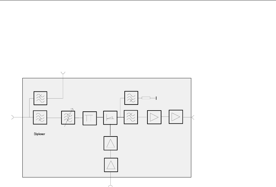
Instrument Design and Function Description FSP
1164.4556.82 3.4 E-1
RF to IF Conversion for Frequencies > 3 GHz - Microwave Converter
The high frequency models of the FSP (frequency range > 3 GHz) also comprise a microwave converter
board. This module converts the analyzer input signals in the range above 3 GHz to the second IF of
404.4 MHz. After the attenuator, the input signals are split within the diplexer into the two signal paths <
3 GHz and > 3 GHz. Signals above 3 GHz are forwarded to the mixer via the YIG filter.
3404.4 to 6595.6 MHz
1.LO, P > -5 dBm
YIG filter
RF input
0 to 7 GHz
0 to 3 GHz
to frontend
IF output
404.4 MHz
Fig. 3-3 RF-to-IF conversion for frequencies > 3 GHz
The first LO converts the input frequency to the 404.4 MHz IF (by mixing fundamental and harmonics).
For this purpose, the LO signal (3.4 to 6.6 GHz) generated in the RF frontend is amplified to the required
LO level.
The basic model is equipped with the necessary interfaces (IF input 404.4 MHz, LO output 3.4 to 6.6
GHz) for extending the frequency range by simply adding a microwave converter.
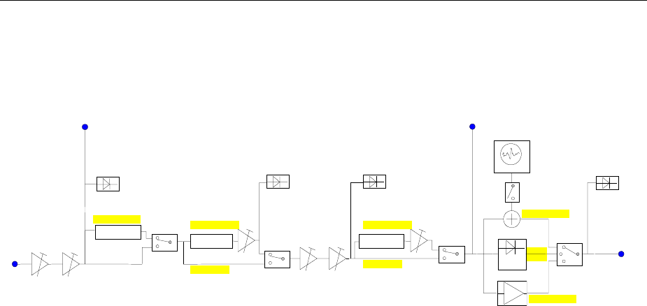
FSP Instrument Design and Function Description
1164.4556.82 3.5 E-1
IF Filter – Module
The frontend in the signal path is followed by the IF filter module (analog IF):
calib.
only
XTAL-Filter
LOG
dither source
LIN
Detecktor X147
X146
X131
X132
CAL_Amp1 CAL_Amp2
StepGain
-10...+40 dB
/ 10 dB
StepGain
0...+10 dB
/ 0.1 dB
RBW 300k ... 3M
RBW 10MHz
RBW ≤100kHz
RBW 10MHz
RBW 300k ... 3M
IF-FILTER BOARD
Signal Path and selftest
RBW ≤100kHz
RBW ≥300kHz
ABC D
LC-Filter IILC-Filter I
Selfttest detector selfttest detector Selftest detektor Selftest detektor
Fig. 3-4 IF filter
The FSP offers resolution bandwidths from 1 Hz to 10 MHz in steps of 1/3/10. The selection filter at the
second IF of 404.4 MHz in the frontend yields the 10 MHz bandwidth. Selection is not performed at the
IF of 20.4 MHz.
The tunable bandwidths from 100 kHz to 3 MHz are at the third IF (20.4 MHz) on the IF filter module.
The bandwidths from 100 kHz to 3 MHz are provided by 4 decoupled LC circuits.
The IF filter module also comprises circuits for the IF gain (step gain) from 0 to 50 dB in 0.1 dB steps,
level correction for all bandwidths and frequency response correction using a variable gain amplifier
each.
The IF filters are followed by a log detector to obtain the display dynamic range.
The module also comprises a limiting amplifier (in the log-amp) with a TTL output for the frequency
counter.
For the digitally implemented resolution bandwidths from 1 Hz to 30 kHz, the 20.4 MHz IF signal at the
IF filter output is routed to the A/D converter.
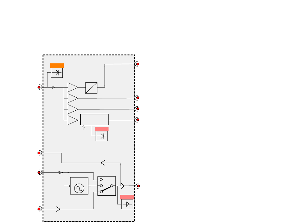
Instrument Design and Function Description FSP
1164.4556.82 3.6 E-1
Reference Frequency 10 MHz - IF Filter Module
The reference frequency is generated by a TCXO, and the frequency is adjustable by means of a D/A
converter. As another choice, an OCXO or an external reference input (REF IN) can be switched on. In
any case, the active reference will be routed to the reference output.
41
32 MHz, 0dBm
to Detector
CAL
Generator
128MHz, 0dBm
to Detector
TCXO
Reference
Adjust
Selftest
Selftest
Selftest
X141
X135
X136 128MHz, 0dBm
to Options
128MHz Cal Signal
0 / -30 dBm
to RF-ATTen
X142
128MHz, 0dBm
from Frontend
X134
10MHz, 0dBm
to Frontend
X133
10MHz, 0dBm
to Rear Panel
REF OUT
X143
10MHz
from Rear Panel
REF IN
X144
10MHz, 0dBm
from OCXO Option
X145
Reference
Adjust
Fig. 3-5 Reference frequency
Reference Frequency 128 MHz - IF Filter Module
This reference is generated on the frontend and is synchronized to the 10 MHz reference.
The signal from the frontend (128 MHz reference) is decoupled and distributed to the detector and to
other options.
The 128 MHz calibration signal is generated with automatic level control. The level is switchable
between 0 dBm and -30 dBm. The level is adjustable with a D/A converter.
A 4:1 divider generates the 32 MHz clock for the detector board ( A/D converter).
OCXO Reference (Option FSP-B4)
The FSP contains the option FSP-B4, an oven-controlled crystal oscillator (OCXO). This OCXO
generates a 10 MHz signal, which is routed to the IF filter board and used as a reference signal.
WCDMA Demodulation Hardware (Option FSP-B15)
Option FSP-B15 is required for broadband vector analysis. The module is inserted into the line of the
128 MHz calibration signal between the IF module and the attenuator. A pulse with a frequency of 62.5
kHz is generated from the 128 MHz signal by frequency division. This pulse is used to calibrate the 10
MHz IF filter.
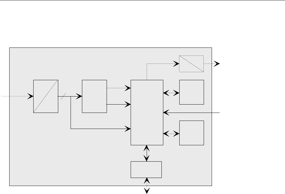
FSP Instrument Design and Function Description
1164.4556.82 3.7 E-1
Processing of Measured Data - Detector Board
The following sections explain the signal and data paths required for result processing in the various
operating modes:
A
D12
ZF / Video
32 MHz
Digital
Down
Converter Detector
Controller
Noise-Filter
Detectors
Counter
Magnitude
Phase
Fast
Measure
R
A
M
Trigger
Sweep Control
PCI Interface
PCI Bus to Host
Control
R
A
M
D
A
DDC DCON
Video
Fig. 3-6 Processing of measured data
Spectrum Analysis Using an RBW >100 kHz
In this mode, only the analog resolution filters on the IF filter board are used. The signal applied to the
A/D converter via the input IF/Video is therefore already a log video signal. The signal is continuously
sampled at 32 MHz in the ADC and digitized.
The signal path is now directly routed to DCON.
In the DCON, the data are directly applied to the noise filter. The noise filter is used to limit the video
bandwidth or to average the noise content. The signal path is routed to the detector logic where the
results are processed, i.e. peak max, peak min, sample, average and RMS values as well as the
number of measured values and quasi-peak values are determined.
With measurement data rates > 1 MHz, detector data have to be stored in the measurement RAM
because online storage is no longer possible at these high speeds. Upon completion of the sweep, the
sweep data are read by the host from the measurement RAM, processed and displayed.
Spectrum Analysis Using an RBW ≤
≤≤
≤ 100 kHz
In this operating mode, the resolution bandwidths are generated digitally with the aid of the DDC. This IC
first mixes its input IF into the baseband using an NCO, and then filters the obtained I/Q signal via an
HDF (high decimation filter) and an FIR (finite impulse response) stage. At the end of the DDC
processing chain, the I/Q signal in the CORDIC block is split into magnitude and phase. For signal
processing in the DDF, the IF signal from the IF filter module directly represents the linear IF.
For a conventional log display of the analyzed spectrum, the magnitude data is logarithmized in the
DCON between the DDC interface and the noise filter.
Further signal processing on the detector board is identical to that of operating mode RBW > 100 kHz.

Instrument Design and Function Description FSP
1164.4556.82 3.8 E-1
FFT Bandwidth
In the FFT bandwidth mode, the synthesizer is set to the desired frequency via the DCON which also
generates the tuning voltages for the analog hardware. The signal path is routed via ADC, Corr RAM
and DDC. The DDC first mixes the input IF into the baseband using an NCO, and then the obtained I/Q
signal is filtered in an HDF (high decimation filter) and FIR stage (finite impulse response). The I/Q
output data are then stored by the DDC in the I/Q RAM. With data logging completed, the I/Q data from
the I/Q RAM is transferred to the host via DDC and PCI interface FPGA. The host then performs the
FFT for this sweep section.
Video Bandwidths (VBW)
The video filters of the FSP can be adjusted between 1 Hz and 10 MHz in steps of 1/3/10. They are
designed as a digital lowpass filter for the video signal. The video bandwidth can either be coupled to
the resolution bandwidth (= default setting) or manually set to a fixed value.
Detectors
The FSP uses a detector for the positive peak (peak+) and one for the negative peak value (peak-). In
the sample mode, the video signal can also be directly sampled by the A/D converter without a peak
detector being required . Quasi-Peak, Average and RMS detectors are available in addition. The RMS
detector forms the rms value of the input signal for one point in the display during the measurement
time.
AF Demodulation (Option FSP-B3)
The FSP may contain option FSP-B3 as an AM/FM demodulator. In the analyzer mode, the signal at the
position of the reference marker during a sweep can be demodulated. In this case, the FSP stops the
sweep for a selectable time and demodulates the input signal. The loudness is adjusted with the volume
control knob.
TV and RF Trigger (Option FSP-B6)
By using the TV and RF trigger option FSP-B6, you can set triggering to a TV signal or to the presence
of an RF signal on the FSP.
For this purpose, the option module has a TV demodulator that provides the trigger signals required for
analyzing TV signals. In addition to the pure trigger function, the demodulated TV signal is available as a
CCVS video signal for operating a TV monitor. The FSP can also derive the trigger signals from an
externally applied CCVS signal. The associated connector is located on the rear panel of the FSP.
The FSP derives different trigger signals from the video signal to display defined sections of the TV
video signal in the time domain. Triggering in response to field frequency and to each line of the TV
video signal is possible.
In addition, the option module contains a broadband RF detector (bandwidth = 80 MHz) that allows
detection of a carrier signal far from the selected frequency range. This RF power trigger will function as
long as the RF signal applied to the input mixer is between -10 dBm and -50 dBm.

FSP Instrument Design and Function Description
1164.4556.82 3.9 E-1
Tracking Generator (Option FSP-B9)
The tracking generator generates a signal exactly at the input frequency of the FSP during normal
operation.
For frequency-converting measurements, it is possible to set a constant frequency offset of ±150 MHz
between the receive frequency of the FSP and the output signal of the tracking generator. In addition,
I/Q modulation or AM and FM modulation of the output signal can be performed using two analog input
signals.
The output level is regulated and can be set between –30 dBm and 0 dBm in 0.1 dB steps.
External Generator Control (Option FSP-B10)
The external generator control option enables different commercial generators to be operated as a
tracking generator on the FSP. The generator is controlled via the optional second IEC/IEEE bus
interface of the FSP (= IEC2, supplied with the option) and via the TTL synchronizing interface contained
in the AUX interface of the FSP on some Rohde & Schwarz generators.
LAN Interface (Option FSP-B16)
The instrument can be connected to an Ethernet LAN (local area network) using the LAN interface
option. This option comprises a network card that can be operated with a 10 MHz Ethernet IEEE 802.3
or a 100 MHz Ethernet IEEE 802.3u.
DC Power Supply (Option FSP-B30)
With the DC power supply option, the FSP can be operated from a DC voltage of 10 to 28 V. A DC/DC
converter transforms the input voltage to a voltage of 120 to 360 VDC that can be directly processed by
the FSP power supply. The option is installed on the rear panel of the FSP.
Battery Pack (Option FSP-B31/32)
Option FSP-B31 is a battery pack for the FSP. If option FSP-B30 is installed, the FSP can be operated
independently of the AC supply for up to 2 hours (depending on model). The option comprises a
charger, two NiMH battery packs and an external power supply. The charger and the batteries are
accommodated in a housing that can be installed on the top of the FSP in no time.
The battery pack is charged by means of the power supply that is included. Option B32 is an additional
battery pack (without external power supply).

Instrument Design and Function Description FSP
1164.4556.82 3.10 E-1
Front Panel
The front panel consists of an aluminum case panel (part of the FSP frame) and a mounting plate which
accommodates the LCD, the backlight inverter, the keyboard mat with the membrane and the
spinwheel. The case panel incorporates the front-module controller
LCD
The color LCD provides a visible output of any information, measurements etc. to the user. The
resolution of the LCD is 640 * 480 pixels (VGA).
The display incorporates a cold cathode tubes for the illumination. The high voltage required for this
purpose is generated in an extra DC/AC converter mounted next to the display on the mounting plate
and connected both to the display and the controller board via a cable.
Keyboard
The keyboard consisting of a keyboard mat and a membrane release a contact when the rubber key is
pressed. Two LEDs for the STANDBY/ON key (orange for STANDBY/green for ON) are also
accommodated on this membrane.
The key evaluation and LED control are effected via a film cable connector on the controller board. Like
the control of the two LEDs, it is controlled in a special microprocessor on the controller board by means
of a matrix technique. This microprocessor permits to store the status of the STANDBY/ON key when
switching off using the power switch.
Front module controller
The front module controller contains all the necessary components on a board such as processor,
memory chips (SIMM modules), I/O devices (ISA bus), lithium battery, IEC-bus controller (IEEE), two
serial interfaces (COM1/2), a parallel interface (LPT), LCD graphics controller, external VGA monitor
graphics interface (monitor) and an external keyboard connection (keyboard PS/2).
In addition, a floppy controller for an external floppy disk drive and an IDE hard disk controller are
integrated on the controller board.
Hard disk
The hard disk is screwed to the rear of the aluminum case panel and connected to the printed circuit
board via a ribbon cable.
Flash Disk (Option FSP-B20)
A flash disk can be installed in the instrument instead of the hard disk by means of option FSB-B20. The
compact flash board contains 2 connectors for compact flash cards of type 1 and a connector for
establishing the connection to the IDE interface of the front-module controller.

FSP Instrument Design and Function Description
1164.4556.82 3.11 E-1
Power Supply Module
The power supply module provides all currents necessary for the operation of the FSP. It can be
switched off by means of the power switch on the rear panel.
The power supply module is a primary clocked switching power supply with Power Factor Correction
(PFC) and Standby circuit (+12 V Standby).On the secondary side, it generates DC voltages (+3.3 V;
+5.2 V; +6 V; +8 V; +12 V; +12 VFAN; +12 V Standby; +28 V; -12 V).
The control signal STANDBY/ON controlled by the front module controller (depending on the
STANDBY/ON key on the front of the instrument frame) activates the power supply. In standby
operation, it only supplies the 12V-standby voltage for the crystal oscillator and the LED STANDBY on
the front panel.
The secondary voltages are open-circuit-proof and short-circuit-proof with respect to ground and each
other.
An overtemperature protective circuit is additionally installed to prevent overheating. This status is taken
to the front module controller via a status signal (OT).
Fuses
Two fuses are also fitted in the power supply as a means of fire protection.
Note: These fuses are not accessible to the user from outside and are only blown in the case of a
serious fault of the power supply (servicing required!).
Motherboard
The motherboard generates the –6V supply for the analog boards with an integrated DC/DC-Converter.
The Noise source output (28V Noise Source) is also generated on this board.
All external supplies (Probe, Keyboard,...) are protected by polyswitches (current-dependent, self-
opening and closing fuses) or electronically against external short circuit.
On the motherboard a circuit for temperature-dependent instrument fan control is also implemented.
Probe / Keyboard
The probe / keyboard board is located at the front of the instrument frame and serves for supply and
connection of the connectors located at the front panel, the KEYBOARD (PS/2) and a PROBE POWER
connector. For connection with motherboard a ribbon cable is used.
Volume / Phones
This board is only fitted with option FSP-B3 (AF-demodulator).
The volume/phones board is located at the front of the instrument frame and is used to connect the
rotary encoder for the Volume setting of the AF-Demodulator and the Headphones connector with the
motherboard.
For connection with the motherboard a 10-pin ribbon cable is used.

Module Replacement FSP
1164.4556.82 3.12 E-1
Module Replacement
This section describes the service concept and contains the spare parts list and the basic documents for
the overall the FSP instrument. Replacement of modules is described in detail in Section 3 under
"Module Replacement".
Note: The numbers indicated in brackets refer to the position in the list of mechanical parts in
Section 5.
These items correspond to the item numbers in the illustrations on board replacement (see
also Section 5):
1164.4391 (FSP Basic Model, Its. 1-455),
1164.4404 (Dig. Basic Unit, Its. 500-775),
1093.4708 (Display Unit, Its. 800-950),
1130.2396 (Converter Unit 8 GHz, Its. 2000-2008),
1130.2544 (Converter Unit 8 GHz, Its. 2000-2035),
1093.8249 (MW Converter Unit 13/30 GHz, Its. 2110-2150),
1093.8584 ( MW Converter Unit 40 GHz, Its. 2210-2245),
1096.6224 (Option FSP-B1),
1129.6540 (Option FSP-B3, Its. 1000-1080)
1129.6791 (Option FSP-B4, Its. 1110-1130).
1129.8613 (Option FSP-B6, Its. 1800-1880),
1129.8613 (Option FSP-B9, Its. 1500-1566),
1129.7298 (Option FSP-B10, Pos. 1600-1626),
1155.1012 (Option FSP-B15, Its. 1160-1180),
1129.8107 (Option FSP-B16, Its. 1240-1310),
1155.1712 (Option FSP-B20, Its. 1700-1770) and
1155.1764 (Option FSP-B21, Pos. 2900-2970),
1129.7800 (Option FSP-B25, Pos. 1400-1490),
1162.9921 (Option FSP-B28, Pos. 1360-1385),
(Option FSP-B30, Pos. 3000-3020),
(Option FSP-B31, Pos. 3040-3060),
1157.0607 (option FSP-B70, Its. 1900-1950).
Note: The words “left” and “right” in the manual always refer to the front view of the instrument.
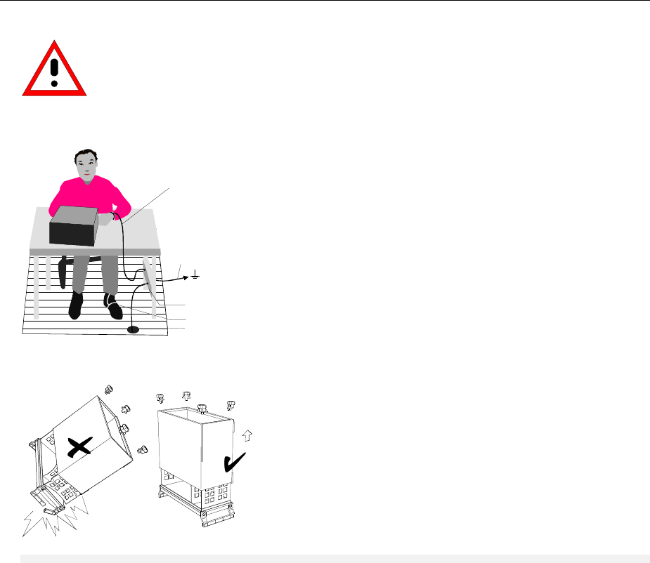
FSP Module Replacement
1164.4556.82 3.13 E-1
Caution!
Wrist strap with cord
Building ground
Floor mat
Ground connection
of operational site
Heel strap
• Please note the safety instructions at the beginning of
this manual.
• Disconnect the instrument from the mains before
opening the case.
• Protect the replacement site against electrostatic
discharge to avoid damage of electronic components of
the modules.
• The following two methods of ESD protection may be used
together or separately:
•
- Wrist strap with cord to ground connection
- Conductive floor mat and heel strap combination
• Put the instrument on the front handles before loosing
the rear feet and the tube to avoid damage of the
instrument.
• When mounting the tube take care not to damage or
pull off cables.

Module Replacement FSP
1164.4556.82 3.14 E-1
Overview of the Modules
Table 3-1 Overview - module replacement
Module Required tests and adjustments after replacement
Function tests and
system error correction Adjustment Other
Front module controller SYSTEM MESSAGES/
SELFTEST / CAL DOS/BIOS update
Lithium battery SYSTEM MESSAGES/
SELFTEST / CAL Cold boot
Hard disk SYSTEM MESSAGES/
SELFTEST / CAL Cold boot / FW update
LCD / DC/AC converter
Keyboard membrane or mat
Labelling panel
Floppy disk drive Check of directories
Power supply SYSTEM MESSAGES/
SELFTEST / CAL
Fan
RF input connector SELFTEST / CAL Frequency response
Motherboard SYSTEM MESSAGES/
SELFTEST / CAL EEPROM entry
Cold boot
RF attenuator SYSTEM MESSAGES/
SELFTEST / CAL Frequency response Cold boot
Key probe and vol./phone Voltage / keyboard / volume
RF frontend SYSTEM MESSAGES/
SELFTEST / CAL Frequency response Cold boot
Detector SYSTEM MESSAGES/
SELFTEST / CAL Cold boot
IF filter SYSTEM MESSAGES/
SELFTEST / CAL Frequency accuracy/
cal. source Cold boot
MW converter SYSTEM MESSAGES/
SELFTEST / CAL Frequency accuracy/
frequency response Cold boot
AF demodulator FSP-B3 SYSTEM MESSAGES/
headphone / volume Cold boot
OCXO FSP-B4 SYSTEM MESSAGES/
SELFTEST / CAL Frequency accuracy Cold boot
TV and RF trigger FSP-B6 SYSTEM MESSAGES/
SELFTEST / CAL Trigger level Cold boot
Tracking generator FSP-B9 SYSTEM MESSAGES/
SELFTEST / CAL Cold boot
External generator control
FSP-B10 SYSTEM MESSAGES/
SELFTEST / CAL
WCDMA Demodulation
Hardware FSP-B15 SYSTEM MESSAGES/
SELFTEST / CAL Cal. source Cold boot
LAN interface FSP-B16 SYSTEM MESSAGES/
SELFTEST / CAL
Flash disk FSP-B20 SYSTEM MESSAGES/
SELFTEST / CAL Cold boot/
FW update
Electronic attenuator/ preamp
FSP-B25 SYSTEM MESSAGES/
SELFTEST / CAL Frequency response Cold boot
Broadband demodulator
FSP-B70 SYSTEM MESSAGES/
SELFTEST / CAL Cold boot

FSP Module Replacement
1164.4556.82 3.15 E-1
Performing a Cold Boot
Ø Connect power cable, switch on power switch.
Ø Simultaneously while switching on with the ON button, press and hold down the decimal-point key
until the computer responds with a beep.
Ø Windows XP subsequently boots the instrument firmware.

Module Replacement FSP
1164.4556.82 3.16 E-1
Replacing the Front Module Controller A90
(See chapter 5, spare parts list, item 570, and explosion drawings 1164.4391, 1164.4404.)
The front module controller is mounted behind the front panel.
Opening the Instrument and Removing the Front Panel
Ø Switch off the instrument and pull the mains plug.
Ø Unscrew the four screws (430) of the front handles on both sides and take off the front handles.
Ø Remove the volume control knob (Option FSP-B3), if present, by pulling it off.
Ø Pull off the labelling panel (270) towards the front.
Ø Unscrew two countersunk screws (610) in the front frame each at the top and at the bottom.
Ø Remove the front panel with keyboard and display (600, 620, 630, 640, 650, 660) to the front and
rotate it to the top of the instrument.
Caution:
Note the connecting cables are still connected to the controller.
Ø Pull off the connecting cables to the adapter board (LCD, DC/AC illumination converter), keyboard
membrane and spinwheel.
Note: When pulling off the connecting cables be careful with the cable connecting to the
keyboard. It is a film cable which can only be disconnected after sliding up the lock of the
film cable plug.
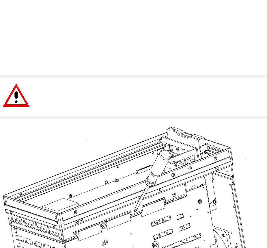
FSP Module Replacement
1164.4556.82 3.17 E-1
Removing the Front Module Controller
Ø Unscrew the ten screws with washers of the front module controller board and take out the front
module controller as follows (see Fig. 3-17)
Note: The force to disconnect the controller connectors of the motherboard are very high.
The pulling of the controller to the front side will be done with the help of the slits at the
bottom side of the mounting plate.
Please push the board with a flat, blunt tool carefully and step by step to the front.
Caution:
Do not insert the tool too deep in the slits and press only against the pc board !.
Pull out the board by pressing at alternate slits.
The board must not be bent!
Fig. 3-7 Removing the front module controller

Module Replacement FSP
1164.4556.82 3.18 E-1
Installing the New Front Module Controller and Completing the Instruments
Ø Carefully plug the new front module controller to the motherboard and fasten it using the ten screws
with washers (590).
Ø Carefully insert the cable connectors to the controller board, taking care not to reverse the polarities.
Battery
+
LAN 1 LAN 2
Contact side of switching
foil (keyboard), top
Port for spinwheel
Memory module
Memory module
CPU
Adapter board port
for display and converter
Hard disk port
on rear side
Fig. 3-8 Installing a new front module controller - position of connectors
Ø Rotate the front panel into the instrument and screw with four countersunk screws (610) in the front
frame at the top and at the bottom.
Caution:
Make sure to route the cables properly.
Ø Install the labelling panel (270).
Ø Push the 2 front handles (420) on the instrument and mount them with the 4 screws (430).
Ø Replace the volume control knob (Option FSP-B3), if it was removed.
Putting into Operation
Ø Connect the instrument to the mains and switch on the instrument power switch. The instrument is
now in stand-by mode.
Ø Insert a floppy disk with DOS and BIOS-Update in the floppy disk drive.
Ø Switch ON the FSP and wait until the first beep. Press the FILE key. The BIOS-Update starts.
Ø During the programming of the flash EEPROM the FSP must not be switched off.
Ø Follow the message indicated on the display, then switch off and on the FSP.
Ø After starting the instrument check for system messages:
- [ SETUP : SYSTEM INFO : SYSTEM MESSAGES ]
Ø Start selftest and check results:
- [ SETUP : SELFTEST ] , then- [SELFTEST RESULT]
Ø Start a total calibration and check the result:
- [ CAL : CAL TOTAL ] , then [ CAL RESULTS ]

FSP Module Replacement
1164.4556.82 3.19 E-1
Replacing the Lithium Battery on the Front Module Controller
(See chapter 5, spare parts list, item 775, and explosion drawings 1093.4495 and 1093.4537.)
The lithium battery is accommodated on the front module controller board behind the front panel.
Caution:
Lithium batteries must not be exposed to high temperatures or fire.
Keep away from children.
If the battery is replaced improperly, there is danger of explosion. Only
replace the battery by R&S type (see spare parts list, item 775).
Lithium batteries are hazardous waste and must be disposed of in dedicated
containers.
Do not short-circuit the battery!
Opening the Instrument and Removing the Front Panel
Ø Switch off the instrument and pull the mains plug.
Ø Unscrew the four screws (430) of the front handles on both sides and take off the front handles.
Ø Remove the volume control knob (Option FSP-B3), if present, by pulling it off.
Ø Pull off the labelling panel (270) towards the front.
Ø Unscrew each two countersunk screws (610) in the front frame at the top and at the bottom.
Remove the front panel with keyboard and display (600, 620, 630, 640, 650, 660) to the front and rotate
it to the top of the instrument
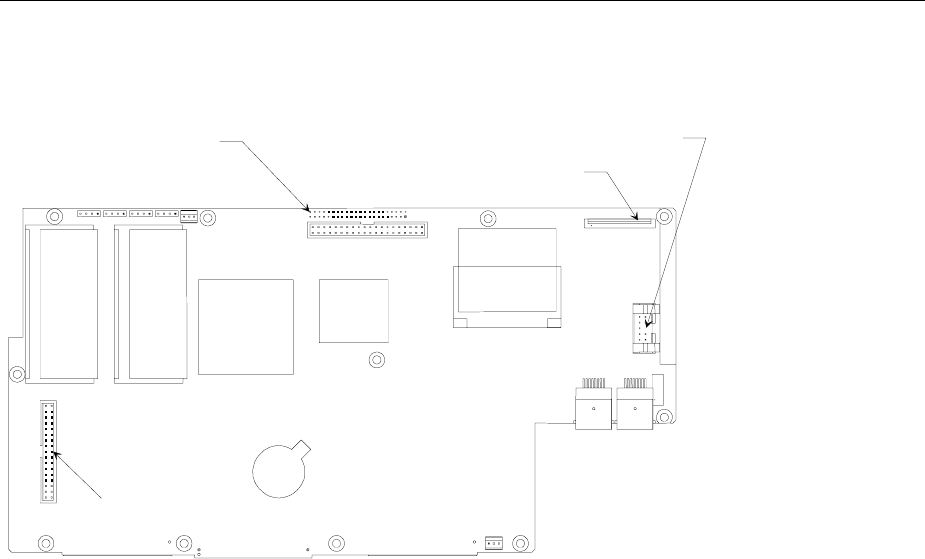
Module Replacement FSP
1164.4556.82 3.20 E-1
Removing the Lithium Battery
Ø Carefully push contact springs of the battery holder up and remove battery.
Battery
+
LAN 1 LAN 2
Contact side of switching foil
(keyboard), top
Port for spinwheel
Memory module
Memory module
CPU
Adapter board port
for display and converter
Hard disk port
on rear side
Fig. 3-9 Position of lithium battery and jumper 12 on the front module controller

FSP Module Replacement
1164.4556.82 3.21 E-1
Installing the New Battery and Completing the Instrument
Ø Carefully push contact springs of the battery holder up and insert battery into the holder beneath the
springs.
Note: The plus pole (+) of the battery points upwards.
Warning!
Do not short-circuit the battery!
Ø REFRotate the front panel into the instrument and screw with four countersunk screws (610) in the
front frame at the top and at the bottom.
Caution:
Make sure to route the cables properly.
Ø Install the labelling panel (270).
Ø Push the 2 front handles (420) on the instrument and mount them with the 4 screws (430).
Ø Replace the volume control knob (Option FSP-B3), if it was removed.
Putting into Operation
Ø Connect the instrument to the mains and switch on the instrument power switch. The instrument is
now in stand-by mode.
Ø After the change of the battery a cold boot is necessary. See section "Performing a Cold Boot" in this
chapter.
Ø After starting the instrument check for system messages:
- [ SETUP : SYSTEM INFO : SYSTEM MESSAGES ]
Ø Start selftest and check results:
- [ SETUP : SERVICE : SELFTEST ], then [SELFTEST RESULT]
Ø Start a total calibration and check the result:
- [ CAL : CAL TOTAL ], then [ CAL RESULTS ]

Module Replacement FSP
1164.4556.82 3.22 E-1
Replacing Hard Disk A60
(See chapter 5, spare parts list, item 710, and explosion drawings 1164.4391 and 1164.4404.)
The hard disk is incorporated between the front module and the analog boards.
The spare part is already formatted for the FSP and contains the complete software.
Opening the Instrument and Removing the Hard Disk
Ø Switch off the instrument, pull the mains plug, unscrew the 4 rear-panel feet (450) and push the tube
(410) backwards and take off.
Ø Unscrew the two countersunk screws (260) at the top of the instrument and the three countersunk
screws (250) at the fan side, lift the cover at the top (240) of the instrument to the left side and take
off.
Ø Disconnect the ribbon cable (720) at the hard disk.
Ø Unscrew the two countersunk screws (740) on the hard disk mounting plate (730).
Ø Take the hard disk (710) completely with the hard disk mounting plate (730 out of the FSP.
Ø Unscrew the four countersunk screws (750) remove the hard disk and mount a new hard disk to the
mounting plate (730).
Installing the New Hard Disk and Putting into Operation
Ø Fit the hard disk and the disk holder with two screws (740) to the instrument
Note: Be careful with the lower cover plate locking in the corresponding opening.
Ø Connect the ribbon cable (720) to the hard disk.
Note: Connect cable as drawing 1164.4404.
Ø Put the top cover (240) on the instrument and mount it with two countersunk screws (260) and three
countersunk screws (250).
Ø Push the tube (410) on the instrument and mount the 4 rear-panel feet (450).
Ø Connect the instrument to the mains and switch on the instrument power switch. The instrument is
now in stand-by mode.
Ø After the change of the hard disk a cold boot is necessary. See section "Performing a Cold Boot" in
this chapter.
Ø After starting the instrument check for system messages:
- [ SETUP : SYSTEM INFO : SYSTEM MESSAGES ]
Ø Start selftest and check results:
- [ SETUP : SERVICE : SELFTEST ], then [SELFTEST RESULT]
Ø Start a total calibration and check the result:
- [ CAL : CAL TOTAL ] , then [ CAL RESULTS ]

FSP Module Replacement
1164.4556.82 3.23 E-1
Replacing Flash Disk A60 (Option FSP-B20)
(See chapter 5, spare parts list, item 1700, and drawings 1093.4495 and 1155.1612.)
The flash disk is located in the instrument between the controller panel and the modules. The spare part
is supplied with pre-installed software.
Opening the Instrument and Removing the Flash Disk
Ø Switch off unit, disconnect it from power supply, unscrew 4 rear-panel feet (450) and pull off
enclosure (410) towards rear.
Ø Unscrew the two countersunk screws (260) at the top of the instrument and the three countersunk
screws (250) at the fan side, lift the cover at the top (240) of the instrument to the left side and take
off.
Ø Disconnect the ribbon cable (720) on the flash disk.
Ø Unscrew the two countersunk screws (740) on the flash disk mounting plate (730).
Ø Remove the flash disk (1700) with the mounting plate (730).
Replacing the Compact Flash Board A60
Ø Undo 4 countersunk screws (750), remove compact flash board (1700) and screw the new board to
the mounting plate (730).
Replacing the Flash Memory A61
Ø Unlock and disconnect 2 flash memory cards (1713). Insert the new flash memory cards according to
the labelling in view A and lock them in place with the clamp (1730).
Installing the New Flash Disk and Putting into Operation
Ø Using two countersunk screws (740), fasten the flash disk and the disk holder to the instrument.
Note: The disk holder is plugged into a metal panel at the bottom.
Ø Connect the ribbon cable (720) to the flash disk.
Note: Connect cable as shown in drawing 1164.4404 in chapter 5.
Ø Put the top cover (240) on the instrument and fasten it in place with 2 countersunk screws (260) and
3 countersunk screws (250).
Ø Slide on enclosure (410) and screw on 4 rear-panel feet (450).
Ø Connect the AC supply cable and switch on the power switch. The unit is now in the standby mode.
Ø A cold boot is required after replacing the flash disk. See section "Performing a Cold Boot" in this
chapter.
Ø After starting the instrument, make sure that no messages are recorded in the log file:
- [ SETUP : SYSTEM INFO : SYSTEM MESSAGES ]
Ø Start the selftest and check the results to make sure that no errors occurred:
- [ SETUP : SERVICE : SELFTEST ], then [SELFTEST RESULT]
Ø Start the system error correction and check the results to make sure that no errors occurred:
- [ CAL : CAL TOTAL ] , then [ CAL RESULTS ]

Module Replacement FSP
1164.4556.82 3.24 E-1
Replacing the LCD and DC/AC Converter in the Front Module
(See chapter 5, spare parts list, items 600 and 870, and explosion drawings 1164.4391, 1164.4404,
1093.4708.)
The LCD is accommodated on the mounting plate together with the associated DC/AC converter. It is
connected to the front module controller via cables, which can also be replaced individually. For
replacement proceed as follows:
Opening the Instrument and Removing the Front Module
Ø Switch off the instrument and pull the mains plug.
Ø Unscrew the four screws (430) of the front handles on both sides and take off the front handles.
Ø Remove the volume control knob (Option FSP-B3), if present, by pulling it off.
Ø Pull off the labelling panel (270) towards the front.
Ø Unscrew two countersunk screws (610) in the front frame each at the top and at the bottom.
Ø Remove the front panel with keyboard and display (600, 620, 630, 640, 650, 660) to the front and
rotate it to the top of the instrument.
Caution:
Note the connecting cables are still connected to the controller
Ø Pull off the connecting cables to the adapter board (LCD, DC/AC illumination converter), keyboard
membrane and spinwheel.
Note: When pulling off the connecting cables be careful with the cable connecting to the
keyboard. It is a film cable which can only be disconnected after sliding up the lock of the
film cable plug.
Ø Place the Front Module onto a clean surface.
Removing the DC/AC Converter
Ø Pull off the plug of the connecting cable to the DC/AC converter (870).
Ø Unplug the display cable (947) leading from the adapter board to the DC/AC converter (870) on the
converter.
Ø Unscrew the two screws (890) and remove the DC/AC converter (870) with the spacing pieces (900).
Removing the LCD
Ø Unscrew two screws with washers (950) and plug off the display cable (947)
Ø Unscrew the four screws at the display (930) and remove the display.
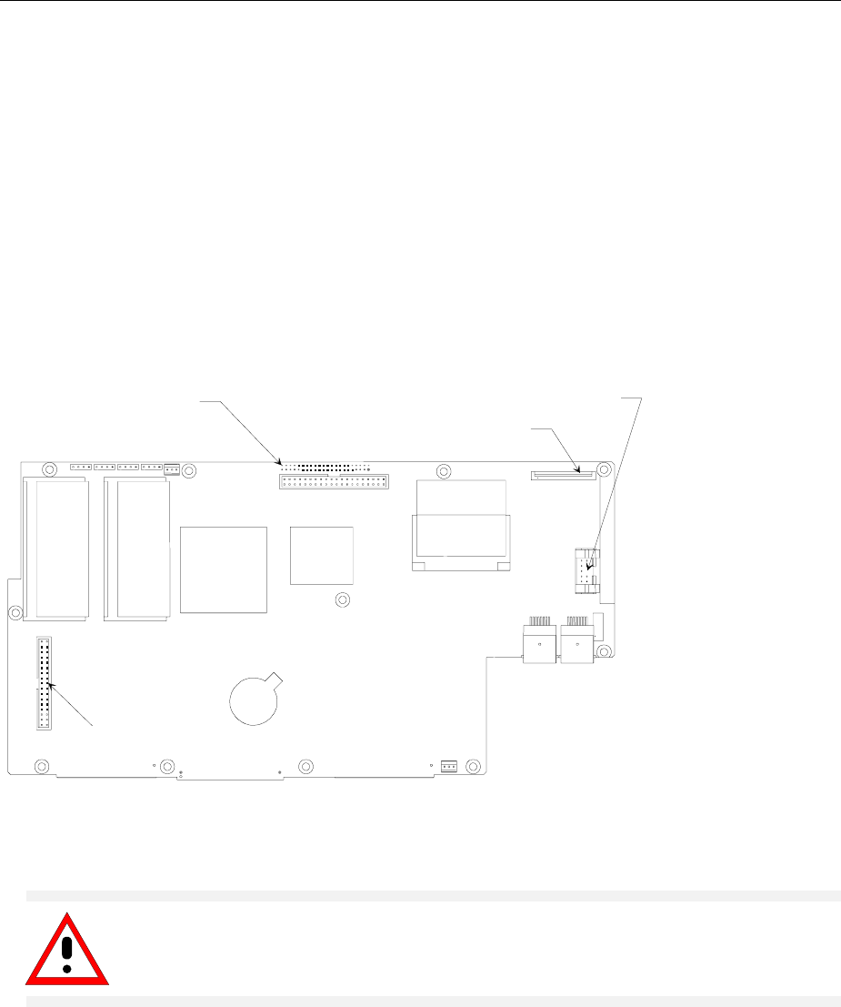
FSP Module Replacement
1164.4556.82 3.25 E-1
Installing the New LCD and DC/AC Converter and Completing the Instrument
Ø Install the new LCD or new DC/AC converter in reverse order, fasten all screws, and connect and
mount the corresponding cables.
Ø When mounting the display cable (947), make sure it is free of mechanical stress.
Ø Observe the following order when installing parts:
1) Before installing the display, connect the display cable (947) to the adapter board. You must hear
the connection engage.
2) Reattach the display (920) with four screws (930).
3) Mount the display cable (947) with 2 screws (950), making sure it is free of mechanical stress.
Ø Place the front panel with the keys on the top of the instrument, with the cables in the right direction
to the front module controller.
Ø Carefully plug the cable connectors to the controller board without reversing the polarities and
replace the mounting plate in the reverse order.
Battery
+
LAN 1 LAN 2
Contact side of switching
foil (keyboard), top
Port for spinwheel
Memory module
Memory module
CPU
Adapter board port
for display and converter
Hard disk port
on rear side
Fig. 3-10 Position of connectors on front module controller
Ø Rotate the front panel into the instrument and screw with four countersunk screws (610) in the front
frame at the top and at the bottom.
Caution:
Make sure to route the cables properly.
Ø Install the labelling panel (270).
Ø Push the 2 front handles (420) on the instrument and mount them with the 4 screws (430).
Ø Replace the volume control knob (Option FSP-B3), if it was removed.
Ø Connect the instrument to the mains, switch on the instrument power switch and switch on the
instrument with the ON/STANDBY key

Module Replacement FSP
1164.4556.82 3.26 E-1
Replacing the Keyboard Membrane or Mat on the Front Module
(See chapter 5, spare parts list, items 630 and 640, and explosion drawings 1164.4391, 1164.4404.)
The keyboard membrane is the contact film for the rubber keys (mat) behind the labelling panel and the
keyboard frame. For replacement proceed as follows:
Opening the Instrument and Removing the Front Panel
Ø Switch off the instrument and pull the mains plug.
Ø Unscrew the four screws (430) of the front handles on both sides and take off the front handles.
Ø Remove the volume control knob (Option FSP-B3), if present, by pulling it off.
Ø Pull off the labelling panel (270) towards the front.
Ø Unscrew each two countersunk screws (610) in the front frame at the top and at the bottom.
Ø Remove the front panel with keyboard and display (600, 620, 630, 640, 650, 660) to the front and
rotate it to the top of the instrument.
Caution:
Note the connecting cables are still connected to the controller .
Ø Pull off the connecting cables to the adapter board (LCD, DC/AC illumination converter), keyboard
membrane and spinwheel.
Note: When pulling off the connecting cables be careful with the cable connecting to the
keyboard. It is a film cable which can only be disconnected after sliding up the lock of the
film cable plug.
Removing the Membrane
Ø Place the mounting plate onto the surface with the keyboard frame pointing upwards.
Ø Pull off the knob (650) of the spinwheel.
Ø Unscrew the 10 countersunk screws (660) and remove the keyboard frame (620).
Ø The keyboard membrane (640) as well as the mat (630) is now accessible.
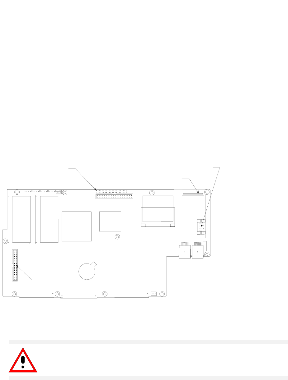
FSP Module Replacement
1164.4556.82 3.27 E-1
Installing the New Membrane and Completing the Instrument
Ø Put the new mat (630) into the keyboard frame (620).
Note: The pins of the mat must be pressed in the wholes at the keyboard frame.
Ø Locate the new keyboard membrane (640) on the back of the mat (630) .
Note: Push the foil cable of the membrane through the slit in the mounting panel.
The membrane must be positioned to let the pins of the mat come trough the holes in the
membrane.
Ø Locate the mounting plate with the display (600) onto the membrane (640) .
Note: The mounting plate must be positioned to let the pins of the mat come trough the holes in
the mounting plate (800).
Ø Press the front panel together, turn the keys to the top and screw ten countersunk screws (660) into
the keyboard frame.
Ø Place the front panel with the keys on the top of the instrument, with the cables in the right direction
to the front module controller.
Ø Carefully plug the cable connectors to the controller board without reversing the polarities and
replace the mounting plate in the reverse order.
Battery
+
LAN 1 LAN 2
Contact side of switching
foil (keyboard), top
Port for spinwheel
Memory module
Memory module
CPU
Display connector port
for display and converter
Hard disk port
on rear side
Fig. 3-11 Position of connectors on front module controller
Ø Rotate the front panel into the instrument and screw with four countersunk screws (610) in the front
frame at the top and at the bottom.
Caution:
Make sure to route the cables properly.
Ø Install the labelling panel (270).
Ø Push the 2 front handles (420) on the instrument and mount them with the 4 screws (430).
Ø Replace the volume control knob (Option FSP-B3), if it was removed.
Ø Connect the instrument to the mains, switch on the instrument power switch and switch on the
instrument with the ON/STANDBY key

Module Replacement FSP
1164.4556.82 3.28 E-1
Replacing the Labelling Panel on the Front Module
(See chapter 5, spare parts list, items 270 and 280, and explosion drawing 1093.4495.)
The labelling panel is the outer front panel which carries the labelling of all the parts on the front side of
the FSP. Every model has its own labelling panel (270, 280, 290)
Ø Switch off the instrument and pull the mains plug.
Ø Unscrew the four screws (430) of the front handles on both sides and take off the front handles.
Ø Remove the volume control knob (Option FSP-B3), if present, by pulling it off.
Ø Pull off the labelling panel (270) towards the front.
Ø Install the New labelling panel and tighten all screws.
Ø Complete the instrument.
Ø Connect the instrument to the mains, switch on the instrument power switch and switch on the
instrument with the ON/STANDBY key

FSP Module Replacement
1164.4556.82 3.29 E-1
Replacing the Floppy Disk Drive A30
(See chapter 5, spare parts list, item 670, and explosion drawings 1164.4391, 1164.4404.)
Opening the Instrument and Removing the Floppy Disk Drive
Ø Switch off the instrument, pull the mains plug, unscrew the 4 rear-panel feet (450) and push the tube
(410) backwards and take off.
Ø Unscrew the two countersunk screws (260) at the top of the instrument and the three countersunk
screws (250) at the fan side, lift the cover at the top (240) of the instrument to the left side and take
off.
Ø Remove two screws (700) at the fan side of the FSP and carefully pull out the Floppy Disk Drive
(670) with Floppy mounting plate (680) to the upper side.
Note: The connecting cable is still connected to the motherboard .
Ø Disconnect the cable at the floppy disk drive .
Note: Please take note of the correct direction of the cable (contact side)
Install the New Floppy Disk Drive and Completing the Instrument
Ø Unscrew the three screws with washers (700) and remove the floppy disk from the mounting plate
(680) and mount a new disk drive (670) to the floppy mounting plate (680).
Ø Connect the foil cable (690) to the disk drive (Note the contact side of the cable).
Ø Insert the floppy mounting plate (680) and mount it to the fan side with two screws with washers
(700).
Note: Please mount the floppy disk drive in the middle of the front panel break out.
Ø Put the top cover (240) on the instrument and mount it with two countersunk screws (260) and three
countersunk screws (250).
Ø Push the tube (410) on the instrument and mount the 4 rear-panel feet (450).
Ø Connect the instrument to the mains, switch on the instrument power switch and switch on the
instrument with the ON/STANDBY key
Function Test
Ø Instrument is booting and the firmware is starting.
Ø Insert 3 ½ ″ disk with any files.
Ø Press the FILE key then the File Manager and Edit Path softkeys.
Ø Enter "a" and ":" and confirm with "Enter" key.
Ø The file structure of the inserted disk must be displayed.

Module Replacement FSP
1164.4556.82 3.30 E-1
Replacing the Power Supply A20
(See chapter 5, spare parts list, item 550, and explosion drawing 1164.4404).
The power supply is fitted at the rear of the instrument frame of the FSP.
Removing the Power Supply
Ø Switch off the instrument, pull the mains plug, unscrew the 4 rear-panel feet (450) and push the tube
(410) backwards and take off.
Ø Unscrew the ten screws (560) at the rear of the power supply.
Ø Pull out the power supply approx. 20 mm towards the rear, slightly tilt towards the bottom and then
pull out completely.
Installing the New Power Supply
Ø Install the New power supply in the reverse order.
Note: Make sure that the 96-contact connector to the MOTHERBOARD locks in place correctly.
Ø Push the tube (410) on the instrument and mount the 4 rear-panel feet (450).
Ø Connect the instrument to the mains and switch on.
Ø After starting the instrument check for system messages:
- [ SETUP : SYSTEM INFO : SYSTEM MESSAGES ]
Ø Start selftest and check results:
- [ SETUP : SERVICE : SELFTEST ], then [SELFTEST RESULT]
Ø Start a total calibration and check the result:
- [ CAL : CAL TOTAL ] , then [ CAL RESULTS ]

FSP Module Replacement
1164.4556.82 3.31 E-1
Replacing the Fan
(See chapter 5, spare parts list, item 15, and explosion drawings 1164.4391.)
The fan is fitted at the right side of the frame.
Opening the Instrument and Removing the Fan
Ø Switch off the instrument, pull the mains plug, unscrew the 4 rear-panel feet (450) and push the tube
(410) backwards and take off.
Ø Unscrew the two countersunk screws (260) at the top of the instrument and the three countersunk
screws (250) at the fan side, lift the cover at the top (240) of the instrument to the left side and take
off.
Ø Disconnect the fan cable at the motherboard connector X35 (FAN) .
Ø Unscrew the four screws off the FAN (15) and remove the fan.
Installing the New Fan and Completing the Instrument
Ø Connect the fan cable at the motherboard connector X35 (FAN)
Ø Insert the new fan and mount it to the frame with 4 pieces fan screws.
Note: Please note the direction of the airflow printed on the fan. The fan must blow the cold air
into the instrument.
Make sure to route the cables with enough space to the fan.
Ø Put the top cover (240) on the instrument and mount it with two countersunk screws (260) and three
countersunk screws (250).
Ø Push the tube (410) on the instrument and mount the 4 rear-panel feet (450).
Ø Connect the instrument to the mains, switch on the instrument power switch and switch on the
instrument with the ON/STANDBY key

Module Replacement FSP
1164.4556.82 3.32 E-1
Replacing the RF Input Connector (Cable W1)
(See chapter 5, spare parts list, items 295, 310, 315, 322, and explosion drawing 1164.4391.)
The RF input connector is fitted at the right lower side of the front panel.
Depending on the frequency range two different models of the connector are available.
Opening the Instrument and Removing the Cable W1
Ø Switch off the instrument, pull the mains plug, unscrew the 4 rear-panel feet (450) and push the tube
(410) backwards and take off.
Ø Unscrew the four screws (430) of the front handles on both sides and take off the front handles.
Ø Remove the volume control knob (Option FSP-B3), if present, by pulling it off.
Ø Pull off the labelling panel (270) towards the front.
Ø Remove three countersunk screws (70) at the frame and 236 countersunk screw (70) at the
connector mounting plate (60).
Ø Unscrew the cable W1 (295) to 7 GHz, (310) to 13.6 GHz, (315) to 30 GHz or (322) to 40 GHz at the
RF attenuator (20), (30) or (35).
Ø Remove the connector mounting plate (60) together with W1 and Probe/Key module (50) to the front.
Note: The Probe/Key module (50) is connected via a ribbon cable to the motherboard X80.
Ø Unscrew the four countersunk screws (350) and remove cable W1 together with mounting plate
(330) or (340).
Installing the New Cable and Completing the Instrument
Ø Put the mounting plate (330) or (340) onto the new cable W1 and mount the connector with four
countersunk screws (350), move the mounting plate (60) back to the instrument and connect cable
W1 (295) or (315) to the input of RF attenuator.
Ø Screw three countersunk screws (70) to the instrument frame and two countersunk screws (70) to
the mounting plate (60).
Ø Install the labelling panel (270).
Ø Push the 2 front handles (420) on the instrument and mount them with the 4 screws (430).
Ø Replace the volume control knob (Option FSP-B3), if it was removed.
Ø Push the tube (410) on the instrument and mount the 4 rear-panel feet (450).
Ø Connect the instrument to the mains, switch on the instrument power switch and switch on the
instrument with the ON/STANDBY key
Ø Start selftest and check results:
- [ SETUP : SERVICE : SELFTEST ], then [SELFTEST RESULT]
Ø Start a total calibration and check the result:
- [ CAL : CAL TOTAL ] , then [ CAL RESULTS ]
Ø Check frequency response with chapter 1 and do a correction if necessary.

FSP Module Replacement
1164.4556.82 3.33 E-1
Replacing the Motherboard A10
(See chapter 5, spare parts list, item 515, and explosion drawings 1164.4391, 1164.4404.)
The motherboard is fitted from the bottom side.
Opening the Instrument and Removing the Motherboard
Ø Switch off the instrument, pull the mains plug, unscrew the 4 rear-panel feet (450) and push the tube
(410) backwards and take off.
Ø Unscrew the two countersunk screws (260) at the top of the instrument and the three countersunk
screws (250) at the fan side, lift the cover at the top (240) of the instrument to the left side and take off.
Ø Place the instrument on the left side frame and loosen all connecting cables to the boards.
Ø Push out all boards to the top side of the instrument.
Note: The boards can be moved up by pressing carefully from the downside through the
connector wholes in the motherboard against the boards.
Ø Removing the power supply(550).
Unscrew the ten screws (560) at the rear of the power supply.
Pull out the power supply approx. 20 mm towards the rear, slightly tilt towards the bottom and then
pull out completely.
Ø Unscrew the four screws (430) of the front handles on both sides and take off the front handles.
Ø Remove the volume control knob (Option FSP-B3), if present, by pulling it off.
Ø Pull off the labelling panel (270) towards the front.
Ø Unscrew each two countersunk screws (610) in the front frame at the top and at the bottom.
Ø Remove the front panel with keyboard and display (600, 620, 630, 640, 650, 660) to the front and
rotate it to the top of the instrument.
Caution:
Note the connecting cables are still connected to the controller .
Ø Pull off the connecting cables to the adapter board (LCD, DC/AC illumination converter), keyboard
membrane and spinwheel.
Note: When pulling off the connecting cables be careful with the cable connecting to the keyboard. It is
a film cable which can only be disconnected after sliding up the lock of the film cable plug.
Ø Remove the front module controller (see chapter: Replacing the Front Module Controller A90)
Ø Remove the screws of all motherboard connectors at the rear panel . Unscrew the bolts (530) at the
"COM" and "LPT" ports and (540) aa "Monitor" port. Unscrew the nuts at "Noise Source" and "Ext.
Trig" connectors and the bolts at the "IEC" port.
Note: Do not change the bolts of the “Monitor” and the “LPT” or “COM” !
Ø Pull off the connecting cables at the motherboard (RF attenuator, fan, floppy, Probe/Key, rear panel, ....).
Ø Unscrew five screws with washers in bottom side of the motherboard
Ø Move the motherboard (515) carefully to the front panel (approx. 15 mm) and lift it out of the
instrument to the downside.

Module Replacement FSP
1164.4556.82 3.34 E-1
Installing the New Motherboard and Completing the Instrument
Ø Insert the motherboard into the instrument in the reverse order.
Note: Please move the motherboard carefully to the rear panel without causing damage to the
parts on the board.
Connect all cables (see label on cable for position).
Ø Insert the front module controller, front panel, power supply, boards and cables, top cover, tube and
rear panel feet in reverse order.
Ø A cold boot is necessary after replacing the motherboard.
See section "Performing a Cold Boot" in this chapter.
Ø Connect the instrument to the mains, switch on the instrument power switch and switch on the
instrument with the ON/STANDBY key
Ø After starting the instrument check for system messages:
- [ SETUP : SYSTEM INFO : SYSTEM MESSAGES ]
Ø Start selftest and check results:
- [ SETUP : SERVICE : SELFTEST ], then [SELFTEST RESULT]
Ø Start a total calibration and check the result:
- [ CAL : CAL TOTAL ] , then [ CAL RESULTS ]
Ø Store the serial number of the instrument to the EEPROM:
- [ SETUP : SERVICE : ENTER PASSWORD „30473035“ ] , then input serial number of the
instrument in HW-Info table (see also Chapter 2, Section "Automatic Adjustment of Module Data").

FSP Module Replacement
1164.4556.82 3.35 E-1
Replacing the Module RF Attenuator A40
(See chapter 5, spare parts list, items 20, 30, 35, and explosion drawing 1164.4391.)
The RF attenuator is fitted at the bottom side behind the RF input connector.
There are different models of the attenuator for instruments up to 7 GHz (20), 30 GHz (30) and 40 GHz
(35).
Opening the Instrument and Removing the RF Attenuator
Ø Switch off the instrument, pull the mains plug, unscrew the 4 rear-panel feet (450) and push the tube
(410) backwards and take off.
Ø Place the instrument on the left side and unscrew the RF cable or the diplexer (150, only with
FSP30) at the RF output of the RF attenuator.
Ø Unscrew the two screws with washers (40) at the right frame.
Note: The RF attenuator will only be fixed with the RF cables at the front.
Ø Disconnect RF-cable W1 (295), (315) or (322) at the input of the RF attenuator.
Ø Move carefully out the RF attenuator and disconnect the flexible RF-cable at the input.
Ø Disconnect ribbon cable at motherboard connector X40.
Installing the New RF Attenuator and Completing the Instrument
Ø Connect the ribbon cable of the new RF Attenuator (20), (30) or (35) at motherboard connector X40.
Ø Connect the flexible RF-cable at the input of new RF Attenuator (see label on cable)
Ø Move the new RF Attenuator in the instrument and connect cable W1 (295), (315) or (35) at the
input.
Ø Screw the two screws with washers (40) at the right frame in the RF attenuator.
Ø Screw the RF cable or the diplexer (150, only with FSP30) at the RF output of the RF Attenuator.
Ø Push the tube (410) on the instrument and mount the 4 rear-panel feet (450).
A cold boot is necessary after replacing the attenuator.
See section "Performing a Cold Boot" in this chapter.
Ø Connect the instrument to the mains, switch on the instrument power switch and switch on the
instrument with the ON/STANDBY key
Ø After starting the instrument check for system messages:
- [ SETUP : SYSTEM INFO : SYSTEM MESSAGES ]
Ø Start selftest and check results:
- [ SETUP : SERVICE : SELFTEST ], then [SELFTEST RESULT]
Ø Start a total calibration and check the result:
- [ CAL : CAL TOTAL ] , then [ CAL RESULTS ]
Ø Create a backup of the EEPROM data (see chapter 2, section "Adjustment of Module Data").
Ø Check frequency response with chapter 1 and make a correction if necessary.

Module Replacement FSP
1164.4556.82 3.36 E-1
Replacing the Key/Probe Module A80 and Vol./Phone Board A191
(Option FSP-B3)
(See chapter 5, spare parts list, items 50 and 1040, and explosion drawings 1164.4391, 1129.6450.)
The boards are fitted behind the front panel connectors Keyboard, Probe, Headphone and the volume
control knob.
Opening the Instrument and Removing the Boards
Ø Switch off the instrument, pull the mains plug, unscrew the 4 rear-panel feet (450) and push the tube
(410) backwards and take off.
Ø Unscrew the four screws (430) of the front handles on both sides and take off the front handles.
Ø Remove the volume control knob (Option FSP-B3), if present, by pulling it off.
Ø Pull off the labelling panel (270) towards the front.
Ø Remove three countersunk screws (70) at the frame and 1 countersunk screw (70) at the connector
mounting plate (60).
Ø Unscrew the cable W1 (310) , W1 (315) ) or (322) at the RF attenuator (20) or (30).
Ø Remove the mounting plate (60) completely with W1 and Probe/Key board (50) and option
Vol./Phone Board (1040) to the front side.
Note: The Probe/Key (50) and Vol./Phone boards (1040) are connected with a ribbon cable to the
motherboard X80 and X81.
Ø Disconnect the ribbon cable at the motherboard connector X80 and X81.
Ø Unscrew the three countersunk screws (55) and remove the board Key-Probe (50).
Ø Undo the three countersunk screws (1060) and remove the board Vol./Phone Board (1040) from
mounting plate (60) .
Ø Undo the screw with washers (1055) and the nut of the volume control at the mounting plate (1050)
and remove Vol./Phone Board (1040) .
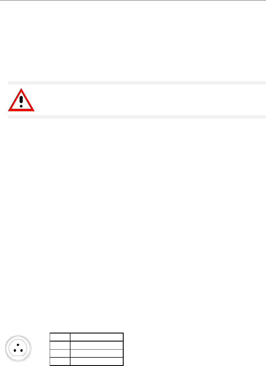
FSP Module Replacement
1164.4556.82 3.37 E-1
Installing the New Modules and Completing the Instrument
Ø Mount the new Key-Probe board (50) with three countersunk screws (55) to mounting plate (60).
Ø Mount the new Vol./Phone Board (1040) with the nut of the volume control and one countersunk
screw (1055) to the mounting plate (1050). Mount Vol./Phone board (1040) with three countersunk
screws (1060) to mounting plate (60).
Ø Connect the ribbon cable at motherboard-connector X80 and X81.
Ø Move the complete mounting plate (60) carefully back in the instrument.
Caution
Make sure to route the cables properly.
Ø Connect RF-cable W1 (295) , (315) ) or (322) at the input of the RF Attenuator (20) or (30).
Ø Screw three countersunk screws (70) to the instrument frame and two countersunk screws (70) to
the mounting plate (60).
Ø Install the labelling panel (270).
Ø Push the 2 front handles (420) on the instrument and mount them with the 4 screws (430).
Ø Replace the volume control knob (Option FSP-B3), if it was removed.
Ø Push the tube (410) on the instrument and mount the 4 rear-panel feet (450).
Function Test
Ø Connect a suitable keyboard to the keyboard jack.
Ø Connect the instrument to the mains, switch on the instrument power switch and switch on the
instrument with the ON/STANDBY key
Ø Press the "Ctrl" and "Esc" keys on the keyboard simultaneously; the Windows-XP taskbar appears at
the bottom of the screen.
Ø Measure the output voltage at the probe connector (see Fig. 3-12 Pin assignments of PROBE
POWER connector).
Ø Connect a keyboard to the instrument and test the function.
Ø If the option FSP-B3 (AF demodulator) is fitted, test the function of headphone connector and volume
control. Press the MKR key, and press the MARKER DEMOD softkey. Noise can be heard in the
loudspeaker, the volume can be changed with the VOLUME knob at the front panel. Connect a
headphone to the AF OUTPUT at the front panel, the loudspeaker must be switched off and the
noise can be heard in the headphone.
Pin Signal
1GND
2 -12.6 V
1
23
3 +15 V
Fig. 3-12 Pin assignments of PROBE POWER connector

Module Replacement FSP
1164.4556.82 3.38 E-1
Replacing the RF Frontend A100
(See chapter 5, spare parts list, item 100, and explosion drawing 1164.4391.)
The RF Frontend is installed in the middle of the instrument .
Opening the Instrument and Removing the Board
Ø Switch off the instrument, pull the mains plug, unscrew the 4 rear-panel feet (450) and push the tube
(410) backwards and take off.
Ø Unscrew the two countersunk screws (260) at the top of the instrument and the three countersunk
screws (250)) at the fan side, lift the cover at the top (240) of the instrument to the left side and take
off.
Ø Place the instrument on the left side frame and loosen all connecting cables to the board.
Ø Push out board to the top side of the instrument.
Note: The board can be moved up by pressing carefully from the downside through the connector
wholes in the motherboard against the board.
Installing the New RF Frontend Module and Completing the Instrument
Ø Plug the new board into the instrument and reconnect all cables to the board.
Note: Please refer to the cable wiring drawing on the motherboard.
Ø Put the top cover (240) on the instrument and mount it with two countersunk screws (260) and three
countersunk screws (250).
Ø Push the tube (410) on the instrument and mount the 4 rear-panel feet (450).
A cold boot is necessary after replacing the frontend.
See section "Performing a Cold Boot" in this chapter.
Ø Connect the instrument to the mains, switch on the instrument power switch and switch on the
instrument with the ON/STANDBY key
Ø After starting the instrument check for system messages:
- [ SETUP : SYSTEM INFO : SYSTEM MESSAGES ]
Ø Start selftest and check results:
- [ SETUP : SERVICE : SELFTEST ], then [SELFTEST RESULT]
Ø Start a total calibration and check the result:
- [ CAL : CAL TOTAL ] , then [ CAL RESULTS ]
Ø Check frequency response with chapter 1 and make a correction if necessary, using the correction
software.
Ø Create a backup of the EEPROM data (see chapter 2, section "Adjustment of Module Data").

FSP Module Replacement
1164.4556.82 3.39 E-1
Replacing the Detector A120 or A140 (Option FSP-B70)
(See chapter 5, spare parts list, item 1100 or 1900, and explosion drawing 1164.4391.)
The board is installed in the front part of the instrument.
Opening the Instrument and Removing the Board
Ø Switch off the instrument, pull the mains plug, unscrew the 4 rear-panel feet (450) and push the tube
(410) backwards and take off.
Ø Unscrew the two countersunk screws (260) at the top of the instrument and three countersunk
screws (250) at the fan side, lift the cover at the top (240) of the instrument to the left side and take
off.
Ø Place the instrument on the left side frame and loosen all connecting cables to the board.
Ø Push out board to the top side of the instrument.
Note: The board can be moved up by pressing carefully from the downside through the connector
holes in the motherboard against the board.
Installing the New Module and Completing the Instrument
Ø Plug the new board into the instrument and reconnect all cables to the board.
Note: Please refer to the cable wiring drawing on the motherboard.
Ø Put the top cover (240) on the instrument and mount it with two countersunk screws (260) and three
countersunk screws (250).
Ø Push the tube (410) on the instrument and mount the 4 rear-panel feet (450).
A cold boot is necessary after replacing the detector.
See section "Performing a Cold Boot" in this chapter.
Ø Connect the instrument to the mains, switch on the instrument power switch and switch on the
instrument with the ON/STANDBY key
Ø After starting the instrument check for system messages:
- [ SETUP : SYSTEM INFO : SYSTEM MESSAGES ]
Ø Start selftest and check results:
- [ SETUP : SERVICE : SELFTEST ], then [SELFTEST RESULT]
Ø Start a total calibration and check the result:
- [ CAL : CAL TOTAL ] , then [ CAL RESULTS ]
Ø Create a backup of the EEPROM data (see chapter 2, section "Adjustment of Module Data").

Module Replacement FSP
1164.4556.82 3.40 E-1
Replacing the IF Filter A130
(See chapter 5, spare parts list, item 120, and explosion drawing 1164.4391.)
The board is installed in the middle of the instrument.
Opening the Instrument and Removing the Board
Ø Switch off the instrument, pull the mains plug, unscrew the 4 rear-panel feet (450) and push the tube
(410) backwards and take off.
Ø Unscrew the two countersunk screws (260) at the top of the instrument and three countersunk
screws (250) at the fan side, lift the cover at the top (240) of the instrument to the left side and take
off.
Ø Place the instrument on the left side frame and loosen all connecting cables to the board.
Ø Push out board to the top side of the instrument.
Note: The board can be moved up by pressing carefully from the downside through the connector
holes in the motherboard against the board.
Installing the New Module and Completing the Instrument
Ø Plug the new board into the instrument and reconnect all cables to the board.
Note: Please refer to the cable wiring drawing on the motherboard.
Ø Put the top cover (240) on the instrument and mount it with two countersunk screws (260) three
countersunk screws (250).
Ø Push the tube (410) on the instrument and mount the 4 rear-panel feet (450).
Ø Connect the instrument to the mains, switch on the instrument power switch and switch on the
instrument with the ON/STANDBY key
Ø A cold boot is necessary after replacing the flash disk.
See section "Performing a Cold Boot" in this chapter.
Ø After starting the instrument check for system messages:
- [ SETUP : SYSTEM INFO : SYSTEM MESSAGES ]
Ø Start selftest and check results:
- [ SETUP : SERVICE : SELFTEST ], then [SELFTEST RESULT]
Ø Start a total calibration and check the result:
- [ CAL : CAL TOTAL ] , then [ CAL RESULTS ]
Ø Check frequency accuracy and the calibration source level with chapter 1 and readjust with chapter 2
if necessary.
Ø Create a backup of the EEPROM data (see chapter 2, section "Adjustment of Module Data").
Ø Write the calibration data to the EEPROM (see chapter 2, section "Adjustment of Module Data").

FSP Module Replacement
1164.4556.82 3.41 E-1
Replacing the MW Converter Unit A160
(See chapter 5, spare parts list, items 130 to 141, and explosion drawing 1164.4391.)
The board is installed in the middle of the instrument.
Opening the Instrument and Removing the Board
Ø Switch off the instrument, pull the mains plug, unscrew the 4 rear-panel feet (450) and push the tube
(410) backwards and take off.
Ø Unscrew the two countersunk screws (260) at the top of the instrument and three countersunk
screws (250) at the fan side, lift the cover at the top (240) of the instrument to the left side and take
off.
Ø Place the instrument on the left side and loosen all cables at the bottom to the board.
Ø Push out board to the top side of the instrument.
Note: The board can be moved up by pressing carefully from the downside through the connector
wholes in the motherboard against the board.
Installing the New Module and Completing the Instrument
Ø Plug the new board into the instrument and reconnect all cables to the board.
Note: Please refer to the cable wiring drawing on the motherboard.
Ø Put the top cover (240) on the instrument and mount it with two countersunk screws (260) and three
countersunk screws (250).
Ø Push the tube (410) on the instrument and mount the 4 rear-panel feet (450).
Ø Connect the instrument to the mains, switch on the instrument power switch and switch on the
instrument with the ON/STANDBY key
Ø After starting the instrument check for system messages:
- [ SETUP : SYSTEM INFO : SYSTEM MESSAGES ]
Ø Start selftest and check results:
- [ SETUP : SERVICE : SELFTEST ], then [SELFTEST RESULT]
Ø Start a total calibration and check the result:
- [ CAL : CAL TOTAL ] , then [ CAL RESULTS ]
Ø Execute software frequency response correction FSP-FRQ.EXE
The software is located on the Gloris server.
- Test setup according to menu item "Schematic" (connect external reference)
- Check IEC/IEEE addresses and configuration of the instrument
- Press Autoselect button and execute measurement with Run.
- The frequency correction of the YIG filter is performed in the YIG section.
- After calibration, the frequency response is corrected over the entire frequency range.
Ø Create a backup of the EEPROM data (see chapter 2, section "Adjustment of Module Data").

Module Replacement FSP
1164.4556.82 3.42 E-1
Replacing Diplexer A162; FSP7
(See chapter 5, spare parts list, item 2030, and drawing 1130.2544.)
(See chapter 5, spare parts list, item 2006, and drawing 1130.2396.)
(See chapter 5, spare parts list, item 40, and drawing 1093.7994.)
The board is installed on the 8 GHz converter unit (1130.2544, 1130.2396) or the 7 GHz converter unit
(1093.7994).
Removing Diplexer on MW Converter 1130.2369
Ø Remove the 8 GHz converter unit (130).
Note: See description "Replacing the MW Converter Unit A160“.
Ø Remove cable W1 from the diplexer (2006).
Ø Undo 4 screws with washers (2008) at the bottom of the printed board.
Ø Take off the diplexer (2006) perpendicularly to the PCB.
Note: The diplexer is still connected to the PCB with contact pins.
Installing Diplexer on MW Converter 1130.2369
Ø Plug in new diplexer (2006) perpendicularly to the PCB.
Note: The diplexer is still connected to the PCB with contact pins.
Ø Refasten 4 screws with washers (2008) to the bottom of the PCB.
Ø Fit cable W1 to diplexer (2006).
Removing Diplexer on MW Converter 1130.2544
Ø Remove 8 GHz converter unit (130).
Note: See description "Replacing 8 GHz Converter Unit A160"
Ø Disconnect cable W1 from diplexer (2030).
Ø Undo 4 screws with washers (2035) from the bottom of the PCB.
Ø Remove diplexer (2006) perpendicularly to the PCB.
Note: The diplexer is still connected to the PCB with contact pins.
Installing Diplexer on MW Converter 1130.2544
Ø Plug in new diplexer (2030) perpendicularly to the PCB.
Note: The diplexer is connected to the PCB with contact pins.
Ø Refasten 4 screws with washers (2035) to the bottom of the PCB.
Ø Fit cable W1 to diplexer (2030).

FSP Module Replacement
1164.4556.82 3.43 E-1
Completing the Instrument and Frequency Response Correction
Ø Insert 7/8 GHz converter unit (130) back into the instrument.
Note: See description "Replacing MW Converter Unit A160".
Ø Execute frequency response correction software FSP-FRQ.EXE.
The software is located on the Gloris server.
- Test setup according to menu item "Schematic" (connect external reference).
- Check IEC/IEEE addresses and configuration of instruments.
- Press Autoselect button and perform the measurement with Run.
- The frequency correction of the YIG filter is performed under item YIG.
- After calibration, the frequency response is corrected over the entire frequency range.
Replacing 7/8 GHz YIG Unit A161; FSP7
(See chapter 5, spare parts list, items 2005, 2010, and drawing 1130.2544.)
The board is installed on the 8 GHz converter unit (1130.2544, 1130.2396.
Note: Only the YIG units (with YIG filter, cable, sheet metal part) are replaced. The interface is
thus always the same when using other YIG filters.

Module Replacement FSP
1164.4556.82 3.44 E-1
Removing 8 GHz YIG Unit on MW Converter 1130.2396
Ø Remove 8 GHz converter unit (130).
Note: See description "Replacing MW Converter Unit A160".
Ø Remove the two module covers by undoing the screws from the bottom of the module.
Ø Disconnect cable W1 from the diplexer (2006) and cable W2 from the 8 GHz converter circuit
(2000).
Ø Depending on the YIG unit used, disconnect cable from YIG filter to X4.
Ø Undo 2 countersunk screws (2004).
Ø Remove the complete YIG unit (2002 or 2003).
Note: YIG Unit 1130.2744.02 (2002) is connected to the PCB via contacts. Remove the YIG unit
towards the top perpendicularly to the PCB.
Installing 8 GHz YIG Unit on MW Converter 1130.2396
Ø Put the new YIG unit (2002 or 2003) onto the PCB.
Note: YIG Unit 1130.2744.02 (2002) is connected to the PCB via contacts. Plug YIG unit to
connector contacts from the top perpendicularly to the PCB.
Ø Fasten YIG unit with 2 countersunk screws (2004).
Ø Screw on cable W1 to the diplexer (2006) and connect cable W2 to 8 GHz converter circuit (2000).
Ø Depending on the YIG unit used, connect cable from YIG filter at X4.
Ø Fit the module cover onto the top of the converter unit (positioning by means of adjusting pins). Turn
8 GHz converter unit upside down, fit module cover to the bottom side and refasten all screws.
Removing 8 GHz YIG Unit on MW Converter 1130.2544
Ø Remove 8 GHz converter unit (130).
Note See description "Replacing MW Converter Unit A160."
Ø Remove the two module covers by undoing the screws from the bottom of the module.
Ø Disconnect cable W1 from the diplexer (2030) and cable W2 from the 8 GHz converter circuit
(2000).
Ø Depending on the YIG unit used, disconnect cable from YIG filter at X4.
Ø Undo 2 countersunk screws (2025).
Ø Remove the complete YIG unit (2005 or 2010).
Note: YIG Unit 1130.2944.02 (2005) is connected to the PCB via contacts. Remove the YIG unit
towards the top perpendicularly to the PCB.

FSP Module Replacement
1164.4556.82 3.45 E-1
Installing 8 GHz YIG Unit on MW Converter 1130.2544
Ø Put the new YIG unit (2005 or 2010) onto the PCB.
Note: YIG Unit 1130.2944.02 (2002) is connected to the PCB via contacts. Plug YIG unit into
connector contacts from the top perpendicularly to the PCB.
Ø Fasten YIG unit with 2 countersunk screws (2025).
Ø Screw on cable W1 to the diplexer (2030) and connect cable W2 to 8 GHz converter circuit (2000).
Ø Depending on the YIG unit used, connect cable from YIG filter at X4.
Ø Fit the module cover onto the top of the converter unit (positioning by means of adjusting pins). Turn
8 GHz converter unit upside down, fit module cover to the bottom side and refasten all screws.

Module Replacement FSP
1164.4556.82 3.46 E-1
Completing the Instrument and Frequency Response Correction
Ø Put 8 GHz converter unit (130) back into the instrument.
Note: See description "Replacing MW Converter Unit A160".
Ø Execute frequency response correction software FSP-FRQ.EXE.
The software is located on the Gloris server.
- Test setup according to menu item "Schematic" (connect external reference).
- Check IEC/IEEE addresses and configuration of instruments.
- Press the Autoselect button and perform the measurement with Run.
- The frequency correction of the YIG filter is performed under item YIG.
- After calibration, the frequency response is corrected over the entire frequency range.
Temperature Adjustment and Test of the YIG Filter
Ø A digital temperature adjustment is to be performed for the following MW converters:
- MW converter unit 8: 1130.2544 Mod: XX Rev: ≥ 05 Subrev: ≥ 01
- All other MW converters should undergo analog adjustment.
Ø Analog adjustment for converter unit 1130.2396 and for converter unit 1130.2544 with HWC = 00:
- Connect the RF output of the signal generator to the RF input of the FSP
- Activate the YIG filter sweep with the service function:
Password 30473035
Service funct. 2.16.10.1
- Span on FSP7: 200 MHz
- Set the signal generator frequency an the center frequency to 5 GHz
Nominal value: Temperature drift (0 to 50 C) < 8 MHz
- If X21 is used for temperature compensation, the temperature drift can be adapted via trimming
resistor R232 or trimming value R374.
Ø Digital adjustment:
- Place FSP7 into a climatic chamber for 2 hours at 50°C.
- Execute frequency response correction software FSP-FRQ.EXE.
The software is located on the Gloris server.
- Test setup according to menu item "Schematic" (connect external reference)
- Check IEC/IEEE addresses and configuration of instruments.
- Press the TK adjustment button.
- Place FSP7 into a climatic chamber for 2 hours at 0°C in the switched-off state.
- Switch on the instrument and repeat the coldness adjustment
Adjustment of Module Data
Ø Create a backup of the EEPROM data (see chapter 2, section "Adjustment of Module Data").

FSP Module Replacement
1164.4556.82 3.47 E-1
Replacing Diplexer (30 GHz) A230; FSP13/30
(See chapter 5, spare parts list, item 150, and drawing 1093.4495.01.)
In FSP13/30, the module is behind the attenuator on the right-hand side.
Removing Diplexer
Ø Disconnect cable X71 from motherboard (515).
Ø Disconnect cables W2 and W30 from diplexer (150).
Ø Disconnect diplexer (150) from attenuator (30).
Ø Remove diplexer (150).
Installing Diplexer
Ø Screw on diplexer (150) to attenuator (30).
Ø Fasten cables W2 and W30 to diplexer (150).
Ø Connect cable X71 to motherboard (510).
Completing the Instrument and Frequency Response Correction
Ø Execute frequency response correction software FSP-FRQ.EXE.
The software is located on the Gloris server.
- Test setup according to menu item "Schematic" (connect external reference).
- Check IEC/IEEE addresses and configuration of instruments.
- Press the Autoselect button and perform the measurement with Run.
- The frequency correction of the YIG filter is performed under item YIG.
- After calibration, the frequency response is corrected over the entire frequency range.
Ø Create a backup of the EEPROM data (see chapter 2, section "Adjustment of Module Data").

Module Replacement FSP
1164.4556.82 3.48 E-1
Replacing 13/30 GHz YIG Unit A161; FSP13/30
(See chapter 5, spare parts list, items 2115, 2120, 2125, 2130, and drawing 1093.8249.)
The board is installed on the 13/30 GHz converter unit (1093.8249).
Note: Only the YIG units (with YIG filter, cable, sheet metal part) are replaced. The interface is
thus always the same when using other YIG filters.
Removing 13 GHz YIG Unit on MW Converter 1093.8249
Ø Remove 13 GHz converter unit (135).
Note: See description "Replacing MW Converter Unit A160".
Ø Remove the two module covers by undoing the screws from the bottom of the module.
Ø Disconnect cable W2 from the RF extension (2140)
Ø Disconnect the cable from the YIG filter at X4.
Ø Undo 4 countersunk screws (2135).
Ø Remove the complete YIG unit (2115 or 2120).
Installing 13 GHz YIG Unit on MW Converter 1093.8249
Ø Put the new YIG unit (2115 or 2120) onto the PCB.
Ø Fasten YIG unit with 4 countersunk screws (2135).
Ø Screw on cable W2 to the RF extension (2140).
Ø Connect the cable from the YIG filter at X4.
Ø Fit the module cover onto the top of the converter unit (positioning by means of adjusting pins). Turn
13 GHz converter unit upside down, fit module cover to the bottom side and refasten all screws.
Removing 30 GHz YIG Unit on MW Converter 1093.8249
Ø Remove 30 GHz converter unit (140).
Note: See description "Replacing MW Converter Unit A160".
Ø Remove the two module covers by undoing the screws from the bottom of the module.
Ø Disconnect cable W2 from the RF extension (2145).
Ø Disconnect the cable from the YIG filter at X4.
Ø Undo 4 countersunk screws (2135).
Ø Remove the complete YIG unit (2125 or 2130).
Installing 30 GHz YIG Unit on MW Converter 1093.8249
Ø Place the new YIG unit (2125 or 2130) on the circuit board.
Ø Fasten YIG unit with four countersunk screws (2135).
Ø Screw cable W2 to RF extension (2145).
Ø Plug cable from YIG filter onto X4.
Ø Fit the module cover onto the top of the converter unit (positioning by means of adjusting pins). Turn
the 30 GHz converter unit upside down, fit module cover to the bottom side and refasten all screws.

FSP Module Replacement
1164.4556.82 3.49 E-1
Completing the Instrument and Frequency Response Correction
Ø Put the 13/30 GHz MW converter unit (135/140) back into the instrument.
Note: See description "Replacing MW Converter Unit A160".
Ø Execute frequency response correction software FSP-FRQ.EXE.
The software is located on the Gloris server.
- Test setup according to menu item "Schematic" (connect external reference).
- Check IEC addresses and configuration of instruments.
- Press the Autoselect button and perform the measurement with Run.
- The frequency correction of the YIG filter is performed under item YIG.
- After calibration, the frequency response is corrected over the entire frequency range.

Module Replacement FSP
1164.4556.82 3.50 E-1
Temperature Adjustment and Test of the YIG Filter
Ø A digital temperature adjustment is to be performed for the following MW converters:
- MW converter unit 13/30: 1093.8249 Mod: XX Rev: ≥ 10 SubRev: ≥ 01
- All other MW converters should undergo analog adjustment.
Ø Analog adjustment:
- Connect the RF output of the signal generator to the RF input of the FSP.
- Activate the YIG filter sweep with the service function:
Password 30473035
Service funct. 2.16.10.1
- Span on FSP30: 200 MHz
- Set the frequency of the signal generator and the center frequency to 15 GHz.
Nominal value: Temperature drift (0 to 50°C) < 8 MHz
- Adjust temperature drift with jumpers X21, X22, X23, trimming values R403, R119, R402 and
potentiometer R232.
Ø Digital adjustment:
- Place FSP30 into a climatic chamber for 2 hours at 50°C.
- Execute frequency response correction FSP-FRQ.EXE.
The software is located on the Gloris server.
- Test setup according to menu item "Schematic" (connect external reference).
- Check IEC/IEEE addresses and configuration of instruments.
- Press the TK adjustment button.
- Place FSP30 into a climatic chamber for 2 hours at 0°C in the switched-off state.
- Switch on the instrument and repeat the coldness adjustment.
Adjustment of Module Data
Ø Create a backup of the EEPROM data (see chapter 2, section "Adjustment of Module Data").

FSP Module Replacement
1164.4556.82 3.51 E-1
Replacing RF Extension 13/30 A162; FSP13/30
(See chapter 5, spare parts list, items 2140, 2145, and drawing 1093.8249.)
The board is installed on the 13/30 GHz converter unit.
Removing RF Extension 13
Ø Remove 13 GHz MW converter unit (135).
Note: See description "Replacing MW Converter Unit A160."
Ø Disconnect all cables from the extension (2140).
Ø Undo 6 screws with washers (2150) from the bottom side of the extension (2140).
Caution: The extension (2140) may fall out.
Ø Remove extension 13 (2140) perpendicularly to the PCB.
Note: The extension is still connected to the PCB with contact pins.
Installing RF Extension 13
Ø Plug extension 13 (2140) perpendicularly into the PCB.
Note: The extension is still connected to the PCB with contact pins.
Ø Refasten 6 screws with washers (2150) to the bottom side of the extension (2140).
Ø Reconnect all cables to the extension (2140).
Removing RF Extension 30
Ø Remove 30 GHz MW converter unit (140).
Note: See description "Replacing MW Converter Unit A160".
Ø Disconnect all cables from the extension (2145).
Ø Undo 6 screws with washers (2150) from the bottom side of the extension (2145).
Caution: The extension (2145) may fall out.
Ø Remove extension 30 (2145) perpendicularly to the circuit board.
Note: The extension is still connected to the PCB with contact pins.
Installing RF Extension 30
Ø Plug extension 30 (2145) perpendicularly into the PCB.
Note: The extension is still connected to the PCB with contact pins.
Ø Refasten 6 screws with washers (2150) to the bottom side of the extension (2145).
Ø Reconnect all cables to the extension (2145).

Module Replacement FSP
1164.4556.82 3.52 E-1
Completing the Instrument and Frequency Response Correction
Ø Put the 13/30 GHz MW converter unit (135/140) back into the instrument.
Note: See description "Replacing MW Converter Unit A160".
Ø Execute frequency response correction software FSP-FRQ.EXE.
The software is located on the Gloris server.
- Test setup according to menu item "Schematic" (connect external reference).
- Check IEC/IEEE addresses and configuration of instruments.
- Press the Autoselect button and perform the measurement with Run.
- The frequency correction of the YIG filter is performed under item YIG.
- After calibration, the frequency response is corrected over the entire frequency range.
Ø Create a backup of the EEPROM data (see chapter 2, section "Adjustment of Module Data").

FSP Module Replacement
1164.4556.82 3.53 E-1
Replacing Diplexer A163; FSP40
(See chapter 5, spare parts list, item 2225, and drawing 1093.8584.)
The board is installed on the 40 GHz converter unit (141).
Removing the Diplexers on the 40 GHz MW Converter
Ø Remove 8 GHz converter unit (130).
Note: See description "Replacing MW Converter Unit A160".
Ø Disconnect cable W5 from diplexer (2225).
Ø Undo 4 screws with washers (2230) from the bottom side of the PCB.
Ø Remove diplexer (2006) perpendicularly to the PCB.
Note: The diplexer is still connected to the PCB with contact pins.
Installing the Diplexer on the 40 GHz MW Converter
Ø Plug diplexer (2225) perpendicularly into the PCB.
Note: The diplexer is connected to the PCB with contact pins.
Ø Refasten 4 screws with washers (2230) to the bottom side of the PCB.
Ø Connect cable W5 to diplexer (2225)
Completing the Instrument and Frequency Response Correction
Ø Put the 40 GHz MW converter unit (141) back into the instrument.
Note: See description "Replacing MW Converter Unit A160".
Ø Execute frequency response correction software FSP-FRQ.EXE.
The software is located on the Gloris server.
- Test setup according to menu item "Schematic" (connect external reference).
- Check IEC/IEEE addresses and configuration of instruments.
- Press the Autoselect button and perform the measurement with Run.
- The frequency correction of the YIG filter is performed under item YIG.
- After calibration, the frequency response is corrected over the entire frequency range.
Ø Create a backup of the EEPROM data (see chapter 2, section "Adjustment of Module Data").

Module Replacement FSP
1164.4556.82 3.54 E-1
Replacing 40 GHz YIG Unit A161; FSP40
(See chapter 5, spare parts list, item 2215, and drawing 1093.8584.)
The board is installed on the 40 GHz converter unit (141).
Note: Only the YIG units (with YIG filter, cable, sheet metal part) are replaced. The interface is
thus always the same when using other YIG filters.
Removing 40 GHz YIG Unit on MW Converter
Ø Remove 40 GHz converter unit (141).
Note: See description "Replacing MW Converter Unit A160".
Ø Remove the two module covers by undoing the screws from the bottom of the module.
Ø Disconnect cable W2 from RF extension (2235) and cable W5 from diplexer (2225).
Ø Disconnect cable from YIG filter at X4.
Ø Undo 4 countersunk screws (2220).
Ø Remove complete YIG unit (2215).
Installing 40 GHz YIG Unit on MW Converter
Ø Put the new YIG unit (2215) onto the PCB.
Ø Fasten YIG unit with 4 countersunk screws (2220).
Ø Screw on cable W2 to RF extension (2235) and cable W5 to diplexer (2225).
Ø Connect cable from YIG filter at X4.
Ø Fit the module cover onto the top of the converter unit (positioning by means of adjusting pins). Turn
40 GHz converter unit upside down, fit module cover to the bottom side and refasten all screws.
Completing the Instrument and Frequency Response Correction
Ø Put the 40 GHz MW converter unit (141) back into the instrument.
Note: See description "Replacing MW Converter Unit A160".
Ø Execute frequency response correction software FSP-FRQ.EXE.
The software is located on the Gloris server.
- Test setup according to menu item "Schematic" (connect external reference).
- Check IEC/IEEE addresses and configuration of instruments.
- Press the Autoselect button and perform the measurement with Run.
- The frequency correction of the YIG filter is performed under item YIG.
- After calibration, the frequency response is corrected over the entire frequency range.

FSP Module Replacement
1164.4556.82 3.55 E-1
Temperature Adjustment and Test of the YIG Filter
Ø The MW converter 40 should undergo digital temperature compensation.
Ø Digital adjustment:
- Place FSP40 into a climatic chamber for 2 hours at 50°C.
- Execute frequency response correction software FSP-FRQ.EXE.
The software is located on the Gloris server.
- Test setup according to menu item "Schematic" (connect external reference).
- Check IEC/IEEE addresses and configuration of instruments.
- Press the TK adjustment button.
- Place FSP40 into a climatic chamber for 2 hours at 0°C in the switched-off state.
- Switch on the instrument and repeat the coldness adjustment.
Ø Create a backup of the EEPROM data (see chapter 2, section "Adjustment of Module Data").

Module Replacement FSP
1164.4556.82 3.56 E-1
Replacing RF Extension 40 A162; FSP40
(See chapter 5, spare parts list, item 2235, and drawing 1093.8584.)
The board is installed on the 40 GHz converter unit.
Removing RF Extension 40
Ø Remove 40 GHz MW converter unit (141).
Note: See description "Replacing MW Converter Unit A160".
Ø Disconnect all cables from the extension (2235).
Ø Remove the two module covers by undoing the screws from the bottom of the module.
Ø Undo 8 screws with washers (2240) from the bottom side of the extension (2235).
Caution: The extension (2235) may fall out.
Ø Remove extension 40 (2235) perpendicularly to the PCB.
Note: The extension is still connected to the PCB with contact pins.
Installing RF Extension 40
Ø Plug extension 40 (2235) perpendicularly into the PCB.
Note: The extension is still connected to the PCB with contact pins.
Ø Refasten 8 screws with washers (2240) to the bottom side of the extension (2235).
Ø Fit the module cover onto the top of the converter unit (positioning by means of adjusting pins). Turn
40 GHz converter unit upside down, fit module cover to the bottom side and refasten all screws.
Ø Refasten all cables to the extension (2235).
Completing the Instrument and Frequency Response Correction
Ø Put the 40 GHz MW converter unit (141) back into the instrument.
Note: See description "Replacing MW Converter Unit A160".
Ø Execute frequency response correction software FSP-FRQ.EXE.
The software is located on the Gloris server.
- Test setup according to menu item "Schematic" (connect external reference).
- Check IEC/IEEE addresses and configuration of instruments.
- Press the Autoselect button and perform the measurement with Run.
- The frequency correction of the YIG filter is performed under item YIG.
- After calibration, the frequency response is corrected over the entire frequency range.
Ø Create a backup of the EEPROM data (see chapter 2, section "Adjustment of Module Data").

FSP Module Replacement
1164.4556.82 3.57 E-1
Replacing AF Demodulator A190 (Option FSP-B3)
(See chapter 5, spare parts list, item 1000, and drawing 1164.4391.)
The board is fitted the front part of the instrument.
Opening the Instrument and Removing the Board
Ø Switch off the instrument, pull the mains plug, unscrew the 4 rear-panel feet (450) and push the tube
(410) backwards and take off.
Ø Unscrew the two countersunk screws (260) at the top of the instrument and the three countersunk screws
(250) at the fan side, lift the cover at the top (240) of the instrument to the left side and take off.
Ø Place the instrument on the left side frame and loosen all connecting cables to the board.
Ø Push out board to the top side of the instrument.
Note: The board can be moved up by pressing carefully from the downside through the
connector wholes in the motherboard against the board.
Installing the New Module and Completing the Instrument
Ø Plug the new board into the instrument and reconnect all cables to the board.
Note: Please refer to the cable wiring drawing on the motherboard.
Ø Put the top cover (240) on the instrument and mount it with 3 countersunk screws (260) and 2
screws with washer (250).
Ø Push the tube (410) on the instrument and mount the 4 rear-panel feet (450).
Ø Connect the instrument to the mains, switch on the instrument power switch and switch on the
instrument with the ON/STANDBY key
Ø After starting the instrument check for system messages:
- [ SETUP : SYSTEM INFO : SYSTEM MESSAGES ]
Ø Test the function of headphone connector and volume control.
Ø Create a backup of the EEPROM data (see chapter 2, section "Adjustment of Module Data").

Module Replacement FSP
1164.4556.82 3.58 E-1
Replacing the OCXO A200 (Option FSP-B4)
(See chapter 5, spare parts list, item 1100, and drawings 1164.4391 and 1129.6791.)
The board is fitted in the front part behind the front module .
Opening the Instrument and Removing the Board
Ø Switch off the instrument, pull the mains plug, unscrew the 4 rear-panel feet (450) and push the tube
(410) backwards and take off.
Ø Unscrew the two countersunk screws (260) at the top of the instrument and the three countersunk screws
(250) at the fan side, lift the cover at the top (240) of the instrument to the left side and take off.
Ø Place the instrument on the left side frame and loosen all connecting cables to board.
Ø Push out board to the top side of the instrument.
Note: The board can be moved up by pressing carefully from the downside through the connector
wholes in the motherboard against the board.
Installing the New Module and Completing the Instrument
Ø Plug the new board into the instrument and reconnect all cables to the board.
Note: Please refer to the cable wiring drawing on the motherboard.
Ø Put the top cover (240) on the instrument and mount it with two countersunk screws (260) and 2
screws with washer (250).
Ø Push the tube (410) on the instrument and mount the 4 rear-panel feet (450).
Ø Connect the instrument to the mains, switch on the instrument power switch and switch on the
instrument with the ON/STANDBY key
Ø After starting the instrument check for system messages:
- [ SETUP : SYSTEM INFO : SYSTEM MESSAGES ]
Ø Start selftest and check results:
- [ SETUP : SERVICE : SELFTEST ], then [SELFTEST RESULT]
Ø Start a total calibration and check the result:
- [ CAL : CAL TOTAL ] , then [ CAL RESULTS ]
Ø Check frequency accuracy with chapter 1 and readjust with chapter 2 if necessary.
Ø Create a backup of the EEPROM data (see chapter 2, section "Adjustment of Module Data").

FSP Module Replacement
1164.4556.82 3.59 E-1
Replacing Trigger A230 (Option FSP-B6)
(See chapter 5, spare parts list, item 1800, and drawings 1164.4391 and 1129.8613.)
The board is installed at the rear of the instrument in front of the power supply.
Opening the Instrument and Removing the Board
Ø Switch off unit, disconnect it from power supply, unscrew 4 rear-panel feet (450) and pull off
enclosure (410) towards rear.
Ø Undo the two countersunk screws (260) at the top of the instrument and the three countersunk
screws (250) at the fan side, lift the cover at the top (240) of the instrument to the left side and take
off.
Ø Place the instrument onto its side and remove all connecting RF cables to board on the bottom of the
instrument.
Ø Pull out the board towards the top of the instrument.
Note: The board can be disconnected from the motherboard connector by carefully pressing
through the motherboard slots from the bottom.
Installing the New Module and Completing the Instrument
Ø Plug the new board into the instrument and reconnect all RF cables.
Note: Please observe the labelling on the motherboard.
Ø Mount top cover (240) and fasten it in place by 2 countersunk screws (260) and three countersunk
screws (250).
Ø Slide on enclosure (410) and screw on 4 rear-panel feet (450).
A cold boot is necessary after replacing the TRIGGER module.
See section "Performing a Cold Boot" in this chapter.
Ø Connect power cable, switch on power switch and press ON key.
Ø After starting the instrument check for system messages:
- [ SETUP : SYSTEM INFO : SYSTEM MESSAGES ]
Ø Start selftest and check results to ensure that no errors occurred:
- [ SETUP : SERVICE : SELFTEST ], then [SELFTEST RESULT]
Ø Start system error correction and check the result to ensure that no errors occurred:
- [ CAL : CAL TOTAL ] , then [ CAL RESULTS ]
Ø Check trigger level according to chapter 1 and adjust if required.
Ø Create a backup of the EEPROM data (see chapter 2, section "Adjustment of Module Data").

Module Replacement FSP
1164.4556.82 3.60 E-1
Replacing the Tracking Generator A170 (Option FSP-B9)
(See chapter 5, spare parts list, item 1500, and drawings 1164.4391 and 1129.7069.)
The board is fitted in the back part of the instrument in front of the power supply.
Opening the Instrument and Removing the Board
Ø Switch off the instrument, pull the mains plug, unscrew the 4 rear-panel feet (450) and push the tube
(410) backwards and take off.
Ø Unscrew the two countersunk screws (260) at the top of the instrument and the three countersunk
screws (250) at the fan side, lift the cover at the top (240) of the instrument to the left side and take
off.
Ø Place the instrument on the left side frame and loosen all connecting cables to the board.
Ø Push out board to the top side of the instrument.
Note: The board can be moved up by pressing carefully from the downside through the connector
wholes in the motherboard against the board.
Installing the New Module and Completing the Instrument
Ø Plug the new board into the instrument and reconnect all cables to the board.
Note: Please refer to the cable wiring drawing on the motherboard.
Ø Put the top cover (240) on the instrument and mount it with two countersunk screws (260) and three
countersunk screws (250).
Ø Push the tube (410) on the instrument and mount the 4 rear-panel feet (450).
A cold boot is necessary after replacing the TRIGGER module.
See section "Performing a Cold Boot" in this chapter.
Ø Connect the instrument to the mains, switch on the instrument power switch and switch on the
instrument with the ON/STANDBY key
Ø After starting the instrument check for system messages:
- [ SETUP : SYSTEM INFO : SYSTEM MESSAGES ]
Ø Start selftest and check results:
- [ SETUP : SERVICE : SELFTEST ], then [SELFTEST RESULT]
Ø Start a total calibration and check the result:
- [ CAL : CAL TOTAL ] , then [ CAL RESULTS ]
Ø Connect the output of the Tracking Generator with the RF-Input (use short low attenuation cable)
and switch on the Generator : [ NETWORK ]. A continuous signal is displayed on the screen.

FSP Module Replacement
1164.4556.82 3.61 E-1
Replacing the External Generator Control A210 (Option FSP-B10)
(See chapter 5, spare parts list, item 1600, and drawings 1093.4495 and 1129.7298.)
The board is fitted in the front part of the instrument .
Opening the Instrument and Removing the Board
Ø Switch off the instrument, pull the mains plug, unscrew the 4 rear-panel feet (450) and push the tube
(410) backwards and take off.
Ø Unscrew the two countersunk screws (260) at the top of the instrument and the three countersunk screws
(250) at the fan side, lift the cover at the top (240) of the instrument to the left side and take off.
Ø Push out board to the top side of the instrument.
Installing the New Module and Completing the Instrument
Ø Plug the new board into the instrument.
Ø Put the top cover (240) on the instrument and mount it with two countersunk screws (260) and three
countersunk screws (250).
Ø Push the tube (410) on the instrument and mount the 4 rear-panel feet (450).
Ø Connect the instrument to the mains, switch on the instrument power switch and switch on the
instrument with the ON/STANDBY key
Ø After starting the instrument check for system messages:
- [ SETUP : SYSTEM INFO : SYSTEM MESSAGES ]
Ø Create a backup of the EEPROM data (see chapter 2, section "Adjustment of Module Data").
Ø Check function as described in chapter 1.
Replacing Wideband Calibrator A190 (Option FSP-B15)
(See chapter 5, spare parts list, item 1160, and drawing 1155.1012.)
The board is installed in the front part of the instrument.
Opening the Instrument and Removing the Board
Ø Switch off unit, disconnect it from power supply, unscrew 4 rear-panel feet (450) and pull off
enclosure (410) towards rear.
Ø Undo the two countersunk screws (260) at the top of the instrument and the three countersunk
screws (250) at the fan side, lift the cover at the top (240) of the instrument to the left side and take
off.
Ø Place the instrument onto its side and remove all connecting cables to board at the rear of the
instrument.
Ø Pull out the board towards the top of the instrument.
Note: The board can be disconnected from the motherboard connector by carefully pressing from
the bottom through the motherboard slots.

Module Replacement FSP
1164.4556.82 3.62 E-1
Installing the New Module and Completing the Instrument
Ø Plug the new board into the instrument and reconnect all RF cables.
Note: Please observe the labelling on the motherboard.
Ø Mount top cover (240) and fix it by 2 countersunk screws (260) and three countersunk screws (250).
Ø Slide on enclosure (410) and screw on 4 rear-panel feet (450).
A cold boot is necessary after replacing the attenuator.
See section "Performing a Cold Boot" in this chapter. Connect power cable, switch on power switch and
press ON key.
Ø After starting the instrument, check for system messages:
- [ SETUP : SYSTEM INFO : SYSTEM MESSAGES ]
Ø Create a backup of the EEPROM data (see chapter 2, section "Adjustment of Module Data").
Ø Check the function according to chapter 1.

FSP Module Replacement
1164.4556.82 3.63 E-1
Replacing the LAN Adapter (Option FSP-B16)
(See chapter 5, spare parts list, item 1270, and drawings 1164.4391 and 1129.8071.)
The adapter is located at the rear of the instrument.
Opening the Instrument and Removing the Board
Ø Switch off the instrument, pull the mains plug, unscrew the 4 rear-panel feet (450) and push the tube
(410) backwards and take off.
Ø Unscrew the two countersunk screws (260) at the top of the instrument and the three countersunk screws
(250) at the fan side, lift the cover at the top (240) of the instrument to the left side and take off.
Ø Disconnect LAN interface cable W32 (1250) ) on the LAN adapter (1270).
Ø Undo the barrier and remove the adapter (1270) inward.
Ø .
Installing the New Module and Completing the Instrument
Ø Hook the new adapter (1270) into the opening in the rear panel from the inside of the instrument and
engage it.
Note: For alignment, see drawing, view B.
Ø Reconnect the LAN cable (1250) to the adapter (1270).
Ø Mount the instrument cover at the top (240) and refasten it with two countersunk screws (260) and
three countersunk screws (250).
Ø
Ø Push the tube (410) on the instrument and mount the 4 rear-panel feet (450).
Ø Connect the instrument to the mains, switch on the instrument power switch and switch on the
instrument with the ON/STANDBY key

Module Replacement FSP
1164.4556.82 3.64 E-1
Replacing the Electronic Attenuator A50 (Option FSP-B25)
(See chapter 5, spare parts list, item 1400, and drawings 1164.4391 and 1129.7800.)
The electronic attenuator is fitted behind the RF attenuator under the fan.
Opening the Instrument and Removing the Electronic Attenuator
Ø Switch off the instrument, pull the mains plug, unscrew the 4 rear-panel feet (450) and push the tube
(410) backwards and take off.
Ø Place the instrument on the left side frame and loosen RF cable W28 (1430/1440) at the electronic
Attenuator output 1400).
Ø Unscrew 4 countersunk screws (1460) at the right frame.
Note: The electronic attenuator will only be fixed with the RF cables at the front.
Ø Fix the electronic attenuator and disconnect RF cable W29 (1420) at the output of the attenuator
(20).
Ø Move carefully out the RF attenuator and disconnect the ribbon cable at the electronic attenuator.
Installing the New Electronic Attenuator
Ø Connect (only loose) cable W29 (1420) at the new electronic attenuator.
Note: Label X3 shows to the electronic attenuator.
Ø Connect the ribbon cable (W50) at the new attenuator.
Ø Move the new electronic attenuator in the instrument and connect cable W29 (1420) to the output of
the attenuator (20).
Ø Screw the four screws with washers (1460) at the right frame in the electronic attenuator.
Ø Fix the RF cable (1420) at the output of the attenuator (20) and the electronic attenuator.
3 GHz Model (1164.4391.03)
Ø Connect cable W28 (1430) between electronic attenuator and the frontend (100) .
7 GHz Model (1164.4391)
Ø Connect cable W28 (1440) between electronic attenuator and the MW converter (130).
Completing the Instrument
Ø Push the tube (410) on the instrument and mount the 4 rear-panel feet (450).
A cold boot is necessary after replacing the attenuator.
See section "Performing a Cold Boot" in this chapter.
Ø Connect the instrument to the mains, switch on the instrument power switch and switch on the
instrument with the ON/STANDBY key
Ø After starting the instrument check for system messages:
- [ SETUP : SYSTEM INFO : SYSTEM MESSAGES ]
Ø Start selftest and check results:
- [ SETUP : SERVICE : SELFTEST ], then [SELFTEST RESULT]
Ø Start a total calibration and check the result:
- [ CAL : CAL TOTAL ] , then [ CAL RESULTS ]
Ø Create a backup of the EEPROM data (see chapter 2, section "Adjustment of Module Data").
Ø Check frequency response with chapter 1 and make a correction if necessary.
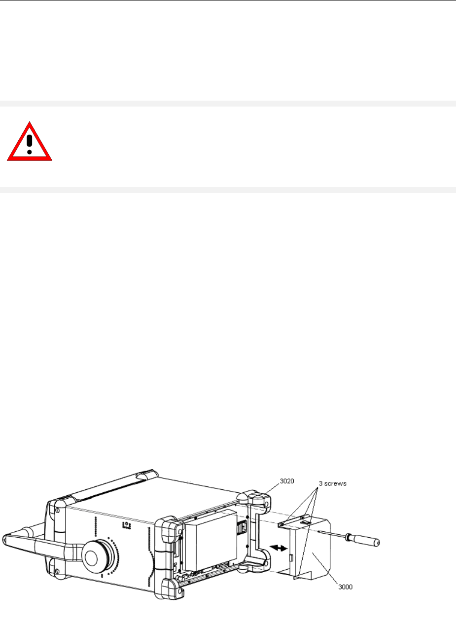
FSP Module Replacement
1164.4556.82 3.65 E-1
Replacing the DC/DC Converter (Option FSP-B30)
(See chapter 5, spare parts list, item 3000.)
The DC/DC converter (3000) is mounted on the rear panel of the instrument.
See also DC Power Supply FSP-B30 operating manual.
Caution:
The DC/DC converter in an unmounted state is a module in "open frame" design.
Therefore make sure that it is mounted only by skilled electricians (see operating
manual, safety instructions, item 9).
Make sure that the DC/DC converter is separated from the supply source.
Removing the DC/DC Converter
Ø Unplug the supply cable on the DC/DC converter.
Ø Unscrew the three captive screws on the converter.
Ø Pull off the converter to the rear.
Installing the new DC/DC Converter
Ø Plug the DC/DC converter (3000) onto the rear-panel power plug.
Note: The power switch is automatically actuated when the DC/DC converter is connected.
Fasten the converter to the rear panel with three fixing screws.
Note:
Rear-panel foot with Options FSP-B30 (DC/DC converter) and FSP-B1 (housing with shock
protection):
If Option FSP-B1 is present, the right rear-panel foot (3020) is modified in order to ensure sufficient
ventilation of the power pack.
Fig. 3-1 Removing and installing the DC/DC converter, FSP-B30

Module Replacement FSP
1164.4556.82 3.66 E-1
Replacing the Battery Charger Module (Option FSP-B31/32)
Opening the Battery Pack and Removing the Module
Ø Remove the battery pack from the instrument.
Ø Undo the three screws (1) on the bottom.
Ø Pull out the cover (2) to the rear.
Ø Unplug all cables.
Ø Undo the two screws on the jack (5) and pull out the jack (5).
Ø Undo six screws (6) and remove the battery charger module (3030).
Installing the Battery Charger Module and Completing the Instrument
Ø Install new battery charger module (3030) and refasten with six screws (6).
Ø Install jack (5), fasten with two screws and reconnect all cables.
Ø Replace the cover (2), pressing the batteries down and making sure that no cables are trapped.
Ø Refasten the cover with three screws (1).
Fig. 3-2 Removing and installing the battery charger module, FSP-B31/32

FSP Module Replacement
1164.4556.82 3.67 E-1
Replacing the Batteries (Option FSP-B31/32)
Opening the Battery Pack and Removing the Batteries
Ø Remove the battery pack from the instrument.
Ø Undo the three screws (1) on the bottom.
Ø Pull out the cover (2) to the rear.
Ø Disconnect the batteries (3).
Ø Take out the batteries (3040).
Installing the Batteries and Completing the Instrument
Ø Insert new batteries (3040) and connect them (3).
Ø Replace the cover, pressing the batteries down and making sure that no cables are trapped.
Ø Refasten the cover (1).
Ø Charge the battery pack.
Fig. 3-3 Removing and installing the batties, FSP-B31/B32
FVREFSEQARABISCHFVREFSEQARABISCH
Troubleshooting FSP
1164.4556.82 3.68 E-1
Troubleshooting
Malfunctions may have simple causes but also may be caused by faulty components.
These troubleshooting instructions allow for locating the error causes down to board level and make the
instrument ready for use again by means of board replacement.
We recommend that the instrument be shipped to our experts in the service centers (cf. address list) for
module replacement and further error elimination.
Warning!
Do not plug or unplug boards prior to disconnecting them from ac supply!
Be careful not to cause short-circuits when measuring voltages!
The following utilities are provided in the FSP for diagnostic purposes:
• Permanent monitoring of levels and frequencies in the instrument
• Selftest
• System error correction
Note: When problems occur, first check, whether any connections (cables, plug-in connections of
boards etc.) are damaged or wrongly connected.
Measuring Equipment and Accessories
Item Type of equipment Specifications recommended Equipment
recommended R&S-
Order No. Use
1 DC meter URE 0350.5315.02 Troubleshooting
2 Spectrum analyzer Frequency range 0 to 7 GHz FSEB 20 1066.3010.20 Troubleshooting
3 Adapting cable 1 m long
SMP- to SMA connection - 1129.8259.00 Troubleshooting
4 Adapting cable 0.5 m long
SMP-to SMP-connection - 1129.8265.00 Troubleshooting
5 Adapter board Extension 150 mm high
48-contact, 2 mm spacing - 1100.3542.02 Troubleshooting

FSP Troubleshooting
1164.4556.82 3.69 E-1
Troubleshooting Start-up Problems
• Error: FSP cannot be switched on.
Action Possible error causes and further steps
Check power-on switch on the rear
ß
Power switch OFF: Switch on power supply..
Check yellow LED (Stand-by).
ß
LED remains dark:
Ø Measure voltage at X20.D24 (power supply unit)
Rated value: +12 V ± 1V
Voltage o.k.: Keyboard or controller faulty.
No voltage: Remove IF-Filter or OCXO modules.
Ø Measure voltage at X20.D24 (power supply unit):
Rated value: +12 V ± 1V
Correct voltage: Removed module faulty
No voltage: Power supply faulty or short-
circuit at 12V standby.
Switch on instrument. Check green LED
ß
LED remains dark:
Measure PWR-ON signal on the power supply X20.B1:
< 1V for ON
Voltage > 1V: Keyboard membrane or controller faulty.
Power supply starts, screen remains dark? Measure voltages on the motherboard, see "Short-
circuit of one or more operating voltages".
• Error: Short-circuit of one or more operating voltages
Action Possible error causes and further steps
Check on the bottom of the motherboard
which of the voltages is short-circuited:
Computer, hard disk, EEPROMs :
X20.A7 to A10: rated value: +5 V2
Detector board :
X20.A5 and X20.A6: rated value +3 V3
Analog boards:
X130.A10: rated value +12 V
X130.A9: rated value +8 V
X130.A8: rated value +6 V
X130.A12: rated value −12 V
No voltage or considerably low voltage:
Remove the respective boards from the instrument one
by one and repeat the measurement.
If the voltage is supplied, then, the error is probably
located on the module removed.
Note: The power supply switches off all voltages after
a short time in case of a short-circuit. Restart
by pressing the Standby/On key.
• Error: Fan does not work.
Action Possible error causes and further steps
Check voltage at connector:
X35 pins 1+ 3 : rated value 12V
Voltage o.k.: fan is defective
Voltage too low: fan is blocked or power consumption
too high

Troubleshooting FSP
1164.4556.82 3.70 E-1
Troubleshooting Problems with Boot Process
• Error: FSP does not start the measurement application.
Following switch-on, the FSP first boots the computer BIOS. After successful initialization of the
computer the Windows XP operating system starts up. Subsequently, the test application is loaded as
start-up program. Simultaneously, selftests are performed at various locations and error messages, if
any, are output. It is advisable for troubleshooting to connect a keyboard to the keyboard socket.
Normal action Error and error cause
Ø Start FSP
Subsequent to switching on the FSP, the following BIOS message
is displayed:
Award Modular BIOS v6.00PG, An Energy Star Ally
Copyright (C) 1984-2000, Award Software, Inc.
R&S ANALYZER BIOS V2.1-20-1
Main Processor : Intel Pentium III 700 MHz
(100x7.0)
Memory Testing :
01/17/03-i815E-LPC47B2-6A69REF2C-00
After the first beep, the computer starts the hardware test and the
message:
, ESC to skip Memory test...
The test results are displayed on the screen. If errors occur during
the boot procedure, these messages may indicate defects.
Award Modular BIOS v6.00PG, An Energy Star Ally
Copyright (C) 1984-2000, Award Software, Inc.
R&S ANALYZER BIOS V1.1-20-1
Main Processor : Intel Pentium III 700MHz (100x7.0)
Memory Testing : 261120K OK + 1024K Shared
Memory
01/17/03-i815E-LPC47B2-6A69REF2C-00
If no result of the memory test is
indicated, the memory is
defective.
The memory test issues the memory capacity of the front module
controller. The basic version of the FSP provides 256 Mbytes.
Subsequently, BIOS starts the hardware check and displays all PC
boards found.

FSP Troubleshooting
1164.4556.82 3.71 E-1
Normal action Error and error cause
Ø This procedure may be interrupted using the "BREAK" key on
the connected external keyboard, any other key continues the
boot process.
Award Modular BIOS v6.00PG, An Energy Star Ally
Copyright (C) 1984-2000, Award Software, Inc.
R&S ANALYZER BIOS V2.1-20-1
Main Processor : Intel Pentium III 700MHz
(100x7.0)
Memory Testing : 261120K OK + 1024K Shared
Memory
Main Memory Clock is 100 MHz
Primary Master : IBM-DJSA-205 JS10ABOA *)
Primary Slave : None
Secondary Master : None
Secondary Slave : None
01/17/03-i815E-LPC47B2-6A69REF2C-00
*) depending on the hard disk installed
If this hard disk entry is missing,
the hard disk may be faulty
Then, the SETUP is displayed.
Ø This procedure may also be interrupted using the BREAK key.
The contents partly depend on the hardware provided:
Award Software, Inc.
System Configurations
CPU Type
CPU ID/ucode
CPU Clock
:
:
:
Intel Pentium III
068A/00
700 MHz
Base Memory
Extended Memory
Cache Memory
:
:
:
640K
260096K
256K
Diskette Drive A
Diskette Drive B
Pri. Master Disk
Pri. Slave Disk
Sec. Master Disk
Sec. Slave Disk
:
:
:
:
:
:
1.44M, 3.5 in.
None
LBA, ATA 66 , 5001MB
None
None
None
Display Type
Serial Port(s)
Parallel Port(s)
SDRAM at Row(s)
Display Cache Size
:
:
:
:
:
EGA/VGA
3F8
378
2 3
None
PCI device listing.....
Bus No. Device No. Funct No. Vendor /Device Class Device Class IRQ
0 2 0 8086 1132 0300 Display Cntrlr 10
0 31 1 8086 244B 0101 DIE Cntrlr 14
0 31 2 8086 2442 0C03 Serial Bus Cntrlr 11
0 31 3 8086 2443 0C05 SMBus Cntrlr NA
0 31 4 8086 2444 0C03 Serial Bus Cntrlr 9
1 8 0 8086 2449 0200 Network Cntrlr 11
1 13 0 162F 4013 FF00 Unknown PCI Device 11
Verifying DMI Pool Data ........ Update Success

Troubleshooting FSP
1164.4556.82 3.72 E-1
Normal action Error and error cause
The PCI hardware test is displayed in the lower half of the screen.
All modules found during the test are displayed with their names
and PCI device IDs. The Device Class column lists the types of PCI
device. The detector board of the FSP is indicated as „Unknown
PCI Device".
If the line "Unknown PCI Device"
is missing, the detector board
was not identified and the
measuring application cannot be
started. If the remaining PCI
devices have all been identified,
the detector board will probably
contain the error, which is why
the board must then be replaced
After this test, the BIOS has been loaded and the operating system
is started. The message „No System Disk
or Disk error ...“ at this point
indicates that the contents of the
hard disk are not correct.
Replace the hard disk.
After Windows XP was installed correctly, the following selection
menu is displayed:
Please select the operating system to start:
Analyzer Firmware
Analyzer Firmware Backup
Use the up and down arrow keys to move the highlight to your
choice.
Press ENTER to choose.
Seconds until highlighted choice will be started automatically: 0
For troubleshooting and advanced startup options for Windows,
press F8.
After Windows XP was installed
correctly, the following selection
menu is displayed:

FSP Troubleshooting
1164.4556.82 3.73 E-1
Normal action Error and error cause
If the operating system on the
hard disk has been destroyed
and cannot be loaded correctly,
Windows XP reacts by displaying
a "bluescreen". This bluescreen
contains all essential information
on the internal states of the
computer which are displayed as
follows (by way of example):
Windows XP and the instrument
firmware must then be updated
from the back-up partition (cf.
Chapter 4, Section "Initial Setup/
Update of the Instrument
Firmware").
Subsequent to starting the operation system, the application for the
FSP is loaded in a start-up program. The program start is initiated
automatically and generates a window , which displays information
on the start-up procedure.

Troubleshooting FSP
1164.4556.82 3.74 E-1
Normal action Error and error cause
If a "bluescreen" is displayed with
loading, a cold start may be
necessary. Proceed as follows in
such a case:
Cold boot (see section
"Performing a Cold Boot" in this
chapter)
Ø Firmware update from the
backup partition, if a cold boot
does not succeed.
(see chapter 4 "Software
Update/Installing Options")
While booting, the detector board is identified again. If the detector board is not
identified, the following message
is issued:

FSP Troubleshooting
1164.4556.82 3.75 E-1
Normal action Error and error cause
When the program has been loaded, the measurement hardware is
initialized first. A timer which is controlled by a 32-MHz clock signal
is set on the detector board. This test reveals proper functioning of
the detector board and the clock oscillator in the FSP (frontend).
After passing the function tests, the analog boards are initialized and
the correction data EEPROMs are loaded.
If an error occurred on the
detector board or the clock is
missing, the following message
is displayed:
SYSTEM MESSAGE
DETECTOR:Access failed, check HW
component !
OK
In this case, first check the clock
generation in the instrument.
The reference is generated on the frontend module. The 128-
MHz reference supplied by the frontend is decoupled in the IF
filter and distributed to the detector board and the options.
The following measurements
are appropriate to check the
reference supply:
Measurement: Result:
RF frontend A100, X114: rated
value 128 MHz, 0 dBm
ß
No signal:
replace frontend.
IF filter A130, X135:
rated value 128 MHz, 0 dBm
ß
No signal:
replace IF filter.
IF filter A130, X141:
rated value 32 MHz, 0 dBm
ß
No signal:
replace IF filter.
If no error occurs with the clock generation,
booting can be continued by acknowledging the
error message entering "OK“
If no error message or any other information on the error source was issued with booting, the error can
only be determined by replacement of the detector board or the front-module controller.

Troubleshooting FSP
1164.4556.82 3.76 E-1
Troubleshooting - Loading Module EEPROMs
• Error: Data of modules cannot be read.
Normal action Error and error cause
On booting the instrument all calibration data
required must be written into the RAM of the
computer. The calibration data of a module is read
from the EEPROM in the case of a cold start,
otherwise from the associated binary file.
In the case of a cold start, it is checked for each
module identified by the software whether the
EEPROM can be read.
If reading at the desired address is not possible,
the software assumes that the module is not
available.
For modules that must always be available (e.g.
IF filter) an error message will be output:
Error reading EEPROM of IF Filter
The calibration data are then read from the file
pertaining to the module (e.g. iffilt.bin). If error-free reading of the binary file is not
possible either, an error message is output again.
Error reading file of IF Filter
If reading at the address of an optional module is
not possible, this module is marked as not
available in the module array for storage of the
module information.
If the file pertaining to the non-available module
does exist, it is assumed that upon the last
successful booting the module was available but
has been removed meanwhile. The file with the
calibration data of the module is erased.
Moreover the data collected during the last
calibration are invalid and only saved as a
backup copy on the hard disk
If reading at the address of a module is possible
but the contents of the data block faulty (e.g.
check sum of header block incorrect), the
calibration data of the respective module are
read from the associated file. The firmware
assumes that the module is available.
Error reading EEPROM of IF Filter

FSP Troubleshooting
1164.4556.82 3.77 E-1
Normal action Error and error cause
Upon successful reading of the module header
from the EEPROM the contents of the module
header is entered into the array for storing the
module information. The module header read
from the EEPROM is compared with the module
header of the associated binary file. If the module
header can be read from the file and agrees with
the header read from the EEPROM it is assumed
that the contents of the module EEPROM has
already been mapped in the binary file. The
calibration data can thus be written from the file to
the RAM.
If however the associated file cannot be found or
if the module header of the EEPROM differs from
that of the file, the total EEPROM contents must
be written to the RAM and then saved in the
binary file.
Error finding file of IF Filter
After loading the calibration data from the
EEPROMs, the calibration data are loaded from
the calibration data files (e.g. DDC settings for
various filters). First the relevant calibration data
file is written to the calibration data memory. If an error occurs upon loading the file into the
memory, an error message is output:
Error reading file of DDC Filter
Upon successful loading of the calibration data file
the latter is compared with its backup copy on the
hard disk.
After loading the calibration data from the
EEPROMs and files, the data collected during the
last calibration are loaded from the ‘rdf_cal.bin’ file
into the calibration data memory. This process
takes only place if valid calibration data (and the
‘rdf_cal.bin’ file) are available.
If there are no valid calibration data, the status
message "UNCAL " is output informing the user
that the instrument is uncalibrated.

Troubleshooting FSP
1164.4556.82 3.78 E-1
Troubleshooting via Selftest
The selftest is provided for identification of instrument errors and tolerance violations which can not be
corrected with self-calibration of the instrument.
All signal paths are connected and the signal is traced via test points. The selftest checks all possible
hardware settings which are used for the self-calibration with regard to sufficient setting range including
reserves.
Service Level - Test Following the Entry of a Password
When entering the password, the test result is recorded in detail and in case of a fatal error (such as a
failure of the operating voltage), the selftest is not aborted..
All operating functions required in connection with the selftest are offered in the SETUP - SERVICE
menu:
SETUP
GENERAL
SETUP
REFERENCE
INT EXT
SERVICE
NOISE SRC
ON OFF
SYSTEM
INFO
INPUT
CAL
INPUT
RF
SELFTEST
SELFTEST
RESULTS
ENTER
PASSWORD
Ø Enter the password 894129 for
service level 1 with ENTER PASSWORD.
Ø Initiate the selftest of the instrument
modules using the SELFTEST softkey
While the selftest is running, a message box
is displayed, which shows the current test and
test result.
Ø Pressing ENTER ABORT aborts the test
run.
All modules are tested one by one and the test
result (selftest PASSED or FAILED) is output
in the message box
SELFTEST
RESULTS
The SELFTEST RESULTS softkey calls a complete list of all test results.
If an error occurs, a brief description of the failed test, the module concerned,
the valid range and the measurement value are displayed.
Total Selftest Status: ***FAILED***
Date (dd/mm/yyyy): 10/06/1999 Time: 16:34:47
Runtime: 05:59
Supply voltages detector
test description min max result state
+6V 5.88 6.42 6.06 PASSED
+8V 7.84 8.96 8.56 PASSED
+12V 11.76 12.83 12.42 PASSED
-12V -11.33 -13.28 -11.85 PASSED
+28V 26.62 29.39 28.34 PASSED

FSP Troubleshooting
1164.4556.82 3.79 E-1
If the result is ***FAILED***, the service technician should pay attention not
only to the entries marked with FAILED** but also to those marked with
SKIPPED. These entries indicate that a test item was not performed because
the preconditions were not observed. In that case, it is an error only if it was
also not possible to calibrate the instrument.
The selftest with a password yields FAILED as the overall status, as it will
relatively soon no longer be possible to calibrate the instrument due to a
temperature drift or aging.
The selftest without a password yields PASSED as the overall status; here
too, however, the skipped test items are marked with SKIPPED as an
indication for the service technician.

Troubleshooting FSP
1164.4556.82 3.80 E-1
Selftest Design and Error Messages
Overview
The calibration source on the IF-filter module is used as signal source for testing the signal path.
1. Measurement of the operating voltages
a) of the power supply
b) regulated operating voltages on the detector and IF-filter modules
2. Temperature measurement on the IF-filter board
3. Testing the fourfold D/A converter on the detector
4. Test of the reference signals on the Standard Frontend (modules 1 and 2) and on the IF filter
modules
5. Synthesizer test on the frontend module
6. Testing of the signal paths on all boards
7. Test of optional modules
All measurements on the analog boards are independent of the gate arrays on the detector board, since
individual A/D converters are provided for them on the analog boards. The interface section in the FPGA
of the detector board must function properly to read these A/D converters. This is always tested with
switching on the instrument.
The signal path via the gate arrays on the detector board is tested using a known, analog signal at the
input of the A/D converter on the detector board. The analog test signal is provided by the preceding
analog tests.
Since the operating voltages are measured first, it is ensured that the selftest can be performed
correctly. If an operating voltage failed which is not required by the selftest this is correctly signalled in
the error list. If, however, all operating voltages are indicated to be faulty, it may well be assumed that
the operating voltage for the selftest has failed or the selftest A/D-converter itself is defective.

FSP Troubleshooting
1164.4556.82 3.81 E-1
Operating Voltages
When an operating voltage fails, the selftest is aborted to avoid subsequent error.
The test is not aborted under service level 1. All subsequent errors are then listed in the result record.
Errors which occurred independent of the voltage failure can then be detected, still.
The error message indicates the error source (power supply, IF filter, detector board) and the voltage
which failed.
Normal action Error and error cause
Power Supply
The voltages of the power supply and the –6 V
regulator (dc-dc converter from –12 V to –6 V on
the motherboard) are measured at the board
connector by means of the selftest A/D-converter
on the detector board.
Channel Nominal voltage
1+6V
2+8V
3 +12V
4 -12V
5 +28V
7-6V
FATAL ERROR!
Power supply: DC FAIL +6V.
Selftest aborted.
Ø If error messages occur, the voltages on the
motherboard should be checked. The
tolerances given in the column "Tolerance
range power supply / voltage regulator" apply
in this case. If the voltages adhere to the
tolerance limits, the error must be located in
the selftest:
Ø Replace the detector board.
Regulated Voltages on the Boards
Detector Board
Channel Nominal voltage
6-5V
FATAL ERROR!
Detector: DC FAIL -5V.
Selftest aborted.
Ø If the preceding tests passed, the detector
board has to be replaced.
Troubleshooting FSP
1164.4556.82 3.82 E-1
Temperature Measurement on IF Filter
Normal action Error and error cause
The temperature is measured, first. If the
temperature violates the permitted range from 0°
to 70°C, the following warning is output:
WARNING!
IF-FILTER: Operating Temperature xx °C -
out of range
Ø Check the temperature data to plausibility.
The fan might be defective or the ventilation
slots might be covered.
If the temperature data indicated are not
reasonable, e.g., if the temperature of the
instrument is indicated to be 120° C, the
temperature sensor or the selftest may be
faulty.
If , in the following, the first operating voltage
(or all operating voltages under service level
1) is measured incorrectly, the selftest will
obviously be defective.
Channel Nominal
voltage Designation,
name which occurs in the
error message
74 - 5 V UREF-5
77 +2.5 V UREF+2.5
76 +3.3 V +3.3V
73 +5 V +5V
72 +10.6 V +10V
71 -5 V -5V
70 -10.6 V -10V
75 +5 V +5VR
Ø The IF filter board must be replaced in any
case, if an error message occurs which refers
to these operating voltages or the
temperature (if not plausible).
The voltage of the temperature sensor is
used for temperature compensation of the
filters. Thus, a faulty temperature sensor may
detune the filters such that subsequent errors
are likely to occur.

FSP Troubleshooting
1164.4556.82 3.83 E-1
Checking the 4-fold D/A Converter on the Detector Board.
Normal action Error and error cause
Detector Board Pretune-DAC Test
The 4-fold D/A-converter on the detector board is
checked.
One D/A converter controls the frequency-
dependant IF gain on the IF filter for frequency
response correction. The other ones are provided
for options (microwave converter, tracking
generator).
The first output voltage of the 4-fold D/A converter
is measured, thus checking the basic function of
the control interface (in DCON gate array), also.
Channel Nominal voltage
8 666 mV
FATAL ERROR!
Detector: Pretune DAC FAIL - check DCON and pretune DAC
Selftest aborted.
Ø Replace the detector board
Troubleshooting FSP
1164.4556.82 3.84 E-1
Testing the Reference Signals on Standard Frontend (Modules 1 and 2) and on
the IF Filter Module
Errors detected do not cause abortion of the test. However, the subsequent checking of the signal path
in the IF filter and detector boards is skipped, since there is no local oscillator provided to convert the
128-MHz calibration signal to the 20.4-MHz IF required for the tests.
Normal action Error and error cause
Reference Signals on the IF Filter Board
Figure 3-5 illustrates the reference signals on the
IF-filter board.
The selftest points are emphasized by color. The
levels are measured at these points with a
permitted tolerance of ±5 dB.
In addition, the level control loop of the calibration
signal generator is monitored. If the loop unlocks,
the level of the calibration signal is not accurate,
even if no error occurs at the other test points.
Channel Test
1128-MHz input level
210-MHz output level
3Calibration signal level
4Control voltage of calibration signal
128 MHZ Input level:
The transfer level should be > –5dBm. It can be
rechecked at the output X114 of the frontend.
FATAL ERROR!
IF Board: 128 MHz Reference input level low.
Selftest aborted
Ø If this signal is missing, the clock for the
detector board is missing, too. If the level is
too low, proper functioning cannot be assured.
Ø Replace Frontend Module 2, if any error
occurs.
10 MHZ Output level:
This is the reference frequency for synchronizing
all oscillators ERROR!
IF Board: 10 MHz Reference output level low,
TCXO / OCXO.
If the signal fails, the instrument continues
functioning properly, however, the frequency
accuracy is violating the tolerance limits.
Option OCXO fitted:
Ø Check output level of option
(10 MHz, > -5 dBm).
If the level is o.k., the IF-filter board is faulty.
Ø Replace IF-filter board
Option OCXO not fitted:
Ø Replace IF-filter board

FSP Troubleshooting
1164.4556.82 3.85 E-1
Normal action Error and error cause
Calibration signal level:
FATAL ERROR!
IF Board: CAL Signal level out of range for selftest
Selftest aborted.
The selftest of the signal path can not be
performed with failure of the calibration signal.
Ø Switch on measurement via the INPUT CAL
softkey in the SETUP - SERVICE menu.
While attending this menu, the level can be
switched over between -30 dBm and 0 dBm
using the step keys ñ ò.
Ø Measure the calibration signal at X142 of the
IF-filter board.
Option W-CDMA Demod. Hardware installed
Ø Measure the calibration signal at X192 of the
W-CDMA Demodulation Hardware.
Control voltage of calibration signal:
ERROR!
IF Board: CAL Signal level control loop unlocked
As soon as the control voltage violates the
tolerance, the level control loop unlocks and the
level becomes inaccurate. If the level error is
small, the selftest of the signal path can be
performed. However, following the calibration of
the instrument, the level measuring accuracy will
be out of tolerance.
Ø Prior to replacing the IF-filter board, check,
whether the level applied in X134 is between -4
and +6 dBm. The typical level range of the CAL
generator is -5 dBm to +8 dBm.
Ø If the level is outside this range, the Frontend
Module 2 must be replaced.

Troubleshooting FSP
1164.4556.82 3.86 E-1
Testing the Signal Paths
Overview of the test sequence
• The internal source for the test signal (CAL signal) has already been tested with testing the reference
signals.
• Testing all attenuators.
• Testing the output level of the standard frontend using a level detector at the IF-filter input.
• Testing all signal paths inside the IF filter.
• Testing all (digital) signal paths and the signal processing incl. RAM on the detector board.
Normal action Error and error cause
Signal Path via RF Attenuator
It is assumed that the signal path is continuous;
an absolute level error of up to 20 dB is permitted.
The attenuators are measured in relation to the
calibration source, by switching over the latter
between 0 dBm and -30 dBm. The 10-dB, 20-dB,
40-dB attenuators are checked to ±3 dB.
RF-Att CAL level Tested attenuator
0-30 Reference measurement
30 0 10 dB + 20 dB
10 -30 Reference measurement
40 0 40 dB
Ø If there is no measured value in the ±20-dB
range, the error is likely to be located in the
subsequent signal path. The test does not
reveal any information on the RF attenuator.
The selftest is continued.
FATAL ERROR!
RF-Attenuator FAIL.
Selftest aborted.
Ø If individual measurements, only, violate the
tolerances, the RF attenuator is clearly faulty:
error message
Important: Since a faulty RF attenuator causes
many subsequent errors to occur with
the IF-filter test, proper functioning of
the attenuator is a must.

FSP Troubleshooting
1164.4556.82 3.87 E-1
Signal Paths on the IF Filter Board
The RF attenuator is used to provide an appropriate test level. Therefore, a fault in the RF attenuator will
entail subsequent errors with the IF filter test.
Normal action Error and error cause
Input Level of IF Filter / Calibration Amplifier
(CAL-Amps 1 + 2 )
Selftest detector A (see block diagram)
The level applied to the RF input is referred to as
mixer level in the following. The RF attenuation is
to be set to 0 dB. The input frequency is always
128 MHz.
The input level at X131 is 8 dB ±3 dB higher than
the mixer level. With maximum mixer level of
-10 dBm the level at X131 is -2 dBm ± 3 dB.
CAL_Amp2 is provided for frequency response
correction. With the input frequency of 128 MHz,
the gain of CAL_Amp2 is set to 0 dB. The
frequency for the selftest is 128 MHz.
The nominal gain between X131 and X132 is
+2 dB.
The level at X132 is 0 dBm with a mixer level of
-10 dBm.
The selftest (A) checks the level to ±5 dB (User)
or ±3 dB (Service Level 1) after passing the
CAL_Amps.
FATAL ERROR!
IF Board: IF input level / CALAMP
Selftest aborted
Possible error causes:
• Signal path interrupted in the frontend.
• Erroneous EEPROM data in the frontend
leading to incorrect setting of CAL_Amp1.
• CAL_Amp1 or 2 faulty.
Troubleshooting
Ø Check the level applied at X131 with
mixer level -10 dBm: -2 dBm, production
tolerance ± 3 dB, maximum tolerance
permitted ± 4.5 dB;
Ø Replace the frontend, if the deviation exceeds
this value

Troubleshooting FSP
1164.4556.82 3.88 E-1
Normal action Error and error cause
If the level adheres to the tolerance, a defective
CAL_Amp may have caused the error. The setting
ranges of the CAL_Amps are tested during the
selftest, later.
The selftest passes under service level 1.
Ø Note, whether the result file contains any error
messages concerning the CAL_Amps. If no
CAL_Amp error occurred, the CAL_Amps will
be set incorrectly. The EEPROM data in the
frontend are obviously incorrect (cf.
troubleshooting instructions for the frontend)
LC Filter I and XTAL Filter
Selftest Detector B (see block diagram)
The level measurement is performed with wide
and narrow bandwidths of the LC filter.
Subsequently, it is additionally measured via the
crystal filter. If the LC filter does not work properly,
the measurement of the crystal filter is not
performed.
ERROR!
IF Board: LC Filter-1/2 wide
XTAL Filter not tested
ERROR!
IF Board: LC Filter-1/2 narrow
XTAL Filter not tested
ERROR!
IF Board: XTAL Filter
Ø The IF filter board must be replaced in all
cases.

FSP Troubleshooting
1164.4556.82 3.89 E-1
Normal action Error and error cause
Step Gain (IF Amplifier)
Selftest Detector C (see block diagram)
The 10-dB Step Gain (Step Gain Coarse) and the
0.1 dB Step Gain (Step Gain Fine) are tested. The
input level is attenuated in steps of 10 dB by the
RF attenuator and amplified by means of the Step
Gain by the same amount, simultaneously. The
level detector C checks to ±6 dB (user) or ±4 dB
(service level 1).
FATAL ERROR!
IF Board: Step Gain Fine
Selftest aborted
Ø Test with Step Gain Coarse by-passed (0 dB)
and Step Gain Fine set to 0 dB
If an error occurs, Step Gain Fine does not
work correctly or the signal path is interrupted.
Ø Replace the IF-filter board.
ERROR!
IF Board: Step Gain Coarse
Ø Testing the amplifier stages.
ERROR!
IF Board: Step Gain Fine
Ø Testing the amplifier stages.
Attention: If the RF attenuator test caused
output of an error message, Step Gain
cannot be tested and an error
message must be ignored
Ø If the RF attenuator test passed without any
error, Step Gain is defective.
Ø Replace the IF-filter board.
However, the selftest can be continued, since it
does not require the IF gain.

Troubleshooting FSP
1164.4556.82 3.90 E-1
Troubleshooting Frontend 1
Depending on the kind of error a few measurements should be performed on the frontend prior to
replacing the module:
• IP3 too high
• Signal level too low
• LO feedthrough too high
• Spurious signals
Depending on the kind of error a few measurements should be performed on the frontend prior to
replacing the module.
Very high values with input frequency 0, > -10 dBm with an input attenuation of 0 dB indicate that the
mixer does not work properly.
Action Error and error cause
Measure with diode tester at X101:
rated value: 0.35 V voltage in the forward and
reverse directions with a current of
1 mA.
Different values in both directions, high-impedance
or very low-impedance:
mixer defective :
replace frontend1
• Signal missing or displayed with incorrect frequency
If the signal is missing or the instrument signals "LOUNL", the conditioning of the 1st LO is probably not
correct. The function of this oscillator requires both, the EEPROM data and the reference frequency of
the second module.
Action Error and error cause
Measure function of the 1st LO in zero span.
check signal at X102:
rated value: 3476.4 MHz above the current
input frequency (between 0 Hz and
3 GHz) and the signal level is
approx. –5 dBm.
The frequency is considerably higher or lower or
the signal is not stable
frontend 1 defective
replace Frontend 1

FSP Troubleshooting
1164.4556.82 3.91 E-1
Troubleshooting – MW Converter
The most frequent error occurring on MW converters is that the signal level displayed on the spectrum
analyzer >3 GHz is too low or missing.
• Level conditions on the MW converter
Action Error and error cause
Apply a high-frequency signal (f >3 GHz) at the
MW converter input with a level of –20 dBm and
measure the converted level at the output
connector.
If the instrument is operated on an adapter the
LO (connector X102 standard frontend) should
be taken out to the MW converter (connector
X167).
FSP7:
- Input connector diplexer X169
- Output connector X161
FSP13/30:
- Input connector YIG filter X169
- Output connector X161
FSP40:
- Input connector diplexer X168
- Output connector X163
Output level at 404.4 MHz: > -20 dBm
If the level is missing or too low, a module is
defective on the MW converter. Check levels of
the modules on the MW converter unit. (see the
following items)
If the measured level is within tolerances, the
attenuator (or the diplexer with FSP13/30) or a
subsequent module in the signal path is
defective.
• Level conditions on the diplexer
Action Error and error cause
Apply a high-frequency signal (f >3 GHz) at the
diplexer input with a level of –20 dBm and
measure at the output connector.
FSP7:
- Input connector diplexer X169
- Output connector diplexer X8
FSP13/30:
- Input connector X231
- Output connector X233
- Note: The diplexer is not installed on the
MW converter unit (see chapter 5 item 150).
FSP40:
- Input connector diplexer X168
- Output connector diplexer X5
Output level >-27 dBm
If the level is missing or too low, replace the
diplexer. (Refer to "Replacing Diplexer".)
If the measured level is within tolerances, one of
the subsequent modules on the MW converter is
defective.

Troubleshooting FSP
1164.4556.82 3.92 E-1
• Level conditions on the YIG filter unit
Action Error and error cause
Apply a high-frequency signal (f >3 GHz) at the
YIG filter input with a level of –25 dBm and
measure at the output connector.
Set the spectrum analyzer to the center
frequency of the signal generator and a span of
0 Hz.
- Input connector J1
- Output connector J2
Output level >-33 dBm
If the level is missing or too low, replace the YIG
filter unit. (Refer to "Replacing YIG Filter Unit“.)
If the measured level is within tolerances, one of
the subsequent modules on the MW converter is
defective.
• Level conditions on the RF extension
Action Error and error cause
Apply a high-frequency signal (f >3 GHz) at the
RF extension input with a level of -10 dBm and
measure at the output connector.
Set the spectrum analyzer to the center
frequency of the signal generator and a span of
0 Hz.
In addition, the LO (connector X102 standard
frontend) should be taken out to the MW
converter (connector X167).
FSP13/30/40:
- Input connector X1
- Output connector X3
- Note concerning the LO: The solid-sheath cable
between X2 and X7 should be connected.
Output level at 404.4 MHz:
f = 3 GHz to 13.6 GHz: >-26 dBm
f = 13.6 GHz to 30 GHz: >-38 dBm
f = 30 GHz to 40 GHz: >-40 dBm
If the level is missing or too low, replace the RF
extension. (Refer to "Replacing RF Extension“.)

FSP Contents - Software Update/Installing Options
1164.4556.82 I-4.1 E-1
Contents - Chapter 4 "Software Update/Installing Options"
4 Software Update / Installing Options................................................................. 4.1
Installation of new FSP Software ................................................................................................... 4.1
Restoring the Operating-System Installation................................................................................ 4.2
Installing the Options ...................................................................................................................... 4.3

Contents - Software Update/Installing Options FSP
1164.4556.82 I-4.2 E-1
This page is left blank intentionally.
FSP Installation of new FSP Software
1164.4556.82 4.1 E-1
4 Software Update / Installing Options
This chapter contains information on updating software, restoring the operating-system installation and
installing options to the FSP. Additional manuals obtained together with a software/firmware update or
with subsequently acquired options can be filed here.
Installation of new FSP Software
The installation of a new firmware version can be performed using the built-in diskette drive. The
firmware update kit contains several diskettes.
The installation program is called up in the SETUP menu.
SETUP side menu:
FIRMWARE
UPDATE
The FIRMWARE UPDATE softkey starts the installation program and
leads the user through the remaining steps of the update
IEC/IEEE-bus command: --
Performing the update:
Insert diskette 1 into the drive.
Call SETUP side menu [SETUP][NEXT]
Start update [FIRMWARE UPDATE]
RESTORE
FIRMWARE
The RESTORE FIRMWARE softkey restores the previous firmware
version
IEC/IEEE-bus command: --
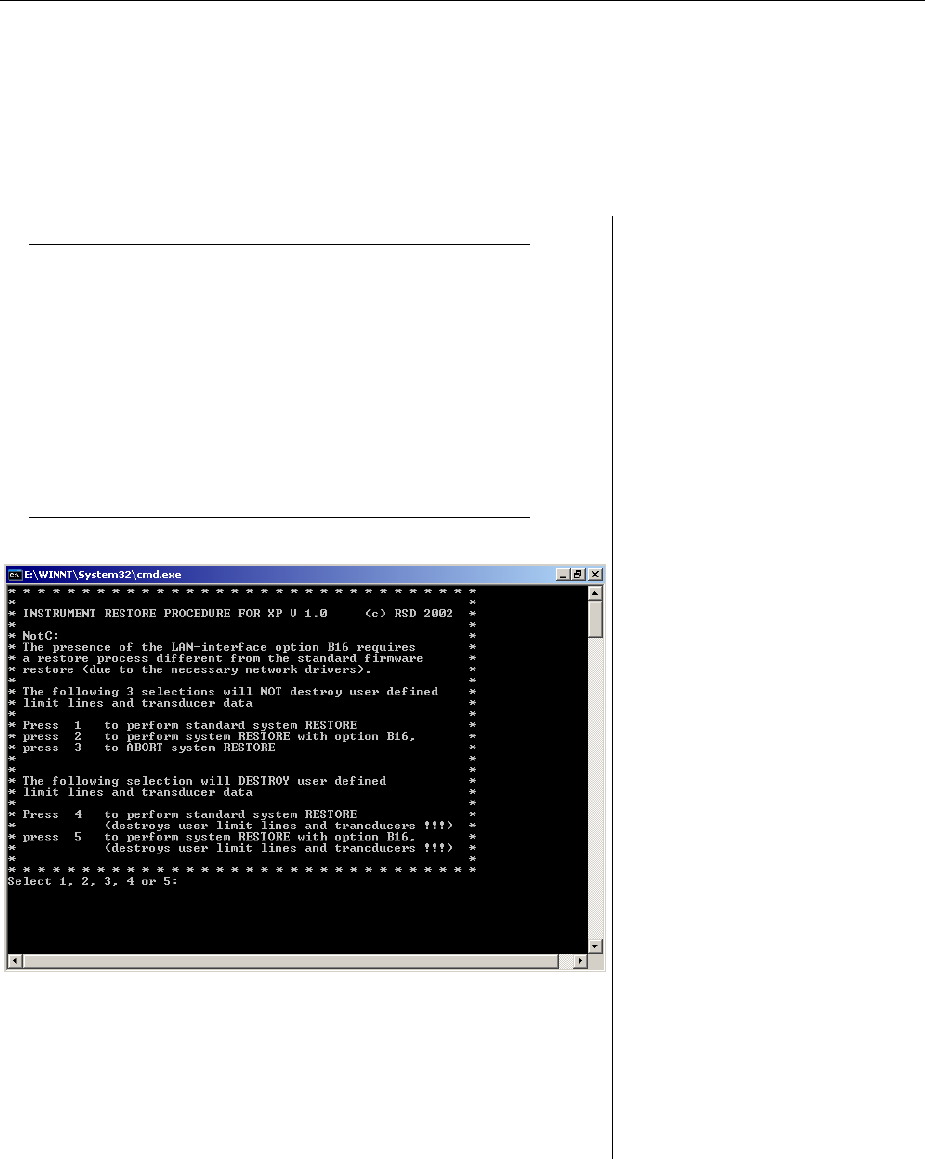
Restoring the Operating-System Installation FSP
1164.4556.82 4.2 E-1
Restoring the Operating-System Installation
If the operating system can no longer be booted, it is possible to boot the analyzer in the boot menu
from the backup partition, and to restore the operating-system installation. The function is not available
for instruments equipped with option B20.
Please select the operating system to start:
Analyzer Firmware
Analyzer Firmware Backup
Use the up and down arrow keys to move the highlight to your
choice.
Press ENTER to choose.
Seconds until highlighted choice will be started automatically: 5
For troubleshooting and advanced startup options for Windows,
press F8.
The boot of the backup partition
is selected in the boot menu
(Analyzer Firmware Backup)
using the cursor keys and
confirmed with ENTER.
After the operating system has
been started from the backup
partition, a window appears
containing the different restore
functions.
The selected operation is started
by entering the corresponding
number, and the operating-
system files are copied from the
backup partition to the analyzer
partition.
After the files have been copied,
the instrument starts up and the
firmware is reinstalled. This is
automatically followed by a cold
for recognizing the analyzer
hardware.

FSP Installing the Options
1164.4556.82 4.3 E-1
Installing the Options
The following options are available with the FSP:
AF Demodulator FSP-B3 1129.6491.02
OCXO Reference FSP-B4 1129.6740.02
TV Trigger / RF Power Trigger FSP-B6 1129.8594.02
Tracking Generator FSP-B9 1129.6991.02
External Generator Control FSP-B10 1129.7246.02
WCDMA Demodulation Hardware FSP-B15 1155.1006.02
LAN Interface FSP-B16 1129.8042.02
Flash Disk FSP-B20 1155.3557.02
Elektronic Attenuator FSP-B25 1129.7746.02
Trigger Port FSP-B28 1162.9915.02
DC Power Supply FSP-B30 1155.1158.02
Battery Pack FSP-B31 1155.1258.02
Additional Battery Pack FSP-B32 1155.1506.02
Demodulation Hardware FSP-B70 1157.0559.02
For retrofitting, please note the mounting instructions enclosed with the options.
These mounting instructions can be filed at this place in the service manual and are thus easily available
whenever they are required.
Caution!
Disconnect the instrument from the mains before opening the casing. Also note
the safety instructions at the beginning of this manual.
The components used in the instrument are sensitive to electrostatic discharges
which is why they are to be dealt with according to the ESD regulations.
When installing hardware options note the following:
Ø Switch off instrument and pull the mains plug.
Ø Unscrew the 4 rear-panel feet (450) and push the tube (410) backwards and take off.
Ø After installing the option replace the tube and fasten the rear panel feet again.
Caution!
When replacing the tube take care not to damage or pull off cables.
Ø Switch on FSP (cold boot).
Ø Install additional software, if supplied, according to the instructions enclosed with the option.
Ø If an adjustment is required for this option, the appropriate hints are to be found in the installation
instructions for the option.

FSP Contents - Documents
11164.4556.82 I-5.1 E-1
Contents - Chapter 5 "Documents"
5 Documents........................................................................................................... 5.1
Shipping of Instrument and Ordering of Spare Parts .................................................................. 5.1
Shipping of Instrument............................................................................................................. 5.1
Shipping of a Module............................................................................................................... 5.1
Ordering Spare Parts............................................................................................................... 5.2
Refurbished Modules............................................................................................................... 5.2
Return of Defective Replaced Modules ................................................................................... 5.2
Spare Parts....................................................................................................................................... 5.3
Available Power Cables........................................................................................................... 5.3
Spare Parts List................................................................................................................................ 5.5
Mechanical Drawings ...................................................................................................................... 5.5
Block Circuit Diagram ................................................................................................................... 5.17
Figures
--
Tables
Table 5-1 List of power cables available........................................................................................... 5.3
Table 5-2 List of all FSP part and spare parts .................................................................................. 5.7

Contents - Documents FSP
11164.4556.82 I-5.2 E-1
This page is left blank intentionally.

FSP Shipping of Instrument and Ordering of Spare Parts
11164.4556.82 5.1 E-1
5 Documents
This chapter provides information on the ordering of spare parts and contains the spare parts list and
the documents for the complete FSP unit.
Shipping of Instrument and Ordering of Spare Parts
Please contact your Rohde & Schwarz support center or our spare parts express service if you need
service or repair of your equipment or to order spare parts and modules.
The list of the Rohde & Schwarz representatives and the address of our spare parts express service are
provided at the beginning of this service manual.
We require the following information in order to answer your inquiry fast and correctly and to decide
whether the warranty still applies for your instrument:
• Instrument model
• Stock No.
• Serial number
• Firmware version
• Detailed error description in case of repair
• Contact partner for checkbacks
Shipping of Instrument
When shipping the instrument, be careful to provide for sufficient mechanical and antistatic protection
Ø Repack the instrument as it was originally packed when transporting or shipping. The two protective
caps for the front and rear panels prevent the control elements and connectors from being damaged.
The antistatic packing foil avoids any undesired electrostatic charging to occur.
Ø If you do not use the original packaging, provide for sufficient padding to prevent the instrument from
slipping inside the package. Wrap antistatic packing foil around the instrument to protect it from
electrostatic charging.
Shipping of a Module
When shipping a module, then, also be also careful to provide for sufficient mechanical and antistatical
protection
Ø Ship the module in a sturdy, padded box.
Ø Wrap the board into antistatic foil.
If the packaging is only antistatic but not conductive, additional conductive packaging is required. The
additional packaging is not required if the enclosed packaging is conductive.
Exception: If the module contains a battery, the tightly fitting packaging must always consist of
antistatic, non-chargeable material to protect the battery from being discharged.

Shipping of Instrument and Ordering of Spare Parts FSP
11164.4556.82 5.2 E-1
Ordering Spare Parts
To deliver replacement parts promptly and correctly we need the following indications:
• Stock number (see component lists in this chapter)
• Designation
• Component number according to component list
• Number of pieces
• Instrument type the replacement part belongs to
• Stock No.
• Contact person for possible questions
The stock numbers necessary for ordering replacement parts and modules as well as power cables can
be found further down.
Refurbished Modules
Refurbished modules are an economic alternative for original modules. It should be kept in mind that
refurbished modules are not new, but repaired and fully tested parts. They may have traces from use
but they are electrically and mechanically equivalent to new modules.
To find out which refurbished modules are available, please refer to your Rohde & Schwarz
representative (or to the central service division, Rohde & Schwarz Munich).
Return of Defective Replaced Modules
Defective modules of the replacement program that can be repaired can be returned within 3
months after delivery of the replaced module. A repurchasing value is credited.
Excluded are parts which can not be repaired, e.g. PCBs that are burnt, broken or damaged by repair
attempts, incomplete modules, parts which are heavily damaged mechanically.
The defective parts must be sent back with a returned accompanying document containing the
following information:
• Stock number, serial number and designation of the dismounted part,
• Precise description of the error,
• Stock number, serial number and designation of the instrument the part was dismounted from,
• Date of dismounting,
• Name of the technician who exchanged the part.
A returned accompanying document is provided with each replacement module.
FSP Spare Part
11164.4556.82 5.3 E-1
Spare Parts
The stock numbers necessary for ordering replacement parts and modules can be found in the
component lists further down.
Important Note!
When replacing a module please note the safety instructions and the repair
instructions given in chapter 3 and at the beginning of this service manual
When shipping a module be careful to provide for sufficient mechanical and
antistatical protection.
Available Power Cables
Table 5-1 List of power cables available
Stock No. Earthed-contact connector Preferably used in
DS 0006.7013 BS1363: 1967' complying with
IEC 83: 1975 standard B2 Great Britain
DS 0006.7020 Type 12 complying with SEV-regulation
1011.1059, standard sheet S 24 507 Switzerland
DS 0006.7036 Type 498/13 complying with
US-regulation UL 498, or with IEC 83 USA/Canada
DS 0006.7107 Type SAA3 10 A, 250 V,
complying with AS C112-1964 Ap. Australia
DS 0025.2365
DS 0099.1456 DIN 49 441, 10 A, 250 V, angular
DIN 49 441, 10 A, 250 V, straight Europe (except Switzerland)

Spare Parts FSP
11164.4556.82 5.4 E-1
This page is left blank intentionally.

11164.4556.82 5.5 E-1
Spare Parts List
Mechanical Drawings

List of FSP parts including spare parts FSP
11164.4556.82 5.6 E-1
This page is left blank intentionally.

FSP List of FSP parts including spare parts
11164.4556.82 5.7 E-1
List of FSP parts including spare parts
The FSP is constructed in accordance with R&S design 2000.
Overall dimension: W x H x L, 372.75 x 176.50 x 395.00
Rack mount: 4E 7/8 T350
Accessories: 19'' Adapter ZZA-411, Stock No. 1096.3283.00
Note: The recommended spare parts are marked with an x in the last column.
Table 5-2 List of all FSP part and spare parts
Position Designation Stock No. Number Electrical
designation Recommended
spare parts
Document 1164.4391.01 (FSP Basic Unit)
10 Basic Unit 1164.4404.02 1 S
15 Fan 1093.4614.00 1 S E1 x
20 Attenuator (FSP-3/7) 1067.7684.03 1 S A40 x
30 Attenuator (FSP-13/30) 1046.5024.05 1 S A40 x
35 Attenuator (FSP 40) 1046.5099.03 1 S A 40 x
40 Screw with washer assembly M2.5X6 1148.3059.00 2 S x
42 Screw with washer assembly M3X6 0041.1682.00 2 S
50 Key probe board 1093.7742.02 1 S A80 x
55 DIN965-M2.5X6-A4-PA 1148.3288.00 3 S
60 Subassembly plate 1164.4456.00 1 S
70 DIN965-M2.5X6-A4-PA 1148.3288.00 4 S
80 Adhesive foil 30X20 SW 1093.9051.00 3 S
90 Cover RD15,9 0009.9200.00 1 S
92 Frontend 1093.5491.06 1 S A100 x
100 FRONTEND 1093.5491.07 1 S A100 x
110 DETECTOR BOARD 1093.6998.06 1 S A120 x
120 IF-FILTER 1093.7242.04 1 S A130 x
130 Converter Unit (7 GHz)
replaced by 1130.2544.02 1093.7994.02 1 S A160 x
130 Converter Unit (8 GHZ) 1130.2544.02 1 S A160 x
135 MW Converter Unit (13 GHz) 1093.8249.13 1 S A160 x

List of FSP parts including spare parts FSP
11164.4556.82 5.8 E-1
Position Designation Stock No. Number Electrical
designation Recommended
spare parts
140 MW Converter Unit (30 GHz) 1093.8249.30 1 S A160 x
141 MW Converter Unit (40 GHz) 1093.8584.40 1 S A 160 x
142 Screw with washer assembly M2.5X6 1148.3059.00 4 S
150 Diplexer (30 GHz) 1108.8508.30 1 S A230 x
160 Air cover 1093.5285.00 1 S
170 Rear panel labelling 1093.4650.00 1 S
180 Screw with washer assembly M2.5X6 1148.3059.00 5 S
190 Cover 9-pin SUB-D 1093.8990.00 1 S
200 Cover 25-pin SUB-D 1093.9000.00 3 S
210 Cover RD11,1/9,9 0009.9217.00 4 S
220 Cover f. IEC Bus (metal) 1050.9272.00 1 S
225 Cover f. IEC Bus 0852.0450.00 1 S
230 Screw with washer assembly M3X6 0041.1682.00 2 S
235 Cover f.. LAN-connector 0852.0467.00 1 S
240 Instrument top cover 1093.4637.00 1 S
250 Screw with washer assembly M2.5X6 1148.3288.00 2 S
260 DIN965-M2.5X6-A4-PA 1148.3288.00 2 S
270 Printed front panel 3 GHz 1164.4462.00 1 S
280 Printed front panel 7 GHz 1164.4479.00 1 S
285 Printed front panel 13 GHz 1164.4485.00 1 S
290 Printed front panel 30 GHz 1164.4491.00 1 S
292 FRONT COVER DESCR. 40 GHz 1164.4504.00 1 S
295 RF cable W1 7GHz 1093.4872.00 1 S W1 x
305 Cable clamp RD4 BR6 0080.3660.00 1 S
312 RF-cable W1 13 GHz 1093.5010.00 1 S W1 x
315 RF-cable W1 30GHz 1093.5027.00 1 S W1 x
316 TESTPORT ADAPTER 1021.0493.00 1 S
322 CABLE W1 40 GHz 1093.5162.00 1 S W1
324 TEST PORT RACK ADAPTER 1036.4702.00 1 S

FSP List of FSP parts including spare parts
11164.4556.82 5.9 E-1
Position Designation Stock No. Number Electrical
designation Recommended
spare parts
330 Assembly plate 1093.4750.00 1 S
340 Assembly plate 1093.4772.00 1 S
350 DIN965-M2.5X6-A4-PA 0852.3614.00 4 S
400 Adhesive foil DRM50 grey 1093.9068.00 1 S
401 Adhesive foil DRM50 grey 1093.9068.00 1 S
410 tube with foots 1164.4662.00 1 S
420 BW2-front panel handle 4E 1096.1480.00 2 S
430 BW2- M4X14 1096.4909.00 4 S
450 BW2-rear panel foot 50MM 1096.2493.00 4 S
455 BW2-foil f. rear panel foot 1096.2435.00 4 S
Drawing 1164.4404.01 (Digital Unit)
500 Instrument frame 1093.4543.00 1 S
510 DIN965-M2,5X6-A4-PA 1148.3288.00 1 S
515 Motherboard 1142.8228.02 1 S A10 x
520 Screw with washer assembly M2.5X6 1148.3059.00 5 S
530 Locking bolt M3 0009.6501.00 4 S
540 Spacer for D-Submin. 1093.9180.00 2 S
550 Power supply unit 230W UL/CSA 1091.2320.00 1 S A20 x
560 Screw with washer assembly M2.5X6 1148.3059.00 10 S
575 Front module controller 6/5 1091.2520.00 1 S A90 x
590 Screw with washer assembly M2.5X6 0071.5040.00 10 S
600 Display unit 1093.4708.04 1 S
610 DIN965-M2.5X6-A4-PA 1148.3288.00 1 S
620 Keyboard frame FSP 1093.5127.00 1 S
630 Keyboard mat FSP 1093.5133.00 1 S x
640 Keyboard membrane FSP 1093.5140.00 1 S x
650 Rotary knob RD28 ACHS-RD6 0852.1086.00 1 S
660 DIN965-M2X6-A4-PA 0041.1599.00 10
670 3,5" Floppy drive slim 0048.6638.00 1 S A30 x

List of FSP parts including spare parts FSP
11164.4556.82 5.10 E-1
Position Designation Stock No. Number Electrical
designation Recommended
spare parts
680 Floppy bracket 1093.4620.00 1 S
690 Fley strip conn.26P.R=1 1091.2066.00 1 S W300
700 Screw with washer assembly M2.5X6 1148.3059.00 5 S
702 DIN7985-M2,5X4-A4-PA 1148.2717.00 3
704 DIN127-B2,5-A4 0082.4786.00 3
710 Hard disk with firmware 1164.4579.02 1 S A60 x
720 Ribbon cable 1093.5156.00 1 S W11
730 Disk bracket 1093.4837.00 1 S
740 DIN965-M2.5X6-A4-PA 1148.3288.00 2 S
750 DIN965-M3X5-A4-PA 1148.2775.00 4 S
775 Lithium batterie CR2032 0858.2049.00 1
Drawing 1093.4708.01 (Display Unit) page 3
800 Assembly tray 1093.4795.00 1 S
810 Shielded filter plate 1091.2014.00 1 S x
820 RF spring (177) 1069.3011.00 2 S
830 RF spring (137) 1069.3105.00 2 S
840 Plate holder 0852.0844.00 4 S
850 DIN965-M2X4-A4-PA 1148.3259.00 4 S
860 Dust sealing 1093.5279.00 1 S
870 CXA-L0605-VJL DC-AC converter 0048.6996.00 1 S T10 x
880 DIN7985-M2X10-A4-PA 1148.2917.00 2 S
890 DIN125-A2,2-HP 0049.7396.00 2 S
906 Converter cable L=350 1091.2650.00 1 S W100 x
910 Spin wheel 0852.1170.00 1 S B10 x
915 SCHRAUBE 1,8X4,4 1066.2066.00 3 S
920 TFT 640x480x3 Color-LCD 0048.6980.00 1 S A80 x
930 Screw with washer assembly M2.5X6 1148.3059.00 4 S
947 Display connector 1091.0911.00 1 S W80 x
950 Screw with washer assembly M2.5X6 0071.5040.00 2 S

FSP List of FSP parts including spare parts
11164.4556.82 5.11 E-1
Position Designation Stock No. Number Electrical
designation Recommended
spare parts
Drawing 1093.7994.01 (7 GHz converter unit) page 3
2000 7 GHz CONVERTER 1093.8003.02 1 S A160
2000 7 GHz YIG UNIT 1093.8090.02 1 S A161
2000 DIN965-M2.5X6-A4-PA 0852.3614.00 2 S
2000 7 GHz DIPLEXER 1108.7001.02 1 S A162
2000 DIN6900-M2.5X5 -A2 0071.6830.00 4 S
2000 8 GHz CONVERTER 1130.2409.02 1 S A160
2002 8 GHz YIG UNIT (MICRO LAMBDA) 1130.2744.02 1 S A161
2003 8 GHz YIG UNIT (FILTRONIC) 1130.2744.03 1 S A161
2004 DIN965-M2.5X6-A4-PA 1148.3288.00 2 S
2006 8 GHz DIPLEXER 1132.6501.02 1 S A162
2008 DIN6900-M2.5X5 -A2 0071.6830.00 4 S
Drawing 1130.2544.01 (8 GHz converter unit)
2000 8 GHz CONVERTER 1130.2550.02 1 S A160 x
2005 8 GHz YIG UNIT (MICRO LAMBDA) 1130.2944.02 1 S A161 x
2010 8 GHz YIG UNIT (FILTRONIC) 1130.2944.03 1 S A161 x
2025 DIN965-M2.5X6-A4-PA 1148.3288.00 2 S
2030 8 GHz DIPLEXER 1132.6501.02 1 S A162 x
2035 DIN6900-M2.5X5 -A2 0071.6830.00 4 S
Drawing 1093.8249.01 (MW CONVERTER UNIT 13 / 30 GHz)
2110 MW CONVERTER 1093.8255.02 1 S A160 x
2115 YIG UNIT (13 GHz , MICRO LAMBDA) 1093.8278.13 1 S A161 x
2120 YIG UNIT (13 GHz, FILTRONIC) 1093.8278.14 1 S A161 x
2125 YIG UNIT (30 GHz, MICRO LAMBDA) 1093.8278.30 1 S A161 x
2130 YIG UNIT (30 GHz, FILTRONIC) 1093.8278.31 1 S A161 x
2135 DIN965-M2.5X8-A4 0825.3620.00 4 S
2140 RF EXTENSION 13 1108.6505.13 1 S A162 x
2145 RF EXTENSION 30 1108.6505.30 1 S A162 x
2150 SCREW WITH WAHSER M2.5X5-A2 0071.6830.00 6 S

List of FSP parts including spare parts FSP
11164.4556.82 5.12 E-1
Position Designation Stock No. Number Electrical
designation Recommended
spare parts
Drawing 1093.8584.01 (UNIT MW CONVERTER 40 GHz)
2210 40 GHz CONVERTER 1093.8610.02 1 S A160 x
2215 YIG UNIT (40 GHz, MICRO LAMBDA) 1093.8655.40 1 S A161
2217 YIG UNIT (40 GHz, FILTRONIC) 1093.8655.41 1 S A161
2220 DIN965-M2.5X6-A4-PA 0852.3614.00 2 S
2225 DIPLEXER 44 1132.9500.02 1 S A163
2230 SCREW WITH WASHER M2.5X6-A2 1148.3059.00 4 S
2235 RF EXTENSION 40 1151.2508.02 1 S A162 x
2240 SCREW WITH WASHER M2.5X6-A2 1148.3059.00 8 S
2245 50 OHM TERMINATION SMA 0249.7823.00 1 S
Drawing 1096.6224.00 (Option FSP-B1 1129.7998.02)
Swivel handle 1096.6118.00 1 S x
Front protector left 1096.6001.00 1 S x
Front protector right 1096.6018.00 1 S x
Rear protector 1096.6076.00 2 S x
Protctive cover 1096.6182:00 1 S x
BW2-TUBE FSP 4E 7/8 1129.8007.00 1 S
DIN934-M4-A4 0016.4400.00 2 S
DIN6797-A4,3-A2 0016.2837.00 2 S
Drawing 1129.6491.02 (Option FSP-B3)
1000 Demodulator 1093.7620.02 1 S A190 x
1010 RF cable W13 1129.6504.00 1 S W13
1020 Loudspeaker 1129.6510.00 1 S B1 x
1025 CABLE HOLDER 6X7 1093.9045.00 1 S
1030 Loudspeaker support spring 1096.2512.00 1 S
1040 Vol./phones board 1093.7094.02 1 S A191 x
1050 Retaining bracket probe/code 1093.4766.00 1 S
1055 Screw with washer assembly M2.5X6 1148.3059.00 1 S
1060 DIN965-M2.5X6-A4-PA 1148.3288.00 3 S

FSP List of FSP parts including spare parts
11164.4556.82 5.13 E-1
Position Designation Stock No. Number Electrical
designation Recommended
spare parts
1070 Rotary knob RD9.5ACHS-RD4T-GR 0852.1111.00 1 S
1086 MASSEFEDER 1142:8242:00 1 S
1090 Mounting instruction / drawing 1129.6540.00 1 S
Drawing 1129.6791.00 (Option FSP-B4)
1100 OCXO 1093.7871.02 1 S A200 x
1120 RF-cable W14 1129.6756.00 1 S W14
1140 Mounting instruction / drawing 1129.6791.00 1 S
Drawing 1129.8613.00 (Option FSP-B6 1129.8594.02)
1800 TRIGGER 1129.8642.04 1 S A230 x
1810 RF CABLE W33 1129.8636.00 1 S W33
1850 CCVS-SCHILD 1129.8707.00 1 S
1870 NUMMERN-SCHILD 1129.8713.00 1 S
1890 MOUNTING INSTRUCTION / DRAWING 1129.8613.00 1 S
Drawing 1129.7069.00 (Option FSP-B9 1129.6991.02)
1500 TRACKING GENERATOR 1093.7371.02 1 S A170 x
1510 RF cable L W16 (FSP-3/7/13/30) 1129.7000.00 1 S W16
1520 RF cable W17 1129.7017.00 1 S W17
1530 RF cable W18 1129.7023.00 1 S W18
1540 RF cable W19 (FSP-3) 1129.7030.00 1 S W19
1550 RF cable W19 (FSP-7/13/30/40) 1129.7075.00 1 S W19
1560 RF cable W20 1129.7046.00 1 S W20 x
1561 Bracket RD 4 BR 6 0080.3660.00 1 S
1565 Assembly plate 1093.4750.00 1 S
1566 DIN965-M2.5X6-A4-PA 1148.3288.00 4 S
1568 RF CABLE W35 (FSP 40) 1129.7117.00 1 S W35
1590 Mounting instruction / drawing 1129.7069.00 1 S
Drawing 1129.7298.00 (Option FSP-B10 1129.7246.02)
1600 EXT. GEN. CONTROL 1093.8590.02 1 S A210 x
1610 IEC-BUS cable W21 1129.7252.00 1 S W21 x

List of FSP parts including spare parts FSP
11164.4556.82 5.14 E-1
Position Designation Stock No. Number Electrical
designation Recommended
spare parts
1612 DIN125-A3.2-A4 0082.4670.00 2 S
1614 DIN137-A3-A2 0005.0296.00 2 S
1620 Aux control cable W22 1129.7269.00 1 S W22 x
1622 Locking bolt M3 0009.6501.00 2 S
1624 DIN137-A3-A2 0005.0296.00 2 S
1626 DIN934-M3-A4 0016.4398.00 2 S
1690 Mounting instruction / drawing 1129.7298.00 1 S
Drawing 1155.1012.00 (Option FSP-B15 1155.1006.02)
1160 WIDEBAND CALIBRATOR 1154.7100.02 1 S A190 x
1170 RF CABLE W34 1155.1029.00 1 S W34
1180 MOUNTING INSTRUCTION / DRAWING 1155.1012.00 1 S
Drawing 1129.8107.00 (Option FSP-B16 1129.8042.03)
1250 Cable 2XRJ45 ST/ST 8P 1138.9677.00 1 S W32
1270 Adapter 8P.GER 1093.9122.00 1 S X220 x
1290 Assembly plate 1129.8065.00 1 S
1300 Screw with washer assembly M2.5X6 0071.5040.00 2 S
1310 Cable clamp BI.RD 1 BIS 25 B2 0015.9038.00 2 S
1340 Mounting instruction / drawing 1129.8107.00 1 S
Drawing 1155.1712.00(Option FSP-B20 1155.1606.06)
1700 COMPACT FLASH BOARD 1130.3557.02 1 S A60 x
1713 FLASH MEM with software 1155.1641.06 1 S A61 x
1730 CF-CARD HOLDER CLAMP 1130.1260.00 2 S
1770 MOUNTING INSTRUCTION / DRAWING 1155.1612.00 1 S
Drawing 1129.7800.00 (Option FSP-B25 1129.7746.02)
1400 Attenuator (electronic) 1108.7230.02 1 S A50 x
1410 Ribbon cable 10POL 1129.7823.00 1 S W50
1420 RF cable W29 1129.7752.00 1 S W27
1430 RF cable W28 (FSP-3) 1129.7769.00 1 S W28
1440 RF cable W28 (FSP-7/13/30) 1129.7775.00 1 S W28

FSP List of FSP parts including spare parts
11164.4556.82 5.15 E-1
Position Designation Stock No. Number Electrical
designation Recommended
spare parts
1460 Screw with washer assembly M2.5X6 0071.5040.00 4 S
1490 Mounting instruction / drawing 1129.7800.00 1 S
Drawing 1162.9921.00 (Option FSP-B28 1162.9915.02)
1360 USER-PORT cable W67 1142.8094.00 1 S W67 x
1365 Locking bolt M3 0009.6501.00 2 S
1370 DIN137-A3-A2 0005.0296.00 2 S
1375 DIN934-M3-A4 0016.4398.00 2 S
1380 Adhesive shield 1162.9938.00 1 S
1385 MOUNTING INSTRUCTION / DRAWING 1162.9921.00 1 S
Drawing in chapter 3 (Option FSP-B30 1155.1158.02)
3000 DC/DC Konverter f. SN230 1155.1164.00 1 S x
3010 Cable EXT. DC 1155.1170.00 1 S
3020 Rear panel feet FSP-B30 1155.1193.00 1 S
Drawing chapter 3 (Option FSP-B31/B32 1155.1258.02/1155.1506.02)
3030 BATTERY CHARGER 1155.1358.02 1 S A1 x
3040 13,2 V 7,6AH AKKU PACK 1102.5607.00 2 S G1, G2 x
3050 Table power supply 70 W 4055.3471.00 1 S x
3060 Cable 1155.1487.00 1 S W2
Drawing 1157.0607.00 (Option FSP-B70 1157.0559.02)
1900 DETECTOR BOARD 1 1130.2196.07 1 S A140 x
1950 MOUNTING INSTRUCTION / DRAWING 1157.0607.00 1 S
11164.4556.82 5.16 E-1
This page is left blank intentionally.

11164.4556.82 5.17 E-1
Block Circuit Diagram
