01a_tb_e7 R&S_SMIQ06B R&S SMIQ06B
User Manual: R&S_SMIQ06B
Open the PDF directly: View PDF ![]() .
.
Page Count: 516 [warning: Documents this large are best viewed by clicking the View PDF Link!]
- Tabbed Divider Overview
- Introduction on how to use the manual
- Contents
- Preparation for Use
- Putting into Operation
- Functional Test
- Fitting the Options
- Opening the Casing
- Overview of the Slots
- Option SM-B1 - Reference Oscillator OCXO
- Option SM-B5 - FM/PM Modulator
- Option SMIQB11 - Data Generator
- Option SMIQB12 - Memory Extension to Data Generator
- Option SMIQB14 - Fading Simulator FSIM1
- Option SMIQB15 - Second Fading Simulator (FSIM2)
- Option SMIQB17 - Noise Generator and Distortion Simulator
- Option SMIQB20 - Modulation Coder
- Option SMIQB21 - Bit Error Rate Test
- Other Software Options
- Option SMIQB19 - Rear Panel Connections for RF and LF
- Mounting into a 19" Rack
- Operation
- Front and Rear Panel
- Basic Operating Steps
- Design of the Display
- Calling the Menus
- Selection and Change of Parameters
- Triggering Action
- Quick Selection of Menu (QUICK SELECT)
- Use of [FREQ] and [LEVEL] Keys
- Use of [RF ON/OFF] and [MOD ON/OFF] Keys
- [ENTER] Key – Special Toggle Function
- Changing Unit of Level
- Correction of Input
- Sample Setting for First Users
- List Editor
- Menu Summary
- RF Frequency
- RF Level
- Modulation - General
- Analog Modulations
- Vector Modulation
- Fading Simulation
- Digital Modulation
- Digital Standard PHS
- Digital Standard IS-95 CDMA
- Digital Standard W-CDMA (NTT DoCoMo/ARIB 0.0)
- Digital Standard 3GPP W-CDMA (FDD)
- Enhanced Functions For Digital Standard 3GPP W-CDMA (FDD)
- Digital Standard NADC
- Digital Standard PDC
- Digital Standard GSM/EDGE
- Digital Standard DECT
- Digital Standard GPS
- Arbitrary Waveform Generator ARB
- External Modulation Source AMIQ
- Bit Error Rate Test
- Noise Generator and Distortion Simulator
- LF Output
- Sweep
- LIST Mode
- Memory Sequence
- Utilities
- IEC˚Bus Address (SYSTEM˚GPIB)
- Parameter of the RS232 Interface (SYSTEM˚RS232)
- Parameter of the SER DATA Input (SYSTEM˚SERDATA)
- Suppressing Indications and Deleting Memories (SYSTEM˚SECURITY)
- Indication of the IEC˚Bus Language (LANGUAGE)
- Reference Frequency Internal/External (REF OSC)
- Phase of the Output Signal (PHASE)
- Password Input With Functions Protected (PROTECT)
- Calibration (CALIB)
- Indications of Module Variants (DIAG-CONFIG)
- Voltage Indication of Test Points (DIAG˚TPOINT)
- Measurement of CARRIER/NOISE RATIO (DIAG˚C/N MEAS)
- Indications of Service Data (DIAG˚PARAM)
- Test (TEST)
- Assigning Modulations to the [MOD ON/OFF] Key (MOD˚KEY)
- Setting Auxiliary Inputs/Outputs (AUX˚I/O)
- Switching On/Off Beeper (BEEPER)
- Installation of Software Option
- The Help System
- Status
- Error Messages
- Index
- k2_ab S70_e9.pdf
- Fading Simulation
- 14_dm_e9.pdf
- 15_phs_e8.pdf
- 16_is95_e7.pdf
- 17_wcd_e7.pdf
- 18-gpp-e9.pdf
- 19_gppen_e9.pdf
- 20_nad_e9.pdf
- 21_pdc_e9.pdf
- 22_gsm_e9.pdf
- 23_dec_e9.pdf
- 231_gps_e9.pdf
- 24_arb_e9.pdf
- 25_amq_e9.pdf
- 26_nds_e9.pdf
- 27_msq_e9.pdf
- Memory Sequence
- Utilities
- IEC˚Bus Address (SYSTEM˚GPIB)
- Parameter of the RS232 Interface (SYSTEM˚RS232)
- Parameter of the SER DATA Input (SYSTEM˚SERDATA)
- Suppressing Indications and Deleting Memories (SYSTEM˚SECURITY)
- Indication of the IEC˚Bus Language (LANGUAGE)
- Reference Frequency Internal/External (REF OSC)
- Phase of the Output Signal (PHASE)
- Password Input With Functions Protected (PROTECT)
- Calibration (CALIB)
- Indications of Module Variants (DIAG-CONFIG)
- Voltage Indication of Test Points (DIAG˚TPOINT)
- Measurement of CARRIER/NOISE RATIO (DIAG˚C/N MEAS)
- Indications of Service Data (DIAG˚PARAM)
- Test (TEST)
- Assigning Modulations to the [MOD ON/OFF] Key (MOD˚KEY)
- Setting Auxiliary Inputs/Outputs (AUX˚I/O)
- Switching On/Off Beeper (BEEPER)
- Installation of Software Option
- The Help System
- Status
- Error Messages
- 40_ind_e9.pdf
- Beiblatt SMIQ06ATE_e.pdf

1125.5610.12-11 I
Test and Measurement
Division
Operating Manual
VECTOR SIGNAL GENERATOR
SMIQ02B
1125.5555.02
SMIQ03B
1125.5555.03
SMIQ03HD
1125.5555.33
SMIQ04B
1125.5555.04
SMIQ06B
1125.5555.06
SMIQ06ATE
1125.5555.26
Volume 1
This Operating Manual consists of 2 volumes
Printed in the Federal
Republic of Germany

SMIQ06ATE Supplement
1125.5555.06 A E-1
Supplement to Manual
SMIQ06ATE
The functionality of model SMIQ06ATE and its compliance with specifications correspond to model
SMIQ06B (see Data sheet SMIQB06B).
Model SMIQ06ATE differs from model SMIQ06B as follows:
• The instrument has no display (item 1 in front panel view)
• The connectors on the front panel (item 4 in front panel view) are provided on the rear panel.
• The following connectors are not fitted:
− I Faded,
− Q Faded,
− I/Q AUX,
− LF,
− EXT 1,
− EXT 2,
− SYM CLK,
− X-AXIS,
− BLANK,
− MARKER,
− SER DATA,
− PULS,
− EXTTUNE
− BER
− DATA
− BITCLOCK and
− PAR DATA
For manual operation of the SMIQ06ATE please download SMIQ-TV from the www.rohde-schwarz.com
website. SMIQ-TV runs on any external Windows™ PC including a GPIB controller and features a full
display of the SMIQ.
SMIQ Supplement
1125.55610.12-10- A E-1
Supplement to Manual SMIQ
Special Features of HD Model
VECTOR MOD menu with model SMIQ03HD:
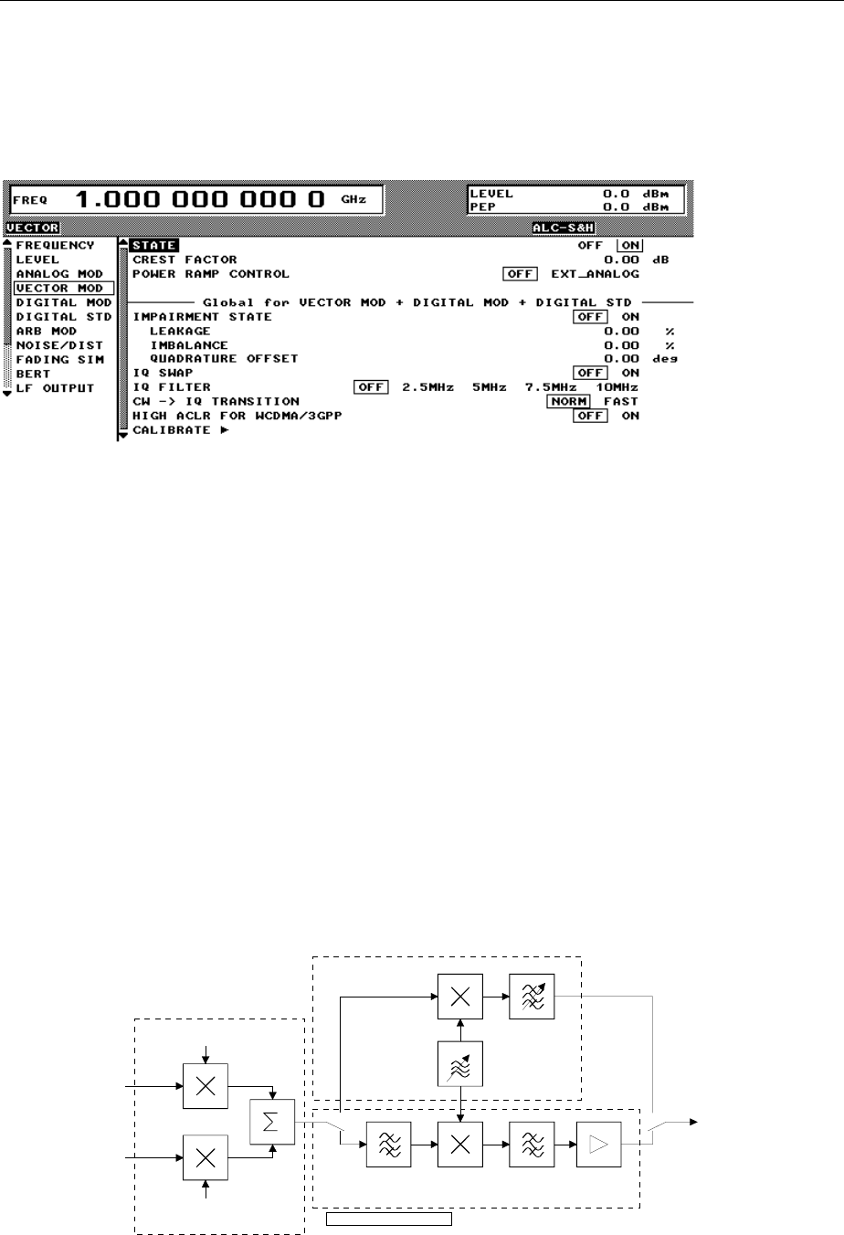
IQ FILTER Selection between filter off and a 2.5 MHz, 5 MHz, 7.5 MHz or 10 MHz lowpass filter in the base-
band. The filters suppress noise in the baseband, which improves adjacent channel power
(ACP) with W-CDMA. The filter frequency response is automatically compensated with DIGITAL
MOD and DIGITAL STD in the MCOD mode, so that the error vector magnitude (EVM)
deteriorates only slightly. If the VECTOR MOD mode is active and AMIQ with WinIQSIM used
as a source, the frequency response is compensated by WinIQSIM. For applications requiring a
very low EVM the I/Q filter should always be switched OFF.
OFF filter off
2.5 MHz 2.5 MHz lowpass filter
5 MHz 5 MHz lowpass filter
7.5 MHz 7.5 MHz lowpass filter
10 MHz 10 MHz lowpass filter
IEC/IEEE-bus commands :SOUR:DM:IQ:FILT:STAT ON|OFF
:SOUR:DM:IQ:FILT:FREQ 2.5MHZ
HIGH ACLR W-CDMA signals with a very high adjacent channel power ratio (ACPR) can be generated
in the 3GPP downlink band by means of option SMIQB57 (High ACLR for W-CDMA) in
conjunction with option SMIQB20 (Modulation Coder). Moreover, RF peak levels up to
+30 dBm can be produced thanks to the extremely linear power amplifier.
Note: Option SMIQB57 can be used only in the 2110 MHz to 2170 MHz 3GPP
downlink band. Although carrier frequencies outside this band can be set, no
specified values exist for such applications.
I/Q modulator
I
Q
WCDMA filter
RF output
G
BP
2110 to 2170MHz
BW 3.84MHz
Power
Amplifier
RF up/down converter
sin
cos
High ACLR option SMIQB57
Fig. 1 High ACLR for W-CDMA

Supplement SMIQ
1125.55610.12-10- B E-1
Option SMIQB57 incorporates a filter tailored to the channel bandwidth of a 3GPP
W-CDMA signal (3.84 MHz) for suppressing unwanted signal components outside the
useful band. SMIQB57 can for this reason be used effectively only with this particular type
of digital modulation. Despite this, the option can be used with other digital modulation
modes provided the occupied bandwidth is smaller than 3.84 MHz and the channel
frequency is in the range of 2110 MHz to 2170 MHz. This may be expedient for
applications requiring very high RF levels.
Output power with option SMIQB57 (High ACLR for W-CDMA):
With option SMIQB57 installed, the maximum output power is +30 dBm. The dynamic range
of the electronic level setting is extended to 30 dB in the Attenuator Fixed mode.
IEC/IEEE-bus command :SOUR:DM:IQ:HACLr:STAT
New Features Not Concerning HD Model
VECTOR MOD menu
IQ FILTER Only with option SMIQB47; not on SMIQ03HD.
Selection between filter off and a 850 kHz, 2.5 MHz or 5 MHz lowpass filter in the
baseband. The filters suppress noise in the baseband from 900 kHz, 3 MHz or 6 MHz,
which improves adjacent channel power (ACP) with IS-95 and W-CDMA. The filter
frequency response is automatically compensated with DIGITAL MOD and DIGITAL STD
in the MCOD mode, so that the error vector magnitude (EVM) deteriorates only slightly.
If the VECTOR MOD mode is active and AMIQ with WinIQSIM used as a source, the
frequency response is compensated by WinIQSIM. For applications requiring a very low
EVM the I/Q filter should always be switched OFF.
OFF filter off
850 kHz 850 kHz lowpass filter
2.5 MHz 2.5 MHz lowpass filter
5 MHz 5 MHz lowpass filter
IEC/IEEE-bus commands :SOUR:DM:IQ:FILT:STAT ON|OFF
:SOUR:DM:IQ:FILT:FREQ 2.5MHZ

SMIQ Supplement
1125.55610.12-10- C E-1
New Features on All Models
DIGITAL MOD – FILTER menu:
A new filter was added:
(FILTER...) FILTER TYPE GAUSS LINEAR linearized Gaussian filter for GSM_EDGE
(to GSM Specification 05.04, Change Request A010)
IEC/IEEE-bus command:
:SOUR:DM:FILT:TYPE LGA
GAUSS LINEAR
(old version) linearized Gaussian filter for GSM_EDGE
(to GSM Specification older than 05.04)
IEC/IEEE-bus command:
:SOUR:DM:FILT:TYPE OLG
DIGITAL STD – WCDMA/3GPP menu:
OCNS CHANNELS was changed to ADD OCNS.
ADD OCNS Simulation of orthogonal channel noise. This menu item is available only in the downlink
and if option SMIQB48 is installed. For more information refer to section 2.15.4.
Section 2.15.4 ADD OCNS:
Generation of orthogonal channel noise (OCNS) to TS 25.101
The OCNS scenario is defined as follows:
Table C.6: DPCH spreading code, timing offsets and relative level settings for OCNS signal
Channelization code Timing offset
(x256Tchip)Level setting (dB)
286-1
11 134 -3
17 52 -3
23 45 -5
31 143 -2
38 112 -4
47 59 -8
55 23 -7
62 1 -4
69 88 -6
78 30 -5
85 18 -9
94 30 -10
125 61 -8
113 128 -6
119 143 0
Parameters common to all OCNS channels:
Type: DPCH
Symbol rate: 30 ksps
Pilot length: 8 bit
The powers of the OCNS channels are to be understood as relative powers only. In the test scenarios
defined by the standard, the OCNS channels are weighted so that a sum power of linear 1 (or 0 dB) is
obtained. This is done automatically in SMIQ.

Supplement SMIQ
1125.55610.12-10- D E-1
If ADD OCNS is set to ON,
• channels 15 to 30 of base station 1 are automatically set as shown in the table above
and
• the power of the OCNS component is adjusted automatically so that the powers of the OCNS
channels and the powers of the non-OCNS channels of base station 1 add up to yield a sum power
of linear 1.
The settings for the 16 OCNS channels are READ ONLY settings, i.e. they cannot be modified. In the
channel table, the OCNS channels are marked by an "O" after the channel number.
If the setting of a non-OCNS channel is modified, the power of the OCNS channels is adjusted
immediately. If adjustment is not possible because the powers of the non-OCNS channels already add
up to 0 dB or higher, the OCNS channels are set to -60 dB. In this case an error message is output
when WCDMA/3GPP is switched on.
Further Settings of ENHANCED CHANNELS Menu:
SEQUENCE LENGTH The maximum sequence length not only depends on free DGEN list memory
space but also decisively on the ENHANCED P-CCPCH/BCH status and,
where applicable, on the number of DPCHs:
ENHANCED P-CCPCH/BCH STATE = OFF
1 DPCH: 1022 frames
2 DPCHs: 511 frames
3 DPCHs: 341 frames
4 DPCHs: 255 frames
ENHANCED P-CCPCH/BCH STATE = ON
SYMBOL RATE DPCH ≤ 30 ksps: 2044 frames
SYMBOL RATE DPCH > 30 ksps: 500 frames
New IEC/IEEE-Bus Commands
[:SOURce]:DM:IQ:FILTer:FREQuency 850 kHz, 2.5 MHz, 5 MHz, 7.5 MHz, 10 MHz
With this command, an IQ filter with the required cutoff frequency is selected. The command is
available, with option SMIQB47 (LOW ACP for IS-95 CDMA and W-CDMA) installed, for cutoff
frequencies 850 kHz, 2.5 MHz and 5 MHz. With model SMIQ03HD, cutoff frequencies 2.5 MHz,
5 MHz, 7.5 MHz and 10 MHz are available.
Example: :SOUR:DM:IQ:FILT:FREQ 2.5MHZ *RST value is 2.5 MHz
[:SOURce]:DM:IQ:HACLr:STATe ON | OFF
This command switches the option SMIQB57 on or off.
Example: :SOUR:DM:IQ:HACL:STAT ON *RST value is OFF
1125.5610.12-08 A E-1
Supplement to Manual SMIQ
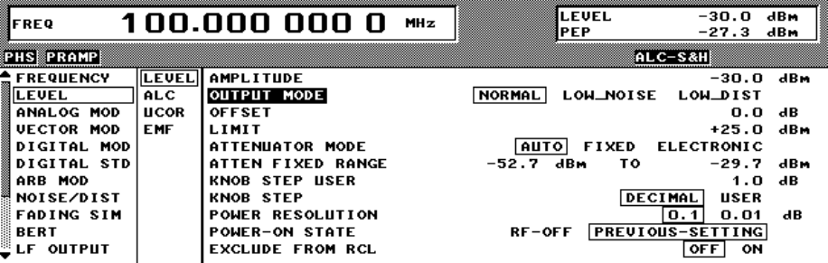
Output Mode
NORMAL This mode corresponds to that of the previous SMIQ.
LOW NOISE: The modulation in the SMIQ is set so that the power of the second and following
adjacent channels (ALT1...) is minimal.
LOW DIST: The modulation in the SMIQ is set so that the power of the first adjacent channel
(ADJ) is minimal. This optimization takes into consideration the modulation signal
and the version-dependent parameters of the module at 2 GHz.
Hints for the individual modes:
CW: The output mode has no effect in this mode.
VECTOR MOD: With the LOW NOISE output mode, you should additionally raise the IQ level
applied (max. 1 V p). The optimal IQ level with LOW DIST depends on the
modulation signal and must be ascertained through measurements. The adjacent
channel power for symbol rates <200 kHz is essentially determined through
multiplicative phase noise. The IQ level can be set to 250 mV p independent of the
modulation signal.
The level error caused by a change in the IQ level can be corrected with the
LEVEL OFFSET.
ARB MOD: With the LOW NOISE / LOW DIST output mode, the modulation in the SMIQ only
changes by a fixed amount. The user can vary the IQ level in order to achieve the
best results with LOW DIST as a function of the modulation signal.
FADSIM/NDSIM: If these modules are activated, the output mode has no effect. If FSIM is activated,
the adjacent channel power can be optimized by the parameter "Insertion Loss
Setting Mode" in the FADSIM menu.
Additional hints:
The specifications for the level accuracy and harmonic ratio are only valid for the NORMAL output
mode; in the other modes they can change.
IEC/IEEE-bus command: SOURce:POWer[:LEVel]:OMODe NORMal
|LDIStortion
|LNOise

SMIQ Tabbed Divider Overview
1125.5610.12 E-7R.1
Tabbed Divider Overview
Volume 1
How to Use this Manual
Contents
Data Sheet
Supplement to Data Sheet
Safety Instructions
Certificate of quality
EC Certificate of Conformity
List of R & S Representatives
Tabbed Divider
1 Chapter 1: Preparation for Use
2 Chapter 2: Manual Operation
10 Index
Volume 2
How to Use this Manual
Contents
Safety Instructions
Tabbed Divider
3 Chapter 3: Remote Control
4 Chapter 4: Maintenance
5 Chapter 5: Performance Test
6 Annex A: Interfaces
7 Annex B: List of Error Messages
8 Annex C: List of Commands
9 Annex D: Programming Example
10 Index

Introduction on how to use the manual SMIQ
1125.5610.12 E-7R.2
Introduction on how to use the manual
This operating manual contains essential information on commissioning, manual control, remote control,
maintenance and checking the rated specifications of SMIQ as well as all specifications of the unit and
available options.
The following models and options are described in this manual:
• SMIQ02B – Vector Signal Generator 300 kHz to 2.2 GHz
• SMIQ03B – Vector Signal Generator 300 kHz to 3.3 GHz
• SMIQ04B – Vector Signal Generator 300 kHz to 4.4 GHz
• SMIQ06B – Vector Signal Generator 300 kHz to 6.4 GHz
• Option SM-B1 – Reference Oscillator OCXO
• Option SM-B5 – FM/PM Modulator
• Option SMIQB11 – Data Generator
• Option SMIQB12 – Memory Extension to Data Generator
• Option SMIQB14 – Fading Simulator FSIM1
• Option SMIQB15 – Second Fading Simulator FSIM2
• Option SMIQB17 – Noise Generator and Distortion Simulator
• Option SMIQB19 – Rear Panel Connections for RF and LF
• Option SMIQB20 – Modulation Coder
• Option SMIQB21 – Bit Error Rate Test
• Option SMIQB42 – Digital Standard IS-95 CDMA
• Option SMIQB43 – Digital Standard W-CDMA
• Option SMIQB45 – Digital Standard 3 GPP W-CDMA
• Option SMIQB47 – LOW ACP Filter
• Option SMIQB48 – Enhanced Functions für 3GPP W-CDMA
• Option SMIQB49 – Dynamic Fading
• Option SMIQB60 – Arbitrary Waveform Generator
The chapters with associated contents are as follows:
Data sheets list guaranteed specifications for the functions and characteristics of the unit
and its options.
Chapter 1 provides information on putting the unit into operation (AC supply connection,
switch-on/off), functional test, preset settings, fitting the options and mounting
the unit into a 19" rack.
Chapter 2 explains the manual control of SMIQ. It contains front and rear panel views,
describes the control elements as well as connectors, provides a short
introduction with sample settings for first-time users. It also explains how to
change parameters and the use of the list editor and gives an overview of the
menus for the functions covered by the unit and its options. It also presents
the functions and menus of the unit and its options (frequency and level
setting, analog and digital modulation, ARB, external modulation source
AMIQ, fading simulation, noise generation and distortion simulation, BERT,
sweep, LIST mode, memory sequence and general functions not relating to
signal generation).

SMIQ Introduction on how to use the manual
1125.5610.12 E-7R.3
Chapter 3 provides information on remote control of SMIQ. It informs about basics like
IEC/IEEE bus, RS-232C interface, interface and device-dependent messages,
command processing, status reporting system etc. It also includes an
overview of each command system and describes all commands available in
the unit and its options.
Chapter 4 informs about preventive maintenance and functional tests.
Chapter 5 contains information on how to check the rated specifications (required test
equipment, test setup, test procedure) and on the performance test report.
Annex A provides information on interfaces.
Annex B contains a list of SCPI- and SMIQ-specific error messages displayed by the
unit.
Annex C provides an alphabetical list of commands.
Annex D gives programming examples for remote control.
Index provides the index with entries in alphabetical order.
1171.0000.42-02.00 Sheet 1
Before putting the product into operation for
the first time, make sure to read the following
Safety Instructions
Rohde & Schwarz makes every effort to keep the safety standard of its products up to date and to offer
its customers the highest possible degree of safety. Our products and the auxiliary equipment required
for them are designed and tested in accordance with the relevant safety standards. Compliance with
these standards is continuously monitored by our quality assurance system. This product has been
designed and tested in accordance with the EC Certificate of Conformity and has left the manufacturer’s
plant in a condition fully complying with safety standards. To maintain this condition and to ensure safe
operation, observe all instructions and warnings provided in this manual. If you have any questions
regarding these safety instructions, Rohde & Schwarz will be happy to answer them.
Furthermore, it is your responsibility to use the product in an appropriate manner. This product is
designed for use solely in industrial and laboratory environments or in the field and must not be used in
any way that may cause personal injury or property damage. You are responsible if the product is used
for an intention other than its designated purpose or in disregard of the manufacturer's instructions. The
manufacturer shall assume no responsibility for such use of the product.
The product is used for its designated purpose if it is used in accordance with its operating manual and
within its performance limits (see data sheet, documentation, the following safety instructions). Using
the products requires technical skills and knowledge of English. It is therefore essential that the
products be used exclusively by skilled and specialized staff or thoroughly trained personnel with the
required skills. If personal safety gear is required for using Rohde & Schwarz products, this will be
indicated at the appropriate place in the product documentation.
Symbols and safety labels
Observe
operating
instructions
Weight
indication for
units >18 kg
Danger of
electric
shock
Warning!
Hot
surface
PE terminal Ground Ground
terminal
Attention!
Electrostatic
sensitive
devices
Supply
voltage
ON/OFF
Standby
indication
Direct
current
(DC)
Alternating
current (AC)
Direct/alternating
current (DC/AC)
Device fully
protected by
double/reinforced
insulation
Safety Instructions
1171.0000.42-02.00 Sheet 2
Observing the safety instructions will help prevent personal injury or damage of any kind caused by
dangerous situations. Therefore, carefully read through and adhere to the following safety instructions
before putting the product into operation. It is also absolutely essential to observe the additional safety
instructions on personal safety that appear in other parts of the documentation. In these safety
instructions, the word "product" refers to all merchandise sold and distributed by Rohde & Schwarz,
including instruments, systems and all accessories.
Tags and their meaning
DANGER This tag indicates a safety hazard with a high potential of risk for the
user that can result in death or serious injuries.
WARNING This tag indicates a safety hazard with a medium potential of risk for the
user that can result in death or serious injuries.
CAUTION This tag indicates a safety hazard with a low potential of risk for the user
that can result in slight or minor injuries.
ATTENTION This tag indicates the possibility of incorrect use that can cause damage
to the product.
NOTE This tag indicates a situation where the user should pay special attention
to operating the product but which does not lead to damage.
These tags are in accordance with the standard definition for civil applications in the European
Economic Area. Definitions that deviate from the standard definition may also exist. It is therefore
essential to make sure that the tags described here are always used only in connection with the
associated documentation and the associated product. The use of tags in connection with unassociated
products or unassociated documentation can result in misinterpretations and thus contribute to personal
injury or material damage.
Basic safety instructions
1. The product may be operated only under
the operating conditions and in the
positions specified by the manufacturer. Its
ventilation must not be obstructed during
operation. Unless otherwise specified, the
following requirements apply to
Rohde & Schwarz products:
prescribed operating position is always with
the housing floor facing down, IP protection
2X, pollution severity 2, overvoltage
category 2, use only in enclosed spaces,
max. operation altitude max. 2000 m.
Unless specified otherwise in the data
sheet, a tolerance of ±10% shall apply to
the nominal voltage and of ±5% to the
nominal frequency.
2. Applicable local or national safety
regulations and rules for the prevention of
accidents must be observed in all work
performed. The product may be opened
only by authorized, specially trained
personnel. Prior to performing any work on
the product or opening the product, the
product must be disconnected from the
supply network. Any adjustments,
replacements of parts, maintenance or
repair must be carried out only by technical
personnel authorized by Rohde & Schwarz.
Only original parts may be used for
replacing parts relevant to safety (e.g.
power switches, power transformers,
fuses). A safety test must always be
performed after parts relevant to safety
have been replaced (visual inspection, PE
conductor test, insulation resistance
measurement, leakage current
measurement, functional test).
3. As with all industrially manufactured goods,
the use of substances that induce an
allergic reaction (allergens, e.g. nickel)
such as aluminum cannot be generally
excluded. If you develop an allergic
reaction (such as a skin rash, frequent
sneezing, red eyes or respiratory
difficulties), consult a physician immediately
to determine the cause.
Safety Instructions
1171.0000.42-02.00 Sheet 3
4. If products/components are mechanically
and/or thermically processed in a manner
that goes beyond their intended use,
hazardous substances (heavy-metal dust
such as lead, beryllium, nickel) may be
released. For this reason, the product may
only be disassembled, e.g. for disposal
purposes, by specially trained personnel.
Improper disassembly may be hazardous to
your health. National waste disposal
regulations must be observed.
5. If handling the product yields hazardous
substances or fuels that must be disposed
of in a special way, e.g. coolants or engine
oils that must be replenished regularly, the
safety instructions of the manufacturer of
the hazardous substances or fuels and the
applicable regional waste disposal
regulations must be observed. Also
observe the relevant safety instructions in
the product documentation.
6. Depending on the function, certain products
such as RF radio equipment can produce
an elevated level of electromagnetic
radiation. Considering that unborn life
requires increased protection, pregnant
women should be protected by appropriate
measures. Persons with pacemakers may
also be endangered by electromagnetic
radiation. The employer is required to
assess workplaces where there is a special
risk of exposure to radiation and, if
necessary, take measures to avert the
danger.
7. Operating the products requires special
training and intense concentration. Make
certain that persons who use the products
are physically, mentally and emotionally fit
enough to handle operating the products;
otherwise injuries or material damage may
occur. It is the responsibility of the
employer to select suitable personnel for
operating the products.
8. Prior to switching on the product, it must be
ensured that the nominal voltage setting on
the product matches the nominal voltage of
the AC supply network. If a different voltage
is to be set, the power fuse of the product
may have to be changed accordingly.
9. In the case of products of safety class I with
movable power cord and connector,
operation is permitted only on sockets with
earthing contact and protective earth
connection.
10. Intentionally breaking the protective earth
connection either in the feed line or in the
product itself is not permitted. Doing so can
result in the danger of an electric shock
from the product. If extension cords or
connector strips are implemented, they
must be checked on a regular basis to
ensure that they are safe to use.
11. If the product has no power switch for
disconnection from the AC supply, the plug
of the connecting cable is regarded as the
disconnecting device. In such cases, it
must be ensured that the power plug is
easily reachable and accessible at all times
(length of connecting cable approx. 2 m).
Functional or electronic switches are not
suitable for providing disconnection from
the AC supply. If products without power
switches are integrated in racks or systems,
a disconnecting device must be provided at
the system level.
12. Never use the product if the power cable is
damaged. By taking appropriate safety
measures and carefully laying the power
cable, ensure that the cable cannot be
damaged and that no one can be hurt by
e.g. tripping over the cable or suffering an
electric shock.
13. The product may be operated only from
TN/TT supply networks fused with max.
16 A.
14. Do not insert the plug into sockets that are
dusty or dirty. Insert the plug firmly and all
the way into the socket. Otherwise this can
result in sparks, fire and/or injuries.
15. Do not overload any sockets, extension
cords or connector strips; doing so can
cause fire or electric shocks.
16. For measurements in circuits with voltages
Vrms > 30 V, suitable measures (e.g.
appropriate measuring equipment, fusing,
current limiting, electrical separation,
insulation) should be taken to avoid any
hazards.
17. Ensure that the connections with
information technology equipment comply
with IEC 950/EN 60950.
18. Never remove the cover or part of the
housing while you are operating the
product. This will expose circuits and
components and can lead to injuries, fire or
damage to the product.
Safety Instructions
1171.0000.42-02.00 Sheet 4
19. If a product is to be permanently installed,
the connection between the PE terminal on
site and the product's PE conductor must
be made first before any other connection
is made. The product may be installed and
connected only by a skilled electrician.
20. For permanently installed equipment
without built-in fuses, circuit breakers or
similar protective devices, the supply circuit
must be fused in such a way that suitable
protection is provided for users and
products.
21. Do not insert any objects into the openings
in the housing that are not designed for this
purpose. Never pour any liquids onto or into
the housing. This can cause short circuits
inside the product and/or electric shocks,
fire or injuries.
22. Use suitable overvoltage protection to
ensure that no overvoltage (such as that
caused by a thunderstorm) can reach the
product. Otherwise the operating personnel
will be endangered by electric shocks.
23. Rohde & Schwarz products are not
protected against penetration of water,
unless otherwise specified (see also safety
instruction 1.). If this is not taken into
account, there exists the danger of electric
shock or damage to the product, which can
also lead to personal injury.
24. Never use the product under conditions in
which condensation has formed or can form
in or on the product, e.g. if the product was
moved from a cold to a warm environment.
25. Do not close any slots or openings on the
product, since they are necessary for
ventilation and prevent the product from
overheating. Do not place the product on
soft surfaces such as sofas or rugs or
inside a closed housing, unless this is well
ventilated.
26. Do not place the product on heat-
generating devices such as radiators or fan
heaters. The temperature of the
environment must not exceed the maximum
temperature specified in the data sheet.
27. Batteries and storage batteries must not be
exposed to high temperatures or fire. Keep
batteries and storage batteries away from
children. If batteries or storage batteries are
improperly replaced, this can cause an
explosion (warning: lithium cells). Replace
the battery or storage battery only with the
matching Rohde & Schwarz type (see
spare parts list). Batteries and storage
batteries are hazardous waste. Dispose of
them only in specially marked containers.
Observe local regulations regarding waste
disposal. Do not short-circuit batteries or
storage batteries.
28. Please be aware that in the event of a fire,
toxic substances (gases, liquids etc.) that
may be hazardous to your health may
escape from the product.
29. Please be aware of the weight of the
product. Be careful when moving it;
otherwise you may injure your back or other
parts of your body.
30. Do not place the product on surfaces,
vehicles, cabinets or tables that for reasons
of weight or stability are unsuitable for this
purpose. Always follow the manufacturer's
installation instructions when installing the
product and fastening it to objects or
structures (e.g. walls and shelves).
31. Handles on the products are designed
exclusively for personnel to hold or carry
the product. It is therefore not permissible
to use handles for fastening the product to
or on means of transport such as cranes,
fork lifts, wagons, etc. The user is
responsible for securely fastening the
products to or on the means of transport
and for observing the safety regulations of
the manufacturer of the means of transport.
Noncompliance can result in personal injury
or material damage.
32. If you use the product in a vehicle, it is the
sole responsibility of the driver to drive the
vehicle safely. Adequately secure the
product in the vehicle to prevent injuries or
other damage in the event of an accident.
Never use the product in a moving vehicle if
doing so could distract the driver of the
vehicle. The driver is always responsible for
the safety of the vehicle; the manufacturer
assumes no responsibility for accidents or
collisions.
33. If a laser product (e.g. a CD/DVD drive) is
integrated in a Rohde & Schwarz product,
do not use any other settings or functions
than those described in the documentation.
Otherwise this may be hazardous to your
health, since the laser beam can cause
irreversible damage to your eyes. Never try
to take such products apart, and never look
into the laser beam.
1171.0000.42-02.00 página 1
Por favor lea imprescindiblemente antes de
la primera puesta en funcionamiento las
siguientes informaciones de seguridad
Informaciones de seguridad
Es el principio de Rohde & Schwarz de tener a sus productos siempre al día con los estandards de
seguridad y de ofrecer a sus clientes el máximo grado de seguridad. Nuestros productos y todos los
equipos adicionales son siempre fabricados y examinados según las normas de seguridad vigentes.
Nuestra sección de gestión de la seguridad de calidad controla constantemente que sean cumplidas
estas normas. Este producto ha sido fabricado y examinado según el comprobante de conformidad
adjunto según las normas de la CE y ha salido de nuestra planta en estado impecable según los
estandards técnicos de seguridad. Para poder preservar este estado y garantizar un funcionamiento
libre de peligros, deberá el usuario atenerse a todas las informaciones, informaciones de seguridad y
notas de alerta. Rohde&Schwarz está siempre a su disposición en caso de que tengan preguntas
referentes a estas informaciones de seguridad.
Además queda en la responsabilidad del usuario utilizar el producto en la forma debida. Este producto
solamente fue elaborado para ser utilizado en la indústria y el laboratorio o para fines de campo y de
ninguna manera deberá ser utilizado de modo que alguna persona/cosa pueda ser dañada. El uso del
producto fuera de sus fines definidos o despreciando las informaciones de seguridad del fabricante
queda en la responsabilidad del usuario. El fabricante no se hace en ninguna forma responsable de
consecuencias a causa del maluso del producto.
Se parte del uso correcto del producto para los fines definidos si el producto es utilizado dentro de las
instrucciones del correspondiente manual del uso y dentro del margen de rendimiento definido (ver
hoja de datos, documentación, informaciones de seguridad que siguen). El uso de los productos hace
necesarios conocimientos profundos y el conocimiento del idioma inglés. Por eso se deberá tener en
cuenta de exclusivamente autorizar para el uso de los productos a personas péritas o debidamente
minuciosamente instruidas con los conocimientos citados. Si fuera necesaria indumentaria de
seguridad para el uso de productos de R&S, encontrará la información debida en la documentación del
producto en el capítulo correspondiente.
Símbolos y definiciones de seguridad
Ver manual
de
instrucciones
del uso
Informaciones
para
maquinaria
con uns peso
de > 18kg
Peligro de
golpe de
corriente
¡Advertencia!
Superficie
caliente
Conexión a
conductor
protector
Conexión
a tierra
Conexión
a masa
conductora
¡Cuidado!
Elementos de
construción
con peligro de
carga
electroestática
potencia EN
MARCHA/PARADA
Indicación
Stand-by
Corriente
continua
DC
Corriente
alterna AC
Corriente
continua/alterna
DC/AC
El aparato está
protegido en su
totalidad por un
aislamiento de
doble refuerzo
Informaciones de seguridad
1171.0000.42-02.00 página 2
Tener en cuenta las informaciones de seguridad sirve para tratar de evitar daños y peligros de toda
clase. Es necesario de que se lean las siguientes informaciones de seguridad concienzudamente y se
tengan en cuenta debidamente antes de la puesta en funcionamiento del producto. También deberán
ser tenidas en cuenta las informaciones para la protección de personas que encontrarán en otro
capítulo de esta documentación y que también son obligatorias de seguir. En las informaciones de
seguridad actuales hemos juntado todos los objetos vendidos por Rohde&Schwarz bajo la
denominación de „producto“, entre ellos también aparatos, instalaciones así como toda clase de
accesorios.
Palabras de señal y su significado
PELIGRO Indica un punto de peligro con gran potencial de riesgo para el
ususario.Punto de peligro que puede llevar hasta la muerte o graves
heridas.
ADVERTENCIA Indica un punto de peligro con un protencial de riesgo mediano para el
usuario. Punto de peligro que puede llevar hasta la muerte o graves
heridas .
ATENCIÓN Indica un punto de peligro con un protencial de riesgo pequeño para el
usuario. Punto de peligro que puede llevar hasta heridas leves o
pequeñas
CUIDADO Indica la posibilidad de utilizar mal el producto y a consecuencia
dañarlo.
INFORMACIÓN Indica una situación en la que deberían seguirse las instrucciones en el
uso del producto, pero que no consecuentemente deben de llevar a un
daño del mismo.
Las palabras de señal corresponden a la definición habitual para aplicaciones civiles en el ámbito de la
comunidad económica europea. Pueden existir definiciones diferentes a esta definición. Por eso se
debera tener en cuenta que las palabras de señal aquí descritas sean utilizadas siempre solamente en
combinación con la correspondiente documentación y solamente en combinación con el producto
correspondiente. La utilización de las palabras de señal en combinación con productos o
documentaciones que no les correspondan puede llevar a malinterpretaciones y tener por
consecuencia daños en personas u objetos.
Informaciones de seguridad elementales
1. El producto solamente debe ser utilizado
según lo indicado por el fabricante referente
a la situación y posición de funcionamiento
sin que se obstruya la ventilación. Si no se
convino de otra manera, es para los
productos R&S válido lo que sigue:
como posición de funcionamiento se define
principialmente la posición con el suelo de la
caja para abajo , modo de protección IP 2X,
grado de suciedad 2, categoría de
sobrecarga eléctrica 2, utilizar solamente en
estancias interiores, utilización hasta 2000 m
sobre el nivel del mar.
A menos que se especifique otra cosa en la
hoja de datos, se aplicará una tolerancia de
±10% sobre el voltaje nominal y de ±5%
sobre la frecuencia nominal.
2. En todos los trabajos deberán ser tenidas en
cuenta las normas locales de seguridad de
trabajo y de prevención de accidentes. El
producto solamente debe de ser abierto por
personal périto autorizado. Antes de efectuar
trabajos en el producto o abrirlo deberá este
ser desconectado de la corriente. El ajuste,
el cambio de partes, la manutención y la
reparación deberán ser solamente
efectuadas por electricistas autorizados por
R&S. Si se reponen partes con importancia
para los aspectos de seguridad (por ejemplo
el enchufe, los transformadores o los
fusibles), solamente podrán ser sustituidos
por partes originales. Despues de cada
recambio de partes elementales para la
seguridad deberá ser efectuado un control de
Informaciones de seguridad
1171.0000.42-02.00 página 3
seguridad (control a primera vista, control de
conductor protector, medición de resistencia
de aislamiento, medición de medición de la
corriente conductora, control de
funcionamiento).
3. Como en todo producto de fabricación
industrial no puede ser excluido en general
de que se produzcan al usarlo elementos
que puedan generar alergias, los llamados
elementos alergénicos (por ejemplo el
níquel). Si se producieran en el trato con
productos R&S reacciones alérgicas, como
por ejemplo urticaria, estornudos frecuentes,
irritación de la conjuntiva o dificultades al
respirar, se deberá consultar inmediatamente
a un médico para averigurar los motivos de
estas reacciones.
4. Si productos / elementos de construcción son
tratados fuera del funcionamiento definido de
forma mecánica o térmica, pueden generarse
elementos peligrosos (polvos de sustancia
de metales pesados como por ejemplo
plomo, berilio, níquel). La partición elemental
del producto, como por ejemplo sucede en el
tratamiento de materias residuales, debe de
ser efectuada solamente por personal
especializado para estos tratamientos. La
partición elemental efectuada
inadecuadamente puede generar daños para
la salud. Se deben tener en cuenta las
directivas nacionales referentes al
tratamiento de materias residuales.
5. En el caso de que se produjeran agentes de
peligro o combustibles en la aplicación del
producto que debieran de ser transferidos a
un tratamiento de materias residuales, como
por ejemplo agentes refrigerantes que deben
ser repuestos en periodos definidos, o
aceites para motores, deberan ser tenidas en
cuenta las prescripciones de seguridad del
fabricante de estos agentes de peligro o
combustibles y las regulaciones regionales
para el tratamiento de materias residuales.
Cuiden también de tener en cuenta en caso
dado las prescripciones de seguridad
especiales en la descripción del producto.
6. Ciertos productos, como por ejemplo las
instalaciones de radiación HF, pueden a
causa de su función natural, emitir una
radiación electromagnética aumentada. En
vista a la protección de la vida en desarrollo
deberían ser protegidas personas
embarazadas debidamente. También las
personas con un bypass pueden correr
peligro a causa de la radiación
electromagnética. El empresario está
comprometido a valorar y señalar areas de
trabajo en las que se corra un riesgo de
exposición a radiaciones aumentadas de
riesgo aumentado para evitar riesgos.
7. La utilización de los productos requiere
instrucciones especiales y una alta
concentración en el manejo. Debe de
ponerse por seguro de que las personas que
manejen los productos estén a la altura de
los requerimientos necesarios referente a
sus aptitudes físicas, psíquicas y
emocionales, ya que de otra manera no se
pueden excluir lesiones o daños de objetos.
El empresario lleva la responsabilidad de
seleccionar el personal usuario apto para el
manejo de los productos.
8. Antes de la puesta en marcha del producto
se deberá tener por seguro de que la tensión
preseleccionada en el producto equivalga a
la del la red de distribución. Si es necesario
cambiar la preselección de la tensión
también se deberán en caso dabo cambiar
los fusibles correspondientes del prodcuto.
9. Productos de la clase de seguridad I con
alimentación móvil y enchufe individual de
producto solamente deberán ser conectados
para el funcionamiento a tomas de corriente
de contacto de seguridad y con conductor
protector conectado.
10. Queda prohibida toda clase de interrupción
intencionada del conductor protector, tanto
en la toma de corriente como en el mismo
producto ya que puede tener como
consecuencia el peligro de golpe de corriente
por el producto. Si se utilizaran cables o
enchufes de extensión se deberá poner al
seguro, que es controlado su estado técnico
de seguridad.
11. Si el producto no está equipado con un
interruptor para desconectarlo de la red, se
deberá considerar el enchufe del cable de
distribución como interruptor. En estos casos
deberá asegurar de que el enchufe sea de
fácil acceso y nabejo (medida del cable de
distribución aproximadamente 2 m). Los
interruptores de función o electrónicos no
son aptos para el corte de la red eléctrica. Si
los productos sin interruptor están integrados
en construciones o instalaciones, se deberá
instalar el interruptor al nivel de la
instalación.
Informaciones de seguridad
1171.0000.42-02.00 página 4
12. No utilice nunca el producto si está dañado el
cable eléctrico. Asegure a través de las
medidas de protección y de instalación
adecuadas de que el cable de eléctrico no
pueda ser dañado o de que nadie pueda ser
dañado por él, por ejemplo al tropezar o por
un golpe de corriente.
13. Solamente está permitido el funcionamiento
en redes de distribución TN/TT aseguradas
con fusibles de como máximo 16 A.
14. Nunca conecte el enchufe en tomas de
corriente sucias o llenas de polvo. Introduzca
el enchufe por completo y fuertemente en la
toma de corriente. Si no tiene en
consideración estas indicaciones se arriesga
a que se originen chispas, fuego y/o heridas.
15. No sobrecargue las tomas de corriente, los
cables de extensión o los enchufes de
extensión ya que esto pudiera causar fuego
o golpes de corriente.
16. En las mediciones en circuitos de corriente
con una tensión de entrada de Ueff > 30 V se
deberá tomar las precauciones debidas para
impedir cualquier peligro (por ejemplo
medios de medición adecuados, seguros,
limitación de tensión, corte protector,
aislamiento etc.).
17. En caso de conexión con aparatos de la
técnica informática se deberá tener en
cuenta que estos cumplan los requisitos de
la EC950/EN60950.
18. Nunca abra la tapa o parte de ella si el
producto está en funcionamiento. Esto pone
a descubierto los cables y componentes
eléctricos y puede causar heridas, fuego o
daños en el producto.
19. Si un producto es instalado fijamente en un
lugar, se deberá primero conectar el
conductor protector fijo con el conductor
protector del aparato antes de hacer
cualquier otra conexión. La instalación y la
conexión deberán ser efecutadas por un
electricista especializado.
20. En caso de que los productos que son
instalados fijamente en un lugar sean sin
protector implementado, autointerruptor o
similares objetos de protección, deberá la
toma de corriente estar protegida de manera
que los productos o los usuarios estén
suficientemente protegidos.
21. Por favor, no introduzca ningún objeto que
no esté destinado a ello en los orificios de la
caja del aparato. No vierta nunca ninguna
clase de líquidos sobre o en la caja. Esto
puede producir corto circuitos en el producto
y/o puede causar golpes de corriente, fuego
o heridas.
22. Asegúrese con la protección adecuada de
que no pueda originarse en el producto una
sobrecarga por ejemplo a causa de una
tormenta. Si no se verá el personal que lo
utilice expuesto al peligro de un golpe de
corriente.
23. Los productos R&S no están protegidos
contra el agua si no es que exista otra
indicación, ver también punto 1. Si no se
tiene en cuenta esto se arriesga el peligro de
golpe de corriente o de daños en el producto
lo cual también puede llevar al peligro de
personas.
24. No utilice el producto bajo condiciones en las
que pueda producirse y se hayan producido
líquidos de condensación en o dentro del
producto como por ejemplo cuando se
desplaza el producto de un lugar frío a un
lugar caliente.
25. Por favor no cierre ninguna ranura u orificio
del producto, ya que estas son necesarias
para la ventilación e impiden que el producto
se caliente demasiado. No pongan el
producto encima de materiales blandos como
por ejemplo sofás o alfombras o dentro de
una caja cerrada, si esta no está
suficientemente ventilada.
26. No ponga el producto sobre aparatos que
produzcan calor, como por ejemplo
radiadores o calentadores. La temperatura
ambiental no debe superar la temperatura
máxima especificada en la hoja de datos.
Informaciones de seguridad
1171.0000.42-02.00 página 5
27. Baterías y acumuladores no deben de ser
expuestos a temperaturas altas o al fuego.
Guardar baterías y acumuladores fuera del
alcance de los niños. Si las baterías o los
acumuladores no son cambiados con la
debida atención existirá peligro de explosión
(atención celulas de Litio). Cambiar las
baterías o los acumuladores solamente por
los del tipo R&S correspondiente (ver lista de
piezas de recambio). Baterías y
acumuladores son deshechos problemáticos.
Por favor tirenlos en los recipientes
especiales para este fín. Por favor tengan en
cuenta las prescripciones nacionales de cada
país referente al tratamiento de deshechos.
Nunca sometan las baterías o acumuladores
a un corto circuito.
28. Tengan en consideración de que en caso de
un incendio pueden escaparse gases tóxicos
del producto, que pueden causar daños a la
salud.
29. Por favor tengan en cuenta que en caso de
un incendio pueden desprenderse del
producto agentes venenosos (gases, líquidos
etc.) que pueden generar daños a la salud.
30. No sitúe el producto encima de superficies,
vehículos, estantes o mesas, que por sus
características de peso o de estabilidad no
sean aptas para él. Siga siempre las
instrucciones de instalación del fabricante
cuando instale y asegure el producto en
objetos o estructuras (por ejemplo paredes y
estantes).
31. Las asas instaladas en los productos sirven
solamente de ayuda para el manejo que
solamente está previsto para personas. Por
eso no está permitido utilizar las asas para la
sujecion en o sobre medios de transporte
como por ejemplo grúas, carretillas
elevadoras de horquilla, carros etc. El
usuario es responsable de que los productos
sean sujetados de forma segura a los medios
de transporte y de que las prescripciones de
seguridad del fabricante de los medios de
transporte sean tenidas en cuenta. En caso
de que no se tengan en cuenta pueden
causarse daños en personas y objetos.
32. Si llega a utilizar el producto dentro de un
vehículo, queda en la responsabilidad
absoluta del conductor que conducir el
vehículo de manera segura. Asegure el
producto dentro del vehículo debidamente
para evitar en caso de un accidente las
lesiones u otra clase de daños. No utilice
nunca el producto dentro de un vehículo en
movimiento si esto pudiera distraer al
conductor. Siempre queda en la
responsabilidad absoluta del conductor la
seguridad del vehículo y el fabricante no
asumirá ninguna clase de responsabilidad
por accidentes o colisiones.
33. Dado el caso de que esté integrado un
producto de laser en un producto R&S (por
ejemplo CD/DVD-ROM) no utilice otras
instalaciones o funciones que las descritas
en la documentación. De otra manera pondrá
en peligro su salud, ya que el rayo laser
puede dañar irreversiblemente sus ojos.
Nunca trate de descomponer estos
productos. Nunca mire dentro del rayo laser.

SMIQ Contents
1125.5610.12 3 E-9
Contents
1 Preparation for Use............................................................................................. 1.2
1.1 Putting into Operation........................................................................................................... 1.2
1.1.1 Supply Voltage ......................................................................................................... 1.2
1.1.2 Switching On/Off the Instrument .............................................................................. 1.2
1.1.3 Initial Status.............................................................................................................. 1.3
1.1.4 Setting Contrast and Brightness of the Display........................................................ 1.3
1.1.5 RAM with Battery Back-Up....................................................................................... 1.3
1.1.6 Preset Setting........................................................................................................... 1.4
1.2 Functional Test...................................................................................................................... 1.4
1.3 Fitting the Options................................................................................................................. 1.5
1.3.1 Opening the Casing.................................................................................................. 1.5
1.3.2 Overview of the Slots ............................................................................................... 1.6
1.3.3 Option SM-B1 - Reference Oscillator OCXO ........................................................... 1.6
1.3.4 Option SM-B5 - FM/PM Modulator........................................................................... 1.8
1.3.5 Option SMIQB11 - Data Generator .......................................................................... 1.9
1.3.6 Option SMIQB12 - Memory Extension to Data Generator ....................................... 1.9
1.3.7 Option SMIQB14 - Fading Simulator FSIM1 .......................................................... 1.10
1.3.8 Option SMIQB15 - Second Fading Simulator (FSIM2) .......................................... 1.12
1.3.9 Option SMIQB17 - Noise Generator and Distortion Simulator............................... 1.14
1.3.10 Option SMIQB20 - Modulation Coder..................................................................... 1.15
1.3.11 Option SMIQB21 - Bit Error Rate Test................................................................... 1.16
1.3.12 Other Software Options.......................................................................................... 1.17
1.3.13 Option SMIQB19 - Rear Panel Connections for RF and LF................................... 1.18
1.4 Mounting into a 19" Rack ................................................................................................... 1.18

Contents SMIQ
1125.5610.12 4 E-9
2 Operation ............................................................................................................. 2.1
2.1 Front and Rear Panel ............................................................................................................ 2.1
2.1.1 Display...................................................................................................................... 2.1
2.1.2 Controls and Inputs/Outputs of the Front Panel....................................................... 2.3
2.1.3 Elements of the Rear Panel ................................................................................... 2.13
2.2 Basic Operating Steps ........................................................................................................2.22
2.2.1 Design of the Display ............................................................................................. 2.22
2.2.2 Calling the Menus................................................................................................... 2.23
2.2.3 Selection and Change of Parameters .................................................................... 2.24
2.2.4 Triggering Action .................................................................................................... 2.25
2.2.5 Quick Selection of Menu (QUICK SELECT) .......................................................... 2.25
2.2.6 Use of [FREQ] and [LEVEL] Keys.......................................................................... 2.26
2.2.7 Use of [RF ON/OFF] and [MOD ON/OFF] Keys .................................................... 2.26
2.2.8 [ENTER] Key – Special Toggle Function ............................................................... 2.26
2.2.9 Changing Unit of Level........................................................................................... 2.26
2.2.10 Correction of Input.................................................................................................. 2.27
2.2.11 Sample Setting for First Users ............................................................................... 2.27
2.2.12 List Editor ...............................................................................................................2.32
2.2.12.1 Select and Generate - SELECT LIST ..................................................... 2.33
2.2.1.2 Deletion of Lists - DELETE LIST ............................................................ 2.34
2.2.11.3 Edition of Lists......................................................................................... 2.35
2.2.11.4 Pattern Setting to Operate the List Editor ............................................... 2.39
2.2.12 Save/Recall - Storing/Calling of Instrument Settings ........................................... 2.43
2.3 Menu Summary.................................................................................................................... 2.44
2.4 RF Frequency....................................................................................................................... 2.45
2.4.1 Frequency Offset.................................................................................................... 2.46
2.5 RF Level................................................................................................................................ 2.47
2.5.1 Level Offset ............................................................................................................ 2.49
2.5.2 Interrupt-free Level Setting..................................................................................... 2.50
2.5.3 Switching On/Off Internal Level Control ................................................................. 2.50
2.5.4 User Correction (UCOR) ........................................................................................ 2.52
2.5.5 EMF........................................................................................................................2.53
2.5.6 [RF ON / OFF]-Key................................................................................................. 2.54
2.5.7 Reset Overload Protection ..................................................................................... 2.54
2.6 Modulation - General........................................................................................................... 2.55
2.6.1 Modulation Sources................................................................................................ 2.55
2.6.2 LF Generator.......................................................................................................... 2.57
2.6.3 Simultaneous Modulation....................................................................................... 2.57
2.6.4 [MOD ON/OFF] Key ............................................................................................... 2.58
2.7 Analog Modulations ............................................................................................................ 2.59
2.7.1 Amplitude Modulation............................................................................................. 2.59
2.7.2 Broadband AM (BB-AM)......................................................................................... 2.60
2.7.3 Frequency Modulation............................................................................................ 2.61
2.7.3.1 FM Deviation Limits ................................................................................ 2.62

SMIQ Contents
1125.5610.12 5 E-9
2.7.3.2 Preemphasis........................................................................................... 2.62
2.7.4 Phase Modulation................................................................................................... 2.63
2.7.4.1 PM Deviation Limits ................................................................................ 2.64
2.7.5 Pulse Modulation.................................................................................................... 2.65
2.8 Vector Modulation ............................................................................................................... 2.66
2.8.1 I/Q Impairment ....................................................................................................... 2.69
2.9 Fading Simulation ............................................................................................................... 2.70
2.9.1 Output Power with Fading...................................................................................... 2.71
2.9.2 Two-Channel Fading.............................................................................................. 2.71
2.9.3 Correlation between Paths..................................................................................... 2.72
2.9.4 Menu FADING SIM ................................................................................................ 2.72
2.9.4.1 Menu STANDARD FADING ................................................................... 2.73
2.9.4.2 Menu FINE DELAY................................................................................. 2.78
2.9.4.3 Menu MOVING DELAY........................................................................... 2.81
2.9.4.4 Menu BIRTH-DEATH.............................................................................. 2.83
2.9.5 Test procedure ....................................................................................................... 2.85
2.10 Digital Modulation ............................................................................................................... 2.86
2.10.1 Digital Modulation Methods and Coding................................................................. 2.87
2.10.1.1 PSK and QAM Modulation...................................................................... 2.87
2.10.1.2 Modulation π/4DQPSK............................................................................ 2.88
2.10.1.3 FSK Modulation ...................................................................................... 2.89
2.10.1.4 Coding..................................................................................................... 2.89
2.10.1.5 Setting Conflicts...................................................................................... 2.91
2.10.2 Internal Modulation Data and Control Signals from Lists ....................................... 2.92
2.10.3 Internal PRBS Data and Pattern ............................................................................ 2.94
2.10.4 Digital Data and Clock output Signals.................................................................... 2.95
2.10.4.1 Serial Interfaces DATA, BIT CLOCK and SYMBOL CLOCK.................. 2.95
2.10.4.2 Parallel Interfaces DATA and SYMBOL CLOCK.................................... 2.95
2.10.5 External Modulation Data and Control Signals....................................................... 2.95
2.10.5.1 External Serial Modulation Data ............................................................. 2.96
2.10.5.2 External Parallel Modulation Data........................................................... 2.97
2.10.5.3 Asynchronous Interface for External Modulation Data ........................... 2.98
2.10.5.4 External Control Signals ......................................................................... 2.98
2.10.6 Envelope Control.................................................................................................... 2.99
2.10.7 Clock Signals........................................................................................................ 2.100
2.10.8 RF Level For Digital Modulation........................................................................... 2.100
2.10.9 Digital Modulation Menu....................................................................................... 2.101
2.11 Digital Standard PHS......................................................................................................... 2.115
2.11.1 Sync and Trigger Signals ..................................................................................... 2.116
2.11.2 PN Generators as Internal Data Source .............................................................. 2.117
2.11.3 Lists as Internal Data Source ............................................................................... 2.118
2.11.4 External Modulation Data..................................................................................... 2.118
2.11.5 Menu DIGITAL STANDARD - PHS...................................................................... 2.119
2.12 Digital Standard IS-95 CDMA............................................................................................ 2.130
2.12.1 Sync and Trigger Signals ..................................................................................... 2.133
2.12.2 PRBS Data Source in Forward Link..................................................................... 2.134
2.12.3 PN Generators as Internal Data Source for Reverse Link ................................... 2.135

Contents SMIQ
1125.5610.12 6 E-9
2.12.4 Menu IS-95 CDMA Standard - Forward Link Signal............................................. 2.136
2.12.5 Menu IS-95 CDMA Standard - Reverse Link Signal without Channel Coding .... 2.146
2.12.6 Menu IS-95 CDMA Standard - Reverse Link Signal with Channel Coding ......... 2.148
2.13 Digital Standard W-CDMA (NTT DoCoMo/ARIB 0.0) ...................................................... 2.150
2.13.1 Sync and Trigger Signals ..................................................................................... 2.152
2.13.2 PN Generators as Internal Data Source .............................................................. 2.153
2.13.3 Lists as an Internal Data Source .......................................................................... 2.154
2.13.4 Menu W-CDMA Standard - Downlink and Uplink Signals without IQ Multiplex ... 2.154
2.13.5 Menu W-CDMA Standard - Uplink Signals with IQ Multiplex............................... 2.165
2.14 Digital Standard 3GPP W-CDMA (FDD) ........................................................................... 2.169
2.14.1 Description of Mobile Radio Transmission Method 3GPP W-CDMA................... 2.169
2.14.1.1 System Components ............................................................................ 2.171
2.14.2 Generation of 3GPP W-CDMA Signals................................................................ 2.177
2.14.2.1 Menu WCDMA/3GPP ........................................................................... 2.179
2.14.2.2 WCDMA/3GPP Menu - Para. Predef. Submenu .................................. 2.189
2.14.2.3 WCDMA/3GPP Menu - Display of CCDF ............................................. 2.191
2.14.2.4 WCDMA/3GPP Menu – Displaying Constellation Diagrams ................ 2.192
2.14.2.5 WCDMA/3GPP Menu - BS Configuration Submenu ............................ 2.193
2.14.2.6 WCDMA/3GPP Menu - MS Configuration Submenu............................ 2.199
2.14.2.7 WCDMA/3GPP – Multi Channel Edit Menu .......................................... 2.208
2.14.2.8 WCDMA/3GPP – Display of Channel Graph Menu.............................. 2.210
2.14.2.9 WCDMA/3GPP Menu – Display of Code Domain and Code Domain
Conflicts ................................................................................................ 2.211
2.14.2.10Effect of CLIPPING LEVEL Parameter on Signal................................. 2.213
2.14.2.11Synchronization and Trigger Signals .................................................... 2.215
2.14.2.12Preset/Default Values ........................................................................... 2.216
2.14.3 Background Information for the Generation of 3GPP W-CDMA Signals ............. 2.219
2.14.3.1 3GPP W-CDMA Signals in Time Domain............................................. 2.219
2.14.3.2 3GPP W-CDMA Signals in the Frequency Range................................ 2.225
2.14.3.3 Effect of Data Source on the 3GPP W-CDMA Signal........................... 2.225
2.14.3.3.1 Two DPCHs with Uncorrelated Data................................... 2.226
2.14.3.3.2 Two DPCHs with Same Data .............................................. 2.226
2.14.3.3.3 16 DPCHs with Uncorrelated Data...................................... 2.227
2.14.3.3.4 16 DPCHs with same Data.................................................. 2.228
2.14.3.3.5 Use of Timing Offset ........................................................... 2.229
2.14.3.4 Effects on Crest Factor......................................................................... 2.230
2.14.3.5 Orthogonality of Channels .................................................................... 2.230
2.14.3.5.1 Ideal Scenario...................................................................... 2.230
2.14.3.5.2 Real Scenario...................................................................... 2.230
2.14.3.5.3 Effect of SCH....................................................................... 2.231
2.14.3.5.4 Effect of S-CCPCH and the Other Downlink Channels....... 2.231
2.14.3.5.5 Effect of PRACH and PCPCH............................................. 2.231
2.14.3.5.6 Effect of Scrambling Code .................................................. 2.232
2.14.3.5.7 Effect of Symbol Rates and Channelization Code Numbers2.232
2.14.3.6 Simulation of Special Scenarios ........................................................... 2.234
2.14.3.6.1 Standard Base Station......................................................... 2.234
2.14.3.6.2 Base Station with More Than 128 DPCHs .......................... 2.234
2.14.3.6.3 Base Stations with Spreading Codes Used Several Times. 2.235
2.14.3.6.4 Several Base Stations ......................................................... 2.235

SMIQ Contents
1125.5610.12 7 E-9
2.15 Enhanced Functions For Digital Standard 3GPP W-CDMA (FDD) ....................................... 2.236
2.15.1 Test Setup............................................................................................................ 2.236
2.15.2 Branching to Menus SMIQB48 of Digital Standard 3GPP WCDMA .................... 2.237
2.15.3 Enhanced Channels BS1/MS1............................................................................. 2.238
2.15.3.1 Downlink ............................................................................................... 2.240
2.15.3.1.1 P-CCPCH/BCH with System Frame Number...................... 2.241
2.15.3.1.2 Channel Coding................................................................... 2.243
2.15.3.1.3 Bit Error Insertion ................................................................ 2.244
2.15.3.1.4 External Power Control........................................................ 2.245
2.15.1.1.5 Further Setting of Enhanced Channels Menu ..................... 2.248
2.15.1.2 Uplink.................................................................................................... 2.253
2.15.1.3 Display of External Power Control Mode of Four Enhanced Channels 2.256
2.15.4 OCNS Channels................................................................................................... 2.257
2.15.4.1 OCNS Menu.......................................................................................... 2.257
2.15.1.2 Test of Maximum Input Level with SMIQ.............................................. 2.259
2.15.1.3 Favourable Sequence Length for OCNS Measurement....................... 2.260
2.15.5 Additional MS Based On MS4.............................................................................. 2.260
2.16 Digital Standard NADC...................................................................................................... 2.262
2.16.1 Sync and Trigger Signals ..................................................................................... 2.263
2.16.2 PN Generators as Internal Data Source .............................................................. 2.264
2.16.3 Lists as Internal Data Source ............................................................................... 2.265
2.16.4 External Modulation Data..................................................................................... 2.265
2.16.5 Menu DIGITAL STANDARD - NADC................................................................... 2.266
2.17 Digital Standard PDC ........................................................................................................ 2.279
2.17.1 Sync and Trigger Signals ..................................................................................... 2.280
2.17.2 PN Generators as Internal Data Source .............................................................. 2.281
2.17.3 Lists as Internal Data Source ............................................................................... 2.282
2.17.4 External Modulation Data..................................................................................... 2.282
2.17.5 Menu DIGITAL STANDARD - PDC...................................................................... 2.283
2.18 Digital Standard GSM/EDGE............................................................................................. 2.301
2.18.1 Sync and Trigger Signals ..................................................................................... 2.302
2.18.2 PN Generators as Internal Data Source .............................................................. 2.303
2.18.3 Lists as Internal Data Source ............................................................................... 2.304
2.18.4 External Modulation Data..................................................................................... 2.304
2.18.5 Menu DIGITAL STANDARD - GSM/EDGE.......................................................... 2.305
2.19 Digital Standard DECT ...................................................................................................... 2.318
2.19.1 Sync and Trigger Signals ..................................................................................... 2.319
2.19.2 PN Generators as Internal Data Source .............................................................. 2.320
2.19.3 Lists as Internal Data Source ............................................................................... 2.321
2.19.4 External Modulation Data..................................................................................... 2.321
2.19.5 Menu DIGITAL STANDARD - DECT ................................................................... 2.322
2.20 Digital Standard GPS ........................................................................................................ 2.334
2.20.1 Description of Global Positioning System (GPS) ................................................. 2.334
2.20.2 GPS Menu............................................................................................................ 2.335
2.20.3 Instructions for Generating GPS Signals ............................................................. 2.339

Contents SMIQ
1125.5610.12 8 E-9
2.21 Arbitrary Waveform Generator ARB ................................................................................ 2.341
2.21.1 Function................................................................................................................ 2.341
2.19.1.1 Use of WinIQSIM.................................................................................. 2.344
2.21.2 ARB MOD Menu................................................................................................... 2.345
2.21.2.1 ARB MOD - TRIGGER Menu ............................................................... 2.347
2.21.2.2 ARB MOD - SELECT WAVEFORM Menu ........................................... 2.349
2.21.2.3 ARB MOD - DELETE WAVEFORM Menu ........................................... 2.352
2.21.2.4 ARB MOD - SET SMIQ ACCORDING TO WAVEFORM Menu .......... 2.352
2.21.2.5 ARB MOD - CLOCK... Menu................................................................ 2.354
2.21.2.6 ARB MOD - IQ OUTPUT... Menu ......................................................... 2.355
2.22 External Modulation Source AMIQ................................................................................... 2.356
2.23 Bit Error Rate Test............................................................................................................. 2.368
2.23.1 Bit Error Rate Measurement with PN Sequences (BER) ..................................... 2.369
2.23.1.1 Operating Menu .................................................................................... 2.369
2.23.1.2 Signal Path and Waveform................................................................... 2.373
2.23.1.3 Test Method.......................................................................................... 2.374
PRBS Polynomials................................................................................ 2.375
Measurement Result, Accuracy, Measurement Time........................... 2.376
Possible Problems with BER Measurement and Related Solutions ..... 2.377
2.23.2 Block Error Rate Measurement (BLER)............................................................... 2.378
2.23.2.1 Operating Menu .................................................................................... 2.378
2.23.2.2 CRC Polynomial.................................................................................... 2.380
2.23.2.3 Measurement Result, Accuracy, Measurement Time........................... 2.380
2.23.2.4 Possible BLER Measurement Problems and Solutions........................ 2.382
2.24 Noise Generator and Distortion Simulator...................................................................... 2.383
2.24.1 Setting NOISE/DIST Menu................................................................................... 2.384
2.24.2 Loading New Distortion Characteristics ............................................................... 2.387
2.24.3 Level Correction of the Distortion Simulator......................................................... 2.388
2.24.4 Calculation of the Distortion Characteristic from Polynomial Equations .............. 2.390
2.25 LF Output ........................................................................................................................... 2.391
2.26 Sweep ................................................................................................................................. 2.392
2.26.1 Setting the Sweep Range (START, STOP, CENTER and SPAN)....................... 2.392
2.26.2 Selecting the Sweep Run (SPACING LIN, LOG) ................................................. 2.393
2.26.3 Operating Modes (MODE) ................................................................................... 2.393
2.26.4 Trigger Input......................................................................................................... 2.394
2.26.5 Sweep Outputs..................................................................................................... 2.394
2.26.6 RF Sweep............................................................................................................. 2.396
2.26.7 LEVEL Sweep ...................................................................................................... 2.398
2.26.8 LF Sweep ............................................................................................................. 2.399
2.27 LIST Mode .......................................................................................................................... 2.401
2.27.1 Operating Modes (MODE) ................................................................................... 2.401
2.27.2 Inputs/Outputs...................................................................................................... 2.402
2.28 Memory Sequence............................................................................................................. 2.406

SMIQ Contents
1125.5610.12 9 E-9
2.29 Utilities................................................................................................................................ 2.410
2.29.1 IEC-Bus Address (SYSTEM-GPIB)..................................................................... 2.410
2.29.2 Parameter of the RS232 Interface (SYSTEM-RS232)......................................... 2.411
2.29.3 Parameter of the SER DATA Input (SYSTEM-SERDATA).................................. 2.412
2.29.4 Suppressing Indications and Deleting Memories (SYSTEM-SECURITY) ........... 2.413
2.29.5 Indication of the IEC-Bus Language (LANGUAGE) ............................................. 2.414
2.29.6 Reference Frequency Internal/External (REF OSC) ............................................ 2.414
2.29.7 Phase of the Output Signal (PHASE)................................................................... 2.415
2.29.8 Password Input With Functions Protected (PROTECT) ...................................... 2.416
2.29.9 Calibration (CALIB) .............................................................................................. 2.417
2.29.10 Indications of Module Variants (DIAG-CONFIG).................................................. 2.424
2.29.11 Voltage Indication of Test Points (DIAG-TPOINT)............................................... 2.425
2.29.12 Measurement of CARRIER/NOISE RATIO (DIAG-C/N MEAS)........................... 2.426
2.29.13 Indications of Service Data (DIAG-PARAM) ........................................................ 2.427
2.29.14 Test (TEST).......................................................................................................... 2.427
2.29.15 Assigning Modulations to the [MOD ON/OFF] Key (MOD-KEY).......................... 2.428
2.29.16 Setting Auxiliary Inputs/Outputs (AUX-I/O) .......................................................... 2.429
2.29.17 Switching On/Off Beeper (BEEPER).................................................................... 2.430
2.29.18 Installation of Software Option ............................................................................. 2.431
2.30 The Help System................................................................................................................ 2.432
2.31 Status.................................................................................................................................. 2.432
2.32 Error Messages.................................................................................................................. 2.433

Contents SMIQ
1125.5610.12 10 E-9
3 Remote Control.................................................................................................... 3.1
3.1 Brief Instructions................................................................................................................... 3.1
3.1.1 IEC-Bus....................................................................................................................... 3.1
3.1.2 RS-232 Interface......................................................................................................... 3.2
3.2 Switchover to Remote Control............................................................................................. 3.2
3.2.1 Remote Control via IEC Bus....................................................................................... 3.3
3.2.1.1 Setting the Device Address....................................................................... 3.3
3.2.1.2 Indications during Remote Control ........................................................... 3.3
3.2.1.3 Return to Manual Operation...................................................................... 3.3
3.2.2 Remote Control via RS-232-Interface......................................................................... 3.4
3.2.2.1 Setting the Transmission Parameters ...................................................... 3.4
3.2.2.2 Indications during Remote Control ........................................................... 3.4
3.2.2.3 Return to Manual Operating...................................................................... 3.4
3.3 Messages ............................................................................................................................... 3.4
3.3.1 Interface Message ...................................................................................................... 3.4
3.3.2 Device Messages (Commands and Device Responses) ........................................... 3.5
3.4 Structure and Syntax of the Device Messages................................................................... 3.5
3.4.1 SCPI Introduction........................................................................................................ 3.5
3.4.2 Structure of a Command ............................................................................................ 3.6
3.4.3 Structure of a Command Line..................................................................................... 3.8
3.4.4 Responses to Queries ................................................................................................ 3.8
3.4.5 Parameter ................................................................................................................... 3.9
3.4.6 Overview of Syntax Elements................................................................................... 3.11
3.5 Description of Commands.................................................................................................. 3.12
3.5.1 Notation..................................................................................................................... 3.12
3.5.2 Common Commands................................................................................................ 3.14
3.5.3 ABORt System.......................................................................................................... 3.17
3.5.4 ARB System.............................................................................................................. 3.18
3.5.4.1 ARB Waveform Format .......................................................................... 3.23
3.5.4.2 Creating a Waveform „Manually“............................................................ 3.25
3.5.4.3 Converting a Waveform with the Application Software AMIQ-K2........... 3.29
3.5.4.4 AMIQ Compatible Commands for Transmission and Administration of
Waveforms ............................................................................................. 3.29
3.5.5 BERT System ........................................................................................................... 3.30
3.5.6 BLER System............................................................................................................ 3.34
3.5.7 CALibration System .................................................................................................. 3.37
3.5.8 DIAGnostic System................................................................................................... 3.40
3.5.9 DISPLAY System...................................................................................................... 3.43
3.5.10 FORMat System ....................................................................................................... 3.44
3.5.11 MEMory System........................................................................................................ 3.45
3.5.12 OUTPut System........................................................................................................ 3.46
3.5.13 OUTPut2 System...................................................................................................... 3.48
3.5.14 SOURce System....................................................................................................... 3.49
3.5.14.1 SOURce:AM Subsystem......................................................................... 3.50
3.5.14.2 SOURce:CORRection Subsystem.......................................................... 3.51
3.5.14.3 SOURce:DECT Subsystem .................................................................... 3.53

SMIQ Contents
1125.5610.12 11 E-9
3.5.14.4 SOURce:DIST Subsystem...................................................................... 3.61
3.5.14.5 SOURce:DM Subsystem ........................................................................ 3.65
Vector Modulation................................................................................... 3.65
Digital Modulation ................................................................................... 3.67
3.5.14.6 SOURce:FM Subsystem......................................................................... 3.78
3.5.14.7 SOURce:FREQuency Subsystem .......................................................... 3.80
3.5.14.8 SOURce:FSIM-Subsystem ..................................................................... 3.82
3.5.14.9 SOURce:GPS Subsystem ...................................................................... 3.93
3.5.14.10SOURce:GSM Subsystem (Digital Standard GSM/EDGE) .................... 3.96
3.5.14.11SOURce:IS95 Subsystem (Digital Standard IS-95 CDMA) .................. 3.102
3.5.14.12SOURce:LIST Subsystem .................................................................... 3.110
3.5.14.13SOURce:MARKer Subsystem .............................................................. 3.112
3.5.14.14SOURce:MODulation Subsystem......................................................... 3.114
3.5.14.15SOURce:NADC Subsystem.................................................................. 3.115
3.5.14.16SOURce:NOISe Subsystem ................................................................. 3.123
3.5.14.17SOURce:PDC Subsystem .................................................................... 3.124
3.5.14.18SOURce:PHASe Subsystem ................................................................ 3.133
3.5.14.19SOURce:PHS Subsystem..................................................................... 3.134
3.5.14.20SOURce:PM Subsystem....................................................................... 3.142
3.5.14.21SOURce:POWer Subsystem................................................................ 3.144
3.5.14.22SOURce:PULM Subsystem.................................................................. 3.147
3.5.14.23SOURce:ROSCillator Subsystem......................................................... 3.148
3.5.14.24SOURce:SWEep Subsystem................................................................ 3.149
3.5.14.25SOURce:WCDMa Subsystem (NTT DoCoMo/ARIB 0.0)..................... 3.152
3.5.14.26SOURce:W3GPp-Subsystem............................................................... 3.159
3.5.14.27SOURce:W3GPp:ENHanced/OCNS/ADDitional Subsystems ............. 3.180
3.5.15 SOURce2 System................................................................................................... 3.194
3.5.15.1 SOURce2:FREQuency Subsystem ...................................................... 3.194
3.5.15.2 SOURce2:MARKer Subsystem ............................................................ 3.196
3.5.15.3 SOURce2:SWEep Subsystem.............................................................. 3.197
3.5.16 STATus System...................................................................................................... 3.199
3.5.17 SYSTem System .................................................................................................... 3.201
3.5.18 TEST System.......................................................................................................... 3.207
3.5.19 TRIGger System ..................................................................................................... 3.210
3.5.20 UNIT System .......................................................................................................... 3.215
3.6 Instrument Model and Command Processing................................................................ 3.215
3.6.1 Input Unit................................................................................................................. 3.215
3.6.2 Command Recognition ........................................................................................... 3.216
3.6.3 Data Set and Instrument Hardware ........................................................................ 3.216
3.6.4 Status Reporting System ........................................................................................ 3.216
3.6.5 Output Unit.............................................................................................................. 3.217
3.6.6 Command Sequence and Command Synchronization........................................... 3.217
3.7 Status Reporting System.................................................................................................. 3.218
3.7.1 Structure of an SCPI Status Register ..................................................................... 3.218
3.7.2 Overview of the Status Registers ........................................................................... 3.220
3.7.3 Description of the Status Registers ........................................................................ 3.221
3.7.3.1 Status Byte (STB) and Service Request Enable Register (SRE) ......... 3.221
3.7.3.2 IST Flag and Parallel Poll Enable Register (PPE) ................................ 3.222
3.7.3.3 Event Status Register (ESR) and Event Status Enable Register (ESE)3.222
3.7.3.4 STATus:OPERation Register ............................................................... 3.223
3.7.3.5 STATus:QUEStionable Register........................................................... 3.224

Contents SMIQ
1125.5610.12 12 E-9
3.7.4 Application of the Status Reporting Systems.......................................................... 3.225
3.7.4.1 Service Request, Making Use of the Hierarchy Structure .................... 3.225
3.7.4.2 Serial Poll.............................................................................................. 3.225
3.7.4.3 Parallel Poll ........................................................................................... 3.226
3.7.4.4 Query by Means of Commands ............................................................ 3.226
3.7.4.5 Error Queue Query ............................................................................... 3.226
3.7.5 Resetting Values of the Status Reporting Systems................................................ 3.227
3.8 Fast Restore Mode ............................................................................................................ 3.228
3.8.1 Commands ............................................................................................................. 3.228
3.8.2 Call-Up and Termination of Operating Mode.......................................................... 3.229
3.8.3 Effects on Device Settings...................................................................................... 3.229
3.8.4 Alternative Use with Other IEC/IEEE-Bus Commands........................................... 3.230
3.8.5 Synchronization Signal............................................................................................ 3.230
4 Maintenance and Troubleshooting .................................................................... 4.2
4.1 Maintenance........................................................................................................................... 4.2
4.1.1 Cleaning the Outside................................................................................................ 4.2
4.1.2 Storage..................................................................................................................... 4.2
4.2 Functional Test...................................................................................................................... 4.2

SMIQ Contents
1125.5610.12 13 E-9
5 Checking the Rated Characteristics.................................................................. 5.2
5.1 Test Equipment and Test Assemblies................................................................................. 5.2
5.1.1 Measuring Equipment and Accessories................................................................... 5.2
5.1.2 Test Assemblies....................................................................................................... 5.3
5.1.2.1 Standard Test Assembly for Analog Modulations..................................... 5.3
5.1.2.2 Test Assembly for Analog Modulations with Audio Analyzer .................... 5.5
5.1.2.3 Test Assembly for Broadband FM ............................................................ 5.5
5.1.2.4 Test Assembly for Pulse Modulation ........................................................ 5.6
5.1.2.5 Test Assembly for Vector Modulation ....................................................... 5.6
5.1.2.6 Test Assembly for SSB Phase Noise ....................................................... 5.7
5.1.2.7 Test Assembly for Output Impedance (VSWR)........................................ 5.7
5.1.2.8 Test Assembly with Spectrum Analyzer for Fading Simulation................. 5.8
5.1.2.9 Test Assembly with Sampling Oscilloscope for Fading Simulation .......... 5.8
5.1.2.10 Test Assembly for Amplitude Settling ....................................................... 5.8
5.2 Preparation, Recommended Test Frequencies and Levels .............................................. 5.9
5.3 Test Procedures .................................................................................................................. 5.10
5.3.1 Display and Keyboard ............................................................................................ 5.10
5.3.2 Frequency .............................................................................................................. 5.10
5.3.2.1 Frequency Setting................................................................................... 5.10
5.3.1.2 Settling Time........................................................................................... 5.12
5.3.1.3 Setting Time LIST MODE ....................................................................... 5.14
5.3.3 Reference Frequency............................................................................................. 5.15
5.3.1.1 Output of Internal Reference .................................................................. 5.15
5.3.1.2 Input for External Reference................................................................... 5.15
5.3.4 Level....................................................................................................................... 5.15
5.3.4.1 Level Uncertainty .................................................................................... 5.15
5.31.1.2 Output Impedance .................................................................................. 5.17
5.3.1.3 Settling Time........................................................................................... 5.18
5.31.1.4 Non-Interrupting Level Setting (ATTENUATOR MODE FIXED)............. 5.20
5.3.1.5 Overvoltage Protection (if provided) ....................................................... 5.21
5.3.5 Spectral Purity........................................................................................................ 5.21
5.3.5.1 Harmonics............................................................................................... 5.21
5.3.1.2 Subharmonics......................................................................................... 5.22
5.3.1.3 Nonharmonics......................................................................................... 5.22
5.3.1.4 Broadband Noise .................................................................................... 5.25
5.3.1.5 SSB Phase Noise ................................................................................... 5.26
5.3.1.6 Residual FM............................................................................................ 5.27
5.3.1.7 Residual AM............................................................................................ 5.27
5.3.6 Sweep .................................................................................................................... 5.27
5.3.7 Internal Modulation Generator................................................................................ 5.28
5.3.8 Vector Modulation .................................................................................................. 5.29
5.3.8.1 Input Impedance (VSWR)....................................................................... 5.29
5.3.1.2 Maximum Level....................................................................................... 5.29
5.3.1.3 Error Vector............................................................................................. 5.30
5.3.1.4 Modulation Frequency Response ........................................................... 5.30
5.3.1.5 Residual Carrier and Leakage................................................................ 5.31
5.3.1.6 I/Q Imbalance ......................................................................................... 5.32
5.3.1.7 Level Control POW RAMP...................................................................... 5.33
5.3.9 Amplitude Modulation............................................................................................. 5.35
5.3.9.1 Modulation Depth Setting........................................................................ 5.35

Contents SMIQ
1125.5610.12 14 E-9
5.3.9.2 AM Distortion .......................................................................................... 5.35
5.3.9.3 AM Frequency Response ....................................................................... 5.35
5.3.9.4 Residual PhiM with AM ........................................................................... 5.36
5.3.9.5 Level Monitoring at Input EXT1............................................................... 5.36
5.3.10 Broadband Amplitude Modulation .......................................................................... 5.37
5.3.11 Pulse Modulation.................................................................................................... 5.37
5.3.11.1 ON/OFF Ratio......................................................................................... 5.37
5.3.11.2 Dynamic Characteristics ......................................................................... 5.38
5.3.12 Frequency Modulation (Option SM-B5).................................................................. 5.38
5.3.12.1 FM Deviation Setting............................................................................... 5.38
5.3.12.2 FM Distortion........................................................................................... 5.39
5.3.12.3 FM Frequency Response........................................................................ 5.40
5.3.12.4 FM Preemphasis (optional)..................................................................... 5.41
5.3.12.5 Residual AM with FM.............................................................................. 5.41
5.3.12.6 Carrier Frequency Error with FM ............................................................ 5.41
5.3.12.7 Level Monitoring at Input EXT2............................................................... 5.42
5.3.13 Phase Modulation (Option SM-B5)......................................................................... 5.42
5.3.13.1 Deviation Setting..................................................................................... 5.42
5.3.13.2 PhiM Distortion........................................................................................ 5.42
5.3.13.3 PhiM Frequency Response..................................................................... 5.43
5.3.14 Digital Modulation (Option SMIQB20) .................................................................... 5.43
5.3.14.1 Level Error and Residual Carrier with Digital Modulation ....................... 5.43
5.3.14.2 Analog Outputs with Digital Modulation .................................................. 5.44
5.3.14.3 Modulation Depth with ASK .................................................................... 5.44
5.3.14.4 Deviation Error with FSK......................................................................... 5.44
5.3.14.5 Deviation Error with GFSK...................................................................... 5.45
5.3.14.6 Phase Error with GMSK.......................................................................... 5.45
5.3.14.7 Error Vector with PSK............................................................................. 5.45
5.3.14.8 Error Vector with QAM............................................................................ 5.45
5.3.15 Data Generator and Memory Extension (Option SMIQB11/SMIQB12) ................. 5.46
5.3.15.1 Battery Test............................................................................................. 5.46
5.3.15.2 Function Test .......................................................................................... 5.46
5.3.15.3 Interface SERDATA................................................................................ 5.48
5.3.15.4 Memory Test (including SMIQB12)......................................................... 5.49
5.3.16 Digital Standards (Options) .................................................................................... 5.51
5.3.16.1 Adjacent-Channel Power Measurement with Higher Resolution ............ 5.51
5.1.16.1.1 Broadband Systems .............................................................. 5.51
5.1.16.1.2 Narrowband Systems ............................................................ 5.52
5.3.16.2 GSM/EDGE............................................................................................. 5.52
5.3.16.3 DECT ...................................................................................................... 5.53
5.3.16.4 NADC...................................................................................................... 5.55
5.3.16.5 TETRA .................................................................................................... 5.55
5.3.16.6 PDC ........................................................................................................ 5.56
5.3.16.7 PHS......................................................................................................... 5.57
5.3.17 IS-95 CDMA (Option SMIQB42)............................................................................. 5.58
5.3.18 W-CDMA - NTT DoCoMo/ARIB 0.0 (Option SMIQB43) ........................................ 5.59
5.3.19 3GPP W-CDMA for SMIQ with firmware version up to 5.20
(Options SMIQB20 and SMIQB45) ........................................................................ 5.60
5.1.19.1 3GPP W-CDMA with 1 Code Channel.................................................... 5.60
5.1.19.2 3GPP W-CDMA with 8 Code Channels.................................................. 5.62
5.3.20 3GPP W-CDMA for SMIQ with Firmware Versions 5.30 or Higher
(Options SMIQB20 and SMIQB45) ........................................................................ 5.64
5.3.20.1 3GPP W-CDMA with 1 Code Channel.................................................... 5.64

SMIQ Contents
1125.5610.12 15 E-9
5.3.20.2 3GPP W-CDMA with 8 Code Channels.................................................. 5.67
5.3.20.3 3GPP W-CDMA Test Model 1, 64 DPCH............................................... 5.68
5.3.21 3GPP W-CDMA Enhanced Channels (SMIQB48)................................................. 5.69
5.3.21.1 External Power Control........................................................................... 5.69
5.3.22 Bit Error Rate Test (Option SMIQB21)................................................................... 5.70
5.3.23 Fading Simulation (Option SMIQB14/SMIQB15) ................................................... 5.72
5.3.23.1 Frequency Response.............................................................................. 5.72
53.23.2 Additional Modulation Frequency Response .......................................... 5.73
5.3.23.3 Carrier Leakage for Fading..................................................................... 5.73
5.3.23.4 Path Attenuation ..................................................................................... 5.73
5.3.23.5 Path Delay (optional)............................................................................... 5.76
5.3.23.6 Doppler Shift (optional) ........................................................................... 5.77
5.3.24 Noise Generation and Distortion Simulation (Option SMIQB17)............................ 5.78
5.3.24.1 RF Bandwidth ......................................................................................... 5.78
5.3.24.2 Additional Modulation Frequency Response .......................................... 5.80
5.3.24.3 Residual Carrier...................................................................................... 5.80
5.3.24.4 Frequency Response through to I-FADED, Q-FADED Outputs ............. 5.81
5.3.24.5 Signal/Noise Ratio (Carrier/Noise Ratio) ................................................ 5.82
5.3.24.6 Signal/Noise Ratio (Carrier/Noise Ratio) Worldspace ............................ 5.84
5.3.24.7 Error Vector............................................................................................. 5.84
5.3.24.8 Noise Frequency Response.................................................................... 5.85
5.3.25 Arbitrary Waveform Generator (ARB, Option SMIQB60)....................................... 5.86
5.3.25.1 Frequency Response.............................................................................. 5.86
5.3.25.2 DC Voltage Offset................................................................................... 5.87
5.3.25.3 Spurious-Free Dynamic Range (SFDR) ................................................. 5.87
5.3.25.4 Level Difference of Channels.................................................................. 5.89
5.3.26 Additional Measurements for SMIQ03S................................................................. 5.90
5.4 Performance Test Report.................................................................................................... 5.92
A Annex A................................................................................................................A.2
A.1 IEC/IEEE Bus Interface..........................................................................................................A.2
A.1.1 Characteristics of the Interface ................................................................................A.2
A.1.2 Bus Lines..................................................................................................................A.2
A.1.3 Interface Functions...................................................................................................A.3
A.1.4 Interface Messages..................................................................................................A.4
A.2 RS-232-C Interface.................................................................................................................A.5
A.2.1 Interface characteristics ...........................................................................................A.5
A.2.2 Signal lines ...............................................................................................................A.5
A.2.2.1 Transmission parameters.........................................................................A.6
A.2.3 Interface functions....................................................................................................A.6
A.2.3.1 Handshake................................................................................................A.7
A.3 Asynchronous Interface SERDATA .....................................................................................A.8
B Annex B................................................................................................................B.2
B.1 List of Error Messages..........................................................................................................B.2
B.1.1 SCPI-Specific Error Messages.................................................................................B.2
B.1.2 SMIQ-Specific Error Messages................................................................................B.6

Contents SMIQ
1125.5610.12 16 E-9
C Annex C................................................................................................................C.1
C.1 List of Commands (with SCPI Conformity Information)....................................................C.1
D Annex D................................................................................................................D.1
D.1 Programming Examples .......................................................................................................D.1
1. Including IEC-Bus Library for QuickBasic ................................................................D.1
2. Initialization and Default Status ................................................................................D.1
2.1. Initiate Controller ......................................................................................................D.1
2.2. Initiate Instrument.....................................................................................................D.1
3. Transmission of Instrument Setting Commands......................................................D.2
4. Switchover to Manual Control ..................................................................................D.2
5. Reading out Instrument Settings..............................................................................D.2
6. List Management......................................................................................................D.3
7. Command synchronization.......................................................................................D.3
8. Service Request.......................................................................................................D.4
10 Index

SMIQ Contents
1125.5610.12 17 E-9
Tables
Table 2-1 Input sockets for the different types of modulation........................................................... 2.55
Table 2-2 Status messages in the case of a deviation from the rated value at the external modulation
inputs EXT1 and EXT2..................................................................................................... 2.56
Table 2-3 Parameter setting ranges ................................................................................................. 2.69
Table 2-4 Phase shifts for π/4DQPSK without coding...................................................................... 2.87
Table 2-5 Phase shifts for π/4DQPSK with coding NADC, PDC, PHS, TETRA or APCO25 ........... 2.87
Table 2-6 Phase shifts for π/4DQPSK with coding TFTS................................................................. 2.87
Table 2-7 Frequency deviations for FSK methods ........................................................................... 2.88
Table 2-8 Possible combination of modulation method and coding ................................................. 2.88
Table 2-9 Coding algorithms............................................................................................................. 2.89
Table 2-10 Examples of settings conflicts 2.90
Table 2-11 PRBS generators of modulation coder............................................................................. 2.93
Table 2-12 Logic function of signals BURST GATE and LEVEL ATT................................................ 2.98
Table 2-13 PRBS generators for PHS 2.116
Table 2-14 CDMA: channel numbers and their frequencies........................................................... 2.131
Table 2-15 Preferred CDMA-frequency channels according to J-STD-008 ..................................... 2.131
Table 2-16 PN generators for IS-95 reverse link .............................................................................. 2.134
Table 2-17 PN generators for W-CDMA 2.152
Table 2-18 Parameters of W-CDMA system 2.169
Table 2-19 Generator polynomials of uplink long scrambling code generators................................ 2.171
Table 2-20 Generator polynomials of uplink short scrambling code generators .............................. 2.172
Table 2-21 Mapping of the quaternary output sequence into the binary IQ level ............................. 2.172
Table 2-22 Hierarchical structure of 3GPP W-CDMA frames .......................................................... 2.174
Table 2-23 Structure of the DPDCH channel table depending on the overall symbol rate............... 2.206
Table 2-24 Change of crest factor in the case of clipping ................................................................ 2.213
Table 2-25 Default values for base station parameters.................................................................... 2.216
Table 2-26 Default values for mobile station parameters................................................................. 2.217
Table 2-27 References to measurement channels .......................................................................... 2.241
Table 2-28 OCNS channels 2.256
Table 2-29 PRBS generators for NADC 2.261
Table 2-30 PRBS generators for PDC 2.278
Table 2-31 PRBS generators for GSM 2.300
Table 2-32 PRBS generators for DECT 2.317
Table 2-33 LIST mode; Example of a list 2.393
Table 2-35 MEMORY SEQUENCE; Example of a list...................................................................... 2.398
Table 3-1 Common Commands ....................................................................................................... 3.14
Table 3-2 List of possible responses to *OPT? ................................................................................ 3.15
Table 3-3 Synchronization with *OPC, *OPC? and *WAI ............................................................... 3.213
Table 3-4 Meaning of the bits used in the status byte .................................................................... 3.217
Table 3-5 Meaning of the bits used in the event status register ..................................................... 3.218
Table 3-6 Meaning of the bits used in the STATus:OPERation register ........................................ 3.219
Table 3-7 Meaning of the bits used in the STATus:QUEStionable register.................................... 3.220
Table 3-8 Resetting instrument functions ....................................................................................... 3.223
Table 5-1 Measuring equipment and accessories.............................................................................. 5.1
Table 5-2 Range limits, main test frequencies with/without vector modulation .................................. 5.7
Table A-1 Interface function................................................................................................................A.2
Table A-2 Universal Commands.........................................................................................................A.3
Table A-3 Addressed Commands.......................................................................................................A.3
Table A-4 Interface functions (RS-232-C)...........................................................................................A.5

Contents SMIQ
1125.5610.12 18 E-9
Figures
Fig. 1-1 SMIQ, view from the top ..............................................................................................1.5
Fig. 1-2 Module FSIM............................................................................................................... 1.9
Fig. 1-3 Module NDSIM.......................................................................................................... 1.13
Fig. 1-4 Module MCOD .......................................................................................................... 1.14
Fig. 2-1 Front panel view.......................................................................................................... 2.2
Fig. 2-2 Rear panel view ........................................................................................................ 2.12
Fig. 2-3 Design of the display................................................................................................. 2.22
Fig. 2-4 MODULATION-AM menu ......................................................................................... 2.23
Fig. 2-5 Display after AM setting............................................................................................ 2.29
Fig. 2-6 Display after pattern setting ...................................................................................... 2.31
Fig. 2-7 OPERATION page of the MEM SEQ menu.............................................................. 2.32
Fig. 2-8 SELECT-LIST-selection window............................................................................... 2.33
Fig. 2-9 DELETE-LIST selection window............................................................................... 2.34
Fig. 2-10 Edit function EDIT/VIEW .......................................................................................... 2.35
Fig. 2-11 Block function FILL: Input window ............................................................................ 2.36
Fig. 2-12 Edit function INSERT: Input window......................................................................... 2.38
Fig. 2-13 Edit function DELETE: Input window ........................................................................ 2.39
Fig. 2-14 Starting point of the pattern setting........................................................................... 2.40
Fig. 2-15, a to c Pattern setting - Edition of a list ................................................................................ 2.42
Fig. 2-16 Menu FREQUENCY (preset setting) ........................................................................ 2.45
Fig. 2-17 Example of a circuit with frequency offset ................................................................ 2.46
Fig. 2-18 Menu LEVEL (preset setting) POWER RESOLUTION is set to 0.01 dB.................. 2.47
Fig. 2-19 Example of a circuit with level offset......................................................................... 2.49
Fig. 2-20 Menu LEVEL - ALC (preset setting) ......................................................................... 2.51
Fig. 2-21 Menu LEVEL - UCOR - OPERATION side............................................................... 2.52
Fig. 2-22 Menu UCOR - LEVEL-EDIT side.............................................................................. 2.53
Fig. 2-23 Menu LEVEL-EMF.................................................................................................... 2.53
Fig. 2-24 Example: Status message "EXT1-LOW" in case of voltage at EXT1 too low .......... 2.56
Fig. 2-25 Example: Settings of the LF generator in the AM menu........................................... 2.57
Fig. 2-26 Menu ANALOG MOD-AM (preset setting)................................................................ 2.59
Fig. 2-27 Menu ANALOG MOD - BB-AM (preset setting)........................................................ 2.60
Fig. 2-28 Menu ANALOG MOD-FM (preset setting), fitted with option SM-B5,
FM/PM-modulator..................................................................................................... 2.61
Fig. 2-29 Dependency of the FM maximal deviation on the RF frequency set ........................ 2.62
Fig. 2-30 Menu ANALOG MOD - PM (preset setting), fitted with option SM-B5, FM/PM-
modulator.................................................................................................................. 2.63
Fig. 2-31 Dependency of the PM maximal deviation on the RF frequency set........................ 2.64
Fig. 2-32 Menu MODULATION-PULSE (preset setting), fitted with option SM-B3, pulse
modulator, and option SM-B4, pulse generator ........................................................ 2.65
Fig. 2-33 Example: vector modulation ..................................................................................... 2.66
Fig. 2-34 VECTOR MOD menu (preset settings), equipped with option SMIQB47 and
IQMOD var. 8 or higher ............................................................................................ 2.67
Fig. 2-35 Effect of I/Q impairment............................................................................................ 2.69
Fig. 2-36 Fading simulator in the SMIQ ................................................................................... 2.70
Fig. 2-37 Two-channel fading .................................................................................................. 2.71
Fig. 2-38 Menu FADING SIM with submenus.......................................................................... 2.72
Fig. 2-39 Menu STANDARD FADING (two Fading Simulators installed) ................................ 2.73
Fig. 2-40 Doppler Frequency shift with moving receiver.......................................................... 2.76
Fig. 2-41 Menu FINE DELAY................................................................................................... 2.78
Fig. 2-42 Two paths with menu MOVING DELAY ................................................................... 2.80
Fig. 2-43 Menu MOVING DELAY............................................................................................. 2.80
Fig. 2-44 Example of hop sequence with BIRTH-DEATH fading............................................. 2.82
Fig. 2-45 Menu BIRTH-DEATH................................................................................................ 2.82

SMIQ Contents
1125.5610.12 19 E-9
Fig. 2-46 Pulse on Oscilloscope .............................................................................................. 2.84
Fig. 2-47 Modulation coder in SMIQ ........................................................................................ 2.85
Fig. 2-48 Digital input signals of modulation coder .................................................................. 2.85
Fig. 2-49 Functional blocks Coding and Mapping.................................................................... 2.86
Fig. 2-50 Constellation diagrams of BPSK, QPSK, 8PSK and 16QAM ................................... 2.86
Fig. 2-51 DATA LIST for modulation data................................................................................ 2.91
Fig. 2-52 CONTROL LIST for control signals .......................................................................... 2.92
Fig. 2-53 9-bit PRBS generator................................................................................................ 2.93
Fig. 2-54 External serial data and bit clock Data change should take place only on the
negative clock edge. ................................................................................................. 2.95
Fig. 2-55 External serial data and symbol clock, 3 bit/symbol SYMBOL CLOCK = High
marks the LSB. A status change of DATA and SYMBOL CLOCK should be
performed synchronously.......................................................................................... 2.95
Fig. 2-56 External serial data, internal clock signals................................................................ 2.95
Fig. 2-57 External parallel data and symbol clock Data change should take place only on
the negative clock edge. ........................................................................................... 2.96
Fig. 2-58 External parallel data and symbol clock SYMBOL CLOCK = High marks the LSB. A
status change of DATA and SYMBOL CLOCK should be performed synchronously......2.96
Fig. 2-59 Envelope control in SMIQ with modulation coder ..................................................... 2.98
Fig. 2-60 Signal waveforms during envelope control ............................................................... 2.99
Fig. 2-61 DIGITAL MOD menu, SMIQ equipped with option Modulation Coder SMIQB20 and
option Data Generator SMIQB11............................................................................ 2.100
Fig. 2-62 DIGITAL MOD-SOURCE menu, SMIQ equipped with option Modulation Coder
SMIQB20 and option Data Generator SMIQB11 .................................................... 2.100
Fig. 2-63 DIGITAL MOD - MODULATION... menu, SMIQ equipped with option Modulation
Coder SMIQB20 and option Data Generator SMIQB11 ......................................... 2.103
Fig. 2-64 DIGITAL MOD -FILTER... menu, SMIQ equipped with option Modulation Coder
SMIQB20 and option Data Generator SMIQB11 .................................................... 2.105
Fig. 2-65 DIGITAL MOD - TRIGGER menu, SMIQ equipped with option Modulation Coder
SMIQB20 and option Data Generator SMIQB11 .................................................... 2.108
Fig. 2-66 DIGITAL MOD - CLOCK, SMIQ equipped with option Modulation Coder
SMIQB20 and option Data Generator SMIQB11 .................................................... 2.109
Fig. 2-67 DIGITAL MOD - POWER RAMP CONTROL menu, SMIQ equipped with option
Modulation Coder SMIQB20 and option Data Generator SMIQB11....................... 2.111
Fig. 2-68 DIGITAL MOD - EXT INPUTS menu, SMIQ equipped with option Modulation
Coder SMIQB20 and option Data Generator SMIQB11 ......................................... 2.112
Fig. 2-69 Menu DIGITAL STD - PHS, SMIQ equipped with Modulation Coder SMIQB20
and Data Generator SMIQB11 ............................................................................... 2.118
Fig. 2-70 Menu DIGITAL STD - PHS - MODULATION..., SMIQ equipped with Modulation
Coder SMIQB20 and Data Generator SMIQB11.................................................... 2.118
Fig. 2-71 Menu DIGITAL STD - PHS_TRIGGER..., SMIQ equipped with Modulation Coder
SMIQB20 and Data Generator SMIQB11............................................................... 2.120
Fig. 2-72 Menu DIGITAL STD - PHS - CLOCK..., SMIQ equipped with Modulation Coder
SMIQB20 and Data Generator SMIQB11............................................................... 2.122
Fig. 2-73 Menu DIGITAL STD - PHS - POWER RAMP CONTROL... , SMIQ equipped with
Modulation Coder SMIQB20 and Data Generator SMIQB11 ................................. 2.123
Fig. 2-74 Menu DIGITAL STD - PHS - SAVE/RCL FRAME, SMIQ equipped with
Modulation Coder SMIQB20 and Data Generator SMIQB11 ................................. 2.124
Fig. 2-75 Menu DIGITAL STD - PHS - SELECT SLOT, SMIQ equipped with Modulation
Coder SMIQB20 and Data Generator SMIQB11.................................................... 2.125
Fig. 2-76 Forward link signal generation................................................................................ 2.129
Fig. 2-77 Reverse link signal generation without channel coding .......................................... 2.130
Fig. 2-78 Traffic channel 9600 in "Reverse Link Coded" mode ............................................. 2.130
Fig. 2-79 Frame structure of traffic channel 9600 in "Reverse Link Coded" mode................ 2.131
Fig. 2-80 CDMA sync signals................................................................................................. 2.132

Contents SMIQ
1125.5610.12 20 E-9
Fig. 2-81 Menu DIGITAL STD - IS-95 - MODE - FWD_LINK_18, equipped with options
modulation coder SMIQB20, data generator SMIQB11 and SMIQB42.................. 2.135
Fig. 2-82 Menu DIGITAL STD - IS-95 - MODULATION..., equipped with options
modulation coder SMIQB20, data generator SMIQB11 and SMIQB42.................. 2.137
Fig. 2-83 Menu DIGITAL STD - IS-95 - TRIGGER..., equipped with options modulation
coder SMIQB20, data generator SMIQB11 and SMIQB42..................................... 2.139
Fig. 2-84 Menu DIGITAL STD - IS-95 - CLOCK..., equipped with options modulation coder
SMIQB20, data generator SMIQB11 and SMIQB42............................................... 2.141
Fig. 2-85 Menu DIGITAL STD - IS-95 - SAVE/RCL MAPPING..., equipped with options
modulation coder SMIQB20, data generator SMIQB11 and SMIQB42.................. 2.143
Fig. 2-86 Menu DIGITAL STD - IS-95 - MODE - REV_LINK ................................................. 2.145
Fig. 2-87 Menu DIGITAL STD - IS-95 - MODE - REV_LINK_CODED .................................. 2.147
Fig. 2-88 Downlink DPCH signal generation for a code channel........................................... 2.149
Fig. 2-89 Uplink signal generation with IQ multiplex and several code channels .................. 2.150
Fig. 2-90 Menu DIGITAL STD - WCDMA - MODE - 8CHAN, LINK DIRECTION/MULTIPLEX -
DOWN, equipped with options modulation coder SMIQB20, data generator
SMIQB11 and SMIQB43......................................................................................... 2.153
Fig. 2-91 Menu DIGITAL STD - WCDMA - MODULATION..., equipped with options
modulation coder SMIQB20, data generator SMIQB11 and SMIQB43.................. 2.156
Fig. 2-92 Menu DIGITAL STD - WCDMA - TRIGGER..., equipped with options
modulation coder SMIQB20, data generator SMIQB11 and SMIQB43.................. 2.158
Fig. 2-93 Menu DIGITAL STD - WCDMA - MULTICODE..., equipped with options
modulation coder SMIQB20, data generator SMIQB11 and SMIQB43.................. 2.160
Fig. 2-94 Menu DIGITAL STD - WCDMA - SPREAD CODE; equipped with options
modulation coder SMIQB20, data generator SMIQB11 and SMIQB43.................. 2.161
Fig. 2-95 Menu DIGITAL STD - WCDMA - DATA; equipped with options modulation coder
SMIQB20, data generator SMIQB11 and SMIQB43............................................... 2.162
Fig. 2-96 Menu DIGITAL STD - WCDMA - MODE - 8CHAN, -LINK DIRECTION/MULTIPLEX -
UP_IQ_MULT, equipped with options modulation coder SMIQB20, data generator
SMIQB11 and SMIQB43......................................................................................... 2.164
Fig. 2-98 Structure of the downlink scrambling code generator ............................................ 2.171
Fig. 2-99 Structure of the uplink short scrambling code generator ........................................ 2.172
Fig. 2-100 Constellation diagram of a channel with 0 dB power.............................................. 2.173
Fig. 2-101 Constellation diagram of a channel with –6 dB power............................................ 2.175
Fig. 2-102 Constellation diagram of a 3GPP W-CDMA signal with two DPCH channels........ 2.176
Fig. 2-103 Overview of DIGITAL STD – 3GPP WCDMA/3GPP menu structure..................... 2.177
Fig. 2-104 DIGITAL STD - WCDMA/3GPP - Downlink menu.................................................. 2.178
Fig. 2-105 DIGITAL STD - WCDMA/3GPP - FILTER... menu................................................. 2.180
Fig. 2-106 DIGITAL STD - WCDMA/3GPP - Downlink - COPY BS(MS) menu....................... 2.182
Fig. 2-107 DIGITAL STD – WCDMA/3GPP – TRIGGER... menu ........................................... 2.183
Fig. 2-108 DIGITAL STD – WCDMA/3GPP – SELECT BS(MS) menu ................................... 2.185
Fig. 2-109 DIGITAL STD - WCDMA/3GPP - PARA. PREDEF. menu (only downlink)............ 2.186
Fig. 2-110 DIGITAL STD – WCDMA/3GPP – CCDF menu with a trace ................................. 2.187
Fig. 2-111 Reading off the crest factor from LEVEL displays .................................................. 2.187
Fig. 2-112 DIGITAL STD – WCDMA/3GPP – CCDF menu with three traces ......................... 2.187
Fig. 2-113 DIGITAL STD - WCDMA/3GPP – CONSTELLATION menu ................................. 2.188
Fig. 2-114 DIGITAL STD - WCDMA/3GPP - BS CONFIGURATION menu ............................ 2.189
Fig. 2-115 Dynamic change of channel power (continuous).................................................... 2.191
Fig. 2-116 DIGITAL STD – WCDMA/3GPP – BS CONFIGURATION / channel table menu .. 2.192
Fig. 2-117 DIGITAL STD – WCDMA/3GPP – MS CONFIGURATION menu.......................... 2.194
Fig. 2-118 DIGITAL STD – WCDMA/3GPP – MS CONFIGURATION: PRACH only Mode
menu....................................................................................................................... 2.197
Fig. 2-119 DIGITAL STD – WCDMA/3GPP – MS CONFIGURATION: PCPCH only Mode
menu....................................................................................................................... 2.198

SMIQ Contents
1125.5610.12 21 E-9
Fig. 2-120 DIGITAL STD – WCDMA/3GPP – MS CONFIGURATION: DPCCH + DPDCH
Mode menu............................................................................................................. 2.200
Fig. 2-121 Dynamic change of channel power (continuous).................................................... 2.201
Fig. 2-122 DIGITAL STD – WCDMA/3GPP – BS CONFIGURATION / MULTI CHANNEL
EDIT menu.............................................................................................................. 2.203
Fig. 2-123 DIGITAL STD – WCDMA/3GPP – BS CONFIGURATION /CHANNEL
GRAPH menu......................................................................................................... 2.205
Fig. 2-124 Code tree of channelization codes.......................................................................... 2.206
Fig. 2-125 WCDMA/3GPP – BS CONFIGURATION / CODE DOMAIN menu (without conflict)2.206
Fig. 2-126 WCDMA/3GPP – BS CONFIGURATION / CODE DOMAIN menu (with conflict).. 2.207
Fig. 2-127 WCDMA/3GPP – BS CONFIGURATION / CODE DOMAIN CONFLICT menu..... 2.207
Fig. 2-128 WCDMA/3GPP – BS CONFIGURATION / CODE DOMAIN menu (after conflict
resolution) ............................................................................................................... 2.208
Fig. 2-129 Constellation at clipping level 100% (not clipped)................................................... 2.209
Fig. 2-130 Constellation at clipping level 50% ......................................................................... 2.209
Fig. 2-131 Signal consisting of P-CCPCH, P-SCH and S-SCH in time domain....................... 2.214
Fig. 2-132 Signal consisting of P-CCPCH, P-SCH and S-SCH in time domain (zoomed) ...... 2.214
Fig. 2-133 Constellation diagram of a signal consisting of P-CCPCH, P-SCH and S-SCH..... 2.215
Fig. 2-134 Envelope of P-CCPCH............................................................................................ 2.215
Fig. 2-135 Envelope of P-SCH or S-SCH ................................................................................ 2.216
Fig. 2-136 Envelope of AICH (Subchannel)............................................................................. 2.216
Fig. 2-137 Envelope of AICH (four subchannels) .................................................................... 2.216
Fig. 2-138 Envelope of DL-DPCCH ......................................................................................... 2.216
Fig. 2-139 Envelope of DPCH 60 ksps without TFCI............................................................... 2.216
Fig. 2-140 Constellation of a DPDCH/DPCCH channel........................................................... 2.217
Fig. 2-141 Constellation of an uplink signal consisting of a DPDCH and a DPCCH................ 2.217
Fig. 2-142 Constellation of a PRACH....................................................................................... 2.218
Fig. 2-143 Envelope of a PRACH ............................................................................................ 2.218
Fig. 2-144 Envelope of a PCPCH ............................................................................................ 2.218
Fig. 2-145 Magnitude spectrum of a 3GPP W-CDMA signal................................................... 2.219
Fig. 2-146 Magnitude spectrum (section) of a 3GPP W-CDMA signal with several channels 2.219
Fig. 2-147 Constellation of a signal with two DPCHs (uncorrelated data) ............................... 2.220
Fig. 2-148 Signal with two DPCHs (same data) in time domain .............................................. 2.220
Fig. 2-149 Constellation of a signal with two DPCHs (uncorrelated data) ............................... 2.221
Fig. 2-150 Constellation with 16 uncorrelated channels (16 time slots)................................... 2.221
Fig. 2-151 Constellation with 16 uncorrelated channels (1 time slot) ...................................... 2.222
Fig. 2-152 Constellation diagram of 16 DPCHs with same data.............................................. 2.222
Fig. 2-153 Constellation diagram of 16 DPCHs with timing offset ........................................... 2.223
Fig. 2-154 CDPA of a signal with compensated SCH.............................................................. 2.225
Fig. 2-155 Effect of SCH on CDP analysis (without compensation) ........................................ 2.225
Fig. 2-156 Effect of different scrambling codes on the power distribution ............................... 2.226
Fig. 2-157 Cancellation possible in case of several channels with identical spreading
sequences .............................................................................................................. 2.226
Fig. 2-158 Incorrect detection at various symbol rates ............................................................ 2.227
Fig. 2-159 Non-restorable DPCH channel ............................................................................... 2.227
Fig. 2-160 Complete setup for testing a W-CDMA receiver with SMIQ................................... 2.230
Fig. 2-161 Menu DIGITAL STD – WCDMA/3GPP – Section Assistant/Enhanced Functions
(downlink)................................................................................................................ 2.231
Fig. 2-162 Menu DIGITAL STD – WCDMA/3GPP – Section Assistant/Enhanced Functions
(uplink) .................................................................................................................... 2.231
Fig. 2-163 Menu DIGITAL STD-WCDMA/3GPP-ENHANCED CHANNEL (downlink) ............ 2.233
Fig. 2-164 Setup for testing Closed Loop Power Control......................................................... 2.236
Fig. 2-165 Change of channel power of 4 enhanced channels................................................ 2.237
Fig. 2-166 DIGTAL STD - WCDMA/3GPP - ENHANCED CHANNELS STATE (uplink) menu......2.243
Fig. 2-167 Display of external power control mode.................................................................. 2.245

Contents SMIQ
1125.5610.12 22 E-9
Fig. 2-168 DIGITAL STD - WCDMA/3GPP - OCNS CHANNELS menu ................................. 2.246
Fig. 2-169 DIGITAL STD - WCDMA/3GPP ADDITIONAL MS STATE menu.......................... 2.249
Fig. 2-170 Menu DIGITAL STD - NADC, SMIQ equipped with Modulation Coder SMIQB20
and Data Generator SMIQB11 ............................................................................... 2.255
Fig. 2-171 Menu DIGITAL STD - NADC - MODULATION..., SMIQ equipped with
Modulation Coder SMIQB20 and Data Generator SMIQB11 ................................. 2.255
Fig. 2-172 Menu DIGITAL STD - NADC_TRIGGER..., SMIQ equipped with Modulation
Coder SMIQB20 and Data Generator SMIQB11.................................................... 2.257
Fig. 2-173 Menu DIGITAL STD - NADC - CLOCK..., SMIQ equipped with Modulation
Coder SMIQB20 and Data Generator SMIQB11.................................................... 2.258
Fig. 2-174 Menu DIGITAL STD - NADC - POWER RAMP CONTROL... , SMIQ equipped
with Modulation Coder SMIQB20 and Data Generator SMIQB11 .......................... 2.259
Fig. 2-175 Menu DIGITAL STD - NADC - SAVE/RCL FRAME, SMIQ equipped with
Modulation Coder SMIQB20 and Data Generator SMIQB11 ................................. 2.261
Fig. 2-176 Menu DIGITAL STD - NADC - SELECT SLOT, LINK DIRECTION = DOWNLINK,
SMIQ equipped with Modulation Coder SMIQB20 and Data Generator SMIQB11 2.262
Fig. 2-177 Menu DIGITAL STD - NADC - SELECT SLOT, LINK DIRECTION = UPLINK,
SMIQ equipped with Modulation Coder SMIQB20 and Data Generator SMIQB11 2.265
Fig. 2-178 Menu DIGITAL STD - NADC - SELECT SLOT, SMIQ equipped with Modulation
Coder SMIQB20 and Data Generator SMIQB11.................................................... 2.266
Fig. 2-179 Menu DIGITAL STD - PDC, SMIQ equipped with Modulation Coder SMIQB20
and Data Generator SMIQB11 ............................................................................... 2.272
Fig. 2-180 Menu DIGITAL STD - PDC - MODULATION..., SMIQ equipped with Modulation
Coder SMIQB20 and Data Generator SMIQB11.................................................... 2.272
Fig. 2-181 Menu DIGITAL STD - PDC_TRIGGER..., SMIQ equipped with Modulation Coder
SMIQB20 and Data Generator SMIQB11............................................................... 2.274
Fig. 2-182 Menu DIGITAL STD - PDC - CLOCK..., SMIQ equipped with Modulation Coder
SMIQB20 and Data Generator SMIQB11............................................................... 2.275
Fig. 2-183 Menu DIGITAL STD - PDC - POWER RAMP CONTROL... , SMIQ equipped
with Modulation Coder SMIQB20 and Data Generator SMIQB11 .......................... 2.276
Fig. 2-184 Menu DIGITAL STD - PDC - SAVE/RCL FRAME, SMIQ equipped with
Modulation Coder SMIQB20 and Data Generator SMIQB11 ................................. 2.278
Fig. 2-185 Menu DIGITAL STD - PDC - SELECT SLOT, LINK DIRECTION DOWNLINK,
SMIQ equipped with Modulation Coder SMIQB20 and Data Generator SMIQB11 2.279
Fig. 2-186 Menu DIGITAL STD - PDC - SELECT SLOT, LINK DIRECTION = DOWNLINK,
SMIQ equipped with Modulation Coder SMIQB20 and Data Generator SMIQB11 2.283
Fig. 2-187 Menu DIGITAL STD - PDC - SELECT SLOT, LINK DIRECTION = DOWNLINK,
SMIQ equipped with Modulation Coder SMIQB20 and Data Generator SMIQB11 2.285
Fig. 2-188 Menu DIGITAL STD - PDC - SELECT SLOT, LINK DIRECTION = UPLINK, SMIQ
equipped with Modulation Coder SMIQB20 and Data Generator SMIQB11 .......... 2.287
Fig. 2-189 Menu DIGITAL STD - GSM/EDGE, SMIQ equipped with Modulation Coder
SMIQB20 and Data Generator SMIQB11............................................................... 2.294
Fig. 2-190 Menu DIGITAL STD - GSM/EDGE - MODULATION..., SMIQ equipped with
Modulation Coder SMIQB20 and Data Generator SMIQB11 ................................. 2.294
Fig. 2-191 Menu DIGITAL STD - GSM/EDGE_TRIGGER..., SMIQ equipped with
Modulation Coder SMIQB20 and Data Generator SMIQB11 ................................. 2.296
Fig. 2-192 Menu DIGITAL STD - GSM/EDGE - CLOCK..., SMIQ equipped with Modulation
Coder SMIQB20 and Data Generator SMIQB11.................................................... 2.297
Fig. 2-193 Menu DIGITAL STD - GSM/EDGE - POWER RAMP CONTROL... , SMIQ
equipped with Modulation Coder SMIQB20 and Data Generator SMIQB11 .......... 2.298
Fig. 2-194 Menu DIGITAL STD - GSM/EDGE - SAVE/RCL FRAME, SMIQ equipped with
Modulation Coder SMIQB20 and Data Generator SMIQB11 ................................. 2.299
Fig. 2-195 Menu DIGITAL STD - GSM/EDGE - SELECT SLOT - NORM, SMIQ equipped
with Modulation Coder SMIQB20 and Data Generator SMIQB11 .......................... 2.300
Fig. 2-196 Menu DIGITAL STD - GSM/EDGE - SELECT SLOT - DUMMY, SMIQ
equipped with Modulation Coder SMIQB20 and Data Generator SMIQB11 .......... 2.302

SMIQ Contents
1125.5610.12 23 E-9
Fig. 2-197 Menu DIGITAL STD - GSM/EDGE - SELECT SLOT – ALL_DATA, SMIQ
equipped with Modulation Coder SMIQB20 and Data Generator SMIQB11 .......... 2.304
Fig. 2-198 Menu DIGITAL STD - GSM/EDGE - SELECT SLOT – EDGE, SMIQ equipped
with Modulation Coder SMIQB20 and Data Generator SMIQB11 .......................... 2.305
Fig. 2-199 Menu DIGITAL STD - DECT, SMIQ equipped with Modulation Coder SMIQB20
and Data Generator SMIQB11 ............................................................................... 2.311
Fig. 2-200 Menu DIGITAL STD - DECT - MODULATION... .................................................... 2.311
Fig. 2-201 Menu DIGITAL STD - DECT_TRIGGER..., SMIQ equipped with Modulation
Coder SMIQB20 and Data Generator SMIQB11.................................................... 2.313
Fig. 2-202 Menu DIGITAL STD - DECT - CLOCK..., SMIQ equipped with Modulation Coder
SMIQB20 and Data Generator SMIQB11............................................................... 2.315
Fig. 2-203 Menu DIGITAL STD - DECT - POWER RAMP CONTROL... , SMIQ equipped
with Modulation Coder SMIQB20 and Data Generator SMIQB11 .......................... 2.316
Fig. 2-204 Menu DIGITAL STD - DECT - SAVE/RCL FRAME, SMIQ equipped with
Modulation Coder SMIQB20 and Data Generator SMIQB11 ................................. 2.317
Fig. 2-205 Menu DIGITAL STD - DECT - SELECT SLOT, SMIQ equipped with Modulation
Coder SMIQB20 and Data Generator SMIQB11.................................................... 2.319
Fig. 2-206 Signal flow of ARB generator.................................................................................. 2.323
Fig. 2-207 Block diagram SMIQB60 ........................................................................................ 2.324
Fig. 2-208 Signal flow SMIQB60.............................................................................................. 2.325
Fig. 2-209 Trigger signals SMIQB60........................................................................................ 2.326
Fig. 2-210 ARB MOD menu..................................................................................................... 2.327
Fig. 2-211 ARB MOD - TRIGGER... menu .............................................................................. 2.329
Fig. 2-212 ARB MOD - SELECT WAVEFORM... menu .......................................................... 2.331
Fig. 2-213 ARB MOD - WAVEFORM INFO menu................................................................... 2.331
Fig. 2-214 ARB MOD - DELETE WAVEFORM... menu .......................................................... 2.334
Fig. 2-215 ARB MOD - SET SMIQ ACCORDING TO WAVEFORM menu............................ 2.334
Fig. 2-216 ARB MOD - CLOCK... menu .................................................................................. 2.336
Fig. 2-217 ARB MOD - IQ OUTPUT... menu ........................................................................... 2.337
Fig. 2-218 Vector modulation with an external AMIQ .............................................................. 2.338
Fig. 2-219 Menu AMIQ CTRL (presetting depends on AMIQ)................................................. 2.340
Fig. 2-220 Menu AMIQ CTRL -SETUP.................................................................................... 2.340
Fig. 2-221 Menu AMIQ CTRL -SAVE/RECALL SETTINGS... ................................................. 2.342
Fig. 2-222 Menu AMIQ - SELECT WAVEFORM/EXECUTE BATCH...................................... 2.343
Fig. 2-223 Menu AMIQ CTRL -LEVEL..................................................................................... 2.345
Fig. 2-224 Menu AMIQ CTRL - MARKER................................................................................ 2.347
Fig. 2-225 Menu AMIQ CTRL – BIT ERROR RATE TEST...................................................... 2.348
Fig. 2-226 BER Measurement ................................................................................................. 2.350
Fig. 2-227 Operating menu for BER measurement ................................................................. 2.351
Fig. 2-228 PRBS polynomials .................................................................................................. 2.357
Fig. 2-229 Block diagram of noise generator and distortion simulator..................................... 2.360
Fig. 2-230 Noise generator and distortion simulator in SMIQ .................................................. 2.360
Fig. 2-231 Menu NOISE/DIST (presetting) .............................................................................. 2.361
Fig. 2-232 Menu NOISE/DIST - POLYNOMIAL....................................................................... 2.362
Fig. 2-233 AM/AM conversion.................................................................................................. 2.364
Fig. 2-234 AM/PM conversion.................................................................................................. 2.364
Fig. 2-235 Menu LF OUTPUT (preset setting)......................................................................... 2.368
Fig. 2-236 Signal example sweep: MODE = AUTO, BLANK TIME = NORMAL..................... 2.372
Fig. 2-237 Signal example sweep: MODE = SINGLE, BLANK TIME = LONG........................ 2.372
Fig. 2-238 Menu SWEEP - FREQ............................................................................................ 2.373
Fig. 2-239 Menu SWEEP - LEVEL .......................................................................................... 2.375
Fig. 2-240 Menu SWEEP - LF GEN......................................................................................... 2.376
Fig. 2-241 Signal example LIST mode: MODE = EXT-STEP.................................................. 2.380
Fig. 2-242 Menu LIST - OPERATION page............................................................................. 2.380
Fig. 2-243 Menu List - EDIT page............................................................................................ 2.382

Contents SMIQ
1125.5610.12 24 E-9
Fig. 2-244 Menu MEM SEQ -OPERATION-page (preset setting) ........................................... 2.385
Fig. 2-245 Menu MEM SEQ - EDIT page ................................................................................ 2.386
Fig. 2-246 Menu UTILITIES -SYSTEM -GPIB ......................................................................... 2.387
Fig. 2-247 Menu UTILITIES - SYSTEM - RS232..................................................................... 2.388
Fig. 2-248 Menu UTILITIES - SYSTEM - SERDATA............................................................... 2.389
Fig. 2-249 Menu UTILITIES - SYSTEM-SECURITY................................................................ 2.390
Fig. 2-250 Menu UTILITIES - REF OSC (preset setting)......................................................... 2.391
Fig. 2-251 Menu UTILITIES - PHASE (preset setting)............................................................. 2.392
Fig. 2-252 Menu UTILITIES - PROTECT (preset setting) ....................................................... 2.393
Fig. 2-253 Menu UTILITIES - CALIB - ALL.............................................................................. 2.394
Fig. 2-254 Menu UTILITIES - CALIB - VCO SUM ................................................................... 2.395
Fig. 2-255 Menu UTILITIES - CALIB - VECTOR MOD menu.................................................. 2.396
Fig. 2-256 Menu UTILITIES - CALIB - LEV PRESET.............................................................. 2.397
Fig. 2-257 Menu UTILITIES - CALIB - ALC TABLE................................................................. 2.398
Fig. 2-258 Menu UTILITIES - CALIB - LEV ATT...................................................................... 2.399
Fig. 2-259 Menu UTILITIES - CALIB – LFGEN ....................................................................... 2.400
Fig. 2-260 Menu UTILITIES - DIAG - CONFIG........................................................................ 2.401
Fig. 2-261 Menu UTILITIES - DIAG - TPOINT ........................................................................ 2.402
Fig. 2-262 Menu UTILITIES - DIAG - C/N MEAS .................................................................... 2.403
Fig. 2-263 Menu UTILITIES - DIAG - PARAM......................................................................... 2.404
Fig. 2-264 Menu UTILITIES - MOD KEY (preset setting) ........................................................ 2.405
Fig. 2-265 Menu UTILITIES - AUX I/O..................................................................................... 2.406
Fig. 2-266 Menu UTILITIES - BEEPER ................................................................................... 2.407
Fig. 2-267 Menu UTILITIES - INSTALL, fitted with options ..................................................... 2.408
Fig. 2-268 Menu STATUS page............................................................................................... 2.409
Fig. 2-269 ERROR page.......................................................................................................... 2.410
Fig. 3-1 Tree structure of the SCPI command systems using the SOURce system by way
of example .................................................................................................................. 3.6
Fig. 3-2 Instrument model in the case of remote control by means of the IEC bus............. 3.205
Fig. 3-3 The status -register model...................................................................................... 3.208
Fig. 3-4 Overview of the status register ............................................................................... 3.210
Fig. 4-1 UTILITIES-TEST menu .............................................................................................. 4.2
Fig. A-1 Contact Assigment of the IEC-bus socket..................................................................A.1
Fig. A-2 Pin assigment of RS-232-C connector .......................................................................A.4
Fig. A-3 Wiring of data, control and signalling lines for hardware handshake .........................A.6
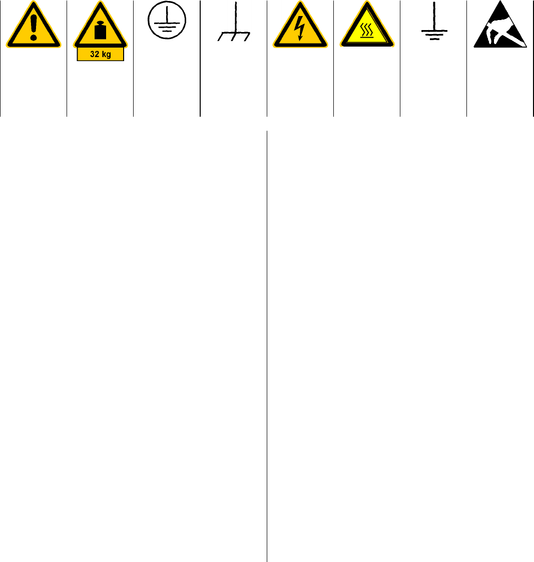
Safety Instructions
095.1000 Sheet 17
This unit has been designed and tested in accordance with the EC Certificate of Conformity and has left the
manufacturer’s plant in a condition fully complying with safety standards.
To maintain this condition and to ensure safe operation, the user must observe all instructions and warnings
given in this operating manual.
Safety-related symbols used on equipment and documentation from R&S:
Observe
operating
instructions
Weight
indication for
units >18 kg
PE terminal Ground
terminal Danger!
Shock hazard
Warning!
Hot surfaces Ground Attention!
Electrostatic
sensitive devi-
ces require
special care
1. The unit may be used only in the operating con-
ditions and positions specified by the manufac-
turer. Unless otherwise agreed, the following
applies to R&S products:
IP degree of protection 2X, Pollution severity 2,
overvoltage category 2, altitude max. 2000 m.
The unit may be operated only from supply net-
works fused with max. 16 A.
2. For measurements in circuits with voltages Vrms
> 30 V, suitable measures should be taken to
avoid any hazards.
(using, for example, appropriate measuring
equipment, fusing, current limiting, electrical
separation, insulation).
3. If the unit is to be permanently wired, the PE
terminal of the unit must first be connected to
the PE conductor on site before any other con-
nections are made. Installation and cabling of
the unit to be performed only by qualified techni-
cal personnel.
4. For permanently installed units without built-in
fuses, circuit breakers or similar protective de-
vices, the supply circuit must be fused such as
to provide suitable protection for the users and
equipment.
5. Prior to switching on the unit, it must be ensured
that the nominal voltage set on the unit matches
the nominal voltage of the AC supply network.
If a different voltage is to be set, the power fuse
of the unit may have to be changed accordingly.
6. Units of protection class I with disconnectible
AC supply cable and appliance connector may
be operated only from a power socket with
earthing contact and with the PE conductor con-
nected.
7. It is not permissible to interrupt the PE conduc-
tor intentionally, neither in the incoming cable
nor on the unit itself as this may cause the unit
to become electrically hazardous.
Any extension lines or multiple socket outlets
used must be checked for compliance with rele-
vant safety standards at regular intervals.
8. If the unit has no power switch for disconnection
from the AC supply, the plug of the connecting
cable is regarded as the disconnecting device.
In such cases it must be ensured that the power
plug is easily reachable and accessible at all
times (length of connecting cable approx. 2 m).
Functional or electronic switches are not suit-
able for providing disconnection from the AC
supply.
If units without power switches are integrated in
racks or systems, a disconnecting device must
be provided at system level.
9. Applicable local or national safety regulations
and rules for the prevention of accidents must
be observed in all work performed.
Prior to performing any work on the unit or
opening the unit, the latter must be discon-
nected from the supply network.
Any adjustments, replacements of parts, main-
tenance or repair may be carried out only by
authorized R&S technical personnel.
Only original parts may be used for replacing
parts relevant to safety (eg power switches,
power transformers, fuses). A safety test must
be performed after each replacement of parts
relevant to safety.
(visual inspection, PE conductor test, insulation-
resistance, leakage-current measurement, func-
tional test).
continued overleaf

Safety Instructions
095.1000 Sheet 18
10. Ensure that the connections with information
technology equipment comply with IEC950 /
EN60950.
11. Lithium batteries must not be exposed to high
temperatures or fire.
Keep batteries away from children.
If the battery is replaced improperly, there is
danger of explosion. Only replace the battery by
R&S type (see spare part list).
Lithium batteries are suitable for environmental-
ly-friendly disposal or specialized recycling.
Dispose them into appropriate containers, only.
Do not short-circuit the battery.
12. Equipment returned or sent in for repair must be
packed in the original packing or in packing with
electrostatic and mechanical protection.
13. Electrostatics via the connectors may dama-
ge the equipment. For the safe handling and
operation of the equipment, appropriate mea-
sures against electrostatics should be imple-
mented.
14. Any additional safety instructions given in this
manual are also to be observed.

1125.5555.26 CE E-1
EC Certificate of Conformity
Certificate No.: 2002-23
This is to certify that:
Equipment type Stock No. Designation
SMIQ06ATE 1125.5555.26 Vector Signal Generator
complies with the provisions of the Directive of the Council of the European Union on the
approximation of the laws of the Member States
- relating to electrical equipment for use within defined voltage limits
(73/23/EEC revised by 93/68/EEC)
- relating to electromagnetic compatibility
(89/336/EEC revised by 91/263/EEC, 92/31/EEC, 93/68/EEC)
Conformity is proven by compliance with the following standards:
EN61010-1 : 1993 + A2 : 1995
EN50081-1 : 1992
EN61000-6-2 : 1999
Affixing the EC conformity mark as from 2002
ROHDE & SCHWARZ GmbH & Co. KG
Mühldorfstr. 15, D-81671 München
Munich, 2002-05-07 Central Quality Management FS-QZ / Becker

1125.5555.33 CE E-1
EC Certificate of Conformity
Certificate No.: 2002-09
This is to certify that:
Equipment type Stock No. Designation
SMIQ03HD 1125.5555.33 Vector Signal Generator
complies with the provisions of the Directive of the Council of the European Union on the
approximation of the laws of the Member States
- relating to electrical equipment for use within defined voltage limits
(73/23/EEC revised by 93/68/EEC)
- relating to electromagnetic compatibility
(89/336/EEC revised by 91/263/EEC, 92/31/EEC, 93/68/EEC)
Conformity is proven by compliance with the following standards:
EN61010-1 : 1993 + A2 : 1995
EN55011 : 1998 + A1 : 1999, Klasse B
EN61326-1 : 1997 + A1 : 1998
For the assessment of electromagnetic compatibility, the limits of radio interference for Class
B equipment as well as the immunity to interference for operation in industry have been used
as a basis.
Affixing the EC conformity mark as from 2002
ROHDE & SCHWARZ GmbH & Co. KG
Mühldorfstr. 15, D-81671 München
Munich, 2002-02-28 Central Quality Management FS-QZ / Becker

1125.5555.02 CE E-5
EC Certificate of Conformity
Certificate No.: 99015
This is to certify that:
Equipment type Order No. Designation
SMIQ02B 1125.5555.02 Vector Signal Generator
SMIQ03B 1125.5555.03
SMIQ04B 1125.5555.04
SMIQ06B 1125.5555.06
SMIQB10 1085.5009.02 Modulation Coder
SMIQB11 1085.4502.02/.04 Data Generator
SMIQB12 1085.2800.02/.04 Memory Extension
SMIQB14 1085.4002.02 Fading Simulator
SMIQB15 1085.4402.02 Second Fading Simulator
SMIQB17 1104.9000.02 Noise Generator
SMIQB20 1125.5190.02 Modulation Coder
SMIQB21 1125.5490.02 BER Measurement
SMIQB46 1105.0006.02 Low ACP
SMIQB47 1125.5090.02 Low ACP
SMIQB60 1136.4390.02 Arbitrary Waveform Generator
complies with the provisions of the Directive of the Council of the European Union on the
approximation of the laws of the Member States
- relating to electrical equipment for use within defined voltage limits
(73/23/EEC revised by 93/68/EEC)
- relating to electromagnetic compatibility
(89/336/EEC revised by 91/263/EEC, 92/31/EEC, 93/68/EEC)
Conformity is proven by compliance with the following standards:
EN61010-1 : 1993 + A2 : 1995
EN50081-1 : 1992
EN50082-2 : 1995
Affixing the EC conformity mark as from 1999
ROHDE & SCHWARZ GmbH & Co. KG
Mühldorfstr. 15, D-81671 München
Munich, 2000-04-06 Central Quality Management FS-QZ / Becker

SMIQ Putting into Operation
1125.5555.03 E-71.1
1 Preparation for Use
1.1 Putting into Operation
Before putting the SMIQ into operation, please make sure that
•the covers of the casing are put on and screwed,
•the ventilation openings are free,
•no signal voltage levels exceeding the permissible limits are applied at the inputs,
•the outputs of the instrument are not overloaded or connected incorrectly.
If these points are not observed, the instrument might be damaged.
1.1.1 Supply Voltage
The SMIQ can be operated at a.c. systems from 90 V to 132 V and 180 V to 265 V at system
frequencies from 47 Hz to 440 Hz. The power supply socket is situated at the rear of the instrument.
The instrument automatically sets itself to the voltage applied within the permissible voltage ranges. It is
not necessary to set the instrument to a certain supply voltage.
1.1.2 Switching On/Off the Instrument
Power switch at the rear of the instrument
Power switch
Power supply socket
Switch on/off:½Press power switch at the top (I) / bottom (0)
The power switch can remain switched on permanently. Switching
off is only necessary when the instrument is to be completely
disconnected from the mains.
On/off switch at the front of the instrument
STBY
ON
Standby check LED Switch on: ½Press switch.
The instrument is ready for operation.
Switch off: ½Release switch.
The instrument assumes the STANDBY mode.

Putting into Operation SMIQ
1125.5555.03 E-71.2
1.1.3 Initial Status
Upon switching on, the instrument either automatically assumes the status which was set when it was
switched off (parameter POWER-ON STATE PREVIOUS SETTING in LEVEL-LEVEL menu) or the RF
output is disconnected (POWER-ON STATE RF OFF).
If the instrument need not to be operated from the initial status any further, a defined default status
should be established by pressing the [PRESET] key prior to further settings.
STANDBY Mode
In the STANDBY mode the optional reference oscillator (option SM-B1) remains switched on, which
increases frequency accuracy.
Frequency accuracy after switching on when the oven-controlled reference oscillator is fitted
(option SM-B1)
When switching on from the STANDBY mode, the specified frequency accuracy is reached immediately.
If the power switch was switched off, the reference oscillator needs some minutes of warm-up time to
reach its nominal frequency. During this period of time, the output frequency does not yet reach its final
value either. In the status line in the header field of the display the message "OVEN COLD" is displayed
for this time.
1.1.4 Setting Contrast and Brightness of the Display
Brightness control
Contrast control
Contrast and brightness of the display can be set by means of the contrast and brightness controls
situated below the display.
1.1.5 RAM with Battery Back-Up
The SMIQ has a static read-write memory (CMOS-RAM) with battery back-up, in which 50 different
complete settings of the instrument can be stored (cf. Chapter 2, section "Storing and Calling of
Instrument Settings"). In addition, all data and/or lists the user enters himself, such as for list mode,
memory sequence, and user correction of the level, are stored in the RAM. Further, all data of the
calibrations running within the instrument in the SMIQ are stored in the RAM (cf. Chapter 2, section
"Calibration").
A lithium battery with a service life of approx. 5 years serves to supply the RAM with power. When the
battery is discharged, the data stored will be lost. For exchange of the battery see Service Manual.

SMIQ Functional Test
1125.5555.03 E-71.3
1.1.6 Preset Setting
A defined setting status is achieved by pressing the [PRESET] key.
Preset Status:
RF frequency 100 MHz
RF level -30 dBm
Reference frequency internal, adjustment off
Offsets 0
Modulations switched off
Transient-free level setting switched off, level attenuator mode: AUTO
Internal level control level ALC: AUTO
User correction level UCOR: OFF
LF output switched off
Sweep switched off
List mode switched off
Memory sequence switched off
Suppression of indications system security: unaltered
Protection of calibration data protection lock: unaltered
Settings stored unaltered
Data, lists etc. stored unaltered
IEC-bus address unaltered
Beeper unaltered
All parameters and circuit states, even those of operating modes which are not activated, are preset by
means of Preset.
The presettings going beyond the above list can be seen from the menu representations as of Section
2.4 which each indicate the Preset setting status.
1.2 Functional Test
On switching on the instrument and permanently during operation, the SMIQ carries out a self test. The
ROM contents as well as the battery of the non-volatile RAM are checked on switching on the
instrument and the RAM contents with every calling the memory. The most important instrument
functions are automatically monitored during operation.
If an error is detected, the message "ERROR" is displayed in the status line. For further identification of
the error, press the [ERROR] key. Thereupon a description of the error/s is displayed (cf. Chapter 2,
section "Error Messages"). Return to the menu exited by pressing the [RETURN] key.
If required, the self tests can be induced purposefully. See Chapter 4, section "Functional Test".
Further, internal test points can be polled by the user and the results be read out and displayed. See
Chapter 2, section "Voltage Indication of Test Points".

Fitting the Options SMIQ
1125.5555.03 E-71.4
1.3 Fitting the Options
Due to its variety of options, the SMIQ offers the possibility of providing the instrument with the
equipment exactly corresponding to the application. Newly fitted options are automatically recognized
and the relevant parameters added in the menu.
After every change of the instrument configuration, the CMOS RAM has to be cleared as the storage
data shift:
½Switch off the instrument
½Switch the instrument on again with the [RESET] key pressed
The internal calibration routines VECTOR MOD, VCO SUM, and LEV PRESET now have to be called
up again to restore the cleared calibration values.
These routines are accessible via menu UTILITIES-CALIB (see also Chapter 2, section "calibration").
The calibration routines have to be carried out in the following order:
1. VCO SUM (Summing loop)
2. VECTOR MOD
3. LEV PRESET
1.3.1 Opening the Casing
Caution:
Prior to opening the SMIQ, unplug the power connector.
Remove paneling ½Remove four screws in the two tilt feet at the rear of the instrument.
½Remove the upper paneling towards the top and rear.
½Turn the instrument.
½Remove the lower paneling towards the top and rear.
Open ventilation ducts When an option is fitted at a slot which has not been used up to now,
the appropriate ventilation duct of the plexiglas plate at the left in the
casing frame must be opened. The openings are pre-punched so that
the respective part is easy to break out.
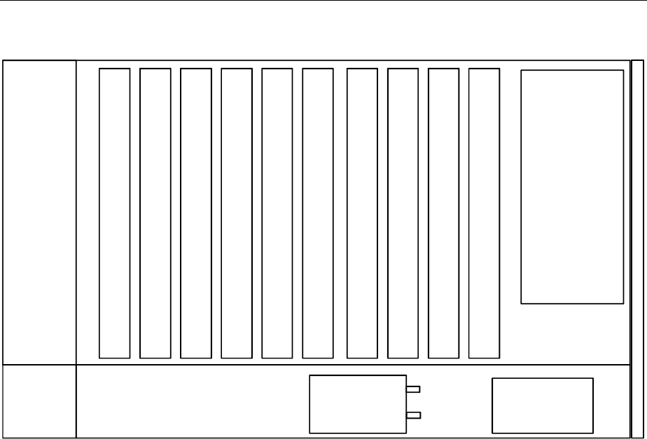
SMIQ Fitting the Options
1125.5555.03 E-71.5
1.3.2 Overview of the Slots
FRO
ATTC Option SM-B1
POWS1
Frequency extension 4 GHz/6 GHz
IQMOD
IQCON
SUM
DSYN
REFSS
MCOD
DGEN
FSIM1 / FMOD / NDSIM
FSIM2 / FMOD / NDSIM
FRO = front unit
FMOD = FM/PM modulator
IQMOD = I/Q modulator
IQCON = I/Q converter
SUM = summing loop
DSYN = digital synthesis
REFSS = reference/step synthesis
MCOD = modulation coder
DGEN = data generator
FSIM = fading simulator
POWS1 = power supply
ATTC = attenuator
NDSIM = Noise generator and
distortion simulator
Fig. 1-1 SMIQ, view from the top
1.3.3 Option SM-B1 - Reference Oscillator OCXO
Fitting the option ½Fasten the option at the back end of the lateral opening by means of
the screw threads provided there.
½If the two last slots are both occupied, one of these modules must
be removed temporarily.
½Feed ribbon cable W710 through the rear square cut-out to the
motherboard, insert into connector X22 and snap in the locking.
½Feed coaxial cable W170 from socket X711 of the option through
the second cut-out along the rear transverse panel to connector
X74 at the A7 module, reference/step synthesis, via the
motherboard and insert there.

Fitting the Options SMIQ
1125.5555.03 E-71.6
Set tuning voltage and
calibrate OCXO The crystal oscillator was factory-tuned to nominal frequency and the
appropriate tuning voltage indicated on the cover of the module. The
calibration value now has to be calculated from this value and
transferred to the memory of the signal generator.
Calculate calibration value The tuning voltage is generated by a 12b-bit-D/A converter which is
scaled such that a tuning voltage of 12 volts is generated with
calibration value (CALIBRATION DATA) 4000.
The calibration value is thus calculated from the tuning voltage (Vtun)
as follows CALIBRATION DATA = Vtun × 4000 / 12
For checking purposes, the voltage at pin 16 of plug X22 on the
motherboard can be remeasured and corrected if necessary. A check
by means of frequency measurement may only be made after a
warm-up of 2 hours and against a calibrated reference.
Store calibration value ½Unlock protection level 2 with code 250751.
v Call menu UTILITIES-CALIB-REF OSC.
½Enter the calculated calibration voltage with CALIBRATION DATA
by means of the rotary knob or keypad.
½Select STORE CALIBRATION DATA
½Terminate entry using the [SELECT] key
The new calibration value is stored in the EPROM.
Note: The flash EPROM does not permit the deletion of individual
data. Thus new memory space is occupied for each calibration.
If there is no memory space available any more, the EPROM
must be cleared by an authorized service shop and be written
into anew. Thus a calibration should only be made if necessary
1.3.4 Option SM-B5 - FM/PM Modulator
The FM/PM modulator is fitted at the slot with label 'FMOD'.
Fitting the option ½Withdraw cable W89 from X99 of the summing loop and use again.
½Establish the following connections:
Cable From To Signal
W89 A8-X89 A6-X67 FDSYN
W65 A6-X65 A7-X71 REF100
W67 A6-X69 A9-X99 FDFM

SMIQ Fitting the Options
1125.5555.03 E-71.7
1.3.5 Option SMIQB11 - Data Generator
The Data Generator is fitted at the slot with label "DGEN".
½ Plug the module into the slot.
½ Lock it and fasten all screws.
½Plug W341 onto X341.
½Open the air inlets at the housing frame by breaking out the safety
glass plate which belongs to the option.
1.3.6 Option SMIQB12 - Memory Extension to Data Generator
The Data Generator can be upgraded with up to two memory extension units (SMIQB12). The first Memory
Extension is fitted at the slot with label "X350", the second Memory Extension at slot with label "X351".
½Remove option Data Generator from SMIQ.
½Withdraw the screws of the labelled screening cover and remove
the cover.
½The first memory extension unit has to be pluged on connector
X350 near the battery.
½The second memory extension unit has to be pluged on connector
X351.
½Refit the screening cover of the Data Generator module.
½Plug the Data Generator back into the appropriate place, lock it and
fasten all screws.
Fitting the Options SMIQ
1125.5555.03 E-71.8
1.3.7 Option SMIQB14 - Fading Simulator FSIM1
The Fading Simulator is fitted at the slot with label ’FSIM1’.
Before fitting the option SMIQB14 (FSIM1) first check the correct settings of the jumpers on the module.
For FSIM modules of series 1085.XXXX (see screening cover) the jumper setting also depends on the
number of fading simulators installed, either one (FSIM1) or two (FSIM1 and FSIM2).
After an instrument warm-up period of 2 hours, the IQ Modulator should be calibrated.
Two coaxial connecting cables (Stock No. 1085.4448.00) are part of the equipment supplied with the
option. The cables can be connected to the outputs I FADED and Q FADED at the rear of SMIQ.
Checking the jumper Jumper Setting for the Fading Simulator FSIM1:
settings (Cf. labeling ’Jumper Setting’ and labeling on the screening cover of
the module)
FSIM1 One Fading Simulator
installed
FADING SIMULATOR:
1085.XXXX
Two Fading Simulators
installed
FADING SIMULATOR:
1085.XXXX
FADING SIMULATOR:
1114.XXXX
Jumper connects X1.1 with X1.2 X1.1 with X1.2 X1.2 with X1.3
X8.1 with X8.2 X8.2 with X8.3 X8.1 with X8.2
X9.1 with X9.2 X9.2 with X9.3 X9.2 with X9.3
X12.2 with X12.3 X12.2 with X12.3 X12.2 with X12.3
X13.1 with X13.2 X13.2 with X13.3 X13.1 with X13.2
X15.1 with X15.2 X15.1 with X15.2 X15.1 with X15.2
X16.1 with X16.2 X16.2 with X16.3 none
Fading modules of series 1114.XXXX also require the setting of a DIP switch. The setting is indicated
on the screening cover.
FADING SIMULATOR
1114.XXXX
Switch 12
FSIM1 OFF ON
SMIQ Fitting the Options
1125.5555.03 E-71.9
Fitting the option ½Plug the module into the appropriate slot, lock it and fasten all
screws.
½Open the air inlets at the housing frame by breaking out the safety
glass plate which belongs to the option.
½Depending on the fact whether the option SMIQB20 (MCOD) has
been installed in the SMIQ, the following coaxial connections have
to be made:
Note: Please store the remaining cables. They will be required if
further options will be installed at a later stage or options will
be removed.
SMIQ with option MCOD SMIQ without option MCOD Remark about cable
Cable from FSIM1 to to
W361 X361 MCOD X325 - W361 was provided with FSIM1
W244 X361 - FRO I socket Withdraw W244 from X244 of module
IQMOD
W363 X363 MCOD X328 - W363 was provided with FSIM1
W245 X363 - FRO Q socket Withdraw W245 from X245 of module
IQMOD
W367 X367 IQMOD X244 IQMOD X244 W367 was provided with FSIM1
W388 X368 REAR I FADED REAR I FADED W388 was provided with FSIM1
W370 X370 IQMOD X245 IQMOD X245 W370 was provided with FSIM1
W391 X371 REAR Q FADED REAR Q FADED W391 was provided with FSIM1
X371 X370 X369 X368 X367 X366 X365
X360
X364 X363 X362 X361
FSIM1
Fig. 1-2 Module FSIM
½The included adhesive label ’Option included’ is to be fixed at the
rear panel of the SMIQ.
Calibrating the
Fading Simulator and the ½Warm-up the instrument for 2 hours.
I/Q Modulator ½Call up menu UTILITIES - CALIB - VECTOR MOD.
Fitting the Options SMIQ
1125.5555.03 E-71.10
1.3.8 Option SMIQB15 - Second Fading Simulator (FSIM2)
The second Fading Simulator is fitted at the slot with label ’FSIM2’.
Before fitting the option SMIQB15 (FSIM2) please check the correct settings of the jumpers on both
fading modules FSIM1 (see Section 1.3.7) and FSIM2. The jumper settings depend on the series of the
FSIM module, they are also indicated on the screening cover.
After an instrument warm-up period of 2 hours, the IQ Modulator should be calibrated.
Checking the jumper Jumper Setting for the Fading Simulator FSIM2:
settings (cf. module number and labeling ’Jumper Setting’ on the screening
cover of the module)
FSIM2 FADING SIMULATOR
1085.XXXX FADING SIMULATOR
1114.XXXX
Jumper connects X1.2 with X1.3 X1.1 with X1.2
X8.2 with X8.3 X8.2 with X8.3
X9.2 with X9.3 X9.1 with X9.2
X12.1 with X12.2 X12.1 with X12.2
X13.2 with X13.3 X13.2 with X13.3
X15.2 with X15.3 X15.2 with X15.3
X16.2 with X16.3 none
Fading modules of series 1114.XXXX also require the setting of a DIP switch. The setting is indicated
on the screening cover.
FADING SIMULATOR
1114.XXXX
Switch 12
FSIM1 OFF ON
FSIM2 ON OFF
SMIQ Fitting the Options
1125.5555.03 E-71.11
Fitting the option ½Plug the module into the appropriate slot for the FSIM2, lock it and
fasten all screws.
½Open the air inlets at the housing frame by breaking out the safety
glass plate which belongs to the option.
½ The following coaxial connections have to be made:
FSIM2
Module number
1085.XXXX
FSIM2
Module number
1114.XXXX
FSIM1
Cable from from to
W362 X361 X362 X362
W364 X363 X364 X364
W365 X365 X365 X365
W366 X367 X368 X366
W369 X370 X371 X369
Note: Please store the remaining cables. They will be required if
further options will be installed at a later stage or options will
be removed.
½ The included adhesive label ’Option included’ is to be fixed at the
rear panel of the SMIQ.
Calibrating the
Fading Simulator and the ½Warm-up the instrument for 2 hours.
I/Q Modulators ½Call up menu UTILITIES - CALIB - VECTOR MOD.
Retrofit for 2-channel fading Cables W388 and W391 have to be repositioned for 2-channel fading.
½Unplug W388 from X368 of FSIM1 and plug to X368 (1085.XXXX)
or X367 (1114.XXXX) of FSIM2.
½Unplug W391 from X371 of FSIM1 and plug to X371 (1085.XXXX)
or X370 (1114.XXXX) of FSIM2.

Fitting the Options SMIQ
1125.5555.03 E-71.12
1.3.9 Option SMIQB17 - Noise Generator and Distortion Simulator
Depending on which options are fitted, the NDSIM module is mounted in the slot labelled
FSIM1/FMOD/NDSIM or FSIM2/FMOD/NDSIM or E6GHZ/FMOD/NDSIM (in older units slot
FSIM1/FMOD or FSIM2/FMOD).
After an instrument warm-up period of 1 hour, the NDSIM as well as the IQ Modulator should be
calibrated. Then the instrument is ready for use.
Six coaxial connecting cables (W601, W602, W603, W388, W605, W391 and the adhesive option label
are part of the equipment supplied with the option.
Fitting the option ½Plug the module into the appropriate slot.
½Lock it and fasten all screws.
½Open the air inlets at the housing frame by breaking out the safety
glass plate which belongs to the option.
½If options FSIM1 and FSIM2 are fitted, cables W388 and W391
have to be connected as shown in Fig. 1-3.
½Depending on which modules are installed in the SMIQ, the
following coaxial connections are to be made:
SMIQ
without option MCOD
without option FSIM1
without option FSIM2
SMIQ
with option MCOD
without option FSIM1
without option FSIM2
Remark about cable
Cable from NDSIM to to
W244 X601 FRO I-connector - Cable was provided with unit
W245 X602 FRO Q-connector - Cable was provided with unit
W601 X601 - MCOD X325 W601 was provided with NDSIM
W602 X602 - MCOD X328 W602 was provided with NDSIM
W603 X603 IQMOD X244 IQMOD X244 W603 was provided with NDSIM
W388 X604 REAR I FADED REAR I FADED W388 was provided with NDSIM
W605 X605 IQMOD X245 IQMOD X245 W605 was provided with NDSIM
W391 X606 REAR Q FADED REAR Q FADED W391 was provided with NDSIM
SMIQ
with option MCOD
with option FSIM1
without option FSIM2
SMIQ
with option MCOD
with option FSIM1
with option FSIM2
Remark about cable
Cabel from NDSIM to to
W601 X601 FSIM1 X367 FSIM1 X367 W601 was provided with NDSIM
W602 X602 FSIM1 X370 FSIM1 X370 W602 was provided with NDSIM
W603 X603 IQMOD X244 IQMOD X244 W603 was provided with NDSIM
W388 X604 REAR I FADED REAR I FADED W388 was provided with NDSIM
W605 X605 IQMOD X245 IQMOD X245 W605 was provided with NDSIM
W391 X606 REAR Q FADED REAR Q FADED W391 was provided with NDSIM
SMIQ Fitting the Options
1125.5555.03 E-71.13
X606 X605 X604 X603 X607
X600
X602
NDSIM
X601
Fig. 1-3 Module NDSIM
Connector X607 is unused and provided only in some modules.
½The included adhesive label ’Option included’ is to be fixed at the
rear panel of the SMIQ.
Calibrating the
NDSIM and ½Warm-up the instrument for 1 hours.
the I/Q Modulator ½Call up menu UTILITIES - CALIB - VECTOR MOD.
1.3.10 Option SMIQB20 - Modulation Coder
The Modulation Coder is fitted at the slot with label "MCOD".
½Plug the module into the appropriate place, lock it and fasten all
screws.
½Open the air inlets at the housing frame by breaking out the safety
glass plate which belongs to the option
½Depending on the fact whether the option SMIQB14 (FSIM1) has
been installed in the SMIQ, the following coaxial connections have
to be made (cf. Fig. 1-4):
Note: Please store the remaining cables. They will be required if
further options will be installed at a later stage or options will
be removed.
SMIQ without option FSIM 1 SMIQ with option FSIM 1 Remark about cable
Cable from
MCOD to to
W322 X321 REFSS X72 REFSS X72 W322 was provided with MCOD.
W72 X322 DSYN X81 DSYN X81 Withdraw W72 from X72 of module REFSS.
W243 X323 BACK POW RAMP
socket BACK POW RAMP
socket Withdraw W243 from X243 of module IQMOD.
W324 X324 IQMOD X243 IQMOD X243 W324 was provided with MCOD.
W325 X325 IQMOD X244 - W325 was provided with MCOD.
W361 X325 - FSIM 1 X361 W361 was provided with FSIM1.
X326 - - - -
W244 X327 FRO I socket FRO I socket Withdraw W244 from X244 of module IQMOD. If
FSIM1 is installed withdraw W244 from X361 of
module FSIM1.
W328 X328 IQMOD X245 - W328 was provided with MCOD.
W363 X328 - FSIM 1 X363 W363 was provided with FSIM1.
X329 - - - -
W245 X330 FRO Q socket FRO Q socket Withdraw W245 from X245 of module IQMOD. If
FSIM1 is installed withdraw W245 from X363 of
module FSIM1.

Fitting the Options SMIQ
1125.5555.03 E-71.14
X330 X329 X328 X327 X326 X325
X320
X324 X323 X322 X321
MCOD
Fig. 1-4 Module MCOD
½ The included adhesive label "Option included" is to be fixed at the
rear panel of the SMIQ.
1.3.11 Option SMIQB21 - Bit Error Rate Test
Software option SMIQB21 has to be enabled by entering a key upon installation. An option label
containing the installation key is supplied and has to be affixed to the rear of SMIQ for service and repair
purposes.
As a prerequisite, SMIQ must be fitted with hardware option SMIQB20 (modulation coder).
Enabling the option ½Switch on SMIQ.
½Call UTILITIES menu (select with rotary knob, confirm with
[SELECT] key).
½Call INSTALL menu ==> [SELECT].
½Call OPTION TO INSTALL menu ==> [SELECT].
½Select option SMIQB21 BERT ==> [SELECT].
½Enter the 6-digit installation key shown on the option label into the
INSTALLATION KEY line. Then press the [ENTER] key.
½You will receive a message confirming that the installation key has
been verified and the option is installed.
½To make the option available, the unit has to be switched off and on
again.
½Once the installation has been successfully completed, BER
measurement can be selected from the main menu.
Once the installation has been completed, the availability of the new option can be checked in the
module list in the UTILITIES DIAG CONFIG menu.
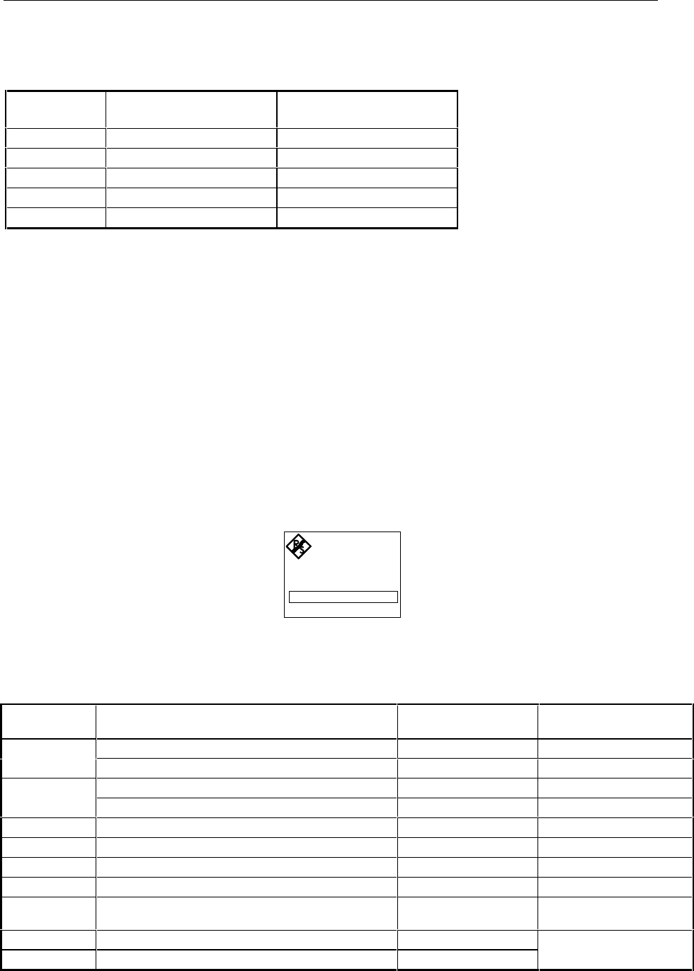
SMIQ Fitting the Options
1125.5555.03 E-71.15
Connector
The clock and data signals output by the DUT must have TTL level and are connected to the BER (bit error
rate) input, a 9-contact SUB-D connector at the rear of the unit labelled BER. Pin assignment is as follows:
SUB-D connector Adapter cable
Order No. 1110.3551.00
1,2,3,4,5 Ground Screen
6 Bit clock input CLOCK
7 Data input DATA
8 Data enable input DAT ENAB
9Restart RES
Polarity of clock and data signals, the PRBS polynomial used and the integration time can be set by
manual or remote-control commands. The input signals are not terminated in the SMIQ but applied to
ICs of type 74LVT14 via a 220 Ω resistor. A cable is supplied with the option. Its contacts are assigned
to BNC connectors as shown in the above table.
1.3.12 Other Software Options
SMIQB42 / SMIQB43 / SMIQB45 / SMIQB47 / SMIQB48 / SMIQB49 /
SMIQB60 / SMIQK11 / SMIQK12
You have acquired a software option to go with your Signal Generator SMIQ from Rohde & Schwarz.
This option must be enabled by an installation keyword. Please affix the enclosed option label including
the installation keyword to the rear panel of the SMIQ since it is required for service and repair. For
installation of software option SMIQB21 cf. section 1.3.11.
Enclosed option label with a typical keyword:
OPTION SMIQ-B43
DIGITAL STANDARD
W-CDMA
1104.8032.02
INSTALLATION KEY
9 5 4 8 7 6
MADE IN GERMANY <== Example
For a sucessful installation the necessary hardware options as well as the firmware version are listed in
the following table. The firmware version is indicated in the right part of the display when only the main
menu appears. If your instrument is equipped with an older version, update the firmware first. Disks,
cables and update instructions are provided with the package.
Option Necessary hardware/software options Firmware version
(at least) Remark
SMIQB10 (MCOD) and SMIQB11 (DGEN) 3.20SMIQB42
SMIQB20 (MCOD2) and SMIQB11 (DGEN) 5.10 HX
SMIQB10 (MCOD) and SMIQB11 (DGEN) 3.80SMIQB43
SMIQB20 (MCOD2) and SMIQB11 (DGEN) 5.10 HX
SMIQB45 SMIQB20 (MCOD2) and SMIQB11 (DGEN) 5.10 HX
SMIQB47 IQ modulator (IQMOD) variant 8 3.91
SMIQB48 SMIQB20 (MCOD2), SMIQB11 (DGEN) and SMIQB45 5.30 HX
SMIQB49 SMIQB14 and /or SMIQB15 (FSIM) 5.40 HX
SMIQB60 SMIQB20 (MCOD2) and SMIQB11 (DGEN) 5.20 HX PC software WinIQSIM
recommended
SMIQK11 SMIQB60 5.20 HX
SMIQK12 SMIQB60 5.20 HX
PC software WinIQSIM
recommended

Mounting into a 19" Rack SMIQ
1125.5555.03 E-71.16
Enabling option: ½ Switch on SMIQ.
½Call up menu UTILITIES. (Select it by means of the rollkey, confirm with
[SELECT] key).
½Call up menu INSTALL ==> [SELECT]
½Call up menu OPTION TO INSTALL ==> [SELECT]
½Select the option you want to install ==> [SELECT]
½Read the 5 or 6-digit keyword on the option label and enter it into the corres-
ponding field in the INSTALLATION KEY line. Then press the [ENTER] key.
½A message will then be issued to the effect that the keyword has been
checked and that the option is being installed.
½For the option to be available the unit has to be switched off and then on
again.
After installation, the new option is listed in the module list of the UTILITIES-DIAG-CONFIG menu. In
case of any problems contact your Rohde&Schwarz service center.
1.3.13 Option SMIQB19 - Rear Panel Connections for RF and LF
The SMIQ can be retrofitted to include rear panel connections for RF and LF for mounting it into a 19"
rack using option SMIQB19. The mounting instructions are attached to the option.
1.4 Mounting into a 19" Rack
Caution: Ensure free air inlet at the perforation of the side walls and air outlet at the rear of the
instrument in rack mounting.
The SMIQ can be mounted into a 19" rack by means of rack adapter ZZA-94 (stock no. 396.4905.00).
The mounting instructions are attached to the adapter.
SMIQ Front Panel
1125.5555.03 2.1 E-7
2 Operation
2.1 Front and Rear Panel
2.1.1 Display
(cf. Fig. 2-1, Front panel view)
1
FREQ
100. 000 000 0
MHz LEVEL
- 30.0
dBm
FM
AM
BB-AM
FM
PM
FM1 DEVIATION
FM1 SOURCE
LFGEN FREQ
FM2 DEVIATION
FM2 SOURCE
EXT1 COUPLING
EXT2 COUPLING
PREEMPHASIS
1.00 kHz
OFF INT EXT1 EXT2
1.000 0 kHz
10.0 kHz
OFF EXT1 EXT2
AC DC
AC DC
OFF 50µ 75µ s
FREQUENCY
LEVEL
ANALOG MOD
VECTOR MOD
DIGITAL MOD
DIGITAL STD
LF OUTPUT
SWEEP
LIST
MEM SEQ
UTILITIES
The display shows in the
header field: - the current frequency and level
settings (considering an offset).
- status messages.
- error messages.
menu field: - the main menu and the submenus
selected with the current settings.
Parameters can be selected and changed in the
menus indicated.
see as well
Chapter 2,
Section "Design of the
Display"

Front Panel SMIQ
1125.5555.03 2.2 E-7
SIGNAL GENERATOR 300kHz...3.3GHz
SMIQ03B 1125.5555.03
SYMBOL
CLOCK
BIT
CLOCK
DATA
89
7
56
4
231
.
-
0
ç
FREQ
LEVEL
SAVE
RCL
Gn
M
k
x1
µ
m
ENTER
dBµV
µV
mV
dB(m)
DATA INPUT
Q
MENU / VARIATION
SELECT
ïð
5
6
7
8
9
4
32
1
!
MAX 50 W
REVERSE P OWER
MADE IN GERMANY
RETURN
(BB-AM)
I
OPERATING
Move cursor
SELECT Next menu
RETURN Previous menu
VERSION: 1.33
FREQUENCY
LEVEL
ANALOG MOD
VECTOR MOD
DIGITAL MOD
DIGITAL STD
LF OUTPUT
SWEEP
LIST
MEM SEQ
UTILITIES
FREQ
100. 000 000 0
MHz LEVEL
- 30.0
dBm
LOCAL
HELP
ERROR
PRESET
STATUS
ASSIGN MENU2
MENU1
STBY
ON
QUICK SELECT
RF
ON/OFF
MOD
ON/OFF
Fig. 2-1 Front panel view

SMIQ Front Panel
1125.5555.03 2.3 E-7
2.1.2 Controls and Inputs/Outputs of the Front Panel
(cf. Fig. 2-1, front panel view)
2 DATA INPUT
Parameter field
FREQ
LEVEL
SAVE
RCL
Parameters RF frequency and RF level can be entered
directly by means of the parameter keys, alternatively
to menu operation. The input value (indicated in the
header field) considers the offset, see Sections 2.4 and
2.5. Further, complete instrument settings can be
stored and called.
FREQ Opens the setting of the RF frequency via
value input or variation by means of a rotary
knob. The current menu is maintained.
Return to the menu by means of the
[RETURN] key. (Setting of the RF frequency
also in the FREQUENCY menu).
LEVEL Opens the setting of the RF level via value
input or variation by means of a rotary knob.
The current menu is maintained. Return to
the menu by means of the [RETURN] key.
(Setting of the RF level also in the LEVEL
menu).
SAVE Opens the storing of the current instrument
setting. Memory selection is effected by
entering a number (1 to 50) and is finished by
means of the [ENTER] key.
RCL Opens the calling of an instrument setting
stored. Memory selection is effected by
entering a number (1 to 50) and is finished by
means of the [ENTER] key.
see as well
Chapter 2
Section
"Use of [FREQ] and
[LEVEL] Keys"
Section
"RF Frequency"
Section
"RF Level"
Section
"Storing and Calling of
Instrument Settings"
Numeric input field
8
9
7
5
6
4
2
3
1
.
-
0
ç
Numeric values, decimal point and minus sign can be
entered by means of the digital keys.,
0...9 Enters the digit.
Enters the decimal point
-/← Enters the minus sign.
Deletes the last input (digit, sign or decimal
point) - key [BACKSPACE].
see as well
Chapter 2
Section
"Basic Operating
Steps"

Front Panel SMIQ
1125.5555.03 2.4 E-7
SIGNAL GENERATOR 300kHz...3.3GHz
SMIQ03B 1125.5555.03
SYMBOL
CLOCK
BIT
CLOCK
DATA
89
7
56
4
231
.
-
0
ç
FREQ
LEVEL
SAVE
RCL
Gn
M
k
x1
µ
m
ENTER
dBµV
µV
mV
dB(m)
DATA INPUT
Q
MENU / VARIATION
SELECT
ïð
5
6
7
8
9
4
32
1
!
MAX 50 W
REVERSE P OWER
MADE IN GERMANY
RETURN
(BB-AM)
I
OPERATING
Move cursor
SELECT Next menu
RETURN Previous menu
VERSION: 1.33
FREQUENCY
LEVEL
ANALOG MOD
VECTOR MOD
DIGITAL MOD
DIGITAL STD
LF OUTPUT
SWEEP
LIST
MEM SEQ
UTILITIES
FREQ
100. 000 000 0
MHz LEVEL
- 30.0
dBm
LOCAL
HELP
ERROR
PRESET STATUS
ASSIGN MENU2
MENU1
STBY
ON
QUICK SELECT
RF
ON/OFF
MOD
ON/OFF
Fig. 2-1 Front panel view

SMIQ Front Panel
1125.5555.03 2.5 E-7
2 DATA INPUT
Unit keys with enter function
Gn
M
k
x1
µ
m
ENTER
dBµV
µV
mV
dB(m)
The unit keys terminate the input of values and specify
the multiplication factor for the respective basic unit.
The basic units are displayed next to the input field
while numbers are entered. In the case of level
settings, the unit keys specify the unit.
G/n dBµV Selects giga/nano, with RF level
dBµV, with LF level dBu.
M/µµV Selects mega/micro, with level
µ
V.
k/m MV Selects kilo/milli, with level mV.
1x
Enter dB(m) Terminates entries in the basic
unit and value inputs without unit.
Selects with level dBm
Selects with level offset and level
step width dB.
In order to change to another level unit, simply press
the unit key desired. Parameter LEVEL must be
activated, e.g. by pressing the [LEVEL] key.
see as well
Chapter 2
Section
"Basic Operating
Steps"
Section
"Change Unit of Level"
3 MENU/VARIATION
Menu keys
SELECT
RETURN
ïð
The menu keys access the menus and settings within
the menus.
RETURN Returns the menu cursor to the
next higher menu level.
SELECT Acknowledges the choice marked
by the menu cursor
⇐Moves the digit cursor to the left by
one position in the marked value
indication.
Moves the menu cursor to the left
by one position in a 1-out-of-n
selection.
ÞMoves the digit cursor to the right
by one position in the marked value
indication.
Moves the menu cursor to the right
by one position in a 1-out-of-n
selection.
see as well
Chapter 2
Section
"Basic Operating
Steps"

Front Panel SMIQ
1125.5555.03 2.6 E-7
SIGNAL GENERATOR 300kHz...3.3GHz
SMIQ03B 1125.5555.03
SYMBOL
CLOCK
BIT
CLOCK
DATA
89
7
56
4
231
.
-
0
ç
FREQ
LEVEL
SAVE
RCL
Gn
M
k
x1
µ
m
ENTER
dBµV
µV
mV
dB(m)
DATA INPUT
Q
MENU / VARIATION
SELECT
ïð
5
6
7
8
9
4
32
1
!
MAX 50 W
REVERSE P OWER
MADE IN GERMANY
RETURN
(BB-AM)
I
OPERATING
Move cursor
SELECT Next menu
RETURN Previous menu
VERSION: 1.33
FREQUENCY
LEVEL
ANALOG MOD
VECTOR MOD
DIGITAL MOD
DIGITAL STD
LF OUTPUT
SWEEP
LIST
MEM SEQ
UTILITIES
FREQ
100. 000 000 0
MHz LEVEL
- 30.0
dBm
LOCAL
HELP
ERROR
PRESET STATUS
ASSIGN MENU2
MENU1
STBY
ON
QUICK SELECT
RF
ON/OFF
MOD
ON/OFF
Fig. 2-1 Front panel view
SMIQ Front Panel
1125.5555.03 2.7 E-7
3 MENU/VARIATION
Rotary knob
The rotary knob moves the menu cursor over the
positions of a menu level to choose from or varies the
value of a parameter. The variation is either effected in
steps of one or in a step width that can be specified at will.
See as well
Chapter 2
Section "Basic
Operating Steps"
Section
"Sample Setting for
First Users"
4
DATA
DATA Input external data signal for digital mo-
dulation. Input resistance 1 kΩ or 50 Ω,
Trigger threshold can be set from -2.5 to
+ 2.5V, max. ± 15 V, max. 40 mA.
Output* data signal with operating mode
internal. Level: TTL
See as well
Chapter 2,
Section
"Digital Modulation"
BIT
CLOCK
BIT
CLOCK Input* external clock-pulse signal for
synchronization of external data signal.
Input resistance 1 kΩ or 50 Ω,
Trigger threshold can be set from -2.5 to
+ 2.5 V, max. ± 15 V, max. 40 mA.
Output* clock-pulse signal with operating
mode internal. Level: TTL
SYMBOL
CLOCK
SYMBOL
CLOCK Input* external clock signal for
synchronization of the external data
signal with polyvalent modulation types
with several bits per symbol.
Input resistance 1 kΩ or 50 Ω,
Trigger threshold can be set from -2.5 to
+ 2.5V, max. ± 15 V, max. 40 mA.
Output* symbol clock signal with
operating mode internal. Level TTL
(BB-AM)
I
(BB-AM)
IInput external modulation signal for I/Q
modulation and broadband-AM.
Output* I-signal with operating mode
internal.
Input/output resistance 50 Ω.
Nominal voltage (I/Q): Us = 0.5 V
Nominal voltage (BB-AM): Us=0.25V
max. permissible overvoltage: ± 5V
Section
"Vector Modulation"
and
Section
"Broadband AM"
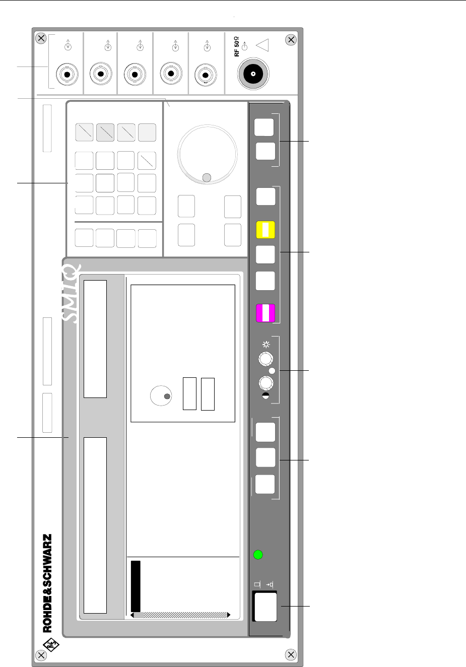
Front Panel SMIQ
1125.5555.03 2.8 E-7
SIGNAL GENERATOR 300kHz...3.3GHz
SMIQ03B 1125.5555.03
SYMBOL
CLOCK
BIT
CLOCK
DATA
89
7
56
4
231
.
-
0
ç
FREQ
LEVEL
SAVE
RCL
Gn
M
k
x1
µ
m
ENTER
dBµV
µV
mV
dB(m)
DATA INPUT
Q
MENU / VARIATION
SELECT
ïð
5
6
7
8
9
4
32
1
!
MAX 50 W
REVERSE P OWER
MADE IN GERMANY
RETURN
(BB-AM)
I
OPERATING
Move cursor
SELECT Next menu
RETURN Previous menu
VERSION: 1.33
FREQUENCY
LEVEL
ANALOG MOD
VECTOR MOD
DIGITAL MOD
DIGITAL STD
LF OUTPUT
SWEEP
LIST
MEM SEQ
UTILITIES
FREQ
100. 000 000 0
MHz LEVEL
- 30.0
dBm
LOCAL
HELP
ERROR
PRESET STATUS
ASSIGN MENU2
MENU1
STBY
ON
QUICK SELECT
RF
ON/OFF
MOD
ON/OFF
Fig. 2-1 Front panel view
SMIQ Front Panel
1125.5555.03 2.9 E-7
4
Q
Q Input external modulation signal for I/Q
modulation.
Output* Q-signal with operating mode
internal.
Input/output resistance 50 Ω.
Nominal voltage: Us = 0.5 V
max. permissible overvoltage: ± 5V
Section
"Vector Modulation"
RF 50
RF Output RF signal.
Source resistance 50 Ω
max. permissible HF-power: 50 W
max. permissible overvoltage: 35 V
Section "Use of
[ON/OFF] and
[MOD ON/OFF] Key"
* When fitted with option Modulation coder, SMIQB20
5
RF
0N/0FF
M0D
0N/0FF
MOD Switches on/off the modulation
ON/OFF selected in the UTILITIES MOD
KEY menu.
RF Switches on/off the RF signal.
ON/OFF
See as well
Chapter 2
Section "Use of
[RF ON/OFF] and
[MOD ON/OFF] Keys"
6
LOCALHELPSTATUS
ERROR
PRESET
PRESET Establishes a defined instrument
status.
ERROR* Indicates error and caution
messages.
STATUS* Indicates the instrument status.
HELP* Indicates context-sensitive auxiliary
text.
LOCAL Switches the instrument from the
REMOTE mode (remote control) to
the LOCAL mode (manual control).
* Exit the menus using the [RETURN] key.
See as well
Chapter 1
Section "Preset Setting"
Chapter 2
Section "Help System"
Section "Status"
Section
"Error Messages"
Chapter 3,
"Remote Control"

Front Panel SMIQ
1125.5555.03 2.10 E-7
SIGNAL GENERATOR 300kHz...3.3GHz
SMIQ03B 1125.5555.03
SYMBOL
CLOCK
BIT
CLOCK
DATA
89
7
56
4
231
.
-
0
ç
FREQ
LEVEL
SAVE
RCL
Gn
M
k
x1
µ
m
ENTER
dBµV
µV
mV
dB(m)
DATA INPUT
Q
MENU / VARIATION
SELECT
ïð
5
6
7
8
9
4
32
1
!
MAX 50 W
REVERSE P OWER
MADE IN GERMANY
RETURN
(BB-AM)
I
OPERATING
Move cursor
SELECT Next menu
RETURN Previous menu
VERSION: 1.33
FREQUENCY
LEVEL
ANALOG MOD
VECTOR MOD
DIGITAL MOD
DIGITAL STD
LF OUTPUT
SWEEP
LIST
MEM SEQ
UTILITIES
FREQ
100. 000 000 0
MHz LEVEL
- 30.0
dBm
LOCAL
HELP
ERROR
PRESET STATUS
ASSIGN MENU2
MENU1
STBY
ON
QUICK SELECT
RF
ON/OFF
MOD
ON/OFF
Fig. 2-1 Front panel view
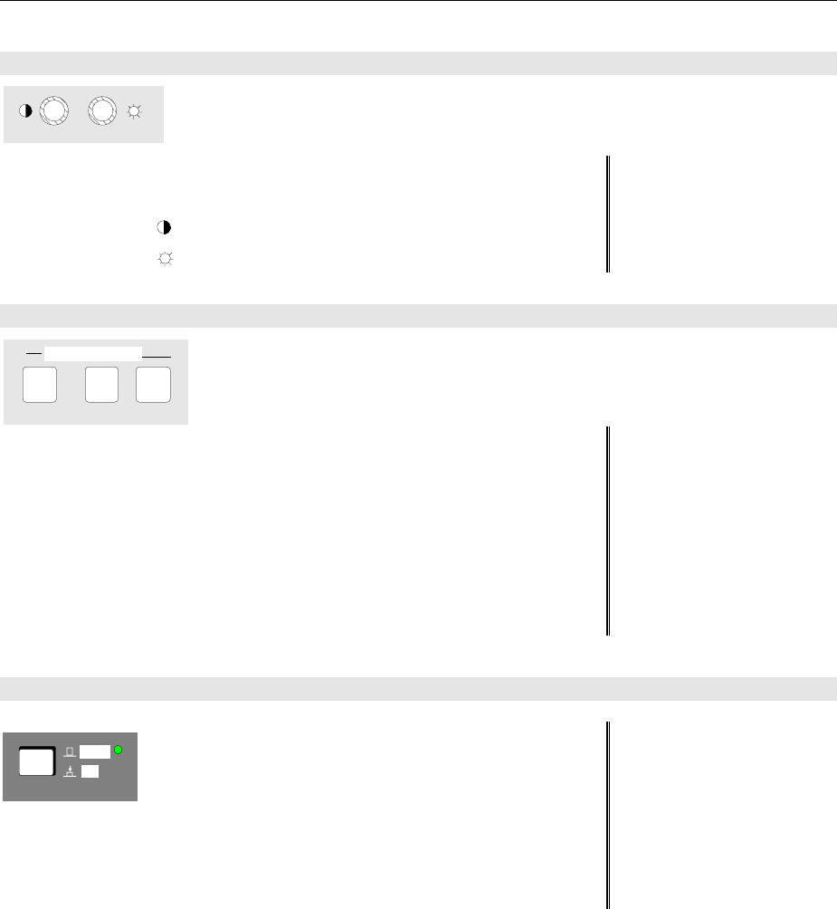
SMIQ Front Panel
1125.5555.03 2.11 E-7
7
Brightness and contrast of the display can be set using
the rotary knobs.
Contrast
Brightness
See as well
Chapter 1
Section "Setting of
Contrast and Bright-
ness of the Display"
8 QUICK SELECT
ASSIGN MENU1 MENU2
QUICK SELECT
The menu-quick-selection keys permit fast access to
two menus selected.
ASSIGN Stores the current menu as menu1
when the MENU1 key is pressed
afterwards or as menu2 when the
MENU2 key is pressed afterwards.
MENU1 Activates menu1 stored.
MENU2 Activates menu2 stored.
See as well
Chapter 2
Section
"Basic Operating
Steps"
9 Switching On/Off
STBY
ON
The On/Off switch switches the instrument from the
standby mode to the ready-for-operation status.
Prerequisite: The power switch at the rear of the
instrument must be switched on.
STBY LED is illuminated in the standby
mode.
see as well
Chapter 1
Section "Switching
On/Off the Instrument"
Chapter 2
Section "Elements of
the Rear Panel, Power
Switch"

Rear Panel SMIQ
1125.5555.03 2.12 E-7
131210 11
21 20 19 18 17 16 15 14
625
PAR DATA
POW RAMP
SYM CLK
IEEE 488
X-AXIS MARKERBLANK
I FADED I/Q AUXQ FADED
LF EXT 2
EXT 1
PULS EXTTUNETRIGGER
RF
REF
RS 232
SER DATA
BIT CLK
DATA
Q
I (BB-AM)
11
REF
BER
Fig. 2-2 Rear panel view
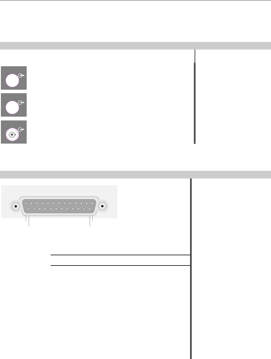
SMIQ Rear Panel
1125.5555.03 2.13 E-7
2.1.3 Elements of the Rear Panel
(Cf. Fig. 2-2, Rear panel view)
10
I FADED I FADED Faded I signal. see as well
Chapter 2,
"Fading Simulation"
Q FADED Q FADED Faded Q signal.
I/Q AUX IQ AUX Output I/Q modulated subcarrier.
Frequency 300 MHz, level -5 dBm,
source resistance 50Ω
11
1
14
13
25
PAR DATA
An adapter between the
PAR DATA connector and
coaxial BNC connectors is
available as an accessory
(SMIQ-Z5, order no.
1104.8555.02).
PAR DATA
Pin Description
1 - ⊥
2 - ⊥
Ground
Ground
3 - DATA-D6
4 - DATA-D4
5 - DATA-D2
6 - DATA-D0
Parallel data input/output D0 to D6 for digital
modulation.
Output: TTL signal.
Input: Input resistance 1kΩ or 50Ω.
Trigger threshold can be set from -2.5 to 2.5V,
max. ± 15V, max. 40 mA
7 - SYMBCLK Symbol clock input/output for synchronization
of the data signal with modulation types with
several bits per symbol.
Output: TTL signal.
Input: Input resistance 1kΩ or 50Ω.
Trigger threshold can be set from -2.5 to 2.5V,
max. ± 15V, max. 40 mA

Rear Panel SMIQ
1125.5555.03 2.14 E-7
131210 11
21 20 19 18 17 16 15 14
625
PAR DATA
POW RAMP
SYM CLK
IEEE 488
X-AXIS MARKERBLANK
I FADED I/Q AUXQ FADED
LF EXT 2
EXT 1
PULS EXTTUNETRIGGER
RF
REF
RS 232
SER DATA
BIT CLK
DATA
Q
I (BB-AM)
11
REF
BER
Fig. 2-2 Rear panel view

SMIQ Rear Panel
1125.5555.03 2.15 E-7
11
PAR DATA
Pin Description
8 - ⊥Ground
9 - LEV-ATT Signal input/output for controlling of level
reduction.
Output: TTL signal.
Input: Input resistance 1kΩ or 50Ω.
Trigger threshold can be set from -2.5 to 2.5V,
max. ± 15V, max. 40 mA
10 - ⊥Ground
11 - TRIGOUT 1 Output for triggering of external instruments.
Output: TTL signal.
12 - ⊥
13 - ⊥
Ground
Ground
14 - TRIGIN Input for triggering of frames, PRBS and data
sequences.
Input: Input resistance 1kΩ or 50Ω.
Trigger threshold can be set from -2.5 to 2.5V,
max. ± 15V, max. 40 mA
15 - DATA-D7
16 - DATA-D5
17 - DATA-D3
18 - DATA-D1
Parallel data input/output D1to D7
see pin 3 - 6
19 - ⊥Ground
20 - BITCLK Output bit clock with operating mode internal.
TTL signal
21 - CW Signal input/output for controlling of
modulation. Switches carrier to CW with FSK
modulation.
Output: TTL signal.
Input: input resistance 1kΩ or 50Ω.
Trigger threshold can be set from -2.5 to 2.5V,
max. ± 15V, max. 40 mA
22 - BURST-
GATE Signal input/output for controlling of the burst
profile.
Output: TTL signal.
Input: input resistance 1kΩ or 50Ω.
Trigger threshold can be set from -2.5 to 2.5V,
max. ± 15V, max. 40 mA
23 - TRIGOUT 2 Output for triggering and controlling of external
instruments.
Output: TTL signal.
24 - TRIGOUT 3 Output for triggering and controlling of external
instruments.
Output: TTL signal.
25 - HOP HOP output provides control signal when
internal frequency hopping is programmed.
Output: TTL signal

Rear Panel SMIQ
1125.5555.03 2.16 E-7
131210 11
21 20 19 18 17 16 15 14
625
PAR DATA
POW RAMP
SYM CLK
IEEE 488
X-AXIS MARKERBLANK
I FADED I/Q AUXQ FADED
LF EXT 2
EXT 1
PULS EXTTUNETRIGGER
RF
REF
RS 232
SER DATA
BIT CLK
DATA
Q
I (BB-AM)
11
REF
BER
Fig. 2-2 Rear panel view
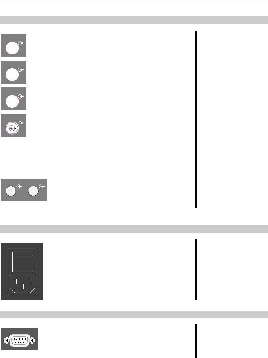
SMIQ Rear Panel
1125.5555.03 2.17 E-7
12
DATA DATA Cut-out, provided to relocate the DATA
input/output at the front to the rear of the
instrument.
BIT CLK BIT CLK Cut-out, provided to relocate the BIT CLK
input/output at the front to the rear of the
instrument.
SYMB CLK SYMB CLK Cut-out, provided to relocate the SYMB
CLK input/output at the front to the rear of
the instrument.
POW RAMP POW RAMP Signal input/output for power ramping.
Input: accepts analog voltages from
0 to 1 V for envelope modulation.
Input resistance 10kΩ
Max. permissible overvoltage ±15 V
Output provides modulation voltage of
burst envelope with internal modulation.
output resistance 10Ω
Max. permissible overvoltage ±15 V
QI (BB_AM) I (BB-AM) Cut-out, provided to relocate the I- input
at the front to the rear of the instrument.
Q Cut-out, provided to relocate the Q- input
at the front to the rear of the instrument.
13
Power switch
ON when pressed at the top ("I")
Power supply connection
see as well
Chapter 1,
Section
"Supply Voltage"
Section
"Switching On/Off the
Instrument"
14
SER DATA
SER DATA Asynchronous data input for digital
modulation.
Interface: RS232 up to 115 kbps
see as well
Annex A
"interfaces"

Rear Panel SMIQ
1125.5555.03 2.18 E-7
131210 11
21 20 19 18 17 16 15 14
625
PAR DATA
POW RAMP
SYM CLK
IEEE 488
X-AXIS MARKERBLANK
I FADED I/Q AUXQ FADED
LF EXT 2
EXT 1
PULS EXTTUNETRIGGER
RF
REF
RS 232
SER DATA
BIT CLK
DATA
Q
I (BB-AM)
11
REF
BER
Fig. 2-2 Rear panel view
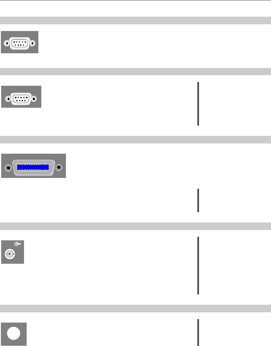
SMIQ Rear Panel
1125.5555.03 2.19 E-7
15
BER Interface for BER Test See as well chapter 2,
section "External Modu-
lation Source AMIQ" and
"Bit Error Rate Test"
16
RS 232
RS-232 RS-232 interface,
used for software update, the loading of
calibration data, and remote control. The
pin assignment corresponds to the pin
assignment of a PC.
see as well
Chapter 3
Remote Control
and
Annex A
"Interfaces"
17
IEC625 IEEE488
IEC 625 IEC-Bus (IEEE 488)
IEEE 488 Remote-control interface See as well
Chapter 3,
"Remote Control"
18
REF
REF Output of the internal 10-MHz reference
signal with reference internal.
Source resistance 50 Ω.
Input for external reference frequency with
reference external. Adjustable to external
reference frequencies from 1 to 16 MHz in
1-MHz steps.
Input resistance 200 Ω.
See as well
Chapter 2,
Section
"Reference Frequency
int/ext"
19
4 optional cut-outs, provided for further
connections
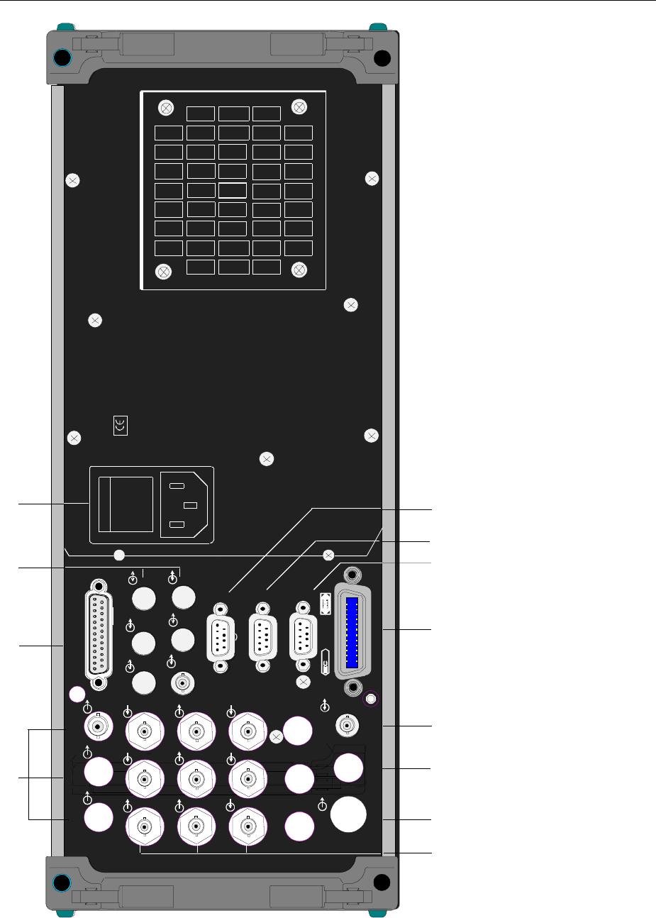
Rear Panel SMIQ
1125.5555.03 2.20 E-7
131210 11
21 20 19 18 17 16 15 14
625
PAR DATA
POW RAMP
SYM CLK
IEEE 488
X-AXIS MARKERBLANK
I FADED I/Q AUXQ FADED
LF EXT 2
EXT 1
PULS EXTTUNETRIGGER
RF
REF
RS 232
SER DATA
BIT CLK
DATA
Q
I (BB-AM)
11
REF
BER
Fig. 2-2 Rear panel view
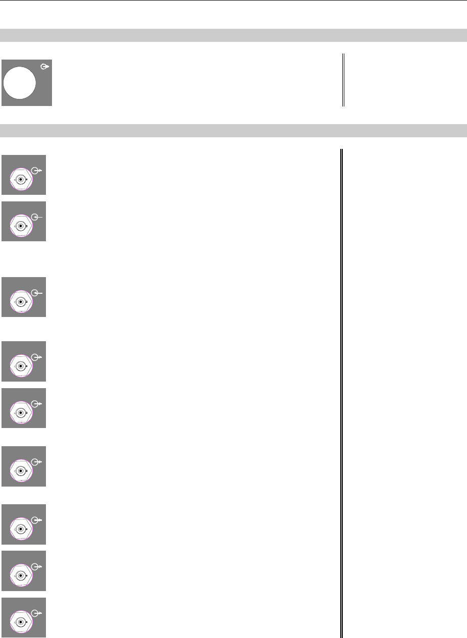
SMIQ Rear Panel
1125.5555.03 2.21 E-7
20
RF RF Cut-out, provided to relocate the RF output
at the front to the rear of the instrument
21
LF LF Output LF signal of the internal LF
generator.
Source resistance < 10 Ω.
EXT 1 EXT1 Input external modulation signal,
alternatively for AM or FM (PM).
Input resistance >100 kΩ.
Nominal voltage: Us = 1 V
Max. permissible overvoltage: ± 15 V
EXT 2 EXT2 Input external modulation signal for FM
(PM).
Input resistance >100 kΩ.
Nominal voltage: Us = 1 V
Max. permissible overvoltage: ± 15 V
X-AXIS X-AXIS Output supplies a voltage ramp of 0 to 10
V, when a sweep is switched on.
BLANK BLANK Output supplies a signal to blank the return
sweep or the settling process in LIST mode
Level: TTL
MARKER MARKER Output is active when the sweep reaches
the marker or at the first step of the LIST
mode. Level: TTL
PULS PULS Input for pulse modulation. Level: TTL
Input resistance 10Ω
TRIGGER TRIGGER Input to trigger sweep, LIST mode and
Memory Sequence. Level: TTL
EXTTUNE EXTTUNE Tuning input for the internal reference
frequency. Voltage range ± 10 V, pulling
range ±1.10-6
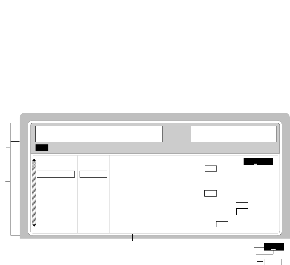
Basic Operating Steps SMIQ
1125.5555.03 E-82.22
2.2 Basic Operating Steps
The operating principle is explained in this section. For better understanding, please read section
"Sample Setting for First Users" (Section 2.2.10) in addition.
To operate the instrument, menus are called in the display. All setting possibilities and the current
setting status are evident from the menus. All settings can be made by accessing the menus.
RF frequency and RF level can also be set without menu operation using keys [FREQ] and [LEVEL].
RF signal and modulation can also be switched on/off without menu operation using keys [RF ON/OFF]
and/or [MOD ON/OFF].
2.2.1 Design of the Display
AM
BB-AM
FM
PM
PULSE
FREQ 100. 000 000 0 MHz LEVEL - 30.0 dBm
FM1 DEVIATION
FM1 SOURCE
LFGEN FREQ
FM2 DEVIATION
FM2 SOURCE
EXT1 COUPLING
EXT2 COUPLING
PREEMPHASIS
FM
1.00 kHz
OFF INT EXT1 EXT2
1.000 0 kHz
10.0 kHz
OFF EXT1 EXT2
AC DC
AC DC
OFF 50µ 75µ s
1
2
3
Main menu Submenu Setting menu
1 Header field
2 Status line
3 Menu fields
Menu cursor
Digit cursor
Select mark
FREQUENCY
LEVEL
ANALOG MOD
VECTOR MOD
DIGITAL MOD
DIGITAL STD
LF OUTPUT
SWEEP
LIST
MEM SEQ
UTILITIES
Fig. 2-3 Design of the display
Header field (1)The header field of the display indicates frequency and level of the RF output signal
which considers the offset value. In the RF-sweep operating mode, the start and stop
frequencies are displayed in two lines one above the other. The start and stop levels
are indicated in the LEVEL-sweep operating mode correspondingly. A two-line level
display appears for digital modulation or digital standard. The upper line indicates the
average power (LEVEL), the lower line the peak envelope power (PEP) of the
modulated RF output signal.
Status line (2) The status line below describes operating mode and operating state of the instrument.
Error messages and notes for caution are also displayed in the status line.

SMIQ Basic Operating Steps
1125.5555.03 E-82.23
Menu fields (3)The indication fields below the header field are reserved for the menu representations.
The image contents of these fields change as a function of the menu selected. The
field at the left-hand display margin is occupied with the main menu, the topmost level
of the menu structure. The main menu is always faded in.
Each further field adjacent at the right contains submenus.
The field ending with the right-hand display margin shows the setting menu. In this
menu all setting values and setting states connected with the menu selected are
indicated. When accessing submenus, the higher-order menus remain in the display.
The current menu path is evident through the select marks.
Menu cursor The menu cursor shows the user at which position in the menu he is.
The position of the menu cursor is evident from the inverse notation of
the term (white characters on a black background)
Digit cursor As an underscore, the digit cursor marks the position which can be
varied by means of the rotary knob in a value indication.
Select mark The frame around a term marks current menus or valid settings in the
setting menu.
2.2.2 Calling the Menus
Accessing the menus is effected using rotary knob [VARIATION], [SELECT] key and [RETURN] key.
Rotary knob Rotary knob [VARIATION] moves the menu cursor over the positions of a menu level
to be selected. If a scrollbar is visible at the left-hand margin of a menu, the menu is
larger than the screen window. If the menu cursor is moved to the margin of the
screen window, the covered lines become visible.
[SELECT] key The [SELECT acknowledges the selection marked by means of the menu cursor.
[RETURN] key The [RETURN] key
- returns the menu cursor to the next higher menu level. The menu cursor is shifted
to the left into the preceding column of the menu structure.
- resets the menu cursor from frequency or level value indication in the header field
into the menu field to the menu called last.
- closes the display pages called using keys [STATUS], [HELP] and [ERROR] again.
Settings are accessed in the setting menus ending with the right-hand display margin.
AM DEPTH
AM SOURCE INT
AM SOURCE EXT
AM EXT COUPLING
LFGEN FREQ
FREQ 100. 000 000 0 MHz LEVEL - 30.0 dBm
AM
30.0 %
OFF INT
OFF EXT1
AC DC
1.000 0 kHz
FREQUENCY
LEVEL
ANALOG MOD
VECTOR MOD
DIGITAL MOD
DIGITAL STD
LF OUTPUT
SWEEP
LIST
MEM SEQ
UTILITIES
AM
BB-AM
FM
PM
PULSE
Fig. 2-4 MODULATION-AM menu

Basic Operating Steps SMIQ
1125.5555.03 E-82.24
2.2.3 Selection and Change of Parameters
Select parameter ØSet the menu cursor to the name of the parameter desired using the rotary
knob, e.g. to AM DEPTH in the AM menu, Fig. 2.4.
Change setting
value
ØVia value input or using rotary knob.
via value inputs ØPress the first digit of the new value or minus sign.
The old value is deleted, the entry is indicated in the marked field.
ØEnter further digits.
ØTerminate the input using a unit key or, in the case of inputs in the base unit
or in the case of inputs without unit, using the [1x/Enter] key.
The menu cursor wraps back to the appropriate parameter.
using rotary knob ØPress the [SELECT] key.
ØThe menu cursor changes from the parameter selected in the left-hand
column of the setting menu to the setting value on the right, e.g. from AM
DEPTH to 30%, Fig. 2-4.
ØSet the underscore to the position of the setting value to be varied using
keys [ð] [ï].
ØTurn the rotary knob.
The position underscored is varied in steps of 1.
Note: RF frequency and RF level can also be varied in a step width which
can be defined arbitrarily using the rotary knob. In the respective
setting menu (FREQUENCY or LEVEL) the step width is entered as
KNOB STEP USER and the KNOB STEP set from DECIMAL to
USER. To point to the fact that the step width has been converted to
the value programmed, the underscore as a symbol of the digit
cursor disappears in the respective value indication.
1-out-of-n selection ØSelect parameters.
ØPress the [SELECT] key.
The menu cursor changes from the parameter selected in the left-hand
column of the setting menu to the current selection on the right, e.g. from
AM SOURCE EXT to OFF, Fig. 2-4.
ØSet the menu cursor to the position desired within the 1-out-of-n selection
using the rotary knob or cursor keys [⇐] [Þ].
ØPress the [SELECT] key.
The setting is made.
The selection mark which has marked the setting valid up to now wraps to
the new position.
ØPress the [RETURN] key.
The menu cursor wraps back to the respective parameter.

SMIQ Basic Operating Steps
1125.5555.03 E-82.25
Quick selection of
a parameter The quick selection of a parameter reduces the number of operating steps if
several parameters are set successively. The menu cursor can directly be set
further from line to line in the column of the setting values by pressing the
[SELECT] key.
The menu cursor wraps from the setting value of a parameter to the setting
value of the parameter in the next line.
The column of the setting values can be exited at each position by pressing
the [RETURN] key.
2.2.4 Triggering Action
Lines in the setting menu which are marked with the " " symbol at the end of the line qualify an action
which can be carried out. Instruction SEARCH ONCE in the LEVEL-ALC menu, e.g., switches on
level control for level calibration for a short period of time.
Trigger action ØSet the menu cursor to the respective instruction.
ØPress the [SELECT] key.
The action is triggered.
While the action is carried out, the instruction remains framed by the
selection mark.
2.2.5 Quick Selection of Menu (QUICK SELECT)
The keys of the QUICK SELECT control field are used to call selected menus quickly by one keystroke.
Store menus ØEstablish the desired operating status of the current menu.
ØPress the [ASSIGN] key.
ØPress key [MENU1] or [MENU2].
The current menu is stored as menu1 or menu2. That is to say, 2 menus
can be stored in total.
Call menus ØPress key [MENU1] or [MENU2].
Menu1 or menu2 stored is displayed. Exactly the operating status which was
current at the point of time of storing is reconstructed.

Basic Operating Steps SMIQ
1125.5555.03 E-82.26
2.2.6 Use of [FREQ] and [LEVEL] Keys
RF frequency and RF level can be set without menu operation as well using direct keys [FREQ] and
[LEVEL]. The input value considers the offset, see Sections 2.4 and 2.5.
Key [FREQ]/ [LEVEL] ØPress the [FREQ] or [LEVEL] key.
The frequency and/or the level indication in the header field of the display
is marked.
The current menu at the display is maintained.
ØAlter the value via a value input or the rotary knob.
ØPress the [RETURN] key.
The menu cursor wraps to the position marked last in the menu.
2.2.7 Use of [RF ON/OFF] and [MOD ON/OFF] Keys
RF signal and modulation can be switched on/off without menu operation as well using direct keys
[RF ON/OFF] and/or [MOD ON/OFF] (see Sections [RF ON/OFF] key and [MOD ON/OFF] key as well).
Key [RF ON/OFF] ØPress the [RF ON/OFF] key.
The RF output signal is switched on/off.
IEC-bus-short command: :OUTP OFF
Key [MOD ON/OFF] ØPress the [MOD ON/OFF] key.
The modulation is switched on/off.
An IEC-bus command is not available. The modulations have to be switched
on and off in the respective modulation sub menus
2.2.8 [ENTER] Key – Special Toggle Function
This additional function of the [ENTER] key facilitates parameter changes.
Some selection parameters can now be selected using the [ENTER] key, and no longer have to be
activated beforehand with [SELECT].
2.2.9 Changing Unit of Level
For the level, the unit of the value set can be changed without a new value input.
Change level unit ØActivate LEVEL parameter.
- Press the [LEVEL] key or
- set the menu cursor in the LEVEL menu to the setting value of the
AMPLITUDE parameter.
ØPress the unit key with the desired level unit.
The level is indicated in the desired unit.

SMIQ Sample Setting for First Users
1125.5555.03 E-82.27
2.2.10 Correction of Input
Digital entries can be corrected by one of the following keys before terminating the input:
Key [-/ç
çç
ç]The backspace key deletes the value entered digit by digit. When the last
digit is deleted, the previous value is displayed.
Key [RETURN] Pressing the [RETURN] key deletes the entire entry and results in the
previous value being indicated again.
For a subsequent new input in the setting menu, the first digit of the new
value is to be entered.
For a subsequent new input via the [FREQ] or [LEVEL] keys, the respective
key has to be pressed again.
Key [FREQ]/ [LEVEL] In the case of a frequency or level input by means of the [FREQ] or [LEVEL]
keys, pressing the [FREQ] and/or [LEVEL] key again deletes the entire input.
2.2.11 Sample Setting for First Users
First users most quickly become familiar with the operation of the instrument if they execute the pattern
setting of this section.
First frequency and level of the RF output signal are set via keys [FREQ] and [LEVEL] in the DATA
INPUT field:
- Frequency 250 MHz
- Level 10 dBm
Operating steps Explanations
PRESET
Reset the instrument to the defined
state.
502
FREQ
Mµ
DATA INPUT
Set the frequency to 250 MHz. The
menu cursor marks the permanent
frequency indication.
01
LEVEL
DATA INPUT
x1
ENTER
Set the level to 10 dBm. The menu
cursor marks the permanent level
indication.
RETURN
Reset the menu cursor to the menu
field.
Sample Setting for First Users SMIQ
1125.5555.03 E-82.28
The output signal is to be amplitude-modulated next.
- AM modulation depth 15.5 %
- Modulation frequency 3 kHz
Operating steps Explanations
.
ANALOG MOD
.
M
E
N
U /
V
ARIA
T
IO
N
SELECT
M
E
NU
/ V
AR
I
A
T
ION
Select ANALOG MOD menu.
ØSet menu cursor to ANALOG
MOD using the rotary knob and
subsequently press
[SELECT] key.
The submenu is displayed.
.
AM
.
M
E
NU
/ V
A
RI
A
T
I
O
N
SELECT
M
E
NU
/ V
A
RI
A
T
I
O
N
Select AM submenu
The AM setting menu is displayed.
.
AM DEPTH
.
MENU / VARIATION Select AM DEPTH parameter.
The menu cursor marks the setting
value.
DATA INPUT
x1
ENTER
15
5
.
Enter modulation depth 15.5 % and
press [x1 ENTER].
The menu cursor is reset to AM
DEPTH.
.
AM SOURCE INT
.
M
E
NU
/ V
A
RI
A
T
I
O
N
SELECT
M
E
NU
/ V
A
RI
A
T
I
O
N
Select AM SOURCE INT.
The menu cursor marks the current
1-out-of-n selection.
SMIQ Sample Setting for First Users
1125.5555.03 E-82.29
Operating steps Explanations
SELECT
. INT
MENU / VARIATION
MENU / VARIATION
Select INT 1 as internal modulation
source.
The selection mark marks INT. AM is
faded in the status line as a hint that
AM is switched on.
RETURN
Reset menu cursor to AM SOURCE
INT.
.
LFGEN FREQ
.
MENU / VARIATION Select parameter LFGEN FREQ.
DATA INPUT
3
km
Enter frequency 3 kHz and press unit
key.
The indications on the display are
represented in Fig. 2-5.
The AM modulation setting is
completed.
AM DEPTH
AM SOURCE INT
AM SOURCE EXT
AM EXT COUPLINGLFGEN FREQ
FREQ 250. 000 000 0 MHz LEVEL - 10.0 dBm
AM
15.5 %
OFF INT
OFF EXT1
AC DC
3.000 0 kHz
FREQUENCY
LEVEL
ANALOG MOD
VECTOR MOD
DIGITAL MOD
DIGITAL STD
LF OUTPUT
SWEEP
LIST
MEM SEQ
UTILITIES
AM
BB-AM
FM
PM
PULSE LFGEN FREQ
Fig. 2-5 Display after AM setting
Sample Setting for First Users SMIQ
1125.5555.03 E-82.30
Subsequently to the above setting, 420 MHz as new RF frequency and 12.5 kHz as the step width for
the RF frequency variation are set in the following. Parameter quick select is used, which reduces the
number of operating steps.
Operating steps Explanations
RETURN RETURN Reset the menu cursor to the main
menu in 2 steps.
SELECT
.
FREQUENCY
.
MENU / VARIATION
MENU / VARIATION
Select FREQUENCY menu.
The frequency setting menu is
displayed.
.
FREQUENCY
.
MENU / VARIATION Select FREQUENCY parameter.
The menu cursor marks the setting
value.
20
4
Mµ
DATA INPUT
Enter frequency 420 MHz and press
unit key.
.
KNOB STEP USER
.
MENU / VARIATION Set menu cursor to parameter KNOB
STEP USER.
5
.
2
km
DATA INPUT
1
Enter step width 12.5 kHz. Press unit
key.
SMIQ Sample Setting for First Users
1125.5555.03 E-82.31
Operating steps Explanations
.
KNOB STEP
.
MENU / VARIATION Set menu cursor to parameter KNOB
STEP.
SELECT
Set menu cursor to the current KNOB
STEP selection.
SELECT
.
USER
.
MENU / VARIATION
MENU / VARIATION
Select USER (user-defined step
width).
The selection mark marks USER.
This results in step width 12.5 kHz
being used in the case of variation
using the rotary knob.
RETURN RETURN Reset the menu cursor to the main
menu in 2 steps.
FREQUENCY
OFFSET
KNOB STEP USER
KNOB STEP
EXCLUDE FROM RCL ON OFF
FREQ
420. 000 000 0
MHz LEVEL
10.0
dBm
AM
420.000 000.0 MHz
0.0 Hz
12.500 0 kHz
DECIMAL USER
FREQUENCY
FREQUENCY
LEVEL
ANALOG MOD
VECTOR MOD
DIGITAL MOD
DIGITAL STD
LF OUTPUT
SWEEP
LIST
MEM SEQ
UTILITIES
Fig. 2-6 Display after pattern setting

List Editor SMIQ
1125.5555.03 E-82.32
2.2.12 List Editor
The SMIQ offers the possibility to generate lists. Lists are used for setting sequences LIST mode or
(memory sequence), as data source for digital modulations or for level correction which can be defined
by the user (UCOR). They consist of elements which are defined by an index and at least one
parameter per index. Each list is marked by a separate name and can be selected via this name. The
lists are accessed in the menus assigned in each case, e.g. to the settings sequences of instrument
settings in the MEM SEQ menu. However, the lists are always generated and processed in the same
way and the procedures are hence explained in detail by the example of the memory sequence mode
(menu MEM SEQ) in this section. A pattern setting at the end of this section allows the user to become
familiar with the operation of the list editor.
Setting menus providing list processing are structured in two pages:
The first page, called OPERATION page in the following contains the general configuration parameters
for processing a list. Further, the general list functions such as selecting and deleting the list as well as
calling an editing mode are provided. The second page, the EDIT page, is automatically displayed when
calling an edit function and serves to enter and modify the parameters of the list.
The OPERATION page has a similar arrangement with all list editors. As an example, the OPERATION
page of the MEM SEQ menu is shown:
Menu selection: MEM SEQ
LEVEL - 30.0
100. 000 000 0
FREQ MHz dBm
MODE OFF AUTO SINGLE STEP EXT-SINGLE EXT-STEP
RESET SEQUENCE
CURRENT INDEX 1
SELECT LIST... CURRENT: MSEQ2
DELETE LIST...
FUNCTION FILL INSERT DELETE EDIT/VIEW
FREQUENCY
LEVEL
ANALOG MOD
VECTOR MOD
DIGITAL MOD
DIGITAL STD
LF OUTPUT
SWEEP
LIST
MEM SEQ
UTILITIES
Fig. 2-7 OPERATION page of the MEM SEQ menu
The settings for MODE, CURRENT INDEX, etc. are irrelevant for the general description of the list
editors and are described in greater detail in Section 2.10, MEMORY SEQUENCE mode.
The last three menu lines of the OPERATION page always exist and are reserved for selecting and
deleting lists as well as for calling the edit functions (and hence the EDIT page).
SELECT LIST Opens a selection window in which a list can be selected from the existing lists or a
new, empty list can be generated. In this line the active list is always displayed.

SMIQ List Editor
1125.5555.03 E-82.33
DELETE LIST Opens a selection window in which the list to be deleted can be selected.
FUNCTION Selection of the edit function for processing the lists. The EDIT page is
automatically called through the selection (cf. Section 2.2.11.3).
FILL Filling a list with elements.
INSERT Insertion of elements into a list.
DELETE Deletion of elements of a list.
EDIT/VIEW Editing the single elements.
2.2.12.1 Select and Generate - SELECT LIST
SELECT LIST opens a selection window in which either an existing list can be selected or a new, empty
list can be generated (cf. Fig. 2-8). By pressing the [RETURN] key, the selection window is closed
without changing the setting.
Select list ØMark the list desired using the rotary knob.
ØPress [SELECT] key.
The selected list is included in the instrument setting. The selection window
is closed. The selected list is displayed under CURRENT.
Generate list ØMark CREATE NEW LIST using rotary knob.
ØPress [SELECT] key.
A new empty list is automatically generated which can be filled using
functions FILL or EDIT. The selection window is closed. The new list is
displayed under CURRENT.
No modification
of the setting
ØPress [RETURN] key.
Selection: SELECT LIST
LEVEL
- 30.0
100. 000 000 0
FREQ MHz
dBm
MODE OFF AUTO SINGLE
EXECUTE SINGLE MODE
RESET
CURRENT INDEX
SELECT LIST...
DELETE LIST...
FUNCTION
CREATE NEW LIST
MSEQ1 199
MSEQ2 100
MSEQ3 1
MSEQ4 123
FREQUENCY
LEVEL
ANALOG MOD
VECTOR MOD
DIGITAL MOD
DIGITAL STD
LF OUTPUT
SWEEP
LIST
MEM SEQ
UTILITIES
Fig. 2-8 SELECT-LIST-selection window

List Editor SMIQ
1125.5555.03 E-82.34
CREATE NEW LIST Generating a new list. The name of the list cannot be selected freely in the
case of manual control. A definite list name is automatically generated in the
following form:
MSEQ<n>, with <n> ∈ {0..9}, e.g. MSEQ1 (with Memory Sequence)
This applies correspondingly to the other operating modes. In the case of
level correction mode, UCOR1 would be generated for example. If a list is
created via IEC bus, an arbitrary list name can be given (cf. Section 3).
Unrestricted access is also possible by means of the selection window.
MSEQ2 100 The list currently set is marked in the selection window by means of the
selection mark, here MSEQ2. In addition to the list name, the length of the list
is given, here 100 elements.
2.2.12.2 Deletion of Lists - DELETE LIST
DELETE LIST opens a selection window in which the list to be deleted can be selected. The lists are
represented together with their name and their length (cf. Fig. 2-9). By pressing the [RETURN] key the
selection window is exited without deleting a list.
Delete list ØMark desired list using the rotary knob.
ØPress [SELECT] key.
The prompt "enter [SELECT] to delete list/sequence?" is displayed
Ø Press [SELECT] key.
The list is deleted. If the prompt is acknowledged with the [RETURN] key,
however, the list is not deleted. The selection window is automatically
closed due to the acknowledgment of the prompt.
Selection: DELETE LIST
LEVEL
- 30.0
100. 000 000 0
FREQ MHz
dBm
MODE OFF AUTO SINGLE
RESET SEQUENCE
CURRENT INDEX
SELECT LIST...
DELETE LIST...
FUNCTION
MSEQ1 199
MSEQ2 100
MSEQ3 1
MSEQ4 123
FREQUENCY
LEVEL
ANALOG MOD
VECTOR MOD
DIGITAL MOD
DIGITAL STD
LF OUTPUT
SWEEP
LIST
MEM SEQ
UTILITIES
Fig. 2-9 DELETE-LIST selection window

SMIQ List Editor
1125.5555.03 2.35 E-8
2.2.11.3 Edition of Lists
Due to the selection of an edit mode on the OPERATION page the EDIT page is automatically activated.
When the EDIT/VIEW function is selected, the largest possible section of the list is displayed (cf. Fig.
2-10). In the case of block functions FILL, INSERT and DELETE, an input window is additionally
displayed (cf. Fig. 2-11 to 2-13).
Functions SELECT LIST and FUNCTION are available on the EDIT page as on the OPERATION page.
Return to the OPERATION page is effected by pressing the [SELECT] key twice.
Single-value function EDIT/VIEW
By selecting the EDIT/VIEW function, the entire list can be viewed or modifications of single values be
carried out.
If the cursor marks a value in the INDEX column of the list, the EDIT mode is exited by pressing the
[RETURN] key. The menu cursor then marks FUNCTION again.
There is no separate function for storing the list. This means that every modification of the list is
transferred to the internal data set and has an effect on exiting the EDIT/VIEW function.
Menu selection: FUNCTION EDIT/VIEW
DELETE
FREQ 100. 000 000 0 MHz LEVEL -30.0 dBm
INSERTFILL EDIT/VIEW
FREQUENCY
LEVEL
ANALOG MOD
VECTOR MOD
DIGITAL MOD
DIGITAL STD
LF OUTPUT
SWEEP
LIST
MEM SEQ
UTILITIES
SELECT LIST... CURRENT: MSEQ2
FUNCTION
-INDEX - FREE 246 - LEN 10 MEMORY DWELL
0001 09 50 ms
0002 02 50 ms
0003 01 60 ms
0004 23 60 ms
0005 09 85 ms
0006 10 85 ms
0007 08 85 ms
0008 11 85 ms
Fig. 2-10 Edit function EDIT/VIEW
INDEX Position in the list
FREE Space available. FREE 256 means that space for 256 parameter elements is
available in the list memory in total.
LEN Occupied space. LEN 0 means that the current list occupies 0 elements in the
list memory.
MEMORY DWELL Identification of the column below. The number and name of parameter
columns is different for the various list editors.

List Editor SMIQ
1125.5555.03 2.36 E-8
Select parameters ØMark the index associated to the parameter using the rotary knob or directly
enter the value of the index via the numeric keys.
ØPress [SELECT] key.
Parameter MEMORY is marked. If the second parameter DWELL is to be
marked, press the [SELECT] key again.
Modify parameters ØVary the value of the parameter selected using the rotary knob or enter the
value directly using numeric keys.
Note: The binary data of the digital modulations which cannot be varied
are an exception. Further, all numeric keys except for "0" and "1" are
ineffective in these cases.
ØPress the [ENTER] key or unit keys.
The value is included in the data set. The menu cursor marks the value of
the next column. In the last column, the menu cursor then marks the next
line of column MEMORY.
ØPress the [RETURN] key.
The menu cursor wraps back to the INDEX column. The EDIT mode is
exited by repeatedly pressing the [RETURN] key (cf. Section 2.2.11.4).
Block function FILL
Using function FILL, a parameter, e.g. MEMORY, is overwritten with constant or linearly
increasing/decreasing values within a defined range. The input window is exited by pressing the
[RETURN] key without a modification being carried out.
If the filler range exceeds the end of the list, the list is automatically extended.
The list entry, in the example for MEMORY, with index [AT +n] is calculated as follows from the
information AT, RANGE, starting value (MEMORY) and WITH INCREMENT:
MEMORY[AT+n] = starting value (MEMORY)+ n · increment | (0 ≤ n ≤ RANGE1)
Selection: FUNCTION-FILL
FREQ 100. 000 000 0 MHz LEVEL - 30.0 dBm
SELECT LIST...
FUNCTION
-INDEX - FREE 246 - LEN 10
0001
0002
0003
0004
0005
0006
0007
0008
FILL AT 10 RANGE 1
PARAMETER MEMORY DWELL
MEMORY 1
WITH INCREMENT 0
EXECUTE
FREQUENCY
LEVEL
ANALOG MOD
VECTOR MOD
DIGITAL MOD
DIGITAL STD
LF OUTPUT
SWEEP
LIST
MEM SEQ
UTILITIES
Fig. 2-11 Block function FILL: Input window

SMIQ List Editor
1125.5555.03 2.37 E-8
FILL AT Setting the filling range.
AT Lower limit (index)
RANGE Number of the elements to be inserted
PARAMETER Selection on which of the parameters the filling function is to have an effect.
This menu option is eliminated if the list only includes elements with one
parameter.
MEMORY
or DWELL Input of the starting value for the parameter selected. This option is only
displayed if a selection has been made under PARAMETER MEMORY or
DWELL.
WITH INCREMENT Input of the increment between two successive values. If 0 is entered as
increment, a filling procedure with constant values is achieved. This option is
only displayed if a selection has been made under PARAMETER MEMORY or
DWELL.
Note: In the case of some types of lists, e.g. digital modulation data, indicating
an increment is eliminated since there are binary data. In these cases
line WITH INCREMENT is eliminated.
EXECUTE Starts the filling sequence. After the function has been executed, the input
window is automatically exited. The current index points to the first element
after the processed range.
Filling a list After selection of function FILL, the menu cursor marks FILL AT.
ØPress the [SELECT] key.
The menu cursor marks the value at AT.
ØVary index value using the rotary knob or enter using the numeric keys and
the [ENTER] key.
ØPress the [SELECT] key.
The menu cursor marks the value at RANGE.
ØVary value using the rotary knob or enter using the numeric keys and the
[ENTER] key.
ØPress the [SELECT] key.
The menu cursor marks MEMORY or DWELL in input line PARAMETER.
ØSelect MEMORY using the rotary knob (if not yet marked) and press the
[SELECT] key.
The menu cursor marks the value in input line MEMORY.
ØVary starting value for column MEMORY using the rotary knob or enter
using the numeric keys and the [ENTER] key.
ØPress the [SELECT] key
The menu cursor marks the value in input line WITH INCREMENT.
ØVary the value of the increment desired using the rotary knob or enter using
the numeric keys and the [ENTER] key.
ØPress the [RETURN] key.
ØMark the action EXECUTE
ØPress the [SELECT] key.
The filling sequence is initiated. After the function has been carried out, the
input window is automatically exited. The menu cursor marks FUNCTION.
The EDIT page shows the end of the range that has been filled right now.
List Editor SMIQ
1125.5555.03 2.38 E-8
Block function INSERT
Function INSERT inserts the desired number of elements with constant or linearly increasing/decreasing
values before the element with the given starting index. All elements which had been stored from the
starting index are shifted to the end of the range to be inserted.
Input is effected analogously to filling a list.
By pressing the [RETURN] key the input window is exited without a modification being effected. The
menu cursor then marks FUNCTION.
The list entry, in the example for MEMORY, with index [AT +n] is calculated as follows from the
information AT, RANGE, starting value (MEMORY) and WITH INCREMENT:
MEMORY[AT+n] = starting value (MEMORY) + n · Increment | (0 ≤ n ≤ RANGE-1)
Selection: FUNCTION INSERT
FREQ 100. 000 000 0 MHz LEVEL - 30.0 dBm
SELECT LIST...
FUNCTION
-INDEX - FREE 256 - LEN 10
0001
0002
0003
0004
0005
0006
0007
0008
INSERT AT 10 RANGE 2
MEMORY 1
WITH INCREMENT 0
DWELL 100ms
WITH INCREMENT 0.0ms
EXECUTE
FREQUENCY
LEVEL
ANALOG MOD
VECTOR MOD
DIGITAL MOD
DIGITAL STD
LF OUTPUT
SWEEP
LIST
MEM SEQ
UTILITIES
Fig. 2-12 Edit function INSERT: Input window
INSERT AT Input of the starting index and the number of the elements to be inserted.
AT Starting index before which the insert operation is to be effective.
RANGE Number of the elements to be inserted
MEMORY Input of the starting value for MEMORY.
DWELL Input of the starting value for DWELL.
WITH INCREMENT Input of the increment between two successive values for MEMORY or
DWELL. If 0 is indicated as increment, constant values are achieved to be
inserted RANGE times.
Note: In the case of some types of lists, e.g. digital modulation data, indicating
an increment is eliminated since there are binary data. In these cases
all lines WITH INCREMENT are eliminated.
EXECUTE Starts the inserting sequence. After the function has been executed, the input
window is automatically exited. The menu cursor marks FUNCTION. The EDIT
page shows the beginning of the range that has moved forward.
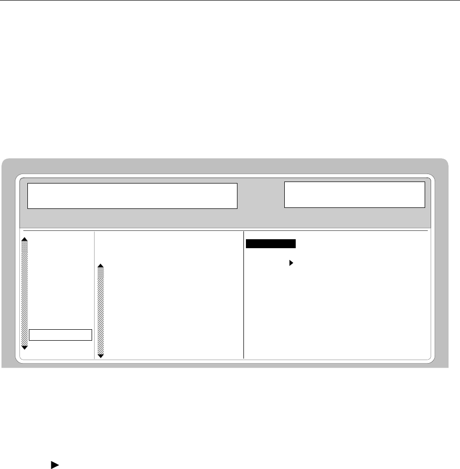
SMIQ List Editor
1125.5555.03 2.39 E-8
Block function DELETE
Function DELETE deletes the elements of the range indicated. This does not leave a gap in the list but
the remaining elements move forward. If the given range exceeds the end of the list, deletion until the
end of the list is effected.
Input is analog to filling a list.
By pressing the [RETURN] key, the input window is exited without a modification being carried out. The
menu cursor then marks FUNCTION.
Selection: Function DELETE
FREQ 100. 000 000 0 MHz LEVEL - 30.0 dBm
SELECT LIST...
FUNCTION
-INDEX - FREE 256 - LEN 10
0001
0002
0003
0004
0005
0006
0007
0008
DELETE AT 10 RANGE 2
EXECUTE
FREQUENCY
LEVEL
ANALOG MOD
VECTOR MOD
DIGITAL MOD
DIGITAL STD
LF OUTPUT
SWEEP
LIST
MEM SEQ
UTILITIES
Fig. 2-13 Edit function DELETE: Input window
DELETE AT Input of the block of the list to be deleted
AT Lower limit (INDEX)
RANGE Number of elements to be deleted.
EXECUTE Starts the deletion. After the function has been executed, the input window is
automatically exited. The menu cursor marks FUNCTION. The EDIT page
shows the beginning of the range that has moved forward.
2.2.11.4 Pattern Setting to Operate the List Editor
The user can become familiar with the operation of the list editor by means of the following pattern
setting in the MEM SEQ menu. A list has to be generated and filled with values by using the single-value
function EDIT/VIEW:
•Memory location number of the first element 20
•Dwell time of the first element 15 s
•Memory location number of the second element 7.
When the setting has been terminated, return to the OPERATION page of the MEM SEQ menu.
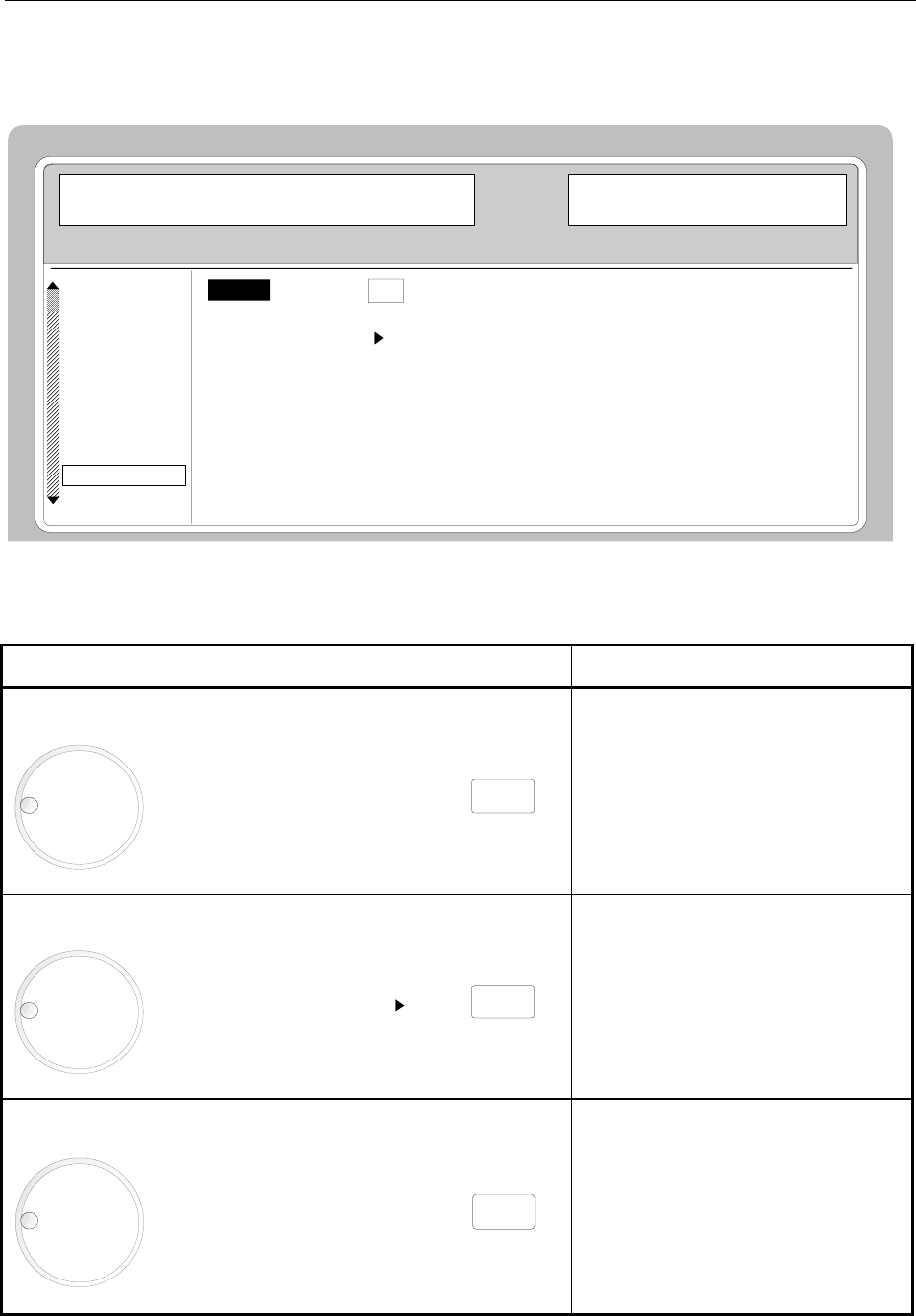
List Editor SMIQ
1125.5555.03 2.40 E-8
At the beginning of the operation sequence, menu MEM SEQ is called. First a list MSEQ0 has to be
generated and then activated. The menu cursor marks a parameter of the setting menu on the
OPERATION page (c.f. Fig. 2-14).
LEVEL - 30.0
100. 000 000 0
FREQ MHz dBm
MODE OFF AUTO SINGLE STEP EXT-SINGLE EXT-STEP
RESET SEQUENCE
CURRENT INDEX 1
SELECT LIST... CURRENT: NONE
DELETE LIST...
FUNCTION FILL INSERT DELETE EDIT/VIEW
FREQUENCY
LEVEL
ANALOG MOD
VECTOR MOD
DIGITAL MOD
DIGITAL STD
LF OUTPUT
SWEEP
LIST
MEM SEQ
UTILITIES
Fig. 2-14 Starting point of the pattern setting
Operating steps Explanations
SELECT
.
SELECT LIST...
.
MENU / VARIATION
MENU / VARIATION Select the SELECT LIST menu item.
SELECT
CREATE NEW LIST
MENU / VARIATION
MENU / VARIATION A new list MSEQ0 is generated. The
menu cursor is reset to SELECT
LIST...
SELECT
.
FUNCTION...
.
MENU / VARIATION
MENU / VARIATION
Select the FUNCTION menu item.
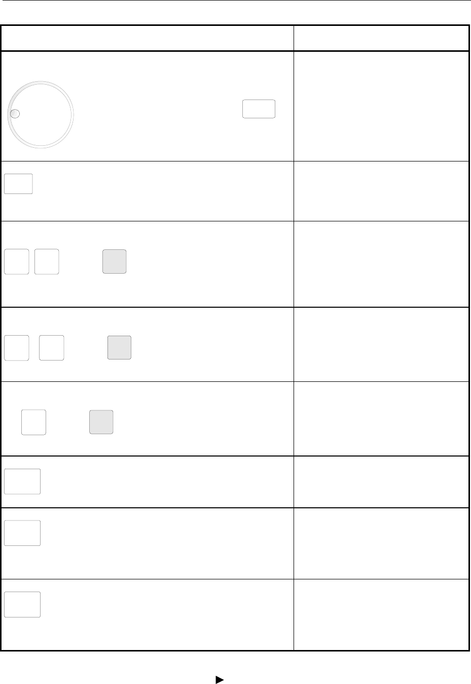
SMIQ List Editor
1125.5555.03 2.41 E-8
Operating steps Explanations
SELECT
.EDIT VIEW.
MENU / VARIATION
MENU / VARIATION Select single-value function
EDIT/VIEW.
The EDIT page of the MEM SEQ
menu is called. The menu cursor
marks the index of the first element
of list MSEQ0.
SELECT
Set the menu cursor to the memory
location number value of the first
element (c.f. Fig. 2-15,A).
DATA INPUT
x1
ENTER
2
0
Enter MEMORY 20.
The menu cursor automatically wraps
to the DWELL value of the first
element (Fig. 2-15,B). The default
value is 100 ms.
DATA INPUT
x1
ENTER
5
1
Enter DWELL 15 s.
The menu cursor automatically wraps
to the MEMORY value of the second
element.
DATA INPUT
x1
ENTER
7
Enter MEMORY 7.
The menu cursor automatically wraps
to the DWELL value of the second
element (default value is 100 ms).
RETURN
Reset the menu cursor to the index.
RETURN
Reset the menu cursor to the
FUNCTION menu item of the EDIT
page of menu MEM SEQ (c.f. Fig. 2-
15,C).
RETURN
Reset the menu cursor to the
FUNCTION menu item of the
OPERATION page of menu MEM
SEQ.
Note: With the return to the OPERATION page the operation of the list editor is finished. In the list
mode (menu LIST), function LEARN must be activated subsequently to ensure that the
settings are transferred to the hardware
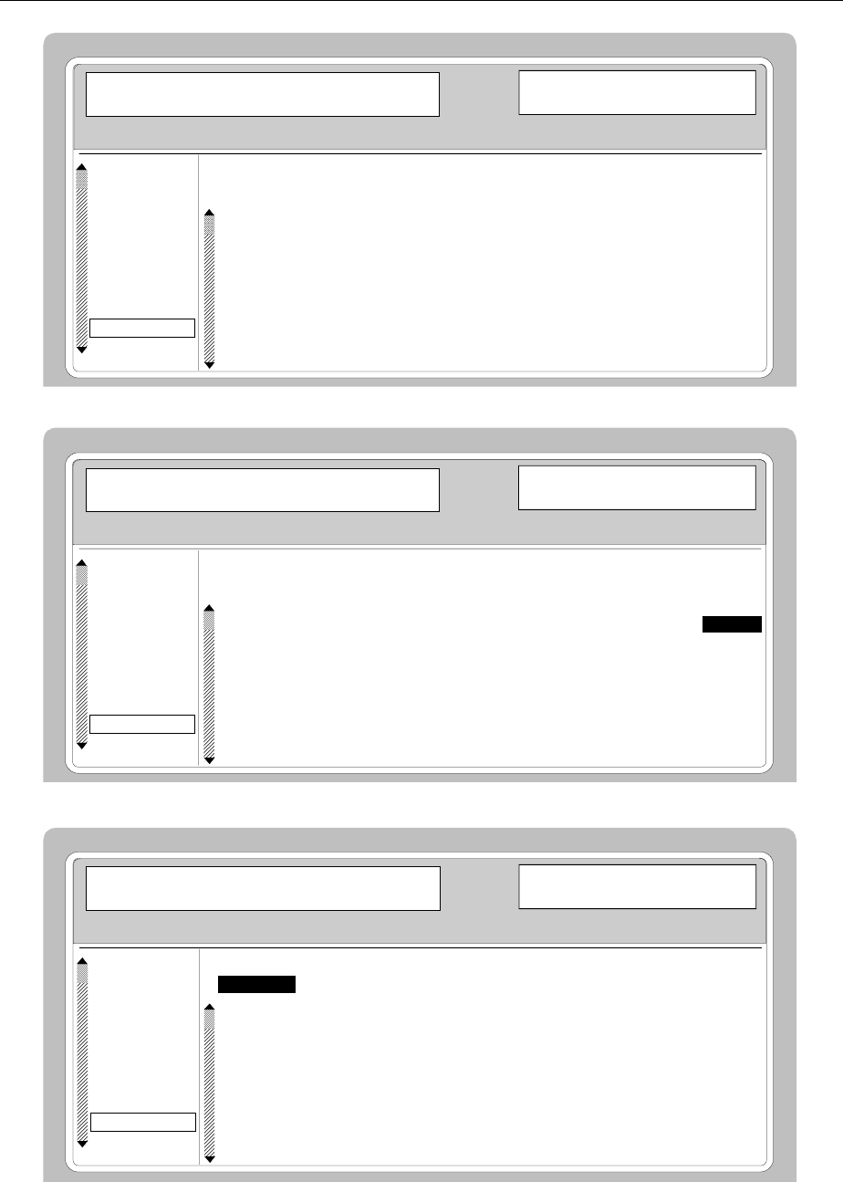
List Editor SMIQ
1125.5555.03 2.42 E-8
DELETE
FREQ 100. 000 000 0 MHz LEVEL - 30.0 dBm
INSERTFILL EDIT/VIEW
SELECT LIST...
FUNCTION
-INDEX - FREE 0246 - LEN 0010 MEMORY DWELL
0001
DELETE
FREQ 100. 000 000 0 MHz LEVEL - 30.0 dBm
INSERTFILL
SELECT LIST...
FUNCTION
-INDEX - FREE 0246 - LEN 0010 MEMORY DWELL
0001 20 100 ms
0002
DELETE
FREQ 100. 000 000 0 MHz LEVEL - 30.0 dBm
INSERTFILL EDIT/VIEW
SELECT LIST...
FUNCTION
-INDEX - FREE 0246 - LEN 0010 MEMORY DWELL
0001 20 15.00 s
0002 07 100 ms
0003
A
B
C
EDIT/VIEW
FREQUENCY
LEVEL
ANALOG MOD
VECTOR MOD
DIGITAL MOD
DIGITAL STD
LF OUTPUT
SWEEP
LIST
MEM SEQ
UTILITIES
FREQUENCY
LEVEL
ANALOG MOD
VECTOR MOD
DIGITAL MOD
DIGITAL STD
LF OUTPUT
SWEEP
LIST
MEM SEQ
UTILITIES
FREQUENCY
LEVEL
ANALOG MOD
VECTOR MOD
DIGITAL MOD
DIGITAL STD
LF OUTPUT
SWEEP
LIST
MEM SEQ
UTILITIES
CURRENT:MSEQ0
CURRENT:MSEQ0
CURRENT:MSEQ0
Fig. 2-15, a to c Pattern setting - Edition of a list

SMIQ Save/Recall
1125.5555.03 2.43 E-8
2.2.12 Save/Recall - Storing/Calling of Instrument Settings
50 complete instrument settings can be stored in memory locations 1 to 50.
Operating steps Explanations
SAVE
DATA INPUT
x1
ENTER
12
Store current instrument setting in
memory location 12.
RCL
DATA INPUT
x1
ENTER
12
Call instrument setting of memory
location 12.
The digital display during a save or recall entry is faded in a window.
Memory location 0 has a special function. Here the instrument setting which was current prior to the last
memory recall and prior to a preset setting is automatically stored. This permits the resetting of
instrument settings which have inadvertently been deleted using Recall 0.
If an instrument setting is stored in which a sweep was switched on, the sweep is started using the
recall.
The parameter EXCLUDE FROM RCL in the FREQUENCY and LEVEL-LEVEL menus determines
whether the saved RF frequency and RF level are loaded when an instrument setting is loaded, or
whether the current settings are maintained.
Store IEC-bus command: "*SAV 12"
Recall IEC-bus command: "*RCL 12"
Notes: - The contents of lists, as they are used for the Memory Sequence (MSEQ) or for user
correction (UCOR), is not saved in the SAVE memory. It is stored under the respective list
name and can be called. If instrument settings are called which go back to list data such as
level setting using UCOR, the current list contents is used. If this has been altered, it is not
identical to the list contents at the point of storing any more.
- The frame configurations (digital standards PHS, NADC, PDC, GSM, DECT) and the channel
configurations (digital standards CDMA, W-CDMA, 3GPP W-CDMA) are not stored in the
SAVE memory either. These settings can be stored and loaded via menu items SAVE/RCL
FRAME and SAVE/RCL MAPPING in the corresponding DIGITAL STD menus.
- The instruments comprise the "Fast Restore" mode for very fast loading of stored device
settings. This mode can be called up only during remote control (see section 3, "Fast Restore
Mode").
Menu Summary SMIQ
1125.5555.03 E-82.44
2.3 Menu Summary
FREQUENCY
LEVEL
ALC
UCOR
EMF
LEVEL
AM
BB-AM
FM
PM
ANALOG MOD
DIGITAL MOD
LF OUTPUT
FREQ
LEVEL
LFGEN
SWEEP
LIST
MEM SEQ
SYSTEM
REF OSC
PHASE
PROTECT
CALIB
DIAG
TEST
MOD KEY
AUX I/O
BEEPER
UTILITIES
HELP
GPIB
RS232
SECURITY
LANGUAGE
CONFIG
TPOINT
PARAM
VCO SUM
VECTOR MOD
LEV PRESET
REF OSC
L
ALC TABLE
LEV ATT
LFGEN
EVEL
(option SM-B5)
(option SM-B5)
VECTOR MOD
DIGITAL STD
FADING SIM (options SMIQB14, SMIQB15 and SMIQB49)
(options SMIQB20, SMIQB11 and SMIQB12)
(options SMIQB20, SMIQB11, SMIQB12 and digital standards
incl. options SMIQB43, SMIQB45 and SMIQB48)
(can be equipped with option SMIQB47)
NOISE/DIST (option SMIQB17)
C/NMEAS
BERT (option SMIQB21)
ARB MOD (option SMIQB60)

SMIQ RF Frequency
1125.5555.03 E-82.45
2.4 RF Frequency
The RF frequency can be set directly using the [FREQ] key (cf. Section 2.2.6) or by accessing menu
FREQUENCY.
The frequency of the RF output signal is entered/indicated under FREQUENCY in the FREQUENCY
menu.
The input value of frequency settings opened by means of the [FREQ] key and indicated in the header
line considers the offset in calculation (cf. next Section). This offers the possibility of entering the desired
output frequency of possibly series-connected instruments such as mixers in the menu.
Note: Further settings: Frequency sweep Menu SWEEP
LF frequency Menu ANALOG MOD
Menu LF-OUTPUT
Int./ext. reference frequency Menu UTILITIES-REF OSC
Phase of the output signal Menu UTILITIES-PHASE
Menu selection: FREQUENCY
FREQUENCY
OFFSET
KNOB STEP USER
KNOB STEP
EXCLUDE FROM RCL
100. 000 000 0 MHz
0.0 Hz
FREQ
100. 000 000 0
MHz LEVEL
- 30.0
dBm
1. 000 000 0 MHz
DECIMAL USER
ON OFF
FREQUENCY
LEVEL
ANALOG MOD
VECTOR MOD
DIGITAL MOD
DIGITAL STD
LF OUTPUT
SWEEP
LIST
MEM SEQ
UTILITIES
Fig. 2-16 Menu FREQUENCY (preset setting)
FREQUENCY Input value of the RF frequency at the RF output connector.
IEC/IEEE-bus command SOUR:FREQ 100E6
OFFSET Input value of the frequency offset, e.g., of a series-connected mixer (cf.
Section "Frequency Offset"). The status line indicates FREQ-OFFST.
IEC/IEEE-bus command SOUR:FREQ:OFFS 0
KNOB STEP USER Input value of the step width for frequency variation using the rotary knob. The
RF frequency is varied in the step width entered if KNOB STEP is set to USER.
IEC/IEEE-bus command SOUR:FREQ:STEP 1MHz
KNOB STEP DECIMAL: Variation step width corresponding to the position of the digit
cursor.
USER: "User Defined", variation step width as entered under KNOB
STEP USER .
RF Frequency SMIQ
1125.5555.03 E-82.46
EXCLUDE FROM RCL OFF The saved frequency is also loaded when instrument settings are
loaded with the [RCL] key or with a memory sequence.
IEC/IEEE-bus command SOUR:FREQ:RCL INCL
ON The RF frequency is not loaded when instrument settings are
loaded, the current frequency is maintained.
IEC/IEEE-bus command SOUR:FREQ:RCL EXCL
2.4.1 Frequency Offset
The SMIQ offers the possibility of entering an offset (OFFSET) of possibly series-connected instruments
in the FREQUENCY menu. The indication/input value of FREQ in the header field considers this input
and represents the frequency value of the RF signal at the output of these instruments (cf. Fig. 2-17).
The entry values FREQUENCY and OFFSET in the menu FREQUENCY or FREQ in the header line are
related to the RF output frequency as follows :
FREQ - OFFSET = output frequency (= FREQUENCY).
An offset entry causes no modification of the RF output frequency but only a modification of the display
value in the FREQ field in the header line, ie FREQ in the header line indicates the offset-associated
frequency and FREQUENCY in the menu FREQUENCY the RF output frequency. The status line
indicates FREQ-OFFST.
The offset setting also remains effective with the frequency sweep.
ïð
SMIQ
Input value
OFFSET
(FREQUENCY menu)
L.O.
RF output frequency
(FREQUENCY in the FREQUENCY menu)
Mixer
FREQ in the header field
Fig. 2-17 Example of a circuit with frequency offset
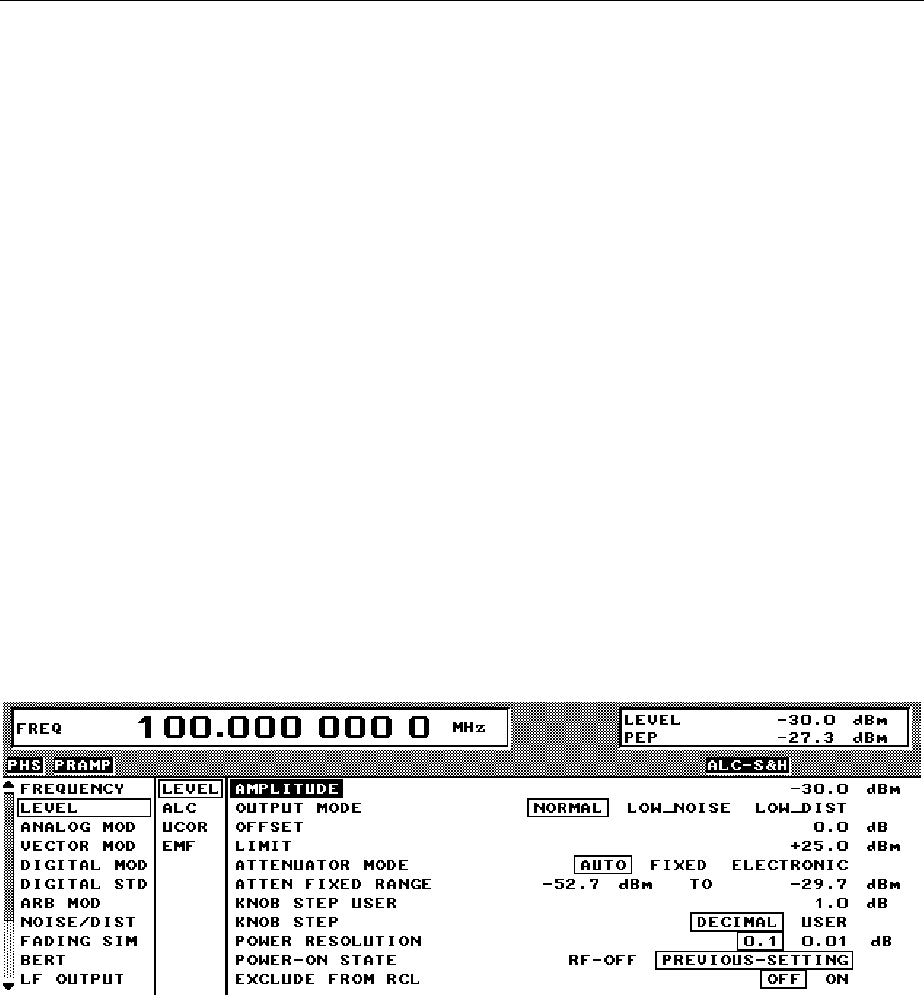
SMIQ RF Level
1125.5555.03 E-82.47
2.5 RF Level
The RF level can be set directly using the [LEVEL] key (cf. Section 2.2.6) or by accessing the LEVEL
menu.
In the LEVEL-LEVEL menu, the set RF output level is indicated under AMPLITUDE. A two-line level
display appears for digital modulation or digital standard. The upper line indicates the average power
(LEVEL), the lower line the peak envelope power (PEP) of the modulated RF output signal.
The input value of level settings effected in the LEVEL-LEVEL menu directly corresponds to the RF
output level.
The input value of the level settings opened using the [LEVEL] key mathematically considers the offset
of an attenuation/amplification element which is possibly series-connected (cf. Section 2.5.1). This offers
the possibility of entering the desired level at the output of series-connected instruments, the SMIQ then
alters the RF output level correspondingly. The offset can also be entered in the LEVEL-LEVEL menu.
dBm, dBµV, mV and µV can be used as level units. The 4 unit keys are directly labeled with these units.
In order to change to another level unit, simply press the desired unit key.
Notes: - The message ERROR is displayed in the status line if the level set in the overrange is
not reached.
- For digital modulation or digital standard, a WARNING message appears in the status
line if the set LEVEL or the displayed PEP are overranged. If the set level cannot be
generated as an overrange value, ERROR will be displayed.
- Further settings: Level sweep menu SWEEP
Menu selection: LEVEL - LEVEL
Fig. 2-18 Menu LEVEL (preset setting) POWER RESOLUTION is set to 0.01 dB
AMPLITUDE Input value of the RF level at the RF output connector.
IEC/IEEE-bus command SOUR:POW -30

RF Level SMIQ
1125.5555.03 E-82.48
OFFSET Input value of the level offset of the RF output level compared to the input
value of the RF level indicated in the LEVEL header field. Input in dB (cf.
Section 2.5.1, Level Offset). The status line indicates LEV-OFFST.
IEC/IEEE-bus command SOUR:POW:OFFS 0
LIMIT Input value of level limitation. This value indicates the upper limit of the level at
the RF output connector. If a level above this limit is attempted to be set, a
warning is displayed in the status line.
IEC/IEEE-bus command SOUR:POW:LIM 16 dBm
ATTENUATOR MODE AUTO Normal operation. The attenuator switching mechanically switches
in steps of 5 dB, the switching points being fixed.
IEC/IEEE-bus command :OUTP:AMOD AUTO
FIXED Level settings are made in a range of somewhat over 20 dB
without switching the attenuator (see section 2.5.2, "Non-
interrupting Level Setting"). The range of variation is fixed
automatically upon selection of this operating mode. The range is
indicated in the ATTEN FIXED RANGE menu. With level settings
out of the indicated range, a warning is displayed.
IEC/IEEE-bus command :OUTP:AMOD FIX
ELECTRONIC
Level settings are made in a range of somewhat over 90 dB with-
out switching the attenuator (see section 2.5.2, "Non-interrupting
Level Setting"). The range of variation is fixed automatically upon
selection of this operating mode. The range is indicated in the
ATTEN FIXED RANGE menu. With level settings out of the
indicated range, a warning is displayed.
This function is only available if the IQMOD module of version
VAR 4 or higher is installed (indication in UTILITIES - DIAG -
CONFIG menu, IQMOD Var 4 required).
IEC/IEEE-bus command :OUTP:AMOD ELEC
ATTEN FIXED RANGE Indication of the level range in which the level is set without interruption in the
"ATTENUATOR MODE FIXED" operating mode.
KNOB STEP USER Input value of the step width for level variation using the rotary knob. The RF
level is varied in the step width entered if KNOB STEP is set to USER.
IEC/IEEE-bus command SOUR:POW:STEP 1
KNOB STEP DECIMAL Variation step width according to the position of the digit cursor.
USER User Defined, variation step width as entered under KNOB STEP
USER.
POWER RESOLUTION Selection of resolution of LEVEL display. For level range -99.9 dBm to +16
dBm the resolution for the level display can be set to 0.1 dB or 0.01 dB.
POWER-ON STATE Selection of the state the RF output is to assume after power-on of the unit
RF OFF Output is switched off
PREVIOUS SETTING Same state as before switch-off
IEC/IEEE-bus command :OUTP:PON ON
SMIQ RF Level
1125.5555.03 E-82.49
EXCLUDE FROM RCL OFF The saved RF level is also loaded when instrument settings are
loaded with the [RCL] key or with a memory sequence.
IEC/IEEE-bus command SOUR:POW:RCL INCL
ON The RF level is not loaded when instrument settings are loaded,
the current level is maintained.
IEC/IEEE-bus command SOUR:POW:RCL EXCL
2.5.1 Level Offset
The SMIQ offers the possibility of entering the offset (OFFSET) of a possibly series-connected
attenuator/amplification element in the LEVEL-LEVEL menu. The indication/input value in the LEVEL
header field considers this input (see below) and represents the level value of the signal at the output of
the series-connected instrument (cf. Fig. 2-19).
The entry values AMPLITUDE and OFFSET in the menu LEVEL or LEVEL in the header line are related
to the RF output level as follows:
LEVEL - OFFSET = output level (= AMPLITUDE)
An offset entry causes no modification of the RF output frequency but only a modification of the display
value in the LEVEL field in the header line, ie LEVEL in the header line indicates the offset-associated
level and AMPLITUDE in the menu LEVEL the RF output level. The status line indicates LEV-OFFST.
The offset is to be entered in dB.
The offset setting also remains effective in the ATTENUATOR MODE FIXED operating mode and with
level sweep.
ïð
SMIQ
Input value
OFFSET
(LEVEL menu)
RF output signal
(AMPLITUDE in the LEVEL menu)
Attenuation/
Amplification LEVEL in the header field
Fig. 2-19 Example of a circuit with level offset

RF Level SMIQ
1125.5555.03 E-82.50
2.5.2 Interrupt-free Level Setting
In the ATTENUATOR MODE FIXED and ATTENUATOR MODE ELECTRONIC operating modes, level
settings are carried out without interruption. The attenuator is switched electronically rather than
mechanically.
The MODE FIXED variation range is somewhat over 20 dB, the variation range of MODE ELECTRONIC
over 90 dB. In case of over- or underranging of the normal variation range, level errors strongly increase
and an under/overrange warning is displayed. At high attenuation values the spectral purity of the output
signal is degraded.
The ATTENUATOR MODE ELECTRONIC mode is only possible with level control switched off. The
ALC OFF mode is automatically set to TABLE.
Note: To ensure highest level accuracy in ATTENUATOR MODE ELECTRONIC mode, the self
calibration routines ALC TABLE and LEV ATT should be called up in the UTILITIES -
CALIB menu after temperature variations of more than 5 degrees.
The MODE ELECTRONIC cannot be used either simultaneously with the SLOT
ATTENUATION function of the digital standards. This applies to all TDMA standards. The
MODE ELECTRONIC cannot be used either simultaneously with the DIGITAL MOD -
POWER RAMP CONTROL - ATTENUATION function.
2.5.3 Switching On/Off Internal Level Control
The LEVEL - ALC menu allows the level control to be switched on and off for special applications. In the
normal operating mode for CW, AM and FM(PM), level control is switched on so that an optimum level
accuracy is obtained. For vector modulation or digital modulation, level control must normally be off. In
this case the SAMPLE&HOLD or the TABLE mode can be selected instead.
In the SAMPLE&HOLD mode the level is recalibrated after each level or frequency setting. To do this,
CW is selected for a short period of time, level control is switched on and the level control held at the
value attained. If this calibration procedure is not desired, the TABLE mode (level control voltage taken
from a table) can be selected. In this mode the correction values required after a frequency or level
change are obtained from a table. With the LEARN TABLE function called up, a new table can be
prepared without any additional measuring instruments being required.
The preset level control is AUTO. Level control in this mode is automatically adapted to the operating
conditions. For special applications, level control can be held in the OFF or ON state. Level control OFF
is useful for improving the intermodulation suppression in multi-signal measurements in the CW mode.
The ON setting is recommended if vector modulation or digital modulation with a constant envelope
curve is required.

SMIQ RF Level
1125.5555.03 E-82.51
Menu selection: LEVEL - ALC
LEVEL
ALC
UCOR
EMF
STATE
ALC OFF MODE
SEARCH ONCE
LEARN TABLE
FREQ
100. 000 000 0
MHz LEVEL
- 30.0
dBm
OFF AUTO ON
SAMPLE&HOLD TABLE
FREQUENCY
LEVEL
ANALOG MOD
VECTOR MOD
DIGITAL MOD
DIGITAL STD
LF OUTPUT
SWEEP
LIST
MEM SEQ
UTILITIES
ALC-ON
Fig. 2-20 Menu LEVEL - ALC (preset setting)
STATE OFF Internal level control is deactivated. In this state no AM is possible.
IEC/IEEE-bus command SOUR:POW:ALC OFF
AUTO Normal state. The internal level control is automatically adjusted to the
operating conditions.
IEC/IEEE-bus command SOUR:POW:ALC AUTO
ON Internal level control is permanently switched on.
IEC/IEEE-bus command SOUR:POW:ALC ON
ALC OFF MODE SAMPLE&HOLD Level recalibration in the ALC OFF mode after the level or
frequency has been set.
IEC/IEEE-bus command SOUR:POW:ALC:SEAR ON
TABLE In the ALC OFF mode correction values are taken from a
table.
IEC/IEEE-bus command SOUR:POW:ALC:SEAR OFF
SEARCH ONCE Manual short-time switching on of the level control for level calibration in the
ALC OFF and SAMPLE&HOLD operating mode.
IEC/IEEE-bus command SOUR:POW:ALC:SEAR ONCE
LEARN TABLE Correction values for the ALC OFF MODE-TABLE function are regenerated
(level control voltage obtained from a table).
IEC/IEEE-bus command SOUR:POW:ALC:TABL?

RF Level SMIQ
1125.5555.03 E-82.52
2.5.4 User Correction (UCOR)
Function "User Correction" can be used to create and activate lists in which arbitrary RF frequencies are
assigned level correction values.
Up to 10 lists with a total of 160 correction values can be compiled. For frequencies which are not
included in the list the level correction is determined by means of interpolation of the nearest correction
values.
When user correction is switched on, the LEVEL indication is completed by the indication UCOR (User
Correction) in the header field of the display. The RF output level is the sum of both values.
LEVEL + UCOR = output level
If the offset setting is used at the same time, the LEVEL indication value is the difference of the input
values AMPLITUDE and OFFSET of the menu LEVEL.
AMPLITUDE - OFFSET = LEVEL
The user correction is effective in all operating modes if switched on.
Menu selection: LEVEL - UCOR
LEVEL
ALC
UCOR
EMF
STATE
SELECT LIST... CURRENT: UCOR1
DELETE LIST...
FUNCTION FILL INSERT DELETE EDIT/VIEW
FREQ
100. 000 000 0
MHz LEVEL
- 27.0
dBm
UCOR
+ 1.9
dB
OFF ON
FREQUENCY
LEVEL
ANALOG MOD
VECTOR MOD
DIGITAL MOD
DIGITAL STD
LF OUTPUT
SWEEP
LIST
MEM SEQ
UTILITIES
Fig. 2-21 Menu LEVEL - UCOR - OPERATION side
STATE Switching on/off user correction.
IEC/IEEE-bus command SOUR:CORR ON
SELECT LIST... Selection of a list or generation of a new list (cf. Section 2.2.11, List Editor).
IEC/IEEE-bus command SOUR:CORR:CSET "UCOR1"
DELETE LIST... Deletion of a list (cf. Section 2.2.11, List Editor).
IEC/IEEE-bus command SOUR:CORR:CSET:DEL "UCOR2"
FUNCTION Selection of the editing mode to process the selected list (cf. Section 2.2.11, List
Editor).
IEC-bus commands SOUR:CORR:CSET:DATA:FREQ 100 MHz, 102 MHz,...
SOUR:CORR:CSET:DATA:POW 1dB, 0.8dB,...

SMIQ RF Level
1125.5555.03 E-82.53
Menu selection: LEVEL - UCOR
LEVEL
ALC
UCOR
EMF
FREQ
100. 000 000 0
MHz
LEVEL
- 27.0
dBm
UCOR
+ 1 .9
dB
SELECT LIST... CURRENT: UCOR1
FUNCTION FILL INSERT DELETE EDIT/VIEW
INDEX - FREE 70 - LEN 10 FREQUENCY UCOR1
005 105.000 000 0 MHz + 1.9 dB
006 107.000 000 0 MHz + 1.2 dB
007 108.000 000 0 MHz + 1.3 dB
008 109.000 000 0 MHz + 1.5 dB
009 111.000 000 0 MHz + 1.6 dB
010 112.000 000 0 MHz + 1.9 dB
011 113.000 000 0 MHz + 2.0 dB
012 114.000 000 0 MHz + 2.1 dB
FREQUENCY
LEVEL
ANALOG MOD
VECTOR MOD
DIGITAL MOD
DIGITAL STD
LF OUTPUT
SWEEP
LIST
MEM SEQ
UTILITIES
Fig. 2-22 Menu UCOR - LEVEL-EDIT side
2.5.5 EMF
The signal level can also be set and indicated as the voltage of EMF (open-circuit voltage).
EMF is displayed in the header field of the display after the unit of the level indication.
Menu selection: LEVEL - EMF
LEVEL
ALC
UCOR
EMF
STATE
FREQ
100. 000 000 0
MHz LEVEL
14.1
mV
OFF ON
emf
FREQUENCY
LEVEL
ANALOG MOD
VECTOR MOD
DIGITAL MOD
DIGITAL STD
LF OUTPUT
SWEEP
LIST
MEM SEQ
UTILITIES
Fig. 2-23 Menu LEVEL-EMF
STATE ON Voltage value of the level is the voltage of EMF.
OFF Voltage value of the level is voltage at 50 Ω (preset setting).

RF Level SMIQ
1125.5555.03 E-82.54
2.5.6 [RF ON / OFF]-Key
The RF output signal is switched on and off again using the [RF ON / OFF] key. This does not influence
the current menu. When the output signal is switched off, the message "RF OFF" is displayed in the
LEVEL indication of the header field. If RF OFF is displayed, the 50-Ω source resistance is maintained.
IEC/IEEE-bus command :OUTP OFF
2.5.7 Reset Overload Protection
The SMIQ is protected against overload by an external signal which is fed into the RF output. If an
external signal is too high, the overload protection responds. This state is indicated by means of the
message "RF OFF" in the LEVEL indication in the header field and the message "OVERLOAD" in the
status line.
ØReset the overload protection by pressing the [RF ON / OFF] key.
IEC/IEEE-bus command :OUTP:PROT:CLE

SMIQ Modulation - General
1125.5555.03 E-82.55
2.6 Modulation - General
The SMIQ offers the following modulations and digital standards:
•Analog modulations
- Amplitude modulation (AM)
- Broadband AM (BB-AM)
- Frequency modulation (FM; with option SM-B5 only)
- Phase modulation (PM; with option SM-B5 only)
- Pulse modulation (PULSE)
•Vector modulation (VECTOR MOD)
•Digital modulation (DIGITAL MOD; option SMIQB20)
•Digital standards (DIGITAL STD;-PHS; IS95/CDMA - option SMIQB42; NADC; PDC; GSM;
DECT; W-CDMA - option SMIQB43; 3GPP W-CDMA - option SMIQB45;
Enhanced Channels – option SMIQB48; options SMIQB20 and SMIQB11)
For AM, FM, PM and digital modulation internal or external modulation sources can be used.
For BB-AM, pulse and vector modulation only external modulation sources can be used.
2.6.1 Modulation Sources
Internal Modulation Sources
The internal modulation generator LF GEN is available for AM, FM and PM. The generator supplies
sinusoidal signals in the frequency range from 0.1 Hz to 1 MHz. For a more detailed description, cf.
Section "LF Generator".
The internal modulation coder (option SMIQB20) supplies PRBS signals, clock signals or modulation
data for the digital modulations. The data generator (option SMIQB11) supplies modulation data and
control signals. For a more detailed description, cf. Section "Digital Modulations".
External Modulation Sources
The appropriate input sockets to the different modulations in the case of external supply can be taken
from Table 2-1.
Table 2-1 Input sockets for the different types of modulation
Input
Modulation EXT1 EXT2 PULS I Q DATA PAR DATA BIT CLOCK SYMBOL
CLOCK POW RAMP
AM X
BB-AM X
FM1 XX
FM2 XX
PM1 XX
PM2 XX
PULSE X
VECTOR MOD XX X
DIGITAL MOD XXXXX
Modulation - General SMIQ
1125.5555.03 E-82.56
EXT1/EXT2-Inputs
The external modulation signal for AM, FM and PM at inputs EXT1 and EXT2 must show a voltage of
Vs = 1 V (Veff = 0.707 V) in order to maintain the modulation depth or deviation indicated. A monitoring
circuit checks the input voltage in the frequency range 10 Hz to 100 kHz. Deviations of more than ±3 %
are signaled in the status line by means of the following messages (cf. Table 2-2). The inputs EXT1 and
EXT2 can be AC- or DC-coupled. Monitoring is only active if the inputs are AC-coupled.
Table 2-2 Status messages in the case of a deviation from the rated value at the external modulation
inputs EXT1 and EXT2
Message Deviation
EXT1-HIGH Voltage at EXT1 too high
EXT1-LOW Voltage at EXT1 too low
EXT2-HIGH Voltage at EXT2 too high
EXT2-LOW Voltage at EXT2 too low
EXT-HI/HI Voltage at EXT1 and EXT2 too high
EXT-LO/LO Voltage at EXT1 and EXT2 too low
EXT-HI/LO Voltage at EXT1 too high and EXT2 too low
EXT-LO/HI Voltage at EXT1 too low and EXT2 too high
FREQ 250. 000 000 0 MHz LEVEL - 10.0 dBm
AM
30.0 %
OFF INT
OFF EXT1
AC DC
1.000 0 kHz
FREQUENCY
LEVEL
ANALOG MOD
VECTOR MOD
DIGITAL MOD
DIGITAL STD
LF OUTPUT
SWEEP
LIST
MEM SEQ
UTILITIES
AM
BB-AM
FM
PM
PULSE
EXT1-LOW
AM DEPTH
AM SOURCE INT
AM SOURCE EXT
AM EXT COUPLING
LFGEN FREQ
Fig. 2-24 Example: Status message "EXT1-LOW" in case of voltage at EXT1 too low
I/Q Inputs
The nominal voltage at the I/Q-inputs for external vector modulation is Us = 0.5 V. Input resistance is
50 Ω. For a more detailed description, cf. Section "Vector Modulation".
For external broadband AM the I-input is used. Input sensitivity is 0,25 V for 100% AM.
SMIQ Modulation - General
1125.5555.03 E-82.57
2.6.2 LF Generator
The SMIQ is equipped with a LF-generator as internal modulation source as a standard. The generator
supplies sinusoidal signals in the frequency range from 0.1 Hz to kHz.
The frequency settings of the internal modulation signals can be made in one of the modulation menus
(AM, FM, PM) as well as in the LF-output menu. Figure 2-25 shows the setting parameters using the AM
menu as an example.
AM DEPTH
AM SOURCE INT
AM SOURCE EXT
AM EXT COUPLING
LFGEN FREQ
FREQ 250. 000 000 0 MHz LEVEL - 10.0 dBm
AM
15.5 %
OFF INT
OFF EXT1
AC DC
1.000 0 kHz
FREQUENCY
LEVEL
ANALOG MOD
VECTOR MOD
DIGITAL MOD
DIGITAL STD
LF OUTPUT
SWEEP
LIST
MEM SEQ
UTILITIES
AM
BB-AM
FM
PM
PULSE
Fig. 2-25 Example: Settings of the LF generator in the AM menu
2.6.3 Simultaneous Modulation
Combination of AM and FM as well as AM and vector modulation is possible. Instead of FM, phase
modulation (PM) can be switched on as well.
Two-tone AM is possible by simultaneously switching on the external and internal source.
Two-tone FM or two-tone PM is possible by simultaneously switching on FM1 and FM2 or PM1 and
PM2. For FM1 and FM2 (PM1 and PM2) separate deviations can be set and separate sources switched
on.
Note: With two-tone modulation please observe that the set deviation or modulation depth is valid for
one signal and the sum deviation or sum modulation depth is determined by adding both
signals. This results in overmodulation if the maximal value for deviation or modulation depth is
exceeded.

Modulation - General SMIQ
1125.5555.03 E-82.58
2.6.4 [MOD ON/OFF] Key
The modulations can directly be switched on/off using the key or by accessing the modulation menus.
When switching on using the [MOD ON/OFF] key, the modulation sources which are set in the
modulation menus are used.
The [MOD ON/OFF] key can either be effective for all modulations or for a selected modulation. The
selection for which modulation the [MOD ON/OFF] key is effective is made in the UTILITIES-MOD KEY
menu (cf. Section "Assigning Modulation to [MOD ON/OFF] Key").
When selecting a certain type of modulation, each pressing the [MOD ON/OFF] key switches on or off
the modulation selected.
In the case of selection "all modulations", the [MOD ON/OFF] key has the following effect:
•At least one modulation is active:
Pressing the [MOD ON/OFF] key switches off all active modulations. Which modulations were active
is stored.
•No modulation is active:
Pressing the [MOD ON/OFF] key switches on the modulations which were last switched off using the
[MOD ON/OFF] key.

SMIQ Analog Modulations
1125.5555.03 E-82.59
2.7 Analog Modulations
2.7.1 Amplitude Modulation
Menu ANALOG MOD-AM offers access to settings for amplitude modulation.
Notes: -The specifications for AM are only valid for the specified Level (PEP) range.
-For AM, setting LEVEL-ALC-STATE ON or AUTO is recommended.
Menu selection: ANALOG MOD - AM
FREQ 100. 000 000 0 MHz LEVEL - 30.0 dBm
FREQUENCY
LEVEL
ANALOG MOD
VECTOR MOD
DIGITAL MOD
DIGITAL STD
LF OUTPUT
SWEEP
LIST
MEM SEQ
UTILITIES
AM
BB-AM
FM
PM
PULSE
AM DEPTH
AM SOURCE INT
AM SOURCE EXT
AM EXT COUPLING
LFGEN FREQ
30.0 %
OFF INT
OFF EXT1
AC DC
1.000 0 kHz
Fig. 2-26 Menu ANALOG MOD-AM (preset setting)
AM DEPTH Input value of the modulation depth.
IEC/IEEE-bus command SOUR:AM 30PCT
AM SOURCE INT Selection of the internal source.
IEC/IEEE-bus command SOUR:AM:SOUR INT1; STAT ON
AM SOURCE EXT Selection of the external source.
IEC/IEEE-bus command SOUR:AM:SOUR EXT; STAT ON
AM EXT COUPLING Selection of the kind of coupling AC or DC with external supply (input EXT1).
IEC/IEEE-bus command SOUR:AM:EXT:COUP AC
LFGEN FREQ Input value of the frequency of the LF generator.
IEC/IEEE-bus command SOUR:AM:INT:FREQ 1kHz

Analog Modulations SMIQ
1125.5555.03 E-82.60
2.7.2 Broadband AM (BB-AM)
In the BB-AM mode the I/Q modulator is used for amplitude modulation. Level control should be set to
AUTO or ON (see section, Switching On/Off Internal Level Control).
The modulation input (BB-AM) is identical with the I input of the I/Q modulator. The input impedance is
50 Ω. A signal of -0.25 V to +0.25 V corresponds to an amplitude modulation of -100% to +100%.
Setting the modulation depth with BB-AM is not possible.
Notes: - For Broadband AM the value for the upper level limit is the same as for vector
modulation. Depending on the modulation depth, PEP can exceed the displayed value
by up to 6 dB.
-Broadband AM cannot be selected together with normal AM or vector modulation.
These modulation deactivate one another
Menu selection: ANALOG MOD - BB-AM
FREQ 100. 000 000 0 MHz LEVEL - 30.0 dBm
FREQUENCY
LEVEL
ANALOG MOD
VECTOR MOD
DIGITAL MOD
DIGITAL STD
LF OUTPUT
SWEEP
LIST
MEM SEQ
UTILITIES
AM
BB-AM
FM
PM
PULSE
STATE
INPUT SENSITIVITY
OFF ON
0.25V/100%
Fig. 2-27 Menu ANALOG MOD - BB-AM (preset setting)
STATE Switches BB-AM on and off.
IEC/IEEE-bus command SOUR:AM:BBAN ON
INPUT SENSITIVITY Display of the input sensitivity. The value cannot be changed.
SMIQ Analog Modulations
1125.5555.03 E-82.61
2.7.3 Frequency Modulation
Menu ANALOG MOD-FM offers access to settings for frequency modulation.
Note: The FM and PM modulations cannot be set simultaneously and deactivate one another:
Menu selection: ANALOG MOD-FM
FREQ 100. 000 000 0 MHz LEVEL - 30.0 dBm
FM1 DEVIATION
FM1 SOURCE
LFGEN FREQ
FM2 DEVIATION
FM2 SOURCE
EXT1 COUPLING
EXT2 COUPLING
PREEMPHASIS
FREQUENCY
LEVEL
ANALOG MOD
VECTOR MOD
DIGITAL MOD
DIGITAL STD
LF OUTPUT
SWEEP
LIST
MEM SEQ
UTILITIES
AM
BB-AM
FM
PM
PULSE
10.0 kHz
OFF INT EXT1 EXT2
1.000 0 kHz
10.0 kHz
OFF EXT1 EXT2
AC DC
AC DC
OFF 50µ 75µ s
Fig. 2-28 Menu ANALOG MOD-FM (preset setting), fitted with option SM-B5, FM/PM-modulator
FM1 DEVIATION Input value of the deviation for FM1.
IEC/IEEE-bus command SOUR:FM1 10kHz
FM1 SOURCE Switching on and off FM1 and selection of the modulation source.
IEC/IEEE-bus command SOUR:FM1:SOUR INT; STAT ON
LFGEN FREQ Input value of the frequency of the LF generator.
EC-bus short command SOUR:FM1:INT:FREQ 1kHz
FM2 DEVIATION Input value of the deviation for FM2.
EC-bus short command SOUR:FM2 10kHz
FM2 SOURCE Switching on and off FM2 and selection of the modulation source.
EC-bus short command SOUR:FM2:STAT OFF
EXT1 COUPLING Selection of the type of coupling AC or DC for the external input EXT1.
IEC/IEEE-bus command SOUR:FM1:EXT1:COUP AC
EXT2 COUPLING Selection of the type of coupling AC or DC for the external input EXT2.
IEC/IEEE-bus command SOUR:FM1:EXT2:COUP AC
PREEMPHASIS Selection of the preemphasis
IEC-bus short command SOUR:FM1:PRE 50us
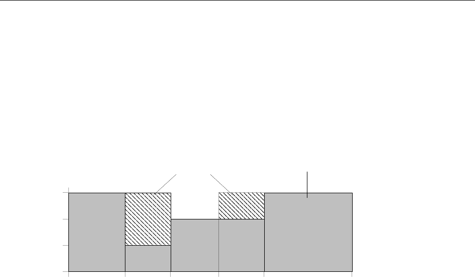
Analog Modulations SMIQ
1125.5555.03 E-82.62
2.7.3.1 FM Deviation Limits
The maximal deviation depends on the RF frequency set (cf. Fig. 2-29). It is possible to enter a
deviation that is too high for a certain RF frequency or to vary the RF frequency to a range in which the
deviation can no longer be set. In this case the maximally possible deviation is set and an error
message is displayed.
In the RF range 450 MHz to 750 MHz and 1200 MHz to 1500 MHz a different synthesis range is
selected depending on the deviation set. If the deviation is smaller than 500 kHz or 1000 kHz, the
synthesizer is in the normal mode with optimal spectral purity. If the deviation set is larger the I/Q mode
is automatically selected.
2000
1000
500
0,3 450 750 1200 1500 3300
I/Q mode
maximal
FM-deviation
[kHz]
RF frequency [MHz]
normal mode
Fig. 2-29 Dependency of the FM maximal deviation on the RF frequency set
2.7.3.2 Preemphasis
Preemphasis results in a preemphasis of the modulation signal with time constants 50 µs or 75 µs. The
higher frequencies of the modulation signal are preemphasized.
When preemphasis is switched on, only 1/4 of the maximal deviation is permissible. The highest
permissible modulation frequency is 15 kHz. Exceeding the permissible modulation frequency can lead
to overmodulation."
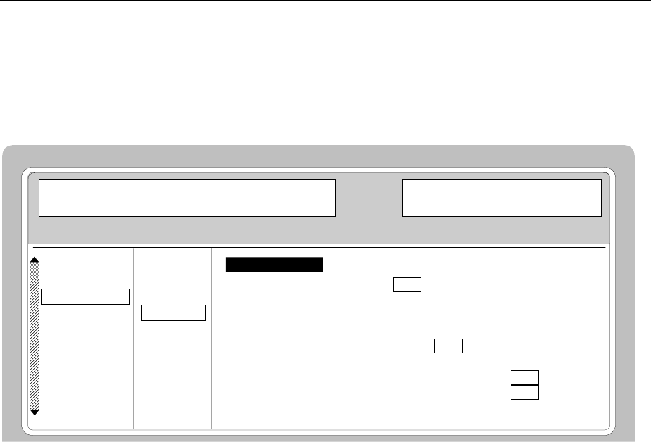
SMIQ Analog Modulations
1125.5555.03 E-82.63
2.7.4 Phase Modulation
Menu ANALOG MOD-PM offers access to settings for phase modulation.
Note: The PM and FM modulations cannot be set simultaneously and deactivate one another.
Menu selection: ANALOG MOD - PM
FREQ 100. 000 000 0 MHz LEVEL - 30.0 dBm
FREQUENCY
LEVEL
ANALOG MOD
VECTOR MOD
DIGITAL MOD
DIGITAL STD
LF OUTPUT
SWEEP
LIST
MEM SEQ
UTILITIES
AM
BB-AM
FM
PM
PULSE
PM1 DEVIATION
PM1 SOURCE
LFGEN FREQ
PM2 DEVIATION
PM2 SOURCE
EXT1 COUPLING
EXT2 COUPLING
1.00 rad
OFF INT EXT1 EXT2
1.000 0 kHz
1.00 rad
OFF EXT1 EXT2
AC DC
AC DC
Fig. 2-30 Menu ANALOG MOD - PM (preset setting), fitted with option SM-B5, FM/PM-modulator
PM1 DEVIATION Input value of the deviation for PM1.
IEC/IEEE-bus command SOUR:PM1 1RAD
PM1 SOURCE Switching on and off PM1 and selection of the modulation source.
IEC/IEEE-bus command SOUR:PM1:SOUR:INT; STAT ON
LFGEN1 FREQ Input value of the frequency of the LF generator.
IEC/IEEE-bus command SOUR:PM1:INT:FREQ 1kHz
PM2 DEVIATION Input value of the deviation for PM2.
IEC/IEEE-bus command SOUR:PM2 1RAD
PM2 SOURCE Switching on and off PM2 and selection of the modulation source.
IEC/IEEE-bus command SOUR:PM2:SOUR INT; STAT ON
EXT1 COUPLING Selection of the type of coupling AC or DC with external supply for PM1 (input
EXT1).
IEC/IEEE-bus command SOUR:PM:EXT1:COUP AC
EXT2 COUPLING Selection of the type of coupling AC or DC with external supply for PM2 (input
EXT2).
IEC/IEEE-bus command SOUR:PM:EXT2:COUP AC
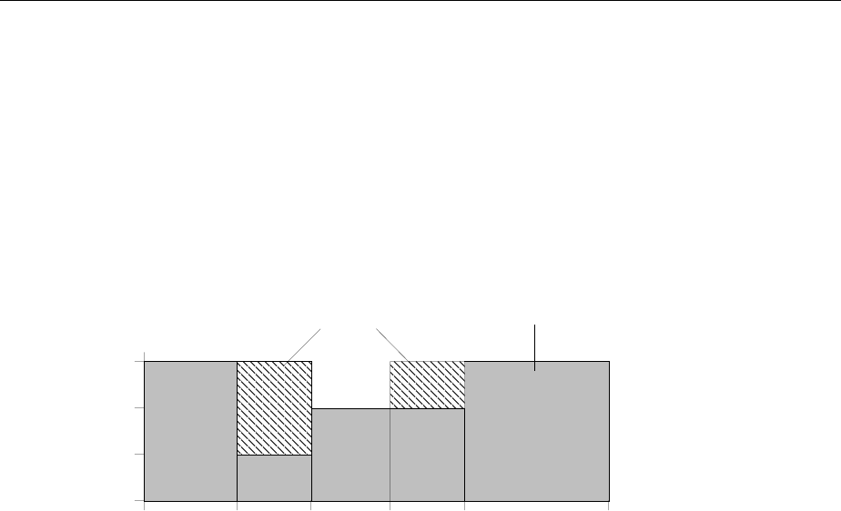
Analog Modulations SMIQ
1125.5555.03 E-82.64
2.7.4.1 PM Deviation Limits
The maximal deviation depends on the RF frequency set (cf. Fig. 2-31). It is possible to enter a
deviation that is too high for a certain RF frequency or to vary the RF frequency to a range in which the
deviation can no longer be set. In this case the maximally possible deviation is set and an error
message displayed.
In the RF range 450 to 750 MHz and 1200 MHz to 1500 MHz a different synthesis range is selected
depending on the deviation set. If the deviation is smaller than 5 rad or 10 rad, the synthesizer is in the
normal mode with optimal spectral purity. If the deviation set is larger, the I/Q mode is automatically
selected.
20
10
5
0,3 450 750 1200 1500 3300
I/Q mode
maximal
PM-deviation
[rad]
RF-frequency [MHz]
normal mode
Fig. 2-31 Dependency of the PM maximal deviation on the RF frequency set

SMIQ Analog Modulations
1125.5555.03 E-82.65
2.7.5 Pulse Modulation
The pulse modulator can be controlled by an external source at the PULSE input.
The polarity of the pulse modulation is selectable. With POLARITY = NORM, the RF level is on with
HIGH level at modulation input PULSE.
Menu MODULATION-PULSE offers access to settings for pulse modulation
Menu selection: MODULATION - PULSE
"
FREQ 100. 000 000 0 MHz LEVEL - 30.0 dBm
FREQUENCY
LEVEL
ANALOG MOD
VECTOR MOD
DIGITAL MOD
DIGITAL STD
LF OUTPUT
SWEEP
LIST
MEM SEQ
UTILITIES
AM
BB-AM
FM
PM
PULSE
SOURCE
POLARITY
OFF EXT
NORM INV
Fig. 2-32 Menu MODULATION-PULSE (preset setting), fitted with option SM-B3, pulse modulator,
and option SM-B4, pulse generator
SOURCE Switching on or off the external pulse modulation.
IEC/IEEE-bus command :SOUR:PULM:SOUR EXT; STAT ON
POLARITY Selection of the polarity of the modulation
NORM The RF signal is on during high level.
INV The RF signal is suppressed during high level.
IEC/IEEE-bus command :SOUR:PULM:POL NORM
Vector Modulation SMIQ
1125.5555.03 E-82.66
2.8 Vector Modulation
In the vector modulation mode (I/Q modulation) external modulation signals can be applied to
modulation inputs I and Q for a complex modulation of the RF carrier.
ï
ð
SMIQ
I = 0.3 V
Q = 0.4 V
I
Q
IQ
V
22
05
+
,
x
input value LEVEL
Amplitude =
Fig. 2-33 Example: vector modulation
If the I/Q modulator is driven by a constant sum vector modulation of IQ V
22
05+=. the actual RF
level corresponds to the displayed RF level. To avoid the I/Q modulator being overdriven, care should
be taken that the sum vector never exceeds 0.5 V when digital modulation modes with amplitude
modulation components such as QPSK are used. For full-scale input, the peak envelope power of the
modulated RF signal is thus equal to the indicated LEVEL. The average power is smaller. The
difference can be entered as an offset in the LEVEL menu.
Vector modulation settings are accessible in the VECTOR MOD menu, see following page.
Note: - Types of modulation VECTOR MOD and BB-AM cannot be set at the same time; they
switch each other off.
-A selectable internal calibration of the I/Q modulator allows accurate and reproducible
measurements to be made. The calibration routine should be called up with the
CALIBRATE in the menu VECTOR MOD or UTILITIES-CALIB-VECTOR MOD after
temperature changes of more than 5° C.
SMIQ Vector Modulation
1125.5555.03 E-82.67
Menu selection: VECTOR MOD
Fig. 2-34 VECTOR MOD menu (preset settings), equipped with option SMIQB47 and IQMOD var. 8
or higher
STATE Switches the vector modulation on and off.
IEC/IEEE-bus command SOUR:DM:IQ:STAT ON
POWER RAMP
CONTROL Switches the POW RAMP input for analog level control on and off. Thus an
external control signal can be used for carrier envelope modulation in parallel
to vector modulation.
IEC/IEEE-bus command SOUR:DM:IQ:PRAM AEXT
IMPAIRMENT STATE Switches I/Q impairment on and off.
IEC/IEEE-bus command SOUR:DM:IQ:IMP:STAT ON
LEAKAGE Value entered for residual carrier .
IEC/IEEE-bus command SOUR:DM:LEAK 10PCT
IMBALANCE Value entered for imbalanced modulation of I and Q vectors.
IEC/IEEE-bus command SOUR:DM:IQR -5PCT
QUADRATURE
OFFSET Value entered for quadrature offset .
IEC/IEEE-bus command SOUR:DM:QUAD:ANGL 4DEG
IQ SWAP Selection between normal and inverted I/Q modulation. Interchanging the I and
Q signals inverts the modulation sidebands.
OFF Normal I/Q modulation.
ON I and Q signals interchanged.
IEC/IEEE-bus command SOUR:DM:IQSW:STAT ON
CW > IQ TRANSITION Selection between normal and fast setting time during the transition to CW
after vector modulation (including DIGITAL MOD, DIGITAL STD and ARB
MOD). In the FAST mode, the CW-IQ mode is activated for CW and the
poorer spectral characteristics of vector modulation apply. For this reason, the
FAST mode should be activated only if very fast switchover between CW and
VECTOR MOD is required.
IEC/IEEE-bus command :SOUR:DM:IQ:TRAN:NORM|FAST

Vector Modulation SMIQ
1125.5555.03 E-82.68
IQ FILTER Only available with option SMIQB47.
Selection between no filter and a 850 kHz, a 2.5 MHz or a 5 MHz lowpass in
the baseband. A filter of these types suppresses noise in the baseband above
900 kHz, 3 MHz or 6 MHz, which improves ACP (Adjacent Channel Power) for
IS95 and W-CDMA. The frequency response of the filter is automatically
compensated for DIGITAL MOD and DIGITAL STD in MCOD, which means
that the EVM (Error Vector Magnitude) gets hardly worse. For VECTOR MOD
and AMIQ with WinIQSIM as source, the frequency response is also
compensated in WinIQSIM. For applications requiring a minimum EVM, the IQ
filter should be set to OFF.
OFF no filter
850 kHz 850 kHz lowpass
2.5 MHz 2.5 MHz lowpass
5 MHz 5 MHz lowpass
IEC/IEEE-bus commands :SOUR:DM:IQ:FILT:STAT ON|OFF
:SOUR:DM:IQ:FILT:FREQ 2.5MHZ
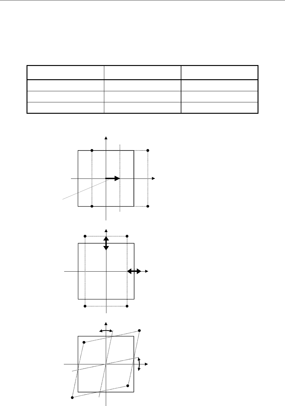
SMIQ Vector Modulation
1125.5555.03 E-82.69
2.8.1 I/Q Impairment
For simulating an impairment of the vector modulation, a residual carrier (LEAKAGE), imbalanced I and
Q modulation (IMBALANCE) and a quadrature offset can be entered. The input values for LEAKAGE
and IMBALANCE are with reference to the voltage.
Table 2-3 Parameter setting ranges
Parameter Setting range Resolution
LEAKAGE 0 ... 50 % 0.5 %
IMBALANCE -12 ... +12 % 0.1 %
QUADRATURE OFFSET -10 ... +10° 0.1°
The following figure shows the effect of I/Q impairment.
I
Q
Carrier Leakage
LEAKAGE:
I
Q
+-
+
-
IMBALANCE:
I
Q
+
+
-
-
QUADRATURE OFFSET:
Fig. 2-35 Effect of I/Q impairment
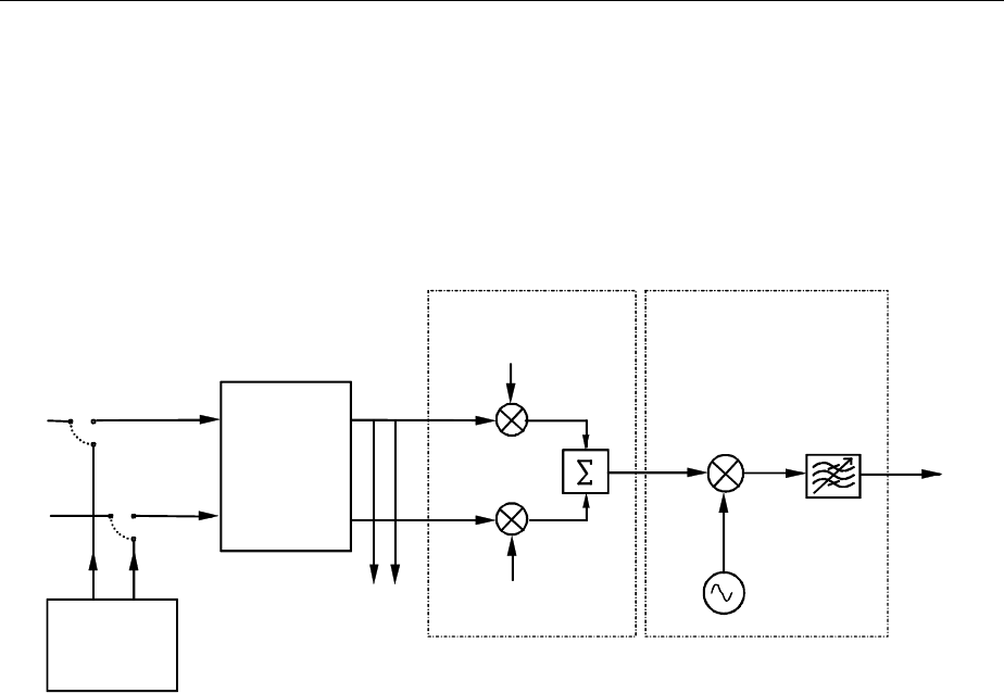
Fading Simulation SMIQ
1125.5555.03 2.70 E-9
2.9 Fading Simulation
By means of the option Fading Simulator SMIQB14, multipath fading signals with 6 independent
transmission paths can be generated.
Important: The Fading Simulator can only be operated with the complex baseband signals
I and Q. Therefore, it is necessary to switch on either Vector Modulation or Digital
Modulation.
sin( t)
ω
cos( t)
ω
I
Q
ext
ext
RF OUT
IQ modulator
Baseband
fading
simulator
RF up/down converter
Modulation
coder
(SMIQB20)
I Q
Fig. 2-36 Fading simulator in the SMIQ
The input signals for the fading simulator can either be applied to the modulation inputs I and Q or will
be generated in the SMIQ by the optional Modulation Coder (SMIQB20). The output signals of the fading
simulator will be passed to the IQ Modulator and then be mixed to the RF.
SMIQ can also be equipped with two Fading Simulators (SMIQB14 and SMIQB15). The second fading
option provides another 6 transmission paths.
If only one fading simulator is built in, output signals I and Q are available at the I FADED and Q FADED
connectors.
If two fading simulators are built in, the sum signal of the two fading options with 12 fading paths are
available at the I FADED and Q FADED connectors.
Note: If option SMIQB17 (NDSIM) is fitted, the faded, noisy and distorted I/Q signals are present
at the I FADED and Q FADED connectors. If neither noise nor distortion is desired, set
DISTORTION in the NOISE/DIST menu to ON and select the predefined TEST list under
SELECT LIST to make sure that an output signal is present at the I FADED and Q FADED
connectors.
A selectable internal calibration of the fading simulator allows internal compensation of DC
offset voltages. The calibration routine should be called up after temperature changes of
more than 5 degree in menu UTILITIES-CALIB-VECTOR MOD.
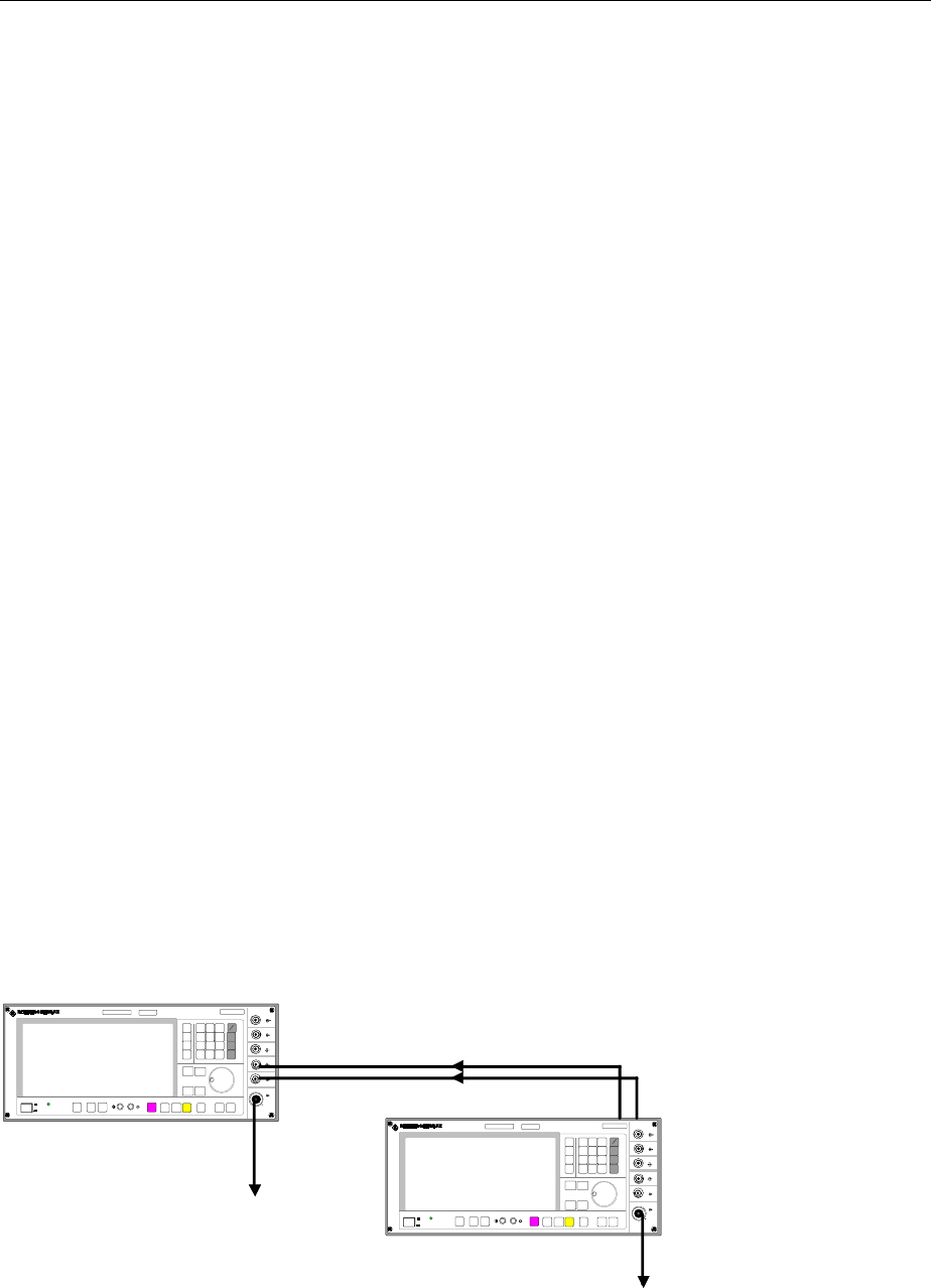
SMIQ Fading Simulation
1125.5555.03 2.71 E-9
2.9.1 Output Power with Fading
With a PATH LOSS setting of 0 dB, a single path of the fading simulator introduces an insertion loss
between 12 dB and 18 dB for the IQ signals applied (with Insertion Loss Setting Mode = NORMAL). This
insertion loss provides a headroom if several paths are superimposed on one another and also for the
statistical influences to which a path is exposed. In the LOW ACP mode, the insertion loss is reduced to
approx. 6 dB to 12 dB. This may lead to the rare case of clipping level being attained in the instrument.
The IQ signals are in such case limited to the maximum level (clipping). The corresponding insertion
loss is automatically corrected in the SMIQ. The output power is kept constant.
Displays:
LEVEL: The rms value of the output signal is displayed.
PEP: The (theoretically possible) peak value is displayed. This value is attained if clipping level
is reached both for the I and the Q path. For signals with a high crest factor it is not likely
that the PEP value is attained.
Due to the insertion loss introduced by the fading simulator, the maximum output power of the SMIQ is
reduced by max. 18 dB.
2.9.2 Two-Channel Fading
For two-channel fading, an SMIQ with two fading options (SMIQB14 and SMIQB15) and a second SMIQ
without fading options is required. Moreover, the SMIQ has to be recabled internally, see description in
Chapter 1, Section "Option SMIQB15 – Second Fading Simulator". After reconnecting the internal
cables, the I/Q baseband signals of the second channel (SMIQB15) are available at connectors I
FADED and Q FADED on the rear panel of the unit. On the second unit, vector modulation has to be
switched on.
Notes: - Because of the insertion loss introduced by the fading simulator in the first SMIQ, the second
SMIQ is not driven correctly. For the second SMIQ to be driven correctly, the current insertion
loss of the first SMIQ must be determined and entered into the second SMIQ. This correction
can be made by entering a CREST FACTOR in the vector modulation menu of the second
SMIQ. The numerical value to be entered can be taken from the first SMIQ from the line SET
SECOND SMIQ CREST FACTOR TO in the fading menu. After this value has been entered,
the second SMIQ supplies the output level indicated in the menu.
- For calibration of the two output levels (with Fading Simulator) it is necessary to leave the
Fading Simulator in the signal path and to switch off fading. At this purpose, select setting
“CALIBRATE“ with Standard in the Fading Simulator menu.
ïð
SMIQ
ïð
SMIQ
I
Q
RF 2
RF 1
Fig. 2-37 Two-channel fading
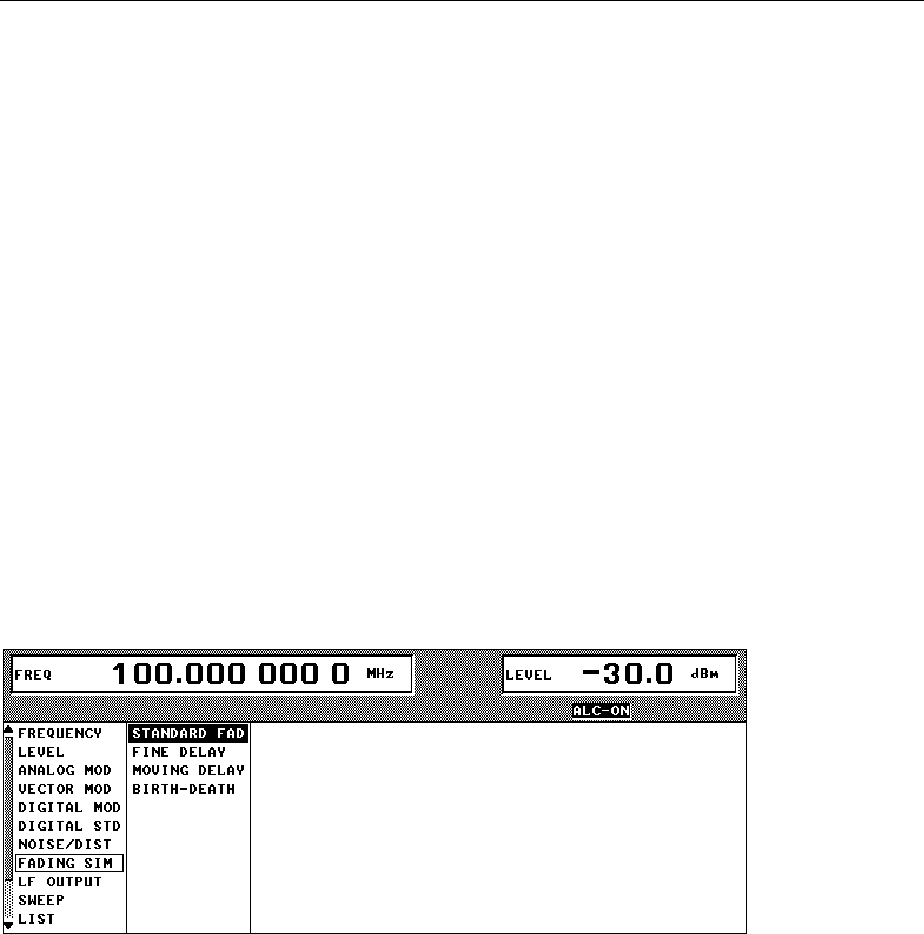
Fading Simulation SMIQ
1125.5555.03 2.72 E-9
2.9.3 Correlation between Paths
Fading processes of different paths normally do not depend on statistical processes. However, it is
possible to set a correlation of paths 1 to 6 with paths 7 to 12 in pairs. To set the correlation, a synchronous
signal processing is required for the two fading options which involves the following restrictions:
• The correlation is always reciprocal, ie if path 1 is correlated with path 7, path 7 is also correlated
with path 1 (CORR PATH).
• The following parameters of the two paths have to correspond:
- Fading profile PROFILE
- Doppler parameter SPEED or DOPPLER FREQ
- Magnitude of correlation coefficient COEFF
• The following equation applies to the phase of the correlation coefficient and thus to the phase shift
between the correlated paths:
ϕ12 = 360° - ϕ21
• The parameters for Log Normal fading have to correspond for correlated paths.
All parameter adaptations due to the limitations mentioned before are automatically performed by SMIQ.
Note: After setting all parameters, the two fading options have to be synchronized by RESET and
then by RUN.
2.9.4 Menu FADING SIM
Fig. 2-38 Menu FADING SIM with submenus
FADING SIM Selection of fading simulator mode.
STANDARD FAD "Normal“ mode with 6 paths (with option SMIQB14) or 12
paths (with SMIQB14 and SMIQB15), time resolution 50 ns.
FINE DELAY Mode with fine time resolution. Two paths are possible for
each option (SMIQB14 / SMIQB15). The system bandwidth
of the paths is limited to 4.6 MHz; this is sufficient for 3GPP
with 3.84 Msymb/s. Time resolution is 1 ns.
MOVING DELAY Mode with 2 paths, one with a fixed delay, the other with
a delay varying sinusoidally. This corresponds to test
case 3GPP, 25.104-320, Annex B3.
BIRTH-DEATH Mode with 2 paths with a delay randomly varying within a
time range.
Note: The modes FINE DELAY, MOVING DELAY, BIRTH-DEATH are
possible only if software option SMIQB49 is built in.
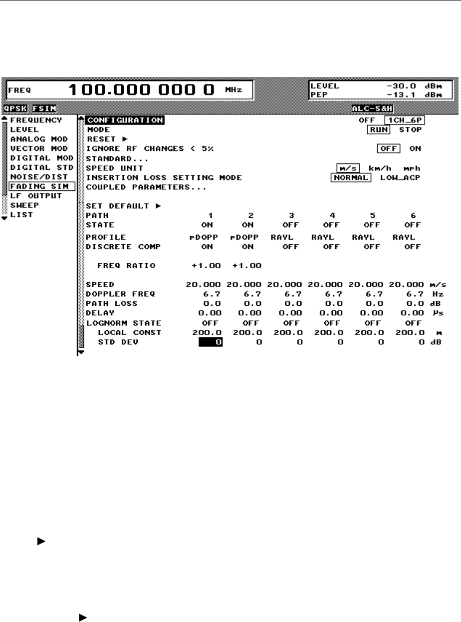
SMIQ Fading Simulation
1125.5555.03 2.73 E-9
2.9.4.1 Menu STANDARD FADING
The settings for fading simulation can be accessed via the FADING SIM menu.
Menu selection: FADING SIM
Fig. 2-39 Menu STANDARD FADING (two Fading Simulators installed)
CONFIGURATION Switching on fading simulation by selection of the number of active paths and
channels.
1CH_6P One channel with 6 paths (with option SMIQB14)
1CH_12P One channel with 12 paths (with SMIQB14 and SMIQB15)
2CH_6+6 Two channels with 6 paths each (with SMIQB14 and SMIQB15)
IEC/IEEE-bus command SOUR:FSIM:CONF S12P
SOUR:FSIM ON
MODE Stopping (STOP) and starting (RUN) the fading process.
Following RESET the mode RUN starts the Pseudo Noise Generator at a
defined starting point for generating the fading process.
IEC/IEEE-bus command SOUR:FSIM:SEQ RUN
RESET Resetting the Pseudo Noise Generator.
If RESET is set, the parameter MODE is automatically set to STOP. RESET
also ensures a synchronization of the two fading options during 2-channel
mode with the correlation switched on.
IEC/IEEE-bus command :SOUR:FSIM:SEQ:RES
IGNORE RF
CHANGES < 5% In the ON state, frequency variations below 5% are ignored. This enables RF
hopping faster than 3 ms. IEC/IEEE-bus command
:SOUR:FSIM:IGN:RFCH ON

Fading Simulation SMIQ
1125.5555.03 2.74 E-9
STANDARD Opens a window for selecting a standard setting of the fading paths. The
parameter settings comply with the measurement specifications of mobile
communication standards (e.g. GSM, CDMA, NADC).
With standards TETRA TYPICAL URBAN and TETRA HILLY TERRAIN, all
6 paths are used with these parameters instead of the stipulated 2 paths. This
yields an improved residual carrier with the same output signal.
IEC/IEEE-bus command SOUR:FSIM:STAN CDMA100
SPEED UNIT Selection of the speed unit.
IEC/IEEE-bus command :SOUR:FSIM:SPE:UNIT KMPH
INSERTION LOSS
SETTING MODE
Selection of setting mode for the insertion loss of the fading simulator.
NORMAL The minimum insertion loss for a path of the fading simulator is
fixed to 18 dB. The value has been chosen so that even with Log
Normal-Fading switched on, the fading simulator will seldom be
overdriven. This setting should be chosen for BER measurements.
IEC/IEEE-bus command :SOUR:FSIM:ILOS:MODE NORM
LOW_ACP The minimum insertion loss is between 6 and 12 dB. The value
depends on the PATH LOSS setting of the selected paths. This
mode is ideal for all STANDARD menu settings regarding
signal/noise ratio and residual carrier suppression. This setting
should be chosen for measurements which involve an adjacent-
channel interfering signal generated by the SMIQ.
IEC/IEEE-bus command :SOUR:FSIM:ILOS:MODE LACP
SHOW PATHS Switching from the display of paths 1 to 6 to the display of paths 7 to 12.
COUPLED
PARAMETERS...
In this submenu, parameters SPEED, COEFF, LOCAL CONST and STD DEV
can be coupled via the ON setting. If one of these parameters is modified
afterwards in a particular path, the parameters of all other paths will be modified.
SPEED SETTING COUPLED ON Parameters coupled for all paths.
OFF Parameter can be set individually.
IEC/IEEE :SOUR:FSIM:COUP:SPE ON
CORR COEFF SETTING ON Parameters coupled for all paths.
COUPLED OFF Parameter can be set individually.
IEC/IEEE :SOUR:FSIM:COUP:CORR:COEF ON
LOCAL CONST SETTING ON Parameters coupled for all paths.
COUPLED OFF Parameter can be set individually.
IEC/IEEE :SOUR:FSIM:COUP:LOGN:LCON ON
STD DEV SETTING COUPLED ON Parameters coupled for all paths.
OFF Parameter can be set individually.
IEC/IEEE :SOUR:FSIM:COUP:LOGN:CSTD ON
SET SECOND SMIQ
CREST FACTOR TO Indication of crest factor which has to be set on the second SMIQ in the vector
modulation menu so that the insertion loss caused by the fading simulator (in the
first SMIQ) is compensated correctly on the second SMIQ.
IEC/IEEE-bus command :SOUR:FSIM:CFAC:EXT?
SET DEFAULT Default setting of path parameter with path 1 switched on and all other paths
switched off.
IEC/IEEE-bus command :SOUR:FSIM:DEF

SMIQ Fading Simulation
1125.5555.03 2.75 E-9
PATH The following parameter have to be set separately for each path.
STATE Switching on and off a path. If the cursor is placed onto a path in the diagram,
it may be switched on and off by pressing one of the unit keys (toggle
function).
IEC/IEEE-bus command :SOUR:FSIM:PATH3:STAT ON
PROFILE Selection of the fading profile.
pDOPP (Pure DOPpler) Simulation of a transmission path having a single
direct connection from the transmitter to the moving receiver
(discrete component). The Doppler Frequency shift is determined
by the parameters DOPPLER FREQ and FREQ RATIO.
IEC/IEEE-bus command :SOUR:FSIM:PATH4:PROF PDOP
RAYL (RAYLeigh) Simulation of a radio field, where a multitude of
broadly scattered partial waves hit upon a moving receiver. The
receiving amplitude resulting therefrom is time-varying. The
probability density function of the receiving amplitude is described
by a Rayleigh distribution. The fading spectrum is a classical
Doppler spectrum.
IEC/IEEE-bus command :SOUR:FSIM:PATH1:PROF RAYL
RICE Simulation of a radio field, where apart from a multitude of
scattered partial waves, one strong direct wave (discrete
component) hits upon a moving receiver. The probability density
function of the receiving amplitude is described by a Rice
distribution. The fading spectrum of an unmodulated signal is an
overlapping of a classical Doppler spectrum with a discrete
spectrum line.
IEC/IEEE-bus command :SOUR:FSIM:PATH7:PROF RICE
CPHAS A radio traffic area without direct and random waves is generated
for this fading type (no discrete and no static component).
The path is multiplied by a constant "pointer“ according to the
path-specific parameter.
IEC/IEEE-bus command :SOUR:FSIM:PATH3:PROF CPH
DISCRETE COMP Shows the status of the discrete component (ON or OFF).
IEC/IEEE-bus command :SOUR:FSIM:PATH4:DCOM:STAT ON
POWER RATIO Input value of the power ratio of the discrete component and distributed
component with Ricean fading switched on. If POWER RATIO is changed the
sum of both components remains constant.
IEC/IEEE-bus command :SOUR:FSIM:PATH6:PRAT 3
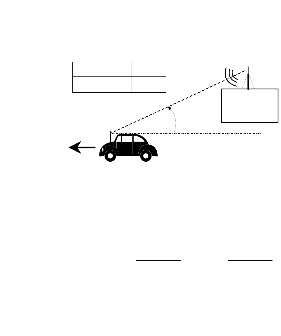
Fading Simulation SMIQ
1125.5555.03 2.76 E-9
FREQ RATIO Input value of the ratio of the actual Doppler Frequency shift to the Doppler
Frequency setting with Ricean fading or Pure Doppler switched on. The actual
Doppler Frequency shift depends on the simulated angle of incidence of the
discrete component.
IEC/IEEE-bus command :SOUR:FSIM:PATH6:FRAT 1
ϕ
/ deg 0 90 180
FREQ RATIO -1 0 +1
ϕ
Fig. 2-40 Doppler Frequency shift with moving receiver
CONST PHASE Entry value of CONST PHASE with CPHAS fading switched on. The
corresponding path is multiplied by this phase.
IEC/IEEE-bus command :SOUR:FSIM:PATH6:CPH 20.0
SPEED Input value of the speed v of the moving receiver.
The Doppler frequency fD (DOPPLER FREQ) is calculated from the speed and
the RF frequency fRF. When changing SPEED the parameter DOPPLER
FREQ will be automatically adjusted. This parameter can be coupled, see
parameter COUPLED PARAMETERS...
Range: vms
fRF
min ./
=⋅003 1092
vms
fRF
max /
=⋅479 1092
h/km99999vmax ≤
IEC/IEEE-bus command :SOUR:FSIM:PATH1:SPE 100
DOPPLER FREQ Input value of the amount of the maximum Doppler Frequency shift (cf. FREQ
RATIO).
When changing the Doppler Frequency fD the parameter SPEED will be
automatically adjusted.
With cms=⋅2998 108
.
/
it is v
c
f
f
D
RF
=
IEC/IEEE-bus command :SOUR:FSIM:PATH2:FDOP 92.3
PATH LOSS Input value of the attenuation of the path.
IEC/IEEE-bus command :SOUR:FSIM:PATH3:LOSS 3
DELAY Input value of the signal delay in the path.
IEC/IEEE-bus command :SOUR:FSIM:PATH3:DEL 14.5

SMIQ Fading Simulation
1125.5555.03 2.77 E-9
CORR PATH Switching on or off (NONE) a correlation with the selected path. This setting is
accessible if both fading options SMIQB14 and SMIQB15 have been installed.
Only a two by two correlation of paths 1 to 6 with paths 7 to 12 can be set.
IEC/IEEE-bus command :SOUR:FSIM:PATH6:CORR:PATH 12
COEFF Input value of the amplitude of the complex correlation coefficient. This
parameter can be coupled, see parameter COUPLED PARAMETERS...
IEC/IEEE-bus command :SOUR:FSIM:PATH6:CORR:COEF 0.5
PHASE Input value of the phase of the complex correlation coefficient.
IEC/IEEE-bus command :SOUR:FSIM:PATH6:CORR:PHAS 180
LOGNORM STATE Switching on or off the Log Normal-Fading.
With Log Normal-Fading set, an additional rather slow continuous changing of
the receiving amplitude of a moving receiver is simulated. Log Normal-Fading
has a multiplying effect on the path loss. The multiplication factor is time-
varying and logarithmically normally distributed. If a Rayleigh profile is set
simultaneously, this results in Suzuki-Fading.
IEC/IEEE-bus command :SOUR:FSIM:PATH6:LOGN:STAT ON
LOCAL CONST Input value of the area constant L. This parameter can be coupled, see
parameter COUPLED PARAMETERS...
The area constant L and the speed v of the moving receiver determine the
corner frequency fL of Log Normal-Fading:
fvL
L
=/
The power density spectrum of an unmodulated carrier (CW) is an overlapping
of a discrete spectrum line at fRF with a frequency dependent continuous
spectrum described by
S f const e
ff
f
RF
L
() .
=⋅
−⋅−
æ
è
çö
ø
÷
05
2
The lower limit of the range is dependent on the RF frequency fRF :
Lms
fRF
min /
=⋅12 109
IEC/IEEE-bus command :SOUR:FSIM:PATH6:LOGN:LCON 150
STD DEV Input value of the standard deviation of the Log Normal-Fading. This
parameter can be coupled, see parameter COUPLED PARAMETERS...
IEC/IEEE-bus command :SOUR:FSIM:PATH6:LOGN:CSTD 6
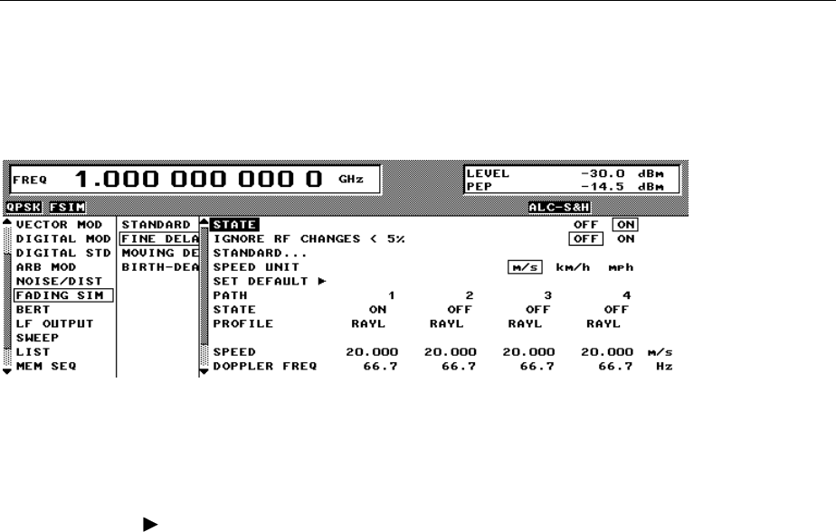
Fading Simulation SMIQ
1125.5555.03 2.78 E-9
2.9.4.2 Menu FINE DELAY
With the FINE DELAY mode a better time delay resolution of the paths is obtained. Two paths are
possible for each option (SMIQB14 / SMIQB15). The system bandwidth of these paths is limited to 4.6
MHz, which is sufficient for 3GPP with 3.84 Msymb/s. Time resolution is 1 ns.
Fig. 2-41 Menu FINE DELAY
STATE Activating/deactivating fine delay simulation.
IEC/IEEE-bus command :SOUR:FSIM:FDEL:STAT ON | OFF
IGNORE RF
CHANGES < 5% When switched on, frequency variations below 5% are ignored. Frequency
hopping is thus faster than 3 ms. IEC/IEEE-bus command
:SOUR:FSIM:IGN:RFCH ON
STANDARD Opens a window for selecting a defined setting of fading paths.
Selection:
3GPP_BS__4.1.0_CASE1: SPEED: 3 km/h
Pfad 1: DELAY 25 ns
PATH LOSS 0 dB
Pfad 2: DELAY 1001 ns
PATH LOSS 10 dB
3GPP_BS_4.1.0_CASE2: SPEED: 3km/h
Pfad 1: DELAY 25 ns
PATH LOSS 0 dB
Pfad 2: DELAY 1001 ns
PATH LOSS 0 dB
Pfad 3: DELAY 20025 ns
PATH LOSS 0 dB
3GPP_BS_4.1.0_CASE3: SPEED: 120km/h
Pfad 1: DELAY 25 ns
PATH LOSS 0 dB
Pfad 2: DELAY 285 ns
PATH LOSS 3 dB
Pfad 3: DELAY 546 ns
PATH LOSS 6 dB
Pfad 4: DELAY 806 ns
PATH LOSS 9 dB
3GPP_3.3.1_CASE5: SPEED: 50 km/h
Path 1: DELAY 25 ns
PATH LOSS 0 dB
Path 2: DELAY 1001 ns
PATH LOSS 10 dB

SMIQ Fading Simulation
1125.5555.03 2.79 E-9
3GPP_BS_4.1.0_CASE4: SPEED: 250 km/h
Pfad 1: DELAY 25 ns
PATH LOSS 0 dB
Pfad 2: DELAY 285ns
PATH LOSS 3 dB
Pfad 3: DELAY 546 ns
PATH LOSS 6 dB
Pfad 4: DELAY 806 ns
PATH LOSS 9 dB
3GPP_UE_4.1.0_CASE1: SPEED: 3 km/h
Pfad 1: DELAY 25 ns
PATH LOSS 0 dB
Pfad 2: DELAY 1001 ns
PATH LOSS 10 dB
3GPP_UE_4.1.0_CASE2: SPEED: 3km/h
Pfad 1: DELAY 25 ns
PATH LOSS 0 dB
Pfad 2: DELAY 1001 ns
PATH LOSS 0 dB
Pfad 3: DELAY 20025 ns
PATH LOSS 0 dB
3GPP_UE_4.1.0_CASE3: SPEED: 120km/h
Pfad 1: DELAY 25 ns
PATH LOSS 0 dB
Pfad 2: DELAY 285 ns
PATH LOSS 3 dB
Pfad 3: DELAY 546 ns
PATH LOSS 6 dB
Pfad 4: DELAY 806 ns
PATH LOSS 9 dB
3GPP_UE_4.1.0_CASE4: SPEED: 3km/h
Pfad 1: DELAY 25 ns
PATH LOSS 0 dB
Pfad 2: DELAY 1001 ns
PATH LOSS 0 dB
3GPP_UE_4.1.0_CASE5: SPEED: 50km/h
Pfad 1: DELAY 25 ns
PATH LOSS 0 dB
Pfad 2: DELAY 1001 ns
PATH LOSS 10 dB
3GPP_UE_4.1.0_CASE6: SPEED: 250km/h
Pfad 1: DELAY 25 ns
PATH LOSS 0 dB
Pfad 2: DELAY 285 ns
PATH LOSS 3 dB
Pfad 3: DELAY 546 ns
PATH LOSS 6 dB
Pfad 4: DELAY 806 ns
PATH LOSS 9 dB

Fading Simulation SMIQ
1125.5555.03 2.80 E-9
IEC/IEEE-bus command :SOUR:FSIM:FDEL:STAN G3C1
IEC/IEEE-bus command :SOUR:FSIM:FDEL:STAN G3UECn ( n=1...6)
Notes:
- The path delays correspond to those in 3GPP, TS 25.101 V4.1.0 (2001-06)
und TS 25.141 V4.1.0 (2001-06). However, they include a basic delay of 25 ns
of the Fading Simulator.
- All test cases requiring more than 2 paths are only possible with option
SMIQB15.
SPEED UNIT Selection of the unit required for the speed of parameter SPEED.
IEC/IEEE-bus command :SOUR:FSIM:FDEL:SPE:UNIT KMPH
SET DEFAULT Sets the default setting of the path parameters with path 1 switched on and all
other paths switched off.
IEC/IEEE-bus command :SOUR:FSIM:FDEL:DEF
PATH Indicates the paths for subsequent parameters. These parameters can be set
individually for each path.
STATE Switch-on/off of a path. If the cursor is placed onto a path, this path may be
switched on or off by pressing one of the unit keys (toggle function).
IEC/IEEE-bus command :SOUR:FSIM:FDEL:PATH2:STAT ON | OFF
PROFILE Selection of a fading profile. See explanations under Standard Fading. Only
the following setting is possible:
pDOPP
IEC/IEEE-bus command :SOUR:FSIM:FDEL:PATH2:PROF PDOP
RAYL (This setting is provided in the 3GPP test cases)
IEC/IEEE-bus command :SOUR:FSIM:FDEL:PATH2:PROF RAYL
FREQ RATIO Entry value of the ratio of the actual Doppler frequency shift to the set Doppler
frequency with FDOP fading switched on. (See explanation under Standard
Fading).
IEC/IEEE-bus command :SOUR:FSIM:FDEL:PATH2:FRAT 1
SPEED Entry value of the speed v of the moving receiver (see explanation under
Standard Fading).
IEC/IEEE-bus command :SOUR:FSIM:FDEL:PATH2:SPE 100
DOPPLER FREQ Entry value of the magnitude of the maximum Doppler frequency shift (see
explanation under Standard Fading).
IEC/IEEE-bus command :SOUR:FSIM:FDEL:PATH2:FDOP 92.3
PATH LOSS Entry value of attenuation in path.
Value range: 0.0 to 50.0 dB.
IEC/IEEE-bus command :SOUR:FSIM:FDEL:PATH2:LOSS 3
DELAY Entry value of signal delay in path.
Value range: 25 ns to 1637 µs.
IEC/IEEE-bus command :SOUR:FSIM:FDEL:PATH2:DEL 14.5E-6
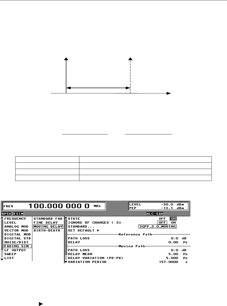
SMIQ Fading Simulation
1125.5555.03 2.81 E-9
2.9.4.3 Menu MOVING DELAY
In the MOVING DELAY mode, the Fading Simulator simulates the dynamic propagation conditions
according to test case 3GPP, 25.104-320, Annex B3.
2 paths are simulated; the delay of path 1 remains unchanged, the delay of path 2 slowly moves to and
fro sinusoidally. The two paths have no fading profile (non-fading), have the same level, the same phase
and have no Doppler shift.
t
2
P2
∆τ
P1
t
1
Fig. 2-42 Two paths with menu MOVING DELAY
The delay of the moving path is obtained with the following equation:
÷
÷
ø
ö
ç
ç
è
æ
÷
÷
ø
ö
ç
ç
è
æ⋅
++= )
PERIOD_VARIATION
t2
sin(1
2
VARIATION_DELAY
MEAN_DELAY
π
τ∆
The following settings are required to obtain the values suggested in Annex B3:
DELAY (path 1) 1µs
DELAY MEAN = DELAY(path 1) + DELAY VARIATION / 2 = 3.5µs
DELAY VARIATION 5 µs
VARIATION PERIOD 157 s
For further tests, DELAY MEAN and the variation parameters can be modified. The two paths can be
levelled differently.
Fig. 2-43 Menu MOVING DELAY
STATE Activating/deactivating the moving delay simulation.
IEC/IEEE-bus command :SOUR:FSIM:MDEL:STAT ON | OFF
IGNORE RF
CHANGES < 5% When switched on, frequency variations below 5% are ignored. RF hopping is
thus faster than 3 ms. IEC/IEEE-bus command :SOUR:FSIM:IGN:RFCH ON
STANDARD Is now the same as SET DEFAULT.

Fading Simulation SMIQ
1125.5555.03 2.82 E-9
SET DEFAULT Sets the default setting of the path parameters.
IEC/IEEE-bus command :SOUR:FSIM:MDEL:DEF
PATH Indicates the paths for subsequent parameters. These parameters can be set
individually for each path.
PATH LOSS Entry value of attenuation in path for the reference.
Value range: 0.0 to 50.0 dB.
IEC/IEEE-bus command :SOUR:FSIM:MDEL:REF:LOSS 3
DELAY Entry value of signal delay in the reference path.
Value range: 0.0 to 1638 µs.
IEC/IEEE-bus command :SOUR:FSIM:MDEL:REF:DEL 14.5E-6
PATH LOSS Entry value of attenuation in path for moving.
Value range: 0.0 to 50.0 dB.
IEC/IEEE-bus command :SOUR:FSIM:MDEL:MOV:LOSS 3
DELAY MEAN Mean value of the moving path delay. See explanation above.
Value range: 0.25 to 1637.8 µs.
IEC/IEEE-bus command :SOUR:FSIM:MDEL:MOV:DEL:MEAN 12.5E-6
DELAY VARIATION
(PK-PK)
Range for delay variation for the moving path. The peak-peak value is set. See
explanations above.
Value range: 0.3 to 100 µs.
IEC/IEEE-bus command :SOUR:FSIM:MDEL:MOV:DEL:VAR 2.1E-6
VARIATION PERIOD Speed of delay variation. After a VARIATION PERIOD has elapsed a
complete cycle is swept.
Only for the moving path.
Value range: 10 to 500 s
IEC/IEEE-bus command :SOUR:FSIM:MDEL:MOV:VPER 13.4
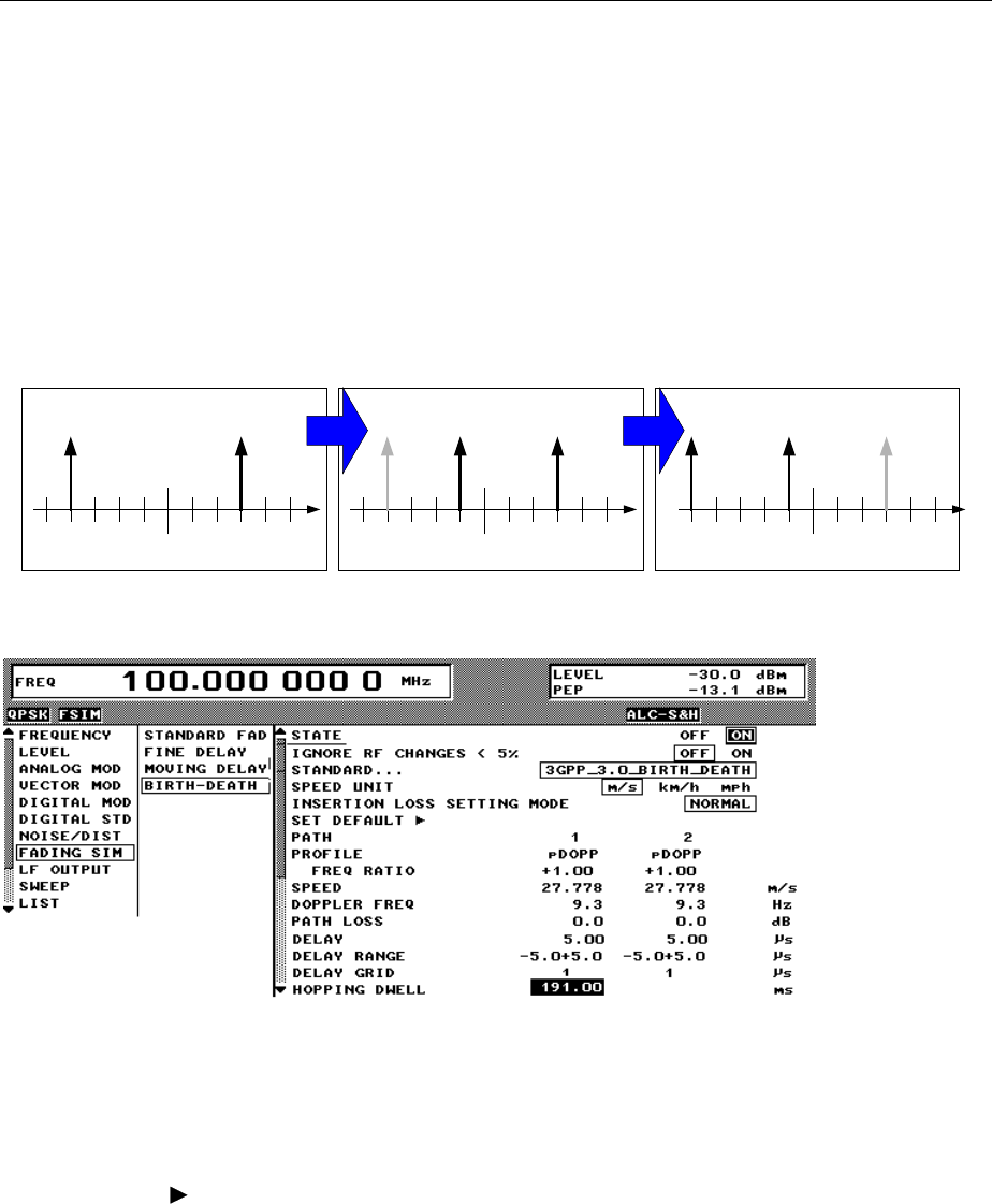
SMIQ Fading Simulation
1125.5555.03 2.83 E-9
2.9.4.4 Menu BIRTH-DEATH
In the BIRTH-DEATH mode the Fading Simulator simulates the dynamic propagation conditions according
to test case 3GPP, 25.104-320, Annex B4.
To do this, 2 paths are simulated which alternately appear (BIRTH) or disappear (DEATH) at random time
positions. The time positions lie within a grid of [-5, -4, -3, -2, -1, 0, 1, 2, 3, 4, 5] µs. After a presettable time
(HOPPING DWELL) a path disappears from a grid position and re-appears at another randomly
selected grid position. During this hop, the second path remains stable at its grid position. After a further
HOPPING DWELL has elapsed, the second path changes its position and the first path remains at its
position, etc. The two paths never appear at the same time position (see Fig. 2-44).
According to Annex B4, each path has the same attenuation and phase and no Doppler shift. However,
this can be set in the menu BIRTH-DEATH for further tests. The dwell period of 191 ms (in line with
3GPP) can be varied between 100 ms and 5 s.
012345-1-2-3-4-5 012345-1-2-3-4-5 012345-1-2-3-4-5
P1 P2 P1 P1 P2 P1P2 P2
Fig. 2-44 Example of hop sequence with BIRTH-DEATH fading
Fig. 2-45 Menu BIRTH-DEATH
STATE Activation/deactivation of the BIRTH-DEATH simulation.
IEC/IEEE-bus command :SOUR:FSIM:BIRT:STAT ON | OFF
IGNORE RF
CHANGES < 5% When switched on, frequency variations below 5% are ignored. RF hopping is
thus faster than 3 ms. IEC/IEEE-bus command :SOUR:FSIM:IGN:RFCH ON
STANDARD Is now the same as SET DEFAULT.
SPEED UNIT Selection of the unit required for the speed of parameter SPEED.
IEC/IEEE-bus command :SOUR:FSIM:BIRT:SPE:UNIT KMPH

Fading Simulation SMIQ
1125.5555.03 2.84 E-9
INSERTION LOSS
SETTING MODE
Selection of a setting mode for the insertion loss of the fading simulator.
See explanation under STANDARD FADING.
IEC/IEEE-bus command :SOUR:FSIM:BIRT:ILOS:MODE NORM
:SOUR:FSIM:BIRT:ILOS:MODE LACP
SET DEFAULT Sets the default setting of the path parameters.
IEC/IEEE-bus command :SOUR:FSIM:BIRT:DEF
PATH Indicates the paths for subsequent parameters. These parameters can be set
individually for each path.
PROFILE Selection of a fading profile. Only pDOPP is available here; when FREQ
RATIO = 0 is set a "non-fading“ path is obtained.
pDOPP (pure DOPPler) Simulation of a transmission path having a single
direct connection from the transmitter to the moving receiver
(discrete component).
The Doppler frequency shift is determined by the parameters
DOPPLER FREQ and FREQ RATIO.
IEC/IEEE-bus command :SOUR:FSIM:BIRT:PATH1:PROF PDOP
FREQ RATIO Entry value of ratio of actual Doppler frequency shift. See explanation under
STANDARD FADING. When FREQ RATIO = 0 is set, a "non-fading" path is
obtained.
IEC/IEEE-bus command :SOUR:FSIM:BIRT:PATH1:FRAT 1
SPEED Entry value of the speed v of the moving receiver.
See explanations under STANDARD FADING.
All entries in path 1 are copied for path 2.
IEC/IEEE-bus command :SOUR:FSIM:BIRT:PATH1:SPE 100
DOPPLER FREQ Entry value of the magnitude of the maximum Doppler frequency shift. See
explanation under STANDARD FADING.
All entries in path 1 are copied for path 2.
IEC/IEEE-bus command :SOUR:FSIM:BIRT:PATH1:FDOP 92.3
PATH LOSS Entry value of attenuation in path. Value range: 0.0 to 50.0 dB.
IEC/IEEE-bus command :SOUR:FSIM:BIRT:PATH2:LOSS 3
DELAY Entry value of signal delay in path 1. All entries in path 1 are copied for path 2.
Value range: 5.0 to 1000.0 µs.
IEC/IEEE-bus command :SOUR:FSIM:BIRT:PATH1:DEL 1000 E-3
DELAY RANGE The delay of the two paths is within this range.
Non-editable parameter.
For the two channels: -5.0 to +5.0 µs.
DELAY GRID Time grid of the different carriers appearing at random. The carriers have
delays which lie within the DELAY RANGE and coincide with
n * DELAY GRID (with n –5 to +5).
Non-editable parameter. Value = 1 µs for the two channels.
HOPPING DWELL Dwell period until the next BIRTH-DEATH action. After this dwell period the
next path changes its delay at random.
Value range: 100.0 to 5000.0 ms.
IEC/IEEE-bus command :SOUR:FSIM:BIRT:PATH1:HOPP:DWEL 1.2
SMIQ Fading Simulation
1125.5555.03 2.85 E-9
2.9.5 Test procedure
The following settings can be used to demonstrate how Option SMIQB49 functions:
Settings on SMIQ
General
Frequency 30 MHz
Level -10 dB
Digital Modulation (DIGITAL MOD)
STATE ON
SOURCE Data List
LIST 1000 0000 0000 0000 0000 0000 0000 0000 (32 bits)
MODULATION ASK
SYMBOL RATE 1 000 000 sym/s
Fading Simulation
MOVING DELAY ON
Reference Path
Path Loss 0 dB
Delay 0
µs
Moving Path
Path Loss 6.0 dB
Delay Mean 5.0 µs
Delay Variation 5.0 µs
Variation Period 10.0 s
Settings on the oscilloscope (BW > 100 MHz)
Vertical 50 mV/div, at 50 Ω
Horizontal 2 µs /div
Trigger level 100 mV
The test result shows a high pulse (about 150 mV), and next to it a pulse which is half as high and
moves from one side to the other accordingly to the setting Delay Variation or Variation Period.
Fig. 2-46 Pulse on Oscilloscope
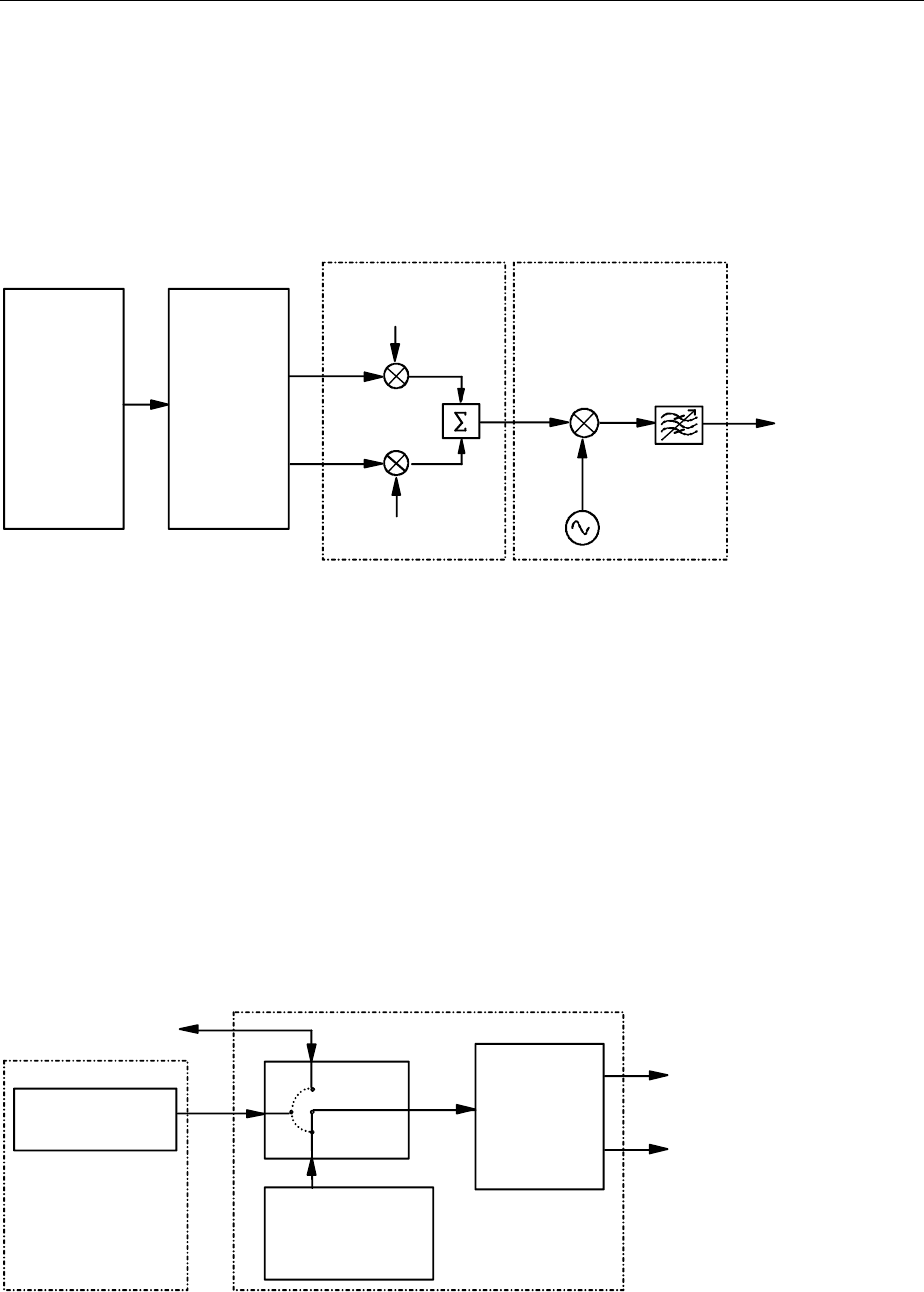
Digital Modulation SMIQ
1125.5555.03 E-92.86
2.10 Digital Modulation
With option Modulation Coder (MCOD) SMIQB20 provided, SMIQ can generate digitally modulated
output signals. Available modulation methods are ASK (amplitude shift keying), FSK (frequency shift
keying), PSK (phase shift keying) as well as QAM (quadrature amplitude modulation). Baseband filtering
and symbol rate can be freely set in a wide range.
The modulation coder generates the analog IQ signals for the I/Q modulator of SMIQ from the digital
input signals.
sin( t)
ω
cos( t)
ω
I
Q
RF OUT
IQ modulator RF up/down converter
Option
Modulation
Coder
SMIQB10
Option
Data
Generator
SMIQB11
Fig. 2-47 Modulation coder in SMIQ
The modulation coder works with digital input signals such as
• clock signals (symbol clock, bit clock),
• modulation data or modulation symbols,
• control signals for envelope control and trigger signals.
The digital input signals may originate from the following sources:
• The modulation coder can generate clock signals such as PRBS data signals and simple data
patterns.
• External clock signals, modulation data and signals for envelope control can be fed in via connectors
at the front or rear panel of SMIQ.
• With option Data Generator SMIQB11 provided, an additional data source is available. This option
has a 16-Mbit memory for modulation data and control signals. The memory can be extended to
48 Mbit or 80 Mbit by installing one or two SMIQB12 options (Memory Extension).
I
DATA MEMORY
Q
DIGITAL
IN/OUT
PRBS GENERATOR
INT CLOCK
DIGITAL
MODULATOR
EXT DATA/CLOCK
Modulation coder
Data generator
Fig. 2-48 Digital input signals of modulation coder
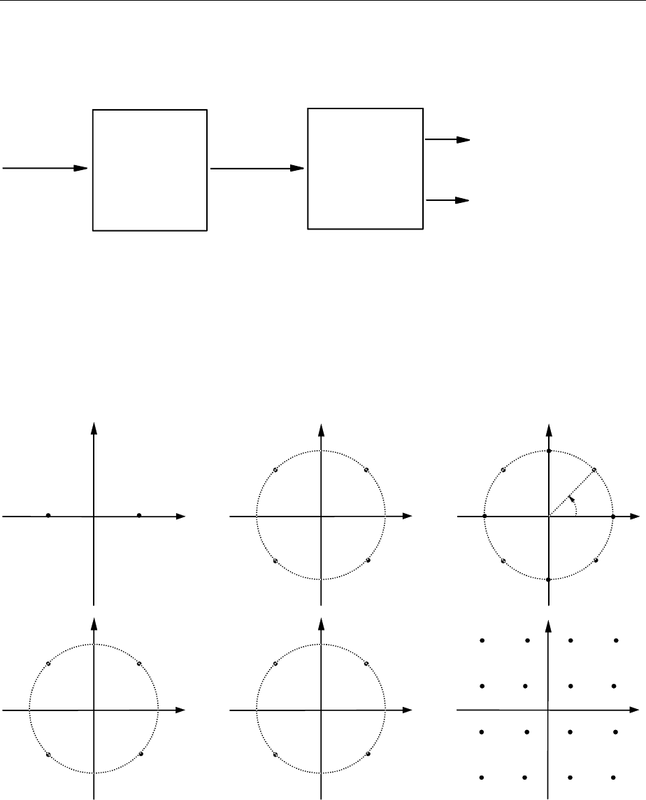
SMIQ Digital Modulation
1125.5555.03 E-92.87
2.10.1 Digital Modulation Methods and Coding
The input sequence of modulation symbols dn can be subject to different types of coding. I and Q values
are assigned to the coded modulation symbols dcn in the functional block MAPPING.
I,
∆
∆∆
∆
F
Q
MAPPING
CODING
modulation
symbols
d
n-2
, d
n-1
, d
n
... dc
n-2
, dc
n-1
, dc
n
...
Fig. 2-49 Functional blocks Coding and Mapping
2.10.1.1 PSK and QAM Modulation
PSK and QAM modulations can be explained on the basis of a rule of assignment (mapping) according
to which each modulation symbol is represented by I and Q values as shown in the following IQ
constellation diagrams. The constellation diagrams apply if no coding is switched on.
I
Q
0
1 I
Q
0001
10 11
I
Q
0000 0001
00110010
1010 1000
10011011
0101 0111
01100100
1111 1110
11001101
I
Q
1101
00 10
I
Q
0010
11 01
I
Q
001
011
101 111
010
100
110
000
BPSK
QPSK; OQPSK
8PSK, DQPSK
QPSK ISAT
Π/4
ϕ
QPSKIS95
OQPSK IS95
Fig. 2-50 Constellation diagrams of BPSK, QPSK, 8PSK and 16QAM

Digital Modulation SMIQ
1125.5555.03 E-92.88
For offset QPSK (OQPSK), the Q signal is delayed by half the symbol period with reference to the I
signal.
QAM modulation methods 16QAM, 32QAM, 64QAM and 256QAM were implemented according to ETSI
standard ETS 300429 for Digital Video Broadcasting (DVB).
All PSK and QAM modulation methods can be combined with COS and SQR_COS baseband filters as
well as with IS-95 filters. A combination with GAUSS and BESSEL filters is not possible.
2.10.1.2 Modulation π
ππ
π/4DQPSK
With differential coding switched on at the same time, a constellation diagram is obtained for π/4DQPSK
which is similar to that obtained for 8PSK. Phase shifts are however assigned to the individual
modulation symbols. The following tables show the assignment of modulation symbols to phase shifts of
IQ vectors at the selected coding.
Table 2-4 Phase shifts for π/4DQPSK without coding
Modulation symbol dn
(binary indication: MSB, LSB) 00 01 10 11
Phase shift ϕ
ϕϕ
ϕ+ 45° +135° -135° -45°
Table 2-5 Phase shifts for π/4DQPSK with coding NADC, PDC, PHS, TETRA or APCO25
Modulation symbol dn
(binary display: MSB, LSB) 00 01 10 11
Phase shift ϕ
ϕϕ
ϕ+ 45° +135° -45° -135°
Table 2-6 Phase shifts for π/4DQPSK with coding TFTS
Modulation symbol dn
(binary display: MSB, LSB) 00 01 10 11
Phase shift ϕ
ϕϕ
ϕ- 135° +135° -45° +45°

SMIQ Digital Modulation
1125.5555.03 E-92.89
2.10.1.3 FSK Modulation
For FSK modulation, frequency shifts are assigned to the modulation symbols. The modulation index h
of this digital frequency modulation is determined by
h
f
f
Symb
=⋅2∆/
The symbol rate fSYMB can be freely set to a maximum of 2.5 Msymb/s for all FSK modulations. With
GMSK selected, the frequency deviation∆
f
(FSK deviation) cannot be set since the modulation index is
fixed to a value of h = 0.5. The following table shows the assignment of modulation symbols and
frequency deviations for the different FSK methods.
Table 2-7 Frequency deviations for FSK methods
Mod. symbol 2FSK, GFSK MSK, GMSK 4FSK APCO
0−∆
f
−∆
f
−∆
f
+∆
f
/3
1+∆
f
+∆
f
−∆
f
/3 +∆
f
10 - - +∆
f
/3 −∆
f
/3
11 - - +∆
f
−∆
f
All FSK modulation methods can be combined with COS, SQR_COS, GAUSS and BESSEL baseband
filters. A combination with IS-95 filters is not permissible.
2.10.1.4 Coding
Modulation symbols are coded directly before an assignment of I and Q values or frequency shifts.
Coding is thus directly related with modulation methods which is the reason why codings are not freely
combinable with modulation methods. The following table shows which combinations are possible.
Table 2-8 Possible combination of modulation method and coding
Coding Selection CODING Combinable with MOD TYPE Example of use
Differential coding DIFF all except for 256QAM
Gray + differential
coding GRAY+DIFF all except for 256QAM D8PSK for VDR
GSM differential coding GSM FSK, GFSK, GMSK Mobile radio standard GSM
π/4DQPSK differential
coding
NADC; PDC;.. π/4DQPSK Mobile radio standards NADC,
PDC, PHS, APCO25, TFTS,
TETRA
Phase differential coding INMARSAT QPSK ISAT Satellite system INMARSAT-M
Phase differential coding PHASE DIFF 16 , 32 , 64 , 256 QAM DVB in line with ETS 300429
VDL coding VDL 8PSK VHF Digital Link
The effect of differential coding on π/4DQPSK has been described in section 'Modulation π/4DQPSK'.
Common coding types are listed in the following table.
Digital Modulation SMIQ
1125.5555.03 E-92.90
Table 2-9 Coding algorithms
CODING Coding algorithm Applicable for K bit/symbol
NONE dcn = dnK = 1 to 8
DIFF dcn = (dn + dcn-1) modulo 2k K = 1 to 7
GRAY+DIFF Gray coding with additional differential coding K = 1 to 7
GSM dcn = not (dn exor dn-1 K = 1
VDL VDL standard K = 3
Example 1: Differential coding for QPSK modulation with K = 2 bit/symbol
Decimal display; value range for modulation symbols
{}
dn∈0123;; ;
Recursive coding is defined as follows: dcn = (dn + dcn-1) modulo 4.
Depending on the state of a preceding modulation symbol dcn-1 the coded modulation
symbol dcn is obtained for example from a modulation symbol dn = 2 as follows:
dn = 2 dcn-1 dcn
02
13
20
31
By means of differential coding, the assignment between modulation symbols and
phase differences shown in the following table is generated:
Modulation symbol dn
(binary, MSB, LSB) 00 01 10 11
Phase difference ∆ϕ 0° 90° 180° 270°
Example 2: Gray and differential coding for 8PSK modulation
First, a gray coding is performed according to the gray code. Afterwards, a differential
coding is performed according to the recursive coding algorithm quoted above. By
means of the mapping rule shown in the figure in Section 'PSK and QAM Modulation'
above, IQ values are assigned to the re-coded modulation symbols. In summary, the
assignment between modulation symbols and phase differences shown in the following
table is generated:
Modulation symbol dn
(binary, MSB, LSB) 000 001 010 011 100 101 110 111
Phase difference ∆ϕ 0° 45° 135° 90° 270° 315° 225° 180°
SMIQ Digital Modulation
1125.5555.03 E-92.91
Differential coding according to VDL is shown in the following table:
Modulation symbol dn
(binary, MSB, LSB) 000 001 010 011 100 101 110 111
Phase difference ∆ϕ 0° 45° 135° 90° 315° 270° 180° 225°
Phase differential coding INMARSAT and PHASE DIFF correspond to system standards Inmarsat-M
and DVB according to ETS 300 429. The INMARSAT coding can generally be used for modulation types
with 2 bit/symbol, such as QPSK. It uses the following algorithm.
dc0
n
dc1
n
(MSB)
INMARSAT
CODING
d0n
d1
n
(MSB)
dc1n =[NOT (d1
n EXOR d0/
n) AND (d1n EXOR dc1n-1)] OR
[(d1n EXOR d0/
n) AND (d1n EXOR dc/0/
n-1)]
dc0/
n =[NOT (d1
n EXOR d0/
n) AND (d0/
n EXOR dc0/
n-1)] OR
[(d1n EXOR d0/
n-1) AND (d0/
n EXOR dc1n-1)]
2.10.1.5 Setting Conflicts
As already mentioned in the previous sections, the combination of the above modulation methods with
modulation parameters such as symbol rate, filtering and coding is limited. This limitation inevitably
causes setting conflicts if a parameter is changed which would lead to an impermissible combination.
Table 2-10 Examples of settings conflicts
Original status Change by selection Conflict Solution
1MOD TYPE π/4DQPSK
SYMBOL RATE 10 Msymb/s MOD TYPE→ GMSK GMSK is only possible
for symbol rates up to
7.5 Msymb/s.
Reduction of symbol rate to
a value of <7.5 MHz.
2MOD TYPE 2FSK
FILTER GAUSS
FILTER PARAMETER 1.0 FILTER → COS Filter COS 1.0 not
possible, the maximum
roll-off factor is 0.7.
Setting of FILTER
PARAMETER to a value
between 0.15 and 0.7.
3SYMBOL RATE 270 ksymb/s
POWER RAMP INT SYMBOL RATE→5 Msymb/s Envelope control is only
possible for symbol rates
up to 2.5 Msymb/s.
Switch-off of envelope
control.
If SMIQ cannot resolve a setting conflict, error message SETTINGS CONFLICT is indicated in the
status line of the display. In this case, SMIQ uses the user-defined setting in the display. However, the
generated modulation signal does not correspond to this indication. The setting conflict can be
eliminated by a change of parameters. Error message SETTINGS CONFLICT disappears as soon as a
conflict-free setting is reinstated. For a list of possible setting conflicts and error messages for digital
modulation see Annex B, thumbnail divider 7.

Digital Modulation SMIQ
1125.5555.03 E-92.92
2.10.2 Internal Modulation Data and Control Signals from Lists
If SMIQ is equipped with option Data Generator SMIQB11, modulation data and control signals can be
stored in a freely programmable data-generator memory. The storage capacity in the basic configuration
is 16 Mbit but can be extended by 32 Mbit or 64 Mbit by fitting one or two SMIQB12 options.
The data are managed via so-called lists. 125 lists can be stored at maximum for modulation data or
control signals. A list editor allows to select, copy, change and delete data lists. For a detailed
description of the list editor see Section 2.2.11, List Editor.
There are two types of lists, the DATA LIST and the CONTROL LIST.
Lists, as a source for modulation data, can be selected in the menu by entering SOURCE -SOURCE-
DATA_LIST and the active list by SOURCE-SELECT DATA LIST.
Lists, as a source for control signals, can be selected in the menu by entering SOURCE -CONTROL
STATE ON and the active list by SOURCE-SELECT CONTROL LIST.
Note: With DATA LIST selected as a source for internal modulation data, the control signals too
have to come from a list. In this case, the setting POWER RAMP CONTROL- SOURCE
EXTERN DIGITAL issues an error message
With CONTROL LIST selected as a source for control signals, the modulation data too
have to come from a list.
Data Lists:
The DATA LIST has a bit-by-bit layout. The length of the programmed data sequence and the available
storage capacity are indicated in the status line of the display.
SELECT LIST... DLIST0
EDIT DATA LIST...
-BIT-------------------------DATA----------------------
00000001 1010 1110 0011 1011 1101 1111 1110 1100
00000033 0100 1010 1001 0101 1110 1011 1011 0010
00000065 0000 1001 1110 0001 0101 0101 0010 1011
00000097 1111 0110 1110 1000 1101 0100 1100 0100
00000129 1001 0111 0100 0001 0010 1110 1110 1010
00000161 1101 0110 1111 0111 1111 1111 1000 0100
00000193 0000 0010 1000 0001 1111 0101 1101 0101
00000225 0110 0111 1100 0000 0111 1111 1111 1111
Fig. 2-51 DATA LIST for modulation data

SMIQ Digital Modulation
1125.5555.03 E-92.93
Control Lists:
A CONTROL LIST can be created to generate control signals that have to be synchronous to the
modulation symbols. The CONTROL LIST has a bit-by-bit layout. Six different control signals can be
freely programmed. The CONTROL LIST can be created such that entries are only made at those
symbol positions where a control signal is changed. The length of the CONTROL LIST is determined by
the symbol number of the last entry and can differ from that of the DATA LIST.
SELECT LIST... CLIST0
EDIT CONTROL LIST COPY DELETE EDIT|VIEW
-SYMBOL-----------BGATE-LATT--CW----HOP---TRIG2-TRIG1--
00000001 100001
00000157 110010
00000313 010000
00001249 010100
00001250 010000
Fig. 2-52 CONTROL LIST for control signals
Signals BGATE (Burst Gate) and LATT (Level Attenuation) are used for envelope control. Envelope
control with these signals is switched on by selecting SOURCE-CONTROL STATE ON and POWER
RAMP CONTROL - SOURCE INT.
Digital modulation can be switched off by the CW (Continuous Wave) signal. HOP (Hopping) is a trigger
signal for frequency hopping (compare with section 'List Mode').
TRIG 1 and TRIG 2 (Trigger Output 1 and 2) can be used to generate synchronization signals such as
frame clocks, start markers of a PRBS sequence or a special modulation symbol.
Signals BGATE, LATT, HOP and CW are used internally by SMIQ but not signals TRIG 1 and TRIG 2.
All the control signals are available at the PAR DATA interface at the rear of SMIQ.
The data sequences stored in the data generator can be run repetitively (TRIGGER MODE AUTO).
Moreover, trigger signals can be used for synchronized sequences. Trigger signals can be fed in via the
TRIGIN input at connector PAR DATA. A trigger event can be initiated manually by
EXECUTE TRIGGER. A trigger signal is generated upon the trigger event at the output TRIGOUT 3.
After a trigger event, the data generator starts to output modulation data from the active list starting with
bit 1. In case of external triggering, the start can be delayed by a selectable number of symbols (EXT
TRIGGER DELAY). Retriggering (RETRIG) can be inhibited for a selectable number of symbols (EXT
TRIGGER INHIBIT).
Digital Modulation SMIQ
1125.5555.03 E-92.94
2.10.3 Internal PRBS Data and Pattern
The PRBS generators in the modulation coder provide pseudo random binary sequences (PRBS) of
different length and period. They are called sequences of maximum length and are generated by means
of feedback shift registers.
The following schematic shows the 9-bit generator with feedback from registers 4 and 0 (output).
8
765
4
3210
SER DAT
A
EXOR
Fig. 2-53 9-bit PRBS generator
The pseudo random sequence of a PRBS generator is determined by the number of registers and the
feedback. The following table describes all available PRBS generators:
Table 2-11 PRBS generators of modulation coder
PRBS generator Length in bit Feedback to
9 Bit 29 -1 = 511 Register 4, 0
15 Bit 215 -1 = 32767 Register 1, 0
16 Bit 216 -1 = 65535 Register 5, 3, 2, 0
20 Bit 220 -1 = 1048575 Register 3, 0
21 Bit 221 -1 = 2097151 Register 2, 0
23 Bit 223 -1 = 8388607 Register 5, 0
PRBS data as a source for modulation data are selected in the menu via SOURCE - SOURCE PRBS.
The period is determined by PRBS LENGTH.
Other internal modulation data are available as simple data patterns such as 0s or 1s. Selection is via
SOURCE - SOURCE PATTERN.
Note: With PRBS data or Pattern selected as source for modulation data, only external control
signals can be used. A combination with control signals from lists is not possible.
SMIQ Digital Modulation
1125.5555.03 E-92.95
2.10.4 Digital Data and Clock output Signals
2.10.4.1 Serial Interfaces DATA, BIT CLOCK and SYMBOL CLOCK
The following figure shows an example for the output signals at the serial interface for QPSK modulation
(2 bits per symbol). A positive CLOCK EDGE is assumed to be set. The following list containing 4
symbols (8 bits) was used as a data source.
SELECT LIST... DLIST00
EDIT DATA LIST...
-BIT-------------------------DATA----------------------
00000001 0001 1011
BIT CLOCK (output)
SYMBOL CLOCK (output)
DATA (output)
Data Symbols
00 01 10 11
MSB LSB
2.10.4.2 Parallel Interfaces DATA and SYMBOL CLOCK
The following figure shows an example for the output signals at the parallel interface. A positive CLOCK
EDGE is assumed to be set.
SYMBOL CLOCK (output)
DATA D7, MSB (output)
2.10.5 External Modulation Data and Control Signals
Digital modulation signals such as data, clock and signals for envelope control can be externally applied
to the modulation coder either via the parallel PAR DATA interface at the rear of SMIQ or via the serial
interface with BNC connectors DATA, BIT CLOCK and SYMBOL CLOCK. Moreover, the asynchronous
serial interface SERDATA can be used. For a detailed description of the interface hardware see Section
Elements at the Rear Panel".
The data source is selected in menu DIGITAL MOD - SOURCE. The clock source is selected in menu
DIGITAL MOD - CLOCK irrespective of the data source selection. The polarity of the active clock edge
can be changed via DIGITAL MOD - EXT INPUTS - CLOCK SLOPE.
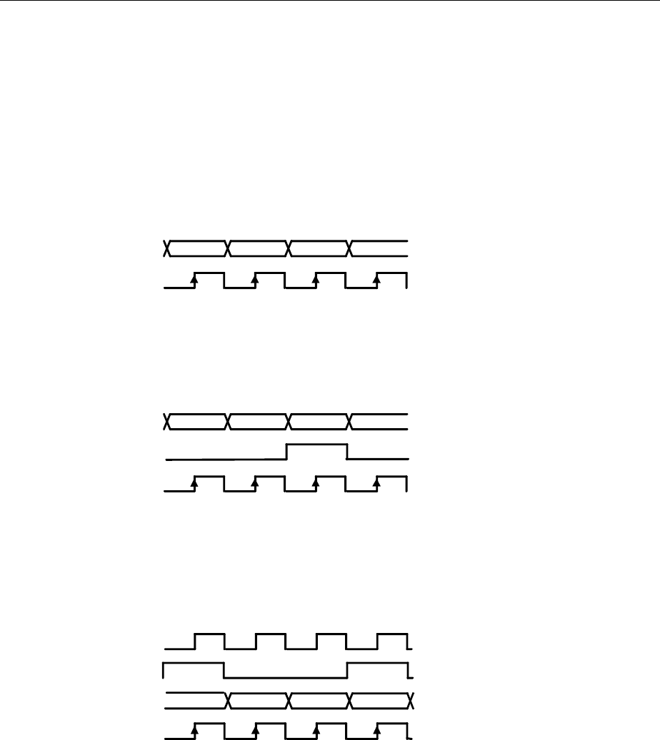
Digital Modulation SMIQ
1125.5555.03 E-92.96
2.10.5.1 External Serial Modulation Data
Serial modulation data can be fed bit-by-bit via connector DATA. For modulation types with more than
1 bit/symbol, the MSB is applied first (MSB first). Either an external bit clock or symbol clock or the
internal clock can be used. The symbol clock serves as strobe to mark the LSB of a symbol. If an
external bit clock is applied, the data at the active clock edges have to be in a stable state. With external
symbol clock, the bit clock for reading the data is internally generated in the modulation coder (internal
data clock). The following figures show the timing at the interface. In all the cases shown, the active
clock edge is assumed to be positive.
DATA (input)
BIT CLOCK (input)
Fig. 2-54 External serial data and bit clock
Data change should take place only on the negative clock edge.
DATA (input)
SYMBOL CLOCK (input)
Internal dataclock
LSBMSB
Fig. 2-55 External serial data and symbol clock, 3 bit/symbol
SYMBOL CLOCK = High marks the LSB. A status change of DATA and SYMBOL CLOCK
should be performed synchronously.
BIT CLOCK (output)
SYMBOL CLOCK (output)
DATA (input)
Internal dataclock
LSB
MSB
Fig. 2-56 External serial data, internal clock signals
External serial modulation data is selected in the menu by SOURCE-SOURCE-EXT_SER.
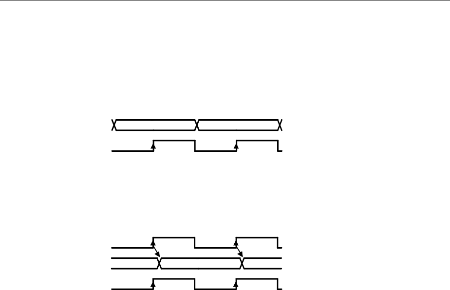
SMIQ Digital Modulation
1125.5555.03 E-92.97
2.10.5.2 External Parallel Modulation Data
Parallel data can be fed as symbols via the PAR DATA interface (DATA-D7, -D6 to D0). Either an
external symbol clock (SYMBCLK) or the internal symbol clock can be used. The data at the active edge
of the symbol clock have to be in a stable state. The following figures show the timings at the interface.
In the two examples shown below, the active clock edge is assumed to be positive.
DATA-D7 (input)
SYMBCLK (input)
Fig. 2-57 External parallel data and symbol clock
Data change should take place only on the negative clock edge.
SYMBCLK (output)
DATA-D7 (input)
Internal dataclock
Fig. 2-58 External parallel data and symbol clock
SYMBOL CLOCK = High marks the LSB. A status change of DATA and SYMBOL CLOCK
should be performed synchronously.
External serial modulation data is selected in the menu by SOURCE-SOURCE-EXT_SER.
For modulation types with less than 8 bit/symbol, line DATA-D7 is always the MSB. For QPSK
modulation, for example (2 bit/symbol), data lines DATA-D7 and DATA-D6 are used.
Note: BITCLK pin on the PARDATA interface is an output. Synchronization to an external bit
clock is not possible in this mode.
External parallel modulation data is selected in the menu by SOURCE-SOURCE-EXT_PAR.

Digital Modulation SMIQ
1125.5555.03 E-92.98
2.10.5.3 Asynchronous Interface for External Modulation Data
The SERDATA interface on the rear of SMIQ serves for the asynchronous serial transmission of
modulation data. The characteristics of this RS-232-C interface is described in Annex A.
For a defined start with specific modulation data it has to be made sure that the backup memories in the
RS-232 transmitter and receiver are deleted. The following setting sequence in the menu is required:
1. Carry out desired settings for digital modulation in menu.
2. Select data source SERDATA using SOURCE - SOURCE SERDATA.
3. Make connection to external data source, but do not yet start external data source.
4. Switch off digital modulation using STATE OFF.
5. Set TRIGGER MODE ARMED_AUTO.
In this state, SMIQ is ready for reception, but discards data that are read in via SERDATA.
6. Switch on digital modulation with STATE ON.
7. Start external data source.
The read-in data are written into the receiving buffer. Only if this buffer is filled can SMIQ react to a
trigger event.
8. Activate trigger event to start digital modulation.
Note: The baud rate has to be selected at least 25% higher than the bit rate of the digital
modulation. If SMIQ has not enough data, the error message "Data underrun" will be
issued in the status line.
2.10.5.4 External Control Signals
The external control signals for envelope control BURST GATE and LEV ATT can be applied via the
SERDATA interface at the rear of SMIQ. The signal for CW control can also be applied to this interface.
Note: The use of control signals from lists in combination with external modulation data is not
possible.
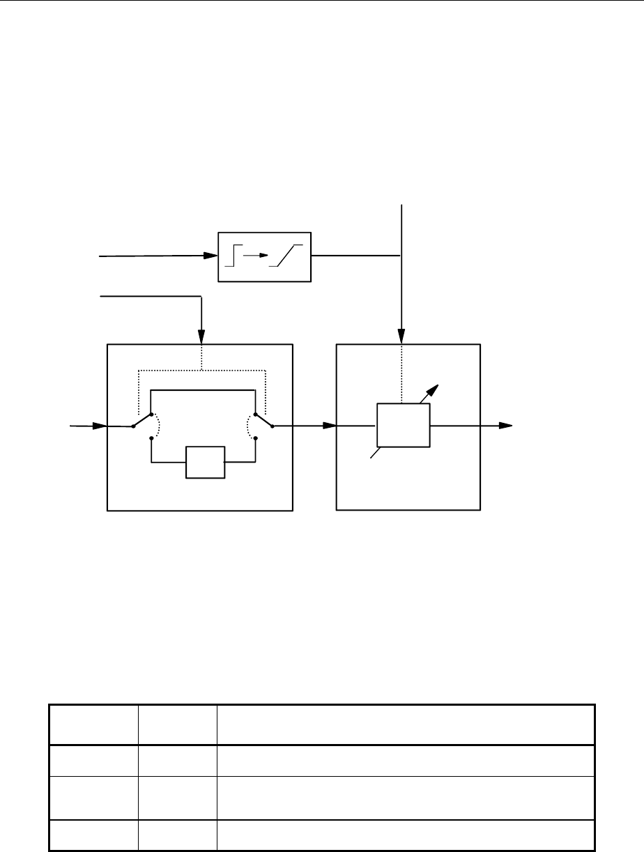
SMIQ Digital Modulation
1125.5555.03 E-92.99
2.10.6 Envelope Control
For TDMA radio networks, in addition to digital modulation, a time-synchronous control of the envelope
of the RF output signal is required. To this effect, SMIQ is equipped with an analog envelope modulator
which can be driven via connector POWER RAMP. Instead of the analog control signal the digital
signals BURST GATE and LEV ATT can be used to control the envelope modulator. In the modulation
coder, a ramp with settable slope is obtained from data changes from high→low or low→high of the
digital BURST GATE signal. The resulting analog signal is taken to the envelope modulator and is
provided at connector POWER RAMP. The LEV ATT signal serves for a defined level reduction.
x dB
Level attenuation
RF ΠRF OUT
Envelope control
BURST GATE
LEV ATT
POWER RAMP
Fig. 2-59 Envelope control in SMIQ with modulation coder
The digital envelope control signals can be fed in externally via connector PAR DATA. With option Data
Generator SMIQB11 provided, the signals can also be generated internally by programming them in the
CONTROL LIST (see Section "Modulation Data from Lists").
The following table shows the logic function of the two signals BURST GATE and LEV ATT.
Table 2-12 Logic function of signals BURST GATE and LEVEL ATT
BURST GATE LEV ATT Remark
1 0 Full level
1 1 Level reduced by the value set in dB under POWER RAMP CONTROL -
ATTENUATION
0 X Maximum level reduction

Digital Modulation SMIQ
1125.5555.03 E-92.100
The following figure illustrates the effect of the envelope control signals.
BURST GATE
LEV ATT
RF OUT
Fig. 2-60 Signal waveforms during envelope control
Note: Envelope control with digital input signals and edge shaping is only possible for symbol
rates of maximum 2.5 Msymb/s.
Envelope control is switched on in the menu via:
analog POWER RAMP CONTROL - SOURCE - EXT ANALOG.
external digital POWER RAMP CONTROL - SOURCE - EXT DIGITAL.
internal digital POWER RAMP CONTROL - SOURCE - INT and SOURCE CONTROL STATE ON.
2.10.7 Clock Signals
The symbol clock and the bit clock are generated in SMIQ by a clock synthesizer on the modulation
coder. All clock signals are synchronized to the 10 MHz reference of the unit. The symbol clock is
available at the SYMBOL CLOCK connector and the bit clock at the BIT CLOCK connector. If required,
the clock synthesizer in SMIQ can synchronize to an externally applied symbol or bit clock.
Only during an operation with external parallel data is synchronization to one symbol clock possible. This
symbol clock is applied via the PAR DATA interface. In all other cases, apply symbol and bit clock to the
corresponding BNC connector.
The clock signal is selected in the menu via CLOCK-MODE SYMBOL/BIT and CLOCK-CLOCK
SOURCE EXT.
To allow for a trouble-free synchronization of the clock synthesizer first apply the external clock and set
the correct symbol rate at SMIQ. Then switch CLOCK SOURCE from INT to EXT.
Notes: The set symbol rate should not differ by more than 1% from the symbol rate of the external
signal.
2.10.8 RF Level For Digital Modulation
With modulation switched on, a level display divided in half appears in the header of the display. The
peak envelope power (PEP) of the modulated RF output level is displayed in addition to average power
(LEVEL).
The difference between PEP and LEVEL depends on the modulation type and the filtering. The power of
QAM signals is calculated on the assumption of a uniform distribution of modulation symbols. For the
PEP calculation, it is always assumed that the most unfavourable case occurs in the sequence of
modulation data. This is definitely the case for PRBS data with a long period (eg PRBS LENGTH 23 bit).
For other data sequences it is possible that the indicated PEP is not attained.
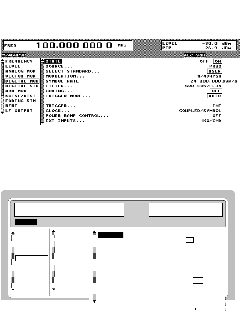
SMIQ Digital Modulation
1125.5555.03 E-92.101
2.10.9 Digital Modulation Menu
The DIGITAL MOD menu provides access to digital modulation settings.
Menu selection: DIGITAL MOD
Fig. 2-61 DIGITAL MOD menu, SMIQ equipped with option Modulation Coder SMIQB20 and option
Data Generator SMIQB11
STATE Switch on/off of digital modulation.
IEC/IEEE-bus command SOUR:DM:STAT ON
SOURCE... Opens a window for defining the data source for digital modulation.
Menu selection depends on option SMIQB11. If option SMIQB11 is installed, the
menu provides more selections and settings for modulation data from lists.
FREQ 100. 000 000 0 MHz
FREQUENCY
LEVEL
ANALOG MOD
VECTOR MOD
DIGITAL MOD
DIGITAL STD
LF OUTPUT
SWEEP
LIST
MEM SEQ
UTILITIES
Π
ΠΠ
Π/4DQPSK
STATE
SOURCE...
SELECT STA
MODULATION
SYMBOL RAT
FILTER...
CODING...
TRIGGER MO
TRIGGER...
CLOCK...
PRBS
0101
91516202123Bit
CURRENT: NONE
OFF ON
CURRENT: NONE
SOURCE...
PATTERN
PRBS LENGTH
SELECT DATA LIST...
COPY CURRENT DATA LIST TO...
DELETE DATA LIST...
EDIT DATA LIST...
CONTROL STATE
SELECT CONTROL LIST...
COPY CURRENT CONTROL LIST TO...
DELETE CONTROL LIST...
EDIT CONTROL LIST...
DELETE ALL DATA AND CONTROL LISTS
LEVEL -30.0 dBm
PEP -27.6 dBm
Fig. 2-62 DIGITAL MOD-SOURCE menu, SMIQ equipped with option Modulation Coder SMIQB20
and option Data Generator SMIQB11

Digital Modulation SMIQ
1125.5555.03 E-92.102
(SOURCE... ) SOURCE... Opens a window for selecting the source for
modulation data.
EXT_PAR The modulation data are fed in via the
parallel PAR DATA interface at the rear
of SMIQ.
IEC -bus :SOUR:DM:SOUR PAR
EXT_SER The modulation data are fed in serially
at input DATA.
IEC -bus :SOUR:DM:SOUR SER
PATTERN A simple data pattern is continuously
generated.
IEC-bus :SOUR:DM:SOUR PATT
PRBS A pseudo random bit sequence is
generated and continuously repeated.
IEC -bus :SOUR:DM:SOUR PRBS
SERDATA The modulation data are fed in via the
asynchronous SER_DATA interface.
IEC -bus :SOUR:DM:SOUR SDAT
DATA LIST Modulation data from lists
IEC-bus :SOUR:DM:SOUR DLIS
PATTERN Selection of a simple data pattern which is
continuously generated.
0 0s are continuously generated.
IEC -bus :SOUR:DM:PATT ZERO
1 1s are continuously generated.
IEC -bus :SOUR:DM:PATT ONE
01 010 data changes are continuously
generated.
IEC -bus :SOUR:DM:PATT ALT
PRBS LENGTH Setting of PRBS generator length. 9 bit, 15 bit, 16 bit,
20 bit, 21 bit and 23 bit can be selected. The period
of the data sequence is then between 29-1 and 223-
1 bit (see Section 2.10.3 "Internal PRBS Data and
Pattern").
IEC/IEEE-bus command :SOUR:DM:PRBS 15
SELECT DATA LIST Opens a window for selecting a stored data list or for
generating a new list.
IEC/IEEE-bus :SOUR:DM:DLIS:SEL ´name´
COPY CURRENT
DATA LIST TO Stores the current data list under a different name.
IEC/IEEE-bus :SOUR:DM:DLIS:COPY ´name´
DELETE DATA LIST Deletes a data list.

SMIQ Digital Modulation
1125.5555.03 E-92.103
(SOURCE... ) EDIT DATA LIST Opens a window for editing a data list bit-by-bit. The
available storage capacity and the length of the
current list is displayed in parameters FREE and LEN
(see also Section List Editor).
COPY Copies a list range
FILL Fills the range with filler pattern
INSERT Inserts a list range at a different
position of the list
DELETE Deletes a list range
EDIT/VIEW Edits or views the list
CONTROL STATE ON The signals from the selected
CONTROL LIST are effective.
OFF The signals are not effective
IEC/IEEE-bus :SOUR:DM:CLIS:CONT ON
SELECT CONTROL
LIST Opens a window for selecting a stored list for control
signals or for generating a new list for control signals.
IEC/IEEE-bus :SOUR:DM:CLIS:SEL ´name´
COPY CURRENT
CONTROL LIST TO Stores the current list for control signals under a
different name.
IEC/IEEE-bus :SOUR:DM:CLIS:COPY ´name´
DELETE CONTROL
LIST Deletes a list for control signals.
EDIT CONTROL LIST Opens a window for editing a list for control signals
symbol-by-symbol. The available storage capacity
and the length of the current list is displayed in
parameters FREE and LEN (see also Section List
Editor).
COPY Copies a list range
DELETE Deletes a list range
EDIT/VIEW Edits or views the list
DELETE ALL DATA
AND CONTROL
LISTS
Deletes all data lists and lists for control signals.
IEC/IEEE-bus -

Digital Modulation SMIQ
1125.5555.03 E-92.104
SELECT
STANDARD... Opens a window for selecting the standard. After the selection, the modulation
parameters MODULATION, SYMBOL RATE, FILTER and CODING are
automatically adjusted to the standard. USER is indicated if the settings of
these parameters do not correspond to the selected standard. The following
standards are available:
APCO4FM IEC\IEEE-bus command :SOUR:DM:STAN APCF
APCOQPSK IEC\IEEE-bus command :SOUR:DM:STAN APCQ
ASK STD-T55 IEC\IEEE-bus command :SOUR:DM:STAN ASK
BLUETOOTH IEC\IEEE-bus command :SOUR:DM:STAN BLU
CDPD IEC/IEEE-bus command :SOUR:DM:STAN CDPD
CT2 IEC/IEEE-bus command :SOUR:DM:STAN CT2
DECT IEC/IEEE-bus command :SOUR:DM:STAN DECT
GSM IEC/IEEE-bus command :SOUR:DM:STAN GSM
GSM_EDGE IEC/IEEE-bus command :SOUR:DM:STAN GSME
IRIDIUM IEC\IEEE-bus command :SOUR:DM:STAN IRID
IS95 FWD IEC\IEEE-bus command :SOUR:DM:STAN FIS95
IS95 REV IEC\IEEE-bus command :SOUR:DM:STAN RIS95
NADC IEC/IEEE-bus command :SOUR:DM:STAN NADC
PDC IEC/IEEE-bus command :SOUR:DM:STAN PDC
PHS IEC/IEEE-bus command :SOUR:DM:STAN PHS
TETRA IEC/IEEE-bus command :SOUR:DM:STAN TETR
TFTS IEC/IEEE-bus command :SOUR:DM:STAN TFTS
PWT IEC/IEEE-bus command :SOUR:DM:STAN PWT
ICOBPSK IEC\IEEE-bus command :SOUR:DM:STAN ICQB
ICOGMSK IEC\IEEE-bus command :SOUR:DM:STAN ICQG
ICOQPSK IEC\IEEE-bus command :SOUR:DM:STAN ICQQ
WORLDSPACE IEC\IEEE-bus command :SOUR:DM:STAN WORL
(only with option SMIQB17)
WCDMA QPSK IEC/IEEE-bus command :SOUR:DM:STAN QWCD
(only with option SMIQB47)
ARIB STD-T55 IEC/IEEE-bus command :SOUR:DM:STAN AT55
MODULATION... Opens a window for defining the modulation method. Moreover, the number
of bits per modulation symbol is displayed. See also Section "Digital
Modulation Methods and Coding".
FREQ 100. 000 000 0 MHz
FREQUENCY
LEVEL
ANALOG MOD
VECTOR MOD
DIGITAL MOD
DIGITAL STD
LF OUTPUT
SWEEP
LIST
MEM SEQ
UTILITIES
Π
ΠΠ
Π/4DQPSK
STATE
SOURCE...
SELECT STA
MODULATION
SYMBOL RAT
FILTER...
CODING...
TRIGGER MO
TRIGGER...
CLOCK...
TYPE... F/4DQPSK 2 b/sym
MODULATION DELAY
LEVEL -30.0 dBm
PEP -27.6 dBm
Fig. 2-63 DIGITAL MOD - MODULATION... menu, SMIQ equipped with option Modulation Coder
SMIQB20 and option Data Generator SMIQB11

SMIQ Digital Modulation
1125.5555.03 E-92.105
(MODULATION...) TYPE... Opens a window for selecting the modulation method.
The following modulations can be selected.
User-defined mapping lists can be loaded by IEC/IEEE-
bus. Then they can be selected by their list name (cf.
chapter 3, :SOURce:DM:MLISt).
ASK Amplitude Shift Keying
IEC/IEEE-bus :DM:FORM ASK
BPSK Binary Phase Shift Keying
IEC/IEEE-bus :DM:FORM BPSK
QPSK Quadrature Phase Shift Keying
IEC/IEEE-bus :DM:FORM QPSK
QPSK IS95 Quadrature Phase Shift Keying with a
mapping according to Interim Standard
95 for CDMA
IEC/IEEE-bus :DM:FORM QIS95
QPSK ISAT QPSK Modulation for INMARSAT-M
IEC/IEEE-bus :DM:FORM QINM
QPSK ICO QPSK Modulation for ICO
IEC/IEEE-bus :DM:FORM QICO
WCDMA QPSK QPSK Modulation for W-CDMA
IEC/IEEE-bus :DM:FORM QWCD
WCDMA QPSK only with option SMIQB47
OQPSK Offset Quadrature Phase Shift Keying
IEC/IEEE-bus :DM:FORM OPSK
OQPSK IS95 Quadrature Phase Shift Keying with a
mapping according to Interim Standard
95 for CDMA
IEC/IEEE-bus :DM:FORM OIS95
π/4 QPSK QPSK with π/4 rotation for each symbol
step (use: NSTAR)
IEC/IEEE-bus :DM:FORM P4QP
π/4 DQPSK QPSK with differential coding
IEC/IEEE-bus :DM:FORM P4DQ
8PSK Phase Shift Keying with 8 points in the
constellation diagram
IEC/IEEE-bus :DM:FORM PSK8
8PSK EDGE Phase Shift Keying with 8 points in the
constellation diagram and 3 π/8 rotation
per symbol.
IEC/IEEE-bus :DM:FORM PSKE8
GMSK Gaussian Minimum Shift Keying
IEC/IEEE-bus :DM:FORM GMSK
GFSK Gaussian filtered Frequency Shift Keying
IEC/IEEE-bus :DM:FORM GFSK
2FSK, 4FSK Frequency Shift Keying
IEC/IEEE-bus :DM:FORM FSK2
4FSK APCO Frequency Shift Keying acording to
APCO25
IEC/IEEE-bus :DM:FORM AFSK4
QAM Quadrature Amplitude Modulation with
16, 32, 64 or 256 points in the
constellation diagram
IEC/IEEE-bus :DM:FORM QAM16
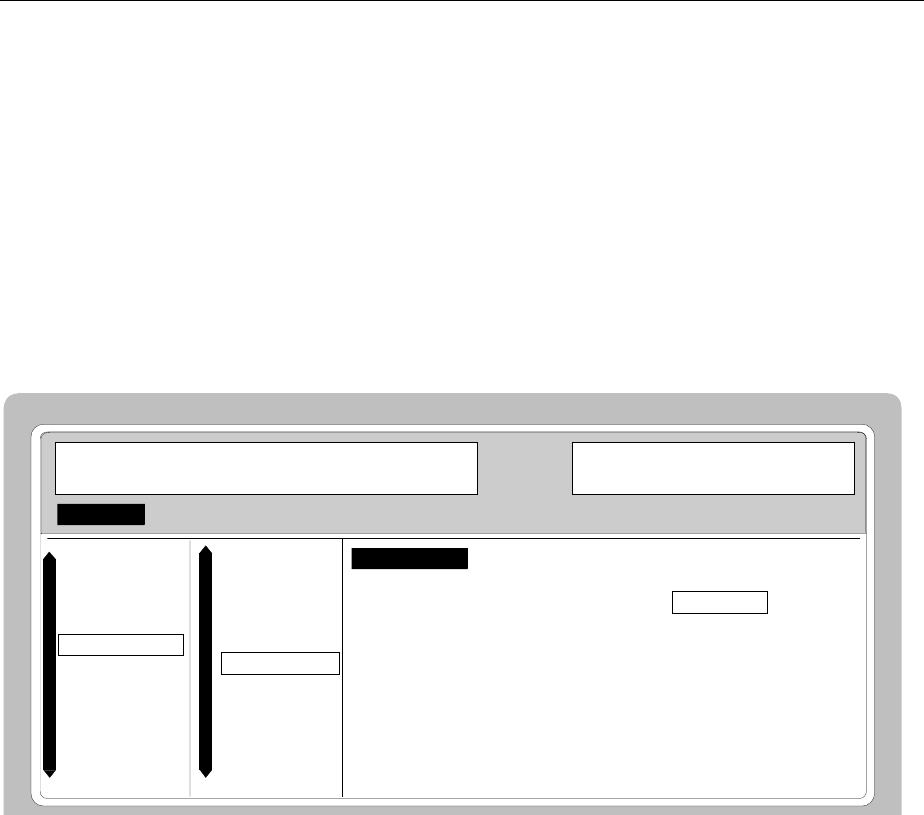
Digital Modulation SMIQ
1125.5555.03 E-92.106
(MODULATION) FSK DEVIATION Input value of deviation with FSK or GFSK selected.
IEC/IEEE-bus :SOUR:DM:FSK:DEV 100 KHZ
ASK DEPTH Input value for ASK modulation depth.
IEC/IEEE-bus :SOUR:DM:ASK:DEPT 10
MODULATION
DELAY Value for time delay of digital modulation between
data input/output and RF output of .
IEC/IEEE-bus :SOUR:DM:MDEL?
SYMBOL RATE Input value of symbol rate.
IEC/IEEE-bus command :SOUR:DM:SRAT 1.2288 MHZ
FILTER... Opens a window for setting the baseband filtering.
FREQ
100. 000 000 0
MHz
FREQUENCY
LEVEL
ANALOG MOD
VECTOR MOD
DIGITAL MOD
DIGITAL STD
LF OUTPUT
SWEEP
LIST
MEM SEQ
UTILITIES
Π
ΠΠ
Π
/4DQPSK
FILTER TYPE
FILTER PARAMETER
FILTER MODE LOW_ACP LOW_EVM
SQR_COS
0.35
LEVEL
-30.0
dBm
PEP
-27.6
dBm
STATE
SOURCE...
SELECT STAN
MODULATION.
SYMBOL RATE
FILTER...
CODING...
TRIGGER MOD
EXECUTE TRI
TRIGGER...
CLOCK...
Fig. 2-64 DIGITAL MOD -FILTER... menu, SMIQ equipped with option Modulation Coder SMIQB20
and option Data Generator SMIQB11

SMIQ Digital Modulation
1125.5555.03 E-92.107
(FILTER...) FILTER TYPE Opens a window for selecting a type of filter. The
following filters can be selected:
SQR_COS Square Root RaisedCosine
IEC :SOUR:DM:FILT:TYPE SCOS
COS Cosine
IEC :SOUR:DM:FILT:TYPE COS
GAUSS Gaussian filter
IEC :SOUR:DM:FILT:TYPE GAUS
GAUSS
LINEAR Linearized Gaussian filter for
GSM_EDGE.
IEC :SOUR:DM:FILT:TYPE LGA
BESSEL Bessel filter with B×T = 1.25 or 2.5
IEC :SOUR:DM:FILT:TYPE BESS1
IS95 Filter for CDMA mobile station
according to Interim Standard 95
IEC :SOUR:DM:FILT:TYPE IS95
IS95 EQUAL Filter for CDMA base station with
equalizer according to IS-95
IEC :SOUR:DM:FILT:TYPE EIS95
APCO C4FM Cosine filter with si(x)-compensation
according to APCO25 standard for
4FSK modulation.
IEC :SOUR:DM:FILT:TYPE APCO
TETRA Filter for PSK/QAM modulation.
IEC :SOUR:DM:FILT:TYPE TETR
WCDMA0.22 Filter for PSK modulation. Square Root
Raised Cosine filter with Roll Off =
0.22, optimized for W-CDMA
IEC :SOUR:DM:FILT:TYPE WCDM
RECTANGLE Filter with a rectangular impulse
answer of 1 symbol length.
IEC :SOUR:DM:FILT:TYPE RECT
SPLIT PHASE Filter for ASK modulation
IEC :SOUR:DM:FILT:TYPE SPH
USER User defined filter. The lists can be
generated via :DM:FLISt:SEL and
filled via :DM:FLISt:DATA.
IEC :SOUR:DM:FILT:TYPE USER
FILTER PARAMETER Opens a window for setting the filter parameter. The
selection depends on the selected filter type:
Parameter Filter Type
Roll-off factor SQR COS, COS, or APCO:
Normalized
band width B×TSymb GAUSS .
IEC/IEEE-bus :SOUR:DM:FILT:PAR 0.2
FILTER MODE Selection of filter mode.
LOW_ACP Filter for minimum Adjacent Channel
Power
IEEE :SOUR:DM:FILT:MODE LACP
LOW_EVM Filter for minimum vector error
IEEE :SOUR:DM:FILT:MODE LEVM

Digital Modulation SMIQ
1125.5555.03 E-92.108
CODING... Opens a window for setting the modulation coding. See also Section " Digital
Modulation Methods and Coding. The following codings can be selected:
OFF No coding
IEC-bus command :SOUR:DM:COD OFF
DIFF Differential coding
IEC-bus command :SOUR:DM:COD DIFF
PHASE_DIFF Phase differential coding
IEC-bus command :SOUR:DM:COD DPHS
GRAY+DIFF Gray and differential coding
IEC-bus command :SOUR:DM:COD DGR
GSM Differential coding according to GSM standard
IEC-bus command :SOUR:DM:COD GSM
NADC Differential coding for π/4 DQPSK according to NADC standard
IEC-bus command :SOUR:DM:COD NADC
PDC Differential coding according to PDC standard
IEC-bus command :SOUR:DM:COD PDC
PHS Differential coding according to PHS standard
IEC-bus command :SOUR:DM:COD PHS
TETRA Differential coding for π/4 DQPSK according to TETRA standard
IEC-bus command :SOUR:DM:COD TETR
APCO25 Differential coding according to APCO25 standard
IEC-bus command :SOUR:DM:COD APCO25
PWT Differential coding for π/4 DQPSK according to PWT standard
IEC-bus command :SOUR:DM:COD PWT
TFTS Differential coding for π/4 DQPSK according to TFTS standard
IEC-bus command :SOUR:DM:COD TFTS
INMARSAT Phase differential coding for INMARSAT-M QPSK modulation
IEC-bus command :SOUR:DM:COD INM
VDL Differential coding according to VDL (VHF Digital Link) for
8PSK modulation.
IEC-bus command :SOUR:DM:COD VDL

SMIQ Digital Modulation
1125.5555.03 E-92.109
TRIGGER MODE Selection of trigger mode.
This selection is only available when option SMIQB11 is installed.
AUTO The data sequences from the selected DATA LIST and
CONTROL LIST are continuously repeated.
IEC/IEEE-bus command :SOUR:DM:SEQ AUTO
RETRIG The data sequences are continuously repeated. A trigger
event causes a restart from symbol 1.
IEC/IEEE-bus command :SOUR:DM:SEQ RETR
ARMED_AUTO A start of data sequences from symbol 1 is caused by a
trigger event. The unit is then automatically set to AUTO
and can no longer be triggered.
IEC/IEEE-bus command :SOUR:DM:SEQ AAUT
ARMED_RETRIG A start of data sequences from symbol 1 is only caused by
a trigger event. The unit is then automatically set to
RETRIG. Each new trigger event causes a restart of the
data sequences.
IEC/IEEE-bus command :SOUR:DM:SEQ ARET
SINGLE A trigger event causes a single data sequence run.
IEC/IEEE-bus command :SOUR:DM:SEQ SING
EXECUTE
TRIGGER Executes a trigger event to start a data sequence.
IEC/IEEE-bus command :TRIG:DM:IMM
TRIGGER... Opens a window for setting the different types of trigger and for setting the
time delay of the trigger signal. The menu is only available if SMIQ is equipped
with option Data Generator SMIQB11.
FREQ
100. 000 000 0
MHz
FREQUENCY
LEVEL
ANALOG MOD
VECTOR MOD
DIGITAL MOD
DIGITAL STD
LF OUTPUT
SWEEP
LIST
MEM SEQ
UTILITIES
Π
ΠΠ
Π
/4DQPSK
TRIGGER SOURCE INT EXT
EXT TRIGGER DELAY 0 Symb
EXT RETRIGGER INHIBIT 0 Symb
LEVEL
-30.0
dBm
PEP
-27.6
dBm
STATE
SOURCE...
SELECT STAN
MODULATION.
SYMBOL RATE
FILTER...
CODING...
TRIGGER MOD
EXECUTE TRI
TRIGGER...
CLOCK...
Fig. 2-65 DIGITAL MOD - TRIGGER menu, SMIQ equipped with option Modulation Coder SMIQB20
and option Data Generator SMIQB11

Digital Modulation SMIQ
1125.5555.03 E-92.110
(TRIGGER...) TRIGGER SOURCE Selection of trigger source
EXT An external trigger signal can be fed in at
TRIGIN of connector PAR DATA at the rear
of SMIQ. With the active edge, a data
sequence is started from the data generator
memory.
INT With INT selected, a trigger event can be
manually executed by EXECUTE TRIGGER.
IEC/IEEE-bus :SOUR:DM:TRIG:SOUR EXT
EXT TRIGGER
DELAY Input value of number of symbols by which an
external trigger signal is delayed before it starts the
data sequence in the data generator. A synchroneity
with the DUT or other units can thus be achieved.
IEC/IEEE-bus :SOUR:DM:TRIG:DEL 3
EXT RETRIGGER
INHIBIT Input of number of symbols for which each new
trigger event is inhibited during MODE RETRIG after
a trigger signal.
During MODE RETRIG, each new trigger signal
restarts the data sequence in the data generator.
This restart can be inhibited for the entered number
of symbols. The entry of 1250 symbols, for example,
causes new trigger signals to be ignored for the
duration of 1250 symbols after execution of a trigger
event.
IEC/IEEE-bus :SOUR:DM:TRIG:INH 1250
CLOCK... Opens a window for selecting the clock source and for setting a delay.
FREQ
100. 000 000 0
MHz
FREQUENCY
LEVEL
ANALOG MOD
VECTOR MOD
DIGITAL MOD
DIGITAL STD
LF OUTPUT
SWEEP
LIST
MEM SEQ
UTILITIES
Π
ΠΠ
Π
/4DQPSK
CLOCK SOURCE INT COUPLED EXT
MODE SYMBOL BIT
DELAY 0.00 Symb
LEVEL
-30.0
dBm
PEP
-27.6
dBm
STATE
SOURCE...
SELECT STAN
MODULATION.
SYMBOL RATE
FILTER...
CODING...
TRIGGER MOD
EXECUTE TRI
TRIGGER...
CLOCK...
Fig. 2-66 DIGITAL MOD - CLOCK, SMIQ equipped with option Modulation Coder SMIQB20 and
option Data Generator SMIQB11

SMIQ Digital Modulation
1125.5555.03 E-92.111
(CLOCK...) CLOCK SOURCE Selection of clock source
INT The symbol and the bit clock in SMIQ
are generated by a clock synthesizer on
the modulation coder. All the clock
signals are synchronized to the 10-MHz
reference of the unit.
IEEE-bus :SOUR:DM:CLOC:SOUR INT
COUPLED The clock comes from the same source
as the data.
IEEE-bus :SOUR:DM:CLOC:SOUR COUP
EXT An external clock signal is fed externally.
The clock synthesizer on the modulation
coder is synchronized to this clock.
Parameter SYMBOL RATE has to be
correctly set with an accuracy of ± 1 %.
IEEE-bus :SOUR:DM:CLOC:SOUR EXT
MODE Selection of clock for the external clock signal
SYMBOL An externally fed clock has to be a
symbol clock.
BIT An externally fed clock has to be a bit
clock.
IEC/IEEE-bus :SOUR:DM:CLOC:MODE SYMB
DELAY Input value of delay of generated modulation signal
compared with an externally fed clock. This can be
used, for example, for synchronization with a second
unit to achieve time synchroneity between the
modulation signals of the two units. The displayed
setting resolution of 1/100 symbol is only attained for
symbol-clock frequencies below 100 kHz. The actual
resolution is reduced with increasing frequency. The
delay can no longer be set for 7 Msymb/s
IEC/IEEE-bus :SOUR:DM:CLOC:DEL 0.5
POWER RAMP
CONTROL... Opens a window for setting the envelope control.
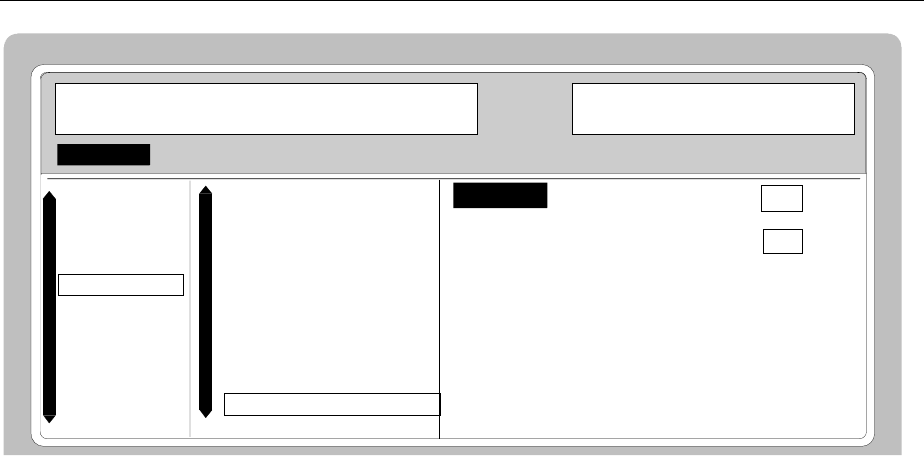
Digital Modulation SMIQ
1125.5555.03 E-92.112
FREQ
100. 000 000 0
MHz
FREQUENCY
LEVEL
ANALOG MOD
VECTOR MOD
DIGITAL MOD
DIGITAL STD
LF OUTPUT
SWEEP
LIST
MEM SEQ
UTILITIES
Π
ΠΠ
Π
/4DQPSK
SOURCE
RAMP TIME
RAMP FUNCTION
RAMP DELAY
ATTENUATION
... OFF
2.0 Symb
LIN COS
0.0 Symb
15.0 dB
LEVEL
- 30.0
dBm
PEP
- 27.6
.
dBm
SOURCE...
SELECT STANDARD...
MODULATION...
SYMBOL RATE
FILTER...
CODING...
TRIGGER MODE...
EXECUTE TRIGGER
TRIGGER...
CLOCK...
POWER RAMP CONTROL...
Fig. 2-67 DIGITAL MOD - POWER RAMP CONTROL menu, SMIQ equipped with option Modulation
Coder SMIQB20 and option Data Generator SMIQB11
(POWER RAMP
CONTROL...) SOURCE Selection between analog and digital envelope
control and selection of source.
OFF Envelope control is switched off.
IEC/IEEE :SOUR:DM:PRAM:STAT OFF
INT Signals BGAT and LATT from the active
CONTROL LIST (CLIST) are used for
envelope control (only with option SMIQB11)
IEC/IEEE :SOUR:DM:PRAM:STAT ON
:SOUR:DM:PRAM:SOUR CLIST
EXT_ANALOG Envelope control is via an external
analog signal that can be fed in via
connector POWER RAMP.
IEC/IEEE-bus commands
:SOUR:DM:PRAM:STAT ON
:SOUR:DM:PRAM:SOUR AEXT
EXT_DIGITAL Envelope control is via external
digital signals to be applied to
BURST GATE and LEV ATT of
connector PAR DATA.
IEC/IEEE-bus commands
:SOUR:DM:PRAM:STAT ON
:SOUR:DM:PRAM:SOUR DEXT
RAMP TIME Input value of rise time of envelope after a transition
from Low→High of signal BURST GATE and of fall
time after a transition from High→Low.
The setting is a multiple of the symbol duration.
IEC/IEEE-bus :SOUR:DM:PRAM:TIME 3.0

SMIQ Digital Modulation
1125.5555.03 E-92.113
(POWER RAMP
CONTROL...) RAMP FUNCTION Determines the shape of the rising and falling edge
during envelope control by means of the
BURST GATE signal.
LIN Selection of a linear ramp function.
COS The edge is shaped according to a
cosine function and a more favourable
spectrum than that under setting LIN is
obtained.
IEC/IEEE-bus :SOUR:DM:PRAM:SHAP COS
RAMP DELAY Input value for a shift of the envelope characteristic
to the modulated signal. A positive value causes a
delay of the envelope. The values are set in the units
of the symbol length.
IEC/IEEE-bus :SOUR:DM:PRAM:DEL 0.1
ATTENUATION Input value of level reduction in dB with digital control
signal LEV ATT used. This function is normally used
- for TDMA frame structures - to generate a slot with
reduced level.
IEC/IEEE-bus :SOUR:DM:PRAM:ATT 0 dB
EXT INPUTS Opens a window for setting the trigger threshold, input impedance and polarity
of the external digital modulation coder inputs, ie connector PAR DATA and
inputs DATA, BIT CLOCK and SYMBOL CLOCK.
FREQ
100. 000 000 0
MHz
FREQUENCY
LEVEL
ANALOG MOD
VECTOR MOD
DIGITAL MOD
DIGITAL STD
LF OUTPUT
SWEEP
LIST
MEM SEQ
UTILITIES
Π
ΠΠ
Π
/4DQPSK
MODULATION
SYMBOL RAT
FILTER...
CODING...
TRIGGER MO
EXECUTE TR
TRIGGER...
CLOCK...
POWER RAMP
LOW DISTOR
EXT INPUTS
THRESHOLD
IMPEDANCE
CLOCK SLOPE
TRIGGER SLOPE
+1.0 V
1k
Ω
/GND 50
Ω
/GND 50
Ω
/-2V
POS NEG
POS NEG
LEVEL
-30.0
dBm
PEP
-27.6
dBm
Fig. 2-68 DIGITAL MOD - EXT INPUTS menu, SMIQ equipped with option Modulation Coder
SMIQB20 and option Data Generator SMIQB11
(EXT INPUTS...) TRESHOLD Input value of high/low threshold in Volt.
IEC/IEEE-bus command :SOUR:DM:THR 1.0

Digital Modulation SMIQ
1125.5555.03 E-92.114
IMPEDANCE Selection of input impedance and reference voltage.
50 Ω/GND should be selected for higher clock rates.
Setting 50 Ω/-2V is suitable for sources with ECL
output. Make sure to select a suitable setting for the
high/low threshold under TRESHOLD.
IEC/IEEE-bus command :SOUR:DM:INP:IMP G1K
CLOCK SLOPE Selection of polarity of active edge of externally fed
bit clock or symbol clock.
Note: In the internal clock mode, CLOCK SLOPE
NEG inverts the clock output signals.
IEC/IEEE-bus :SOUR:DM:CLOC:POL NORM
TRIGGER SLOPE Selection of polarity of active trigger edge for input
TRIGIN.
IEC/IEEE-bus :SOUR:DM:TRIG:SLOP POS

SMIQ Digital Standard PHS
1125.5555.03 E-92.115
2.11 Digital Standard PHS
With the options Modulation Coder (SMIQB20) and Data Generator (SMIQB11) provided, modulation
signals according to the Japanese PHS standard1 can be generated. PHS is a TDMA standard for
private and public cordless phones.
SMIQ can generate both the transmit signal of a cell station (CS) and the transmit signal of a personal
station (PS). Transmission from CS to PS is called "downlink", "uplink" being used for transmission in
the opposite direction.
Uplink and downlink are transmitted in the separate time slots of a frame using the time duplex method.
Each frame consists of 8 slots. The data contents of each slot can be defined individually by SMIQ by
means of a slot editor. SMIQ can generate a control physical slot and also a communication physical
slot. Each slot can be switched on or off. A defined intermediate level can also be set.
A burst type has to be defined to configure a slot. The following burst types can be selected:
•TCHFULL simulation of a communication channel for a speech coder rate of 32 kbit/s,
•TCHHALF simulation of a communication channel for a speech coder rate of 16 kbit/s,
•VOX simulation of a communication channel in non-speech intervals with uplink
transmission only in every fourth frame,
•SYNC, simulation of a sync channel and
•ALL_DATA burst type for test purposes with freely programmable data contents in the selected
slot.
The following internal modulation sources are available:
•different PRBS generators with a sequence length between 29-1 and 223-1 and
•data lists, ie freely programmable data sequences from the data generator memory.
For generating the PHS signals, SMIQ inserts the modulation data continuously (in real time) into the
selected slots. Using a digital signal processor the data generator generates a data sequence with
modulation data and control signals for envelope control.
The data generator in SMIQ generates a data stream which is converted into IQ signals in the
modulation coder. According to the PHS standard, the modulation type is π/4 DQPSK at a symbol rate of
192 ksymbol/s and √COS filtering. Symbol rate and filtering can be changed in SMIQ.
1 Personal Handy Phone System ARIB Standard (RCR STD-28)

Digital Standard PHS SMIQ
1125.5555.03 E-92.116
2.11.1 Sync and Trigger Signals
The data generator generates a data sequence with modulation data, control signals for envelope
control, and synchronization signals.
When TRIGGER MODE AUTO is selected, the PHS signal generation automatically starts.
This start can also be activated by an external trigger signal (TRIGGER MODE ARMED_AUTO) which
allows a synchronous sequence for BER measurements to be carried out on receivers.
Trigger signals for synchronized sequences can be used for measuring the bit error rate of receivers. A
trigger signal can be fed via the TRIGIN input at connector PAR DATA. The active slope of a trigger
signal applied there executes a trigger event.
PHS signal generation at a frame limit is started after a trigger event. Data from data lists are inserted
into the selected slots starting from the first bit. PRBS generators start with the set initialization status.
Signal generation either starts immediately after the active slope of the trigger signal or after a settable
number of symbols (EXT TRIGGER DELAY). Retriggering (RETRIG) can be inhibited for a settable
number of symbols (EXT RETRIGGER INHIBIT).
A trigger event can be executed manually or via the IEC/IEEE bus using EXECUTE TRIGGER.
When a trigger event is executed, a trigger signal is output at the TRIGOUT 3 output of SMIQ.
SMIQ also generates the following sync signals:
•a frame clock at TRIGOUT 1 output,
•a frame or multiframe clock at TRIGOUT 2 output with settable position in the frame,
•the symbol clock and the bit clock.
A clock synthesizer on the modulation coder generates the symbol clock and the bit clock in SMIQ. All
the clock signals are synchronized to the 10-MHz reference of SMIQ. The symbol clock is available at
connector SYMBOL CLOCK and the bit clock at connector BIT CLOCK. If required, the clock
synthesizer in SMIQ can be synchronized to an external symbol or bit clock.
The clock signal is selected in the menu via CLOCK-CLOCK SOURCE EXT.
To allow for a trouble-free synchronization of the clock synthesizer first apply the external clock and set
the correct symbol rate at SMIQ. Then switch CLOCK SOURCE from INT to EXT.
Notes: - The set symbol rate should not differ by more than 1% from the symbol rate of the
external signal.

SMIQ Digital Standard PHS
1125.5555.03 E-92.117
2.11.2 PN Generators as Internal Data Source
Independent PN generators (Pseudo Noise) can be selected for each slot as data source for data fields
DATA and SACCH. These PN generators provide pseudo-random bit sequences of different length or
period. That is why they are also called PRBS generators (Pseudo Random Binary Sequence).
Data sequences are sequences of maximum length which are generated by means of feedback shift
registers.
The following figure gives an example of a 9 bit generator with feedbacks after register 4 and 0 (output).
8
765
4
3210
DATA
EXOR
The pseudo-random sequence of a PRBS generator is clearly defined by the number of registers and
the feedback. The following table describes all PRBS generators available:
Table 2-13 PRBS generators for PHS
PRBS generator Length in bits Feedback after
9 bit 29 -1 = 511 Register 4, 0
11 bit 211 -1 =2047 Register 2, 0
15 bit 215 -1 = 32767 Register 1, 0
16 bit 216 -1 = 65535 Register 5, 3, 2, 0
20 bit 220 -1 = 1048575 Register 3, 0
21 bit 221 -1 = 2097151 Register 2, 0
23 bit 223 -1 = 8388607 Register 5, 0
PN generators PN9,11,15,20 and PN23 are configured according to CCITT Rec. 0.151/152/153. The
output sequence is inverted for generators PN15 and PN23.
The start value of the PN generators is different in the slots and equals
start value hex slotnumber=+ ×114
Example: PN9 generator in slot 1 with start value 15hex = 10101 binary.
10
DATA
EXOR
1100
0
0
0
The resulting output sequence is 1010100000010100101011110010 etc.

Digital Standard PHS SMIQ
1125.5555.03 E-92.118
2.11.3 Lists as Internal Data Source
A freely programmable memory on the data generator serves as internal data source for the data fields
of the slots. The data are managed in so-called lists. A list editor allows to select, copy, modify and
delete data lists (DATA LIST).
The list editor is available via menu DIGITAL-MOD - SOURCE....
2.11.4 External Modulation Data
External data can (only) be applied via the SERDATA interface. A selection of SERDATA as data
source is only possible for a single data field of a slot. For further information on the characteristics of
the SERDATA interface see Annex A.
To ensure that the external data bits are assigned to specific positions in the data field of the selected
slot and that they are reproducible, the buffer of the RS-232 transmitter and receiver has to be deleted.
A triggered start has to follow.
The following setting sequence is required in the DIGITAL STD - PHS menu:
1. Carry out desired settings in menu.
2. Select data source SERDATA for the data field of the slot using SELECT SLOT - ....
3. Make connection to external data source, but do not yet start external data source.
4. Switch off digital standard using STATE - OFF.
5. Set TRIGGER MODE ARMED_AUTO.
In this state, SMIQ is ready for reception, but discards data that are read in via SERDATA.
6. Switch on digital standard with STATE ON.
7. Start external data source.
The read-in data are written into the receiving buffer. Only if this buffer is filled can SMIQ react to a
trigger event.
8. Activate trigger event. Signal generation is thus started at a frame limit. The first bit received via
SERDATA is put to the first bit position in the selected data field.
SMIQ Digital Standard PHS
1125.5555.03 E-92.119
2.11.5 Menu DIGITAL STANDARD - PHS
Menu DIGITAL STD - PHS provides access to settings for generating PHS signals.
Menu selection:DIGITAL STD - PHS
FREQ
100. 000 000 0
MHz
FREQUENCY
LEVEL
ANALOG MOD
VECTOR MOD
DIGITAL MOD
DIGITAL STD
LF OUTPUT
SWEEP
LIST
MEM SEQ
UTILITIES
PHS
PHS
IS-95
NADC
PDC
GSM
STATE
MODULATION...
TRIGGER MODE...
EXECUTE TRIGGER
TRIGGER...
CLOCK...
POWER RAMP CONTROL...
SLOT ATTENUATION
SAVE/RCL FRAME...
SELECT SLOT
DN UP
12341234
OFF ON
Π
/4DQPSK 2 b/sym
AUTO
INT
INT
...
15.0 dB
SYNC
LEVEL
-30.0
dBm
PEP
-27.5
dBm
Fig. 2-69 Menu DIGITAL STD - PHS, SMIQ equipped with Modulation Coder SMIQB20 and Data
Generator SMIQB11
STATE Switch on/off of Digital Standard PHS modulation. Vector Modulation or Digital
Modulation will be switched off automatically.
IEC/IEEE-bus command :SOUR:PHS:STAT ON
MODULATION... Opens a window for setting the modulation parameters.
Fig. 2-70 Menu DIGITAL STD - PHS - MODULATION..., SMIQ equipped with Modulation Coder
SMIQB20 and Data Generator SMIQB11

Digital Standard PHS SMIQ
1125.5555.03 E-92.120
(MODULATION...) SET TO
STANDARD Sets the subsequent modulation parameters to the
values predefined by the standard.
MODULATION TYPE Displays the modulation type.
SYMBOL RATE Input value for the symbol rate. 192 ksymbol/s are
preset.
IEC/IEEE-bus :SOUR:PHS:SRAT 192.01 KHZ
FILTER Selection of baseband filter. A selection between
Nyquist filters COS, SQRCOS and a user-defined filter
USER (cf. Section Digital Modulation) is possible.
IEC/IEEE-bus :SOUR:PHS:FILT:TYPE COS
ROLL OFF FACTOR Input value for the roll-off factor.
IEC/IEEE-bus SOUR:PHS:FILT:PAR 0.50
FILTER MODE Selection of filter mode.
LOW_ACP Filter for minimum Adjacent Channel
Power.
IEC :SOUR:PHS:FILT:MODE LACP
LOW_EVM Filter for minimum vector error.
IEC :SOUR:PHS:FILT:MODE LEVM
TRIGGER MODE... Opens a window for selecting the trigger mode.
AUTO The PHS signals are continuously transmitted in the
activated slots.
IEC/IEEE-bus command :SOUR:PHS:SEQ AUTO
RETRIG The PHS signals are continuously transmitted in the
activated slots. A trigger event causes a restart.
IEC/IEEE-bus command :SOUR:PHS:SEQ RETR
ARMED_AUTO The PHS signal generation does not start until a trigger
event has occurred. The unit then automatically
switches over to the AUTO mode and can no longer be
triggered.
IEC/IEEE-bus command :SOUR:PHS:SEQ AAUT
ARMED_RETRIG The PHS signal generation does not start until a trigger
event has occurred. The unit then automatically
switches over to the RETRIG mode. Each new trigger
event causes a restart.
IEC/IEEE-bus command :SOUR:PHS:SEQ ARET
EXECUTE
TRIGGER Executes a trigger even to start the PHS signal generation.
IEC/IEEE-bus command :TRIG:DM:IMM
TRIGGER... Opens a window for selecting the trigger source, for configuring the trigger
output signals and for setting the time delay of an external trigger signal.
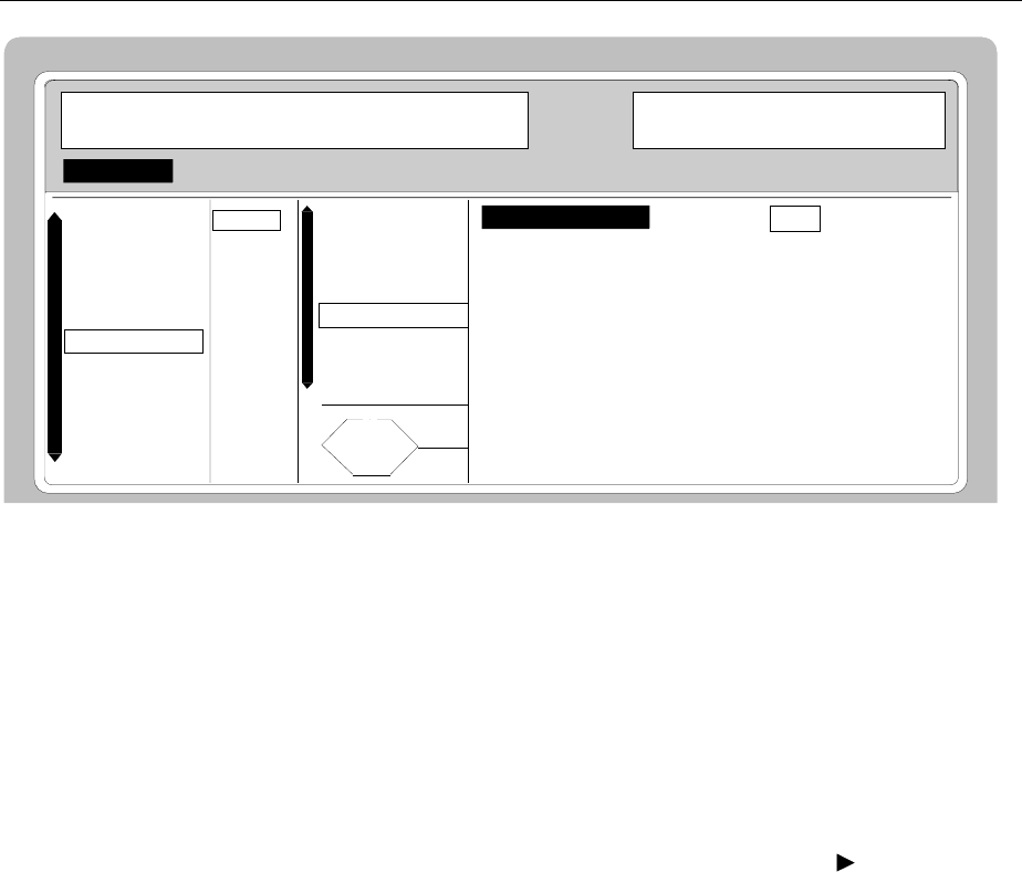
SMIQ Digital Standard PHS
1125.5555.03 E-92.121
FREQ
100. 000 000 0
MHz
FREQUENCY
LEVEL
ANALOG MOD
VECTOR MOD
DIGITAL MOD
DIGITAL STD
LF OUTPUT
SWEEP
LIST
MEM SEQ
UTILITIES
PHS
PHS
IS-95
NADC
PDC
GSM
STATE
MODULATION...
TRIGGER MODE
EXECUTE TRIG
TRIGGER....
CLOCK...
POWER RAMP C>
SLOT ATTENUA
TRIGGER SOURCE INT EXT
EXT TRIGGER DELAY 0 Symb
EXT RETRIGGER INHIBIT 0 Symb
TRIGGER OUT2 DELAY 0 Symb
TRIGGER OUT2 PERIOD 1 Frames
LEVEL
- 30.0
dBm
PEP
-27.5
dBm
SYNC
DN 12
Fig. 2-71 Menu DIGITAL STD - PHS_TRIGGER..., SMIQ equipped with Modulation Coder SMIQB20
and Data Generator SMIQB11
(TRIGGER...) TRIGGER SOURCE Selection of trigger source.
EXT The PHS signal generation is started by
the active slope of an external trigger
signal.
The polarity, the trigger threshold and
the input resistance of the TRIGIN input
can be modified in menu
DIGITAL MOD - EXT INPUTS.
INT A trigger event can be executed by
EXECUTE TRIGGER .
IEC/IEEE-bus :SOUR:PHS:TRIG:SOUR EXT

Digital Standard PHS SMIQ
1125.5555.03 E-92.122
(TRIGGER...) EXT TRIGGER
DELAY Setting the number of symbols by which an external
trigger signal is delayed before it starts the PHS
signal generation.
This is used for setting the time synchronization
between the the SMIQ and the DUT.
IEC/IEEE-bus command :SOUR:PHS:TRIG:DEL 3
EXT RETRIGGER
INHIBIT Setting the number of symbols for which a restart is
inhibited after a trigger event.
With TRIGGER MODE RETRIG selected, each new
trigger signal restarts the PHS signal generation. This
restart can be inhibited for the entered number of
symbols.
Example:
The entry of 1000 symbols causes new trigger
signals to be ignored for the duration of 1000 sym-
bols after a trigger event
IEC/IEEE-bus :SOUR:PHS:TRIG:INH 1000
TRIGGER OUT 2
DELAY Input value of delay of trigger signal at TRIGOUT 2
output compared with beginning of frame.
IEC/IEEE-bus :SOUR:PHS:TRIG:OUTP:DEL 2
TRIGGER OUT2
PERIOD Input value of output signal period at TRIGOUT 2
output given in frames.
IEC/IEEE-bus :SOUR:PHS:TRIG:OUTP:PER 1
SMIQ Digital Standard PHS
1125.5555.03 E-92.123
CLOCK... Opens a window for selecting the clock source and for setting a delay.
FREQ
100. 000 000 0
MHz
FREQUENCY
LEVEL
ANALOG MOD
VECTOR MOD
DIGITAL MOD
DIGITAL STD
LF OUTPUT
SWEEP
LIST
MEM SEQ
UTILITIES
PHS
PHS
IS-95
NADC
PDC
GSM
STATE
MODULATION...
TRIGGER MODE
EXECUTE TRIG
TRIGGER....
CLOCK...
POWER RAMP C>
SLOT ATTENUA
CLOCK SOURCE INT EXT
MODE SYMBOL BIT
DELAY 0.00 Symb
LEVEL
-30.0
dBm
PEP
- 27.5
dBm
SYNC
DN 12
Fig. 2-72 Menu DIGITAL STD - PHS - CLOCK..., SMIQ equipped with Modulation Coder SMIQB20
and Data Generator SMIQB11
(CLOCK...) CLOCK SOURCE Selection of clock source.
INT SMIQ uses internally generated clock signals.
EXT An external symbol clock or bit clock is fed in
at connectors SYMBOL CLOCK or BIT
CLOCK. The clock synthesizer on the
modulation coder is synchronized to this
clock.
The symbol rate has to be set with an
accuracy of ± 1 %.
The polarity, the trigger threshold and the
input resistance of the clock inputs can be
modified in menu DIGITAL MOD - EXT
INPUTS.
IEC/IEEE-bus command :SOUR:PHS:CLOC:SOUR INT
MODE Selection of clock for external clock signal.
SYMBOL The external clock has to be a symbol clock.
BIT The external clock has to be a bit clock.
IEC/IEEE-bus command :SOUR:PHS:CLOC:MODE SYMB
DELAY Setting the delay of generated modulation signal to an
external clock.
This can be used, for example, for synchronization with a
second unit to achieve time synchronization between the
modulation signals of the two units.
IEC/IEEE-bus command :SOUR:PHS:CLOC:DEL 0.5
Digital Standard PHS SMIQ
1125.5555.03 E-92.124
POWER RAMP
CONTROL... Opens a window for setting the envelope control, especially for the rising and
falling ramp at the beginning and end of a slot.
FREQ 100. 000 000 0 MHz
FREQUENCY
LEVEL
ANALOG MOD
VECTOR MOD
DIGITAL MOD
DIGITAL STD
LF OUTPUT
SWEEP
LIST
MEM SEQ
UTILITIES
PHS
PHS
IS-95
NADC
PDC
GSM
STATE
MODULATION...
TRIGGER MODE...
EXECUTE TRIGGER
TRIGGER....
CLOCK...
POWER RAMP CONTROL...
SLOT ATTENUATION
SET DEFAULT
RAMP TIME 1.0 Symb
RAMP FUNCTION LIN COS
RAMP DELAY -0.1 Symb
RISE OFFSET 0 Symb
FALL OFFSET 0 Symb
LEVEL -30.0 dBm
PEP -27.5 dBm
SYNC
DN 12 3
Fig. 2-73 Menu DIGITAL STD - PHS - POWER RAMP CONTROL... , SMIQ equipped with
Modulation Coder SMIQB20 and Data Generator SMIQB11
(POWER RAMP
CONTROL...) SET DEFAULT Resets the subsequent parameters to the factory-set
values.
IEC/IEEE-bus :SOUR:PHS:PRAM:PRES
RAMP TIME Input value for the rise and fall time of the envelope
at the beginning or end of a slot. The time is set in
units of symbol period.
IEC/IEEE-bus :SOUR:PHS:PRAM:TIME 0.25
RAMP FUNCTION Selection of shape of rising and falling ramp for
envelope control.
LIN Linear ramp function.
COS Cosine function. A more favourable
spectrum than that of the LIN function is
obtained.
IEC/IEEE-bus :SOUR:PHS:PRAM:SHAP LIN
RAMP DELAY Input value for a shift of the envelope characteristic
to the modulated signal. A positive value causes a
delay of the envelope. The values are set in the units
of the symbol length.
IEC/IEEE-bus :SOUR:PHS:PRAM:DEL 0.1
RISE OFFSET Input value for a positive or negative offset of the
rising ramp of the envelope at the beginning of a slot.
IEC/IEEE-bus :SOUR:PHS:PRAM:ROFF -1
FALL OFFSET Input value for a positive or negative offset of the
falling ramp of the envelope at the end of a slot.
IEC/IEEE-bus :SOUR:PHS:PRAM:FOFF 1
SMIQ Digital Standard PHS
1125.5555.03 E-92.125
SLOT ATTENUATION Input value for the level reduction in dB of all active slots whose SLOT LEVEL
was set to ATTEN. Menu SELECT SLOT allows the slots to be determined
whose level is to be reduced.
IEC/IEEE-bus command :SOUR:PHS:SLOT:ATT 40 DB
SAVE/RCL FRAME... Opens a window for saving and loading a frame configuration. Loading a
frame affects all parameters that can be set under SELECT SLOT.
FREQ 100. 000 000 0 MHz
FREQUENCY
LEVEL
ANALOG MOD
VECTOR MOD
DIGITAL MOD
DIGITAL STD
LF OUTPUT
SWEEP
LIST
MEM SEQ
UTILITIES
PHS
PHS
IS95
NADC
PDC
GSM
TRIGGER MODE
EXECUTE TRIG
TRIGGER....
CLOCK...
POWER RAMP C>
SLOT ATTENUA
SAVE/RCL FRA
GET PREDEFINED FRAME...
RECALL FRAME...
SAVE FRAME...
DELETE FRAME...
LEVEL -30.0 dBm
PEP -27.5 dBm
SYNC
DN 12
Fig. 2-74 Menu DIGITAL STD - PHS - SAVE/RCL FRAME, SMIQ equipped with Modulation Coder
SMIQB20 and Data Generator SMIQB11
(SAVE/RCL FRAME...) GET PREDEFINED
FRAME... Loads a factory-set frame configuration.
DN1_TCH Downlink Traffic Channel in slot1
UP1_TCH Uplink Traffic Channel in slot1
DN1_SYNC Downlink Sync Channel in slot1
IEEE :SOUR:PHS:FLIS:PRED:LOAD "DN1_TCH"
RECALL FRAME... Loads a frame configuration saved by the user.
IEC/IEEE-bus :SOUR:PHS:FLIS:LOAD "name"
SAVE FRAME... Saves a user-defined frame configuration.
IEC/IEEE-bus :SOUR:PHS:FLIS:STOR "name"
DELETE FRAME... Deletes a frame configuration saved by the user.
IEC/IEEE-bus :SOUR:PHS:FLIS:DEL "name"
Digital Standard PHS SMIQ
1125.5555.03 E-92.126
SELECT SLOT... Selection of one of 8 possible slots. When selecting the slot, a window is
opened in which the data contents belonging to this slot can be defined.
4 slots are available for uplink and downlink. They are designated as UP<i>
and DN<i> in the display. For remote control, the slots are numbered from 1 to
8. The following assignment applies:
Slot DN1 DN2 DN3 DN4 UP1 UP2 UP3 UP4
Slot number 1 2 3 4 5 6 7 8
If the cursor is placed onto a slot in the diagram, it may be switched on and off
by pressing one of the unit keys (toggle function).
FREQ 100. 000 000 0 MHz
FREQUENCY
LEVEL
ANALOG MOD
VECTOR MOD
DIGITAL MOD
DIGITAL STD
LF OUTPUT
SWEEP
LIST
MEM SEQ
UTILITIES
PHS
PHS
IS95
NADC
PDC
GSM
SLOT R SS PR UW CS_ID PS-ID IDLE CRC GUARD
1DN4262 32 42 28 34 16 16
BURST TYPE... SYNC
SLOT LEVEL OFF ATTEN FULL
SET DEFAULT
CS-ID SCRAMBLE STATE OFF ON
CS ID CODE 000 H
----------------BURST CONTENTS----------------
ROH
SS 2 H
PR 1999 9999 9999 9999 H
UW 50EF 2993 H
CI 9 H
CS ID 202 0002 0001 H
PS ID 000 0001 H
IDLE 0 0000 0000 H
CRC CI+CS_ID+PS_ID+IDLE
GUARD 0000 H
-----------------CHANGE DATA------------------
SELECT DATA LIST... CURRENT: R&STDM
COPY CURRENT DATA LIST TO...
DELETE DATA LIST...
EDIT DATA LIST...
LEVEL -30.0 dBm
PEP - 27.5 dBm
Fig. 2-75 Menu DIGITAL STD - PHS - SELECT SLOT, SMIQ equipped with Modulation Coder
SMIQB20 and Data Generator SMIQB11

SMIQ Digital Standard PHS
1125.5555.03 E-92.127
(SELECT SLOT) BURST TYPE... Opens a window for the selection of the burst type used
to configure the selected slot.
TCH_FULL Traffic channel configuration (rate 32 kbit/s)
IEEE-bus :SOUR:PHS:SLOT2:TYPE TCHF
TCH_HALF Traffic channel configuration (rate 16 kbit/s)
IEEE-bus :SOUR:PHS:SLOT2:TYPE TCHH
VOX VOX configuration. In slots 4 to 8 (uplink)
transmission is only in every fourth frame.
IEEE-bus :SOUR:PHS:SLOT2:TYPE VOX
SYNC Sync burst
IEEE-bus :SOUR:PHS:SLOT2:TYPE SYNC
ALL DATA Burst type for testing with freely
programmable data contents
IEEE-bus SOUR:PHS:SLOT2:TYPE ADAT
SLOT LEVEL Selection of level for selected slot.
OFF Maximum attenuation
IEEE bus :SOUR:PHS:SLOT2:LEV OFF
FULL The level corresponds to the value indicated
on the SMIQ LEVEL display.
IEEE bus :SOUR:PHS:SLOT2:LEV FULL
ATTEN The level is reduced by the value set under
SLOT ATTENUATION.
IEEE bus :SOUR:PHS:SLOT2:LEV ATT
SET DEFAULT Resets the subsequent parameters to the factory-set
values.
IEC/IEEE-bus command :SOUR:PHS:SLOT8:PRES
CS-ID SCRAMBLE
STATE Switch on/off of CS-ID scrambling function.
IEC/IEEE-bus :SOUR:PHS:SLOT2:SCR:STAT ON
CS-ID CODE Input value in hexadecimal form for initializing the
scramble generator.
IEEE-bus :SOUR:PHS:SLOT2:SCR:CODE #H123
ENCRYPTION
STATE Switch on/off of encryption scrambling function. This
parameter is only available for TCH burst types.
IEC/IEEE-bus :SOUR:PHS:SLOT2:ENCR:STAT ON
SECURITY KEY Input value in hexadecimal form for initializing the
scramble generator. This parameter is only available for
TCHburst types.
IEEE-bus :SOUR:PHS:SLOT2:ENCR:KEY #H1234

Digital Standard PHS SMIQ
1125.5555.03 E-92.128
(SELECT SLOT) R Display of data contents in the 4-bit data field "Ramp".
SS Display of data contents in the 2-bit data field
"Start Symbol".
PR Display of "Preamble".
UW Input value for the "Unique Word" in hexadecimal form.
The length of the hexadecimal value depends on the slot
type (16 | 32 bit).
IEC/IEEE-bus :SOUR:PHS:SLOT2:UWOR #H3D4C
CI Display of the "Channel Identifier" data field in hexa-
decimal form.
SA Selection of data source for SACCH. This data field is
only displayed for burst types TCH and VOX.
PN.. PRBS data according to CCITT V52 or Rec.
0.151 with periods between 29-1 and 223-1.
IEEE :SOUR:PHS:SLOT3:SACCH PN9
DLIST Data from a programmable data list.
IEEE :SOUR:PHS:SLOT3:SACCH DLIS
SERDATA Data from data input SER DATA
IEEE :SOUR:PHS:SLOT3:SACCH SDAT
TCH / VOX Selection of data source for TCH data field. This data
field is only displayed for burst types TCH and VOX.
PN.. PRBS data according to CCITT V52 or Rec.
0.151 with periods between 29-1 and 223-1.
IEEE :SOUR:PHS:SLOT3:TCH PN9
DLIST Data from a programmable data list.
IEEE :SOUR:PHS:SLOT3:TCH DLIS
SERDATA Data from data input SER DATA
IEEE :SOUR:PHS:SLOT3:TCH SDAT
CS-ID Input value for the "Cell Station ID Code" field in hexa-
decimal form. This data field is only displayed for the
burst type SYNC.
IEEE-bus :SOUR:PHS:SLOT2:CSID #H20200020001

SMIQ Digital Standard PHS
1125.5555.03 E-92.129
(SELECT SLOT) PS-ID Input value for the "Personal Station ID Code" field in
hexadecimal form. This data field is only displayed for the
burst type SYNC.
IEEE-bus :SOUR:PHS:SLOT2:PSID #H0000001
IDLE Display of data contents in the "Idle" field. This field is
only displayed for the burst type SYNC.
CRC Indication of data fields for calculating the CRC code.
GUARD Display of data contents in the "Guard" field in hexa-
decimal form.
SELECT DATA
LIST... Opens a window for selecting a stored data list or for
generating a new list.
COPY CURRENT
DATA LIST TO... Stores the current data list under a different name.
DELETE DATA
LIST... Deletes a data list.
EDIT DATA
LIST... Opens a window for editing a data list bit-by-bit. The
available storage capacity and the length of the current
list is displayed in parameters FREE and LEN (see also
Section List Editor).
COPY Copies a list range
FILL Fills the range with filler pattern
INSERT Inserts a list range at a different position of
the list
DELETE Deletes a list range
EDIT/VIEW Edits or views the list
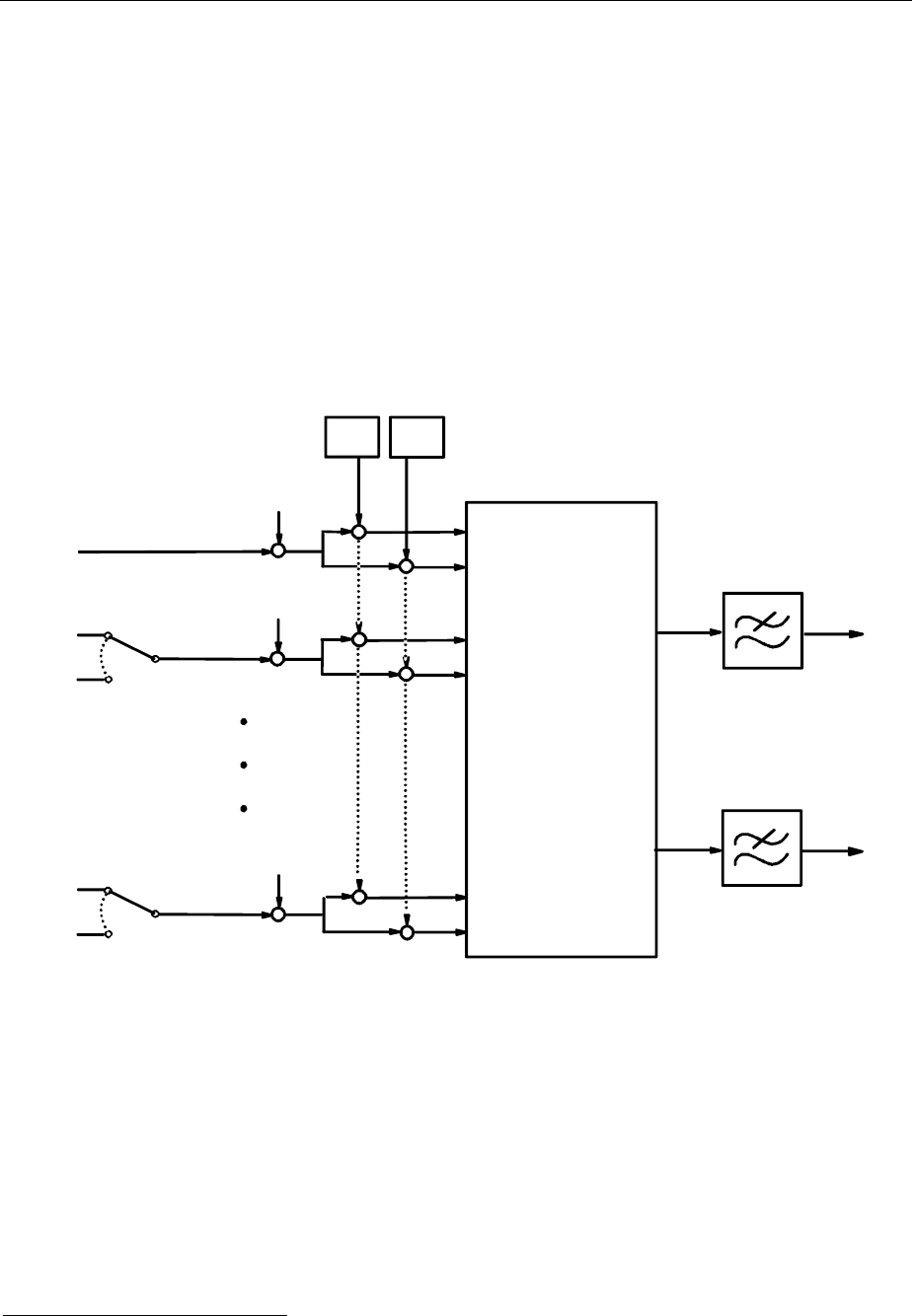
Digital Standard IS-95 CDMA SMIQ
1125.5555.03 E-92.130
2.12 Digital Standard IS-95 CDMA
With the options Modulation Coder (SMIQB20), Data Generator (SMIQB11) and option Digital Standard
CDMA (SMIQB42) provided, CDMA signals can be generated according to standard IS-951 as well as
J-STD-008.
SMIQ can simulate both the transmit signal of a base station (forward link) and the transmit signal of a
mobile station (reverse link). The forward link signal consists of up to 64 code channels. A reverse link
signal can be generated in the full-rate or half-rate mode.
Simple bit patterns or pseudo random bit sequences (PRBS) can be selected as modulation data for
forward link. Every code channel has a different PRBS. Modulation data are not subject to channel
coding (convolution coding, interleaving).
The following figure shows the schematic of forward link signal generation.
Walsh 0
PN
I
Walsh 1
PN
Q
I
Q
Walsh k
Σ
ΣΣ
Σ
Baseband
FIR Filter
Baseband
FIR Filter
Channel Power Setting
QPSK Mapping
Pattern
PRBS
19200 bps 1.2288 Mcps
Pattern
PRBS
0000...
+
+
+
+
+
+
+
+
+
Fig. 2-76 Forward link signal generation
At a chip rate of 1.2288 Mcps, the modulation data rate for forward link is 19200 bp/s for all channels.
The modulation type is QPSK. For baseband filtering, a FIR filter with equalizer is preset according to
IS-95 (FILTER TYPE IS-95 EQUAL). Other filters can be set as well. The chip rate is preset to
1.2288 Mcps according to IS-95 but can be freely selected.
1 TIA/EIA/IS-95, Mobile Station-Base Station Compatibility Standard for Dual-Mode Wideband Spread Spectrum Cellular
Systems
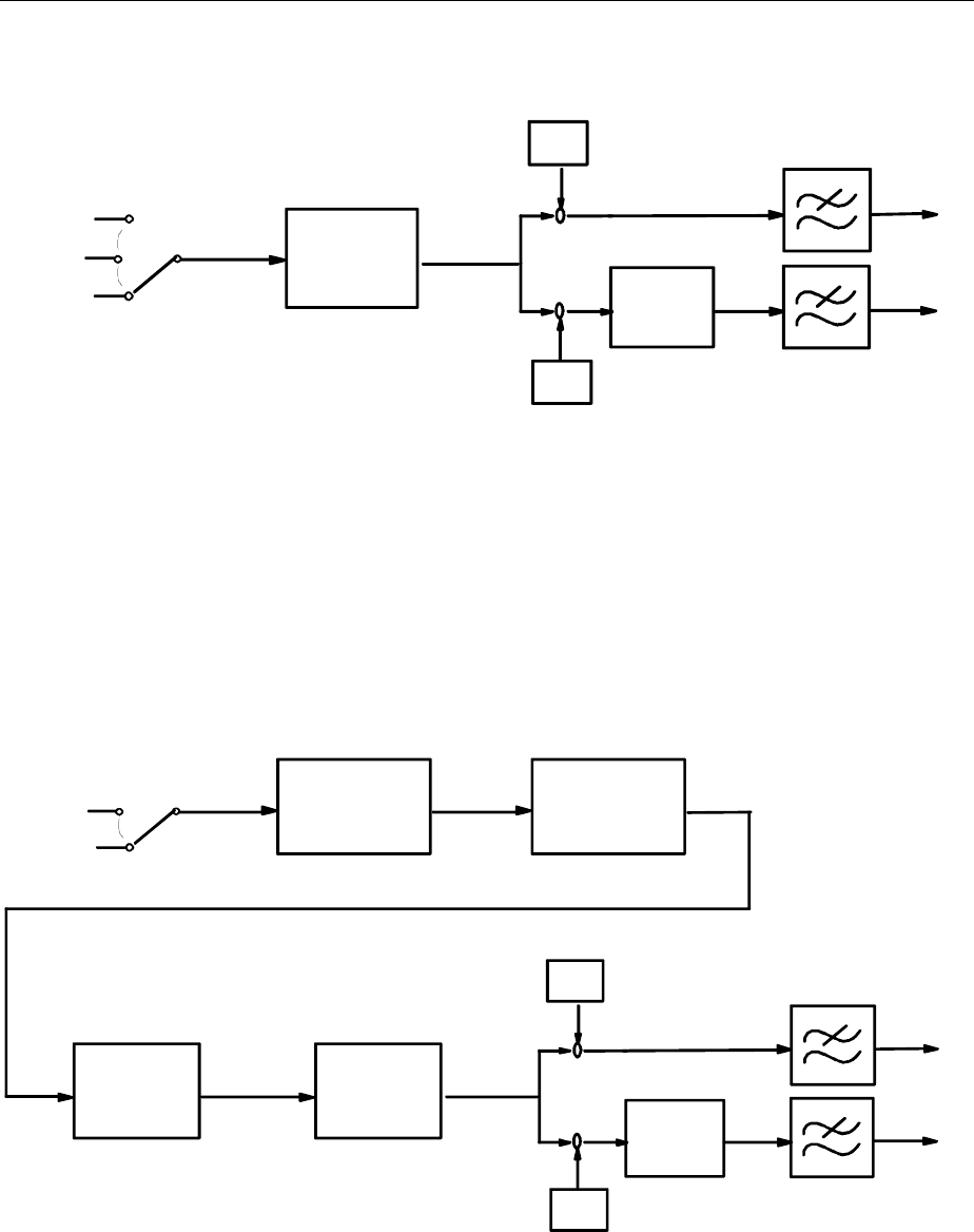
SMIQ Digital Standard IS-95 CDMA
1125.5555.03 E-92.131
To generate a reverse link signal, two different operating modes are available. The following figure
shows the schematic of reverse link signal generation without channel coding.
Delay
1/2 Chip
64 fach
Orthogonal
Modulator
307200 bps
28800 bps
Pattern
PRBS
PN
I
PN
Q
1.2288 Mcps
+
+
I
Q
Baseband
FIR Filter
List
Fig. 2-77 Reverse link signal generation without channel coding
Simple bit patterns, PRBS and freely programmable data sequences in a data list are available as
modulation data. At a chip rate of 1.2288 MHz, the modulation data rate of the reverse link is
28800 bps/s. The modulation type is offset-QPSK. A FIR filter is preset as baseband filter without
equalizer according to IS-95 (FILTER TYPE IS-95).
The second reverse link mode also comprises channel coding. With this reverse link coded mode, both
an access channel (4800 bps) and a traffic channel can be generated with all the data rates between
1200 bps and max. 14400 bps complying with IS-95 (Rate Set 1 and 2). The following figure gives an
example of signal generation for the traffic channel with 9600 bps and shows the associated frame
structure.
Delay
1/2 Chip
64 fach
Orthogonal
Modulator
307200 bps
PN
I
PN
Q
1.2288 Mcps
+
+
I
Q
Baseband
FIR Filter
28800 bps
PRBS
List
Block
Interleaver
Convolutional
Encoder
Add
FQ Indicator,
Encoder Tail
8600 bps 9600 bps
Fig. 2-78 Traffic channel 9600 in "Reverse Link Coded" mode
Digital Standard IS-95 CDMA SMIQ
1125.5555.03 E-92.132
172 Bit 12 8
9600 bps
Frame
DATA FQI TAIL
Fig. 2-79 Frame structure of traffic channel 9600 in "Reverse Link Coded" mode
PRBS of different lengths and a list of freely programmable data sequences are available as modulation
data. In the reverse link coded mode, MIQ generates a test signal for BER and FER easurements at a
base station receiver. A special ervice mode is required for the DUT since the long code is set to 0 in
the SMIQ test signal.
To facilitate operation, the following tables show the frequency channels according to regulations IS-95
and J-STD-008. The tables are also available on the SMIQ display via the HELP function for IS-95 menu
selection.
Table 2-14 CDMA: channel numbers and their frequencies
IS-95 channel number generator frequency /MHz
Mobile station 1 ≤ N ≤ 777 0.03N + 825.0
1013 ≤ N ≤ 1023 0.03(N-1023)+825.0
Base station 1 ≤ N ≤ 777 0.03N + 870.0
1013 ≤ N ≤ 1023 0.03(N-1023)+870.0
J-STD-008 channel number generator frequency/MHz
Mobile station 1 ≤ N ≤ 1199 0.050N + 1850.000
Base station 1 ≤ N ≤ 1199 0.050N + 1930.000
Table 2-15 Preferred CDMA-frequency channels according to J-STD-008
channel number generator-frequency/MHz channel number generator-frequency/MHz
mobile station base station mobile station base station
25 1851.25 1931.25 600 1880.00 1960.00
50 1852.50 1932.50 625 1881.25 1961.25
75 1853.75 1933.75 650 1882.50 1962.50
100 1855.00 1935.00 675 1883.75 1963.75
125 1856.25 1936.25 725 1886.25 1966.25
150 1857.50 1937.50 750 1887.50 1967.50
175 1858.75 1938.75 775 1888.75 1968.75
200 1860.00 1940.00 825 1891.25 1971.25
225 1861.25 1941.25 850 1892.50 1972.50
250 1862.50 1942.50 875 1893.75 1973.75
275 1863.75 1943.75 925 1896.25 1976.25
325 1866.25 1946.25 950 1897.50 1977.50
350 1867.50 1947.50 975 1898.75 1978.75
375 1868.75 1948.75 1000 1900.00 1980.00
425 1871.25 1951.25 1025 1901.25 1981.25
450 1872.50 1952.50 1050 1902.50 1982.50
475 1873.75 1953.75 1075 1903.75 1983.75
500 1875.00 1955.00 1100 1905.00 1985.00
525 1876.25 1956.25 1125 1906.25 1986.25
550 1877.50 1957.50 1150 1907.50 1997.50
575 1878.75 1958.75 1175 1908.75 1988.75
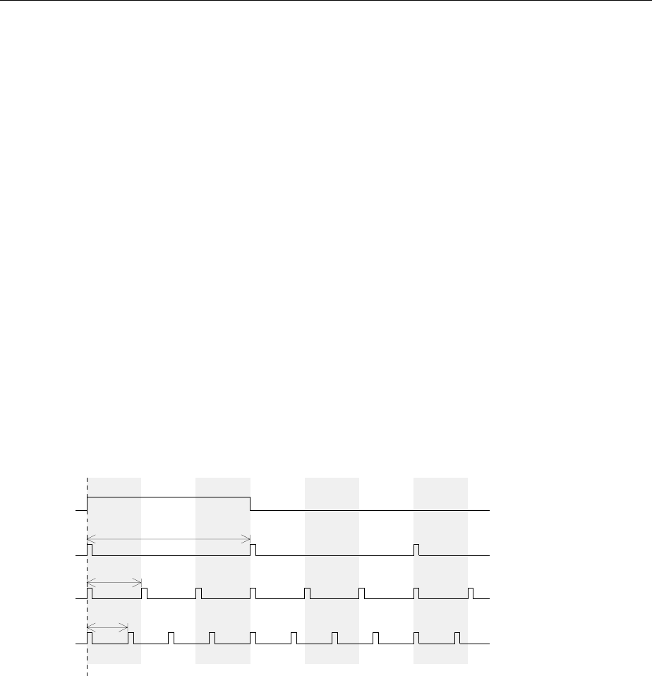
SMIQ Digital Standard IS-95 CDMA
1125.5555.03 E-92.133
2.12.1 Sync and Trigger Signals
A CDMA sequence with a length of 98304 chips is calculated for the generation of forward link CDMA
signals and stored in the memory of the data generator (option SMIQB11). This chip sequence can be
run repetitively (TRIGGER MODE AUTO). During reverse link signal generation with channel coding, the
modulation data are continuously processed in real time.
Trigger signals can be used for synchronized measurements on receivers.
A trigger signal can be fed via the TRIGIN input at connector PAR DATA. The chip sequence either
starts immediately after the active slope of the trigger signal or after a settable number of chips
(TRIGGER DELAY). Retriggering (RETRIG) can be inhibited for a settable number of chips (TRIGGER
INHIBIT).
A trigger event can be executed manually or via the IEC/IEEE bus using EXECUTE TRIGGER. When a
trigger event is executed, a trigger signal is output at the TRIGOUT 3 output of SMIQ.
SMIQ also generates the following sync signals:
•a 20-ms frame clock (traffic channel frame clock)
•a 80/3-ms clock (short sequence rollover)
•a 80-ms clock (super frame clock))
•a 2-s clock (even second clock)
•a PCG clock in reverse link at half rate, 1/4 rate and 1/8 rate
SMIQ can output two of the four signals via pins TRIGOUT 1 and 2 of connector PAR DATA.
80 ms
t=0
Short Code I_PN=15 *'0'
Even second clock
Period: 2 sec.
Paging Frame,
Traffic Frame
Short Sequence
Roll Over
Superframe
Short Code
Period
80/3 ms
20 ms
Fig. 2-80 CDMA sync signals
A clock synthesizer on the modulation coder generates the chip clock and a multifold chip clock in the
SMIQ. All the clock signals are synchronized to the 10-MHz reference of the SMIQ. The chip clock is
available at connector SYMBOL CLOCK and the multifold chip clock at connector BIT CLOCK. If
required, the clock synthesizer in the SMIQ can be synchronized to an external chip clock which is fed in
at connector SYMBOL CLOCK.
The clock signal is selected in the menu via CLOCK-CLOCK SOURCE EXT.
To allow for a trouble-free synchronization of the clock synthesizer first apply the external clock and set
the correct symbol rate at SMIQ. Then switch CLOCK SOURCE from INT to EXT.
Note: The set symbol rate should not differ by more than 1% from the symbol rate of the external
signal.
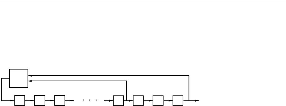
Digital Standard IS-95 CDMA SMIQ
1125.5555.03 E-92.134
2.12.2 PRBS Data Source in Forward Link
A PN generator is used as PRBS data source for forward link modes. This PN generator provides a
pseudo random bit sequence with a period of 217-1. The PRBS data sequence is a so-called sequence
of maximum length that is generated by means of a feedback shift register. The following schematic
shows the PN generator with feedback to registers 3 and 0 (output). The data of the start value are
entered into the register.
3210
DATA
EXOR
16 15 14
1
1
11100
The start value of the PN generator is 1100 0100 1110 0011 1
The bit sequence after the start thus is:
1100 0100 1110 0011 1111 0001 1111 1110...
... 0011 1111 0000 0111 1110 0011 1001 1100...
... 0111 1111 1011 1111 1100 0001 0010 0000...
... 1110 0100 0001 0011 1110 0010 0100 0110..........
The generated bits are assigned to the modulation data of the different forward link modes as follows:
Mode FWD_LINK_18
The PN bits are assigned to the different code channels as follows:
Modulation data bit 0:
1100 0100 1110 0011 1111 0001 1111 1110 ...
↑↑
c31, ch30, .........................ch0 ...
Modulation data bit 1:
0011 1111 0000 0111 1110 0011 1001 1100 ...
↑↑
ch31, ch30, ........................ch0 ...
etc.
The data bits of the unused code channels c18 to c31 and those of the deactivated code channels
are discarded, ie not used.
Modus FWD_LINK_64
The PN bits are assigned to the different code channels as follows:
Modulation data bit 0:
11000100111000111111000111111110 00111111000001111110001110011100 ...
↑↑↑↑
c31, ch30, ..................ch0,ch63, ch62, ................ch32 ...
Modulation data bit 1:
01111111101111111100000100100000.11100100000100111110001001000110 ...
↑↑↑↑
c31, ch30, ..................ch0,ch63, ch62, ................ch32 ...
etc.
The data bits of the deactivated code channels are discarded, ie not used.
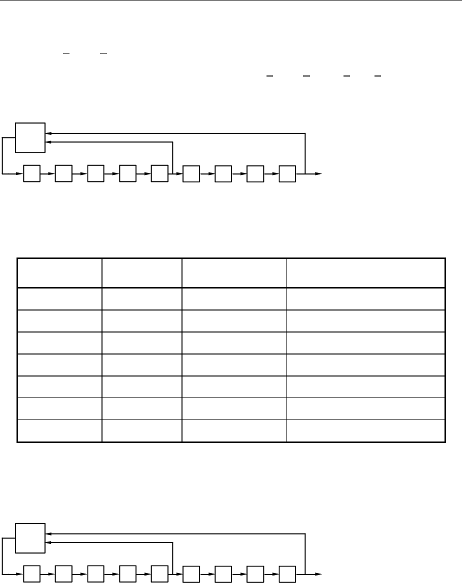
SMIQ Digital Standard IS-95 CDMA
1125.5555.03 E-92.135
2.12.3 PN Generators as Internal Data Source for Reverse Link
Different PN (Pseudo Noise) generators can be selected as data source for modulation data in the two
reverse link modes. These PN generators provide pseudo random bit sequences of different lengths or
periods which is why they are also called PRBS generators (Pseudo Random Binary Sequence).
The data sequences are so-called sequences of maximum lengths that are generated by means of
feedback shift registers.
The following schematic shows the 9 bit generator with feedback to registers 4 and 0 (output).
8
765
4
3210
DATA
EXOR
The pseudo random sequence of a PRBS generator is determined by the number of registers and the
feedback. The following table describes all available PRBS generators:
Table 2-16 PN generators for IS-95 reverse link
PRBS generator Length in bits Feedback to Start value
9 bits 29 -1 = 511 Register 4, 0 1100 0100 1
11 bits 211 -1 =2047 Register 2, 0 1100 0100 111
15 bits 215 -1 = 32767 Register 1, 0 1100 0100 1110 001
16 bits 216 -1 = 65535 Register 5, 3, 2, 0 1100 0100 1110 0011
20 bits 220 -1 = 1048575 Register 3, 0 1100 0100 1110 0011 1111
21 bits 221 -1 = 2097151 Register 2, 0 1100 0100 1110 0011 1111 0
23 bits 223 -1 = 8388607 Register 5, 0 1100 0100 1110 0011 1111 000
PN generators PN9,11,15,20 and PN23 are designed according to CCITT Rec. 0.151/152/153. The
output sequence is inverted for generators PN15 and PN23.
Example: PN9 generator in slot 1 with start value 110001001 (binary)
11
DATA
EXOR
0001
0
0
1
The resulting output sequence is 110001001100010001000 etc.

Digital Standard IS-95 CDMA SMIQ
1125.5555.03 E-92.136
2.12.4 Menu IS-95 CDMA Standard - Forward Link Signal
Menu DIGITAL STD - IS-95 provides access to settings for IS-95 CDMA signal generation. The
following figure shows the menu for generating the forward link signal (transmit signal of base station) in
the FWD_LINK_18 mode. The menus for generating reverse link signals are described in the following
section. Parameters that are identical for both modes are explained in the menu for forward link.
Menu selection: DIGITAL STD - IS-95- MODE - FWD_LINK_18
FREQ 100. 000 000 0 MHz
FREQUENCY
LEVEL
ANALOG MOD
VECTOR MOD
DIGITAL MOD
DIGITAL STD
LF OUTPUT
SWEEP
LIST
MEM SEQ
UTILITIES
IS95
PHS
IS-95
STATE
MODE...
SET DEFAULT
MODULATION...
TRIGGER MODE...
EXECUTE TRIGGER
TRIGGER....
CLOCK...
TOTAL POWER
ADJUST TOTAL POWER
SAVE/RCL MAPPING...
CHANNEL NO. WALSH CODE POWER [dB] DATA STATE
0 (PILOT) 0 -7.0 0000 ON
1 32 -13.0 PRBS ON
2 1 -7.3 PRBS ON
3 9 -10.3 PRBS ON
4 10 -10.3 PRBS ON
5 11 -10.3 PRBS ON
6 12 -10.3 PRBS ON
7 17 -10.3 PRBS ON
8 25 -10.3 PRBS ON
9 33 -10.3 PRBS OFF
10 34 -10.3 PRBS OFF
11 35 -10.3 PRBS OFF
12 36 -10.3 PRBS OFF
13 37 -10.3 PRBS OFF
14 38 -10.3 PRBS OFF
15 39 -10.3 PRBS OFF
16 40 -10.3 PRBS OFF
17 41 -10.3 PRBS OFF
OFF ON
FWD_LINK_18
QPSK IS-95
AUTO
INT
INT
0.00 dB
LEVEL -30.0 dBm
PEP - 13.9.dBm
Fig. 2-81 Menu DIGITAL STD - IS-95 - MODE - FWD_LINK_18, equipped with options
modulation coder SMIQB20, data generator SMIQB11 and SMIQB42
STATE Switch on/off of modulation Digital Standard IS-95 CDMA. Vector modulation
and digital modulation will be switched off automatically.
IEC/IEEE-bus command SOUR:IS95:STAT ON

SMIQ Digital Standard IS-95 CDMA
1125.5555.03 E-92.137
MODE... Selection between the different modes for generating a forward link signal or
reverse link signals. The REV_LINK modes will be described in the following
sections.
FWD_LINK_18 Activates the generation of a forward link signal with
up to 18 code channels (channel No. 0 to 17).
The Walsh code (WALSH CODE) and the source for
modulation data (DATA) can be determined
individually for each channel.
Each channel can be switched on/off (STATE).
The relative power (POWER) of channels 0 (pilot), 1
and 2 can be freely determined in range -30 dB to
0 dB.
The power setting of channel 3 also determines the
power setting of channels 4 to 17. This means that
channels 3 to 17 all have the same power provided
when the channels are switched on.
IEC/IEEE-bus :SOUR:IS95:MODE FLIN18
FWD_LINK_64 Activates the generation of a forward link signal with
up to 64 code channels.
Walsh codes 0 to 63 (WALSH CODE) are assigned
to the channels.
The source for modulation data (DATA) can be
determined individually for each channel.
Each channel can be switched on/off (STATE).
The relative power (POWER) of the pilot channel
(Walsh 0) can be freely determined in range -30 dB to
0 dB.
The power setting of channel 1 also determines the
power setting of channels 2 to 63. This means that
channels 1 to 63 all have the same power provided
when the channels are switched on.
IEC/IEEE-bus :SOUR:IS95:MODE FLIN64
REV_LINK Activates the generation of a reverse link signal
without channel coding. A selection between the full-
rate and half-rate mode (RATE) is possible.
IEC/IEEE-bus :SOUR:IS95:MODE RLIN
REV_LINK_CODED Activates the generation of a reverse link signal with
channel coding. A selection between the access
channel and traffic channel with different rates is
possible.
IEC/IEEE-bus :SOUR:IS95:MODE RLCO
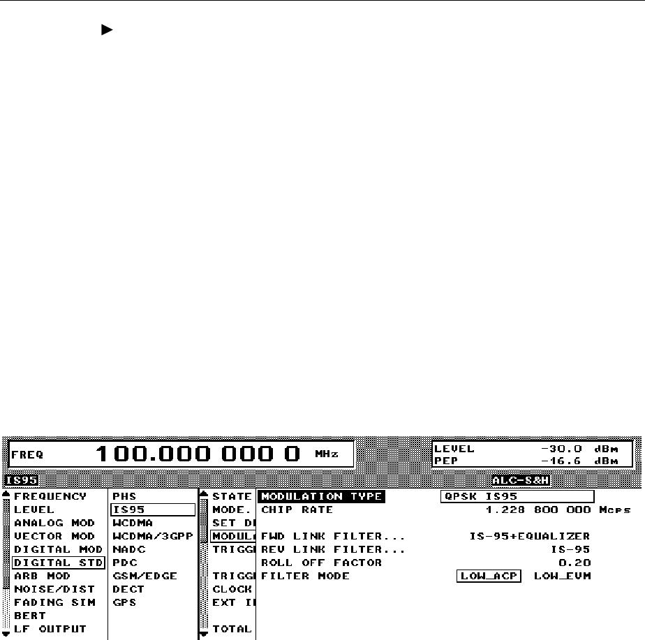
Digital Standard IS-95 CDMA SMIQ
1125.5555.03 E-92.138
SET DEFAULT Provides the default setting for the channel configuration of the forward link
modes.
For FWD_LINK_18:
- channels 0 to 8 are switched on
- the power of the pilot channel (channel 0) makes out 20% of the total power
(-7 dB).
- channel 1 is set as sync channel by WALSH CODE 32
- channel 2 is set as paging channel
- the remaining 7 channels are configured as traffic channels
The power setting was selected according to the "Base Station Test Model"
of TIA standard IS-97.
For FWD_LINK_64:
- all 64 channels are switched on
- the power of the pilot channel makes out 20% of the total power (-7 dB).
- the remaining 80% of the transmit power is distributed equally on the
remaining 63 channels.
IEC/IEEE-bus command :SOUR:IS95:PRES
MODULATION... Opens a window for setting the modulation parameters.
Fig. 2-82 Menu DIGITAL STD - IS-95 - MODULATION..., equipped with options modulation coder
SMIQB20, data generator SMIQB11 and SMIQB42
(MODULATION...) MODULATION TYPE Indicates the modulation type.
CHIP RATE Setting value of chip clock frequency.
Preset to 1.2288 Mcps.
IEEE-bus command :SOUR:IS95:CRAT 1.2 MHZ
(MODULATION...) FWD LINK FILTER... Opens a window for selecting the baseband filters
for the forward link. A selection between the FIR
filters defined in IS-95, the Nyquist filters COS and
SQRCOS or a user-defined filter USER (cf. Section
Digital Modulation) is possible. A FIR filter is preset
with equalizer according to IS-95.
IEEE command :SOUR:IS95:FILT:FTYP EIS95

SMIQ Digital Standard IS-95 CDMA
1125.5555.03 E-92.139
REV LINK FILTER... Opens a window for selecting the baseband filter for
the reverse link. A selection between the FIR filters
defined in IS-95, the Nyquist filters COS and
SQRCOS or a user-defined filter USER (cf. Section
Digital Modulation) is possible. A FIR filter is preset
according to IS-95.
IEEE command :SOUR:IS95:FILT:RTYP IS95
ROLL OFF FACTOR Setting value of roll-off factor.
The setting is only possible provided that a COS or
SQRCOS filter is selected under FILTER.
IEEE-bus command :SOUR:IS95:FILT:PAR 0.22
FILTER MODE Selection of filter mode.
LOW_ACP Filter for minimum Adjacent Channel
Power.
IEEE SOUR:IS95:FILT:MODE LACP
LOW_EVM Filter for minimum vector error.
IEEE SOUR:IS95:FILT:MODE LEVM
Digital Standard IS-95 CDMA SMIQ
1125.5555.03 E-92.140
TRIGGER MODE... Opens a window for selecting the CDMA sequence.
AUTO The calculated CDMA chip sequence is cyclically
repeated.
IEC/IEEE-bus command :SOUR:IS95:SEQ AUTO
RETRIG The CDMA chip sequence is continuously repeated. A
trigger event causes a restart from frame 1.
IEC/IEEE-bus command :SOUR:IS95:SEQ RETR
ARMED_AUTO The CDMA chip sequence cannot be started from frame
1 until a trigger event has occurred. The unit then
automatically switches over to the AUTO mode and can
no longer be triggered.
IEC/IEEE-bus command :SOUR:IS95:SEQ AAUT
ARMED_RETRIG The CDMA chip sequence cannot be started from frame
1 until a trigger event has occurred. each new trigger
event causes a restart.
IEC/IEEE-bus command :SOUR:IS95:SEQ ARET
EXECUTE TRIGGER Executes a trigger event to start the CDMA chip sequence.
IEC/IEEE-bus command :TRIG:DM:IMM
TRIGGER... Opens a window for selecting the trigger source, for configuring the trigger
output signals and for setting the time delay of an external trigger signal.
FREQ 100. 000 000 0 MHz
FREQUENCY
LEVEL
ANALOG MOD
VECTOR MOD
DIGITAL MOD
DIGITAL STD
LF OUTPUT
SWEEP
LIST
MEM SEQ
UTILITIES
IS95
PHS
IS-95
STATE
MODE
SET DEFAULT
MODULATION...
TRIGGER MODE
EXECUTE TRIG
TRIGGER....
CLOCK...
TOTAL POWER
ADJUST TO TO
TRIGGER SOURCE INT EXT
EXT TRIGGER DELAY 0 Symb
EXT RETRIGGER INHIBIT 0 Symb
TRIGGER OUT1 EVEN SECOND
TRIGGER OUT2 SHORT SEQ ROLLOVER
TRIGGER OUT1 POL POS NEG
TRIGGER OUT2 POL POS NEG
TRIGGER OUT1 DELAY 0
TRIGGER OUT2 DELAY 0
LEVEL -30.0 dBm
PEP - 13.9.dBm
Fig. 2-83 Menu DIGITAL STD - IS-95 - TRIGGER..., equipped with options modulation coder
SMIQB20, data generator SMIQB11 and SMIQB42

SMIQ Digital Standard IS-95 CDMA
1125.5555.03 E-92.141
(TRIGGER...) TRIGGER SOURCE Selection of trigger source.
EXT The CDMA chip sequence is started
from frame 1 by means of the active
slope of an external trigger signal.
The polarity, the trigger threshold and
the input resistance of the TRIGIN input
can be modified in menu DIGITAL
MOD - EXT INPUTS.
INT A trigger event is manually executed by
EXECUTE TRIGGER.
IEC/IEEE-bus :SOUR:IS95:TRIG:SOUR EXT
EXT TRIGGER
DELAY Setting the number of chips (symbols) by which an
external trigger signal is delayed before it starts the
CDMA chip sequence.
This is used for setting the time synchroneity
between the DUT and other units.
IEC/IEEE-bus :SOUR:IS95:TRIG:DEL 3
EXT RETRIGGER
INHIBIT Setting the number of chips for which a restart is
inhibited after a trigger event.
With TRIGGER MODE RETRIG selected, each new
trigger signal restarts the CDMA chip sequence. This
restart can be inhibited for the entered number of
chips (symbols).
Example:
The entry of 98000 symbols, for example, causes
new trigger signals to be ignored for the duration of
98000 chips after a trigger event.
IEC/IEEE-bus :SOUR:IS95:TRIG:INH 16000
TRIGGER OUT 1/2 Selection of signals for outputs TRIGOUT 1 and
TRIGOUT 2 of connector PARDATA.
All the times indicated are valid for a chip rate of
1.2288 Mcps.
TRAFFIC FRAME 20-ms frame clock
IEC :SOUR:IS95:OUTP1 TFR
SHORT SEQ
ROLLOVER 80/3-ms clock
IEC :SOUR:IS95:OUTP1 SSR
SUPER FRAME 80-ms clock
IEC :SOUR:IS95:OUTP1 SFR
EVEN SECOND 2-s clock
IEC :SOUR:IS95:OUTP1 ESEC
PCG power control group rate
IEC :SOUR:IS95:OUTP1 GATE
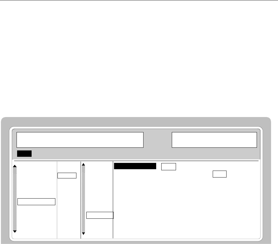
Digital Standard IS-95 CDMA SMIQ
1125.5555.03 E-92.142
(TRIGGER...) TRIGGER OUT 1/2 POL Selection of signal polarity at outputs TRIGOUT 1
and TRIGOUT 2 of the PARDATA connector.
IEC/IEEE-bus :SOUR:IS95:OUTP1:POL NORM
TRIGGER OUT 1/2
DELAY Setting the number of chips by which the selected
trigger signal is delayed.
IEC/IEEE-bus :SOUR:IS95:OUTP1:DEL –50
CLOCK... Opens a window for selecting the clock source.
The CDMA chip clock in SMIQ corresponds to the symbol clock of the
modulation. Therefore, the terms symbol clock and chip clock are
synonymous.
FREQ 100. 000 000 0 MHz
FREQUENCY
LEVEL
ANALOG MOD
VECTOR MOD
DIGITAL MOD
DIGITAL STD
LF OUTPUT
SWEEP
LIST
MEM SEQ
UTILITIES
IS95
PHS
IS-95
STATE
MODE
SET DEFAULT
MODULATION...
TRIGGER MODE
EXECUTE TRIGGER>
TRIGGER....
CLOCK...
TOTAL POWER
ADJUST TOTA
CLOCK MODE CHIP CHIPX4 CHIPX8 CHIPX16
CLOCK SOURCE INT EXT
DELAY 0.35 Symb
LEVEL -30.0 dBm
PEP -13.9.dBm
Fig. 2-84 Menu DIGITAL STD - IS-95 - CLOCK..., equipped with options modulation coder
SMIQB20, data generator SMIQB11 and SMIQB42
(CLOCK...) CLOCK MODE Selection of the type of external clock signal.
CHIP Chip clock
CHIPXn Four-, eight- or sixteen-fold chip clock
(n=4, 8 or 16).
IEC/IEEE-bus :SOUR:IS95:CLOC:MODE CHIP

SMIQ Digital Standard IS-95 CDMA
1125.5555.03 E-92.143
(CLOCK...) CLOCK SOURCE Selection of clock source.
INT SMIQ uses internally generated clock
signals.
EXT An external chip clock is fed in at connec-
tor SYMBOL CLOCK. Multifolds of the
chip clock are fed in at connector BIT
CLOCK .
The clock synthesizer on the modulation
coder is synchronized to this clock.
Parameter CHIP RATE has to be set with
an accuracy of ± 1 %.
The polarity, the trigger threshold and the
input resistance of the SYMBOL CLOCK
input can be modified in menu DIGITAL
MOD - EXT INPUTS.
IEC/IEEE-bus :SOUR:IS95:CLOC:SOUR INT
DELAY Setting the delay of generated modulation signal to
an external clock.
This can be used, for example, for synchronization
with a second unit to achieve time synchroneity
between the modulation signals of the two units.
The displayed setting resolution of 1/100 symbol is
only attained for symbol-clock frequencies below
100 kHz.
The resolution is reduced with increasing frequency.
At a chip rate of 1.2288 Mcps, the resolution equals
the chip duration × 0.1.
IEC/IEEE-bus :SOUR:IS95:CLOC:DEL 0.5
TOTAL POWER Display of the total power of all active code channels. The TOTAL POWER is
calculated when the modulation is active (STATE = ON). It is the sum of the
channel power of all active channels. If the value is not equal 0 dB then all active
channel power were internally adjusted so that the total power equals 0 dB (the
power relation between single code channels is not affected!) This is nessessary
to keep the setted output power (LEVEL) constant. In addition to this average
power (LEVEL) the peak envelope power (PEP) is also indicated in the header of
the display. The value for PEP is calculated based on a worst case. The actual
peak powers are mostly smaller.
IEC/IEEE-bus command :SOUR:IS95:POW?
ADJUST
TOTAL POWER Changes the power of every code channel switched on. After this adjustment
the total power is 0 dB. The power relation between single active code
channels is not affected.
IEC/IEEE-bus command :SOUR:IS95:POW:ADJ

Digital Standard IS-95 CDMA SMIQ
1125.5555.03 E-92.144
SAVE/RCL
MAPPING... Saves/calls up the set channel configuration.
This setting is only possible in the forward link mode.
For FWD_LINK_18, the following is saved for each channel number:
- selected WALSH CODE
- set POWER
- type of modulation data (DATA) and
- switch-on state.
For FWD_LINK_64, the following is saved for each channel number:
- set POWER
- modulation data (DATA) and
- switch-on state.
The channel configuration of the two forward-link modes is stored and loaded
at the same time.
FREQ
100. 000 000 0
MHz
FREQUENCY
LEVEL
ANALOG MOD
VECTOR MOD
DIGITAL MOD
DIGITAL STD
LF OUTPUT
SWEEP
LIST
MEM SEQ
UTILITIES
IS95
PHS
IS-95
MODE
SET DEFAULT
MODULATION...
TRIGGER MODE
EXECUTE TRIGGER>
TRIGGER....
CLOCK...
TOTAL POWER
ADJUST TOTAL
SAVE/RCL MAP
GET PREDEFINED MAPPING...
RECALL MAPPING...
SAVE MAPPING...
DELETE MAPPING...
LEVEL
-30.0
dBm
PEP
-13.9.
dBm
Fig. 2-85 Menu DIGITAL STD - IS-95 - SAVE/RCL MAPPING..., equipped with options
modulation coder SMIQB20, data generator SMIQB11 and SMIQB42
(SAVE/RCL
MAPPING...) GET PREDEFINED
MAPPING... Loads a factory-set channel configuration.
PILOT A pilot signal is generated only.
09CHAN A signal with 9-code channels is
generated according to the Base Station
Test Model (IS95).
18CHAN A signal with 18-code channels is
generated.
IEEE-bus :SOUR:IS95:MAPP:SEL:PRED "pilot"
RECALL MAPPING... Loads a stored channel configuration.
IEEE-bus :SOUR:IS95:MAPP:LOAD "name"

SMIQ Digital Standard IS-95 CDMA
1125.5555.03 E-92.145
(SAVE/RCL
MAPPING...) SAVE MAPPING... Stores the channel configuration. For remote control,
a name with 7 characters at max. can be used.
IIEEE-bus :SOUR:IS95:MAPP:STOR "name"
DELETE MAPPING... Deletes a stored channel configuration.
IEEE bus :SOUR:IS95:MAPP:DEL "name"
CHANNEL NO Display of channel number.
This menu column is only displayed in the forward link mode.
WALSH CODE Setting the Walsh code.
This menu column is only displayed in the forward link mode.
For FWD_LINK_18
- the Walsh code can be set individually for each channel.
IEC/IEEE-bus command :SOUR:IS95:CHAN1:WALS 32
For FWD_LINK_64
- the Walsh code cannot be set. In this mode, the Walsh code corresponds to
the channel number. All the 64 code channels are displayed.
POWER Setting the power of channel.
This menu column is only displayed in the forward link mode.
POWER indicates the average power of the code channel relative to the
power indicated in LEVEL display (code domain power).
For FWD_LINK_18
- the power of channels 0, 1, 2 is set individually.
- the other channels have the same power. The power for all the channels is
set in channel 3.
For FWD_LINK_64
- the power of the pilot channel is set individually.
- the other channels have the same power. The power for all the channels is
set in channel 1.
IEC/IEEE-bus command :SOUR:IS95:CHAN1:POW -10 DB
DATA Setting the modulation data for the selected code channel.
This menu column is only displayed in the forward link mode.
The data rate for all forward link channels corresponds to the chip rate/64, ie
19200 bps at a chip rate of 1.2288 Mcps
0000 Continuous sequence of zeros
IEC/IEEE-bus command SOUR:IS95:CHAN1:DATA ZERO
1111 Continuous sequence of ones
IEC/IEEE-bus command SOUR:IS95:CHAN1:DATA ONE
1010 Alternating sequence of zeros and ones
IEC/IEEE-bus command SOUR:IS95:CHAN1:DATA ALT
PRBS Pseudo random data, different in every code channel
IEC/IEEE-bus command SOUR:IS95:CHAN1:DATA PRBS
STATE Switch on/off of assigned code channel.
This menu column is only displayed in the forward link mode.
IEC/IEEE-bus command :SOUR:IS95:CHAN1:STAT ON
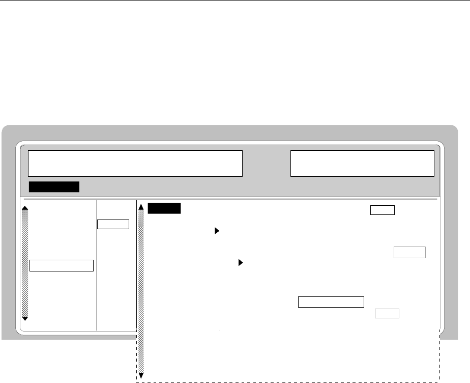
Digital Standard IS-95 CDMA SMIQ
1125.5555.03 E-92.146
2.12.5 Menu IS-95 CDMA Standard - Reverse Link Signal without
Channel Coding
Menu DIGITAL STD - IS-95 provides access to settings for IS-95 CDMA signal generation. The
following figure shows the menu for generating the reverse link signal (transmit signal of mobile station)
without signal coding. The previous section showed the menu for generating the forward link signals as
well as the parameters that are identical for both modes.
Menu selection: DIGITAL STD - IS-95- MODE - REV_LINK
FREQ 100. 000 000 0 MHz
FREQUENCY
LEVEL
ANALOG MOD
VECTOR MOD
DIGITAL MOD
DIGITAL STD
LF OUTPUT
SWEEP
LIST
MEM SEQ
UTILITIES
IS95
PHS
IS95
NADC
PDC
GSM
L
OFF ON
MODE... REV_LINK
SET DEFAULT
MODULATION... QPSK IS-95
TRIGGER MODE... AUTO
EXECUTE TRIGGER
TRIGGER... INT
CLOCK... INT
RATE FULL_RATE HALF_RATE
BURST RANDOMIZER OFF ON
DATA 0000
-----------------CHANGE DATA------------------
SELECT DATA LIST... CURRENT: R&STDM
COPY CURRENT DATA LIST TO...
DELETE DATA LIST...
EDIT DATA LIST...
EVEL -30.0 dBm
PEP - 23.3 dBm
STATE
Fig. 2-86 Menu DIGITAL STD - IS-95 - MODE - REV_LINK
STATE to CLOCK see section "Menu IS-95 CDMA-Standard- Forward Link Signal"
RATE Selection of full-rate or half-rate transmission of modulation data. This
selection is only possible in the reverse link mode.
In the half-rate mode, only 8 of 16 power control groups of a frame are
transmitted ("power gating").
IEC/IEEE-bus command :SOUR:IS95:RATE HALF
BURST
RANDOMIZER Switch on/off of burst randomizer. This selection is only possible during half-
rate transmission in the reverse link mode.
OFF Every second power control group is transmitted.
ON A random algorithm determines which eight of the 16 power
control groups of a frame will be transmitted.
IEC/IEEE-bus command :SOUR:IS95:RAND ON

SMIQ Digital Standard IS-95 CDMA
1125.5555.03 E-92.147
DATA Selection of modulation data for the reverse link signal. The data rate
corresponds to the chip rate x3/128, ie 28800 bps at 1.2288 Mcps.
0000 Continuous sequence of zeros
IEC/IEEE-bus :SOUR:IS95:DATA ZERO
1111 Continuous sequence of ones
IEC/IEEE-bus :SOUR:IS95:DATA ONE
1010 Alternating zeros and ones
IEC/IEEE-bus :SOUR:IS95:DATA ALT
PRBS PRBS data.
IEC/IEEE-bus :SOUR:IS95:DATA PRBS
DLIST Data from a programmable data list.
IEC/IEEE-bus :SOUR:IS95:DATA DLIS
SELECT DATA LIST... Opens a window for selecting a stored data list or for generating a new list
(only with Reverse Link or Reverse Link Coded modes).
COPY CURRENT
DATA LIST TO... Stores the current data list under a different name (only with Reverse Link or
Reverse Link Coded modes).
DELETE DATA LIST... Deletes a data list (only with Reverse Link or Reverse Link Coded modes).
EDIT DATA LIST... Opens a window for editing a data list bit-by-bit. The available storage capacity
and the length of the current list is displayed in parameters FREE and LEN
(see also Section List Editor). Only with Reverse Link or Reverse Link Coded
modes.
COPY Copies a list range
FILL Fills the range with filler pattern
INSERT Inserts a list range at a different position of the list
DELETE Deletes a list range
EDIT/VIEW Edits or views the list
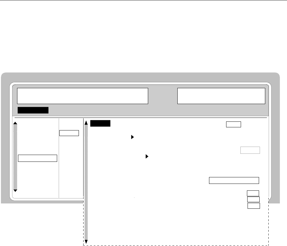
Digital Standard IS-95 CDMA SMIQ
1125.5555.03 E-92.148
2.12.6 Menu IS-95 CDMA Standard - Reverse Link Signal with
Channel Coding
Menu DIGITAL STD - IS-95 provides access to settings for generating IS-95 CDMA signals. The
following figure shows the menu for generating a reverse link signals with channel coding. The section
on the menu for forward link signal generation shows the parameters that are identical for both modes.
Menu selection: DIGITAL STD - IS-95- MODE - REV_LINK_CODED
FREQ 100. 000 000 0 MHz
FREQUENCY
LEVEL
ANALOG MOD
VECTOR MOD
DIGITAL MOD
DIGITAL STD
LF OUTPUT
SWEEP
LIST
MEM SEQ
UTILITIES
IS95
PHS
IS95
NADC
PDC
GSM
L
OFF ON
MODE... REV_LINK
SET DEFAULT
MODULATION... QPSK IS-95
TRIGGER MODE... AUTO
EXECUTE TRIGGER
TRIGGER... INT
CLOCK... INT
CHANNEL TYPE/RATE TRAFFIC 14400
DATA CURRENT: PN9
ADD FRAME QUAL INDICATOR OFF ON
CONVOLUTIONAL ENCODER OFF ON
BLOCK INTERLEAVER OFF ON
ERASURE BIT 0 1
-----------------CHANGE DATA------------------
SELECT DATA LIST... CURRENT: R&STDM
COPY CURRENT DATA LIST TO...
DELETE DATA LIST...
EDIT DATA LIST...
EVEL -30.0 dBm
PEP - 23.3 dBm
STATE
Fig. 2-87 Menu DIGITAL STD - IS-95 - MODE - REV_LINK_CODED
Parameter STATE to CLOCK... see section "Menu IS-95 CDMA Standard - Forward Link Signal".

SMIQ Digital Standard IS-95 CDMA
1125.5555.03 E-92.149
CHANNEL
TYPE/RATE Selects the type of channel and the associated data rate. This selection is only
possible in the reverse link mode. The selection also determines the structure
of the channel coding and the number of data bits to be inserted into each
frame.
TRAFFIC 14400 Traffic channel with 14400 bps. 267 bits are inserted into
each frame
TRAFFIC 7200 Traffic channel with 7200 bps. 125 bits are inserted into
each frame
TRAFFIC 3600 Traffic channel with 3600 bps. 55 bits are inserted into
each frame
TRAFFIC 1800 Traffic channel with 1800 bps. 21 bits are inserted into
each frame
ACCESS 4800 Access channel with 4800 bps. 88 bits are inserted into
each frame
TRAFFIC 9600 Traffic channel with 9600 bps. 172 bits are inserted into
each frame
TRAFFIC 4800 Traffic channel with 4800 bps. 80 bits are inserted into
each frame
TRAFFIC 2400 Traffic channel with 2400 bps. 40 bits are inserted into
each frame
TRAFFIC 1200 Traffic channel with 1200 bps. 16 bits are inserted into
each frame
IEC/IEEE-bus :SOUR:IS95:RLC:CTYP TRAF7200
:SOUR:IS95:RLC:CTYP ACC4800
DATA SOURCE Selects the modulation data for the reverse link signal with channel coding. The
data are continuously inserted into the data field of the corresponding frame.
PN.. PRBS data to CCITT with period length between 29-1 and 223-1.
IEC/IEEE-bus command :SOUR:IS95:RLC:DATA PN1
DLIST Data from a previously programmed and stored data list.
IEC/IEEE-bus command :SOUR:IS95:RLC:DATA DLISt
ADD FRAME QUAL
INDICATOR Switches the frame quality indicator (CRC calculation) on or off. With OFF
selected, only zeros are sent instead of CRC bits.
IEC/IEEE-bus command :SOUR:IS95:RLC:FQIN ON
CONVOLUTIONAL
ENCODER Switches the convolutional encoder on or off. With OFF selected, the data rate
is attained by repeating the symbol.
IEC/IEEE-bus command :SOUR:IS95:RLC:CENC ON
BLOCK
INTERLEAVER Switches the interleaver function on or off.
IEC/IEEE-bus command :SOUR:IS95:RLC:BINT ON
ERASURE BIT Selects 1 or 0 for the erasure bit.
IEC/IEEE-bus command :SOUR:IS95:RLC:EBIT 0
Parameter SELECT DATA LIST... to EDIT DATA LIST... see section "Menu IS-95 CDMA Standard -
Forward Link Signal"
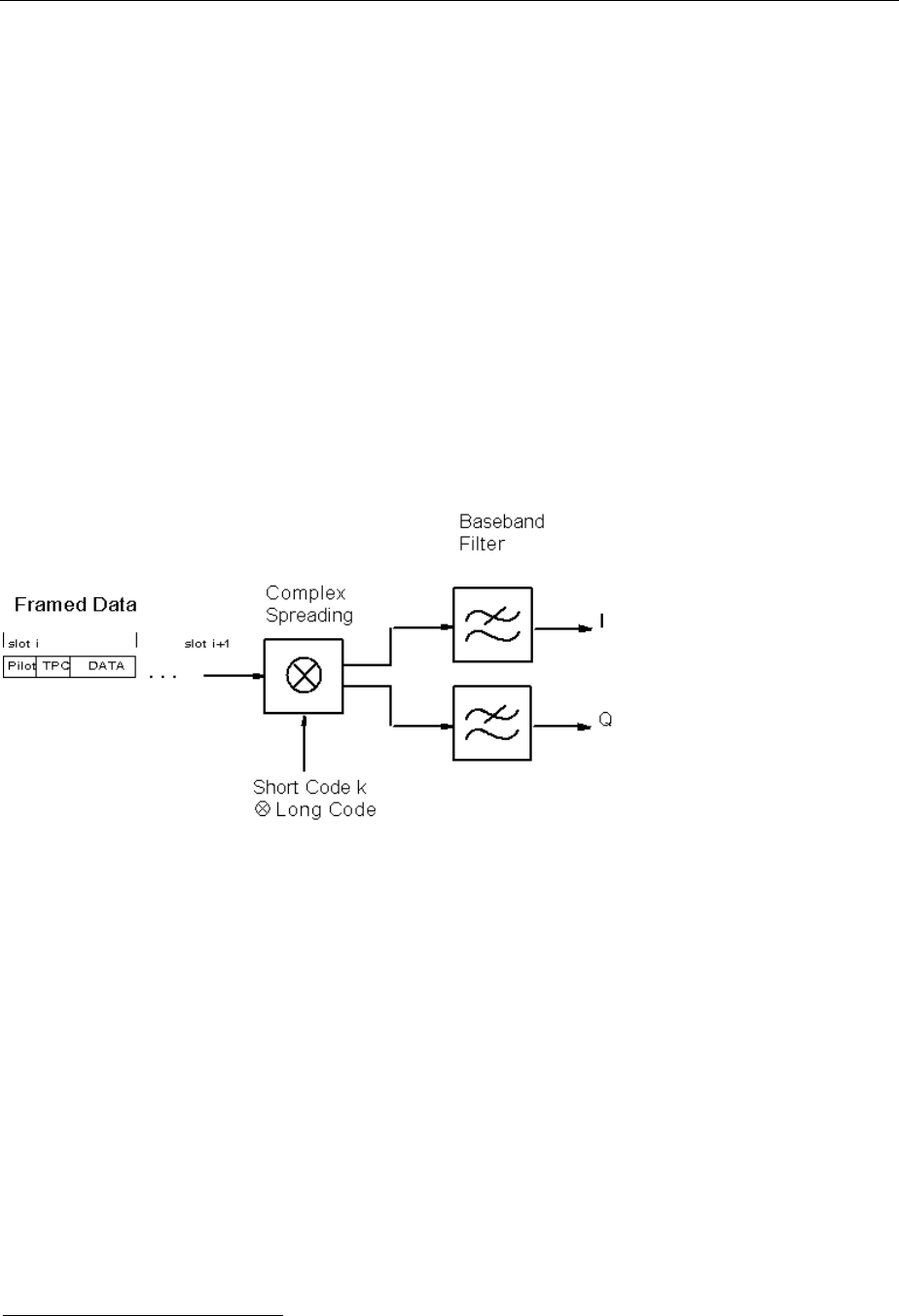
Digital Standard W-CDMA (NTT DoCoMo/ARIB 0.0) SMIQ
1125.5555.03 E-92.150
2.13 Digital Standard W-CDMA (NTT DoCoMo/ARIB 0.0)
With the options Modulation Coder (SMIQB20), Data Generator (SMIQB11) and option Digital Standard
W-CDMA (SMIQB43) provided, W-CDMA signals can be generated according to the Japanese
experimental system NTT DoCoMo or the ARIB 0.0 standard1.
SMIQ can simulate both the transmit signal of a base station (Downlink), and the transmit signal of a
mobile station (Uplink) with up to 15 code channels.
Different physical channel types such as Perch, Common Control or Dedicated Physical Channel can be
selected. For this purpose, SMIQ generates modulation data with the frame structure specified in the
standard (framed data). Data fields with pilot symbols, TPC symbols (Traffic Power Control) or LMS
symbols (Long Code Mask) are automatically generated. Freely programmable data lists or pseudo-
random bit sequences (PRBS) can be used for the modulation symbols in the DATA fields. These
modulation data are not subjected to any channel coding (convolution coding, interleaving). The user
can, however, store channel-coded modulation data in a data list to generate a logic channel, eg a
Dedicated Traffic Channel.
The following figure shows the schematic of forward link signal generation.
Fig. 2-88 Downlink DPCH signal generation for a code channel
The Perch Channel, DPCH (Dedicated Physical Channel) and CCPCH (Common Control Physical
Channel) are available as channel types in the downlink. The data rate for modulation data (framed
data) of the DPCH can be selected (32, 64, to 1024 ksymbol/s). The type of modulation is QPSK, but O-
QPSK can also be set. A root cosine filter with roll-off factor 0.22 is preset for baseband filtering. Other
filters can also be set (MODULATION FILTER). The chip rate is preset to 4.096 Mcps but can be
modified within wide limits.
Two modes (LINK DIRECTION/MULTIPLEX) are available to generate an uplink signal. A mobile station
transmitter of the Japanese W-CDMA experimental system is simulated in the UP mode. The frame
structure of data corresponds to that of the downlink. DPCH and CCPCH are available as channel
types.
1 Association of Radio Industries and Businesses (ARIB), Specifications of Air-Interface for a 3 G Mobile System
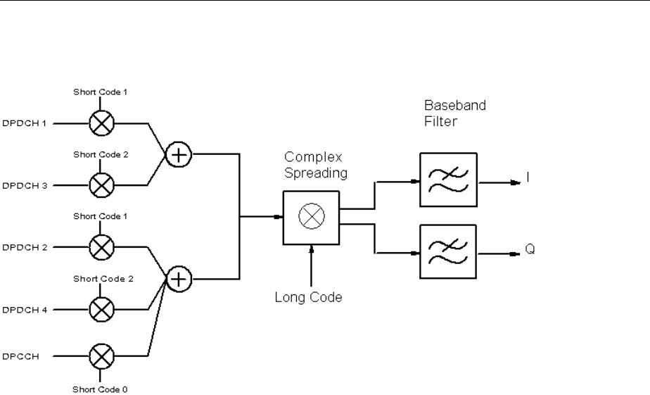
SMIQ Digital Standard W-CDMA (NTT DoCoMo/ARIB 0.0)
1125.5555.03 E-92.151
A mobile station transmitter in line with the ARIB standard is simulated in the UP_IQ_MULT mode.
Separate channel types and data sources for I and Q are available in the multiplex mode.
Fig. 2-89 Uplink signal generation with IQ multiplex and several code channels
According to ARIB, DPDCH (Dedicated Physical Data Channel) and DCPCH (Dedicated Control
Physical Channel) are available as channel types in the uplink. The data rate for modulation data
(framed data) of the DPDCH can be selected (16, 32, 64, to 1024 ksymbol/s).
The modulation data are not calculated in real time in SMIQ. On the user request, a W-CDMA chip
sequence is calculated (STATE = ON) and then stored in the data memory of the data generator (option
SMIQ B11). The sequence length is settable (SEQUENCE LENGTH [FRAMES]), the maximum possible
length depends on the memory capacity of the data generator.
A special multicode mode is available (MULTICODE) for LINK DIRECTION/MULTIPLEX DOWN and
UP modes. The data fields Pilot and TPC have the same settings and are spread with the same
spreading codes of the MASTER CHANNEL.

Digital Standard W-CDMA (NTT DoCoMo/ARIB 0.0) SMIQ
1125.5555.03 E-92.152
2.13.1 Sync and Trigger Signals
A chip sequence is calculated for the generation of W-CDMA signals and stored in the memory of the
data generator (option SMIQB11). This chip sequence can be run repetitively (TRIGGER MODE
AUTO).
Trigger signals can be used for synchronized measurements on receivers (TRIGGER MODE RETRIG,
ARMED_AUTO or ARMED_RETRIG).
A trigger signal can be fed via the TRIGIN input at connector PAR DATA of SMIQ. The chip sequence
either starts immediately after the active slope of the trigger signal or after a settable number of chips
(EXT TRIGGER DELAY). Retriggering (RETRIG) can be inhibited for a settable number of chips (EXT
RETRIGGER INHIBIT).
A trigger event can be executed manually or via the IEC/IEEE bus using EXECUTE TRIGGER.
When a trigger event is executed, a trigger signal is output at the TRIGOUT 3 output of SMIQ.
SMIQ generates the following sync signals:
•a 0.625 ms slot clock
•a 10 ms radio frame clock
• a marker signal for identifying the periodic repetition of the generated chip sequence
SMIQ can output two of the three signals via pins TRIGOUT 1 and 2 of connector PAR DATA.
A clock synthesizer on the modulation coder generates the chip clock in the SMIQ. All the clock signals
are synchronized to the 10-MHz reference of the SMIQ. The chip clock is available at connector
SYMBOL CLOCK. If required, the clock synthesizer in the SMIQ can be synchronized to an external
chip clock which is fed in at connector SYMBOL CLOCK.
To allow for a trouble-free synchronization of the clock synthesizer first apply the external clock and set
the correct chip rate at SMIQ (MODULATION - CHIPRATE VARIATION). Then switch CLOCK
SOURCE from INT to EXT.
Note: The set symbol rate should not differ by more than 1% from the symbol rate of the external
signal.
SMIQ Digital Standard W-CDMA (NTT DoCoMo/ARIB 0.0)
1125.5555.03 E-92.153
2.13.2 PN Generators as Internal Data Source
Different PN (Pseudo Noise) generators can be selected as data source for DATA fields. These PN
generators provide pseudo random bit sequences of different lengths or periods which is why they are
also called PRBS generators (Pseudo Random Binary Sequence).
The data sequences are so-called sequences of maximum lengths that are generated by means of
feedback shift registers.
The following schematic shows the 9 bit generator with feedback to registers 4 and 0 (output).
8
765
4
3210
DATA
EXOR
The pseudo random sequence of a PRBS generator is determined by the number of registers and the
feedback. The following table describes all available PRBS generators:
Table 2-17 PN generators for W-CDMA
PRBS generator Length in bits Feedback to Start value (*)
9 bits 29 -1 = 511 Register 4, 0 Channel 0: 0000 0100 1
Channel 1: 1000 0100 1
Channel 2: 0100 0100 1
Channel 3: 1100 0100 1
...
Channel 15: 1111 0100 1
11 bits 211 -1 =2047 Register 2, 0 Channel 0: 0000 0100 100
...
Channel 15: 1111 0100 100
15 bits 215 -1 = 32767 Register 1, 0 Channel 0: 0000 0100 1000 000
...
Channel 15: 1111 0100 1000 000
16 bits 216 -1 = 65535 Register 5, 3, 2, 0 Channel 0: 0000 0100 1000 0000
...
Channel 15: 1111 0100 1000 0000
*) the 5th start value bit of channels in Q phase is 1 (for example: channel 3: 1100 1100 1...)
PN generators PN9,11 and PN15 are designed according to CCITT Rec. 0.151/152/153. The output
sequence is inverted for generator PN15.
Example: PN9 generator in channel 3 with start value 110001001 (binary)
11
DATA
EXOR
0001
0
0
1
The resulting output sequence is 110001001100010001000 etc.

Digital Standard W-CDMA (NTT DoCoMo/ARIB 0.0) SMIQ
1125.5555.03 E-92.154
2.13.3 Lists as an Internal Data Source
A freely programmable memory can be used as a data source for DATA or TPC fields. The data are
managed in lists. A list editor enables the data lists (DATA LIST) to be selected, copied, modified and
erased. The list editor can be accessed via the menu DIGITAL MOD SOURCE...
2.13.4 Menu W-CDMA Standard - Downlink and Uplink Signals without IQ
Multiplex
Menu DIGITAL STD - W-CDMA provides access to settings for W-CDMA signal generation.
The figure below shows an example of the menu for generating the downlink signal (transmit signal of
the base station) in the 8CHAN mode. The menus for generating uplink signals without IQ multiplex
have nearly the same structure. A menu for generating uplink signals with IQ multiplex is shown in the
next section. Parameters that are identical for all modes are explained in this section.
Menu selection: DIGITAL STD - WCDMA - MODE - 8CHAN, -LINK DIRECTION/MULTIPLEX DOWN
FREQ 100. 000 000 0 MHz
FREQUENCY
LEVEL
ANALOG MOD
VECTOR MOD
DIGITAL MOD
DIGITAL STD
LF OUTPUT
SWEEP
LIST
MEM SEQ
UTILITIES
WCDMA
PHS
IS-95
WCDMA
NADC
PDC
GSM
DECT
STATE
MODE 4CHAN 8CHAN 15CHAN
SET DEFAULT
CHIP RATE 4.096 Mcps
LINK DIRECTION/MULTIPLEX DOWN
MODULATION... QPSK
TRIGGER MODE... RETRIG
EXECUTE TRIGGER
TRIGGER.... INT
CLOCK... INT EXT
TOTAL POWER 0.0 dB
ADJUST TOTAL POWER
SAVE/RECALL SETTINGS... COMING SOON
MULTICODE... OFF
SEQUENCE LENGTH (FRAMES) 1
_________SYMB RATE SPREAD POWER_______________
CHNO TYPE [ks/s] CODE [dB] DATA STATE
0 PERCH 16 0 -9.0 PN15 ON
1 DPCH 32 10 -9.0 PN15 ON
2 DPCH 32 11 -9.0 PN15 ON
3 DPCH 32 12 -9.0 PN15 ON
4 DPCH 32 13 -9.0 PN15 ON
5 DPCH 32 14 -9.0 PN15 ON
6 DPCH 32 15 -9.0 PN15 ON
7 DPCH 32 16 -9.0 PN15 ON
OFF ON
LEVEL -30.0 dBm
PEP - 14.9.dBm
Fig. 2-90 Menu DIGITAL STD - WCDMA - MODE - 8CHAN, LINK DIRECTION/MULTIPLEX - DOWN,
equipped with options modulation coder SMIQB20, data generator SMIQB11 and SMIQB43

SMIQ Digital Standard W-CDMA (NTT DoCoMo/ARIB 0.0)
1125.5555.03 E-92.155
STATE Switch on/off of modulation Digital Standard W-CDMA. Vector modulation and
digital modulation will be switched off automatically.
STATE = ON starts the calculation of a chip sequence based on the current
settings. The lenght of the chip sequence and therefore the duration of
calculation are determined by parameter SEQUENCE LENGTH.
IEC/IEEE-bus command :SOUR:WCDM:STAT ON
MODE... Opens a window for selecting from the different modes to determine the
number of code channels.
The physical channel type (TYPE), the symbol rate, some spreading para-
meters (SPREAD CODE) and the source for modulation data (DATA) can be
separately defined for each channel. Each channel can be switched on or off
(STATE).
4CHAN Activates the generation of a signal with up to 4 code
channels (channel No. 0 to 3).
The relative power (POWER) of the channels can be
freely determined in range -30 dB to 0 dB.
IEC/IEEE-bus :SOUR:WCDM:MODE CHAN4
8CHAN Activates the generation of a signal with up to 8 code
channels (channel No. 0 to 7).
The relative power (POWER) of channel 0 can be freely
determined in range -30 dB to 0 dB. The power setting of
channel 1 also determines the power setting of channels
2 to 7. This means that channels 1 to 7 all have the same
power provided when the channels are switched on.
IEC/IEEE-bus :SOUR:WCDM:MODE CHAN8
15CHAN Activates the generation of a signal with up to 15 code
channels (channel No. 0 to 14).
The relative power of channels cannot be freely defined
since all activated code channels have the same power.
The relative power is displayed (POWER).
IEC/IEEE-bus :SOUR:WCDM:MODE CHAN15

Digital Standard W-CDMA (NTT DoCoMo/ARIB 0.0) SMIQ
1125.5555.03 E-92.156
SET DEFAULT Provides the default setting for W-CDMA.
For LINK DIRECTION/MULTIPLEX DOWN
- in mode 8, channel 0 is a Perch channel, it is switched on and its symbol
rate is 16 ksymbol/s
- all other channels are also switched on (STATE ON), channel type (TYPE)
is DPCH, symbol rate is 32 ksymbol/s
- the channels have the same relative power (POWER)
- the data are pseudo random (PN15), except for Perch channel, a data offset
of three times the channel number (3 • CHNO) is set.
For LINK DIRECTION/MULTIPLEX UP
- only channel 0 is switched on, channel type is DPCH, symbol rate is
32 ksymbol/s
- the data are pseudo random (PN15), no data offset is set.
For LINK DIRECTION/MULTIPLEX UP_IQ_MULT
- all channels are switched on except I-channel 0 in mode 8
- Q-channel 0 is configured as DPCCH, all the other channels are configured
as DPDCH with a symbol rate of 16 ksymbol/s
- all channels have the same relative power (POWER)
- the data are pseudo random (PN15), no data offset is set.
IEC/IEEE-bus :SOUR:WCDM:PRES
CHIP RATE Selection between 4.096 Mcps and 8.192 Mcps. Selecting 8.192 Mcps
depends on the hardware configuration of the unit and is not offered yet.
Selecting CHIP RATE has an effect on the generation of spreading codes and
thus on the calculated chip sequence.
IEC/IEEE-bus :SOUR: WCDM:CRAT R4M
LINK DIRECTION/
MULTIPLEX Opens a window for selecting the type of transmit signal from the different
modes.
DOWN Activates the generation of a downlink signal. In this
mode, the transmit signal of a base station can be
generated in line with the Japanese ARIB standard or
according to NTTDoCoMo specifications for an
experimental system.
IEC/IEEE-bus :SOUR:WCDM:LINK DOWN
UP Activates the generation of an uplink signal. In this mode,
the transmit signal of a mobile station can be generated
in line with the NTTDoCoMo specifications for an
experimental system.
IEC/IEEE-bus :SOUR:WCDM:LINK UP
UP_IQ_MULT Activates the generation of an uplink signal with a
multiplex mode for the I and Q channel. Separate
channel types and data sources are available for I and
Q. In this mode, the transmit signal of a mobile station
can be generated in line with the Japanese ARIB
standard.
IEC/IEEE-bus :SOUR:WCDMA:LINK UPM
SMIQ Digital Standard W-CDMA (NTT DoCoMo/ARIB 0.0)
1125.5555.03 E-92.157
MODULATION... Opens a window for setting the modulation parameters.
Menu selection: DIGITAL STD - WCDMA - MODULATION...
FREQ 100. 000 000 0 MHz
FREQUENCY
LEVEL
ANALOG MOD
VECTOR MOD
DIGITAL MOD
DIGITAL STD
LF OUTPUT
SWEEP
LIST
MEM SEQ
UTILITIES
WCDMA
PHS
IS-95
WCDMA
NADC
PDC
GSM
DECT
STATE
MODE
SET DEFAULT
CHIP RATE
LINK DIRECT
MODULATION...
TRIGGER MODE
EXECUTE TRIGGER>
TRIGGER....
CLOCK
TOTAL POWER
LEVEL -30.0 dBm
PEP -14.9.dBm
MODULATION TYPE... QPSK 2b/sym
CHIP RATE VARIATION 4.096 Mcps
FILTER... WCDMA 0.22
FILTER MODE LOW_ACP LOW_EVM
LOW DISTORTION MODE OFF ON
Fig. 2-91 Menu DIGITAL STD - WCDMA - MODULATION..., equipped with options modulation coder
SMIQB20, data generator SMIQB11 and SMIQB43
(MODULATION...) MODULATION TYPE Selection between the types of modulation QPSK
and offset QPSK.
IEC/IEEE-bus :SOUR:WCDM:FORM QPSK
CHIP RATE
VARIATION Setting value for the chip clock frequency. The value
for CHIPRATE from the main menu is preset. CHIP
RATE VARIATION modifies the output clock and the
modulation bandwidth as well as the output
synchronization signals. It has no effect on the
calculated chip sequence.
IEC/IEEE-bus :SOUR:WCDM:CRAT:VAR 4096001
FILTER... Opens a window for selecting the baseband filter.
Selection can be made between a filter optimized for
W-CDMA, the standard Nyquist filters COS and
SQRCOS or a user-defined filter USER (cf. Section
Digital Modulation) is possible. The optimized root
cosine filter WCDMA 0.22 is preset. Its roll-off factor
is fixed to 0.22.
IEC/IEEE-bus :SOUR:WCDM:FILT:TYPE WCDM
ROLL OFF FACTOR Setting value of roll-off factor.
The setting is only possible provided that a COS or
SQRCOS filter is selected under FILTER.
IEC/IEEE-bus :SOUR:WCDM:FILT:PAR 0.22

Digital Standard W-CDMA (NTT DoCoMo/ARIB 0.0) SMIQ
1125.5555.03 E-92.158
(MODULATION...) FILTER MODE Selection of filter mode.
LOW_ACP Filter for minimum Adjacent Channel
Power.
IEC/IEEE-bus command
:SOUR:WCDM:FILT:MODE LACP
LOW_EVM Filter for minimum vector error.
IEC/IEEE-bus command
:SOUR:WCDM:FILT:MODE LEVM
LOW DISTORTION
MODE Switch on/off of low-distortion mode.
After switch-on, the level of the IQ baseband signals
is reduced by 3 dB. In some cases, this might reduce
undesired intermodulation products. OFF is normally
the more favourable setting.
IEC/IEEE-bus :SOUR:WCDM:LDIS:STAT OFF
TRIGGER MODE Opens a window for selecting the W-CDMA sequence.
AUTO The calculated W-CDMA chip sequence is cyclically
repeated.
IEC/IEEE-bus command :SOUR:WCDM:SEQ AUTO
RETRIG The W-CDMA chip sequence is continuously re-
peated. A trigger event causes a restart from frame 1.
IEC/IEEE-bus command :SOUR:WCDM:SEQ RETR
ARMED_AUTO The W-CDMA chip sequence cannot be started from
frame 1 until a trigger event has occurred. The unit
then automatically switches over to the AUTO mode
and can no longer be triggered.
IEC/IEEE-bus command :SOUR:WCDM:SEQ AAUT
ARMED_RETRIG The W-CDMA chip sequence cannot be started from
frame 1 until a trigger event has occurred. each new
trigger event causes a restart.
IEC/IEEE-bus command :SOUR:WCDM:SEQ ARET
EXECUTE TRIGGER Executes a trigger event to start the W-CDMA chip sequence.
IEC/IEEE-bus command :TRIG:DM:IMM
TRIGGER... Opens a window for selecting the trigger source, for configuring the trigger
output signals and for setting the time delay of an external trigger signal.
SMIQ Digital Standard W-CDMA (NTT DoCoMo/ARIB 0.0)
1125.5555.03 E-92.159
Menu selection: DIGITAL STD - WCDMA - TRIGGER...
FREQ 100. 000 000 0 MHz
FREQUENCY
LEVEL
ANALOG MOD
VECTOR MOD
DIGITAL MOD
DIGITAL STD
LF OUTPUT
SWEEP
LIST
MEM SEQ
UTILITIES
WCDMA
PHS
IS-95
WCDMA
NADC
PDC
GSM
DECT
STATE
MODE
SET DEFAULT
CHIP RATE
LINK DIRECT
MODULATION
TRIGGER MODE
EXECUTE TRIG
TRIGGER....
CLOCK
TOTAL POWER
TRIGGER SOURCE INT EXT
EXT TRIGGER DELAY 0 Chip
EXT RETRIGGER INHIBIT 0 Chip
TRIGGER OUT1 RADIO FRAME
TRIGGER OUT2 CHIP SEQUENCE PERIOD
TRIGGER OUT1 POL POS NEG
TRIGGER OUT2 POL POS NEG
TRIGGER OUT1 DELAY 0 Chip
TRIGGER OUT2 DELAY 0 Chip
LEVEL -30.0 dBm
PEP - 14.9.9.dBm
Fig. 2-92 Menu DIGITAL STD - WCDMA - TRIGGER..., equipped with options modulation coder
SMIQB20, data generator SMIQB11 and SMIQB43
TRIGGER... TRIGGER SOURCE Selection of trigger source.
EXT The W-CDMA chip sequence is started
from frame 1 by means of the active
slope of an external trigger signal.
The polarity, the trigger threshold and
the input resistance of the TRIGIN input
can be modified in menu
DIGITAL MOD - EXT INPUTS.
INT A trigger event is manually executed by
EXECUTE TRIGGER.
IEC/IEEE-bus :SOUR:WCDM:TRIG:SOUR EXT
EXT TRIGGER
DELAY Setting the number of chips by which an external
trigger signal is delayed before it starts the W-CDMA
chip sequence.
This is used for setting the time synchroneity
between the DUT and other units.
IEC/IEEE-bus :SOUR:WCDM:TRIG:DEL 3
EXT RETRIGGER
INHIBIT Setting the number of chips for which a restart is
inhibited after a trigger event.
With TRIGGER MODE RETRIG selected, each new
trigger signal restarts the W-CDMA chip sequence.
This restart can be inhibited for the entered number
of chips.
Example:
The entry of 82000 chips, for example, causes new
trigger signals to be ignored for the duration of
82000 chips after a trigger event.
IEC/IEEE-bus :SOUR:WCDM:TRIG:INH 82000

Digital Standard W-CDMA (NTT DoCoMo/ARIB 0.0) SMIQ
1125.5555.03 E-92.160
(TRIGGER...) TRIGGER OUT 1/2 Selection of signals for outputs TRIGOUT 1 and
TRIGOUT 2 of connector PARDATA.
The time specifications are valid only if the frequency
of the internal clock generation is not modified with
the parameter CHIP RATE VARIATION.
SLOT 0.625 ms time slot clock
IEC/IEEE-bus:
:SOUR:WCDM:TRIG:OUTP1 SLOT
RADIO FRAME 10 ms frame clock
IEC/IEEE-bus:
:SOUR:WCDM:TRIG:OUTP1 RFR
CHIP SEQUENCE Marker signal for identifying the
PERIOD periodic repetition of the gene-
rated chip sequence
IEC/IEEE-bus:
:SOUR:WCDM:TRIG:OUTP1 CSP
TRIGGER OUT 1/2 POL Selection of signal polarity at outputs TRIGOUT 1
and TRIGOUT 2 of the PARDATA connector.
IEC/IEEE-bus :SOUR:WCDM:OUTP2:POL POS
TRIGGER OUT 1/2
DELAY Setting the number of chips by which the selected
trigger signal is delayed.
IEC/IEEE-bus :SOUR:WCDM:OUTP2:DEL 0
CLOCK... Enables the selection of the clock source of the chip clock.
INT SMIQ uses internally generated clock signals.
EXT A chip clock should externally be applied to connector SYMBOL
CLOCK. Parameter CHIP RATE should be correctly set with a
precision of ± 1 %.
The polarity, the trigger threshold and the input resistance of the
SYMBOL CLOCK input can be modified in menu
DIGITAL MOD - EXT INPUTS.
IEC/IEEE-bus :SOUR:WCDM:CLOC:SOUR INT
TOTAL POWER Display of the total power of all active code channels. The TOTAL POWER is
calculated when the modulation is active (STATE = ON). It is the sum of the
channel power of all active channels. If the value is not equal 0 dB then all active
channel power were internally adjusted so that the total power equals 0 dB (the
power relation between single code channels is not affected!) This is nessessary
to keep the setted output power (LEVEL) constant. In addition to this average
power (LEVEL) the peak envelope power (PEP) is also indicated in the header of
the display. The value for PEP is calculated based on a worst case. The actual
peak powers are mostly smaller.
IEC/IEEE-bus command :SOUR:WCDM:POW?
ADJUST
TOTAL POWER Changes the power values of all activated code channels. After this
adjustment the total power is 0 dB. The power relation between single active
code channels is not affected.
IEC/IEEE-bus command :SOUR:WCDM:POW:ADJ
SMIQ Digital Standard W-CDMA (NTT DoCoMo/ARIB 0.0)
1125.5555.03 E-92.161
Menu selection: DIGITAL STD - WCDMA - MULTICODE...
FREQ 100. 000 000 0 MHz
FREQUENCY
LEVEL
ANALOG MOD
VECTOR MOD
DIGITAL MOD
DIGITAL STD
LF OUTPUT
SWEEP
LIST
MEM SEQ
UTILITIES
WCDMA
PHS
IS-95
WCDMA
NADC
PDC
GSM
DECT
CHIP RATE
LINK DIRECT
MODULATION
TRIGGER MODE
EXECUTE TRIG
TRIGGER....
CLOCK
TOTAL POWER
ADJUST TOTAL
SAVE RECALL
MULTICODE..
STATE OFF ON
MASTER CHANNEL 1
01234567
MULTICODE OF CHANNELS XXXXXXX
LEVEL -30.0 dBm
PEP - 14.9.dBm
Fig. 2-93 Menu DIGITAL STD - WCDMA - MULTICODE..., equipped with options modulation coder
SMIQB20, data generator SMIQB11 and SMIQB43
MULTICODE... Opens a window for selecting multicode settings. The multicode mode cannot
be activated in the LINK DIRECTION/MULTIPLEX UP-IQ_MULT mode. In the
multicode mode, the data fields Pilot and TPC have the same settings and are
spread with the same spread codes of the MASTER CHANNEL for all
selected code channels.
STATE Switch on/off the multicode mode.
IEC/IEEE-bus :SOUR:WCDM:MULT:STAT ON
MASTER CHANNEL Selection of the master channel. This channel defines
spread code and contents for data fields Pilot and TPC
in all multicode channels. The selection also causes
that parameters LONG CODE INIT, LONG CODE
OFFSET, SYMBOL RATE and DATA OFFSET of the
selected multicode channels are set to the same
values as the master channel.
IEC/IEEE-bus :SOUR:WCDM:MULT:MAST 1
MULTICODE
OF CHANNELS Selection of the channels for multicode transmission.
The selected channels are marked with an X.
IEC/IEEE-bus :SOUR:WCDM:MULT:CHAN #H1E
SEQUENCE LENGTH
[FRAMES] Defines the length of the calculated chip sequence in number of frames.
IEC/IEEE-bus command :SOUR:WCDM:SLEN 4
CHNO Column title for the display of the number of the channel for which the settings
of the corresponding line are valid. The other columns can be selected with
"=>" and "<=".
Digital Standard W-CDMA (NTT DoCoMo/ARIB 0.0) SMIQ
1125.5555.03 E-92.162
TYPE Opens a window for selecting the channel type.
PERCH Perch 1-channel with Pilot, DATA and LMS data field. Selection is
possible with LINK DIRECTION - DOWN.
CCPCH Common Control Physical Channel with Pilot and DATA field.
Selection is possible with LINK DIRECTION - DOWN and UP.
DPCH Dedicated Control Physical Channel with Pilot, TPC and DATA
field. Selection is possible with LINK DIRECTION - DOWN and UP.
ALLD All data channel type only with DATA field. Selection is possible
with LINK DIRECTION - DOWN and UP.
IEC/IEEE-bus command :SOUR:WCDM:CHAN4:DPCH
SYMBOL RATE Opens a window for selecting the symbol rate. The admissible selection
depends on the channel type selected (TYPE). The possible values are
represented in the following table:
TYPE SYMBOL RATE
kS/s
PERCH 16
CCPCH 64
DPCH 32, 64, 128, 256, 512, 1024
DPDCH 16, 32, 64, 128, 256, 512, 1024
DPCCH 16
ALLD 16, 32, 64, 128, 256, 512, 1024
IEC/IEEE-bus command :SOUR:WCDM:CHAN4:SRAT D64
Menu selection: DIGITAL STD - WCDMA - SPREAD CODE
FREQ 100. 000 000 0 MHz
FREQUENCY
LEVEL
ANALOG MOD
VECTOR MOD
DIGITAL MOD
DIGITAL STD
LF OUTPUT
SWEEP
LIST
MEM SEQ
UTILITIES
WCDMA
PHS
IS-95
WCDMA
NADC
PDC
GSM
DECT
CLOCK
TOTAL
ADJUST TOTAL
SAVE/RECALL
MULTICODE..
SEQUENCE LE
___________
CHNO TYPE
0 PERCH
1 DPCH
2 DPCH
SPREADING OF CHANNEL 1
SHORT CODE 10
LONG CODE INIT 00001 H
LONG CODE OFFSET 0 Chip
LEVEL -30.0 dBm
PEP - 14.9 dBm
Fig. 2-94 Menu DIGITAL STD - WCDMA - SPREAD CODE; equipped with options modulation coder
SMIQB20, data generator SMIQB11 and SMIQB43
SPREAD CODE Opens a window for the spread code settings. The first line of the window
indicates the code channel for which the settings are done (SPREADING OF
CHANNEL NO).

SMIQ Digital Standard W-CDMA (NTT DoCoMo/ARIB 0.0)
1125.5555.03 E-92.163
(SPREAD CODE) SHORT CODE Entry value for the short code index. The upper limit
depends on parameters CHIP RATE, SYMBOL RATE
as well as on the channel type.
IEC/IEEE :SOUR:WCDM:CHAN4:SCOD 12
LONG CODE INIT Entry value for initializing the long code generator in
hexadecimal notation.
IEC/IEEE :SOUR: WCDM:CHAN4:LCOD #HFFF
LONG CODE OFFSET Entry value for a time shift of the long code with
respect to the data symbols in units of chip duration.
IEC/IEEE :SOUR:WCDM:CHAN4:LCOD:OFFS 1
LMS SHORT CODE Entry value for the short code index used for
spreading the long code mask symbols (LMS) of the
Perch channel.
IEC/IEEE :SOUR:WCDM:CHAN4:SCOD:LMS #HFF
POWER Input value for channel power.
POWER indicates the average power of the code channel relative to the
power indicated in LEVEL display (code domain power).
For MODE - 4CHAN
- the power of channels 0, 1, 2 and 3 is set separately.
For MODE - 8CHAN
- the power of channel 0 is set separately.
- the other channels have the same power. The power for all the channels is
set, for instant, in channel 1.
For MODE - 15CHAN
- Since all channels have the same power, they cannot be set. POWER is
only a display parameter in this case.
When this value is modified, the value of TOTAL POWER is automatically adapted.
IEC/IEEE-bus command :SOUR:WCDM:CHAN4:POW -3
Menu selection: DIGITAL STD - WCDMA - DATA
FREQ 100. 000 000 0 MHz
FREQUENCY
LEVEL
ANALOG MOD
VECTOR MOD
DIGITAL MOD
DIGITAL STD
LF OUTPUT
SWEEP
LIST
MEM SEQ
UTILITIES
WCDMA
PHS
IS-95
WCDMA
NADC
PDC
GSM
DECT
CLOCK
TOTAL
ADJUST TOTAL
SAVE/RECALL
MULTICODE..
SEQUENCE LE
___________
CHNO TYPE
0 PERCH
1 DPCH
2 DPCH
DATA CONFIGURATION OF CHANNEL 1
DATA PN15
DATA OFFSET 3 Symb
TPC ALT
LEVEL -30.0 dBm
PEP - 14.9.dBm
Fig. 2-95 Menu DIGITAL STD - WCDMA - DATA; equipped with options modulation coder SMIQB20,
data generator SMIQB11 and SMIQB43

Digital Standard W-CDMA (NTT DoCoMo/ARIB 0.0) SMIQ
1125.5555.03 E-92.164
DATA... Opens a window for selecting data sources and setting a data offset. The first
line of the window indicates the code channel for which the settings are done
(DATA CONFIGURATION OF CHANNEL NO).
DATA Selection of the data source for the DATA field of the
selected channel type. The data from the selected
data source are permanently continued from slot to
slot in the data field.
PN.. PRBS data to CCITT with period lengths
between 29-1 and 216-1.
DLIST Data from a list previously programmed
and stored. Programming is performed in
the menu
DIGITAL MOD - SOURCE - EDIT DATA LIST
IEC/IEEE-bus :SOUR:WCDM:CHAN4:DATA PN9
DATA OFFSET Entry value for a data offset in units of symbol
duration. The admissible range is as large as the
length of a radio frame. The entry of a data offset
shifts in time the modulation data with respect to the
spread code.
IEC/IEEE-bus :SOUR:WCDM:CHAN4:DATA:OFFS 3
TPC Selection of the data source for the TPC field in
channel types DPCH and DPCCh.
0 0 data are continuously generated
1 1 data are continuously generated
ALT The TPC field is alternately assigned with
1 or 0 from slot to slot.
(The first slot contains 1 data).
DLIST Data from a list previously programmed
and stored. Programming is performed in
the menu DIGITAL MOD - SOURCE -
EDIT DATA LIST
IEC/IEEE-bus :SOUR:WCDM:CHAN4:TPC ZERO
STATE Switch on/off of assigned code channel.
IEC/IEEE-bus command :SOUR:WCDM:CHAN4:STAT ON

SMIQ Digital Standard W-CDMA (NTT DoCoMo/ARIB 0.0)
1125.5555.03 E-92.165
2.13.5 Menu W-CDMA Standard - Uplink Signals with IQ Multiplex
The settings for generating W-CDMA signals can be accessed via the menu DIGITAL STD - W-CDMA.
The figure below shows the menu for generating the uplink signal with multiplex mode for the I and Q
channel in the 8CHAN mode. The previous section shows the menu for generating the up and downlink
signals without IQ multiplex as well as the parameters which are identical for all modes.
Selection: DIGITAL STD - WCDMA- MODE -8CHAN, -LINK DIRECTION/MULTIPLEX - UP_IQ_MULT
FREQ 100. 000 000 0 MHz
FREQUENCY
LEVEL
ANALOG MOD
VECTOR MOD
DIGITAL MOD
DIGITAL STD
LF OUTPUT
SWEEP
LIST
MEM SEQ
UTILITIES
WCDMA
PHS
IS-95
WCDMA
NADC
PDC
GSM
DECT
STATE
MODE 4CHAN 8CHAN 15CHAN
SET DEFAULT
CHIP RATE 4.096 Mcps
LINK DIRECTION/MULTIPLEX UP_IQ_MULT
MODULATION... QPSK
TRIGGER MODE... RETRIG
EXECUTE TRIGGER
TRIGGER.... INT
CLOCK... INT EXT
TOTAL POWER 0.0 dB
ADJUST TOTAL POWER
SAVE/RECALL SETTINGS... COMING SOON
MULTICODE... OFF
SEQUENCE LENGTH (FRAMES) 1
_________SYMB RATE SPREAD POWER_______________
CHNO TYPE [ks/s] CODE [dB] DATA STATE
0I DPDCH 16 1 -11.8 PN15 OFF
0Q DPCCH 16 0 -11.8 PN15 ON
1I DPDCH 16 8 -11.8 PN15 ON
1Q DPDCH 16 8 -11.8 PN15 ON
2I DPDCH 16 9 -11.8 PN15 ON
2Q DPDCH 16 9 -11.8 PN15 ON
3I DPDCH 16 10 -11.8 PN15 ON
3Q DPDCH 16 10 -11.8 PN15 ON
4I DPDCH 16 11 -11.8 PN15 ON
4Q DPDCH 16 11 -11.8 PN15 ON
...
7I DPDCH 16 14 -11.8 PN15 ON
7Q DPDCH 16 14 -11.8 PN15 ON
OFF ON
LEVEL -30.0 dBm
PEP - 14.9.dBm
Fig. 2-96 Menu DIGITAL STD - WCDMA - MODE - 8CHAN, -LINK DIRECTION/MULTIPLEX -
UP_IQ_MULT, equipped with options modulation coder SMIQB20, data generator
SMIQB11 and SMIQB43
Parameters STATE to SEQUENCE LENGTH see section " Menu W-CDMA Standard -Downlink and
Uplink Signals without IQ Multiplex"

Digital Standard W-CDMA (NTT DoCoMo/ARIB 0.0) SMIQ
1125.5555.03 E-92.166
CHNO Column title for the display of channel numbers.
I Line for the parameters of the I channel
Q Line for the parameters of the Q channel
TYPE Opens a window for selecting the channel type. The channel type can be
separately set for the I and Q channel.
DPDCH Dedicated Physical Data Channel with data field DATA
DPCCH Dedicated Physical Control Channel with data field Pilot and TPC
IEC/IEEE-bus command :SOUR:WCDM:CHAN4:I:TYPE DPCC
SYMBOL RATE Opens a window for selecting the symbol rate. The admissible selection
depends on the channel type selected (TYPE). Possible values for DPDCH
are 16, 32, 64, 128, 256, 512 and 1024 ksymbol/s ( ksymbols per second).
The DPDCH type has a fixed symbol rate of 16 ksymbol/s.
The symbol rate can be separately set for the I and Q channel.
IEC/IEEE-bus command :SOUR:WCDM:CHAN4:I:SRAT D16
SPREAD CODE Opens a window for the spread code settings. The first line of the window
indicates the code channel for which the settings are done (SPREADING OF
CHANNEL NO).
The long code settings are valid in common for the I and Q channel. For the
short code of I and Q separate settings are possible within a channel number
line.
SHORT CODE Entry value for the short code index.
The upper limit depends on parameters CHIP RATE,
SYMBOL RATE.
IEC/IEEE :SOUR:WCDM:CHAN4:I:SCOD 9
LONG CODE INIT Entry value for initializing the long code generator in
hexadecimal notation.
IEC/IEEE :SOUR:WCDM:CHAN4:I:LCOD #H1
LONG CODE OFFSET Entry value for a time shift of the long code with
respect to the data symbols in units of chip duration.
IEC/IEEE :SOUR:WCDM:CHAN4:I:LCOD:OFFS 5

SMIQ Digital Standard W-CDMA (NTT DoCoMo/ARIB 0.0)
1125.5555.03 E-92.167
POWER Input value for channel power
POWER indicates the average power of the I or Q code channel component in
relation to the power indicated in the LEVEL display (Code Domain Power).
The setting values for the I and Q code channels having the same channel
number should always be identical.
For MODE - 4CHAN
- the power of channels 0, 1, 2 and 3 is set separately.
For MODE - 8CHAN
- the power of channel 0 is set separately.
- the other channels have the same power. The power for all the channels is
set, for instant, in channel 1.
For MODE - 15CHAN
- Since all channels have the same power, they cannot be set. POWER is
only a display parameter in this case.
When this value is modified, the value of TOTAL POWER is automatically
adapted if STATE = ON.
IEC/IEEE-bus command :SOUR:WCDM:CHAN4:I:POW -6
DATA... Opens a window for selecting data sources and setting a data offset. The first
line of the window indicates the code channel for which the settings are done
(DATA CONFIGURATION OF CHANNEL NO).
The data source, the data offset and TPC can be separately set for the I and
Q channel.
DATA Selection of the data source for the DATA field of a
DPDCH channel.
PN.. PRBS data to CCITT with period lengths
between 29-1 and 216-1.
DLIST Data from a list previously programmed
and stored. Programming is performed in
the menu DIGITAL MOD - SOURCE -
EDIT DATA LIST
IEC/IEEE-bus :SOUR:WCDM:CHAN4:I:DATA PN15
DATA OFFSET Entry value for a data offset in units of symbol
duration. The admissible range is as large as the
length of a radio frame. The entry of a data offset
shifts in time the modulation data with respect to the
spread code.
IEC/IEEE-bus :SOUR:WCDM:CHAN4:I:DATA:OFFS 2

Digital Standard W-CDMA (NTT DoCoMo/ARIB 0.0) SMIQ
1125.5555.03 E-92.168
(DATA...) TPC Selection of the data source for the TPC field of a
DPDCH channel.
0 0 data are continuously generated
1 1 data are continuously generated
ALT The TPC field is alternately assigned with
1 or 0 from slot to slot.
(The first slot contains 1 data).
DLIST Data from a list previously programmed
and stored. Programming is performed in
the menu DIGITAL MOD - SOURCE -
EDIT DATA LIST
IEC/IEEE-bus :SOUR:WCDM:CHAN4:I:TPC ZERO
STATE Activation or deactivation of the I or Q component of the assigned code
channel. The I or Q component of channels with common power-up should
always have the same state ON or OFF.
IEC/IEEE-bus command :SOUR:WCDM:CHAN4:I:STAT ON

SMIQ Digital Standard 3GPP W-CDMA (FDD)
1125.5555.03 E-92.169
2.14 Digital Standard 3GPP W-CDMA (FDD)
The SMIQ can generate 3GPP W-CDMA signals provided that the SMIQ is equipped with the following
options: Modulation Coder (SMIQB20), Data Generator (SMIQB11) and Digital Standard 3GPP W-CDMA
(SMIQB45). Section 2.14.1 gives an overview of this mobile transmission method. Section 2.14.2
describes the associated operating functions. Section 2.14.3 provides in-depth information about the
generation of 3GPP W-CDMA signals.
Chapter 2.15 describes all enhanced functions for digital standard 3GPP W-CDMA (option SMIQB48).
2.14.1 Description of Mobile Radio Transmission Method 3GPP W-CDMA
W-CDMA (wideband CDMA) designates a group of mobile radio transmission methods which differ in
numerous details. The SMIQ provides a version developed by the 3 GPP standard organization ("3rd
Generation Partnership Project").
This version can be regarded as an amalgamation of the IMT-2000 proposals by
• Association of Radio Industries and Businesses (ARIB)
• The European Telecommunications Standards Institute (ETSI)
and is thus also the successor of versions to 3GPP 2.0.0, 2.1.0, 3.1.1,3.2.0 and 3.4.0 implemented in
former firmware versions.
The current version (SIMQ firmware version 5.70 or higher) supports W-CDMA according to 3GPP in
version 4.1.0 (FDD mode). It is compatible with "Release 1999".
References:
[1] 3GPP TS 25.211 Version 4.1.0 Physical channels and mapping of transport channels onto physical
channels (FDD)
[2] 3GPP TS 25.213 Version 4.1.0 Spreading and modulation (FDD)
[3] 3GPP TS 25.141 Version 4.1.0 Base station conformance testing (FDD)
The SMIQ simulates W-CDMA 3GPP at the physical channel layer. The following description is
therefore limited to this layer.

Digital Standard 3GPP W-CDMA (FDD) SMIQ
1125.5555.03 E-92.170
Table 2-18 Parameters of W-CDMA system
Chip rate 3.84 Mcps
Channel types Downlink :
• Primary Common Pilot Channel (P-CPICH)
• Secondary Common Pilot Channel (S-CPICH)
• Primary Sync Channel (P-SCH)
• Secondary Sync Channel (S-SCH)
• Primary Common Control Phys. Channel (P-CCPCH)
• Secondary Common Control Phys. Channel (S-CCPCH)
• Page Indication Channel (PICH)
• Acquisition Indication Channel (AICH)
• Access Preamble Acquisition Indication Channel (AP-AICH)
• Phys. Downlink Shared Channel (PDSCH)
• Dedicated Physical Control Channel (DL-DPCCH)
• Dedicated Phys. Channel (DPCH)
Uplink :
• Phys. Random Access Channel (PRACH)
• Phys. Common Packet Channel (PCPCH)
• Dedicated Physical Control Channel (DPCCH)
• Dedicated Physical Data Channel (DPDCH)
Symbol rates 7.5 ksps, 15 ksps, 30 ksps to 960 ksps depending on type of
channel
Number of channels 4 base stations in the downlink with up to 128 DPCHs and 11
special channels each
4 mobile stations in the uplink either with PRACH or PCPCH or
DPDCH and up to 6 DPDCHs.
Frame structure Timeslot: 0.667 ms,
Radio Frame: 15 timeslots = 10 ms, the structure of the frames
depends on the symbol rate.
Scrambling code Downlink: 18 bit M sequence
Uplink: 25 bit M sequence in long mode and 8 bit M sequence in
short mode
Channelization code for DPCH, DPDCH and DPCCH “Orthogonal Variable Spreading Factor Code (OVSF)“
Orthogonal matrix of chip rate/symbol rate
SMIQ Digital Standard 3GPP W-CDMA (FDD)
1125.5555.03 E-92.171
2.14.1.1 System Components
Scrambling Code Init
Channelization Code
Generator
Channelization Code
Number
Data Source
Slot and Frame Builder
Data Offset
Demultiplexer
Scrambling Unit
CH
SCi SCq
Ci
Cq
Si
Sq
Power Control
Channel Power
Summation
Filtering
Ch. 0
Ch. N
Uplink Modifier ("HPSK")
SCq'
Di
Dq
Scrambling Code
Generator I
Scrambling Code Init
Scrambling Code
Generator Q
Fig. 2-97 Components of 3GPP W-CDMA transmission system
The individual functional blocks are described below in detail.
Scrambling code generator
The scrambling code generator (formerly long code generator) is used to scramble the chip sequence
as a function of the transmitter. The structure and initialization rule of the generator differ depending on
the link direction and the mode (long or short).
1. Downlink scrambling code generator
This generator consists of a pair of shift registers from which the binary sequences for in-phase and
quadrature components of the scrambling code are determined. Fig. 2-98 shows that the I component
results from an EXOR link of the LSB outputs whereas for the Q component the register contents are
first output masked and then EXORed.
Note: As an alternative, the Q component can be determined via a second pair of registers with
the same structure, which idle for a certain number of cycles before the scrambling code
bits are output. This I/Q offset is 131.072 in the downlink and 16.777.232 in the similarly
designed uplink long scrambling code generator. For reasons of simplicity, the
implementation shown in Fig. 2-98 is the better choice.
Generator polynomials of downlink scrambling code generators
Shift register 1 x18+x7+1
Shift register 2 x18+x10+x7+x5+1
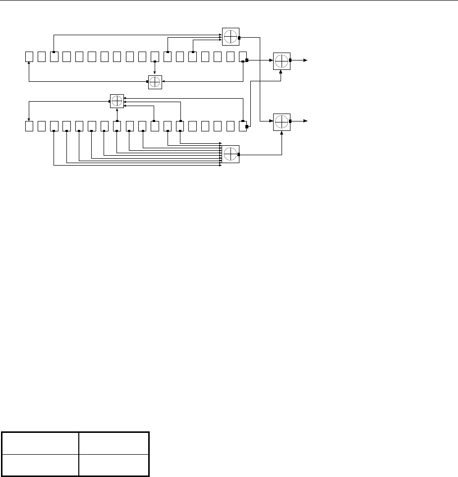
Digital Standard 3GPP W-CDMA (FDD) SMIQ
1125.5555.03 E-92.172
I
Q
1
10
02
2
3
3
4
4
5
5
6
6
7
7
8
8
9
9
17
17
16
16
15
15
14
14
13
13
12
12
11
11
10
10
Fig. 2-98 Structure of the downlink scrambling code generator
The shift registers are initialized by loading shift register 1 with "0 to 01" and shift register 2 with all "1".
In addition, shift register 1 is run forward by n cycles, n being the scrambling code number or in short the
"scrambling code" (SC).
After a cycle time of one radio frame the generators are reset, i.e. the above initialization is carried out
again.
2. Uplink scrambling code generator
In the uplink, distinction is made between two modes of the SC. There is on the one hand the long SC
which can be used for all types of channel. On the other hand, there is the short SC which can be used
for all channels except PRACH and PCPCH as an alternative to the long SC.
a) Uplink long scrambling code generator
The code generator of the long SC in the uplink has basically the same structure as the SC in the
downlink. However, the generator polynomials of the shift registers and the type of initialization differ.
Table 2-19 Generator polynomials of uplink long scrambling code generators
Shift register 1 x25+x3+1
Shift register 2 x25+x3+x2+x+1
The shift registers are initialized by assigning 1 to bit number 24 in shift register 1 and the binary form of
the scrambling code number n to bits 23 to 0. Shift register 2 is loaded with all "1".
The readout positions for the Q component are such that they correspond to an IQ offset of 16.777.232
cycles.
After a cycle time of one radio frame the generators are reset, i.e. the above initialization is carried out
again.
b) Uplink short scrambling code generator
The code generator of the short SC in the uplink comprises altogether 3 coupled shift registers.
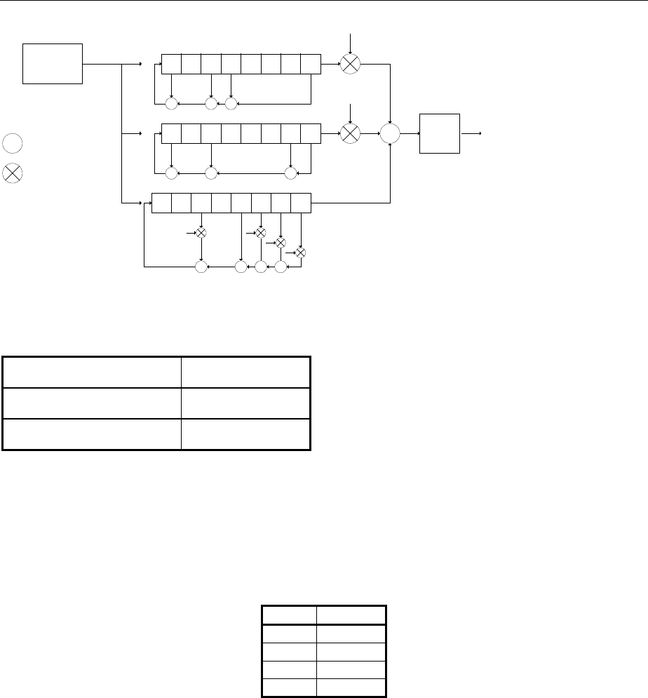
SMIQ Digital Standard 3GPP W-CDMA (FDD)
1125.5555.03 E-92.173
0
74
+
mod n addition
c
t
(n)
12356
2
mod 2
07 4
b
s
(n)
12356
2
mod 2
+
mod 4
multiplication
z
v
(n)
07 412356
+
mod 4
Mapper
S
v
(n)
Shift suspend after
every 256-th chip
cycle
a
r
(n)
+++
+ ++
+ ++
33
3
2
Fig. 2-99 Structure of the uplink short scrambling code generator
Table 2-20 Generator polynomials of uplink short scrambling code generators
Shift register 1 (binary) x8+x7+x5+x4+1
Shift register 2 (binary) x8+x7+x5+x+1
Shift register 3 (quaternary) x8+x5+3x3+x2+2x1
The output sequences of the two binary shift registers are weighted with factor 2 and added to the
output sequence of the quaternary shift register (Modulo 4 addition). The resulting quaternary output
sequence is mapped into the binary complex level by the mapper block.
For initialization of the three 8-bit shift registers (in a modified way) the binary form of the 24-bit short SC
number n is used, for details see section 4.3.2.3 in [2].
Table 2-21 Mapping of the quaternary output sequence into the binary IQ level
zv(n) Sv(n)
0+1 + j1
1-1 + j1
2-1 - j1
3+1 - j1
c) Preamble scrambling code generator
When generating the preambles of the PRACH and PCPCH a special SC is used. It is based on the
long SC described under a), however only the I component is taken and subsequently a pointer (ej(PI/4 +
PI/4 * k), k=0 to 4095) modulated upon it.
Modification of the long and short scrambling code output sequence
The scrambling code sequence of the Q component is modified as standard to reduce the crest factor of
the signal. Zero-crossings can then be avoided for every second chip using this method. (This method is
often called HPSK).
For details see [2], section 4.3.2.1. The SMIQ uses a decimation factor of 2.

Digital Standard 3GPP W-CDMA (FDD) SMIQ
1125.5555.03 E-92.174
Scrambling Unit
In the scrambling unit, the output of the scrambling code generator and the spread symbols are combined.
If the input signal and the scrambling code signal are interpreted as complex numbers (Ci , Cq, SCi , SCq'
∈ { -1, +1 }), the output signal is a complex multiplication of the two signals:
Si + j Sq = (Ci + j Cq) * (SCi + j SCq')
This gives:
Si = CiSCi – CqSCq'
Sq = CiSCq' + CqSCi
The signal obtained in this way has a constellation diagram like a QPSK signal:
Si
Sq
1
1-1
-1
-2
-2
2
2
Fig. 2-100 Constellation diagram of a channel with 0 dB power
Note: There are auxiliary conditions for some types of channels that may result in different
constellation diagrams.
If, for instance, symbols of SCH or preamble part of PRACH are coded, a BPSK
constellation is obtained without the scrambling unit. For an explanation of the different
constellation diagrams see section 2.14.3.
Channelization code generator
The channelization code generator cyclically outputs a channel-specific bit pattern. The length of the
cycle corresponds to the duration of the source symbol to be spread, i.e. the number of bits corresponds
to the spread factor. The spreading sequence for the I and Q branches is identical (real). Spreading
itself is a simple EXOR operation.
Two different channelization code generators are used depending on the type of channel:
Channelization code generator for all channels except SCH
Due to this channelization code the channel separation takes place in the sum signal. The
channelization code number is the row in an orthogonal spreading matrix which is generated by an
iterative process (OVSF).
Channelization code generator SCH
This generator replaces the one described above if the synchronization code symbol of the SCH
channels is spread.
The spreading matrix is replaced by a method that forms the spreading sequence from a Hadamard
sequence and a statistical sequence. For details see [2], section 5.2.3.1.
Data source
The data source used in the SMIQ is implemented at the physical layer. There is neither mapping of
logical channels to physical channels nor is inner coding/outer coding performed. If the data source is to
be implemented at a higher layer, this can be done with the aid of a file interface (see section 5.6 in the
operating manual).

SMIQ Digital Standard 3GPP W-CDMA (FDD)
1125.5555.03 E-92.175
Slot and frame builder
The bits from the data source are first entered into a frame structure. The frames are made up of two
hierarchical levels:
Table 2-22 Hierarchical structure of 3GPP W-CDMA frames
Hierarchy Length in ms Remarks
Time slot 0.667
Radio frame 10 After a radio frame, pilot symbols are repeated. A radio
frame consists of 15 time slots. This is also the length of a
scrambling code cycle. Frames are the basic unit in the SMIQ.
The sequence length is stated in radio frames.
The configuration of the time slots depends on the channel type and symbol rate.
The following components are distinguished:
• Pilot sequence
The pilot sequence characterizes the time slot position within the radio frame and also depends on
the symbol rate, transmit diversity and the pilot length parameter.
Channel types DPCH, S-CCPCH, DL-DPCCH, DPCCH, PRACH and PCPCH have a pilot
sequence.
The pilot sequence cannot be changed by the user.
• Synchronization code symbol
The synchronization code symbol is the only symbol of the SCH.
It is fixed to “11“.
• TPC symbol
This symbol is used to control the transmit power. It is used in DPCH, DL-DPCCH and DPCCH.
A bit pattern for the sequence of TPC symbols can be indicated as a channel-specific pattern.
• Data symbols
These symbols carry the user information and are fed from the data source. They are used in
DPCH, P-CCPCH, S-CCPCH,PDSCH, DL-DPCCH, DPDCH, PRACH and PCPCH.
• Signature
The signature is used in PRACH and PCPCH. 16 fix bit patterns are defined of which the user may
select one.
• TFCI
The “Transport Format Combination Indicator“ is used in DPCH/DPCCH if the corresponding button
of the interface (Base Station Configuration, see section 2.14.2.5/ Mobile Station Configuration, see
section 2.14.2.6) is activated. In this case, a code sequence with the length of 30 is defined using
this value and distributed among 15 subsequent time slots. In PRACH and PCPCH, the TFCI field is
provided as standard.
• FBI
Feedback indication bits are only used in DPCCH and PCPCH.
Digital Standard 3GPP W-CDMA (FDD) SMIQ
1125.5555.03 E-92.176
Timing offset
The symbol stream can be shifted in time relative to the other channels. For this purpose a timing offset
can be entered into the channel table, stating the range of shifting in multiples of 256 chips. Since the
SMIQ does not generate infinite symbol streams like a realtime system, this offset is implemented as a
rotation.
Example for DPCH 30 ksps, 1 time slot,
Timing offset = 2 è 2 x 256 chips = 512 chip offset è 4 data symbols shifting at a symbol rate of 30 ksps
(1 symbol corresponds to 3.84 Mcps / 30 ksps = 128 chips).
previously:
11 11 11 11 00 01 10 11 00 10 01 11 11 01 00 01 10 11 01 00
afterwards:
10 11 01 00 11 11 11 11 00 01 10 11 00 10 01 11 11 01 00 01
The use of the timing offset usually causes a reduction of the crest factor of the total signal, since it is
not always the same spreading chips (channelization chips) CH and scramble chips SCi/SCq' that are
applied to the pilot sequences of the channels.
Demultiplexer
In the downlink, the symbol stream is divided into two bit streams Di and Dq prior to processing in the
spreading unit. The symbol stream is divided by allocating bits 1, 3, 5, to 2n-1 to the in-phase bit stream
Di, and bits 2, 4, 6, 2n to the quadrature bit stream Dq.
For the above example with timing offset:
Di = 1 1 0 0 1 1 1 1 0 0 1 1 0 1 0 1 1 0 0 0
Dq = 0 1 1 0 1 1 1 1 0 1 0 1 0 0 1 1 1 1 0 1
(lefthand bit is always the first one in the time sequence)
In the uplink, independent data are used for the two paths.
PRACH/PCPCH: Preamble: signature parallel to I and Q
Message part : data to I, pilot and TFCI to Q
DPCCH: All bits to I, Q always unused
DPDCH: All bits are always to I or Q (dependent on channel number), the other path is
unused.
Power control
After spreading and scrambling, a channel-specific power factor p is applied to the signal. A value of –6 dB
therefore results in half the level (or ¼ power) and the following diagram (DPCH):
1
1-1
-1
Si*p
Sq*p
Fig. 2-101 Constellation diagram of a channel with –6 dB power

SMIQ Digital Standard 3GPP W-CDMA (FDD)
1125.5555.03 E-92.177
Summation
After application of the channel power, the components of the individual channels are summed up.
The constellation diagram of the sum signal is obtained by superposition of the diagrams of the
individual channels. If the signal consists of two channels with a power of -6 dB and -12 dB and each
channel contains independent source data (DPCH), the following constellation diagram is obtained:
1
1-1
-1
Fig. 2-102 Constellation diagram of a 3GPP W-CDMA signal with two DPCH channels
Filtering
An unfiltered spread signal is obtained after summation. Due to filtering the number of samples is
increased by the oversampling factor and band-limiting is performed.
Multi code
3GPP W-CDMA supports multi-code transmission for downlink-dedicated physical channels (DPCH) .
This form of transmission is used for channels intended for the same receiver, i.e. those receivers that
belong to a radio link. The first channel of this group is used as a master channel.
Shared parts (pilot, TPC and TCFI) are spread for all channels using the spreading code of the master
channel.
Note: Instead of changing the spreading code within a slot several times, the master code rather
than the shared parts can be sent at higher power. The other channels then have to be
blanked out correspondingly.
2.14.2 Generation of 3GPP W-CDMA Signals
The DIGITAL STD - WCDMA/3GPP menu is used to configure W-CDMA signals to the 3GPP standard
(FDD). Up to 512 channels (distributed amongst up to four base or mobile stations) can be simulated in
the downlink. The operation in the uplink was changed due to the extension to 3GPP version 3.1.1. In
contrast to the 3GPP versions 2.0.0 and 2.1.0, there is no longer a large channel table with 128 DPDCHs.
A mobile station has now 6 DPDCHs at maximum, the parameters of which are prescribed to a large
extent by the standard. In order to obtain clear and simple operation, distinction is now made between
3 modes in the uplink (PRACH only, PCPCH only and DPCCH + DPDCH). In each mode, only the
relevant parameters are displayed. But it is still possible to simulate a signal scenario of up to 4 mobile
stations.
The menu is hierarchical with several levels. This organizes the large number of parameters in a clear
way.
There are also other menus with parameters that modify the W-CDMA signal.
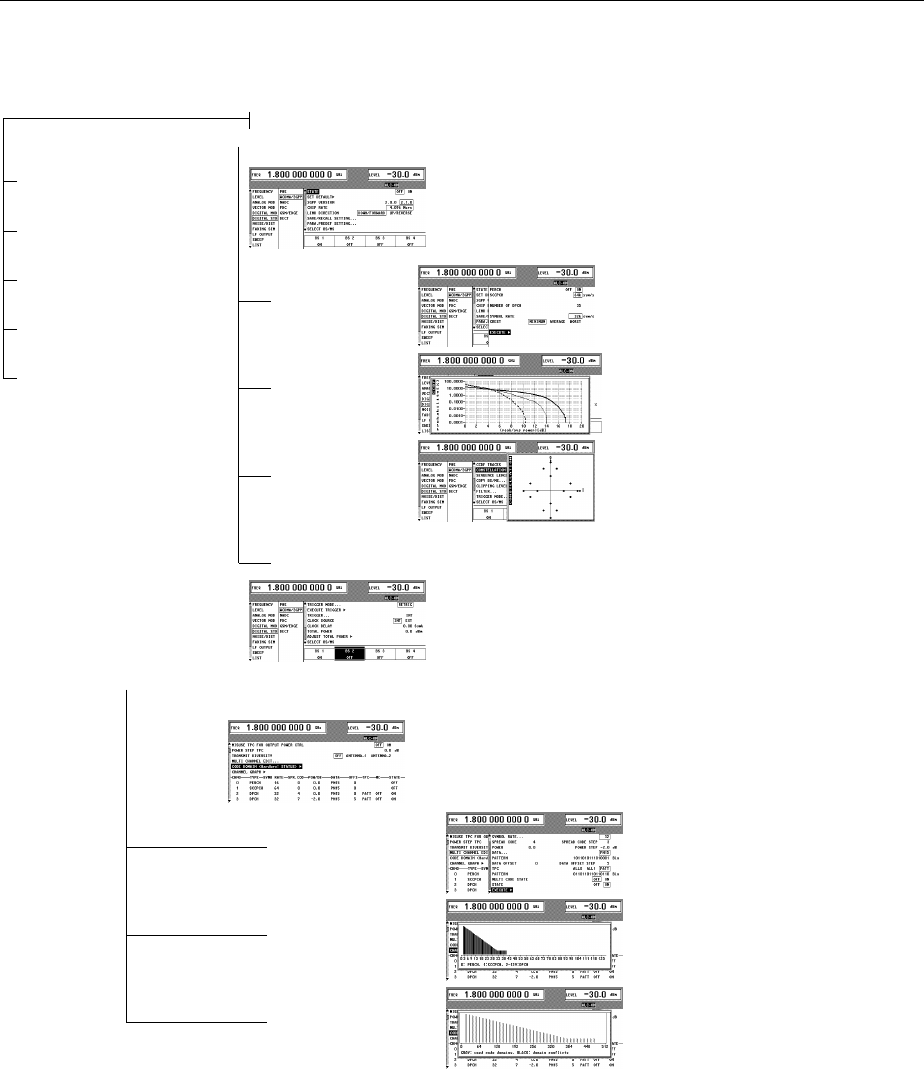
Digital Standard 3GPP W-CDMA (FDD) SMIQ
1125.5555.03 E-92.178
The following figure overviews all menus relevant for the W-CDMA signal and refers to related sections
in the manual.
SMIQ
DIGITAL STD - WCDMA/3GPP
PARA.PREDEF...
CONSTELLATION...
CCDF...
2.14.2.1
2.4
2.14.2.3
2.14.2.4
2.14.2.2
FREQUENCY
LEVEL
VECTOR MOD
FSIM
NDSIM
2.5
2.8
2.20
2.9
SELECT BS(MS)
DIGITAL STD - WCDMA/3GPP - BS(MS) CONFIGURATION
2.14.2.1
MULTI CHANNEL EDIT...
CODE DOMAIN...
CHANNEL GRAPH...
2.14.2.8
2.14.2.9
2.14.2.7
Fig. 2-103 Overview of DIGITAL STD – 3GPP WCDMA/3GPP menu structure
Note: The parts of the DIGITAL STD – WCDMA/3GPP menu that are below the SELECT BS(MS)
function are not required if a signal is parameterized by means of the PARA. PREDFEF
function (see section 2.14.2.2).
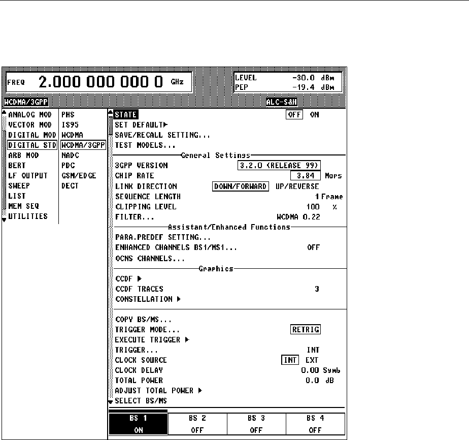
SMIQ Digital Standard 3GPP W-CDMA (FDD)
1125.5555.03 E-92.179
2.14.2.1 Menu WCDMA/3GPP
The following figure shows the menu for generating a downlink signal (transmit signal of base station).
Fig. 2-104 DIGITAL STD - WCDMA/3GPP - Downlink menu
For clarity, associated parameters are combined to subgroups by horizontal lines.
STATE Switch-on/off of modulation - digital standard 3GPP W-CDMA. If vector
modulation, digital modulation or another digital standard are on, they are
automatically switched off.
STATE = ON starts the calculation of a chip sequence based on current
settings. The length of the chip sequence, and so the duration of the
calculation, is determined by the SEQUENCE LENGTH parameter.
IEC/IEEE-bus command :SOUR:W3GP:STAT ON
Note: When a parameter is changed, STATE is automatically switched to OFF to ensure that the set
values and the output signal are consistent. After changing all the values, STATE can
manually be set to ON. This is possible via menu parameter STATE and with the MOD
ON/OFF key below the rollkey.
A progress bar is displayed while the chip sequence is calculated. The progress of the calculation can
also be read via the remote control interfaces.
IEC/IEEE-bus command :SOUR:W3GP:CAL:PROG?
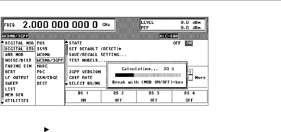
Digital Standard 3GPP W-CDMA (FDD) SMIQ
1125.5555.03 E-92.180
Fig. 2-105 DIGITAL STD - WCDMA/3GPP menu – progress bar
SET DEFAULT Sets the default setup for 3GPP W-CDMA.
For further information about the default setting see section 2.14.2.12.
IEC/IEEE-bus command :SOUR:W3GP:PRES
SAVE/RECALL... The SMIQ supports two parallel SAVE/RECALL memory systems: The SAVE
and RCL hardkeys are used to handle the frequency, level and state in the
3GPP W-CDMA menu. Menu selection SAVE/REALL, however, manages all
the other parameters in the 3GPP W-CDMA menu. This also includes station-
specific parameters such as the channel table.
RECALL SETTING Recalling a saved configuration.
IEC/IEEE bus :SOUR:W3GP:SETT:LOAD "MYSETUP"
SAVE SETTING Saving the current configuration.
An existing setting can be overwritten or a new setting
can be created. The name of the new setting is assigned
automatically, e.g. WCDMASEQ1.
If the setting is created via the IEC/IEEE bus, the name
is user-selectable and the usual restrictions apply.
IEC/IEEE bus :SOUR:W3GP:SETT:STOR "MYSETUP"
DELETE SETTING Deleting a configuration.
IEC/IEEE bus :SOUR:W3GP:SETT:DEL "MYSETUP"
Selection of one of the test models defined in the 3GPP standard [3]. This menu
item is available only in the downlink. The following test scenarios are available:
Test Model Application/measurement
Test1_16
TEST MODEL 1 (16 channels)
Spectrum emission mask
ACLR
Spurious emissions
Transmit intermodulation
Modulation accuracy
Peak code domain error
TEST MODELS
Test1_32
TEST MODEL 1 (32 channels)
Spectrum emission mask
ACLR
Spurious emissions
Transmit intermodulation
Modulation accuracy

SMIQ Digital Standard 3GPP W-CDMA (FDD)
1125.5555.03 E-92.181
Test1_64
TEST MODEL 1 (64 channels)
Spectrum emission mask
ACLR
Spurious emissions
Transmit intermodulation
Modulation accuracy
Test2
TEST MODEL 2 Output power dynamics
Test3_16
TEST MODEL 3 (16 channels) Peak code domain error
Test3_32
TEST MODEL 3 (32 channels) Peak code domain error
IEC/IEEE-bus command :SOUR:W3GP:SETT:TMOD "TEST1_16"
No test models are defined for the uplink in the 3GPP standard. To be able to
generate appropriate test signals by a keystroke nevertheless, the SMIQ offers
predefined test signals also for the uplink.
Test model Description
C+D60 k Mobile station 1 is activated in the
DPCCH + DPDCH mode. 60 ksps is
selected as overall symbol rate and
the power of DPCCH and DPDCH is
set to 0 dB.
TEST MODELS (NOT
STANDARDIZED)
C+D960 k Mobile station 1 is activated in the
DPCCH + DPDCH mode. 960 ksps is
selected as overall symbol rate and
the power of DPCCH and DPDCH is
set to 0 dB.
IEC/IEEE bus :SOUR:W3GP:SETT:TMOD "C+D60 k"
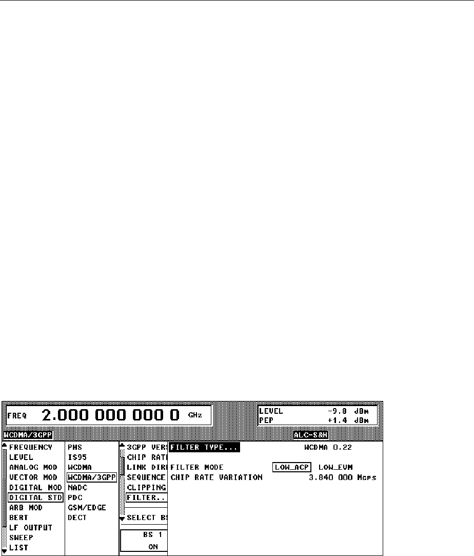
Digital Standard 3GPP W-CDMA (FDD) SMIQ
1125.5555.03 E-92.182
----------------------General Settings------------------------------------------------------------------------------
3GPP VERSION Display of current 3GPP version 3.2.0.
IEC/IEEE-bus command :SOUR:W3GP:GPP3:VERS?
CHIP RATE Display of fixed chip rate for a 3GPP W-CDMA of 3.84 Mcps.
IEC/IEEE-bus command :SOUR:W3GP:CRAT?
LINK DIRECTION Selecting the link direction:
DOWN/FORWARD Activates downlink-signal generation. In this mode, the
base-station transmit signal can be generated.
IEC/IEEE-bus command :SOUR:W3GP:LINK FORW
UP/REVERSE Activates uplink-signal generation. In this mode, the
mobile-station transmit signal can be generated.
IEC/IEEE-bus command :SOUR:WCDM:LINK REV
SEQUENCE LENGTH
(FRAMES) The sequence length can be set.
The maximum length is 13 frames.
IEC/IEEE-bus command :SOUR:W3GP:SLEN 4
CLIPPING LEVEL Sets a clipping level relative to the highest peak in per cent. The value range is 1
to 100 %. A value of 100% means that the signal is not clipped. Clipping reduces
the crest factor. For background information on how to use this parameter see
section 2.14.2.10.
This menu item is only available with Option SMIQB48 installed. For details,
see section 2.15.1.
IEC/IEEE-bus command :SOUR:W3GP:CLIPP:LEV 50
Fig. 2-106 DIGITAL STD - WCDMA/3GPP - FILTER... menu
FILTER... FILTER Selects the baseband filter.
Either the W-CDMA standard filter WCDMA 0.22, the
general Nyquist filters COS and SQRCOS or a user-
defined filter USER (see section Digital Modulation) can
be selected. The optimized square-root cosine filter
WCDMA 0.22 is preset. Its roll-off factor is fixed at 0.22.
IEC/IEEE bus :SOUR:W3GP:FILT:TYPE WCDM

SMIQ Digital Standard 3GPP W-CDMA (FDD)
1125.5555.03 E-92.183
(FILTER...) ROLL OFF
FACTOR Setting value for the roll-off factor. The setting is only
possible if a COS or SQRCOS filter is selected under
FILTER.
IEC/IEEE bus :SOUR:W3GP:FILT:PAR 0.22
FILTER MODE Selection of filter mode.
LOW_ACP Filter for lowest adjacent-channel power.
IEC bus :SOUR:W3GP:FILT:MODE LACP
LOW_EVM Filter for lowest error vector magnitude.
IEC bus :SOUR:W3GP:FILT:MODE LEVM
CHIP RATE
VARIATION Input value of chip clock frequency. The value for CHIP
RATE from the main menu is preset. CHIP RATE
VARIATION changes the output clock, the modulation
bandwidth and the output sync signals. It has no effect
on the calculated chip sequence. The value range is
100 cps to 18 Mcps.
IEC bus :SOUR:W3GP:CRAT:VAR 4096001
----------------------Assistant/Enhanced Functions------------------------------------------------------------
PARA. PREDEF. Calling parameterized predefined settings. This menu item is only available in
the downlink. For a description of this function see section 2.14.2.2.
ENHANCED
CHANNELS BS1/MS1 Calling an operating menu for the configuration of extended functions of the
digital standard 3GPP W-CDMA. The menu item is available only if option
SMIQB48 is installed. For more detail on this menu see section 2.15.1.
OCNS CHANNELS Simulation of Orthogonal Channel Noise. The menu item can be accessed
only in the downlink an is available provided option SMIQB48 is installed. For
more detail on this menu see section 2.15.1.
ADDITIONAL MS
BASED ON MS4 Simulation of up to 50 further mobile stations. The menu item can be
accessed only in the uplink and is available provided option SMIQB48 is
installed. For more detail on this menu see section 2.15.1.
----------------------Graphics------------------------------------------------------------
CCDF A complementary cumulative distribution function is calculated and displayed
using the signal in the waveform memory. For details see section 2.14.2.3.
CCDF TRACES The number of simultaneously displayed CCDF traces can be set. For details
see section 2.14.2.3.
CONSTELLATION The constellation diagram for the signal in the waveform memory is calculated
and displayed. For details see section 2.14.2.4.
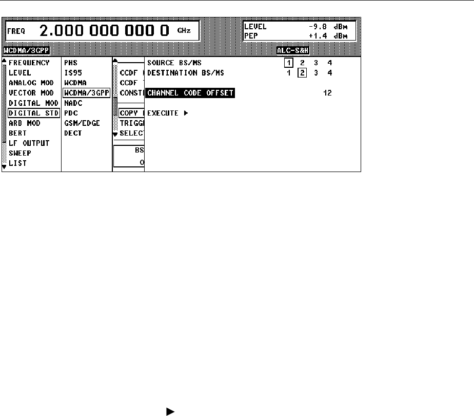
Digital Standard 3GPP W-CDMA (FDD) SMIQ
1125.5555.03 E-92.184
Fig. 2-107 DIGITAL STD - WCDMA/3GPP - Downlink - COPY BS(MS) menu
COPY BS(MS)... Using COPY BS (MS) it is easy to create a new base/mobile station from an
existing station. This feature is useful, say, when base stations with more than
128 data channels are to be simulated. For examples, see section 2.14.3.6.2.
SOURCE BS/MS For selecting the BS(MS) whose parameter set is to be
copied. Possible values are 1, 2, 3 or 4.
IEC/IEEE-bus command :SOUR:W3GP:COPY:SOUR 1
DESTINATION For selecting the destination BS(MS) whose parameter
BS/MS set is to be overwritten. Possible values are 1, 2, 3 or 4.
IEC/IEEE-bus command :SOUR:W3GP:COPY:DEST 2
CHANNELIZATION
CODE OFFSET Offset used for the spreading codes during copying from
the source BS to the channelization codes. The
minimum value is 0 and the maximum value 511. This
parameter is only available in the downlink.
IEC/IEEE-bus command :SOUR:W3GP:COPY:COFF 123
EXECUTE Starts copying.
IEC/IEEE-bus command :SOUR:W3GP:COPY:EXEC
TRIGGER MODE Configuration of W-CDMA sequence control (see section 2.14.2.11).
AUTO The calculated W-CDMA chip sequence is immediately
output and repeated cyclically. Trigger events are ignored.
IEC/IEEE-bus command :SOUR:W3GP:SEQ AUTO
RETRIG The calculated W-CDMA chip sequence is immediately
output and repeated cyclically. A trigger event causes a
restart from frame 1.
IEC/IEEE-bus command :SOUR:W3GP:SEQ RETR
ARMED_AUTO Only a trigger event results in the W-CDMA chip sequence
being started from frame 1. Other trigger events are
ignored.
IEC/IEEE-bus command :SOUR:W3GP:SEQ AAUT
ARMED_RETRIG Only a trigger event results in the W-CDMA chip sequence
being started from frame 1. Each further trigger event
causes a restart.
IEC/IEEE-bus command :SOUR:W3GP:SEQ ARET
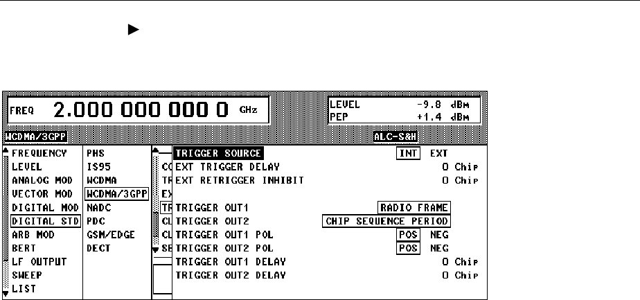
SMIQ Digital Standard 3GPP W-CDMA (FDD)
1125.5555.03 E-92.185
EXECUTE TRIGGER Executes a trigger event at the start of the W-CDMA chip sequence.
IEC/IEEE-bus command :TRIG:DM:IMM
Fig. 2-108 DIGITAL STD – WCDMA/3GPP – TRIGGER... menu
TRIGGER... Opens a window to select the trigger source, to configure trigger output signals
and to set the delay of an external trigger signal (see also section 2.14.2.11).
TRIGGER SOURCE For selecting the trigger source.
EXT The W-CDMA chip sequence is started from
frame 1 on the active edge of an external
trigger signal. The polarity, the trigger threshold
and the input resistance of the TRIGIN input
can be changed in the DIGITAL MOD - EXT
INPUTS menu.
INT A trigger event is activated manually by
EXECUTE TRIGGER.
IEC/IEEE-bus :SOUR:W3GP:TRIG:SOUR EXT
EXT TRIGGER
DELAY For setting the number of chips by which an external
trigger signal is delayed before it starts the W-CDMA
chip sequence. This is used to set up synchronization
with the DUT or other units.
IEC/IEEE-bus :SOUR:W3GP:TRIG:DEL 3
EXT RETRIGGER
INHIBIT Sets the number of chips by which a restart is
delayed after a trigger event. If the RETRIG
TRIGGER MODE is selected, every further trigger
signal restarts the W-CDMA chip sequence. This
restart is inhibited for the number of chips that have
been entered.
Example:
The effect of entering 82000 chips is that any further
trigger signal is ignored for 82000 chips after a
trigger event.
IEC/IEEE-bus :SOUR:W3GP:TRIG:INH 82000

Digital Standard 3GPP W-CDMA (FDD) SMIQ
1125.5555.03 E-92.186
(TRIGGER...) TRIGGER OUT 1/2 For selecting signals for outputs TRIGOUT 1 and
TRIGOUT 2 in the PARDATA connector.
The times only apply if the internal clock generation
frequency was not modified with the CHIP RATE
VARIATION parameter.
SLOT 0.667 ms slot clock
IEC/IEEE-bus command:
:SOUR:W3GP:TRIG:OUTP1 SLOT
RADIO FRAME 10 ms frame clock
IEC/IEEE-bus command:
:SOUR:W3GP:TRIG:OUTP1 RFR
CHIP SEQUENCE Marker signal for identifying the
PERIOD periodic repetition of the gener-
ated chip sequence
IEC/IEEE-bus command:
:SOUR:W3GP:TRIG:OUTP1 CSP
ENHANCED Marker signal for marking the
CHIP SEQUENCE periodic repetition of generated
PERIOD enhanced chip sequence (only
displayed with option SMIQB48
installed).
IEC/IEEE-bus command:
:SOUR:W3GP:TRIG:OUTP1 ECSP
P-CCPCH Marker signal for identifying
/BCH SFN the restart of the system
RESTART frame number (SFN Restart)
after 4096 frames (available only
when option SMIQB48 is installed
and a P-CCPCH/BCH is
generated).
IEC/IEEE-bus command:
:SOUR:W3GP:TRIG:OUTP1 SFNR
TRIGGER OUT 1/2 POL Selects the polarity of signals at the TRIGOUT 1 and
TRIGOUT 2 outputs in the PARDATA connector.
IEC/IEEE-bus :SOUR:W3GP:OUTP2:POL POS
TRIGGER OUT 1/2
DELAY Setting of the number of chips by which the selected
trigger output signal is delayed.
IEC/IEEE-bus :SOUR:W3GP:OUTP2:DEL 0

SMIQ Digital Standard 3GPP W-CDMA (FDD)
1125.5555.03 E-92.187
CLOCK SOURCE Allows selection of the clock source for the chip clock
(see section 2.14.2.11).
INT The SMIQ operates with internally
generated clock signals.
EXT A chip clock has to be fed in externally at the
SYMBOL CLOCK connector. The CHIP
RATE parameter must be set with an
accuracy of ± 1 %. The polarity, the trigger
threshold and the input resistance of the
SYMBOL CLOCK input can be changed in
DIGITAL MOD - EXT INPUTS menu.
IEC/IEEE-bus command
:SOUR:W3GP:CLOC:SOUR INT
EXT CLOCK MODE Selection of type of external chip signal.
CHIP chip clock
CHIPX4 Vierfacher Chiptakt
ATTENTION:
An external chip clock is fed in at connector
SYMBOL CLOCK. Multi-folds chip clock has to
be fed in at the connector BIT CLOCK!
IEC/IEEE bus command
:SOUR:W3GP:CLOCk:MODE CHIP4
CLOCK DELAY Setting the delay of generated modulation signal to an
external clock. This can be used, for example, for syn-
chronization with a second unit to achieve time
synchroneity between the modulation signals of the
two units. The displayed setting resolution of
1/100 symbol is only attained for symbol-clock
frequencies below 100 kHz. The resolution is reduced
with increasing frequency. At a chip rate of
1.2288 Mcps, the resolution equals the chip duration ×
0.1.
IEC/IEEE-bus command
:SOUR:W3GP:CLOC:DEL 0.5
TOTAL POWER Displays the total power of activated code channels.
The total power is calculated from the power ratio of the
activated code channels with the modulation switched
on (STATE=ON). If the value is not equal to 0 dB, the
individual code channels are internally adjusted (while
maintaining the power ratios) so that the TOTAL
POWER is 0 dB to obtain the output level (LEVEL) set
in the header of the display. In addition to the average
power, the peak envelope power (PEP) is also
displayed.
IEC/IEEE-bus command :SOUR:W3GP:POW?
Digital Standard 3GPP W-CDMA (FDD) SMIQ
1125.5555.03 E-92.188
ADJUST
TOTAL POWER Changes the power of every activated code channel
so that the TOTAL POWER returns to 0 dB again,
while the ratio of the powers of the individual code
channels remains the same.
IEC/IEEE-bus command
:SOUR:W3GP:POW:ADJ
SELECT BS/MS
Fig. 2-109 DIGITAL STD – WCDMA/3GPP – SELECT BS(MS) menu
SELECT BS/MS has a special significance in the 3GPP W-CDMA menu: It is always displayed in the
bottom line of the scrollable area, i.e. above the four station blocks. After selection of this menu item
(SELECT hardkey), the cursor is positioned in the area below. The station whose parameters are to be
edited can be selected by means of the spinwheel or the arrow keys.
Note: The state of the BS/MS can also be toggled without selecting the station. Just move the cursor
to the station and press the ENTER key.
For editing the station parameters see section 2.14.2.5.
SMIQ Digital Standard 3GPP W-CDMA (FDD)
1125.5555.03 E-92.189
2.14.2.2 WCDMA/3GPP Menu - Para. Predef. Submenu
With the Para. Predef. function, it is possible to create highly complex scenarios with just a few
keystrokes. This function is of use if, say, just the envelope of the signal is of interest. The menu is only
available in the downlink.
Fig. 2-110 DIGITAL STD - WCDMA/3GPP - PARA. PREDEF. menu (downlink only)
CHANNELS FOR
SYNC OF MOBILE When this parameter is set to ON, all "special channels" required by a mobile
for synchronization are automatically activated. These are the following
channels: P-CPICH, P-SCH, S-SCH, PCCPCH.
IEC/IEEE-bus command :SOUR:W3GP:PPAR:SCH OFF
SCCPCH OFF SCCPCH is not used in the scenario.
IEC/IEEE-bus command
:SOUR:W3GP:PPAR:SCCPC:STAT OFF
15k, 30k, to 960k SCCPCH is used in the scenario at the stated symbol rate.
IEC/IEEE-bus commands
:SOUR:W3GP:PPAR:SCCPC:STAT ON
:SOUR:W3GP:PPAR:SCCPC:SRAT D15K
NUMBER OF DPCH Number of DPCH in the scenario. The minimum number is 0. The maximum
number is the ratio of the chip rate and the symbol rate (maximum 512 at the
lowest symbol rate of 7.5 ksps).
IEC/IEEE-bus command :SOUR:W3GP:PPAR:DPCH:COUN 123
SYMBOL RATE Symbol rate of all DPCH.
Possible values are 7,5k, 15k, 30k, 60k, 120k, 240k, 480k and 960k.
IEC/IEEE-bus command :SOUR:W3GP:PPAR:DPCH:SRAT D30K
CREST The crest factor of the signal can be modified by setting appropriate
channelization codes and timing offsets.
MINIMUM: The crest factor is minimized (the channelization codes are
distributed uniformly over the code domain. The timing offsets are
increased by 3 per channel).
IEC/IEEE-bus command :SOUR:W3GP:PPAR:CRES MIN
AVERAGE:An average crest factor is set (the channelization codes are
distributed uniformly over the code domain. The timing offsets are all
set to 0).
IEC/IEEE-bus command :SOUR:W3GP:PPAR:CRES AVER
WORST: The crest factor is set to an unfavourable value (i.e. maximum)
(the channelization codes are assigned in ascending order. The
timing offsets are all set to 0.)
IEC/IEEE-bus command :SOUR:W3GP:PPAR:CRES WORS

Digital Standard 3GPP W-CDMA (FDD) SMIQ
1125.5555.03 E-92.190
EXECUTE The channel table is automatically filled up with the set parameters.
Scrambling Code 0 is automatically selected (as defined in the 3GPP test
models).
IEC/IEEE-bus command :SOUR:W3GP:PPAR:EXEC
SMIQ Digital Standard 3GPP W-CDMA (FDD)
1125.5555.03 E-92.191
2.14.2.3 WCDMA/3GPP Menu - Display of CCDF
Fig. 2-111 DIGITAL STD – WCDMA/3GPP – CCDF menu with a trace
A complementary cumulative distribution function" can be generated from the filtered I/Q samples. This
function gives the probability of the magnitude of a complex sample exceeding a predefined threshold.
The complete waveform, i.e. the sum for all (max. 4) stations is used to calculate the CCDF.
If this threshold is thought of as the radius of a circle centered on the origin, the radius is plotted along the
horizontal axis and the probability of the samples lying outside this circle along the vertical axis. Only radii
that correspond to values that are at least as great as the average power are considered.
The crest factor can be read off at the intersection of the trace with the x axis. The precise value is
obtained from the displayed levels (PEP-LEVEL).
Fig. 2-112 Reading off the crest factor from LEVEL displays
In this example, the crest factor is 7.8 dB.
The number of simultaneously displayed traces can be set with the menu item NUMBER OF CCDF
TRACES. Displaying several traces shows the effect of the parameters on the envelope. The baseband
filter, the timing offsets and the channelization codes in particular have an effect on the CCDF.
The last three traces are distinguished in the following way:
Current trace:
Last trace:
Last but one trace:
Fig. 2-113 DIGITAL STD – WCDMA/3GPP – CCDF menu with three traces
Digital Standard 3GPP W-CDMA (FDD) SMIQ
1125.5555.03 E-92.192
2.14.2.4 WCDMA/3GPP Menu – Displaying Constellation Diagrams
A constellation diagram can be calculated and displayed from the unfiltered I/Q samples (menu item
CONSTELLATION).
Fig. 2-114 DIGITAL STD - WCDMA/3GPP – CONSTELLATION menu
In addition to the code domain display (see section 2.14.2.9) and the CCDF display (see section
2.14.2.3) the constellation diagram is the most important display for a W-CDMA signal. In addition to
channel powers, the effect of data sources etc and also the spreading scheme can be read off as a
function of the type of channel. For further information on W-CDMA constellation diagrams see sections
2.14.3.1 and 2.14.3.3. The complete waveform, i.e. the sum for all (max. 4) stations is used to calculate
the constellation diagram.
SMIQ Digital Standard 3GPP W-CDMA (FDD)
1125.5555.03 E-92.193
2.14.2.5 WCDMA/3GPP Menu - BS Configuration Submenu
The channel configuration for each base station is performed in this window. In the upper part of the
window, the parameters valid for the whole BS are set and the channel-specific parameters are set in
the bottom part of the table.
Note: To simplify handling of the large tables, state parameters like channel state or multi-code
state can be toggled (ON/OFF) with the ENTER key.
The ENTER key can also be used to switch from 1 value to the next when 1 of n values
can be selected (e.g. symbol rate).
Fig. 2-115 DIGITAL STD - WCDMA/3GPP menu – extended function of ENTER key
Fig. 2-116 DIGITAL STD - WCDMA/3GPP - BS CONFIGURATION menu

Digital Standard 3GPP W-CDMA (FDD) SMIQ
1125.5555.03 E-92.194
Parameters that are valid for the current base station:
BS 1(2,3,4) STATE ON The BS is active. All other parameters are activated.
IEC/IEEE-bus command :SOUR:W3GP:BST1:STAT ON
OFF The BS is inactive. The other parameters are ignored.
IEC/IEEE-bus command :SOUR:W3GP:BST2:STAT OFF
SCRAMBLING CODE
STATE ON The scrambling code is active.
IEC/IEEE-bus :SOUR:W3GP:BST1:SCOD:STAT ON
OFF The scrambling code is inactive (test mode).
IEC/IEEE-bus :SOUR:W3GP:BST2:SCOD:STAT OFF
SCRAMBLING CODE Code of base station. At the same time, the initial value for the scrambling code
generator. Permissible values are in the range 0 to 0x5FFF.
IEC/IEEE-bus command :SOUR:W3GP:BST1:SCOD #H1
TFCI STATE ON TFCI field is used in the frame.
IEC/IEEE-bus command :SOUR:W3GP:BST1:TFCI:STAT ON
OFF TFCI field is not used in the frame.
IEC/IEEE-bus command :SOUR:W3GP:BST2:TFCI:STAT OFF
TFCI (DPCH) Setting the TFCI value in the range 0 to 1023. A combination of 30 bits is
selected by this value. This combination is distributed over 15 successive slots
in groups of two.
IEC/IEEE-bus command :SOUR:W3GP:BST4:TFCI 21
2ND SEARCH CODE
GROUP This parameter indexes the “Allocation of SSCs for secondary SCH“ table
described in the 3GPP standard, reference [2], Table 9. For each slot in the
frame, this table assigns a certain spreading code to the synchronization code
symbol. The parameter’s range is 0 to 63. This parameter can only be read.
The value is calculated from the SCRAMBLING CODE.
IEC/IEEE-bus command :SOUR:W3GP:BST3:SSCG?
TPC PATTERN READ
OUT MODE TPC bits are used for W-CDMA to inform the called station if the transmit
power is being increased or decreased. The contents of the TPC field can be
separately defined in this panel in the table below for the channels of the BS.
The parameter TPC Pattern Read Out Mode is used to define how this bit
pattern is to be used. The following modes are distinguished:
• Continuous: A bit is taken for each slot from the up to 24-bit long bit
pattern for the Transmitter Power Control field of the slots and entered in
the bit stream several times (depending on the symbol rate). The specified
bit pattern is used cyclically.
• Single + All 0: A bit is taken for each slot from the up to 24-bit long bit
pattern for the Transmitter Power Control field of the slots and entered the
bit stream several times (depending on the symbol rate). The specified bit
pattern is used once, then the TPC sequence is continued with 0 bits.
• Single + All 1: A bit is taken for each slot from the max. 24-bit long bit
pattern for the Transmitter Power Control field of the slots and entered in
the bit stream several times (depending on the symbol rate. The specified
bit pattern is used once, then the TPC sequence is continued with 1 bits.
SMIQ Digital Standard 3GPP W-CDMA (FDD)
1125.5555.03 E-92.195
(TPC PATTERN READ
OUT MODE) • Single + alt. 01: A bit is taken for each slot from the up to 24-bit long bit
pattern for the Transmitter Power Control field of the slots and entered the
bit stream several times (depending on the symbol rate. The specified bit
pattern is used once, then the TPC sequence is continued with 0 and 1
bits alternately (multiplied depending on the symbol rate, e.g. 00001111).
• Single + alt. 10: A bit is taken for each slot from the up to 24-bit long bit
pattern for the Transmitter Power Control field of the slots and entered in
the bit stream several times (depending on the symbol rate. The specified
bit pattern is used once, then the TPC sequence is continued with 1 and 0
bits alternately (multiplied depending on the symbol rate, e.g. 11110000).
The different modes can be used for example to set a mobile to a specific
output power (e.g. with pattern 11111) and then let it oscillate about this
power (using Single + alt. 01 or Single + alt. 10). Thus power measurements
on the mobile can be performed (with a quasi-constant power). In conjunction
with the option (Mis-)Use TPC for output power control (see below) the TPC
Read Out Mode can also be used for generation of various output power
profiles.
IEC/IEEE-bus command :SOUR:W3GP:BST2:TPC:READ CONT
MISUSE TPC FOR
OUTPUT POWER
CONTROL
TPC bits are used for W-CDMA to inform the called station if the transmit
power is being increased or decreased. If this option is activated, the given
pattern is being misused to vary one’s own transmit power over time. For each
slot, one bit of this pattern is taken to increase (bit = 1) or decrease (bit = 0)
the channel power by the stated power step (POWER STEP TPC). The upper
limit is 0 dB and the lower –60 dB. The following envelope occurs at a channel
power of 0 dB, a power step of 1.0 dB, the pattern "001110100000011" and
TPC Pattern ReadOut Mode Continuous:
Fig. 2-117 Dynamic change of channel power (continuous)
Note: Observe that the power change (as specified in the standard) is
always performed at the beginning of the slot pilot field.
IEC/IEEE-bus command :SOUR:W3GP:BST1:TPC:MIS ON
POWER STEP TPC Size of power step in dB, if option MISUSE TPC FOR OUTPUT POWER
CONTROL is activated. The value range is –10.0 dB to +10.0 dB.
IEC/IEEE-bus command :SOUR:W3GP:BST1:POW:STEP 1.0

Digital Standard 3GPP W-CDMA (FDD) SMIQ
1125.5555.03 E-92.196
TRANSMIT
DIVERSITY The 3GPP standard describes various forms of transmit diversity. The signal is
distributed with different coding between two antennas. The SMIQ can
simulate the signal for one of the two antennas. A fixed diversity scheme is
assigned to each channel type:
DPCH, PCCPCH, SCCPH: STTD (Space time block coding transmit
antenna diversity).
Primary SCH, secondary SCH: TSTD (Time switched transmit diversity for SCH).
Both schemes are described in detail in reference [1], section 5.3.1.
If transmit diversity is required, the antenna whose signal is to be simulated
can be specified.
OFF: no transmit diversity
ANTENNA 1: calculate antenna signal for antenna 1 and display result
ANTENNA 2: calculate antenna signal for antenna 2 and display result
IEC/IEEE-bus command :SOUR:W3GP:BST1:TRAN:DIV ANT1
NUMBER OF PAGE
INDICATORS PER
FRAME
The number of page indicators per frame in the page indication channel (PICH)
can be defined thanks to this menu item. The value range is 18, 36, 72, 144.
IEC/IEEE-bus command :SOUR:W3GP:BST2:PIND:COUNT D36
MULTI CHANNEL
EDIT... A certain number of DPCHs can be configured with just a few keystrokes
using this menu item, see section 2.14.2.7.
CHANNEL GRAPH This menu item gives an overview of the assigned channels, see section 2.14.2.8.
CODE DOMAIN This menu item indicates the assignment of code domain, see section 2.14.2.9.
SMIQ Digital Standard 3GPP W-CDMA (FDD)
1125.5555.03 E-92.197
Channel table:
Fig. 2-118 DIGITAL STD – WCDMA/3GPP – BS CONFIGURATION / channel table menu
Below the general parameters of the current base station follows a table comprising all the parameters
that can be edited on a channel-specific basis.
CH NO Channel number, consecutive from 0 to 138. This value cannot be edited. All
rows are displayed even if the channels are inactive. Activating/deactivating is
via STATE at the end of the row.
TYPE Channel type which is permanently linked to the channel number and which
cannot be edited:
The first 11 code channels in the table are occupied for the special channels
P-CPICH to DL-DPCCH. All other code channels are DPCHs. The channel
type is a pure display parameter and cannot be edited. Not all parameters in
the table can be edited. This depends on the type of channel.
SYMBOL RATE Symbol rate of channel in ksps.
The value range of symbol rate is modified depending on the channel type.
For example, the P-CPICH is fixed at a symbol rate of 15 ksps by the 3GPP
standard, but all symbol rates between 7.5 ksps and 960 ksps are available for
a DPCH.
IEC/IEEE-bus command :SOUR:W3GP:BST3:CHAN12:SRAT D30K
CHANNELIZATION
CODE The channelization code (previously called spreading code number) is
selected here. The code channel is then spread with the channelization code
(spreading code) thus determined. The value range of the channelization code
depends on the symbol rate of the channel. A fixed channelization code is
allocated to a few channels as standard (the P-CPICH e.g. always uses the
channelization code 0).
The maximum value range extends from 0 to 1
843 −
=
rate_symbol
)Mcps.(rate_chip
IEC/IEEE-bus command :SOUR:W3GP:BST3:CHAN12:CCOD 11

Digital Standard 3GPP W-CDMA (FDD) SMIQ
1125.5555.03 E-92.198
POWER [DB] Channel power in dB; range –60 to 0.0 dB.
The stated power is relative to the powers of other channels and initially does not
refer to the LEVEL power display. After activating ADJUST TOTAL POWER
(top level of 3GPP W-CDMA menu) all power readings as referred to LEVEL.
IEC/IEEE-bus command :SOUR:W3GP:BST3:CHAN3:POW –10.0
DATA Selects the data source for the DATA field.
Selection of PN9, PN11, PN15, PN16, ALL0, ALL1 and PATTern.
The PN generator function is explained in section 2.12.3, for example.
If the PATTern data type is used, the pattern can be modified with a special
editor. The length is limited to 24 digits.
IEC/IEEE-bus command :SOUR:W3GP:BST3:CHAN3:DATA PN15
IEC/IEEE-bus command :SOUR:W3GP:BST3:CHAN3:DATA:PATT #H1234,15
TIMING OFFSET A value greater than 0 causes the source symbols to be shifted prior to
spreading. An offset of 1 for instance is recommended to obtain a low crest
factor.
The absolute starting time of the frames (slot 0) is shifted relative to the
beginning of the scrambling code sequence by TOffset * 256 chips. This means
that the resolution of the timing offset is always 256 chips, irrespective of the
symbol rate. The effect of the timing offset is explained in the following. The
value range of the timing offset is from 0 to 149. The parameter is accessible
for DPCHs only.
IEC/IEEE-bus command :SOUR:W3GP:BST3:CHAN3:TOFF 5
PILOT LENGTH Length of the pilot field in the slot structure of a channel. The value range of
this parameter depends on the symbol rate. For DPCHs, the value range is
2 bits to max. 16 bits, for S_CCPCH 0, 8 and 16 bits. To achieve a constant
length of the slot the data fields are lengthened or shortened depending on the
pilot length as defined in the standard.
IEC/IEEE-bus command :SOUR:W3GP:BST3:CHAN12:PLEN BIT2
TPC Selects the data source for the TPC field.
ALL0 All 0s are continuously entered in the TPC field.
IEC/IEEE-bus command :SOUR:W3GP:BST1:CHAN2:TPC ZERO
ALL1 All 1s are continuously entered in the TPC field.
IEC/IEEE-bus command :SOUR:W3GP:BST2:CHAN129:TPC ONE
PATT The TPC field is cyclically filled with a pattern that is up to 24 bits long.
One bit is taken from this pattern per slot and, if necessary, redupli-
cated. A special pattern editor is displayed.
IEC/IEEE-bus commands
:SOUR:W3GP:BST2:CHAN24:TPC PATT
:SOUR:W3GP:BST2:CHAN24:TPC:PATT #H3F, 8
MC ON This channel is to be simulated with multicode.
IEC/IEEE-bus command :SOUR:W3GP:BST1:CHAN2:MCOD ON
OFF This channel is to be simulated without multicode.
IEC/IEEE-bus command :SOUR:W3GP:BST2:CHAN99:MCOD OFF
STATE ON The channel is activated. All parameters in this row are active.
IEC/IEEE-bus command :SOUR:W3GP:BST1:CHAN1:STATE ON
OFF The channel is not active. All parameters in this row are ignored.
IEC/IEEE-bus command :SOUR:W3GP:BST2:CHAN9:STATE OFF
SMIQ Digital Standard 3GPP W-CDMA (FDD)
1125.5555.03 E-92.199
2.14.2.6 WCDMA/3GPP Menu - MS Configuration Submenu
The channels for each mobile station are configured in this window. The operation in the uplink was
changed due to the extension to 3GPP version 3.1.1. In contrast to the 3GPP versions 2.0.0 and 2.1.0,
there is no longer a large channel table with 128 DPDCHs. A mobile station has now 6 DPDCHs at
maximum, the parameters of which are prescribed to a large extent by the standard. In order to obtain
clear and simple operation, distinction is now made between 3 modes in the uplink (PRACH only,
PCPCH only and DPCCH + DPDCH). In each mode, only the relevant parameters are displayed.
Fig. 2-119 DIGITAL STD – WCDMA/3GPP – MS CONFIGURATION menu
Parameters that are globally valid for current mobile station:
MS 1(2,3,4) STATE ON The MS is active. All other parameters are active.
IEC/IEEE-bus command :SOUR:W3GP:MST1:STAT ON
OFF The MS is not active. The other parameters are ignored.
IEC/IEEE-bus command :SOUR:W3GP:MST2:STAT OFF
MS MODE Mode in which the mobile station is to operate. Depending on the mode, the
lower part of the panel changes. Only the parameters relevant to the current
mode are displayed. The following modes can be selected:
PRACH only In this mode, the MS generates a single Physical Random
Access Channel (PRACH). This channel is required when a
call is set up from the mobile to the base station. The specific
parameters of the PRACH can be set according to the section
PRACH Settings (see further down in this section).
IEC/IEEE-bus command:
:SOUR:W3GP:MST2:MODE PRACH
PCPCH only In this mode, the MS generates a single Physical Common
Packet Channel (PCPCH). This channel is used for the
transmission of packet-oriented services (e.g. SMS). The
specific parameters of the PCPCH can then be set
according to the section PCPCH Settings (see further
down in this chapter).
IEC/IEEE-bus command:
:SOUR:W3GP:MST2:MODE PCPCH
DPCCH + DPDCH This is the standard mode of the mobile for speech and
data transmission. The MS generates a control channel
(DPCCH) and up to 6 data channels (DPDCH). The
channel-specific parameters can then be set in the
sections DPCCH Settings and DPDCH Settings (see
further down in this section).
IEC/IEEE-bus command:
:SOUR:W3GP:MST2:MODE DPCDCH

Digital Standard 3GPP W-CDMA (FDD) SMIQ
1125.5555.03 E-92.200
SCRAMBLING CODE
MODE A distinction is made between Long and Short Scrambling Code. The
differences between the two codes can be found in section 2.14.1.1. The short
SC can only be selected in the mode DPCCH + DPDCH. For PRACH and
PCPCH, the long SC is always used.
IEC/IEEE-bus command :SOUR:W3GP:MST2:SCOD:MODE LONG
For test purposes, it is also possible to deactivate the scrambling code (OFF).
IEC/IEEE-bus command :SOUR:W3GP:MST2:SCOD:MODE OFF
SCRAMBLING CODE The scrambling code generator (previously called long code generator) is used
to scramble the chip sequence depending on the transmitter. For more
information of the structure of the generator and its initialization refer to section
2.14.1.1. The value range of the scrambling code is 0 to FF FFFF.
IEC/IEEE-bus command :SOUR:W3GP:MST1:SCOD #H1
TPC Selects the data source for the TPC field.
ALL0 All 0s are continuously entered in the TPC field.
IEC/IEEE-bus command :SOUR:W3GP:BST1:CHAN2:TPC ZERO
ALL1 All 1s are continuously entered in the TPC field.
IEC/IEEE-bus command :SOUR:W3GP:BST2:CHAN129:TPC ONE
PATT The TPC field is cyclically filled with a pattern that is up to 24 bits long.
One bit is taken from this pattern per slot and, if necessary, redupli-
cated. A special pattern editor is displayed.
IEC/IEEE-bus commands
:SOUR:W3GP:MST1:TPC:DATA PATT
:SOUR:W3GP:BST2:CHAN24:TPC:PATT #H3F, 8
DLIST The TPC field is cyclically filled with a data list. Per slot, one bit is
taken from the list and duplicated (only offered with option SMIQB48
installed and the DPCCH is calculated as an enhanced channel.)
IEC/IEEE-bus command
:SOUR:W3GP:MST1:TPC:DATA DLIS "mylist"

SMIQ Digital Standard 3GPP W-CDMA (FDD)
1125.5555.03 E-92.201
TPC PATTERN/DLIST
READ OUT MODE TPC bits are used for W-CDMA to inform the called station if the transmit
power is being increased or decreased. The parameter TPC Pattern Read Out
Mode is used to define how this bit pattern is to be used. The following modes
are distinguished:
• Continuous: A bit is taken for each slot from the up to 24-bit long bit pattern
for the Transmitter Power Control field of the slots and entered in the bit
stream several times (depending on the symbol rate). The specified bit
pattern is used cyclically.
• Single + All 0: A bit is taken for each slot from the up to 24-bit long bit
pattern for the Transmitter Power Control field of the slots and entered the
bit stream several times (depending on the symbol rate). The specified bit
pattern is used once, then the TPC sequence is continued with 0 bits.
• Single + All 1: A bit is taken for each slot from the max. 24-bit long bit
pattern for the Transmitter Power Control field of the slots and entered in
the bit stream several times (depending on the symbol rate. The specified
bit pattern is used once, then the TPC sequence is continued with 1 bits.
• Single + alt. 01: A bit is taken for each slot from the up to 24-bit long bit
pattern for the Transmitter Power Control field of the slots and entered the
bit stream several times (depending on the symbol rate. The specified bit
pattern is used once, then the TPC sequence is continued with 0 and 1 bits
alternately (multiplied depending on the symbol rate, e.g. 00001111).
• Single + alt. 10: A bit is taken for each slot from the up to 24-bit long bit
pattern for the Transmitter Power Control field of the slots and entered in
the bit stream several times (depending on the symbol rate. The specified
bit pattern is used once, then the TPC sequence is continued with 1 and 0
bits alternately (multiplied depending on the symbol rate, e.g. 11110000).
The different modes can be used for example to set a BS to a specific output
power (e.g. with pattern 11111) and then let it oscillate about this power
(using Single + alt. 01 or Single + alt. 10). Thus power measurements on a
channel of the BS can be performed (with a quasi-constant power). In
conjunction with the option (Mis-)Use TPC for output power control (see
below) the TPC Read Out Mode can also be used for generation of various
output power profiles.
If option SMIQB48 is installed and if a data list is used as TPC data source,
the READ OUT MODE is also valid.
IEC/IEEE-bus command :SOUR:W3GP:MST2:TPC:READ CONT
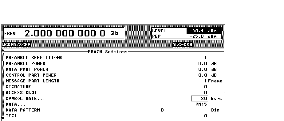
Digital Standard 3GPP W-CDMA (FDD) SMIQ
1125.5555.03 E-92.202
Parameters in the PRACH only mode:
Fig. 2-120 DIGITAL STD – WCDMA/3GPP – MS CONFIGURATION: PRACH only Mode menu
PREAMBLE
REPETITIONS Number of repetitions of the preamble. Values between 1 and 10 can be
selected.
IEC/IEEE-bus command :SOUR:W3GP:MST2:PRAC:PREP 3
PREAMBLE POWER Power of the components of the PRACH. The value range of the power is from
–60 dB to 0 dB.
IEC/IEEE-bus command :SOUR:W3GP:MST2:PRAC:PPOW –5
DATA PART POWER Power of the data components of the PRACH. The value range of the power is
from –60 dB to 0 dB.
IEC/IEEE-bus command :SOUR:W3GP:MST2:PRAC:DPOW –3
CONTROL PART
POWER Power of the control components of the PRACH. The value range of the power
is from –60 dB to 0 dB.
IEC/IEEE-bus command :SOUR:W3GP:MST2:PRAC:CPOW –7
MESSAGE PART
LENGTH Length of message parts in Frames. Lengths 1 and 2 frames can be set.
IEC/IEEE-bus command :SOUR:W3GP:MST2:PRAC:MLEN 2
SIGNATURE This field permits to determine the signature to be used for the PRACH.
Values between 0 and 15 are possible.
IEC/IEEE-bus command :SOUR:W3GP:MST2:PRAC:SIGN 2
ACCESS SLOT# Shifting of the starting time of the PRACH. The value range is 0 to 14.
(Shifting of the starting time in time slots can be calculated as follows:
2 * Access Slot #).
IEC/IEEE-bus command :SOUR:W3GP:MST2:PRAC:ASLO 2
SYMBOL RATE Symbol rate of the PRACH. It is possible to select between 15 ksps, 30 ksps,
60 ksps and 120 ksps.
IEC/IEEE-bus command :SOUR:W3GP:MST2:PRAC:SRAT D30k
DATA / DATA
PATTERN Selection of the data source for the DATA field. Selection from PN9, PN11,
PN15, PN16, ALL0, ALL1 and PATTern. The PN generator function is
explained in section 2.12.3, for example.
If PATTern data type is used, the pattern can be modified with a special editor.
The length is limited to 24 digits.
IEC/IEEE-bus command :SOUR:W3GP:MST2:PRAC:DATA PN9
IEC/IEEE-bus command :SOUR:W3GP:MST2:PRAC:PATT #H1234, 15
TFCI Value of the TFCI (Transport Format Combination Indicator) field in the control
part of the PRACH. The value range of the TFCI is 0 to 1023.
IEC/IEEE-bus command :SOUR:W3GP:MST2:PRAC:TFCI 123
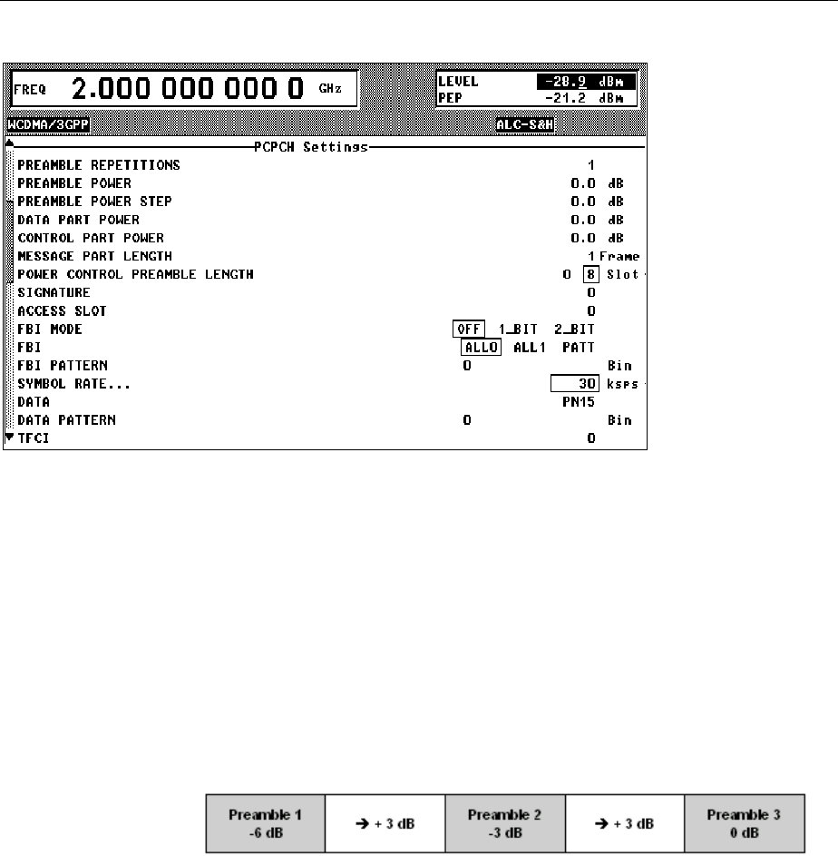
SMIQ Digital Standard 3GPP W-CDMA (FDD)
1125.5555.03 E-92.203
Parameters in the PCPCH only mode:
Fig. 2-121 DIGITAL STD – WCDMA/3GPP – MS CONFIGURATION: PCPCH only Mode menu
PREAMBLE
REPETITIONS Number of repetitions of the preamble. Values between 1 and 10 can be
selected.
IEC/IEEE-bus command :SOUR:W3GP:MST2:PCPC:PREP 3
PREAMBLE POWER Power of the preamble components of the PCPCHs. The value range of the
power is from –60 dB to 0 dB.
IEC/IEEE-bus command :SOUR:W3GP:MST2: PCPC:PPOW –5
PREAMBLE POWER
STEP The power by which the preamble is increased from repetition to repetition can
be set. The value range is 0 dB to 10 dB.
Note: The preamble power that can be entered at the top of the panel is the
destination power used in the last repetition of the preamble. If, for
example, a preamble power of 0 dB, a repetition of 3 and a power
step of 3 dB are set, the following power sequence will be generated:
IEC/IEEE-bus command :SOUR:W3GP:MST2:PCPC:PPOW:STEP 3
DATA PART POWER Power of the data components of the PCPCH. The value range of the power is
from –60 dB to 0 dB.
IEC/IEEE-bus command :SOUR:W3GP:MST2: PCPC:DPOW –3
CONTROL PART
POWER Power of the control components of the PCPCH. The value range of the power
is from –60 dB to 0 dB.
IEC/IEEE-bus command :SOUR:W3GP:MST2: PCPC:CPOW –7
SHARED RESOURCE
MODE The Shared Resource Mode influences the type of the scrambling code in the
access preamble and in the message part of the PCPCH. For more details
refer to [1] section 5.2.2.2.2 and [2] section 4.3.4.4.
IEC/IEEE-bus command :SOUR:W3GP:MST2: PCPC:SHAR ON
MESSAGE PART
LENGTH Length of the message in frames. Lengths between 1 and 10 frames can be set.
IEC/IEEE-bus command :SOUR:W3GP:MST2: PCPC:MLEN 3

Digital Standard 3GPP W-CDMA (FDD) SMIQ
1125.5555.03 E-92.204
POWER CONTROL
PREAMBLE LENGTH Length of Power Control Preamble in slots. Lengths between 0 and 8 slots can
be set.
IEC/IEEE-bus command :SOUR:W3GP:MST2:PCPC:PLEN 8
SIGNATURE This field permits to determine the signature to be used for the PCPCH.
Values between 0 and 15 can be set.
IEC/IEEE-bus command :SOUR:W3GP:MST2: PCPC:SIGN 2
ACCESS SLOT# Shifting of the starting time of the PCPCH. The value range is 0 to 14. (Shifting
of the starting time in time slots can be calculated as follows:
2 * Access Slot #).
IEC/IEEE-bus command :SOUR:W3GP:MST2: PCPC:ASLO 2
FBI MODE OFF The FBI field is not used in the frame.
IEC/IEEE-bus command
:SOUR:W3GP:MST2:PCPC:FBI:MODE OFF
1 BIT The FBI field is used in the frame and is 1 bit long.
IEC/IEEE-bus command
:SOUR:W3GP:MST2:PCPC:FBI:MODE D1B
2 BIT The FBI field is used in the frame and is 2 bits long.
IEC/IEEE-bus command
:SOUR:W3GP:MST2:PCPC:FBI:MODE D2B
FBI / FBI PATTERN Selecting the data source for the FBI field.
ALL0 All 0s are continuously entered in the FBI field.
IEC/IEEE-bus command
:SOUR:W3GP:MST2:PCPC:FBI:DATA ZERO
ALL1 All 1s are continuously entered in the FBI field.
IEC/IEEE-bus command
:SOUR:W3GP:MST2:PCPC:FBI:DATA ONE
PATT The FBI field is cyclically filled with a pattern that is up to 24 bits
long. A special pattern editor is displayed.
IEC/IEEE-bus commands
:SOUR:W3GP:MST2:PCPC:FBI:DATA PATT
:SOUR:W3GP:MST2:PCPC:FBI:PATT #H3F, 8
SYMBOL RATE Symbol rate of the PCPCH. All symbol rates between 15 ksps and 960 ksps
are available.
IEC/IEEE-bus command :SOUR:W3GP:MST2:PCPC:SRAT D30K
DATA / DATA
PATTERN Selection of the data source for the DATA field. Selection from PN9, PN11,
PN15, PN16, ALL0, ALL1 and PATTern. The PN generator function is
explained in section 2.12.3, for example. If PATTern data type is used, the
pattern can be modified with a special editor. The length is limited to 24 digits.
IEC/IEEE-bus command :SOUR:W3GP:MST2:PCPC:DATA PN9
IEC/IEEE-bus command :SOUR:W3GP:MST2:PCPC:PATT #H1234, 15
TFCI Value of the TFCI (Transport Format Combination Indicator) field in the control
part of the PCPC. The value range of the TFCI is 0 to 1023.
IEC/IEEE-bus command :SOUR:W3GP:MST2:PCPC:TFCI 123
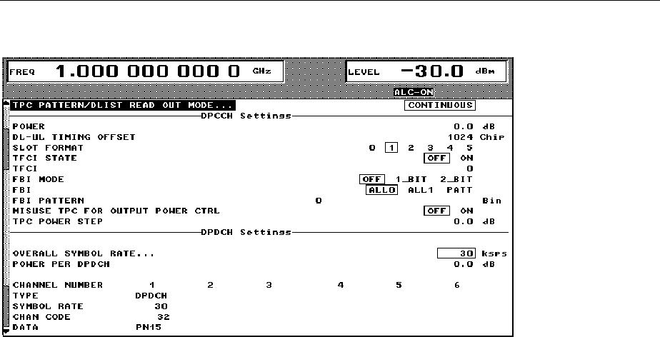
SMIQ Digital Standard 3GPP W-CDMA (FDD)
1125.5555.03 E-92.205
Parameters in the DPCCH + DPDCH mode:
Fig. 2-122 DIGITAL STD – WCDMA/3GPP – MS CONFIGURATION: DPCCH + DPDCH Mode menu
--------------------------DPCCH Settings--------------------------------------------------------------------------
POWER Channel power of the DPCCH, value range –60 to 0 dB
IEC/IEEE-bus command :SOUR:W3GP:MST2:DPCC:POW –3
TIMING OFFSET For the DPCCH (together with the DPDCHs), a fixed timing offset of 1024 chips
(= 4 * 256 chips) is specified as standard. It is only displayed here and cannot be
changed.
IEC/IEEE-bus command :SOUR:W3GP:MST2:DPCC:TOFF?
SLOT FORMAT Setting the TFCI STATE and FBI MODE parameters according to the following
table :
SLOT FORMAT TFCI STATE FBI MODE
0ONOFF
1OFFOFF
2 ON 1bit
3 OFF 1bit
4 OFF 2bits
5 ON 2bits
TFCI STATE ON The TFCI field is used in the frame.
IEC/IEEE-bus :SOUR:W3GP:MST1:DPCC:TFCI:STAT ON
OFF The TFCI field is not used in the frame.
IEC/IEEE-bus :SOUR:W3GP:MST2:DPCC:TFCI:STAT OFF
Note: Any changes of this parameter will affect the SLOT FORMAT
parameter (see table under SLOT FORMAT).
TFCI Setting the TFCI value in the range 0 to 1023. A combination of 30 bits is
selected by this value. This combination is distributed over 15 successive slots
in groups of two.
IEC/IEEE-bus command :SOUR:W3GP:MST4:DPCC:TFCI 21
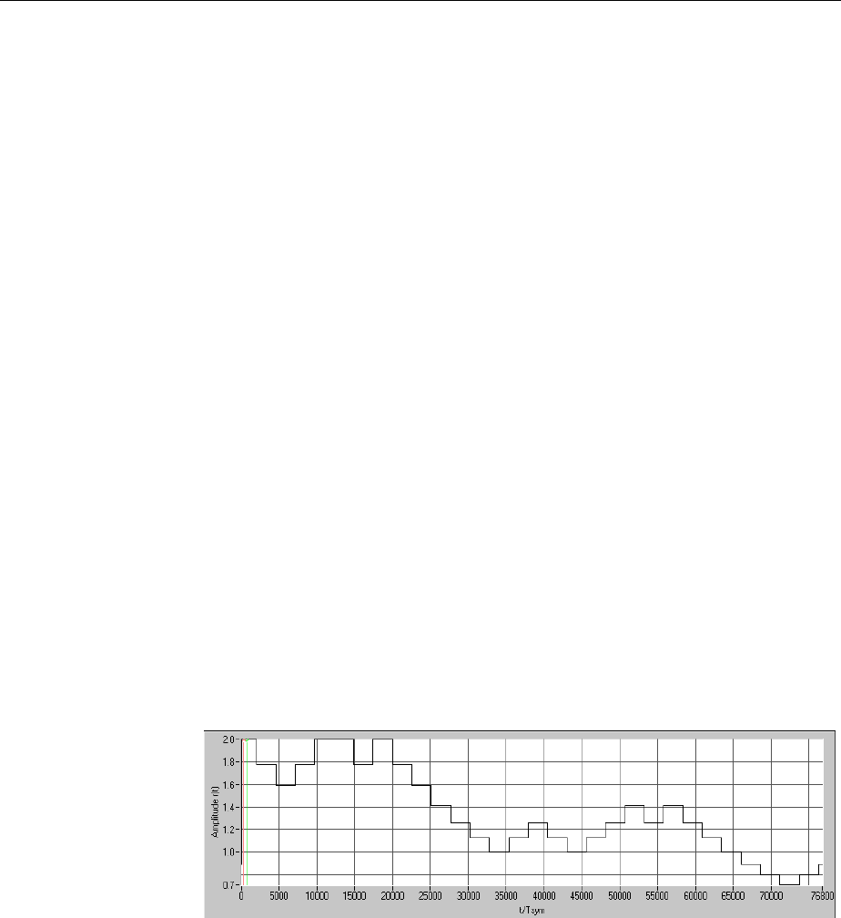
Digital Standard 3GPP W-CDMA (FDD) SMIQ
1125.5555.03 E-92.206
FBI MODE OFF The FBI field is not used in the frame.
IEC/IEEE-bus :SOUR:W3GP:MST2:DPCC:FBI:MODE OFF
1 BIT The FBI field is used in the frame and is 1 bit long.
IEC/IEEE-bus :SOUR:W3GP:MST2:DPCC:FBI:MODE D1B
2 BIT The FBI field is used in the frame and is 2 bits long.
IEC/IEEE-bus :SOUR:W3GP:MST2:DPCC:FBI:MODE D2B
Note: Any changes of this parameter will affect the SLOT FORMAT
parameter (see table under SLOT FORMAT).
FBI / FBI PATTERN Selecting the data source for the FBI field.
ALL0 All 0s are continuously entered in the FBI field.
IEC/IEEE-bus command
:SOUR:W3GP:MST2:PCPC:FBI:DATA ZERO
ALL1 All 1s are continuously entered in the FBI field.
IEC/IEEE-bus command
:SOUR:W3GP:MST2:PCPC:FBI:DATA ONE
PATT The FBI field is cyclically filled with a pattern that is up to 24 bits
long. A special pattern editor is displayed.
IEC/IEEE-bus commands:
:SOUR:W3GP:MST2:DPCC:FBI:DATA PATT
:SOUR:W3GP:MST2:DPCC:FBI:PATT #H3F, 8
MISUSE TPC FOR
OUTPUT POWER
CONTROL
TPC bits are used for W-CDMA to inform the called station if the transmit
power is being increased or decreased. If this option is activated, the given
pattern is being misused to vary one’s own transmit power over time. For each
slot, one bit of this pattern is taken to increase (bit = 1) or decrease (bit = 0)
the channel power by the stated power step (POWER STEP TPC). The upper
limit is 0 dB and the lower –60 dB.
The following envelope occurs at a channel power of 0 dB, a power step of
1.0 dB, the pattern "001110100000011" and TPC Pattern ReadOut Mode
Continuous:
Fig. 2-123 Dynamic change of channel power (continuous)
Note: Observe that the power change (as specified in the standard) is
always performed at the beginning of the slot pilot field.
IEC/IEEE-bus command :SOUR:W3GP:MST1:DPCC:TPC:MIS ON
TPC POWER STEP Size of power step in dB, if option MISUSE TPC FOR OUTPUT POWER CONTROL
is activated.
The range is –10.0 dB to +10.0 dB.
IEC/IEEE-bus command :SOUR:W3GP:MST1:DPCC:TPC:PST 1.0

SMIQ Digital Standard 3GPP W-CDMA (FDD)
1125.5555.03 E-92.207
--------------------------DPDCH Settings--------------------------------------------------------------------------
ENHANCED
CHANNELS... Calling an operating menu for the configuration of extended functions of the
digital standard 3GPP W-CDMA. The menu item is available only if option
SMIQB48 is installed. For more details on this menu see section "Enhanced
Functions for Digital Standard 3GPP W-CDMA".
OVERALL SYMBOL
RATE Overall data rate of all uplink DPDCHs. The structure of the DPDCH table
depends on this parameter. The overall symbol rate indicates the active
DPDCHs, their symbol rate and the channelization codes used (see table
further down).
Value range: off, 15 ksps, 30 ksps, 60 ksps, 120 ksps, 240 ksps, 480 ksps, 960
ksps, 2 x 960 ksps, 3 x 960 ksps, 4 x 960 ksps, 5 x 960 ksps and 6 x 960 ksps.
If OFF is selected, the signal only consists of one DPDCH. In this case, no channel
table is displayed.
IEC/IEEE-bus command :SOUR:W3GP:MST1:DPDC:ORAT D60K
POWER PER DPCH Power of active DPDCHs. Each active DPDCH features this channel power.
The power of the active channels cannot be configured independently (this
also complies with the definition of 3GPP). Value range -60...0.0 dB.
IEC/IEEE-bus command :SOUR:W3GP:MST1:DPDC:POW –23
Table 2-23 Structure of the DPDCH channel table depending on the overall symbol rate
Overall symbol rate DPDCH 1 DPDCH 2 DPDCH 3 DPDCH 4 DPDCH 5 DPDCH 6
15 ksps State: ON
S-Rate: 15 k
Ch. Code: 64
State: OFF State: OFF State: OFF State: OFF State: OFF
30 ksps State: ON
S-Rate: 30 k
Ch. Code: 32
State: OFF State: OFF State: OFF State: OFF State: OFF
60 ksps State: ON
S-Rate: 60 k
Ch. Code: 16
State: OFF State: OFF State: OFF State: OFF State: OFF
120 ksps State: ON
S-Rate: 120 k
Ch. Code: 8
State: OFF State: OFF State: OFF State: OFF State: OFF
240 ksps State: ON
S-Rate: 240 k
Ch. Code: 4
State: OFF State: OFF State: OFF State: OFF State: OFF
480 ksps State: ON
S-Rate: 480 k
Ch. Code: 2
State: OFF State: OFF State: OFF State: OFF State: OFF
960 ksps State: ON
S-Rate: 960 k
Ch. Code: 1
State: OFF State: OFF State: OFF State: OFF State: OFF
2 x 960 ksps State: ON
S-Rate: 960 k
Ch. Code: 1
State: ON
S-Rate: 960 k
Ch. Code: 1
State: OFF State: OFF State: OFF State: OFF
3 x 960 ksps State: ON
S-Rate: 960 k
Ch. Code: 1
State: ON
S-Rate: 960 k
Ch. Code: 1
State: ON
S-Rate: 960 k
Ch. Code: 3
State: OFF State: OFF State: OFF
4 x 960 ksps State: ON
S-Rate: 960 k
Ch. Code: 1
State: ON
S-Rate: 960 k
Ch. Code: 1
State: ON
S-Rate: 960 k
Ch. Code: 3
State: ON
S-Rate: 960 k
Ch. Code: 3
State: OFF State: OFF
5 x 960 ksps State: ON
S-Rate: 960 k
Ch. Code: 1
State: ON
S-Rate: 960 k
Ch. Code: 1
State: ON
S-Rate: 960 k
Ch. Code: 3
State: ON
S-Rate: 960 k
Ch. Code: 3
State: ON
S-Rate: 960 k
Ch. Code: 2
State: OFF
6 x 960 ksps State: ON
S-Rate: 960 k
Ch. Code: 1
State: ON
S-Rate: 960 k
Ch. Code: 1
State: ON
S-Rate: 960 k
Ch. Code: 3
State: ON
S-Rate: 960 k
Ch. Code: 3
State: ON
S-Rate: 960 k
Ch. Code: 2
State: ON
S-Rate: 960 k
Ch. Code: 2
Note: With an overall rate smaller than 960 ksps only DPDCH1 is active, its rate is equal to the overall rate
and the channelization code is equal to spreading factor/4 (spreading factor = chip rate / symbol
rate). With an overall rate greater than 960 ksps, all active DPDCHs have the rate 960 ksps.
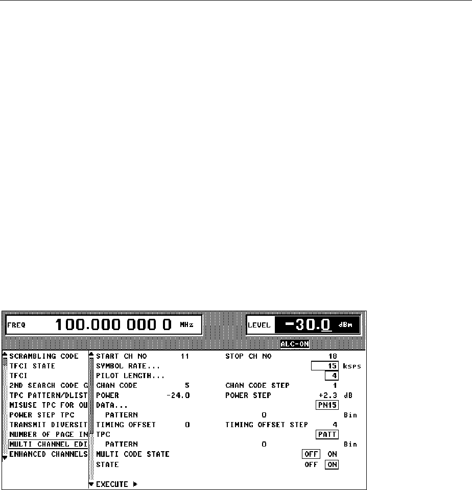
Digital Standard 3GPP W-CDMA (FDD) SMIQ
1125.5555.03 E-92.208
Channel table of the DPDCHs:
SYMBOL RATE The symbol rate of the DPDCH is displayed. This parameter cannot be
changed. Its value depends on the overall symbol rate.
IEC/IEEE-bus command :SOUR:W3GP:MST1:DPDC2:SRAT?
CHANNELIZATION
CODE The channelization code of the DPDCH is displayed. This parameter cannot
be changed. Its value depends on the overall symbol rate.
IEC/IEEE-bus command :SOUR:W3GP:MST1:DPDC2:CCOD?
DATA Selection of the data source for the DATA field. Selection from PN9, PN11,
PN15, PN16, ALL0, ALL1 and PATTern. The PN generator function is
explained in section 2.12.3, for example.
If PATTern data type is used, the pattern can be modified with a special editor.
The length is limited to 24 digits.
IEC/IEEE-bus :SOUR:W3GP:MST3:DPDC3:DATA PN15
:SOUR:W3GP:MST3:DPDC3:DATA:PATT #H1234, 15
2.14.2.7 WCDMA/3GPP – Multi Channel Edit Menu
When MULTI CHANNEL EDIT is selected, a submenu in which several DPCHs can be configured is
opened. This menu item is only available for base stations.
Fig. 2-124 DIGITAL STD – WCDMA/3GPP – BS CONFIGURATION / MULTI CHANNEL EDIT menu
In this submenu, all parameters in the channel table can be set for a group of DPCHs. The parameter
ranges are identical to those in the channel table.
MULTI CHANNEL
EDIT... START CH NO (DPCH)/
STOP CH NO (DPCH) Range of DPCHs that are to be commonly configured.
Range 11 to 138.
IEC/IEEE-bus command:
:SOUR:W3GP:MCH:STAR 14
IEC/IEEE-bus command:
:SOUR:W3GP:MCH:STOP 54
SYMBOL RATE Symbol rate of DPCHs:
7.5 ksps, 15 ksps, 30 ksps, 60 ksps, 120 ksps,
240 ksps, 480 ksps or 960 ksps
IEC/IEEE-bus command:
:SOUR:W3GP:MCH:SRAT D64K

SMIQ Digital Standard 3GPP W-CDMA (FDD)
1125.5555.03 E-92.209
(MULTI CHANNEL
EDIT...) PILOT LENGTH Length of the pilot field in the slot structure of a
channel. The value range of this parameter depends
on the symbol rate (2 bits to max. 16 bits). To
achieve a constant length of the slot the data fields
are lengthened or shortened depending on the pilot
length as defined in the standard.
IEC/IEEE-bus :SOUR:W3GP:MCH:PLEN BIT2
CHANNELIZATION
CODE / STEP Channelization code for the first channel and step
width for all other channels. The value ranges depend
on the symbol rate.
IEC/IEEE-bus commands
:SOUR:W3GP:MCH:CCOD 4
:SOUR:W3GP:MCH:CCOD:STEP 1
POWER / dB
POWER STEP / dB Channel power for the first channel (value range
-60 dB to 0 dB) and stepwidth for all other channels
(value range -60 dB to 60 dB).
IEC/IEEE-bus commands
:SOUR:W3GP:MCH:POW –20
:SOUR:W3GP:MCH:POW:STEP 1
DATA Selection of data pattern for the DPCHs. For other
patterns see channel table.
IEC/IEEE bus commands
:SOUR:W3GP:MCH:DATA PN9
:SOUR:W3GP:MCH:DATA:PATT #HFFFF, 16
TIMING OFFSET /
TIMING OFFSET STEP A value > 0 causes the source symbols to be shifted
prior to spreading. An offset of 1 for instance is
recommended to obtain a lower crest factor.
The absolute starting time of frames (slot 0) is shifted
relative to the start of the scrambling code sequence
by TOffset * 256 chips. This means that the resolution
of the timing offset is always 256 chips, irrespective
of the symbol rate. The step width of the timing offset
between two adjacent channels is defined with STEP.
IEC/IEEE bus commands
:SOUR:W3GP:MCH:TIM:OFFS 0
:SOUR:W3GP:MCH:TIM:STEP 3
TPC Data source for the TPC field.
IEC/IEEE-bus :SOUR:W3GP:MCH:TPC ZERO
MULTI CODE STATE ON The channels should be simulated with
multicode.
IEC/IEEE bus :SOUR:W3GP:MCH:MCOD ON
OFF The channels should be simulated without
multicode.
IEC/IEEE bus :SOUR:W3GP:MCH:MCOD OFF
STATE ON The channels are active.
IEC/IEEE bus :SOUR:W3GP:MCH:STAT ON
OFF The channels are not active.
IEC/IEEE bus :SOUR:W3GP:MCH:STAT OFF
EXECUTE Configuration of DPCHs according to the set para-
meters.
IEC/IEEE bus :SOUR:W3GP:BST2:MCH:EXEC
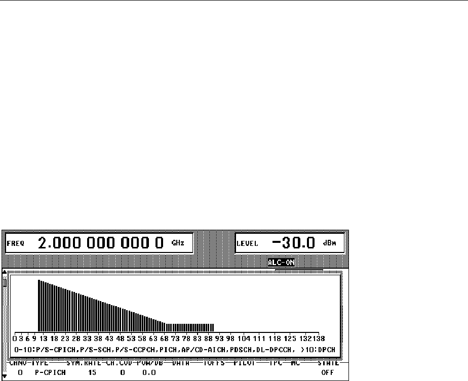
Digital Standard 3GPP W-CDMA (FDD) SMIQ
1125.5555.03 E-92.210
The channel parameter ranges correspond to the associated parameters in the channel table (see
above).
Start Channel No (DPCH)/Stop Channel No (DPCH): The range of the DPCHs that are to be set
jointly is defined.
For channel scenarios to be set up easily, start values and step widths can be entered for some
parameters which are used to set the channel parameters. Channelization Code and Channelization
Code Step parameters, for example, can be used to create simple scenarios in which spreading codes
with a fixed step width are assigned to the various code channels. Power profiles (via the code axis) can
be created in the same way with power and power step. The timing offset and timing offset step
parameters can be used to change the relative slot timings of the channels, so changing the crest factor
of the signal (see section 2.14.3.4).
2.14.2.8 WCDMA/3GPP – Display of Channel Graph Menu
The channel graph provides an overview of the contents of the channel table.
Fig. 2-125 DIGITAL STD – WCDMA/3GPP – BS CONFIGURATION /CHANNEL GRAPH menu
All active channels and their channel powers are displayed. Unlike the code domain display (next
chapter), all channels are shown with the same width. Multiple assignment of a code domain range
cannot be recognized.
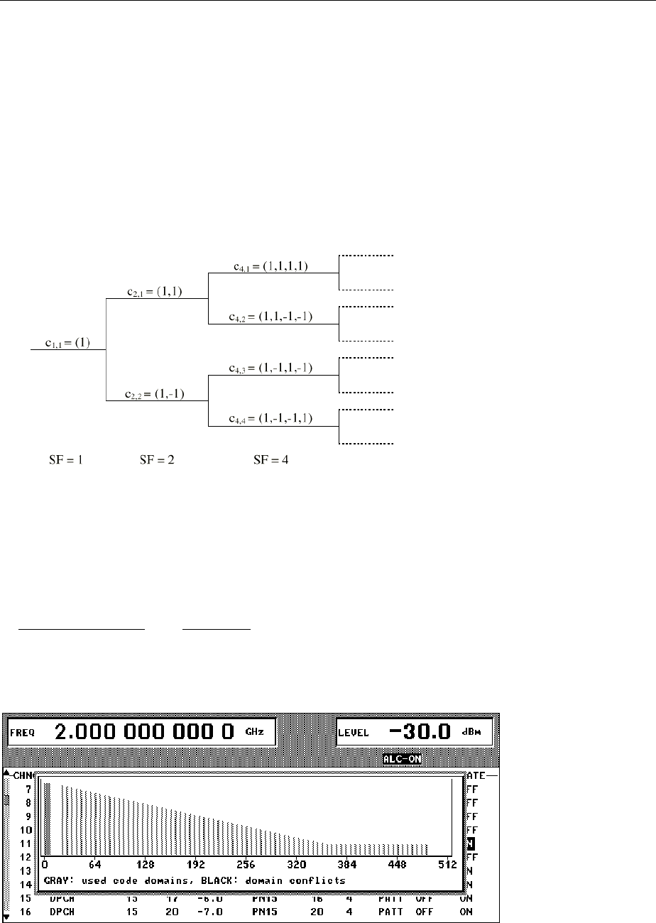
SMIQ Digital Standard 3GPP W-CDMA (FDD)
1125.5555.03 E-92.211
2.14.2.9 WCDMA/3GPP Menu – Display of Code Domain and Code Domain
Conflicts
The channelization codes are taken from a code tree (see below).
The greater the spreading factor, the smaller the symbol rate and vice versa. The product of the spreading
factor and the symbol rate is constant and always equals the current chip rate. The outer branches of the
tree (right-most position in the figure) give the channelization codes for the lowest symbol rate (and so the
highest spreading factor). The use of a channelization code from the level with a spreading factor N blocks
the use of all other channelization codes from levels with spreading factor >N in the same branch of the
code tree. Channelization codes with a smaller spreading factor are contained in the codes with larger
spreading factor in the same code branch. If channelization codes of this type are used at the same time,
the signals of associated code channels will be mixed up to such an extent that they could not be
separated in the receiver and orthogonality would be lost.
Fig. 2-126 Code tree of channelization codes
Example: If in Fig. 2-126 code c2,1 is already used, the remaining branch is blocked with c4,1 and c4,2 .
The outer branch region (with minimum symbol rate and max. spreading factor) which is based on the
channelization code selected in the code tree is defined as the domain of a certain channelization code.
Using a channelization code means that its entire domain is used. The whole domain ranges from 0 to
511 at the chip rate of 3.84 Mcps:
1
5.7
84.3
1
_min_
_−=−= ksps
Mcps
ratesymbol
rateChip )
A graphic is displayed with the CODE DOMAIN menu item or the STATUS hardkey. This graphic shows
the occupancy of the code domain by the active code channels.
Fig. 2-127 WCDMA/3GPP – BS CONFIGURATION / CODE DOMAIN menu (without conflict)
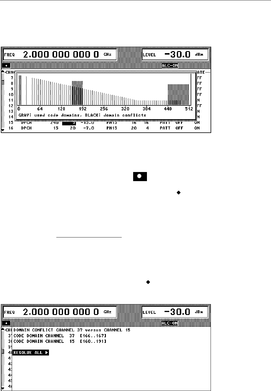
Digital Standard 3GPP W-CDMA (FDD) SMIQ
1125.5555.03 E-92.212
This display shows at a glance whether assigned code domains of various channels overlap, i.e.
whether a domain conflict occurs. The symbol rates of code channels are indicated by the width of the
associated bars. The height of the bars gives the power of the code channel. If a bar is grey, the code
domain at this position is assigned once which means that no conflicts occur. If a bar is black (at least
partly), the code domain is assigned at least twice and conflicts occur.
Fig. 2-128 WCDMA/3GPP – BS CONFIGURATION / CODE DOMAIN menu (with conflict)
Display of domain conflicts
If a domain conflict occurs in the base station/mobile station, this conflict is displayed at two locations
(next to the code domain display).
1. Centrally for the whole station in the status line ,
2. All lines in the channel table (processed in ascending channel numbers) showing a domain conflict
in a row with a lower index are indicated with a warning symbol to the left of STATE.
A domain conflict occurs when the assigned domains of different channel rows overlap. The assigned
code domain of a channel is calculated from the symbol rate of the channel, the minimum possible
symbol rate (depending on the link direction), the chip rate and the channelization code number using
the following equation:
symbolrateimum
symbolratecurrent
factorDomain _min
_
_=(the minimum symbol rate is 7.5 ksps in downlink),
where:
Lower domain limit = current channelization code number * domain factor
Upper domain limit = lower domain limit + domain_factor –1.
If the cursor is positioned on one of the warning symbols and if the SELECT button is clicked, a window
is opened and shows more accurate information about the domain conflict that has occurred. The numbers
of channel rows in the channel table and the assigned domains of the conflicting channels are displayed.
Fig. 2-129 WCDMA/3GPP – BS CONFIGURATION / CODE DOMAIN CONFLICT menu
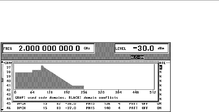
SMIQ Digital Standard 3GPP W-CDMA (FDD)
1125.5555.03 E-92.213
Resolve all Conflicts
If you select the RESOLVE ALL button in the domain conflict info window, the SMIQ tries to arrange the
active code channels so that no overlapping occurs in the code domain. The channelization code
number of the channels is varied to do this. The effect of a conflict resolution is shown by the code
domain display.
Fig. 2-130 WCDMA/3GPP – BS CONFIGURATION / CODE DOMAIN menu (after conflict resolution)
If the assigned domain of all active channels is greater than the physically available domain (e.g. 5
channels with 960 ksps at a chip rate of 3.84 Mcps), conflicts can no longer be resolved. The message "no
resolution of domain conflicts possible" is displayed.
2.14.2.10 Effect of CLIPPING LEVEL Parameter on Signal
W-CDMA signals may have very high crest factors - especially if the number of channels is high and the data
offset is unfavourable (see sections 2.14.3.3 and 2.14.3.4). High crest factors entail two basic problems:
1. The nonlinearity of the power amplifier (compression) causes intermodulation which expands the
spectrum (spectral regrowth).
2. Since the level in the D/A converter is relative to the maximum value, the average value is converted
with a relatively low resolution. This results in a high quantization noise.
Both effects increase the adjacent-channel power.
From all the possibilities listed in section 2.14.3.4 for influencing the crest factor, changing the
CLIPPING LEVEL is the simplest and most effective. In this case a limit value is defined which is a
percentage of the highest peak value. All current values exceeding this limit will be clipped to this value.
Since clipping is done prior to filtering, the procedure does not influence the spectrum. The EVM
however increases. Since clipping the signal not only changes the peak value but also the average
value, the effect on the crest factor is unpredictable. The following table shows the effect of the
CLIPPING LEVEL on the crest factor for typical scenarios.
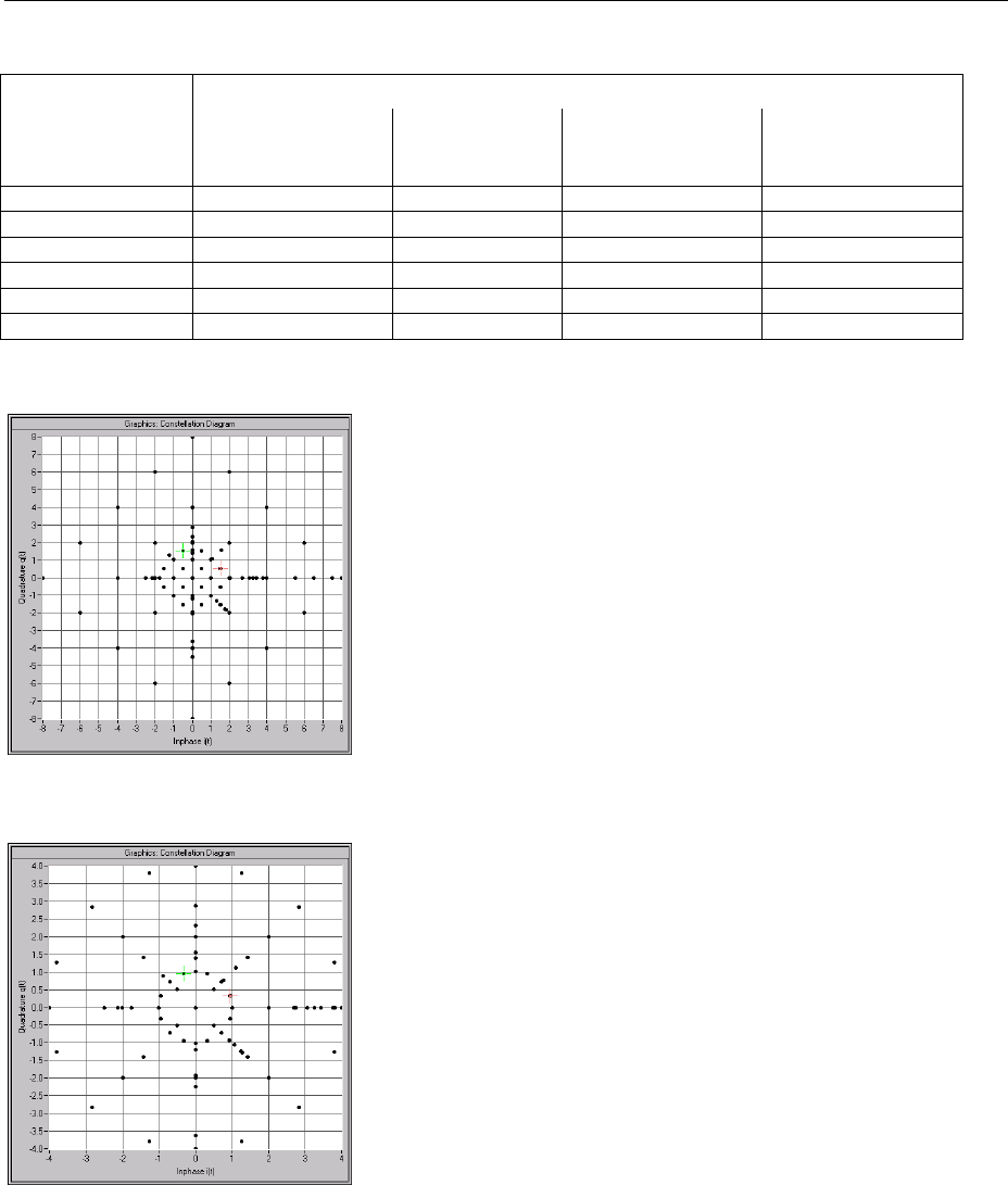
Digital Standard 3GPP W-CDMA (FDD) SMIQ
1125.5555.03 E-92.214
Table 2-24 Change of crest factor in the case of clipping
Crest factor with scenarioCLIPPING LEVEL
Downlink:
10 DPCHs "minimum
crest" 30 ksps
Downlink:
10 DPCHs "worst
crest" 30 ksps
Downlink:
10 DPCHs "average
crest" 30 ksps
Downlink:
128 DPCHs "average
crest" 30 ksps
100% 9.89 dB 14.7 dB 10.9 dB 21.7 dB
80% 8.86 dB 12.9 dB 9.39 dB 20.2 dB
50% 7.50 dB 10.1 dB 8.29 dB 16.9 dB
20% 5.50 dB 6.47 dB 6.23 dB 12.5 dB
10% 5.34 dB 6.06 dB 5.80 dB 9.57 dB
5% 5.34 dB 6.06 dB 5.80 dB 8.17 dB
Effect of clipping on the constellation shown by way of a 4-DPCH configuration:
Fig. 2-131 Constellation at clipping level 100% (not clipped)
Fig. 2-132 Constellation at clipping level 50%

SMIQ Digital Standard 3GPP W-CDMA (FDD)
1125.5555.03 E-92.215
2.14.2.11 Synchronization and Trigger Signals
To generate the W-CDMA signals, a chip sequence is calculated and stored in the waveform memory of
the modulation coder (option SMIQB20). This chip sequence is automatically repeated (TRIGGER
MODE AUTO).
For measurements on receivers, trigger signals can also be used for synchronized sequences
(TRIGGER MODE RETRIG, ARMED_AUTO or ARMED_RETRIG).
The trigger signal is applied to the TRIGIN input of the PAR DATA connector. The chip sequence either
starts immediately after the active edge of this trigger signal or after a settable number of chips (EXT
TRIGGER DELAY). A retrigger (RETRIG) can be inhibited for a settable number of chips (EXT
RETRIGGER INHIBIT).
A trigger event can be triggered manually with EXECUTE TRIGGER or via the IEC/IEEE bus. A trigger
signal is always output at TRIGOUT 3 output of the SMIQ at the same time as a trigger event.
The SMIQ generates the following sync signals:
• a 0.667 ms slot clock
• a 10 ms radio-frame clock
• a marker signal to identify the periodic repetition of the generated chip sequence
• a marker signal to identify the periodic repetition of the generated enhanced chip sequence (only
available if Option SMIQB48 is installed)
• a marker signal to identify a restart of the system frame number (SFN Restart) after 4096 frames
(only available if Option SMIQB48 is installed and a BCH is generated).
The SMIQ can output a selection of two or three signals via connectors TRIGOUT 1 and 2 of the
PAR DATA connector.
The chip clock in the SMIQ is generated by a clock synthesizer in the modulation coder. All clock signals
are in sync with the unit’s 10 MHz reference. The chip clock is available at the SYMBOL CLOCK
connector. If required, the clock synthesizer in the SMIQ can use an external chip clock which is fed in via
the SYMBOL CLOCK connector.
To ensure reliable clock-synthesizer synchronization, the external clock must first be applied and the
correct SMIQ chip rate set (MODULATION – CHIPRATE VARIATION). The CLOCK SOURCE can then
be switched from INT to EXT.
Note: The set chip rate may not differ by more than 1% from the chip rate of the external signal.

Digital Standard 3GPP W-CDMA (FDD) SMIQ
1125.5555.03 E-92.216
2.14.2.12 Preset/Default Values
The following settings are made if the menu item SET DEFAULT is selected or if the PRESET key is
pressed during switch-on.
General default settings
CHIP RATE 3.84 Mcps
LINK DOWN/FORWARD
3GPP VERSION 3.2.0 (RELEASE 99)
MODULATION WCDMA filter, roll-off 0.22, LOW ACP, chip rate of 3.84 Mcps
TRIGGER
MODE RETRIG
SOURCE INT
DELAY 0
INHIBIT 0
OUT 1 RADIO FRAME
OUT 2 CHIP SEQUENCE PERIOD
OUT1/2 POL POS
OUT ½ DELAY 0
CLOCK SOURCE INT
CLOCK DELAY 0.00
SEQUENCE LENGTH 1
Default settings for DOWN/FORWARD Link
Para. Predef. settings
CHANNELS FOR SYNC... ON
SCCPCH 60 ksps
NO OF DPCH 3
SYMBOL RATE 30 ksps
CREST MINIMUM
Base station parameters
Table 2-25 Default values for base station parameters
Parameter BS1 BS2 BS3 BS4
STATE OFF OFF OFF OFF
SCRAMBLING CODE
STATE ON ON ON ON
SCRAMBLING CODE 0 0 0 0
USE TFCI OFF OFF OFF OFF
TFCI 0000
2nd SEARCH CODE GR. 0 0 0 0
Misuse TPC... OFF OFF OFF OFF
TPC Read Out Mode continuous continuous continuous continuous
Power Step 0 0 0 0
Transmit Diversity OFF OFF OFF OFF
Page indicators per frame 18 18 18 18

SMIQ Digital Standard 3GPP W-CDMA (FDD)
1125.5555.03 E-92.217
Multi Channel Edit
START DPCH 11
STOP DPCH 11
SYMBOL RATE 30 ksym/s
PILOT LENGTH 4 bit
CHAN. CODE 0
CHAN. STEP 0
POWER 0dB
POWER STEP 0dB
DATA PN15
TIMING OFFSET 0
TIMING OFFSET STEP 0
TPC ALL 0 (0)
MULTI CODE STATE OFF
STATE ON
Channel table parameters
SYMBOL RATE 15 ksps (if possible, otherwise min. permissible rate)
CHAN. CODE 0 (if possible, otherwise min. permissible code)
POWER 0 dB
DATA PN15
TIMING OFFSET 0
PILOT LENGTH 4 bit (if possible, otherwise min. permissible length)
TPC ALL0 (0)
MC STATE OFF
DATA PATTERN "0000 0000 0000 0000"
TPC PATTERN "0000 0000 0000 0000"
Digital Standard 3GPP W-CDMA (FDD) SMIQ
1125.5555.03 E-92.218
Default settings for UP/REVERSE link
Mobile station parameters
Table 2-26 Default values for mobile station parameters
Parameters MS1 MS2 MS3 MS4
STATE OFF OFF OFF OFF
MODE DPCCH + DPDCH DPCCH + DPDCH DPCCH + DPDCH DPCCH + DPDCH
SCRAMBLING CODE 0 0 0 0
SC MODE LONG LONG LONG LONG
TPC READ OUT MODE CONTINUOUS CONTINUOUS CONTINUOUS CONTINUOUS
TPC All 0 All 0 All 0 All 0
Parameter PRACH only mode:
PREAMBLE REPETITION 1
PREAMBLE POWER 0 dB
DATA PART POWER 0 dB
CONTROL PART POWER 0 dB
Message Part Length 1
SIGNATURE 0
ACCESS SLOT 0
SYMBOL RATE 30 ksps
DATA PN15
DATA PATTERN "0000 0000 0000 0000"
TFCI 0
Parameter PCPCH only mode:
PREAMBLE REPETITION 1
PREAMBLE POWER 0 dB
PREAMBLE POWER STEP 0 dB
DATA PART POWER 0 dB
CONTROL PART POWER 0 dB
MESSAGE PART LENGTH 1
Power CONTROL
PREAMBLE LENGTH 0 slots
SIGNATURE 0
ACCESS SLOT 0
FBI MODE OFF
FBI ALL 0
FBI PATTERN "0000 0000 0000 0000"
SYMBOL RATE 30 ksps
DATA PN15
DATA PATTERN "0000 0000 0000 0000"
TFCI 0

SMIQ Digital Standard 3GPP W-CDMA (FDD)
1125.5555.03 E-92.219
Parameter DPCCH + DPDCH mode:
DPCCH settings
POWER 0 dB
TIMING OFFSET 4 (fix)
TFCI STATE OFF
TFCI 0
FBI MODE OFF
FBI ALL 0
FBI PATTERN "0000 0000 0000 0000"
MISUSE TPC... OFF
TPC POWER STEP 0 dB
PREAMBLE POWER 0 dB
PREAMBLE POWER STEP 0 dB
DATA PART POWER 0 dB
CONTROL PART POWER 0 dB
SHARED RESOURCE... OFF
MESSAGE PART LENGTH 1
DPDCH settings
OVERALL SYMBOL RATE 30 ksps
POWER 0 dB
DATA PN15 (for all DPDCHs)
2.14.3 Background Information for the Generation of 3GPP W-CDMA Signals
This section provides some background information on W-CDMA signals to support the user in
generating signals with certain characteristics.
2.14.3.1 3GPP W-CDMA Signals in Time Domain
For information on 3GPP W-CDMA signals in the frequency domain refer to section 2.14.3.2.
Downlink
The two spreading methods for SCHs and the remaining (downlink) channel types are explained for the
channels P-CCPCH, P-SCH and S-SCH. (These three channels were referred to as “Perch” in previous
versions of the W-CDMA standard and option SMIQB45)
A (downlink) signal containing the following components is generated:
• P-CCPCH (-20 dB)
• P-SCH (-14 dB)
• S-SCH (-14 dB)
The SCH components are generated with double amplitude for better distinction against PCCPCH.
Sequence length = 1
Filtering: root cosine (roll-off = 0.22), impulse length = 32, oversampling = 8
Data source: PRBS23
No superimposed impairments active
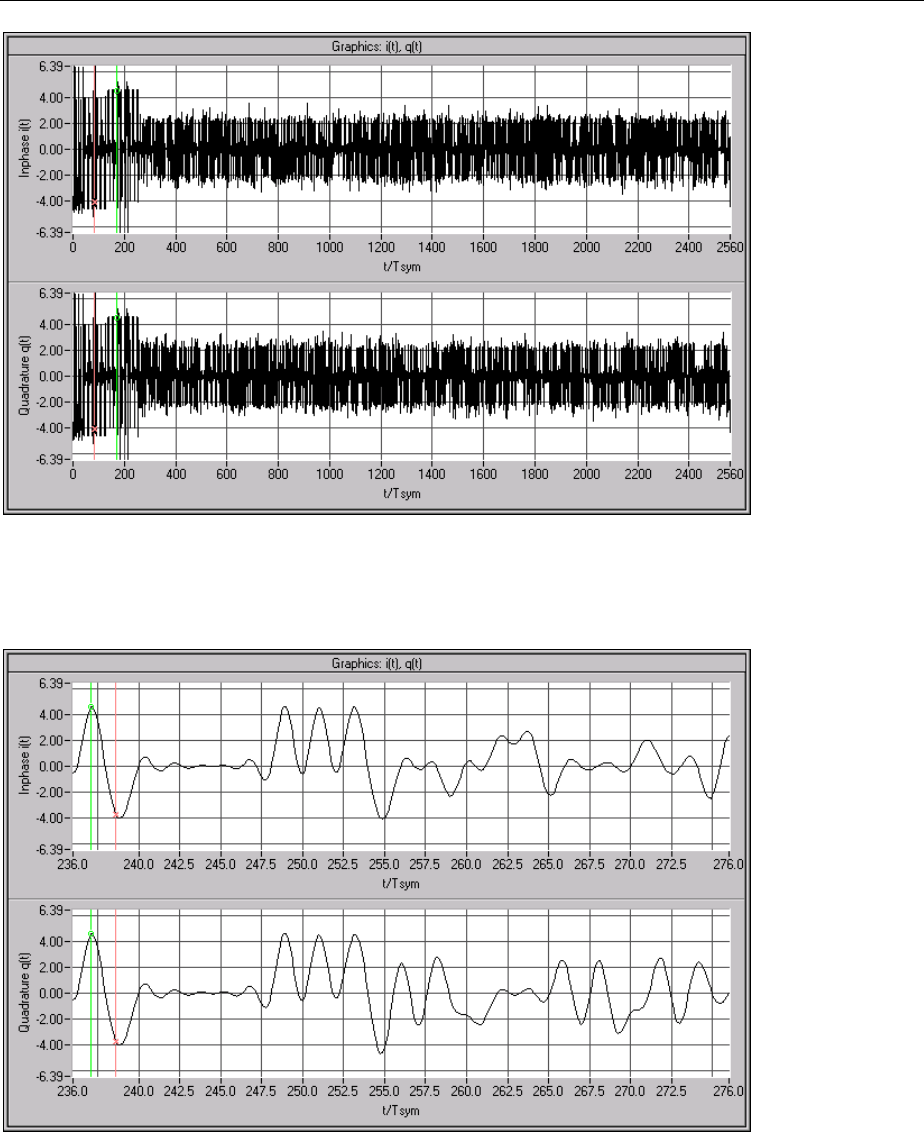
Digital Standard 3GPP W-CDMA (FDD) SMIQ
1125.5555.03 E-92.220
Fig. 2-133 Signal consisting of P-CCPCH, P-SCH and S-SCH in time domain
The above diagram reveals that a time slot consists of 2560 chips and the power is higher with the first
10% of the signal. This is the SCH. Zooming in on this transition point reveals the following:
Fig. 2-134 Signal consisting of P-CCPCH, P-SCH and S-SCH in time domain (zoomed)
The right section (i.e. the 9 PCCPCH symbols) is spread as described in Fig. 2-90. You can see that for
each symbol clock one of the two components is 0 and the other one ±2 (a certain inaccuracy results
from the root cosine filter used).
This is the standard spreading scheme as it is also used for S-CCPCH, DPCH and all other downlink
channel types.
The left section (the synchronization code symbol occupying the chip range 0 to 255) is obtained using
special synchronization code spreading: there is no scrambling unit ( Si = Ci , Sq = Cq ).
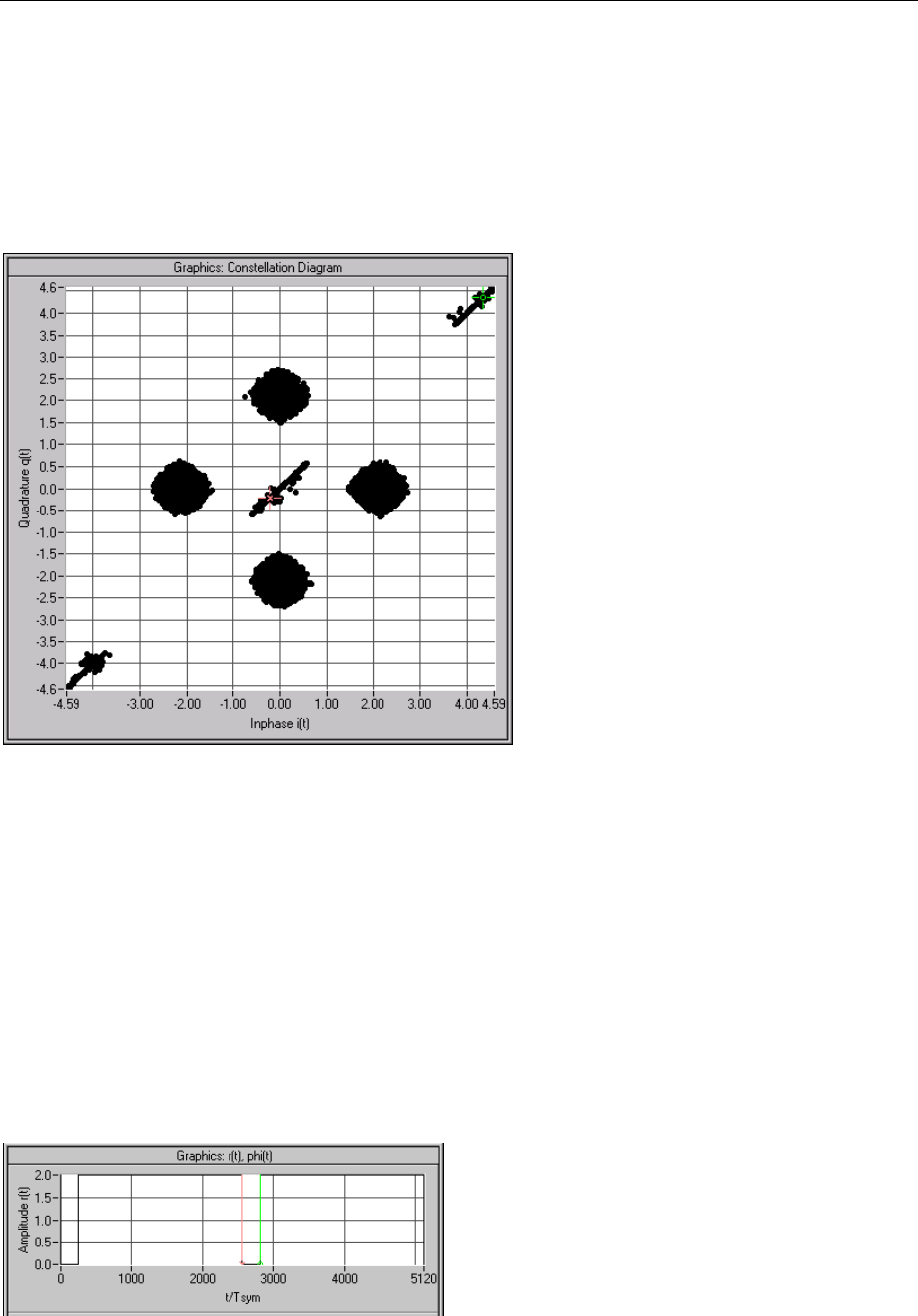
SMIQ Digital Standard 3GPP W-CDMA (FDD)
1125.5555.03 E-92.221
Since the synchronization code symbol is defined as 11, the following is always true:
Si = Sq.
The result is a BPSK mapping turned by 45° relative to the QPSK constellation of the S-CCPCH
component.
Since the synchronization code symbol is sent twice (in the primary and secondary SCH) with different
spreading, the signal power is doubled in this range.
The constellation diagram of the perch channel, therefore, has the following appearance:
Fig. 2-135 Constellation diagram of a signal consisting of P-CCPCH, P-SCH and S-SCH
The four circular areas are due to P-CCPCH ("QPSK"), the linear areas (diagonals) to SCH ("BPSK").
The spreading/constellation diagram of P-CPICH, S-CPICH, S-CCPCH, PICH, AP-AICH, AICH,
PDSCH, DL-DPCCH and DPCH are identical to the spreading/constellation diagram of P-CCPCH.
Envelopes
The following figures are based on a power of 0 dB.
To eliminate smearing of the amplitude due to the root cosine filter, all envelopes are calculated using a
squarewave filter.
The channels P-CPICH, S-CPICH, S-CCPCH, PICH, PDSCH feature a constant envelope during the
complete sequence.
Note: Section 2.14.2.5, "Misuse TPC for output power control", describes how the envelope of
e.g. DPCHs can be varied.
The P-CCPCH is blanked during the first 256 chips of the slot.
Fig. 2-136 Envelope of P-CCPCH
Digital Standard 3GPP W-CDMA (FDD) SMIQ
1125.5555.03 E-92.222
P-SCH and S-SCH are active during the first 256 chips only:
Fig. 2-137 Envelope of P-SCH or S-SCH
AP-AICH and AICH are transmitted only during the first 4096 chips of the signal:
Fig. 2-138 Envelope of AICH (Subchannel)
AP-AICH and AICH consist of up to 16 superimposed single channels that are modulated with different
orthogonal vectors. In some sections, cancellations or excessive levels may result. The following
diagram shows the signal with the input pattern "1010":
Fig. 2-139 Envelope of AICH (four subchannels)
The DL-DPCCH is used during transmission of the PCPCH to readjust the output power of the mobile.
Since there is no data transfer to the mobile in this phase, the DL-DPCCH is based on a DPCH
(7.5 ksps without TFCI), the data fields of which are blanked (“DTX“):
Fig. 2-140 Envelope of DL-DPCCH
At first, DPCHs are permanently active, however the TFCI fields are blanked at high data rates
(>= 60 ksps) if no TFCI information is transferred ("DTX"). A 60-ksps channel, for example, then has the
following appearance:
Fig. 2-141 Envelope of DPCH 60 ksps without TFCI
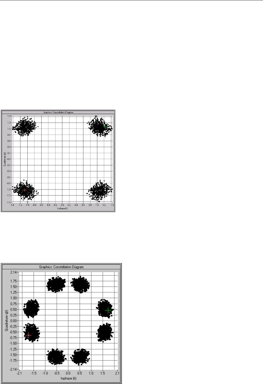
SMIQ Digital Standard 3GPP W-CDMA (FDD)
1125.5555.03 E-92.223
Uplink
In the "DPCCH+DPDCH" mode, the signal consists of a DPCCH and one or several (max. 6) DPDCHs.
To derive the constellation of this signal, the constellation of a single channel (DPDCH or DPCCH) is
considered first. Its data are exclusively supplied to the I or Q path. The second path is not used
(second path is: Cq = 0).
with Si = CiSCi – CqSCq'
Sq = CiSCq' + CqSCi
the following equation is obtained:
Si = CiSCi
Sq = CiSCq'
This corresponds to a QPSK constellation diagram. Compared to the DPCH constellation diagram, this
diagram is shifted and the constellation points only have half the amplitude:
Fig. 2-142 Constellation of a DPDCH/DPCCH channel
Note: A suitable modification of the PN sequences ("HPSK") in the uplink eliminates 50 % of all zero-
crossings, which, in contrast to the downlink, causes a deformation of the constellation ranges.
If DPCCH and DPDCH are combined, the constellation considerably depends on the ratio of the channel
powers. If the two powers are equal, a constellation as with the P-CCPCH will be obtained. The
following illustration shows the constellation with DPCCH power 0dB and DPDCH power –6 dB:
Fig. 2-143 Constellation of an uplink signal consisting of a DPDCH and a DPCCH
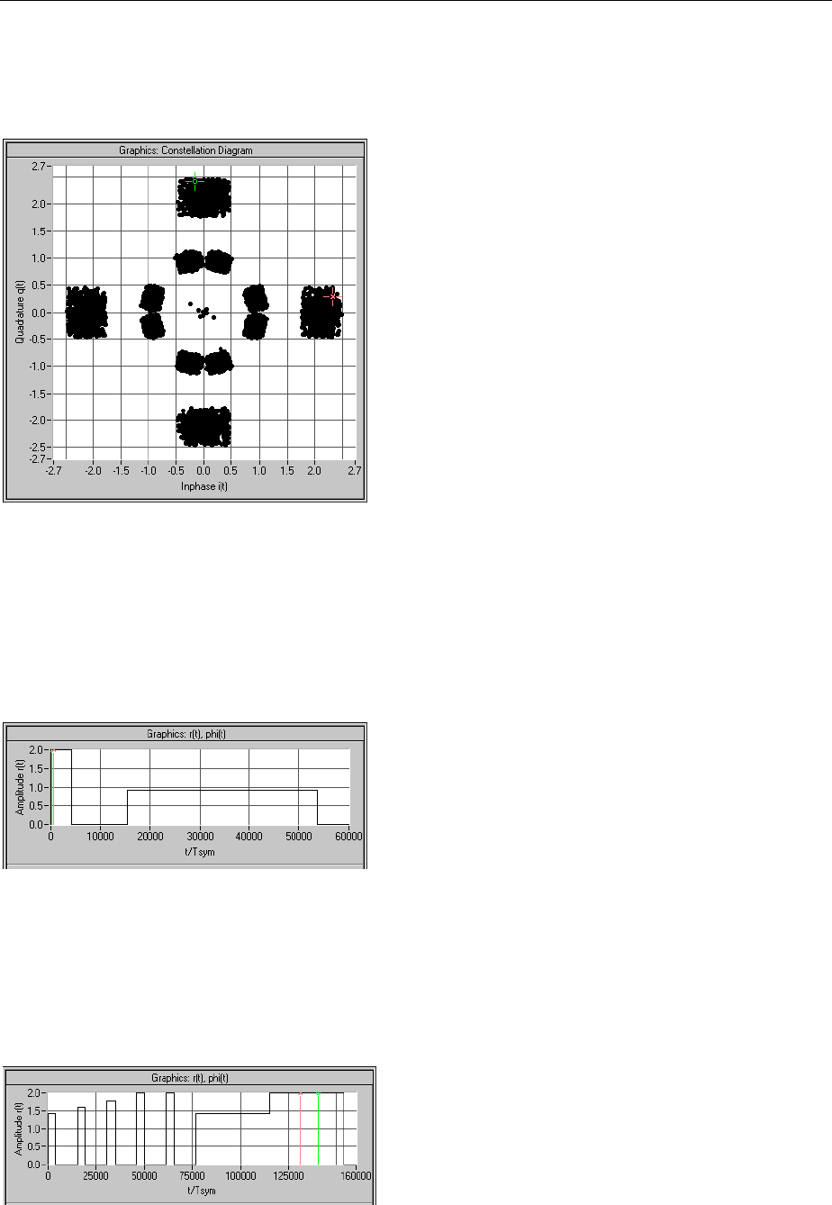
Digital Standard 3GPP W-CDMA (FDD) SMIQ
1125.5555.03 E-92.224
PRACH and PCPCH consist of preambles and the message part. Similar to a P-CCPCH, the preamble
uses the 4 constellation points (2, 0), (0,2), (-2, 0) and (0, -2). In the case of the message part, separate
powers can set for Data (on the I path) and Control (on the Q path) so that a component is obtained as
described above for the DPCCH+DPDCH signal. As the third part of the constellation, points can be seen
at the origin, which can be assigned to the interval between preamble and message part:
Fig. 2-144 Constellation of a PRACH
Envelopes
To eliminate smearing of the amplitude due to the root-cosine filter, all envelopes are calculated using a
square-wave filter. The DPCCH and the DPDCHs are continuous channels that feature a constant
envelope during the complete sequence.
Note: Section 2.14.2.6 "Misuse TPC for output power control", describes how to vary also the
envelope of DPCCH and DPDCHs.
PRACH and PCPCH consist of one or several preambles and the message part.
Example of a PRACH with a preamble and reduced power in the message part:
Fig. 2-145 Envelope of a PRACH
Example of a PCPCH with the parameters
• Access Slot # = 0
• Preamble Repetition = 4
• Preamble Power Step = 1 dB
• Message Part Length = 1 frame
• Preamble Power = 0 dB
• Control Part Power = 0 dB
• Data Part Power = 0 dB
Fig. 2-146 Envelope of a PCPCH
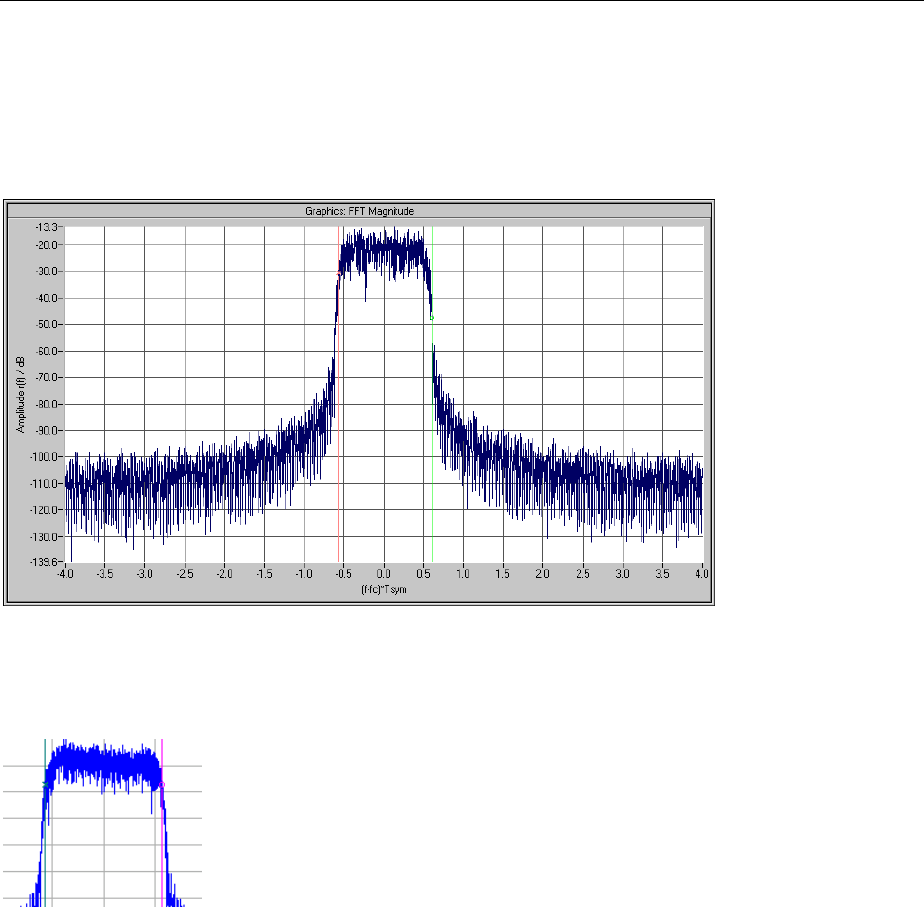
SMIQ Digital Standard 3GPP W-CDMA (FDD)
1125.5555.03 E-92.225
2.14.3.2 3GPP W-CDMA Signals in the Frequency Range
For information on 3GPP W-CDMA signals in the time domain, refer to section 2.14.3.1.
The spectrum of a 3GPP W-CDMA signal (a DPCH channel) corresponds to that of a QPSK signal with
identical filter parameters.
Fig. 2-147 Magnitude spectrum of a 3GPP W-CDMA signal
If signals with several channels are investigated, a certain ripple may occur in the range +/-0.5 of the
chip rate.
Fig. 2-148 Magnitude spectrum (section) of a 3GPP W-CDMA signal with several channels
This effect can be influenced by the choice of the channelization codes and is reduced with increasing
period of observation, i.e. higher averaging for the FFT settings.
2.14.3.3 Effect of Data Source on the 3GPP W-CDMA Signal
The choice of the data sources is of vital importance for the signal characteristics. Especially the
constellation diagram and the crest factor can be modelled to a large extent by an appropriate data
selection.
Since the number of channels can be very high, particularly in the downlink, this section deals only with
the simulation of downlink signals.
In the following it is assumed that all channels are generated with the same scrambling code sequences
and the same channel powers of 0.0 dB.
A symbol rate of 60 ksps is selected.
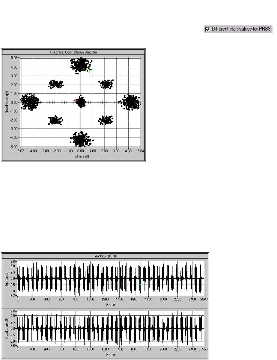
Digital Standard 3GPP W-CDMA (FDD) SMIQ
1125.5555.03 E-92.226
2.14.3.3.1 Two DPCHs with Uncorrelated Data
If the two channels are uncorrelated (data source PRBS with active option ),
the resulting constellation diagram is obtained from the superposition of the constellations of two
separate signals (see Fig. 2-102).
Fig. 2-149 Constellation of a signal with two DPCHs (uncorrelated data)
The resulting crest factor is 8.07 dB.
2.14.3.3.2 Two DPCHs with Same Data
If the two channels contain exactly the same data (PRBS data source with equal initial values), the individual
components only differ in the channelization codes. Comparing any two lines of the channelization code matrix
shows that 50% of the bits are identical and 50% are different (orthogonal matrix)). Where the bits are
identical, the two channels furnish the same components; where the bits are different, the components cancel
each other. The I/Q signal of this sum signal would then have the following characteristic:
Fig. 2-150 Signal with two DPCHs (same data) in time domain
Note: The bursts occurring at regular intervals are due to the use of the channelization code numbers
0 and 1. The two lines of the matrix are identical in the first half and different in the second half.
Therefore, each of the 40 source symbols causes one of these bursts, the period of which is
equivalent to half the symbol length. Other combinations of channelization code numbers often
cause erratic results.
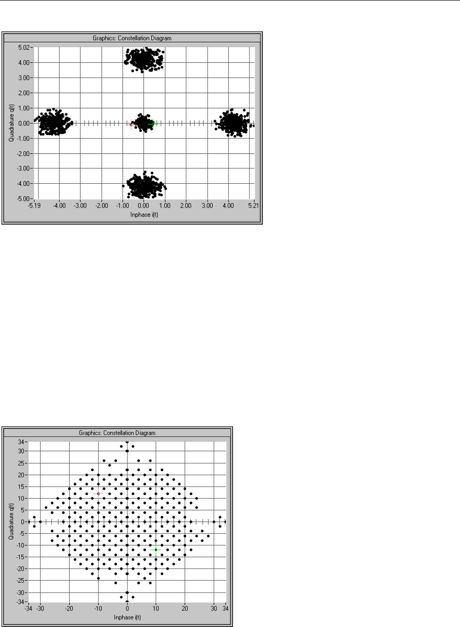
SMIQ Digital Standard 3GPP W-CDMA (FDD)
1125.5555.03 E-92.227
The following associated constellation diagram is obtained:
Fig. 2-151 Constellation of a signal with two DPCHs (uncorrelated data)
The new crest factor is 7.64 dB. Compared to section 2.14.3.1 the value has decreased since with
constant peak value the average value has increased.
2.14.3.3.3 16 DPCHs with Uncorrelated Data
If the data of all channels are uncorrelated, the constellation diagram is obtained similarly to
section 2.14.3.3 by multiple superposition of the basic constellation. Whether all possible points (channel
number+1)2 = 17*17 = 289 will be displayed depends on the data sequences and the sequence length.
Note: In contrast to the last constellation diagrams, the following diagrams were recorded with active
receiver filter (root cosine 0.22). This allows better differentiation of the individual points.
Setting of the receiver filter is described in section 5.17.
Example for 16 time slots:
Fig. 2-152 Constellation with 16 uncorrelated channels (16 time slots)
This signal has a crest factor of 15.35 dB. The crest factor increases with the number of channels since
the increase of the average value is slower than that of the peak value (cancelling effects).
Digital Standard 3GPP W-CDMA (FDD) SMIQ
1125.5555.03 E-92.228
The same diagram for a signal with one slot only is obtained:
Fig. 2-153 Constellation with 16 uncorrelated channels (1 time slot)
The crest factor has the value of 15.35 dB even if the CCDF has a different characteristic.
2.14.3.3.4 16 DPCHs with same Data
Similar to section 2.14.3.3.2 there are strong cancellation effects and only points remain on the axes.
The position of the points also depends on the choice of the channelization codes. The following
diagram is an example for 16 channels, channelization code 0 to 15:
Fig. 2-154 Constellation diagram of 16 DPCHs with same data
In this case the crest factor is 16.17 dB. The high value arises because about 94 % of the points lie at
the origin and only 6% of the points at the outer positions.
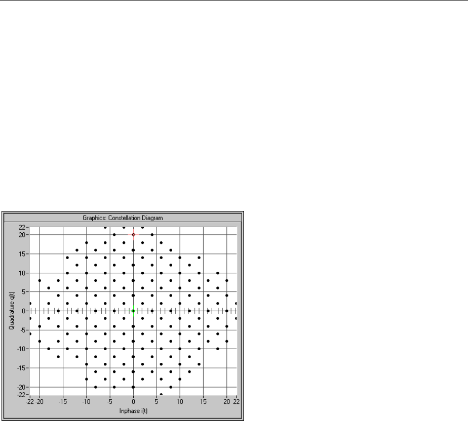
SMIQ Digital Standard 3GPP W-CDMA (FDD)
1125.5555.03 E-92.229
2.14.3.3.5 Use of Timing Offset
All previous scenarios did not use a timing offset. Therefore all channels contained the same bits at
least in the pilot symbol part. The result of this special feature was that the 4 corner points (0, 2*number
of channels), (0, -2*number of channels), (2*number of channels, 0), (-2*number of channels, 0) where
always there (constructive superposition).
Through the use of a timing offset (in our example 1 unit (=256 chips) from channel to channel) the data
bits (including pilot and TPC) are shifted against each other.
Note: In contrast to earlier versions of the W-CDMA standard or WinIQSIM, the timing offset
(previously "data offset") is no longer defined in symbols but in units of 256 chips. Thus shifting
becomes independent of the spreading factor.
The worst case is thus eliminated, the crest factor becomes smaller and the spread symbols are
arranged as follows:
Fig. 2-155 Constellation diagram of 16 DPCHs with timing offset
Through the use of the timing offset the crest factor was reduced by approx. 4 dB to 12.26 dB.
The effect of the timing offset increases with the number of channels. If for instance 64 channels are
used, the crest factor is reduced from 18.57 dB to 12.28 dB.

Digital Standard 3GPP W-CDMA (FDD) SMIQ
1125.5555.03 E-92.230
2.14.3.4 Effects on Crest Factor
The crest factor of the signal is mainly influenced by the following parameters:
• Link direction
By modifying the Q component of the scrambling code in the uplink, it is possible to avoid every
second zero crossing. In contrast to the downlink, the crest factor is reduced by approx. 1.8 dB.
(Standard case DPCCH + 1DPDCH, the effect decreases with increasing number of channels.)
• Timing offset (see 2.14.3.3.5)
In the case of more than 10 channels, an increment of 1 (i.e. the first channel is assigned 0, the
second 1, etc.) causes a low crest factor. With a small number of channels, an increment of 3 or 5
permits to obtain even better values.
• Sequence length if timing offset is active
Longer sequences cause higher peak values and hence higher crest factors since the probability of
even higher peak values increases.
• Number of channels
More channels cause higher crest factors.
• Selection of channelization codes
Neighbouring channelization codes usually cause higher crest factors than numbers distributed over
the full range of available values.
• Example: 16 channels with channelization codes 0 to 15: 16.7 dB
16 channels with channelization codes 0, 4, 8, to 60: 12,45 dB
• Value of clipping level (see section 2.14.2.10)
2.14.3.5 Orthogonality of Channels
To enable a 3GPP W-CDMA demodulator to restore the information of the individual channels from the
sum signal, only certain combinations of
• scrambling code sequences,
• channel power and
• symbol rate and channelization codes
are allowed.
2.14.3.5.1 Ideal Scenario
In an ideal scenario the measured channel power (with code domain power analyzers) is equal to the
transmitted power (setting value in the channel configuration table), Even with great differences between
the channel powers the information of the channels can be restored 100%. For this purpose however
orthogonality of the channels is required. Orthogonality is given in all cases described in section 2.14.3.3
Orthogonality is given for instance if DPCH channels are used only and all of them have the same
symbol rate but different channelization codes. In addition, identical scrambling code values have to be
set for all channels, i.e. all channels have to belong to a base station.
In this case the bit streams SCi and SCq' are identical for all channels. Since the channelization code
sequences of two channels are orthogonal, the chip sequences Si and Sq of two channels are also
orthogonal.
2.14.3.5.2 Real Scenario
A real scenario usually consist of signals from different base/mobile stations that are operated at
different scrambling codes and have different delays. In this case there is no orthogonality, the channel
powers overlap and the bit error rates increase with decreasing channel power (therefore power control
is extremely important for all CDMA systems).
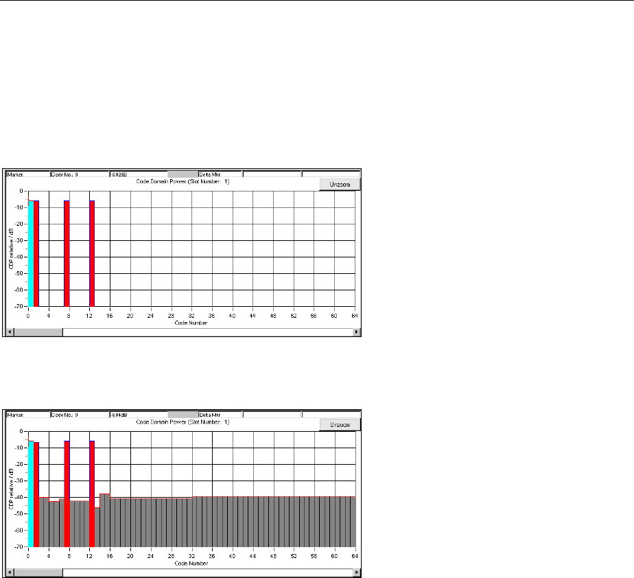
SMIQ Digital Standard 3GPP W-CDMA (FDD)
1125.5555.03 E-92.231
2.14.3.5.3 Effect of SCH
The SCH is not orthogonal to the DPCHs and all other downlink channels since the synchronization
code symbol is spread according to a special scheme (see section 2.14.1.1, System Components).
In the following example, the channels P-SCH, S-SCH, CPICH, P-CCPCH and two DPCHs (15 ksps to
code 7 and 12) are included. If the SCH is compensated with the code domain power analysis, the
channel powers can be determined ideally:
Fig. 2-156 CDPA of a signal with compensated SCH
If the SCH is not compensated, crosstalk to the other channels can be clearly seen:
Fig. 2-157 Effect of SCH on CDP analysis (without compensation)
The transmitted channels are measured with an error of <0.2 dB. For all other channels a power of
approx. -40 dB is determined.
These conditions still allow error-free decoding of all transmitted channels.
2.14.3.5.4 Effect of S-CCPCH and the Other Downlink Channels
Like a DPCH, S-CCPCH, P-CPICH, S-CPICH, PDSCH, PICH, AICH and DL-DPCCH are spread with
the same symbol rate. Therefore the same conditions as for DPCHs apply to the parameters of these
channels (see section 2.14.3.5.7).
2.14.3.5.5 Effect of PRACH and PCPCH
The PRACH and the PCPCH are not orthogonal to DPCCH and DPDCHs since the scrambling code is
formed differently. Mobile stations never use PRACH or PCPCH and DPCCH/DPDCH simultaneously –
therefore mixed operation is only possible in WinIQSIM if these channel types are distributed to different
stations (e.g. MS1 and MS2).
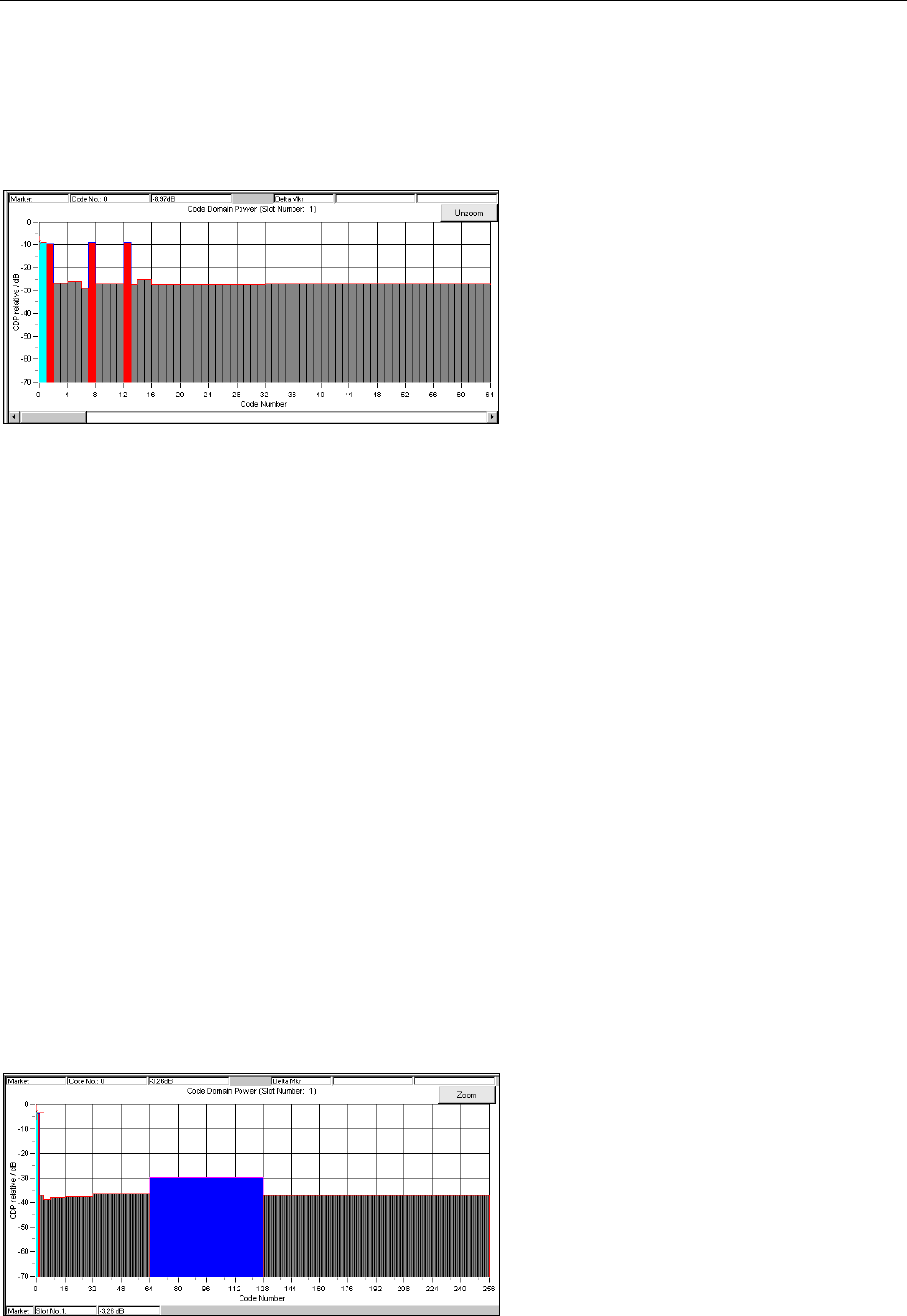
Digital Standard 3GPP W-CDMA (FDD) SMIQ
1125.5555.03 E-92.232
2.14.3.5.6 Effect of Scrambling Code
The scrambling code permits to distinguish between base stations (downlink) and mobile stations (uplink).
If different scrambling codes are used within a signal (in this example, the scenario under section 2.14.3.5.3 is
coded twice with different scrambling codes), the orthogonality between the channels will be lost.
The following example shows the level conditions measured after despreading:
Fig. 2-158 Effect of different scrambling codes on the power distribution
These conditions still allow error-free reconstruction of the bit streams. A certain guard interval should
however always be observed between the transmitted channel power and the measured power of the
other (non-orthogonal) channels.
In this example a channel power of -10 dB is sufficient for error-free decoding, whereas with a power of
-15 dB the bit error rate is about 10 % already. (The given values were evaluated at the physical layer
using a CDPA. Even under worse conditions error-free reconstruction of the bit stream can be made
through channel coding!)
2.14.3.5.7 Effect of Symbol Rates and Channelization Code Numbers
The channelization code generation method has the effect that with certain symbol rate/channelization
code combinations the identical spreading sequences Si/Sq are generated. This is always the case with
channelization code number 0 (all bits 0), but also with the combination 960 ksps/channelization code 1
(0011) <-> 480 ksps/channelization code 2 (00110011).
As a rule, the spreading sequences are identical if the products of symbol rate and
channelization code are identical.
The despreader can therefore no longer differentiate between the two channels. Depending on the data
contents, the channel powers are either added up or cancel each other. Restoring of all source data is
not possible.
The following signal contains
• a DPCH with 960 ksps, channelization code number 1, 0 dB, data all 0
• a DPCH with 480 ksps, channelization code number 2, 0 dB, data all 1
An analysis at 960 ksps gives the following result:
Fig. 2-159 Cancellation possible in case of several channels with identical spreading sequences
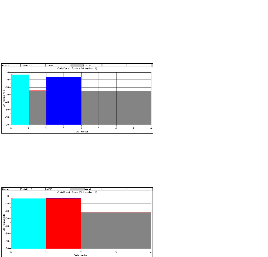
SMIQ Digital Standard 3GPP W-CDMA (FDD)
1125.5555.03 E-92.233
Apart from this trivial case there are other cases in which problems may occur.
The above example is modified by changing the channelization code of the second DPCH from 2 to 3:
• a DPCH with 960 ksps, channelization code 1, 0 dB, data all 0
• a DPCH with 480 ksps, channelization code 3, 0 dB, data all 1
After despreading at symbol rate 480 ksps, the following power distribution is obtained:
Fig. 2-160 Incorrect detection at various symbol rates
The 960-ksps channel (channelization code 1) is detected as channel 2 at 480 ksps. There is however
no crosstalk to channel 3. Therefore the 480-ksps channel is detected with the original power and all
bits can be restored.
Despreading of the 960-ksps channel however gives the following power distribution:
Fig. 2-161 Non-restorable DPCH channel
Both channels synchronize with channel 1, despreading is no longer possible with these level conditions.
For despreading all transmitted DPCHs, two channels of half the symbol rate (channelization codes 2n,
2n+1) should therefore be avoided for each channel used with a certain symbol rate (channelization
code n). This is continued for four channels of one fourth of the symbol rate (channelization codes 4n,
4n+1, 4n+2, 4n+3), etc.
For further information refer to section 2.14.2.9.

Digital Standard 3GPP W-CDMA (FDD) SMIQ
1125.5555.03 E-92.234
2.14.3.6 Simulation of Special Scenarios
It is shown in the following how special scenarios can be simulated by means of WinIQSIM parameters.
The downlink is used as an example, since a mobile station can always be completely implemented in
an MS. Scenario for the simulation of several base stations 2.14.3.6.4 can also be applied to the
simulation of mobile station signals.
Note: Section 2.14.2.2 describes a particularly simple method for setting a base station.
2.14.3.6.1 Standard Base Station
A standard base station is the easiest example of a base station.
• Activate the channels P-CPICH, P-SCH, S-SCH and P-CCPCH (State = ON). These channels are
absolutely necessary for the synchronization of a mobile station with the signal.
• Activate between 0 and 128 DPCHs.
• Select channelization codes and symbol rates so that no code domain conflicts occur.
• Use timing offset in channels to model the offsets TDPCH, TPICH, TS-CCPCH ( [1], section 7) as specified
in the 3GPP W-CDMA standard.
• Set a valid combination of scrambling code and 2nd Search Code Group. (For details refer to [2] 5.2.2)
In [3], Appendix D, a few test models are specified that have been designed for certain tests. These
scenarios are supplied as WinIQSIM setups.
They can be found in the 3GPP W-CDMA - TEST MODELS menu.
2.14.3.6.2 Base Station with More Than 128 DPCHs
To avoid the channel table becoming ambiguous, a BS in WinIQSIM may contain a maximum of 128
DPCHs. If a base station is to be simulated with more than 128 DPCHs, these channels have to be
distributed to several BS.
• Make the same settings as in section 2.14.3.6.1 for the first BS.
• Assign the remaining DPCHs to the other BSs.
• Select the channelization codes and symbol rates so that no code domain conflicts occur, even
beyond the limits of a BS.
Note: The SMIQ does not support code domain power (conflict) display beyond the limits of a
MS/BS. If several stations are available it is useful to divide the available range in
subranges (e.g. BS1 : 0 to 256, BS2 : 257 to 467, BS3: 468 to 511).
• Set the same value and type for the scrambling code for all BSs.
Note: The function “Copy BS/MS“, as described in section 2.14.3.6.1 facilitates the transfer of
these values from one BS to another.

SMIQ Digital Standard 3GPP W-CDMA (FDD)
1125.5555.03 E-92.235
2.14.3.6.3 Base Stations with Spreading Codes Used Several Times
3GPP W-CDMA envisages an increase in the number of channels using primary and secondary
scrambling codes. The PCCPCH and the first part of DPCHs is then sent with the primary scrambling
code, the remaining DPCHs with one of the assigned secondary scrambling codes. The following range
of values is given in [2]:
Primary scrambling code : n = 16 * i with i=0 to 511
Secondary scrambling code : n = 16 * i + k with i=0 to 511 and k=1 to 15
Note: The use of secondary scrambling codes principally yields the same results as the
parameter Toffset specified in former standards.
When the secondary scrambling codes are used, orthogonality is impaired and a crosstalk is produced
(see section 2.14.3.5.6).
This scrambling code can be entered for a BS. If channels with different scrambling codes are to be
simulated, a division into several BSs is required as described under 2.14.3.6.2:
• Set several BSs according to 2.14.3.6.1. The special channels (SCH, CPICH, ...) will be activated in
one BS only.
• Set the desired values for the scrambling code for all BSs.
2.14.3.6.4 Several Base Stations
3GPP W-CDMA base stations can be at different RF frequencies. This case can be simulated in
WinIQSIM using the multicarrier mixed signal system and option SMIQB60.
Since there are normally not enough frequencies available, the base stations within a transmit frequency
are distinguished by the primary scrambling code.
• Set several BSs according to 2.14.3.6.1.
• Set the desired values for the scrambling code for all BSs.
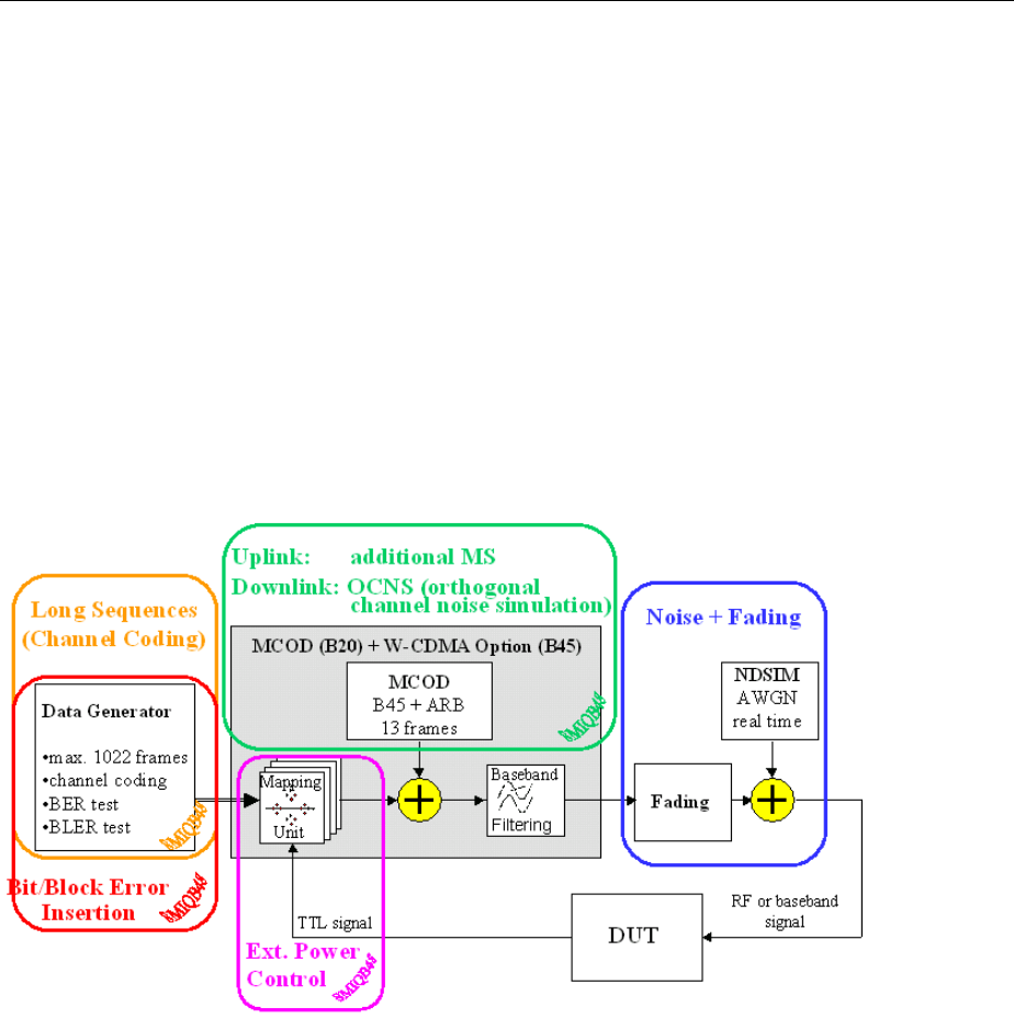
Enhanced Functions For Digital Standard 3GPP W-CDMA (FDD) SMIQ
1125.5555.03 2.236 E-9
2.15 Enhanced Functions For Digital Standard 3GPP W-CDMA (FDD)
Option SMIQB48 expands the scope of functions of option SMIQB45 and offers the following features:
• Sequences with a length of up to 2044 frames (SMIQB45: 13 frames)
• Data lists for data fields and TPC
• External control of channel power in real time
• Channel coding
• Insertion of bit errors (for testing a BER tester)
• Insertion of block errors (for testing a BLER tester
• Simulation of orthogonal channel noise (OCNS)
• Simulation of up to 64 additional mobile stations
• Simulation of a channel-coded P-CCPCH (BCP) with system frame number
2.15.1 Test Setup
Fig. 2-163 Complete setup for testing a W-CDMA receiver with the SMIQ
This block shows the different functional blocks of the SMIQ with built-in option SMIQB48.
Blocks "Long Sequences/Channel Coding", "Bit/Block Error Insertion", "OCNS" and "External Power
Control" are part of option SMIQB48 and will be described in detail.
"Noise" is available only if option SMIQB17 is built-in. For a description see section " Noise Generator
and Distortion Simulator".
To simulate "Fading", option SMIQB14/SMIQB15 or SMIQB49 is required. This option is described in
the section on "Fading Simulation".
References:
[1] 3GPP TS25.101 V4.1.0 UE Radio transmission and reception (FDD)
[2] 3GPP TS25.212 V4.1.0 Multiplexing and channel coding (FDD)
[3] 3GPP TS25.104 V4.1.0 BS Radio transmission and reception (FDD)
[4] 3GPP TS25.141 V4.1.0 Base Stations Conformance Testing (FDD)
[5] 3GPP TS25.944 V4.1.0 Channel Coding and multiplexing examples
[6] 3GPP TS25.331 V4.1.0 RRC Protocol Specification
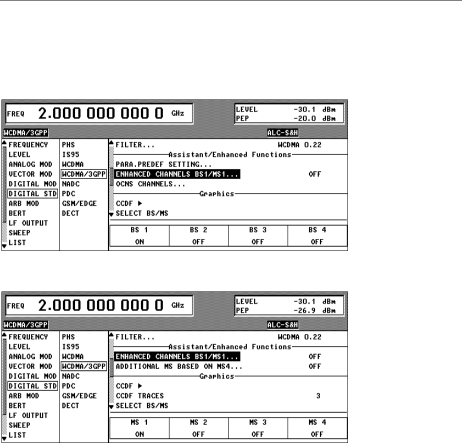
SMIQ Enhanced Functions For Digital Standard 3GPP W-CDMA (FDD)
1125.5555.03 E-92.237
2.15.2 Branching to Menus SMIQB48 of Digital Standard 3GPP WCDMA
The enhanced functions of option SMIQB48 are directly accessible from the menu of option SMIQB45, i.e.
the digital standard WCDMA/3GPP must be selected. This section only describes the parameters and
functions that are directly available with option SMIQB48 installed and which have not been described in
the sections "Digital Standard 3GPP W-CDMA" and "Generation of 3GPP W-CDMA Signals".
Fig. 2-164 Menu DIGITAL STD – WCDMA/3GPP – Section Assistant/Enhanced Functions (downlink)
Fig. 2-165 Menu DIGITAL STD – WCDMA/3GPP – Section Assistant/Enhanced Functions (uplink)
----------------------Assistant/Enhanced Functions------------------------------------------------------------
ENHANCED
CHANNELS BS1/MS1
Call-up of user menu for configuring the enhanced channels. The menu item
is only available with option SMIQB48 installed. For more detailed information
regarding this menu see section 2.15.3
OCNS CHANNELS Simulation of orthogonal channel noise. The menu item is only available in the
downlink with option SMIQB48 installed. For more detailed information
regarding this menu see section 2.15.4.
ADDITIONAL MS
BASED ON MS4
Simulation of up to 50 additional mobile stations. The menu item is only
available in the uplink and with option SMIQB48 installed. For more detailed
information regarding this menu see section 2.15.5.

Enhanced Functions For Digital Standard 3GPP W-CDMA (FDD) SMIQ
1125.5555.03 2.238 E-9
2.15.3 Enhanced Channels BS1/MS1
Enhanced Channels are channels which – in contrast to option SMIQB45 – are neither calculated nor
generated on the modulation coder but on the data generator. Up to four enhanced channels (or seven
with uplink mode) are possible where the maximum sequence length is calculated from the free list
memory and the number of channels:
Downlink:
384002**Channels_Enhanced_Of_Number
Bits/Memory_List_Data_Available
Frames/Length_Sequence =
With maximum memory capacity, there are thus between 255 (4 DPCH) and 1022 (1 DPCH) frames.
In the downlink (possibly depending on memory capacity), a P-CCPCH/BCH with a continuous system
frame number (period 4096 frames) can also be generated at the same time as a DPCH (period 2044
frames) with a max physical rate of 30 ksps.
The simulation of higher rate channels (>30 ksps) together with the P-CCPCH/BCH is also supported
however with a reduced maximum sequence length of 500 frames.
(For a systematic list of all possible sequence lengths see description of SEQUENCE LENGTH
parameter, section Fehler! Verweisquelle konnte nicht gefunden werden.).
Note: This sequence length is sufficient for all performance tests in [1], section 8, since in these
tests the block error rate is measured.
Uplink:
384001 *)Channels_Enhanced_Of_Number(
Bits/Memory_List_Data_Available
Frames/Length_Sequence +
=
With maximum memory capacity, there are thus between 255 (DPCCH + 6 DPDCH) and 1022 (1 DPCCH
or 1 DPDCH) frames.
Note: The higher number of channels in the uplink is possible through the BPSK data modulation.
These long sequences allow a physical BER measurement (PN9) without a restart of the BER tester
being required. An enhanced channel with a length of 511 frames is to be set.
If the maximum length of 1022 frames is used, BER measurements with channel coding and without
restart as required for receiver tests to [1], [3], [4] are possible.
Compared to the clearly enhanced sequence length range (max. 13 frames for SMIQB45), option
SMIQB48 offers the following advantages:
After generation of the sequence in the data generator Data lists are available as data sources for the
data fields and the TPC fields. Externally precoded data can be loaded into the SMIQ by the user, for
example to implement channel-coding schemes that are not supported by option SMIQB48.
Analogously, the long TPC lists are necessary to generate long non-repetitive power profiles.
Moreover, a base station can be simulated, which comprises a channel-coded P-CCPCH (BCH) and a
12.2 kbps reference measurement channel in addition to background and synchronization channels.
The system frame number (SFN) in BCH is automatically incremented in steps of two from 0 to 4094
(period 4096). The remaining system information of BCH can be filled from data lists, for example.
Another feature of enhanced channels is the possibility to generate the reference measurement
channels described in [1], [3] and [4] and the AMR channels described in [5]. For a description see
2.15.3.1.1.
The chip sequences of the enhanced channels are transmitted in binary form to the modulation coder
and are converted into (initially digital) I/Q levels in a mapper. This mapping can be switched by an
external input line (TTL, connected to LEVATT (PARDATA pin 9 or SMIQ-Z5)). The channel powers of
the enhanced channels can be controlled in real time, allowing the test of "SIR based closed loop
power control", for example. For further information see 2.15.3.1.3.

SMIQ Enhanced Functions For Digital Standard 3GPP W-CDMA (FDD)
1125.5555.03 E-92.239
For testing BER/BLER testers (e.g. integrated into base station), artificial bit errors (or block errors
into the CRC checksum) can be integrated in all data sources. The required parameters can be
found in section 2.15.3.1.5
The menu structure depends on the link direction. Since there are only slight differences, first the
downlink and all common parameters are described in section 2.15.3.2 and then all uplink parameters.
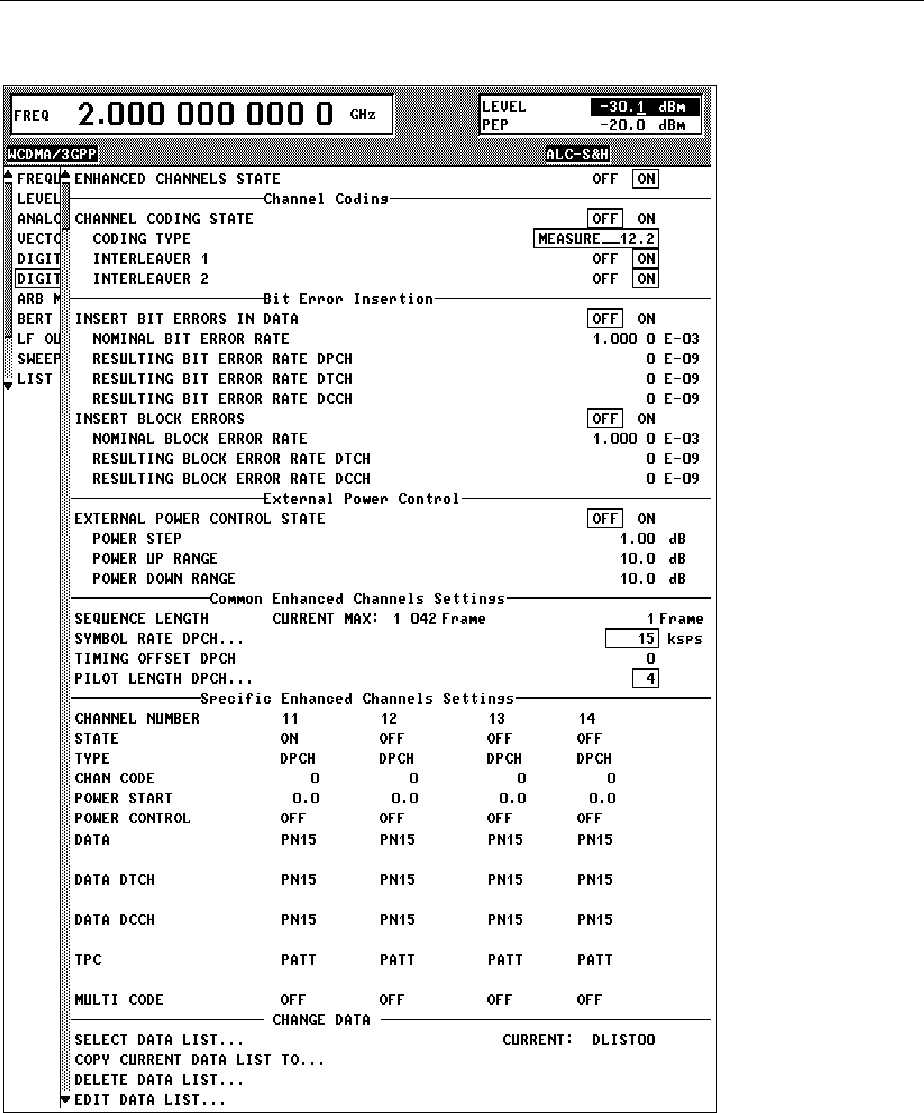
Enhanced Functions For Digital Standard 3GPP W-CDMA (FDD) SMIQ
1125.5555.03 2.240 E-9
2.15.3.1 Downlink
Fig. 2-166 Menu DIGITAL STD-WCDMA/3GPP-ENHANCED CHANNEL (downlink)
ENHANCED
CHANNELS STATE
Switch for activating or deactivating the calculation of up to 4 enhanced
channels on DGEN.
In the OFF state, all the following menu parameters no longer influence the
3GPP W-CDMA signal which is only calculated in MCOD ARB.
IEC/IEEE-bus command :SOUR:W3GP:BST:ENH:STAT ON
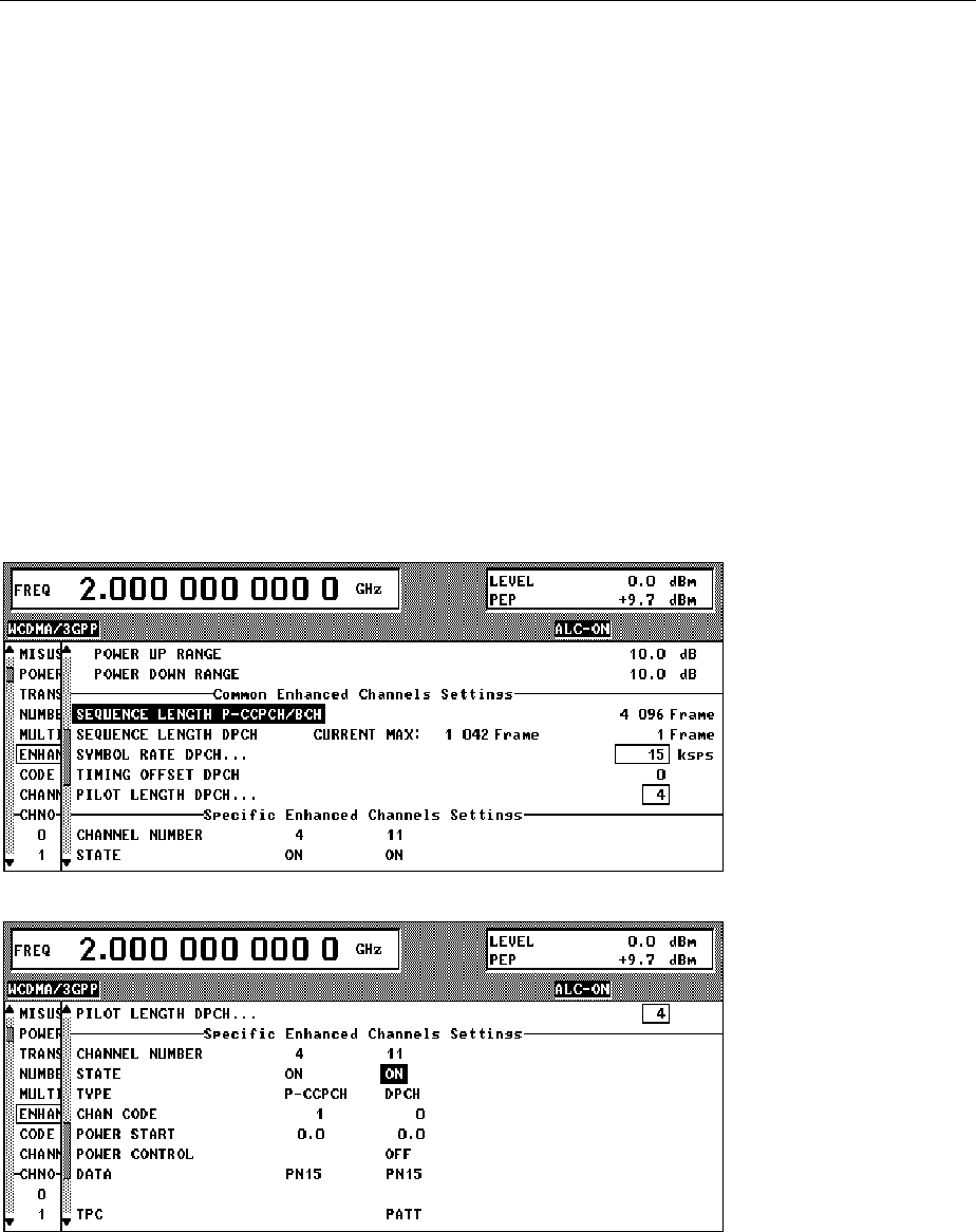
SMIQ Enhanced Functions For Digital Standard 3GPP W-CDMA (FDD)
1125.5555.03 E-92.241
2.15.3.1.1 P-CCPCH/BCH with System Frame Number
In addition to channel-coded reference measurement channels, test specifications for mobile or UE
tests (see [1]) often stipulate a channel-coded P-CCPCH (BCH). With the Enhanced P-CCHCP/BCH
State activated, the SMIQ can generate this test scenario.
The SMIQ then offers one P-CCPCH and one DPCH instead of the 4 enhanced DPCHs in the Standard
Enhanced mode (Enhanced P-CCHCP/BCH State Off).
ENHANCED P-
CCPCH/BCH (INCL.
SFN) STATE
This switch enables one P-CCPCH/BCH and one DPCH to be generated as
enhanced channels (OFF) instead of the 4 DPCHs.
IEC/IEEE-bus command :SOUR:W3GP:BST:ENH:PCCP:STAT ON
With Enhanced P-CCHCP/BCH State On, this may affect the structure of the other operating menus:
• The channel table under Specific Enhanced Channel Settings contains the P-CCPCH and a
DPCH.
• If the P-CCPCH is activated under Specific Enhanced Channel Settings, it will automatically be
generated with the sequence length 4096 frames (SFN period).
• The maximum sequence length (SEQUENCE LENGTH DPCH) changes:
- for symbol rates ≤ 30 ksps: 2044 frames
- for symbol rates >30 ksps: 500 frames
Fig. 2-167 Common Enhanced Channel Settings with Enhanced P-CCHCP/BCH State On
Fig. 2-168 Specific Enhanced Channel Settings with Enhanced P-CCHCP/BCH State On
Enhanced Functions For Digital Standard 3GPP W-CDMA (FDD) SMIQ
1125.5555.03 2.242 E-9
Generation principle of channel-coded P-CCPCH with system frame number
With Enhanced P-CCHCP/BCH State On, channel coding activated (Channel Coding State On) and with
P-CCPCH State under Specific Enhanced Channel Settings On, the SMIQ generates a channel-coded
P-CCPCH (i.e. a broadcast channel BCH) according to the following principle:
BCH Channel Coding
SFN
(11 bit) Sys Info
(235 bit) . . .
BCH Transport Block 0 (20 ms) BCH Transport Block 2047 (20 ms)
Counting SFN User selectable data (e.g. data list)
Coded BCH Transport Block 0 Coded BCH Transport Block 2047
P-CCPCH Frame 0 P-CCPCH Frame 1 P-CCPCH Frame 4094 P-CCPCH Frame 4095
P-CCPCH Slot 0 P-CCPCH Slot 1 P-CCPCH Slot 14
. . .
. . .
. . .
SFN
(11 bit) Sys Info
(235 bit)
Fig. 2-169 Generation principle P-CCPCH/BCH
The data blocks of BCH at transport-channel level comprise data determined for 20 ms of the P-CCPCH
(i.e. 2 frames) after channel coding. The first field of such a data block is an 11-bit long field for the
system frame number (SFN). The SFN is automatically incremented by 1 (as stipulated in the standard)
from transport block to transport block (equivalent to a step width of 2 frames due to the transport time
interval length of 20 ms). After 2048 transport blocks (equivalent to 4096 frames) SFN is reset and
starts again at 0 (SFN restart). An output trigger indicating the SFN restart can be generated (see
2.14.2.1).
The SFN format is defined in [6], sections 10.2.48, 11.2 (page 578) and 11.3 (page 691). It is MSB-first
coded.
The remaining system information (a 235-bit long field per block) is filled from the data source selected
for the P-CCPCH under Specific Enhanced Channel Settings.
A data list can be used to transmit further specific system information in addition to the SFN. If only the
SFN is required, ALL 0 is recommended as data source for P-CCPCH.
The BCH transport blocks are then channel-coded. A coded transport block comprises the data
sequence for two P-CCPCH frames.

SMIQ Enhanced Functions For Digital Standard 3GPP W-CDMA (FDD)
1125.5555.03 E-92.243
2.15.3.1.2 Channel Coding
Many tests can be found in [1] and [3] all of which require channel-coded measurement channels, so-
called Reference Measurement Channels. Types 12.2 kbps, 64 kbps, 144 kbps and 384 kbps are
indicated for each link direction.
In addition, the SMIQ can simulate an AMR voice channel according to [5]. The detailed structure of
these channels is described in the following documents:
Table 2-27 References to measurement channels
CODING TYPE Reference downlink Reference uplink
MEASURE__12.2 [1], A.3.1 [3], A.2 and [4], A.2
MEASURE__64 [1], A.3.2 [3], A.3 and [4], A.3
MEASURE_144 [1], A.3.3 [3], A.4 and [4], A.4
MEASURE_384 [1], A.3.5 [3], A.5 and [4], A.5
AMR_CODER [5], 4.1.1.3.1.2 [5], 4.1.2.2.1.2
To simplify the implementation of channel decoding in the test receiver the two interleaver stages in the
measurement channels can separately be switched on and off.
----------------------Channel Coding-----------------------------------------------------------------------------
CHANNEL CODING
STATE Switch for activating or deactivating the channel coding of all enhanced
channels.
In the OFF state, the following menu parameters are not effective:
CODING TYPE,
INTERLEAVER 1,
INTERLEAVER 2,
CODING (enhanced channel specific).
IEC/IEEE-bus command :SOUR:W3GP:BST:ENH:CCOD ON
CODING TYPE Setting the channel coding type of all enhanced channels.
The 3GPP specification currently stipulates 4 predefined MEASUREMENT
channel coding types which differ in the input data bit rate to be processed
(12.2, 64, 144 and 384 KBPS). The additional AMR_CODER coding scheme
generates the coding of a speech channel.
For channel coding, the input data bits are taken from the data source
specified in menu parameter DATA. The bits with a higher data rate are
available at the output of channel coding. There are fixed assignments
between the measurement input data bit rate and the output symbol rate, i.e.
the menu parameters SYMBOL RATE DPCH (Downlink) or OVERALL
SYMBOL RATE are adapted automatically.
MEASURE_12.2 Measurement channel 12.2 kbps
MEASURE_64 Measurement channel 64 kbps
MEASURE_144 Measurement channel 144 kbps
MEASURE_384 Measurement channel 384 kbps
AMR_CODER Channel coding for AMR Coder
IEC/IEEE-bus command :SOUR:W3GP:BST:ENH:CCOD:TYP M12K
INTERLEAVER 1,2 Switch for separately activating or deactivating channel coding interleaver stages 1
and 2 of all enhanced channels. (The interleaver stages do not change the symbol
rate.)
IEC/IEEE-bus command :SOUR:W3GP:BST:ENH:CCOD:INT1 ON

Enhanced Functions For Digital Standard 3GPP W-CDMA (FDD) SMIQ
1125.5555.03 2.244 E-9
2.15.3.1.3 Bit Error Insertion
Errors can be inserted in the data source or the CRC checksum for testing the bit/block error rate tester.
If channel coding is inactive (CHANNEL CODING STATE = OFF), the data bits are fed into the slots at the
physical level. If channel coding is active (CHANNEL CODING STATE = ON), the data bits are fed at the
transport layer level. The bit errors are always generated at the data source level.
INSERT BIT ERRORS
IN DATA
Switch used to activate or deactivate the insertion of bit errors in the data fields
of all active enhanced channels at the frequency indicated under the NOMINAL
BIT ERROR RATE parameter.
In the OFF state, the following menu parameters NOMINAL BIT ERROR
RATE and RESULTING BIT ERROR RATE are not effective.
IEC/IEEE-bus :SOUR:W3GP:BST:ENH:DERR:BIT:STAT ON
NOMINAL BIT
ERROR RATE
Sets a user-defined bit error rate in the range of 10-
1
to 10-
7
with which the bits
can be inserted into the data fields of the enhanced channel timeslots. Upon
readout of the data source individual bits are inverted at random at a given
error rate to simulate an erroneous signal.
Since the bit error rate set by the user may not be adhered to as a function of
the frame SEQUENCE LENGTH and the selected SYMBOL RATE DPCH or
OVERALL SYMBOL RATE, the actual bit error rate is displayed in the next
line, i.e. RESULTING BIT ERROR RATE.
IEC/IEEE-bus :SOUR:W3GP:BST:ENH:DERR:BIT:RATE 2E-3
RESULTING BIT
ERROR RATE
Parameter indicating the resulting bit error rate used to insert the bits into the
data fields of the enhanced channel timeslots (see NOMINAL BIT ERROR
RATE parameter).
CHANNEL CODING STATE = OFF:
The BER of DPCH is displayed here.
IEC/IEEE-bus :SOUR:W3GP:BST:ENH:DERR:BIT:DPCH?
CHANNEL CODING STATE = ON:
The BER of DTCH and DCCH is displayed here.
IEC/IEEE-bus :SOUR:W3GP:BST:ENH:DERR:BIT:DTCH?
IEC/IEEE-bus :SOUR:W3GP:BST:ENH:DERR:BIT:DCCH?
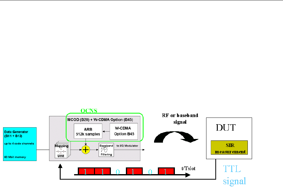
SMIQ Enhanced Functions For Digital Standard 3GPP W-CDMA (FDD)
1125.5555.03 E-92.245
2.15.3.1.4 External Power Control
Two test constellations have to be distinguished in the test of Closed (Inner) Loop Power Control:
1. Test whether the DUT responds with the correct output power to received TPC bits (e.g. for testing
according to [1], 6.4.2.1). This can be carried out by using a data list adapted to the test condition as TPC
data source. The TPC pattern can be defined in the channel table (see previous section, “Menu
WCDMA/3GPP - Submenu BS Configuration“ or “Menu WCDMA/3GPP - Submenu MS Configuration“,
and also section 2.15.3.1.5).
2. Test whether the DUT correctly performs the SIR (Signal to Interference Ratio) measurement and
inserts the corresponding bits into the TPC field of its transmit signal. Since the SMIQ has no
receive channel, the TPC control information has to be taken to the generator via another channel.
This is possible via "External Power Control".
Fig. 2-170 Setup for testing Closed Loop Power Control
The power of all activated enhanced channels can be increased or decreased in a predefined dynamic
range (= POWER UP RANGE + POWER DOWN RANGE) and in the defined step width (= POWER
STEP) with the TTL signal “External Power Control“.
The power change of the channels is performed by a switchover of the mapping table, controlled by the
external power control signal which is queried at the beginning of the pilot field. Since the number of
mappings is limited, the maximum dynamic range is restricted to 30 dB and the step width to min. 0.25 dB.
The output power of each channel is thus limited to the
[POWER_START-POWER_DOWN_RANGE...POWER_START+POWER_UP_RANGE] range.
Note : To obtain optimum signal quality, the POWER_UP_RANGE should not be set higher than
necessary since the mapping of the I/Q level in this range must be maintained as a level
margin.
POWER_START and POWER_CONTROL = UP/DOWN can be set channel-specifically (see section
2.15.3.1.5).
In the following example it is assumed that
• POWER_UP_RANGE = POWER_DOWN_RANGE
• POWER_CONTROL = UP for channels 0, 2 and 3, POWER_CONTROL = DOWN for channel 1
Available mappings are shown at the right with MAPM being the starting point. In this point, all channels
have the power which was set in the menu as POWER_START.
At the beginning of the pilot field the LEVATT line is queried in each timeslot. If this line is set to logical
"0" switchover is made to the left mapping MAPM-1. This means a reduction of the output power by
POWER_STEP for all channels with POWER_CONTROL = UP . The power of channel 1 is increased
by the same value.
If the LEVATT line is set to logical "0" switchover is made to the right mapping MAPM+1. This means an
increase of the output power by POWER_STEP for all channels with POWER_CONTROL = UP. The
power of channel 1 is decreased by the same value.
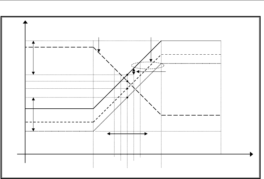
Enhanced Functions For Digital Standard 3GPP W-CDMA (FDD) SMIQ
1125.5555.03 2.246 E-9
Fig. 2-171 Change of channel power of 4 enhanced channels
----------------------External Power Control-----------------------------------------------------------------------------
EXTERNAL POWER
CONTROL STATE
Switch for activating or deactivating the external power control mechanism of
all enhanced channels.
In the OFF state, the following menu parameters are not effective:
POWER UP RANGE,
POWER DOWN RANGE,
POWER STEP,
POWER CONTROL GRAPH ?,
POWER START DPCCH,
POWER START DPDCH,
POWER START (enhanced channel-specific).
POWER CONTROL (enhanced channel-specific).
IEC/IEEE-bus command :SOUR:W3GP:BST:ENH:EPOW:STAT ON
POWER STEP Step width (0.25 to 6.0 dB) by which – with the external power control
mechanism being switched on - the channel powers of the activated enhanced
channels in the timeslot grid are increased or decreased within the set
dynamic range.
IEC/IEEE-bus command :SOUR:W3GP:BST:ENH:EPOW:STEP 1.0
POWER
[dB]
POWMA
POWMIN
POWER
START
CH0
CH1
CH2
CH3
POWER STEP
Mapping
Table
External
Power
Control
Signal
{0;1}
POWER
DOWN
RANGE
POWER
UP
RANGE
MAP0,DOWN MAPM
MAPM+1
MAPM-1
MAPM+2
MAPM-2
MAPX,U
Down Up
POWER CONTROL = UPPOWER CONTROL = DOWN

SMIQ Enhanced Functions For Digital Standard 3GPP W-CDMA (FDD)
1125.5555.03 E-92.247
POWER UP RANGE Dynamic range (0 to 30 dB) by which – with external power control mechanism
switched on – the channel powers of all activated enhanced channels can be
increased. The value POWER UP RANGE can be changed by POWER STEP.
If the dynamic range is exceeded, the warning MAX. POWER UP REACHED is
displayed.
The resulting external power control dynamic range (= POWER UP RANGE –
POWER DOWN RANGE) may be 30 dB at max. which is why the POWER UP
RANGE is limited as a function of the POWER DOWN RANGE.
IEC/IEEE-bus command :SOUR:W3GP:BST:ENH:EPOW:RANG:UP 10.0
POWER DOWN
RANGE Dynamic range (0 to 30 dB) by which – with external power control mechanism
switched on – the channel powers of all activated enhanced channels can be
decreased. The value POWER UP RANGE can be changed by POWER STEP.
If the dynamic range is underranged, the warning MAX. POWER UP REACHED
is displayed.
The resulting external power control dynamic range (= POWER UP RANGE –
POWER DOWN RANGE) may be 30 dB at max. which is why the POWER
DOWN RANGE is limited as a function of the POWER UP RANGE.
IEC/IEEE-bus command :SOUR:W3GP:BST:ENH:EPOW:RANG:DOWN 10.0
POWER CONTROL
GRAPH ►
With this menu parameter selected, the display window is opened again and -
with external power control mechanism switched on - the "current" deviation of
the channel power from the set power start value of the corresponding
enhanced channels is displayed graphically(see section 2.15.3.3).
The display window is only shown if the EXTERNAL POWER CONTROL
switch is set to ON and if the specific POWER CONTROL switch is positioned
to UP or DOWN in the downlink for at least one enhanced channel.
Note : This window is opened automatically after calculation of the signals
triggered by STATE = ON or MOD ON but can be closed again
manually by the user. This menu parameter allows the insertion of
the window again without recalculating the signal.
Note: With Enhanced P-CCPCH/BCH State On in the downlink, only the DPCH is power-
controlled. The P-CCPCH always has the power set in the enhanced channel table.

Enhanced Functions For Digital Standard 3GPP W-CDMA (FDD) SMIQ
1125.5555.03 2.248 E-9
2.15.3.1.5 Further Setting of Enhanced Channels Menu
----------------------Common Enhanced Channels Settings-----------------------------------------------------
SEQUENCE LENGTH
P-CCPCH/BCH
With Enhanced P-CCPCH/BCH State On in the downlink, the sequence length
of the P-CCPCH/BCH is displayed. The length is always 4096 frames and
cannot be edited.
IEC/IEEE-bus command (query) :SOUR:W3GP:BST:ENH:PCCP:SLEN?
SEQUENCE LENGTH Sets the sequence length in radio frames used to calculate the 3 GPP W-
CDMA enhanced channel signal component on DGEN.
Depending on the currently available free DGEN list memory, the currently
available maximum frame sequence length is displayed in the middle of the
menu parameter line.
Note : After triggering a new calculation, the 3GPP W-CDMA signal
component calculated on DGEN is stored in a hidden data list. The
maximum number of radio frames depends on the currently
available free DGEN list memory for the hidden data list max. 80
Mbit).
In addition to the free DGEN list memory the maximum sequence length
crucially depends on the ENHANCED P-CCPCH/BCH state and the number of
DPCHs:
ENHANCED P-CCPCH/BCH STATE = OFF
1 DPCH: 1022 frames
2 DPCHs: 511 frames
3 DPCHs: 341 frames
4 DPCHs: 255 frames
ENCHANCED P-CCPCH/BCH STATE = ON
SYMBOL RATE DPCH ≤30 ksps: 2044 frames
SYMBOL RATE DPCH >30 ksps: 500 frames
IEC/IEEE-bus command :SOUR:W3GP:BST:ENH:SLEN 123
SYMBOL RATE DPCH Sets symbol rate of all downlink enhanced channels in ksps.
If the CHANNEL CODING STATE switch is set to ON, there is a close relation
between the settings CODING TYPE and SYMBOL RATE DPCH:
MEASURE_12.2KBPS : SYMBOL RATE DPCH = 30 ksps
MEASURE_64KBPS : SYMBOL RATE DPCH = 120 ksps
MEASURE_144KBPS : SYMBOL RATE DPCH = 240 ksps
MEASURE_384KBPS : SYMBOL RATE DPCH = 480 ksps
AMR_CODEC : SYMBOL RATE DPCH = 30 ksps;
When a parameter is changed (CODING TYPE or SYMBOL RATE DPCH) the
associated parameter is adapted automatically.
In the higher BS1 menu the SYMBOL RATE settings of all activated enhanced
channels are automatically updated in the channel table.
IEC/IEEE-bus command :SOUR:W3GP:BST:ENH:SRAT D30K

SMIQ Enhanced Functions For Digital Standard 3GPP W-CDMA (FDD)
1125.5555.03 E-92.249
TIMING OFFSET Sets a time offset (0 to 149) with which the corresponding downlink enhanced
channels are sent. (The resulting crest factor of the overall signal can be
influenced).
The timing offset can be set in an interval of 256 chips.
IEC/IEEE-bus command :SOUR:W3GP:BST:ENH:TOFF 1
PILOT LENGTH Sets the pilot field size in the timeslots of the corresponding downlink
enhanced channels (2, 4, 8 or 16 depending on the symbol rate).
IEC/IEEE-bus command :SOUR:W3GP:BST:ENH:PLEN BIT4

Enhanced Functions For Digital Standard 3GPP W-CDMA (FDD) SMIQ
1125.5555.03 2.250 E-9
----------------------Specific Enhanced Channel Settings--------------------------------------------------
CHANNEL NUMBER Display parameter for the assigned serial number of a downlink enhanced
DPCH or an uplink enhanced DPDCH from the BS1 or MS1 channel table.
The enhanced channels are assigned to the first 4 dedicated channels in the
BS1 channel table or to the DPCCH/DPDCH of the MS1 channel table.
With Enhanced P-CCPCH/BCH State On in the downlink, also the P-CCPCH
with channel number 4 is available.
STATE Switch for activating or deactivating the corresponding downlink enhanced
channel. In the ON state the channel is marked as enhanced channel by an
additional E (in addition to CH. NO) in the channel table line determined by the
CHANNEL NUMBER in the higher BS1 menu – under the precondition that the
ENHANCED CHANNELS STATE switch is set to ON.
In the OFF state, the following channel-specific menu parameters are not
effective:
CHAN CODE
POWER START
POWER CONTROL
DATA
TPC
MULTI CODE
In the higher BS1 menu, the STATE parameter has to be updated in the
channel table line determined by the ENHANCED CHANNEL NUMBER.
Note: The enhanced channels cannot be activated individually in the
uplink; the required enhanced channels are automatically activated
via the OVERALL SYMBOL RATE setting.
IEC/IEEE-bus command :SOUR:W3GP:BST:ENH:CHAN11:STAT ON
TYPE Display parameter for the channel type of the corresponding enhanced
channel.
The type is taken from the TYPE parameter of the channel table line or
column determined by the ENHANCED CHANNEL NUMBER with the channel
table belonging to the higher BS1/MS1 menu.
In the downlink, enhanced channels have the DPCH type and in the uplink, the
DPCCH type (1st enhanced channel) or DPDCH (2nd to 4th enhanced
channel).
With Enhanced P-CCPCH/BCH State On in the downlink, channel type
P-CCPCH is additionally available in the table.

SMIQ Enhanced Functions For Digital Standard 3GPP W-CDMA (FDD)
1125.5555.03 E-92.251
CHAN CODE Sets the corresponding enhanced channel.
Downlink:
The channelization codes of the downlink enhanced channels are variable from
0 to -1 (3.840 MCPS/enhanced channel symbol rate). In the higher BS1 menu,
the CH. CODE parameter is updated in the channel-table line determined by the
ENHANCED CHANNEL NUMBER.
With Enhanced P-CCPCH/BCH State On in the downlink, the P-CCPCH
automatically has the data rate of 15 ksps and the channelization code 1
stipulated in the standard.
Uplink:
The channelization codes of the uplink enhanced channels are constant and
described in [2].
IEC/IEEE-bus command :SOUR:W3GP:BST:ENH:CHAN11:CHNC 0
POWER START Sets the channel (start) power of the corresponding downlink enhanced
channel. If the EXTERNAL POWER CONTROL STATE switch is set to ON
and the channel-specific POWER CONTROL switch to UP or DOWN, this
value is the channel start power for the external power control mechanism.
In the higher BS1 menu, the POWER DB parameter has to be updated in the
channel table line determined by the ENHANCED CHANNEL NUMBER.
Note : By starting the ADJUST TOTAL POWER menu parameter in the
upper menu level of 3GPP W-CDMA all channel powers (POWER
DB parameter) of the BS1 channel table and thus also the POWER
START values of the set enhanced channel are adapted so that the
average overall power of all activated channels is 0 dB with
reference to the LEVEL indicated in the SMIQ display.
In the uplink, the channel start powers are determined via the parameters
POWER START DPCCH and POWER START DPDCH.
IEC/IEEE-bus command :SOUR:W3GP:BST1:ENH:CHAN11:POW:STAR -30.0
POWER CONTROL Switch indicating the direction (UP or DOWN) with external power control
mechanism activated – with which the channel power of the corresponding
downlink enhanced channel is changed in the POWER STEP. The link is with
reference to the high level of the external power control TTL signal at the
beginning of the pilot field of a timeslot.
In the OFF state, the corresponding downlink enhanced channel of the
external power control mechanism is not taken into account.
IEC/IEEE-bus command :SOUR:W3GP:BST:ENH:CHAN1:POW:CONT UP
Note: The Power Control parameter is not provided with P-CCPCH
since it is not power-controlled.
DATA
DATA DTCH
DATA DCCH
If channel coding is inactive, the data source for the data fields of the timeslots
of the corresponding enhanced channel can be selected here (DATA DTCH
and DATA DCCH are nor displayed in this case.).
If channel coding is active, data sources can be selected for the two
components of the channel (DTCH and DCCH).
In a submenu the data sources PN9, PN11, PN15, PN16, ALL0, ALL1 and a
24-bit PATTERN as well as any data lists DLISTxx can be selected. In the first
uplink enhanced channel (DPCCH) a data source cannot be indicated since
no data field is available for this channel in the timeslots.
IEC/IEEE-bus :SOUR:W3GP:BST:ENH:CHAN1:DATA PN9
IEC/IEEE-bus :SOUR:W3GP:BST:ENH:CHAN1:DATA:PATT #H3F, 8
IEC/IEEE-bus :SOUR:W3GP:BST:ENH:CHAN1:DATA:DSEL 'name'

Enhanced Functions For Digital Standard 3GPP W-CDMA (FDD) SMIQ
1125.5555.03 2.252 E-9
TPC Selects the data source for the TPC fields of the timeslots of the
corresponding enhanced channel.
In a submenu the data sources ALL0, ALL1 and a 24-bit PATTERN as well as
any data lists DLISTxx can be selected.
Only one bit is read out from the data source per TPC field. This bit is then
multiplied in the whole TPC field.
IEC/IEEE-bus :SOUR:W3GP:BST:ENH:CHAN1:TPC ONE
IEC/IEEE-bus :SOUR:W3GP:BST:ENH:CHAN1:TPC:PATT #H3F, 8
MULTI CODE Switch with which the multicode channel trunking of the corresponding
downlink enhanced channel can be activated or deactivated with other
dedicated channels.
All dedicated channels of a base station whose multicode switch is set to ON
are trunked to form one virtual channel – irrespective of whether they are
declared as enhanced dedicated channels or as normal dedicated channels.
IEC/IEEE-bus command :SOUR:W3GP:BST:ENH:CHAN1:MCOD OFF
SELECT DATA LIST...
CURRENT: DLIST01
Selects an available data list or generation of a new data list (in the submenu).
The currently selected data list is displayed on the right.
IEC/IEEE-bus command :SOUR:W3GP:BST:ENH:DSEL 'ABC'
COPY CURRENT
DATA LIST TO...
Copies the contents of the current data list into an existing or new data list.
IEC/IEEE-bus command :SOUR:DM:DLIS:COPY 'ABC'
DELETE DATA LIST... Deletes an existing data list.
IEC/IEEE-bus command :SOUR:DM:DLIS:DEL 'ABC'
EDIT DATA LIST... Edits an existing data list.
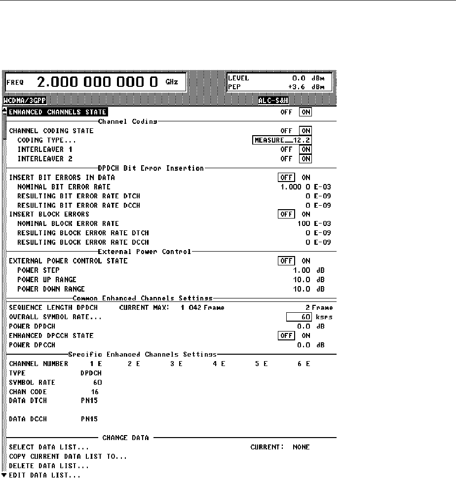
SMIQ Enhanced Functions For Digital Standard 3GPP W-CDMA (FDD)
1125.5555.03 E-92.253
2.15.3.2 Uplink
Only the uplink parameters are described here. If the parameters of section 2.15.3.1 are also available
in the uplink, :BST has to be replaced by :MST for the corresponding remote-control command.
Fig. 2-172 DIGITAL STD - WCDMA/3GPP - ENHANCED CHANNELS STATE (uplink) menu

Enhanced Functions For Digital Standard 3GPP W-CDMA (FDD) SMIQ
1125.5555.03 2.254 E-9
----------------------External Power Control-----------------------------------------------------------------------------
EXTERNAL POWER
CONTROL STATE
Switch for activating or deactivating the external power control mechanism of
all enhanced channels.
In the OFF state, the following menu parameters are not effective:
POWER UP RANGE,
POWER DOWN RANGE,
POWER STEP,
IEC/IEEE-bus command :SOUR:W3GP:MST:ENH:EPOW:STAT
ON
POWER STEP Step width (0.25 to 6.0 dB) by which – with the external power control
mechanism switched on – the channel powers of the activated enhanced
channels in the timeslot grid are increased or decreased within the set
dynamic range.
IEC/IEEE-bus command :SOUR:W3GP:MST:ENH:EPOW:STEP
1.0
POWER UP RANGE Dynamic range (0 to 30 dB) in which – with the external power control
mechanism switched on – the channel powers of all the activated enhanced
channels can be increased. The value POWER UP RANGE can be changed by
POWER STEP. If the dynamic range is exceeded, the warning "MAX. POWER
UP REACHED” is displayed.
The resulting external power control dynamic range (= POWER UP RANGE –
POWER DOWN RANGE) must not exceed 30 dB. For this reason, the
POWER UP RANGE is limited as a function of the POWER DOWN RANGE.
IEC/IEEE-bus command
:SOUR:W3GP:MST:ENH:EPOW:RANG:UP 10.0
POWER DOWN
RANGE Dynamic range (0 to 30 dB) in which – with the external power control
mechanism switched on – the channel powers of all the activated enhanced
channels can be decreased. The value POWER DOWN RANGE can be
changed by POWER STEP. If the dynamic range is underranged, the warning
"MIN. POWER DOWN REACHED" is displayed.
The resulting external power control dynamic range (= POWER UP RANGE –
POWER DOWN RANGE) must not exceed 30 dB. For this reason, the
POWER DOWN RANGE is limited as a function of the POWER UP RANGE.
IEC/IEEE-bus command
:SOUR:W3GP:MST:ENH:EPOW:RANG:DOWN 10.0

SMIQ Enhanced Functions For Digital Standard 3GPP W-CDMA (FDD)
1125.5555.03 E-92.255
----------------------Common Enhanced Channel Settings-----------------------------------------------------
OVERALL SYMBOL
RATE
Sets the overall symbol rate in ksps and the required uplink DPDCHs.
For an overall uplink symbol rate of up to 960 ksps only one DPDCH is
required in addition to the normally available DPCCH. Further DPDCHs with
960 ksps each are added to the signal to obtain a higher overall symbol rate
(maximum 6 DPDCHs).
The enhanced channel table is adapted depending on the setting for
OVERALL SYMBOL RATE (e.g. number of active enhanced channels). In the
channel table of the higher MS1 menu, the enhanced channels are marked by
an additional E (in addition to CHANNEL NUMBER).
If the CHANNEL CODING STATE switch is set to ON, there is a close relation
between the settings CODING TYPE and OVERALL SYMBOL RATE:
MEASURE__12.2: OVERALL SYMBOL RATE = 60 ksps
MEASURE__64: OVERALL SYMBOL RATE = 240 ksps
MEASURE_144: OVERALL SYMBOL RATE = 480 ksps
MEASURE_384: OVERALL SYMBOL RATE = 1 * 960 ksps
AMR_CODER: SYMBOL RATE DPDCH = 60 ksps;
When a parameter is changed (CODING TYPE or OVERALL SYMBOL RATE)
the associated parameter is adapted automatically.
IEC/IEEE-bus command :SOUR:W3GP:MST:ENH:ORAT X2
DPDCH POWER Sets the channel power (-60 dB to 0 dB) of the DPDCHs. Each active DPDCH
is sent with this power. If the EXTERNAL POWER CONTROL STATE switch
is set to ON, this power is also the start power for the power control.
Note: Starting the ADJUST TOTAL POWER menu parameter at the top
menu level of 3GPP W-CDMA adapts all the channel powers
(POWER DB parameter) of the mobile stations (and, thus, also the
POWER START values of the set enhanced channels) so that the
average overall power of all the activated channels is 0 dB with
reference to the LEVEL in the SMIQ display.
IEC/IEEE-bus command :SOUR:W3GP:MST:ENH: POW:DPDC -30.0
ENHANCED DPCCH
STATE This parameter is used to determine whether the DPCCH is calculated as
enhanced channel (on the data generator) or as "normal" channel (on the
modulation coder).
STATE = ON:
The DPCCH is calculated as enhanced channel. This setting is useful when
External Power Control is active.
STATE = OFF:
The DPCCH is calculated as a normal channel. This setting is useful for all
measurements which require no External Power Control.
IEC/IEEE-bus :SOUR:W3GP:MST:ENH:DPCC:STAT OFF

Enhanced Functions For Digital Standard 3GPP W-CDMA (FDD) SMIQ
1125.5555.03 2.256 E-9
DPCCH POWER Sets the channel power (-60 dB to 0 dB) of the DPCCH. If the EXTERNAL
POWER CONTROL STATE switch is set to ON, this power is also the start
power for power control.
Note : Starting the ADJUST TOTAL POWER menu parameter at the top
menu level of 3GPP W-CDMA adapts all the channel powers
(POWER DB parameter) of the mobile stations (and, thus, also the
POWER START values of the set enhanced channel) so that the
average overall power of all the activated channels is 0 dB with
reference to the LEVEL indicated in the SMIQ display.
IEC/IEEE-bus command :SOUR:W3GP:MST:ENH:POW:DPCC -
30.0
----------------------Specific Enhanced Channel Settings--------------------------------------------------
SYMBOL RATE Display parameter indicating the symbol rates of the individual uplink
enhanced channels.
2.15.3.3 Display of External Power Control Mode of Four Enhanced Channels
The current External Power Control mode of the four enhanced channels is displayed here. The
deviation of the channel power (= ∆POW) of the set POWER START caused by the external power
control mechanism is displayed in graphical form.
The window is shown in the SMIQ display after calculating the 3GPP W-CDMA signal triggered by
STATE = ON or MOD ON. The window is blanked out after pressing the RETURN key to be able to
operate the SMIQ during the signal output.
Since a realtime update of the window in the timeslot (= 0.667 ms) is not possible for reasons of speed,
an update can be performed in a more coarse time interval. Fast channel power changes are not
displayed but the settled state of the control loop can be recognized very easily by the user.
Fig. 2-173 Display of external power control mode
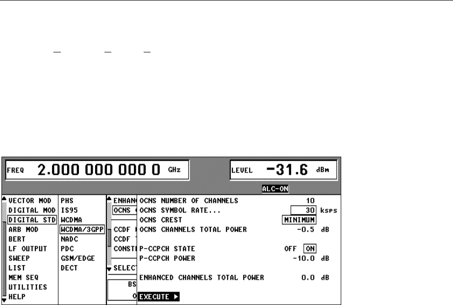
SMIQ Enhanced Functions For Digital Standard 3GPP W-CDMA (FDD)
1125.5555.03 E-92.257
2.15.4 OCNS Channels
A so-called Orthogonal Channel Noise (OCNS) has to be simulated for testing the maximum input level
([1], 7.4) of mobile stations (user equipment).
In addition to the 12.2 kbps measurement channel the base station signal comprises further high-power
orthogonal channels and a PCCPCH.
The OCNS setting function has a similar effect as Para. Predef. (see sect. Digital Standard 3GPP W-CDMA),
i.e. all parameters of the WCDMA/3GPP system are set to useful values.
2.15.4.1 OCNS Menu
Fig. 2-174 DIGITAL STD - WCDMA/3GPP - OCNS CHANNELS menu
OCNS NUMBER OF
CHANNELS
Number of OCNS channels additionally added to the 3GPP W-CDMA signal
(in addition to the enhanced channels). The maximum number of OCNS
channels depends on the OCNS symbol rate:
MAX_NOF_OCNS_Channels =
(Chip rate / OCNS SYMBOL RATE)
– 4 enhanced channels
This menu parameter is only effective after pressing EXECUTE ►.
IEC/IEEE-bus command :SOUR:W3GP:BST:OCNS:COUN 10
OCNS SYMBOL
RATE
Sets the symbol rate of all OCNS channels in ksps.
This menu parameter is only effective after pressing EXECUTE ►.
IEC/IEEE-bus command :SOUR:W3GP:BST:OCNS:SRAT D240K
OCNS CREST The crest factor of the OCNS signal can be influenced by setting the
channelization codes and timing offsets.
MINIMUM: The crest factor is minimized (the channelization codes are
distributed uniformly over the code domain, the timing offsets are
increased by 3 from channel to channel).
IEC/IEEE-bus command :SOUR:W3GP:BST:OCNS:CRES MIN
AVERAGE: An average crest factor is set (the channelization codes are
distributed uniformly over the code domain, the timing offsets are
all set to 0).
IEC/IEEE-bus command :SOUR:W3GP:BST:OCNS:CRES AVER
WORST: The crest factor is set to an unfavourable value (i.e. maximum)
(the channelization codes are assigned in ascending order. The
timing offsets are all set to 0).
IEC/IEEE-bus command :SOUR:W3GP:BST:OCNS:CRES WORS

Enhanced Functions For Digital Standard 3GPP W-CDMA (FDD) SMIQ
1125.5555.03 2.258 E-9
OCNS CHANNELS
TOTAL POWER Fraction of power of OCNS channel signal component at the overall signal
normalized to 0 dB. This menu parameter is only effective after pressing
EXECUTE ►.
IEC/IEEE-bus command :SOUR:W3GP:BST:OCNS:POW –10.0
P-CCPCH STATE Switch with which the P-CCPCH can be added to the OCNS dedicated
channels. This menu parameter is only effective after pressing EXECUTE ►.
IEC/IEEE-bus command :SOUR:W3GP:BST:OCNS:PCCP:STAT ON
P-CCPCH POWER Fraction of power of P-CCPCH signal component at the overall signal
normalized to 0 dB. This menu parameter is only effective after pressing
EXECUTE ►.
IEC/IEEE-bus command :SOUR:W3GP:BST:OCNS:PCCP:POW –10.0
ENHANCED CH.
TOTAL POWER Fraction of power of enhanced channel signal component at the overall signal
normalized to 0 dB. The value for ENHANCED CH. TOTAL POWER is
determined from the POWER START values of all activated enhanced
channels and offered to the user as default value. If the user changes this
value, also the values for POWER START of the activated enhanced
channels are adapted. If all enhanced channels are inactive, ENHANCED CH.
TOTAL POWER are set to –60.0 dB.
This menu parameter is only effective after pressing EXECUTE ".
IEC/IEEE-bus command :SOUR:W3GP:BST:OCNS:EPOW –10.0
EXECUTE ►The EXECUTE command is used to validate the settings described above and
to fill in the channel tables of the base stations.
The rules for filling in the channel tables correspond to those of the
PARA.PREDEF SETTING... menu parameter with the following exceptions:
The first 4 DPCHs are reserved for the enhanced channels. The OCNS
channel settings are entered from the 5th DPCH in the channel table. The
maximum number of DPCHs (= OCNS channels) is reduced by 4 (= number
of enhanced channels).
S-CCPCH is switched off (STATE = OFF).
The channel power values of OCNS channels must be determined from menu
parameters NUMBER OF OCNS CHANNELS and OCNS CHANNELS TOTAL
POWER. The P-CCPCH channel power is taken over from P-CCPCH POWER
menu parameter (if P-CCPCH is switched on) .
IEC/IEEE-bus command :SOUR:W3GP:BST:OCNS:EXEC

SMIQ Enhanced Functions For Digital Standard 3GPP W-CDMA (FDD)
1125.5555.03 E-92.259
2.15.4.2 Test of Maximum Input Level with SMIQ
To test the maximum input level of a mobile station (UE) (according to [1], 7.4) proceed as follows:
1. In the DIGITAL-STD menu select menu item SET DEFAULT to set all parameters to defined values.
2. Set sequence length to 13. (see section 2.15.4.3)
3. Enter the DIGITAL STD-WCDMA/3GPP-ENHANCED CHANNELS menu.
4. Set STATE to ON.
5. Set CHANNEL CODING STATE to ON.
6. Select CODING TYPE = MEASURE__12.2 and switch on both interleavers.
7. Switch off EXTERNAL POWER CONTROL.
8. Select a sequence length of 1022 (see section 2.15.4.3).
9. Activate channel 11 (STATE to ON), all other channels are inactive.
10. Set the following parameters for channel 11:
CHAN CODE = 25 (not defined in [1], other code also possible)
DATA DTCH = PN9
DATA DCCH = PN15 (not defined in [1], other data also possible)
11. Change to the DIGITAL STD-WCDMA/3GPP-OCNS CHANNELS menu.
12. Set number of channels (NUMBER OF CHANNELS) to 60. (A value for [1] is not given but a
utilization of 50% for the code domain is recommended.)
13. Set SYMBOL RATE to 30 ksps. (A value is not given in [1] but normal voice channels are
recommended.)
14. Select CREST=MINIMUM.
15. Set OCNS CHANNELS TOTAL POWER to –1 dB.
16. Activate P-CCPCH (STATE=ON).
17. Select –12 dB as P-CCPCH POWER.
18. Set ENHANCED CHANNELS TOTAL POWER to –19 dB.
19. Activate EXECUTE.
20. Change to the DIGITAL STD-WCDMA/3GPP - BS1 menu.
21. Set TFCI STATE = ON.
22. Activate P-CPICH with –10 dB.
23. Activate P-SCH and S-SCH with –15 dB each.
24. Activate PICH with –15 dB. Select its channelization code so that no domain conflict occurs.
Overview of all active channels in the OCNS measurement:
Table 2-28 OCNS channels
Physical channel Power (log.) Power (lin.)
DPCH (measurement) -19 dB 1.26 %
CPICH -10 dB 10.0 %
PCCPCH -12 dB 6.30 %
SCH -12 dB 6.30 % -15 dB for P-SCH and -15 dB
for S-SCH
PICH -15 dB 3.16 %
OCNS -1 dB 79.3 % 60 channels, -18.8 dB each
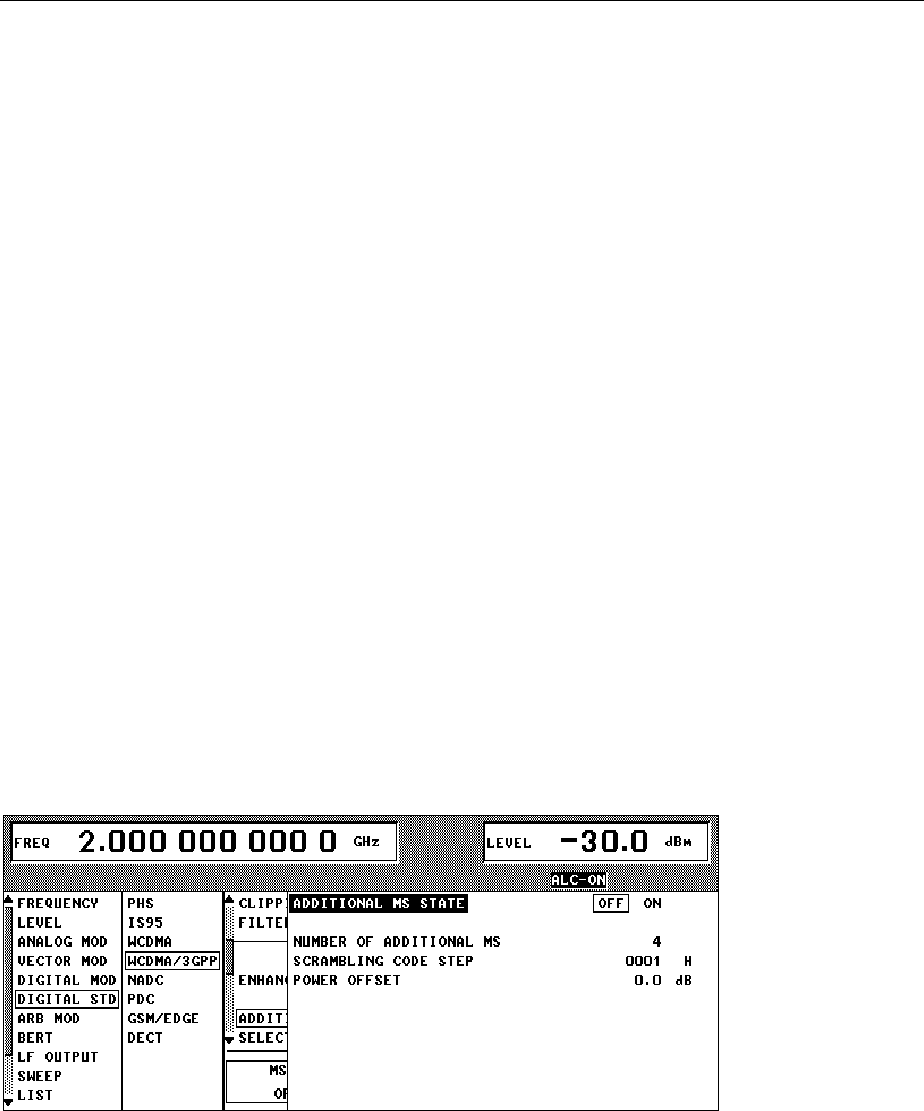
Enhanced Functions For Digital Standard 3GPP W-CDMA (FDD) SMIQ
1125.5555.03 2.260 E-9
2.15.4.3 Favourable Sequence Length for OCNS Measurement
To perform a realistic OCNS measurement, certain sequence length combinations are to be preferred.
Both signal components (measurement channel and OCNS channels) are cyclically output. The cycle
length of the measurement channel can be entered in the ENHANCED CHANNEL (SEQUENCE
LENGTH) menu, the cycle of the OCNS channel in the WCDMA/3GPP menu.
If these lengths are identical, also the overall signal is repeated with this cycle length. If the two lengths are
different, the overall signal is repeated with a cycle length that corresponds to the least common multiple
of the individual lengths.
To simulate a real base-station signal optimally, the overall cycle length should be selected as large as
possible. Therefore, both sequence lengths should be relatively prime. This is the case if two prime
numbers are used, for example. The overall cycle length then becomes the product of the two sequence
lengths.
The values in section 2.15.4.2 are selected so that the overall cycle length becomes a maximum
(1022*13 frames = 133 seconds).
Note : To reduce the computation time for the signal it can be useful to use smaller sequence lengths.
2.15.5 Additional MS Based On MS4
Similar to simulating a realistic downlink signal for testing a mobile station receiver with OCNS (section
2.15.4), there is a realistic uplink signal (for testing a base station receiver) consisting of the individual
signals of many mobile stations.
Up to three mobile stations are configured, see section “Digital Standard 3GPP W-CDMA“ and section
“WCDMA/3GPP menu - Submenu MS Configuration“.
The fourth mobile station MS4 is used as a reference for all other stations. Based on the settings of this
mobile station, all Additional Mobile Stations are calculated and the following parameters are modified:
• Scrambling code (all stations are different)
• Power (different from MS4, but same power)
Fig. 2-175 DIGITAL STD - WCDMA/3GPP ADDITIONAL MS STATE menu

SMIQ Enhanced Functions For Digital Standard 3GPP W-CDMA (FDD)
1125.5555.03 E-92.261
ADDITIONAL MS
STATE
Switch with which up to 50 additional mobile stations can be added (ON) to a
3GPP W-CDMA signal (defined in MS1 to MS4) otherwise all additional MS
are deactivated (OFF).
The additional MS are also calculated on the MCOD and added to the ARB
memory with the signal component of the primary MS.
The basic settings of the additional mobile stations (e.g. Signature, Access
Slot, TFCI, FBI and TPC settings as well as the channel scenario from
PRACH, PCPCH, DPCCH + DPDCHs) are taken over from the primary
reference mobile station 4.
In the OFF state, the following menu parameters have no influence on the
3GPP W-CDMA signal:
NUMBER OF ADDITIONAL MS,
SCRAMBLING CODE STEP,
POWER OFFSET [RELATIVE TO MS4].
IEC/IEEE-bus command :SOUR:W3GP:MST:ADD:STAT ON
NUMBER OF
ADDITIONAL MS
Number of additional mobile stations 1 to 64.
IEC/IEEE-bus command :SOUR:W3GP:MST:ADD:COUNT 33
SCRAMBLING CODE
STEP
Initialization increment of uplink scrambling code generator for additional mobile
stations. The scrambling code value of the primary reference MS4 is used as the
basic value of the scrambling code initialization of an additional MS.
IEC/IEEE-bus command :SOUR:W3GP:MST:ADD:SCOD:STEP 5
POWER OFFSET With this menu parameter it is possible to set a power offset of the active
channels of the additional MS relative to the powers of the active channels of
the primary reference MS4.
The resulting power value of the channel must be in the range from 0 to –60
dB (limitation in case of underrange or overrange).
IEC/IEEE-bus command :SOUR:W3GP:MST:ADD:POW:OFFS –3.0

Digital Standard NADC SMIQ
1125.5555.03 E-92.262
2.16 Digital Standard NADC
With the options Modulation Coder (SMIQB20) and Data Generator (SMIQB11) provided, modulation
signals according to the American NADC standard (IS-541 or IS-136) can be generated. NADC is a
TDMA standard for cellular mobile radio networks.
SMIQ can generate both the transmit signal of a base station (BS) and the transmit signal of a mobile
station (MS). Transmission from BS to MS is called "downlink", "uplink" being used for transmission in
the opposite direction.
Each TDMA frame consists of 6 slots. The 6 slots can be configured for both full rate and half rate
mode. For half rate, the data content for each of the 6 slots can be defined separately by means of a
slot editor whereas in the full rate mode 2 slots for example slot 1 and 4 are combined in a frame. The
settings for the first slot are then automatically used for the assigned second slot. Each slot can be
switched on or off. Moreover, a defined intermediate level can be set for uplink slots.
A burst type has to be defined to configure a slot. The following burst types can be selected:
•TCH a traffic channel burst with a different structure for uplink and downlink,
•SHORT the so-called "shortened burst" only available during uplink and,
•ALL_DATA burst type for test purposes with freely programmable data contents in the selected
slot.
The following internal modulation sources are available:
•different PRBS generators with a sequence length between 29-1 and 223-1 and
•data lists, ie freely programmable data sequences from the data generator memory.
For generating the NADC signals, SMIQ inserts the modulation data continuously (in real time) into the
selected slots. Using a digital signal processor the data generator generates a data sequence with
modulation data and control signals for envelope control.
The data generator in SMIQ generates a data stream which is converted into IQ signals in the
modulation coder. According to the NADC standard, the modulation type is π/4 DQPSK at a symbol rate
of 24.3 ksymbol/s and √COS filtering. Symbol rate and filtering can be changed in SMIQ.
1 Personal Handy Phone System ARIB Standard (RCR STD-28)

SMIQ Digital Standard NADC
1125.5555.03 2.263 E-9
2.16.1 Sync and Trigger Signals
The data generator generates a data sequence with modulation data, control signals for envelope
control, and synchronization signals.
When TRIGGER MODE AUTO is selected, the NADC signal generation is started automatically.
This start can also be activated by an external trigger signal (TRIGGER MODE ARMED_AUTO) which
allows a synchronous sequence for BER measurements to be carried out on receivers.
A trigger signal can be fed via the TRIGIN input at connector PAR DATA. The active slope of a trigger
signal applied there executes a trigger event.
NADC signal generation at a frame limit is started after a trigger event. Data from data lists are inserted
into the selected slots starting from the first bit. PRBS generators start with the set initialization status.
Signal generation either starts immediately after the active slope of the trigger signal or after a settable
number of symbols (EXT TRIGGER DELAY). Retriggering (RETRIG) can be inhibited for a settable
number of symbols (EXT RETRIGGER INHIBIT).
A trigger event can be executed manually or via the IEC/IEEE bus using EXECUTE TRIGGER.
When a trigger event is executed, a trigger signal is output at the TRIGOUT 3 output of SMIQ.
SMIQ also generates the following sync signals:
•a frame clock at TRIGOUT 1 output,
•a frame or multiframe clock at TRIGOUT 2 output with settable position in the frame,
•the symbol clock and the bit clock.
A clock synthesizer on the modulation coder generates the symbol clock and the bit clock in SMIQ. All
the clock signals are synchronized to the 10-MHz reference of SMIQ. The symbol clock is available at
connector SYMBOL CLOCK and the bit clock at connector BIT CLOCK. If required, the clock
synthesizer in SMIQ can be synchronized to an external symbol or bit clock.
The clock signal is selected in the menu via CLOCK-CLOCK SOURCE EXT.
To allow for a trouble-free synchronization of the clock synthesizer first apply the external clock and set
the correct symbol rate at SMIQ. Then switch CLOCK SOURCE from INT to EXT.
Note: The set symbol rate should not differ by more than 1% from the symbol rate of the external
signal.
Digital Standard NADC SMIQ
1125.5555.03 E-92.264
2.16.2 PN Generators as Internal Data Source
Independent PN generators (Pseudo Noise) can be selected for each slot as data source for data fields
DATA and SACCH. These PN generators provide pseudo-random bit sequences of different length or
period. That is why they are also called PRBS generators (Pseudo Random Binary Sequence).
Data sequences are sequences of maximum length which are generated by means of feedback shift
registers.
The following figure gives an example of a 9 bit generator with feedbacks after register 4 and 0 (output).
8
765
4
3210
DATA
EXOR
The pseudo-random sequence of a PRBS generator is clearly defined by the number of registers and
the feedback. The following table describes all PRBS generators available:
Table 2-29 PRBS generators for NADC
PRBS generator Length in bits Feedback after
9 bit 29 -1 = 511 Register 4, 0
11 bit 211 -1 =2047 Register 2, 0
15 bit 215 -1 = 32767 Register 1, 0
16 bit 216 -1 = 65535 Register 5, 3, 2, 0
20 bit 220 -1 = 1048575 Register 3, 0
21 bit 221 -1 = 2097151 Register 2, 0
23 bit 223 -1 = 8388607 Register 5, 0
PN generators PN9,11,15,20 and PN23 are configured according to CCITT Rec. 0.151/152/153. The
output sequence is inverted for generators PN15 and PN23.
The start value of the PN generators is different in the slots and equals
start value hex slotnumber=+ ×114
Example: PN9 generator in slot 1 with start value 15hex = 10101 binary.
10
DATA
EXOR
1100
0
0
0
The resulting output sequence is 1010100000010100101011110010 etc.

SMIQ Digital Standard NADC
1125.5555.03 2.265 E-9
2.16.3 Lists as Internal Data Source
A freely programmable memory on the data generator serves as internal data source for the data fields
of the slots. The data are managed in so-called lists. A list editor allows to select, copy, modify and
delete data lists (DATA LIST).
The list editor is available via menu DIGITAL-MOD - SOURCE....
2.16.4 External Modulation Data
External data can (only) be applied via the SERDATA interface. A selection of SERDATA as data
source is only possible for a single data field of a slot. For further information on the characteristics of
the SERDATA interface see Annex A.
To ensure that the external data bits are assigned to specific positions in the data field of the selected
slot and that they are reproducible, the buffer of the RS-232 transmitter and receiver has to be deleted.
A triggered start has to follow.
The following setting sequence is required in the DIGITAL STD - NADC menu:
1. Carry out desired settings in menu.
2. Select data source SERDATA for the data field of the slot using SELECT SLOT - ....
3. Make connection to external data source, but do not yet start external data source.
4. Switch off digital standard using STATE - OFF.
5. Set TRIGGER MODE ARMED_AUTO.
In this state, SMIQ is ready for reception, but discards data that are read in via SERDATA.
6. Switch on digital standard with STATE ON.
7. Start external data source.
The read-in data are written into the receiving buffer. Only if this buffer is filled can SMIQ react to a
trigger event.
8. Activate trigger event. Signal generation is thus started at a frame limit. The first bit received via
SERDATA is put to the first bit position in the selected data field.
Digital Standard NADC SMIQ
1125.5555.03 E-92.266
2.16.5 Menu DIGITAL STANDARD - NADC
Menu DIGITAL STD - NADC provides access to settings for generating NADC signals.
Menu selection: DIGITAL STD - NADC
FREQ
100. 000 000 0
MHz
FREQUENCY
LEVEL
ANALOG MOD
VECTOR MOD
DIGITAL MOD
DIGITAL STD
LF OUTPUT
SWEEP
LIST
MEM SEQ
UTILITIES
NADC
PHS
IS-95
NADC
PDC
GSM
STATE
MODULATION...
TRIGGER MODE...
EXECUTE TRIGGER
TRIGGER...
CLOCK...
POWER RAMP CONTROL...
SLOT ATTENUATION
SAVE/RCL FRAME...
LINK DIRECTION
RATE CONFIGURATION
SELECT SLOT
123456
TCH TCH TCH TCH TCH TCH
OFF ON
π
/4DQPSK 2 b/sym
AUTO
INT
INT
15 dB
UPLINK DOWNLINK
ALL_FULL
LEVEL
-30.0
dBm
PEP
-27.6
dBm
Fig. 2-176 Menu DIGITAL STD - NADC, SMIQ equipped with Modulation Coder SMIQB20 and Data
Generator SMIQB11
STATE Switch on/off of Digital Standard NADC modulation. Vector Modulation or
Digital Modulation will be switched off automatically.
IEC/IEEE-bus command :SOUR:NADC:STAT ON
MODULATION... Opens a window for setting the modulation parameters.
FREQ
100. 000 000 0
MHz
FREQUENCY
LEVEL
ANALOG MOD
VECTOR MOD
DIGITAL MOD
DIGITAL STD
LF OUTPUT
SWEEP
LIST
MEM SEQ
UTILITIES
NADC
PHS
IS-95
NADC
PDC
GSM
STATE
MODULATION...
TRIGGER MODE..
EXECUTE TRIGGER
TRIGGER....
CLOCK...
POWER RAMP CONT...
SLOT ATTENUATION
1
TCH
SET TO STANDARD
MODULATION TYPE
π
/4 DQPSK 2 b/sym
SYMBOL RATE 24 300.0 sym/s
FILTER TYPE... SQRCOS
ROLL OFF FACTOR 0.35
FILTER MODE LOW_ACP LOW_EVM
LOW DISTORTION MODE OFF ON
LEVEL
-30.0
dBm
PEP
- 27.6
dBm
Fig. 2-177 Menu DIGITAL STD - NADC - MODULATION..., SMIQ equipped with Modulation Coder
SMIQB20 and Data Generator SMIQB11

SMIQ Digital Standard NADC
1125.5555.03 2.267 E-9
(MODULATION...) SET TO
STANDARD Sets the subsequent modulation parameters to the
values predefined by the standard.
MODULATION TYPE Displays the modulation type.
SYMBOL RATE Input value for the symbol clock. 24.3 ksymbol/s are
preset.
IEC/IEEE-bus :SOUR:NADC:SRAT 24.31KHZ
FILTER Selection of baseband filter. A selection between
Nyquist filters COS, SQRCOS or a user-defined filter
USER (cf. Section Digital Modulation) is possible.
IEC/IEEE-bus :SOUR:NADC:FILT:TYPE COS
ROLL OFF FACTOR Input value for the roll-off factor.
IEC/IEEE-bus :SOUR:NADC:FILT:PAR 0.35
FILTER MODE Selection of filter mode.
LOW_ACP Filter for minimum Adjacent Channel
Power.
IEEE :SOUR:NADC:FILT:MODE LACP
LOW_EVM Filter for minimum vector error.
IEEE :SOUR:NADC:FILT:MODE LEVM
LOW DISTORTION Switch on/off of low-distortion mode..
After switch-on, the level of the IQ baseband signals
is reduced by 3 dB. In some cases, this might reduce
undesired intermodulation products. OFF is normally
the more favourable setting.
IEC/IEEE-bus command :SOUR:NADC:LDIS OFF
TRIGGER MODE... Opens a window for selecting the trigger mode.
AUTO The NADC signals are continuously transmitted in the
activated slots.
IEC/IEEE-bus :SOUR:NADC:SEQ AUTO
RETRIG The NADC signals are continuously transmitted in the
activated slots. A trigger event causes a restart.
IEC/IEEE-bus :SOUR:NADC:SEQ RETR
ARMED_AUTO The NADC signal generation does not start until a
trigger event has occurred. The unit then
automatically switches over to the AUTO mode and
can no longer be triggered.
IEC/IEEE-bus :SOUR:NADC:SEQ AAUT
ARMED_RETRIG The NADC signal generation does not start until a
trigger event has occurred. The unit then
automatically switches over to the RETRIG mode.
Each new trigger event causes a restart.
IEC/IEEE-bus :SOUR:NADC:SEQ ARET

Digital Standard NADC SMIQ
1125.5555.03 E-92.268
EXECUTE
TRIGGER Executes a trigger even to start the NADC signal generation.
IEC/IEEE-bus command :TRIG:DM:IMM
TRIGGER... Opens a window for selecting the trigger source, for configuring the trigger
output signals and for setting the time delay of an external trigger signal.
FREQ
100. 000 000 0
MHz
FREQUENCY
LEVEL
ANALOG MOD
VECTOR MOD
DIGITAL MOD
DIGITAL STD
LF OUTPUT
SWEEP
LIST
MEM SEQ
UTILITIES
NADC
PHS
IS-95
NADC
PDC
GSM
STATE
MODULATION...
TRIGGER MODE
EXECUTE TRIG
TRIGGER....
CLOCK...
POWER RAMP C>
SLOT ATTENUA
1
TCH
TRIGGER SOURCE INT EXT
EXT TRIGGER DELAY 0 Symb
EXT RETRIGGER INHIBIT 0 Symb
TRIGGER OUT2 DELAY 0 Symb
TRIGGER OUT2 PERIOD 1 Frames
LEVEL
-30.0
dBm
PEP
- 27.6
dBm
Fig. 2-178 Menu DIGITAL STD - NADC_TRIGGER..., SMIQ equipped with Modulation Coder
SMIQB20 and Data Generator SMIQB11
(TRIGGER...) TRIGGER SOURCE Selection of trigger source.
EXT The NADC signal generation is started
by the active slope of an external trigger
signal.
The polarity, the trigger threshold and
the input resistance of the TRIGIN input
can be modified in menu DIGITAL MOD
- EXT INPUTS.
INT A trigger event can be executed by
EXECUTE TRIGGER .
IEC/IEEE-bus :SOUR:NADC:TRIG:SOUR EXT
EXT TRIGGER
DELAY Setting the number of symbols by which an external
trigger signal is delayed before it starts the NADC
signal generation.
This is used for setting the time synchronization
between the the SMIQ and the DUT.
IEC/IEEE-bus :SOUR:NADC:TRIG:DEL 3

SMIQ Digital Standard NADC
1125.5555.03 2.269 E-9
(TRIGGER...) EXT RETRIGGER
INHIBIT Setting the number of symbols for which a restart is
inhibited after a trigger event.
With TRIGGER MODE RETRIG selected, each new
trigger signal restarts the NADC signal generation.
This restart can be inhibited for the entered number
of symbols.
Example:
The entry of 1000 symbols causes new trigger
signals to be ignored for the duration of 1000 sym-
bols after a trigger event
IEC/IEEE-bus :SOUR:NADC:TRIG:INH 1000
TRIGGER OUT 2
DELAY Input value of delay of trigger signal at TRIGOUT 2
output compared with beginning of frame.
IEC/IEEE-bus :SOUR:NADC:TRIG:OUTP:DEL 2
TRIGGER OUT2
PERIOD Input value of output signal period at TRIGOUT 2
output given in frames.
IEC/IEEE-bus :SOUR:NADC:TRIG:OUTP:PER 1
CLOCK... Opens a window for selecting the clock source and for setting a delay.
FREQ
100. 000 000 0
MHz
FREQUENCY
LEVEL
ANALOG MOD
VECTOR MOD
DIGITAL MOD
DIGITAL STD
LF OUTPUT
SWEEP
LIST
MEM SEQ
UTILITIES
NADC
PHS
IS-95
NADC
PDC
GSM
STATE
MODULATION...
TRIGGER MODE
EXECUTE TRIG
TRIGGER....
CLOCK...
POWER RAMP C>
SLOT ATTENUA
1
TCH
CLOCK SOURCE INT EXT
MODE SYMBOL BIT
DELAY 0.00 Symb
LEVEL
-30.0
dBm
PEP
- 27.6
dBm
Fig. 2-179 Menu DIGITAL STD - NADC - CLOCK..., SMIQ equipped with Modulation Coder SMIQB20
and Data Generator SMIQB11

Digital Standard NADC SMIQ
1125.5555.03 E-92.270
(CLOCK...) CLOCK SOURCE Selection of clock source.
INT SMIQ uses internally generated clock signals.
EXT An external symbol clock or bit clock is fed in
at connectors SYMBOL CLOCK or BIT
CLOCK. The clock synthesizer on the
modulation coder is synchronized to this
clock.
The symbol rate has to be set with an
accuracy of ± 1 %.
The polarity, the trigger threshold and the
input resistance of the clock inputs can be
modified in menu DIGITAL MOD - EXT
INPUTS.
IEC/IEEE-bus command :SOUR:NADC:CLOC:SOUR INT
MODE Selection of clock for external clock signal.
SYMBOL The external clock has to be a symbol clock.
BIT The external clock has to be a bit clock.
IEC/IEEE-bus command :SOUR:NADC:CLOC:MODE SYMB
DELAY Setting the delay of generated modulation signal to an
external clock.
This can be used, for example, for synchronization with a
second unit to achieve time synchronization between the
modulation signals of the two units.
IEC/IEEE-bus command :SOUR:NADC:CLOC:DEL 0.5
POWER RAMP
CONTROL... Opens a window for setting the envelope control, especially for the rising and
falling ramp at the beginning and end of a slot.
FREQ 100. 000 000 0 MHz
FREQUENCY
LEVEL
ANALOG MOD
VECTOR MOD
DIGITAL MOD
DIGITAL STD
LF OUTPUT
SWEEP
LIST
MEM SEQ
UTILITIES
NADC
PHS
IS95
NADC
PDC
GSM
STATE
MODULATION...
TRIGGER MODE
EXECUTE TRIG
TRIGGER....
CLOCK...
POWER RAMP C>
SLOT ATTENUA
1
TCH
SET DEFAULT
RAMP TIME 2.0 Symb
RAMP FUNCTION LIN COS
RAMP DELAY 0.0 Symb
RISE OFFSET 0 Symb
FALL OFFSET 0 Symb
LEVEL -30.0 dBm
PEP - 27.6 dBm
Fig. 2-180 Menu DIGITAL STD - NADC - POWER RAMP CONTROL... , SMIQ equipped with
Modulation Coder SMIQB20 and Data Generator SMIQB11

SMIQ Digital Standard NADC
1125.5555.03 2.271 E-9
(POWER RAMP
CONTROL...) SET DEFAULT Resets the subsequent parameters to the factory-set
values.
IEC/IEEE-bus :SOUR:NADC:PRAM:PRES
RAMP TIME Input value for the rise and fall time of the envelope
at the beginning or end of a slot. The time is set in
units of symbol period.
IEC/IEEE-bus :SOUR:NADC:PRAM:TIME 0.25
RAMP FUNCTION Selection of shape of rising and falling ramp for
envelope control.
LIN Linear ramp function.
COS Cosine function. A more favourable
spectrum than that of the LIN function is
obtained.
IEC/IEEE-bus :SOUR:NADC:PRAM:SHAP LIN
RAMP DELAY Input value for a shift of the envelope characteristic
to the modulated signal. A positive value causes a
delay of the envelope. The values are set in the units
of the symbol length.
IEC/IEEE-bus SOUR:NADC:PRAM:DEL 0.1
RISE OFFSET Input value for a positive or negative offset of the
rising ramp of the envelope at the beginning of a slot.
IEC/IEEE-bus :SOUR:NADC:PRAM:ROFF -1
FALL OFFSET Input value for a positive or negative offset of the
falling ramp of the envelope at the end of a slot.
IEC/IEEE-bus :SOUR:NADC:PRAM:LOFF 1
SLOT ATTENUATION Input value for the level reduction in dB of all active slots whose SLOT LEVEL
was set to ATTEN. Menu SELECT SLOT allows the slots to be determined
whose level is to be reduced.
IEC/IEEE-bus command :SOUR:NADC:SLOT:ATT 40 DB
Digital Standard NADC SMIQ
1125.5555.03 E-92.272
SAVE/RCL FRAME... Opens a window for saving and loading a frame configuration. Loading a
frame affects all parameters that can be set under SELECT SLOT.
FREQ 100. 000 000 0 MHz
FREQUENCY
LEVEL
ANALOG MOD
VECTOR MOD
DIGITAL MOD
DIGITAL STD
LF OUTPUT
SWEEP
LIST
MEM SEQ
UTILITIES
NADC
PHS
IS-95
NADC
PDC
GSM
TRIGGER MODE
EXECUTE TRIG
TRIGGER....
CLOCK...
POWER RAMP C>
SLOT ATTENUA
SAVE/RCL FRA
1
TCH
GET PREDEFINED FRAME...
REFCALL FRAME...
SAVE FRAME...
DELETE FRAME...
LEVEL -30.0 dBm
PEP -27.6 dBm
Fig. 2-181 Menu DIGITAL STD - NADC - SAVE/RCL FRAME, SMIQ equipped with Modulation Coder
SMIQB20 and Data Generator SMIQB11
(SAVE/RCL FRAME...) GET PREDEFINED
FRAME... Loads a factory-set frame configuration.
DN_TCH Downlink traffic channels in all slots.
UP1TCH Uplink traffic channels in slot 1
IEEE :SOUR:NADC:FLIS:PRED:LOAD "dn_tch"
RECALL FRAME Loads a frame configuration saved by the user.
IEC/IEEE-bus :SOUR:NADC:FLIS:LOAD "name"
SAVE FRAME Saves a user-defined frame configuration.
IEC/IEEE-bus :SOUR:NADC:FLIS:STOR "name"
DELETE FRAME Deletes a frame configuration saved by the user.
IEC/IEEE-bus :SOUR:NADC:FLIS:DEL "name"
LINK DIRECTION Selection between UPLINK and DOWNLINK. Depending on this selection,
various burst types are offered under SELECT SLOT.
IEC/IEEE-bus command :SOUR:NADC:LINK UP
SMIQ Digital Standard NADC
1125.5555.03 2.273 E-9
RATE
CONFIGURATION... Opens a window for determining which slots in the frame are to be configured
as half-rate and full-rate channels. Full-rate channels occupy two slots in a
frame, the second slot is fully determined by the configuration of the first slot.
The following eight combinations can be selected:
Selection Full-rate slots Half-rate slots
ALL HALF - 1, 2, 3, 4, 5, 6
FULL 1 1 + 4 2, 3, 5, 6
FULL 2 2 + 5 1, 3, 4, 6
FULL 3 3 + 6 1, 2, 4, 5
FULL 1+2 1 + 4 and 2 + 5 3, 6
FULL 1+3 1 + 4 and 3 + 6 2, 5
FULL 2+3 2 + 5 and 3 + 6 1, 4
ALL FULL 1 + 4 and 2 + 5 and 3 + 6 -
IEC/IEEE-bus command :SOUR:NADC:RCON AHAL
SELECT SLOT... Selection of one of 6 possible slots. The number depends on the setting under
RATE CONFIGURATION. When selecting the slot, a window is opened in
which the data contents belonging to this slot can be defined. The content of
the window depends on whether an UPLINK or DOWNLINK was selected
under LINK DIRECTION.
If the cursor is placed onto a slot in the diagram, it may be switched on and off
by pressing one of the unit keys (toggle function).
Menu selection: BURST TYPE = TCH
FREQ 100. 000 000 0 MHz
FREQUENCY
LEVEL
ANALOG MOD
VECTOR MOD
DIGITAL MOD
DIGITAL STD
LF OUTPUT
SWEEP
LIST
MEM SEQ
UTILITIES
NADC
PHS
IS95
NADC
PDC
GSM
SLOT SYNC SACCH DATA CDVCC DATA RSVD
1 DN 28 12 130 12 130 12
BURST TYPE... TCH
BURST STATE OFF ON
SET DEFAULT
----------------BURST CONTENTS----------------
SYNC A91 DE4A H
SACCH PN9
DATA PN9
CDVCC 013 H
RSVD 800 H
-----------------CHANGE DATA------------------
SELECT DATA LIST... CURRENT: R&STDM
COPY CURRENT DATA LIST TO...
DELETE DATA LIST...
EDIT DATA LIST...
LEVEL -30.0 dBm
PEP -27.6 dBm
POWE
SLOT
SAVE
LINK
RATE
SELE
EDIT
1
TC
Fig. 2-182 Menu DIGITAL STD - NADC - SELECT SLOT, LINK DIRECTION = DOWNLINK, SMIQ
equipped with Modulation Coder SMIQB20 and Data Generator SMIQB11

Digital Standard NADC SMIQ
1125.5555.03 E-92.274
(SELECT SLOT...)
TCH BURST TYPE Selection of burst type used to configure the selected slot.
TCH Traffic channel burst
IEC/IEEE-bus :SOUR:NADC:SLOT2:TYPE TCH
SLOT LEVEL
(UPLINK only) Selection of level for selected slot.
OFF Maximum attenuation
IEC/IEEE :SOUR:NADC:SLOT2:LEV OFF
FULL The level corresponds to the value indicated on
the SMIQ LEVEL display.
IEC/IEEE :SOUR:NADC:SLOT2:LEV FULL
ATTEN The level is reduced by the value set under
SLOT ATTENUATION.
IEC/IEEE :SOUR:NADC:SLOT2:LEV ATT
BURST STATE
(DOWNLINK only) Substitute for parameter SLOT LEVEL for DOWNLINK.
ON The burst contents defined in the data fields are
sent in the selected slot.
IEC/IEEE-bus :SOUR:NADC:SLOT2:LEV FULL
OFF Only 1s will be sent.
IEC/IEEE-bus :SOUR:NADC:SLOT2:LEV OFF
Parameter SLOT LEVEL is omitted since the NADC base
station in downlink always sends with the same power in
each slot.
SET DEFAULT Resets the subsequent parameters to the factory-set values.
IEC/IEEE-bus command :SOUR:NADC:SLOT8:PRES
G
(UPLINK only) Display of data contents in the 6 bit data field "Guard" in
hexadecimal form.
R
(UPLINK only) Display of data contents in the 6 bit data field "Ramp".
DATA Selection of data source for DATA fields. These fields are
regarded as a continuous field, ie a pseudo-random
sequence is fully continued from one DATA field to the next.
The following data sources are available:
PN.. PRBS data according to CCITT with periods
between 29-1 and 223-1.
IEEE :SOUR:NADC:SLOT3:DATA PN15
DLIST Data from a programmable data list.
IEEE :SOUR:NADC:SLOT3:DATA DLIS
SERDATA Data from data input SER DATA.
IEEE :SOUR:NADC:SLOT3:DATA SDAT

SMIQ Digital Standard NADC
1125.5555.03 2.275 E-9
(SELECT SLOT...)
TCH SYNC Input value for the 28 bit sync word in hexadecimal form.
Depending on the selected slot, the following sync words are
predefined according to the NADC standard:
SLOT 1 A91DE4A
SLOT 2 A9D127A
SLOT 3 C7E3C0C
SLOT 4 342C3F3
SLOT 5 13E23D1
SLOT 6 DC2EC1D
IEC/IEEE-bus :SOUR:NADC:SLOT2:SYNC A91EE4A
SACCH Selection of data source for SACCH field (Slow Associated
Control Channel).
PN.. PRBS data according to CCITT with periods
between 29-1 and 223-1.
IEEE :SOUR:NADC:SLOT3:SACC PN15
DLIST Data from a programmable data list.
IEEE :SOUR:NADC:SLOT3:SACC DLIS
SERDATA Data from data input SER DATA.
IEEE :SOUR:NADC:SLOT3:SACC SDAT
CDVCC Input value for the 12 bit "Coded digital verification color
code" field in hexadecimal form. SMIQ does not perform any
coding but directly accepts the input data. 013 hex. is preset.
This corresponds to a value of 1 for the uncoded colour code
DVCC.
IEC/IEEE-bus :SOUR:NADC:SLOT2:CDVC #HFFF
RSVD
(DOWNLINK only) Input value for the 12 bit "Reserved" field in hexadecimal
form.
IEC/IEEE-bus :SOUR:NADC:SLOT2:CDVC #HFFF
SELECT DATA
LIST... Opens a window for selecting a stored data list or for
generating a new list.
COPY CURRENT
DATA LIST TO... Stores the current data list under a different name.
DELETE DATA
LIST... Deletes a data list.
EDIT DATA
LIST... Opens a window for editing a data list bit-by-bit. The
available storage capacity and the length of the current list is
displayed in parameters FREE and LEN (see also Section
List Editor).
COPY Copies a list range
FILL Fills the range with filler pattern
INSERT Inserts a list range at a different position of the
list
DELETE Deletes a list range
EDIT/VIEW Edits or views the list
Digital Standard NADC SMIQ
1125.5555.03 E-92.276
Menu selection: BURST TYPE = ALL_DATA
FREQ 100. 000 000 0 MHz
FREQUENCY
LEVEL
ANALOG MOD
VECTOR MOD
DIGITAL MOD
DIGITAL STD
LF OUTPUT
SWEEP
LIST
MEM SEQ
UTILITIES
NADC
PHS
IS95
NADC
PDC
GSM
LEVEL -30.0 dBm
PEP -27.6 dBm
POWE
SLOT
SAVE
LINK
RATE
SELE
EDIT
1
AL
SLOT G R DATA
1UP 6 6 312
BURST TYPE... ALL_DATA
SLOT LEVEL OFF ATTEN FULL
----------------BURST CONTENTS----------------
G00H
R00H
DATA PN9
-----------------CHANGE DATA------------------
SELECT DATA LIST... CURRENT: R&STDM
COPY CURRENT DATA LIST TO...
DELETE DATA LIST...
EDIT DATA LIST...
Fig. 2-183 Menu DIGITAL STD - NADC - SELECT SLOT, LINK DIRECTION = UPLINK,SMIQ
equipped with Modulation Coder SMIQB20 and Data Generator SMIQB11
(SELECT SLOT...)
ALL_DATA BURST TYPE Selection of burst type used to configure the selected slot.
ALL DATA Burst type for testing with freely programmable
data contents
IEC/IEEE-bus :SOUR:NADC:SLOT2:TYPE ADAT
SLOT LEVEL
(UPLINK only) Selection of level for selected slot.
OFF Maximum attenuation
IEC/IEEE :SOUR:NADC:SLOT2:LEV OFF
FULL The level corresponds to the value indicated on
the SMIQ LEVEL display.
IEC/IEEE :SOUR:NADC:SLOT2:LEV FULL
ATTEN The level is reduced by the value set under
SLOT ATTENUATION.
IEC/IEEE :SOUR:NADC:SLOT2:LEV ATT
BURST STATE
(DOWNLINK only) Substitute for parameter SLOT LEVEL for LINK DIRECTION
= DOWNLINK.
ON The burst contents defined in the data fields are
sent in the selected slot.
OFF Only 1s will be sent.
Parameter SLOT LEVEL is omitted since the NADC base
station in downlink always sends with the same power in
each slot.
IEC/IEEE-bus command :SOUR:NADC:SLOT2:LEV FULL
G
(UPLINK only) Display of data contents in the 6 bit data field "Guard" in
hexadecimal form.
SMIQ Digital Standard NADC
1125.5555.03 2.277 E-9
(SELECT SLOT...)
ALL_DATA R
(UPLINK only) Display of data contents in the 6 bit data field "Ramp".
DATA Selection of data source for DATA fields. These fields are
regarded as a continuous field, ie a pseudo-random
sequence is fully continued from one DATA field to the next.
The following data sources are available:
PN.. PRBS data according to CCITT with periods
between 29-1 and 223-1.
IEEE :SOUR:NADC:SLOT3:DATA PN15
DLIST Data from a programmable data list.
IEEE :SOUR:NADC:SLOT3:DATA DLIS
SERDATA Data from data input SER DATA.
IEEE :SOUR:NADC:SLOT3:DATA SDAT
Parameter SELECT DATA LIST... to EDIT DATA LIST... see menu selection BURST TYPE = TCH
Menu selection: BURST TYPE = SHORT (only available with LINK DIRECTION = UPLINK)
FREQ 100. 000 000 0 MHz
FREQUENCY
LEVEL
ANALOG MOD
VECTOR MOD
DIGITAL MOD
DIGITAL STD
LF OUTPUT
SWEEP
LIST
MEM SEQ
UTILITIES
NADC
PHS
IS95
NADC
PDC
GSM
SLOT G R SY CD SY CD V SY CD W SY CD X SY CD Y SY G2
1UP66281228124281282812122812162844
BURST TYPE... SHORT
SLOT LEVEL OFF ATTEN FULL
SET DEFAULT
-------------------BURST CONTENTS-------------------
G00H
R00H
SYNC A91 DE4A H
CDVCC 013 H
G2 00000000000H
V0H
W00H
X000H
Y0000H
--------------------CHANGE DATA -------------------
SELECT DATA LIST... CURRENT: R&STDM
COPY CURRENT DATA LIST...
DELETE DATA LIST...
EDIT DATA LIST...
LEVEL -30.0 dBm
PEP -27.6 dBm
POWE
SLOT
SAVE
LINK
RATE
SELE
EDIT
1
SH
Fig. 2-184 Menu DIGITAL STD - NADC - SELECT SLOT, SMIQ equipped with Modulation Coder
SMIQB20 and Data Generator SMIQB11
(SELECT SLOT...)
SHORT
(UPLINK ONLY)
BURST TYPE Selection of burst type used to configure the selected slot.
SHORT Shortened Burst
IEC/IEEE-bus :SOUR:NADC:SLOT2:TYPE SHOR

Digital Standard NADC SMIQ
1125.5555.03 E-92.278
(SELECT SLOT...)
SHORT
(UPLINK ONLY)
SLOT LEVEL Selection of level for selected slot.
OFF Maximum attenuation
IEC/IEEE :SOUR:NADC:SLOT2:LEV OFF
FULL The level corresponds to the value indicated on
the SMIQ LEVEL display.
IEC/IEEE :SOUR:NADC:SLOT2:LEV FULL
ATTEN The level is reduced by the value set under
SLOT ATTENUATION.
IEC/IEEE :SOUR:NADC:SLOT2:LEV ATT
SET DEFAULT Resets the subsequent parameters to the factory-set values.
IEC/IEEE-bus command :SOUR:NADC:SLOT8 PRES
GDisplay of data contents in the 6 bit data field "Guard" in
hexadecimal form.
RDisplay of data contents in the 6 bit data field "Ramp" in
hexadecimal form..
SYNC Input value for the sync word in hexadecimal form.
Depending on the selected slot, the following sync words are
predefined according to the NADC standard:
SLOT 1 A91DE4A
SLOT 2 A9D127A
SLOT 3 C7E3C0C
SLOT 4 342C3F3
SLOT 5 13E23D1
SLOT 6 DC2EC1D
IEC/IEEE-bus :SOUR:NADC:SLOT2:SYNC A91EE4A
CDVCC Input value for the 12 bit "Coded digital verification color
code" field in hexadecimal form. SMIQ does not perform any
coding but directly accepts the input data. 013 hex. is preset.
This corresponds to a value of 1 for the uncoded colour code
DVCC.
IEC/IEEE-bus :SOUR:NADC:SLOT2:CDVC #HFFF
V, W, X, Y Display of data contens of other data fields that are
predefined by the NADC standard.
G2 Display of data contents in the second "Guard" in
hexadecimal form.
Parameter SELECT DATA LIST... to EDIT DATA LIST... see menu selection BURST TYPE = TCH

SMIQ Digital Standard PDC
1125.5555.03 E-92.279
2.17 Digital Standard PDC
With the options Modulation Coder (SMIQB20) and Data Generator (SMIQB11) provided, modulation
signals according to the Japanese PDC standard1 can be generated. PDC is a TDMA standard for
cellular mobile radio networks.
SMIQ can generate both the transmit signal of a base station (BS) and the transmit signal of a mobile
station (MS). Transmission from BS to MS is called "downlink", "uplink" being used for transmission in
the opposite direction.
Each TDMA frame consists of 6 slots. The 6 slots can be configured for both full rate and half rate
mode. For half rate, the data content for each of the 6 slots can be defined separately by means of a
slot editor whereas in the full rate mode 2 slots for example slot 1 and 4 are combined in a frame. The
settings for the first slot are then automatically used for the assigned second slot. Each slot can be
switched on or off. Moreover, a defined intermediate level can be set for uplink slots.
A burst type has to be defined to configure a slot. The following burst types can be selected:
•TCH a traffic channel burst with a different structure for uplink and downlink,
•SYNC a burst type for simulation of a sync channel,
•VOX a burst type which is only available in uplink for simulating a communication channel
in speech intervals,
•ALL_DATA burst type for test purposes with freely programmable data contents in the selected
slot.
For TCH and VOX bursts, SMIQ supports the generation of superframes with a length of 18 frames.
The frame position of the so-called "housekeeping channel" RCH can be set in the superframe.
According to the standard, the beginning of the superframe is marked by a special sync word in the
SYNC data field of the first slot.
The following internal modulation sources are available:
•different PRBS generators with a sequence length between 29-1 and 223-1 and
•data lists, ie freely programmable data sequences from the data generator memory.
For generating the PDC signals, SMIQ inserts the modulation data continuously (in real time) into the
selected slots. Using a digital signal processor the data generator generates a data sequence with
modulation data and control signals for envelope control.
The data generator in SMIQ generates a data stream which is converted into IQ signals in the
modulation coder. According to the PDC standard, the modulation type is π/4 DQPSK at a symbol rate
of 21 ksymbol/s and √COS filtering. Symbol rate and filtering can be changed in SMIQ.
1 Personal Digital Cellular Telecommunication System, RCR STD-27 D

Digital Standard PDC SMIQ
1125.5555.03 2.280 E-9
2.17.1 Sync and Trigger Signals
The data generator generates a data sequence with modulation data, control signals for envelope
control, and synchronization signals.
When TRIGGER MODE AUTO is selected, the PDC signal generation is started automatically.
This start can also be activated by an external trigger signal (TRIGGER MODE ARMED_AUTO) which
allows a synchronous sequence for BER measurements to be carried out on receivers.
A trigger signal can be fed via the TRIGIN input at connector PAR DATA. The active slope of a trigger
signal applied there executes a trigger event.
PDC signal generation at a frame or a super frame limit is started after a trigger event. Data from data
lists are inserted into the selected slots starting from the first bit. PRBS generators start with the set
initialization status.
Signal generation either starts immediately after the active slope of the trigger signal or after a settable
number of symbols (EXT TRIGGER DELAY). Retriggering (RETRIG) can be inhibited for a settable
number of symbols (EXT RETRIGGER INHIBIT).
A trigger event can be executed manually or via the IEC/IEEE bus using EXECUTE TRIGGER.
When a trigger event is executed, a trigger signal is output at the TRIGOUT 3 output of SMIQ.
SMIQ also generates the following sync signals:
•a frame clock at TRIGOUT 1 output,
•a frame or multiframe clock at TRIGOUT 2 output with settable position in the frame,
•the symbol clock and the bit clock.
A clock synthesizer on the modulation coder generates the symbol clock and the bit clock in SMIQ. All
the clock signals are synchronized to the 10-MHz reference of SMIQ. The symbol clock is available at
connector SYMBOL CLOCK and the bit clock at connector BIT CLOCK. If required, the clock
synthesizer in SMIQ can be synchronized to an external symbol or bit clock.
The clock signal is selected in the menu via CLOCK-CLOCK SOURCE EXT.
To allow for a trouble-free synchronization of the clock synthesizer first apply the external clock and set
the correct symbol rate at SMIQ. Then switch CLOCK SOURCE from INT to EXT.
Note: The set symbol rate should not differ by more than 1% from the symbol rate of the external
signal.
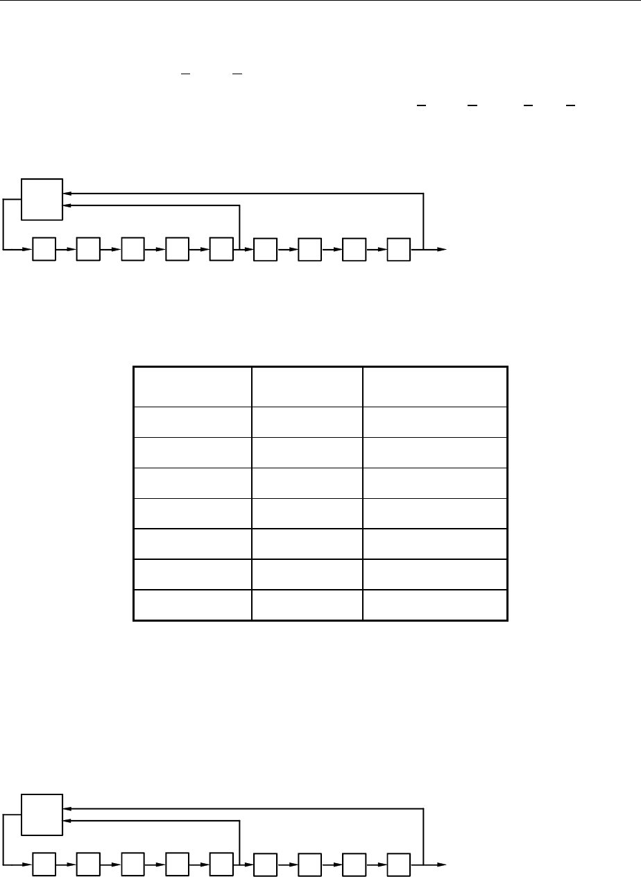
SMIQ Digital Standard PDC
1125.5555.03 E-92.281
2.17.2 PN Generators as Internal Data Source
Independent PN generators (Pseudo Noise) can be selected for each slot as data source for data fields
DATA, SACCH, RCH and SI. These PN generators provide pseudo-random bit sequences of different
length or period. That is why they are also called PRBS generators (Pseudo Random Binary Sequence).
Data sequences are sequences of maximum length which are generated by means of feedback shift
registers.
The following figure gives an example of a 9 bit generator with feedbacks after register 4 and 0 (output).
8
765
4
3210
DATA
EXOR
The pseudo-random sequence of a PRBS generator is clearly defined by the number of registers and
the feedback. The following table describes all PRBS generators available:
Table 2-30 PRBS generators for PDC
PRBS generator Length in bits Feedback after
9 bit 29 -1 = 511 Register 4, 0
11 bit 211 -1 =2047 Register 2, 0
15 bit 215 -1 = 32767 Register 1, 0
16 bit 216 -1 = 65535 Register 5, 3, 2, 0
20 bit 220 -1 = 1048575 Register 3, 0
21 bit 221 -1 = 2097151 Register 2, 0
23 bit 223 -1 = 8388607 Register 5, 0
PN generators PN9,11,15,20 and PN23 are configured according to CCITT Rec. 0.151/152/153. The
output sequence is inverted for generators PN15 and PN23.
The start value of the PN generators is different in the slots and equals
start value hex slotnumber=+ ×114
Example: PN9 generator in slot 1 with start value 15hex = 10101 binary.
10
DATA
EXOR
1100
0
0
0
The resulting output sequence is 1010100000010100101011110010 etc.

Digital Standard PDC SMIQ
1125.5555.03 2.282 E-9
2.17.3 Lists as Internal Data Source
A freely programmable memory on the data generator serves as internal data source for the data fields
of the slots. The data are managed in so-called lists. A list editor allows to select, copy, modify and
delete data lists (DATA LIST).
The list editor is available via menu DIGITAL-MOD - SOURCE....
2.17.4 External Modulation Data
External data can (only) be applied via the SERDATA interface. A selection of SERDATA as data
source is only possible for a single data field of a slot. For further information on the characteristics of
the SERDATA interface see Annex A.
To ensure that the external data bits are assigned to specific positions in the data field of the selected
slot and that they are reproducible, the buffer of the RS-232 transmitter and receiver has to be deleted.
A triggered start has to follow.
The following setting sequence is required in the DIGITAL STD - PDC menu:
1. Carry out desired settings in menu.
2. Select data source SERDATA for the data field of the slot using SELECT SLOT - ....
3. Make connection to external data source, but do not yet start external data source.
4. Switch off digital standard using STATE - OFF.
5. Set TRIGGER MODE ARMED_AUTO.
In this state, SMIQ is ready for reception, but discards data that are read in via SERDATA.
6. Switch on digital standard with STATE ON.
7. Start external data source.
The read-in data are written into the receiving buffer. Only if this buffer is filled can SMIQ react to a
trigger event.
8. Activate trigger event. Signal generation is thus started at a frame limit. The first bit received via
SERDATA is put to the first bit position in the selected data field.
SMIQ Digital Standard PDC
1125.5555.03 E-92.283
2.17.5 Menu DIGITAL STANDARD - PDC
Menu DIGITAL STD - PDC provides access to settings for generating PDC signals.
Menu selection: DIGITAL STD - PDC
FREQ
100. 000 000 0
MHz
FREQUENCY
LEVEL
ANALOG MOD
VECTOR MOD
DIGITAL MOD
DIGITAL STD
LF OUTPUT
SWEEP
LIST
MEM SEQ
UTILITIES
PDC
PHS
IS95
NADC
PDC
GSM
STATE
MODULATION...
TRIGGER MODE...
EXECUTE TRIGGER
TRIGGER...
CLOCK...
POWER RAMP CONTROL...
SLOT ATTENUATION
SAVE/RCL FRAME
LINK DIRECTION
RATE CONFIGURATION
SELECT SLOT
012345
OFF ON
π
/4DQPSK 2 b/sym
AUTO
INT
INT
15 dB
UPLINK DOWNLINK
ALL_FULL
TCH TCH TCH TCH TCH TCH
LEVEL
-30.0
dBm
PEP
- 27.4
dBm
Fig. 2-185 Menu DIGITAL STD - PDC, SMIQ equipped with Modulation Coder SMIQB20 and Data
Generator SMIQB11
STATE Switch on/off of Digital Standard PDC modulation. Vector Modulation or Digital
Modulation will be switched off automatically.
IEC/IEEE-bus command :SOUR:PDC:STAT ON
MODULATION... Opens a window for setting the modulation parameters.
FREQ
100. 000 000 0
MHz
FREQUENCY
LEVEL
ANALOG MOD
VECTOR MOD
DIGITAL MOD
DIGITAL STD
LF OUTPUT
SWEEP
LIST
MEM SEQ
UTILITIES
PDC
PHS
IS95
NADC
PDC
GSM
STATE
MODULATION...
TRIGGER MODE..
EXECUTE TRIGGER
TRIGGER....
CLOCK...
POWER RAMP CONT...
SLOT ATTENUATION
0
TCH
SET TO STANDARD
MODULATION TYPE
π
/4 DQPSK 2 b/sym
SYMBOL RATE 21 000.0 sym/s
FILTER TYPE... SQRCOS
ROLL OFF FACTOR 0.5
FILTER MODE LOW_ACP LOW_EVM
LOW DISTORTION MODE OFF ON
LEVEL
-30.0
dBm
PEP
-27.4
dBm
Fig. 2-186 Menu DIGITAL STD - PDC - MODULATION..., SMIQ equipped with Modulation Coder
SMIQB20 and Data Generator SMIQB11

Digital Standard PDC SMIQ
1125.5555.03 2.284 E-9
(MODULATION...) SET TO
STANDARD Sets the subsequent modulation parameters to the
values predefined by the standard.
MODULATION TYPE Displays the modulation type.
SYMBOL RATE Input value for the symbol clock. 21 ksymbol/s are
preset.
IEC/IEEE-bus :SOUR:PDC:SRAT 21.1KHZ
FILTER Selection of baseband filter. A selection between
Nyquist filters COS, SQRCOS or a user-defined filter
USER (cf. Section Digital Modulation) is possible.
IEC/IEEE-bus :SOUR:PDC:FILT:TYPE COS
ROLL OFF FACTOR Input value for the roll-off factor.
IEC/IEEE-bus :SOUR:PDC:FILT:PAR 0.51
FILTER MODE Selection of filter mode.
LOW_ACP Filter for minimum Adjacent Channel
Power.
IEC :SOUR:PDC:FILT:MODE LACP
LOW_EVM Filter for minimum vector error.
IEC :SOUR:PDC:FILT:MODE LEVM
LOW DISTORTION Switch on/off of low-distortion mode..
After switch-on, the level of the IQ baseband signals
is reduced by 3 dB. In some cases, this might reduce
undesired intermodulation products. OFF is normally
the more favourable setting.
IEC/IEEE-bus command :SOUR:PDC:LDIS OFF
TRIGGER MODE... Opens a window for selecting the trigger mode.
AUTO The PDC signals are continuously transmitted in the
activated slots.
IEC/IEEE-bus :SOUR:PDC:SEQ AUTO
RETRIG The PDC signals are continuously transmitted in the
activated slots. A trigger event causes a restart.
IEC/IEEE-bus :SOUR:PDC:SEQ RETR
ARMED_AUTO The PDC signal generation does not start until a
trigger event has occurred. The unit then
automatically switches over to the AUTO mode and
can no longer be triggered.
IEC/IEEE-bus :SOUR:PDC:SEQ AAUT
ARMED_RETRIG The PDC signal generation does not start until a
trigger event has occurred. The unit then
automatically switches over to the RETRIG mode.
Each new trigger event causes a restart.
IEC/IEEE-bus :SOUR:PDC:SEQ ARET

SMIQ Digital Standard PDC
1125.5555.03 E-92.285
EXECUTE
TRIGGER Executes a trigger even to start the PDC signal generation.
IEC/IEEE-bus command :TRIG:DM:IMM
TRIGGER... Opens a window for selecting the trigger source, for configuring the trigger
output signals and for setting the time delay of an external trigger signal.
FREQ
100. 000 000 0
MHz
FREQUENCY
LEVEL
ANALOG MOD
VECTOR MOD
DIGITAL MOD
DIGITAL STD
LF OUTPUT
SWEEP
LIST
MEM SEQ
UTILITIES
PDC
PHS
IS-95
NADC
PDC
GSM
STATE
MODULATION...
TRIGGER MODE
EXECUTE TRIG
TRIGGER....
CLOCK...
POWER RAMP C>
SLOT ATTENUA
0
TCH
TRIGGER SOURCE INT EXT
EXT TRIGGER DELAY 0 Symb
EXT RETRIGGER INHIBIT 0 Symb
TRIGGER OUT2 DELAY 0 Symb
TRIGGER OUT2 PERIOD 1 Frames
LEVEL
-30.0
dBm
PEP
- 27.4
dBm
Fig. 2-187 Menu DIGITAL STD - PDC_TRIGGER..., SMIQ equipped with Modulation Coder SMIQB20
and Data Generator SMIQB11
(TRIGGER...) TRIGGER SOURCE Selection of trigger source.
EXT The PDC signal generation is started by the
active slope of an external trigger signal.
The polarity, the trigger threshold and the
input resistance of the TRIGIN input can be
modified in menu DIGITAL MOD - EXT
INPUTS.
INT A trigger event is executed by EXECUTE
TRIGGER .
IEC/IEEE-bus :SOUR:PDC:TRIG:SOUR EXT
EXT TRIGGER
DELAY Setting the number of symbols by which an external
trigger signal is delayed before it starts the PDC
signal generation.
This is used for setting the time synchronization
between the SMIQ and the DUT.
IEC/IEEE-bus :SOUR:PDC:TRIG:DEL 3

Digital Standard PDC SMIQ
1125.5555.03 2.286 E-9
(TRIGGER...) EXT RETRIGGER
INHIBIT Setting the number of symbols for which a restart is
inhibited after a trigger event.
With TRIGGER MODE RETRIG selected, each new
trigger signal restarts the PDC signal generation.
This restart can be inhibited for the entered number
of symbols.
Example:
The entry of 1000 symbols causes new trigger
signals to be ignored for the duration of 1000 sym-
bols after a trigger event
IEC/IEEE-bus :SOUR:PDC:TRIG:INH 1000
TRIGGER OUT 2
DELAY Input value of delay of trigger signal at TRIGOUT 2
output compared with beginning of frame.
IEC/IEEE-bus :SOUR:PDC:TRIG:OUTP:DEL 2
TRIGGER OUT2
PERIOD Input value of output signal period at TRIGOUT 2
output given in frames.
IEC/IEEE-bus :SOUR:PDC:TRIG:OUTP:PER 1
CLOCK... Opens a window for selecting the clock source and for setting a delay.
FREQ
100. 000 000 0
MHz
FREQUENCY
LEVEL
ANALOG MOD
VECTOR MOD
DIGITAL MOD
DIGITAL STD
LF OUTPUT
SWEEP
LIST
MEM SEQ
UTILITIES
PDC
PHS
IS95
NADC
PDC
GSM
STATE
MODULATION...
TRIGGER MODE
EXECUTE TRIG
TRIGGER....
CLOCK...
POWER RAMP C>
SLOT ATENUA
0
TCH
CLOCK SOURCE INT EXT
MODE SYMBOL BIT
DELAY 0.00 Symb
LEVEL
-30.0
dBm
PEP
- 27.4
dBm
Fig. 2-188 Menu DIGITAL STD - PDC - CLOCK..., SMIQ equipped with Modulation Coder SMIQB20
and Data Generator SMIQB11

SMIQ Digital Standard PDC
1125.5555.03 E-92.287
(CLOCK...) CLOCK SOURCE Selection of clock source.
INT SMIQ uses internally generated clock signals.
EXT An external symbol clock or bit clock is fed in at
connectors SYMBOL CLOCK or BIT CLOCK. The
clock synthesizer on the modulation coder is
synchronized to this clock.
The symbol rate has to be set with an accuracy of
± 1 %.
The polarity, the trigger threshold and the input
resistance of the clock inputs can be modified in
menu DIGITAL MOD - EXT INPUTS.
IEC/IEEE-bus command :SOUR:PDC:CLOC:SOUR INT
MODE Selection of clock for external clock signal.
SYMBOL The external clock has to be a symbol clock.
BIT The external clock has to be a bit clock.
IEC/IEEE-bus command :SOUR:PDC:CLOC:MODE SYMB
DELAY Setting the delay of generated modulation signal to an
external clock.
This can be used, for example, for synchronization with a
second unit to achieve time synchronization between the
modulation signals of the two units.
IEC/IEEE-bus command :SOUR:PDC:CLOC:DEL 0.5
POWER RAMP
CONTROL... Opens a window for setting the envelope control, especially for the rising and
falling ramp at the beginning and end of a slot.
FREQ 100. 000 000 0 MHz
FREQUENCY
LEVEL
ANALOG MOD
VECTOR MOD
DIGITAL MOD
DIGITAL STD
LF OUTPUT
SWEEP
LIST
MEM SEQ
UTILITIES
PDC
PHS
IS95
NADC
PDC
GSM
STATE
MODULATION...
TRIGGER MODE
EXECUTE TRIG
TRIGGER....
CLOCK...
POWER RAMP C>
SLOT ATTENUA
0
TCH
SET DEFAULT
RAMP TIME 2 Symb
RAMP FUNCTIOM LIN COS
RAMP DELAY 0.0 Symb
RISE OFFSET 0 Symb
FALL OFFSET 0 Symb
LEVEL -30.0 dBm
PEP -27.4 dBm
Fig. 2-189 Menu DIGITAL STD - PDC - POWER RAMP CONTROL... , SMIQ equipped with
Modulation Coder SMIQB20 and Data Generator SMIQB11

Digital Standard PDC SMIQ
1125.5555.03 2.288 E-9
(POWER RAMP
CONTROL...) SET DEFAULT Resets the subsequent parameters to the factory-set
values.
IEC/IEEE-bus :SOUR:PDC:PRAM:PRES
RAMP TIME Input value for the rise and fall time of the envelope
at the beginning or end of a slot. The time is set in
units of symbol period.
IEC/IEEE-bus :SOUR:PDC:PRAM:TIME 0.25
RAMP FUNCTION Selection of shape of rising and falling ramp for
envelope control.
LIN Linear ramp function.
COS Cosine function. A more favourable
spectrum than that of the LIN function is
obtained.
IEC/IEEE-bus :SOUR:PDC:PRAM:SHAP LIN
RAMP DELAY Input value for a shift of the envelope characteristic
to the modulated signal. A positive value causes a
delay of the envelope. The values are set in the units
of the symbol length.
IEC/IEEE-bus :SOUR:PDC:PRAM:DEL 0.1
RISE OFFSET Input value for a positive or negative offset of the
rising ramp of the envelope at the beginning of a slot.
IEC/IEEE-bus :SOUR:PDC:PRAM:ROFF -1
FALL OFFSET Input value for a positive or negative offset of the
falling ramp of the envelope at the end of a slot.
IEC/IEEE-bus :SOUR:PDC:PRAM:LOFF 1
SLOT ATTENUATION Input value for the level reduction in dB of all active slots whose SLOT LEVEL
was set to ATTEN. Menu SELECT SLOT allows the slots to be determined
whose level is to be reduced.
IEC/IEEE-bus command :SOUR:PDC:SLOT:ATT 15 DB
SAVE/RCL FRAME... Opens a window for saving and loading a frame configuration. Loading a
frame affects all parameters that can be set under SELECT SLOT.
SMIQ Digital Standard PDC
1125.5555.03 E-92.289
FREQ 100. 000 000 0 MHz
FREQUENCY
LEVEL
ANALOG MOD
VECTOR MOD
DIGITAL MOD
DIGITAL STD
LF OUTPUT
SWEEP
LIST
MEM SEQ
UTILITIES
PHS
PHS
IS95
NADC
PDC
GSM
TRIGGER MODE
EXECUTE TRIG
TRIGGER....
CLOCK...
POWER RAMP C>
SLOT ATTENUA
SAVE/RCL FRA
GET PREDEFINED FRAME...
RECALL FRAME...
SAVE FRAME...
DELETE FRAME...
LEVEL -30.0 dBm
PEP -27.5 dBm
SYNC
DN 12
Fig. 2-190 Menu DIGITAL STD - PDC - SAVE/RCL FRAME, SMIQ equipped with Modulation Coder
SMIQB20 and Data Generator SMIQB11
(SAVE/RCL FRAME...) GET PREDEFINED
FRAME... Loads a factory-set frame configuration.
DN_TCH Downlink traffic channels in all slots.
UP0_TCH Uplink traffic channels in slot 0
IEEE :SOUR:PDC:FLIS:PRED:LOAD "dn_tch"
RECALL FRAME... Loads a frame configuration saved by the user.
IEC/IEEE-bus :SOUR:PDC:FLIS:LOAD "name"
SAVE FRAME... Saves a user-defined frame configuration.
IEC/IEEE-bus :SOUR:PDC:FLIS:STOR "name"
DELETE FRAME... Deletes a frame configuration saved by the user.
IEC/IEEE-bus :SOUR:PDC:FLIS:DEL "name"
LINK DIRECTION Selection between UPLINK and DOWNLINK. Depending on the selection,
different burst types are offered under SELECT SLOT.
IEC/IEEE-bus command :SOUR:PDC:LINK UP
Digital Standard PDC SMIQ
1125.5555.03 2.290 E-9
RATE
CONFIGURATION... Opens a window for determining which slots in the frame are to be configured
as half-rate and full-rate channels. Full-rate channels occupy two slots in a
frame, the second slot is fully determined by the configuration of the first slot.
The following eight combinations can be selected:
Selection Full-rate slots Half-rate slots
ALL HALF keine 0, 1, 2, 3, 4, 5
FULL 1 0 + 3 1, 2, 4, 5
FULL 2 1 + 4 0, 2, 3, 5
FULL 3 2 + 5 0, 1, 3, 4
FULL 1+2 0 + 3 and 1 + 4 2, 5
FULL 1+3 0 + 3 and 2 + 5 1, 4
FULL 2+3 1 + 4 and 2 + 5 0, 3
ALL FULL 0 + 3 and 1 + 4 and 2 + 5 none
IEC/IEEE-bus command SOUR:PDC:RCON AHAL
SELECT SLOT... Selection of one of 6 possible slots. The number depends on the setting under
RATE CONFIGURATION. When selecting the slot, a window is opened in
which the data contents belonging to this slot can be defined. The content of
the window depends on whether an UPLINK or DOWNLINK was selected
under LINK DIRECTION. If the cursor is placed onto a slot in the diagram, it
may be switched on and off by pressing one of the unit keys (toggle function).
Menu selection: BURST TYPE = TCH
FREQ 100. 000 000 0 MHz
FREQUENCY
LEVEL
ANALOG MOD
VECTOR MOD
DIGITAL MOD
DIGITAL STD
LF OUTPUT
SWEEP
LIST
MEM SEQ
UTILITIES
PDC
PHS
IS95
NADC
PDC
GSM
SLOT R P DATA SYNC CC SF SACCH DATA
0 DN 4 2 112 20 8 1 21 112
BURST TYPE... TCH
BURST STATE OFF ON
SET DEFAULT
SCRAMBLE STATE OFF ON
SCRAMBLE START 001 H
SUPER FRAME OFF ON
RCH POSITION 1
------------------BURST CONTENTS----------------
R0H
P2H
DATA PN9
SYNC 8 7A4B H
SYNC2 3 1BAF H
CC 00 H
SF 0 H
SACCH PN9
RCH PN9
-------------------CHANGE DATA------------------
SELECT DATA LIST... CURRENT: R&STDM
COPY CURRENT DATA LIST...
DELETE DATA LIST...
EDIT DATA LIST...
LEVEL -30.0 dBm
PEP -27.4 dBm
POWE
SLOT
SAVE
LINK
RATE
SELE
EDIT
0
TC
Fig. 2-191 Menu DIGITAL STD - PDC - SELECT SLOT, LINK DIRECTION DOWNLINK, SMIQ
equipped with Modulation Coder SMIQB20 and Data Generator SMIQB11

SMIQ Digital Standard PDC
1125.5555.03 E-92.291
(SELECT SLOT...)
TCH BURST TYPE Selection of burst type used to configure the selected slot.
TCH Traffic channel burst
IEC/IEEE-bus :SOUR:PDC:SLOT2:TYPE TCH
SLOT LEVEL
(UPLINK only) Selection of level for selected slot.
OFF Maximum attenuation
IEC/IEEE :SOUR:PDC:SLOT2:LEV OFF
FULL The level corresponds to the value indicated on
the SMIQ LEVEL display.
IEC/IEEE :SOUR:PDC:SLOT2:LEV FULL
ATTEN The level is reduced by the value set under
SLOT ATTENUATION.
IEC/IEEE :SOUR:PDC:SLOT2:LEV ATT
BURST STATE
(DOWNLINK only) Substitute for parameter SLOT LEVEL for downlink.
ON The burst contents defined in the data fields are
sent in the selected slot.
IEC/IEEE-bus :SOUR:PDC:SLOT2:LEV FULL
OFF Only 1s will be sent.
IEC/IEEE-bus :SOUR:PDC:SLOT2:LEV OFF
Parameter SLOT LEVEL is omitted since the NADC base
station in downlink always sends with the same power in
each slot.
SET DEFAULT Resets the subsequent parameters to the factory-set values.
IEC/IEEE-bus command SOUR:PDC:SLOT8:PRES
SCRAMBLE Switch on/off of scrambling function. Scrambling with the
continuous scramble sequence from a PN9 generator is
applied to the data fields DATA, SF, and SACCH.
IEC/IEEE-bus :SOUR:PDC:SLOT2:SCR:STAT ON
SCRAMBLE
START 9 bit input value for initializing the scramble PN9 generator in
hexadecimal form. The value 0 is not permissible, 1 is
preset. The input field is only displayed if SCRAMBLE is
switched on.
IEC/IEEE-bus :SOUR:PDC:SLOT2:SCR:STAR #H12
SUPERFRAME Switch on/off of the superframe generation. 18 frames form a
superframe. If SUPERFRAME is switched on, RCH data
instead of SACCH data will be sent in 2 slots. The first of the
two RCH blocks is fixed in the first slot of the superframe,
the position of the second can be set.
IEC/IEEE-bus :SOUR:PDC:SLOT2:SFR:STAT ON
Digital Standard PDC SMIQ
1125.5555.03 2.292 E-9
(SELECT SLOT...)
TCH RCH POSITION Input value for the position of the second RCH block. The
input field is only displayed if SUPERFRAME is switched on.
IEC/IEEE-bus :SOUR:PDC:SLOT2:SFR:RCHP 10
RDisplay of data contents in the 4 bit data field "RAMP" in
hexadecimal form.
PInput value of the 2 bit data field "Preamble".
IEC/IEEE-bus :SOUR:PDC:SLOT2:PRE #H1
DATA Selection of data source for DATA fields. These fields are
regarded as a continuous field, ie a pseudo-random
sequence is fully continued from one DATA field to the next.
The following data sources are available:
PN.. PRBS data according to CCITT with periods
between 29-1 and 223-1.
IEC/IEEE :SOUR:PDC:SLOT3:DATA PN15
DLIST Data from a programmable data list.
IEC/IEEE :SOUR:PDC:SLOT3:DATA DLIS
SERDATA Data from data input SER DATA.
IEC/IEEE :SOUR:PDC:SLOT3:DATA SDAT
SYNC Input value for the 20 bit sync word in hexadecimal form.
Depending on the selected slot the LINK DIRECTION, the
following sync words are predefined according to the PDC
standard:
Slot No. Downlink Sync Word Uplink Sync Word
0 87A4B 785B4
1 9D236 62DC9
2 81D75 7E28A
3 A94EA 56B15
4 5164C AE9B3
5 4D9DE B2621
According to the standard, the sync words of the uplink are
the inverted sync words of the downlink.
IEC/IEEE-bus :SOUR:PDC:SLOT2:SYNC #H62DC8
SMIQ Digital Standard PDC
1125.5555.03 E-92.293
(SELECT SLOT...)
TCH SYNC2 Input value for the 20 bit sync word in the first slot of a
superframe in hexadecimal form. This sync word marks the
beginning of the superframe. The input field is only displayed
if SUPERFRAME is switched on. Depending on the selected
slot and the LINK DIRECTION, the following sync words are
predefined according to the PDC standard:
Slot No. Downlink Sync2 Word Uplink Sync2 Word
0 31BAF CE450
1 1E56F E1A90
2 E712C 18ED3
3 FBC1F 043E0
4 8279E 7D861
5 98908 676F7
According to the standard, the sync words of the uplink are
the inverted sync words of the downlink.
IEC/IEEE-bus :SOUR:PDC:SLOT2:SYNC #HE2A90
CC Input value of the 8 bit data field " Color code ".
IEC/IEEE-bus command :SOUR:PDC:SLOT2:CCOD #HFF
SF Input value of the data field " Steal Flag ".
IEC/IEEE-bus command :SOUR:PDC:SLOT2:SF #H0
SACCH Selection of data source for SACCH field (Slow Associated
Control Channel).
PN.. PRBS data according to CCITT with periods
between 29-1 and 223-1.
IEC/IEEE :SOUR:PDC:SLOT3:SACC PN15
DLIST Data from a programmable data list.
IEC/IEEE :SOUR:PDC:SLOT3:SACC DLIS
SERDATA Data from data input SER DATA.
IEC/IEEE :SOUR:PDC:SLOT3:SACC SDAT
RCH Selection of data source for the RCH data field. RCH data
replace SACCH data in certain slots of a superframe. The
input field is only displayed if SUPERFRAME is switched on.
PN.. PRBS data according to CCITT with periods
between 29-1 and 223-1.
IEC/IEEE :SOUR:PDC:SLOT3:RCH PN15
DLIST Data from a programmable data list.
IEC/IEEE :SOUR:PDC:SLOT3:RCH DLIS
SERDATA Data from data input SER DATA.
IEC/IEEE :SOUR:PDC:SLOT3:RCH SDAT

Digital Standard PDC SMIQ
1125.5555.03 2.294 E-9
(SELECT SLOT...)
TCH G
(UPLINK only) Display of data content in the 6 bit "Guard" field in hexa-
decimal form.
SELECT DATA
LIST... Opens a window for selecting a stored data list or for
generating a new list.
COPY CURRENT
DATA LIST TO... Stores the current data list under a different name.
DELETE DATA
LIST... Deletes a data list.
EDIT DATA
LIST... Opens a window for editing a data list bit-by-bit. The
available storage capacity and the length of the current list is
displayed in parameters FREE and LEN (see also Section
List Editor).
COPY Copies a list range
FILL Fills the range with filler pattern
INSERT Inserts a list range at a different position of the
list
DELETE Deletes a list range
EDIT/VIEW Edits or views the list
Menu selection: BURST TYPE = ALL_DATA
FREQ 100. 000 000 0 MHz
FREQUENCY
LEVEL
ANALOG MOD
VECTOR MOD
DIGITAL MOD
DIGITAL STD
LF OUTPUT
SWEEP
LIST
MEM SEQ
UTILITIES
PDC
PHS
IS95
NADC
PDC
GSM
LEVEL -30.0 dBm
PEP - 27.4 dBm
POWE
SLOT
SAVE
LINK
RATE
SELE
EDIT
0
ALL
SLOT DATA
0DN 280
BURST TYPE... ALL_DATA
BURST STATE OFF ON
SET DEFAULT
------------------BURST CONTENTS----------------
DATA PN9
-------------------CHANGE DATA------------------
SELECT DATA LIST... CURRENT: R&STDM
COPY CURRENT DATA LIST...
DELETE DATA LIST...
EDIT DATA LIST...
Fig. 2-192 Menu DIGITAL STD - PDC - SELECT SLOT, LINK DIRECTION = DOWNLINK, SMIQ
equipped with Modulation Coder SMIQB20 and Data Generator SMIQB11

SMIQ Digital Standard PDC
1125.5555.03 E-92.295
(SELECT SLOT...)
ALL_DATA BURST TYPE Selection of burst type used to configure the selected slot.
ALL DATA Burst type for testing with freely programmable
data contents
IEC/IEEE-bus command :SOUR:PDC:SLOT2:TYPE ADAT
SLOT LEVEL
(UPLINK only) Selection of level for selected slot.
OFF Maximum attenuation
IEC/IEEE :SOUR:PDC:SLOT2:LEV OFF
FULL The level corresponds to the value indicated on
the SMIQ LEVEL display.
IEC/IEEE :SOUR:PDC:SLOT2:LEV FULL
ATTEN The level is reduced by the value set under
SLOT ATTENUATION.
IEC/IEEE :SOUR:PDC:SLOT2:LEV ATT
BURST STATE
(DOWNLINK only) Substitute for parameter SLOT LEVEL for downlink.
ON The burst contents defined in the data fields are
sent in the selected slot.
IEC/IEEE-bus :SOUR:PDC:SLOT2:LEV FULL
OFF Only 1s will be sent.
IEC/IEEE-bus :SOUR:PDC:SLOT2:LEV OFF
Parameter SLOT LEVEL is omitted since the NADC base
station in downlink always sends with the same power in
each slot.
R
(UPLINK only) Display of data contents in the 6 bit data field "Ramp" in
hexadecimal form..
G
(UPLINK only) Display of data contents in the 6 bit data field "Guard" in
hexadecimal form.
DATA Selection of data source for DATA fields. These fields are
regarded as a continuous field, ie a pseudo-random
sequence is fully continued from one DATA field to the next.
The following data sources are available:
PN.. PRBS data according to CCITT with periods
between 29-1 and 223-1.
IEC/IEEE :SOUR:PDC:SLOT3:DATA PN15
DLIST Data from a programmable data list.
IEC/IEEE :SOUR:PDC:SLOT3:DATA DLIS
SERDATA Data from data input SER DATA.
IEC/IEEE :SOUR:PDC:SLOT3:DATA SDAT
Parameter SELECT DATA LIST... to EDIT DATA LIST... see menu selection BURST TYPE = TCH
Digital Standard PDC SMIQ
1125.5555.03 2.296 E-9
Menu selection: BURST TYPE = SYNC
FREQ 100. 000 000 0 MHz
FREQUENCY
LEVEL
ANALOG MOD
VECTOR MOD
DIGITAL MOD
DIGITAL STD
LF OUTPUT
SWEEP
LIST
MEM SEQ
UTILITIES
PDC
PHS
IS95
NADC
PDC
GSM
SLOT R P SYNC SI SI SI Q PO
0DN4 102 32 21 21211 78
BURST TYPE... SYNC
BURST STATE OFF ON
SET DEFAULT
------------------BURST CONTENTS------------------
R0H
P 26 6666 6666 6666 6666 6666 6666 H
DATA PN9
SYNC 2F94 D06B H
SI PN9
Q1
PO 2666 6666 6666 6666 6666 H
-------------------CHANGE DATA------------------
SELECT DATA LIST... CURRENT: R&STDM
COPY CURRENT DATA LIST...
DELETE DATA LIST...
EDIT DATA LIST...
LEVEL -30.0 dBm
PEP - 27.4 dBm
POWE
SLOT
SAVE
LINK
RATE
SELE
EDIT
0
SYN
Fig. 2-193 Menu DIGITAL STD - PDC - SELECT SLOT, LINK DIRECTION = DOWNLINK, SMIQ
equipped with Modulation Coder SMIQB20 and Data Generator SMIQB11
(SELECT SLOT...)
SYNC BURST TYPE Selection of burst type used to configure the selected slot.
SHORT Shortened Burst
IEC/IEEE-bus command :SOUR:PDC:SLOT2:TYPE SYNC
SLOT LEVEL
(UPLINK only) Selection of level for selected slot.
OFF Maximum attenuation
IEC/IEEE :SOUR:PDC:SLOT2:LEV OFF
FULL The level corresponds to the value indicated on
the SMIQ LEVEL display.
IEC/IEEE :SOUR:PDC:SLOT2:LEV FULL
ATTEN The level is reduced by the value set under
SLOT ATTENUATION.
IEC/IEEE :SOUR:PDC:SLOT2:LEV ATT
BURST STATE
(DOWNLINK only) Substitute for parameter SLOT LEVEL for downlink.
ON The burst contents defined in the data fields are
sent in the selected slot.
OFF Only 1s will be sent.
Parameter SLOT LEVEL is omitted since the PDC base
station in downlink always sends with the same power in
each slot.
IEC/IEEE-bus command :SOUR:PDC:SLOT2:LEV FULL
SMIQ Digital Standard PDC
1125.5555.03 E-92.297
(SELECT SLOT...)
SYNC SET DEFAULT Resets the subsequent parameters to the factory-set values.
IEC/IEEE-bus command :SOUR:PDC:SLOT8 PRES
G
(UPLINK only) Display of data contents in the 54 bit data field "Guard" in
hexadecimal form.
The field is only displayed with link direction UPLINK
selected.
RDisplay of data contents in the 6 bit data field "Ramp".
PInput value of the data field "Preamble" in hexadecimal
form.The length of the field is 48 bit with link direction =
UPLINK, and 102 bit with DOWNLINK
IEC/IEEE-bus command :SOUR:PDC:SLOT2:PRE #HFF
SYNC Input value for the 32 bit sync word in hexadecimal form.
Depending on the selected slot and the link direction, the
following sync words are predefined according to the PDC
standard:
Slot No. Downlink Sync Word Uplink Sync Word
0 2F94D06B D06B2F94
1 1D4EE2B1 E2B11D4E
2 70168FE9 8FE97016
3 83527CAD 7CAD8352
4 3678C987 C9873678
5 48D8B727 B72748D8
According to the standard, the sync words of the uplink are
the inverted sync words of the downlink.
IEC/IEEE-bus :SOUR:PDC:SLOT2:SYNC #HE2B11D4F
SI Selection of data source for "Sync Information" field. The
data in each of the three SI fields are identical
PN.. PRBS data according to CCITT with periods
between 29-1 and 223-1.
IEC/IEEE :SOUR:PDC:SLOT2:SOUR:SI PN15
DLIST Data from a programmable data list.
IEC/IEEE :SOUR:PDC:SLOT2:SOUR:SI DLIS
SERDATA Data from data input SER DATA.
IEC/IEEE :SOUR:PDC:SLOT2:SOUR:SI SDAT
QDisplay of the tail bits.
PO
(DOWNLINK only) Input value for the 78 bit "Postamble" field in hexadecimal
form.
IEC/IEEE-bus command :SOUR:PDC:SLOT2:POST #HFF
G2
(UPLINK only) Display of data contents in the 78 bit "Guard" field in
hexadecimal form at the end of the slot.
Parameter SELECT DATA LIST... to EDIT DATA LIST... see menu selection BURST TYPE = TCH
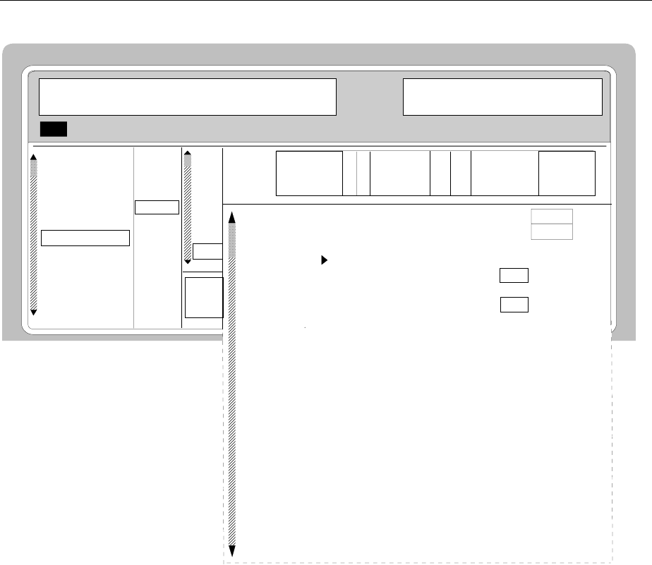
Digital Standard PDC SMIQ
1125.5555.03 2.298 E-9
Menu selection: BURST TYPE = VOX (only available with LINK DIRECTION = UPLINK)
FREQ 100. 000 000 0 MHz
FREQUENCY
LEVEL
ANALOG MOD
VECTOR MOD
DIGITAL MOD
DIGITAL STD
LF OUTPUT
SWEEP
LIST
MEM SEQ
UTILITIES
PDC
PHS
IS95
NADC
PDC
GSM
SLOT G R P SYNC CC SF SACCH G2
0 UP 108 4 6 20 8 1 15 118
BURST TYPE... VOX
SLOT LEVEL OFF ATTEN FULL
SET DEFAULT
SCRAMBLE STATE OFF ON
SCRAMBLE START 001 H
SUPER FRAME OFF ON
RCH POSITION 1
------------------BURST CONTENTS----------------
G 000 0000 0000 0000 0000 0000 0000 H
R0H
P26H
SYNC 7 85B4 H
SYNC2 C E450 H
CC 00 H
SF 0 H
SACCH PN9
RCH PN9
G2 00 0000 0000 0000 0000 0000 0000 0000 H
-------------------CHANGE DATA------------------
SELECT DATA LIST... CURRENT: R&STDM
COPY CURRENT DATA LIST...
DELETE DATA LIST...
EDIT DATA LIST...
LEVEL -30.0 dBm
PEP - 27.4 dBm
POWE
SLOT
SAVE
LINK
RATE
SELE
EDIT
0
VO
Fig. 2-194 Menu DIGITAL STD - PDC - SELECT SLOT, LINK DIRECTION = UPLINK, SMIQ
equipped with Modulation Coder SMIQB20 and Data Generator SMIQB11
(SELECT SLOT...)
VOX
(UPLINK ONLY)
BURST TYPE Selection of burst type used to configure the selected slot.
VOX is only available with LINK DIRECTION = UPLINK
selected.
VOX VOX burst
IEC/IEEE-bus command :SOUR:PDC:SLOT2:TYPE VOX
SLOT LEVEL Selection of level for selected slot.
OFF Maximum attenuation
IEC/IEEE :SOUR:PDC:SLOT2:LEV OFF
FULL The level corresponds to the value indicated on
the SMIQ LEVEL display.
IEC/IEEE :SOUR:PDC:SLOT2:LEV FULL
ATTEN The level is reduced by the value set under
SLOT ATTENUATION.
IEC/IEEE :SOUR:PDC:SLOT2:LEV ATT

SMIQ Digital Standard PDC
1125.5555.03 E-92.299
(SELECT SLOT...)
VOX
(UPLINK ONLY)
SET DEFAULT Resets the subsequent parameters to the factory-set values.
IEC/IEEE-bus command SOUR:PDC:SLOT8 PRES
SCRAMBLE Switch on/off of scrambling function. Scrambling with the
continuous scramble sequence from a PN9 generator is
applied to the data fields SF and SACCH.
IEC/IEEE-bus :SOUR:PDC:SLOT2:SCR:STAT ON
SCRAMBLE
START 9 bit input value for initializing the scramble PN9 generator in
hexadecimal form. The value 0 is not permissible, 1 is
preset. The input field is only displayed if SCRAMBLE is
switched on.
IEC/IEEE-bus :SOUR:PDC:SLOT2:SCR:STAR #H2
SUPERFRAME Switch on/off of the superframe generation. 18 frames form a
superframe. If SUPERFRAME is switched on, RCH data
instead of SACCH data will be sent in 2 slots. The first of the
two RCH blocks is fixed in the first slot of the superframe,
the position of the second can be set.
IEC/IEEE-bus :SOUR:PDC:SLOT2:SFR:STAT ON
RCH POSITION Input value for the position of the second RCH block. The
input field is only displayed if SUPERFRAME is switched on.
IEC/IEEE-bus :SOUR:PDC:SLOT2:SFR:RCHP 10
GDisplay of data contents in the 108 bit "Guard" field at the
beginning of the slot in hexadecimal form.
RDisplay of data contents in the 4 bit data field "RAMP" in
hexadecimal form.
PInput value of the 26 bit data field "Preamble".
IEC/IEEE-bus command :SOUR:PDC:SLOT2:PRE #HFF
SYNC Input value for the 20 bit sync word in hexadecimal form.
Depending on the selected slot, the following sync words are
predefined according to the PDC standard:
Slot No. VOX Sync Word
0 785B4
1 62DC9
2 7E28A
3 56B15
4 AE9B3
5 B2621
IEC/IEEE-bus :SOUR:PDC:SLOT2:SYNC #H72DC9

Digital Standard PDC SMIQ
1125.5555.03 2.300 E-9
(SELECT SLOT...)
VOX
(UPLINK ONLY)
SYNC2 Input value for the 20 bit sync word in the first slot of a
superframe in hexadecimal form. This sync word marks the
beginning of a superframe. The input field is only displayed if
SUPERFRAME is switched on. Depending on the selected
slot, the following sync words are predefined according to the
PDC standard:
Slot No. VOX Sync2 Word
0 CE450
1 E1A90
2 18ED3
3 043E0
4 7D861
IEC/IEEE-bus command :SOUR:PDC:SLOT2:SYNC E1A91
CC Input value of the 8 bit data field " Color code ".
IEC/IEEE-bus command :SOUR:PDC:SLOT2:CCOD #HFF
SF Input value of the data field " Steal Flag ".
IEC/IEEE-bus command :SOUR:PDC:SLOT2:SF #H0
SACCH Selection of data source for SACCH field (Slow Associated
Control Channel).
PN.. PRBS data according to CCITT with periods
between 29-1 and 223-1.
IEC/IEEE :SOUR:PDC:SLOT3:SACC PN15
DLIST Data from a programmable data list.
IEC/IEEE :SOUR:PDC:SLOT3:SACC DLIS
SERDATA Data from data input SER DATA.
IEC/IEEE :SOUR:PDC:SLOT3:SACC SDAT
RCH Selection of data source for the RCH data field. RCH data
replace SACCH data in certain slots of a superframe. The
input field is only displayed if SUPERFRAME is switched on.
PN.. PRBS data according to CCITT with periods
between 29-1 and 223-1.
IEC/IEEE :SOUR:PDC:SLOT3:RCH PN9
DLIST Data from a programmable data list.
IEC/IEEE :SOUR:PDC:SLOT3:RCH DLIS
SERDATA Data from data input SER DATA.
IEC/IEEE :SOUR:PDC:SLOT3:RCH SDAT
G2 Display of data contents in the 118 bit "Guard" field at the
end of the slot in hexadecimal form. The field is only
displayed with LINK DIRECTION = UPLINK selected.
Parameter SELECT DATA LIST... to EDIT DATA LIST... see menu selection BURST TYPE = TCH

SMIQ Digital Standard GSM/EDGE
1125.5555.03 E-92.301
2.18 Digital Standard GSM/EDGE
With the options Modulation Coder (SMIQB20) and Data Generator (SMIQB11) provided, modulation
signals according to the GSM standard can be generated. GSM is a TDMA standard for cellular mobile
radio networks used worldwide. SMIQ is suitable for use as a signal generator for all GSM types.
With option SMIQB20, the use of GSM and EDGE slots is not limited. GSM/EDGE may also be used
with the older modulation coder option (SMIQB10), however in this case GSM and EDGE cannot be
mixed.
SMIQ can generate both the transmit signal of a base station (BS) and the transmit signal of a mobile
station (MS). Transmission from BS to MS is called "downlink", "uplink" being used for transmission in
the opposite direction.
Each TDMA frame consists of 8 slots. Each slot can be switched on or off separately. Moreover, a
defined intermediate level can be set.
A burst type has to be defined to configure a slot. The following burst types can be selected:
•NORM the so-called "normal burst",
•DUMMY burst type with a defined data pattern according to GSM standard and
•ALL_DATA burst type for test purposes with freely programmable data contents.
•EDGE the so-called EDGE Normal Burst
The following internal modulation sources are available:
•different PRBS generators with a sequence length between 29-1 and 223-1 and
•data lists, i.e. freely programmable data sequences from the data generator memory.
For generating the GSM signals, SMIQ inserts the modulation data continuously (in real time) into the
selected slots. Using a digital signal processor the data generator generates a data sequence with
modulation data and control signals for envelope control.
The data generator in SMIQ generates a data stream which is converted into IQ signals in the
modulation coder. According to the GSM standard, the modulation type is GMSK at a symbol rate of
270.833 ksymbol/s and Gauss filtering. The symbol rate can be changed in SMIQ. GFSK with adjustable
frequency deviation can be used as a modulation type, too.
The modulation type for EDGE slots is 8PSK, with 3/8π rotation at a symbol rate of 270.833 ksymbols/s
and linear Gauss filter.

Digital Standard GSM/EDGE SMIQ
1125.5555.03 2.302 E-9
2.18.1 Sync and Trigger Signals
The data generator generates a data sequence with modulation data, control signals for envelope
control, and synchronization signals.
When TRIGGER MODE AUTO is selected, the GSM signal generation is started automatically.
This start can also be activated by an external trigger signal (TRIGGER MODE ARMED_AUTO) which
allows a synchronous sequence for BER measurements to be carried out on receivers.
A trigger signal can be fed via the TRIGIN input at connector PAR DATA. The active slope of a trigger
signal applied there executes a trigger event.
GSM signal generation at a frame limit is started after a trigger event. Data from data lists are inserted
into the selected slots starting from the first bit. PRBS generators start with the set initialization status.
Signal generation either starts immediately after the active slope of the trigger signal or after a settable
number of symbols (EXT TRIGGER DELAY). Retriggering (EXT RETRIG) can be inhibited for a settable
number of symbols (EXT RETRIGGER INHIBIT).
A trigger event can be executed manually using EXECUTE TRIGGER or via the IEC/IEEE bus.
When a trigger event is executed, a trigger signal is output at the TRIGOUT 3 output of SMIQ.
SMIQ also generates the following sync signals:
•a slot or frame clock at TRIGOUT 1 output with settable position in the frame,
•a frame or multiframe clock at TRIGOUT 2 output with settable position in the frame,
•the symbol clock and the bit clock.
A clock synthesizer on the modulation coder generates the symbol clock and the bit clock in SMIQ. The
two clocks are identical for GSM. All the clock signals are synchronized to the 10-MHz reference of
SMIQ. The bit clock is available at connector BIT CLOCK. If required, the clock synthesizer in SMIQ can
be synchronized to an external bit clock.
The clock signal is selected in the menu via CLOCK-CLOCK SOURCE EXT.
To allow for a trouble-free synchronization of the clock synthesizer first apply the external clock and set
the correct symbol rate at SMIQ. Then switch CLOCK SOURCE from INT to EXT.
Note: The set symbol rate should not differ by more than 1% from the symbol rate of the external
signal.
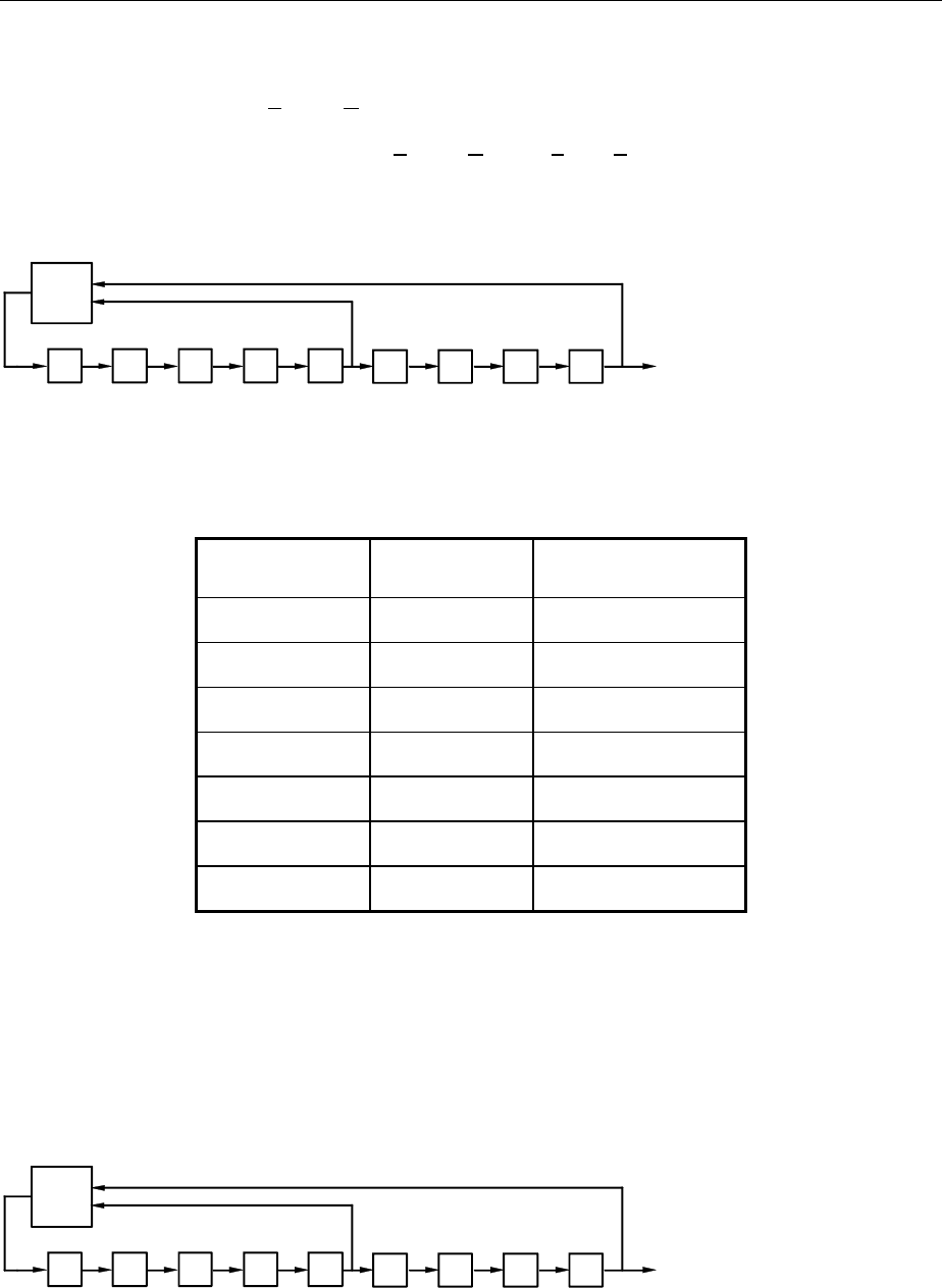
SMIQ Digital Standard GSM/EDGE
1125.5555.03 E-92.303
2.18.2 PN Generators as Internal Data Source
Independent PN generators (Pseudo Noise) can be selected for each slot as data source for data field
DATA. These PN generators provide pseudo-random bit sequences of different length or period. That is
why they are also called PRBS generators (Pseudo Random Binary Sequence).
Data sequences are sequences of maximum length which are generated by means of feedback shift
registers.
The following figure gives an example of a 9 bit generator with feedbacks after register 4 and 0 (output).
8
765
4
3210
DATA
EXOR
The pseudo-random sequence of a PRBS generator is clearly defined by the number of registers and
the feedback. The following table describes all PRBS generators available:
Table 2-31 PRBS generators for GSM
PRBS generator Length in bits Feedback after
9 bit 29 -1 = 511 Register 4, 0
11 bit 211 -1 =2047 Register 2, 0
15 bit 215 -1 = 32767 Register 1, 0
16 bit 216 -1 = 65535 Register 5, 3, 2, 0
20 bit 220 -1 = 1048575 Register 3, 0
21 bit 221 -1 = 2097151 Register 2, 0
23 bit 223 -1 = 8388607 Register 5, 0
PN generators PN9,11,15, 20 and PN23 are configured according to CCITT Rec. 0.151/152/153. The
output sequence is inverted for generators PN15 and PN23.
The start value of the PN generators is different in the slots and equals
start value hex slotnumber=+ ×114
Example: PN9 generator in slot 1 with start value 15hex = 10101 binary.
10
DATA
EXOR
1100
0
0
0
The resulting output sequence is 1010100000010100101011110010 etc.

Digital Standard GSM/EDGE SMIQ
1125.5555.03 2.304 E-9
2.18.3 Lists as Internal Data Source
A freely programmable memory on the data generator serves as internal data source for the data fields
of the slots. The data are managed in so-called lists. A list editor allows data lists (DATA LIST) to be
selected, copied, modified, and deleted.
The list editor is available via menu DIGITAL-MOD - SOURCE....
2.18.4 External Modulation Data
External data can (only) be applied via the SERDATA interface. A selection of SERDATA as data
source is only possible for a single data field of a slot. For further information on the characteristics of
the SERDATA interface see Annex A.
To ensure that the external data bits are assigned to specific positions in the data field of the selected
slot and that they are reproducible, the buffer of the RS-232 transmitter and receiver has to be deleted.
A triggered start has to follow.
The following setting sequence is required in the DIGITAL STD - GSM/EDGE menu:
1. Carry out desired settings in menu.
2. Select data source SERDATA for the data field of the slot using SELECT SLOT - ....
3. Make connection to external data source, but do not yet start external data source.
4. Switch off digital standard using STATE - OFF.
5. Set TRIGGER MODE ARMED_AUTO.
In this state, SMIQ is ready for reception, but discards data that are read in via SERDATA.
6. Switch on digital standard with STATE ON.
7. Start external data source.
The read-in data are written into the receiving buffer. Only if this buffer is filled can SMIQ react to a
trigger event.
8. Activate trigger event. Signal generation is thus started at a frame limit. The first bit received via
SERDATA is put to the first bit position in the selected data field.
SMIQ Digital Standard GSM/EDGE
1125.5555.03 E-92.305
2.18.5 Menu DIGITAL STANDARD - GSM/EDGE
Menu DIGITAL STD - GSM/EDGE provides access to settings for generating GSM signals.
Menu selection: DIGITAL STD - GSM/EDGE
Fig. 2-195 Menu DIGITAL STD - GSM/EDGE, SMIQ equipped with Modulation Coder SMIQB20 and
Data Generator SMIQB11
STATE Switch on/off of Digital Standard GSM/EDGE modulation. Vector Modulation
or Digital Modulation will be switched off automatically.
IEC/IEEE-bus command SOUR:GSM:STAT ON
MODULATION... Opens a window for setting the modulation parameters.
Fig. 2-196 Menu DIGITAL STD - GSM/EDGE - MODULATION..., SMIQ equipped with Modulation
Coder SMIQB20 and Data Generator SMIQB11
MODULATION... SET TO
STANDARD Sets the subsequent modulation parameters to the
values predefined by the standard.
SYMBOL RATE Input value for the symbol clock. 270.833 ksymbol/s
are preset.
IEC/IEEE-bus :SOUR:GSM:SRAT 270KHZ

Digital Standard GSM/EDGE SMIQ
1125.5555.03 2.306 E-9
(MODULATION...) The following parameters are used with GSM
MODULATION TYPE Opens a window for selection of the modulation type.
GMSK Gaussian Minimum Shift Keying
GFSK Gaussian filtered Frequency Shift Keying
IEC/IEEE-bus SOUR:GSM:FORMat GMSK
FSK DEVIATION Input value of deviation with GFSK selected.
With GMSK selected, the deviation is fixed to the
fourth part of the symbol rate.
IEC/IEEE-bus SOUR:GSM:FSK:DEV 67 KHZ
FILTER TYPE Display of the baseband filter for GSM.
FILTER PARAMETER Input value for the B×T value (Gaussian filter).
IEC/IEEE-bus SOUR:GSM:FILT:PAR 0.31
The following parameters are used with EDGE
MODULATION TYPE The modulation type for EDGE is displayed. It is
permanently set to 8PSK EDGE. In contrast to the
modulation types for GSM, the one for EDGE has
three bits per symbol.
FILTER TYPE The filter for EDGE is displayed. It is permanently set
to GAUSS LINEAR.
TRIGGER MODE... Opens a window for selecting the trigger mode.
AUTO The GSM signals are continuously transmitted in the
activated slots.
IEC/IEEE-bus command SOUR:GSM:SEQ AUTO
RETRIG The GSM signals are continuously transmitted in the
activated slots. A trigger event causes a restart.
IEC/IEEE-bus command SOUR:GSM:SEQ RETR
ARMED_AUTO The GSM signal generation does not start until a
trigger event has occurred. The unit then
automatically switches over to the AUTO mode and
can no longer be triggered.
IEC/IEEE-bus command SOUR:GSM:SEQ AAUT
ARMED_RETRIG The GSM signal generation does not start until a
trigger event has occurred. The unit then
automatically switches over to the RETRIG mode.
Each new trigger event causes a restart.
IEC/IEEE-bus command SOUR:GSM:SEQ ARET
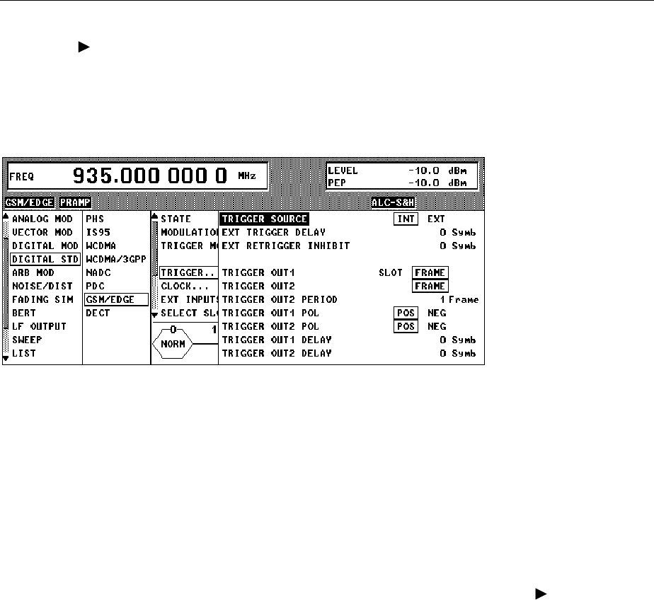
SMIQ Digital Standard GSM/EDGE
1125.5555.03 E-92.307
EXECUTE
TRIGGER Executes a trigger even to start the GSM signal generation.
IEC/IEEE-bus command :TRIG:DM:IMM
TRIGGER... Opens a window for selecting the trigger source, for configuring the trigger
output signals and for setting the time delay of an external trigger signal.
Fig. 2-197 Menu DIGITAL STD - GSM/EDGE_TRIGGER..., SMIQ equipped with Modulation Coder
SMIQB20 and Data Generator SMIQB11
(TRIGGER...) TRIGGER SOURCE Selection of trigger source.
EXT The GSM signal generation is started by
the active slope of an external trigger
signal.
The polarity, the trigger threshold and
the input resistance of the TRIGIN input
can be modified in menu
DIGITAL MOD - EXT INPUTS.
INT A trigger event can be executed by
EXECUTE TRIGGER .
IEC/IEEE-bus SOUR:GSM:TRIG:SOUR EXT
EXT TRIGGER
DELAY Setting the number of symbols by which an external
trigger signal is delayed before it starts the GSM
signal generation.
This is used for setting the time synchronization
between the SMIQ and the DUT.
IEC/IEEE-bus SOUR:GSM:TRIG:DEL 3
(TRIGGER...) EXT RETRIGGER
INHIBIT Setting the number of symbols for which a restart is
inhibited after a trigger event.
With TRIGGER MODE RETRIG selected, each new
trigger signal restarts the GSM signal generation.
This restart can be inhibited for the entered number
of symbols.
Example:
The entry of 1000 symbols causes new trigger
signals to be ignored for the duration of 1000 sym-
bols after a trigger event
IEC/IEEE-bus SOUR:GSM:TRIG:INH 1000

Digital Standard GSM/EDGE SMIQ
1125.5555.03 2.308 E-9
TRIGGER OUT 1 Selecting the signal for TRIGOUT 1 output in
PARDATA connector.
The times only apply if the default value of 270.833
ksps for GSM/EDGE is used as the symbol rate in
the Modulation menu.
SLOT 0.577 ms e.g. clock
IEC/IEEE-bus command:
:SOUR:GSM:TRIG:OUTP1 SLOT
FRAME 4.615 ms frame clock
IEC/IEEE-bus command:
:SOUR:GSM:TRIG:OUTP1 FRAM
TRIGGER OUT 2 Selecting the signal for TRIGOUT 2 output in
PARDATA connector.
The times only apply if the default value of 270.833
ksps for GSM/EDGE is used as the symbol rate in
the Modulation menu.
FRAME 4.615 ms frame clock
IEC/IEEE-bus command:
:SOUR:GSM:TRIG:OUTP2 FRAM
TRIGGER OUT 1/2
DELAY Input value of delay of trigger signal at TRIGOUT 2
output compared with beginning of slot or frame.
IEC/IEEE-bus SOUR:GSM:TRIG:OUTP:DEL 2
TRIGGER OUT2
PERIOD Input value of output signal period at TRIGOUT 2
output given in frames.
IEC/IEEE-bus SOUR:GSM:TRIG:OUTP:PER 1
TRIGGER OUT 1/2 POL Selecting the polarity of signals at the TRIGOUT 1
and TRIGOUT 2 outputs in the PARDATA
connector.
IEC/IEEE-bus command
:SOUR:GSM:TRIG:OUTP2:POL POS
CLOCK... Opens a window for selecting the clock source and for setting a delay.
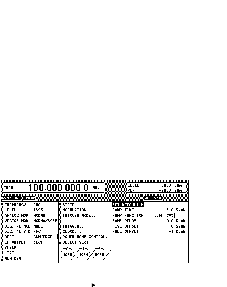
SMIQ Digital Standard GSM/EDGE
1125.5555.03 E-92.309
Fig. 2-198 Menu DIGITAL STD - GSM/EDGE - CLOCK..., SMIQ equipped with Modulation Coder
SMIQB20 and Data Generator SMIQB11
(CLOCK...) CLOCK SOURCE Selection of clock source.
INT SMIQ uses internally generated clock signals.
EXT An external bit clock is fed in at connector
BIT CLOCK. The clock synthesizer on the
modulation coder is synchronized to this
clock.
The symbol rate has to be set with an
accuracy of ± 1 %.
The polarity, the trigger threshold and the
input resistance of the clock inputs can be
modified in menu DIGITAL MOD - EXT
INPUTS.
IEC/IEEE-bus SOUR:GSM:CLOC:SOUR INT
DELAY Setting the delay of generated modulation signal to an
external clock.
This can be used, for example, for synchronization with a
second unit to achieve time synchronization between the
modulation signals of the two units.
IEC/IEEE-bus SOUR:GSM:CLOC:DEL 0.5
POWER RAMP
CONTROL... Opens a window for setting the envelope control, especially for the rising and
falling ramp at the beginning and end of a slot.
Fig. 2-199 Menu DIGITAL STD - GSM/EDGE - POWER RAMP CONTROL... , SMIQ equipped with
Modulation Coder SMIQB20 and Data Generator SMIQB11
(POWER RAMP
CONTROL...) SET DEFAULT Resets the subsequent parameters to the factory-set
values.
IEC/IEEE-bus :SOUR:GSM:PRAM:PRES
RAMP TIME Input value for the rise and fall time of the envelope
at the beginning or end of a slot. The time is set in
units of symbol period.
IEC/IEEE-bus SOUR:GSM:PRAM:TIME 2.5
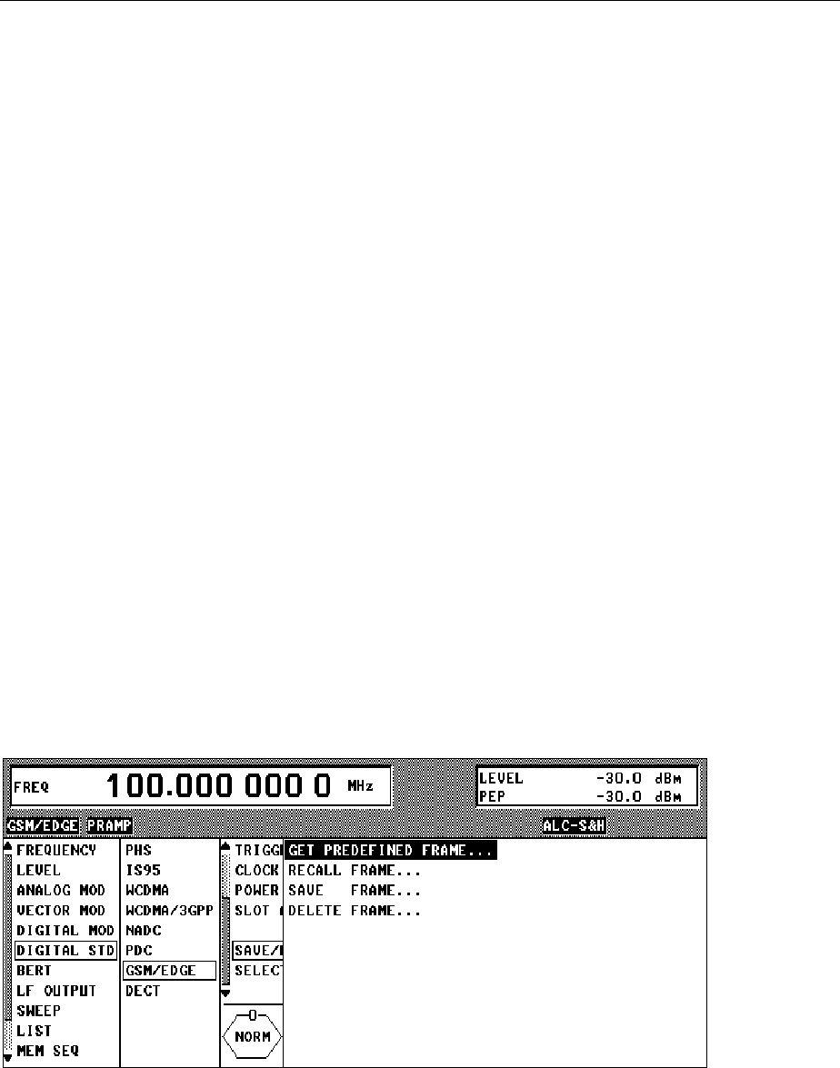
Digital Standard GSM/EDGE SMIQ
1125.5555.03 2.310 E-9
(POWER RAMP
CONTROL...) RAMP FUNCTION Selection of shape of rising and falling ramp for
envelope control.
LIN Linear ramp function.
COS Cosine function. A more favourable
spectrum than that of the LIN function is
obtained.
IEC/IEEE-bus SOUR:GSM:PRAM:SHAP LIN
RAMP DELAY Input value for a shift of the envelope characteristic
to the modulated signal. A positive value causes a
delay of the envelope. The values are set in the units
of the symbol length.
IEC/IEEE-bus SOUR:GSM:PRAM:DEL 0.1
RISE OFFSET Input value for a positive or negative offset of the
rising ramp of the envelope at the beginning of a slot.
IEC/IEEE-bus SOUR:GSM:PRAM:ROFF -1
FALL OFFSET Input value for a positive or negative offset of the
falling ramp of the envelope at the end of a slot.
IEC/IEEE-bus SOUR:GSM:PRAM:FOFF 1
SLOT ATTENUATION Input value in dB for the level reduction of all active slots whose SLOT LEVEL
was set to ATTEN. Menu SELECT SLOT allows the slots to be determined
whose level is to be reduced.
IEC/IEEE-bus command SOUR:GSM:SLOT:ATT 40 DB
SAVE/RCL FRAME... Opens a window for saving and loading a frame configuration. Loading a
frame affects all parameters that can be set under SELECT SLOT.
Fig. 2-200 Menu DIGITAL STD - GSM/EDGE - SAVE/RCL FRAME, SMIQ equipped with Modulation
Coder SMIQB20 and Data Generator SMIQB11
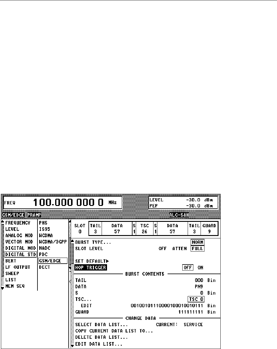
SMIQ Digital Standard GSM/EDGE
1125.5555.03 E-92.311
(SAVE/RCL FRAME...) GET PREDEFINED
FRAME... Loads a factory-set frame configuration.
NB0 Normal Burst in slot 0
IEC/IEEE-bus :SOUR:GSM:FLIS:PRED:LOAD "nb0"
RECALL FRAME... Loads a frame configuration saved by the user.
IEC/IEEE-bus :SOUR:GSM:FLIS:LOAD "name"
SAVE FRAME... Saves a user-defined frame configuration.
IEC/IEEE-bus :SOUR:GSM:FLIS:STOR "name"
DELETE FRAME... Deletes a frame configuration saved by the user.
IEC/IEEE-bus :SOUR:GSM:FLIS:DEL "name"
SELECT SLOT... Selection of one of 8 possible slots. When selecting the slot, a window is
opened in which the data contents belonging to this slot can be defined.
If the cursor is placed onto a slot in the diagram, it may be switched on and off
by pressing one of the unit keys (toggle function).
Menu selection: BURST TYPE = NORM
Fig. 2-201 Menu DIGITAL STD - GSM/EDGE - SELECT SLOT - NORM, SMIQ equipped with
Modulation Coder SMIQB20 and Data Generator SMIQB11

Digital Standard GSM/EDGE SMIQ
1125.5555.03 2.312 E-9
(SELECT SLOT...)
NORM BURST TYPE Opens a window for the selection of the burst type used to
configure the selected slot.
NORM Normal Burst
IEC/IEEE :SOUR:GSM:SLOT2:TYPE NORM
SLOT LEVEL Selection of level for selected slot.
OFF Maximum attenuation
IEC/IEEE :SOUR:GSM:SLOT2:LEV OFF
FULL The level corresponds to the value indicated on
the SMIQ LEVEL display.
IEC/IEEE :SOUR:GSM:SLOT2:LEV FULL
ATTEN The level is reduced by the value set under
SLOT ATTENUATION.
IEC/IEEE :SOUR:GSM:SLOT2:LEV ATT
SET DEFAULT Resets the subsequent parameters to the factory-set values.
IEC/IEEE-bus command :SOUR:GSM:SLOT8:PRES
HOP TRIGGER Switches the HOP trigger signal on or off. With ON selected,
a HOP signal will be generated at the end of the selected
slot. The signal is available at the HOP output of the
PARDATA connector. It can be used to perform a frequency
hop mode in the LIST MODE (see section 'List Mode').
IIEEE-bus command SOUR:GSM:SLOT1:HOPP:TRIG
TAIL Display of data contents in the 3 bit data field "Tail". The tail
bits are set to 000 according to the GSM standard.
DATA Selection of data source for DATA fields. These fields are
regarded as a continuous field, i.e. a pseudo-random
sequence is fully continued from one DATA field to the next.
The following data sources are available:
PN.. PRBS data according to CCITT with periods
between 29-1 and 223-1.
IEC/IEEE :SOUR:GSM:SLOT3:DATA PN15
DLIST Data from a programmable data list.
IEC/IEEE :SOUR:GSM:SLOT3:DATA DLIS
SERDATA Data from data input SER DATA.
IEC/IEEE :SOUR:GSM:SLOT3:DATA SDAT
SSetting for the so-called "Stealing Flag". The selected setting
is valid for the two S fields.
IEC/IEEE-bus command SOUR:GSM:SLOT2:SF 1
TSC... Opens a window for selecting the so-called "Training
Sequence Code". A selection between 8 different training
sequences is possible.
IEC/IEEE-bus command SOUR:GSM:SLOT2:TSC 0
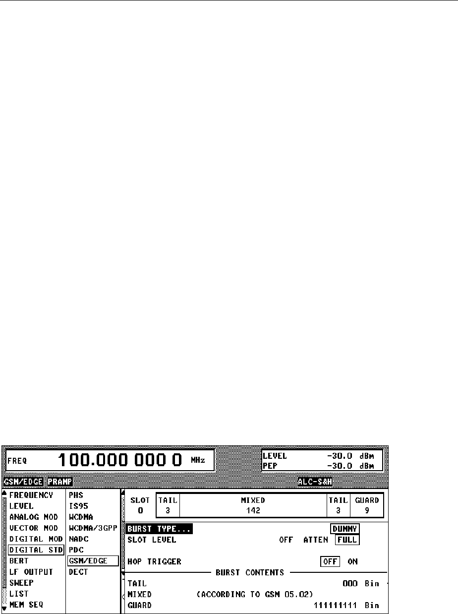
SMIQ Digital Standard GSM/EDGE
1125.5555.03 E-92.313
(SELECT SLOT...)
NORM EDIT Input field for binary modifications of the
training sequence. A modified training
sequence is stored as a USER sequence
after a SAVE FRAME has been called up.
IEC/IEEE-bus command
SOUR:GSM:SLOT2:USER #B011011...
GUARD Display of data content in the "Guard" field in binary form.
The length of the field is 8 bit in slots 1,2,3,5,6,7 and 9 bit in
slots 0 and 4. It is thus ensured that a frame has exactly
1250 bit as stipulated in the GSM standard.
SELECT DATA
LIST... Opens a window for selecting a stored data list or for
generating a new list.
COPY CURRENT
DATA LIST TO... Stores the current data list under a different name.
DELETE DATA
LIST... Deletes a data list.
EDIT DATA
LIST... Opens a window for editing a data list bit-by-bit. The
available storage capacity and the length of the current list is
displayed in parameters FREE and LEN (see also Section
List Editor).
COPY Copies a list range
FILL Fills the range with filler pattern
INSERT Inserts a list range at a different position of the
list
DELETE Deletes a list range
EDIT/VIEW Edits or views the list
Menu selection: BURST TYPE = DUMMY
Fig. 2-202 Menu DIGITAL STD - GSM/EDGE - SELECT SLOT - DUMMY, SMIQ equipped with
Modulation Coder SMIQB20 and Data Generator SMIQB11

Digital Standard GSM/EDGE SMIQ
1125.5555.03 2.314 E-9
(SELECT SLOT...)
DUMMY BURST TYPE Opens a window for the selection of the burst type used to
configure the selected slot.
DUMMY Synchronization Burst
IEC/IEEE-bus command SOUR:GSM:SLOT2:TYPE DUMM
SLOT LEVEL Selection of level for selected slot.
OFF Maximum attenuation
IEC/IEEE :SOUR:GSM:SLOT2:LEV OFF
FULL The level corresponds to the value indicated on
the SMIQ LEVEL display.
IEC/IEEE :SOUR:GSM:SLOT2:LEV FULL
ATTEN The level is reduced by the value set under
SLOT ATTENUATION.
IEC/IEEE .....:SOUR:GSM:SLOT2:LEV ATT
TAIL Display of data content in the 3 bit data field "Tail ". The tail
bits are set to 000 according to the GSM standard.
MIXED Display of data content of the mixed-bit field. It has a data
content stipulated by GSM 05.02, the so-called mixed bits":
11111011011101100000101001001110000010010001000000
01111100011100010111000101110001010111010010100011
001100111001111010011111000100101111101010
GUARD Display of data content in the Guard field in binary form. The
length of the field is 8 bit in slots 1,2,3,5,6,7 and 9 bit in slots
0 and 4. It is thus ensured that a frame has exactly 1250 bit
as stipulated in the GSM standard.
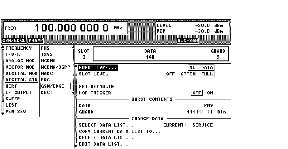
SMIQ Digital Standard GSM/EDGE
1125.5555.03 E-92.315
Menu selection: BURST TYPE = ALL_DATA
Fig. 2-203 Menu DIGITAL STD - GSM/EDGE - SELECT SLOT – ALL_DATA, SMIQ equipped with
Modulation Coder SMIQB20 and Data Generator SMIQB11
(SELECT SLOT...)
ALL_DATA BURST TYPE Opens a window for the selection of burst type used to
configure the selected slot.
ALL_DATA Burst type for testing with freely programmable
data contents.
IEC/IEEE :SOUR:GSM:SLOT2:TYPE ADAT
SLOT LEVEL Selection of level for selected slot.
OFF Maximum attenuation
IEC/IEEE :SOUR:GSM:SLOT2:LEV OFF
FULL The level corresponds to the value indicated on
the SMIQ LEVEL display.
IEC/IEEE :SOUR:GSM:SLOT2:LEV FULL
ATTEN The level is reduced by the value set under
SLOT ATTENUATION.
IEC/IEEE :SOUR:GSM:SLOT2:LEV ATT
DATA Selection of data source for DATA fields. These fields are
regarded as a continuous field, i.e. a pseudo-random
sequence is fully continued from one DATA field to the next.
The following data sources are available:
PN.. PRBS data according to CCITT with periods
between 29-1 and 223-1.
IEC/IEEE :SOUR:GSM:SLOT3:DATA PN15
DLIST Data from a programmable data list.
IEC/IEEE :SOUR:GSM:SLOT3:DATA DLIS
SERDATA Data from data input SER DATA.
IEC/IEEE :SOUR:GSM:SLOT3:DATA SDAT
GUARD Display of data content in the Guard field in binary form. The
length of the field is 8 bit in slots 1,2,3,5,6,7 and 9 bit in slots
0 and 4. It is thus ensured that a frame exactly has 1250 bit
as stipulated in the GSM standard.
Parameter SELECT DATA LIST... to EDIT DATA LIST... see menu selection BURST TYPE = NORM
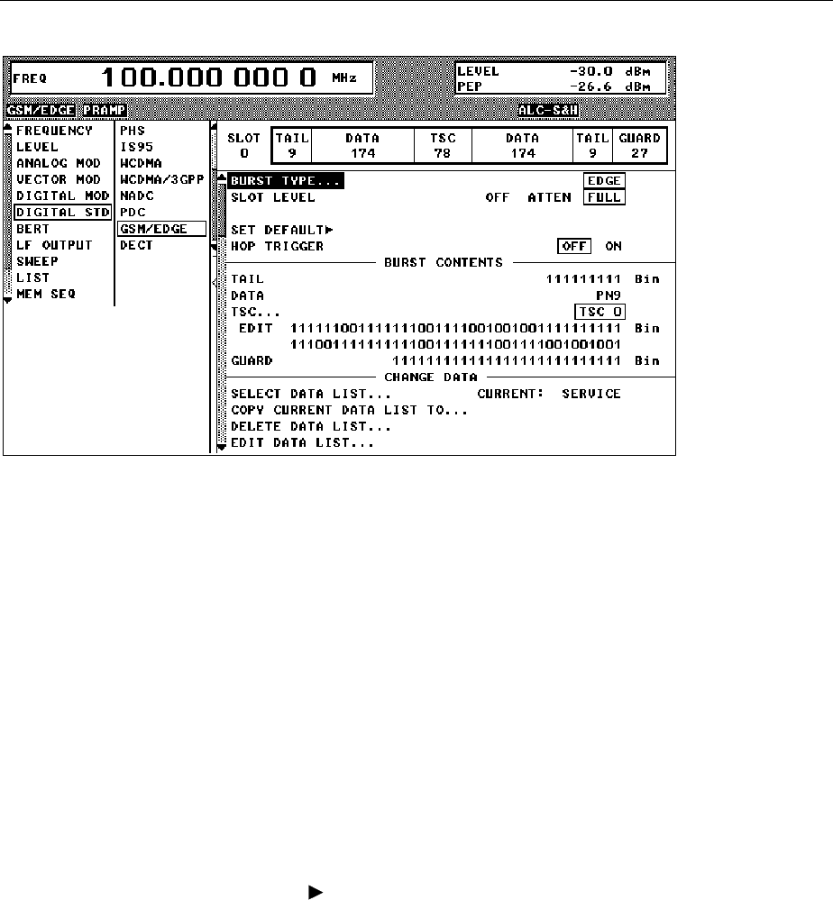
Digital Standard GSM/EDGE SMIQ
1125.5555.03 2.316 E-9
Selection: BURST TYPE = EDGE
Fig. 2-204 Menu DIGITAL STD - GSM/EDGE - SELECT SLOT – EDGE, SMIQ equipped with
Modulation Coder SMIQB20 and Data Generator SMIQB11
(SELECT SLOT...)
EDGE BURST TYPE Opens a window for selecting the burst type to be used for
configuring the selected slot.
EDGE EDGE Normal Burst
IEC/IEEE bus :SOUR:GSM:SLOT2:TYPE EDGE
SLOT LEVEL Selection of the level for the selected slot.
OFF Maximum attenuation
IEC/IEEE bus :SOUR:GSM:SLOT2:LEV OFF
FULL The level is the same as that indicated in the
LEVEL display of SMIQ.
IEC/IEEE bus :SOUR:GSM:SLOT2:LEV FULL
ATTEN The level is reduced by the value set under
SLOT ATTENUATION.
IEC/IEEE bus :SOUR:GSM:SLOT2:LEV ATT
SET DEFAULT Resets the following parameters to the factory-selected values.
IEC/IEEE bus command :SOUR:GSM:SLOT1:PRES
HOP TRIGGER Switches the HOP trigger signal on or off. When set to ON, a
HOP signal is generated at the end of the selected slot. The
signal is available at the HOP output of the PARDATA
connector. It may be used for implementing frequency
hopping in the LIST MODE (see section "List Mode").
IEC/IEEE-bus :SOUR:GSM:SLOT1:HOPP:TRIG
TAIL Display of data contents in the 9-bit data field "Tail". The tail
bits are permanently set to 111111111 in line with the GSM
standard.

SMIQ Digital Standard GSM/EDGE
1125.5555.03 E-92.317
(SELECT SLOT...)
EDGE DATA Selection of the data source for the DATA fields. These fields
are considered as one continuous field, i.e. a pseudo
random sequence continues seamlessly from one DATA
field to the next. The following data sources can be chosen:
PN.. PRBS data according to CCITT with period
lengths between 29-1 and 223-1.
IEC/IEEE :SOUR:GSM:SLOT3:DATA PN15
DLIST Data from a programmable data list.
IEC/IEEE :SOUR:GSM:SLOT3:DATA DLIS
SERDATA Data via the data input SER DATA.
IEC/IEEE :SOUR:GSM:SLOT3:DATA SDAT
TSC... Opens a window for selecting the so-called "training
sequence code". One of eight different training sequences
can be chosen.
IEC/IEEE-bus command :SOUR:GSM:SLOT2:TSC 0
EDIT Field for entering changes to the training
sequence in binary form. A modified training
sequence is saved as USER sequence after
SAVE FRAME was called.
IEC/IEEE bus command
:SOUR:GSM:SLOT2:USER #B011011...
GUARD Display of data contents in the GUARD field in binary form.
The length of the field is 24 bits in slots 1, 2, 3, 5, 6, 7, and
27 bits in slots 0 and 4.
SELECT DATA
LIST... Opens a window for selecting a stored data list or generating
a new list.
COPY CURRENT
DATA LIST TO... Saves the current data list under a different name.
DELETE DATA
LIST... Deletes a data list.
EDIT DATA
LIST... Opens a window for editing a data list bit by bit. The
parameters FREE and LEN indicate the free memory
capacity and the length of the current list (see also chapter 2,
section "List Editor").
COPY Copying part of a list
FILL Filling a part of the list with a pattern
INSERT Inserting a part of the list at a different position
within the list
DELETE Deleting a part of the list
EDIT/VIEW Editing or viewing the list

Digital Standard DECT SMIQ
1125.5555.03 E-92.318
2.19 Digital Standard DECT
With the options Modulation Coder (SMIQB20) and Data Generator (SMIQB11) provided, modulation
signals according to the ETSI DECT standard can be generated. DECT is a TDMA standard for private
and public cordless phones.
SMIQ can generate both the transmit signal of a cell station (FP, Fixed Part) and the transmit signal of a
personal station (PP, Portable Part). Transmission from FP to PP is called "downlink", "uplink" being
used for transmission in the opposite direction.
Uplink and downlink are transmitted in the separate time slots of a frame using the time duplex method.
Each frame consists of 24 slots. The data contents of each slot can be defined individually by SMIQ by
means of a slot editor. Each slot can be switched on or off. A defined intermediate level can also be set.
A maximum of 12 slots within a frame can be switched on simultaneously.
A slot type has to be defined to configure a slot. The following slot types can be selected:
•FULL full slot; simulation of a basic R32 physical channel,
•DOUBLE double slot, simulation of a high capacity R80 physical channel and
•ALL_DATA slot type for test purposes with arbitrarily programmable data contents in full slot
format.
The following internal modulation sources are available:
•different PRBS generators with a sequence length between 29-1 and 223-1 and
•data lists, i.e. freely programmable data sequences from the data generator memory.
For generating DECT signals, SMIQ inserts the modulation data continuously (in real time) into the
selected slots. Using a digital signal processor the data generator generates a data sequence with
modulation data and control signals for envelope control.
The data generator in SMIQ generates a data stream which is converted into IQ signals in the
modulation coder. According to the DECT standard, the default modulation type is GFSK with a symbol
rate of 1152 ksymbols/s and Gauss filtering. Symbol rate and filtering can be changed in SMIQ.
Alternatively, π/4 DQPSK with √cos filtering may be selected.

SMIQ Digital Standard DECT
1125.5555.03 2.319 E-9
2.19.1 Sync and Trigger Signals
The data generator generates a data sequence with modulation data, control signals for envelope
control, and synchronization signals.
When TRIGGER MODE AUTO is selected, the DECT signal generation starts automatically.
This start can also be activated by an external trigger signal (TRIGGER MODE ARMED_AUTO) which
allows a synchronous sequence for BER measurements to be carried out on receivers.
Trigger signals for synchronized sequences can be used for measuring the bit error rate of receivers. A
trigger signal can be fed via the TRIGIN input at connector PAR DATA. The active slope of a trigger
signal applied there executes a trigger event.
DECT signal generation at a frame limit is started after a trigger event. Data from data lists are inserted
into the selected slots starting from the first bit. PRBS generators start with the set initialization status.
Signal generation either starts immediately after the active slope of the trigger signal or after a settable
number of symbols (EXT TRIGGER DELAY). Retriggering (RETRIG) can be inhibited for a settable
number of symbols (EXT RETRIGGER INHIBIT).
A trigger event can be executed manually or via the IEC/IEEE bus using EXECUTE TRIGGER.
When a trigger event is executed, a trigger signal is output at the TRIGOUT 3 output of SMIQ.
SMIQ also generates the following sync signals:
•a frame clock at TRIGOUT 1 output,
•a frame or multiframe clock at TRIGOUT 2 output with settable position in the frame,
•the symbol clock and the bit clock.
A clock synthesizer on the modulation coder generates the symbol clock and the bit clock in SMIQ. All
clock signals are synchronized to the 10-MHz reference of SMIQ. The bit clock is available at connector
BIT CLOCK. If desired, the clock synthesizer in SMIQ can be synchronized to an external bit clock.
The clock source is selected in the CLOCK-CLOCK SOURCE EXT menu.
To allow for a trouble-free synchronization of the clock synthesizer first apply the external clock and set
the correct symbol rate at SMIQ. Then switch CLOCK SOURCE from INT to EXT.
Note: The set symbol rate should not differ by more than 1% from the symbol rate of the external
signal.
Digital Standard DECT SMIQ
1125.5555.03 E-92.320
2.19.2 PN Generators as Internal Data Source
Independent PN generators (Pseudo Noise) can be selected for each slot as data sources for the data
fields A-FIELD, B-FIELD and DATA. These PN generators provide pseudo-random bit sequences of
different length or period. That is why they are also called PRBS generators (Pseudo Random Binary
Sequence).
Data sequences are sequences of maximum length which are generated by means of feedback shift
registers.
The following figure gives an example of a 9-bit generator with feedbacks after register 4 and 0 (output).
8
765
4
3210
DATA
EXOR
The pseudo-random sequence of a PRBS generator is clearly defined by the number of registers and
the feedback. The following table describes all PRBS generators available:
Table 2-32 PRBS generators for DECT
PRBS generator Length in bits Feedback after
9 bit 29 -1 = 511 Register 4, 0
11 bit 211 -1 =2047 Register 2, 0
15 bit 215 -1 = 32767 Register 1, 0
16 bit 216 -1 = 65535 Register 5, 3, 2, 0
20 bit 220 -1 = 1048575 Register 3, 0
21 bit 221 -1 = 2097151 Register 2, 0
23 bit 223 -1 = 8388607 Register 5, 0
PN generators PN9,11,15,20 and PN23 are configured according to CCITT Rec. 0.151/152/153. The
output sequence is inverted for generators PN15 and PN23.
The start value of the PN generators is different in the slots and equals
start value hex slotnumber=+ ×114
Example: PN9 generator in slot 1 with start value 15hex = 10101 binary.
10
DATA
EXOR
1100
0
0
0
The resulting output sequence is 1010100000010100101011110010 etc.

SMIQ Digital Standard DECT
1125.5555.03 2.321 E-9
2.19.3 Lists as Internal Data Source
A freely programmable memory on the data generator serves as an additional internal data source for
the data fields of the slots. The data are managed in so-called lists. A list editor allows to select, copy,
modify and delete data lists (DATA LIST).
The list editor is available via menu DIGITAL-MOD - SOURCE....
2.19.4 External Modulation Data
External data can (only) be applied via the SERDATA interface. A selection of SERDATA as data
source is only possible for a single data field of a slot. For further information on the characteristics of
the SERDATA interface see Annex A.
To ensure that the external data bits are assigned to specific positions in the data field of the selected
slot and that they are reproducible, the buffer of the RS-232 transmitter and receiver has to be deleted.
A triggered start has to follow.
The following setting sequence is required in the DIGITAL STD - DECT menu:
1. Carry out desired settings in menu.
2. Select data source SERDATA for the data field of the slot using SELECT SLOT - ....
3. Make connection to external data source, but do not yet start external data source.
4. Switch off digital standard using STATE - OFF.
5. Set TRIGGER MODE ARMED_AUTO.
In this state, SMIQ is ready for reception, but discards data that are read in via SERDATA.
6. Switch on digital standard with STATE ON.
7. Start external data source.
The read-in data are written into the receiving buffer. Only if this buffer is filled can SMIQ react to a
trigger event.
8. Activate trigger event. Signal generation is thus started at a frame limit. The first bit received via
SERDATA is put to the first bit position in the selected data field.
Digital Standard DECT SMIQ
1125.5555.03 E-92.322
2.19.5 Menu DIGITAL STANDARD - DECT
Menu DIGITAL STD - DECT provides access to settings for generating DECT signals.
Menu selection: DIGITAL STD - DECT
FREQ 100. 000 000 0 MHz
FREQUENCY
LEVEL
ANALOG MOD
VECTOR MOD
DIGITAL MOD
DIGITAL STD
LF OUTPUT
SWEEP
LIST
MEM SEQ
UTILITIES
DECT
PHS
IS-95
NADC
PDC
GSM
DECT
OFF ON
GFSK
AUTO
INT
INT
15.0 dB
0 Bit
0 Bit
NORMAL PROLONGED
LEVEL -30.0 dBm
PEP -30.0 dBm
FULL
STATE
MODULATION...
TRIGGER MODE...
EXECUTE TRIGGER
TRIGGER...
CLOCK...
POWER RAMP CONTROL...
SLOT ATTENUATION
TIMING ADJUSTMENT SIMULATION
JITTER SIMULATION
PREAMBLE
SAVE/RCL FRAME...
SELECT SLOT
1234567
0
Fig. 2-205 Menu DIGITAL STD - DECT, SMIQ equipped with Modulation Coder SMIQB20 and Data
Generator SMIQB11
STATE Switch on/off of Digital Standard DECT modulation. Vector Modulation or
Digital Modulation will be switched off automatically.
IEC/IEEE-bus command :SOUR:DECT:STAT ON
MODULATION... Opens a window for setting some of the modulation parameters.
FREQ 100. 000 000 0 MHz
FREQUENCY
LEVEL
ANALOG MOD
VECTOR MOD
DIGITAL MOD
DIGITAL STD
LF OUTPUT
SWEEP
LIST
MEM SEQ
UTILITIES
DECT
PHS
IS-95
NADC
PDC
GSM
DECT
STATE
MODULATION...
TRIGGER MODE..
EXECUTE TRIGGER
TRIGGER....
CLOCK...
POWER RAMP CONT...
SLOT ATTENUAT
LEVEL -30.0 dBm
PEP - 30.0.dBm
FULL
01
SET TO STANDARD
MODULATION TYP GFSK
FSK DEVIATION 288.0 kHz
SYMBOL RATE 1 152 000.0 sym/s
FILTER TYPE SQRCOS COS GAUSS
FILTER PARAMETER 0.50
Fig. 2-206 Menu DIGITAL STD - DECT - MODULATION...

SMIQ Digital Standard DECT
1125.5555.03 2.323 E-9
(MODULATION...) SET TO
STANDARD Sets the subsequent modulation parameters to the
values predefined by the standard.
IEC/IEEE-bus :SOUR:DECT:STAN
MODULATION TYPE Selection of the modulation type. GFSK is preset.
IEC/IEEE-bus :SOUR:DECT:FORM GFSK
FSK DEVIATION Input value for the frequency deviation for GFSK
modulation
IEC/IEEE-bus :SOUR:DECT:FSK 280 KHZ
SYMBOL RATE Input value for the symbol rate. 1152 ksymbols/s are
preset.
IEC/IEEE-bus :SOUR:DECT:SRAT 1151 KHZ
FILTER TYPE Selection of baseband filter. For π/4 DQPSK modul-
ation, a selection between Nyquist filters COS and
SQRCOS or a user-defined filter USER (cf. Section
Digital Modulation) is possible.
IEC/IEEE-bus :SOUR:DECT:FILT:TYPE COS
FILTER PARAMETER Input value for the BT value for Gauss filtering or for
the roll-off factor for Nyquist filtering.
IEC/IEEE-bus SOUR:DECT:FILT:PAR 0.51
TRIGGER MODE... Opens a window for selecting the trigger mode.
AUTO The DECT signals are continuously transmitted in the
activated slots.
IEC/IEEE-bus command SOUR:DECT:SEQ AUTO
RETRIG The DECT signals are continuously transmitted in the
activated slots. A trigger event causes a restart. This
mode is not available if values different from zero are
set for TIMING ADJUSTMENT or JITTER
SIMULATION.
IEC/IEEE-bus command :SOUR:DECT:SEQ RETR
ARMED_AUTO DECT signal generation does not start until a trigger
event has occurred. The unit then automatically
switches over to the AUTO mode and can no longer be
triggered.
IEC/IEEE-bus command :SOUR:DECT:SEQ AAUT
ARMED_RETRIG DECT signal generation does not start until a trigger
event has occurred. The unit then automatically
switches over to the RETRIG mode. Each new trigger
event causes a restart. This mode is not available if
values different from zero are set for TIMING
ADJUSTMENT or JITTER SIMULATION.
IEC/IEEE-bus command :SOUR:DECT:SEQ ARET

Digital Standard DECT SMIQ
1125.5555.03 E-92.324
EXECUTE
TRIGGER Executes a trigger even to start the DECT signal generation. This menu item
is not available if TRIGGER MODE - AUTO is set.
IEC/IEEE-bus command :TRIG:DM:IMM
TRIGGER... Opens a window for selecting the trigger source, for configuring the trigger
output signals and for setting the time delay of an external trigger signal.
FREQ 100. 000 000 0 MHz
FREQUENCY
LEVEL
ANALOG MOD
VECTOR MOD
DIGITAL MOD
DIGITAL STD
LF OUTPUT
SWEEP
LIST
MEM SEQ
UTILITIES
DECT
PHS
IS-95
NADC
PDC
GSM
DECT
STATE
MODULATION...
TRIGGER MODE
EXECUTE TRIG
TRIGGER....
CLOCK...
POWER RAMP C>
SLOT ATTENUA
TRIGGER SOURCE INT EXT
EXT TRIGGER DELAY 0 Symb
EXT RETRIGGER INHIBIT 0 Symb
TRIGGER OUT2 DELAY 0 Symb
TRIGGER OUT2 PERIOD 1 Frame
LEVEL -30.0 dBm
PEP - 30.0 dBm
FULL
01
Fig. 2-207 Menu DIGITAL STD - DECT_TRIGGER..., SMIQ equipped with Modulation Coder
SMIQB20 and Data Generator SMIQB11
(TRIGGER...) TRIGGER SOURCE Selection of trigger source.
EXT The DECT signal generation is started
by the active slope of an external trigger
signal.
The polarity, the trigger threshold and
the input resistance of the TRIGIN input
can be modified in menu DIGITAL MOD
- EXT INPUTS.
INT A trigger event can be executed by
EXECUTE TRIGGER .
IEC/IEEE-bus :SOUR:DECT:TRIG:SOUR EXT

SMIQ Digital Standard DECT
1125.5555.03 2.325 E-9
(TRIGGER...) EXT TRIGGER
DELAY Setting the number of symbols by which an external
trigger signal is delayed before it starts the DECT
signal generation.
This is used for setting the time synchronization
between the SMIQ and the DUT.
IEC/IEEE-bus :SOUR:DECT:TRIG:DEL 3
EXT RETRIGGER
INHIBIT Setting the number of symbols for which a restart is
inhibited after a trigger event.
With TRIGGER MODE RETRIG selected, each new
trigger signal restarts the DECT signal generation.
This restart can be inhibited for the entered number
of symbols.
Example:
The entry of 1000 symbols causes new trigger
signals to be ignored for the duration of 1000 sym-
bols after a trigger event
IEC/IEEE-bus :SOUR:DECT:TRIG:INH 1000
TRIGGER OUT2
DELAY Input value of delay of trigger signal at TRIGOUT 2
output compared with beginning of frame.
IEC/IEEE-bus :SOUR:DECT:TRIG:OUTP:DEL 2
TRIGGER OUT2
PERIOD Input value of output signal period at TRIGOUT 2
output given in frames.
IEC/IEEE-bus :SOUR:DECT:TRIG:OUTP:PER 1
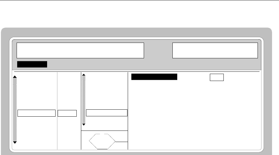
Digital Standard DECT SMIQ
1125.5555.03 E-92.326
CLOCK... Opens a window for selecting the clock source and for setting a delay.
FREQ 100. 000 000 0 MHz
FREQUENCY
LEVEL
ANALOG MOD
VECTOR MOD
DIGITAL MOD
DIGITAL STD
LF OUTPUT
SWEEP
LIST
MEM SEQ
UTILITIES
DECT
PHS
IS-95
NADC
PDC
GSM
DECT
STATE
MODULATION...
TRIGGER MODE
EXECUTE TRIG
TRIGGER....
CLOCK...
POWER RAMP C>
SLOT ATTENUA
CLOCK SOURCE INT EXT
DELAY 0.00 Symb
LEVEL -30.0 dBm
PEP - 30.0 dBm
FULL
01
Fig. 2-208 Menu DIGITAL STD - DECT - CLOCK..., SMIQ equipped with Modulation Coder SMIQB20
and Data Generator SMIQB11
(CLOCK...) CLOCK SOURCE Selection of clock source.
INT SMIQ uses internally generated clock signals.
EXT An external symbol clock or bit clock is fed in
at connectors SYMBOL CLOCK or BIT
CLOCK. The clock synthesizer on the
modulation coder is synchronized to this
clock.
The symbol rate has to be set with an
accuracy of ± 1 %.
The polarity, the trigger threshold and the
input resistance of the clock inputs can be
modified in menu DIGITAL MOD - EXT
INPUTS.
IEC/IEEE-bus command :SOUR:DECT:CLOC:SOUR INT
DELAY Setting the delay of generated modulation signal to an
external clock.
This can be used, for example, for synchronization with a
second unit to achieve time synchronization between the
modulation signals of the two units.
IEC/IEEE-bus command :SOUR:DECT:CLOC:DEL 0.5
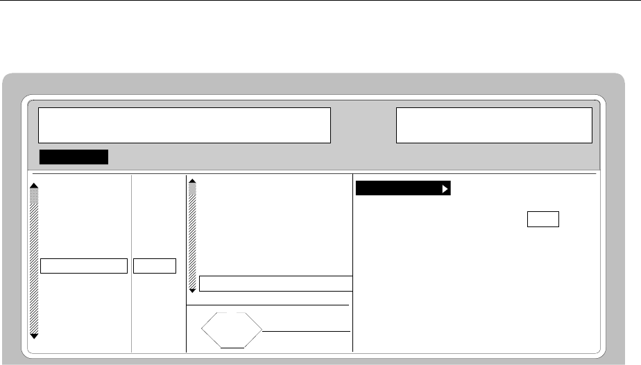
SMIQ Digital Standard DECT
1125.5555.03 2.327 E-9
POWER RAMP
CONTROL... Opens a window for setting the envelope control, especially for the rising and
falling ramp at the beginning and end of a slot.
FREQ 100. 000 000 0 MHz
FREQUENCY
LEVEL
ANALOG MOD
VECTOR MOD
DIGITAL MOD
DIGITAL STD
LF OUTPUT
SWEEP
LIST
MEM SEQ
UTILITIES
DECT
PHS
IS-95
NADC
PDC
GSM
DECT
STATE
MODULATION...
TRIGGER MODE...
EXECUTE TRIGGER
TRIGGER....
CLOCK...
POWER RAMP CONTROL...
SLOT ATTENUATION
SET DEFAULT
RAMP TIME 2.0 Symb
RAMP FUNCTIOM LIN COS
RAMP DELAY 0.0 Symb
RISE OFFSET 0 Symb
FALL OFFSET 0 Symb
LEVEL -30.0 dBm
PEP - 30.0 dBm
FULL
01 2
Fig. 2-209 Menu DIGITAL STD - DECT - POWER RAMP CONTROL... , SMIQ equipped with
Modulation Coder SMIQB20 and Data Generator SMIQB11
(POWER RAMP
CONTROL...) SET DEFAULT Sets the subsequent parameters to factory-set
default values.
IEC/IEEE-bus SOUR:DECT:PRAM:PRES
RAMP TIME Input value for the rise and fall time of the envelope
at the beginning or end of a slot. The time is set in
units of the symbol period.
IEC/IEEE-bus SOUR:DECT:PRAM:TIME 1.5
RAMP FUNCTION Selection of shape of rising and falling ramp for
envelope control.
LIN Linear ramp function.
COS Cosine function. A more favorable
spectrum than that of the LIN function is
obtained.
IEC/IEEE-bus SOUR:DECT:PRAM:SHAP LIN
RAMP DELAY Input value for a shift of the envelope characteristic
to the modulated signal. A positive value causes a
delay of the envelope. The values are set in units of
the symbol length.
IEC/IEEE-bus SOUR:DECT:PRAM:DEL 0.1
RISE OFFSET Input value for a positive or negative offset of the
rising ramp of the envelope at the beginning of a slot.
IEC/IEEE-bus SOUR:DECT:PRAM:ROFF -1
FALL OFFSET Input value for a positive or negative offset of the
falling ramp of the envelope at the end of a slot.
IEC/IEEE-bus :SOUR:DECT:PRAM:FOFF 1

Digital Standard DECT SMIQ
1125.5555.03 E-92.328
SLOT ATTENUATION Input value for the level attenuation in dB of all active slots whose SLOT
LEVEL was set to ATTEN. The slots whose level is to be attenuated are
defined in the menu SELECT SLOT.
IEC/IEEE-bus command :SOUR:DECT:SLOT:ATT 40 DB
TIMING
ADJUSTMENT
SIMULATION
Input value for the number of bits used for simulating "Timing Adjust" in DECT
instruments. Each 35
th
frame is extended (positive input values) or shortened
(negative values) by the number of bits set.
IEC/IEEE-bus command :SOUR:DECT:SIM:TADJ -1
JITTER SIMULATION Input value for the number of bits used for jitter simulation. A jitter is simulated
by advancing the selected number of bits for even-numbered frames in time
whereas ordinary timing is generated for odd-numbered frames.
IEC/IEEE-bus command :SOUR:DECT:SIM:JITT 1
PREAMBLE Selection of the preamble type for full and double slot.
NORMAL The preamble field has a length of 16 bits.
PROLONGED The preamble field has a length of 32 bits.
IEC/IEEE-bus command :SOUR:DECT:PRE NORM
SAVE/RCL FRAME... Opens a window for saving and loading a frame configuration. Loading a
frame affects all parameters that can be set under SELECT SLOT.
FREQ 100. 000 000 0 MHz
FREQUENCY
LEVEL
ANALOG MOD
VECTOR MOD
DIGITAL MOD
DIGITAL STD
LF OUTPUT
SWEEP
LIST
MEM SEQ
UTILITIES
DECT
PHS
IS95
NADC
PDC
GSM
DECT
TRIGGER....
CLOCK...
POWER RAMP C>
SLOT ATTENUA
TIMING ADJUS
JITTER SIMUL
PREAMBLE
SAVE/RCL FRA
GET PREDEFINED FRAME...
RECALL FRAME...
SAVE FRAME...
DELETE FRAME...
LEVEL -30.0 dBm
PEP - 30.0 dBm
FULL
01
Fig. 2-210 Menu DIGITAL STD - DECT - SAVE/RCL FRAME, SMIQ equipped with Modulation Coder
SMIQB20 and Data Generator SMIQB11

SMIQ Digital Standard DECT
1125.5555.03 2.329 E-9
(SAVE/RCL FRAME...) GET PREDEFINED
FRAME... Loads a factory-set frame configuration.
DNFULL All downlink slots numbered 0 to 11
are active as full slots.
UPFULL All uplink slots numbered 12 to 23 are
active as full slots.
FULL_0 Only slot no. 0 is active as a full slot.
DOUB_0 Slots no. 0 and 1 are active as double
slots.
IEEE SOUR:DECT:FLIS:PRED:LOAD "name"
RECALL FRAME... Loads a frame configuration saved by the user.
IEC/IEEE-bus SOUR:DECT:FLIS:LOAD "name"
SAVE FRAME... Saves a user-defined frame configuration.
IEC/IEEE-bus SOUR:DECT:FLIS:STOR "name"
DELETE FRAME... Deletes a frame configuration saved by the user.
IEC/IEEE-bus SOUR:DECT:FLIS:DEL "name"
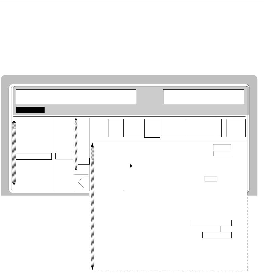
Digital Standard DECT SMIQ
1125.5555.03 E-92.330
SELECT SLOT... Selection of one of 24 possible slots. When selecting the slot, a window is
opened in which the data contents belonging to this slot can be defined.
12 slots are available for uplink and downlink, respectively. They are labeled
UP<i> and DN<i> in the display where i varies from 0 to 23. Up to 12 of the 24
slots can be active at the same time.
If the cursor is placed onto a slot in the diagram, the SLOT LEVEL may be
modified by pressing one of the unit keys (toggle function).
FREQ 100. 000 000 0 MHz
FREQUENCY
LEVEL
ANALOG MOD
VECTOR MOD
DIGITAL MOD
DIGITAL STD
LF OUTPUT
SWEEP
LIST
MEM SEQ
UTILITIES
DECT
PHS POW
IS95 SLO
NADC TIM
PDC JIT
GSM PRE
DECT SAV
SEL
EDI
SLOT RAMP PREAMB SYNC A FIELD B FIELD X Z GUARD
0 12 16 16 64 320 4 4 44
SLOT TYPE... FULL
SLOT LEVEL OFF ATTEN FULL
SET DEFAULT
SLOT TIMING SHIFT 0 Bit
CW DURING RAMP UP OFF ON
----------------SLOT CONTENTS-----------------
RAMP 101010101010 Bin
NORMAL PREAMBLE 1010101010101010 Bin
SYNC 1110100110001010 Bin
A FIELD DATA PN9
B FIELD DATA PN9
X B FIELD CRC
Z OFF ON
GUARD ALL ZERO
---------------- CHANGE DATA-------------------
SELECT DATA LIST... CURRENT: R&STDM
COPY CURRENT DATA LIST TO...
DELETE DATA LIST...
EDIT DATA LIST...
LEVEL -30.0 dBm
PEP - 30.0 dBm
Fu
Fig. 2-211 Menu DIGITAL STD - DECT - SELECT SLOT, SMIQ equipped with Modulation Coder
SMIQB20 and Data Generator SMIQB11
(SELECT SLOT) SLOT TYPE... Opens a window for selecting the slot type.
FULL Full slot configuration for simulating a basic
R32 physical channel.
IEEE-bus :SOUR:DECT:SLOT2:TYPE FULL
DOUBLE Double slot configuration for simulating a high
capacity R80 physical channel.
IEEE-bus :SOUR:DECT:SLOT2:TYPE DOUB
ALL_DATA SLOT type for test purposes with arbitrarily
programmable data contents.
IEEE-bus :SOUR:DECT:SLOT2:TYPE ADAT

SMIQ Digital Standard DECT
1125.5555.03 2.331 E-9
(SELECT SLOT) SLOT LEVEL Selection of the level for the selected slot.
OFF Maximum attenuation
IEEE bus :SOUR:DECT:SLOT2:LEV OFF
FULL The level corresponds to the value indicated on
the SMIQ LEVEL display.
IEEE bus :SOUR:DECT:SLOT2:LEV FULL
ATTEN The level is attenuated by the value set under
SLOT ATTENUATION.
IEEE bus :SOUR:DECT:SLOT2:LEV ATT
Note: If the cursor is placed onto a slot in the diagram,
the SLOT LEVEL may be modified by pressing
one of the unit keys (toggle function).
SET DEFAULT Resets the subsequent parameters to factory-set default
values.
IEC/IEEE-bus command SOUR:DECT:SLOT8:PRES
SLOT TIMING
SHIFT Input value for the number of bits used for simulating a faulty
slot timing. The active slot is shifted in time by the selected
number of bits. A positive input value delays the slot, a
negative value advances the slot in time.
IEEE bus command :SOUR:DECT:SLOT2:STSH 1
CW DURING
RAMP UP Switches the modulation during the rise of the power ramp
on or off.
ON Before the preamble starts, the modulation is
switched off so that only the unmodulated
carrier is generated.
OFF Before the preamble starts, the modulation is
switched on and the data bits in the ramp field
are modulated.
IEEE bus command :SOUR:DECT:SLOT2:RAMP:CW ON
RAMP Input value for the 12-bit data field RAMP in binary format.
This data field is not defined in the DECT standard. It is used
to define the data contents during the rise of the power ramp.
A series of data representing the natural extension of the
preamble bits in forward direction is set by default.
IEEE :SOUR:DECT:SLOT2:RAMP:DATA #B111111111111
NORMAL
PREAMBLE Input value for the NORMAL PREAMBLE in binary format.
According to the DECT standard, the default setting for this
16-bit data field is different for uplink and downlink slots. This
data field is not available for slot type ALL_DATA.
IEEE :SOUR:DECT:SLOT2:PRE:DATA #B1010...

Digital Standard DECT SMIQ
1125.5555.03 E-92.332
(SELECT SLOT) PROLONGED
PREAMBLE Input value for the PROLONGED PREAMBLE in binary
format. According to the DECT standard, the default setting
for this 32-bit data field is different for uplink and downlink
slots. This data field is not available for slot type ALL_DATA.
IEEE :SOUR:DECT:SLOT2:PRE:PROL:DATA #B1010...
SYNC Input value for the 16-bit data field SYNC in binary format.
According to the DECT standard, the default setting for this
32-bit data field is different for uplink and downlink slots. This
data field is not available for slot type ALL_DATA.
IEEE :SOUR:DECT:SLOT2:SYNC #B1001...
A FIELD DATA Selection of the data source for the A FIELD. The 64-bit A
data field is only displayed for the slot types FULL and
DOUBLE.
PN.. PRBS data according to CCITT V52 or Rec.
0.151 with period lengths between 2
9
-1 and
223-1.
IEEE bus :SOUR:DECT:SLOT3:AFI PN15
DLIST Data from a programmable list.
IEEE bus :SOUR:DECT:SLOT3:AFI DLIS
"name"
:SOUR:DECT:SLOT3:AFI DLIS
SERDATA Data fed in via the entry SER DATA.
IEEE-bus :SOUR:DECT:SLOT3:AFI SDAT
B FIELD DATA Selection of the data source for the B FIELD. The B data
field is only displayed for the slot types FULL and DOUBLE.
Its length is 320 bits for full slot and 800 bits for double slot.
PN.. PRBS data according to CCITT V52 or Rec.
0.151 with period lengths between 2
9
-1 and
223-1.
IEE-bus :SOUR:DECT:SLOT3:BFI PN15
DLIST Data from a programmable list.
IEEE-bus :SOUR:DECT:SLOT3:BFI DLIS
"name"
:SOUR:DECT:SLOT3:BFI DLIS
SERDATA Data fed in via the entry SER DATA.
IEEE-bus :SOUR:DECT:SLOT3:BFI SDAT

SMIQ Digital Standard DECT
1125.5555.03 2.333 E-9
(SELECT SLOT) DATA Selection of the data source for the 424-bit data field DATA.
The B data field is only displayed for the slot type
ALL_DATA.
PN.. PRBS data according to CCITT V52 or Rec.
0.151 with period lengths between 2
9
-1 and
223-1.
IEEE-bus :SOUR:DECT:SLOT3:DATA PN15
DLIST Data from a programmable list.
IEEE-bus :SOUR:DECT:SLOT3:DATA DLIS
"name"
:SOUR:DECT:SLOT3:DATA DLIS
SERDATA Data fed in via the entry SER DATA.
IEEE-bus :SOUR:DECT:SLOT3:DATA SDAT
XThis 4-bit data field can not be edited. It contains a CRC
(Cyclic Redundancy Code) generated from the data in the B
data field according to the DECT standard. This data field is
not available for slot type ALL_DATA.
ZSwitches the Z field on and off. This function is available for
the slot types FULL and DOUBLE.
ON The CRC (Cyclic Redundancy Code) generated
for the X field is repeated in the 4-bit data
field Z.
OFF The Z field is not activated. The guard field is
extended by 4 bits.
IEEE-bus command :SOUR:DECT:SLOT2:ZFI ON
GUARD This data field can not be edited and contains zero data. At
the beginning of the GUARD field, the power ramp of the
active slot starts falling.
SELECT DATA
LIST... Opens a window for selecting a stored data list or for
generating a new list.
COPY CURRENT
DATA LIST TO... Stores the current data list under a different name.
DELETE DATA
LIST... Deletes a data list.
EDIT DATA
LIST... Opens a window for editing a data list bit-by-bit. The
available storage capacity and the length of the current list is
displayed in parameters FREE and LEN (see also Section
List Editor).
COPY Copies a list range
FILL Fills the range with filler pattern
INSERT Inserts a list range at a different position of the
list
DELETE Deletes a list range
EDIT/VIEW Edits or views the list

Digital Standard GPS SMIQ
1125.5555.03 E-92.334
2.20 Digital Standard GPS
When equipped with the options Modulation Coder (SMIQB20), Data Generator (SMIQB11) and Digital
Standard GPS (SMIQB51), SMIQ can generate the signal of a GPS satellite. Section 2.20.1 provides an
introductory overview of the Global Positioning System (GPS). Section 2.20.2 then describes the
associated control functions. For more detailed information on generating GPS signals, refer to section
2.20.3.
2.20.1 Description of Global Positioning System (GPS)
The Global Positioning System consists of several satellites circling the earth in low orbits. The position
of a receiver on the earth can be determined by carrying out delay measurements of at least four signals
emitted by different satellites.
Being transmitted on a single carrier frequency, the signals of the individual satellites can be
distinguished by means of correlation (Gold) codes (with GPS, these codes are known as C/A codes).
Information on time and satellite orbit is contained in the navigation data emitted by each satellite. In this
case, the C/A codes are used as spreading codes (see CDMA) for the navigation data.
Each GPS satellite emits an individual navigation data sequence spread by the C/A code assigned to it
at the carrier frequency L1 = 1.57542 GHz. A GPS signal of this type (see Table 2-33 GPS system
parameters), which allows basic receiver function tests to be carried out, can be generated by SMIQ for
one satellite.
Table 2-33 GPS system parameters
Carrier frequency 1.57542 GHz
Signal level, after antenna Approx. –125 dBm to [1] and [2], depending on receive
conditions
Doppler shift -10 kHz to +10 kHz settable
Symbol rate (C/A code) 1.023 Msps
C/A codes 1 to 37 settable, 1023 chips per C/A code
Modulation BPSK
Information data rate (navigation data) 50 Hz
Frame structure of navigation data 25 frames consisting of 5 subframes where
1 subframe consists of 10 words,
1 word consists of 30 data bits,
1 data bit consists of 20460 C/A code chips.
Use of navigation data
The C/A code used is fundamental to the simulation of GPS signals. The C/A code can be set from 1 to
37 in the operating menu and specifies the satellite to be simulated.
In addition to this, navigation data play an extremely important role, since they are essential for
calculating the positions of the four satellites, which are the minimum prerequisite for localization
purposes. However, even if only one satellite is available (as simulated by SMIQ), pseudo navigation
data can be used to check the decoding of navigation information (such as GPS time, almanac and
ephemeris) in addition to the recognition of the C/A code.
Current almanac data can be downloaded via the Internet. Once converted into navigation data via PC
application software available on the Rohde & Schwarz homepage (www.rohde-schwarz.com,
Application Note 1GP46, AlmanacUploader), the data can be transferred to SMIQ as a data list. This
ensures that any navigation data records can be used for GPS signal generation in SMIQ.
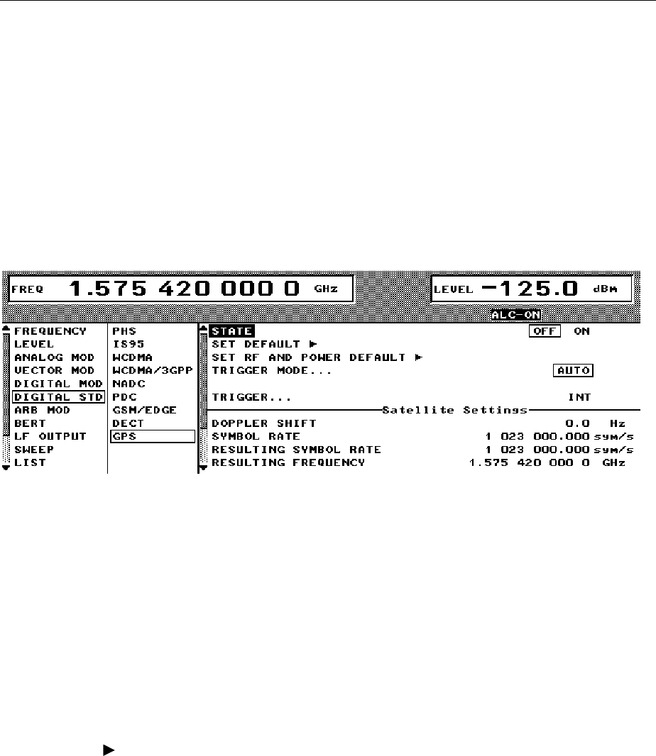
SMIQ Digital Standard GPS
1125.5555.03 D-92.335
For more detailed information on the content and frame structure of navigation data, as well as C/A
code generation, refer to the following documentation.
References:
[1] Interface Control Document ICD-GPS-200.
[2] Global Positioning System Standard Positioning Service Signal Specification, 2nd Edition, 1995.
2.20.2 GPS Menu
The following graphics show the menu for generating a GPS signal for one satellite. The individual menu
items are explained below:
Fig. 2-212 DIGITAL STD - GPS menu
STATE Switch-on/off of modulation - digital standard GPS. If vector modulation, digital
modulation or another digital standard were switched on, they are
automatically switched off.
STATE = ON starts the calculation and output of the GPS signal on the basis
of the current settings. There are no significant delays until the signal is output,
since the signal is generated in realtime.
IEC/IEEE-bus command:SOUR:GPS:STAT ON
Note: When a parameter is changed (exception: DOPPLER SHIFT and SYMBOL RATE), STATE is
automatically switched to OFF to ensure that the set values and the output signal are
consistent. Once all the values have been changed, STATE can manually be set to ON again.
This can be done using the menu parameter STATE or the MOD ON/OFF key below the
rollkey.
SET DEFAULT Sets the default setting for GPS:
• The DOPPLER SHIFT is set to 0 kHz.
• The set SYMBOL RATE is positioned to 1.023 Msps.
• The C/A CODE 1 is used.
• PATTERN is used as NAVIGATION DATA SOURCE.
• The PATTERN is set to 1010101010101010.
• All TRIGGER settings are set to default values.
IEC/IEEE-bus command :SOUR:GPS:PRES:STAN

Digital Standard GPS SMIQ
1125.5555.03 E-92.336
SET RF AND POWER
DEFAULT Sets the RF default setting for GPS:
• The frequency FREQ is set to the GPS carrier frequency L1 of 1.57542
GHz.
• The output level LEVEL is set to –125.0 dBm.
IEC/IEEE-bus command :SOUR:GPS:PRES:RF
TRIGGER MODE Configuration of autorun control of generated GPS signal.
AUTO The GPS signal calculated in realtime is immediately output and
cyclically repeated. Trigger events are ignored.
IEC/IEEE-bus command :SOUR:GPS:SEQ AUTO
RETRIG The GPS signal calculated in realtime is immediately output and
cyclically repeated. A trigger event causes a restart from
the first navigation data bit.
IEC/IEEE-bus command :SOUR:GPS:SEQ RETR
ARMED_AUTO Only a trigger event causes a start of the GPS signal from
the first navigation data bit. Further trigger events are
ignored.
IEC/IEEE-bus command :SOUR:GPS:SEQ AAUT
ARMED_RETRIG Only a trigger event causes a start of the GPS signal from
the first navigation data bit. Any other trigger event causes
a restart.
IEC/IEEE-bus command :SOUR:GPS:SEQ ARET
EXECUTE TRIGGER Executes a trigger event to start the GPS signal.
IEC/IEEE-bus command:TRIG:DM:IMM
TRIGGER... Opens a window for selecting the trigger source, configuring trigger output
signals, and setting the delay of an external trigger signal.
TRIGGER SOURCE Selects the trigger source.
EXT The GPS signal is started from the first
navigation bit with the active edge of an
external trigger signal. The polarity, trigger
threshold, and input impedance of the
TRIGIN input can be changed in the DIGITAL
MOD - EXT INPUTS menu.
INT A trigger event is manually started by
EXECUTE TRIGGER.
IEC/IEEE-bus command :SOUR:GPS:TRIG:SOUR
EXT
EXT TRIGGER
DELAY Sets the number of chips by which an external trigger
signal is delayed before it starts the GPS signal. This
is used to set up synchronization with the DUT or
other units.
IEC/IEEE-bus command
:SOUR:GPS:TRIG:DEL 3

SMIQ Digital Standard GPS
1125.5555.03 D-92.337
TRIGGER... EXT RETRIGGER
INHIBIT Sets the number of chips by which a restart is
delayed after a trigger event. If the TRIGGER MODE
RETRIG was selected, every further trigger signal
restarts the GPS signal. This restart can be inhibited
for the number of chips that have been entered.
Example:
Entry of 20460 chips (corresponds to a navigation
data bit) causes every further trigger signal to be
ignored for the duration of 20460 chips after the last
trigger event.
IEC/IEEE-bus command :SOUR:GPS:TRIG:INH
20460
TRIGGER OUT 1/2 Selects the signals for outputs TRIGOUT 1 and
TRIGOUT 2 of the PARDATA connector.
C/A_CODE Marker signal for every C/A-code
sequence (1023 chips).
IEC/IEEE-bus command:
:SOUR:GPS:TRIG:OUTP1 CODE
NAVBIT Marker signal for every navigation data
bit (20460 chips).
IEC/IEEE-bus command:
:SOUR:GPS:TRIG:OUTP1 NBIT
NAVWORD Marker signal for every navigation data
word (30 bits).
IEC/IEEE-bus command:
:SOUR:GPS:TRIG:OUTP1 NWOR
SUBFRAME Marker signal for every navigation
subframe (corresponds to 10
words).
IEC/IEEE-bus command:
:SOUR:GPS:TRIG:OUTP1 SFR
FRAME Marker signal for every navigation
frame (corresponds to 5
subframes).
IEC/IEEE-bus command:
:SOUR:GPS:TRIG:OUTP1 FRAM
TRIGGER OUT 1/2 POL Selects the polarity of the signals at the TRIGOUT 1
and TRIGOUT 2 outputs of the PARDATA connector.
IEC/IEEE-bus command :SOUR:GPS:OUTP2:POL
POS
TRIGGER OUT 1/2
DELAY Enters the number of chips by which the selected
trigger output signal is delayed.
IEC/IEEE-bus command :SOUR:GPS:OUTP2:DEL
0
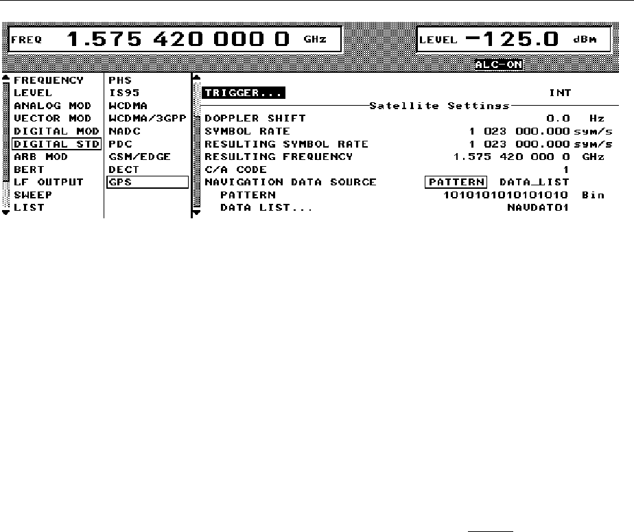
Digital Standard GPS SMIQ
1125.5555.03 E-92.338
Fig. 2-213 DIGITAL STD - GPS menu
DOPPLER SHIFT Sets the desired Doppler shift of the GPS signal. This affects the symbol rate
used as well as the frequency shift of the carrier signal.
IEC/IEEE-bus command :SOUR:GPS:DSH 0
SYMBOL RATE Sets the basic value of the symbol rate for zero Doppler, i.e. without Doppler
shift. This value is used to calculate the actual symbol rate as a function of the
Doppler shift set. At a Doppler shift of 0 Hz, the values of SYMBOL RATE and
RESULTING SYMBOL RATE (see below) are identical.
IEC/IEEE-bus command:SOUR:GPS:SRAT 1023000.0
RESULTING SYMBOL
RATE Displays the physical symbol rate currently used. The value is obtained from
the set frequency, the Doppler shift and the set basic symbol rate for zero
Doppler according to the following equation:
÷
÷
ø
ö
ç
ç
è
æ+∗= FREQ
f
ff Doppler
SymbolSymbol rZeroDoppleresulting 1
IEC/IEEE-bus command:SOUR:GPS:CURR:SRAT?
RESULTING
FREQUENCY Displays the physical carrier frequency currently output. The value is obtained
from the sum of the set frequency under FREQ and Doppler shift according to
the following equation:
Doppler
fFREQf +=
IEC/IEEE-bus command :SOUR:GPS:CURR:FREQ?
C/A CODE Sets the C/A code for spreading the navigation data. This clearly defines the
simulated GPS satellite.
IEC/IEEE-bus command :SOUR:GPS:CODE 1
NAVIGATION DATA
SOURCE Selects the navigation data source. Either simple bit patterns (see PATTERN)
or more complex data lists (see DATA LIST) with GPS-specific navigation data
(ephemeris and almanac), for example, can be selected.
IEC/IEEE-bus command :SOUR:GPS:DATA PATT

SMIQ Digital Standard GPS
1125.5555.03 D-92.339
PATTERN Sets the bit pattern to be used as navigation data source provided that
PATTERN has been selected as NAVIGATION DATA SOURCE.
IEC/IEEE-bus command :SOUR:GPS:DATA:PATT #H1234,16
DATA LIST Selects the data list to be used as navigation data source provided that
DATA_LIST has been selected as NAVIGATION DATA SOURCE .
IEC/IEEE-bus command :SOUR:GPS:DATA:DLIS ″name″
2.20.3 Instructions for Generating GPS Signals
This section provides background information for generating GPS signals and is intended to facilitate
generating signals with specific characteristics as well as user prompting.
1. Generating a simple GPS signal
After the default values have been set, a cyclically repetitive GPS signal is generated for one satellite by
switching STATE to ON. Changing the C/A CODE setting enables the satellite to be simulated to be
selected from 1 to 37. The associated signal level is set under LEVEL.
Note: To avoid any damage to connected receivers, the user must ensure that the signal level used is
not too high. A downstream attenuator pad must be connected to generate output levels below
-144 dBm.
Signals generated in this way can be recognized by a GPS receiver. However, since there are no real
navigation data on the C/A code (as standard, a bit pattern with up to 16 characters is used as the
navigation data source), only the signal level of the simulated satellite can be measured and displayed
by the receiver.
A signal of this type is usually sufficient for performing simple function tests. It should be noted,
however, that the receiver to be tested may have to be switched to a special test mode, since signals
without correct navigation data are often not indicated (on a display, for example).
2. GPS signals with pseudo navigation data
Switching NAVIGATION DATA SOURCE over to DATA_LIST enables any data lists to be selected on
SMIQ and used as navigation data. Real GPS navigation data with ephemeris and almanac information
as generated with the AlmanacUploader PC tool from Rohde & Schwarz and transmitted to SMIQ, for
example would be appropriate. The program can be downloaded from the Rohde & Schwarz Internet
page (www.rohde-schwarz.com) under Application Notes 1GP46.
When pseudo-real navigation data with a length of 37500 bits (i.e. with a total signal time of 12.5
minutes) are used, for example, satellite-specific information on position and time is transmitted, which
can be recognized by the receiver. In addition to information on the received satellite, almanac and
ephemeris data can usually be output, thereby enabling the decoding of navigation data to be checked.
Note: The GPS signal is cyclically repeated as a function of the TRIGGER MODE. When navigation
data from data lists are used, this causes the transmitted GPS time to be set to its initial value
for each new cycle.
3. Doppler-shifted GPS signals
For enhanced receiver characteristics checking, a Doppler shift of the type that occurs with real GPS
signals can also be simulated. The relevant change to the symbol rate of the C/A code is carried out
automatically. The currently valid values for Doppler-shifted carrier frequency and symbol rate are
displayed under RESULTING FREQUENCY and RESULTING SYMBOL RATE.

Digital Standard GPS SMIQ
1125.5555.03 E-92.340
The simulation of Doppler-shifted GPS signals can be used to check the receiver characteristics under
more realistic conditions than with zero Doppler. In contrast to the real system, however, the set Doppler
frequency is fixed and must eventually be changed manually.
4. GPS signals with modified carrier frequency and symbol rate
Additional settings for carrier frequency and symbol rate can be made to perform more comprehensive
receiver tests. However, these settings may result in signals that do not conform to GPS.
The basic carrier frequency without Doppler shift can be freely set under FREQ. The actual frequency
output physically is yielded by the following equation
Doppler
fFREQf +=
and is displayed under RESULTING FREQUENCY.
The symbol rate used for zero Doppler is set under SYMBOL RATE. Taking into account a Doppler
shift, the actual symbol rate is determined by the following equation
÷
÷
ø
ö
ç
ç
è
æ+∗= FREQ
f
ff Doppler
SymbolSymbol rZeroDoppleresulting 1
and is given under RESULTING SYMBOL RATE.
Selecting the appropriate parameters enables the characteristics of the receiver (such as dependence
of receiver synchronization on the symbol rate/carrier frequency ratio, etc.) to be easily checked.
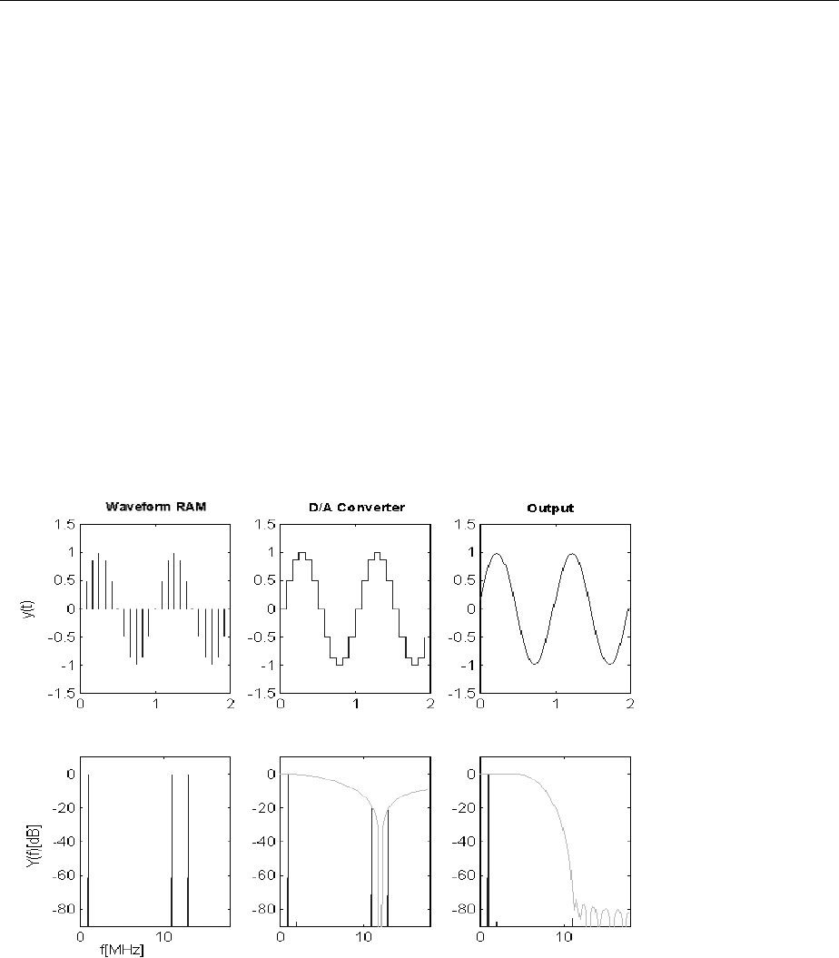
SMIQ Arbitrary Waveform Generator ARB
1125.5555.03 2.341 E-9
2.21 Arbitrary Waveform Generator ARB
The option SMIQB60, a two-channel ARB generator, is an integrated I/Q modulation source of the
SMIQ. Thus, arbitrary modulation signals such as COFDM, multicarrier or noise can be generated. The
software WinIQSIM enables the calculation of modulation signals and the loading of these signals into
the instrument. Furthermore, signals which were calculated by a mathematical program such as Matlab
may be transferred.
2.21.1 Function
Conventional ARB generators substantially consist of an output memory with series-connected D/A
converter and analog filter. Due to the limited number of filters and their steepness the sampling rate
often has to be set considerably higher than required by Nyquist's theorem, in order for the aliasing
effects to be sufficiently suppressed by the analog filter. Fig. 2-214 shows these ratios for a 1-MHz
sinewave signal. If a filter provides a cutoff-frequency of 11 MHz, a sampling rate of at least 12 MHz
must be selected to make sure that the aliasing effects are suppressed sufficiently.
Fig. 2-214 Signal flow of ARB generator
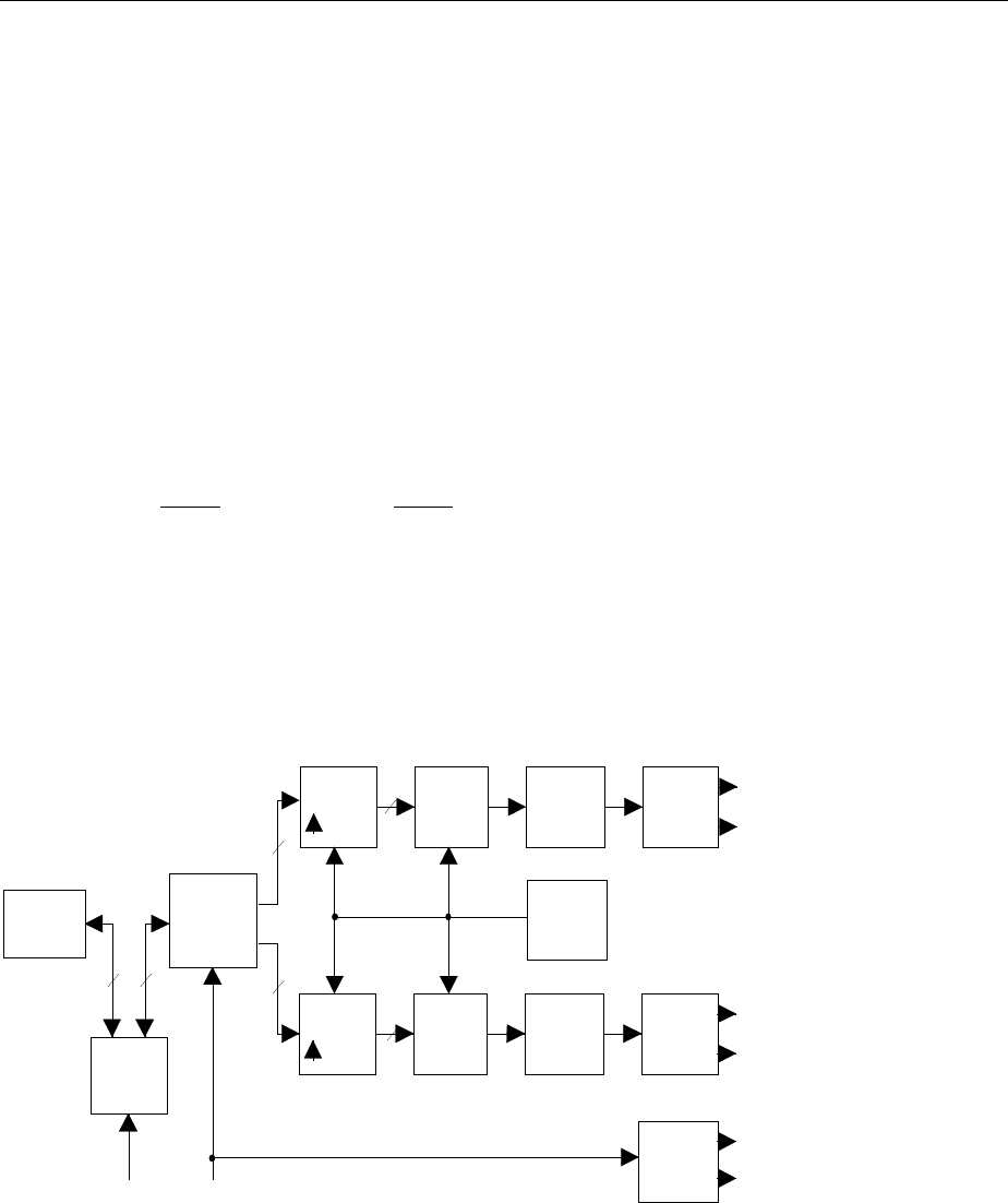
Arbitrary Waveform Generator ARB SMIQ
1125.5555.03 E-92.342
This conception has been considerably improved in the option SMIQB60. The modulation signal is
interpolated to a higher sampling rate by means of a very steep-edged, digital interpolation filter and is
then output. The interpolation rate is set by the SMIQB60 automatically such that aliasing of the
interpolated sampling rate is suppressed by the analog filter. This procedure offers the following
advantages to the user:
1. Oversampling has to be selected such that the bandwidth of the interpolation filter exceeds that of
the modulation signal. The following equation applies:
ov * int_bw >= mod_bw,
ov == Oversampling,
int_bw == 0.375, standardized bandwidth of the interpolation filter,
mod_bw == bandwidth of the modulation signal standardized to symbol rate
The following value is thus obtained for the digital standard W-CDMA with the baseband filter √cos,
α = 0.22:
mod_bw = 2
α)(1+
++
+= 0.61, => ov >= 0.375
0.61 = 1.63.
2. Due to the reduced oversampling, the duration of the signal increases with constant number of
sampling values. Accordingly, the number of sampling values decreases with constant signal
duration. Usually, with conventional ARB generators, the minimum oversampling is limited to 4. Thus,
provided that the above parameters of the W-CDMA system apply, the 512 ksamples of the SMIQB60
correspond to 4/1.63 * 512 = 1256 kSamples memory in a conventional ARB generator.
The block diagram in Fig. 2-215 roughly illustrates the structure of the ARB generator.
FLASH RAM
1.5MSamples
Waveform RAM
512kSamples
DSP
D/A
Converter
Filter
45kHz, 12MHz
Out put
Ampli fier
Interpolator
up
I_OUT
i_MOD
D/A
Converter
Filter
45kHz, 12MHz
Out put
Ampl i f ier
Interpolator
up
Q_OUT
Q_MOD
Trigger Unit
TRIGOUT_2
TRIGOUT_1
32 24 12
12
14
14
DATA IN
Clock
Synthesizer
up*clock
TRIGGER IN
Fig. 2-215 Block diagram SMIQB60
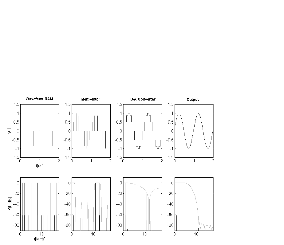
SMIQ Arbitrary Waveform Generator ARB
1125.5555.03 2.343 E-9
The I/Q data are loaded by the host computer via the DATA IN interface to the DSP which passes them
into a non-volatile FLASH RAM. The latter is organized in 22 blocks of 64ksamples, each. At least one
block is occupied by each waveform. The I/Q data are subject to a convolution filter which limits the
signal bandwidth. This is required for further processing.
If a waveform is selected, the I/Q data are loaded into the output memory. They are convoluted by a
correction filter, which compensates all errors in the path to the I/Q modulator. In particular, the Si
frequency response of the D/A converter as well as the frequency responses of the analog filter on the
SMIQB60 and of the I/Q filter of the option SMIQB47 are corrected. Fig. 2-216 illustrates the further
signal flow in the frequency and time domains.
Fig. 2-216 Signal flow SMIQB60
A 1-MHz sinewave signal with fa = 3 MHz is sampled by way of example. The sampling procedure
causes aliasing to occur in the frequency range (n*3 ± 1) MHz. The following interpolation filter
increases the sampling rate by the factor 4. This corresponds to a correct reconstruction of the
additional sampling values in the time domain. Due to the sample-and-hold process at the output of the
subsequent D/A converter, a stair-step signal is generated in the time domain which corresponds to a
SI-weighting in the frequency domain. The analog filter compensates for the aliasing of the interpolated
sampling rate, the output signal is a sinewave signal in the time domain. SMIQB60 automatically sets
the interpolation rate such that aliasing is suppressed by the analog filter.
The sampling rate is increased internally by the factor 4, in order to avoid errors with CCDF
determination of the waveform with low sampling rate.
The absolute value of the I/Q output signal is 0.5 Vs at 50 Ω (= 0 dB) in Normal mode. This is the
nominal output of the I/Q modulator. The output level may be varied in Manual mode between -6 dB and
3 dB in order to optimize the ACP in various channel offsets, e.g. The range above 0 dB is not specified,
signal frequencies above 10 MHz may lead to a limitation.
The internal calibration of the SMIQB60, which is performed automatically with calibration of the vector
modulation, corrects offset and gain errors to a minimum.
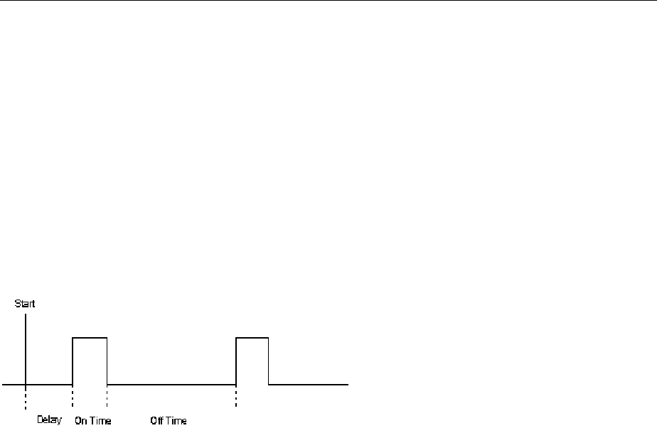
Arbitrary Waveform Generator ARB SMIQ
1125.5555.03 E-92.344
The trigger facilities of the SMIQB60 are similar to those of the data generator SMIQB11 (see Digital
Modulation). The trigger generator consists of programmable counters which generate a periodic
sequence with a pulse duty ratio of On Time/Off Time with settable start delay. E.g., to generate a slot
trigger for a W-CDMA signal with a chip rate of 3.84 MHz, the following values are set:
tSlot = Slot time
tChip = Chip time
ta = Sampling time
tSlot = 625µs = 2400 tChip, tChip = ov * ta, ov = 2, => tChip = 4800 * ta
On Time = 100 (for example) => Off Time = 4700.
The trigger signals are time-synchronous with the I/Q output signals. WinIQSIM supports the generation
of predefined trigger signals (see Use of WinIQSIM Software).
Fig. 2-217 Trigger signals SMIQB60
2.21.1.1 Use of WinIQSIM
The SMIQB60 is supported by WinIQSIM starting with version 3.30. Waveforms can be loaded via the
IEC/IEEE bus into the FLASH memory, an individual operating menu allows for setting numerous SMIQ
parameters. It must be noted that settings of WinIQSIM cannot be read from the waveform. WinIQSIM
provides predefined settings for bit and symbol clock for the generation of trigger signals, slot and frame
trigger and the restart signal for the BERT (SMIQB21). Si and filter compensation is not supported by
WinIQSIM since these functions are carried out directly on the SMIQB60. Waveforms which contain
these corrections may also be loaded in the SMIQB60. This is recognized and the internal correction
filters are modified accordingly.
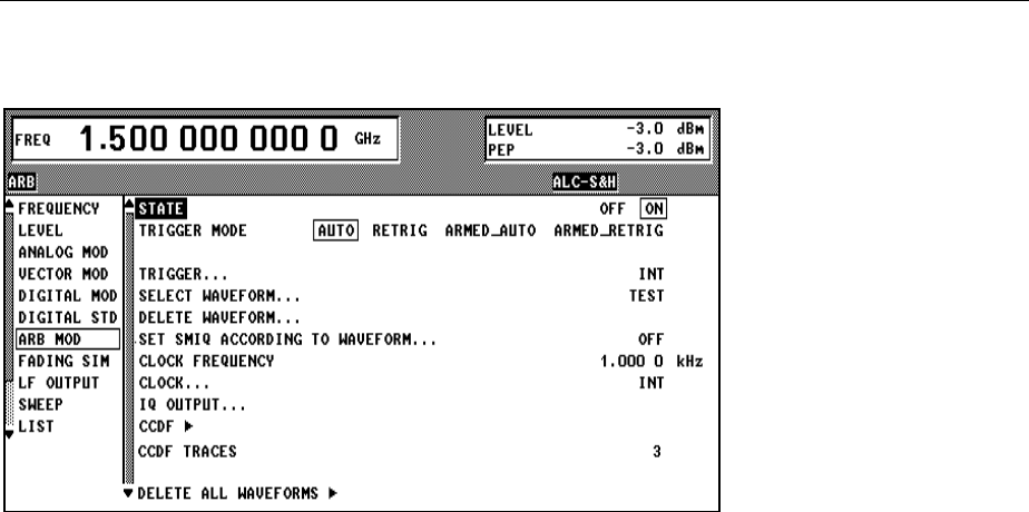
SMIQ Arbitrary Waveform Generator ARB
1125.5555.03 2.345 E-9
2.21.2 ARB MOD Menu
Fig. 2-218 ARB MOD menu
STATE Switching on/off ARB function. The state is indicated in the status line.
ON Loads the selected waveform in the output RAM and sets the
module according to the current settings. This may last a few
seconds depending on the length of the selected waveform. If
vector modulation, digital modulation or digital standard were
switched on, they are switched off automatically.
IEC/IEEE bus command :ARB:STAT ON
OFF Modulation is switched off, output of ARB waveform stops.
IEC/IEEE bus command :ARB:STAT OFF
TRIGGER MODE Configuration of run control of ARB mode.
AUTO The calculated waveform (sequence) is output imme-
diately and repeated in cycles. Trigger events are
ignored.
IEC/IEEE bus command :ARB:SEQ AUTO
RETRIG Cyclic repetition of output. A trigger event initiates a
restart.
IEC/IEEE bus command :ARB:SEQ RETR
ARMED_AUTO Only a trigger event initiates a start. Subsequent trigger
events are ignored.
IEC/IEEE bus command :ARB:SEQ AAUT
ARMED_RETRIG Like ARMED_AUTO. Each following trigger event
initiates a new start.
IEC/IEEE bus command :ARB:SEQ ARET
EXECUTE TRIGGER Ø
ØØ
ØInitiates a trigger to start the ARB sequence (not displayed with TRIGGER
MODE = AUTO).
IEC/IEEE bus command :TRIG:DM:IMM

Arbitrary Waveform Generator ARB SMIQ
1125.5555.03 E-92.346
TRIGGER... Opens a window for setting the trigger facilities and the trigger outputs.
SELECT WAVEFORM... Opens a window for selection of an ARB waveform and for display of its
parameters.
DELETE WAVEFORM... Opens a window for selection of an ARB waveform to be deleted.
SET SMIQ ACCORDING TO
WAVEFORM...
Opens a window for configuration of the automatic setting of SMIQ
parameters.
CLOCK FREQUENCY Input value for the sample clock. If the clock is supplied by an external
source, the applied frequency must be entered here.
IEC/IEEE bus command :ARB:CLOC 4.096MHz
CLOCK... Opens a window for selection of the clock source and delay of the clock
signal.
IQ OUTPUT... Opens a window for entry of the IQ level and mode.
CCDF Ø
ØØ
ØDisplay of the Complementary Cumulative Distribution Function of the
waveform loaded.
CCDF TRACES Entry of the number of CCDFs. 1 to 3 may be selected.
DELETE ALL WAVEFORMS Ø
ØØ
ØAll waveforms are deleted (after being confirmed by the user).
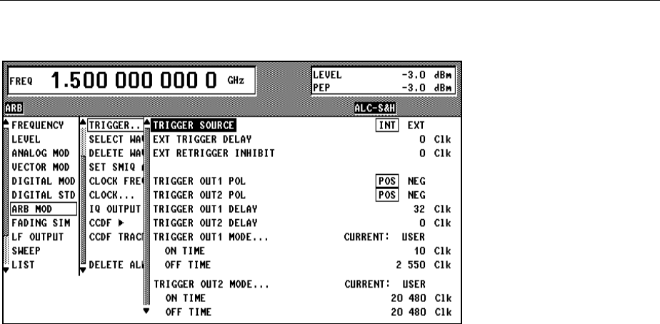
SMIQ Arbitrary Waveform Generator ARB
1125.5555.03 2.347 E-9
2.21.2.1 ARB MOD - TRIGGER Menu
Fig. 2-219 ARB MOD - TRIGGER... menu
TRIGGER... Opens a window for setting the trigger facilities and the trigger outputs.
TRIGGER SOURCE Configuration of trigger source.
INT Manually via EXECUTE TRIGGER or via software.
IEC/IEEE bus command :ARB:TRIG:SOUR INT
EXT Triggering with active edge at input socket.
IEC/IEEE bus command :ARB:TRIG:SOUR EXT
EXT TRIGGER DELAY Delays the start of sequence by the indicated samples
after occurrence of an external trigger event. The
resolution is 2 samples with clock rates (CLOCK) above
20 MHz (otherwise, 1 sample).
IEC/IEEE bus command :ARB:TRIG:DEL 234
EXT RETRIGGER INHIBIT Retriggering is inhibited until the sequence has reached the
indicated sample.
IEC/IEEE bus command :ARB:TRIG:INH 345
TRIGGER OUT1(2) POL Signal polarity at the trigger outputs.
POS active state: positive voltage
IEC/IEEE bus command
:ARB:TRIG:OUTP1:POL POS
NEG active state: 0 or lower voltage
IEC/IEEE bus command
:ARB:TRIG:OUTP2:POL NEG
TRIGGER OUT1(2) DELAY Delay of the supplied trigger signals by the set number of
samples.
IEC/IEEE bus command :ARB:TRIG:OUTP:DEL 765

Arbitrary Waveform Generator ARB SMIQ
1125.5555.03 E-92.348
(TRIGGER...) TRIGGER OUT1(2) MODE The user may select one of the displayed modes for
generation of the trigger output signals.
Depending on the system, WinIQSIM can calculate clock
signals for BIT, SYMBOL, SLOT, FRAME and the restart
signal (sequence) and transmit them together with the
waveform. These modes set the counters for ON TIME
and OFF TIME (see below). The names are defined as
modes by WinIQSIM, stored in the waveform where they
can be selected. The maximum number of defined
counters is 4. It may occur that only the SEQUENZ and
USER modes can be provided since the entirety of modes
is not always available for all systems.
BIT_CLK edge at beginning of each bit
SYMB_CLK edge at beginning of each modulation
symbol
SLOT_CLK edge at beginning of each slot
FRAM_CLK edge at beginning of each frame
SEQUENZ edge at beginning of each sequence
(may, e.g., be used as restart signal for
BERT)
PULSE pulse defined by WinIQSIM user
USER The user defines a pulse by means of
the parameters for ON and OFF TIME.
IEC/IEEE bus command :ARB:TRIG:OUTP:MODE USER
....ON TIME Length of the active state of the output trigger signals
indicated as number of samples. Can be modified only, if
MODE = USER.
This time is repeated after OFF TIME has run off.
IEC/IEEE bus command :ARB:TRIG:OUTP:ONT 3789
....OFF TIME Length of the non-active state of the output trigger signals
indicated as number of samples. Can be modified only, if
MODE = USER.
IEC/IEEE bus command :ARB:TRIG:OUTP2:OFFT 639
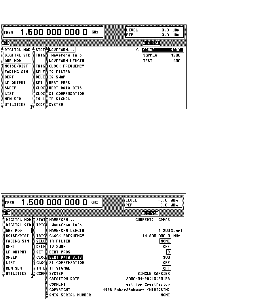
SMIQ Arbitrary Waveform Generator ARB
1125.5555.03 2.349 E-9
2.21.2.2 ARB MOD - SELECT WAVEFORM Menu
Fig. 2-220 ARB MOD - SELECT WAVEFORM... menu
SELECT WAVEFORM... Opens a window for selection of an ARB waveform and for display of its
parameters.
WAVEFORM A list of ARB waveforms is offered to the right. The length of the
waveforms is indicated in samples. The user selects a waveform
from this list, which then becomes the active waveform. Further
information on this waveform is then provided.
IEC/IEEE bus command :ARB:WAV:SEL ‘TEST’
Fig. 2-221 ARB MOD - WAVEFORM INFO menu
SELECT WAVEFORM... ----Waveform Info --------
These lines are for display purposes only, they cannot be modified. They are
filled with values from the active waveform when opening the menu. After being
confirmed by the user they are updated via (SELECT). Setting parameters are
not set until this confirmation and errors are signaled with conflicts, when the
menu is left via RETURN (see SET SMIQ ACCORDING TO WAVEFORM
menu). IEC/IEEE bus commands have the form of queries.

Arbitrary Waveform Generator ARB SMIQ
1125.5555.03 E-92.350
SELECT WAVEFORM... WAVEFORM LENGTH Displays the number of samples contained in the
waveform.
IEC/IEEE bus command :ARB:WAV:POIN?
CLOCK FREQUENCY Provides the sample rate which the waveform has
been generated for. This value is always entered as
CLOCK FREQUENCY parameter of the ARB MOD
menu with loading a waveform (independent of SET
SMIQ ACCORDING TO WAVEFORM).
IEC/IEEE bus command :ARB:WAV:TAG? 'CLOCK'
IQ FILTER Displays the setting used for calculation of the
waveform in WinIQSIM. WinIQSIM sets this value to
0 (OFF), if the waveform is calculated for the SMIQ
in particular. If, however, a compensation for an IQ
filter is taken into account (for example when
calculating the waveform for AMIQ), the
compensation is automatically counted back by the
SMIQ. Independently from this setting, however, a
suitable IQ filter can be selected in the SMIQ.
Compensation of the IQ filter is executed
automatically by the SMIQ.
The value of the waveform is used in the VECTOR
MOD menu for the IQ filter if this is enabled in the
SET SMIQ ACCORDING TO WAVEFORM menu.
IEC/IEEE bus command
:ARB:WAV:TAG? 'LACP FILTER'
IQ SWAP Indicates the setting used with the waveform
calculation in WinIQSIM. The value is used in the
VECTOR MOD menu for the IQ SWAP setting after
enabling in the SET SMIQ ACCORDING TO
WAVEFORM menu.
IEC/IEEE bus command
:ARB:WAV:TAG? 'IQ SWAP'
BERT PRBS Displays the type of PRBS used for the data in
WinIQSIM, if the data have been prepared for a
BER measurement.
The setting is used in the BERT menu for setting the
type of PRBS after clearing in the SET SMIQ
ACCORDING TO WAVEFORM menu. A waveform
cannot be used always for a BER measurement. If
not, the display reads NONE.
IEC/IEEE bus command
:ARB:WAV:TAG? 'PRBS LENGTH'
BERT DATA BITS Indicates the number of data bits in a waveform, if
the data have been prepared for a BER measure-
ment by WinIQSIM. If the waveform cannot be used
for a BER measurement, zero is displayed, here.
IEC/IEEE bus command
:ARB:WAV:TAG? 'BERT DATABITS'

SMIQ Arbitrary Waveform Generator ARB
1125.5555.03 2.351 E-9
(SELECT WAVEFORM...) SI COMPENSATION ON indicates that the SI compensation of WinIQSIM
was taken into account with calculation of the
waveform. Since the SMIQ, independent of that
calculation, also takes into account the SI
compensation, it is disabled in WinIQSIM, if the
waveform is calculated particularly for the SMIQ. It is
however counted back by the SMIQ, if it was taken
into account e.g., with calculation of a waveform for
the AMIQ.
IEC/IEEE bus command
:ARB:WAV:TAG? 'SI COMPENSATED'
IF SIGNAL ON indicates that the waveform was converted into
an IF signal by WinIQSIM. This signal is not
intended to be used as IQ vector. However, the user
may derive it from the I-channel output and apply as
IF signal.
IEC/IEEE bus command
:ARB:WAV:TAG? 'IF_SIGNAL'
SYSTEM Indicates the standard used to calculate the
waveform in WinIQSIM. The following standards
have been defined: Single Carrier, Multi Carrier,
Multi Carrier Mixed Signal, 3GPP W-CDMA, IS-95,
CDMA2000 and Import.
IEC/IEEE bus command :ARB:WAV:TAG? 'SYSTEM'
CREATION DATE Displays the creation date of the waveform. Provides
the user with information and is added automatically
with calculation in WinIQSIM.
IEC/IEEE bus command :ARB:WAV:TAG? 'DATE'
COMMENT Is provided for information purposes and may be
entered as comment text in WinIQSIM.
IEC/IEEE bus command
:ARB:WAV:TAG? 'COMMENT'
COPYRIGHT Indicates whether the waveform was generated
using the protected software WinIQSIM.
IEC/IEEE bus command
:ARB:WAV:TAG? 'COPYRIGHT'
SMIQ SERIAL NUMBER Is important, if the wave was generated in WinIQSIM
with IQ FILTER = ON. In this case, filter coefficients
have been used for compensation, which are best
only for SMIQs with this serial number.
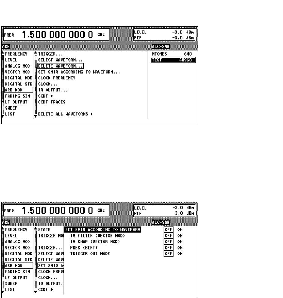
Arbitrary Waveform Generator ARB SMIQ
1125.5555.03 E-92.352
2.21.2.3 ARB MOD - DELETE WAVEFORM Menu
Fig. 2-222 ARB MOD - DELETE WAVEFORM... menu
DELETE WAVEFORM... Opens a window for selection of an ARB waveform to be deleted. A list of ARB
waveforms including information on their lengths is offered to the right, where
the user may select a waveform.
IEC/IEEE bus command :ARB:WAV:DEL ‘TEST’
2.21.2.4 ARB MOD - SET SMIQ ACCORDING TO WAVEFORM Menu
Fig. 2-223 ARB MOD - SET SMIQ ACCORDING TO WAVEFORM menu
SET SMIQ ACCORDING
TO WAVEFORM...
Opens a window for configuration of the automatic setting of SMIQ parameters.
SET SMIQ ACCORDING
TO WAVEFORM ON In any case, settings on the SMIQ are
made based on the information from the
waveform to be loaded.
IEC/IEEE bus command
:ARB:ASET:STAT ON
OFF No settings are made, even if the following
configurations are set ON. CLOCK
FREQUENCY in the ARB MOD menu is
always set.
IEC/IEEE bus command
:ARB:ASET:STAT OFF

SMIQ Arbitrary Waveform Generator ARB
1125.5555.03 2.353 E-9
(SET SMIQ ACCORDING
TO WAVEFORM...) ....IQ FILTER
(VECTOR MOD)
The parameter IQ FILTER (filter of LACP Option
SMIQB47) is set in the VECTOR MOD menu. If a
waveform in WinIQSIM was compensated with the
frequency responses of this filter, it should be
switched on. A warning is output, if the waveform is
compensated, however, this compensation does not
apply for an SMIQ of this serial number or if the option
is not fitted to the SMIQ.
ON Parameter is set
IEC/IEEE bus command
:ARB:ASET:DM:IQF ON
OFF Parameter is not set
IEC/IEEE bus command
:ARB:ASET:DM:IQF OFF
...IQ SWAP
(VECTOR MOD)
The IQ SWAP parameter in the VECTOR MOD
menu is set. If a waveform has been generated in
WinIQSIM for this mode, it should be switched on. A
warning is output, if the parameter is not set as
indicated in the waveform.
ON Parameter is set
IEC/IEEE bus command
:ARB:ASET:DM:IQSW ON
OFF Parameter is not set
IEC/IEEE bus command
:ARB:ASET:DM:IQSW OFF
...PRBS (BERT) The type of PRBS in the BERT menu is set. If a
waveform has been generated in WinIQSIM with this
PRBS, the latter should be selected with BER
measurement. A warning is output, if the parameter
is not set as indicated in the waveform.
ON Parameter is set
IEC/IEEE bus command
:ARB:ASET:BERT:TYPE ON
OFF Parameter is not set
IEC/IEEE bus command
:ARB:ASET:BERT:TYPE OFF
...TRIGGER OUT MODE The parameters TRIGGER OUT1 MODE and
TRIGGER OUT2 MODE in the ARB MOD
TRIGGER... menu are set. Thus, the user can select
the function of the SMIQ trigger outputs in WinIQSIM
(see TRIGGER menu).
ON Parameter is set
IEC/IEEE bus command
:ARB:ASET:TRIG:MODE ON
OFF Parameter is not set
IEC/IEEE bus command
:ARB:ASET:TRIG:MODE OFF
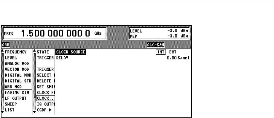
Arbitrary Waveform Generator ARB SMIQ
1125.5555.03 E-92.354
2.21.2.5 ARB MOD - CLOCK... Menu
Fig. 2-224 ARB MOD - CLOCK... menu
CLOCK... Opens a window for selection of the clock source and delay of the clock signal.
CLOCK SOURCE Defines the source for the sample clock.
INT Clock is generated internally.
IEC/IEEE bus command :ARB:CLOC:SOUR INT
EXT Clock must be applied at the socket.
IEC/IEEE bus command :ARB:CLOC:SOUR EXT
DELAY Delay of the modulation signal against the clock signal. This may
be used, e.g., for synchronization with a second instrument, to
obtain time-synchronous modulation signals of both instruments.
IEC/IEEE bus command :ARB:CLOC:DEL 0.55
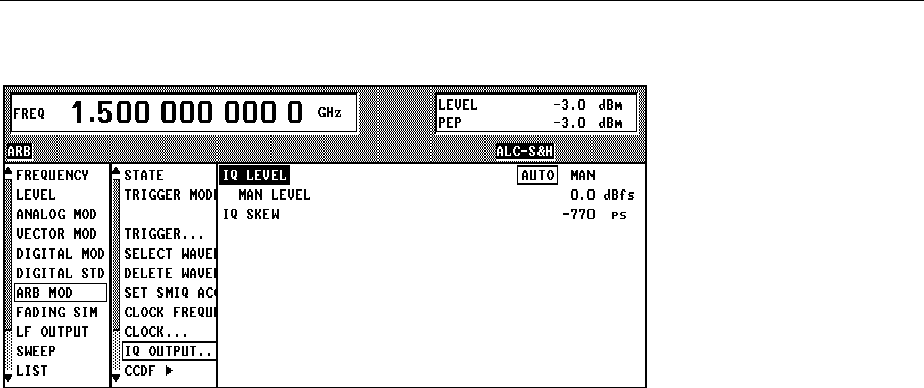
SMIQ Arbitrary Waveform Generator ARB
1125.5555.03 2.355 E-9
2.21.2.6 ARB MOD - IQ OUTPUT... Menu
Fig. 2-225 ARB MOD - IQ OUTPUT... menu
IQ OUTPUT... Opens a window for entry of the IQ level and automatic level setting.
IQ LEVEL Defines the operating mode for setting the IQ level.
AUTO The level is set automatically to a maximum sum vector
of 0.5 V for maximum input level of the IQ modulator.
The subsequent level entry is not effective.
IEC/IEEE bus command
:ARB:IQ:LEV:MODE AUTO
MAN The level is set using the level entry below. The
instrument data can not be guaranteed for entry values
above 0 dB, since the output level is limited. However,
the signal-to-noise ratio, e.g., may thus be increased.
IEC/IEEE bus command
:ARB:IQ:LEV:MODE MAN
MAN LEVEL Indicates the IQ level referred to maximum voltage.
Range: -6 to 3 dBfs
IEC/IEEE bus command :ARB:IQ:LEV –2.5DB
IQ SKEW Determines the delay between I and Q channel. Positive values
delay I against Q.
IEC/IEEE bus command :ARB:IQ:SKEW –250ps
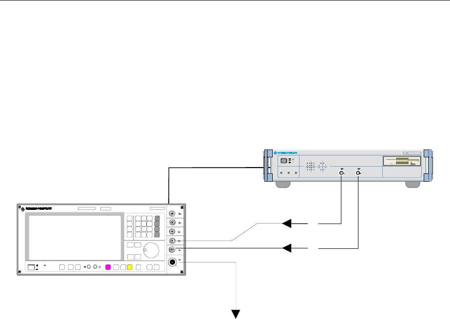
External Modulation Source AMIQ SMIQ
1125.5555.03 2.356 E-9
2.22 External Modulation Source AMIQ
AMIQ from Rohde&Schwarz is now available as an external source for I/Q modulation signals. The
generated signals are provided by the unit at modulation outputs I and Q on the front panel. The signals
can be fed to modulation inputs I and Q of SMIQ.
With vector modulation mode activated, SMIQ modulates (I/Q modulation) the modulation signals
generated by AMIQ onto the RF carrier.
ïð
SMIQ I
Q
RF
IEC 625 /
IEEE 488 MADE IN GERM ANY
CON T ROLON
I/Q MODULATION GENERATOR AMIQ
.1110.2003. 02
RUNN I N G I Q
AMIQ
Fig. 2-226 Vector modulation with an external AMIQ
Menu VECTOR MOD provides access to settings required for vector modulation. Settings for generating
the modulation signals are made in menu AMIQ CTRL. This menu allows to set the most important
parameters of AMIQ via the remote-control interface IEC625/IEEE488. The IEC/IEEE-bus address of
AMIQ is given in menu UTILITIES / SYSTEM / GPIB.
Note: Menu AMIQ CTRL is masked out when SMIQ is delivered. It has to be switched on in menu
UTILITIES / INSTALL.

SMIQ External Modulation Source AMIQ
1125.5555.03 E-92.357
Complex signal data are created on the PC using Windows software WinIQSIM.
1. If WinIQSIM and AMIQ are linked via IEC/IEEE-bus or RS232 interface, signal data can be
fully stored as waveform file on the hard disk of AMIQ. Signal data are then loaded from
SMIQ to AMIQ by means of the following commands: SELECT WAVEFORM/EXECUTE
BATCH ... DRIVE, HARDDISK and by selection of the file name.
2. If there is no remote-control connection between WinIQSIM and AMIQ, signal data up to
300.000 samples can be stored as waveform file on floppy. Signal data are then loaded
from SMIQ to AMIQ by means of the following commands:
SELECT WAVEFORM/EXECUTE BATCH ... DRIVE, FLOPPY.
A faster access is possible if signal data are stored as batch files on a floppy. The floppy is
then inserted into AMIQ and the batch file is called up from SMIQ by means of the following
commands:
SELECT WAVEFORM/EXECUTE BATCH ...EXECUTE BATCH FROM FLOPPY.
The signal data are stored as waveform file on the AMIQ hard disk under the name defined
in WinIQSIM. After that, the waveform file can be loaded as described under 2.
For generation of waveform files for AMIQ see chapter on "Menu item AMIQ" in the WinIQSIM
manual".
The system consisting of SMIQ as modulation coder, AMIQ as source for baseband signals and
WinIQSIM for signal data configuration makes the generation of any complex, digitally modulated
communication signals convenient and easy.
External Modulation Source AMIQ SMIQ
1125.5555.03 2.358 E-9
To remote control AMIQ via IEC625/IEEE488, SMIQ is configured as a system controller. In the normal
mode, SMIQ is configured as a talker/listener.
In general, only one unit can be the system controller on the bus.
With menu AMIQ CTRL called up, SMIQ is automatically configured as the controller. If this is not
possible since for example another unit (eg a PC) has already taken over the controller function, menu
AMIQ CTRL will not be opened and an error message will be issued.
When menu AMIQ CTRL is closed, SMIQ will again switch to the talker/listener mode.
Menu selection: AMIQ CTRL
FREQ 100. 000 000 0 MHz LEVEL - 30.0 dBm
FREQUENCY
LEVEL
ANALOG MOD
VECTOR MOD
DIGITAL MOD
DIGITAL STD
AMIQ CTRL
LF OUTPUT
SWEEP
LIST
MEM SEQ
IQDATA
OFF AUTO SINGLE GATED EXT-AUTO EXT-SINGLE
POS/HIGH NEG/LOW
OFF 2.5MHz 25MHz EXT
INT EXT
10 MHz
SETUP...
SAVE/RECALL SETTINGS
SELECT WAVEFORM/EXECUTE BATCH...
MODE
EXECUTE SINGLE
EXT TRIG SLOPE
FILTER
LEVEL...
MARKER...
REFERENCE OSCILLATOR
CLOCK
BIT ERROR MEASUREMENT...
Fig. 2-227 Menu AMIQ CTRL (presetting depends on AMIQ)
SETUP... Opens a window to set the basic configuration of AMIQ.
The window offers functions to perform automatic adjustment, fine adjustment,
selftest and to reset to a defined basic state.
SETUP..
SAVE/RE
SELECT
MODE
EXECUT
EXT TRI
FILTER
LEVEL..
MARKER.
REFEREN
FREQ 100. 000 000 0 MHz LEVEL - 30.0 dBm
FREQUENCY
LEVEL
ANALOG MOD
VECTOR MOD
DIGITAL MOD
DIGITAL STD
AMIQ CTRL
LF OUTPUT
SWEEP
LIST
MEM SEQ
SOFTWARE VERSION 1.00
OPTIONS 0,0,0,0
RESET AMIQ
ADJUSTMENT
INT ADJUST
USER CORRECTION
SET DEFAULT
LEVEL I GAIN 0.000 OFFSET I FIX 0.000
OFFSET I VAR 0.000
LEVEL Q GAIN 0.000 OFFSET Q FIX 0.000
OFFSET Q VAR 0.000
SKEW (Q-I) 1.000
SELF TEST
Fig. 2-228 Menu AMIQ CTRL -SETUP...

SMIQ External Modulation Source AMIQ
1125.5555.03 E-92.359
(SETUP...) SOFTWARE
VERSION Display of the current AMIQ firmware version AMIQ.
OPTIONS Display of AMIQ options.
RESET AMIQ Resets AMIQ to a defined basic state.
INT ADJUST Starts automatic self-adjustment of AMIQ:
− Level adjustment (I/Q) to 1.0 Volt when fully
equipped
− Offset adjustment (I/Q) to a minimum
− Fine adjustment of reference oscillator to 10 MHz
− Minimization of delay between I and Q channel
USER CORRECTION The user correction allows the fine adjustment of
level and offset of the I and Q channel as well as the
minimization of the delay between the channels of
the complete system.
The internal adjustment (INT ADJUST) is not taken
into account.
SET DEFAULT Resets the user correction to the default values.
This applies to the following parameters:
− LEVEL I GAIN (*)
− OFFSET I FIX (*)
− OFFSET I VAR (**)
− LEVEL Q GAIN (*)
− OFFSET Q FIX (*)
− OFFSET Q VAR (**)
− SKEW (I-Q)
* These parameters will only be effective
provided that a fixed level of 0.5 V/50 Ohm has
been assigned to the corresponding channel.
For variable levels, the settings of these para-
meters are ineffective. A correction of the gain
factor is possible when the level is entered.
** These parameters are only effective in case of
variable levels and have no effect in case of
fixed levels.
The level is set in the submenu LEVEL...
(LEVEL I/Q = 0.5V/50 Ohm or VAR).
LEVEL I GAIN Fine adjustment of gain factor for I channel in case of
fixed level. Relative gain factors in the range ±10%
can be entered.
OFFSET I FIX Fine adjustment of level offset for the I channel in
case of fixed level. The relative factors ±1.0
correspond to a an offset detuning of ±30 mV.
External Modulation Source AMIQ SMIQ
1125.5555.03 2.360 E-9
(SETUP...) OFFSET I VAR Fine adjustment of level offset for the I channel in
case of variable level. The offset detuning depends
on the of the mechanical attenuator setting of AMIQ.
See AMIQ manual, section SOURce - Hardware
Settings.
LEVEL Q GAIN Fine adjustment of gain factor for the Q channel in
case of fixed level.
OFFSET Q FIX Fine adjustment of level offset for the Q channel in
case of fixed level.
OFFSET Q VAR Fine adjustment of level offset for the Q channel in
case of variable level.
SKEW (Q-I) Defining the delay between the I and Q channel.
Positive values delay I compared with Q. The delay
can be modified by entering the relative factors ±1.0
in a range of approx. ±1 ns at a resolution of 10 ps.
SELF TEST Triggers the internal AMIQ selftest which comprises
the following:
− memory test of the output memory.
− control of components of analog hardware and
check of signal paths by means of the built-in
diagnostic A/D converter.
SAVE/RECALL
SETTINGS... Opens a window to save/load/delete a maximum number of 100 AMIQ setups.
SETUP...
SAVE/RECALL
SELECT WAVE
MODE
EXECUTE SIN
EXTTRIGSL
FILTER
LEVEL...
MARKER...
REFERENCE O
FREQ 100. 000 000 0 MHz LEVEL - 30.0 dBm
FREQUENCY
LEVEL
ANALOG MOD
VECTOR MOD
DIGITAL MOD
DIGITAL STD
AMIQ CTRL
LF OUTPUT
SWEEP
LIST
MEM SEQ
RECALL SETTING...
SAVE SETTING...
DELETE SETTING...
Fig. 2-229 Menu AMIQ CTRL -SAVE/RECALL SETTINGS...
(SAVE/RECALL
SETTINGS...) RECALL SETTING... Selects and loads a stored AMIQ setup. The
available setups are offered in a select window.
SMIQ External Modulation Source AMIQ
1125.5555.03 E-92.361
(SAVE/RECALL
SETTINGS...) SAVE SETTING... Saves the current AMIQ setup. An already existing
setup can be selected and overwritten in a select
window.
A new setup is created by selecting CREATE NEW
SETTING . SMIQ automatically offers SETTxx with
xx being in the range from 0 to 99. This name can be
modified any time as required.
DELETE SETTING... Deletes AMIQ setups. The available setups are
offered in a select window.
SELECT
WAVEFORM/
EXECUTE BATCH...
Opens a window to
− load signal data from diskette or hard disk into the AMIQ internal memory,
− transfer signal data generated by WinIQSIM to the AMIQ hard disk,
− display current signal data.
SETUP...
SAVE/RECALL
SELECT WAVE
MODE
EXECUTE SIN
EXTTRIGSL
FILTER
LEVEL...
MARKER...
REFERENCE O
FREQ 100. 000 000 0 MHz LEVEL - 30.0 dBm
FREQUENCY
LEVEL
ANALOG MOD
VECTOR MOD
DIGITAL MOD
DIGITAL STD
AMIQ CTRL
LF OUTPUT
SWEEP
LIST
MEM SEQ
FLOPPY HARDDISK
NONE
DRIVE
WAVEFORM...
EXECUTE BATCH FROM FLOPPY
File Info
CREATION DATE: NONE
COMMENT: NONE
MODULATED POWER OFFSET: NONE
COPYRIGHT: NONE
Fig. 2-230 Menu AMIQ - SELECT WAVEFORM/EXECUTE BATCH...
(SELECT
WAVEFORM/
EXECUTE BATCH...)
DRIVE Selects storage medium with the signal data to be
activated.
DIRECTORY... Selects the directory comprising the required signal
data on the AMIQ hard disk. The directory structure
is freely selectable and can be modified with
WinIQSIM. SMIQ does not allow to change the
directory structure.
The menu item is only visible with DRIVE =
HARDDISK.

External Modulation Source AMIQ SMIQ
1125.5555.03 2.362 E-9
(SELECT
WAVEFORM/
EXECUTE BATCH...)
WAVEFORM... Selects the signal data to be loaded. The data
available on diskette or hard disk are offered in a
select window. After selecting the signal data, the
following actions are performed:
1. stopping the currently active signal output,
2. preparing the selected signal data,
3. further procedure is according to parameter
MODE in main menu.
SET SMIQ LEVEL
ACCORDING TO
WAVEFORM
Waveform files may contain information on LEVEL
OFFSET and CREST FACTOR. If this function is
active, these values are set automatically upon
loading the waveform. If no waveform is loaded, they
are set to zero.
EXECUTE BATCH
FROM FLOPPY Executes the batch file WINIQSIM.IEC generated by
WinIQSIM from diskette. The signal data including
the given directory structure are stored on the AMIQ
hard disk.
The directory structure is defined by the user during
the generation of the diskette.
FILE INFO All menu entries displayed under FILE INFO are not
editable. The file info (date, comment and origin as
well as power offset of modulation) from the selected
files is displayed.
MODE Configuration of trigger conditions for signal output. Any change in the trigger
conditions resets the signal output and starts it again. Retriggering a running
signal output is inhibited.
OFF Stops the signal output, output of the idle signal.
AUTO Continuous signal output, trigger events are ignored.
SINGLE Prepares a single signal output. The idle signal is output
first. Signal output is started via menu item EXECUTE
SINGLE . After completion of the signal output, the idle
signal is output. External trigger events are ignored.
GATED The level of the signal applied to the trigger input controls
the output.
If the level (HIGH/LOW) set under EXT TRIG SLOPE is
applied, the signal output will be restarted and the signal
will be output continuously. If the level set under EXT
TRIG SLOPE is not applied, the output will be interrupted
and the idle signal will be output.
EXT-AUTO Continuous signal output. The idle signal is output first.
The signal output is started via an external trigger event.
Further trigger events are ignored. A signal slope whose
polarity is configured in menu item EXT TRIG SLOPE
(POS/NEG) is taken as a trigger event.
EXT-SINGLE Prepares a single signal output. The idle signal is output
first. The signal output is started via an external trigger
event. After completion of the signal output, the idle
signal is output until the next trigger event is obtained.
SMIQ External Modulation Source AMIQ
1125.5555.03 E-92.363
EXECUTE SINGLE Starts a single signal output. This menu item is displayed only with MODE =
SINGLE.
EXT TRIG SLOPE Selects the polarity of an external trigger signal at connector TRIG. This
external trigger signal generates a trigger event. This setting has an effect on
modes GATED (HIGH/LOW), EXT-AUTO and EXT-SINGLE (POS/NEG).
FILTER Configuration of reconstruction filters for signal paths I and Q.
OFF Output of unfiltered I/Q signals
2.5 MHz Loop in of the internal 2.5 MHz lowpass filter.
25 MHz Loop in of the internal 25 MHz lowpass filter
EXT Loop in of external bandpass filters for the I and Q
channel. For a detailed specification of the filter see
AMIQ manual, section Signal Inputs and Outputs.
Note: With external filtering it has to be made sure that a filter is
connected to both filter inputs I and Q on the rear of AMIQ. The
two signal outputs can be switched off completely during external
filtering provided that no filter is connected to the corresponding
filter input.
LEVEL... Opens a window to set the level for the two signal paths I and Q.
SETUP...
SAVE/REC
SELECT W
MODE
EXECUTE
EXT TRIG
FILTER
LEVEL...
MARKER..
REFERENC
FREQ 100. 000 000 0 MHz LEVEL - 30.0 dBm
FREQUENCY
LEVEL
ANALOG MOD
VECTOR MOD
DIGITAL MOD
DIGITAL STD
AMIQ CTRL
LF OUTPUT
SWEEP
LIST
MEM SEQ
OFF ON
OFF 0.5V/50 Ohm VAR
OFF 0.5V/50 Ohm VAR
OUTPUT TYPE UNBALANCED BALANCED
OUTPUT OFF IMPEDANCE 50 Ohm HIGH
CHANNEL COUPLING
LEVEL I
LEVEL Q
Fig. 2-231 Menu AMIQ CTRL -LEVEL...

External Modulation Source AMIQ SMIQ
1125.5555.03 2.364 E-9
(LEVEL...) OUTPUT TYPE This command switches between ground-referred
outputs I and Q (UNBalanced) and differential I and
Q outputs (BALanced).
UNBalanced The level indicated for LEVEL I/Q (0 V
to 1 V) is the amplitude Vp of the inner
conductor of BNC connectors I and Q
referred to ground, measured on a
terminating impedance of 50 W.
BALanced The level indicated for LEVEL I/Q (0 V
to 4 V) is the amplitude Vpp between
the inner conductors of BNC
connectors I and as well as Q and
with a high-impedance termination.
OUTPUT OFF
IMPEDANCE This command sets the impedance of the AMIQ
outputs disconnected by LEVEL I/Q=OFF, with or
without option AMIQ-B2 (differential outputs). The
output impedance is indicated for both channels.
If the command LEVEL I/Q != OFF is activated when
the AMIQ outputs are switched on, this is equivalent
to presetting which will only have an effect when the
AMIQ outputs are turned off.
509Corresponds to the setting LEVEL I/Q
VAR = 0 V.
HIGH The output connectors are isolated with
a relay and become high impedance.
DIGITAL OUTPUT Switching the digital outputs on or off (option AMIQ-B3).
CHANNEL COUPLING Switches on/off coupling of level setting for the I and
Q channel.
OFF Separate setting of the two channels
ON Combined setting of the two channels
LEVEL I/Q Selection of level setting for the I/Q channel.
OFF Switch-off of output
0.5V/50Ohm Fixed setting of 1 Vpp into 50 Ohm
VAR Variable setting of level
Note: The fine setting of level and offset can
be made in menu AMIQ CTRL -
SETUP....
LEVEL Variable setting of level for the I/Q channel. This
menu item is displayed only with LEVEL I/Q = VAR.
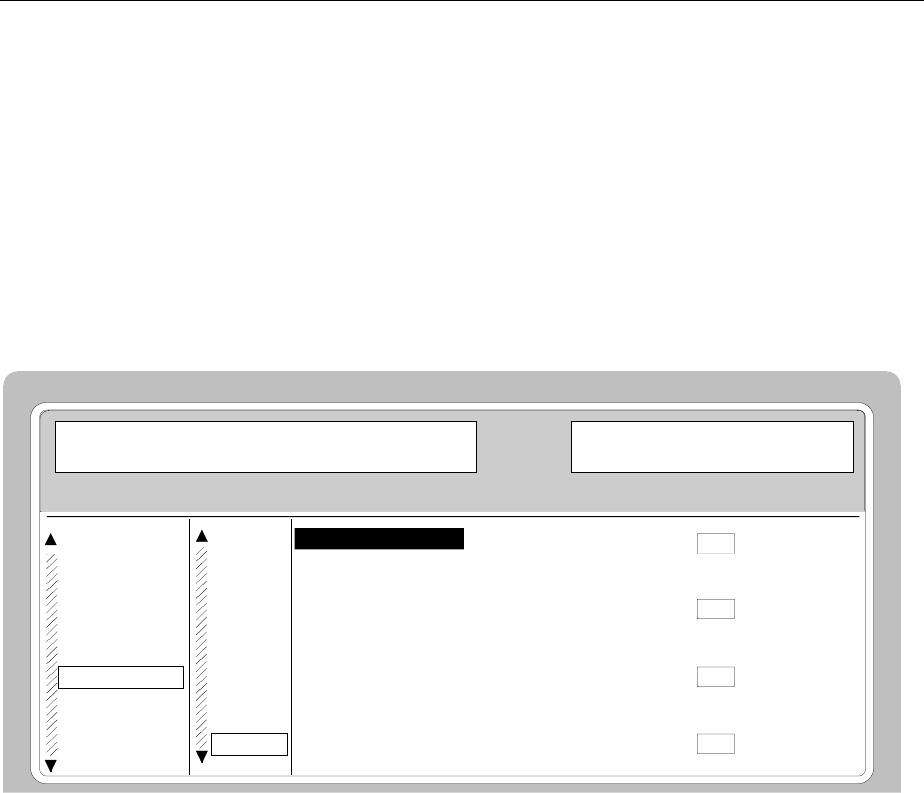
SMIQ External Modulation Source AMIQ
1125.5555.03 E-92.365
(LEVEL) BIAS DC offset in I/Q channel for the BALANCED setting.
The indicated level remains the same with the I/Q
output (LEVEL I/Q = OFF) turned off, provided the
output impedance was prior set to 50 9 with the
command OUTPUT OFF IMPEDANCE.
If the output impedance is set to HIGH with the I/Q
output off, the output connector is isolated with a
relay and the BIAS setting has no effect.
(Only with option AMIQ-B2).
MARKER... Opens a window to configure the four binary marker outputs of AMIQ (eg to
control power ramping of SMIQ), see AMIQ operating manual, section Marker
Outputs.
SETUP...
SAVE/RECA
SELECT WA
MODE
EXECUTE S
EXT TRIG
FILTER
LEVEL...
MARKER...
REFERENCE
FREQ 100. 000 000 0 MHz LEVEL - 30.0 dBm
FREQUENCY
LEVEL
ANALOG MOD
VECTOR MOD
DIGITAL MOD
DIGITAL STD
AMIQ CTRL
LF OUTPUT
SWEEP
LIST
MEM SEQ
OFF ON
0
OFF ON
0
OFF ON
0
OFF ON
0
MARKER CHANNEL 1
SHIFT SAMPLES
MARKER CHANNEL 2
SHIFT SAMPLES
MARKER CHANNEL 3
SHIFT SAMPLES
MARKER CHANNEL 4
SHIFT SAMPLES
Fig. 2-232 Menu AMIQ CTRL - MARKER...
(MARKER...) MARKER CHANNEL
1/2/3/4 Configuration of marker output 1/2/3/4.
OFF No marker output
ON Marker output
SHIFT Marker output displaced by SHIFT
SAMPLES.
SHIFT SAMPLES Number of samples by which the marker of the
corresponding marker channel is displaced. Negative
values cause the marker sequence to be started
earlier while positive values make for a delay of the
marker sequence.
REFERENCE
OSCILLATOR Setting the synchronization by a reference clock.
INT Use of internally generated 10 MHz clock.
EXT The frequency can be synchronized to an external
clock of 10 MHz via the REF input of AMIQ.
Note: The high-precision 10 MHz clock generated by the internal reference
oscillator is always output at the REF output of AMIQ.
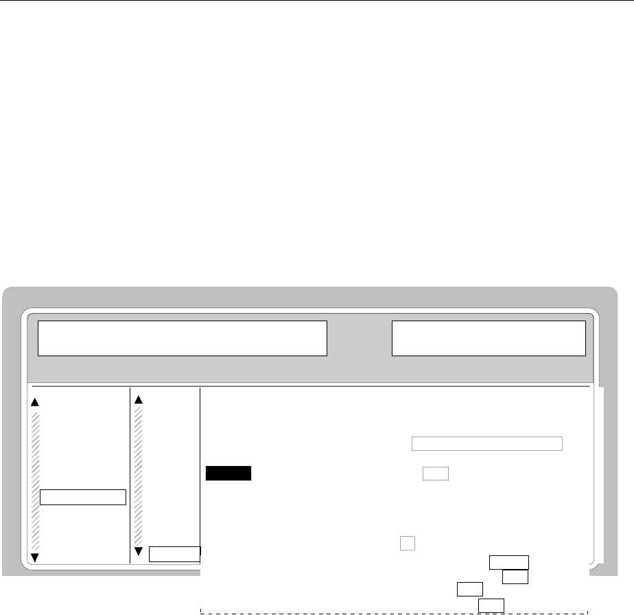
External Modulation Source AMIQ SMIQ
1125.5555.03 2.366 E-9
CLOCK Sets a clock rate, at which samples can be read out of the output buffer and
transferred to the output connectors I and Q via the D/A converters.
Range: 5 MHz to 200 MHz
CLOCK SOURCE Selection of the clock signal source (model AMIQ03 or higher).
INT The internal clock is used. This is the standard setting present
upon switching on the unit or changing the clock.
EXT_SLOW For external clock < 4 MHz
EXT_FAST For external clock > 2 MHz
OUTPUT
RESOLUTION Output resolution of the signal. The resolution set for output cannot be higher
than for waveform generation.
BIT ERROR RATE
TEST This menu enables configuration and performance of BER measurement.
SAVE/RE
SELECT
MODE
EXECUTE
EXT TRI
FILTER
LEVEL..
MARKER.
REFEREN
BIT ERR
FREQ 100. 000 000 0 MHz LEVEL - 30.0 dBm
FREQUENCY
LEVEL
ANALOG MOD
VECTOR MOD
DIGITAL MOD
DIGITAL STD
AMIQ CTRL
LF OUTPUT
SWEEP
LIST
MEM SEQ
BIT ERROR RATE (BER) 2.3
DATA BITS 10000000
ERRORS 23
TERMINATED BY NUMBER OF DATA BITS
_______________________________________________________
MODE OFF AUTO SINGLE
EXECUTE SINGLE
TERMINATION ATTRIBUTES
DATA BITS 10000000
ERRORS 100
PRBS 911152023Bit
DATA POLARITY NORM INV
CLOCK SLOPE POS NEG
MASK POLARITY OFF LOW HIGH
UNIT OFF % ppm
Fig. 2-233 Menu AMIQ CTRL – BIT ERROR RATE TEST...
(BIT ERROR RATE
TEST...) BIT ERROR RATE
(BER) Cyclical indication of the BER measured, ie the ratio
of errors occurred to the number of data bits
transmitted.
DATA BITS Number of data bits transmitted so far.
ERRORS Number of errors occurred so far.
TERMINATED BY The cause of the indicated measurement result is:
NUMBER OF DATA BITS The specified number of
data bits has been
attained.
NUMBER OF ERRORS The specified number of
errors has been detected.
USER User's manual interruption
of the measurement
---- Measurement in progress

SMIQ External Modulation Source AMIQ
1125.5555.03 E-92.367
(BIT ERROR RATE
TEST...) STATE Indication of activities on data and clock line as well as
synchronization status.
MODE Setting the operating mode for the BER measurement.
OFF Terminating measurement.
AUTO Continuous BER measurement. If one or
both termination criteria are met, a new
measurement is initiated. SMIQ cyclically
fetches the current measurement results
from AMIQ. A measurement can take con-
siderable time, depending on the settings
made. During the first measurement, the
intermediate results are displayed. For all
further measurements, only the final results
are shown (by AMIQ). The DATA BITS and
ERRORS displayed are continuously
updated and indicate the relative values
referred to the current measurement.
SINGLE Single BER measurement. SMIQ cyclically
fetches the current measurement results
from AMIQ while the measurement is
being performed. If one of the termination
criteria is met (TERMINATION
ATTRIBUTES - DATA BITS and
TERMINATION ATTRIBUTES - ERRORS),
the measurement is terminated.
A SINGLE measurement can only be
initiated by selecting the EXECUTE SINGLE
menu.
EXECUTE SINGLE Initiating a single BER measurement. This menu item
is only shown if MODE = SINGLE has been set.
TERMINATION
ATTRIBUTES DATA BITS Setting the termination criterion
„Number of data bits transmitted“
ERRORS Setting the termination criterion
„Maximum number of errors
occurred“
PRBS Setting the data period length 9, 11, 15, 20, 23 bits.
DATA POLARITY Setting the polarity of the data bits.
NORM Normal polarity
INV Inverted polarity
CLOCK SLOPE Setting the polarity of the clock slopes.
POS Rising slope
NEG Falling slope
ENABLE RESTART Switching on or off the external restart.
DATA ENABLE Setting the polarity of the DUT's Data Valid signal. 3
possibilities: NOT_USED, LOW and HIGH.
UNIT Setting the unit for indicating the BIT ERROR RATE.
OFF Indication without unit, decadic
% Indication of relative frequency in per cent
ppm Indication of relative frequency in thousandths
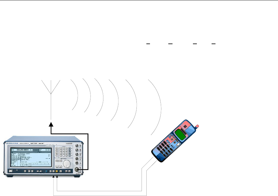
Bit Error Rate Test SMIQ
1125.5555.03 2.368 E-9
2.23 Bit Error Rate Test
Option SMIQB21 allows evaluation of the signal demodulated and decoded by the DUT. For this
purpose, a PRBS-modulated data sequence (PRBS = Pseudo Random Binary Sequence) is sent to the
DUT. This data sequence can be generated continuously (by means of option SMIQB20) or in sections
(option SMIQB60), using a loaded waveform.
The PRBS data sequence is decoded by the DUT and sent to the SMIQ in the form of clock and data
signals. The SMIQ synchronizes to the known PRBS sequence and counts the bit errors.
RF, containing
PRBS Data
Clock
Demodulated Data
Fig. 2-234 BER Measurement
Termination of a measurement can be induced by various criteria. With option SMIQB21,
measurements can be stopped either manually or because of one of the following two criteria: a user-
defined number of data bits has been transmitted or a maximum number of errors has been detected.
By means of the RESTART function (eg for IQ signals that are not generated continuously and therefore
do not contain integer multiples of PRBS sequences) BER results can be integrated onto the (partial)
sequences. In this way, long BER measurements can also be performed on short IQ signals (which
normally do not allow BER measurement because the PRBS sequence is not continuous).
The BER measurement can also be performed separately (with data from another source).
In addition to testing PN bit sequences, the option may also be used to verify CRC checksums. This
operating mode is described in section 2.23.2.
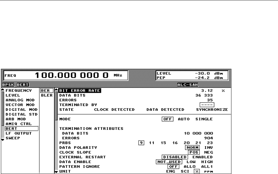
SMIQ Bit Error Rate Test
1125.5555.03 2.369 E-9
2.23.1 Bit Error Rate Measurement with PN Sequences (BER)
2.23.1.1 Operating Menu
In the operating menu, the configuration for the BER measurement is made and the results are
displayed.
Fig. 2-235 Operating menu for BER measurement
In the upper section of the menu (display area), the measurement results are displayed together with the
way in which they have been established, and additional information on the applied signal. In the lower
section, settings can be made.
BIT ERROR RATE
(BER) Cyclic display of the measured bit error rate, the ratio of detected errors to
transmitted data bits.
DATA BITS Number of transmitted data bits.
ERRORS Number of detected errors.
TERMINATED BY The displayed measurement result was obtained as follows:
NUMBER OF DATA BITS The defined number of data bits was reached.
NUMBER OF ERRORS The defined number of errors was detected.
USER The measurement was interrupted manually by
the user.
---- Measurement in progress.

Bit Error Rate Test SMIQ
1125.5555.03 2.370 E-9
STATE The status information described in the following tells the user whether the
BER measurement is working. The STATE display signals the status of clock
line, data line and synchronization. If the clock signal changes, CLOCK is
indicated as status, otherwise NO CLOCK. The same applies to the data
display DATA or NO DATA. NO DATA may be displayed because DATA
ENABLE is not set to NOT USED or the data enable signal does not enable
the data. SYNC indicates a successful attempt of PRBS synchronization by
the analyzer. It is not before all three of CLOCK, DATA and SYNC are "active"
that the measurement results are valid.
CLOCK Change of clock signal.
NO CLOCK No change of clock signal.
DATA Change of data signal.
NO DATA No change of data signal.
SYNC Successful synchronization to PRBS.
NO SYNC No synchronization.
The seven parameters listed above (data bits, error bits, error rate, attribute
"terminated", attribute CLOCK, attribute DATA, attribute SYNC) are jointly
polled by the IEC/IEEE bus query :BERT:RES? .
MODE Setting for the BER measurement.
OFF Terminate measurement.
AUTO Continuous measurement of bit error rate. If one or both criteria for
termination are fulfilled, a new measurement is initiated
automatically. Depending on the settings made, a measurement
may take considerable time. During the first measurement,
intermediate results are displayed. For the measurements that
follow, only the final results are shown. The parameters DATA BITS
and ERRORS are continuously updated and indicate the relative
values for the measurement in progress.
SINGLE Single measurement of bit error rate. During the measurement, the
SMIQ cyclically displays the updated values for rate, number of
errors and number of data bits. If any one of the termination criteria
(TERMINATION ATTRIBUTES [DATA BITS] and TERMINATION
ATTRIBUTES [ERRORS]) is reached, the measurement is stopped.
A single measurement is initiated only if the menu item EXECUTE
SINGLE is selected.
IEC/IEEE-bus command :BERT:STAT ON
:BERT:SEQ SING
EXECUTE SINGLEä
ää
äInitiates a single BER measurement. This menu item is only displayed if
MODE = SINGLE is set.
IEC/IEEE-bus command :TRIG:BERT:IMM
TERMINATION
ATTRIBUTES DATA BITS Setting the termination criterion "Number of transmitted data bits".
IEC/IEEE-bus command :BERT:SET:MCO <1>
ERRORS Setting the termination criterion "Maximum number of detected
errors".
IEC/IEEE-bus command :BERT:SET:MERR <1>

SMIQ Bit Error Rate Test
1125.5555.03 2.371 E-9
PRBS Setting the period length of data: 9, 11, 15, 16, 20, 21, 23 bits.
Note: Data inversion for PRBS15 and PRBS23, which is contained in the
standard, is performed automatically when the PRBS is selected.
DATA POLARITY remains unaffected.
IEC/IEEE-bus command :BERT:SET:TYPE PRBS9
DATA POLARITY Setting the data bit polarity.
NORM Normal polarity
INV Inverted polarity
IEC/IEEE-bus command :BERT:SET:DATA NORM
CLOCK SLOPE Setting the clock edge polarity.
POS Rising edge
NEG Falling edge
IEC/IEEE-bus command :BERT:SET:CLOC RIS
EXTERNAL RESTART Activating/deactivating an external restart of the BER measurement.
Note: An enabled RESTART works always independently of PATTERN
IGNORE or DATA ENABLE.
DISABLED Deactivated
ENABLED Activated
IEC/IEEE-bus command :BERT:SET:REST INT
DATA ENABLE Setting the polarity of the DUT's DATA ENABLE signal.
Note: If the data are not enabled, the execution of the BER
measurement is stopped completely. The identification circuit
for PATTERN IGNORE as well as the PRBS generator of the
BER measurement wait as long as data are not enabled. If the
data are enabled, the measurement is continued.
NOT USED Irrespective of the data enable signal applied, all data at the
BERT data input are used for the BER measurement.
LOW Only the data applied at the BERT data input with a low-level
data enable signal are used for the BER measurement.
HIGH Only the data applied at the BERT data input with a high-level
data enable signal are used for the BER measurement.
IEC/IEEE-bus command :BERT:SET:DEN OFF
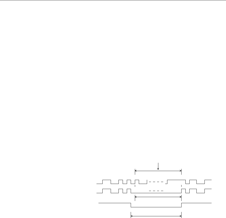
Bit Error Rate Test SMIQ
1125.5555.03 2.372 E-9
PATTERN IGNORE In the event of a so-called frame error (eg an error detected in the check sum),
some mobile radio standards communicate a complete "0" or "1" frame to the
BERT instead of the detected frame data. This is to signal to the BERT that
this frame is not to be used for the BER measurement.
OFF PATTERN IGNORE is not active.
ALL 1 Bit sequences consisting of 31 or more subsequent "1" data
are not used (ie ignored) for the BER measurement.
ALL 0 Bit sequences consisting of 31 or more subsequent "0" data
are not used (ie ignored) for the BER measurement.
IEC/IEEE-bus command :BERT:SET:IGN OFF
Notes:
- While ignoring the bits, the PRBS generator for the BER measurement
keeps running. Following the "0" or "1" sequence, the BER measurement
is continued as if the ignored sequence had contained PRBS data.
- If PATTERN IGNORE is switched on, synchronization time is 32 bits
longer.
- If PATTERN IGNORE and RESTART are active at the same time, the
presence of the restart signal causes the measurement to stop
immediately. None of the 32 bits within the PATTERN IGNORE detector
is evaluated.
- If DATA ENABLE and PATTERN IGNORE are active at the same time,
DATA ENABLE is given priority, ie bits that are not enabled are not
examined for "0" or "1" sequences.
50 Bits
PRBS at Generator
PRBS at DUT Output
BER "active"
Drop Out of DUT
These bits are ingored
Example 50 bits were set to "0" by the DUT. These 50 bits plus the preceding
"0" are ignored in the measurement.
UNIT Setting the unit for displaying the bit error rate.
OFF No unit, decade values
% Relative frequency in percent
ppm Relative frequency in parts per million
IEC/IEEE-bus command :BERT:UNIT OFF

SMIQ Bit Error Rate Test
1125.5555.03 2.373 E-9
2.23.1.2 Signal Path and Waveform
See also chapter 1, section "Option SMIQB21", Connector.
Test setup The signal is computed using one of the modulation sources listed above and then
output by the SMIQ and sent to the DUT (device under test). The latter
demodulates the source bits contained and returns them to the SMIQ together
with a transfer clock. In the SMIQ, the data bits are checked for errors. The total of
the transmitted bits and the faulty bits are counted. The quotient of error bits/total
bits is the BER.
PRBS data To be able to detect faulty bits in a BER measurement, the data generation
polynomial must be known. Data are calculated with the aid of so-called pseudo-
random binary sequences (PRBS). These are quasi-random bit sequences which
are repeated according to the selected polynomial.
An advantage of the PRBS data is that the bit error detector has only to know the
polynomial but not the total sequence. Furthermore, the analysis can be started
anywhere in the bit stream, ie the bit-stream source and the analyzer need not be
synchronized.
Transfer clock Should the DUT not provide a transfer clock, the bit clock can be taken from the
output connector PAR-DATA for the generation of the signal using option
SMIQB11 (DGEN). If AMIQ is used as the IQ source, a marker channel may be
programmed as clock output. However, the clock-to-data ratio is to be observed.

Bit Error Rate Test SMIQ
1125.5555.03 2.374 E-9
2.23.1.3 Test Method
Generation of PRBS
data PRBS data are generated with the aid of a shift register with feedback points
determined by the polynomial. A random start status yields one subsequent
state. The start status and therefore the subsequent status occur only once in
the whole sequence.
Feedback of data
stream If the shift register is filled with a data sequence at the beginning of a
measurement and the register is then switched from "filling" to "feedback",
the register generates the same data sequence as it expects to receive.
Faulty bits can thus be identified and counted by comparing the received data
to the results obtained from the shift register.
This method has the advantage that the analyzer can be used separately
from signal generation (logically and with respect to time). Consequently,
delays caused by the DUT, the use of other PRBS sources and transmission
over long distances with spatially separated transmitter and receiver, do not
cause any problems.
Errors in start status If a bit error is already present in the start status (faulty bits are not detected
during filling), the shift register starts from an incorrect position in the data
sequence. As a result all subsequent states will be faulty. Since, statistically,
every second bit is faulty, the BER will be about 50%. In this case the
measurement is started again automatically, without the user realizing.
BER measurement
with uninterrupted
repetition of the
random sequence
The (non-integrating) BER measurement operates on the basis of random
sequences that are run continuously. These sequences are either generated
continuously or by cyclic output of a stored sequence, with the number of
encoded bits being an integer multiple of the length of the random sequence.
The length of the random sequence is 2 to the power of the degree of the
polynomial less 1, ie PRBS9 has a length of 511 (29 equals 512 less 1).
This type of BER measurement is selected by either setting External Restart to
DISABLED or by issuing the IEC/IEEE-bus command :BERT:SET:REST INT.
The CLOCK and DATA lines are sufficient for this measurement.
The data to be
analyzed are
interrupted by other
data
The data bits contain data like sync, preambles, other channels, etc in
addition to the PRBS data. To mark the data to be evaluated, a DAT ENABle
signal has to be sent with the data. Either this DAT ENABle signal is
generated by the DUT or an additional channel of the IQ source is used (eg
marker channel of AMIQ).
The BER measurement in the SMIQ has to be adjusted for the use of a DAT
ENABle signal; this is done by setting the required polarity in the menu or by
means of IEC/IEEE-bus command (:BERT:SET:DEN Low|High). Data
Enable = high means that data are only counted by the DUT and subjected to
the BER measurement if the data enable input is set to 1.
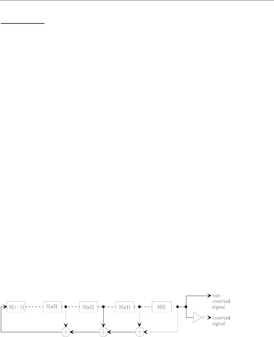
SMIQ Bit Error Rate Test
1125.5555.03 2.375 E-9
BER measurement
with interrupted
random sequence -
integrating BER
measurement
Due to the type of data, oversampling and the finite memory length of the SMIQ
(option SMIQB60) or the AMIQ, it may happen that the generated random
sequence is not cyclically repeated at the memory wrap-around but has a break
at this point. In a normal BER measurement operating exclusively with CLOCK
and DATA signals, a break of this kind would lead to approx. 50% faulty bits due
to the loss of synchronization.
A random sequence with a break can be processed by means of the integrating
BER measurement, it is switched on in the menu under EXTERNAL RESTART
(or by the remote-control command BERT:SETup:RESTart EXTern). The
BER measurement is to be stopped in time and then restarted at the beginning
of the data sequence. The measurement is stopped and started via a signal at
the RES input (pin 9 of SUB-D connector): A transition from logic 0 to 1 causes
a partial result to be generated and the measurement to be stopped. A transition
from 1 to 0 starts the measurement for the next sub-interval. This measurement
is synchronized anew.
This input is best connected to an AMIQ marker channel or the SMIQ trigger
output, with a single 1 encoded both at the start and at the end of the data
sequence. This causes the BER measurement to stop briefly at memory wrap-
around (the break) and start again. The partial results are integrated.
When the signals are interrupted by other data (eg preambles), these data will
normally cause bit errors. The BER measurement for these data can then be
interrupted using the data enable input .
In the integrating BER measurement, partial BER results are added up
(controlled by a signal at the RES input) until the predefined total number of data
or error bits is attained or exceeded.
Note: Since the test hardware can be programmed flexibly, other bit error
measurement techniques such as comparison with the output pattern, masking
of certain time and data ranges, are also possible. In this matter, please contact
your nearest R&S representative.
PRBS Polynomials
For generating and testing the PRBS, a shift register with feedback is used. The feedback depends on
the type of polynomial used. The sequence length of a generator is the result of 2n - 1, n being the
degree of the polynomial.
EXOR EXOR EXOR
Fig. 2-236 PRBS polynomials

Bit Error Rate Test SMIQ
1125.5555.03 2.376 E-9
PN generator N a1 a2 a3 Output Acc. to standard
PN9 9 4 - - non-inverted ITU-T Rec. O.153 Fascicle IV.4
PN11 11 2 - - non-inverted ITU-T Rec. O.152 Fascicle IV.4
PN15 15 1 - - inverted ITU-T Rec. O.151 Fascicle IV.4
PN16 16 5 3 2 non-inverted --
PN20 20 3 - - non-inverted ITU-T Rec. O.153 Fascicle IV.4
PN21 21 2 - - non-inverted --
PN23 23 5 - - inverted ITU-T Rec. O.151 Fascicle IV.4
Measurement Result, Accuracy, Measurement Time
Value range Measurement results for the bit error rate (ie the quotient of error bits and total
bits) are usually found between 10-
2
and 10-
9
. This means that a large number of
bits may have to be checked before a faulty bit is detected. Because of the large
number of bits involved the measurement time is usually very long.
Since 32-bit-wide counters are used for the total bits and the error bits, the
maximum measurement time is 4.29 x 109 bits.
Statistics The BER measurement measures statistical bit errors, ie errors which do not
occur at regular intervals but at random. Although a single measurement
determines the exact number of errors in the measured interval, a statistically
reliable BER can only be obtained when a sufficient number of errors occurs in the
observed interval. Only this ensures that the single BER measurement result
approaches the true error rate with high probability .
Termination
criteria To keep the measurement time short with low and high bit error rates, two
termination criteria have been defined in the SMIQ for the BER measurement.
• Criterion 1: Total number of bits
The measurement is terminated when the specific number of data bits is
reached. Due to this criterion the BER measurement is reliably stopped after
the specified number of bits even if no error or only a few errors were detected;
the measurement result is not statistically reliable (few bit errors).
• Criterion 2: Number of errors
The measurement is terminated when the specified number of bit errors is
detected. With this criterion, the measurement is rapidly terminated when high
bit error rates occur. Since a great number of errors is counted, the
measurement result is statistically reliable.
The two criteria are used together. The criterion which finally yields a valid result is
indicated in the results screen ("Measurement terminated by...").
Interruption of
measurement At the end of a measurement, the restart of a new one is delayed until the first
measurement result has been queried with :BERT:RES?. The resulting brief
measurement interruption is irrelevant because the subsequent measurement will
be synchronized within 24 data bits.

SMIQ Bit Error Rate Test
1125.5555.03 2.377 E-9
Possible Problems with BER Measurement and Related Solutions
Fault Possible cause Fault description/remedy
No signals received from
DUT or the signal level is
not correct.
Ø Check displays for activity at BER measurement inputs.
If a status is displayed (Clock, Data, Sync) for a line, there is
activity.
The selected PRBS is not
correct. Normally, the PRBS on which the data are based is used as the
default setting. If the PRBS is changed, the BER measurement
cannot synchronize to the data (because the polynomial is not
correct).
A wrong clock edge is
used, which violates setup
or hold times.
Ø Check the bit clock signal, the data signal and the data enable
signal, if any, on an oscilloscope.
The fault may also be caused by reflections on the clock line, which
switch the data signal twice into the BER measurement, eg on lines
without termination. The SMIQ input is not terminated.
Incorrect polarity of data
signal (or data enable
signal).
In this case the PRBS cannot synchronize. Note that an inversion
of the output signal specified for some cases by the PRBS
standard is performed automatically upon PRBS selection.
Manual inversion of the data signal is therefore not required.
BER
measurement
does not
synchronize
A bit error occurs during
synchronization (nine data
bits with PRBS9)
The BER measurement is started at a wrong position so that
about 50% of the subsequent data bits are identified as faulty.
No clock received
from DUT When testing RF
components, clock
recovery is not available.
An external clock is
however required for
clocking the data during the
BER measurement
Instead of a clock recovery circuit, the bit clock at the PAR-DATA
connector of the SMIQ may be possibly used as a replacement.
This is possible if DGEN (SMIQB11) is used as a data source.
However, this bit clock is not possible with all modulation types.
Also, the delay between data and clock has to be observed.
Measured BER
too high The data are clocked with
the wrong edge and/or the
eye aperture of the data is
not optimally met.
Ø Check the clock/data relationship by means of an oscilloscope and
set optimum timing.
.
BER measurement does
not synchronize If data that are not cyclically continued (ie when a break occurs at the
memory wrap-around), the measurement will identify about 50% of the
bits as faulty after the wrap-around.
Make sure the measurement is started optimally at the beginning of the
sequence by means of a signal on the REStart line (see: "BER
measurement with interrupted random sequence – integrating BER
measurement" in section 2.23.1.3, "Test Method").
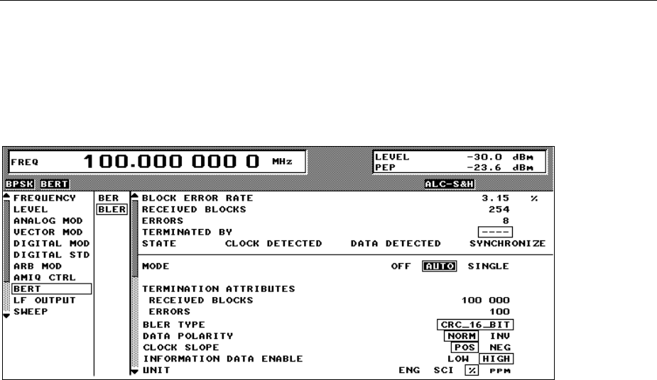
Bit Error Rate Test SMIQ
1125.5555.03 2.378 E-9
2.23.2 Block Error Rate Measurement (BLER)
2.23.2.1 Operating Menu
In the operating menu, the BLER measurement is configured and the results are displayed.
Fig. 2-1 Operating menu for BLER measurement
In the upper section of the menu (display area), the measurement results are displayed, the way in
which they have been obtained, and additional information on the applied signal. In the lower section,
settings can be made.
BLOCK ERROR
RATE (BLER) Cyclic display of measured block error rate, the ratio of detected errors to
transmitted data blocks.
IEC/IEEE bus :BLER:RES? Return value3(of7)
RECEIVED BLOCKS Number of transmitted data blocks.
IEC/IEEE bus :BLER:RES? Return value1(of7)
ERRORS Number of detected errors.
IEC/IEEE bus :BLER:RES? Return value2(of7)
TERMINATED BY The displayed measurement result was obtained as follows:
NUMBER OF RECEIVED BLOCKS
The defined number of data blocks was reached.
NUMBER OF ERRORS The defined number of errors was detected.
USER The measurement was manually aborted by the
user.
---- Measurement in progress.
IEC/IEEE bus :BLER:RES? Return value4(of7)

SMIQ Bit Error Rate Test
1125.5555.03 2.379 E-9
STATE The status information described in the following tells the user whether the
BLER measurement functions correctly. The STATE display signals the status
of clock line, data line and synchronization. If the clock signal changes,
CLOCK is indicated as status, otherwise NO CLOCK. The same applies to the
DATA or NO DATA display. SYNCHRONIZE indicates a successful attempt of
synchronization by the CRC tester. Only when all three displays (CLOCK,
DATA and SYNCHRONIZE) are "active" will the measurement results become
valid.
CLOCK Change of clock signal.
NO CLOCK No change of clock signal.
DATA Change of data signal.
NO DATA No change of data signal.
SYNCHRONIZE Successful synchronization to CRC.
NO SYNC No synchronization.
The seven parameters listed above (data blocks, error blocks, block error rate,
attribute "terminated", attribute CLOCK, attribute DATA, attribute SYNC) are
queried together with the IEC/IEEE bus query :BERT:RES? .
MODE Setting the BLER measurement mode.
OFF Terminate measurement.
AUTO Continuous measurements of block error rate. If one or both
termination criteria are fulfilled, a new measurement is started
automatically. Depending on the settings made, a measurement
may take considerable time. During the first measurement,
intermediate results are displayed. For all subsequent
measurements, only the final results are displayed. The parameters
RECEIVED BLOCKS and ERRORS are continuously updated and
indicate the relative values for the measurement in progress.
SINGLE Single measurement of block error rate. During the measurement,
the SMIQ cyclically displays the current values for rate, number of
errors and data blocks. If any one of the termination criteria
(TERMINATION ATTRIBUTES [RECEIVED BLOCKS] and
TERMINATION ATTRIBUTES [ERRORS]) is reached, the
measurement is terminated. A SINGLE measurement can only be
triggered when the menu item EXECUTE SINGLE is selected.
IEC/IEEE-bus command :BLER:STAT ON
:BLER:SEQ SING
EXECUTE TRIGGERä
ää
äTriggers a single BLER measurement. This menu item is only displayed when
MODE = SINGLE is selected.
IEC/IEEE-bus command :TRIG:BLER:IMM
TERMINATION
ATTRIBUTES RECEIVED BLOCKS
Setting of termination criterion "Number of received data
blocks".
IEC/IEEE-bus command :BLER:SET:MCO <1>
ERRORS Setting of termination criterion "Maximum number of detected
errors".
IEC/IEEE-bus command :BLER:SET:MERR <1>

Bit Error Rate Test SMIQ
1125.5555.03 2.380 E-9
BLER TYPE Displays the CRC type. Only the CRC_16_BIT type is supported at present.
IEC/IEEE-bus command :BLER:SET:TYPE?
DATA POLARITY Setting the data bit polarity.
NORM Normal polarity
INV Inverted polarity
IEC/IEEE-bus command :BLER:SET:DATA[:POL] NORM
CLOCK SLOPE Setting the clock edge polarity.
POS Rising edge
NEG Falling edge
IEC/IEEE-bus command :BLER:SET:CLOC[:POL] RIS
INFORMATION DATA
ENABLE Setting the polarity of the DUT's DATA ENABLE signal.
LOW The bits received at low level of the data enable signal are
interpreted as information bits.
The bits received at high level of the data enable signal are
interpreted as checksum bits.
HIGH The bits received at high level of the data enable signal are
interpreted as information bits.
The bits received at low level of the data enable signal are
interpreted as checksum bits.
IEC/IEEE-bus command :BLER:SET:DEN LOW
UNIT Setting the unit for BLOCK ERROR RATE display.
ENG Display in exponential notation, exponent -3 or -6
SCI Display in scientific notation, i.e. normalized to one character
ahead of the decimal point
% Display of relative frequency in percent
ppm Display of relative frequency in parts per million
IEC/IEEE-bus command :BLER:UNIT ENG
2.23.2.2 CRC Polynomial
CCITT CRC 16 : G(x) = x16 + x12 + x5 + x1 is the only CRC polynomial currently supported.
At the beginning of information data (marked by the edge of the DATA ENABLE signal) the shift register
is initialized with 0. All information bits are then shifted through the shift register. The CRC component
is then read into a second register and compared bit by bit with the result of the calculation.
2.23.2.3 Measurement Result, Accuracy, Measurement Time
Range of values The measurement results for the block error rate (i.e. the quotient of erroneous
blocks and total blocks) are normally between 10-
2
and 10-
4
. This means that a large
number of blocks may have to be tested before an erroneous block occurs.
Because of the large number of blocks involved the measurement time is usually
very long. Since 32-bit-wide counters are used for the total number of blocks and the
error bits, the maximum measurement time is 4.29 x 10⁹ blocks.
Statistics The BLER measurement measures statistical block errors, i.e. errors which do not
occur at regular intervals but at random. Although a single measurement
determines the exact number of errors in the measured interval, a statistically

SMIQ Bit Error Rate Test
1125.5555.03 2.381 E-9
reliable BLER can only be obtained when a sufficient number of errors occurs in
the observed interval. Only this ensures that the single BLER measurement result
approaches the true error rate with high probability.
Termination
criteria To keep the measurement time short for low and high block error rates, two
termination criteria have been provided in the SMIQ for the BLER measurement.
• Criterion 1: Total number of blocks
The measurement is terminated when the specified number of data blocks is
checked. Due to this criterion the BLER measurement is reliably terminated
after the specified number of blocks even if no error or only a few errors were
detected; the measurement result may not be statistically reliable (if few block
errors occur).
• Criterion 2: Number of errors
The measurement is terminated when the specified number of block errors has
occurred. With this criterion, the measurement is rapidly terminated when the
block error rate is high. Since a great number of errors has been counted, the
measurement result is statistically reliable.
The two criteria are used together. The criterion which finally yields a valid result is
displayed under ("Measurement terminated by...").
Interruption of
measurement After termination of a measurement, the restart of a new one is delayed until the
first measurement result has been queried with :BLER:RES?.

Bit Error Rate Test SMIQ
1125.5555.03 2.382 E-9
2.23.2.4 Possible BLER Measurement Problems and Solutions
Fault Possible cause Fault description/remedy
BLER
measurement
does not
synchronize
No signals received from
DUT or the signal level is not
correct.
Ø Check activity at BLER measurement inputs in the display.
A status display (Clock, Data, Sync) signals activity on the respective
line.
A wrong clock edge is used,
which violates setup or hold
times.
Ø Check the bit clock signal, the data signal and the DATA ENABLE
signal, if any, on an oscilloscope.
The fault may also be caused by reflections on the clock line, which
clock the data signal twice into the BLER measurement, e.g. if lines are
not terminated. The SMIQ input is not terminated.
Incorrect polarity of data
signal (or DATA ENABLE
signal).
In this case the CRC tester cannot synchronize.
No clock received
from DUT When testing RF
components, clock recovery
may not be available. An
external clock is however
required for clocking the data
during the BLER
measurement.
The bit clock at the PAR DATA connector of the SMIQ may be used
instead of a clock recovery circuit. This is possible if DGEN (SMIQB11)
is used as a data source. However, this bit clock is not available with all
modulation types. Also, the delay between data and clock has to be
taken into account.
Measured BLER
too high The data is switched with the
wrong clock edge and/or the
eye pattern of the data is not
optimally met.
ØCheck the clock/data relationship by means of an oscilloscope and
optimize the timing.
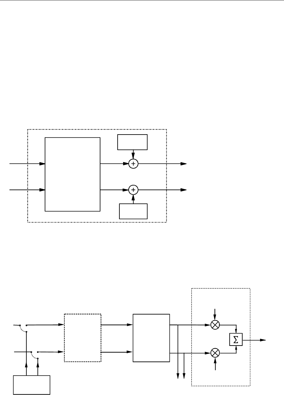
SMIQ Noise Generator and Distortion Simulator
1125.5555.03 2.383 E-9
2.24 Noise Generator and Distortion Simulator
The noise generator and the distortion simulator (Option SMIQB17) perform the following two functions:
• Addition of noise to the SMIQ output level. Since the C/N can be finely varied, different reception
conditions can be realistically simulated.
• Simulation of TWTA (traveling wave tube amplifier) distortion of satellite. The signal received by the
satellite is strongly distorted and thus more difficult to demodulate than an undistorted signal. Real
reception conditions can be simulated with the distortion simulator and the receivers can thus be
tested realistically.
The noise generator outputs an AWGN signal (Additive White Gaussian Noise) , ie the noise power ratio
is Gaussian-distributed and the noise signal is added to the signal.
Distortion is performed via AM/AM conversion and AM/PM conversion. The respective characteristics
can be loaded or modified via IEC/IEEE bus.
I
Q
Distortion
AM/AM conversion
AM/PM conversion
Noise
generator
Noise
generator
I
Q
in out
in
I
Qout
Fig. 2-237 Block diagram of noise generator and distortion simulator
The noise generator and distortion simulator are independent functional units and can be operated
separately. They exclusively use baseband signals I and Q. Both external I/Q signals and I/Q signals
internally generated by the modulation coder can be distorted and superimposed with noise. The noise
generator can also be switched on if internal and external modulation are switched off. The unmodulated
carrier is then superimposed with the noise signal.
sin( t)
ω
cos( t)
ω
I
Q
ext
ext
RF OUT
IQ modulator
Modulation
coder IQ
AUX
Option
Fading
Simulator
SMIQB14
Noise
generator
Distortion
simulator
Fig. 2-238 Noise generator and distortion simulator in the SMIQ
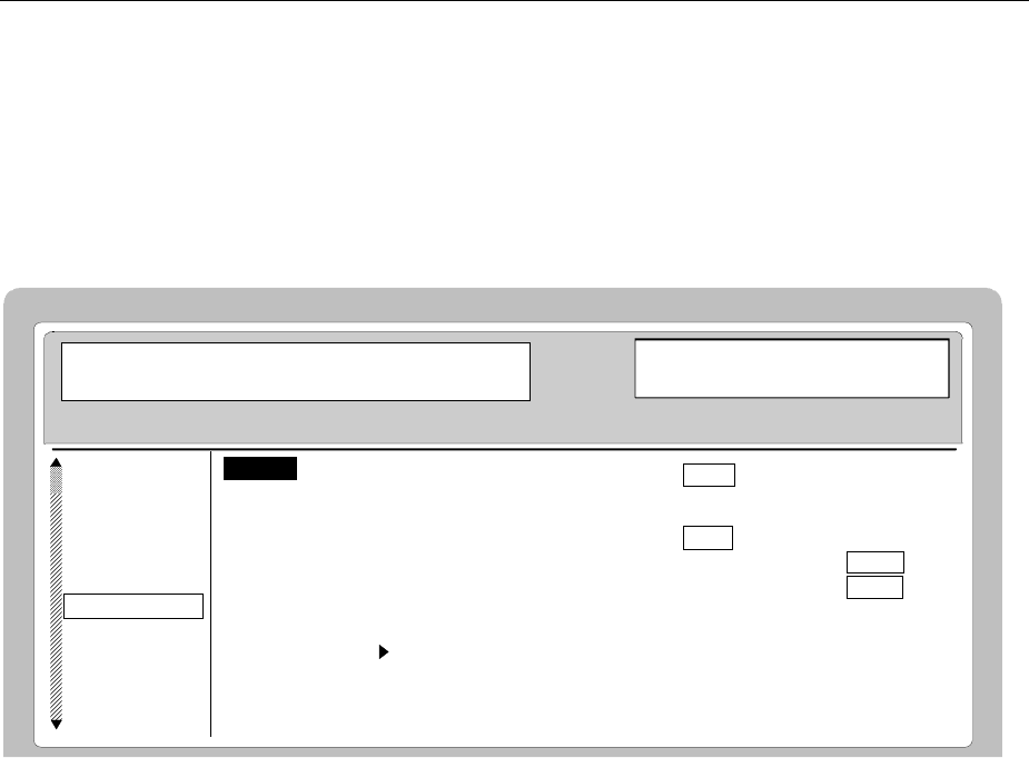
Noise Generator and Distortion Simulator SMIQ
1125.5555.03 2.384 E-9
2.24.1 Setting NOISE/DIST Menu
The NOISE/DIST menu comprises all the settings of the noise generator and the distortion simulator.
For calibration of the noise generator and the distortion simulator, see Chapter 2, Section Calibration
VECTOR MOD.
Note: Functions NOISE/DIST and BB-AM cannot be set at the same time and switch off
mutually.
Menu selection: NOISE/DIST
FREQ 100.000 000 0
MHz LEVEL - 30.0 dBm
FREQUENCY
LEVEL
ANALOG MOD
VECTOR MOD
DIGITAL MOD
DIGITAL STD
NOISE/DIST
LF OUTPUT
SWEEP
LIST
MEM SEQ
UTILITIES
OFF ON
0.0 dB
20.0 kHz
OFF ON
POLYNOMIAL LIST
CURRENT: TWTA
-3.12 dB
NOISE
CARRIER/NOISE RATIO
SYSTEM BANDWIDTH
DISTORTION
CHARACTERISTIC...
SELECT LIST...
POLYNOMIAL...
LEVEL CORRECTION
RECALCULATE
Fig. 2-239 Menu NOISE/DIST (presetting)
NOISE Switch on/off of noise source. The noise source is an AWGN (Additive White
Gaussian Noise) signal.
IEC/IEEE-bus commands :SOUR:NOIS ON
CARRIER/NOISE
RATIO Input value of the carrier-to-noise ratio. Setting range is 5.0 to 30 dB. When
changing the CARRIER/NOISE RATIO, the noise power is changed as well
but the carrier power remains unchanged. The carrier power is the power
displayed in the header under LEVEL.
IEC/IEEE-bus command :SOUR:NOIS:SNR 10 dB
SYSTEM
BANDWIDTH Input value of system bandwidth.
The system bandwidth is the HF-bandwidth by which the noise power is
calculated. The bandwidth of the generated noise can only be set in steps.
The set bandwidth is to be 1.4 times the system bandwidth at minimum and
10 MHz at maximum.
Setting range: 10 kHz to 10 MHz;
Resolution: three digits
IEC/IEEE-bus command :SOUR:NOIS:BAND 1.23 MHz
DISTORTION Switch on/off of distortion.
IEC/IEEE-bus command :SOUR:DIST ON

SMIQ Noise Generator and Distortion Simulator
1125.5555.03 2.385 E-9
CHARACTERISTIC... Switchover between distortion data from the polynomial and list. Under
polynomial the distortion data are calculated from the coefficients entered into
the polynomial menu. Under list they are calculated according to the
characteristic transferred via the IEC/IEEE-bus and selected under SELECT
LIST.
IEC/IEEE-bus command :SOUR:DIST:MODE POLY | DATA
SELECT LIST... Opens a window for selecting the distortion characteristics. Several distortion
characteristics can be stored in the memory at the same time.
IEC/IEEE-bus command :SOUR:DIST:DATA:SEL "TWTA"
POLYNOMIAL... Opens a window for entering the polynomial parameters.
Menu selection: NOISE/DIST - POLYNOMIAL...
FREQ 100.000 000 0
MHz LEVEL - 30.0 dBm
FREQUENCY
LEVEL
ANALOG MOD
VECTOR MOD
DIGITAL MOD
DIGITAL STD
NOISE/DIST
LF OUTPUT
SWEEP
LIST
MEM SEQ
UTILITIES
COEFFICIENTS AM-AM
COEFFICIENTS AM-PM
INVERSE FUNCTION
LEVEL CORRECTION
NOISE
CARRIER/NOI
SYSTEM BANDW
DISTORTION
CHARACTERIST
SELECT LIST
POLYNOMIAL..
LEVEL CORRECTI
RECALCULATE
CALIBRATE CARR
k2 0.0dB
k3 0.0dB
k4 0.0dB
k5 0.0dB
k2 0.0deg
k3 0.0deg
k4 0.0deg
k5 0.0deg
OFF ON
0.0deg
Fig. 2-240 Menu NOISE/DIST - POLYNOMIAL...
(POLYNOMIAL...) COEFFICIENT AM-AM Entry of polynomial coefficients k2 to k5 for the
AM-AM distortion in dB. The polynomial has the
following form:
Aout = Ain + n2*Ain^2 + n3*Ain^3 + n4*Ain^4 + n5*Ain^5
with n<i> = 10^(k<i>/20) - 1, i = 2, 3, 4, 5
Normalization: Aout_n = 0 ... 1, Ain = 0...1
The coefficient n0 is always 0 and n1 is always 1.
Value range: -10.0 to +10.0 dB
IEEE-bus :SOUR:DIST:POLY:AMAM:K2 -2 DB
COEFFICIENT AM-PM Entry of polynomial coefficients k2 to k5 for the
AM-PM distortion in degrees. The polynomial has the
following form:
Pout = Pin + k2*Ain^1 + k3*Ain^2 + k4*Ain^3 + k5*Ain^4
The coefficients K0 and K1 are always 0.
Value range: - 60.0 to + 60.0 degrees.
IEEE-bus :SOUR:DIST:POLY:AMPM:K3 -45 DEG

Noise Generator and Distortion Simulator SMIQ
1125.5555.03 2.386 E-9
(POLYNOMIAL...) INVERSE FUNCTION Compensation of an amplifier connected after the
SMIQ, the coefficients entered correspond to the
measured distortion of the amplifier.
OFF The above equations are applicable.
ON AM-AM distortion:
inverse function of Aout_n (Ain),
AM-PM distortion:
Pout = Pin - k2*Aout_n(Ain)^1 -
k3*Aout_n(Ain)^2 - k4*Aout_n(Ain)^3 -
k5*Aout_n(Ain)^4
IEEE-bus :SOUR:DIST:POLY:IFUN ON
LEVEL CORRECTION Entry of the level correction for the polynomial. The
value entered is active and is displayed in the main
menu after selection of the polynomial and calling up
RECALCULATE. It can be edited only here.
Value range: -20 dB to +6 dB
IEEE-bus :SOUR:DIST:POLY:LEV:CORR -10 DB
LEVEL CORRECTION Display of level correction to correct the output level so that the attenuation or
gain of the distortion simulator can be compensated. For the polynomial the
level correction can be entered into submenu POLYNOMIAL. The level
correction for the lists can only be transferred via the IEC/IEEE bus.
Value range: -20 dB to +6 dB
IEC/IEEE-bus command :SOUR:DIST:DATA:LEV:CORR -3.12 DB
RECALCULATE Distortion data are active since as they are transferred into the module. This is
necessary when the available characteristic has been overwritten via the
IEC/IEEE bus or when a polynomial parameter has been modified.
IEC/IEEE-bus command :SOUR:DIST:REC
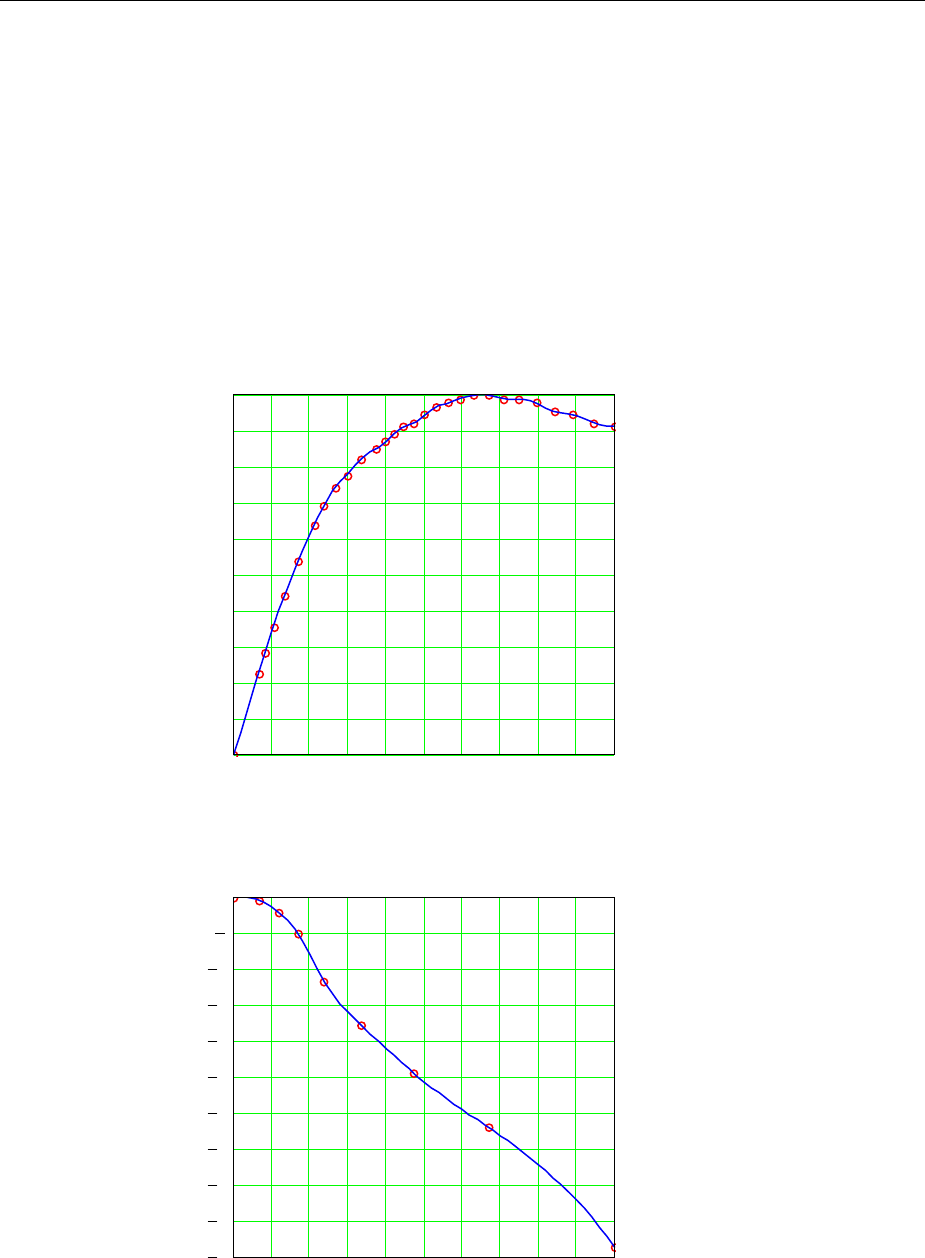
SMIQ Noise Generator and Distortion Simulator
1125.5555.03 2.387 E-9
2.24.2 Loading New Distortion Characteristics
The SMIQ is supplied with a preset distortion characteristic that corresponds to the typical characteristic
of a traveling wave tube amplifier in WorldSpace satellites. The name of the characteristic set as
standard is TWTA (Traveling Wave Tube Amplifier). Other user-defined distortion characteristics can
also be stored in the SMIQ. If several characteristics are stored, they can be selected under SELECT
CHARACTERISTIC... .
A new characteristic is formed by the interpolation points of AM/AM and AM/PM conversion. Entry is
possible via IEC/IEEE bus. The SMIQ determines the complete characteristic based on these
interpolation points by cubic spline interpolation. The factory-set characteristics (TWTA) of AM/AM and
AM/PM conversion are shown in the following figures. The continuous line indicates the interpolated
characteristic. The circles show the reference points. The input values are on the x-axis, the output
values on the y-axis.
Fig. 2-241 AM/AM conversion
Fig. 2-242 AM/PM conversion
0 0.1 0.2 0.3 0.4 0.5 0.6 0.7 0.8 0.9 1
0
0.1
0.2
0.3
0.4
0.5
0.6
0.7
0.8
0.9
1
Output values
Input values
0 0.1 0.2 0.3 0.4 0.5 0.6 0.7 0.8 0.9 1
50
45
40
35
30
25
20
15
10
5
0
Output values (degree)
Input values

Noise Generator and Distortion Simulator SMIQ
1125.5555.03 2.388 E-9
The two characteristics are formed by 2 data fields, the x-axis and the y-axis. 4 data fields therefore
have to be loaded for a new distortion characteristic. The minimum number of interpolation points that
can be entered for a characteristic is 5, the maximum number is 30. The limit values for the data fields
are as follows:
Input values (x-axis) of AM/AM conversion: -100 dB to 0 dB
Output values (y-axis) of AM/AM conversion: -100 dB to 0 dB
Input values (x-axis) of AM/PM conversion: -100 dB to 0 dB
Output values (y axis) of AM/PM conversion: -180° to +180°
2.24.3 Level Correction of the Distortion Simulator
The level correction influences the level if digital modulation is switched on (not with VECTOR MOD ON)
and the distortion simulator is active.
For the rms level set as LEVEL to appear at the RF output, the level control has to compensate for the
attenuation or gain of the distortion characteristic. For this purpose, level correction (-20 dB to 6 dB)
stored under the previously selected name is transmitted via IEC/IEEE-bus command. If this
characteristic is active, the output level is increased or decreased by the level-correction value. The
value by which the level is increased or decreased is indicated under LEVEL CORRECTION.
As the attenuation/gain of the distortion characteristic is dependent on the type of input signal being
dealt with, the level correction applies only to one particular type of digital modulation (modulation type,
filter type and filter parameters) and fading setting.
For the characteristic TWTA, for instance, which is supplied as standard, -3.12 dB is stored as level
correction. This value only applies to "WorldSpace Modulation" (QPSK, SQR-COS/0.4).
For the determination of level correction through measurement, the parameter is at first set to 0 dB via
IEC/IEEE bus. The desired type of digital modulation is then set, and the characteristic TEST (linear
characteristic supplied, LEVEL CORRECTION = 0 dB) activated, followed by the new characteristic. The
level difference of the two characteristics is measured at the RF output by means of an RF level meter.
The level correction for the new characteristic is then adjusted to the level difference measured via
IEC/IEEE bus. If the level difference is measured again, the result should be 0 dB ± 0.1 dB.
As theoretically the characteristic gain (negative level correction) cannot exceed the crest factor of the
modulation used, the warning "Warning 426 Absolute value of level correction > crest factor of Digital
Mod;" is displayed if the magnitude of the negative level correction exceeds the crest factor. The
correction is also restricted to the crest factor when the level is set, so LEVEL and PEP are identical.

SMIQ Noise Generator and Distortion Simulator
1125.5555.03 2.389 E-9
Step-by-step instruction to enter a new distortion characteristic via IEC/IEEE bus:
1. Enter the name of a new characteristic IEC/IEEE-bus command
:SOUR:DIST:DATA:SEL "TWTA1"
The characteristic is listed under a freely selectable
name (max. 8 characters) in the select menu that
comprises different characteristics.
2. Enter the data field for input values
(x-axis) of AM/AM conversion in dB IEC/IEEE-bus command
:SOUR:DIST:DATA:AMB -23.5,-21.5,
-19.5,-17.5,-15.5,-13.5,-12.5,-11.5,
-10.5,-9.5,-8.5,-8,-7.5,-7,-6.5,-6,
-5.5,-5,-4.5,-4,-3.5,-3,-2.5,-2,-1.5,
-1,-0.5,0
3. Enter the data field for output values
(y-axis) of AM/AM conversion in dB IEC/IEEE-bus command
:SOUR:DIST:DATA:AM -12.9,-10.9,-9,
-7.1,-5.4,-3.9,-3.2,-2.6,-2.2,-1.7,
-1.4,-1.2,-1,-0.8,-0.7,-0.5,-0.3,
-0.2,-0.1,0,0,-0.1,-0.1,-0.2,-0.4,
-0.5,-0.7,-0.8
4. Enter the data field for input values
(x-axis) of AM/PM conversion in dB IEC/IEEE-bus command
:SOUR:DIST:DATA:PMB -23.5,-18.5,
-15.5,-12.5,-9.5,-6.5,-3.5,0
5. Enter the data field for output values
(y-axis) of AM/PM conversion in degrees IEC/IEEE-bus command
:SOUR:DIST:DATA:PM 0,-2.1,-5,-11.6,
-17.7,-24.4,-31.9,-48.6
6. Enter the level correction IEC/IEEE-bus command
:SOUR:DIST:DATA:LEV:CORR -3.12
7. Data transmission to the module IEC/IEEE-bus command
:SOUR:DIST:REC
Note: The values of the above example correspond to the TWTA characteristic that is supplied.

Noise Generator and Distortion Simulator SMIQ
1125.5555.03 2.390 E-9
2.24.4 Calculation of the Distortion Characteristic from Polynomial
Equations
A characteristic can be defined by entering polynomial coefficients in submenu POLYNOMIAL instead of
transferring reference values via the IEC/IEEE bus. The characteristic is calculated and loaded from the
four polynomial coefficients for AM-AM and AM-PM using the equations specified under section 2.24.1.
An IEC/IEEE-bus transfer is not required in this case.
It is possible to compensate the distortion of an amplifier connected after the SMIQ using the INVERSE
FUNCTION.
The characteristic entered via polynomial coefficients should be identical to the distortion characteristic
of the amplifier.
The level correction described in section 2.24.3 can be directly entered in the POLYNOMIAL menu. If
the polynomial is activated, this value can be displayed and set in the NOISE/DIST menu under LEVEL
CORRECTION. The determination by measurement of the level correction is performed as described in
section 2.24.3.

SMIQ LF Output
1125.5555.03 2.391 E-9
2.25 LF Output
The internal LF generator is available as a signal source for the LF output.
Menu LF OUTPUT offers access to the settings of the LF output.
Notes: - An alteration of the frequency of the internal modulation generator in the LF-output menu
automatically effects the modulation for which the generator is selected as modulation
source.
- The SWEEP function of LF generator can be activated in menu SWEEP-LF-GEN.
Menu selection: LF OUTPUT
STATE OFF ON
VOLTAGE 1.000 V
LFGEN FREQ 1.000 0 kHz
FREQ
100. 000 000 0
MHz LEVEL
- 30.0
dBm
FREQUENCY
LEVEL
ANALOG MOD
VECTOR MOD
DIGITAL MOD
DIGITAL STD
LF OUTPUT
SWEEP
LIST
MEM SEQ
UTILITIES
Fig. 2-243 Menu LF OUTPUT (preset setting)
STATE Switching on/off the LF output. Parameter STATE has no influence on the
modulation settings.
IEC/IEEE-bus command :OUTP2 ON
VOLTAGE Input value of the output voltage of the LF output. The input is effected in the
form of a peak voltage.
IEC/IEEE-bus command :OUTP2:VOLT 1V
LFGEN FREQ Input value of the frequency of internal modulation generator.
IEC/IEEE-bus command :SOUR2:FREQ 1kHz

Sweep SMIQ
1125.5555.03 2.392 E-9
2.26 Sweep
The SMIQ offers a digital step-by-step sweep for parameters:
•RF frequency
•LF frequency
•RF level
Setting a sweep is effected in five basic steps which are shown in the following example, the setting of a
frequency sweep:
1. Set sweep range (START and STOP or CENTER and SPAN).
2. Select linear or logarithmic sequence (SPACING).
3. Set step width (STEP) and dwell time (DWELL).
4. Activate marker if desired (MARKER).
5. Switch on sweep (MODE set to AUTO, SINGLE or STEP).
2.26.1 Setting the Sweep Range (START, STOP, CENTER and SPAN)
The sweep range of the RF sweep can be entered in two different ways. Either by entering the START
and STOP value or by entering CENTER and SPAN. Please observe that the two parameter sets
influence one another. The influence is exerted in the following way:
START frequency altered: STOP = unaltered
CENTER = (START + STOP)/2
SPAN = (STOP - START)
STOP frequency altered: START = unaltered
CENTER = (START + STOP)/2
SPAN = (STOP - START)
CENTER frequency altered SPAN = unaltered
START = (CENTER - SPAN/2)
STOP = (CENTER + SPAN/2)
CENTER = unaltered
START = (CENTER - SPAN/2)
STOP = (CENTER + SPAN/2)

SMIQ Sweep
1125.5555.03 2.393 E-9
2.26.2 Selecting the Sweep Run (SPACING LIN, LOG)
The sweep run, linear or logarithmic, can be selected using SPACING. For the RF and LF sweep, a
linear or logarithmic run is possible. For level sweep, only the logarithmic run is possible.
With the logarithmic sweep, step width STEP is equal to a constant fraction of the present setting. The
logarithmic step width is entered in unit % with RF or LF sweep, in unit dB with level sweep.
2.26.3 Operating Modes (MODE)
The following sweep operating modes are available:
AUTO Sweep from the starting point to the stop point, with automatic restart at the starting
point. If another sweep operating mode was activated prior to the AUTO operating
mode, continuation is made from the current sweep setting.
IEC/IEEE-bus commands:
RF sweep: LF sweep: Level sweep:
SOUR:FREQ:MODE SWE SOUR2:FREQ:MODE SWE SOUR:POW:MODE SWE
SOUR:SWE:MODE AUTO SOUR2:SWE:MODE AUTO SOUR:SWE:POW:MODE AUTO
TRIG:SOUR AUTO TRIG2:SOUR AUTO TRIG:SOUR AUTO
SINGLE Single run from the starting point to the stop point. If SINGLE is selected, the run is
not started yet. Function EXECUTE SINGLE SWEEP to be executed, which can
be used to start the run, is displayed below the MODE line.
IEC/IEEE-bus commands:
RF sweep: LF sweep: Level sweep:
SOUR:FREQ:MODE SWE SOUR2:FREQ:MODE SWE SOUR:POW:MODE SWE
SOUR:SWE:MODE AUTO SOUR2:SWE:MODE AUTO SOUR:SWE:POW:MODE AUTO
TRIG:SOUR SING TRIG2:SOUR SING TRIG:SOUR SING
STEP Step-by-step, manual run within the sweep limits. Activating STEP stops a running
sweep and the cursor wraps to the indication value of CURRENT. The sweep run
can now be controlled upwards or downwards in discrete steps using the rotary knob
or the numeric keys.
IEC/IEEE-bus commands:
RF sweep: LF sweep: Level sweep:
SOUR:FREQ:MODE SWE SOUR2:FREQ:MODE SWE SOUR:POW:MODE SWE
SOUR:SWE:MODE STEP SOUR2:SWE:MODE STEP SOUR:SWE:POW:MODE STEP
TRIG:SOUR SING TRIG2:SOUR SING TRIG:SOUR SING
EXT-SINGLE Single run from the starting point to the stop point as in the case of SINGLE, but
triggered by an external trigger signal.
IEC-bus short commands:
RF sweep: LF sweep: Level sweep:
SOUR:FREQ:MODE SWE SOUR2:FREQ:MODE SWE SOUR:POW:MODE SWE
SOUR:SWE:MODE AUTO SOUR2:SWE:MODE AUTO SOUR:SWE:POW:MODE AUTO
TRIG:SOUR EXT TRIG2:SOUR EXT TRIG:SOUR EXT

Sweep SMIQ
1125.5555.03 2.394 E-9
EXT-STEP Step-by-step run by means of the external trigger signal. Each trigger event triggers
a single step.
IEC-bus short commands:
RF sweep: LF sweep: Level sweep:
SOUR:FREQ:MODE SWE SOUR2:FREQ:MODE SWE SOUR:POW:MODE SWE
SOUR:SWE:MODE STEP SOUR2:SWE:MODE STEP SOUR:SWE:POW:MODE STEP
TRIG:SOUR EXT TRIG2:SOUR EXT TRIG:SOUR EXT
OFF The sweep operating mode is switched off.
IEC-bus short commands:
RF sweep: LF sweep: Level sweep:
SOUR:FREQ:MODE CW SOUR2:FREQ:MODE CW SOUR:POW:MODE CW
2.26.4 Trigger Input
An external signal at the rear input triggers the sweep in the EXT-SINGLE and EXT-STEP operating
modes. The polarity of the active trigger edge can be set in menu UTILITIES - AUX I/O EXT TRIG
SLOPE .
2.26.5 Sweep Outputs
Outputs X-AXIS, BLANK and MARKER are available at the rear of the instrument to control and trigger
oscilloscopes or XY recorders.
X_AXIS With sweep switched on, this output supplies a voltage ramp of 0 to 10 V for the X-
deflection of an oscilloscope or an XY recorder.
BLANK This output supplies a signal (0V/5V) to trigger and blank an oscilloscope or for the
PEN LIFT control of an XY recorder. The polarity and the period of the signal can be
set under UTILITIES - AUX I/O - BLANK POLARITY and - BLANK TIME.
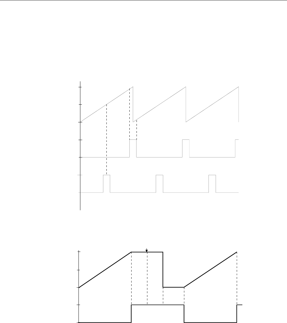
SMIQ Sweep
1125.5555.03 2.395 E-9
MARKER This output becomes active when the sweep run has reached the mark. The
MARKER signal can be used for the brightness control of an oscilloscope. Up to
three marks can be set in order to mark certain positions in the sweep run. The
polarity of the signal can be set in menu UTILITIES - AUX I/O - MARKER
POLARITY. The period of the active signal is equal to the dwell time (DWELL) of a
step.
Signal examples:
10 V
0 V
X-AXIS
BLANK
5 V
0 V
0 V
5 V
MARKER
Fig. 2-244 Signal example sweep: MODE = AUTO, BLANK TIME = NORMAL
10 V
0 V
X-AXIS
BLANK
5 V
0 V
200 ms 300 ms
SINGLE new s tart
Fig. 2-245 Signal example sweep: MODE = SINGLE, BLANK TIME = LONG
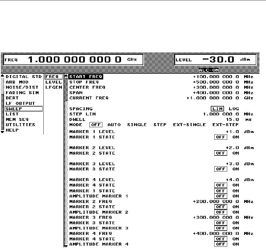
Sweep SMIQ
1125.5555.03 2.396 E-9
2.26.6 RF Sweep
Menu SWEEP - FREQ offers access to settings for RF sweep.
Menu selection: SWEEP - FREQ
Fig. 2-246 Menu SWEEP - FREQ
START FREQ Input value of the starting frequency.
IEC/IEEE-bus command :SOUR:FREQ:STAR 100MHz
STOP FREQ Input value of the stop frequency.
IEC/IEEE-bus command :SOUR:FREQ:STOP 500MHz
CENTER FREQ Input value of the center frequency.
IEC/IEEE-bus command :SOUR:FREQ:CENT 300MHz
SPAN Input value of the span.
IEC/IEEE-bus command :SOUR:FREQ:SPAN 100MHz
CURRENT FREQ Indication of the current frequency value.
Operating mode STEP: Input value of the frequency.

SMIQ Sweep
1125.5555.03 2.397 E-9
STEP LIN (LOG) Input value of the step width. Depending on whether SPACING LIN or LOG
is selected, STEP LIN or STEP LOG is displayed.
IEC/IEEE-bus command :SOUR:SWE:STEP:LIN 1MHz
DWELL Input value of the dwell time per step.
IEC/IEEE-bus command :SOUR:SWE:DWEL 10ms
SPACING Input value of the dwell time per step.
IEC/IEEE-bus command SOUR:SWE:SPAC LIN
MODE Selection of the sweep operating mode.
IEC/IEEE-bus commands :SOUR:FREQ:MODE SWE;
:SOUR:SWE:MODE AUTO;
:TRIG:SOUR SING
EXECUTE SINGLE
SWEEP Starts a single sweep run. This action to be executed is only indicated and is
only effective if MODE SINGLE has been selected.
IEC/IEEE-bus command :TRIG
RESET SWEEP Sets the starting frequency.
IEC/IEEE-bus command :ABOR
MARKER 1 FREQ
MARKER 2 FREQ
MARKER 3 FREQ
MARKER 4 FREQ
Input value of the frequency for the marker selected
IEC/IEEE-bus command :SOUR:MARK1:FREQ 100MHz
MARKER 1 STATE
MARKER 2 STATE
MARKER 3 STATE
MARKER 4 STATE
Switching on/off the marker selected
IEC/IEEE-bus command :SOUR:MARK1 OFF
AMPLITUDE MARKER1
AMPLITUDE MARKER 2
AMPLITUDE MARKER 3
AMPLITUDE MARKER 4
Switching on/off the amplitude marker selected
OFF Input value of the frequency for the marker selected
ON Amplitude marker is switched on. On reaching the mark the output
level is reduced by 1 dB.
IEC/IEEE-bus command :SOUR:MARK1:AMPL OFF
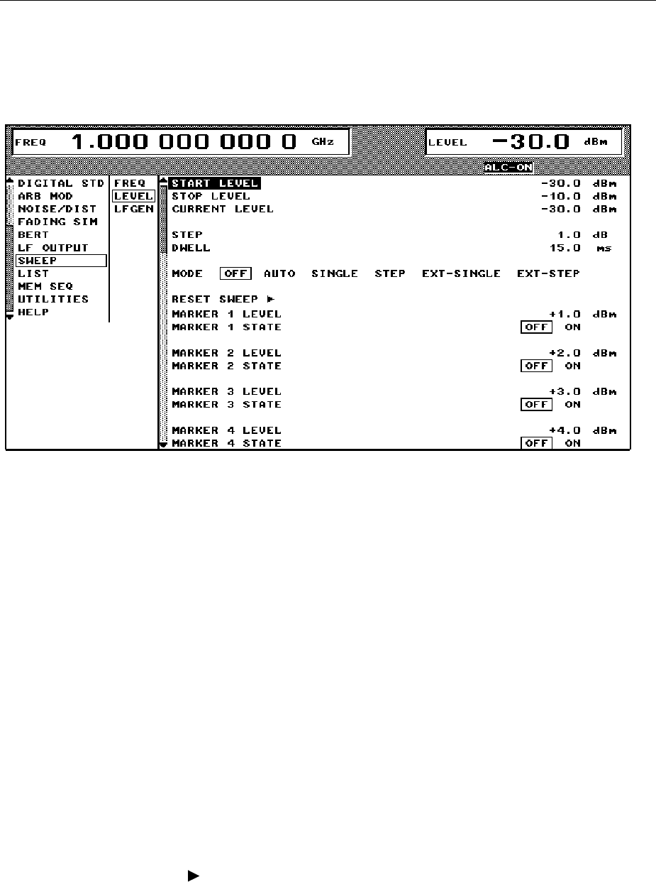
Sweep SMIQ
1125.5555.03 2.398 E-9
2.26.7 LEVEL Sweep
Menu SWEEP - LEVEL offers access to settings for LEVEL sweep.
Menu selection: SWEEP - LEVEL
Fig. 2-247 Menu SWEEP - LEVEL
START LEVEL Input value of the starting level.
IEC/IEEE-bus command :POW:STAR -30dBm
STOP LEVEL Input value of the stop level.
IEC/IEEE-bus command :SOUR:POW:STOP -10dBm
CURRENT LEVEL Indication of the current level.
Operating mode STEP: Input value of the level.
STEP Input value of the step width.
IEC/IEEE-bus command :SOUR:SWE:POW:STEP 1dB
DWELL Input value of the dwell time per step
IEC/IEEE-bus command :SOUR:SWE:POW:DWEL 15ms
MODE Selection of the sweep operating mode.
IEC/IEEE-bus commands :SOUR:POW:MODE SWE;
:SOUR:SWE:POW:MODE AUTO;
:TRIG:SOUR SING
EXECUTE SINGLE SWEEP Starts a single sweep run. This action to be executed is only
indicated and is only effective if MODE SINGLE is selected.
IEC/IEEE-bus command :TRIG
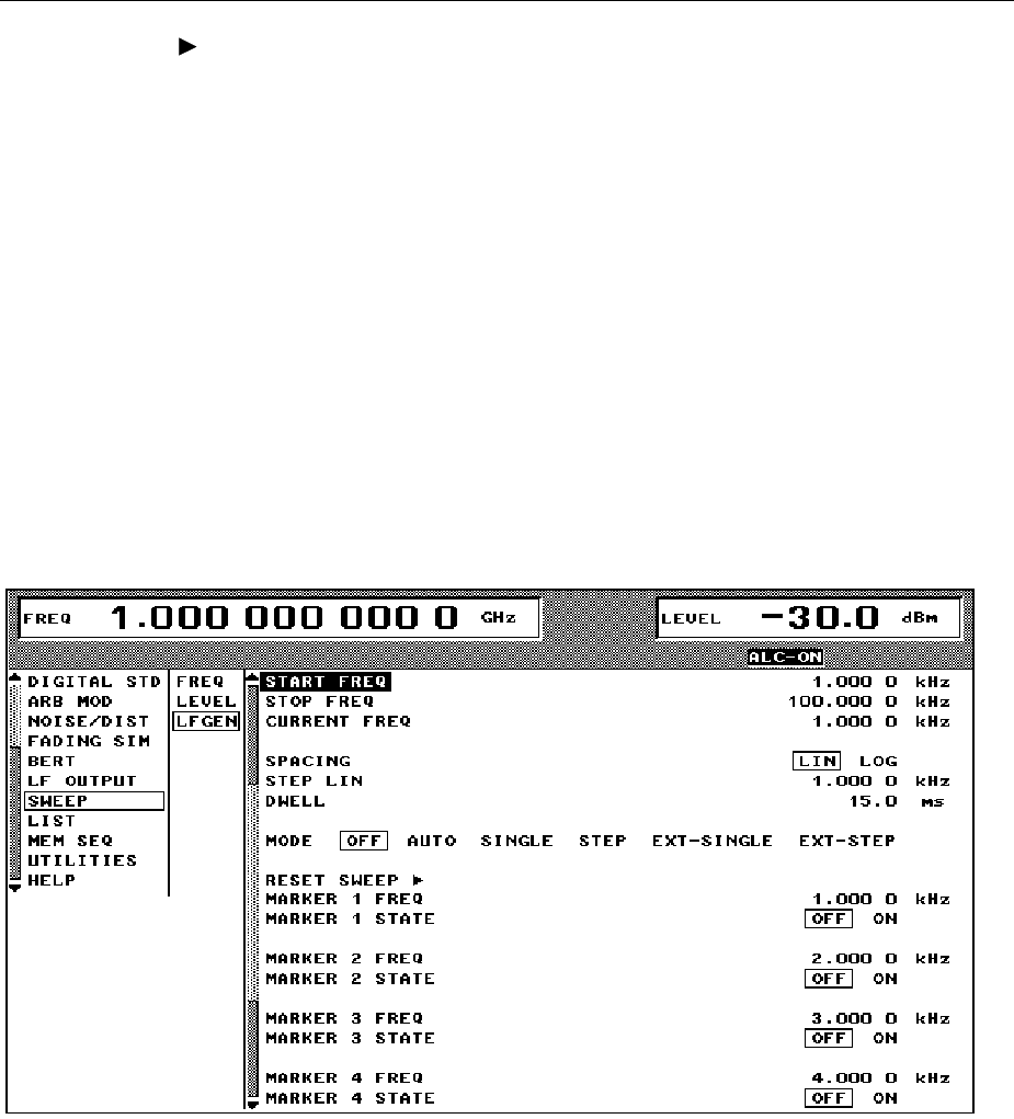
SMIQ Sweep
1125.5555.03 2.399 E-9
RESET SWEEP Sets the starting level.
IEC/IEEE-bus command :ABOR
MARKER 1 LEVEL
MARKER 2 LEVEL
MARKER 3 LEVEL
MARKER 4 LEVEL
Input value of the level for the marker selected.
IEC/IEEE-bus command :SOUR:MARK1:PSW:POW 0dBm
MARKER 1 STATE
MARKER 2 STATE
MARKER 3 STATE
MARKER 4 STATE
Switching on/off the marker selected.
IEC/IEEE-bus command :SOUR:MARK1:PSW OFF
2.26.8 LF Sweep
Menu SWEEP - LF GEN offers access to settings for LF sweep.
Menu selection: SWEEP - LF GEN
Fig. 2-248 Menu SWEEP - LF GEN

Sweep SMIQ
1125.5555.03 2.400 E-9
START FREQ Input value of the starting frequency.
IEC/IEEE-bus command :SOUR2:FREQ:STAR 100kHz
STOP FREQ Input value of the stop frequency.
IEC/IEEE-bus command :SOUR2:FREQ:STOP 50kHz
CURRENT FREQ Indication of the current frequency value.
Operating mode STEP: Input value of the frequency.
STEP Input value of the step width.
IEC/IEEE-bus command :SOUR2:SWE:STEP:LIN 1kHz
DWELL Input value of the dwell time per step.
IEC/IEEE-bus command :SOUR2:SWE:DWEL 15ms
SPACING Selection of the sweep run, linear or logarithmic.
IEC/IEEE-bus command :SOUR2:SWE:SPAC LIN
MODE Selection of the sweep operating mode.
IEC/IEEE-bus command :SOUR2:FREQ:MODE SWE
:SOUR2:SWE:MODE AUTO
:TRIG2:SOUR SING
EXECUTE SINGLE SWEEP Starts a single sweep run. This action to be executed is only indicated
and is only effective if MODE SINGLE is selected.
IEC/IEEE-bus command :TRIG
RESET SWEEP Sets the starting frequency.
IEC/IEEE-bus command :ABOR
MARKER 1 FREQ
MARKER 2 FREQ
MARKER 3 FREQ
MARKER 4 FREQ
Input value of the frequency for the marker selected.
IEC/IEEE-bus command :SOUR2:MARK1:FREQ 1kHz
MARKER 1 STATE
MARKER 2 STATE
MARKER 3 STATE
MARKER 4 STATE
Switching on/off the marker selected.
IEC/IEEE-bus command :SOUR2:MARK1 OFF
SMIQ LIST Mode
1125.5555.03 2.401 E-9
2.27 LIST Mode
A sequence of predefined frequency and level points is executed in the LIST mode, similar as in a
sweep. Differently from the sweep, however, a list with freely selectable pairs of values (frequency and
level) can be generated. The specified range of the frequency comprises the entire adjustable frequency
range of the instrument. The specified range of the level covers a 20-dB range. If the permissible
variation range is exceeded, the level error increases.
Caution: After the generation or change of a list in the LIST mode, function LEARN has to be started
to ensure that the new settings are transferred to the hardware (IEC-bus short command:
LIST:LEAR.
Table 2-33 LIST mode; Example of a list
Index Frequency Level
0001 100 MHz 0 dBm
0002 575 MHz 13 dBm
0003 235 MHz 7 dBm
0100 333 MHz 5 dBm
:::
Up to 10 lists can be created. The total amount of possible pairs of values including all lists may
maximally be 2000. I.e., a list may have 2000 entries at the most, or less if several lists have been
created.
Each list is identified by a separate name and selected via this name. A detailed description how to
process the lists can be found in Section 2.2.11, List Editor.
2.27.1 Operating Modes (MODE)
The following LIST-operating modes are available:
AUTO Run from the beginning to the end of the list with automatic restart at the beginning.
If another mode was activated prior to the AUTO operating mode, continuation is
made from the current index.
IEC/IEEE-bus commands: :SOUR:FREQ:MODE LIST
:SOUR:LIST:MODE AUTO
:TRIG:LIST:SOUR AUTO
SINGLE Single run from the beginning to the end of the list. If SINGLE is selected, the run is
not yet started. Function EXECUTE SINGLE LIST to be executed, which can be
used to start the run, is displayed below the MODE line.
IEC/IEEE-bus commands: :SOUR:FREQ:MODE LIST
:SOUR:LIST:MODE AUTO
:TRIG:LIST:SOUR SING

LIST Mode SMIQ
1125.5555.03 2.402 E-9
STEP Step-by-step manual processing of the list. Activating STEP stops a list running and
the cursor wraps to the indication value of CURRENT INDEX. The list can now be
controlled upwards or downwards in discrete steps using the rotary knob or the
numeric keys.
IEC/IEEE-bus commands: :SOUR:FREQ:MODE LIST
:SOUR:LIST:MODE STEP
:TRIG:LIST:SOUR SING
EXT-SINGLE Single run from the beginning to the end of the list as with SINGLE, but triggered by
an external trigger signal.
IEC/IEEE-bus commands: :SOUR:FREQ:MODE LIST;
:SOUR:LIST:MODE AUTO
:TRIG:LIST:SOUR EXT
EXT-STEP Step-by-step run by means of the external trigger signal. Each trigger event triggers
a single step.
IEC/IEEE-bus commands: :SOUR:FREQ:MODE LIST
:SOUR:LIST:MODE STEP
:TRIG:LIST:SOUR EXT
HOP Step-by-step run by means of the internal trigger signal of the data generator (see
also Section 'Internal Modulation Data and Control Signals from Lists' and Section
'Menu DIGITAL STANDARD - GSM'). Each trigger event triggers a single step.
IEC/IEEE-bus commands: :SOUR:FREQ:MODE LIST
:SOUR:LIST:MODE STEP
:TRIG:LIST:SOUR HOP
OFF Operating mode LIST is switched off.
IEC/IEEE-bus command: :SOUR:FREQ:MODE CW
Note: The minimum step time of 1 ms must not be violated in modes EXT-STEP and HOP either.
With fading switched on, the minimum step time is increased to 3 ms, in case of Lognormal
fading it is increased to 50 ms.
2.27.2 Inputs/Outputs
TRIGGER input and BLANK output are available at the rear of the instrument for synchronization with
other instruments.
TRIGGER An external signal at this input triggers the LIST mode in operating modes
EXT-SINGLE and EXT-STEP. The polarity of the active trigger edge can be
set in the UTILITIES - AUX I/O - EXT TRIG SLOPE menu.
BLANK This output supplies a signal (0 V/5 V) to blank the settling process by means
of pulse modulation or AM. The signal can also be used to synchronize other
instruments. The polarity of the signal can be set in the UTILITIES - AUX I/O -
BLANK POLARITY menu.
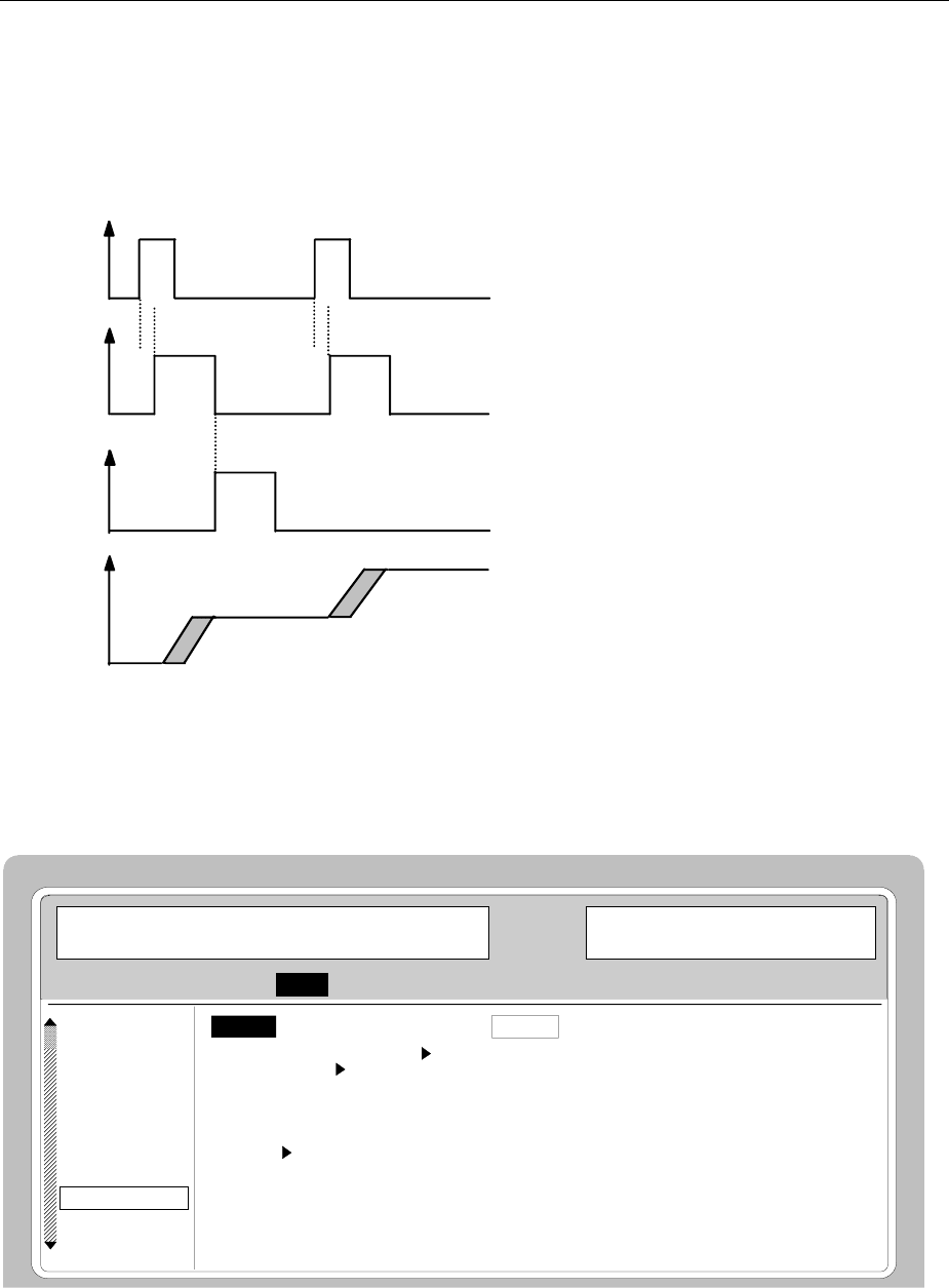
SMIQ LIST Mode
1125.5555.03 2.403 E-9
MARKER At the first step of the LIST mode, this output provides an approx. 200 µs
trigger signal immediately after blanking. At small DWELL times, this signal
can be used for an accurate synchronization to trigger other devices and
shows the first stable output frequency. The delay to the fed-in signal at the
TRIGGER input for EXT-SINGLE or EXT-STEP is 1.5 to 2 ms and has a jitter
of 0.5 ms.
TRIGGER
Input
BLANK
Output
MARKER
Output
Frequency
Fig. 2-249 Signal example LIST mode: MODE = EXT-STEP
The LIST menu offers access to settings for the LIST mode.
Menu selection: LIST
LEVEL - - -.-
- - -.- - -
MODE OFF AUTO SINGLE STEP EXT-SINGLE EXT-STEP
RESET LIST
DWELL 10.0 ms
CURRENT INDEX 1
LEARN
SELECT LIST... CURRENT: LIST2
DELETE LIST...
FUNCTION FILL INSERT DELETE EDIT/VIEW
FREQ
LIST
EXECUTE SINGLE LIST
FREQUENCY
LEVEL
ANALOG MOD
VECTOR MOD
DIGITAL MOD
DIGITAL STD
LF OUTPUT
SWEEP
LIST
MEM SEQ
UTILITIES
Fig. 2-250 Menu LIST - OPERATION page

LIST Mode SMIQ
1125.5555.03 2.404 E-9
MODE Selection of the operating mode.
IEC/IEEE-bus commands : :SOUR:FREQ:MODE LIST;
:SOUR:LIST:MODE AUTO;
:TRIG:LIST:SOUR SING
EXECUTE SINGLE LIST Starts a single run of a list. This menu option is only visible if MODE
SINGLE is selected.
IEC/IEEE-bus command : :TRIG:LIST
RESET LIST Sets the starting point.
IEC/IEEE-bus command :ABOR:LIST
DWELL Input value of the dwell time per step.
IEC/IEEE-bus command :SOUR:LIST:DWEL 10ms
CURRENT INDEX Indication of the current list index. Setting value of the current list index
in the STEP operating mode.
LEARN Starts the LEARN function. All value pairs of the active list are
subsequently set by the instrument with the current additional
parameters, and the hardware setting data are stored.
Caution: This function must be called after every creating and
altering the list (or the remaining setting data). The list
must be learned as well after temperature changes or
after calling internal calibration routines, as all parameters
usually controlled are replaced by stored values in the
LIST mode.
IEC/IEEE-bus command :SOUR:LIST:LEAR
SELECT LIST... Selection of a list or creation of a new list (cf. Section 2.2.11, List
Editor).
IEC/IEEE-bus command :SOUR:LIST:SEL 'LIST2'
DELETE LIST... Deletion of a list (cf. Section 2.2.11, List Editor).
IEC/IEEE-bus command :SOUR:LIST:DEL 'LIST1'
FUNCTION Selection of the editor functions to process a list (cf. Section 2.2.11,
List Editor).
IEC/IEEE :SOUR:LIST:FREQ 100MHz, 1.2GHz; POW 0dBm, 6dBm

SMIQ LIST Mode
1125.5555.03 2.405 E-9
The second page of the LIST menu, the EDIT page is automatically activated if one of the editor
functions of line FUNCTION is selected. The list which is displayed as CURRENT LIST in the SELECT
LIST line is shown.
FREQ
100. 000 000 0
MHz
LEVEL
- 30.0
dBm
SELECT LIST... CURRENT: LIST2
FUNCTION FILL-LIST INSERT DELETE EDIT/VIEW
-INDEX- FREE 2041 - LEN 2055 ------ FREQ ----------- LEVEL --
0001 575.000 000 0 MHz 13.0 dBm
0002 235.000 000 0 MHz 7.0 dBm
0003 123.000 000 0 MHz 1.0 dBm
0004 456.000 000 0 MHz 1.0 dBm
0005 735.000 000 0 MHz 3.0 dBm
0006 333.000 000 0 MHz 4.0 dBm
0007 400.000 000 0 MHz 7.0 dBm
0008 235.000 000 0 MHz 7.0 dBm
FREQUENCY
LEVEL
ANALOG MOD
VECTOR MOD
DIGITAL MOD
DIGITAL STD
LF OUTPUT
SWEEP
LIST
MEM SEQ
UTILITIES
Fig. 2-251 Menu List - EDIT page
INDEX Index of the list.
FREE Indication of the list entries still vacant.
LENGTH Length of the current list.
FREQ Parameter: Frequency.
LEVEL Parameter: Level; specified range 20 dB.

Memory Sequence SMIQ
1125.5555.03 E-92.406
2.28 Memory Sequence
In the memory-sequence operating mode the instrument automatically services a list with stored
instrument settings. Memory locations 1 to 50, which are loaded using SAVE and whose stored settings
are called either separately using RECALL or automatically and subsequently in the SEQUENCE mode,
are available.
The list is continuously serviced from the beginning to the end with a continual index. The order of the
memories to be passed through is arbitrary. Each setting can be assigned a freely selectable dwell time.
The dwell time determines the duration of the setting, its minimal value is 50 ms, its maximal value
60 sec.
The list is divided up into 3 columns for list index, memory location number (Memory) and dwell time
(Dwell). The beginning of the list has index 1.
Table 2-35 MEMORY SEQUENCE; Example of a list
Index Memory Dwell
001 09 50.0 ms
002 02 50.0 ms
003 01 75.0 ms
004 10 75.0 ms
... ... ...
Up to 10 sequence lists can be created. The total number of possible list elements is maximally 256.
I.e., a list can have 256 entries at the most, or less if several lists have been created.
Each list is identified by a separate name and selected via this name. A detailed description how to
process the lists can be found in Section 2.2.4, List Editor.
Note: Frequently changing the level in the operating mode MEMORY SEQUENCE can stress the
mechanically switched attenuator. The attenuator is also actuated when AM is switched on or
off. For this reason we recommend that you make use of the non-interrupting level setting as
much as possible and that you use the setting AM 0% instead of switching AM off.

SMIQ Memory Sequence
1125.5555.03 2.407 E-9
Operating Modes (MODE)
The following operating modes are available:
AUTO Run from the beginning to the end of the list with automatic restart at the
beginning. If another mode was activated prior to the AUTO operating mode,
continuation is made from the current index.
IEC/IEEE-bus command: :SYST:MODE MSEQ;
:SYST:MSEQ:MODE AUTO
:TRIG:MSEQ:SOUR AUTO
SINGLE Single run from the beginning to the end of the list. If SINGLE is selected, the
run is not yet started. Below the MODE line, function EXECUTE SINGLE
SEQUENCE to be executed is displayed which can be used to start the run.
IEC/IEEE-bus command :SYST:MODE MSEQ;
:SYST:MSEQ:MODE AUTO
:TRIG:MSEQ:SOUR SING
STEP Step-by-step manual processing of the list. Activating STEP stops an automatic
run and the cursor wraps to the indication value of CURRENT INDEX. The list
can now be passed through upwards or downwards step by step using the
rotary knob.
IEC/IEEE-bus command :SYST:MODE MSEQ;
:SYST:MSEQ:MODE STEP
:TRIG:MSEQ:SOUR SING
EXT-SINGLE Single run from the beginning to the end of the list as with SINGLE, but
triggered by an external trigger signal.
IEC/IEEE-bus command :SYST:MODE MSEQ;
:SYST:MSEQ:MODE AUTO
:TRIG:MSEQ:SOUR EXT
EXT-STEP Step-by-step run using the external trigger signal. Each trigger event triggers a
single step.
IEC/IEEE-bus command :SYST:MODE MSEQ;
:SYST:MSEQ:MODE STEP
:TRIG:MSEQ:SOUR EXT
OFF Step-by-step run using the external trigger signal. Each trigger event triggers a
single step.
IEC/IEEE-bus command :SYST:MODE FIX
External Trigger
An external signal at the rear input TRIGGER triggers the MEMORY SEQUENCE in the EXT-SINGLE
and EXT-STEP operating modes. The polarity of the active trigger edge can be set in the UTILITIES -
AUX I/O - EXT TRIG SLOPE menu.
Menu MEM SEQ with the two menu pages OPERATION and EDIT offers access to the
memory-sequence operating mode.
Memory Sequence SMIQ
1125.5555.03 E-92.408
Menu selection: MEM SEQ
MODE
RESET SEQUENCE
CURRENT INDEX
SELECT LIST...
DELETE LIST...
FUNCTION
OFF AUTO EXT-SINGLE EXT-STEP
STEP
CURRENT: MSEQ1
DELETE
FREQ
100. 000 000 0
MHz LEVEL
-30.0
dBm
SINGLE
INSERT
FILL EDIT/VIEW
1
FREQUENCY
LEVEL
ANALOG MOD
VECTOR MOD
DIGITAL MOD
DIGITAL STD
LF OUTPUT
SWEEP
LIST
MEM SEQ
UTILITIES
Fig. 2-252 Menu MEM SEQ -OPERATION-page (preset setting)
MODE Selection of the operating mode; setting the operating mode
regards various command systems at the IEC bus (cf. above).
EXECUTE SINGLE SEQUENCE Starts the single run of a memory sequence. This menu option is
only visible if MODE SINGLE is selected.
IEC/IEEE-bus command :TRIG:MSEQ
RESET SEQUENCE Wrap to the beginning of the list.
IEC/IEEE-bus command :ABOR:MSEQ
CURRENT INDEX Indication of the current list index. Setting value of the current list
index in the MODE STEP operating mode.
SELECT LIST... Selection of a list or generation of a new list (cf. Section 2.2.4, List
Editor).
IEC/IEEE-bus command :SYST:MSEQ:SEL "MSEQ1"
DELETE LIST... Deletion of a list (cf. Section 2.2.4, List Editor).
IEC/IEEE-bus command :SYST:MSEQ:DEL "MSEQ2"
FUNCTION Selection of the editor functions to process a list (cf. Section 2.2.4,
List Editor).
IEC/IEEE-bus command :SYST:MSEQ 9,2,...;
:SYST:MSEQ:DWEL 50ms, 50ms,.

SMIQ Memory Sequence
1125.5555.03 2.409 E-9
The second page of menu MEM SEQ, the EDIT page, is automatically activated if one of the editor
functions of the FUNCTION line is selected. The list which is entered as CURRENT LIST in the
SELECT LIST line is shown.
CURRENT: MSEQ1
DELETE
FREQ
100. 000 000 0
MHz LEVEL
-30.0
dBm
INSERTFILL EDIT/VIEW
SELECT LIST...
FUNCTION
-INDEX - FREE 2041 - LEN 2055 ------ MEMORY --------- DWELL
001 09 50 ms
002 02 50 ms
003 01 60 ms
004 23 60 ms
005 09 85 ms
006 10 85 ms
007 08 85 ms
008 11 85 ms
FREQUENCY
LEVEL
ANALOG MOD
VECTOR MOD
DIGITAL MOD
DIGITAL STD
LF OUTPUT
SWEEP
LIST
MEM SEQ
UTILITIES
Fig. 2-253 Menu MEM SEQ - EDIT page
INDEX Index of the list.
FREE Indication of the list entries still vacant.
LEN Length of the current list.
MEMORY Parameter: number of memory location; range 1 to 50.
DWELL Parameter: dwell time; specified range 50 ms to 60 sec, step width 1 ms.
Utilities SMIQ
1125.5555.03 E-92.410
2.29 Utilities
The UTILITIES menu contains submenus for general functions which do not directly relate to the signal
generation.
2.29.1 IEC-Bus Address (SYSTEM-GPIB)
Submenu SYSTEM-GPIB offers access to the remote-control address. The setting range is 0 to 30. At
the point of delivery address 28 is set.
Menu selection: UTILITIES -SYSTEM -GPIB
SYSTEM
REF OSC
PHASE
PROTECT
CALIB
DIAG
TEST
MOD KEY
AUX I/O
BEEPER
INSTALL
ADDRESS
AMIQ ADDRESS
FREQ 100. 000 000 0 MHz LEVEL -30.0 dBm
GPIB
RS232
SERDATA
SECURITY
LANGUAGE
28
6
FREQUENCY
LEVEL
ANALOG MOD
VECTOR MOD
DIGITAL MOD
DIGITAL STD
LF OUTPUT
SWEEP
LIST
MEM SEQ
UTILITIES
Fig. 2-254 Menu UTILITIES -SYSTEM -GPIB
ADDRESS Input value of the IEC-bus address
IEC/IEEE-bus command :SYST:COMM:GPIB:ADDR 28
AMIQ ADDRESS IEC/IEEE-bus address of AMIQ.

SMIQ Utilities
1125.5555.03 2.411 E-9
2.29.2 Parameter of the RS232 Interface (SYSTEM-RS232)
Submenu SYSTEM-RS232 offers access to the configuration of the RS-232 interface. The pin
assignment of the interface corresponds to the pin assignment of a PC.
Menu selection: UTILITIES - SYSTEM - RS232
SYSTEM
REF OSC
PHASE
PROTECT
CALIB
DIAG
TEST
MOD KEY
AUX I/O
BEEPER
INSTALL
DATA FORMAT 8 Bits
PARITY NO
STOP BIT 1
BAUD RATE 9600 bps
HANDSHAKE OFF RTS/CTS XON/XOFF
FREQ
100. 000 000 0
MHz
LEVEL
-30.0
dBm
GPIB
RS232
SERDATA
SECURITY
LANGUAGE
FREQUENCY
LEVEL
ANALOG MOD
VECTOR MOD
DIGITAL MOD
DIGITAL STD
LF OUTPUT
SWEEP
LIST
MEM SEQ
UTILITIES
Fig. 2-255 Menu UTILITIES - SYSTEM - RS232
DATA FORMAT Indication of the number of data bits. This value cannot be changed.
PARITY Indication of parity. This value cannot be changed.
STOP BIT Indication of the number of stop bits. This value cannot be changed.
BAUD RATE Selection of the baud rate.
IEC/IEEE-bus command :SYST:COMM:SER:BAUD 9600
HANDSHAKE Selection of the handshake.
OFF No handshake
IEC/IEEE-bus command :SYST:COMM:SER:PACE NONE
:SYST:COMM:SER:CONT:RTS ON
RTS/CTS Hardware handshake using the interface lines RTS and CTS. This
mode always is to be preferred to XON/XOFF mode, if permitted by
the configuration of the host computer.
IEC/IEEE-bus command :SYST:COMM:SER:CONT:RTS RFR
XON/XOFF Software handshake using the ASCII codes 11h <XON> and 13h
<XOFF>. This mode is not recommended for binary data and for
baud rates above 9600 baud.
IEC/IEEE-bus command :SYST:COMM:SER:PACE XON

Utilities SMIQ
1125.5555.03 E-92.412
2.29.3 Parameter of the SER DATA Input (SYSTEM-SERDATA)
Submenu SYSTEM-SERDATA offers access to the configuration of the SERDATA input.
Menu selection: UTILITIES - SYSTEM - SERDATA
SYSTEM
REF OSC
PHASE
PROTECT
CALIB
DIAG
TEST
MOD KEY
AUX I/O
BEEPER
INSTALL
BAUD RATE 9600 bps
FREQ
100. 000 000 0
MHz
LEVEL
-30.0
dBm
GPIB
RS232
SERDATA
SECURITY
LANGUAGE
FREQUENCY
LEVEL
ANALOG MOD
VECTOR MOD
DIGITAL MOD
DIGITAL STD
LF OUTPUT
SWEEP
LIST
MEM SEQ
UTILITIES
Fig. 2-256 Menu UTILITIES - SYSTEM - SERDATA
BAUD RATE Selection of the baud rate.
IEC/IEEE-bus command :SYST:COMM:SDAT:BAUD 9600

SMIQ Utilities
1125.5555.03 2.413 E-9
2.29.4 Suppressing Indications and Deleting Memories (SYSTEM-SECURITY)
For security interests, indications can be suppressed and memories deleted in the SYSTEM-SECURITY
submenu.
Menu selection: UTILITIES - SYSTEM-SECURITY
SYSTEM
REF OSC
PHASE
PROTECT
CALIB
DIAG
TEST
MOD KEY
AUX I/O
BEEPER
INSTALL
STATE OFF ON
ANNOTTATION FREQ OFF ON
ANNOTTATION AMPLITUDE OFF ON
CLEAR MEMORY
FREQ
100. 000 000 0
MHz LEVEL
-30.0
dBm
GPIB
RS232
SERDATA
SECURITY
LANGUAGE
FREQUENCY
LEVEL
ANALOG MOD
VECTOR MOD
DIGITAL MOD
DIGITAL STD
LF OUTPUT
SWEEP
LIST
MEM SEQ
UTILITIES
Fig. 2-257 Menu UTILITIES - SYSTEM-SECURITY
STATE Selection of the SECURITY state
ON Locks the suppression of the indications. Can only be
set via IEC bus.
OFF Deactivates the interlock of the indication
suppression. The preset state is set in the transition
ON→OFF, and all data stored such as settings, with
the exception of the DM lists are deleted. Can only
be set via IEC bus.
IEC/IEEE-bus command :SYST:SEC OFF
ANNOTATION FREQ OFF All frequency indications are suppressed.
ON The frequency setting is displayed..
IEC/IEEE-bus command :DISP:ANN:FREQ ON
ANNOTATION AMPLITUDE OFF All level indications are suppressed.
ON The level setting is displayed.
IEC/IEEE-bus command :DISP:ANN:AMPL ON
CLEAR MEMORY Deletion of all data stored such as settings, user correction and
list settings stored, with the exception of the DM lists.
For this action, two commands are necessary at the IEC bus:
IEC/IEEE-bus command :SYST:SEC ON; SEC OFF

Utilities SMIQ
1125.5555.03 E-92.414
2.29.5 Indication of the IEC-Bus Language (LANGUAGE)
Submenu UTILITIES-SYSTEM LANGUAGE indicates the IEC-bus language and the current SCPI
version.
2.29.6 Reference Frequency Internal/External (REF OSC)
In the internal-reference operating mode, the internal reference signal at a frequency of 10 MHz is
available at the REF socket (rear of the instrument).
Signal level: Veff (EMF, sine) = 1 V.
The frequency of the internal reference oscillator can be detuned via the EXT TUNE input (rear of the
instrument). Input voltage range ±10 V, pulling range ±1×10⁻⁶.
The external detuning is possible in both states of the ADJUSTMENT STATE (ON or OFF) unless
option SM-B1, reference oscillator OCXO, is fitted. If option SM-B1, reference oscillator OCXO, is fitted,
the detuning via the TUNE input is only possible if the ADJUSTMENT STATE selection has been
switched to ON in the UTILITIES-REF OSC menu.
In the external-reference operating mode, an external signal at a frequency of 1 MHz to 16 MHz
(spacing 1 MHz) is to be fed into socket REF. The setting to external frequency is effected in the
UTILITIES-REF OSC menu.
Signal level: Veff = 0.1 to 2 V
The message "EXT REF" is displayed in the status line in the header field of the display in the
external-reference operating mode.
Menu selection: UTILITIES - REF OSC
SYSTEM
REF OSC
PHASE
PROTECT
CALIB
DIAG
TEST
MOD KEY
AUX I/O
BEEPER
INSTALL
SOURCE
EXT FREQUENCY
ADJUSTMENT STATE
FREQUENCY ADJUSTMENT
FREQ
100. 000 000 0
MHz
LEVEL
- 30.0
dBm
INT EXT
10 MHz
OFF ON
2048
FREQUENCY
LEVEL
ANALOG MOD
VECTOR MOD
DIGITAL MOD
DIGITAL STD
LF OUTPUT
SWEEP
LIST
MEM SEQ
UTILITIES
Fig. 2-258 Menu UTILITIES - REF OSC (preset setting)
SOURCE Selection of the operating mode.
INT Internal-reference operating mode
EXT External-reference operating mode
IEC/IEEE-bus command SOUR:ROSC:SOUR INT

SMIQ Utilities
1125.5555.03 2.415 E-9
EXT FREQUENCY Input value of the external reference frequency (1 MHz to 16 MHz,
spacing 1 MHz).
IEC/IEEE-bus command SOUR:ROSC:EXT:FREQ 10E6
ADJUSTMENT STATE OFF Tuning value of the internal reference frequency as
calibrated (cf. menu UTILITIES-CALIB)
ON Tuning value according to setting value FREQUENCY
ADJUSTMENT. Option SM-B1, reference oscillator
OCXO, is switched off. Only the standard reference
oscillator is in operation.
IEC/IEEE-bus command SOUR:ROSC:ADJ:STAT ON
FREQUENCY ADJUSTMENT Input value in the range 0 to 4095 to set the internal reference
frequency. Pulling range ±4×10⁻⁶
IEC/IEEE-bus command SOUR:ROSC:ADJ:VAL 2048
2.29.7 Phase of the Output Signal (PHASE)
Menu UTILITIES-PHASE offers access to the phase setting of the RF output signal with respect to a
reference signal of the same frequency.
Menu selection: UTILITIES - PHASE
SYSTEM
REF OSC
PHASE
PROTECT
CALIB
DIAG
TEST
MOD KEY
AUX I/O
BEEPER
INSTALL
DELTA PHASE
RESET DELTA PHASE DISPLAY
FREQ
100. 000 000 0
MHz LEVEL
- 30.0
dBm
0deg
FREQUENCY
LEVEL
ANALOG MOD
VECTOR MOD
DIGITAL MOD
DIGITAL STD
LF OUTPUT
SWEEP
LIST
MEM SEQ
UTILITIES
Fig. 2-259 Menu UTILITIES - PHASE (preset setting)
DELTA PHASE Setting value of the phase.
IEC/IEEE-bus command :SOUR:PHAS 10 DEG
RESET DELTA PHASE DISPLAY Sets the display of the DELTA PHASE to 0 without the phase of
the output signal being influenced.
IEC/IEEE-bus command :SOUR:PHAS:REF

Utilities SMIQ
1125.5555.03 E-92.416
2.29.8 Password Input With Functions Protected (PROTECT)
The execution of calibrating and service functions is protected by a password. To unlock the lock-out,
the correct password, a 6-digit number, has to be entered and then the [ENTER] key has to be pushed.
After the instrument has been switched on, the lock-out is automatically activated.
Password 1 unlocks the lock-out for calibrations LEV PRESET and VCO SUM.
Password 2 unlocks the lock-out for calibration REF OSC.
Password 3 permits the input of the serial number and the value of the counter for POWER ON,
operating hours and attenuator circuits.
Menu UTILITIES-PROTECT offers access to the unlocking of protected functions.
Menu selection: UTILITIES - PROTECT
SYSTEM
REF OSC
PHASE
PROTECT
CALIB
DIAG
TEST
MOD KEY
AUX I/O
BEEPER
INSTALL
LOCK LEVEL 1
PASSWORD LEVEL 1
LOCK LEVEL 2
PASSWORD LEVEL 2
LOCK LEVEL 3
PASSWORD LEVEL 3
FREQ
100. 000 000 0
MHz LEVEL
- 30.0
dBm
OFF ON
XXXXXX
OFF ON
XXXXXX
OFF ON
XXXXXX
FREQUENCY
LEVEL
ANALOG MOD
VECTOR MOD
DIGITAL MOD
DIGITAL STD
LF OUTPUT
SWEEP
LIST
MEM SEQ
UTILITIES
Fig. 2-260 Menu UTILITIES - PROTECT (preset setting)
LOCK LEVEL XActivating/deactivating the lock-out.
ON The lock-out is activated.
OFF The cursor automatically wraps to the input of the
password. After the password has been entered, the
lock-out is deactivated.
IEC/IEEE-bus command :SYST:PROT1 ON
PASSWORD LEVEL XInput of the password; termination with [ENTER] key.
IEC/IEEE-bus command :SYST:PROT1 OFF, 123456

SMIQ Utilities
1125.5555.03 2.417 E-9
2.29.9 Calibration (CALIB)
For servicing, the following menus offer access to calibrating routines and correction values:
UTILITIES - CALIB - ALL
VCO SUM
VECTOR MOD
LEV PRESET
REF OSC (cf. service manual)
LEVEL (cf. service manual)
ALC TABLE
LEV ATT
LFGEN
Internal calibration routines LEV PRESET and VCO SUM are protected by a password. They can only
be executed if the lock-out in the UTILITIES - PROTECT menu has been unlocked. The password is
PASSWORD LEVEL 1 = "123456".
Caution: Execute calibration routines only when the instrument has warmed up
Calibration routines LEVEL and REF OSC are described in the service manual.
Calibration ALL
CALIB ALL triggers all internal calibrations which do not require any external measuring equipment. The
calibrations with external measurements are described in the service manual.
Menu selection: UTILITIES - CALIB - ALL
SYSTEM
REF OSC
PHASE
PROTECT
CALIB
DIAG
TEST
MOD KEY
AUX I/O
BEEPER
INSTALL
ALL
VCO SUM
VECTOR MOD
LEV PRESET
OSC REF
LEVEL
ALC TABLE
LEV ATT
LFGEN
FREQ 100. 000 000 0 MHz LEVEL - 30.0 dBm
FREQUENCY
LEVEL
ANALOG MOD
VECTOR MOD
DIGITAL MOD
DIGITAL STD
LF OUTPUT
SWEEP
LIST
MEM SEQ
UTILITIES
CALIBRATE ALL
Fig. 2-261 Menu UTILITIES - CALIB - ALL
CALIBRATE ALL Triggers all internal calibrations.
IEC\IEEE-bus command :CAL:ALL?
Utilities SMIQ
1125.5555.03 E-92.418
Calibration VCO SUM
To synchronize the summing loop, the frequency the oscillator generates must be so close to the rated
frequency that the phase control can lock in. This is effected by means of presetting values. The
presetting values are stored in a table and can be renewed using internal calibration routine VCO SUM.
The calibration routine needs only be executed after a data loss in the RAM or after an exchange of
modules.
Menu selection: UTILITIES - CALIB - VCO SUM
SYSTEM
REF OSC
PHASE
PROTECT
CALIB
DIAG
TEST
MOD KEY
AUX I/O
BEEPER
INSTALL
ALL
VCO SUM
VECTOR MOD
LEV PRESET
OSC REF
LEVEL
ALC TABLE
LEV ATT
FREQ 100. 000 000 0 MHz LEVEL - 30.0 dBm
CALIBRATE
VIEW
750.0 MHz
760.0 MHz
770.0 MHz
780.0 MHz
790.0 MHz
800.0 MHz
810.0 MHz
820.0 MHz
2
2
2
2
2
2
2
2
0001
0002
0003
0004
0005
0006
0007
0008
-22mV
-24mV
-25mV
-26mV
-27mV
-28mV
-29mV
-30mV
88
108
127
147
167
187
207
217
FREQUENCY
LEVEL
ANALOG MOD
VECTOR MOD
DIGITAL MOD
DIGITAL STD
LF OUTPUT
SWEEP
LIST
MEM SEQ
UTILITIES
Fig. 2-262 Menu UTILITIES - CALIB - VCO SUM
CALIBRATE Triggers the calibration for the VCO summing loop.
IEC/IEEE-bus command :CAL:VSUM?
VIEW Indication of the list of correction values.
The cursor wraps to index 1 of the list. The list can be executed using the rotary
knob. This index can be obtained by entering the index value on the digit block.
IEC/IEEE-bus command :CAL:VSUM:OFFS?
:CAL:VSUM:DAC?
:CAL:VSUM:KOS?
SMIQ Utilities
1125.5555.03 2.419 E-9
Calibration VECTOR MOD
In order to obtain accurate and reproducible measurements, the I/Q modulator has to be calibrated. To
do this the internal calibration routine VECTOR MOD is used for adjusting the residual carrier, I/Q
imbalance and quadrature offset of the modulator. Calibration should be carried out prior to the
measurement but after a warm-up time of approx. 1 h or in the case of temperature changes of more
than 5° C.
Menu selectiom: UTILITIES - CALIB - VECTOR MOD
SYSTEM
REF OSC
PHASE
PROTECT
CALIB
DIAG
TEST
MOD KEY
AUX I/O
BEEPER
INSTALL
ALL
VCO SUM
VECTOR MOD
LEV PRESET
OSC REF
LEVEL
ALC TABLE
LEV ATT
FREQ 100. 000 000 0 MHz LEVEL - 30.0 dBm
CALIBRATE
FREQUENCY
LEVEL
ANALOG MOD
VECTOR MOD
DIGITAL MOD
DIGITAL STD
LF OUTPUT
SWEEP
LIST
MEM SEQ
UTILITIES
Fig. 2-263 Menu UTILITIES - CALIB - VECTOR MOD menu
CALIBRATE Triggers a calibration for the I/Q modulator, for FSIM, NDSIM and MCOD.
IEC/IEEE-bus command :CAL:VMOD?

Utilities SMIQ
1125.5555.03 E-92.420
Calibration LEV PRESET
The vector modulator is aligned in terms of residual carrier, IQ imbalance and quadrature. With options
SMIQB10/B20 MCOD, SMIQB14/15 FSIM and SMIQB17 NDSIM provided, calibrations are called up for
these modules too and the module offset and partly the IQ imbalance are calibrated. Since the
calibrations are interdependent, calling up individual calibrations is not recommended. All calibrations
are run internally. Calibration should be called up after a warm-up time of approx. 1 h or in case of a
temperature change of more than 5°C .
Menu selection: UTILITIES - CALIB - LEV PRESET
SYSTEM
REF OSC
PHASE
PROTECT
CALIB
DIAG
TEST
MOD KEY
AUX I/O
BEEPER
INSTALL
ALL
VCO SUM
VECTOR MOD
LEV PRESET
OSC REF
LEVEL
ALC TABLE
LEV ATT
FREQ 100. 000 000 0 MHz LEVEL - 30.0 dBm
CALIBRATE
TABLE IQMOD-CW IQMOD-VM IQCON
VIEW
300.000 0 kHz +23
1.000 000 0 MHz +23
1.000 000 1 MHz +24
2.000 000 0 MHz +24
2.000 000 1 MHz +25
3.000 000 0 MHz +25
0001
0002
0003
0004
0005
0006
FREQUENCY
LEVEL
ANALOG MOD
VECTOR MOD
DIGITAL MOD
DIGITAL STD
LF OUTPUT
SWEEP
LIST
MEM SEQ
UTILITIES
Fig. 2-264 Menu UTILITIES - CALIB - LEV PRESET
CALIBRATE Triggers the calibration for level preset.
IEC/IEEE-bus command :CAL:LPR?
The following parameters are only necessary for the indication of the correction values:
TABLE Selection of the correction values displayed by VIEW
IQMOD-CW Correction values of module "IQ-Modulator", valid with CW
mode
IQMOD-VM Correction values of module "IQ-Modulator", valid with IQ
mode
CONVERTER Correction values of module "IQ-Converter"
VIEW The cursor wraps to index 1 of the list. The list can be executed using the
rotary knob. This index can be directly obtained by entering the index value on
the digit block.
IEC/IEEE-bus command :CAL:LPR:DATA?
SMIQ Utilities
1125.5555.03 2.421 E-9
Calibration ALC TABLE
For vector modulation or digital modulation, SMIQ is operated with the internal level control switched off.
In mode ALC MODE - SAMPLE & HOLD, the level is recalibrated for each level or frequency setting. In
mode TABLE, the latter does not apply since the necessary input values are taken from a table. This
table can be regenerated using LEARN TABLE . This is required to attain an optimum level accuracy
for the given operating temperature.
Menu selection: UTILITIES - CALIB - ALC TABLE
SYSTEM
REF OSC
PHASE
PROTECT
CALIB
DIAG
TEST
MOD KEY
AUX I/O
BEEPER
INSTALL
ALL
VCO SUM
VECTOR MOD
LEV PRESET
OSC REF
LEVEL
ALC TABLE
LEV ATT
FREQ 100. 000 000 0 MHz LEVEL - 30.0 dBm
LEARN TABLE
FREQUENCY
LEVEL
ANALOG MOD
VECTOR MOD
DIGITAL MOD
DIGITAL STD
LF OUTPUT
SWEEP
LIST
MEM SEQ
UTILITIES
Fig. 2-265 Menu UTILITIES - CALIB - ALC TABLE
LEARN TABLE Triggers the generation of the new correction value for the function LEVEL-
ALC-ALC OFF MODE TABLE.
IEC/IEEE-bus command :SOUR:POW:ALC:TABL?
Utilities SMIQ
1125.5555.03 E-92.422
Calibration LEV ATT
For digital modulation (DIGITAL MOD and DIG STANDARD) and with the function LEV ATT switched
on, the output level of SMIQ is reduced by a settable value in dB for a certain time (eg a slot).
Calibration serves for attaining an optimum accuracy of level reduction.
Menu selection: UTILITIES - CALIB - LEV ATT
SYSTEM
REF OSC
PHASE
PROTECT
CALIB
DIAG
TEST
MOD KEY
AUX I/O
BEEPER
INSTALL
ALL
VCO SUM
VECTOR MOD
LEV PRESET
OSC REF
LEVEL
ALC TABLE
LEV ATT
FREQ 100. 000 000 0 MHz LEVEL - 30.0 dBm
CALIBRATE
FREQUENCY
LEVEL
ANALOG MOD
VECTOR MOD
DIGITAL MOD
DIGITAL STD
LF OUTPUT
SWEEP
LIST
MEM SEQ
UTILITIES
Fig. 2-266 Menu UTILITIES - CALIB - LEV ATT
CALIBRATE Triggers the calibration for the function LEV ATT.
IEC/IEEE-bus command :CAL:LATT?
SMIQ Utilities
1125.5555.03 2.423 E-9
Calibration LFGEN
Calibrates the output level of the LF generator to 1.000 V. This calibration is only available with I/Q
modulator IQMOD Var. 10 or higher.
Menu selection: UTILITIES – CALIB - LFGEN
SYSTEM
REF OSC
PHASE
PROTECT
CALIB
DIAG
TEST
MOD KEY
AUX I/O
BEEPER
INSTALL
ALL
VCO SUM
VECTOR MOD
LEV PRESET
OSC REF
LEVEL
ALC TABLE
LEV ATT
LFGEN
FREQ 100. 000 000 0 MHz LEVEL - 30.0 dBm
FREQUENCY
LEVEL
ANALOG MOD
VECTOR MOD
DIGITAL MOD
DIGITAL STD
LF OUTPUT
SWEEP
LIST
MEM SEQ
UTILITIES
CALIBRATE
Fig. 2-267 Menu UTILITIES - CALIB – LFGEN
CALIBRATE Triggers calibration for the LFGEN function.
IEC/IEEE bus command :CAL:LFG?
Utilities SMIQ
1125.5555.03 E-92.424
2.29.10 Indications of Module Variants (DIAG-CONFIG)
For service purposes, the modules installed can be indicated with their variants and states of
modification. Submenu DIAG-CONFIG offers access to the module indication.
IEC/IEEE-bus command :DIAG:INFO:MOD?
Menu selection: UTILITIES - DIAG - CONFIG
SYSTEM
REF OSC
PHASE
PROTECT
CALIB
DIAG
TEST
MOD KEY
AUX I/O
BEEPER
INSTALL
CONFIG
TPOINT
C/NMEAS
PARAM
FREQ 100. 000 000 0 MHz LEVEL -30.0 dBm
VAR
VAR
VAR
VAR
VAR
VAR
VAR
VAR
VAR
VAR
REV
REV
REV
REV
REV
REV
REV
REV
REV
REV
FRO
REFSS
DSYN
SUM
IQCON
IQMOD
ROSC SM-B1
FMOD SM-B5
MCOD SMIQB11
DGEN SMIQB20
FREQUENCY
LEVEL
ANALOG MOD
VECTOR MOD
DIGITAL MOD
DIGITAL STD
LF OUTPUT
SWEEP
LIST
MEM SEQ
UTILITIES
Fig. 2-268 Menu UTILITIES - DIAG - CONFIG
SMIQ Utilities
1125.5555.03 2.425 E-9
2.29.11 Voltage Indication of Test Points (DIAG-TPOINT)
Submenu DIAG-TPOINT offers access to internal test points. If a test point is switched on, the voltage
indication is displayed in a window in the header field. For greater detail, see service manual.
Menu selection: UTILITIES - DIAG - TPOINT
SYSTEM
REF OSC
PHASE
PROTECT
CALIB
DIAG
TEST
MOD KEY
AUX I/O
BEEPER
INSTALL
CONFIG
TPOINT
C/NMEAS
PARAM
FREQ 100. 000 000 0 MHz
OFF ON
7
STATE
POINT
LEVEL -30.0 dBm
TP 007
+3.570V
FREQUENCY
LEVEL
ANALOG MOD
VECTOR MOD
DIGITAL MOD
DIGITAL STD
LF OUTPUT
SWEEP
LIST
MEM SEQ
UTILITIES
Fig. 2-269 Menu UTILITIES - DIAG - TPOINT
STATE Switching on/off the voltage indication in the header field.
POINT........... Input value of the test point.
IEC/IEEE-bus command :DIAG:POINxx?

Utilities SMIQ
1125.5555.03 E-92.426
2.29.12 Measurement of CARRIER/NOISE RATIO (DIAG-C/N MEAS)
The submenu DIAG - C/N MEAS can only be called with the option SMIQB17 (Noise generator and
distortion simulator). For C/N measurements in servicing the generator can be set to the service modes
as far are concerned. The carrier/noise ratio can then be easily determined this way. The submenu
DIAG - C/N MEAS offers an access to these modes.
Menu selection: UTILITIES - DIAG - C/N MEAS
SYSTEM
REF OSC
PHASE
PROTECT
CALIB
DIAG
TEST
MOD KEY
AUX I/O
BEEPER
INSTALL
CONFIG
TPOINT
C/N MEAS
PARAM
FREQ 100. 000 000 0 MHz LEVEL -30.0 dBm
TP 007
+3.570V
FREQUENCY
LEVEL
ANALOG MOD
VECTOR MOD
DIGITAL MOD
DIGITAL STD
NOISE/DIST
LF OUTPUT
SWEEP
LIST
MEM SEQ
UTILITIES
C/N MEAS MODE... CARRIER NOISE
CARRIER
NOISE
Fig. 2-270 Menu UTILITIES - DIAG - C/N MEAS
CARRIER NOISE Noise and carrier signal
IEC/IEEE-bus command :DIAG:CNM:MODE CN
CARRIER Only carrier signal
IEC/IEEE-bus command :DIAG:CNM:MODE CARR
NOISE Only noise signal
IEC/IEEE-bus command :DIAG:CNM:MODE NOIS
SMIQ Utilities
1125.5555.03 2.427 E-9
2.29.13 Indications of Service Data (DIAG-PARAM)
Submenu DIAG-PARAMETER offers access to different parameters such as serial number, software
version, operating-hours counter and attenuator circuits.
Menu selection: UTILITIES - DIAG - PARAM
SYSTEM
REF OSC
PHASE
PROTECT
CALIB
DIAG
TEST
MOD KEY
AUX I/O
BEEPER
INSTALL
CONFIG
TPOINT
C/NMEAS
PARAM
FREQ 100. 000 000 0 MHz LEVEL -30.0 dBm
FREQUENCY
LEVEL
ANALOG MOD
VECTOR MOD
DIGITAL MOD
DIGITAL STD
LF OUTPUT
SWEEP
LIST
MEM SEQ
UTILITIES
MODEL SMIQ03B
SERIAL NUMBER XXXX XXXX.X
SOFTWARE VERSION 1.03
SOFTWARE DATE FEB 04 1993
SOFTWARE VERSION DGEN 1.01
SOFTWARE VERSION MCOD 1.01
SOFTWARE VERSION FSIM 1.01
POWER ON COUNT 173
OPERATION TIME 300 h
ATTEN COUNT 5dB 456
ATTEN COUNT 10dB 466
ATTEN COUNT 20dB 523
ATTEN COUNT 20dB 250
ATTEN COUNT 40dB 320
ATTEN COUNT 40dB 400
BOOT ROM SIZE 128
FLASH SIZE 4096
RAM SIZE 1024
DB HEAP LENGTH 610
DB HEAP FREE 35
Fig. 2-271 Menu UTILITIES - DIAG - PARAM
For IEC-bus commands, cf. Chapter 3, Section "DIAGnostic System" and Section "Common
Commands; *IDN?".
2.29.14 Test (TEST)
(cf. Chapter 4, Section "Functional Test")

Utilities SMIQ
1125.5555.03 E-92.428
2.29.15 Assigning Modulations to the [MOD ON/OFF] Key (MOD-KEY)
The modulations can be switched on/off in the individual modulation menus and parallely by means of
the [MOD ON/OFF] key.
For which modulations the [MOD ON/OFF] key is effective can be defined in the UTILITIES-MOD KEY
menu. The key can either be effective for all modulations or for a selected one.
Function of the [MOD ON/OFF] key if effective for a type of modulation:
ØEvery pressing a key alters the state (ON or OFF) of the selected modulation.
Function of the [MOD ON/OFF] key if effective for all types of modulation (ALL):
ØIf at least one modulation is switched on, pressing the [MOD ON/OFF] key switches the modulation/s
off. Which modulations were switched on is stored.
If no modulation is switched on, pressing the [MOD ON/OFF] key switches on the modulations which
were last switched off using the [MOD ON/OFF] key.
On switching on using the [MOD ON/OFF] key, the modulation sources are used as defined in the
modulation menus.
Access to the selection of the modulation to be switched using the [MOD ON/OFF] key is possible in the
UTILITIES-MOD KEY menu.
Menu selection: UTILITIES - MOD KEY
SYSTEM
REF OSC
PHASE
PROTECT
CALIB
DIAG
TEST
MOD KEY
AUX I/O
BEEPER
INSTALL
MODULATION... ALL
FREQ
100. 000 000 0
MHz
LEVEL
-30.0
dBm
FREQUENCY
LEVEL
ANALOG MOD
VECTOR MOD
DIGITAL MOD
DIGITAL STD
LF OUTPUT
SWEEP
LIST
MEM SEQ
UTILITIES
Fig. 2-272 Menu UTILITIES - MOD KEY (preset setting)
MODULATION Open a window for selection of the modulation for which the [MOD ON/OFF]
key is to be effective. The following is to choose from:
ALL, AM, BB-AM, FM, PM, PULSE, DM, VM, FSIM, DISTO, NOISE.
Note: Preset switches off all modulations, sets the selection to ALL and
stores AM 30%, AM SOURCE INT as default setting.
SMIQ Utilities
1125.5555.03 2.429 E-9
2.29.16 Setting Auxiliary Inputs/Outputs (AUX-I/O)
Menu UTILITIES - AUX I/O offers access to settings for the TRIGGER input, BLANK output and
MARKER output. Sections Sweep, LIST Mode and Memory Sequence provide further information.
Menu selection: UTILITIES - AUX I/O
SYSTEM
REF OSC
PHASE
PROTECT
CALIB
DIAG
TEST
MOD KEY
AUX I/O
BEEPER
INSTALL
EXT TRIGGER SLOPE POS NEG
SWEEP BLANK TIME NORM LONG
BLANK POLARITY NORM INV
MARKER POLARITY NORM INV
FREQ
100. 000 000 0
MHz
LEVEL
- 30.0
dBm
FREQUENCY
LEVEL
ANALOG MOD
VECTOR MOD
DIGITAL MOD
DIGITAL STD
LF OUTPUT
SWEEP
LIST
MEM SEQ
UTILITIES
Fig. 2-273 Menu UTILITIES - AUX I/O
EXT TRIGGER SLOPE Selection of the active edge of the external trigger signal.
POS The instrument triggers on the positive edge of the
external signal.
NEG The instrument triggers on the negative edge of the
external signal.
IEC/IEEE-bus command :TRIG:SLOP POS
SWEEP BLANK TIME Selection of the blank duration.
NORM BLANK duration is set to the shortest duration
possible.
LONG The BLANK duration is set for the PEN LIFT control of
an XY recorder (approx. 500ms).
IEC/IEEE-bus command :SOUR2:SWE:BTIM NORM
BLANK POLARITY Selection of the polarity for the blank signal.
NORM With active BLANK, the output signal is HIGH.
INV Polarity is inverted.
IEC/IEEE-bus command :OUTP:BLAN NORM
MARKER POLARITY Selection of the polarity for the marker signal.
NORM The output signal is HIGH when the sweep cycle
reaches the mark.
INV Polarity is inverted.
IEC/IEEE-bus command SOUR:MARK:POL NORM

Utilities SMIQ
1125.5555.03 E-92.430
2.29.17 Switching On/Off Beeper (BEEPER)
Menu UTILITIES-BEEPER offers access to the switching on/off of the beeper.
Note: Preset does not alter the current state (ON or OFF).
Menu selection: UTILITIES - BEEPER
SYSTEM
REF OSC
PHASE
PROTECT
CALIB
DIAG
TEST
MOD KEY
AUX I/O
BEEPER
INSTALL
KEY BEEP STATE OFF ON
FREQ
100. 000 000 0
MHz LEVEL
- 30.0
dBm
FREQUENCY
LEVEL
ANALOG MOD
VECTOR MOD
DIGITAL MOD
DIGITAL STD
LF OUTPUT
SWEEP
LIST
MEM SEQ
UTILITIES
Fig. 2-274 Menu UTILITIES - BEEPER
KEY BEEP STATE Switching on/off the beeper
IEC-bus command :SYST:BEEP:STAT ON

SMIQ Utilities
1125.5555.03 2.431 E-9
2.29.18 Installation of Software Option
Optionss are installed in the menu UTILITIES-INSTALL by means of a keyword. The keyword is part to
the equipment supplied in case of a follow-up order.
Menu UTILITIES-INSTALL gives access to the keyword entry.
Menu selection: UTILITIES - INSTALL
SYSTEM
REF OSC
PHASE
PROTECT
CALIB
DIAG
TEST
MOD KEY
AUX I/O
BEEPER
INSTALL
OPTION TO INSTALL SMIQB42 IS95
INSTALLATION KEY ******
AMIQ CTRL VISIBLE ON OFF
FREQ 100. 000 000 0 MHz LEVEL - 30.0 dBm
FREQUENCY
LEVEL
ANALOG MOD
VECTOR MOD
DIGITAL MOD
DIGITAL STD
LF OUTPUT
SWEEP
LIST
MEM SEQ
UTILITIES
Fig. 2-275 Menu UTILITIES - INSTALL, fitted with options
OPTION TO INSTALL Selection of the option to be installed.
INSTALLATION KEY Entry of the keyword; after entry, press key [ENTER].
AMIQ CTRL VISIBLE Activates or deactivates menu AMIQ CTRL.

The Help System SMIQ
1125.5555.03 E-92.432
2.30 The Help System
The SMIQ has two help systems. On the one hand the context-sensitive help which is called by means
of the HELP key and which gives information on the current menu. On the other hand, auxiliary texts
can be selected according to headwords in alphabetical order by accessing menu HELP.
HELP Key
The yellow HELP key can be pressed at any point in time. The current setting menu is faded out and
context-sensitive text faded in. The help panel can be exited by means of the RETURN key.
Menu HELP
After calling the help menu, access to all auxiliary texts is possible via an index. Operation is analog to
menu operation.
ØSet the menu cursor to the index desired using the shaft encoder.
ØPress the [SELECT] key.
ØThe information for the index marked is displayed.
ØPress the [RETURN] key to exit the menu.
2.31 Status
By means of a STATUS page, the SMIQ permits an overview over all settings of the instrument. The
settings are displayed in an abbreviated form. The STATUS page is called by pressing the [STATUS]
key. Return to the preceding menu is effected using the [RETURN] key.
AM: INT 30.0% LFGEN1;
BB-AM: OFF
FM1: OFF / PM1: OFF
FM2: OFF / PM2: OFF
PULSE: OFF
VECTOR: OFF; IMPAIR: OFF
POWER RAMP CONTROL: OFF
DM:OFF
LF: 1.000 0kHz
LF-OUTPUT: OFF
SWEEP / LIST: OFF
BLANK POL: NORM; TIME: NORM
REF OSC: 10MHz INT ADJUST: OFF
ALC: ON
TRIGGER SLOPE: POS
LOCAL
UNLOCKED
FREQ 100. 000 000 0 MHz
AM
LEVEL - 30.0 dBm
ALC-ON
Fig. 2-276 Menu STATUS page

SMIQ Error Messages
1125.5555.03 2.433 E-9
2.32 Error Messages
The SMIQ displays error and caution messages in a different manner, depending on how long, for a
short period of time or permanently, the cause exists.
Short-term message The short-term message is displayed in the status line. Part of it
overwrites the status indications and disappears after approx. 2
seconds or in the case of a new entry.
The instrument shows, e.g., short-term messages if the attempt is
made to enter an overrange or if incompatible operating modes
deactivate one another.
Long-term message The long-term message is displayed in the status line by means of
the message "WARNING" or "ERROR". Pressing the [ERROR] key
calls the ERROR page in which the messages are entered. Several
messages can be entered at the same time. The long-term message
remains existing until there is no cause any more. The ERROR page
is exited using the [RETURN] key.
The instrument displays, e.g., the long-term message "ERROR" if
there is a hardware error or "WARNING" if overrange settings have
been made.
Notes: – An error message "ERROR" does not necessarily point to a defect instrument. There are
various operating states which can cause an ERROR message. E. g. if the instrument is set
to external reference but no external reference is connected.
– Error 313 indicates the loss of calibration data and is also applicable in case of a cold start
(key [PRESET] is pressed during switch-on). The calibration values can be restored with
internal calibration routines. These routines are accessible via menu UTILITIES-CALIB (see
section on calibration).
The ERROR page offers access to long-term messages if the [ERROR] key is pressed.
WARNING -221 Settings conflict; modulation forces peak level into overrange
ERROR 211 Summing loop unlocked
WARNING 153 Input voltage out of range; EXT1 too low
FREQ
100. 000 000 0
MHz
AM
LEVEL
12.0
dBm
EXT1-LOW ERROR
Fig. 2-277 ERROR page
A list of the possible error messages is to be found in annex B.

SMIQ Index
1125.5555.03 I.1 E-9
Index
#
π
/4DQPSK modulation......................................................2.88
A
A field (DECT) .......................................................2.332, 3.59
Abort actions triggered......................................................3.17
Active edge (external trigger)........... 2.114, 2.429, 3.77, 3.214
Additional........................................................................3.180
mobile station...........................................................3.192
Additional MS (Enhanced Channels) ..............................2.260
Address
IEC/IEEE bus ................................................2.410, 3.202
Addressed commands ....................................................... A.3
ALC TABLE- calibration....................................... 2.421, 3.144
AM/AM conversion .........................................................2.387
AM/PM conversion .........................................................2.387
Amplitude marker (RF sweep) ........................................2.397
Amplitude marker (RF-sweep) ........................................3.112
Amplitude modulation ..............................................2.59, 3.50
frequency ..........................................................2.59, 3.50
test procedure ............................................................5.31
ANTENNA DIVERSITY (3GPP W-CDMA)........... 2.196, 3.170
ARB....................................................................... 2.341, 3.18
AMIQ compatible commands......................................3.29
Interpolation rate ......................................................2.343
Use of WinIQSIM......................................................2.344
Waveform format........................................................3.23
ARB waveform
Automatic SMIQ settings ................................. 2.352, 3.21
converting...................................................................3.29
Creating manually.......................................................3.25
Data ...........................................................................3.19
Delete..............................................................2.352, 3.19
IQ level............................................................ 2.355, 3.22
Select..............................................................2.349, 3.19
Arbitrary Waveform Generator............................... 2.341, 3.18
test procedure ............................................................5.77
Area constant (fading simulation).............................2.77, 3.88
ASCII character (
#
)...........................................................3.11
Asterix ..............................................................................3.11
Attenuator.........................................................................2.48
Attenuator circuits
indication..................................................................2.427
ATTENUATOR MODE FIXED ..........................................5.17
AWGN signal..................................................................2.383
B
B field (DECT) .......................................................2.332, 3.60
Base station
CDMA.......................................................................2.130
configuration (3GPP W-CDMA).................................. 2.193
DECT .......................................................................2.318
Enhanced.................................................................3.183
GSM/EDGE..............................................................2.301
NADC.......................................................................2.262
name (3GPP W-CDMA)............................................2.194
OCNS.......................................................................3.187
PDC .........................................................................2.279
PHS ......................................................................... 2.115
W-CDMA.................................................................. 2.150
Baseband filter
3GPP W-CDMA.............................................2.182, 3.165
GSM/EDGE ............................................................... 3.97
W-CDMA........................................................2.157, 3.154
Battery test
data generator.............................................................. 4.2
RAM............................................................................. 4.2
Test procedure........................................................... 5.41
Baud rate
RS232.................................................... 2.411, 3.202, A.5
SERDATA......................................................2.412, 3.202
BB-AM .................................................................... 2.60, 3.50
BB-AM output..................................................................... 2.7
Beeper .................................................................2.430, 3.202
BER (connector) ............................................................... 1.15
BER interface................................................................... 2.19
BIRTH-DEATH
Dwell period...................................................... 2.84, 3.92
Bit clock
DECT.............................................................. 2.326, 3.56
digital modulation............................................ 2.111, 3.76
NADC.............................................................2.270, 3.118
PDC...............................................................2.287, 3.127
PHS ...............................................................2.123, 3.137
BIT CLOCK input/output....................................2.7, 2.95, 3.77
Bit error (Enhanced Channels)..................3.184, 3.185, 3.190
Bit error rate test
continuous measurement........................................... 3.30
single measurement................................................... 3.30
Bit error rate test BERT...............................2.366, 2.368, 3.30
Break ....................................................................... 2.375
Continuous measurement ........................................ 2.370
Cyclic random sequences ........................................ 2.374
Cyclic restart............................................................ 2.375
Data interruption ...................................................... 2.374
DECT....................................................................... 2.319
Integrating .................................................................2.375
Interrupted random sequence.....................................2.375
Memory wrap-around............................................... 2.375
mode............................................................... 2.370, 3.30
problems and solutions ............................................ 2.377
Single measurement ................................................ 2.370
statistics................................................................... 2.376
synchronization........................................................ 2.377
termination criteria.................................................... 2.376
test procedure............................................................ 5.63
value range.............................................................. 2.376
Bit error rates ................................................................. 2.230
Bit errors (Enhanced Channels) ..................................... 2.244
BITCLK output.................................................................. 2.15
BLANK output ..................................2.21, 2.394, 2.402, 2.429
Blank time ............................................................2.429, 3.149
Block data........................................................................ 3.44
Block error rate measurement BERT
continuous measurement......................................... 2.379
operating mode........................................................ 2.379
termination criteria.................................................... 2.381
Block error rate measurement BLER................................ 3.34
continuous measurement........................................... 3.34
single measurement........................................ 2.379, 3.34
statistics................................................................... 2.380
synchronization........................................................ 2.382

Index SMIQ
1125.5555.03 I.2 E-9
value range ............................................................... 2.380
Boolean parameter .............................................................3.9
Brief instructions.................................................................3.1
Brightness
control (oscilloscope)................................................2.395
display.................................................................1.2, 2.11
Broadband amplitude modulation (BB-AM) ..............2.60, 3.50
test procedure ............................................................5.33
Broadband FM
test assembly ...............................................................5.3
Burst
Normal Burst (GSM/EDGE)......................................2.316
BURST GATE input/output...............................................2.15
Burst gate signal (digital modulation) ............ 2.93, 2.112, 3.71
Burst type
GSM/EDGE..............................................................2.316
BxT rate (digital modulation) .................................. 2.107, 3.75
C
Calibration
ALC TABLE................................................... 2.421, 3.144
disable......................................................................3.205
FADING SIM ..............................................................3.37
LEV ATT............................................... 2.422, 2.423, 3.37
LEV PRESET.................................................. 2.420, 3.38
LEVEL............................................................. 2.417, 3.38
password....................................................... 2.417, 3.205
REF OSC ........................................................ 2.417, 3.38
VCO SUM ....................................................... 2.418, 3.39
VECTOR MOD................................................2.419, 3.39
Cancellation......................................................... 2.228, 2.232
CARRIER/NOISE RATIO ...................................... 2.384, 5.75
Caution messages..........................................................2.433
CCDF (3GPP W-CDMA).................................................2.191
CCDF (ARB)...................................................................2.343
CDMA.................................................................. 2.130, 3.102
CDVCC (NADC) .............................................................2.275
Cell station (CS)
DECT .......................................................................2.318
GSM/EDGE..............................................................2.301
NADC.......................................................................2.262
PDC .........................................................................2.279
PHS..........................................................................2.115
Center frequency (RF sweep)................................ 2.396, 3.80
Channel (CDMA) ................................................. 2.145, 3.107
Channel coding
enhanced channels ..................................................2.243
Enhanced Channels .................................................3.183
mobile station.....................................................3.189
Channel configuration
base station (3GPP W-CDMA).................................. 2.193
delete (3GPP W-CDMA)................................ 2.180, 3.164
load (3GPP W-CDMA)................................... 2.180, 3.163
mobile station (3GPP W-CDMA)...............................2.199
Several DPCHs (3GPP W-CDMA)............................. 2.208
store (3GPP W-CDMA) ................................. 2.180, 3.163
Channel graph (3GPP W-CDMA)..................................... 2.210
Channel parameters (3GPP W-CDMA) ............................ 2.210
Channel simulation (3GPP W-CDMA) ................... 2.209, 3.171
Channel table DPDCH....................................................2.207
Channel types
3GPP W-CDMA........................................................2.170
Channel-coded P-CCPCH ................................... 2.236, 2.242
Channelization code (3GPP W-CDMA) .......2.197, 2.211, 3.172
step width .................................................................2.209
Channelization code (enhanced channels)......................2.251
Channelization code (Enhanced Channels) ....................3.185
Channelization code generator .......................................2.174
Character data....................................................................3.8
Characteristics
distortion .................................................................. 2.387
Check
rated characteristics..................................................... 5.1
Checksum
control list............................................................ 3.41, 4.2
data list ............................................................... 3.40, 4.2
Chip clock
3GPP W-CDMA ..................................2.183, 2.187, 3.168
CDMA............................................................2.143, 3.106
W-CDMA........................................................2.160, 3.156
Chip rate
3GPP W-CDMA.............................................2.182, 2.338
CDMA............................................................2.138, 3.103
W-CDMA........................................................2.157, 3.154
CI - Channel Identifier-data field (PHS) .......................... 2.128
Cleaning the outside........................................................... 4.1
Clipping (3GPP WCDMA).....................................2.182, 3.165
CLIPPING LEVEL (3GPP W-CDMA)
Effect on signal ........................................................ 2.213
Clock recovery (BLER)................................................... 2.382
Clock source
3GPP W-CDMA ..............................................2.187, 3.168
ARB ................................................................ 2.354, 3.22
CDMA............................................................2.143, 3.106
DECT.............................................................. 2.326, 3.56
digital modulation............................................ 2.111, 3.75
GSM/EDGE .................................................... 2.308, 3.98
NADC.............................................................2.269, 3.118
PDC...............................................................2.286, 3.127
PHS ...............................................................2.123, 3.137
W-CDMA........................................................2.160, 3.156
CMOS-RAM ....................................................................... 1.2
Code domain
Conflict ................................................................... 2.212
Display..................................................................... 2.212
Code tree of channelization codes ....................................2.211
Coding (digital modulation).................2.87, 2.104, 2.108, 3.75
Colon................................................................................ 3.11
Color code data field (PDC)..................................2.293, 2.300
Combination of modulation methods ................................ 2.91
Comma ............................................................................ 3.11
Command
addressed....................................................................A.3
line structure ................................................................ 3.8
list ................................................................................C.1
parameter..................................................................... 3.9
recognition ............................................................... 3.216
sequence ................................................................. 3.217
structure....................................................................... 3.6
synchronization........................................................ 3.217
syntax elements......................................................... 3.11
universal ......................................................................A.3
Commands
AMIQ compatible commands ..................................... 3.29
Common commands............................................... 3.5, 3.14
Complementary cumulative distribution function (3GPP W-
CDMA) ........................................................................... 2.191
Condition register ........................................................ 3.219
Constellation (3GPP W-CDMA)...................................... 2.192
Constellation of previous perch channel......................... 2.221
Contrast (display)...................................................... 1.2, 2.11
Control list (digital modulation) ......................2.93, 2.103, 3.71
checksum................................................................... 3.40
Conversion
AM/AM..................................................................... 2.387
interpolation points............................................. 2.387
AM/PM..................................................................... 2.387
Interpolation points ............................................ 2.387
Copy data of a base/mobile station (3GPP W-CDMA)2.184,
3.167
Correlation (fading simulation).......................................... 3.88

SMIQ Index
1125.5555.03 I.3 E-9
Counter.................................................................. 2.427, 3.42
Coupled parameters ................................................2.74, 3.86
Coupling
EXT1 (AM) ........................................................2.59, 3.50
EXT1/2
FM...............................................................2.61, 3.78
PM ............................................................ 2.63, 3.142
CRC
Polynomial................................................................2.380
CRC (Cyclic Redundancy Code).....................................2.333
Crest factor.....................................................................2.230
3GPP W-CDMA............................................. 2.189, 3.166
enhanced Channels..................................................2.257
Enhanced Channels .................................................3.188
Crosstalk ........................................................................2.233
CS-ID - Cell Station ID (PHS) .............................. 2.128, 3.140
CW input/output................................................................2.15
CW signal (digital modulation) ..........................................2.93
D
Data
bits (RS232) ......................................................2.411, A.5
input/output ................................................ 2.7, 2.13, 2.96
lines (IEC/IEEE-bus) ................................................... A.1
offset ........................................................................3.158
rate (CDMA).................................................. 2.145, 3.108
Data enable input............................................................2.375
Data generator
installation ....................................................................1.7
test procedure ............................................................5.41
Data list ........... 2.129, 2.147, 2.275, 2.294, 2.313, 2.333, 3.69
checksum............................................................3.41, 4.2
enhanced channels ..................................................2.252
GSM/EDGE..............................................................2.317
Data source....................................................................2.174
data field........................................................ 2.251, 3.186
DCCH field ...............................................................3.192
DCCH field ...............................................................3.186
DTCH field................................................................3.186
DTCH field................................................................3.192
TPC field ....................................................... 2.252, 3.187
DC voltage offset
test procedure ............................................................5.78
DCL................................................................................3.215
Decimal point...............................................................2.3, 3.9
DECT.....................................................................2.318, 3.53
test procedure ............................................................5.47
Default setting
3GPP W-CDMA............................................. 2.335, 2.336
Default setting (3GPP W-CDMA)......................... 2.180, 3.163
Default setting (CDMA)........................................ 2.138, 3.103
Default setting (W-CDMA) ................................... 2.156, 3.153
Default values (3GPP W-CDMA)....................................2.216
Delay
clock
3GPP W-CDMA....................................... 2.187, 3.168
ARB ..........................................................2.354, 3.22
CDMA ..................................................... 2.143, 3.106
DECT........................................................ 2.326, 3.56
digital modulation ...................................... 2.111, 3.76
GSM/EDGE............................................... 2.309, 3.99
NADC...................................................... 2.270, 3.118
PDC ........................................................2.287, 3.127
PHS ........................................................2.123, 3.137
signal
3GPP W-CDMA ........................... 2.186, 2.337, 3.168
ARB ..........................................................2.347, 3.20
DECT........................................................ 2.325, 3.56
GSM/EDGE............................................... 2.308, 3.98
NADC ......................................................2.269, 3.118
PDC.........................................................2.286, 3.127
PHS.........................................................2.122, 3.136
trigger
3GPP W-CDMA............................2.185, 2.336, 3.167
ARB.......................................................... 2.347, 3.20
CDMA......................................................2.141, 3.105
DECT........................................................ 2.325, 3.56
digital modulation...................................... 2.110, 3.77
GSM/EDGE .............................................. 2.307, 3.98
NADC ......................................................2.268, 3.117
PDC.........................................................2.285, 3.127
PHS.........................................................2.122, 3.136
W-CDMA .................................................2.159, 3.155
Delay range
Fading simulation....................................................... 2.84
Delete
all data stored ................................................2.413, 3.205
frame (DECT).................................................. 2.329, 3.58
frame (GSM/EDGE).......................................2.311, 3.100
frame (NADC) ................................................2.272, 3.120
frame (PDC)...................................................2.289, 3.129
frame (PHS)...................................................2.125, 3.139
list .............................................................................. 2.33
list entry ..................................................................... 2.39
mapping (CDMA) ...........................................2.145, 3.107
memory..........................................................2.413, 3.205
Delimiter......................................................................... 3.215
Delta phase..........................................................2.415, 3.133
Demultiplexer ................................................................. 2.176
Detuning, external .......................................................... 2.414
Deviation
FM .................................................................... 2.61, 3.78
FSK (digital modulation).................................. 2.106, 3.75
PM .................................................................. 2.63, 3.142
Deviation error
FSK............................................................................ 5.39
GFSK......................................................................... 5.40
Deviation limits
FM ............................................................................. 2.62
PM ............................................................................. 2.64
Differential coding (digital modulation)................... 2.104, 3.75
Digit cursor....................................................................... 2.23
Digital modulation.................................................... 2.86, 3.65
coding ............................................................... 2.87, 3.75
constellation diagram ................................................. 2.87
control list........................................................ 2.103, 3.71
data list2.103, 2.129, 2.147, 2.275, 2.294, 2.313, 2.333,
3.69
envelope control.............................................. 2.99, 2.112
FSK............................................................................ 2.89
menu........................................................................ 2.101
modulation data ......................................2.92, 2.102, 3.69
modulation methods................................................... 2.87
PRBS data................................................................. 2.94
PSK ........................................................................... 2.87
QAM .......................................................................... 2.87
setting conflicts .......................................................... 2.91
test procedure............................................................ 5.38
trigger.............................................................. 2.109, 3.77
Digital standard
3GPP W-CDMA.............................................2.169, 3.159
DECT.............................................................. 2.318, 3.53
GSM/EDGE .................................................... 2.301, 3.96
IS-95 CDMA...................................................2.130, 3.102
NADC.............................................................2.262, 3.115
PDC...............................................................2.279, 3.124
PHS ...............................................................2.115, 3.134
test procedure............................................................ 5.45
W-CDMA........................................................2.150, 3.152
Digital synthesis (slot) ........................................................ 1.5
Disabling keyboard......................................................... 3.203

Index SMIQ
1125.5555.03 I.4 E-9
Display
brightness...................................................................2.11
contrast ......................................................................2.11
test procedure ..............................................................5.8
Distortion characteristics.................................................2.387
calculation from polynomial equations ......................2.390
enter a new distortion characteristic .........................2.389
loading new distortion characteristics .......................2.387
selection...................................................................2.385
Distortion simulation
test procedure ............................................................5.70
Distortion simulator.........................................................2.383
level correction.........................................................2.388
Domain conflict.............................................................2.212
Doppler shift
Fading simulation ...........2.76, 2.80, 2.84, 3.87, 3.89, 3.92
Downlink
DECT .......................................................................2.318
GSM/EDGE..............................................................2.301
NADC.......................................................................2.262
PDC .........................................................................2.279
PHS..........................................................................2.115
Downlink signal
3 GPPW-CDMA............................................. 2.182, 3.165
DPCCH POWER ............................................................2.256
DPDCH POWER ............................................................2.255
DUMMY Burst (GSM/EDGE) ..........................................2.314
Duration blank signal ........................................... 2.429, 3.197
Dwell list
LIST .........................................................................2.404
MSEQ ...........................................................2.406, 3.204
Dwell time
level sweep ................................................... 2.398, 3.150
LF sweep....................................................... 2.400, 3.197
LIST ..............................................................2.404, 3.110
MSEQ ...........................................................2.409, 3.204
RF sweep...................................................... 2.397, 3.149
E
ECL output .....................................................................2.114
Edge (external trigger)..................... 2.114, 2.429, 3.77, 3.214
Edit list..............................................................................2.35
EMF..................................................................................2.53
Enable register ...............................................................3.219
Encryption scrambling (PHS)............................... 2.127, 3.140
Enhanced channels
bit error.......................................................... 3.185, 3.190
bit errors...................................................................2.244
channel coding .........................................................2.243
channel start power ..................................................2.251
channelization code..................................................2.251
data source ..............................2.251, 2.252, 3.186, 3.192
external power control mechanismus........................2.254
multicode..................................................................2.252
symbol rate...............................................................2.256
Enhanced Channels ............................................2.236, 3.180
Additional MS ...........................................................2.260
Base station .............................................................3.183
bit error.....................................................................3.184
Branching with 3GPP W-CDMA ...............................2.237
channel coding .........................................................3.183
channel start power ..................................................3.185
channelization code..................................................3.185
crest factor .................................................... 2.257, 3.188
data field...................................................................3.187
data source ..............................................................3.186
External power control..............................................2.256
external power control mechanism ..... 2.246, 3.183, 3.189
Maximum input level.................................................2.259
mobile station........................................................... 3.188
Multicode ................................................................. 3.187
OCNS channels ....................................................... 3.187
Overall symbol rate in uplink.................................... 2.255
overall symbol rate uplink......................................... 3.190
sequence length....................................................... 3.184
Sequence length...................................................... 2.248
symbol rate ....................................................2.248, 3.184
test procedure............................................................ 5.62
timing offset ...................................................2.249, 3.184
Enhanced P-CCHCP/BCH State.................................... 2.241
Envelope control
DECT.............................................................. 2.327, 3.56
digital modulation....................................2.99, 2.112, 3.76
GSM/EDGE .................................................... 2.309, 3.99
NADC.............................................................2.270, 3.118
PDC...............................................................2.287, 3.128
PHS ...............................................................2.124, 3.137
Envelopes (3GPP W-CDMA) ........................................ 2.224
EOI (command line) ........................................................... 3.8
EPROM, test...................................................................... 4.2
Equalizer (CDMA) .......................................................... 2.138
Error messages............................................ 2.433, 3.206, B.1
Error queue ...............................................3.200, 3.203, 3.226
Error rate measurement BLER
operating mode.......................................................... 3.34
Error vector
noise generation and distortion simulation ................. 5.75
PSK ........................................................................... 5.40
QAM .......................................................................... 5.40
test procedure............................................................ 5.27
Error vector magnitude
measure..................................................................... 5.27
ESE (event status enable register)................................. 3.222
Event status enable register (ESE) ................................ 3.222
Exponent............................................................................ 3.9
EXT TUNE input.................................................... 2.21, 2.414
EXT1/2
coupling ....................... 2.59, 2.61, 2.63, 3.50, 3.78, 3.142
input........................................................................... 2.21
External detuning ........................................................... 2.414
External modulation sources ........................................ 2.55
External power control
Enhanced Channels................................................. 2.256
External power control mechanism.2.246, 2.254, 3.183, 3.189
External reference................................................2.414, 3.148
External trigger
active edge ................................2.114, 2.429, 3.77, 3.214
LIST...............................................................2.402, 3.212
MSEQ............................................................2.407, 3.214
sweep ............................................................2.394, 3.210
F
Fading simulation.................................................... 2.70, 3.82
Area constant.................................................... 2.77, 3.88
BIRTH-DEATH........................................................... 2.83
Configuration.............................................2.72, 2.73, 3.84
Correlation ........................................................ 2.77, 3.88
Correlation between paths ......................................... 2.72
Correlation coefficient ....................................... 2.77, 3.88
Coupled parameters.......................................... 2.74, 3.86
Delay range................................................................ 2.84
Doppler shift...................2.76, 2.80, 2.84, 3.87, 3.89, 3.92
Dwell period...................................................... 2.84, 3.92
Fine Delay.................................................................. 2.78
Insertion loss....................................2.74, 2.84, 3.86, 3.91
Log Normal fading............................................. 2.77, 3.88
Moving Delay............................................................. 2.81
Output power ............................................................. 2.71

SMIQ Index
1125.5555.03 I.5 E-9
Profile.............................2.75, 2.80, 2.84, 3.87, 3.89, 3.92
Pseudo Noise Generator ................................... 2.73, 3.84
Rayleigh fading................................ 2.75, 2.80, 3.87, 3.89
Ricean fading ....................................................2.75, 3.87
Signal delay...........2.76, 2.80, 2.82, 2.84, 3.88, 3.90, 3.92
Standard Fading.........................................................2.73
test assembly ...............................................................5.6
test procedure ............................................................5.64
Time grid ....................................................................2.84
Two-channel fading ....................................................2.71
Variation period ................................................. 2.82, 3.91
Fading simulator
calibration...................................................................3.37
installation ....................................................................1.8
slot ...............................................................................1.5
test................................................................................ 4.2
FBI (3GPP W-CDMA)............................... 2.175, 2.204, 2.206
Filter
3GPP W-CDMA.............2.182, 2.183, 2.339, 3.165, 3.166
CDMA............................................................2.138, 3.104
DECT ..............................................................2.323, 3.55
digital modulation.............................................2.107, 3.75
GSM/EDGE............................................ 2.306, 3.97, 3.98
NADC............................................................ 2.267, 3.116
PDC ..............................................................2.284, 3.126
PHS............................................................... 2.120, 3.135
W-CDMA.......................................................2.157, 3.154
Filtering...........................................................................2.177
Fitting options.....................................................................1.4
FM coupling............................................................. 2.61, 3.78
deviation............................................................ 2.61, 3.78
deviation limits............................................................2.62
frequency ..........................................................2.61, 3.79
modulator .....................................................................1.6
slot .........................................................................1.5
preemphasis............................................. 2.61, 2.62, 3.79
Format, data (IEC/IEEE bus) ............................................3.44
Forward link signal (CDMA)................................. 2.136, 3.103
Frame
DECT ..............................................................2.328, 3.57
GSM/EDGE................................................... 2.310, 3.100
NADC............................................................ 2.272, 3.120
PDC ..............................................................2.288, 3.129
PHS............................................................... 2.125, 3.138
Frequency
accuracy......................................................................1.2
AM.....................................................................2.59, 3.50
FM.....................................................................2.61, 3.79
indication....................................................................2.22
suppression...............................................2.413, 3.43
LF generator.................................................. 2.391, 3.194
LF sweep....................................................... 2.399, 3.195
list (LIST)....................................................... 2.401, 3.111
offset .................................................................2.45, 3.81
PM................................................................... 2.63, 3.143
RF output signal .........................................................3.80
RF sweep........................................................2.396, 3.81
test procedure ..............................................................5.8
Frequency marker
LF sweep....................................................... 2.400, 3.196
RF sweep...................................................... 2.397, 3.112
Frequency modulation (FM).....................................2.61, 3.78
test procedure ............................................................5.34
Frequency range (3GPP W-CDMA)................................2.225
Frequency sweep
LF.................................................................. 2.399, 3.197
RF ................................................................. 2.396, 3.149
FSK modulation (digital modulation) .................................2.89
Full rate (CDMA).................................................. 2.146, 3.108
Functional test ....................................................................4.1
G
GET (Group Execute Trigger) ........................................ 3.216
GPS.. ............................................................................... 3.93
GSM/EDGE........................................................... 2.301, 3.96
test procedure............................................................ 5.46
Guard data field
DECT....................................................................... 2.333
GSM/EDGE ............................................................. 2.314
NADC....................................................................... 2.274
PDC....................................................2.295, 2.297, 2.299
PHS ......................................................................... 2.129
H
Half rate (CDMA)..................................................2.146, 3.108
Handshake (RS232)..................................... 2.411, 3.202, A.6
Header (commands)........................................................... 3.6
Header field (display) ..................................................... 2.22
HOP mode(LIST)..................................................2.402, 3.213
HOP output ...................................................................... 2.15
HOP trigger signal (GSM/EDGE)..........................2.312, 3.101
Hopping.......................................................................... 2.316
Hopping signal (digital modulation)................................... 2.93
I
I FADED output................................................................ 2.13
I/Q constellation diagram ................................................. 2.87
filter............................................................................ 2.68
modulation ..............................................2.66, 2.356, 3.65
I/Q imbalance
test procedure............................................................ 5.29
I/Q modulator
calibration ....................................................... 2.419, 3.39
Idle data field (PHS)....................................................... 2.129
IEC/IEEE bus
address..........................................................2.410, 3.202
interface..............................................................2.19, A.1
language.................................................................. 2.414
Imbalance ............................................................... 2.67, 3.66
Impairment ......................................................2.67, 2.69, 3.65
Indentations.................................................................... 3.12
Indication
attenuator circuits..................................................... 2.427
counter..................................................................... 2.427
error messages..............................................2.433, 3.200
modules .......................................................... 2.424, 3.41
operating hours.......................................................... 3.42
operating-hours........................................................ 2.427
serial number .................................................. 2.427, 3.15
software version.............................................. 2.427, 3.42
suppress .................................................................. 2.413
Inhibition of retrigger
3GPP W-CDMA.............................................2.185, 3.167
ARB ................................................................ 2.347, 3.20
CDMA............................................................2.141, 3.105
DECT.............................................................. 2.325, 3.56
digital modulation............................................ 2.110, 3.77
GSM/EDGE .................................................... 2.307, 3.98
NADC.............................................................2.269, 3.117
PDC...............................................................2.286, 3.127
PHS ...............................................................2.122, 3.136
W-CDMA........................................................2.159, 3.155
Inhibition trigger
3GPP W-CDMA ....................................................... 2.337
Initial status........................................................................ 1.2
Input................................................................................. 2.15

Index SMIQ
1125.5555.03 I.6 E-9
BIT CLOCK .........................................................2.7, 2.95
buffer........................................................................3.215
correction ...................................................................2.27
CW.............................................................................2.15
data............................................................................2.13
DATA ..................................................................2.7, 2.96
Data enable..............................................................2.375
DATA-Dx....................................................................2.97
EXT TUNE ...................................................... 2.21, 2.414
EXT1/2.......................................................................2.21
LEV-ATT ....................................................................2.15
POW RAMP ...................................................... 2.17, 2.99
PULS..........................................................................2.21
REF............................................................................2.19
RES..........................................................................2.375
resistance.......................................................... 2.19, 2.21
SER DATA ........................................................2.17, 2.98
SYMBCLK.........................................................2.13, 2.97
SYMBOL CLOCK................................................2.7, 2.95
TRIGGER.............2.21, 2.394, 2.402, 2.407, 2.429, 3.214
TRIGIN.......................................................................2.15
Inputs for modulations ......................................................2.55
Insert list entry..................................................................2.38
Installation
options..........................................................................1.4
software options.........................................1.15, 2.431
Instrument reset.............................................. 1.3, 3.16, 3.205
Instrument settings
recall ................................................................. 2.43, 3.16
save .................................................................. 2.43, 3.16
Integrating BER measurement ......................................... 2.375
Interface
BER............................................................................2.19
functions (IEC/IEEE-bus)............................................. A.2
functions (RS-232-C)................................................... A.5
IEC/IEEE-bus.............................................................2.19
messages (IEC/IEEE-bus)........................................... A.3
PAR DATA .................................................................2.97
RS232 ........................................................................2.19
SERDATA ...........................................................2.98, A.7
Interleaver function (Enhanced Channels) ......................3.183
Intermodulation suppression.............................................2.50
Interpolation rate (ARB)..................................................2.343
Interrupt..........................................................................3.221
Interrupt-free level setting.................................................2.50
IQ AUX output ..................................................................2.13
IQ Multiplex (W-CDMA) ..................................................2.165
IS-95 CDMA ........................................................2.130, 3.102
test procedure ............................................................5.51
IST flag.............................................................................3.15
J
Jitter simulation (DECT)..................................................2.328
K
Key-/...................................................................................2.3
[ASSIGN]...........................................................2.11, 2.25
[BACKSPACE] .............................................................2.3
[ERROR] ...........................................................2.9, 2.433
[FREQ]................................................................2.3, 2.45
[G/n
]
.............................................................................
2.5
[HELP]............................................................... 2.9, 2.432
[k/m] .............................................................................2.5
[LEVEL]...............................................................2.3, 2.47
[LOCAL] ................................................................2.9, 3.3
[M/
µ]
.............................................................................
2.5
[MENU 1/2] ....................................................... 2.11, 2.25
[MOD ON/OFF].........................................2.9, 2.58, 2.428
[PRESET] ............................................................. 1.3, 2.9
[RCL] .................................................................. 2.3, 2.43
[RETURN]........................................................... 2.5, 2.23
[RF ON/OFF] ..............................................2.9, 2.26, 2.54
[SAVE]................................................................ 2.3, 2.43
[SELECT]............................................................ 2.5, 2.23
[STATUS].......................................................... 2.9, 2.432
[X1/Enter]..................................................................... 2.5
Key words (commands)...................................................... 3.6
Keyboard
disabling................................................................... 3.203
test procedure.............................................................. 5.8
L
Leakage .................................................................. 2.67, 3.66
LEARN (LIST mode) ............................................2.404, 3.111
LEV ATT
calibration .............................................2.422, 2.423, 3.37
input/output................................................................ 2.15
Level
attenuation
DECT........................................................ 2.328, 3.57
digital modulation..............................2.93, 2.112, 3.77
GSM/EDGE .............................................. 2.310, 3.99
NADC ......................................................2.271, 3.119
PDC.........................................................2.288, 3.128
PHS.........................................................2.125, 3.138
calibration .................................................................. 3.38
control............................................................. 2.50, 3.144
control of burst
DECT........................................................ 2.327, 3.56
digital modulation...................................... 2.112, 3.76
GSM/EDGE .............................................. 2.309, 3.99
NADC ......................................................2.270, 3.118
PDC.........................................................2.287, 3.128
PHS.........................................................2.124, 3.137
correction
list UCOR.................................................... 2.52, 3.51
indication.................................................................... 2.22
resolution............................................................. 2.48
suppression .............................................. 2.413, 3.43
limit ................................................................. 2.48, 3.145
list ..................................................................2.401, 3.111
marker............................................................2.399, 3.113
offset............................................................... 2.48, 3.145
presetting (calibration)................................................ 3.38
RF output........................................................ 2.47, 3.145
sweep .................................................2.398, 3.146, 3.150
test procedure............................................................ 5.12
unit..........................................................2.26, 2.47, 3.215
Level correction
polynomial................................................................ 2.386
Polynomial ................................................................. 3.64
Level reduction
GSM/EDGE ............................................................. 2.316
LF frequency.......................................................2.391, 3.194
generator ..............................................2.57, 2.391, 3.194
output......................................................2.21, 2.391, 3.48
sweep ............................................................2.399, 3.195
Link direction
3 GPP W-CDMA ............................................2.182, 3.165
List commands ...................................................................C.1
control (digital modulation) ......................2.93, 2.103, 3.71
delete......................................................................... 2.34

SMIQ Index
1125.5555.03 I.7 E-9
dwell (LIST)................................................... 2.404, 3.110
dwell (MSEQ)................................................ 2.406, 3.204
edit .............................................................................2.35
fill................................................................................2.36
frequency (LIST)............................................ 2.401, 3.111
function LEARN............................................. 2.404, 3.111
generate.....................................................................2.33
instrument states (MSEQ) ........................................3.204
level (LIST).................................................... 2.401, 3.111
level correction (UCOR).....................................2.52, 3.51
manual processing of the list ....................................2.402
open...........................................................................2.33
operating modes (LIST)...................... 2.401, 3.110, 3.213
operating modes (MSEQ)................... 2.407, 3.204, 3.214
select..........................................................................2.33
store...........................................................................2.35
LIST
inputs/outputs...........................................................2.402
operating modes.......................................................3.111
List entry
delete .........................................................................2.39
insert ..........................................................................2.38
Load
frame (DECT)..................................................2.329, 3.58
frame (GSM/EDGE).......................................2.311, 3.100
frame (NADC)................................................ 2.272, 3.120
frame (PDC) .................................................. 2.289, 3.129
frame (PHS) .................................................. 2.125, 3.138
mapping (CDMA)........................................... 2.144, 3.107
Log Normal fading ...................................................2.77, 3.88
Long form (commands).......................................................3.7
Low-distortion mode
CDMA.......................................................................3.104
digital modulation........................................................3.76
NADC............................................................ 2.267, 3.117
PDC ..............................................................2.284, 3.126
PHS..........................................................................3.136
W-CDMA.......................................................2.158, 3.155
Lower-case (commands) ....................................................3.7
M
Magnitude spectrum of a W-CDMA signal ......................2.225
Maintenance.......................................................................4.1
Mapping (CDMA)................................................. 2.144, 3.106
Mapping data list (digital modulation)................................3.72
Marker
level sweep ................................................... 2.399, 3.113
LF sweep....................................................... 2.400, 3.196
RF sweep...................................................... 2.397, 3.112
MARKER
output ...................2.21, 2.395, 2.403, 2.429, 3.113, 3.196
Maximal deviation
FM..............................................................................2.62
PM..............................................................................2.64
Maximum input level (Enhanced Channels)....................2.259
Maximum value (commands)..............................................3.9
Memory
delete ............................................................ 2.413, 3.205
depth (data generator)................................................2.92
extension....................................................................2.86
installation..............................................................1.7
sequence (MSEQ).............................. 2.406, 3.203, 3.214
Memory extension SMIQB12
test procedure ............................................................5.41
Menu
ANALOG MOD - AM...................................................2.59
ANALOG MOD - BB-AM.............................................2.60
ANALOG MOD - FM...................................................2.61
ANALOG MOD - PM...................................................2.63
BIRTH-DEATH........................................................... 2.83
call............................................................................. 2.25
cursor......................................................................... 2.23
DIGITAL MOD.......................................................... 2.101
DIGITAL STD - DECT.............................................. 2.322
DIGITAL STD - GSM/EDGE .................................... 2.305
DIGITAL STD - IS-95- MODE - FWD_LINK_18........ 2.136
DIGITAL STD - IS-95- MODE - REV_LINK .............. 2.146
DIGITAL STD - IS-95- MODE - REV_LINK_CODED 2.148
DIGITAL STD - NADC.............................................. 2.266
DIGITAL STD - PDC................................................ 2.283
DIGITAL STD - PHS ................................................ 2.119
DIGITAL STD - WCDMA/3GPP - Downlink.............. 2.338
DIGITAL STD - WCDMA/3GPP – downlink menu.... 2.179
ERROR.................................................................... 2.433
fields ......................................................................... 2.23
FINE DELAY.............................................................. 2.78
FREQUENCY ............................................................ 2.45
HELP ....................................................................... 2.432
keys ............................................................................. 2.5
LEVEL - ALC .................................................... 2.51, 2.53
LEVEL - EMF............................................................. 2.53
LEVEL - LEVEL ......................................................... 2.47
LEVEL - UCOR.......................................................... 2.52
LF OUTPUT............................................................. 2.391
LIST......................................................................... 2.403
MEM SEQ................................................................ 2.408
MODULATION - PULSE ............................................ 2.65
MOVING DELAY........................................................ 2.81
NOISE/DIST ............................................................ 2.384
NOISE/DIST - POLYNOMIAL .................................. 2.385
overview (3GPP W-CDMA)...................................... 2.178
path............................................................................ 2.23
quick selection ........................................................... 2.25
STATUS................................................................... 2.432
store.......................................................................... 2.25
summary .................................................................... 2.44
SWEEP - FREQ....................................................... 2.396
SWEEP - LEVEL ..................................................... 2.398
SWEEP - LF GEN.................................................... 2.399
UTILITIES - AUX I/O................................................ 2.429
UTILITIES - BEEPER .............................................. 2.430
UTILITIES - CALIB - ALC TABLE ............................ 2.421
UTILITIES - CALIB - ALL ......................................... 2.417
UTILITIES - CALIB - LEV ATT................................. 2.422
UTILITIES - CALIB - LEV PRESET.......................... 2.420
UTILITIES - CALIB - VCO SUM............................... 2.418
UTILITIES - CALIB - VECTOR MOD........................ 2.419
UTILITIES - DIAG - C/N MEAS................................ 2.426
UTILITIES - DIAG - CONFIG ................................... 2.424
UTILITIES - DIAG - PARAM .................................... 2.427
UTILITIES - DIAG - TPOINT.................................... 2.425
UTILITIES - INSTALL .............................................. 2.431
UTILITIES - MOD KEY ............................................ 2.428
UTILITIES - PHASE................................................. 2.415
UTILITIES - PROTECT............................................ 2.416
UTILITIES - REF OSC............................................. 2.414
UTILITIES - SYSTEM - GPIB................................... 2.410
UTILITIES - SYSTEM - LANGUAGE ....................... 2.414
UTILITIES - SYSTEM - RS232 ................................ 2.411
UTILITIES - SYSTEM - SECURITY ......................... 2.413
UTILITIES - SYSTEM - SERDATA .......................... 2.412
UTILITIES - TEST........................................................ 4.2
VECTOR MOD........................................................... 2.67
Menü
DIGITAL STD - WCDMA/3GPP - Downlink.............. 2.335
Messages
IEC/IEEE-bus............................................................... 3.5
RS232.......................................................................... 3.5
Minimum value (commands)............................................... 3.8
Misuse (3GPP W-CDMA)..........................2.195, 2.206, 3.169
Mobile station

Index SMIQ
1125.5555.03 I.8 E-9
additional..................................................................3.192
CDMA.......................................................................2.130
configuration (3GPP W-CDMA)................................2.199
Enhanced.................................................................3.188
W-CDMA..................................................................2.150
Modulation
AM.....................................................................2.59, 3.50
analog
test assembly .........................................................5.2
BB-AM............................................................... 2.60, 3.50
data (digital modulation) ........2.92, 2.96, 2.97, 2.102, 3.69
asynchronous transmission..................................2.98
DECT ..............................................................2.318, 3.53
Delay........................................................................2.106
digital.................................................................2.86, 3.67
external signal ............................................................2.56
FM.....................................................................2.61, 3.78
GSM/EDGE..................................................... 2.301, 3.96
I/Q .....................................................................2.66, 3.65
inputs .........................................................................2.55
IS-95 CDMA.................................................. 2.130, 3.102
methods (digital modulation).......................................2.87
NADC............................................................ 2.262, 3.115
PDC ..............................................................2.279, 3.124
PHS............................................................... 2.115, 3.134
PM................................................................... 2.63, 3.142
pulse ............................................................... 2.65, 3.147
simultaneous ..............................................................2.57
sources.......................................................................2.55
vector ................................................................ 2.66, 3.65
W-CDMA..................................................................2.150
Modulation coder
installation ..................................................................1.13
Modulation data
GSM/EDGE..............................................................2.317
Modulation depth
AM.....................................................................2.59, 3.50
ASK............................................................................5.39
DECT .........................................................................3.55
PM................................................................... 2.63, 3.142
Modulation generator
test procedure ............................................................5.25
Module indication...................................................2.424, 3.41
MSEQ (Memory Sequence)...................... 2.406, 3.203, 3.214
Multi Channel (3GPP W-CDMA).....................................2.208
Multichannel (3GPP W-CDMA).......................................3.170
Multicode........................................................................2.177
3GPP W-CDMA ........................................................ 3.173
Channel simulation (3GPP W-CDMA) ............. 2.209, 3.171
enhanced channels ..................................................2.252
Enhanced Channels .................................................3.187
W-CDMA.......................................................2.161, 3.156
Multiplex
Link Direction (W-CDMA) .........................................2.156
Multisignal measurements ................................................2.50
N
NADC.................................................................. 2.262, 3.115
test procedure ............................................................5.48
Name of sequence (MSEQ)................................... 2.34, 3.205
NAN....................................................................................3.9
New Line (command line) ...................................................3.8
NINF...................................................................................3.9
Noise generation
test procedure ............................................................5.70
Noise generator and distortion simulator...................2.383
installation ................................................................1.12
NORM, Normal Burst (GSM/EDGE) ...............................2.312
NTRansition register ....................................................3.219
Numeric
input field ..................................................................... 2.3
suffix ............................................................................ 3.7
values ................................................................... 2.3, 3.9
Nyquist filter
3GPP W-CDMA.............................................2.182, 3.165
CDMA.................................................2.138, 2.139, 3.104
DECT.............................................................. 2.323, 3.55
NADC.............................................................2.267, 3.116
PDC...............................................................2.284, 3.126
PHS ...............................................................2.120, 3.135
W-CDMA........................................................2.157, 3.154
O
OCNS............................................................................. 3.180
base station ............................................................. 3.187
Measurement........................................................... 2.260
OCNS channels ............................................................. 3.187
fraction of power ...................................................... 2.258
Offset
frequency.......................................................... 2.46, 3.81
level ................................................................ 2.48, 3.145
Operating hours ............................................................... 3.42
Operating modes
LIST................................ 2.401, 3.81, 3.111, 3.146, 3.212
MSEQ.................................................2.407, 3.203, 3.214
sweep .................. 2.393, 3.81, 3.146, 3.149, 3.197, 3.210
Operating-hours ............................................................. 2.427
Option
fitting............................................................................ 1.4
SM-B1 - Reference oscillator OCXO................. 1.5, 2.414
SM-B5 - FM/PM modulator..........................1.6, 2.61, 2.63
SMIQB11 - Data Generator................................. 1.7, 2.92
SMIQB12 - Memory Extension................................... 2.92
SMIQB14 - Fading Simulator ....................................... 1.8
SMIQB15 - Second Fading Simulator ........................ 1.10
SMIQB17 - Noise generator and distortion simulator
....................................................................... 1.12, 2.383
SMIQB19 - Rear panel connections for RF and LF .... 1.16
SMIQB20 - Modulation Coder ........................... 1.13, 2.86
SMIQB21 – Bit Error Rate Test....................... 1.14, 2.368
SMIQB42 - Digital Standard IS-95 CDMA ................ 2.130
SMIQB47 - LOW ACP Filter....................................... 2.68
SMIQB48 - Enhanced Channels .............................. 2.236
SMIQB60 - Arbitrary Waveform Generator............... 2.341
Orthogonality ......................................................... 2.226, 2.230
Output
BB-AM ......................................................................... 2.7
BIT CLOCK.................................................................. 2.7
BITCLK ...................................................................... 2.15
BLANK.......................................2.21, 2.394, 2.402, 2.429
buffer ....................................................................... 3.217
CW............................................................................. 2.15
data............................................................................ 2.13
DATA........................................................................... 2.7
ECL.......................................................................... 2.114
HOP........................................................................... 2.15
I FADED..................................................................... 2.13
IQ AUX ...................................................................... 2.13
LEV-ATT.................................................................... 2.15
level RF........................................................... 2.47, 3.144
LF ...........................................................2.21, 2.391, 3.48
MARKER ............. 2.21, 2.395, 2.403, 2.429, 3.113, 3.196
POW RAMP...................................................... 2.17, 2.99
Q.................................................................................. 2.9
Q FADED................................................................... 2.13
REF ................................................................ 2.19, 2.414
RF...............................................................2.9, 3.47, 3.80
SYMBCLK.................................................................. 2.13

SMIQ Index
1125.5555.03 I.9 E-9
SYMBOL CLOCK.........................................................2.7
TRIGOUT...................................................................2.15
voltage.............................................................2.391, 3.48
X_AXIS ...........................................................2.21, 2.394
Output impedance
test assembly ...............................................................5.5
OVEN COLD ......................................................................1.2
Overall symbol rate
enhanced channels in uplink ....................................2.255
Enhanced Channels in uplink ...................................3.190
Overlapping execution....................................................3.216
OVERLOAD......................................................................2.54
Overload protection .................................................2.54, 3.47
Overmodulation ................................................................2.57
Overview
menus ........................................................................2.44
modulation sources ....................................................2.55
slots..............................................................................1.5
status register...........................................................3.220
syntax elements .........................................................3.11
P
Page indicators................................................................ 2.196
PAR DATA interface.........................................................2.97
Para. Predef. (3GPP W-CDMA)......................................2.189
Parallel modulation data ...................................................2.97
Parallel poll.....................................................................3.226
Parallel poll enable register (PPE) ..................................3.222
Parameter (commands) ......................................................3.9
Parity (RS232)........................................................ 3.202, A.5
Password............................................................. 2.416, 3.205
Path (commands) ...............................................................3.6
Pattern setting
getting started.............................................................2.27
list editor.....................................................................2.39
P-CCPCH/BCH...............................................................2.238
PCPCH (3GPP W-CDMA)..............................................2.204
PDC..................................................................... 2.279, 3.124
test procedure ............................................................5.49
Performance test report ....................................................5.82
Period of output signal
DECT ..............................................................2.325, 3.56
GSM/EDGE..................................................... 2.308, 3.98
NADC............................................................ 2.269, 3.118
PDC ..............................................................2.286, 3.127
PHS............................................................... 2.122, 3.137
Personal station (PS)
DECT .......................................................................2.318
GSM/EDGE..............................................................2.301
NADC.......................................................................2.262
PDC .........................................................................2.279
PHS..........................................................................2.115
Phase (RF output signal) ..................................... 2.415, 3.133
Phase error
GMSK ........................................................................5.40
Phase modulation..................................................2.63, 3.142
test procedure ............................................................5.37
Phase noise
test assembly ...............................................................5.5
PHS..................................................................... 2.115, 3.134
test procedure ............................................................5.50
Physical quantities..............................................................3.8
PM coupling........................................................... 2.63, 3.142
deviation.......................................................... 2.63, 3.142
deviation limits............................................................2.64
frequency ........................................................2.63, 3.143
generator......................................................... 2.63, 3.142
modulator ..........................................................1.6, 3.142
slot......................................................................... 1.5
Polarity
BLANK signal.................................................. 2.429, 3.47
marker signal ......................................2.429, 3.113, 3.196
pulse modulation............................................. 2.65, 3.147
signal
3GPP W-CDMA................................................. 2.186
3GPP W-CDMA signal....................................... 2.337
GSM .................................................................. 2.308
Trigger
ARB.......................................................... 2.347, 3.20
Polynomial
coefficient AM-AM.................................................... 2.385
Coefficient AM-AM..................................................... 3.63
coefficient AM-PM.................................................... 2.385
Coefficient AM-PM..................................................... 3.64
entering the parameters ........................................... 2.385
equations ................................................................. 2.390
level correction......................................................... 2.386
Level correction.......................................................... 3.64
PRBS....................................................................... 2.375
POW RAMP input/output......................................... 2.17, 2.99
Power
channel (CDMA) .................................2.145, 3.106, 3.107
channel (W-CDMA)..................2.163, 2.167, 3.156, 3.158
gating (CDMA)...............................................2.146, 3.108
ramping (DECT).............................................. 2.327, 3.56
ramping (digital modulation)............................ 2.112, 3.76
ramping (GSM/EDGE) .................................... 2.309, 3.99
ramping (NADC).............................................2.270, 3.118
ramping (PDC) ...............................................2.287, 3.128
ramping (PHS) ...............................................2.124, 3.137
ratio (fading simulation).............................................. 3.87
supply .......................................................................... 1.1
total (W-CDMA)........................................................ 3.156
Power control ................................................................. 2.176
Power offset (additional MS) .......................................... 2.261
PPE (Parallel poll enable register).................................. 3.222
PRACH (3GPP W-CDMA).............................................. 2.202
PRBS
Polynomial ............................................................... 2.375
PRBS data (digital modulation)................................ 2.94, 3.69
Preamble (DECT)
normal...................................................................... 2.331
prolonged................................................................. 2.332
Preamble (PHS)............................................................. 2.128
Preamble data field (PDC).........................2.292, 2.297, 2.299
Preamble Repetition.............................................2.202, 2.203
Preemphasis (FM)...........................................2.61, 2.62, 3.79
Preset (instrument states) ....................................... 1.3, 3.205
Profile (fading simulation)..... 2.75, 2.80, 2.84, 3.87, 3.89, 3.92
Programming Examples .....................................................D.1
Protection level............................................................... 3.205
Protective circuit...................................................... 2.54, 3.47
PS-ID-Code-Data field (PHS)......................................... 2.129
PSK modulation ............................................................... 2.87
PTRansition register .................................................... 3.219
Pulling range .................................................................. 2.414
PULS input....................................................................... 2.21
Pulse modulation................................................... 2.65, 3.147
polarity ............................................................ 2.65, 3.147
test assembly............................................................... 5.4
test procedure............................................................ 5.33
Pure doppler profile (fading simulation) ............................ 3.87
Putting into operation ......................................................... 1.1
Q
Q FADED output .............................................................. 2.13
Q output ............................................................................. 2.9

Index SMIQ
1125.5555.03 I.10 E-9
QAM modulation...............................................................2.87
Quadrature error
vector modulation ....................................................5.29
Quadrature offset.....................................................2.67, 3.66
Queries..............................................................................3.5
responses.....................................................................3.8
Question...........................................................................3.11
Quick selection
menu ..........................................................................2.25
parameter..................................................................2.25
Quotation marks ...............................................................3.11
R
Rack 19"...........................................................................1.16
RAM, test............................................................................4.2
Ramp data field
NADC.......................................................................2.274
PDC .........................................................................2.292
PHS..........................................................................2.128
RAMP data field
DECT .......................................................................2.331
Rated characteristics
checking.......................................................................5.1
test procedures.............................................................5.8
Rayleigh fading...................................... 2.75, 2.80, 3.87, 3.89
RCL list (MSEQ).................................................. 2.406, 3.204
RECALCULATE ....................................................2.386, 3.64
Recall
frame (DECT)..................................................2.329, 3.58
frame (GSM/EDGE).......................................2.311, 3.100
frame (NADC)................................................ 2.272, 3.120
frame (PDC) .................................................. 2.289, 3.129
frame (PHS) .................................................. 2.125, 3.138
instrument settings ............................................2.43, 3.16
mapping (CDMA)........................................... 2.144, 3.107
REF input/output......................................... 2.19, 2.414, 3.148
Reference
external ......................................................... 2.414, 3.148
internal .......................................................... 2.414, 3.148
oscillator (calibration)....................................... 2.417, 3.38
oscillator OCXO...................................... 1.5, 2.414, 3.148
Reference frequency
test procedure ............................................................5.12
Remote control ...................................................................3.1
REMOTE state ...................................................................3.2
Remove paneling..............................................................1.4
RES input .......................................................................2.375
Reset status reporting system ........................................3.227
Responses to queries.........................................................3.8
Reverse link signal (CDMA)...................... 2.146, 2.148, 3.103
RF frequency ..........................................................2.45, 3.80
output ..................................................................2.9, 3.47
output level...................................................... 2.47, 3.145
sweep............................................................ 2.396, 3.149
RF OFF ............................................................................2.54
Ricean fading...........................................................2.75, 3.87
Roll-off factor
3GPP W-CDMA............................................. 2.183, 3.165
CDMA............................................................2.139, 3.104
digital modulation.............................................2.107, 3.75
NADC............................................................ 2.267, 3.117
PDC ..............................................................2.284, 3.126
PHS............................................................... 2.120, 3.136
W-CDMA.......................................................2.157, 3.154
Rotary knob...............................................................2.7, 2.23
RS232 interface...................................2.19, 2.411, 3.202, A.4
S
Same data (3GPP W-CDMA)......................................... 2.226
Sample setting ................................................................. 2.27
Sample-and-hold mode .................................................... 2.50
Save
frame (DECT).................................................. 2.329, 3.58
frame (GSM/EDGE).......................................2.311, 3.100
frame (NADC) ................................................2.272, 3.120
frame (PDC)...................................................2.289, 3.129
frame (PHS)...................................................2.125, 3.138
instrument settings............................................ 2.43, 3.16
mapping (CDMA) ...........................................2.145, 3.107
SCPI
conformity information..................................................C.1
introduction .................................................................. 3.5
Scrambling
PDC....................................................2.291, 2.299, 3.130
PHS ...............................................................2.127, 3.139
Scrambling code ............................................................ 2.232
Scrambling code generator......................................... 2.171
Scrambling Unit............................................................ 2.174
Scrollbar........................................................................... 2.23
Select
1-out-of-n .................................................................. 2.24
mark........................................................................... 2.23
Self test...........................................................3.16, 3.207, 4.1
Semicolon ........................................................................ 3.11
Sequence length (3GPP W-CDMA)......................2.182, 3.165
SER DATA input ............................................................ 2.412
SERDATA-Interface ...........................................................A.7
Serial modulation data (digital modulation)....................... 2.96
Serial number........................................................ 2.427, 3.15
Serial poll ....................................................................... 3.225
Service request (SRQ).......................................... 3.16, 3.225
Service request enable register (SRE) .................. 3.16, 3.221
Setting commands........................................................... 3.5
Setting conflicts (digital modulation)................................. 2.91
Setting time
Test assembly.............................................................. 5.6
Setting value................................................................... 2.24
Settling bit .................................................................... 3.223
SFN................................................................................ 2.242
SFN restart..................................................................... 2.242
SFN Restart Trigger ....................................................... 2.215
Short form (commands)...................................................... 3.7
Sign.................................................................................... 3.9
Signal (data generator)
BGATE (burst gate) ................................................... 2.93
CW (continuous wave)............................................... 2.93
HOP (hopping)........................................................... 2.93
LATT (level attenuation)............................................. 2.93
TRIG1/2 (trigger output1/2) ........................................ 2.93
Signal delay
Fading simulation.. 2.76, 2.80, 2.82, 2.84, 3.88, 3.90, 3.92
Signal generation
downlink (W-CDMA)................................................. 2.150
downlink and uplink without IQ multiplex (W-CDMA) 2.154
uplink with IQ multiplex (W-CDMA) ................2.151, 2.165
Signature (3GPP W-CDMA)......................2.175, 2.202, 2.204
Simulation of scenarios .................................................. 2.234
Simultaneous modulation ................................................. 2.57
SlotConfiguration
GSM/EDGE ....................................................... 2.316
Slot (DECT).................................................................... 2.330
Slot and frame builder ................................................. 2.175
SMIQ03S
Additional measurements........................................... 5.80
Software option .............................................................. 2.431
Software version ................................................... 2.427, 3.42
SOURce

SMIQ Index
1125.5555.03 I.11 E-9
Modulation subsystem..............................................3.114
Source resistance.............................................................2.54
Span (RF sweep)................................................... 2.396, 3.81
Special characters ..........................................................3.13
Spectral purity..........................................................2.62, 2.64
test procedure ............................................................5.18
Spectrum of a W-CDMA signal.......................................2.225
Spreading scheme..........................................................2.220
Spurious-Free Dynamic Range
test procedure ............................................................5.78
Square brackets .................................................................3.7
SRE (service request enable register) ................... 3.16, 3.221
SRQ (service request) ...........................................3.16, 3.225
Standard Fading...............................................................2.73
STANDBY mode.................................................. 1.1, 1.2, 2.11
Start bit (RS232)............................................................... A.5
Start frequency
LF sweep....................................................... 2.400, 3.195
RF sweep........................................................2.396, 3.81
Start level (level sweep)....................................... 2.398, 3.146
State REMOTE...................................................................3.2
STATus
OPERation register........................................3.199, 3.223
QUEStionable register................................... 3.200, 3.224
Status byte (STB) ...........................................................3.221
Status line .......................................................................2.22
STATUS page ................................................................2.432
Status register (overview)...............................................3.220
Status reporting system..................................................3.218
STB (status byte)............................................................3.221
Steal Flag data field (PDC) .................................. 2.293, 2.300
Step width
frequency ..........................................................2.45, 3.81
level.................................................................2.48, 3.146
level sweep ................................................... 2.398, 3.151
LF sweep....................................................... 2.400, 3.198
RF sweep...................................................... 2.397, 3.150
rotary knob
frequency variation...................................... 2.45, 3.81
level ...................................................................3.146
level variation.......................................................2.48
Stop bit (RS232)...........................................2.411, 3.202, A.5
Stop frequency
LF sweep....................................................... 2.400, 3.195
RF sweep........................................................2.396, 3.81
Stop level (level sweep)..................................................3.146
Storage...............................................................................4.1
Store
frame (DECT)..................................................2.329, 3.58
frame (GSM/EDGE).......................................2.311, 3.100
frame (NADC)................................................ 2.272, 3.120
frame (PDC) .................................................. 2.289, 3.129
frame (PHS) .................................................. 2.125, 3.138
instrument settings ............................................2.43, 3.16
list...............................................................................2.35
mapping (CDMA)........................................... 2.145, 3.107
Structure
command......................................................................3.6
command line...............................................................3.8
Sum bit..........................................................................3.219
Sum deviation...................................................................2.57
Sum modulation depth......................................................2.57
two-tone modulation ...................................................2.57
Summation .....................................................................2.177
Summing loop.................................................................2.418
slot ...............................................................................1.5
Sweep ............................................................................2.392
level.................................................... 2.398, 3.146, 3.151
level sweep ..............................................................2.398
LF.................................................................. 2.399, 3.197
outputs .....................................................................2.394
RF ........................................................ 2.396, 3.81, 3.149
test procedure............................................................ 5.24
trigger.............................................................2.394, 3.210
Switchover to remote control.............................................. 3.2
SYMBCLK input/output ........................................... 2.13, 2.97
Symbol............................................................................. 2.25
Symbol clock
CDMA ...................................................................... 2.142
digital modulation............................................ 2.111, 3.76
NADC.............................................................2.270, 3.118
PDC...............................................................2.287, 3.127
PHS ...............................................................2.123, 3.137
SYMBOL CLOCK input/output .................................. 2.7, 2.95
Symbol rate
3GPP W-CDMA........................ 2.189, 2.197, 2.208, 3.170
DECT.............................................................. 2.323, 3.55
digital modulation............................................ 2.106, 3.75
enhanced channels.............................2.248, 2.256, 3.184
GSM/EDGE .................................................... 2.305, 3.97
NADC.............................................................2.267, 3.116
OCNS ............................................................2.257, 3.188
PDC...............................................................2.284, 3.126
PHS ...............................................................2.120, 3.135
SYNC burst (DECT)....................................................... 2.330
SYNC burst (PHS) ......................................................... 2.127
Synchronization
CDMA ...................................................................... 2.133
command ................................................................. 3.217
DECT....................................................................... 2.319
PHS ......................................................................... 2.116
signal generation (digital modulation)......................... 2.93
W-CDMA.................................................................. 2.152
Synchronization signal
3GPP W-CDMA ....................................................... 2.215
Synthesis range ...................................................... 2.62, 2.64
System bandwidth.......................................................... 2.384
System components (3GPP W-CDMA).......................... 2.171
System frame number...............................2.236, 2.238, 2.242
System Frame Number .................................................. 2.241
System information BCH................................................ 2.242
T
Tags (ARB) ...................................................................... 3.23
Tail data field (GSM/EDGE) .................................2.312, 2.316
TCH, Traffic Channel configuration
NADC.............................................................2.274, 3.121
PDC...............................................................2.291, 3.130
PHS ...............................................................2.127, 3.139
Termination criteria
BLER ....................................................................... 2.381
Test................................................................................ 2.427
Test assembly.................................................................... 5.2
analog modulations...................................................... 5.2
broadband FM.............................................................. 5.3
fading simulation.......................................................... 5.6
output impedance......................................................... 5.5
pulse modulation.......................................................... 5.4
Setting time.................................................................. 5.6
SSB phase noise ......................................................... 5.5
vector modulation......................................................... 5.4
Test equipment .................................................................. 5.1
Test frequency (recommended).......................................... 5.7
Test level (recommended).................................................. 5.7
Test model (3GPP W-CDMA)......................................... 2.180
Test points ............................................................ 2.425, 3.42
Test procedure
3GPP W-CDMA ......................................................... 5.53
amplitude modulation ................................................. 5.31
Arbitrary Waveform Generator ................................... 5.77
Bit error rate test ........................................................ 5.63

Index SMIQ
1125.5555.03 I.12 E-9
broadband AM............................................................5.33
data generator............................................................5.41
DC voltage offset........................................................5.78
DECT .........................................................................5.47
digital modulation........................................................5.38
digital standards .........................................................5.45
Enhanced Channels ...................................................5.62
error vector.................................................................5.27
fading simulation ........................................................5.64
frequency .....................................................................5.8
frequency modulation .................................................5.34
GSM/EDGE................................................................5.46
I/Q imbalance.............................................................5.29
IS-95 CDMA...............................................................5.51
level............................................................................5.12
Measurements for SMIQ03S ......................................5.80
memory extension SMIQB12......................................5.41
modulation generator..................................................5.25
NADC.........................................................................5.48
noise generation and distortion simulation..................5.70
PDC ...........................................................................5.49
phase modulation .......................................................5.37
PHS............................................................................5.50
pulse modulation ........................................................5.33
reference frequency....................................................5.12
spectral purity.............................................................5.18
spurious-free dynamic range ......................................5.78
sweep.........................................................................5.24
TETRA .......................................................................5.48
vector modulation.......................................................5.26
W-CDMA....................................................................5.52
Test procedures..................................................................5.8
TETRA - Digital standard
test procedure ............................................................5.48
TFCI (3GPP W-CDMA)...................2.175, 2.194, 2.205, 3.169
Time domain (3GPP W-CDMA)......................................2.219
Time grid
Fading simulation .......................................................2.84
Timing offset (3GPP W-CDMA)2.176, 2.198, 2.205, 2.209,
2.229, 3.173
Timing offset (Enhanced Channels)................................2.249
Total power
3GPP W-CDMA...............................................2.187, 3.168
CDMA............................................................2.143, 3.106
TPC (3GPP W-CDMA) ...................2.175, 2.198, 2.200, 3.173
TPC bit (3GPP W-CDMA)......................... 2.195, 2.206, 3.169
Training sequence code (GSM/EDGE) ................ 2.312, 2.317
Transfer clock.................................................................2.373
Trigger
3GPP W-CDMA.................................. 2.184, 2.336, 3.167
active edge................................ 2.114, 2.429, 3.77, 3.214
ARB................................................................. 2.347, 3.20
CDMA............................................................2.140, 3.105
DECT ................................................... 2.319, 2.323, 3.55
delay
3GPP W-CDMA .................................................2.336
digital modulation.................................... 2.109, 3.69, 3.77
GPS ...........................................................................3.94
GSM/EDGE..................................................... 2.306, 3.98
inhibition
3GPP W-CDMA .................................................2.337
ARB ..........................................................2.347, 3.20
inhibition (3GPP W-CDMA) ........................... 2.185, 3.167
inhibition (CDMA) ..........................................2.141, 3.105
inhibition (DECT)............................................. 2.325, 3.56
inhibition (digital modulation) ........................... 2.110, 3.77
inhibition (GSM/EDGE).................................... 2.307, 3.98
inhibition (NADC)........................................... 2.269, 3.117
inhibition (PDC) ............................................. 2.286, 3.127
inhibition (PHS) ............................................. 2.122, 3.136
inhibition (W-CDMA).................................................2.159
LIST ..............................................................2.402, 3.212
MSEQ...................................................................... 3.214
NADC.............................................................2.267, 3.117
OFF TIME (ARB) ............................................ 2.348, 3.21
ON TIME (ARB).............................................. 2.348, 3.21
oscilloscope ...................................................2.394, 3.112
PDC...............................................................2.284, 3.126
PHS ....................................................2.116, 2.120, 3.136
Sequence control (ARB) ................................. 2.345, 3.19
source
3GPP W-CDMA............................2.185, 2.336, 3.167
ARB.......................................................... 2.347, 3.20
sweep ............................................................2.394, 3.210
W-CDMA........................................................2.158, 3.155
XY recorder....................................................2.394, 3.149
TRIGGER
input...........................................2.21, 2.402, 2.407, 2.429
Trigger generator (ARB)................................................. 2.344
Trigger Out GSM............................................................ 2.308
Trigger signal
3GPP W-CDMA ....................................................... 2.215
Triggering action............................................................ 2.25
TRIGIN input.................................................................... 2.15
TRIGOUT output.............................................................. 2.15
Truth values ....................................................................... 3.8
Tuning voltage................................................................ 2.415
Two-channel fading.......................................................... 2.71
Two-tone modulation........................................................ 2.57
U
UCOR (level correction) .......................................... 2.52, 3.51
Uncorrelated data (3GPP W-CDMA).............................. 2.226
Unique word (PHS) ........................................................ 2.128
Unit ...................................................................2.5, 3.8, 3.215
Universal commands..........................................................A.3
Uplink
DECT....................................................................... 2.318
GSM/EDGE ............................................................. 2.301
NADC....................................................................... 2.262
PDC......................................................................... 2.279
PHS ......................................................................... 2.115
Uplink signal
3 GPPW-CDMA .............................................2.182, 3.165
User correction (UCOR) .......................................... 2.52, 3.51
V
Variation period
Fading simulation.............................................. 2.82, 3.91
VCO SUM calibration ............................................ 2.418, 3.39
Vector modulation ................................2.66, 2.67, 2.356, 3.65
calibration ....................................................... 2.419, 3.39
IQ filter....................................................................... 2.68
Quadrature error ...................................................... 5.29
test assembly............................................................... 5.4
test procedure............................................................ 5.26
Ventilation ducts .............................................................. 1.4
Voltage
external modulation signal.......................................... 2.56
LF output......................................................... 2.391, 3.48
VOX
PDC...............................................................2.298, 3.130
PHS ...............................................................2.127, 3.139

SMIQ Index
1125.5555.03 I.13 E-9
W
Walsh code (CDMA)............................................ 2.145, 3.107
Waveform memory (3GPP W-CDMA).............................2.183
W-CDMA ........................................................................2.150
Multicode..................................................................3.156
test procedure ............................................................5.52
Trigger......................................................................2.158
W-CDMA 3GPP................................................... 2.169, 3.159
Additional .................................................................3.180
Enhanced Channels .................................................3.180
OCNS.......................................................................3.180
test procedure ............................................................5.53
White space......................................................................3.11
WinIQSIM
Support of ARB ........................................................2.344
X
X field (DECT)................................................................ 2.333
X_AXIS output ...................................................... 2.21, 2.394
XY recorder..........................................................2.394, 3.149
Z
Z field (DECT)....................................................... 2.333, 3.60
