133G( ) RT32SZ30
User Manual: RT32SZ30
Open the PDF directly: View PDF ![]() .
.
Page Count: 50
ON/OFF
TV/AV
MENU OK VOL PR
LCD Projection TV
SERVICE MANUAL
CAUTION
BEFORE SERVICING THE CHASSIS,
READ THE SAFETY PRECAUTIONS IN THIS MANUAL.
CHASSIS : MB-03CA
MODEL : RT-52SZ30RB/RP
website:http://biz.LGservice.com
e-mail:http://www.LGEservice.com/techsup.html
Jul.,2003
Printed in KoreaP/NO : 3828VD0133G

- 2 -
CONTENTS
CONTENTS ..................................................................................................................... 2
SAFETY PRECAUTIONS ................................................................................................3
SERVICING PRECAUTIONS .......................................................................................... 4
CONTROL DESCRIPTIONS ............................................................................................6
SPECIFICATIONS ..........................................................................................................10
ADJUSTMENT INSTRUCTIONS ....................................................................................14
BLOCK DIAGRAM..........................................................................................................20
PRINTED CIRCIUT BOARD ...........................................................................................25
EXPLODED VIEW ......................................................................................................... 34
EXPLODED VIEW PARTS LIST.....................................................................................35
REPLACEMENT PARTS LIST .......................................................................................36
SVC. SHEET ......................................................................................................................
- 3 -
SAFETY PRECAUTIONS
Many electrical and mechanical parts in this chassis have special safety-related characteristics. These parts are identified by in
the Schematic Diagram and Replacement Parts List.
It is essential that these special safety parts should be replaced with the same components as recommended in this manual to
prevent X-RADIATION, Shock, Fire, or other Hazards.
Do not modify the original design without permission of manufacturer.
General Guidance
An lsolation Transformer should always be used during
the servicing of a receiver whose chassis is not isolated from
the AC power line. Use a transformer of adequate power rating
as this protects the technician from accidents resulting in
personal injury from electrical shocks.
It will also protect the receiver and it's components from being
damaged by accidental shorts of the circuitary that may be
inadvertently introduced during the service operation.
If any fuse (or Fusible Resistor) in this TV receiver is blown,
replace it with the specified.
When replacing a high wattage resistor (Oxide Metal Film
Resistor, over 1W), keep the resistor 10mm away from PCB.
Keep wires away from high voltage or high temperature parts.
Due to high vacuum and large surface area of picture tube,
extreme care should be used in handling the Picture Tube.
Do not lift the Picture tube by it's Neck.
X-RAY Radiation
Warning:
To determine the presence of high voltage, use an accurate
high impedance HV meter.
Adjust brightness, color, contrast controls to minimum.
Measure the high voltage.
The meter reading should indicate
23.5 ¡1.5KV: 14-19 inch, 26 ¡1.5KV: 19-21 inch,
29.0 ¡1.5KV: 25-29 inch, 30.0 ¡1.5KV: 32 inch
If the meter indication is out of tolerance, immediate service
and correction is required to prevent the possibility of
premature component failure.
Before returning the receiver to the customer,
always perform an AC leakage current check on the exposed
metallic parts of the cabinet, such as antennas, terminals, etc.,
to be sure the set is safe to operate without damage of
electrical shock.
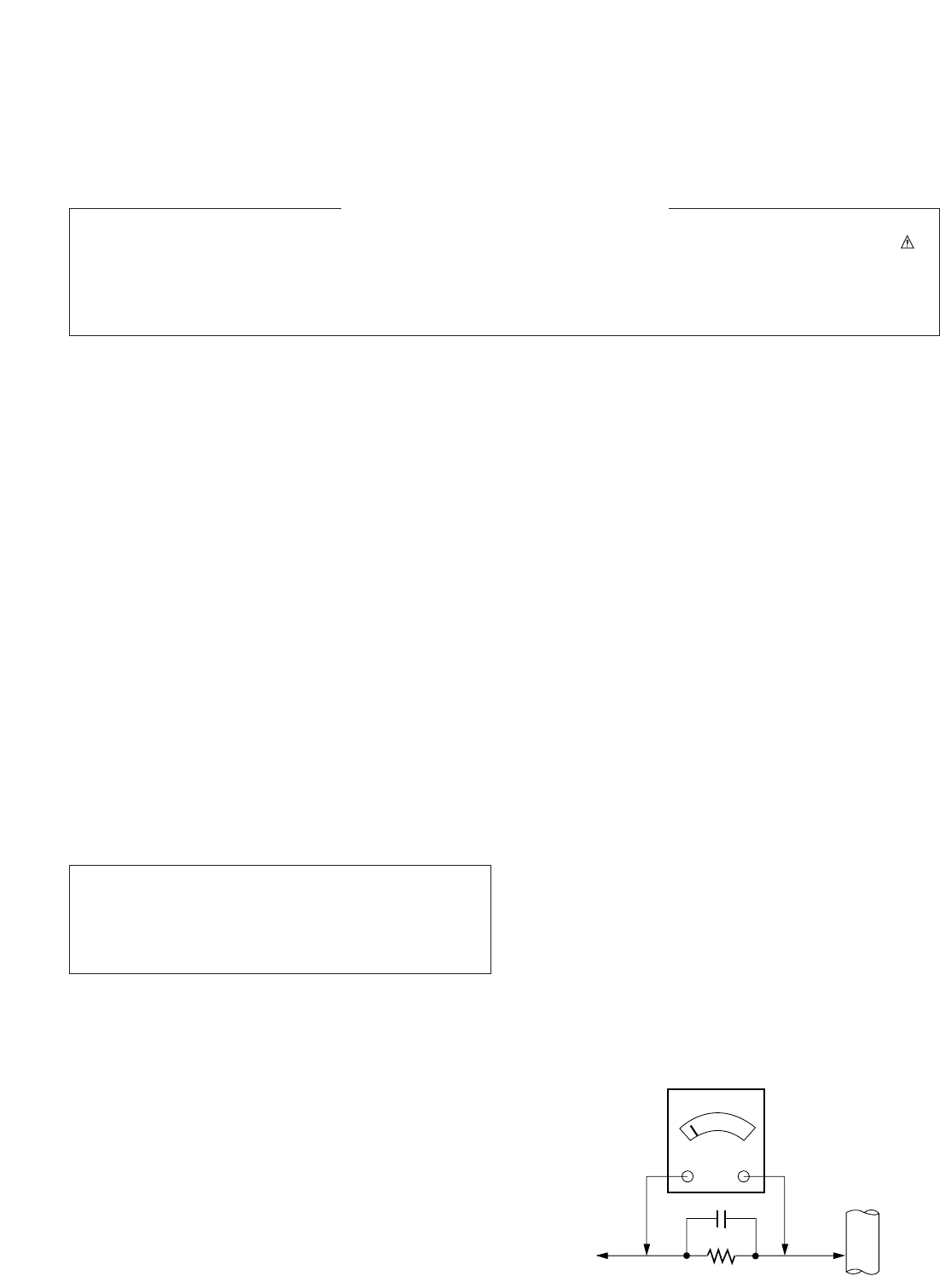
Leakage Current Cold Check(Antenna Cold Check)
With the instrument AC plug removed from AC source,
connect an electrical jumper across the two AC plug prongs.
Place the AC switch in the on positioin, connect one lead of
ohm-meter to the AC plug prongs tied together and touch other
ohm-meter lead in turn to each exposed metallic parts such as
antenna terminals, phone jacks, etc.
If the exposed metallic part has a return path to the chassis, the
measured resistance should be between 1MΩ and 5.2MΩ.
When the exposed metal has no return path to the chassis the
reading must be infinite.
An other abnormality exists that must be corrected before the
receiver is returned to the customer.
Leakage Current Hot Check (See below Figure)
Plug the AC cord directly into the AC outlet.
Do not use a line Isolation Transformer during this check.
Connect 1.5K/10watt resistor in parallel with a 0.15uF capacitor
between a known good earth ground (Water Pipe, Conduit, etc.)
and the exposed metallic parts.
Measure the AC voltage across the resistor using AC
voltmeter with 1000 ohms/volt or more sensitivity.
Reverse plug the AC cord into the AC outlet and repeat AC
voltage measurements for each esposed metallic part. Any
voltage measured must not exceed 0.75 volt RMS which is
corresponds to 0.5mA.
In case any measurement is out of the limits sepcified, there is
possibility of shock hazard and the set must be checked and
repaired before it is returned to the customer.
Leakage Current Hot Check circuit
The source of X-RAY RADIATION in this TV receiver is the
High Voltage Section and the Picture Tube.
For continued X-RAY RADIATION protection, the
replacement tube must be the same type tube as specified in
the Replacement Parts List.
1.5 Kohm/10W
To Instrument's
exposed
METALLIC PARTS
Good Earth Ground
such as WATER PIPE,
CONDUIT etc.
AC Volt-meter
IMPORTANT SAFETY NOTICE
0.15uF

- 4 -
CAUTION: Before servicing receivers covered by this service
manual and its supplements and addenda, read and follow the
SAFETY PRECAUTIONS
on page 3 of this publication.
NOTE:
If unforeseen circumstances create conflict between the
following servicing precautions and any of the safety
precautions on page 3 of this publication, always follow the
safety precautions. Remember: Safety First.
General Servicing Precautions
1. Always unplug the receiver AC power cord from the AC
power source before;
a. Removing or reinstalling any component, circuit board
module or any other receiver assembly.
b. Disconnecting or reconnecting any receiver electrical plug
or other electrical connection.
c.
Connecting a test substitute in parallel with an electrolytic
capacitor in the receiver.
CAUTION: A wrong part substitution or incorrect
polarity installation of electrolytic capacitors may result
in an explosion hazard.
d. Discharging the picture tube anode.
2. Test high voltage only by measuring it with an appropriate
high voltage meter or other voltage measuring device (DVM,
FETVOM, etc) equipped with a suitable high voltage probe.
Do not test high voltage by "drawing an arc".
3. Discharge the picture tube anode only by (a) first connecting
one end of an insulated clip lead to the degaussing or kine
aquadag grounding system shield at the point where the
picture tube socket ground lead is connected, and then (b)
touch the other end of the insulated clip lead to the picture
tube anode button, using an insulating handle to avoid
personal contact with high voltage.
4. Do not spray chemicals on or near this receiver or any of its
assemblies.
5. Unless specified otherwise in this service manual, clean
electrical contacts only by applying the following mixture to
the contacts with a pipe cleaner, cotton-tipped stick or
comparable nonabrasive applicator; 10% (by volume)
Acetone and 90% (by volume) isopropyl alcohol (90%-99%
strength)
CAUTION: This is a flammable mixture.
Unless specified otherwise in this service manual, lubrication
of contacts in not required.
6. Do not defeat any plug/socket B+ voltage interlocks with
which receivers covered by this service manual might be
equipped.
7. Do not apply AC power to this instrument and/or any of its
electrical assemblies unless all solid-state device heat sinks
are correctly installed.
8. Always connect the test receiver ground lead to the
receiver chassis ground before connecting the test receiver
positive lead.
Always remove the test receiver ground lead last.
9.
Use with this receiver only the test fixtures specified in this
service manual.
CAUTION: Do not connect the test fixture ground strap to
any heatsink in this receiver.
Electrostatically Sensitive (ES) Devices
Some semiconductor (solid state) devices can be damaged
easily by static electricity. Such components commonly are
called
Electrostatically Sensitive (ES) Devices.
Examples of
typical ES devices are integrated circuits and some fieldeffect
transistors and semicounductor "chip" components. The
following techniques should be used to help reduce the
incidence of component damage caused by static by static
electricity.
1. Immediately before handling any semiconductor component
or semiconductor-equipped assembly, drain off any
electostatic charge on your body by touching a known earth
ground. Alternatively, obtain and wear a commercially
available discharging wrist strap device, which should be
removed to prevent potential shock reasons prior to
applying power to the unit under test.
2. After removing an electrical assembly equipped with ES
devices, place the assembly on a conductive surface such as
aluminum foil, to prevent electrostatic charge buildup or
exposure of the assembly.
3. Use only a grounded-tip soldering iron to solder or unsolder
ES devices.
4. Use only an anti-static type solder removal device. Some
solder removal devices not classified as "anti-static" can
generate electrical charges sufficent to demage ES devices.
5. Do not use freon-propelled chemicals. These can generate
electrical charges sufficient to damage ES devices.
6. Do not remove a repalcement ES device from its protective
package until immediately before you are ready to install it.
(Most replacement ES devices are packaged with leads
electrically shorted together by conductive foam, aluminum
foil or comparable conductive material).
7. Immediately before removing the protective material from
the ieads of a replacement ES device, touch the protective
material to the chassis or circuit assembly into which the
device will be installed.
CAUTION:Be sure no power is applied to the chassis or
circuit, and observe all other safety precautions.
8. Minimize bodily motions when handling unpackaged
replacement ES devices. (Otherwise harmless motion such
as the bruching together of your clothes fabric or the lifting
of your foot from a carpeted floor can generate static
electricity sufficient to damage an ES device.)
General Soldering Guidelines
1. Use a grounded-tip, low-wattage soldering iron and
appropriate tip size and shape that will maintan tip
temperature within the range or 500¡£F to 600¡£F.
2. Use an appropriate gauge of RMA resin-core solder
composed of 60 parts tin/40 parts lead.
3. Keep the soldering iron tip clean and well tinned.
4. Thorohly clean the surfaces to be soldered. Use a mall
wirebristle (0.5 inch, or 1.25cm) brush with a metal handle.
Do not use freon-propelled spray-on cleaners.
5. Use the following unsoldering technique
a. Allow the soldering iron tip to reach normal temperature.
(500¡£F to 600¡£F)
b. Heat the component lead until the solder melts.
c. Quickly draw the melted solder with an anti-static,
suction-type solder removal device or with solder braid.
CAUTION: Work quickly to avoid overheating the
circuiboard printed foil.
6. Use the following soldering technique.
a. Allow the soldering iron tip to reach a normal
temperature (500¡£F to 600¡£F)
b. First, hold the soldering iron tip and solder the strand
against the component lead until the solder melts.
SERVICING PRECAUTIONS

- 5 -
c. Qulckly move the soldering iron tip to the junction of the
component lead and the printed circuit foil, and hold it
there only until the solder flows onto and around both the
component lead and the foil.
CAUTION: Work quickly to avoid overheating the circuit
board printed foil.
d. Closely inspect the solder area and remove any excess
or splashed solder with a small wire-bristle brush.
IC Remove/Replacement
Some chassis circuit boards have slotted holes (oblong) through
which the IC leads are inserted and then bent flat against the
circuit foil. When holes are the slotted type, the following
technique should be used to remove and replace the IC. When
working with boards using the familiar round hole, use the
standard technique as outlined in parapraphs 5 and 6 above.
Removal
1. Desolder and straighten each IC lead in one operation by
gently prying up on the lead with the soldering iron tip as the
solder melts.
2. Draw away the melted solder with an anti-static suction-
type solder removal device (or with solder braid) before
removing the IC.
Replacement
1. Carefully insert the replacement IC in the circuit boare.
2. Carefully bend each IC lead against the circuit foil pad and
solder it.
3. Clean the soldered areas with a small wire-bristle brush.
(It is not necessary to reapply acrylic coating to the areas).
"Small-Signal" Discrete Transistor
Removal/Replacement
1. Remove the defective transistor by clipping its leads as
close as possible to the component body.
2. Bend into a "U" shape the end of each of three leads
remaining on the circuit board.
3. Bend into a "U" shape the replacement transistor leads.
4. Connect the replacement transistor leads to the
corresponding leads extending from the circuit board and
crimp the "U" with long nose pliers to insure metal to metal
contact then solder each connection.
Power Output, Transistor Device
Removal/Replacement
1. Heat and remove all solder from around the transistor leads.
2. Remove the heatsink mounting screw (if so equipped).
3. Carefully remove the transistor from the heat sink of the
circuit board.
4. Insert new transistor in the circuit board.
5. Solder each transistor lead, and clip off excess lead.
6. Replace heatsink.
Diode Removal/Replacement
1. Remove defective diode by clipping its leads as close as
possible to diode body.
2. Bend the two remaining leads perpendicula y to the circuit
board.
3. Observing diode polarity, wrap each lead of the new diode
around the corresponding lead on the circuit board.
4. Securely crimp each connection and solder it.
5. Inspect (on the circuit board copper side) the solder joints of
the two "original" leads. If they are not shiny, reheat them
and if necessary, apply additional solder.
Fuse and Conventional Resistor
Removal/Replacement
1. Clip each fuse or resistor lead at top of the circuit board
hollow stake.
2. Securely crimp the leads of replacement component around
notch at stake top.
3. Solder the connections.
CAUTION: Maintain original spacing between the replaced
component and adjacent components and the circuit board
to prevent excessive component temperatures.
Circuit Board Foil Repair
Excessive heat applied to the copper foil of any printed circuit
board will weaken the adhesive that bonds the foil to the circuit
board causing the foil to separate from or "lift-off" the board.
The following guidelines and procedures should be followed
whenever this condition is encountered.
At IC Connections
To repair a defective copper pattern at IC connections use the
following procedure to install a jumper wire on the copper
pattern side of the circuit board. (Use this technique only on IC
connections).
1. Carefully remove the damaged copper pattern with a sharp
knife. (Remove only as much copper as absolutely
necessary).
2. carefully scratch away the solder resist and acrylic coating
(if used) from the end of the remaining copper pattern.
3. Bend a small "U" in one end of a small gauge jumper wire and
carefully crimp it around the IC pin. Solder the IC connection.
4. Route the jumper wire along the path of the out-away
copper pattern and let it overlap the previously scraped end
of the good copper pattern. Solder the overlapped area and
clip off any excess jumper wire.
At Other Connections
Use the following technique to repair the defective copper
pattern at connections other than IC Pins. This technique
involoves the installation of a jumper wire on the component
side of the circuit board.
1. Remove the defective copper pattern with a sharp knife.
Remove at least 1/4 inch of copper, to ensure that a
hazardous condition will not exist if the jumper wire opens.
2. Trace along the copper pattern from both sides of the
pattern break and locate the nearest component that is
directly connected to the affected copper pattern.
3. Connect insulated 20-gauge jumper wire from the lead of
the nearest component on one side of the pattern break to
the lead of the nearest component on the other side.
Carefully crimp and solder the connections.
CAUTION: Be sure the insulated jumper wire is dressed so
the it does not touch components or sharp edges.
- 6 -
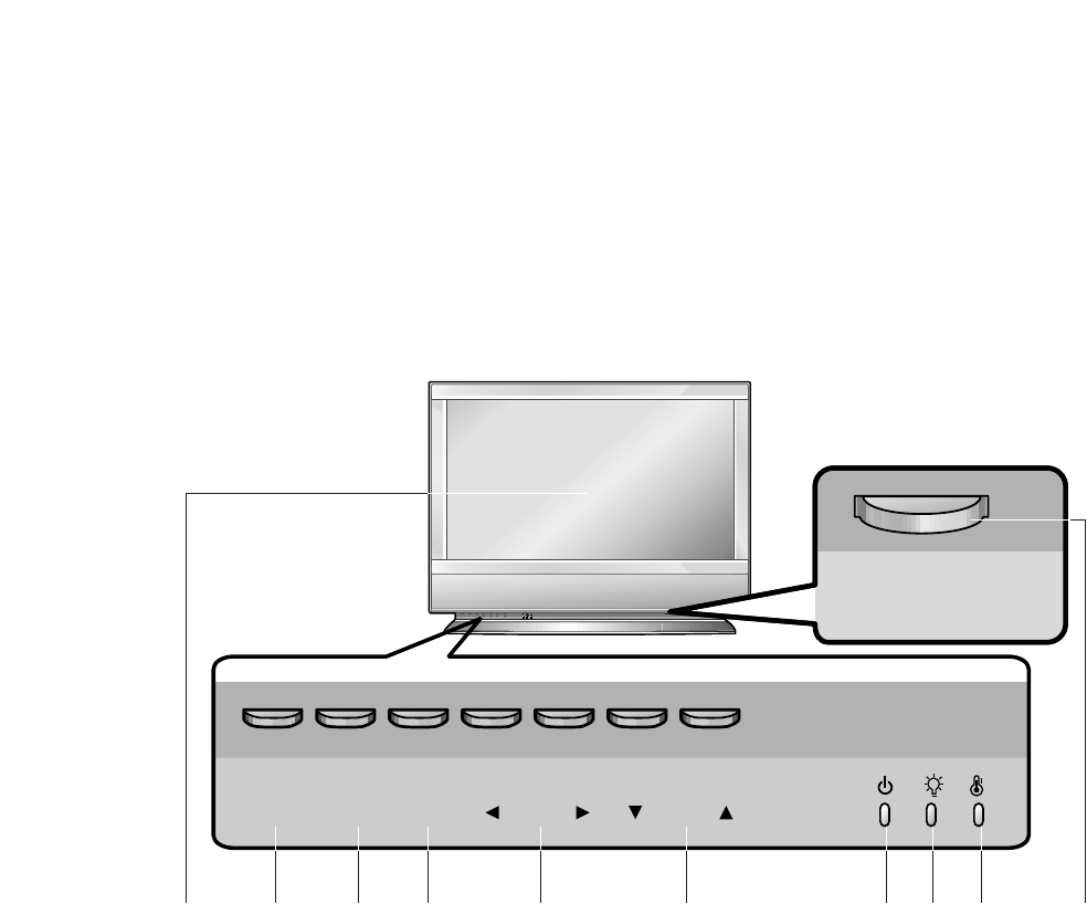
CONTROL DESCRIPTIONS
All the functions can be controlled with the remote control handset.
Some functions can also be adjusted with the buttons on the front
panel of the set.
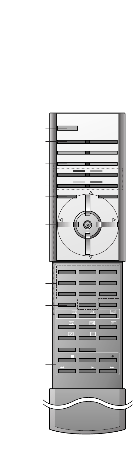
Remote control handset
Before you use the remote control handset, please install the bat-
teries. See the next page.
1. POWER
switches the set on from standby or off to standby.
2. MULTIMEDIA
selects Component 1/2, RGB-DTV or RGB-PC modes.
3. MUTE
switches the sound on or off.
4. PIP BUTTONS
PIP
switches the sub picture on or off.
PR +/-
selects a programme for the sub picture.
SWAP
alternates between main and sub picture.
INPUT
selects the input mode for the sub picture.
SIZE
adjusts the sub picture size.
STILL
freezes motion of the sub picture.
POSITION
relocates the sub picture in clockwise direction.
5. SWAP
returns to the previously viewed programme.
6. MENU
selects a menu.
7. D/E(Programme Up/Down)
selects a programme or a menu item.
switches the set on from standby.
F/G(Volume Up/Down)
adjusts the volume.
adjusts menu settings.
OK
accepts your selection or displays the current mode.
8. NUMBER BUTTONS
switches the set on from standby or directly select a number.
9. PSM (Picture Status Memory)
recalls your preferred picture setting.
10. I/II
selects the language during dual language broadcast.
selects the sound output.
11. VCR BUTTONS
control a LG video cassette recorder.
123
456
7
PSM SSM
8
0
POSITION
STILL
MIX
I/II ARC
REVEAL
?
TIME
LIST
MODE
STOP REC
P/STILL
REW FF
PLAY
9
POWER
MULTIMEDIA TV/AV
MUTE SLEEP
PIP TEXT
PR - PR +
INPUTSWAP
MENU PR
VOL OK VOL
PR
CANCEL/EXIT
INDEX
M
SIZE
1
2
3
4
5
6
9
10
11
8
7
- 7 -
12. TV/AV
selects the remote operating mode.
switches the set on from standby.
13. SLEEP
sets the sleep timer.
14. TELETEXT BUTTONS
These buttons are used for teletext.
For further details, see the ‘Teletext’ section.
15. CANCEL/EXIT
Clears all on-screen displays and returns to TV viewing from any
menu.
16. SSM (Sound Status Memory)
recalls your preferred sound setting.
17. STILL
freezes motion of the picture.
18. LIST
displays the programme table.
19. ARC (Aspect Ratio Control)
changes the picture format.
Note : In teletext mode, the PR +/-,SWAP and INPUT buttons are
used for teletext function.
Battery installation
The remote control handset is powered by two AAA type batteries.
To load the batteries, turn the remote control handset over and
open the battery compartment. Install two batteries as indicated by
the polarity symbols ( and ) marked inside the compartment.
Note : To avoid damage from possible battery leakage, remove the
batteries if you do not plan to use the remote control handset for an
extended period of time.
+
-
1 2 3
4 5 6
7
PSM SSM
8
0
POSITION
STILL
MIX
I/II ARC
REVEAL
?
TIME
LIST
MODE
STOP REC
P/STILL
REW FF
PLAY
9
POWER
MULTIMEDIA TV/AV
MUTE SLEEP
PIP TEXT
PR - PR +
INPUTSWAP
MENU PR
VOL OK VOL
PR
CANCEL/EXIT
INDEX
M
SIZE
12
13
14
15
16
17
18
19
- 8 -
1. MAIN POWER (ON/OFF)
switches the set on or off.
2. TV/AV
selects the remote operating mode.
switches the set on from standby.
3. MENU
selects a menu.
4. OK
accepts your selection or displays the current
mode.
5. FF/GG(Volume Down/Up)
adjusts the volume.
adjusts menu settings.
6. DD/EE(Programme Up/Down)
selects a programme or a menu item.
switches the set on from standby.
7. OPERATION INDICATOR (Refer to p.7)
8. LAMP INDICATOR (Refer to p.7)
9. TEMPERATURE INDICATOR (Refer to p.7)
10. REMOTE CONTROL SENSOR
Note : There might be a faint white trace on the
center of the screen according to the position.
This is normal and is a characteristic of the
screen.
Front panel
ON/OFF
ON/OFF
TV/AV
MENU OK VOL PR
TV/AV MENU OK VOL PR
2 3 4 5 6 7 8 9 110
Lamp indicator, operation indicator, and temperature indicator, located below the front panel con-
trols reveal the operating status of the LCD projection TV.
- 9 -
P
O
R
T
U
P
G
R
A
D
E
P
R
P
B
Y
DTV/DVD INPUT
RGB
(XGA/
576p/
480p/
720p/
1080i)
(L)
AUDIO
(R)
V
A
U
D
I
O
O
U
T
A
A
B
L
E
R
I
(L)
AUDIO
(R)
MONO
A/V 1
INPUT
A/V 2
INPUT
MONITOR
OUT
(L)
AUDIO
(R)
(L)
AUDIO
(R)
AUDIO
CENTER
MODE IN
PC/DTV INPUT
COMPONENT
INPUT 1
576i/480i
576p/480p
720p/
1080i
576i/480i
576p/480p
720p/
1080i
COMPONENT
INPUT 2
ANT IN
75Ω
L
L
P
O
R
T
U
P
G
R
A
D
E
PC/DTV
(XGA
/480p
/720p
/1080i)
P
R
P
B
Y
DTV/DVD
(480i/480p/720p/1080i)
PC/DTV
(XGA
/480p
/720p
/1080i)
RGB2
RGB1
RGB1,2
S-VIDEO
VIDEO
AUDIO
A/V 3
SIDE A/V
INPUT
L/MONO
R
S-VIDEO
VIDEO
AUDIO
A/V 3
SIDE A/V
INPUT
L/MONO
R
S-VIDEO
75Ω
L
L
ANT IN
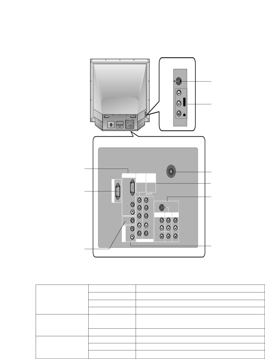
Rear panel
AERIAL SOCKET
UPGRADE PORT
This port is used to
upgrade the software
version and debug
without changing the
hardware.
Be careful not to use
this port. Just contact
your dealer or service
centre.
DTV/DVD INPUT
SOCKETS
PC/DTV INPUT
SOCKETS
CENTER SPEAKER
MODE IN SOCKETS
AV1/2 / MONITOR
OUT(AUDIO/VIDEO),
S-VIDEO INPUT
SOCKETS
VARIABLE AUDIO
OUT SOCKETS
S-VIDEO INPUT
SOCKET
AV3 INPUT SOCKET
Off Power cord is not connected.
Red Power Cord is connected, unit is on standby.
Green On
Orange (flashing) Preparing operation in standby.
Orange Projection lamp is reaching the end of its life and
needs to be replaced with a new lamp.
Green (flashing) The lamp cover is not closed.
Orange The set is overheating.
Red The set has shut down due to overheating.
Red (flashing) The set has shut down, check the cooling fan.
Operation Indicator
Lamp Indicator
Temperature Indicator
•Status Indicators
SPECIFICATIONS
NOTE : Specifications and others are subject to change without notice for improvement
.
FScope
This specification can be applied to the LCD Projection(RT-52SZRB/RP)
FTest and Inspection Method
1) performance:Follow the Standard of LG TV test
2) Standards of Etc requirement
Safety: Follow the standard of CB
EMC : Follow the standard of CE
FTest Condition
1) Temperature :25¡5°C
2) Relative Humidity:65¡10%
3) PowerVoltage:Standard input voltage(AC 240V¡10%, 50/60Hz)
But Standard input voltage mark value is marked by model.
4) Use the parts only designated in B.O.M.,PARTS SPEC.,or drawings.
5) Follow each drawing or spec for spec and performance of parts,based upon P/N of B.O.M
6) Warm up TV set for more than 30min. before the measurement.
Specification
PAL – B/G, D/K, I, M, N
SECAM B/G, D/K
NTSC - M, 4.43
(1) VHF : 1 ~ 9
UHF : 20 ~ 75
CATV : 1~44
AC 240V, 50H/60Hz
Australia
52 inch
16:9 (wide)
0
-20
- 10 -
Remark
- RB :Teletext
- RP :W/O Teletext
option
Model Name
RT-52SZ30RB/RP
Market Place
Austrailia
China
Moroco
FGeneral Specification
1
2
3
4
5
6
7
8
9
10
Only AV input signal
for NTSC - 4.43
Video input applicable
system
Available Channel
Input Voltage
Market
Screen size
Aspet ratio
Operating Temperature
Operating Humidity
Storage Temperature
Storage Humidity
Min Typ Max Unit
No Item Remark
deg
%
deg
%
40
85
60
85
- 11 -
FFeature and Function
No
1.
2.
3.
4.
5.
6.
7.
8.
9.
10.
11.
12.
13.
14.
15.
16.
17
18
19
20
21
22
D-Sub 15 Pin
RS-232C
Item
Specification Remark
LG Code
1 Separate
1
1
2L/R
2Y, P
B
, P
R
3(1 Side / 2Rear)
2 (1 Side / 1Rear)
1 1Rear
1
1
Power, Menu, ok, Volume (F,G)
Channel (D, E)
Dynamic/ Standard/ Mild/ Game/ User
Contrast/ Brightness/ Colour/ Sharpness/ Tint
DTV & PC : 16:9/ 4:3/ Zoom/ Auto
CVBS : 4:3/ 16:9/ Zoom/ Auto
Dolby Virtual/ Flat/ Music/ Movie/ Speech
A2 : B/ G, D/ K, NICAM : B/ G, D/ K, I, L/ L’
O
O
Top/ Flop 128Page
Sleep Timer/ Auto Sleep
English
REMOCON
RGB Input
RGB Audio (L, R) Input
Center Speaker Mode Input
Component Audio (R, L) Input
Component Input
AV Input
S-Video Input
Monitor out
Variable Audio out
Serial Port
Local key
Picture, EZ Video mode
Picture, User Control
Display mode
Sound, EZ Sound mode
Sound Stereo/ Dual
PIP/ POP Mode
SSC (Split Screen) Mode
Teletext
Timer
OSD Language
At Room Temperature
At -10 °C
1
2
3
4
5
6
7
8
Power ON/OFF operation
Staring Voltage (AC INPUT)
Staring Voltage (AC INPUT)
DC Voltage, Ballast
DC Voltage, Audio AMP
DC Voltage, 3.3V, stand-by
DC Voltage, Analog 3.3V
DC Voltage, Analog 2.5V
10000
-20
-15
360
28
3.15
3.15
2.438
380
32
3.3
3.3
2.5
400
36
3.45
3.45
2.600
times
%
%
V
V
V
V
V
No Item Specification
Min Typ Max Unit Remark
FPower
Min Typ Max Unit
- 12 -
9
10
11
12
13
14
15
DC Voltage, Digital, 5V
DC Voltage, Turning voltage
DC Voltage, LCD Driver, 5V
DC Voltage, LCD Driver, 17.5V
DC Voltage 3.3, SUB MICOM
DC Voltage 2.5V, SUB MICOM
DC Voltage, FAN
2.4
3.2
4.8
11.5
30
4.8
11.5
2.5
3.3
5.0
12
32
5
12
2.6
3.4
5.2
12.5
33
5.2
12.5
V
V
V
V
V
V
V
No Item Specification
Min Typ Max Unit Remark
75 ohm
(480I/P, 576I, 720P, 1080I)
75 ohm
1.
2.
3.
4.
5.
6.
7.
8.
9.
10.
11.
12.
Video Input Level
Video Input Frequency Response
Video output S/N
S-Video Input Level (Y)
S-Video Input Level (C-Burst)
Component Video Input Level
(Y, CB/ PB, CR/ PR)
R/G/B Video Input Level
Audio Input S/N
Audio Input Distortion
Audio Input Dynamic Range
Audio Input Level
Audio Input Frequencyl Response
0.85
3
40
0.85
0.256
0.6
0.6
40
2
0.47
0.05
1
1
0.286
0.7
0.7
0.63
1.15
1.15
0.316
0.8
0.8
2
0.79
10
Vpp
MHz
dB
Vpp
Vpp
Vpp
Vpp
dB
%
V
Vrms
kHz
No Item Specification
Min Typ Max Unit Remark
FExternal Interface
SDTV, DVD 480I
SDTV, DVD 480I
EDTV 480P
SDTV, DVD 576I
EDRV 576P
HDTV 720P (60Hz)
HDTV 720P (50Hz)
HDTV 1080I (60Hz)
HDTV 1080I (50Hz)
1.
2.
3.
4.
5.
6.
7.
8.
9.
640x480
640x480
704x480
720x576
720x576
1280x720
1280x720
1920x1080
1920x1080
15.75
15.73
31.47
15.625
31.250
45.00
37.50
33.75
28.125
60
59.94
59.94
50
50
60.00
50
60.00
50
No
FComponent Video Input (Y, PB, PR)
Proposed
Specification
Resolution H-freq(kHz) V-freq(Hz) Pixel clock
- 13 -
0 : Standard
1 : Non-Standard (Southeast Asia,Central America)
0 : Support FLOP
1 : Support All (FLOP + TOP)
0 : Do not save DUAL When converting Channel
1 : Save DUAL when Converting Channel
0 : OSRAM
1 : PHILIPS
0 : Not Ready to Over-Modulation in DK Mono
1 : Ready to Over-Modulation in DK Mono
0 : BG / I /D
1 : BG / L
2 : BG / I DK / M
0 : west EU
1 : East EU 1
2 : East EU 2
3 : Turkey EU
4 : Cyrillic 1
5 : Cyrillic 2
6 : Cyrillic 3
7 : Turk GRE 1
8 : Turk GRE 2
9 : Turk GRE 3
10 : Arab FRA
11 : Arab ENG
12 : Arab HEB 1
13 : Arab HEB 2
14 : FARS ENG
15 : FARS FRA
16 : FARS All
1.
2.
3.
4.
5.
6.
7.
Volume Curve
Text Top
I_II SVC
Lamp_Type
C_Mute
system
Text Language
0
0
0
0
0
2
0
No Item Specification
Min Typ Max Unit Remark
FOption

- 14 -
1. Application Object
This instruction is for the application to the LCD Projection
2. Notes
(1) The power source insulation of this LCD Projection is not
charging type and you may not use the transformer for
insulation. But you’d better adjust the set after operating it
with insulation transformer between power supply cable
and input part of the set for protecting the adjusting
equipments.
(2) The adjustment must be performed under the correct
sequence.
(3) The adjustment must be performed in the circumstance of
25!5°C of temperature and 65!10% of relative humidity if
there is no specific designation.
(4) The input voltage of the receiver must keep 230V, 50Hz in
adjusting.
(5) The set must be operated for 5 minutes preliminarily
before adjustment if there is no specific designation.
The preliminary operation must be performed after
receiving 100% white pattern,but reception of the moving
picture may also be possible in unavoidable case.
3. Composition of Adjustment Mode
(1) All adjustment mode are entered by pressing the ADJ key
on the remore control,after adjustment pess the ADJ key to
come out.
(2) Below picture is screen composition when press the first
ADJ key.
(3) Select menu to adjust with using (CH+(D),CH-(E)) key
above screen and press Volume+(G)key to adjust on the
wanting menu.
(4) Adjust the value of adjustment with using the volume
+(F),volume -(G) key.
(5) Press the ADJ key to come out after adjustment.
(6) ex.) Composition of each adjustment mode.
1). RGB Alignment:This is the sub adjustment item by
selected Adjust key.
2) F, G(Vol +/ -): This is the key to change the data.
3) D, E (CH +/ -):This is the key to change the sub menu.
4. LCD adjustment
4-1. NRS adjustment
[When the LCD pannel load data on regular pixel using high
speed charge/ discharge with sample & holder, the drain width
of TFT gradually dicreases and the non-resistance increases,
and comes out regular noise on screen (shows vertical line by
12 pixel]
(1) Required Test Equipments
1) PC Pattern generator; 16 Gray Pattern
2) Fixation stand
3) Remote control of adjustment
4) Circuit thing Jig for adjustment (Except Driver Board Assy)
(2) Equipment composition : Refer to <Fig 2>
(3) Preparation for Adjustment
1) Connect PC PATTERN GENERATOR to JIG SET as
shown <Fig 2>.(Except drive part of a circuit block)
2) Select 16 Gray pattern of PC PATTERN GENERATOR
(4) Adjustment Sequence
1) Turn on power supply in the JIG for adjustment.
2) Press the INPUT key to select RGB_PC mode.
3) Press the ADJ key on remote control for adjustment to
enter the adjustment mode.
4) Select the ‘62352’ and press the G key. Then select 6.
RNRSH, 9.GNRSH, 11.BNRSH of ADJUST MODE to
adjust.
5) Let’s decrease vertical line Noise by using Volume button.
(Input a R, G, B input signal, then adjust it individually)
6) When finishing the adjustment, get out of adjustment mode
by pressing Adjust key.
4-2. VCOM ADJUSTMENT
(1) Required Test Equipments
1) PC PATTERN GENERATOR ; Pattern Generator which
can generator each R, G, B signal and can observe the
FLICKER best (ex : me Character Pattern)
2) <Fig.2> Equipment composition
3) Remote control
4) Circuit thing Jig for Adjustment (Except Driver Board Assy
of adjustment model)
(2) Equipment Composition
RT52SZ30RB [V*.*]
RGB Alignment
62352
Uniformity Adj
Gamma Adjust
AD9883 Adjust
Sub Micom Ver. **
Main Micom Ver. **
RGB Alignment
9.DXOUTB D
10.H_positon F0 G
E
ADJUSTMENT INSTRUCTIONS
<The first screen of adjustment mode>
Adjustment Jig
Screen
PC Pattern
Generator
Optical measuring equipment
Optical box
Circuit for
Adjustment
Set stand
PC
<Fig 1.Adjustment of circuit>
(3)Preparation for Adjustment
1) Connect the PC PATTERN GENERATOR, circuit for
adjustment and adjustment JIG as shown <Fig 2>.
2) Adjust output pattern of PC PATTERN GENERATOR to
possible display and then turn on the power.
(4) Adjustment Sequence
1) Turn on the adjustment Jig
2) Select RGB_PC by pressing input Select Key on Remote
control.
3) Enter to adjustment mode by pressing Adjust key on
Remote control.
4) Select the ‘62352’, then ready to adjust 4. RVCOM, 7.
GVCOM, 10.BVCOM
5) Let’s decrease flicker by using Volume key
(Input a R, G, B input signal, then adjust it individually)
6) When finishing the adjustment, get out of adjustment mode
by pressing Adjust key.
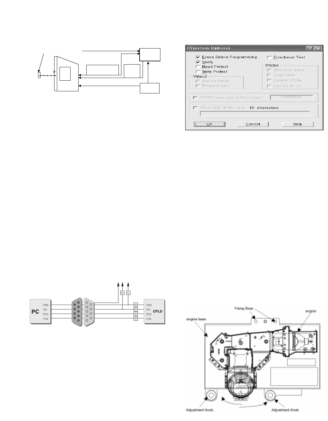
5. CPLD Download Work
(1) Required Test Equipments & Preparation for Adjustment
1) Connect the PC and memory JIG as shown <fig3>.
2) Turn on JIG MAIN POWER SW.
3) After turn on the PC and moniter, operate the device
programming.
(2) Adjustment Sequence
1) After program running, displayed [OPTION MODE
SELECTION] window.
Check the “Load configuration File(.cdf, .pdr)” in this
window and click the finish button
2) When the screen displays the open window, select the
suitable file(*.cdf) according to model.
3) IC figure is change to green by clicking it.
4) Select the program of operations.
5) Check the [Erase before programming] and [Verify] menu
as shown <Fig4> and press the OK button.
f) At this time, the download starts. The download finished
after 10 seconds.
6.Assembling Adjustment
6-1. Screen Tilt & Keystone Adjustment
(1) Required Test Equipments
1) Six angles wrench and spanner for knob adjustment or
fixation
2) Remote control
(2) Preparation for Adjustment
1) Do not assemble the front pannel equipment so that you
can adjust the adjustment knob of <Fig 5>
2) Turn on TV and press EYE key on remote control.
3) 11th screen - Select the pattern of small white squares,
diagonal and a big red square.
(3) Adjustment Sequence
1) Stick the Engine of <Fig 5> to the knob poll for adjustment
and check the key stone & tilt watching TV screen.
2) Rotate left/right adjustment knob bellow and adjust engine
angle.
3) Adjust the adjustment knob of both sides so that the tilt and
keystone are to be under the spec.(The gap between max
and min : under 4mm)
4) After adjusting like 3), fix the engine with the screw for
fixation.(2EA. adjustment knob and engine fixing screw)
- 15 -
<Fig 4. Program Options>
<Fig 3.How to connect the MEMORY JIG and PC>
<Fig 5>
Optical measuring equipment
TV
Set
Connector for
Adjustment RS-232C
Cable
PC
PC Pattern
Generator
Adjustment
Jig
<Fig 2.TV set status Adjustment>
6-2. Screen Position Adjustment
(1) Required Test Equipments
A remote control of adjustment
(2) Preparation for Adjustment
1) Connect the power source with TV Set and turn TVset on
2) Do Heat Run for 5 minutes and over before adjustment.
3) Recieve main/sub signal of company through 13CH by split
screen.
(3) Horizontal Position Adjustment
a) Press ADJ key on the remote control to enter the
adjustment mode
b) Select the RGB Alignment of the adjustment menu.
c) Select H-position with Gkey.
d) Adjust data with using th left/right key on the remote
control in order to be left/right semmetry screen. (Three
blocks of the most outer block must be located the most
outer block.
(4). Vertical Position Adjustment
1) Select V-position with channel key.
2) Change the data to symmetrized upper and down of screen
(refer to Fig6) and then press the Volume key on Remote
control to get out of adjustment mode.
6-3. Component Offset Adjustment
(1) Required Test Equipments :
A remote control for adjustment, 801GF
(2) Preparation for Adjustment
1) Connect a power source with TV Set and turn TV set on.
2) Do Heat-Run for 15 minutes and over before adjustment.
3) Receive the Component 1 or 2.
4) Receive the 720P, HozTVBar Pattern of 801GF(Fig 7).
(3) Offset Adjustment
1) Press Adjust key on the remote control to enter the
adjustment mode after more than 10 seconds of receiving
the signals.
2) Press “4.AD9883 Adjust” to adjust.
3) When the OSD of “AD9883 Adjust End” appeared and
disappears,The adjustment is completed
(4) Component & RGB Mode White Balance passivity
adjustment
1) After inputting the 16 Gray pattern (RGB or Component),
check the White Balance status of Low Level (2-6 Gray
Level).
2) After Pressing the IN-START key of remote control, select
the AD9883 and press the G key. - Red Offset, Blue Offset
is able to adjust.
3) After selecting the adjustment mode with the channel key,
adjust Red Offset, Blue Offset value with the volume key to
adjust passively white Balance in Low Level.
adjustment limite : Red Offset - +/-2 step
Blue Offset - +/-4step
6-4. White Balance & Gamma Adjustment
(1) Required Test Equipments
1) CA100 : 1EA
-> Measure colour of projecting screen center
[CA-110(name of model) is possible to measure White
Balance and Gamma - leave it 20Cm from screen center
Follow a measurement machine manual to set CA -100
and CA - 110 measurement machine.]
2) pattern Generator : 1EA -> 16 step Gray Pattern, 64 step
Gray Pattern
3) SET Fixation Stand : 1EA
4) Remote control : 1EA
5) Circuit thing Jig for adjustment (Except Drive Board Assy of
adjustment model)
--- Programmed Digital Board so that the VDP Test Pattern
can output white signal by 1 level from 0 to 255 level.
(2) Equipment composition : Follow <Fig 2>
Adjust at same condition of equipment composition diagram.
(3) Preparation for Adjustment
Compose the equipment follow Fig.2 and place the set on the
fixation stand.
1) Select the VDP Test Pattern signal to R1, G1, B1.
2) Press the Adjust key to select 62352 and then select
RVREF, GVREF, BVREF in adjust mode
3) Adjust the luminance of CA100 to be below 0.75Cd by
volume key.(Range : 196~ 202)
4) Exit adjustment mode by pressing Adjust key.
5) Press the IN-START key on the remote control and select
the 7050 RGB Set of adjustment mode and then press the
Gkey.
6) Check the data value of Rcontast, Gcontrast, Bcontrast is
515, Otherwise set the data 515 by using volume key.
(4) Adjustment Sequence
1) Output 255,255,255 signal of VDP TEST PATTERN, then
display maximum WHITE PATTERN on screen.
2) Gamma Adjust Mode is display as below when select
Gamma adjust by pressing ADJ key on remote control.
3) Change the 16 Step RGB data to select white balance
x:283, y:294.
* When white balance x:283, y:294 in VDP PATTERN,
picture signal is set to x:283, y:297, in as a matter of fact.
4) Measure the luminace with chanded data.
5) Set the every Gamma data of 16 steo to 2.5 on the basis of
measured luminance data in 3).
(Max lumenance *(n1/16)**2.5 --- Max luminance :
measured luminance data n1= every step unit when
separating signal level to 16 step)
- 16 -
<Fig 7 720P HozTVBar Pattern>
<Fig 6> H/V screen for Position adjustment

- 17 -
* First column : R adjustment data
display
* Second column : G adjustment
data display
* Third column : B adjustment data
display
6) Output the 240, 240, 240
(15th data in max white output signal level) in the VDP Test
Pattern, change the 15th RGB data value to come out
white valance x=283, y=294 and measured step luminance
in 5).
7) Output the 240, 240, 240 (14th data in max white output
signal level) in the VDP Test Pattern, change the 14th RGB
data value to come out white valance x=283, y=294 and
measured step luminance in 5).
8) As shown above, output the VDP Test Pattern signal
(208/192/176/160/144/128/112/96/80/64/48/32/16) and
change the RGB data value of each step to come out white
balance x=283, y=294 and measured luminance in 3).
(5) Sequence of Gamma manually adjustment
This is adjustment (after finish the 3-4) to check whether
Gamma/ White balance adjustment are well adjusted and
make correction manually.
1) Prepare the PC Pattern Generator which is possible to out-
put R/G/B of 16 step Gray Pattern.
2) Equipment composition : Follow <Fig. 2>.
3) Turn on the Jig for adjustment.
4) Select the RGB_PC by pressing the input select button on
Remote Control.
5) Output the 16 Gray Pattern in PC Pattern Generator.
Check it with the naked eye whether Screen Gamma and
White balance is right about each Gray.
If it’s not, press the ADJ button on Remote Control and
then adjust the level data of each step manually.in “Gamma
adjust”.
6) Output the 64 Gray Pattern in PC Pattern Generator.
Check it with the naked eye whether Screen Gamma and
White balance is right about each Gray or whether there is
Gamma noise.
If there’s any problem, adjust in 5)
7) After finishing adjustment, exit adjustment mode by using
ADJ button on Remote Control.
6-5. White Uniformity Adjustment
(1) Required Test Equipments
1) Uniformity measuring equipment : Equipment which can
measure chromatiity in the whole screen
2) Set stand : 1EA
3) Remote controller for adjustment : 1EA
4) Circuit thing Jig for Adjustment (Except Driver Board Assy
of adjustment model)
--- Programmed Digital Board so that the VDP Test Pattern
can output white signal by 1level form 0 to 255 level.
(2) Equipment composition
Compose the equipment as Fig.2
(3) Preparation for Adjustment
1) Composite the equipment as shown Fig.2, and place the
set on fixation stand.
2) After inputting company channel 13, adjust colour uniformity
like Horizontal/ Vertical position adjustment of input signal
part adjustment by using remote control for adjustment.
3) After pressing IN_START key on remote control for
adjustment, select the adjustment mode 7050 Uniformity.
<Resister Explanation about uniformity adjustment>
1. RamCtrl : s/w saving uniformity write order (Do not adjust)
2. CSHP : Horizontal start point designation --- adjustable
3. CSVP : Vertical start point designation --- adjustable
4. CEHP : Horizontal END point designation --- adjustable
5. CEVP : Vertical END point 6.designation --- adjustable
6. Mode : uniformity mode select --- adjustable if need
*** 0 : 221point & 3level ---- defalut value
*** 1 : 221point & 4level
*** 2 : 825point & 3level
*** 3 : 825point & 4level
7. KHH : Upper 2byte of horizontal line correction coefficient --
Change according to CSHP, CEHP value.
8. KHL : Upper 2byte of vertical line correction coefficient --
Change according to CSHP, CEHP value.
** How to calculate KHH, KHL value
LCD panel size = 1280 x 720
Correction Point = 221 point
--> 17 horizontal points x 13 vertical points
(16 horizontal segments x 12 vertical poins)
O H Coefficient(KHH, KHL)
--> Calculation method (CEHP-CSHP=1280, Horizontal
segment value =16)
9. KVH : Upper 2byte of vertical line correction coefficient
-- Change according to CSVP, CEVP value.
10. KVL : Upper 2byte of vertical line correction coefficient
-- Change according to CSVP, CEVP value.
OV Coefficient(KVH, KVL)
Calculation method (CEVP-CSVP=720, Vertical segment
value =12)
11. RL1H : Upper 9bit of MID2 brightness correction
coefficient in R MIN.
--- Change according to RMIN and RMID2 value.
12. RL1L : Lower 9bit of MID2 brightness correction coefficient
in R MIN.
--- Change according to RMIN and RMID2 value.
13. RL2H : Upper 9bit of MID1 brightness correction
coefficient in R MID2.
--- Change according to RMID2 and RMID1 value.
H coefficient = 1/(number of pixel intervals between setting in the horizontal
direction)
Hcoeff = 1/((1280/16)-1) = 0.012658227
hex (0.012658227 x 216) = 0 x 033D, Hcoeff (hex) = 0 x 033D + 1 = 0 x 33E
V coefficient = 1/(number of pixel intervals between setting in the vertical
direction)
Vcoeff = 1/((720/12)-1) = 0.016949152
hex (0.016949152 x 216) = 0 x 0456, Vcoeff (hex) = 0 x 0456 + 1 = 0 x 0457
Gamma Adjust
R:1 G:2 B:3
80 100 100
234 216 216
453 411 387
--------------------------
--------------------------
724 690 780

14. RL2L : Lower 9bit of MID1 brightness correction
coefficient in R MID2.
--- Change according to RMID2 and RMID1 value.
15. RL3H : Upper 9bit of MAX brightness correction coefficient
in R MID1.
--- Change according to RMID1 and RMAX value.
(use it while adjusting 4 coefficient)
16. RL3L : Lower 9bit of MAX brightness correction coefficient
in R MID1.
--- Change according to RMID1 and RMAX value.
(use it while adjusting 4 coefficient)
<L Coefficient Calculation Method>
Using 3coefficient Level
Assume that the value of R/G/B MIN, MID2,MID1 is 192, 448,
704.
R/G/B MIN = 192
R/G/B MID2 = 448
R/G/B MID1 = 704
OL Coefficient(RL1H~BL3L)
--> Calculation method (L1)
- calcuate L2, L3 same with L1
17. GL1H : Upper 9bit of MID2 brightness correction
coefficient in G MIN.
--- Change according to GMIN and GMID2 value.
18. GL1L : Lower 9bit of MID2 brightness correction
coefficient in G MIN.
--- Change according to GMIN and GMID2 value.
19. GL2H : Upper 9bit of MID1 brightness correction
coefficient in G MID2.
--- Change according to GMID2 and GMID1 value.
20. GL2L : Lower 9bit of MID1 brightness correction
coefficient in G MID2.
--- Change according to GMID2 and GMID1 value.
21. GL3H : Upper 9bit of MAX brightness correction
coefficient in G MID1.
--- Change according to GMID1 and GMAX value.
(use it while adjusting 4 coefficient)
22. GL3L : Lower 9bit of MAX brightness correction coefficient
in G MID1.
--- Change according to GMID1 and GMAX value.
(use it while adjusting 4 coefficient)
23. BL1H : Upper 9bit of MID2 brightness correction
coefficient in B MIN.
--- Change according to BMIN and BMID2 value.
24. BL1L : Lower 9bit of MID2 brightness correction coefficient
in B MIN.
--- Change according to BMIN and BMID2 value.
25. BL2H : Upper 9bit of MID1 brightness correction
coefficient in B MID2.
--- Change according to BMID2 and BMID1 value.
26. BL2L : Lower 9bit of MID1 brightness correction coefficient
in B MID2.
--- Change according to BMID2 and BMID1 value.
27. BL3H : Upper 9bit of MAX brightness correction coefficient
in B MID1.
--- Change according to BMID1 and BMAX value.
(use it while adjusting 4 coefficient)
28. BL3L : Lower 9bit of MAX brightness correction coefficient
in B MID1.
--- Change according to BMID1 and BMAX value.
(use it while adjusting 4 coefficient)
29. RLMIN : Setting up the MINIUM Level of R --- Set under
200
30. RLMID2 : Setting up the MIDDLE 2nd Level of R ---Middle
level when 3coefficient
31. RLMID1 : Setting up the MIDDLE 1st Level of R --- Max
level when 3coefficient
32. RLMAX : Setting up the MAX Level of R
33. GLMIN : Setting up the MINIUM Level of G --- Set under
200
34. GLMID2 : Setting up the MIDDLE 2nd Level of G ---Middle
level when 3coefficient
35. GLMID1 : Setting up the MIDDLE 1st Level of G --- Max
level when 3coefficient
36. GLMAX : Setting up the MAX Level of G
37. BLMIN : Setting up the MINIUM Level of B --- Set under
200
38. BLMID2 : Setting up the MIDDLE 2nd Level of B --- Middle
level when 3coefficient
39. BLMID1 : Setting up the MIDDLE 1st Level of B --- Max
level when 3coefficient
40. BLMAX : Setting up the MAX Level of B
41. HVSCAN : Setting up the scan direction while adjusting
unifomity - Do not adjust
42. TestMode : uniformity adjustment test - Do not adjust
(4) Adjustment Sequence
1) Adjust the screen coordinates as shown below.
2) Output the VDP TEST PATTERN signal correspond to the
Max value.
Read the white coordinates and communicate 3 line with
ET7050 IC through measurement equipment of optics.
Adjust screen coordinates data to adjust the color
uniformity of max point.
At this time, make sure that deviation is +5~-5% and
standard is color coordinate of center.
3) Output the VDP TEST PATTERN signal correspond to the
MID value.
Read the white coordinates and communicate 3 line with
ET7050 IC through measurement equipment of optics.
Adjust screen coordinates data to adjust the color
uniformity of mid point.
At this time, make sure that deviation is +5~-5% and
standard is color coordinate of center.
- 18 -
L2 coefficient =1/(brightness level(MID1) - brightness level(MID2)
L3 coefficient = 1/(brightness level(MAX) - brightness level(MID1)
: case of 4 brightness Level
0 1 2 3 ............xx..........15 16
1
.
yy
.
11
12
<Fig.5 Screen division diagram for uniformity adjustment>
L1 coefficient = 1/(brightness level(MID2) - brightness level(MIN))
L1 coeff = 1/(448 - 192) = 1 / 256 =0.00390625
L1 coeff(hex) =hex(0.00393625 x 218) =0 x 0400
-> L1H(high 9bit) = b’000000010 L1L(low 9bit) = b’000000000

4) Output the VDP TEST PATTERN signal correspond to the
MIN value.
Read the white coordinate and communicate with ET7050
IC through measurement equipment of optics.
Adjust screen coordinates data to adjust the color
uniformity of miner point.
At this time, make sure that deviation is +5~-5% and
standard is color coordinate of center.
5) White the miner, middle, maximum data for each point to
confront to each MICOM address.
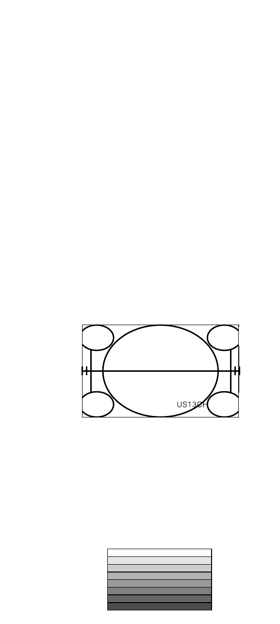
6-6. Brightness Adjusment of Main/Sub screen
Operate this adjustment when the brightness of Main/Sub
screen is different.
(1) Receive RF 06Ch. to Main/Sub screen in twin picture.
(2) Let the screen clearly.
(3) Check the “US06CH” with naked eyes in 06Ch. pattern
and if there is difference, adjust like this.
- The field and the letters are distinguished.
(4) Adjusting Main screen
1) Press the “IN Start” key on R/C for adjustment to select
VPC3230_Main.
2) Adjust to Luma Contrast of adjustment item with
Channel key. (initial value 32)
(5) Adjusting Sub screen
1) Press the “IN Start” key on R/C for adjustment to select
2. VPC3230_Sub.
2) Adjust to Lima Contrast of adjustment item with +/- key.
(initial value 32)
6-7. Lamp Replace
Use it when the Lamp time is ‘0’.
At the same time press the ‘OK’ key and ‘Mute’ key during 5
seconds.
Displaying the OSD as <Fig.8> , press the Volume +(G)
Displaying the OSD as <Fig.9>, press the ‘OK’ key to reset
the lamp use time.
Press the IN-START key on R/C for adjustment to select
Lamp replace and adjust with volume key.
- 19 -
<Fig9. Reset Confirm>
<Fig8. Lamp Use Time Reset Menu>
- 20 -
RGB_PC
RGB_DTV
COMP1
COMP2
R/G/B
TV_S(V)
AV1(V)
AV2(V,Y,C)
MNT_OUT(V)
VPC3230_S
(IC102)
CXA2151 YCbCr(HD)
M_V,Y,C
S_V/Y,C
SDA5550
VPC3230_M
(IC104)
TXT_R,G,B
TXT_Y, Cb,Cr
ReaeyII
D_Y,Cb,Cr
D_Y,Cb,Cr
CH_A
CH-B
DTV_HS/VS LPF_CTL2
* H : 30MHz, L: 6MHz
AV3(V,Y,C))
Tuner(Main)
Tuner(Sub)
CXA2119
TXT_FB
SC-R,G,B
SC-R,G,B
Component Board
Tuner/AV
Digital Board
Main Board
CX2069
Switching
LPF AD9883A
(ADC)
16
33
3
3
5
1. Video Input Path
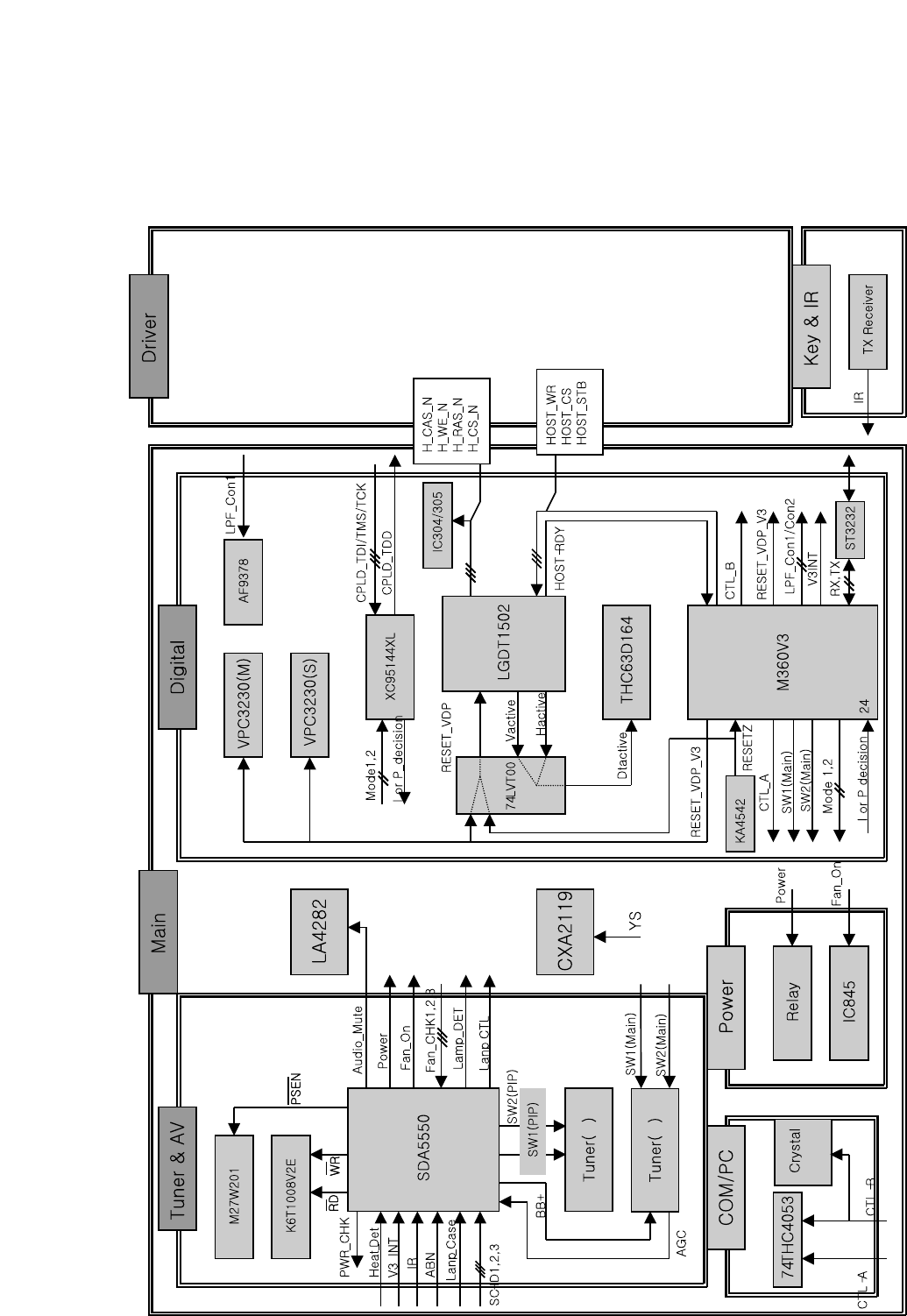
BLOCK DIAGRAM
- 21 -
ADC9883
VPC3230_S
(IC102)
CXA2151
SDA5550
VPC3230_M
(IC104)
ReaeyII
CH_A
CH-B
RGB_HS/VS(DTV)
Component Board
Tuner/AV
Digital Board
Main Board
74HC4053
CTL -A
RGB_HS/VS(PC)
Comp/RGB-DTV
HS/VS
S-V
Comp_Y
XC95144XL
(CPLD)
AV -HS
S-V/Y
TXT-HS/VS
HS/VS_VDP_S
M-V
M-Y
HS/VS_VDP_M
HS/VS_ADC
FID_VDP_S
FID_VDP_M
* H:Comp/RGB-DTV
L: RGB-PC
74VHC123
AV -VS V_sync
R,C LPF
2. Syns I/O Path
- 22 -
2003.04.30
CXA2069
Tuner(M)
Tuner & AV
MAIN
MSP3411G LA4282
SIF
L/R1
L/R3
L/R2
L/R-TV
L/R-COM2
L/R-COM1
L/R-PC
Main -L/R
L/R-out
Main-R/Lout
L/R-Var
Component
CTR(Center)-IN
KA4558D
Audio Mute
3. Audio Input Path
- 23 -
SDA5550
M360V3
M37272
L/S
IIC0-3.3 IIC0-5
IIC1-5
IIC2-5
24LC256
IIC0-3.3
THC63D164
LGDT1502
VPC3230(S)
VPC3230(M)
AD9883A
IIC2 -5
IIC2-5
IIC3-3.3
IIC1-3.3
Tuner(ÁÖ)
Tuner(ºÎ )
MSP3411G
CXA2069
CXA2151 IIC0-5
IIC0-5
L3E07050
ATC24C256
M62352
SCLK
SDATA
ATC24C16
IIC0 : General Control
(Signal & Control)
IIC1 : Communication
Btwn V3 and SDA550
IIC2 :Communication
Btwn V3 and M37272
IIC3 : Key Board & LED
Control
IICX: Driver Control &
Driving Bias Generator
& Line Á¶Á¤¿ë
( SCLK/SDATA)
PURPOSE OF IIC
M62320 M62320
L/S
IIC3-3.3 IIC3-5
IIC3-5
Voltage Level
In IICn-M,
2.5 ; 2.5V 5; 5V
3.3 ; 3.3V
What is M
L/S IIC1-5IIC1-3.3
Tuner & AV
COM/PC
Main Digital Driver
Key & IR
4. Control Signal Connection Diagram- IIC
- 24 -
5. General Control Signal
- 25 -
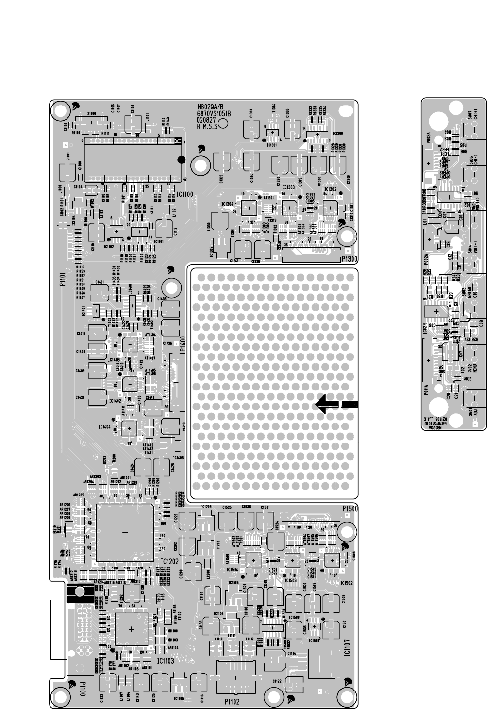
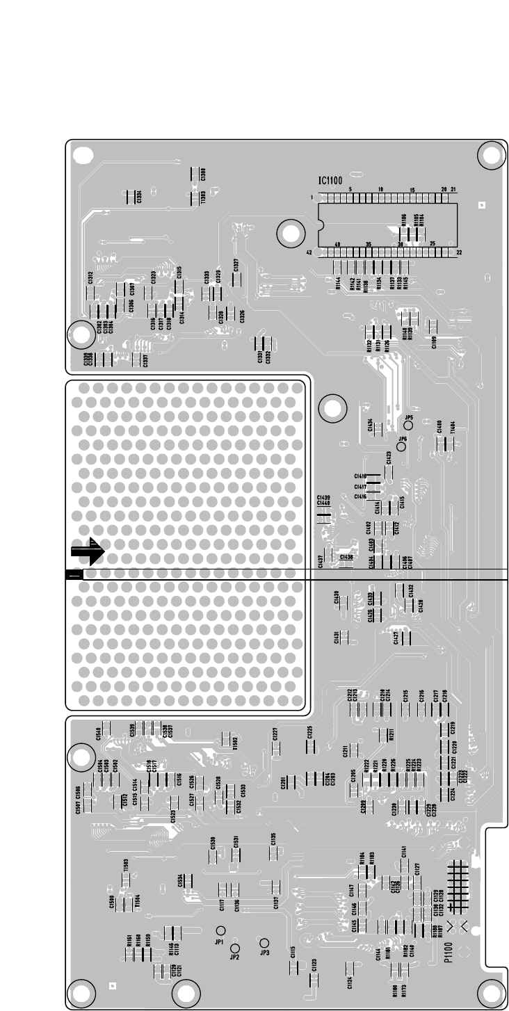
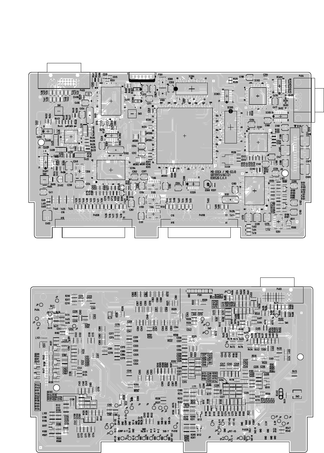
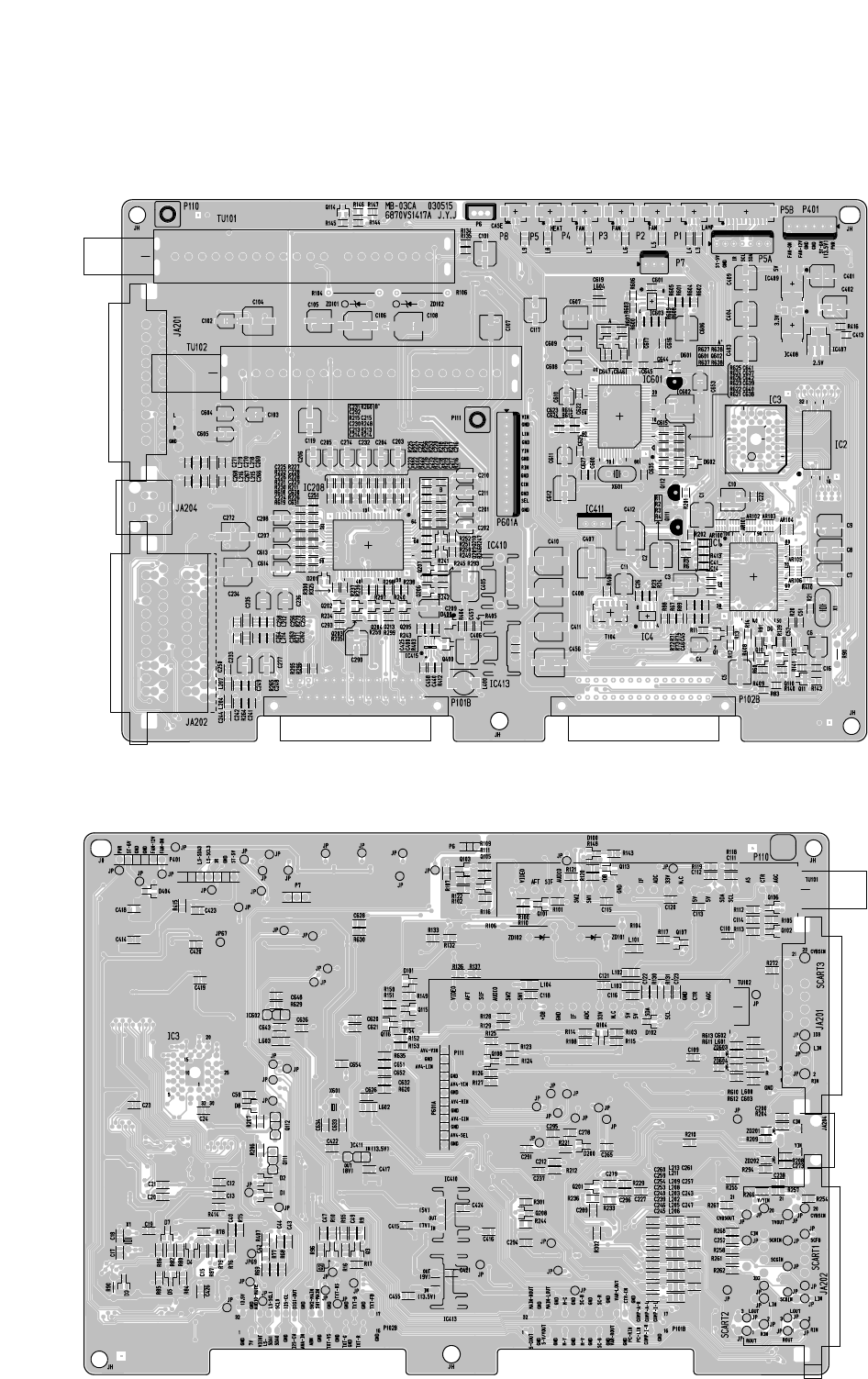
PRINTED CIRCUIT BOARD
MAIN (TOP)
- 26 -
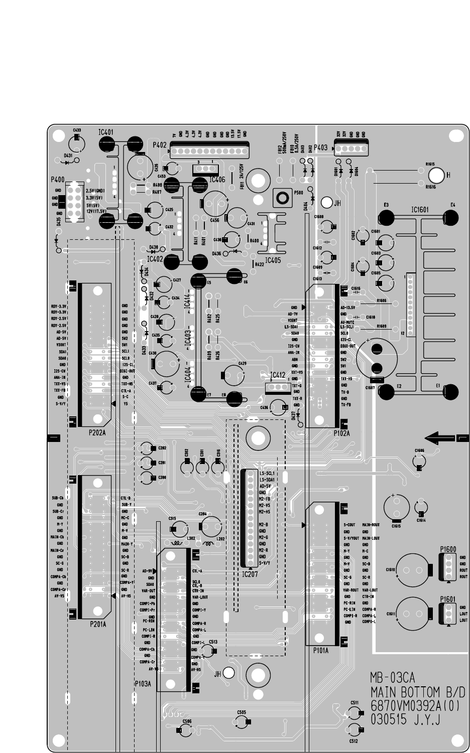
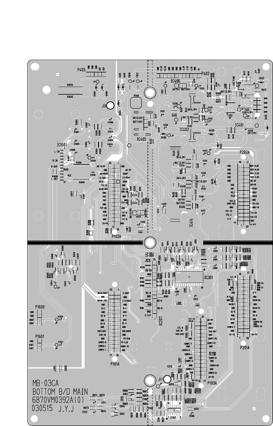
MAIN (BOTTOM)
- 27 -
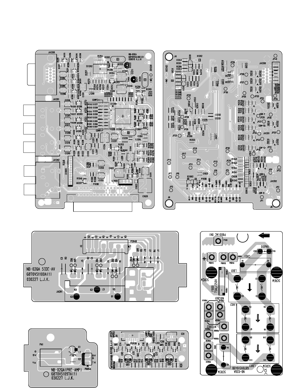
COMPONENT (TOP) COMPONENT (BOTTOM)
SIDE A/V
PRE-AMP LED
AC INPUT
- 28 -
LCD DRIVER (TOP) CONTROL
- 29 -
LCD DRIVER (BOTTOM)
- 30 -
DIGITAL (BOTTOM)
DIGITAL (BOTTOM)
- 31 -
TUNER (TOP)
TUNER (BOTTOM)
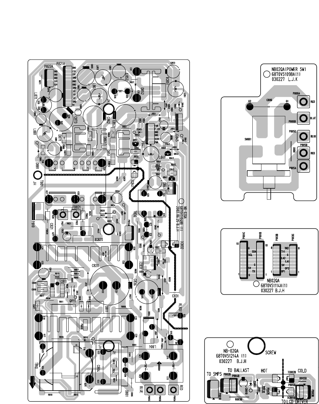
- 32 -
SMPS POWER S/W
INTERFACE
BALLAST

MEMO
- 33 -
- 34 -
EXPLODED VIEW
430
690
410
420
120
121
300
310
640
650
630
303
590
307
304
302
305
301
306
123
308
620
670
621
610
611
600
612
124
125
520
550
560
503
502
530
122
174
540
501
680 570
580
401
660

- 35 -
EXPLODED VIEW PARTS LIST
120 120-D38E SPEAKER, MID-RANGE LG FOSTER 8 OHM 15/25W 87DB 12
121 6400VG0001B SPEAKER, TWEETER NO FOSTER 8 OHM 20W/30W XX D77
122 3110V00123A CASE, SPEAKER BOX LEFT
123 3550V00159A COVER, SPEAKER BOX LEFT
124 3110V00124A CASE, SPEAKER BOX RIGHT
125 3550V00160A COVER SPEAKER BOX RIGHT
174 174-222Y POWER CORD ASSEMBLY, NON NON SAA L=450MM 219A BLACK NON
300 3091V00B46B CABINET ASSEMBL, RT-52SZ30RP STEREO MB03CA
301 4980V00591A SUPPORTER, SCREEN SBHG, BOTTOM
302 4980V00592B SUPPORTER, SCREEN SECC RN-52SZ30H
303 3211V00080A FRAME ASSEMBLY, FRONT RN-52SZ10H 3210V00104
304 3211V00081H FRAME ASSEMBLY, ASSY RT-52SZ30RP .
305 3350V00019B SCREEN, TOPPAN NON RN-52SZ30H 1178*670 SAME 19A PITCH
306 4811V00035A BRACKET ASSEMBLY, GRILLE. NB02QA
307 4980V00439B SUPPORTER, FRAME ET CENTER FIX RN-52SZ10H
308 3550V00225A COVER, LENS PC+ABS RN-52SZ10H
310 5020V00654C BUTTON, CONTROL RN-52SZ30H ABS, HF-380 7KEY BUTTON
401 3550V00232B COVER, LAMP RN-52SZ30H PC-ABS
410 3809V00A39E BACK COVER ASSEMBLY, RT-52SZ30RP NON UPPER
420 3809V00A41D BACK COVER ASSEMBLY, RT-52SZ30RB NON LOWER
430 5018V00025B MIRROR, ASSY NONE NONE NONE RN-52SZ10H
501 3210V00127A FRAME, RN-52SZ10H CHASSIS DIGITAL
502 3210V00073B FRAME, RU-60SZ10 CHASSIS(SMPS) AB-00EA
503 4811V00021E BRACKET ASSEMBLY, REAR AV RT-52SZ30RP NB03JA
520 6871VMMP50A PWB(PCB) ASSEMBLY,MAIN AUS M/I
530 6871VPMA14A PWB(PCB) ASSEMBLY,POWER SMPS MB-03CA RT-52SZ30RP SMPS M/I
540 6871VSMU54B PWB(PCB) ASSEMBLY,SUB TUNER MB03CA M/I
550 6871VSMU56A PWB(PCB) ASSEMBLY,SUB DIGIT MB03CA M/I
560 6871VSMU55A PWB(PCB) ASSEMBLY,SUB SUB MB03CA AUS COMPONENT M/I
570 6871VPMA15A PWB(PCB) ASSEMBLY,POWER SMPS MB-03CA RT-52SZ30RP AC INPUT M/I
580 6871VSMB13F PWB(PCB) ASSEMBLY,SUB INTER MB03CA BALLAST
590 6871VSN154E PWB(PCB) ASSEMBLY,SUB NB-03JA MAIN POWER SWITCH
600 3141VSNA61B CHASSIS ASSEMBLY SUB NB02QA BRACK OPTICAL
610 3110V00140A CASE ASSY,LAMP RN-60SZ10
611 6912V00006A LAMP, HIGH PRESSURE MECURY UHP100W 1.3 PHILIPS 100V 1A RN60SZ10
612 4930V00230A HOLDER, DUCT BACK FAN PC+ABS RN-52SZ10H
620 5900V09002C FAN,DC G9225L12B2-FL DONGYANG 92MM 12V140MA 2000RPM 99GM MOTOR
621 3300V00156A PLATE DUCT,FAN SECC
622 5900V11001C FAN,DC B1232S12B2 DONGYANG 110MM 12V130MA 1300RPM 212GM BLOWER
630 6871VSN156D PWB(PCB) ASSEMBLY,MAIN SUB NB03JA PRE-AMP RU-52SZ30
640 6871VSMD03E PWB(PCB) ASSEMBLY,SUB CONT NB03JA RN-52SZ30H
650 6871VSN194A PWB(PCB) ASSEMBLY,SUB INTER NB02QA 52 LCD PJTV
660 6871VSN187B PWB(PCB) ASSEMBLY,SUB LED NB-02QA RN-52SZ10H M/I
670 6871VSMV06A PWB(PCB) ASSEMBLY,SUB SUB MB03CA RT-52SZ30RP DRIVER M/I
680 6913V00002A BALLAST, EUC-100L/100V PHILIPS FOR LAMP(UHP100W)
690 6871VSN155B PWB(PCB) ASSEMBLY, SUB NB-02QA SIDE A/V
No. Part No. Description

- 36 -
REPLACEMENT PARTS LIST
LOCA. NO PART NO DESCRIPTION
IC304
IC305
IC306
IC320
IC4
IC401
IC401
IC402
IC403
IC403
IC404
IC404
IC405
IC406
IC407
IC407
IC408
IC409
IC410
IC411
IC412
IC413
IC414
IC415
IC5
IC601
IC602
IC603
IC801B
IC802B
IC811
IC820
IC831
IC832
IC841
IC845
IC851
Q111
Q112
T110
D01
D02
D03
D1
D100
D101
D102
D1200
D1602
D1603
D1605
0IMMRHY033A
0IMMRHY033A
0IIC271600A
0IPH741400E
0IMCRAL006A
0ICTMMI038B
0ISH052100C
0IFA752700A
0IMCRSG010A
0ISH302122A
0IMCRTI019A
0ISH052100C
0IMP242560A
0IKE780500Q
0IPRPFA007A
0IPH741400E
0IMCRKE008A
0IMCRFA015A
0ISH052100C
0IKE780800J
0IKE780900M
0IKE780900M
0ISH302122A
0ITK118100B
0IMX811000A
0IMCRMN001C
0IFA753307A
0ISS455880A
0ISH817300B
0ISH817300B
0IMCRON002A
0ISK666813A
0ISK615311B
0ISH817300B
0ISH817300B
0ISS781200H
0IMO257633A
0IFA270000A
0IFA270000A
0IZZVF0022B
0DL200000CA
0DL200000CA
0DL200000CA
0DD184009AA
0DD184009AA
0DD184009AA
0DD184009AA
0DD184009AA
0DD184009AA
0DD184009AA
0DD184009AA
IC, HY57V643220C(L)T-6 HYNIX 86P TSOP
IC, HY57V643220C(L)T-6 HYNIX 86P TSOP
IC, MK2716STR 8P,SOP TP
IC, 74HC14D 14SOP TP SHITTER TRIGGER
IC, AT24C16AN-10SI-2.7 ATMEL 8P SOIC R/TP
IC, COPY M306V3FGFP MITSUBISHI 100P QFP
IC, PQ05RD21 4SIP ST REGULATOR
IC, KA75270Z 3 TP RE-SET IC MC-007
IC, ST3232CDR SOP16 R/TP RS232 DRIVER/RECEIVER
IC, PQ30RV21 TO-220
IC, TFP410 TEXAS INSTRUMENT 64P TQFP
IC, PQ05RD21 4SIP ST REGULATOR
IC, 24LC256-I/SM 8P,SOP TP 256K IIC
IC, KIA7805API 3P TO-220 ST
IC, RC1117S25T FAIRCHILD SOT-223
IC, 74HC14D 14SOP TP SHITTER TRIGGER
IC, KIA78D33F KEC 3P DPAK R/TP 3.3V
IC, KA7805R FAIRCHILD 2P D-PAK R/TP 500MA
IC, PQ05RD21 4SIP ST REGULATOR
IC, KIA7808API 3 ST REGULATOR
IC, KIA7809API TO220 ST 3P 9V REGULATOR
IC, KIA7809API TO220 ST 3P 9V REGULATOR
IC, PQ30RV21 TO-220
IC, TK11840L 8P SOT23L R/TP
IC, MAX811REUT-T 128QFP BK RESET DI-32Q82
IC, MSP3411G QA B8 V3 MICRONAS 80P QFP
IC, KA75330ZTA(KA7533ZTA) 3P,TO-92 TP 3.3V
IC, KA4558D 8SOP OP AMP
IC, PC817XF3 4D PHOTO COUPLER
IC, PC817XF3 4D PHOTO COUPLER
IC, MC33262P ON SEMI 8P DIP ST
IC, STR-F6668B(LF1352) 5PIN BK STR FD-60X3R
IC, STR-G6153T(LF1101) 5PIN BK STR HN-61A40R
IC, PC817XF3 4D PHOTO COUPLER
IC, PC817XF3 4D PHOTO COUPLER
IC, KA78R12 4P,TO-220F BK LOW DROP 12V
IC, LM2576TV-3.3 5PIN ST REGULATOR HN-61A40R
IC, 2N7000TA TO-92, 3P TP LEVEL SHIFT 60V/0.2A
IC, 2N7000TA TO-92, 3P TP LEVEL SHIFT 60V/0.2A
IC, AMF730F6M00X2(AF-9397) 15P SIP ST
LED SAM5670(DL-2LRG) BK Y-GREEN
LED SAM5670(DL-2LRG) BK Y-GREEN
LED SAM5670(DL-2LRG) BK Y-GREEN
DIODE,SWITCHING KDS184S 85V 300MA KEC TP
DIODE,SWITCHING KDS184S 85V 300MA KEC TP
DIODE,SWITCHING KDS184S 85V 300MA KEC TP
DIODE,SWITCHING KDS184S 85V 300MA KEC TP
DIODE,SWITCHING KDS184S 85V 300MA KEC TP
DIODE,SWITCHING KDS184S 85V 300MA KEC TP
DIODE,SWITCHING KDS184S 85V 300MA KEC TP
DIODE,SWITCHING KDS184S 85V 300MA KEC TP
LOCA. NO PART NO DESCRIPTION
IC01
IC02
IC1
IC101
IC102
IC103
IC104
IC105
IC1100
IC1100
IC1101
IC1102
IC1103
IC1104
IC1105
IC1106
IC1107
IC120
IC1200
IC1200
IC1202
IC1202
IC1203
IC1300
IC1301
IC1302
IC1303
IC1304
IC1305
IC1400
IC1401
IC1402
IC1403
IC1404
IC1405
IC1500
IC1501
IC1502
IC1503
IC1504
IC1505
IC1601
IC1602
IC2
IC208
IC3
IC301
IC301
IC302
IC302
IC303
0IMI623200B
0IMI623200B
0ISM555000A
0IMCRAD002A
0IIT323000E
0IMCRXL003A
0IIT323000E
0IFA741230A
0IZZVA0072A
0IMI372728A
0IMI623520B
0IAL242561B
0IPRPTI001A
0IKE704200J
0IPRPFA006A
0IPRPFA006A
0IPRPML001B
0ISJ111733A
0IMCRSO008A
0IPRPML001A
0IMCRSB010A
0IMO744053B
0IPRPFA006A
0IMO324000C
0IMCRET001A
0IMCRSB009A
0IMCRSB009A
0IMCRSB008A
0IPRPFA006A
0IMO324000C
0IMCRET001A
0IMCRSB009A
0IMCRSB009A
0IMCRSB008A
0IPRPFA006A
0IMO324000C
0IMCRET001A
0IMCRSB009A
0IMCRSB009A
0IMCRSB008A
0IPRPFA006A
0ISA428200A
0IKE780500Q
0ISS610082A
0ISO206900A
6620VF3201A
0ICTMLG003C
0ISO211900A
0INA562300A
0ITI740000Q
0ITI740000Q
IC, M62320FP,I/O EXPANDER 16P
IC, M62320FP,I/O EXPANDER 16P
IC, SDA5550 MQFP100 BK MICOM TXT MC006A
IC, AD9883A ANALOG DEVICE 80P TQFP R/TP
IC, VPC3230D C5 80P QFP
IC, XC95144XL-10TQ100C 3.3V XILINX TQFP 100P
IC, VPC3230D C5 80P QFP
IC, DM74LS123MX 16SOP TP DUAL RETRIG.
IC, M37272E8A 42 DIP DRIVER 52
IC, M37272E8A(OTP) 42SD BK M-COM
IC, M62352GP 20P SSOP TP 8BITS 12CH D/A
IC, AT24C256W-10SI-2.7V 8P 2.7V-5V
IC, TFP401PZP TEXAS INSTRUMENT 100,TQFP
IC, KIA7042AF SOT-89 TP 4.2V
IC, RC1117S33T FAIRCHILD SOT-223
IC, RC1117S33T FAIRCHILD SOT-223
IC, MIC29152 MICREL 5P TO-263
IC, EZ1117CST-3.3 3P,SOT-223 TP 3.3V
IC, CXA2151Q SONY 48P QFP TRAY 60LCD
IC, MIC39100 MICREL 3P SOT223
IC, L3E07050K0A SEIKO EPSON 176QFP
IC, MC74HC4053DW 16SOP 3*2CH.MUX
IC, RC1117S33T FAIRCHILD SOT-223 R/TP
IC, LM324D SO-14 TP OP AMP
IC, EL2244CS ELANTEC 8P SO
IC, L3E06070D0A SEIKO EPSON 48QFP
IC, L3E06070D0A SEIKO EPSON 48QFP
IC, L3E01031F0A SEIKO EPSON 48QFP
IC, RC1117S33T FAIRCHILD SOT-223
IC, LM324D SO-14 TP OP AMP
IC, EL2244CS ELANTEC 8P SO
IC, L3E06070D0A SEIKO EPSON 48QFP
IC, L3E06070D0A SEIKO EPSON 48QFP
IC, L3E01031F0A SEIKO EPSON 48QFP
IC, RC1117S33T FAIRCHILD SOT-223
IC, LM324D SO-14 TP OP AMP
IC, EL2244CS ELANTEC 8P SO
IC, L3E06070D0A SEIKO EPSON 48QFP
IC, L3E06070D0A SEIKO EPSON 48QFP
IC, L3E01031F0A SEIKO EPSON 48QFP
IC, RC1117S33T FAIRCHILD SOT-223
IC, LA4282 12S 2CHX10W AUDIO AMP
IC, KIA7805API 3P TO-220
IC, K6T1008V2E-TB(F)70 [K6T1008BLT-7L]
IC, CXA2069Q QFP64 BK I2C BUS AV S/W
IC, 822473-3 AMP 32PIN 2.54MM NIKEL PLCC
IC, LGDT1502M LG IC 304P QFP
IC, CXA2119M 28P,SOP TP VIDEO SWITCHING
IC, CLC5623IMX 14P,SOP TP AMP
IC, SN74LVC00AD 14SOP R/TP LOGIC D-TV
IC, SN74LVC00AD 14SOP R/TP LOGIC D-TV
IC
DIODE

- 37 -
LOCA. NO PART NO DESCRIPTION
D2
D200
D201
D3
D300
D4
D400
D402
D402
D403
D403
D404
D404
D404
D405
D406
D410
D411
D431
D432
D433
D434
D435
D437
D5
D500
D501
D6
D601
D602
D7
D8
D801
D810
D820
D821
D822
D832
D833
D834
D841
D845
D851
D852
D861
D871
D881
Q810
ZD01
ZD1
ZD10
ZD11
0DD184009AA
0DD184009AA
0DD184009AA
0DD226239AA
0DL112100AA
0DD184009AA
0DD184009AA
0DR050008AA
0DD414809ED
0DR050008AA
0DD414809ED
0DR050008AA
0DD414809ED
0DD184009AA
0DR050008AA
0DD184009AA
0DRSE00038A
0DRSE00038A
0DD414809ED
0DD414809ED
0DD414809ED
0DD414809ED
0DD414809ED
0DD414809ED
0DD184009AA
0DD184009AA
0DD184009AA
0DD184009AA
0DD226239AA
0DD184009AA
0DD184009AA
0DD184009AA
0DD606000AA
0DD100009AM
0DD100009AM
0DD100009AM
0DD100009AM
0DR010009AA
0DD100009AM
0DD260000BB
0DD120000BB
0DD414809ED
0DD120000BB
0DR460009AA
0DD120000BB
0DD120000BB
0DD100009AP
0DR260001AA
0DR050008AA
0DZ620009BB
0DZ620009BB
0DR050008AA
DIODE,SWITCHING KDS184S 85V 300MA KEC TP
DIODE,SWITCHING KDS184S 85V 300MA KEC TP
DIODE,SWITCHING KDS184S 85V 300MA KEC TP
DIODE,SWITCHING CHIP KDS226 SOT-23
LED SR3411(DL-11S2RN1) BK RED
DIODE,SWITCHING KDS184S 85V 300MA KEC TP
DIODE,SWITCHING KDS184S 85V 300MA KEC TP
DIODE,RECTIFIERS SD05.SOD323 5V 5A 15A
DIODE,SWITCHING 1N4148 TP GRANDE
DIODE,RECTIFIERS SD05.SOD323 5V 5A 15A
DIODE,SWITCHING 1N4148 TP GRANDE
DIODE,RECTIFIERS SD05.SOD323 5V 5A 15A
DIODE,SWITCHING 1N4148 TP GRANDE
DIODE,SWITCHING KDS184S 85V 300MA KEC TP
DIODE,RECTIFIERS SD05. SOD323 5V 5A 15A
DIODE,SWITCHING KDS184S 85V 300MA KEC TP
DIODE,RECTIFIERS SDC15 SOT23 12.8V 10A
DIODE,RECTIFIERS SDC15 SOT23 12.8V 10A
DIODE,SWITCHING 1N4148 TP GRANDE
DIODE,SWITCHING 1N4148 TP GRANDE
DIODE,SWITCHING 1N4148 TP GRANDE
DIODE,SWITCHING 1N4148 TP GRANDE
DIODE,SWITCHING 1N4148 TP GRANDE
DIODE,SWITCHING 1N4148 TP GRANDE
DIODE,SWITCHING KDS184S 85V 300MA KEC TP
DIODE,SWITCHING KDS184S 85V 300MA KEC TP
DIODE,SWITCHING KDS184S 85V 300MA KEC TP
DIODE,SWITCHING KDS184S 85V 300MA KEC TP
DIODE,SWITCHING CHIP KDS226 SOT-23
DIODE,SWITCHING KDS184S 85V 300MA KEC TP
DIODE,SWITCHING KDS184S 85V 300MA KEC TP
DIODE,SWITCHING KDS184S 85V 300MA KEC TP
DIODE,RECTIFIERS BK NA 600V 6A 150A NA 10UA
DIODE,RECTIFIERS EU1ZV(1) TP SANKEN
DIODE,RECTIFIERS EU1ZV(1) TP SANKEN
DIODE,RECTIFIERS EU1ZV(1) TP SANKEN
DIODE,RECTIFIERS EU1ZV(1) TP SANKEN
DIODE,RECTIFIERS 1000V 0.5A 10A 100NSEC 50UA
DIODE,RECTIFIERS EU1ZV(1) TP SANKEN
DIODE,RECTIFIERS BRIDGE D2SBA60(STK)
DIODE,RECTIFIERS FML-G12S
DIODE,SWITCHING 1N4148 TP GRANDE
DIODE, RECTIFIERS FML-G12S
DIODE, RECTIFIERS RK46 DO-214AC 60V 3.5A
DIODE, RECTIFIERS FML-G12S
DIODE, RECTIFIERS FML-G12S
DIODE, RECTIFIERS EG1ZV(1) TP SANKEN TP
DIODE, RECTIFIERS TO220 600V 6A 50A
DIODE, RECTIFIERS SD05. SOD323 5V 5A 15A
DIODE, TP ROHM-K DO34 0.5W 6.2V 5UA
DIODE, TP ROHM-K DO34 0.5W 6.2V 5UA
DIODE,RECTIFIERS SOD323 5V 5A 15A
LOCA. NO PART NO DESCRIPTION
ZD12
ZD2
ZD3
ZD4
ZD5
ZD6
ZD841
ZD851
ZD9
IC202
IC203
Q01
Q02
Q03
Q04
Q05
Q06
Q10
Q101
Q102
Q102
Q103
Q103
Q106
Q106
Q107
Q108
Q108
Q109
Q110
Q110
Q111
Q112
Q113
Q113
Q114
Q114
Q115
Q115
Q116
Q116
Q1200
Q1201
Q1202
Q1203
Q1204
Q1205
Q1206
Q1207
Q1208
0DR050008AA
0DZ620009BB
0DZ620009BB
0DZ620009BB
0DZ620009BB
0DZ620009BB
0DZ620009BB
0DZ620009BB
0DZ620009BB
0TR830009BA
0TR830009BA
0TR387500AA
0TR387500AA
0TR387500AA
0TR387500AA
0TR387500AA
0TR387500AA
0TR387500AA
0TR387500AA
0TR387500AA
0TR387500AA
0TR387500AA
0TR387500AA
0TR387500AA
0TR150400BA
0TR387500AA
0TR387500AA
0TR387500AA
0TR387500AA
0TR387500AA
0TR387500AA
0TR387500AA
0TR387500AA
0TR387500AA
0TR387500AA
0TR387500AA
0TR387500AA
0TR387500AA
0TR830009BA
0TR387500AA
0TR830009BA
0TR387500AA
0TR387500AA
0TR387500AA
0TR387500AA
0TR387500AA
0TR387500AA
0TR387500AA
0TR387500AA
0TR387500AA
DIODE, RECTIFIERS SOD323 5V 5A 15A
DIODE, 2B TP ROHM-K DO34 0.5W 6.2V 5UA
DIODE, TP ROHM-K DO34 0.5W 6.2V 5UA
DIODE, TP ROHM-K DO34 0.5W 6.2V 5UA
DIODE, TP ROHM-K DO34 0.5W 6.2V 5UA
DIODE, TP ROHM-K DO34 0.5W 6.2V 5UA
DIODE, TP ROHM-K DO34 0.5W 6.2V 5UA
DIODE,.TP ROHM-K DO34 0.5W 6.2V 5UA
DIODE, TP ROHM-K DO34 0.5W 6.2V 5UA
TR, BSS83 TP PHILIPS NON N-CHANNEL S/W
TR, BSS83 TP PHILIPS NON N-CHANNEL S/W
TR, CHIP 2SC3875S(ALY) KEC
TR, CHIP 2SC3875S(ALY) KEC
TR, CHIP 2SC3875S(ALY) KEC
TR, CHIP 2SC3875S(ALY) KEC
TR, CHIP 2SC3875S(ALY) KEC
TR, CHIP 2SC3875S(ALY) KEC
TR, CHIP 2SC3875S(ALY) KEC
TR, CHIP 2SC3875S(ALY) KEC
TR, CHIP 2SC3875S(ALY) KEC
TR, CHIP 2SC3875S(ALY) KEC
TR, CHIP 2SC3875S(ALY) KEC
TR, CHIP 2SC3875S(ALY) KEC
TR, CHIP 2SC3875S(ALY) KEC
TR, CHIP 2SA1504S(ASY) KEC
TR, CHIP 2SC3875S(ALY) KEC
TR, CHIP 2SC3875S(ALY) KEC
TR, CHIP 2SC3875S(ALY) KEC
TR, CHIP 2SC3875S(ALY) KEC
TR, CHIP 2SC3875S(ALY) KEC
TR, CHIP 2SC3875S(ALY) KEC
TR, CHIP 2SC3875S(ALY) KEC
TR, CHIP 2SC3875S(ALY) KEC
TR, CHIP 2SC3875S(ALY) KEC
TR, CHIP 2SC3875S(ALY) KEC
TR, CHIP 2SC3875S(ALY) KEC
TR, CHIP 2SC3875S(ALY) KEC
TR, CHIP 2SC3875S(ALY) KEC
TR, BSS83 TP PHILIPS NON N-CHANNEL S/W
TR, CHIP 2SC3875S(ALY) KEC
TR, BSS83 TP PHILIPS NON N-CHANNEL S/W
TR, CHIP 2SC3875S(ALY) KEC
TR, CHIP 2SC3875S(ALY) KEC
TR, CHIP 2SC3875S(ALY) KEC
TR, CHIP 2SC3875S(ALY) KEC
TR, CHIP 2SC3875S(ALY) KEC
TR, CHIP 2SC3875S(ALY) KEC
TR, CHIP 2SC3875S(ALY) KEC
TR, CHIP 2SC3875S(ALY) KEC
TR, CHIP 2SC3875S(ALY) KEC
TRANSISTOR
- 38 -
For Capacitor & Resistors,
the charactors at 2nd and 3rd
digit in the P/No. means as
follows;
CC, CX, CK, CN : Ceramic
CQ : Polyestor
CE : Electrolytic
RD : Carbon Film
RS : Metal Oxide Film
RN : Metal Film
RF : Fusible
CAPACITOR
LOCA. NO PART NO DESCRIPTION
Q1209
Q1210
Q1211
Q1212
Q1213
Q1214
Q1215
Q1216
Q1216
Q1217
Q1218
Q1219
Q1221
Q1222
Q1223
Q1230
Q1232
Q1235
Q1236
Q1601
Q2
Q201
Q202
Q203
Q204
Q205
Q206
Q207
Q208
Q209
Q210
Q213
Q3
Q301
Q302
Q304
Q350
Q351
Q400
Q501
Q510
Q511
Q601
Q602
Q810
Q841
Q842
Q851
C01
C07
0TR150400BA
0TR102009AG
0TR127009AA
0TR387500AA
0TR387500AA
0TR387500AA
0TR150400BA
0TR387500AA
0TR150400BA
0TR150400BA
0TR150400BA
0TR150400BA
0TR102009AG
0TR127009AA
0TR387500AA
0TR387500AA
0TR102009AG
0TR150400BA
0TR150400BA
0TR150400BA
0TR150400BA
0TR150400BA
0TR150400BA
0TR150400BA
0TR150400BA
0TR150400BA
0TR150400BA
0TR150400BA
0TR150400BA
0TR150400BA
0TR150400BA
0TR150400BA
0TR387500AA
0TR150400BA
0TR150400BA
0TR150400BA
0TR150400BA
0TR387500AA
0TRKE80038A
0TR102009AG
0TR387500AA
0TR387500AA
0TR150400BA
0TR150400BA
0TF283700AA
0TR945009AA
0TR322709AA
0TR945009AA
0CE226VF6DC
0CE476VF6DC
TR, CHIP 2SA1504S(ASY) KEC
TR, CHIP KRC102S KEC TP SOT-23 NA NA
TR, KEC TP TO92 50V 100MA
TR, CHIP 2SC3875S(ALY) KEC
TR, CHIP 2SC3875S(ALY) KEC
TR, CHIP 2SC3875S(ALY) KEC
TR, CHIP 2SA1504S(ASY) KEC
TR, CHIP 2SC3875S(ALY) KEC
TR, CHIP 2SA1504S(ASY) KEC
TR, CHIP 2SA1504S(ASY) KEC
TR, CHIP 2SA1504S(ASY) KEC
TR, CHIP 2SA1504S(ASY) KEC
TR, CHIP KRC102S KEC TP SOT-23 NA NA
TR, KTA1270-Y(KTA562TM) TP TO92 50V 100MA
TR, CHIP 2SC3875S(ALY) KEC
TR, CHIP 2SC3875S(ALY) KEC
TR, CHIP KRC102S KEC TP SOT-23 NA NA
TR, CHIP 2SA1504S(ASY) KEC
TR, CHIP 2SA1504S(ASY) KEC
TR, CHIP 2SA1504S(ASY) KEC
TR, CHIP 2SA1504S(ASY) KEC
TR, CHIP 2SA1504S(ASY) KEC
TR, CHIP 2SA1504S(ASY) KEC
TR, CHIP 2SA1504S(ASY) KEC
TR, CHIP 2SA1504S(ASY) KEC
TR, CHIP 2SA1504S(ASY) KEC
TR, CHIP 2SA1504S(ASY) KEC
TR, CHIP 2SA1504S(ASY) KEC
TR, CHIP 2SA1504S(ASY) KEC
TR, CHIP 2SA1504S(ASY) KEC
TR, CHIP 2SA1504S(ASY) KEC
TR, CHIP 2SA1504S(ASY) KEC
TR, CHIP 2SC3875S(ALY) KEC
TR, CHIP 2SA1504S(ASY) KEC
TR, CHIP 2SA1504S(ASY) KEC
TR, CHIP 2SA1504S(ASY) KEC
TR, CHIP 2SA1504S(ASY) KEC
TR, CHIP 2SC3875S(ALY) KEC
TR, KTC3552T-RTK KEC R/TP SOT-23F 50V 3A
TR, CHIP KRC102S KEC TP SOT-23 NA NA
TR, CHIP 2SC3875S(ALY) KEC
TR, CHIP 2SC3875S(ALY) KEC
TR, CHIP 2SA1504S(ASY) KEC
TR, CHIP 2SA1504S(ASY) KEC
TR, 2SK2837 BK TOSHIBA 500V 20A TO3P
TR, KSC945C-Y SAMSUNG TP TO92 50V 150MA
TR, KTC3227-Y,TP(KTC1627A),KEC
TR, KSC945C-Y SAMSUNG TP TO92 50V 150MA
22UF MV 16V 20% R/TP(SMD) SMD
47UF MV 16V 20% R/TP(SMD) SMD
LOCA. NO PART NO DESCRIPTION
C1
C1
C10
C101
C104
C105
C106
C107
C108
C11
C1100
C1101
C1102
C1103
C1104
C1105
C1106
C1107
C1108
C1110
C1111
C1112
C1114
C1116
C1118
C1122
C1125
C1133
C1134
C1138
C1139
C114
C1143
C119
C120
C1200
C1201
C1201
C1202
C1204
C1205
C1206
C1207
C1208
C1209
C1210
C1216
C1217
C1218
C1219
C1226
C1234
0CE476DF618
0CE476VF6DC
0CE476VF6DC
0CE476VF6DC
0CE226SF6DC
0CE476VF6DC
0CE476VK6DC
0CE476VF6DC
0CE476VK6DC
0CE226VF6DC
0CK103CK56A
0CE476VH6DC
0CK103CK56A
0CK103CK56A
0CE105VK6DC
0CC180CKH1A
0CC180CKH1A
0CK103CK56A
0CE476VH6DC
0CE476VH6DC
0CK103CK56A
0CE476VH6DC
0CE107VH6DC
0CE107SF6DC
0CE107SF6DC
0CE476VH6DC
0CE476VH6DC
0CE476VH6DC
0CE476VH6DC
0CE476VH6DC
0CE476VH6DC
0CK105DF64A
0CE476VH6DC
0CE476VF6DC
0CE106SF6DC
0CE476VH6DC
0CE226VF6DC
0CE106VF6DC
0CE107SF6DC
0CE106VF6DC
0CE106VF6DC
0CE106VF6DC
0CE106VF6DC
0CE106VF6DC
0CE106VF6DC
0CE106VF6DC
0CE106VF6DC
0CE106VF6DC
0CE106VF6DC
0CE226VF6DC
0CE476VH6DC
0CE476VF6DC
47UF STD 16V M FL TP5
47UF MV 16V 20% R/TP(SMD) SMD
47UF MV 16V 20% R/TP(SMD) SMD
47UF MV 16V 20% R/TP(SMD) SMD
22UF MVG 16V M SMD R/TP
47UF MV 16V 20% R/TP(SMD) SMD
47UF MV 50V 20% R/TP(SMD) SMD
47UF MV 16V 20% R/TP(SMD) SMD
47UF MV 50V 20% R/TP(SMD) SMD
22UF MV 16V 20% R/TP(SMD) SMD
0.01UF 1608 50V 10% R/TP X7R
47UF MV 25V 20% R/TP(SMD) SMD
0.01UF 1608 50V 10% R/TP X7R
0.01UF 1608 50V 10% R/TP X7R
1UF MV 50V 20% R/TP(SMD) SMD
18PF 1608 50V 2% R/TP NP0
18PF 1608 50V 2% R/TP NP0
0.01UF 1608 50V 10% R/TP X7R
47UF MV 25V 20% R/TP(SMD) SMD
47UF MV 25V 20% R/TP(SMD) SMD
0.01UF 1608 50V 10% R/TP X7R
47UF MV 25V 20% R/TP(SMD) SMD
100UF MV 25V 20% R/TP(SMD) SMD
100UF MVG 16V M SMD R/TP
100UF MVG 16V M SMD R/TP
47UF MV 25V 20% R/TP(SMD) SMD
47UF MV 25V 20% R/TP(SMD) SMD
47UF MV 25V 20% R/TP(SMD) SMD
47UF MV 25V 20% R/TP(SMD) SMD
47UF MV 25V 20% R/TP(SMD) SMD
47UF MV 25V 20% R/TP(SMD) SMD
1UF 2012 16V 20% R/TP F(Y5V)
47UF MV 25V 20% R/TP(SMD) SMD
47UF MV 16V 20% R/TP(SMD) SMD
10UF MVG 16V 20% R/TP(SMD) SMD
47UF MV 25V 20% R/TP(SMD) SMD
22UF MV 16V 20% R/TP(SMD) SMD
10UF MV 16V 20% R/TP(SMD) SMD
100UF MVG 16V M SMD R/TP
10UF MV 16V 20% R/TP(SMD) SMD
10UF MV 16V 20% R/TP(SMD) SMD
10UF MV 16V 20% R/TP(SMD) SMD
10UF MV 16V 20% R/TP(SMD) SMD
10UF MV 16V 20% R/TP(SMD) SMD
10UF MV 16V 20% R/TP(SMD) SMD
10UF MV 16V 20% R/TP(SMD) SMD
10UF MV 16V 20% R/TP(SMD) SMD
10UF MV 16V 20% R/TP(SMD) SMD
10UF MV 16V 20% R/TP(SMD) SMD
22UF MV 16V 20% R/TP(SMD) SMD
47UF MV 25V 20% R/TP(SMD) SMD
47UF MV 16V 20% R/TP(SMD) SMD

- 39 -
LOCA. NO PART NO DESCRIPTION
C1237
C124
C1246
C125
C1250
C1251
C1252
C126
C1260
C127
C1301
C1305
C1308
C1309
C1310
C1311
C1313
C1319
C1320
C1321
C1322
C1324
C1325
C1330
C1335
C1336
C1340
C1341
C139
C1401
C1405
C1408
C1409
C1410
C1411
C1413
C1419
C1420
C1421
C1422
C1424
C1425
C1429
C1435
C1436
C1441
C147
C148
C1501
C1505
C1508
C1509
0CE105VK6DC
0CK224DF56A
0CE226VF6DC
0CK224DF56A
0CE105VK6DC
0CE105VK6DC
0CE106VF6DC
0CK224DF56A
0CE106VF6DC
0CK224DF56A
0CE476VH6DC
0CK103CK56A
0CE476VH6DC
0CE476VH6DC
0CK103CK56A
0CK103CK56A
0CK103CK56A
0CE476VH6DC
0CE476VH6DC
0CK103CK56A
0CK103CK56A
0CE476VH6DC
0CE476VH6DC
0CE476VH6DC
0CE476VH6DC
0CE476VH6DC
0CK103CK56A
0CE476VH6DC
0CE476SF6DC
0CE476VH6DC
0CK103CK56A
0CE476VH6DC
0CE476VH6DC
0CK103CK56A
0CK103CK56A
0CK103CK56A
0CE476VH6DC
0CE476VH6DC
0CK103CK56A
0CK103CK56A
0CE476VH6DC
0CE476VH6DC
0CE476VH6DC
0CE476VH6DC
0CE476VH6DC
0CE476VH6DC
0CE226SF6DC
0CE106SF6DC
0CE476VH6DC
0CK103CK56A
0CE476VH6DC
0CE476VH6DC
1UF MV 50V 20% R/TP(SMD) SMD
220000PF 2012 16V 10% R/TP X7R
22UF MV 16V 20% R/TP(SMD) SMD
220000PF 2012 16V 10% R/TP X7R
1UF MV 50V 20% R/TP(SMD) SMD
1UF MV 50V 20% R/TP(SMD) SMD
10UF MV 16V 20% R/TP(SMD) SMD
220000PF 2012 16V 10% R/TP X7R
10UF MV 16V 20% R/TP(SMD) SMD
220000PF 2012 16V 10% R/TP X7R
47UF MV 25V 20% R/TP(SMD) SMD
0.01UF 1608 50V 10% R/TP X7R
47UF MV 25V 20% R/TP(SMD) SMD
47UF MV 25V 20% R/TP(SMD) SMD
0.01UF 1608 50V 10% R/TP X7R
0.01UF 1608 50V 10% R/TP X7R
0.01UF 1608 50V 10% R/TP X7R
47UF MV 25V 20% R/TP(SMD) SMD
47UF MV 25V 20% R/TP(SMD) SMD
0.01UF 1608 50V 10% R/TP X7R
0.01UF 1608 50V 10% R/TP X7R
47UF MV 25V 20% R/TP(SMD) SMD
47UF MV 25V 20% R/TP(SMD) SMD
47UF MV 25V 20% R/TP(SMD) SMD
47UF MV 25V 20% R/TP(SMD) SMD
47UF MV 25V 20% R/TP(SMD) SMD
0.01UF 1608 50V 10% R/TP X7R
47UF MV 25V 20% R/TP(SMD) SMD
47UF MVG 16V M SMD R/TP
47UF MV 25V 20% R/TP(SMD) SMD
0.01UF 1608 50V 10% R/TP X7R
47UF MV 25V 20% R/TP(SMD) SMD
47UF MV 25V 20% R/TP(SMD) SMD
0.01UF 1608 50V 10% R/TP X7R
0.01UF 1608 50V 10% R/TP X7R
0.01UF 1608 50V 10% R/TP X7R
47UF MV 25V 20% R/TP(SMD) SMD
47UF MV 25V 20% R/TP(SMD) SMD
0.01UF 1608 50V 10% R/TP X7R
0.01UF 1608 50V 10% R/TP X7R
47UF MV 25V 20% R/TP(SMD) SMD
47UF MV 25V 20% R/TP(SMD) SMD
47UF MV 25V 20% R/TP(SMD) SMD
47UF MV 25V 20% R/TP(SMD) SMD
47UF MV 25V 20% R/TP(SMD) SMD
47UF MV 25V 20% R/TP(SMD) SMD
22UF MVG 16V M SMD R/TP
10UF MVG 16V 20% R/TP(SMD) SMD
47UF MV 25V 20% R/TP(SMD) SMD
0.01UF 1608 50V 10% R/TP X7R
47UF MV 25V 20% R/TP(SMD) SMD
47UF MV 25V 20% R/TP(SMD) SMD
LOCA. NO PART NO DESCRIPTION
C1510
C1511
C1513
C1519
C1520
C1521
C1522
C1524
C1525
C1529
C1535
C1536
C1541
C158
C159
C1601
C1602
C1603
C1604
C1605
C1606
C1607
C1608
C1609
C1610
C1611
C1612
C1613
C1614
C1615
C1616
C1618
C1620
C1621
C1630
C1631
C168
C172
C173
C175
C183
C185
C186
C187
C187
C188
C190
C191
C192
C193
C194
C195
0CK103CK56A
0CK103CK56A
0CK103CK56A
0CE476VH6DC
0CE476VH6DC
0CK103CK56A
0CK103CK56A
0CE476VH6DC
0CE476VH6DC
0CE476VH6DC
0CE476VH6DC
0CE476VH6DC
0CE476VH6DC
0CK105DF64A
0CK105DF64A
0CE107DH618
0CE106DK618
0CE107DH618
0CE106DK618
0CE107DH618
0CE106DF618
0CE108DK61A
0CE106DF618
0CE106DF618
0CE108DJ618
0CE108DJ618
0CQ6821N509
0CQ6821N509
0CE226DF618
0CE108DF618
0CQ1041N509
0CQ1041N509
0CE477VF6DC
0CE107VF6DC
0CE476VF6DC
0CE476VF6DC
0CE106SF6DC
0CK224DF56A
0CE476SF6DC
0CE476SF6DC
0CE106SF6DC
0CE106SF6DC
0CE106SF6DC
0CE106SF6DC
0CE106TH6DC
0CE106SF6DC
0CE106SF6DC
0CE106SF6DC
0CE106SF6DC
0CE106SF6DC
0CE106SF6DC
0CE106SF6DC
0.01UF 1608 50V 10% R/TP X7R
0.01UF 1608 50V 10% R/TP X7R
0.01UF 1608 50V 10% R/TP X7R
47UF MV 25V 20% R/TP(SMD) SMD
47UF MV 25V 20% R/TP(SMD) SMD
0.01UF 1608 50V 10% R/TP X7R
0.01UF 1608 50V 10% R/TP X7R
47UF MV 25V 20% R/TP(SMD) SMD
47UF MV 25V 20% R/TP(SMD) SMD
47UF MV 25V 20% R/TP(SMD) SMD
47UF MV 25V 20% R/TP(SMD) SMD
47UF MV 25V 20% R/TP(SMD) SMD
47UF MV 25V 20% R/TP(SMD) SMD
1UF 2012 16V 20% R/TP F(Y5V)
1UF 2012 16V 20% R/TP F(Y5V)
100UF STD 25V M FL TP5
10UF STD 50V M FL TP5
100UF STD 25V M FL TP5
10UF STD 50V M FL TP5
100UF STD 25V M FL TP5
10UF STD 16V M FL TP5
1000UF STD 50V M FL TP7.5
10UF STD 16V M FL TP5
10UF STD 16V M FL TP5
1000UF STD 35V M FL TP5
1000UF STD 35V M FL TP5
0.0068U 100V K POLY TP
0.0068U 100V K POLY TP
22UF STD 16V M FL TP5
1000UF STD 16V M FL TP5
0.1U 100V K POLY TP
0.1U 100V K POLY TP
470UF MV 16V 20% R/TP(SMD) SMD
100UF MV 16V 20% R/TP(SMD) SMD
47UF MV 16V 20% R/TP(SMD) SMD
47UF MV 16V 20% R/TP(SMD) SMD
10UF MVG 16V 20% R/TP(SMD) SMD
220000PF 2012 16V 10% R/TP X7R
47UF MVG 16V M SMD R/TP
47UF MVG 16V M SMD R/TP
10UF MVG 16V 20% R/TP(SMD) SMD
10UF MVG 16V 20% R/TP(SMD) SMD
10UF MVG 16V 20% R/TP(SMD) SMD
10UF MVG 16V 20% R/TP(SMD) SMD
10UF MV-BP 25V 20% SMD R/TP
10UF MVG 16V 20% R/TP(SMD) SMD
10UF MVG 16V 20% R/TP(SMD) SMD
10UF MVG 16V 20% R/TP(SMD) SMD
10UF MVG 16V 20% R/TP(SMD) SMD
10UF MVG 16V 20% R/TP(SMD) SMD
10UF MVG 16V 20% R/TP(SMD) SMD
10UF MVG 16V 20% R/TP(SMD) SMD
For Capacitor & Resistors,
the charactors at 2nd and 3rd
digit in the P/No. means as
follows;
CC, CX, CK, CN : Ceramic
CQ : Polyestor
CE : Electrolytic
RD : Carbon Film
RS : Metal Oxide Film
RN : Metal Film
RF : Fusible

- 40 -
LOCA. NO PART NO DESCRIPTION
C198
C2
C2
C200
C201
C202
C203
C204
C205
C206
C207
C207
C208
C209
C210
C211
C211
C212
C212
C213
C214
C215
C215
C216
C216
C217
C219
C220
C224
C224
C225
C226
C227
C232
C232
C234
C235
C236
C237
C238
C240
C249
C260
C261
C262
C274
C290
C3
C301
C302
C31
C312
0CE226SF6DC
0CN1030F679
0CE476VF6DC
0CE106SF6DC
0CE105VK6DC
0CE105VK6DC
0CE105VK6DC
0CE105VK6DC
0CE105VK6DC
0CE105VK6DC
0CE106SF6DC
0CE105VK6DC
0CE105VK6DC
0CE226VF6DC
0CE105VK6DC
0CK224DF56A
0CE105VK6DC
0CK224DF56A
0CK105DF64A
0CK224DF56A
0CK224DF56A
0CK224DF56A
0CK105DF64A
0CK105DF64A
0CK224DF56A
0CK224DF56A
0CK105DF64A
0CK105DF64A
0CE476SF6DC
0CK105DF64A
0CK105DF64A
0CK105DF64A
0CK105DF64A
0CK105DF64A
0CE105VK6DC
0CE227VF6DC
0CE106VF6DC
0CE106VF6DC
0CK224DF56A
0CE476SF6DC
0CE476SF6DC
0CE106SF6DC
0CE106SF6DC
0CE106SF6DC
0CE106SF6DC
0CE105VK6DC
0CE107VF6DC
0CE476VF6DC
0CE106DF618
0CE106DF618
0CE226VF6DC
0CE226SF6DC
22UF MVG 16V M SMD R/TP
10000P 16V M Y TA52
47UF MV 16V 20% R/TP(SMD) SMD
10UF MVG 16V 20% R/TP(SMD) SMD
1UF MV 50V 20% R/TP(SMD) SMD
1UF MV 50V 20% R/TP(SMD) SMD
1UF MV 50V 20% R/TP(SMD) SMD
1UF MV 50V 20% R/TP(SMD) SMD
1UF MV 50V 20% R/TP(SMD) SMD
1UF MV 50V 20% R/TP(SMD) SMD
10UF MVG 16V 20% R/TP(SMD) SMD
1UF MV 50V 20% R/TP(SMD) SMD
1UF MV 50V 20% R/TP(SMD) SMD
22UF MV 16V 20% R/TP(SMD) SMD
1UF MV 50V 20% R/TP(SMD) SMD
220000PF 2012 16V 10% R/TP X7R
1UF MV 50V 20% R/TP(SMD) SMD
220000PF 2012 16V 10% R/TP X7R
1UF 2012 16V 20% R/TP F(Y5V)
220000PF 2012 16V 10% R/TP X7R
220000PF 2012 16V 10% R/TP X7R
220000PF 2012 16V 10% R/TP X7R
1UF 2012 16V 20% R/TP F(Y5V)
1UF 2012 16V 20% R/TP F(Y5V)
220000PF 2012 16V 10% R/TP X7R
220000PF 2012 16V 10% R/TP X7R
1UF 2012 16V 20% R/TP F(Y5V)
1UF 2012 16V 20% R/TP F(Y5V)
47UF MVG 16V M SMD R/TP
1UF 2012 16V 20% R/TP F(Y5V)
1UF 2012 16V 20% R/TP F(Y5V)
1UF 2012 16V 20% R/TP F(Y5V)
1UF 2012 16V 20% R/TP F(Y5V)
1UF 2012 16V 20% R/TP F(Y5V)
1UF MV 50V 20% R/TP(SMD) SMD
220UF MV 16V 20% R/TP(SMD) SMD
10UF MV 16V 20% R/TP(SMD) SMD
10UF MV 16V 20% R/TP(SMD) SMD
220000PF 2012 16V 10% R/TP X7R
47UF MVG 16V M SMD R/TP
47UF MVG 16V M SMD R/TP
10UF MVG 16V 20% R/TP(SMD) SMD
10UF MVG 16V 20% R/TP(SMD) SMD
10UF MVG 16V 20% R/TP(SMD) SMD
10UF MVG 16V 20% R/TP(SMD) SMD
1UF MV 50V 20% R/TP(SMD) SMD
100UF MV 16V 20% R/TP(SMD) SMD
47UF MV 16V 20% R/TP(SMD) SMD
10UF STD 16V M FL TP5
10UF STD 16V M FL TP5
22UF MV 16V 20% R/TP(SMD) SMD
22UF MVG 16V M SMD R/TP
LOCA. NO PART NO DESCRIPTION
C314
C315
C316
C359
C362
C371
C372
C401
C402
C403
C403
C404
C405
C406
C406
C407
C408
C409
C410
C411
C411
C412
C412
C417
C426
C427
C428
C429
C430
C433
C434
C435
C436
C437
C450
C453
C456
C456
C456
C5
C505
C506
C507
C507
C508
C508
C509
C509
C510
C511
C512
C513
0CE226SF6DC
0CE107DF618
0CE106DF618
0CE106SF6DC
0CE226SF6DC
0CE336SC6DC
0CE226SF6DC
0CE227VF6DC
0CE227VF6DC
0CE107SF6DC
0CE107VF6DC
0CE107VF6DC
0CE476VK6DC
0CE226SF6DC
0CE476VH6DC
0CE227VF6DC
0CE227VF6DC
0CE107VF6DC
0CE227VF6DC
0CE106SF6DC
0CE227VF6DC
0CK105DF64A
0CE227VF6DC
0CE106SF6DC
0CE477DD618
0CE227BF618
0CE227DD618
0CE227BH618
0CE477DF618
0CE107DD618
0CE107BF618
0CE107DD618
0CE107DF618
0CE107DD618
0CE226SF6DC
0CE107BF618
0CE477DH618
0CK105DF64A
0CE227VF6DC
0CE476VF6DC
0CE225DK618
0CE225DK618
0CE106SF6DC
0CE106TH6DC
0CE106SF6DC
0CE106TH6DC
0CE106SF6DC
0CE106TH6DC
0CE226SF6DC
0CE225DK618
0CE225DK618
0CE336DF618
22UF MVG 16V M SMD R/TP
100UF STD 16V M FL TP5
10UF STD 16V M FL TP5
10UF MVG 16V 20% R/TP(SMD) SMD
22UF MVG 16V M SMD R/TP
33UF MVG 6.3V M SMD R/TP
22UF MVG 16V M SMD R/TP
220UF MV 16V 20% R/TP(SMD) SMD
220UF MV 16V 20% R/TP(SMD) SMD
100UF MVG 16V M SMD R/TP
100UF MV 16V 20% R/TP(SMD) SMD
100UF MV 16V 20% R/TP(SMD) SMD
47UF MV 50V 20% R/TP(SMD) SMD
22UF MVG 16V M SMD R/TP
47UF MV 25V 20% R/TP(SMD) SMD
220UF MV 16V 20% R/TP(SMD) SMD
220UF MV 16V 20% R/TP(SMD) SMD
100UF MV 16V 20% R/TP(SMD) SMD
220UF MV 16V 20% R/TP(SMD) SMD
10UF MVG 16V 20% R/TP(SMD) SMD
220UF MV 16V 20% R/TP(SMD) SMD
1UF 2012 16V 20% R/TP F(Y5V)
220UF MV 16V 20% R/TP(SMD) SMD
10UF MVG 16V 20% R/TP(SMD) SMD
470UF STD 10V M FL TP5
220UF KME 16V M FL TP5
220UF STD 10V M FL TP5
220UF KME 25V M FL TP5
470UF STD 16V 20% FL TP 5
100UF STD 10V M FL TP5
100UF KME 16V M FL TP5
100UF STD 10V M FL TP5
100UF STD 16V M FL TP5
100UF STD 10V M FL TP5
22UF MVG 16V M SMD R/TP
100UF KME 16V M FL TP5
470UF STD 25V M FL TP5
1UF 2012 16V 20% R/TP F(Y5V)
220UF MV 16V 20% R/TP(SMD) SMD
47UF MV 16V 20% R/TP(SMD) SMD
2.2UF STD 50V 20% FL TP 5
2.2UF STD 50V 20% FL TP 5
10UF MVG 16V 20% R/TP(SMD) SMD
10UF MV-BP 25V 20% SMD R/TP
10UF MVG 16V 20% R/TP(SMD) SMD
10UF MV-BP 25V 20% SMD R/TP
10UF MVG 16V 20% R/TP(SMD) SMD
10UF MV-BP 25V 20% SMD R/TP
22UF MVG 16V M SMD R/TP
2.2UF STD 50V 20% FL TP 5
2.2UF STD 50V 20% FL TP 5
33UF STD 16V M FL TP5
For Capacitor & Resistors,
the charactors at 2nd and 3rd
digit in the P/No. means as
follows;
CC, CX, CK, CN : Ceramic
CQ : Polyestor
CE : Electrolytic
RD : Carbon Film
RS : Metal Oxide Film
RN : Metal Film
RF : Fusible
C862
C863
C865
C866
C873
C876
C881
C883
C884
C886
C9
JA1201
JA1202
JA201
JA202
JA204
P101B
P102B
P103B
P1100
P401B
P402B
P403
AT1301
AT1302
AT1303
AT1304
AT1305
AT1306
AT1307
AT1401
AT1402
AT1403
AT1404
AT1405
AT1406
AT1407
AT1501
AT1502
AT1503
AT1504
AT1505
AT1506
AT1507
L01
L02
L03
L1
- 41 -
LOCA. NO PART NO DESCRIPTION
C515
C6
C606
C607
C608
C609
C610
C611
C612
C613
C614
C615
C616
C617
C653
C7
C8
C801
C801B
C802
C804
C805
C806
C806
C807
C808
C809
C814
C818
C820
C821
C822
C823
C824
C825
C829
C831
C833
C834
C835
C836
C837
C841
C842
C843
C845
C852
C853
C855
C856
C857
C859
0CK105DF64A
0CE226VF6DC
0CE107VF6DC
0CE107VF6DC
0CE106VF6DC
0CE106VF6DC
0CE335VK6DC
0CE106VF6DC
0CE476VF6DC
0CE105VK6DC
0CE105VK6DC
0CE227VF6DC
0CE106VF6DC
0CE106VF6DC
0CE335VK6DC
0CE476VF6DC
0CE476VF6DC
0CQZVBK002B
0CE106BK618
0CQZVBK002A
0CF1050W470
0CK10202510
0CK10202510
0CQZVBK002C
0CK1020K515
0CQ1021N519
181-007J
0CE107BK618
181-091R
181-001K
181-014Y
181-091R
181-091R
0CE107BK618
0CE476BK618
181-120K
181-035N
0CE476BK618
0CE476BK618
181-010K
0CE3366W650
0CK1030K945
0CE108BF618
0CE107BF618
0CK1040K945
0CE476BK618
0CE228BH61A
0CE108BF618
0CE228BF618
0CK1040K945
0CE108BF618
181-091Q
1UF 2012 16V 20% R/TP F(Y5V)
22UF MV 16V 20% R/TP(SMD) SMD
100UF MV 16V 20% R/TP(SMD) SMD
100UF MV 16V 20% R/TP(SMD) SMD
10UF MV 16V 20% R/TP(SMD) SMD
10UF MV 16V 20% R/TP(SMD) SMD
3.3UF MV 50V 20% R/TP(SMD) SMD
10UF MV 16V 20% R/TP(SMD) SMD
47UF MV 16V 20% R/TP(SMD) SMD
1UF MV 50V 20% R/TP(SMD) SMD
1UF MV 50V 20% R/TP(SMD) SMD
220UF MV 16V 20% R/TP(SMD) SMD
10UF MV 16V 20% R/TP(SMD) SMD
10UF MV 16V 20% R/TP(SMD) SMD
3.3UF MV 50V 20% R/TP(SMD) SMD
47UF MV 16V 20% R/TP(SMD) SMD
47UF MV 16V 20% R/TP(SMD) SMD
A.C 275V 0.15UF K (S=22.5)
10UF KME 50V M FL TP5
A.C 275V 0.1UF M (S=15)
1UF 0 500V 5% BULK M/PP NI
1000P 2KV K B S
1000P 2KV K B S
A.C 275V 0.22UF K (S=22.5)
1000P 50V K B TS
0.001U 100V K POLY NI TP
MPE ECQ-V1H564JL3(TR), 50V 0.56UF J MATSUSHITA
100UF KME 50V M FL TP5
R 1000PF 1KV 10%,-10% R/TP TP5
CE 450V 220UF M LUG(105)
MPP 1.6KV 0.0015UF J
R 1000PF 1KV 10%,-10% R/TP TP5
R 1000PF 1KV 10%,-10% R/TP TP5
100UF KME 50V M FL TP5
47UF KME 50V M FL TP5
2200PF 4KV M E FMTW LEAD 4.5
DE1010 B KD 471M
47UF KME 50V M FL TP5
47UF KME 50V M FL TP5
PP 0.01UF 630V 5% FM 7.5MM
33UF SMS,SG 500V 20% FM7.5 BULK
0.01UF 50V Z F TR
1000UF KME 16V M FL TP5
100UF KME 16V M FL TP5
0.1UF 50V Z F TR
47UF KME 50V M FL TP5
2200UF KME 25V M FL TP7.5
1000UF KME 16V M FL TP5
2200UF KME 16V M FL TP5
0.1UF 50V Z F TR
1000UF KME 16V M FL TP5
R 470PF 1KV 10%,-10% R/TP TP5
LOCA. NO PART NO DESCRIPTION
0CE228BH61A
0CE108BF618
181-091Q
0CE105CK636
0CE228BK650
0CE337DK618
0CE477BJ618
0CE227BH618
181-091Q
181-091Q
0CE476VF6DC
6613V00013D
6612VJH006B
6613V00010B
6612JH003FA
380-404A
6612VMH003A
6612VMH003A
6612VMH003A
6612BBBHN6A
6612VMH003A
6612VMH003A
6612BBBHN6A
0LCCE00018A
0LCCE00018A
0LCCE00018A
0LCCE00018A
0LCCE00018A
0LCCE00018A
0LCCE00018A
0LCCE00018A
0LCCE00018A
0LCCE00018A
0LCCE00018A
0LCCE00018A
0LCCE00018A
0LCCE00018A
0LCCE00018A
0LCCE00018A
0LCCE00018A
0LCCE00018A
0LCCE00018A
0LCCE00018A
0LCCE00018A
0LC3332101A
0LC3332101A
0LC3332101A
0LA0102K119
2200UF KME 25V M FL TP7.5
1000UF KME 16V M FL TP5
R 470PF 1KV 10%,-10% R/TP TP5
1UF SHL,SD 50V M FM5 BP(D) TP
2200UF KME TYPE 50V 20% FM7.5 BULK
330UF STD 50V M FL TP5
470UF KME TYPE 35V 20% FL TP 5
220UF KME 25V M FL TP5
R 470PF 1KV 10%,-10% R/TP TP5
R 470PF 1KV 10%,-10% R/TP TP5
47UF MV 16V 20% R/TP(SMD) SMD
JACK ASSY A/V 9P(MONO 7P + S/W 2P)
JACK,RCA PJ6061D PARK ELEC. HORIZONTAL 2*3 6P
JACK ASSY A/V 3P + S-VHS (RD WH YL)
JACK,RCA PPJ136A RN-52SZ10H,RE-44SZ20
JACK,DIN PHSJ-9504 HOSIDEN .
JACK,SCART 36510-0032 MOLEX 48PIN PITCH2.54MM
JACK,SCART 36510-0032 MOLEX 48PIN PITCH2.54MM
JACK,SCART 36510-0032 MOLEX 48PIN PITCH2.54MM
JACK,DIN 440062-1 AMP DVI INTERACED RIGHT ANGLE
JACK,SCART 36510-0032 MOLEX 48PIN PITCH2.54MM
JACK,SCART 36510-0032 MOLEX 48PIN PITCH2.54MM
JACK,DIN 440062-1 AMP DVI INTERACED RIGHT ANGLE
INDUCTOR, HB-4M3216-301J 100MHZ 300OHM
INDUCTOR, HB-4M3216-301J 100MHZ 300OHM
INDUCTOR, HB-4M3216-301J 100MHZ 300OHM
INDUCTOR, HB-4M3216-301J 100MHZ 300OHM
INDUCTOR, HB-4M3216-301J 100MHZ 300OHM
INDUCTOR, HB-4M3216-301J 100MHZ 300OHM
INDUCTOR, HB-4M3216-301J 100MHZ 300OHM
INDUCTOR, HB-4M3216-301J 100MHZ 300OHM
INDUCTOR, HB-4M3216-301J 100MHZ 300OHM
INDUCTOR, HB-4M3216-301J 100MHZ 300OHM
INDUCTOR, HB-4M3216-301J 100MHZ 300OHM
INDUCTOR, HB-4M3216-301J 100MHZ 300OHM
INDUCTOR, HB-4M3216-301J 100MHZ 300OHM
INDUCTOR, HB-4M3216-301J 100MHZ 300OHM
INDUCTOR, HB-4M3216-301J 100MHZ 300OHM
INDUCTOR, HB-4M3216-301J 100MHZ 300OHM
INDUCTOR, HB-4M3216-301J 100MHZ 300OHM
INDUCTOR, HB-4M3216-301J 100MHZ 300OHM
INDUCTOR, HB-4M3216-301J 100MHZ 300OHM
INDUCTOR, HB-4M3216-301J 100MHZ 300OHM
INDUCTOR, HB-4M3216-301J 100MHZ 300OHM
INDUCTOR, 33UH 10% 3216 R/TC FI-D3216-333KJT
INDUCTOR, 33UH 10% 3216 R/TC FI-D3216-333KJT
INDUCTOR, 33UH 10% 3216 R/TC FI-D3216-333KJT
INDUCTOR,AXIAL LEAD 10UH K 2.3*3.4 TP
JACK
COIL
For Capacitor & Resistors,
the charactors at 2nd and 3rd
digit in the P/No. means as
follows;
CC, CX, CK, CN : Ceramic
CQ : Polyestor
CE : Electrolytic
RD : Carbon Film
RS : Metal Oxide Film
RN : Metal Film
RF : Fusible

- 42 -
LOCA. NO PART NO DESCRIPTION
L101
L102
L103
L104
L1100
L1101
L1102
L1103
L1104
L1105
L1107
L111
L114
L120
L1200
L1200
L1201
L1203
L1204
L1206
L1207
L1208
L1208
L202
L203
L205
L206
L208
L209
L211
L212
L213
L214
L3
L302
L350
L351
L4
L400
L401
L402
L405
L5
L6
L602
L603
L604
L7
L8
L841
L851
L852
0LC1032101A
0LC1032101A
0LC1032101A
0LC1032101A
6140VB0003A
6140VB0003A
6140VB0003A
6140VB0003A
6140VB0003A
6140VB0003A
6140VB0003A
0LC6832101A
0LC6832101A
0LC0233002A
6140VB0003A
0LC2232101A
0LC2232101A
0LC2232101A
0LC2232101A
0LC2232101A
0LC2232101A
0LC3332101A
0LC2232101A
0LC1032101A
0LC1032101A
0LC1032101A
0LC1032101A
0LC1032101A
0LC1032101A
0LC1032101A
0LC1032101A
0LC1032101A
0LC1032101A
0LC1032101A
0LA0102K119
0LC0233002A
0LC2232101A
0LC1032101A
0LC6461201A
0LC2220101A
0LCML00003B
0LCML00003B
0LC1032101A
0LC1032101A
0LC1032101A
0LC1032101A
0LC1032101A
0LC1032101A
0LC1032101A
150-C02F
150-C02F
6170VZ0005A
INDUCTOR, 10UH 10% 3216 R/TC FI-C3216-103KJT
INDUCTOR, 10UH 10% 3216 R/TC FI-C3216-103KJT
INDUCTOR, 10UH 10% 3216 R/TC FI-C3216-103KJT
INDUCTOR, 10UH 10% 3216 R/TC FI-C3216-103KJT
COIL,CHOKE 4.7UH .PHY .TURN
COIL,CHOKE 4.7UH .PHY .TURN
COIL,CHOKE 4.7UH .PHY .TURN
COIL,CHOKE 4.7UH .PHY .TURN
COIL,CHOKE 4.7UH .PHY .TURN
COIL,CHOKE 4.7UH .PHY .TURN
COIL,CHOKE 4.7UH .PHY .TURN
INDUCTOR, 6.8UH 10% 3216 R/TC FI-C3216-682KJT
INDUCTOR, 6.8UH 10% 3216 R/TC FI-C3216-682KJT
INDUCTOR, 3.3UH CERATECH R/TP
COIL,CHOKE 4.7UH .PHY .TURN
INDUCTOR, 22UH 10% 3216 R/TC FI-D3216-223KJT
INDUCTOR, 22UH 10% 3216 R/TC FI-D3216-223KJT
INDUCTOR, 22UH 10% 3216 R/TC FI-D3216-223KJT
INDUCTOR, 22UH 10% 3216 R/TC FI-D3216-223KJT
INDUCTOR, 22UH 10% 3216 R/TC FI-D3216-223KJT
INDUCTOR, 22UH 10% 3216 R/TC FI-D3216-223KJT
INDUCTOR, 22UH 10% 3216 R/TC FI-D3216-223KJT
INDUCTOR, 22UH 10% 3216 R/TC FI-D3216-223KJT
INDUCTOR, 22UH 10% 3216 R/TC FI-D3216-223KJT
INDUCTOR, 22UH 10% 3216 R/TC FI-D3216-223KJT
INDUCTOR, 22UH 10% 3216 R/TC FI-D3216-223KJT
INDUCTOR, 22UH 10% 3216 R/TC FI-D3216-223KJT
INDUCTOR, 22UH 10% 3216 R/TC FI-D3216-223KJT
INDUCTOR, 22UH 10% 3216 R/TC FI-D3216-223KJT
INDUCTOR, 22UH 10% 3216 R/TC FI-D3216-223KJT
INDUCTOR, 22UH 10% 3216 R/TC FI-D3216-223KJT
INDUCTOR, 22UH 10% 3216 R/TC FI-D3216-223KJT
INDUCTOR, 22UH 10% 3216 R/TC FI-D3216-223KJT
INDUCTOR, 22UH 10% 3216 R/TC FI-D3216-223KJT
INDUCTOR,AXIAL LEAD 10UH K 2.3*3.4 TP
INDUCTOR, 3.3UH CERATECH R/TP
INDUCTOR, 22UH 10% 3216 R/TC FI-D3216-223KJT
INDUCTOR, 10UH 10% 3216 R/TC FI-C3216-103KJT
INDUCTOR, TOKO R/TP
INDUCTOR, 22UH 10% 3216 R/TC FI-D3216-223KJT
INDUCTOR, MLB-201209-0120P-N2 5A
INDUCTOR, MLB-201209-0120P-N2 5A
INDUCTOR, 10UH 10% 3216 R/TC FI-C3216-103KJT
INDUCTOR, 10UH 10% 3216 R/TC FI-C3216-103KJT
INDUCTOR, 10UH 10% 3216 R/TC FI-C3216-103KJT
INDUCTOR, 10UH 10% 3216 R/TC FI-C3216-103KJT
INDUCTOR, 10UH 10% 3216 R/TC FI-C3216-103KJT
INDUCTOR, 10UH 10% 3216 R/TC FI-C3216-103KJT
INDUCTOR, 10UH 10% 3216 R/TC FI-C3216-103KJT
COIL,CHOKE 82UH PHY TURN
COIL,CHOKE 82UH PHY TURN
TRANSFORMER, 15 120UH LM2576,ND00GA
LOCA. NO PART NO DESCRIPTION
L853
L861
L871
L881
L9
T1301
T1302
T1303
T1304
T1401
T1402
T1403
T1404
T1501
T1502
T1503
T1504
T801
T810
T830
JA1200
P001A
P001B
P001C
P002A
P003A
P003B
P003B
P003C
P005A
P1
P101A
P102A
P103A
P110
P1101
P1102
P111
P1300
P1400
P1500
P1600
P1601
P2
P201A
P202A
P204B
P301
P4
P400
150-C02F
150-C02F
150-C02F
150-C02F
0LC1032101A
0LCCE00017A
0LCCE00017A
0LCCE00017A
0LCCE00017A
0LCCE00017A
0LCCE00017A
0LCCE00017A
0LCCE00017A
0LCCE00017A
0LCCE00017A
0LCCE00017A
0LCCE00017A
6170VMCA03D
6170VMCA37B
6170VS0001B
6630VGA001B
6602V12001D
366-169J
366-169J
6602V12001B
6602V12001G
6602V12001G
366-169G
366-169G
366-932B
6602V12001B
6932V25004A
6932V25004A
6932V25004A
366-043A
6602V12001D
6630V800208
366-043A
6630VZS001C
6630VZS001C
6630VZS001C
366-932C
366-932B
6602V12001B
6932V25004A
6932V25004A
366-922L
366-921F
6602V12001B
6630V800108
COIL,CHOKE 82UH PHY TURN
COIL,CHOKE 82UH PHY TURN
COIL,CHOKE 82UH PHY TURN
COIL,CHOKE 82UH PHY TURN
INDUCTOR, 10UH 10% 3216 R/TC FI-C3216-103KJT
INDUCTOR, HD-1M2012-301J 100MHZ 300OHM
INDUCTOR, HD-1M2012-301J 100MHZ 300OHM
INDUCTOR, HD-1M2012-301J 100MHZ 300OHM
INDUCTOR, HD-1M2012-301J 100MHZ 300OHM
INDUCTOR, HD-1M2012-301J 100MHZ 300OHM
INDUCTOR, HD-1M2012-301J 100MHZ 300OHM
INDUCTOR, HD-1M2012-301J 100MHZ 300OHM
INDUCTOR, HD-1M2012-301J 100MHZ 300OHM
INDUCTOR, HD-1M2012-301J 100MHZ 300OHM
INDUCTOR, HD-1M2012-301J 100MHZ 300OHM
INDUCTOR, HD-1M2012-301J 100MHZ 300OHM
INDUCTOR, HD-1M2012-301J 100MHZ 300OHM
TRANSFORMER,SMPS EER4942 1200UH STR-F6669
TRANSFORMER,SMPS PQ3535 310UH
TRANSFORMER,SMPS EE1927 2200UH
CONNECTOR, 68114-1522 MOLEX-KOR 15PIN 2.29MM
CONNECTOR, 1.25MM 10P 53261-1090 J-MOLEX
CONNECTOR, WAFER 2MM,10PIN,GIL-S
CONNECTOR, WAFER 2MM,10PIN,GIL-S
CONNECTOR, 1.25MM 3P 53261-0390 J-MOLEX
CONNECTOR, 1.25MM 8PINP 53261-0890 JPN-MOLEX
CONNECTOR, 1.25MM 8PINP 53261-0890 JPN-MOLEX
CONNECTOR, 2.0MM 8P GIL-S LG CABLE S
CONNECTOR, 2.0MM 8P GIL-S LG CABLE S
CONNECTOR, 2.5MM 3P GIL-G LG CABLE S
CONNECTOR, 1.25MM 3P 53261-0390 J-MOLEX
CONNECTOR, 36512-0098 MALE MOLEX 48 2.54 D-TV
CONNECTOR, 36512-0098 MALE MOLEX 48 2.54 D-TV
CONNECTOR, 36512-0098 MALE MOLEX 48 2.54 D-TV
CONNECTOR, ASSY,PLUG(1P)
CONNECTOR, 1.25MM 10P 53261-1090 J-MOLEX
CONNECTOR, 794636-8 AMP 8P 3.0MM
CONNECTOR, ASSY,PLUG(1P)
CONNECTOR, 54104-3692 MOLEX 36PIN
CONNECTOR, 54104-3692 MOLEX 36PIN
CONNECTOR, 54104-3692 MOLEX 36PIN
CONNECTOR, 2.5MM 4P GIL-G LG CABLE S
CONNECTOR, 2.5MM 3P GIL-G LG CABLE S
CONNECTOR, 1.25MM 3P 53261-0390 J-MOLEX
CONNECTOR, 36512-0098 MALE MOLEX 48 2.54 D-TV
CONNECTOR, 36512-0098 MALE MOLEX 48 2.54 D-TV
CONNECTOR, 2.5MM 12P GIL-G LG CABLE R/A
CONNECTOR, 2.5MM 7P GIL-G LG CABLE.
CONNECTOR, 1.25MM 3P 53261-0390 J-MOLEX
CONNECTOR, 794680-8 AMP 8P 3.0MM
CONNECTOR
- 43 -
LOCA. NO PART NO DESCRIPTION
P401
P402
P403
P404
P5
P500
P5B
P601A
P8
P801B
P804B
P805
P805A
P805A
P805B
P805B
P805B
P805C
P805C
P806A
P806B
P810
P815
P821
P821A
P822
P822A
P841
AR100
AR101
AR102
AR103
AR104
AR105
AR106
AR1100
AR1101
AR1102
AR1103
AR1104
AR1105
AR1200
AR1201
AR1202
AR1203
AR1204
AR1205
AR1206
AR1207
AR1208
366-922E
366-921L
366-932D
6630VGA004A
6602V12001A
366-043A
6602V12001D
366-932L
6602V12001A
366-932C
366-169B
6631V23001J
366-009D
366-009D
366-009D
366-169B
366-009D
366-009D
366-009D
366-009D
366-009D
6602V39002A
366-932C
366-009D
366-921L
366-009D
366-932D
366-932E
0RRZVTA001A
0RRZVTA001A
0RRZVTA001A
0RRZVTA001A
0RRZVTA001A
0RRZVTA001A
0RRZVTA001A
0RRZVTA001D
0RRZVTA001D
0RRZVTA001D
0RRZVTA001D
0RRZVTA001D
0RRZVTA001D
0RRZVTA001D
0RRZVTA001D
0RRZVTA001D
0RRZVTA001D
0RRZVTA001D
0RRZVTA001D
0RRZVTA001D
0RRZVTA001D
0RRZVTA001D
CONNECTOR, 2.5MM 6P GIL-G LG CABLE R/A
CONNECTOR, 2.5MM 12P GIL-G LG CABLE.
CONNECTOR, 2.5MM 5P GIL-G LG CABLE S
CONNECTOR, 68107-0922 MOLEX 9PIN 2.77MM ANGLE GOLD
CONNECTOR, 1.25MM 2P 53261-0290 J-MOLEX
CONNECTOR, ASSY,PLUG(1P)
CONNECTOR, 1.25MM 10P 53261-1090 J-MOLEX
CONNECTOR, 2.5MM 12P GIL-G LG CABLE S
CONNECTOR, 1.25MM 2P 53261-0290 J-MOLEX
CONNECTOR, 2.5MM 4P GIL-G LG CABLE S
CONNECTOR, WAFER 2MM,3PIN,GIL-S
CONNECTOR, 2P 10.0MM 250MM H-H UL1617 AWG22
CONNECTOR, 2.36PAI 1P . K/M AUTO
CONNECTOR, 2.36PAI 1P . K/M AUTO
CONNECTOR, 2.36PAI 1P . K/M AUTO
CONNECTOR, WAFER 2MM,3PIN,GIL-S
CONNECTOR, 2.36PAI 1P . K/M AUTO
CONNECTOR, 2.36PAI 1P . K/M AUTO
CONNECTOR, 2.36PAI 1P . K/M AUTO
CONNECTOR, 2.36PAI 1P . K/M AUTO
CONNECTOR, 2.36PAI 1P . K/M AUTO
CONNECTOR, 3.96MM 2P YW396-03AV
CONNECTOR, 2.5MM 4P GIL-G LG CABLE S
CONNECTOR, 2.36PAI 1P . K/M AUTO
CONNECTOR, 2.5MM 12P GIL-G LG CABLE.
CONNECTOR, 2.36PAI 1P . K/M AUTO
CONNECTOR, 2.5MM 5P GIL-G LG CABLE S
CONNECTOR, 2.5MM 6P GIL-G LG CABLE S
MNR-14-E0A-J-101 R OHM 100 OHM 5% CHIP 100 OHM*4
MNR-14-E0A-J-101 R OHM 100 OHM 5% CHIP 100 OHM*4
MNR-14-E0A-J-101 R OHM 100 OHM 5% CHIP 100 OHM*4
MNR-14-E0A-J-101 R OHM 100 OHM 5% CHIP 100 OHM*4
MNR-14-E0A-J-101 R OHM 100 OHM 5% CHIP 100 OHM*4
MNR-14-E0A-J-101 R OHM 100 OHM 5% CHIP 100 OHM*4
MNR-14-E0A-J-101 R OHM 100 OHM 5% CHIP 100 OHM*4
22 OHM 1 / 16 W 1608 5% R/TP 4P E24 SERIES
22 OHM 1 / 16 W 1608 5% R/TP 4P E24 SERIES
22 OHM 1 / 16 W 1608 5% R/TP 4P E24 SERIES
22 OHM 1 / 16 W 1608 5% R/TP 4P E24 SERIES
22 OHM 1 / 16 W 1608 5% R/TP 4P E24 SERIES
22 OHM 1 / 16 W 1608 5% R/TP 4P E24 SERIES
22 OHM 1 / 16 W 1608 5% R/TP 4P E24 SERIES
22 OHM 1 / 16 W 1608 5% R/TP 4P E24 SERIES
22 OHM 1 / 16 W 1608 5% R/TP 4P E24 SERIES
22 OHM 1 / 16 W 1608 5% R/TP 4P E24 SERIES
22 OHM 1 / 16 W 1608 5% R/TP 4P E24 SERIES
22 OHM 1 / 16 W 1608 5% R/TP 4P E24 SERIES
22 OHM 1 / 16 W 1608 5% R/TP 4P E24 SERIES
22 OHM 1 / 16 W 1608 5% R/TP 4P E24 SERIES
22 OHM 1 / 16 W 1608 5% R/TP 4P E24 SERIES
LOCA. NO PART NO DESCRIPTION
AR1209
AR1210
AR1211
AR1212
AR1213
AR1214
AR1215
AR1216
AR1217
AR301
AR302
AR303
AR304
AR305
AR306
D812
R1
R104
R106
R1253
R1606
R1609
R1615
R1616
R2
R3
R4
R402
R409
R425
R426
R5
R801
R801B
R802B
R803
R803B
R805
R805B
R806
R807
R808
R809
R810
R811
R812
R813
R814
R815
R816
R817
R818
0RRZVTA001D
0RRZVTA001D
0RRZVTA001D
0RRZVTA001D
0RRZVTA001D
0RRZVTA001D
0RRZVTA001D
0RRZVTA001D
0RRZVTA001D
0RRZVTA001D
0RRZVTA001D
0RRZVTA001D
0RRZVTA001D
0RRZVTA001D
0RRZVTA001D
0RD0302F609
0RD0752F609
0RD1000H609
0RD1000H609
0RN1002F409
0RF0331H609
0RF0331H609
0RS2201K607
0RS2201K607
0RD4703F609
0RD4703F609
0RD0752F609
0RN1201F409
0RN2001F409
0RN1201F409
0RN1201F409
0RD0752F609
0RKZVTA001K
0RD1801F609
0RD3301F609
0RN3903F409
0RD0562H609
0RN3303F409
0RD3300F609
0RN3903F409
0RN3903F409
0RD2402H609
0RD0302F609
0RD0562H609
180-A01B
0RN3903F409
0RN3903F409
0RN3903F409
0RD1203F609
0RD2202F609
0RD1202F609
0RD2200F609
22 OHM 1 / 16 W 1608 5% R/TP 4P E24 SERIES
22 OHM 1 / 16 W 1608 5% R/TP 4P E24 SERIES
22 OHM 1 / 16 W 1608 5% R/TP 4P E24 SERIES
22 OHM 1 / 16 W 1608 5% R/TP 4P E24 SERIES
22 OHM 1 / 16 W 1608 5% R/TP 4P E24 SERIES
22 OHM 1 / 16 W 1608 5% R/TP 4P E24 SERIES
22 OHM 1 / 16 W 1608 5% R/TP 4P E24 SERIES
22 OHM 1 / 16 W 1608 5% R/TP 4P E24 SERIES
22 OHM 1 / 16 W 1608 5% R/TP 4P E24 SERIES
22 OHM 1 / 16 W 1608 5% R/TP 4P E24 SERIES
22 OHM 1 / 16 W 1608 5% R/TP 4P E24 SERIES
22 OHM 1 / 16 W 1608 5% R/TP 4P E24 SERIES
22 OHM 1 / 16 W 1608 5% R/TP 4P E24 SERIES
22 OHM 1 / 16 W 1608 5% R/TP 4P E24 SERIES
22 OHM 1 / 16 W 1608 5% R/TP 4P E24 SERIES
30 OHM 1/6 W 5.00% TA52
75 OHM 1/6 W 5.00% TA52
100 OHM 1/2 W 5.00% TA52
100 OHM 1/2 W 5.00% TA52
10K OHM 1/6 W 1.00% TA52
3.3 OHM 1/2 W 5.00% TA52
3.3 OHM 1/2 W 5.00% TA52
2.2K OHM 2 W 5.00% TA62
2.2K OHM 2 W 5.00% TA62
470K OHM 1/6 W 5.00% TA52
470K OHM 1/6 W 5.00% TA52
75 OHM 1/6 W 5.00% TA52
1.2K OHM 1/6 W 1.00% TA52
2K OHM 1/6 W 1.00% TA52
1.2K OHM 1/6 W 1.00% TA52
1.2K OHM 1/6 W 1.00% TA52
75 OHM 1/6 W 5.00% TA52
0.47M OHM 1/2 W 5% TA52 PILKOR
1.8K OHM 1/6 W 5.00% TA52
3.3K OHM 1/6 W 5.00% TA52
390K 1/6W 1% TA52
56 OHM 1/2 W 5.00% TA52
330K OHM 1/6 W 1.00% TA52
330 OHM 1/6 W 5.00% TA52
390K 1/6W 1% TA52
390K 1/6W 1% TA52
24K OHM 1/2 W 5.00% TA52
30 OHM 1/6 W 5.00% TA52
56 OHM 1/2 W 5.00% TA52
RW ROUND G 2W 0.11 K TA31(63)
390K 1/6W 1% TA52
390K 1/6W 1% TA52
390K 1/6W 1% TA52
120K OHM 1/6 W 5.00% TA52
22K OHM 1/6 W 5% TA52
12K OHM 1/6 W 5% TA52
220 OHM 1/6 W 5.00% TA52
RESISTOR
For Capacitor & Resistors,
the charactors at 2nd and 3rd
digit in the P/No. means as
follows;
CC, CX, CK, CN : Ceramic
CQ : Polyestor
CE : Electrolytic
RD : Carbon Film
RS : Metal Oxide Film
RN : Metal Film
RF : Fusible
- 44 -
LOCA. NO PART NO DESCRIPTION
R819
R820
R821
R822
R823
R824
R825
R826
R827
R829
R831
R833
R834
R835
R836
R840
R841
R842
R843
R844
R845
R851
R852
R853
R854
R855
R857
R871
R90
SW01
SW02
SW03
SW04
SW05
SW06
SW07
SW2
SW801
FB819
FB820
FB821
FB822
FB861
FB871
FB872
L801
L802
L803
0RN1002F409
0RN1002F409
180-A01M
0RD1001F609
0RD2701F609
0RD0332H609
0RD4701F609
0RS2202K607
0RS2202K607
0RKZVTA001D
0RS4702K607
0RS0161K607
0RS1203K607
0RF0221H609
0RD1502F609
0RD1601F609
0RD1501F609
0RD3001F609
0RD2701F609
0RD3601F609
0RD4701F609
0RD2401F609
0RD1501F609
0RD3601F609
0RD2701F609
0RD1601F609
0RD1201F609
0RD1002H609
0RN4701F409
140-315A
140-315A
140-315A
140-315A
140-315A
140-315A
140-315A
140-313A
140-289A
125-123A
125-022K
125-022K
125-022K
125-123A
125-123A
125-123A
150-F06T
150-F06T
150-F06T
10K OHM 1/6 W 1.00% TA52
10K OHM 1/6 W 1.00% TA52
0.22 OHM 2 W 5% TA62 RW ROUND
1K OHM 1/6 W 5% TA52
2.7K OHM 1/6 W 5% TA52
33 OHM 1/2 W 5.00% TA52
4.7K OHM 1/6 W 5% TA52
22K OHM 2 W 5.00% TA62
22K OHM 2 W 5.00% TA62
10M OHM 1/2 W 5% TA52 UL PILKOR
47K OHM 2 W 5.00% TA62
1.6 OHM 2 W 5.00% TA62
120K OHM 2 W 5.00% TA62
2.2 OHM 1/2 W 5.00% TA52
15K OHM 1/6 W 5.00% TA52
1.6K OHM 1/6 W 5.00% TA52
1.5K OHM 1/6 W 5% TA52
3K OHM 1/6 W 5.00% TA52
2.7K OHM 1/6 W 5% TA52
3.6K OHM 1/6 W 5.00% TA52
4.7K OHM 1/6 W 5% TA52
2.4K OHM 1/6 W 5.00% TA52
1.5K OHM 1/6 W 5% TA52
3.6K OHM 1/6 W 5.00% TA52
2.7K OHM 1/6 W 5% TA52
1.6K OHM 1/6 W 5.00% TA52
1.2K OHM 1/6 W 5% TA52
10K OHM 1/2 W 5.00% TA52
4.7K OHM 1/6 W 1.00% TA52
SWITCH, TACT SKHV17910B LG C&D NON 12V
SWITCH, TACT SKHV17910B LG C&D NON 12V
SWITCH, TACT SKHV17910B LG C&D NON 12V
SWITCH, TACT SKHV17910B LG C&D NON 12V
SWITCH, TACT SKHV17910B LG C&D NON 12V
SWITCH, TACT SKHV17910B LG C&D NON 12V
SWITCH, TACT SKHV17910B LG C&D NON 12V
SWITCH, TACT 2LEAD 100G(TA) LG C&D NON
SWITCH,PUSH POWER SDDF3PASP013 LG C&D UL/C
FILTER FERRITE BFD3565R2F(TAPING)
FILTER FERRITE 1UH TAPING
FILTER FERRITE 1UH TAPING
FILTER FERRITE 1UH TAPING
FILTER FERRITE BFD3565R2F(TAPING)
FILTER FERRITE BFD3565R2F(TAPING)
FILTER FERRITE BFD3565R2F(TAPING)
FILTER SQE3535 20MH PHY TURN
FILTER SQE3535 20MH PHY TURN
FILTER SQE3535 20MH PHY TURN
LOCA. NO PART NO DESCRIPTION
L804
T104
T105
T106
T1102
T1110
T1111
T1112
T250
T251
T400
T401
T401
T402
T402
T403
T406
T407
T408
T409
T410
T414
T415
T416
T417
T418
T419
T420
T421
T422
T423
T424
T425
T426
T427
T430
T431
T432
T438
T440
T444
T445
T446
X1
X101
X102
X1100
X1201
X1202
X401
X601
150-F06T
6200C000012
6200C000012
6200C000012
6200JB8009Q
6200VJT006A
6200VJT006A
6200VJT006A
6200C000012
6200C000012
6200QJ3001A
6200QJ3001A
6200VJT006A
6200QJ3001A
6200VJT006A
6200VJT006A
6200QJ3001A
6200QJ3001A
6200QJ3001A
6200QJ3001A
6200QJ3001A
6200QJ3001A
6200QJ3001A
6200QJ3001A
6200QJ3001A
6200QJ3001A
6200QJ3001A
6200QJ3001A
6200QJ3001A
6200QJ3001A
6200QJ3001A
6200VJT006A
6200VJT006A
6200QJ3001A
6200QJ3001A
6200QJ3001A
6200QJ3001A
6200QJ3001A
6200QJ3001A
6200VJT006A
6200QJ3001A
6200QJ3001A
6200QJ3001A
156-A01L
6202VDT002E
6202VDT002E
6202VDT002D
156-A01B
156-A01E
6212AB2015D
156-A02M
FILTER SQE3535 20MH PHY TURN
FILTER TH355LSK-K5218 KOREA TOKO BK 4FW TYPE
FILTER TH355LSK-K5218 KOREA TOKO BK 4FW TYPE
FILTER TH355LSK-K5218 KOREA TOKO BK 4FW TYPE
FILTER SCR470R220 NIIGATA R/TP RN52NZ10H
FILTER STC222D NIIGATA 50VOLT 4A 2200PF
FILTER STC222D NIIGATA 50VOLT 4A 2200PF
FILTER STC222D NIIGATA 50VOLT 4A 2200PF
FILTER TH355LSK-K5218 KOREA TOKO BK 4FW TYPE
FILTER TH355LSK-K5218 KOREA TOKO BK 4FW TYPE
FILTER FILTER,EMI REEL/TAPING BMS400 NIGATA 25V 200MA
FILTER FILTER,EMI REEL/TAPING BMS400 NIGATA 25V 200MA
FILTER STC222D NIIGATA 50VOLT 4A 2200PF
FILTER FILTER,EMI REEL/TAPING BMS400 NIGATA 25V 200MA
FILTER STC222D NIIGATA 50VOLT 4A 2200PF
FILTER STC222D NIIGATA 50VOLT 4A 2200PF
FILTER FILTER,EMI REEL/TAPING BMS400 NIGATA 25V 200MA
FILTER FILTER,EMI REEL/TAPING BMS400 NIGATA 25V 200MA
FILTER FILTER,EMI REEL/TAPING BMS400 NIGATA 25V 200MA
FILTER FILTER,EMI REEL/TAPING BMS400 NIGATA 25V 200MA
FILTER FILTER,EMI REEL/TAPING BMS400 NIGATA 25V 200MA
FILTER FILTER,EMI REEL/TAPING BMS400 NIGATA 25V 200MA
FILTER FILTER,EMI REEL/TAPING BMS400 NIGATA 25V 200MA
FILTER FILTER,EMI REEL/TAPING BMS400 NIGATA 25V 200MA
FILTER FILTER,EMI REEL/TAPING BMS400 NIGATA 25V 200MA
FILTER FILTER,EMI REEL/TAPING BMS400 NIGATA 25V 200MA
FILTER FILTER,EMI REEL/TAPING BMS400 NIGATA 25V 200MA
FILTER FILTER,EMI REEL/TAPING BMS400 NIGATA 25V 200MA
FILTER FILTER,EMI REEL/TAPING BMS400 NIGATA 25V 200MA
FILTER FILTER,EMI REEL/TAPING BMS400 NIGATA 25V 200MA
FILTER FILTER,EMI REEL/TAPING BMS400 NIGATA 25V 200MA
FILTER STC222D NIIGATA 50VOLT 4A 2200PF
FILTER STC222D NIIGATA 50VOLT 4A 2200PF
FILTER FILTER,EMI REEL/TAPING BMS400 NIGATA 25V 200MA
FILTER FILTER,EMI REEL/TAPING BMS400 NIGATA 25V 200MA
FILTER FILTER,EMI REEL/TAPING BMS400 NIGATA 25V 200MA
FILTER FILTER,EMI REEL/TAPING BMS400 NIGATA 25V 200MA
FILTER FILTER,EMI REEL/TAPING BMS400 NIGATA 25V 200MA
FILTER FILTER,EMI REEL/TAPING BMS400 NIGATA 25V 200MA
FILTER STC222D NIIGATA 50VOLT 4A 2200PF
FILTER EMI REEL/TAPING BMS400 NIGATA 25V 200MA
FILTER EMI REEL/TAPING BMS400 NIGATA 25V 200MA
FILTER EMI REEL/TAPING BMS400 NIGATA 25V 200MA
RESONATOR,CRYSTAL HC49U 6.000MHZ 30PPM 16PF BK
RESONATOR,CRYSTAL SX-1SMD 20250000HZ 30PPM 16PF TP
RESONATOR,CRYSTAL SX-1SMD 20250000HZ 30PPM 16PF TP
RESONATOR,CRYSTAL SX-1SMD 8.0MHZ 30PPM 16PF TP
RESONATOR,CRYSTAL HC49U 3.579545MHZ 30PPM 16PF BK
RESONATOR,CRYSTAL HC49U 4.000MHZ 30PPM 15PF BK
RESONATOR,CRYSTAL HC-49/SM 16MHZ +/- 50 PPM 16PF T/R
RESONATOR,CRYSTAL HC49U 18.432MHZ 30PPM 10PF BK
FILTER & CRYSTAL
SWITCH
For Capacitor & Resistors,
the charactors at 2nd and 3rd
digit in the P/No. means as
follows;
CC, CX, CK, CN : Ceramic
CQ : Polyestor
CE : Electrolytic
RD : Carbon Film
RS : Metal Oxide Film
RN : Metal Film
RF : Fusible

- 45 -
LOCA. NO PART NO DESCRIPTION
A1
A1
A2
F800
L852
NTC801
NTC802
PA1
RL831
TU101
TU102
VA800
X300
3828VA0401R
3828VA401P
6710V00100E
0FS5001B51D
6170VZ0005A
163-048D
163-048D
6726VH0001A
141-018E
6700MF0001C
6700MF0001D
164-003K
6204B60001B
MANUAL,OWNERS MB03CA AP LG EN 100E TX 395A
MANUAL,OWNERS MB03CA NEU LG AR/EN/FR
REMOTE CONTROLLER NB03JA MONO
FUSE,SLOW BLOW 5000MA 250 V 5.2X20 CY/GL
TRANSFORMER, IRON-15 120UH LM2576, ND00GA
THERMISTOR KL15L2R5 SSANSHIN +/- 15% 125V
THERMISTOR KL15L2R5 SSANSHIN +/- 15% 125V
REMOTE CONTROLLER RECEIVER 38KHZ
RELAY DG12D1 12 44
TUNER TAUD-Z240D LG MULTI FS 4SYS,2IN1,MAIN
TUNER TAFD-Z241P LG MULTI FS 4SYS,2 IN 1,SUB
VARISTOR SVC621D-14A ILJIN 620V 0%
OSCILLATOR VCXO BUBANG 27MHZ +/- 100 PPM 3.3V
LOCA. NO PART NO DESCRIPTION
ACCESSORIES
MISCELLANEOUS
P/No : 3854VA0117A-S1(1/2)
2003.6.21
P/No : 3854VA0117A-S1(2/2)
2003.6.21
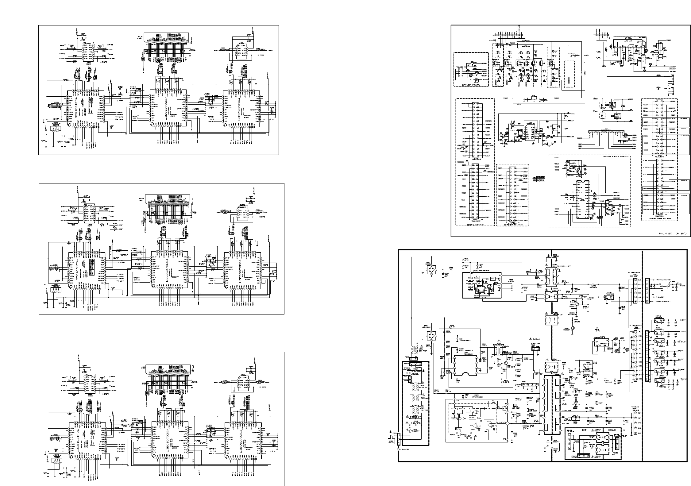
P/No : 3854VA0117A-S2(1/2)
2003.6.21
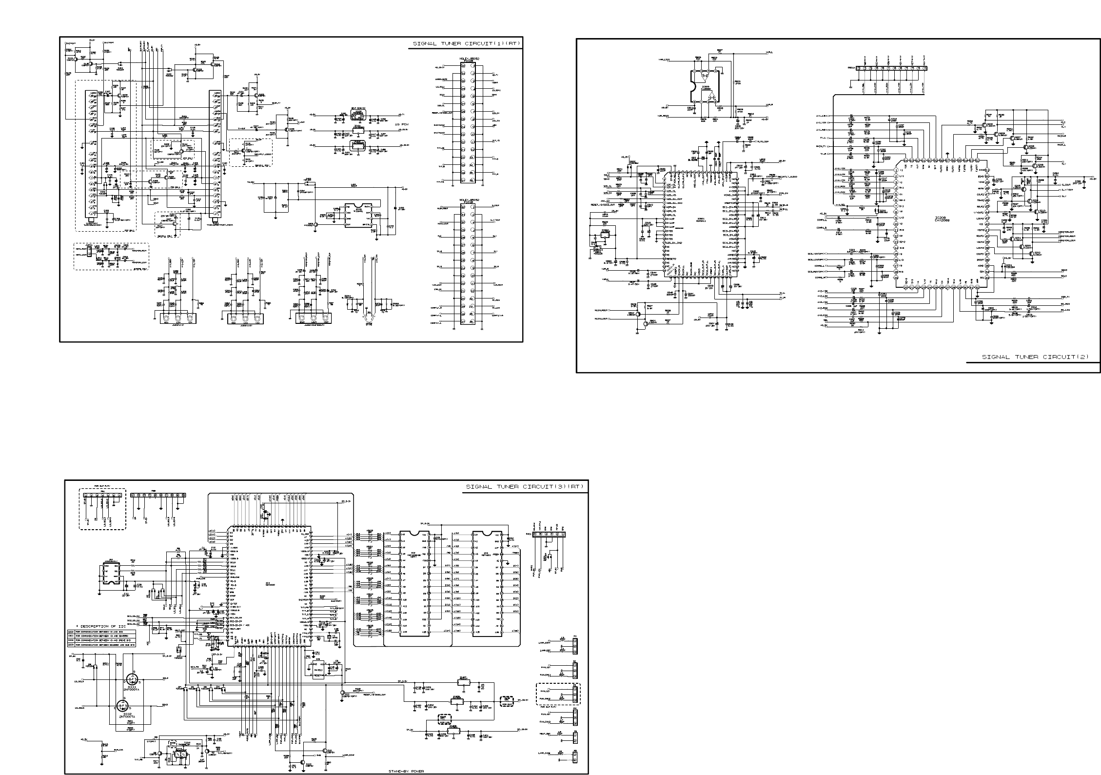
P/No : 3854VA0117A-S2(2/2)
2003.6.21

SVC. SHEET : 3854VA0117A-S1
SVC. SHEET : 3854VA0117A-S2
SVC. SHEET :
