RTL8762C Memory User Guide EN
User Manual:
Open the PDF directly: View PDF ![]() .
.
Page Count: 21
Realtek Confidential
RTL8762C Memory User Guide
V1.1
2018/09/12
Realtek Confidential
RTL8762C Memory User Guide
Copyright 2018 Realtek Semiconductor Corporation.
All Rights Reserved.
2
Revision History
Date
Version
Comments
Author
Reviewer
2018/06/11
V1.0
First release version
Grace
Rui
2018/09/12
V1.1
Modify chapter 5
Grace
Rui

Realtek Confidential
RTL8762C Memory User Guide
Copyright 2018 Realtek Semiconductor Corporation.
All Rights Reserved.
3
Contents
Revision History ................................................................................................................................................ 2
Figure List ......................................................................................................................................................... 4
Table List ........................................................................................................................................................... 5
1 Overview ................................................................................................................................................... 6
2 ROM .......................................................................................................................................................... 6
3 RAM .......................................................................................................................................................... 6
3.1 Data RAM .......................................................................................................................................... 7
3.2 Buffer RAM ....................................................................................................................................... 9
3.3 APIs .................................................................................................................................................... 9
3.4 Memory Usage Calculation .............................................................................................................. 10
3.4.1 Statistics of Static Zone Size on Data RAM ............................................................................. 11
3.4.2 Statistics of Static Zone Size on Cache Shared RAM Space .................................................... 11
3.4.3 Statistics of Remaining Heap Size ............................................................................................ 11
4 Cache ....................................................................................................................................................... 11
5 External Flash .......................................................................................................................................... 12
5.1 Flash Layout ..................................................................................................................................... 12
5.2 Flash APIs ........................................................................................................................................ 19
5.3 FTL ................................................................................................................................................... 20
6 Flash Code and RAM Code Setting ........................................................................................................ 20
7 eFuse ........................................................................................................................................................ 21

Realtek Confidential
RTL8762C Memory User Guide
Copyright 2018 Realtek Semiconductor Corporation.
All Rights Reserved.
4
Figure List
Figure 3-1 Data RAM layout ..................................................................................................................................... 7
Figure 3-2 Adjust Data RAM Layout ........................................................................................................................ 8
Figure 3-3 Buffer RAM Layout ................................................................................................................................. 9
Figure 5-1 Flash Layout........................................................................................................................................... 13

Realtek Confidential
RTL8762C Memory User Guide
Copyright 2018 Realtek Semiconductor Corporation.
All Rights Reserved.
5
Table List
Table 1-1 Memory Layout ......................................................................................................................................... 6
Table 3-1 Data RAM Usage....................................................................................................................................... 7
Table 3-2 Buffer RAM Usage .................................................................................................................................... 9
Table 3-3 os_mem_alloc .......................................................................................................................................... 10
Table 4-1 Configure Cache Usage ........................................................................................................................... 12
Table 5-1 Flash Section ........................................................................................................................................... 13
Realtek Confidential
RTL8762C Memory User Guide
Copyright 2018 Realtek Semiconductor Corporation.
All Rights Reserved.
6
1 Overview
This document describes memory system of RTL8762C and introduces how to use them. RTL8762C memory
consists of ROM, RAM, external SPI Flash and eFuse, as is shown in Table 1-1. Cache has dedicated RAM, and
the dedicated RAM also can be configured as general RAM using Realtek Vendor registers. This flexible memory
configuration mechanism makes RTL8762C support a wide range of applications whose memory usage are total
different.
Table 1-1 Memory Layout
Memory Type
Start Addr
End Addr
Size(K bytes)
ROM
0x0
0x00060000
384
Data RAM
0x00200000
0x0021C000
112
Cache (Shared as data RAM)
0x0021C000
0x00220000
16
Buffer RAM
0x00280000
0x00288000
32
SPI Flash (Cacheable)
0x00800000
0x01000000
8192
SPI Flash (Non Cache)
0x01800000
0x02000000
8192
2 ROM
The ROM code is located at [0x0, 0x60000), in which Bootloader, RTOS, BT Stack, Flash Driver and other
platform modules are built in. RTL8762C opens some modules such as RTOS, BT Stack for application to use.
RTL8762C SDK contains the header files of these ROM modules which enables users to access built in ROM
functions. This reduces both application code size and RAM size.
3 RAM
RTL8762C has two pieces of RAM, the Data RAM located at [0x00200000, 0x0021C000) and the Buffer RAM
Realtek Confidential
RTL8762C Memory User Guide
Copyright 2018 Realtek Semiconductor Corporation.
All Rights Reserved.
7
located at [0x00280000, 0x00288000). Both RAM memories can be used to store data and execute code. In the
current SDK, data RAM has been used for BT stack and running RAM code, while Buffer RAM has been used as
heap for buffer of BT stack, log buffer, task stack and FTL mapping table.
3.1 Data RAM
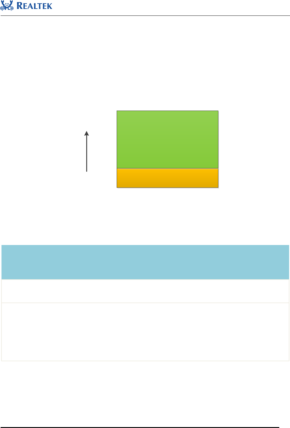
In the current SDK, Data RAM is divided into 6 parts by default, as is shown in Figure 3-1.
APP RAM
(35 KB*)
Rom Data (12KB)
Main Stack (2KB)
Patch RAM1 (17 KB)
Patch RAM2 (16 KB)
Data RAM Heap
(30 KB*)
0x00200000
* means the size is adjustable
Figure 3-1 Data RAM Layout
Each part has its dedicated usage, and only APP RAM and Data RAM Heap have changeable size, as is shown in
Table 3-1.
Table 3-1 Data RAM Usage
Realtek Confidential
RTL8762C Memory User Guide
Copyright 2018 Realtek Semiconductor Corporation.
All Rights Reserved.
8
Memory Type
Memory Usage
Memory size
changeable or not
ROM data
for all global and static variables used by ROM code
NO
Main Stack
for Cortex-M4 MSP, which is used by boot code and ISR
(interrupt service routine) as stack pointer
NO
Patch RAM1
for global/static variables and RAM code of patch
NO
APP RAM
for global/static variables and RAM code of APP
YES
Data RAM Heap
for dynamic memory allocation of ROM code, Patch code and
APP code
11K of the 30K data RAM heap has been used by rom code, so
19k is left for application
YES
Patch RAM2
for global/static variables and RAM code of patch, could be shut
down to save power if not used
NO
The total size of APP RAM and data RAM heap are 65K, which is unchangeable, while the size of each block can
be adjusted by modifying mem_config.h, as is shown in Figure 3-2. Increase the size of APP RAM means
decreasing the size of data RAM heap, vice versa.
Realtek Confidential
RTL8762C Memory User Guide
Copyright 2018 Realtek Semiconductor Corporation.
All Rights Reserved.
9
Figure 3-2 Adjust Data RAM Layout
3.2 Buffer RAM
In the current SDK, the address space of Buffer RAM is located in [0x00280000, 0x00288000] which is divided
into 2 parts by default, as is shown in Figure 3-3. The first 2KB is used for ROM Global Data, while the other 30
KB is used as heap. In the 30KB heap, ROM occupies about 25.5 KB dynamic spaces, while the remaining 4.5KB
is used by APP, shown as table 3-2.
Rom Data (2KB)
Buffer RAM Heap
(30 KB)
0x280000
Figure 3-3 Buffer RAM Layout
Each part has its dedicated usage, as is shown in Table 3-2,
Table 3-2 Buffer RAM Usage
Memory Type
Memory Usage
Memory size
changeable or not
ROM data
for all global and static variables used by ROM code
NO
Buffer RAM Heap
for dynamic memory allocation of ROM code, Patch code and
APP code
25.5K of the 30K buffer RAM heap has been used by rom
code, so 4.5k is left for application.
NO
3.3 APIs
os_mem_alloc can be used to allocate memory dynamically from Data RAM Heap or Buffer RAM heap
according to the parameter of ram_type, as is shown in Table 3-3.

Realtek Confidential
RTL8762C Memory User Guide
Copyright 2018 Realtek Semiconductor Corporation.
All Rights Reserved.
10
Table 3-3 os_mem_alloc
typedef enum
{
RAM_TYPE_DATA_ON = 0,
RAM_TYPE_BUFFER_ON = 1,
} RAM_TYPE;
/**
* @brief Allocate memory dynamically from Data RAM Heap or Buffer RAM heap
* @param ram_type : specify which heap to allocate memory from
* size: memory size in bytes to be allocated
* @retval pointer to the allocated memory
*/
#define os_mem_alloc(ram_type, size) os_mem_alloc_intern(ram_type, size, __func__, __LINE__)
Other APIs are list as below:
os_mem_zalloc: allocated memory will be initialized to 0
os_mem_aligned_alloc: allocated memory will be aligned to the specified alignment
os_mem_free: free a memory block that had been allocated from data ram heap or buffer ram heap
os_mem_aligned_free: free an aligned memory block that had been allocated
os_mem_peek: peek the unused memory size of the specified RAM type
Refer to os_mem.h for more details.
3.4 Memory Usage Calculation
In order to make using of RAM more convenient, allocating memory dynamically from heap will always allocate
memory from Buffer RAM firstly. If allocate fails, then it will allocate memory from Data RAM again. This
allows static data and code centralization to be placed in Data RAM instead of spreading between Data RAM and
Buffer RAM, thus easier to manage.

Realtek Confidential
RTL8762C Memory User Guide
Copyright 2018 Realtek Semiconductor Corporation.
All Rights Reserved.
11
3.4.1 Statistics of Static Zone Size on Data RAM
Find the first address (fixed 0x00207c00) and end address allocated in Data RAM by finding in the app.map file
generated by building app keil project, for example:
APP used Data RAM’s starting address and size is as follows.
enc_signature 0x00207c00 Data 16 system_rtl8762c.o(.encryption.signature)
APP used Data RAM’s ending address and size is as follows:
Image$$OVERLAY_A$$ZI$$Base 0x0020fa1c Number 0 anon$$obj.o ABSOLUTE
So the calculation method of APP used static zone size on Data RAM is as follows.
Data RAM Size = 0x0020fa1c - 0x00207c00 = 32284 Bytes;
3.4.2 Statistics of Static Zone Size on Cache Shared RAM Space
Find the first address (fixed 0x0021c000) and end address allocated in Cache Shared RAM by finding in the
app.map file generated by building app keil project, for example:
APP used Cache Shared RAM’s starting address.
Image$$CACHE_DATA_ON$$RO$$Base 0x0021c000 Number 0 anon$$obj.o ABSOLUTE
APP used Cache Shared RAM’s ending address and size .
hids_cbs 0x0021f130 Data 12 hids_rmc.o(.constdata)
So the calculation method of APP used static zone size on Cache Shared RAM is as follows.
Cache Shared RAM Size = 0x0021f130 + 12 - 0x0021c000 = 12604 Bytes
3.4.3 Statistics of Remaining Heap Size
The remaining heap size of the specified RAM type can be obtained through the os_mem_peek function.
4 Cache
RTL8762C has a 16K bytes cache, it co-works with SPIC (SPI Flash Controller) to speed up the SPI Flash read
and write operation. And it also can be used as data RAM. If it is configured as data RAM, it can be used for Data
Realtek Confidential
RTL8762C Memory User Guide
Copyright 2018 Realtek Semiconductor Corporation.
All Rights Reserved.
12
Storage or Code Execution. If Cache is configured as data RAM, its range is [0x0021C000, 0x00220000). This
range is just at the end of data RAM.
The Data RAM size of cache could be configured by setting SHARE_CACHE_RAM_SIZE micro in
mem_config.h, as is shown in Table 4-1.
Table 4-1 Configure Cache Usage
SHARE_CACHE_RAM_SIZE
Flash Cache Size
Data RAM Size
Scenario
0 KB
16 KB
0 KB
Run large amounts of flash Code that
requires a large piece of cache
8 KB
8 KB
8 KB
Run small amounts of flash code that
requires a small piece of cache
16 KB
0 KB
16 KB
Not run flash code
5 External Flash
RTL8762C supports external SPI Flash by integrating a SPI Flash Controller (SPIC). Realtek offers the bottom
level API of Flash driver, FTL for user application. SPIC supports memory mapping to SPI Flash on board and
the maximum Flash size is 8M bytes. There are two range of memory mapping spaces. The range of [0x800000,
0x1000000) is with cache, and [0x1800000, 0x2000000) is without cache. When enabled, cache will work while
CPU accesses this space. This improves the data read and code execution efficiency of SPI Flash greatly.
5.1 Flash Layout
In the current SDK, the FLASH memory layout is summarized as in Figure 5-1 and consists of 7 fields :
“Reserve”, “OEM Header”, “OTA Bank 0”, “OTA Bank 1”, “FLASH Transport Layer” , “OTA Tmp” and
“APP Defined Section”. Note that the defined starting address of the FLASH memory accessible by MCU is
0x800000. Flash layout could be adjusted by MP tool.
Realtek Confidential
RTL8762C Memory User Guide
Copyright 2018 Realtek Semiconductor Corporation.
All Rights Reserved.
13
OTA Bank 0
OTA Bank 1
FLASH Transport Layer
OTA Tmp (Reserved for legacy)
Starting Address: 0x800000
Starting Address: 0x800000
Starting Address: 0x801000
Starting Address: 0x801000
APP Defined Section
OEM Header
Reserve
Figure 5-1 Flash Layout
The description of each field in the Flash layout is summarized in table below.
Table 5-1 Flash Section
Memory
Segment
Starting Address
Size
(Bytes)
Functions
Reserved
0x800000
0x1000
Reserved
OEM Header
0x801000
0x1000
Store configure information which includes
BT Address, AES Key and user defined Flash
layout
OTA Bank 0
Variable
(defined in OEM
Header)
Variable length
(defined in OEM
Header )
Store data and executable code. It can be
divided into several sections: OTA Header,
Secure boot, Patch, APP, APP Data1, and APP
Data2.
If bank switch of OTA update is not supported,
OTA_TMP is used for backup. If bank switch
of OTA update is supported, one of bank0 and
bank1 is executable zone, while the other is
back-up zone.
OTA Bank 1
Variable
(defined in OEM
Header)
Variable length
(defined in OEM
Header )
The same as bank0, and the size of bank1 must
also be the same with bank0
FLASH
Variable
Variable length
Support accessing flash with logic address.
Realtek Confidential
RTL8762C Memory User Guide
Copyright 2018 Realtek Semiconductor Corporation.
All Rights Reserved.
14
Transport
layer
(defined in OEM
Header)
(defined in OEM
Header )
User can read/write flash with unit size of 4
bytes at least
OTA_TMP
Variable
(defined in OEM
Header)
Variable length
(defined in OEM
Header )
Used as backups for OTA when bank switch of
OTA update is not supported. Its size can’t be
less than the largest image of OTA bank0.
APP Defined
Section
Variable
(defined in OEM
Header)
Variable length
(defined in OEM
Header )
The remaining zone of the Flash. User can use
it freely except for OTA update.
There are 6 types of images in OTA Bank: OTA Header, Secure boot, Patch, APP, APP Data1 and APP Data2,
shown in figure 5-2. The layout of OTA Bank is determined by OTA Header, which is generated by MP Pack Tool.
Patch
App
App Data1
Low
Address
High
Address
OTA Header
Secure Boot Loader
App Data2
Figure 5-2 POTA Bank Layout
Table 5-2 Image Description of OTA Bank
Memory
Segment
Starting Address
Size
Functions
OTA Header
Depend by OEM
Header
4KB
OTA version, start address and size of each bank
Secure Boot
Loader
Depend by OEM
Header
changeable
Security check of code in boot process
Patch
Depend by OEM
Header
changeable
Extended function of BT protocol stack and system
in ROM

Realtek Confidential
RTL8762C Memory User Guide
Copyright 2018 Realtek Semiconductor Corporation.
All Rights Reserved.
15
App
Depend by OEM
Header
changeable
User application code
App Data1
Depend by OEM
Header
changeable
APP Data need to be updated by OTA
App Data2
Depend by OEM
Header
changeable
APP Data need to be updated by OTA
RTL8762C supports flexible configuration of flash layout according to different application scenarios. User can
customize flash layout through “config set” option of MP tool. Realtek offers FlashMapGenerateTool to generate
files of flash_map.ini and flash_map.h. Flash_map.ini can be imported to MPTool and MPPack Tool to generate
config file and OTA Header. Flash_map.h can be copied to APP project directory to build the target APP image.
But you must pay attention to some of the principles of adjusting flash layout as described below.
1. If OTA supports bank switch, size of OTA bank0 and bank1 must be equal, while size of OTA tmp should be
set to 0.
2. If OTA supports bank switch, layout of OTA bank0 and bank1 can be different. But the size of bank0 and
bank1 cannot be changed and less than the total size of internal images.
3. If OTA doesn’t support bank switch, size of OTA bank1 is set to 0. The size of OTA tmp can’t be less than
size of the largest image in OTA bank0.
4. If OTA doesn’t support bank switch, besides OTA Header, patch and APP, user should burn secure
boot image. The address should be fixed to 0x80d0000, and size must be less than 4KB. The secure boot
image is released by Realtek.
5. If sizes of APP Data1 and APP Data2 are not set to 0 when generating OTA Header, the responding images
must be burnt. Otherwise, image check will fail in boot process. After handled by tool, the original APP data
bin file will be added a 1KB image header which meets some specific format. Note that, sections of APP
Data1 and APP Data2 are used as storage of app data for OTA. If the data don’t need to update, it should be
placed in the APP Defined Section.
6. Make sure the offset between end address of OTA bank1 image and flash start address (0x800000) aligned to
flash protected address range, such as 64KB, 128KB, 256KB and 512KB. This can lock all the code zone to
protect from unexpected flash write and erase operation.
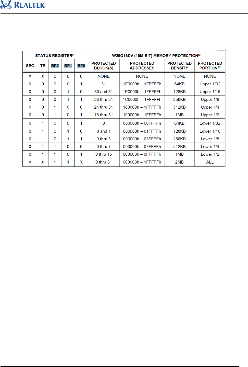
As to the 6th principle, RTL8762C supports a mechanism named flash software Block Protect to lock flash to
prevent writing and erasing operations. Flash software block protect uses some BP bits in flash status register to
Realtek Confidential
RTL8762C Memory User Guide
Copyright 2018 Realtek Semiconductor Corporation.
All Rights Reserved.
16
select the level (range) to protect as described below.
Figure 5-3 Flash Software Block Protect
Flash uses BP(x) bits in status register to identify number of blocks to lock, and TB bit to decide the direction to
lock. However, Realtek only supports lock flash from low address to protect some important data such as
configuration, security, and code sections. In order to support this feature, it is necessary to pass some checking
rules to guarantee selected flash meets our requirement for software Block Protect. That is why Approved Vendor
List (AVL) exists. Most flash in Qualified Vendor List supports protecting flash by level for different size, such as
64KB, 128KB, 256KB, 512KB, etc.
Therefore, when we divide flash layout, we need to ensure that the end address offset of OTA bank1 segment can
be aligned to a certain level of protection that the selected flash supports as far as possible. Then RTL8762C will
parse flash layout configuration parameters and query selected flash information to set block protect value. In
order to maximize the use of BP, some flash layout examples are as follows. But what you have to notice is that
there are two kinds of flash in AVL, which does not support protecting flash by block level. More details please
refer to Qualified Vendor List.
The protected flash zone can’t be written and erased. If necessary, user can unlock flash first, and then write or
erase, finally lock the flash to the previous level. But this operation is not recommended, as the flash status
register is accessed by way of NVRAM. There is 100K times limit, so frequently unlocking may make the flash
Realtek Confidential
RTL8762C Memory User Guide
Copyright 2018 Realtek Semiconductor Corporation.
All Rights Reserved.
17
unavailable.
Table 5-3 Sample Flash layout (total flash size is 256KB)
Sample Flash Layout (total size is
256KB)
Size
Start Address
Block Protect size
1) Reserved
4K
0x800000
The front 128KB
space starting from
flash low address
(OTA Bank1 end
address offset is
148KB. It is not
aligned so just lock
128KB.)
2) OEM Header
4K
0x801000
3) OTA Bank0
140K
0x802000
a) OTA Header
4K
0x802000
b) Secure boot loader
4K
0x80D000
c) Patch code
40K
0x803000
d) APP code
92K
0x80E000
e) APP data1
0K
0x825000
f) APP data2
0K
0x825000
4) OTA Bank1
0K
0x825000
5) FTL
16K
0x825000
6) OTA Temp
92K
0x829000
7) APP Defined Section
0K
0x840000
Table 5-4 Sample Flash layout (total flash size is 1MB)
Sample Flash Layout (Total size is
1MB)
Size
Start
Address
Block Protect Size
1) Reserved
4K
0x800000
The front 512KB
space starting from
flash low address
(OTA Bank1 end
address offset is
512KB.)
2) OEM Header
4K
0x801000
3) OTA Bank0
252K
0x802000
a) OTA Header
4K
0x802000
b) Secure boot loader
0K
0x803000
c) Patch code
40K
0x803000
d) APP code
208K
0x80D000
e) APP data1
0K
0x841000

Realtek Confidential
RTL8762C Memory User Guide
Copyright 2018 Realtek Semiconductor Corporation.
All Rights Reserved.
18
f) APP data2
0K
0x841000
4) OTA Bank1 (size must be same as OTA
Bank0)
252K
0x841000
a) OTA Header
4K
0x842000
b) Secure boot loader
0K
0x842000
c) Patch code
40K
0x842000
d) APP code
208K
0x84C000
e) APP data1
0K
0x880000
f) APP data2
0K
0x880000
5) FTL
16K
0x880000
6) OTA Temp
0K
0x880000
7) APP Defined Section
200K
0x884000
Table 5-5 Sample Flash layout (total flash size is 2MB)
Sample flash layout (total size is 2MB)
Size
Start Addr
Block Protect Size
1) Reserved
4K
0x800000
The front 1MB
space starting from
flash low address
(OTA Bank1 end
address offset is
1MB.)
2) OEM Header
4K
0x801000
3) OTA Bank0
508K
0x802000
a) OTA Header
4K
0x802000
b) Secure boot loader
0K
0x803000
c) Patch code
40K
0x803000
d) APP code
464K
0x80D000
e) APP data1
0K
0x881000
f) APP data2
0K
0x881000
4) OTA Bank1 (size must be same as OTA
Bank0)
508K
0x881000
a) OTA Header
4K
0x881000
b) Secure boot loader
0K
0x882000
c) Patch code
40K
0x882000

Realtek Confidential
RTL8762C Memory User Guide
Copyright 2018 Realtek Semiconductor Corporation.
All Rights Reserved.
19
d) APP code
464K
0x88C000
e) APP data1
0K
0x900000
f) APP data2
0K
0x900000
5) FTL
16K
0x900000
6) OTA Temp
0K
0x904000
7) APP Defined Section
200K
0x904000
5.2 Flash APIs
Flash operation APIs are listed as follows, refer to Bee2-SDK.chm for more details.
1, Basic Operation APIs:
bool flash_auto_read_locked(uint32_t addr, uint32_t *data);
bool flash_read_locked(uint32_t start_addr, uint32_t data_len, uint8_t *data);
bool flash_auto_write_locked(uint32_t start_addr, uint32_t data);
bool flash_auto_write_buffer_locked(uint32_t start_addr, uint32_t *data, uint32_t len);
bool flash_write_locked(uint32_t start_addr, uint32_t data_len, uint8_t *data);
bool flash_erase_locked(T_ERASE_TYPE type, uint32_t addr);
2, Flash High Speed Read APIs:
bool flash_auto_dma_read_locked(T_FLASH_DMA_TYPE dma_type, FlashCB flash_cb,
uint32_t src_addr, uint32_t dst_addr, uint32_t data_len);
bool flash_auto_seq_trans_dma_read_locked(T_FLASH_DMA_TYPE dma_type, FlashCB flash_cb,
uint32_t src_addr, uint32_t dst_addr, uint32_t data_len);
bool flash_split_read_locked(uint32_t start_addr, uint32_t data_len, uint8_t *data, uint32_t *counter);
If the three above APIs are used, user needs to copy file sdk\src\flash\flash_hs_read.c into the project and
include header file flash_device.h.

Realtek Confidential
RTL8762C Memory User Guide
Copyright 2018 Realtek Semiconductor Corporation.
All Rights Reserved.
20
5.3 FTL
FTL (flash transport layer) is used as abstraction layer for bt stack and user application to read/write data in flash.
Through FTL interface, user can read or write the responding data in flash space for FTL by logic address. The
FTL space can be divided into 2 spaces according to functions:
1. BT storage space
(1) Logic address range: [0x0000, 0x0C00). But this space size can be changed by otp parameter.
(2) This region is used to store BT information such as device address, link key, etc.
(3) Refer to RTL8762C BLE Stack User Manual for more details.
2. APP storage space
(1) Logic address range: [0x0C00, 0x17f0)
(2) APP can use this region to store user defined information.
(3) The following APIs can be called to read/write data in this region, and they are defined in ftl.h.
Please refer to Bee2-SDK.chm for more details.
uint32_t ftl_save(void * p_data, uint16_t offset, uint16_t size)
uint32_t ftl_load(void * p_data, uint16_t offset, uint16_t size)
6 Flash Code and RAM Code Setting
The code can run on Flash or on RAM. This section describes how to place code in a specific memory to execute.
1. Modify the macro FEATURE_RAM_CODE definition:
(1) 1 indicates that the code without any section modified runs on RAM.
(2) 0 indicates that the code without any section modified runs on Flash.
2. If you want to specify a function to place on a specific memory, use the section macro in app_section.h. For
example:
(1) APP_FLASH_TEXT_SECTION means putting the function into Flash to execute.
(2) DATA_RAM_FUNCTION means putting the function into RAM to execute.

Realtek Confidential
RTL8762C Memory User Guide
Copyright 2018 Realtek Semiconductor Corporation.
All Rights Reserved.
21
7 eFuse
eFuse is a block of one-time programming memory which is used to store the important and fixed information,
such as UUID, security key and other one-time programming configuration. The single bit of eFuse cannot be
changed from 0 to 1, and there is no erase operation to eFuse, so be careful to update eFuse. Realtek offers MP
Tool to update certain eFuse sections.
