RXV563
User Manual: RXV563
Open the PDF directly: View PDF ![]() .
.
Page Count: 114 [warning: Documents this large are best viewed by clicking the View PDF Link!]
- CONTENTS
- TO SERVICE PERSONNEL
- FRONT PANELS
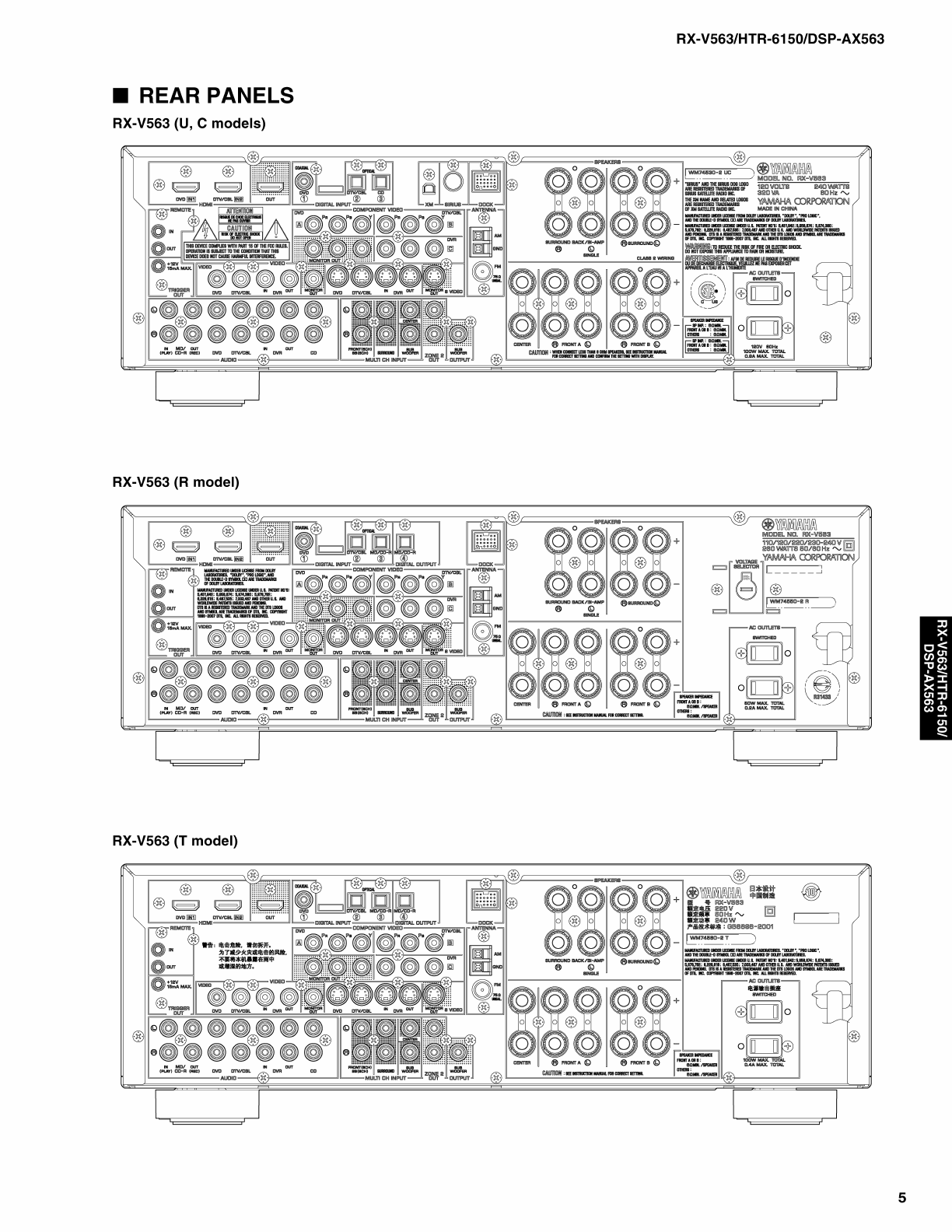
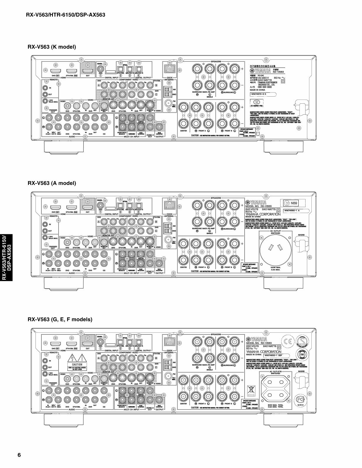
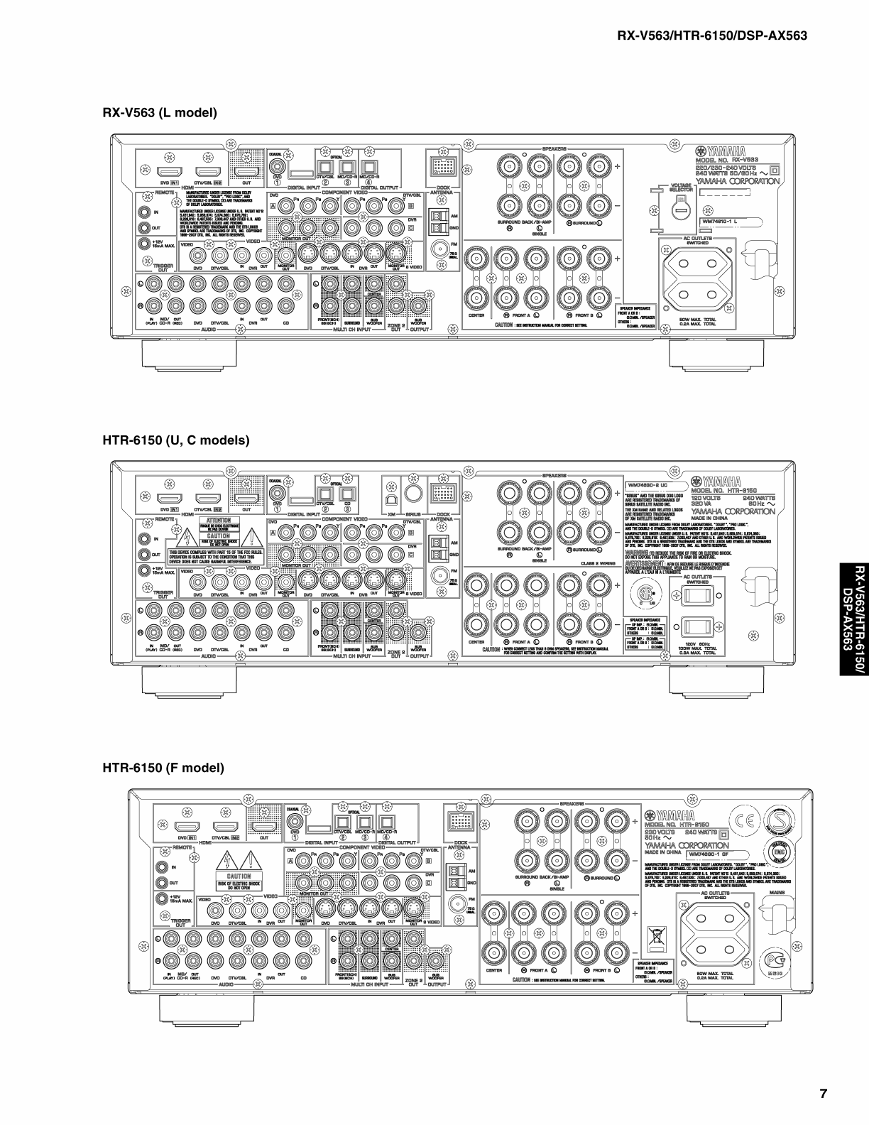
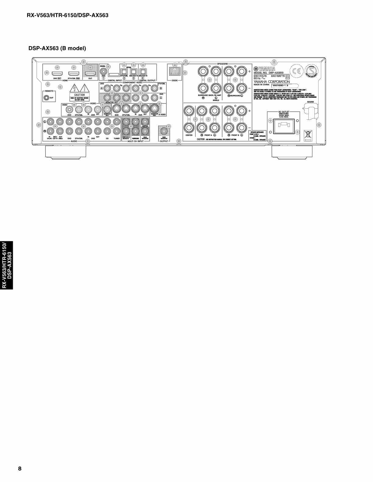
- REAR PANELS
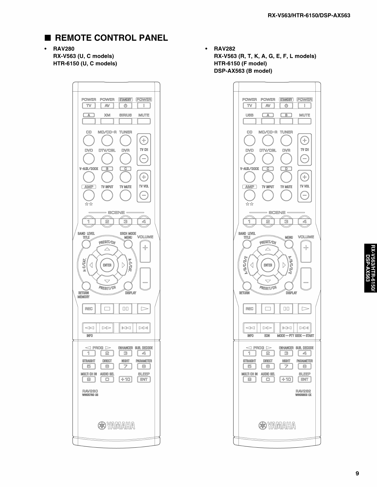
- REMOTE CONTROL PANEL
- SPECIFICATIONS
- INTERNAL VIEW
- DISASSEMBLY PROCEDURES
- UPDATING FIRMWARE
- SELF- DIAGNOSTIC FUNCTION
- Starting Self-diagnostic Function
- Starting Self-diagnostic Function in the protection cancel mode
- Canceling Self-diagnostic Function
- Display provided when Self-diagnostic Function started
- Operation procedure of Main menu and Sub-menu
- Functions in Self-Diagnostic Function mode
- Initial settings used to start Self-Diagnostic Function
- Details of Self-Diagnostic Function menu
- A. BYPASS
- B. AUDIO CHECK
- C. SPEAKER SET
- D. XCH INPUT
- E. MIC CHECK
- F. FL CHECK
- G. TEST TONE
- H. XM STATUS (U, C models)
- I. iPod
- J. USB (R, T, K, A, B, G, E, F, L models)
- K. SIRIUS (U, C models)
- L. VIDEO CONVERSION
- M. HDMI SELECT
- N. A/D DATA CHECK
- O. PROTECTION
- P. PROTECTION HISTORY
- Q. RESERVED
- R. FACTORY PRESET
- S. ROM VER/SUM
- DISPLAY DATA
- IC DATA
- BLOCK DIAGRAMS
- PRINTED CIRCUIT BOARDS
- PIN CONNECTION DIAGRAMS
- SCHEMATIC DIAGRAMS
- REPLACEMENT PARTS LIST
- REMOTE CONTROL
- Advanced setup
SERVICE MANUAL
101086
IMPORTANT NOTICE
This manual has been provided for the use of authorized YAMAHA Retailers and their service personnel.
It has been assumed that basic service procedures inherent to the industry, and more specifically YAMAHA Products, are already
known and understood by the users, and have therefore not been restated.
WARNING: Failure to follow appropriate service and safety procedures when servicing this product may result in personal
injury, destruction of expensive components, and failure of the product to perform as specified. For these reasons,
we advise all YAMAHA product owners that any service required should be performed by an authorized
YAMAHA Retailer or the appointed service representative.
IMPORTANT: The presentation or sale of this manual to any individual or firm does not constitute authorization, certification or
recognition of any applicable technical capabilities, or establish a principle-agent relationship of any form.
The data provided is believed to be accurate and applicable to the unit(s) indicated on the cover. The research, engineering, and
service departments of YAMAHA are continually striving to improve YAMAHA products. Modifications are, therefore, inevitable
and specifications are subject to change without notice or obligation to retrofit. Should any discrepancy appear to exist, please
contact the distributor's Service Division.
WARNING: Static discharges can destroy expensive components. Discharge any static electricity your body may have
accumulated by grounding yourself to the ground buss in the unit (heavy gauge black wires connect to this buss).
IMPORTANT: Turn the unit OFF during disassembly and part replacement. Recheck all work before you apply power to the unit.
P.O.Box 1, Hamamatsu, Japan
2008 All rights reserved.
This manual is copyrighted by YAMAHA and may not be copied or
redistributed either in print or electronically without permission.
'08.03
■CONTENTS
TO SERVICE PERSONNEL .......................................... 2
FRONT PANELS ........................................................ 3–4
REAR PANELS .......................................................... 5–8
REMOTE CONTROL PANEL ........................................ 9
SPECIFICATIONS.................................................. 10–12
INTERNAL VIEW ......................................................... 13
DISASSEMBLY PROCEDURES ........................... 14–16
UPDATING FIRMWARE ........................................ 17–21
SELF DIAGNOSIS FUNCTION (DIAG) ................. 22–44
DISPLAY DATA ........................................................... 45
IC DATA ................................................................. 46–59
BLOCK DIAGRAMS .............................................. 61–65
PRINTED CIRCUIT BOARDS................................ 66–79
PIN CONNECTION DIAGRAMS ............................ 80–81
SCHEMATIC DIAGRAMS ...................................... 83–96
REPLACEMENT PARTS LIST ............................ 97–109
REMOTE CONTROL.......................................... 110–112
Advanced setup ......................................................... 113
AV RECEIVER/AV AMPLIFIER
RX-V563/HTR-6150/
DSP-AX563
RX-V563/HTR-6150/
DSP-AX563
2
RX-V563/HTR-6150/DSP-AX563
RX-V563/HTR-6150/
DSP-AX563
WALL
OUTLET EQUIPMENT
UNDER TEST
AC LEAKAGE
TESTER OR
EQUIVALENT
INSULATING
TABLE
■TO SERVICE PERSONNEL
1. Critical Components Information
Components having special characteristics are marked s and
must be replaced with parts having specifications equal to those
originally installed.
2. Leakage Current Measurement (For 120V Models Only)
When service has been completed, it is imperative to verify
that all exposed conductive surfaces are properly insulated
from supply circuits.
●Meter impedance should be equivalent to 1500 ohms shunted
by 0.15µF.
●Leakage current must not exceed 0.5mA.
●Be sure to test for leakage with the AC plug in both polarities.
For U model
“CAUTION”
“F3401, F3402: FOR CONTINUED PROTECTION AGAINST RISK OF FIRE, REPLACE ONLY WITH SAME
TYPE 6A, 125V FUSE.”
For C model
CAUTION
F3401, F3402: REPLACE WITH SAME TYPE 6A, 125V FUSE.
ATTENTION
F3401, F3402: UTILISER UN FUSIBLE DE RECHANGE DE MÉME TYPE DE 6A, 125V.
All of the P.C.B.s installed in this unit and solder joints are soldered using the lead free solder.
Among some types of lead free solder currently available, it is recommended to use one of the following types for the repair
work.
• Sn + Ag + Cu (tin + silver + copper)
• Sn + Cu (tin + copper)
• Sn + Zn + Bi (tin + zinc + bismuth)
Caution:
As the melting point temperature of the lead free solder is about 30°C to 40°C (50°F to 70°F) higher than that of the lead solder, be sure
to use a soldering iron suitable to each solder.
About lead free solder
WARNING: CHEMICAL CONTENT NOTICE!
This product contains chemicals known to the State of California to cause cancer, or birth defects or other reproductive
harm.
DO NOT PLACE SOLDER, ELECTRICAL/ELECTRONIC OR PLASTIC COMPONENTS IN YOUR MOUTH FOR ANY
REASON WHAT SO EVER!
Avoid prolonged, unprotected contact between solder and your skin! When soldering, do not inhale solder fumes or expose
eyes to solder/flux vapor!
If you come in contact with solder or components located inside the enclosure of this product, wash your hands before
handling food.

10
RX-V563/HTR-6150/DSP-AX563
RX-V563/HTR-6150/
DSP-AX563
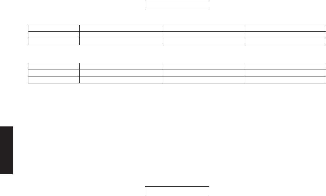
■SPECIFICATIONS
■ Audio Section
Minimum RMS Output Power (Power Amp. Section)
(1 kHz, 0.9 % THD)
FRONT L/R, CENTER, SURROUND L/R, SURROUND
BACK L/R
U, C models (8 ohms) .......................................... 90 W/ch
R, T, K, A, B, G, E, F, L models (6 ohms) ........... 90 W/ch
Maximum Power (JEITA) (1 kHz, 0.9 % THD, 6 ohms)
FRONT L/R, CENTER, SURROUND L/R, SURROUND
BACK L/R
R, T, K, L models ............................................... 115 W/ch
Dynamic Power Per Channel (IHF) (FRONT L/R drive)
U, C models
(8/6/4/2 ohms) ...................................... 90/110/130/150 W
R, T, K, A, B, G, E, F, L models
(6/4/2 ohms) .............................................. 100/110/125 W
Dynamic Headroom
U, C models (8 ohms) ............................................. 0.18 dB
Input Sensitivity/Input Impedance (1 kHz, 100 W / 8 ohms)
CD, etc. ............................................... 200 mV / 47 k-ohms
MULTI CH INPUT
FRONT L/R, CENTER, SURROUND L/R, SUBWOOFER
........................................................ 200 mV / 47 k-ohms
Maximum Input Signal (1 kHz, 0.5 % THD, Effect on)
CD, etc. .......................................................... 2.0 V or more
Output Level/Output Impedance
REC OUT .......................................... 200 mV / 1.2 k-ohms
SUBWOOFER (2ch STEREO and FRONT SP: Small)
................................................................ 4 V / 1.2 k-ohms
Headphone Jack Rated Output/Impedance
CD, etc. (1 kHz, 200 mV, 8 ohms) ....... 400 mV / 470 ohms
Frequency Response (10 Hz to 100 kHz)
CD, etc. to FRONT L/R .......................................... 0 / -3 dB
Total Harmonic Distortion (1 kHz, 50 W)
Direct to FRONT L/R SP OUT
U, C models (8 ohms) ................................. 0.06 % or less
R, T, K, A, B, G, E, F, L models (6 ohms) .. 0.06 % or less
Signal to Noise Ratio (IHF-A Network)
Direct STEREO to Input shorted SP OUT
200 mV ........................................................ 98 dB or more
250 mV ...................................................... 100 dB or more
Residual Noise (IHF-A Network)
FRONT L/R SP OUT .................................... 150 µV or less
Channel Separation
CD, etc. (Input 5.1 k-ohms shorted, 1 kHz / 10 kHz)
......................................... 60 dB or more / 45 dB or more
Tone Control Characteristics
BASS
Boost/Cut ................................................ ±10 dB (100 Hz)
TREBLE
Boost/Cut ................................................ ±10 dB (20 kHz)
Filter Characteristics
FRONT, CENTER, SURROUND, SURROUND BACK small
(H.P.F.)
....... fc=40/60/80/90/100/110/120/160/200 Hz, 12 dB/oct.
SUBWOOFER (L.P.F.)
....... fc=40/60/80/90/100/110/120/160/200 Hz, 24 dB/oct.
■ Video Section
Video Signal Type
Gray back
U, C, R, K models .................................................... NTSC
T, A, B, G, E, F, L models .......................................... PAL
Video conversion
......................................................................... NTSC/PAL
Composite Video Signal Level
.................................................................. 1 Vp-p / 75 ohms
S-Video Signal Level
Y ............................................................... 1 Vp-p / 75 ohms
C ........................................................ 0.286 Vp-p / 75 ohms
Component Signal Level
Y ............................................................... 1 Vp-p / 75 ohms
Pb/Pr...................................................... 0.7 Vp-p / 75 ohms
Video Maximum Input Level
.................................................................. 1.5 Vp-p or more
Signal to Noise Ratio
....................................................................... 50 dB or more
Monitor Out Frequency Response
Component video signal .................. 5 Hz to 60 MHz, -3 dB
HDMI ........................................................................ Ver. 1.2a
■ FM Section [U, C, R, T, K, A, G, E, F, L models]
Tuning Range
U, C models............................................ 87.5 to 107.9 MHz
R, L models ............... 87.5 to 108.0 / 87.50 to 108.00 MHz
T, K, A, G, E, F models ...................... 87.50 to 108.00 MHz
50dB Quieting Sensitivity (IHF) (1 kHz, 100 % Mod.)
Mono......................................................... 2.8 µV (20.2 dBf)
Signal to Noise Ratio (IHF)
Mono / Stereo ................................................. 73 dB / 70 dB
Harmonic Distortion (1 kHz)
Mono / Stereo ................................................. 0.5 % / 0.5 %
Antenna Input .................................... 75 ohms unbalanced
■ AM Section [U, C, R, T, K, A, G, E, F, L models]
Tuning Range
U, C models.............................................. 530 to 1,710 kHz
R, L models ....................... 530 to 1,710 / 531 to 1,611 kHz
T, K, A, G, E, F models ............................ 531 to 1,611 kHz
Antenna Input .................................................Loop antenna
■ General
Power Supply
U, C models............................................... AC 120 V, 60 Hz
R model ................. AC 110, 120/220, 230-240 V, 50/60 Hz
T model ..................................................... AC 220 V, 50 Hz
K model .....................................................AC 220 V, 60 Hz
A model .....................................................AC 240 V, 50 Hz
B, G, E, F models ...................................... AC 230 V, 50 Hz
L model ................................. AC 220, 230-240 V, 50/60 Hz
Power Consumption
U, C models................................................ 240 W / 320 VA
R model .................................................................... 260 W
T, K, A, B, G, E, F, L models .................................... 240 W
11
RX-V563/HTR-6150/DSP-AX563
Dolby Digital
DTS
Dolby Pro Logic
Dolby Pro Logic IIx, II Music
Dolby Pro Logic IIx, II Movie
Dolby Pro Logic IIx, II Game
Neo:6 Cinema
Neo:6 Music
Neural Surround (U, C models)
O
OO O
Program
STRAIGHT
MOVIE
MUSIC
MOVIE
DIRECT STEREO
STEREO
STEREO
DIRECT STEREO
STEREO
STEREO
MUSIC ENHANCER
MUSIC ENHANCER
MUSIC ENHANCER
MUSIC ENHANCER
MUSIC ENHANCER
STRAIGHT
ENTERTAINMENT
ENTERTAINMENT
–
Movie Dramatic
Pop/Rock
Movie Dramatic
–
2ch Stereo
7ch Stereo
–
7ch Stereo
2ch Stereo
7ch Enhancer
7ch Enhancer
7ch Enhancer
7ch Enhancer
7ch Enhancer
–
TV Sports
Game
Mode Sub-mode
Movie
Music Live
Music Disc
Music Disc
FM/AM
XM
SIRIUS
iPod
Bluetooth
USB
151 (5-15/16")
130 (5-1/8")
21
(13/16") 308.9 (12-1/8")
255 (10-1/16")
21
(13/16")
21.7
(7/8")
351.6 (13-13/16")
435 (17-1/8")
395 (15-9/16")
• DIMENSIONS
Unit: mm (inch)
Manufactured under license from Dolby Laboratories.
“Dolby”, “Pro Logic”, and the double-D symbol are trademarks of
Dolby Laboratories.
Bluetooth is a registered trademark of the Bluetooth SIG and is used
by Yamaha in accordance with a license agreement.
“SILENT CINEMA” is a trademark of YAMAHA CORPORATION.
“iPod” is a trademark of Apple, Inc., registered in the U.S. and other
countries.
DVD
DVD
DVD
DVR
DVD
DVD
DVD
CD
CD
CD
FM/AM
(TUNER)
XM
SIRIUS
DOCK
(V-AUX)
USB
DTV/CBL
DTV/CBL
V-AUX
DVD Viewing
DVD Movie Viewing
DVD Live Viewing
DVR Viewing
Disc Hi-fi Listening
Music Disc Listening
Disc Listening
CD Hi-fi Listening
CD Listening
CD Music Listening
Radio Listening
XM Listening
SIRIUS Listening
Dock Listening
USB Audio Listening
TV Viewing
TV Sports Viewing
Game Playing
• SCENE TEMPLATE
• SOUND/SURROUND SELECT MENU
Sound Field Parameters
Surround Decoders
Standby Power Consumption (reference data)
U, C, T, K, A, B, G, E, F models ................................ 0.8 W
Maximum Power Consumption (5ch drive, 10 % THD)
R, L models ............................................................... 490 W
AC Outlets
2 switched outlets
U, C models ........................................... 100 W max. total
R, T, G, E, F, L models ............................ 50 W max. total
1 switched outlet
A, B models .................................................... 100 W max.
Dimensions (W x H x D)
..... 435 x 151 x 351.6 mm (17-1/8" x 5-15/16" x 13-13/16")
Weight ................................................. 9.0 kg (19 lbs. 13 oz.)
Finish
[RX-V563]
Gold color ....................................................... R, T models
Black color .............................. U, C, R, A, G, E, F models
Titanium color ................................... K, G, E, F, L models
Silver color ...................................................... A, L models
[HTR-6150]
Black color ................................................ U, C, F models
Silver color ............................................................ F model
[DSP-AX563]
Black color ........................................................... B model
Titanium color ...................................................... B model
Accessories ............................................ Remote control x 1
Batteries (R03, AAA, UM-4) x 2
Indoor FM antenna x 1 (U, C, R, T, K, A, G, E, F, L models)
AM loop antenna x 1 (U, C, R, T, K, A, G, E, F, L models)
Optimizer microphone x 1
* Specifications are subject to change without notice due to
product improvements.
※ 参考仕様および外観は予告なく変更されることがありま
す。
U .......... U.S.A. model
C .......... Canadian model
R .......... General model
T .......... Chinese model
K .......... Korean model
A .......... Australian model
B .......... British model
G .......... European model
E .......... South European model
F .......... Russian model
L .......... Singapore model
“HDMI”, the “HDMI” logo and “High-Definition Multimedia Interface”
are trademarks or registered trademarks of HDMI Licensing LLC.
DTS-ES | NEO:6 | 96/24. Product “DTS” and “DTS-ES | NEO:6” are
registered trademarks of DTS, Inc.
“96/24” is a trademark of DTS, Inc.
The XM name and related logos are registered trademarks of XM
Satellite Radio Inc.
Neural Surround™ name and related logos are trademarks owned by
Neural Audio Corporation.
©2006 SIRIUS Satellite Radio Inc. “SIRIUS”, “Sirius Connect”, the
SIRIUS dog logo, channel names and logos are trademarks of
SIRIUS Satellite Radio Inc.
DVD
DVR
DVD-Audio /
SA-CD / CD
CD
TUNER/RADIO
DAP
TV
GAME
SYSTEM
SYSTEM
SYSTEM
SYSTEM
SYSTEM
SYSTEM
SYSTEM
SYSTEM
SYSTEM
SYSTEM
SYSTEM
SYSTEM
SYSTEM
SYSTEM
SYSTEM
SYSTEM
SYSTEM
SYSTEM
Select (Default)
O (SCENE 1)
O
O
O
O
O
O (SCENE 2)
O
O
O
O (SCENE 4)
O
O
O
–
O (SCENE 3)
O
O
U, C models
NIGHTContentsSCENE name Source
O
O (SCENE 1)
O
O
O
O (SCENE 2)
O
O
O
O
O (SCENE 4)
–
–
O
O
O (SCENE 3)
O
O
R, T, K, A, B, G,
E, F, L models
DSP LEVEL
MIN, [MID], MAX
MUSIC ENHANCER
LOW, [HIGH]
STEREO
MUSIC
ENTERTAIN
MOVIE
MUSIC ENHANCER
2ch Stereo
7ch Stereo
Pop/Rock
Hall
Jazz
Game
TV Sports
Movie Spacious
Movie Dramatic
Music Enh. 2ch
Music Enh. 7ch
O
O
O
O
O
O
O
O
O
DECODING
FORMAT
POST DECODING
FORMAT
PANORAMA
ON, [OFF]
DIMENSION
-3, [STD], +3
CENTER WIDTH
0, 1, 2, [3], 4, 5, 6, 7
CENTER IMAGE
0.0, [0.3], 1.0
RX-V563/HTR-6150/DSP-AX563
12
1 SOUND MENU
2 INPUT MENU
3 OPTION MENU
AUDIO
VIDEO
[FRONT] / ZONE B
SMALL / [LARGE]
NONE / [SMALL] / LARGE
NONE / SMLx1 / [SMLx2] / LRGx1 / LRGx2
SWFR / FRONT / [BOTH]
40 / 60 / [80] / 90 / 100 / 110 / 120 / 160 / 200 Hz
[NRM (normal)] / REV (reverse)
-10 to +10 dB, [0 dB], 1 dB step
feet / meters
1.0 to 80.0 ft, [10.0 ft], 0.5 ft step
1.0 to 80.0 ft, [8.5 ft], 0.5 ft step
1.0 to 80.0 ft, [10.0 ft], 0.5 ft step
1.0 to 80.0 ft, [8.0 ft], 0.5 ft step
0.30 to 24.00 m, [3.00 m], 0.10 m step
0.30 to 24.00 m, [2.60 m], 0.10 m step
0.30 to 24.00 m, [3.00 m], 0.10 m step
0.30 to 24.00 m, [2.40 m], 0.10 m step
[OFF] / ON
-6.0 dB to +6.0 dB, [0 dB], 0.5 dB step
-20 dB to 0 dB, [0 dB], 1 dB step
MIN / STD / [MAX]
[FULL] / -20 dB
0 to 160 ms, [0 ms], 1 ms step
+16 dB / +10 to -30 dB, [+16 dB], 5 dB step
OFF / MUTE / -80 to +16 dB, [OFF], 1 dB step
[RX-V563 / HTR-6150 / DSP-AX563] / OTHER
[AUTO] / LAST
[AUTO] / PLIIxMovie / PLIIxMusic / EX/ES / OFF
CD / MD/CD-R / [DVD] / DTV/CBL / V-AUX / DVR / TUNER (B model)
CD / MD/CD-R / DVD / [DTV/CBL] / V-AUX / DVR / TUNER (B model)
[CD] / MD/CD-R / DVD / DTV/CBL / V-AUX / DVR / TUNER (B model)
[DVD] / DTV/CBL / V-AUX / DVR
DVD / [DTV/CBL] / V-AUX / DVR
CD / MD/CD-R / DVD / DTV/CBL / V-AUX / DVR
Input is possible to 8 characters
Input possible Character type: Capital/ A to Z, Small/ a to z, Figure/ 0 to 9, Space,
Marks/ # * + , - . / : < > ?
CD / MD/CD-R / TUNER / DVD / DTV/CBL / V-AUX / DVR / DOCK / USB (X, X models) /
MULTI CH / XM (U, C models) / SIRIUS (U, C models)
-6.0 to +6.0 dB, [0.0 dB], 1.0 dB step
[AUTO] / LAST
[AUTO] / DTS
DVD / DTV/CBL / V-AUX / DVR / [LAST]
[6CH] / 8CH
[DVD] / DTV/CBL / DVR / V-AUX
* Setting is possible only when 8ch is selected using “INPUT CH”.
-4 to 0, [0], 1 step
[ON] / OFF
[CONT] / ONCE
-5 (upward) to +5 (downward), [0], 1step
ON / 10s / [30s]
ON / 10s / [30s]
[OFF] / ON
[AUTO] / LAST
[NO] / YES
NONE / 0 to 100 %
[OFF] / SINGLE / ALL
[OFF] / ON
Analog / – – – / – – – / – – – / – – – / – – – / – – –
3/2/0.1 (front/surround/LFE)
DTS, Dolby Digital, or PCM
(HDMI –> DVI)
(1080p –> 1080p)
DEVICE OVER / HDCP ERROR / OUT OF RES.
AUTO SETUP
MANUAL SETUP
SIGNAL INFO
MAIN MENU SUB MENU
CATEGORY VALUE [INITIAL]
SELECT MENU
•SET MENU TABLE
A) SPEAKER SET
B) SP LEVEL
C) SP DISTANCE
D) CENTER GEQ
E) LFE LEVEL
F) D. RANGE
G) AUDIO SET
H) HDMI SET
I) EXTD SUR.
A) INPUT ASSIGN
B) INPUT RENAME
C) VOLUME TRIM
D) DECODER MODE
E) MULTI CH SET
A) DISPLAY SET
B) MEMORY GUARD
C) AUDIO SELECT
D) PARAM. INI
E) BLUETOOTH SET
F) XM RADIO SET
G) SIRIUS SET
F) USB PLAY STYLE
FRONT B FRONT
FRONT LARGE
CENTER SMALL
SUR. LR SMALL
SUR. B LR SMLx2
BASS OUT BOTH
CROSSOVER 80 Hz
SWFR PHASE NRM
FL • • • • • || • • • • •
FR • • • • • || • • • • •
C • • • • • || • • • • •
SWFR • • • • • || • • • • •
SUR. L • • • • • || • • • • •
SUR. R • • • • • || • • • • •
SBL • • • • • || • • • • •
SBR • • • • • || • • • • •
UNIT feet
FRONT L 10.0 ft
FRONT R 10.0 ft
CENTER 8.5 ft
SWFR 10.0 ft
SUR. L 8.0 ft
SUR. R 8.0 ft
SB L 8.0 ft
SB R 8.0 ft
FRONT L 3.00 m
FRONT R 3.00 m
CENTER 2.60 m
SWFR 3.00 m
SUR. L 2.40 m
SUR. R 2.40 m
SB L 2.40 m
SB R 2.40 m
TEST TONE OFF
100 Hz - - || - - 0 dB
300 Hz - - || - - 0 dB
1 kHz - - || - - 0 dB
3 kHz - - || - - 0 dB
10 kHz - - || - - 0 dB
SP LFE 0 dB
HP LFE 0 dB
SP D. R MAX
HP D. R MAX
MUTE TYP FULL
A. DELAY 0 ms
MAX VOL. +16 dB
INI. VOL. OFF
S. AUDIO
>AUTO LAST
EXTD AUTO
IN (1) [COAXIAL] DVD
IN (2) [OPTICAL] DTV/CBL
IN (3) [OPTICAL] CD
HDMI1 DVD
HDMI2 DTV/CBL
CD / DTV/CBL / V-AUX
BGV LAST
INPUT CH 6CH
FRONT DVD
DIMMER 0
VIDEO CONV. ON
FL SCROLL CONT
OSD SHIFT 0
OSD-SOURCE 30s
OSD-AMP 30s
MEMORY GUARD OFF
>AUTO LAST
XM ANT.
PARENTAL LOCK
REPEAT OFF
SHUFFLE OFF
Use this feature to automatically adjust speaker and system parameters.
(U, C models)
(R, T, K, A, B, G,
E, F, L models)
FORMAT (Signal format)
SAMPLING
CHANNEL
BITRATE
FLAG
HDMI SIGNAL
HDMI RES.
HDMI ERROR (HDMI MESSAGE)
UNIT: feet
UNIT: meters
13
RX-V563/HTR-6150/DSP-AX563
RX-V563/HTR-6150/
DSP-AX563
1
D E F G
1
2
3
4
5
6
7
8
9
0
A
B
C
D
E
F
G
H
I
VIDEO (3) P.C.B.
VIDEO (5) P.C.B. (R, L models)
MAIN (1) P.C.B.
VIDEO (4) P.C.B.
Tuner
DSP P.C.B.
VIDEO (6) P.C.B.
OPERATION (8) P.C.B.
OPERATION (2) P.C.B.
MAIN (2) P.C.B.
OPERATION (9) P.C.B.
Power Transformer
OPERATION (3) P.C.B.
OPERATION (7) P.C.B.
OPERATION (1) P.C.B.
OPERATION (5) P.C.B. (U, C models)
OPERATION (4) P.C.B. (R, T, K, A, B, G, E, F, L models)
OPERATION (6) P.C.B. (R, T, K, A, B, G, E, F, L models)
VIDEO (2) P.C.B.
VIDEO (1) P.C.B.
4
32 5 6 7
8A
C
B 0 9
HI
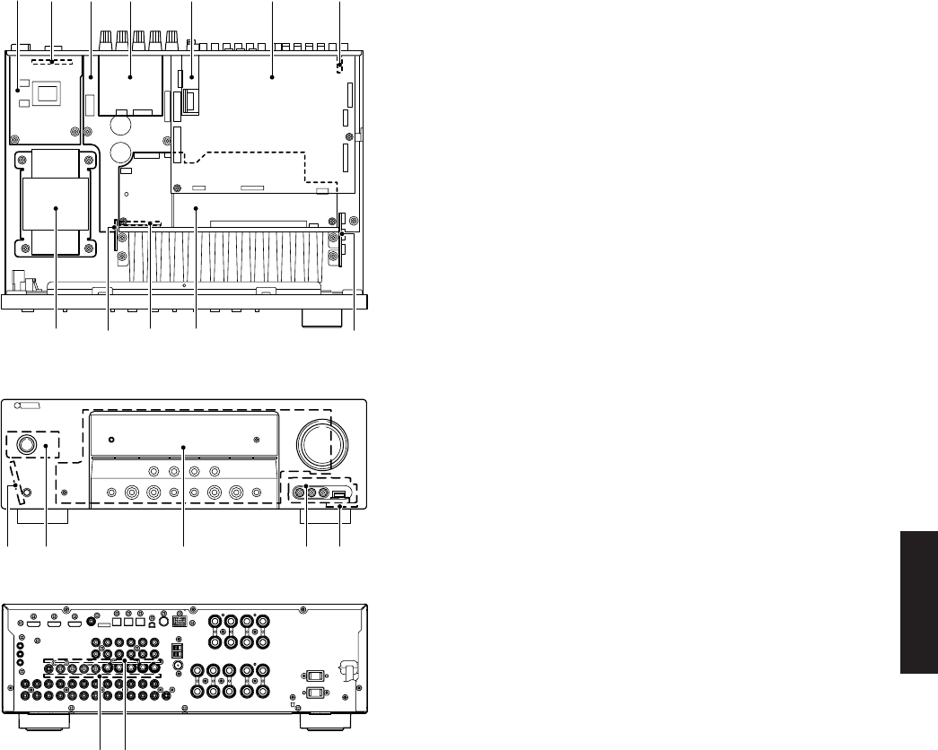
■INTERNAL VIEW
• Top view
• Front view
• Rear view
14
RX-V563/HTR-6150/DSP-AX563
RX-V563/HTR-6150/
DSP-AX563
Fig. 1
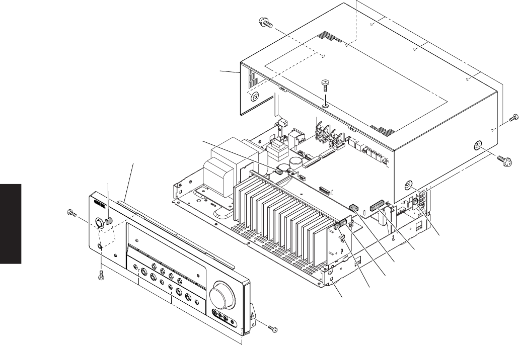
■DISASSEMBLY PROCEDURES
(Remove parts in the order as numbered.)
Disconnect the power cable from the AC outlet.
1. Removal of Top Cover
a. Remove 5 screws (1), 4 screws (2) and 1 screw (3).
(Fig. 1)
b. Slide the top cover rearward to remove it. (Fig. 1)
2. Removal of Front Panel Unit
a. Remove 6 screws (4). (Fig. 1)
b. Remove CB71 (R, T, K, A, B, G, E, F, L models), CB83,
CB366, CB601, CB602, CB608 and CB703. (Fig. 1)
c. Release hook and then remove the front panel unit.
(Fig. 1)
1
3
2
2
4
4
4
Top cover
Front panel unit
CB601
CB703
CB83
CB366
CB71 (R, T, K, A, B, G, E, F, L models)
CB608
CB602
Hook
15
RX-V563/HTR-6150/DSP-AX563
Fig. 3
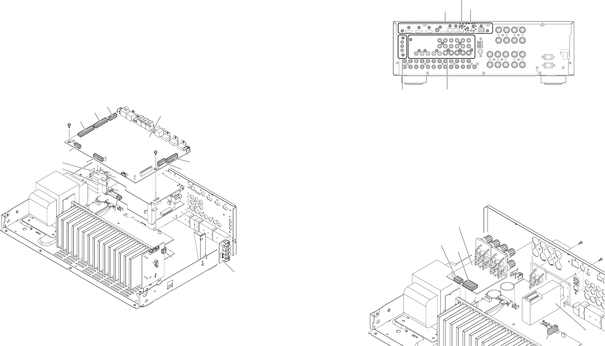
Fig. 2
5
5
DSP P.C.B.
VIDEO (6) P.C.B.
VIDEO (1) P.C.B.
VIDEO (2) P.C.B. CB21
CB22
CB609
CB32
CB31
CB84
CB81
CB82
CB301
7
6U, C models
R, T, K, A, B, G, E, F, L models
8
4. Removal of VIDEO (1), (2) and (6) P.C.B.s
a. Remove 2 screws (7). (Fig. 3)
b. Remove VIDEO (6) P.C.B. (Fig. 2)
c. Remove 9 screws (8). (Fig. 3)
d. Remove CB301 and CB609. (Fig. 2)
e. Remove VIDEO (1) and (2) P.C.B.s. (Fig. 2)
3. Removal of DSP P.C.B.
Note: U, C, F models
After replacement of DSP P.C.B. or writing of the
firmware, make sure to activate the self-diagnos-
tic function and change the “M6 Model ID” setting
to the same model name as this unit (RX-V563 or
HTR-6150).
a. Remove 2 screws (5). (Fig. 2)
b. Remove 11 screws (U, C models) / 10 scrwes (R, T, K,
A, B, G, E, F, L models) (6). (Fig. 3)
c. Remove CB21, CB22, CB31, CB32, CB81, CB82 and
CB84. (Fig. 2)
d. Remove DSP P.C.B. (Fig. 2)
Fig. 4
0
9
VIDEO (4) P.C.B.
CB353
CB351
CB403
FM / AM tuner
6. Removal of FM/AM Tuner
a. Remove 2 screws (0). (Fig. 4)
b. Remove CB403. (Fig. 4)
c. Remove FM/AM tuner. (Fig. 4)
5. Removal of VIDEO (4) P.C.B.
a. Remove 2 screws (9). (Fig. 4)
b. Remove CB351 and CB353. (Fig. 4)
g. Remove VIDEO (4) P.C.B. (Fig. 4)
RX-V563/HTR-6150/DSP-AX563
16
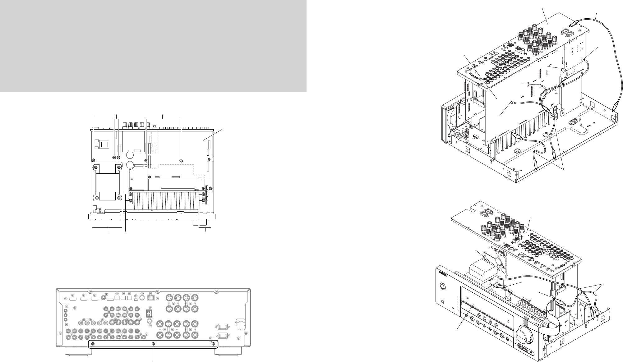
Fig. 6
Fig. 5
When checking the P.C.B.:
a. Remove the top cover. (Fig. 1)
b. Remove DSP P.C.B.. (Fig. 2)
c. Remove 6 screws (A). (Fig. 5)
d. Remove 2 screws (B). (Fig. 5)
e. Remove 3 screws (C). (Fig. 6)
f. Remove 2 screws (D). (Fig. 5)
g. Remove 4 screws (E). (Fig. 5)
h. Place the P.C.B. upright. (Fig. 7)
i. The P.C.B. removed from the chassis does not work because its grounding is loose.
Be sure to connect the ground of rear panel and MAIN (1) P.C.B. (G5004, G5005, G5006 and G3401) and DSP P.C.B.
(G801 and G802) to the chassis with a ground lead or the like. (Fig. 7)
Fig. 7
AB
A
D
A
DSP P.C.B.
E
C
MAIN (1) P
.C.B.
Ground lead
Ground lead
Rear panel
G5005
G5004
G5006
G3401
OPERATION (1) P.C.B.
Rear panel
DSP P.C.B.
G802
G801 Ground lead
17
RX-V563/HTR-6150/DSP-AX563
RX-V563/HTR-6150/
DSP-AX563
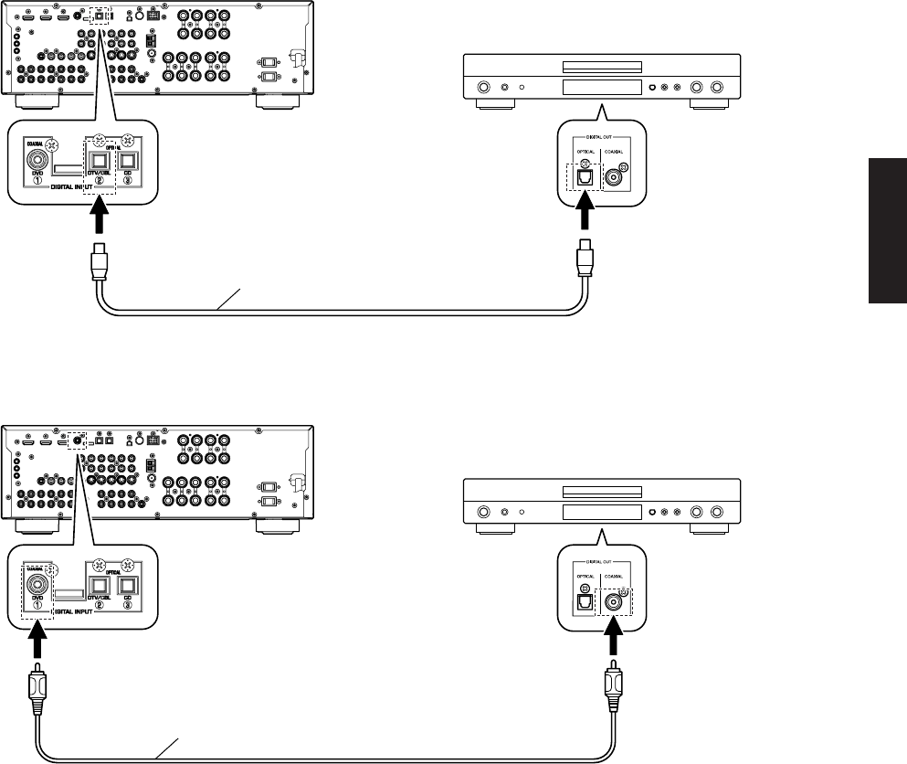
Optical cable
DVD/CD player
This unit
Digital audio pin cable
DVD/CD player
This unit
Note: U, C, F models
After replacement of DSP P.C.B. or writing of the firmware, make sure to activate the self-diagnostic function and
change the “M6 Model ID” setting to the same model name as this unit (RX-V563 or HTR-6150).
After replacing the following parts, be sure to write the latest firmware.
• P.C.B. ass’y DSP P.C.B.
• IC52 FLASH ROM of DSP P.C.B.
■UPDATING FIRMWARE
Example of connection between digital OPTICAL jacks
Example of connection between digital COAXIAL jacks
●Required Tools
• DVD or CD player (with DIGITAL OUTPUT (OPTI-
CAL or COAXIAL) jack)
• Optical cable (when OPTICAL jack is used)
• Digital audio pin cable (when COAXIAL jack is used)
• Firmware CD
* To make the firmware CD, download the latest
firmware from the specified download source to
PC.
●Operation Procedures
1. Connect this unit and DVD/CD player as shown be-
low. (Fig. 1)
Fig. 1
18
RX-V563/HTR-6150/DSP-AX563
RX-V563/HTR-6150/
DSP-AX563
Fig. 2
"SPEAKERS A/B/OFF" key
"MAIN ZONE ON/OFF" key
(RX-V563, HTR-6150)
"STANDBY/ON" key
(DSP-AX563)
* When the version of the firmware to be written is the same as the one existing in this unit, “Same Version”,
“Please...” and “Turn off!!” are displayed repeatedly. (Upgrading is not necessary.)
If the display remains unchanged for more than 10 seconds after starting the firmware CD play procedure, per-
form the firmware CD play procedure again from the beginning.
If “FILE CORRUPTED” is displayed after “Address:XXXXXX”, make sure that the firmware CD is not corrupted
and perform steps 1 to 8 of “Operation Procedures” again.
If “Upgrade Failed” is displayed, perform Steps 1 to 8 of “Operation Procedures” again.
Writing is completed.Writing is started.
Fig. 3
FIRMWARE UPDATE mode
SPDIF Upgrade
Address:XXXXXX Upgrade OK
Please...
Turn off!!
XXXXXX: Address information of the received data
2. While simultaneously pressing the “MAIN ZONE ON/OFF” (RX-V563, HTR-6150) / “STANDBY/ON” (DSP-AX563)
and “SPEAKERS A/B/OFF” keys of this unit, connect the power cable of this unit to the AC outlet. (Fig. 2)
The FIRMWARE UPDATE mode is activated and “SPDIF Upgrade” is displayed. (Fig. 2)
3. Connect the power cable of DVD/CD player to the AC outlet.
4. Press the “STANDBY/ON” key of the DVD/CD player.
5. Press the “EJECT” key of the DVD/CD player to open the disc tray.
6. Place the firmware CD in the disc tray and close the disc tray.
7. Press the “PLAY” key of the DVD/CD player.
Then writing of the firmware is started. (Fig. 3)
8. When writing of the firmware is completed, “Upgrade OK”, “Please...” and “Turn off!!” are displayed repeatedly. (Fig. 3)
19
RX-V563/HTR-6150/DSP-AX563
RX-V563/HTR-6150/
DSP-AX563
R1.PRESET INHI R2.PRESET RSRV
"STRAIGHT" key "AUDIO SELECT" key
"MAIN ZONE ON/OFF" key
(RX-V563, HTR-6150)
"STANDBY/ON" key
(DSP-AX563)
9. Press the “STOP” key of the DVD/CD player.
10. Press the “EJECT” key of the DVD/CD player to open the disc tray.
11. Remove the firmware CD from the disc tray and close the disc tray.
12. Turn off the power of the DVD/CD player and disconnect the power cable from the AC outlet.
13. Turn off the power by pressing the “MAIN ZONE ON/OFF” (RX-V563, HTR-6150) / “STANDBY/ON” (DSP-AX563)
key of this unit.
●Initializing of this unit
* After updating the firmware, be sure to initialize this unit.
1. Connect the power cable of this unit to the AC outlet.
2. Press the “MAIN ZONE ON/OFF” (RX-V563, HTR-6150) / “STANDBY/ON” (DSP-AX563) key while simultaneously
pressing the “STRAIGHT” and “AUDIO SELECT” keys. (Fig. 4)
The self-diagnostic function is activated.
PRESET RESERVED (Initialization reserved)PRESET INHIBIT (Initialization inhibited)
5. Turn off the power of this unit and disconnect the power cable from the AC outlet.
Fig. 4
3. Select the main menu “R. FACTORY PRESET”.
4. Select the “PRESET RSRV”.
20
RX-V563/HTR-6150/DSP-AX563
RX-V563/HTR-6150/
DSP-AX563
Fig. 5
4. Select the self-diagnostic function menu “S2. All checksum/S3. Program checksum”.
Confirm the displayed checksum is the same as the written firmware checksum. (Fig. 6)
(The checksum value is found where downloading is specified to.)
S1. VER. E048
Fig. 6
S2.A.SUM:EDA1
"STRAIGHT" key "AUDIO SELECT" key
"MAIN ZONE ON/OFF" key
(RX-V563, HTR-6150)
"STANDBY/ON" key
(DSP-AX563)
Example:
Example:
S3.P.SUM:FE77
5. Turn off the power of this unit and disconnect the power cable from the AC outlet.
●Confirmation of firmware version and checksum
To confirm that the firmware is updated successfully, check the firmware version and checksum value by using the self-
diagnostic function menu “S. ROM VER/SUM”.
For more information, refer to “SELF-DIAGNOSTIC FUNCTION”.
* When the displayed firmware version and checksum are different from written firmware version and checksum, follow
the steps from 1 to 13 of “Operation Procedures” again.
1. Reconnect the power cable of this unit to the AC outlet.
2. Press the “MAIN ZONE ON/OFF” (RX-V563, HTR-6150) / “STANDBY/ON” (DSP-AX563) key while simultaneously
pressing the “STRAIGHT” and “AUDIO SELECT” keys. (Fig. 5)
Then the self-diagnostic function is activated.
3. Select the self-diagnostic function menu “S1. Version”.
Confirm the displayed firmware version is the same as the written firmware version. (Fig. 5)
21
RX-V563/HTR-6150/DSP-AX563
Fig. 7
"STRAIGHT" key "AUDIO SELECT" key
"MAIN ZONE ON/OFF" key
(RX-V563, HTR-6150)
"STANDBY/ON" key
(DSP-AX563)
"PRESET/TUNING " key "PRESET/TUNING " key
M6.RX-V563 M6.HTR-6150
4. Press “PRESET/TUNING<” or “PRESET/TUNING>”key and select the model name.
Fig. 8
●Confirmation of model name (U, C, F models)
After replacement of DSP P.C.B. or writing of the firmware, make sure to activate the self-diagnostic function and change
the “M6 Model ID” setting to the same model name as this unit (RX-V563 or HTR-6150).
1. Connect the power cable of this unit to the AC outlet.
2. Press the “MAIN ZONE ON/OFF” (RX-V563, HTR-6150) / “STANDBY/ON” (DSP-AX563) key while simultaneously
pressing the “STRAIGHT” and “AUDIO SELECT” keys. (Fig. 7)
The self-diagnostic function is activated.
3. Select the self-diagnostic function menu “M6. Model ID”.
RX-V563/HTR-6150/DSP-AX563
22
1
2
3
4
5
1
2
3
4
5
6
1
2
3
4
5
1
2
3
4
5
6
7
8
9
10
1
2
3
4
1
2
1
2
3
4
5
6
7
8
9
10
L
M
N
O
P
Q
R
S
VIDEO CONVERSION
HDMI Check
AD DATA CHECK
PROTECTION
PROTECTION HIST.
RESERVED
FACTORY PRESET
ROM VER/SUM
Sub-menuNo. Main menu
V–IN (Video info.)
V–CONV S–V (Conversion S-video)
V–CONV CVBS (Conversion CVBS)
V–CONV OFF (Conversion OFF)
V–TestPttrn (Video test pattern)
HDMI SPDIF (SPDIF audio playback)
HDMI NONE
HDMI IN1
HDMI IN2
I2C : xx xxx (I2C access check)
Model ID for EDID setting
PD : xxx DI : xxx (ex. N1PD: 45DI: 0)
V1 : xxx V2 : xxx (ex. N2V1: 94V2:128)
TH : xxx PL : xxx (ex. N3TH: 64PL:255)
PI : xxx DE : xxx (ex. N4PI: 0DE: 0)
K0 : xxx K1 : xxx (ex. N5K0:254K1:254)
PRD : xxx/xxx (ex. O1.PRD: 23/ 70)
PV1 : xxx/xxx (ex. O2.PV1: 68/161)
PV2 : xxx/xxx (ex. O3.PV2:104/181)
THM : xxx/xxx (ex. O4.THM: 0/131)
L66 : xxx/xxx (PLDET 6ch 6ohms : xxx/xxx) (ex. O5.L66: 0/ 0)
L86 : xxx/xxx (PLDET 8ch 6ohms : xxx/xxx) (ex. O6.L86: 0/ 0)
L68 : xxx/xxx (PLDET 6ch 8ohms : xxx/xxx) (ex. O7.L68: 0/ 0)
L88 : xxx/xxx (PLDET 8ch 8ohms : xxx/xxx) (ex. O8.L88: 0/ 0)
PRI : xxx/xxx (PRI : xxx/xxx) (ex. O9.PRI: 0/100)
PDE : xxx/xxx (PDET : xxx/xxx) (ex. O10PDE: 0/255)
History 1 (ex. PRV:xxx)
History 2 (ex. THM:xxx)
History 3 (ex. PRI:xxx)
History 4
PRESET INHI
PRESET RSRV
Microprocessor version
All checksum
Program checksum
SPI checksum
SPD checksum
XM version (U, C models)
SIRIUS version (U, C models)
FlashROM test
SDRAM test
EEPROM test
■SELF-DIAGNOSTIC FUNCTION
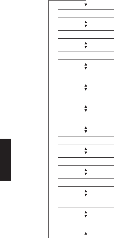
This unit has self diagnosis functions that are intended for inspection, measurement and location of faulty point.
There are 19 main menu items, each of which has sub-menu items.
Listed in the table below are menu items and sub-menu items.
Note that not all menu items listed will apply to the models covered in this service manual.
Sub-menuNo. Main menu
1
2
1
2
3
4
5
1
2
3
4
5
1
2
3
4
5
1
1
2
3
4
5
1
2
3
4
5
6
7
8
9
1
2
3
4
5
6
7
8
9
10
11
1
2
3
4
1
2
3
4
1
2
3
4
5
6
7
8
A
B
C
D
E
F
G
H
I
J
K
BYPASS
AUDIO CHECK
SPEAKERS SET
XCH-INPUT
MIC CHECK
FL/OSD CHECK
TEST TONE
XM STATUS
(U, C models)
iPod
USB
(R, T, K, A, B, G, E, F, L models)
SIRIUS
(U, C models)
ANLOG BYPAS
DSP BYPASS
AUDIO CHECK
ANALOG AUDIO PLAYBACK
MUTE ALL
MUTE SYS IC
MUTE TR
FRNT : SML0dB
CENTER : NONE
LFE/B : FRNT
TONE : MAX
TONE : MIN
6chINPUT 6Ω
8chINPUT 6Ω
6chINPUT 8Ω
8chINPUT 8Ω
LIM : PLDET : THM (ex. D5.255:255: 64)
MIC CHECK
VFD CHECK
VFD DISP OFF
VFD DISP ALL
VFD DIMMER
CHECK PATTERN
TEST ALL
TEST FRNT L
TEST CENTER
TEST FRNT R
TEST SURR R
TEST SURB R
TEST SURB L
TEST SURR L
TEST LFE
1k – 1dB/44
1k –61dB/44
MUTE /44
XM TONE/44
ISO TONE/44
1k – 1dB/32
1k –61dB/32
MUTE /32
XM TONE/32
ISOTONE/32
BUSPWR (BUS power) : OFF
DOCK : xx xxx
DOCK IGNORE
Bluetooth version
Clear Bluetooth pairing info.
USBFile1/xx
USBFile2/xx
High Speed TEST_PACKET mode
High Speed TEST_SE0_NAK mode
SIRIUS connection check
SIRIUS antenna status
SIRIUS loop back test
SIRIUS SSP version display (only for SIRIUS certification engineer)
SIRIUS firmware #1 version display (only for SIRIUS certification engineer)
SIRIUS Firmware #2 version display (only for SIRIUS certification engineer)
SIRIUS FW product_id version display (only for SIRIUS certification engineer)
SIRIUS FW sequence_id version display (only for SIRIUS certification engineer)
23
RX-V563/HTR-6150/DSP-AX563
RX-V563/HTR-6150/
DSP-AX563
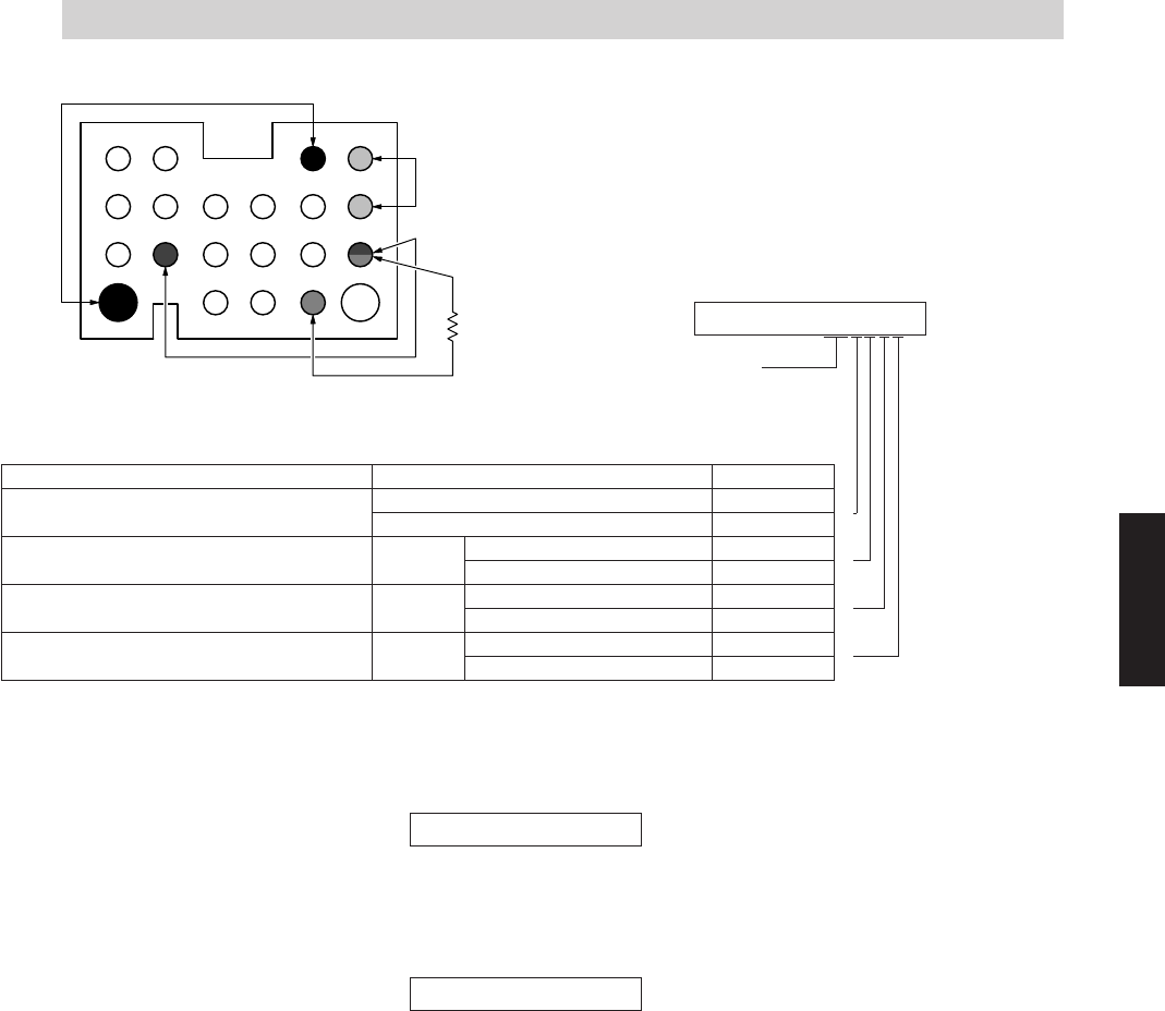
• Starting Self-diagnostic Function
Press the “MAIN ZONE ON/OFF” (RX-V563, HTR-6150) / “STANDBY/ON” (DSP-AX563) key while simultaneously
pressing those two keys of this unit as indicated in the figure below.
Turn on the power while pressing these keys.
Keys of this unit
RX-V563 / HTR-6150
DSP-AX563
• Starting Self-diagnostic Function in the protection cancel mode
If the protection function works and causes hindrance to trouble diagnosis, cancel the protection function as described
below, and it will be possible to enter the self-diagnostic function mode. (The protection functions other than the excess
current detect function will be disabled.)
Press the “MAIN ZONE ON/OFF” (RX-V563, HTR-6150) / “STANDBY/ON” (DSP-AX563) key while simultaneously
pressing those two keys indicated in the figure above. At this time, keep pressing those two keys for 3 seconds or longer.
In this mode, the [SLEEP] segment of the FL display of this unit flashes to indicate that the mode is self-diagnostic
function mode with the protection functions disabled.
CAUTION!
Using this product with the protection function disabled may cause damage to this unit. Use special care for this
point when using this mode.
• Canceling Self-diagnostic Function
1. Before canceling self-diagnostic function, execute setting for FACTORY PRESET of main menu No.R (Memory
initialization inhibited or Memory initialized).
* In order to keep the user memory stored, be sure to select PRESET INHIBITED (Memory initialization inhibited).
2. Turn off the power by pressing the “MAIN ZONE ON/OFF” (RX-V563, HTR-6150) / “STANDBY/ON” (DSP-AX563)
key of this unit.
• Display provided when Self-diagnostic Function started
On the FL display of this unit, an opening message (including the protection history) appears for a few seconds followed
by the self-diagnostic function menu display (1. ANALOG BYPASS).
24
RX-V563/HTR-6150/DSP-AX563
RX-V563/HTR-6150/
DSP-AX563
When there is a history of protection function due to excess current
Cause: An excessive current flowed through the power amplifier.
Supplementary information:
As current of the power amplifier is detected, the abnormal channel can be identified by checking the current
detect transistor.
Turning on the power without correcting the abnormality will cause the protection function to work immediately
and the power supply will instantly be shut off.
When there is no history of protection function:
NO PROTECTION
After a few seconds
A1.ANLOG BYPAS
When there is no protection history
Note)
• Applying the power to this unit without correcting the abnormality can be dangerous and cause additional
circuit damage. To avoid this, if “PRI” and “PRD” protection function has been activated 3 times continuously,
the power will not turn on even when the “STANDBY/ON” key is pressed. In order to turn on the power again,
disconnect the power cable of this unit from the AC outlet once and then reconnect it again.
• The output transistors in each power amplifier channel should be checked for damage before applying power to
this unit.
• Power amplifier current should be monitored by measuring DC voltage across the emitter resistors for each
channel.
PRI PRT:xxx
AD value when the protection function is working
AD value when the protection function is working
PRD PRT:xxx
When there is a history of protection function due to abnormal DC output
Cause: DC output of the power amplifier is abnormal.
Supplementary information:
The protection function worked due to a DC voltage appearing at the speaker terminal.
A cause could be a defect in the amplifier.
If the power is turned on with the abnormality unsolved, the protection function works in 3 seconds to turn off
the power.

25
RX-V563/HTR-6150/DSP-AX563
RX-V563/HTR-6150/
DSP-AX563
Cause: The temperature of the heat sink is excessive.
Supplementary information:
The protection function worked due to the temperature limit being exceeded.
Causes could be poor ventilation or a defect related to the thermal sensor.
History of protection function
When the protection function has worked, its history is stored in memory with a backup.
Even if no abnormality is noted while servicing the unit, an abnormality which has occurred previously can be
defined as long as the backup data has been stored.
The history of the protection function is cleared when self-diagnostic function is cancelled by selecting PRESET
RESERVED (Memory initialized) of main menu No. R or when the backup data is erased.
When there is a history of protection function due to abnormal voltage in the power supply section
Cause: The voltage in the power supply section is abnormal.
Supplementary information:
The protection function worked due to a defect or overload in the power supply.
If the power is turned on with the abnormality unsolved, the protection function works in 1 second to turn off the
power.
PRV1 PRT:xxx
AD value when the protection function is working
THM PRT:xxx
AD value when the protection function is working
When there is a history of protection function due to excessive heat sink temperature
If the power is turned on with the abnormality unsolved, the protection function works in 1 second to turn off the power.
For detection of each protection function, refer to main menu described later.
When there is a history of protection function due to abnormal voltage in the power supply section
Cause: The voltage in the power supply section is abnormal.
Supplementary information:
The protection function worked due to a defect or overload in the power supply.
If the power is turned on with the abnormality unsolved, the protection function works in 1 second to turn off the
power.
PRV2 PRT:xxx
AD value when the protection function is working
26
RX-V563/HTR-6150/DSP-AX563
RX-V563/HTR-6150/
DSP-AX563
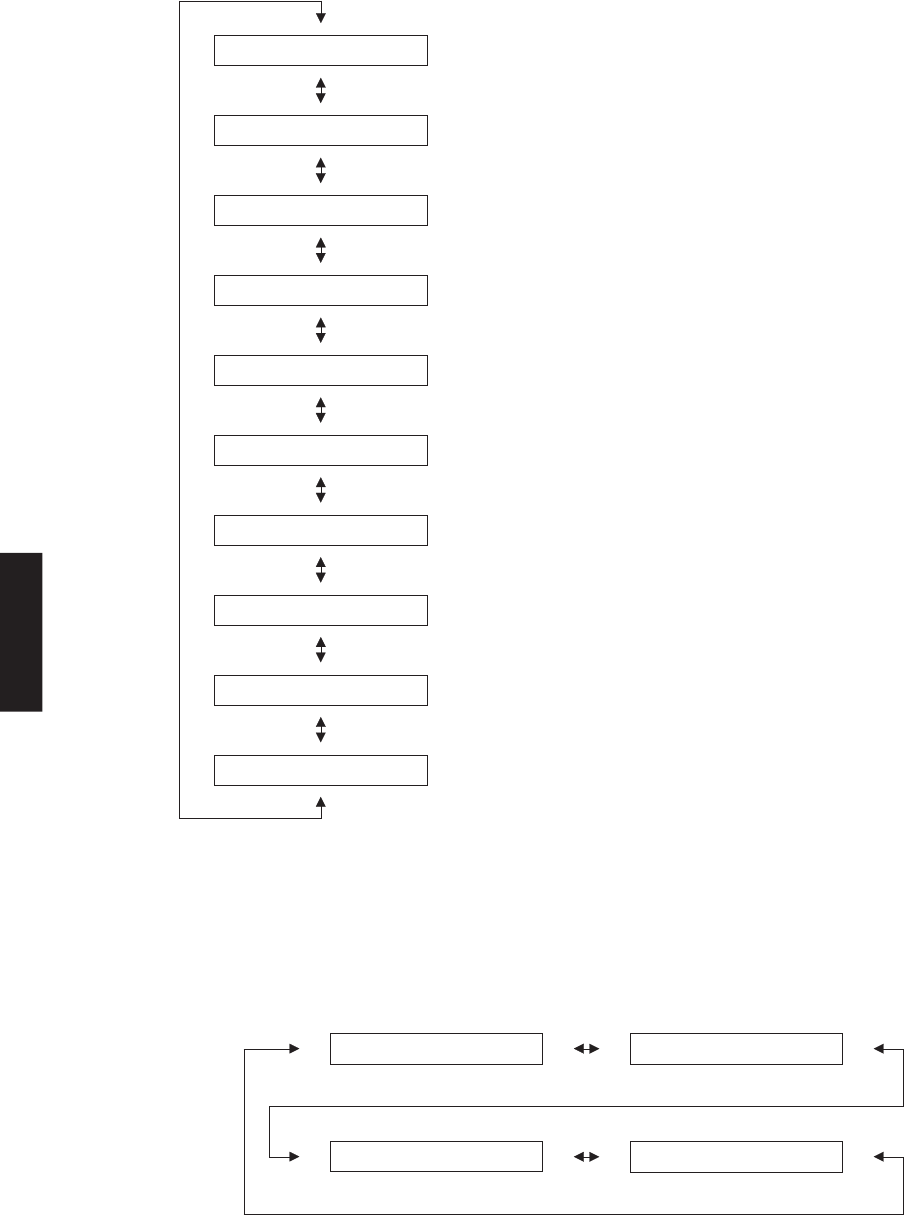
• Operation procedure of Main menu and Sub-menu
There are 19 main menu items, each of having sub-menu items.
Main menu selection:
Select the main menu using “ ww
ww
w ” (forward) and “ qq
qq
q ” (reverse) keys of PROGRAM.
Sub-menu selection:
Select the sub-menu using “SCENE 2” (forward) and “SCENE 1” (Reverse) keys.
• Functions in Self-Diagnostic Function mode
In addition to the self-diagnostic function menu items, functions as listed below are available.
• Power on/off
• Master volume
• Muting
• Speakers A/B/OFF
• Input selection
• Audio select
• Tone control
* Functions related to the tuner and the set menu are not available.
Keys of this unit
ForwardReverse
ForwardReverse
Sub-menu selection
Main menu selection
• Initial settings used to start Self-Diagnostic Function
The following initial settings are used when starting self-diagnostic function.
When self-diagnostic function is canceled, these settings are restored to those before starting self-diagnostic function.
• Master volume: -20 dB
• Input: DVD (MULTI CHANNEL INPUT OFF)
• Effect level: 0 dB
• Main menu: 1. ANALOG BYPASS
27
RX-V563/HTR-6150/DSP-AX563
RX-V563/HTR-6150/
DSP-AX563
B. AUDIO CHECK
AUDIO CHECK
The input sound signal is output.
* When the inputted sound signal is 2 ch L/R, it is distributed as follows when output.
L ch: FRONT L, CENTER, SURROUND L, LFE ( L ch +10 dB)
R ch: SURROUND R
B1.AUDIO CHECK
Input level Volume SPEAKER OUT SUBWOOFER
OUTPUT
A1.ANLOG BYPAS
• Details of Self-Diagnostic Function menu
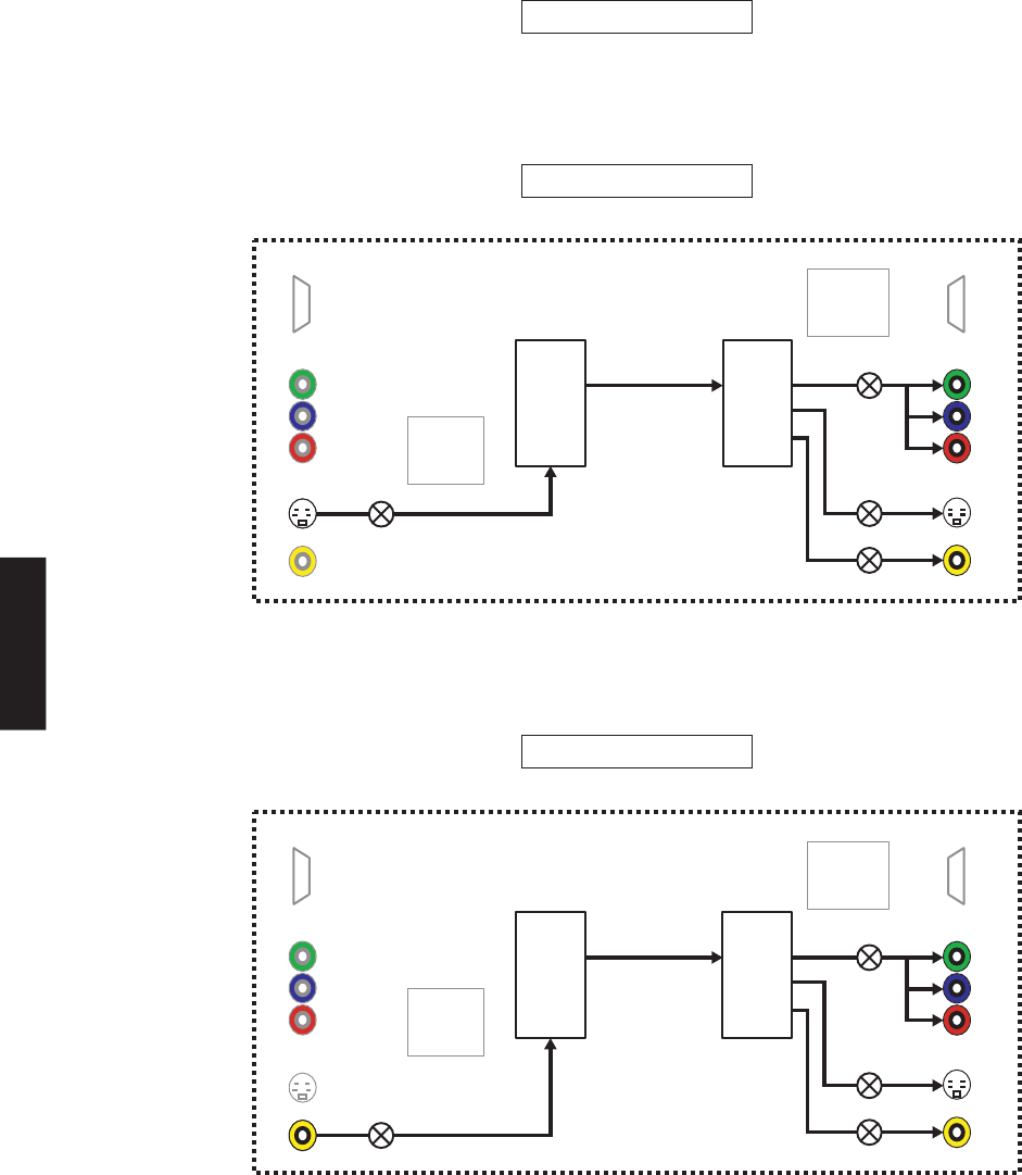
A. BYPASS
Using the sub-menu, it is possible to select ANALOG BYPASS output or DSP BYPASS output.
ANALOG BYPASS
The analog input sound signal is output to FRONT L/R with EFFECT OFF.
INPUT: DVD ANALOG
SPEAKER OUT: 1 kHz, SUBWOOFER OUTPUT: 50 Hz
A2.DSP BYPASS
Both ch, -20 dBm +6.0 dB
FRONT
+11.5 dBm
CENTER
-∞
SURROUND
-∞-∞
Input level Volume SPEAKER OUT SUBWOOFER
OUTPUT
INPUT: DVD ANALOG
SPEAKER OUT: 1 kHz, SUBWOOFER OUTPUT: 50 Hz
Both ch, -20 dBm +6.0 dB
FRONT
+11.5 dBm
CENTER
-∞
SURROUND
-∞-∞
DSP BYPASS
The digital input sound signal is output to FRONT L/R with EFFECT OFF.
Input level Volume SPEAKER OUT SUBWOOFER
OUTPUT
INPUT: DVD ANALOG
SPEAKER OUT: 1 kHz, SUBWOOFER OUTPUT: 50 Hz
Both ch, -20 dBm +6.0 dB
FRONT
+11.5 dBm
CENTER
+11.5 dBm
SURROUND
+11.5 dBm 0 dBm
B3.MUTE ALL
B4.MUTE SYS IC
B5.MUTE TR
MUTE SYSTEM IC
Sound signals of all channels are muted by System IC
(MAIN P.C.B.).
MUTE ALL
Sound signals of all channels are muted by System IC
(MAIN P.C.B.) and Transistor (Q5008-5011 MAIN
P.C.B.).
MUTE TRANSISTOR
Sound signals of all channels are muted by Transistor
(Q5008-5011 MAIN P.C.B.).
B2.ANALOG PLAY
ANALOG AUDIO PLAYBACK
The input sound signal is output.
28
RX-V563/HTR-6150/DSP-AX563
RX-V563/HTR-6150/
DSP-AX563
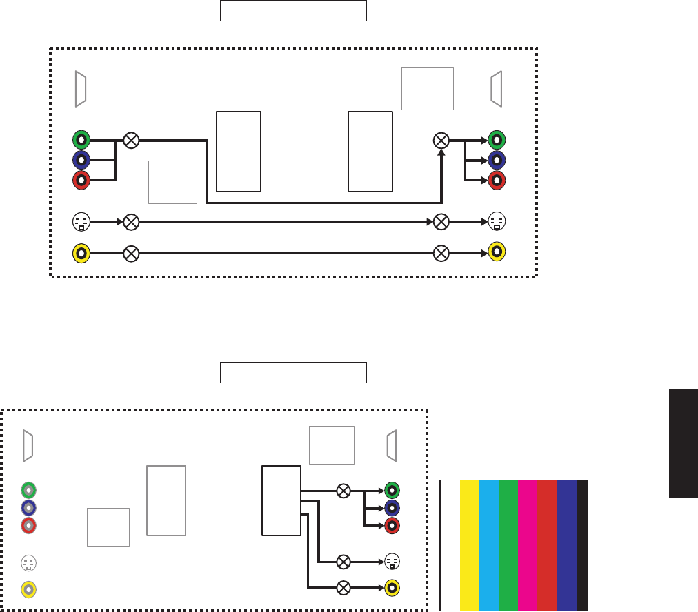
C. SPEAKER SET
The analog switch settings for each sub-menu are as shown in the table below.
LARGE: This mode is used for a speaker with high bass reproduction performance (a large unit).
Full bandwidth signals are output.
SMALL: This mode is used for a speaker with low bass reproduction performance (a small unit).
The signals of 90 Hz or less are mixed into the channel specified by LFE/BASS.
NONE: This mode is used for no center speaker.
The center content is reduced by 3 dB and distributed to FRONT L/R.
SWFR: LFE of 5.1 ch signal or LFE/BASS lower than 90 Hz is output through SUBWOOFER OUT.
FRONT: LFE of 5.1 ch signal or LFE/BASS lower than 90 Hz is distributed to FRONT L/R.
C1.FRNT:SML0dB FRONT: SML 0dB
The FRONT L/R signal, when 90 Hz or lower, is mixed to the channel specified by LFE/
BASS.
CENTER: NONE
The CENTER signal is distributed to FRONT L/R.
LFE / BASS: FRONT
The LFE (SUBWOOFER) signal is distributed to FRONT L/R.
TONE: MAX
The signal is output with the tone control [BASS +10 dB, TREBLE +10 dB].
TONE: MIN
The signal is output with the tone control [BASS -10 dB, TREBLE -10 dB].
C2.CENTER:NONE
C3.LFE/B:FRNT
C4.TONE:MAX
C5.TONE:MIN
Input level Volume SPEAKER OUT SUBWOOFER
OUTPUT
INPUT: DVD ANALOG
SPEAKER OUT: 1 kHz, SUBWOOFER OUTPUT: 50 Hz
Both ch, -20 dBm
Both ch, -20 dBm
Both ch, -20 dBm
Both ch, -20 dBm
Both ch, -20 dBm
+6.0 dB
+6.0 dB
+6.0 dB
+6.0 dB
+6.0 dB
FRONT
+11.5 dBm
+11.5 dBm
+11.5 dBm
+14.5 dBm
+8.5 dBm
CENTER
-∞
-∞
-∞
-∞
-∞
SURROUND
-∞
-∞
-∞
-∞
-∞
-3.5 dBm
-∞
-∞
-∞
-∞
Sub-menu
FRONT : SML 0dB
CENTER : NONE
LFE/B : FRNT
TONE : MAX
TONE : MIN
SMALL
LARGE
LARGE
LARGE
LARGE
LARGE
NONE
SMALL
LARGE
LARGE
LARGE
LARGE
SMALL
LARGE
LARGE
SWFR
SWFR
FRONT
SWFR
SWFR
FRONT : SML 0dB
CENTER : NONE
LFE/B : FRNT
TONE : MAX
TONE : MIN
29
RX-V563/HTR-6150/DSP-AX563
RX-V563/HTR-6150/
DSP-AX563
D. XCH INPUT
The input source [MULTI CHANNEL INPUT] is selected.
It is possible to select the 6-ohm/8-ohm by using the sub-menu.
6 ch INPUT 6-ohm
D1.6chINPUT 6 Ω
D2.8chINPUT 6 Ω
Input level Volume SPEAKER OUT SUBWOOFER
OUTPUT
INPUT: MULTI CH INPUT
SPEAKER OUT: 1 kHz, SUBWOOFER OUTPUT: 50 Hz
Both ch, -20 dBm +6.0 dB
FRONT
+11.5 dBm
CENTER
+11.5 dBm
SURROUND
+11.5 dBm -3.5 dBm
Sub-menu
8 ch INPUT 6-ohm
Input level Volume SPEAKER OUT SUBWOOFER
OUTPUT
INPUT: MULTI CH INPUT
SPEAKER OUT: 1 kHz, SUBWOOFER OUTPUT: 50 Hz
Both ch, -20 dBm +6.0 dB
FRONT
+11.5 dBm
CENTER
+11.5 dBm
SURROUND
+11.5 dBm -3.5 dBm
Sub-menu
LIM/PLDET/THM
LIM: Setting value of LIM (Limiter control)
* Do not change the setting value because this item is only for the use of development staff.
PLDET: Power limiter detection
The A/D conversion value during operation is displayed.
THM: Thermo protection detection
The A/D conversion value during operation is displayed.
(Reference voltage: 3.3 V=255)
D5.255:255: 64
THM (Thermo protection detection)
PLDET (Power limiter detection)
LIM (Limiter control)
D3.6chINPUT 8 Ω
6 ch INPUT 8-ohm
Input level Volume SPEAKER OUT SUBWOOFER
OUTPUT
INPUT: MULTI CH INPUT
SPEAKER OUT: 1 kHz, SUBWOOFER OUTPUT: 50 Hz
Both ch, -20 dBm +6.0 dB
FRONT
+11.5 dBm
CENTER
+11.5 dBm
SURROUND
+11.5 dBm -3.5 dBm
Sub-menu
D4.8chINPUT 8 Ω
8 ch INPUT 8-ohm
Input level Volume SPEAKER OUT SUBWOOFER
OUTPUT
INPUT: MULTI CH INPUT
SPEAKER OUT: 1 kHz, SUBWOOFER OUTPUT: 50 Hz
Both ch, -20 dBm +6.0 dB
FRONT
+11.5 dBm
CENTER
+11.5 dBm
SURROUND
+11.5 dBm -3.5 dBm
Sub-menu
6 ch INPUT 6-ohm
6 ch INPUT 8-ohm
6 ch INPUT 8-ohm
6 ch INPUT 8-ohm
30
RX-V563/HTR-6150/DSP-AX563
RX-V563/HTR-6150/
DSP-AX563
E. MIC CHECK
The signals input through the microphone are output of FRONT L/R via A/D and D/A.
E1.MIC CHECK
F1.VFD CHECK
Checking FL display section
Initial display
All segments OFF
All segments ON (dimmer 100 %)
All segments ON (dimmer 50 %)
Lighting of segments in lattice
Check of the Video control section. (Monitor out)
Initial display (OSD OFF)
OSD OFF
OSD characters ON
OSD characters ON
OSD characters ON
Lighting in lattice
NormalShort
OSD characters
F. FL CHECK
Use this program to check the FL display section and video control section. When checking the video control
section, connect a TV monitor to this unit with a component video cable, S video cable and video pin cable.
Selection of the FL display section or video control section varies according to the submenu operation as shown
below.
For audio signal processing, use STRAIGHT.

31
RX-V563/HTR-6150/DSP-AX563
RX-V563/HTR-6150/
DSP-AX563
G. TEST TONE
The outputs the noise through the channels specified by the submenu.
The noise frequency for LFE (SUBWOOFER) is 35 to 80 Hz.
Other than that, the noise frequency is 500 to 2 kHz.
G1.TEST ALL TEST ALL
Noise is output from all channels.
TEST FRONT L
Noise is output from the FRONT L channel.
TEST CENTER
Noise is output from the CENTER channel.
TEST FRONT R
Noise is output from the FRONT R channel.
TEST SURROUND R
Noise is output from the SURROUND R channel.
TEST SURROUND BACK R
Noise is output from the SURROUND BACK R channel.
TEST SURROUND BACK L
Noise is output from the SURROUND BACK L channel.
TEST SURROUND L
Noise is output from the SURROUND L channel.
TEST LFE (SUBWOOFER)
Noise is output from the LFE (SUBWOOFER) channel.
G2.TEST FRNT L
G4.TEST FRNT R
G3.TEST CENTER
G5.TEST SURR R
G6.TEST SURB R
G7.TEST SURB L
G8.TEST SURR L
G9.TEST LFE
32
RX-V563/HTR-6150/DSP-AX563
RX-V563/HTR-6150/
DSP-AX563
H1.1k - 1dB/44 1 kHz, -1 dB / 44.1 kHz
The test tone (1 kHz, -1 dB / 44.1 kHz) is output.
1 kHz, -61 dB / 44.1 kHz
The test tone (1 kHz, -61 dB / 44.1 kHz) is output.
Mute / 44.1 kHz
No signal is output.
XM tone / 44.1 kHz
The XM tone / 44.1 kHz is output.
ISO tone / 44.1 kHz
The ISO tone /44.1 kHz is output.
1 kHz, -1 dB / 32.0 kHz
The test tone (1 kHz, -1 dB / 32.0 kHz) is output.
1 kHz, -61 dB / 32.0 kHz
The test tone (1 kHz, -61 dB / 32.0 kHz) is output.
Mute / 32.0 kHz
No signal is output.
XM tone / 32.0 kHz
The XM tone / 32.0 kHz is output.
ISO tone / 32.0 kHz
The ISO tone / 32.0 kHz is output.
XM bus power: OFF
The power of XM module is turned off.
H3.MUTE /44
H4.XM TONE /44
H5.ISO TONE/44
H6.1k - 1dB/32
H7.1k -61dB/32
H8.MUTE /32
H9.XM TONE /32
H10.ISOTONE/32
H11.BUSPWR:OFF
H. XM STATUS (U, C models)
The output check of XM radio is executed.
(Connect XM radio antenna module to this unit before executing.)
H2.1k -61dB/44
33
RX-V563/HTR-6150/DSP-AX563
RX-V563/HTR-6150/
DSP-AX563
UART loop back test
iPAP (iPod accessory power) detection
iPDET (iPod installation to DOCK) detection
DKID (DOCK ID) detection
OK
NG
IC83
pin No.5
IC82
pin No.5
IC82
pin No.4
High
Low
Low (iPod universal dock)
High (Bluetooth adapter)
10 k-ohms, 1/4 W pull down
Other
Check item Result Display
I. iPod
This menu is used to test the DOCK connector without the iPod itself. After turning off the power to this unit short
between pins No. 14 (TX) and No. 18 (RX), between pins No. 1 (PWR) and No. 17 (ACCPOW), between pins No. 4
(iPDET) and No. 8 (DGND) and between pins No. 21 (DKID) and No. 8 (DGND) of the DOCK connector. (Make sure
that the power is turned off when shorting pins.)
Start the self-diagnostic function and select this menu.
The check result is displayed according to the following display specifications.
DOCK CONNECTOR
I1.DOCK:NG NNN
All Y = “OK”
Others = “NG”
Y
N
Y
N
Y
N
Y
N
I2.DOCK IGNORE
DOCK ignore
When DOCK and iPod are connected, the input source [DOCK (iPod)] is made ineffective and [V-AUX] is selected.
10 k-ohms
1/4 W
12
19
3456 78
91011121314
15 16 17 18
20 21
I3.BTYS:x.xxx
Bluetooth version
When the Bluetooth DOCK is connected, the firmware version of that Bluetooth module is displayed.
Note) Be sure to return the shorted pins to their original condition after executing this test.
34
RX-V563/HTR-6150/DSP-AX563
RX-V563/HTR-6150/
DSP-AX563
J. USB (R, T, K, A, B, G, E, F, L models)
The music file recorded in the USB flash memory is reproduced.
a. Copy the 2 music files from PC into the roof folder of the USB flash memory.
b. Insert the USB flash memory to the USB terminal of this unit.
USB FILE1
Reproduced at this time is the first piece of the music file in the USB flash memory connected to the USB terminal on the
front panel.
USB FILE2
Reproduced at this time is the second piece of the music file in the USB flash memory connected to the USB terminal on
the front panel.
J1.USBFile1/OK
OK: Connected/Playback
NG: No music file
J2.USBFile2/OK
OK: Connected/Playback
NG: No music file
I4.BT CLR:INHI I4.BT CLR:RSRV
Initialization inhibited Initialization reserved
Initialization inhibited
User memory initialization is not executed. Select this sub-
menu to protect the user memory.
Initialization reserved
Initialization of the use memory is reserved. (Actually, initial-
ization is executed the next time that the power is turned on.)
Select this sub-menu to reset to the original factory settings
or to reset the use memory.
Any protection history will be cleared.
Clear Bluetooth pairing information
While the Bluetooth DOCK is connected, initialization of the Bluetooth DOCK pairing information is inhibited/reserved.
Use “PRESET/TUNING<” and “PRESET TUNING>” keys for operation.
35
RX-V563/HTR-6150/DSP-AX563
RX-V563/HTR-6150/
DSP-AX563
K. SIRIUS (U, C models)
The SIRIUS antenna module is checked.
(Connect SIRIUS antenna module to this unit before executing.)
K1.SIRIUS : xx
K3.SR-LOOP: xx
K4SSP:xx xx xx
K5MAC:xx xx xx
K6ADP:xx xx xx
K7PRD:xx xx xx
K2.SR:xx xx xx
SIRIUS:
Connection of the SIRIUS antenna module connection is checked.
SR:
The connection information of the SIRIUS antenna module is displayed.
SR-LOOP: SIRIUS loop back test
SSP:
The SIRIUS version #0 (SSP) is displayed.
MAC:
The SIRIUS version #1 (MAC) is displayed.
ADP:
The SIRIUS version #2 (ADP) is displayed.
PRDID:
The PRD ID (product id) is displayed.
SEQID:
The SEQ ID (sequence id) is displayed.
K8SEQ:xx xx xx
OK : Normal
NG : Abnormal
—: No connected
The result of antenna diagnostic mode (status)
Antenna error history (SSP Error Codes)
Antenna generation (gen_id)
OK : Normal
NG : Abnormal
36
RX-V563/HTR-6150/DSP-AX563
RX-V563/HTR-6150/
DSP-AX563
CONVERSION CVBS
The signal passage as shown below is checked.
L3.V-CONV CVBS
CONVERSION S-Video
The signal passage as shown below is checked.
L2.V-CONV S-V
L. VIDEO CONVERSION
The video circuit is checked by the sub-menu operation.
Video INFO.
The information of video signal is displayed.
L1. V-IN:
S Video
Video
S-Video
HDMI INComponent
HDMI OUTComponent
S Video
Video
VIDEO
IC304
LC74782
OSD
DIGITAL
IC11
AD9389
HDMI Tx
DIGITAL
IC12
ADV7441
VIDEO
DECODER
DIGITAL
IC21
ADV7172
VIDEO
ENCODER
CVBS
HDMI INComponent
S Video
Video
HDMI OUTComponent
S Video
Video
VIDEO
IC304
LC74782
OSD
DIGITAL
IC11
AD9389
HDMI Tx
DIGITAL
IC12
ADV7441
VIDEO
DECODER
DIGITAL
IC21
ADV7172
VIDEO
ENCODER
37
RX-V563/HTR-6150/DSP-AX563
RX-V563/HTR-6150/
DSP-AX563
CONVERSION OFF
The signal passage as shown below is checked.
L4.V-CONV OFF
Video
S Video
Conversion OFF
HDMI INComponent
HDMI OUTComponent
S Video
Video
Bypass
VIDEO
IC304
LC74782
OSD
DIGITAL
IC11
AD9389
HDMI Tx
DIGITAL
IC12
ADV7441
VIDEO
DECODER
DIGITAL
IC21
ADV7172
VIDEO
ENCODER
Test pattern
The test pattern is output from IC84 (DIGITAL P.C.B.).
L5.V-TestPttrn
S Video
Video
Test pattern
HDMI INComponent
HDMI OUTComponent
S Video
Video
Test
pattern
VIDEO
IC304
LC74782
OSD
DIGITAL
IC11
AD9389
HDMI Tx
DIGITAL
IC12
ADV7441
VIDEO
DECODER
DIGITAL
IC21
ADV7172
VIDEO
ENCODER
IC21 Test pattern
38
RX-V563/HTR-6150/DSP-AX563
RX-V563/HTR-6150/
DSP-AX563
M. HDMI SELECT
The audio signals input to HDMI IN are selected by the sub-menu and output.
HDMI SPDIF (SPDIF audio playback)
SPDIF signal is output.
M1.HDMI SPDIF
HDMI NONE
No signal is output.
M2.HDMI MONE
HDMI IN1
HDMI “IN 1” is output.
M3.HDMI IN1
HDMI IN2
HDMI “IN 2” is output.
M4.HDMI IN2
I2C : xx xxx (I2C access check)
M5.I2C:NG NYY
All Y = “OK”
Others = “NG”
HDMI Rx
(IC12 DSP P.C.B.)
HDMI Tx
(IC11 DSP P.C.B.)
VIDEO ENCODER
(IC21 DSP P.C.B.)
OK
NG
OK
NG
OK
NG
Y
N
Y
N
Y
N
Check item Result Display
Model ID for EDID setting (U, C, F models)
After replacement of DSP P.C.B or writing of the firmware, make sure to change the “M6 Model ID” setting to the same
model name as this unit (RX-V563 or HTR-6150).
Press “PRESET/TUNING<” or “PRESET TUNING>” key for selection.
M6.HTR-6150M6.RX-V563
M6.RX-V563
R, T, K, A, G, E, L models
M6.DSP-AX563
B model
39
RX-V563/HTR-6150/DSP-AX563
RX-V563/HTR-6150/
DSP-AX563
N2V1: 94V2:128
N. A/D DATA CHECK
This menu is used to display the A/D conversion value of the microprocessor which detects panel keys of the main
unit and protection functions in using the sub-menu.
When K0/K1 menu is selected, keys become non-operable due to detection of the values of all keys. However, it is
possible to advance to the next sub-menu by turning the VOLUME of the main unit. When using this function, note
that turning the VOLUME more than 1 click would cause the volume value to change.
During signal processing, the condition before execution is maintained.
* The figures in the diagram are given as reference only.
PD/DI
PD: PRD (Power amplifier DC protection detection)
The output of power amplifier DC (DC voltage) is detected.
Normal value: 27 to 70 (Reference voltage: 3.3 V=255)
* If PRD is out of the normal value range, the protection function works to turn off the power.
DI: DOCK ID (DOCK ID detection)
(Reference voltage: 3.3 V=255)
N1PD: 45DI: 0
V1/V2
V1: PRV1 (Voltage protection detection)
Voltage detects: ACL, 10V, VP, +6.3H and +3.3H
Normal value: 68 to 161 (Reference voltage: 3.3 V=255)
V2: PRV1 (Voltage protection detection)
Voltage detects: AC2, +12, -12, +5D, +5I, +5V and -5V
Normal value: 104 to 181 (Reference voltage: 3.3 V=255)
* If PRD and PRV are out of the normal value range, the protection function works to turn off the power.
DOCK detection for AD port (IC82 AD converter pin no. 4)
Pull-up resistance 10 k-ohms
DOCK type
Ohm
DKID (Pin no. 21)
DOCK
(Bluetooth)
0.56k
5-25
Reserved
2.7k
50-60
Reserved
5.6k
85-100
DOCK
(iPod)
10.0k
120-140
Reserved
18.0k
150-170
(Develop-
ment)
39.0k
195-210
No connect
–
245-255
40
RX-V563/HTR-6150/DSP-AX563
RX-V563/HTR-6150/
DSP-AX563
N4PI: 0DE: 0
PI/DE
PI: PRI (Current protection detection)
The current of the power amplifier is detected.
Normal value: 0 to 100 (Reference voltage: 3.3 V=255)
DE: PDET (Sub-trans power detection)
Normal value: 0 to 255 (Reference voltage: 3.3 V=255)
* If PRI and PDET are out of the normal value range, the protection function works to turn off the power.
TH/PL
TH: THM (Thermo protection detection)
The temperature of the heat sink is detected.
Normal value: 0 to 136 (Reference voltage: 3.3 V=255)
* If THM is out of the normal value range, the protection function works to turn off the power.
PL: PLDET (Power limiter detection)
The output voltage of power amplifier is detected.
N3TH: 64PL:255
PLDET
LIM H: 255 / L: 102
U, C models (Reference voltage: 3.3 V=255)
During normal operation
255
H
Value for starting limiter operation
77
L
Value for canceling limiter operation
108
H
R, T, K, A, B, G, E, F, L models (Reference voltage: 3.3V=255)
(LIM: Limiter control)
During normal operation Value for starting limiter operation Value for canceling limiter operation
PLDET
LIM H: 255 / L: 90
255
H
108
L
139
H
(LIM: Limiter control)
41
RX-V563/HTR-6150/DSP-AX563
RX-V563/HTR-6150/
DSP-AX563
Displayed
0 + 4
23 ± 4
42 ± 4
66 ± 4
92 ± 4
112 ± 4
134 ± 4
156 ± 4
176 ± 4
195 ± 4
215 ± 4
K0
–
SPEAKERS
A/B/OFF
TONE
CONTROL
PROGRAM
<
PROGRAM
>
STRAIGTH
EFFECT
A/B/C/D/E
BAND
ZONE2
ON/OFF
EDIT
PRESET/TUNING
SYSTEM
OFF
–
–
AUDIO
SELECT
INPUT
>
INPUT
<
DIRECT
PRESET/TUNING
<
PRESET/TUNING
>
MEMORY
INFO
TUNING AUTO/MAN’L
ZONE
CONTROL
K1
N5K0:254K1:254
K0/K1
K0/K1: KEY0/KEY1 (Panel key of main unit)
A/D value of the key fails to function properly when the standard value is deviated by ± 4.
In this case, check the constant of partial pressure resistor, solder condition, etc. Refer to table.
(Reference voltage: 3.3 V=255)
U, C, R, T, K, A, G, E, F, L models
Displayed
0 + 4
23 ± 4
42 ± 4
66 ± 4
92 ± 4
112 ± 4
134 ± 4
156 ± 4
176 ± 4
195 ± 4
215 ± 4
K0
–
SPEAKERS
A/B/OFF
TONE
CONTROL
PROGRAM
<
PROGRAM
>
STRAIGTH
EFFECT
–
–
–
–
–
–
–
AUDIO
SELECT
INPUT
>
INPUT
<
DIRECT
–
–
–
–
–
K1
B model
42
RX-V563/HTR-6150/DSP-AX563
RX-V563/HTR-6150/
DSP-AX563
O1.PRD: 23/ 70 PRD (Amplifier DC protection) Low/High
The minimum and maximum preset value of PRD is displayed.
PV1 (Voltage protection 1) Low/High
The minimum and maximum preset value of PV1 is displayed.
PV2 (Voltage protection 2) Low/High
The minimum and maximum preset value of PV2 is displayed.
THM (Thermo protection) Low/High
The minimum and maximum preset value of THM is displayed.
PLD (PLDET (Power limiter detection)) 6ch/6-ohm Low/High
The value for starting limiter operation of PLD6 is displayed.
PLD (PLDET (Power limiter detection)) 8ch/6-ohm Low/High
The value for canceling limiter operation of PLD6 is displayed.
PLD (PLDET (Power limiter detection)) 6ch/8-ohm Low/High
The value for starting limiter operation of PLD8 is displayed.
PLD (PLDET (Power limiter detection)) 8ch/8-ohm Low/High
The value for canceling limiter operation of PLD8 is displayed.
PRI (Amplifier current protection) Low/High
The minimum and maximum preset value of PRI is displayed.
PDET Low/High
The minimum and maximum preset value of PDET is displayed.
O2.PV1: 68/161
O3.PV2:104/181
O4.THM: 0/131
O5.L66: 0/ 0
O6.L86: 0/ 0
O7.L68: 0/ 0
O8.L88: 0/ 0
O9.PRI: 0/100
O10PDE: 0/255
O. PROTECTION
The A/D setting value of each protection is displayed.
(Reference voltage: 3.3 V=255)
P. PROTECTION HISTORY
Four protection histories are displayed.
P1.PRV1: 90
Example
P4.PRI : 34
Example
P2.HTM : 34
Example
P3.PRV2: 90
Example
History 1
History 4
History 2
History 3
43
RX-V563/HTR-6150/DSP-AX563
RX-V563/HTR-6150/
DSP-AX563
Q. RESERVED
R. FACTORY PRESET
This menu is used to reserve/inhibit initialization of the user memory (Parameters and set menu contents, etc. of the
sound field program).
The signals are processed using EFFECT OFF (The L/R signal is output using ANALOG BYPASS).
R1.PRESET INHI PRESET INHIBIT (Initialization inhibited)
User memory initialization is not executed. Select this sub-menu to protect the user memory.
PRESET RESERVED (Initialization reserved)
Initialization of the use memory is reserved. (Actually, initialization is executed the next time that the
power is turned on.)
Select this sub-menu to reset to the original factory settings or to reset the use memory.
Any protection history will be cleared.
R2.PRESET RSRV
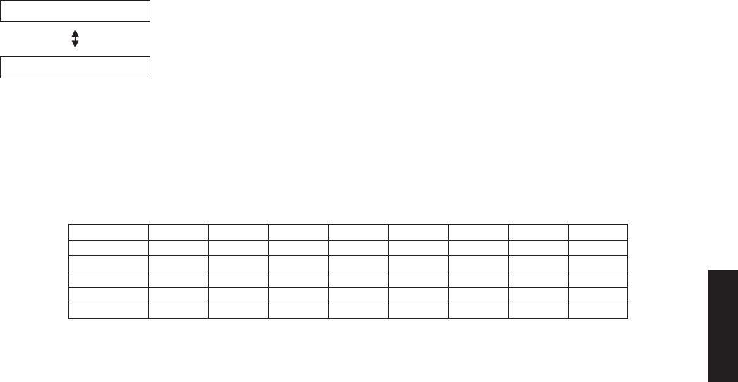
Preset Group P1 P2 P3 P4 P5 P6 P7 P8
CAUTION: Before setting to the PRESET RESERVED, write down the existing preset memory content of the tuner in a table
as shown below.
(This is because setting to the PRESET RESERVED will cause the user memory content of the tuner to be
erased.)
A
B
C
D
E
44
RX-V563/HTR-6150/DSP-AX563
RX-V563/HTR-6150/
DSP-AX563
S. ROM VER/SUM
The version and checksum are displayed. The signal is processed using EFFECT OFF.
The checksum is obtained by adding the data at every 8-bit for each program area and expressing the result as a 4-
figure hexadecimal data.
S1. VER. E048 Microprocessor version
Firmware version of microprocessor is displayed.
All checksum
Checksum value of microprocessor is displayed.
Program checksum
Checksum value of application and standby code program is displayed.
SPI (Serial Peripheral Interface) checksum
Checksum value of SPI firmware update code is displayed.
SPD (S/PDIF) checksum
Checksum value of SPD firmware update code is displayed.
XM version (U, C models)
Firmware version of XM is displayed.
SIRIUS version (U, C models)
Firmware version of SIRIUS is displayed.
FlashROM test
The read/write test of microprocessor (IC41 DSP P.C.B.) and flash ROM (IC52 DSP P.C.B.).
SDRAM test
The read/write test of microprocessor (IC41 DSP P.C.B.) and SDRAM (IC51 DSP P.C.B.).
EEPROM test
The read/write test of microprocessor (IC41 DSP P.C.B.) and EEPROM (IC42 DSP P.C.B.).
S2.A.SUM:EDA1
S3.P.SUM:FE77
S4.SPI.S:2D61
S5.SPD.S:5BEE
S6. XM :
S7. SR :
S8.FROMTEST:OK
S9.DRAMTEST:NG
S10PROMTEST:OK
OK: No error detected NG: An error is detected
OK: No error detected NG: An error is detected
OK: No error detected NG: An error is detected
45
RX-V563/HTR-6150/DSP-AX563
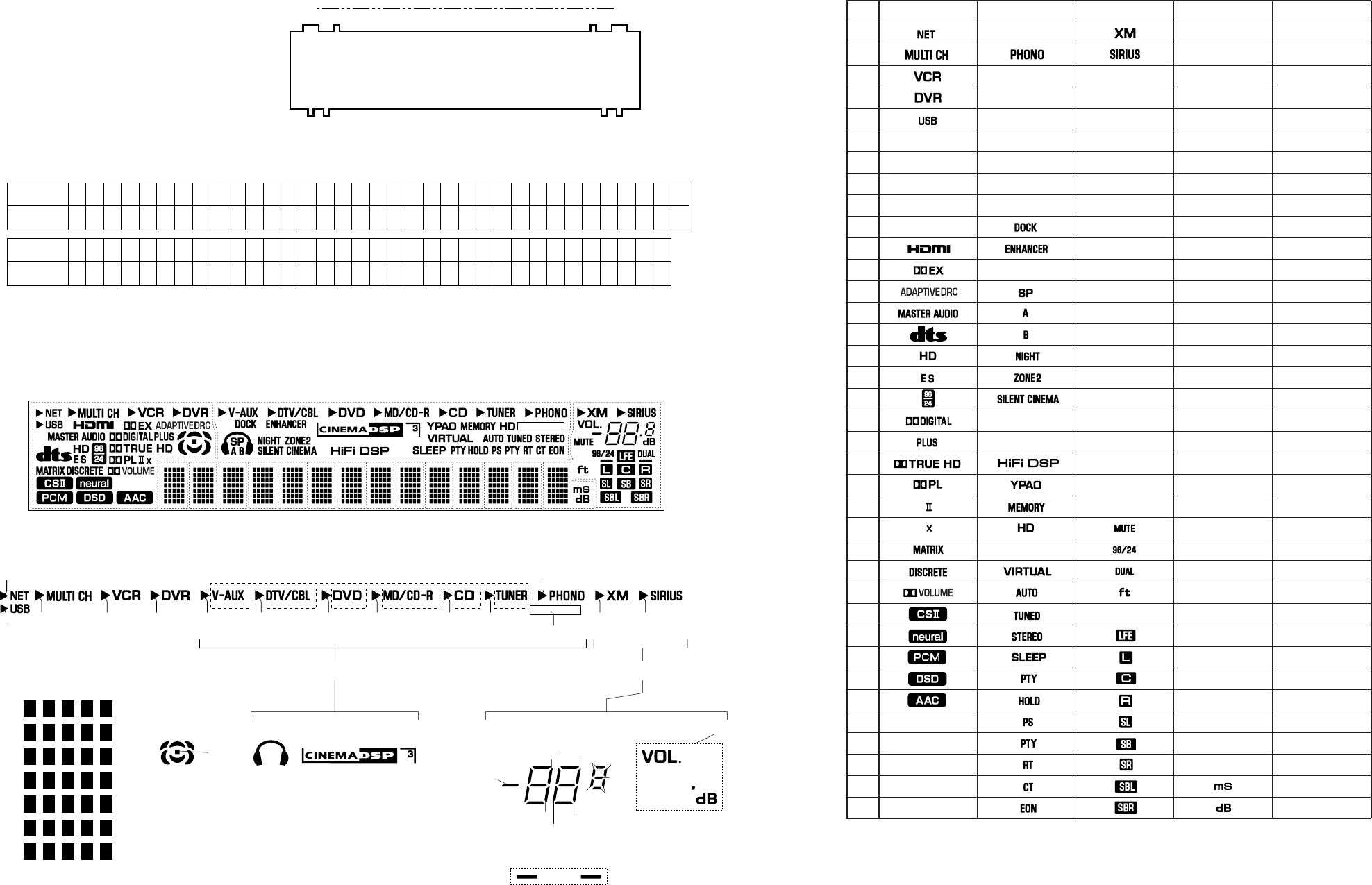
■DISPLAY DATA
S5
S3
S4
S6 S7 S8 S9 S10 S11 S12 S13
S17
S14
S15 S16
S1
Note : 1) F1, F2 ..... Filament pin 2) NP ..... No pin 3) NX ..... No extend pin 4) 1G~17G ..... Grid pin
Pin No.
Connection
Pin No.
69
F2NX
68 67
NP
66
NP
65
P1
64
P2
63
P3
62
P4
61
P5
60
P6
59
P7
58
P8
57
P9
56
P10
55
P11
54
P12
53
P13
52
P14
51
P15
50
P16
49
P17
48
P18
47
P19
46
P20
45
P21
44
P22
43
P23
42
P24
41
P25
40
P26
39
P27
38
P28
37
P29
34
P32
33
P33
32
P34
31
P35
30
P36
29
P37
28
NX
27
NX
26
NX
25
NX
24
NX
23
NX
22
NX
21
17G
20
16G
19
15G
18
14G
17
13G
16
12G
15
11G
14
10G
13
9G
12
8G
11
7G
10
6G
9
5G
8
4G
7
3G
6
2G
5
1G
4
NP
3
NP
36
P30
35
P31
21
F1NX
Connection
● V6001: 17-BT-32GNK (OPERATION P.C.B.)
● PIN CONNECTION
● GRID ASSIGNMENT
2G1G 3G 4G 5G 6G 7G 11G10G9G8G 12G 13G 14G
(17G)
16G 15G17G
1-1
1-2
1-3
1-4
1-5
1-6
1-7
2-1
2-2
2-3
2-4
2-5
2-6
2-7
3-1
3-2
3-3
3-4
3-5
3-6
3-7
4-1
4-2
4-3
4-4
4-5
4-6
4-7
5-1
5-2
5-3
5-4
5-5
5-6
5-7
(16G)
S30
S25 S25
S22
S24 S24
S23
S26 S21 S20 S19 S18
S2
1a
a
bb
c
2b
(96/24) (DUAL)
c
f
e
d
gg
d
f
a
S27
S29
S29 S28
S28
e
(1G~14G)
PATTERN AREA
}1
(15G)
14G
1-1
2-1
3-1
4-1
5-1
1-2
2-2
3-2
4-2
5-2
1-3
2-3
3-3
4-3
5-3
1-4
2-4
3-4
4-4
5-4
1-5
2-5
3-5
4-5
5-5
1-6
2-6
3-6
4-6
5-6
1-7
2-7
3-7
4-7
5-7
15G
S15
S16
S2
S18
1a
1b
1c
1d
1e
1f
1g
2a
2b
2c
2d
2e
2f
2g
S27
S28
S29
S30
16G
S1
S8
S9
S10
S11
S12
S13
S14
S21
S20
S19
S17
13G~1G
1-1
2-1
3-1
4-1
5-1
1-2
2-2
3-2
4-2
5-2
1-3
2-3
3-3
4-3
5-3
1-4
2-4
3-4
4-4
5-4
1-5
2-5
3-5
4-5
5-5
1-6
2-6
3-6
4-6
5-6
1-7
2-7
3-7
4-7
5-7
–
–
1P
2P
3P
4P
5P
6P
7P
8P
9P
10P
11P
12P
13P
14P
15P
16P
17P
18P
19P
20P
21P
22P
23P
24P
25P
26P
27P
28P
29P
30P
31P
32P
33P
34P
35P
36P
37P
S3
S5
S6
S7
S4
S22
S23
S24
S25
S26
17G
● ANODE CONNECTION
(RT)
(HOLD)
(ES)
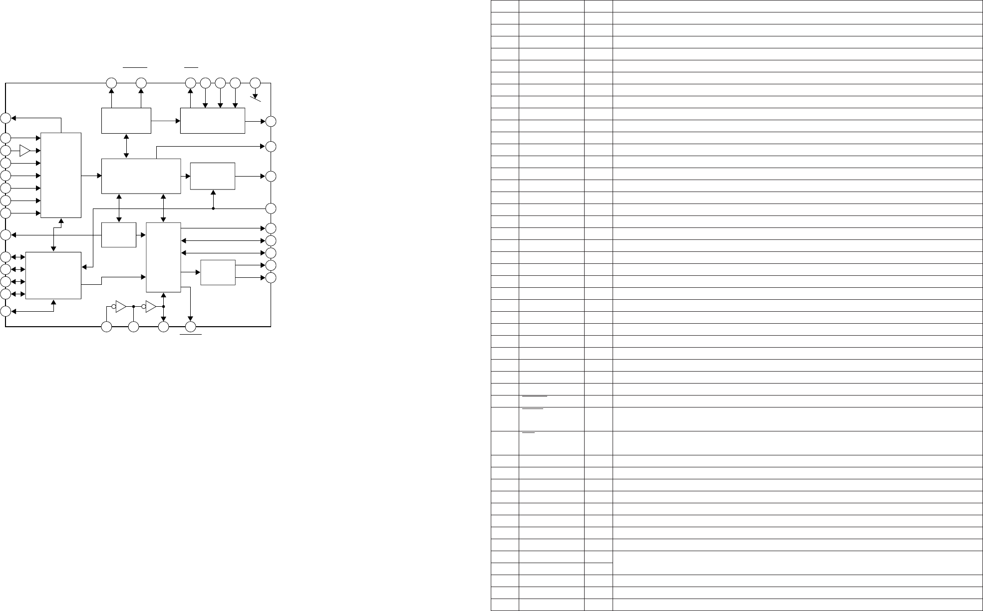
RX-V563/HTR-6150/DSP-AX563
46
IC31: LC89057W-VF4AD-E (DSP P.C.B.)
Digital audio interface transceiver
Input
Selector
RXOUT
RX0
RX1
RX2
RX3
RX4
RX5/VI
RX6/UI
LPF
TMCK/PIO0
TBCK/PIO1
TLRCK/PIO2
TDATA/PIO3
TXO/PIOEN
Cbit, Ubit Microcontroller
I/F
Data
Selector
Clock
Selector
Modulation
&
Parallel Port
PLL
XIN XOUT XMCK CKST
SLRCK
SBCK
RLRCK
RBCK
RMCK
SDIN
RDATA
RERR
DO
XMODECICECLINTAUDIO/VOEMPHA/UO
1/N
Demodulation
&
Lock detect
1
2
3
4
5
8
9
10
13
44
45
46
47
48
29 28 27 34
23
22
20
17
16
24
21
36
37
41383940353332
■IC DATA
1) Withstand voltage input/output: I or O = -0.3 to 3.6 V, Is = -0.3 to 5.5 V
2) Pins 32 and 33 are input pins for chip address setting, when pin 41 = "L".
3) Pin 34 is a demodulation function master or an input pin for slave setting, when pin 41 = "L".
4) Pin 35 is a modulation function or an input pin for general-purpose I/O function switch setting, when pin 41 = "L".
5) ON/OFF for all power supplies must be done at the same timing as a latch-up countermeasure.
1
2
3
4
5
6
7
8
9
10
11
12
13
14
15
16
17
18
19
20
21
22
23
24
25
26
27
28
29
30
31
32
33
34
35
36
37
38
39
40
41
42
43
44
45
46
47
48
RXOUT
RX0
RX1
RX2
RX3
DGND
DVDD
RX4
RX5
RX6
DVDD
DGND
LPF
AVDD
AGND
RMCK
RBCK
DGND
DVDD
RLRCK
RDATA
SBCK
SLRCK
SDIN
DGND
DVDD
XMCK
XOUT
XIN
DVDD
DGND
EMPHA/UO/CD
AUDIO/VO
CKST/PT
INT
RERR
DO
DI
CE
CL
XMODE
DGND
DVDD
PIO0
PIO1
PIO2
PIO3
PIOEN
O
Is
I
Is
Is
Is
Is
Is
O
O
O/I
O/I
O
O
O
Is
O
O
I
I/O
I/O
I/O
I/O
O
O
Is
Is
Is
Is
O
O
O
O
I/O
Detail of Function
Output pin of input bi-phase selection data
Input pin of TTL-compatible digital data
Digital data input pin with built-in amplifier that supports coaxial
Input pin of TTL-compatible digital data
Input pin of TTL-compatible digital data
Digital GND
Digital power supply (3.3 V)
Input pin of TTL-compatible digital data
TTL-compatible digital data / Validity flag input pin for modulation
TTL-compatible digital data / User data input pin for modulation
Digital power supply for PLL
Digital GND for PLL
PLL loop filter connection pin
Analog power supply for PLL (3.3 V)
Analog GND for PLL
R system clock output pin (256 fs, 512 fs, XIN, VCO)
R bit clock input/output pin (64 fs)
Digital GND
Digital power supply (3.3 V)
R LR clock input/output pin (fs)
Output pin of serial audio data
S bit clock output pin (32 fs, 64 fs, 128 fs) (No connected.)
S LR clock output pin (fs/2, fs, 2 fs) (No connected.)
Input pin of serial audio data
Digital GND
Digital power supply (3.3 V)
Oscillation amplifier output pin
Quartz resonator connection output pin
Quartz resonator connection, input pin of external supply clock (24.576 MHz or 12.288 MHz)
Digital power supply (3.3 V)
Digital GND
Emphasis information / U data output / C data output / Chip address setting pin
Non-PCM detection / V flag output / Chip address setting pin
Output of clock switch transitional period signal / Preamble B output / Demodulation master or slave
function switch pin
Interrupt output for microprocessor (Possible to select an interrupt factor.) / Modulation or general-
purpose I/O switch pin
PLL clock error, data error flag output
Microprocessor I/F, read data output pin (3-state)
Microprocessor I/F, write data input pin
Microprocessor I/F, chip enable input pin
Microprocessor I/F, clock input pin"
System reset input pin
Digital GND
Digital power supply (3.3 V)
Sport input select
Audio direct stereo ON
Audio clock select
Modulation data output / General-purpose I/O enable output pin
Pin No.
Function Name I/O
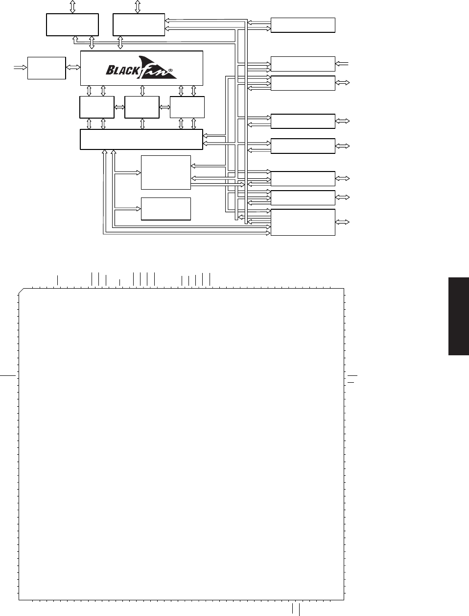
47
RX-V563/HTR-6150/DSP-AX563
RX-V563/HTR-6150/
DSP-AX563
IC41: AD91089SKBC CPU (DSP P.C.B.)
Microprocessor
PPI/GPIO
L1 data
memory
JTAG test
and emulation
Voltage
regulator
L1 instruction
memory
Memory
management
unit
Core/System bus interface
Real time clock
UART port IrDA®
Serial port (2)
DMA controller
Boot ROM
SPI port
External port FLASH,
SDRAM control
Event controller/
Core timer Watch dock timer
Timer0, Timer1, Timer2
GND
GND
GND
VROUT1
VROUT0
VDDEXT
GND
GND
GND
CLKIN
XTAL
VDDEXT
RESET
NMI
GND
RTXO
RTXI
VDDRTC
GND
VDDEXT
PPI_CLK
PPI0
PPI1
PPI2
VDDINT
PPI3
PF15
PF14
PF13
GND
VDDEXT
PF12
PF11
PF10
PF9
PF8
PF7
PF6
GND
GND
GND
GND
GND
GND
1
2
3
4
5
6
7
8
9
10
11
12
13
14
15
16
17
18
19
20
21
22
23
24
25
26
27
28
29
30
31
32
33
34
35
36
37
38
39
40
41
42
43
44
132
131
130
129
128
127
126
125
124
123
122
121
120
119
118
117
116
115
114
113
112
111
110
109
108
107
106
105
104
103
102
101
100
99
98
97
96
95
94
93
92
91
90
89
GND
GND
GND
GND
GND
ADDR13
ADDR14
ADDR15
ADDR16
ADDR17
ADDR18
ADDR19
BGH
BG
VDDEXT
GND
DATA 0
DATA 1
DATA 2
DATA 3
DATA 4
VDDINT
DATA 5
DATA 6
DATA 7
VDDEXT
GND
DATA 8
DATA 9
DATA 1 0
DATA 1 1
DATA 1 2
DATA 1 3
DATA 1 4
DATA 1 5
GND
BMODE0
BMODE1
TCK
VDDEXT
GND
GND
GND
GND
45
46
47
48
49
50
51
52
53
54
55
56
57
58
59
60
61
62
63
64
65
66
67
68
69
70
71
72
73
74
75
76
77
78
79
80
81
82
83
84
85
86
87
88
176
175
174
173
172
171
170
169
168
167
166
165
164
163
162
161
160
159
158
157
156
155
154
153
152
151
150
149
148
147
146
145
144
143
142
141
140
139
138
137
136
135
134
133
GND
GND
GND
SCKE
SMS
VDDEXT
GND
CLKOUT
VDDINT
SRAS
SCAS
SWE
SA10
BR
ARDY
AMS0
AMS1
AMS2
AMS3
VDDINT
VDDEXT
GND
AOE
ARE
AWE
ABE0
ABE1
ADDR1
ADDR2
ADDR3
ADDR4
VDDEXT
GND
VDDINT
ADDR5
ADDR6
ADDR7
ADDR8
ADDR9
ADDR10
ADDR11
ADDR12
VDDEXT
GND
VDDEXT
PF5
PF4
PF3
PF2
PF1
PF0
VDDINT
SCK
MISO
MOSI
GND
VDDEXT
DT1SEC
DT1PRI
TFS1
TSCLK1
DR1SEC
DR1PRI
RFS1
RSCLK1
VDDINT
DT0SEC
DT0PRI
TFS0
GND
VDDEXT
TSCKL0
DR0SEC
DR0PRI
RFS0
RSCLK0
TMR2
TMR1
TMR0
VDDINT
TX
RX
EMU
TRST
TMS
TDI
TDO
GND
48
RX-V563/HTR-6150/DSP-AX563
RX-V563/HTR-6150/
DSP-AX563
Pin
No.
Function
Name I/O Detail of Function
121
122
123
124
125
126
127
135
136
137
138
139
140
141
142
146
147
148
149
98
99
100
101
102
103
104
105
108
109
110
112
113
114
115
116
150
151
163
119
120
ADDR19
ADDR18
ADDR17
ADDR16
ADDR15
ADDR14
ADDR13
ADDR12
ADDR11
ADDR10
ADDR9
ADDR8
ADDR7
ADDR6
ADDR5
ADDR4
ADDR3
ADDR2
ADDR1
DATA15
DATA14
DATA13
DATA12
DATA11
DATA10
DATA9
DATA8
DATA7
DATA6
DATA5
DATA4
DATA3
DATA2
DATA1
DATA0
ABE1
ABE0
BR
BG
BGH
O
O
O
I/O
I/O
I/O
O
I
O
O
Address bus for async/Sync access
Address bus for async/Sync access
Address bus for async/Sync access
Daea bus for async access
Daea bus for async access
Daea bus for async access
Byte enables/Data masks for async/
Sync access
Bus request (This pin should be pulled
HIGH if not used.)
Bus grant
Bus grant hang
Memory Interface
Pin
No.
Function
Name I/O Detail of Function
158
159
160
161
162
154
153
152
AMS3
AMS2
AMS1
AMS0
ARDY
AOE
ARE
AWE
O
I
O
O
O
Banks select
hardware ready control (This pin
should be pulled HIGH if not used.)
Output enable
Read enable
Write enable
Asynchronous memory control
Pin
No.
Function
Name I/O Detail of Function
167
166
165
173
169
164
172
SRAS
SCAS
SWE
SCKE
CLKOUT
SA10
SMS
O
O
O
O
O
O
O
Row address strobe
Column address strobe
Write enable
Clock enable
Clock output
A10 pin
Bank select
Synchronous memory control
Pin
No.
Function
Name I/O Detail of Function
79
78
77
TMR0
TMR1
TMR2
I/O
I/O
I/O
Timer0
Timer1/PPI frame sync1
Timer2/PPI frame sync2
Timers
Pin
No.
Function
Name I/O Detail of Function
22
23
24
26
21
PPI0
PPI1
PPI2
PPI3
PPI_CLK
I/O
I
PPI3-0
PPI clock/External timer reference
PPI port
Pin
No.
Function
Name I/O Detail of Function
51
50
49
48
47
46
38
37
36
35
34
33
32
29
28
27
PF0
PF1
PF2
PF3
PF4
PF5
PF6
PF7
PF8
PF9
PF10
PF11
PF12
PF13
PF14
PF15
I/O
I/O
I/O
I/O
I/O
I/O
I/O
I/O
I/O
I/O
I/O
I/O
I/O
I/O
I/O
I/O
GPIO/SPI slave select input
GPIO/SPI slave select enable 1/
Timer alternate clock input
GPIO/SPI slave select enable 2
GPIO/SPI slave select enable 3/
PPI frame sync 3
GPIO/SPI slave select enable 4/
PPI 15
GPIO/SPI slave select enable 5/
PPI 14
GPIO/SPI slave select enable 6/
PPI 13
GPIO/SPI slave select enable 7/
PPI 12
GPIO/PPI 11
GPIO/PPI 10
GPIO/PPI 9
GPIO/PPI 8
GPIO/PPI 7
GPIO/PPI 6
GPIO/PPI 5
GPIO/PPI 4
Port F:
GPOI/Parallel peripheral interface port/SPI/Timers
49
RX-V563/HTR-6150/DSP-AX563
RX-V563/HTR-6150/
DSP-AX563
Pin
No.
Function
Name I/O Detail of Function
94
87
86
85
84
83
TCK
TDO
TDI
TMS
TRST
EMU
I
O
I
I
I
O
JTAG clock
JTAG serial data out
JTAG serial data in
JTAG mode select
JTAG reset (This pin is should be
pulled LOW if JTAG is not used.)
Emulation output
JTAG port
Pin
No.
Function
Name I/O Detail of Function
55
54
53
MOSI
MISO
SCK
I/O
I/O
I/O
Master out slave in
Master in slave out (This pin is should
be pulled HIGH throug a 4.7 k-ohms
resistor if booting via the SPI port.)
SPI clock
SPI port
Pin
No.
Function
Name I/O Detail of Function
76
75
74
73
72
69
68
67
65
64
63
62
61
60
59
58
RSCLK0
RFS0
DR0PRI
DR0SEC
TSCLKO
TFSO
DTOPRI
DTOSEC
RSCLK1
RFS1
DR1PRI
DR1SEC
TSCLK1
TFS1
DT1PRI
DT1SEC
I/O
I/O
I
I
I/O
I/O
O
O
I/O
I/O
I
I
I/O
I/O
O
O
SPORT0 receive serial clock
SPORT0 receive frame sync
SPORT0 receive data primary
SPORT0 receive data secondry
SPORT0 transmit serial clock
SPORT0 transmit frame sync
SPORT0 transmit data primary
SPORT0 transmit data secondary
SPORT1 receive serial clock
SPORT1 receive frame sync
SPORT1 receive data primary
SPORT1 receive data secondary
SPORT1 transmit serial clock
SPORT1 transmit frame sync
SPORT1 transmit data primary
SPORT1 transmit data secondary
Serial ports
Pin
No.
Function
Name I/O Detail of Function
82
81
RX
TX
I
O
UART receive
UART transmit
UART port
Pin
No.
Function
Name I/O Detail of Function
17
16
RTXI
RTXO
I
O
RTC crystal input (This pin should be
pulled LOW when not used.)
RTC crystal output
Real-time clock
Pin
No.
Function
Name I/O Detail of Function
10
11
CLKIN
XTAL
I
O
Clock/Crystal input (This pin needs to
be at a level or clocking.)
Crystal output
Clock
Pin
No.
Function
Name I/O Detail of Function
13
14
95
96
RESET
NMI
BMODE1
BMODE0
I
I
I
Reset (This pin is always active dur-
ing core power-on.)
Nonmaskable interrypt (This pin
should be pulled LOW when not used.)
Boot mode strap (These pins must be
pulled to the state required for the
desired boot mode.)
Mode controls
Pin
No.
Function
Name I/O Detail of Function
4
5
VROUT1
VROUT0 O Extarnal FET drive
Voltage regulator
50
RX-V563/HTR-6150/DSP-AX563
RX-V563/HTR-6150/
DSP-AX563
Pin
No.
Function
Name I/O Detail of Function
1
2
3
7
8
9
15
19
30
39
40
41
42
43
44
56
70
88
89
90
91
92
97
106
117
128
133
144
155
170
171
172
173
174
175
176
GND G External ground
Pin
No.
Function
Name I/O Detail of Function
6
12
20
31
45
57
71
93
107
118
134
145
156
171
25
52
66
80
111
143
157
168
18
VDDEXT
VDDINT
VDDRTC
P
P
P
I/O power supply
Core power supply
Real-time clock power supply
Supplies
51
RX-V563/HTR-6150/DSP-AX563
RX-V563/HTR-6150/
DSP-AX563
1
2
3
4
5
6
7
8
9
10
20
19
18
17
16
15
14
13
12
11
OE
1D
2D
3D
4D
5D
6D
7D
8D
GND
VCC
1Q
2Q
3Q
4Q
5Q
6Q
7Q
8Q
CLK
OE 1
11
2
19
CLK
1D
C1
1D 1Q
9
12
8D
C8
8D 8Q
1
2
3
4
5
6
7
8
9
10
11
12
13
14
15
16
17
18
19
20
• Microprocessor extended port
IC57-IC59: SN74LV574APWR (DSP P.C.B.)
Octal edge-triggered D-type flip-flops with 3-state outputs
/OE
1D
2D
3D
4D
5D
6D
7D
8D
GND
LCK
8Q
7Q
6Q
5Q
4Q
3Q
2Q
1Q
VCC
/EXPE
D00
D01
D02
D03
D04
D05
D06
D07
DGND
NPGA_EXSTB
–
R2A_CLK
R2A_DATA
VIDEO_MTVR1
/DAC_CS
/ADC_CS
/VFD_CS
/DIR_CS
VCC
Extended port enable
Data bus 00
Data bus 01
Data bus 02
Data bus 03
Data bus 04
Data bus 05
Data bus 06
Data bus 07
Ground of external
Bank select 1
–
E-Vol control clock
E-Vol control data
DVR REC output inhibit
DA converter chip select
AD converter chip select
VFD (Front display) chip select
Audio CODEC chip select
Power supply +3.3V
Pin No.
Port Name Function Name Detail of Function
1
2
3
4
5
6
7
8
9
10
11
12
13
14
15
16
17
18
19
20
/OE
1D
2D
3D
4D
5D
6D
7D
8D
GND
CLK
8Q
7Q
6Q
5Q
4Q
3Q
2Q
1Q
VCC
/EXPE
D00
D01
D02
D03
D04
D05
D06
D07
DGND
NPGA_EXSTB
PRY
XM_POWER
/Z2MT
/SBMT
/SWMT
/CMT
/SMT
/FMT
VCC
Extended port enable
Data bus 00
Data bus 01
Data bus 02
Data bus 03
Data bus 04
Data bus 05
Data bus 06
Data bus 07
Ground of external
Bank select 1
Power relay control
XM power enable
Zone2 L/R mute
Surround back L/R mute
Subwoofer mute
Center mute
Surround L/R mute
Front L/R mute
Power supply +3.3V
Pin No.
Port Name Function Name Detail of Function
IC58
IC57
52
RX-V563/HTR-6150/DSP-AX563
RX-V563/HTR-6150/
DSP-AX563
1
2
3
4
5
6
7
8
9
10
20
19
18
17
16
15
14
13
12
11
OE
1D
2D
3D
4D
5D
6D
7D
8D
GND
VCC
1Q
2Q
3Q
4Q
5Q
6Q
7Q
8Q
CLK
OE 1
11
2
19
CLK
1D
C1
1D 1Q
9
12
8D
C8
8D 8Q
1
2
3
4
5
6
7
8
9
10
11
12
13
14
15
16
17
18
19
20
/OE
1D
2D
3D
4D
5D
6D
7D
8D
GND
CLK
8Q
7Q
6Q
5Q
4Q
3Q
2Q
1Q
VCC
/EXPE
D00
D01
D02
D03
D04
D05
D06
D07
DGND
NPGA_EXSTB
ADC_SELECT_C
ADC_SELECT_B
ADC_SELECT_A
SBRY
HPRY
CSRY
MRYB
MRYA
VCC
Extended port enable
Data bus 00
Data bus 01
Data bus 02
Data bus 03
Data bus 04
Data bus 05
Data bus 06
Data bus 07
Ground of external
Bank select 0
Selector C
Selector B
Selector A
Speaker relay SB
Headphone relay
Speaker relay C/SW
Speaker relay F/B
Speaker relay F/A
Power supply +3.3V
Pin No.
Port Name Function Name Detail of Function
IC59
1
2
3
4
5
6
7
8
9
10
11
12
13
14
15
16
17
18
19
20
/OE
1D
2D
3D
4D
5D
6D
7D
8D
GND
CLK
8Q
7Q
6Q
5Q
4Q
3Q
2Q
1Q
VCC
/EXPE
D00
D01
D02
D03
D04
D05
D06
D07
DGND
NPGA_EXSTB
5VIDEO_VIA
5VIDEO_VIB
5VIDEO_VIC
/5VIDEO_MTMON
/5VIDEO_CMON
5VIDEO_CBYPASS
5VIDEO_CMP1
5VIDEO_CMP0
VCC
Extended port enable
Data bus 00
Data bus 01
Data bus 02
Data bus 03
Data bus 04
Data bus 05
Data bus 06
Data bus 07
Ground of external
Bank select 0
Video input selector A
Video input selector B
Video input selector C
Monitor output inhibit
Component output inhibit
Component bypass
Component select 1
Component select 2
Power supply +5V
Pin No.
Port Name Function Name Detail of Function
IC56: SN74AHCT574AWR (DSP P.C.B.)
Octal edge-triggered D-type flip-flops with 3-state outputs
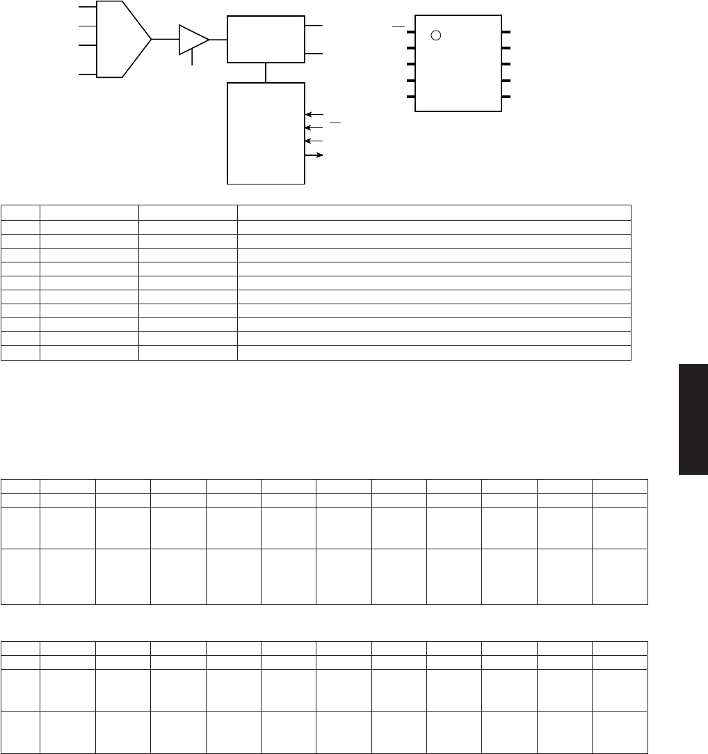
53
RX-V563/HTR-6150/DSP-AX563
RX-V563/HTR-6150/
DSP-AX563
IN1
IN2
IN3 MUX T/H
VA
8-Bit
SUCCESSIVE
APPROXIMATION
ADC
GND
IN4
GND
SCLK
CONTROL
LOGIC
CS
DIN
DOUT
CS 1
VA2
GND 3
IN4 4
IN3 5
SCLK
ADC084S021
10
DOUT
9
DIN8
IN17
IN26
Ohm
V
KEY
INPUT 0
(7 pin)
KEY
INPUT 1
(6 pin)
0
0–0.2
–
–
+ 1.0 k
0.2–0.4
SPEAKERS
A/B/OFF
–
+ 1.0 k
0.4–0.7
TONE
CONTROL
AUDIO
SELECT
+ 1.5 k
0.7–1.0
PROGRAM
<
INPUT
>
+ 2.2 k
1.0–1.3
PROGRAM
>
INPUT
<
+ 2.2 k
1.3–1.6
STRAIGTH
EFFECT
DIRECT
+ 3.3 k
1.6–1.9
A/B/C/D/E
PRESET/
TUNING
<
+ 4.7 k
1.9–2.1
BAND
PRESET/
TUNING
>
+ 6.8 k
2.1–2.4
ZONE2
ON/OFF
MEMORY
+ 10.0 k
2.4–2.7
EDIT
PRESET/
TUNING
INFO
TUNING
AUTO/
MAN’L
Key detection for A/D port
Key input (A/D) pull-up resistance 10 k-ohms
+ 22.0 k
2.7–3.0
SYSTEM
OFF
ZONE
CONTROL
Ohm
V
KEY
INPUT 0
(7 pin)
KEY
INPUT 1
(6 pin)
0
0–0.2
–
–
+ 1.0 k
0.2–0.4
SPEAKERS
A/B/OFF
–
+ 1.0 k
0.4–0.7
TONE
CONTROL
AUDIO
SELECT
+ 1.5 k
0.7–1.0
PROGRAM
<
INPUT
>
+ 2.2 k
1.1–1.3
PROGRAM
>
INPUT
<
+ 2.2 k
1.3–1.6
STRAIGTH
EFFECT
DIRECT
+ 3.3 k
1.6–1.9
–
–
+ 4.7 k
1.9–2.1
–
–
+ 6.8 k
2.1–2.4
–
–
+ 10.0 k
2.4–2.7
–
–
B model
+ 22.0 k
2.7–2.9
–
–
IC81: ADC084S021CIMM (DSP P.C.B.)
4-channel, 200 kSPS, 8-bit A/D converter
1
2
3
4
5
6
7
8
9
10
/CS
VA
GND
IN4
IN3
IN2
IN1
DIN
DOUT
SCLK
/ADC_CS
+3.3S
DGND
ADC_COM2
ADC_COM1
KEY1
KEY0
SPIMI
SPIMO
SPISCK
CS for microprocessor
Power supply +3.3V
Ground of external
SPI bus COM (IC83)
SPI bus COM (IC82)
Key input 1
Key input 0
Master output/slave input
Master input/slave output
SPI clock
Pin No.
Port Name Function Name Detail of Function
•Microprocessor ADC select port
U, C, R, T, K, A, G, E, F, L models
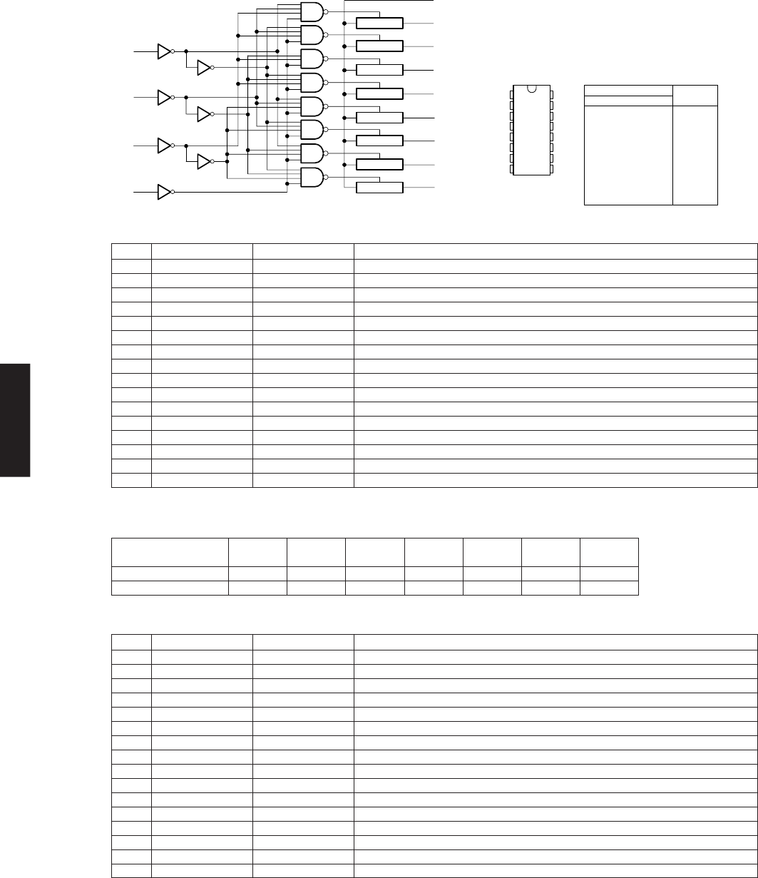
54
RX-V563/HTR-6150/DSP-AX563
RX-V563/HTR-6150/
DSP-AX563
IC82
IC83
DOCK detection for AD port (IC82 AD converter pin no. 4)
Pull-up resistance 10 k-ohms
DOCK connector
Ohm
DKID (Pin no. 21)
DOCK
(Bluetooth)
0.56k
5-25
Reserved
2.7k
50-60
Reserved
5.6k
85-100
DOCK
(iPod)
10.0k
120-140
Reserved
18.0k
150-170
(Develop-
ment)
39.0k
195-210
No connect
–
245-255
Y0
Y1
Y2
Y3
Y4
Y5
Y6
Y7
COM
INH
C
B
A11
10
9
6
3
13
14
15
12
1
5
2
4
1
2
3
4
5
6
7
89
10
16
15
14
13
12
11
Y4
Y6
COM
Y7
Y5
INH
GND
GND
VCC
Y2
Y1
Y0
Y3
A
B
C
INPUTS ON
CHANNEL
INH
L
L
L
L
L
L
L
L
H
L
L
L
H
H
H
H
X
C
L
L
H
H
L
L
H
H
X
L
H
L
H
L
H
L
H
X
L
Y1
Y2
Y3
Y4
Y5
Y6
Y7
None
Y0
BA
1
2
3
4
5
6
7
8
9
10
11
12
13
14
15
16
Y4
Y6
COM
Y7
Y5
INH
GND
GND
C
B
A
Y3
Y0
Y1
Y2
Vcc
/TUNER_TUNED
XM_ANT
ADC_COM1
DOCK_ID
IP_DET
DGND
DGND
DGND
SELECT C
SELECT B
SELECT A
THM
DEST1
PRV1
PRD
+3.3S
Tuner tuned detection
XM antenna
SPI bus COM (IC81)
DOCK detection (Normal DOCK or Bluetooth adapter)
iPod detection
Ground of external
Ground of external
Ground of external
ADC selecter C
ADC selecter B
ADC selecter A
Temperature detection
Destination detection
Power supply protection 1
AMP DC protecton
Power supply +3.3V
Pin No.
Port Name Function Name Detail of Function
1
2
3
4
5
6
7
8
9
10
11
12
13
14
15
16
Y4
Y6
COM
Y7
Y5
INH
GND
GND
C
B
A
Y3
Y0
Y1
Y2
Vcc
/TUNER_STEREO
XM_LINK
ADC_COM2
/HP_DET
IP_AP
DGND
DGND
DGND
SELECT C
SELECT B
SELECT A
PRI
DEST2
PRV2
PLDET
+3.3S
Tuner stereo detection
XM link
SPI bus COM (IC81)
Headphone detect
iPod
Ground of external
Ground of external
Ground of external
ADC selector C
ADC selector B
ADC selector A
AMP curent protection
–
Power supply protection 2
Output voltage of power amplifier detection
Power supply +3.3V
Port Name Function Name Detail of Function
IC82, IC83: SN74LV4051APWR (DSP P.C.B.)
8-channel analog multiplexers/demultiplexers
55
RX-V563/HTR-6150/DSP-AX563
RX-V563/HTR-6150/
DSP-AX563
51
52
53
54
55
56
57
58
59
60
61
62
63
64
65
66
67
68
69
70
71
72
73
74
75
76
77
78
80
81
79
MUTE
AVEE
ADCL
ADCR
AGND
INR1
INR2
INR3
INR4
INR5
INR6
INR7
INR8
INR9
INL1
INL2
INL3
INL4
INL5
INL6
INL7
INL8
INL9
N.C.
N.C.
N.C.
N.C.
INRB/RECR2
INLB/RECL2
INR10/RECR4
INR11/RECR5
INL10/RECL4
INL11/RECL5
RECR3
RECL3
FLIN1
FRIN1
CIN1
SWIN1
SLIN1
SRIN1
SBLIN1
SBRIN1
N.C.
N.C.
N.C.
INRA/RECR1
INLA/RECL1
N.C.
N.C.
30
29
28
27
26
25
24
23
22
21
20
19
18
17
16
15
14
13
12
11
10
9
8
7
6
5
4
3
1
2
AVCC
N.C.
N.C.
N.C.
N.C.
FRC
FROUT
FLOUT
FLC
CC
COUT
SWOUT
SROUT
SLOUT
SBR OUT
SBL OUT
SBLC
SBRC
SWC
SRC
SLC
AGND
AGND
AGND
AGND
A GND
AGND
TREL
BASSL2
BASSL1
82 83 84 85 86 87 88 89 90 91 92 93 94 95 96 97 98 99 100
50
A VEE
0/-6/-12/-18dB
ATT
SUB
0~-95dB,
-∞
(0.5dBstep)
SUB
SUB
MAIN
MAIN
MAIN
CLOCK
DATA
DGND
SUBR
SUBL
SBLCIN
SBRCIN
FRIN2
FLIN2
SRIN2
SLIN2
SWIN2
SBRIN2
SBLIN2
N.C.
TRER
BASSR1
BASSR2
N.C.
CIN2
49 48 47 46 45 44 43 42 41 40 39 38 37 36 35 34 33 32 31
MCU
I/F
A VCC
REC
Tone
Tone
Bass/Treble
-14~+14dB
(2dBstep) +42~0dB
(0.5dBstep)
+42~0dB
(0.5dBstep)
+42~-95dB
-∞(0.5dBstep)
+42~-95dB
-∞(0.5dBstep)
+42~-95dB
-∞(0.5dBstep)
+42~-95dB
-∞(0.5dBstep)
+42~-95dB
-∞(0.5dBstep)
+42~-95dB
-∞(0.5dBstep)
Bass/Treble
-14~+14dB
(2dBstep)
0~-95dB,
-∞
(0.5dBstep) Bypass
Tone+MIX
Tone+MIX Tone
Tone
Bypass
CMIX
SWMIX
IC401 : R2A15218FP (MAIN P.C.B.)
8 ch electronic volume with 11 input selector and tone control

56
RX-V563/HTR-6150/DSP-AX563
RX-V563/HTR-6150/
DSP-AX563
Pin No.
Function Name
1
2
3
4
5
6
7
8
9
10
11
12
13
14
15
16
17
18
19
20
21
22
23
24
25
26
27
28
29
30
31
32
33
34
35
36
37
38
39
40
41
42
43
44
45
46
47
48
49
50
NC
SBLC
SBL OUT
AGND
SBR OUT
SBRC
AGND
SLC
SLOUT
AGND
SROUT
SRC
NC
SWC
SWOUT
AGND
COUT
CC
AGND
FLC
FLOUT
AGND
FROUT
FRC
NC
BASSL1
BASSL2
TREL
NC
AVCC
NC
BASSR1
BASSR2
TRER
NC
SBLIN2
SBRIN2
CIN2
SWIN2
SLIN2
SRIN2
FLIN2
FRIN2
SBRCIN
SBLCIN
SUBL
SUBR
DGND
DATA
CLOCK
Detail of Function
Connects capacitor for reducing click noise of L/R/C/SW/SL/SR/SBL/SBR channel volume
Output pin of FL/FR/C/SW/SL/SR/SBL/SBR channel
Analog ground of internal circuit
Output pin of FL/FR/C/SW/SL/SR/SBL/SBR channel
Connects capacitor for reducing click noise of L/R/C/SW/SL/SR/SBL/SBR channel volume
Analog ground of internal circuit
Connects capacitor for reducing click noise of L/R/C/SW/SL/SR/SBL/SBR channel volume
Output pin of FL/FR/C/SW/SL/SR/SBL/SBR channel
Analog ground of internal circuit
Output pin of FL/FR/C/SW/SL/SR/SBL/SBR channel
Connects capacitor for reducing click noise of L/R/C/SW/SL/SR/SBL/SBR channel volume
Connects capacitor for reducing click noise of L/R/C/SW/SL/SR/SBL/SBR channel volume
Output pin of FL/FR/C/SW/SL/SR/SBL/SBR channel
Analog ground of internal circuit
Output pin of FL/FR/C/SW/SL/SR/SBL/SBR channel
Connects capacitor for reducing click noise of L/R/C/SW/SL/SR/SBL/SBR channel volume
Analog ground of internal circuit
Connects capacitor for reducing click noise of L/R/C/SW/SL/SR/SBL/SBR channel volume
Output pin of FL/FR/C/SW/SL/SR/SBL/SBR channel
Analog ground of internal circuit
Output pin of FL/FR/C/SW/SL/SR/SBL/SBR channel
Connects capacitor for reducing click noise of L/R/C/SW/SL/SR/SBL/SBR channel volume
Frequency characteristic setting pin of L/R channel tone control (Bass)
Frequency characteristic setting pin of L/R channel tone control (Treble)
Positive power supply to internal circuit
Frequency characteristic setting pin of L/R channel tone control (Bass)
Frequency characteristic setting pin of L/R channel tone control (Treble)
Input pin of L/R/C/SW/SL/SR/SBL/SBR channel (Multi IN 1/2)
Input pin for SBL/SBR channel volume
Output pin for L/R channel SUB output
Digital ground of internal circuit
Input pin of control data
Input pin of control clock

57
RX-V563/HTR-6150/DSP-AX563
RX-V563/HTR-6150/
DSP-AX563
Pin No.
Function Name Detail of Function
51
52
53
54
55
56
57
58
59
60
61
62
63
64
65
66
67
68
69
70
71
72
73
74
75
76
77
78
79
80
81
82
83
84
85
86
87
88
89
90
91
92
93
94
95
96
97
98
99
100
MUTE
AVEE
NC
ADCL
ADCR
AGND
NC
INR1
INL1
INR2
INL2
INR3
INL3
INR4
INL4
INR5
INL5
INR6
INL6
INR7
INL7
INR8
INL8
NC
INRA/RECR1
INLA/RECL1
NC
INR9
INL9
NC
INRB/RECR2
INLB/RECL2
INR10/RECR4
INL10/RECL4
INR11/RECR5
INL11/RECL5
NC
NC
NC
RECR3
RECL3
NC
FLIN1
FRIN1
CIN1
SWIN1
SLIN1
SRIN1
SBLIN1
SBRIN1
Outside mute control pin
Negative power supply to internal circuit
Output pin for L/R channel ADC
Analog ground of internal circuit
Input pin of L/R channel (Input selector)
Input pin of L/R channel (Input selector) / Output pin for L/R channel REC output
Input pin of L/R channel (Input selector)
Input pin of L/R channel (Input selector) / Output pin for L/R channel REC output
Output pin for L/R channel REC output
Input pin of L/R/C/SW/SL/SR/SBL/SBR channel (Multi IN 1/2)
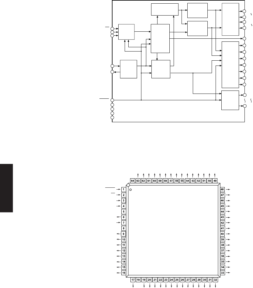
58
RX-V563/HTR-6150/DSP-AX563
RX-V563/HTR-6150/
DSP-AX563
RESET
SCK
SDATA
XOUT
XIN
Vcc1
SEG34
SEG33
SEG32
SEG31
SEG30
SEG29
SEG28
SEG27
SEG26
SEG25
SEG24
SEG23
SEG22
SEG21
SEG20
SEG19
SEG18
SEG17
SEG16
SEG15
SEG14
SEG13
SEG12
Vcc2
Vss
CS
SEG11
SEG10
SEG09
SEG08
SEG07
SEG06
SEG05
SEG04
SEG03
SEG02
SEG01
SEG00
SEG35
DIG17/SEG36
DIG16/SEG37
DIG15/SEG38
DIG14/SEG39
DIG13/SEG40
DIG12/SEG41
DIG11/SEG42
DIG10
DIG09
DIG08
DIG07
DIG06
DIG05
DIG04
DIG03
DIG02
DIG01
DIG00
VP
52
Display
controller
Serial
receive
circuit
Digit
output
circuit
Clock
generator
DIG11/
SEG42
51
DIG12/
SEG41
50
DIG13/
SEG40
49
DIG14/
SEG39
48
DIG15/
SEG38
47
DIG16/
SEG37
46
DIG17/
SEG36
45
SEG35
XOUT
6
Vcc1
8
Vcc2
18
Vss
5
Vp
64
XIN
7
CS
SCK
3
SDATA
4
RESET
1
SEG00
44
9
SEG34
SEG26
17
19
SEG25
Segment
output
circuit
Display code
RAM
(8-bit x 60)
CGROM
(35-bit x 166)
CGROM
(35-bit x 16)
code
select
Code
write
Code/
command
control
circuit
DIG00
63
53
DIG10
2
data
timing
clock
dot data
write
scan pulse
Segment/
Digit
select/
output
circuit
IC603: M66003-0131FP-R (OPERATION P.C.B.)
18 digit 5x7 segment VFD controller/driver

59
RX-V563/HTR-6150/DSP-AX563
RX-V563/HTR-6150/
DSP-AX563
/RESET
/CEFL
CKFL
DTFL
VSS
XOUT
XIN
VDD
P1I
P2
P3
P4
P5
P6
P7
P8
P9
VDD
P10
P11
P12
P13
P14
P15
P16
P17
P18I
P19
P20
P21
P22
P23
P24
P25
P26
P27
P28
P29
P30
P31
P32
P33
P34
P35
P36
P37
G17I
G16I
G15I
G14
G13
G12
G11
G10
G9
G8
G7
G6
G5
G4
G3
G2
G1
VP
Reset
CS
SCK
SDATA
Vss
XOUT
XIN
Vcc1
SEG34
SEG33
SEG32
SEG31
SEG30
SEG29
SEG28
SEG27
SEG26
Vcc2
SEG25
SEG24
SEG23
SEG22
SEG21
SEG20
SEG19
SEG18
SEG17
SEG16
SEG15
SEG14
SEG13
SEG12
SEG11
SEG10
SEG09
SEG08
SEG07
SEG06
SEG05
SEG04
SEG03
SEG02
SEG01
SEG00
SEG35
DIG17/SEG36
DIG16/SEG37
DIG15/SEG38
DIG14/SEG39
DIG13/SEG40
DIG12/SEG41
DIG11/SEG42
DIG10
DIG09
DIG08
DIG07
DIG06
DIG05
DIG04
DIG03
DIG02
DIG01
DIG00
Vp
Pin No.
Port Name I/O Detail of FunctionFunction Name
1
2
3
4
5
6
7
8
9
10
11
12
13
14
15
16
17
18
19
20
21
22
23
24
25
26
27
28
29
30
31
32
33
34
35
36
37
38
39
40
41
42
43
44
45
46
47
48
49
50
51
52
53
54
55
56
57
58
59
60
61
62
63
64
Reset input
Chip select input
Shift clock input
Serial data input
Clock output
Clock input
Segment output
Segment output
Segment output
Segment output
Segment output
Segment output
Segment output
Segment output
Segment output
Segment output
Segment output
Segment output
Segment output
Segment output
Segment output
Segment output
Segment output
Segment output
Segment output
Segment output
Segment output
Segment output
Segment output
Segment output
Segment output
Segment output
Segment output
Segment output
Segment output
Segment output
Segment output
Segment output
Segment output
Segment output
Segment output
Segment output
Segment output
Digit output
Digit output
Digit output
Digit output
Digit output
Digit output
Digit output
Digit output
Digit output
Digit output
Digit output
Digit output
Digit output
Digit output
Digit output
Digit output
Digit output
When "L", M66003 is initialized
When "L", communication with the MCU is possible
When "H", any instruction from the MCU is neglected
Serial input data is taken and shifted by the positive edge of SCK
GND (0V)
When use as a CR oscillator, connect external resistor and capacitor / When
use an external clock, input external clock to XIN, and XOUT must be opened
Positive power supply for internal logic
Positive power supply for DIG and SEG outputs
Connect to segment (anode) pins of VFD
Connect to digit (grid) pins of VFD
Negative power supply to pull down

60
RX-V563/HTR-6150/DSP-AX563
RX-V563/HTR-6150/
DSP-AX563
MEMO
MEMO
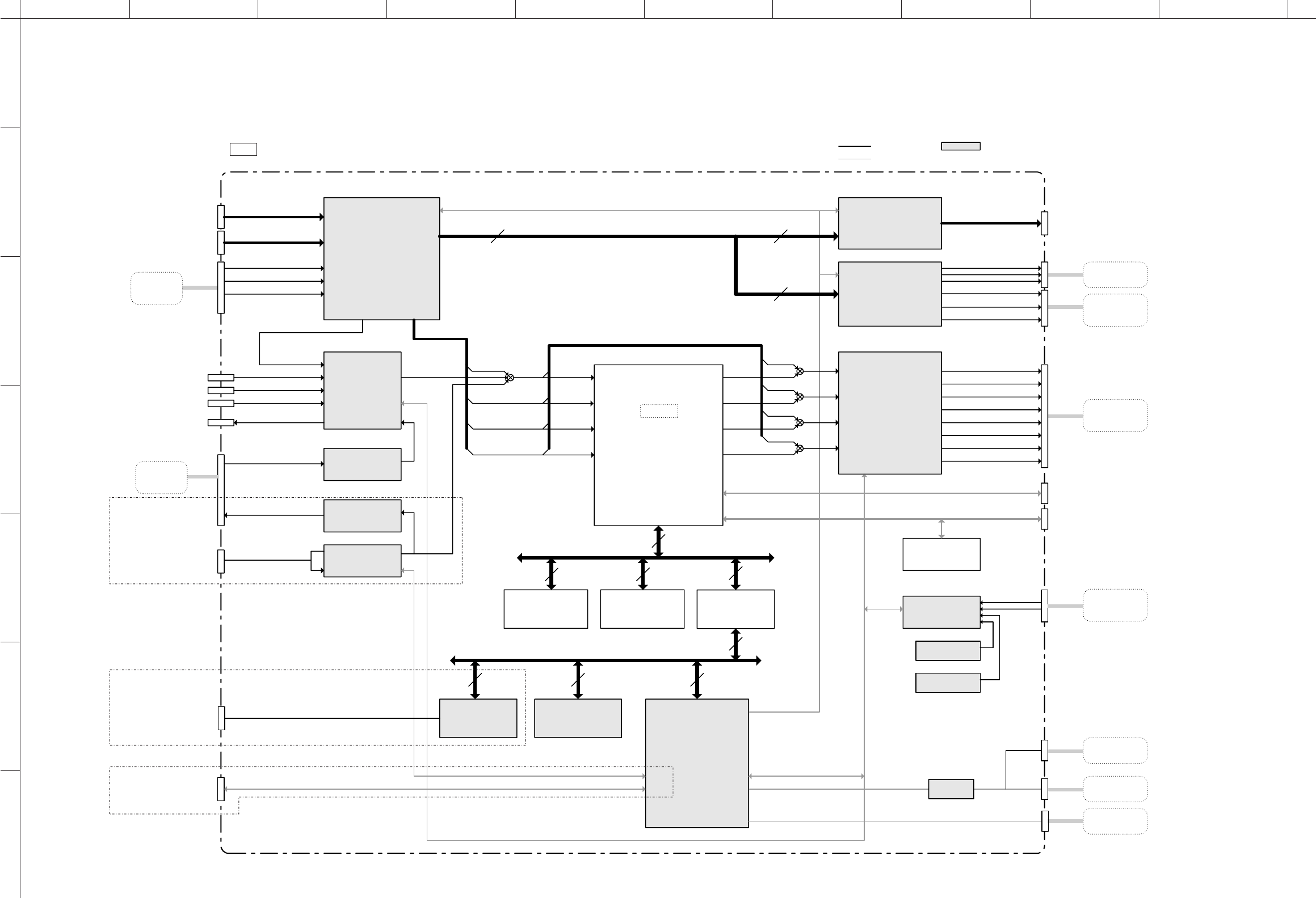
ABCDE FGH I J
1
2
3
4
5
6
7
RX-V563/HTR-6150/DSP-AX563
61
HDMI Tx
IC11
ADV9389B
MICROPROCESSOR
IC41
AD91089Z
VIDEO
ENCODER
IC21
ADV7172
SDRAM
IC51
K4S641632-UC75000
NPGA
IC61
MB87L8760
FLASH MEMORY
IC52
EN29LV160AB-70T
ADC
IC39
PCM1803DBR
HDMI RX
VIDEO DECODER
IC12
ADV7441A
HDMI IN 1
HDMI IN 2
S Video IN (Y)
XM DT
IC36
F2621E
DR0 PRI
SPORT
Direct Stereo Bus
Digital Video Data Bus
I2S PCM DataSPDIF
COAX IN
OPT IN 1
OPT OUT
XM
EEPROM
IC42
BR25L320F-W
ADC
IC81
ADC084S021
SPI
3.3V->5V
IC62
SN74VHCT245
BUS BUFFER
IC54,55
SN74LVC245APW
OPT IN 2
(Up to 150MHz)
133MHz
DIR
IC31
LC89057W
DAC
IC38
PCM1680
CB12CB13
PCB VIDEO
CB21
Analog In L/R
CB31
PortA
PortB
AIN3
S Video IN (C)
CVBS IN
AIN6
AIN7
P[2:9]
P[12:19]
P[22:29] P[2:9]
P[12:19]
P[22:29]
TMDS
Port
I2C I2C
I2C
P[12:19]
HDMI OUT
CB11
PCB VIDEO
CB22
COMPONENT Out
(Y)
(Cb)
(Cr)
CB21
S Video Out (Y)
S Video Out (C)
CVBS Out
PCB VIDEO
DAC A
DAC B
DAC C
DAC D
DAC E
DAC F
24bit
8bit
24bit
PJ31
U32
U33
U31
RX5
RX1
RX3
RX4
RX OUT
HDMI SPDIF
SDIN
HDMI I2S[0]
XMSDO
DIR RDATA
HDMI I2S[1]
HDMI I2S[2]
HDMI I2S[3]
DR0 SEC
DR1 PRI
DR1 SEC
DT0 PRI
DT0 SEC
DT1 PRI
DT1 SEC
SDO[0]
HDMI I2S[1]
HDMI I2S[2]
HDMI I2S[3]
SDO[0]
27
6821
5
8
9
3
1,2
14,15
1
99
76
81
24
12
6
67
59
58
74
73
63
62
6
11
12
13
35
33
29
28
25
24
26
22
21
20
19
16
15
DATA[1]
DATA[2]
DATA[3]
DATA[4]
CB31
DAC
IC37
PCM1781DBQR
Frout L
VOUT1
VOUT2
VOUT3
VOUT4
VOUT5
VOUT6
VOUT7
VOUT8
SPI Bus
I2C Bus
Frout R
Surround L
Surround R
Subwoofer
Center
Surround Back L
Surround Back R
PCB MAIN
XM Analog L/R
CB31
DOUT
DATA
VIN
VOUT
DATA
TX
RX
16bit
16bit
16bit 16bit
16bit
CB34
USB HOST
IC71
ISP1760
EXTENDED PORTS
IC56,57,58,59
TC74VHC574FT
TC74VHCT574FT
16bit 16bit 8bit
CB33
DOCK (iPod)
UART
Power off during standby mode
I2C0
I2C1
I2C2
UART0
UART1
UART3
SIRIUS
JK31
UART
SPI0
SPI1
SPI2
PIO
USB
CB71
SPI
IC83
SN74LV4051APWR
IN1
IN2
IN3
IN4
SPI
SELECTOR
SELECTOR
IC82
SN74LV4051APWR
COM
COM
CB83
KEY0
KEY1
SPI
OSD
TUNER
(U, C, R, T, K, A, G, E, F, L models)
PCB VIDEO
VFD
PCB OPERATION
CB84 CB84 CB32
Data Line
Control Line
PCB DSP
PF
EBIU
533MHz
D[0:23]
P[0:7]
(Writing port)
PCB
OPERATION
2
PCB MAIN
(U, C models)
(U, C models)
(R, T, K, A, B, G, E, F, L models)
DSP
• See page 83-90 →
SCHEMATIC DIAGRAM
■BLOCK DIAGRAMS
AUDIO (DIGITAL) SECTION BLOCK DIAGRAM
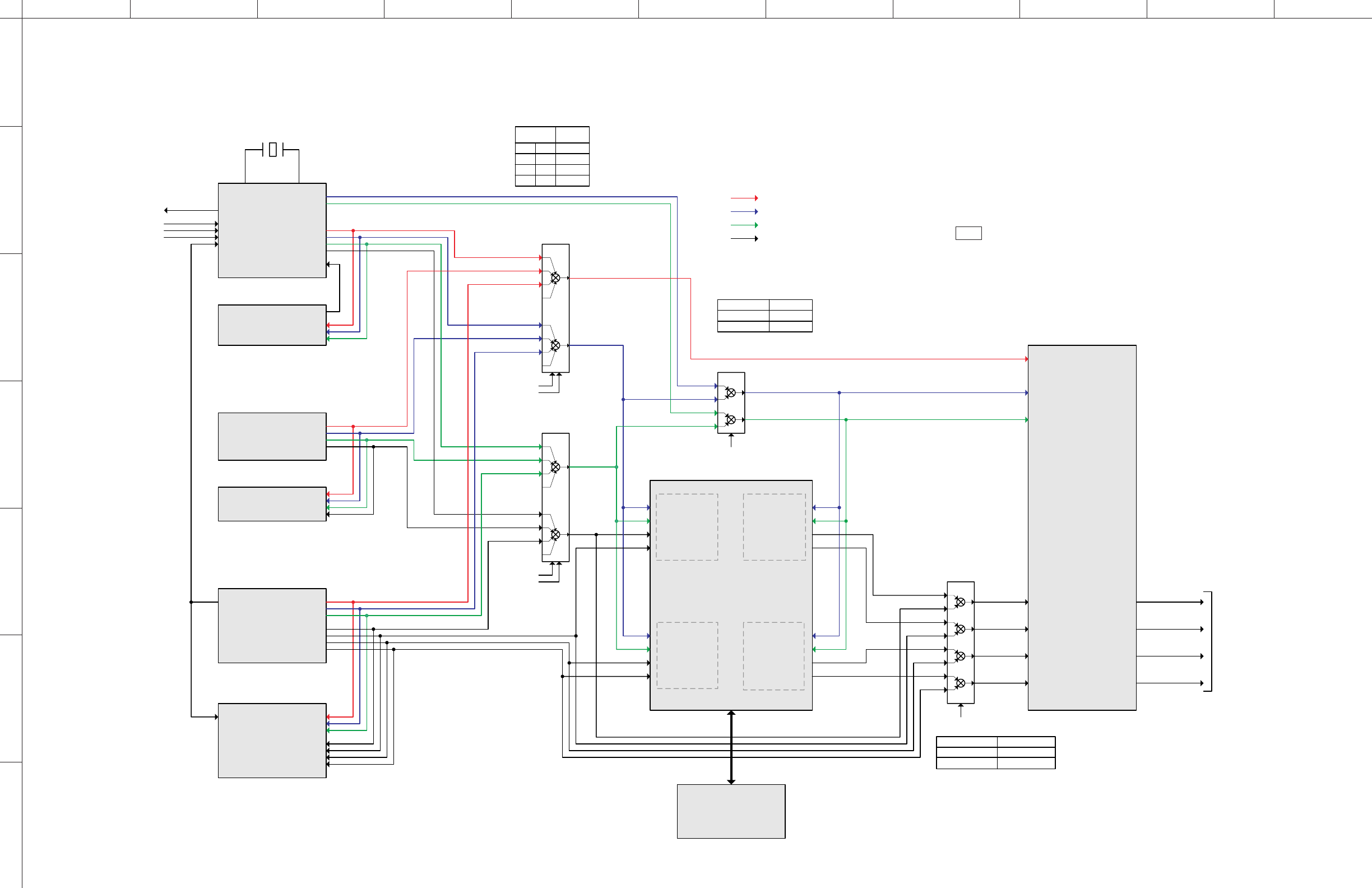
2
ABCDEFGH I J
1
3
4
5
7
RX-V563/HTR-6150/DSP-AX563
6
62
MICROPROCESSOR
IC41
AD91089Z
HDMI
Rx
IC12
ADV7441A
SPORT0
Tx
TSCLK0
TFS0
DT0PRI
DT0SEC
SPORT1
Tx
TSCLK1
TFS1
DT1PRI
DT1SEC
SPORT0
Rx
RSCLK0
RFS0
DR0PRI
DR0SEC
24.576MHz
ADC
IC39
PCM1803DBR
XM DT
IC36
F2621E
DIR
IC31
LC89057W
RX5
RX1
RX3
RX4
RX OUT
SDIN
DAC
IC37
PCM1781DBQR
DOUT
RMCK
HDMI
Tx
IC11
AD9389B
RBCK
RLRCK
RDATA
SCKI
BCK
LRCK
SBCK
SLRCK
256fs
64fs
fs
128fs
2fs
OCLK
SCLK
LRCLK
DATA
DATA
OCLK
SCLK
LRCLK
MCLKOUT
SCLK
LRCLK
I2S[0]
I2S[1]
I2S[2]
I2S[3]
SPDIF
MCLKOUT
SCLK
LRCLK
I2S[0]
I2S[1]
I2S[2]
I2S[3]
Optical Out
Coaxial In
Optical In1
Optical In2
DAC
IC38
PCM1680
DATA1
SCK
BCK
LRCK
SPORT1
Rx
RSCLK1
RFS1
DR1PRI
DR1SEC
Clock for DTS96/24 Master Clock
Bit Clock
Word Clock
Serial Data
IC33
TC74VHC157FT
IC44
TC74VHC153FT
IC43
TC74VHC153FT
IC34
To MAIN P.C.B.
TC74VHC157FT
AUDIO_CLK_SEL
AUDIO_SEL_A
AUDIO_SEL_B
AUDIO_SEL_A
AUDIO_SEL_B
SEL
SEL
AUDIO_DIRECT_ON
Direct Through Pass
DATA2
DATA3
DATA4
DAFL/DAFR
DAC/DASW
DASL/DASR
DASBL/DASBR
27,26
19,20
22,21
16,15
0
1
2
3
0
1
2
3
AB
AB
0
1
2
3
0
1
2
3
A
B
A
B
A
B
A
B
A
B
A
B
SPDIF
AUDIO_SEL
DIR0
AB
1
0
1
0
0
1
1
XM
HDMI (I2S)
AUDIO_CLK_SEL
A (normal)0
1
(default)
B (DTS96/24)
(default)
AUDIO_DIRECT_ON
A (Microprocessor)0
1B (direct through)
(default)
(512fs for DTS96/24)
USB Host
IC71
ISP1760
EBIU
D[0:16]
DSP
•See page 83-90 →
SCHEMATIC DIAGRAM
DSP CONTROL SECTION BLOCK DIAGRAM
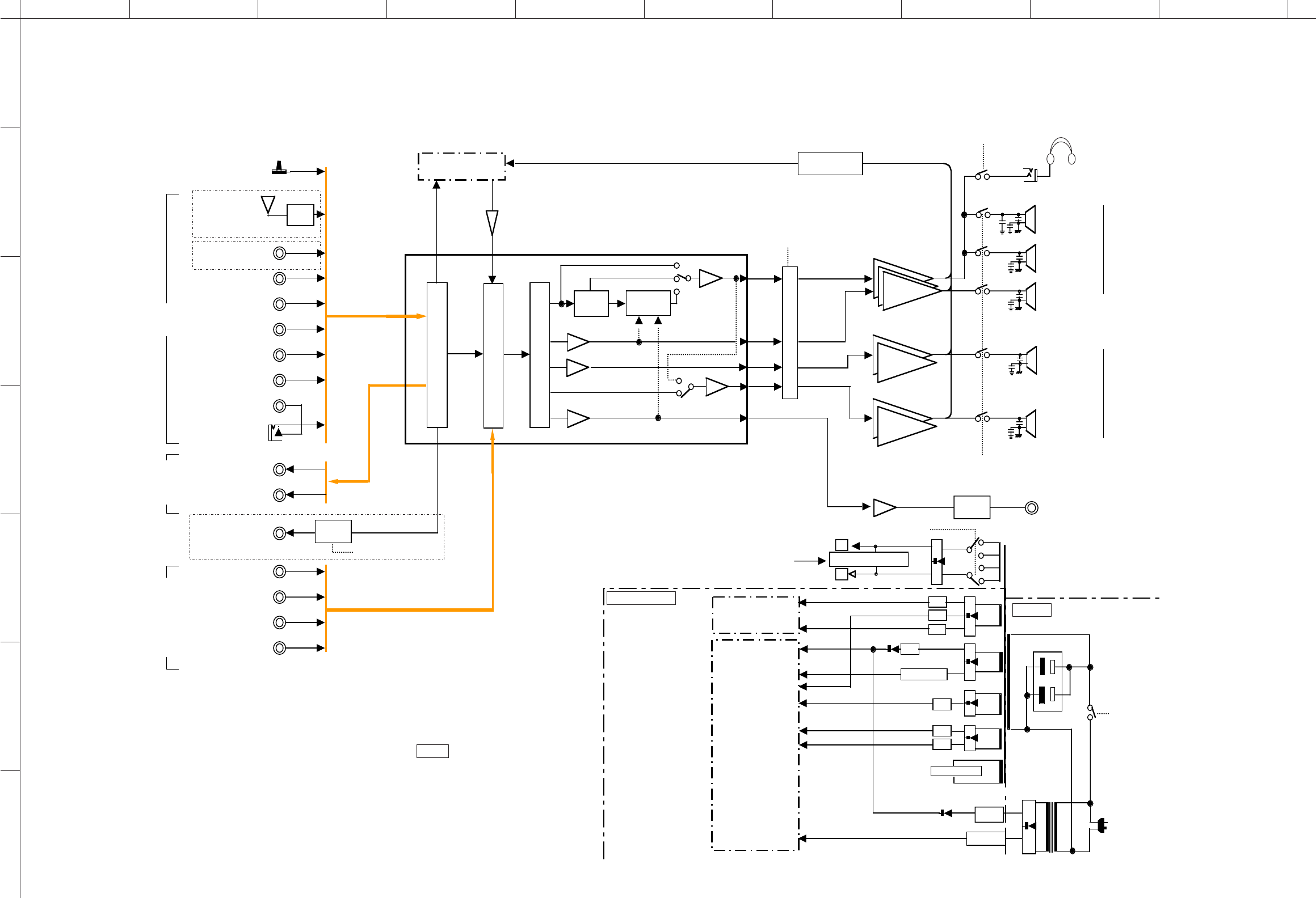
ABCDE FGH I J
1
2
3
4
5
6
7
RX-V563/HTR-6150/DSP-AX563
63
FM/AM
TUNER
TUNER
MD/CD-R
FM/AM
YPAO
MIC
DVD
DTV/CBL
DVR
AUX
PORTABLE
MD/CD-R
CD
ZONE2
FRONT/SB
SURROUND
CENTER
SUB WOOFER
INPUT
REC OUT
MULTI CH INPUT
Muting
INPUT & ZONE2 SELECTOR
8ch SELECTOR
ADL/ADR
DAFL/DAFR
DAC/DASW
DASL/DASR
DASBL/DASBR
To DSP P.C.B.
MASTER VOLUME
Tone
Control
Center Mix
LFE Mix
DVR
Mute Control
Muting
Center
SR L/R
SB L/R
SW 15
23,21
36-4354,55
46,47
5,3
17
11,9
FL/FR/C
SL/SR
SBL/SBR
Front A
Front B
Center
Surround
Surround Back
SP Relay
Control
HP Relay
Control
Mute Control
Muting SUBWOOFER OUT
(B model)
(U, C, R, T, K, A, G, E, F, L models)
(U, C, R, T, K, A, G, E, F, L model)
R2A15215FP
IC401
T3401
S9
Power Relay
Control
AC Detect
To FL Display
+12
ACH
ACL
AC6
AC5
AC2
AC3
AC4
D7014
D7018
IC707
IC702
IC703
IC705
IC704
IC503
IC407
IC501
IC502
IC701
IC706
IC700 D7019
D7015
D5021RY506
-12
+5D
+5XM/+5USB
+3.3
+5I
+6.3
+3.3
To DSP P.C.B.
To VIDEO P.C.B.
Power Limit Detect
Power Supply Control
-B
+B
Power Supply Control
Power Supply Relay Control
Head Phone
AC IN
RY341
Power transformer
MAIN
•See page 93, 94 →
SCHEMATIC DIAGRAM
VIDEO
•See page 95, 96 →
SCHEMATIC DIAGRAM
OPERATION
•See page 91, 92 →
SCHEMATIC DIAGRAM
SPEAKERS
AUDIO (ANALOG) / POWER SUPPLY SECTION BLOCK DIAGRAM
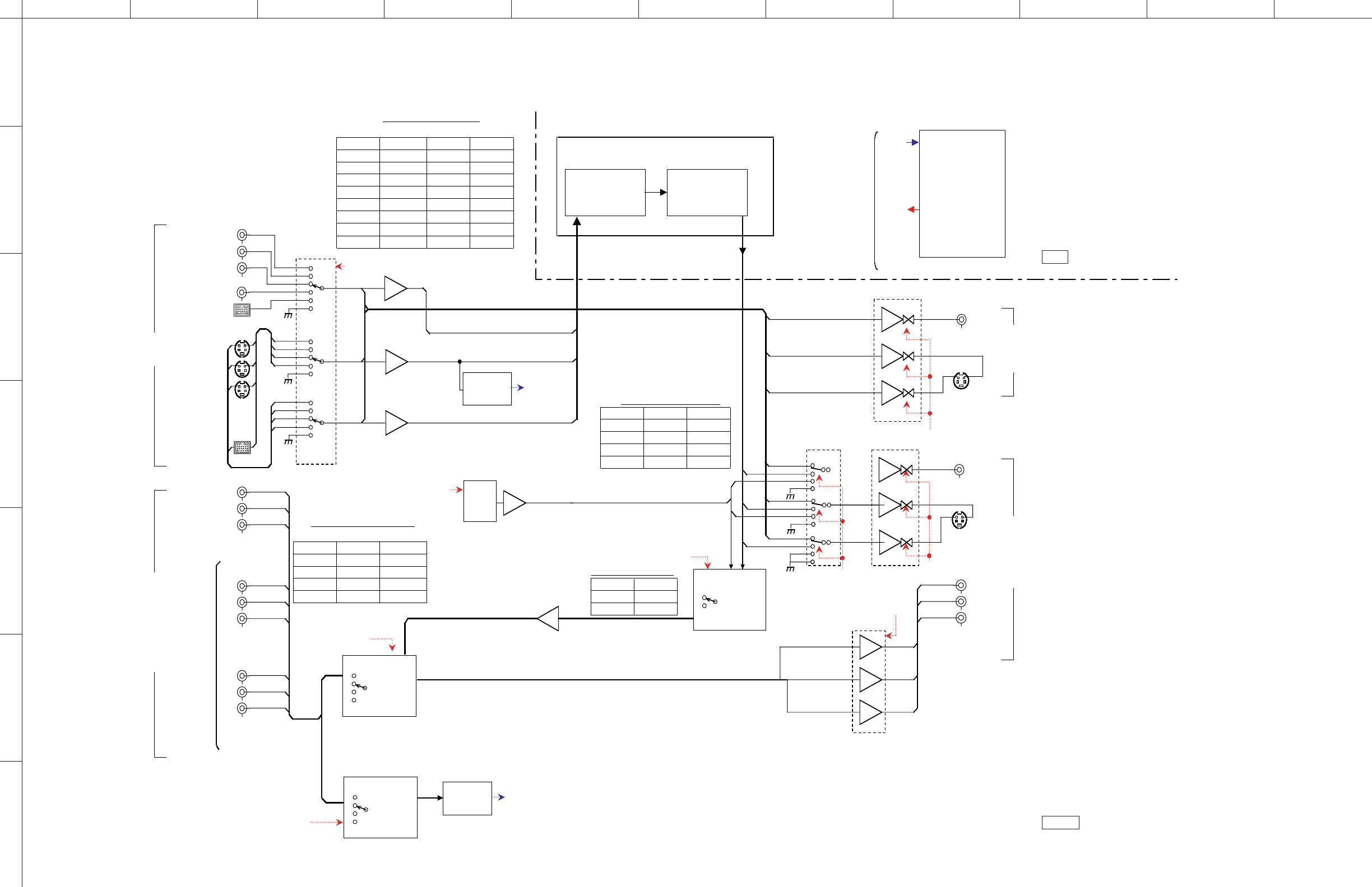
2
ABCDEFGH I J
1
3
4
5
7
RX-V563/HTR-6150/DSP-AX563
6
64
(4051)
INPUT VIA VIB VIC
MUTE L L L
DVD H L L
DVR L H L
DTV H H L
V-AUX L L H
iPod H L H
MUTE L H H
MUTE H H H
OUT YPASS conv
OSD L L
BYPASS H L
Vconv L H
MUTE H H
(4052)
INPUT CMP0 CMP1
MUTE L L
DVD H L
DVR L H Vconv
DTV/CBL H H OSD L
V conv H
COMPONENT OSD SELECTOR
PCB DSP
CVBS & YC INPUT SELECTOR
COMPONENT INPUT SELECTOR
CVBS & YC Monitor SELECTOR
MONITOR OUT
COMPONENT VIDEO VIDEO
DVR OUT
DVD
DVR
V-AUX
CY
CVBS
Y
C
INPUT SELECTOR
S-DETECTOR
TC74HCU04
Pb/Cb
Pr/Cr
Y
Pb/Cb
Pr/Cr
DVD
DTV/
CBL
DTV/CBL
6dB
6dB
6dB
Y
Pb/Cb
Pr/Cr
DVR
OUTPUT AMP
NJM2581
Y
Pb/Cb
Pr/Cr
6dB
Y
Cb
Cr
BYPASS SWITCH
TC74HC4052 x2
C
Y
CVBS
Y
C
Y
CVBS
CY
BYPASS
OUTPUT AMP
LA73050
6dB
6dB
6dB
/MTMON
BYPASS
Vconv
/MTMON
/CNON
Conv V
SVDET
INPUT SELECTOR
TC74HC4052 x2
Y/Cb/Cr
IN
Vconv
CMP0
CMP1
CBYPAS
OSD CONVERSION
S
OUTPUT AMP
LA73050
/MTVR1
DVD
DVR
DTV/CBL
OSD_CE
OSD_CK
OSD_DT
SEL V
SEL Y
SEL C
OSD
0dB
iPod
iPod
6dB
C
Conv
6dB
Conv C
MICROPROCESSOR
Y/Cb/Cr
OUT
0dB
0dB
0dB
VIA
VIB
VIC
BYPASS
Vconv
CMP0
CMP1
CBYPASS
OSD_CE
OSD_CK
OSD_DT
/MTMON
/MTVR1
/CNON
SVDET
CPNTD
VIDEO
RECOUT
OSD
LC74782
VIA
VIB
MM74HC4051 x3
VIC
IC301
IC302
IC303
Q3001
Q3003
Q3002
IC305
IC304 Q3005
IC307
IC307
IC310,311
IC325
IC389
IC322
IC323
Conv/OSD
SELECTOR
74HC4053
INPUT SELECTOR
TC74HC4052
0dB
Q3201 - 3203
IC321
IC326
Y-DETECTOR
TC74HCU04
CPNTD
CMP0
Y IN
CMP1
HDMI Rx/
VIDEO DECODER
ADV7441A
VIDEO ENCODER
ADV7172
Y
IC21IC12
IC41
DSP
•See page 83-90 →
SCHEMATIC DIAGRAM
VIDEO
•See page 95, 96 →
SCHEMATIC DIAGRAM
VIDEO SECTION BLOCK DIAGRAM
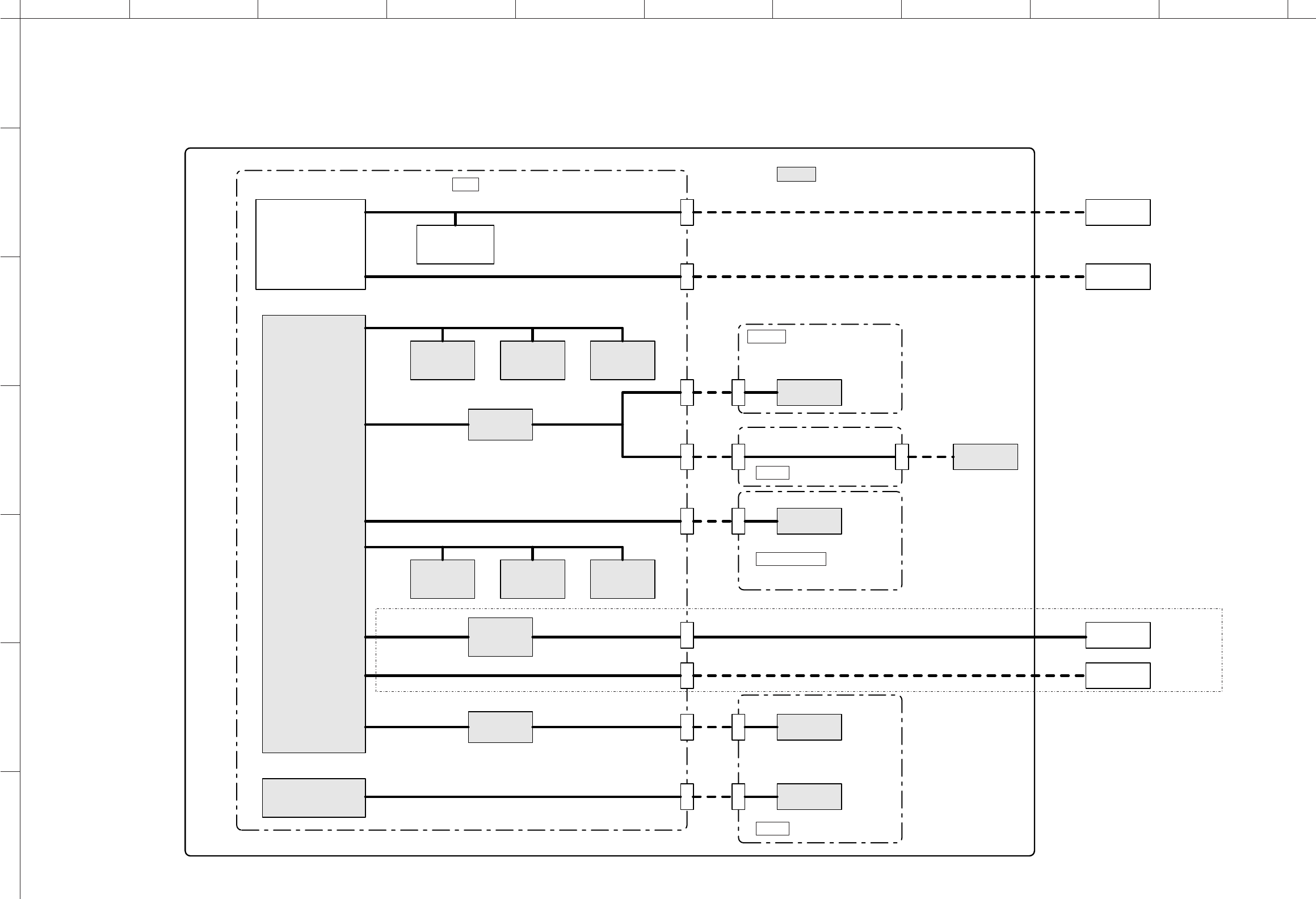
ABCDE FGH I J
1
2
3
4
5
6
7
RX-V563/HTR-6150/DSP-AX563
65
MICROPROCESSOR
IC41
NPGA
IC61
DOCK
EEPROM
IC42
BR25L320F-W
RDS
LC72725
TUNER
DIR
IC31
LC89057W
DAC
IC38
PCM1680DBQ
ADC
IC39
IC603
IC402
IC401
IC304
ADC084S021C
(Writing port)
XM
IC36
F2621E
SIRIUS
XM
OSD
LC74782
VFD
M66003
HDMI Tx
IC11
AD9389B
HDMI Rx
IC12
ADV7441A
VIDEO
IC21
ADV7172
CB34 CB33
SPI
UART
CB32 CB83 CB35CB84
IC62
SN74VHCT245
3.3V->5V
IC62
SN74VHCT245
SPI0
SPI1
SPI2
I2C0
I2C1
I2C2
UART0
UART1
UART2
JK31
EXTENDED
IC57
TC74VHC574FT
SYSTEM IC
R2A15215FP
CB84
PIO
CB84
Power off during standby mode
(no use)
(no use)
(no use)
3.3V->5V
(U, C models)
VIDEO
•See page 95, 96 →
SCHEMATIC DIAGRAM
MAIN
•See page 93, 94 →
SCHEMATIC DIAGRAM
MAIN
•See page 93, 94 →
SCHEMATIC DIAGRAM
OPERATION
•See page 91, 92 →
SCHEMATIC DIAGRAM
DSP
•See page 83-90 →
SCHEMATIC DIAGRAM
CONTROL SECTION BLOCK DIAGRAM
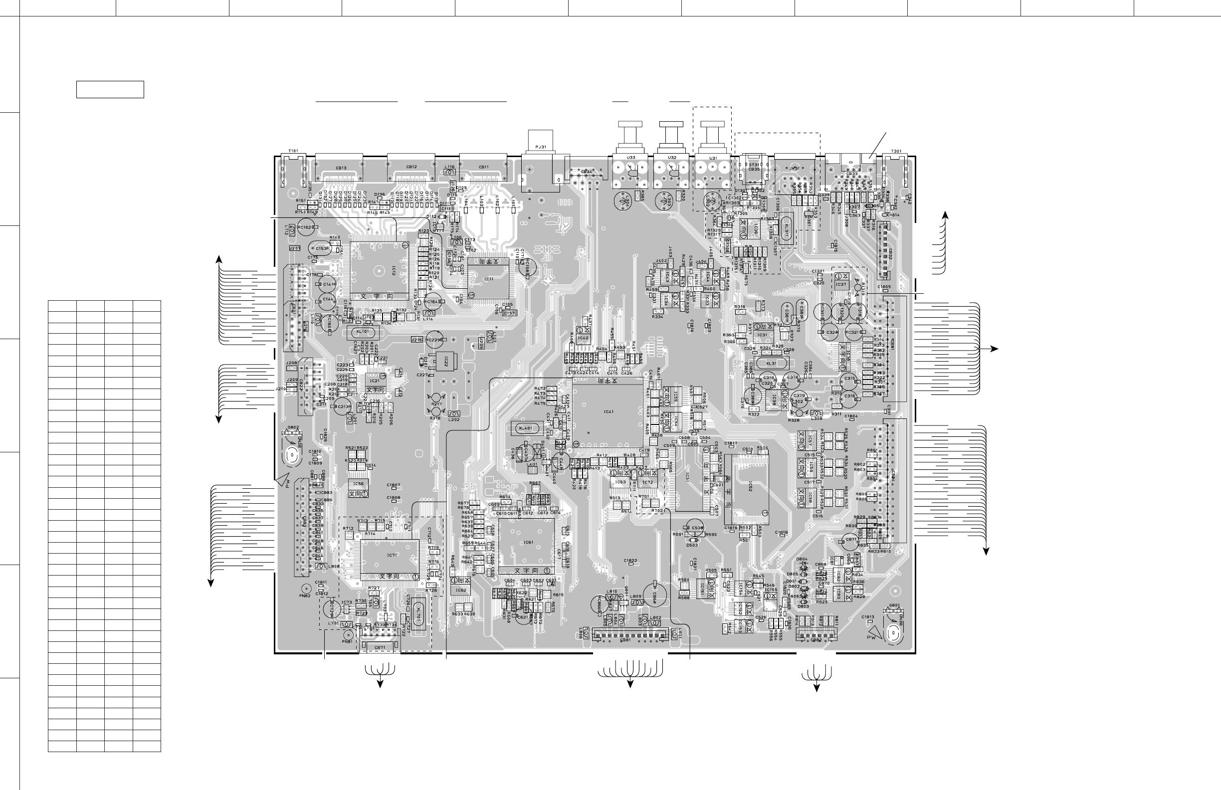
2
ABCDEFGH I J
1
3
4
5
7
RX-V563/HTR-6150/DSP-AX563
6
66
CB13 CB12 CB11
CB34
IC11
IC12
IC43
IC44 IC33
IC34
IC55
IC36
CB35 JK31
CB33
IC37
CB32 CB31
IC38
IC31
IC39
IC57 IC59 IC58
IC81
IC82 IC83
CB84
IC41
IC42
IC22
IC21
CB21
CB22 CB83
IC56 IC53 IC72
IC51
IC52
IC54
CB82
IC155
IC154 IC152 IC153
IC151
CB81
IC61
IC62
IC71
IC73
CB71
(Side A)
DSP P.C.B.
VIDEO (1)
(CB302)
VIDEO (2)
(CB326)
SEL C
VE SEL Y
VE SEL V
VE VconvV
VE VconvY
VE VconvC
VE Vconv
BYPASS
Y
VE Pb
VE Pr
VE CMP1
CMP0 CBYPASS
/CNON /MTMON
CPNTD Vconv
NC
FG
GND
D+
D-
Vcc
+5USB
+6.3H
+3.3H
HG
+3.3D
DG
DG
DG
+5D
+5XM
+5I
IG
/RESET
/PDET
PRY
XMPWR
THM
PRV2
VIC
VIB VIA
/MTMON /MTVR1
SVDET NC
RMSCN
SCENE4 SCENE3
SCENE2
MG
V_CN
+3.3S
SCENE1
TRG /MICDET
SSEL3 SSEL2
SSEL1 VRB
VRA REM1
/PSW /RSTFD
CKFD DTFD
/CEFD ZONE2 SW
ADKEY2 ADKEY0
R2A_CLK
/SWMT
/FMT
CSRY
MRYA
/HP
TMT
/ST
SPICK
CEP
RDS_CLK
RDS_RDY
/CMT
PRI
PLDET
PRV1
R2A_DATA
SBRY
/SMT
MRYB
HPRY
/8ohmSW
TUNED
SPIMI
SPIMO
RDS_RST
RDS_DATA
/Z2MT
/SBMT
PRD
LIM
iPod_R
iPod_L
DA_FL
SIR_R
SIR_L
AGND
DA_SBR
DA_SBL
AGND
AGND
AGND
DA_FR
AGND
1GND
U, C models
OSD_DT
OSD_CK
OSD_CE
IP_VE
IP_CVBS
IP_VE
IP_SY
IP_VE
IP_SC
REMSENSE
AD_L
SIR_GND
XM_R
XM_L
AGND
DA_C
DA_SW
DA_SR
DA_SL
AGND
AD_R
VIDEO (1)
(W3002)
MAIN (1)
(CB402)
OPERATION (1)
(CB603)
MAIN (1)
(CB401)
OPERATION (6)
(W6006)
R, T, K, A, B, G, E, F, L models
R, T, K, A, B, G, E, F, L models
OPERATION (2)
(W702)
OPERATION (2)
(W700)
DTV/CBL
IN2
HDMI
OUT
(Writing port)
DVD DVD/CBL CD MD/CD-R
COAXIAL OPTICAL
XM
U, C models
R, T, K, A, B, G, E, F, L models
SIRIUS DOCKDVD
IN1
1
13
54
1
20
21 40
80 61
41
60
36
108
73
37
1
1
1
1110
20 11
38
1
34
5
10265
39
64
128
103
36
10873
37
72
144
109
10
2011
12
36
25 1324
4837
GND
VOUT
VIN
72
144109 1
1
8
16
1
1
1
1
1
44
1
58
4
132
89
45 88
176 133
10
1
1
10
20
11
1
8
16
9
1
7
14 71
1
8
16
1
5
6
10
9
1
8
16
9
814
8
1
7
14
8
1
27
54
1
10
20
11
1
110
20 11
110
20 11
10
20
11
28
1
10
20
11
1
10
20
11
1
10
20
11
24
4925
20
11
14
28
15
8
16 9
12
36
48
37 25
13
24
9
16
9
1
8
1
8
1
8
16
9
16
9
12
36
25
13 24
48 37
No replacement part available.
No replacement part available.
No replacement part available.
R, T, K, A, B, G, E, F, L models
■PRINTED CIRCUIT BOARDS
IC12 D3
IC13 D3
IC21 D4
IC22 D4
IC31 G3
IC33 G3
IC34 F3
IC36 G3
IC37 H3
IC38 H4
IC39 G4
IC41 F4
IC42 F3
IC43 F3
IC44 G3
IC51 G5
IC52 G5
IC53 F5
IC54 F4
IC55 F4
IC56 D5
IC57 H4
IC58 H5
IC59 H5
IC61 E5
IC62 E6
IC71 D5
IC72 F5
IC73 D6
IC81 H5
IC82 H6
IC83 H6
IC151 G6
IC152 G6
IC153 G6
IC154 G6
IC155 G6
Q301 H2
Q401 E5
Q801 F6
• Semiconductor Location
Ref no.
D109 E2
D110 D2
D111 D2
D112 D2
D113 D2
D114 D2
D115 D2
D116 D2
D117 D2
D118 D2
D119 D2
D120 D2
D121 D2
D122 D2
D123 D2
D124 D2
D125 D2
D126 D2
D127 C2
D128 C2
D129 C2
D130 D2
D131 C2
D132 C2
D135 C2
D136 D2
D201 D4
D305 H2
D306 H2
D401 E4
D503 G5
D801 H6
D802 H6
D803 H6
D804 H6
D805 H6
D806 H6
D1301 G2
D1302 G2
IC11 E3
Location Location
Ref no.
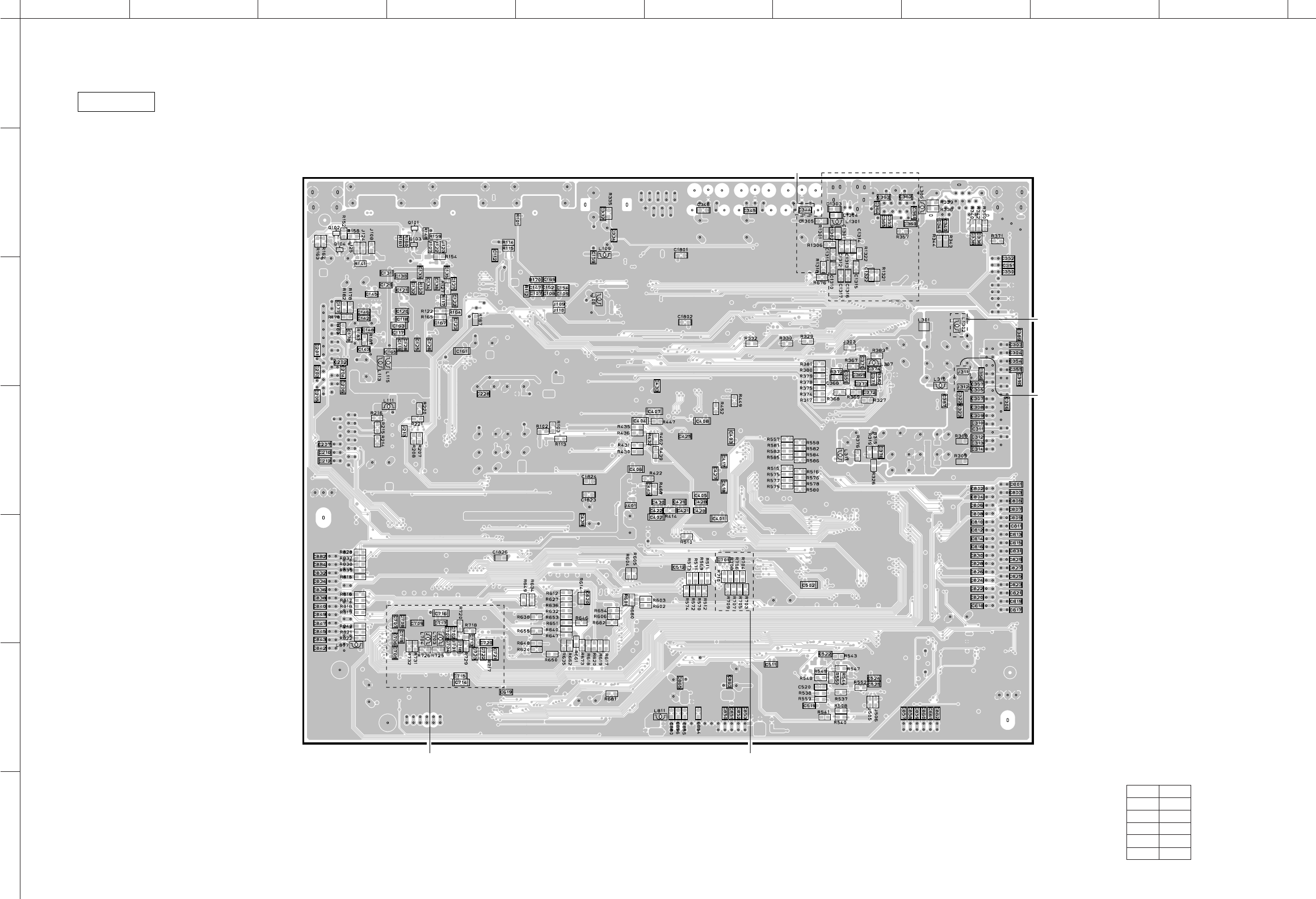
ABCDE FGH I J
1
2
3
4
5
6
7
RX-V563/HTR-6150/DSP-AX563
67
(Side B)
DSP P.C.B.
U, C modelsR, T, K, A, B, G, E, F, L models
U, C models
R, T, K, A, B, G, E, F, L models
R, T, K, A, B, G, E, F, L models
R, T, K, A, B, G, E, F, L models
•Semiconductor Location
Ref no.
Location
D1303 G2
Q101 D2
Q102 C2
Q103 D2
Q104 C2
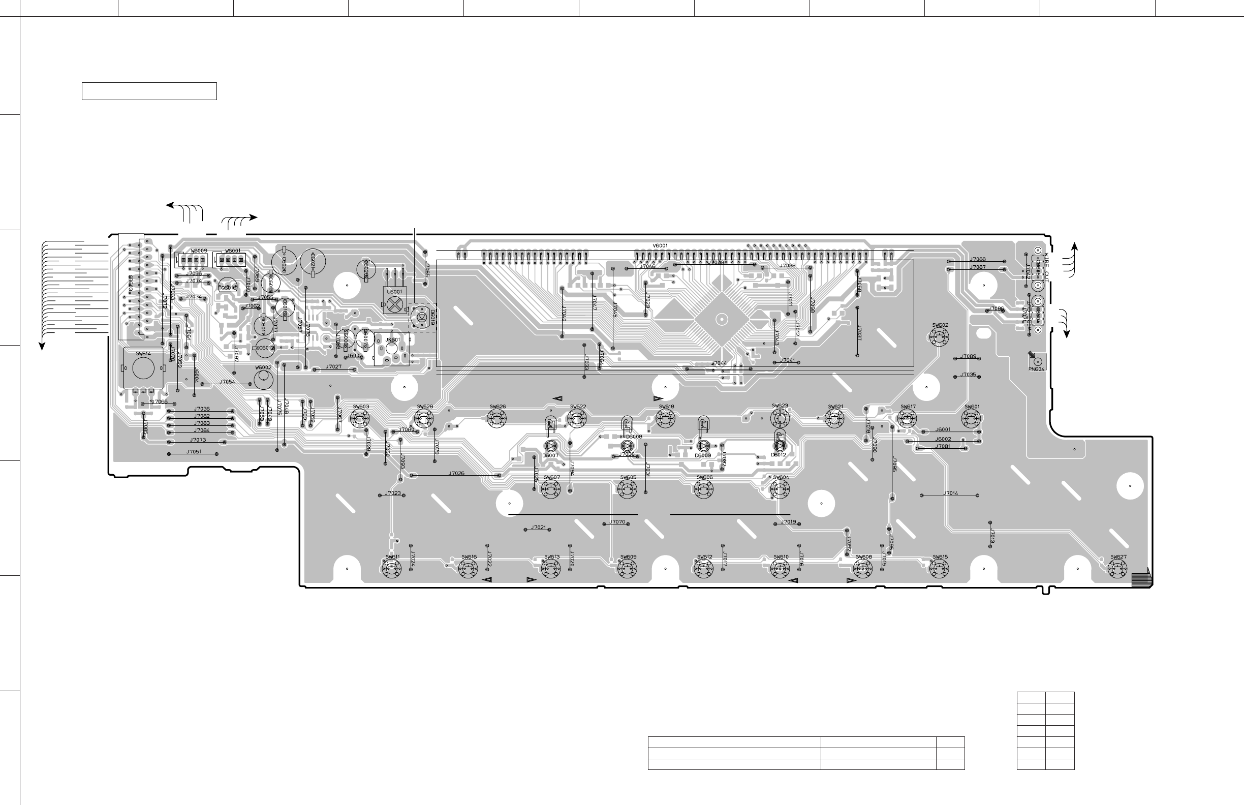
2
ABCDEFGH I J
1
3
4
5
7
RX-V563/HTR-6150/DSP-AX563
6
68
W6009 W6001
W6002
CB603
JK601
CB605 CB604
(Side A)
OPERATION (1) P.C.B.
RMSCN
SCENE4
SCENE2
TRG
SSEL3
SSEL1
VRA
PSW
CKFD
/CEFD
ADKEY1
+3.3S
V_CN
SCENE3
SCENE1
/MICDET
SSEL2
VRB
REM1
/BLK
DTFD
ZONE2SW
ADKEY0
MG
-12
+12
E
MIC
GND
CN_OUT
-RM
+RM
FG
FG
MG
/PSW
F2
VP
F1
OPERATION (8)
(CB602)
VIDEO (6)
(CB366)
OPERATION (7)
(CB606)
OPERATION (2)
(CB703)
DSP
(CB83)
PRESET/TUNING/CH
SCENE
1234
ZONE
CONTROL
VOLUME MEMORY BAND
CATEGORY
A/B/C/D/E
ZONE 2
ON/OFF
SYSTEM OFF
TONE CONTROL SPEAKERS
A/B/OFF
STRAIGHTDIRECT
AUDIO SELECT INPUT EFFECT PROGRAM
EDIT
SEARCH MODE
PRESET/TUNING
INFO
TUNING AUTO/MAN'L
U, C, R, T, K, A, G, E, F, L models
•Semiconductor Location
Ref no.
Location
D6007 E4
D6008 F4
D6009 G4
D6012 G4
D6019 D3
Q6016 B3
U, C, R, T, K, A, G, E, F, L B
OX
OX
SW601-603, 617, 618, 621, 622, 625, 626, 628
J6002
Circuit No.
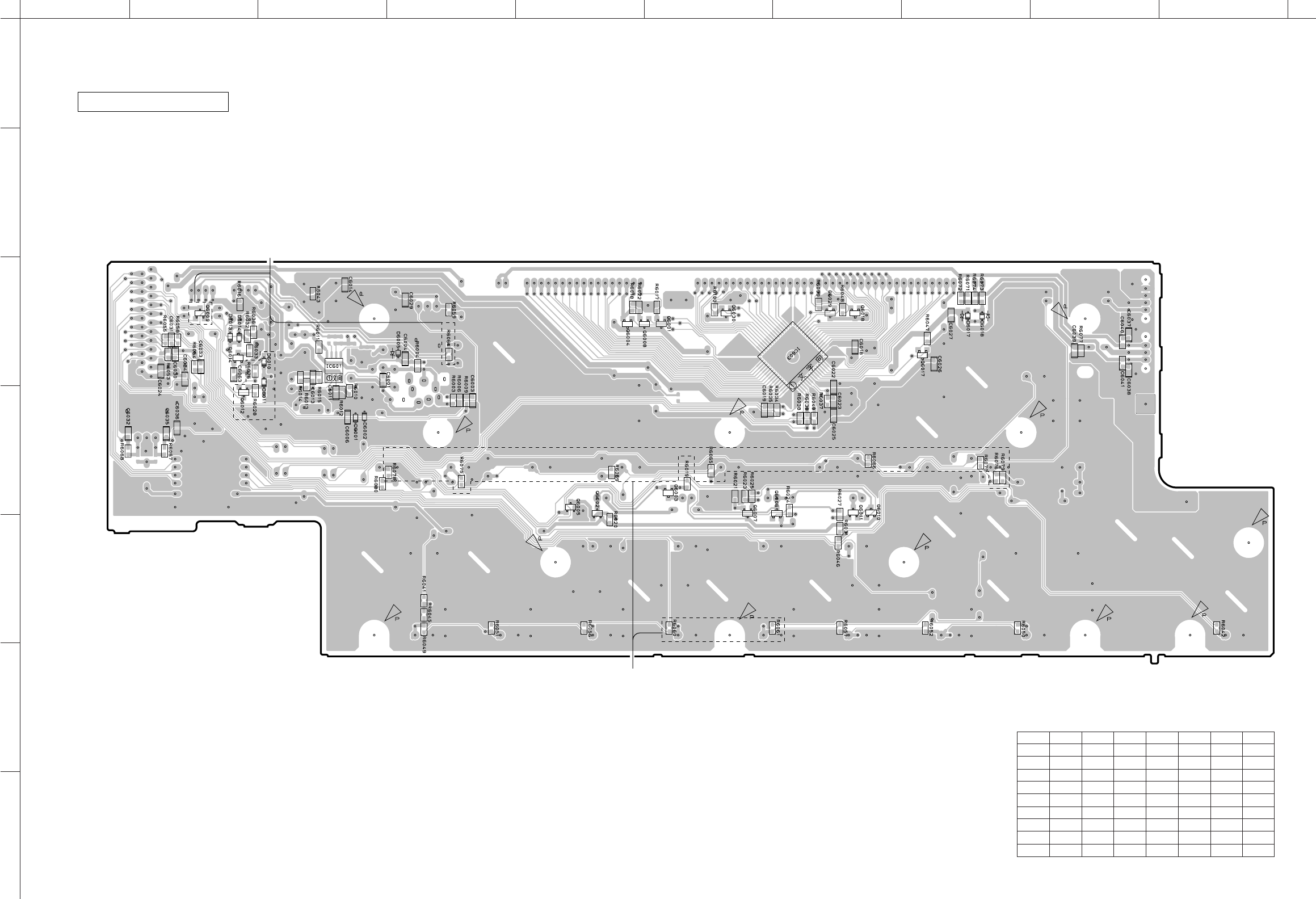
ABCDE FGH I J
1
2
3
4
5
6
7
RX-V563/HTR-6150/DSP-AX563
69
IC601
IC603
(Side B)
OPERATION (1) P.C.B.
14
85
164
3233
16
17
49
48
U, C, R, T, K, A, G, E, F, L models
U, C, R, T, K, A, G, E, F, L models
•Semiconductor Location
Ref no.
Location
Ref no.
Location
Ref no.
Location
Ref no.
Location
D6001 C4
D6002 C4
D6005 D3
D6010 C3
D6011 C3
D6013 B3
D6014 B3
D6017 H3
D6018 H3
IC601 C3
IC603 G3
Q6001 F3
Q6002 E4
Q6003 F4
Q6004 E3
Q6005 E4
Q6006 G4
Q6007 F4
Q6008 E3
Q6009 B3
Q6010 G4
Q6011 G4
Q6012 B4
Q6014 B3
Q6017 H3
Q6018 G3
Q6029 G3
Q6030 F3
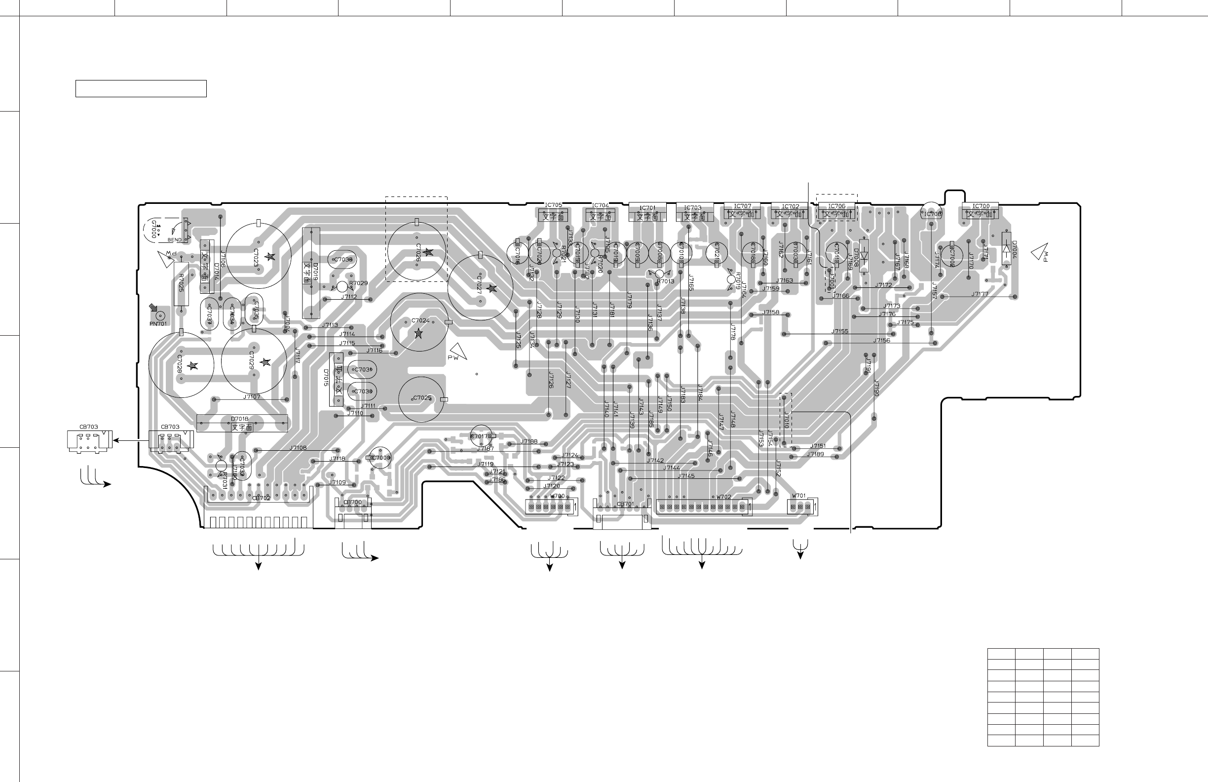
2
ABCDEFGH I J
1
3
4
5
7
RX-V563/HTR-6150/DSP-AX563
6
70
IC705 IC704 IC701 IC703 IC707 IC702 IC706
IC708
IC700
W701
W702
CB701
W700
CB700
CB702
CB703
(Side A)
OPERATION (2) P.C.B.
PRV2
AC2
E
AC2
AC3
AC3
AC4
AC4
AC5
AC5
AC6
AC6
VP
PRV1
+5D
+3.3
-12
AGND
+12
IG
+5I
+5XM
+5D
DG
DG
DG
+3.3D
HG
+3.3H
+6.3H
+5USB
-12
PRV2
+12
S9
PRY
ACDET
MG
AC6
VP
AC6
THM
XMPWR
PRY
/PDET
/RESET
POWER TRANSFORMER
VIDEO (3)
(W3401)
OPERATION (1)
(CB604)
MAIN (1)
(W506)
DSP
(CB81)
VIDEO (1)
(CB301)
DSP
(CB82)
OUT
OUT
OUT
IN
IN
COM
COM
IN
COM
OUT
IN
1
4
1
4
1
GND
OUT
VCC
4
1
4
COM
U, C, R, T, K, A, B, G, E, F, L models U, C, R, T, K, A, B, G, E, F, L models
R, T, K, A, B, G, E, F, L models
R, T, K, A, B, G, E, F, L models
•Semiconductor Location
Ref no.
Location
Ref no.
Location
D7004 I3
D7008 H3
D7014 B3
D7015 C4
D7018 C4
D7019 C3
IC700 I2
IC701 F2
IC702 H2
IC703 G2
IC704 F2
IC705 E2
IC706 H2
IC707 G2
IC708 I2
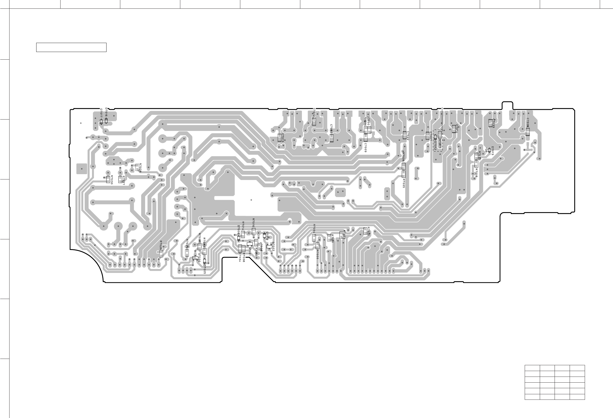
ABCDE FGH I J
1
2
3
4
5
6
7
RX-V563/HTR-6150/DSP-AX563
71
(Side B)
OPERATION (2) P.C.B.
U, C models
•Semiconductor Location
Ref no.
Location
Ref no.
Location
D7005 D5
D7006 D4
D7010 E4
D7012 H3
D7013 I3
D7016 B3
D7017 B3
Q7000 D5
Q7001 E5
Q7002 E5
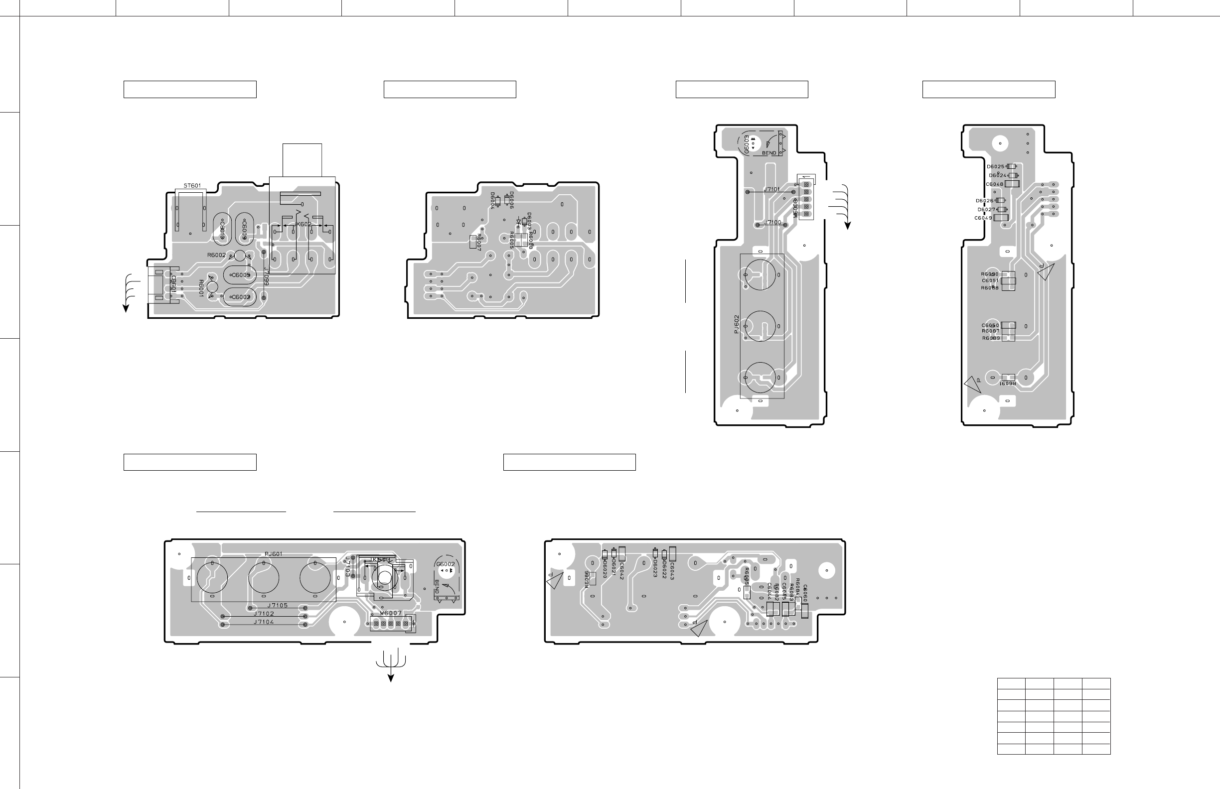
2
ABCDEFGH I J
1
3
4
5
7
RX-V563/HTR-6150/DSP-AX563
6
72
JK602
CB601
W6008
W6007
(Side A)
OPERATION (3) P.C.B.
(Side A)
OPERATION (5) P.C.B.
(Side A)
OPERATION (4) P.C.B.
HPR
E
HPL
/HP
AUX-V
VE
AXL
E
AXR
AUX-V
VE
AXL
E
AXR
MAIN
(W501)
OPERATION (8)
(CB608)
OPERATION (8)
(CB608)
PHONES
SILENT CINEMA
LVIDEO AUDIO
VIDEO AUX
R
LVIDEO AUDIO PORTABLE
VIDEO AUX
R
(Side B)
OPERATION (5) P.C.B.
(Side B)
OPERATION (3) P.C.B. (Side B)
OPERATION (4) P.C.B.
R, T, K, A, B, G, E, F, L modelsR, T, K, A, B, G, E, F, L models
U, C modelsU, C models
•Semiconductor Location
Ref no.
Location
Ref no.
Location
D6003 E2
D6004 E2
D6006 E2
D6020 F5
D6021 F5
D6022 F5
D6023 F5
D6024 I2
D6025 I2
D6026 I2
D6027 I2
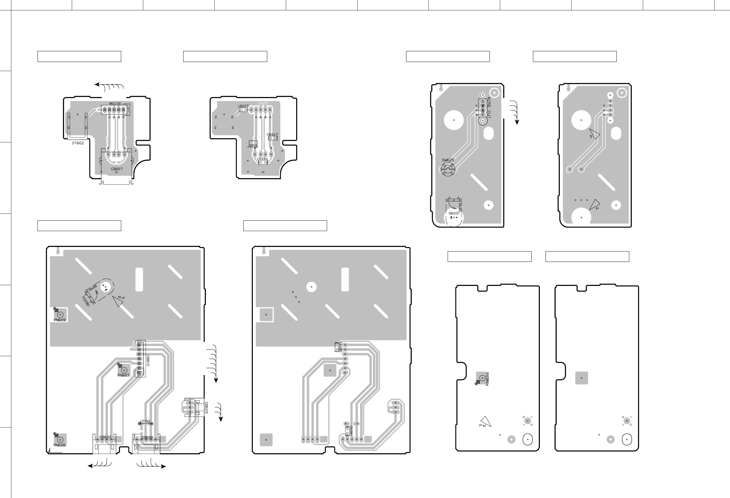
ABCDE FGH I J
1
2
3
4
5
6
7
RX-V563/HTR-6150/DSP-AX563
73
W6006
CB607
CB606
CB602 CB608
CB610
CB609
(Side A)
OPERATION (6) P.C.B.
(Side A)
OPERATION (8) P.C.B.
(Side A)
OPERATION (9) P.C.B.
(Side A)
OPERATION (7) P.C.B.
FG
GND
+Data
-Data
VBus
FG
FG
MG
/PSW
AXR
E
AXL
-12
+12
E
MIC
AXV
VE
VE
-12
+12
E
MIC
AXV
VE
AXL
E
AXR
DSP
(CB71)
USB
OPERATION (1)
(CB605)
MAIN ZONE ON/OFF
(U, C, R, T, K, A, G, E, F, L models)
(R, T, K, A, B, G, E, F, L models)
(U, C models)
STANDBY/ON
(B model)
MAIN (1)
(W401)
VIDEO (1)
(W3001)
OPERATION (4)
(W6008)
OPERATION (1)
(W6001)
OPERATION (5)
(W6007)
R, T, K, A, B, G, E, F, L models
(Side B)
OPERATION (8) P.C.B.
(Side B)
OPERATION (9) P.C.B.
(Side B)
OPERATION (7) P.C.B.
(Side B)
OPERATION (6) P.C.B.
R, T, K, A, B, G, E, F, L models
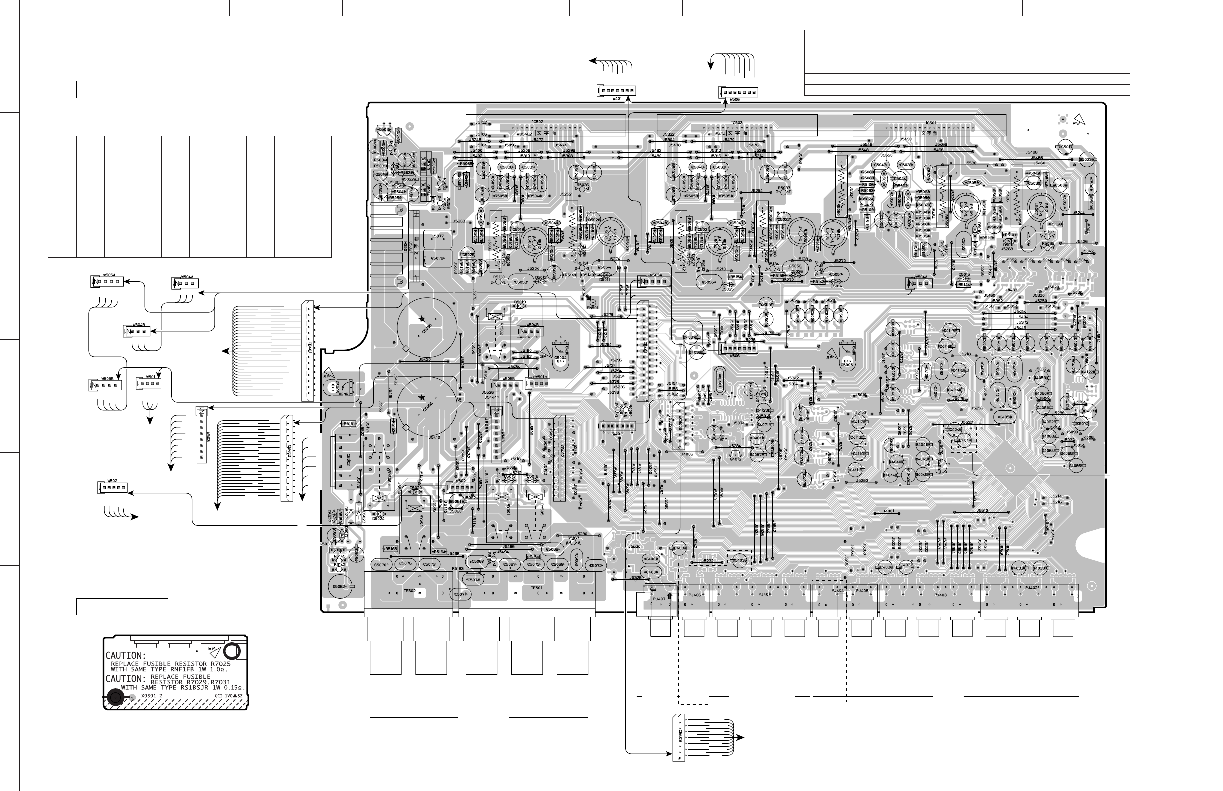
2
ABCDEFGH I J
1
3
4
5
7
RX-V563/HTR-6150/DSP-AX563
6
74
IC502 IC503 IC501
W504A
W506
W505A
CB401
CB403
W504B
W501
CB502
W503
W505B
CB402
W401
W502
(Side A)
MAIN (1) P.C.B.
(Side A)
MAIN (2) P.C.B.
IPR
AGND
PRV1
LIM PLDET
PRD PRI
/SBMT /CMT
/SMT /FMT
/Z2MT RDS_RDY
RDS_DATA RDS_CLK
RDS_RST CEP
SPIMO SPICK
SPIMI /ST
TUNED TMT
8ohmSW /HP
HPRY MRYA
MRYB CSRY
SBRY /SWMT
R2A_DATA R2A_CLK
IPL
REMSEMSE SIRR
AGND SIRL
XMR AGND
XML DASBR
AGND DASBL
DAC E
DASW AGND
DASR AGND
DASL DAFR
EDAFL
ADL E
ADR
SL
ACL
ACL
E
E
ACH
ACH
SLG
SRG
SR
SBL
SBLG
SBRG
SBR
+12
-12
SBRY
SRY
GND
HPR
HPG
HPL
/HP
SBR
SBL
SR
SL
+12
AXR
AGND
AXL
-12
+12
AGND
AMIC
CHASSIS
-12
+3.3
+5
PRV1
VP
SL
SR
SBL
SBR
L
R
C
L
R
C
POWER TRANSFORMER
CEP
SDTP SCKP
SDRP TUR
TE TUL
TMT /ST
TUNED +10B
COMP NC
VIDEO (4)
(CB353)
VIDEO (4)
(CB351)
Tuner
OPERATION (2)
(CB701)
OPERATION (8)
(CB610)
DSP
(CB31)
DSP
(CB84)
OPERATION (3)
(CB601)
115 115 119
FRONT
(6CH)
SB
(6CH)
SUR
ROUND
MULTI CH INPUT
SPEAKERS
CENTER
+/-+/-+/-+/-+/-
FRONT AFRONT B AUDIO
ZONE 2
OUT
OUTPUT
CENTER
L/R
TUNER
L/R
CD DVR
L/R
OUT IN
L/R L/R
DTV/CBL
L/R
DVD MD/CD-R
L/R
OUT
(REC)
L/R
IN
(PLAY)
L/RL/RL/R L/R L/R
SUB
WOOFER
SUB
WOOFER
U, C, R, T, K, A, G, E, F, L models
U, C, R, T, K, A, G, E, F, L models
B model
U, C, R, T, K, A, G, E, F, L models
LR LR
•Semiconductor Location
Ref no.
Location
Ref no.
Location
Ref no.
Location
Ref no.
Location
D5001 D2
D5002 D2
D5005 E3
D5006 F3
D5007 G3
D5008 G3
D5010 I3
D5011 F3
D5012 E3
D5013 E5
D5014 H3
D5015 I3
D5016 I3
D5017 C5
D5018 E5
D5019 E3
D5020 D5
D5021 D3
D5022 D5
D5023 D5
D5024 D5
D5025 G3
D5026 G3
D5027 C5
IC501 I2
IC502 E2
IC503 G2
Q4009 H4
Q4010 I5
Q4011 G4
Q4012 G5
Q5012 D2
Q5013 D2
Q5014 D2
Q5015 D2
Q5016 D2
Q5017 D2
Q5018 I3
Q5019 E3
Q5020 F2
Q5021 G3
Q5022 G2
Q5023 I3
Q5024 H2
Q5025 E3
Q5030 C5
Q5031 G3
Ref no.
Location
U, C, R, T, K, A, L G, E, F B
OOX
XOX
XOX
XOX
XOX
C4037
C4109, 4123, 4126
Q4012
L4001
XL401
Circuit No.
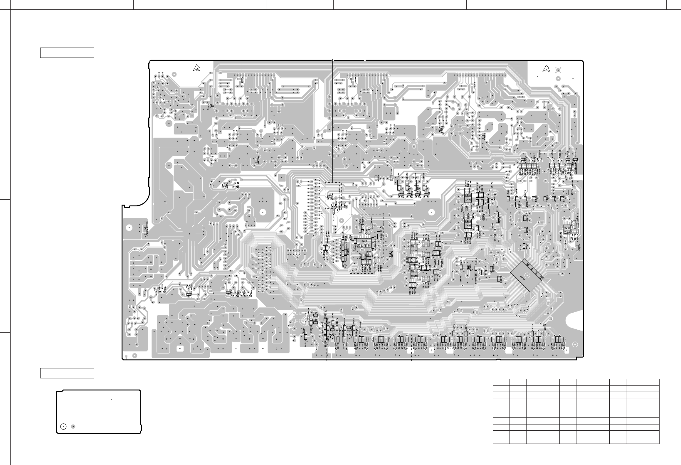
ABCDE FGH I J
1
2
3
4
5
6
7
RX-V563/HTR-6150/DSP-AX563
75
IC402
IC404
IC403
IC406
IC405
IC407
IC401
14
85
14
85
58
4
1
1
3031
8180
100
50
51
1
8
4
5
1
8
4
5
18
16 9
U, C, R, T, K, A, G, E, F, L models
G, E, F models
B model
U, C, R, T, K, A, G, E, F, L models
(Side B)
MAIN (2) P.C.B.
(Side B)
MAIN (1) P.C.B.
•Semiconductor Location
Ref no.
Location
Ref no.
Location
Ref no.
Location
Ref no.
Location
D4001 H5
D4002 H5
D4003 F4
D5003 D2
D5004 H3
D5009 G2
IC401 H5
IC402 F4
IC403 G5
IC404 G4
IC405 H4
IC406 H3
IC407 I4
Q4001 E5
Q4002 F6
Q4003 E6
Q4004 E5
Q4005 E5
Q4006 F5
Q4007 E3
Q4008 E4
Q5001 I3
Q5002 I3
Q5003 H3
Q5004 I3
Q5005 I3
Q5006 I3
Q5007 H3
Q5008 G3
Q5009 G3
Q5010 G3
Q5011 G3
Q5026 D5
Q5027 C5
Q5028 D5
Q5029 D3
Q5032 D3
Q5033 D5
Q5034 C5
Q5035 D5
Q5036 C5
Q5037 C5
Ref no.
Location
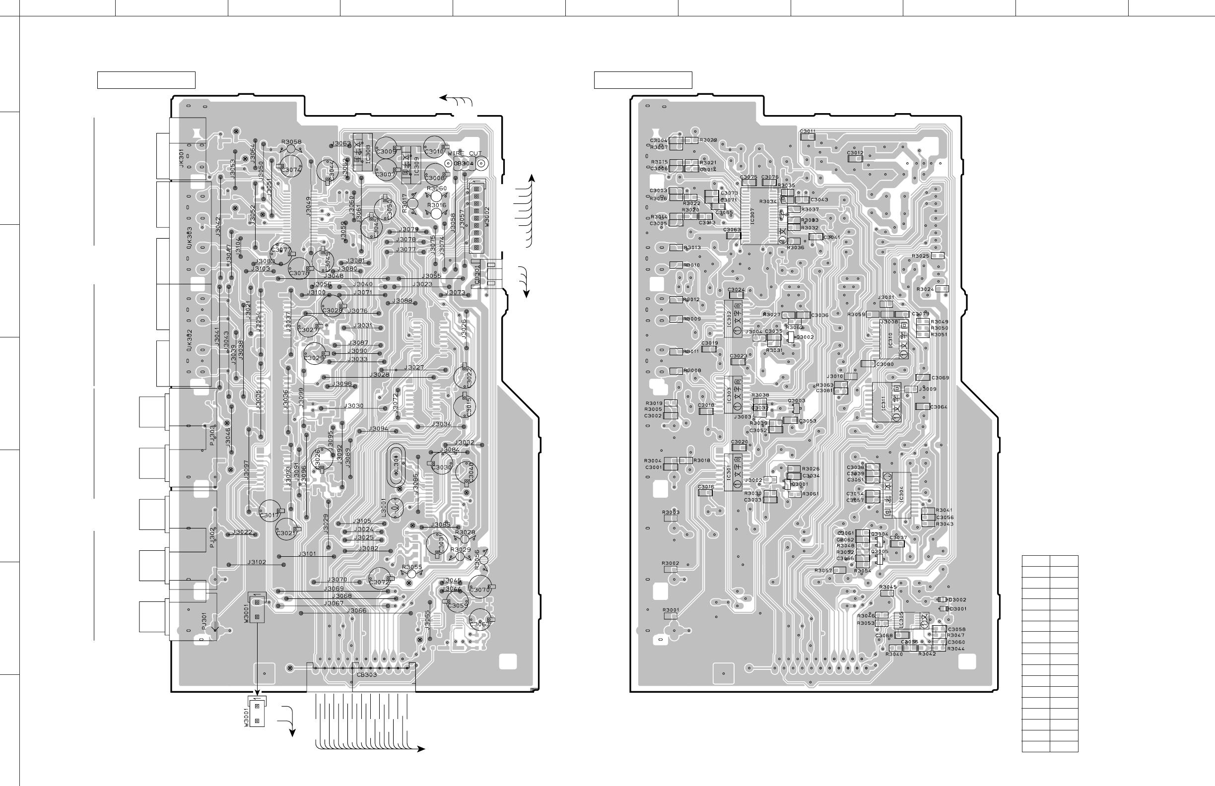
2
ABCDEFGH I J
1
3
4
5
7
RX-V563/HTR-6150/DSP-AX563
6
76
JK301
JK303JK302
IC308
IC309
W3002
CB301
CB303
W3001
IC307
IC310
IC311
IC304
IC302IC303
IC301
IC305
(Side A)VIDEO (1) P.C.B.
AXV
VE
IP_C
IP_VE
IP_Y
IP_VE
IP_V
IP_VE
OSD_CE
OSD_CK
OSD_DT
-12V
PRV2
+12V
+5V
OUT
IN
IN
COM
OUT
COM
OSD
-5V
VE
VE
VE
VE
VE
VE
BYPASS
VIB
/MTMON
SVDET
SEL C
SEL Y
SEL V
VconvV
VconvY
VconvC
Vconv
VIC
VIA
/MTVR1
NC
OPERATION (2)
(W701)
VIDEO (2)
(CB325)
DSP
(CB32)
DSP
(CB21)
OPERATION (8)
(CB609)
MONITOR
OUT
DVRDTV/CBLDVDMONITOR
OUT
DVD DVRDTV/CBL
OUTINOUTIN
VIDEO S VIDEO
(Side B)VIDEO (1) P.C.B.
1
18
26
19
1
8
16
9
1
8
16
9
1
8
16
9
1
8
16
9
1
1
12
24
13
8
16
9
1
7
14
8
•Semiconductor Location
Ref no.
Location
D3001 I6
D3002 I6
IC301 G5
IC302 G3
IC303 G4
IC304 H5
IC305 I6
IC307 G2
IC308 D2
IC309 D2
IC310 H4
IC311 H4
Q3001 G5
Q3002 G3
Q3003 H4
Q3004 H5
Q3005 H5
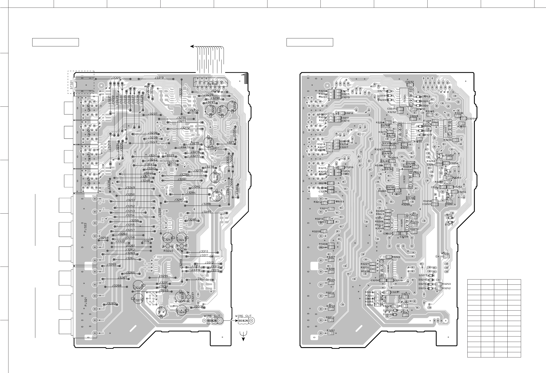
ABCDE FGH I J
1
2
3
4
5
6
7
RX-V563/HTR-6150/DSP-AX563
77
CB324
CB323
CB322
CB321
CB326
CB325
IC324
IC323
IC322
IC327
IC325
IC321
IC326
VIDEO (2) P.C.B. (Side A)
+5V
OSD
-5V
VE
VE
VE
CMP0
/CNON
CPNTD
Y
CB
CR
CMP1
CBYPASS
/MTMON
VconV
VIDEO (1)
(CB304)
DSP
(CB22)
P
R
/P
B
/Y P
R
/P
B
/Y
DTV/CBL
DVR
DVDDVD
COMPONENT VIDEO
MONITOR OUT
MONITOR OUT DVR DTV/CBL DVDP
R
/P
B
/Y P
R
/P
B
/Y P
R
/P
B
/Y P
R
/P
B
/Y
U, C, R, T, K, A, B, G, E, F, L models
VIDEO (2) P.C.B. (Side B)
1
8
16
9
9
16
8
1
16
9
1
1
1
8
16
9
1
7
14
8
7
14
8
8
1
8
16
9
•Semiconductor Location
Ref no.
Location
Ref no.
Location
D3201 H2
D3202 H2
D3203 H2
D3204 H3
D3205 H2
D3206 H6
D3207 H6
D3208 H3
D3209 H2
D3210 H3
D3211 H2
D3212 I5
D3213 I5
D3214 I6
D3215 I6
D3216 I6
D3217 I6
IC321 H6
IC322 H4
IC323 H3
IC324 H2
IC325 H5
IC326 H6
IC327 I3
Q3201 I4
Q3202 I4
Q3203 I3
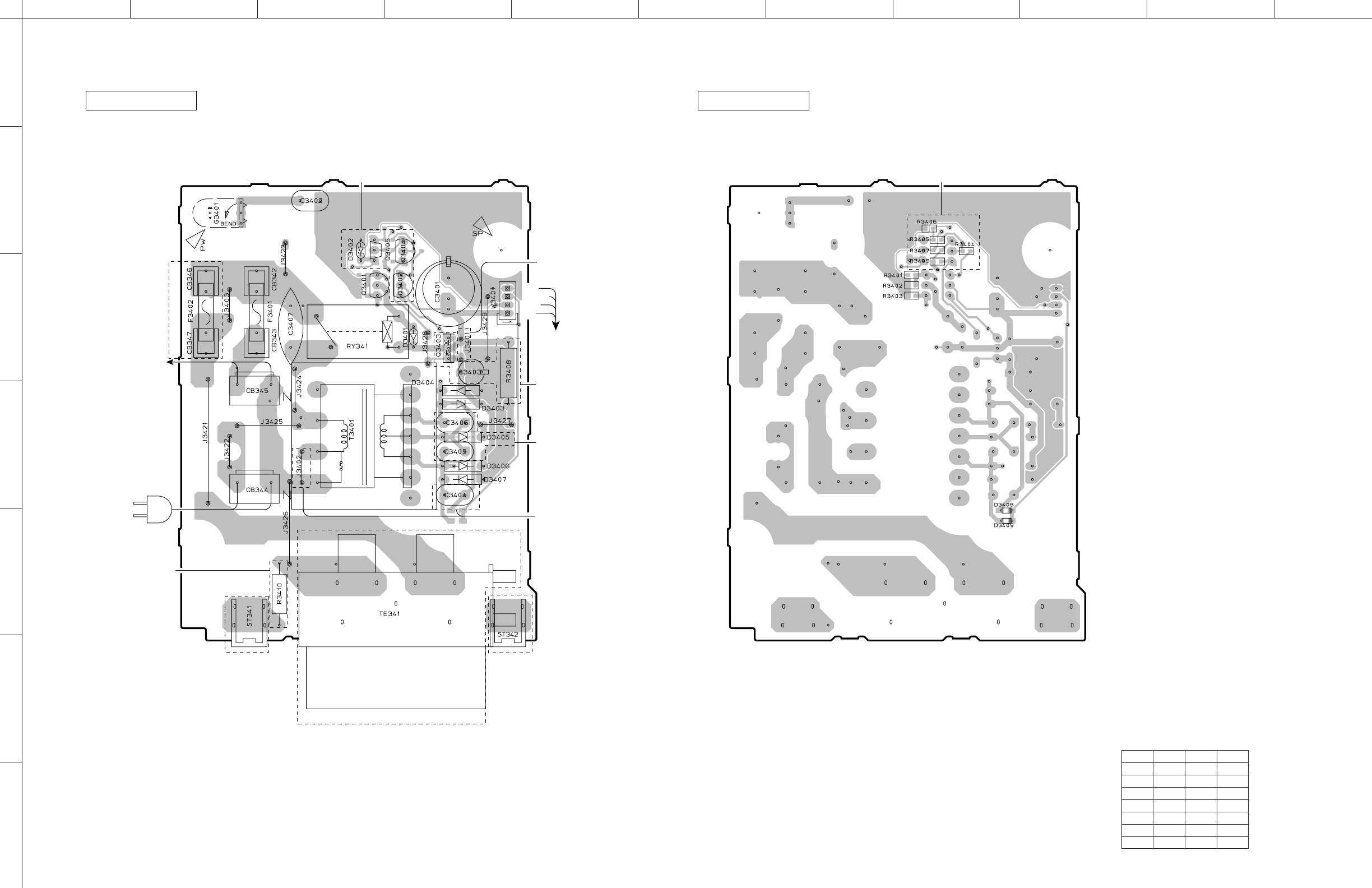
2
ABCDEFGH I J
1
3
4
5
7
RX-V563/HTR-6150/DSP-AX563
6
78
CB346CB347
CB342CB343
CB345
W3401
CB344
VIDEO (3) P.C.B. (Side A)
MG
ACDET
PRY
S9
OPERATION (2)
(CB700)
POWER TRANSFORMER
AC IN
AC OUTLTE(S)
U, C, R, T, A, B, G, E, F, L models
R, L models
R, L models
U, C, T, K, A, B, G, E, F models
U, C, T, K, A, B, G, E, F models
K model
U, C, R, T, A, B, G, E, F, L models
U, C, K models
U, C models
R, L models
VIDEO (3) P.C.B. (Side B)
R, L models
•Semiconductor Location
Ref no.
Location
Ref no.
D3401 D3
D3402 C2
D3403 D4
D3404 D4
D3405 D4
D3406 D4
D3407 D4
D3408 H5
D3409 H5
Q3401 C3
Q3402 D3
Q3403 D3
Q3404 D2
Q3405 C2
Location
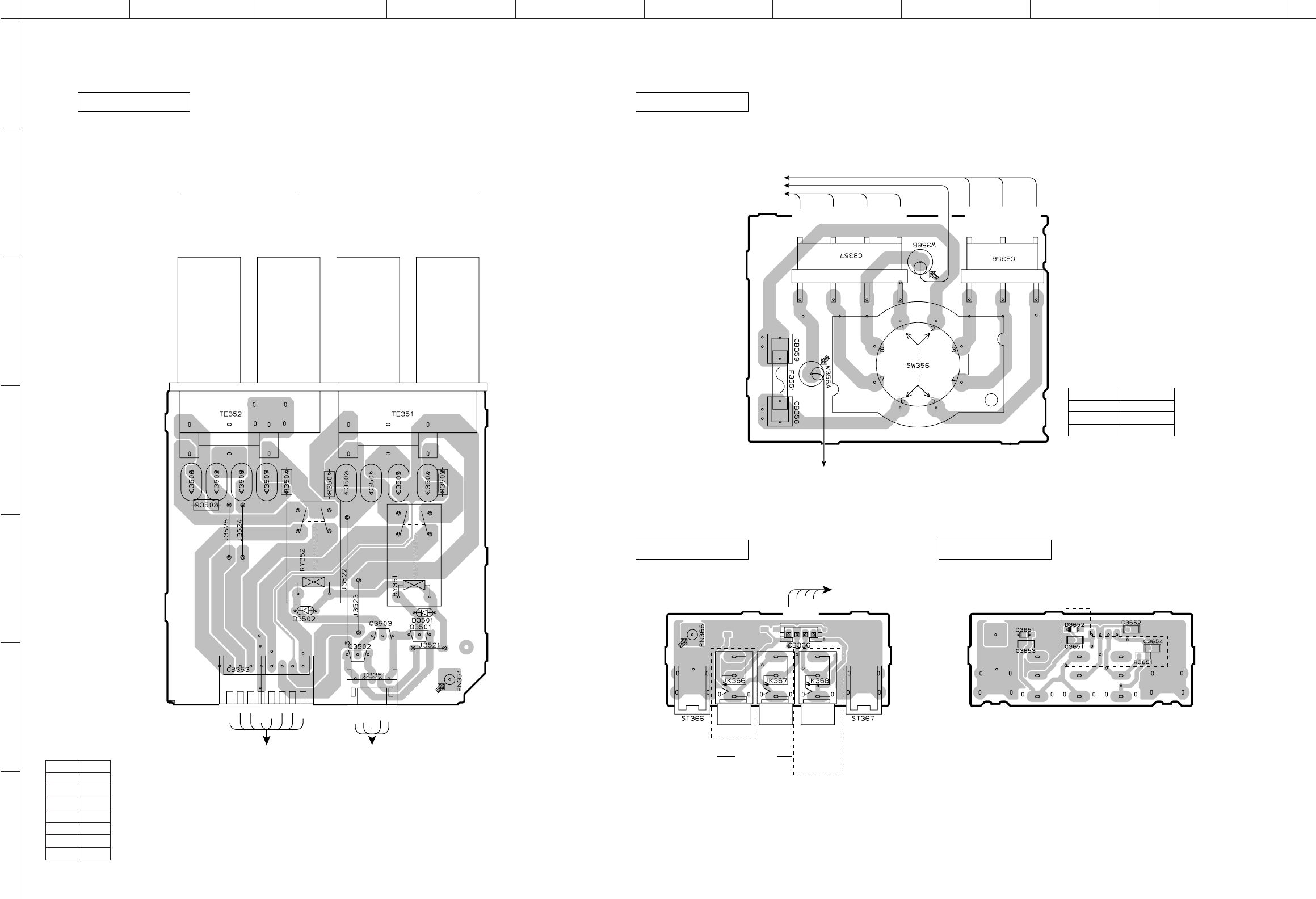
ABCDE FGH I J
1
2
3
4
5
6
7
RX-V563/HTR-6150/DSP-AX563
79
CB353 CB351
CB359
W356A
CB358
CB357
W356B
CB356
CB366
JK366 JK367 JK368
VIDEO (4) P.C.B. (Side A) VIDEO (5) P.C.B. (Side A)
VIDEO (6) P.C.B. (Side A)
SBR
E
E
SBL
SR
E
E
SL
GND
SRY
SBRY
-12
+12
IN
OUT
COUT
GND
R, L models
WH
BE
POWER TRANSFORMER
POWER TRANSFORMER
BE
GY
VI
YE
RE
OR
WH
MAIN (1)
(W503)
MAIN (1)
(W502)
OPERATION (1)
(W6009)
IN
REMOTE TRIGGER
OUT
OUT +12V
15mA MAX.
VOLTAGE
SELECTOR
SPEAKERS
SURROUND BACK/
BI AMP SURROUND
RLRL
+/- +/-+/- +/-
230-240V 1-2/5-6
2-3/6-7
3-4/7-8
4-5/8-1
VOLTAGE SELECTOR
220V
110V
120V
U, C, R, T, K, A, G, E, F, L models
U, C, R, T, K, A, G, E, F, L models
VIDEO (6) P.C.B. (Side B)
U, C, R, T, K, A, G, E, F, L models
•Semiconductor Location
Ref no.
Location
D3501 D5
D3502 C5
D3651 H5
D3652 I5
Q3501 D5
Q3502 C6
Q3503 C5
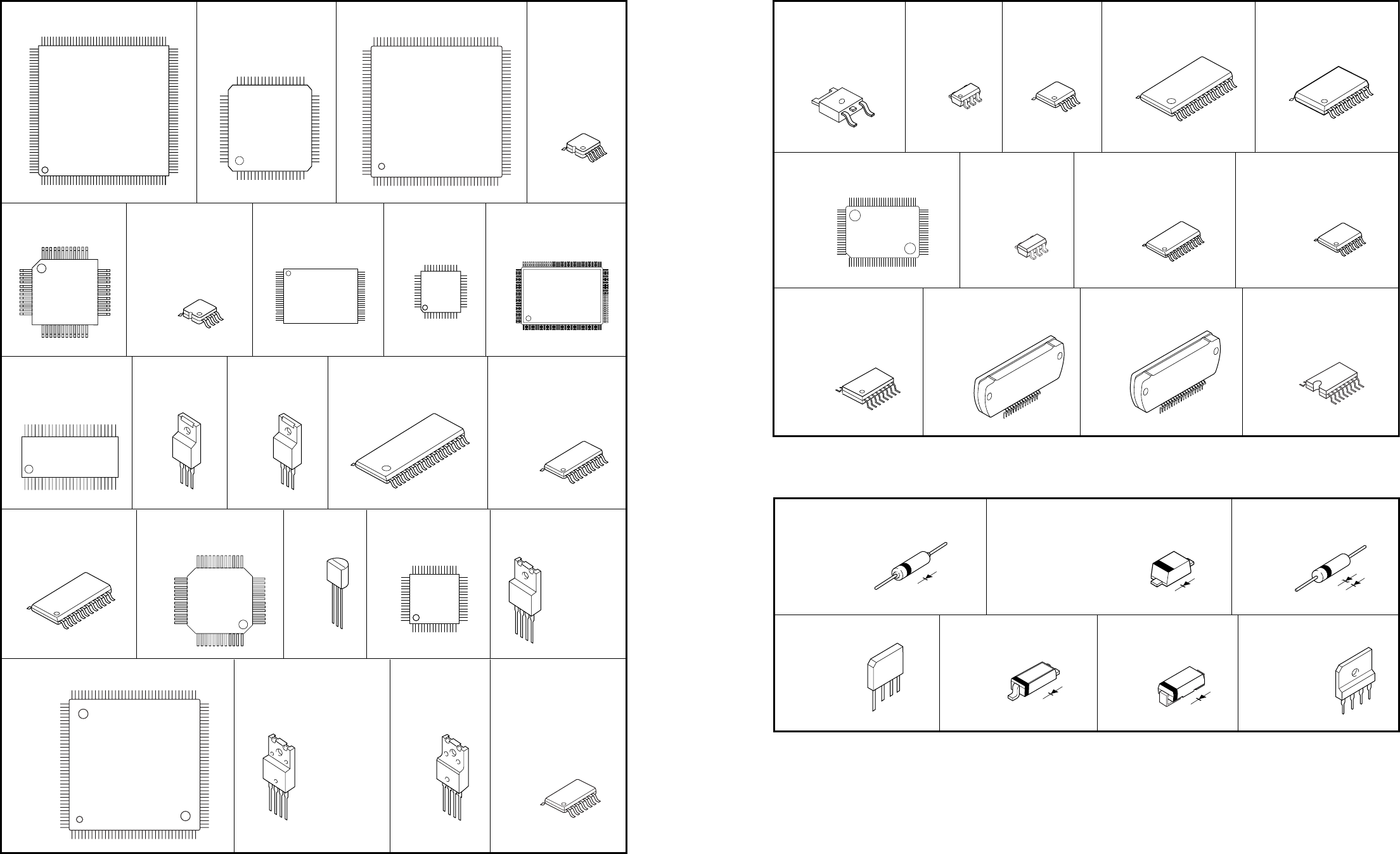
RX-V563/HTR-6150/DSP-AX563
80
40
60
61
1
41
20
2180
136
37
72
73108
109
144
1
12
1324
25
36
37 48
1
24
36
37
12
25
13
48
1
4
8
144
45
89
88
132
133
176
54
1
28
27
16
8
1
48
1
25
24
13 24
25
36
3748
1
12
136
37
72
73108
109
144 4
1
1.
IN
2.
VOUT
3.
GND
4.
ON/OFF CONTROL
116
17
32
3348
49
64
4
1
1.
VIN
2.
VOUT
3.
GND
4.
ON/OFF CONTROL
4
1
OUT
COM
IN
OUT
GND
IN
+VS
GND
VOUT
36
18
1
24
12
1
14 7
1
1
5
10
65102
381
103
128
64
39
AD9389BBSTZ-165 ADV7441ABSTZ-170AD91089ZSKBC
F2621E-01-TRBR25L320F-W EEPROM EN29LV160AB-70TCPADV7172KST
ADC084S021 CIMM
K4S641632K-UC60000 KIA7805API
KIA7812API
KIA7912PI
KIA79M05PI-U
MB87L8760 NJM2388F63 NJM2396F33 NJM2581M
TC74VHCU04FT
LC89057W-VF4AD-E M66003-0131FP-R NJM2388F05LM61CIZ
LC74782JM-8A16-TLMC
PCM1781DBQR
SN74LV123APWR
LC72725KM-UY-TLM-ELA73050-TLM-E
MM74HC4051SJX
MM74HC4053SJX
ISP1760BE
1
3
4
5
28
14
1
1
10
20
20 10
1
14
7
1
1
3
4
5
1
8
16
84
1
80
1
51
30
81
100
50
31
1
8
16
1
15
1
19
3:V
OUT
1:V
IN
2:GND
NJM2845DL1-18 NJM2867F3-05 PCM1803DBR
PCM1680DBQR
SN74LV157APWR
TC74VHC153FT
SN74LV14APWR
SN74LVC245APWR
SN74LVC32APW
SN74LV574APWR 8D-F
SN74AHCT574PWR
SN74LVC08APWR
R5523N001A-TR-F
SN74AHCT245PWR
SN74LV4051APWR
NJM4565M
R2A15218FP
TC74HC4052AFSTK433-130-E STK433-330-E
Anode
Cathode
Anode
Cathode
Anode
Cathode
Anode
Cathode
+
ACAC
–
Anode
Cathode
+AC AC
–
KDS160-RTK
MA8075-H 7.7V
MA8100-H 10.3V
RB500V-40
1SS355
UDZ3.6BTE-17 3.6V
UDZ5.1B
UDZS3.3BTE-17 3.3V
UDZS9.1B
1T2
1SS133
1SS176
1SS270A
MTZJ4.7A
MTZJ16A
KBP103G 1.0A 200V RB160L-40 TE25 RS403M
TS6P03G 6.0A 200V
Diodes
■PIN CONNECTION DIAGRAMS
ICs
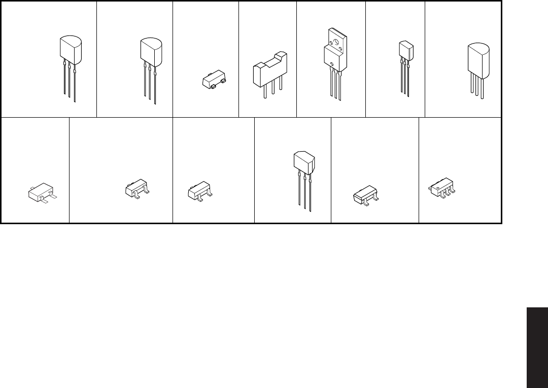
81
RX-V563/HTR-6150/DSP-AX563
RX-V563/HTR-6150/
DSP-AX563
ECB
B
E
C
ECB
BCE
ECB
C
E
BECBIN
COMMON
OUT
1. Drain
2. Drain
3. Gate
4. Source
5. Drain
6. Drain
1
3
4
6
B
E
C
2
1 1: GND
2: IN
3: OUT
3
BCE
BCE
2SD1938F
2SC3326-A (TE85R, F)
2SC3326-B (TE85R, F)
2SC4081 T106
2SA1037K 2SA1708 2SB1274 2SC1815 Y
2SC2412K
2SC2705
KRA102M-AT/P KRA102S-RTK/P
KRA104S-RTK
KRC102M-AT
KRC102S-RTK
KRC104S-RTK
RTQ040P02DTA143EKA
DTC114EKA
2N5401C-AT/P
2SA1015-Y
2N5551C-AT 2SC1740S
Transistors

82
RX-V563/HTR-6150/DSP-AX563
RX-V563/HTR-6150/
DSP-AX563
MEMO
MEMO
CB11
IC11
IC12
CB12 CB13
IC13
A
1
2
3
4
5
6
7
8
9
10
BCDEFGH I JKLMN
RX-V563/HTR-6150/DSP-AX563
83
★All voltages are measured with a 10MΩ/V DC electronic voltmeter.
★Components having special characteristics are marked s and must be replaced
with parts having specifications equal to those originally installed.
★Schematic diagram is subject to change without notice.
DSP 1/8
SCHEMATIC DIAGRAMS
A-1
5.1
0
0
1.9
0
0
0
0
1.9
0
0
0
0
0
0
1.9
0
0
1.9
1.9
0
0
0
3.3
0
3.3
3.3
5.1
0
0
0
0
0
0
0
0
0
1.9
1.9
1.9
1.9
0
1.7
0
0
0
0
0
0
0
0
0
0
0
0
0
0
0
1.7
0
1.9
1.9
0
0
1.9
0
1.7
1.7
0
0
0
0
1.6
0
1.7
3.1
3.1
2.7
0
1.9
0
6.4 6.4
5.1
5.1
0
0
0
5.1
5.1
3.3
0
0
0
0
0
0
0
0
0
0
0
0
0
0
0
0
0
0
0
0
0
0
0
0
0
0
0
0
0
0
0
0
0
0
0
0
0
0
0
0
0
00 00
0
0
0
00
0
0
0
0
0
0
0
0
0.4
0
1.8
1.8
0
3.3
0
0
0
0
0
0
0
0
0
0
0
3.3
0
1.8
0
0
0
0
0
0
0
0
0
0
3.3
0
1.8
3.3
3.3
0
0
1.8
0
0
1.8
0
0
0
0
0
0
0
0.7
0.9
0
0.7
1.8
1.8
0
0.9
0.7
0
0
0
0
0
0
0
0
0
0
0
0
0
0
3.3
0
0
0
0
0
1.7
1.7
1.6
0
3.3
3.3
3.3
0
3.3
2.7
3.1
3.1
0
3.3
3.3
0
1.8
3.3
0
0
0
0
0
0
0
0
0
0
0
0
0
0
0
1.7
0
1.7
0
1.7
0
0
0
0
0
0
0
0
0
0
0
0
0
1.6
1.3
1.8
0.6
0
3.3
1.8
0
0
1.8
1.7
0
3.3
0
0
V
OUT
V
IN
Control
GND
1
45
2
IC13: NJM2867F3-05
Low dropout voltage regulator
Bandgap
Reference
Thermal
Protection
IC12: ADV7441ABSTZ-170
10-bit, integrated, multiformat SDTV/HDTV video decoder,
RGB graphic digitizer, and 2:1 multiplexed HDMI/DVI interface
OUTPUT FORMATTER
FAST BLANK OVERLAY CONTROL
MUX
MUX
EDID/REPEATER
CONTROLLER DATA RECOVERY
ALIGNMENT
HDMI DECODE
XOR
4:2:2 TO 4:4:4
CONVERSION
HDCP
ENGINE
HDCP
EEPROM
PACKET
PROCESSOR
EQUALIZER EQUALIZER
MUX
INT1
HS/CS
VS/FIELD
DE/FIELD
LLC
SFL/
SYNC_OUT/
INT2
P0 TO P9
PIXEL
DATA
P10 TO P19
P20 TO P29
10
10
G
B
R
FB
10
CLAMP
ANALOG INTERFACE
INPUT
MATRIX
ADC 0
CVBS
RGB
YPrPb
CVBS
SOG
SOY
HS_IN/CS_IN
VS_IN
FB
SCL
SDA
ALSB
RXB_2
DDCA_SCL
DDCA_SDA
DDCB_SDA
DDCB_SCL
RXB_C
RXB_1
RXB_0
RXA_2
RXA_C
RXA_1
RXA_0
YC AND
10 CHA
CHA
DATA
PROCESSOR
DECIMATION AND
DOWNSAMPLING
FILTERS
COLOR SPAC
CONVERTER
EMBEDDED
SYNC
VBI DATA PROCESSOR ANCILLARY
DATA
COMPONENT PROCESSOR
STANDARD DEFINITION PROCESSOR
SYNC SOURC
AND
POLARITY DETECT
SYNC EXTRACT
STANDARD
IDENTIFICATION
MACROVISION R AND
CGMS DETECTION
GAIN
CONTROL
OFFSET
ADDRESS
AV
CODE
INSERTION
PROGRAM
DELAY
DIGITAL
FINE
CLAMP
NOISE AND
CALOBRATION
VBI DATA
RECOVERY
CHROMA
DEMOD
SYNC
EXTRACT
FSC
RECOVERY
CHROMA
RE-
SAMPLE
RE-
SAMPLE
CONTROL
CTI
C-DNR
AV
CODE
INSERTION
CHROMA
2D COMB
(0x04 MAX)
GAIN
CONTROL
GAIN
CONTROL
LINE
LENGTH
PREDICTOR
GLOBAL
CONTROL
STANDARD
AUTODETECTION
FREE RUN
OUTPUT CONTROL
SYNTHESIZED
LLC CONTROL
MACROVISION
DETECTION
ACTIVE OEAK AND
HSYNC DEPTH
DIGITAL PROCESSING BLOCK
VBI
DECODER
ANCIKKARY
DATA
FORMATTER
CHB
CHB
CHC
CHC
CHD
CY
CLAMP
SYNC PROCESSING
AND CLOCK
GENARATION
CONTROL
INTERFACE
I2C
SAMPLER
PLL
ADC 1
10
CLAMP ADC 2
10
CLAMP ADC 3
HS/CS, VS
CONTROL
CONTROL
CONTROL
DE
VS
HS
MDA
PACKET/
INFOFRAME
MEMORY
AUDIO
PROCESSING
MCL
I2C
LRCLK
SCLK
MCLKOUT
SPDIF
FILTER
CONTROL AND DATA
10
LLC
GENERATION
SAMPLER
LUMA
RE-
SAMPLE
LUMA
2D COMB
(0x04 MAX)
LUMA
FILTER
LUMA
DIGITAL
FINE
CLAMP
CHROMA
DIGITAL
FINE
CLAMP
GAIN
CONTROL
IC11: AD9389BBSTZ-165
High performance HDMI/DVI transmitter
CLK
SCL SDA MCL MDA INT
HPD
DDCSDA
DDCSCL
TxC-/TxC+
Tx2-/Tx2+
Tx0-/Tx0+
Tx1-/Tx1+
HSYNC
VSYNC
DE
D[23:0]
VIDEO
DATA
CAPTURE
COLOR
SPACE
CONVER-
SION
4:2:2 TO
4:4:4
CONVER-
SION
REGISTERS
CONFIGURATION
LOGIC
HDCP
CORE
INTERRUPT
HANDLER
HDCP_EDID
MICRO-
CONTROLLER
I2C
MASTER
I2C
SLAVE
SCLK
LRCLK
MCLK
S/PDIF
I2S[3:0]
AUDIO
DATA
CAPTURE
XOR
MASK
HDMI
Tx
CORE
POINT A-1 XL101 (Pin 65 of IC12)
No replacement part available.
No replacement part available.
HDMI RX
VIDEO DECODER
HDMI TX
to DSP 6/8
HDMI
DTX/CBLOUT DVD
to DSP 2/8
to DSP 2/8
to DSP 2/8
to DSP 6/8
to DSP 6/8
to DSP 6/8
to DSP 4/8
to DSP 2/8
to DSP 6/8
to DSP 6/8
to DSP 4/8
to DSP 3/8 / to DSP 4/8
IC21
IC22
CB21
CB22
A
1
2
3
4
5
6
7
8
9
10
BCDEFGH I JKLMN
RX-V563/HTR-6150/DSP-AX563
84
★All voltages are measured with a 10MΩ/V DC electronic voltmeter.
★Components having special characteristics are marked s and must be replaced
with parts having specifications equal to those originally installed.
★Schematic diagram is subject to change without notice.
DSP 2/8
3.3
1.7
0
3.3
3.3
3.3
3.3
3.3
1.3
1.3
1.9
0
3.3
0
3.3
0
3.3
0
0.4
0.4
3.3
0
0
0
0
0
0
0
1.7
0
1.7
1.7
3.3
0
0
3.1
3.3
3.3
3.3
0
3.2
3.2
1.3
1.4
0.7
3.1
1.9
1.9
0
3.0
3.0
V OUTV IN
GND
13
2
IC22: NJM2845DL1-18
Low dropout voltage regulator
Bandgap
Reference
Thermal
Protection
IC21: ADV7172KSTZ
Digital PAL/NTSC video encoder
8
8
10-BIT
DAC
R
SET1
COMP1
ADV7172/ADV7173
COLOR
DATA
P0
V
REF
R
SET2
COMP2
P7
DAC E
DAC F
DAC D
DAC A
DAC B
DAC C
BRIGHTNESS AND
CONTRAST CONTROL
+
ADD SYNC
+
INTERPOLATOR
10
LUMA
PROGRAMMABLE
FILTER
+
SHARPNESS
FILTER
SATURATION CONTROL
+
ADD BURST
+
INTERPOLATOR
10
PROGRAMMABLE
CHROMA
FILTER
10
8
8
8
REAL-TIME
CONTROL CIRCUIT
SCRESET/RTC
MODULATOR
+
HUE
CONTROL
10
10
10
10
10-BIT
DAC
10
10-BIT
DAC
10
M
U
L
T
I
P
L
E
X
E
R
Y
U
V
8
4:2:2 TO
4:4:4
INTER-
POLATOR
10 10
SIN/COS
DDS BLOCK
DAC
CONTROL
BLOCK
DAC
CONTROL
BLOCK
10-BIT
DAC
10
10
10
10
10-BIT
DAC
10
10-BIT
DAC
10
M
U
L
T
I
P
L
E
X
E
R
YUV TO
RBG
MATRIX
+
YUV
LEVEL
CONTROL
BLOCK
I
2
C MPU PORT
HSYNC
FIELD/
VSYNC
BLANK
TTX
TTXREQ
V
AA
RESET
TELETEXT
INSERTION BLOCK
YCrCb
TO
YUV
MATRIX
CLOCK CSO_HSO VSO CLAMP SCLOCK SDATA ALSB
VIDEO TIMING
GENERATOR
GND
PAL NTSC
VIDEO ENCODER
to DSP 6/8
to DSP 6/8
to DSP 1/8
to DSP 1/8
to DSP 1/8
to DSP 1/8
to DSP 1/8
to DSP 6/8
to DSP 1/8
to DSP 5/8
to DSP 5/8
to DSP 5/8
to DSP 5/8
to DSP 5/8
to DSP 5/8
to DSP 5/8
to DSP 5/8
to DSP 5/8
to DSP 6/8
to DSP 6/8
to DSP 6/8
to DSP 6/8
to VIDEO (1)_CB303
Page 95 K4
to VIDEO (2)_CB326
Page 96 D1
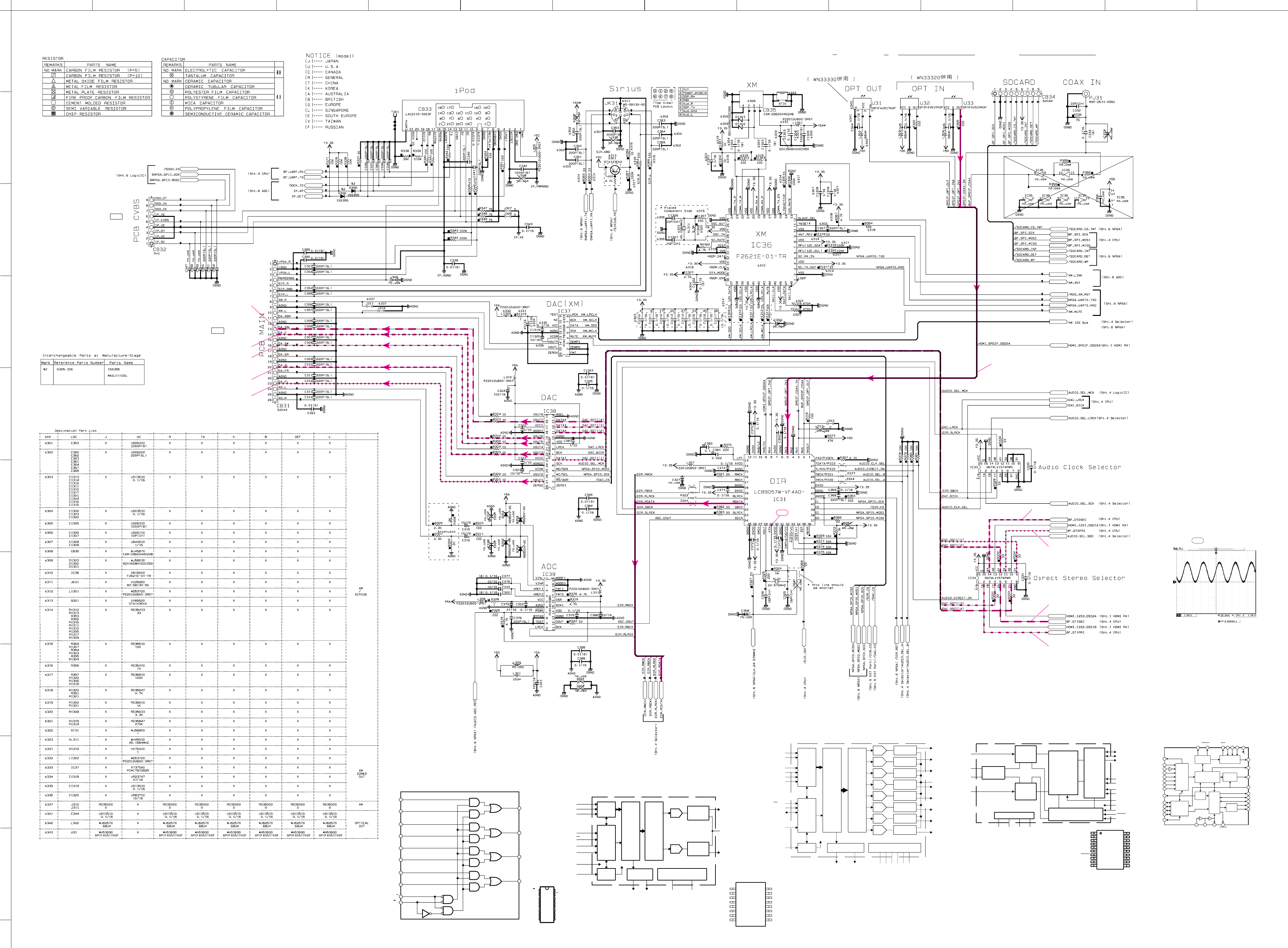
CB32
CB31
IC36
CB34
IC31
IC39
IC38
IC37
CB33
JK31
CB35
IC33
IC34
A
1
2
3
4
5
6
7
8
9
10
BCDEFGH I JKLMN
RX-V563/HTR-6150/DSP-AX563
85
★All voltages are measured with a 10MΩ/V DC electronic voltmeter.
★Components having special characteristics are marked s and must be replaced
with parts having specifications equal to those originally installed.
★Schematic diagram is subject to change without notice.
DSP 3/8
A-2
2.4
4.9
2.4
2.4
2.4
2.4
4.9
2.5
2.4
2.4
0
0
2.5 0
0
0
1.7
0
1.7
0
1.7
3.3
0
1.7
1.7
4.9
2.5
2.5
4.9
4.9
0
3.3
0
0
1.7
2.5 0
0
0
3.0
3.0
3.3
1.7
1.3
0
3.7
0
5.0
0
3.13.3
0.30.8
5.0
0
4.0
5.0
0
4.0
0
0
0
3.3
0
3.3
0
4.0
0
2.0
0
0
0
0
0
0
0
0
3.3
0
0
0
2.9
2.9
3.3
4.0
0
1.7
1.7
0
3.3
1.7
1.3
0
1.6
1.5
3.3
0
0
0
0
3.3
3.3
3.3
1.6
1.7
1.2
1.7
3.3
03.3
0
1.7
1.7
1.7
0
0
1.7
1.7
1.7
0
0
0
03.3
0
1.7
0
1.7
1.7
1.2
1.7
1.7
0
0
0
0
0
C
SW
SL
FL
SBL
DIGITAL IN
SL/SR
FL/FR
SBL/SBR
SW/C
Input
Selector
RXOUT
RX0
RX1
RX2
RX3
RX4
RX5/VI
RX6/UI
LPF
TMCK/PIO0
TBCK/PIO1
TLRCK/PIO2
TDATA/PIO3
TXO/PIOEN
Cbit, Ubit Microcontroller
I/F
Data
Selector
Clock
Selector
Modulation
&
Parallel Port
PLL
XIN XOUT XMCK CKST
SLRCK
SBCK
RLRCK
RBCK
RMCK
SDIN
RD ATA
RERR
DO
XMODECICECLINTAUDIO/VOEMPHA/UO
1/N
Demodulation
&
Lock detect
1
2
3
4
5
8
9
10
13
44
45
46
47
48
29 28 27 34
23
22
20
17
16
24
21
36
37
41383940353332
IC31: LC89057W-VF4AD-E
Digital audio interface transceiver
IC38 : PCM1680DBQR
Audio digital-to-analog converter
Output Amp and
Low-Pass Filter
System Clock
Manager
Enhanced
Multilevel
DeltaœSigma
Modulator
DAC
Serial
Input
I/F
Function
Control
I/F
System Clock
Zero Detect Power Supply
DAC Output Amp and
DAC
DAC Output Amp and
DAC Output Amp and
DAC Output Amp and
VOUT1
VOUT2
VOUT3
VCOM
VOUT4
VOUT5
VOUT6
Low-Pass Filter
Low-Pass Filter
Low-Pass Filter
Low-Pass Filter
Low-Pass Filter
Output Amp and
AGND2
VCC2
AGND1
VCC1
DGND
VDD
ZERO1
ZERO2
BCK
LRCK
DATA1 (1, 2)
DATA2 (3, 4)
DATA3 (5, 6)
DATA4 (7, 8)
MS/ADR
MC/SCL
MD/SDA
MSEL
SCK
8
Oversampling
Digital Filter
With
Function
Controller
DAC Output Amp and
DAC Output Amp and
VOUT7
VOUT8
Low-Pass Filter
Low-Pass Filter
IC33, 34: SN74LV157APWR
Quadruple 2-line to 1-line data selectors/multiplexers
Pin numbers shown are for the D, DB, DGV, J, NS, PW, and W packages.
2
3
5
6
11
10
14
13
15
1
G
A/B
4B
4A
3B
3A
2B
2A
1B
1A
4
7
9
12
1Y
2Y
3Y
4Y
1
2
3
4
5
6
7
8
16
15
14
13
12
11
10
9
A/B
1A
1B
1Y
2A
2B
2Y
GND
VCC
G
4A
4B
4Y
3A
3B
3Y
(1) Open-drain output for the PCM1782
NOTE: Signal names in parentheses ( ) are for the PCM1781.
Power Supply
Enhanced
Multilevel
Delta-Sigma
Modulator
VOUTL
4/8
Oversampling
Digital
Filter
With
Function
Control
Audio
Serial
Port
BCK
LRCK
DATA
Serial
Control
Port
Zero Detect
(TEST)
SCK System
Clock
Manager
MC (DEMP1)
MS (DEMP0)
Output Amp
and
Low-Pass Filter
MD (MUTE)
DAC
VCOM
System Clock
AGND
VCC
ZEROR/ZEROA(1)
(ZEROA)
ZEROL/NA(1)
Output Amp
and
Low-Pass Filter
DAC
VOUTR
(FMT)
ZEROA
VOUTL
VOUTR
VCOM
AGND
VCC
NC
TEST
16
15
14
13
12
11
10
9
FMT
DEMP0
DEMP1
MUTE
SCK
DATA
BCK
LRCK
1
2
3
4
5
6
7
8
IC37: PCM1781DBQR
Audio digital-to-analog converter
1
2
3
4
5
6
7
8
9
10
20
19
18
17
16
15
14
13
12
11
VINL
VINR
VREF1
VREF2
VCC
AGND
PDWN
BYPAS
TEST
LRCK
MODE1
MODE0
FMT1
FMT0
OSR
SCKI
VDD
DGND
DOUT
BCK
IC39: PCM1803DBR
Stereo A/D converter
BCK
VINL
Reference
VREF1
VREF2
VINR
Delta-Sigma
Modulator
Delta-Sigma
Modulator
x 1/64, x 1/128
Decimation
Filter
With
High-Pass Filter
Power Supply
AGNDVCC VDD
DGND
Clock and Timing Control
Serial
Interface
Mode/
Format
Control
LRCK
DOUT
FMT0
FMT1
MODE0
MODE1
BYPAS
OSR
PDWN
SCKI
TEST
POINT A-2 XL301 (Pin 29 of IC31)
No replacement part available.
XM DT
DIR
to DSP 4/8
to DSP 5/8
to DSP 8/8
to DSP 6/8
to DSP 6/8
to DSP 4/8
to DSP 4/8
to DSP 4/8
to DSP 4/8
to DSP 1/8
to DSP 4/8
to DSP 4/8
to DSP 1/8
to DSP 4/8
to DSP 1/8
to DSP 4/8
to DSP 4/8
to DSP 4/8
to DSP 4/8
to DSP 8/8
to DSP 6/8
to DSP 6/8
to DSP 6/8
to DSP 1/8
to DSP 6/8
to DSP 6/8
to DSP 4/8
to DSP 4/8
to DSP 6/8
to DSP 4/8
to DSP 4/8
to DSP 6/8
to DSP 6/8
to DSP 5/8
to DSP 5/8
DAC
DAC
ADC
SIRIUS XM
DIGITAL INPUTDIGITAL OUTPUT
DVDDTV/CBL
CD
MD/CD-R MD/CD-R
to MAIN_CB402
Page 94 G3
to VIDEO (1)_W3002
Page 95 F2
(Writing port)
DOCK
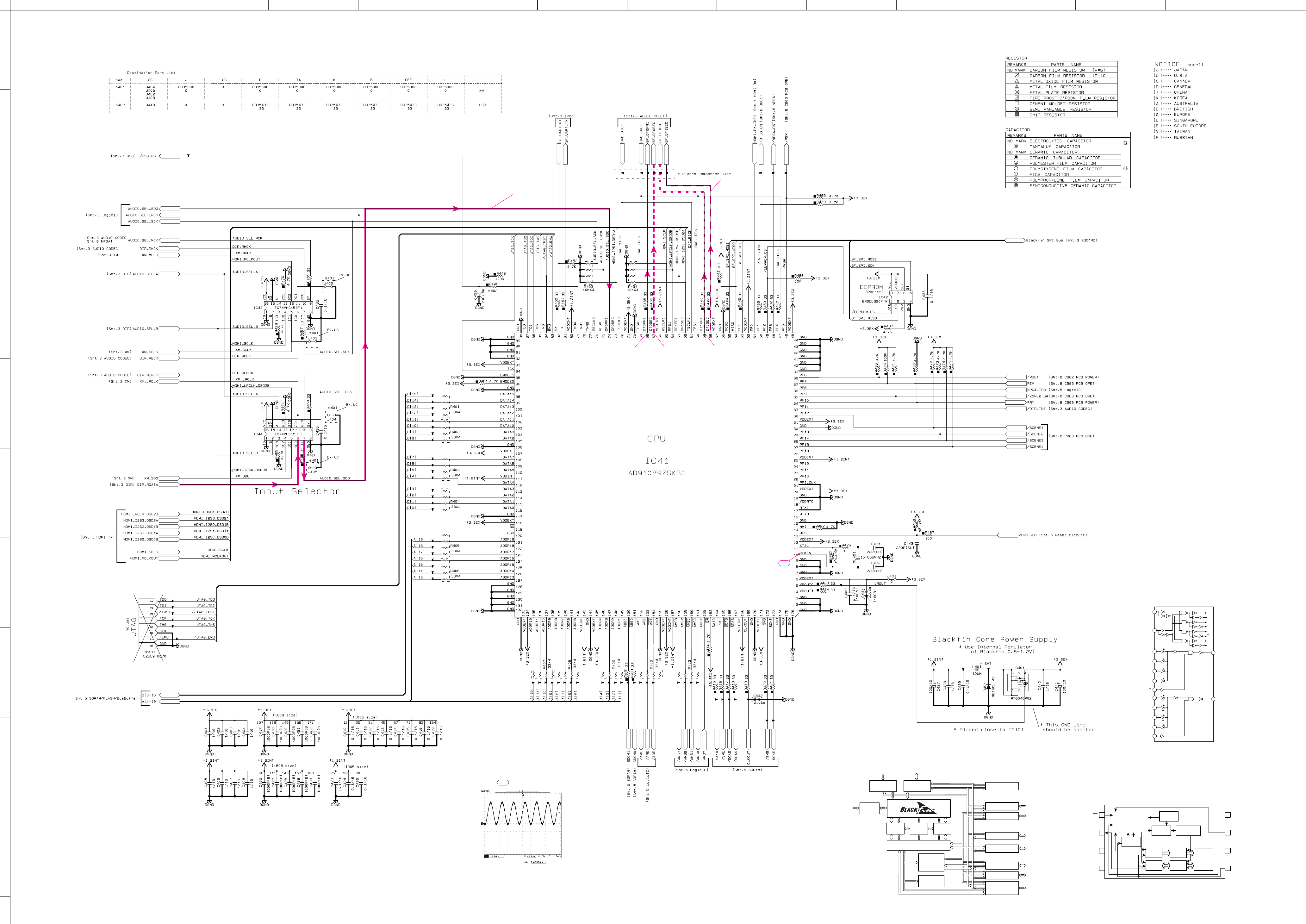
IC43
IC44
IC41
A
1
2
3
4
5
6
7
8
9
10
BCDEFGH I JKLMN
RX-V563/HTR-6150/DSP-AX563
86
★All voltages are measured with a 10MΩ/V DC electronic voltmeter.
★Components having special characteristics are marked s and must be replaced
with parts having specifications equal to those originally installed.
★Schematic diagram is subject to change without notice.
DSP 4/8
DIGITAL IN
SL/SRFL/FR SW/C
SBL/SBR
A-3
3.3
0
0
0
1.6
0
1.7
1.7
0
0
0
1.7
0
1.7
1.7
0
3.3
0
0
0
1.7
0
1.7
1.7
0
0
0
0
0
1.2
1.2
0
3.3
3.3
0
0
3.3
0
3.3
3.3
1.4
1.4
1.4
3.3
1.4
1.4
2.0
0
0
0
0
0
0
0
0
0
0
1.3
3.3
1.7
1.7
1.2
0
1.7
1.7
1.7
1.3
1.7
1.7
0
0
1.7
1.7
1.7
0
3.3
0
0
3.3
0
1.3
0
0
3.3
1.7
3.3
3.3
0
0
0
0
0
0
3.3
3.3
0.1
3.3
3.3
3.3
3.3
3.3
0
3.3
3.3
3.3
1.4
0
0
3.3
3.3
1.4
1.6
0
0
0
3.3
2.0
2.0
0
0
0
0
3.3
0
0
3.3
1.7
0
0
0
0
3.3
0
0
0.4
0.4
0.4
0.4
0.4
0.3
0.5
0.3
0
3.3
0
1.0
0.9
1.3
1.1
1.2
0.6
1.3
1.3
0
3.3
1.1
2.2
0
0
0
0
1.9
0
0
0
0
0
3.3
0
1.3
1.3
1.2
1.4
0.4
3.3
1.8
3.1
0
1.3
3.3
3.3
3.3
3.3
0
3.3
3.3
0
3.3
3.3
3.3
0
3.3
1.3
3.3
3.3
3.3
3.3
3.3
3.3
3.3
3.3
1.3
3.3
0
1.7
3.3
3.3
3.3
0
0
0
0
3.3
IC42: BR25L320F-W EEPROM
SPI BUS 32 k-bits (4,096 x 8-bit) EEPROM
1
CS
INSTRUCTION DECODE
CONTROL CLOCK
GENERATION
INSTRUCTION
REGISTER
2
SO
3
WP
4
GND
8Vcc
7HOLD
6SCK
5SI
VOLTAGE
DETECTION
WRITE
INHIBITION
ADDRESS
REGISTER
DATA
REGISTER 8bit READ/WRITE
AMP
32,768bit
EEPROM
STATUS REGISTER
ADDRESS
DECODER
HIGH VOLTAGE
GENERATOR
8bit
12bit 12bit
IC43, 44: TC74VHC153FT
Dual 4-channel multiplexer
14
AS0
S0
6
1C0
2
B
S1
S1
S2
S2
S3
S3
S0 71Y
5
1C1
S1
4
1C2
S2
1
1G
3
1C3
S3
10
2C0
S0
92Y
11
2C1
S1
12
2C2
S2
15
2G
13
2C3
S3
IC41: AD91089ZSKBC
Microprocessor
PPI/GPIO
L1 data
memory
JTAG test
and emulation
Voltage
regulator
L1 instruction
memory
Memory
management
unit
Core/System bus interface
Real time clock
UART port IrDA®
Serial port (2)
DMA controller
Boot ROM
SPI port
External port FLASH,
SDRAM control
Event controller/
Core timer Watch dock timer
Timer0, Timer1, Timer2
POINT A-3 XL401 (Pin 10 of IC41)
No replacement part available.
MICROPROCESSOR
EEPROM
to DSP 7/8
to DSP 3/8
to DSP 3/8
to DSP 3/8
to DSP 3/8
to DSP 3/8
to DSP 3/8
to DSP 3/8
to DSP 3/8
to DSP 5/8
to DSP 5/8
to DSP 5/8
to DSP 5/8
to DSP 5/8
to DSP 3/8
to DSP 3/8
to DSP 1/8
to DSP 5/8
to DSP 3/8
to DSP 3/8
to DSP 6/8
to DSP 5/8
to DSP 8/8
to DSP 8/8
to DSP 8/8
to DSP 8/8
to DSP 8/8
to DSP 3/8
to DSP 5/8
to DSP 1/8
to DSP 8/8
to DSP 8/8
to DSP 6/8
to DSP 3/8to DSP 3/8
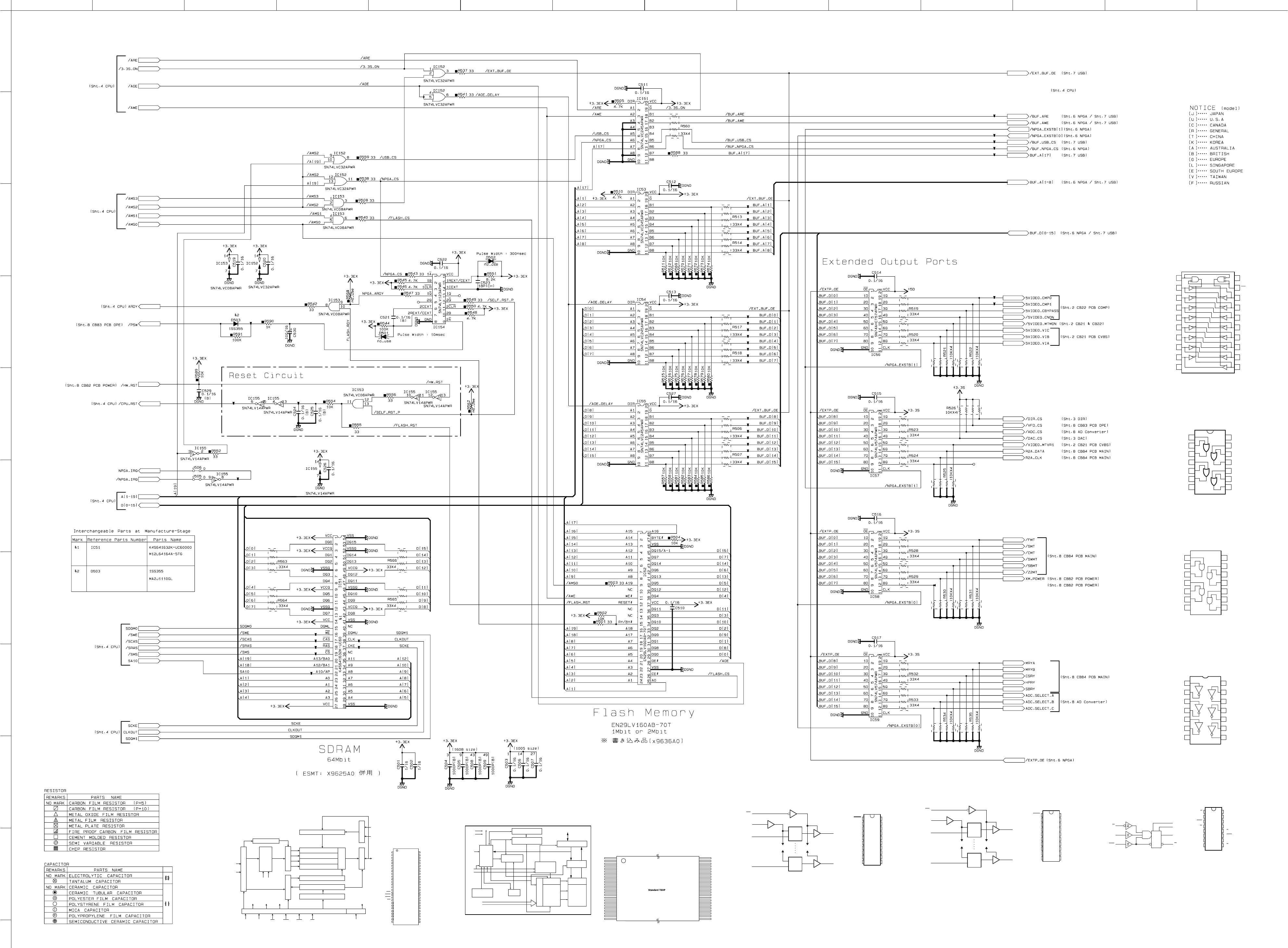
IC152
IC152
IC152
IC152
IC153
IC153
IC153
IC153 IC155IC155
IC155IC155
IC155
IC155
IC51
IC52
IC154
IC59
IC58
IC57
IC56
IC55
IC54
IC53
IC151
A
1
2
3
4
5
6
7
8
9
10
BCDEFGH I JKLMN
RX-V563/HTR-6150/DSP-AX563
87
★All voltages are measured with a 10MΩ/V DC electronic voltmeter.
★Components having special characteristics are marked s and must be replaced
with parts having specifications equal to those originally installed.
★Schematic diagram is subject to change without notice.
DSP 5/8
3.2
3.2
0
3.2
3.3
3.3
3.2
3.3
3.0
3.2
3.3
3.3
3.3
3.3
3.3
3.3
3.3 3.3
3.3
3.3
00
3.3
3.3
00 3.3
3.3
3.3
3.3
3.3
3.2
3.3
3.3
0
0
0
3.3
3.3
3.3
0
3.3
1.3
3.3
3.3
3.2
0
3.3
0
3.3
0
3.2
3.3
1.1
3.01.1
3.3
3.3
1.3
3.3
0.4
0
0.4
0
3.3
0.4
0.4
0.4
0
0.3
0.5
3.3
0.3
0
0
1.7
3.3
0.6
0.4
1.2
3.3
0.4
3.1
1.8
0
0.6
1.3
1.1
1.2
0
0.9
3.3
0
0
1.0
0
3.3
3.3
3.3
3.3
1.1
2.2
3.3
3.3
3.3
3.3
3.3
3.3
3.3
0
0.13.3
3.3
3.3
3.3
3.3
0
0
3.2
3.2
0
0
0
0
3.3
3.3
3.3
3.3
0
3.2
3.3
3.3
3.3
3.3
3.3
1.8
3.1
0.4
3.3
0
0
0
0
0
0
0.2
0
0
3.2
3.3
3.2
1.3
1.3
0.6
1.2
1.1
0.9
1.0
0
0
0
0
0
0
0
0
0
0
3.2
3.3
3.2
0.3
0.5
0.3
0.4
0.4
0.4
0.4
0.4
0
0
0
3.3
0
0.4
0
0.4
0
1.0
0.4
0.9
0.4
1.1
3.3
0.4
1.2
0.3
0.6
0.5
1.3
0.3
1.3
3.3
0
3.3
3.3
1.3
1.9
1.2
1.4
1.3
3.3
3.3
3.3
3.3
3.3
0
0
3.1
1.8
3.3
0.4
3.3
3.3
0
0
0
0
0
0
0
0
0
5.0
5.0
0
0
0
0
0
0
0
0
0
0
0
0
4.9
0
3.3
0
3.3
4.9
0
3.3
0
0
0
0
0
0
0
0
0
0
3.3
3.0
3.3
0
0
0
3.3
0
3.3
3.3
0
0
0
0
0
0
0
0
0
0
3.3
3.3
3.3
3.3
3.3
0
3.3
0
3.3
3.3
0
0
0
0
0
0
0
0
0
0
0
3.3
0
3.3
1.8
3.1
3.3
0.3
IC51: K4S641632K-UC60000
64 M synchronous DRAM
Bank Select
CLK
Row Decoder
I/O Control
Output Buffer
Sense AMP
Address Register
Data Input Register
Column Decoder
Latency & Burst Length
Programming Register
2M x 8 / 1M x16
2M x 8 / 1M x16
2M x 8 / 1M x16
2M x 8 / 1M x16
Col. Buffer
Row Buffer
Refresh Counter
ADD
LCKE
LRAS
CLK
LRAS LCAS
Timing Register
LCBR LWE
DQi
LDQM
LWE
LWCBR
CKE CS
LCBR
WE L(U)DQM
LDQM
RAS CAS
1
VDD
VDD
VSS
N.C/RFU
VSS
VSS
VSSQ
VSSQ
VDDQ
VDDQ
DQ15
A4
A5
A6
A7
A8
A9
A11
CKE
CLK
N.C
DQ14
DQ13
DQ12
DQ11
DQ10
DQ9
DQ8
UDQM
VDDQ
VDDQ
VSSQ
VSSQ
DQ0
DQ1
DQ2
DQ3
DQ4
DQ5
DQ6
DQ7
2
3
4
5
6
7
8
9
10
11
12
13
14
15
16
17
18
19
20
21
22
23
24
25
26
27
30
29
28
33
32
31
36
35
34
39
38
41
40
43
42
45
44
46
48
47
50
49
51
53
54
52
37
BA0
LDQM
VDD
WE
CAS
RAS
CS
BA1
A10/AP
A3
A0
A1
A2
IC155: SN74LV14APWR
Hex schmitt trigger inverters
GND
Y3
A3
A2
A1 VCC
A6
A5
A4
Y6
Y5
Y4
Y2
Y1
1
2
3
4
5
6
7
14
13
12
11
10
9
8
1
DIR
A1
A2
A3
A4
A5
A6
A7
A8
GND
Vcc
OE
B1
B2
B3
B4
B5
B6
B7
B8
2
3
4
5
6
7
8
9
10
20
19
18
17
16
15
14
13
12
11
IC53-55, 151: SN74LVC245APWR
Octal bus transceivers with 3-state outputs
4B13
4A12
4Y11
3B10
3A9
3Y8
1B 2
1Y 3
2A 4
2B 5
2Y 6
GND 7
IC152: SN74LVC32APW
Quadruple 2-input positive-OR gates
Vcc141A 1
1
2
3
4
5
6
7
8
9
10
20
19
18
17
16
15
14
13
12
11
OE
1D
2D
3D
4D
5D
6D
7D
8D
GND
VCC
1Q
2Q
3Q
4Q
5Q
6Q
7Q
8Q
CLK
IC56: SN74AHCT574PWR
Octal edge-triggered D-type flip-flops with 3-state outputs
OE 1
11
2
19
CLK
1D
C1
1D 1Q
9
12
8D
C8
8D 8Q
1
2
3
4
5
6
7
8
9
10
20
19
18
17
16
15
14
13
12
11
OE
1D
2D
3D
4D
5D
6D
7D
8D
GND
VCC
1Q
2Q
3Q
4Q
5Q
6Q
7Q
8Q
CLK
IC57-59: SN74LV574APWR 8D-F
Octal edge-triggered D-type flip-flops with 3-state outputs
OE 1
11
2
19
CLK
1D
C1
1D 1Q
9
12
8D
C8
8D 8Q
4B13
4A12
4Y11
3B10
3A9
3Y8
1B 2
1Y 3
2A 4
2B 5
2Y 6
GND 7
IC153: SN74LVC08APWR
Quadruple 2-input positive-AND gate
Vcc141A 1
IC154: SN74LV123APWR
Dual retriggerable monostable multivibrators with schmitt-trigger inputs
1B
1CLR
2CLR
1A
A
B
Q
Q
CLR
2B
2A
VCC
1Q
2Q
GND
1Q
2Q
2Cext
2Rext/Cext
Rext/Cext
Cext
1Rext/Cext
1Cext
2
3
4
5
6
7
8
1
15
14
13
12
11
10
9
16
R
IC52: EN29LV160AB-70TCP
16 M-bit flash memory boot sector flash memory, CMOS 3.0 V-only
Vcc Detector Timer
Program Voltage
Generator
Chip Enable
Output Enable
Logic
Y-Decoder
Input/Output buffers
Y- G a t i n g
Cell Matrix
X-Decoder
Address Latch
Erase Voltage Generator
Block Protect Switches
WE#
CE#
OE#
A0-A19
Vcc RY/BY#
Vss
DQ0-DQ15 (A-1)
STB
STB
State
Control
Command
Register Data Latch
A1
A15
A18
A14
A13
A12
A11
A10
A19
A9
A8
NC
WE#
RESET#
NC
NC
RY/BY#
A17
A7
A6
A5
A4
A3
A2
1
16
2
3
4
5
6
7
8
17
18
19
20
21
22
23
24
9
10
11
12
13
14
15
A16
DQ2
BYTE#
VSS
DQ15/A-1
DQ7
DQ14
DQ6
DQ13
DQ9
DQ1
DQ8
DQ0
OE#
VSS
CE#
A0
DQ5
DQ12
DQ4
VCC
DQ11
DQ3
DQ10
48
33
47
46
45
44
43
42
41
40
39
38
37
36
35
34
25
32
31
30
29
28
27
26
EXTENDED PORTS
SDRAM
BUS BUFFER
BUS BUFFER
FLASH MEMORY
to DSP 4/8
to DSP 4/8
to DSP 4/8
to DSP 4/8
to DSP 4/8
to DSP 4/8
to DSP 4/8
to DSP 8/8
to DSP 8/8
to DSP 7/8
to DSP 7/8
to DSP 7/8
to DSP 2/8
to DSP 2/8
to DSP 2/8
to DSP 2/8
to DSP 8/8
to DSP 8/8
to DSP 8/8
to DSP 8/8
to DSP 8/8
to DSP 8/8
to DSP 8/8
to DSP 6/8
to DSP 8/8
to DSP 8/8
to DSP 3/8
to DSP 3/8
to DSP 6/8
to DSP 6/8 / to DSP 7/8
to DSP 6/8 / to DSP 7/8
to DSP 6/8 / to DSP 7/8
to DSP 6/8 / to DSP 7/8
to DSP 6/8
to DSP 6/8
to DSP 4/8
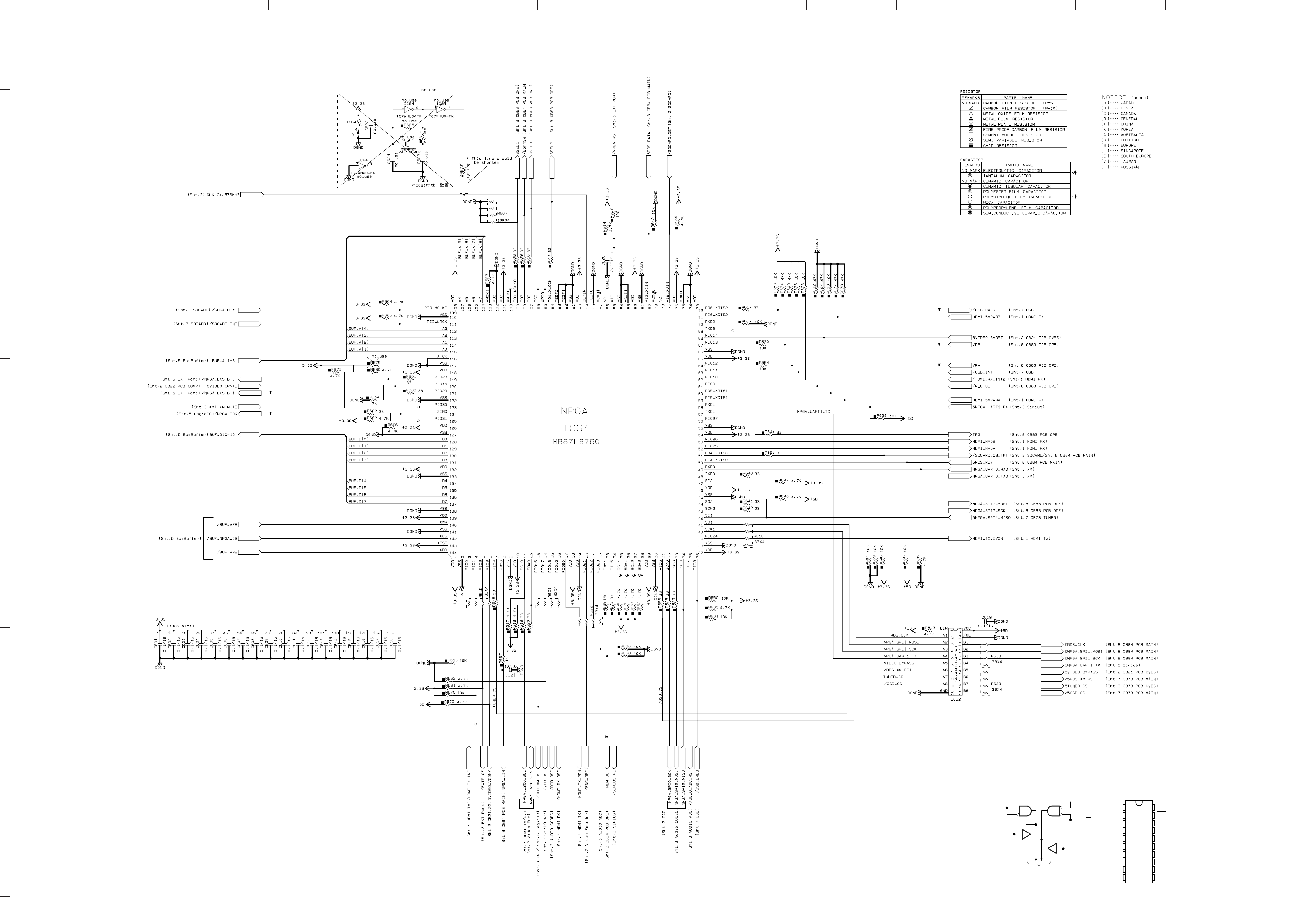
IC61
IC62
A
1
2
3
4
5
6
7
8
9
10
BCDEFGH I JKLMN
RX-V563/HTR-6150/DSP-AX563
88
★All voltages are measured with a 10MΩ/V DC electronic voltmeter.
★Components having special characteristics are marked s and must be replaced
with parts having specifications equal to those originally installed.
★Schematic diagram is subject to change without notice.
DSP 6/8
3.3
3.3
0
0.2
0
0
3.3
3.3
0
0
0
3.3
1.6
0
3.3
0
0
3.3
3.3
0
0
3.3
0
3.3
3.3
3.3
3.3
4.3
0
0
0
5.0
0
3.3
5.0
3.3
3.3
0
0
0
0
0
3.3
0
0
3.3
3.3
3.3
3.3
3.3
0
3.3
0
0
3.3
0
3.3
0
0
0
3.3
0
0
3.3
3.3
0
0
0
0
0
0
0
0
3.3
3.3
0
3.3
0
0
3.3
3.3
3.3
0
0
0
0
0
3.3
0
0
0
0
0
0
3.3
3.3
0
3.3
3.3
3.3
0
3.3
3.3
0
3.3
0
3.1
0
3.3
3.3
3.3
3.3
3.3
0
0
3.3
3.3
0
3.3
0
3.3
3.3
0
3.3
3.3
0
0
0
2.9
3.3
3.3
3.3
3.3
3.3
3.3
3.3
3.3
5.0 5.0
0
0
3.3
3.3
0
0
0
3.3
0
0
0
0
5.0
5.0
0
0
0
0
IC62: SN74AHCT245PWR
Octal bus transceivers with 3-state outputs
1
2
3
4
5
6
7
8
9
10
20
19
18
17
16
15
14
13
12
11
DIR
A1
A2
A3
A4
A5
A6
A7
A8
GND
VCC
OE
B1
B2
B3
B4
B5
B6
B7
B8
DIR
OE
A1
B1
To Seven Other Channels
1
2
19
18
NPGA
to DSP 7/8
to DSP 7/8
to DSP 1/8
to DSP 1/8
to DSP 1/8
to DSP 1/8
to DSP 3/8
to DSP 3/8 / to DSP 8/8
to DSP 3/8
to DSP 3/8
to DSP 1/8
to DSP 2/8
to DSP 8/8
to DSP 8/8
to DSP 8/8
to DSP 8/8
to DSP 8/8
to DSP 8/8
to DSP 8/8
to DSP 8/8
to DSP 8/8
to DSP 8/8
to DSP 7/8
to DSP 5/8
to DSP 5/8
to DSP 5/8
to DSP 2/8
to DSP 5/8
to DSP 5/8
to DSP 5/8
to DSP 3/8
to DSP 3/8
to DSP 3/8
to DSP 3/8
to DSP 7/8
to DSP 7/8
to DSP 7/8
to DSP 8/8
to DSP 8/8
to DSP 8/8
to DSP 8/8
to DSP 8/8
to DSP 5/8
to DSP 3/8
to DSP 3/8
to DSP 3/8
to DSP 3/8
to DSP 2/8
to DSP 3/8
to DSP 3/8 / to DSP 6/8
to DSP 2/8
to DSP 2/8
to DSP 3/8
to DSP 1/8
to DSP 1/8
to DSP 2/8
to DSP 1/8
to DSP 1/8
to DSP 8/8
to DSP 8/8
to DSP 3/8
to DSP 3/8
to DSP 3/8
to DSP 3/8
to DSP 2/8
to DSP 1/8
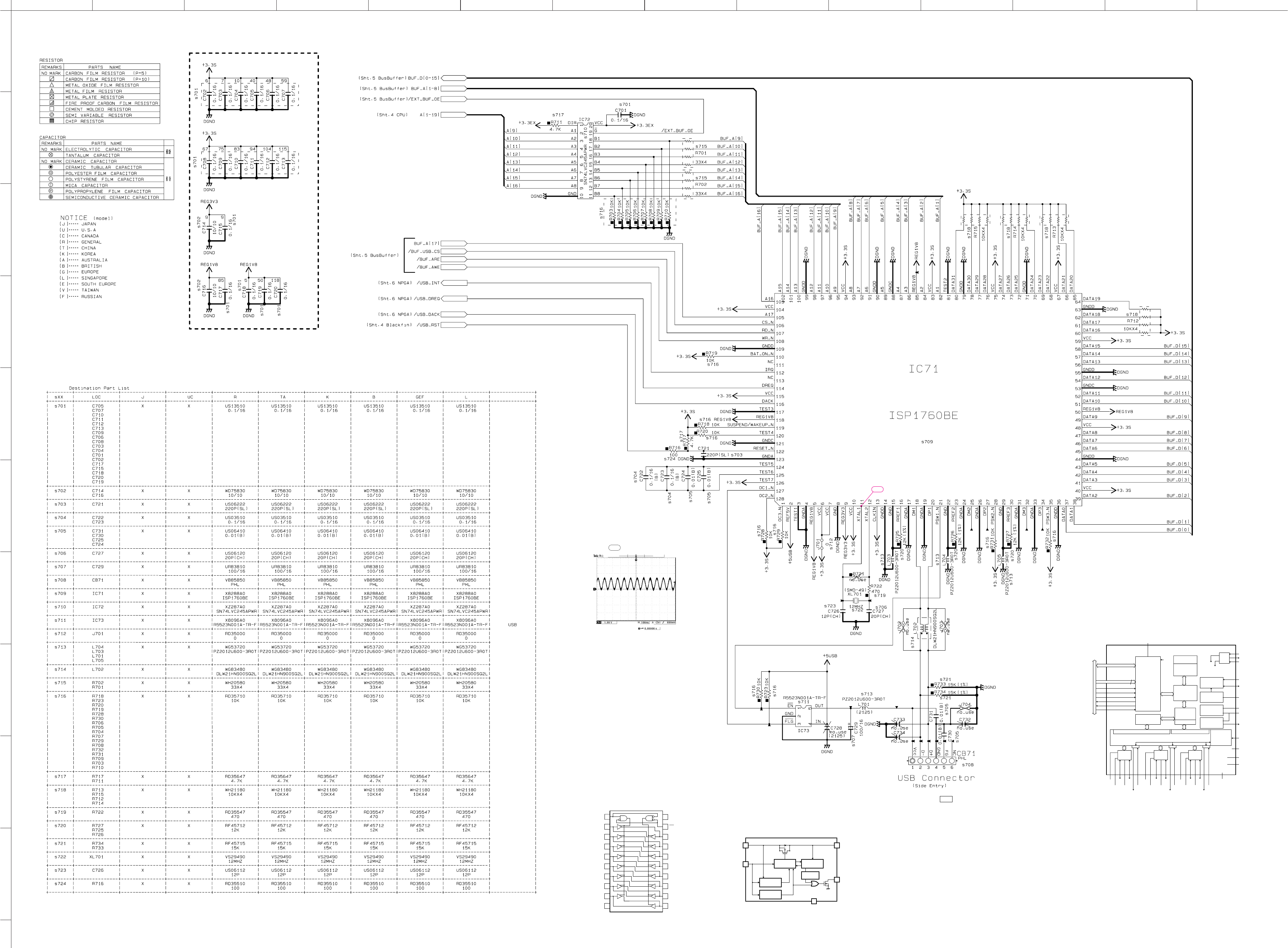
IC72
IC73
CB71
IC71
A
1
2
3
4
5
6
7
8
9
10
BCDEFGH I JKLMN
RX-V563/HTR-6150/DSP-AX563
89
★All voltages are measured with a 10MΩ/V DC electronic voltmeter.
★Components having special characteristics are marked s and must be replaced
with parts having specifications equal to those originally installed.
★Schematic diagram is subject to change without notice.
DSP 7/8
B-1
3.3
1.2
1.4
1.3
1.3
1.9
0
0
0
0
3.3
3.2
0
0
0
0
0
0
0
0
5.1
5.1
4.3
0
0
0
0
0
0
0
0
0
0
0
0.2
0
0
3.3
0
0
0
3.3
0
1.9
0
0
3.3
0
3.3
3.3
3.3
3.3
3.3
3.3
0
3.3
3.3
3.3
3.3
3.3
3.3
3.3
0
3.3
3.3
3.3
3.3
0
0
0
0
0
0
0
0
1.9
0
3.3
0
0
0
0
0
0
0
3.3
0
3.3
0
3.3
0
3.3
3.3
3.3
0
3.3
3.3
3.3
3.3
0
0
0
0
0
1.9
3.3
4.3
3.3
3.3
5.1
0
3.3
3.3
0
3.3
1.0
0.9
3.3
0
0
0
0
0
0
0
0
0
0
0
0
1.3
0
0
0
0
0
0
0
0
3.3
0
1.9
3.3
1.9
0
3.3
1
DIR
A1
A2
A3
A4
A5
A6
A7
A8
GND
Vcc
OE
B1
B2
B3
B4
B5
B6
B7
B8
2
3
4
5
6
7
8
9
10
20
19
18
17
16
15
14
13
12
11
IC72: SN74LVC245APWR
Octal bus transceivers with 3-state outputs
IC71: ISP1760BE
Embedded hi-speed USB host controller
ISP1760BE
37 to 39, 41 to 43,
45 to 47, 49, 51,
52, 54, 56 to 58,
60 to 62, 64 to 66,
68 to 70, 72 to 74,
76 to 78, 80
82, 84, 86, 87,
89, 91, to 93,
95 to 98,
100 to 103, 105
SUSPEND/
WAKEUP_N
BAT_ON_N
REG1V8
REG3V3
REF5V
GND(OSC)
GNDA
GNDC
GNDD
GNDA
VCC(5V0)
RESET_N
CLKIN
XTAL1
XTAL2
VCC(I/O)
119
122
17
106
107
108
112
114
116
11
12
10, 40, 48, 59, 67,
75, 83, 94, 104, 115
16-bit
or
32-bit
13
30 MHz
60 MHz
110
5, 50,
85, 118
4, 17, 24
31, 123
53, 88, 121
14, 36, 44, 55, 63,
71, 79, 90, 99, 109
004aaa435
6, 7
9
2
8
16 15 20 19 18 21 127 23 22 27 26 25 28 128 30 29 34 33 32 35 1
GLOBAL CONTROL
AND POWER
MANAGEMENT
HC PAYLOAD
MEMORY (60 kB)
HC PTD MEMORY
(3 kB)
RISC PROCESSOR
INTERFAC:
A[17:1]
DATA [15:0]/DATA [31:0]
GENERIC PROCESSOR BUS
MEMORY
MANAGEMENT
UNIT
+
INTERRUPT
CONTROL
+
SLAVE DMA
CONTROLLER
+
HARDWARE
CONFIGURATION
REGISTERS
5 V-TO-1.8 V
VOLTAGE
REGULATOR
5 V-TO-3.3 V
VOLTAGE
REGULATOR
HI-SPEED
USB ATX3
DIGITAL
AND ANALOG
OVERCURRENT
DETECTION
PIE
USB HIGH-SPEED DATA PATH
EHCI AND
OPERATIONAL
REGISTERS
TRANSACTION
TRANSLATOR
AND RAM
MEMORY
ARBITER
AND FIFO
PLL
POWER-ON RESET
AND VBAT ON
OC3_N
PSW3_N
DP3
GND
(RREF3)
RREF3 DM3
USB FULL-SPEED AND LOW-SPEED DATA PATH
PORT ROUTING CONTROL LOGIC + HOST AND HUB PORT STATUS
PSW2_N
OC2_N
PSW1_N
OC1_N GNDA
HI-SPEED
USB ATX2
DP2
GND
(RREF2)
RREF2 DM2
GNDA
HI-SPEED
USB ATX1
DP1
GND
(RREF1)
RREF1 DM1
DACK
IRQ
WR_N
RD_N
CS_N
DWEQ
VIN 4
EN 1
2
5
GATE
CONTROL
UVLO
THERMAL
SHUTDOWN
CURRENT
LIMIT
FLAG
DELAY
VOUT
3 FLG
GND
IC73: R5523N001A-TR-F
High side switch IC
POINT B-1 XL701 (Pin 11 of IC71)
No replacement part available.
USB HOST
to DSP 5/8
to DSP 5/8
to DSP 5/8
to DSP 5/8
to DSP 4/8
to DSP 6/8
to DSP 6/8
to DSP 6/8
to DSP 4/8
to OPERATION (6)_W6006
(R, T, K, A, B, G, E, F, L models)
Page 91 L4
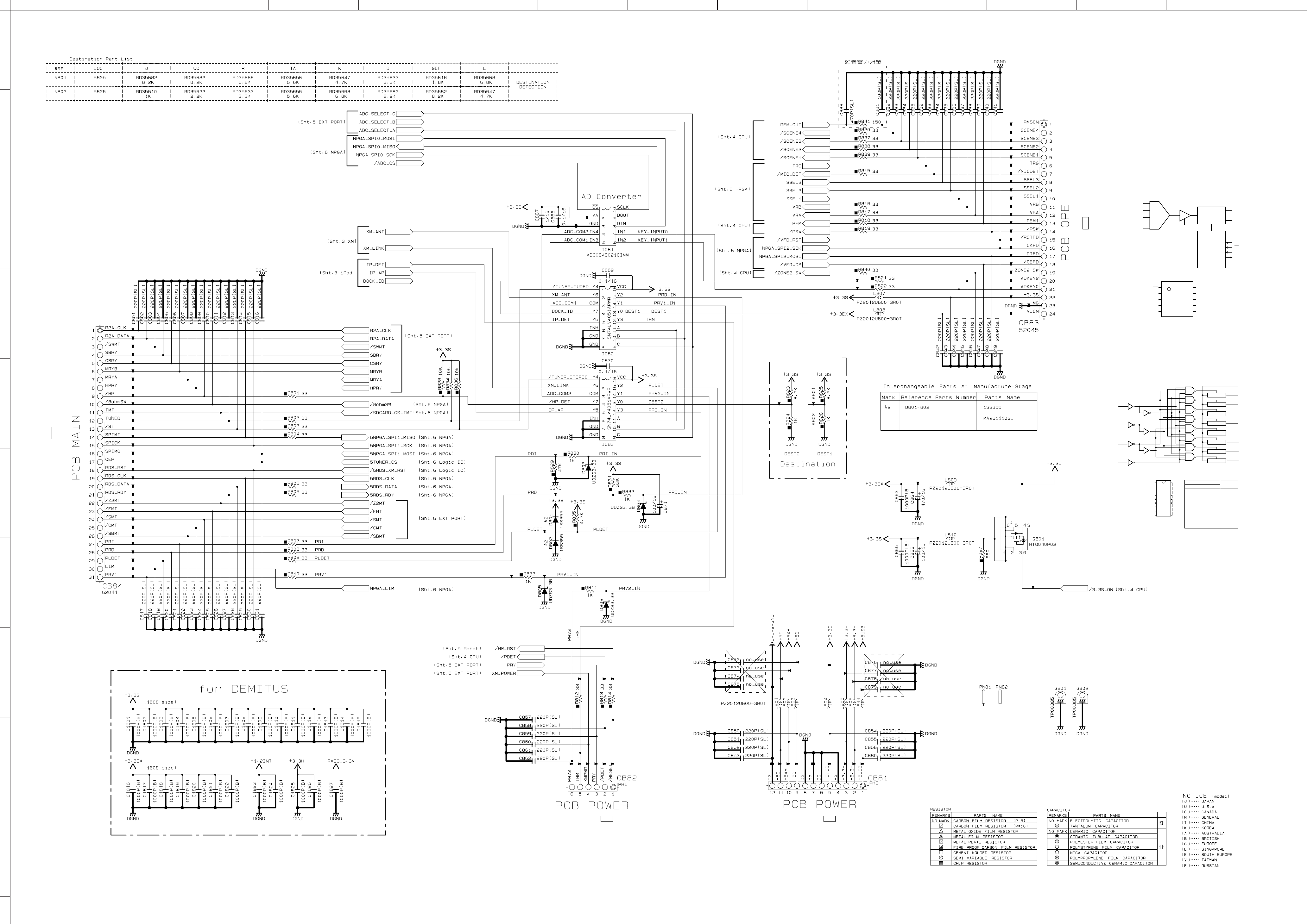
IC81
IC82
IC83
CB82
CB84
CB81
CB83
A
1
2
3
4
5
6
7
8
9
10
BCDEFGH I JKLMN
RX-V563/HTR-6150/DSP-AX563
90
★All voltages are measured with a 10MΩ/V DC electronic voltmeter.
★Components having special characteristics are marked s and must be replaced
with parts having specifications equal to those originally installed.
★Schematic diagram is subject to change without notice.
DSP 8/8
0
3.0
3.3
0
1.6
1.3
2.9
0
3.3
3.3
3.3
3.3
0
1.3
3.3
3.3
0
0
0
0.6
1.2
2.7
1.1
1.8
3.1
0.3
3.3
3.3
0
1.6
3.3
0.8
0
0
0
3.3
1.7
0.4
0
1.8
3.1
0.3
0
0
3.3
0
3.3
0
1.2
0
1.7
0
0.6
3.3
3.3
03.3
3.3
3.3
IC81: ADC084S021 CIMM
4-channel, 200 ksps, 8-bit A/D converter
IN1
IN2
IN3 MUX T/H
VA
8-Bit
SUCCESSIVE
APPROXIMATION
ADC
GND
IN4
GND
SCLK
CONTROL
LOGIC
CS
DIN
DOUT
CS 1
VA2
GND 3
IN4 4
IN3 5
SCLK
ADC084S021
10
DOUT
9
DIN8
IN17
IN26
IC82, 83: SN74LV4051APWR
8-channel analog multiplxers/demultiplexers
Y0
Y1
Y2
Y3
Y4
Y5
Y6
Y7
COM
INH
C
B
A11
10
9
6
3
13
14
15
12
1
5
2
4
1
2
3
4
5
6
7
89
10
16
15
14
13
12
11
Y4
Y6
COM
Y7
Y5
INH
GND
GND
VCC
Y2
Y1
Y0
Y3
A
B
C
INPUTS ON
CHANNEL
INH
L
L
L
L
L
L
L
L
H
L
L
L
H
H
H
H
X
C
L
L
H
H
L
L
H
H
X
L
H
L
H
L
H
L
H
X
L
Y1
Y2
Y3
Y4
Y5
Y6
Y7
None
Y0
BA
SELECTOR1
ADC
SELECTOR2
to DSP 5/8
to DSP 5/8
to DSP 5/8
to DSP 5/8
to DSP 5/8
to DSP 4/8
to DSP 5/8
to DSP 6/8
to DSP 6/8
to DSP 4/8
to DSP 4/8
to DSP 4/8
to DSP 6/8
to DSP 6/8
to DSP 6/8
to DSP 6/8
to DSP 6/8
to DSP 6/8
to DSP 6/8
to DSP 6/8
to DSP 6/8
to DSP 6/8
to DSP 6/8
to DSP 6/8
to DSP 3/8
to DSP 3/8
to DSP 4/8
to MAIN_CB401
Page 94 D10
to OPERATION (2)_W700
Page 92 B7
to OPERATION (2)_W702
Page 92 B6
to OPERATION (1)_CB603
Page 91 G8
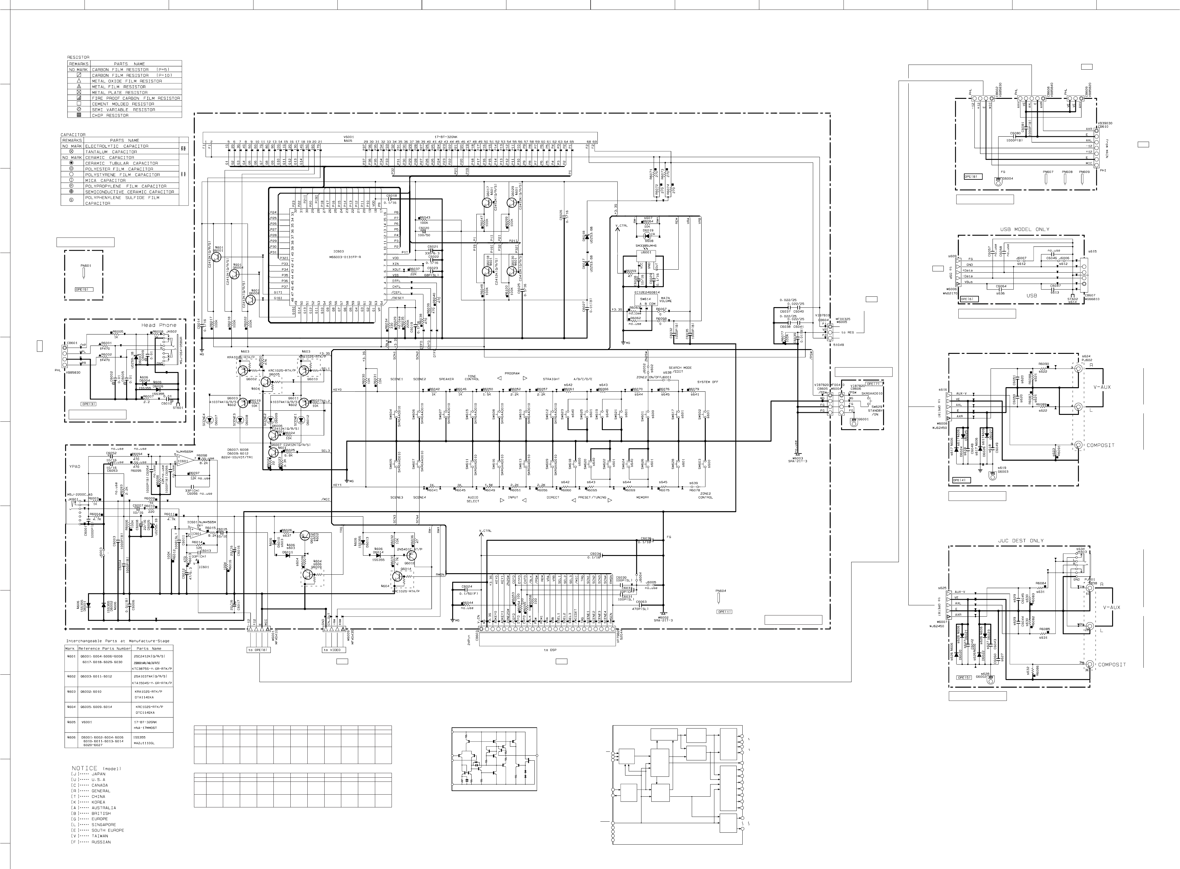
IC603
CB601
JK602
IC601
IC601
IC601
JK601
W6001
W6009
CB603
W6005
CB604
CB605 CB606W6004
W6008
W6007
JK603
W6006
CB607
CB610
CB609
CB608
CB602
A
1
2
3
4
5
6
7
8
9
10
BCDEFGH I JKLMN
RX-V563/HTR-6150/DSP-AX563
91
★All voltages are measured with a 10MΩ/V DC electronic voltmeter.
★Components having special characteristics are marked s and must be replaced
with parts having specifications equal to those originally installed.
★Schematic diagram is subject to change without notice.
OPERATION 1/2
-30.7
-30.7
-30.7
-30.7
-30.7
-30.7
-30.7
-30.7
-30.7
-30.7
-30.7
-30.7
-30.7
-30.7
3.3
1.5
1.5
0
0
3.2
3.2
3.3
-30.7
-30.7
-30.7
-30.7
-30.7
-30.7
-30.7
-30.7
-30.7
-30.7
-30.7
-29.0
3.3
-29.0
-29.0
3.3
-29.0
-29.0
3.3
-29.0
-30.7
-30.7
-30.7
-30.7
-30.7
-30.7
-30.7
-29.0
-29.0
-29.0
-29.1
-29.1
-29.1
-29.1
-29.1
-29.1
-29.1
-29.1
-29.1
-29.1
-29.1
-29.1
-29.1
-29.1
-30.9
-30.7
-30.7
-30.7
-30.7
-30.7
-30.7
-23.1
-23.1
-29.1
-29.1
-29.1
-29.1
-29.1
-29.1
-29.1
-29.1
-29.1
-29.1
-29.1
-29.1
-29.1
-29.1
-29.0
-29.0
-29.0
-30.7
-30.7
-30.7
-30.7
-30.7
-30.7
-30.7
-30.7
-30.7
-30.7
-30.7
-30.7
-30.7
-30.7
-30.6
-30.7
-30.6
-30.6
-30.7
-30.7
-30.7
-30.7
-30.7
-30.7
-30.7
-30.7
-30.7
-30.7
-30.7
-30.7
-30.7
-30.7
-30.7
-30.7
-2.3.1
-23.1
-30.7
-30.7
-30.6
3.3
-30.6 -30.7
3.3
-30.6
-30.7
3.3
-30.6 -30.7
3.3
-30.6 -30.7
3.3
0
0
0
3.3 3.3
3.3
0
2.0
2.0
2.0
2.0
0
0
3.3
0
1.3
5.1
0
0
012.1
11.6
0
0
-11.8
0
1.1
12.1
11.9
12.1
11.9
11.9
12.1
12.1
0
12.1
0
0
12.1
12.1
11.6
0
11.6
0
11.6
3.3
2.0
0.3
0
0
3.3
0
0
0
0
0
3.3
2.6
2.0
3.3
-30.9
3.3
0
3.3
-27.2
-27.2
-23.6
0
0
0
0
0
0
0
00
0
0
0
0
0
0
0
0
0
0
0
INFO
TUNING AUTO/MAN'L
BAND
52
Display
controller
Serial
receive
circuit
Digit
output
circuit
Clock
generator
DIG11/
SEG42
51
DIG12/
SEG41
50
DIG13/
SEG40
49
DIG14/
SEG39
48
DIG15/
SEG38
47
DIG16/
SEG37
46
DIG17/
SEG36
45
SEG35
XOUT
6
Vcc1
8
Vcc2
18
Vss
5
Vp
64
XIN
7
CS
SCK
3
SDATA
4
RESET
1
SEG00
44
9
SEG34
SEG26
17
19
SEG25
Segment
output
circuit
Display code
RAM
(8-bit x 60)
CGROM
(35-bit x 166)
CGROM
(35-bit x 16)
code
select
Code
write
Code/
command
control
circuit
DIG00
63
53
DIG10
IC603: M66003-0131FP-R
18 digit 5 x 7 segment VFD controller/driver
2
data
timing
clock
dot data
write
scan pulse
Segment/
Digit
select/
output
circuit
IC601: NJM4565M
Dual operational amplifier
8
2, 6
3, 5
1, 7
4
V+
–INPUT
+INPUT
V–
OUTPUT
VFD
OPERATION (9)
OPERATION (3)
OPERATION (1)
OPERATION (7)
OPERATION (4)
OPERATION (6)
OPERATION (8)
OPERATION (5) U, C models
R, T, K, A, B, G, E, F, L models
R, T, K, A, B, G, E, F, L models
USB
MAIN ZONE ON/OFF
(U, C, R, T, K, A, G, E, F,
L models)
STANDBY/ON (B model)
PHONES
OPTIMIZER
MIC
AUDIO
VIDEO AUX
VIDEO
AUDIO
PORTABLE
VIDEO AUX
VIDEO
VOLUME
to DSP_CB71
Page 89 K9
to DSP_CB83
Page 90 L3
to VIDEO (6)_CB366
Page 96 H7
to OPERATION (2)_CB703
Page 92 H8
to MAIN_W501
Page 93 I4
to MAIN_W401
Page 94 E3
to VIDEO (1)_W3001
Page 95 E2
Ohm
V
KEY
INPUT 0
(7 pin)
KEY
INPUT 1
(6 pin)
0
0–0.2
–
–
+ 1.0 k
0.2–0.4
SPEAKERS
A/B/OFF
–
+ 1.0 k
0.4–0.7
TONE
CONTROL
AUDIO
SELECT
+ 1.5 k
0.7–1.0
PROGRAM
<
INPUT
>
+ 2.2 k
1.0–1.3
PROGRAM
>
INPUT
<
+ 2.2 k
1.3–1.6
STRAIGTH
EFFECT
DIRECT
+ 3.3 k
1.6–1.9
A/B/C/D/E
PRESET/
TUNING
<
+ 4.7 k
1.9–2.1
BAND
PRESET/
TUNING
>
+ 6.8 k
2.1–2.4
ZONE2
ON/OFF
MEMORY
+ 10.0 k
2.4–2.7
EDIT
PRESET/
TUNING
INFO
TUNING
AUTO/
MAN’L
Key detection for A/D port
Key input (A/D) pull-up resistance 10 k-ohms
U, C, R, T, K, A, G, E, F, L models
+ 22.0 k
2.7–3.0
SYSTEM
OFF
ZONE
CONTROL
Ohm
V
KEY
INPUT 0
(7 pin)
KEY
INPUT 1
(6 pin)
0
0–0.2
–
–
+ 1.0 k
0.2–0.4
SPEAKERS
A/B/OFF
–
+ 1.0 k
0.4–0.7
TONE
CONTROL
AUDIO
SELECT
+ 1.5 k
0.7–1.0
PROGRAM
<
INPUT
>
+ 2.2 k
1.1–1.3
PROGRAM
>
INPUT
<
+ 2.2 k
1.3–1.6
STRAIGTH
EFFECT
DIRECT
+ 3.3 k
1.6–1.9
–
–
+ 4.7 k
1.9–2.1
–
–
+ 6.8 k
2.1–2.4
–
–
+ 10.0 k
2.4–2.7
–
–
B model
+ 22.0 k
2.7–2.9
–
–
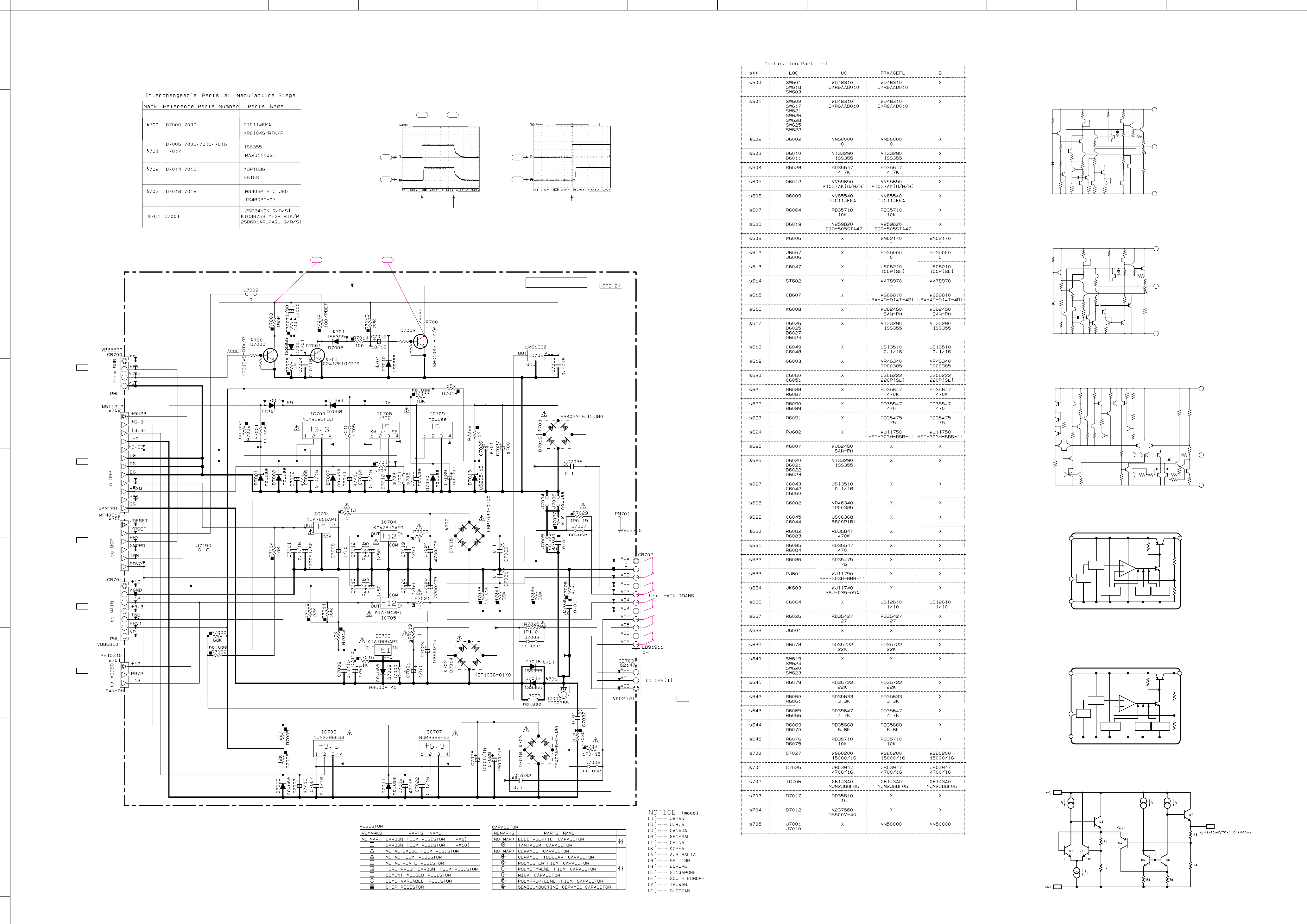
CB700
CB701
W702
W700
W701
CB702
CB703
IC700 IC706
IC708
IC701
IC704
IC703
IC705
IC707IC702
A
1
2
3
4
5
6
7
8
9
10
BCDEFGH I JKLMN
RX-V563/HTR-6150/DSP-AX563
92
★All voltages are measured with a 10MΩ/V DC electronic voltmeter.
★Components having special characteristics are marked s and must be replaced
with parts having specifications equal to those originally installed.
★Schematic diagram is subject to change without notice.
OPERATION 2/2
B-2B-3
AC30.6
AC10.1
AC10.2
AC8.4
AC5.0
8.5
11.4
10.8
10.8
3.3
11.5
5.1
0
0
0
0
0
0
1.0
11.6
0
5.5
0
0
0
3.3
3.3
3.3
5.4
18.7
-19.6
0
12.2
5.0
-11.9
4.5
0
0
0
0
0
18.2
18.5
-19.3
12.0
12.0
0
5.4
0
0
0
0
5.4
9.3
0
4.1 4.2
9.3
3.3
0
9.3
6.4
0
0
3.3
0
10.8 11.5
0
0
0
IC701, 703: KIA7805API
Voltage regulator
R1
R2
R3
R4 R5 R6
R7
R8
Z1
Q12
Q13
Q18
Q17
Q14
Q19
Q10
Q8
Q16
INPUT
OUTPUT
COMMON (GND)
Q15
Q11-1
Q11
Q2
Q3
Q4
Q5 Q9
Q7
Q1 Q6
R12
R19
R10
R9
R15 R14
R16
R21
R20
R22 R23R17
R13
R11 R18
C1
1
3
2
IC704: KIA7812API
Voltage regulator
R1
R2
R3
R4 R5 R6
R7
R8
Z1
Q12
Q13
Q18
Q17
Q14
Q19
Q10
Q8
Q16
INPUT
OUTPUT
COMMON (GND)
Q15
Q11-1
Q11
Q2
Q3
Q4
Q5 Q9
Q7
Q1 Q6
R12
R19
R10
R9
R15 R14
R16
R21
R20
R22 R23R17
R13
R11 R18
C1
1
3
2
COMMON (GND)
IC705: KIA7912PI
Voltage regulator
Q28 Q17
Q18
Q19
Q20
Q31
Q23
Q21
Q22 Q24
Q25
Q26 Q27
Q10
Q11
Q14
Q15
Q16
Q27-1
Q26-1
Q12 Q13
Q8
Q9
Q2
Q7
Q4
Q5
Q6
Q3
Q29
Q30
R0
R1
R2
R14 R17
R19
R20
R21
R22
R23
R24
R25
R26
R3
R4 R5 R6
R10 R11
R12R13
D4
R9
R7 R8
C2 C1
R16
R15 R18
1
OUTPUT
INPUT
3
2
IC708: LM61CIZ
Temperature sensor
POINT B-2 / +3.3D, B-3 / Q7002 (C)
Power cable ON
Power cable OFF
+3.3D
Q7002 (C)
+3.3D
Q7002 (C)
B-2
B-3
Power cable ON
IC706: NJM2388F05
Low dropout voltage regulator with ON/OFF control
ON/OFF
control
Over Voltage
Protection
Bandgap
Reference
VIN
Cont
GND
V
OUT
Over Current
Protection
Thermal
Protection
IC707: NJM2388F63
Low dropout voltage regulator with ON/OFF control
ON/OFF
control
Over Voltage
Protection
Bandgap
Reference
VIN 1
4
3
Cont
GND
V
OUT
Over Current
Protection
Thermal
Protection
2
B-2
B-3
OPERATION (2)
to DSP_CB82
Page 90 G9
to MAIN_W506
Page 93 I6
to VIDEO (1)_CB301
Page 95 B2
to OPERATION (1)_CB604
To POWER TRANSFORMER
Page 91 J4
to DSP_CB81
Page 90 J9
to VIDEO (3)_W3401
Page 96 G9
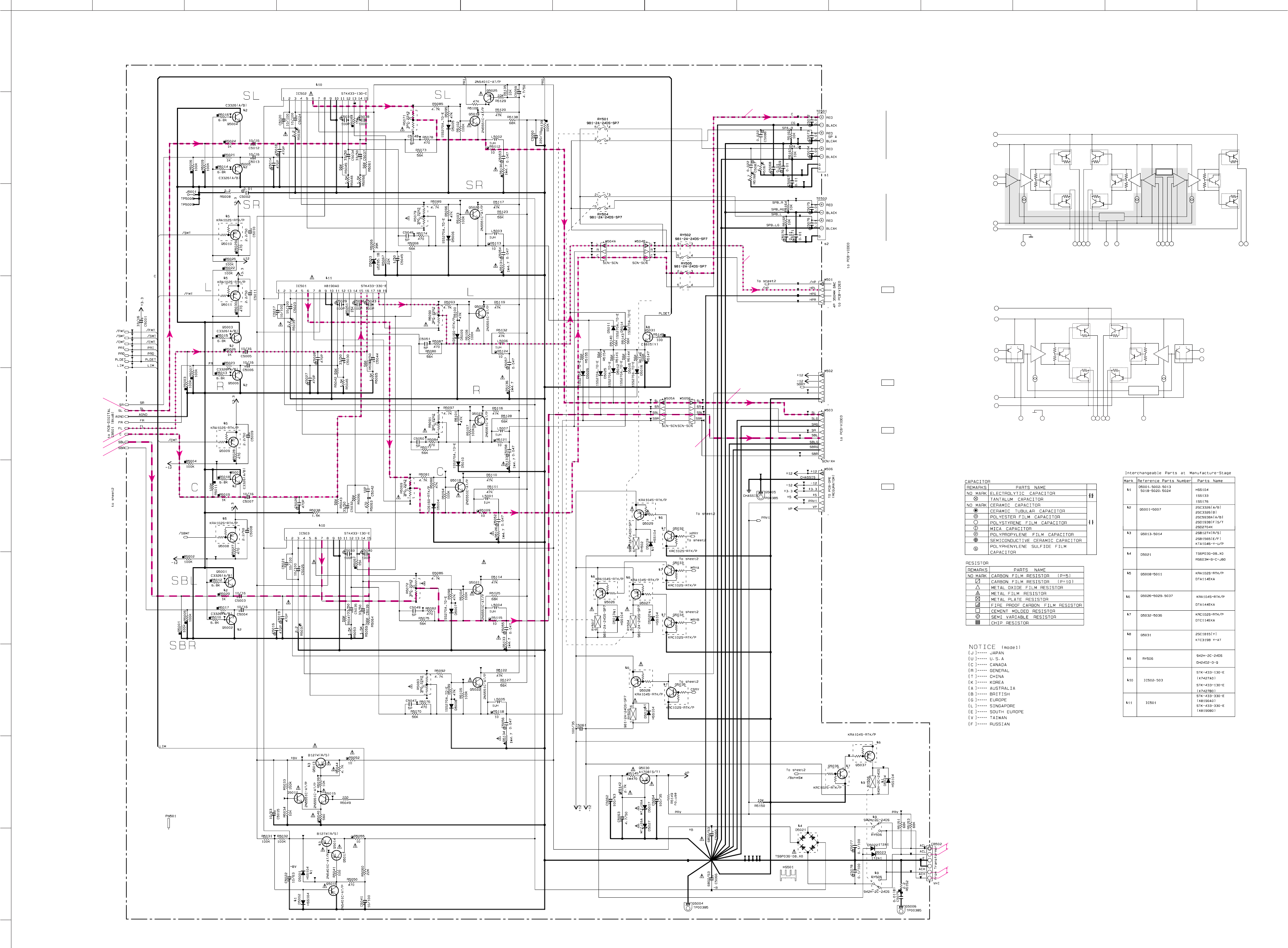
W501
W502
W503
W506
CB502
W505A W505B
W504A W504B
IC502
IC501
IC503
CB501
A
1
2
3
4
5
6
7
8
9
10
BCDEFGH I JKLMN
RX-V563/HTR-6150/DSP-AX563
93
★All voltages are measured with a 10MΩ/V DC electronic voltmeter.
★Components having special characteristics are marked s and must be replaced
with parts having specifications equal to those originally installed.
★Schematic diagram is subject to change without notice.
MAIN 1/2
AC48.2
AC64.9
0.3
-43.4
-43.1
3.1
2.5
43.2
42.5
2.4
-43.1
0
-42.3
-42.3
2.4
2.8
43.2
43.2
-42.9
-42.9
-43.5
-43.4
0.3
0
0
0
43.6
0
0
-12.1
-12.1
3.3
3.3
-12.1 0
0
-12.1
0
0
-12.1 0
0
-12.1 0
0
-12.1 0
0
-42.3
-43.6
43.8
0
0
0
0
43.2
0
0
0
0
0.7
0
0
-42.3
-43.6
43.8
0
0
0
0
43.2
0
0
0
0
1.6
0
0
0
0
0
0
-42.3
-43.6
43.8
0
0
0
0
43.2
0
0
0
0
0.7
0
0
0
0
0
3.3
3.3
-12.1
3.3
3.3
-12.1
3.3
3.3
-12.1
-12.1
0
0
0
43.8
0
0
43.6
43.7
0
0
0
43.6
0
0
0
0
43.6
0
0
43.6
0
0
43.6
0
0
0
43.6
0
0
0
0
0
0
0
0
0
0
0
0
0
0
0
0
0
0
0
0
0
03.3
0
11.8
-12.2
-12.2
0
0
11.6
11.7
0
3.3
0
11.6
-12.2 -12.2
0
0
3.3
-30.8
-31.4
-10.7
0
11.6
-12.2
11.8
-12.4 11.6
0
-12.4
11.6
0
-37.0
-31.4
0
11.8
11.6
-12.2
11.6
11.6
0
-43.6
11.7
11.6
-12.1
-12.1
-12.1
11.7
0
0
0
0
43.8
0
-43.0
-43.0
0
SURROUND L
SURROUND L
CENTER
CENTER
FRONT L
FRONT L
SURROUND
BACK L
SURROUND
BACK L
IC502, 503: STK433-130-E
2-channel AF power amplifier, stand-by circuit built-in
SUB 971364510
2
1
12
11 +
–
+
–14
15
8
3
Pre Driver
CH1
Pre Driver
CH2
Bias Circuit
IC501: STK433-330-E
3-channel AF power amplifier, stand-by circuit built-in
SUB
Pre
Driver
CH1
+
–
Pre
Driver
CH2
MONO IC
Bias Circuit
Pre
Driver
CH3
9 5 4 6 7 10 13 14151617 19 18
3
8
11
12
1
2
+
–
+
–
to MAIN 2/2
to MAIN 2/2
to MAIN 2/2
to MAIN 2/2
to MAIN 2/2
to MAIN 2/2
to MAIN 2/2
to MAIN 2/2
CENTER
FRONT A
FRONT B
SPEAKERS
to OPERATION (3)_CB601
Page 91 A5
to OPERATION (2)_CB701
Page 92 B7
to VIDEO (4)_CB351
Page 96 H2
to VIDEO (4)_CB353
Page 96 H3
To POWER TRANSFORMER
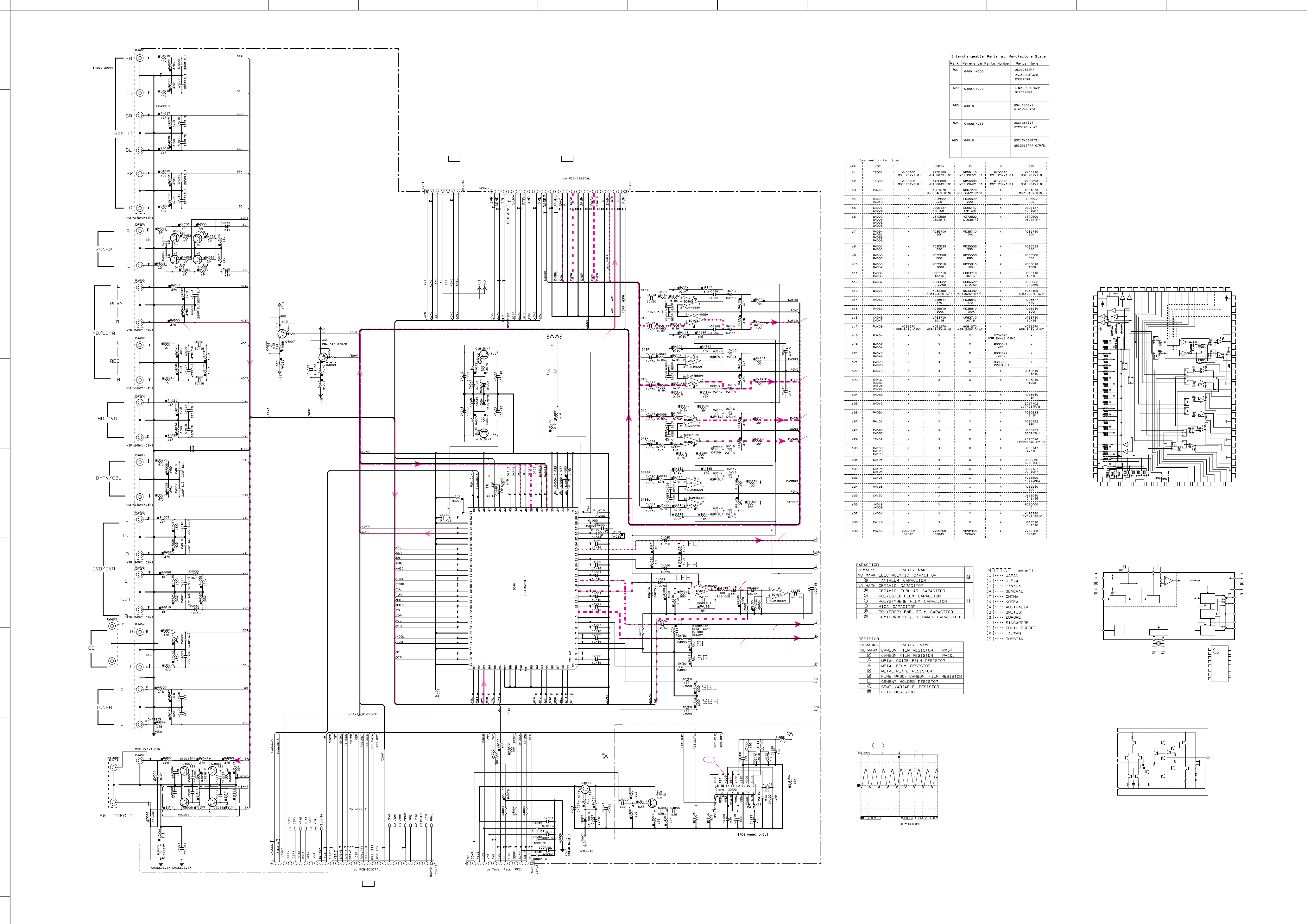
IC407
IC407
IC402
IC401
IC406
IC406
IC405
IC405
IC404
IC404
IC403
IC403
W401
CB402
CB401
CB403
A
1
2
3
4
5
6
7
8
9
10
BCDEFGH I JKLMN
RX-V563/HTR-6150/DSP-AX563
94
★All voltages are measured with a 10MΩ/V DC electronic voltmeter.
★Components having special characteristics are marked s and must be replaced
with parts having specifications equal to those originally installed.
★Schematic diagram is subject to change without notice.
MAIN 2/2
C-2
-12.0
0
0
-12.0
0
0
0
00.7
0
0
0.7
0
0
0.7
0
0
0.7
0
3.3
3.3
3.3
3.3
-12.2
7.2
7.9
7.9
-7.8
0
0
11.9
-7.1-12.1
0
0
0
0
0
0
0
0
0
0
0
0
0
0
0
0
0
0
0
0
0
7.2
0
0
0
0
0
0
0
0
0
0
0
0
0
0
0
0
0
0
0
0
0
0
0
0
0
0
0
0
0
-7.1
0
0
0
0
0
0
0
0
0
0
0
0
0
0
0
0
0
0
0
0
0
0
0
0
0
0
0
0
0
0
0
0
0
0
0
0
0
0
0
0
0
0
0
0
0
0
11.9
9.8
9.9
5.5
5.0
11.9
9.3
4.7
0
0
2.0
2.1
4.7
0
4.7
0
0
2.2
-2.1
4.5
0
2.2
2.1
-12.0
-12.0
11.8
0
0
0
0
0
0
0
0
-12.0
11.8
0
0
0
0
0
0
-12.0
11.8
0
0
0
0
0
0
-12.0
11.8
0
0
0
0
0
0
0
11.8
0
0
0
SURROUND L
CENTER
FRONT L
SUB
WOOFER
ANALOG IN
ANALOG L
FL
SL
C
SW
IC403-407: NJM4565M
Dual operational amplifier
8
2, 6
3, 5
1, 7
4
V+
–INPUT
+INPUT
V–
OUTPUT
REFERENCE
VOLTAGE
CINFLOUTVREF
VREF
ANTIALIASING
FILTER
57kHz
BPF
(SCF)
SMOOTHING
FILTER
MPXIN
+3V
Vdda
Vssa
PLL
(57kHz)
CLOCK
RECOVERY
(1187.5Hz)
+3V
Vddd
RDS-ID/
READY
RST
Vssd
DATA
DECODER
XOUTXIN
TEST
TEST
CLK(4.332MHz)
OSC
RAM
(128bits)
RDDA
RDCL
RDS-ID
DETECT
MODE
IC402: LC72725KM-UY-TLM-E
RDS signal demodulation IC
CIN TEST
Vssd
MODE
Vddd
XIN
XOUT
RST
RDCL
FLOUT
RDS-ID/READY
RDDA
VREF
MPXIN
Vdda
Vssa
2
3
4
5
6
7
89
10
11
12
13
14
15
16
1
IC401: R2A15218FP
8-channel electronic volume with 11 input selector and tone control
51
52
53
54
55
56
57
58
59
60
61
62
63
64
65
66
67
68
69
70
71
72
73
74
75
76
77
78
80
81
79
MUTE
AVEE
ADCL
ADCR
AGND
INR1
INR2
INR3
INR4
INR5
INR6
INR7
INR8
INR9
INL1
INL2
INL3
INL4
INL5
INL6
INL7
INL8
INL9
N.C.
N.C.
N.C.
N.C.
INRB/RECR2
INLB/RECL2
INR10/RECR4
INR11/RECR5
INL10/RECL4
INL11/RECL5
RECR3
RECL3
FLIN1
FRIN1
CIN1
SWIN1
SLIN1
SRIN1
SBLIN1
SBRIN1
N.C.
N.C.
N.C.
INRA/RECR1
INLA/RECL1
N.C.
N.C.
30
29
28
27
26
25
24
23
22
21
20
19
18
17
16
15
14
13
12
11
10
9
8
7
6
5
4
3
1
2
AVCC
N.C.
N.C.
N.C.
N.C.
FRC
FROUT
FLOUT
FLC
CC
COUT
SWOUT
SROUT
SLOUT
SBR OUT
SBL OUT
SBLC
SBRC
SWC
SRC
SLC
AGND
AGND
AGND
AGND
A GND
AGND
TREL
BASSL2
BASSL1
82 83 84 85 86 87 88 89 90 91 92 93 94 95 96 97 98 99 100
50
A VEE
0/-6/-12/-18dB
AT T
SUB
0~-95dB,
-∞
(0.5dBstep)
SUB
SUB
MAIN
MAIN
MAIN
CLOCK
DATA
DGND
SUBR
SUBL
SBLCIN
SBRCIN
FRIN2
FLIN2
SRIN2
SLIN2
SWIN2
SBRIN2
SBLIN2
N.C.
TRER
BASSR1
BASSR2
N.C.
CIN2
49 48 47 46 45 44 43 42 41 40 39 38 37 36 35 34 33 32 31
MCU
I/F
A VCC
REC
Tone
Tone
Bass/Treble
-14~+14dB
(2dBstep) +42~0dB
(0.5dBstep)
+42~0dB
(0.5dBstep)
+42~-95dB
-∞(0.5dBstep)
+42~-95dB
-∞(0.5dBstep)
+42~-95dB
-∞(0.5dBstep)
+42~-95dB
-∞(0.5dBstep)
+42~-95dB
-∞(0.5dBstep)
+42~-95dB
-∞(0.5dBstep)
Bass/Treble
-14~+14dB
(2dBstep)
0~-95dB,
-∞
(0.5dBstep) Bypass
Tone+MIX
Tone+MIX Tone
Tone
Bypass
CMIX
SWMIX
POINT C-2 XL401 (Pin 13 of IC402)
RDS
to MAIN 1/2 to MAIN 1/2
(G, E, F models)
MULTI CH INPUT
ZONE 2 OUTAUDIO
FRONT (6CH)
SB (8CH)
SURROUND
SUBWOOFER
CENTER
INPUT & ZONE2
8ch SELECTOR/
MASTER VOLUME
to DSP_CB31
Page 85 C4
to OPERATION (8)_CB610
Page 91 N2
to DSP_CB84
Page 90 B5 To TUNER
(U, C, R, T, K, A, G, E, F, L models)
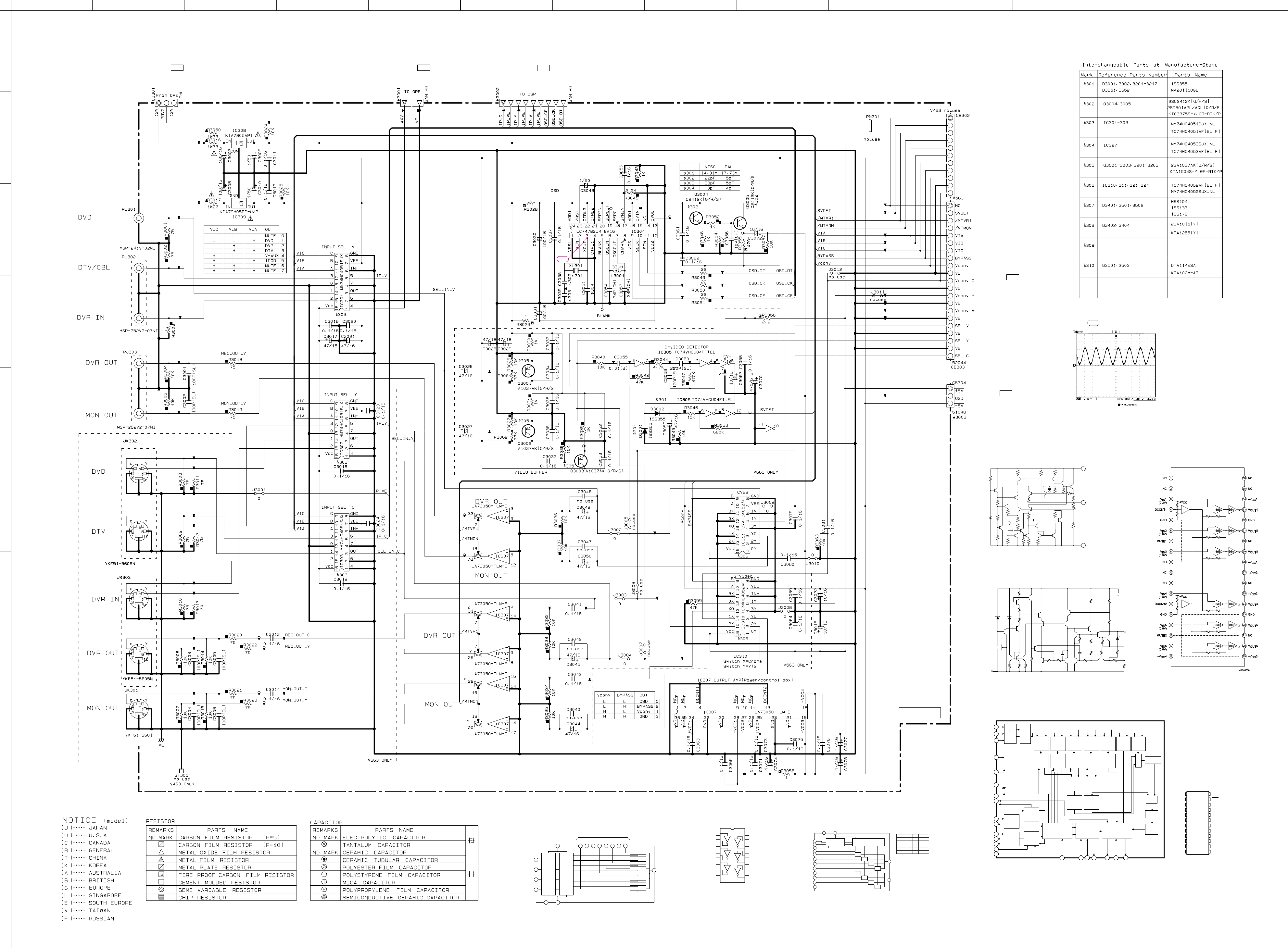
CB301
IC308
IC309
IC301IC302IC303
JK301
JK303
JK302
W3001
W3002
IC304
IC305
IC305
IC307
IC307
IC307
IC307
IC307
IC307
IC310 IC311
IC310
IC307
IC307
CB304
CB303
W3003
A
1
2
3
4
5
6
7
8
9
10
BCDEFGH I JKLMN
RX-V563/HTR-6150/DSP-AX563
95
★All voltages are measured with a 10MΩ/V DC electronic voltmeter.
★Components having special characteristics are marked s and must be replaced
with parts having specifications equal to those originally installed.
★Schematic diagram is subject to change without notice.
VIDEO 1/2
C-1
5.0
-5.0
0
0
8.5
-8.7
00
-5.0
0
0
0
0
0
0
0
0
0
0
0
0
5.0
00
-5.0
0
0
0
0
0
0
0
0
0
0
0
0
5.0
00
-5.0
0
0
0
0
0
0
0
0
0
0
0
0
5.0
5.00
2.5
2.6
0
5.0
2.5
5.0
5.0
0
5.0
2.5
0
5.0
5.0
0
5.0
0
2.0
2.0
5.0
0
0
1.7
1.7
0.5
1.0
5.0
5.0
0
0.9
0.3
-5.0
0
0
-5.0
0
0
-5.0
2.5 2.5 2.5 2.5 2.5
0
0
0
5.0
0
0
0
0
0
00
0
0
0
0
0
-5.0
0
0
5.0
0
0
0
0
0
00
0
0
0
0
0
-5.0
0
4.9
2.2
0
0
0
0
4.9 04.9
4.9
0
4.9
0
0
04.9 0
0
0
4.9
0
0
04.9 0
0
0
0
4.9
0
0
4.9 0
0
0
5.0
5.0
0
-5.0
-5.0
-4.9
0
0
-5.0
IC308: KIA7805API
Voltage regulator
R1
R2
R3
R4 R5 R6
R7
R8
Z1
Q12
Q13
Q18
Q17
Q14
Q19
Q10
Q8
Q16
INPUT
OUTPUT
COMMON (GND)
Q15
Q11-1
Q11
Q2
Q3
Q4
Q5 Q9
Q7
Q1 Q6
R12
R19
R10
R9
R15 R14
R16
R21
R20
R22 R23R17
R13
R11 R18
C1
1
3
2
Q1
D1
6.2V
D3
6.2V
Q2
D2
6.2V
Q6
Q7
Q9
Q13
Q15 Q20 Q21
Q11
Q10
Q16
Q12
Q17
Q18
Q19
R6
7K
R1
750
VIN
VOUT
R2
1K
R3
6K
R4
20K
R8
20K
R9
20K
R13
5K R16
0.05
R21
150
R5
15K
R10
3K R11
10K
R18
4K R19
5K
R15
2K
R17
5.4K
R12
600
R14
15K
R20
20K
R7
1.4K
Q8
Q4 Q5 Q14
20pF 10pF
Q3
IC309: KIA79M05PI-U
Voltage regulator
-5V
IC307: LA73050-TLM-E
6-channel 75-ohm video driver
Serial 8-bits
latch
command
decoder
Horizontal
character
size
register
Horizontal
size
counter
+
parallel
converter
IC304: LC74782JM-8A16-TLMC
The on-screen display controller LSI
RST
CTRL3
CTRL2
SEPIN
SYNIN
CVIN
CVOUT
SEPOUT
SEPC
VDD1
VDD1
NC
1
2
3
4
24
23
22
21
XtalIN
XtalOUT
CTAL1
BLANK
OSCIN
CHARA
SCLK
SIN
VDD2
CS
OSCOUT
VSS1
5
6
7
8
9
10
11
12
20
19
18
17
16
15
14
13
Ver tical
character
size
register
Ver tical
size
counter
Horizontal
display
position
register
Horizontal
character
size
register
Horizontal
dot counter
31 inking
3nd inversion
control
register
31 inking
3nd inversion
control
register
31 inking
3nd inversion
control
register
Character
control
counter
Timing generator
Line
control
counter
31 inking
3nd inversion
control
register
Ver tical
display
position
register
Ver tical
dot counter
Horizontal
character
size
register
Horizontal
character
size
register
Horizontal
character
size
register
Display
control
register
RAM write
address
counter
Display RAM
Decoder
Decoder
Font RAM
Shift
register
Character output
control
Background control
Video output control
Synchronization
signal generator
131552421
22
20
19
18
17
3
7
6
12
24
23
10
11
9
1
8
IC301-303: MM74HC4051SJX
8-channel analog multiplexer
16
11
10
9
7
VEE
8
GND
C
B
A
VCC
4
Y7
1
Y4Y5Y6
12
Y3
2515
Y2
CHANNEL IN/OUT
14
Y1
13
Y0
COMMON
OUT/IN
6INH
Logic
Level
Conversion
Binary
to
1 of 8
Decoder
with
INHIBIT
TG
TG
TG
TG
TG
TG
TG
TG
3
VCC
6A
5A
4A
6Y
5Y
4Y
GND
3Y
3A
2A
1A
2Y
1Y
1
2
3
4
5
6
7
14
13
12
11
10
9
8
IC310, 311: TC74HC4052AF
Analog multiplexer/demultiplexer
16
VCC
6
INH
10
A
9
B
8
GND
7
VEE
12
0X
14
1X
15
2X
11
3X
1
0Y
5
1Y
2
2Y
4
3Y
LEVEL
CONVERTER
BINARY TO 1-OF-4
DECODER WITH INHIBIT
SW
SW
SW
SW
SW
SW
SW
SW
13 X-COM
3Y- C O M
INHIBIT
0
0
0
0
1
B
0
0
1
1
X
A
0
1
0
1
X
0x, 0y
1x, 1y
2x, 2y
3x, 3y
NONE
IC305: TC74VHCU04FT
Hex inverters
POINT C-1 XL301 (Pin 3 of IC304)
VIDEO (1)
VIDEO
S VIDEO
DTV/CBL
OSD
INPUT
SELECTOR
S-DETECTOR
BYPASS
SWITCH
OUTPUT AMP
to DSP_CB21
Page 84 M3
to VIDEO (2)_CB325
Page 96 C1
to DSP_CB32
Page 85 B3
to OPERATION (2)_W701
Page 92 B8
to OPERATION (8)_CB609
Page 91 M2
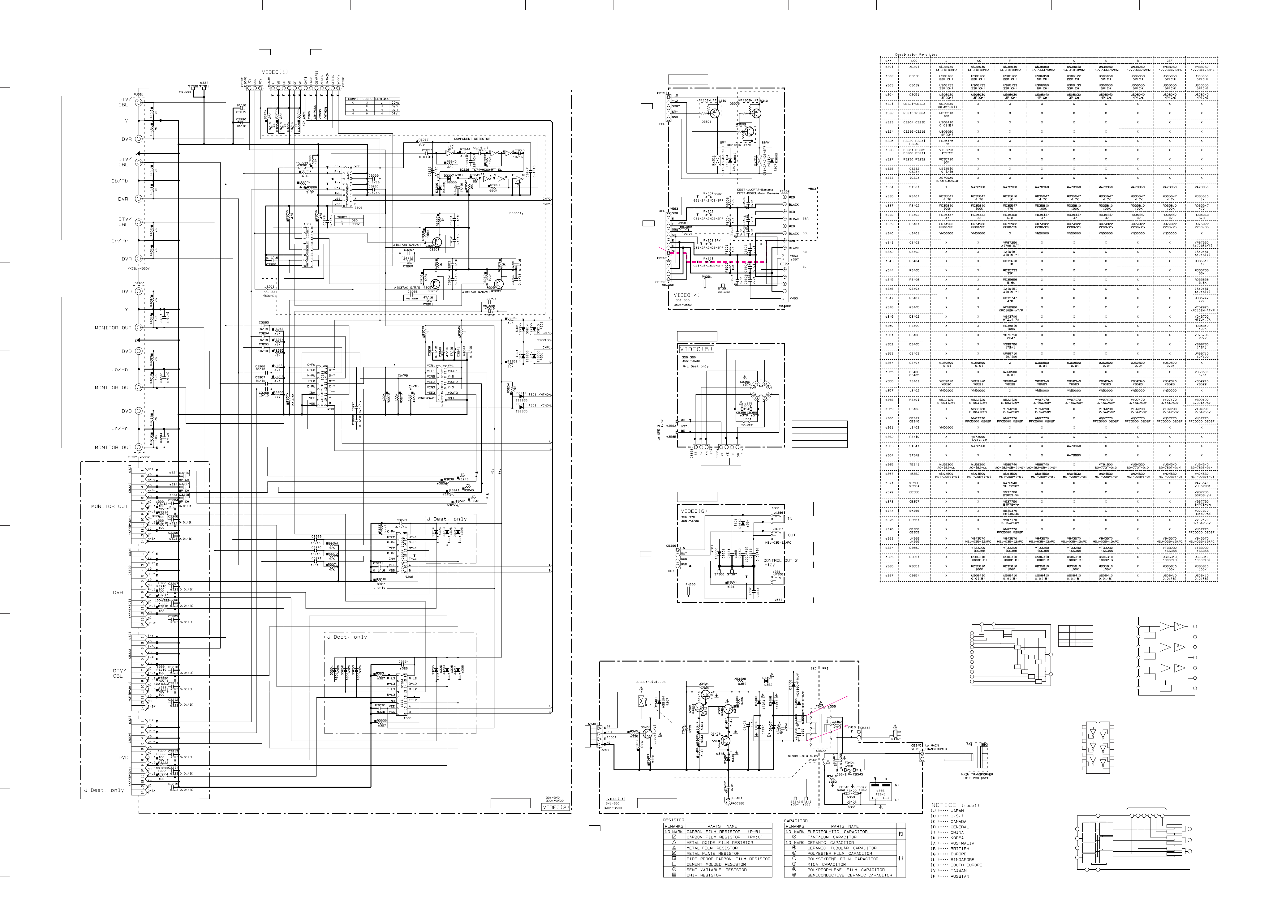
CB325
CB326
IC321
IC327
IC322
IC325
IC323
IC326
CB321CB322CB323CB324
CB351
CB353
CB352
W356A
CB358 CB359
W356B
CB356
CB357
JK366
JK367
JK368
CB366
CB344
CB343CB342
CB346 CB347
CB345
W3401
A
1
2
3
4
5
6
7
8
9
10
BCDEFGH I JKLMN
RX-V563/HTR-6150/DSP-AX563
96
★All voltages are measured with a 10MΩ/V DC electronic voltmeter.
★Components having special characteristics are marked s and must be replaced
with parts having specifications equal to those originally installed.
★Schematic diagram is subject to change without notice.
VIDEO 2/2
05.0
2.5
0
0.3
0.9
2.5 2.5
00
0
4.9
4.9
2.5
0
0
-5.0
0.3
0.9
-5.0
0.3
0.9
-5.0
0
2.5
4.9 4.9
0
2.5
00
3.3
12.1
12.1 12.1
12.1
0
0
-11.8
12.1
-11.8
12.1
0
0
0
0
0
4.9
0
0
0
0
0
-5.0
0
0
05.0
0.9
0.9
0
0
3.3
3.3
3.3
0
0.9
0
0
-5.0
0
0
0.9 5.0
0
0
0.9
0.9
0
0.6
0.6
0
0
0
0
-5.0
0
0.9
05.0
0
0
4.9
0
0.6 0.6
0.6
4.9
4.9
2.9
2.9
0.6
0
5.0
0
5.0
0
0
-4.9
-4.9
0
-4.9
2.9
0
0.3
5.0
0
0
0
0
0
0.6
0.6
0
0
0
0
0
-4.9
0.9
0
0
0
0
11.4
3.0
3.0
3.0
1.3
11.4
4.2
11.4
8.5
4.2
8.5
4.2
4.2
4.2 4.2
00
AC10.7
SURROUND L
IC327: MM74HC4053SJX
Triple 2-channel analog multiplexer
16
11
10
9
7
VEE
8
GND
C
B
A
VCC
5
CXCY
1
BY
32
BX
IN/OUT
13
AY
12
AX
6INH Logic
Level
Conversion
Binary to
1 of 2
Decoders
with
INHIBIT
Logic
Level
Conversion
Logic
Level
Conversion
Logic
Level
Conversion
Binary to
1 of 2
Decoders
with
INHIBIT
Binary to
1 of 2
Decoders
with
INHIBIT
TG
TG
TG
TG
TG
TG
OUT/IN
BX or BY
15
OUT/IN
CX or CY
4
OUT/IN
AX or AY
14
IC325: NJM2581M
Video amplifier
13 VOUT1
11 VOUT2
9VOUT3
8GND
10 V+3
14 V+1
12 V+2
2
NEE1
4
VEE2
6
VEE3
7
PowerSave
5
VIN3
1
VIN1
3
VIN2
75
Driver
6dB
AMP
BIAS
75
Driver
6dB
AMP
BIAS
75
Driver
6dB
AMP
BIAS
REF
VCC
6A
5A
4A
6Y
5Y
4Y
GND
3Y
3A
2A
1A
2Y
1Y
1
2
3
4
5
6
7
14
13
12
11
10
9
8
IC321-323: TC74HC4052AF
Analog multiplexer/demultiplexer
16
VCC
6
INH
10
A
9
B
8
GND
7
VEE
12
0X
14
1X
15
2X
11
3X
1
0Y
5
1Y
2
2Y
4
3Y
LEVEL
CONVERTER
BINARY TO 1-OF-4
DECODER WITH INHIBIT
SW
SW
SW
SW
SW
SW
SW
SW
13 X-COM
3Y- C O M
INHIBIT
0
0
0
0
1
B
0
0
1
1
X
A
0
1
0
1
X
0x, 0y
1x, 1y
2x, 2y
3x, 3y
NONE
IC326: TC74VHCU04FT
Hex inverters
VIDEO (2) VIDEO (3)
VIDEO (6)
VIDEO (5)
VIDEO (4)
R, L models
VOLTAGE
SELECTOR
VOLTAGE SELECTOR
230-240V
220V
110V
120V
1-2/5-6
2-3/6-7
3-4/7-8
4-5/8-1
SPEAKERS
SURROUND BACK/
BI AMP
SURROUND
REMOTETRIGGER
OUT
COMPONENT VIDEO
OUTPUT AMP
INPUT
SELECTOR
L1 SELECTOR
Y-DETECTOR
to DSP_CB22
Page 84 M5
to VIDEO (1)_CB304
Page 95 K5
to MAIN_W502
Page 93 I5
to MAIN_W503
Page 93 I5
to OPERATION (1)_W6009
To POWER TRANSFORMER
To POWER TRANSFORMER
AC IN
To POWER TRANSFORMER
Page 91 D8
to OPERATION (2)_CB700
Page 92 B5

97
RX-V563/HTR-6150/DSP-AX563
RX-V563/HTR-6150/
DSP-AX563
■REPLACEMENT PARTS LIST
ABBREVIATIONS IN THIS LIST ARE AS FOLLOWS:
• ELECTRICAL COMPONENT PARTS
WARNING
●Components having special characteristics are marked s and must be replaced with parts having specifications
equal to those originally installed.
●The chip resistor is not supplied as a replacement part.
* When a chip resistor is necessary, use the following part.
AAX60720: CHIP RESISTOR SAMPLE BOOK
C.A.EL.CHP : CHIP ALUMI.ELECTROLYTIC CAP
C.CE : CERAMIC CAP
C.CE.ARRAY : CERAMIC CAP ARRAY
C.CE.CHP : CHIP CERAMIC CAP
C.CE.ML : MULTILAYER CERAMIC CAP
C.CE.M.CHP : CHIP MULTILAYER CERAMIC CAP
C.CE.SAFTY : RECOGNIZED CERAMIC CAP
C.CE.TUBLR : CERAMIC TUBULAR CAP
C.CE.SMI : SEMI CONDUCTIVE CERAMIC CAP
C.EL : ELECTROLYTIC CAP
C.MICA : MICA CAP
C.ML.FLM : MULTILAYER FILM CAP
C.MP : METALLIZED PAPER CAP
C.MYLAR : MYLAR FILM CAP
C.MYLAR.ML : MULTILAYER MYLAR FILM CAP
C.PAPER : PAPER CAPACITOR
C.PLS : POLYSTYRENE FILM CAP
C.POL : POLYESTER FILM CAP
C.POLY : POLYETHYLENE FILM CAP
C.PP : POLYPROPYLENE FILM CAP
C.TNTL : TANTALUM CAP
C.TNTL.CHP : CHIP TANTALUM CAP
C.TRIM : TRIMMER CAP
CN : CONNECTOR
CN.BS.PIN : CONNECTOR,BASE PIN
CN.CANNON : CONNECTOR,CANNON
CN.DIN : CONNECTOR,DIN
CN.FLAT : CONNECTOR,FLAT CABLE
CN.POST : CONNECTOR,BASE POST
COIL.MX.AM : COIL,AM MIX
COIL.AT.FM : COIL,FM ANTENNA
COIL.DT.FM : COIL,FM DETECT
COIL.MX.FM : COIL,FM MIX
COIL,OUTPT : OUTPUT COIL
DIOD.ARRAY : DIODE ARRAY
DIODE.BRG : DIODE BRIDGE
DIODE.CHP : CHIP DIODE
DIODE.VAR : VARACTOR DIODE
DIOD.Z.CHP : CHIP ZENER DIODE
DIODE.ZENR : ZENER DIODE
DSCR.CE : CERAMIC DISCRIMINATOR
FER.BEAD : FERRITE BEADS
FER.CORE : FERRITE CORE
FET.CHP : CHIP FET
FL.DSPLY : FLUORESCENT DISPLAY
FLTR.CE : CERAMIC FILTER
FLTR.COMB : COMB FILTER MODULE
FLTR.LC.RF : LC FILTER,EMI
GND.MTL : GROUND PLATE
GND.TERM : GROUND TERMINAL
HOLDER.FUS : FUSE HOLDER
IC.PRTCT : IC PROTECTOR
JUMPER.CN : JUMPER CONNECTOR
JUMPER.TST : JUMPER,TEST POINT
L.DTCT : LIGHT DETECTING MODULE
L.EMIT : LIGHT EMITTING MODULE
LED.DSPLY : LED DISPLAY
LED.INFRD : LED,INFRARED
MODUL.RF : MODULATOR,RF
PHOT.CPL : PHOTO COUPLER
PHOT.INTR : PHOTO INTERRUPTER
PHOT.RFLCT : PHOTO REFLECTOR
PIN.TEST : PIN,TEST POINT
PLST.RIVET : PLASTIC RIVET
R.ARRAY : RESISTOR ARRAY
R.CAR. : CARBON RESISTOR
R.CAR.CHP : CHIP RESISTOR
R.CAR.FP : FLAME PROOF CARBON RESISTOR
R.FUS : FUSABLE RESISTOR
R.MTL.CHP : CHIP METAL FILM RESISTOR
R.MTL.FLM : METAL FILM RESISTOR
R.MTL.OXD : METAL OXIDE FILM RESISTOR
R.MTL.PLAT : METAL PLATE RESISTOR
RSNR.CE : CERAMIC RESONATOR
RSNR.CRYS : CRYSTAL RESONATOR
R.TW.CEM : TWIN CEMENT FIXED RESISTOR
R.CEMENT : CEMENT RESISTOR
SCR.BND.HD : BIND HEAD B-TIGHT SCREW
SCR.BW.HD : BW HEAD TAPPING SCREW
SCR.CUP : CUP TIGHT SCREW
SCR.TERM : SCREW TERMINAL
SCR.TR : SCREW,TRANSISTOR
SUPRT.PCB : SUPPORT,P.C.B.
SURG.PRTCT : SURGE PROTECTOR
SW.TACT : TACT SWITCH
SW.LEAF : LEAF SWITCH
SW.LEVER : LEVER SWITCH
SW.MICRO : MICRO SWITCH
SW.PUSH : PUSH SWITCH
SW.RT.ENC : ROTARY ENCODER
SW.RT.MTR : ROTARY SWITCH WITH MOTOR
SW.RT : ROTARY SWITCH
SW.SLIDE : SLIDE SWITCH
TERM.SP : SPEAKER TERMINAL
TERM.WRAP : WRAPPING TERMINAL
THRMST.CHP : CHIP THERMISTOR
TR.CHP : CHIP TRANSISTOR
TR.DGT : DIGITAL TRANSISTOR
TR.DGT.CHP : CHIP DIGITAL TRANSISTOR
TRANS : TRANSFORMER
TRANS.PULS : PULSE TRANSFORMER
TRANS.PWR : POWER TRANSFORMER ASS’Y
TUNER.AM : TUNER PACK,AM
TUNER.FM : TUNER PACK,FM
TUNER.PK : FRONT-ENDTUNER PACK
VR : ROTARY POTENTIOMETER
VR.MTR : POTENTIOMETER WITH MOTOR
VR.SW : POTENTIOMETER WITH ROTARY SW
VR.SLIDE : SLIDE POTENTIOMETER
VR.TRIM : TRIMMER POTENTIOMETER

98
RX-V563/HTR-6150/DSP-AX563
RX-V563/HTR-6150/
DSP-AX563
✻ New Parts
P.C.B. DSP
Ref. No. Part No. Description Markets
* WN276000 P.C.B. DSP UC
* WN276100 P.C.B. DSP R
* WN276200 P.C.B. DSP TA
* WN276300 P.C.B. DSP K
* WN276400 P.C.B. DSP B
* WN276500 P.C.B. DSP GEF
* WN276600 P.C.B. DSP L
* CB11-13 WM462600 CN.HDMI 19P SE
CB21 VQ047600 CN.BS.PIN 21P
CB22 VM923600 CN.BS.PIN 13P
CB31 VQ045500 CN.BS.PIN 26P
CB32 VB390500 CN.BS.PIN 9P
CB34 VQ044400 CN.BS.PIN 9P
CB35 WJ458700 CN.XM 4P CAM-D96 UC
CB71 VB858500 CN.BS.PIN 6P
RTKABGEFL
CB81 VB390800 CN.BS.PIN 12P
CB82 VB390200 CN.BS.PIN 6P
CB83 VP127700 CN 24P
CB84 VQ046000 CN.BS.PIN 31P
C101-110 US135100 C.CE.CHP 0.1uF 16V
C111 WD758300 C.CE.CHP 10uF 10V
C112 US135100 C.CE.CHP 0.1uF 16V
C113 US060900 C.CE.CHP 9pF 50V D
C114 US060800 C.CE.CHP 8pF 50V B
C115 US034820 C.CE.CHP 0.082uF 16V K
C116 US064100 C.CE.CHP 0.01uF 50V B
C117-136 US135100 C.CE.CHP 0.1uF 16V
C141 UR837100 C.EL 10uF 16V
C142-143 US135100 C.CE.CHP 0.1uF 16V
C144 UR837100 C.EL 10uF 16V
C145-146 US035100 C.CE.CHP 0.1uF 16V B
C147 US064100 C.CE.CHP 0.01uF 50V B
C148 US035100 C.CE.CHP 0.1uF 16V B
C151 US063820 C.CE.CHP 8200pF 50V B
C152 US064100 C.CE.CHP 0.01uF 50V B
C153 WJ606100 C.MYLAR 0.082uF 50V
C154 US064100 C.CE.CHP 0.01uF 50V B
C156-157 WD758300 C.CE.CHP 10uF 10V
C158 UR037100 C.EL 10uF 16V
C159 US135100 C.CE.CHP 0.1uF 16V
C160 UR037100 C.EL 10uF 16V
C161 WD758300 C.CE.CHP 10uF 10V
C162 UR037100 C.EL 10uF 16V
C163 WD758300 C.CE.CHP 10uF 10V
C164 UR037100 C.EL 10uF 16V
C165 US135100 C.CE.CHP 0.1uF 16V
C167 US062220 C.CE.CHP 220pF 50V B
C169 US062220 C.CE.CHP 220pF 50V B
C171-174 US064100 C.CE.CHP 0.01uF 50V B
C175-176 US035100 C.CE.CHP 0.1uF 16V B
C177 US061100 C.CE.CHP 10pF 50V B
C178 US061150 C.CE.CHP 15pF 50V B
C201-212 US062220 C.CE.CHP 220pF 50V B
C213 UR037100 C.EL 10uF 16V
C214-221 US635100 C.CE.CHP 0.1uF 16V
C222 US062100 C.CE.CHP 100pF 50V B
C223-225 US035100 C.CE.CHP 0.1uF 16V B
C227-228 US135100 C.CE.CHP 0.1uF 16V
C229 UR237220 C.EL 22uF 16V
C301 UR038100 C.EL 100uF 16V
C302 US135100 C.CE.CHP 0.1uF 16V
C303-314 US062220 C.CE.CHP 220pF 50V B
C315-316 UR037100 C.EL 10uF 16V
C319 UR037100 C.EL 10uF 16V
C320 US035100 C.CE.CHP 0.1uF 16V B
C321 UR067100 C.EL 10uF 50V
C322-323 US126100 C.CE.CHP 1uF 10V
C324 UU238100 C.EL 100uF 16V
C325 US135100 C.CE.CHP 0.1uF 16V
C326 US064100 C.CE.CHP 0.01uF 50V B
C328-329 US061200 C.CE.CHP 20pF 50V B
C330-331 US135100 C.CE.CHP 0.1uF 16V
C332 US061220 C.CE.CHP 22pF 50V B
C334 US035100 C.CE.CHP 0.1uF 16V B
C335-338 US062220 C.CE.CHP 220pF 50V B
C339 US064100 C.CE.CHP 0.01uF 50V B
C340-341 US062220 C.CE.CHP 220pF 50V B
C342 US063100 C.CE.CHP 1000pF 50V B
C343 US135100 C.CE.CHP 0.1uF 16V
C344 US135100 C.CE.CHP 0.1uF 16V
RTKABGEFL
C345-346 US135100 C.CE.CHP 0.1uF 16V
C350-352 US062220 C.CE.CHP 220pF 50V B
C353 US063100 C.CE.CHP 1000pF 50V B UC
C354-357 US062220 C.CE.CHP 220pF 50V B
C359 US135100 C.CE.CHP 0.1uF 16V
C360-365 US062220 C.CE.CHP 220pF 50V B UC
C367 US062220 C.CE.CHP 220pF 50V B UC
C368 US062220 C.CE.CHP 220pF 50V B
C369-375 US135100 C.CE.CHP 0.1uF 16V
C376 US062220 C.CE.CHP 220pF 50V B
C377 US035100 C.CE.CHP 0.1uF 16V B
C378 UR037100 C.EL 10uF 16V
C379 UR237470 C.EL 47uF 16V
C380 WJ606200 C.MYLAR 0.1uF 50V
C381 WJ605400 C.MYLAR 0.022uF 50V J
C382 US062220 C.CE.CHP 220pF 50V B
C384 US135100 C.CE.CHP 0.1uF 16V
C385 US064100 C.CE.CHP 0.01uF 50V B
C386 US135100 C.CE.CHP 0.1uF 16V
C387 US126100 C.CE.CHP 1uF 10V
C388 UR037100 C.EL 10uF 16V
C389-391 US064100 C.CE.CHP 0.01uF 50V B
C401-408 UB446100 C.CE.CHP 1uF 16V
C409-416 US635100 C.CE.CHP 0.1uF 16V
C417-418 US063100 C.CE.CHP 1000pF 50V B
C419 US635100 C.CE.CHP 0.1uF 16V
C420-422 US063100 C.CE.CHP 1000pF 50V B
C423-424 US635100 C.CE.CHP 0.1uF 16V
C425 US063100 C.CE.CHP 1000pF 50V B
C426 US635100 C.CE.CHP 0.1uF 16V
C427-430 US063100 C.CE.CHP 1000pF 50V B
C431-432 US061220 C.CE.CHP 22pF 50V B
C433 US135100 C.CE.CHP 0.1uF 16V
C435-436 US135100 C.CE.CHP 0.1uF 16V
C437 WH771300 C.EL 100uF 10V
C438 UB446100 C.CE.CHP 1uF 16V
C439 US135100 C.CE.CHP 0.1uF 16V
C440 UB446100 C.CE.CHP 1uF 16V
C441 WH771300 C.EL 100uF 10V
C443 US062220 C.CE.CHP 220pF 50V B
✻ New Parts
Ref. No. Part No. Description Markets

99
RX-V563/HTR-6150/DSP-AX563
RX-V563/HTR-6150/
DSP-AX563
C501-502 UB446100 C.CE.CHP 1uF 16V
C503 US635100 C.CE.CHP 0.1uF 16V
C504-505 US063100 C.CE.CHP 1000pF 50V B
C506-507 US635100 C.CE.CHP 0.1uF 16V
C508-509 US063100 C.CE.CHP 1000pF 50V B
C510-517 US135100 C.CE.CHP 0.1uF 16V
C519-520 US135100 C.CE.CHP 0.1uF 16V
C521 US035100 C.CE.CHP 0.1uF 16V B
C522 US135100 C.CE.CHP 0.1uF 16V
C523 US061180 C.CE.CHP 18pF 50V B
C524-525 US035100 C.CE.CHP 0.1uF 16V B
C526-527 US135100 C.CE.CHP 0.1uF 16V
C529 US035100 C.CE.CHP 0.1uF 16V B
C530 UR038100 C.EL 100uF 16V
C601-618 US635100 C.CE.CHP 0.1uF 16V
C619 US135100 C.CE.CHP 0.1uF 16V
C620 US062220 C.CE.CHP 220pF 50V B
C621 UR837100 C.EL 10uF 16V
C701-713 US135100 C.CE.CHP 0.1uF 16V
RTKABGEFL
C714 WD758300 C.CE.CHP 10uF 10V
RTKABGEFL
C715 US135100 C.CE.CHP 0.1uF 16V
RTKABGEFL
C716 WD758300 C.CE.CHP 10uF 10V
RTKABGEFL
C717-720 US135100 C.CE.CHP 0.1uF 16V
RTKABGEFL
C721 US062220 C.CE.CHP 220pF 50V B
RTKABGEFL
C722-723 US035100 C.CE.CHP 0.1uF 16V B
RTKABGEFL
C724-725 US064100 C.CE.CHP 0.01uF 50V B
RTKABGEFL
C726 US061120 C.CE.CHP 12pF 50V B
RTKABGEFL
C727 US061200 C.CE.CHP 20pF 50V B
RTKABGEFL
C729 UR838100 C.EL 100uF 16V
RTKABGEFL
C730-731 US064100 C.CE.CHP 0.01uF 50V B
RTKABGEFL
C801-862 US062220 C.CE.CHP 220pF 50V B
C863 US063100 C.CE.CHP 1000pF 50V B
C864 UR038470 C.EL 470uF 16V
C865 US063100 C.CE.CHP 1000pF 50V B
C866 UR238100 C.EL 100uF 16V
C867 UB446100 C.CE.CHP 1uF 16V
C868-870 US135100 C.CE.CHP 0.1uF 16V
C871 UR038100 C.EL 100uF 16V
C880 US062220 C.CE.CHP 220pF 50V B
C881 US062100 C.CE.CHP 100pF 50V B
C882-885 US062220 C.CE.CHP 220pF 50V B
C886 US062470 C.CE.CHP 470pF 50V B
C1301 US135100 C.CE.CHP 0.1uF 16V UC
C1302-1303 US035100 C.CE.CHP 0.1uF 16V B UC
C1304 US135100 C.CE.CHP 0.1uF 16V UC
C1305 US063100 C.CE.CHP 1000pF 50V B UC
C1306-1307 US061100 C.CE.CHP 10pF 50V B UC
C1308-1309 UB446100 C.CE.CHP 1uF 16V UC
C1310-1317 US135100 C.CE.CHP 0.1uF 16V UC
C1318 UR237470 C.EL 47uF 16V UC
C1319 US135100 C.CE.CHP 0.1uF 16V UC
C1320 UR837100 C.EL 10uF 16V UC
C1321 US064100 C.CE.CHP 0.01uF 50V B
C1322 US035100 C.CE.CHP 0.1uF 16V B UC
C1801-1827 US063100 C.CE.CHP 1000pF 50V B
D109-111 WJ586300 VARISTOR
SDV1608H100C050YPT
D112 VT332900 DIODE 1SS355
D113-116 WH641900 ESD PESD0603-140
D117-118 WJ586300 VARISTOR
SDV1608H100C050YPT
D119-130 WH641900 ESD PESD0603-140
D131-132 WJ586300 VARISTOR
SDV1608H100C050YPT
D135-136 WJ586300 VARISTOR
SDV1608H100C050YPT
D201 VT332900 DIODE 1SS355
D305-306 VT332900 DIODE 1SS355
D401 VS597600 DIODE.CHP RB160L-40 TE25
D503 VT332900 DIODE 1SS355
D801-802 VT332900 DIODE 1SS355
D803-806 VU171400
DIODE.ZENR
UDZS3.3BTE-17 3.3V
D1301-1303 WJ586300 VARISTOR
SDV1608H100C050YPT
UC
IC13 X7741A00 IC NJM2867F3-05(TE1)
IC21 X6671A00 IC ADV7172KSTZ
IC22 X7907A00 IC NJM2845DL1-18
IC31 X7746A00 IC LC89057W-VF4AD-E
IC33-34 X6123A00 IC SN74LV157APWR
* IC36 X8192A00 IC F2621E-01-TR UC
IC37 X7375A00 IC PCM1781DBQR UC
IC38 X7355A00 IC PCM1680DBQR
IC39 X7357A00 IC PCM1803DBR
IC42 X8653A00 IC
BR25L320F-W EEPROM
IC43-44 XV894A00 IC
TC74VHC153FT MULTI
* IC51 X9626A00 IC.MEMORY
K4S641632K-UC60000
* IC52 X9636A00 IC.MEMORY EN29LV160AB-70TCP (
written
)
IC53-55 XZ287A00 IC SN74LVC245APWR
* IC56 X9439A00 IC SN74AHCT574PWR
IC57-59 X5135A00 IC
SN74LV574APWR 8D-F
IC61 X8813A00 IC MB87L8760
IC62 X2709A00 IC SN74AHCT245PWR
IC72 XZ287A00 IC SN74LVC245APWR
RTKABGEFL
IC73 X8096A00 IC R5523N001A-TR-F
RTKABGEFL
IC81 X6905A00 IC ADC084S021CIMM
IC82-83 X5875A00 IC SN74LV4051APWR
IC151 XZ287A00 IC SN74LVC245APWR
IC152 X5405A00 IC SN74LVC32APWR OR
IC153 X5404A00 IC SN74LVC08APWR AND
IC154 X6611A00 IC SN74LV123APWR
IC155 X6688A00 IC SN74LV14APWR INV
JK31 VV269500 CN 8P DIN UC
PJ31 V8795700 JACK.PIN 1P
PN81-82 V9637500 PIN L=70 #18
Q101-104 VQ986700 TR 2SC4081 T106
Q301 VV655200 TR.DGT DTA143EKA UC
Q401 WE736300 FET RTQ040P02
Q801 WE736300 FET RTQ040P02
R217-218 WJ682800 R.MTL.FLM 2.2Ω 1W
R328 HV753100 R.CAR.FP 1Ω 1/4W
R1319 HV753100 R.CAR.FP 1Ω 1/4W UC
T101 WA789600 SCR.TERM M3
T301 WA789600 SCR.TERM M3
U31 WH536900
CN.PHOTO.T
1P GP1FAV51TK0F
RTKABGEFL
U32-33 WH169900
CN.PHOTO.R
1P GP1FAV51RK0F
XL31 WJ625200 RSNR.CRYS 24.576MHz
XL101 VZ772700 RSNR.CRYS 28.63636MHz
XL311 WH455300 RSNR.CRYS 45.1584MHz UC
XL401 WB551700 RSNR.CRYS 16.666MHz SMD-49
XL701 VS294900 RSNR.CRYS 12MHz SMD-49
RTKABGEFL
✻ New Parts
P.C.B. DSP
Ref. No. Part No. Description Markets
✻ New Parts
Ref. No. Part No. Description Markets

100
RX-V563/HTR-6150/DSP-AX563
RX-V563/HTR-6150/
DSP-AX563
* WN278000 P.C.B. OPERATION UC
* WN278100 P.C.B. OPERATION RTKAGEFL
* WN278200 P.C.B. OPERATION B
CB601-602 VB858300 CN.BS.PIN 4P
CB603 VP798200 CN.BS.PIN 24P
CB607 WG668100 CN.USB USB 4P SE
RTKABGEFL
CB608 VB858400 CN.BS.PIN 5P
CB609 VB858200 CN.BS.PIN 3P
CB610 VB390300 CN.BS.PIN 7P
CB700 VB858300 CN.BS.PIN 4P
CB701 VB858600 CN.BS.PIN 7P
CB702 LB919110 CN.BS.PIN 11P SE
CB703 VK024700 CN.BS.PIN 3P
C6001 US063100 C.CE.CHP 1000pF 50V B
C6002 WJ605000 C.MYLAR 0.01uF 50V J
C6003-6004 US063100 C.CE.CHP 1000pF 50V B
C6005 WJ605000 C.MYLAR 0.01uF 50V J
C6006 US064100 C.CE.CHP 0.01uF 50V B
C6007 UM397100 C.EL 10uF 16V
C6008 UM397220 C.EL 22uF 25V
C6009-6010 WJ605000 C.MYLAR 0.01uF 50V J
C6011 US062100 C.CE.CHP 100pF 50V B
C6012 UM387470 C.EL 47uF 16V
C6013 US061330 C.CE.CHP 33pF 50V B
C6014 US135100 C.CE.CHP 0.1uF 16V
C6015 UM397100 C.EL 10uF 16V
C6016-6017 UM397220 C.EL 22uF 25V
C6018-6019 US135100 C.CE.CHP 0.1uF 16V
C6020 UR868100 C.EL 100uF 50V
C6021 UM388330 C.EL 330uF 6.3V
C6022 US135100 C.CE.CHP 0.1uF 16V
C6023 US061680 C.CE.CHP 68pF 50V B
C6024 US065100 C.CE.CHP 0.1uF 50V B
C6025-6026 US135100 C.CE.CHP 0.1uF 16V
C6027 US064100 C.CE.CHP 0.01uF 50V B
C6028 UM397100 C.EL 10uF 16V
C6029 US135100 C.CE.CHP 0.1uF 16V
C6030-6031 US062100 C.CE.CHP 100pF 50V B
C6032 US063100 C.CE.CHP 1000pF 50V B
C6033 US061100 C.CE.CHP 10pF 50V B
C6034 US135100 C.CE.CHP 0.1uF 16V
C6035 US063100 C.CE.CHP 1000pF 50V B
C6036 US135100 C.CE.CHP 0.1uF 16V
C6037-6038 US044220 C.CE.CHP 0.022uF 25V B
C6039 US064100 C.CE.CHP 0.01uF 50V B
C6040-6041 US044220 C.CE.CHP 0.022uF 25V B
C6042-6043 US135100 C.CE.CHP 0.1uF 16V UC
C6044-6045 US063680 C.CE.CHP 6800pF 50V B UC
C6047 US062100 C.CE.CHP 100pF 50V B
RTKABGEFL
C6048-6049 US135100 C.CE.CHP 0.1uF 16V
RTKABGEFL
C6050-6051 US062220 C.CE.CHP 220pF 50V B
RTKABGEFL
C6060 US135100 C.CE.CHP 0.1uF 16V UC
C6063 US062470 C.CE.CHP 470pF 50V B
C6064 US126100 C.CE.CHP 1uF 10V
RTKABGEFL
C6080-6081 US063100 C.CE.CHP 1000pF 50V B
C6082 US135100 C.CE.CHP 0.1uF 16V
C7000 UR866100 C.EL 1uF 50V
C7001 US135100 C.CE.CHP 0.1uF 16V
C7002-7003 UR837470 C.EL 47uF 16V
C7004 US064100 C.CE.CHP 0.01uF 50V B
C7005 UR866100 C.EL 1uF 50V
C7006-7007 US135100 C.CE.CHP 0.1uF 16V
C7008 UR866100 C.EL 1uF 50V
C7009 US135100 C.CE.CHP 0.1uF 16V
C7010 UR866100 C.EL 1uF 50V
C7011 UR837470 C.EL 47uF 16V
C7012-7014 US135100 C.CE.CHP 0.1uF 16V
C7015-7016 UR866100 C.EL 1uF 50V
C7017 UR837100 C.EL 10uF 16V
C7018 UR837470 C.EL 47uF 16V
C7019-7021 UR866100 C.EL 1uF 50V
C7022 US135100 C.CE.CHP 0.1uF 16V
C7023 UR73A100 C.EL 10000uF 16V
C7024 UR749470 C.EL 4700uF 25V
C7025 UR749220 C.EL 2200uF 25V
C7026 UR039470 C.EL 4700uF 16V
C7027 WG602000 C.EL 15000uF 16V
C7028 UR73A100 C.EL 10000uF 16V
C7029 WG602000 C.EL 15000uF 16V
C7030-7032 VE326000 C.MYLAR 0.1uF 50V
C7033 US135100 C.CE.CHP 0.1uF 16V
C7034-7035 WJ605000 C.MYLAR 0.01uF 50V J
C7036 VE326000 C.MYLAR 0.1uF 50V
C7037 WJ605000 C.MYLAR 0.01uF 50V J
D6001-6002 VT332900 DIODE 1SS355
D6003 VU172500
DIODE.ZENR
UDZS9.1B
D6004 VT332900 DIODE 1SS355
D6005 VU171900
DIODE.ZENR
UDZ5.1B 5.1V
D6006 VT332900 DIODE 1SS355
D6007-6009 WJ249600 LED ORANGE
D6010-6011 VT332900 DIODE 1SS355
UCRTKAGEFL
D6011 VT332900 DIODE 1SS355
D6012 WJ249600 LED ORANGE
D6013-6014 VT332900 DIODE 1SS355
D6017-6018 VU171500
DIODE.ZENR
UDZ 3.6BTE-17 3.6V
sD6019 V2598200 LED SIR-505ST
UCRTKAGEFL
D6020-6023 VT332900 DIODE 1SS355 UC
D6024-6027 VT332900 DIODE 1SS355
RTKABGEFL
D7004 VS997800 DIODE 1T2
D7005-7006 VT332900 DIODE 1SS355
D7008 VS997800 DIODE 1T2
D7010 VT332900 DIODE 1SS355
D7012 V2376600
DIODE.SHOT
RB500V-40 UC
D7013 VU171900
DIODE.ZENR
UDZ5.1B 5.1V
sD7014-7015 WA653100 DIODE.BRG
KBP103G 1A 200V
D7016-7017 VT332900 DIODE 1SS355
sD7018-7019 WJ286700 DIODE.BRG
RS403M 4A 140V
IC601 X7378A00 IC NJM4565M(TE1)
IC603 X6386A00 IC M66003-0131FP
sIC700 X4419A00 IC NJM2396F33 3.3V
sIC701 X4928A00 IC KIA7805API 5V
sIC702 X4419A00 IC NJM2396F33 3.3V
sIC703 X4928A00 IC KIA7805API 5V
sIC704 X4153A00 IC KIA7812API
sIC705 X4154A00 IC KIA7912PI
sIC706 X6143A00 IC NJM2388F05 5.0V
sIC707 X7976A00 IC NJM2388F63
IC708 X0515A00 IC LM61CIZ THERMAL
JK601 WJ117300
JACK.PHONE
PHONES
JK602 V9408200
JACK.PHONE
MSJ-064-05B GR
✻ New Parts
P.C.B. OPERATION
Ref. No. Part No. Description Markets
✻ New Parts
Ref. No. Part No. Description Markets

101
RX-V563/HTR-6150/DSP-AX563
RX-V563/HTR-6150/
DSP-AX563
✻ New Parts
P.C.B. OPERATION and P.C.B. MAIN
Ref. No. Part No. Description Markets
✻ New Parts
Ref. No. Part No. Description Markets
JK603 WJ117400 JACK.MNI OPTIMIZER MIC UC
PJ601 WJ117500 JACK.PIN 3P UC
PJ602 WJ117500 JACK.PIN 3P
PJ602 WJ117500 JACK.PIN 3P
RTKABGEFL
PN601 V9637500 PIN L=70 #18
PN604 V9637500 PIN L=70 #18
PN607-609 V9637500 PIN L=70 #18
PN701 V9637500 PIN L=70 #18
Q6001 VV556400 TR 2SC2412K Q,R,S
Q6002 WC434800 TR.DGT KRA102S-RTK/P
Q6003 VV556500 TR 2SA1037K Q,R,S
Q6004 VV556400 TR 2SC2412K Q,R,S
Q6005 WC435000 TR.DGT KRC102S-RTK
Q6006-6008 VV556400 TR 2SC2412K Q,R,S
Q6009 VV655400 TR.DGT DTC114EKA
UCRTKAGEFL
Q6010 WC434800 TR.DGT KRA102S-RTK/P
Q6011 VV556500 TR 2SA1037K Q,R,S
Q6012 VV556500 TR 2SA1037K Q,R,S
UCRTKAGEFL
Q6012 VV556500 TR 2SA1037K Q,R,S
Q6014 WC435000 TR.DGT KRC102S-RTK
Q6016 WC397700 TR 2N5401C-AT
Q6017-6018 VV556400 TR 2SC2412K Q,R,S
Q6029-6030 VV556400 TR 2SC2412K Q,R,S
Q7000 WC435100 TR.DGT KRC104S-RTK
Q7001 VV556400 TR 2SC2412K Q,R,S
Q7002 WC435100 TR.DGT KRC104S-RTK
R6001-6002 WJ685600 R.MTL.FLM 470Ω 1W J
sR7013 HV753100 R.CAR.FP 1Ω 1/4W
sR7019-7021 HV753100 R.CAR.FP 1Ω 1/4W
sR7025 WH820300 R.FUSE 1Ω 1W J
sR7029 WJ681400 R.MTL.FLM 0.15Ω 1W
sR7031 WJ681400 R.MTL.FLM 0.15Ω 1W
ST601 WA789700 SCR.TERM D3.5
ST602 WA789700 SCR.TERM D3.5
RTKABGEFL
SW601-603 WD483100 SW.TACT SKRGAAD010
UCRTKAGEFL
SW604-613 WD483100 SW.TACT SKRGAAD010
SW614 V9597100 SW.RT.ENC EC12E2460802
SW615-616 WD483100 SW.TACT SKRGAAD010
SW617-618 WD483100 SW.TACT SKRGAAD010
UCRTKAGEFL
SW621-622 WD483100 SW.TACT SKRGAAD010
UCRTKAGEFL
SW625-626 WD483100 SW.TACT SKRGAAD010
UCRTKAGEFL
SW627 WD483100 SW.TACT SKRGAAD010
SW628 WD483100 SW.TACT SKRGAAD010
UCRTKAGEFL
SW629 WD483100 SW.TACT SKRGAAD010
U6001 WJ645300 L.DTCT SM3385UMH6
* V6001 WN049000 FL.DSPLY 17-BT-32GNK
WA790900 SPACER 4.6/10/32
* WN272300 P.C.B. MAIN UCRTA
* WN272400 P.C.B. MAIN KL
* WN272500 P.C.B. MAIN B
* WN272600 P.C.B. MAIN GEF
CB401 VQ048000 CN.BS.PIN 31P
CB402 VN520900 CN.BS.PIN 52045 26P TE
CB403 VM923600 CN.BS.PIN 13P
UCRTKAGEFL
CB502 LB932060 CN.BS.PIN 6P
C4001 WJ605000 C.MYLAR 0.01uF 50V J
C4002 WJ603300 C.MYLAR 470pF 50V J
C4003 US064100 C.CE.CHP 0.01uF 50V B
C4005-4006 US061470 C.CE.CHP 47pF 50V B
UCRTKAGEFL
C4008-4019 US062220 C.CE.CHP 220pF 50V B
C4020-4021 US061470 C.CE.CHP 47pF 50V B
C4022-4025 US062220 C.CE.CHP 220pF 50V B
C4026-4027 US061470 C.CE.CHP 47pF 50V B
C4028-4029 US062220 C.CE.CHP 220pF 50V B B
C4030-4033 UR837100 C.EL 10uF 16V
C4035-4036 UR837100 C.EL 10uF 16V
UCRTKAGEFL
C4037 UR866220 C.EL 2.2uF 50V
UCRTKAGEFL
C4038 UR866220 C.EL 2.2uF 50V
C4039 US135100 C.CE.CHP 0.1uF 16V
C4040-4041 UR067100 C.EL 10uF 50V
C4042-4043 UR847470 C.EL 47uF 25V
C4044-4045 UR038100 C.EL 100uF 16V
C4046-4047 UR837100 C.EL 10uF 16V
UCRTKAGEFL
C4048 US063100 C.CE.CHP 1000pF 50V B
C4049-4050 US062100 C.CE.CHP 100pF 50V B
C4051 US064100 C.CE.CHP 0.01uF 50V B
C4052-4053 US062100 C.CE.CHP 100pF 50V B
C4054 WJ605400 C.MYLAR 0.022uF 50V J
C4055 WJ605800 C.MYLAR 0.047uF 50V J
C4056 VE326200 C.MYLAR 0.15uF 50V
C4057 UR837470 C.EL 47uF 16V
C4058 WJ605400 C.MYLAR 0.022uF 50V J
C4059-4066 UR837100 C.EL 10uF 16V
C4067 UR837470 C.EL 47uF 16V
C4068 VE326200 C.MYLAR 0.15uF 50V
C4069 US135100 C.CE.CHP 0.1uF 16V
C4070 WJ605800 C.MYLAR 0.047uF 50V J
C4071 UR837470 C.EL 47uF 16V
C4072 US135100 C.CE.CHP 0.1uF 16V GEF
C4073 UR038100 C.EL 100uF 16V
C4074-4081 UR067100 C.EL 10uF 50V
C4082 UR866220 C.EL 2.2uF 50V
C4083 US062330 C.CE.CHP 330pF 50V B GEF
C4084-4086 UR067100 C.EL 10uF 50V
C4087-4090 US162820 C.CE.CHP 820pF 50V J
C4091 WJ603600 C.MYLAR 820pF 50V J
C4092 WJ605400 C.MYLAR 0.022uF 50V J
C4093-4094 US162820 C.CE.CHP 820pF 50V J
C4095 US062330 C.CE.CHP 330pF 50V B GEF
C4096-4099 UR067100 C.EL 10uF 50V
C4100 US062100 C.CE.CHP 100pF 50V B
C4101-4105 US061820 C.CE.CHP 82pF 50V B
C4106 WJ604200 C.MYLAR 2700pF 50V
C4107-4108 US061820 C.CE.CHP 82pF 50V B
C4109 UR837470 C.EL 47uF 16V GEF
C4110-4118 UR837100 C.EL 10uF 16V
C4119-4120 US135100 C.CE.CHP 0.1uF 16V GEF
C4121 US062560 C.CE.CHP 560pF 50V B GEF
C4122 UR038100 C.EL 100uF 16V
C4123 UR837470 C.EL 47uF 16V GEF
C4124-4125 US061270 C.CE.CHP 27pF 50V B GEF
C4126 UR837470 C.EL 47uF 16V GEF
C4127-4128 UR038100 C.EL 100uF 16V
C5001 UR837330 C.EL 33uF 16V
C5002 WJ605000 C.MYLAR 0.01uF 50V J
C5003-5007 UR037100 C.EL 10uF 16V
C5008-5011 UR866220 C.EL 2.2uF 50V

102
RX-V563/HTR-6150/DSP-AX563
RX-V563/HTR-6150/
DSP-AX563
✻ New Parts
P.C.B. MAIN
Ref. No. Part No. Description Markets
✻ New Parts
Ref. No. Part No. Description Markets
C5012-5013 UR037100 C.EL 10uF 16V
C5014 WJ603300 C.MYLAR 470pF 50V J
C5015 UR277220 C.EL 22uF 63V
C5016 WJ603300 C.MYLAR 470pF 50V J
C5017 UR297100 C.EL 10uF 100V
sC5018-5019 WJ603300 C.MYLAR 470pF 50V J
C5020-5021 UR297100 C.EL 10uF 100V
C5022 UR277220 C.EL 22uF 63V
C5023-5025 UR297100 C.EL 10uF 100V
C5026-5028 WJ603300 C.MYLAR 470pF 50V J
C5029 WJ602900 C.MYLAR 100pF 50V K
C5030 UR067330 C.EL 33uF 50V
C5031 WJ602900 C.MYLAR 100pF 50V K
C5032 UR067330 C.EL 33uF 50V
C5033 WJ602900 C.MYLAR 100pF 50V K
C5034-5035 UR067330 C.EL 33uF 50V
C5036 WJ602900 C.MYLAR 100pF 50V K
C5037 UR067330 C.EL 33uF 50V
C5038 WJ602900 C.MYLAR 100pF 50V K
C5039 UR067330 C.EL 33uF 50V
C5040 WJ602900 C.MYLAR 100pF 50V K
C5041 UR897100 C.EL 10uF 100V
C5042 FG651100 C.CE 10pF 50V
C5043 WJ602900 C.MYLAR 100pF 50V K
C5044 UR067330 C.EL 33uF 50V
C5045 UR866100 C.EL 1uF 50V
C5046-5051 FG650500 C.CE 5pF 50V
C5052-5058 WJ605800 C.MYLAR 0.047uF 50V J
C5059 UR866470 C.EL 4.7uF 50V
C5060 UR828220 C.EL 220uF 10V
C5061 UR858100 C.EL 100uF 35V
C5062 UR278100 C.EL 100uF 63V
C5063 UR866470 C.EL 4.7uF 50V
C5064 UR058100 C.EL 100uF 35V
*sC5065-5066 WN524400 C.EL 6800uF 63V
C5067-5076 WJ605000 C.MYLAR 0.01uF 50V J
C5077-5078 WJ611400 C.MYLAR 0.1uF 100V J
C5079 US064100 C.CE.CHP 0.01uF 50V B
C5086-5087 WJ605400 C.MYLAR 0.022uF 50V J
C5088-5089 UR837100 C.EL 10uF 16V UCRTA
D4001-4002 VU994300
DIODE.ZENR
MA8075-H 7.7V
D4003 VU995500
DIODE.ZENR
MA8100-H 10.3V
D5001-5002 VD631600 DIODE 1SS133,176
D5003 VU171900
DIODE.ZENR
UDZ5.1B 5.1V
D5004 WC398800 DIODE KDS160-RTK
D5005-5008 VN008700 DIODE 1SS270A
D5009 WC398800 DIODE KDS160-RTK
D5010-5012 VN008700 DIODE 1SS270A
D5013 VD631600 DIODE 1SS133,176
D5014-5016 VN008700 DIODE 1SS270A
sD5017 VG441000
DIODE.ZENR
MTZJ16A 16V
D5018-5020 VD631600 DIODE 1SS133,176
sD5021 WA653200 DIODE.BRG TS6P03G 6A 200V
D5022-5023 VS997800 DIODE 1T2
D5024 VD631600 DIODE 1SS133,176
D5025-5026 VN008700 DIODE 1SS270A
sD5027 VG441000
DIODE.ZENR
MTZJ16A 16V
IC401 X8155B00 IC R2A15218FP
IC402 X8235A00 IC LC72725KM GEF
IC403-407 X7378A00 IC NJM4565M(TE1)
sIC501 X8190A00 IC STK433-330-E
sIC502-503 X7427A00 IC STK433-130-E
PJ401 V7190400 JACK.PIN 6P
PJ402-403 V7046800 JACK.PIN 6P MSP-246V1-01NI
PJ404 V7046700 JACK.PIN 4P MSP-244V1-01NI B
PJ406 WC612700 JACK.PIN 2P
UCRTKAGEFL
PJ407 V7189700 JACK.PIN 1P
PJ408 WC612700 JACK.PIN 2P
UCRTKAGEFL
PN501 V9637500 PIN L=70 #18
Q4001 VZ725900 TR 2SD1938F S,T
Q4002-4003 VZ725900 TR 2SD1938F S,T
UCRTKAGEFL
Q4004 VZ725900 TR 2SD1938F S,T
Q4005-4006 VZ725900 TR 2SD1938F S,T
UCRTKAGEFL
Q4007 WC434800 TR.DGT KRA102S-RTK/P
UCRTKAGEFL
Q4008 WC434800 TR.DGT KRA102S-RTK/P
Q4009 iC1815I0 TR 2SC1815 Y
Q4010 iA1015I0 TR 2SA1015 Y
Q4011 iC1815I0 TR 2SC1815 Y
Q4012 iC174020 TR 2SC1740S QRS GEF
Q5001-5007 VD303700 TR 2SC3326 A,B
Q5008-5011 WC434800 TR.DGT KRA102S-RTK/P
sQ5012 WC398400 TR 2N5551C-AT
sQ5013-5014 VC614000 TR 2SB1274 Q,R,S
sQ5015 WC398400 TR 2N5551C-AT
sQ5016-5017 WC397700 TR 2N5401C-AT
sQ5018-5024 WC398400 TR 2N5551C-AT
sQ5025 WC397700 TR 2N5401C-AT
sQ5026-5029 WC434900 TR.DGT KRA104S-RTK
sQ5030 VP872600 TR 2SA1708 S,T
Q5031 iC1815I0 TR 2SC1815 Y
Q5032-5036 WC435000 TR.DGT KRC102S-RTK
Q5037 WC434900 TR.DGT KRA104S-RTK
R4080-4081 HV753220 R.CAR.FP 2.2Ω 1/4W
sR5035-5037 HV753220 R.CAR.FP 2.2Ω 1/4W
sR5040 HV755560 R.CAR.FP 560Ω 1/4W
sR5052 HV754100 R.CAR.FP 10Ω 1/4W
sR5055 HV754100 R.CAR.FP 10Ω 1/4W
*sR5069 WM216400 R.WW 0.22Ω 3W (
RF-3EGKR22
)
*sR5071-5072 WM216400 R.WW 0.22Ω 3W (
RF-3EGKR22
)
*sR5079 WM216400 R.WW 0.22Ω 3W (
RF-3EGKR22
)
*sR5083 WM216400 R.WW 0.22Ω 3W (
RF-3EGKR22
)
*sR5090-5091 WM216400 R.WW 0.22Ω 3W (
RF-3EGKR22
)
R5109 HV754100 R.CAR.FP 10Ω 1/4W
R5112-5113 HV754100 R.CAR.FP 10Ω 1/4W
R5115 HV754100 R.CAR.FP 10Ω 1/4W
R5118 HV754100 R.CAR.FP 10Ω 1/4W
R5121 HV754100 R.CAR.FP 10Ω 1/4W
R5124 HV754100 R.CAR.FP 10Ω 1/4W
sR5126 WB625100 R.MTL.FLM 4.7Ω 1W J
sR5130-5131 WB625100 R.MTL.FLM 4.7Ω 1W J
sR5133-5134 WB625100 R.MTL.FLM 4.7Ω 1W J
R5136-5137 WB625100 R.MTL.FLM 4.7Ω 1W J
sR5142 HV756270 R.CAR.FP 2.7KΩ 1/4W
sR5145 WB627300 R.MTL.OXD 470Ω 1W
R5167-5168 HV753470 R.CAR.FP 4.7Ω 1/4W
sRY501-502 WJ122400 RELAY 981-2A-24DS-SP7
sRY504-505 WJ122400 RELAY 981-2A-24DS-SP7
*sRY506 WJ117200 RELAY
DC24V 942H-2C-24DS
* TE501 WK561000 TERM.SP
6P MST-207V1-01 NC
UCRTA
* TE501 WK561100 TERM.SP
6P MST-207V1-01 WC
KBGEFL

103
RX-V563/HTR-6150/DSP-AX563
RX-V563/HTR-6150/
DSP-AX563
✻ New Parts
P.C.B. MAIN and P.C.B. VIDEO
Ref. No. Part No. Description Markets
✻ New Parts
Ref. No. Part No. Description Markets
* TE502 WK560800 TERM.SP
4P MST-204V1-01 NC
UCRTA
* TE502 WK560900 TERM.SP
4P MST-204V1-01 WC
KBGEFL
* XL401 WJ588000 RSNR.CRYS 4.332MHz GEF
WE774200
SCR.BND.HD
3x10 MFZN2W3
* WN273300 P.C.B. VIDEO UC
* WN273400 P.C.B. VIDEO R
* WN273500 P.C.B. VIDEO T
* WN273600 P.C.B. VIDEO K
* WN273700 P.C.B. VIDEO A
* WN273800 P.C.B. VIDEO B
* WN273900 P.C.B. VIDEO GEF
* WN274000 P.C.B. VIDEO L
CB301 VB858200 CN.BS.PIN 3P
CB303 VQ045100 CN.BS.PIN 21P
CB326 VM923600 CN.BS.PIN 13P
* CB342-343 WN077700 CLIP.FUSE
CLIP PFC5000-0202F
CB344-345 VG879900 CN.BS.PIN 2P
* CB346-347 WN077700 CLIP.FUSE
CLIP PFC5000-0202F
UCRTABGEFL
CB351 VB858400 CN.BS.PIN 5P
CB353 LB919080 CN.BS.PIN 8P
CB356 V9377800 CN.BS.PIN 3P RL
CB357 V9377900 CN.BS.PIN 4P RL
* CB358-359 WN077700 CLIP.FUSE
CLIP PFC5000-0202F
RL
CB366 VB390000 CN.BS.PIN 4P
C3001-3006 US062100 C.CE.CHP 100pF 50V B
sC3007-3008 WG218100 C.EL 100uF 16V
C3009-3010 V7887800 C.EL 1uF 50V
C3011-3014 US135100 C.CE.CHP 0.1uF 16V
C3015 UR837100 C.EL 10uF 16V
C3016 US135100 C.CE.CHP 0.1uF 16V
C3017 UR837470 C.EL 47uF 16V
C3018-3020 US135100 C.CE.CHP 0.1uF 16V
C3021 UR837470 C.EL 47uF 16V
C3022 UR837100 C.EL 10uF 16V
C3023-3024 US135100 C.CE.CHP 0.1uF 16V
C3026-3029 UR837470 C.EL 47uF 16V
C3030-3031 UR838100 C.EL 100uF 16V
C3032-3037 US135100 C.CE.CHP 0.1uF 16V
C3038 US061220 C.CE.CHP 22pF 50V B UCRK
C3038 US060500 C.CE.CHP 5pF 50V B TABGEFL
C3039 US061330 C.CE.CHP 33pF 50V B UCRK
C3039 US060500 C.CE.CHP 5pF 50V B TABGEFL
C3041 US135100 C.CE.CHP 0.1uF 16V
C3043 US135100 C.CE.CHP 0.1uF 16V
C3044-3045 UR837470 C.EL 47uF 16V
C3048 UR866100 C.EL 1uF 50V
C3049-3050 UR837470 C.EL 47uF 16V
C3051 US060300 C.CE.CHP 3pF 50V B UCRK
C3051 US060400 C.CE.CHP 4pF 50V B TABGEFL
C3052-3053 US135100 C.CE.CHP 0.1uF 16V
C3054 US061240 C.CE.CHP 24pF 50V B
C3055 US064100 C.CE.CHP 0.01uF 50V B
C3056 US135100 C.CE.CHP 0.1uF 16V
C3057 US061240 C.CE.CHP 24pF 50V B
C3058 US062120 C.CE.CHP 120pF 50V B
C3059 UR837470 C.EL 47uF 16V
C3060 US062220 C.CE.CHP 220pF 50V B
C3061-3065 US135100 C.CE.CHP 0.1uF 16V
C3066 US061100 C.CE.CHP 10pF 50V B
C3067 UR837100 C.EL 10uF 16V
C3068-3069 US135100 C.CE.CHP 0.1uF 16V
C3070 UR818470 C.EL 470uF 6.3V
C3071 US135100 C.CE.CHP 0.1uF 16V
C3072 UR837100 C.EL 10uF 16V
C3073 US135100 C.CE.CHP 0.1uF 16V
C3074 UR837470 C.EL 47uF 16V
C3075-3076 US135100 C.CE.CHP 0.1uF 16V
C3077-3078 UR837470 C.EL 47uF 16V
C3079-3081 US135100 C.CE.CHP 0.1uF 16V
C3201-3203 US060800 C.CE.CHP 8pF 50V B
C3219-3220 UR837100 C.EL 10uF 16V
C3221-3222 US135100 C.CE.CHP 0.1uF 16V
C3224 UR837100 C.EL 10uF 16V
C3226 UR837100 C.EL 10uF 16V
C3228 UR837100 C.EL 10uF 16V
C3229-3231 US135100 C.CE.CHP 0.1uF 16V
C3237 US064100 C.CE.CHP 0.01uF 50V B
C3238 UR837100 C.EL 10uF 16V
C3239 US135100 C.CE.CHP 0.1uF 16V
C3240-3242 UR837470 C.EL 47uF 16V
C3243 US135100 C.CE.CHP 0.1uF 16V
C3244 US061220 C.CE.CHP 22pF 50V B
C3245 US062560 C.CE.CHP 560pF 50V B
C3246 UR837100 C.EL 10uF 16V
C3247-3256 US135100 C.CE.CHP 0.1uF 16V
C3260-3262 UR837470 C.EL 47uF 16V
C3263-3271 WD758300 C.CE.CHP 10uF 10V
C3401 UR749220 C.EL 2200uF 25V
UCTKABGEF
C3401 UR759220 C.EL 2200uF 35V RL
C3402 WJ605000 C.MYLAR 0.01uF 50V J
C3403 UR897100 C.EL 10uF 100V RL
C3404 WJ605000 C.MYLAR 0.01uF 50V J
UCTKABGEF
C3405-3406 WJ605000 C.MYLAR 0.01uF 50V J RL
sC3407 WB121400 C.CE.SAFTY 0.01uF 295V
C3501-3508 WJ605000 C.MYLAR 0.01uF 50V J
C3651 US063100 C.CE.CHP 1000pF 50V B
UCRTKAGEFL
C3652 US063100 C.CE.CHP 1000pF 50V B
C3653 US064100 C.CE.CHP 0.01uF 50V B
C3654 US064100 C.CE.CHP 0.01uF 50V B
UCRTKAGEFL
D3001-3002 VT332900 DIODE 1SS355
D3206-3207 VT332900 DIODE 1SS355
D3212-3217 VT332900 DIODE 1SS355
D3401 VD631600 DIODE 1SS133,176
sD3402 VG437000
DIODE.ZENR
MTZJ4.7A 4.7V RL
sD3403-3404 VS997800 DIODE 1T2
sD3405 VS997800 DIODE 1T2 RL
sD3406-3407 VS997800 DIODE 1T2
D3408-3409 WC398800 DIODE KDS160-RTK
D3501-3502 VD631600 DIODE 1SS133,176
D3651 VT332900 DIODE 1SS355
D3652 VT332900 DIODE 1SS355
UCRTKAGEFL
sF3401 WB221200 FUSE T6A 125V UCRL
sF3401 VV071700 FUSE 3.15A 250V TKABGEF
sF3402 WB221200 FUSE T6A 125V UC
sF3402 VT942900 FUSE T2.5A 250V RTABGEFL
sF3551 VV071700 FUSE 3.15A 250V RL
IC301-303 XY550A00 IC MM74HC4051SJX

104
RX-V563/HTR-6150/DSP-AX563
RX-V563/HTR-6150/
DSP-AX563
✻ New Parts
P.C.B. VIDEO
Ref. No. Part No. Description Markets
✻ New Parts
Ref. No. Part No. Description Markets
IC304 X7818A00 IC
LC74782JM-8A16-TLM
IC305 XZ509A00 IC
TC74VHCU04FT INVER
IC307 X6742A00 IC LA73050-TLM-E
sIC308 X4928A00 IC KIA7805API 5V
sIC309 X7973A00 IC KIA79M05PI-U
IC310-311 XS790A00 IC TC74HC4052AF MPX
IC321-323 XS790A00 IC TC74HC4052AF MPX
IC325 X2904A00 IC
NJM2581M VIDEO AMP
IC326 XZ509A00 IC
TC74VHCU04FT INVER
IC327 XY877A00 IC MM74HC4053SJX
JK301 VS867300 CN.DIN 4P YKF51-5501
JK302-303 V9273500 CN.DIN 2P YKF51-5605
JK366 V9435700 JACK.MNI MSJ-035-12APC
UCRTKAGEFL
JK367 V9435700 JACK.MNI MSJ-035-12APC
JK368 V9435700 JACK.MNI MSJ-035-12APC
UCRTKAGEFL
PJ301 V7189800 JACK.PIN 1P
PJ302-303 V7190000 JACK.PIN 2P
PJ321-322 WG471900 JACK.PIN 6P
PN351 V9637500 PIN L=70 #18
PN366 V9637500 PIN L=70 #18
Q3001-3003 VV556500 TR 2SA1037K Q,R,S
Q3004-3005 VV556400 TR 2SC2412K Q,R,S
Q3201-3203 VV556500 TR 2SA1037K Q,R,S
sQ3401 VE198800 TR 2SC2705 O,Y
sQ3402 iA1015I0 TR 2SA1015 Y RL
sQ3403 VP872600 TR 2SA1708 S,T RL
sQ3404 iA1015I0 TR 2SA1015 Y RL
sQ3405 WC529200 TR.DGT KRC102M-AT RL
Q3501 WC398500 TR.DGT KRA102M-AT
Q3502 WC529200 TR.DGT KRC102M-AT
Q3503 WC398500 TR.DGT KRA102M-AT
R3016 WB625900 R.MTL.OXD 33Ω 1W
sR3017 WB625800 R.MTL.OXD 27Ω 1W
R3028-3029 HV753100 R.CAR.FP 1Ω 1/4W
R3055 HV755470 R.CAR.FP 470Ω 1/4W
R3056 HV753220 R.CAR.FP 2.2Ω 1/4W
R3058 HV753100 R.CAR.FP 1Ω 1/4W
R3060 WB625900 R.MTL.OXD 33Ω 1W
R3237 HV753220 R.CAR.FP 2.2Ω 1/4W
R3238 HV753100 R.CAR.FP 1Ω 1/4W
R3245 HV753100 R.CAR.FP 1Ω 1/4W
R3408 VC757900 R.MTL.OXD 47Ω 2W RL
sR3410 V6730000 R.CAR. 2.2MΩ 1/2W UC
sRY341 V9366900 RELAY DLS9D1-O(M)0.25W
RY351-352 WJ122400 RELAY 981-2A-24DS-SP7
ST321 WA789600 SCR.TERM M3
UCRTKABGEFL
ST341 WA789600 SCR.TERM M3 UCK
ST342 WA789600 SCR.TERM M3 K
ST366-367 WA789600 SCR.TERM M3
sSW356 WB493700
VOLT.SELCT
R8140246 R
sSW356 WD073700
VOLT.SELCT
R8140254 L
sT3401 X8521A00 TRANS.PWR UC
sT3401 X8522A00 TRANS.PWR RL
sT3401 X8523A00 TRANS.PWR T
sT3401 X8523A00 TRANS.PWR TKABGEF
sTE341 WJ583000 AC.OUTLET 2P AC-182-UL UC
sTE341 V5867400 OUTLET.AC 2P RT
sTE341 VT915000 OUTLET.AC 1P A
sTE341 VU543300 OUTLET.AC 1P B
sTE341 VU543400 OUTLET.AC 2P GEFL
* TE352 WN045900 TERM.SCR 8P UCRTA
* TE352 WN046300 TERM.SCR 8P KBGEFL
* XL301 WN380400 RSNR.CRYS 14.3181MHz AT-49 UCRK
* XL301 WN380500 RSNR.CRYS 17.7344MHz AT-49 TABGEFL
105
RX-V563/HTR-6150/DSP-AX563
10mm
HJ35
1/4W Type
5mm
HF85
1/6W Type
HF45
1/4W Type
Value 1/4W Type Part No. 1/6W Type Part No.
10 kΩHF45 7100 HF45 7100
11 kΩHF45 7110 HF45 7110
12 kΩHJ35 7120 HF85 7120
13 kΩHF45 7130 HF45 7130
15 kΩHF45 7150 HF45 7150
18 kΩHF45 7180 HF45 7180
22 kΩHF45 7220 HF45 7220
24 kΩHF45 7240 HF45 7240
27 kΩHJ35 7270 HF85 7270
30 kΩHF45 7300 HF45 7300
33 kΩHF45 7330 HF45 7330
36 kΩHF45 7360 HF45 7360
39 kΩHF45 7390 HF45 7390
47 kΩHF45 7470 HF45 7470
51 kΩHF45 7510 HF45 7510
56 kΩHF45 7560 HF45 7560
62 kΩHF45 7620 HF45 7620
68 kΩHF45 7680 HF45 7680
82 kΩHF45 7820 HF45 7820
91 kΩHF45 7910 HF45 7910
100 kΩHF45 8100 HF45 8100
110 kΩHF45 8110 HF45 8110
120 kΩHF45 8120 HF45 8120
150 kΩHF45 8150 HF45 8150
180 kΩHF45 8180 HF45 8180
220 kΩHJ35 8220 HF85 8220
270 kΩHF45 8270 HF45 8270
300 kΩHF45 8300 HF45 8300
330 kΩHF45 8330 HF45 8330
390 kΩHJ35 8390 HF85 8390
470 kΩHF45 8470 HF45 8470
560 kΩHJ35 8560 HF85 8560
680 kΩHJ35 8680 HF85 8680
820 kΩHJ35 8820 HF85 8820
1.0 MΩHF45 9100 HF45 9100
1.2 MΩHJ35 9120 ❊
1.5 MΩHJ35 9150 HF85 9150
1.8 MΩHJ35 9180 HF85 9180
2.2 MΩHJ35 9220 HF85 9220
3.3 MΩHJ35 9330 HF85 9330
3.9 MΩHJ35 9390 ❊
4.7 MΩHJ35 9470 HF85 9470
Value 1/4W Type Part No. 1/6W Type Part No.
1.0 ΩHJ35 3100 HF85 3100
1.8 ΩHJ35 3180 ❊
2.2 ΩHJ35 3220 HF85 3220
3.3 ΩHJ35 3330 HF85 3330
4.7 ΩHJ35 3470 HF85 3470
5.6 ΩHJ35 3560 HF85 3560
10 ΩHF45 4100 HF45 4100
15 ΩHJ35 4150 HF85 4150
22 ΩHF45 4220 HF45 4220
27 ΩHJ35 4270 HF85 4270
33 ΩHF45 4330 HF45 4330
39 ΩHJ35 4470 HF85 4390
47 ΩHF45 4470 HF45 4470
56 ΩHF45 4560 HF45 4560
68 ΩHF45 4680 HF45 4680
75 ΩHF45 4750 HF45 4750
82 ΩHF45 4820 HF45 4820
91 ΩHF45 4910 HF45 4910
100 ΩHF45 5100 HF45 5100
110 ΩHJ35 5110 HF85 5110
120 ΩHF45 5120 HF45 5120
150 ΩHF45 5150 HF45 5150
160 ΩHJ35 5160 ❊
180 ΩHF45 5180 HF45 5180
200 ΩHF45 5200 HF45 5200
220 ΩHF45 5220 HF45 5220
270 ΩHF45 5270 HF45 5270
330 ΩHF45 5330 HF45 5330
390 ΩHF45 5390 HF45 5390
430 ΩHF45 5430 HF45 5430
470 ΩHF45 5470 HF45 5470
510 ΩHF45 5510 HF45 5510
560 ΩHF45 5560 HF45 5560
680 ΩHF45 5680 HF45 5680
820 ΩHF45 5820 HF45 5820
910 ΩHF45 5910 HF45 5910
1.0 kΩHF45 6100 HF45 6100
1.2 kΩHF45 6120 HF45 6120
1.5 kΩHF45 6150 HF45 6150
1.8 kΩHF45 6180 HF45 6180
2.0 kΩHJ35 6200 HF85 6200
2.2 kΩHF45 6220 HF45 6220
2.4 kΩHJ35 6240 HF85 6240
2.7 kΩHF45 6270 HF45 6270
3.0 kΩHF45 6300 HF45 6300
3.3 kΩHF45 6330 HF45 6330
3.6 kΩHJ35 6360 HF85 6360
3.9 kΩHF45 6390 HF45 6390
4.7 kΩHF45 6470 HF45 6470
5.1 kΩHF45 6510 HF45 6510
5.6 kΩHF45 6560 HF45 6560
6.8 kΩHF45 6680 HF45 6680
8.2 kΩHF45 6820 HF45 6820
9.1 kΩHF45 6910 HF45 6910
❊ : Not available
Chip Resistors
2
ABCDEFGH I J
1
3
4
5
7
RX-V563/HTR-6150/DSP-AX563
6
106
202
200
200-1
U, C, R, T, L models
U, C, R, T, K, A,
G, E, F, L models
202
203
K, A, B, G, E, F models
U, C, R, T, K, A,
G, E, F, L
models
163
163
120
163
120
121
163
152
151
152
163
163
16
25 26
17
12
160
101
167
167
109
109
109
109
109
171
171
172
2-24
1-2
204
2-23
2-22
Front Panel Unit
AMP Unit
R, T, K, A, B, G, E, F models
156
157
157
157 160
103
158
158
170
170
167
167
167
168
168
163
160
160
160
103
108
160
160
160
R, L models
15
(3)
6
(4)
6
(1)
6
(2)
6
(5)
7
(6)
(C1)
(C2)
6
6
(B1)
(B2)
(A)
• OVERALL ASS’Y

107
RX-V563/HTR-6150/DSP-AX563
1-2 MF124250 FLEXIBLE FLAT CABLE 24P 250mm P=1.25
2-22 MF131120 FLEXIBLE FLAT CABLE 31P 120mm P=1.25
2-23 MF126100 FLEXIBLE FLAT CABLE 26P 100mm P=1.25
2-24 MF113160 FLEXIBLE FLAT CABLE 13P 160mm P=1.25
* 6 WN273300 P.C.B. ASS'Y VIDEO UC
* 6 WN273400 P.C.B. ASS'Y VIDEO R
* 6 WN273500 P.C.B. ASS'Y VIDEO T
* 6 WN273600 P.C.B. ASS'Y VIDEO K
* 6 WN273700 P.C.B. ASS'Y VIDEO A
* 6 WN273800 P.C.B. ASS'Y VIDEO B
* 6 WN273900 P.C.B. ASS'Y VIDEO GEF
* 6 WN274000 P.C.B. ASS'Y VIDEO L
* 7 WN276000 P.C.B. ASS'Y DSP UC
* 7 WN276100 P.C.B. ASS'Y DSP R
* 7 WN276200 P.C.B. ASS'Y DSP TA
* 7 WN276300 P.C.B. ASS'Y DSP K
* 7 WN276400 P.C.B. ASS'Y DSP B
* 7 WN276500 P.C.B. ASS'Y DSP GEF
* 7 WN276600 P.C.B. ASS'Y DSP L
12 WB424000 AM/FM TUNER ENG06709Q UCRL
12 WB877300 AM/FM TUNER FAE381-A07F T
12 WB424100 AM/FM TUNER ENG07711Q KA
12 WB877400 AM/FM TUNER FAE481-E07F GEF
*s15 X9539A00 POWER TRANSFORMER UC
*s15 X9540A00 POWER TRANSFORMER RL
*s15 X9541A00 POWER TRANSFORMER TK
*s15 X9542A00 POWER TRANSFORMER A
*s15 X9543A00 POWER TRANSFORMER BGEF
s16 WB120500 POWER CABLE 2m UC
s16 WC992700 POWER CABLE 2m R
s16 WB120600 POWER CABLE 2m T
s16 WC753000 POWER CABLE 2m K
s16 WC743700 POWER CABLE 2m A
s16 WB212200 POWER CABLE 2m B
s16 WB212300 POWER CABLE 2m GEFL
17 V2438700 CORD STOPPER 10P1
25 MF113100 FLEXIBLE FLAT CABLE 13P 100mm P=1.25
26 MF121120 FLEXIBLE FLAT CABLE 21P 120mm P=1.25
* 101 WM744900 TOP COVER GD
* 101 WM744800 TOP COVER BL
* 101 WM745000 TOP COVER TI
* 101 WM745100 TOP COVER SI
* 103 WM745300 REAR PANEL V563 UC
* 103 WM745500 REAR PANEL V563 R
* 103 WM745600 REAR PANEL V563 T
* 103 WM745700 REAR PANEL V563 K
* 103 WM745800 REAR PANEL V563 A
* 103 WM745900 REAR PANEL AX563 B
* 103 WM746000 REAR PANEL V563 GEF
* 103 WM746100 REAR PANEL V563 L
* 103 WM746300 REAR PANEL 6150 UC
* 103 WM746800 REAR PANEL 6150 F
* 109 WM749300 SUPPORT PCB
120 WA790600 LEG D60/H21 GD GD
120 WA790500 LEG D60/H21 HS BL, TI, SI
* 121 WM749500 KNOB D48 GD
* 121 WM749400 KNOB D48 BL
* 121 WM749600 KNOB D48 TI
* 121 WM749700 KNOB D48 SI
✻ New Parts
Ref. No. Part No. Description Remarks Markets
✻ New Parts
Ref. No. Part No. Description Remarks Markets
151 WB408400 DAMPER 10x30 t=4
152 WB484700 DAMPER SCREW MASK
156 WJ589800 SHEET TOP RTKABGEF
157 WJ323900 RIVET TOP RTKABGEF
158 VQ368600 PUSH RIVET P3555-B
160 WE774100 BIND HEAD BONDING B-T. SCREW 3x8 MFZN2B3
163 WE774300 BIND HEAD B-TIGHT SCREW 3x8 MFZN2W3
167 WF002600 PW HEAD B-TIGHT SCREW 3x8 MFZN2W3
168 WE774600 SCREW IC 3x18 MFZN2W3
170 WE774700 BIND HEAD S-TIGHT SCREW 4x10 MFZN2W3
171 VD069600 PW HEAD S-TIGHT SCREW 4x8-10 MFNI33 GD, TI, SI
171 VH313200 PW HEAD S-TIGHT SCREW 4x8-10 MFNI3BL BL
172 WE200400 DISH HEAD B-TIGHT SCREW 3x6 MFNI33 GD, TI, SI
172 WE200500 DISH HEAD B-TIGHT SCREW 3x6 MFNI3BL BL
ACCESSORIES
* 200 WN057800 REMOTE CONTROL RAV280 UC
* 200 WN058000 REMOTE CONTROL RAV282 RTKABGEFL
200-1 AAX82380 BATTERY COVER CG-2209
202 WB212500 INDOOR FM ANTENNA 1.4m 1pc UCRTL
202 WB212400 INDOOR FM ANTENNA 1.4m 1pc KAGEF
203 WB212600 AM LOOP ANTENNA 1.0m 1pc UCRTKAGEFL
* 204 WN649600 OPTIMIZER MICROPHONE 6.0m 1pc EM6022L-HN1700
BATTERY R03,AAA,UM-4 2pcs
SERVICE TOOLS
2
ABCDEFGH I J
1
3
4
5
7
RX-V563/HTR-6150/DSP-AX563
6
108
✻ New Parts
Ref. No. Part No. Description Remarks Markets
• FRONT PANEL UNIT
1-2 MF124250 FLEXIBLE FLAT CABLE 24P 250mm P=1.25
* 1-4 WM752400 FRONT PANEL GD
* 1-4 WM751100 FRONT PANEL V563BL UC
* 1-4 WM751200 FRONT PANEL V563BL RAGEF
* 1-4 WM994500 FRONT PANEL AX563BL B
* 1-4 WM753600 FRONT PANEL TI KGEFL
* 1-4 WM994700 FRONT PANEL TI B
* 1-4 WM994800 FRONT PANEL V563SI
* 1-4 WM751400 FRONT PANEL 6150BL UC
* 1-4 WM751500 FRONT PANEL 6150BL F
* 1-4 WM754300 FRONT PANEL 6150SI
* 1-5 WM808800 BUTTON CASE GD
* 1-5 WM808600 BUTTON CASE BL UCRAGEF
1-5 WJ192300 BUTTON CASE BL B
* 1-5 WM809000 BUTTON CASE TI KGEFL
1-5 WJ192700 BUTTON CASE TI B
* 1-5 WM808900 BUTTON CASE SI
* 1-6 WM749900 BUTTON TUNER UCRTKAGEFL
1-7 WJ193200 LENS BUTTON SCENE
1-8 WJ193400 EMBLEM GD GD
1-8 WJ193300 EMBLEM BL BL, TI, SI
* 1-12 WM750100 ESCUTCHEON VOL GD
* 1-12 WM750000 ESCUTCHEON VOL BL
* 1-12 WM750200 ESCUTCHEON VOL TI
* 1-12 WM750300 ESCUTCHEON VOL SI
* 1-13 WM761200 SHEET WINDOW UC
* 1-13 WM761300 SHEET WINDOW RTKAGEFL
* 1-13 WM750400 SHEET WINDOW B
* 1-14 WM749800 BUTTON SYSTEM OFF UCRTKAGEFL
1-22 WA790900 SPACER FL 4.6/10/32
1-25 WE774800 BIND HEAD P-TIGHT SCREW 3x8 MFZN2W3
1-26 WF268000 BIND HEAD P-TIGHT SCREW 3x10 MFZN2B3 RTKABGEFL
* 2-2 WN278000 P.C.B. ASS'Y OPERATION UC
* 2-2 WN278100 P.C.B. ASS'Y OPERATION RTKAGEFL
* 2-2 WN278200 P.C.B. ASS'Y OPERATION B
1-13
1-13
1-12
1-2
1-4
1-5 (1)
1-5 (5)
1-5 (2)
1-5 (3)
2-2
2-2
2-2
2-2
2-2
(4)
2-2
1-5 (4)
1-5 (6)
1-6
1-7
1-8
1-25
1-25 1-25
1-25
1-25
1-14
1-25
1-25
1-25
1-25
(1)
(6)
1-25
(5)
(7)
(3)
1-25
B model
U, C models
R, T, K, A, B,
G, E, F, L models
U, C, R, T, K, A,
G, E, F, L models
U, C, R, T, K, A, G, E, F, L models
ABCDE FGH I J
1
2
3
4
5
6
7
RX-V563/HTR-6150/DSP-AX563
109
• AMP UNIT
✻ New Parts
Ref. No. Part No. Description Remarks Markets
* 2-1 WN272300 P.C.B. ASS'Y MAIN UCRTA
* 2-1 WN272400 P.C.B. ASS'Y MAIN KL
* 2-1 WN272500 P.C.B. ASS'Y MAIN B
* 2-1 WN272600 P.C.B. ASS'Y MAIN GEF
* 2-2 WN278000 P.C.B. ASS'Y OPERATION UC
* 2-2 WN278100 P.C.B. ASS'Y OPERATION RTKAGEFL
* 2-2 WN278200 P.C.B. ASS'Y OPERATION B
* 2-20 WM749200 SUPPORT TR-8P
2-22 MF131120 FLEXIBLE FLAT CABLE 31P 120mm P=1.25
2-23 MF126100 FLEXIBLE FLAT CABLE 26P 100mm P=1.25
2-24 MF113160 FLEXIBLE FLAT CABLE 13P 160mm P=1.25 UCRTKAGEFL
2-103 WE774600 SCREW IC 3x18 MFZN2W3
2-104 WF002600 PW HEAD B-TIGHT SCREW 3x8 MFZN2W3
2-105 WE774300 BIND HEAD B-TIGHT SCREW 3x8 MFZN2W3
2-1 (1)
U, C, R, T,
K, A, G, E,
F, L models
2-23 2-22
2-24
2-104
2-104
2-104
2-104
2-104
2-104
2-104
2-104
2-103
2-105
(2)
(9)
2-1
2-20
2-2
2-2
2-2
(2)
(8)
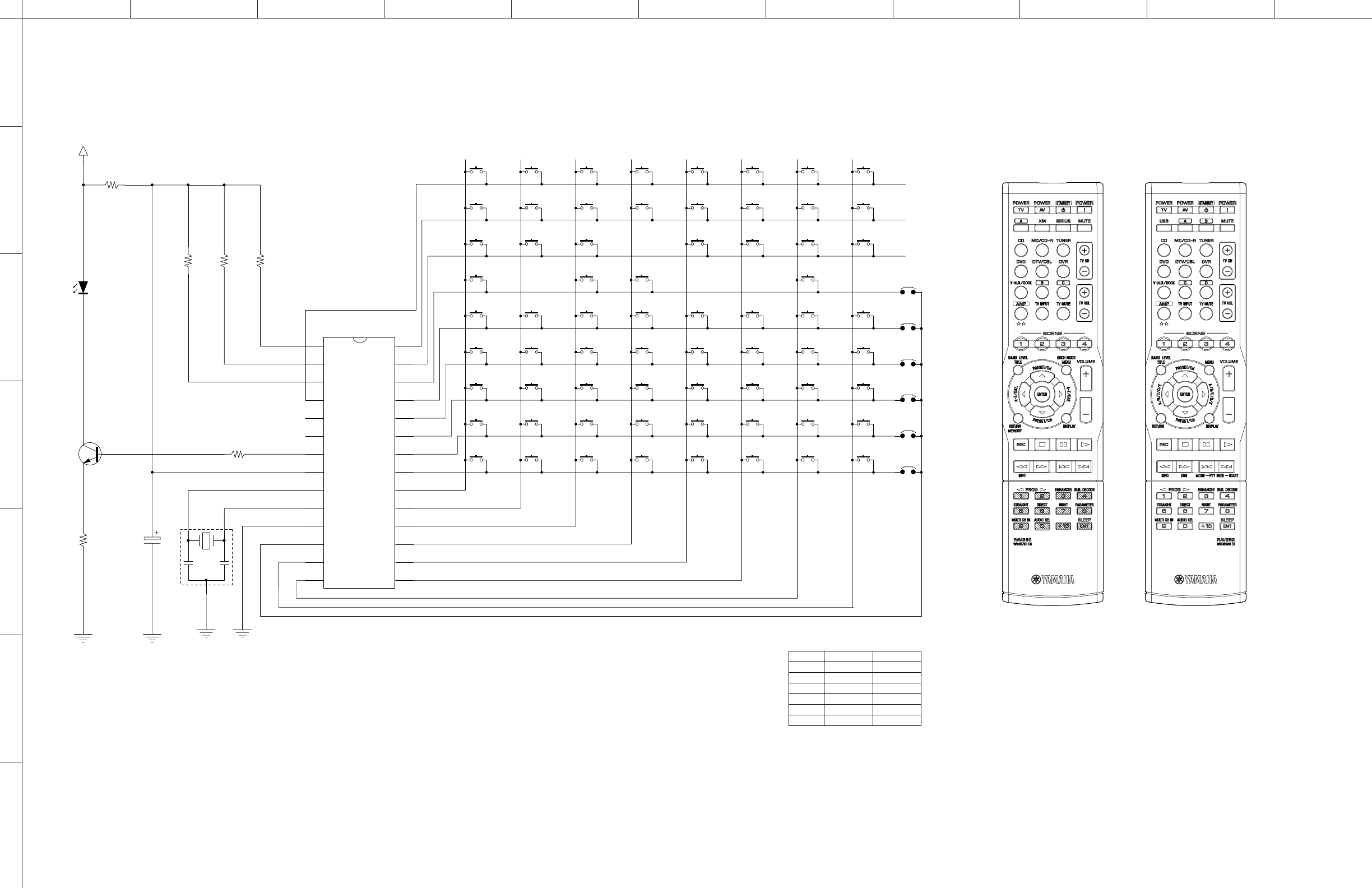
2
ABCDEFGH I J
1
3
4
5
7
RX-V563/HTR-6150/DSP-AX563
6
110
■REMOTE CONTROL
●RAV280 (U, C models), RAV282 (R, T, K, A, B, G, E, F, L models)
• SCHEMATIC DIAGRAM • PANELS
R2
47 ohms
R3
100 ohms
R4
100 k-ohms
R5
100 k-ohms
D1
IR diode
R1
1 ohm C1
47uF
Q1
SMT
P25
1
P26
2
P27
3
P04
4
VDD
8
XTAL2
9
XTAL1
10
P31
11
P32
12
P35
15
P05
5
P06
6
P07
7
P37
16
P36
17
P30/Pref
18
P00
19
P01
20
P02
21
VSS
22
P03
23
P20
24
P21
25
13
2
P22
26
P23
RAV280
O
X
X
X
X
X
J1
J2
J3
J4
J5
J6
RAV282
X
X
O
X
X
X
27
P24
28
P34
14
P33
13
U1
ZLR32300H2832G
+3V
J1
J2
R6
100 k-ohms
J3
J4
J5
J6
X1
8MHz
TV POWER A/USB AV POWER MUTE POWER SIRIUS/C STANDBY XM/B
DVD CD DTV/CBL TV CH + TV CH - TUNER DVR
C/D
MD/CD-R
V-AUX/DOCK AMP TV VOL -B/C TV VOL + TV MUTE TV INPUT
TITLE SCENE1 UP SCENE4 VOL up SCENE3 MENU SCENE2
5 9 6 8 ENTER +10 7 0
124 3
LEFT RETURN ENTER VOL down DISPLAY RIGHT DOWN
REW
(SEARCH -)
FF
(SEARCH +)
REC SKIP+ PLAY PAUSE SKIP- STOP
15284736
13 9 141216111510
17 21 18 24 20 23 19 22
29 25 30 28 32 27 31 26
52 56 53 55 59 58 54 57
44 40 45 47 43 42 46 41
64 60 65 67 63 62 66 61
33 36 34 39 38 35 37
48 49 51 50
RAV280
(U, C models)
RAV282
(R, T, K, A, B, G, E, F, L
models)
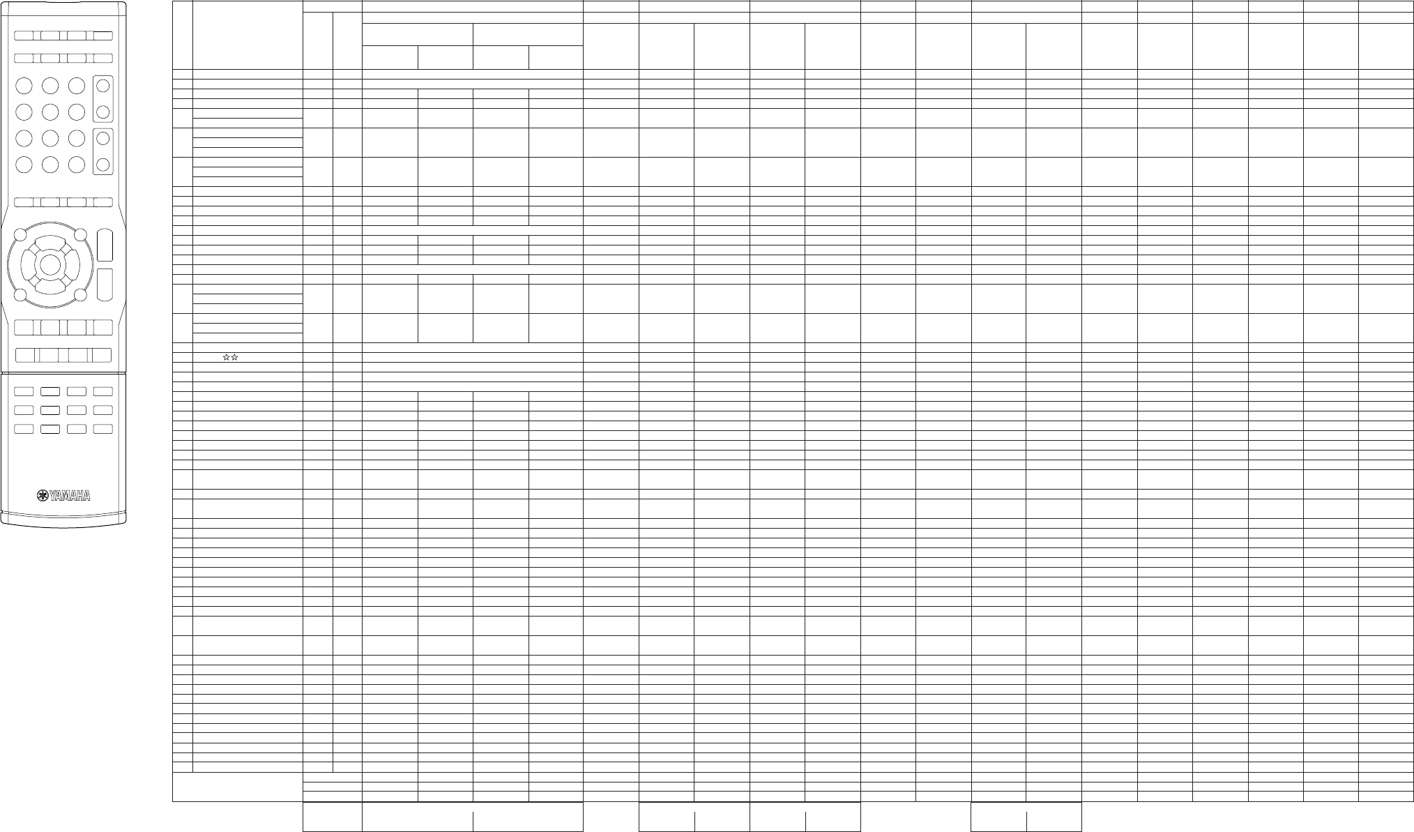
111
RX-V563/HTR-6150/DSP-AX563
K11
[TUNER]
(TV POWER)
7F01-D0
$$
$$
$
$$
$$
$
$$
$$
$
$$
$$
$
$$
$$
$
$$
$$
$
$$
$$
$
$$
$$
$
$$
$$
$
(TV CH +)
$$
$$
$
$$
$$
$
$$
$$
$
(TV CH -)
$$
$$
$
$$
$$
$
$$
$$
$
(TV VOL +)
(TV INPUT)
(TV MUTE)
(TV VOL-)
$$
$$
$
$$
$$
$
$$
$$
$
$$
$$
$
7F01-DD
7F01-E1
7F01-DE
$$
$$
$
7F01-E2
7F01-E3
7F01-E4
7F01-DF
7F01-E5
7F01-E0
$$
$$
$
7F01-E6
7F01-E9
7F01-E7
7F01-E8
7F01-EA
7F01-EB
7F01-EC
7F01-ED
7F01-D1
7F01-D2
7F01-D3
7F01-D4
7F01-D5
7F01-D6
7F01-D7
7F01-D8
7F01-D9
7F01-DA
7F01-DB
7F01-DC
TUNER
Yamaha-9
5017
• KEY LAYOUT
1234
5
9101112
16
20
24
13 14 15
17 18 19
21
25
29 31
30
37
33 35
32
39
34
36
40 41 42 43
47464544
48 49 50 51
52 53 54 55
56 57 58 59
38
26 27 28
22 23
678
•IR CODE
Label
Key
default
Common
ZONE2 code
K21
7E-7F
7E-7E
7F01-3F
7A-B4
7A-39
7A-1C
7A-15
7A-C9
7A-16
7A-C1
7A-54
7A-13
7A-55
7A-0F
7A-14
7A-007F
7A-037C
7A-0679
7A-0976
7A-86
7A-9D
7A-84
7A-1A
7A-9F
7A-DE
7A-9E
7A-AA
7A-9C
7A-C2
7A-1B
(device)
(device)
(device)
(device)
(device)
(device)
(device)
(device)
7A-59
7A-58
7A-94
7A-8D
7A-56
7A-DD
7A-95
7A-C4
7A-87
7A-C3
–
7A-57
AMP
Yamaha-1
5019
[AMP]
MAIN ZONE2
7E-BB
7E-BA
7F01-40
7A-B8
7A-3A
7A-DC
7A-D1
7A-CF
7A-D2
7A-CD
7A-D9
7A-D7
7A-D8
7A-D6
7A-D0
7A-017E
7A-047B
7A-0778
7A-0A75
7A-DA
7A-DB
–
–
–
Library
Brand
Preset number
setting
1
2
3
4
5
6
7
8
9
10
11
12
13
14
15
16
17
18
19
20
21
22
23
24
25
26
27
28
29
30
31
32
33
34
35
36
37
38
39
40
41
42
43
44
45
46
47
48
49
50
51
52
53
54
55
56
57
58
59
POWER_TV
POWER_AV
STANDBY
POWER
A (RAV280, RAV281)
USB (RAV282)
XM (RAV280)
B (RAV281)
A (RAV282)
SIRIUS (RAV280)
C (RAV281)
B (RAV282)
MUTE
CD
MD/CD-R
TUNER
TV CH +
DVD
DTV/CBL
DVR
TV CH –
V-AUX/DOCK
B (RAV280)
D (RAV281)
C (RAV282)
C (RAV281)
E (RAV282)
D (RAV283)
TV VOL +
AMP /
TV INPUT
TV MUTE
TV VOL –
SCENE_1
SCENE_2
SCENE_3
SCENE_4
BAND LEVEL / TITLE
PRESET/CH_ HH
HH
H (UP)
SRCH MODE / MENU
VOLUME +
A-E/CAT. / A/B/C/D/E
_ QQ
QQ
Q (LEFT)
ENTER
A-E/CAT. / A/B/C/D/E
_ WW
WW
W (RIGHT)
RETURN / MEMORY
PRESET/CH_ GG
GG
G (DOWN)
DISPLAY
VOLUME –
REC
AA
AA
A (STOP)
DD
DD
D (PAUSE)
WW
WW
W (PLAY)
EE
EE
E (REW)_INFO
RR
RR
R (FF)
TT
TT
T (SKIP –)
_PTY SEEK–MODE
YY
YY
Y (SKIP +)
_PTY SEEK–START
1_ QQ
QQ
Q PRG
2_PRG WW
WW
W
3_ENHANCER
4_SUR. DECODE
5_STRAIGHT
6_DIRECT
7_NIGHT
8_PARAMETER
9_MULTI CH IN
0_AUDIO SEL
+10
ENT_SLEEP
MAIN ZONE2
ID1 (default) ID2
7E-7F81
7E-7E80
7F01-3FC1
7A-B44A
7A-39C7
7A-1CE2
7A-15EB
7A-C937
7A-16E8
7A-C13F
7A-54AA
7A-13ED
7A-55AB
7A-0FF1
7A-14EA
7A-007E
7A-037D
7A-0678
7A-0977
7A-8678
7A-9D63
7A-847A
7A-1AE4
7A-9F61
7A-DE20
7A-9E60
7A-AA54
7A-9C62
7A-C23C
7A-1BE5
(device)
(device)
(device)
(device)
(device)
(device)
(device)
(device)
7A-59A7
7A-58A6
7A-946A
7A-8D73
7A-56A8
7A-DD23
7A-956B
7A-C43A
7A-8779
7A-C33D
–
7A-57A9
AMP
Yamaha-2
5020
7E-BB45
7E-BA44
7F01-40BE
7A-B846
7A-3AC4
7A-DC22
7A-D12F
7A-CF31
7A-D22C
7A-CD33
7A-D927
7A-D729
7A-D826
7A-D628
7A-D02E
7A-017F
7A-047A
7A-0779
7A-0A74
7A-DA24
7A-DB25
–
–
–
@@
@@
@
[5019]
@@
@@
@
[5020]
–
–
O
O
O
O
O
O
O
O
O
–
O
O
O
–
O
O
O
–
O
–
–
–
O
O
O
O
O
O
–
–
O
O
O
O
O
O
O
O
O
–
O
O
O
–
O
O
O
–
–
–
–
–
O
O
O
O
O
O
K5
[USB] RAV282
(TV POWER)
7F01-20
$$
$$
$
$$
$$
$
$$
$$
$
$$
$$
$
$$
$$
$
$$
$$
$
$$
$$
$
$$
$$
$
$$
$$
$
(TV CH +)
$$
$$
$
$$
$$
$
$$
$$
$
(TV CH -)
$$
$$
$
$$
$$
$
$$
$$
$
(TV VOL +)
(TV INPUT)
(TV MUTE)
(TV VOL-)
$$
$$
$
$$
$$
$
$$
$$
$
$$
$$
$
7F01-2D
7F01-2E
7F01-2F
$$
$$
$
7F01-30
7F01-31
7F01-32
7F01-33
7F01-34
7F01-35
$$
$$
$
7F01-36
7F01-3D
7F01-3A
7F01-3E
7F01-37
7F01-38
7F01-3B
7F01-3C
7F01-21
7F01-22
7F01-23
7F01-24
7F01-25
7F01-26
7F01-27
7F01-28
7F01-29
7F01-2A
7F01-2B
7F01-2C
TUNER
Yamaha-8
5012
K6
[XM] RAV280
(TV POWER)
–
$$
$$
$
$$
$$
$
$$
$$
$
$$
$$
$
$$
$$
$
$$
$$
$
$$
$$
$
$$
$$
$
$$
$$
$
(TV CH +)
$$
$$
$
$$
$$
$
$$
$$
$
(TV CH -)
$$
$$
$
$$
$$
$
$$
$$
$
(TV VOL +)
(TV INPUT)
(TV MUTE)
(TV VOL-)
$$
$$
$
$$
$$
$
$$
$$
$
$$
$$
$
7A-70
7A-6A
7A-6D
$$
$$
$
7A-6E
7A-6F
7A-6C
7A-71
7A-6B
7A-72
$$
$$
$
–
–
–
–
7A-3D
7A-3E
7A-3F
7A-EF
7A-61
7A-62
7A-63
7A-64
7A-65
7A-66
7A-67
7A-68
7A-69
7A-60
–
7A-BF
TUNER
Yamaha-5
5009
(TV POWER)
–
$$
$$
$
$$
$$
$
$$
$$
$
$$
$$
$
$$
$$
$
$$
$$
$
$$
$$
$
$$
$$
$
$$
$$
$
(TV CH +)
$$
$$
$
$$
$$
$
$$
$$
$
(TV CH -)
$$
$$
$
$$
$$
$
$$
$$
$
(TV VOL +)
(TV INPUT)
(TV MUTE)
(TV VOL-)
$$
$$
$
$$
$$
$
$$
$$
$
$$
$$
$
7A-708E
7A-6A94
7A-6D93
$$
$$
$
7A-6E90
7A-6F91
7A-6C92
7A-718F
7A-6B95
7A-728C
$$
$$
$
–
–
–
–
7A-3DC3
7A-3EC0
7A-3FC1
7A-EF11
7A-619F
7A-629C
7A-639D
7A-649A
7A-659B
7A-6698
7A-6799
7A-6896
7A-6997
7A-609E
–
7A-BF41
TUNER
Yamaha-11
5015
ID1
(default)
ID2
K7
[SIRIUS] RAV280
ID1
(default)
ID2
(TV POWER)
7F01-D02E
$$
$$
$
$$
$$
$
$$
$$
$
$$
$$
$
$$
$$
$
$$
$$
$
$$
$$
$
$$
$$
$
$$
$$
$
(TV CH +)
$$
$$
$
$$
$$
$
$$
$$
$
(TV CH -)
$$
$$
$
$$
$$
$
$$
$$
$
(TV VOL +)
(TV INPUT)
(TV MUTE)
(TV VOL-)
$$
$$
$
$$
$$
$
$$
$$
$
$$
$$
$
7F01-DD23
7F01-E11F
7F01-DE20
$$
$$
$
7F01-E21C
7F01-E31D
7F01-E41A
7F01-DF21
7F01-E51B
7F01-E01E
$$
$$
$
7F01-E618
7F01-E917
7F01-E719
7F01-E816
7F01-EA14
7F01-EB15
7F01-EC12
7F01-ED13
7F01-D12F
7F01-D22C
7F01-D32D
7F01-D42A
7F01-D52B
7F01-D628
7F01-D729
7F01-D826
7F01-D927
7F01-DA24
7F01-DB25
7F01-DC22
TUNER
Yamaha-10
5018
@@
@@
@
[5009]
@@
@@
@
[5015]
@@
@@
@
[5017]
@@
@@
@
[5018]
K9
[CD]
(TV POWER)
79-60
$$
$$
$
$$
$$
$
$$
$$
$
$$
$$
$
$$
$$
$
$$
$$
$
$$
$$
$
$$
$$
$
$$
$$
$
(TV CH +)
$$
$$
$
$$
$$
$
$$
$$
$
(TV CH -)
$$
$$
$
$$
$$
$
$$
$$
$
(TV VOL +)
(TV INPUT)
(TV MUTE)
(TV VOL-)
$$
$$
$
$$
$$
$
$$
$$
$
$$
$$
$
–
–
–
$$
$$
$
–
–
–
–
–
79-0A
$$
$$
$
7A-4F
7A-09
7A-09
7A-08
7A-0D
7A-0C
7A-0B
7A-0A
79-11
79-12
79-13
79-14
79-15
79-16
79-17
79-18
79-19
79-10
79-1A
79-0B
CD
Yamaha-1
5013
K10
[MD/CD-R]
(TV POWER)
7F-80
$$
$$
$
$$
$$
$
$$
$$
$
$$
$$
$
$$
$$
$
$$
$$
$
$$
$$
$
$$
$$
$
$$
$$
$
(TV CH +)
$$
$$
$
$$
$$
$
$$
$$
$
(TV CH -)
$$
$$
$
$$
$$
$
$$
$$
$
(TV VOL +)
(TV INPUT)
(TV MUTE)
(TV VOL-)
$$
$$
$
$$
$$
$
$$
$$
$
$$
$$
$
–
–
–
$$
$$
$
–
–
–
–
–
7F-9E
$$
$$
$
–
7F-84
7F-83
7F-82
7F-88
7F-89
7F-86
7F-87
7F-91
7F-92
7F-93
7F-94
7F-95
7F-96
7F-97
7F-98
7F-99
7F-90
7F-9A
7F-8A
CD-R
Yamaha
5001
(TV POWER)
D1-1B
$$
$$
$
$$
$$
$
$$
$$
$
$$
$$
$
$$
$$
$
$$
$$
$
$$
$$
$
$$
$$
$
$$
$$
$
(TV CH +)
$$
$$
$
$$
$$
$
$$
$$
$
(TV CH -)
$$
$$
$
$$
$$
$
$$
$$
$
(TV VOL +)
(TV INPUT)
(TV MUTE)
(TV VOL-)
$$
$$
$
$$
$$
$
$$
$$
$
$$
$$
$
7A-AE
7A-10
7A-AB
$$
$$
$
7A-AC
7A-AD
7A-12
7A-AF
7A-11
7A-B0
$$
$$
$
–
–
–
–
7A-A4
7A-A5
7A-A6
7A-A7
7A-E5
7A-E6
7A-E7
7A-E8
7A-E9
7A-EA
7A-EB
7A-EC
7A-B1
7A-B2
–
7A-B3
TUNER
Yamaha-3
5007
(TV POWER)
–
$$
$$
$
$$
$$
$
$$
$$
$
$$
$$
$
$$
$$
$
$$
$$
$
$$
$$
$
$$
$$
$
$$
$$
$
(TV CH +)
$$
$$
$
$$
$$
$
$$
$$
$
(TV CH -)
$$
$$
$
$$
$$
$
$$
$$
$
(TV VOL +)
(TV INPUT)
(TV MUTE)
(TV VOL-)
$$
$$
$
$$
$$
$
$$
$$
$
$$
$$
$
7A-AE50
7A-10EE
7A-AB55
$$
$$
$
7A-AC52
7A-AD53
7A-12EC
7A-AF51
7A-11EF
7A-B04E
$$
$$
$
–
–
–
–
7A-A45A
7A-A55B
7A-A658
7A-A759
7A-E51B
7A-E618
7A-E719
7A-E816
7A-E917
7A-EA14
7A-EB15
7A-EC12
7A-B14F
7A-B24C
–
7A-B34D
TUNER
Yamaha-12
5016
ID 1
(default)
ID2
@@
@@
@
[5007]
@@
@@
@
[5016]
K13
[DVD]
(TV POWER)
7C-80
$$
$$
$
$$
$$
$
$$
$$
$
$$
$$
$
$$
$$
$
$$
$$
$
$$
$$
$
$$
$$
$
$$
$$
$
(TV CH +)
$$
$$
$
$$
$$
$
$$
$$
$
(TV CH -)
$$
$$
$
$$
$$
$
$$
$$
$
(TV VOL +)
(TV INPUT)
(TV MUTE)
(TV VOL-)
$$
$$
$
$$
$$
$
$$
$$
$
$$
$$
$
7C-B1
7C-B4
7C-B2
$$
$$
$
7C-B5
7C-B8
7C-B6
7C-B7
7C-B3
7C-A6
$$
$$
$
7C-8B
7C-85
7C-83
7C-82
7C-86
7C-87
7C-B9
7C-BA
7C-94
7C-95
7C-96
7C-97
7C-98
7C-99
7C-9A
7C-9B
7C-9C
7C-93
7C-9D
7C-9E
DVD
Yamaha-1
2000
K14
[DVD/CBL]
TV POWER
(DVR POWER)
$$
$$
$
$$
$$
$
$$
$$
$
$$
$$
$
$$
$$
$
$$
$$
$
$$
$$
$
$$
$$
$
$$
$$
$
(TV CH +)
$$
$$
$
$$
$$
$
$$
$$
$
(TV CH -)
$$
$$
$
$$
$$
$
$$
$$
$
TV VOL +
TV INPUT
TV MUTE
TV VOL-
$$
$$
$
$$
$$
$
$$
$$
$
$$
$$
$
–
–
–
$$
$$
$
–
–
–
–
–
–
$$
$$
$
(DVR REC)
(DVR STOP)
(DVR PAUSE)
(DVR PLAY)
(DVR REW)
(DVR FF)
(DVR SKIP -)
(DVR SKIP +)
–
–
–
–
–
–
–
–
–
–
–
–
–
–
–
K15
[DVR]
(TV POWER)
048.012
$$
$$
$
$$
$$
$
$$
$$
$
$$
$$
$
$$
$$
$
$$
$$
$
$$
$$
$
$$
$$
$
$$
$$
$
TV CH +
$$
$$
$
$$
$$
$
$$
$$
$
TV CH -
$$
$$
$
$$
$$
$
$$
$$
$
(TV VOL +)
(TV INPUT)
(TV MUTE)
(TV VOL-)
$$
$$
$
$$
$$
$
$$
$$
$
$$
$$
$
048.200
048.088
048.084
$$
$$
$
048.090
048.092
048.091
048.131
048.089
048.015
$$
$$
$
048.055
048.049
048.048
048.044
048.041
048.040
048.033
048.032
048.001
048.002
048.003
048.004
048.005
048.006
048.007
048.008
048.009
048.000
–
–
DVR
Yamaha
2011
K17
[V-AUX]
(TV POWER)
7F01-00
$$
$$
$
$$
$$
$
$$
$$
$
$$
$$
$
$$
$$
$
$$
$$
$
$$
$$
$
$$
$$
$
$$
$$
$
(TV CH +)
$$
$$
$
$$
$$
$
$$
$$
$
(TV CH -)
$$
$$
$
$$
$$
$
$$
$$
$
(TV VOL +)
(TV INPUT)
(TV MUTE)
(TV VOL-)
$$
$$
$
$$
$$
$
$$
$$
$
$$
$$
$
7F01-0D
7F01-0E
7F01-0F
$$
$$
$
7F01-10
7F01-11
7F01-12
7F01-13
7F01-14
7F01-15
$$
$$
$
7F01-16
7F01-1D
7F01-1A
7F01-1E
7F01-17
7F01-18
7F01-1B
7F01-1C
7F01-01
7F01-02
7F01-03
7F01-04
7F01-05
7F01-06
7F01-07
7F01-08
7F01-09
7F01-0A
7F01-0B
7F01-0C
TUNER
Yamaha-7
5011
K18
[VCR]
(TV POWER)
–
$$
$$
$
$$
$$
$
$$
$$
$
$$
$$
$
$$
$$
$
$$
$$
$
$$
$$
$
$$
$$
$
$$
$$
$
(TV CH +)
$$
$$
$
$$
$$
$
$$
$$
$
(TV CH -)
$$
$$
$
$$
$$
$
$$
$$
$
(TV VOL +)
(TV INPUT)
(TV MUTE)
(TV VOL-)
$$
$$
$
$$
$$
$
$$
$$
$
$$
$$
$
–
–
–
$$
$$
$
–
–
–
–
–
–
$$
$$
$
–
–
–
–
–
–
–
–
–
–
–
–
–
–
–
–
–
–
–
–
–
–
–
TV POWER
(DVR POWER)
$$
$$
$
$$
$$
$
$$
$$
$
$$
$$
$
$$
$$
$
$$
$$
$
$$
$$
$
$$
$$
$
$$
$$
$
TV CH +
$$
$$
$
$$
$$
$
$$
$$
$
TV CH -
$$
$$
$
$$
$$
$
$$
$$
$
TV VOL +
TV INPUT
TV MUTE
TV VOL-
$$
$$
$
$$
$$
$
$$
$$
$
$$
$$
$
–
–
–
$$
$$
$
–
–
–
–
–
–
$$
$$
$
(DVR REC)
(DVR STOP)
(DVR PAUSE)
(DVR PLAY)
(DVR REW)
(DVR FF)
(DVR SKIP -)
(DVR SKIP +)
–
–
–
–
–
–
–
–
–
–
–
–
–
–
–
Key
no.
K19
[PHONO]
K7 [SIRIUS] + K2
(TV POWER)
(device)
(TV CH +)
(TV CH +)
(TV VOL +)
(TV INPUT)
(TV MUTE)
(TV VOL-)
K21 [AMP] + K2 [AV POWER] K6[XM] + K2 K11 [TUNER] + K2
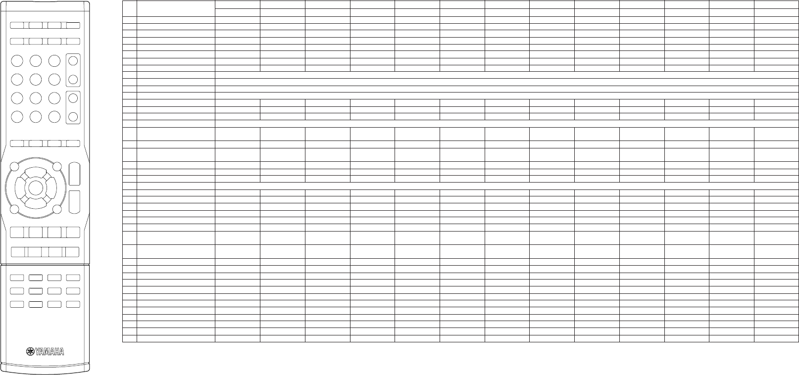
RX-V563/HTR-6150/DSP-AX563
112
•FUNCTION CHART
1
2
12
16
20
22
23
24
25
26
27
28
29
30
31
32
33
34
35
36
37
38
39
40
41
42
43
44
45
46
47
48
49
50
51
52
53
54
55
56
57
58
59
POWER_TV
POWER_AV
TV CH +
TV CH –
TV VOL +
TV INPUT
TV MUTE
TV VOL –
SCENE_1
SCENE_2
SCENE_3
SCENE_4
BAND LEVEL / TITLE
PRESET/CH_ HH
HH
H (UP)
SRCH MODE / MENU
VOLUME +
A-E/CAT. / A/B/C/D/E
_ QQ
QQ
Q (LEFT)
ENTER
A-E/CAT. / A/B/C/D/E
_ WW
WW
W (RIGHT)
RETURN / MEMORY
PRESET/CH_ GG
GG
G (DOWN)
DISPLAY
VOLUME –
REC
AA
AA
A (STOP)
DD
DD
D (PAUSE)
WW
WW
W (PLAY)
EE
EE
E (REW)_INFO
RR
RR
R (FF)
TT
TT
T (SKIP –)
_PTY SEEK–MODE
YY
YY
Y (SKIP +)
_PTY SEEK–START
1_ QQ
QQ
Q PRG
2_PRG WW
WW
W
3_ENHANCER
4_SUR. DECODE
5_STRAIGHT
6_DIRECT
7_NIGHT
8_PARAMETER
9_MULTI CH IN
0_AUDIO SEL
+10
ENT_SLEEP
(TV POWER)
(device)
(TV CH +)
(TV CH -)
(TV VOL +)
(TV INPUT)
(TV MUTE)
(TV VOL -)
LEVEL
MENU UP
MENU
MENU LEFT
MENU SELECT
MENU RIGHT
RETURN
MENU DOWN
SUB MENU
(device)
(device)
(device)
(device)
(device)
(device)
(device)
(device)
PROG (-)
PROG (+)
ENHANCER
SUR.DECODE
STRAIGHT
(PURE) DIRECT
NIGHT
PARAMENTER
MULTI CH IN
AUDIO SEL
–
SLEEP
(TV POWER)
POWER
(TV CH +)
(TV CH -)
(TV VOL +)
(TV INPUT)
(TV MUTE)
(TV VOL -)
TITLE
UP
MENU
LEFT
ENTER
RIGHT
RETURN
DOWN
DISPLAY
–
STOP
PAUSE
PLAY
–
–
SKIP (-)
SKIP (+)
P1
P2
P3
P4
P5
P6
P7
P8
P9
P10
–
P.ENTER
(TV POWER)
POWER
(TV CH +)
(TV CH -)
(TV VOL +)
(TV INPUT)
(TV MUTE)
(TV VOL -)
BAND
PRESET (+)
SRCH MODE
A-E/CAT. (-)
ENTER
A-E/CAT. (+)
MEMORY
PRESET (-)
DISPLAY
–
–
–
–
INFO
EON
PTY MODE
PTY START
P1
P2
P3
P4
P5
P6
P7
P8
P9
P0
–
P.ENTER
(TV POWER)
POWER
(TV CH +)
(TV CH -)
(TV VOL +)
(TV INPUT)
(TV MUTE)
(TV VOL -)
TITLE
UP
SRCH MODE
LEFT
ENTER
RIGHT
MEMORY
DOWN
DISPLAY
REC
STOP
PAUSE
PLAY
REW
FF
SKIP (-)
SKIP (+)
1
2
3
4
5
6
7
8
9
10
11
12
(TV POWER)
POWER
(TV CH +)
(TV CH -)
(TV VOL +)
(TV INPUT)
(TV MUTE)
(TV VOL -)
–
–
–
–
–
–
–
–
DISPLAY
DISC SKIP
STOP
PAUSE
PLAY
REW
FF
SKIP (-)
SKIP (+)
1
2
3
4
5
6
7
8
9
0/10
+10
INDEX
(TV POWER)
POWER
(TV CH +)
(TV CH -)
(TV VOL +)
(TV INPUT)
(TV MUTE)
(TV VOL -)
–
–
–
–
-
–
–
–
DISPLAY
REC
STOP
PAUSE
PLAY
REW
FF
SKIP (-)
SKIP (+)
1
2
3
4
5
6
7
8
9
0/10
+10
INDEX
(TV POWER)
POWER
(TV CH +)
(TV CH -)
(TV VOL +)
(TV INPUT)
(TV MUTE)
(TV VOL -)
BAND
PRESET (+)
SRCH MODE
A-E/CAT. (-)
ENTER
A-E/CAT. (+)
MEMORY
PRESET (-)
DISPLAY
–
–
–
–
INFO
EON
PTY MODE
PTY START
P1
P2
P3
P4
P5
P6
P7
P8
P9
P0
–
P.ENTER
(TV POWER)
POWER
(TV CH +)
(TV CH -)
(TV VOL +)
(TV INPUT)
(TV MUTE)
(TV VOL -)
TITLE
MENU UP
MENU
MENU LEFT
MENU ENTER
MENU RIGHT
RETURN
MENU DOWN
DISPLAY
DISC SKIP
STOP
PAUSE
PLAY
REW
FF
SKIP (-)
SKIP (+)
1
2
3
4
5
6
7
8
9
0
+10
TITLE/INDEX
TV POWER
(DVR POWER)
(TV CH +)
(TV CH -)
(TV VOL +)
(TV INPUT)
(TV MUTE)
(TV VOL -)
TITLE
MENU UP
MENU
MENU LEFT
MENU ENTER
MENU RIGHT
RETURN
MENU DOWN
DISPLAY
(DVR REC)
(DVR STOP)
(DVR PAUSE)
(DVR PLAY)
(DVR REW)
(DVR FF)
(DVR SKIP -)
(DVR SKIP +)
1
2
3
4
5
6
7
8
9
0/10
_/_ _,11
ENTER/12
(TV POWER)
POWER
(TV CH +)
(TV CH -)
(TV VOL +)
(TV INPUT)
(TV MUTE)
(TV VOL -)
TITLE
MENU UP
MENU
MENU LEFT
MENU ENTER
MENU RIGHT
RETURN
MENU DOWN
DISPLAY
REC
STOP
PAUSE
PLAY
REW
FF
SKIP (-)
SKIP (+)
1
2
3
4
5
6
7
8
9
0
+10
TITLE/INDEX
(TV POWER)
POWER
(TV CH +)
(TV CH -)
(TV VOL +)
(TV INPUT)
(TV MUTE)
(TV VOL -)
BAND
PRESET (+)
SRCH MODE
A-E/CAT. (-)
ENTER
A-E/CAT. (+)
MEMORY
PRESET (-)
DISPLAY
–
–
–
–
INFO
EON
PTY MODE
PTY START
P1
P2
P3
P4
P5
P6
P7
P8
P9
P0
–
P.ENTER
(TV POWER)
POWER
(TV CH +)
(TV CH -)
(TV VOL +)
(TV INPUT)
(TV MUTE)
(TV VOL -)
TITLE
–
–
–
–
–
RETURN
–
–
REC
STOP
PAUSE
PLAY
REW
FF
–
–
1
2
3
4
5
6
7
8
9
0/10
>10
ENTER
TV POWER
(DVR POWER)
(TV CH +)
(TV CH -)
(TV VOL +)
(TV INPUT)
(TV MUTE)
(TV VOL -)
TITLE
MENU UP
MENU
MENU LEFT
MENU ENTER
MENU RIGHT
RETURN
MENU DOWN
DISPLAY
(DVR REC)
(DVR STOP)
(DVR PAUSE)
(DVR PLAY)
(DVR REW)
(DVR FF)
(DVR SKIP -)
(DVR SKIP +)
1
2
3
4
5
6
7
8
9
0/10
_/_ _,11
ENTER/12
K21
[AMP]
K5
[USB] RAV282
K6
[XM] RAV280
K7
[SIRIUS] RAV280
K9
[CD]
K10
[MD/CD-R]
K11
[TUNER]
K13
[DVD]
K14
[DTV/CBL]
K15
[DVR]
K17
[V-AUX]
K18
[VCR]
K19
[PHONO]
Label
Key
no.
1234
5
9101112
16
20
24
13 14 15
17 18 19
21
25
29 31
30
37
33 35
32
39
34
36
40 41 42 43
47464544
48 49 50 51
52 53 54 55
56 57 58 59
38
26 27 28
22 23
678
SCENE 1
SCENE 2
SCENE 3
SCENE 4
VOLUME (+)
VOLUME (-)
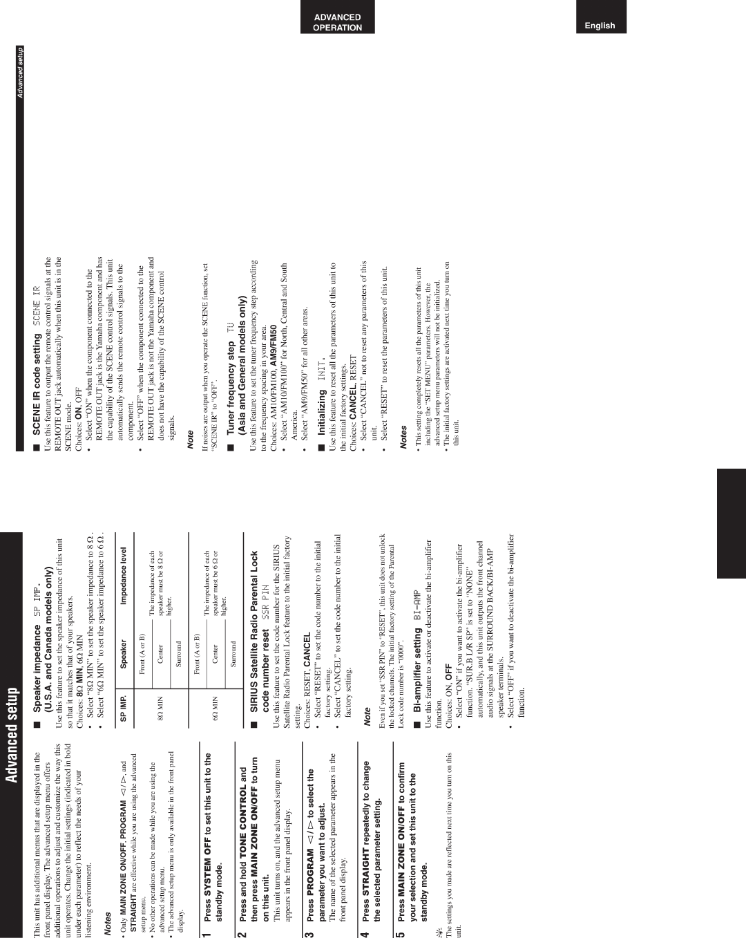
113
RX-V563/HTR-6150/DSP-AX563
RX-V563/HTR-6150/
DSP-AX563

RX-V563/HTR-6150/
DSP-AX563
