S32K1XXSM, S32K1xx Series Safety Manual Manual(REV 4)
S32K1xx-safety-manual
User Manual:
Open the PDF directly: View PDF ![]() .
.
Page Count: 101 [warning: Documents this large are best viewed by clicking the View PDF Link!]
- S32K1XX Safety Manual
- Contents
- Chapter 1: Preface
- Chapter 2: MCU Safety Context
- Chapter 3: MCU Safety Concept
- Chapter 4: Hardware Requirements
- Chapter 5: Software Requirements
- Software requirements on system level
- Power
- Clock
- Flash
- SRAM
- Processing modules
- Cortex-M4/M0+ Structural Core Self Test (SCST)
- Disabled modes of operation
- Additional configuration information
- Crossbar Switch (AXBS-Lite)
- Memory protection unit
- Nested Vectored Interrupt Controller (NVIC)
- Enhanced Direct Memory Access (eDMA)
- Reset Control Module (RCM)
- Watchdog timer (WDOG)
- Low power periodic interrupt timer (LPIT)
- Low Power Mode Monitoring
- Cyclic Redundancy Check (CRC)
- Error reporting path tests
- Peripheral
- Communications
- I/O functions
- PBRIDGE protection
- Analog to Digital Converter (ADC)
- Asynchronous Wake-up Interrupt Controller (AWIC) / External NMI
- Chapter 6: Failure Rates and FMEDA
- Chapter 7: Dependent Failures
- Chapter 8: Acronyms and Abbreviations
- Appendix A: Release Notes for Revision 4
- Contents

S32K1xx Series Safety Manual
Supports S32K116, S32K118, S32K142, S32K144, S32K146, and
S32K148
Document Number: S32K1XXSM
Rev. 4, 09/2018

S32K1xx Series Safety Manual, Rev. 4, 09/2018
2 NXP Semiconductors

Contents
Section number Title Page
Chapter 1
Preface
1.1 Overview.......................................................................................................................................................................... 9
1.2 Safety manual assumptions.............................................................................................................................................. 9
1.3 Safety manual guidelines..................................................................................................................................................10
1.4 Functional safety standards.............................................................................................................................................. 10
1.5 Related documentation..................................................................................................................................................... 11
1.6 Other considerations.........................................................................................................................................................11
Chapter 2
MCU Safety Context
2.1 Target applications........................................................................................................................................................... 13
2.2 Safety integrity level.........................................................................................................................................................14
2.3 Safety function..................................................................................................................................................................14
2.3.1 MCU safety functions..........................................................................................................................................14
2.3.2 Correct operation................................................................................................................................................. 15
2.4 Safe states......................................................................................................................................................................... 15
2.4.1 MCU Safe state....................................................................................................................................................15
2.4.2 Transitions to Safe statesystem............................................................................................................................16
2.4.3 Continuous reset transitions.................................................................................................................................16
2.5 Faults and failures.............................................................................................................................................................17
2.5.1 Faults....................................................................................................................................................................17
2.5.2 Dependent failures...............................................................................................................................................19
2.6 Single-point fault tolerant time interval and process safety time.....................................................................................21
2.6.1 MCU fault indication time ..................................................................................................................................22
2.7 Latent-fault tolerant time interval for latent faults........................................................................................................... 22
2.7.1 MCU fault indication time...................................................................................................................................23
2.8 MCU Failure Indication................................................................................................................................................... 24
2.8.1 Failure handling...................................................................................................................................................24
S32K1xx Series Safety Manual, Rev. 4, 09/2018
NXP Semiconductors 3

Section number Title Page
Chapter 3
MCU Safety Concept
3.1 General concept................................................................................................................................................................25
3.2 ECC.................................................................................................................................................................................. 28
3.2.1 ECC for storage................................................................................................................................................... 28
3.2.2 ECC failure handling........................................................................................................................................... 28
3.3 Clock and power monitoring............................................................................................................................................29
3.3.1 Clock....................................................................................................................................................................29
3.3.2 Power................................................................................................................................................................... 29
3.4 Operational interference protection..................................................................................................................................29
Chapter 4
Hardware Requirements
4.1 Hardware requirements on system level...........................................................................................................................31
4.1.1 Assumed functions by separate circuitry.............................................................................................................32
4.1.1.1 High impedance outputs...................................................................................................................... 32
4.1.1.2 Reset.................................................................................................................................................... 33
4.1.1.3 Power Supply Monitoring....................................................................................................................33
4.1.1.4 Error Monitoring..................................................................................................................................34
Chapter 5
Software Requirements
5.1 Software requirements on system level............................................................................................................................35
5.2 Power................................................................................................................................................................................35
5.2.1 Power Management Controller (PMC)................................................................................................................35
5.2.1.1 3.3 V supply supervision..................................................................................................................... 36
5.3 Clock.................................................................................................................................................................................36
5.3.1 System Phase-locked loop (SPLL) Available in S32K14x variants only ...........................................................36
5.3.1.1 Initial checks and configurations.........................................................................................................37
5.3.2 Clock Monitor Unit (CMU)Available in S32K11x variants only ...................................................................... 38
5.3.2.1 Initial checks and configurations ........................................................................................................38
5.3.3 Clock Monitor for devices with SPLL.................................................................................................................39
S32K1xx Series Safety Manual, Rev. 4, 09/2018
4 NXP Semiconductors

Section number Title Page
5.3.3.1 Initial checks and configurations.........................................................................................................40
5.3.4 System Oscillator Clock (SOSC).........................................................................................................................41
5.3.4.1 Initial checks and configurations.........................................................................................................41
5.3.4.2 Runtime checks....................................................................................................................................41
5.3.5 Internal RC oscillators......................................................................................................................................... 41
5.3.5.1 Initial checks and configurations.........................................................................................................42
5.3.5.2 Runtime checks....................................................................................................................................43
5.4 Flash................................................................................................................................................................................. 43
5.4.1 Flash memory...................................................................................................................................................... 43
5.4.1.1 EEPROM............................................................................................................................................. 43
5.4.1.2 Runtime checks....................................................................................................................................44
5.4.1.3 Security................................................................................................................................................45
5.5 SRAM...............................................................................................................................................................................45
5.5.1 Error Correction Code (ECC)..............................................................................................................................46
5.6 Processing modules.......................................................................................................................................................... 46
5.6.1 Cortex-M4/M0+ Structural Core Self Test (SCST) ........................................................................................... 46
5.6.2 Disabled modes of operation............................................................................................................................... 47
5.6.2.1 Debug mode.........................................................................................................................................47
5.6.3 Additional configuration information..................................................................................................................48
5.6.3.1 Stack.................................................................................................................................................... 48
5.6.3.2 S32K1xx configuration........................................................................................................................49
5.6.4 Crossbar Switch (AXBS-Lite).............................................................................................................................50
5.6.4.1 Runtime checks....................................................................................................................................50
5.6.5 Memory protection unit....................................................................................................................................... 50
5.6.5.1 Memory Protection Unit (MPU)..........................................................................................................51
5.6.5.2 Initial checks and configurations.........................................................................................................51
5.6.6 Nested Vectored Interrupt Controller (NVIC).....................................................................................................51
5.6.6.1 Periodic low latency IRQs...................................................................................................................52
5.6.6.2 Runtime checks....................................................................................................................................52
S32K1xx Series Safety Manual, Rev. 4, 09/2018
NXP Semiconductors 5

Section number Title Page
5.6.7 Enhanced Direct Memory Access (eDMA).........................................................................................................52
5.6.7.1 Runtime checks....................................................................................................................................53
5.6.8 Reset Control Module (RCM)............................................................................................................................. 54
5.6.8.1 Initial checks and configurations.........................................................................................................54
5.6.9 Watchdog timer (WDOG)................................................................................................................................... 54
5.6.9.1 Run-time checks.................................................................................................................................. 56
5.6.9.2 Fast testing of the watchdog................................................................................................................ 56
5.6.10 Low power periodic interrupt timer (LPIT).........................................................................................................56
5.6.10.1 Runtime checks....................................................................................................................................56
5.6.11 Low Power Mode Monitoring............................................................................................................................. 56
5.6.12 Cyclic Redundancy Check (CRC).......................................................................................................................57
5.6.12.1 Runtime checks....................................................................................................................................57
5.6.13 Error reporting path tests..................................................................................................................................... 59
5.7 Peripheral..........................................................................................................................................................................59
5.7.1 Communications..................................................................................................................................................59
5.7.1.1 Diversity of system resources and redundant communications...........................................................60
5.7.1.2 Fault-tolerant communication protocol............................................................................................... 61
5.7.2 I/O functions........................................................................................................................................................ 62
5.7.2.1 Digital inputs....................................................................................................................................... 63
5.7.2.2 Digital outputs..................................................................................................................................... 69
5.7.2.3 Analog inputs.......................................................................................................................................80
5.7.2.4 Other requirements.............................................................................................................................. 87
5.7.3 PBRIDGE protection...........................................................................................................................................87
5.7.3.1 Initial checks and configurations.........................................................................................................88
5.7.4 Analog to Digital Converter (ADC).................................................................................................................... 88
5.7.4.1 Initial checks and configurations.........................................................................................................88
5.7.5 Asynchronous Wake-up Interrupt Controller (AWIC) / External NMI.............................................................. 89
Chapter 6
Failure Rates and FMEDA
S32K1xx Series Safety Manual, Rev. 4, 09/2018
6 NXP Semiconductors

Section number Title Page
6.1 Failure rates...................................................................................................................................................................... 91
6.2 FMEDA............................................................................................................................................................................ 91
6.2.1 Module classification...........................................................................................................................................92
Chapter 7
Dependent Failures
7.1 Provisions against dependent failures.............................................................................................................................. 93
7.1.1 Causes of dependent failures............................................................................................................................... 93
7.1.2 Measures against dependent failures................................................................................................................... 94
7.1.2.1 Environmental conditions....................................................................................................................94
7.1.2.2 Failures of common signals.................................................................................................................94
7.1.3 Dependent failure avoidance on system level..................................................................................................... 94
7.1.3.1 I/O pin/ball configuration.................................................................................................................... 95
7.1.4 βIC considerations...............................................................................................................................................95
Chapter 8
Acronyms and Abbreviations
8.1 Acronyms and abbreviations............................................................................................................................................ 97
S32K1xx Series Safety Manual, Rev. 4, 09/2018
NXP Semiconductors 7

S32K1xx Series Safety Manual, Rev. 4, 09/2018
8 NXP Semiconductors

Chapter 1
Preface
1.1 Overview
This document discusses requirements for the integration and use of the S32K1xx
Microcontroller Unit (MCU) in safety-related systems. It is intended to support safety
system developers in building their safety-related systems using the safety mechanisms of
the S32K1xx, and describes the system level hardware or software safety measures that
should be implemented to achieve the desired system level of functional safety integrity.
The S32K1xx is developed according to ISO 26262 and has an integrated safety concept.
1.2 Safety manual assumptions
During the development of the S32K1xx, assumptions were made on the system level
safety requirements with regards to the MCU. During the system level development, the
safety system developer is required to establish the validity of the MCU assumptions in
the context of the specific safety-related system. To enable this, all relevant MCU
assumptions are published in the Safety Manual and can be identified as follows:
•Assumption: An assumption that is relevant for functional safety in the specific
safety system. It is assumed that the safety system developer fulfills an assumption in
the design.
•Assumption under certain conditions: An assumption that is relevant under certain
conditions. If the associated condition is met, it is assumed that the safety system
developer fulfills the assumption in the design.
Example: Assumption: It is assumed that the system is designed to go into a safe state
(Safe statesystem) when the safe state of the MCU (Safe stateMCU) is entered.
Example: Assumption under certain conditions: If a high impedance state on an output
is not safe, pull-up or pull-down resistors shall be added to safety-critical outputs. The
need for this will be application dependent for the unpowered or reset condition (tristated
I/O) of the S32K1xx.
S32K1xx Series Safety Manual, Rev. 4, 09/2018
NXP Semiconductors 9

The safety system developer will need to use discretion in deciding whether these
assumptions are valid for their particular safety-related system. In the case where an
MCU assumption does not hold true, the safety system developer should initiate a change
management activity beginning with impact analysis. For example, if a specific
assumption is not fulfilled, an alternate implementation should be shown to be similarly
effective at meeting the functional safety requirement in question (for example, the same
level of diagnostic coverage is achieved, the likelihood of dependent failures are similarly
low, and so on). If the alternative implementation is shown to be not as effective, the
estimation of an increased failure rate and reduced metrics (SFF: Safe Failure Fraction,
SPFM: Single-Point Fault Metrics, LFM: Latent Fault Metric) due to the deviation must
be specified. The FMEDA can be used to help make this analysis.
1.3 Safety manual guidelines
This document also contains guidelines on how to configure and operate the S32K1xx in
safety-related systems. These guidelines are preceded by one of the following text
statements:
•Recommendation: A recommendation is either a proposal for the implementation of
an assumption, or a reasonable measure which is recommended to be applied, if there
is no assumption in place. The safety system developer has the choice whether or not
to adhere to the recommendation.
•Rationale: The motivation for a specific assumption and/or recommendation.
•Implementation hint: An implementation hint gives specific details on the
implementation of an assumption and/or recommendation on the S32K1xx. The
safety system developer has an option to follow the implementation hint.
The safety system developer will need to use discretion in deciding whether these
guidelines are appropriate for their particular safety-related system.
1.4 Functional safety standards
It is assumed that the user of this document is familiar with the functional safety
standards ISO 26262 Road vehicles - Functional safety and IEC 61508 Functional safety
of electrical/electronic/programmable electronic safety-related systems. The S32K1xx is
a component as seen in the context of ISO 26262 and in this case its development is
completely decoupled from the development of an item or system. Therefore the
development of the S32K1xx is considered a Safety Element out of Context (SEooC)
development, as described in ISO 26262-10.9 Safety element out of context and more
Safety manual guidelines
S32K1xx Series Safety Manual, Rev. 4, 09/2018
10 NXP Semiconductors

specifically detailed in ISO 26262-10.9.2.3 Development of a hardware component as a
safety element out of context and ISO 26262-10 Annex A ISO 26262 and
microcontrollers.
1.5 Related documentation
The S32K1xx is developed according to ISO 26262 and has an integrated safety concept
targeting safety-related systems requiring high safety integrity levels. In order to support
the integration of the S32K1xx into safety-related systems, the following documentation
will be available:
• Reference Manual - Describes the S32K1xx functionality
• Data Sheet - Describes the S32K1xx operating conditions
• Safety Manual - Describes the S32K1xx safety concept and possible safety
mechanisms (integrated in S32K1xx, system level hardware or system level
software), as well as measures to reduce dependent failures
• FMEDA - Inductive analysis enabling customization of system level safety
mechanisms, including the resulting safety metrics for ISO 26262 (SPFM, LFM and
PMHF) and IEC 61508 (SFF and β-factor βIC)
• FMEDA Report - Describes the FMEDA methodology and safety mechanisms
supported in the FMEDA, including source of failure rates, failure modes and
assumptions made during the analysis.
The FMEDA and FMEDA report are available upon request. The S32K1xx is a
SafeAssure solution; for further information regarding functional safety at NXP, visit
www.nxp.com/safeassure.
1.6 Other considerations
When developing a safety-related system using the S32K1xx, the following information
should be considered:
• The S32K1xx is handled in accordance with JEDEC standards J-STD-020 and J-
STD-033.
• The operating conditions given in the S32K1xx Data Sheet.
• If applicable, any published S32K1xx errata.
• The recommended production conditions given in the S32K1xx quality agreement.
• The safety system developer is required to report all field failures of the S32K1xx to
NXP.
Chapter 1 Preface
S32K1xx Series Safety Manual, Rev. 4, 09/2018
NXP Semiconductors 11

As with any technical documentation, it is the reader’s responsibility to ensure he or she
is using the most recent version of the documentation.
Other considerations
S32K1xx Series Safety Manual, Rev. 4, 09/2018
12 NXP Semiconductors

Chapter 2
MCU Safety Context
2.1 Target applications
As a SafeAssure solution, the microcontroller targets applications requiring an
Automotive Safety Integrity Level (ASIL), especially:
• Automotive - The S32K product family consists of general purpose MCUs which can
fit a wide range of automotive applications, such as
• BCM
• Gateway
• Infotainment Connection Module
• Park Assistance
• Electronic Park Brake
• TPMS
• Battery Management
• Passive Keyless Push Start
• Lighting
• HVAC
• Window Lift
• Door Control Unit
• Sunroof Control Unit
• Wiper Control Unit
• DC/BLDC Motor Control
• Industrial - This family can also be used in general-purpose industrial applications
which require 125°C ambient temperature grade.
All devices in this family are built around an integrated safety concept targeting
ISO26262 ASIL-B.
S32K1xx Series Safety Manual, Rev. 4, 09/2018
NXP Semiconductors 13

2.2 Safety integrity level
The S32K1xx is designed to be used in automotive, or industrial, applications which need
to fulfill functional safety requirements as defined by functional safety integrity levels
(for example, ASIL B of ISO 26262 or SIL 2 of IEC 61508). The S32K1xx is a
component as seen in the context of ISO 26262 and in this case its development is
completely decoupled from the development of an item or system. Therefore the
development of the S32K1xx is considered a Safety Element out of Context (SEooC)
development.
The S32K1xx is seen as a Type B subsystem in the context of IEC 61508 (“complex,”
see IEC 61508-2, section 7.4.4.1.3) with a HFT = 0 (Hardware Fault Tolerance) and may
be used in any mode of operation (see IEC 61508-4, section 3.5.16).
2.3 Safety function
2.3.1 MCU safety functions
Given the application independent nature of the S32K1xx, no specific safety function can
be specified. Therefore, during the SEooC development of the S32K1xx, MCU safety
functions were assumed. During the development of the safety-related system, the MCU
safety functions are mapped to the specific system safety functions (application
dependent). The assumed MCU safety functions are:
•Software Execution Function (Application Independent): Read instructions out of
the S32K flash memory, buffer these within instruction cache (if supported), execute
instructions, read data from the S32K System SRAM or flash memory, buffer these
in data cache (if supported), process data and write result data into S32K System
SRAM. Functional safety of the Software Execution Function is primarily
achieved by safety mechanisms integrated on the S32K.
Moreover, the following approach is assumed for Input / Output related functions and
debug functions:
Safety integrity level
S32K1xx Series Safety Manual, Rev. 4, 09/2018
14 NXP Semiconductors

•Input / Output Functions (Application dependent): Input / Output functions of the
S32K1xx have a high application dependency. Functional safety will be primarily
achieved by system level safety measures.
•Not Safety Related Functions: It is assumed that some functions are Not Safety
Related (e.g. debug).
Please see the Module classification section for further details.
2.3.2 Correct operation
Correct operation of the S32K1xx is defined as:
•MCU Safety Function and Safety Mechanism modules are operating according to
specification.
•Peripheral modules are usable by qualifying data with system level safety measures
or by using modules redundantly. Qualification should have a low risk of dependent
failures. In general, Peripheral module safety measures are implemented in system
level software.
•Not Safety Related modules are not interfering with the operation of other modules.
2.4 Safe states
A safe state of the system is named Safe statesystem, whereas a safe state of the S32K1xx
is named Safe stateMCU. A Safe statesystem is an operating mode without an unreasonable
probability of occurrence of physical injury or damage to the health of any persons. A
Safe statesystem may be the intended operating mode or a mode where the system has been
disabled.
Assumption: [SM_200] It is assumed that the system is able to manage its safe state
(Safe statesystem) behavior when the safe state of the MCU (Safe stateMCU) is entered.
[end]
2.4.1 MCU Safe state
The safe states (Safe stateMCU) of the S32K1xx are:
Chapter 2 MCU Safety Context
S32K1xx Series Safety Manual, Rev. 4, 09/2018
NXP Semiconductors 15
• Operating correctly (see Figure 2-1 and section "Correct operation")
• In reset (see Figure 2-1)
• Completely unpowered (see Figure 2-1)
communication
input
element
correct output
correct
a) Correct operation
b) Reset
wrong
communication
input
element
wrong output
RESET
c) Completely unpowered
input
element
wrong
output
wrong
communication
Figure 2-1. Safe stateMCU of S32K1xx
2.4.2 Transitions to Safe statesystem
Assumption: [SM_016] The system transitions itself to a Safe statesystem when the MCU
is in a reset state. [end]
Assumption: [SM_017] The system transitions itself to a Safe statesystem when the MCU
is unpowered. [end]
Assumption: [SM_018] The system transitions itself to a Safe statesystem when the MCU
has no active output (for example, tristate). [end]
Rationale: If there is not active output from MCU to the external environment, the state
of the MCU is unknown. In such a case the whole system shall be put to Safe statesystem
which needs to be done on the system level.
2.4.3 Continuous reset transitions
If a system continuously switches between a standard operating state and the reset state,
without any device shutdown, it is not considered to be in a Safe state.
Safe states
S32K1xx Series Safety Manual, Rev. 4, 09/2018
16 NXP Semiconductors

Assumption: [SM_019] It is assumed that the application identifies, and signals,
continuous switching between reset and standard operating mode as a failure
condition. [end]
2.5 Faults and failures
Failures are the main detrimental impact to functional safety:
• A systematic failure is manifested in a deterministic way to a certain cause
(systematic fault), that can only be eliminated by a change of the design process,
manufacturing process, operational procedures, documentation, or other relevant
factors. Thus, measures against systematic faults can reduce systematic failures (for
example, implementing and following adequate processes).
• A random hardware failure can occur unpredictably during the lifetime of a hardware
element and follows a probability distribution. A reduction in the inherent failure rate
of the hardware will reduce the likelihood of random hardware faults to occur.
Detection and control will mitigate the effects of random hardware faults when they
do occur. A random hardware failure is caused by a permanent fault (for example,
physical damage), an intermittent fault, or a transient fault. Permanent faults are
unrecoverable. Intermittent faults are, for example, faults linked to specific
operational conditions, or noise. Transient faults are, for example, particles (alpha,
neutron) or EMI-radiation. An affected configuration register can be recovered by
setting the desired value or by power cycling. Due to a transient fault, an element
may be switched into a self destructive state (for example, single event latch up), and
therefore may cause permanent destruction.
•Assumption: [SM_020] The minimum number of random hardware faults causing
the loss of correct operation is assumed to be 1. Hardware Fault Tolerance (HFT) is
assumed to be 0 for the MCU. The MCU is designed to be fail-silent or fail-indicate.
[end]
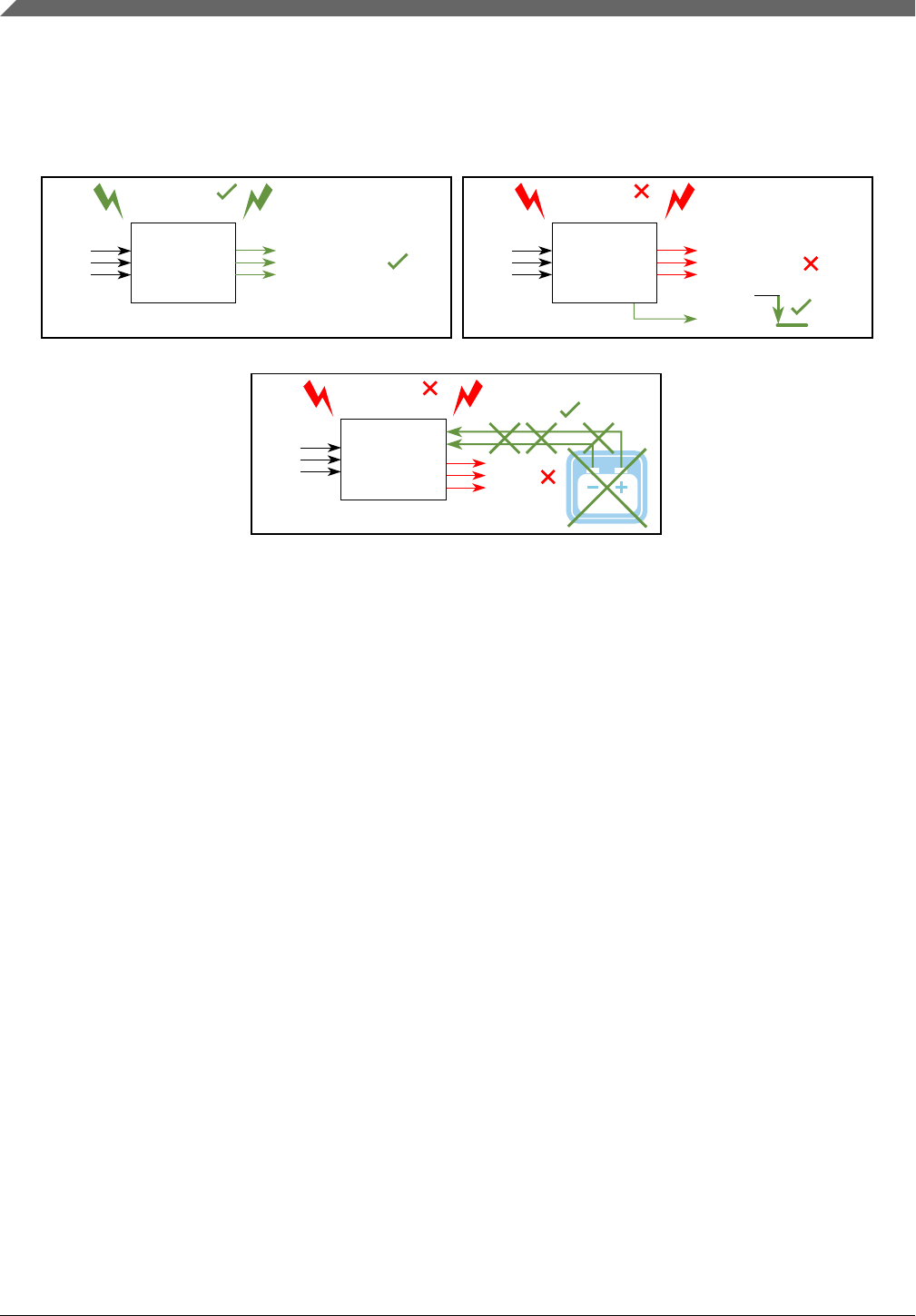
2.5.1 Faults
The following random faults may generate failures, which may lead to the violation of a
functional safety goal. Citations are according to ISO 26262-1. Random hardware faults
occur at a random time, which results from one or more of the possible degradation
mechanisms in the hardware.
Chapter 2 MCU Safety Context
S32K1xx Series Safety Manual, Rev. 4, 09/2018
NXP Semiconductors 17

•Single-Point Fault (SPF): A fault in an element that is not covered by a safety
mechanism, and results in a single-point failure. This leads directly to the violation of
a safety goal. 'a' in the Figure 2-2 shows a SPF inside an element, which generates a
wrong output. The equivalent in IEC 61508 to Single-Point Fault is a Random fault.
Whenever a SPF is mentioned in this document, it is to be read as a random fault for
IEC 61508 applications.
•Latent Fault (LF): A fault whose presence is not detected by a safety mechanism
nor perceived by the automobile driver. A LF is a fault that does not violate the
functional safety goal(s) itself, but leads to a dual-point or multiple-point failure
when combined with at least one additional independent fault, which then leads
directly to the violation of a functional safety goal. 'b' in the Figure 2-2 shows a LF
inside an element, which still generates a correct output. No equivalent in IEC 61508
to LF is named.
•Dual-Point Fault (DPF): An individual fault that, in combination with another
independent fault, leads to a dual-point failure. This leads directly to the violation of
a functional safety goal. 'd' in the Figure 2-2 shows two LFs inside an element, which
generate a wrong output.
•Multiple-Point Fault (MPF): An individual fault that, in combination with other
independent faults, leads to a multiple-point failure. This leads directly to the
violation of a functional safety goal. Unless otherwise stated, multiple-point faults
are considered safe faults and are not covered in the functional safety concept of
S32K1xx.
•Residual Fault (RF): A portion of a fault that independently leads to the violation of
a functional safety goal, where that portion of the fault is not covered by a functional
safety mechanism. 'c' in the Figure 2-2 shows a RF inside an element, which –
although a functional safety mechanism is set in place – generates a wrong output, as
this particular fault is not covered by the functional safety mechanism.
•Safe Fault (SF): A fault whose occurrence will not significantly increase the
probability of violation of a functional safety goal. Safe faults are not covered in this
document. SPFs, RFs or DPFs are not safe faults.
Faults and failures
S32K1xx Series Safety Manual, Rev. 4, 09/2018
18 NXP Semiconductors
input
element
LF
a) Single-Point Fault (SPF)
c) Residual Fault (RF)
LF LF
SPF wrong
output
System
input
element
correct
output
System
b) Latent Fault (LF)
input
element
RF
wrong
output
System
safety
measure
failure
undetected
d) Dual-Point Fault (DPF)
input
element
wrong
output
System
Figure 2-2. Faults
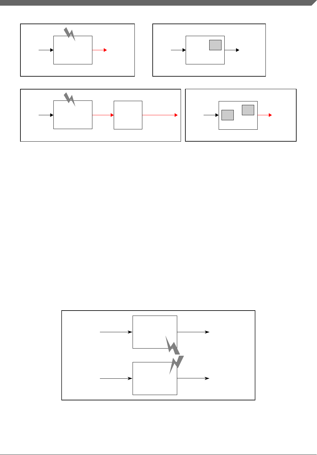
2.5.2 Dependent failures
•Common cause failure (CCF): Subset of dependent failures in which two or more
component fault states exist at the same time, or within a short time interval, as a
result of a shared cause (see Figure 2-3).
A CCF is the coincidence of random failure states of two or more elements on
separate channels of a redundancy element which lead to the failure of the defined
element to perform its intended safety function, resulting from a single event or root
cause (chance cause, non-assignable cause, noise, natural pattern, and so on). A CCF
causes the probability of multiple channels (N) to have a failure rate larger than
λsingle channelN (λredundant element > λsingle channelN).
input
input
failure b
failure a
channel 1
fault1
element
element
fault2
channel 2
CCF
Figure 2-3. Common Cause Failures
Chapter 2 MCU Safety Context
S32K1xx Series Safety Manual, Rev. 4, 09/2018
NXP Semiconductors 19
•Common mode failure (CMF):A single root cause leads to similar coincidental
erroneous behavior (with respect to the safety function) of two or more (not
necessarily identical) elements in redundant channels, resulting in the inability to
detect the failures. Figure 2-4 shows three elements within two redundant channels.
One single root cause (CMFA or CMFB) leads to undetected failures in the primary
channel and in one of the elements of the redundant channel.
input
input
failure
failure
fault1
element
CMF A
fault2
element
fault2'
element
comparison
CMF B
fault1'
output
output
secondary
channel
primary
channel
Figure 2-4. Common Mode failures
•Cascading failure (CF): CFs occur when local faults of an element in a system
ripple through interconnected elements causing another element or elements of the
same system and within the same channel to fail. Cascading failures are dependent
failures that are not common cause failures. Figure 2-5 shows two elements within a
single channel, in which a single root cause leads to a fault (fault 1) in one element
resulting in a failure (failure a). This failure then cascades to the second element,
causing a second fault (fault 2) that leads to a failure (failure b).
input
failure a
channel 1
element
fault1
failure b
channel 1
element
fault2
Figure 2-5. Cascading failures
Faults and failures
S32K1xx Series Safety Manual, Rev. 4, 09/2018
20 NXP Semiconductors
2.6 Single-point fault tolerant time interval and process
safety time
The single-point Fault Tolerant Time Interval (FTTI)/Process Safety Time (PST) is the
time span between a failure that has the potential to give rise to a hazardous event and the
time by which counteraction has to be completed to prevent the hazardous event from
occurring.
Assumption: [SM_211] It is assumed that the Application Fault Tolerant Time Interval
is 100 ms. A list with the reaction time of the Hardware measures is attached to the safety
manual. [end]
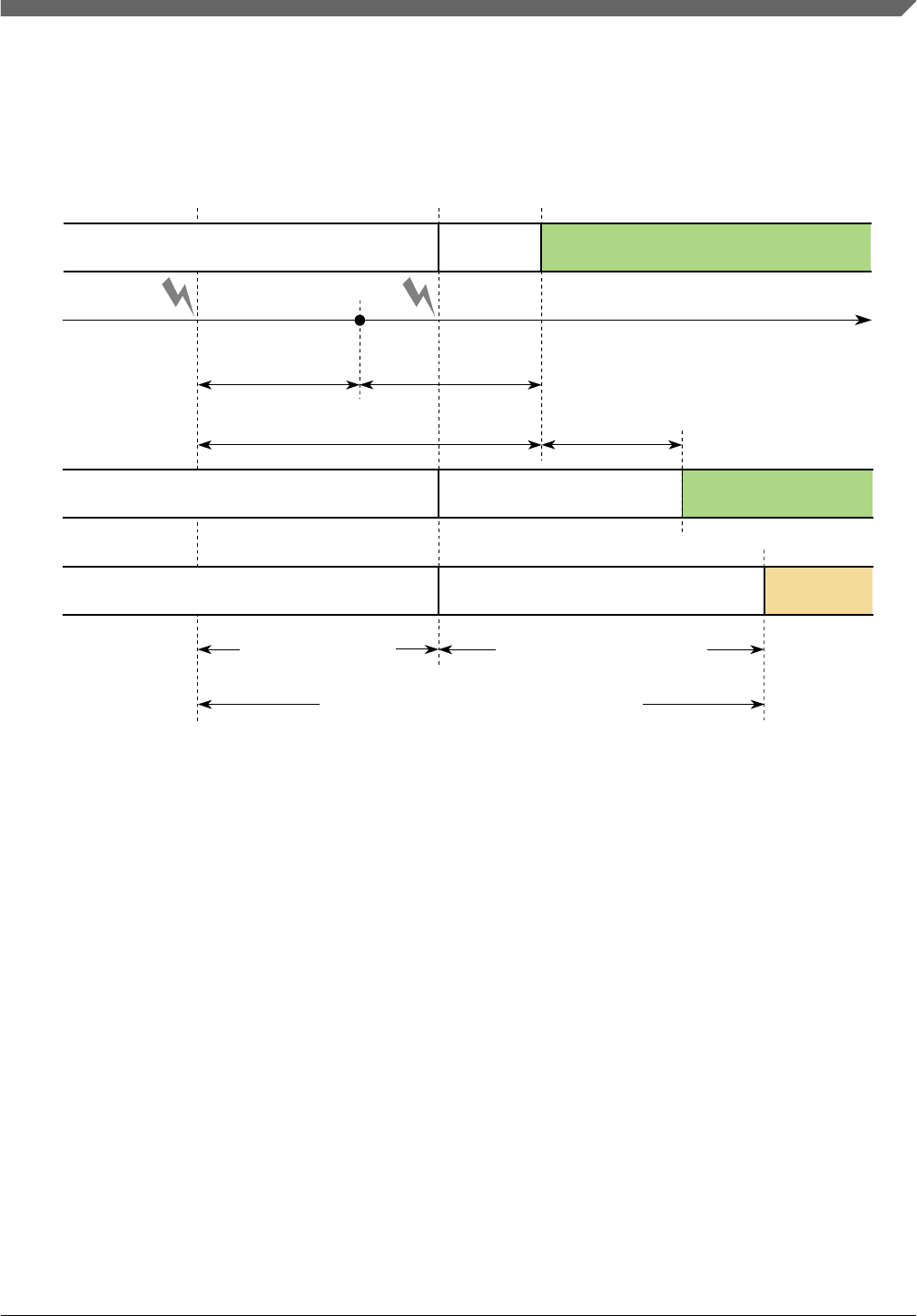
Figure 2-6 shows the FTTI for a system:
• Normal MCU operation (a).
• With an appropriate functional safety mechanism to manage the fault (b).
• Without any suitable functional safety mechanism, a hazard may appear after the
FTTI has elapsed (c).
The equivalent in IEC 61508 to FTTI is Process Safety Time (PST). Whenever single-
point fault tolerant time interval or FTTI is mentioned in this document, it shall be read as
PST for IEC 61508 applications.
MCU normal
operation
MCU failure operation
Safe stateMCU
Single point fault*
not all failure
measures are visible
on system level
(controlled faults)
e.g. ECC-correction
of single-bit
time
a)
*)
b)
c)
fault detection
(MCU)
fault detection time fault reaction time
(MCU)
(MCU)
fault indication time
(system)
fault reaction
time
system normal
operation
system failure operation
or Safe statesystem
system normal
operation
longest possible failure operation possible
hazard
Fault Tolerant Time Interval (FTTI) of the safety
goal regarding single point faults
Emergency Operationsystem
Figure 2-6. Fault tolerant time interval for single point faults
Chapter 2 MCU Safety Context
S32K1xx Series Safety Manual, Rev. 4, 09/2018
NXP Semiconductors 21

Fault indication time is the time from the occurrence of a fault to when the S32K1xx is
switched into a Safe stateMCU (for example, indication of that failure by driving the error
out pins, forcing outputs of the S32K1xx to a high impedance state, or by assertion of
reset).
2.6.1 MCU fault indication time
Fault indication time is the sum of Fault detection time and Fault reaction time.
•Fault detection time (Diagnostic test interval + Recognition time) is the maximum
time for a fault to be detected by a safety mechanism and consists of:
•Diagnostic test interval is the interval between online tests (for example,
software based self-test) to detect faults.
•Recognition time is the time it takes a safety mechanism to detect a fault. The
mechanisms with the longest time are:
• ADC recognition time is a very demanding hardware test in terms of timing.
• Recognition time related to the SPLL loss of clock: it depends on how the
SPLL is configured.
• Software execution time of software based functional safety mechanisms.
This time depends closely on the software implementation.
•Fault reaction time (Internal processing time + External indication time) is the
maximum of the reaction time of all involved functional safety mechanisms
consisting of internal processing time and external indication time:
•Internal processing time is the time/interval to communicate the fault to the
corresponding error flag status register.
•External indication time to notify an observer about a failure external to the
S32K1xx (for example, higher priority IRQs, Crossbar Switch contention,
register saving, and so on).
The sum of the S32K1xx fault indication time and system fault reaction time should be
less than the FTTI of the functional safety goal.
2.7 Latent-fault tolerant time interval for latent faults
The Latent-fault tolerant time interval (L-FTTI) is the time span between a latent fault,
that has the potential to coincide along with other latent faults and give rise to a
hazardous multiple-point event, and the time at which counteraction has to be completed
Latent-fault tolerant time interval for latent faults
S32K1xx Series Safety Manual, Rev. 4, 09/2018
22 NXP Semiconductors
to prevent the hazardous event from occurring. L-FTTI defines the sum of the respective
worst case fault indication time and the time for execution of the corresponding
countermeasure. Figure 2-7 shows the L-FTTI for multiple-point faults in a system.
There is no equivalent to L-FTTI in IEC 61508.
MCU normal operation
MCU failure
operation
Safe stateMCU
fault not infringing
the safety for itself,
only together with
an additional fault
(multiple fault)
time
a)
*)
b)
c)
fault detection
(MCU)
fault detection time fault reaction time
(MCU)
fault reaction
time
failure operation
or Safe statesystem
longest possible failure operation hazard
Fault Tolerant Time Interval (L-FTTI) of the
safety goal regarding Latent Faults
latent fault*
(MCU)
fault indication time
multiple point fault**
**)
probability of multiple point fault
infringing safety function is significant
e.g. 1/1000 of the total failure rate
multiple-point fault
detection interval of
the safety goal
Fault Tolerant Time Interval (FTTI)
of the safety goal regarding
multiple point faults
normal operation
normal operation
Emergency Operationsystem
Figure 2-7. Fault Tolerant Time Interval for latent faults
Latent fault indication time is the time it takes from the occurrence of a multiple-point
failure to when the indication of that failure is forcing the outputs of the S32K1xx to a
high impedance state or by assertion of reset.
Assumption:[SM_212] The assumed application Latent Fault Tolerant Time Interval (L-
FTTI) is typically 12 hours. It is assumed that the MCU will go through a complete
power-up/power-down cycle within the L-FTTI. [end]
Rationale: To remove the effect of any transient faults.
2.7.1 MCU fault indication time
Fault indication time is the sum of Fault detection time and Fault reaction time. In
general, the Fault detection time and Fault reaction time are negligible for multiple-point
failures since the L-FTTI is significantly larger (hours, rather than seconds) than typical
Chapter 2 MCU Safety Context
S32K1xx Series Safety Manual, Rev. 4, 09/2018
NXP Semiconductors 23

safety mechanism detection and reaction times. Typically the safety mechanisms to detect
latent faults are executed during start-up, shut-down or periodically as required by the
diagnostic test interval of the safety system.
The sum of latent fault indication time and latent and multiple point fault reaction time
should be less than the L-FTTI of the functional safety goal.
Note
Detection and handling of a latent fault by a latent fault
detection mechanism must be completed within the Multi-Point
Fault (MPF) detection interval. Afterwards, it is assumed that
the fault caused a multi-point failure, and latent fault detection
is no longer guaranteed to work properly.
2.8 MCU Failure Indication
2.8.1 Failure handling
Failure handling can be split into two categories:
• Handling of failures before enabling the system level safety function (for example,
during/following the S32K1xx initialization). These failures are required to be
handled before the system enables the safety function, or in a time shorter than the
respective FTTI or L-FTTI after enabling the safety function.
• Handling of failures during runtime with repetitive supervision while the safety
function is enabled. These errors are to be handled in a time shorter than the
respective FTTI or L-FTTI.
Assumption:[SM_022] It is assumed that single-point and latent fault diagnostic
measures complete operations (including fault reaction time) in a time shorter than the
respective FTTI or L-FTTI when the safety function is enabled. [end]
Recommendation: It is recommended to identify startup failures before enabling system
level safety functions.
A typical failure reaction, with regards to power-up/start-up diagnostic measures, is to not
initialize and start the safety function, but instead provide failure indication to the user.
Software can read the failure source (register indicating clock errors, voltage errors) and
can do so either before or after a functional reset. If necessary, software can also reset the
S32K1xx.
MCU Failure Indication
S32K1xx Series Safety Manual, Rev. 4, 09/2018
24 NXP Semiconductors

Mux
Trace
port
Crossbar switch (AXBS-Lite)
eDMA
DMA
MUX
Core
Peripheral bus controller
CRC
WDOG
S1
M0 M1
DSP
NVIC
ITM
FPB
DWT
AWIC
SWJ-DP
TPIU
JTAG &
Serial Wire
Arm Cortex M4F
ICODE
DCODE
AHB-AP
PPB
System
M2
S2
GPIO
Mux
FPU Clock
SPLL
LPO
128 kHz
Async
512B
TCD
LPIT
LPI2C FlexIO
Flash memory
controller
Code flash
S0
Data flash
Low Power
Timer
12-bit ADC
TRGMUX
LPUART
LPSPI
FlexCAN FlexTimer
PDB
generation
LPIT
Peripherals present
on all S32K devices
Peripherals present
on selected S32K devices
Key:
Device architectural IP
on all S32K devices
S3
FIRC
48 MHz
M3
ENET
SAI
SOSC
8-40 MHz
(see the "Feature Comparison"
memory memory
4-40 MHz
QuadSPI
RTC
CMP
8-bit DAC
SIRC
8 MHz
FlexRAM/
SRAM
1: On this device, NXP’s system MPU implements the safety mechanisms to prevent masters from
accessing restricted memory regions. This system MPU provides memory protection at the
level of the Crossbar Switch. Each Crossbar master (Core, DMA, Ethernet) can be assigned
different access rights to each protected memory region. The Arm M4 core version in this family
does not integrate the Arm Core MPU, which would concurrently monitor only core-initiated memory
accesses. In this document, the term MPU refers to NXP’s system MPU.
2: For the device-specific sizes, see the "On-chip SRAM sizes" table in the "Memories and Memory Interfaces"
chapter of the S32K1xx Series Reference Manual.
section)
ERM
EWM
MCM
Lower region
Upper region
Main SRAM2
Code Cache
System MPU1
EIM
LMEM
controller
LMEM
QSPI
CSEc3
System MPU1System MPU1System MPU1
3: CSEc (Security) or EEPROM writes/erase will trigger error flags in HSRUN mode (112 MHz) because this
use case is not allowed to execute simultaneously. The device need to switch to RUN mode (80 MHz) to
execute CSEc (Security) or EEPROM writes/erase.
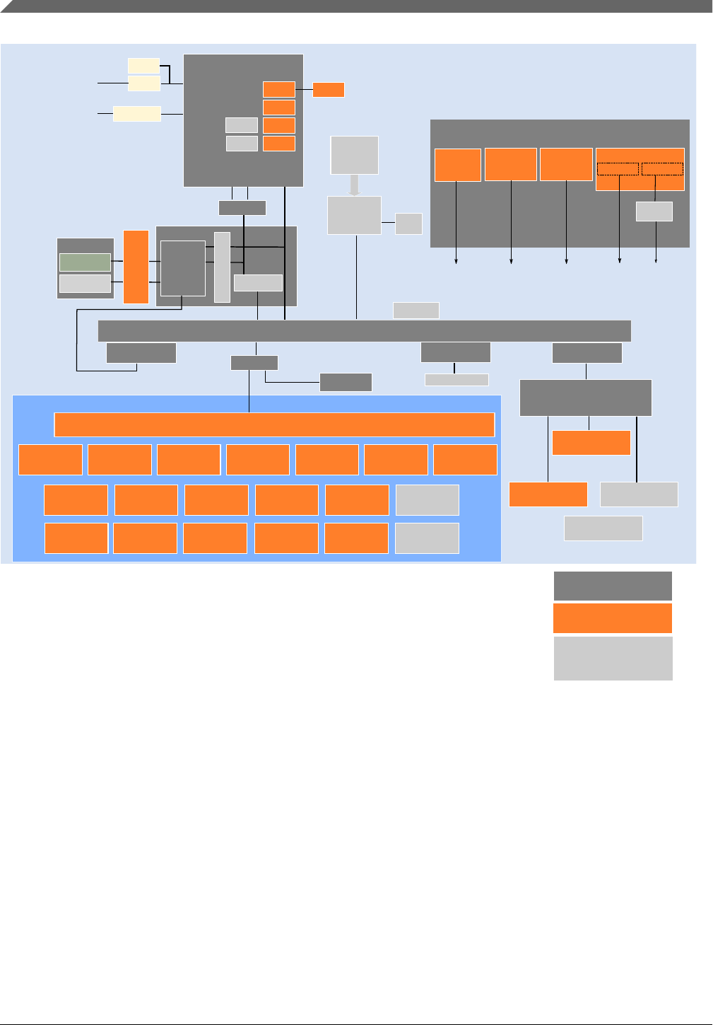
Figure 3-1. S32K14x block diagram
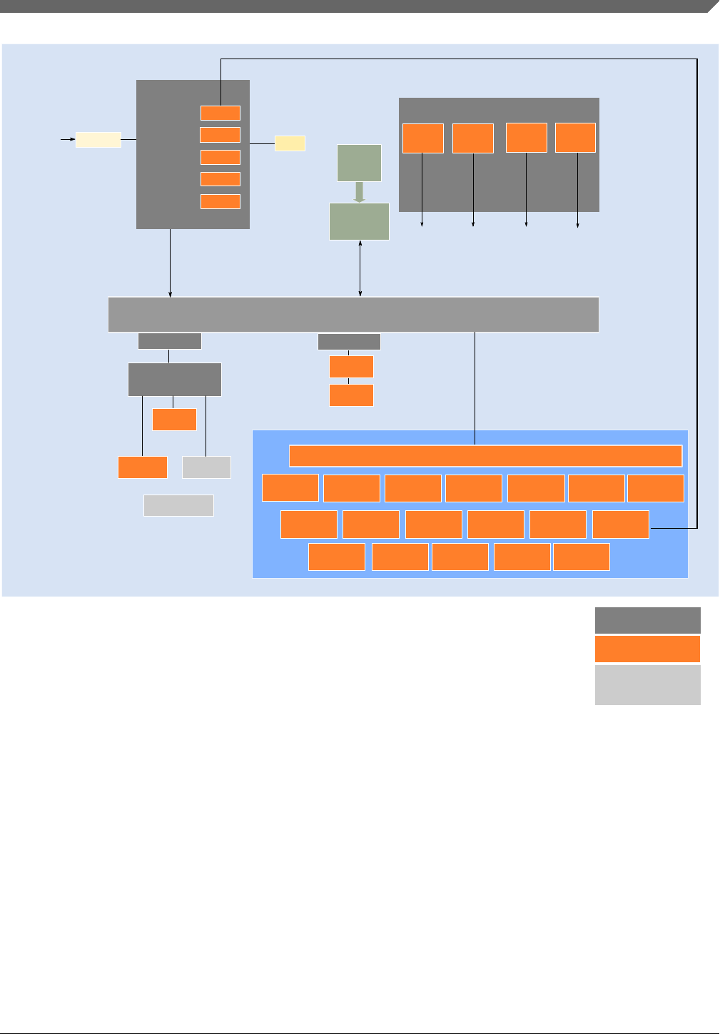
Figure 3-2 is a top-level diagram showing the functional organization of the S32K11x.
General concept
S32K1xx Series Safety Manual, Rev. 4, 09/2018
26 NXP Semiconductors
Crossbar switch (AXBS-Lite)
eDMA
DMA
MUX
SW-DP
Unified Bus
Serial Wire
AHBLite
AHBLite
AWIC
S0 S1
Clock
LPO
128 kHz
generation
Peripheral bus controller
CRC
WDOG
LPIT
LPI2C FlexIO Low Power
Timer
12-bit ADC
TRGMUX
LPUART
LPSPI
FlexCAN FlexTimer
PDB
LPIT
RTC
CMP
8-bit DAC
ERM
CMU GPIO
M0 M2
Flash memory
controller
Data flash
memory
FlexRAM/
SRAM2
Code flash
memory
IO PORT
NVIC
PPB
MTB+DWT
BPU
AHB-AP
Arm Cortex M0+
Peripherals present
on all S32K devices
Peripherals present
on selected S32K devices
Key:
Device architectural IP
on all S32K devices
(see the "Feature Comparison"
1: On this device, NXP’s system MPU implements the safety mechanisms to prevent masters from
accessing restricted memory regions. This system MPU provides memory protection at the
level of the Crossbar Switch. Crossbar master (Core, DMA) can be assigned
different access rights to each protected memory region. The Arm M0+ core version in this family
does not integrate the Arm Core MPU, which would concurrently monitor only core-initiated memory
accesses. In this document, the term MPU refers to NXP’s system MPU.
2: For the device-specific sizes, see the "On-chip SRAM sizes" table in the "Memories and Memory Interfaces"
chapter of the S32K1xx Series Reference Manual.
section)
S2
IO PORT
CSEc
System MPU1System MPU1
SOSC
4-40 MHz
SIRC
8 MHz
FIRC
48 MHz
EIM
SRAM2
Figure 3-2. S32K11x block diagram
The S32K1xx has an integrated safety concept targeting safety-related systems requiring
high safety integrity levels. In general, safety integrity is achieved in the following ways:
• Clock and power, generation and distribution, are supervised by dedicated monitors
(see section Clock and power monitoring)
• Operational interference protection is ensured via a hierarchical memory protection
schema allowing concurrent execution of software with different (lower) ASIL (see
section Operational interference protection)
Chapter 3 MCU Safety Concept
S32K1xx Series Safety Manual, Rev. 4, 09/2018
NXP Semiconductors 27

3.2 ECC
3.2.1 ECC for storage
In S32K14x, the Flash and SRAM memories, except for the 4 KB FlexRAM used as
system RAM in the region 1400_0000h – 1400_0FFFh, use an ECC algorithm with
SEC/DED (Single Error Correct and Double Error Detect) computed over stored data.
In S32K11x, the Flash and SRAM memories, except for the 2 KB FlexRAM used as
system RAM in the region 1400_0000h – 1400_07FFh, and 1 KB of SRAM_L used as
system RAM in region 1FFF_FC00h – 1FFF_FFFFh use an ECC algorithm with
SEC/DED (Single Error Correct and Double Error Detect) computed over stored data.
3.2.2 ECC failure handling
During a "read flash memory" access:
• Detected double-bit uncorrectable faults are reported in the FTFC and an interrupt is
triggered if enabled. The customer software can handle double bit error interrupt in
different ways depending on whether the error occurred in Code Space (for example:
enter safe state) or Data space (for example: continue if data is not safety relevant). If
an uncorrectable ECC fault occurs during execution of a machine exception, a safe
state shall be entered.
• Detected single-bit faults are corrected without notification.
Single-bit correctable faults and double-bit uncorrectable faults in System RAM, as well
as the corresponding access address, are reported in the Error Reporting Module (ERM)
and an interrupt is triggered if enabled. Single-bit correctable faults and double-bit
uncorrectable faults in System RAM are also reported in MCM (if enabled).
Assumption: [SM_111] The ECC SRAM reporting has to be enabled by the software
application (in LMEM module), before the safety application starts. [end]
The Error Injection Module (EIM) allows you to induce single-bit and multi-bit
inversions on read data when accessing the System RAM. Due to ECC correction
mechanism, an error in ECC could directly violate the safety goal. ECC shall be checked
once within the FTTI.
ECC
S32K1xx Series Safety Manual, Rev. 4, 09/2018
28 NXP Semiconductors

Assumption: [SM_112] It is assumed that customer software can handle double bit error
interrupt in different ways depending on whether the error occurred in Code Space (for
example: enter safe state) or Data space (for example: continue if data is not safety
relevant). If an uncorrectable ECC fault occurs during execution of a machine exception,
a safe state shall be entered. [end]
3.3 Clock and power monitoring
3.3.1 Clock
For Safety applications, always use PLL (with clock monitoring enabled for LOL and
LOC in S32K14x parts) and FIRC (with CMU enabled in S32K11x parts) as system
clock. In S32K1xx, FXOSC loss of clock reset indication to the system may take up to
512 us while in S32K11x CMU will indicate the loss of FIRC clock within 5 us.
3.3.2 Power
The Low Voltage Detect (LVD) monitor and Low Voltage Reset (LVR) on the S32K1xx
are the voltage supervisors. Safety relevant voltages (recommended operating voltages)
are supervised for values that are out of these ranges. Since any voltage running outside
of the safety relevant range has the potential to disable the failure indication mechanisms
of the MCU the indication of these supply voltage errors can be used to cause a direct
transition of the MCU into the safe state (reset assertion) (see the "Power Management
Controller block (PMC)" chapter in the S32K1xx Reference Manual and the S32K1xx
Data Sheet for details).
3.4 Operational interference protection
S32K1xx is a multi-master system. Therefore, it provides safety mechanisms to prevent
non-safety masters from interfering with the operation of the core, as well as mechanisms
to handle the concurrent execution of software with different (lower) ASIL. Interference
freedom is guaranteed via a hierarchical memory protection schema including:
• System Memory Protection Unit (MPU)
• Peripheral bridge
• Register protection
Chapter 3 MCU Safety Concept
S32K1xx Series Safety Manual, Rev. 4, 09/2018
NXP Semiconductors 29

The system MPU on S32K1xx prevents access of different bus masters to address ranges.
It is typically intended for use by the safety application to prevent non-safety related
modules access to the application's safety-relevant resources.
Furthermore, the peripheral bridge can restrict read and write access to individual I/O
modules based on the origin of the access and its state (user mode/supervisor mode).
Finally, the register protection prevents individual registers from any manipulation until
the registers are unlocked.
Operational interference protection
S32K1xx Series Safety Manual, Rev. 4, 09/2018
30 NXP Semiconductors

Chapter 4
Hardware Requirements
4.1 Hardware requirements on system level
This section describes the system level hardware safety measures needed to complement
the integrated safety mechanisms of the S32K1xx.
The S32K1xx integrated safety concept enables SPFs and latent failures to be detected
with high diagnostic coverage. However, not all CMFs may be detected. In order to
detect failures which may not be detected by the S32K1xx, it is assumed that there will
be some separate means to bring the system into Safe statesystem.
Figure 4-1 depicts a simplified application schematic for a functional safety-relevant
application in conjunction with an external IC (only functional safety related elements
shown). The supplies generated from the external IC should be protected against voltage
over the absolute maximum rating of the device (as documented in the S32K1xx Data
Sheet in section "Absolute maximum ratings").
Through a digital interface (for example, SPI), the S32K1xx repetitively triggers the
watchdog of the external IC. If there is a recognized failure (for example, watchdog not
being serviced, the reset output of the external IC will be asserted to reset the S32K1xx.
For safety, a redundant watchdog system, External Watchdog Monitor (EWM), is
designed to monitor external circuits, as well as the MCU software flow. This provides a
back-up mechanism to the internal watchdog (WDOG) that resets the MCU's CPU and
peripherals. One output port, EWM_out, when asserted is used to reset or place the
external circuit into safe mode. One input port, EWM_in, allows an external circuit to
control the assertion of the EWM_out signal. 1
Recommendation: [SM_037] The external watchdog usage is a recommendation to be
implemented at system level as a robust external monitoring safety mechanism for the
MCU. There is no requirement that these external measures should be provided in an IC
1. Available in S32K14x variants only
S32K1xx Series Safety Manual, Rev. 4, 09/2018
NXP Semiconductors 31
or even in the specific way as described (For example, external watchdog functionality
can be provided by another component of the system which can recognize that the chip
has stopped sending periodic packets on a communication network). [end]
Fail safe output
overvoltage
supervision
error
monitor
watchdog
External IC
SPI (or alternative)
Supply
RESET
error out signal(s)1
MCU
1. Available in S32K14x variants only
Figure 4-1. Functional safety related connection to external circuitry
4.1.1 Assumed functions by separate circuitry
This section describes external components used in a system in conjunction with the
S32K1xx for safety-related systems.
It should be noted that failure modes of external services are only partially considered in
the FMEDA of the S32K1xx (for example, clock(s), power supply), and must be fully
analyzed in the system FMEDA by the safety system developer.
4.1.1.1 High impedance outputs
If the S32K1xx is considered to be in a Safe stateMCU (for example, unpowered and
outputs tristated), the system containing the S32K1xx may not be compliant with the
Safe statesystem. A possible system level safety measure to achieve Safe statesystem may be
to place pull-up or pull-down resistors on I/O when the high-impedance state is not
considered safe.
Assumption: [SM_038] If a high-impedance state on an output pin is not safe, pull-up or
pull-down resistors shall be added to safety-related outputs. The need for this will be
application dependent for the unpowered or reset (tristated I/O) S32K1xx.[end]
Hardware requirements on system level
S32K1xx Series Safety Manual, Rev. 4, 09/2018
32 NXP Semiconductors

Rationale: In order to bring the safety-related outputs to such a level, that a
Safe statesystem is achieved.
4.1.1.2 Reset
The reset pad is pulled high by default (see the S32K1xx Data Sheet for the exact value),
and the Input Reset Function is configurable. The dedicated reset pin function is available
until the exit of reset; after that, the pin must be configured to perform the Input Reset
Function so that the application (the safety mechanism) can use it.
Whenever the reset delay is enabled, the application should ensure that the LPO clock is
available.
4.1.1.3 Power Supply Monitoring
Supply voltages outside of the specified operational ranges may cause permanent damage
to the S32K1xx, even if it is held in reset.
Assumption: [SM_042] It is assumed that safety measures on system level maintain the
Safe statesystem during and after any supply voltage above the specified operational range.
[end]
The S32K1xx Microcontroller Data Sheet provides specific operating voltage ranges that
must be maintained.
Assumption: [SM_087] It is assumed that the external power is supervised for high and
low deviations where no supervision is provided on the MCU. [end]
Assumption: [SM_088] It is assumed that the MCU is kept in reset if the external
voltage is outside specification and is protected against voltage over the absolute
maximum rating of the device (as documented in Data Sheet in section "Absolute
maximum ratings"). [end]
If the power supply is out of range, S32K1xx shall be kept in reset or unpowered, or other
measures must possibly be used to keep the system in a safe state. Overvoltage outside
the specified range of the technology may cause permanent damage to the S32K1xx even
if kept in reset.
Implementation hint: An external and independent device may provide an over voltage
monitor for the external S32K1xx supplies. If the supplied voltage supply is above the
recommended operating voltage range of the S32K1xx, the S32K1xx should be
maintained with no power. The external power supply monitor will switch the system to a
Chapter 4 Hardware Requirements
S32K1xx Series Safety Manual, Rev. 4, 09/2018
NXP Semiconductors 33

Safe statesystem within the FTTI, and maintain it in Safe statesystem (for example, over-
voltage protection with functional safety shut-off, or a switch-over to a second power
supply unit).
If the S32K1xx power supply can be designed to avoid any potential of over-voltage, the
external voltage monitoring can be excluded from the system design.
Over-voltage on some supplies will be detected by the S32K1xx itself, but system level
measures might be required to maintain the Safe statesystem in case an over-voltage
situation may cause damage to the S32K1xx.
4.1.1.4 Error Monitoring
If the S32K1xx signals an internal failure (error flag) in its status registers, the system
may no longer rely on the integrity of the other S32K1xx outputs for safety functions. If
an error is indicated, the system has to switch to, and remain in, Safe statesystem without
relying on the S32K1xx. Depending on its functionality, the system might disable or reset
the device as a reaction to the error indication (see Assumptions in Safe states).
Assumption: [SM_043] The overall system needs to include measures to monitor error
flags in registers of the MCU and move the system to a Safe statesystem when an error is
indicated. [end]
Hardware requirements on system level
S32K1xx Series Safety Manual, Rev. 4, 09/2018
34 NXP Semiconductors

Chapter 5
Software Requirements
5.1 Software requirements on system level
This section lists required, or recommended, safety measures which should be in place
when using the S32K1xx in safety systems.
The S32K1xx on-chip modules not explicitly mentioned here do not require specific
safety measures to be used in safety systems. The modules that are replicated reach a very
high diagnostic coverage without additional dedicated safety measures at application or
system level.
5.2 Power
5.2.1 Power Management Controller (PMC)
The PMC manages the supply voltages for all modules on the device. This unit includes
the internal regulator for the logic power supply and a set of voltage monitors for low
voltage detector (LVD) and low voltage reset (LVR). If the monitored voltage goes
below LVR-given thresholds, a reset is initiated to control erroneous voltages before
these could cause a potential failure (for correct operating voltage ranges please see the
S32K1xx Data Sheet).
The LVD has warning, interrupt, and reset (brownout) capability. See the "Low voltage
detect (LVD)" section in the "Reset and Boot" chapter of the S32K1xx Series Reference
Manual for more details.
Assumption: [SM_084] The application software must check the status registers of the
RCM for error flags. [end]
S32K1xx Series Safety Manual, Rev. 4, 09/2018
NXP Semiconductors 35
Assumption: [SM_204] It is assumed that the ADCs are used to monitor the bandgap
reference voltage of the PMC and to monitor the internal supplies connected to ADCs.
[end]
Apart from monitoring error flags and ADC monitoring of the bandgap reference voltage,
the use of the PMC for safety-relevant applications is transparent to the user.
Undervoltage conditions are primarily reported to the RCM, where they directly cause a
transition into a safe state by a reset. This solution was chosen because safety-relevant
voltages have the potential to disable the failure indication mechanisms of the S32K1xx.
Assumption: [SM_085] Software must not disable the direct transition by the RCM into
a safe state due to an overvoltage or undervoltage indication. [end]
Over voltage supply shall be monitored externally as described in Power Supply
Monitoring.
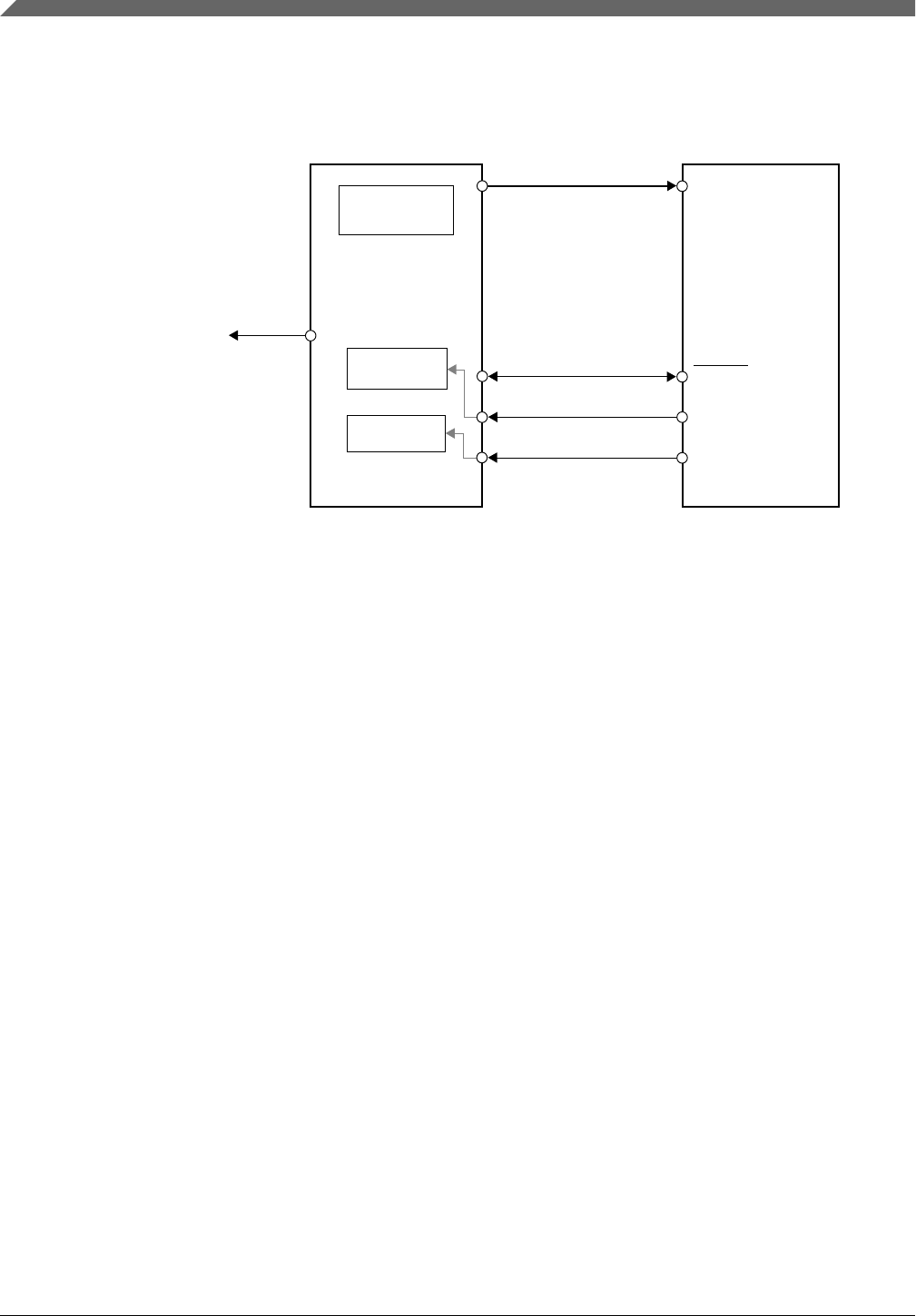
5.2.1.1 3.3 V supply supervision
Voltage detectors LVD and LVR monitor the VDD supplies for under voltage in relation
to a reference voltage. The figure below depicts the logic scheme of the voltage detectors.
In case an LVD detects an under-voltage condition during normal operation of the
S32K1xx, then (depending on SW configuration) a low voltage detect flag, low voltage
warning flag, low voltage interrupt, or destructive reset is triggered. The low voltage
detect system (Low voltage detect flag, Low voltage warning flag and Low voltage detect
reset generation) is disabled in low power mode. If the supply voltage falls below the
reset trip point (VLVR), the LVR will generate a system reset regardless of the operating
mode.
VDD supply
To RCM
(system reset,
interrupt)
LVD / LVR
(in module)
Reference voltage
Figure 5-1. Logic scheme of the 3.3 V voltage detectors
5.3 Clock
Clock
S32K1xx Series Safety Manual, Rev. 4, 09/2018
36 NXP Semiconductors

5.3.1 System Phase-locked loop (SPLL) 1
The S32K14x features a System Phase-locked loop (SPLL) which is used to generate
high-speed clocks. The SPLL provides a loss of lock error indication that is routed to the
RCM. Glitches which may appear on the crystal clock are filtered (low-pass filter) by the
SPLL. The SPLL dedicated to the system clock is distributed to most of the S32K14x
modules
5.3.1.1 Initial checks and configurations
After system reset, the external crystal oscillator is powered down and the PLL is
deactivated. Software shall enable the oscillator. After system reset, the S32K1xx uses
the fast internal RC oscillator clock (FIRC) as its clock source (see the "Clocking" and
"FIRC Digital Interface" chapters in the S32K1xx Reference Manual and Internal RC
oscillators for details on FIRC configuration).
Assumption: [SM_078] Before executing any safety function, a high quality clock (low
noise, low likelihood for glitches) based on an external clock source shall be configured
as the system clock of the S32K14x. [end]
Rationale: Since the SIRC is used by the clock monitors as reference to monitor the
output of the SPLL, it cannot be used as input of the SPLL.
Implementation hint: The system oscillator clock (SOSC) is the SPLL source clock.
Implementation hint: RCM_SRS[LOL], RCM_SSRS[SLOL] and
SCG_SPLLCSR[SPLLVLD] indicate that a loss of lock event occurred. You can
configure SCG_SPLLCSR[SPLLCM] and SCG_SPLLCSR[SPLLCMRE] to enable
interrupt/reset request upon loss of lock. For a reset event, program both
SCG_SPLLCSR[SPLLCM] and SCG_SPLLCSR[SPLLCMRE] to 1. For an interrupt,
program SCG_SPLLCSR[SPLLCM]=1 and SCG_SPLLCSR[SPLLCMRE]=0.
Assumption under certain conditions: [SM_079] When clock glitches endanger the
system level functional safety integrity measure, respective functional safety-relevant
modules shall be clocked with a PLL generated clock signal, as the PLL serves as a filter
to reduce the likelihood of clock glitches due to external disturbances. Alternatively a
high quality external clock having low noise and low likelihood of clock glitches shall be
used. [end]
Rationale: To reduce the impact of glitches stemming from the external crystal and its
hardware connection to the S32K14x.
1. Available in S32K14x variants only
Chapter 5 Software Requirements
S32K1xx Series Safety Manual, Rev. 4, 09/2018
NXP Semiconductors 37

Implementation hint: This requirement is fulfilled by appropriately programming the
System Clock Generator (SCG).
Implementation hint: Either during or after initialization, but before executing any
safety function, application software can check the current system clock by checking the
SCG_CSR[SCS] bit field. SCG_CSR[SCS] = 0110b indicates that the System PLL
(SPLL) clock is being used as the system clock.
Assumption: [SM_213] A check should be implemented to verify that with an intended
PLL configuration the PLL locks with the correct output clock. [end]
Implementation hint: You can compare the PLL input clock and PLL output clock
based on 2 timers configured one to run on the SOSC and the other on the SPLL. If the
timers interrupts are not triggered within a certain time window to confirm that the output
clock SPLL is correct, you can choose to reset the device in this case.
5.3.2 Clock Monitor Unit (CMU)2
The S32K11x variants does not have SPLL and the system clock shall be driven by the
FIRC. At startup, the CMUs are not initialized and the FIRC is the default system clock.
The CMUs are driven by the 8 MHz SIRC to ensure independence from the monitored
clock(FIRC). CMUs flag events associated with conditions due to clock out of a
programmable bounds and loss of monitored clock. If a monitored clock leaves the
programmed frequency range for the device, the configured reaction is generated by
CMU. S32K11x devices includes CMU which monitors only FIRC which is a main
source of System Clock. The CMU uses the SIRC (8 MHz slow internal oscillator) as the
reference clock for independent operation from the monitored clock.
The purpose is to check for:
• Loss of FIRC (main source of system clock)
• FIRC(main source of system clock) out of programmable frequency range (frequency
too high or low)
For safety-relevant applications, use of the CMU is mandatory. If the modules that the
CMU monitors are used by the application safety function, the user shall verify that the
CMU is not disabled.
5.3.2.1 Initial checks and configurations
Assumption: [SM_083] The following supervisor functions are required:
• Loss of fast internal reference clock
2. Available in S32K11x variants only
Clock
S32K1xx Series Safety Manual, Rev. 4, 09/2018
38 NXP Semiconductors

• System FIRC frequency higher than the (programmable) upper frequency reference
• System FIRC frequency lower than the (programmable) lower frequency reference
[end]
Rationale: To monitor the integrity of the system clock signal.
Recommendation: The CMU should be used for monitoring firc clock for functional
safety-relevant application. Application software shall check that the CMU is enabled as
it is disabled by default. It is recommend to always generate a reset in case of loss of
clock or clock out of range condition. For the out of range clock condition, the reset event
shall be generate inside the interrupt condition. Before entering any low power mode, the
CMU shall be disabled and the CMU clock shall be turned off by configuring the CGC
field of the CMU control register in PCC module.
Implementation hint: In general, the following application-dependent configurations
shall be executed before CMU monitoring can be enabled.
• The first configuration is related to the low frequency reference
(CMU_FC_LTCR[LFREF]) in CMU0 instance for loss of FIRC clock detection and
reset generation.
• The second configuration is related to the high frequency
(CMU_FC_HTCR[HFREF]) and low frequency reference
(CMU_FC_LTCR[LFREF]) in CMU1 instance for interrupt generation.
After CMU is enabled by writing CMU_FC_GCR[FCE]=1, CMU takes a few cycles
before internal operations start as indicated by CMU_FC_SR[RS]=1. The safety
application must be enabled after CMU_FC_SR[RS]=1.
5.3.3 Clock Monitor for devices with SPLL
At startup, the clock monitors are not initialized and the FIRC is the default system clock.
Stuck-at faults on the system oscillator clock (SOSC) are not detected by the clock
monitor at power-on since the monitoring units are not initialized and the S32K14x is still
running on the FIRC.
The clock monitors are driven by the 8 MHz Slow Internal RC Clock (SIRC) to ensure
independence from the monitored clocks. Clock monitors flag errors associated with
conditions due to clock out of a programmable bounds and loss of reference clock. If a
supervised clock leaves the specified range for the device, an error flag is set in the
corresponding status register. The S32K14x includes clock monitors for the SOSC and
SPLL.
Chapter 5 Software Requirements
S32K1xx Series Safety Manual, Rev. 4, 09/2018
NXP Semiconductors 39

The clock monitors use the SIRC (8 MHz internal oscillator) as the reference clock for
independent operation from the monitored clocks. Their purpose is to check for error
conditions due to:
• loss of clock from external crystal (SOSC)
• SPLL clock out of a programmable frequency range (frequency too high or too low -
loss of clock)
• loss of SPLL clock
The clock monitors supervise the frequency range of various clock sources. In case of
abnormal behavior, the information is forwarded to the corresponding SCG status
registers.
Assumption: [SM_080] For safety-relevant applications, the use of the clock monitors is
mandatory. If the modules that the SCG monitors are used by the application safety
function, the user shall verify that the clock monitors are not disabled and their faults are
managed by the software. [end]
5.3.3.1 Initial checks and configurations
Assumption: [SM_081] The following supervisor functions are required: Loss of
external clock, SPLL frequency higher than the (programmable) upper frequency
reference and SPLL frequency lower than the (programmable) lower frequency reference.
[end]
Rationale: To monitor the integrity of the clock signals
Recommendation: The clock monitors should be used for each clock that is being
monitored and used by a functional safety-relevant module. Application software shall
check that the clock monitors are enabled and their faults managed by software. To
prevent unexpected loss of clock reset events, all clock monitors should be disabled
before entering any low power modes.
Implementation hint: In general, the following two application-dependent
configurations shall be executed before clock monitoring can be enabled.
Clock
S32K1xx Series Safety Manual, Rev. 4, 09/2018
40 NXP Semiconductors

• The first configuration is related to the crystal oscillator clock (SOSC) monitor.
Software configures the SCG_SOSCCSR[SOSCM] and enables the System OSC
clock monitor. The SCG SOSC Control Status Register (SCG_SOSCCSR) can only
be written if the Lock Register (LK) bit is zero. The divided SIRC frequency is
compared with the SOSC.
• The second configuration is related to the PLL clock being monitored.
SCG_SPLLCSR[SPLLCM] enables the PLL clock monitor. The SCG PLL Control
Status Register (SCG_SPLLCSR) can only be written if the Lock Register (LK) bit is
zero.
5.3.4 System Oscillator Clock (SOSC)
FlexCAN, CLKOUT, and other peripherals feature a mode in which they are directly
clocked from the SOSC. For a complete list, see the "Clock Distribution" chapter of the
S32K1xx Series Reference Manual.
The oscillator clock should be selected whenever a tight tolerance (up to 0.1%) is
required. The crystal oscillator clock also has better jitter performance than the peripheral
clock.
5.3.4.1 Initial checks and configurations
Assumption: [SM_075]FlexCAN and CLKOUT, both of which feature a mode to be
clocked directly by the SOSC, should not make use of these modes in normal operation
unless effects of clock glitches are sufficiently detected by the applied FT-COM layer.
[end]
5.3.4.2 Runtime checks
Assumption: [SM_076] Software shall check that the system clock is available, and
sourced by the SOSC, before running any safety element function.[end]
5.3.5 Internal RC oscillators
Three internal RC oscillators are implemented:
• Fast Internal RC (FIRC) has a nominal frequency of 48 MHz.
Chapter 5 Software Requirements
S32K1xx Series Safety Manual, Rev. 4, 09/2018
NXP Semiconductors 41

• Slow Internal RC (SIRC) has a nominal frequency of 8 MHz.
• LPO_CLK, which offers 128 kHz. A 32 kHz and a 1 kHz clock can be derived from
it.
Frequency accuracy over the full range of voltage and temperature has to be taken into
account (see the S32K1xx Data Sheet). Functional safety related modules which can use
the clock generated by the internal clocks are shown in the table below. For more details,
see the "Clock Distribution" chapter of the S32K1xx Series Reference Manual.
Table 5-1. Modules and internal clocks
Module name FIRC SIRC LPO_CLK or divided
LPO_CLK
ADC Yes Yes No
CLKOUT Yes Yes Yes
EWM No No Yes
FlexIO Yes Yes No
FlexTimer Yes Yes No
LPI2C Yes Yes No
LPIT Yes Yes No
LPSPI Yes Yes No
LPTMR Yes Yes Yes
LPUART Yes Yes No
PMC No No Yes
RTC No No Yes
WDOG No Yes Yes
5.3.5.1 Initial checks and configurations
The Fast IRC Clock Error flag (SCG_FIRCCSR[FIRCVLD]) shall be used to check the
availability of the Fast Internal RC Oscillator (FIRC). Further, the nominal FIRC
frequency should be verified by implementing a SW test routine comparing counter
values of two independant timers (e.g. FTM and WDOG) based on different clock
sources (FIRC and SOSC).
Assumption: [SM_073] The FIRC frequency is measured and compared to the expected
frequency by comparing counter values generated by independent timers based on
different clock sources.. This test is performed after power-on, but before executing any
safety function. [end]
Rationale: To check the integrity of the FIRC
Clock
S32K1xx Series Safety Manual, Rev. 4, 09/2018
42 NXP Semiconductors

5.3.5.2 Runtime checks
Comparing counter values of two independent timers based on different clock sources
shall be used to verify the availability and frequency of the FIRC. This method allows
measurement of the FIRC frequency using the SOSC as reference clock source.
Assumption: [SM_074] To detect failure of the FIRC, the application software shall
utilize a method comparing counter values of two independent timers based on different
clock sources to compare the FIRC frequency against the expected value of 48 MHz.
[end]
Implementation hint: See the Assumption: in Initial checks and configurations for an
explanation on how to check the FIRC.
If the measured FIRC frequency does not match the expected value, there exists the
possibility of a complete failure of all safety measures. Software should then bring the
system to a Safe statesystem without relying on the modules driven by the FIRC.
Recommendation: To increase the fault detection, this functional safety integrity
measure should be executed once per FTTI.
5.4 Flash
5.4.1 Flash memory
The S32K1xx provides programmable non-volatile flash memory (NVM) with ECC,
which can be used for instruction and/or data storage.
The ECC used for flash memory marks All-0 as being in error, but allows All-1 situations
to take into consideration reading erased, uninitialized flash memory.
The flash subsystem has an internal embedded controller with internal memory, which
shall be considered safety relevant if the activation of embedded controller is done during
the safety application. Activation of embedded flash controller is done in the following
cases:
• Erase/Program flash array
• EEPROM emulation
• Use of security engine
Chapter 5 Software Requirements
S32K1xx Series Safety Manual, Rev. 4, 09/2018
NXP Semiconductors 43

5.4.1.1 EEPROM
We recommend that you use software emulation to directly store safety relevant data into
the DFLASH. However, if EEPROM emulation is used to store safety-relevant data, you
must implement a software check in this case to verify the correct functionality of the
memory controller.
The user needs in this case to configure FlexNVM to EEPROM by PGMPART
command.
Implementation hint: The check could be implemented based on the SETRAM
command. This command will copy the active records from the FlexNVM to the
EEEPROM emulation, and the EEPROM emulation can have a CRC check done before
and after command execution to ensure that the correct data was backed up in FlexNVM.
The S32K116 and S32K118 provide one block (32 KB) of FlexNVM, consisting of 2 KB
sectors for EEPROM emulation. The S32K142, S32K144 and S32K146 provide one
block (64 KB) of FlexNVM, consisting of 2 KB sectors for EEPROM emulation. The
S32K148 provides up to 512 KB (as part of the program flash memory) of FlexNVM,
consisting of 2 KB sectors for EEPROM emulation. An ECC algorithm is implemented to
correct single-bit faults and detect double-bit faults. The double-bit error is signaled via a
status register and an interrupt, if configured.
Assumption: [SM_114] The software using the EEPROM for storage of information will
use checks to detect incorrect data returned from the EEPROM emulation. [end]
Typically, a CRC will be stored to validate the data.
You must check the integrity of the safety-relevant code after execution of a flash-
memory programming operation. You could use a CRC check or a CMAC check for this
purpose, depending on the application.
5.4.1.2 Runtime checks
If the embedded flash controller is activated during the safety application, application
software checks shall be implemented to check the status of the intended operation and
the content of safety relevant data saved in flash array. In case of programming/erase
operation, one shall check the content of the programmed/erased sector at the end of a
programming/erasing operation. The result of programmed/erase operation can be based
on a read-back scheme, where the written word is read back and compared with the
intended value. Safety relevant data shall be saved with CRC check to validate them. You
could use the built-in HW CRC for this purpose.
Flash
S32K1xx Series Safety Manual, Rev. 4, 09/2018
44 NXP Semiconductors

Assumption: [SM_116] A software test should be implemented to check for potential
multi-bit errors introduced by permanent failures in the flash controller. It is assumed that
if the embedded controller is classified as safety relevant, the activation of embedded
controller is accompanied by flash integrity checks. First, one shall check that the started
flash related command was completed and returned with a pass status. Depending on the
safety application, the flash integrity checks shall be done for code flash or/and data
flash. Safety relevant code and data shall be saved in flash with a CRC or hash signature
to detect any integrity violation. [end]
Assumption: [SM_117] A software safety mechanism shall be implemented to ensure
the correctness of any write operation to the flash memory. [end]
Rationale: To check that the written data is coherent with the expected data
You should perform this test after every write operation or after a series of write
operations to the flash memory.
Implementation hint: The programming of flash memory may be validated by checking
the value of FTFC_FSTAT[MGSTAT0] the Memory Controller Command Completion
Status Flag. Furthermore, the data written may be read back, then checked by software if
identical to the programmed data. The data read back may be executed in Margin Read
mode (FCMD = 0x02 (Program Check)). This enables validation of the programmed data
using read margins that are more sensitive to weak program or erase status.
Assumption: [SM_119] The Flash memory ECC failure reporting path should be
checked to validate if detected ECC faults are correctly reported. [end]
Rationale: The intention of this test is to assure that failure detection is correctly
reported.
Implementation hint: The flash memory ECC fault report check is executed in software.
5.4.1.3 Security
Due to permanent/transient faults in the security sub-system, the data could be corrupted
during an encryption or decryption process and erroneous outputs from the security
engine could be used in a safety application as safety-relevant variables.
Recommendation: [SM_118] Depending on the application type and its safety
requirements regarding the security subsystem, a set of software checks is recommended
to be implemented to guarantee data integrity involved in a security operation. [end]
5.5 SRAM
Chapter 5 Software Requirements
S32K1xx Series Safety Manual, Rev. 4, 09/2018
NXP Semiconductors 45

5.5.1 Error Correction Code (ECC)
The S32K1xx includes Error Correction Code (ECC) support for improved functional
and transient fault detection capabilities. Memory-protected by the traditional ECC/EDC
generates and checks additional error parity information local to the memory unit to
detect and/or correct errors which have occurred on stored data in the memory.
All-X errors in memory have special handling as it is thought that there may be a higher
probability of All-X errors than random wrong bits.
The ECC for RAM, without inclusion of address, mark All-X as errors.
No ECC and access error will be generated for 4 KB (for S32K14x series) or 2 KB (for
S32K11x series) FlexRAM used as system RAM or (for S32K11x series) 1 KB SRAM_L
location (that can also used as Message Trace buffer).
Assumption: [SM_113] It is assumed that if safety relevant data are stored in this
memory, additional integrity checks are done. [end]
See ECC for storage for details.
5.6 Processing modules
5.6.1 Cortex-M4/M0+ Structural Core Self Test (SCST)
Cortex-M4/M0+ Structural Core Self Test (SCST) is a software product from NXP. It is
required to detect SPFs in Core and it has to be executed once within FTTI. It was
developed for detecting hardware permanent faults in a core by executing machine
opcodes with a fixed set of operands and comparing their execution results. This library
is considered a Safety Element out of context and was developed according to ASIL-B.
The SCST delivery contains the SCST library, a quality package, and a safety package.
• The quality package contains code coverage analysis, a MISRA report, a software
requirements specification, and a Test Specification.
• The safety package consists of the SCST fault coverage estimation, the Safety
Analysis and Concept, and the SCST Safety Manual.
The Safety Manual for Structural Core Self Test Library contains a list of
recommendations and assumptions that should be fulfilled and verified by a user for the
proper use of the SCST library for a Cortex-M4/M0+ core.
Processing modules
S32K1xx Series Safety Manual, Rev. 4, 09/2018
46 NXP Semiconductors

5.6.2 Disabled modes of operation
The system level and application software must ensure that the functions described in this
section are not activated while running functional safety-relevant operations.
5.6.2.1 Debug mode
The debugging facilities of the S32K1xx pose a possible source of failures if they are
activated during the operation of functional safety-relevant applications. They can halt
the cores, cause breakpoints to hit, write to core registers and the address space, and so
on. To reduce the likelihood of interference with the normal operation of the application
software, the S32K1xx may not enter debug mode.
The state of the JTAG_TMS signal determines whether the system is being debugged or
whether the system operates in normal operating mode. When JTAG_TMS is logic low,
the JTAGC TAP controller is kept in reset for normal operating mode. When it is logic
high, the JTAGC TAP controller is enabled to enter debug mode. During boot, measures
must be taken to ensure that JTAG_TMS is not be asserted by external sources so
entering debug mode can be avoided. In the field, JTAG_TMS should be pulled low to
ensure that JTAGC TAP controller is disabled.
Assumption: [SM_047] Debugging will be disabled in the field while the device is being
used for safety-relevant functions. [end]
Assumption under certain conditions: [SM_048] If modules like the Watchdog Timer
(WDOG), Low Power Serial Peripheral Interface (LPSPI), Low Power Periodic Interrupt
Timer (LPIT), FlexCAN, or in general any modules which can be frozen in debug mode,
are functional safety-relevant, it is required that application software configure these
modules to continue execution during debug mode, and not freeze the module operation
if debug mode is entered. [end]
Rationale: To improve resilience against erroneous activation of debug mode
Implementation hint: In debug mode, the DBG bit in the Watchdog Control and Status
Register (CS) controls operation of the WDOG. If the CS[DBG] = 1, the WDOG counter
continues to run in debug mode.
In debug mode, modules behave as follows:
Chapter 5 Software Requirements
S32K1xx Series Safety Manual, Rev. 4, 09/2018
NXP Semiconductors 47

Table 5-2. Behavior of modules in debug mode
Module Behavior in debug mode
eDMA Continues to operate if DMA_CR[EDBG] = 0.
FlexCAN CAN_ MCR[FRZ] controls operation. If CAN_MCR[FRZ] = 0, FlexCAN continues communication
(not affected by debug mode) when the device in the debug mode.
FlexIO FLEXIO_CTRL[DBGE] controls operation. If FLEXIO_CTRL[DBGE] = 1, the FlexIO continues to
run.
FlexTimer Continues normal operation if FTM_CONF[BDMMODE] = 11b.
LPI²C LPI2C_MCR[DBGEN] controls operation. If LPI2C_MCR[DBGEN] = 1, the LPI²C continues to run.
LPIT LPIT_MCR[DBG_EN] controls operation of the LPIT counter. If LPIT_MCR[DBG_EN] = 1, the
counter continues to run.
LPSPI The LPSPI_CR[DBGEN] controls operation. If LPSPI_CR[DBGEN] = 1, the LPSPI continues all
active serial transfers when the device in the debug mode.
NVIC Operates the same as in normal mode. No specific action is required by application software.
5.6.3 Additional configuration information
5.6.3.1 Stack
Stack overflow and stack underflow is a common mode fault due to systematic faults
within application software. A stack overflow occurs when using too much memory
(pushing to much data) on the stack. A stack underflow occurs when reading (pop) too
much data from memory. The stack contains a limited amount of memory, often
determined during development of the application software. When a program attempts to
use more space than is reserved (available) on the stack (when accessing memory beyond
the stack's upper and lower bounds), the stack is said to overflow or underflow, typically
resulting in a program crash.
It may be beneficial to implement a measure supervising the stack and respectively
generating a fault signal in case of stack overflow and stack underflow.
5.6.3.1.1 Initial checks and configurations
Assumption under certain conditions:[SM_139] When stack underflow and stack
overflow due to systematic faults within the application software endangers the system
level, functional safety mechanisms may be implemented to detect stack underflow and
stack overflow faults. [end]
Rationale: To have a notification in case of stack overflow or stack underflow error
Processing modules
S32K1xx Series Safety Manual, Rev. 4, 09/2018
48 NXP Semiconductors

Implementation hint: It is possible to to use the data watchpoint comparator in DWT to
trigger a debug monitor exception on stack overflow and underflow.
5.6.3.2 S32K1xx configuration
Assumption:[SM_140] Application software must verify that the initialization of the
S32K1xx is correct before activating the safety-relevant functionality.[end]
After startup, the application software must ensure the conditions described in this
section are satisfied before safety-relevant functions are enabled.
Below is a list of the minimum number of checks by safety integrity functions which
must pass before you execute any safety function:
• LPO enabled
• WDOG enabled
• Error flag handling in SCG and RCM status registers:
• Check clock source and clock errors in SCG registers
• Check for the source of the most resets in RCM_SRS register
• IRC_SW_CHECK (also see Initial checks and configurations)
• WDOG fast test (see Fast testing of the watchdog)
• ERM SW check for notification of memory error events associated with ECC in
system RAM
• Clock monitors enabled
Prerequisites are not listed. If any of these checks fails, functional safety cannot be
ensured.
Recommendation: Configure the microcontroller to trigger an exception in case of any
access to a peripheral slot not used on the device.
Recommendation: After the boot, perform an intended access to an unimplemented
memory space and check for the expected abort to occur.
Rationale: To detect erroneous addressing and fault in address and bus logic.
Recommendation:Configure unused interrupt vectors to point, or jump, to an address
that is illegal to execute, contains an illegal instruction, or in some other way causes
detection of their execution.
Chapter 5 Software Requirements
S32K1xx Series Safety Manual, Rev. 4, 09/2018
NXP Semiconductors 49

Recommendation:Run only hardware related software (OS, drivers) in supervisor mode.
Rationale: To reduce the risk accidental writes to configuration registers affecting the
execution of the S32K1xx's safety function or disable the safety mechanism due to their
change.
Recommendation: Protect all configurations registers, and registers that are not
modified during application execution, with Hard Lock Protection (if that option is
available for the register) or using Peripheral Access Control.
Rationale: To reduce the risk accidental writes configuration registers affecting the
execution of the S32K1xx's safety function or disable the safety mechanism due to their
change.
Implementation hint: Some of the off-platform peripherals have their own register
protection. Each peripheral that may be protected through the register protection has a
lock bit. This bit may be asserted to enable the protection of the related peripheral.
The Lock Register bit (PORT_PCRn_LK = 1) may be set for best pin control register
write protection.
5.6.4 Crossbar Switch (AXBS-Lite)
The crossbar switch is designed for minimal gate count and allows concurrent
transactions from any master (for example core, eDMA) to any slave (for example,
memories, peripheral bridge, and so on).
5.6.4.1 Runtime checks
The crossbar switch does not require initialization. You could check for the presence of a
bus slave connection or master connection in the MCM registers associated with crossbar
switch slave and master configuration.
5.6.5 Memory protection unit
As a multimaster, concurrent bus system, the S32K1xx provides safety mechanisms to
prevent non-safety masters from interfering with the operation of the safety core.
S32K1xx also contains mechanisms to handle the concurrent operation of software tasks
with different or lower ASIL classifications.
Processing modules
S32K1xx Series Safety Manual, Rev. 4, 09/2018
50 NXP Semiconductors

Recommendation: For safety-relevant applications, the system MPU should be used to
ensure that only authorized software tasks can configure modules and can access only
their allocated resources according to their access rights.
5.6.5.1 Memory Protection Unit (MPU)
The system Memory Protection Unit (MPU) provides memory protection at the crossbar
(AXBS-Lite). The system MPU allows splitting of the physical memory into 16 different
regions. Each AXBS-Lite master (Core, eDMA) can be assigned different access rights to
each region. The system MPU can be used to prevent non-safety masters (including
eDMA) from accessing restricted memory regions.
Memory accesses that have sufficient access control rights are allowed to complete, while
accesses that are not mapped to any region descriptor or have insufficient rights are
terminated with a protection error response. The system MPU implements a set of
program-visible region descriptors that monitor all system bus addresses. The result is a
hardware structure with a two-dimensional connection matrix, where the region
descriptors represent one dimension and the individual system bus addresses and
attributes represent the second dimension.
Assumption: [SM_094] It is assumed that the system MPU is checked for correct
functionality before it is used in safety applications. One can configure the possible
access rights of each present master and check for expected system reaction. The check
shall be done once within L-FTTI (at start up). [end]
5.6.5.2 Initial checks and configurations
Assumption under certain conditions: [SM_095] System level functional safety
integrity measures must cover bus operations to reduce the likelihood of shared resources
being erroneously modified by the present masters (Core, eDMA). [end]
Rationale: Access restriction at the system MPU level is protection against unwanted
read/write accesses to some predefined memory mapped address locations by specific
software routines (processes).
Implementation hint: The system MPU shall be used to ensure that only authorized
software routines can configure modules and all other bus masters (eDMA, core) can
access only their allocated resources according to their access rights.
Chapter 5 Software Requirements
S32K1xx Series Safety Manual, Rev. 4, 09/2018
NXP Semiconductors 51

5.6.6 Nested Vectored Interrupt Controller (NVIC)
The Nested Vectored Interrupt Controller (NVIC) provides the ability to prioritize, block,
and direct Interrupt Requests (IRQs). The NVIC can fail by dropping or delaying IRQs,
directing them to the wrong core or handler, or by creating spurious ones. No specific
hardware protection is provided to reduce the likelihood of spurious or missing interrupt
requests, caused by faults before the IRQ, such as by Electromagnetic Interference (EMI)
on the interrupt lines, bit flips in the interrupt registers of the peripherals, or a fault in the
peripherals. The Nested Vectored Interrupt Controller (NVIC) can drop, delay or create
spurious interrupts.
Assumption: [SM_098] It is assumed that application software will detect the critical
failure modes of NVIC for all safety critical interrupts. [end]
Implementation hint: One way to detect spurious or multiple unexpected interrupts is
for the application software to read the interrupt status register of the corresponding
peripheral before executing the Interrupt Service Routine (ISR). This checks that the
respective peripheral has really requested an interrupt.
5.6.6.1 Periodic low latency IRQs
An on-chip timer can be configured to start when the interrupt request is generated and
the application software can read the timer value to determine when the ISR is entered.
This method can be used to determine whether the measured interrupt latency exceeds the
requirements.
Assumption: [SM_099] Periodic low latency IRQs will use a running timer/counter to
ensure their call period is expected.[end]
5.6.6.2 Runtime checks
Assumption under certain conditions: [SM_100] Applications that are not resilient
against spurious or missing interrupt requests may need to include detection or protection
measures on the system level. [end]
Rationale: To manage spurious or missing interrupt requests.
Implementation hint: A possible way to detect spurious interrupts is to check
corresponding interrupt status in the interrupt status register (polling) of the related
peripheral before executing the Interrupt Service Routine (ISR) service code.
Processing modules
S32K1xx Series Safety Manual, Rev. 4, 09/2018
52 NXP Semiconductors

5.6.7 Enhanced Direct Memory Access (eDMA)
The eDMA provides the capability to perform data transfers with minimal intervention
from the core. It supports programmable source and destination addresses and transfer
size.
Software must detect safety-relevant failures both inside and outside the eDMA.
Implementation hint: As a software check example, a signature could be written into the
destination address, then a check performed to verify that the signature has been
overwritten after the transfer has completed. Channel linking could be used to chain
notification of completion of a minor or major loop during a DMA transfer.
5.6.7.1 Runtime checks
Assumption: [SM_101] The eDMA will be supervised by software which detects
spurious, excessive, or constant activation. [end]
Rationale: Prevent the eDMA from consuming transfer bandwidth on the crossbar
switch, as well as prevent it from copying data at a wrong point in time
Implementation hint: Possible software implementation to protect against spurious or
missing interrupts, or transfer requests that over burden the MCU are as follows:
• Software counts the number of eDMA transfers triggered inside a control period and
compares this value to the expected value.
• If the eDMA is used to manage the analog acquisition with the PDB and ADC, the
number of the converted ADC channels is saved into the ADC_RN and ADC_SC2
together with the acquired value. The eDMA transfers this value from the ADC to a
respective SRAM location. Spurious or missing transfer requests can be detected by
comparing the converted channel with the expected one.
• A checksum may be calculated on safety-critical data at the source prior to transfer,
then recalculated at the destination after transfer.
Assumption under certain conditions: [SM_102] Applications that are not resilient to
spurious, or missing functional safety-relevant, eDMA requests cannot use the LPIT
module to trigger functional safety-relevant eDMA transfer requests. [end]
Rationale: To reduce the likelihood of a faulty LPIT (which is not redundant) from
triggering an unexpected eDMA transfer
Chapter 5 Software Requirements
S32K1xx Series Safety Manual, Rev. 4, 09/2018
NXP Semiconductors 53

5.6.7.1.1 Non-replicated eDMA transfers
In cases where the eDMA is used to transferred data to non-replicated peripherals such as
the GPIO, additional software measures are needed since both halves of the eDMA
Channel Mux will not implicitly supervise each other.
Assumption: [SM_104] If safety-relevant software is using the eDMA to transfer data to
a non-replicated peripheral or within the RAM, the following holds: "always on"
channels of the eDMA Channel Mux should not be used. Instead, the eDMA should be
triggered by software. If "always on" channels are used, their failure has to be detected by
software. In this case, software must ensure that the eDMA transfer was triggered as
expected at the correct rate and the correct number of times. This test should detect
unexpected, spurious interrupts. [end]
5.6.8 Reset Control Module (RCM)
5.6.8.1 Initial checks and configurations
Recommendation: To enable critical events to trigger a reset sequence, you should write
the RCM System Reset Interrupt Enable Register (RCM_SRIE) register with zeros. If the
customer wants to exclude particular critical events from triggering a reset sequence, you
should set the corresponding bit (= 1).
At any point, customer software can initiate a reset sequence. You can trigger a reset of
the chip by software by setting the SYSRESETREQ bit in the Application Interrupt and
Reset Control Register of the ARM core. Alternately, you can use the WDOG timer to
generate a reset.
5.6.9 Watchdog timer (WDOG)
The objective of the Watchdog Timer (WDOG) is to detect a defective program sequence
when individual elements of a program are processed in the wrong sequence, or in an
excessive period of time. Once the WDOG is enabled, it requires periodic and timely
execution of the watchdog servicing procedure. The service procedure must be performed
within the configured time window, before the service timeout expires. When a timeout
occurs, the WDOG can first generate an interrupt.
Assumption: [SM_067] Before the safety function is executed, the WDOG must be
enabled and configuration registers hard-locked against modification. Additionally, it
should be verified that the clock source is configured as LPO. [end]
Processing modules
S32K1xx Series Safety Manual, Rev. 4, 09/2018
54 NXP Semiconductors

Assumption: [SM_202] The WDOG time window settings must be set to a value less
than the FTTI. Detection latency shall be smaller than the FTTI. [end]
Implementation hint: All watchdog control bits, timeout value, and window value are
write-once after reset. This means that after a write has occurred they cannot be changed
unless a reset occurs. This provides a robust mechanism to configure the watchdog and
ensure that a runaway condition cannot mistakenly disable or modify the watchdog
configuration after configured. This is guaranteed by the user configuring the window
and timeout value first, followed by the other control bits, and ensuring that
CS[UPDATE] is also set to 0. The new configuration takes effect only after all registers
except CNT are written once after reset. Otherwise, the WDOG uses the reset values by
default. If window mode is not used (CS[WIN] is 0), writing to WIN is not required to
make the new configuration take effect. The timeout register (WDOG_TOVAL) should
contain a 32-bit value that represents a timeout less than the FTTI. The watchdog counter
runs continuously using a selectable clock source and expects to be serviced periodically.
If it is not, it generates a reset triggering event. The time out period, window mode, and
clock source are all programmable but must be configured within 128 bus clocks after
reset. Refer to the S32K1xx Reference Manual on how to unlock and reconfigure the
WDOG.
In general, it is expected that the WDOG helps to detect lost or significantly slow clocks.
Thus, the WDOG needs to be used to also detect hardware faults, not only to detect
software faults. Using the WDOG to detect clock issues is a secondary measure since
there are primary means for checking clock integrity (for example, by clock monitors).
The S32K1xx provides the hardware support (WDOG) to implement both control flow
and temporal monitoring methods. If Watchdog Window mode is enabled, it is possible
to reach a high effective temporal flow monitoring.
Assumption: [SM_069] It is the responsibility of the application software to insert
control flow checkpoints with the required granularity as required by the application.
[end]
A fix service sequence represented by a write of two fix values (A602h, B480h) to the
WDOG_CNT register. Writing the service sequence reloads the internal down counter
with the timeout period.
The WDOG module has following selectable clock sources:
• Internal Low Power Oscillator (LPOCLK)
• Internal Slow IRC Clock (SIRC)
• System Oscillator Clock (SOSC)
• Bus Clock
Chapter 5 Software Requirements
S32K1xx Series Safety Manual, Rev. 4, 09/2018
NXP Semiconductors 55

5.6.9.1 Run-time checks
Recommendation: Control flow monitoring can be implemented using the WDOG.
However, other control flow monitoring approaches that do not use the WDOG may also
be used. When using the WDOG, the WDOG shall be enabled and its configuration
registers shall be hard-locked to prohibit modification by application software.
5.6.9.2 Fast testing of the watchdog
Before executing application code in safety critical applications, you must test that the
watchdog works as expected and resets the MCU. To help minimize the startup delay for
application code after reset, you can use the watchdog test feature and a faster clock for
the counter reference.
Implementation of the watchdog test is described in the Reference Manual.
Before starting a safety application, you should verify that the watchdog test has
successfully executed.
Depending on the application, you can extend the WDOG self test and check its correct
functionality for different clock sources and configured time windows.
5.6.10 Low power periodic interrupt timer (LPIT)
5.6.10.1 Runtime checks
Recommendation: [SM_107] When using the LPIT module, it should be used in such a
way that a possible functional safety-relevant failure is detected by the Watchdog Timer
(WDOG). [end]
Rationale: To catch possible LPIT failures
A checksum of its configuration register using the CRC can be calculated and compared
with the expected value to verify that the LPIT configuration is correct.
Processing modules
S32K1xx Series Safety Manual, Rev. 4, 09/2018
56 NXP Semiconductors

5.6.11 Low Power Mode Monitoring
Assumption under certain conditions: [SM_082] If application uses Low Power mode,
it is required to monitor the duration of LP mode. If the system does not wakeup within a
specified period, the system will be reset by the monitoring circuitry. [end]
Implementation hint: The WDOG may provide the time monitoring.
Rationale: To overcome faults in the wakeup and interrupt inputs if the application uses
Low Power mode.
5.6.12 Cyclic Redundancy Check (CRC)
The Cyclic Redundancy Check (CRC) offloads the CPU in computing a CRC checksum.
The CRC module may be used to detect erroneous corruption of data during transmission
or storage. The CRC module provides a programmable polynomial and other parameters
required to implement a 16-bit or 32-bit CRC standard. The 16/32-bit code is calculated
for 32 bits of data at a time.
5.6.12.1 Runtime checks
Parts of the S32K1xx configuration registers do not provide the functional safety integrity
IEC 61508 series and ISO 26262 requires for high functional safety integrity targets on
their own. This relates to systematic faults (for example, application software incorrectly
overwriting registers), as well as random hardware faults (bit flipping in registers).
Assumption: [SM_070] The safety-relevant configuration registers shall be checked at
least once per FTTI to verify their proper content. [end]
Recommendation: For checking the content of safety relevant configuration registers a
CRC check as described bellow can be used. If the CRC method to check configuration
register is not feasible, an alternative register check can be implemented, like read
configuration registers and check against expected value.
Implementation hint: The CRC of the configuration registers of the modules involved
with the safety function should be calculated offline. Online CRC calculation (for
example, if some registers are dynamically modified) is possible if an independent source
for the expected register content is available.
At run time, the value calculated by the CRC module needs to be identical to the offline
value. To avoid overloading the core, the eDMA module can be used to support the data
transfer from the registers under check to the CRC module.
Chapter 5 Software Requirements
S32K1xx Series Safety Manual, Rev. 4, 09/2018
NXP Semiconductors 57

Implementation hint: To verify the content of the S32K1xx configuration registers of
the modules involved with the safety function, the CRC module may be used to calculate
a signature of the content of the registers and compare this signature with a value
calculated during development.
Alternatively, the CPU could be used instead of the CRC module to check that the value
of the configuration registers has not been modified. However, using the CRC module is
more effective.
The application shall include detection, or protection measures, against possible faults of
the CRC module only if the CRC module is used as safety integrity measure or within the
safety function.
Implementation hint: An alternative approach would be to use the eDMA to reinitialize
the content of the configuration registers of the modules involved with the safety function
within the respective FTTI when the safety function is active (application runtime). This
approach may require additional measures to detect permanent failures (not fixed by
reinitialization). It also needs measures against transfer errors and ignores the fact that
some configuration registers cannot be changed except by a mode change.
5.6.12.1.1 Implementation details
The eDMA and CRC modules should be used to implement these safety integrity
measures to unload the CPU.
Note
Caution: The signature of the configuration registers is
computed in a correct way only if these registers do not contain
any volatile status bit.
5.6.12.1.1.1 <module>_SWTEST_REGCRC
The following safety integrity functions for register configuration checks are
recommended in this document. Depending on the application, you can choose to check
them differently or can consider other peripherals as per safety:
•FLEXTIMERn_SWTEST_REGCRC
The FlexTimer configuration registers are read and a CRC checksum is computed.
The checksum is compared with the expected value.
• PORT_SWTEST_REGCRC
Processing modules
S32K1xx Series Safety Manual, Rev. 4, 09/2018
58 NXP Semiconductors

The configuration registers of the PORT are read and a CRC checksum is computed.
The checksum is compared with the expected value.
•ADCn_SWTEST_REGCRC
The ADC configuration registers are read and a CRC checksum is computed. The
checksum is compared to the expected value.
•PDBn_SWTEST_REGCRC
The PDB configuration registers are read and a CRC checksum is computed. The
checksum is compared to the expected value.
• LPIT_SWTEST_REGCRC
The LPIT_SWTEST_REGCRC configuration registers are read and a CRC
checksum is computed. The checksum is compared to the expected value.
5.6.13 Error reporting path tests
ECC errors can be injected into SRAM to check the reporting of such errors.
A multiple cell failure caused for example, by a neutron or alpha particle or a short circuit
between cells may cause three or more bits to be corrupted in an ECC-protected word. As
result, either the availability may be reduced or the ECC logic may perform an additional
data corruption labeled as single-bit correction. This is prevented within the design of
S32K1xx by the use of bit scrambling (column multiplexing) which effects, that
physically neighboring columns of the RAM array do not contain bits of the same logical
word but the same bit of neighboring logical words. Thus, the information is logically
spread over several words causing only single-bit faults in each word which can be
correctly corrected by the ECC (see ECC for storage for the column multiplexing factor
of each memory).
5.7 Peripheral
The following section contains recommendations on how to the test peripherals and how
a safety system developer has the choice whether or not to implement the same.
Chapter 5 Software Requirements
S32K1xx Series Safety Manual, Rev. 4, 09/2018
NXP Semiconductors 59

5.7.1 Communications
An appropriate safety software protocol should be utilized (for example, Fault-Tolerant
Communication Layer, FTCOM) for any communication peripheral used in a safety-
relevant application.
Recommendation: [SM_051] It is recommended that communication over CAN
interfaces is to be protected by a fault-tolerant communication protocol. [end]
CAN does not have safety mechanisms other than what is included in its protocol
specifications. The application software, or operating system, needs to provide the safety
measures for these modules to meet safety requirements.
5.7.1.1 Diversity of system resources and redundant
communications
Parts of the integrated LPSPI and FlexIO communication controller do not on their own
provide the functional safety integrity IEC 61508 series and ISO 26262 requires for high
functional safety integrity targets. As these communication protocols often deal with low
complex slave communication nodes, higher level functional safety protocols as
described in Fault-tolerant communication protocol may not be feasible. Therefore,
appropriate communication channel redundancy may be required. Multiple instances of
communication controllers may be used to build up a single fault robust communication
link.
Recommendation: If communications over the following interfaces is part of the safety
function, redundant instances of the hardware communication controller should be used,
preferable using different data coding (for example, inversion):
• Low Power SPI (LPSPI)
• FlexIO
There are no special functional safety mechanisms for LSPI and FlexIO other than what
is included via the protocol specifications. The system level communication architecture
needs to provide the functional safety mechanisms on the interface of the modules to
meet functional safety requirements.
The FLexIO is a highly configurable module providing a wide range of functionality
including the emulation of a variety of communication protocols (UART, i2C, SPI, I2S
and PWM/waveform generation). If configured to work as one of the previously
mentioned modules, then a hardware redundancy is provided for this module. For
Peripheral
S32K1xx Series Safety Manual, Rev. 4, 09/2018
60 NXP Semiconductors

example, the FlexIO is configured as UART and both of them are connected to a transmit
pin of a sensor. Then, the UART and the FlexIO's UART should receive the same data
from the sensor. Comparing the data can detect a failure at the UART module.
5.7.1.2 Fault-tolerant communication protocol
Portions of the integrated LPUART (LIN) and FlexCAN communication channels do not
independently provide the functional safety integrity required by IEC 61508 and ISO
26262 for high functional safety-relevant applications.
If communication over the following interfaces is part of the functional safety function, a
software interface with the hardware communication channel, in accordance with the IEC
61784-3 or IEC 62280 series, is required for the following:
• FlexCAN Communication Controller
• Low Power Universal Asynchronous Receiver/Transmitter (LPUART)
FlexCAN, and LPUART do not have specific functional safety mechanisms other than
ECC protection of SRAM arrays and what is included in their protocol specifications.
The application software, middleware software, or operating system needs to provide the
functional safety mechanisms on the interface of the IP modules to meet functional safety
requirements.
Typically mechanisms are:
• Sequence numbering to detect message repetitions, deletions, insertions, and
resequencing
• An acknowledgment mechanism or time domain multiplexing to detect message
delay or loss
• Sender identification to detect masquerade
The LPUART transmit and received path can be checked by using the loop mode or
single-wire mode, where the transmitter output is internally connected to receiver input.
As the 'black channel' typically includes the physical layer (for example, communication
line driver, wire, connector), the functional safety software protocol layer is an end-to-
end functional safety mechanism from message origin to message destination.
Chapter 5 Software Requirements
S32K1xx Series Safety Manual, Rev. 4, 09/2018
NXP Semiconductors 61

An appropriate functional safety software protocol layer (for example, Fault Tolerant
Communication Layer, FTCOM, CANopen Safety Protocol) may be necessary to ensure
the failure performance of the communication process. Software protocol layer
implements a software interface with the hardware communication channel in accordance
with the IEC 61784-3 or IEC 62280 series (so-called 'black channel').
An alternative approach to improve the functional safety integrity of CAN may be to use
multiple instances of the FlexCAN channels and use an appropriate protocol to
redundantly communicate data (for example, using the CANopen Safety protocol). This
approach communicates redundant data (for example, one message payload inverted, the
other message payload not inverted) using a different communication controller. The
CRC module or CSEc can be used to protect payload data for CAN or Ethernet.
Due to the limited bandwidth and the point to point communication architecture for LIN,
only a simplified functional safety protocol layer may be required.
5.7.2 I/O functions
The integrity of functional safety-relevant periphery will mainly be ensured by
application level measures (for example, connecting one sensor to different I/O modules,
sensor validation by sensor fusion, and so on).
Functional safety-relevant peripherals are assumed to be used redundantly in some way.
Different approaches can be used, for example, by implementing replicated input (for
example, connect one sensor to two LSPIs or even connect two sensors measuring the
same quantity to two ADCs) or by crosschecking some I/O operations with different
operations (for example, using sensor values of different quantities to check for validity).
Also, intelligent self-checking sensors are possible if the data transmitted from the
sensors contains redundant information in the form of a checksum, for example.
Preferably, the replicated modules generate or receive the replicated data using different
coding styles (for example, inverted in the voltage domain or using voltage and time
domain coding for redundant channels). Safety system developers may choose the
approach that best fits their needs.
Recommendation: [SM_133] Comparison of redundant operation of I/O modules is the
responsibility of the application software, as no hardware mechanism is provided for this.
[end]
Implementation hint: Possible measures could use different coding schemes within each
redundant I/O channel (for example, inverted signals, different time periods).
Implementation hint: Possible measures could be using different replicated peripherals
to implement multiple independent and different channels.
Peripheral
S32K1xx Series Safety Manual, Rev. 4, 09/2018
62 NXP Semiconductors

5.7.2.1 Digital inputs
Assumption under certain conditions:[SM_137] When safety functions use digital
input, system level functional safety mechanisms have to be implemented to achieve
required functional safety integrity.[end]
5.7.2.1.1 Hardware
Implementation hint: Functional safety digital inputs may need to be acquired
redundantly. To reduce the risk of CMFs, the redundant channels may not use GPIO
adjacent to each other (see Causes of dependent failures).
• Double read operation of a digital input is implemented by two general purpose
inputs (GPI) of the PORT unit. A comparison (by software) between the double reads
(for example, reads from both GPIOs) detects an error (please refer to Figure 5-2).
• A double read PWM input is implemented by using two modules as two channels.
The functional safety integrity is achieved by double reads and a software
comparison. One channel is provided by FlexTimer_0 and the other by FlexTimer_1.
Read PWM input means any input read related to signal transitions (rise or fall). This
may also include the time that the signal was high, low or both (see Figure 5-2).
For each signal of a double read, the PORT can provide additional channels to support
interrupt-based reading for each signal (see Figure 5-3).
Chapter 5 Software Requirements
S32K1xx Series Safety Manual, Rev. 4, 09/2018
NXP Semiconductors 63
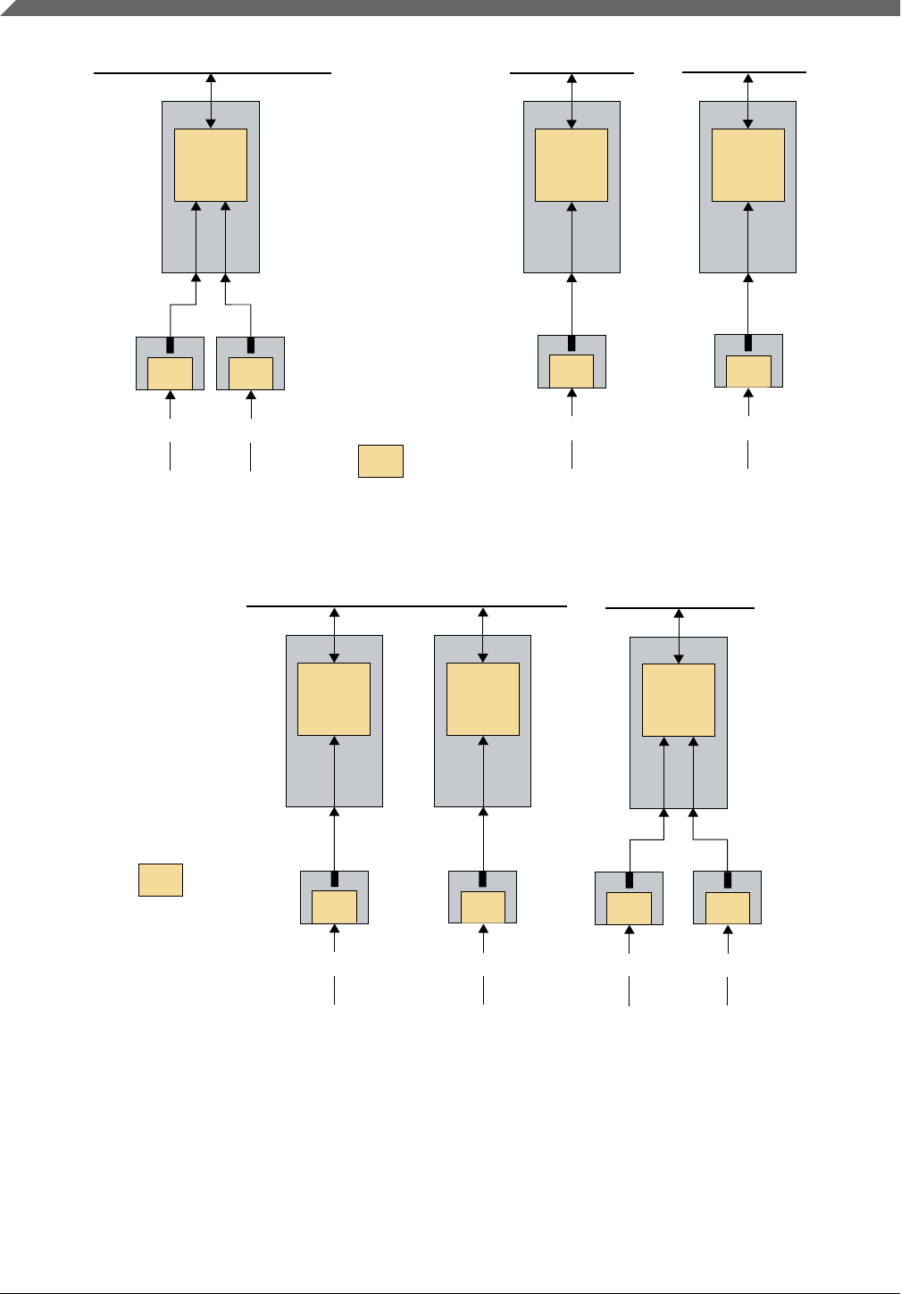
l
PBRIDGE_n
PORT
ll
FlexTimer
l
l
GPI[x] GPI[y]
= Input
FTM1[x] FTM0[y]
Double Digital Input Double PWM Input
PBRIDGE_nPBRIDGE_m
_0
FlexTimer
_1
Figure 5-2. Double Digital input and Double PWM input
l
PBRIDGE_n
PORT
ll
EIRQ[x] EIRQ[y]
= Input
l
PBRIDGE_n
l
FTM1[x] FTM0[y]
FlexTimer
_0
FlexTimer
_1
Figure 5-3. Double read encoder input (IRQ triggered)
Implementation hint: If sufficient diagnostic coverage can be obtained by a plausibility
check on a single acquisition for a specific application, that check can replace a
redundant acquisition.
Peripheral
S32K1xx Series Safety Manual, Rev. 4, 09/2018
64 NXP Semiconductors
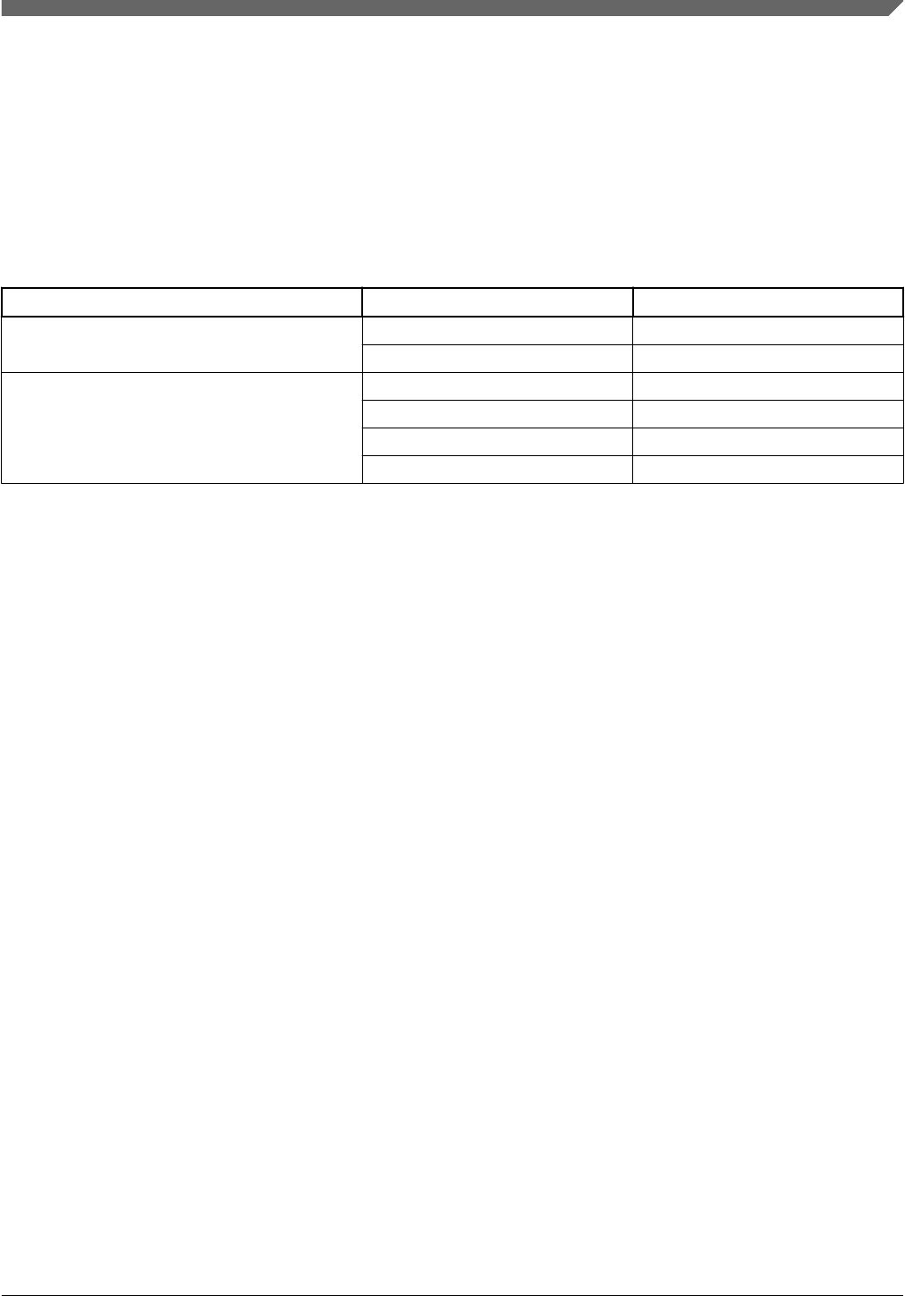
5.7.2.1.2 Software
Digital inputs used for functional safety purposes are assumed to be input redundantly as
described in this section. The table below lists two element safety functions for input in
the 'Function' column, the corresponding safety integrity functions in the 'Test' column
and their execution frequency. Alternative solutions with sufficient diagnostic coverage
are possible in the 'Frequency' column.
Table 5-3. Digital inputs software tests
Function Test Frequency
Double Read Digital Inputs PORT_SWTEST_REGCRC Once after programming
GPI_SWTEST_CMP Once for every acquisition
Double Read PWM Inputs
FLEXTIMER1_SWTEST_REGCRC Once after programming
FLEXTIMER2_SWTEST_REGCRC Once after programming
PORT_SWTEST_REGCRC Once after programming
FLEXTIMERI_SWTEST_CMP Once for every acquisition
5.7.2.1.2.1 Double read digital inputs
Rationale: To check that the configuration of the two I/Os used correspond with the
expected configuration, to reduce the likelihood of CMF caused by incorrectly configured
I/Os, and to check that the two input values read are similar.
Implementation hint: Functional safety integrity is achieved by replicated reading and
software comparison by the processing function. The application can implement the tests
PORT_SWTEST_REGCRC and GPI_SWTEST_CMP.
5.7.2.1.2.1.1 Implementation details
The only hardware element that can be used for the safety function is the general purpose
input/output (GPIO).
Implementation hint: Every I/O that is not dedicated to a single function can be
configured as GPIO. I/Os that are dedicated to ADC are an exception to this rule, as they
can only be configured as inputs.
Note
Caution: Redundant GPIO should be selected in a way that
their signals are not adjacent, which helps minimize the
likelihood of CMFs.
Chapter 5 Software Requirements
S32K1xx Series Safety Manual, Rev. 4, 09/2018
NXP Semiconductors 65

5.7.2.1.2.1.2 PORT_SWTEST_REGCRC
For implementation details of <module>_SWTEST_REGCRC functions, refer to Cyclic
Redundancy Check (CRC).
5.7.2.1.2.1.3 GPI_SWTEST_CMP
This software test is used to execute the comparison between the double reads performed
by the independent channels. It reads the outputs sequentially. This allows any GPIO to
be used, but could result in a wrong result if the state of the input changes between
reading the first and second inputs.
5.7.2.1.2.2 Double read PWM inputs
This approach reads two PWM inputs in parallel using two FlexTimers, then compares
the results.
Rationale: To check that the configuration of the modules used by this safety function
compare to the expected configuration and to validate that the two sets of read data
correlate.
Implementation hint: The software tests that the application may implement are:
• FLEXTIMER1_SWTEST_REGCRC
• FLEXTIMER0_SWTEST_REGCRC
• PORT_SWTEST_REGCRC
In addition, the double reads shall be compared by the application with the
implementation of the following test:
• FLEXTIMERI_SWTEST_CMP.
The PORT module may be configured to provide configuration and input direction of the
input GPIO.
5.7.2.1.2.2.1 Implementation details
Rationale: To reduce the risk of cascading faults due to shared resources.
Implementation hint: The following hardware elements shall be used for the safety
function:
Peripheral
S32K1xx Series Safety Manual, Rev. 4, 09/2018
66 NXP Semiconductors

• FlexTimer_1 channels
• FlexTimer_0 channels
The system integrator may select one channel from the FlexTimer_1 module and another
from the FlexTimer_0.
5.7.2.1.2.2.2 FLEXTIMERx_SWTEST_REGCRC and PORT_SWTEST_REGCRC
These functions check the correct configuration of all involved modules. See Cyclic
Redundancy Check (CRC) for implementation of the <module>_SWTEST_REGCRC
functions.
5.7.2.1.2.2.3 FLEXTIMERI_SWTEST_CMP
This test is used to execute the comparison between the double reads of PWM inputs
performed by two channels of different FlexTimer. The comparison may take into
account possible approximation because of different capturing of the asynchronous input
signals.
5.7.2.1.2.3 Synchronize sequential read input
The synchronize sequential read inputs is implemented by the PDB, which generates the
trigger for events according to the triggered mode or the sequential mode. The PDB can
be used if the synchronization of the reading of some inputs with some events is required.
The following mix of hardware mechanisms and software safety integrity measures
implemented at the application level provides respective functional safety integrity:
• PDB_HWSWTEST_TRIGGERNUM
• PDB_SWTEST_TRIGGERTIME
• PDB_HWSWTEST_TRIGGEROVERRUN
• PDB_HWSWTEST_ADCCOMMAND (only if the input is an analog signal)
• PDB_SWTEST_FLEXTIMERCOMMAND
• PDB_HW_CFGINTEGRITY
5.7.2.1.2.3.1 Hardware element
The synchronize sequential read input is implemented by the PDB, which generates the
trigger events according to one of the two operation modes shown in Figure 5-4.
Chapter 5 Software Requirements
S32K1xx Series Safety Manual, Rev. 4, 09/2018
NXP Semiconductors 67
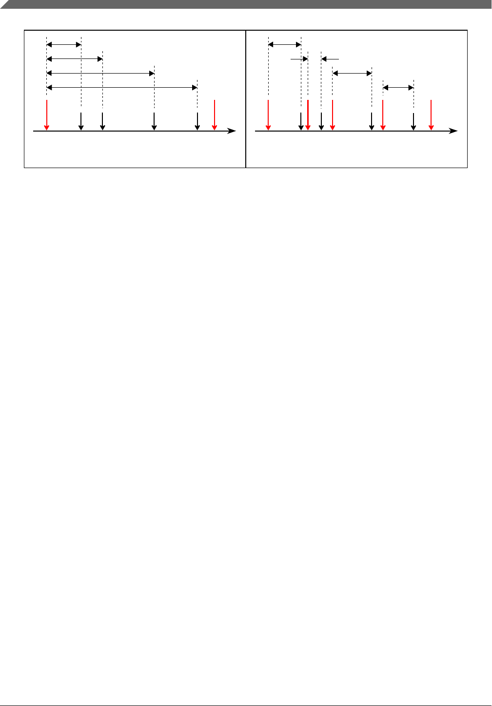
Delay T
0
Delay T
1
Delay T
2
Delay T
3
Delay T
0
Delay T
1
Delay T
2
Delay T
3
Trigger 1
Event
Trigger 0 Trigger 2 Trigger 3
Event
a)
Event 0
Trigger 0 Trigger 3
Event 3
b)
... ...
... ...
... ...
Figure 5-4. PDB operating modes: a) triggered and b) sequential
The PDB receives various incoming signals (Event X in Figure 5-4) from different
sources. These signals are then processed to generate trigger events (Trigger X in Figure
5-4). An event can be a rising edge, a falling edge or both edges of each incoming signal.
The output trigger can be a pulse, an ADC command (or a stream of consecutive
commands) or both to one or more peripherals (for example, ADC, FlexTimers, and so
on).
In triggered mode, the input event, which can be also a combination (logical OR) of
several signals, determines the reload/restart of the PDB counter and up to eight
comparators are available to generate up to eight output triggers with a given delay with
respect to the reload signal. In sequential mode, one comparator can be used to generate a
trigger with a given delay with respect to one out of eight input events (Event 0 works as
the reload event).
Implementation hint: The PDB is configured so that the output triggers are generated
with the desired time schedule with respect to the input event(s).
For each trigger the set of ADC commands and pulses to be generated are defined.
Particularly, each ADC command specifies which channel is acquired by which ADC, if
two ADCs perform a concurrent conversion or just one of them is operational, and in
which internal FIFO the result(s) will be stored. In case of a concurrent acquisition the
same FIFO is used for both results. ADCs are configured to accept commands from the
PDB (instead of commands provided via software). Multiple single or concurrent
acquisitions can be scheduled for each trigger events. The next command is sent when the
ADC signals the completion of previous acquisition.
Recommendation: The PDB can be configured to generate interrupt requests when a
trigger occurs (for example, to trigger READ DIGITAL INPUTS).
5.7.2.1.2.3.2 Implementation details
The following hardware elements may be used for the safety function:
Peripheral
S32K1xx Series Safety Manual, Rev. 4, 09/2018
68 NXP Semiconductors
• PDB
• One FlexTimer channel
• Another FlexTimer channel
Table 5-4. PDB software tests
Function Test Frequency
Synchronize sequential read input
PDB_HWSWTEST_TRIGGERNUM Once for every control period (< FTTI)
PDB_SWTEST_TRIGGERTIME Once for every PDB control period
(triggered mode) or every trigger
(sequential mode)
PDB_HWSWTEST_TRIGGEROVERRUN Once for every trigger
PDB_HWSWTEST_ADCCOMMAND Once for every ADC command
PDB_SWTEST_FLEXTIMERCOMMAND Once for every control period (< FTTI)
PDB_HW_CFGINTEGRITY Once for every control period (< FTTI)
5.7.2.2 Digital outputs
Functional safety digital outputs are always assumed to be written either redundantly or
with read back. In case of single output with read back, the feedback loop should be as
large as possible to cover faults on system level also. The figure below depicts the
connection of two (functional safety critical) actuators connected to the S32K1xx.
Actuator 1 is connected to an output peripheral, for example, a motor is connected to a
PWM output (output peripheral 3). The signal generated by the output peripheral 3 can be
input to an input peripheral, for example, a FlexTimer. This measure is to confirm, that
the generated output signal is correct. This read back may be internally of the S32K1xx
(internal read back) or externally (external read back). The external read back covers
more types of failures (for example, corrupt wire bonds or solder joints) than the internal
read back, but still does not guarantee, that the actuator really behaves as desired. This is
achieved by including the actuator and sensor into the read back loop. An alternative
solution is to redundantly output a signal. For example, actuator 2 consists of two relays
in series to switch off a functional safety-relevant supply voltage. The selection of the
suited output connection is part of the I/O functional safety concept on system level.
Chapter 5 Software Requirements
S32K1xx Series Safety Manual, Rev. 4, 09/2018
NXP Semiconductors 69
actuator 2
peripheral 1
output
peripheral 2
output
peripheral 3
peripheral
input
O
O
O
I
output
actuator 1
internal
read back external
read back
external read back
with actuator/sensor
in the loop
sensor
torque, position,
angle, pressure,
temperature,
voltage, etc.
torque, position,
angle, pressure,
temperature,
voltage, etc.
Figure 5-5. Digital Outputs with redundancy and read back
Implementation hint: If a sufficient diagnostic coverage can be reached by a plausibility
check on a single output channel for a specific application, that check can replace a
redundant write or read-back. This hint is a special case of deviating from Assumptions
as described in the preface.
5.7.2.2.1 Hardware
5.7.2.2.1.1 Single write digital output
• Single Write Digital Output with external read-back (Figure 5-6, left):
A comparison between the desired output values and the value read back via external
read-back configuration is done. After writing the output value, the status of the
digital input is evaluated.
• Single Write Digital Output with internal read-back (Figure 5-6, right):
A comparison between the desired output values and the value read back via internal
read-back configuration. After writing the output value, the internal read-back status
is evaluated.
• Single Write PWM Output with external read-back (Figure 5-7, left):
3. Internal read back does not cover package faults (for example, wire bond, etc.).
Peripheral
S32K1xx Series Safety Manual, Rev. 4, 09/2018
70 NXP Semiconductors
This procedure output compares the PWM read-back provided by a single channel of
the FlexTimer_0 (FlexTimer_1, FlexTimer_2) with the expected values that have
been written to the external pad of the FlexTimer_3_PWM output channel.
• Single Write PWM Output with internal read-back 3 (Figure 5-7, right):
This procedure output compares the PWM read-back by a single channel of the
FlexTimer_0 (FlexTimer_1, FlexTimer_2) with the expected values that have been
written to the FlexTimer_PWM output channel.
l
PORT
l
= Input
Digital Out External Readback
Configuration
O
PORT
O
= Output
O
GPI GPO GPO
Digital Out External Readback
Configuration
PBRIDGE_nPBRIDGE_n
Figure 5-6. Single write digital output with read-back
Chapter 5 Software Requirements
S32K1xx Series Safety Manual, Rev. 4, 09/2018
NXP Semiconductors 71
l
= Input
PWM Out Single Write External
Read-back Configuration
PRBIDGE_n
FlexTimer
l
PWM Out Single Write Internal
Read-back Configuration
PBRIDGE_n
FlexTimer
_PWM FlexTimer FlexTimer
_PWM
OlO
= Output
O
FTM n[z]* n[z]*
*Note:
n[z] represents any FlexTimer_PWM output (for example, A[z], B[z] or X[z]),
but each output must be driven by different FlexTimer_PWM modules.
Figure 5-7. Single write PWM output with read-back
5.7.2.2.1.2 Double write digital output
• Double write digital output
The PORT hardware element is used to perform a double-write digital output.
• Double write PWM output
• The hardware elements are used to perform a double write PWM output:
• FlexTimer_0 and FlexTimer_1
• FlexTimer_1 and FlexTimer_2
• FlexTimer_2_PWM and FlexTimer_3_PWM
Peripheral
S32K1xx Series Safety Manual, Rev. 4, 09/2018
72 NXP Semiconductors
Timer_0
Timer_1
PBRIDGE_nPBRIDGE_n
FTM[x]* FTM[y]* n[z]* n[z]*
Output
Note: n[z] represents any FlexTimer_PWM output (for example, A[z], B[z], or
X[z]), but each output must be driven by a different FlexTimer_PWM module.
The same consideration is valid for the FlexTimer; any FlexTimer output may
be used, but each output must be driven by a different FlexTimer module.
FlexFlex Flex
Timer_2
_PWM
Flex
Timer_3
_PWM
Figure 5-8. Double write PWM output
GPO[x] GPO[y]
PORT
Digital Out Double
Configuration
Figure 5-9. Double write digital output
Chapter 5 Software Requirements
S32K1xx Series Safety Manual, Rev. 4, 09/2018
NXP Semiconductors 73

5.7.2.2.2 Software
Digital outputs used for functional safety purposes are assumed to be written either
redundantly or with read back as described in this section. Table 5-5 lists four element
safety functions for output, the corresponding safety integrity functions and their
execution frequency. Alternative solutions with sufficient diagnostic coverage are
possible.
Table 5-5. Digital outputs software tests
Function Test Frequency
Single Write Digital Outputs With
Read Back
PORT_SWTEST_REGCRC Once after programming
GPOERB_SWTEST_CMP Once per FTTI
GPOIRB_SWTEST_CMP Once per FTTI
Double Write Digital Outputs PORT_SWTEST_REGCRC Once after programming
GPODW_SWAPP_WRITE Once per FTTI
Single Write PWM Outputs With
Read Back
PORT_SWTEST_REGCRC Once after programming
FLEXTIMER0_SWTEST_REGCRC1Once after programming
FLEXTIMER1_SWTEST_REGCRC1 Once after programming
FLEXTIMER2_SWTEST_REGCRC1 Once after programming
FLEXTIMER2PWM_SWTEST_REGCRC2Once after programming
FLEXTIMER3PWM_SWTEST_REGCRC2 Once after programming
PWMRB_SWTEST_CMP Once per FTTI
Double Write PWM Outputs
PORT_SWTEST_REGCRC Once after programming3
FLEXTIMER0_SWTEST_REGCRC1 Once after programming
FLEXTIMER1_SWTEST_REGCRC1 Once after programming
FLEXTIMER2_SWTEST_REGCRC1 Once after programming
FLEXTIMER2PWM_SWTEST_REGCRC2 Once after programming
FLEXTIMER3PWM_SWTEST_REGCRC2 Once after programming
PWMDW_SWAPP_WRITE Once per FTTI
1. This test is required only if the FlexTimer channels are used for the safety function.
2. This test is required only if the FlexPWM channels are used for the safety function.
3. If a change in a single PORT configuration register is capable of affecting both the output and the read-back paths, then
PORT_SWTEST_REGCRC may be executed every FTTI. In all other cases configuration errors are covered by the
software comparison.
5.7.2.2.2.1 Single write digital outputs with read-back
The PORT hardware element is used to perform a Single Write Digital Output With
Read-Back (see Figure 5-6).
Rationale: To check whether written data is coherent to the expected data
Implementation hint: The read back may be implemented either with external or with
internal readback.
Peripheral
S32K1xx Series Safety Manual, Rev. 4, 09/2018
74 NXP Semiconductors

The PORT element is correctly configured to provide the output write and the pad
directions as follows:
• External read back – PORT is configured to read back the signal via an additional
pad, and the loopback is performed outside the device. In this configuration, only
half of the available digital outputs are available as functional safety outputs.
• Internal read back – PORT is configured to read back the pad value via an internal
read path. All pads dedicated to digital input/output are capable of reading the pad
digital status using the input logic.
Rationale: To reduce the likelihood of a CMF caused by incorrect configuration of pads
Implementation hint: The application software integrates software test
PORT_SWTEST_REGCRC in the application to check the correct configuration of the
pads, and to compare a read back with the digital output write.
GPOERB_SWTEST_CMP may be used for the external read back or
GPOIRB_SWTEST_CMP for internal read back.
5.7.2.2.2.1.1 Implementation details
The PORT hardware element may be used for the safety function.
Note
Pads that are not dedicated to a single function can be
configured as GPIO. Pads dedicated to ADC are an exception to
this rule, as they can only be configured as inputs.
5.7.2.2.2.1.2 PORT_SWTEST_REGCRC
For implementation of a <module>_SWTEST_REGCRC function please refer to Cyclic
Redundancy Check (CRC).
5.7.2.2.2.1.3 GPOERB_SWTEST_CMP
This software test is used to execute the comparison between the desired output values
and the value read back via external read back configuration. After writing the output
value, the test reads the status of the digital input.
Rationale: To check if the read data equals the written data
Implementation hint: The output is externally (on system level) connected to an input
I/O. After writing the value to the output signal, the input is read to check that the correct
output is present.
Chapter 5 Software Requirements
S32K1xx Series Safety Manual, Rev. 4, 09/2018
NXP Semiconductors 75

From the scenarios described in Figure 5-5, the GPOERB_SWTEST_CMP supports the
internal read back scenario and the external read back scenario. The
GPOERB_SWTEST_CMP supports the external read back with actuator/sensor in the
loop scenario only under certain condition. It will depend on the type of the signal the
sensor is giving as response and if the MCU can handle it.
5.7.2.2.2.1.4 GPOIRB_SWTEST_CMP
Rationale: To check if the read data equals the written data.
This software test is used to execute the comparison between the desired output values
and the value read back via internal read back configuration. After writing the output
value, the test reads the status.
5.7.2.2.2.2 Double write digital outputs
The PORT hardware element is used to perform a Double Write Digital Output.
Rationale: To configure pads used by this safety function and reduce the likelihood of a
CMF caused by incorrect configuration of pads
Implementation hint: The PORT is configured by application software to correctly
define the configuration of the outputs used. The software performs a double write.
Rationale: To reduce the likelihood of a CMF caused by incorrect configuration of the
pads
Implementation hint: To achieve the integrity of the two output channels, the
application validates the PORT configuration implementing the
PORT_SWTEST_REGCRC.
Rationale: To write a digital output by exploiting redundancy
Implementation hint: The application software implements the double output write as
defined by the GPODW_SWAPP_WRITE.
5.7.2.2.2.2.1 Implementation details
The only hardware element that can be used for the safety function is the GPIO.
Every pad not dedicated to a single function may be configured as GPIO. Pads dedicated
to ADC are an exception to this rule, as they can be configured as inputs only.
Peripheral
S32K1xx Series Safety Manual, Rev. 4, 09/2018
76 NXP Semiconductors

5.7.2.2.2.2.2 GPODW_SWAPP_WRITE
Rationale: To prevent SPFs in the PORT to influence the actuator control in a dangerous
way
Implementation hint: The output write of a redundant channel may be implemented by
writing the two outputs to the appropriate register and this register may be checked by
read back.
5.7.2.2.2.3 Single write PWM outputs with read-back
The following combination of elements may be used to perform a Write PWM Output
With Read-Back:
• FlexTimer_0 – FlexTimer_2_PWM
• FlexTimer_1 – FlexTimer_3_PWM
• FlexTimer_2 – FlexTimer_2_PWM
These units shall be configured to implement one PWM output channel and (via internal
read-back) the FlexTimer_0 input PWM channel. The PORT shall be configured to
define the configuration of the output pads used. The software performs a write operation
followed by a read operation. To achieve the integrity of the two output channels, the
application shall tests the PORT configuration implementing the
PORT_SWTEST_REGCRC (to reduce the likelihood of a CMF caused by incorrect
configuration of the pads).
Rationale: To check that the configuration of the modules used by this safety function
adheres to the expected configuration.
Implementation hint: A single channel of the FlexTimer is used with a multiplexing of
the internal read-back of the different output of the FlexTimer_2_PWM. The read-back
paths are limited to six signals, two for each sub-module of the FlexTimer_2_PWM.
The following test validate the correct configuration for the FlexTimer(s):
• FLEXTIMER2PWM_SWTEST_REGCRC
• FLEXTIMER3PWM_TEST_REGCRC
• FLEXTIMER0_SWTEST_REGCRC
• FLEXTIMER1_SWTEST_REGCRC
• FLEXTIMER2_SWTEST_REGCRC
Rationale: To check that the written data is what is expected.
Chapter 5 Software Requirements
S32K1xx Series Safety Manual, Rev. 4, 09/2018
NXP Semiconductors 77

Implementation hint: The application software writes to the output port and then
compare the written value via the read-back (PWMRB_SWTEST_CMP).
5.7.2.2.2.3.1 Implementation details
The following hardware elements may be used for the safety function:
• FlexTimer_0 channels
• FlexTimer_1 channels
• FlexTimer_2 channels
• FlexTimer_2_PWM channels
• FlexTimer_3_PWM channels
5.7.2.2.2.3.2 FLEXPWMx_SWTEST_REGCRC and FLEXTIMERx_SWTEST_REGCRC
For implementation of a <module>_SWTEST_REGCRC function please refer to Cyclic
Redundancy Check (CRC).
5.7.2.2.2.3.3 PWMRB_SWTEST_CMP
This test compares the PWM read back provided by a single channel of the FlexTimer_1
(FlexTimer_0) with the expected values that have been written to the FlexTimer_2_PWM
(FlexTimer_3_PWM) output channel.
For this test, FlexTimer_2_PWM is used to generate a PWM output and FlexTimer_1 is
used to read back and verify the output. Another combination could be used if required in
an application.
5.7.2.2.2.4 Double write PWM outputs
Rationale: The hardware elements FlexTimer_0, FlexTimer_1, FlexTimer_2,
FlexTimer_2_PWM and FlexTimer_3_PWM are used to perform a double Write PWM
Output.
Implementation hint: These units are configured to implement two independent PWM
channels. The PORT is configured to define the configuration of the output pads used.
The software performs a double write (see PWMDW_SWAPP_WRITE).
Rationale: To reduce the risk of CCF due to spatial proximity
Peripheral
S32K1xx Series Safety Manual, Rev. 4, 09/2018
78 NXP Semiconductors

Implementation hint: Using adjacent pads as redundant I/O increases the likelihood of
CMFs. Therefore, it is preferable to use I/O that do not share the same configuration and
data registers in the PORT.
Rationale: To reduce the likelihood of a CMF caused by incorrect configuration of the
pads
Implementation hint: To improve the integrity of the two output channels, the
application should test the PORT configuration implementing the
PORT_SWTEST_REGCRC.
Rationale: To check that the configuration of the modules used by this safety function
adhere to the expected configuration
Implementation hint: The application software shall implement a test for the register
configuration:
• FLEXTIMER0_SWTEST_REGCRC (for FlexTimer_0)
• FLEXTIMER1_SWTEST_REGCRC (for FlexTimer_1)
• FLEXTIMER2_SWTEST_REGCRC (for FlexTimer_2)
• FLEXTIMER2PWM_PWM_SWTEST_REGCRC (for FlexTimer_2_PWM)
• FLEXTIMER3PWM_SWTEST_REGCRC (for FlexTimer_3_PWM)
Rationale: To reduce the possibility of cascading a failure to shared circuitries, different
modules should be used.
Implementation hint: The output write of a redundant PWM channel is implemented by
writing the new output values to both PWM channels.
5.7.2.2.2.4.1 Implementation details
The following hardware elements are used for the safety function:
• FlexTimer_0 channels
• FlexTimer_1 channels
• FlexTimer_2 channels
• FlexTimer_2_PWM
• FlexTimer_3_PWM channels
Chapter 5 Software Requirements
S32K1xx Series Safety Manual, Rev. 4, 09/2018
NXP Semiconductors 79

5.7.2.2.2.4.2 PORT_SWTEST_REGCRC
For implementation of a <module>_SWTEST_REGCRC function please refer to Cyclic
Redundancy Check (CRC).
5.7.2.2.2.4.3 PWMDW_SWAPP_WRITE
If the content of the PWM outputs are changed, care must be taken since the outputs can
not be updated synchronously. Therefore for a short period of time both outputs could be
different.
5.7.2.3 Analog inputs
5.7.2.3.1 Hardware
Two options are available for reading analog inputs:
• Single read analog inputs
• Double read analog inputs
5.7.2.3.1.1 Single read analog inputs
The single-read analog input uses a single-analog-input channel either of ADC_0 or
ADC_1 to acquire an analog voltage signal (see the figure below).
Peripheral
S32K1xx Series Safety Manual, Rev. 4, 09/2018
80 NXP Semiconductors
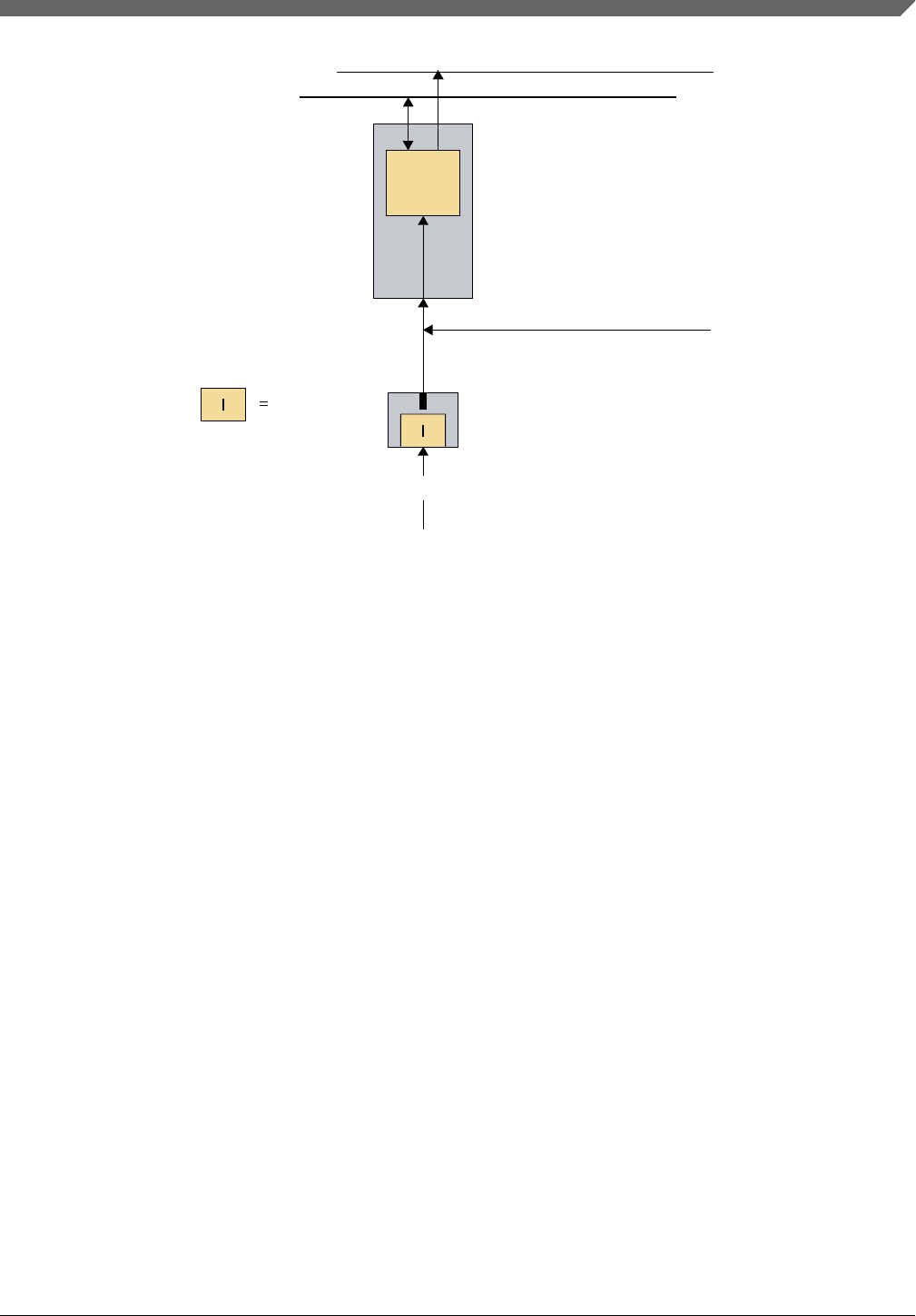
ADC_x
Fault Routing
PBRIDGE_n
Input
AN[x]
Reference voltages
Figure 5-10. Single read analog input configuration
5.7.2.3.1.2 Double read analog inputs
The Double Read Analog Input uses two analog input channels to acquire a replicated
analog input signal. Two ADC units acquire and digitize the two copies of a redundant
analog signal connected to the inputs. In this configuration only a portion of the analog
inputs are available. The comparison of the results is performed by the system level
application software (see the figure below).
The following is the list of S32K14x ADC channels that may be used with the Double
Read Analog Inputs function:
• ADC0_SE[4:5] and [8:9]
• ADC1_SE[8:9] and [14:15]
Rationale: ADC_0 and ADC_1 share input channels. Using double reads on these shared
channels is a possible source of CCFs.
Implementation hint: One shared ADC-channel may not be used for both inputs of the
Double Read Analog Input function.
Chapter 5 Software Requirements
S32K1xx Series Safety Manual, Rev. 4, 09/2018
NXP Semiconductors 81
Using channels ADC0_SE4 and ADC1_SE14 as an example, these two channels can
work independently but they can also be hardware interleaved. In hardware interleaved
mode, a signal on pin PTB0 can be sampled by both ADC0 and ADC1. Interleaved mode
is enabled by SIM_CHIPCTL[ADC_INTERLEAVE_EN].The possible combinations of
double read ADC inputs are as follows:
• Channels ADC0_SE5 and ADC1_SE15 are interleaved on pin PTB1
• Channels ADC0_SE4 and ADC1_SE14 are interleaved on pin PTB0
• Channels ADC0_SE8 and ADC1_SE8 are interleaved on pin PTB13
• Channels ADC0_SE9 and ADC1_SE9 are interleaved on pin PTB14
The functional safety integrity is achieved by replicated acquisition with separated analog
input channels and software comparison by the processing function (see the figure
below).
PBRIDGE
Fault Routing
Input
AN[x] AN[y]
ADC1
ADC0
Figure 5-11. Double read analog inputs configuration
NOTE
The S32K11x variants have only one ADC. In this case, use
only two analog inputs and measure both inputs sequential on
the ADC. This will reduce the pin failure rate which is higher
than the ADC analog failure rate.
Peripheral
S32K1xx Series Safety Manual, Rev. 4, 09/2018
82 NXP Semiconductors

5.7.2.3.2 Software
Analog inputs used for functional safety purposes are assumed to be input redundantly as
described in this section. Table 5-6 lists two element safety functions for analog input, the
corresponding safety integrity functions and their execution frequency. Alternative
solutions with sufficient diagnostic coverage are possible.
Table 5-6. Analog inputs software tests
Function Test Frequency
Single Read Analog
Inputs
ADC_SWTEST_TEST1 Once after reset and before start of the safety
application
ADC_SWTEST_TEST2 Once after reset and before start of the safety
application
ADC_SWTEST_VALCHK Once for every acquisition
ADC_SWTEST_OVERSAMPLING Once for every acquisition
ADC0_SWTEST_REGCRC Once in the FTTI
ADC1_SWTEST_REGCRC Once in the FTTI
PORT_SWTEST_REGCRC Once in the FTTI
Double Read Analog
Inputs
ADC_SWTEST_TEST3 Once in the FTTI
ADC0_SWTEST_REGCRC Once after programming
ADC1_SWTEST_REGCRC Once after programming
PORT_SWTEST_REGCRC Once after programming
ADC_SWTEST_CMP Once for every acquisition
5.7.2.3.2.1 Single read analog inputs
To support a high diagnostic coverage two known reference supply voltages are utilized
by two software tests which are described in the following sections
(ADC_SWTEST_TEST1 and ADC_SWTEST_TEST2).
The reference supply voltages are the following:
• VREFH (ADC0/ADC1 high voltage reference)
• VREFL (ADC0/ADC1 reference ground)
The PORT unit is configured to correctly enable the ADC inputs. The pads used for
analog inputs can only be configured as inputs.
Single Read Analog Inputs may be implemented using the following safety integrity
functions at the application level:
• ADC_SWTEST_TEST1
Chapter 5 Software Requirements
S32K1xx Series Safety Manual, Rev. 4, 09/2018
NXP Semiconductors 83

• ADC_SWTEST_TEST2
• ADC_SWTEST_VALCHK
• ADC0_SWTEST_REGCRC, ADC1_SWTEST_REGCRC
• PORT_SWTEST_REGCRC
• ADC_SWTEST_OVERSAMPLING
5.7.2.3.2.1.1 Implementation details
The following S32K1xx hardware elements can be used for the safety integrity functions:
• Analog input channels ADC0_SE[0:3], ADC0_SE[6:7] and ADC0_SE[10:15]
• Analog input channels AN[11:14] of ADC0_SE[4:5], ADC1_SE[8:9] and
ADC1_SE[14:15] (shared channels)
• Analog input channels ADC1_SE[0:7] and ADC1_SE[10:13]
5.7.2.3.2.1.2 PORT_SWTEST_REGCRC
For implementation of a <module>_SWTEST_REGCRC function please refer to Cyclic
Redundancy Check (CRC).
5.7.2.3.2.1.3 ADCn_SWTEST_REGCRC
If ADC_0 is used the ADC0_SWTEST_REGCRC may be used. If ADC_1 is used the
ADC1_SWTEST_REGCRC may be used.
For implementation of a <module>_SWTEST_REGCRC function please refer to Cyclic
Redundancy Check (CRC).
5.7.2.3.2.1.4 ADC_SWTEST_TEST1
Check ADC correct functionality.
Rationale: To detect possible failure of the ADC conversion logic.
Implementation hint: Enable and configure the ADC internal supply monitoring feature
to sample and convert the fixed internal voltages of 0 V and 5 V. Then, compare the
conversion results with the corresponding expected values.
Peripheral
S32K1xx Series Safety Manual, Rev. 4, 09/2018
84 NXP Semiconductors

5.7.2.3.2.1.5 ADC_SWTEST_TEST2
Check that the analog input path is not floating.
Rationale: To detect failures of the channel multiplexing circuitry.
Implementation hint: Alternately, configure the ADC to convert two fixed internal
constant values, followed by an application-dependent voltage value. Then, compare the
conversion results with the expected values. Choose an application-dependent voltage
value that is between the two fixed constant values. Perform a conversion in both
directions -- from low voltage to high voltage, and from high voltage to low voltage.
5.7.2.3.2.1.6 ADC_SWTEST_VALCHK
When ADC conversion is triggered by the PDB, the acquired digital sample data are
stored into a dual queue along with information about the channel that performed the
acquisition. The checking of the expected channel provides coverage of the control logic
and part of the queue logic. Checking of the expected sequence of acquired channels
provides the coverage of the control logic and part of the queue logic.
The goal of this software test is to verify correct operation of the control and queue logic
of the ADC, and also the PDB, if used. The way this software measure is implemented
depends on how the ADC is configured (for example, PDB or CPU mode):
•When the ADC is used in CPU mode, the acquired value is read by the ADC_Rn.
ADC_SC1n[COCO] provides status information about the data acquisition.
Application software should read and verify these fields after every acquisition.
• When ADC conversion is triggered by the PDB, status bits in Status and Control
Register 2 (ADC_SC2) should be considered in addition. The checking of the
expected channel provides coverage of the control logic and part of the queue logic.
5.7.2.3.2.1.7 ADC_SWTEST_OVERSAMPLING
During Single Read Analog Inputs, the ADC_SWTEST_OVERSAMPLING may be
implemented as counter measure against random fault.
ADC_SWTEST_OVERSAMPLING is an acquisition redundant in time.
It refers to sampling the signal at a rate significantly higher than the Nyquist frequency
related to the input signal. If there is a fault, the acquired values will not be correlated.
This safety integrity measure compares the acquired value to check the correlation.
Against a random fault, three consecutive analog values are converted for each
acquisition to implement the ADC_SWTEST_OVERSAMPLING. The figure below
shows the sampling of an analog signal at different points in time (A1, A2 and A3). Every
Chapter 5 Software Requirements
S32K1xx Series Safety Manual, Rev. 4, 09/2018
NXP Semiconductors 85
conversion is indicated by an arrow, which indicates the converted digital value by its
length. The second acquisition (A2) is faulty because the first converted value is quite
different respect the other two.
Faulty Acquisition
t
A
3
A
2
A
1
Figure 5-12. Series of acquired analog values
5.7.2.3.2.2 Double Read Analog Inputs
Rationale: To validate that the configuration of the modules used by this safety function
corresponds with what is expected. To reduce the likelihood of CMFs caused by
improper configuration of the pads.
Implementation hint: Double Read Analog Inputs may be implemented using the
following safety integrity functions at the application level:
•ADCx_SWTEST_REGCRC
• PORT_SWTEST_REGCRC
Rationale: To validate that the two sets of read data correlate.
Implementation hint: Double Read Analog Inputs may be implemented using the
software test ADC_SWTEST_CMP to compare the channel reads. In addition, you can
use the interleave functionality of ADC_SWTEST_TEST3 to verify that both ADCs are
converting an analog input to the same digital value. See ADC_SWTEST_TEST3 for
details.
5.7.2.3.2.2.1 Implementation details
The following hardware elements may be used for the safety function:
• Analog input channels AN[0:8] of ADC_0
• Analog input channels AN[0:8] of ADC_1
One channel from different ADC modules may be used, for example, one from ADC0
and one from the ADC1.
Peripheral
S32K1xx Series Safety Manual, Rev. 4, 09/2018
86 NXP Semiconductors

5.7.2.3.2.2.2 PORT_SWTEST_REGCRC
For implementation of a <module>_SWTEST_REGCRC function, see Cyclic
Redundancy Check (CRC).
5.7.2.3.2.2.3 ADC_SWTEST_CMP
This software test is used to execute the comparison between the double reads performed
by any combination of two ADCn module channels. The comparison may take possible
conversion tolerances into account.
5.7.2.3.2.2.4 ADC_SWTEST_TEST3
This software test uses the interleave functionality, and can be used to verify that the
involved ADCs are converting the analog input to the same digital value. To increase
coverage, you can use different clock sources for the used ADCs.
5.7.2.4 Other requirements
Rationale: To detect missing FlexTimer acquisition.
Implementation hint: In the FlexTimer module, the capture flag
(FTM_n_STATUS_[CHnF]) may be used.
Implementation hint: Use fault inputs for global fault control and the corresponding
fault condition interrupt and the FlexTimer input capture testing feature. .
Implementation hint:
• When an application needs to access the ADC result FIFO, a 32-bit read access
enables the verification of the correct channel number on which the conversion was
executed.
• All the FIFO empty interrupt flags should checked when the motor control period
interrupt occurs
• In the FlexTimer module, the capture flag should be used to detect missing
FlexTimer acquisition.
• If the ADC analog watchdog function is used for functional safety-relevant signal,
two analog watchdog channels should monitor the same signal.
Chapter 5 Software Requirements
S32K1xx Series Safety Manual, Rev. 4, 09/2018
NXP Semiconductors 87

5.7.3 PBRIDGE protection
The PBRIDGE access protection can be used to restrict read and write access to
individual peripheral modules and restrict access based on the master's access attributes.
• Master privilege level – The access privilege level associated with each master is
configurable. Each master can be configured to be trusted for read and write
accesses.
• Peripheral access level – The access level of each on-platform and off-platform
peripheral is configurable. The peripheral can be configured to require the master
accessing the peripheral to have supervisor access attribute. Furthermore, if the
peripheral write protection is enabled, write accesses to the peripheral are terminated.
The peripheral can also be configured to block accesses from an untrusted master.
Recommendation: Using application software, periodically check the contents of
configuration registers (more than 10 registers) of modules attached to the PBRIDGEs to
help detect faults in the PBRIDGE.
5.7.3.1 Initial checks and configurations
The application software should configure the PBRIDGEs to define the access
permissions for each slave module that requires access protection.
Application software should configure the PBRIDGE to prevent write accesses to the
RCM address space for all masters except the core.
5.7.4 Analog to Digital Converter (ADC)
Parts of the Successive Approximation Register (SAR) Analog-to-Digital Converter
(ADC) of the S32K1xx do not provide the functional safety integrity to achieve high
functional safety integrity targets. Therefore, system level measures are required.
5.7.4.1 Initial checks and configurations
Assumption under certain conditions: [SM_130] When Analog-to-Digital Converter
(ADC) of the S32K1xx are used in a safety function, suitable system level functional
safety integrity measures must be implemented once per L-FTTI. [end]
Rationale: To check the integrity of the ADC modules against failures
Peripheral
S32K1xx Series Safety Manual, Rev. 4, 09/2018
88 NXP Semiconductors

Implementation hint: After reset, but before executing any safety function, the
following software tests of one or both ADC modules may be executed by the application
software to detect faults:
• ADC_SWTEST_TEST1
• ADC_SWTEST_TEST2
• ADC_SWTEST_TEST3
Calibration needs to be completed after destructive reset.
When using the ADC for an analog input function, additional software tests are required
(see Analog inputs).
5.7.5 Asynchronous Wake-up Interrupt Controller (AWIC) /
External NMI
Assumption under certain conditions:[SM_126] If external NMI and Wake-up are used
as a safety mechanism, especially if waking up within a certain timespan or at all is
considered safety-relevant, it is required to implement corresponding system level
measures to detect latent faults in the AWIC. [end]
Rationale: To test the AWIC for external NMIs and wakeup events.
Implementation hint: To test the AWIC for external NMIs, application software may
configure the NMI during startup to cause only a critical interrupt, then trigger the
external NMI and check that the critical interrupt occurred.
Chapter 5 Software Requirements
S32K1xx Series Safety Manual, Rev. 4, 09/2018
NXP Semiconductors 89

Peripheral
S32K1xx Series Safety Manual, Rev. 4, 09/2018
90 NXP Semiconductors

Chapter 6
Failure Rates and FMEDA
6.1 Failure rates
In order to analyze and quantify the effectiveness of the S32K1xx integrated safety
architecture to handle random hardware failures, the inductive analysis method of
FMEDA (Failure Modes Effects and Diagnostic Analysis) was performed during the
development of the S32K1xx. The following methods for deriving the base failure rates
of the S32K1xx were used as input to the FMEDA:
• Permanent faults (Die & Package): IEC TR 62380 - Reliability data handbook –
Universal model for reliability prediction of electronics components, PCBs and
equipment
• Transient faults (Die): JEDEC Standard JESD89 - Measurement and Reporting of
Alpha Particle and Terrestrial Cosmic Ray-Induced Soft Errors in Semiconductor
Devices
6.2 FMEDA
In order to support the integration of the S32K1xx into safety-related systems and to
enable the safety system developer to perform the system level safety analysis, the
following documentation is available:
• FMEDA - Inductive analysis of the S32K1xx enabling customization of system level
safety mechanisms, including the resulting safety metrics for ISO 26262 (SPFM,
LFM and PMHF) and IEC 61508 (SFF and β-factor βIC)
• FMEDA Report - Describes the FMEDA methodology and safety mechanisms
supported in the FMEDA, including source of failure rates, failure modes and
assumptions made during the analysis.
The FMEDA and FMEDA report are available upon request.
S32K1xx Series Safety Manual, Rev. 4, 09/2018
NXP Semiconductors 91

6.2.1 Module classification
For calculating the safety metrics for ISO 26262 (Single-Point Failure Metric (SPFM),
Latent Failure Metric (LFM) and Probabilistic Metric for random Hardware Failures
(PMHF)) and for IEC 61508 (Safe Failure Fraction (SFF) and βIC factor) the modules of
the S32K1xx are classified as follows:
•MCU Safety Functions: All modules which can directly influence the correct
operation of the MCU Safety Functions.
•Safety Mechanism: All modules which detect faults or control failures to achieve or
maintain a safe state. These modules cannot independently directly influence the
correct operation of one of the safety functions in the case of a single fault.
•Peripheral: All modules which are involved in I/O operation. Peripheral modules are
usable by qualifying data with system level safety measures or by using modules
redundantly. Qualification should have a low risk of dependent failure. In general,
Peripheral module safety measures are implemented in system level software.
•Debug Functions: All modules which are not safety related, i.e. none of their
failures can influence the correct operation of one of the safety functions.
FMEDA
S32K1xx Series Safety Manual, Rev. 4, 09/2018
92 NXP Semiconductors

Chapter 7
Dependent Failures
7.1 Provisions against dependent failures
7.1.1 Causes of dependent failures
ISO 26262-9 lists the following dependent failures, which are applicable to the S32K1xx
on chip level:
• Random hardware failures, for example:
• dependent failures that are able to influence an on-chip function and its
respective safety mechanisms
• Environmental conditions, for example:
• temperature
• EMI
• Failures of common signals (external resources), for example:
• clock
• power-supply
• non-application control signals (for example, testing, debugging)
• signals from modules that are not replicated
Additionally, the following topics are mentioned, which are out of scope of this
document and not treated here:
• Development faults:
• development faults are systematic faults which are addressed by design-process
• Manufacturing faults:
• manufacturing faults are usually systematic faults addressed by design-process
and production test
• Installation and repair faults:
• installation and repair faults need to be considered at system level
• Stress due to specific situations:
S32K1xx Series Safety Manual, Rev. 4, 09/2018
NXP Semiconductors 93

• Specific situations may be considered at system level. Additionally, the result of
stress (for example, wear and aging due to electro-migration) usually lead to
single-point faults and are not considered dependent failures.
7.1.2 Measures against dependent failures
Environmental conditions
7.1.2.1.1 EMI and I/O
To cope with noise on digital inputs, the I/O circuitry provides input hysteresis on all
digital inputs. Moreover, the digital inputs including interrupt and timer inputs, as well as
the RESET pin contain glitch filtering capabilities, which are described in the Port
Control and Interrupts (PORT), FlexTimer Module (FTM), Low-Power Timer (LPTMR),
and Reset Control Module (RCM).
To reduce interference due to digital outputs, the I/O circuitry provides drive strength
control where applicable. An internal weak pull up or pull down structure is also
provided to define the input state.
Failures of common signals
7.1.2.2.1 Clock
To cover dependent failures caused by clock issues, clock monitors for supervision are
implemented which are described in the SCG (System Clock Generator). Major failures
in the clock system are also detected by the WDOG (Watchdog Timer).
7.1.2.2.2 Power supply
To cover dependent failures caused by issues with the power supplies, supervision
modules are implemented (see Power Management Controller (PMC)). Some dependent
failures (for example, loss of power supply) are detected since software will no longer be
able to trigger the external watchdog (External Watchdog Monitor (EWM)).
7.1.2.1
7.1.2.2
Environmental conditions
S32K1xx Series Safety Manual, Rev. 4, 09/2018
94 NXP Semiconductors

7.1.3 Dependent failure avoidance on system level
It is recommended to not use adjacent input and output signals of peripherals, which are
used redundantly, in order to reduce dependent failures. As internal pad position and
external pin/ball position do not necessarily correspond to each other, the safety system
developer may take the following recommendations into consideration:
• Usage of non-contiguous balls of the package
• Usage of non-contiguous pads of the silicon
• Non-contiguous routing of these signals on the PCB
Assumption under certain conditions: [SM_142] If the system requires robustness
regarding dependent failures, configurations that place redundant signals on neighboring
pads or pins should be avoided. [end]
Implementation hint: Pad position as well as pin/ball position should be taken into
consideration.
The pin/ball assignment for individual peripherals can be extracted from the S32K1xx
Microcontroller Data Sheet. The following section explains how this can be achieved.
7.1.3.1 I/O pin/ball configuration
Whether two functions on two signals are adjacent to each other can be determined by
looking at the mechanical drawings of the packages (see the S32K1xx Data Sheet)
together with the ball number information of the packages as seen in the S32K1xx
Reference Manuals.
The layout of the device balls and the order of die pad signals need to both be taken into
consideration. Adjacency of the package balls is straight forward since it can be seen in
the package layout. It is more difficult to determine adjacency on the die. The Signal
Multiplexing and Pin Assignment chapter in the S32K1xx Reference Manual can be used
in assisting to determine adjacency of signals on the die. To help avoid potential issues,
redundant signals cannot be on adjacent balls or on adjacent die pads. Avoiding
adjacency limits crosstalk, signal drive strength, and other assocaiated issues.
7.1.4 βIC considerations
During the development of the S32K1xx, the susceptability of the MCU to dependent
failures is evaluated by ensuring sufficient independence between on-chip functions and
their respective safety mechanisms.
Chapter 7 Dependent Failures
S32K1xx Series Safety Manual, Rev. 4, 09/2018
NXP Semiconductors 95

One method to do this for an MCU is to determ the β-factor βIC as defined in annex E of
IEC 61508-2. The βIC is calculated based on a checklist of questions with associated
scoring. The smaller the βIC, the less susceptible the on-chip function and their respective
safety mechanisms are to dependent failures. The final βIC estimate should not exceed
25%. The βIC is calculated multiple times, for each pairing of on-chip function and their
respective safety mechamisms.
The FMEDA includes the βIC calculations and is available upon request.
Failures of common signals
S32K1xx Series Safety Manual, Rev. 4, 09/2018
96 NXP Semiconductors

Chapter 8
Acronyms and Abbreviations
8.1 Acronyms and abbreviations
A short list of acronyms and abbreviations used in this document is shown in the table
below.
Table 8-1. Acronyms and abbreviations
Terms Meanings
CCF Common Cause Failures
CMF Common Mode Failures
DC Diagnostic Coverage
DED Double-Error Detection
DPF Dual-Point Fault
ECC Error Correction Code
EDC Error Detection Code
FMEDA Failure Modes, Effects & Diagnostic Analysis
LF Latent Fault
LFM Latent Fault Metric
MCU Microcontroller Unit
MPF Multiple-Point Fault
PMHF Probabilistic Metric for random Hardware Failures
PST Process Safety Time
RF Residual Fault
SEooC Safety Element out of Context
SEC Single-Error Correction
SF Safe Fault
SFF Safe Failure Fraction
SIL Safety Integrity Level
SM Safety Manual
SPF Single-Point Fault
SPFM Single-Point Faults Metric
TED Triple-Error Detection
S32K1xx Series Safety Manual, Rev. 4, 09/2018
NXP Semiconductors 97

Acronyms and abbreviations
S32K1xx Series Safety Manual, Rev. 4, 09/2018
98 NXP Semiconductors

Appendix A
Release Notes for Revision 4
A.1 S32K1XX Safety Manual release history
Table A-1. S32K1XX Safety Manual release history
Rev. No Release date
4 18 September 2018
3 18 June 2018
2 29 March 2018
1 1 March 2018
A.2 S32K1xx Safety Manual general changes
• No substantial content changes
S32K1xx Safety Manual chapter changes
A.3.1 Preface changes
• In Overview, removed the caution
A.3.2 MCU safety context changes
• No substantial content changes
A.3
S32K1xx Series Safety Manual, Rev. 4, 09/2018
NXP Semiconductors 99

A.3.3 MCU safety concept changes
• No substantial content changes
A.3.4 Hardware requirements changes
• No substantial content changes
A.3.5 Software requirements changes
• No substantial content changes.
A.3.6 Failure Rates and FMEDA changes
• No substantial content changes
A.3.7 Dependent Failures changes
• No substantial content changes
A.3.8 Acronyms and abbreviations changes
• No substantial content changes
S32K1xx Series Safety Manual, Rev. 4, 09/2018
100 NXP Semiconductors

How to Reach Us:
Home Page:
nxp.com
Web Support:
nxp.com/support
Information in this document is provided solely to enable system and software implementers to use
NXP products. There are no express or implied copyright licenses granted hereunder to design or
fabricate any integrated circuits based on the information in this document. NXP reserves the right to
make changes without further notice to any products herein.
NXP makes no warranty, representation, or guarantee regarding the suitability of its products for any
particular purpose, nor does NXP assume any liability arising out of the application or use of any
product or circuit, and specifically disclaims any and all liability, including without limitation
consequential or incidental damages. “Typical” parameters that may be provided in NXP data sheets
and/or specifications can and do vary in different applications, and actual performance may vary over
time. All operating parameters, including “typicals,” must be validated for each customer application
by customerʼs technical experts. NXP does not convey any license under its patent rights nor the
rights of others. NXP sells products pursuant to standard terms and conditions of sale, which can be
found at the following address: nxp.com/SalesTermsandConditions.
While NXP has implemented advanced security features, all products may be subject to unidentified
vulnerabilities. Customers are responsible for the design and operation of their applications and
products to reduce the effect of these vulnerabilities on customer's applications and products, and
NXP accepts no liability for any vulnerability that is discovered. Customers should implement
appropriate design and operating safeguards to minimize the risks associated with their applications
and products.
NXP, the NXP logo, NXP SECURE CONNECTIONS FOR A SMARTER WORLD, COOLFLUX,
EMBRACE, GREENCHIP, HITAG, I2C BUS, ICODE, JCOP, LIFE VIBES, MIFARE, MIFARE
CLASSIC, MIFARE DESFire, MIFARE PLUS, MIFARE FLEX, MANTIS, MIFARE ULTRALIGHT,
MIFARE4MOBILE, MIGLO, NTAG, ROADLINK, SMARTLX, SMARTMX, STARPLUG, TOPFET,
TRENCHMOS, UCODE, Freescale, the Freescale logo, AltiVec, C-5, CodeTEST, CodeWarrior,
ColdFire, ColdFire+, C-Ware, the Energy Efficient Solutions logo, Kinetis, Layerscape, MagniV,
mobileGT, PEG, PowerQUICC, Processor Expert, QorIQ, QorIQ Qonverge, Ready Play, SafeAssure,
the SafeAssure logo, StarCore, Symphony, VortiQa, Vybrid, Airfast, BeeKit, BeeStack, CoreNet,
Flexis, MXC, Platform in a Package, QUICC Engine, SMARTMOS, Tower, TurboLink, and UMEMS
are trademarks of NXP B.V. All other product or service names are the property of their respective
owners. AMBA, Arm, Arm7, Arm7TDMI, Arm9, Arm11, Artisan, big.LITTLE, Cordio, CoreLink,
CoreSight, Cortex, DesignStart, DynamIQ, Jazelle, Keil, Mali, Mbed, Mbed Enabled, NEON, POP,
RealView, SecurCore, Socrates, Thumb, TrustZone, ULINK, ULINK2, ULINK-ME, ULINK-PLUS,
ULINKpro, μVision, Versatile are trademarks or registered trademarks of Arm Limited (or its
subsidiaries) in the US and/or elsewhere. The related technology may be protected by any or all of
patents, copyrights, designs and trade secrets. All rights reserved. Oracle and Java are registered
trademarks of Oracle and/or its affiliates. The Power Architecture and Power.org word marks and the
Power and Power.org logos and related marks are trademarks and service marks licensed by
Power.org.
© 2016–2018 NXP B.V.
Document Number S32K1XXSM
Revision 4, 09/2018
