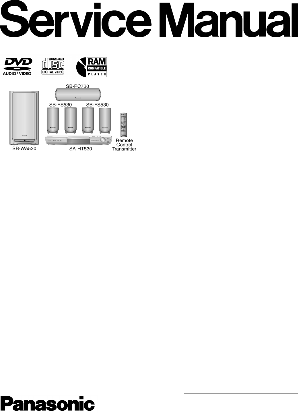
SAHT530
SAHT530GCP SAHT530GCP
User Manual: SAHT530
Open the PDF directly: View PDF ![]() .
.
Page Count: 101 [warning: Documents this large are best viewed by clicking the View PDF Link!]
nAmplifier Section
RMS Output Power: Dolby Digital Mode
Front Ch
55 W per channel (6 Ω), 1 kHz, 10% THD
Surround Ch
55 W per channel (6 Ω), 1 kHz, 10% THD
Center Ch
160 W per channel (6 Ω), 1 kHz, 10% THD
Subwoofer Ch
220 W per channel (4 Ω), 100 Hz, 10% THD
Total RMS Dolby Digital Mode Power 600 W
DIN Output Power: Dolby Digital Mode
Front Ch
40 W per channel (6 Ω), 1 kHz, 1% THD
Surround Ch
40 W per channel (6 Ω), 1 kHz, 1% THD
Center Ch
120 W per channel (6 Ω), 1 kHz, 1% THD
Subwoofer Ch
150 W per channel (4Ω), 100 Hz, 1% THD
Total DIN Dolby Digital Mode Power 430 W
nFM/AM Tuner, Terminals Section
Preset station FM 15 stations
AM/MW 15 stations
Frequency Modulation (FM)
Frequency Range
87.50-108.00 MHz (50-kHz step)
©2005 Matsushita Electric Industrial Co. Ltd.. All
rights reserved. Unauthorized copying and
distribution is a violation of law.
SA-HT530GCP
Colour
(S)...Silver Type
Sensitivity 2.5 µV (IHF)
S/N 26 dB 2.2 µV
A
ntenna terminals 75 Ω(unbalanced)
A
mplitude Modulation (AM/MW)
Frequency Range 522-1629 kHz (9-kHz step)
520-1630 kHz (10-kHz step)
A
M Sensitivity S/N 20 dB at 999 kHz 560 µV/m
Phone Jack
Terminal Stereo, 3.5 mm jack
Mic Jack
Sensitivity 0.7mV,1.2kΩ
Terminal Mono, 6.3 mm jack (2 systems)
nDisc Section
Disc played [8 cm or 12 cm]
1. DVD-RAM (DVD-VR compatible, JPEG formatted disc)
2. DVD-Audio
3. DVD-Video
4. DVD-R, DVD-RW (DVD-Video compatible) + R, + RW (Video
compatible)
5. CD-Audio (CD-DA)
6. Video CD
7. SVCD (Conforming to IEC62107)
8. CD-R/RW (CD-DA, Video-CD, SVCD, MP3, WMA, JPEG formatted
disc)
9. MP3/WMA*1
DVD Home Theater Sound System
Specification
ORDER NO. MD0503084C3
·
Compatible compression rate:
MP3: between 32 kbps and 320 kbps
WMA: between 48 kbps and 320 kbps
10. JPEG*1
·
Exif Ver 2.1 JPEG Baseline files
·
Picture resolution: between 320 x 240 and 6144 x 4096 pixels
(sub sampling is 4:2:2 or 4:2:0)
11. HighMAT Level 2 (Audio and Image)
*1 The total combined maximum number of recognizable audio and
picture contents and groups: 4000 audio and picture contents and 400
groups.
Pick up
Wavelength CD 785 nm
DVD 662 nm
Laser power CLASS 2/CLASS 3A
A
udio output (Disc)
Number of channels 5.1ch (FL, FR, C, SL, SR, SW)
nVideo Section
Video System
Signal system PAL625/50, PAL525/60, NTSC
Composite video output
Output level 1Vp-p(75Ω)
Terminal Pinjack(1system)
S-video output
Y output level 1Vp-p(75Ω)
C output level PAL; 0.3 Vp-p (75 Ω)
NTSC; 0.286 Vp-p (75 Ω)
Terminal S terminal (1 system)
Component Video Output (480p/480i)
Y output level 1Vp-p(75Ω)
1 Before Use 3
2 Use of Active Subwoofer 4
2.1. Checking Main Unit when Active Subwoofer is Used 4
2.2. Checking Main Unit Using Power Jig 5
3 Before Repair and Adjustment 5
4 SAFETY PRECAUTIONS 5
4.1. GENERAL GUIDELINES 5
5 Handling the Lead Solder 6
5.1. About lead free solder (PbF) 6
6 Protection Circuitry 6
7 Prevention of Electro Static Discharge (ESD) to
Electrostatically Sensitive (ES) Devices 7
8 Cautions to Be Taken When Handling Optical Pickup 8
8.1. Handling Optical Pickup 8
PBoutput level 0.7 Vp-p (75 Ω)
PRoutput level 0.7 Vp-p (75 Ω)
Terminal
Pin jack (Y: green, PB:blue,P
R:red)(1system)
nGeneral
Power Supply
AC 110/127/220-230/240 V, 50/60 Hz
Power consumption 25 W (SA-HT530),
250 W (SB-WA530)
Dimensions (W x H x D) 430 x 60 x 348.3 mm
Mass 2.7 kg (SA-HT530)
Operating temperature range +5 °C to +35 °C
Operating humidity range
5 % to 90 % RH (no condensation)
Power consumption in standby mode: approx. 0.9 W
*
2
Rating with low cut filter equipped amplifier
nSystem
SC-HT530 (GCP)
Note:
1. Specifications are subject to change without notice. Mass and
dimensions are approximate.
2. Total harmonic distortion is measured by the digital spectrum
analyzer.
8.2. Cautions to Be Taken During Replacement of Optical
Pickup 9
8.3. Grounding for Preventing Electrostatic Destruction
9
9 Precaution of Laser Diode 10
10 Accessories 11
11 Remote Control Reference 12
12 Disc information 13
13 About HighMAT 17
13.1. What 痴HighMAT? 17
13.2. Why take advantage of HighMat? 18
13.3. Benefits of HighMat? 18
14 Optical Pickup Self-Diagnosis and Replacement Procedure 21
14.1. Self-diagnosis 21
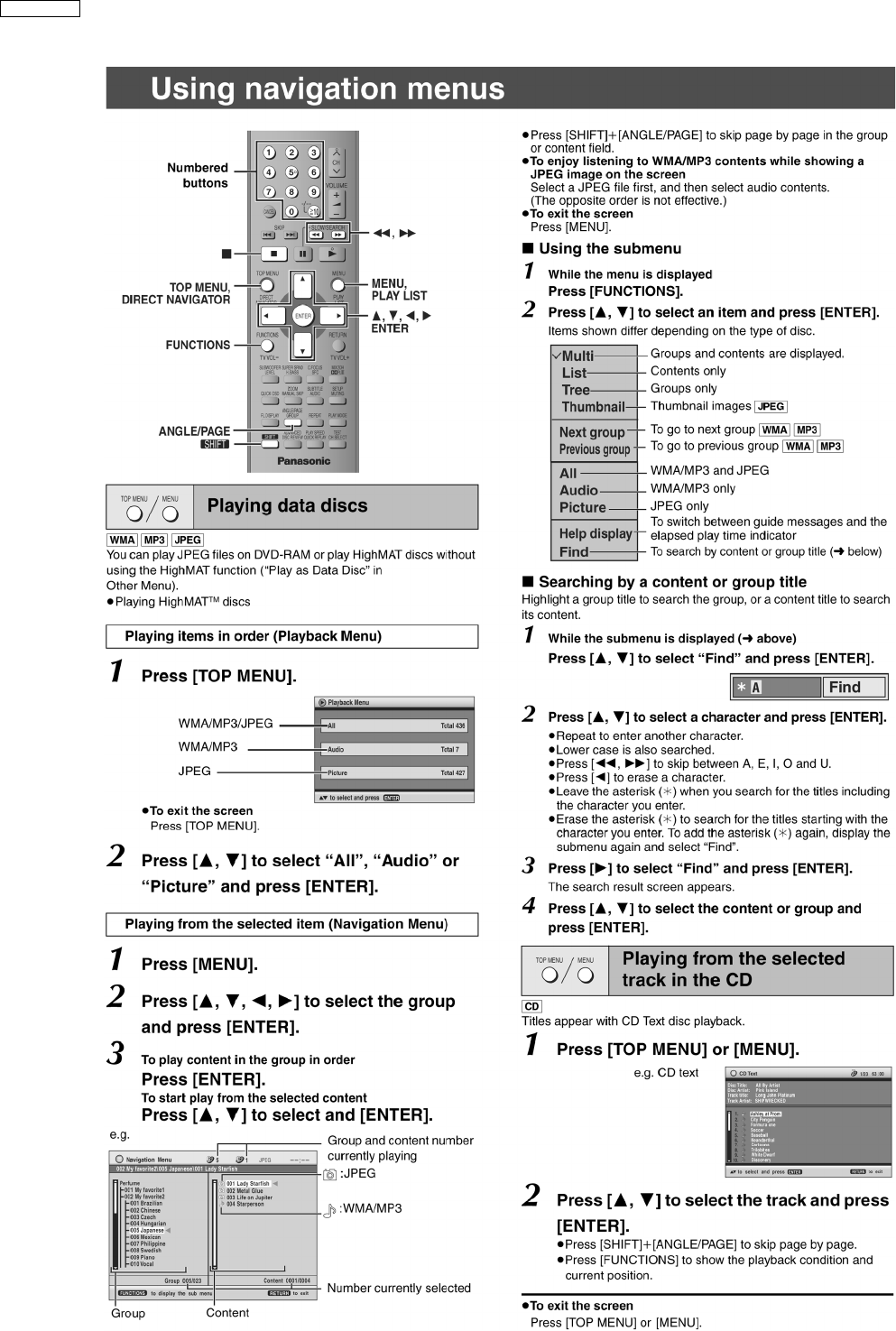
CONTENTS
Page Page
2
SA-HT530GCP

14.2. Cautions to Be Taken During Replacement of Optical
Pickup and Spindle Motor 22
15 Self-Diagnosis Function 23
15.1. Automatic Displayed Error Codes 23
15.2. Memorized Error Codes 23
15.3. Service Mode Table 1 24
15.4. DVD/CD Self-Diagnosis Error Code Description 24
15.5. Mode Table 2 25
15.6. Lock Function 27
15.7. Things to Do After Repair 27
16 Service precautions 28
16.1. Recovery after the player is repaired 28
16.2. DVD Player Firmware Version Upgrade Process 28
16.3. Firmware Version Upgrade Process by Using Recovery
Disc 28
17 Disassembly and Main Component Replacement Procedures
30
17.1. Disassembly flow chart 30
17.2. P.C.B. Locations 31
17.3. Disassembly of Top Cabinet 32
17.4. Disassembly of Front Panel Unit 32
17.5. Disassembly of Panel P.C.B., Headphone P.C.B. & MIC
P.C.B. 33
17.6. Disassembly of Main P.C.B. 33
17.7. Disassembly of CD/ DVD Mechanism 34
17.8. Disassembly and Assembly Mechanism Unit 34
18 Service Position 42
18.1. Checking the Main P.C.B. 42
18.2. Checking the Main P.C.B., Panel P.C.B., MIC P.C.B. and
Headphone P.C.B. 43
19 Adjustment Procedure 44
19.1. Required Tools and Equipment 44
20 Block Diagram 46
21 Schematic Diagram 54
21.1. Optical Pickup Unit Circuit 55
21.2. (A) DVD Module (DV2) Circuit 56
21.3. (B) Main Circuit 63
21.4. (C) Panel Circuit 70
21.5. (D) Microphone Circuit 71
21.6. (E) Headphone Circuit & (F) CD Tray Loading Circuit 72
22 Printed Circuit Board 73
22.1. (A) DVD Module P.C.B. (Side A & B) 73
22.2. (B) Main P.C.B. 75
22.3. (C) Panel P.C.B., (D) Mic P.C.B. & (E) Headphone P.C.B.
77
22.4. (F) CD Tray Loading P.C.B. 79
23 Wiring Connection Diagram 80
24 Illustration of IC 痴, Transistors and Diodes 82
25 Terminal Function of IC 痴 83
25.1. IC2018(C2CBHG000168): Microprocessor 83
25.2. IC8001 (MN2DS0003APH) DV2.1 IC 83
26 Parts Location and Replacement Parts List 87
26.1. DVD Loading Mechanism 88
26.2. Cabinet 90
26.3. Component Parts List 92
26.4. Packing Materials & Accessories Parts List 100
26.5. Packaging 101
1 Before Use
Be sure to disconnect the mains cord before adjusting the voltage selector.
Use a minus(-) screwdriver to set the voltage selector (on the rear panel) to the voltage setting for the area in which the unit will
be used. (If the power supply in your area is 117V or 120V, set to the “127V” position.)
Note that this unit will be seriously damaged if this setting is not made correctly. (There is no voltage selector for some countries,
the correct voltage is already set.)
3
SA-HT530GCP
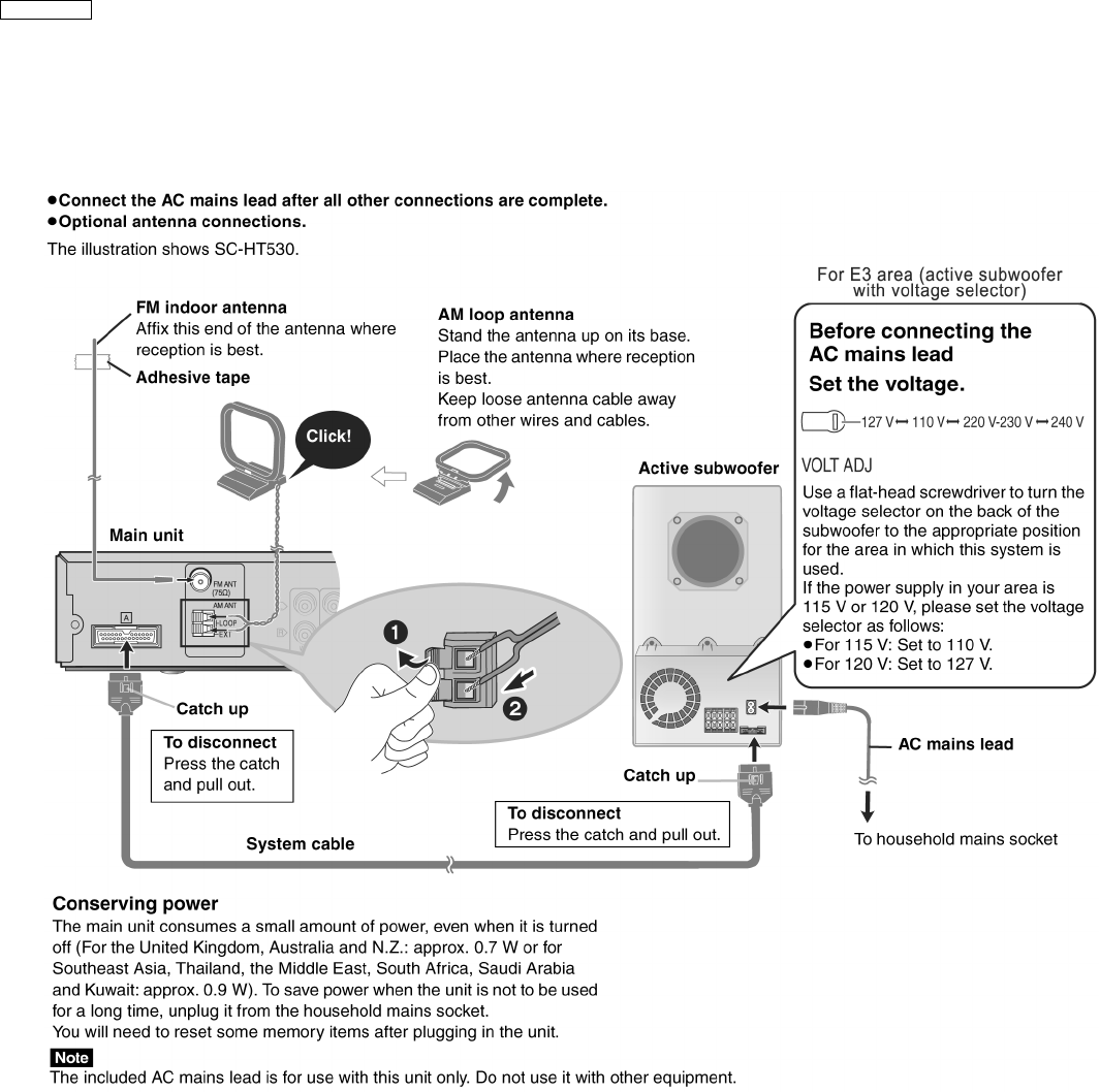
2 Use of Active Subwoofer
2.1. Checking Main Unit when Active Subwoofer is Used
4
SA-HT530GCP
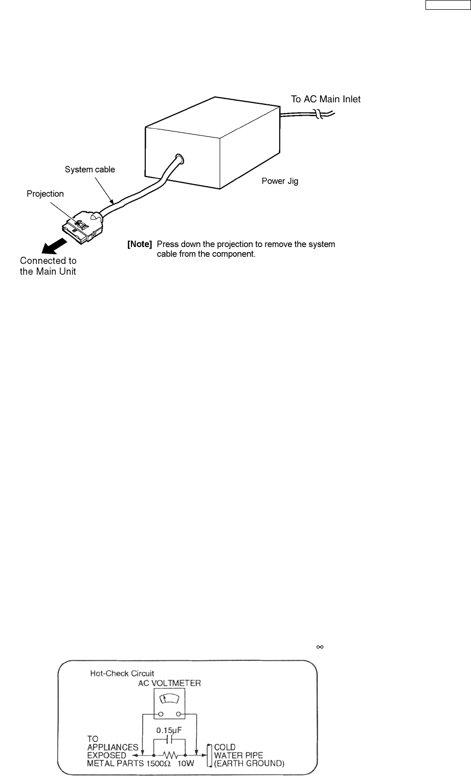
2.2. Checking Main Unit Using Power Jig
If the active subwoofer is not available during time of repair to the unit, the following equipment could be used.
Jig product number
RFKZ0182 (110V , 127V, 220V, 230V - 240V for with voltage selector overseas domestic use).
3 Before Repair and Adjustment
Disconnect AC power, discharge Power Supply Capacitors C2080 through a 10 Ω, 10 W resistor to ground.
DO NOT SHORT-CIRCUIT DIRECTLY (with a screwdriver blade, for instance), as this may destroy solid state devices.
After repairs are completed, restore power gradually using a variac, to avoid overcurrent.
Current consumption at AC 110V, 50/60Hz in NO SIGNAL mode should be ~835 mA (Active Subwoofer).
Current consumption at AC 230V - 240V, 50Hz in NO SIGNAL mode should be ~420 mA (Active Subwoofer).
4 SAFETY PRECAUTIONS
4.1. GENERAL GUIDELINES
1. When servicing, observe the original lead dress. If a short circuit is found, replace all parts which have been overheated or
damaged by the short circuit.
2. After servicing, ensure that all the protective devices such as insulation barriers, insulation papers shields are properly installed.
3. After servicing, make the following leakage current checks to prevent the customer from being exposed to shock hazards.
4.1.1. LEAKAGE CURRENT COLD CHECK (FOR ACTIVE SUBWOOFER)
1. Unplug the AC cord and connect a jumper between the two prongs on the plug.
2. Measure the resistance value, with an ohmmeter, between the jumpered AC plug and each exposed metallic cabinet part on
the equipment such as screwheads, connectors, control shafts, etc. When the exposed metallic part has a return path to the
chassis, the reading should be between 1MΩand 5.2Ω.
When the exposed metal does not have a return path to the chassis, the reading must be .
Fig. 1
5
SA-HT530GCP

4.1.2. LEAKAGE CURRENT HOT CHECK (See Figure 1.)
1. Plug the AC cord directly into the AC outlet. Do not use an isolation transformer for this check.
2. Connect a 1.5kΩ, 10 watts resistor, in parallel with a 0.15µF capacitor, between each exposed metallic part on the set and a
good earth ground such as a water pipe, as shown in Figure 1.
3. Use an AC voltmeter, with 1000 ohms/volt or more sensitivity, to measure the potential across the resistor.
4. Check each exposed metallic part, and measure the voltage at each point.
5. Reverse the AC plug in the AC outlet and repeat each of the above measurements.
6. The potential at any point should not exceed 0.75 volts RMS. A leakage current tester (Simpson Model 229 or equivalent) may
be used to make the hot checks, leakage current must not exceed 1/2 milliamp. In case a measurement is outside of the limits
specified, there is a possibility of a shock hazard, and the equipment should be repaired and rechecked before it is returned to
the customer.
5 Handling the Lead Solder
5.1. About lead free solder (PbF)
Distinction of PbF P.C.B. :
P.C.B.s (manufactured) using lead free solder will have a PbF stamp on the P.C.B.
Caution:
·
Pb free solder has a higher melting point that standard solder; Typically the melting point is 50 - 70°F (30 - 40°C) higher.
Please use a high temperature soldering iron. In case of the soldering iron with temperature control, please set it to 700 ± 20°F
(370 ± 10°C).
·
Pb free solder will tend to splash when heated too high (about 1100°F/600°C).
·
When soldering or unsoldering, please completely remove all of the solder on the pins or solder area, and be sure to heat the
soldering points with the Pb free solder until it melts enough.
6 Protection Circuitry
The protection circuitry may have operated if either of the following conditions are noticed:
·
No sound is heard when the power is turned on.
·
Sound stops during a performance.
The function of this circuitry is to prevent circuitry damage if, for example, the positive and negative speaker connection wires are
“shorted”, or if speaker systems with an impedance less than the indicated rated impedance of the amplifier are used.
If this occurs, follow the procedure outlines below:
1. Turn off the power.
2. Determine the cause of the problem and correct it.
3. Turn on the power once again after one minute.
Note :
When the protection circuitry functions, the unit will not operate unless the power is first turned off and then on again.
6
SA-HT530GCP
7 Prevention of Electro Static Discharge (ESD) to
Electrostatically Sensitive (ES) Devices
Some semiconductor (solid state) devices can be damaged easily by electricity. Such components commonly are called
Electrostatically Sensitive (ES) Devices. Examples of typical ES devices are integrated circuits and some field-effect transistors and
semiconductor “chip” components. The following techniques should be used to help reduce the incidence of component damage
caused by electro static discharge (ESD).
1. Immediately before handling any semiconductor component or semiconductor-equiped assembly, drain off any ESD on your
body by touching a known earth ground. Alternatively, obtain and wear a commercially available discharging ESD wrist strap,
which should be removed for potential shock reasons prior to applying power to the unit under test.
2. After removing an electrical assembly equiped with ES devices, place the assembly on a conductive surface such as aluminium
foil, to prevent electrostatic charge build up or exposure of the assembly.
3. Use only a grounded-tip soldering iron to solder or unsolder ES devices.
4. Use only an anti-static solder remover device. Some solder removal devices not classified as “anti-static (ESD protected)” can
generate electrical charge to damage ES devices.
5. Do not use freon-propelled chemicals. These can generate electrical charges sufficient to damage ES devices.
6. Do not remove a replacement ES device from its protective package until immediately before you are ready to install it. (Most
replacement ES devices are packaged with leads electrically shorted together by conductive foam, aluminium foil or
comparable conductive material).
7. Immediately before removing the protective material from the leads of a replacement ES device, touch the protective material
to the chassis or circuit assembly into which the device will be installed.
Caution
Be sure no power is applied to the chassis or circuit, and observe all other safety precautions.
8. Minimize bodily motions when handling unpackaged replacement ES devices. (Otherwise harmless motion such as the
brushing together of your clothes fabric or the lifting of your foot from a carpeted floor can generate static electricity (ESD)
sufficient to damage an ES device).
7
SA-HT530GCP
8 Cautions to Be Taken When Handling Optical Pickup
·
The laser diode used inside the optical pickup could be destroyed due to static electricity (potential difference is caused by
electrostatic load discharged from clothes and human body). Handle the parts carefully to avoid electrostatic destruction during
repair & during replacement.
8.1. Handling Optical Pickup
1. Do not cause any strong impact on optical pickup as the unit structurally uses an extremely precise technology.
2. Short-circuit the flexible cable of optical pickup removed from the circuit board using a short-circuit pin or clip in order to prevent
laser diode from electrostatic destruction. (Refer to Fig. 8-1 and Fig. 8-2.)
3. Do not handle flexible cables forcibly as this may cause snapping. Handle the parts carefully. (Refer to Fig. 8-1)
4. A new optical pickup is equipped with an anti-static flexible cable. After replacing and connecting to the flexible board, cut the
anti-static flexible cable. (Refer to Fig. 8-1)
Fig. 8-1
Fig. 8-2
8
SA-HT530GCP
8.2. Cautions to Be Taken During Replacement of Optical Pickup
Supplied optical pickup is equipped with a short clip found at the end of flexible cable in order to prevent electrostatic destruction
of laser diode. Before connection, remove the short clip, and check that the short land is opened (remove solder if the part is short-
circuited). Also ensure human body is properly ground (Refer Section 8.3)
8.3. Grounding for Preventing Electrostatic Destruction
1. Human body grounding
Use an anti-static wrist strap to release static electricity accumulated in your body. (Refer to Fig. 8-3)
2. Workplace grounding
Place a conductive material (conductive sheet) or iron board where optical pickup is placed. (Refer to Fig. 8-3)
Note:
Keep your clothes away from optical pickup as wrist strap does not release the static electricity charged in clothes.
Fig. 8-3
9
SA-HT530GCP
9 Precaution of Laser Diode
CAUTION :
This product utilizers a class 1 laser. Invisible laser radiation is emitted from the optical pick up lens.
When the unit is turned on:
Wavelenght : 662nm/785nm
Maximum output radiation power from pick up : 100µW/VDE
1. Do not disassemble the optical pick up unit, since radiation from exposed laser diode is dangerous.
2. Do not adjust the variable resistor on the pick up unit. It was already adjusted.
3. Do not look at the focus lens using optical instruments.
4. Recommend not to look at pick up lens for a long time.
CAUTION!
THIS PRODUCT UTILIZES A LASER.
USE OF CONTROLS OR ADJUSTMENTS OR PERFORMANCE OF PROCEDURES OTHER THAN THOSE SPECIFIED HEREIN MAY RESULT
IN HAZARDOUS RADIATION EXPOSURE.
nUse of Caution Labels
10
SA-HT530GCP
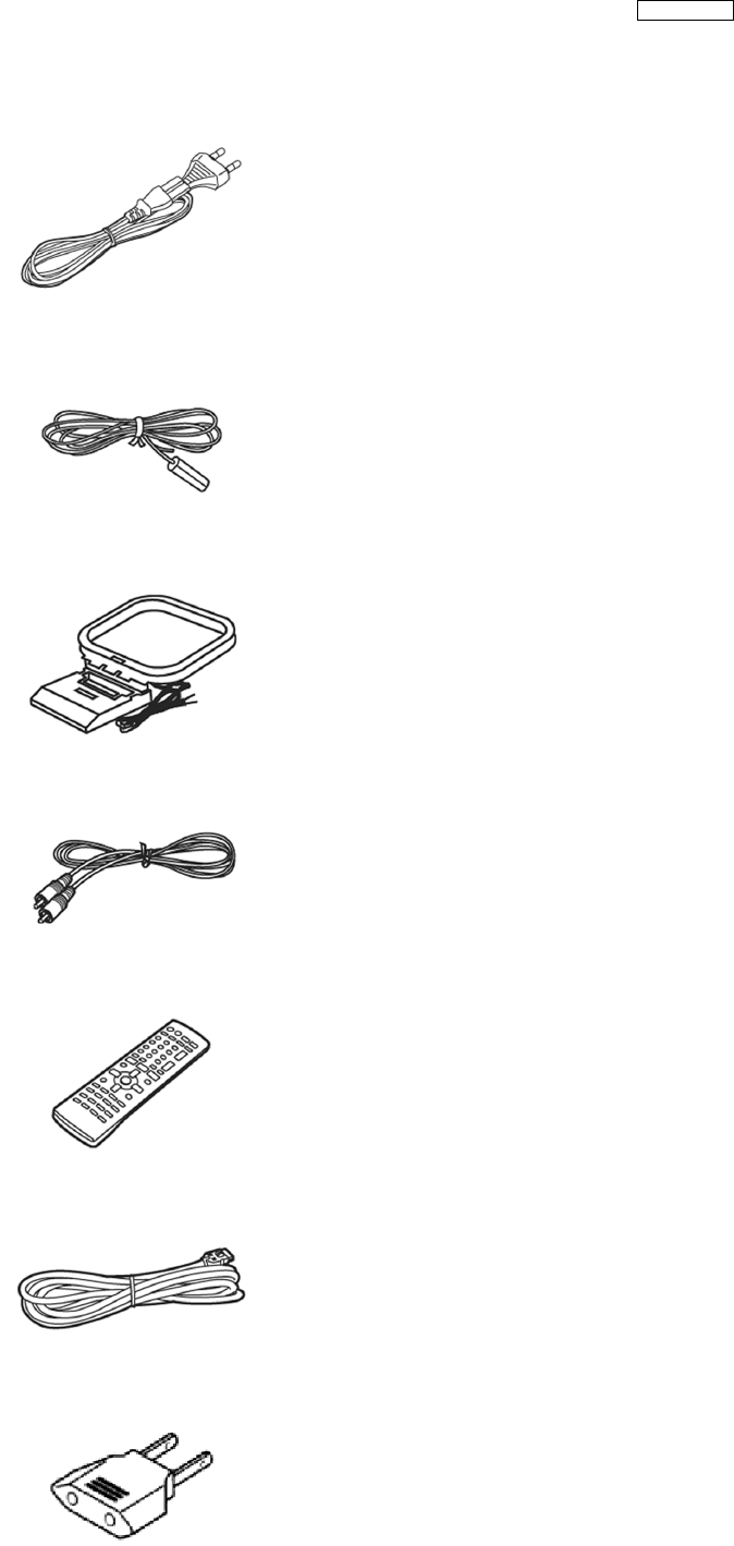
10 Accessories
AC cord
FM indoor antenna
AM loop antenna
Video cable
Remote control
System cable
Antenna plug
adapter
11
SA-HT530GCP
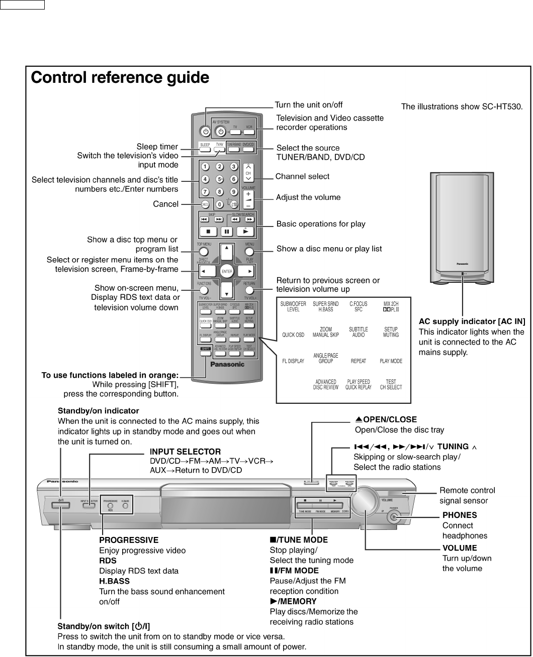
11 Remote Control Reference
12
SA-HT530GCP
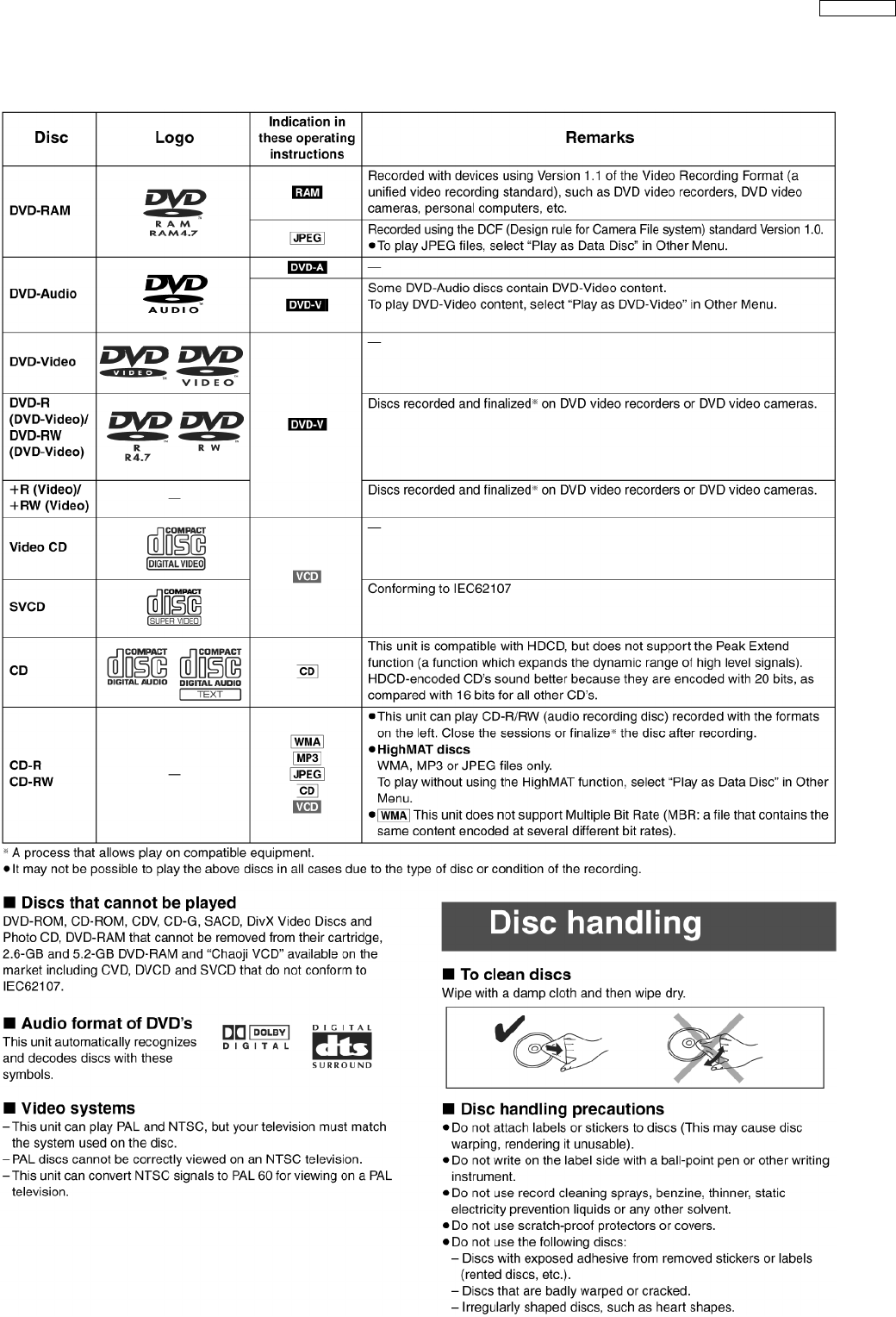
12 Disc information
13
SA-HT530GCP
14
SA-HT530GCP

15
SA-HT530GCP
16
SA-HT530GCP

13 About HighMAT
13.1. What’s HighMAT?
Consumers worldwide are using PCs to create their own collections of music, photos and even video by burning them onto CDs.
But how these collections can be experienced across different devices can be confusing to navigate, time consuming to access for
a DVD player, and be incomplete in terms of music information available to the customer.
HighMAT offers a solution to this growing consumer problem. HighMAT dramatically improves the digital media experience on
consumer electronic devices by delivering a simple, standardized approach that allows consumers who have created personal
collections of digital music, photography and video on their PC to:
·
Create a HighMAT CD or DVD which can be easily played back on consumer electronics devices such as CD and DVD players,
and car stereos.
·
Move digital media files (using recordable media such as CD-R and CD-RW) between the PC and various playback devices
such as CD and DVD players.
A new standard for creating personal media on consumer electronic devices, HighMAT enable easier and more seamless
interoperability between Windows PCs and devices designed for your living room, or the car.
17
SA-HT530GCP
13.2. Why take advantage of HighMat?
A Problem Defined:Today, when consumers create their own digital audio, video or photo collections on CD-R or other physical
formats, there are numerous, inconsistent ways that devices read the data. For the consumer, the playback experience can be
confusing:
A Solution Created: HighMat delivers a better digital media access experience by creating a standard approach for PCs to structure
digital media on various physical formats and for playback devices to read the data.
13.3. Benefits of HighMat?
Conventional HighMat
Even though DVD player is CD-R/RW compatible, the inconsistent
ways that various DVD players can read the music or photos files often
leads to a confusing and inconsistant playback experince.
HighMAT compatible products play content back with consistent
interface. This includes products which are JPEG compatible products
without HighMAT support.
18
SA-HT530GCP
Conventional HighMat
19
SA-HT530GCP
HighMAT is now available for CD Burning and in Leading DVD Players.HighMAT is a new technology that is now available in
leading software and consumer electronic devices to dramatically improve the digital media experience when you create
homemade CDs.
HighMAT™ delivers a simple, standardized way for PC software and consumer electronics devices to talk to each other and work
better together.
When you create your homemade CDs with software that supports HighMAT CD burning, and then play them back on a DVD
player that supports HighMAT, you get better, easier navigation. You get folders you can access with a single click of your DVD
player´s remote control. You can view important information about your music like full song names, artist titles, album names and
genre. And you can get faster startup on your home entertainment device.
To enjoy the benefits of HighMAT, all you need is software that supports HighMAT for CD burning of music or photos, as well as
a home entertainment device like a DVD player that supports HighMAT for playback. Always look for the HighMAT logo on your
software or home entertainment device to ensure it supports the HighMAT experience.
20
SA-HT530GCP
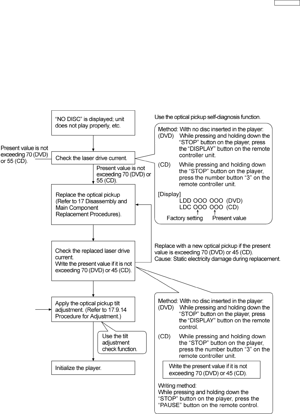
14 Optical Pickup Self-Diagnosis and Replacement
Procedure
14.1. Self-diagnosis
This unit is equipped with the optical pickup self-diagnosis function and the tilt adjustment check function. Follow the procedure
described below during repair in order to perform self-diagnosis and tilt adjustment effectively. Especially when “NO DISC” is
displayed, be sure to apply the self-diagnosis function before replacing with an optical pickup. Replacement of optical pickup
generally requires when the present value of laser drive exceeds 70 (DVD) or 55 (CD).
Note:
Start diagnosis within three minutes after turning on the power (as diagnosis fails when the unit becomes warm).
21
SA-HT530GCP

14.2. Cautions to Be Taken During Replacement of Optical Pickup and
Spindle Motor
Before replacing the optical pickup and spindle motor, check the total usage time respectively. Follow the checking method
described as below.
Item Status and Key Function Display
Checking DVD, CD laser usage time With the unit stopped and no disc inserted,
press the. button on the player and the
button on the remote controller unit.
T1_xxxx_yyyy
xxxx(DVD), yyyy(CD): total time is displayed with a
four-digit number by the ten hours.
Checking spindle motor usage time With the unit stopped and no disc inserted,
press the button on the player and the
button on the remote controller unit.
T2_xxxx
xxxx: total time is displayed with a four-digit number
by the ten hours.
Resetting DVD, CD laser usage time While the DVD and CD laser usage times are
displayed, press the button on the player
and the button on the remote controller unit.
T1_0000_0000
Resetting spindle motor usage time While the spindle motor usage time is
displayed, press the button on the player
and the button on the remote controller unit.
T2_0000
22
SA-HT530GCP
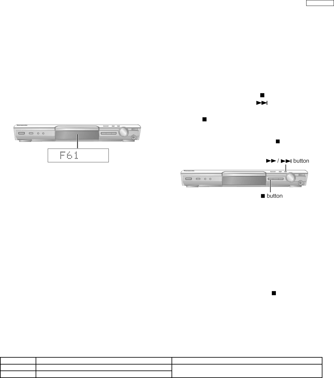
This unit is equipped with the self-diagnosis function, which
displays an error when it occurs, for use during servicing.
15.1. Automatic Displayed Error
Codes
15.1.1. Automatic Display Function
For a power unit error, the code is automatically displayed.
F61: Automatically displayed on the LCD of
the player.
Fig. 15-1
15.1.2. Re-Display
·
For F61 Display
−
− −
− When the code, F61 is displayed, the power is
automatically turned off.
−
− −
− The code, F61 is displayed for three seconds, and then
the current time appears.
−
− −
− To retrieve the code, turn on the power button so that
the code F61 appears, however, is switched to time
display after three seconds, and the power is
automatically turned off.
15.1.3. Description of Error Code
15.1.3.1. F61
·
State, Condition
When the power is turned on, the unit is automatically
turned off. The power does not turn on.
·
Cause, Troubleshooting
Power circuit system failure and/or direct current flown to
speaker terminal
Identify the cause and replace with new parts.
15.2. Memorized Error Codes
15.2.1. Activating Self-Diagnosis Function
and Displaying Method
1. Turn on the power.
2. Select DVD/CD function. With no DVD/CD inserted in the
player, press and hold down the button for at least two
seconds, and press the F_SKIP button for at least two
seconds in order to display “T___________”.
3. Press the button. If a memorized error is detected, the
result of self diagnosis is displayed. (Ex.: T H15) (See table
below)
If several errors are detected, press the button to display
each.
Fig. 15-2
15.2.2. Re-Display
·
Press the power button to turn off the power, and then turn
on the power.
·
The details of self diagnosis are stored in the unit memory.
To retrieve them, follow the procedure described the above,
“Activating Self-Diagnosis Function and Displaying
Method”.
15.2.3. Deleting Details of Self Diagnosis
·
After repair, press and hold down the button for at least
five seconds, “T___ --- __” appears for a second and then
“T________” appears. (Deleting the details of self
diagnosis)
·
After repairing errors, be sure to delete the details of self
diagnosis.
15 Self-Diagnosis Function
Error Code State, Conditon Cause, Troubleshooting
H15 The disc tray cannot be opened: it closes spontaneously. Disc tray open/close detection switch (S901, S902) failure.
(Check and replace)
H16 The disc tray cannot be closed: it opens spontaneously.
23
SA-HT530GCP
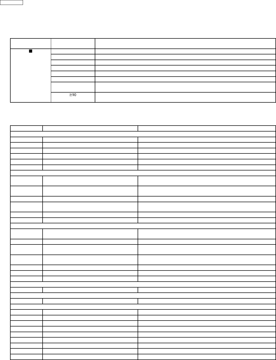
15.3. Service Mode Table 1
Following modes are available with combinations of the pressed buttons on the player and on the remote controller unit.
Player Remote controller
unit
Usage
button
0Error code display (Refer to the item, 15.4. DVD Error Code Description)
5Tilt adjustment
6Area number and broadcasting system check
7 MICRO - P & Firmware Version.
DISPLAY DVD laser drive current check
3 CD laser drive current check
PAUSE Writing of laser drive current value after replacement of optical pickup
(Do use this function only when optical pickup is replaced.)
Initialization of the player (factory setting is restored.)
Used after replacement of micro-computer and its peripherals and printed circuit board.
15.4. DVD/CD Self-Diagnosis Error Code Description
Error Code Meaning Details
U. H. Error
U11 Focus servo failure
H01 Tray loading failure
H02 Spindle servo failure (Spindle servo, DSC, SP motor, CLV servo failure)
H03 Traverse motor failure
H04 Tracking servo error
H05 Seek timeout failure
DSC system
F500 DSC failure DSC stops due to servo failure.
(Startup, focus failure, etc.)
F501 DSC not Ready failure Communication failure between DSC and system computer
(No communication because DSC does not move)
F502 DSC Time out failure See F500.
F503 DSC communication failure Communication failure (Result failure occurs after communication
command is transmitted.)
F505 DSC Attention Error See F500.
F506 Invalid media Disc is placed upside down; TOC is unreadable or invalid disc is inserted.
ODC system
F600 Unable to obtain control information due to form
recovery failure
Operation stops because navigation data cannot be obtained due to form
recovery system failure.
F601 Illegal sector ID requested Operation stops because access of illegal ID data is requested.
F602 Unable to obtain LEAD IN due to form recovery
failure
Unable to read LEAD IN data
F603 Unable to obtain KEY DET due to form recovery
failure
Unable to obtain CSS data
F610 ODC failure No permission of command issue
F611 No CRC OK appearing for a certain time Unable to obtain seek address at CD system
F612 No CRC OK appearing for a certain time Unable to obtain ID data at DVD system
Disc Code
F103 Ilegal highlight position Disc standard is possibly illegal when highlight is displayed.
IIC Error
F4FF Forced initialization failure (Time out)
Micro-computer Error
F700 MBX overflow When replying a message to Disc Manager
F701 Unable to complete a message command A message is issued before replying to Disc Manager.
F702 Change in a message command A message is issued before replying to Disc Manager.
F880 Unsuitable task number When a message arrives from not existing task
F890 A message is sent during AV task transmission During transmission of a message to AV task
F891 Unable to transmit a message to AV task When transmission of a message to AV task starts
F893 FROM altered
F894 EEPROM failure
F8A0 Unsuitable message command When transmission of a message to AV task starts
24
SA-HT530GCP

15.5. Mode Table 2
Following modes are available with combinations of the pressed buttons on the player and on the remote controller unit.
Item Operational Condition
and Key Function
Details Display To Exit Mode
Jitter display While the player is
stopped and no disc is
inserted, press and
hold down the
button on the player
and the number
button, “5” on the
remote controller unit.
Jitter display
Measures and displays jitter.
Measurement is repeated every
second. Read error counter starts at 0
at the mode setting, and increased by
one as data read fails at target block. A
small defect is allowed to correct by
retry. Any possibility is counted as one
increment. Repetitive errors after retry
increase by two levels or more.
J*1 xxx*2 _yyy*3 _zz*4
*1 : Jitter display mode
*2 : Jitter measurement value
*3 : Read error counter
*4 : Focus driving value
Values are shown to one decimal place
in the decimal digit.Focus driving value is
displayed in the hexadecimal digit.
Press the STOP or
OPEN button.
Error code
display
While the player is
stopped and no disc is
inserted, press and
hold down the
button on the player
and the number
button, “0” on the
remote controller unit.
Error code display
Displays the latest error code stored in
EEPROM.
DVDnn_F---
*nn: Error history
*--: Error number
Automatically exits
the mode after five
seconds.
Measurement of
laser current
electricity
initialization value
While the player is
stopped and no disc is
inserted, press and
hold down the
button on the player
and the button on
the remote controller
unit.
Measurement of laser current
electricity initialization value
Memorizes each initialization value of
DVD and CD in EEPROM.
DO*1 _034*2 _028*3
*1 : Laser current electricity measurement
mode
*2 : DVD current electricity value
*3 : CD current electricity value
Values are shown in the decimal digit.
The above example indicates that the
current electricity initialization value is
34mA at DVD laser and 28mA at CD
laser when laser is turned on.
Automatically exits
the mode after five
seconds.
Measurement of
DVD laser current
electricity
While the player is
stopped and no disc is
inserted, press and
hold down the
button on the player
and the DISPLAY
button on the remote
controller unit.
Measurement of DVD laser current
electricity
Measures DVD laser current electricity
and displays the result together with
the initialization value stored in
EEPROM. After measurement, DVD
laser is lit till the power is turned off (or
goes off when the primary power is
turned off).
DD*1 _034*2 _032*3
*1 : DVD laser current electricity
measurement mode
*2 : Current electricity initialization value
stored in EEPROM
*3 : Present value of current electricity
Values are shown in the decimal digit.
The above example indicates that the
current electricity initialization value is
34mA and its present value is 32mA.
Automatically exits
the mode after five
seconds.
ADSC internal
RAM display
While the player is
stopped and no disc is
inserted, press and
hold down the
button on the player
and the number button
“1” or “2” on the remote
controller unit.
ADSC internal RAM display
Reads and displays the RAM value
inside ADSC. The address is renewed
when the CLEAR key is pressed so
that the values at eleven points appear.
A*1 _0FA*2 _6901*3
*1 :ADSC internal RAM display mode
*2 : Address
*3 : RAM value at displayed address
Values are shown in the hexadecimal
digit. The above example indicates that
ADSC value at the address, 0FAh is
6901h.
Press the STOP or
OPEN button.
Measurement of
CD laser current
electricity
While the player is
stopped and no disc is
inserted, press and
hold down the
button on the player
and the number button
“3” on the remote
controller unit.
Measurement of CD laser current
electricity
Measures CD laser current electricity
and displays the result together with
the initialization value stored in
EEPROM. After measurement, CD
laser is lit till the power is turned off (or
goes off when the primary power is
turned off).
DC*1 _028*2 _026*3
*1 : CD laser current electricity
measurement mode
*2 : Current electricity initialization value
stored in EEPROM
*3 : Present value of current electricity
Values are shown in the decimal digit.
The above example indicates the current
electricity initialization value is 28mA and
its present value is 26mA when laser is
turned on.
Automatically exits
the mode after five
seconds.
25
SA-HT530GCP

Item Operational Condition
and Key Function
Details Display To Exit Mode
User initialization While the player is
stopped and no disc is
inserted, press and
hold down the
button on the player
and the number button
on the remote
controller unit.
User initialization
The user setting recovers the factory
setting.
“INITIALIZED” None
Region display While the player is
stopped and no disc is
inserted, press and
hold down the
button on the player
and the number
button, “6” on the
remote controller unit.
Region display __w*1 _x*2 y*3 _zzz*4
*1 : Region number
*2 : N; no PAL/P; PAL
*3 : N; NTSC/6; PAL60
*4 : Panel computer jumper information
Automatically exits
the mode after five
seconds.
Firm version
display
While the player is
stopped and no disc is
inserted, press and
hold down the
button on the player
and the number
button, “7” on the
remote controller unit.
Firm version display rrr*1 _xx*2 y*3 zzz*4
*1 : Panel computer release number
*2 : System computer generation
*3 : System computer model type
*4 : System computer release number
Automatically exits
the mode after five
seconds.
Region and firm
version display
While the player is
stopped and no disc is
inserted, press and
hold down the
button on the player
and the number
button, “8” on the
remote controller unit.
Region and firm version display _r*1 __xx*2 y*3 zzz*4
*1 : Region number
*2 : System computer generation
*3 : System computer model type
*4 : System computer release number
Automatically exits
the mode after five
seconds.
Usage time 1 While the player is
stopped and no disc is
inserted, press and
hold down the
button on the player
and the button on
the remote controller
unit.
Usage time 1
Laser usage time
Measures each for DVD and CD
respectively.
T1_1234_5678
The numbers in the left show usage time
for DVD laser and those in the right for
CD laser. The four-digit number is shown
by the ten hours in the decimal digit. The
number after 0000 is 9999.
Automatically exits
the mode after five
seconds.
Usage time 1
reset
While the usage time 1
is displayed, press and
hold down the
button on the player
and the button on
the remote controller
unit.
Usage time 1 reset
Laser usage time‘
Resets both for DVD and CD at once.
T1_0000_0000 Automatically exits
the mode after five
seconds.
Usage time 2 While the player is
stopped and no disc is
inserted, press and
hold down the
button on the player
and the button on
the remote controller
unit.
Usage time 2
Spindle motor usage time
T2_1234
The four-digit number is shown by the ten
hours in the decimal digit. The number
after 0000 is 9999.
Automatically exits
the mode after five
seconds.
Usage time 2
reset
While the usage time 2
is displayed, press and
hold down the
button on the player
and the button on
the remote controller
unit.
Usage time 2 reset
Spindle motor usage time
T2_0000 Automatically exits
the mode after five
seconds.
Communication
error display
While the player is
stopped and no disc is
inserted, press and
hold down the
button on the player
and the MENU button
on the remote
controller unit.
Displays frequency of communication
errors between system computer firm
IC and mechanical computer IC during
DVD module.
ERR_00_/30 Automatically exits
the mode after five
seconds.
26
SA-HT530GCP
15.6. Lock Function
This function prohibits removal of disc and some disc operations to prevent loss of disc at a shop during sales promotion or
equivalent occasions.
While this function is activated, the player displays “___LOCKED_” if any button is touched.
The lock function can be used in two ways.
15.6.1. Setting
·
LOCK MODE A/LOCK MODE B
1. While the player is set to SELECTOR DVD/CD and POWER ON, press and hold down the button on the player and the
[POWER] button on the remote controller for at least three seconds so that the player displays "___LOCKED_" for three
seconds to indicate that LOCK MODE A is activated and the currently loaded disc is played.
2. The following button is invalid during LOCK MODE A.
OPEN/CLOSE button are invalid and the player displays “___LOCKED_” while the lock function mode is entered.
3. While LOCK MODE A is activated and the player is locked, press and hold down the button on the player and the
[POWER] button on the remote controller for at least three seconds so that the player displays "_UNLOCKED_" to indicate
the function is deactivated.
4. While the player is set to SELECTOR DVD/CD and POWER ON, press and hold down the button on the player and the
[POWER] button on the remote controller for at least three seconds so that the player displays "___LOCKED_" for three
seconds to indicate that LOCK MODE B is activated and the currently loaded disc in played.
5. The following buttons are invalid, based on the "selector or disc related", during LOCK MODE B.
Player , , , SELECTOR, , , VOL. JOG
Remote
controller unit
SLEEP, REPEAT, D.MIX (REPEAT holding down), 0~9, ,RETURN, FL DISPLAY, TEST ( FL DISPLAY holding
down), DISPLAY, SCREEN, CH SELECT, , , , , , , SET UP, GROUP, MUTING, P MEMORY,
TUNER/BAND, TV, VCR/AUX
6. The keys prohibited during PLAY and LOCK MODE B need not to correspond each other. The keys related to sound quality
and shown on the DVD screen are not prohibited. Following buttons are always valid:
Player POWER, DVD/CD>, PROGRESSIVE, VOL. JOG
Remote
controller unit
POWER, PLAY MODE, CANCEL, SFC, B. B LEVEL, VOL-, VOL+, DVD/CD>, MENU, TOP MENU, , , , ,
ENTER, DPL, SSS,C.F, CSM, ZOOM
7. While LOCK MODE B is activated and the player is locked, press and hold down the button on the player and the
[POWER] button on the remote controller for at least three seconds so that the player displays "_UNLOCKED_" for three
seconds to indicate that the function is deactivated.
8. The tray lock function is deactivated by "AC Prohibition".
9. LOCK MODE A or B is an exclusive control over whichever is activated first.
10. While the player is set to a lock mode and POWER OFF, the auto power on function can be controlled by the DVD/CD
button on the remote controller. The auto power on function is invalid by the other selector buttons (such as TUNER/BAND
button).
11. While a lock mode is turned on and the prohibition button is pressed, "___LOCKED_" appears on FL.
12. While a lock mode is turned on and set to POWER OFF, the OPEN/CLOSE button is invalid to control the auto power on
function.
15.7. Things to Do After Repair
Follow the procedure described below after repair.
1. While the power is on, press the button to close the tray.
2. Press the power button to turn off the power.
3. Unplug the power cable.
Note:
It is prohibited to unplug the power cable while the tray is opened and to close the tray manually.
27
SA-HT530GCP
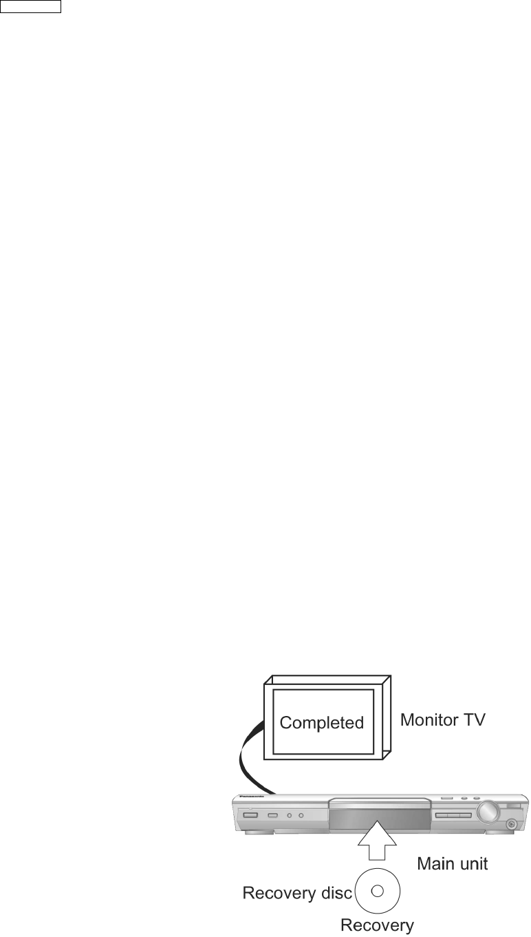
16 Service precautions
16.1. Recovery after the player is repaired
·
When FLASH ROM IC or DVD Module P.C.B. is replaced, carry out the recovery processing to optimize the drive. Playback the
recovery disc to process the recovery automatically.
·
Recovery disc (Product number=RFKZD03R005)
·
Performing recovery
1. Load the recovery disc (Product number: RFKZD03R005) to the player and run it.
2. Recovery is performed automatically. When it is finished, a message appears on the screen.
3. Remove the recovery disc.
4. Turn off the power.
Note:
This unit requires no initialization process carried out after the traditional DVD players were repaired. When the recovery
measures are taken, the customer setting will return to the factory setting as same as the procedure described in item
“Initialization” in 13.6 is carried out. Write down the contents of the setting before recovery processing and reset the player.
16.2. DVD Player Firmware Version Upgrade Process
Firmware of DVD player may upgrade to conform to improvement of its performance and quality including operational range,
playability of non-standardized discs, etc. The version upgrade disc contains the recovery function, and the recovery disc is not
necessary.
Note:
Version upgrade process cannot be complete if the AC power is cut off due to power failure and other occasions during the
process. If this occurs, replace FLASH ROM IC and restart version upgrade. Version upgrade disc number is informed when
ordered.
16.3. Firmware Version Upgrade Process by Using Recovery Disc
·
Recovery process
·
Firmware version upgrade process
Both of the above procedures automatically start when the recovery disc is replayed.General CD-R disc allows version upgrade
process and recovery process, making version upgrade through disc simple.
Recovery process: Optimization process of player after replacement of FLASH ROM IC, EEPROM IC, or DVD Module Circuit board
Version upgrade process: Renewal of firmware for improvement of operational range and performance
16.3.1. Version Upgrade Process
1. Insert the recovery disc to the player to replay.
2. The version of player is automatically checked and prompts if necessary.
3. Select version upgrade process using the cursor keys on the remote controller unit. (Select YES or NO)
4. a. If YES is selected, the process starts.
28
SA-HT530GCP

b. If NO is selected, only the recovery process is applied.
5. a. When the version upgrade process is complete, a message of completion appears on the screen. Remove the disc.
b. Follow the instruction appearing on the screen, and remove the disc.
6. Turn off the power.
29
SA-HT530GCP
Some chassis components may have sharp edges.
Be careful when disassembling and servicing.
17 Disassembly and Main Component Replacement
Procedures
“ATTENTION SERVICER”
1. This section describes procedures for checking the operation of the major printed circuit boards and replacing the main
components.
2. For reassembly after operation checks or replacement, reverse the respective procedures.
Special reassembly procedures are described only when required.
3. Select items from the following index when checks or replacement are required.
Warning:
This product uses a laser diode. Refer to caution statement Precaution of Laser Diode.
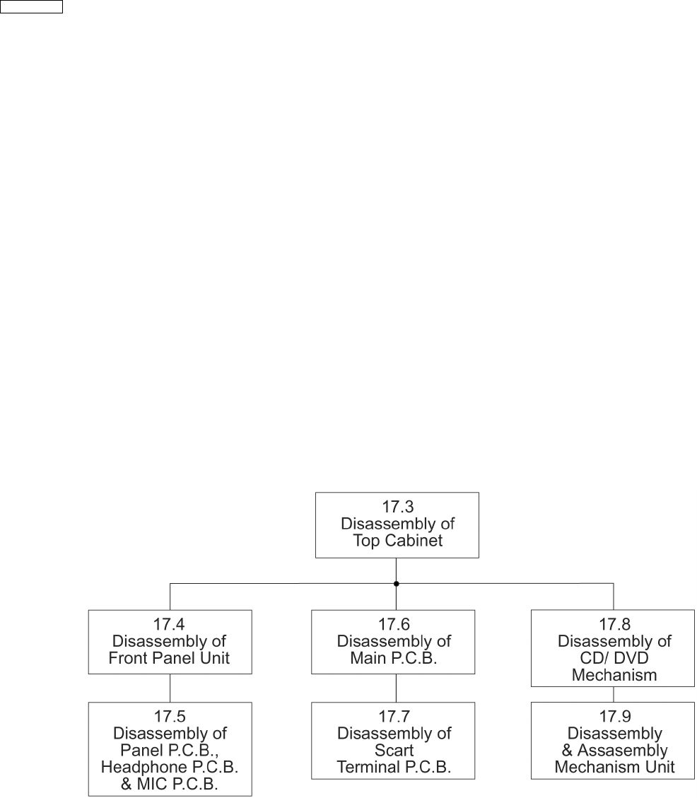
17.1. Disassembly flow chart
The following chart is the procedure for disassembling the casing and inside parts for internal inspection when carrying out the
servicing
To assemble the unit, reverse the steps shown in the chart below.
30
SA-HT530GCP
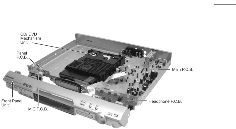
17.2. P.C.B. Locations
31
SA-HT530GCP
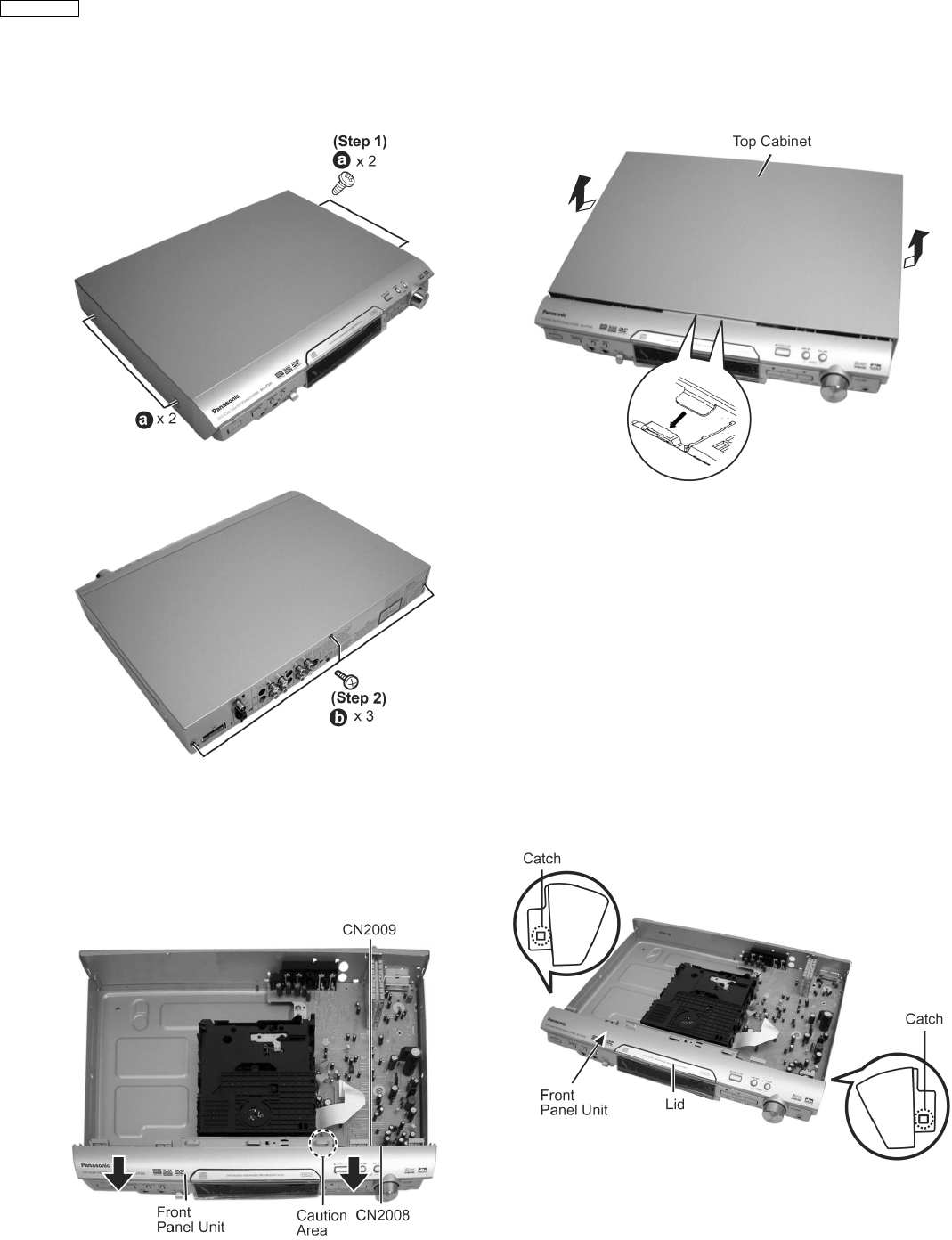
Step 1: Remove 4 screws.
Step 2: Remove 3 screws at rear panel.
Step 1: Remove lid. (Using active subwoofer unit/ jig to power-
up the unit.)
Step 2: Detach FFC Boards (CN2008 and CN2009).
Step 3: Release the catches on the left and right side of front
unit.
Step 3: Lift the top cabinet upwards and push in backward.
Step 4: Release the catches from bottom chassis.
17.3. Disassembly of Top Cabinet
17.4. Disassembly of Front Panel Unit
·
Follow the (Step 1) -(Step 3) of item 17.3 - Disassembly of Top Cabinet
32
SA-HT530GCP
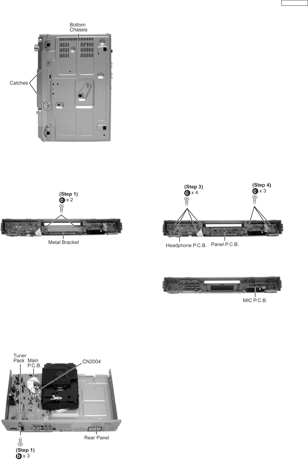
Step 1: Remove 2 screws.
Step 2: Lift up the Metal Bracket.
Step 1: Remove 3 screws at the rear panel.
Step 5: Draw front panel unit forward.
·
Note:
Avoid pulling the front panel unit using strong force.
This may cause damage to Main P.C.B. due to abrasion
between metal bracket and the mechanism unit.
Step 3: Remove 4 screws at Headphone P.C.B.
Step 4: Remove 3 screws at Panel P.C.B.
Step 2: Detach 50P FFC Board (CN2004).
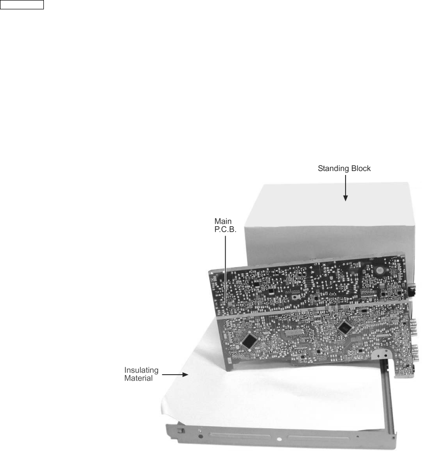
Step 3: Remove 3 screws at Main P.C.B..
Step 4: Push the Main P.C.B. backwards and lift up the P.C.B.
sideway.
17.5. Disassembly of Panel P.C.B., Headphone P.C.B. & MIC P.C.B.
·
Follow the (Step 1) -(Step 3) of item 17.3 - Disassembly of Top Cabinet
·
Follow the (Step 1) -(Step 5) of item 17.4 - Disassembly of Front Panel Unit
17.6. Disassembly of Main P.C.B.
·
Follow the (Step 1) -(Step 3) of item 17.3 - Disassembly of Top Cabinet
·
Follow the (Step 1) -(Step 5) of item 17.4 - Disassembly of Front Panel Unit
33
SA-HT530GCP
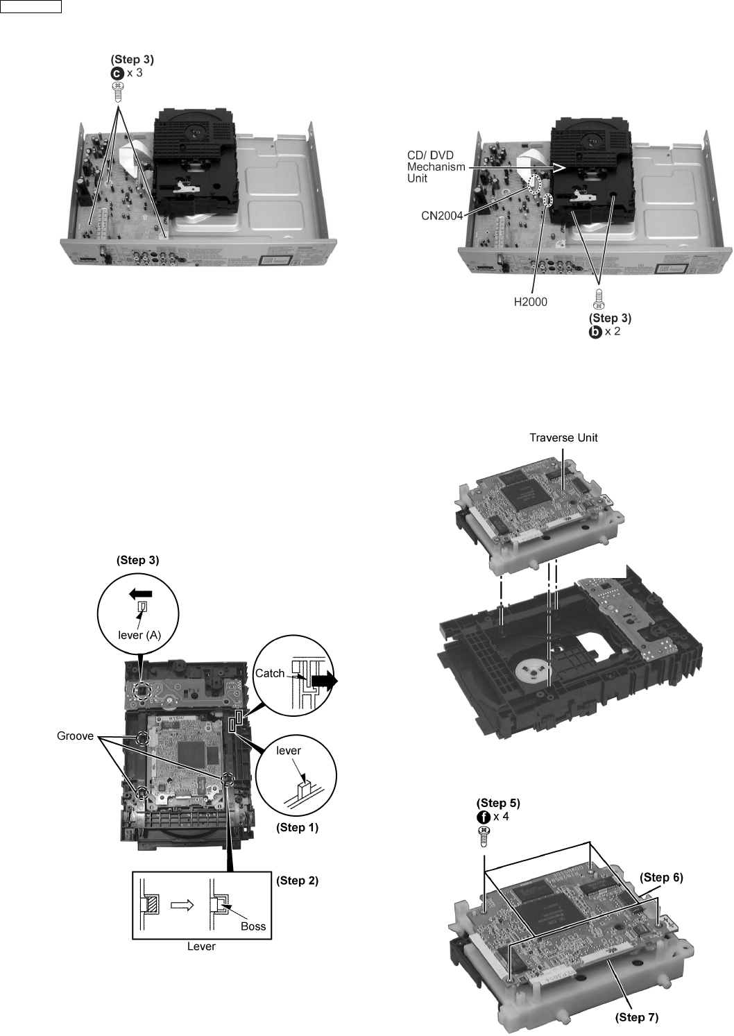
17.7. Disassembly of CD/ DVD
Mechanism
·
Follow the (Step 1) -(Step 3) of item 17.3 - Disassembly of
Top Cabinet
·
Follow the (Step 1) -(Step 5) of item 17.4 - Removal of
17.8.1. Replacement of Traverse Unit.
Step 1: Slide the lever backward to the furthest.
Step 2: While bending the catch at right to the lever to the right
direction, slide the lever further until it stops. (The groove at
right opens, the boss can be seen.)
Step 3: Press lever (A) to the left. (Two grooves at left open.)
Step 4: Take out the traverse Unit.
Front Panel Unit
Step 1: Detach 50P FFC Boards (CN2004).
Step 2: Detach connector (H2000).
Step 3: Remove 2 screws.
Step 4: Lift up the CD/ DVD mechanism unit.
·
Disassembly of DVD Module P.C.B.
Step 5: Remove 4 screws.
Step 6: Detach 15 P FFC Board (FP8271).
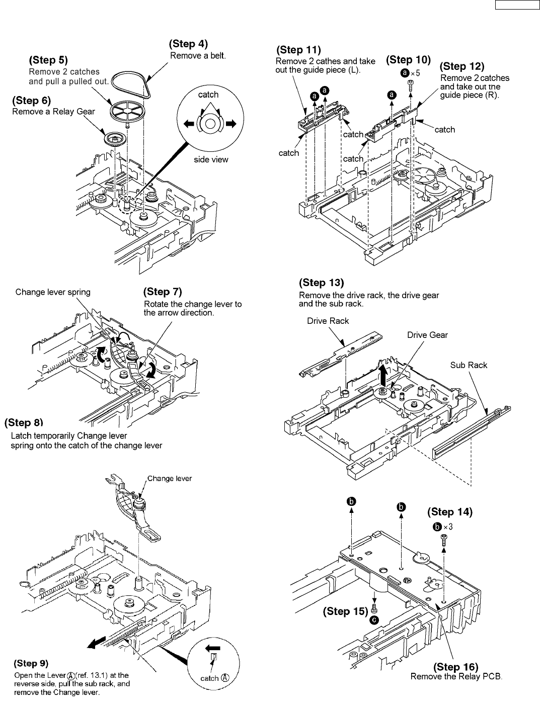
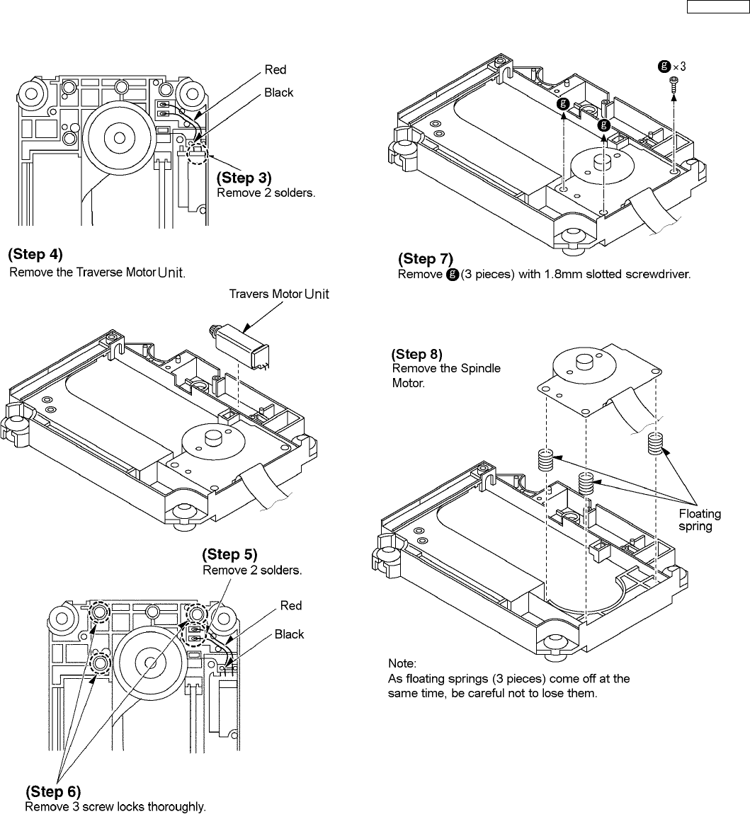
17.8. Disassembly and Assembly Mechanism Unit
34
SA-HT530GCP
Step 7: Detach 20P FFC Board (FP8501).
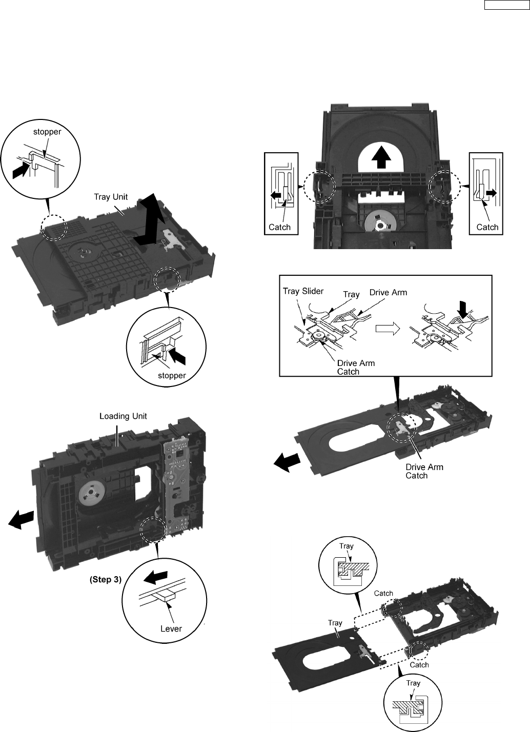
Step 1: While pressing the stopper to the arrow direction, slide
the guide tray unit to remove.
Step 2: Stand the Loading Unit.
Step 3: Push the lever forward (the tray will move).
Step 4: Widen the catches at both sides and pull out the tray.
(The tray will stop after a few slides)
Step 5: Remove Drive Arm Catch from Tray Slider and Tray.
·
Fixing the Tray
Step 1: Insert Tray slightly into groove of chassis.
Step 2: Insert Tray into the area to avoid catching the
mechanism chassis claw.
17.8.2. Replacement of Tray.
·
Follow the (Step 1) -(Step 7) of item 17.8.1 - Replacement of Traverse Unit
35
SA-HT530GCP
Step 3: Latch Drive Arm Catch onto Tray and Tray Slider.
Step 4: Push Tray .
Step 5: Check Tray and Drive Arm move smoothly.
17.8.3. Disassembly of loading section.
·
Follow the (Step 1) -(Step 4) of item 17.8.1 - Replacement of Traverse Unit
·
Follow the (Step 1) -(Step 5) of item 17.8.2 - Replacement of Tray
36
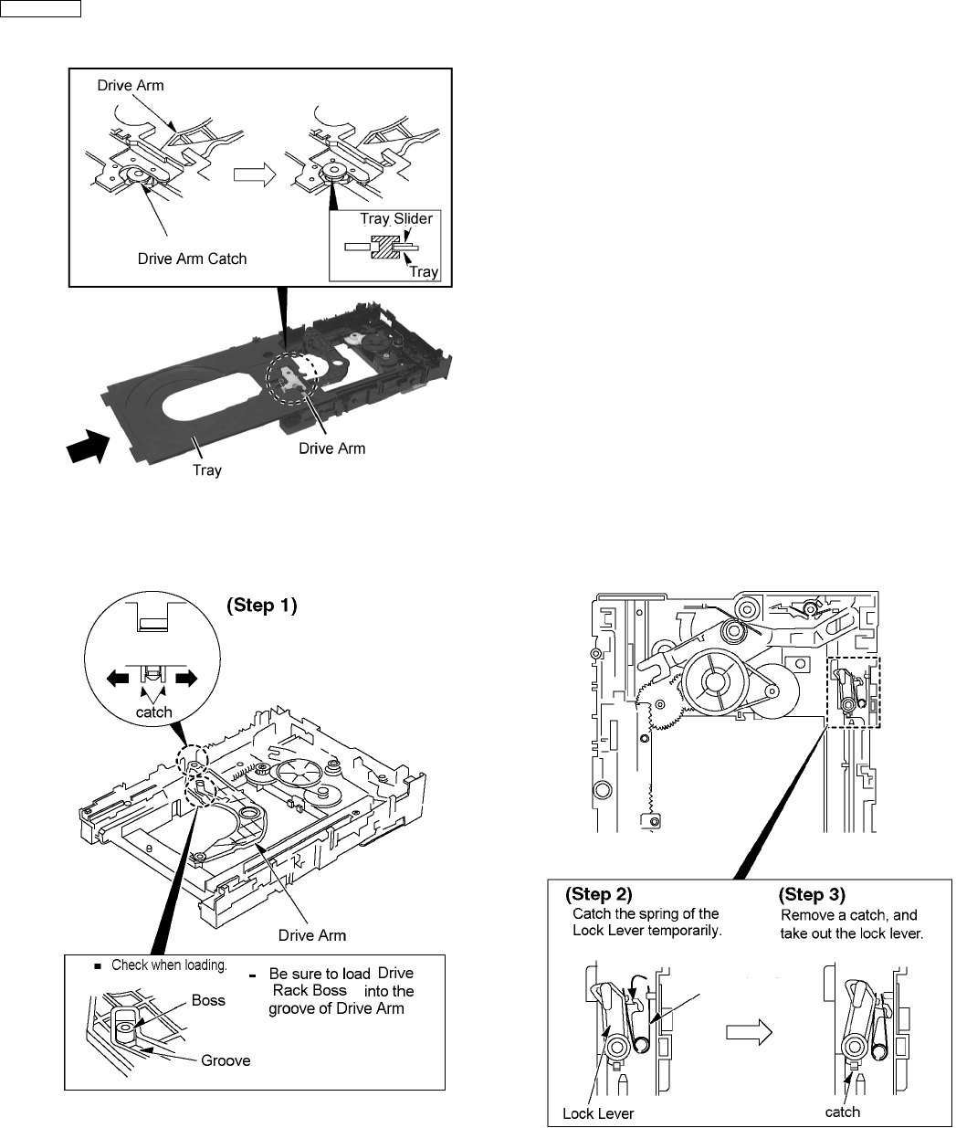
SA-HT530GCP
Step 1: Widen the catch, push the pin in.
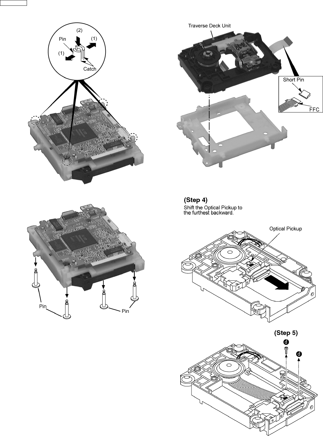
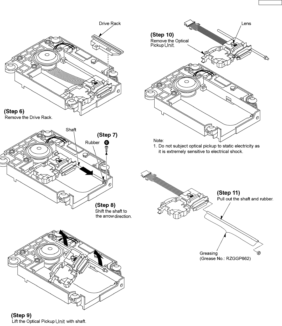
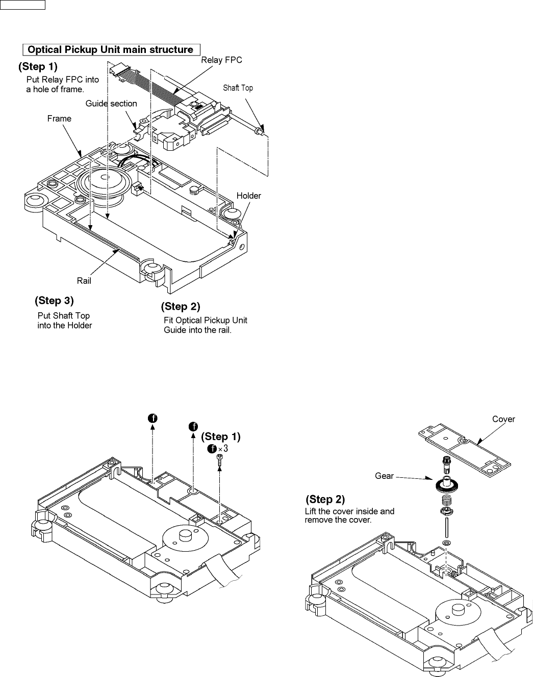
17.8.4. Replacement of Optical Pickup Unit
·
Follow the (Step 1) -(Step 5) of item 17.8.1 - Replacement of Traverse Unit
·
Follow the (Step 1) -(Step 5) of item 17.8.2 - Replacement of Tray
37
SA-HT530GCP
Step 2: Remove 4 pins.
Step 3: Remove Traverse Unit.
Note:
Insert a short pin into FFC of the optical pickup.
38
SA-HT530GCP
39
SA-HT530GCP
17.8.5. Disassembly of traverse motor (Unit) and spindle motor (Unit).
·
Follow the (Step 1) -(Step 5) of item 17.8.1 - Replacement of Traverse Unit
·
Follow the (Step 1) -(Step 5) of item 17.8.2 - Replacement of Tray
·
Follow the (Step 1) -(Step 11) of item 17.8.4 - Replacement of Optical Pickup Unit
40
SA-HT530GCP
41
SA-HT530GCP
18 Service Position
18.1. Checking the Main P.C.B.
Below are the neccessary steps required for checking of Main P.C.B..
1. Disassembly of Top Cabinet.
2. Disassembly of Front Panel.
3. Disassembly of Rear Panel.
4. Disassembly of Main P.C.B..
42
SA-HT530GCP
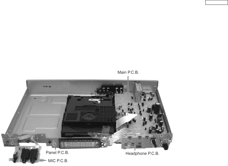
18.2. Checking the Main P.C.B., Panel P.C.B., MIC P.C.B. and Headphone
P.C.B.
Below are the neccessary steps required for cheking of Panel and Headphone P.C.B..
1. Remove Top Cabinet.
2. Disassembly of Front Panel.
3. Disassembly of Headphone P.C.B., MIC P.C.B. and Panel P.C.B..
43
SA-HT530GCP

19 Adjustment Procedure
19.1. Required Tools and Equipment
19.1.1. Usage Equipment
Application Name Number
Tilt adjustment DVD test disc DVDT-S20 [SPG]
TORX screw driver (T6) Available on sales route. (T6) or
RFKZ0185 [SPG]
Others Hanari VFK1784
Grease RFKXPG641 [SPG]
Drysurf RFKXGUD24 [SPG]
Confirmation CD test disc PVCD-K06 and any other
commercially available disc
Recovery disc RFKZD03R005 [SPG]
19.1.2. Important points in adjustment
19.1.2.1. Important points in Optical Adjustment
·
Before starting optical system adjustment, be sure to take anti-static measures.
·
Optical adjustment (optical pickup tilt adjustment) is required after following parts are replaced:
1. Optical pickup unit.
2. Spindle motor assembly unit.
3. Optical pickup peripherals
Note:
Optical adjustment is not necessary after replacement of other parts inside the traverse unit. However, may require when picture
deterioration is detected. Optical adjustments cannot be applied to the inside of optical pickup. When a traverse unit is replaced,
the adjustment is not necessary.
19.1.3. Storing and Handling Test Discs
Surface precision is vital for DVD test discs. Be sure to store and handle them carefully.
·
Do not place discs directly onto the workbench, etc, after use.
·
Handle the discs carefully in order to maintain their flatness. Place them into their case after use and store them vertically. Store
discs in a cool place where they are not exposed to direct sunlight or air from air conditioned.
·
Accurate adjustment will not be possible if the disc is warped when placed on a surface made of glass, etc. If this happens, use
a new test disc to make optical adjustments.
·
If adjustment is done using a warped disc, the adjustment will be incorrect and some discs will not be playable.
44
SA-HT530GCP
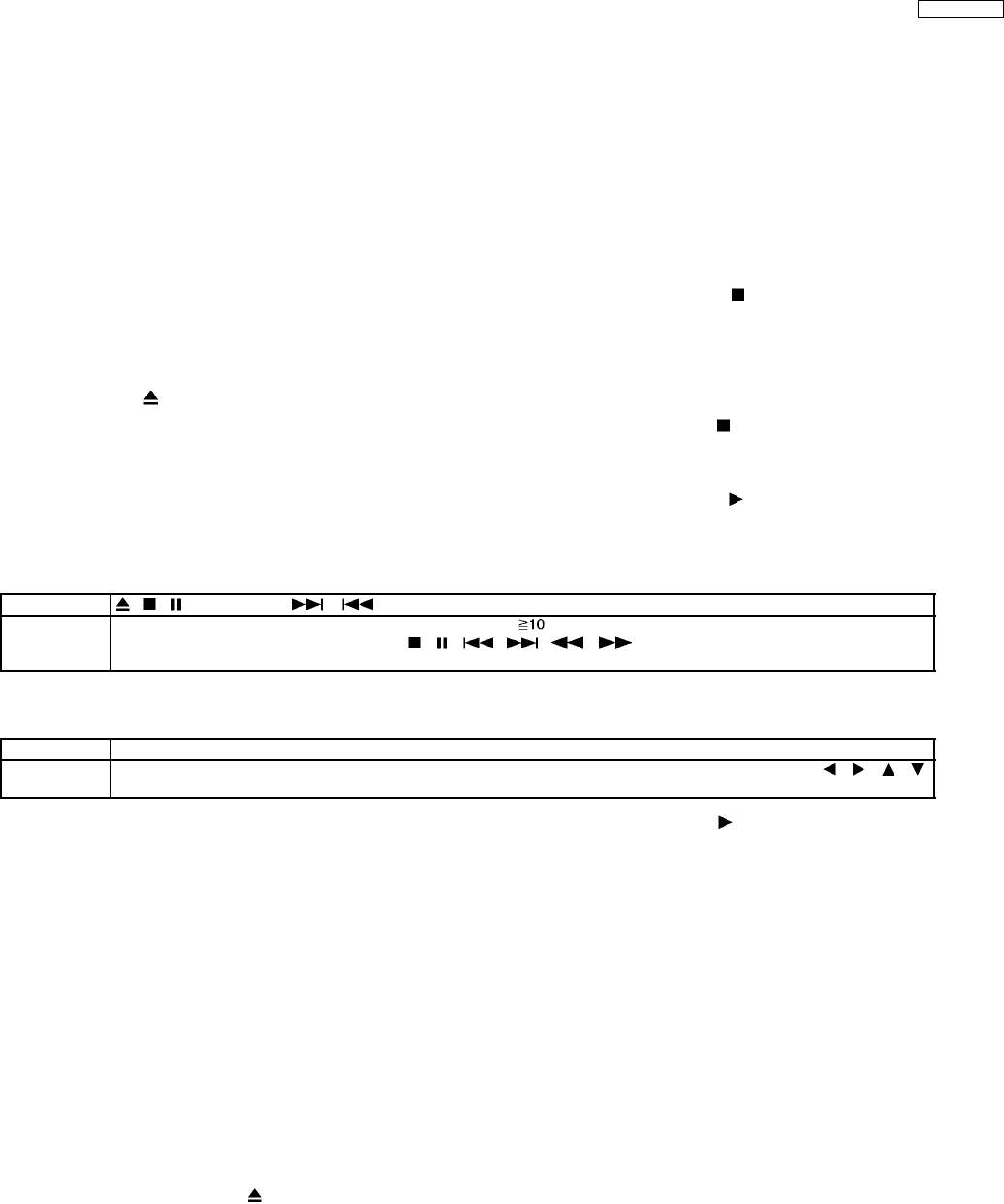
19.1.4.1. Adjustment Procedure
1. While the player is stopped and no disc is inserted, select
the DVD function. Press and hold down the button on the
player and the number button, “5” on the remote controller
unit.
2. Check that “J_xxx_yyy_zz” is appearing on the display.
For your information:
The values, “yyy” and “zz” are not associated to jitter
value.
“yyy” indicates the frequency of error occurrence.
“zz” indicates the focus drive value.
Note:
Jitter value appears on the display.
3. Replay T01 (inner track) of the test disc.
4. Adjust till the jitter value becomes minimum, using a
tangential adjustment screw. <Fig. 19-1>
5. Replay T43 (outer track) of the test disc.
6. Adjust till the jitter value becomes minimum, using a tilt
adjustment screw 1. <Fig. 19-1>
7. Replay T43 (outer track ) of the test disc.
8. Adjust till the jitter value becomes minimum, using a tilt
adjustment screw 2.<Fig. 19-1>
9. Adjust till the jitter value becomes, using the tilt adjustment
screws 1 and 2 alternatively.
Fig. 19-1
19.1.4.2. Tips
1. Apply the tangential adjustment first and then the tilt
adjustment.
2. Repeat the adjustment a couple of times to find the
optimum point.
3. Complete with the tilt adjustment.
19.1.4.3. Check After Adjustment
Replay test discs or other commercial discs in order to confirm
that no picture deterioration or sound skipping is detected in the
inner, middle, and outer tracks. After this, fasten each
adjustment screw securely using a screw lock.
19.1.4.4. Procedure for Screw Lock
1. After adjustment, remove the top cover, clamper base, disc
tray and then traverse unit.
2. Place the traverse unit upside down, and fasten the
adjustment screws with a screw lock. <Fig. 19-2>
3. After fastening the screws, assemble in order of the
traverse unit, disc tray, clamper base, and then top cover.
Fig. 19-2
19.1.4. Optical Adjustment (Optical Pickup Tilt Adjustment)
Measurement point Adjustment point Mode Disc
Tangential adjustment screw
Tilt adjustment screw
T1 (inner track) replay
T43 (outer track) replay
DVDT-S20 [SPG]
Measuring equipment Adjustment value
None (LCD display of the player is used.) Adjust that jitter value becomes minimum.
45
SA-HT530GCP
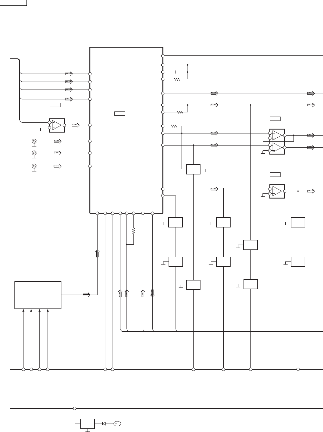
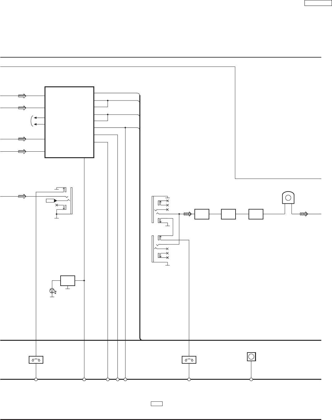
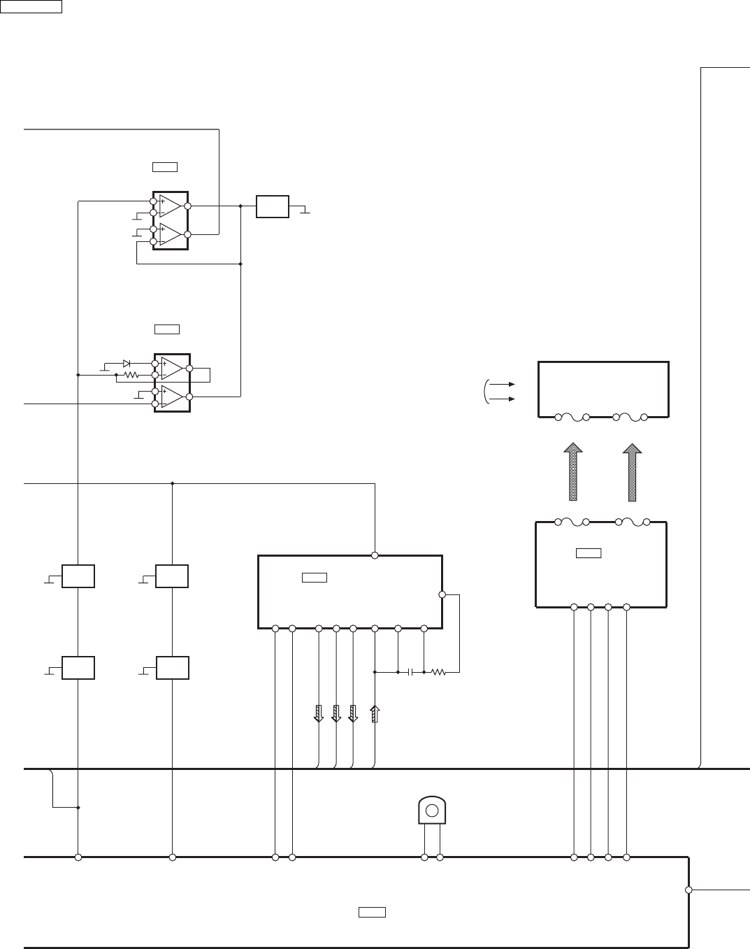
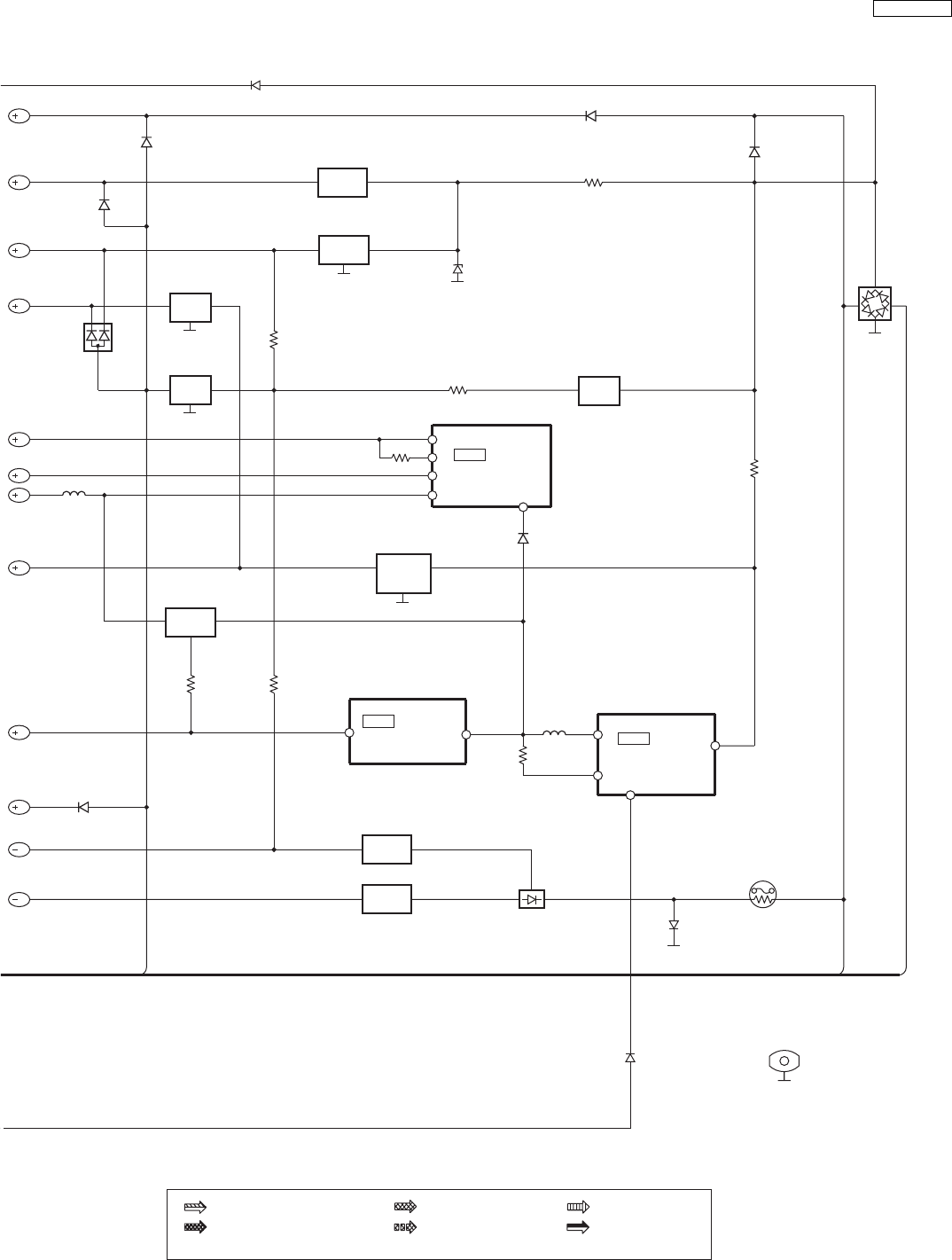
20 Block Diagram
LDU
HFM
82
DRV7
127
VREFH
110
RFINN
111
RFINP
132
VIN7
131
VIN8
136
VIN3
115
VIN3RF
135
VIN4
114
VIN4RF
137
VIN2
116
VIN2RF
138
VIN1
117
VIN1RF
13
V01-
11
V02-
12
V02+
14
V01+
15
V04+
16
V04-
1
BIAS
4
OPIN+
24
LDIN
25
BIAS2
26
TRIN
VIN3
23
MUTE12
9
76
DRV1
MUTE4
20
83
DRV8
VIN1
2
146
VCOF/AD4
VIN2
3
139
AD2
147
PWM1
148
PWM0
128
VHALF
75
DRV0
140
AD1
81
DRV6
TRVM-
TRVM+
TRV_INNER_SW
OSCO
166
OSCI
165
X8621
P9
59
P8
60
65
T+
F+
F-
T-
TA(DVD)
TB(DVD)
TD(DVD)
TC(DVD)
FE2(DVD/CD)
FE1(DVD/CD)
RF
VREF2 (RF-)
VREF1
PIN(CD)
SUBSEL
TRACKING COIL
FOCUS COIL
124
LPC01
Q8551
SWITCH
Q8552
SWITCH
126
LPC02
Q8561
SWITCH
Q8562
SWITCH
143
AD0
LDCD
LDDVD
78
DRV3
QR8571
SUPPLY
CONTROL
SWITCH
HFN VCC
OUT
130
VIN9
134
VIN5
129
VIN10
133
VIN6 SUB2
SUB1
123
LPC1 PIN(DVD)
SW
15
1M
8
SUB1
14
SUB2
13
VREF
11
RF
9
FE1
6
FE2
7
TC
4
OPTICAL PICKUP
SPINDLE MOTOR UNIT
TD
5
TB
2
TA
3
LD(DVD)
17
LD(CD)
16
B
LDCNT
28
R
17
V03+
18
V03- SPM-
SPM+
125
LPC2
MUTE3
27
79
MUTE3
5
OPIN-
6
OPOUT
IC8001 DV2.1 LSI
MN2DS0003APH
MOTOR DRIVE
IC8251
C0GBG0000048
EEPROM
(NOT SUPPLIED)
IC8611
C3EBGC000044
46
SA-HT530GCP
DQ0
2,4,5,7,8,10,11,
13,42,44,45,47,
48,50,51,53
DQ15
MDQ0
MDQ15
1,2,4,5,7,8,10,
11,13-15,17,18,
252,254,256
MA0
MA11
217,220,221,223,
224,226-228,230,
233,237,238
A0
22-26,
29-35
A11
BA0
20
232
BA0
BA1
21
234
BA1
LDQM
15
249
DQM0
UDQM
39
251
DQM1
/CS
19
240
NCSM
CLK
38
243
MCK
241
MCKI
/RAS
18
244
NRAS
/CAS
17
245
NCAS
/WE
16
248
NWE
A16
9,10,16,17,48
A20
A0
1-8,18-25
A15
EXADR16
EXADR20
21,30,31,43,45
EXADT0
EXADT15
23-25,27,32,
33,36,37,39-42,
46,47,50,51
DQ0
29-36,
38-45
DQ15
MDQ16
MDQ31
192-195,197-200,
203,204,206-208,
210-212
XWE
11
22
NEXWE
XCE
26
38
NEXCE
XOE
28
52
NEXOE
12
XRESET
73
NRST
Q8607
SWITCH
Q8606
SWITCH
Q8560
SWITCH
Q8550
SWITCH
B
D8550
R
IC8001 DV2.1 LSI
MN2DS0003APH
IC8051
C3ABPG000133
64 SDRAM IC
IC8651
IC8601
C0EBE0000384
VOLTAGE
DETECTOR
RESET IC
IC8606
C0EBA0000031
RFKWMH82B160
16M FLASH ROM IC
47
SA-HT530GCP
DIN1
45-47
DIN3
ADOUT0
ADOUT2
174-176
LRCIN
41
169
LRCK
DATA4
31
171
ADOUT3
BCKIN
40
170
SRCK
SCLKI
38
163
DACCK
MDO
33
58
P10
MDI
34
57
P11
MC
35
56
P12
ML
36
53
P15
ZFLGA
48
55
P13
16(20)
VOUT7(8)
14(13)
VOUT1(2)
12(11)
VOUT3(4)
10
VOUT5
9
VOUT6
149
DAC1OUT
151
DAC2OUT
QR8420
MUTING
SWITCH
152
DAC3OUT
156
DAC4OUT
158
DAC5OUT
70
P1
69
P2
2
1
68
P3
2
1
55
8
1
B
DVD_MIXL(R)
DVDFL(R)
DVDSL(R)
DVDCNT
SUBW
ZFLAG
PY
CB_B
CR_R
S_Y
S_C
DVD_CMD
DVD_STAT
DVD_CLK
44
A
5
QR8111, QR8112
SWITCH
B
IC8421
C0FBBK000050
AUDIO DAC
IC8001 DV2.1 LSI
MN2DS0003APH
IC8691
C0JBAA000346
AND GATE
LOGIC IC
POWER
SUPPLY
IC8111
C0CBCBD00018
TO MAIN
BLOCK
IC8695
C0JBAA000346
AND GATE
LOGIC IC
48
SA-HT530GCP
A
13
CYOUT
Y
12
CBOUT
CB
11
CROUT
CR
15
VOUT
14
YOUT
JK2001
16
COUT
Q2004
SWITCH
CRIN
9
CBIN
8
CIN
2
YIN
4
CYIN
6
CR_R
CB_B
S_C
S_Y
XOUT
13
XIN
15
X2000
38
WIDE1
37 DVD_CLK
DVD_CLK
36 DVD_STAT
DVD_STAT
35 DVD_CMD
DVD_CMD
44 DVD_MUTE
ZFLAG
Q2028
INVERTER
SWTCH
(ZFLAG)
GY
C
VIDEO
OUT
S-VIDEO
IC2018 MICROPROCESSOR
C2CBHG000168
PY
IC904
C0GAH0000002
RELFECTIVE PHOTO
SENSOR
Q2030
SWITCH
2
TRAY_CCW
9
1
TRAY_CLOSE
S901
PLAY
4
TRAY_OPEN
S902
OPEN
3
TRAY_CW
1
7
BRAKE_H
8
7
RM902
3
B
M
345
25
ECS
24
ECK
23
EEDA
6
TO
DVD
BLOCK
IC2006
C9ZB00000466
VIDEO
SELECTOR IC
IC2019
C3EBEG000072
EEPROM IC
(NOT SUPPLIED)
49
SA-HT530GCP
5(3)
7(1)
IC2010
C0ABBB000118
DUAL OP
AMP
DVDFL(R)
INFLA(R)
75(76)
DVDSL(R) INLSA(R)
78(79)
SUBW INSUBA
80
DVDCNT INCA
77
DVD_MIXL(R) INE1(2)
69(70)
INA1(2)
61(62)
INB1(2)
63(64)
INC1(2)
65(66)
27
TUN_SD(TUNED)
28
TUN_DO(STEREO)
29
TUN_CLK
30
TUN_DA
67(68)
IND1(2)
CL
46
49
VOL_CLK
DA
45
48
VOL_DATA
INCB
6
SS_C
INRSB
8
SS_S
INSLB
7
EXIN1(2)
72(73)
EXT_L(R)
Q2500,
Q2600
MUTING
CONTROL
40, 42
MUTE_C,
MUTE_SUB
39(36)
OUTFL(R)
28
FOUT1
7
1
3
IC2015
C0ABBB000118
DUAL OP AMP
5
27
OUTC
26
OUTCN
2(6) 1(7)
IC2013
C0AABB000125
HP AMP IC
25(23)
OUTLS(R)
Q2200
MUTING
SWITCH
Q2105
MUTING
CONTROL
39
MUTE_FRONT
24(22)
OUTLSN(R)
34
MUTE_S
Q2104
MUTING
SWITCH
Q2103
MUTING
CONTROL
Q2102
MUTING
SWITCH
Q2201
MUTING
CONTROL
41(38)
FOUT4(3)
Q2601
MUTING
SWITCH
TV
VCR
AUX
JK2001
Q2000
RESET
SWITCH
D2001
B
6(2)
3(5)
6
2
IC2018 MICROPROCESSOR
C2CBHG000168
AOUT1(2)
1(2)
SS_L(R)
43
HP_MUTE
52(50)
GOUTFL(R)
17
GOUTSUB
51(49)
VINFL(R)
18
VINSUB
RESET
12
21
OUTSUB
Q2608
SWITCH
Q2609
SWITCH
HB_LVL
IC2011
C1BB00000845
ASP IC
TUNER PACK
(J3CCBB000004)
50
SA-HT530GCP
RCH
FRONTL(R)
SURR L(R)
CENTER
SUBWOOFER
SUB+B SUB+B
SUBAC1 SUBAC1
DVDAC1
S6000~S6005
KEYSW
91
KEY2
SUBAC2 SUBAC2
DVDAC2
DCDET
MUTE_H
SYNC
PCONT
Q2029
LED
DRIVE
D6000
70
PCONT
19
SYNC
71
MUTE_H
72
DC_DET
DCDET
REMOTE
SENSOR
Z6000
JK2000
TO ACTIVE SUBWOOFER BLOCK
TO
FL DISPLAY
IC2018 MICROPROCESSOR
C2CBHG000168
S6011~S6014
KEYSW
Q6071
MIC AMP
Q6072
MIC AMP
Q6073
MIC AMP
JOG VOL
VR6001
97
KEY1
18
RMT
JK6002
HEADPHONE
JK6010
MIC1
JK6011
MIC2
51
SA-HT530GCP
IC2014
C1BB00000979
ANALOG SURROUND IC
EXT_L(R)
68
DVD_PCNT
JOG VOL
VR6000
76
JOG_A
75
JOG_B
G1
5,10,12,16,
19,21,22,24,
30,31,33,35,38
G10
P1
6~9,11,13~15,
17,18,20,32,34,
36,37,49~41
P17
G1
14,18,20,22~24,
26,29,33,35
G10
P1
12,13,16,17,19,21,25,
27,28,30~32,34,36~39
P17
87
FLD_RST
88
FLD_CS
81
FLD_DA
SUB+B
89
FLD_CK
FROM POWER
TRANSFORMER
IC2018 MICROPROCESSOR
C2CBHG000168
SS_L(R) LSIN(R)
8(9)
LCIN(R)
6(7)
LIN(R)
1(5)
2(4)
LF(R)
IC2601
C0ABBB000118
DUAL OP-AMP
SS_C COUT
13
SS_S SOUT
12
LOUT(R)
15(14)
52
SS_DA DATA
18
53
SS_CLK CLOCK
19
7
1
3
5
6
2
IC2602
C0ABBB000118
DUAL OP-AMP
7
1
3
5
6
2
Q2607
SWITCH
Q2604
SWITCH
Q2605
SWITCH
55
HB_MUTE
D2601
FLD_DA
10
FLD_CS
3
FLD_RST
8
FLD_CLK
9
HB_LVL
3
MICIN
Q2703
XXX
Q2702
XXX
51
MIC_MUTE
FL6000
FL DISPLAY
IC6000
C0HBB0000044
FL DRIVER IC
52
SA-HT530GCP
B
IC2803
C0DBEZG00021
REGULATOR IC
IC2802
C0CBADG00023
5V REGULATOR IC2801
C0DAAZG00012
DC-TO-DC
CONVERTER
+7.5V
B
+12V
B
D2827
TUNER+9V
D2824
B
SW5V
B
M+9V
Q2803, Q2804
CURRENT
CONTROL,
CURRENT
STABLIZER
Q2801
SWITCH
D2822
SUBAC2
SUBAC1
FP2000
D2813
~D2817
D2812
B
-VP
B
-7.5V
Q2807, Q2808
REGULATOR
D2803
Q2818
DCDET
SWITCH
SIGNAL LINES
( ) Indicates the Pin No. of Right Channel. NOTE : Signal Lines are applicable to the Left Channel only.
: MAIN SIGNAL LINE : DVD AUDIO SIGNAL LINE
: DVD VIDEO SIGNAL LINE
: CD-DA (AUDIO /VIDEO) SIGNAL LINE
: AUX SIGNAL LINE
: FM/AM SIGNAL LINE
1
5
3
B
D+5V
3
B
D+5V 2
4
DCDET
Q2809
REGULATOR
Q2814
REGULATOR
Q2816
REGULATOR
E2000
1
D2851
Q2813
XXXX
D2853
B
C+9V D2852
D2850
D2826
D2825
D2831
L2801
2
1
4
B
D+1.2V
5
B
A+5V L2801
Q2805, Q2806
REGULATOR
53
SA-HT530GCP

(All schematic diagrams may be modified at any time with the
development of the new technology)
Note:
S901 : PLAY switch
S902 : OPEN switch
S6000 : OPEN/CLOSE switch
S6001 : FF switch
S6002 : REW switch
S6003 : STOP switch
S6004 : PAUSE switch
S6005 : PLAY switch
S6011 : POWER switch
S6012 : SELECTOR switch
S6013 : RDS switch
S6014 : H_BASS switch
VR6000 : VOLUME
VR6001 : MIC VOLUME
·
The voltage value and waveforms are the reference voltage
of this unit measured by DC electronic voltmeter (high
impedance) and oscilloscope on the basis of chassis.
Accordingly, there may arise some error in voltage values
and waveforms depending upon the internal impedance of
the tester or the measuring unit.
·
Importance safety notice :
Components identified by mark have special
characteristics important for safety. Furthermore, special
parts which have purposes of fire-retardant (resistors), high-
quality sound (capacitors), low-noise (resistors), etc. are
used. When replacing any of components, be sure to use
only manufacturer´s specified parts shown in the parts list.
Caution !
IC, LSI and VLSI are sensitive to static electricity.
Secondary trouble can be prevented by taking care during
repair.
·
Cover the parts boxes made of plastics with aluminium foil.
·
Put a conductive mat on the work table.
·
Ground the soldering iron.
·
Do not touch the pins of IC, LSI or VLSI with fingers directly.
21 Schematic Diagram
54
SA-HT530GCP
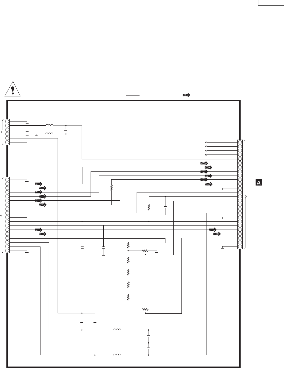
21.1. Optical Pickup Unit Circuit
16
17
18
19
20
21
25
23
22
24
26
1
2
3
4
5
6
14
12
10
8
7
9
11
13
15
2
4
6
5
3
1
15
14
13
12
11
10
2
4
6
8
9
7
5
3
1
17
18
16
TO ACT
TO
DVD
MODULE
CIRCUIT
(FP8501) ON
SCHEMATIC
DIAGRAM-2
TO
HFM
PCB
TO
LDU
PCB
L4
J0JBC0000105
L1
J0JBC0000105
L2
J0JCC0000307
C5
22P
C6
22P
C1
0.1
C3
0.1
C2
0.1
R1
0
R4
0
R2
0
C8
0.1
R3
0
R5
0
R6
0
R7
6.8K
C7
0.1
VR2
6.8K
VR1
6.8K
C4
0.1
L3
J0JBC0000105
T+
F+
F-
T-
HFM
TA
TB
TD
TC
FE2
FE1
GND (IM)
RF
VREF2(RF-)
PIN (DVD)
LD (CD)
LD GND
LD (DVD)
GND (OEIC)
VREF1
VCC
SUB2
SUB1
PIN(CD)
SUBSEL
GND (IM)
GND
VCC
GND
GND
OUT
GND
GND
TB
TA
TC
TD
FE1
FE2
IM
RF
GND
VREF
VCC
SUB2
SUB1
SW
LD (CD)
LD (DVD)
LDGND
SCHEMATIC DIAGRAM - 1
OPTICAL PICKUP UNIT CIRCUIT
: +B SIGNAL LINE : CD-DA SIGNAL LINE
55
SA-HT530GCP
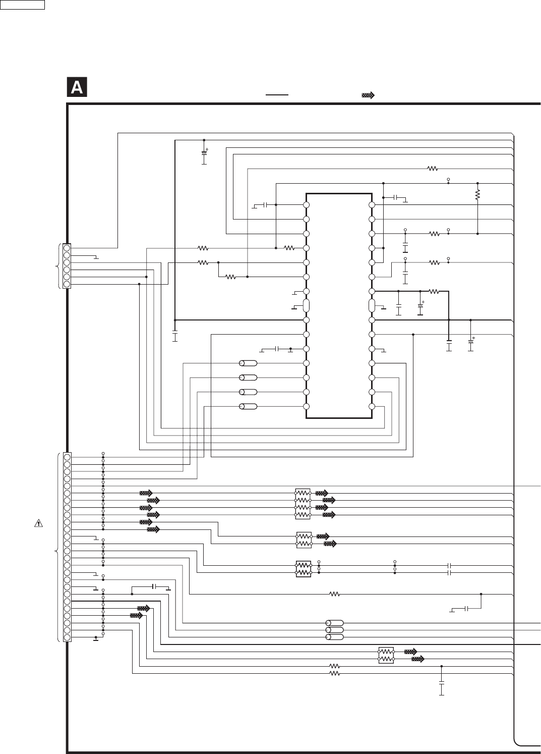
21.2. (A) DVD Module (DV2) Circuit
SCHEMATIC DIAGRAM - 2
DVD MODULE (DV2) CIRCUIT
: +B SIGNAL LINE : CD-DA SIGNAL LINE
3029
15
16
17
12
13
14
18
11
19
10
20
9
21
8
22
7
23
6
24
5
25
4
26
3
27
2
28
1
16
17
18
19
20
21
25
23
22
24
26
1
2
3
4
5
6
14
12
10
8
7
9
11
13
15
CKE26
TP8253
TP8254
TP8252
TP8502
TP8514
TP8515
TP8517
TP8516
TC8504
TP8520
TP8510
TP8501
TC8501
TP8525
TP8524
TP8521
TC8502
TP8500
TC8503
TP8519
TP8518
TP8511
T+
F+
F-
T-
HFM
TA(DVD)
TB(DVD)
TD(DVD)
TC(DVD)
FE2(DVD/CD)
FE1(DVD/CD)
GND
RF
VREF2(RF-)
PIN(DVD)
LDCD
LDGND
LDDVD
GND(OEIC)
VREF1
VCC
SUB2
SUB1
PIN(CD)
SUBSEL
GND(VRCD)
FP8501
LDCNT
MUTE3
TRIN
BIAS2
LDIN
VIN3
PREVCC
FIN
VCC(CH3.4)
MUTE4
GND(CH3.4)
VO3-
VO3+
VO4-
VO4+
BIAS1
VIN1
VIN2
OPIN+
OPIN-
OPOUT
GND(PRE)
FIN
VCC(CH1.2)
MUTE12
GND(CH1.2)
VO2-
VO2+
VO1-
VO1+
VIN1
VIN2
VIN4
VIN3
VIN8
VIN7
RFINP
RFINN
LPC1
VREFH
VIN6
VIN5
LPC2
RAM_CD
PNRST
LB8512 ERJ3GEY0R00V
LB8513 ERJ3GEY0R00V
LB8511 ERJ3GEY0R00V
LB8514 ERJ3GEY0R00V
LB8505 J0JCC0000119
LB8504 J0JCC0000119
LB8503 ERJ2GE0R00X
R8501 0
R8506 1.5K
C8504 0.1
C8256
0.1
C8257
0.1
R8251
6.8
RX8502
(56 x 4)
RX8504
(56 x 2)
RX8503
(56 x 2)
C8506
100P
C8505
220P
RX8501
(56 x 2)
IC8251
DRIVE IC
C0GBG0000048 IC8251
CL8502
CL8501
TO
OPTICAL
PICKUP
UNIT
CIRCUIT
ON
SCHEMATIC
DIAGRAM-1
C8253
16V22
C8255
0.1 C8252
16V47
R8505 2.2K
MUTE12
C8262
0.1
C8261
0.1
R8262
4.7K
R8261
82K
R8263
82K
R8264
4.7K
R8265
0
CL8242 CL8241
TL8201
R8241
22K
R8201
2.2K
C8241
0.1
DRV0
CL8244 CL8243
R8242
7.5K
C8242
0.1
DRV1
C8254
0.1
C8251
6.3V220
D+5V
TO
SPINDLE
MOTOR
2
4
6
5
3
1
FP8201
SPM-
SPM+
TRVM-
TRVM+
DGND
TRV_INNER_SW
M+9V
MUTE3
AD1
TRDRV
FODRV
VHALF
TRV-I-SW
CL8202
CL8201
C8218 1
C8217 1
56
SA-HT530GCP
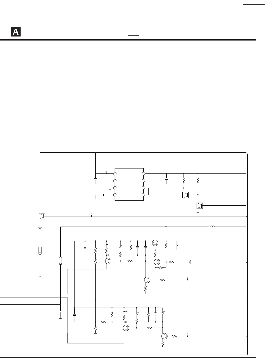
SCHEMATIC DIAGRAM - 3
DVD MODULE (DV2) CIRCUIT
: +B SIGNAL LINE
1
2
36
7
8
45
D+5V
CL8571
TP8523
TP8522
TP8513
TP8512
CL8551
CL8561
VO
NC
GND
CN
VIN
NC
NC
Cont
D+3.3V
HFMON
AD0
LPCO2
LPCO1
A+5V
D+1.2V
LB8507
J0JCC0000119
LB8502
J0JHC0000045
C8502
0.1
C8501
10
D8571
MA2J72800L
TP8111
C8112
1
C8113
470P
C8111
0.1
L8550
G1C100KA0055
C8561
0.1
C8551
0.1
C8503
0.1
R8559
15K
R8558
47K
R8557
51 R8556
56
C8553
6.3V47
R8555
2.2
R8553
1K
R8552
1K
R8551
0
R8554 68
C8552
16V10
R8567
51
R8568
47K
R8566
56
C8563
6.3V47
R8565
2.2
R8563
1K
C8564 1
C8562
16V10
R8564
22
R8562
1K
R8561
0
R8560
1K
R8569
12K
R8570
100K
R8550
7.5K C8550
6.3V33
D8550
MA2J11100L
C8554 1
QR8571
UNR511V00L
SUPPLY CONTROL SWITCH
Q8562
2SB09700RL
SWITCH
Q8552
2SB09700RL
SWITCH
Q8560
2SD1819A0L
SWITCH
Q8550
2SB1219AHL
SWITCH
Q8560
Q8561
2SD1819A0L
SWITCH
Q8551
2SD1819A0L
SWITCH
IC8111
IC8111
C0CBCBD00018
3.3 REGULATOR IC
PNRST
R8112
22K
QR8112
UNR521400L
SWITCH
QR8111
UNR521400L
SWITCH
R8111
22K
57
SA-HT530GCP
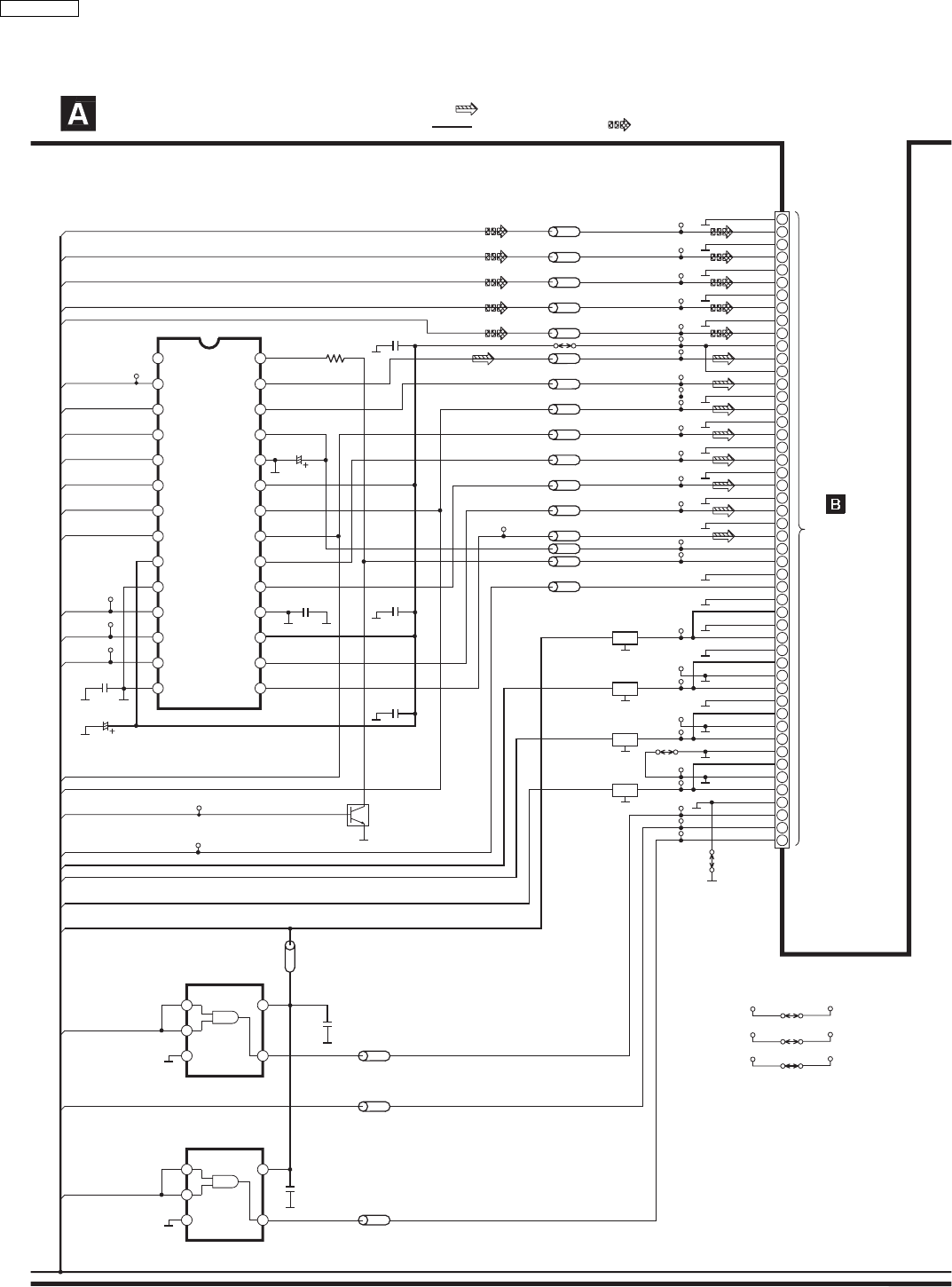
15
14
13
12
11
10
2
4
6
8
9
7
5
3
1
30
29
28
27
26
25
17
19
21
23
24
22
20
18
16
36
35
34
33
32
31
50
49
48
47
46
38
40
42
44
45
43
41
39
37
SCHEMATIC DIAGRAM - 4
DVD MODULE (DV2) CIRCUIT
: +B SIGNAL LINE
TO
MAIN CIRCUIT
(CN2004) ON
SCHEMATIC
DIAGRAM-9
FP8101
4
51
2
3
4
51
2
3
Y/PY/G
VGND
VGND
VGND
VGND
VGND
ADAC5V
ADAC5V
ADACGND
ADACGND
ADACGND
ADACGND
ADACGND
ADACGND
DGND
DGND
D+5V
D+5V
D+5V
A+5V
A+5V
A+5V
AGND
AGND
D+1.2V
D+1.2V
DGND
DGND
M+9V
M+9V
MGND
MGND
DGND
DGND
LB8303 TC8303J0JCC0000119
CB/PB/B
LB8304 TC8304J0JCC0000119
CR/PR/R
LB8305 TC8305J0JCC0000119
Y
LB8301 TC8301J0JCC0000119
C
LB8302
K8421
TC8302J0JCC0000119
MIX-L
LB8421 TC8423
TC8421
ERJ2GE0R00X
MIX-R
LB8422 TC8424
TC8422
ERJ2GE0R00X
OP_CPU-CLK
TC8691
LB8691
ERJ2GEJ101X
FL
LB8425 TC8425ERJ2GE0R00X
FR
LB8426 TC8426ERJ2GE0R00X
SL
LB8427 TC8427ERJ2GE0R00X
SR
LB8428 TC8428ERJ2GE0R00X
CNT
LB8429 TC8429ERJ2GE0R00X
SW
LB8430 ERJ2GE0R00X
A-REF
LB8423 TC8431ERJ2GE0R00X
ZFLAG&AMUTE
LB8424 TC8432
TC8105
TC8103
TC8104
TC8102
TC8108
TC8101
TC8107
ERJ2GE0R00X
AUDIODIGITAL
LB8491
TC8430
CL8491
ERJ2GE0R00X
OP_CPU-CMD
TC8692
OP_CPU-STAT
TC8693
FL8103
F1H0J1050022
FL8102
F1H0J1050022
FL8101
F1H0J1050022
FL8104
F1J1E1040022
VCC
GND
GND
VCC
CPU-CLK
CPU-CMD
CPU-STAT
Y/PY/G
CB/PB/B
CR/PR/R
Y
C
D+1.2V
C8695
0.1
C8691
0.1
LB8690
J0JCC0000091
IC8421
IC8691
C0JBAA000346
AND GATE LOGIC IC
IC8421
C0FBBK000050
8-CH DAC IC
QR8420
UNR521100L
AUDIO MUTING SWITCH
IC8695
C0JBAA000346
AND GATE LOGIC IC
K8001
: MAIN SIGNAL LINE
M+9V
ZERO2
VOUT1
VOUT2
VCOM
AGND2
VCC2
VOUT3
VOUT3
VOUT4
VOUT4
VOUT5
VOUT6
AGND1
VCC1
VOUT7
VOUT8
ZERO1
MS
MC
MD
SCK
DATA1
BCK
LRCK
VDD
DGND
DATA2
DATA3
DATA4
MSEL
1
C8423
6.3V33
C8424
0.1
C8428
0.1
0.1
C8422
0.1
C8427
0.1
C8426
R8420
2.2K
CL8424
C8421
6.3V100
AUDIODIGITAL
CL8021
SBT3
227
28
326
425
524
623
722
821
920
10 19
11 18
12 17
13 16
14 15
STBDAC
SBO3
CL8023
AMUT
ADAC-CLK
DMIXOUT
SRCK
LRCK
ADOUT0
CL8425
ADOUT1
CL8426
ADOUT2
LB8692
ERJ2GEJ101X
LB8693
ERJ2GEJ101X
K8003 CL8014CL8012
K8006 CL8007CL8006
K8106
K8008 CL8009CL8006
: DVD VIDEO SIGNAL LINE
58
SA-HT530GCP
SCHEMATIC DIAGRAM - 5
DVD MODULE (DV2) CIRCUIT
: +B SIGNAL LINE
1
2
346
47
48
445
544
643
742
841
940
10 39
11 38
12 37
13 36
14 35
15 34
16 33
17 32
18 31
19 30
20 29
21 28
22 27
23 26
24 25
8
7
2
1
6
3
5
4
RX8611
(4.7K x 2) C8611
0.1
R8611
100
R8021 10K
R8022 10K
R8023 47K
RX8021
(10K x 2)
CL8612
CL8611
CL8024
CL8031
CL8032
CL8033
C8651
0.1
C8652
0.1
A0
A1
A2
GND
VCC
WP
SCL
SDA
A15
A14
A13
A12
A11
A10
A9
A8
A19
A20
XWE
XRESET
NC
WP/ACC
RDY/XBSY
A18
A17
A7
A6
A5
A4
A3
A2
A1
A16
XBYTE
VSS
DQ15/A-1
DQ7
DQ14
DQ6
DQ13
DQ5
DQ12
DQ4
VDD
DQ11
DQ3
DQ10
DQ2
DQ9
DQ1
DQ8
DQ0
XOE
VSS
XCE
A0
FDT15
FDT7
FDT14
FDT6
FDT13
FDT5
FDT12
FDT4
FDT11
FDT3
FDT10
FDT2
FDT9
FDT1
FDT8
FDT0
EXADT15 EXADR16
EXADT14
EXADT13
EXADT12
EXADT11
EXADT10
EXADT9
EXADT8
EXADR19
EXADR20
NEXWE
EXADR18
EXADR17
EXADT7
EXADT6
EXADT5
EXADT4
EXADT3
EXADT2
EXADT1 EXADT0
PNRST
SCL
SDA
SBT3
CPU-CLK
CPU-STAT
CPU-CMD
TRV-I-SW
IC8611
IC8611
C3EBGC000044
16M EEPROM IC (NOT SUPPLIED)
IC8651
RFKWMH82B160
16M FLASH ROM IC
59
SA-HT530GCP
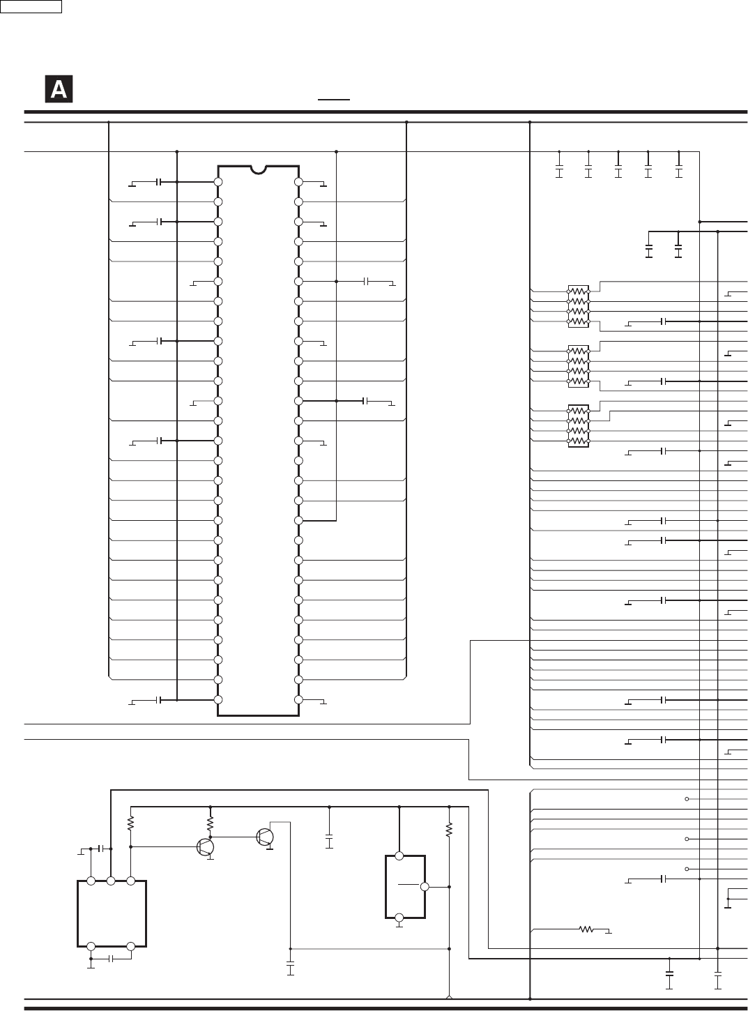
SCHEMATIC DIAGRAM - 6
DVD MODULE (DV2) CIRCUIT
: +B SIGNAL LINE
1
2
352
53
54
451
550
649
748
847
946
10 45
11 44
12 43
13 42
14 41
15 40
16 39
17 38
18 37
19 36
20 35
21 34
22 33
23 32
24 31
25 30
26 29
27 28
CL8022
CL8026
CL8027
C8031
0.1
VDD
DQ0
VDDQ
DQ1
DQ2
VSSQ
DQ3
DQ4
VDDQ
DQ5
DQ6
VSSQ
DQ7
VDD
LDQM
/WE
/CAS
/RAS
/CS
BA0
BA1
A10/AP
A0
A1
A2
A3
VDD
VSS
DQ15
VSSQ
DQ14
DQ13
VDDQ
DQ12
DQ11
VSSQ
DQ10
DQ9
VDDQ
DQ8
VSS
NC
UDQM
CLK
CKE
NC
A11
A9
A8
A7
A6
A5
A4
VSS
SDA
SCL
SBO3
SBT3
AMUT
STBDAC
EXADT3
EXADT7
EXADT11
EXADT15
EXADR19
EXADR17
EXADT13
EXADT9
EXADT5
EXADT1
EXADT2
EXADT6
EXADT10
EXADT14
EXADR18
EXADR16
EXADT12
EXADT8
EXADT4
EXADT0
NEXWE
EXADR20
MDQ15
MDQ0
MDQ14
MDQ1
MDQ13
MDQ2
MDQ12
MDQ3
MDQ11
MDQ4
MDQ10
MDQ5
MDQ15
MDQ14
MDQ13
MDQ12
MDQ11
MDQ10
MDQ9
MDQ8
DQM1
CLK
MA11
MA9
MA8
MA7
MA6
MA5
MA4
MDQ0
MDQ1
MDQ2
MDQ3
MDQ4
MDQ5
MDQ6
MDQ7
DQM0
NWE
NCAS
NRAS
NCSM
BA0
BA1
MA10
MA0
MA1
MA2
MA3
FG
C8051
1
C8052
0.1
C8053
220P
C8054
1
C8055
1
C8056
0.1
C8057
2200P
C8011
1
C8010
0.1
C8008
0.1
C8007
0.1
C8005
0.1
C8009 0.1
C8006 0.1
C8004 0.1
C8003 2200P
RX8011
(82 x 4)
RX8012
(82 x 4)
RX8013
(82 x 4)
C8025
0.1
C8022
0.1
C8023
1
C8024
1
C8026
2200P
C8027
0.1
C8028
1
C8013
0.1
C8012
0.1
IC8051
IC8051
64 SDRAM IC
C3ABPG000133
45
12
3
1
2
3
GND
VDD
OUT
NC
CD
VDD
GND
RESET
PNRST
C8606
0.1
C8607
0.22
R8606
100K R8607
10K R8601
1K
C8601
0.1
IC8606
C0EBA0000031
RESET IC
Q8606
2SD1819A0L
SWITCH
IC8601
C0EBE0000384
RESET IC
R8243 10K
Q8607
2SD1819A0L
SWITCH
60
SA-HT530GCP
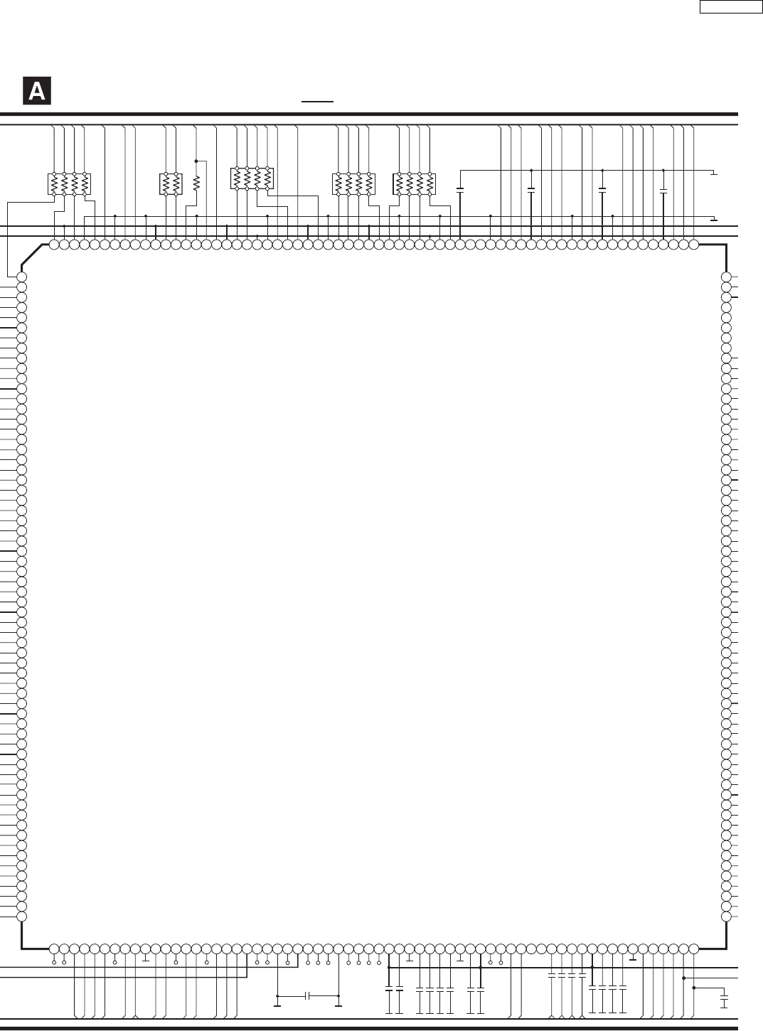
SCHEMATIC DIAGRAM - 7
DVD MODULE (DV2) CIRCUIT
: +B SIGNAL LINE
1
2
3
4
5
6
7
8
9
65 66 67 68 69 70 71 72 73
185
186
187
188
189
190
191
192
248249250251252
253
254
255
256
10
184
74
247
11
183
75
246
12
182
13
181
76
245
77
244
14
180
15
179
16
178
78
243
79
242
80
241
17
177
18
176
19
175
20
174
81
240
82
239
83
238
84
237
21
173
22
172
23
171
24
170
25
169
85
236
86
235
87
234
88
233
89
232
26
168
27
167
28
166
29
165
30
164
31
163
32
162
90
231
91
230
92
229
93
228
94
227
95
226
96
225
33
161
34
35
159
36
158
97
224
98
223
99
222
100
221
37
157
38
156
39
155
40
154
41
153
42
152
43
151
44
150
101
220
102
219
103
218
104
217
105
216
106
215
107
214
108
213
160
45
149
46
148
47
147
48
146
49
145
50
144
51
143
52
142
109
212
110
211
111
210
112
209
113
208
114
207
115
206
116
205
53
141
54
140
55
138
56
137
57
136
58
135
59
134
60
133
61
132
62
131
63
130
64
129
117
204
118
203
119
202
120
201
121
200
122
199
123
198
124
197
125
196
126
195
127
194
128
193
139
CL8028
CL8029
CL8030
CL8035
CL8036
MDQ9
MDQ5
VSS
MDQ10
MDQ4
VDD33
MDQ11
MDQ3
VSS
MDQ12
MDQ2
VDD33
MDQ13
MDQ1
MDQ14
VSS
MDQ0
MDQ15
VDD33
VSS
EXADR20
NEXWE
EXADT0
EXADT4
EXADT8
VDD12
EXADT12
VDD33
VSS
EXADR16
EXADR18
EXADT14
EXADT10
VDD33
VSS
EXADT6
EXADT2
NEXCE
EXADT1
EXADT5
EXADT9
EXADT13
EXADR17
VDD12
EXADR19
EXADT15
EXADT11
VDD33
VSS
EXADT7
EXADT3
NEXOE
P15
P14
P13
P12
P11
P10
P9
P8
P7
VDD33
MMOD
VSS
MDQ24
VSS
VDD33
TRCST
TRCDATA3
TRCDATA2
TRCDATA1
TRCDATA0
TRCCLK
EXTRG1
SDATA
EXTRG0
SCLOCK
VSS
VDD33
IECOUT
ADOUT0
ADOUT1
ADOUT2
VSS
VDD12
ADOUT3
SRCK
LRCK
EXTCK
VDD33
OSCO
OSCI
VSS
DACCK
AVSSG
AVDDG
AVSSE
AVDDE
DAC5OUT
AVSSF
DAC4OUT
COMP
IREF1
VREF
DAC3OUT
DAC2OUT
AVDDF
DAC1OUT
PWM0
PWM1
VCOF/AD4
AVSSH
VREFH10
AD0
VREFL10
AVDDH
AD1
AD2
VIN1
VIN2
VIN3
VIN4
VIN5
VIN6
VIN7
VIN8
VIN9
VIN10
P6
P5
P4
P3
P2
P1
P0
FG
NRST
VSS
DRV0
DRV1
DRV2
DRV3
DRV4
DRV5
DRV6
DRV7
DRV8
VDD33
P16
P17
VSS
MONI7
VDD12
MONI6
MONI5
MONI4
VSS
MONI3
MONI2
MONI1
MONI0
AVDDD
PLFIL1
AVSSD
VREFH7
VREFM7
VREFL7
CCAPA
AVSSC
CDATA
AVDDC
ANAMONI1
ANAMONI2
RFINN
RFINP
VIN6RF
VIN5RF
VIN4RF
VIN3RF
VIN2RF
VIN1RF
AVDDB
VREFH5
VREFM5
VREFL5
AVSSB
LPC1
LPC01
LPC2
LPC02
VREFH
VHALF
MDQ6
VDD33
MDQ8
VSS
MDQ7
DQM1
VSS
DQM0
NWE
VSS
VDD33
NCAS
NRAS
MCK
VSS
MCKI
NCSM
VDD33
MA9
MA11
VDD12
VSS
BA0
MA8
BA1
VDD33
MA10
VSS
MA7
MA0
MA6
VDD33
MA1
MA5
VSS
MA2
MA4
VDD12
VSS
MA3
VDD33
DQM2
DQM3
VSS
MDQ16
MDQ31
MDQ17
VDD33
MDQ30
MDQ18
MDQ29
VSS
MDQ19
MDQ28
VDD33
VSS
MDQ20
MDQ27
MDQ21
MDQ26
VDD33
MDQ22
MDQ25
MDQ23
VHALF
VREFH
LPC02
LPC2
LPC01
LPC1
VIN1
VIN2
VIN3
VIN4
RFINP
RFINN
MUTE12
CL8002
TP8220
TP8219
TP8218
TP8217
TP8216
TP8215
TP8214
TP8213
CL8003
RAM_CD
TRV-I-SW
MUTE3
HFMON
DRV1
DRV0
PNRST
FG
CPU-CMD
CPU-STAT
CPU-CLK
KMODE
MDQ9
MDQ6
MDQ8
MDQ7
DQM1
DQM0
NWE
NCAS
NRAS
NCSM
CLK
MA9
MA11
MA8
MA10
BA0
BA1
MA7
MA0
MA6
MA1
MA5
MA2
MA4
MA3
FDT0
FDT15
FDT1
FDT14
FDT2
FDT13
FDT3
FDT12
FDT4
FDT11
FDT5
FDT10
FDT6
FDT9
FDT7
C8203 0.1
C8211 0.033
C8212 0.1
C8213 0.1
C8214 0.1
C8215 5600P
C8216 0.018
C8204 0.1
C8205 0.1
C8225 0.1
C8226 0.1
C8227 0.1
C8221 0.1
C8222 0.1
C8223 0.1
C8224 0.1
C8229
1
RX8014
(82 x 4)
RX8015
(22 x 2)
RX8016
(82 x 4)
RX8017
(82 x 4)
RX8018
(82 x 4)
C8021
0.1
R8011 22
C8020 0.1
C8019 1
C8018 0.1
IC8001
MN2DS0003APH
DV2.1 IC
TP8211
TP8212
0.1
C8207
61
SA-HT530GCP
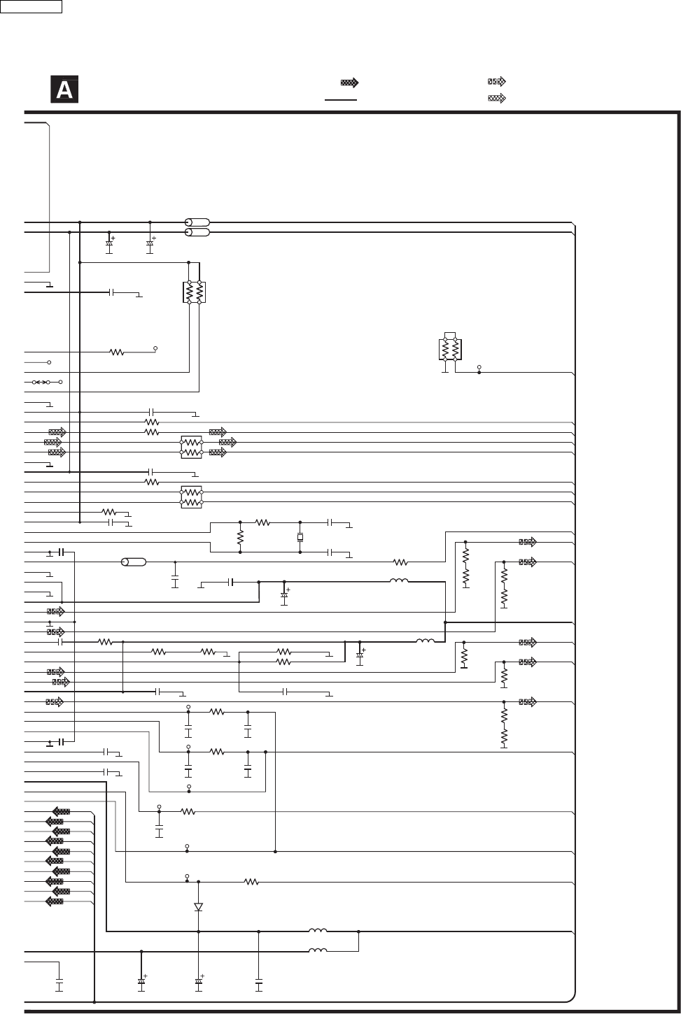
D8231
MA2J11100L
SCHEMATIC DIAGRAM - 8
DVD MODULE (DV2) CIRCUIT
: +B SIGNAL LINE
: CD-DA SIGNAL LINE
: DVD AUDIO SIGNAL LINE
: DVD VIDEO SIGNAL LINE
D+1.2V
AUDIODIGITAL
ADOUT0
ADOUT1
ADOUT2
DMIXOUT
C
Y
CR/PR/R
CB/PB/B
Y/PY/G
SRCK
LRCK
ADAC-CLK
FODRV
TRDRV
AD0
KMODE
CL8034
RX8032
(4.7K x 2)
RX8031
(4.7K x 2)
L8302
J0JCC0000079
L8301
G1C100KA0055
C8302
6.3V33
C8301
6.3V220
R8325
160
R8326
0
R8321
160
R8322
10
R8341
82
R8335
82
R8331
160
R8332
10
VIN1
VIN2
VIN3
VIN4
VIN5
VIN6
VIN7
VIN8
VIN5
VIN6
FDT8
C8228
1
C8201
6.3V100
C8202
6.3V100
C8206
1
L8201
G1C100K00020
L8202
J0JCC0000079
R8231
10K
CL8231
CL8206
CL8233
CL8234
CL8236
CL8235
C8233
4700P
C8237
1000P C8238
820P
C8236
1000P
C8235
1000P
R8233
15K
R8236
8.2K
R8235
8.2K
C8232 0.1
C8234 0.1
C8303 0.1
C8312 1
C8304 1
C8311 0.1
R8311 2.4K
R8312 1KR8313 24K R8314 0
LB8401
ERJ2GEJ151X
C8308
15P
R8621
1M
R8622 1K C8622 12P
C8621 12P
H0J270500085
X8621
C8014 0.1
R8401 47K RX8401
(100 x 2)
RX8402
(100 x 2)
R8402 100
R8407 100
R8404 100
R8041
33
C8015 1
C8016 1
C8017
0.1
CL8040
CKA1
C8002
4V330
C8001
6.3V100 LB8002
J0JHC0000045
LB8001
J0JHC0000045
R8315 6.8
C8208 0.1
C8307 0.1
D+3.3V
AD1
D+3.3V
D+3.3V
R8421
0
K8031
62
SA-HT530GCP
21.3. (B) Main Circuit
SCHEMATIC DIAGRAM - 9
MAIN CIRCUIT
1
2
3
4
5
6
10
8
7
9
1
2
3
4
5
6
7
H2000
CN2002
TO
CD TRAY
LOADING
CIRCUIT
(CN901) ON
SCHEMATIC
DIAGRAM-18
TO
TUNER
PACK
(J3CCBB000004)
TRY_CW
C+9V
GND
VREF+
TRY_CCW
TRY_CLOSE
TRY_OPEN
C+9V
BRAKE_H
CLK
PORT_SEL
TUN_CLK
DI TUN_DI
SD TUN_SD
LCH TUN_L
DO/ST TUN_DO
RCH TUN_R
DETECT TUN_FMDET
M+9V
GND
T+9V
VREF+
R2803
2.2K
R2804
2.7K
Q2030
B1GBCFJN0033
SWITCH
D2042 D2041
D2041, D2042
B0EAKM000117
R2100 1K
R2200 1K
C2101 0.022
C2201 0.022
R2101 47K
R2201 47K
12
78
3
6
4
5
DVDFL
DVDFR
WIDE1
CR_R
PY
S_C
A+5V
CB_B
-7.5V
+7.5V
C2223
50V10
R2214
10K
IC2010
IC2010
C0ABBB000118
DUAL OP AMP
C2040
6.3V1000
C2039
0.01
L2010
ELESN220JA
R2820
2.2K
R2891 75
R2889 75
Q2004
B1GBCFJN0033
SWITCH
TO
DVD MODULE
CIRCUIT
(FP8101) ON
SCHEMATIC
DIAGRAM-4
CN2004
: +B SIGNAL LINE : MAIN SIGNAL LINE
: FM/AM SIGNAL LINE
: -B SIGNAL LINE : DVD VIDEO SIGNAL LINE
TRAY_CCW
TRAY_CLOSE
TRAY_OPEN
TRAY_CW
IC2006
C9ZB00000466
VIDEO SELECTOR IC
CBIN
GND1
CYIN
VCC1
YIN
BIAS
CIN
VCC1
COUT
VOUT
YOUT
CYOUT
CBOUT
CROUT
GND2
CRIN
R2890 75
C2042
6.3V1000
R2886 75
R2887 75
R2888 75
C2047
6.3V330
C2046
6.3V330
C2044
6.3V1000
C2028
1
C2029
1C2037
0.01
C2038
10V220
C2035
0.01
S_Y
C2032
0.1
C2034
0.1
C2036
50V22
R2112
10K
C2121 150P
C2123
50V10 R2114
10K
R2113
10K
C2122
390P
C2124
100P
C2125
33P
R2115
27K
C2127
1
C2126
0.01
R2212
10K
R2213
10K
C2221 150P
C2222
390P
C2224
100P
R2215
27K
C2225
33P
C2227
1
C2226
0.01
C2855
25V100
C2202 0.039
C2102 0.039
C2090
0.01
W2059
0
W2016
0
W2055
0
36
37
38
39
40
41
49
47
45
43
42
44
46
48
50
21
22
23
24
25
26
34
32
30
28
27
29
31
33
35
15
16
17
18
19
20
1
2
3
4
5
13
11
9
7
6
8
10
12
14
MGND
MGND
DGND
DGND
AGND
AGND
DGND
DGND
DGND
DGND
ZFLAG
AUDIODIGITAL
ADACGND
ADACGND
ADACGND
ADACGND
ADACGND
ADACGND
VGND
VGND
VGND
VGND
VGND
STATUS DVD_STAT
CMD DVD_CMD
DSPCLK DVD_CLK
M+9V M+9V
D+1.2V D+1.2V
A+5V
D+5V
DVD_MUTE
SUBW
DVDCNT
DVDSR
DVDSL
DVDFR
DVDFL
DVD_MIXR
DVD_MIXL
R2600 10K
M+9V
D+1.2V
A+5V
D+5V
ADAC5V A+5V
CS_C
YS_Y
CR/PR/R CR_R
CB/PB/B CB_B
PY/Y/G PY
ADAC5V
SUBW
CENTER
SR
SL
FR
FL
MIXR
MIXL
C2600 1
C2500 16V10
C2400 50V10
C2300 16V10
C2256 1
C2156 1
C2257
50V1
C2157 50V1
R2500 10K
R2400 10K
R2300 10K
R2256 10K
R2156
10K
R2257
12K
R2157 12K
Q2028
Q2028
B1GBCFJN0033
INVERTER SWITCH (ZFLAG)
R2895
10K
R2269 5.6K
R2169 5.6K
D+5V
VREF
L2028
J0JBC0000019
C2053
0.01
C2813
10V220
R2073 0
R2074
2.7K
MIC_MUTE
R2708
1.8K
Q2702
B1GDCFGA0018
MUTING SWITCH
Q2030
R2709 27K
-7.5V_1
C2702
50V4.7
R2710
56K
R2711
2.2K
Q2703
B1ABEB000002
MUTING SWITCH
R2712
100K
R2713 1K
W2004
0
R2918
0
R2919
0
R2917
0
R2920
10K
R2020
47K
C2705
470P
W2051
0
1
2
15 16
3
14
4
13
5
12
6
11
7
10
8
9
63
SA-HT530GCP
R2607 22K
SCHEMATIC DIAGRAM - 10
MAIN CIRCUIT
123456789
21
22
23
24
25
26
27
28
29
52
53
54
55
56
57
58
59
60
72
73
74
75
76
77
78
79
80
10
51
30
71
11
50
31
70
12
49
13
48
32
69
33
68
14
47
15
46
16
45
34
67
35
66
36
65
17
44
18
43
19
42
20
41
37
64
38
63
39
62
40
61
VOL_DA
VOL_CLK
L2027 J0JBC0000015
C2808 100P
C2810 100P
C2807
C2805 100P
R2232
10K
C2239
100P
TV_L
TV_R
VCR_L
VCR_R
YCBCR
LINE OUT
VIDEO OUT S-VIDEO
TV VCR AUX
JK2001
TV_L
TV_R
VCR_L
VCR_R
TUN_L
TUN_R
DVD_MIXL
DVD_MIXR
DVDCNT
DVDSL
DVDSR
SUBW
EXT_L
EXT_R
R2111 33K
C2604 2200P
C2260 470P
C2160 470P
C2507 470P
R2260 8.2K
R2160 8.2K
R2507 8.2K
R2117 100K
R2217 100K
R2116 100K
R2216 100K
C2501 50V10
C2405 1
C2401 1
C2602
50V10
R2271
0
R2172
0
SS_C
SS_L
SS_S
C2169 470P
C2301 470P
C2402 470P
R2170 3.3K
R2301 3K
R2401 3K
C2265 2700P
C2164 2700P
C2219 0.12
C2220 0.12
C2165 0.12
C2166 0.12
C2167
50V4.7
C2266
50V4.7
C2818 220P
C2816 220P
C2820 0.01
C2822
0.01
FRONTL
OUTSUB
FRONTR
GAOUT
FIN2
FOUT2
FIN1
-7.5V
+7.5V
OUTSUB
OUTRS
OUTLS
OUTC
GAOUT
FIN2
FOUT2
FIN1
R2605 2.2K
R2405 1K
R2305 1KC2302 1
C2403 1
C2502 50V1
R2892
10K
R2261 6.8K
R2161 33K
R2262 33K
R2162 6.8K
R2893
15K
R2612 6.8K
C2605
0.47
C2249 1
C2149 1
C2261 0.1
C2161 0.1
C2603 50V10
C2263 50V3.3
C2163 50V3.3
C2827 50V10
R2894 220K
R2163
1K
R2263
1K
R2403 47K
R2303 47K
R2501 47K
INA1
INA2
INB1
INB2
INC1
INC2
IND1
IND2
INE1
INE2
GND
EXIN1
EXIN2
GND
INFLA
INFRA
INCA
INLSA
INRSA
INSUBA
FIN4
OUTFL
FOUT3
FIN3
OUTFR
MIX IN
AGCR
AGCC
GAOUT
FIN2
FOUT2
FIN1
FOUT1
OUTC
OUTCN
OUTLS
OUTSN
OUTRS
OUTRSN
OUTSUB
LOUT2
LOUT1
TNFR
TNFL
BNFRA
BNFRB
BNFLA
BNFLB
GOUTFL
VINFL
GOUTFR
VINFR
GND
GND
CL
DA
GND
VCC
VEE
FOUT4
AOUT1
AOUT2
GND
INFLB
INFRB
INCB
INLSB
INRSB
OUTSB
GND
GOUTC
VINC
GOUTLS
VINLS
GOUTSUB
GOUTRS
VINRS
VINSUB
GND
OUTSUBN
IC2011
C1BB00000845
ASP IC
R2144 2.2K
: +B SIGNAL LINE
: -B SIGNAL LINE
: MAIN SIGNAL LINE
: FM/AM SIGNAL LINE
: DVD VIDEO SIGNAL LINE
C2801 100P
R2878 1
R2879 1
R2880 1
R2881 1
R2882 1
R2883 1
R2884 1
R2885 1
C2803 100P
C2140
680P
C2237
0.1
S_C
S_Y
R2231
10K
C2139
100P
R2133
10K
R2132
10K
C2238
220P
R2229
10K
R2230
10K
C2138
220P
R2130
10K
R2131
10K
L2025 J0JBC0000015
L2026 J0JBC0000015
L2022 J0JBC0000015
L2023 J0JBC0000015
L2024 J0JBC0000015
100P
C2812 100P
C2814 100P
R2211
33K
SS_R
R2978
10K
R2521
0
R2402
10K
R2302
10K
R2650
33K
GOUTSUB
VINSUB
R2603
20K
R2604
33K
R2606
10K
R2404
7.5K
R2304
7.5K
R2502
7.5K
C2608
0.1
R2611
56K C2609
5600P
R2609
56K
C2618
0.047
R2625
22K
C2607
0.47 R2608
180K
C2606
0.12
R2610
1.5K
C2262
0.033
C2162 0.033
R2265
6.8K
R2165
6.8K
GOUTSUB
R2178
22K
R2278
22K
R2264
27K
R2164
27K
C2270
0.056
C2175
0.056
C2212
470P
C2112
470P
W2003
0
W2031 0
W2017 0
W2033
0
W2013
0
W2032 0
W2026
0
W2027
0
23 21 20 18 19
V
22 17 13
16
15
14
12 10 11 9 7 8 6 4 5 3 1 2
W2014
0
MIC
CON20143
64
SA-HT530GCP
SCHEMATIC DIAGRAM - 11
MAIN CIRCUIT
12
78
3
6
4
5
1
2
3
456
4
5
6
123
OUTC
-7.5V
+7.5V
OUTRS
OUTLS
-7.5V
IC2015
C0ABBB000118
DUAL OP AMP
R2244
2.2K
R2145 6.8K
4
5
6
1
2
3
4
5
6
123
R2167
12K
R2168
22K
R2308 1.8K
R2508
1.8K
R2620
1.8K
R2153
10
C2168
50V3.3
Q2104
Q2104
B1GFGCAA0001
MUTING SWITCH
Q2601
B1GFGCAA0001
MUTING SWITCH
Q2200
B1GFGCAA0001
MUTING SWITCH
Q2201
B1GDCFGA0018
MUTING CONTROL
Q2105
B1GDCFGA0018
MUTING CONTROL
Q2103
B1GDCFGA0018
MUTING CONTROL
Q2500
B1GDCFGA0018
MUTING CONTROL
Q2600
B1GDCFGA0018
MUTING CONTROL
HP_L
-7.5V
SUBWOOFER
MUTE_S
SURR_R
CENTER
MUTE_C
MUTE_SUB
MUTE_HP
HP_R
MUT_FRNT
: +B SIGNAL LINE
: -B SIGNAL LINE : MAIN SIGNAL LINE
R2310
27K
R2407
100
R2307
100
C2404
50V0.33
C2303
50V0.33
R2309
56K C2170
50V4.7
-7.5V
SURR_L
R2306
100K
R2406
100K
R2509
56K
R2510
27K
C2508
50V4.7
R2621
56K
R2622
27K
C2617
50V10
R2311
2.2K
R2312
2.2K
R2503
3.3K
R2623
100K
C2503
0.033
C2504
0.1
R2506
33K
R2504
6.8K
C2250
50V1 R2245
6.8K
R2246
33K
C2252
47P
C2251
100P
C2154
0.01
C2253 16V100
R2247
22
R2249
22
R2248
22
R2250
22
C2255
1000P R2251
4.7K
R2253
10
R2255
100K
C2150
50V1
R2146
33K
C2152
47P
C2151
100P
C2153
16V100 R2147
22
R2149
22
R2148
22
R2150
22
C2155
1000P
R2151
4.7K
R2152
2.7K
R2252
2.7K
R2267
56K
C2267
50V4.7
R2268
27K
R2266
1.8K
C2254
0.01
C2831
16V47
C2833
16V47
IC2013
C0AABB000125
DUAL OP AMP
R2155
100K
C2613
0.01
R2615
100K
R2614
1K
C2611
50V4.7
R2613
3.3K
C2610
50V10
R2624
100K
R2619
2.2K
R2511
2.2K
C2506
0.01
C2615
5600P
R2617
27K
R2616
27K
C2612
50V4.7 C2616
16V10
R2618
1K
C2505
50V1
R2505
1K
R2154
2.2K
R2254
2.2K
R2166
1.2K
Q2102
B1GFGCAA0001
MUTING SWITCH
W2028
0
W4000
0
W3000
0
W2012
0
W2065
0
W2058
0
W2128
0
W2015
0
1
2
78
3
6
4
5
65
SA-HT530GCP
SCHEMATIC DIAGRAM - 12
MAIN CIRCUIT
VINSUB
: +B SIGNAL LINE
: -B SIGNAL LINE : MAIN SIGNAL LINE
DVDAC2
DCDET
DVDAC1
SYS6V
MUTE_H
DGND
FRONTL
SUB+B
OUTPUT_GND
FRONTR
SURR_L
SURR_R
CENTER
SUBWOOFER
PCONT
FAN DRIVE
SYNC
FL1
SUBAC1
FL2
SUBAC2
SUBAC2
DCDET
SUBAC1
SYS6V
MUTE_H
FRONTL
SUB+B
FRONTR
SURR_L
SURR_R
CENTER
SUBWOOFER
PCONT
SYNC
FL1
SUBAC1
FL2
SUBAC2
JK2000
TO
ACTIVE SUBWOOFER UNIT
SB-WA530GC-S
IC2601
C0ABBB000118
DUAL OP AMP
+7.5V
R2636
10K
C2633
220P
R2656
4.7K
R2657
100K
C2628
50V1 C2630
50V10
IC2602
C0ABBB000118
DUAL OP AMP
R2654
10K
R2655
10K
R2635
10K
C2619
0.47
Q2607
B1ABCE000016
SWITCH
Q2607
R2634
8.2K
C2620
0.1
R2633
100K
-7.5V
R2640
0
R2638
100K
R2642
68K
C2621
33P
Q2604
B1ABEB000002
SWITCH
R2649
2.2K
R2646
1.8K
HB_MUTE
Q2605
B1GDCFGA0018
SWITCH
C2631
50V4.7
R2644
27K
R2645
56K
-7.5V
R2652
100K
C2635
0.022
R2651
12K
C2264
50V10
GOUTSUB
C2632
100P
D2601
B0ACCK000005
R2631
100K
R2630
100K
R2647
3.3K
C2627
50V10
R2643
100K
R2629
33K
R2632
8.2K
R2641
3.9K
R2648
10K
R2627
100K
C2636
50V4.7
R2637
1K
R2639
6.8K
IC2014
C1BB00000979
ANALOG SURROUND IC
-7.5V
C2857
2.2
SS_CLK
SS_DAT
+7.5V
C2858
2.2
EXT_L
C2133 1
EXT_R
C2231 1
SS_C
C2522 1
SS_S
C2320 1
DGND
CLOCK
DATA
VEE
VCC
LOUT
ROUT
COUT
SOUT
AGND
LIN
LF
MICIN
RF
RIN
LCIN
RCIN
LSIN
RSIN
SF
1
219
20
318
417
516
615
714
813
912
10 11
C2211 0.082
C2310 0.022
C2210 0.022
C2521 1
C2511 1
C2228
0.15
C2130
0.15
R2129
12K
R2235
12K
SS_R
SS_L
C2229
1
C2232
3300P
C2128
1
C2131
3300P
CASE_GND
C2845
0.1
R2663
3.9K
Q2609
Q2609
B1GDCFGA0018
SWITCH
HB_LVL
R2660
1.8K
C2637
50V4.7 R2661
27K
R2659
56K
R2658
2.2K
Q2608
B1ABEB000002
SWITCH
OUTSUB
R2664
6.8K
R2662
100K
W2009
0
W2086
0
W2042
0
W2005
0
W2057
0
W2023
0
W2056
0
W2002
0
W2064 0
W2074 0
W2119 0
W2001 0
W2019 0
W2018 0
CON20143
C2706
1000P
R2125
1.8K
R2126
1K
C2901
50V1
-7.5V_1
1
2
7
8
3
6
4
5
1
2
7
8
3
6
4
5
15 14 13 12 11 10 2
4
6
8
97531
26 25 17
19
21
23
24 22 20 18 16
66
SA-HT530GCP
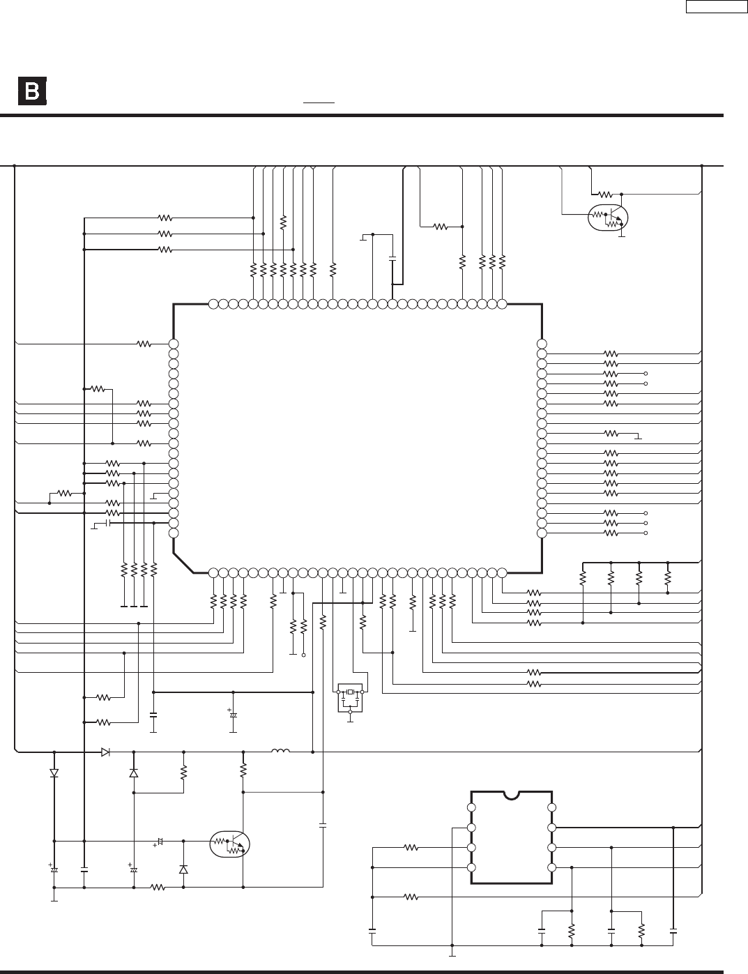
SCHEMATIC DIAGRAM - 13
MAIN CIRCUIT
123456789
31
32
33
34
35
36
37
38
39
72
73
74
75
76
77
78
79
80
92
93
94
95
96
97
98
99
100
10
71
40
91
11
70
41
90
12
69
13
68
42
89
43
88
14
67
15
66
16
65
44
87
45
86
46
85
17
64
18
63
19
62
20
61
47
84
48
83
49
82
50
81
21
60
22
59
23
58
24
57
25
56
26
55
27
54
28
53
29
52
30
51
FLD_RST
FLD_CS
FLD_CK
FLD_DA
KEY2
KEY1
VREF+
TRAY_CCW
TRAY_CW
TRAY_OPEN
BRAKE_H
SYS6V
TRAY_CLOSE
8
72
1
63
54
NC
FLD_DA
NC
NC
NC
KEY3 (CATER)
FLD_RST
FLD_CS
FLD_CK
NC
KEY2
NC
DES3
MODEL_SEL
DES1
AVSS
KEY1
VREF
AVCC
MIC_SW
TRY_CLOSE
TRY_OPEN
NC
NC
BRAKE_H
BYTE
CNVSS
RESET
XOUT
VSS
XIN
VCC
NMI
RMT
SYNC
PORTSEL2
EEDA
ECK
ECS
TUN_SD (TUNED)
TUN_DO (STEREO)
TUN_CLK
TUN_DI
NC
PORTSEL1
NC
TRY_CCW
TRY_CW
SCART_MUTE
VOL_CLK
VOL_DATA
MUTE_L
YC_H
RGB_H
DVD_MUTE
HP_MUTE
MUTE_SUB
EPM
MUTE_C
MUTE_FRNT
WIDE1
DVD_CLK
DVD_STAT
DVD_CMD
MUTE_S
CLK
RXD
TXD
MIC_
MUTE
SS_DA
SS_CLK
HB_MUTE
HB_LVL
C_MIX
SURR_FC2
NC
VCC
VSS
RF_DET
RF_LINK
DVD_PCNT
PCONT
MUTE_H
DC_DET
RDS_CLK
RDS_DA
JOG_B
JOG_A
SURR_FC1
NC
RF_PCON
IC2018
C2CBHG000168
MICROPROCESSOR IC
R2057 47K
R2056 47K
R2058 56K
R2060 100
R2080
10K
R2061 220
R2062 220
R2059
220
R2064 100
R2065 10K
R2066 10K
R2067 10K
R2069 22K
R2001 220
R2002 220
R2003 220
R2006
220
R2017 10K
R2079 22K
R2007 1K
R2008 10K
R2012 220
R2013 220
R2014 220
R2078 470
R2016 220
R2018 220
R2019 220
R2025 220
R2026 220
R2027 220
R2028 1K
R2029 220
R2030 220
R2031 220
R2032 220
R2033 220
R2034 220
R2035 220
R2036 1K
R2037 1K
R2039 220
R2040 220
R2041 220
R2043 220
R2070 0
R2071 4.7K
R2072
100
R2068
10K
C2001
0.1
R2000
220
R2077
4.7K
C2008
0.1
C2009
6.3V100
R2076
100K
D2000~D2002
B0ACCE000003
X2000
H2B100500004
R2021
47K
R2022
47K
R2023
10K R2861
10K
C2000 0.1
R2047 220
R2048 220
R2049 220
R2050 220
R2051 220
R2052 220
R2053 220
R2054 220
D2000
D2001 D2002 R2083
680
C2006
50V2.2
C2005
10V1000
C2004
0.01
R2082
47K
C2007
0.1 R2092
4.7K
C2019
330P
C2020
330P
R2094
22K
C2021
330P
R2093
22K
D2003
B0ACCK000005
L2000
G0C3R3JA0027
Q2000
Q2000
B1GBCFLL0037
RESET SWITCH
IC2019
C3EBEG000072
EEPROM IC
(NOT SUPPLIED)
IC2019
SS_DAT
PCONT
SYS6V
VCC
DVD_PCONT
PCONT
MUTE_H
DCDET
RDS_CLK
RDS_DA
JOG_B
JOG_A
STBY_LED
VOL_CLK
VOL_DA
RGB_H
DVD_MUTE
MUTE_HP
MUTE_SUB
MUTE_C
MUT_FRNT
WIDE1
DVD_CLK
DVD_STAT
DVD_CMD
TUN_DI
VREF+
TUN_CLK
TUN_DO
TUN_SD
ECS
ECK
EDA
SYNC
RMT
VCC
VREF+
ECS
ECK
EDA
R2897
1K
Q2029
B1GBCFJN0033
LED DRIVE
: +B SIGNAL LINE
C2022
0.022
NC
NC
NC
FAN_CTRL
NC
HB_MUTE
SS_CLK
MUTE_S
R2011 47K VREF+
R2916 0
C2003
10V22
HB_LVL
R2085
0
W2060 0
W2061 0
W2072 0
W2049
0
31
2
W2045 0
W2044 0
W1208
0
W2043 0
W2041 0
W2071 0
MIC_MUTE
NC
NC
NC
NC
GND
OUT IN
67
SA-HT530GCP
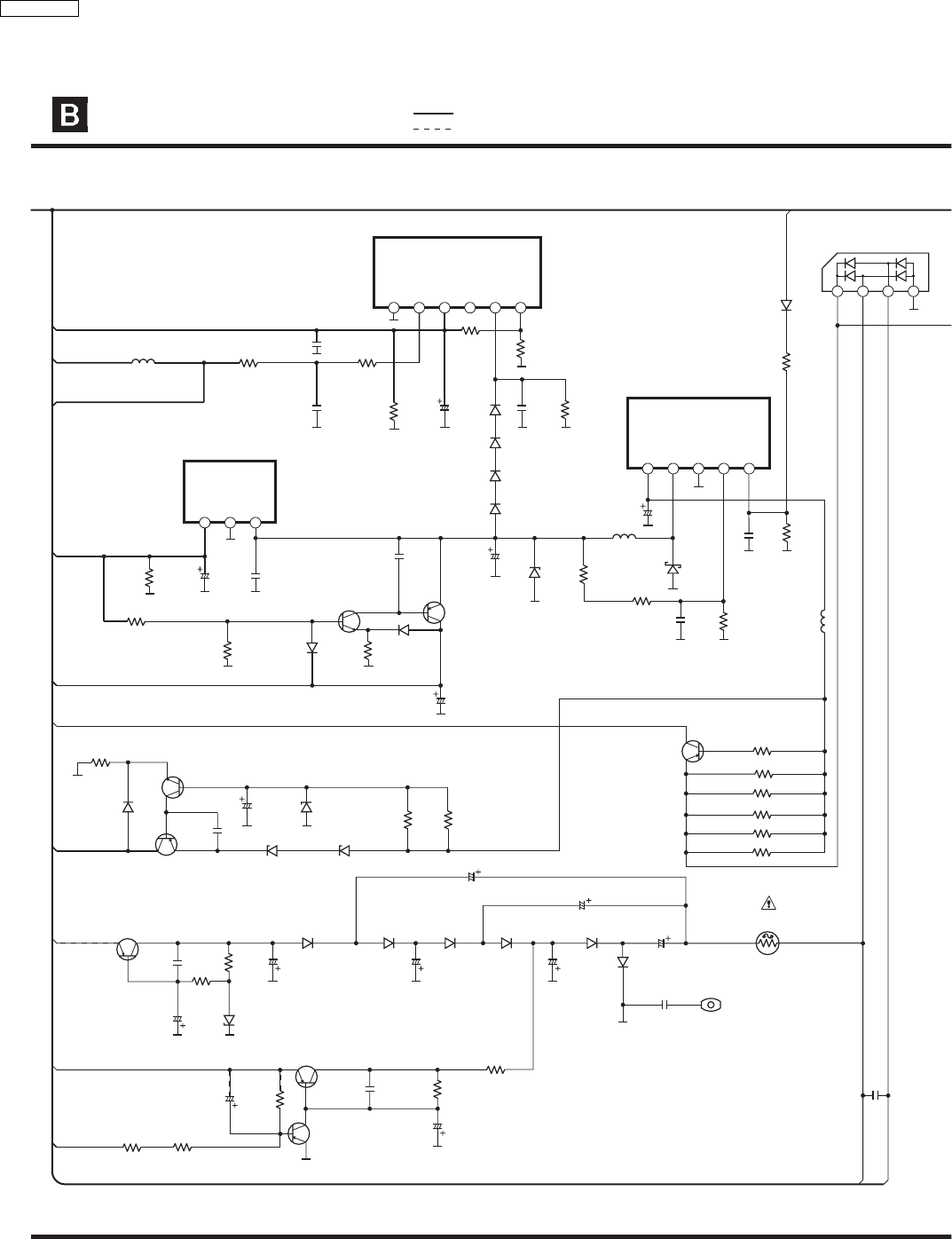
SCHEMATIC DIAGRAM - 14
MAIN CIRCUIT
1234
-VP
SUBAC1
SUBAC2
M+9V
D+5V
DVD_AC
-7.5V
+7.5V
D2807
B0ACCK000005
C2811
0.01
R2823
2.2K
R2824
820
C2809
25V33
D2804
B0BC9R000008
C2836
16V100
C2838
0.01 R2828
2.7K
R2830
2.7K
R2837
560
R2838
2.7K
R2825
4.7
C2828
50V100
C2829
50V100
C2830
25V1000
C2840
0.1
E2000
K4CZ01000027
FP2000
2A
D2812
D2813
D2814
D2815
D2812~D2817
B0EAKM000117
D2816
D2817
C2832
25V1000
C2835
50V100
C2834
50V100
C2856
50V100
D2818
MAZ82200ML
C2837
0.01
R2831
4.7K
R2832
150
C2839
10V33
D2822
B0FBAM000010
C2826
0.1
Q2809
B1ACKD000005
REGULATOR
Q2807
Q2808
B1ADCF000001
REGULATOR
Q2804
B1ABCE000016
CURRENT STABILIZER
Q2803
B1BCCG000023
CURRENT CONTROL
R2855 1K
Q2801
B1ADCF000001
SWITCH R2801 1
C2804
100P
D2801
B0JCPD000025
R2811
10K
R2905 1
R2805 1
R2806 1
C2859
0.01
L2801
G0ZZ00001930
R2815
4.7K
R2817
1K
C2802
25V220
D2802
B0BC7R500001
C2806
6.3V820
IC2802
C0CBADG00023
5V REGULATOR IC
123
C2821
6.3V47
R2819
470
DVD_PCONT
D2803
B0ACCK000005
: +B SIGNAL LINE
: -B SIGNAL LINE
IC2802
Q2807
B1BCCD000019
REGULATOR
R2808 1
R2813
470
R2833
1K
D2806
B0ECKM000016
D2805
B0ECKM000016
R2822
2.2K
C2819
1
VCC
OUT
GND
INV
STBY
12345
IC2801
C0DAAZG00012
DC-TO-DC CONVERTER IC
GND
VCC
V0
NC
PVCC
IC2803
C0DBEZG00021
REGULATOR IC
ADJ
654321
C2815
0.01
C2817
6.3V220
AA+5V
Q2806
B1BCCD000019
REGULATOR
D2808
B0ACCK000005
R2827
470
Q2805
B1ABCE000016
REGULATOR
D2829
B0ACCK000005
R2856
82K
R2821
1.8K
D2831
D2809
D2810
D2811
D2809~D2811, D2831
B0EAKM000117
C2823
1R2898
330
R2829
1K
R2826
680
C2825
6.3V330
D+1.2V
A+5V
R2834
1K
AA+5V
C2824
1
L2802
G0A200D00002
C2842
1
W2062
0
L2803
G0A200D00002
R2835
680
68
SA-HT530GCP
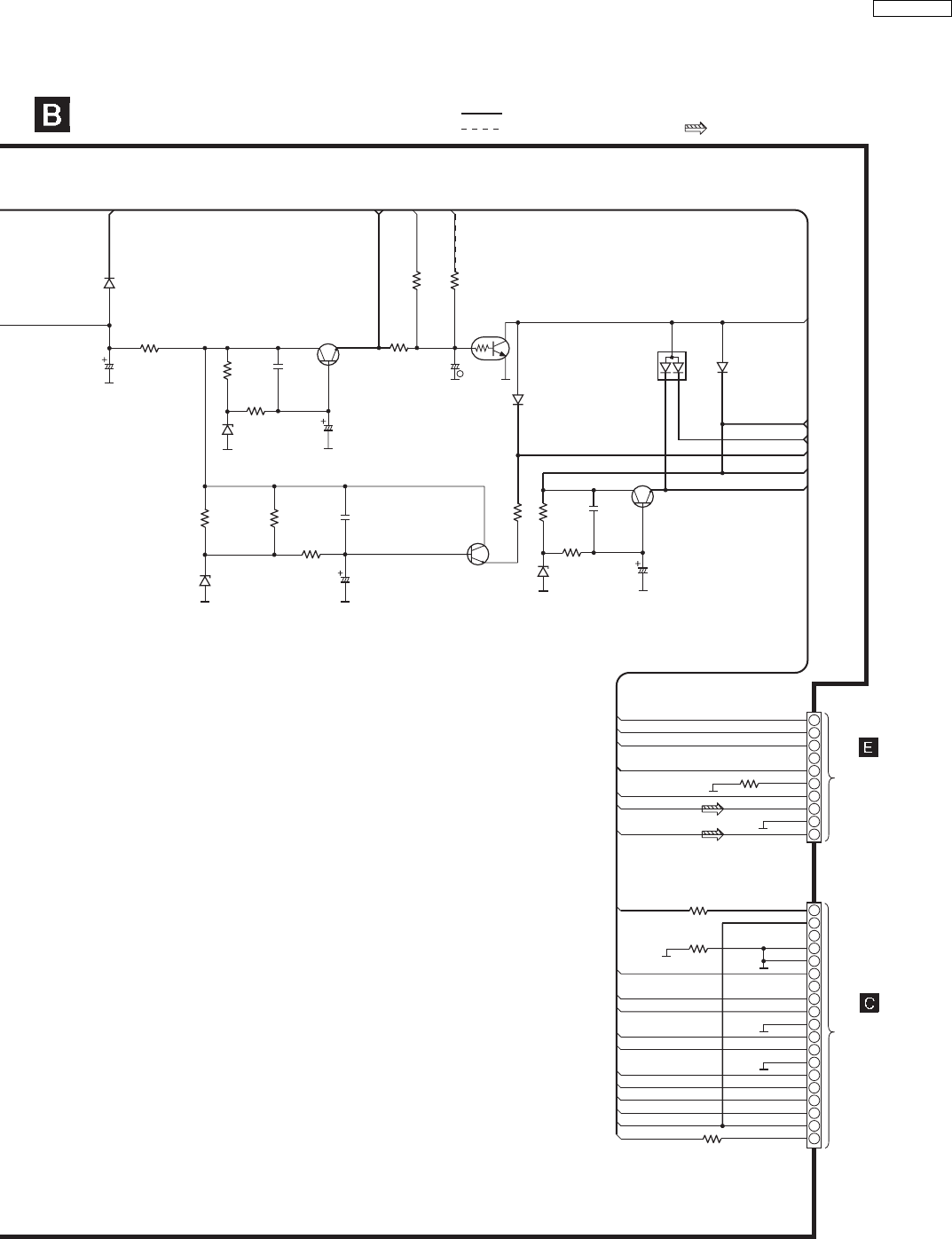
SCHEMATIC DIAGRAM - 15
MAIN CIRCUIT
KEY2
JOG_A
JOG_B
VREF+
RMT
HP_L
HP_R
STBY_LED
-VP
FLD_RST
FLD_CS
FLD_CK
FLD_DA
FL1
SW5V
FL2
C+9V
STBY_LED
GND1
-VP
FLD_RST
FLD_CS
FLD_CLK
FLD_DA
FL1
SW5V
FL2
KEY2
JOG_A
JOG_B
VREF+
GND1
RMT
HP_L
HPGND
HP_R 10
2
4
6
8
9
7
5
3
1
15
14
13
12
11
10
2
4
6
8
9
7
5
3
1
17
19
18
16
CN2009
CN2008
TO
HEADPHONE
CIRCUIT
(CN6032) ON
SCHEMATIC
DIAGRAM-18
TO
PANEL
CIRCUIT
(CN6008) ON
SCHEMATIC
DIAGRAM-16
Q2814
2SD21370PA
REGULATOR
Q2813
B1AAKD000014
REGULATOR
Q2818
B1GBCFJA0028
DCDET SWITCH
Q2818
C2841
25V4700 R2842
1.8K
R2843
470
R2841
4.7
D2824
B0BC7R500001
C2847
0.01
R2840
150
C2844
0.01
C2848
16V100
+7.5V
C2846
25V100
DVD_AC
TUNER+9V
SUB+B
SW5V
+7.5V
DCDET
C2853
50V4.7
R2849
4.7K R2851
15K
R2850
39K
-7.5V
R2839
820
D2823
B0BC5R600003
D2850
B0ACCK000005
M+9V
C+9V
D2851
B0ADCJ000020
: +B SIGNAL LINE
: -B SIGNAL LINE : MAIN SIGNAL LINE
D2852
B0ACCK000005
GND1
KEY1 KEY1
R2848
8.2
Q2816
B1BACD000018
REGULATOR
C2851
0.01
R2854
100
R2847
2.2K
R2846
2.2K
D2830
B0BC01000014
C2854
25V100
W2030 0
W2068 0
D2827
B0EAKM000117
MIC MIC
GND1
+7.5V +7.5V
R2904 0
R2903 0
N
69
SA-HT530GCP
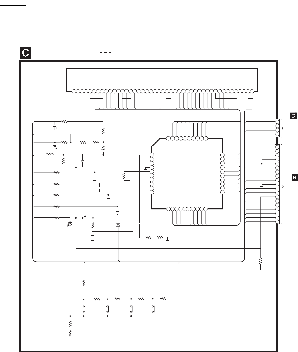
21.4. (C) Panel Circuit
FL6000
A2BD00000108
FL DISPLAY
28 27 26 25 24 23 22 21 20 19 18 17 16 15 14 13 12 11 10 9 8 7 6 5 4 2 144 43 42 41 40 39 38 37 36 35 34 33 32 31 30 2945
PANEL CIRCUIT
SCHEMATIC DIAGRAM - 16
: -B SIGNAL LINE
: +B SIGNAL LINE
P17
D6008
B0BC5R000009
FL
STBY_LED
KEY1
-VP
FLD_RST
FLD_CS
FLD_CLK
FLD_DA
FL1
SW5V
SW5V
FL2
KEY1
GND1
-VP
FLD_RST
GND1
FLD_CS
FLD_CLK
FLD_DA
FL1
SW5V
FL2
C6012
0.01
C6011
6.3V100
STBY_LED
R6005
680
D6000
B3AAA0000583
-VP
FL2
C6014
100P
FLD_RST
R6027
1K
C6015
100P
FLD_CS
R6015
1K
TO
MAIN
CIRCUIT
(CN2009) ON
SCHEMATIC
DIAGRAM-15
CN6008
L6003
J0JBC0000041 R6013
22K
C6007
50V10
C6003
50V22
R6050
2.7
FL1
C6005
50V22
R6051
2.7
R6012
150
R6011
150
D6006
B0BC5R000009
KEY1
MIC_SW
S6011
(POWER)
R6038
1K
R6006
1K
R6007
1.2K
R6008
1.8K
S6012
(SELECTOR)
S6013
(RDS) S6014
(H_BASS)
3
P2
P3
P4
G10
P5
P6
P7
G9
G8
P9
P10
G7
P11
G6
G5
G4
P12
P16
G1
P15
P14
G2
P13
G3
FL
R6030
22K
C6016
100P
FLD_CLK
R6019
68
C6017
100P
FLD_DA
R6017
1K
C6009
0.01
G10
P1
P2
P3
P5
G9
P6
P7
P8
G8
P9
P10
G7
P11
G6
G5
G4
P12
G3
P13
G2
P14
P15
G1
P16
P17
1
2
3
4
5
6
7
8
9
11 12 13 14 15 16 17 18 19
22
23
24
25
26
27
28
29
30
323334353637383940
10 21
20
31
FL02
IC6000
C0HBB0000044
FL DRIVER IC
FL12
FL03
FL04
FL05
FL06
FL07
FL08
FL09
FL10
FL11
FL13
FL14
FL15
FL16
FL17
FL18
FL19
FL20
FL21
FL22
FL23
FL24
FL25
FL26
-VP
FL27
FL28
FL29
FL30
FL01
FL00
FLD_CS
GND
XIN
XOUT
VCC
FLD_RST
FLD_CLK
FLD_DA
P1
P8
P4
W6013
0
W6010
0
W6033
0
W6034
0
W6035
0
W6014
0
W6012
0
W6011
0
MIC MIC
GND1
+7.5V +7.5V
TO
MICROPHONE
CIRCUIT
(CN6009) ON
SCHEMATIC
DIAGRAM-17
H6010
+7.5V +7.5V
MIC MIC
MIC_SW MIC_SW
MIC_GND
4
3
2
1
19
18
17
16
15
14
6
8
10
12
13
11
9
7
5
2
4
3
1
70
SA-HT530GCP
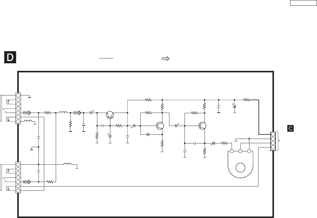
21.5. (D) Microphone Circuit
MIC CIRCUIT
SCHEMATIC DIAGRAM - 17
: +B SIGNAL LINE : MIC SIGNAL LINE
+7.5V
MIC
MIC_GND
MIC_SW
TO
PANEL
CIRCUIT
(H6010) ON
SCHEMATIC
DIAGRAM-16
CN6009
R6095
68
C6087
10V220
C6086
1000P
C6082
50V1
R6089
100K
R6086
1M
R6085
8.2K
R6088
4.7K
C6079
1000P
C6080
100P
R6090
1.5K
R6087
100
R6083
4.7K
C6078
50V1
C6076
50V1
R6082
560
C6077
0.033
C6072
470P
C6074
1000P
C6071
1000P
R6084
470K
C6068
50V4.7
C6070
50V4.7
2
4
6
7
5
3
1
2
4
6
7
5
3
1
L6005
J0JBC0000030
L6004
L6006
J0JBC0000019
R6081
680
R6080
680
JK6011
MIC2
JK6010
MIC1
Q6071
B1ABCF000011
MIC AMP
Q6072 Q6073
Q6072
B1ABCF000011
MIC AMP
Q6073
B1ABCF000011
MIC AMP
Q6071
JOG VOL
VR6001
R6091
100
L6004
J0JBC0000019
C6092
0.1
C6093
0.1
R6092
1K
2
4
3
1
1
23
COMBA
71
SA-HT530GCP
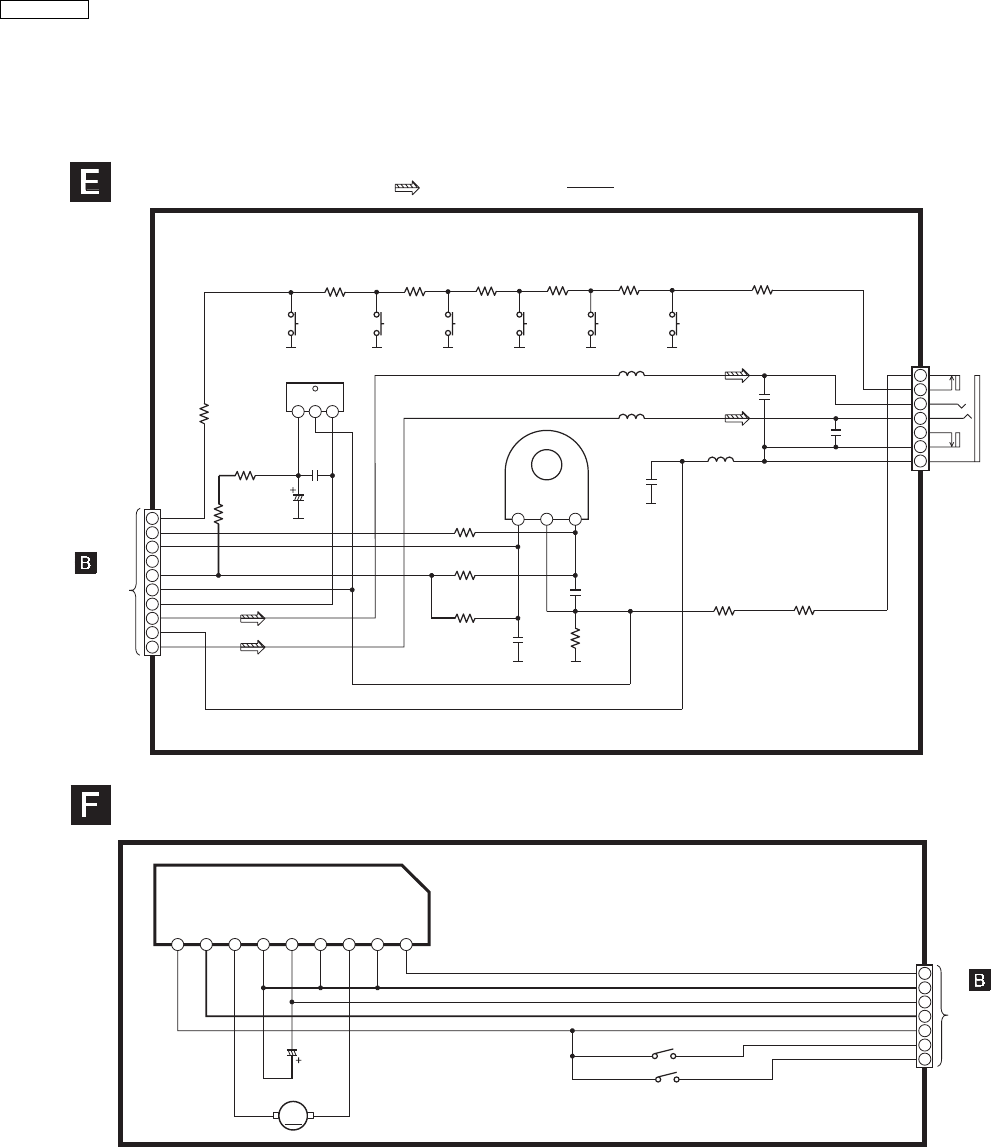
21.6. (E) Headphone Circuit & (F) CD Tray Loading Circuit
HEADPHONE CIRCUIT
SCHEMATIC DIAGRAM - 18
: +B SIGNAL LINE
: MAIN SIGNAL LINE
10
2
4
6
8
9
7
5
3
1
HPL
HP_GND
HPR
RMT
JOG VOL
VR6000
Z6000
REMOTE SENSOR
GND1
VREF+
JOG_B
JOG_A
KEY2
TO
MAIN
CIRCUIT
(CN2008) ON
SCHEMATIC
DIAGRAM-15
CN6032
S6004
(PAUSE)
S6003
(STOP)
R6025
1.8K
R6024
1.2K
R6023
1K
R6022
1K
R6028
22K
S6002
(REW)
S6001
(FF)
S6000
(OPEN/CLOSE)
2
5
6
7
4
3
1
JK6002
HEADPHONE
R6026
2.2K
123
COM BA
C6021
100P
R6029
22K
R6009
39
C6022
100P
L6002
J0JBC0000019
L6001 J0JBC0000019
L6000 J0JBC0000019
C6001
0.047
C6000
0.047
C6002
1000P
C6006
1000P
G
VDD O
321
C6008
6.3V47
S6005
(PLAY)
R6099
2.7K
CD TRAY LOADING CIRCUIT
1
2
3
456
7
8
9
1
2
3
4
5
6
7
CN901
S901 PLAY
S902 OPEN
C984
25V10
RM902
VCC
OUT2
NC
GND
VS
OUT1
VREF
IC904
C0GAH0000002
REFLECTIVE PHOTO SENSOR
TO
MAIN
CIRCUIT
(H2000) ON
SCHEMATIC
DIAGRAM-9
W6001
0
W6002
0W6015
0
W6003
0
W6006
0W6005
0
M
72
SA-HT530GCP
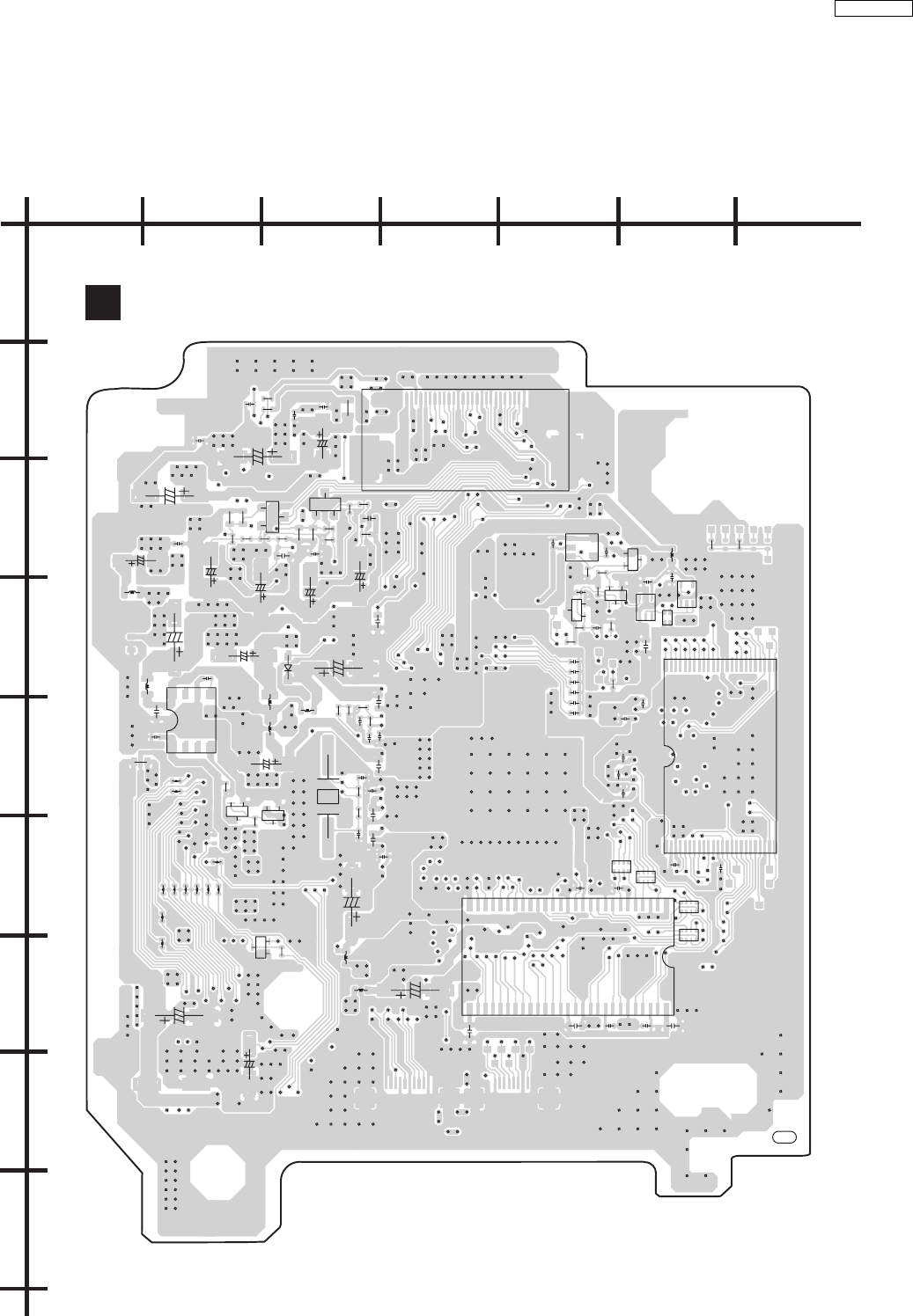
22 Printed Circuit Board
22.1. (A) DVD Module P.C.B. (Side A & B)
ABCDEFG
1
2
3
4
5
6
7
8
9
DVD MODULE P.C.B (REP3867F)
A
PbF
C8001
C8002
C8011
C8014
C8015
C8016
C8017
C8031
C8111
C8112
C8113
C8201 C8202
C8206
C8208
C8211
C8212
C8213
C8214
C8215
C8216
C8228
C8252
C8253
C8255
C8256
C8257
C8262
C8301
C8302
C8303
C8304
C8421
C8423
C8550 C8551
C8552
C8553
C8554
C8561
C8562
C8563
C8564
C8601
C8606
C8607
C8621
C8622
C8691
C8695
D8231
IC8111
IC8601
IC8606
K8008
K8421
L8201
L8202
L8301
L8302
L8550
LB8001
LB8002
LB8421
LB8422
LB8423
LB8424
LB8425 LB8426 LB8427
LB8428
LB8429
LB8430
LB8491
LB8690
Q8552
Q8562
Q8606
Q8607
QR8420
R8021
R8022
R8023
R8243
R8251
R8261
R8263
R8313
R8314
R8420
R8553
R8554
R8555
R8556
R8557
R8558
R8559
R8563
R8564
R8565
R8566
R8567
R8568
R8601
R8606
R8607
R8621R8622
X8621
QR8112 QR8111
R8112
R8111
RX8014
RX8013
C8057C8056
C8055
C8054 C8053 C8052 C8051
IC8051
FP8501
TO OPTICAL
PICKUP UNIT
C8006
C8007
C8008
C8009
C8010
C8651
C8652
IC8651
RX8011
RX8012
RX8021
R8312
R8311
C8311
C8251
IC8691
IC8695
(SIDE A)
CKA5
CKA6
CKA2
CKA4 CKA3
CKA1
CKA7
TL8111
CL8007
CL8008
CL8009
CL8010
CL8011
CL8012
CL8002
CL8003
CL8024
CL8026
CL8025
K8006
1234
5678
5
4
1
2
3
127
28 54
25 20 15 10 51
26
124
2548
123
45
123
45
2
3
46
7
8
9
11
12
13
14
19 16
17
1824
23 21
22
C
EB
C
E
B
C
E
B
BE
C
1
2
3
C
E
B
C
E
B
CE
B
XXXX
XXX
X
XXXXX
X
X
X
X
X
X
73
SA-HT530GCP
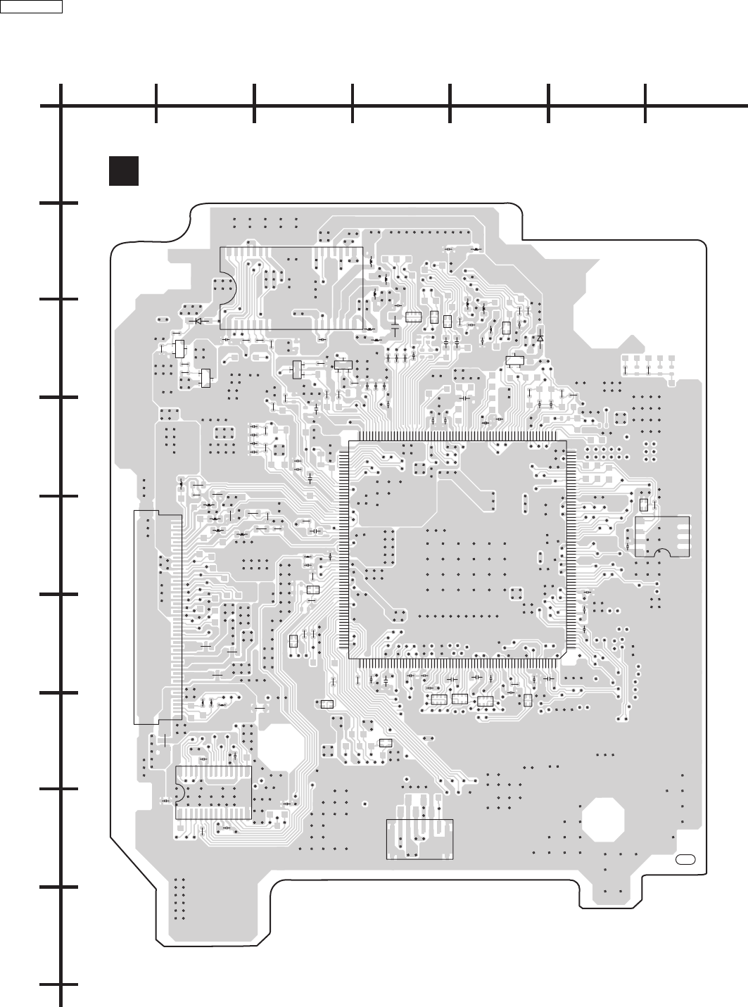
ABCDEFG
1
2
3
4
5
6
7
8
9
DVD MODULE P.C.B (REP3867F)
A
PbF
C8012
C8013
C8018
C8019
C8203
C8204
C8205
C8221
C8222
C8223
C8224
C8225
C8226
C8227
C8229
C8233
C8234
C8235
C8236
C8237
C8238
C8241
C8242
C8254
C8261
C8308
C8312
C8422
C8501
C8502
D8550
D8571
FL8101
FL8102
FL8103
FL8104
FP8101
IC8001
IC8251
K8003
K8106
LB8691
LB8692
LB8693
LB8401
LB8302
LB8301
LB8303
LB8304
LB8305
LB8507
Q8550
Q8551
Q8561
QR8571
R8041
R8201
R8231
R8233
R8235 R8236
R8241
R8242
R8262 R8264
R8315
R8321
R8322
R8325 R8326
R8331
R8332 R8335
R8341
R8401
R8402
R8404
R8407
R8421
R8550
R8551
R8552
R8560
R8561
R8562
R8569
R8570
RX8401
RX8402
IC8421
Q8560
LB8514
LB8512
LB8513
LB8511
RX8018 RX8016
RX8017
C8023
C8022
C8021
C8020
C8025
R8011
RX8015
C8027
C8028
C8426
C8217
C8218
RX8502 RX8504
RX8503
RX8501
R8506
R8505
R8501
LB8505
LB8504
LB8503
LB8502
C8506
C8505
C8504
C8503
C8003 C8004
C8005
C8611
FP8201
TO SPINDLE MOTOR
IC8611
R8611
RX8031
RX8032
RX8611
C8424 C8428
K8031
R8265
C8427
C8232
C8207
C8026
C8024
C8307
(SIDE B)
X
X
TL8513
TL8522 X
TL8512
X
X
X
TL8201
CL8551
CL8561
X
CL8233
XX
CL8234
CL8236
X
X
CL8231
CL8235
XX
CKC1 CKC2
X
X
XX
CKC8 CKC10
CKC4
CKC6
XX
X
X
CKC11 CKC12
CKC14
CKC16
XXX
X
X
CKC15
CKC18
CKC20
CKC22
CKC24
X
X
X
X
CKC32
CKC36
CKC37
CKC40
X
XX
X
CKC44
CKC48
CKC49
CKC50
XX
X
CL8430
X
CL8421
XX
X
CL8424
CL8425
CL8426
CKC41
CKC45
XX
CL8040
CL8491
CKB1
CKB2
CKB3
CKB4
CKB6
CKB8
CKB9
CL8034
X
XXX
XXX
X
XCKF1
CKF2
CKF3
CKF4
CKF5
CKF6
XX
XXX
CL8021
CL8022
CL8023 CL8027
CL8611
CL8612
XXX
XXX
CL8028 CL8029
CL8031
CL8032
XX
X
X
CL8030
X
CL8033
X
X
CL8241
X
CL8243
TL8211
TL8212
TL8213
TL8214
TL8215
TL8216
TL8217
TL8218
TL8219
TL8220
CL8242
CL8571
CL8036
CL8244 XX
XX
XCL8035
X
X
X
X
XXX
X
X
XCL8006
CL8001
CL8013
CL8014
CL8004
CL8005
XXXXX
X
CL8201
CKE4
XX
CKE2
CKE3
CKE5
CKE7
CKE9
X
XXX
X
CKE23
CKE25
CKE22
CKE19
CKE18
CKE21
CKE12
CKE13
CKE14
CKE16
CKE17
CKE24
CKE1
CKE20
CKE11
X
X
X
X
XXXX
XXX
XXX
X
CKE6
X
K8001
50
45
40
35
30
25
20
15
10
5
1
1
64
129
192
65
128
193 256
28 15
141
14
1528
1
123456
1
45
8
2
3
4
9
6
7
8
11
12
13
14
16
17
18
19
21
22
23
24
26
27
28
29
31
32
33
34
36
37
38
39
41
42
43
44
46
47
48
49
30
29
B
EC
B
EC
B
E
C
BE
C
BE
C
74
SA-HT530GCP
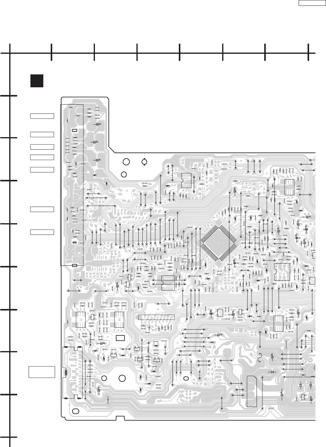
22.2. (B) Main P.C.B.
ABCDEFG
1
2
3
4
5
6
7
8
9
G
BMAIN P.C.B (REPX0452F)
B
C
EB
C
E
B
C
E
B
C
E
B
CE
B
C
E
1+
2~
3~
4-
C
E
B
C
E
B
C
E
BC
E
L2027
L2025
L2026
L2023
L2024
L2022
IC2015
W2012
IC2010
W2017
W2032
W2014
IC2006
IC2014
R2885
R2884
C2805
C2807
R2891
R2890
C2803
C2801
R2878
R2879 R2886
C2814
C2808
R2889
R2883
R2882
R2880
R2887
R2881
C2812
C2810
R2888
R2130
R2131
C2237
C2138
C2140
R2230
R2229
C2238
R2200
R2201
C2201
C2090
R2100
R2101
C2101
C2405
R2603
R2502
Q2804
R2824
D2804
D2806
D2805
D2807
R2111
R2271
R2605
R2606
R2407
R2307
R2312
Q2104
Q2103
R2406
R2311
R2310
R2306
R2309
R2308
C2506
R2506
R2616
R2617
C2615
R2614
R2615
C2613
R2504
C2504
C2503
C2840
W2002
W2042
W2068
C2521
C2511
W2009
W2052
W2016
R2652
R2651
R2654
W2004
W2027
W2026
R2163
R2263
R2505
R2618
W2001
W2019
W2018
C2039
C2037
C2032
C2035
R2133
R2132
C2139
C2239
R2232
R2231
W2028
C2210
C2310
W2086
C2635
R2112
C2121
R2113
R2114
C2124
R2169
C2122
C2226
C2222
R2115
C2125
C2126
C2225
R2215
R2214
R2212
C2224
C2221
R2213
W2059
R2300
R2269
R2157
R2257
Q20
R2400
R2500
R2895
R2600
C2600
C2818
C2816
C2034
C2028
C2029
W2013 R2604
R2405
R2305
C2401 R2404
R2403
R2304
C2219
C2220
C2165
C2166
R2265
R2165
W2031
C2822
R2503
Q2200
R2155
R2255
W4000
R2244
R2144
C2249
C2149
W2003
C2820
C2164
C2265
W2128
R2246
C2252
R2245
C2154
C2251
C2151
C2254
R2146
C2152
R2145
R2178
C2175
C2162
C2161
R2161
C2262
R2162
R2262
C2261
R2261
R2264
R2650
R2612
R2278
C2270
R2164
R2893
R2610
C2618
C2609
R2894
R2892
C2607
C2605
R2608
C2606
R2625
C2608 R2611
R2609
R2501
R2303
W2033
C2403
C2302
R2613
W2005
R2646
R2644
R2645
Q2605
W2023
R2648
C2621
R2638
R2642
R2632
R2630
R2629
R2656
C2633
R2636
R2655
R2217
R2117
R2211
R2116
R2216
R2160
C2160
R2507
C2507
C2604
R2607
C2260
R2260
R2640
C2845
D2601
R2631
R2172
C2301
R2301
R2402
R2302
C2402
R2401
R2170
C2169
R2978
C2231
C2133
C2320
R2521
C2522
W2064
W2074
C2211
C2130
R2129
C2131
C2232
C2228
R2235
C2632
IC2602
IC2601
R2639
R2657
Q2607
C2619
R2635
R2634
R2633
C2620
R2627
R2647
Q2604
R2643
R2649
R2641
R2637
D2850
C2127
C2227
C2112
C2212
R2660
W2057
Q2609
R2659
R2661
R2663
R2658
R2664
Q2608
R2662
C2858
C2229
C2128
C2857
L2028
C2202
C2102
W2056
C2811
W2500
C2036
C2047
C2046
C2040
C2042
W2400
W2401
W2403
W2600
W2501
W2502
C2501
W2601
C2257
C2400
W2103
C2827
C2264
C2603
C2502
C2150
IC2013
JK2001
W2317
W2319
W2105
W2407
W2804
W2603
W2324
W2408
C2612
W2109
W2112
C2610
W2220
W2517
W2122
W2123
C2223
C2123
W2222
W2223
W2224
W2341
W2229
W2424
W2343
C2253
W2347
R2841
D2822
JK2000
C2505
C2616
W2227
W2228
C2163
C2833
C2831
C2830
W2803
W2800
W2521
W2107
W2172
FP2000
2A W2267
C2627
C2631
C2263
W2260
W2261
C2170
C2602
W2121
W2622
CN2002
TO TUNER PACK (J3CCBB000004)
W2256
W2259
W2208
W2216
W2262
E2
W2520
W2336
C2611
W2201
C2157
Q
C2809
W2559
W2238
W2239
W2241
W2120
W2169
K2308
W2560
W2244
W2168
W2214
W2234
C2303
C2404
W2409
W5206
W2702
W2519
W2113
W2614
W2425
W2615
W232
W2402
W2430
W2101
W2322
W2565
C2300
C2500
W2584
W2166
W2700
W2158
W2268
C2250
W2604
W2505
W2245
W2248
W2342
W2309
W2307
W2264
W2159
W2405
W2251
C2630
W2802
W2801
W2106
W2240
C2826
W2040
W2243
C2636 W2104
W2102
W2303
W2302
D2827
W2346
C2841
C2044
W2335 W2585
C2167
C2266
W2263
C2855
W2233
W2036
W2250
W2328
W2345
W2413
W2414
W2232
C2637
W2567
C2628
W2254
W2255
W2427
W2114
W2164
W2507
W2131
W2237
W2503
W2037
W2038
W2039
W2035
W2423
W2034
IC2011
TO ACTIVE
SUBWOOFER
SB-WA530GC-S
VCR AUDIO IN
TV AUDIO IN
VOUT-CR
VOUT-CB
VIDEO OUT
VOUT-Y
S-VIDEO
R2920
R2020
R2918
R2919
R2917
R2708
C2702
R2709
R2711
Q2702
Q2703
R2710
C2901
R2125
C2706
R2126
R2712
C2705
R2713
W2029
W2051
K2704
W2314
W2623
4
110
11
18
9
16
17-Y
1
25
10
1
58
41
58
23
21
19
17
15
11
9
7
5
3
1
24
22
20
18
16
14
13
12
10
8
6
4
2
987654321
16-G
15-G
13-C
23-Y21-G
22-V
20-CB
18-G
19-CR
9-R
7-G
8-R
6-L
4-G
5-R
20
13
64
2
5
61
80
21
40
41
60
1
20
4
85
46
31
5
2
85
14
85
14
14-G
75
SA-HT530GCP
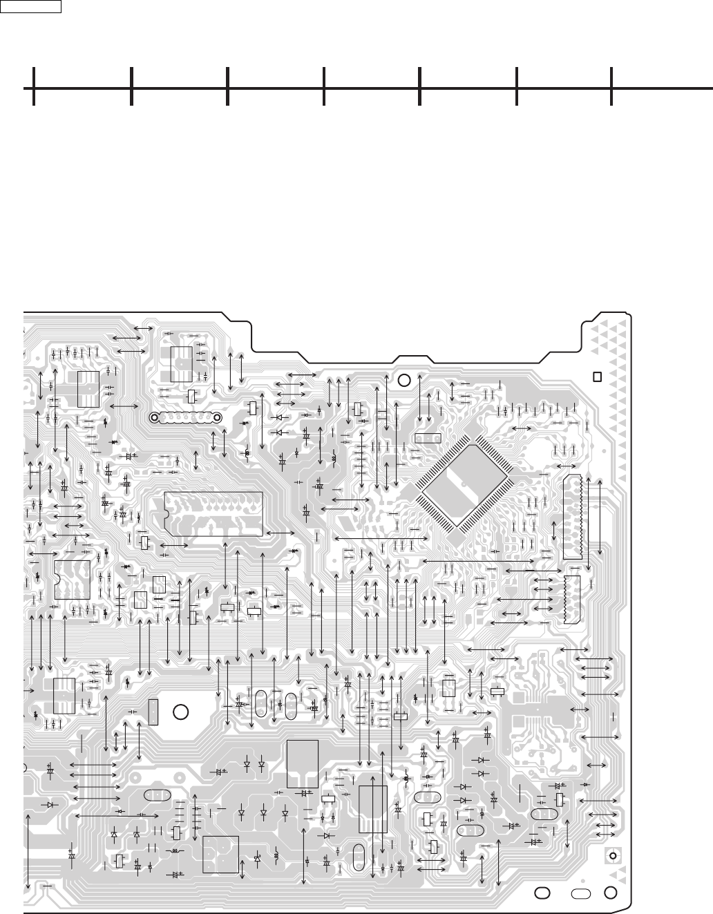
G
GHI J KL M
B
CE
B
CE
BC
E
B
CEB
C
EB
C
E
B
C
E
B
C
E
BC
E
B
C
E
B
C
E
N
CA A
CA
B
CE
E
C
B
E
C
B
B
C
E
B
C
E
CBE
ECB
B
CE
ECB
B
CE
PbF
IC2015
W2012
IC2010
IC2802
IC2019
(NOT SUPPLIED)
IC2803
R2039
R2041
R2040
R2059
R2033
R2036
R2037
R2034
R2035
R2023
R2022
R2021
Q2804
R2824
D2804
D2806
D2805
D2807
6
R2506
R2616
R2617
C2615
R2614
R2615
C2613
R2504
C2504
C2503
C2840
R2806
R2805
R2823
R2822
R2855
R2801
R2905
R2808
Q2801
C2804
R2811
R2817
R2815
R2813
D2801
R2833
C2819
R2061
R2060
R2072
R2062
R2064
R2068
R2080
R2007
R2065
R2069
R2070
R2066
R2067
R2071
W2041
W2043 R2076
R2000
R2001
R2077
R2002
R2003
R2006
R2017
C2001
R2053
R2054
R2052
R2048
R2050
R2051
R2049
R2047
R2058
R2057
R2056
W2071
C2000
R2043
W2061
R2253
W2068
R2861 R2028
R2029
R2030
R2025
R2031
R2027
R2026
R2011
R2008
R2079
R2078
R2016
R2018
R2019
R2916
R2012
R2013
R2014
W2072
W1208
W2049
W2044
W2045
C2007
R2083
R2082
C2004
D2852
R2838
R2837
D2802
R2827
D2808
Q2805
R2821
R2819
R2856
R2898
C2823
W2060
R2251
R2267
R2252
R2268
R2152
R2151
R2153
Q2102
R2829
C2815
R2849
C2824
D2803
R2826
R2851
D2851
R2850
Q2818
C2859
C2837
R2832
R2831
D2818
R2840
R2839
C2844
D2823
R2830
C2838
R2828
Q2808
R2897
Q2029
Q2201
R2266
C2255
C2155
R2250
R2249
R2149
R2150
R2147
R2148
R2248
R2247
W2119
C2022 R2092
C2019
C2020
R2094
R2093
C2021
R2803
R2804
Q2030
C2847
R2843
R2842
D2824
R2166
R2509
R2621
R2620
R2508
R2510
R2622
R2167
W2058 W2015
Q2500
Q2600
D2000
D2001
D2002
W2055
R2820
Q2004
C2008 R2032
Q2000
D2003
Q2105
R2168
R2254
R2511
W2065
R2112
C2121
R2113
R2114
C2124
R2169
C2122
C2226
C2222
R2115
C2125
C2126
C2225
R2215
R2214
R2212
C2224
C2221
R2213
W2059
C2156
C2256
R2156
R2300
R2269
R2157
R2257
R2256
Q2028
R2400
R2500
R2895
R2600
C2600
C2818
C2816
W2031
C2822
R2154
W3000
R2619
R2624
R2623
R2503
Q2601
Q2200
R2155
R2255
W4000
R2244
R2144
C2249
C2149
W2128
R2246
C2252
R2245
C2154
C2251
C2151
C2254
R2146
C2152
R2145
75
C2162
C2161
R2161
C2262
R2264
R2650
R2612
2278
C2270
R2164
R2893
R2610
W2030
D2829
R2847
R2846
R2854
C2851
D2830
R2085
W2062
R2848
R2834
R2835
R2074
R2073
C2842
L2028
C2053
C2811
C2257
C2400
C2264
C2502
C2150
IC2013
W2317
C2612
C2223
C2123
W2229
W2424
W2343
C2253
W2347
R2841
C2833
C2830
W2622
W2208
D2809
D2810
D2831
C2817
C2825
C2806
IC2801
W2522
W2707
W2108
CN2009
W2134
W2210
D2042
D2041
W2410
C2802
C2829
C2848
L2801
W2901
R2825
C2836
Q2807
C2853
C2821
W2236
W2235
C2839
C2856
C2834
C2835
D2817
D2816
D2815
D2814
C2828
C2846
C2267
C2153
W2129
C2617
W2518 W2609
L2010
W2709
W2705
W2851
W2805
W2212
C2005
C2003
X2000
L2000
W2110
W2323
C2038
C2168
W2613
D2812
D2813
C2832
E2000
W2520
W2855
W2336
W2124
W2854
W2514
C2611
W2201
H2000
C2157
W2524
W2582
W2549
C2009
Q2803
C2809
W2537
W2554
D2811
W2812
W2811
W2810
W2540
W2596
W2538
W2807
W2547
W2542
W2544
W2548
W2595
W2556
W2555
W2593
W2553
W2591
W2597
W2852 W2247
W2226
W2806
CN2004
W2551
W2252
W2234
W2702
W2519
W2614
W2425
W2615
Q2806
W2586
W2620
W2701
W2266
W2588
W2552
W2808
W2900
W2951
W2426
Q2809
Q2813
W2952
W2541
W2265
W2557
W2142
W2344
W2231
W2545
W2809
W2714
W2543
W2326
W2546
W2566
W2706
Q2814
W2610
W2708
C2508
W2562
W2218
W2576
W2580
W2513
W2565
C2300
C2500
W2584
C2250
W2604
W2505
W2342
W2309
W2307
W2405
CN2008
W2145
W2167
W2249
W2535
W2225
W2412
W2417
W2213
C2006
W2587
W2594
W2592
W2340
W2561
W2563
W2304
D2827
W2346
C2841
W2335 W2585
W2428
W2130
Q2816
C2854
W2712
W2429
W2710
W2250
W2328
W2345
C2813
W2253
2
W2257
W2950
W2427
L2803
L2802
IC2018
R2904
R2903
321
1
6
1
1
10
1
1
3
1
4
85
46
31
5
2
46
31
5
2
85
14
234567
85
14
3
1
2
4
85
14
2
1
3
5
2
4
5
46
31
5
2
8
6
4
2
1
3
5
7
9
23
3
2
5
7
9
11
13
15
17
19
4
6
8
10
12
14
16
18
1
30
100
31
5150
80
81
5913172125293337414549
711151923273135394347
81216
2024283236404448
61014182226303438424650
76
SA-HT530GCP
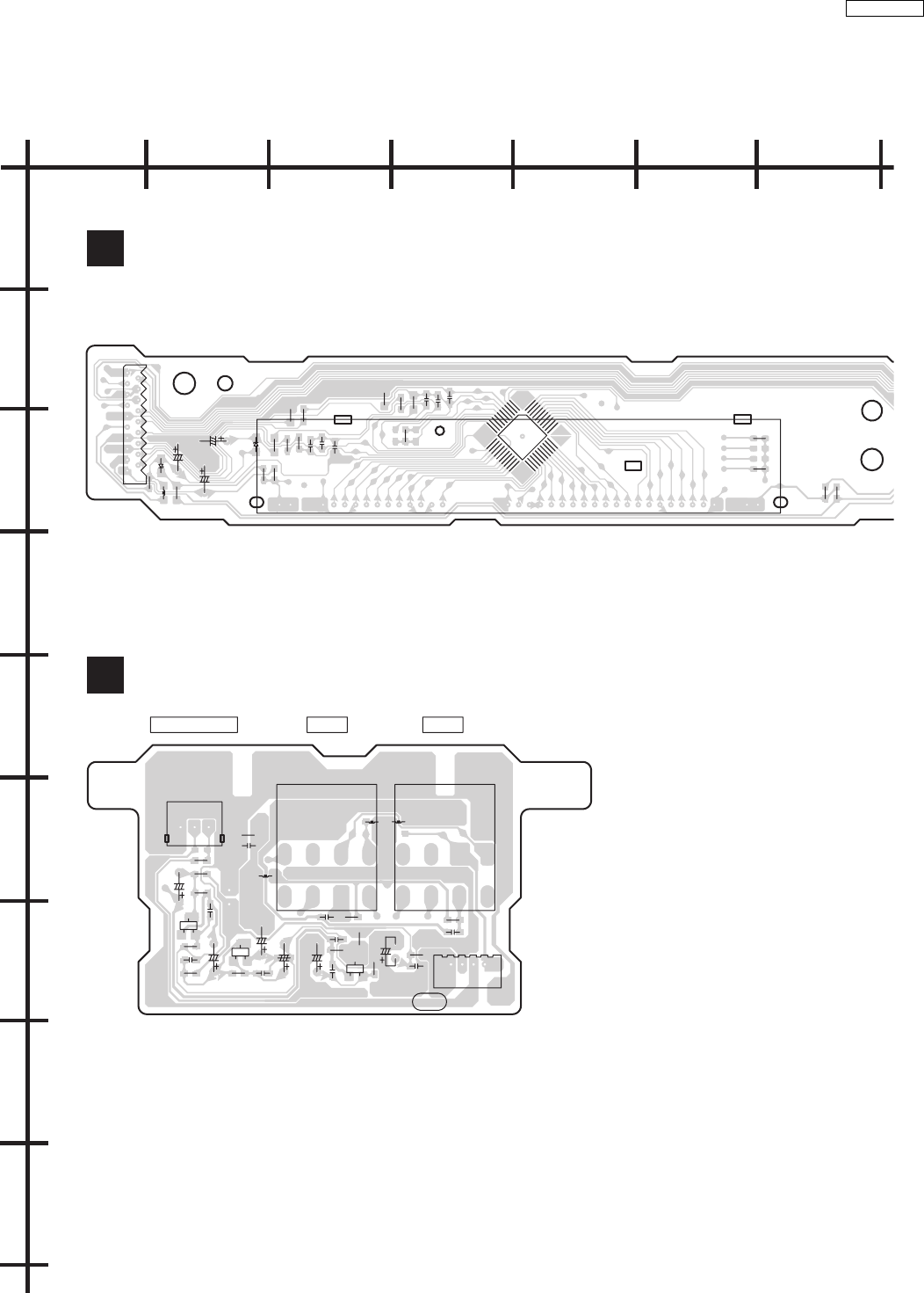
22.3. (C) Panel P.C.B., (D) Mic P.C.B. & (E) Headphone P.C.B.
ABCDEFG
1
2
3
4
5
6
7
8
9
G
CPANEL P.C.B (REPX0456B)
DMIC P.C.B (REPX0452F)
B
C
E
PbF
B
C
E
B
C
E
C6011
C6003
CN6008
C6007
FL6000
R6011
C6009
C6016
C6015
R6015
C6012
R6051
R6030
W6011
D6008
R6012
R6050
R6027
C6014
W6012
W6013
W6010
W6014
D6006
L6003
R6013
C6017
R6017
R6019
W603
HT530
IC6000
W602
GCP
MIC VOLUME MIC 2 MIC 1
VR6001
JK6011 JK6010
L6004 L6006
Q6071
Q6072
R6088
C6077
R6087
C6074
R6091
R6086
R6085
C6076
C6078
Q6073
C6086
R6095
R6090
C6080
C6079
C6072
R6084
C6071
R6082
L6005
R6080
R6081
R6083
R6089
C6093
C6092
C6070
CN6009
C6068
C6082
C6087
R6092
1
45
3
44 41 40 35 30 24 20 15 10 2 15
1
10
11
20 21
30
31
40
5
7
9
11
13
15
17
19
2
4
6
8
10
12
14
16
18
1
8745
1
8
123
745
9326 9326
1234
77
SA-HT530GCP
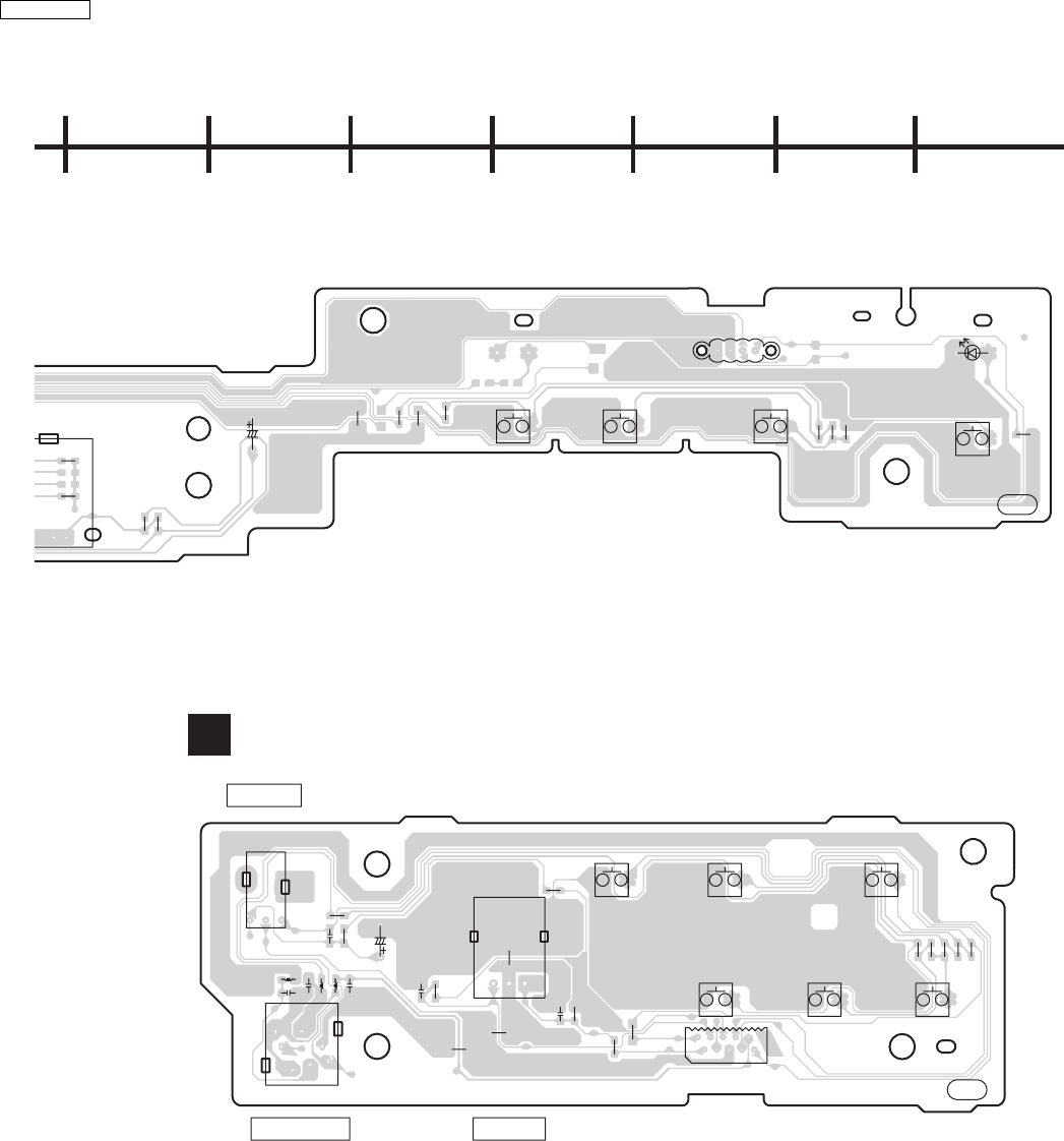
G
GHI J KL M
EHEADPHONE P.C.B (REPX0456B)
PbF
PbF
C6005
S6014
H_BASS
D6000
R6038
R6011
R6005
W6033
R6008
R6051
R6006
R6007
W6035
W6034
W603
30
S6013
RDS S6012
SELECTOR S6011
POWER
S6001
FF
JK6002
VR6000
CN6032
Z6000
C6008
R6025
R6022
R6024
R6026
C6022
C6021
R6029
L6002
C6000
R6099
L6000
L6001
C6001
C6002
R6028
W6002
C6006
W6003
R6009
R6023
W6005
W6006
W6001
W6015
S6002
REW
S6000
OPEN/CLOSE
S6005
PLAY
S6004
PAUSE
S6003
STOP
HEADPHONE VOLUME
SENSOR
W602
CP
H6010
21
1
123
32
1
3579
246810
72-L
6
13-R
4
5
1234
78
SA-HT530GCP
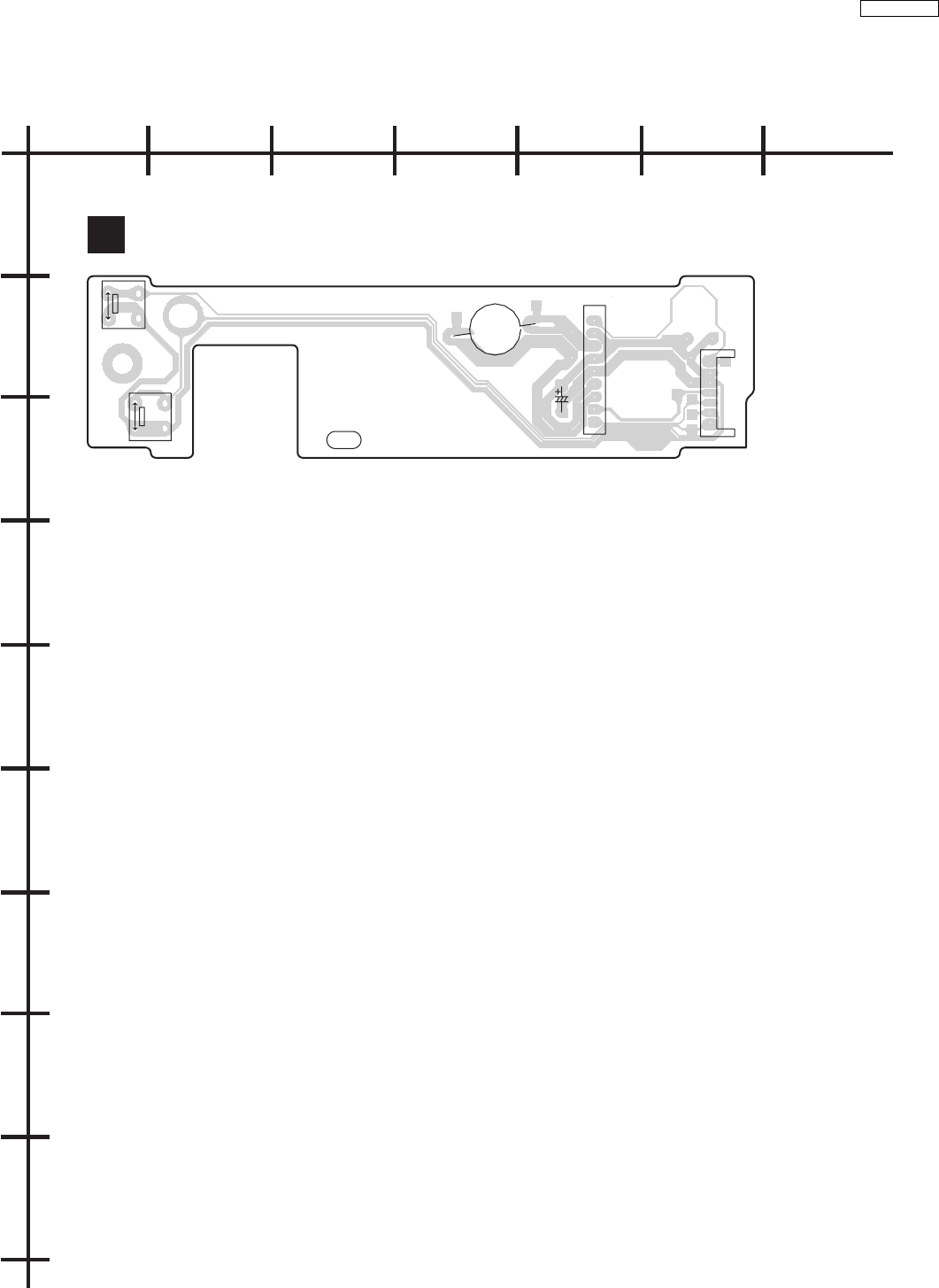
22.4. (F) CD Tray Loading P.C.B.
ABCDEFG
1
2
3
4
5
6
7
8
9
F
CD TRAY LOADING P.C.B (REP3288A)
PbF
S902
OPEN SW
RM902
+
-
IC904
C984
CN901
-
M
S901
PLAY SW
1
2
3
4
5
6
7
8
9
7
6
5
4
3
2
1
79
SA-HT530GCP
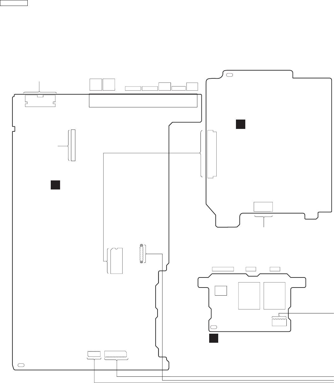
23 Wiring Connection Diagram
TO
SPINDLE MOTOR
DVD MODULE P.C.B.
A
FP8101
FP8201
50
1
. . . . . . . . . . . . . . . . . . . . . . . . . .
SIDE:B
MAIN P.C.B.
B
TO ACTIVE
SUBWOOFER
SB-WA530GCP-S
6 . . . . . . . 1
PbF
PbF
CN2002
CN2004
JK2000
H2000
7
1
. . . . . .
3
47
. . . . . . . . . .
1
10
. . . . . . . . . . . . . . . . .
CN2009
CN2008
18 . . . . . . . . . 2
19 . . . . . . . . . . . .1
1 . . . . . 9
2 . . . . .10
S-
VIDEO
JK2001
VOUT-Y
VIDEO
OUT
TV
VIDEO
IN
VCR
AUDIO
IN VOUT-CBVOUT-CR
TO
TUNER
PACK
1
49
. . . . . . . . . . . . .
4
48
. . . . . . . . . .
2
50
. . . . . . . . . . . . .
MIC VOLUME MIC 2 MIC 1
VR6001
JK6011 JK6010
CN6009
1 . . . . . . . 4
PbF
MIC P.C.B.
D
80
SA-HT530GCP
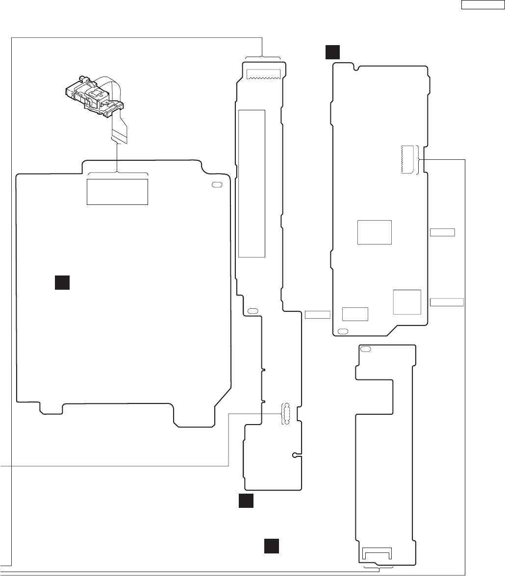
OPTICAL PICKUP
DVD MODULE P.C.B.
ASIDE:A
FP8501
1 . . . . . . . . . . . . . . 25
CN6008
19 . . . . . . . . . . 1
18 . . . . . . . . .2
CN901
1 . . . . . . 7
PbF
PbF
PbF
PbF
1
PANEL P.C.B.
C
CD TRAY
LOADING P.C.B.
F
HEADPHONE P.C.B.
E
CN6032
1
9
. . . . . .
2
10
. . . . . .
2 . . . . . . . . . . . . . . 26
HEADPHONE
VOLUME
SENSOR
JK6002
Z6000
H6010
VR6000
FL6000
4
1
. .
81
SA-HT530GCP
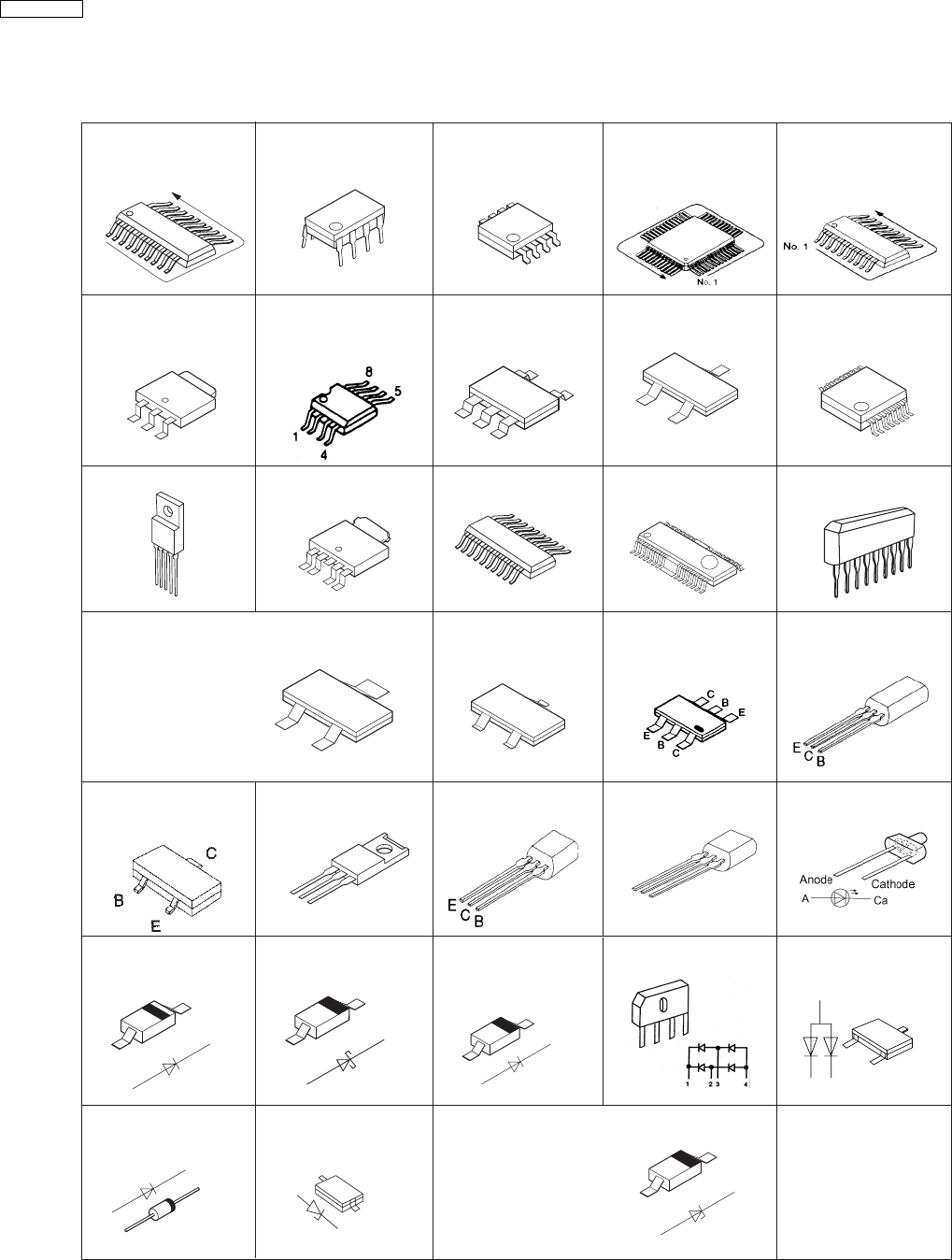
24 Illustration of IC’s, Transistors and Diodes
RFKWMH82B160
C3ABPG000133 (54p)
1
2SD1819A0L
UNR521100L
B1ADCF000001
UNR511V00L
UNR521400L
2SB09700RL
B1ABCF000011
2SB1219AHL
B0ACCK000005
B0JCPD000025
A
Ca
Cathode
Anode
E
C
B
B1GFGCAA0001
MA2J72800L
A
Ca
Cathode
Anode
C0ABBB000118
1
4
8
5
C1BB00000979 (20p)
C0EBA0000031 (5p)
C0JBAA000346 (5p)
C0EBE0000384
C0CBCBD00018 (8p)
C3EBGC000044 (8p)
B1ACKD000005
B1AAKD000014
A
Ca
Cathode
Anode
B0ACCE000003
MA2J11100L
A
Ca
Cathode
Anode
B0EAKM000117 B0ECKM000016
Anode
Cathode
A
Ca
B0ADCJ000020
B3AAA0000583
1
4
8
5
C0AABB000125
B0FBAM000010
B0BC7R500001
B0BC9R000008
B0BC5R600003
B0BC5R000009
MAZ82200ML
B0BC01000014
A
Ca
Anode
Cathode
Ca
A
Cathode
Anode
C1BB00000845 (80p)
C0HBB0000044 (48p)
C2CBHG000168
MN2DS0003APH (256p)
1
3
C0CBADG00023 (3p)
C0DAAZG00012 C0DBEZG00021 C0FBBK000050 (28p) C0GBG0000048 (28p)
1
3
4
5
2
2
3
1
+~~-
51
1
5
1
14
15
28
14
1
28
15
C9ZB00000466 (16p)
1
8
16
9
2SD21370PA
B1BCCD000019
C0GAH0000002
B1GBCFLL0037
B1GBCFJN0033
B1GDCFGA0018
B1ABCE000016
B1ABEB000002
E
C
B
B1GBCFJA0028
B1BCCG000023 B1BACD000018
BCE
B
C
E
82
SA-HT530GCP

25.1. IC2018(C2CBHG000168):
Microprocessor
Pin No. Mark I/O Function
1TRY_CLOSE ILoading Mecha Close Sw
(L: Sw ON)
2TRY_CCW OTerminal for tray control 1
3TRY_CW OTerminal for tray control 2
4TRY_OPEN ILoading Mecha Open SW
(L: Sw ON)
5 N.C. - No connection
6 N.C. - No connection
7 BRAKE_H O Terminal for tray control 3
8BYTE I VSS (GND)
9 CNVss - VSS (GND)
10-11 N.C. - No connection
12 RESET I System Reset Input
13 Xout - Main clock output (10.0 MHz)
14 Vss - GND (0V)
15 XIN - Main clock Input (10 MHz)
16 Vcc - Power supply (5V)
17 NMI I Connect to VCC, external interrupt
I/P
18 RMT I Remocon Input
19 SYNC IAC failure detect input
20 N.C. - No connection
21 PORTSEL1 I DivX Model Selection (L= No
DivX, H= DivX)
22 PORTSEL2 I Speaker Protection (L= Speaker
Protect OFF, H= Speaker Protect
ON)
23 EEDA I/O DATA signal for the EEPROM
24 ECK O CLOCK signal for the EEPROM
25 ECS O LAT signal for the EEPROM
26 N.C. - No connection
27 TUN_SD I Station Detect
28 TUN_DO I Stereo Detect
29 TUN_CLK O 12C Clock for Tuner
30 TUN_DI O 12C Data for Tuner
31 TXD I(for FLASH writer)
32 RXD O (for FLASH writer)
33 Clk O (for FLASH writer)
34 MUTE_S O Mute signal for surround Audio
signal/ (for FLASH writer)
35 DVD_CMD OCMD signal for the DVD Module
36 DVD_STAT I STATUS signal from the DVD
module
37 DVD_CLK ICLK signal for the DVD Module
38 WIDE1 OControl Signal for the WIDE
function
39 MUTE_FRNT O Mute Signal for FRONT END
40 MUTE_C O Mute signal for CENTRE
41 EPM I For Flash
42 MUTE_SUB O Subwoofer Mute Signal
43 HP_MUTE O Head Phone Mute Signal
44 DVD_MUTE I Signal from DVD module control
mute circuit
45 RGB_H O Mute signal 1 for video output
46 YC_H OControl signal for the video signal
Mix
47 MUTE_L O MUTE signal for the Line output
48 VOL_DATA O DATA signal for 6ch VOL ASP
49 VOL_CLK O CLOCK signal for 6ch VOL ASP
50 SCART_ MUTE O Line out for SCART terminal
51 MIC_MUTE O Muting circuit for the MIC input
52 SS_DA O DATA Signal for S.SRND IC
53 SS_CLK O Clock Signal for S.SRND IC
Pin No. Mark I/O Function
54 N.C. - No connection
55 HB_MUTE O H.Bass Mute
56 HB_LVL OH.Bass Level Select
57 C_MIX O DPL II Bass Improve
58 SURR_FC1 OSurround Freq. Limiter 1
59 SURR_FC2 OSurround Freq. Limiter 2
60-61 N.C. - No connection
62 Vcc - Power supply 5.0V
63 FAN_CTRL O FAN Control Output (Only for
HT880, High for above -10dB)
64 VSS - GND (0V)
65 RF_DET I RF input (Wireless Module)
66 RF_PCON O RF output (Wireless Module)
67 RF_LINK I RF link detection (Wireless
Module)
68 DVD_PCNT OControl signal for the Power for
rthe DVD MODULE
69 N.C. - No connection
70 PCONT O Control Signal for the Power
Control Relay
71 MUTE_H O HIC MUTE
72 DC_DET I Signal from the DC Detection
circuit
73 RDS_CLK IClock signal from the RDS
decoder
74 RDS_DA IData signal from the RDS decoder
75 JOG_B I Signal B from Volume JOG
76 JOG_A I Signal A from Volume JOG
77-80 N.C. - No connection
81 FLD_DA O Data input for the FL Driver
82-83 N.C. - No connection
84 MIC_SW -No connection
85 N.C. - No connection
86 KEY 3 -Key 3 line input (cater)
87 FLD_RST O Reset Signal for the FL Driver
88 FLD_CS O Latch Signal for the FL Driver
89 FLD_CK O Clock Signal for the FL Driver
90 N.C. - No connection
91 KEY2 IKey 2 line input
92 N.C. - No connection
93 DES3 I REGION Setting for DVD
94 MODEL_SEL I Model Selector
95 DES1 I REGION Setting for Tuner
96 AVss - Analog Power Supply Input
97 KEY 1 IKey 1 line input
98 VREF - Reference Voltage Input
99 AVCC - Analog Power Supply Input
100 N.C. - No connection
25.2. IC8001 (MN2DS0003APH)
DV2.1 IC
Pin No. Mark I/O Function
1 MDQ9 I/O SDRAM Data 9
2 MDQ5 I/O SDRAM Data 5
3 VSS - GND
4 MDQ10 I/O SDRAM Data 10
5 MDQ4 I/O SDRAM Data 4
6VDD33 - I/O Power Supply
7 MDQ11 I/O SDRAM Data 11
8 MDQ3 I/O SDRAM Data 3
9 VSS - GND
10 MDQ12 I/O SDRAM Data 12
11 MDQ2 I/O SDRAM Data 2
12 VDD33 - I/O Power Supply
25 Terminal Function of IC’s
83
SA-HT530GCP

Pin No. Mark I/O Function
13 MDQ13 I/O SDRAM Data 13
14 MDQ1 I/O SDRAM Data 1
15 MDQ14 I/O SDRAM Data 14
16 VSS - GND
17 MDQ0 I/O SDRAM Data 0
18 MDQ15 I/O SDRAM Data 15
19 VDD33 - I/O Power Supply
20 VSS - GND
21 EXADR20 I/O Exterior Memory Address
General Use Port
22 NEXWE OExterior Memory Write Enable
23 EXADT0 I/O Exterior Memory Address Data 0
24 EXADT4 I/O Exterior Memory Address Data 4
25 EXADT8 I/O Exterior Memory Address Data 8
26 VDD12 -Logic Power Supply
27 EXADT12 I/O Exterior Memory Address Data12
28 VDD33 - I/O Power Supply
29 VSS - GND
30 EXADR16 I/O Exterior Memory Address 16
31 EXADR18 I/O Exterior Memory Address 18
32 EXADT14 I/O Exterior Memory Address Data 14
33 EXADT10 I/O Exterior Memory Address Data 10
34 VDD33 - I/O Power Supply
35 VSS - GND
36 EXADT6 I/O Exterior Memory Address Data 6
37 EXADT2 I/O Exterior Memory Address Data 2
38 NEXCE O Exterior Memory Chip Select
39 EXADT1 I/O Exterior Memory Address Data 1
40 EXADT5 I/O Exterior Memory Address Data 5
41 EXADT9 I/O Exterior Memory Address Data 9
42 EXADT13 I/O Exterior Memory Address Data 13
43 EXADR17 I/O Exterior Memory Address 17
44 VDD12 -Logic Power Supply
45 EXADR19 I/O Exterior Memory Address 19
General Port 19
46 EXADT15 I/O Exterior Memory Address Data 15
47 EXADT11 I/O Exterior Memory Address Data 11
48 VDD33 - I/O Power Supply
49 VSS - GND
50 EXADT7 I/O Exterior Memory Address Data 7
51 EXADT3 I/O Exterior Memory Address Data 3
52 NEXOE OExterior Memory Output Enable
53 P15 I/O General Port 15
Exterior Memory Address 21
Remote Reception Interruption
Exterior Interruption 3
54 P14 I/O General Use Port 14
Serial 3 Transmission Completion
Flag
55 P13 I/O General Use Port 13
Serial 3 Transmission Completion
Flag
56 P12 I/O General Use Port 12
Serial 3 Clock
57 P11 I/O General Use Port 11
Serial 3 Output Data
Serial 1 Output Data
58 P10 I/O General Use Port 10
Serial 3 Input Data
Serial 1 Input Data
59 P9 I/O General Use Port 9
Serial 2 Clock
60 P8 I/O General Use Port 8
Serial 2 Output Data
Serial 1 Output Data
61 P7 I/O General Use Port 7
Serial 2 Input Data
Serial 1 Input Data
62 VDD33 - I/O Power Supply
63 MMOD7I Test Mode Setting
Pin No. Mark I/O Function
64 VSS - GND
65 P6 I/O General Use Port 6
Exterior Interruption 2
16 Bits Timer Exterior Count Source
B
66 P5 I/O General Use Port 5
Serial 1 Output Data
16 Bits Timer Exterior Count Source
A
67 P4 I/O General Use Port 4
Serial 1 Input Data
Exterior Interruption 1
Remote Reception Interrruption
68 P3 I/O General Use Port 3
Serial 0 Clock
Exterior Interruption 0
69 P2 I/O General Use Port 2
Serial 0 Output Data
8 Bits Timer Exterior Count Source
1
70 P1 I/O General Use Port 1
Serial 0 Input Data
8 Bits Timer Exterior Count Source
0
71 P08I/O General Use Port 0
Extension Chip Selection
72 FG I Motor FG
73 NRST I Master Reset
74 VSS - GND
75 DRV0 I/O Servo General Use Port 0
76 DRV1 I/O Servo General Use Port 1
77 DRV2 I/O Servo General Use Port 2
78 DRV3 I/O Servo General Use Port 3
79 DRV4 I/O Servo General Use Port 4
80 DRV5 I/O Servo General Use Port 5
81 DRV6 I/O Servo General Use Port 6
82 DRV7 I/O Servo General Use Port 7
83 DRV8 I/O Servo General Use Port 8
84 VDD33 - I/O Power Supply
85 P169I/O General Use Port 39
86 P173I/O General Use Port 40
87 VSS - GND
88 MONI7 I/O Inside/ Internal Monitor 7
Exterior/ Outside Memory Data 7
General Use Port 38
Digital Video Output 7
89 VDD12 -Logic Power Supply
90 MONI6 I/O Inside/ Internal Monitor 6
Exterior/ Outside Memory Data 6
General Use Port 37
Digital Video Output 6
91 MONI5 I/O Inside/ Internal Monitor 5
Exterior/ Outside Memory Data 5
General Use Port 36
Digital Video Output 5
92 MONI4 I/O Inside/ Internal Monitor 4
Exterior/ Outside Memory Data 4
General Use Port 35
Digital Video Output 4
93 VSS - GND
94 MONI3 I/O Inside/ Internal Monitor 3
Exterior/ Outside Memory Data 3
General Use Port 34
Digital Video Output 3
95 MONI2 I/O Inside/ Internal Monitor 2
Exterior/ Outside Memory Data 2
General Use Port 33
Digital Video Output 2
96 MONI1 I/O Inside/ Internal Monitor 1
Exterior/ Outside Memory Data 1
General Use Port 32
Digital Video Output 1
Stream Error Flag Output
84
SA-HT530GCP

Pin No. Mark I/O Function
97 MONI0 I/O Inside/ Internal Monitor 0
Exterior/ Outside Memory Data 0
General Use Port 31
Digital Video Output 0
Stream Sector Head Output
98 AVDDD - Analog power Supply
99 PLFIL1 O DRCVCO Use Capacity Connection
1
100 AVSSD - Analog GND
101 VREFH7 O DRC Use ADC Voltage (Top)
102 VREFM7 O DRC Use ADC Voltage (MDL)
103 VREFL7 O DRC Use ADC Voltage (BTM)
104 CCAPA O INLINE CAPA Use Capacity
Connection
105 AVSSC - Analog Ground
106 CDATA O INLINE DATA Use Capacity
Connection
107 AVDDC - Analog Power Supply
108 ANAMONI1 O Inside Analog Monitor 1
109 ANAMONI2 O Inside Analog Monitor 2
110 RFINN I Exterior/ Outside RF Input (-)
111 RFINP I Exterior/ Outside RF Input (+)
112 VIN6RF I RF Input 6
113 VIN5RF I RF Input 5
114 VIN4RF I RF Input 4
115 VIN3RF I RF Input 3
116 VIN2RF I RF Input 2
117 VIN1RF I RF Input 1
118 AVDDB - Analog Power Supply
119 VREFH5 I 5 Bits Standard Voltage (H)
120 VREFM5 I 5 Bits Standard Voltage (M)
121 VREFL5 I 5 Bits Standard Voltage (L)
122 AVSSB - Analog GND
123 LPC1 I DVD LPC Input
124 LPCO1 O DVD LPC Output
125 LPC2 I CD LPC Input
126 LPCO2 O CD LPC Output
127 VREFH O Standard Voltage 2.20 V Output
128 VHALF O Standard Voltage 1.65 V Output
129 VIN10 I CD Head Input
130 VIN9 I CD Head Input
131 VIN8 I DVD Head Input
132 VIN7 I DVD Head Input
133 VIN6 I CD Head Input
134 VIN5 I CD Head Input
135 VIN4 I DVD Head Input
136 VIN3 I DVD Head Input
137 VIN2 I DVD Head Input
138 VIN1 I DVD Head Input
139 AD2 I General Use AD Input (BSDA Offset
Revision TK Use)
140 AD1 I General Use AD Input
141 AVDDH - Analog power Supply
142 VREFL10 O AD Self Bias Reference Low-side
143 AD0 I General Use AD Input
144 VREFH10 O AD Self Bias Reference Hi-side
145 AVSSH - Analog GND
146 VCOF I JFVCO Control Voltage (include
iRAM Edition)/
General Use AD Input (BSDA Offset
Revision FC Use)
147 PWM1 O Tracking Drive Output
148 PWM0 O Focus Drive Output
149 DAC1OUT O Y (Brightness)/ G (Green) Analog
Signal
150 AVDDF - DAC Use Power Supply
151 DAC2OUT O Cb (Colour Difference)/ B (Blue)
Analog Signal
Pin No. Mark I/O Function
152 DAC3OUT O Cr (Colour Difference)/ R (Red)
Analog Signal
153 VREF I Inside/ Internal DAC Reference
Voltage
154 IREF1 I Inside/ Internal DAC Bias Current
Setting Use Resistance Terminal
155 COMP I Inside/ Internal DAC Stabilizer
Capacity Connection Terminal
156 DAC4OUT O Y (Brightness)/ Comp (Composite)
Analog Terminal
157 AVSSF - DAC Use GND
158 DAC5OUT O C (Colour) Analog Signal
159 AVDDE - PLL Use Power Supply
160 AVSSE - PLL Use GND
161 AVDDG PLL Use Power Supply
162 AVSSG - PLL Use GND
163 DACCK O Audio Clock Phase Difference/
Stream Data Output 7
164 VSS - GND
165 OSCI I Oscillation Input (27 MHz/54 MHz)
166 OSCO O Oscillation Output (27 MHz/54 MHz)
167 VDD33 - I/O Power Supply
168 EXTCK I/O Exterior Audio Clock
Stream Clock Output
169 LRCK O LR Channel Clock
Stream Data Output 6
170 SRCK O Bits Clock/ Stream Data Output 5
171 ADOUT3 O Audio Down Mix
Stream Data Output 4
172 VDD12 -Logic Power Supply
173 VSS - GND
174 ADOUT2 O Audio Data
Inside/ Internal Monitor 11
Stream Data Output 3
175 ADOUT1 O Audio Data
Inside/ Internal Monitor 10
Stream Data Output 2
176 ADOUT0 O Audio Data
Inside/ Internal Monitor 9
Stream Data Output 1
177 IECOUT O IEC958 Digital Audio Data
Inside/ Internal Monitor 8
Stream Data Output 0
178 VDD33 - I/O Power Supply
179 VSS - GND
180 SCLOCK I/O Debug Use Input Clock
Stream Sector Head Output
181 EXTRG0 I/O Debug Use Input Output Trigger
Exterior Memory Data 15
General Port/ Mode Setup Data
182 SDATA I/O Debug Use Input Output Data
Stream Error Flag Output
183 EXTRG1 I/O Debug Use Input Output Trigger 1
Exterior Memory Data 14
General Port 28
Mode Setup Clock
184 TRCCLK I/O Debug Use Output Trace Clock
Exterior Memory Data 13
General Port 29
185 TRCDATA0 I/O Debug Use Input Output Trace Data
0
Exterior Memory Data 12
General Port 23
186 TRCDATA1 I/O Debug Use Input Output Trace Data
1
Exterior Memory Data 11
General Port 24
187 TRCDATA2 I/O Debug Use Input Output Trace Data
2
Exterior Memory Data 10
General Port 25
85
SA-HT530GCP

Pin No. Mark I/O Function
188 TRCDATA3 I/O Debug Use Input Output Trace Data
3
Exterior Memory Data 9
General Port 26
189 TRCST I/O Debug Use Output Trace Status
Exterior Memory Data 8
General Port 30
190 VDD33 - I/O Power Supply
191 VSS - GND
192 MDQ24 I/O SDRAM Data 24
Exterior Memory Data 8
193 MDQ23 I/O SDRAM Data 23
Exterior Memory Data 7
194 MDQ25 I/O SDRAM Data 25
Exterior Memory Data 9
195 MDQ22 I/O SDRAM Data 22
Exterior Memory Data 6
196 VDD33 I/O I/O Power Supply
197 MDQ26 I/O SDRAM Data 26
Exterior Memory Data 10
198 MDQ21 I/O SDRAM Data 21
Exterior Memory Data 5
199 MDQ27 I/O SDRAM Data 27
Exterior Memory Data 11
200 MDQ20 I/O SDRAM Data 20
Exterior Memory Data 4
201 VSS - GND
202 VDD33 - I/O Power Supply
203 MDQ28 I/O SDRAM Data 28
Exterior Memory Data 12
204 MDQ19 I/O SDRAM Data 19
Exterior Memory Data 3
205 VSS - GND
206 MDQ29 I/O SDRAM Data 29
Exterior Memory Data 13
207 MDQ18 I/O SDRAM Data 18
Exterior Memory Data 2
208 MDQ30 I/O SDRAM Data 30
Exterior Memory Data 14
209 VDD33 I/O Power Supply
210 MDQ17 I/O SDRAM Data 17
Exterior Memory Data 1
211 MDQ31 I/O SDRAM Data 31
Exterior Memory Data 15
212 MDQ16 I/O SDRAM Data 16
Exterior Memory Data 0
213 VSS - GND
214 DQM3 O SDRAM Data Mask 3
215 DQM2 O SDRAM Data Mask 2
216 VDD33 I/O Power Supply
217 MA3 O SDRAM Address 3
218 VSS - GND
219 VDD12 -Logic Power Supply
220 MA4 O SDRAM Address 4
221 MA2 O SDRAM Address 2
222 VSS - GND
223 MA5 O SDRAM Address 5
224 MA1 O SDRAM Address 1
225 VDD33 - I/O Power Supply
226 MA6 O SDRAM Address 6
227 MA0 O SDRAM Address 0
228 MA7 I SDRAM Address 7
229 VSS - GND
230 MA10 O SDRAM Address 10
231 VDD33 - I/O Power Supply
232 BA1 O SDRAM Bank Address 1
233 MA8 I/O SDRAM Address 8
234 BA0 O SDRAM Bank Address 0
235 VSS - GND
236 VDD12 -Logic Power Supply
237 MA11 O SDRAM Address 11
Pin No. Mark I/O Function
238 MA9 O SDRAM Address 9
239 VDD33 - I/O Power Supply
240 NCSM O SDRAM Chip Select
241 MCKI I SDRAM Output Clock
242 VSS - GND
243 MCK O SDRAM Input Clock
244 NRAS O SDRAM Low Address Strobe
245 NCAS O SDRAM Colume Address Strobe
246 VDD33 - I/O Power Supply
247 VSS - GND
248 NWE O SDRAM Write Enable
249 DQM0 O SDRAM Data Mack 0
250 VSS - GND
251 DQM1 O SDRAM Data Mask 1
252 MDQ7 I/O SDRAM Data 7
253 VSS - GND
254 MDQ8 I/O SDRAM Data 8
255 VDD33 - I/O Power Supply
256 MDQ6 I/O SDRAM Data 6
86
SA-HT530GCP

Notes:
26 Parts Location and Replacement Parts List
·
Important safety notice:
Components identified by mark have special characteristics important for safety.
Furthermore, special parts which have purposes of fire-retardent (resistors), high-quality sound (capacitors), low noise
(resistors), etc are used.
When replacing any of these components, be sure to use only manufacturer’s specified parts shown in the parts list.
·
The parenthesized indications in the Remarks columns specify the areas or colour. (Refer to the cover page for area or colour)
Parts without these indications can be used for all areas.
·
Warning: This product uses a laser diode. Refer to caution statements on “Precaution of Laser Diode”.
·
Capacitor values are in microfarads (µF) unless specified otherwise, P= Pico-farads (pF), F= Farads.
·
Resistance values are in ohms, unless specified otherwise, 1K=1,000 (OHM).
·
The marking (RTL) indicates that the Retention Time is limited for this items. After the discontinuation of this assembly in
production, the item will continue to be available for a specific period of time. The retention period of a availability is dependent
on the type of assembly, and in accordance with the laws governing part and product retention. After the end of this period, the
assembly will no longer be available.
·
[M] Indicates in the Remarks columns indicates parts supplied by PAVCSG.
·
[SPG] markings in the Remarks columns indicates parts that are supplied by PAVC (SPG).
·
The “(SF)” mark denotes the standard part.
·
Reference for O/I book languages are as follows:
Ar : Arabic Du : Dutch It : Italian Sp : Spanish
Cf : Canadian French En : English Ko : Korean Sw : Swedish
Cz : Czech Fr : French Po : Polish Co : Traditional Chinese
Da : Danish Ge : German Ru : Russian Cn : Simplified Chinese
Pe : Persian Ur : Ukraine
87
SA-HT530GCP
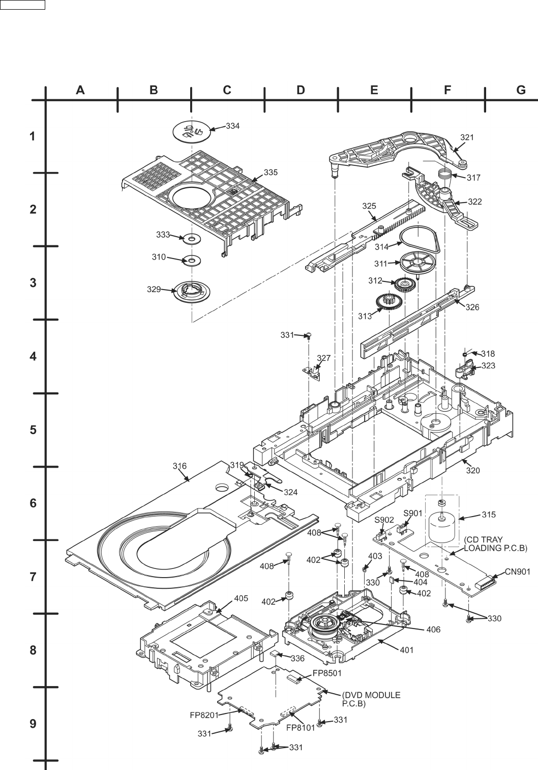
26.1. DVD Loading Mechanism
26.1.1. DVD Loading Mechanism Parts Location
88
SA-HT530GCP

Ref. No. Part No. Part Name & Description Remarks
TRAVERSE DECK
310 RHM0003-J MAGNET [M]
311 RDG0547 PULLEY GEAR [M]
312 RDG0548 RELAY GEAR [M]
313 RDG0549 DRIVE GEAR [M]
314 RDV0070 BELT [M]
315 REM0102 MOTOR UNIT [M]
316 RGQ0395-K TRAY [M]
317 RME0350 CHANGE LEVER SPRING [M]
318 RME0351 LOCK LEVER SPRING [M]
319 RME0353 TRAY SLIDER SPRING [M]
320 RMK0591 MECHA CHASSIS [M]
321 RML0627-2 DRIVE ARM [M]
322 RML0628 CHANGE LEVER [M]
323 RML0629 LOCK LEVER [M]
324 RML0631 TRAY SLIDER [M]
325 RMM0247-2 DRIVE RACK [M]
326 RMM0248 SUB RACK [M]
327 RMC0387 SUPPORT SPRING [M]
329 RMR1446-X CLAMPER [M]
330 XTN26+6GFJ SCREW [M]
331 XTV2+6GFJ SCREW [M]
333 XWG6FFY WASHER [M]
334 RMR1447-X MAGNET HOLDER [M]
335 RMR1468-K CLAMP PLATE [M]
336 RMX0290 PLASTIC SHEET [M]
401 RAE2012Z-S DU69U TRAVESE UNIT [M]
402 RMG0598-A FLOATING RUBBER [M]
403 RMG0617-H CUSHION RUBBER A [M]
404 RMG0618-H CUSHION RUBBER B [M]
405 RMR1596-X2 MIDDLE CHASSIS [M]
406 RXQ1252 DVD OPU SUB ASS’Y [M]
408 RMS0789 FIXED PIN [M]
26.1.2. DVD Loading Mechanism Parts List
89
SA-HT530GCP
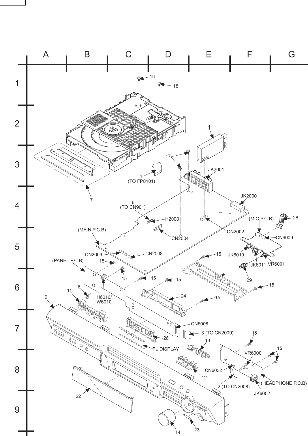
26.2. Cabinet
26.2.1. Cabinet Parts Location
90
SA-HT530GCP
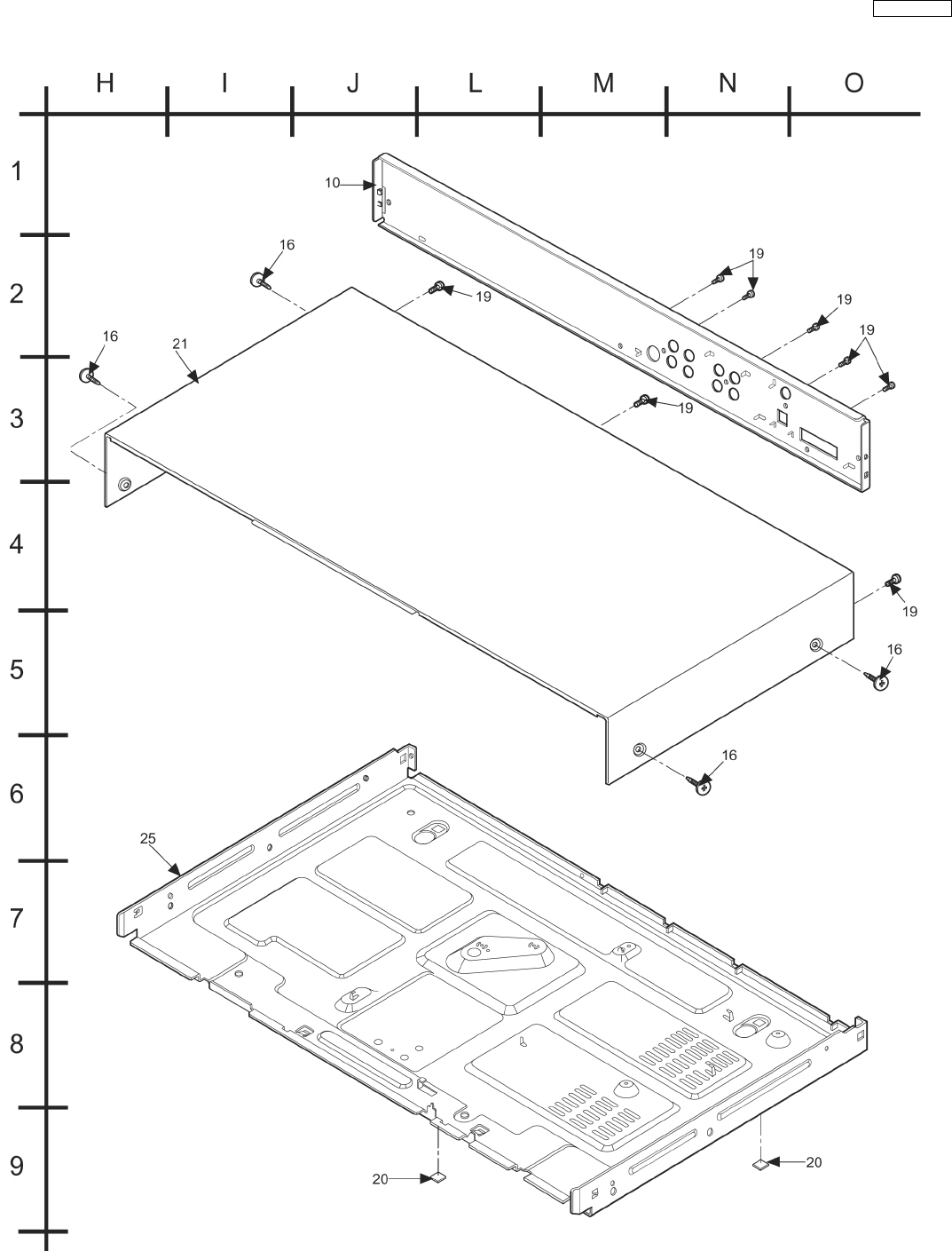
91
SA-HT530GCP

Ref. No. Part No. Part Name & Description Remarks
CABINET AND CHASSIS
1J3CCBB000004 TUNER PACK [M]
2REEX0426 10P FFC WIRE (PANEL) [M]
3REEX0427 19P FFC WIRE (FL) [M]
4REEX0429 50P FFC (MECHA) [M]
6REXX0384 7P FLAT WIRE (DVD) [M]
7RYQX0207-S DVD LID ASS’Y [M]
8RGLX0105-Q LIGHTING PIECE [M]
9RGPX0170A-S1 FRONT PANEL [M]
10 RGRX0043B-D1 REAR PANEL [M]
11 RGUX0601-S POWER BUTTON [M]
12 RGUX0602-S OPERATION BUTTON [M]
13 RGUX0603-S REV-FWD BUTTON [M]
14 RGWX0076-S VOLUME KNOB [M]
Ref. No. Part No. Part Name & Description Remarks
PRINTED CIRCUIT BOARD
REP3867F DVD MODULE P.C.B. (SIDE A &
B)
[M](RTL)
REPX0452F MAIN P.C.B. [M](RTL)
REPX0456B PANEL P.C.B. [M](RTL)
REPX0452F MIC P.C.B. [M](RTL)
REPX0456B HEADPHONE P.C.B. [M](RTL)
REP3288A CD TRAY LOADING P.C.B. [M](RTL)
INTEGRATED CIRCUITS
IC904 C0GAH0000002 IC REFLECTIVE PHOTO SENSOR [M]
IC2006 C9ZB00000466 IC VIDEO SELECTOR [M]
IC2010 C0ABBB000118 IC DUAL OP AMP [M]
IC2011 C1BB00000845 IC ASP [M]
IC2013 C0AABB000125 IC DUAL OP AMP [M]
IC2014 C1BB00000979 IC ANALOG SURROUND [M]
IC2015 C0ABBB000118 IC DUAL OP AMP [M]
IC2018 C2CBHG000168 IC MICROPROCESSOR [M]
IC2601 C0ABBB000118 IC DUAL OP AMP [M]
IC2602 C0ABBB000118 IC DUAL OP AMP [M]
IC2801 C0DAAZG00012 IC DC-TO-DC CONVERTER [M]
IC2802 C0CBADG00023 IC 5V REGULATOR [M]
IC2803 C0DBEZG00021 IC REGULATOR [M]
IC6000 C0HBB0000044 IC FL DRIVER [M]
IC8001 MN2DS0003APH IC DV2.1 [M]
IC8051 C3ABPG000133 IC 64 SDRAM [M]
IC8111 C0CBCBD00018 IC 3.3 REGULATOR [M]
IC8251 C0GBG0000048 IC DRIVE [M]
IC8421 C0FBBK000050 IC 8-CH DAC [M]
IC8601 C0EBE0000384 IC RESET [M]
IC8606 C0EBA0000031 IC RESET [M]
IC8651 RFKWMH82B160 IC 16M FLASH ROM [SPG]
IC8691 C0JBAA000346 IC AND GATE LOGIC [M]
IC8695 C0JBAA000346 IC AND GATE LOGIC [M]
TRANSISTORS
Q2000 B1GBCFLL0037 TRANSISTOR [M]
Q2004 B1GBCFJN0033 TRANSISTOR [M]
Q2028 B1GBCFJN0033 TRANSISTOR [M]
Q2029 B1GBCFJN0033 TRANSISTOR [M]
Q2030 B1GBCFJN0033 TRANSISTOR [M]
Q2102 B1GFGCAA0001 TRANSISTOR [M]
Q2103 B1GDCFGA0018 TRANSISTOR [M]
Q2104 B1GFGCAA0001 TRANSISTOR [M]
Q2105 B1GDCFGA0018 TRANSISTOR [M]
Q2200 B1GFGCAA0001 TRANSISTOR [M]
Q2201 B1GDCFGA0018 TRANSISTOR [M]
Q2500 B1GDCFGA0018 TRANSISTOR [M]
Q2600 B1GDCFGA0018 TRANSISTOR [M]
Q2601 B1GFGCAA0001 TRANSISTOR [M]
Ref. No. Part No. Part Name & Description Remarks
15 RHD26046 SCREW [M]
16 RHD30007-1SJ SCREW [M]
17 RHD30090-1 SCREW [M]
18 RHD30102-1 SCREW [M]
19 RHD30119 SCREW [M]
20 RKA0059-K LEG RUBBER [M]
21 RKMX0107-S TOP CABINET [M]
22 RKWX0241-Q FL WINDOW [M]
23 RKWX0243-S SENSOR WINDOW [M]
24 RMAX0071 MECHA SUPPORT [M]
25 RMKX0102 BOTTOM CHASSIS [M]
26 RMNX0149 FL HOLDER [M]
28 REXX0447 4P FLAT WIRE (MIC) [M]
29 RGW0352-S MIC KNOB [M]
Ref. No. Part No. Part Name & Description Remarks
Q2604 B1ABEB000002 TRANSISTOR [M]
Q2605 B1GDCFGA0018 TRANSISTOR [M]
Q2607 B1ABCE000016 TRANSISTOR [M]
Q2608 B1ABEB000002 TRANSISTOR [M]
Q2609 B1GDCFGA0018 TRANSISTOR [M]
Q2702 B1GDCFGA0018 TRANSISTOR [M]
Q2703 B1ABEB000002 TRANSISTOR [M]
Q2801 B1ADCF000001 TRANSISTOR [M]
Q2803 B1BCCG000023 TRANSISTOR [M]
Q2804 B1ABCE000016 TRANSISTOR [M]
Q2805 B1ABCE000016 TRANSISTOR [M]
Q2806 B1BCCD000019 TRANSISTOR [M]
Q2807 B1BCCD000019 TRANSISTOR [M]
Q2808 B1ADCF000001 TRANSISTOR [M]
Q2809 B1ACKD000005 TRANSISTOR [M]
Q2813 B1AAKD000014 TRANSISTOR [M]
Q2814 2SD21370PA TRANSISTOR [M]
Q2816 B1BACD000018 TRANSISTOR [M]
Q2818 B1GBCFJA0028 TRANSISTOR [M]
Q6071 B1ABCF000011 TRANSISTOR [M]
Q6072 B1ABCF000011 TRANSISTOR [M]
Q6073 B1ABCF000011 TRANSISTOR [M]
Q8550 2SB1219AHL TRANSISTOR [M]
Q8551 2SD1819A0L TRANSISTOR [M]
Q8552 2SB09700RL TRANSISTOR [M]
Q8560 2SD1819A0L TRANSISTOR [M]
Q8561 2SD1819A0L TRANSISTOR [M]
Q8562 2SB09700RL TRANSISTOR [M]
Q8606 2SD1819A0L TRANSISTOR [M]
Q8607 2SD1819A0L TRANSISTOR [M]
QR8111 UNR521400L TRANSISTOR [M]
QR8112 UNR521400L TRANSISTOR [M]
QR8420 UNR521100L TRANSISTOR [M]
QR8571 UNR511V00L TRANSISTOR [M]
DIODES
D2000 B0ACCE000003 DIODE [M]
D2001 B0ACCE000003 DIODE [M]
D2002 B0ACCE000003 DIODE [M]
D2003 B0ACCK000005 DIODE [M]
D2041 B0EAKM000117 DIODE [M]
D2042 B0EAKM000117 DIODE [M]
D2601 B0ACCK000005 DIODE [M]
D2801 B0JCPD000025 DIODE [M]
D2802 B0BC7R500001 DIODE [M]
D2803 B0ACCK000005 DIODE [M]
D2804 B0BC9R000008 DIODE [M]
D2805 B0ECKM000016 DIODE [M]
D2806 B0ECKM000016 DIODE [M]
D2807 B0ACCK000005 DIODE [M]
D2808 B0ACCK000005 DIODE [M]
26.2.2. Cabinet Parts List
26.3. Component Parts List
92
SA-HT530GCP

Ref. No. Part No. Part Name & Description Remarks
D2809 B0EAKM000117 DIODE [M]
D2810 B0EAKM000117 DIODE [M]
D2811 B0EAKM000117 DIODE [M]
D2812 B0EAKM000117 DIODE [M]
D2813 B0EAKM000117 DIODE [M]
D2814 B0EAKM000117 DIODE [M]
D2815 B0EAKM000117 DIODE [M]
D2816 B0EAKM000117 DIODE [M]
D2817 B0EAKM000117 DIODE [M]
D2818 MAZ82200ML DIODE [M]
D2822 B0FBAM000010 DIODE [M]
D2823 B0BC5R600003 DIODE [M]
D2824 B0BC7R500001 DIODE [M]
D2827 B0EAKM000117 DIODE [M]
D2829 B0ACCK000005 DIODE [M]
D2830 B0BC01000014 DIODE [M]
D2831 B0EAKM000117 DIODE [M]
D2850 B0ACCK000005 DIODE [M]
D2851 B0ADCJ000020 DIODE [M]
D2852 B0ACCK000005 DIODE [M]
D6000 B3AAA0000583 DIODE [M]
D6006 B0BC5R000009 DIODE [M]
D6008 B0BC5R000009 DIODE [M]
D8231 MA2J11100L DIODE [M]
D8550 MA2J11100L DIODE [M]
D8571 MA2J72800L DIODE [M]
VARIABLE RESISTORS
VR6000 EVEKE2F3024M VR VOLUME JOG [M]
VR6001 EVUE27FK3B53 VR MIC [M]
SWITCHES
S901 RSH1A044-1A SW PLAY [M]
S902 RSH1A044-1A SW OPEN [M]
S6000 EVQ21405R SW OPEN/CLOSE [M]
S6001 EVQ21405R SW FF [M]
S6002 EVQ21405R SW REW [M]
S6003 EVQ21405R SW STOP [M]
S6004 EVQ21405R SW PAUSE [M]
S6005 EVQ21405R SW PLAY [M]
S6011 EVQ21405R SW POWER [M]
S6012 EVQ21405R SW SELECTOR [M]
S6013 EVQ21405R SW RDS [M]
S6014 EVQ21405R SW H_BASS [M]
CONNECTORS
CN901 K1KA07B00027 7P CONNECTOR [M]
CN2002 K1KA10A00263 10P CONNECTOR [M]
CN2004 K1MN50A00008 50P CONNECTOR [M]
CN2008 K1MN10A00052 10P CONNECTOR [M]
CN2009 K1MN19A00036 19P CONNECTOR [M]
CN6008 K1MN19B00026 19P CONNECTOR [M]
CN6009 K1KA04B00057 4P CONNECTOR [M]
CN6032 K1MN10B00088 10P CONNECTOR [M]
FP8101 K1MN50B00031 50P CONNECTOR [M]
FP8201 K1MN06B00080 6P CONNECTOR [M]
FP8501 K1MN26B00094 26P CONNECTORS [M]
COILS
L2000 G0C3R3JA0027 COIL [M]
L2010 ELESN220JA COIL [M]
L2022 J0JBC0000015 CHIP INDUCTOR [M]
L2023 J0JBC0000015 CHIP INDUCTOR [M]
L2024 J0JBC0000015 CHIP INDUCTOR [M]
L2025 J0JBC0000015 CHIP INDUCTOR [M]
L2026 J0JBC0000015 CHIP INDUCTOR [M]
L2027 J0JBC0000015 CHIP INDUCTOR [M]
L2028 J0JBC0000019 CHIP INDUCTOR [M]
L2801 G0ZZ00001930 COIL [M]
Ref. No. Part No. Part Name & Description Remarks
L2802 G0A200D00002 COIL [M]
L2803 G0A200D00002 COIL [M]
L6000 J0JBC0000019 CHIP INDUCTOR [M]
L6001 J0JBC0000019 CHIP INDUCTOR [M]
L6002 J0JBC0000019 CHIP INDUCTOR [M]
L6003 J0JBC0000041 CHIP INDUCTOR [M]
L6004 J0JBC0000019 CHIP INDUCTOR [M]
L6005 J0JBC0000030 CHIP BEEZ [M]
L6006 J0JBC0000019 CHIP INDUCTOR [M]
L8201 G1C100K00020 CHIP INDUCTOR [M]
L8202 J0JCC0000079 FILTER [M]
L8301 G1C100KA0055 CHIP INDUCTOR [M]
L8302 J0JCC0000079 FILTER [M]
L8550 G1C100KA0055 CHIP INDUCTOR [M]
COMPONENT COMBINATION
Z6000 B3RAB0000025 REMOTE SENSOR [M]
OSCILLATORS
X2000 H2B100500004 CERAMIC RESONATOR [M]
X8621 H0J270500085 CRYSTAL [M]
DISPLAY TUBES
FL6000 A2BD00000108 FL DISPLAY [M]
FL8101 F1H0J1050022 CHIP CAPACITOR [M]
FL8102 F1H0J1050022 CHIP CAPACITOR [M]
FL8103 F1H0J1050022 CHIP CAPACITOR [M]
FL8104 F1J1E1040022 CHIP CAPACITOR [M]
FUSE PROTECTOR
FP2000 K5G202AA0002 FUSE PROTECTOR [M]
HOLDERS
H2000 RMR0316 7P WIRE HOLDER [M]
H6010 K1ZZ00000832 4P WIRE HOLDER [M]
JACKS
JK2000 K1FB125B0097 JK SYSTEM CONNECTOR [M]
JK2001 K2HZ921B0002 JK COMBO [M]
JK6002 K2HC103A0023 JK [M]
JK6010 K2HB102J0038 JACK [M]
JK6011 K2HB102J0038 JACK [M]
EARTH TERMINAL
E2000 K4CZ01000027 TERMINAL [M]
CHIP RESISTORS
W602 ERJ3GEY0R00V CHIP RESISTOR [M]
W603 ERJ3GEY0R00V CHIP RESISTOR [M]
W1208 ERJ6GEY0R00V CHIP RESISTOR [M]
W2001 ERJ3GEY0R00V CHIP RESISTOR [M]
W2002 ERJ3GEY0R00V CHIP RESISTOR [M]
W2003 ERJ3GEY0R00V CHIP RESISTOR [M]
W2004 ERJ3GEY0R00V CHIP RESISTOR [M]
W2005 ERJ3GEY0R00V CHIP RESISTOR [M]
W2009 ERJ6GEY0R00V CHIP RESISTOR [M]
W2012 ERJ3GEY0R00V CHIP RESISTOR [M]
W2013 ERJ3GEY0R00V CHIP RESISTOR [M]
W2014 ERJ3GEY0R00V CHIP RESISTOR [M]
W2015 ERJ3GEY0R00V CHIP RESISTOR [M]
W2016 ERJ6GEY0R00V CHIP RESISTOR [M]
W2017 ERJ3GEY0R00V CHIP RESISTOR [M]
W2018 ERJ3GEY0R00V CHIP RESISTOR [M]
W2019 ERJ6GEY0R00V CHIP RESISTOR [M]
W2023 ERJ6GEY0R00V CHIP RESISTOR [M]
W2026 ERJ3GEY0R00V CHIP RESISTOR [M]
93
SA-HT530GCP

Ref. No. Part No. Part Name & Description Remarks
W2027 ERJ6GEY0R00V CHIP RESISTOR [M]
W2028 ERJ6GEY0R00V CHIP RESISTOR [M]
W2030 ERJ3GEY0R00V CHIP RESISTOR [M]
W2031 ERJ3GEY0R00V CHIP RESISTOR [M]
W2032 ERJ3GEY0R00V CHIP RESISTOR [M]
W2033 ERJ3GEY0R00V CHIP RESISTOR [M]
W2041 ERJ3GEY0R00V CHIP RESISTOR [M]
W2042 ERJ3GEY0R00V CHIP RESISTOR [M]
W2043 ERJ3GEY0R00V CHIP RESISTOR [M]
W2044 ERJ6GEY0R00V CHIP RESISTOR [M]
W2045 ERJ6GEY0R00V CHIP RESISTOR [M]
W2049 ERJ6GEY0R00V CHIP RESISTOR [M]
W2051 ERJ6GEY0R00V CHIP RESISTOR [M]
W2055 ERJ6GEY0R00V CHIP RESISTOR [M]
W2056 ERJ6GEY0R00V CHIP RESISTOR [M]
W2057 ERJ6GEY0R00V CHIP RESISTOR [M]
W2058 ERJ6GEY0R00V CHIP RESISTOR [M]
W2059 ERJ6GEY0R00V CHIP RESISTOR [M]
W2060 ERJ6GEY0R00V CHIP RESISTOR [M]
W2061 ERJ6GEY0R00V CHIP RESISTOR [M]
W2062 ERJ6GEY0R00V CHIP RESISTOR [M]
W2064 ERJ6GEY0R00V CHIP RESISTOR [M]
W2065 ERJ6GEY0R00V CHIP RESISTOR [M]
W2068 ERJ6GEY0R00V CHIP RESISTOR [M]
W2071 ERJ3GEY0R00V CHIP RESISTOR [M]
W2072 ERJ3GEY0R00V CHIP RESISTOR [M]
W2074 ERJ6GEY0R00V CHIP RESISTOR [M]
W2086 ERJ6GEY0R00V CHIP RESISTOR [M]
W2119 ERJ6GEY0R00V CHIP RESISTOR [M]
W2128 ERJ3GEY0R00V CHIP RESISTOR [M]
W3000 ERJ3GEY0R00V CHIP RESISTOR [M]
W4000 ERJ3GEY0R00V CHIP RESISTOR [M]
W6001 ERJ6GEY0R00V CHIP RESISTOR [M]
W6002 ERJ6GEY0R00V CHIP RESISTOR [M]
W6003 ERJ6GEY0R00V CHIP RESISTOR [M]
W6005 ERJ6GEY0R00V CHIP RESISTOR [M]
W6006 ERJ6GEY0R00V CHIP RESISTOR [M]
W6010 ERJ6GEY0R00V CHIP RESISTOR [M]
W6011 ERJ6GEY0R00V CHIP RESISTOR [M]
W6012 ERJ6GEY0R00V CHIP RESISTOR [M]
W6013 ERJ6GEY0R00V CHIP RESISTOR [M]
W6014 ERJ6GEY0R00V CHIP RESISTOR [M]
W6015 ERJ3GEY0R00V CHIP RESISTOR [M]
W6033 ERJ6GEY0R00V CHIP RESISTOR [M]
W6034 ERJ6GEY0R00V CHIP RESISTOR [M]
W6035 ERJ6GEY0R00V CHIP RESISTOR [M]
RX8011 D1H88204A024 CHIP RESISTOR [M]
RX8012 D1H88204A024 CHIP RESISTOR [M]
RX8013 D1H88204A024 CHIP RESISTOR [M]
RX8014 D1H88204A024 CHIP RESISTOR [M]
RX8015 D1H422020001 CHIP RESISTOR [M]
RX8016 D1H88204A024 CHIP RESISTOR [M]
RX8017 D1H88204A024 CHIP RESISTOR [M]
RX8018 D1H88204A024 CHIP RESISTOR [M]
RX8021 D1H410320002 CHIP RESISTOR [M]
RX8031 D1H447220001 CHIP RESISTOR [M]
RX8032 D1H447220001 CHIP RESISTOR [M]
RX8401 D1H410120001 CHIP RESISTOR [M]
RX8402 D1H410120001 CHIP RESISTOR [M]
RX8501 D1H456020001 CHIP RESISTOR [M]
RX8502 D1H85604A024 CHIP RESISTOR [M]
RX8503 D1H456020001 CHIP RESISTOR [M]
RX8504 D1H456020001 CHIP RESISTOR [M]
RX8611 D1H447220001 CHIP RESISTOR [M]
RESISTORS
R2000 ERJ3GEYJ221V 220 1/16W [M]
R2001 ERJ3GEYJ221V 220 1/16W [M]
R2002 ERJ3GEYJ221V 220 1/16W [M]
R2003 ERJ3GEYJ221V 220 1/16W [M]
R2006 ERJ3GEYJ221V 220 1/16W [M]
R2007 ERJ3GEYJ102V 1K 1/16W [M]
Ref. No. Part No. Part Name & Description Remarks
R2008 ERJ3GEYJ103V 10K 1/16W [M]
R2011 ERJ3GEYJ473V 47K 1/16W [M]
R2012 ERJ3GEYJ221V 220 1/16W [M]
R2013 ERJ3GEYJ221V 220 1/16W [M]
R2014 ERJ3GEYJ221V 220 1/16W [M]
R2016 ERJ3GEYJ221V 220 1/16W [M]
R2017 ERJ3GEYJ103V 10K 1/16W [M]
R2018 ERJ3GEYJ221V 220 1/16W [M]
R2019 ERJ3GEYJ221V 220 1/16W [M]
R2020 ERJ3GEYJ473V 47K 1/16W [M]
R2021 ERJ3GEYJ473V 47K 1/16W [M]
R2022 ERJ3GEYJ473V 47K 1/16W [M]
R2023 ERJ3GEYJ103V 10K 1/16W [M]
R2025 ERJ3GEYJ221V 220 1/16W [M]
R2026 ERJ3GEYJ221V 220 1/16W [M]
R2027 ERJ3GEYJ221V 220 1/16W [M]
R2028 ERJ3GEYJ102V 1K 1/16W [M]
R2029 ERJ3GEYJ221V 220 1/16W [M]
R2030 ERJ3GEYJ221V 220 1/16W [M]
R2031 ERJ3GEYJ221V 220 1/16W [M]
R2032 ERJ3GEYJ221V 220 1/16W [M]
R2033 ERJ3GEYJ221V 220 1/16W [M]
R2034 ERJ3GEYJ221V 220 1/16W [M]
R2035 ERJ3GEYJ221V 220 1/16W [M]
R2036 ERJ3GEYJ102V 1K 1/16W [M]
R2037 ERJ3GEYJ102V 1K 1/16W [M]
R2039 ERJ3GEYJ221V 220 1/16W [M]
R2040 ERJ3GEYJ221V 220 1/16W [M]
R2041 ERJ3GEYJ221V 220 1/16W [M]
R2043 ERJ3GEYJ221V 220 1/16W [M]
R2047 ERJ3GEYJ221V 220 1/16W [M]
R2048 ERJ3GEYJ221V 220 1/16W [M]
R2049 ERJ3GEYJ221V 220 1/16W [M]
R2050 ERJ3GEYJ221V 220 1/16W [M]
R2051 ERJ3GEYJ221V 220 1/16W [M]
R2052 ERJ3GEYJ221V 220 1/16W [M]
R2053 ERJ3GEYJ221V 220 1/16W [M]
R2054 ERJ3GEYJ221V 220 1/16W [M]
R2056 ERJ3GEYJ473V 47K 1/16W [M]
R2057 ERJ3GEYJ473V 47K 1/16W [M]
R2058 ERJ3GEYJ563V 56K 1/16W [M]
R2059 ERJ3GEYJ221V 220 1/16W [M]
R2060 ERJ3GEYJ101V 100 1/16W [M]
R2061 ERJ3GEYJ221V 220 1/16W [M]
R2062 ERJ3GEYJ221V 220 1/16W [M]
R2064 ERJ3GEYJ101V 100 1/16W [M]
R2065 ERJ3GEYJ103V 10K 1/16W [M]
R2066 ERJ3GEYJ103V 10K 1/16W [M]
R2067 ERJ3GEYJ103V 10K 1/16W [M]
R2068 ERJ3GEYJ103V 10K 1/16W [M]
R2069 ERJ3GEYJ223V 22K 1/16W [M]
R2070 ERJ3GEY0R00V 0 1/16W [M]
R2071 ERJ3GEYJ472V 4.7K 1/16W [M]
R2072 ERJ3GEYJ101V 100 1/16W [M]
R2073 ERJ3GEY0R00V 0 1/16W [M]
R2074 ERJ3GEYJ272V 2.7K 1/16W [M]
R2076 ERJ3GEYJ104V 100K 1/16W [M]
R2077 ERJ3GEYJ472V 4.7K 1/16W [M]
R2078 ERJ3GEYJ471V 470 1/16W [M]
R2079 ERJ3GEYJ223V 22K 1/16W [M]
R2080 ERJ3GEYJ103V 10K 1/16W [M]
R2082 ERJ3GEYJ473V 47K 1/16W [M]
R2083 ERJ3GEYJ681V 680 1/16W [M]
R2085 ERJ3GEY0R00V 0 1/16W [M]
R2092 ERJ3GEYJ472V 4.7K 1/16W [M]
R2093 ERJ3GEYJ223V 22K 1/16W [M]
R2094 ERJ3GEYJ223V 22K 1/16W [M]
R2100 ERJ3GEYJ102V 1K 1/16W [M]
R2101 ERJ3GEYJ473V 47K 1/16W [M]
R2111 ERJ3GEYJ333V 33K 1/16W [M]
R2112 ERJ3GEYJ103V 10K 1/16W [M]
R2113 ERJ3GEYJ103V 10K 1/16W [M]
R2114 ERJ3GEYJ103V 10K 1/16W [M]
R2115 ERJ3GEYJ273V 27K 1/16W [M]
94
SA-HT530GCP

Ref. No. Part No. Part Name & Description Remarks
R2116 ERJ3GEYJ104V 100K 1/16W [M]
R2117 ERJ3GEYJ104V 100K 1/16W [M]
R2125 ERJ3GEYJ182V 1.8K 1/16W [M]
R2126 ERJ3GEYJ102V 1K 1/16W [M]
R2129 ERJ3GEYJ123V 12K 1/16W [M]
R2130 ERJ3GEYJ103V 10K 1/16W [M]
R2131 ERJ3GEYJ103V 10K 1/16W [M]
R2132 ERJ3GEYJ103V 10K 1/16W [M]
R2133 ERJ3GEYJ103V 10K 1/16W [M]
R2144 ERJ3GEYJ222V 2.2K 1/16W [M]
R2145 ERJ3GEYJ682V 6.8K 1/16W [M]
R2146 ERJ3GEYJ333V 33K 1/16W [M]
R2147 ERJ3GEYJ220V 22 1/16W [M]
R2148 ERJ3GEYJ220V 22 1/16W [M]
R2149 ERJ3GEYJ220V 22 1/16W [M]
R2150 ERJ3GEYJ220V 22 1/16W [M]
R2151 ERJ3GEYJ472V 4.7K 1/16W [M]
R2152 ERJ3GEYJ272V 2.7K 1/16W [M]
R2153 ERJ3GEYJ100V 10 1/16W [M]
R2154 ERJ3GEYJ222V 2.2K 1/16W [M]
R2155 ERJ3GEYJ104V 100K 1/16W [M]
R2156 ERJ3GEYJ103V 10K 1/16W [M]
R2157 ERJ3GEYJ123V 12K 1/16W [M]
R2160 ERJ3GEYJ822V 8.2K 1/16W [M]
R2161 ERJ3GEYJ333V 33K 1/16W [M]
R2162 ERJ3GEYJ682V 6.8K 1/16W [M]
R2163 ERJ3GEYJ102V 1K 1/16W [M]
R2164 ERJ3GEYJ273V 27K 1/16W [M]
R2165 ERJ3GEYJ682V 6.8K 1/16W [M]
R2166 ERJ3GEYJ122V 1.2K 1/16W [M]
R2167 ERJ3GEYJ123V 12K 1/16W [M]
R2168 ERJ3GEYJ223V 22K 1/16W [M]
R2169 ERJ3GEYJ562V 5.6K 1/16W [M]
R2170 ERJ3GEYJ332V 3.3K 1/16W [M]
R2172 ERJ3GEY0R00V 0 1/16W [M]
R2178 ERJ3GEYJ223V 22K 1/16W [M]
R2200 ERJ3GEYJ102V 1K 1/16W [M]
R2201 ERJ3GEYJ473V 47K 1/16W [M]
R2211 ERJ3GEYJ333V 33K 1/16W [M]
R2212 ERJ3GEYJ103V 10K 1/16W [M]
R2213 ERJ3GEYJ103V 10K 1/16W [M]
R2214 ERJ3GEYJ103V 10K 1/16W [M]
R2215 ERJ3GEYJ273V 27K 1/16W [M]
R2216 ERJ3GEYJ104V 100K 1/16W [M]
R2217 ERJ3GEYJ104V 100K 1/16W [M]
R2229 ERJ3GEYJ103V 10K 1/16W [M]
R2230 ERJ3GEYJ103V 10K 1/16W [M]
R2231 ERJ3GEYJ103V 10K 1/16W [M]
R2232 ERJ3GEYJ103V 10K 1/16W [M]
R2235 ERJ3GEYJ123V 12K 1/16W [M]
R2244 ERJ3GEYJ222V 2.2K 1/16W [M]
R2245 ERJ3GEYJ682V 6.8K 1/16W [M]
R2246 ERJ3GEYJ333V 33K 1/16W [M]
R2247 ERJ3GEYJ220V 22 1/16W [M]
R2248 ERJ3GEYJ220V 22 1/16W [M]
R2249 ERJ3GEYJ220V 22 1/16W [M]
R2250 ERJ3GEYJ220V 22 1/16W [M]
R2251 ERJ3GEYJ472V 4.7K 1/16W [M]
R2252 ERJ3GEYJ272V 2.7K 1/16W [M]
R2253 ERJ3GEYJ100V 10 1/16W [M]
R2254 ERJ3GEYJ222V 2.2K 1/16W [M]
R2255 ERJ3GEYJ104V 100K 1/16W [M]
R2256 ERJ3GEYJ103V 10K 1/16W [M]
R2257 ERJ3GEYJ123V 12K 1/16W [M]
R2260 ERJ3GEYJ822V 8.2K 1/16W [M]
R2261 ERJ3GEYJ682V 6.8K 1/16W [M]
R2262 ERJ3GEYJ333V 33K 1/16W [M]
R2263 ERJ3GEYJ102V 1K 1/16W [M]
R2264 ERJ3GEYJ273V 27K 1/16W [M]
R2265 ERJ3GEYJ682V 6.8K 1/16W [M]
R2266 ERJ3GEYJ182V 1.8K 1/16W [M]
R2267 ERJ3GEYJ563V 56K 1/16W [M]
R2268 ERJ3GEYJ273V 27K 1/16W [M]
R2269 ERJ3GEYJ562V 5.6K 1/16W [M]
Ref. No. Part No. Part Name & Description Remarks
R2271 ERJ3GEY0R00V 0 1/16W [M]
R2278 ERJ3GEYJ223V 22K 1/16W [M]
R2300 ERJ3GEYJ103V 10K 1/16W [M]
R2301 ERJ3GEYJ302V 3K 1/16W [M]
R2302 ERJ3GEYJ103V 10K 1/16W [M]
R2303 ERJ3GEYJ473V 47K 1/16W [M]
R2304 ERJ3GEYJ752V 7.5K 1/16W [M]
R2305 ERJ3GEYJ102V 1K 1/16W [M]
R2306 ERJ3GEYJ104V 100K 1/16W [M]
R2307 ERJ3GEYJ101V 100 1/16W [M]
R2308 ERJ3GEYJ182V 1.8K 1/16W [M]
R2309 ERJ3GEYJ563V 56K 1/16W [M]
R2310 ERJ3GEYJ273V 27K 1/16W [M]
R2311 ERJ3GEYJ222V 2.2K 1/16W [M]
R2312 ERJ3GEYJ222V 2.2K 1/16W [M]
R2400 ERJ3GEYJ103V 10K 1/16W [M]
R2401 ERJ3GEYJ302V 3K 1/16W [M]
R2402 ERJ3GEYJ103V 10K 1/16W [M]
R2403 ERJ3GEYJ473V 47K 1/16W [M]
R2404 ERJ3GEYJ752V 7.5K 1/16W [M]
R2405 ERJ3GEYJ102V 1K 1/16W [M]
R2406 ERJ3GEYJ104V 100K 1/16W [M]
R2407 ERJ3GEYJ101V 100 1/16W [M]
R2500 ERJ3GEYJ103V 10K 1/16W [M]
R2501 ERJ3GEYJ473V 47K 1/16W [M]
R2502 ERJ3GEYJ752V 7.5K 1/16W [M]
R2503 ERJ3GEYJ332V 3.3K 1/16W [M]
R2504 ERJ3GEYJ682V 6.8K 1/16W [M]
R2505 ERJ3GEYJ102V 1K 1/16W [M]
R2506 ERJ3GEYJ333V 33K 1/16W [M]
R2507 ERJ3GEYJ822V 8.2K 1/16W [M]
R2508 ERJ3GEYJ182V 1.8K 1/16W [M]
R2509 ERJ3GEYJ563V 56K 1/16W [M]
R2510 ERJ3GEYJ273V 27K 1/16W [M]
R2511 ERJ3GEYJ222V 2.2K 1/16W [M]
R2521 ERJ3GEY0R00V 0 1/16W [M]
R2600 ERJ3GEYJ103V 10K 1/16W [M]
R2603 ERJ3GEYJ203V 20K 1/16W [M]
R2604 ERJ3GEYJ333V 33K 1/16W [M]
R2605 ERJ3GEYJ222V 2.2K 1/16W [M]
R2606 ERJ3GEYJ103V 10K 1/16W [M]
R2607 ERJ3GEYJ223V 22K 1/16W [M]
R2608 ERJ3GEYJ184V 180K 1/16W [M]
R2609 ERJ3GEYJ563V 56K 1/16W [M]
R2610 ERJ3GEYJ152V 1.5K 1/16W [M]
R2611 ERJ3GEYJ563V 56K 1/16W [M]
R2612 ERJ3GEYJ682V 6.8K 1/16W [M]
R2613 ERJ3GEYJ332V 3.3K 1/16W [M]
R2614 ERJ3GEYJ102V 1K 1/16W [M]
R2615 ERJ3GEYJ104V 100K 1/16W [M]
R2616 ERJ3GEYJ273V 27K 1/16W [M]
R2617 ERJ3GEYJ273V 27K 1/16W [M]
R2618 ERJ3GEYJ102V 1K 1/16W [M]
R2619 ERJ3GEYJ222V 2.2K 1/16W [M]
R2620 ERJ3GEYJ182V 1.8K 1/16W [M]
R2621 ERJ3GEYJ563V 56K 1/16W [M]
R2622 ERJ3GEYJ273V 27K 1/16W [M]
R2623 ERJ3GEYJ104V 100K 1/16W [M]
R2624 ERJ3GEYJ104V 100K 1/16W [M]
R2625 ERJ3GEYJ223V 22K 1/16W [M]
R2627 ERJ3GEYJ104V 100K 1/16W [M]
R2629 ERJ3GEYJ333V 33K 1/16W [M]
R2630 ERJ3GEYJ104V 100K 1/16W [M]
R2631 ERJ3GEYJ104V 100K 1/16W [M]
R2632 ERJ3GEYJ822V 8.2K 1/16W [M]
R2633 ERJ3GEYJ104V 100K 1/16W [M]
R2634 ERJ3GEYJ822V 8.2K 1/16W [M]
R2635 ERJ3GEYJ103V 10K 1/16W [M]
R2636 ERJ3GEYJ103V 10K 1/16W [M]
R2637 ERJ3GEYJ102V 1K 1/16W [M]
R2638 ERJ3GEYJ104V 100K 1/16W [M]
R2639 ERJ3GEYJ682V 6.8K 1/16W [M]
R2640 ERJ3GEY0R00V 0 1/16W [M]
R2641 ERJ3GEYJ392V 3.9K 1/16W [M]
95
SA-HT530GCP

Ref. No. Part No. Part Name & Description Remarks
R2642 ERJ3GEYJ683V 68K 1/16W [M]
R2643 ERJ3GEYJ104V 100K 1/16W [M]
R2644 ERJ3GEYJ273V 27K 1/16W [M]
R2645 ERJ3GEYJ563V 56K 1/16W [M]
R2646 ERJ3GEYJ182V 1.8K 1/16W [M]
R2647 ERJ3GEYJ332V 3.3K 1/16W [M]
R2648 ERJ3GEYJ103V 10K 1/16W [M]
R2649 ERJ3GEYJ222V 2.2K 1/16W [M]
R2650 ERJ3GEYJ333V 33K 1/16W [M]
R2651 ERJ3GEYJ123V 12K 1/16W [M]
R2652 ERJ3GEYJ104V 100K 1/16W [M]
R2654 ERJ3GEYJ103V 10K 1/16W [M]
R2655 ERJ3GEYJ103V 10K 1/16W [M]
R2656 ERJ3GEYJ472V 4.7K 1/16W [M]
R2657 ERJ3GEYJ104V 100K 1/16W [M]
R2658 ERJ3GEYJ222V 2.2K 1/16W [M]
R2659 ERJ3GEYJ563V 56K 1/16W [M]
R2660 ERJ3GEYJ182V 1.8K 1/16W [M]
R2661 ERJ3GEYJ273V 27K 1/16W [M]
R2662 ERJ3GEYJ104V 100K 1/16W [M]
R2663 ERJ3GEYJ392V 3.9K 1/16W [M]
R2664 ERJ3GEYJ682V 6.8K 1/16W [M]
R2708 ERJ3GEYJ182V 1.8K 1/16W [M]
R2709 ERJ3GEYJ273V 27K 1/16W [M]
R2710 ERJ3GEYJ563V 56K 1/16W [M]
R2711 ERJ3GEYJ222V 2.2K 1/16W [M]
R2712 ERJ3GEYJ104V 100K 1/16W [M]
R2713 ERJ3GEYJ102V 1K 1/16W [M]
R2801 ERJ3GEYJ1R0V 1 1/16W [M]
R2803 ERJ3GEYJ222V 2.2K 1/16W [M]
R2804 ERJ3GEYJ272V 2.7K 1/16W [M]
R2805 ERJ3GEYJ1R0V 1 1/16W [M]
R2806 ERJ3GEYJ1R0V 1 1/16W [M]
R2808 ERJ3GEYJ1R0V 1 1/16W [M]
R2811 ERJ3GEYJ103V 10K 1/16W [M]
R2813 ERJ3GEYJ471V 470 1/16W [M]
R2815 ERJ3GEYJ472V 4.7K 1/16W [M]
R2817 ERJ3GEYJ102V 1K 1/16W [M]
R2819 ERJ3GEYJ471V 470 1/16W [M]
R2820 ERJ3GEYJ222V 2.2K 1/16W [M]
R2821 ERJ3GEYJ182V 1.8K 1/16W [M]
R2822 ERJ3GEYJ222V 2.2K 1/16W [M]
R2823 ERJ3GEYJ222V 2.2K 1/16W [M]
R2824 ERJ3GEYJ821V 820 1/16W [M]
R2825 ERD2FCVJ4R7T 4.7 1/4W [M]
R2826 ERJ3GEYJ681V 680 1/16W [M]
R2827 ERJ3GEYJ471V 470 1/16W [M]
R2828 ERJ3GEYJ272V 2.7K 1/16W [M]
R2829 ERJ3GEYJ102V 1K 1/16W [M]
R2830 ERJ3GEYJ272V 2.7K 1/16W [M]
R2831 ERJ3GEYJ472V 4.7K 1/16W [M]
R2832 ERJ3GEYJ151V 150 1/16W [M]
R2833 ERJ3GEYJ102V 1K 1/16W [M]
R2834 ERJ3GEYJ102V 1K 1/16W [M]
R2835 ERJ3GEYJ681V 680 1/16W [M]
R2837 ERJ3GEYJ561V 560 1/16W [M]
R2838 ERJ3GEYJ272V 2.7K 1/16W [M]
R2839 ERJ3GEYJ821V 820 1/16W [M]
R2840 ERJ3GEYJ151V 150 1/16W [M]
R2841 ERD2FCVJ4R7T 4.7 1/4W [M]
R2842 ERJ3GEYJ182V 1.8K 1/16W [M]
R2843 ERJ3GEYJ471V 470 1/16W [M]
R2846 ERJ3GEYJ222V 2.2K 1/16W [M]
R2847 ERJ3GEYJ222V 2.2K 1/16W [M]
R2848 ERJ3GEYJ8R2V 8.2 1/16W [M]
R2849 ERJ3GEYJ472V 4.7K 1/16W [M]
R2850 ERJ3GEYJ393V 39K 1/16W [M]
R2851 ERJ3GEYJ153V 15K 1/16W [M]
R2854 ERJ3GEYJ101V 100 1/16W [M]
R2855 ERJ3GEYJ102V 1K 1/16W [M]
R2856 ERJ3GEYJ823V 82K 1/16W [M]
R2861 ERJ3GEYJ103V 10K 1/16W [M]
R2878 ERJ3GEYJ1R0V 1 1/16W [M]
R2879 ERJ3GEYJ1R0V 1 1/16W [M]
Ref. No. Part No. Part Name & Description Remarks
R2880 ERJ3GEYJ1R0V 1 1/16W [M]
R2881 ERJ3GEYJ1R0V 1 1/16W [M]
R2882 ERJ3GEYJ1R0V 1 1/16W [M]
R2883 ERJ3GEYJ1R0V 1 1/16W [M]
R2884 ERJ3GEYJ1R0V 1 1/16W [M]
R2885 ERJ3GEYJ1R0V 1 1/16W [M]
R2886 D0HB750ZA003 75 3W [M]
R2887 D0HB750ZA003 75 3W [M]
R2888 D0HB750ZA003 75 3W [M]
R2889 D0HB750ZA003 75 3W [M]
R2890 D0HB750ZA003 75 3W [M]
R2891 D0HB750ZA003 75 3W [M]
R2892 ERJ3GEYJ103V 10K 1/16W [M]
R2893 ERJ3GEYJ153V 15K 1/16W [M]
R2894 ERJ3GEYJ224V 220K 1/16W [M]
R2895 ERJ3GEYJ103V 10K 1/16W [M]
R2897 ERJ3GEYJ102V 1K 1/16W [M]
R2898 ERJ3GEYJ331V 330 1/16W [M]
R2903 ERJ3GEY0R00V 0 1/16W [M]
R2904 ERJ3GEY0R00V 0 1/16W [M]
R2905 ERJ3GEYJ1R0V 1 1/16W [M]
R2916 ERJ3GEY0R00V 0 1/16W [M]
R2917 ERJ3GEY0R00V 0 1/16W [M]
R2918 ERJ3GEY0R00V 0 1/16W [M]
R2919 ERJ3GEY0R00V 0 1/16W [M]
R2920 ERJ3GEYJ103V 10K 1/16W [M]
R2978 ERJ3GEYJ103V 10K 1/16W [M]
R6005 ERJ3GEYJ681V 680 1/16W [M]
R6006 ERJ3GEYJ102V 1K 1/16W [M]
R6007 ERJ3GEYJ122V 1.2K 1/16W [M]
R6008 ERJ3GEYJ182V 1.8K 1/16W [M]
R6009 ERJ3GEYJ390V 39 1/16W [M]
R6011 ERJ3GEYJ151V 150 1/16W [M]
R6012 ERJ3GEYJ151V 150 1/16W [M]
R6013 ERJ3GEYJ223V 22K 1/16W [M]
R6015 ERJ3GEYJ102V 1K 1/16W [M]
R6017 ERJ3GEYJ102V 1K 1/16W [M]
R6019 ERJ3GEYJ680V 68 1/16W [M]
R6022 ERJ3GEYJ102V 1K 1/16W [M]
R6023 ERJ3GEYJ102V 1K 1/16W [M]
R6024 ERJ3GEYJ122V 1.2K 1/16W [M]
R6025 ERJ3GEYJ182V 1.8K 1/16W [M]
R6026 ERJ3GEYJ222V 2.2K 1/16W [M]
R6027 ERJ3GEYJ102V 1K 1/16W [M]
R6028 ERJ3GEYJ223V 22K 1/16W [M]
R6029 ERJ3GEYJ223V 22K 1/16W [M]
R6030 ERJ3GEYJ223V 22K 1/16W [M]
R6038 ERJ3GEYJ102V 1K 1/16W [M]
R6050 ERJ3GEYJ2R7V 2.7 1/16W [M]
R6051 ERJ3GEYJ2R7V 2.7 1/16W [M]
R6080 ERJ3GEYJ681V 680 1/16W [M]
R6081 ERJ3GEYJ681V 680 1/16W [M]
R6082 ERJ3GEYJ561V 560 1/16W [M]
R6083 ERJ3GEYJ472V 4.7K 1/16W [M]
R6084 ERJ3GEYJ474V 470K 1/16W [M]
R6085 ERJ3GEYJ822V 8.2K 1/16W [M]
R6086 ERJ3GEYJ105V 1M 1/16W [M]
R6087 ERJ3GEYJ101V 100 1/16W [M]
R6088 ERJ3GEYJ472V 4.7K 1/16W [M]
R6089 ERJ3GEYJ104V 100K 1/16W [M]
R6090 ERJ3GEYJ152V 1.5K 1/16W [M]
R6091 ERJ3GEYJ101V 100 1/16W [M]
R6092 ERJ3GEYJ102V 1K 1/16W [M]
R6095 ERJ3GEYJ680V 68 1/16W [M]
R6099 ERJ3GEYJ272V 2.7K 1/16W [M]
R8011 ERJ2GEJ220X 22 2W [M]
R8021 ERJ2GEJ103X 10K 2W [M]
R8022 ERJ2GEJ103X 10K 2W [M]
R8023 ERJ2GEJ473X 47K 2W [M]
R8041 ERJ2GEJ330X 33 2W [M]
R8111 ERJ2GEJ223X 22K 2W [M]
R8112 ERJ2GEJ223X 22K 2W [M]
R8201 ERJ2GEJ222X 2.2K 2W [M]
R8231 ERJ2GEJ103X 10K 2W [M]
96
SA-HT530GCP

Ref. No. Part No. Part Name & Description Remarks
R8233 ERJ2GEJ153X 15K 2W [M]
R8235 ERJ2GEJ822X 8.2K 2W [M]
R8236 ERJ2GEJ822X 8.2K 2W [M]
R8241 ERJ2GEJ223X 22K 2W [M]
R8242 ERJ2GEJ752X 7.5K 2W [M]
R8243 ERJ2GEJ103X 10K 2W [M]
R8251 ERJ6GEYJ6R8V 6.8 1/10W [M]
R8261 ERJ2GEJ823X 82K 2W [M]
R8262 ERJ2GEJ472X 4.7K 2W [M]
R8263 ERJ2GEJ823X 82K 2W [M]
R8264 ERJ2GEJ472X 4.7K 2W [M]
R8265 ERJ2GE0R00X 02W [M]
R8311 ERJ2RHD242X 2.4K 2W [M]
R8312 ERJ2RHD102X 1K 2W [M]
R8313 ERJ2RHD243X 24K 2W [M]
R8314 ERJ2GE0R00X 02W [M]
R8315 ERJ2GEJ6R8X 6.8 2W [M]
R8321 ERJ3RBD161V 160 3W [M]
R8322 ERJ2RKD100X 10 2W [M]
R8325 ERJ3RBD161V 160 3W [M]
R8326 ERJ2GE0R00X 02W [M]
R8331 ERJ3RBD161V 160 3W [M]
R8332 ERJ2RKD100X 10 2W [M]
R8335 ERJ3RED820V 82 3W [M]
R8341 ERJ3RED820V 82 3W [M]
R8401 ERJ2GEJ473X 47K 2W [M]
R8402 ERJ2GEJ101X 100 2W [M]
R8404 ERJ2GEJ101X 100 2W [M]
R8407 ERJ2GEJ101X 100 2W [M]
R8420 ERJ2GEJ222X 2.2K 2W [M]
R8421 ERJ2GE0R00X 02W [M]
R8501 ERJ2GE0R00X 02W [M]
R8505 ERJ2GEJ222X 2.2K 2W [M]
R8506 ERJ2GEJ152X 1.5K 2W [M]
R8550 ERJ2GEJ752X 7.5K 2W [M]
R8551 ERJ2GE0R00X 02W [M]
R8552 ERJ2GEJ102X 1K 2W [M]
R8553 ERJ2GEJ102X 1K 2W [M]
R8554 ERJ2GEJ680X 68 2W [M]
R8555 ERJ2GEJ2R2X 2.2 2W [M]
R8556 ERJ3GEYJ560V 56 1/16W [M]
R8557 ERJ3GEYJ510V 51 1/16W [M]
R8558 ERJ2GEJ473X 47K 2W [M]
R8559 ERJ2GEJ153X 15K 2W [M]
R8560 ERJ2GEJ102X 1K 2W [M]
R8561 ERJ2GE0R00X 02W [M]
R8562 ERJ2GEJ102X 1K 2W [M]
R8563 ERJ2GEJ102X 1K 2W [M]
R8564 ERJ2GEJ220X 22 2W [M]
R8565 ERJ2GEJ2R2X 2.2 2W [M]
R8566 ERJ3GEYJ560V 56 1/16W [M]
R8567 ERJ3GEYJ510V 51 1/16W [M]
R8568 ERJ2GEJ473X 47K 2W [M]
R8569 ERJ2GEJ123X 12K 2W [M]
R8570 ERJ2GEJ104X 100K 2W [M]
R8601 ERJ2GEJ102X 1K 2W [M]
R8606 ERJ2GEJ104X 100K 2W [M]
R8607 ERJ2GEJ103X 10K 2W [M]
R8611 ERJ2GEJ101X 100 2W [M]
R8621 ERJ2GEJ105X 1M 2W [M]
R8622 ERJ2RHD102X 1K 2W [M]
K8001 ERJ2GE0R00X CHIP JUMPER [M]
K8003 ERJ2GE0R00X CHIP JUMPER [M]
K8006 ERJ2GE0R00X CHIP JUMPER [M]
K8008 ERJ2GE0R00X CHIP JUMPER [M]
K8031 ERJ2GE0R00X CHIP JUMPER [M]
K8106 ERJ3GEY0R00V CHIP JUMPER [M]
K8421 ERJ3GEY0R00V CHIP JUMPER [M]
CHIP INDUCTORS
LB8001 J0JHC0000045 CHIP INDUCTOR [M]
LB8002 J0JHC0000045 CHIP INDUCTOR [M]
Ref. No. Part No. Part Name & Description Remarks
LB8301 J0JCC0000119 CHIP INDUCTOR [M]
LB8302 J0JCC0000119 CHIP INDUCTOR [M]
LB8303 J0JCC0000119 CHIP INDUCTOR [M]
LB8304 J0JCC0000119 CHIP INDUCTOR [M]
LB8305 J0JCC0000119 CHIP INDUCTOR [M]
LB8401 ERJ2GEJ151X CHIP RESISTOR [M]
LB8421 ERJ2GE0R00X CHIP INDUCTOR [M]
LB8422 ERJ2GE0R00X CHIP INDUCTOR [M]
LB8423 ERJ2GE0R00X CHIP INDUCTOR [M]
LB8424 ERJ2GE0R00X CHIP INDUCTOR [M]
LB8425 ERJ2GE0R00X CHIP INDUCTOR [M]
LB8426 ERJ2GE0R00X CHIP INDUCTOR [M]
LB8427 ERJ2GE0R00X CHIP INDUCTOR [M]
LB8428 ERJ2GE0R00X CHIP INDUCTOR [M]
LB8429 ERJ2GE0R00X CHIP INDUCTOR [M]
LB8430 ERJ2GE0R00X CHIP INDUCTOR [M]
LB8491 ERJ2GE0R00X CHIP INDUCTOR [M]
LB8502 J0JHC0000045 CHIP INDUCTOR [M]
LB8503 ERJ2GE0R00X CHIP INDUCTOR [M]
LB8504 J0JCC0000119 CHIP INDUCTOR [M]
LB8505 J0JCC0000119 CHIP INDUCTOR [M]
LB8507 J0JCC0000119 CHIP INDUCTOR [M]
LB8511 ERJ3GEY0R00V CHIP RESISTOR [M]
LB8512 ERJ3GEY0R00V CHIP RESISTOR [M]
LB8513 ERJ3GEY0R00V CHIP RESISTOR [M]
LB8514 ERJ3GEY0R00V CHIP RESISTOR [M]
LB8690 J0JCC0000091 FILTER [M]
LB8691 ERJ2GEJ101X CHIP RESISTOR [M]
LB8692 ERJ2GEJ101X CHIP RESISTOR [M]
LB8693 ERJ2GEJ101X CHIP RESISTOR [M]
CAPACITORS
C984 ECA1EAK100XE 10 25V [M]
C2000 ECJ1VB1C104K 0.1 16V [M]
C2001 ECJ1VB1C104K 0.1 16V [M]
C2003 ECEA1AKA220B 22 10V [M]
C2004 ECJ1VB1E103K 0.01 25V [M]
C2005 ECA1AM102B 1000 10V [M]
C2006 ECEA1HKA2R2B 2.2 50V [M]
C2007 ECJ1VB1C104K 0.1 16V [M]
C2008 ECJ1VB1C104K 0.1 16V [M]
C2009 ECEA0JKA101B 100 6.3V [M]
C2019 ECJ1VB1H331K 330P 50V [M]
C2020 ECJ1VB1H331K 330P 50V [M]
C2021 ECJ1VB1H331K 330P 50V [M]
C2022 ECJ1VB1H223K 0.022 50V [M]
C2028 ECJ1VB1A105K 1 10V [M]
C2029 ECJ1VB1A105K 1 10V [M]
C2032 ECJ1VB1C104K 0.1 16V [M]
C2034 ECJ1VB1C104K 0.1 16V [M]
C2035 ECJ1VB1H103K 0.01 50V [M]
C2036 ECEA1HKA220I 22 50V [M]
C2037 ECJ1VB1H103K 0.01 50V [M]
C2038 ECEA1AKA221I 220 10V [M]
C2039 ECJ1VB1H103K 0.01 50V [M]
C2040 ECA0JM102B 1000 6.3V [M]
C2042 ECA0JM102B 1000 6.3V [M]
C2044 ECA0JM102B 1000 6.3V [M]
C2046 ECA0JM331I 330 6.3V [M]
C2047 ECA0JM331I 330 6.3V [M]
C2053 ECJ1VB1E103K 0.01 25V [M]
C2090 ECJ1VB1E103K 0.01 25V [M]
C2101 ECJ1VB1H223K 0.022 50V [M]
C2102 ECJ1VB1C393K 0.039 16V [M]
C2112 ECJ1VC1H471J 470P 50V [M]
C2121 ECJ1VC1H151K 150P 50V [M]
C2122 ECJ1VC1H391K 390P 50V [M]
C2123 ECEA1HKA100I 10 50V [M]
C2124 ECJ1VC1H101K 100P 50V [M]
C2125 ECJ1VC1H330J 33P 50V [M]
C2126 ECJ1VB1E103K 0.01 25V [M]
C2127 ECJ1VB1A105K 1 10V [M]
C2128 ECJ1VB1A105K 1 10V [M]
97
SA-HT530GCP

Ref. No. Part No. Part Name & Description Remarks
C2130 ECJ1VB1A154K 0.15 10V [M]
C2131 ECJ1VB1H332K 3300P 50V [M]
C2133 ECJ1VB1A105K 1 10V [M]
C2138 ECJ1VC1H221J 220P 50V [M]
C2139 ECJ1VC1H101K 100P 50V [M]
C2140 ECJ1VB1H681K 680P 50V [M]
C2149 ECJ1VB1A105K 1 10V [M]
C2150 ECEA1HKA010I 1 50V [M]
C2151 ECJ1VC1H101K 100P 50V [M]
C2152 ECJ1VC1H470J 47P 50V [M]
C2153 ECA1CM101B 100 16V [M]
C2154 ECJ1VB1E103K 0.01 25V [M]
C2155 ECJ1VB1H102K 1000P 50V [M]
C2156 ECJ1VB1A105K 1 10V [M]
C2157 ECEA1HKA010B 1 50V [M]
C2160 ECJ1VB1H471K 470P 50V [M]
C2161 ECJ1VB1C104K 0.1 16V [M]
C2162 ECJ1VB1C333K 0.033 16V [M]
C2163 ECEA1HKA3R3B 3.3 50V [M]
C2164 ECJ1VB1H272K 2700P 50V [M]
C2165 ECJ1VB1A124K 0.12 10V [M]
C2166 ECJ1VB1A124K 0.12 10V [M]
C2167 ECEA1HKA4R7I 4.7 50V [M]
C2168 ECEA1HKA3R3I 3.3 50V [M]
C2169 ECJ1VB1H471K 470P 50V [M]
C2170 ECEA1HKA4R7I 4.7 50V [M]
C2175 ECJ1VB1C563K 0.056 16V [M]
C2201 ECJ1VB1H223K 0.022 50V [M]
C2202 ECJ1VB1C393K 0.039 16V [M]
C2210 ECJ1VB1H223K 0.022 50V [M]
C2211 ECJ1VB1C823K 0.082 16V [M]
C2212 ECJ1VC1H471J 470P 50V [M]
C2219 ECJ1VB1A124K 0.12 10V [M]
C2220 ECJ1VB1A124K 0.12 10V [M]
C2221 ECJ1VC1H151K 150P 50V [M]
C2222 ECJ1VC1H391K 390P 50V [M]
C2223 ECEA1HKA100I 10 50V [M]
C2224 ECJ1VC1H101K 100P 50V [M]
C2225 ECJ1VC1H330J 33P 50V [M]
C2226 ECJ1VB1E103K 0.01 25V [M]
C2227 ECJ1VB1A105K 1 10V [M]
C2228 ECJ1VB1A154K 0.15 10V [M]
C2229 ECJ1VB1A105K 1 10V [M]
C2231 ECJ1VB1A105K 1 10V [M]
C2232 ECJ1VB1H332K 3300P 50V [M]
C2237 ECJ1VB1C104K 0.1 16V [M]
C2238 ECJ1VC1H221J 220P 50V [M]
C2239 ECJ1VC1H101K 100P 50V [M]
C2249 ECJ1VB1A105K 1 10V [M]
C2250 ECEA1HKA010I 1 50V [M]
C2251 ECJ1VC1H101K 100P 50V [M]
C2252 ECJ1VC1H470J 47P 50V [M]
C2253 ECA1CM101B 100 16V [M]
C2254 ECJ1VB1E103K 0.01 25V [M]
C2255 ECJ1VB1H102K 1000P 50V [M]
C2256 ECJ1VB1A105K 1 10V [M]
C2257 ECEA1HKA010B 1 50V [M]
C2260 ECJ1VB1H471K 470P 50V [M]
C2261 ECJ1VB1C104K 0.1 16V [M]
C2262 ECJ1VB1C333K 0.033 16V [M]
C2263 ECEA1HKA3R3I 3.3 50V [M]
C2264 ECEA1HKA100I 10 50V [M]
C2265 ECJ1VB1H272K 2700P 50V [M]
C2266 ECEA1HKA4R7I 4.7 50V [M]
C2267 ECEA1HKA4R7I 4.7 50V [M]
C2270 ECJ1VB1C563K 0.056 16V [M]
C2300 ECEA1CKA100B 10 16V [M]
C2301 ECJ1VB1H471K 470P 50V [M]
C2302 ECJ1VB1A105K 1 10V [M]
C2303 ECEA1HKAR33B 0.33 50V [M]
C2310 ECJ1VB1H223K 0.022 50V [M]
C2320 ECJ1VB1A105K 1 10V [M]
C2400 ECEA1HKA100B 10 50V [M]
C2401 ECJ1VB1A105K 1 10V [M]
Ref. No. Part No. Part Name & Description Remarks
C2402 ECJ1VB1H471K 470P 50V [M]
C2403 ECJ1VB1A105K 1 10V [M]
C2404 ECEA1HKAR33B 0.33 50V [M]
C2405 ECJ1VB1A105K 1 10V [M]
C2500 ECEA1CKA100B 10 16V [M]
C2501 ECEA1HKA100I 10 50V [M]
C2502 ECEA1HKA010I 1 50V [M]
C2503 ECJ1VB1C333K 0.033 16V [M]
C2504 ECJ1VB1C104K 0.1 16V [M]
C2505 ECEA1HKA010I 1 50V [M]
C2506 ECJ1VB1E103K 0.01 25V [M]
C2507 ECJ1VB1H471K 470P 50V [M]
C2508 ECEA1HKA4R7I 4.7 50V [M]
C2511 ECJ1VB1A105K 1 10V [M]
C2521 ECJ1VB1A105K 1 10V [M]
C2522 ECJ1VB1A105K 1 10V [M]
C2600 ECJ1VB1A105K 1 10V [M]
C2602 ECEA1HKA100I 10 50V [M]
C2603 ECEA1HKA100I 10 50V [M]
C2604 ECJ1VB1H222K 2200P 50V [M]
C2605 ECJ1VB1A474K 0.47 10V [M]
C2606 ECJ1VB1A124K 0.12 10V [M]
C2607 ECJ1VB1A474K 0.47 10V [M]
C2608 ECJ1VB1C104K 0.1 16V [M]
C2609 ECJ1VB1H562K 5600P 50V [M]
C2610 ECEA1HKA100B 10 50V [M]
C2611 ECEA1HKA4R7I 4.7 50V [M]
C2612 ECEA1HKA4R7I 4.7 50V [M]
C2613 ECJ1VB1E103K 0.01 25V [M]
C2615 ECJ1VB1H562K 5600P 50V [M]
C2616 ECEA1CKA100I 10 16V [M]
C2617 ECEA1HKA100I 10 50V [M]
C2618 ECJ1VB1C473K 0.047 16V [M]
C2619 ECJ1VB1A474K 0.47 10V [M]
C2620 ECJ1VB1H104K 0.1 50V [M]
C2621 ECJ1VC1H330J 33P 50V [M]
C2627 ECEA1HKA100I 10 50V [M]
C2628 ECEA1HKA010B 1 50V [M]
C2630 ECEA1HKA100I 10 50V [M]
C2631 ECEA1HKA4R7I 4.7 50V [M]
C2632 ECJ1VC1H101K 100P 50V [M]
C2633 ECJ1VC1H221J 220P 50V [M]
C2635 ECJ1VB1H223K 0.022 50V [M]
C2636 ECEA1HKA4R7I 4.7 50V [M]
C2637 ECEA1HKA4R7I 4.7 50V [M]
C2702 ECEA1HKA4R7B 4.7 50V [M]
C2705 ECJ1VB1H471K 470P 50V [M]
C2706 ECJ1VB1H102K 1000P 50V [M]
C2801 ECJ1VC1H101K 100P 50V [M]
C2802 ECA1EM221B 220 25V [M]
C2803 ECJ1VC1H101K 100P 50V [M]
C2804 ECJ1VC1H101K 100P 50V [M]
C2805 ECJ1VC1H101K 100P 50V [M]
C2806 EEUFC0J821B 820P 6.3V [M]
C2807 ECJ1VC1H101K 100P 50V [M]
C2808 ECJ1VC1H101K 100P 50V [M]
C2809 ECEA1EKA330B 33 25V [M]
C2810 ECJ1VC1H101K 100P 50V [M]
C2811 ECJ1VB1H103K 0.01 50V [M]
C2812 ECJ1VC1H101K 100P 50V [M]
C2813 ECEA1AKA221I 220 10V [M]
C2814 ECJ1VC1H101K 100P 50V [M]
C2815 ECJ1VB1H103K 0.01 50V [M]
C2816 ECJ1VC1H221J 220P 50V [M]
C2817 ECEA0JKA221B 220 6.3V [M]
C2818 ECJ1VC1H221J 220P 50V [M]
C2819 ECJ1VB1A105K 1 10V [M]
C2820 ECJ1VB1E103K 0.01 25V [M]
C2821 ECEA0JKA470B 47 6.3V [M]
C2822 ECJ1VB1E103K 0.01 25V [M]
C2823 ECJ1VB1A105K 1 10V [M]
C2824 ECJ1VB1A105K 1 10V [M]
C2825 ECA0JM331B 330 6.3V [M]
C2826 ECQB1H104JF4 0.1 50V [M]
98
SA-HT530GCP

Ref. No. Part No. Part Name & Description Remarks
C2827 ECEA1HKA100I 10 50V [M]
C2828 ECA1HM101B 100 50V [M]
C2829 ECA1HM101B 100 50V [M]
C2830 F2A1E1020065 1000P 25V [M]
C2831 ECEA1CKA470B 47 16V [M]
C2832 F2A1E1020065 1000P 25V [M]
C2833 ECEA1CKA470B 47 16V [M]
C2834 ECA1HM101B 100 50V [M]
C2835 ECA1HM101B 100 50V [M]
C2836 ECA1CM101B 100 16V [M]
C2837 ECJ1VB1H103K 0.01 50V [M]
C2838 ECJ1VB1H103K 0.01 50V [M]
C2839 ECEA1AKA330B 33 10V [M]
C2840 ECJ1VB1C104K 0.1 16V [M]
C2841 ECA1EM472B 4700 25V [M]
C2842 ECJ1VB1A105K 1 10V [M]
C2844 ECJ1VB1H103K 0.01 50V [M]
C2845 ECJ1VB1C104K 0.1 16V [M]
C2846 ECA1EM101B 100 25V [M]
C2847 ECJ1VB1H103K 0.01 50V [M]
C2848 ECA1CM101B 100 16V [M]
C2851 ECJ1VB1H103K 0.01 50V [M]
C2853 ECEA1HKN4R7B 4.7 50V [M]
C2854 ECA1EM101B 100 25V [M]
C2855 ECA1EM101B 100 25V [M]
C2856 ECA1HM101B 100 50V [M]
C2857 ECJ1VB1A225K 2.2 10V [M]
C2858 ECJ1VB1A225K 2.2 10V [M]
C2859 ECJ1VB1H103K 0.01 50V [M]
C2901 ECEA1HKA010I 1 50V [M]
C6000 ECJ1VB1H473K 0.047 50V [M]
C6001 ECJ1VB1H473K 0.047 50V [M]
C6002 ECJ1VB1H102K 1000P 50V [M]
C6003 ECEA1HKA220B 22 50V [M]
C6005 ECEA1HKA220B 22 50V [M]
C6006 ECJ1VB1H102K 1000P 50V [M]
C6007 ECEA1HKA100B 10 50V [M]
C6008 ECEA0JKS470B 47 6.3V [M]
C6009 ECJ1VB1H103K 0.01 50V [M]
C6011 ECEA0JKS101B 100 6.3V [M]
C6012 ECJ1VB1H103K 0.01 50V [M]
C6014 ECJ1VC1H101K 100P 50V [M]
C6015 ECJ1VC1H101K 100P 50V [M]
C6016 ECJ1VC1H101K 100P 50V [M]
C6017 ECJ1VC1H101K 100P 50V [M]
C6021 ECJ1VC1H101K 100P 50V [M]
C6022 ECJ1VC1H101K 100P 50V [M]
C6068 ECEA1HKA4R7B 4.7 50V [M]
C6070 ECEA1HKA4R7B 4.7 50V [M]
C6071 ECJ1VB1H102K 1000P 50V [M]
C6072 ECJ1VB1H471K 470P 50V [M]
C6074 ECJ1VB1H102K 1000P 50V [M]
C6076 ECEA1HKA010B 1 50V [M]
C6077 ECJ1VB1C333K 0.033 16V [M]
C6078 ECEA1HKA010B 1 50V [M]
C6079 ECJ1VB1H102K 1000P 50V [M]
C6080 ECJ1VC1H101K 100P 50V [M]
C6082 ECEA1HKA010B 1 50V [M]
C6086 ECJ1VB1H102K 1000P 50V [M]
C6087 ECEA1AKA221B 220 10V [M]
C6092 ECJ1VB1H104K 0.1 50V [M]
C6093 ECJ1VB1H104K 0.1 50V [M]
C8001 F2G0J101A066 100P 6.3V [M]
C8002 F2G0G331A012 330P 4V [M]
C8003 ECJ0EB1E222K 2200P 25V [M]
C8004 ECJ0EF1C104Z 0.1 16V [M]
C8005 ECJ0EF1C104Z 0.1 16V [M]
C8006 ECJ0EF1C104Z 0.1 16V [M]
C8007 ECJ0EF1C104Z 0.1 16V [M]
C8008 ECJ0EF1C104Z 0.1 16V [M]
C8009 ECJ0EF1C104Z 0.1 16V [M]
C8010 ECJ0EF1C104Z 0.1 16V [M]
C8011 ECJ1VB0J105K 1 6.3V [M]
C8012 ECJ0EF1C104Z 0.1 16V [M]
Ref. No. Part No. Part Name & Description Remarks
C8013 ECJ0EF1C104Z 0.1 16V [M]
C8014 ECJ0EF1C104Z 0.1 16V [M]
C8015 ECJ1VB0J105K 1 6.3V [M]
C8016 ECJ1VB0J105K 1 6.3V [M]
C8017 ECJ0EF1C104Z 0.1 16V [M]
C8018 ECJ0EF1C104Z 0.1 16V [M]
C8019 ECJ1VB0J105K 1 6.3V [M]
C8020 ECJ0EF1C104Z 0.1 16V [M]
C8021 ECJ0EF1C104Z 0.1 16V [M]
C8022 ECJ0EF1C104Z 0.1 16V [M]
C8023 ECJ1VB0J105K 1 6.3V [M]
C8024 ECJ1VB0J105K 1 6.3V [M]
C8025 ECJ0EF1C104Z 0.1 16V [M]
C8026 ECJ0EB1E222K 2200P 25V [M]
C8027 ECJ0EF1C104Z 0.1 16V [M]
C8028 ECJ1VB0J105K 1 6.3V [M]
C8031 ECJ0EF1C104Z 0.1 16V [M]
C8051 ECJ1VB0J105K 1 6.3V [M]
C8052 ECJ0EF1C104Z 0.1 16V [M]
C8053 ECJ0EC1H221J 220P 50V [M]
C8054 ECJ1VB0J105K 1 6.3V [M]
C8055 ECJ1VB0J105K 1 6.3V [M]
C8056 ECJ0EF1C104Z 0.1 16V [M]
C8057 ECJ0EB1E222K 2200P 25V [M]
C8111 ECJ0EB1A104K 0.1 10V [M]
C8112 ECJ1VB0J105K 1 6.3V [M]
C8113 ECJ0EB1E471K 470P 25V [M]
C8201 F2H0J101A003 100P 6.3V [M]
C8202 F2G0J101A066 100P 6.3V [M]
C8203 ECJ0EF1C104Z 0.1 16V [M]
C8204 ECJ0EF1C104Z 0.1 16V [M]
C8205 ECJ0EF1C104Z 0.1 16V [M]
C8206 ECJ1VB0J105K 1 6.3V [M]
C8207 ECJ1VF1C104Z 0.1 16V [M]
C8208 ECJ0EF1C104Z 0.1 16V [M]
C8211 ECJ0EB1A333K 0.033 10V [M]
C8212 ECJ0EF1C104Z 0.1 16V [M]
C8213 ECJ0EF1C104Z 0.1 16V [M]
C8214 ECJ0EF1C104Z 0.1 16V [M]
C8215 ECJ0EB1E562K 5600P 25V [M]
C8216 ECJ0EB1C183K 0.018 16V [M]
C8217 ECJ1VB0J105K 1 6.3V [M]
C8218 ECJ1VB0J105K 1 6.3V [M]
C8221 ECJ0EB1A104K 0.1 10V [M]
C8222 ECJ0EB1A104K 0.1 10V [M]
C8223 ECJ0EB1A104K 0.1 10V [M]
C8224 ECJ0EB1A104K 0.1 10V [M]
C8225 ECJ0EF1C104Z 0.1 16V [M]
C8226 ECJ0EF1C104Z 0.1 16V [M]
C8227 ECJ0EF1C104Z 0.1 16V [M]
C8228 ECJ1VB0J105K 1 6.3V [M]
C8229 ECJ1VB0J105K 1 6.3V [M]
C8232 ECJ1VF1C104Z 0.1 16V [M]
C8233 ECJ0EB1E472K 4700P 25V [M]
C8234 ECJ0EF1C104Z 0.1 16V [M]
C8235 ECJ0EB1H102K 1000P 50V [M]
C8236 ECJ0EB1H102K 1000P 50V [M]
C8237 ECJ0EB1H102K 1000P 50V [M]
C8238 ECJ0EB1H821K 820P 50V [M]
C8241 ECJ0EB1A104K 0.1 10V [M]
C8242 ECJ0EB1A104K 0.1 10V [M]
C8251 F2G0J221A065 220P 6.3V [M]
C8252 F2G1C470A076 47P 16V [M]
C8253 F2H1C220A003 22P 16V [M]
C8254 ECJ0EF1C104Z 0.1 16V [M]
C8255 ECJ0EF1C104Z 0.1 16V [M]
C8256 ECJ0EF1C104Z 0.1 16V [M]
C8257 ECJ0EF1C104Z 0.1 16V [M]
C8261 ECJ0EF1C104Z 0.1 16V [M]
C8262 ECJ0EF1C104Z 0.1 16V [M]
C8301 F2H0J2210006 220P 6.3V [M]
C8302 F2H0J330A003 33P 6.3V [M]
C8303 ECJ0EF1C104Z 0.1 16V [M]
C8304 ECJ1VB0J105K 1 6.3V [M]
99
SA-HT530GCP

Ref. No. Part No. Part Name & Description Remarks
C8307 ECJ0EF1C104Z 0.1 16V [M]
C8308 ECJ0EC1H150J 15P 50V [M]
C8311 ECJ0EF1C104Z 0.1 16V [M]
C8312 ECJ1VB0J105K 1 6.3V [M]
C8421 F2G0J101A083 100P 6.3V [M]
C8422 ECJ0EF1C104Z 0.1 16V [M]
C8423 F2G0J330A083 33P 6.3V [M]
C8424 ECJ0EF1C104Z 0.1 16V [M]
C8426 ECJ0EF1C104Z 0.1 16V [M]
C8427 ECJ0EF1C104Z 0.1 16V [M]
C8428 ECJ0EF1C104Z 0.1 16V [M]
C8501 ECJ3YB1A106M 10 10V [M]
C8502 ECJ0EF1C104Z 0.1 16V [M]
C8503 ECJ0EF1C104Z 0.1 16V [M]
C8504 ECJ0EF1C104Z 0.1 16V [M]
C8505 ECJ0EC1H221J 220P 50V [M]
C8506 ECJ0EC1H101J 100P 50V [M]
C8550 F2H0J330A003 33P 6.3V [M]
Ref. No. Part No. Part Name & Description Remarks
PACKING MATERIALS
P1 RPGX1440 PACKING CASE [M]
P2 RPNX0290 POLYFOAM [M]
P3 RPFX0058 MIRAMAT SHEET [M]
ACCESSORIES
A1 EUR7722XF0 REMOTE CONTROL [M]
Ref. No. Part No. Part Name & Description Remarks
C8551 ECJ0EF1C104Z 0.1 16V [M]
C8552 F2G1C100A072 10P 16V [M]
C8553 F2H0J470A003 47P 6.3V [M]
C8554 ECJ1VB0J105K 1 6.3V [M]
C8561 ECJ0EF1C104Z 0.1 16V [M]
C8562 F2G1C100A072 10P 16V [M]
C8563 F2H0J470A003 47P 6.3V [M]
C8564 ECJ1VB0J105K 1 6.3V [M]
C8601 ECJ0EF1C104Z 0.1 16V [M]
C8606 ECJ0EF1C104Z 0.1 16V [M]
C8607 ECJ0EB0J224K 0.22 6.3V [M]
C8611 ECJ0EF1C104Z 0.1 16V [M]
C8621 ECJ0EC1H120J 12P 50V [M]
C8622 ECJ0EC1H120J 12P 50V [M]
C8651 ECJ0EF1C104Z 0.1 16V [M]
C8652 ECJ0EF1C104Z 0.1 16V [M]
C8691 ECJ0EF1C104Z 0.1 16V [M]
C8695 ECJ0EF1C104Z 0.1 16V [M]
Ref. No. Part No. Part Name & Description Remarks
A1-1 UR76EC3103A R/C BATTERY COVER [M]
A2 K2CQ2CA00002 AC CORD [M]
A3 RQT7981-M O/I BOOK (Sp) [M]
A4 RSA0007-L FM ANTENNA [M]
A5 K1HA25HA0001 SYSTEM CABLE [M]
A6 N1DAAAA00001 AM LOOP ANTENNA [M]
A7 K2KA2CA00011 VIDEO CABLE [M]
A8 K2DA42E00001 AC PLUG ADAPTOR [M]
A9 RQCA1029 SPEAKER LABEL [M]
26.4. Packing Materials & Accessories Parts List
100
SA-HT530GCP
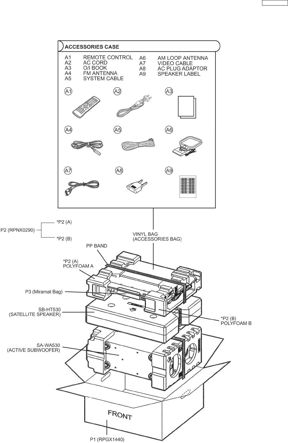
26.5. Packaging
101
SA-HT530GCP
PRT0503D/K/J/E/A/L
