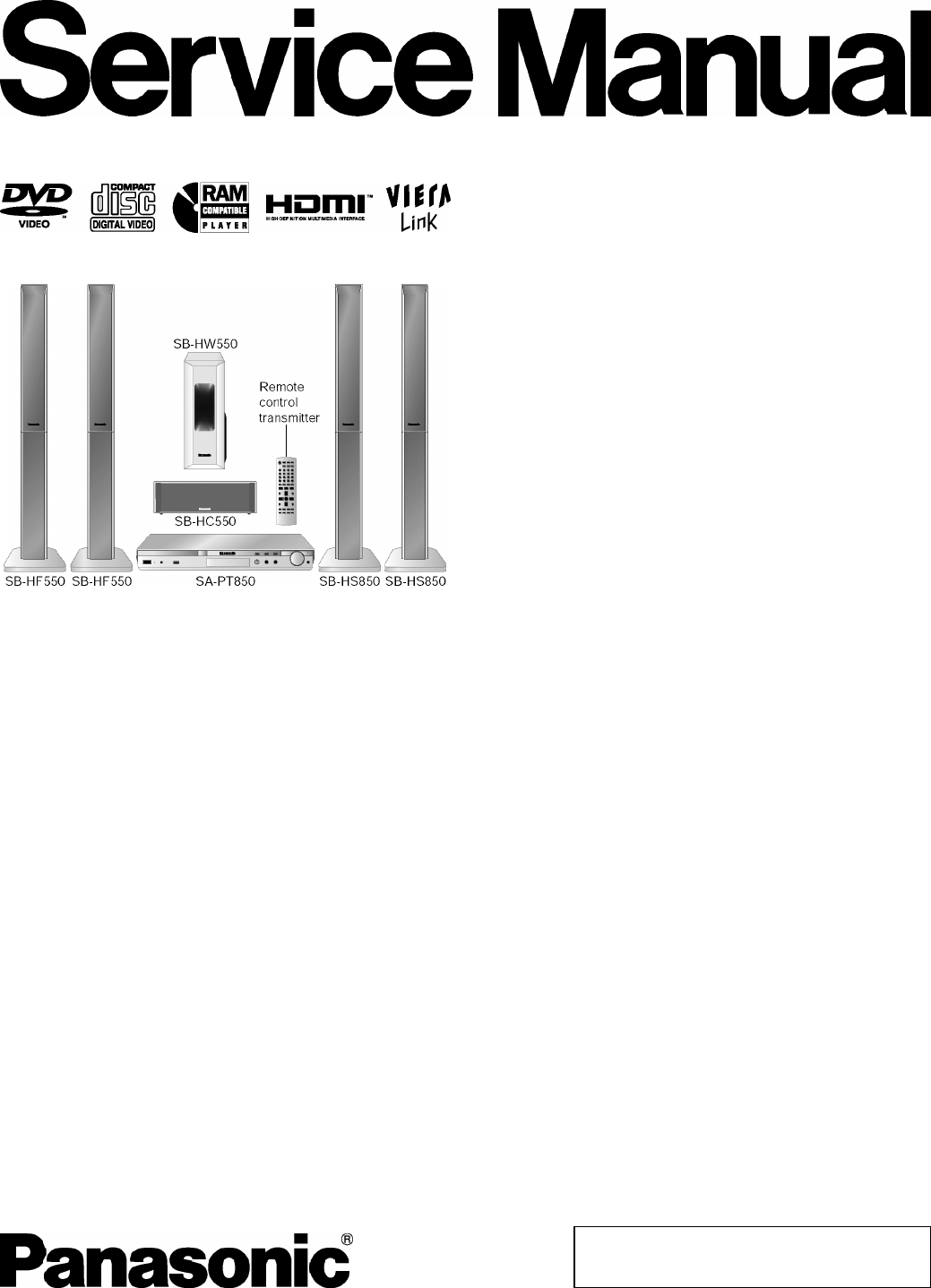
SAPT850EE
User Manual: SAPT850EE
Open the PDF directly: View PDF ![]() .
.
Page Count: 133 [warning: Documents this large are best viewed by clicking the View PDF Link!]
lGENERAL
Power Supply:
A
C 230 V, 50 Hz
Power Consumption: 135 W
Power Consumption in Standby Mode:
approx. 0.8 W
Dimensions (W×H×D): 430×60×363 mm
Mass: Main unit approx. 3.5 kg
Operating Temperature Range: +5°C to +35°C (+41°F to
+95°F)
Operating Humidity Range: 5% to 90% RH (no
condensation)
lAMPLIFIER SECTION
RMS Output Power: Dolby Digital Mode
lTotal RMS Dolby Digital mode power:
1000 W
At 1 kHz and total harmonic of 10%
lFront Ch: 125 W / Channel (3 Ω)
lCenter Ch: 250 W / Channel (6 Ω)
lSurround Ch: 125 W / Channel (3 Ω)
At 100 Hz and total harmonic of 10%
lSubwoofer Ch: 250 W / Channel (6 Ω)
©2007 Matsushita Electric Industrial Co., Ltd. All
rights reserved. Unauthorized copying and
distribution is a violation of law.
SA-PT850EE
Colour
(S).......................Silver Type
(K).......................Black Type
DIN Output Power: Dolby Digital Mode
lTotal DIN Dolby Digital mode power:
590 W
At 1 kHz and total harmonic of 1%
lFront Ch: 75 W / Channel (3 Ω)
lCenter Ch: 145 W / Channel (6 Ω)
lSurround Ch: 75 W / Channel (3 Ω)
At 100 Hz and total harmonic of 1%
lSubwoofer Ch: 145 W / Channel (6 Ω)
lFM TUNER, TERMINALS SECTION
Preset Memory: FM 30 stations
Frequency Modulation (FM)
Frequency range: 87.50-108.00 MHz
(50-kHz step)
Sensitivity: 1.8 µV (IHF)
S/N 26 dB: 1.4 µV
Antenna terminals: 75 Ω(unbalanced)
Digital Audio Input:
Optical digital input: Optical terminal
Sampling frequency: 32 kHz, 44.1 kHz, 48 kHz
Phone Jack:
DVD Home Theater Sound System
Specifications
ORDER NO. MD0705016CE
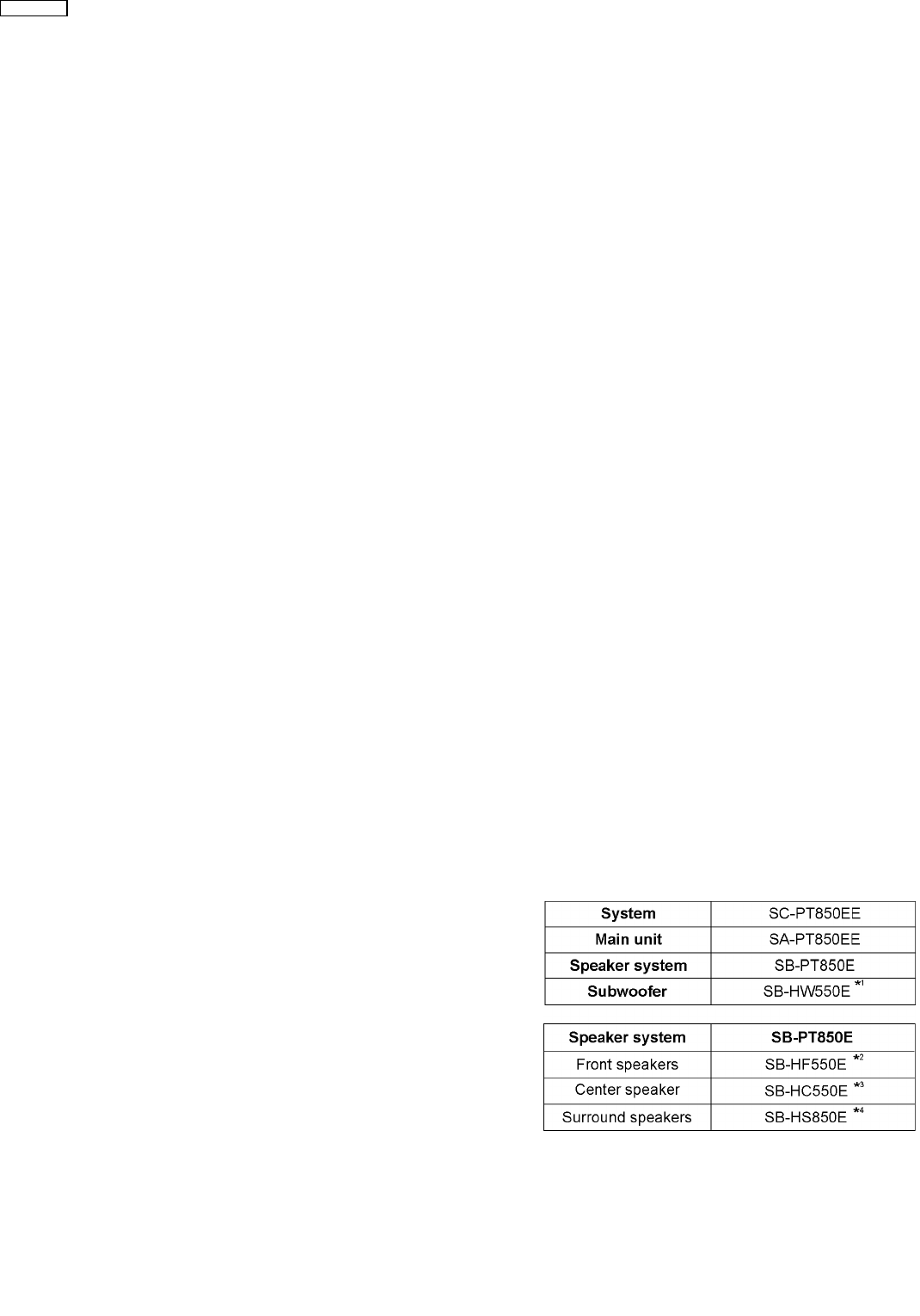
Terminal: Stereo, 3.5 mm jack
Mic Jack:
Sensitivity: 0.7 mV, 1.2 kΩ
Terminal: Mono, 6.3 mm jack (2 system)
Front Music Port:
Sensitivity: 100 mV, 1.4 kΩ
Terminal: Stereo, 3.5 mm jack
USB Port:
USB standard: USB 2.0 full speed
Media file format support: MP3 (*.mp3)
WMA (*.wma)
JPEG (*.Jpg, *.JPEG)
MPEG4 (*.asf)
USB device file system: (FAT12) (FAT16) (FAT32)
USB Port power: Max. 500 mA
lDISC SECTION
Discs played (8 cm or 12 cm):
(1) DVD [DVD-Video, DivX (*6, *7)]
(2) DVD-RAM [DVD-VR, MP3 (*2, *7), JPEG (*4, *7), MPEG4
(*5, *7), DivX (*6, *7)]
(3) DVD-R [DVD-Video, DVD-VR, MP3 (*2, *7), JPEG (*4, *7),
MPEG4 (*5, *7), DivX (*6, *7)]
(4) DVD-R DL [DVD-Video, DVD-VR]
(5) DVD-RW [DVD-Video, DVD-VR, MP3 (*2, *7), JPEG (*4, *7),
MPEG4 (*5, *7), DivX (*6, *7)]
(6) +R/+RW [Video]
(7) +R DL [Video]
(8) CD, CD-R/RW [CD-DA, Video CD, SVCD (*1), MP3 (*2, *7),
WMA (*3, *7), JPEG (*4, *7), MPEG4 (*5, *7), DivX (*6, *7),
HighMAT Level 2 (Audio and Image)]
*1 Conforming to IEC62107
*2 MPEG-1 Layer 3, MPEG-2 Layer 3
*3 Windows Media Audio Ver.9.0 L3
lNot compatible with Multiple Bit Rate (MBR)
*4 Exif Ver 2.1 JPEG Baseline files
lPicture resolution: between 160 x 120 and 6144 x 4096
pixels (Sub sampling is 4:0:0, 4:2:0, 4:2:2, or 4:4:4).
Extremely long and narrow pictures may not be displayed.
*5 MPEG4 data recorded with the Panasonic SD multi cameras
or DVD video recorders.
lConforming to SD VIDEO specifications (ASF standard)/
MPEG4 (Simple Profile) video system/G.726 audio system.
*6 Plays all versions of DivX® video (including DivX®6) with
standard playback of DivX® media files. Certified to the DivX
Home Theater Profile.
*7 The total combined maximum number of recognizable audio,
picture and video contents and groups: 4000 audio, picture
and video contents and 400 groups.
Pick Up:
Wavelength:
lCD: 785 nm
lDVD: 662 nm
Laser power:
lCD: CLASS 1M
lDVD: CLASS 1
Audio Output (Disc):
Number of channels: 5.1 ch (FL, FR, C, SL, SR,
SW)
lVIDEO SECTION
V
ideo System: PAL 625/50, PAL 525/60,
NTSC
Composite Video Output:
lOutput level: 1 Vp-p (75 Ω)
lTerminal: Scart jack (1 system)
S-video Output:
lY output level: 1 Vp-p (75 Ω)
lC output level: PAL; 0.3 Vp-p (75 Ω)
NTSC; 0.286 Vp-p (75 Ω)
lTerminal Scart jack (1 system)
Component Video Output: (NTSC: 480p/480i, PAL: 576p/576i)
lY output level: 1 Vp-p (75 Ω)
lPBoutput level: 0.7 Vp-p (75 Ω)
lPRoutput level: 0.7 Vp-p (75 Ω)
lTerminal: Pin jack (Y: green, PB: blue,
PR: red) (1 system)
RGB Video Output:
lR output level: 0.7 Vp-p (75 Ω)
lG output level: 0.7 Vp-p (75 Ω)
lB output level: 0.7 Vp-p (75 Ω)
lTerminal: Scart jack (1 system)
HDMI AV Output:
lTerminal: Type A connector (19 pin)
This unit supports “HDAVI Control 2” function.
Note:
1. Specifications are subject to change without notice.
Mass and dimensions are approximate.
2. Total harmonic distortion is measured by the digital spectrum
analyzer.
Solder:
This model uses lead free solder (PbF).
Mechanism:
This model uses DL2S (Single tray) mechanism.
Refer to their respective original service manuals for *1, *2,
*3, *4.
2
SA-PT850EE
3
SA-PT850EE
1 Safety Precautions 6
1.1. GENERAL GUIDELINES 6
1.2. Before Repair and Adjustment 6
1.3. Protection Circuitry 6
1.4. Safety Parts Information 7
2 Prevention of Electrostatic Discharge (ESD) to
Electrostatically Sensitive (ES) Devices 8
3 Precaution of Laser Diode 9
4 About Lead Free Solder (PbF) 10
4.1. Service caution based on legal restrictions 10
5 Handling Precautions for Traverse Unit 11
5.1. Cautions to Be Taken in Handling the Optical Pickup Unit
11
5.2. Grounding for electrostatic breakdown prevention 11
6 Accessories 13
7 Operation Procedures 14
7.1. Remote Control Key Buttons Operations 14
7.2. Main Unit Key Buttons Operations 15
7.3. Using the VIERA Link "HDAVI Control™" 16
7.4. Music Port Connection and Operation 17
7.5. USB Connection and Operation 18
7.6. Audio & Video Connections 19
7.7. Disc Information 20
8 New Features 22
8.1. About HDMI 22
9 Self-Diagnosis and Special Mode Setting 24
9.1. Service Mode Summary Table 24
9.2. Service Mode Table 24
9.3. DVD Self Diagnostic Function-Error Code 32
9.4. Sales Demonstration Lock Function 35
9.5. Service Precautions 36
10 Assembling and Disassembling 37
10.1. Disassembly Flow Chart 38
10.2. Main Components and P.C.B. Locations 39
10.3. Disassembly of Top Cabinet 40
10.4. Disassembly of the DVD Lid (When taking out disc
manually) 40
10.5. Disassembly of Front Panel 41
10.6. Disassembly of Volume P.C.B. 41
10.7. Disassembly of Mic P.C.B. 42
10.8. Disassembly of Panel P.C.B. 42
10.9. Disassembly of USB P.C.B. 43
10.10. Disassembly of Scart P.C.B. 43
10.11. Disassembly of Rear Panel 43
10.12. Disassembly of DVD Mechanism Unit 44
10.13. Disassembly of Relay P.C.B. 44
10.14. Disassembly of DVD Module P.C.B. 44
10.15. Disassembly of Main P.C.B. 45
10.16. Replacement of Regulator IC (IC2903) 45
10.17. Disassembly of D-Amp P.C.B. 46
10.18. Replacement of Digital Amp IC (IC5000) 47
10.19. Disassembly of SMPS & AC-Inlet P.C.B. 47
10.20. Replacement of Switch Regulator IC/Diode
(IC5701/D5702) 48
10.21. Replacement of Regulator Diode (D5801/D5 802) 48
10.22. Replacement of Regulator Diode (D5803) 49
11 Assembly and Disassembly of DVD Mechanism Unit 50
11.1. Disassembly Procedure 50
12 Service Position 55
12.1. Checking & Repairing Scart P.C.B. 55
12.2. Checking & Repairing Panel P.C.B. 55
12.3. Checking & Repairing Mic P.C.B. 55
12.4. Checking & Repairing Main P.C.B. 55
12.5. Checking & Repairing D-Amp P.C.B. 56
12.6. Checking & Repairing DVD Module P.C.B. 56
12.7. Checking & Repairing SMPS P.C.B. 57
13 Measurements and Adjustments 58
13.1. Service Tools and Equipment 58
13.2. Important points in adjustment 58
13.3. Storing and handling of test discs 58
13.4. Optical adjustment 59
14 Abbreviations 60
15 Voltage and Waveform Chart 62
15.1. DVD Module P.C.B. 62
15.2. Main P.C.B. 64
15.3. D-Amp P.C.B. 65
15.4. SMPS P.C.B. 65
15.5. Panel & Tray Loading P.C.B. 66
15.6. Scart P.C.B. 66
15.7. Mic P.C.B. 66
15.8. Waveform Chart 67
16 Illustration of IC's, Transistors and Diodes 69
17 Wiring Connection Diagram 71
18 Block Diagram 73
18.1. System Control 73
18.2. DVD (Servo) 74
18.3. DVD (Audio) 75
18.4. DVD (Video) 76
18.5. DVD (HDMI) 77
18.6. Audio 78
CONTENTS
Page Page
4
SA-PT850EE

18.7. Audio Digital Amp 79
18.8. Power 80
19 Schematic Diagram Notes 81
20 Schematic Diagram 83
20.1. DVD Module (DV5/HDMI) Circuit 83
20.2. Main, Panel & Mic Circuit 88
20.3. D-Amp & SMPS Circuit 94
20.4. Scart Circuit 98
20.5. Volume, USB, AC-Inlet, Relay, Tray Loading & Optical
Pickup Unit Circuit 99
21 Printed Circuit Board 101
21.1. DVD Module P.C.B. 101
21.2. Main P.C.B. 102
21.3. Panel, Volume & Mic P.C.B. 103
21.4. D-Amp & USB P.C.B. 104
21.5. SMPS P.C.B. 105
21.6. AC-Inlet, Scart, Relay & Tray Loading P.C.B. 106
22 Basic Troubleshooting Guide 107
22.1. Basic Troubleshooting Guide for Traverse Unit (DVD
Module P.C.B) 107
22.2. Basic Troubleshooting Guide for HDMI AV output 108
23 Overall Block Diagram for PT850 110
23.1. SC-PT850 Simplified Block 110
23.2. SC-PT850 Power Block 111
23.3. SC-PT850 SMPS Block 112
24 Terminal Function of ICs 113
24.1. IC2001 (C2CBYY000418): System Control IC 113
25 Exploded Views 114
25.1. Cabinet Parts Location 115
25.2. Packaging 117
26 Replacement Parts List 118
26.1. Component Parts List 119
5
SA-PT850EE
1 Safety Precautions
1.1. GENERAL GUIDELINES
1. When servicing, observe the original lead dress. If a short circuit is found, replace all parts which have been overheated or
damaged by the short circuit.
2. After servicing, see to it that all the protective devices such as insulation barriers, insulation papers shields are properly
installed.
3. After servicing, carry out the following leakage current checks to prevent the customer from being exposed to shock hazards.
1.1.1. LEAKAGE CURRENT COLD CHECK
1. Unplug the AC cord and connect a jumper between the two prongs on the plug.
2. Measure the resistance value, with an ohmmeter, between the jumpered AC plug and each exposed metallic cabinet part on
the equipment such as screwheads, connectors, control shafts, etc. When the exposed metallic part has a return path to the
chassis, the reading should be between 1MΩand 5.2MΩ.
When the exposed metal does not have a return path to the chassis, the reading must be
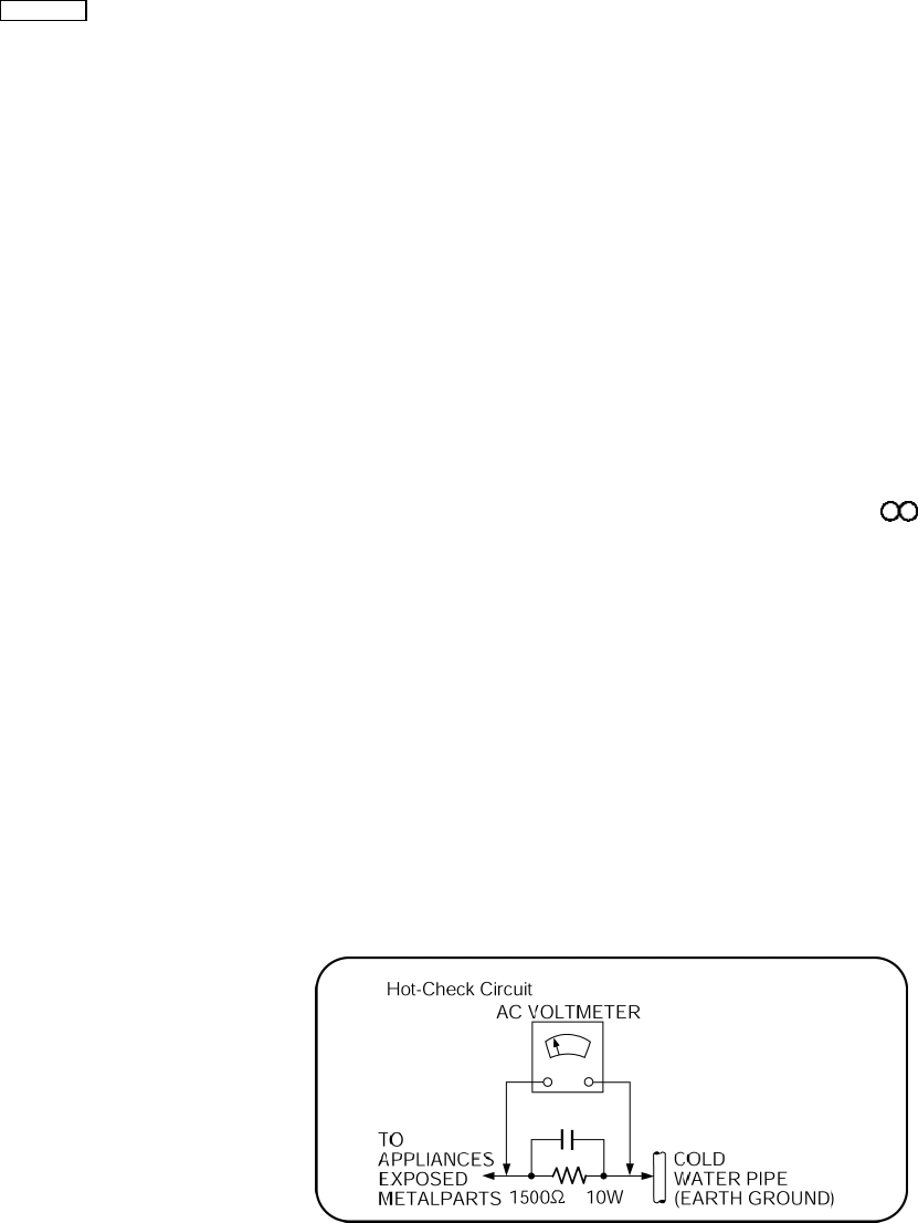
1.1.2. LEAKAGE CURRENT HOT CHECK
1. Plug the AC cord directly into the AC outlet. Do not use an isolation transformer for this check.
2. Connect a 1.5kΩ, 10 watts resistor, in parallel with a 0.15µF capacitors, between each exposed metallic part on the set and a
good earth ground such as a water pipe, as shown in Figure 1.
3. Use an AC voltmeter, with 1000 ohms/volt or more sensitivity, to measure the potential across the resistor.
4. Check each exposed metallic part, and measure the voltage at each point.
5. Reverse the AC plug in the AC outlet and repeat each of the above measurements.
6. The potential at any point should not exceed 0.75 volts RMS. A leakage current tester (Simpson Model 229 or equivalent) may
be used to make the hot checks, leakage current must not exceed 1/2 milliamp. In case a measurement is outside of the limits
specified, there is a possibility of a shock hazard, and the equipment should be repaired and rechecked before it is returned to
the customer.
Figure 1
1.2. Before Repair and Adjustment
Disconnect AC power to discharge unit AC Capacitors as such C5700, C5701, C5703, C5706, C5707 through a 10 Ω,10W
resistor to ground.
Caution:
DO NOT SHORT-CIRCUIT DIRECTLY (with a screwdriver blade, for instance), as this may destroy solid state devices.
After repairs are completed, restore power gradually using a variac, to avoid overcurrent.
Current consumption at AC 230 V, 50 Hz in NO SIGNAL mode volume minimal should be ~ 600 mA.
1.3. Protection Circuitry
The protection circuitry may have operated if either of the following conditions are noticed:
·
No sound is heard when the power is turned on.
·
Sound stops during a performance.
The function of this circuitry is to prevent circuitry damage if, for example, the positive and negative speaker connection wires are
6
SA-PT850EE

“shorted”, or if speaker systems with an impedance less than the indicated rated impedance of the amplifier are used.
If this occurs, follow the procedure outlines below:
1. Turn off the power.
2. Determine the cause of the problem and correct it.
3. Turn on the power once again after one minute.
Note:
When the protection circuitry functions, the unit will not operate unless the power is first turned off and then on again.
1.4. Safety Parts Information
Safety Parts List:
There are special components used in this equipment which are important for safety.
These parts are marked by in the Schematic Diagrams & Replacement Parts List. It is essential that these critical parts
should be replaced with manufacturer’s specified parts to prevent shock, fire or other hazards. Do not modify the original design
without permission of manufacturer.
Table 1
Reference No. Part No. Part Name & Description Remarks
340 RAE2024Z-S TRAVERSE UNIT [M]
PC5701 B3PBA0000402 PHOTO COUPLER [M]
PC5702 B3PBA0000402 PHOTO COUPLER [M]
PC5720 B3PBA0000402 PHOTO COUPLER [M]
PC5799 B3PBA0000402 PHOTO COUPLER [M]
D5701 B0FBAR000041 DIODE [M]
DZ5701 ERZV10V511CS ZENER [M]
TH5701 D4CAC8R00002 THERMISTOR [M]
TH5860 D4CC11040013 THERMISTOR [M]
L2101 J0JBC0000015 CHIP INDUCTOR [M]
L2201 J0JBC0000015 CHIP INDUCTOR [M]
L2802 J0JBC0000015 CHIP INDUCTOR [M]
L2803 J0JBC0000015 CHIP INDUCTOR [M]
L2804 J0JBC0000015 CHIP INDUCTOR [M]
L5001 G0B9R5K00003 LINE CHOKE COIL [M]
L5002 G0B9R5K00003 LINE CHOKE COIL [M]
L5201 G0B9R5K00003 LINE CHOKE COIL [M]
L5301 G0B9R5K00003 LINE CHOKE COIL [M]
L5401 G0B9R5K00003 LINE CHOKE COIL [M]
L5402 G0B9R5K00003 LINE CHOKE COIL [M]
L5701 ELF15N035AN LINE FILTER [M]
L5702 ELF22V035B COIL [M]
L5703 ELF22V020A LINE FILTER COIL [M]
L6101 J0JBC0000019 CHIP INDUCTOR [M]
L6201 J0JBC0000019 CHIP INDUCTOR [M]
L6801 J0JBC0000019 CHIP INDUCTOR [M]
L6904 J0JBC0000019 CHIP INDUCTOR [M]
L6905 J0JBC0000019 CHIP INDUCTOR [M]
L6906 J0JBC0000019 CHIP INDUCTOR [M]
L6907 J0JBC0000019 CHIP INDUCTOR [M]
L6908 J0JBC0000019 CHIP INDUCTOR [M]
L6909 J0JBC0000019 CHIP INDUCTOR [M]
T2900 G4D1A0000117 SWITCHING TRANSFORMER [M]
T5701 ETS42BN1A6AD MAIN TRANSFORMER [M]
T5751 ETS19AB236AG BACK-UP TRANSFORMER [M]
F1 K5D502BNA005 FUSE [M]
FP2900 K5G401A00008 FUSE PROTECTOR [M]
P5701 K2AA2B000015 JACK AC INLET [M]
A2 K2CQ2CA00007 AC CORD [M]
C5700 F1BAF1020020 1000P [M]
C5701 ECQU2A334MLA 0.33 [M]
C5703 ECQU2A104MLC 0.1 [M]
C5706 F1BAF1020020 1000P [M]
C5707 F1BAF1020020 1000P [M]
7
SA-PT850EE

2 Prevention of Electrostatic Discharge (ESD) to
Electrostatically Sensitive (ES) Devices
Some semiconductor (solid state) devices can be damaged easily by static electricity. Such components commonly are called
Electrostatically Sensitive (ES) Devices. Examples of typical ES devices are integrated circuits and some field-effect transistors and
semiconductor "chip" components. The following techniques should be used to help reduce the incidence of component damage
caused by electrostatic discharge (ESD).
1. Immediately before handling any semiconductor component or semiconductor-equipped assembly, drain off any ESD on your
body by touching a known earth ground. Alternatively, obtain and wear a commercially available discharging ESD wrist strap,
which should be removed for potential shock reasons prior to applying power to the unit under test.
2. After removing an electrical assembly equipped with ES devices, place the assembly on a conductive surface such as
aluminum foil, to prevent electrostatic charge buildup or exposure of the assembly.
3. Use only a grounded-tip soldering iron to solder or unsolder ES devices.
4. Use only an anti-static solder removal device. Some solder removal devices not classified as "anti-static (ESD protected)" can
generate electrical charge sufficient to damage ES devices.
5. Do not use freon-propelled chemicals. These can generate electrical charges sufficient to damage ES devices.
6. Do not remove a replacement ES device from its protective package until immediately before you are ready to install it. (Most
replacement ES devices are packaged with leads electrically shorted together by conductive foam, aluminum foil or comparable
conductive material).
7. Immediately before removing the protective material from the leads of a replacement ES device, touch the protective material
to the chassis or circuit assembly into which the device will be installed.
Caution:
Be sure no power is applied to the chassis or circuit, and observe all other safety precautions.
8. Minimize bodily motions when handling unpackaged replacement ES devices. (Otherwise harmless motion such as the
brushing together of your clothes fabric or the lifting of your foot from a carpeted floor can generate static electricity (ESD)
sufficient to damage an ES device).
8
SA-PT850EE
3 Precaution of Laser Diode
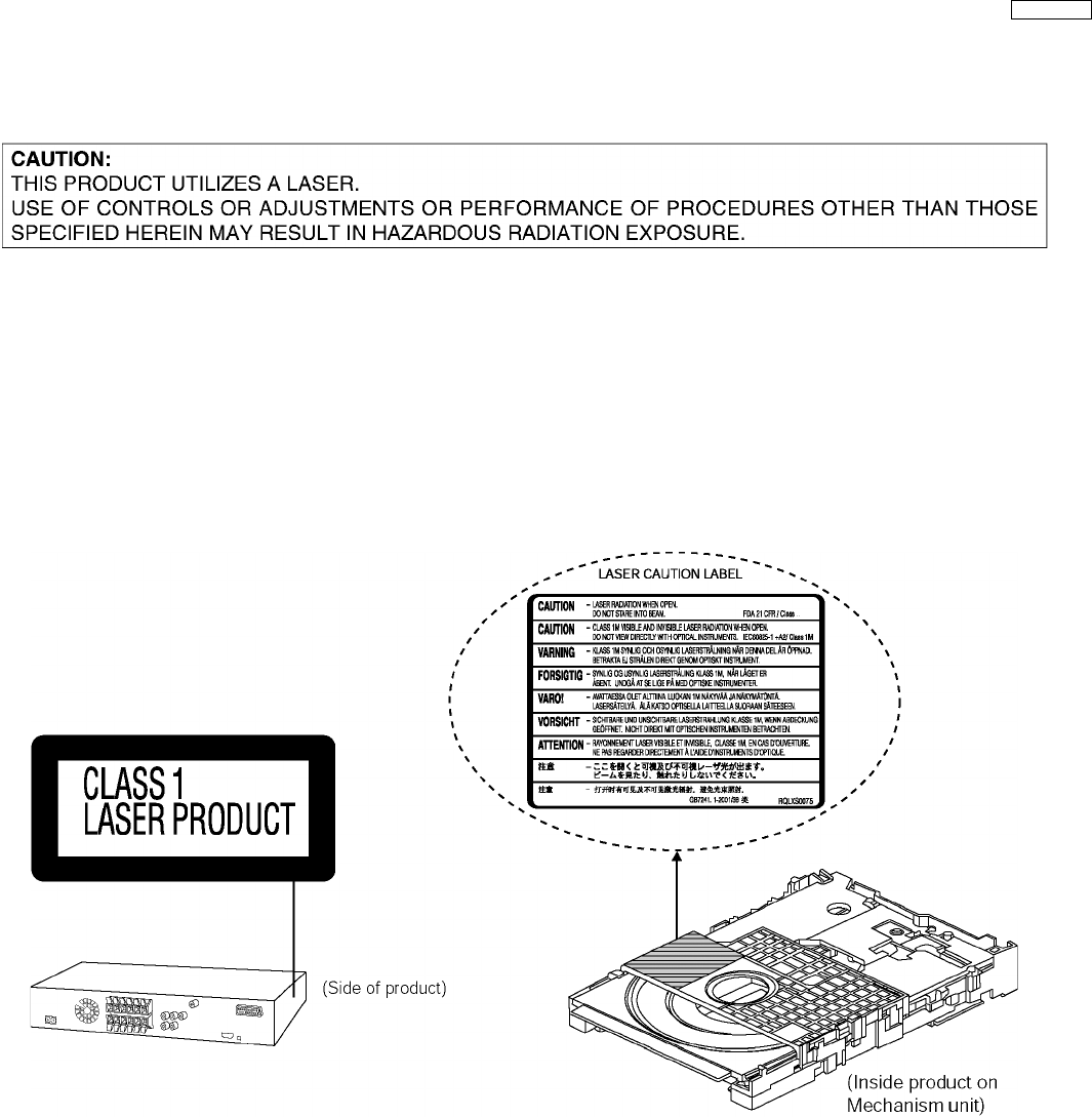
CAUTION :
This product utilizes a laser diode with the unit turned on, invisible laser radiation is emitted from the pickup lens.
Wavelength : 662nm/785nm
Maximum output radiation power from pickup : 100µW/VDE
Laser radiation from pickup unit is safety level, but be sure the followings:
1. Do not disassemble the pickup unit, since radiation from exposed laser diode is dangerous.
2. Do not adjust the variable resistor on the pickup unit. It was already adjusted.
3. Do not look at the focus lens using optical instruments.
4. Recommend not to look at pickup lens for a long time.
9
SA-PT850EE

4 About Lead Free Solder (PbF)
4.1. Service caution based on legal restrictions
4.1.1. General description about Lead Free Solder (PbF)
The lead free solder has been used in the mounting process of all electrical components on the printed circuit boards used for this
equipment in considering the globally environmental conservation.
The normal solder is the alloy of tin (Sn) and lead (Pb). On the other hand, the lead free solder is the alloy mainly consists of tin
(Sn), silver (Ag) and Copper (Cu), and the melting point of the lead free solder is higher approx.30 degrees C (86°F) more than that
of the normal solder.
Definition of PCB Lead Free Solder being used
The letter of “PbF” is printed either foil side or components side on the PCB using the lead free solder.
(See right figure)
Service caution for repair work using Lead Free Solder (PbF)
·
The lead free solder has to be used when repairing the equipment for which the lead free solder is used.
(Definition: The letter of “PbF” is printed on the PCB using the lead free solder.)
·
To put lead free solder, it should be well molten and mixed with the original lead free solder.
·
Remove the remaining lead free solder on the PCB cleanly for soldering of the new IC.
·
Since the melting point of the lead free solder is higher than that of the normal lead solder, it takes the longer time to melt
the lead free solder.
·
Use the soldering iron (more than 70W) equipped with the temperature control after setting the temperature at 350±30
degrees C (662±86°F).
Recommended Lead Free Solder (Service Parts Route.)
·
The following 3 types of lead free solder are available through the service parts route.
RFKZ03D01K-----------(0.3mm 100g Reel)
RFKZ06D01K-----------(0.6mm 100g Reel)
RFKZ10D01K-----------(1.0mm 100g Reel)
Note
* Ingredient: tin (Sn), 96.5%, silver (Ag) 3.0%, Copper (Cu) 0.5%, Cobalt (Co) / Germanium (Ge) 0.1 to 0.3%
10
SA-PT850EE
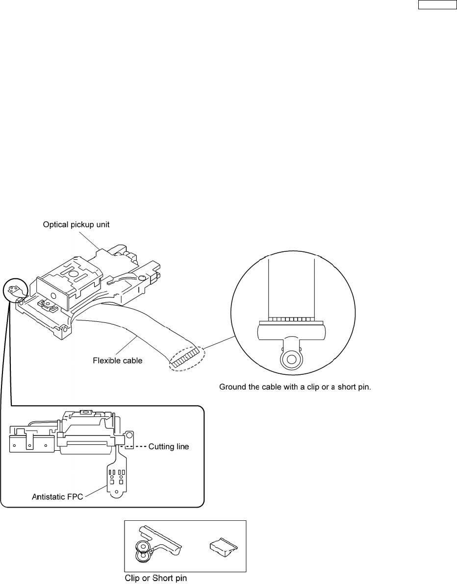
5 Handling Precautions for Traverse Unit
The laser diode in the optical pickup unit may break down due to static electricity of clothes or human body. Special care must be
taken avoid caution to electrostatic breakdown when servicing and handling the laser diode in the traverse unit.
5.1. Cautions to Be Taken in Handling the Optical Pickup Unit
The laser diode in the optical pickup unit may be damaged due to electrostatic discharge generating from clothes or human body.
Special care must be taken avoid caution to electrostatic discharge damage when servicing the laser diode.
1. Do not give a considerable shock to the optical pickup unit as it has an extremely high-precise structure.
2. To prevent the laser diode from the electrostatic discharge damage, the flexible cable of the optical pickup unit removed should
be short-circuited with a short pin or a clip.
3. The flexible cable may be cut off if an excessive force is applied to it. Use caution when handling the flexible cable.
4. The antistatic FPC is connected to the new optical pickup unit. After replacing the optical pickup unit and connecting the flexible
cable, cut off the antistatic FPC.
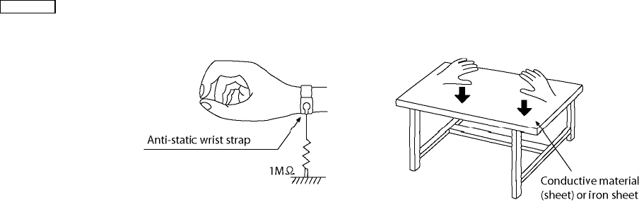
5.2. Grounding for electrostatic breakdown prevention
Some devices such as the DVD player use the optical pickup (laser diode) and the optical pickup will be damaged by static
electricity in the working environment. Proceed servicing works under the working environment where grounding works is
completed.
5.2.1. Worktable grounding
1. Put a conductive material (sheet) or iron sheet on the area where the optical pickup is placed, and ground the sheet.
5.2.2. Human body grounding
1. Use the anti-static wrist strap to discharge the static electricity form your body.
11
SA-PT850EE
12
SA-PT850EE
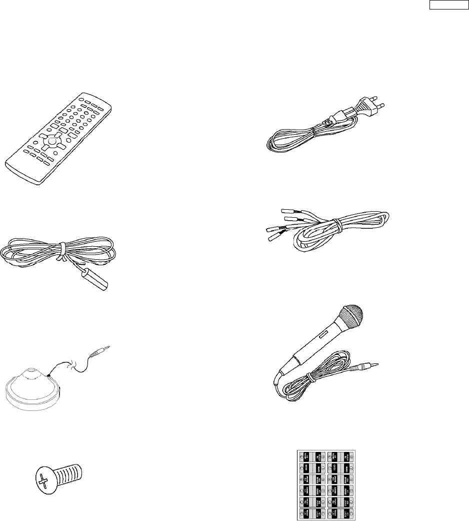
Remote control
Antenna wire
Calibration mic
Screw
AC cord
Speaker cord
Mic
Speaker label
6 Accessories
·
Note: Refer to “Replacement Parts List” (Section 26) for the part number.
13
SA-PT850EE
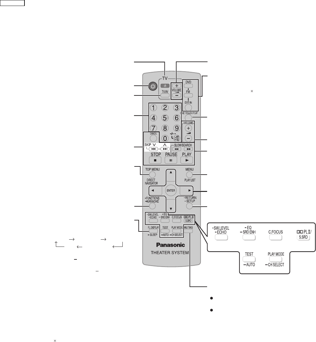
7 Operation Procedures
7.1. Remote Control Key Buttons Operations
Adjust the television volume
Select the source
DVD: DVD/CD
FM
EXT-IN: USB , AV , AUX,
D-IN, MUSIC P.
Start up and play a disc automatically,
Control both the home theater system and the
television
Adjust the volume of the main unit
Basic operations for play
Show a disc menu or play list
Select or confirm menu items on the
television screen , Frame-by-frame
Return to previous screen
Show the Setup menu
Television operations
Switch the main unit on or off
Change the television’s video input mode
Select disc’s title numbers and etc.,
Enter numbers
Select preset radio stations
Show a disc top menu
or program list
Show the display on the main unit,
This function enables you to turn off the unit
automatically after the set time
SLEEP 30 SLEEP 60 SLEEP 90
OFF SLEEP 120
To confi rm the remaining time
To mute the sound
To cancel
Press [MUTING] again or adjust the
volume.
Muting is cancelled when you switch the
unit to standby.
To cancel the timer
Press and hold [ SLEEP] to select "OFF".
Press and hold [ SLEEP] again.
"AV" works only when the scart cable is connected.
Show on-screen menu
Karaoke
14
SA-PT850EE
7.2. Main Unit Key Buttons Operations
AC supply indicator [AC IN]
This indicator lights when the unit
is connected to the AC mains
supply.
Open or close the
disc tray
Display
Stop playback, Select the tuning mode,
Adjust the FM reception condition
/ TUNE
Skipping or slow-search play,
Select the radio stations
MUSIC PORT jack
C
Auto speaker setup
onnect an external device
VOLUME , +
Turn the volume
up or down
SELECTOR
DVD/CD USB FM AV
MUSIC P. D-IN (Digital In) AUX
USB jack
Connect a USB device
Press to switch the unit from on to
standby mode or vice versa. In standby
mode, the unit is still consuming a small
amount of power.
Disc playback
Memorise the receiving
radio stations
Headphones
(not included)
Headphone plug type:
Standby/on switch [ /I]
OPEN/CLOSE
/ TUNE MODE / FM MODE
/MEMORY
3.5 mm stereo mini plug
Reduce the volume before
connecting.
Audio is automatically
switched to 2-channel stereo.
To prevent hearing damage,
avoid listening for prolonged
periods of time.
"AV" works only when the scart cable is connected.
MIC jack
Connect a microphone
MIC VOL
Adjust the microphone volume
Remote control signal sensor
15
SA-PT850EE

7.3. Using the VIERA Link “HDAVI Control™”
What is VIERA Link "HDAVI Control"?
VIERA Link "HDAVI Control" is a convenient function that
offers linked operation of this unit, and a Panasonic television
(VIERA) under "HDAVI Control". You can use this function
by connecting the equipment with the HDMI cable. See the
operating instructions for connected equipment for operational
details.
This unit supports "HDAVI Control 2" function.
The TV with "HDAVI Control 2" function enables the following
operation:
VIERA Link Control only with TV’s remote control (for "HDAVI
Control 2") ( see right)
Preparation
Confirm that the HDMI connection (Refer to the O/I book)
has been made.
Confirm that the scart cable is not connected.
Set "VIERA Link" to "On"
( pOI age 28, "HDMI" tab).
To complete and activate the connection correctly, turn on
all VIERA Link HDAVI Control compatible equipment and set
the television to the corresponding HDMI input mode for the
home theater system.
Whenever the connection or settings are changed, reconfi rm
the points above.
One Touch Play
You can turn on the home theater system and television, and
start playing the disc in the play position with a single press of
a button.
Note
Playback may not be immediately displayed on the television. If
you miss the beginning portion of playback, press [ ] or [ ]
to go back to where playback started.
Auto input switching
HDMI input mode for the home theater system, the home
theater system will automatically switch to "DVD/CD" if it is
in "AUX " or "D-IN " mode.
When you start disc play, the television will automatically switch
to the HDMI input mode for the home theater system.
Speaker control
You can select whether audio is output from the home theater
system or the television speakers by using the television menu
settings. For details, refer to the operating instructions of your
television.
Home Cinema
Theater speakers are active.
To cancel muting, you can also use the home theater remote
control ( Refer to the O/I book).
If you turn off the home theater system, television speakers
will be automatically activated.
TV
Television speakers are active.
To toggle which input source the main unit will automatically
switch to, press [ SETUP] while the main unit is in "AUX " or
"D-IN" mode.
The default setting is "AUX".
Power off link
When the television is turned off, the home theater system
goes into standby mode automatically.
When the television is turned on, the home theater system
does not turn on automatically. (Power on link is not
available.)
For "AUX" or "D-IN" mode, power off link can be set to work
with one or the other. To toggle the mode that this function
works with, press [ SETUP] while the main unit is in "AUX"
or "D-IN" mode.
The default setting is "AUX".
Note
Only the home theater system turns off when you press [ ] for
shutting it down. Other connected equipment compatible with
VIERA Link HDAVI Control stay on.
VIERA Link Control only with TV’s remote control
(for "HDAVI Control 2")
You can control the disc menus of the home theater system
with the TV s remote control when using the "DVD/CD" or
"USB" source. When operating the TV s remote control, refer to
the below illustration for operation buttons.
1. Select the theater operation menu by using
the television menu settings.
(For details, refer to the operating
instructions of your television.)
ENTER/
PLAY
RETURN
2. Select the desired item.
: Shows a disc
top menu or
progam list.
: Shows a disc menu
or play list.
: The basic operations
for discs are
available.
Note
Depending on the menu, some button operations cannot be
performed from the TV’s remote control.
"Control Panel" can be selected directly by using a button on the
TV s remote control (e.g. [OPTION]).
The television speakers are automatically muted.
You can control the volume setting using the volume or
mute button on the TV’s remote control. (The volume level is
displayed on the main unit’s FL display.)
Theater speakers will be automatically activated ( see below).
This function also works if you press [ , PLAY] on the home
theater remote control during home theater standby mode.
When you switch the television input to:
TV tuner mode, the home theater system will automatically
switch to "AUX " or "D-IN ".
When the home theater system is in standby mode,
changing the television speakers to theater speakers in the
television menu will automatically turn the home theater
system on and select "AUX " or "D-IN " as the source.
To toggle the mode that this function works with, press
[ SETUP] while the main unit is in "AUX " or "D-IN" mode.
The default setting is "AUX ".
Audio output is 2-channel audio.
When switching between the theater and television speakers,
the TV screen may be blank for several seconds.
This function works only when "DVD/CD", "USB", "AUX "
or "D-IN " is selected as the source on the home theater
system.
The volume of the home theater system is set to "0".
This function works only when "DVD/CD", "USB", "AUX "
or "D-IN " is selected as the source on the home theater
system.
"TOP MENU"
"MENU"
"Control Panel"
To toggle the mode that this function works with, press
[ SETUP] while the main unit is in "AUX" or "D-IN" mode.
The default setting is "AUX".
The home theater system will
automatically switch to "DVD/CD" if it
is in "AUX " or "D-IN ".
16
SA-PT850EE
7.4. Music Port Connection and Operation
The Music Port allows you to connect and enjoy music from
an external device (example: MP3 player) through your
home theater system.
Preparation
To avoid distorted sound, make sure that any equalizer
function of your external device is turned off.
1
Reduce the volume and connect the external device
(not included).
Plug type 3.5 mm stereo mini plug
External device
(not included)
Reduce the volume
before connecting.
2
To select "MUSIC P.".
USB AUX D-IN (Digital In)
MUSIC P.
3
Adjust the external device volume to a normal listening
level, and then adjust the volume of the main unit.
You can enjoy surround sound when you turn on
Super Surround (MOVIE, MUSIC) ( Refer to the O/I book).
17
SA-PT850EE
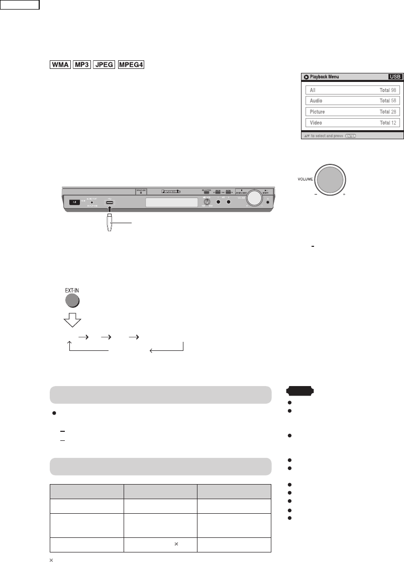
7.5. USB Connection and Operation
The USB connectivity enables you to connect and play
tracks or files from USB mass storage class devices.
Typically, USB memory devices. (Bulk only transfer)
Preparation
Before connecting any USB mass storage device to the
unit, ensure that the data stored therein has been backed
up.
It is not recommended to use a USB extension cable. The
USB device is not recognised by this unit.
1
Connect the USB mass storage device (not included).
USB enabled device
(not included)
It is not recommended to use a
USB extension cable. The device
connected via the cable will not be
recognised by this unit.
2
To select "USB" as the source, press several times.
USB AV
AUX
D-IN (Digital In)
MUSIC P.
3
Adjust the volume of the main unit.
4
Begin playback by selecting the track from the USB
mass storage device.
To return to the previous screen
Press [ RETURN]
For other operating functions, they are similar as those
described in "DISC OPERATIONS" ( Refer to the O/I book).
Compatible Devices
Devices w hich are defined as USB m ass storage
class :
USB devices that support bulk only transfer.
USB devices that support USB 2.0 full speed.
Supported Formats
Fil e name tFil e ex ension
Still pictures JPG .jpg .jpeg
Music MP3
WMA
.mp3
.wma
Video MPEG4 .asf
For Panasonic D-Snap/DIGA
Note
CBI (Control/Bulk/Interrupt) is not supported.
Digital Cameras that use PTP protocol or which require
additional program installation when connected to a PC are not
supported.
[Only FAT 12/16/32 (File Allocation Table 12/16/32) file system is
supported].
Depending on the sector size, some files may not work.
It will not operate with Janus enabled MTP (Media Transfer
Protocol) devices.
A device using NTFS file system is not supported.
Maximum folder: 400 fo
file
file
files
lders
Maximum : 4000
Maximum name: 44 characters
Maximum folder name: 44 characters
Only one memory card will be selected when connecting a multi-
port USB card reader. Typically the first memory card inserted.
18
SA-PT850EE
7.6. Audio & Video Connections
7.6.1. Television with an HDMI Terminal
Television with an HDMI terminal
AV IN AV OUT
HDMI cable (not included)
HDMI-compatible
television
(not included)
Use the HDMI connection to enjoy higher quality audio and video
with a single cable.
Set "Video Output Mode" ( "Picture Menu" of the O/I book).
VIERA Link (HDAVI Control)
If your Panasonic television is a VIERA Link compatible television,
you can operate your television synchronising with home theater
operations or vice versa.
Note
Make the extra audio connection (Refer to the O/I book) when you use HDAVI
Control function.
It is recommended that you use Panasonic’s HDMI cable.
[Recommended part number: RP-CDHG15 (1.5 m), RP-CDHG30 (3.0 m),
RP-CDHG50 (5.0 m), etc.]
Non-HDMI-compliant cables cannot be utilised.
Set "Video Mode" to "On" and "Audio Output" to "On"
(Refer to
Refer to
"HDMI" tab of the O/I book)..
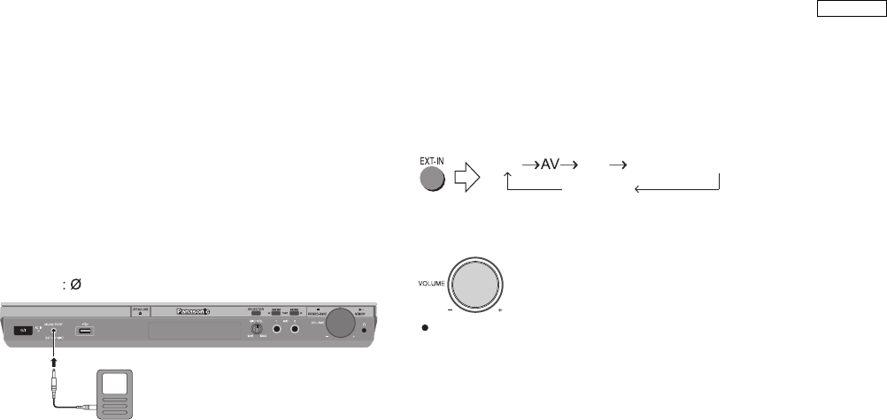
7.6.2. Optional Connection for Set Top Box, Cable TV, or Video Cassette Recorder
Set top box
(not included)
Television
(not included)
Rear panel of
this main unit
SCART cable (not included)
SCART cable
(not included)
To listen to the
sound from the
television, select the
appropriate audio out
(example: Monitor) on
the television.
Sound from the television
Press [EXT-IN] (Refer to the O/I book) to select the "AV" audio input on the
remote control.
7.6.3. Optional Audio Connection for Video Cassette Recorder or Television
Video cassette
recorder/ TV
(not included)
(not included)
Rear panel of
this main unit
Audio cable
Press [EXT-IN] (Refer to the O/I book) to select "AUX" as the source
to operate the audio input.
This audio connection will enable you to play audio from
your video cassette recorder or television through your
home theater system.
19
SA-PT850EE
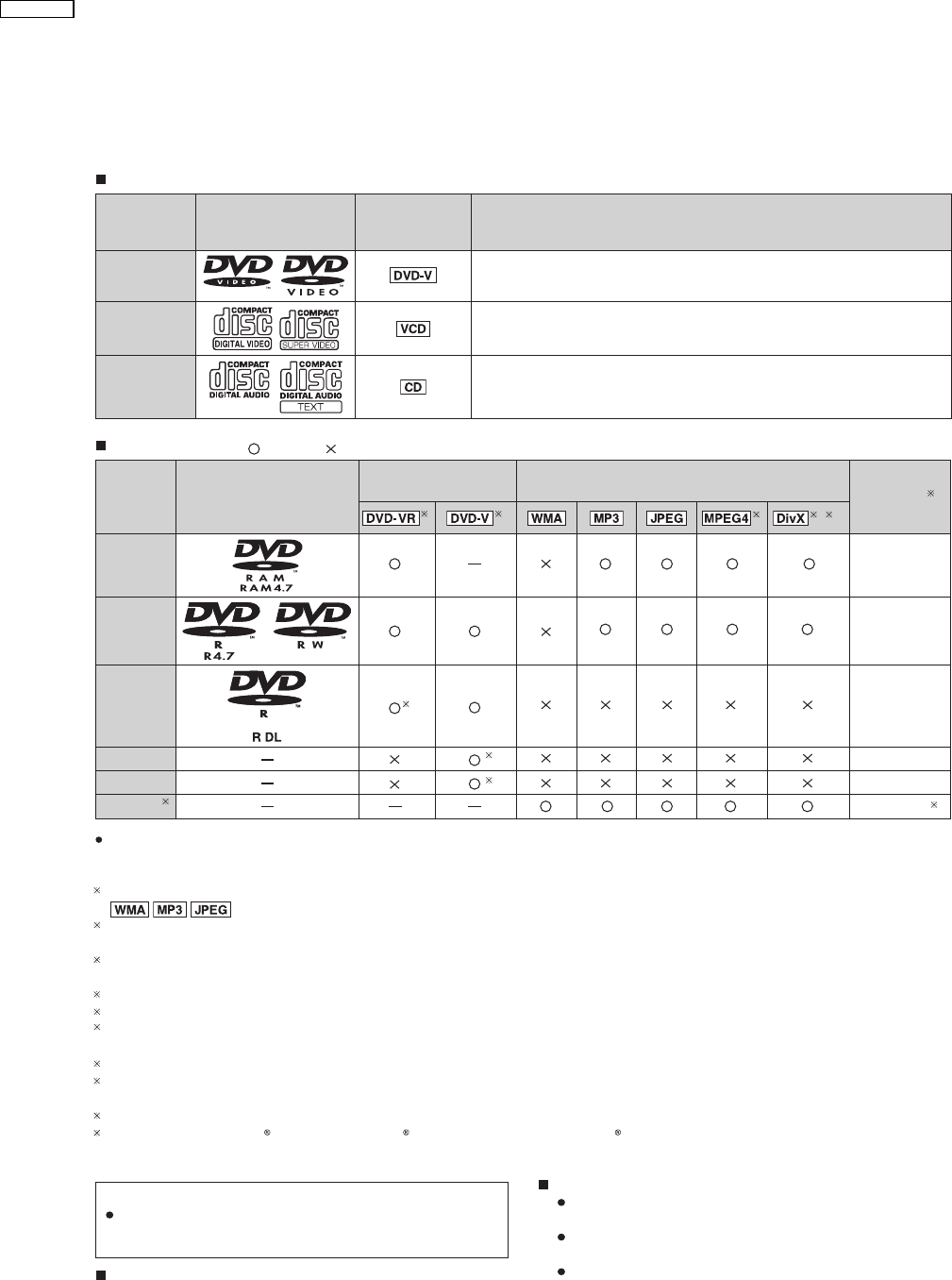
7.7. Disc Information
7.7.1. Disc Playability (Media)
This unit can play CD-R/RW recorded with CD-DA or Video CD format.
This unit also plays HighMAT discs.
MPEG4 data recorded with the Panasonic SD multi cameras or DVD video recorders [conforming to SD VIDEO specifications (ASF
standard)/MPEG4 (Simple Profile) video system/G.726 audio system].
Functions added with DivX ultra are not supported.
Plays all versions of DivX video (including DivX 6) with standard playback of DivX media lfi fies. Certi ed to the DivX Home Theater
Profile.
Disc Logo
Indicated in
these
instructions by
Remarks
DVD-Video High quality movie and music discs.
Video CD
Music discs with video.
Including SVCD (Conforming to IEC62107).
CD Music discs
Disc Logo
Recorded on a DVD
video recorder, etc. Recorded on a personal computer, etc.
Finalizing
DVD-RAM Not
necessary
DVD-R/RW Necessary
DVD-R DL Necessary
+R/+RW Necessary
+R DL Necessary
CD-R/RW Necessary
Recorded discs ( : Playable, : Not playable)
Note about using a DualDisc
The digital audio content side of a DualDisc does not meet the
technical specifi cations of the Compact Disc Digital Audio
(CD-DA) format so playback may not be possible.
Discs that cannot be played
DVD-RW version 1.0, DVD-Audio, DVD-ROM, CD-ROM,
CDV, CD-G, SACD, Photo CD, DVD-RAM that cannot be
removed from their cartridge, 2.6-GB and 5.2-GB DVD-RAM,
and "Chaoji VCD" available on the market including CVD,
DVCD and SVCD that do not conform to IEC62107.
Video systems
This unit can play PAL and NTSC, but your television
must match the system used on the disc.
PAL discs cannot be correctly viewed on an NTSC
television.
This unit can convert NTSC signals to PAL 60 for
viewing on a PAL television (O/I page 26, "NTSC Disc
Output" in "Video" tab).
1
6
9, 10
8
2
3
5
1
Discs recorded on DVD video recorders or DVD video cameras, etc. using Version 1.1 of the Video Recording Format (a uni ed video
recording standard).
fi
2
Discs recorded on DVD video recorders or DVD video cameras using Version 1.2 o f the Video Recording Format (a uni efi d video
recording standard).
3
Discs recorded on DVD video recorders or DVD video cameras using DVD-Video Format.
4
Recorded using a format different from DVD-Video Format, therefore, some functions cannot be used.
5
A process that allows play on compatible equipment. To play a disc that is displa yed as "Necessary" on this unit, the disc must rfi st be
nfi alized on the device it was recorded on.
6
Closing the session will also work.
7
8
9
10
5
4
7
()
()
It may not be possible to play all the above-mentioned discs in some cases due to the type of disc, the condition of the
recording, the recording method, or how the files were created [Item 7.7.2 File Extension Type Support (WMA/MP3/JPEG/
MPEG4/DivX]
Commercial discs
20
SA-PT850EE
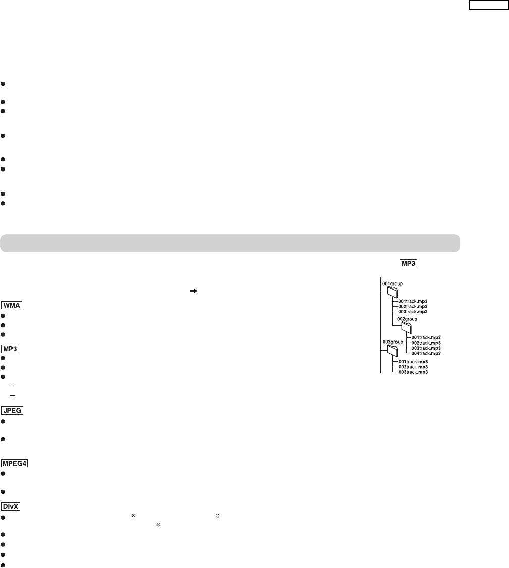
7.7.2. File Extension Type Support (WMA/MP3/JPEG/MPEG4/DivX)
Ti ps
for
maki ng
data
discs
Tips for making data discs
When there are more than eight groups, the eighth group onwards will be displayed on one vertical line in the menu
screen.
There may be differences in the display order on the menu screen and computer screen.
This unit cannot play lfi es recorded using packet write.
DVD-RAM
Discs must conform to UDF 2.0.
DVD-R/RW
Discs must conform to UDF bridge (UDF 1.02/ISO9660).
This unit does not support multi-session. Only the default session is played.
CD-R/RW
Discs must conform to ISO9660 level 1 or 2 (except for extended formats).
This unit supports multi-session but if there are many sessions it takes more time for play to start. Keep the number of
sessions to a minimum to avoid this.
Naming folders and files
Files are treated as contents and folders are treated as groups on this unit.
At the time of recording, prefi fix folder and le names. This should be with numbers that have
an equal number of digits, and should be done in the order you want to play them (this may
not work at times). Files must have the extension ( see below).
(Extension: ".WMA" or ".wma")
Compatible compression rate: between 48 kbps and 320 kbps.
You cannot play WMA fi les that are copy-protected.
This unit does not support Multiple Bit Rate (MBR).
(Extension: ".MP3" or ".mp3")
Compatible compression rate: between 32 kbps and 320 kbps.
This unit does not support ID3 tags.
Example:
root
Compatible sampling rates:
DVD-RAM, DVD-R/RW: 11.02, 12, 22.05, 24, 44.1 and 48 kHz
CD-R/RW: 8, 11.02, 12, 16, 22.05, 24, 32, 44.1 and 48 kHz
(Extension: ".JPG", ".jpg", ".JPEG" or ".jpeg")
(Extension: ".ASF" or ".asf")
(Extension: ".DIVX", ".divx", ".AVI" or ".avi")
JPEG lfi es taken on a digital camera that conform to DCF Standard (Design rule for Camera F ile system) Version 1.0 are
displayed. Files that have been altered, edited or saved with computer picture edi ting software may not be displayed.
You can play MPEG4 data [conforming to SD VIDEO speci cfi ations (ASF standard)/MPEG4 (Simple Pro le) video
system/G.726 audio system] recorded with Panasonic SD multi cameras or DVD video rec orders with this unit.
The recording date may differ from that of the actual date.
This unit cannot display moving pictures, MOTION JPEG and other such formats, and still pictures other than JPEG
(Example: TIFF), or play pictures with attached audio.
You can play all versions of DivX video (including DivX 6) [DivX video system/MP3, Dolby Digital or MPEG audio
system] with standard playback of DivX media lfi es. Functions added with DivX Ultra are not supported.
GMC (Global Motion Compensation) is not supported.
This unit supports all resolutions up to maximum of 720 x 480 (NTSC)/720 x 576 (PAL).
You can select up to eight types of audio and subtitles on this unit.
fi
DivX les greater than 2 GB or have no index may not be played properly on this unit.
fi
21
SA-PT850EE
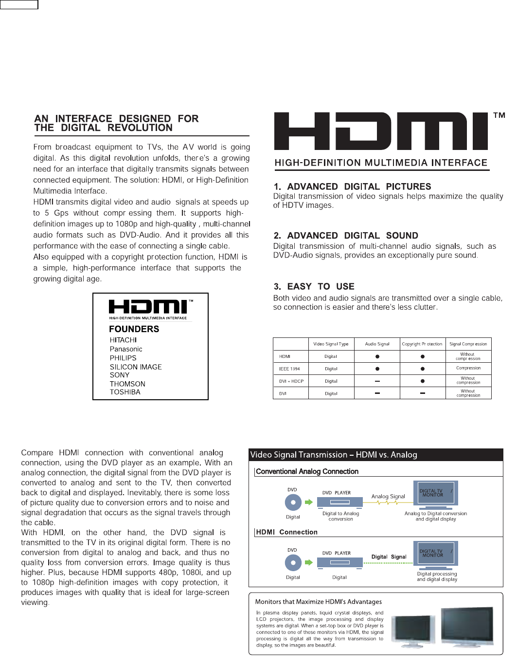
8 New Features
8.1. About HDMI
8.1.1. What is HDMI?
8.1.2. Advanced Digital Pictures
22
SA-PT850EE
8.1.3. Advanced Digital Sound
8.1.4. Easy to Use
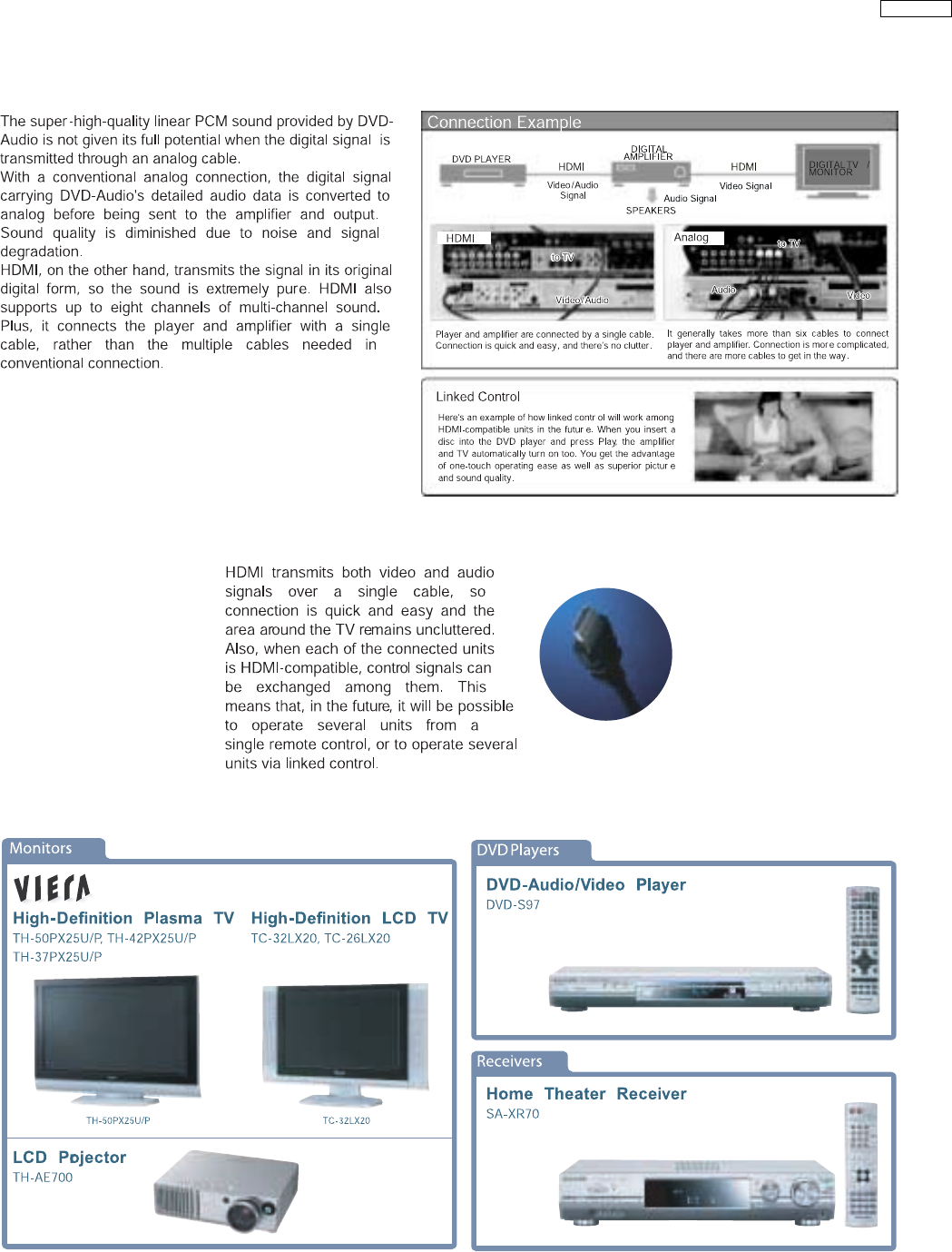
8.1.5. HDMI Compatible Products
23
SA-PT850EE
9 Self-Diagnosis and Special Mode Setting
9.1. Service Mode Summary Table
The service modes can be activated by pressing various button combination on the main unit and remote control unit.
Below is the summary for the various modes for checking:
Player buttons Remote control unit buttons Application Note
[STOP] [0] Error code check. (Refer to the section
“9.2.1. Service Mode
Table 1” for more
information.)
[5] Jitter checking.
[PAUSE] Initial setting of laser drive current.
[FUNCTIONS] DVD laser drive current check. (Refer to the section
“9.2.2. Service Mode
Table 2” for more
information.)
[1] ADSC internal RAM data check.
[3] CD laser drive current check.
[6] Region display and mode. (Refer to the section
“9.2.3. Service Mode
Table 3“ for more
information.)
[7] Micro-processor firmware version check.
Initialization of the player (factory setting is restored).
Used after replacement of Micro-processor (DV5 LSI) IC, FLASH
ROM IC (IC8651), EEPROM IC (IC8611) and DVD Module
P.C.B.
[8] DVD Module P.C.B. firmware version check. (Refer to the section
“9.2.4. Service Mode
Table 4“ for more
information.)
[MENU] Communication error display.
[TOP MENU] ECC error check.
[EQ] CPPM/CRM keys check.
[ENTER] DVD Module P.C.B. reset.
[ ] Timer 1 check. (Refer to the section
“9.2.5. Service Mode
Table 5“ for more
information.)
[ ] Timer 1 reset.
[ ] Timer 2 check.
[ ] Timer 2 reset.
Note:
An error code will be canceled if a power supply is turned OFF.
*1: CPPM is the copy guard function beforehand written in the disk for protection of copyrights.
*2: CEC is the consumer electronic control used for high-level user control of HDMI-connected devices.
*3: HDCP is the specification developed to control digital audio & video contents transmission for DVI or HDMI connections.
9.2. Service Mode Table
By pressing various button combinations on the main unit and remote control unit, you can activate the various service modes for
checking.
Special Note:
·
Due to the limitations of the no. characters that can be shown on the FL Display, the “FL Display” button on the remote
control unit can be used to show the two display pages. (Display 1 / Display 2).
·
Refer to Section 7.1 for the section on “Remote Control Key Buttons Operations”.
24
SA-PT850EE
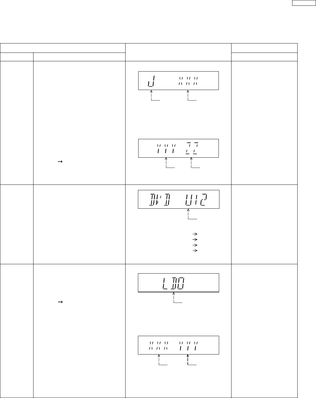
9.2.1. Service Mode Table 1
FL Display Key Operation
Front Key
Item
Jitter check
Description
Mode Name
Initial setting
of laser drive
current
Error code
check
Cancelled automatically
5 seconds later.
To exit, press [POWER]
button on main unit or
remote control.
Press [FL Display] on
remote control unit for next
page (FL Display) on values
of laser drive current.
Cancelled automatically
5 seconds later.
Press [POWER] button to
exit.
In STOP (no disc) mode,
press [STOP] button on the
main unit, and [5] button on
the remote control unit.
Jitter check.
Jitter rate is measured and displayed.
Measurement is repeatedly done in
the cycle of one second. Read error
counter starts from zero upon mode
setting.
When target block data failed to be
read out, the counter advances by one
increment. When the failure is caused
by minor error, it may be corrected
when retried to enable successful
reading.
In this case, the counter advances by
one. When the error persists even
after retry, the counter may jump by
two or more.
FL Display sequence:
Display 1 2.
Jitter rate is shown in decimal notation to
one place of decimal.
Focus drive value is shown in hexadecimal
notation.
(Display 1)
(Display 1)
(Display 2)
(Display 2)
In STOP (no disc) mode,
press [STOP] button on the
main unit, and [0] button on
the remote control unit. * With
pointing of cursor up and
down on display.
Error code check
The latest error code stored in the
EEPROM IC is displayed.
Note: Refer to "Section 9.3 DVD Self
Diagnostic Function-Error Code" for
more detailed information on the error
codes.
In STOP (no disc) mode,
press [STOP] button on the
main unit, and [PAUSE]
button on the remote
control unit.
Initial setting of laser drive current.
Initial current value for the DVD laser
and CD laser is separately saved in
the EEPROM IC.
FL Display sequence:
Display 1 2.
Press [FL Display] on
remote control unit for next
page (FL Display).
Jitter rate
Lead
Error
Counter
Focus Drive
Value
Jitter check
mode
U / H / F
Laser current
measurement
mode
CD
Laser DVD Laser
Error code (play_err) is expressed in the
following convention.
Error code = 0 x DAXX is expressed: DVDnn U12
Error code = 0 x DBXX is expressed: DVDnn H12
Error code = 0 x DXXX is expressed: DVDnn F123
Error code = 0 x 0000 is expressed: DVDnn F---
* "xx" denotes the error code
The value denotes the current in decimal
notation.
The above example shows the initial
current is XXXmA and YYYmA for CD
laser and DVD laser respectively when
the laser is switched on.
25
SA-PT850EE
9.2.2. Service Mode Table 2
FL Display Key Operation
Front Key
Item
DescriptionMode Name
Press [FL Display] on
remote control unit for next
page. (FL Display)
Cancelled automatically
5 seconds later.
CD laser drive
current
measurement
In STOP (no disc) mode,
press [STOP] button on
the main unit, and [3]
button on the remote
control unit.
CD laser drive current measurement.
CD laser drive current is measured
and the result is displayed together
with the initial value stored in the
EEPROM IC.
After the measurement, CD laser
emission is kept on. It is turned off
when POWER key is switched off.
FL Display sequence:
Display 1 2.
CD laser current
measurement mode
CD
laser initial
value
CD laser
value
The value denotes the current in decimal
notation.
The above example shows the initial current
is 0XXmA and the measured value is 0YYmA.
To exit, press [POWER]
button.
ADSC internal
RAM data
check
In STOP (no disc) mode,
press [STOP] button on
the main unit, and [1]
button on the remote
ADSC internal RAM data check.
ADSC internal RAM data is read out
and displayed.
The value is shown in hexadecimal
notation. The above example shows the
data in ADSC address FBOh is XXXXh.
Address RAM data
for specified
address
DVD laser
drive current
measurement
Press [FL Display] on
remote control unit for next
page (FL Display) on values
of dvd drive current.
Cancelled automatically
5 seconds later.
(Display 1)
(Display 2)
(Display 1)
(Display 2)
In STOP (no disc) mode,
press [STOP] button on the
main unit, and
[FUNCTIONS] button on
the remote control unit.
DVD laser drive current measurement.
DVD laser drive current is measured
and the result is displayed together
with the initial value stored in the
EEPROM IC.
After the measurement, DVD laser
emission is kept on. It is turned off
when POWER key is switched off.
FL Display sequence:
Display 1 2.
DVD laser current
measurement mode
DVD
Laser
Initial Value
DVD
Laser
Value
The value denotes the current in decimal
notation.
The above example shows the initial
current is XXXmA and the measured
value is YYYmA.
26
SA-PT850EE
9.2.3. Service Mode Table 3
FL Display Key Operation
Front Key
Item
DescriptionMode Name
Initialization
Cancelled automatically
5 seconds later.
Initialization.
User settings are cancelled and player
is initialized to factory setting.
It is necessary when after replacement
of Micro-processor (DV5 LSI) IC,
FLASH ROM IC (IC8651), EEPROM
IC (IC8611) & DVD Module P.C.B.
Cancelled automatically
5 seconds later.
Region code display, TV broadcasting
system & the model no. information.
Note: Refer to Figure 2 for "Video
Design Information".
Region display In STOP (no disc)
mode, press [STOP]
button on the main unit,
and [6] button on the
remote control unit.
Region No.: 0-8
N: no PAL / P: PAL
N: NTSC / 6: PAL60
Model
No.
Information
In STOP (no disc)
mode, press [STOP]
button on the main unit,
and [ 10] button on the
remote control unit.
If the EEPROM version matches, checksum
[YYYY] is displayed.
If the version of the EEPROM does not match,
[NG] is displayed.
(a) If there is NO EEPROM header string
OR
(b) If there is no EEPROM (no data is received
by Micro-processor), [NO] is displayed.
EEPROM
Checksum
(If applicable,
refer below.)
(Condition1)
Opecon
Version
(Display 1)
(Display 2)
(Display 3)
(Condition 2)
(Condition 3)
Micro-processor
firmware version
display &
EEPROM
checksum
display. Cancelled automatically
5 seconds later.
In STOP (no disc)
mode, press [STOP]
button on the main unit,
and [7] button on the
remote control unit.
Press [FL Display] button on
remote control unit for next
page. (FL Display)
Micro-processor firmware version
display & EEPROM checksum display.
EEPROM checksum is only available
due to existence of EEPROM IC.
Note: Condition 1/2/3 shows the state
of EEPROM IC.
FL Display sequence:
Display 1 2 3.
27
SA-PT850EE
TV Broadcasting Signal System Region Display
Code System (Default) (Default)
English, Spanish, Canadian
French
(S) Japan 2 NTSC NTSC (*A) 2PN Japanese, English
English, French, German,
Spanish, Polish, Russian,
Czech, Hungarian
English, French, German,
Italian, Spanish, Polish,
Swedish, Dutch
English, French, German,
Spanish, Polish, Russian,
Czech, Hungarian
GCS, GD, South East Asia, PAL English, Traditional Chinese
GT, GCT Korea, Taiwan NTSC
New Zealand, English, French, German,
Australia Italian, Spanish, Polish,
Swedish, Dutch
Central/South/ NTSC (*D) 4PN English, Spanish, French,
Latin America Brazilian Portuguese
English, French, German,
Spanish, Polish, Russian,
Czech, Hungarian
GK China 6 PAL NTSC (*B) 6PN English, Simplified Chinese
5P6
PAL (*C)SECAM5
NTSC4
4GN
EE CIS
PL, GCP, LB
3PN
4P6
PAL (*C)PAL
2P6
PAL (*C)PAL2
2P6
PAL (*C)PAL2
1PN
NTSC1
E Europe 2 PAL PAL (*C)
2P6
P, PC, PX USA, Canada, PX NTSC (*A)
Europe
GC, GS
EB, EG
Middle East
3 NTSC (*B)
Product
OSD Menu Language
Model Series Country Region Region
Explanation of Display
Individual Model Code
can play PAL disc
Region code
N: If NTSC disc is played, NTSC output.
6: If NTSC disc is played, PAL60 output.
NTSC (*A) NTSC (*B)
Source Output Source Output
Screen Saver NTSC Screen Saver NTSC
NTSC disc NTSC NTSC disc NTSC (default)
PAL disc PAL (DVD-V) PAL60
NTSC (DVD-A/VCD) PAL disc PAL60
PAL (*C) NTSC (*D)
Source Output Source Output
Screen Saver PAL Screen Saver NTSC
NTSC disc PAL60 (default) NTSC disc NTSC
NTSC PAL disc NTSC
PAL disc PAL
28
SA-PT850EE
9.2.4. Service Mode Table 4
FL Display Key Operation
Front Key
Item
Description
Mode Name
DVD
Module P.C.B.
Reset
To reset DVD Module P.C.B.
This process is used when the DVD
Module P.C.B. or FLASH ROM
IC is replaced with a new one.
Cancelled automatically
5 seconds later.
While in initialization
mode, press & hold
[STOP] button on the main
unit, follow by [ENTER]
button on the remote
control unit.
ECC Error
Check
Cancelled automatically
5 seconds later.
Cancelled automatically
5 seconds later.
Displays frequency of communication
errors between system control IC and
mechanism control IC in the DVD
Module P.C.B.
Communication
error display
CPPM/CRM
Keys Check
In STOP (no disc)
mode, press [STOP]
button on the main unit,
and [MENU] button on the
remote control unit.
In STOP (no disc)
mode, press [STOP]
button on the main unit,
and [TOP MENU] button
on the remote control unit.
In STOP (no disc)
mode, press [STOP]
button on the main unit,
and [EQ] button on the
remote control unit.
No. of
communication
error No. of
communication
ECC Lead
Error
(Display 1)
(Display 2)
Press [POWER] button to
exit.
Press [FL Display] on
remote control unit for next
page (FL Display).
Video
Decode
Error
0: NG
1: OK 0: NG
1: OK
Audio Lead
Error
DVD
Module P.C.B.
firmware
version display
Cancelled automatically
5 seconds later.
In STOP (no disc)
mode, press [STOP]
button on the main unit,
and [8] button on the
remote control unit.
System controller
generation
Destination
System
controller
version
Region No.: 0-8
DVD Module P.C.B. firmware version
is displayed on the FL Display.
The firmware version can be updated
using recovery disc.
ECC refers to Error Correction Code. It
describes the error correction code
that was carried out for the decoding
of audio & video.
FL Display sequence:
Display 1 2.
Note: It is necessary to check for
firmware version before carrying out
the version up using the disc.
CPPM/CRM refers to the Content
Protection for Recordable Media and
Pre-Recorded Media. It displays the
existence of the keys as "1" or "0".
OK: Existing of keys.
NG: Non existing of keys.
29
SA-PT850EE
9.2.5. Service Mode Table 5
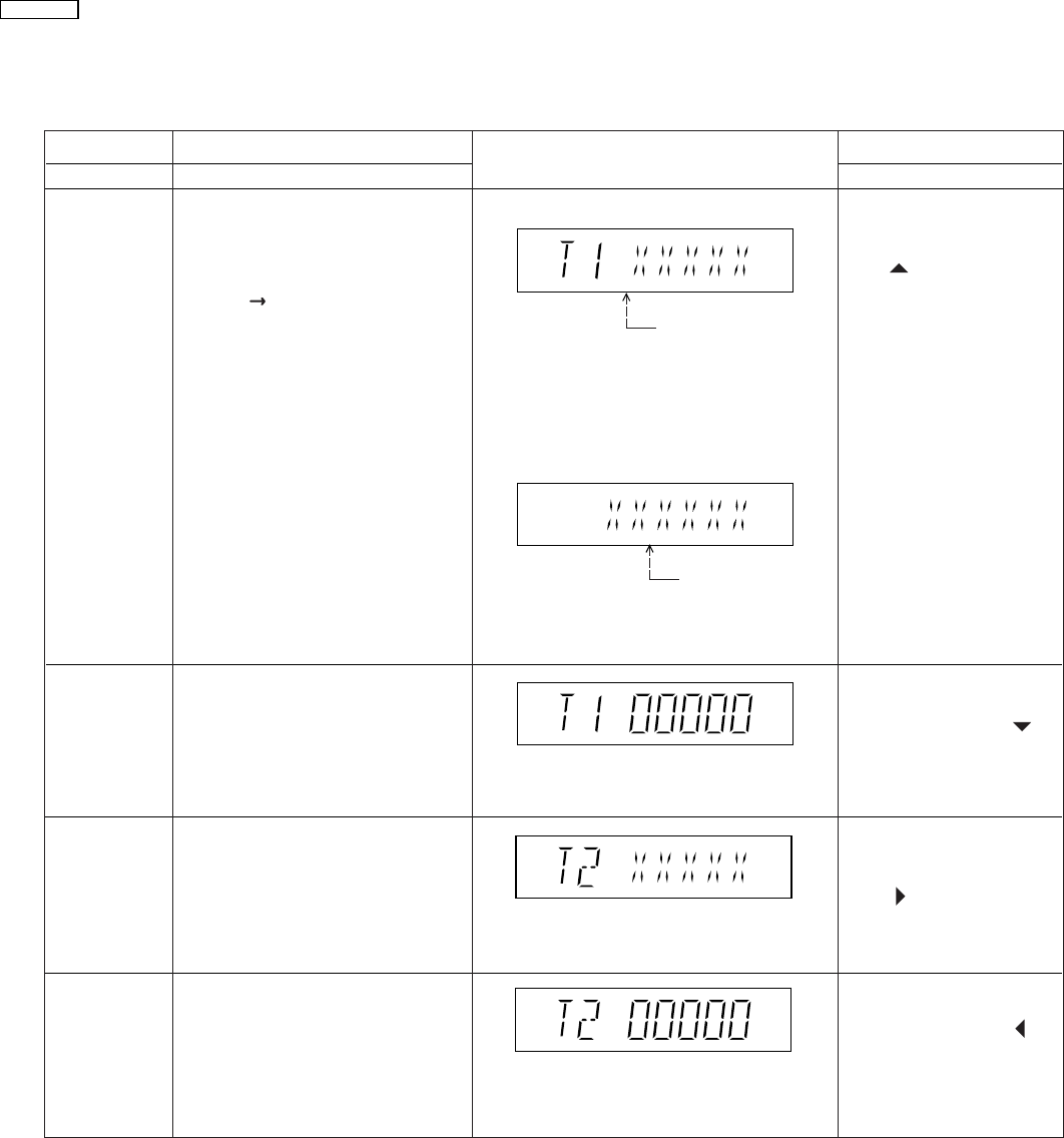
Timer 1 check
Cancelled automatically
5 seconds later.
DVD laser usage time
(Display 1)
(Display 2)
CD laser usage time
Cancelled automatically
5 seconds later
Cancelled automatically
5 seconds later.
Cancelled automatically
5 seconds later.
Timer 1 reset
Timer 2 check
Timer 2 reset
In STOP (no disc)
mode, press [STOP]
button on the main unit,
and [ ] button on the
remote control unit.
While displaying Timer 1
data, press [STOP] button
on the main unit, and [ ]
button on the remote
control unit.
In STOP (no disc)
mode, press [STOP]
button on the main unit,
and [ ] button on the
remote control unit.
While displaying Timer 2
data, press [STOP] button
on the main unit, and [ ]
button on the remote
control unit.
Timer 1 check
Laser operation timer is measured
separately for DVD laser and CD laser.
FL Display sequence:
Display 1 2.
Press [FL Display] button for
next page of FL Display.
Timer 1 reset
Laser operation timer of both DVD
laser and CD laser is reset all at once.
Timer 2 check
Spindle motor operation timer
Timer 2 reset
Spindle motor operation timer
Time is shown in 5 digits of decimal notation in
a unit of 1 hour.
"00000" will follow "99999".
Shown to the above is DVD laser usage
time, and to the below is CD laser usage
time.
Time is shown in 5 digits of decimal notation
in a unit of 10 hours.
"00000" will follow "99999". (DVD laser)
Time is shown in 6 digits of decimal notation
in a unit of 10 hours.
"000000" will follow "999999". (CD laser)
Time is shown in 5 digits of decimal notation
in a unit of 10 hours.
It will clear to "00000" upon reset.
Time is shown in 5 digits of decimal notation in
a unit of 1 hour.
It will be cleared to "00000" upon activating
this.
FL Display Key Operation
Front Key
Item
DescriptionMode Name
30
SA-PT850EE
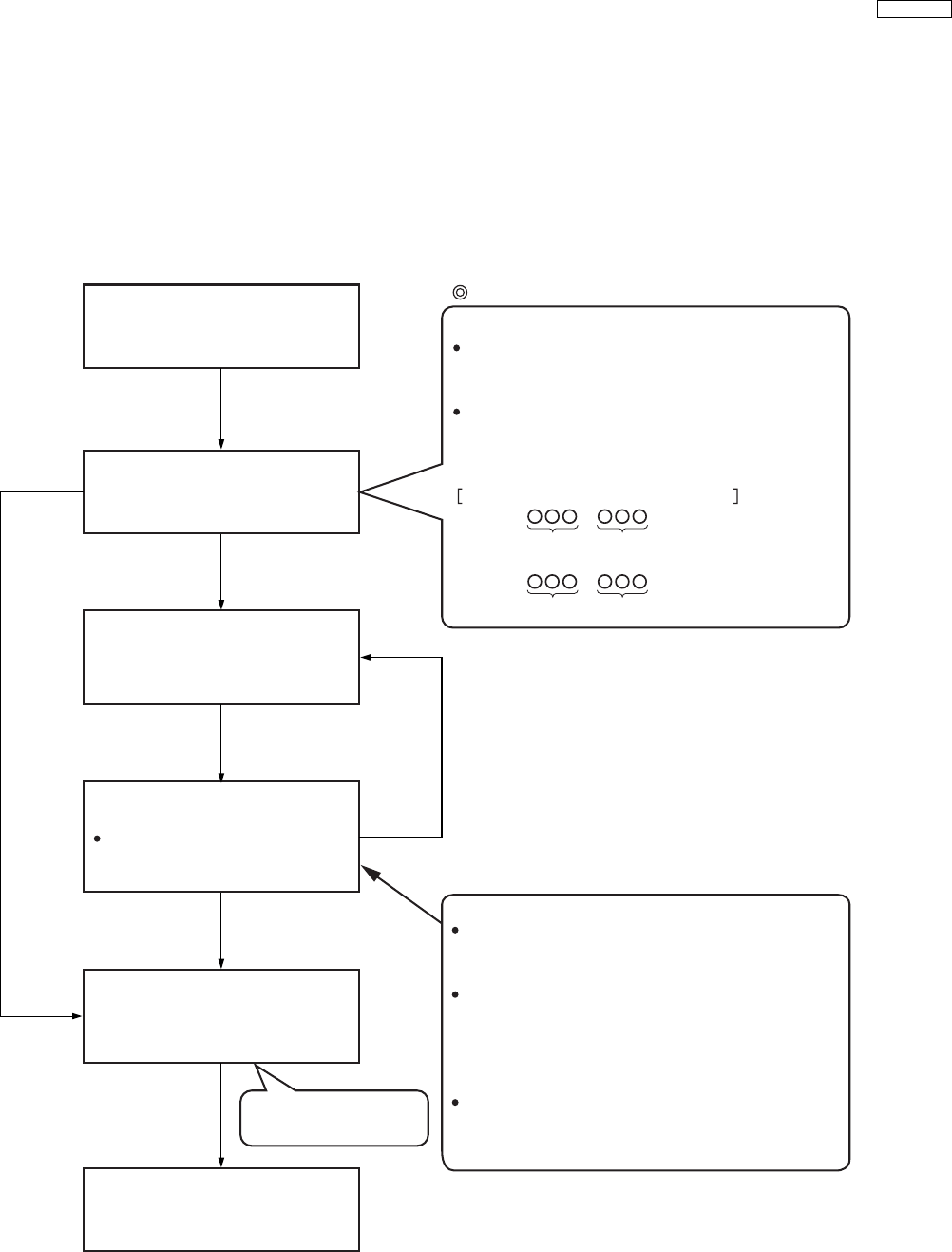
9.2.6. Optical Pick-up Self-Diagnosis
The optical pickup self-diagnosis function and tilt adjustment check function have been included in this unit. When repairing, use
the following procedure for effective self-diagnosis and tilt adjustment. Be sure to use the self-diagnosis function before replacing
the optical pickup when "NO DISC" is displayed. As a guideline, you should replace the optical pickup when the value of the laser
drive current is more than 55.
Note:
Press the power button to turn on the power, and check the value within three minutes before the unit warms up. (Otherwise,
the result will be incorrect.)
"NO DISC" is displayed, unit
does not play smoothly, etc.
Check the laser drive current.
Replace the optical pickup.
(Refer to the section "OPTICAL
PICKUP REPLACEMENT
PROCEDURE" in this Guide.)
Do the optical pickup tilt
adjustment. (Refer to the section
"TILT ADJUSTMENT" in this
Guide.)
Initialize the main unit.
Check the laser drive current
after replacement.
Write the present value into the
unit if it is 23 (DVD), 34 (CD) or
less.
Value is 23 (DVD),
34 (CD) or less. Value is more than
23 (DVD), 34 (CD).
Use the tilt adjustment
check function.
Note: Press "FL DISPLAY" button on remote
Note:
Press
"FL
DISPLAY"
button
on
remote
control unit for next page display.
control
unit
for
next
page
display.
Replace with a new optical pickup if the present
value is more than 23 (DVD), 34 (CD).
Cause: Damage due to static electricity
during replacement.
Method: With no disc in the main unit:
· Press the "FUNCTIONS" button on the remote
control unit while pressing the "STOP"
button on the main unit. (DVD)
· Press the "3" button on the remote
control unit while pressing the "STOP"
button on the main unit. (CD)
Use the optical pickup self-diagnosis function.
Method: With no disc in the main unit:
· Press the "FUNCTIONS" button on the remote
control unit while pressing the "STOP"
button on the main unit. (DVD)
· Press the "3" button on the remote
control unit while pressing the "STOP"
button on the main unit. (CD)
Display content (display1/display2)
LDD (DVD)
LDC (CD)
Factory setting Present value
Factory setting Present value
/
/
Writing method:
· Press the "PAUSE" button on the remote
control unit while pressing the "STOP"
button on the main unit.
31
SA-PT850EE
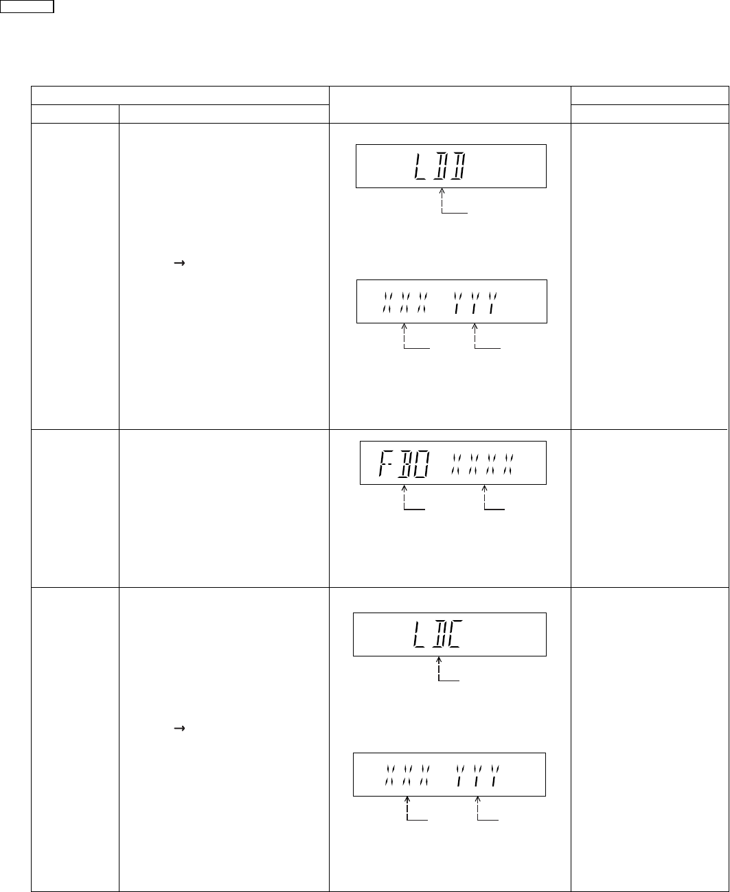
9.3. DVD Self Diagnostic Function-Error Code
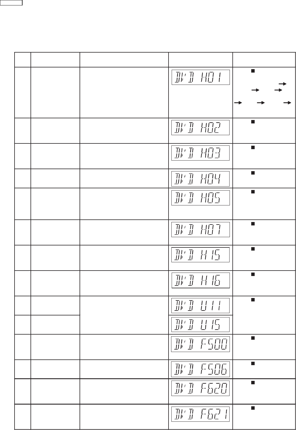
9.3.1. Mechanism Error Code Table
Error
Code
H01 Tray loading error The tray opening and closing is Press [ STOP] on
abnormal. CLOSE and OPEN of the main unit for next error.
tray cannot be carried out properly. (OPEN time: OPEN
Loading motor error, DV5 LSI IC CLOSE OPEN
(IC8001) error. H01 at CLOSE: CLOSE
OPEN CLOSE
H01)
H02 Spindle servo error The spindle servo/motor is abnormal. Press [ STOP] on
The FG pulse is abnormal. CLV servo main unit for next error.
error.
H03 Traverse servo error The traverse is abnormal. (Traverse Press [ STOP] on
servo, DV5 LSI IC (IC8001), TRV main unit for next error.
motor error.)
H04 Tracking servo error Tracking coil NG (OPU unit Press [ STOP] on
abnormal), DV5 LSI IC (IC8001) main unit for next error.
error.
H05 Seek time out error It is not possible to access the disc. Press [ STOP] on
TOC cannot read. Abnormal disc etc. main unit for next error.
Pickup abnormal or disk is dirty.
(TRV motor error, DV5 LSI IC
(IC8001) error.)
H07 Driver IC thermal The spindle motor is abnormal. (short Press [ STOP] on
shut down between brushes) main unit for next error.
H15 Disc tray open The disc tray cannot be opened & it Press [ STOP] on
detection switch closes spontaneously. main unit for next error.
failure
H16 Disc tray close The disc tray cannot be closed & it Press [ STOP] on
detection switch opens spontaneously. main unit for next error.
failure
U11 Focus servo error Focus coil, FE signal error. Press [ STOP] on
main unit for next error.
(Unfinalized DVD-R
U15 Unfinalized DVD-R is likely to beocme U11.)
F500 DSC error DV5 LSI IC (IC8001) stops in the Press [ STOP] on
occurance of servo error (startup, main unit for next error.
focus error, etc)
F506 Invalid media Disc is flipped over, TOC unreadable, Press [ STOP] on
incompatible disc. main unit for next error.
F620 OPU unit Laser protection at high temperature. Press [ STOP] on
abnormality main unit for next error.
temperature
F621 OPU unit Laser protection at circuit failure. Press [ STOP] on
circuitry main unit for next error.
temperature
Diagnosis Contents Description of error Automatic FL Display Remarks
32
SA-PT850EE
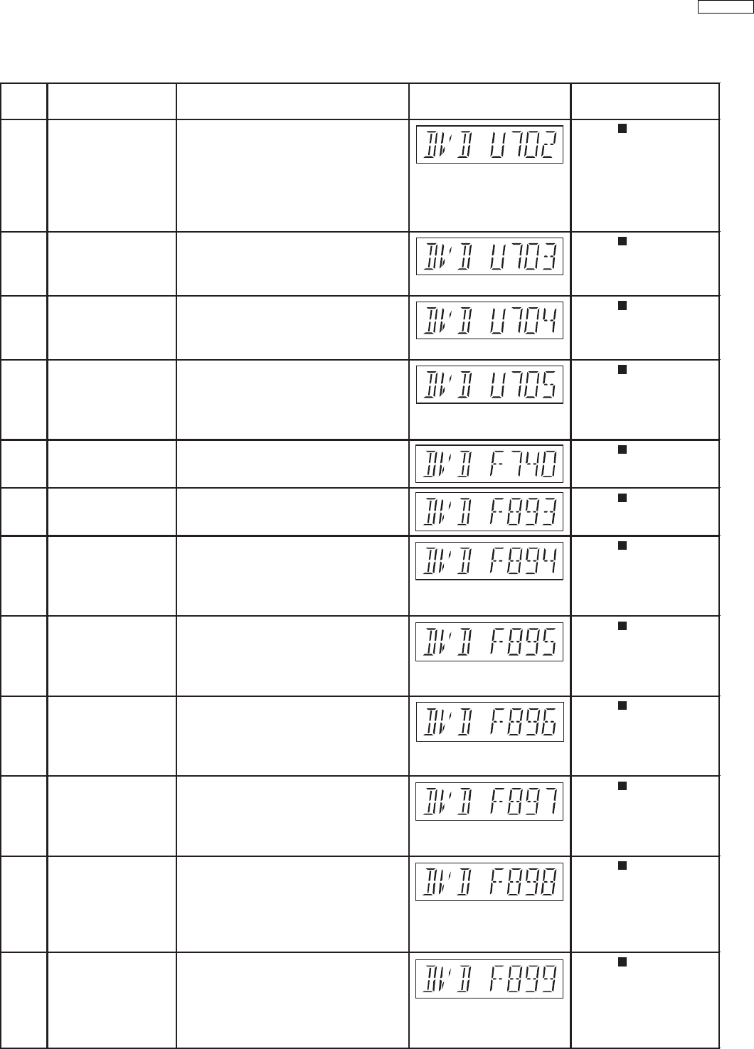
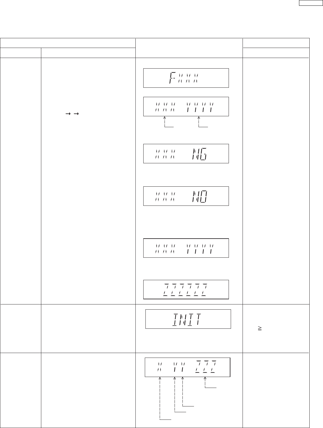
9.3.2. DVD Module Error Code Table
Error
Code
U702 HDMI/DVI I2C The communication error of I2C Press
[
STOP
]
on
communication error when connecting it with HDMI/ main unit for next error.
DVI. For instance, when EDID
information to which information on the
TV set side has been described
cannot be read, it is generated.
U703 HDMI/DVI attestation When attestation
(
HDCP
)
with the TV Press
[
STOP
]
on
error side fails when connecting it with main unit for next error.
HDMI/DVI, it is generated.
U704 HDMI/DVI SRM It is
g
enerated at the e
q
ui
p
ment to Press
[
STOP
]
on
Riborcerar which the TV set is Riborced when main unit for next error.
connecting it with HDMI/DVI.
U705 HDMI/DVI SRM disk It is
g
enerated at the time of it is time Press
[
STOP
]
on
falsification check when illegal the SRM data of the main unit for next error.
error reproducing disk (verify error), when
connecting it with HDMI/DVI.
F740 HDMI device key I2C error when writing HDMI Key Press [ STOP] on
device into transmitter. main unit for next error.
F893 FLASH ROM IC data Firmware error, DV5 LSI IC (IC8651) Press [ STOP] on
falsification error error. main unit for next error.
F894 EEPROM IC When failing in the access to Press [ STOP] on
abnormality error EEPROM IC located in the DVD main unit for next error.
Module P.C.B. (IC8611)
F895 Language area Firmware version agreement check for Press [ STOP] on
abnormal factory preset setting failure main unit for next error.
prevention.
F896 No existence model Firmware version agreement check for Press [ STOP] on
factory preset setting failure main unit for next error.
prevention.
F897 Initialization Incomplete initialization after writing of Press [ STOP] on
error new firmware (Factory preset setting main unit for next error.
failure prevention)
F898 Disagreement of Unsuitable combination of AV Decoder, Press [ STOP] on
hardware and SDRAM & FLASH ROM IC (firmware). main unit for next error.
software
F899 The communication Unsuitable combination of number of Press [ STOP] on
specification system com and panel com used. main unit for next error.
disagreement (Frimware)
between
micro-processor
Diagnosis Contents Description of error
Automatic FL Display
Remarks
33
SA-PT850EE
9.3.3. Power Supply Error Code Table
Error
Code
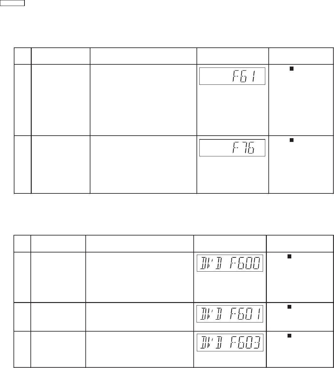
F61 The abnormalities In normal operation, when DCDET2 Press [ STOP] on
in an output or power goes to "L" (Low) (Not during POWER main unit for next error.
supply circuit of OFF condition), F61 appears on FL
POWER AMP Display and PCONT goes to "L" (Low).
This is due to speaker output has DC
voltage or fan is not working.
F76 Abnormality in the In normal operation when DCDET1 is Press [ STOP] on
output voltage of detected "L" (Low) for two consecutive main unit for next error.
stabilized power times, F76 is displayed on FL for 2
supply seconds and after that PCONT will be
turned to "L" (Low). This is due to any of
the DC voltages (+9V, +7V, -7V, +5V,
+5.3V etc.) not available.
Diagnosis Contents
Description of error
Automatic FL Display
Remarks
9.3.4. ECC Error Code Table
Error
Code
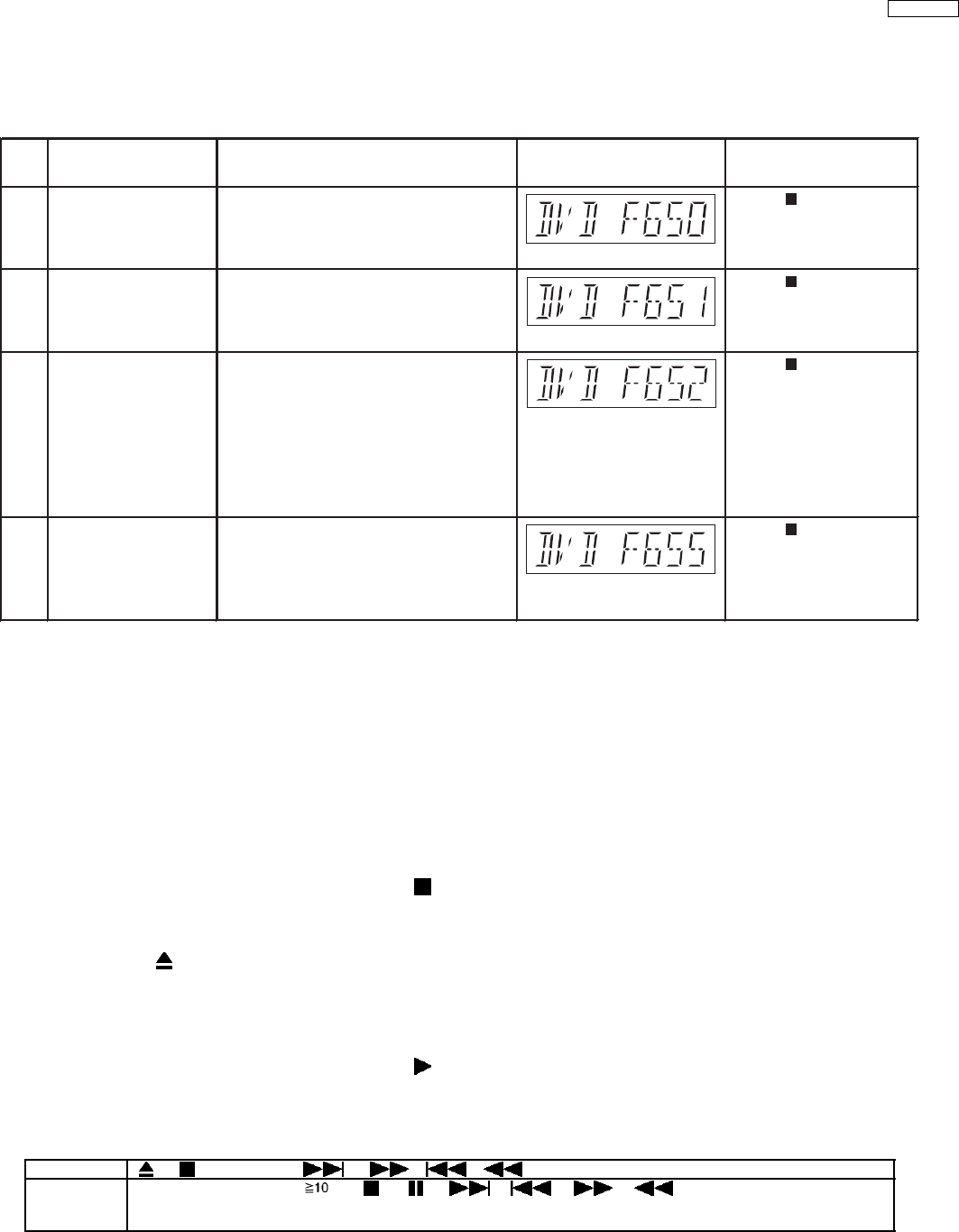
F600 Administrative It becomes impossible NaviPack etc. Press [ STOP] on
information cannot were done, and not to be able to main unit for next error.
be acquired by the acquire necessary information in the
recovery error. navigation’s changing due to wound
etc. of DISC, and to have done the
reproduction transition.
F601 Irregular sector ID It tried to access the position that did Press [ STOP] on
was demanded. not exist on DISC by the recording main unit for next error.
error etc. of authoring.
F603 KEYDET cannot be The data for decoding copyright Press [ STOP] on
acquired by the protection (CSS) cannot be acquired main unit for next error.
recovery error. due to wound etc. of DISC, and it is not
possible to reproduce.
Diagnosis Contents
Description of error Automatic FL Display Remarks
34
SA-PT850EE
9.3.5. USB Error Code Table
Error
Code
F650 USB device: Devices Devices other than the mass storage Press [ STOP] on
other than mass class are connected. main unit for next error.
storage
F651 USB device: Non- The device that the transfer rate did not Press [ STOP] on
Full Speed Device correspond to Full Speed was main unit for next error.
connected.
F652 USB device: The device in the interface (subclass) Press [ STOP] on
Interface NG outside correspondence was main unit for next error.
connected. (correspondence interface)
001b: Reduced Block Commands
(RBC)
010b: SFF-8020i. MMC-2 (ATAPI)
110b: SCSI transparent command set.
F655 USB device: The overcurrent of 500mA or more was Press [ STOP] on
Overcurrent detected in VDD USB, and the USB main unit for next error.
detection device driver function was intercepted.
(To intercept the current.)
Diagnosis Contents Description of error Automatic FL Display Remarks
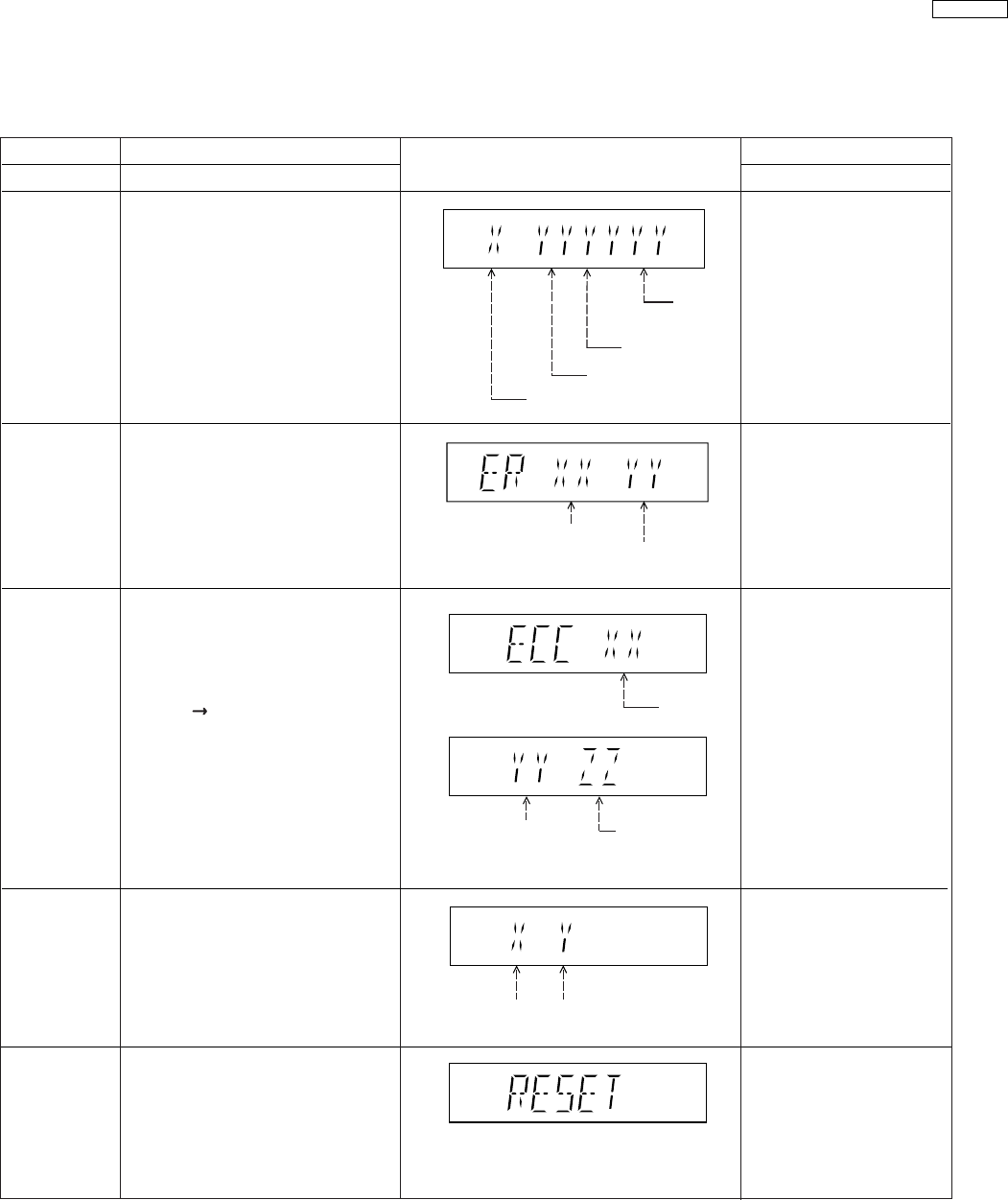
9.4. Sales Demonstration Lock Function
This function prevents discs from being lost when the unit is used for sales demonstrations by disabling the disc eject function.
"LOCKED" is displayed on the unit, and ordinary operation is disabled.
9.4.1. Setting
·
Prohibiting removal of disc
1. Select the DVD/CD function.
2. At POWER ON condition, press and hold down the button and the power button on the player for at least three seconds.
(The message, “___LOCKED_” appears when the function is activated.)
Note:
OPEN/CLOSE is invalid and the player displays “___LOCKED_” while the lock function mode is entered.
·
Prohibiting operation of selector and disc
1. Select the DVD/CD function.
2. At POWER ON condition, press and hold down the button and the power button on the player for at least three seconds.
(The message, “___LOCKED_” appears when the function is activated.)
Note:
The following buttons are invalid and the player displays “___LOCKED_” while the lock function mode is entered.
Player , , SELECTOR, /, , /
Remote
controller unit
NUMERIC KEYS 0~9, , , , , , , , FUNCTIONS/KARAOKE, TOP
MENU/DIRECT NAVIGATOR, RETURN/SETUP, FL DISPLAY/SLEEP, MUTING, MENU/PLAY LIST, TEST/AUTO,
EXT-IN, FM, UP, DOWN, LEFT & RIGHT
9.4.2. Cancellation
The lock can be cancelled by the same procedure as used in setting. ("UNLOCKED" is displayed on cancellation. Disconnecting
the power cable from power outlet does not cancel the lock.)
35
SA-PT850EE

9.5. Service Precautions
9.5.1. Recovery after the DVD player is repaired
·
When the FLASH ROM IC or DVD Module P.C.B. is replaced, carry out the recovery processing to optimize the drive.
Playback the recovery disk to process the recovery automatically.
·
Recovery disc (Product number: RFKZD03R005) [SPG]
·
Performing recovery process
1. Load the recovery disc RFKZD03R005 on to the player and run it.
2. Recovery is performed automatically. When it is finished, a message appears on the screen.
3. Remove the recovery disc.
4. Turn off the power.
5. Initialize the player.
9.5.2. Firmware version-up of the DVD player
·
The firmware of the DVD player may be renewed to improve the quality including operability and playability to the substandard
discs.processing to optimize the drive.
The recovery disc has also firmware version-up.
·
After version-up, recovery processing is executed automatically.
·
Part number of the recovery disc for version-up will be noticed when it is supplied.
·
Updating firmware
1. Load the recovery disc on to the player and run it.
2. Firmware version of the player is automatically checked. Appropriate message appears whenever necessary.
3. Using remote controller´s cursor key, select whether version updating is to be done or not. (Selection of Yes/No)
4. a. If Yes is selected, version updating is performed.
b. If No is selected, only recovery is performed.
5. a. When updating is finished, remove the disc according to the message appearing on the screen.
b. Remove the disc according to the message appearing on the screen.
6. Turn off the power.
Note:
If the AC power supply is shut out during version-up due to a power failure, the version-up is improperly carried out.
In such a case, replace the FLASH ROM IC and carry out the version-up again.
9.5.3. DVD Module P.C.B. Reset
·
When after replacing FLASH ROM IC or DVD Module P.C.B., FL displays error code “ DVD F897”. This means the unit is not
initialized properly and the following process needs to be carry out.
·
Procedures:
1. Press on remote control while pressing “STOP” button on main unit. (To enter into initialization)
2. FL display show “INIT”
3. While still pressing “STOP” button on main unit, press “ENTER” on remote control. (To reset the unit)
4. FL will display “RESET” before FL display will change to TOC reading again.
5. Power off unit. Unplug the AC cord.
6. Power on the unit. It should be no problem. If problem persist check on the DVD Module P.C.B. or FLASH ROM IC.
36
SA-PT850EE
Be careful when disassembling and servicing.
Some chassis components may have sharp edges.
Special Note:
10 Assembling and Disassembling
“ATTENTION SERVICER”
1. This section describes the disassembly procedures for all the major printed circuit boards and main components.
2. Before the disassembly process was carried out, do take special note that all safety precautions are to be carried out.
(Ensure that no AC power supply is connected during disassembling.)
3. For assembly after operation checks or replacement, reverse the respective procedures.
Special reassembly procedures are described only when required.
4. The Switch Regulator IC may have high temperature after prolonged use.
5. Use caution when removing the top cabinet and avoid touching heat sinks located in the unit.
6. Select items from the following index when checks or replacement are required.
·
Disassembly of Top Cabinet
·
Disassembly of DVD Lid (When taking out disc manually)
·
Disassembly of Front Panel
·
Disassembly of Volume P.C.B.
·
Disassembly of Mic P.C.B.
·
Disassembly of Panel P.C.B.
·
Disassembly of USB P.C.B.
·
Disassembly of Scart P.C.B.
·
Disassembly of Rear Panel
·
Disassembly of DVD Mechanism Unit
·
Disassembly of Relay P.C.B.
·
Disassembly of DVD Module P.C.B.
·
Disassembly of Main P.C.B.
·
Replacement of Regulator IC (IC2903)
·
Disassembly of D-Amp P.C.B.
·
Replacement of Digital Amp IC (IC5000)
·
Disassembly of SMPS & AC-Inlet P.C.B.
·
Replacement of Switch Regulator IC/Diode (IC5701/D5702)
·
Replacement of Regulator Diode (D5801/D5802)
·
Replacement of Regulator Diode (D5803)
37
SA-PT850EE

10.1. Disassembly Flow Chart
10.4. DVD Lid 10.10. Scart P.C.B.
10.3. Top Cabinet
10.11. Rear Panel
10.7. Mic P.C.B.
10.6. Volume P.C.B.
10.5. Front Panel 10.12. DVD Mechanism
Unit
10.19. SMPS & AC-Inlet
P.C.B.
10.20. Switch Regulator IC/
Diode (IC5701/D5702)
10.22. Regulator Diode
(D5803)
10.21. Regulator Diode
(D5801/D5802)
10.9. USB P.C.B.
10.8. Panel P.C.B. 10.18. Digital Amp IC
(IC5000)
10.16. Regulator IC
(IC2903)
10.15. Main P.C.B.
10.13. Relay P.C.B.
10.14. DVD Module
P.C.B. 10.17. D-Amp P.C.B.
38
SA-PT850EE
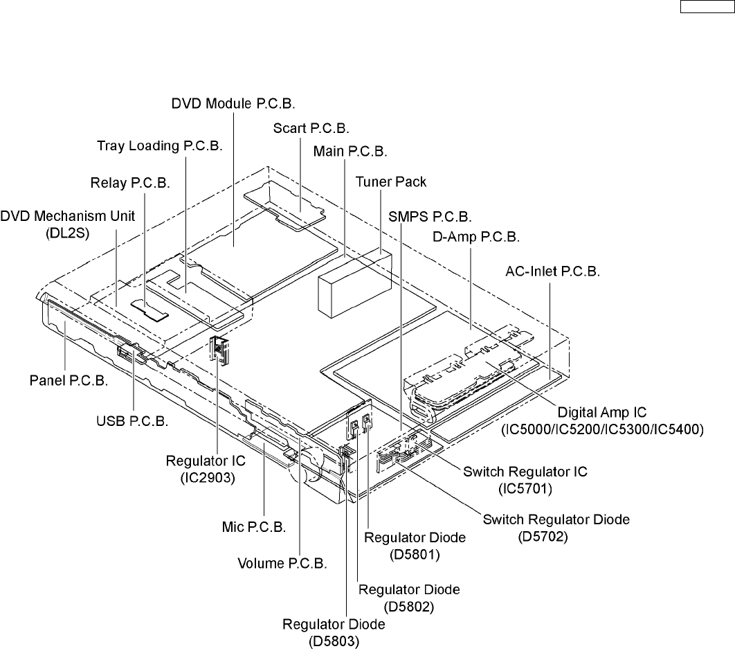
10.2. Main Components and P.C.B. Locations
39
SA-PT850EE
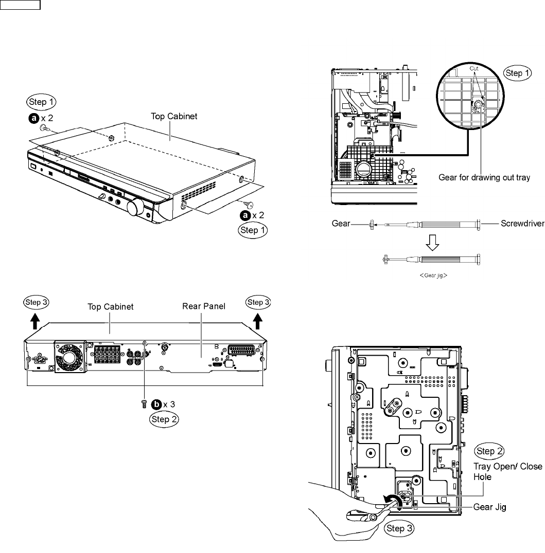
10.3. Disassembly of Top Cabinet
Step 1 Remove 4 screws.
Step 2 Remove 3 screws at the rear panel
Step 3 Lift up and remove the top cabinet in the direction of
arrows.
10.4. Disassembly of the DVD Lid
(When taking out disc
manually)
·
Follow (Step 1) to (Step 3) of Item 10.3.
Step 1 Detach the gear (For drawing out tray) from the
mechanism unit. It inserts a screw driver in the gear. (The gear
jig)
Step 2 Insert the gear jig into the tray open/ close hole.
Step 3 Turn the gear jig counterclockwise to open the tray.
Note : Do not use force to push the tray backwards as it can
damage the mechanism unit.
Step 4 Release the tabs in the direction of arrows and remove
the DVD lid.
40
SA-PT850EE
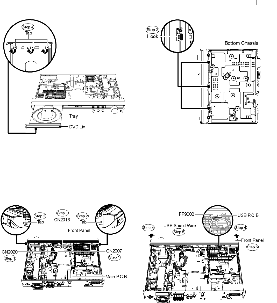
Note : You can return the tray by turning the gear jig clockwise.
10.5. Disassembly of Front Panel
·
Follow (Step 1) to (Step 3) of Item 10.3.
·
Follow (Step 1) to (Step 4) of Item 10.4.
Step 1 Detach FFC cables from the connectors. (CN2007,
CN2013 & CN2020) on Main P.C.B.
Step 2 Release the tab on each side of the front panel.
Step 3 Upset the unit and release 3 hooks at the bottom
chassis.
Special Note : Avoid placing the set in a position that might
cause damage to the jacks when removing the front panel.
Step 4 Detach the front panel slightly forward in the direction of
arrows.
Caution: Do not attempt to exert strong force when
detaching the front panel.
Step 5 Detach the USB shield wire from the connector
(FP9002) from USB P.C.B.
Caution: Remember to attach USB shield wire during
assembling.
Step 6 Remove the front panel.
10.6. Disassembly of Volume P.C.B.
·
Follow (Step 1) to (Step 3) of Item 10.3.
·
Follow (Step 1) to (Step 4) of Item 10.4.
·
Follow (Step 1) to (Step 6) of Item 10.5.
Step 1 Remove the volume knob from the front panel.
41
SA-PT850EE
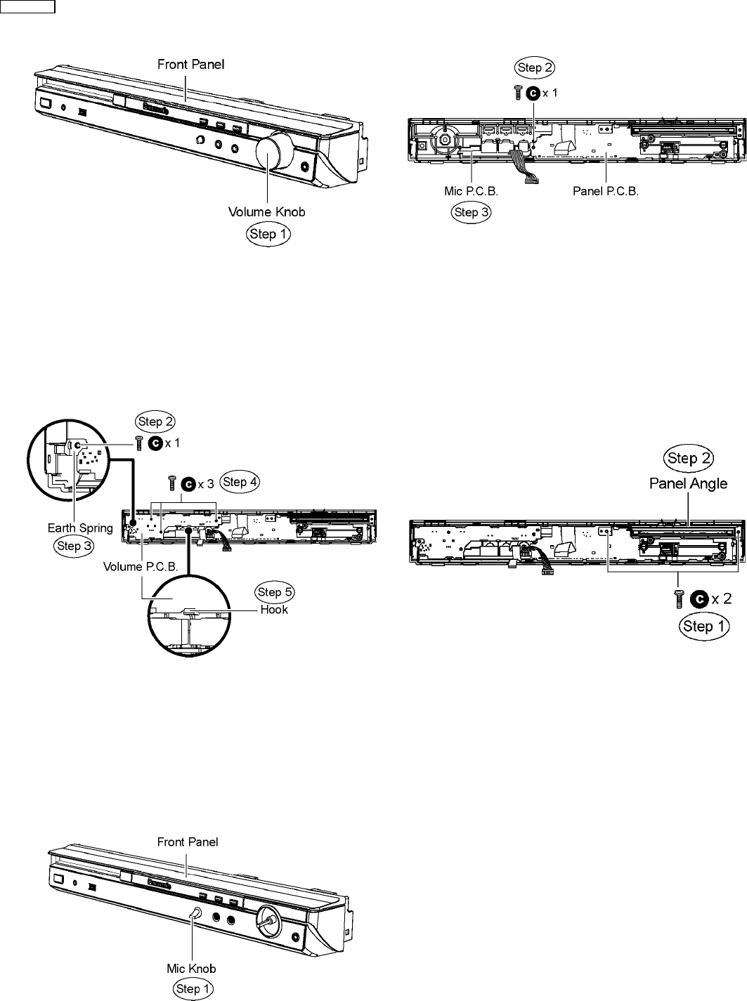
·
Disassembly of Earth Spring
Step 2 Remove 1 screw from the earth spring.
Step 3 Remove the earth spring.
·
Disassembly of Volume P.C.B.
Step 4 Remove 3 screws from the Volume P.C.B.
Step 5 Release the hook & remove Volume P.C.B.
10.7. Disassembly of Mic P.C.B.
·
Follow (Step 1) to (Step 3) of Item 10.3.
·
Follow (Step 1) to (Step 4) of Item 10.4.
·
Follow (Step 1) to (Step 6) of Item 10.5.
·
Follow (Step 1) to (Step 5) of Item 10.6.
Step 1 Remove the mic knob.
Step 2 Remove 1 screw from Panel P.C.B.
Step 3 Remove Mic P.C.B.
10.8. Disassembly of Panel P.C.B.
·
Follow (Step 1) to (Step 3) of Item 10.3.
·
Follow (Step 1) to (Step 4) of Item 10.4.
·
Follow (Step 1) to (Step 6) of Item 10.5.
·
Disassembly of Panel Angle
Step 1 Remove 2 screws.
Step 2 Remove the panel angle.
·
Disassembly of Mecha Holder
Step 3 Remove 2 screws.
Step 4 Remove the USB earth part & mecha holder.
·
Disassembly of Panel P.C.B.
Step 5 Remove 1 screw from Panel P.C.B.
Step 6 Release the hook and remove Panel P.C.B.
42
SA-PT850EE
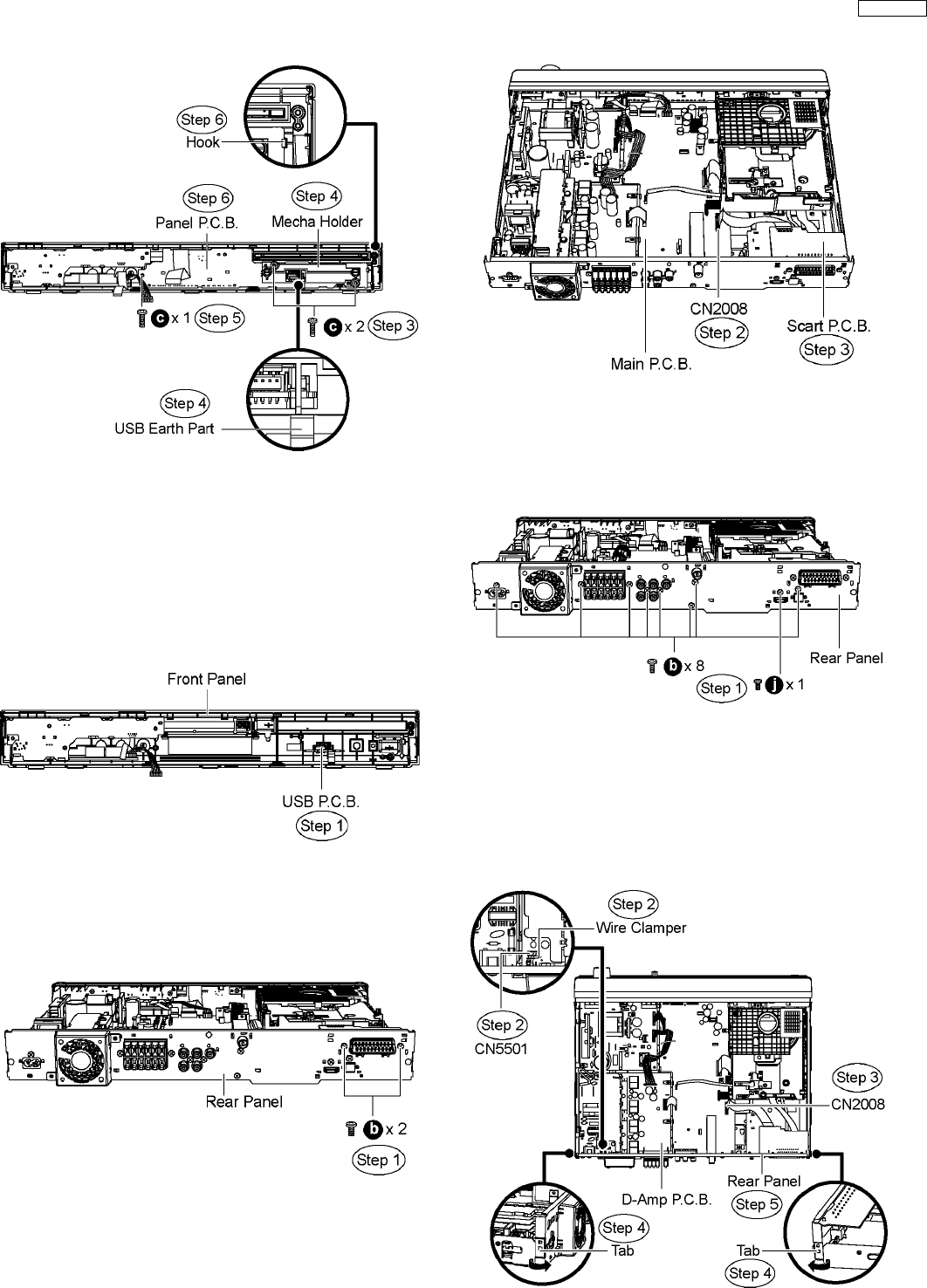
10.9. Disassembly of USB P.C.B.
·
Follow (Step 1) to (Step 3) of Item 10.3.
·
Follow (Step 1) to (Step 4) of Item 10.4.
·
Follow (Step 1) to (Step 6) of Item 10.5.
·
Follow (Step 1) to (Step 6) of Item 10.8.
Step 1 Remove USB P.C.B. from the front panel.
10.10. Disassembly of Scart P.C.B.
·
Follow (Step 1) to (Step 3) of Item 10.3.
Step 1 Remove 2 screws from the rear panel.
Step 2 Detach FFC cable from the connector (CN2008) on
Main P.C.B.
Step 3 Remove Scart P.C.B.
10.11. Disassembly of Rear Panel
·
Follow (Step 1) to (Step 3) of Item 10.3.
Step 1 Remove 9 screws from the rear panel.
Step 2 Remove the wire clamper to detach the fan unit
connector (CN5501) on D-Amp P.C.B.
Step 3 Detach FFC cable from the connector (CN2008) on
Main P.C.B.
Step 4 Release the tab on each side of the rear panel in the
direction of arrow.
Step 5 Remove the rear panel.
43
SA-PT850EE
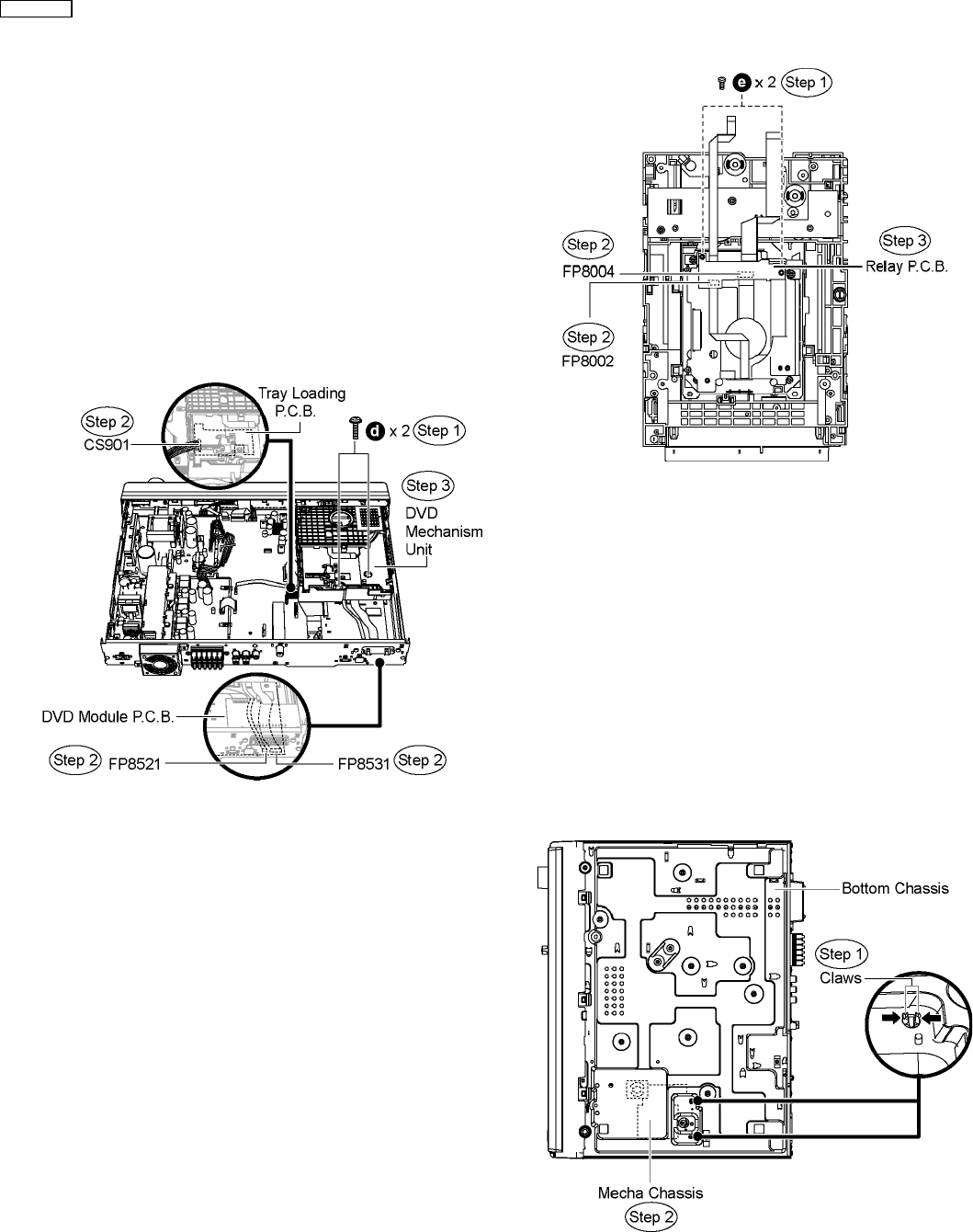
10.12. Disassembly of DVD
Mechanism Unit
·
Follow (Step 1) to (Step 3) of Item 10.3.
·
Follow (Step 1) to (Step 4) of Item 10.4.
·
Follow (Step 1) to (Step 3) of Item 10.10.
Step 1 Remove 2 screws from the DVD mechanism unit.
Step 2 Detach FFC cable from the connectors (FP8251 &
FP8531) on DVD Module P.C.B. and (CS901) on Tray Loading
P.C.B.
Step 3 Lift up & remove the DVD mechanism unit.
10.13. Disassembly of Relay P.C.B.
·
Follow (Step 1) to (Step 3) of Item 10.3.
·
Follow (Step 1) to (Step 4) of Item 10.4.
·
Follow (Step 1) to (Step 3) of Item 10.10.
·
Follow (Step 1) to (Step 3) of Item 10.12.
Step 1 Remove 2 screws from the Relay P.C.B.
Step 2 Detach FFC cable from the connectors (FP8002 &
FP8004)
Step 3 Remove Relay P.C.B.
Caution : Do not use strong or excessive force to avoid
damage to FFC cables.
10.14. Disassembly of DVD Module
P.C.B.
·
Follow (Step 1) to (Step 3) of Item 10.3.
·
Follow (Step 1) to (Step 4) of Item 10.4.
·
Follow (Step 1) to (Step 3) of Item 10.10.
·
Follow (Step 1) to (Step 3) of Item 10.12.
·
Disassembly of Mecha Chassis
Step 1 Release the claws of the mecha chassis in the direction
of arrows at the bottom chassis.
Step 2 Remove the mecha chassis.
·
Disassembly of DVD Module P.C.B.
Step 3 Detach the USB shield wire from the connector
(FP9002) on USB P.C.B.
Step 4 Release the claws of two mini clamps on the bottom
chassis in the direction of arrows.
Step 5 Remove the USB shield wire from the mini clamps.
44
SA-PT850EE
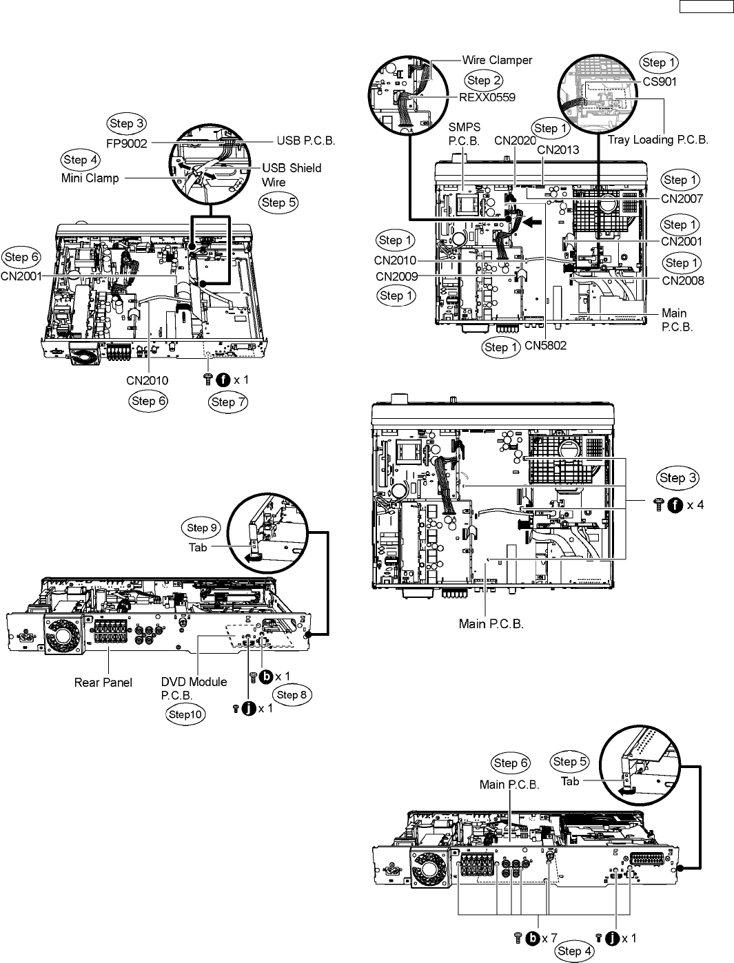
Step 6 Detach FFC cable from the connectors (CN2001 &
CN2010) on Main P.C.B.
Step 7 Remove 1 screw from DVD Module P.C.B.
Step 8 Remove 2 screws from the rear panel.
Step 9 Release the tab of rear panel in the direction of arrow.
Step 10 Remove DVD Module P.C.B.
Caution : Do not use strong or excessive force to avoid
damage to FFC cables.
10.15. Disassembly of Main P.C.B.
·
Follow (Step 1) to (Step 3) of Item 10.3.
Step 1 Detach FFC cable from the connectors (CN2001,
CN2007, CN2008, CN2009, CN2010, CN2013 & CN2020) on
Main P.C.B., (CS901) on Tray Loading P.C.B. and (CN5802)
on SMPS P.C.B.
Step 2 Remove the wire clamper to move aside the FFC cable
(REXX0559, SMPS to D-Amp) in the direction of arrow.
Step 3 Remove 4 screws from Main P.C.B.
Step 4 Remove 8 screws from the rear panel.
Step 5 Release the tab of the rear panel in the direction of
arrow.
Step 6 Remove Main P.C.B.
10.16. Replacement of Regulator IC
(IC2903)
·
Follow (Step 1) to (Step 3) of Item 10.3.
·
Follow (Step 1) to (Step 6) of Item 10.15.
45
SA-PT850EE
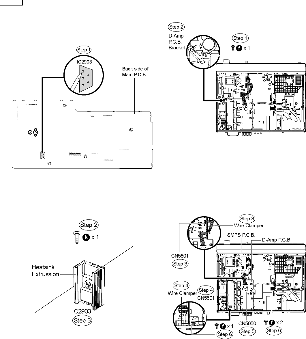
Step 1 Desolder pins of the regulator IC (IC2903) on the back
side of Main P.C.B.
Step 2 Remove 1 screw from the regulator IC (IC2903).
Step 3 Remove the regulator IC (IC2903) from the heatsink
extrussion.
Caution : Handle the heatsink extrussion with caution due to its
high temperature after prolonged use. Touching it may lead to
injuries.
Note: Refer to the diagrams of Main P.C.B. (Item 10.15) for the
location of the part.
10.17. Disassembly of D-Amp P.C.B.
·
Follow (Step 1) to (Step 3) of Item 10.3.
·
Disassembly of D-Amp P.C.B. Bracket.
Step 1 Remove 1 screw from AC-Inlet P.C.B.
Step 2 Remove the D-Amp P.C.B. bracket.
·
Disassembly of D-Amp P.C.B.
Step 3 Remove the wire clamper to detach FFC cable from the
connector (CN5801) on SMPS P.C.B.
Step 4 Remove the wire clamper to detach FFC cable from the
connector (CN5501) of fan unit on D-Amp P.C.B.
Step 5 Detach FFC cable from the connector (CN5050) on D-
Amp P.C.B.
Step 6 Remove 3 screws from D-Amp P.C.B.
Step 7 Remove 5 screws from the rear panel.
Step 8 Release the tab of the rear panel in the direction of
arrow.
Step 9 Remove D-Amp P.C.B.
46
SA-PT850EE
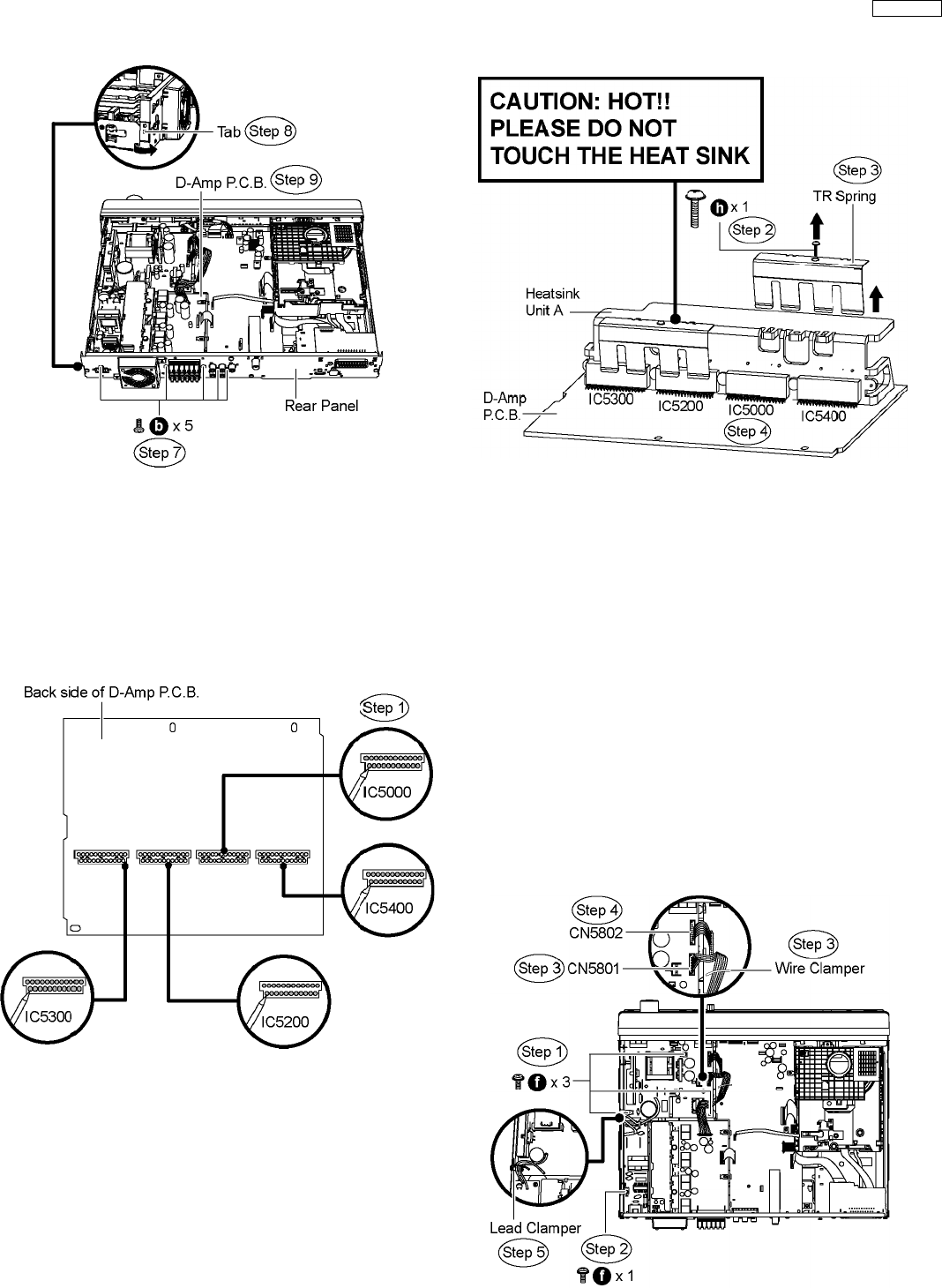
10.18. Replacement of Digital Amp IC
(IC5000)
·
Follow (Step 1) to (Step 3) of Item 10.3.
·
Follow (Step 1) to (Step 9) of Item 10.17.
Step 1 Desolder pins of the digital amp IC (IC5000) on the back
side of D-Amp P.C.B.
Step 2 Remove 1 screw from the top of the heatsink unit A.
Step 3 Remove the TR spring in the direction of the arrow.
Step 4 Remove the digital amp IC (IC5000) from the heatsink
unit A.
Caution : Handle the heatsink unit A with caution due to its
high temperature after prolonged use. Touching it may lead to
injuries.
Note : For replacement of IC5200, IC5300 & IC5400, repeat
the (Step 1) to (Step 4). Refer to the diagrams of D-Amp P.C.B.
(Item 10.17) for location of the parts.
10.19. Disassembly of SMPS & AC-
Inlet P.C.B.
·
Follow (Step 1) to (Step 3) of Item 10.3.
·
Follow (Step 1) to (Step 2) of Item 10.17. for Disassembly
of D-Amp P.C.B. Bracket.
Step 1 Remove 3 screws from SMPS P.C.B.
Step 2 Remove 1 screw from AC-Inlet P.C.B.
Step 3 Remove the wire clamper to detach FFC cable from the
connector (CN5801) on SMPS P.C.B.
Step 4 Detach FFC cable from the connector (CN5802) on
SMPS P.C.B.
Step 5 Remove the lead clamper.
Step 6 Remove 1 screw from the rear panel.
Step 7 Release the tab of the rear panel in the direction of
arrow.
47
SA-PT850EE
Step 8 Remove SMPS & AC-Inlet P.C.B.
10.20. Replacement of Switch
Regulator IC/Diode
(IC5701/D5702)
·
Follow (Step 1) to (Step 3) of Item 10.3.
·
Follow (Step 1) to (Step 8) of Item 10.19.
Step 1 Desolder pins of the switch reguIator IC or diode
(IC5701/D5702) on the back side of SMPS P.C.B.
Step 2 Remove 1 screw from the switch regulator IC (IC5701)
or diode (D5702).
Step 3 Remove the switch regulator IC (IC5701) or diode
(D5702) from the heatsink unit B.
Caution : Handle the heatsink unit B with caution due to its
high temperature after prolonged use. Touching it may lead to
injuries.
Note : Refer to the diagrams of SMPS P.C.B. (Item 10.19) for
location of the parts.
10.21. Replacement of Regulator
Diode (D5801/D5802)
·
Follow (Step 1) to (Step 3) of Item 10.3.
·
Follow (Step 1) to (Step 8) of Item 10.19.
Step 1 Desolder pins of the regulator diode (D5801/D5802) on
the back side of SMPS P.C.B.
Step 2 Remove 1 screw from the regulator diode
(D5801/D5802).
Step 3 Remove the regulator diode (D5801/D5802) from the
heatsink unit C.
Caution : Handle the heatsink unit C with caution due to its
high temperature after prolonged use. Touching it may lead to
injuries.
48
SA-PT850EE
Note : Refer to the diagrams of SMPS P.C.B. (Item 10.19) for
location of the parts.
10.22. Replacement of Regulator
Diode (D5803)
·
Follow (Step 1) to (Step 3) of Item 10.3.
·
Follow (Step 1) to (Step 8) of Item 10.19.
Step 1 Desolder pins of the regulator diode (D5803) on the
back side of SMPS P.C.B.
Step 2 Remove 1 screw from the regulator diode (D5803).
Step 3 Remove the regulator diode (D5803) from the small
heatsink .
Caution : Handle the small heatsink with caution due to its high
temperature after prolonged use. Touching it may lead to
injuries.
Note : Refer to the diagrams of SMPS P.C.B. (Item 10.19) for
location of the part.
49
SA-PT850EE
11 Assembly and
Disassembly of DVD
Mechanism Unit
11.1. Disassembly Procedure
11.1.1. Disassembly of Traverse Unit (with
Middle Chassis)
Step 1 Slide the lever (A) in the arrow direction (to the opposite
side) till it stops.
Step 2 Slide the lever (A) further by bending the tab at the right
side of the lever A in the right direction. (The right groove opens
and the boss becomes seen.)
Step 3 Open the lever (B) to left. (The 2 grooves at the left side
open.).
Step 4 Remove the traverse unit.
11.1.2. Disassembly of Tray
Step 1 Slide the clamp plate while pressing the stopper in the
arrow direction, and remove the clamp plate.
50
SA-PT850EE
Step 2 Raise the mecha chassis vertically.
Step 3 Slide the lever in the arrow direction till it stops and pull
the tray out.
Step 4 Spread the tabs at the both sides and pull the tray out.
(The tray slides a little forword and stops.).
Step 5 Remove the drive arm concave phase from the tray
slider and tray.
l(Assembly of the tray unit)
Step 1 Insert a part of the tray into the unit sliding over the
groove on the mecha chassis.
Step 2 Insert the tray to the point before the tab of the
mecha chassis.
Step 3 Hook the drive arm concave phase over the tray and
the tray slider.
Step 4 Press in the tray.
Step 5 Make sure that the tray and the drive arm move
smoothly.
51
SA-PT850EE
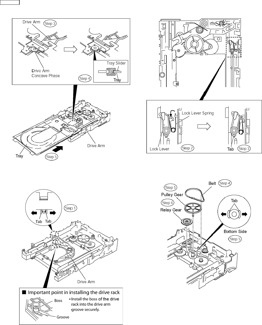
11.1.3. Disassembly of Loading Section
Step 1 Spread the tabs at the both sides and push out the drive
arm.
Step 2 Hook the lock lever spring on the lock lever projection
part temporarly.
Step 3 Unlock the tab and remove the lock lever.
Step 4 Remove the belt.
Step 5 Unlock the tab and remove the pulley gear.
Step 6 Remove the relay gear.
Step 7 Turn the change lever in the arrow direction till it stops.
Step 8 Hook the change lever spring on the change lever
project part temporarily.
52
SA-PT850EE
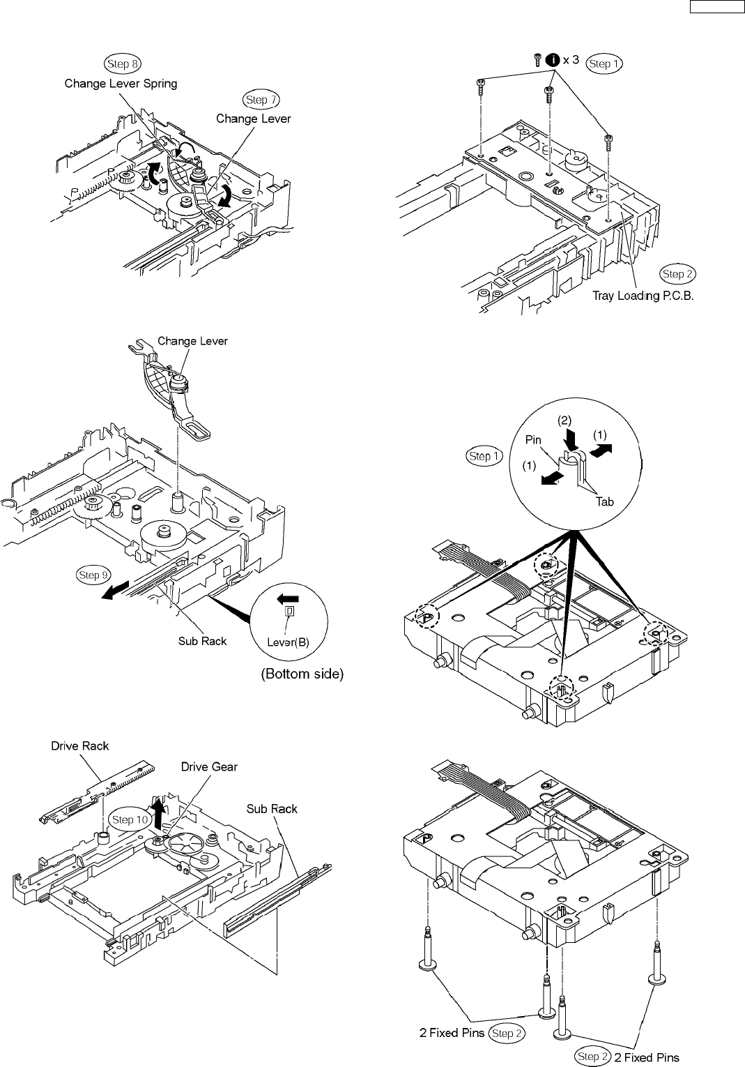
Step 9 Pull the lever (B) at the bottom side in the direction of
arrow and remove the change lever.
Step 10 Remove the drive rack, the sub rack and the drive gear
in the direction of arrow.
11.1.4. Disassembly of Tray Loading
P.C.B.
Step 1 Remove 3 screws
Step 2 Remove Tray Loading P.C.B.
11.1.5. Disassembly of Traverse Unit
Step 1 Spread the tabs to push in the pin in the direction of
arrows.
Step 2 Remove 4 fixed pins.
53
SA-PT850EE
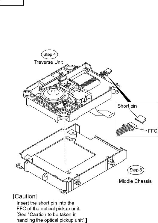
Step 3 Remove the middle chassis.
Step 4 Remove the traverse unit.
54
SA-PT850EE
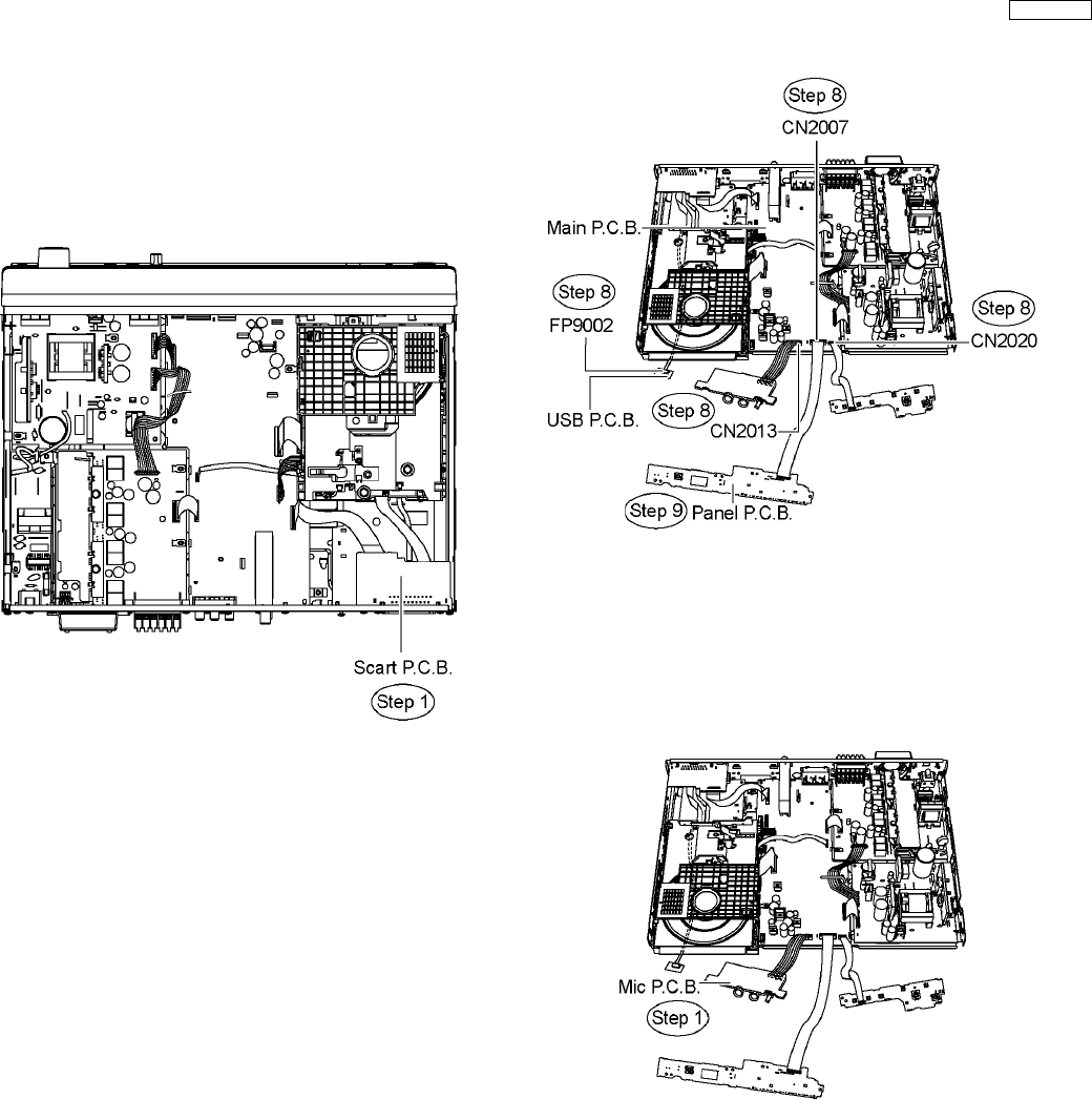
12 Service Position
12.1. Checking & Repairing Scart
P.C.B.
Step 1 Remove the top cabinet to service Scart P.C.B.
12.2. Checking & Repairing Panel
P.C.B.
Step 1 Remove the top cabinet.
Step 2 Remove the DVD lid.
Step 3 Disassemble the front panel.
Step 4 Disassemble Panel P.C.B.
Step 5 Disassemble Volume P.C.B.
Step 6 Disassemble Mic P.C.B.
Step 7 Disassemble USB P.C.B.
·
Servicing Position of Panel P.C.B.
Step 8 Connect FFC cable at the connectors (CN2020,
CN2013 & CN2007) on Main P.C.B and (FP9002) on USB
P.C.B.
Step 9 Turn over Panel P.C.B horizontally and place it
according to the diagram shown below.
12.3. Checking & Repairing Mic
P.C.B.
·
Follow (Step 1) to (Step 8) of Item 12.2.
Step 1 Turn over Mic P.C.B horizontally and place it according
to the diagram shown below.
12.4. Checking & Repairing Main
P.C.B.
Step 1 Remove the top cabinet.
Step 2 Remove the DVD lid.
Step 3 Disassemble the front panel.
Step 4 Disassemble Volume P.C.B.
Step 5 Disassemble Mic P.C.B.
Step 6 Disassemble Panel P.C.B.
Step 7 Disassemble USB P.C.B.
Step 8 Disassemble Scart P.C.B.
Step 9 Disassemble the rear panel.
Step 10 Disassemble the DVD mechanism unit.
Step 11 Disassemble DVD Module P.C.B.
Step 12 Disassemble Main P.C.B.
Step 13 Disassemble D-Amp P.C.B.
Step 14 Disassemble SMPS & AC-Inlet P.C.B.
55
SA-PT850EE
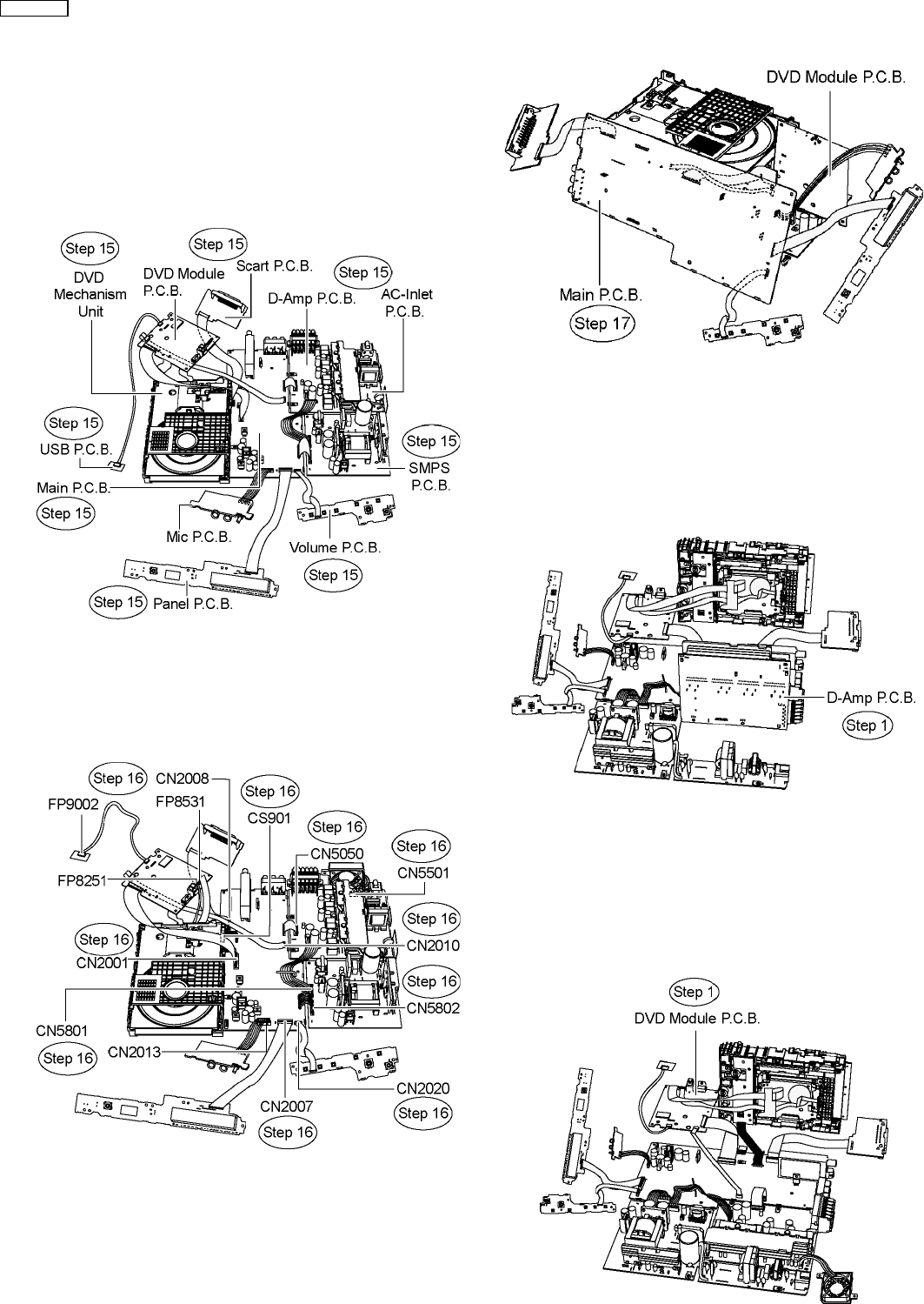
·
Servicing Position of Main P.C.B.
Step 15 Position Volume P.C.B., Mic P.C.B., Panel P.C.B.,
USB P.C.B., Scart P.C.B., DVD mechanism unit, DVD Module
P.C.B., Main P.C.B., D-Amp P.C.B., SMPS P.C.B. & AC-Inlet
P.C.B. according to to diagram shown below.
Step 16 Connect FFC cable at the connectors (CN2001,
CN2007, CN2008, CN2010, CN2013 & CN2020) on Main
P.C.B., (CN5050 & CN5501) on D-Amp P.C.B., (CN5801 &
CN5802) on SMPS P.C.B. (CS901) on Tray Loading P.C.B.,
(FP8251 & FP8531) on DVD Module P.C.B. and (FP9002) on
USB P.C.B.
Step 17 Turn over Main P.C.B vertically and place it according
to the diagram shown below.
12.5. Checking & Repairing D-Amp
P.C.B.
·
Follow (Step 1) to (Step 16) of Item 12.4.
Step 1 Turn over D-Amp P.C.B vertically and place it according
to the diagram shown below.
12.6. Checking & Repairing DVD
Module P.C.B.
·
Follow (Step 1) to (Step 16) of Item 12.4.
Step 1 Turn over DVD Module P.C.B vertically and place it
according to the diagram shown below.
56
SA-PT850EE
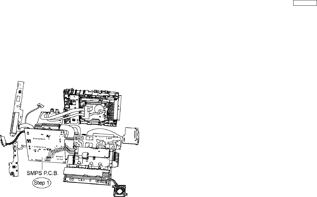
12.7. Checking & Repairing SMPS
P.C.B.
·
Follow (Step 1) to (Step 16) of Item 12.4.
Step 1 Turn over SMPS P.C.B vertically and place it according
to the diagram shown below.
57
SA-PT850EE

13 Measurements and Adjustments
13.1. Service Tools and Equipment
Application Name Number
Tilt adjustment DVD test disc DVDT-S20 [SPG]
TORX screw driver (T6) Available on sales route. (T6) or
RFKZ0185 [SPG]
Others Grease RFKXPG641 [SPG]
Confirmation CD test disc PVCD-K06 or any other commercially
available disc
VCD test disc PVCD-K06 or any other commercially
available disc
Recovery disc RFKZD03R005 [SPG]
13.2. Important points in adjustment
13.2.1. Important points in optical adjustment
·
Before starting optical adjustment, be sure to take anti-static measures.
·
Optical pickup tilt adjustment is needed after replacement of the following components.
1. Optical pickup unit
2. Spindle motor unit
3. Optical pickup peripheral parts
Notes
Adjustment is generally unnecessary after replacing other parts of the traverse unit. However, make adjustment if there is a
noticeable degradation in picture quality. Optical adjustments cannot be made inside the optical pickup. Adjustment is generally
unnecessary after replacing the traverse unit.
13.2.2. Important points in electrical adjustment
·
Follow the adjustment procedures described in this manual.
13.3. Storing and handling of test discs
·
Surface precision is vital for DVD test discs. Be sure to store and handle them carefully.
1. Do not place discs directly onto the workbench, etc., after use.
2. Handle discs carefully in order to maintain their flatness. Place them into their case after use and store them vertically. Store
discs in a cool place where they are not exposed to direct sunlight or air from air conditioners.
3. Accurate adjustment will not be possible if the disc is warped when placed on a surface made of glass, etc. If this happens, use
a new test disc to make optical adjustments.
4. If adjustment is done using a warped disc, the adjustment will be incorrect and some discs will not be playable.
58
SA-PT850EE
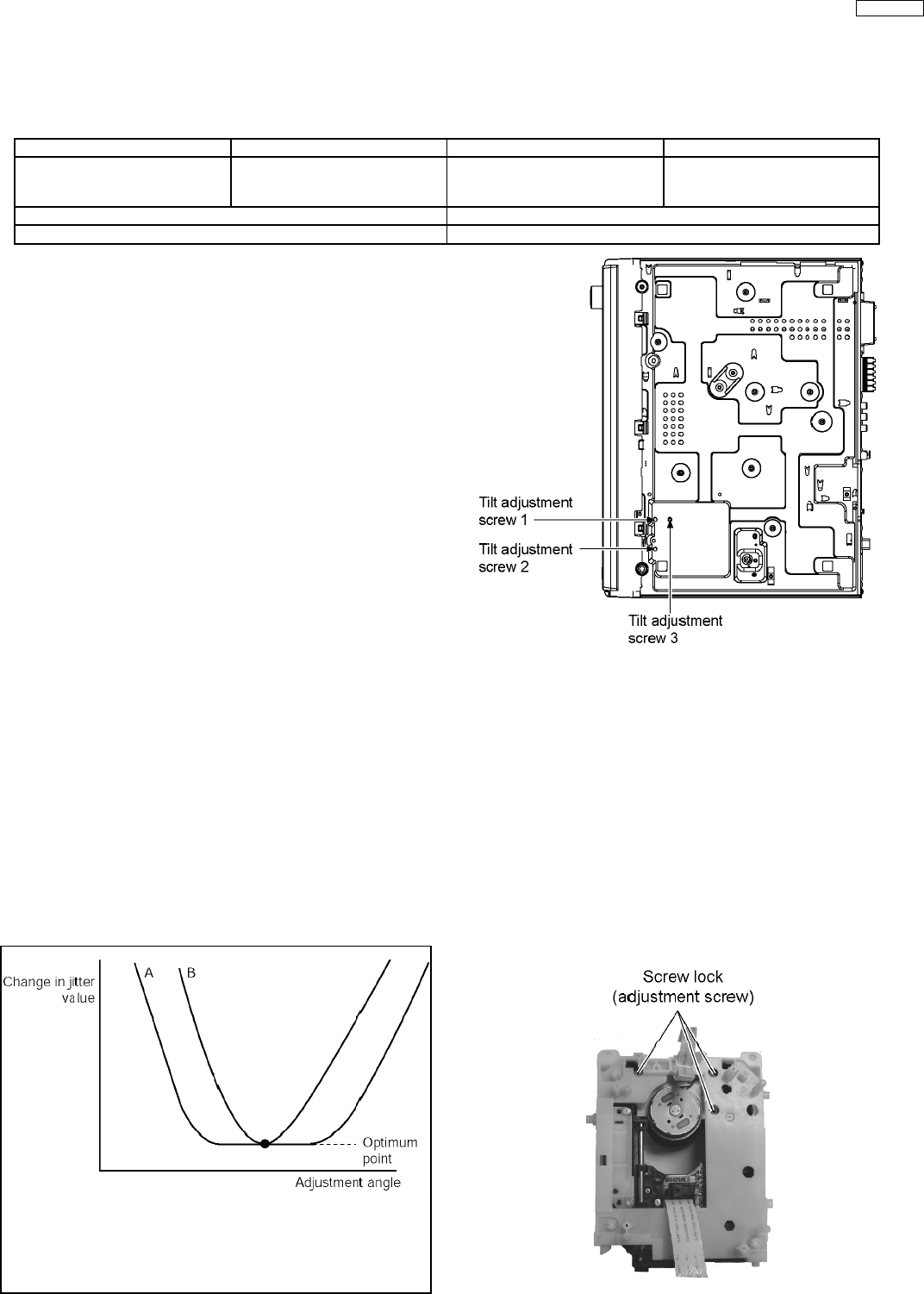
13.4.1.1. Adjustment procedure
1. While pressing STOP button on the main unit, press "5" on
the remote control unit.
2. Confirm that "J_xxx/yyy_zz" (display1/display2) is shown on
the front display.
For your information:
"yyy" and "zz" shown to the right have nothing to do with
the jitter value. "yyy" is the error counter, while "zz" is
the focus drive value.
Note:
Jitter value appears on the front display.
3. Play test disc T30 (center periphery).
4. Adjust tangential adjustment screw so that the jitter value is
minimized.
5. Play test disc T30 (center periphery).
6. Adjust tilt adjustment screw 1 so that the jitter value is
minimized.
7. Play test disc T30 (center periphery).
8. Adjust tilt adjustment screw 2 so that the jitter value is
minimized.
9. Repeat adjusting tilt adjustment screws 1 and 2 alternately
until the jitter value is minimized.
13.4.1.2. Important points
1. Make tangential adjustment first, and then make tilt
adjustment.
2. Repeat adjusting two or three times to find the optimum
point.
3. Finish the procedure with tilt adjustment.
Jitter value depends on the model:
1. If the jitter value changes like B, the optimum point is easy to
find.
2. If the jitter value changes like A, set the optimum point near the
middle.
13.4.1.3. Check after adjustment
Play test disc or any other disc to make sure there is no picture
degradation in the inner, middle and outer peripheries, and no
audio skipping. After adjustment is finished, lock each
adjustment screw in position using screw lock.
13.4.1.4. Procedure for screw lock
1. After adjustment, remove top cover, tray, clamper base and
traverse unit in this sequence.
2. Lay the traverse unit upside down, and fix adjustment screw
with screw lock.
3. After fixing, reassemble traverse unit, clamper base, tray
and top cover.
13.4. Optical adjustment
13.4.1. Optical pickup tilt adjustment
Measurement point Adjustment point Mode Disc
Tangential adjustment screw
Tilt adjustment screw
T01 (inner periphery) play
T30 (center periphery)
T43 (outer periphery) play
DVDT-S20 [SPG]
Measuring equipment Adjustment value
None (Main unit display for servicing is used.) Adjust to the minimum jitter value.
59
SA-PT850EE

14 Abbreviations
INITIAL/LOGO ABBREVIATIONS
AA0~UP
ACLK
AD0~UP
ADATA
ALE
AMUTE
AREQ
ARF
ASI
ASO
ASYNC
ADDRESS
AUDIO CLOCK
ADDRESS BUS
AUDIO PES PACKET DATA
ADDRESS LATCH ENABLE
AUDIO MUTE
AUDIO PES PACKET REQUEST
AUDIO RF
SERVO AMP INVERTED INPUT
SERVO AMP OUTPUT
AUDIO WORD DISTINCTION SYNC
B BCK
BCKIN
BDO
BLKCK
BOTTOM
BYP
BYTCK
BIT CLOCK (PCM)
BIT CLOCK INPUT
BLACK DROP OUT
SUB CODE BLOCK CLOCK
CAP. FOR BOTTOM HOLD
BYPATH
BYTE CLOCK
C CAV
CBDO
CD
CDSCK
CDSRDATA
CDRF
CDV
CHNDATA
CKSL
CLV
COFTR
CPA
CPCS
CPDT
CPUADR
CPUADT
CPUIRQ
CPRD
CPWR
CS
CSYNCIN
CSYNCOUT
CONSTANT ANGULAR VELOCITY
CAP. BLACK DROP OUT
COMPACT DISC
CD SERIAL DATA CLOCK
CD SERIAL DATA
CD RF (EFM) SIGNAL
COMPACT DISC-VIDEO
CHANNEL DATA
SYSTEM CLOCK SELECT
CONSTANT LINEAR VELOCITY
CAP. OFF TRACK
CPU ADDRESS
CPU CHIP SELECT
CPU DATA
CPU ADDRESS LATCH
CPU ADDRESS DATA BUS
CPU INTERRUPT REQUEST
CPU READ ENABLE
CPU WRITE ENABLE
CHIP SELECT
COMPOSITE SYNC IN
COMPOSITE SYNC OUT
D DACCK
DEEMP
DEMPH
DIG0~UP
DIN
DMSRCK
DMUTE
DO
DOUT0~UP
DRF
DRPOUT
DREQ
DRESP
DSC
DSLF
DVD
D/A CONVERTER CLOCK
DEEMPHASIS BIT ON/OFF
DEEMPHASIS SWITCHING
FL DIGIT OUTPUT
DATA INPUT
DM SERIAL DATA READ CLOCK
DIGITAL MUTE CONTROL
DROP OUT
DATA OUTPUT
DATA SLICE RF (BIAS)
DROP OUT SIGNAL
DATA REQUEST
DATA RESPONSE
DIGITAL SERVO CONTROLLER
DATA SLICE LOOP FILTER
DIGITAL VIDEO DISC
INITIAL/LOGO ABBREVIATIONS
E EC
ECR
ENCSEL
ETMCLK
ETSCLK
ERROR TORQUE CONTROL
ERROR TORQUE CONTROL
REFERENCE
ENCODER SELECT
EXTERNAL M CLOCK (81MHz/40.5MHz)
EXTERNAL S CLOCK (54MHz)
F FBAL
FCLK
FE
FFI
FEO
FG
FSC
FSCK
FOCUS BALANCE
FRAME CLOCK
FOCUS ERROR
FOCUS ERROR AMP INVERTED INPUT
FOCUS ERROR AMP OUTPUT
FREQUENCY GENERATOR
FREQUENCY SUB CARRIER
FS (384 OVER SAMPLING) CLOCK
G GND COMMON GROUNDING (EARTH)
HHA0~UP
HD0~UP
HINT
HRXW
HOST ADDRESS
HOST DATA
HOST INTERRUPT
HOST READ/WRITE
I IECOUT
IPFRAG
IREF
ISEL
IEC958 FORMAT DATA OUTPUT
INTERPOLATION FLAG
I (CURRENT) REFERENCE
INTERFACE MODE SELECT
L LDON
LPC
LRCK
LASER DIODE CONTROL
LASER POWER CONTROL
L CH/R CH DISTINCTION CLOCK
MMA0~UP
MCK
MCKI
MCLK
MDATA
MDQ0~UP
MDQM
MLD
MPEG
MEMORY ADDRESS
MEMORY CLOCK
MEMORY CLOCK INPUT
MEMORY SERIAL COMMAND CLOCK
MEMORY SERIAL COMMAND DATA
MEMORY DATA INPUT/OUTPUT
MEMORY DATA I/O MASK
MEMORY SERIAL COMMAND LOAD
MOVING PICTURE EXPERTS GROUP
O ODC
OFTR
OSCI
OSCO
OSD
OPTICAL DISC CONTROLLER
OFF TRACKING
OSCILLATOR INPUT
OSCILLATOR OUTPUT
ON SCREEN DISPLAY
PP1~UP
PCD
PCK
PDVD
PEAK
PLLCLK
PLLOK
PWMCTL
PWMDA
PWMOA, B
PORT
CD TRACKING PHASE DIFFERENCE
PLL CLOCK
DVD TRACKING PHASE DIFFERENCE
CAP. FOR PEAK HOLD
CHANNEL PLL CLOCK
PLL LOCK
PWM OUTPUT CONTROL
PULSE WAVE MOTOR DRIVE A
PULSE WAVE MOTOR OUT A, B
60
SA-PT850EE

INITIAL/LOGO ABBREVIATIONS
R RE
RFENV
RFO
RS
RSEL
RST
RSV
READ ENABLE
RF ENVELOPE
RF PHASE DIFFERENCE OUTPUT
(CD-ROM) REGISTER SELECT
RF POLARITY SELECT
RESET
RESERVE
S SBI0, 1
SBO0
SBT0, 1
SCK
SCKR
SCL
SCLK
SDA
SEG0~UP
SELCLK
SEN
SIN1, 2
SOUT1, 2
SPDI
SPDO
SPEN
SPRCLK
SPWCLK
SQCK
SQCX
SRDATA
SRMADR
SRMDT0~7
SS
STAT
STCLK
STD0~UP
STENABLE
STSEL
STVALID
SUBC
SBCK
SUBQ
SYSCLK
SERIAL DATA INPUT
SERIAL DATA OUTPUT
SERIAL CLOCK
SERIAL DATA CLOCK
AUDIO SERIAL CLOCK RECEIVER
SERIAL CLOCK
SERIAL CLOCK
SERIAL DATA
FL SEGMENT OUTPUT
SELECT CLOCK
SERIAL PORT ENABLE
SERIAL DATA IN
SERIAL DATA OUT
SERIAL PORT DATA INPUT
SERIAL PORT DATA OUTPUT
SERIAL PORT R/W ENABLE
SERIAL PORT READ CLOCK
SERIAL PORT WRITE CLOCK
SUB CODE Q CLOCK
SUB CODE Q DATA READ CLOCK
SERIAL DATA
SRAM ADDRESS BUS
SRAM DATA BUS 0~7
START/STOP
STATUS
STREAM DATA CLOCK
STREAM DATA
STREAM DATA INPUT ENABLE
STREAM DATA POLARITY SELECT
STREAM DATA VALIDITY
SUB CODE SERIAL
SUB CODE CLOCK
SUB CODE Q DATA
SYSTEM CLOCK
T TE
TIBAL
TID
TIN
TIP
TIS
TPSN
TPSO
TPSP
TRCRS
TRON
TRSON
TRACKING ERROR
BALANCE CONTROL
BALANCE OUTPUT 1
BALANCE INPUT
BALANCE INPUT
BALANCE OUTPUT 2
OP AMP INPUT
OP AMP OUTPUT
OP AMP INVERTED INPUT
TRACK CROSS SIGNAL
TRACKING ON
TRAVERSE SERVO ON
INITIAL/LOGO ABBREVIATIONS
V VBLANK
VCC
VCDCONT
VDD
VFB
VREF
VSS
V BLANKING
COLLECTOR POWER SUPPLY
VOLTAGE
VIDEO CD CONTROL (TRACKING
BALANCE)
DRAIN POWER SUPPLY VOLTAGE
VIDEO FEED BACK
VOLTAGE REFERENCE
SOURCE POWER SUPPLY VOLTAGE
WWAIT
WDCK
WEH
WSR
BUS CYCLE WAIT
WORD CLOCK
WRITE ENABLE HIGH
WORD SELECT RECEIVER
X X
XALE
XAREQ
XCDROM
XCS
XCSYNC
XDS
XHSYNCO
XHINT
XI
XINT
XMW
XO
XRE
XSRMCE
XSRMOE
XSRMWE
XVCS
XVDS
XVSYNCO
X´ TAL
X ADDRESS LATCH ENABLE
X AUDIO DATA REQUEST
X CD ROM CHIP SELECT
X CHIP SELECT
X COMPOSITE SYNC
X DATA STROBE
X HORIZONTAL SYNC OUTPUT
XH INTERRUPT REQUEST
X´ TAL OSCILLATOR INPUT
X INTERRUPT
X MEMORY WRITE ENABLE
X´ TAL OSCILLATOR OUTPUT
X READ ENABLE
X SRAM CHIP ENABLE
X SRAM OUTPUT ENABLE
X SRAM WRITE ENABLE
X V-DEC CHIP SELECT
X V-DEC CONTROL BUS STROBE
X VERTICAL SYNC OUTPUT
61
SA-PT850EE

15 Voltage and Waveform Chart
15.1. DVD Module P.C.B.
Ref No.
MODE 1234567891011121314151617181920
CD PLAY----1.31.402.93.4000.23.40003.4000
Ref No.
MODE 21 22 23 24 25 26 27 28 29 30 31 32 33 34 35 36 37 38 39 40
CD PLAY 3.4 0 0 0 3.4 1.3 0 3.4 - - - - 1.6 3.4 0.9 0.1 0.1 0.9 0 3.4
Ref No.
MODE 41 42 43 44 45 46 47 48 49 50 51 52 53 54 55 56 57 58 59 60
CD PLAY1.71.31.701.701.300003.4001.300000
Ref No.
MODE 61 62 63 64 65 66 67 68 69 70 71 72 73 74 75 76 77 78 79 80
CD PLAY000- -00003.400001.300000
Ref No.
MODE 81 82 83 84 85 86 87 88 89 90 91 92 93 94 95 96 97 98 99 100
CD PLAY 0 0 0 3.4 1.3 0 1.0 0.7 0.8 2.3 0 1.3 1.3 1.8 1.2 - - - 0 3.4
Ref No.
MODE 101 102 103 104 105 106 107 108 109 110 111 112 113 114 115 116 117 118 119 120
CD PLAY 0 1.3 0 0 0 3.4 3.4 3.4 1.3 0 1.8 0 3.3 3.2 3.4 1.3 1.6 0 0 3.4
Ref No.
MODE 121 122 123 124 125 126 127 128
CD PLAY3.401.33.401.6- -
Ref No.
MODE 12345
CD PLAY 8.5 0 1.3 5.1 8.9
Ref No.
MODE 1234567891011121314151617181920
CD PLAY 1.2 1.4 1.5 0 0 3.4 1.8 1.3 1.4 1.2 1.3 0 1.1 1 0 3.4 1.3 1.1 1.9 0.7
Ref No.
MODE 21 22 23 24 25 26 27 28 29 30 31 32 33 34 35 36 37 38 39 40
CD PLAY 0.6 0.4 2.3 0.5 1.4 2.6 2 0.8 1.8 0.7 3.4 0 3.4 0.7 1.1 1.5 1.6 1.8 1.4 2
Ref No.
MODE 41 42 43 44 45 46 47 48 49 50 51 52 53 54 55 56 57 58 59 60
CD PLAY 1.8 0 0 1.3 0 3.4 3.4 3.4 3.4 1.7 0 3.4 2.8 2.8 3 3.4 3.2 3.2 0 3.2
Ref No.
MODE 61 62 63 64 65 66 67 68 69 70 71 72 73 74 75 76 77 78 79 80
CD PLAY0.1000.80.11.91.603.23.203.23.200.100000
Ref No.
MODE 81 82 83 84 85 86 87 88 89 90 91 92 93 94 95 96 97 98 99 100
CD PLAY 0 0 1.2 3.2 0.8 2.3 0 1.8 0 0.5 1.8 3.3 2.2 2.2 1.8 1.8 1.7 1.7 1.7 1.7
Ref No.
MODE 101 102 103 104 105 106 107 108 109 110 111 112 113 114 115 116 117 118 119 120
CD PLAY 0 0 0.4 0.1 0.2 1.9 3.3 0 2.2 1.7 2.6 2.6 2.6 2.6 2.7 2.7 2.4 2.5 2.5 2.5
Ref No.
MODE 121 122 123 124 125 126 127 128 129 130 131 132 133 134 135 136 137 138 139 140
CD PLAY 1.8 2.0 2 1.7 0 1.7 1.7 3.4 0.9 0.9 0.4 3.3 2.4 1 1 2.4 0 0.4 0.9 0
Ref No.
MODE 141 142 143 144 145 146 147 148 149 150 151 152 153 154 155 156 157 158 159 160
CD PLAY3.43.400003.41.51.71.70.91.703.41.51.601.333.1
Ref No.
MODE 161 162 163 164 165 166 167 168 169 170 171 172 173 174 175 176 177 178 179 180
CD PLAY 2.9 3.2 2.9 3.1 0 3.4 3.2 3.1 3 3 3.1 3 0 3.4 3.2 3 3.1 2.9 2.9 2.9
Ref No.
MODE 181 182 183 184 185 186 187 188 189 190 191 192 193 194 195 196 197 198 199 200
CD PLAY 3.3 0 1.6 3.4 1.6 0 1.3 3.3 3.3 3.2 3.1 0.1 2.1 0 0 3 1.5 0 0 1.6
Ref No.
MODE 201 202 203 204 205 206 207 208 209 210 211 212 213 214 215 216
CD PLAY 3.4 0.1 2.2 0.1 0 3.4 0.3 1.6 1.6 0 1.2 1.8 2.7 2.5 1.4 1
Ref No.
MODE 1234567891011121314151617181920
CD PLAY 3.32.93.33.13.00.13.13.33.3 3 3 0 2.93.32.63.33.23.23.11.8
Ref No.
MODE 21 22 23 24 25 26 27 28 29 30 31 32 33 34 35 36 37 38 39 40
CD PLAY 1.6 0.1 0.1 0.2 0.2 1.4 3.3 0 1.6 1.6 1.7 1.6 0.1 0.1 0.1 - 3.3 1.6 2.6 -
Ref No.
MODE 41 42 43 44 45 46 47 48 49 50 51 52 53 54
CD PLAY 0 2.9 3.3 3.1 3 0 2.9 3.2 3.3 2.8 2.8 0 3.0 0
Ref No.
MODE 12345678
CD PLAY 3.2 - 0 - 4.6 - - 5
Ref No.
MODE 12345
CD PLAY 2.5 2.5 0 1.3 0.8
Ref No.
MODE 1234567891011121314151617181920
CD PLAY 1.7 1.7 1.7 2.2 2.2 1.8 0 5.1 3.3 0 2.4 2.8 2.6 2.6 4.1 4.3 4.8 3.7 0 3.3
Ref No.
MODE 21 22 23 24 25 26 27 28 29 30
CD PLAY 8.98.81.71.71.71.73.35.1 0 0
IC8251
IC8251
IC8051
IC8051
IC8111
IC8151
IC8001
IC8001
IC8001
IC8051
IC8001
IC8001
IC8001
IC8001
IC8001
IC8001
IC8001
IC8001
IC3901
IC3901
IC3901
IC3952
IC3901
IC3901
IC3901
IC3901
62
SA-PT850EE
Ref No.
MODE 1234567891011121314151617181920
CD PLAY 0 3.3 2.9 3.3 1.6 0.9 1.7 1.7 5.2 0 0.9 0.1 0.1 0 2.5 2.5 5.2 0 2.5 2.5
Ref No.
MODE 21 22 23 24 25 26 27 28
CD PLAY 2.5 2.5 5.2 0 2.6 2.5 2.6 5.1
Ref No.
MODE 1234
CD PLAY 1.2 3.3 0 0
Ref No.
MODE 12345
CD PLAY 3.3 3.3 0 0 -
Ref No.
MODE 12345678
CD PLAY00003.23.303.3
Ref No.
MODE 1234567891011121314151617181920
CD PLAY 1.1 1.0 1.8 1.0 1.7 2.3 1.3 1.8 1.2 0.1 3.3 3.3 3.3 3.3 1.6 1.6 0.6 1.2 1.5 1.7
Ref No.
MODE 21 22 23 24 25 26 27 28 29 30 31 32 33 35 36 37 38 39 40
CD PLAY 1.8 1.8 2 1.9 0 2 0 2.5 1.7 1.1 0.8 1.6 1.0 1.6 2.3 1.4 3.3 1.7 1.1 1.4
Ref No.
MODE 41 42 43 44 45 46 47 48
CD PLAY1.61.71.721.903.30.8
Ref No.
MODE 12345 12345 12345
CD PLAY 3 3 0 4.6 5.1 2.7 2.7 0 4.2 5.1 - 1.5 0 1.7 3.3
Ref No.
MODE 12345
CD PLAY 3.3 3.3 0 3.4 3.4
Ref No.
MODE 1234567891011121314151617181920
CD PLAY 0.1 2.7 1.8 2 1.7 1.7 1.6 1.5 1.1 0 2 1.1 1.5 1.7 1.8 1.8 2 1.9 2.3 3.3
Ref No.
MODE 1234567891011121314151617181920
CD PLAY 0.1 1.7 1.3 2.2 1.7 1.0 1.6 0.8 1.1 0 2 1 0.9 1.8 1 1.7 2.3 1.3 1.8 3.3
Ref No.
MODE 123456
CD PLAY 1.6 0.1 1.6 1.7 3.3 1.6
Ref No.
MODE 12345678
CD PLAY 0.15.15.13.32.23.30.13.4
Ref No.
MODE ECB SDG SDG ECB ECB
CD PLAY 0.1 4.2 -0.5 3.4 5.1 3.4 3.4 5.1 3.4 3.6 3.5 3.6 0 3.5 0
Ref No.
MODEECBECBECBECBECB
CD PLAY 4 5.6 4.3 1.1 0 0.4 1.5 0 0.9 1.1 0 0.4 1.6 0 0.9
Ref No.
MODEECBECBECBECBECB
CD PLAY 1.5 0 0.9 0.1 5.1 0.1 5.1 0 5.1 1.3 3.9 1.9 4.5 2.3 3.9
Ref No.
MODE 123456 ECB ECB
CD PLAY 0 0 1.3 0.1 0.1 4.8 0 4.3 0.1 3.4 3.3 0.1
IC8651
IC8701IC8695IC8691
IC8601
IC8606
IC8611
IC8421
IC8421
IC8651
IC8651
IC8901
IC9002
Q3902 Q3903
Q3941
IC9001
IC9003
Q3942
IC9005
Q8335
Q8341
Q8551 Q8552
Q8561
Q8562
Q3943
Q3901
Q8325
Q8331
Q8321
SA-PT850EE DVD MODULE P.C.B.
QR8111 QR8420
QR8571
63
SA-PT850EE

15.2. Main P.C.B.
Ref No.
MODE 1234567891011121314151617181920
CD PLAY05.105.11.2000005.15.12.502.55.15.153.30
STANDBY05552.200000552.402.35553.30
Ref No.
MODE 21 22 23 24 25 26 27 28 29 30 31 32 33 34 35 36 37 38 39 40
CD PLAY00000000.14.12.85.12.35.15.15.15.15.15.105.1
STANDBY000005.104.64.22.702.25.15.15.15.15.15.105
Ref No.
MODE 41 42 43 44 45 46 47 48 49 50 51 52 53 54 55 56 57 58 59 60
CD PLAY0050005.1000000005.1000.40
STANDBY05.154.9005000000000.1000.40
Ref No.
MODE 61 62 63 64 65 66 67 68 69 70 71 72 73 74 75 76 77 78 79 80
CD PLAY5.15.15000055055.105.10.20002.75
STANDBY5.15.15.1000055055055.3004.92.75
Ref No.
MODE 81 82 83 84 85 86 87 88 89 90 91 92 93 94 95 96 97 98 99 100
CD PLAY 2.5 0 0 0 3.9 2.2 1.8 0 0.5 0.4 5.1 2.4 0.8 2.1 1.3 0 0.9 5.1 5.1 5
STANDBY 2.5 0 0 0 3.9 2.2 1.9 0 0.8 0.4 5.1 2 0.8 2.1 1.3 0 0.9 5.1 5.1 5
Ref No.
MODE 12345678
CD PLAY-5.100000-
STANDBY-5.100000-
Ref No.
MODE 1234567891011121314151617181920
CD PLAY00.30.30.30.30.30.30.30.30.30.30.300000000
STANDBY00.30.30.30.30.30.30.30.30.30.30.300000000
Ref No.
MODE 21 22 23 24 25 26 27 28 29 30 31 32 33 34 35 36 37 38 39 40
CD PLAY0.30.70.70006.100000000.70.70000
STANDBY0.30.70.70006.100000000.80.70000
Ref No.
MODE 41 42 43 44 45 46 47 48 49 50 51 52 53 54 55 56 57 58 59 60
CD PLAY00000000.10.11.40000.700.700.30.3-1.1
STANDBY00000000.10.11.40000.700.800.300
Ref No.
MODE 61 62 63 64 65 66 67 68 69 70 71 72 73 74 75 76 77 78 79 80
CD PLAY05.1050.30.300000000000.10.10.20.1
STANDBY05050.30.3000000000000.10.10.1
Ref No.
MODE 81 82 83 84 85 86 87 88 89 90 91 92 93 94 95 96 97 98 99 100
CD PLAY0.10-6.86.9000000000000000.30.3
STANDBY00-6.86.900000000000.10.1000.20.2
Ref No.
MODE 12345678 12345678
CD PLAY 0 0 0 -6.8 0 0 0.2 6.9 -5.3 1.2 0 -6.8 0 2.5 -5.3 5.1
STANDBY000-6.80007 -5.31.20-6.802.5-5.35.1
Ref No.
MODE 1234567891011121314151617181920
CD PLAY 4.9 0 2.1 4.8 1.6 0 1.6 2.1 0 0 0 2.1 4.8 2.1 4.9 2.2 2.2 0 2.2 2.2
STANDBY 4.9 0 2.1 4.8 1.5 0 1.5 2.1 0 1.5 0 2.1 4.8 2.1 4.9 2.2 2.2 0 2.2 2.2
Ref No.
MODE2122232425262728293031 123456
CD PLAY 0 1.3 1.3 0 1.3 1.3 0 1.4 1.6 0 2.2 0 2.5 4.9 2.5 0 2.5
STANDBY01.31.301.31.301.41.602.2 02.54.92.502.5
Ref No.
MODE 12345 12345
CD PLAY 16.8 5.3 0 1 16.3 16.8 8.9 0 1 16.2
STANDBY 16.9 8.9 0 1 16.3 16.9 5.3 0 1 16.4
Ref No.
MODE E C B E C B E C B ECB ECB
CD PLAY0-4.60 050 004.2 5.6 -4.6 5.5 0 5.5 0
STANDBY1.81.70 0 5 0 05.10 4.4 4.3 0 0 0 4.4
Ref No.
MODE ECB ECB ECB 123456
CD PLAY 0 0 4.9 0 0.1 0.6 0 5.2 0.1 0 -4.6 0 0 -4.6 0
STANDBY 0 0 4.8 0 0.1 0.6 0 5.3 0.1 0 0.7 0 0 0.7 0
Ref No.
MODE 123456 123456 ECB
CD PLAY 0-4.60 0-4.60 0-4.60 0-4.60 0-4.60
STANDBY 00.70 00.70 0 0.7 0 0 0.7 0 1.5 1.5 0
Ref No.
MODE E C B 123456 123456
CD PLAY 0-4.60 0-4.60 0-4.60 0-4.60 0-4.60
STANDBY 1.51.50 00.70 00.70 00.70 00.70
Ref No.
MODEECBECBECBECBECB
CD PLAY 0 4.8 0 0 4.8 0 0 0 5 0 16.7 -0.6 -6.9 -10.9 -7.4
STANDBY 0 4.6 2 0 4.8 0 0 0.1 4.8 0 16.8 -0.6 -6.9 -11 -7.5
Ref No.
MODEECBECBECBECBECB
CD PLAY 0 -7.4 -0.6 6.9 8.7 7.6 2.7 4.7 3.4 4.5 4.5 5.1 4.4 4.5 5.1
STANDBY 0 -7.5 -0.6 7 8.7 7.6 2.7 4.7 3.4 4.5 4.5 5.1 4.4 4.5 5.1
Ref No.
MODEECBECBECBECBECB
CD PLAY 5.3 5.2 4.5 0 5.1 -2.5 5.3 5.1 4.5 4.9 8.9 5.6 8.7 14 9.6
STANDBY 5.3 5.2 4.5 0 4.9 -2.4 5.3 5.1 4.5 5 8.9 5.6 9 14.4 9.7
Ref No.
MODE E C B E C B E C B
CD PLAY 0 5.1 0.1 5.3 0 5.1 0 5 0
STANDBY 0 5.1 0.2 5.3 0 5.2 0 5.1 0
Q2096
Q2202 Q2302
Q2103
Q2097 Q2101Q2030
IC2001
IC2751IC2102
IC2001
IC2001
IC2001
IC2001
IC2003
IC2101
IC2101
IC2101
IC2101
IC2101
IC2801
IC2802IC2801
IC2900 IC2903
Q1009 Q2003 Q2006 Q2008Q2007
Q2904Q2903
Q2201
Q2801 Q2804 Q2805
Q2502
Q2102
Q2916
Q2902
Q2901
Q2907
Q2908 Q2911Q2910Q2909
Q2900
Q2906
Q2922Q2921Q2919
SA-PT850EE MAIN P.C.B.
64
SA-PT850EE
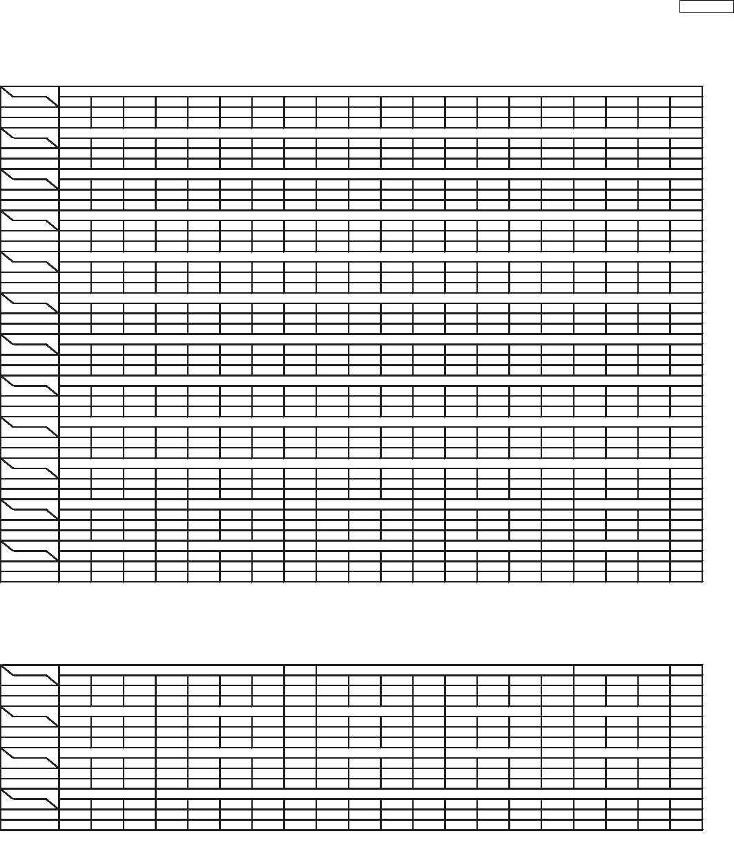
15.3. D-Amp P.C.B.
Ref No.
MODE 1234567891011121314151617181920
CD PLAY 2.5 0 0 29.1 0 -29.2 -21.2 29.4 10.8 -0.1 -29.4 -17.3 -29.4 -0.1 10.8 29.4 -29.2 -29.2 0 29.1
STANDBY 2.5 0 0 29.1 0 -29.2 -21.2 29.4 11 -0.1 -29.4 -17.2 -29.4 -0.1 11 29.4 -29.2 -29.2 0 29.1
Ref No.
MODE 21 22 23
CD PLAY 0 0 2.6
STANDBY 0 0 2.5
Ref No.
MODE 1234567891011121314151617181920
CD PLAY 2.5 0 0 27.9 0 -29.2 -28.3 29.4 0 0 -29.4 -29.4 -29.4 0 0 29.4 -29.2 -29.2 0 27.9
STANDBY 2.5 0 0 29.1 0 -29.2 -21.3 29.4 11.1 0 -29.4 -17.1 -29.4 0.1 11 -29.4 -29.2 -29.2 29.1 0
Ref No.
MODE 21 22 23
CD PLAY 0 0 2.6
STANDBY 0 0 2.6
Ref No.
MODE 1234567891011121314151617181920
CD PLAY 2.54 0 0 29.1 0 -29.2 -21 29.4 10.8 -0.1 -29.4 -17.3 -29.4 -0.1 10.8 29.4 -29.2 -29.2 0 29.1
STANDBY 2.5 0 0 29.1 0 -29.1 -21.2 29.4 11 -0.1 -29.4 -17.2 -29.4 0 11 29.4 -29.2 -29.2 0 29.1
Ref No.
MODE 21 22 23
CD PLAY 0 0 2.6
STANDBY 0 0 2.5
Ref No.
MODE 1234567891011121314151617181920
CD PLAY 2.5 0 0 29.1 0 -29.2 -21.2 29.4 11.3 -0.1 -29.4 -16.8 -29.4 -0.1 11.3 29.4 -29.2 -29.2 0 29.1
STANDBY 2.5 0 0 29.1 0 -29.2 -21.3 29.4 11.1 -0.1 -29.4 -17 -29.4 -0.1 11.1 29.4 -29.2 -29.2 0 29.1
Ref No.
MODE 21 22 23
CD PLAY 0 0 2.6
STANDBY 0 0 2.5
Ref No.
MODE 1234567891011121314
CD PLAY 0 5.3 4.8 0 2.5 2.5 0 2.6 2.6 2.6 2.5 0 5.3 5.3
STANDBY 0 5 4.6 0 2.4 2.4 0 2.5 2.5 2.5 2.4 0 5.1 5.2
Ref No.
MODE 1234567891011121314
CD PLAY2.52.62.602.600000005.35.3
STANDBY2.52.72.602.700000005.25.2
Ref No.
MODEECBECBECBECBECB
CD PLAY050 050 0.700 0.700 5.35.24.6
STANDBY050 050 0.700 0.700 5.35.24.6
Ref No.
MODEECBECBECBECBECB
CD PLAY000.7 716.97.6 050 000.7 03.90.4
STANDBY 0 0 0.7 7 16.9 7.6 0 5 0 0 0.1 0.7 0 3.8 0.2
IC5000
IC5000
IC5200
IC5500
IC5400
IC5200
IC5300
IC5300
IC5400
IC5501
Q5101
Q5102 Q5601
Q5602
Q5603
SA-PT850EE D-AMP P.C.B.
Q5644
Q5604
Q5640 Q5641
Q5642
15.4. SMPS P.C.B.
Ref No.
MODE 12345671234567 123
CD PLAY 14 -11.3 -14.4 -14.6 -14.7 -14.6 -14.6 -13.7 -14.4 -14.1 -10.8 14.4 -14.7 -14.2 -27.1 -29.8 -2
STANDBY 14.1 -11.2 -14.4 -14.7 -14.7 -14.7 -14.6 -13.6 -14.4 -14.1 -10.9 14.4 -14.8 -14.2 -27.1 -29.8 -2
Ref No.
MODEECBECBECBECBECB
CD PLAY -14 -13.4 -14.2 -11 -11 -11.2 -14.8 -2.6 -14.8 -22 -2 -22.2 1.3 0 0.7
STANDBY -14 -13.4 -14.3 -11.1 -11 -11.2 -14.8 -2.6 -14.8 -22 -2 -22.2 1.3 0 0.7
Ref No.
MODEECBECBECBECBECB
CD PLAY 0 0 0.7 0 5.1 0 0 3.3 0.5 3.6 4.5 4.2 0 5.1 -2.5
STANDBY 0 0 0.7 0 5.1 0 0 3.3 0.5 3.6 4.5 4.2 0 5.1 -2.4
Ref No.
MODE E C B
CD PLAY 0 0.1 4.9
STANDBY 0 0.1 4.8
SA-PT850EE SMPS P.C.B.
Q5720
Q5721 Q5722
Q5802
QR5801
QR5810
IC5799
Q5860
Q5861
Q5862 Q5898
Q5899
IC5801IC5701
65
SA-PT850EE
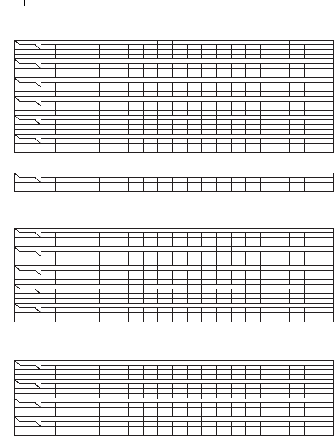
15.5. Panel & Tray Loading P.C.B.
Ref No.
MODE 12345678 12345678
CD PLAY000-6.90007 000-6.10006.9
STANDBY000-70007 000-6.90007
Ref No.
MODE 1234567891011121314151617181920
CD PLAY00002.92.21.842.32.22.205-24.4-22-24.4-24.4-19.6-19.8-15
STANDBY00002.92.11.942.22.22.205-24.4-24.4-22-24.4-14.9-19.6-12.5
Ref No.
MODE 21 22 23 24 25 26 27 28 29 30 31 32 33 34 35 36 37 38 39 40
CD PLAY -24.4 -24.4 -24.3 -17.2 -14.8 -24.4 -24.4 -24.4 14.8 -24.8 -15 -22 -22.3 -22.2 -22.2 -22.2 -22.2 -22.2 -22.2 -22.2
STANDBY -24.3 -24.3 -24.3 -17.2 -14.9 -24.3 -24.3 -24.3 -17.2 -24.8 -15 -15 -22.2 -22.2 -22.2 -22.2 -22.2 -22.2 -22.2 -22.2
Ref No.
MODE 41 42 43 44
CD PLAY -22.2 -22.2 5 0
STANDBY -22.2 -22.2 5 0
Ref No.
MODEECBECBECBECBECB
CD PLAY 0 0 0.7 7 0 6.9 0 0.1 4.9 0 6.8 0.1 2.3 2.3 0
STANDBY 0 0 0.7 7 0 6.9 0 0.1 4.9 0 6.8 0.1 2.3 2.3 0
Ref No.
MODE E C B
CD PLAY 4.8 - 4.5
STANDBY 4.9 - 4.5
Ref No.
MODE 123456789
CD PLAY 5.1 7.5 0.6 7.5 0 7.5 0.6 2.8 5.1
STANDBY 5.1 7.6 0.6 7.6 0 7.6 0.6 2.8 5.1
IC6106 IC6107
Q6102
Q6105 Q6110
Q6111
Q6201
SA-PT850EE PANEL P.C.B.
SA-PT850EE TRAY LOADING P.C.B.
IC6901
IC6901
IC6901
IC904
Q6202
15.6. Scart P.C.B.
Ref No.
MODE 1234567891011121314151617181920
CD PLAY 4.8 0 0 2.1 4.6 1.6 0 1.6 2.2 4.8 0.1 0 0 0 0.1 4.8 2.6 2.6 0 3.7
STANDBY 4.8 0 0 2.1 4.6 1.6 0 1.6 2.2 4.8 0.1 0 0 0 0.1 4.8 2.6 2.6 0 3.7
Ref No.
MODE212223242526272829303132 123456
CD PLAY 0 0 3.5 3.5 0 1.3 1.3 0 1.4 1.6 0 0 0 2.4 4.8 2.8 0 2.5
STANDBY03.73.701.31.301.41.602.30 02.54.82.402.4
Ref No.
MODEECBECBECBECB
CD PLAY 0 8.3 0.1 1.1 0 1.1 11.5 11.5 0 0 0.1 4.5
STANDBY 0 7.3 0 1 0 1.1 11.5 11.5 0.1 0 0.1 4.5
Ref No.
MODE 123456 ECB ECB ECB
CD PLAY 4.8 4.8 4.8 0 0 0 11.5 16.8 12.1 0 4.6 0 0 0 -4.6
STANDBY 4.8 4.8 4.8 0 0 0 11.4 16.9 12.1 0 4.6 0 0 0 0.7
Ref No.
MODE E C B
CD PLAY 0 0 4.6
STANDBY 0 0 0.7
Q1002
Q1005
Q1004Q1003
SA-PT850EE SCART P.C.B.
IC1101
IC1102IC1101
Q1006 Q1007 Q1008 Q1100
Q1200
15.7. Mic P.C.B.
Ref No.
MODE 12345678
CD PLAY000-6.90006.9
STANDBY000-6.90007
Ref No.
MODE 12345678910111213141516
CD PLAY - 2.6 2.6 2.6 2.6 0.6 0.6 0 2.6 2.6 2.6 2.6 2.6 0.9 5.2 -
STANDBY - 2.6 2.6 2.6 2.6 0.6 0.6 0 2.6 2.6 2.6 2.6 2.6 0.9 5.2 -
Ref No.
MODE 12345678
CD PLAY 6.6 0 0 -6.9 0 0 0.1 6.9
STANDBY 6.6 0 0 -6.9 0 0 0.1 7
Ref No.
MODE E C B E C B E C B
CD PLAY000 005 000
STANDBY000 005 000
IC7000
SA-PT850EE MIC P.C.B.
IC7100
IC7200
Q7102Q7101
Q7100
66
SA-PT850EE
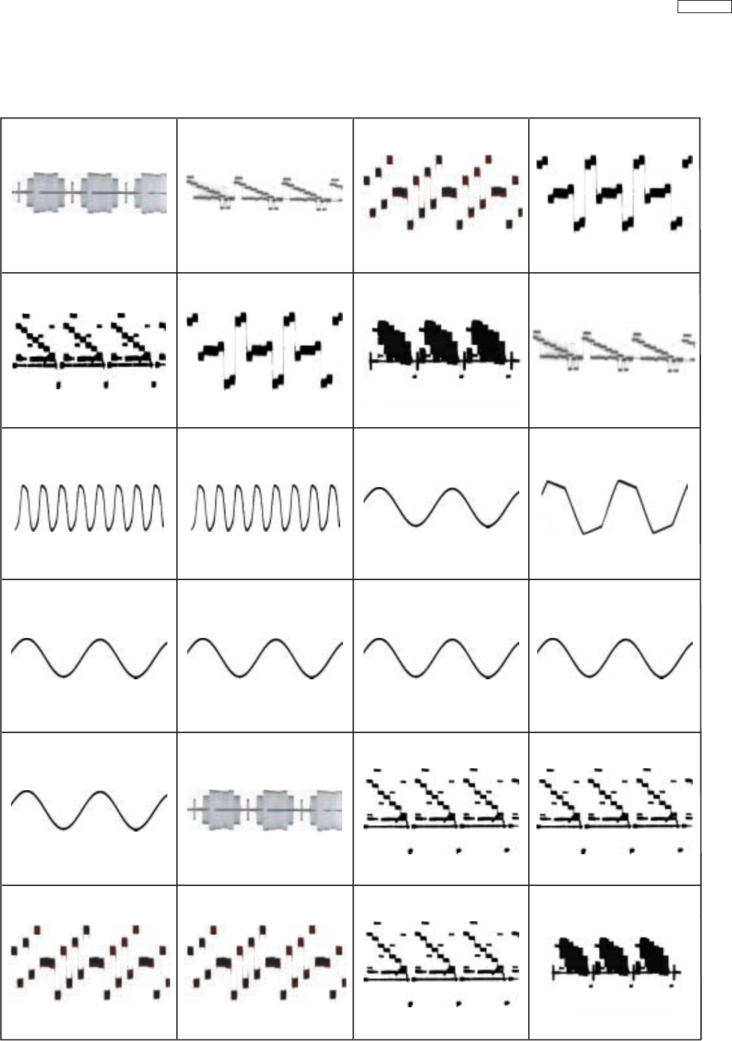
15.8. Waveform Chart
15.8.1. Waveform 1
WF No. IC1101-4 (PLAY)
1.3Vp-p(20usec/div)
WF No. IC1101-8,21,24 (PLAY) WF No. IC1101-11 (PLAY)
0.5Vp-p(20usec/div)
WF No. IC1101-13 (PLAY)
0.5Vp-p(20usec/div)
WF No. IC1101-18 (PLAY)
0.9Vp-p(20usec/div)0.8Vp-p(20usec/div)
WF No. IC1101-15 (PLAY)
WF No. IC1102-2 (PLAY)
2.1Vp-p(20usec/div)
WF No. IC1101-32 (PLAY)
2.1Vp-p(20usec/div)
1.1Vp-p(20usec/div)
WF No. IC2001-13 (PLAY)
5.2Vp-p(100nsec/div)
WF No. IC2001-15 (PLAY)
2.8Vp-p(100sec/div)
WF No. IC2101-14,19 (PLAY)
2.4Vp-p(200usec/div)
WF No. IC2101-15,16,17,
18 (PLAY)
8Vp-p(200usec/div)
WF No. IC2101-81,82 (PLAY)
3.2Vp-p(200usec/div)1.5Vp-p(200usec/div)
WF No. IC2101-80 (PLAY)
WF No. IC2101-95, 96 (PLAY)
3.2Vp-p(200usec/div)
WF No. IC2102-1 (PLAY)
6.8Vp-p(200usec/div)
WF No. IC2102- 7(PLAY)
1.5Vp-p(200usec/div)
WF No. IC2801-6 (PLAY)
1.2Vp-p(20usec/div)
WF No. IC2801-8,11 (PLAY)
1.3Vp-p(100nsec/div)
WF No. IC2801-4 (PLAY)
0.7Vp-p(20usec/div)
WF No. IC2801-13,15 (PLAY)
3.4Vp-p(2usec/div)
WF No. IC2801-18,21 (PLAY)
0.25Vp-p(20usec/div)
WF No. IC2801-24 (PLAY)
3.4Vp-p(20usec/div)
WF No. IC2801-30 (PLAY)
3.4Vp-p(20usec/div)
67
SA-PT850EE
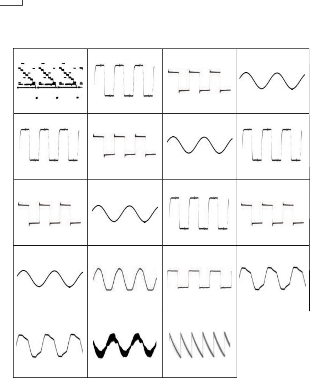
15.8.2. Waveform 2
WF No. IC5500-5 (PLAY)
7.2Vp-p(500nsec/div)
WF No. IC5701-1,4 (PLAY)
WF No. IC5799-2,3,5 (PLAY)
170Vp-p(5msec/div)
180Vp-p(5msec/div)
WF No. IC5500-8 (PLAY)
5.6Vp-p(500nsec/div)
WF No. IC6901-5 (PLAY)
2.8Vp-p(100nsec/div)
WF No. IC5400-2,22 (PLAY)
0.6Vp-p(200usec/div)
WF No. IC5400- 1 (PLAY)
5.8Vp-p(1usec/div)
WF No. IC5400-10,14 (PLAY)
76Vp-p(1usec/div)
WF No. IC5300-10,14 (PLAY)
76Vp-p(1usec/div)
WF No. IC5300-2,22 (PLAY)
0.6Vp-p(200usec/div)
WF No. IC5801-1,2,3 (PLAY)
0.5Vp-p(2usec/div)
WF No. IC5000- 1 (PLAY)
5.8Vp-p(1usec/div)
WF No. IC5000-10,14 (PLAY)
76Vp-p(1usec/div)
WF No. IC5200- 1 (PLAY)
5.8Vp-p(1usec/div)
WF No. IC5200-10,14 (PLAY)
76Vp-p(1usec/div)
WF No. IC5000- 2,22 (PLAY)
0.6Vp-p(200usec/div)
WF No. IC5200-2,22 (PLAY)
0.6Vp-p(200usec/div)
WF No. IC2802-2 (PLAY)
2Vp-p(20usec/div)
WF No. IC5300- 1 (PLAY)
5.8Vp-p(1usec/div)
68
SA-PT850EE
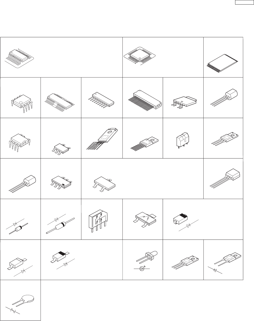
16 Illustration of IC's, Transistors and Diodes
No.1
No.1
1
3
2
B0EAKM000117
B0EAMM000057
B0JAME000029
B0EAKB000004
A
Ca
Cathode
Anode
C3ABPG000145 (54p)
C9ZB00000461 (32p)
XP0621400L
C0EBA0000029 (4p)
C0FBBK000050 (28p)
C0DBZYY00018 (8p) C0JBAF000716 (14p)
C1BB00001061 (16p)
C0DBZYE00002 (8p)
C0ABBB000350 (8p)
C0JBAB000902 (14p)
C0JBAB000908 (6p)
C1AB00001731 (6p)
C0JBAZ001251 (20p)
C0HBB0000057 (44p)
C1AB00002735 (100p)
C2CBYY000418 (100p)
RFKWMHB0E321
MN864702A (128P)
MN2DS0018MP (216P)
1
24
25
48
C0AABB000125
C0ABBB000230 (8p)
MIP4110MSSCF
1
4
8
5
14
25
3
E
C
B
B1BACD000018
B0ACCK000005
A
Ca
Cathode
Anode
B0JCAE000001
B0JCPD000025
B0BC01700015
B0BC035A0007
B0BC3R400001
B0BC4R600016
B0BC7R500001
B0BC6R100010
A
Ca
Cathode
Anode
B0BC2R4A0006
B0BC3R700004
B0BC01200019
B0BC5R000009
B0BC5R600003
B0BC010A0007
Cathode
A
Ca
Anode
MA2J11100L
MAZ82400HL
A
Ca
Cathode
Anode
MA2J72800L
C0GBG0000048 C0GAY0000013
2SD1819A0L
2SB0709AHL
2SD0601AHL
2SB1218ARL
UNR511V00L
UNR211H00L
UNR221200L
UNR521100L
B1ABCF000176
B1ABCF000011
B1GBCFJJ0051
B1GDCFGA0018
B1ADGB000008
B1GBCFLL0037
B1CFHA000002
B1ABEB000002 B1ADCE000012
B1ABGC000005
B1ADCF000001
B1GBCFJN0033
Anode
Anode
Anode
Cathode
B0FBAR000041
1
28
15
14
7
21
30
22
8
29
B1GFGCAA0001
XN0460100L
1
2
3
456
C0DABFC00002C0DBEHG00006C1BA00000487
Ca
A
A
B0HBSM000043
C
E
B
B1BACG000023
B1BCCG000002
ECB
2SC3940ARA
B1AAKD000012
B1ACKD000006
C0EBE0000456
C0JBAA000501
C0JBAA000502
C0JBAB000907
C0CBCDC00063 C5HACYY00003
1
4
5
23
B0ZAZ0000052 B0HFRJ000012
A
Ca
Cathode
Anode
ERZV10V511CS
Cathode
Anode
B0ADCJ000020
Anode
Cathode
1
23
1
4
8
5
B1BABK000001
12
3
C0DAAYY00042
C0DAAMH00012
2
1345
E
C
B
1
9
1
24
3576
B3AAA0000803
Anode
Cathode
Ca
A
Ca
A
69
SA-PT850EE

SA-PT850EE
70
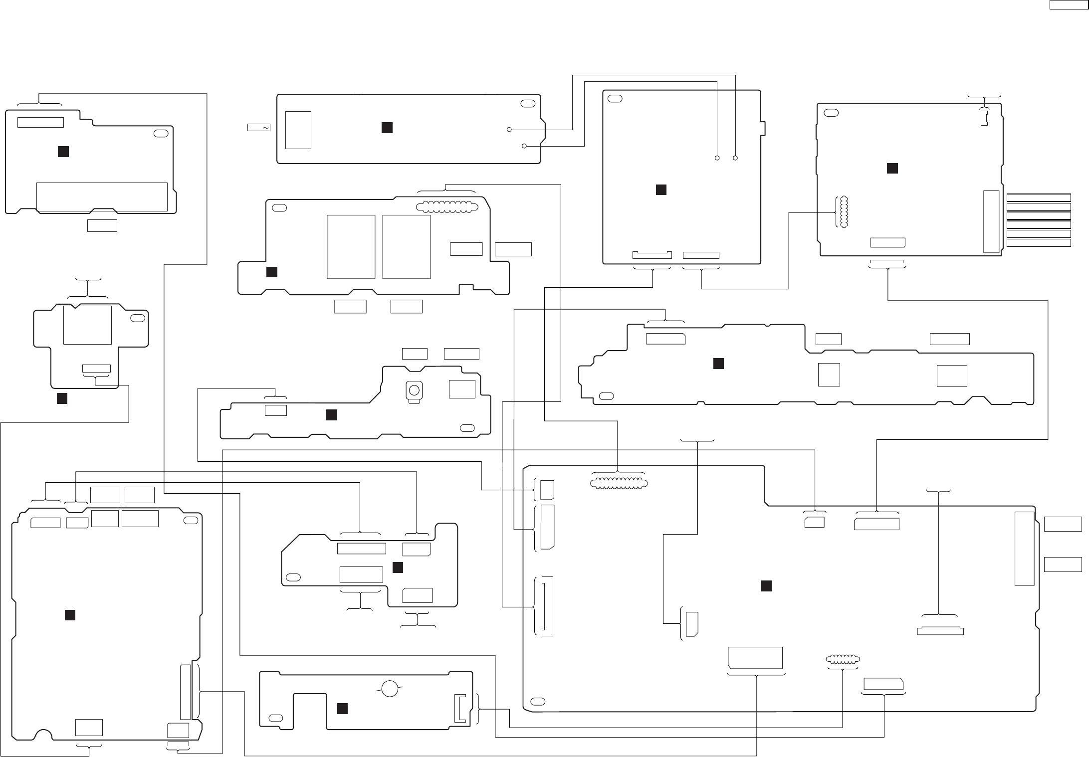
17 Wiring Connection Diagram
SA-PT850EE WIRING CONNECTION
VR7001
H7000
JK7001
JK7002
MIC 2 MIC 1
MIC VOLUME
1
23
4
5
1
123
7
9
8
23
4
5
1
78
BMAIN P.C.B.
(SOLDER SIDE)
CPANEL P.C.B.
(SOLDER SIDE)
DVOLUME P.C.B.
(SOLDER SIDE)
EMIC P.C.B.
(SOLDER SIDE)
FUSB P.C.B.
(SOLDER SIDE)
REF
NO.316
+
-
MCS901
7
1
PbF
TO TUNER
PACK UNIT
FOR SOFTWARE
TO OPTICAL
PICKUP TO SPINDLE
MOTOR ASS’Y
FP8101
FP8251 JK8001
FP8531
FP3902
125
226
1
5
2
6
1
50
17
P3901
23
22 21
20
19151051
HDMI AV
OUT
OPTICAL
IN
AV
PbF
PbF
ADVD MODULE P.C.B.
(SIDE:B)
1
7
TO USB
AUX
COMPONENT
VIDEO OUT
CN2008
CN2001
CN2015
CN2002
JK2001
CN2009
CN2006
CN2010
CN2004
CN2007
CN2020
1
19 18
2
1
2
781
11
12
78
1
3
2
4
49
50
47
48
1
267
17
1
218
19
1
2
17
16
110
8
97
6
5
4
CN5802 CN5801
118
11
FP8002
FP8001
FP8004
FP8003
16
1
6
1
1
26
26
FRONT SPEAKER L
TO FAN UNIT
FRONT SPEAKER R
SURROUND SPEAKER R
SURROUND SPEAKER L
CENTER SPEAKER
SUBWOOFER
CN5050
H5500
CN5501
JK5001
1
8
2
1
16
17
1
3
1
2
3
4
5
6
7
8
9
10
11
12
2
117
230V 50HZ
WHT
GRY
P5701
CN1001
JK1001
1
218
19
1
2
3
4
5
6
7
8
9
10
11
12
13
14
15
16
17
18
19
20
21
JK6802
18
19
2
1
CN6902
Z6900
1
2
3
1
3
5
4
2
6
7
CN9000
FP9002
1
5
JK6801
VR6801
VOLUME
CN6901
1
2
7
8
1
2
3
4
5
6
7
GD-AMP P.C.B.
(SOLDER SIDE)
HSMPS P.C.B.
(SOLDER SIDE)
IAC-INLET P.C.B.
(SOLDER SIDE)
JSCART P.C.B.
(SOLDER SIDE)
K RELAY P.C.B.
(SOLDER SIDE)
L TRAY LOADING P.C.B.
(SOLDER SIDE)
GRY
WHT
123 4
SENSOR MUSIC PORT
HEADPHONE
PbF
PbF
PbF
PbF
PbF
PbF
PbF
PbF
PbF
53421
FP9001
1
9
CN2013
2
1
3
AC IN
SA-PT850EE
71

SA-PT850EE
72
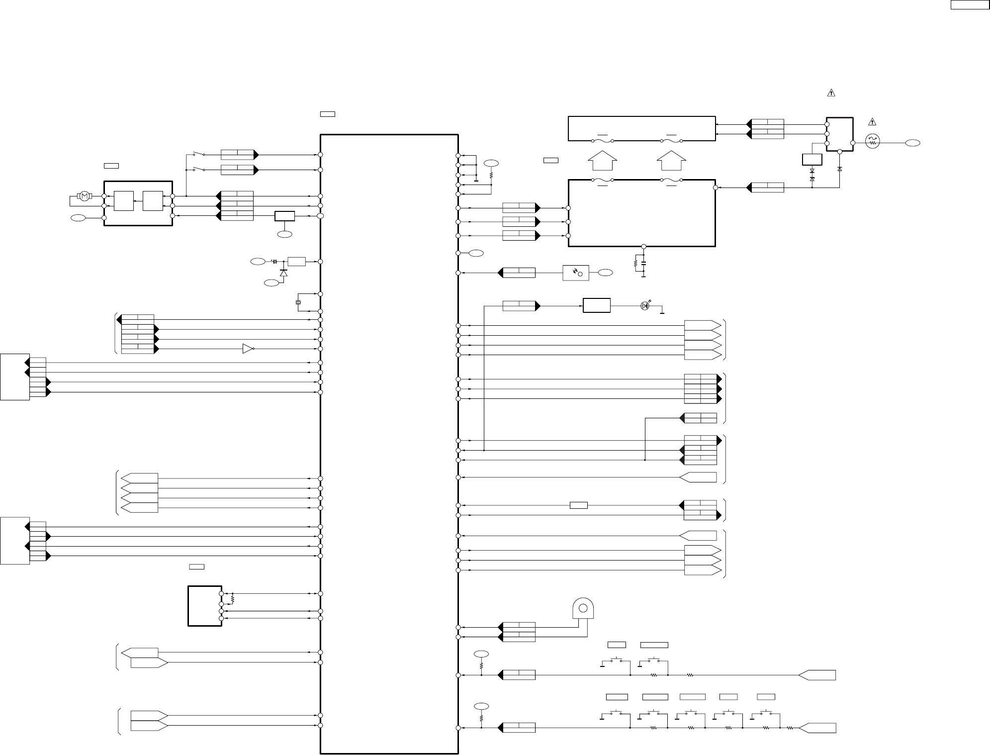
18 Block Diagram
18.1. System Control
CN6902
9
CN2007
CN6902
10
CN2007
CN6902
11
CN2007
CN6902
5
CN2007
CN6902
2
CN2007
CN6901
1
CN2020
CN2007
5
CN6902
CN2007
6
CN6902
CN2007
7
CN6902
Q6201 D6901
DRIVE
LED
CN6902
1
CN2007
AC IN LED
SYNC
(VOLUME)
JOG A
76
JOG B
77
CN6901
CN6901
CN2020
3
CN2020
4
ACS MUTE
ACS
ACS MUTE
ACS IN
74
92
FOR SOFTWARE
TXD
CLOCK
RXD
BUSY
1
2
3
5
CN2006
CN2006
CN2006
CN2006
FX DO
FX CLK
FX DI
FX DET1
31
33
32
34
AUDIO
FROM/TO
ECHO LV1
ECHO LV2
ECHO MUTE
MIC SW
ECHO LVL1
ECHO LVL2
ECHO MUTE
83
84
88
MIC SW
5
Q2006, Q2007, Q2008
SYSTEM CONTROL
IC2001
C2CBYY000418
SA-PT850EE SYSTEM CONTROL BLOCK DIAGRAM
13
15
30
DVD CMD
TUN CLK
39
TUN DI
38
DVD CLK
28
DVD STAT
29
DVD MUTE
42
TUN SD
49
TUN DO
37
SENSE1
59
FROM/TO
AUDIO
FROM/TO
AUDIO
SENSE1
SENSE2
60
SENSE2
ECS
25
ASP CLK
47
ASP DAT
48
MIC EN
21
TV EN
26
FX EN
39
AGC EN
45
OPT EN
61
ECK
24
EDA
23
SYNC
19
DC DET2
63
DC DET1
43
78
MODE DA
MUTE F SW
68
PCONT
72
MUTE C S
69
71
KEY2
91
HP MUTE
KEY1
97
MPORT
FROM AUDIO
HP DETECT
FROM AUDIO
HP MUTE
46
SCART MUTE
SCART MUTE
DC DET1
MUTE S
MUTE F
MOD DA
IC2003
EEPROM
(Not Supplied)
CS
DO
SK
DI
FL DISPLAY
G1
P17
G10
P1
G1
P17
G10
P1
FL6901
DISPLAY DRIVER
IC6901
C0HBB0000057
FL CLK
D IN
FL2
3
4
6
5
ASP CLK
ASP DAT
TO AUDIO
CEC OUT
73
CEC IN
75
BUFFER
Q2096,Q2097
CEC OUT
CEC IN
VMUTE
VMUTE
TO
DVD (VIDEO)
87
STB
18
CLK
85
7
8
9
FLD OUT
RMT
OSC
5
30
-VP
(REMOTE SENSOR)
Z6900
98
86
FL STB
FL1
+18V
X IN
X OUT
X2001
10MHz
TUN CLK
TUN DI
TUN SD
TUN DO
TUNER PACK
SYNC
DC DET
DC DET
PCONT
Q2900
ZFLAG
CPU CLOCK
CPU STATUS
CPU CMD
FP8101
2
CN2001
FP8101
CN2001
FP8101
CN2001
CN2002
2
CN2002
CN2002
CN2002
3
4
6
1
FP8101
CN2001
23
3
VREF
S6801 S6802 S6803 S6804 S6907
REVERSE FORWARDSELECTOR STOP
S6902
S6901
POWER OPEN/CLOSE
PLAY
12 6
CN5050
CN2009
13 5
CN5050
CN2009
17 1
CN5050
CN2009
16 2
10
CN5802
CN2004
1
CN5802CN2004
4
CN5802CN2004
7
CN2010
5
FP3902
CN2010
FP3902
SWITCHING
TRANSFORMER
T2900
PSAVE
CONTROL
FP2900
8
9
31
5
VREF
VREFVREF
VREF
VREF
CN5050CN2009
DIGITAL AUDIO
AMP
FROM/TO
POWER
FROM/TO
SYSTEM CONTROL
FROM/TO
DVD (AUDIO)
TO/FROM
100
S902
Q2030
CONTROL
VREF
BRAKE H
VCC VREF
TRY CW
TRY CCW
MOTOR
TRAY
LOADING
C0GAY0000013
TRAY LOADING MOTOR DRIVE
IC904
CONTROL
DRIVE
7
3
28
1
9 2
3
4
TRAY CLOSE
M+9V
OPEN
1
3
7
4
S901
1
TRAY OPEN
PLAY
2
CS901
CS901
CN2015
CN2015
CN2015
CN2015
CN2015
CS901
CS901
CS901
VREF
12
RGB H
RGB H
53
YC H
YC H
65
WIDE 1
WIDE 1
80
46
RESET
Q2003
RESET
VREF
SYS6V
VR6801
SA-PT850EE
73
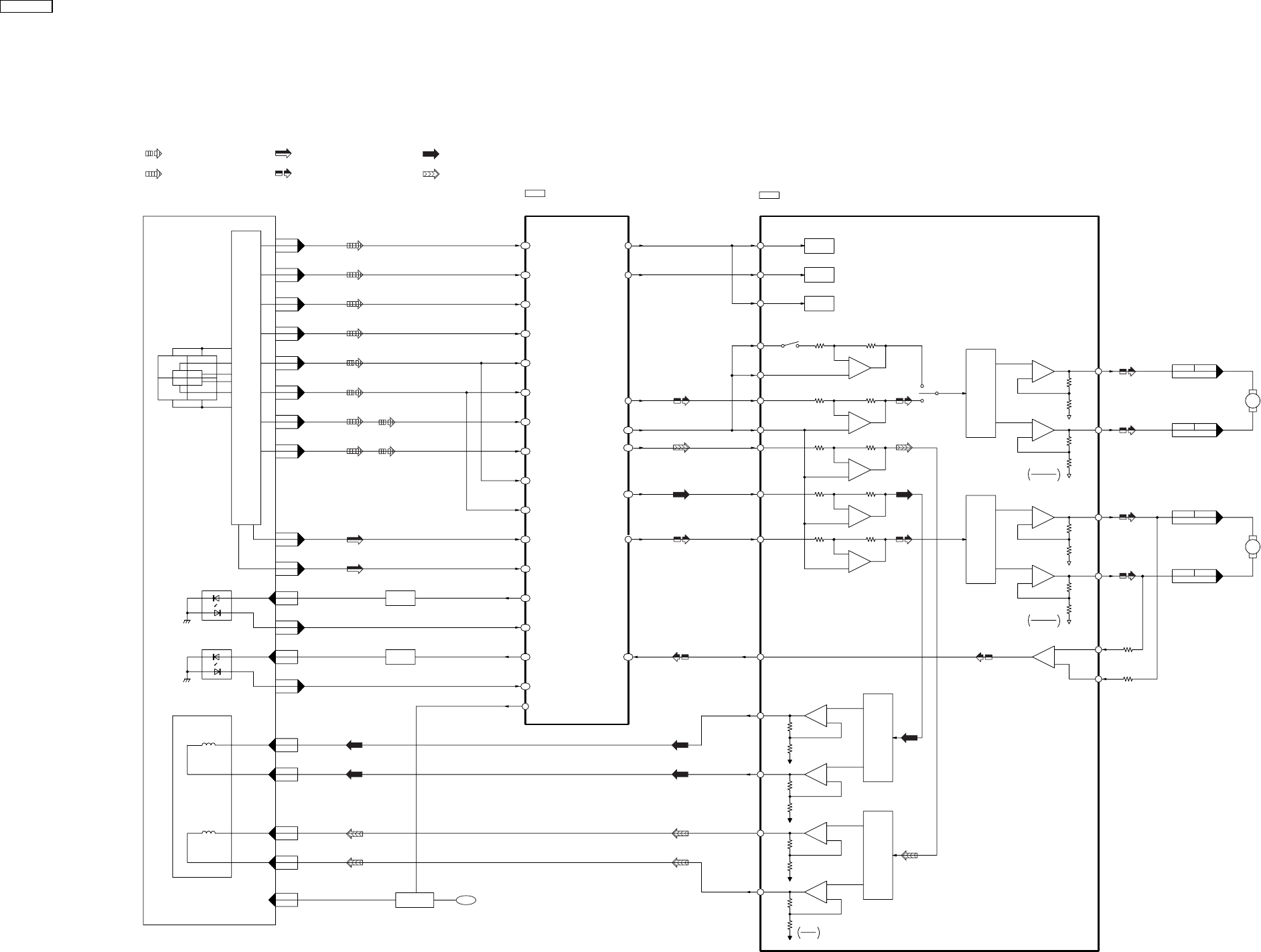
18.2. DVD (Servo)
1
-
FP8251
2
-
FP8251
MOTOR
SPINDLE
M
3
-
FP8251
4
-
FP8251
CH3
CH3
VCC2-Vf
2
2
VCC2-Vf
CH4
CH4
-
+
2
VCC1
CH2
CH2
CH1
CH1
OPIN+
OPIN-
4
5
+
-
MOTOR
TRAVERS
M
BIAS2
+
-
LDIN
24
25
1
VO3-
18
+
-
VO3+
17
+
-
SHIFT
LEVEL
VO4-
16
+
-
VO4+
15
-
+
-
+
-
+
SHIFT
LEVEL
+
-
BIAS1
SHIFT
LEVEL
SHIFT
LEVEL
-
+
-
+
-
+
-
+
VO2-
VO2+
VO1-
VO1+
OPOUT
VIN3
VIN1
VIN2
TRIN
OPTICAL PICK UP UNIT
PHOTO DETECTOR
A3A4
B3B4
A2A1
B2B1
24
FP8531
F-
22
FP8531
HFM
25
COIL
FOCUS
FP8531
F+
ACTUATOR
COIL
TRACKING
23
FP8531
T-
T+
26
FP8531
(CD)
DIODE
LASER
(DVD)
DIODE
LASER
AMP
HEAD
11
12
13
14
AD1
6
122
66 23
DRV1
PWM1
2
126
127
3
PWM0
DRV0
26
67
VHALF
110
MOTOR DRIVE
48 27
MUTE
CH3
P3
P4
MUTE
CH1,2
9
49
LPC2
TRCDATA1
LPCO2
LPC1
LPCO1
RFINP
RFINN
VIN10
VIN9
VIN8
VIN7
VIN6
VIN5
VIN4
VIN3
VIN2
VIN1
105
PIN(CD)
FP8531
3
FP8531
PIN(DVD)
103
12
LD DRIVE
11
106
LD+(CD)
FP8531
Q8561,Q8562
SUPPLY CONTROL
SWITCH
QR8571
LD DRIVE
Q8551,Q8552
FP8531
LD+(DVD)
104
9
14
96
RFP
FP8531
FP8531
RFN 95
13
111
112
17
116
FE2(DVD/CD)
FP8531
FP8531
FE1(DVD/CD)
115
16
5
114
SUB2
FP8531
4
FP8531
SUB1
113
118
TD(DVD)
FP8531
19
TC(DVD)
117
18
FP8531
20
FP8531
TB(DVD)
119
TA(DVD)
21
FP8531
DV5.0 LSI
120
20
MUTE
CH4
78
HFMON
D+3.3V
IC8001 IC8251
MN2DS0018MP C0GBG0000048
SA-PT850EE DVD (SERVO) BLOCK DIAGRAM
: DVD HEAD SIGNAL LINE
: DVD RF SIGNAL LINE
: MOTOR DRIVE SIGNAL LINE
: CD HEAD SIGNAL LINE : TRACKING ERROR SIGNAL LINE
: FOCUS ERROR SIGNAL LINE
SA-PT850EE
74
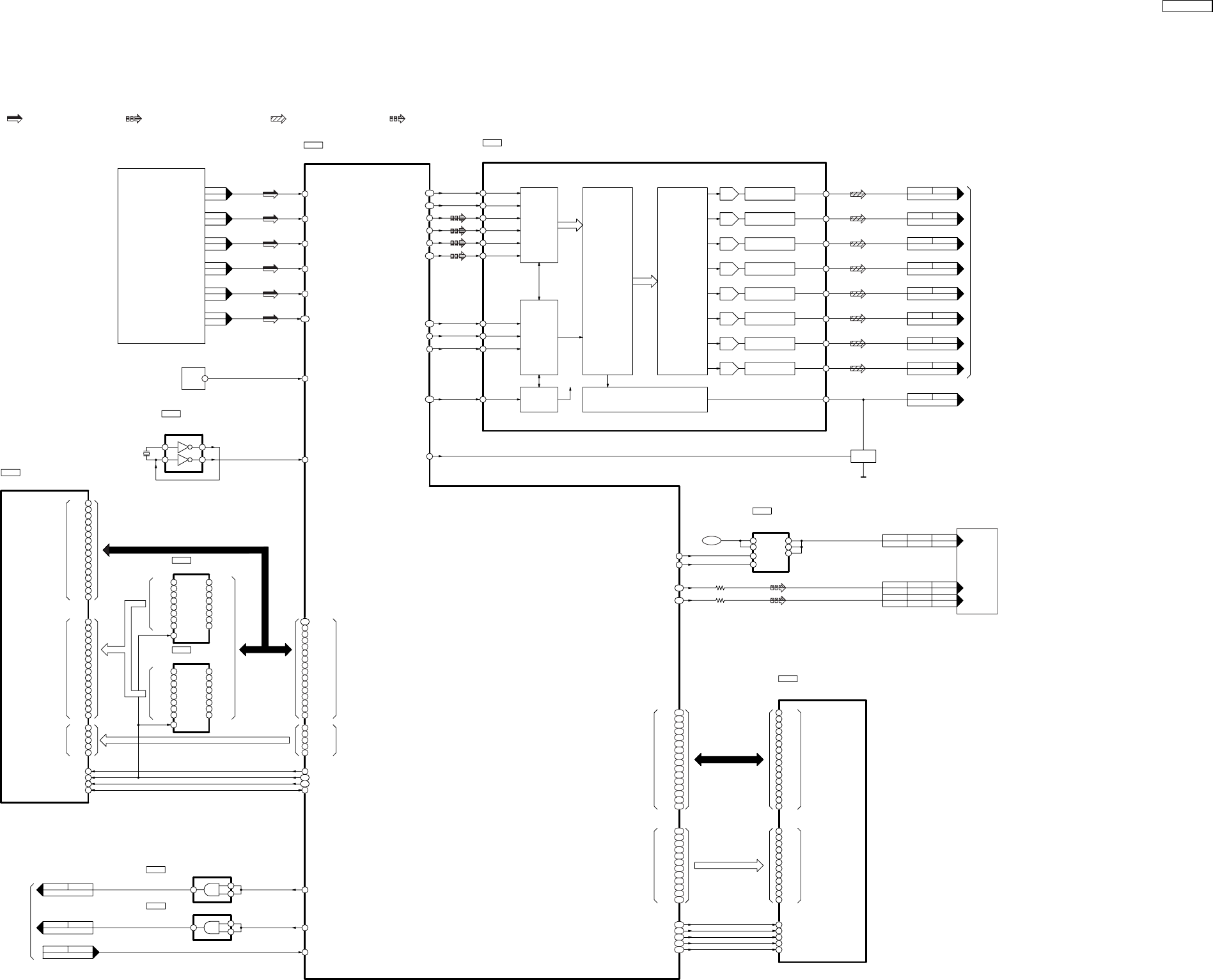
18.3. DVD (Audio)
4
6
USB
RECEPTACLE
D +
D -
3
1
CN9000
VBUS OUT
2
3
FP9001
1
FP9001
2
FP9001
3
5
FP9002
CN9000FP9002
CN9000FP9002
4
IC9005
5
4
3
2
OC
EN
IN
IN
OUT
OUT
6
7
OUT 8
C0DBZYE00002
USB VBUS
USB OVER
D+5V
146
ROUT
144
LOUT
60
65
P13
DRV2
REGULATOR
OPTICAL PIC-UP UNIT
ADDRESS
MEMORY
DATA
MEMORY
IC8051
64M SDRAM
ADDRESS
MEMORY
DATA
MEMORY
CLK
NWE
NCAS
NRAS
NCS
A11
A10
A9
A8
A7
A6
A5
A4
A3
A2
A1
A0
DQ15
DQ14
DQ13
DQ12
DQ11
DQ10
DQ9
DQ8
DQ7
DQ6
DQ5
DQ4
DQ3
DQ2
DQ1
DQ0
38
16
17
18
19
35
22
34
33
32
31
30
29
26
25
24
23
53
51
50
48
47
45
44
42
13
11
10
8
7
5
4
2
MCK
NWE
NCAS
NRAS
NCSM
MA11
(DQM3)
MA10
MA9
MA8
MA7
MA6
MA5
MA4
MA3
MA2
MA1
MA0
MDQ15
MDQ14
MDQ13
MDQ12
MDQ11
MDQ10
MDQ9
MDQ8
MDQ7
MDQ6
MDQ5
MDQ4
MDQ3
MDQ2
MDQ1
MDQ0
IC8001
DV5.0 LSI
RFINP
VN1RF
VN2RF
VN3RF
VN4RF
RFINN
P6
P7
P8
53
55
SYSTEM
CONTROL
TO/FROM
CPU CLOCK
CPU STATUS
CPU CMD
FP8101
2
CN2001
1
3
FP8101
CN2001
100
14
FP8531
RFP
RFN
13
FP8531
160
162
164
168
170
172
176
178
177
175
171
169
201
203
207
209
208
206
202
200
198
199
192
190
189
188
194
181
185
167
163
161
159
TD(DVD)
19
TC(DVD)
18
20
TB(DVD)
TA(DVD)
21
95
96
97
98
99
1
2
4
54
FP8101
CN2001
62
151
63
64
150
149
58
215
148
57
71
FP8101
CN2001
39
FP8101
CN2001
37
FP8101
CN2001
35
FP8101
CN2001
33
FP8101
CN2001
31
FP8101
CN2001
29
FP8101
CN2001
27
FP8101
CN2001
25
23
FP8101
CN2001
A MUTE
QR8420
MUTING
OUTPUT AMP AND
LOW-PASS FILTER
OUTPUT AMP AND
AND GATE
AND GATE
IC8695
C0JBAA000502
IC8691
C0JBAA000502
6
13
12
11
7
8
SRCK
LRCK
DRV3
DRV4
DRV5
ADOUT
DATA1
DATA4
DATA3
DATA2
LRCK
BCK
4
3
2
DACCK
P11
STB DAC
P10
MD
5
FG
SCK
MC
MS
27
28
15
16
19
20
21
22
26
DVD MIX L
DVD MIX R
DVD FL
DVD FR
DVD SL
DVD SR
DVD CNT
SUBW
ZFLAG
MN2DS0018MP
IC8421
AUDIO DAC
C0FBBK000050
I/F
INPUT
SERIAL
CONTROLLER
FUNCTION
WITH
DIGITAL FILTER
OVERSAMPLING
4X/8X
MODULATOR
DELTA-SIGMA
MULTI-LEVEL
ENHANCED
LOW-PASS FILTER
OUTPUT AMP AND
DAC
LOW-PASS FILTER
OUTPUT AMP AND
DAC
LOW-PASS FILTER
OUTPUT AMP AND
DAC
LOW-PASS FILTER
OUTPUT AMP AND
DAC
LOW-PASS FILTER
OUTPUT AMP AND
DAC
V OUT5
V OUT4
V OUT3
V OUT2
V OUT1
LOW-PASS FILTER
DAC
OUTPUT AMP AND
DAC
LOW-PASS FILTER
DAC
ZERO2
V OUT8
V OUT7
V OUT6
MANAGER
CLOCK
SYSTEM
ZERO DETECT
CLOCK
SYSTEM
I/F
CONTROL
FUNCTION
TO AUDIO
TO
SYSTEM CONTROL
C3ABPG000145
FP8531
FP8531
FP8531
FP8531
1
2
4
FP8101
CN2001
SA-PT850EE
DVD (AUDIO) BLOCK DIAGRAM
P5
50
IC9003
X9004
INVERTER GATE
C0JBAB000908
60
65
82
3
4
5
7
6
IC8651
32M FLASH MEMORY
ADDRESS
ADDRESS
DATA
ADDRESS
ADDRESS / DATA
NRST
NEXOE
NEXCE
NEXWE
EXADR20
EXADR19
EXADR18
EXADR17
EXADR16
EXADT15
EXADT14
EXADT13
EXADT12
EXADT11
EXADT10
EXADT9
EXADT8
EXADT7
EXADT6
EXADT5
EXADT4
EXADT3
EXADT2
EXADT1
EXADT0
XRST
12
28
XOE
XCE
26
11
XWE
A20
10
9
A19
A18
16
17
A17
A16
48
1
A15
A14
2
3
A13
A12
4
5
A11
A10
6
7
A9
A8
8
18A7
A6 19
20A5
A4 21
22A3
A2 23
24A1
A0 25
45
DQ15
DQ14
43
41
DQ13
DQ12
39
36
DQ11
DQ10
34
32
DQ9
DQ8
30
DQ7
44
DQ6
42
DQ5
40
38
DQ4
DQ3
35
33
DQ2
31
DQ1
DQ0
29
212
42
41
40
39
38
37
36
29
28
27
26
25
24
23
22
21
35
34
30
45
31
213
214
70
IC9002
LATCH
LE
11
D8 9
D7
D6
8
7
D5
D4
6
5
D3
D2
4
3
D1
EXADT15
EXADT14
EXADT13
EXADT12
EXADT11
EXADT10
EXADT9
EXADT8
EXADT7
EXADT6
EXADT5
EXADT4
EXADT3
EXADT2
EXADT1
EXADT0 2
12
13
14
15
16
17
18
19
Q8
Q7
Q6
Q5
Q4
Q3
Q2
Q1
IC9001
LATCH
LE
11
D8 9
D7
D6
8
7
D5
D4
6
5
D3
D2
4
3
D1
EXADT7
EXADT6
EXADT5
EXADT4
EXADT3
EXADT2
EXADT1
EXADT0
EXADT7
EXADT6
EXADT5
EXADT4
EXADT3
EXADT2
EXADT1
EXADT0 2
12
13
14
15
16
17
18
19
Q8
Q7
Q6
Q5
Q4
Q3
Q2
Q1
C0JBAZ001251
C0JBAZ001251
RFKWMHB0E321
3
1
3
OPTICAL IN
JK8001
EXTRG1
75
IECINPUT
: DVD : MAIN SIGNAL LINE
AUDIO SIGNAL LINE : USB SIGNAL LINE
: DVD RF SIGNAL LINE
SA-PT850EE
75
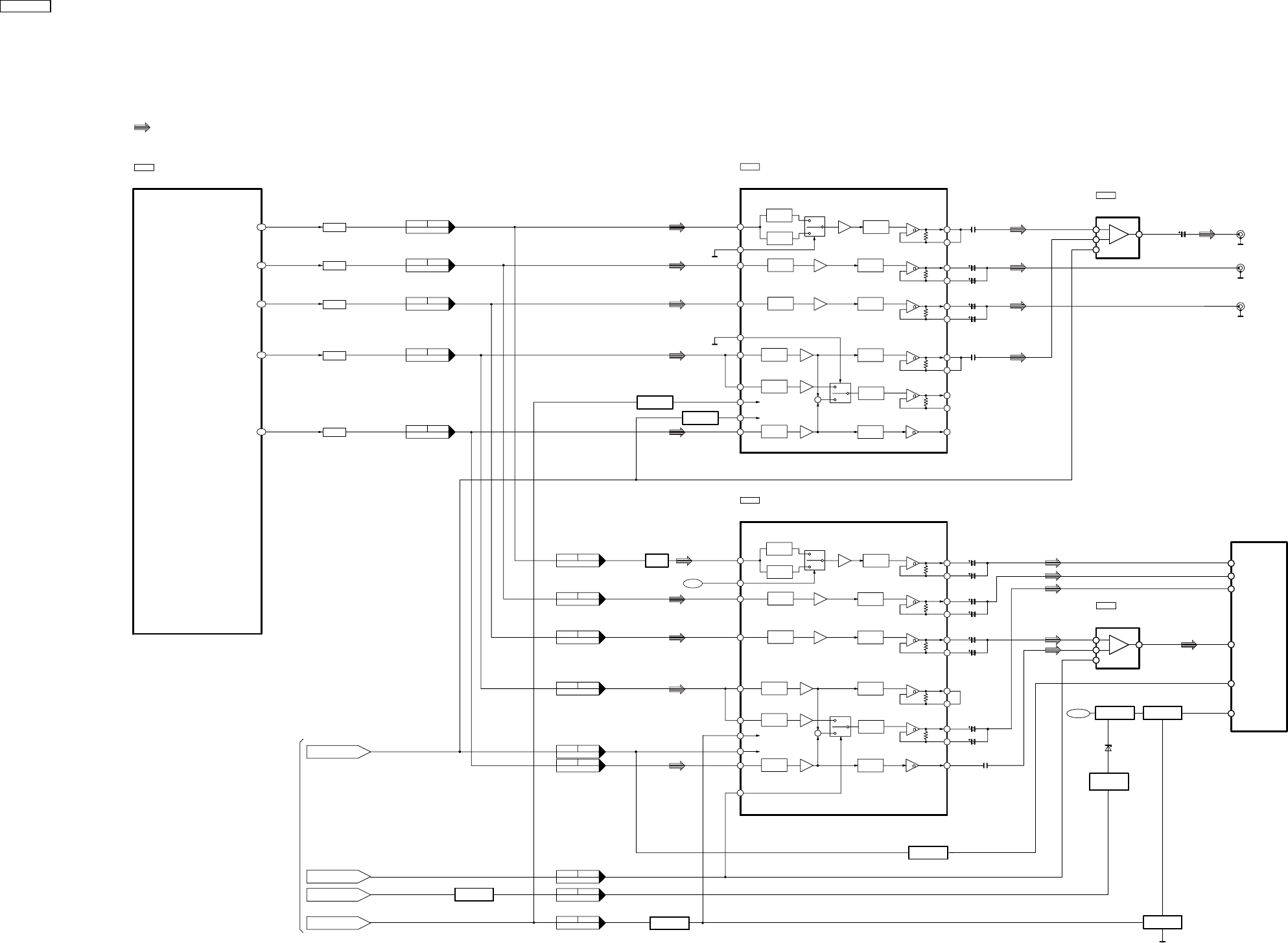
18.4. DVD (Video)
4
C IN
8
5
14
Y IN
MUTE 1
MUTE 2
CR IN
15
13
CB IN
CY IN
11
C OUT
32
IC1101
VIDEO BUFFER
C9ZB00000461
10
BIAS
6dB LPF
6 MHz
CLAMP
6dB LPF
6 MHz
LPF
6 MHz
BIAS
6dB LPF
12 MHz
BIAS
6dB LPF
12 MHz
6dB LPF
12 MHz
CLAMP
+
CY OUT
CY SAG
23
24
75
CR OUT
CR SAG
17
18
75
Y OUT
Y SAG
26
27
75
V OUT
V SAG
29
30
75
CB OUT
CB SAG
20
21
75
75
BIAS
6
CV IN
CLAMP
6dB
L
H
SEL
7
SEL
L
H
REGULATOR
Q1004Q1003
Q1005
SWITCH
Q1002
SWITCH
SWITCH
JK1001
21PIN AV JACK
GREEN I/O
BLUE I/O
FUNK SW
BLK I/O
V OUT
RED I/O
Q1006
BUFFER
Q2805
INVERTER
Q1008
INVERTER
11
7
19
15
8
16
SCART+18V
Q1007
AMP
9
CN1001
CN2008
CN2008
CN2008
11
13
7
5
CN1001
CN1001
CN1001
CN1001
4
CN1001
14
CN1001
3
CN1001
10
CN1001
DVD A+5V
CN2008
CN2008
CN2008
CN2008
CN2008
CN2008
IC8001
DV5.0 LSI
MN2DS0018MP
CR/PR/R
CB/PB/B
Y/PY/G
4
C IN
8
5
14
Y IN
MUTE 1
MUTE 2
CR IN
15
13
CB IN
CY IN
11
C OUT
32
IC2801
VIDEO BUFFER
C9ZB00000461
10
PR(BLUE)
JK2001
PB(GREEN)
JK2001
BIAS
6dB LPF
6 MHz
CLAMP
6dB LPF
6 MHz
LPF
6 MHz
BIAS
6dB LPF
12 MHz
BIAS
6dB LPF
12 MHz
6dB LPF
12 MHz
CLAMP
+
CY OUT
CY SAG
23
24
75
CR OUT
CR SAG
17
18
75
Y OUT
Y SAG
26
27
75
V OUT
V SAG
29
30
75
CB OUT
CB SAG
20
21
75
75
BIAS
6
CV IN
CLAMP
6dB
L
H
SEL
7
SEL
131
130
L
H
C
Y
129
138
DAC1 OUT
DAC2 OUT
DAC3 OUT
DAC4 OUT
DAC5 OUT
139
RGB H
YC H
FROM
SYSTEM CONTROL
WIDE 1
VMUTE
BUFFER
Q8331
BUFFER
Q8335
BUFFER
Q8341
BUFFER
Q8321
BUFFER
Q8325
MUTING
Q2801
MUTING
Q2804
49
CN2001
FP8101
47
CN2001
FP8101
45
CN2001
FP8101
43
CN2001
FP8101
41
CN2001
FP8101
SA-PT850EE DVD (VIDEO) BLOCK DIAGRAM
: DVD VIDEO SIGNAL LINE
6
4
1
Y(RED)
JK2001
VIDEO BUFFER
IC2802
C1AB00001731
IN1
IN2
SW
OUT
2
6
4
1
VIDEO BUFFER
IC1102
C1AB00001731
IN1
IN2
SW
OUT
2
SA-PT850EE
76
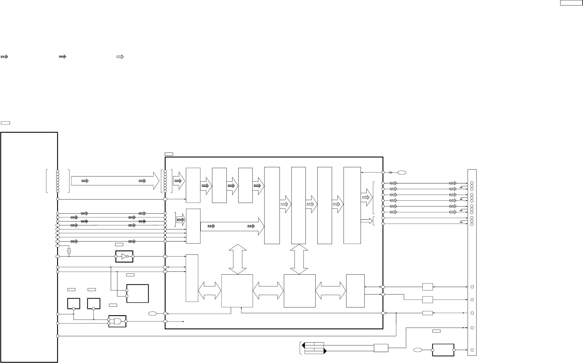
18.5. DVD (HDMI)
SCLOCK VCLK
X8621
OSCO
OSCI
NRST
TRCDATA2
P1
P2
FG
HDMI TRANSMITTER
MN864702A
HDMI
CONNECTOR
P3901
IC8001
DV5.0 LSI
MN2DS0018MP
61
156
155
70
5
6
1
1
79
46
47
71
PCLK IN
HCLK
HSDA
HSCL
NRESET
107
NIRQ
HPD
SDA
SCL
10
119
120
121
12
14
16
18
20
22
24
8
TXCM
TXCP
TX0M
TX0P
TX1M
TX1P
TX2M
TX2P
EXT SWING
D2-
D2 GND
D2+
D1-
D1 GND
D1+
D0-
D0 GND
D0+
CLK-
CLK GND
HDMISDA
HDMISCL
HOTPLG
CEC
18 + 5V
CLK+
OUT
1
OUT
RESET
C0EBA0000029
C0JBAB000907
( Not Supplied)
SDA
SDA
HOTPLG
TXRST
SCL
SCL
RESET
C0EBE0000456
IC8606
16M EEPROM
IC8611
AND GATE
C0JBAA000501
IC8901
INVERTER GATE
24
1
IC8601
IC3901
117
114
113
CEC CIRCUIT
Q3941,Q3942,Q3943
AMSDI0
AMSDI1
AMSDI2
AMSDI3
AMDAWS
AMDACL
AUDIO I/F
VIDEO I/F
DRV4
SRCK
LRCK
DRV3
DRV5
ADOUT
38
37
36
35
41
151
62
63
149
150
64
45
9
10
11
12
13
14
17
18
EXDT15
EXDT7
EXDT14
EXDT6
EXDT13
EXDT15
EXDT12
EXDT4
DVOUT0
DVOUT1
DVOUT2
DVOUT3
DVOUT4
DVOUT5
DVOUT6
DVOUT7 D7
D6
D5
D4
D3
D2
D1
D0
87
88
89
90
92
93
94
95
AMRX
AMDAM
DACCK
IEC OUT
33
43
148
152
UP
CONVERTER
&
SQUEEZE
COLOR
SPACE
CONVERTER
AV
CONTROLLER
HDCP
CIPHER /
ENCRYPTOR
TDMS
ENCODER
TDMS
TRANSMITTER
CONFIGURATION
REGISTER DDC I/F
D+3.3V
D+3.3V
CEC IN
CEC OUT
CONFIGURATION
REGISTER
I2C I/F
LEVEL
SHIFTER
LEVEL
SHIFTER
BUFFER
Q3902
Q3903
Q3901
1
2
3
4
5
6
7
8
9
10
11
12
16
15
19
13
IC8701
111
108
54
IN OUT
TERMINAL VOLTAGE
REGULATOR
IC3952
M + 9V
4
2
C0CBCDC00063
7
CN2010
5
FP3902
CN2010
FP3902
SYSTEM CONTROL
TO/FROM
SA-PT850EE DVD (HDMI) BLOCK DIAGRAM
: DVD : DVD VIDEO SIGNAL LINE : MAIN SIGNAL LINE
AUDIO SIGNAL LINE
SA-PT850EE
77
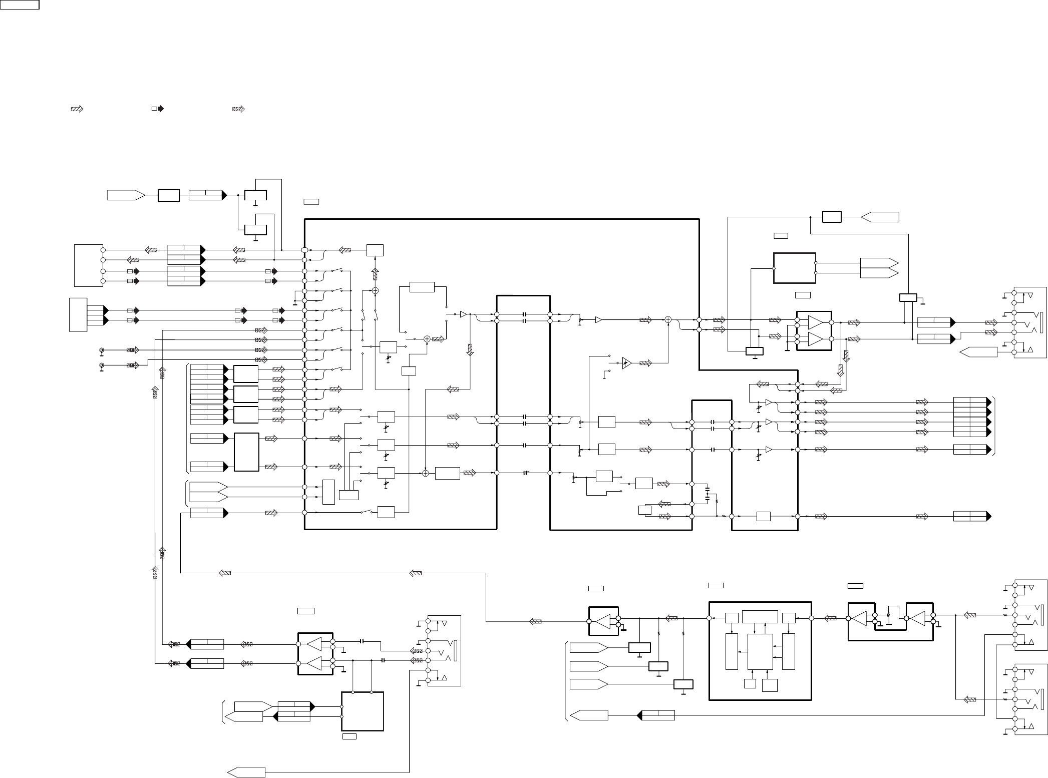
18.6. Audio
+
_
+
_
Q1200
MUTING
Q1009
MUTING
CONTROL
Q1100
MUTING
TV RCH
TV LCH
LINEOUT R
LINEOUT L
JK1001
3
1
6
2
21PIN AV JACK
SCART MUTE
FROM
SYSTEM CONTROL
OPERATIONAL AMP
C0ABBB000230
IC6106
Q6102,Q6105,Q6110,
Q6111,Q6202
ACS
ACS MUTE
TO/FROM
SYSTEM
CONTROL
17
16
ACS MUTE
ACS
CN6902
CN6902
CN2007
CN2007
9
IC7100
DIGITAL DELAY WITH ECHO VOLUME
C1BB00001061
LPF1
LPF2
2
A/DD/A MAIN
CONTROL
OSC AUTO
RESET
20KBIT SRAM
IC7200
C0ABBB000230
MIC AMP
SWITCH
SWITCH
ECHO LV1
Q7100
MUTING
Q7102
Q7101
LPF2OUT LPF1IN ASP MICIN
MIC SW
JK7002
7
6
1
2
3
4
5
MIC 2
MIC SW
JK7001
7
6
1
2
3
4
5
MIC 1
5
H7000
CN2013
+
_
+
_
MIC AMP
IC7000
C0ABBB000230
VR7001
6
5
7
2
3
1
+
_
5
6
7
ECHO MUTE
ECHO LV2
FROM/TO
SYSTEM
CONTROL
MIC VOLUME
1
CN2013
H7000
C0ABBB000350
IC2751
LEVEL
PROTECTION
CIRCUIT
MPORT
SUB IN
MIC IN
C IN
OP IN 1
OP IN 2 OP OUT 2
FLVOL OUT
FRVOL OUT
FLF IN
FRF IN
SL OUT
SR OUT
FL OUT
FR OUT
C OUT
SURROUND L
SURROUND R
FRONT L
FRONT R
CENTER
SUBOUT
OP OUT 1
46
C1AB00002735
AUDIO SIGNAL PROCESSOR
FL IN
SL IN
SR IN
INL2
INR2
INL3
INR4
INR3
INL4
RECOUTR
RECOUTL
AUX L
JK2001
FLSEL OUT
FRSEL OUT
FLVOL IN
FRVOL IN
SLVOL IN
SRVOL IN
CVOL IN
SUBVOL IN
SLSEL OUT
SRSEL OUT
CSEL OUT
SUBSEL OUT
IC2101
AUX R
JK2001
AMP
AMP
AMP
AMP
AMP
AMP
AMP
AGC
AMP
AMP
AMP
AMP
H BASS
ASS
TONE
INL1
INR1
AMP
100
MIX R
MIX L
TUN R-CH
TUN L-CH
AUX R-CH
AUX L-CH
FR IN
RMPORT L
RMPORT R
99
90
89
92
91
93
95
86
85
82
81
79
78
80
7777
97
62
63
12
21
36
35
22
60
20
37
23
52
34
13
19
FRF IN
15
27
14
30
16
44
SRVOL OUT
SLVOL OUT
CVOL OUT
39
25
32
SRF IN
CF IN
SLF IN
40
26
31
48
47
45
46
MCU
I/F
DVD FR
DVD FL
DVD SR
DVD SL
DVD CNT
DVD SUBW
96
94
C0AABB000125
IC2102
HEADPHONES AMP
5
67
-
+
-
+
31
Q2201
Q2101
MUTING
CONTROL
MUTING
17
41
18
2
ASP CLK
ASP DAT
FROM
SYSTEM
CONTROL
FROM
DVD
(AUDIO)
OPERATIONAL AMP
SENSE 1
SENSE 2
TO
SYSTEM CONTROL
HP MUTE
FROM
SYSTEM CONTROL
SA-PT850EE AUDIO BLOCK DIAGRAM
SUBWOOFER
TUNER PACK
JK6801
HP DETECT
TO SYSTEM CONTROL
HEADPHONES
7
6
1
2
3
4
5
TO
SYSTEM CONTROL
INR5
INL5
FMPORT R
FMPORT L
88
87
JK6802
7
6
1
2
3
4
5
MUSIC PORT
MPORT R-CH
MPORT L-CH
MPORT
Q2103
MUTING
TO
AUDIO
DIGITAL AMP
TO AUDIO
DIGITAL AMP
25
CN2001
FP8101
27
CN2001
FP8101
31
CN2001
FP8101
29
CN2001
FP8101
35
CN2001
FP8101
33
CN2001
FP8101
39
CN2001
FP8101
37
CN2001
FP8101
5
7
CN2002
CN2002
117
CN5050
CN2009
315
CN5050
CN2009
711
CN5050
CN2009
99
CN5050
CN2009
11 7
CN5050
CN2009
513
CN5050
CN2009
6
8
CN2020
CN6901
CN2020
CN6901
HP L-CH
HP R-CH
13
CN6902
CN2007
15
CN6902
CN2007
18
CN2008
CN1001
CN1001
16
CN2008
19
CN2008
CN1001
CN1001
15
CN2008
CLOCK
DATA
12
3
6
5
7
C0ABBB000230
IC6107
MUSIC PORT AMP
12
CN2008
CN1001
A(A)IN
A(B)IN
A(A)OUT
A(B)OUT
L IN
R IN
L OUT
R OUT
AUTO
CALIBRATION
CERCUIT
:FM SIGNAL LINE
:MAIN SIGNAL LINE :AUX, MUSIC PORT SIGNAL LINE
Q2202
Q2102
Q2302
Q2502
MUTING
MUTING
MUTING
MUTING
SA-PT850EE
78
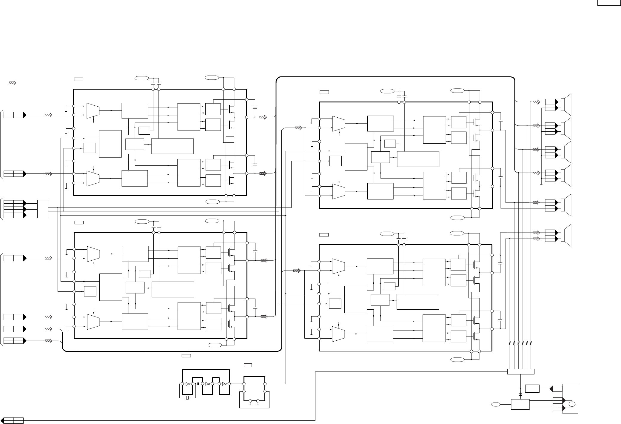
18.7. Audio Digital Amp
IN1M
IN2M
IN1P
IN2P
SGND1
SGND2
OSC
MODE
INPUT
STAGE
INPUT
STAGE
PWM
MODULATOR CONTROL
AND
HANDSHAKE
CONTROL
AND
HANDSHAKE
DRIVER
HIGH
DRIVER
LOW
DRIVER
HIGH
DRIVER
LOW
TEMPERATURE SENSOR
CURRENT PROTECTION
VOLTAGE PROTECTION
PWM
MODULATOR
OSCILLATOR MANAGER
STABI
RELEASE1
RELEASE2
SWITCH1
SWITCH2
ENABLE1
ENABLE2
MUTE
MUTE
MODE
2
3
STABI
PROT
VDDP2
VSSP2 VDDP1
VSSP1
BOOT1
BOOT2
OUT1
SL +
SR +
OUT2
IC5400
C1BA00000487
AUDIO DIGITAL POWER AMP
5
19
23
1
21
22
9
10
15
14
13
11
816
12 7
IN1M
IN2M
IN1P
IN2P
SGND1
SGND2
OSC
MODE
INPUT
STAGE
INPUT
STAGE
PWM
MODULATOR CONTROL
AND
HANDSHAKE
CONTROL
AND
HANDSHAKE
DRIVER
HIGH
DRIVER
LOW
DRIVER
HIGH
DRIVER
LOW
TEMPERATURE SENSOR
CURRENT PROTECTION
VOLTAGE PROTECTION
PWM
MODULATOR
OSCILLATOR MANAGER
STABI
RELEASE1
RELEASE2
SWITCH1
SWITCH2
ENABLE1
ENABLE2
MUTE
MUTE
MODE
2
3
STABI
PROT
VDDP2
VSSP2 VDDP1
VSSP1
BOOT1
BOOT2
OUT1
FL +
FR +
OUT2
IC5000
C1BA00000487
AUDIO DIGITAL POWER AMP
5
19
23
1
21
22
9
10
15
14
13
11
816
12 7
IN1M
IN2M
IN1P
IN2P
SGND1
SGND2
OSC
MODE
INPUT
STAGE
INPUT
STAGE
PWM
MODULATOR CONTROL
AND
HANDSHAKE
CONTROL
AND
HANDSHAKE
DRIVER
HIGH
DRIVER
LOW
DRIVER
HIGH
DRIVER
LOW
TEMPERATURE SENSOR
CURRENT PROTECTION
VOLTAGE PROTECTION
PWM
MODULATOR
OSCILLATOR MANAGER
STABI
RELEASE1
RELEASE2
SWITCH1
SWITCH2
ENABLE1
ENABLE2
MUTE
MUTE
MODE
2
3
STABI
PROT
VDDP2
VSSP2 VDDP1
VSSP1
BOOT1
BOOT2
OUT1
OUT2
IC5200
C1BA00000487
AUDIO DIGITAL POWER AMP
5
19
23
1
21
22
9
10
15
14
13
11
816
12 7
IN1M
IN2M
IN1P
IN2P
SGND1
SGND2
OSC
MODE
INPUT
STAGE
INPUT
STAGE
PWM
MODULATOR CONTROL
AND
HANDSHAKE
CONTROL
AND
HANDSHAKE
DRIVER
HIGH
DRIVER
LOW
DRIVER
HIGH
DRIVER
LOW
TEMPERATURE SENSOR
CURRENT PROTECTION
VOLTAGE PROTECTION
PWM
MODULATOR
OSCILLATOR MANAGER
STABI
RELEASE1
RELEASE2
SWITCH1
SWITCH2
ENABLE1
ENABLE2
MUTE
MUTE
MODE
2
STABI
PROT
VDDP2
VSSP2 VDDP1
VSSP1
BOOT1
BOOT2
OUT1
OUT2
IC5300
C1BA00000487
AUDIO DIGITAL POWER AMP
5
19
23
1
21
22
9
10
15
14
13
11
816
12 7
CENTER
C +
C -
MODE 1
SUBWOOFER
SW -
SW +
MODE 2
SURROUND R
SURROUND L
FRONT R
FRONT L
MUTE C S
MUTE F SW
MOD DA
CENTER
SUBWOOFER
SL +
SR +
FL +
FR +
+
-
+
-
+
-
+
-
+
-
+
-
IC5500
INVERTER GATE
(CLOCK GENERATOR)
C0JBAB000902
X5500
D-TYPE FLIP-FLOP
C0JBAF000716
CP1 Q1
IC5501
68
10 9
11
3
D1
5
46
Q1
2
1
5
CD1 SD1
MUTING
CIRCUIT
Q5601,Q5602
Q5603,Q5604
MODE 1
MODE 2
CENTER
SUBWOOFER
SURROUND L
SURROUND R
FRONT L
FRONT R
SPEAKERS
SA-PT850EE AUDIO DIGITAL AMP BLOCK DIAGRAM
DC DET
Q5640,
Q5642,
Q5644
FAN MOTOR
DRIVE
M
Q5101,
Q5102
DC DETECT
Q5641
FAN LOCK
DETECT
FAN LOCK
FAN DC OUT
FAN GND
FAN DC
3
FAN
FROM AUDIO
FROM SYSTEM CONTROL
FROM AUDIO
TO SYSTEM CONTROL
- 30V SENSE
- 30V SENSE
- 30V SENSE
- 30V SENSE + 30V SENSE
+ 30V SENSE
- 30V SENSE
- 30V SENSE + 30V SENSE
- 30V SENSE
- 30V SENSE + 30V SENSE
315
117
99
711
11 7
CN5050
CN2009
513
CN5050
CN2009
16 2
CN5050
CN2009
CN5050
CN2009
CN5050
CN2009
12 6
CN5050
CN2009
CN5050
CN2009
CN5050
CN2009
3
JK5001
7
JK5001
8
JK5001
5
JK5001
6
JK5001
4
JK5001
1
JK5001
2
JK5001
11
JK5001
12
JK5001
9
JK5001
10
JK5001
13 5
CN5050
CN2009
17 1
CN5050
CN2009
1
CN5501
3
CN5501
2
CN5501
:MAIN SIGNAL LINE
SA-PT850EE
79
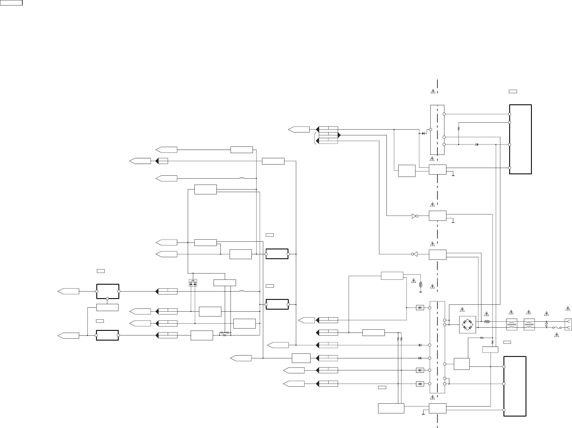
18.8. Power
5
4
2
3
2
6
7
5
2
8
4
7
18
15
17
11
14
3CL
L5702
Q2911, D2919
+5V REGULATOR
+9V REGULATOR
Q2907, Q2910
+5V
POWER SUPPLY
Q2906, Q2908
+5V
POWER SUPPLY
D5804
D5803
D5805
MAIN
TRANSFORMER
D5801
T5701
D5802
Q5898
Q5899
T5751
D5896
PC5799
D5701 L5701 DZ5701
SA-PT850EE POWER BLOCK DIAGRAM
C0DBZYY00018
SYSTEM CONTROL
TO
Q2904, D2912
+1.2V REGULATOR
C0DBEHG00006
POWER CONTROL
QR8111
+3.3V DC-DC
CONVERTER
CONT
Q5860,Q5861,Q5862
TRANSFORMER
TEMP. DETECT
C0DAAYY00042
SWITCHING
REGULATOR
SWITCHING
REGULATOR
C0DAAMH00012
OUT VCC
12
OUT VCC
12
Q5720,
Q5722
CURRENT
LIMITING
SWITCH
Q5721
SWITCHING
F1
P5701
AC INLET
SWITCHING
REGULATOR
C5HACYY00003
VCC
D
FB
4
1
6
FEED BACK
CURRENT
LIMITING
SWITCH
BACKUP
TRANSFORMER
PC5701
FEED BACK
PC5720
FEED BACK
FEED BACK CIRCUIT
D
VCC
FB
IC5799
SWITCHING
REGULATOR
MIP4110MSSCF
IC2900
IC2903
IC8151
IC8111
IC5701
QR5810
TH5701
PC5702
SYNC
SWITCH
SHUNT
REGULATOR
IC5801
Q5802, D5806
C0DABFC00002
TH5860
- 7V
REGULATOR
Q2901, Q2902
+ 2.7V
REGULATOR
OUT VCC
24
VO VIN
81
5
QR5801
DC DETECT
+ 7V
REGULATOR
Q2903
Q2921, Q2922
Q2919
DC DETECT
Q2916, D2937, D2938
Q2909
DC DETECT
D2943
DC DETECT
SW+5V
M+9V
DC DET1
+7V
-7V
D+3.3V
NSW1.2V
TO SYSTEM
CONTROL
3, 4
CN5801H5500
7, 8
CN5801H5500
5
CN5802CN2004
8, 9
CN5802CN2004
4
CN5802CN2004
- 30V SENSE
- 13V
DC18V
DCDET
+ 30V SENSE
9, 11
CN2001FP8101
17, 19, 20, 22
CN2001FP8101
2
CN5802CN2004
SYS6V
10
CN5802CN2004
PCONT
1
CN5802CN2004
SYNC
38, 40
CN2001FP8101
15
CN2001FP8101
D+5V
A+5V
ADAC5V
+2.7V
9
CN2002
T+9V
SYS6V
SYSTEM CONTROL
TO/FROM
+ 30V SENSE
- 30V SENSE
T+9V
A+5V
ADAC5V
+ 18V
2
CN5801H5500
FAN 18V
FAN DC
SA-PT850EE
80
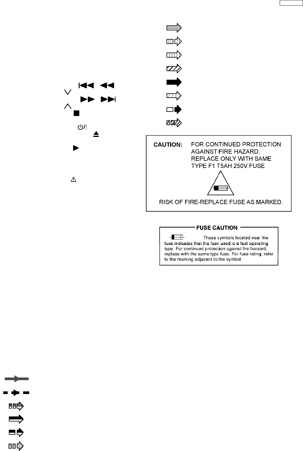
19 Schematic Diagram Notes
·
This schematic diagram may be modified at any time
with the development of new technology.
Notes:
S901: Play switch.
S902: Open switch.
S6801: Selector switch.
S6802: Reverse switch / /
TUNING ).
S6803: Forward switch ( / /
TUNING ).
S6804: Stop switch ( / -TUNE MODE/—
FM MODE).
S6901: Power switch ( AC IN).
S6902: Open / close switch ( OPEN /
CLOSE).
S6907: Play switch ( / MEMORY).
VR6801: volume jog.
VR7001: Mic volume.
·
Important safety notice:
Components identified by mark have special
characteristics important for safety.
Furthermore, special parts which have purposes of fire-
retardant (resistors), high-quality sound (capacitors), low-
noise (resistors), etc. are used.
When replacing any of components, be sure to use only
manufacturer´s specified parts shown in the parts list.
·
In case of AC rated voltage Capacitor, the part no. and
values will be indicated in the Schematic Diagram.
AC rated voltage capacitor:
C5700, C5701,C5703, C5706, C5707
·
Resistor
Unit of resistance is OHM [Ω] (K=1,000, M=1,000,000).
·
Capacitor
Unit of capacitance is µF, unless otherwise noted. F=Farad,
pF=Pico-Farad
·
Coil
Unit of inductance is H, unless otherwise noted.
·
Voltage and signal line
: +B signal line
: -B signal line
: USB signal line
: DVD RF signal line
: Motor Drive signal line
: DVD Audio signal line
: DVD Video signal line
: CD Head signal line
: DVD Head signal line
: Main signal line
: Tracking Error signal line
: Focus Error signal line
: FM signal line
: AUX/ Mic/ Music Port signal line
81
SA-PT850EE

82
SA-PT850EE
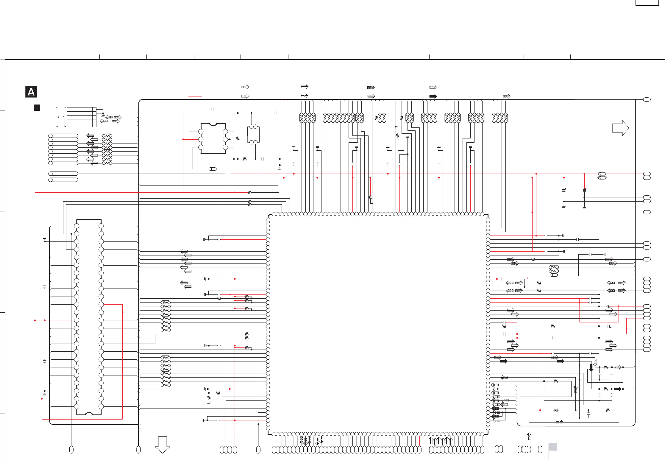
20 Schematic Diagram
20.1. DVD Module (DV5/HDMI) Circuit
TO
USB CIRCUIT
(FP9002)
IN SCHEMATIC
DIAGRAM - 17
F
: TRACKING ERROR SIGNAL LINE
: FOCUS ERROR SIGNAL LINE
: USB SIGNAL LINE
A
B
C
D
E
F
G
H
1234567891011121314
TO DVD MODULE (DV5)
SECTION (2/4)
TO DVD MODULE (DV5)
SECTION (3/4)
: DVD
: DVD VIDEO SIGNAL LINE
: +B SIGNAL LINE : DVD HEAD SIGNAL LINE
: DVD RF SIGNAL LINE
: MOTOR DRIVE SIGNAL LINE
: CD HEAD SIGNAL LINE AUDIO SIGNAL LINE
FODRV
TRDRV
R8225
C8222
820P
C8226
1000P
R8221
8.2K
8.2K
C8301
6.3V220
C8302
6.3V33
1000P
C8221
1000P
C8225
J0JHC0000045
LB8001
LB8011
J0JHC0000045
1200P
C8211 R8211
10K
EXADR13_DT9
EXADR2_DT7
EXADR1_DT15
EXADR14_DT1 FEXDT_7
EXADR3_DT14
DVOUT1
DVOUT0
0.1
C8020
DVOUT2
FEXDT_12
FEXDT_13
EXADR1_DT15
FEXDT_11
EXADR2_DT7
FEXDT_14
FEXDT_15
EXADR_17
EXADR_18
EXADR_20
XWE
FEXDT_9
FEXDT_10
FEXDT_8
EXADR4_DT6
EXADR5_DT13
C8652 0.1
EXADR3_DT14
EXADR7_DT12
EXADR9_DT11
EXADR11_DT10
EXADR12_DT2
EXADR10_DT3
EXADR8_DT4
EXADR6_DT5
C8651 0.1
47
R9086
R9041 10K
47
R9087
C8022
0.1
C8007 0.1
R9088 47
CPU-CMD
CPU-STAT
TRVFTMUTE
SPMUTE
0.1
C8021
EXADR_18
EXADR_17
XWE
EXADR_20
10K
R9040
R9085 47
R9080
10K
10K
R8001
R8003 10K
EXADR_0
D1H85604A024
RX9017
EXADR0_DT0
0.1
C8006
EXADR_16
EXADR_16
EXADR9_DT11
EXADR11_DT10
8
65
7
1
3
2
4
8
65
7
1
3
2
4
8
65
7
1
3
2
4
8
65
7
1
3
2
4
8
65
7
1
3
2
4
8
65
7
1
3
2
4
D1H85604A024
RX9014
EXADR15_DT8
EXADR13_DT9
EXADR12_DT2
EXADR14_DT1
EXADR10_DT3
EXADR8_DT4
DVOUT7
DVOUT2
DVOUT4
DVOUT3
DVOUT0
DVOUT1
DVOUT6
D1H84714A024
RX3707
D1H84714A024
RX3708
DVOUT5
R9084 47
47
R9083
0.1
C8018
C9007
0.1
DVOUT3
EXADR5_DT13
EXADR7_DT12
RX9015
D1H85604A024
EXADR6_DT5
DVOUT5
DVOUT7
DVOUT6
EXADR4_DT6
D1H85604A024
RX9016
DVOUT4
FEXDT_3
VOUT6
VOUT4
VOUT2
VOUT0
VOUT1
VOUT3
VOUT5
VOUT7
FEXDT_2
FEXDT_1
DMIX_SEL
2CH_SEL
FEXDT_0
FEXDT_6
FEXDT_5
EXADR0_DT0
EXADR15_DT8
FEXDT_4
22
23
21
14
15
13
18
17
20
19
16
3
5
4
6
1
2
12
10
8
7
9
11
26
28
30
32
39
40
36
37
34
35
38
47
45
46
48
41
43
44
42
33
31
29
27
2425
32M FLASH MEMORY
RFKWMHB0E321
IC8651
VHALF
MDQ_5
DQM1
RX8019
D1H422020001
DQM0
NCAS
NRAS
NCSM
RX8018
D1H422020001
22
R8011
NWE
R8012 22
C8003 0.1
C8013 0.1
MDQ_6
MDQ_9
C8014 0.1
MDQ_7
RX8014
D1H88204A024
MDQ_8
MDQ_12
MDQ_1
MDQ_0
MDQ_14
MDQ_2
MDQ_13
MDQ_11
MDQ_10
MDQ_4
D1H88204A024
RX8013
MDQ_3
D1H88204A024
RX8012
C8015 0.1
MA_4
MA_3
10K
R9045
EXADR_0
C8004 0.1
R9042 10K
C8016 0.1
C8012 0.1
215 213 211 209 207 173174 166165167 163164171170172 168169187188 184183186185191 189190 178177181182 179180194193203204 200202201206205 196195199 197198 192 175176208210212214
106
989694929088
868482807876747270686664626058
56 57 59 61 63 65 67 69 71 73 75 77 79 81 83 85 87 89 91 93 95 97 99
103100 102101 105104 108107
161
159
109
115
113
114
118
117
121
120
125
124
129
130
127
128
135
133
134
139
151
152
149
150
154
156
158
157
155
153
141
143
142
140
147
148
144
146
145
137
136
138
131
132
126
122
123
119
116
110
112
111
160
162
2
4
3
1
8
9
5
7
6
11
10
17
16
19
18
13
15
14
26
27
22
23
20
21
25
24
12
216
53
50
51
46
48
47
42
43
38
39
34
35
30
31
28
29
33
32
37
36
41
40
45
44
49
52
54
55
DV5.0 LSI
MN2DS0018MP
IC8001
MA_6
MA_0
MA_1
BA1
22
R8013
BA0
D1H422020001
RX8020
D1H88204A024
RX8016
D1H88204A024
RX8015
MA_9
MA_10
MA_8
MA_11
MA_7
MA_5
D1H88204A024
RX8017
MA_2
MA2J11100L
D8211
15P
C8401
ADAC-CLK
C8203 0.1
C8305 0.1
C8304 0.1
4
2
1
3
RX8401
D1H410120001
J0JBC0000042
LB8401
LRCK
SRCK
R8541 15K
C8202 0.1
4700P
C8541
R8314 15K
C8303 0.1
C8306 0.10.1C8005
C8026 0.1
C8001
4V330
C8011
6.3V100
C8312
1
1
C8313
15K
R8313
R8401 100
VIN6
VREFH
VIN5
1
2
3
4
5
6
7
8
1
2
3
4
5
6
7
8
1
2
3
4
5
6
7
8
1
2
3
4
1
2
3
4
1
2
3
4
1
2
3
4
5
6
7
8
1
2
3
4
5
6
7
8
1
2
3
4
5
6
7
8
1
2
3
4
5
6
7
8
D1H88204A024
RX8011
C8429
0.1
MDQ_15
VIN7
VIN2
VIN4
VIN1
VIN8
VIN3
3R3_L8420
DMIXOUT
EXDT2
EXDT1
MA9
BA1
MA6
MA0
MA5
VSS
MA4
VSS
HD
HD
HD
HD
HD
HD
HD
HD
HD
HD
MA3
MA2
MA1
MA8
MA7
VSS
MA10
MDQ4
MDQ3
NWE
MCK
BA0
CLK
CKE
VSS
VSS
VSS
MDQ9
MDQ7
DQM1
NCAS
NCSM
DQM3
DQM2
NRAS
MCKI
DQM0
MDQ6
MDQ8
MDQ5
EXDT9
A0 A1
VDD33
EXADT0
NEXOE
NEXCE
VDD12
VDD33
VDD33
MDQ10
VDD33
VDD12
VDD33
MDQ12
MDQ11
MDQ0
MDQ1
VSS
MDQ14
A3VSS VDD33
XWE
A20
XRESET XRESET
A9
A12
A13
A10
A11
A15
A14
A8
A19
DQ4
DQ12
VDD
VSS
A16
DQ6
DQ5
DQ7
XBYTE
DQ15/
A-1
DQ13
DQ14
A18
A6
A4
A5
A7
A17
NC
WP/
ACC
RDY/
XBSY
DQ2
DQ10
DQ1
DQ0
XOE
DQ8
DQ9
DQ3
DQ11
EXDT5
VSS
EXDT7
VSS
P3
P1
P2
P5
P7
P6
P4
P0
VSS
VSS
VSS
NEXWE
VDD12
VDD33
VDD33
VDD12
VDD33
EXDT6
EXDT3
EXDT4
VSS
XCE A2
EXDT11
VDD33
OSCO
OSCI
ANAMONI1
VIN4RF
VREFH5
LPC2
VREFH
LPCO2
LPC1
LPCO1
VHALF
VREFL5
VIN3RF
RFINP
RFINN
VIN2RF
VIN1RF
[107]AVDDB
VIN4
VIN3
VIN2
VIN6
VIN8
VIN7
AD4
PWM1
VREF
SRCK
LRCK
ROUT
LOUT
PWM0
AD0
VIN1
AD2
AD1
AVDDH
COMP2
AVSSI
ADOUT
AVDDI
AVSSF
AVDDE
AVSSG
DACCK
AVDDG
AVSSE
COMP1
AVDDF
IREF1
DAC4OUT
DAC5OUT
DAC3OUT
DAC1OUT
DAC2OUT
AVSSH
[108]AVSSB
VIN10
VIN5
VIN9
ANAMONI2
EXDT13
EXTRG0
VDD12
AVSSD
CCAPA
AVDDC
CDATA
AVSSC
AVDDD
VSS
TRCST
PLFIL1
VREFL7
VREFH7
EXTRG1
TRCCLK
TRCDATA3
TRCDATA2
TRCDATA1
TRCDATA0
EXDT15
DRV1
DRV2
VSS
FG
NRST
DRV0
SCLOCK
SDATA
VDD33
EXADT14
P13
P14
DRV3
DRV5
DRV4
EXADT11
EXADT12
EXADT8
EXADT3
EXADT1
EXADT2
EXADT6
EXADT7
EXADT4
EXADT5
EXADT9
P11
P10
P12
[55]P8
[56]P9
EXADR19
EXADR17
EXADR18
EXADT10
EXADT13
EXADR16
EXADT15
EXDT14
VSS
IECOUT
EXDT12
VDD12
[164]MDQ2
MDQ15
[163]MDQ13
VSS
[215]STBDAC
EXDT10
[216]FPGACS
STBDAC
TRV_INNER_SW
A2
A3
A4
A5
A6
A7
A8
A9
A10
A11
A12
A13
A14
A15
A16
A17
A18
A19
A20
A21
A22
A23
A24
A25
A26
A28
A29
A30
A31
A32
A33
A34
A35
A36
A37
A38
A39
A40
A41
A42
A43
A44
A45
A46
A47
A48
A49
A50
A51
A52
A53
A54
A55
A56
A57
A58
A59
A60
A64
A61
A62
A63
A75
A76
A77
A78
A79
A80
A81
A82
A83
A84
A88
A89
A90
A91
A92
A93
A94
A95
A96
A97
A0
A1
DVD MODULE (DV5) CIRCUIT
SCHEMATIC DIAGRAM - 1
1/4 2/4
3/4 4/4
DVD MODULE (DV5) CIRCUIT
SA-PT850EE
VBUS_OUT
D+
D-
2
3
1
15
5
4
FP9001
D+
D-
DGND
DGND
VBUS
R9009
1K
3
2
14
X9004
H1A4805B0027
1M
R9008
C9005
9P
8P
C9004
1
2
5
6
3
4
C0JBAB000908
INVERTER GATE
IC9003
2Y 2A
1A
1Y
VC GND
J0JCC0000119
LB9001
A27
A85
A87
A86
R8315 24
R8316 24
HD: DVD MODULE (HDMI): SCHEMATIC DIAGRAM - 5
D2: DVD MODULE (DV5): SCHEMATIC DIAGRAM 1 - 4
SA-PT850EE
83
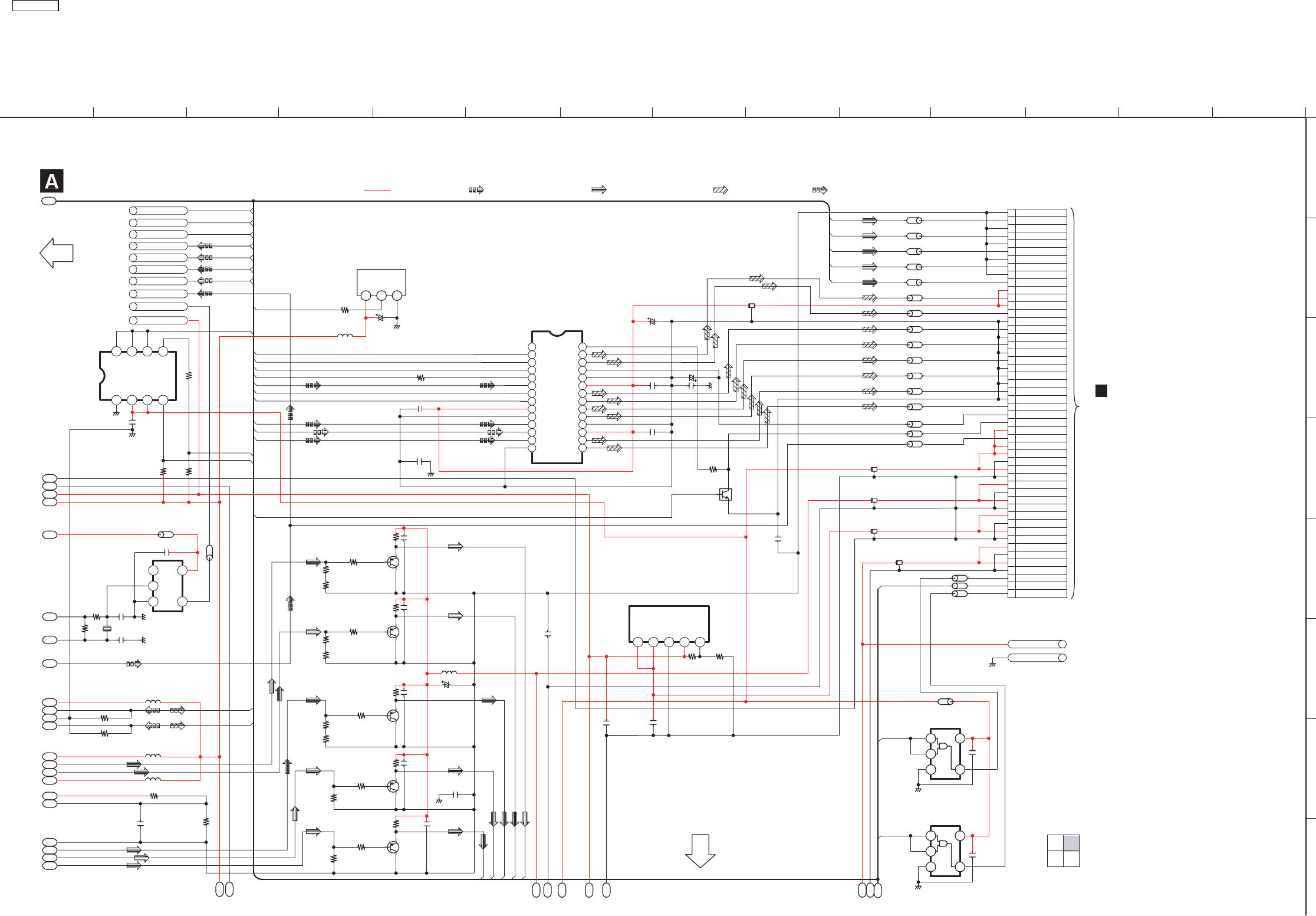
B
15 16 17 18 19 20 21 22 23 24 25 26 27 28
A
B
D
E
F
H
G
C
TO DVD MODULE (DV5)
SECTION (1/4)
TO DVD MODULE (DV5)
SECTION (4/4)
: DVD : DVD VIDEO SIGNAL LINE : MAIN SIGNAL LINE : USB SIGNAL LINE
: +B SIGNAL LINE AUDIO SIGNAL LINE
AOUT2
AOUT2
AUDIODIGITAL
AOUT0
AOUT0
AOUT1
AOUT1
3
1
2
4
5
IC8701
C0JBAB000907
INVERTER GATE
R8312
1K
R8311 2.4K
L8302
G1C100K00019
L8301 G1C100K00019
3R3_L8301
3R3_L8302
C8311
0.1
C8621
7P
G1C100K00019
L8303
OSC27M
H0J270500085
X8621
C8622
8P
R8621
1M
R8622
1K
DGND
FL8421
F1H0J1050018
ERJ2GE0R00XLB8428
ERJ2GE0R00XLB8427
ERJ2GE0R00XLB8429
ERJ2GE0R00XLB8421
ERJ2GE0R00XLB8426
ERJ2GE0R00XLB8422
ERJ2GE0R00XLB8425
CB_PB_B
CR_PR_R
Y_PY_G
C
Y
J0JBC0000042LB8304
J0JBC0000042LB8303
J0JBC0000042LB8301
J0JBC0000042LB8302
J0JBC0000042LB8305
ERJ2GE0R00XLB8431
ERJ2GEJ101X
LB8693
CPU-CMD
ERJ2GEJ101X
LB8691
ERJ2GEJ101X
LB8692
0.1
C8430
FL8101
F1H0J1050018
FL8104
F1J1E1040022
ERJ2GE0R00XLB8424
ERJ2GE0R00XLB8423
ERJ2GE0R00XLB8491
F1H0J1050018
FL8103
FL8102
F1H0J1050018
M+9V
6
7
5
9
47
44
39
40
35
31
27
24
21
20
22
16
15
18
17
11
13
12
10
14
19
23
26
25
30
28
29
34
32
33
38
36
37
43
41
42
46
45
49
48
8
1
3
4
2
50
FP8101
C8423
6.3V33
C8424
0.1
6.3V100
C8421
C8422
0.1
1K
R8154
R8153
620
42135
+1.2V REGULATOR
IC8151
C0DBEHG00006
4.7
C8151
UNR521100L
QR8420
2.2K
R8420
C8427
0.1
7
8
6
5
4
14
12
10
9
11
13
3
2
128
27
26
25
24
23
22
21
20
19
18
17
16
15
AUDIO DAC
C0FBBK000050
IC8421
C8152
1
C8330
L8330
G1C100K00019
0R8421
C8426 0.1
A5V_L8330
CPU-CLK
CPU-STAT
0.1
C8695
3
1
2
4
5
0.1
C8320
0.1
C8340
C8691
0.1
3
1
2
4
5
AND GATE
C0JBAA000502
IC8691
AND GATE
C0JBAA000502
IC8695
J0JBC0000044
LB8690
R8323 33
LB8702 J0JBC0000044
SRCK
LRCK
SRCK
LRCK
DMIXOUT
DMIXOUT
ADAC-CLK ADAC-CLK
C8701
0.1
LB8701
J0JBC0000044
R8322
0
200
R8321
R8326
0
R8325
200
0
R8332
200
R8331
33R8336
Q8335
2SB1218ARL
33
R8333
R8327 33
0.1
C8428
C
Y
Y_PY_G
Q8321
2SB1218ARL
C8325
0.1
R8328
BUFFER
BUFFER
BUFFER
BUFFER
BUFFER
1K
Q8325
2SB1218ARL
ADAC-CLK
AOUT1
AOUT2
SBT3
SBO3
DMIXOUT
AOUT0
LRCK
SRCK
R8324
1K C8321
0.1
AMUTE
AMUTE
MUTING
R8334
1K C8331
0.1
R8337
1K
CB_PB_B
Q8331
2SB1218ARL
C8335
0.1
R8335
200
R8341
200
33R8342
C8341
0.1
R8343
1K
Q8341
2SB1218ARL
CR_PR_R
10K
R9036
10K
R9037
USB_OVER
C9006
0.1
VCC_LB8001
USB_VBUS
STBDAC
C
Y
SL
FL
FR
SW
SR
CNT
ADGND
MIX-R
ADGND
ADGND
ADGND
ADGND
VGND
ADGND
MIX-L
ADAC5V
ADAC5V
M+9V
MGND
MGND
M+9V
DGND
2R5V
2R5V
A+5V
AGND
DGND
A+5V
DGND
D+5V
D+5V
D+5V
D+5V
AGND
DGND
A-REF
VGND
VGND
CR/PR/R
VGND
Y/PY/G
CB/PB/B
VGND
MC
MD
MS
SCK
VDD
BCK
DGND
LRCK
MSEL
DATA4
DATA2
DATA3
DATA1
ZERO1
GND
VCC
ADJ
VCC
GND
GND
OUT
DGND
AGND
A+5V
2R7V
VCOM
AGND2
VOUT1
VOUT2
VOUT4
CTL
VCC1
VCC
VOUT7
AGND1
VOUT8
VOUT5
VOUT6
VCC2
VOUT3
ZERO2
ZFLAG&AMUTE
AUDIODIGTAL
HD
HD
DOP_CPU-CLK
DOP_CPU-CMD
DOP_CPU-STAT
HD
HD
HD
NSW1R2V
HD
HD
HD
HD
HD
HD
HD
INA
VCC
NC
OUT
GND
TO
MAIN CIRCUIT
(CN2001)
IN SCHEMATIC
DIAGRAM - 8
A67
A65
A66
A68
A69
A70
A71
A72
A73
A74
A88
A89
A90
A91
A92
A93
A94
A95
A96
A97
A84
A76
A77
A80
A81
A82
A83
A78
A79
A75
DVD MODULE (DV5) CIRCUIT
SCHEMATIC DIAGRAM - 2
SA-PT850EE
1/4 2/4
3/4 4/4
DVD MODULE (DV5) CIRCUIT
6.3V47
R8025
VCC OUT GND
0
C8002
6.3V33
L8001
G1C100K00019
231
JK8001
OPTICAL IN
IECINPUT
VBUS_OUT
67
243
8
1
C0DBZYE00002
IC9005
REGULATOR
OC
OUT
OUT
OUTIN
GND
IN
EN
0
R9035
5
A85
A86
A87
R8318 15K
R8317 15K
D+
D-
HD: DVD MODULE (HDMI): SCHEMATIC DIAGRAM - 5
D2: DVD MODULE (DV5): SCHEMATIC DIAGRAM 1 - 4
SA-PT850EE
84
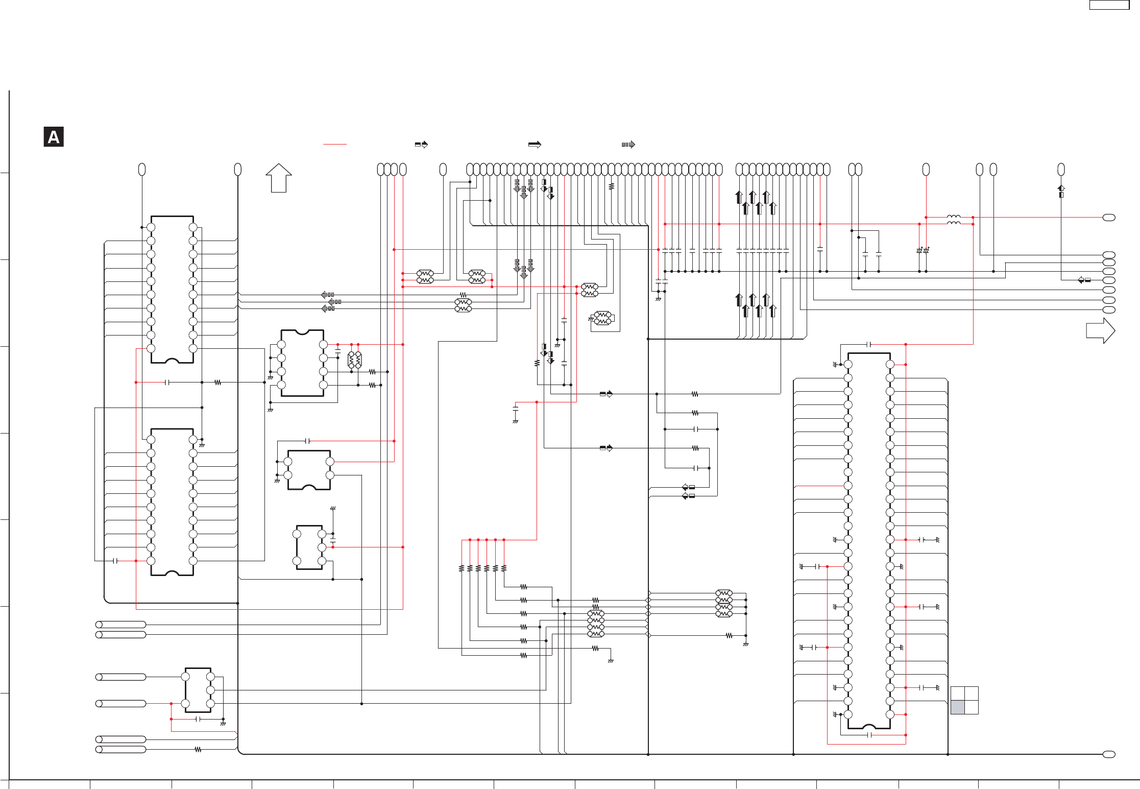
1234567891011121314
I
J
L
M
N
P
O
K
TO DVD MODULE (DV5)
SECTION (4/4)
TO DVD MODULE (DV5)
SECTION (1/4)
: +B SIGNAL LINE
AOUT2
FEXDT_6 EXADR6_DT5
FEXDT_4 EXADR4_DT6
EXADR3_DT14
FEXDT_3
FEXDT_1 EXADR1_DT15
EXADR0_DT0FEXDT_0
0.015
C8602
FEXDT_2 EXADR2_DT7
C8511 1
C8512 1
VIN3
VIN4
FEXDT_5 EXADR5_DT13
AOUT1
C8023 0.1
0.1
C8505
R8601 100K
AOUT0
C8506
0.1
R8402 10 4
2
1
3
RX8031
D1H447220001
4
2
1
3
4
2
1
3
4
2
1
3
RX8402
D1H410120001
VIN2
VIN1
TRCCLK 33R8041
TRCDATA3
TRCDATA1
TRCDATA0
HOTPLG
TRCDATA2
TRCST
SBT3
SBO3
TRACESEL
USB_VBUS
V_CLK
USB_OVER
MDQ_10
DQM1
MDQ_8
MDQ_9
2200P
C8056
MDQ_6
MDQ_5
220P
C8054
NWE
NRAS
NCAS
MDQ_7
DQM0
MDQ_13
MDQ_15
MDQ_14
MDQ_12
MDQ_11
1
C8057
0.1
C8052
MDQ_3
MDQ_0
MDQ_2
MDQ_1
0.1
C8053
MDQ_4
MA_3
MA_0
MA_1
MA_10
BA0
NCSM
BA1
MA_2
1
C8055
MA_6
MA_5
MA_9
MA_11
MA_7
MA_8
MA_4
RX8001
D1H410320002
RX8691
D1H410320002
EXADR7_DT12FEXDT_7
RDATA
CPU-CLK
C8503 0.1
C8526 0.018
C8513 0.1
C8523 0.1
C8524 0.1
C8502 0.1
0.033C8527
C8525 5600P
C8515 0.1
C8514 0.1
C8516 0.1
C8504 0.1
C8522 0.1
C8521 0.1
L8501
G1C100K00019
G1C100K00019
L8201
3R3_L8501
3R3_L8201
6.3V100
C8501 C8201
6.3V100
C8051 1
C8528 1
C8529 1
29
28
30
31
27
26
24
25
20
21
19
16
12
14
15
13
18
17
9
10
8
7
6
11
2
3
1
4
5
34
36
39
41
42
40
38
49
52
51
54
53
50
44
43
45
47
48
46
37
35
23
22
32
33
64M SDRAM
C3ABPG000145
IC8051
SP_DRV
7.5K
R8232
C8232
0.1
C8601 0.1
EXADR14_DT1
EXADR12_DT2
EXADR13_DT9
FEXDT_14
FEXDT_12
FEXDT_13
EXADR15_DT8
FEXDT_15
100
R8611
4
21
3
RX8032
D1H447220001
TRCST R9055 10K
EXADR8_DT4
TRCDATA1
TRCDATA0
47
R8901
D+3R3V
D+3R3V
D+3R3V
VCLK
HOTPLG
C8901 0.1
TXRST
A B GND
YVCC
AND GATE
3
1
2
4
5
IC8901
C0JBAA000501
TXRST
I2C_SDA
I2C_SCL
R9023
R9016 0
V_CLK
HOTPLG
HDMIRST
TRCDATA2
HFMON
R9015 0
0
R9014 0
TRCDATA3
FEXDT_8
0.1
C9003
FEXDT_11 EXADR11_DT10
R9024 10K
R9026 10K
R9028 10K
R9029 10K
R9027 10K
R9025 10K
1
1
2
3
4
8
7
6
5
4
2
3
C0EBA0000029
IC8601
RESET
R9013 0
FEXDT_9
C8606
0.1
AMUTE
DVD_CD
R9022 0
R9017 0
EXADR10_DT3
FEXDT_10
EXADR9_DT11 3
1
2
4
5
RESET
C0EBE0000456
IC8606
1011
912
813
714
615
516
417
318
219
120
I2C_SDA
R9012 0
R9011 0
TRCST
TRCCLK
12
34
56
78
RX9019
D1H8R0040009
TRV_DRV
C8611
0.1
TRCDATA0
TRCDATA1
TRCDATA2
TRCDATA3
2.2K
R8230
4
21
3
4
21
3
RX9020
D1H447220001
D1H447220001
RX9018
C9002 0.1
R9007
10K
100
R8613
I2C_SCL
42
1
3
RX8611
D1H447220001
7
8
9
6
1
2
5
3
4
12
14
16
18
19
20
17
15
13
1011
C0JBAZ001251
IC9001
(NOT SUPPLIED)
16M EEPROM
IC8611
C8231
0.1
22K
R8231
RFINP
RFINN
LPC1
LPC2
A11 BA0
A9 BA1
A1A6
A2A5
VSS VDD
A3A4
A8 A10/AP
A7 A0
DQ11 DQ4
VDDQ
DQ12
VSSQ
DQ3
DQ8 DQ7
NC LDQM
/CS
/CAS
/RAS
NC
CLK
CLK
CKE
CKE
/WE
UDQM
VDD
VSS
DQ9 DQ6
DQ5DQ10
VSSQ VDDQ
VSSQ
VDDQ
VDD33
DQ15
VSS
DQ14
VSSQ
DQ0
VDD
DQ1
VDDQ
DQ13 DQ2
XRESET
OE
D3
D4
OE
D2
D8
D6
D5
D7
D1
D6
D5
D8
D7
D1
D2
D4
D3
GND
GND
Q3
Q2
Q4
Q6
Q7
Q3
Q4
Q2
HD
HD
HD
HD
HD
HD
Q5
LE
Q8
Q1
Q1
Q7
Q6
Q8
Q5
LE
VCC
VCC
LATCH
LATCH
NCCD
OUT VDD
OUT
VDD
VSS
SCL
WP
VCC
SDA
A2
A0
A1
GND
NC
GND
A0
A1
A2
A3
A4
A5
A6
A7
A8
A9
A10
A11
A12
A13
A14
A15
A16
A17
A18
A19
A20
A21
A22
A23
A24
A25
A26
A28
A29
A30
A31
A32
A33
A34
A35
A36
A37
A38
A39
A40
A41
A42
A43
A44
A45
A46
A47
A48
A49
A50
A51
A52
A53
A54
A55
A56
A57
A58
A59
A60
A64
A61
A62
A63
A98
A99
A100
A101
A102
A105
A106
A103
A104
DVD MODULE (DV5) CIRCUIT
SCHEMATIC DIAGRAM - 3
1/4 2/4
3/4 4/4
DVD MODULE (DV5) CIRCUIT
SA-PT850EE
C0JBAZ001251
IC9002
0.1
C9017
IECINPUT A27
HD: DVD MODULE (HDMI): SCHEMATIC DIAGRAM - 5
D2: DVD MODULE (DV5): SCHEMATIC DIAGRAM 1 - 4
: DVD AUDIO SIGNAL LINE
: DVD RF SIGNAL LINE
: MOTOR DRIVE SIGNAL LINE
SA-PT850EE
85
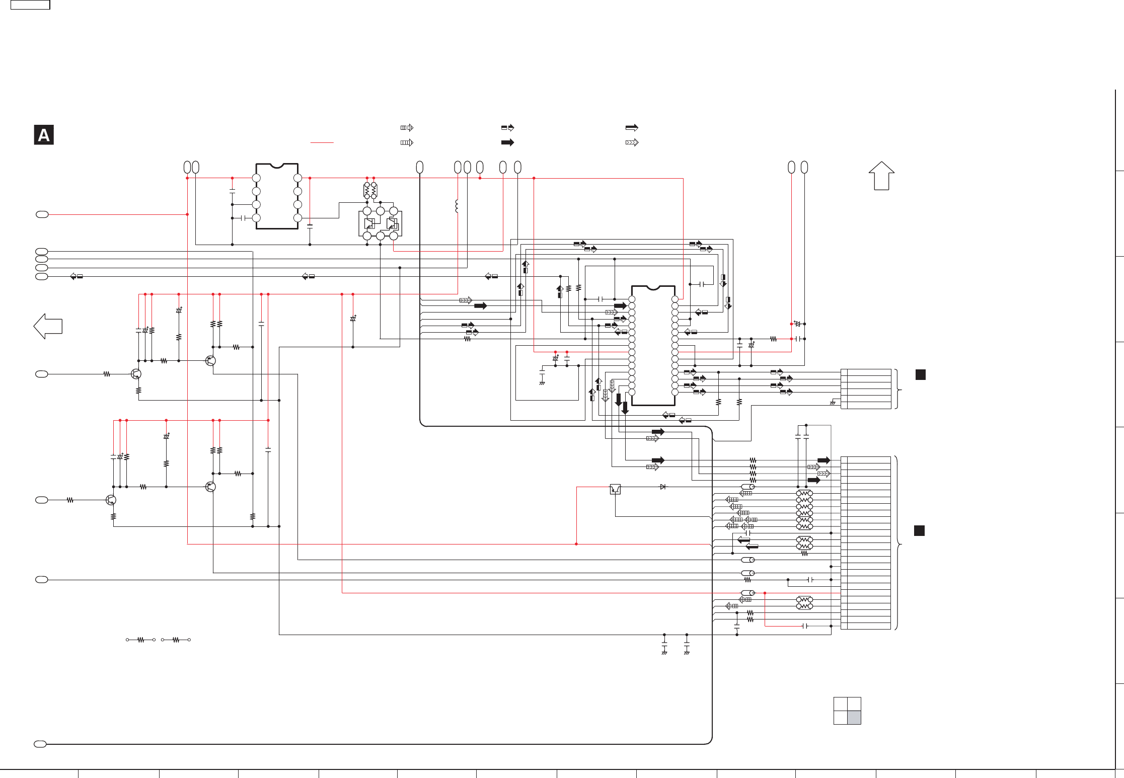
TO
RELAY CIRCUIT
(FP8003)
IN SCHEMATIC
DIAGRAM - 17
: DVD RF SIGNAL LINE
15 16 17 18 19 20 21 22 23 24 25 26 27 28
I
J
L
M
N
P
O
K
6
7
5
2
4
3
8
1
TO
RELAY CIRCUIT
(FP8001)
IN SCHEMATIC
DIAGRAM - 17
K
K
TO DVD MODULE (DV5)
SECTION (2/4)
TO DVD MODULE (DV5)
SECTION (3/4)
: +B SIGNAL LINE
22
R8564
47K
R8568
0.1C8561
R8563 1K
R8567 51
R8566 56
2.2
R8565 C8563
6.3V47
R8261
82K
82K
R8263
C8258
0.1
16V47
C8257
R8251
6.8
C8255
16V22
C8256
0.1
0.1
C8262
2
4
3
1
6
5
FP8251
K8251 0
R8262 15K
R8264 15K
0.1
C8261
TRDRV
FODRV
TRVFTMUTE
C8251
6.3V220 0.1
C8252
0.1
C8253
1
2
3
4
5
6
7
8
9
29 30
10
11
14
12
13
19
20
21
22
23
24
25
26
27
28
18
15
17
16
MOTOR DRIVE
C0GBG0000048
IC8251
231
546
POWER CONTROL
XP0621400L
QR8111
SPMUTE
SPMUTE
TRV_DRV
SP_DRV
TRVFTMUTE
4
2
13
D1H422320002
RX8111
C8112
1
D+3R3V
C8113
470P
L8550
G1C100KA0055
6.3V33
C8550
A5V_L8550
C8111
0.1
68
R8554
R8553 1K
R8532
2.2K
R8533
0
C8532
220P
VIN5
VIN6
C8530 0.1
DVD_CD
C8533 0.1
LB8551 J0JBC0000042
0LB8531
D1H456020001
RX8533
C8531
100P
LB8561 J0JBC0000042 1.5KR8531
LB8530 J0JHC0000045
RX8534
D1H456020001
UNR511V00L
QR8571
4
2
1
3
4
2
1
2
1
3
4
3
D1H456020001
RX8531
VIN3
VIN7
VIN8
VIN2
VIN4
VIN1
LB8258
LB8260 0
0
0
0
LB8571 J0JBC0000042
5
7
1
3
6
8
2
4
D1H85604A024
RX8532
LB8257
LB8259
D8571
MA2J72800L
SUPPLY CONTROL SWITCH
HFMON
47K
R8558
15K
R8559
C8572
0.1
C8571
10
TRVFTMUTE
7
8
5
6
9
24
14
16
15
11
12
10
13
22
23
19
20
17
18
21
2
1
4
3
26
25
FP8531
0.1C8551
2.2
R8555
6.3V47
C8553
Q8552
LD DRIVE
Q8552
B1ADGB000008
LD DRIVE
Q8562
B1ADGB000008
R8557 51
R8556 56
D+3R3V
R8562
1K
R8552
1K
C8554 1
C8552 16V10
0
R8551
C8562 16V10
C8564 1
LD DRIVE
2SD1819A0L
Q8551
LD DRIVE
2SD1819A0L
Q8561
0
R8561
RFINP
RFINN
LPC1
LPC2
T+
F-
RF
VCC
GND
T-
TA(DVD)
SUB2
SUB1
LDCD
LDDVD
VREF1
SUBSEL
LDGND
TB(DVD)
TC(DVD)
PIN(CD)
PIN(DVD)
GND(VRCD)
GND(OEIC)
FE2(DVD/CD)
VREF2(RF-)
FE1(DVD/CD)
TD(DVD)
HFM
F+
MUTE4
FIN
LDIN
VIN3
VCC
[CH3,4]
M+9V
VO4-
VO4+
VO3+
VO3-
GND
[CH3,4]
PREVCC
LDCNT
TRIN
MUTE3
BIAS2
SPM+
SPM-
TRVM-
DGND
TRVM+
MGND
TRV_INNER_SW
OPIN-
OPIN+
VO2-
VO1+
VO2+
VO1-
FIN
OPOUT
GND
[CH1,2]
MUTE12
VCC
[CH1,2]
D+5V
BIAS1
VIN2
VIN1
OPIN-
OPIN+
GND
[PRE]
PIN_23
PIN_26
PIN_27
MGND
DGND
PIN_9/20
VO VIN
CN
NC
NC
CONT
TRV_INNER_SW
GND
NC
IC8111
+3.3V DC-DC CONVERTER
C0DBZYY00018
VREFH
A65
A66
A67
A68
A69
A70
A71
A72
A106
A99
A100
A101
A102
A103
A104
A105
A98
A73
A74
DVD MODULE (DV5) CIRCUIT
SCHEMATIC DIAGRAM - 4
1/4 2/4
3/4 4/4
SA-PT850EE DVD MODULE (DV5) CIRCUIT
C8537
0.1
C8538
0.1
K8003
0
K8008
0
HD: DVD MODULE (HDMI): SCHEMATIC DIAGRAM - 5
D2: DVD MODULE (DV5): SCHEMATIC DIAGRAM 1 - 4
: DVD HEAD SIGNAL LINE
: MOTOR DRIVE SIGNAL LINE
: TRACKING ERROR SIGNAL LINE : FOCUS ERROR SIGNAL LINE
: CD HEAD SIGNAL LINE
SA-PT850EE
86
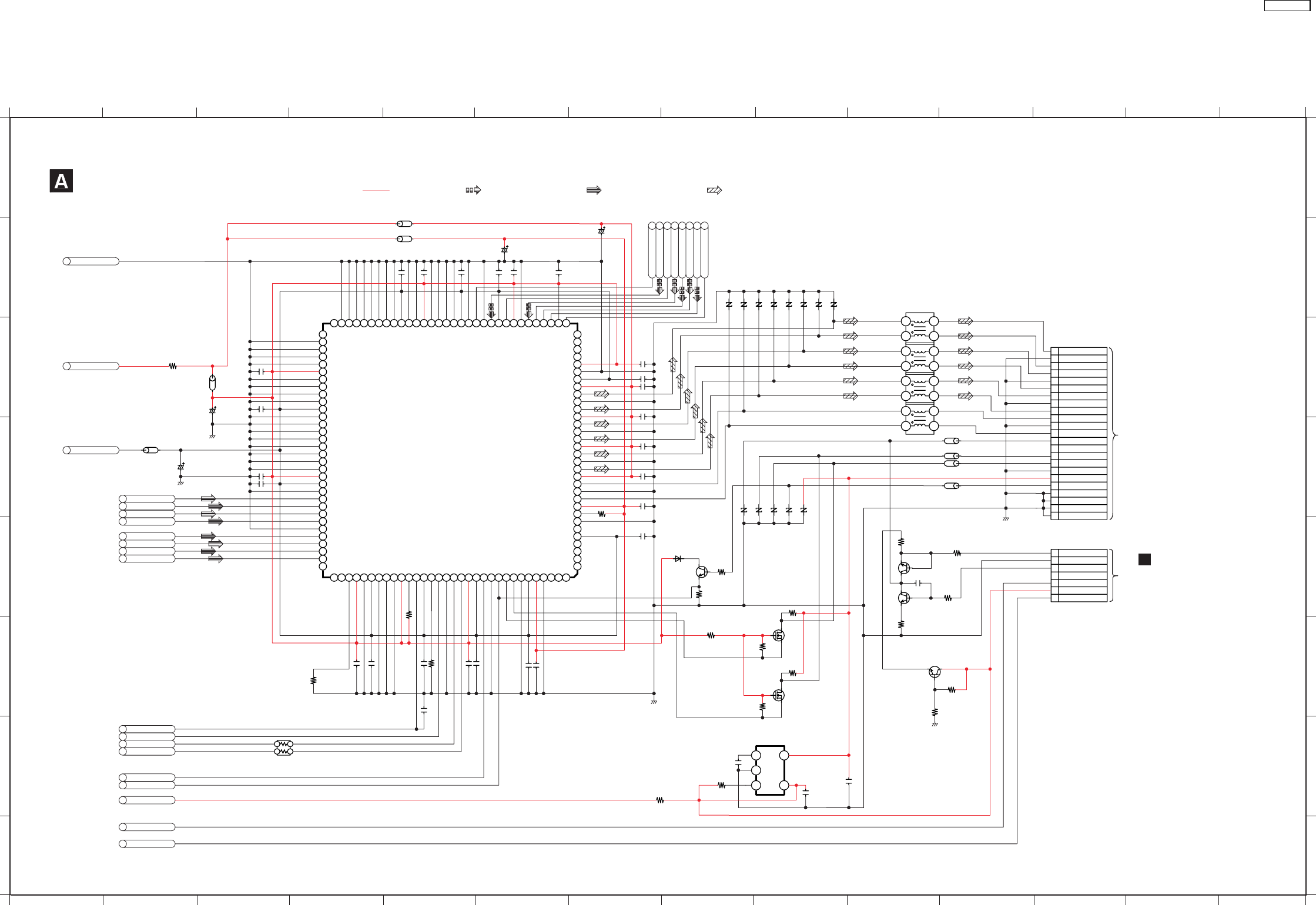
SCHEMATIC DIAGRAM - 5
B
TO
MAIN CIRCUIT
(CN2010)
IN SCHEMATIC
DIAGRAM - 8
: +B SIGNAL LINE : DVD AUDIO SIGNAL LINE
DVD MODULE(HDMI) CIRCUIT : DVD VIDEO SIGNAL LINE : MAIN SIGNAL LINE
SA-PT850EE DVD MODULE (HDMI) CIRCUIT
A
B
C
D
E
F
G
H
1234567891011121314
1234567891011121314
A
B
D
E
F
H
G
C
4
3
1
2
4
3
1
2
VA3901
1
C3956
J0JCC0000119LB3906
R3943
100K
R3942
220K
2.7K
R3946
4
5
1
3
2
7
6
FP3902
J0JCC0000119LB3905
R3941
27K
R3944
220
Q3941 - Q3942
2SD1819A0L
Q3941
Q3942
10K
R3945
Q3943
2SD1819A0L
C3941
220P
LB3903 J0JCC0000119
4
3
1
2
4
3
1
2
J0JCC0000119LB3904
6
7
5
9
12
10
11
18
19
16
17
21
20
13
15
14
8
1
3
4
2
23
22
P3901
D+3R3V
1
C3917
K3908
0
C3901
LB3901
J0JHC0000045 0.1
C3929
C3940
0.1
C3911
1
AOUT1
AOUT2
ADAC-CLK
DMIXOUT
VA3908
VA3901-VA3908
EZAEG2A50AX
4V330
C3904
SRCK
LRCK
AOUT0
AUDIODIGITAL
C3907
0.1
VA3907
VA3906
DGND
LB3907 J0JHC0000045
C3902
4V330
1
C3909
LB3902 J0JHC0000045
C3914
0.1
C3910
0.1 1
C3924
C3908
0.1
VA3902
VA3905
VA3903
VA3904
VOUT6
VOUT7
C3923
1
VOUT4
VOUT1
VOUT2
VOUT0
VOUT3
C3928
0.1
R3901 510
VOUT5
MA2J72800L
D3901
R3902
10K
Q3901
R3903
10K
2CH_SEL
DMIX_SEL
0
0.1C3916
R3924
C3925 0.1
C3927 1
0.1C3921
C3918 0.1
0.1
C3964
0
K3903
C3919 1
TXRST
R3921
0
C3920 1
10K
R3925
HOTPLG
VCLK
M+9V
4
21
3
RX3901
D1H410120001
OSC27M
I2C_SDA
I2C_SCL
0
K3905
0.01
C3955
10K
R3947
1
C3915
0.1
C3913
0.1
C3922
C3930
1
NSW1R2V
LB3908
J0JHC0000045
C3906
4V330
C3932
1
0.1
C3926
127
125
123
117
116 118115 120 121
119
9897 99
105104 106
102
100 101 103 113
111
109108 110 112 114107 122 124 126
63 5052 51 4547 46 4142 38 343637 3540 3944 4349 486062 61 5657 5355 5459 5864
95
92
93
88
89
84
85
80
81
72
67
65
66
71
69
68
70
76
78
79
77
73
75
74
83
82
87
86
91
90
94
96
9
10
7
8
12
15
16
13
14
11
1
4
2
3
6
5
128
31
29
23
26
27
24
25
18
19
17
22
20
21
28
30
32
33
2K
R3905
R3907
2.2K
S
D
G
VA3912
VA3911
C3954
0.1
S
D
G
VA3913
VA3910
VA3909
VA3909-VA3913
EZJZ0V800AA
3
1
2
4
5
4.7K
R3906
4.7K
R3904
RSV
CEC
+5V
CLK-
CLK+
DGND
D2-
D2+
D1-
D0-
D0+
D1+
CLKGND
HDMISCL
FRAME
FRAME
CECIN
FRAME
FRAME
HOTPLG
CECGND
+5V_SW
CECOUT
NSW+6V
2CH_SEL
DMIX_SEL
HDMISDA
D2GND
D0GND
D1GND
D2
D2
D2
D2
D2
D2
D2
D2
D2
D2
D2
PVDD1
TXCM
PVSS1
EXT_SWING
AVDD
NC
AMDAM
VSS
AMSDI0
VSS
VDD12
AMRX
AMDAWS
VDD33
AMSDI1
AVSS
AVDD
VDD33
AMSDI3
AVSS
AVDD
AVSS
AVDD
TX2P
TX2M
VDD33
VDD12
TX1P
TX1M
AMSDI2
[32]NC
[31]NC
[30]NC
TXOP
TX0M
AVSS
TXCP
NC
NC
PVDD2
NC
NC
NC
PVSS2
HPD
VSS
SCL
VSS
VDD12
SDA
NC
NC
VDD12
[1]NC
Q3901
2SD1819A0L
D9
D7
D5
D3
D1
D0
D2
D4
D6
D8
NC
DSD0
VDD12
PCLKIN
D35
D32
D29
D27
D25
D23
D24
D26
VSS
D30
D34
D33
VSS
VDD33
VDD12
NRESET
HCLK
HCLKDIV
D22
VDD12
D20
D18
NC
VSS
VSS
D15
D13
D12
D10
D11
VSS
D14
D16
D17
D19
VDD12
NC
VDD12
VDD33
LPSA
VDD33
D21
VSS
HSYNC
NIRQ
NTEST
DE
[96]NC
VDD12
VDD33
VSYNC
[65]NC
HSCL
HSDA
VDD33
VSS
VDD12
AMDACL
D31
D28
D2
D2
D2
D2
D2
D2
D2
D2
OUTIN
GND
D2
D2
D2
D2
D2
Noise
Bypass
D2
D2
D2
D2
VC
HDMI AV OUT
IC3901
MN864702A
HDMI TRANSMITTER
LEVEL SHIFTER
LEVEL SHIFTER
TERMINAL VOLTAGE REGULATOR
Q3903
B1CFHA000002
IC3952
C0CBCDC00063
Q3902
B1CFHA000002
BUFFER
L3903
J0MAB0000170
L3904
J0MAB0000170
L3905
J0MAB0000170
L3906
J0MAB0000170
BUFFER
SWITCH
4V330
HD: DVD MODULE (HDMI): SCHEMATIC DIAGRAM - 5
D2: DVD MODULE (DV5): SCHEMATIC DIAGRAM 1 - 4
SA-PT850EE
87
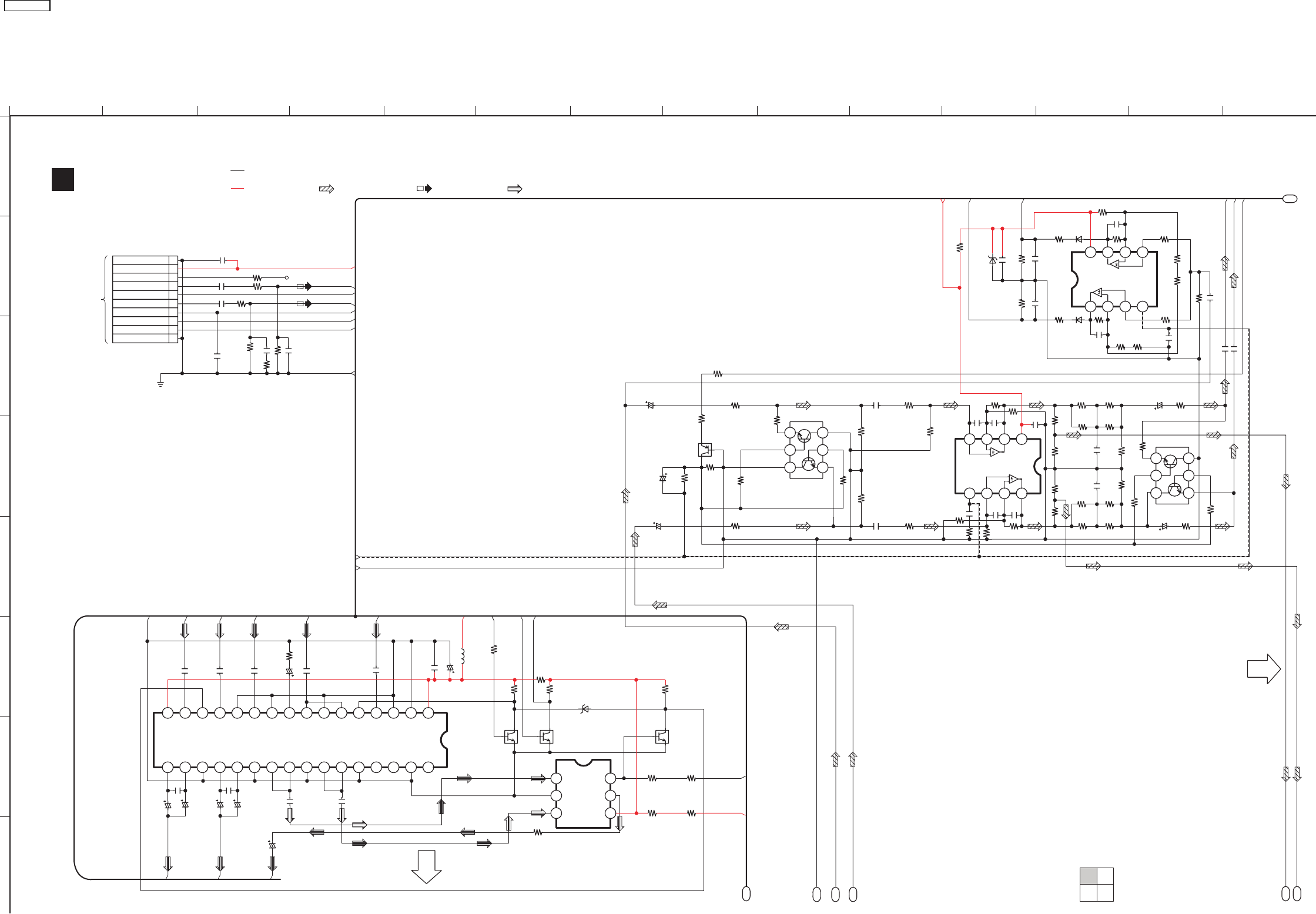
20.2. Main, Panel & Mic Circuit
B
SCHEMATIC DIAGRAM - 6
MAIN CIRCUIT
SA-PT850EE MAIN CIRCUIT
B16
B1
B6
B7
B8
B11
B12
:+B SIGNAL LINE :FM SIGNAL LINE :DVD VIDEO SIGNAL LINE
:MAIN SIGNAL LINE
:-B SIGNAL LINE
1/4 2/4
3/4 4/4
TO MAIN
SECTION (3/4)
TO MAIN
SECTION (2/4)
A
B
C
D
E
F
G
H
1234567891011121314
100
R2756R2755
4.7K
0.01
C2753
C2197 0
C2297 0
820K
R2760
R2752
10K
C2754
100P
R2753
4.7K
22K
R2758
R2754
1K
22K
R2759
C2751 1
R2757 47K
R2181
4.7K
W2660
0
R2282
10
4.7K
R2281
2.2K
2.2K
R2198
R2298
C2181
1000P
22
R2277
22
R2278
22
R2280
22
R2279
C2281
1000P
R2182
10
C2196
16V100
C2296
16V100
22
R2179R2177
22
R2178
HEADPHONE AMP
22 22
R2180
HP-LCH
HP-RCH
R2172
1.8K
R2171
27K
R2271
56K
B1GDCFGA0018
Q2201
1.2KR2175
C2171
25V4.7
1.2K
R2275
R2170
2.2K
R2270 2.2K
MUTING
3
25
4
16
B1GFGCAA0001
Q2101
MUTING
B1GFGCAA0001
Q2103
Q2103
FL
50V1
C2177
2.2K
R2196
0
W2540
0
W2658
1
C2294
100K
R2197
3.3K
R2192
100K
R2297
1
C2194
2.2K
R2296
50V1
C2277
FR
C2755
100P
R2761
820K
R2185
1.2K
1.2K
R2285
0.1C2756
R2276
22K
0.1
C2757
R2751 470
3.9K
R2291
D2751
B0BC5R000009
22K
R2176
3.9K
R2191
C2752 0.01
0.1
C2280
100P
C2178
C2278
100P
SENSE1
SENSE2
470K
R2765
C2179
150P
R2764 470K
+7V
B0ACCK000005
D2752
D2753
B0ACCK000005
675
243
8
1
C0ABBB000350
IC2751
IC2751
150P
C2279
R2762
10K
C2180
0.1
R2763
10K
675
243
8
1
IC2102
C0AABB000125
-7V
HP_MUTE
CYOUT
CROUT
6
8
9
7
2
1
4
5
3
10
CN2002
TO TUNER PACK
(J3CBBB000001)
R2261
47K
680P
C2262
R2161
47K
W2611
0C2162
680P
TUN-LCH
TUN-RCH
1KR2260
1K
R2160
0.01
C2169
1C2960
C2261 0
C2161
0TUN_SD
TUN_DO
TUN_CLK
AGND
TUN_DI
-7V
CBOUT
TU+9V +VCC
-VCC
6dB Clip
MUTING CONTROL
-VCC
+VCC
4
52
3
61
T+9V
PORT_SEL
TUNER SD
TUNER DI
AGND
TUNERGND
CHASSIS GND
TUNER CLK
RDS DETECT
TUNER LCH
TUNER RCH
TUNER DO/ST
C2835
25V22
0.1
C2838
6.3V100
C2806
25V22
C2834
6.3V1000
C2801
10
C2839
10
C2836
0.1
C2837
6.3V100
C2805
VMUTE
WIDE1
WIDE_OUT
VIDEO BUFFER
MUTING
1K
R2804
0
K2811
Q2801
B1GBCFJN0033
INVERTER
VIDEO BUFFER
Q2805
B1GBCFJN0033
MUTING
Q2804
B1GBCFJN0033
2625 27 2817 18 20 22 24232119
87 56
16 15 10 913
14 1112 312
30 3231
4
29
C9ZB00000461
IC2801 IC2801
1
C2817
C2818
1
VIDEO_+5V
VIDEO_+5V
PY
C2811
0.1
CR
VGND
CB
L2801
G0C220JA0055
C2812
0.1
C2808
10V220
C2810
0.01
C2807
0.01
Y
DVD_A+5V
C2809
25V22
C
CBIN
YIN
GND
SEL
CYIN
BIAS
S2
S1
SEL
CIN
CVIN
MUTE1
VCC1
IN1
GND
IN2
SW
OUT
VCC
IC2802
C1AB00001731
CYSAG
GND2
CBOUT
CBSAG
SDCOUT
VOUT
COUT
YSAG
CYOUT
VSAG
YOUT
GND2
GND2
VCC2
MUTE2
CRIN
CRSAG
GND2
CROUT
3dB Clip
1K
R2803
1K
R2807
0
W2593
RGB_H
B0JCAE000001
D2810
OP AMP
3
25
4
16
R2186
R2286
1.5K 1.5K
R2292
3.3K
0
W2632
W2615
0
W2573
0
W2619
0
W2618
0
W2617
0
W2616
0
W2303 0
SA-PT850EE
88
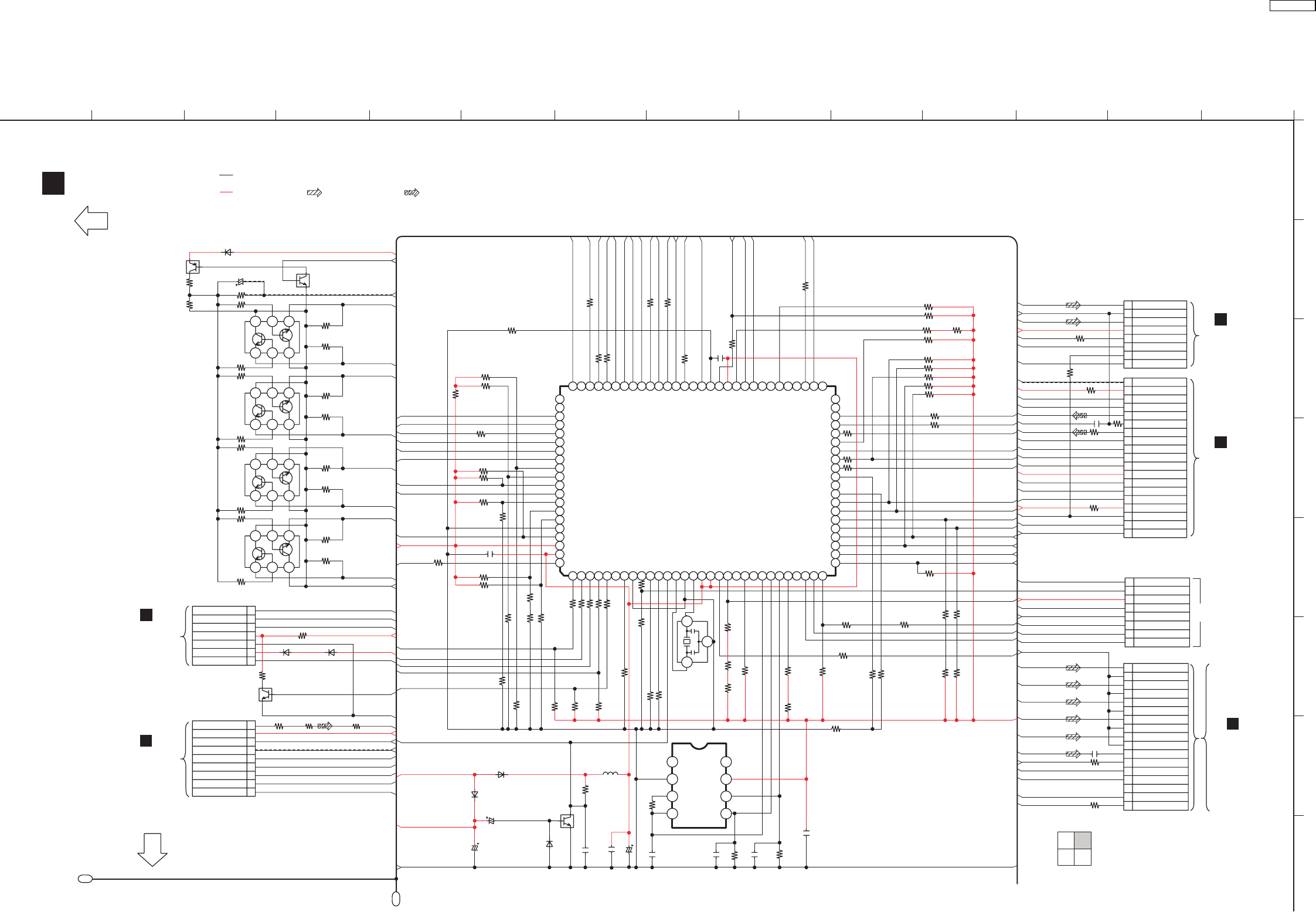
B
SCHEMATIC DIAGRAM - 7
MAIN CIRCUIT
B16
B14
:+B SIGNAL LINE :MAIN SIGNAL LINE :MIC / MUSIC PORT SIGNAL LINE
:-B SIGNAL LINE
SA-PT850EE MAIN CIRCUIT
1/4 2/4
3/4 4/4
TO MAIN
SECTION (1/4)
TO MAIN
SECTION (4/4)
FOR SOFTWARE
TO
TRAY LOADING
CIRCUIT
(CS901)
IN SCHEMATIC
DIAGRAM - 17
L
TO
VOLUME CIRCUIT
(CN6901)
IN SCHEMATIC
DIAGRAM - 17
D
TO
PANEL CIRCUIT
(CN6902)
IN SCHEMATIC
DIAGRAM - 10
C
TO
D-AMP CIRCUIT
(CN5050)
IN SCHEMATIC
DIAGRAM - 13
G
TO
MIC CIRCUIT
(H7000)
IN SCHEMATIC
DIAGRAM - 11
E
15 16 17 18 19 20 21 22 23 24 25 26 27 28
A
B
D
E
F
H
G
C
10K
R2862
10K
R2079
10K
10K
R2081
R2080
10K
R2863
FX_DO
FX_DI
R2037 47K
R2041 4.7K
R2051 56K
47K
R2034
HOP_DA
JOG_A
R2054 220
ACS_MUTE
CEC_IN
MUTE_C_S
YC_H
AMBP
PCONT
CEC_OUT
MOD_DA
MUTE_F_SW
R2062 220 JOG_B
R2060 220
HP_MUTE
WIDE1
W2649 0
W2531 0
W2533 0
ASP_DAT
R2069 220
R2068 220
DC_DET1
VMUTE
ASP_CLK
SCART_MUTE
RGB_H
R2043 10K
R2021 56K
R2045 10K
DC_DET2
R2022
220
C2000
0.1
SENSE1
SENSE2
3425
98
94
95
92
91
93
97
96
1
100
99
80 78 767779
87
86
88
89
82
84
83
81
85
90
1614 15 1711 1312
69 67 65 64666870 51
49
45
47
46
41
44
42
43
48
50
30
39
37
35
32
31
34
33
36
38
40
22 2320 21 26 282724 2518 19
53555762 60 596163 58 56 54
29
5275 73 717274
976810
IC2001
C2CBYY000418
TUN_CLK
TUN_DO
DVD_MUTE
FX_DET1
FX_CLK
TUN_SD
TUN_CLK
TUN_SD
TUN_DI
R2010 0
R2003 220
R2000 220
220R2005
220R2004
DVD_CMD
R2031 220
R2040
R2024
10K
1K
DVD_STAT
DVD_CLK
RMT
SYNC
3
1
2
H2B100500004
X2001
R2093
R2869
220
10K
10KR2077
FLD_CLK
FLD_OUT
FLD_STB
KEY2
1.8K
R2088
KEY1
VREF
C2001 0.1
BRAKE_H
TRAY_OPEN
TRAY_CLOSE
TRAY_CCW
ACS_IN
25V22
C2003
VREF
B0ACCK000005
D2005
B0ACCK000005
D2007
R2865 4.7K
6.8K
820R2864
R2871
C2012
330P
ECS
EEPROM
(NOT SUPPLIED)
R2017
W2519
0
W2501
027K
R2086
22K
ECK
5
6
1
3
4
2
8
7
CN2006
FX_DET1
RESET
FX_DI
FX_DO
FX_CLK
MUTE_C_S
DC_DET2
MOD_DA
MUTE_F_SW
HOP_DA
6
5
8
9
11
12
10
14
15
13
7
2
1
4
3
17 1
17
16
CN2009
GNDE
GNDE
GNDE
C2013
0.022
R2087
22K
220R2016
220
10K
R2872
10K
R2092
R2001 27K
R2032 47K
TRAY_CW
TRAY_OPEN
MIC_SW
TRAY_CLOSE
TRAY_CCW
TRAY_CW
R2089
4.7K
R2082 0
W2641
0
W2534
R2870
10K
R2095
56K
R2053
10K
R2015 220
C2007
0.1
B1GBCFLL0037
Q2003
R2084
47K
50V2.2
C2006 RESET
D2008
B0ACCK000005
RESET
RESET
6
7
5
2
4
3
81
IC2003
IC2003
R2085
4.7K
C2008
6.3V100
0.1
C2009
SL_OUT
CENTER_OUT
C2520
W2643 0
W2558 0
0
SR_OUT
FRONTR
FRONTL
330P
C2011
C2010
330P
SYS6V
EDA
NC
GND
DI
DO
NC
XIN
BYTE
MOD_DA
GND
RDS_EN
HP_MUTE
PCONT
ACS_MUTE
CEC_IN
CEC_OUT
ACS
WIDE1
XM_EN
[97]KEY1
MD3
FLD_STB
RDS_DAT
[84]ECHO_LVL2
SYSTEM CONTROL
FLD_CLK
FLD_OUT
JOG_B/VOL_DN
ECHO_MUTE
[83]ECHO_LVL1
[82]WS_LED
[81]RDS_CLK
JOG_A/VOL_UP
[98]VREF
[99]AVCC
[100]BRAKE_H
MD2
KEY2
AVSS
DES1
DES2
DES3
VSS
MUTE_C_S
HOP_DA
XOUT
MUTE_F_SW
AMBP
RESET
NC
CNVSS
AGND
AGND
SURROUND L
SUBWOOFER
AGND
SURROUND R
AGND
AGND
FRONT R
FRONT L
AGND
SW+5V
FHOP
CENTER
DC_DET
MOD_DA
MUTE_F (MODE 2)
MUTE_S (MODE 1)
SK
NMI VSS
SYNC
NC
ECK
EDA
ECS
RMT
SENS1
SENSE2
NC
(CLK)
[33]FX_CLK
[32]FX_DI
FX_EN
TUN_DI
TUN_DO
DVD_PCONT
FX_DET1
[31]FX_DO
(BUSY)
MULTI_1
RGB_H
[47]ASP_CLK
VMUTE
SCART_MUTE
ACS_EN
HBASS_SW
NC
EPM
DVD_MUTE
DC_DET1
NC
VMUTE_MAIN
POS_SW
[48]ASP_DAT
[50]NC
[49]NC
NC
MIC_EN
(TxD)
TV_EN
(RxD)
DVD_STAT
NC
DVD_CMD
DVD_CLK
VCC
OPT_EN
DC_DET2
CS
NC
CLOCK
RxD
DGND
TxD
CNVSS
RESET
BUSY
VREF
VREF
VREF
VCC YC_H
VCC
R2030
1K
K2812
0
R2023
220
R2094
220
SUBW_OUT
HP-RCH
HP-LCH
KEY2
JOG_B
JOG_A
5
6
1
3
4
2
8
7
CN2020
HP_RCH
KEY2
DGND
VREF VREF
AGND
AGND
JOG_B
HP_LCH
JOG_A
18
16
14
8
9
11
12
10
2
3
1
5
7
6
4
13
15
17
19
CN2007
RMT
F-
F+
SW+5V
DGND
SW+5V_GND
KEY1
SYNC
VREF
+7V
+7V -7V
-7V
MPORT_RCH
MPORT_LCH
ACS
ACS_MUTE
AGND
FL_IC_CLK
FL_IC_DAT
FL_IC_STB
-VP
TRAY_OPEN
VREF CONTROL
FLD_CLK
ACS_IN
F_MPORT-LCH
ACS_MUTE
F_MPORT-RCH
1000P
C2199
RMT
FLD_OUT
SYNC
KEY1
TRAY_CCW
TRAY_CLOSE
2.7K
R2943
0
W2659
0
W2625
0
W2633
Q2030
B1GBCFJN0033
TRAY_CW
D2935
B0EAKM000117
D2936
B0EAKM000117
R2942 2.2K
4
5
1
3
2
7
6
CN2015
VREF
VREF
M+9V
VREF
SW+5V
-VP
GND
F+
F-
C+7.5V
GND (MGND)
TRAY_CW
MGND
TRAY_OPEN
TRAY_CCW
TRAY_CLOSE
FLD_STB
BRAKE_H
R2006 220
G0C3R3JA0027
L2008
10KR2008
HBASS_SW
W2536
0
W2511
W2532
0
0
W2614
0
W2523
W2527
0
0
W2524
0
W2613
0
W2612
0
W2526
0
W2634
W2648
0
W2539
W2610
0
0
W2650
W2623 0
0
0
150
R2195
56K
R2244
Q2007
UNR211H00L
B0ACCK000005
D2009
1KR2240
1KR2620
1KR2420
1KR2242
1KR2320
1KR2142
1KR2520
1KR2140
R2145 27K
50V4.7C2140
MUTING CONTROL
MUTING
MUTING
INVERTER
MUTING
MUTING R2421 100K
100KR2521
R2621 100K
R2321 100K
100KR2143
100KR2243
R2141 100K
R2241 100K
B1GBCFJN0033
Q2008
DVD_MUTE
32
54
1
6
32
54
1
6
32
54
1
6
32
54
1
6
Q2302
B1GFGCAA0001
Q2502
B1GFGCAA0001
Q2202
B1GFGCAA0001
Q2102
B1GFGCAA0001
DVD_D+5V
-7V
MIXL
MIXR
DVD-FL
DVD-FR
DVD-CNT
DVD-SUBW
DVD-SL
DVD-SR
AGND
3
2
6
7
4
5
1
9
8
CN2013
CHASSIS GND
ECHO_LVL2
MIC_IN
+7V
-7V
ECHO_LVL1
ECHO_MUTE
AGND
MIC_SW MIC_SW
ECHO_LVL1
MIC_IN
ECHO_LVL2
ECHO_MUTE
-7V
+7V
CHASSIS GND
AGND
ECHO_LVL2
ECHO_LVL1
ECHO_MUTE
MIC_SW
220
R2052
R2027 220
27KR2019
27KR2014
SA-PT850EE
89
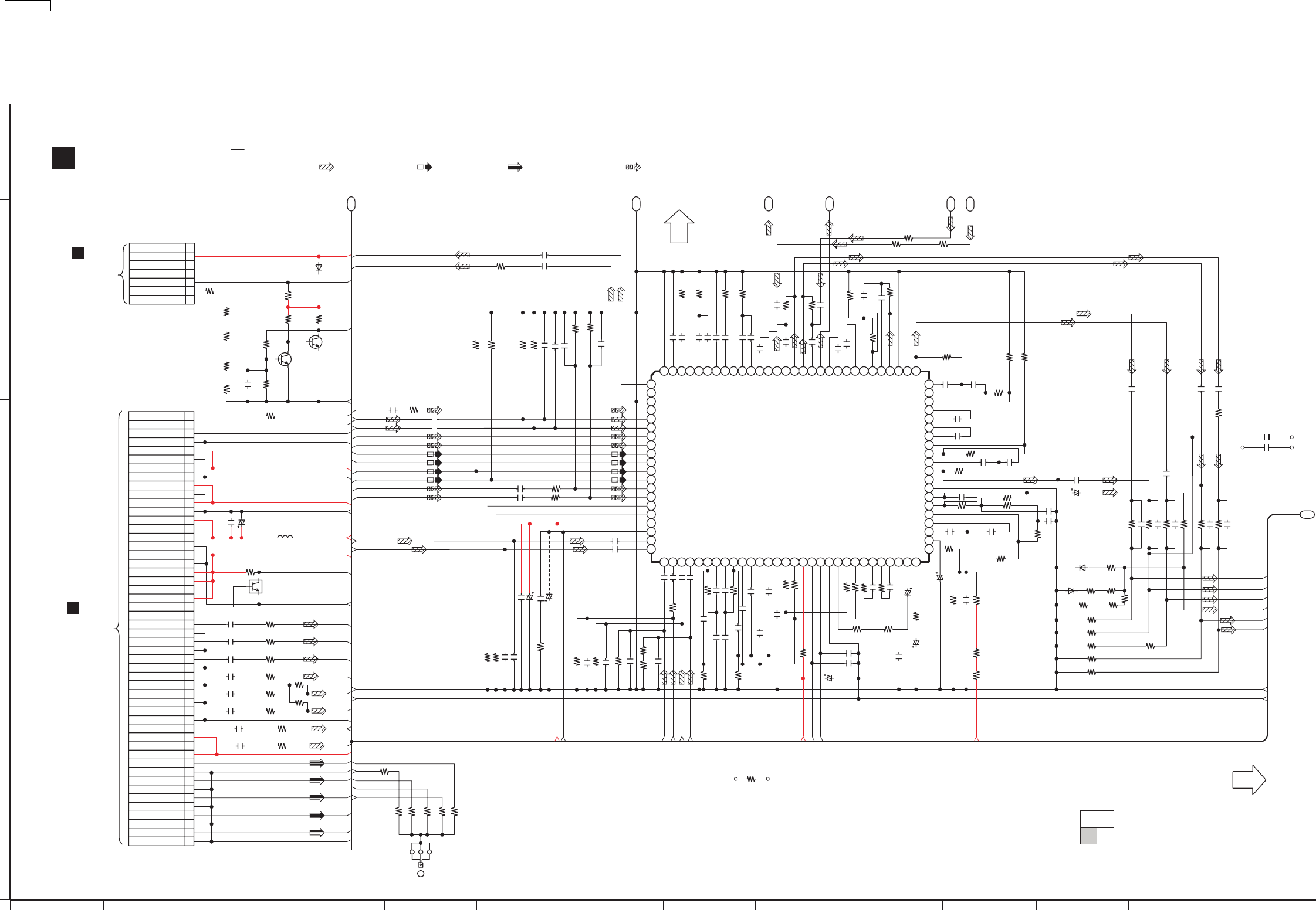
B
SCHEMATIC DIAGRAM - 8
MAIN CIRCUIT
B13
B1
B7
B8
B12
B11
B6
SA-PT850EE MAIN CIRCUIT
1/4 2/4
3/4 4/4
TO MAIN
SECTION (1/4)
TO MAIN
SECTION (4/4)
A
TO
DVD MODULE
(DV5) CIRCUIT
(FP8101)
IN SCHEMATIC
DIAGRAM - 2
:+B SIGNAL LINE :FM SIGNAL LINE :DVD VIDEO SIGNAL LINE:MAIN SIGNAL LINE
:-B SIGNAL LINE
:AUX / MUSIC PORT / MIC SIGNAL LINE
TO
DVD MODULE
(HDMI) CIRCUIT
(FP3902)
IN SCHEMATIC
DIAGRAM - 5
A
1234567891011121314
I
J
L
M
N
P
O
K
0C2421
0C2321
SL_OUT
SR_OUT
1KR2183
1KR2283
R2617 3.3K
0.033
0.033
C2130
C2230
R2510
2.7K
R2312 1.5K
R2412 1.5K
C2509 0.01
D2601
B0ACCK000005
W2265
0
W2651
068
R2661
68
R2662D2602
B0ACCK000005
4.7K
4.7K
R2184
R2284
4.7KR2339
R2626
3.9K
W2640
0
4.7KR2439
R2512 2.2K
FRONTL
AGND
GNDE
FRONTR
R2113 0
C2115 330P
C2114 5600P
25V4.7C2602
1K
1K
R2120
R2220
12K
R2404
C2515 0
C2320 0
C2420 0
C2640 0
12K
R2304
C2307
1
0.047
C2202
27KR2103
R2206 56K
R2106 56K
0.047
C2102
R2203 27K
0
R2299
C2121 0.1
C2221 0.1
C2218 0.1
C2103
1
C2204 0.039
R2214 5.6K
2.7K
R2215
C2104 0.039
2.7KR2115
R2503 8.2K
C2503
0.047
C2501 4.7
R2501 8.2K
0.047C2502
5.6KR2502
C2203
1
0.1C2117
0.1C2118
R2114 5.6K
3425
98
94
95
92
91
93
97
96
1
100
99
80 78 767779
87
86
88
89
82
84
83
81
85
90
1614 15 1711 1312
69 67 65 64666870 51
49
45
47
46
41
44
42
43
48
50
30
39
37
35
32
31
34
33
36
38
40
22 2320 21 26 282724 2518 19
53555762 60 596163 58 56 54
29
5275 73 717274
976810
C1AB00002735
AUDIO SIGNAL PROCESSOR
IC2101
0.1C2217
5600PC2214
330PC2215 R2213 0
C2014
50V10
ASP_CLK
C2308
0.022
C2309 0.082
C2304 10
C2407
1
0.15C2306
0.15C2406
C2404
10
C2408 0.022
C2605 6800P
3300PC2405
680PC2504
DVD-SUBW
3300PC2305
SW+5V
DVD-CNT
DVD-SR
DVD-SL
ASP_DAT
C2601
50V22
W2629
0
W2579
0
W2631
0
R2664
0
K2600
0
C2310
0.022
C2015
220P
220P
C2016
R2609
1.2K
0.47
C2609
0.33
50V10
C2604
27KR2614
+7V
R2613 6.8K
C2603 0.022
R2302
5.6K
R2301
8.2K
8.2K
R2303
R2199
0
C2303
0.068
4.7
C2401
4.7
C2301
0.047
C2302
R2612 56K
C2403
0.068
8.2KR2401
C2612 5600P
8.2K
R2403
R2610
15K
C2611
0.22
C2412
1
C2619
50V10
C2506
1
C2312
1
C2282
1
C2182
1
W2654
0
C2617
0.18
R2611 27K
R2627 47K
C2402
0.047
C2610
R2402
5.6K
R2233 10K
C2206 680P
R2212 4.7K
R2112 4.7K
C2213 680P
C2113 680P
C2500 1
C2400 1
C2600 1
R2500 12K
12K
12K
R2600 1K
R2400
R2300
C2300 1
G0C220JA0055
C2106
C2193
C2293
0
0
AGND
GNDE
680P
F_MPORT-RCH
R2133 10K
R2290 10K
C2195 1
C2295 1
R2190 10K
F_MPORT-LCH
B1GBCFJN0033
Q2006
INVERTER
1.8K
R2903
47
44
39
40
35
31
27
24
21
20
22
16
15
18
17
19
23
26
25
30
28
29
34
32
33
38
36
37
43
41
42
46
45
49
48
50
CN2001
R2201 10K
R2101
10K
3.3KR2200
3.3KR2100
3.3KR2202
3.3KR2102
C2211 1
C2201 1
C2101 1
C2111 1
R2504 10K
R2601 W2622
0
12K
C2415 680P
680PC2315
R2410 10K
-7V
R2105 1.5K
R2310 10K
+7V
+7V
R2205 1.5K
2200P
C2208
C2019 10V47
-7V
0.01
C2020
C2191 1
CR
CB
C
Y
PY
0.01
C2017
2.7K
2.7K
R2104
2200PC2108
R2204
C2192
C2292
0
0
C2018 10V47
C2291 1
TV-RCH
DVD-FR
DVD-FL
MIXR
TUN-RCH
AUX-RCH
AUX-LCH
TUN-LCH
TV-LCH
FRFIN
[34]SLVOLIN
SRVOLIN
SRSELOUT
SLSELOUT
FRVOLIN
[31]SLFIN
[33]SLNFIN
[32]SLVOLOUT
CFIN
CVOLIN
AGND
COUT
CNFIN
SLOUT
FRSELOUT
CSELOUT
CVOLOUT
REARSLOUT
FRVOLOUT
DATA
AGC2
DGND
AGND
[48]SUBOUT
[49]SUBC
SRNFIN
OPIN2
OPOUT2
OPOUT1
SRFIN
SRVOLOUT
SROUT
REARSROUT
EXTINR
EXTINL
MIXCAPL1
MIXCAPL2
SUBSELOUT
WIDECAP
SUBVOLIN
MIXCAPR2
MIXCAPR1
OPIN1
[50]AGC1
CLOCK
FLOUT
TTR
TML2
TML1
TBL2
TBL1
TTL
AGND
TBR1
TBR2
TMR1
TMR2
FLFIN
FLVOLIN
INL1 [MIX L]
AGND
MICIN [100]RECOUTL
RECOUT_L
[99]RECOUTR
RECOUT_R
INL2 [AUX L]
INR1 [MIX R]
FLSELOUT
FLVOLOUT
FROUT
LSIN
SF
EXTOUTR
EXTOUTL
RCIN
LCIN
RF
RIN
LF
LIN
AGND
CIN
SRIN
SLIN
RMPORTL
AVEE
AVCC
RMPORTR [81]FRIN
[82]FLIN
SUBIN
AGND
RSIN
INR2 [AUX R]
FMPORTR
FMPORTL
INL4 [TV L]
INR4 [TV R]
INL3 [FM L]
INR3 [FM R]
DVDD
CENTER_OUT
A+5V
D+5V
DGND
FL
SL
FR
ADGND
ADGND
C
MIX-L
MIX-R
VGND
VGND
VGND
VGND
VGND
Y
ADGND
VGND
ADGND
ADAC5V
CR/PR/R
ADAC5V
Y/PY/G
CB/PB/B
SW
CNT
SR
D+5V
D+5V
ADGND
ADGND
ADGND
A-REF
VGND
DGND
DGND
D+5V
AUDIODIGITAL
ZFLAG&AMUT
4
5
1
3
2
7
6
CN2010
220P
C2025
0W2647
R2097
4.7K
2SD0601AHL
BUFFER
Q2096-Q2097
Q2097
CEC_IN
CEC_OUT
D2010
B0ACCK000005
R2941
22K
Q2096
R2096
47K
R2098
2.2M
R2099
100K
GNDE
SYS6V
DGND
CECOUT
CECIN
NSW+6V
+5V_SW
2CH_SEL
DMIX_SEL
6
7
5
9
11
13
12
10
14
8
1
3
4
2
A+5V
AGND
AGND
MGND
DGND
DGND
M+9V
M+9V
MGND
+2.7V
+2.7V
DOP_CPU_CMD
DOP_CPU_STAT
DOP_CPU_CLK
DVD-CNT
DVD-SR
DVD-SUBW
L2009
DVD_MUTE
DVD_CMD
DVD_STAT
DVD_CLK
DVD_2R7
C2921
0.1
10V220
C2021
DVD_A+5V
DVD_D+5V
M+9V
AGND
DGND_1
MGND
DVD_ADAC+5V
DVD-SL
DVD-FR
MIXR
DVD-FL
MIXL
R2992 0
R2991 0
R2990 0
R2995 0
R2993 0
32 1
E2901
VGND
CHASSIS
DGND
W2606
0
ADGND
DGND_1
AGND
SUBW_OUT
C2313 2700P
C2413 2700P
MIXL
W2599 0
W2576 0
W2655
0
W2626
0
W2574 0
W2415 0
0
W2642
C2198
1
R2193
1.5K
MIC_IN
R2119
3.9K
3.9K
R2219
W2557
0
W2542
0W2652
0
W2653
0
W2637
0
W2630
0
SA-PT850EE
90
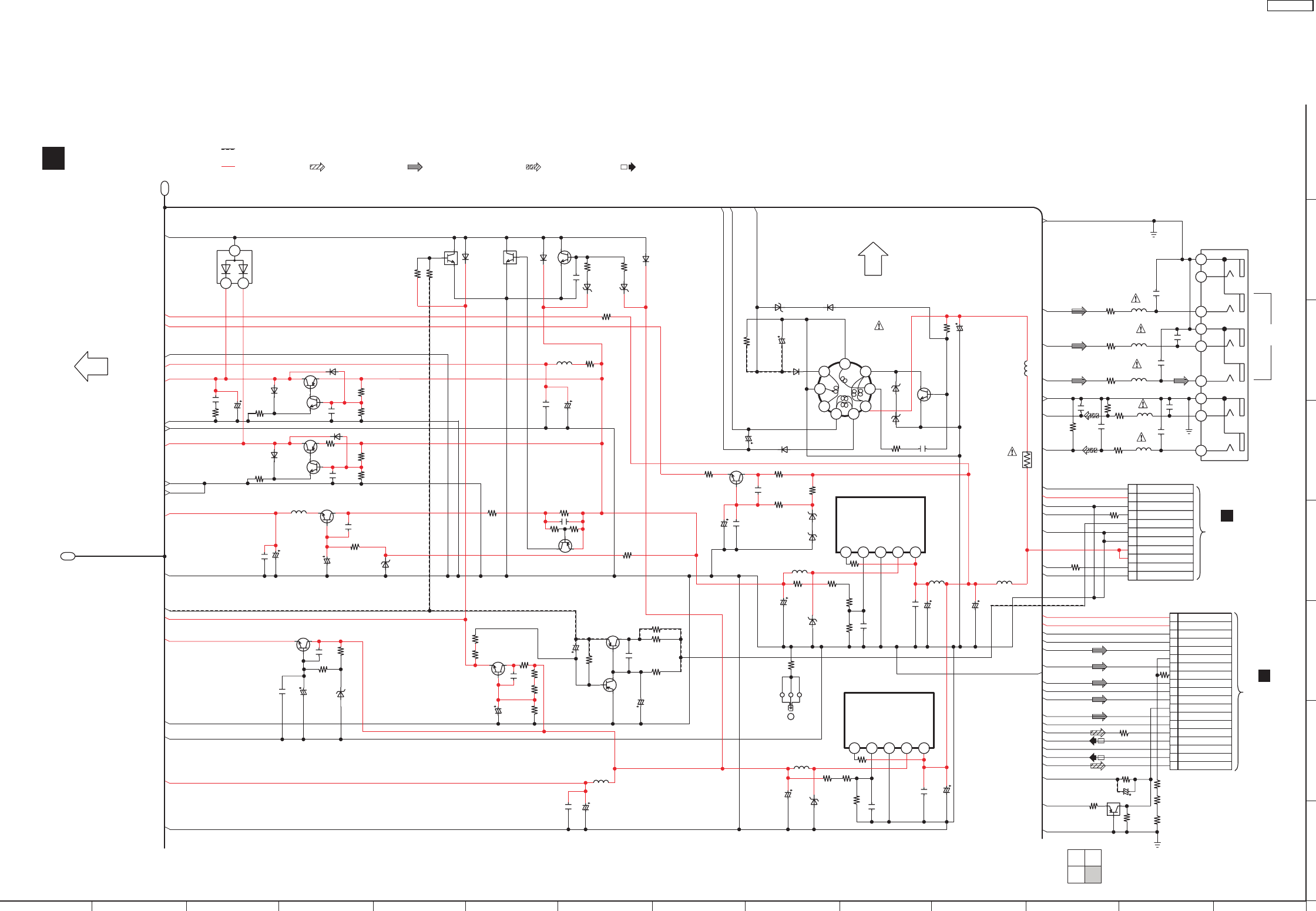
B
SCHEMATIC DIAGRAM - 9
MAIN CIRCUIT
B13
B14
SA-PT850EE MAIN CIRCUIT
1/4 2/4
3/4 4/4
TO MAIN
SECTION (3/4)
TO MAIN
SECTION (2/4)
:+B SIGNAL LINE :DVD VIDEO SIGNAL LINE:MAIN SIGNAL LINE
:-B SIGNAL LINE
:AUX SIGNAL LINE
TO
SCART CIRCUIT
(CN1001)
IN SCHEMATIC
DIAGRAM - 16
J
TO
SMPS CIRCUIT
(CN5802)
IN SCHEMATIC
DIAGRAM - 14
H
:FM SIGNAL LINE
15 16 17 18 19 20 21 22 23 24 25 26 27 28
I
J
L
M
N
P
O
K
DC_DET1
R2946 33
L2908
G0A200D00002
C2940
0.01
C2925
6.3V220
C2932
16V100
C2926
0.1
B1BACG000023
Q2904
Q2904
Q2908
Q2906
Q2910
Q2907
+2.7V REGULATOR
B1ACKD000006
Q2908
+5V POWER SUPPLY
+5V POWER SUPPLY
+5V POWER SUPPLY
+5V POWER SUPPLY
D2942
B0ACCK000005
D2941
B0ACCK000005
R2984
470
R2982
470
C2968
0.1
C2969
0.1
R2931
330
R2933
330
R2932
10K
R2934
10K
D2939
B0ACCK000005
D2940
B0ACCK000005
B1ABCF000176
Q2906
B1ACKD000006
Q2910
B1ABCF000176
Q2907
D2915
B0ACCK000005
Q2909
Q2909
B1GBCFJN0033
39KR2937
B1GBCFJJ0051
Q2922
DC DETECTDC DETECT DC DETECT
15KR2938
3
12
D2943
B0ADCJ000020
-7V
R2902
47
DC_DET2
GND
+18V
FP2900
0.4
SYNC
R2935
4.7K
C2900
25V100
G0A200D00002
L2910
5.6K
R2900
D2901
D2901
D2920
B0BC035A0007
D2920
B0BC035A0007
B1BABK000001
PSAVE CONTROL
Q2900
Q2900
TRANSFORMER
SWITCHING
C2903
3900P
PCONT
AMBP
4.7K
R2930
L2909
G0A200D00002
25V1000
C2901
R2055
1K
6
8
9
7
2
1
4
5
3
10
11
CN2004
0.01
C2939
C2955
25V220
L2911
G0A200D00002
0.01
C2915
L2907
G0A220GA0026
R2985
0
6.3V220
C2916
0.1
C2924
0
W2620
0
W2621
6.3V100
C2933
B0ACCK000005
D2945
D2945
D2944
B0ACCK000005
B1ABCF000176
Q2919
Q2919
4.7K
R2948
R2947
4.7K
R2926
47K
D2947
B0BC010A0007
D2947
D2946
B0BC7R500001
D2946
Q2922
C2970
1
R2949
1
B0JAME000029
D2906
2.2K
R2971
22
R2972
+9V REGULATOR
Q2916
Q2916
B1BACG000023
B0BC4R600016
D2937
B0BC5R000009
D2938
1R2939
91
R2974
0.1
C2962
16V100
C2963
0.01
C2961
C2918
16V100
B0EAMM000057
D2903
D2908
B0EAMM000057
53
4
8
7
62
1
9
T2900
G4D1A0000117
D2909
MAZ82400HL
C2904
35V33
D2904
B0JCPD000025
R2936
330
32 1
E2900
1K
R2919
0
R2994
D2912
B0BC3R400001
R2908
560
R2907
2.7K
C2908
16V100
C2913
16V100
560
R2953
3.9
R2951
3.9K
R2952
R2954
22
C2910
0.01
22
R2913
10V33
C2914
B1BCCG000002
Q2901
R2915
2.7K
R2914
3.9K
B1ADCF000001
Q2902
B1BACD000018
Q2903
R2905
39
C2906
0.01
R2921
3.3K
R2999
0
10K
R2976
R2975
15K
+5.3V
C2922
6.3V820
Q2921
Q2921
B1ADCF000001
DC DETECT
G0A101G00022
L2902
1.5
R2925
C2975
0.1
R2927
1.5
R2920
1K
42135
C0DAAYY00042
IC2900
C2920
1000P
42135
C0DAAMH00012
IC2903
-13V
GNDE
SYS6V
R2813
75
CYOUT
CROUT
VGND
C2826
100P
G0A101G00022
L2903
R2906
6.8K
R2923
1.2K
C2923
25V220
L2905
G0A100HA0023
1K
R2922
D2913
B0JCPD000025
0.01
C2927
10V680
C2930
C2929
0.01
C2938
16V220
C2937
0.01
DGND
DGND_1
DGND
AGND
VGND
10K
R2264
AUX-LCH
R2812
75
10K
R2164
R2809
75
+7V
CBOUT
AGND
AUX-RCH
DVD_2R7
DVD_A+5V
DVD_ADAC+5V
DVD_D+5V
TU+9V
+12V
R2265
10K
C2283
470P
C2183
470P R2165
10K
J0JBC0000015
L2802
C2823
100P
L2201
J0JBC0000015
L2101
J0JBC0000015
C2164
220P
C2264
220P
5
6
3
1
2
4
7
8
9
JK2001
J0JBC0000015
L2804
L2803
J0JBC0000015
C2825
100P
M+9V
AGND
CHASSIS GND
CHASSIS GND
PCONT
AMBP
+18V
DC_DET
GND
GND
+18V
-13V
OUT
GND
VCC
INV
+9V
STBY
GND
VCC
SYS6VGND
SYS6V
SYNC
OUT
STBY
SWITCHING REGULATOR
SWITCHING REGULATOR
INV
ADGND
F+
F-
-VP
MGND
+7V REGULATOR
-7V REGULATOR
-7V REGULATOR
COMPONENT
VIDEO OUT
[RCH]
AUX
[LCH]
[PB]
[PR]
[Y]
-7V
SCART_MUTE
MUTING CONTROL
R1021
1K
27K
R1022
C1020
50V4.7
W2609
0
W2572
0
W2578
0
W2571
0
Q1009
Q1009
B1GDCFGA0018
56K
R1023
18
16
14
8
9
11
12
10
2
3
1
5
7
6
4
13
15
17
19
CN2008
VMUTE
RGB_H
RECOUT_R
TV-LCH
RECOUT_L
TV-RCH
YC_H
+12V
CB
PY
CR
Y
C
ROUT
LIN
RIN
AGND
AGND
VGND
LOUT
B
VIDEO_MUTE
R
YC_H
G
SCARTMUTE
C
VGND
Y
VGND
WIDE OUT
WIDE_OUT
RGB
DVD_A+5V
SCART+12V
VIDEO_+5V
D2919
0.1
C2907
R2929
150
C2909
16V47
C2958
0.01
B1AAKD000012
+5V REGULATOR
Q2911
SW+5V_GND
SW+5V
B0BC5R600003 R2924
820
W2656
0
W2577
0
CHASSIS GND
SA-PT850EE
91
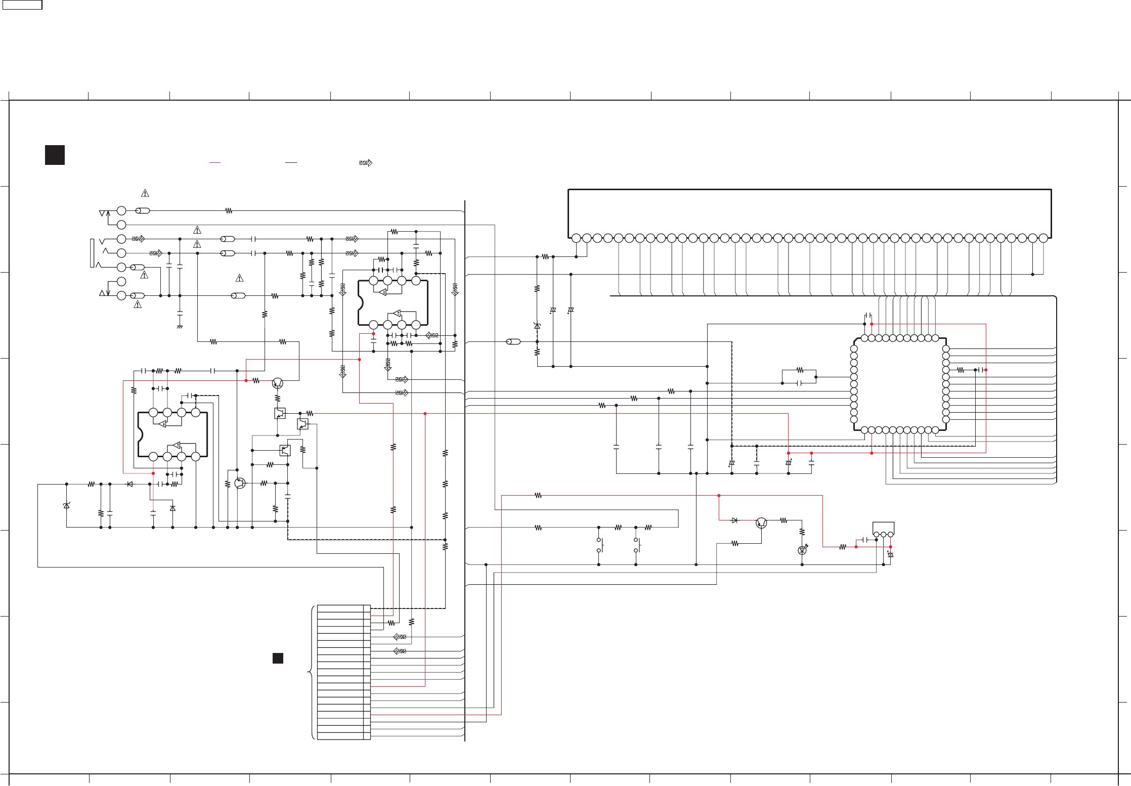
C
SCHEMATIC DIAGRAM - 10
PANEL CIRCUIT
SA-PT850EE PANEL CIRCUIT
:+B SIGNAL LINE :-B SIGNAL LINE
TO
MAIN CIRCUIT
(CN2007)
IN SCHEMATIC
DIAGRAM - 7
B
:MUSIC PORT SIGNAL LINE
A
B
C
D
E
F
G
H
1234567891011121314
1234567891011121314
A
B
D
E
F
H
G
C
G8
G7
G1
G4
G6
G5
G9
G8
G2
G5
G7
G6
G10
P17
G2
G3
G4
P11
P9
P10
P12
P13
0.01
C6929
P5
P1
P2
G1
P4
P3
P8
P6
P7
P14
P15
P16
S6902
1K
R6962
S6901
1K
R6923
B1ADCE000012
Q6201
1K
R6920
LED DRIVER
1K
R6961
D6901
B3AAA0000803
AQUA RED LED
R6919
4.7K
B0ACCK000005
D6902
C6916
100P
C6919
100P
C6910
6.3V100
50V3.3
C6913
C6911
0.01
C6917
100P
P7
P8
P5
P6
P11
P9
P10
50V22
C6903
R6951
1.2K
W6127
0
W6102
0
W6126
0
W6124
0
R6950
1.2K
50V22
C6905
R6935
10
47K
R6966 R6970
47K
10K
R6967
R6918
22K
330P
C6940
C6937
330P
675
243
8
1
IC6107
IC6107
C0ABBB000230
B0BC2R4A0006
D6910
C6935
0.1
W6129
0
W6123
0
W6101
0
W6110
0
W6117
0
W6118
0
W6114
0
W6113
0
W6128
0
W6119
0
L6903
J0JBC0000041
R6949
MUSIC PORT AMP
220
R6948
220 R6971
47K
W6122
0
C6936
330P 330P
C6941
C6921 0.033
C6920
0.033
R6968
10K
W6130
0
C6934
0.1
47K
R6965
P3
P1
P2
P4
R6917 68
68R6916
R6927 68
L6909
J0JBC0000019
L6908
J0JBC0000019
1
2
3
7
6
4
5
JK6802 L6905
J0JBC0000019
L6904
J0JBC0000019
C6938
1
W6125
0
W6103
0
L6907
J0JBC0000019
C6933
W6115
0
1
L6906
J0JBC0000019
C6923 0.01
C6924 0.01
0.01
C6930
P14
G3
123
Z6900
B3RAD0000143
G10
P15
G9 P16
P17
0.01
C6925
21
5
6
3
1
2
4
19
9
7
8
16 17
11
10
12 151413 18 20
35374244 43 39 3841 40 36
33
22
31
29
27
24
23
26
25
28
30
32
34
C0HBB0000057
IC6901
C6904
REMOTE SENSOR
1000P
C6918
10V47
P13
P12
C6906 100P
R6914
56K
232116 1714 15 19 2018108 9 12 13117123 45 6 22 444140 423736 383332 3429 3025 2624 2827 31 35 39 43 45
FL6901
A2BD00000170
C6909
0.01
R6934
47
18
16
14
8
9
11
12
10
2
3
1
5
7
6
4
13
15
17
19
CN6902
SW+5V
FL_IC_CLK
FL_IC_CLK
F+
F+
F-
F-
FL_IC_IN
FL_IC_IN
-VP
-VP
FL_IC_STB
FL_IC_STB
P3
-VP
P5
P4
LED5
G10
G9 P16
P1
P2
[34]G2
G6
G4
G1
G3
F+
F+
G1
G4
G6
G8
G9
G7
NX(G1)
NX(G1)
G5
NP
G10
G5
G8 P17
G7
G2
LED3
P15
VCC
GND
[1]LED2
LED4
P16
P17
P14
P15
[11]K2
VCC
GND
P18
P11
P12
P8
P10
P6
P7
[23]P9
P13
POWER
F-
P7
NX(G9)
NX(G8)
P5
P3
P1
P2
P4
NX(G10)
NX(G10)
P6
NX(G7)
NP
F-
OPEN/CLOSE
MUSIC PORT
V+
V-
CHASSIS
DGND
DIN
G3
P13
P12
FL DISPLAY
DISPLAY DRIVER
NX(G4)
NX(G4)
P14
OSC
DOUT
K1
STB
CLK
P10
P9
P8
NX(G6)
NX(G6)
P11
NX(G5)
F-
DGND
VREF
SYNC SYNC
SYNC
DGND
KEY1 KEY1
KEY1
RMT
F+
FL_IC_CLOCK
-7V
+7V
FL_IC_STB
SW_+5V
ACS
AGND
-VP
MPORT-RCH MPORT-RCH
MPORT-RCH
ACS_MUTE
MPORT-LCH MPORT-LCH
MPORT-LCH
FL_IC_DATA
W6106
0
C6184
10
R6192
47K
B0BC5R000009
D6102
D6101
B0ACCK000005
180K
R6291
R6294
2.2K
1
C6284
R6293
27K
R6188 4.7K
Q6102
Q6102
B1ABEB000002
C6283
0.1
0
R6231
1.8K
R6193
B1GDCFGA0018
Q6202
Q6202
R6194
56K
Q6105
B1ADCE000012
UNR221200L
Q6110
R6210
2.2K
UNR221200L
Q6111
Q6111
10K
R6196
R6191
220
C6187
150P
C6183
1
150P
C6288
R6292
OP AMP
INVERTER
SWITCH
BUFFER
MUTING
MUTING
100
C6189
1
D6100
B0ACCK000005
675
243
8
1
IC6106
C0ABBB000230
V+
V-
AGND
R6290
150K
1
C6186 C6185
1
15K
R6100
R6190
1K
R6202
10K
SA-PT850EE
92
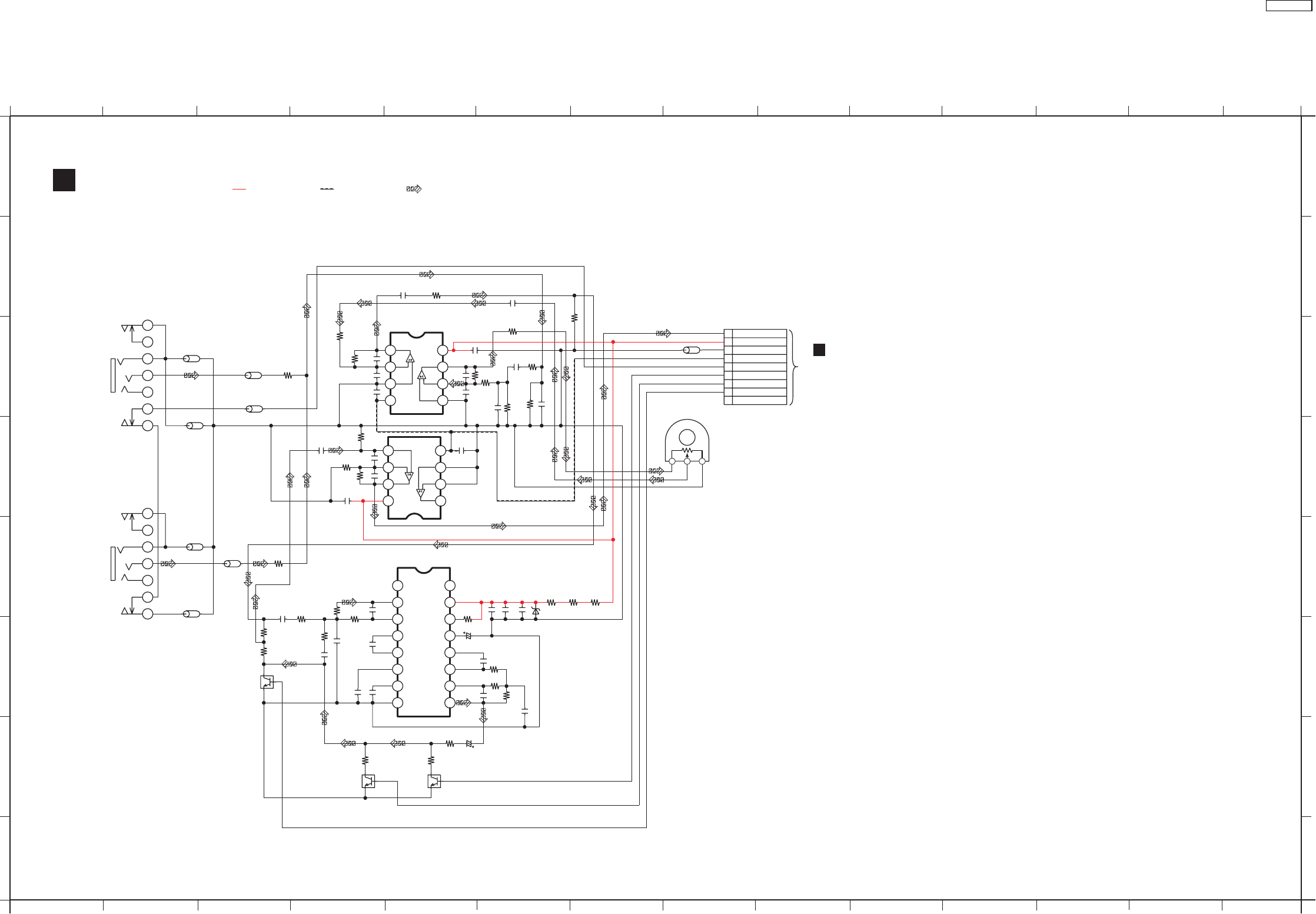
:+B SIGNAL LINE :-B SIGNAL LINE
SCHEMATIC DIAGRAM - 11
SA-PT850EE MIC CIRCUIT
E
MIC CIRCUIT
TO
MAIN CIRCUIT
(CN2013)
IN SCHEMATIC
DIAGRAM - 7
B
:MIC SIGNAL LINE
A
B
C
D
E
F
G
H
1234567891011121314
1234567891011121314
A
B
D
E
F
H
G
C
3
2
6
7
4
5
1
9
8
H7000
C7110
10V47
R7113
10K
12K
R7123
R7114
5.6K
6800P
C7102
C7104
0.068
0.1
C7124
1
C7012
MIC AMP
MIC AMP
R7010
1K
3.3K
R7008
J0JBC0000030
L7002
J0JBC0000030
L7005
L7303
L7303
J0JBC0000019
L7202
J0JBC0000019
L7101
J0JBC0000019
L7003
J0JBC0000019
L7001
J0JBC0000019
0.1
C7122
47P
C7005
R7106
120K
1
C7120
C7121
0.1
22K
R7119
R7120
10K
C7123
220P220P
C7119
R7122
47K
R7116
680
R7100
15K
C7101
MUTING
SWITCH
SWITCH
1
15K
R7102
R7101
15K
C7103
1500P
6
7
5
2
4
3
81
IC7200
C0ABBB000230
47P
C7010 100P
C7009
220P
C7006 R7006
68K
6
7
5
2
4
3
81
IC7000
C0ABBB000230
R7001
680
0.1
C7011
82K
R7009
JK7002
MIC 2
MIC 1
JK7001
15K
R7105
R7011 2.2K
J0JBC0000019
L7004
1K
R7003
C7002 4700P
R7002 560
R7107
68
W7006
0W7007
0
D7100
DIGITAL DELAY
WITH ECHO VOLUME
B0BC5R000009
1K
R7005
C7004
4700P
0.1C7007
1
C7003
EVUE27FK3B53
VR7001
R7004
10K
C7008 0.47
R7007 1K
10
C7111 C7112
0.1
10
C7115
R7112
2.7K
Q7101
B1GBCFJJ0051
C7105
0.22 0.22
C7106
Q7100
B1GBCFJJ0051
C7113
50V1
R7109
4.7K
1.5K
R7110
Q7102
B1GBCFJJ0051
6800P
C7107
0.068
C7109
7
5
6
1
2
4
3
10
12
14
15
16
13
11
89
IC7100
C1BB00001061
R7104
15K
R7103
15K
C7108
1500P
+7V
-7V
AGND
MIC_SW
MIC VOLUME
-VCC
+VCC
-VCC
+VCC
ECHO LVL 1
ECHO LVL 2
ECHO MUTE
CHASSIS GND
ASP_MICIN
CC1
OP2IN
OP2OUT
OP1IN
CLOCK
OP1OUT REF
LPF1OUT
GND
LPF2IN
LPF2OUT
CC2
NC
VCC
NC
LPFIN
321
1
7
6
4
2
3
5
1
7
6
4
2
3
5
SA-PT850EE
93
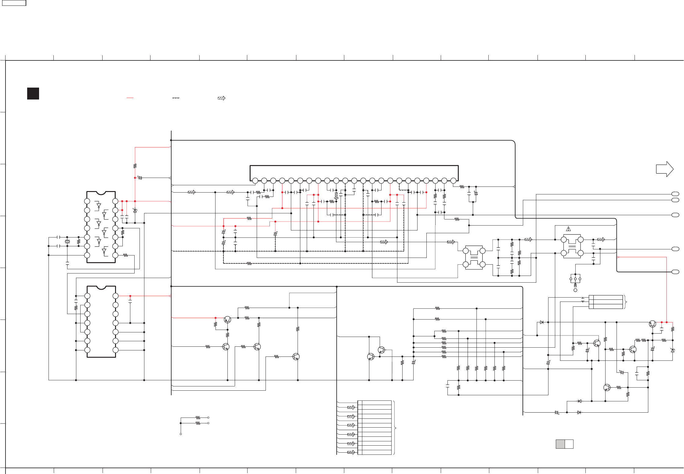
20.3. D-Amp & SMPS Circuit
G
SCHEMATIC DIAGRAM - 12
D-AMP CIRCUIT
SA-PT850EE D-AMP CIRCUIT
1/2 2/2
G1
G2
G3
G4
G6
TO FAN
:+B SIGNAL LINE :-B SIGNAL LINE :MAIN SIGNAL LINE
TO D-AMP
SECTION (2/2)
TO SPEAKERS
A
B
C
D
E
F
G
H
1234567891011121314
1234567891011121314
10K
R5657
6.3V220
C5692
2
43
1
L5301
32 1
ZJ5410
1
3
2
CN5501
C5693
FAN LOCK DETECT
FAN MOTOR DRIVE
FAN MOTOR DRIVE
FAN MOTOR DRIVE
0.1
100K
R5659
C5695
0.1
10K
R5655
25V22
C5696
D5640
B0BC01200019
3.3K
R5639 R5640
0
Q5642
Q5642
B1ABCF000011
1.8M
R5658
10
R5637
25V10
C5691
R5636
3.9K
B1BACD000018
Q5640
C5690
1000P
SW+
SW_+
C5350
0.1
C5351
0.1
SW-
FAN_DC
Q5644
Q5644
B1ABCF000011
10K
R5656
B1ABCF000011
Q5641
10K
R5660
10K
R5606
B1ADCE000012
Q5603
R5608
10K
R5604
1.2K
R5610
1.2K
1.2K
R5611
R5603
10K
R5602
10K
Q5604
B1ABCF000176
B1ABCF000176
R5609
10K
Q5601 - Q5602
Q5601
Q5602
R5302
10
220P
C5307
35V470
C5516
1M
R5507
390P
C5552
X5500
X5500
H2A6023A0011
B0BC5R000009
D5503
10
C5555
0.1
C5554
R5311
10
1M
R5508
100P
C5553
35V470
C5517
C5525
0.1
C5524
0.1
VDDA3
C5540
63V47
R5510
270
C5315
1000P
5.6K
R5307
0.47
C5317
C5562
6.3V1000 OSC
IN+_SW
FAN_DC
FAN_GND
C5312
330P
R5306
5.6K
C5314
0.47
C5313
0.1
VDDP
VSSP
C5316
0.1 C5323
220P
0.1C5319
0.1C5318
0.1
C5560
R5511
22
100P
C5561
SW+5V
5
6
4
1
2
3
9
11
13
14
12
10
78
IC5501
C0JBAF000716
VSSA3
10
R5310
R5505
100
47P
C5558
5
6
4
1
2
3
9
11
13
14
12
10
78
C0JBAB000902
INVERTER GATE
(CLOCK GENERATOR)
D-TYPE FLIP-FLOP
IC5500
OSC
SW+5V
SW+5V
MOD_DA
MUTE_F
MUTE_S
FL_+
SW_+
SW_-
DC_DET
68KR5218
C_+
120K
R5228
120KR5020 FR_+
R5019
68K
Q5101
B1ABCF000176
6.3V100
C5133
R5110
22K
68KR5328
1.2K
R5023
SIGNAL
SIGNAL
R5317 1.2K
R5327 1.2K
AGND
1.2KR5022
1.2KR5021
0.1
C5033
B1ABCF000176
Q5102
R5318 120K
R5607 1.2K
56K
R5654
0
R5670
B0ACCK000005
DC_DET
FAN_GND
D5645
50V1
C5697
C5694
16V33
B0ACCK000005
D5644
D5643
B0ACCK000005
C_-
R5035
5.6K
R5034
5.6K
220P
C5325 1000P
C5333
K5500
220P
C5326
R5304
100
C5304
330P
C5601
16V10
C5331
1000P
R5308
5.6K0.47
C5334
R5309
5.6K0.47
C5332
C5305
0.1
C5306
0.1
19 21 2322201023178945 6 12 1514 17 18161311
IC5300
C1BA00000487
AUDIO DIGITAL POWER AMP
C5324
0.015
C5321
0.22
C5302
0.1
0.1C5310
220P
C5311
0.1C5309
C5322
0.015
C5303
0.1
R5305
10
R5319
22
0.68
C5328
R5300
22
C5327
0.1
C5301
0.1
0.68
C5300
2
43
1
L5300
MODE2
MODE1
MODE1_2
MODE2
FAN GND
FAN DC OUT
CD2D1
MUTING
MUTING
MUTING
DC DETECT
DC DETECT
GND
D2
SD1
SD2
SGND1
VSSD
OUT1
PROT
OUT2
BOOT2
VSSP1
VSSP2
STABI
VSSA2
VDDP2
VSSA1
BOOT1
VDDP1
OSC
VDDA1
6Y
5A
6A
VCC
O2
4Y
02
CP2
VCC
4A
5Y3A
2A
2Y
1A
1Y
3Y
O1
01
CP1
CD1
GND
IN1+
IN1-
MODE
IN2-
signal_trigger
IN2+
SGND2
VDDA2
FAN LOCK
G0B9R5K00003
G0A150L00003
K5253 0
K5252 0
0
6
4
3
5
9
8
12
10
11
7
1
2
JK5001
CENTER +
FRONT L+
FRONT L-
FRONT R+
CENTER -
FRONT R-
SUBWOOFER -
SUBWOOFER +
SURROUND L+
SURROUND L-
SURROUND R+
SURROUND R-
C-
FR-
FL-
SL+
SR+
SL-
SR-
FL+
FR+
SW-
C+
SW+
R5114 1.2K
R5115 1.2K
FL_-SL_+
SR_+
68KR5113
120KR5111
SA-PT850EE
94
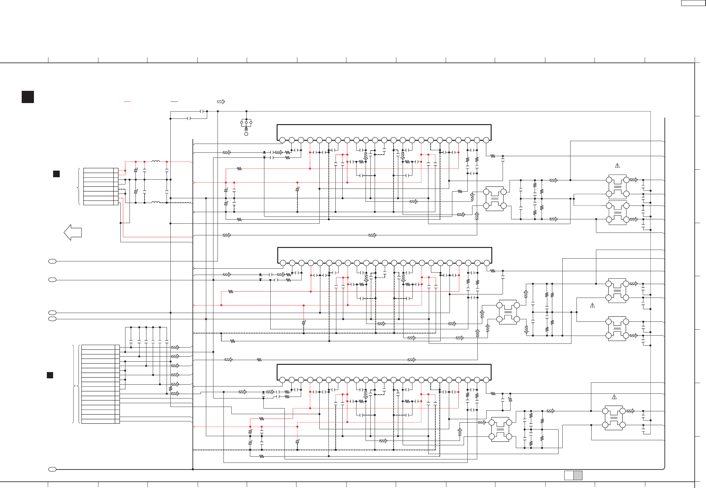
G
SCHEMATIC DIAGRAM - 13
D-AMP CIRCUIT
B
TO
MAIN CIRCUIT
(CN2009)
IN SCHEMATIC
DIAGRAM - 7
H
TO
SMPS CIRCUIT
(CN5801)
IN SCHEMATIC
DIAGRAM - 14
SA-PT850EE D-AMP CIRCUIT
G1
G2
G3
G4
G6
1/2 2/2
:+B SIGNAL LINE :-B SIGNAL LINE
TO D-AMP
SECTION (1/2)
1
17
:MAIN SIGNAL LINE
15 16 17 18 19 20 21 22 23 24 25 26 27 28
15 16 17 18 19 20 21 22 23 24 25 26 27 28
A
B
D
E
F
H
G
C
C5051
0.1
C5052
0.1 0.1
C5050
C5053
0.1
2
43
1
G0B9R5K00003
L5001 - L5002
FL+
FL_+
FR-
FR+
FR_+
FL-
2
43
1
G0B9R5K00003
L5201
C-
C_-
C5250
0.1
C5251
0.1
C+
C_+
R5200
10
220P
C5211
220P
C5203
C5201
0.015
C5200
0.1
C5150
1000P
C5152
1000P
C5155
1000P
W5032
0
C5151
1000P
C5522
0.1
10
R5211
C5523
0.1
63V47
C5240
35V470
C5509
35V470
C5508
C5223
0.47
R5206
5.6K
330P
C5224
6
5
8
9
11
12
10
14
15
13
7
2
1
4
3
17
16
CN5050
R5210 10 VDDA2
R5205
5.6K
C5222
0.47
1000P
C5221
0.1C5213
0.1C5207
VSSP
VSSA2
VDDP
C5208
0.1
C5209
0.1
C5212
220P
C5020
0.1
C5008
0.015
220P
C5010
0.1C5019
R5004
10 R5005
10
220P
C5012
35V1000
C5513
L5500
J0JKB0000020
0.1
C5445
AGND
0.1
C5514
35V1000
C5512
0.1
C5519
0.1
C5515
L5501
J0JKB0000020
C5518
0.1
5
6
1
3
4
2
8
7
H5500
63V47
C5040
VSSP
VSSP
C5510
35V470
C5511
35V470
C5521
0.1
10
R5010
VDDP
C5520
0.1
VDDA0
VDDP
0.1C5018
C5030
220P
32 1
ZJ5400
C5450
0.1
C5004
0.47
R5002
5.6K
C5002
0.47 5.6K
R5000
C5001
1000P
330P
C5006 C5025
0.1
C5024
0.1
10
R5011
OSC
OSC
IN+_FR
IN+_FR
IN+_FL
IN+_FL
IN+_SW
VSSA0
C5014
0.68
C5015
0.68
R5006
22
R5007
22
R5031
5.6K
C5016
0.1
R5030
5.6K
0.1
C5017
2
43
1
L5000
G0A150L00003
K5004
0
C5000
1000P
5.6K
R5003
0.47
C5005
1000P
C5032
R5008
100
C5007
330P
R5001
5.6K
C5003
0.47
2
43
1
L5002
L5001
220P
C5011
0.1C5023
0.1C5021
C5028
0.1
C5027
0.1
C5234
1000P
C5225
0.68
2
43
1
G0A150L00003
L5200
C5228
0.68
22
R5209
R5033
5.6K
22
R5217
0.1
C5227
0.1
C5226
R5032
5.6K
16V10
C5602
R5207
5.6K0.47
C5232
C5231
1000P
R5208
5.6K
0.47
C5233
R5204
100
C5216
330P
C5220
0.1
C5214
0.1
220P
C5218
0.1C5219
0.1C5217
C5031
0.22
C5009
0.015
220P
C5013
19 21 23222010213 7894 5 6 12 1514 17 18161311
C5022
0.1
C5202
0.22
C5206
0.1
C5204
0.015
19 21 232220102317894 5 6 12 1514 17 18161311
220P
C5205
R5201
10
AUDIO DIGITAL POWER AMP
AUDIO DIGITAL POWER AMP
MODE1
MODE2
SGND1 SGND1
OUT2
STABI
BOOT2
VSSP2
OUT1
VSSP1
VSSD
VSSA2
VDDP2
PROT
VSSA1
BOOT1
VDDP1
OUT1
VSSP1
PROT
VDDP1
BOOT1
OUT2
BOOT2
VSSP2
VSSD
VSSA2
VDDP2
STABI
VSSA1
AGND
AGND
SUBWOOFER
FRONTL
FRONT R
SIGNAL A_GND
SURROUND L
AGND
CENTER
AGND
SURROUND R
IN1-
VDD
GND
VSS
VDD
GND
OSC
IN1+
FAN DC
FAN_DC
FAN GND
FAN_GND
VSS
VDDA1 VDDA1
MUTE S_C (MODE 1)
MUTE F_SW (MODE 2)
MUTE_S
MUTE_F
MOD_DA MOD_DA
FHOP
NC
DC_DET DC_DET
OSC
IN1-
IN1+
IN2+
MODE MODE
IN2+
SGND2 SGND2
VDDA2
IN2-
VDDA2
IN2-
IC5000
C1BA00000487
IC5200
C1BA00000487
C5154
1000P
C5153
1000P
0.1C5402
220P
C5411
0.1C5410
0.1C5409
C5421
0.22
0.015
C5422
C5403
0.1
220P
C5425
R5405
10
220P
C5426
63V47
C5440
220P
C5407
C5418 0.1
C5424
R5402
10
330P
C5412
R5118
5.6K
C5120
C5117
1000P
R5119
5.6K
C5121
0.47
C5419 0.1
C5413
0.1
C5423
220P
C5416
0.1
VDDA4
VDDP
R5410
10
R5411
VSSP
VSSA4
OSC
IN+_SR
IN+_SL
10
C5119
1000P
0.47
C5107 R5104
5.6K
R5103
5.6K
C5106
330P
C5404
C5405
0.1
0.015
0.47
C5406
0.1
19 21 23222010 12 1514 17 18161311
OUT1
VSSP1
OUT2
VSSD
BOOT2
VSSP2
VSSA2
VDDP2
STABI
IN2+
MODE
SGND2
IN2-
VDDA2
23 5617894
SGND1
BOOT1
VSSA1
PROT
VDDP1
IN1-
OSC
IN1+
VDDA1
0.47
C5452
0.1
C5451
0.1
SR-
SL-
SR+
2
43
1
L5402
SL+
C5454
0.1
C5453
0.1
2
43
1
L5401
MODE1_2
SR_+
FL_-SL_+
R5037
5.6K
R5419
22
C5400
0.68
C5427
0.1
R5036
5.6K
R5400
22
C5401
0.1
2
43
1
L5400
G0A150L00003
C5428
0.68
R5404
100
C5431
1000P
IC5400
C1BA00000487
AUDIO DIGITAL POWER AMP
G0B9R5K00003
L5401 - L5402
IN+_SR
IN+_SL
K5406 0
SA-PT850EE
95
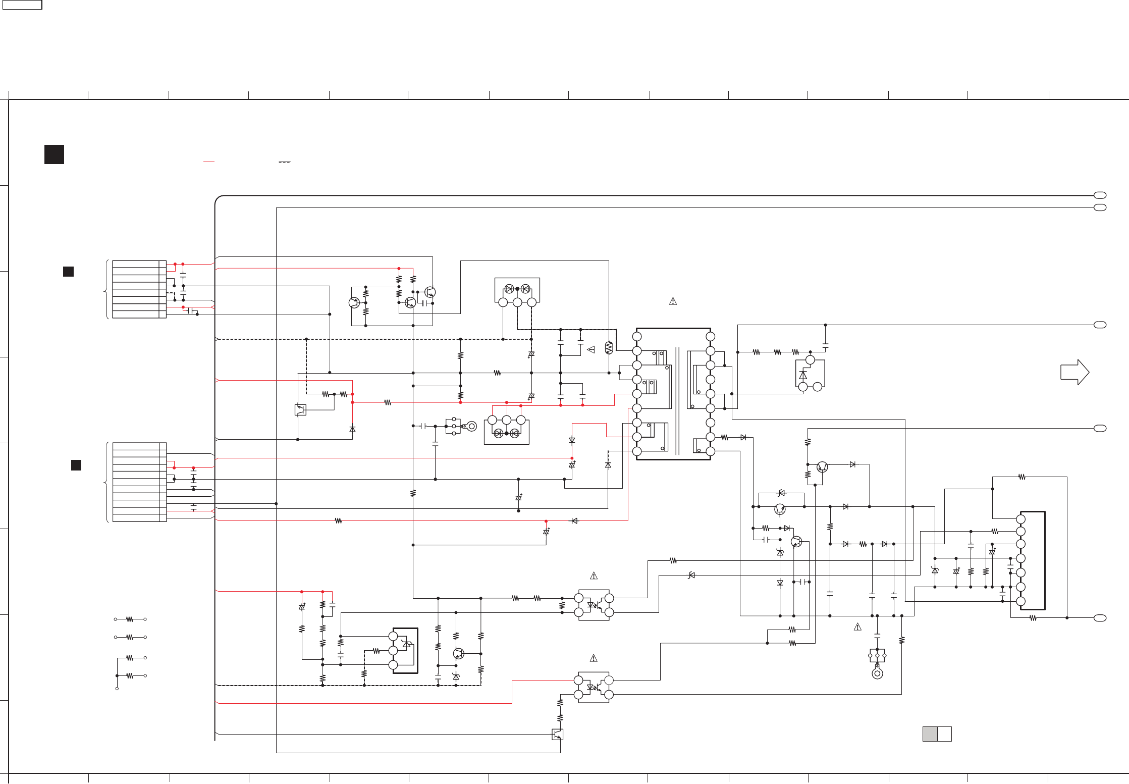
H1
H2
H4
H5
H
SCHEMATIC DIAGRAM - 14
SMPS CIRCUIT
SA-PT850EE SMPS CIRCUIT
1/2 2/2
:+B SIGNAL LINE :-B SIGNAL LINE
G
TO
D-AMP CIRCUIT
(H5500)
IN SCHEMATIC
DIAGRAM - 13
B
TO
MAIN CIRCUIT
(CN2004)
IN SCHEMATIC
DIAGRAM - 9
TO SMPS
SECTION (2/2)
H8
A
B
C
D
E
F
G
H
1234567891011121314
1234567891011121314
2
3
1
IC5701
C5HACYY00003
SWITCHING REGULATOR
0
R5725
312
B0HBSM000043
D5801
R5834
2.2K
321
ZJ5801
2.2K
R5832
+30V_SENSE FAN_18V
10K
R5863
DCDET
10K3K R5862
FAN_18V
C5823
0.1
-30V_SENSE
10K
R5864
DCDET
B1GBCFJN0033
QR5801
-30V_SENSE
R5801
12K
D5807
B0ACCK000005
+30V_SENSE
R5800
10K
R5860
Q5860
10K
0.1
C5831
0.1
C5832
5
6
1
3
4
2
8
7
CN5801
B1ADCF000001
Q5860
C5800
0.01
C5826
0.01
Q5862
R5861
Q5861 - Q5862
Q5861
B1ABCF000176
68K
R5703
68K
R5706
68K
R5702
35V2200
C5805
B0HFRJ000012
D5803
35V2200
C5808
C5819
0.01
C5822
0.01
22
R5720
D5731
B0EAMM000057
3
21
D5702
B0ZAZ0000052
C5713
0.01
321
ZJ5803
R5750 0
C5700
F1BAF1020020
1000P
EST42BN1A6AD
MAIN TRANSFORMER
C5821
0.01
C5820
0.01
35V470
C5824
SYNC
SYS6V
2.2K
R5805
15K
R5806
AR
3
2
C
1
C0DABFC00002
SHUNT REGULATOR
FEED BACK CONTROL
FEED BACK
INVERTER
CURRENT
LIMITING SWITCH
CURRENT
LIMITING SWITCH
FEED BACK
IC5801
0.1
C5818
-13V
DCDET
0.1
C5815
C5812 0.1
DC_18V
270
R5803
47K
R5804
0.1
C5810
2.7K
R5802
C5896 0.1
6
8
9
7
2
1
4
5
3
10
11
CN5802
PCONT
B1GBCFLL0037
QR5810
330
R5809
330
R5807
1K
R5730
B0BC6R100010
D5725
2.2K
R5808
4
3
1
2
B3PBA0000402
PC5720
R5817
330
R5810
330
4
3
1
2
B3PBA0000402
PC5701
1.5K
R5811
0.1
C5825
1.5K
R5816
8.2K
R5812
B0BC7R500001
D5806
SYS6V
-30V_SENSE
+30V_SENSE
2.7K
R5815
24K
R5813
Q5802
Q5802 B1ABCF000176
120
R5724
DC_18V
312
B0HBSM000043
D5802
-13V
FAN_18V
35V470
C5816
B0EAMM000057
D5805
D5804
B0EAMM000057
11
13
14
12
10
8
6
5
7
9
18
15
16
17
1
4
3
2
T5701
C5813
35V1000
R5722
1K
C5722
1000P
C5723
470P
220P
C5721
R5729 10K
C5728
1000P
R5728 100K
D5724 D5727
B0ACCK000005 B0ACCK000005
R5732
100
R5726 0.82
B1ABCF000176
Q5722
10K
R5721
D5722
B0BC01700015
B0ACCK000005
D5723
C5720
0.1
B0EAMM000057
D5729
B0BC01700015
D5721
D5726
B0EAKM000117
SWITCHING
1K
R5723
B1ADCF000001
Q5721
B0ACCK000005
D5728
2SC3940ARA
Q5720
Q5720
Q5722
D
C5727
470P
C5726
0.1
C5730
50V1
C5724
D5732
B0BC035A0007
50V56
R5733
47K
R5731
0
C5725
0.1
S
GND
FB
VCC
OLP/SS
OCP/BD
+30V_SENSE
PCONT
DC18V
AM_BP
-13V
DCDET
DC18V
+18V.-12V_GND
+18V.-12V_GND
GND
GND
-30V_SENSE
FAN_GND
FAN_13V
-30V_SENSE
SYS6V
SYNC
SYS_GND
+30V_SENSE
4
5
7
6
TRANSFORMER TEMP DETECT
TRANSFORMER TEMP DETECT
DC DETECT
C5869
0.1
TH5860
D4CC11040013
PCONT
8.2K
R5814
100V0.22
C5817
W5012
0
W5706
0
W5710
0
W5002
0
W5000
0
W5006
0
W5707
0
W5001
0
VIN
DRAIN
+30V
-30V
+FAN 18V
GND
+18V
AMPGND
-12V
W5009
0
W5007
0
W5010
0
SA-PT850EE
96
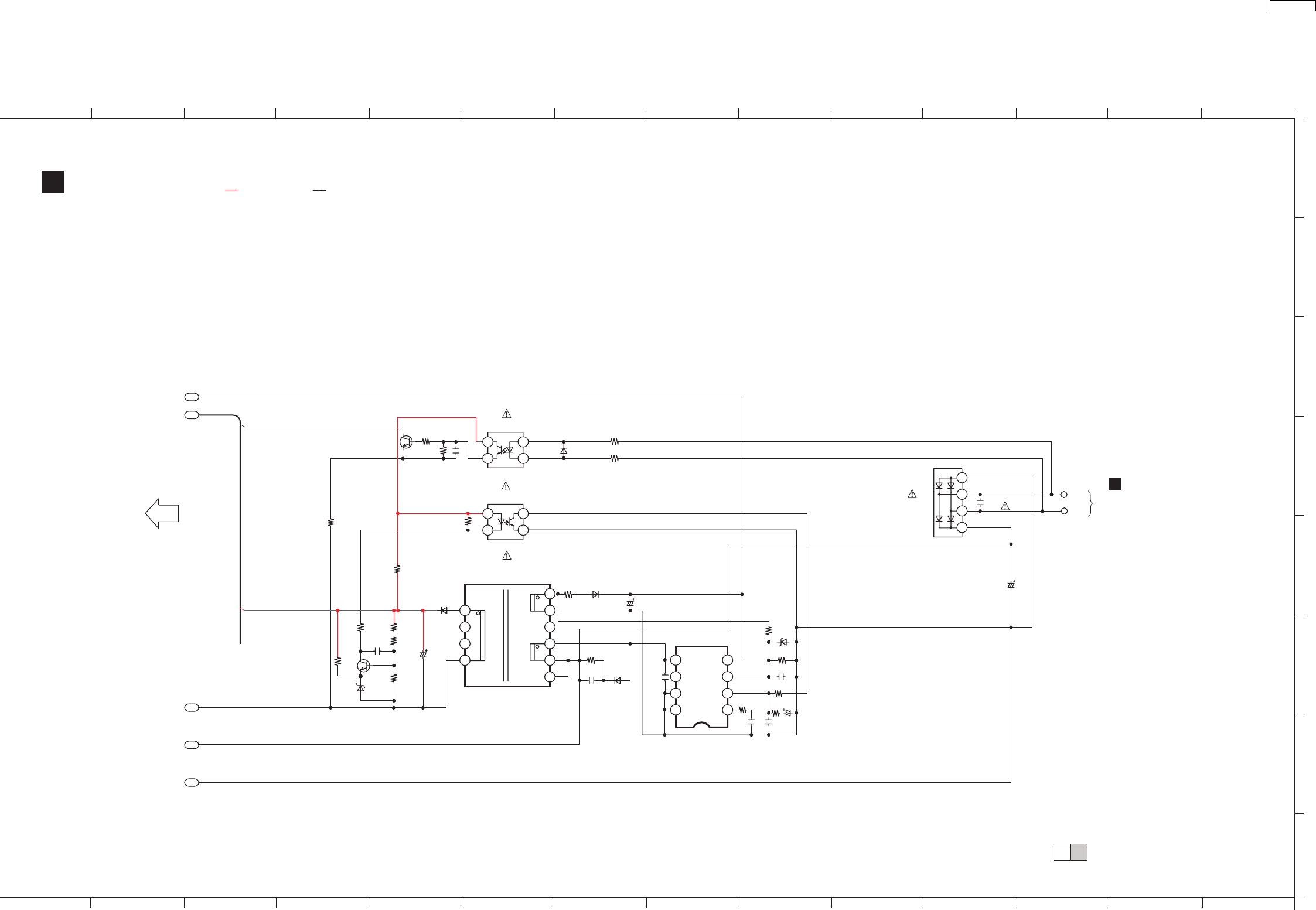
H1
H5
H2
H4
H8
1/2 2/2
SA-PT850EE SMPS CIRCUIT
H
SCHEMATIC DIAGRAM - 15
SMPS CIRCUIT
:+B SIGNAL LINE :-B SIGNAL LINE
TO SMPS
SECTION (1/2)
15 16 17 18 19 20 21 22 23 24 25 26 27 28
15 16 17 18 19 20 21 22 23 24 25 26 27 28
A
B
D
E
F
H
G
C
GRY
WHT
SYS6V
680R5895
400V180
C5712
6
7
5
2
4
3
81
IC5799
MIP4110MSSCF
47P
C5797
R5795
43K
D5797
D5797
MA2J72800L
22P
C5794
R5787
75K
2.2K
R5796
50V2.2
C5791
0.1
C5796
1000P
C5795
R5797
4.7K
C5703
0.1
ECQU2A104MLC
3
2
1
4
B0FBAR000041
D5701
330
R5894
1.2K
R5893
SYNC
C5899
16V220
D5730
B0ACCK000005
D5798
B0EAMM000057
390K
R5704
390K
R5705
R5798
10
C5798
50V56
4
3
1
2
PC5702
B3PBA0000402
4
3
1
2
B3PBA0000402
PC5799
100
R5897
Q5898
B1ABCF000176
R5896
100K
C5897
0.1
2.2K
R5890
B0EAMM000057
D5896
D5897
D5897
B0BC3R700004
Q5899
Q5899
B1ABCF000176
B0EAKB000004
D5793
C5790
2200P
R5891
4.7K
68K
R5786
9
10
7
8
1
6
ETS19AB236AG
BACKUP TRANSFORMER
SWITCHING REGULATOR
T5751
560
R5892
0.1
C5898
CURRENT
INVERTER
SYNC SWITCH
FEED BACK
LIMITING SWITCH
FB
S
S
D
NC
VDD
CL
VCC
5
4
2
3
I
TO
AC-INLET
CIRCUIT
IN SCHEMATIC
DIAGRAM - 17
W5011
0
W5708
0
W5004
0
SA-PT850EE
97
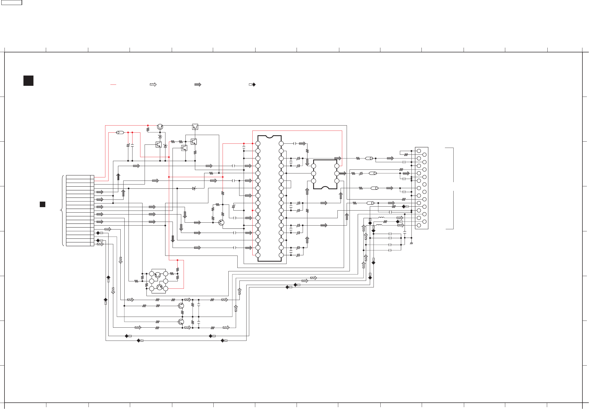
20.4. Scart Circuit
J
SCHEMATIC DIAGRAM - 16
SCART CIRCUIT
SA-PT850EE SCART CIRCUIT
TO
MAIN CIRCUIT
(CN2008)
IN SCHEMATIC
DIAGRAM - 9
B
:+B SIGNAL LINE : DVD VIDEO SIGNAL LINE: MAIN SIGNAL LINE :FM SIGNAL LINE
A
B
C
D
E
F
G
H
1234567891011121314
1234567891011121314
A
B
D
E
F
H
G
C
8
10
2
3
4
6
5
20
16
12
14
18
19
15
11
7
9
1
13
17
21
JK1001
C1001
16V220
Q1003
2SD0601AHL
R1020
1K
B0BC01200019
D1002
D1002
C1002
0.1
L1001
J0JBC0000015
UNR221200L
Q1002
Q1002
B0BC6R100010
D1001
R1004
4.7K
0.01
C1011
75R1018
10V220
C1031
R1016
75
L1003
J0JBC0000015
75
R1014 100P
C1027
C1024
6.3V100
R1017
75
L1002
J0JBC0000015
R1013
75
C1026 100P
25V22
C1012
C1030
0.1
0.01
C1005
B0JCAE000001
D1010
0.1
C1006
Q1008
Q1008
UNR221200L
UNR221200L
Q1005
0.01
C1004
Q1004
UNR211H00L
R1103
220
Q1100
Q1100
B1ABGC000005
2.7K
R1102
C1100
100P
R1100 470
R1101 820
C1200
100P
R1203
220
2.7K
R1202
Q1200
Q1200
B1ABGC000005
R1201
820
470R1200
R1009
4.7K
1K
R1011
K1001
0
1K
R1012
4.7K
R1008
22K
R1010
1
2
34
6
5
XN0460100L
Q1006
18
16
14
8
9
11
12
10
2
3
1
5
7
6
4
13
15
17
19
CN1001
R1007
22K
R1006
22K
R1019 470
C1028 100P
10KR1104
J0JBC0000015
L1004
75
R1015
J0JBC0000015L1005
10KR1204
C1029 100P
25V22
C1014
1
25
6
34
C1AB00001731
IC1102
6.3V100
C1023
C1019
0.1
25V22
C1016
C1018
0.1
6.3V100
C1022
C1021
6.3V100
C1017
0.1
C1015
25V22
26
25
27
28
17
18
20
22
24
23
21
19
8
7
5
6
16
15
10
9
13
14
11
12
3
1
2
30
32
31
429
C9ZB00000461
IC1101
1000P
1000P
1000P
1000P
C1036
C1035
C1033
C1034
J0JBC0000015
L1008
L1007 J0JBC0000015
C1025
470P
C1007
10V33
FUNC_SW
C1010 1
C1008
1
Q1007
2SB0709AHL
C1009 1
BLANKING_IO
GND
VIN
RETURN
RETURN
RETURN
RETURN
VOUT
CONT
ACOM
A(B)IN
A(A)IN
FUNCTION SW
A(A)OUT
BLUE I/O
RETURN
RETURN
BLANKING I/O
NC
VSAG
CIN IN2 VCC
VCC1 COUT
VOUT
S2
SDCOUT
S1
C
G
Y
R
B
VIDEO_MUTE
VGND
SCART_MUTE
VGND
LOUT
LIN
YC_H
ROUT
AGND
RIN
WIDE
RGB
SCART+18V
DVD_A+5V
GREEN I/O
AV
CHASSIS
A(B)OUT
YSAG
GND2
GND2
GND2
CROUT
CRSAG
CYSAG
CBOUT
CYOUT
CBSAG
SEL
YIN
BIAS
CRIN
VCC2
CYIN
GND
CBIN
MUTE2
IN1
CVIN
SEL
YOUT SW
RED I/O
MUTE1 GND2 GND OUT
REGULATOR SWITCH
SWITCH
VIDEO BUFFER
VIDEO BUFFER
INVERTER
SWITCH
AMP
BUFFER
MUTING
MUTING
W1028
0
W1029
0
W1023
0
W1033
0
W1020
0
W1021
0
W1022
0
W1031
0
W1032
0
W1025
0
W1027 0
SA-PT850EE
98
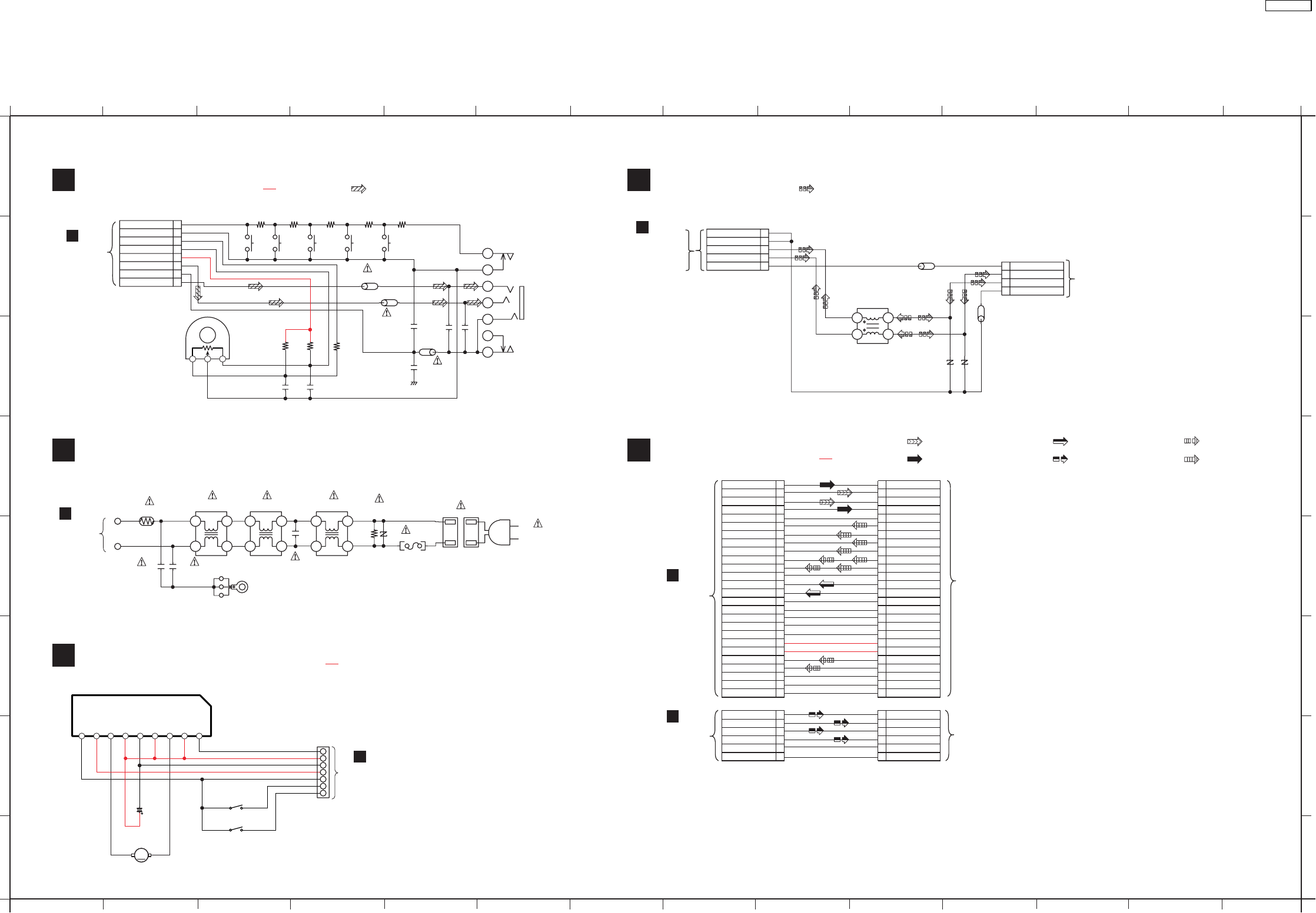
20.5. Volume, USB, AC-Inlet, Relay, Tray Loading & Optical Pickup Unit Circuit
H
TO
SMPS CIRCUIT
IN SCHEMATIC
DIAGRAM - 15
SCHEMATIC DIAGRAM - 17
IAC-INLET CIRCUIT KRELAY CIRCUIT
FUSB CIRCUIT
DVOLUME CIRCUIT
SA-PT850EE VOLUME / USB / AC-INLET / RELAY / TRAY LOADING CIRCUIT
TO
DVD MODULE
(DV5) CIRCUIT
(FP9001)
IN SCHEMATIC
DIAGRAM - 1
A
TO
DVD MODULE
(DV5) CIRCUIT
(FP8531)
IN SCHEMATIC
DIAGRAM - 4
ATO OPTICAL
PICKUP UNIT
IN SCHEMATIC
DIAGRAM - 18
TO
DVD MODULE
(DV5) CIRCUIT
(FP8251)
IN SCHEMATIC
DIAGRAM - 4
A
TO TRAVERSE/SPINDLE
:+B SIGNAL LINE
TO USB
TRAY LOADING CIRCUIT :+B SIGNAL LINE
L
TO
MAIN CIRCUIT
(CN2015)
IN SCHEMATIC
DIAGRAM - 7
B
TO
MAIN CIRCUIT
(CN2020)
IN SCHEMATIC
DIAGRAM - 7
B
:+B SIGNAL LINE :MAIN SIGNAL LINE :USB SIGNAL LINE
: DVD RF SIGNAL LINE
: DVD HEAD SIGNAL LINE
: MOTOR DRIVE SIGNAL LINE
: TRACKING ERROR SIGNAL LINE
: FOCUS ERROR SIGNAL LINE : CD HEAD SIGNAL LINE
A
B
C
D
E
F
G
H
1234567891011121314
1234567891011121314
A
B
D
E
F
H
G
C
7
M
321
2
1
4
3
CN9000
2
3
1
15
5
4
FP9002
LB9001
J0JHC0000034
VA9001
EZJZ1V171AA
3
2
4
1
G1BYYYB00009
J0JHC0000034
LB9002
VA9002
EZJZ1V171AA
DGND
D+ D+
D- D-
D+
VBUS
D-
D+
DGND
DGND
D-
VBUS
GRY
TH5701
D4CAC8R00002
WHT
C5707
F1BAF1020020
1000P
L5702
ELF22V035B
C5706
F1BAF1020020
1000P ZJ5702
ZA5702
DZ5701
ERZV10V511CS
ZA5701
P5701
C5701
ECQU2A334MLA
0.33
470K
R5701
230V 50Hz
AC IN
250V T5AH
F1
321
2
34
1
L5703
ELF22V020A
2
34
1
L5701
ELF15N035AN
2
34
1
7
8
5
6
9
24
14
16
15
11
12
10
13
22
23
19
20
17
18
21
2
1
4
3
26
25
FP8004
2
4
3
1
6
5
FP8002
2
4
3
1
6
5
FP8001
7
8
5
6
9
24
14
16
15
11
12
10
13
22
23
19
20
17
18
21
2
1
4
3
26
25
FP8003
LDGND
VREF1
LDDVD
LDGND
VREF1
LDDVD
GND[OEIC]
GND
RF
TC[DVD]
T-
HFM
T+
F-
F+
TA[DVD]
TD[DVD]
TB[DVD]
PIN[DVD]
LDCD
GND
RF
TD[DVD]
TC[DVD]
F-
T-
HFM
T+
F+
TA[DVD]
TB[DVD]
PIN[DVD]
VREF2[RF-]
FE2[DVD/CD]
FE1[DVD/CD]
LDCD
GND[OEIC]
FE2[DVD/CD]
VREF2[RF-]
FE1[DVD/CD]
SUBSEL
DGND
TRVM+
SPM-
SPM+
TRVM-
SUBSEL
SPM-
DGND
SPM+
TRVM-
TRVM+
GND[VRCD]
TRV_INNER_SW
SUB1
VCC
SUB2
PIN[CD]
VCC
SUB2
SUB1
PIN[CD]
TRV_INNER_SW
GND[VRCD]
L9005
VCC
OUT2
NC
GND
VS
OUT1
VREF
IC904
C0GAY0000013
TRAY LOADING MOTOR DRIVE
TRAY CW
TRY OPEN
CS901
TRAY CW
M+9V
GND1
VREF+
TRAY CCW
TRY CLOSE
TRY OPEN
C984
25V10
S901
PLAY
S902
OPEN
1
2
3
4
7
123456789
5
6
LOADING MOTOR
(REF NO. 316)
JK6801
C6101 0.047
1K
R6804 1.2K
R6803
S6804
S6802
S6803
1K
R6805
S6801
1.8K
R6812 2.2K
R6960
S6907
22K
R6809
C6806
100P
5
6
1
3
4
2
8
7
CN6901
VR6801
EVEKE2F3024M
VOLUME JOG
C6805
100P
22K
R6807
0.047
C6201
J0JBC0000019
L6101
L6201
J0JBC0000019
0.1C6801
L6801
J0JBC0000019
0.1
C6931
HEADPHONE
KEY2
RCH
LCH
CHASSIS
AGND
HP-RCH
HP-LCH
STOP
SELECTOR
PLAY
FORWARD
REVERSE
VREF
DGND
JOG B
JOG A
1
7
6
4
2
3
5
W6111
0
SA-PT850EE
99
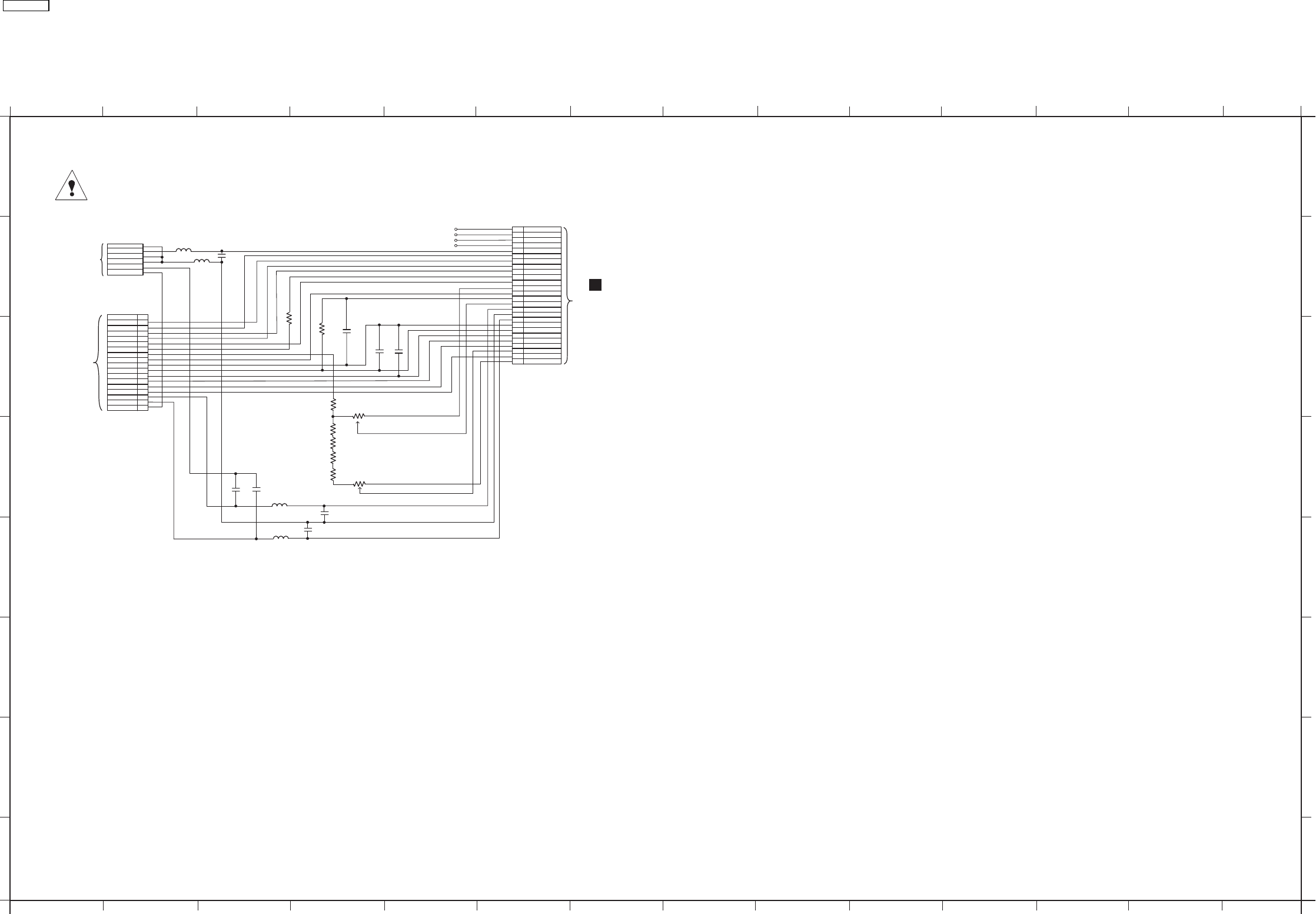
SCHEMATIC DIAGRAM - 18
(FOR REFERENCE ONLY)
OPTICAL PICKUP UNIT CIRCUIT
SA-PT850EE OPTICAL PICKUP UNIT CIRCUIT
TO
RELAY CIRCUIT
(FP8004)
IN SCHEMATIC
DIAGRAM - 17
K
A
B
C
D
E
F
G
H
1234567891011121314
1234567891011121314
A
B
D
E
F
H
G
C
R2
R4
R1
R3
VR1
VR2
R5
R6
R7
C2
C5 C6
C1 C3
T+
F+
F-
T-
TA
TB
TD
TC
FE2
FE1
VREF2(RF-)
PIN(DVD)
LD(CD)
LD(DVD)
LD GND
RF
GND(Im)
GND(Im)
SW
PIN(CD)
SUB1
SUB2
VCC
VREF1
GND(OEIC)
HFM
1
2
3
4
5
6
7
8
9
10
11
12
13
14
15
16
17
18
GND
L2
L1 C4
C7
L3
L4
C8
GND
GND
OUT
GND
GND
TB
TA
TC
FE1
FE2
1m
RF
TD
GND
VREF
VCC
SUB2
SUB1
SW
LD(CD)
LD(DVD)
LDGND
VCC
1
3
2
4
5
6
8
7
9
10
11
12
13
14
15
16
18
19
20
21
22
23
24
25
26
17
TO HFM
TO LDU
TO ACT
SA-PT850EE
100
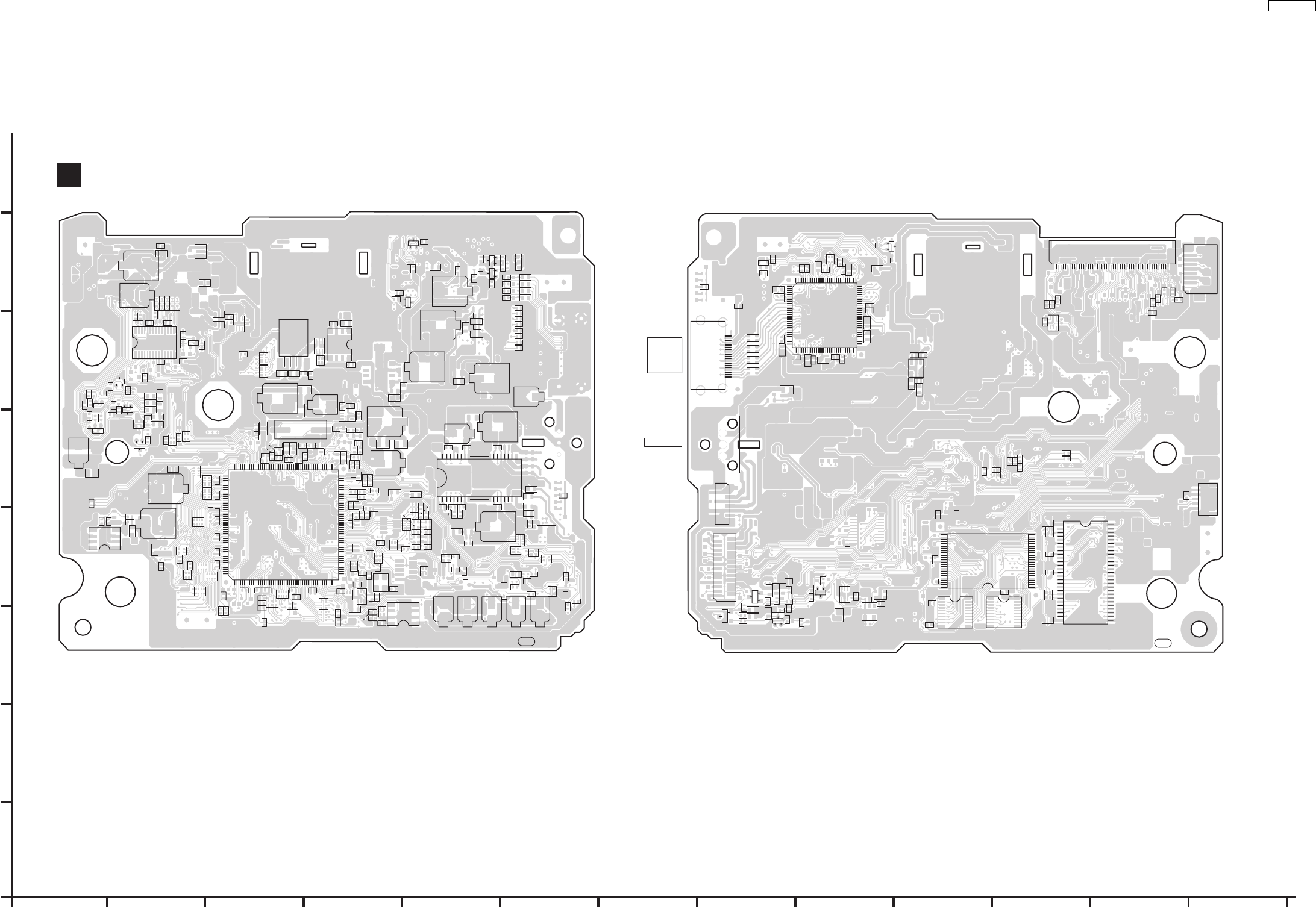
21 Printed Circuit Board
21.1. DVD Module P.C.B.
123456789
A
B
C
D
E
F
G
H
10 11 12 13
A
DVD MODULE P.C.B (REPX0563D)
(SIDE A) (SIDE B)
SA-PT850EE
DVD MODULE P.C.B.
0519A
0519A 0519A
0519A
C
B
E
C
B
E
C
BE
C
B
E
C
BE
BC
E
B
C
E
B
C
E
B
C
E
B
C
E
B
C
E
BC
E
B
C
E
G
DS
G
DS
BC
E
B
C
E
C3901
C3902
C3904
C3920
C3926
C3929
C3930
C3932
C3941
C8001
C8003
C8004
C8005
C8007
C8006
C8011
C8012
C8013
C8014
C8015
C8016
C8018
C8020
C8021
C8022
C8023
C8026
C8056
C8057
C8111
C8112
C8113
C8151
C8152
C8202
C8203
C8211
C8221
C8222
C8225 C8226
C8231
C8232
C8251
C8252
C8253
C8255
C8256
C8257
C8258
C8261
C8262
C8301
C8302
C8303
C8304
C8305
C8306
C8312
C8313
C8320
C8321
C8325
C8330
C8331
C8335
C8340
C8341
C8401
C8421
C8422
C8423
C8424
C8426
C8427
C8428
C8501
C8502
C8503
C8504
C8505
C8506
C8511 C8512
C8513
C8514 C8515
C8516
C8521
C8522
C8523
C8524
C8525
C8526
C8527
C8528
C8529
C8530
C8531
C8532
C8533
C8541
C8550 C8552 C8553C8562 C8563
C8571
C8572
C8602
C8611
C8691
C8701
C9006
C9007
D3901
D8211
D8571
FL8101
FL8102
FL8103
FL8104
FL8421
IC8001
IC8151
IC8251
IC8421
IC8691
IC8701
K3905
K3908
K8251
L8201
L8301
L8302
L8303
L8330
L8501
LB3901
LB3902
LB3903
LB3904
LB3905
LB3906
LB3907
LB8001
LB8011
LB8257
LB8258
LB8259
LB8260
LB8401
LB8421
LB8422
LB8423
LB8424
LB8425LB8426
LB8427
LB8428
LB8429
LB8431
LB8491
LB8530
LB8531
LB8551
LB8561
LB8571
LB8690
Q3902
Q3903
Q3941
Q3942
Q8321
Q8325
Q8331
Q8335
Q8341
QR8420
QR8571
R3904
R3905
R3906
R3907
R3941
R3942
R3943
R3944
R8001
R8003
R8011
R8012
R8013
R8041
R8153
R8154
R8211
R8221
R8225
R8230
R8231
R8232
(NOT SUPPLIED)
R8251
R8261
R8262
R8263
R8264
R8313R8314
R8321
R8322
R8323
R8324
R8325
R8326
R8327
R8328
R8331
R8332
R8333
R8334
R8335
R8336
R8337
R8341
R8342
R8343
R8401
R8402
R8420
R8421
R8531
R8532
R8533
R8541
R8601
R8611
R8613
R8901
R9011
R9012
R9013
R9014
R9015
R9016
R9017
R9022
R9023
R9024
R9025
R9026
R9027
R9028
R9029
R9036
R9037
R9040
R9041
R9045
R9055
R9080
R9083
R9084
R9085
R9086
R9087
R9088
RX3707
RX3708
RX8001
RX8011
RX8012
RX8013
RX8014
RX8015
RX8016
RX8017
RX8018
RX8019
RX8031
RX8032
RX8111
RX8401
RX8402
RX8531
RX8532
RX8533
RX8534
RX8611
RX8691
RX9014
RX9015
RX9016
RX9017
RX9018
RX9019
RX9020
VA3901
VA3902
VA3903
VA3904
VA3905
VA3906
VA3907
VA3908
VA3909
VA3910
VA3911
VA3912
X8621
C3906
LB8702
LB8701
C3964
R3924
IC8611
IC8111
C8429
PbF
C3907
C3908
C3909
C3910
C3911
C3913
C3914
C3915
C3917
C3918
C3919
C3954
C3955
C3956
C8051
C8052
C8053
C8054
C8055
C8311
C8537
C8538
C8551
C8554
C8561
C8564
C8601
C8606
C8621
C8622
C8651
C8652
C8695
C8901
C9002
C9003
FP8101
FP8251
FP8531
IC3952
IC8051
IC8601
IC8606
IC8651
IC8695
IC8901
IC9001
IC9002
K3903
L3903
L3904
L3905
L3906
LB8691
LB8692
LB8693
P3901
HDMI
AV OUT
Q3901
Q3943
Q8551
Q8552 Q8561
Q8562
R3902
R3903
R3945
R3946
R3947
R8311
R8312
R8551
R8552
R8553
R8554
R8555
R8556
R8557
R8558 R8559
R8561
C9017
R8562
R8563
R8564
R8565
R8566
R8567
R8568
R8621
R8622
R9007
R9042
RX3901
RX8020
VA3913
FP3902
LB8302
LB8301
LB8303
LB8304
LB8305
L8550
IC3901
C3922
R3901
R3925
C3940
C3923
C3928
C3924
LB3908
C3927
C3921
R3921
C3916
C8430
C3925
PbF
35
45
23
22
21 20
C8201
4
1
8
5
IC9005
R8318
R9035
321
456
C9004
C9005
LB9001
R9008
R9009
IC9003
C8002
K8008
JK8001
OPTICAL IN
K8003
1
2
3
R8025
5
3
4
2
1
FP9001
R8315
R8316
R8317
4
32
1
X9004
L8001
QR8111
28
33
38
48
54
43
1
5
10
15
20
27
25
1
5
10 11
15
20
5
10
15
24
20
1
25
40
48
30
1
5
10 11
15
20
1
23
4
5
4
12
3
123
45
1
5
25
10
2
26
34
6
8
7
9
11 12
14
16
18
20
22
24
13
15
17
19
21
23
1
5
2
6
3
4
4
3
1
2
4
3
1
2
4
3
1
2
4
3
1
2
19
15
10
5
1
1
5
10
15
20
25
30
33 35 40 45 50 55 60 64 65
70
75
80
85
90
95 96
97
100
105
110115
120
125
128
32
5
4
12
3
123
4
5
1 5 10 15 20 25 30 35 40 5045
1
5
7
2
3
4
6
14
152028
5
25
101
123
4
5
1510 15 20 25 30 35 40 45 50
55
60
65
70
75
80
85
90
95
100
105
108
110
115
120125
130
135
140
145150
155
160
162
163
165
170
175
180
185
190
195
200
205
210
215
216
54
109
1
2
4
3
5
6
7
8
28 25 20 15
10
5
129
30
14
1
2
34
5
34251
321
456
1234
5678
SA-PT850EE
101
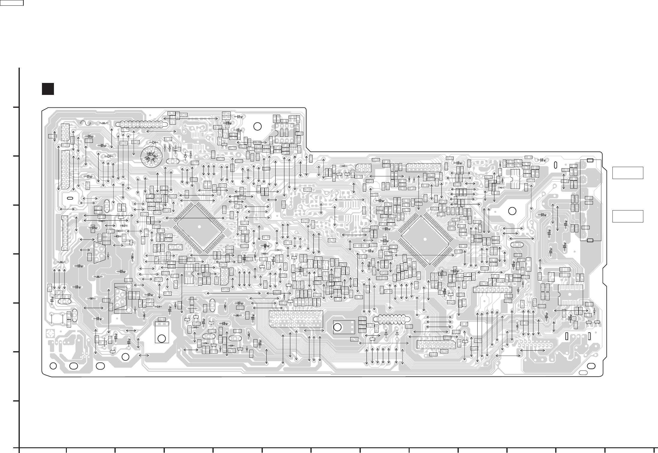
21.2. Main P.C.B.
1
123456789
A
B
C
D
E
F
G
H
10 1 12 13
BMAIN P.C.B. (REPX0587F)
SA-PT850EE
MAIN P.C.B.
AUX
COMPONENT
VIDEO OUT
0540A-1
0540A-1
PbF
B
C
E
B
C
E
B
C
E
B
C
E
B
C
E
B
C
E
B
C
E
BCE
B
C
E
B
C
E
BC
E
B
C
E
B
C
E
B
C
E
B
C
E
B
C
E
A
C
CA
B
C
E
B
C
E
B
C
E
B
C
E
B
C
E
B
C
E
B
C
E
B
C
E
B
C
E
HEATSINK
W2417
C2199
W2648
W2634 W2348
W2347
W2148
W2125
W2333
W2354
W2356
W2370
W2371
W2351
Q2911
W2360
R2938
R2937
C2909
C2907
R2930
R2923
R2948
R2906
R2922
C2929
W2113
W2 111
C2927
D2913
IC2900
IC2903
C2923
C2901
Q2903 Q2901
C2914
L2911
L2903
L2905
C2930
C2938
C2922
C2932
R2946
D2912
D2940
D2939
D2942
D2941
Q2906
Q2907
W2621
D2943
R2936
R2933
C2969
R2934
W2620 C2924
R2931
C2968
R2982 R2932
R2985
C2921
R2984
C2915
Q2904
R2927
R2925
C2926
R2976
Q2921
Q2922
R2975
C2933
W2153
L2908
L2009
L2907
C2925
C2940
C2021
C2916
W2154
W2245
W2154
W2349
W2217
W2215
W2216
W2213
E2901
W2191
W2226
W2220
W2222
W2223
W2214
W2221
W2186
W2210
W2270
CN2008
W2289
W2393
W2315
W2249
W2337
W2384
W2272
W2273
W2271
W2277
W2312
W2318
W2344
W2413
L2801
W2338
D2938
D2937
C2321
W2617
C2421
W2573
C2839
C2836
C2837
C2838
IC2802
IC2801
W2618
W2619
W2616
W2339
K2300
W2341
C2808
W2310
C2809
W2311
W2392
W2391
D2936
D2935
CN2001
E2900
W2152
W2150
Q2910 Q2908
L2902
W2401
W2350
C2955
C2939
R2935
W2343
W2336
R2951
Q2902
C2913
W2402
W2408
R2954
R2913 W2115
W2407
W2114
R2915
R2907
R2908 C2906
C2910
R2914
R2905
R2952
C2908
R2953
L2909
W2346
W2374
W2352
W2357
W2137
W2373
W2110
W2372
W2138
W2121
W2107
W2108
W2109
W2112
W2155
W2158
W2409
W2174
W2342
IC2003
W2159
W2160
W2156
W2161
C2008
C2007
W2527
R2068
R2069
R2030
R2094
W2536
C2000
R2022
R2041
R2021
R2054
W2531
R2060
R2062
W2533
W2649
W2542
W2557
W2539
W2540
W2658
R2008
W2526
C2006
W2361
W2363
W2364
W2365
W2366
W2367
W2368
W2234
W2237
CN2015
W2369
W2281
W2282
W2397
W2286
W2279
C1020
W2319
C2019
W2295
C2018
W2297
W2292
W2325
W2280
CN2002
W2410
W2324
W2328
W2327
W2334
C2801
W2330
W2170
C2177
W2322
JK2001
W2333
C2835
C2834
C2805
C2806
W2398
C2963
Q2916
R2974
W2290
W2291
W2288
W2396
W2395
W2258
W2257
W2296
C2014
C2601
C2604
C2619
W2379
W2335
CN2009
W2306
W2304
C2277
W2331
W2380
W2323
W2332
W2298
W2377
K2412
W2375
W2376
W2378
K2411
W2241
W2252
C2602
W2362
W2233
C2003
D2008
D2005
D2007
K2812
Q2003
R2084
R2034
R2872
W2647
R2600
R2400
R2500
C2500
C2400
C2201
C2101
C2211
C2 111
R2102
C2600
C2300
R2200
R2201
W2622
C2515
R2202
R2942 W2606
R2943
R2991
R2990
R2993
Q2030
R2995
R2992
R2504
C2504
C2315
R2310
R2601
C2640
W2655
C2320
C2404
K2600
R2614
R2613
C2603
R2664
W2579
W2626
W2629
W2631
W2632
Q2096
Q2097
C2310
C2202
C2102
R2203
R2103
C2016
C2015
C2405
R2404
C2406
C2305
R2304
C2309
R2220
C2308
C2408
C2307
C2407
C2306
C2420
C2206 C2292
C2192
R2105
R2205
C2017
C2191
C2293
C2193
C2291
C2262
C2169
C2106
R1023
W2576
R1021
R2949
W2571
W2609
W2593
Q2805
W2578
R2807
W2572
K2811
Q1009 W2577
R2261
(TO TUNER PACK)
W2599
R2190
R2233
C2113
R2133
C2213
R2290
R2260
C2261
R2161 R2971
C2807
C2812
C2817
C2818
D2810
W2615
R2803
R2804
Q2804
Q2801
C2811
C2162
C2960
W2611
C2810
C2208 R2204
R2104
C2108
R1022
C2020
C2304
R2206
R2106
R2120 W2574
R2300
C2605 R2101
C2415
R2410
R2100
W2303
R2903
Q2006
W2612
L2008
W2157
W2176
W2416
W2240
W2231
W2181
W2628
W2166
W2164
W2167
W2219
CN2006
W2175
R2871
W2613
R2016
R2092
C2013
W2173
X2001
W2116
W2414
D2947
D2945
D2915
Q2909
Q2919
W2139
W2188
W2189
W2209
W2208
W2207
W2178
W2179
W2177
W2204
W2185
W2203
W2359 W2193
W2358
R2285
R2286
R2186
W2197
W2200
W2406
W2250
W2195
W2198
W2172
W2171
W2254
W2383
W2386
W2390
W2389
W2247
W2394
CN2010
W2388
W2412
W2387
W2385
W2381
W2382
W2129
W2194
W2183
W2182
W2205
W2206
W2405
W2404
W2264
W2269
W2263
W2268
W2261
W2262
W2260
W2259
W2199
W2168
IC2001
W2196
W2355
W2142
W2143
W2144
W2141
CN2004
D2903
(SWITCHING
TRANSFORMER)
R2902
D2920
D2901
D2909
R2298
Q2103
W2660
R2271
Q2101
R2282
R2182
13
46
R2198
R2171 R2170
R2900
W2637
W2650
W2532
R2865
R2077
R2864
R2079
R2081
R2080
R2051
R2869
C2001
R2000
R2003
R2010
W2614
R2870
R2004
R2095
C2010
R2085
W2519
W2501
R2024
C2970
R2947
R2994
R2999
R2921
D2904
D2946
D2944
C2975
R2920
C2920
R2919
C2937
R2017
C2011
R2086
R2087
(NOT SUPPLIED) (FOR SOFTWARE)
C2012
R2040
R2043
R2045
R2001
W2523
W2524
R2037
R2015
R2032
R2031
C2009
R2006
R2005
R2023
W2641
R2082
R2089
R2088
R2863
W2511
W2534
R2093
R2862
T2900
C2903
Q2900
C2171
R2270
R2281
R2279
C2281
R2181 R2179
R2180
R2177
R2176
C2179
R2192
C2178 R2175
R2297
C2278
R2275
C2194
W2656
R2097
R2096
R2941
C2025
R2099
W2640
W2415
W2265
D2010
R2098
R2626
W2558
R2439
R2339
C2130
C2230
R2283
D2601
D2602
R2661
W2651
R2284
R2183
R2184
R2617
C2611
R2627
R2610
C2617 C2612
R2611
R2612
R2401
R2302
C2302
W2610
C2402
R2403
C2403
R2301
C2303
R2303
C2313
C2312
C2509
R2512
C2506
R2502
C2502
R2501
C2203
C2221
R2115
R2299
R2199
C2182
C2204
R2215
C2104
C2121
C2218
C2103
C2217
R2214
R2112
C2118
C2215
C2117
R2113 R2265
R2165
C2961
C2962
R2972
C2161
R2160
R2939
C2114
C2115
R2212
C2195
C2295
R2213
C2214
R2114
C2503
R2503
C2501
IC2101
R2510
W2654
R2296
R2412
C2413
W2643
R2764
R2765
C2757
C2752 R2762
R2760
IC2751
C2754 C2751
R2196
R2754
R2753
R2761
C2755
R2755
C2753
R2757
C2183
L2201
R2264
R2164
C2164
C2283
R2812
R2809
L2802
R2813
L2804 L2803
C2825
C2823
C2826
C2264
L2101
R2759
R2756
R2758
R2752
D2752
R2751
C2756
R2763
D2753
D2751
C2412
C2282
W2642
C2520
R2312
R2662
C2301
C2401
R2402
C2610 C2609
R2609
R2197
R2292
C2280 C2294
C2279
R2276
R2291
R2191
R2178
C2180
R2185
C2181
R2172
W2652
Q2201
R2280
R2277
R2278
C2296
C2196
W2202
IC2102
W2653
D2908
W2403
W2201
D2906
W2400
C2918
W2623
C2958
R2929
D2919
R2924
C2900
R2055
C2297
C2197
W2147
C2904
R2926
L2910
0.4
FP2900
W2399
W2418
CN2007
CN2020
1
2
3
4
5
6
7
8
9
CN2013
R2052
R2027
R2053 R2019
C2140
R2140
Q2007
R2145 R2195
R2244
R2141
Q2008
D2009
B
C
E
B
C
E
64
31
64
4
31
6
31
13
46
R2240
R2520
R2521
R2320
R2243
R2420
R2321
R2421
R2621
R2142
R2143
R2620
R2242
R2241
Q2202 Q2102
Q2502
Q2302
R2219
R2119
C2198 R2193
W2633
W2625
W2659
W2630
R2014
1
19
18
2
1
4
3
6
5
8
7
10
9
12
11
14
13
15
16
17
2
3
4
5
6
7
8
123
4
5
6
7
8
9
1234567891011
1
2
3
4
5
1
2
3
4
5
12 3
123
1
2
3
4
5
6
7
8
14
58
15
7
6
8
3
2
4
913
15
14
16
11
10
12
17
19
18
20
21 25
27
26
28
23
22
24
29
31
30
32
33
35
34
36
37 41
43
42
44
39
38
40
45 49
50 1
3
2
47
46
48
1
2
3
4
5
6
7
1234567
1
2
3
4
5
6
7
8
9
10
11
12
13
14
15
16
17
18
19
5
6
7
8
1
2
3
4
11
12
13
14
17
16
15
9
10
12345 67 8 910
8-R
9-L 7-G
6-PB
5-PR
4-G
31
64
58
1
4
1
32
1 5 10 16
172228
3
46
58
41
50
31 30
1
81
100
80
51
100
81 80
51
50
31
30
1
3-Y
2
1-G
85
90
95
55
60
65
70
75
35
45
5
10
15
20
25
40
35
40
45
5
10
15
20
25
85
90
95
55
60
65
70
75
SA-PT850EE
102
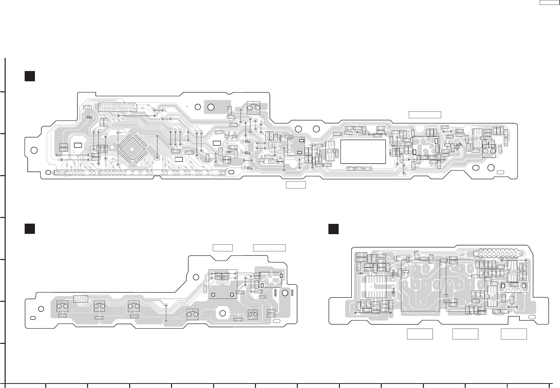
21.3. Panel, Volume & Mic P.C.B.
1
123456789
A
B
C
D
E
F
G
H
10 1 12 13
CPANEL P.C.B. (REPX0587F)
SA-PT850EE
PANEL/VOLUME/MIC P.C.B.
DVOLUME P.C.B. (REPX0587F) EMIC P.C.B. (REPX0587F)
0540A-1
0540A-1
0540A-1
0540A-1
0540A-1
0540A-1
PbF
PbF
B
C
E
PbF
B
CE
B
CE
B
C
E
JK6801
C6201
L6201
L6101
R6807
R6809
C6806
C6805
L6801
R6812
(PLAY)
W6111
R6803
R6804
R6805
(SELECTOR) (REVERSE) (FORWARD)
(STOP)
C6931
R6960
VR6801 C6101
S6907
S6804
W6020
S6803
S6802
CN6901
1
2
3
4
5
6
7
8
S6801
W6035
W6036
W6043
W6034
C6801
1
2
3
4
5
321
6
7
S6901
IC6107
Q6201
W6057
W6051
W6002
W6001
W6055
JK6802
D6901
W6052
W6019
W6058
W6047
W6048
W6049
W6050
W6013
12578
101113141617
202123
25
3536
40 39 3841
42
44
45 30 29 28 27313233
W6007
W6045
W6027
W6040
FL6901
W6041
W6028
W6021
C6925
C6916
C6919
C6906
R6914
C6917
C6909
R6916
C6929 W6106
L6903
C6911
W6114
W6118
(OPEN/CLOSE)
R6918
W6117
C6904
W6101
W6102
R6948
C6938
L6906
R6920
R6919
C6921
C6934 R6966
C6937
R6967
D6902
C6935
C6936
R6965
C6941
R6971
W6126
R6923
W6124
W6122
C6940
(POWER)
58
14
R6961
R6949
C6923
W6127
W6115
R6951
R6970
L6908
C6924
L6907
R6968
W6123
L6909
C6933
R6962
C6920
R6950
L6904
L6905
W6125
W6129
W6113
W6128
W6110
C6930
W6130
R6935
R6934
D6910
R6927
R6917
W6029
W6032
W6013
W6053
W6054
W6046
IC6901
34
39
44
1
5
11 12
17
23
28
22
33
18
19
16
17
2
13
4
57
8
9
10
11
12
13
14
15
6
CN6902
W6039
W6038
W6037
W6044
W6056
W6042
W6003
W6006
C6918
C6913
C6910
C6903
C6905
Z6900
SENSOR
VOLUME HEADPHONE
MUSIC PORT
S6902
W6119
W6103
Q6110
Q6111
B
C
E
B
C
E
R6210
R6193
Q6202 Q6105
R6196
B
C
EB
C
E
C6183
41
58
IC6106
C6283
Q6102
BC
E
R6231 C6284
R6294
R6188
R6194
R6293
C6186
D6101
R6202
D6100
R6191
R6100
R6192
C6185 R6292 R6290
C6187
C6184
D6102
R6190
R6291 C6288 C6189
VR7001
IC7000
H7000
JK7001
JK7002
MIC 2 MIC 1 MIC VOLUME
W7003
W7002
12
2
3
3
4
4
5
5
6
1
1
123
14
4
7
7
8
9
8
85
58
IC7100
Q7101 Q7100
Q7102
C7113
R7110
W7006
L7202
R7116
L7303
C7121
L7101
R7007
C7007
R7003C7003
R7005
C7004
R7004
R7119
C7119
C7120
C7123R7122
R7120
C7002
R7002
L7004
C7005
C7011
C7008
C7006
R7006
R7011
R7010
C7012
C7115
C7111
D7100
16 9
81
C7104
R7101
C7106
R7109
C7105
C7102
R7102
C7108
R7104
R7105
R7100
R7112
R7107
W7007
R7001
L7003
R7009
C7009 C7010
C7122
IC7200
R7008
L7001
L7002
R7103
L7005
C7109
C7112
R7123
C7107
C7101
C7103
R7114
R7113
C7124
R7106
C7110
W7001
23
45
1
78
1
2
3
1
3
5
4
2
6
7
SA-PT850EE
103
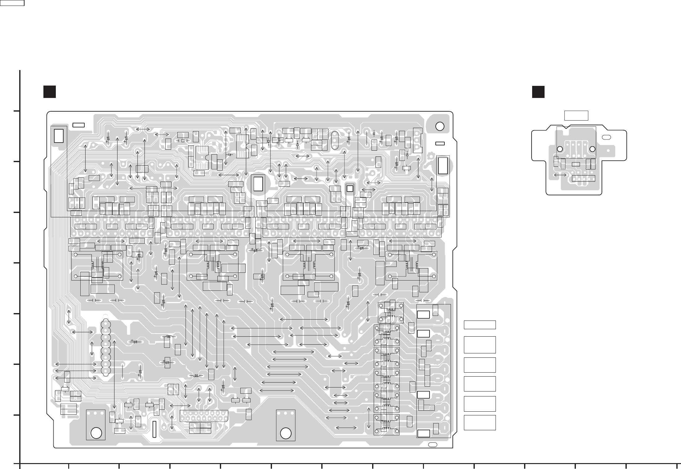
21.4. D-Amp & USB P.C.B.
1
123456789
A
B
C
D
E
F
G
H
10 1 12 13
GD-AMP P.C.B. (REPX0560D)
SA-PT850EE
D-AMP/USB P.C.B.
SUBWOOFER
CENTER
SPEAKER
FRONT
SPEAKER R
FRONT
SPEAKER L
SURROUND
SPEAKER R
SURROUND
SPEAKER L
USB
FUSB P.C.B. (REPX0587F)
0516A-1
0516A-1
0540A-1
0540A-1
L9005
B
C
E
B
C
E
B
C
E
B
C
E
B
C
E
B
C
E
B
C
E
PbF
B
C
EB
C
E
B
C
EPbF
C5000
C5001
C5002
C5003
C5004
C5005
C5006
C5007
C5008
C5009
C5010
C5011
C5012
C5013
C5016
C5017
C5018 C5019
C5020
C5021
C5022
C5023
C5024
C5025
C5027
C5028
C5030
C5031
C5032
C5033
C5050
C5051
C5052
C5053
C5200
C5201
C5202
C5203
C5204
C5205
C5206
C5207
C5208
C5209
C5211
C5212
C5213
C5214
C5216
C5217
C5218
C5219
C5220
C5221
C5222
C5223
C5224
C5226
C5227
C5231
C5232 C5233
C5234
C5250
C5251
C5301
C5302
C5303
C5304
C5305C5306
C5307
C5309
C5310
C5311
C5312
C5313
C5314
C5315
C5316
C5317
C5318
C5319
C5321
C5322
C5323
C5324
C5325
C5326
C5327
C5331
C5332
C5333
C5334
C5350
C5351
C5450
C5514
C5515
C5518
C5519
C5520
C5521
C5522
C5523
C5524
C5525
C5552
C5553
C5554
C5558
C5690
C5693
C5695
D5503
D5640
D5643
D5644
D5645
R5000
R5001
R5002
R5003
R5004
R5005
R5006
R5007
R5008
R5010
R5011
R5019
R5020
R5021
R5022
R5023
R5030
R5031
R5032
R5033
R5034
R5035
R5110
R5200
R5201
R5204
R5205
R5206
R5207
R5208
R5209
R5210
R5211
R5217
R5218
R5228
R5300
R5302
R5304
R5305
R5306
R5307
R5308
R5309
R5310
R5311
R5317
R5318
R5319
R5327
R5328
R5505
R5507
R5508
R5602
R5603
R5604
R5606
R5607
R5608
R5609
R5610
R5611
R5637
R5639
R5654
R5655
R5656
R5657
R5658
R5659
R5660
R5670
W5032
R5640
C5555
R5511
C5561
C5560
C5151
C5155
C5152
C5150
K5252...2
K5253...3
C5445
K5004
K5500
C5014 C5015
C5040
C5133
C5225
C5228
C5240
C5300
C5328
C5508
C5509
C5510
C5511
C5512
C5513
C5516
C5517
C5540
C5601
C5602
C5691
C5692 C5694
C5696
C5697
CN5050
H5500
K5003
K5011
K5012
K5013
K5017
K5018
K5404
K5403
K5301
L5001
L5002
L5201
L5301
L5500
L5501
R5510
R5636
X5500
ZJ5400 ZJ5410
W5067
W5066
W5068
W5061
W5060
W5059
W5065
W5005
W5042
W5051
W5062 W5052
W5039
W5055
W5064
W5023
W5019
W5053
W5056
W5021
W5050
W5054
W5038
W5012 W5003
W5024
W5022
W5020
W5013
W5063
W5045
W5046
W5044
W5047
W5049
W5048
W5035
W5033
W5006
W5037
W5034
W5009
W5010
W5011
W5007
W5008
W5036
W5002
W5001
W5004
W5026
W5041
W5043
W5058
W5015
W5040
W5069
W5028
W5025
W5029
W5030
W5031
W5014
W5016
W5017
W5027
W5070
W5018
W5071
L5300
L5200
L5000
C5562
W5075
W5076
K5555
Q5603
IC5500
Q5101 Q5102
Q5601 Q5602
Q5604
IC5501
IC5000
Q5644
IC5200
Q5642
Q5640
CN5501
Q5641
IC5300
JK5001
HEATSINK
(TO FAN)
23
22 2
1
1
2
4
3
C5106
C5107
C5117
C5119
C5120
C5121
C5401
C5402
C5403
C5404
C5405C5406
C5407
C5409 C5410
C5411
C5412
C5413
C5416
C5418
C5419
C5421
C5422
C5423
C5424
C5425
C5426
C5427
C5431
R5036
R5103
R5104
R5118
R5119
R5400
R5402
R5404
R5405
R5410
R5411
R5419
C5400
C5428
C5440
L5400
IC5400
R5037
C5153
C5154
43
21
43
21
C5451
C5452
C5453
C5454
R5111
R5113
R5114
R5115 L5401
L5402
K5406
K5601
9
10
11
12
K5402
CN9000
FP9002
LB9001
VA9002
VA9001
LB9002
W9000
1
2
3
4
5
6
7
8
1
3
1
2
3
4
5
6
7
8
43
21
43
21
43
21
43
21
31 3
1
1
2
4
3
1
2
4
31
2
4
3
2
22 2
123
22 2
123
22 2
1
2
1
4
3
6
5
8
7
10
9
12
11
14
13
16
1517
2
2
23
1
7
814
1
7
814 123 4
12
3
4
5
1
24
3
SA-PT850EE
104

21.5. SMPS P.C.B.
0526A-2
0526A-2
1
123456789
A
B
C
D
E
F
G
H
10 1 12 13
HSMPS P.C.B. (REPX0569A)
SA-PT850EE
SMPS P.C.B.
CAUTION
RISK OF ELECTRIC SHOCK
AC VOLTAGE LINE.
PLEASE DO NOT TOUCH THIS P.C.B
A
CA NC
ACA A ACA A
B
C
E
B
C
E
B
C
E
B
C
E
B
C
E
B
C
E
B
C
E
B
C
E
B
C
E
BC
E
PRI
PRI
SEC
SEC
10 7
61 2345
98
C5700
PbF
W5813
W5811
W5832
W5831
W5830
W5812
W5003
W5820
W5825
W5718
W5709
R5733
K5711
W5824
W5822
W5816
W5821
W5810
D5802 D5801
W5723
W5722
W5715
W5802
W5803
W5719
W5717
W5721
W5724
W5712
W5713
W5714
W5716
W5720
R5801
R5800
CN5802
C5831 C5832
R5832
R5834
W5002
C5823
W5001
Q5899
Q5898
C5824
CN5801
W5004
C5899
D5896
T5751
(BACKUP TRANSFORMER)
D5897
R5892
R5897 C5897
R5896
W5708
R5891
R5893
R5895
R5894
C5898
C5805
W5818
W5705
C5808
C5817
IC5801
C5816
R5815
C5810
R5803
D5807
D5806
C5825
R5812
R5863
R5862
R5861
C5869
R5864
R5860
W5006
R5816 R5811
R5813
C5812
C5815
Q5802 Q5861 Q5860
Q5862
QR5801
R5802
R5814
R5804
R5806
C5818
R5805
W5012
W5706
W5707
C5813
ZJ5801
D5803
QR5810
D5804
C5896
C5800
C5826
HEATSINK
HEATSINK
C5821C5819
C5822 C5820
R5795
R5798
C5790
R5787
R5797
R5796
R5724 R5705 R5704
C5794
C5795
C5796
W5011
D5797
R5890
PC5799
TH5860
R5810
R5817
R5808
R5807
R5809
D5805
D5731
R5730
PC5720
PC5701
D5725
R5729
R5728
R5720
R5750
HEATSINK
R5721
C5720
R5722
C5721
R5731
C5726
R5732
C5722
D5727
C5723
W5000
C5725
R5706
R5703
(MAIN TRANSFORMER)
R5702
C5713
D5702
Q5720 D5729
D5724
R5725
D5726
D5728
Q5722
Q5721
D5722
D5723 C5728
R5723
W5710
ZJ5803
R5726
IC5701
C5727
C5730
C5712
T5701
C5703
GRYWHT
D5701
C5798
W5828
W5833
W5829
W5827
C5791
R5786 D5793 W5826
D5798
C5797
D5730
PC5702
IC5799
C5724
D5732
D5721
B
C
E
1+ 2~ 3~ 4-
W5007
W5010
W5009
113456782
234567891011
1
45
8
321
1
23
4
5
6
7
123
12
34
12
34
123
1
23
4
12
34
12 45678
1112131415161718
9
SA-PT850EE
105
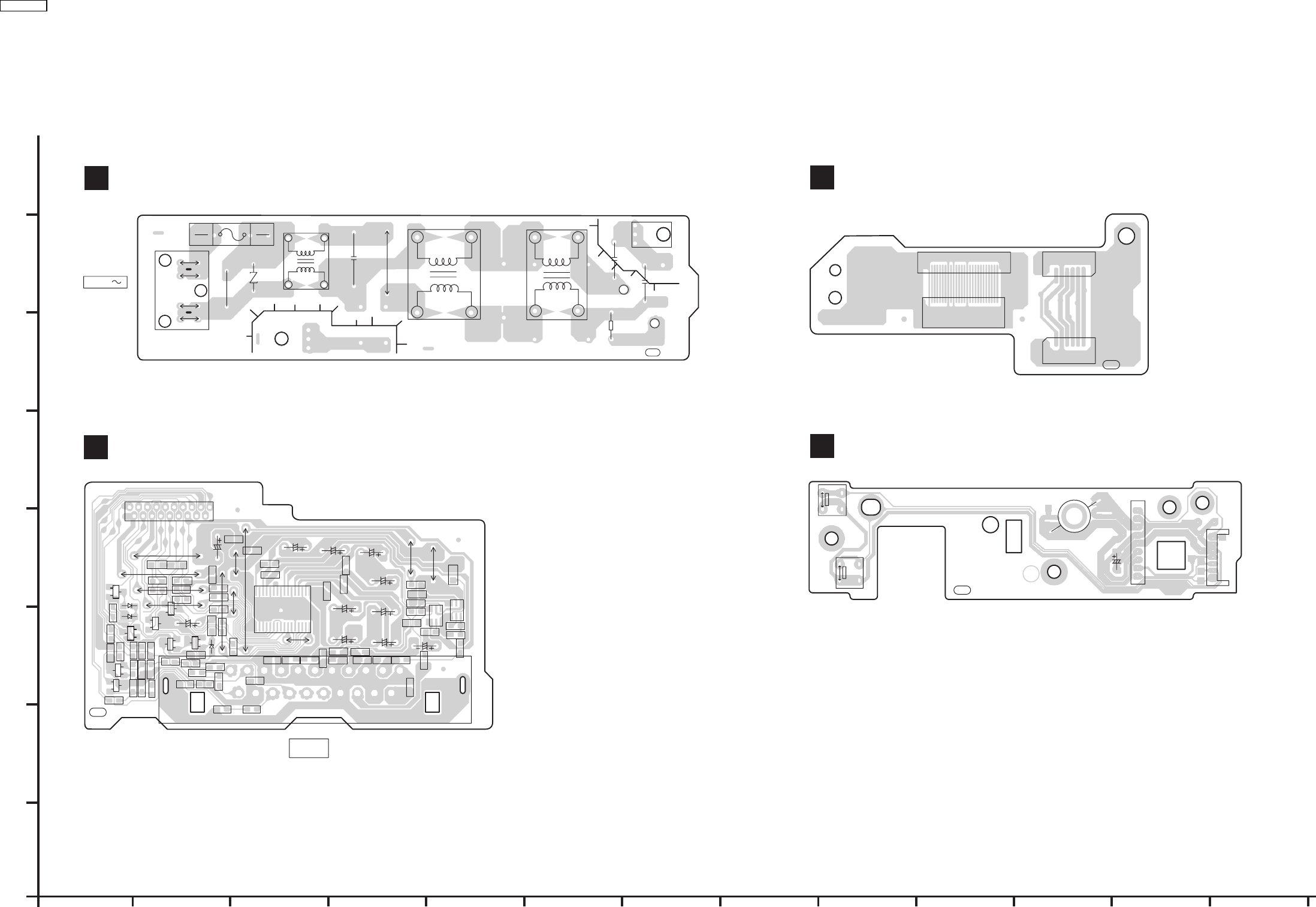
21.6. AC-Inlet, Scart, Relay & Tray Loading P.C.B.
1
123456789
A
B
C
D
E
F
G
H
10 1 12 13
KRELAY P.C.B. (REPX0604A)
LTRAY LOADING P.C.B. (REP4238A)
SA-PT850EE
AC-INLET/SCART/RELAY/TRAY LOADING P.C.B.
JSCART P.C.B. (REPX0587F)
IAC-INLET P.C.B. (REPX0569A)
PbF 2462A-1
2462A-1
0540A-1
0540A-1
0553A
+
-
M
PbF
0553A
PbF
BC
E
BC
E
B
CE
B
CE
B
CE
BC
E
B
C
E
BC
E
L5703
S902
(OPEN SW)
S901
(PLAY SW)
REF NO.316
C984
IC904
CS901
FP8002
FP8001
FP8004
FP8003
CN1001
W1005
W1006
W1001
D1001
D1002 C1007
JK1001
AV
C1015 C1031
C1016 C1022
C1021
C1023
C1012
IC1101
Q1002
Q1003
Q1200
Q1100
C1024 C1014
W1003
W1008
W1002
W1027
W1004
W1009
W1011
W1010
W1033
R1013
R1008
R1010
IC1102
13
46
Q1006
13
46
W1031
R1017
C1018
C1017
C1019
L1004
C1026 L1002C1027
C1028R1015
L1005C1029
R1014
C1011
L1001
C1009
D1010
C1002
C1008
C1006
Q1008
Q1007
Q1004
Q1005
W1029
R1011K1001
R1100
R1200
W1022
W1021
R1101
R1201
C1033
W1020
C1200
R1102
C1100
R1103 R1202
R1004
C1035 R1019
L1008
L1007
C1036
C1034 R1104
C1025
R1204
C1010
R1203
W1028
W1025
R1012
R1020
W1023
C1005
C1004
C1030
L1003
R1016
W1032
R1009
R1007
R1006
R1018
C1001
W1007
AC IN
230V 50HZ
0526A-2
0526A-2
PbF
1
2
34
1
2
34
WHT
GRY
ZA5701
W5780
W5781
R5701
DZ5701
P5701
W5782
W5783
F1 ZA5702
L5701
C5701
W5737
L5702
TH5701
250V T5AH
(TO SPINDLE/
TRAVERSE MOTOR)
(TO OPTICAL PICKUP UNIT)
ZJ5702
1
2
3
C5706
C5707
1
2
3
4
5
6
7
8
9
7
6
5
4
3
2
1
123456
1
2
3
45
6
1
1
5
5
10
10
15
15
20
20
26
26
1
2
3
4
5
6
7
8
9
10
11
12
13
14
15
16 18
19
17
1
2
3
4
5
6
7
8
9
10
11
12
13
14
15
16
17
18
19
20
21
32
116
17
1
2
34
SA-PT850EE
106

22 Basic Troubleshooting Guide
22.1. Basic Troubleshooting Guide for Traverse Unit (DVD Module P.C.B)
Problems
Checking Points
Checking Components
a) Check SDRAM address,
data bus, CLK and other
control signals waveform
IC8051
b) Check video signals LB8301, R8321, R8322,
LB8302, R8325, R8326
1) Distorted picture or
abnormal sound is head
during the initialization
c) Check audio DAC circuitry
* Compare the above with
OK condition HDMI
module P.C.B.
IC8421
*Check for solder short
and/or component
missing/damaged
a) Check motor driver
circuitry (+5V)
IC8251 Pin 8, 21
b) Check laser drive
circuitry (Voltages &
current)
Q8551, Q8552, Q8561,
Q8562
2) No TOC / Long TOC
c) Check LSI IC connection
to motor drive circuitry
*Compare the above with
OK condition HDMI
Module P.C.B.
IC8001 Pin 144 ,145
* Check for solder short
and/or component
missing/damaged
a) Check connection from
HDMI Module to Traverse
unit
FP8251 3) Disc not spinning
4) Traverse not moving
5) Traverse and spindle
abnormal movement b) Check motor driver
circuitry on the voltages and
control signals
*Compare the above with
OK condition HDMI
Module P.C.B
IC8251
*Check for solder short
and/or component damaged
6) Cannot read the disc but
spindle motor is spinning
- Cannot read CD/DVD
a) Check laser drive
circuitry (voltages
and current)
- Check CD Laser
Drive
- Check DVD Laser
Drive
* Check voltages and LD
current and compare with
OK condition HDMI
Module P.C.B.
Q8551, Q8552, LB8531
(For DVD Laser Drive
current)
Q8561, Q8562, LB8561
(For CD Laser Drive
current)
7) Block Noise during play a) Check SDRAM address
and data bus signal
IC8051
8) Jitter out of specification
a) Check LD current
b) Check OPU
(Change to other unit and
confirmed operating
condition)
OPU Unit (Traverse unit),
FPC connection
9) Cannot read data from USB a) Check USB connector & FFC
b) Check LSI O/P
c) Check IC supply (+5V)
FP9001
IC8001 Pin 144, 146
IC9005 Pin 2, 3
107
SA-PT850EE

22.2. Basic Troubleshooting Guide for HDMI AV output
Problems Checking Points Checking Components
1) Check setting of the set *This year HDMI always
ON. No need check Setup
Menu.
If no resolution selection
GUI, then only check
SETUP.
in Setup Menu whether the
HDMI Video output is
turned On
2) +5V Supply to the TV IC3952 (Pin 4)
3) HDMI Connector
Solderability condition
P3901
4) HDMI Output TDMS
signal lines (IC3901)
- Data (Pin 72, 73, 76,
77, 80, 81)
- Clock (Pin 10,12)
L3903, L3904, L3905,
L3906
5) HDMI Transmitter
communication lines to TV
- Data, SDA (Pin 120,
IC8001)
- Clock, SCL (Pin
121, IC8001)
LB3905, R3905, Q3902,
R3904
LB3904, R3907, Q3903,
R3906
6) HDMI Transmitter
communications from LSI
(IC8001)
RX3901
7) Local Port Slave Address
setting resistor
R3921
8) HDMI Transmitter
+3. 3V Supply
LB3901, IC3901 (Pin 26,
42, 47, 52, 70, 84, 100, 106,
115)
9) HDMI Transmitter
+1.2V Supply
IC3901 (Pin 5, 26, 47, 42,
55, 75, 85, 102, 109, 116,
123), LB3908, IC8151 (Pin
2, 4)
10) HDMI Up -Con +3.3V
Supply
LB3901
11) HDMI Pixel Clock
Output from Up -Con to
HDMI Transmitter
R8902
12) Up -Con IC I2C Data
and Clock Line
RX3706
13) Hot -Plug Signal LB3906, R3902, R3903,
Q3901, D3901
1) TV does not have any
display. Set FL display
shows U702/U703
14) TDMS Output swing
amplitude control resistor
R3901
15) Host Interface External
Input Clock from LSI
(IC8001) to Up - Con IC
(IC3901) OSC27M
LB8702
16) Video Data Lines from
LSI (IC8001) to Up-Con
(IC3901)
RX3707, RX3708
108
SA-PT850EE

2) When switching the
video output mode from
480P to 720p/1080i, TV
display becomes blank
1) Supply for Up-Con
(IC3901)
2) GND for Up-Con
- Pin 7, 125
3) Check for capacitor short
to GND
1) Check digital video data
line from LSI (IC8001) to
Up-Converter (IC3901),
VOUT0-VOUT7.
- Pin 9, 124
LB3902
C3902, C3928, C3925
RX3707, RX3708
3) Color Problem. TV
screen is White/Blue/
Purple
4) HDMI got no audio output 1) Audio data lines
2) Check setting of the set
in Setup Menu whether the
HDMI Audio output is
turned ON
R8402, RX8402
* Check for solder short
and/or component
missing/damaged as well as
signal condition.
Problems Checking Points Checking Components
109
SA-PT850EE
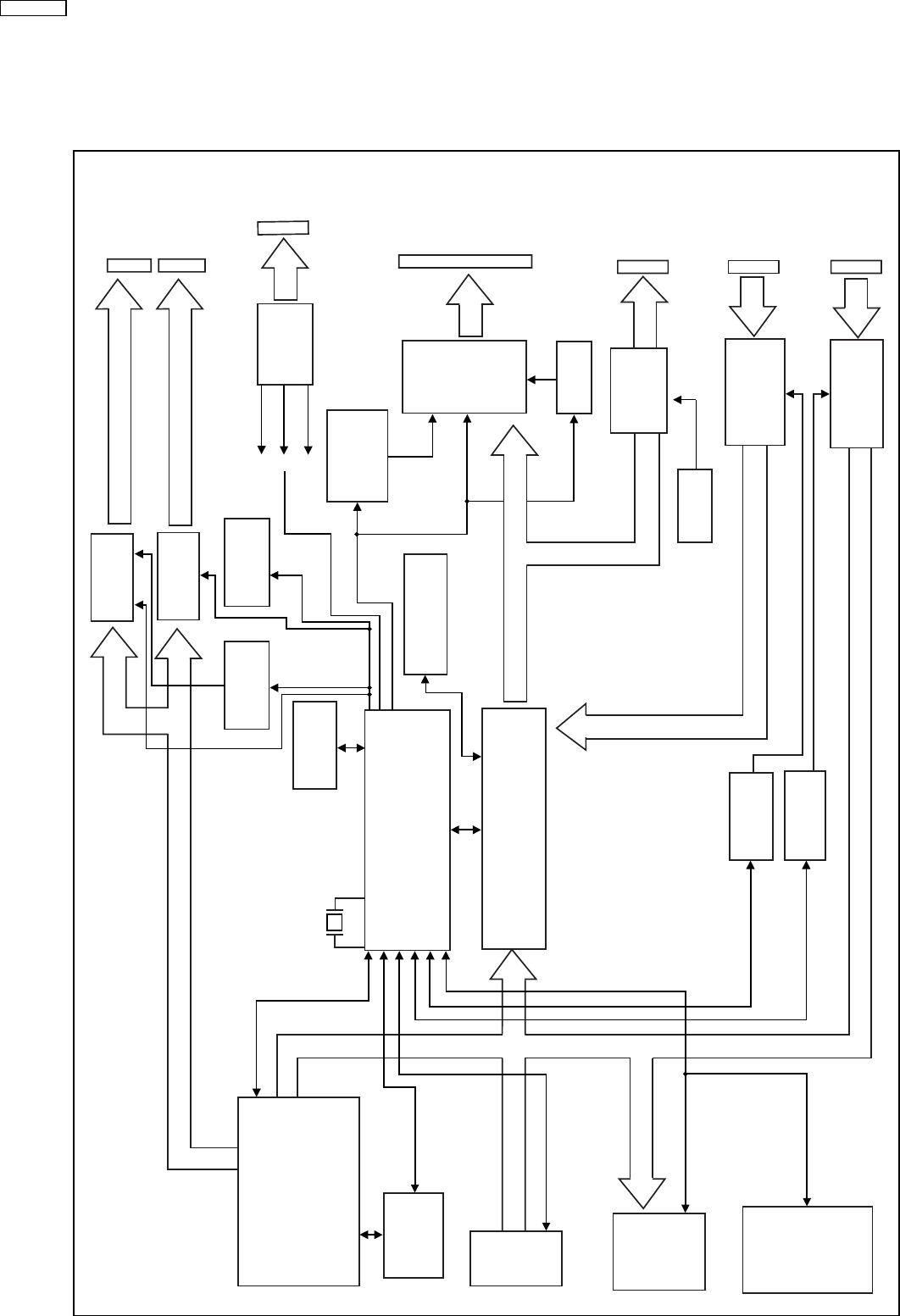
23 Overall Block Diagram for PT850
23.1. SC-PT850 Simplified Block
DV5
SC-PT850 SIMPLIFIED BLOCK
DL2S
LOADING
T
U
N
E
R
WIRELESS
MODULE
POWER
SUPPLY
BLK
PCONT/DCDET1/
(FX_DET1/FX_DO/
FX_DI/FX_CLK)
(RDS_DET/TUN_DO/
TUN_SD/TUN_DI/
TUN_CLK)
(TRAY_OPEN/
TRAY_CLOSE/
TRAY_CCW/
TRAY_CW)
DCDET2
IC2001
MICRO-P
IC
(ASP_DAT/ASP_CLK)
IC2101
ASP IC
IC6106
MPORT AMP
IC
IC2102
HP AMP
IC
MUTING
MUTING
MUTE_S_C/
MUTE_F_SW
IC5000
IC5200
IC5300
IC5400
CLK
GENERATOR
IC5500/IC5501
FHOP
D-AMP BLK
OSC
IC6901
FL Driver IC
FL_IC_IN
FL_IC_CLK
FL_IC_STB
IC2003
EEPROM
IC2802
Swicth IC
(RGB_H)
(VIDEO_
MUTE/
SCART_
MUTE)
IC1102
Swicth IC IC
YC_H
IC1101
SCART IC
IC2801
VIDEO IC
IC2751
Level Proctection
OSC
(C/Y/CR/CB/PY)
VMUTE
(DVD_MUTE/DVD_STAT/
DVD_CMD/DVD_CLK)
(VOUT/CBOUT/CROUT/CYOUT) JK2001
JK1001
CB/CR/Y
COMPOSITE
SCART
TERMINAL
FL6901
P1~P17
G1~G10
JK5001
TO
SPEAKERS
JK6801
TO
HEADPHONE
JK6802
FROM
MUSIC
PORT
{
(ACS/ACS_MUTE)
JK7001/JK7002
FROM
MIC
IC7100
ECHO IC
(ECHO_LVL1/
ECHO_LVL2/
ECHO_MUTE) MIC AMP
IC
IC7000/IC7200
SA-PT850EE
110
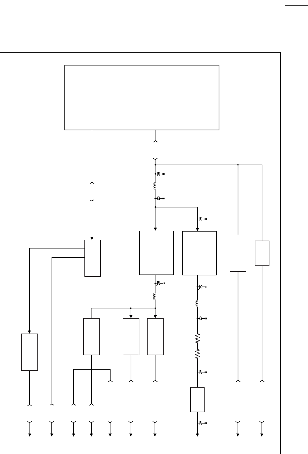
23.2. SC-PT850 Power Block
SC-PT850 POWER BLOCK
-7V
D+5V
-13V
+18V
A+5V
DVD_ADAC+5V
DVD_2R7
SW+5V
TU+9V
F+/F-
IC2903
DC-DC
CONVERTER
IC2900
DC-DC
CONVERTER
REGULATOR
REGULATOR
REGULATOR
REGULATOR
LIMITER
+7V
T2900
IC2901
RF+5V
S
M
P
S
C-
+C-
+C-
+C-
+
C-
+C-
+
RR L
D
D
LL
SA-PT850EE
111
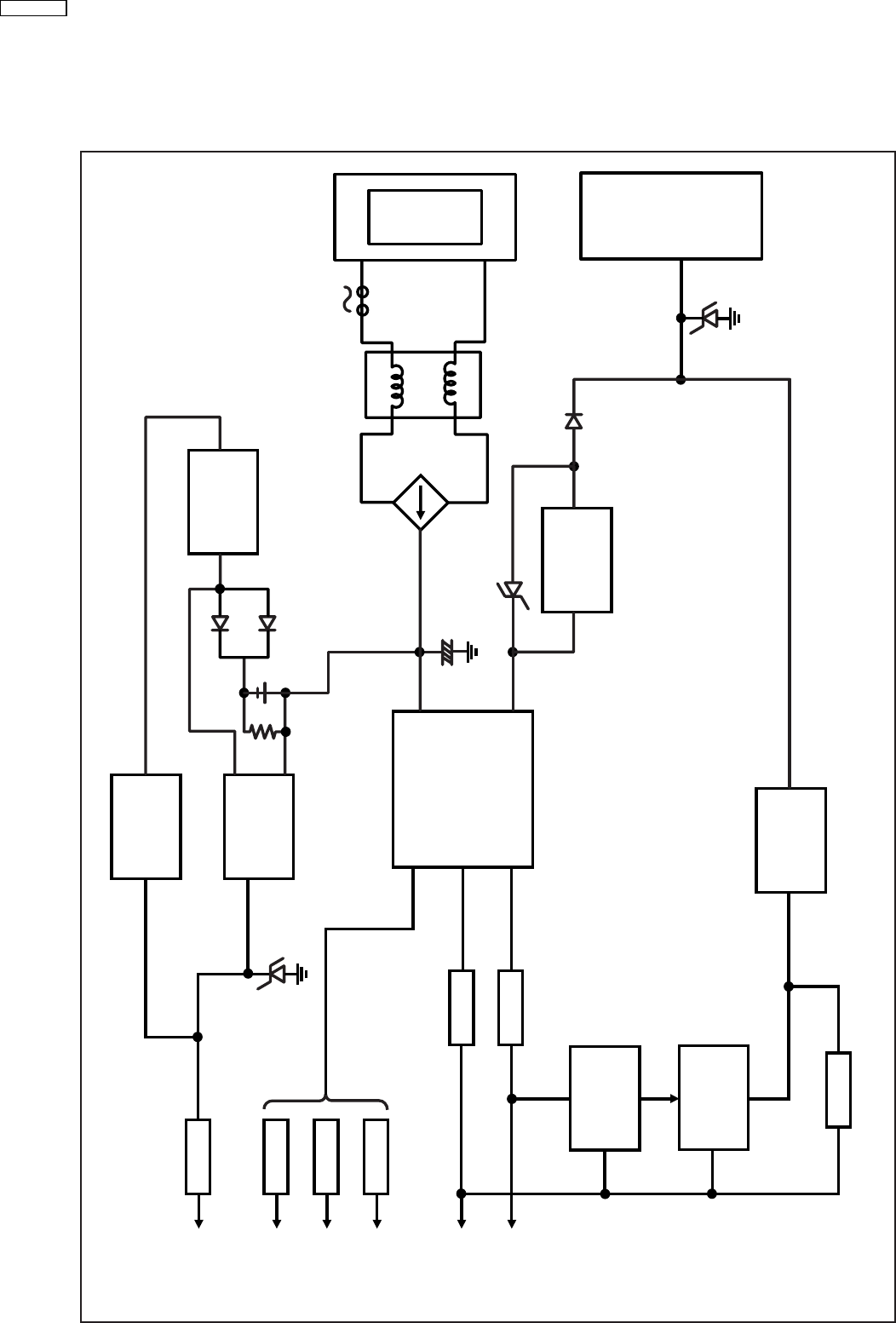
23.3. SC-PT850 SMPS Block
VOLTAGE
DIVIDER
SHUNT
REGULATOR
A
C
R
IC5801
FEEDBACK
PC5720
T5701
13V
-13V
18V
FAN_18V
+30V
D5801
+30V_SENSE
-30V
D5802
-30V_SENSE
OVP
Q5802/D5806
DC_18V
18V
T5751
IC5799
DFB
FEEDBACK
PC5799
VCC
IC5701
AC IN
+6V
SYS6V
L5702
+
-
C5711
VCC
REGULATOR
D5722/D5723
D5721
F1
SC-PT850 SMPS BLOCK
SA-PT850EE
112

24.1. IC2001 (C2CBYY000418):
System Control IC
Pin
No.
Terminal Name I/O Function
1TRAY_CLOSE I LOADING MECHA CLOSE SW (L: SW
ON)
2TRAY_CCW OTerminal for tray control 1
3TRAY_CW OTerminal for tray control 2
4TRAY_OPEN I LOADING MECHA OPEN SW (L: SW
ON)
5MIC_SW -MIC Insertion Detect (if MIC_EN=1)
6 NC - No Connection
7 XM_EN I Wireless Data Input (Disable)
8BYTE I VSS (GND)
9 CNVSS - VSS (GND)
10 GND - GND (0V)
11 RDS_EN IRDS Enable (H=Enable, L=Disable)
12 RESET I SYSTEM RESET INPUT
13 XOUT - MAIN CLOCK OUTPUT (10.0MHZ)
14 VSS - GND (0V)
15 XIN - MAIN CLOCK INPUT (10 MHZ)
16 VCC - POWER SUPPLY (5V)
17 NMI I CONNECT TO VCC, EXTERNAL
INTERRUPT I/P
18 RMT I REMOCON INPUT
19 SYNC I AC FAILURE DETECT INPUT
20 NC - No Connection
21 MIC_EN I Microphone Enable (L=Disable,
H=Enable)
22 NC - No Connection
23 EDA I/O DATA signal for the EEPROM
24 ECK O CLOCK signal for the EEPROM
25 ECS O LAT signal for the EEPROM
26 TV_EN I Disable/Enable for TV Selector
27 NC - No Connection
28 DVD_CLK ICLK signal for the DVD Module
29 DVD_STAT I STATUS signal from the DVD Module
30 DVD_CMD OCMD signal for the DVD Module
31 FX_DO OFor Flash Programming
32 FX_DI IFor Flash Programming
33 FX_CLK O For Flash Programming
34 FX_DET1 O (for FLASH writing)
35 TUN_SD I Tuner Station Detect
36 TUN_CLK 0 I2C Clock for Tuner
37 TUN_DO I Stereo Detect
38 TUN_DI O I2C Data for Tuner
39 FX_EN I Wireless Enable
40 DVD_PCONT O Control Signal for the Power for the
DVD MODULE
41 EPM I [Flash Connector]
42 DVD_MUTE I Signal from DVD module control mute
circuit
43 DC_DET1 IDC Detection circuit 1
44 SCART_MUTE O Line out for SCART terminal
45 ACS_EN I Wide Surround Enable
46 VMUTE O Video Mute Control
47 ASP_CLK O Clock signal for 6ch VOL ASP
48 ASP_DAT O Data signal for 6ch VOL ASP
49 NC - No Connection
50 NC - No Connection
51 NC - No Connection
52 HBASS_SW OHBASS Control
53 RGB_H O Mute signal 1 for video output
54 MULTI_1 O Multi Room selector 1
55 VMUTE_MAIN - No connection
Pin
No.
Terminal Name I/O Function
56 POS_SW IPosition Sensor
57 NC - No Connection
58 NC - No Connection
59 SENS1 I Digital Amp Output Sensor 1
60 SENSE2 I Digital Amp Output Sensor 2
61 OPT_EN I Optical IN Enable (L=Disble,
H=Enable)
62 VCC - POWER SUPPLY 5.0V
63 DC_DET2 IDC Detection Circuit 2
64 VSS - GND (0V)
65 YC_H OControl signal for the video signal Mix
66 NC - No Connection
67 HOP_DA O Frequency Hop Control DA
68 MUTE_C_S O Center and Surround L & R Mute
69 MUTE_F_SW O Front L & R Mute and SubWoofer
Mute
70 AMBP O AM Beat Proof for SMPS
71 MOD_DA O Digital Amp Standby Control
72 PCONT O System Power Control
73 CEC_OUT I Output Port for HDMI/CEC
74 ACS_MUTE O ACS Mute Control
75 CEC_IN I HDMI/CEC Input
76 JOG_A/VOL_UP ISignal A from Volume JOG / Volume
Up Button
77 JOG_B/VOL_DN ISignal B from Volume JOG / Volume
Down Button
78 HP_MUTE O Head Phone Mute signal
79 RDS_DAT I Data signal from the RDS decoder
80 WIDE1 OControl Signal for the WIDE function
81 RDS_CLK IClock signal from the RDS decoder
82 WS_LED OWide Surround LED
83 ECHO_LVL1 OEcho Level 1 Control
84 ECHO_LVL2 OEcho Level 2 Control
85 FLD_CLK OClock Signal for the FL Driver
86 FLD_STB O FL Strobe
87 FLD_OUT O FL Data Out
88 ECHO_MUTE O Echo Mute
89 MD3 I Model Code 3
90 MD2 I Model Code 2
91 KEY 2 IKey 2 line input
92 ACS I Auto Calibration
93 DES3 I DVD Region Setting
94 DES2 I Model Selector
95 DES1 I REGION Setting for Tuner
96 AVSS - Analog Power Supply Input
97 KEY1 IKey 1 Line input
98 VREF - Reference Voltage Input
99 AVCC - Analog Power Supply Input
100 BRAKE_H O Terminal for tray control 3
24 Terminal Function of ICs
113
SA-PT850EE

25 Exploded Views
114
SA-PT850EE
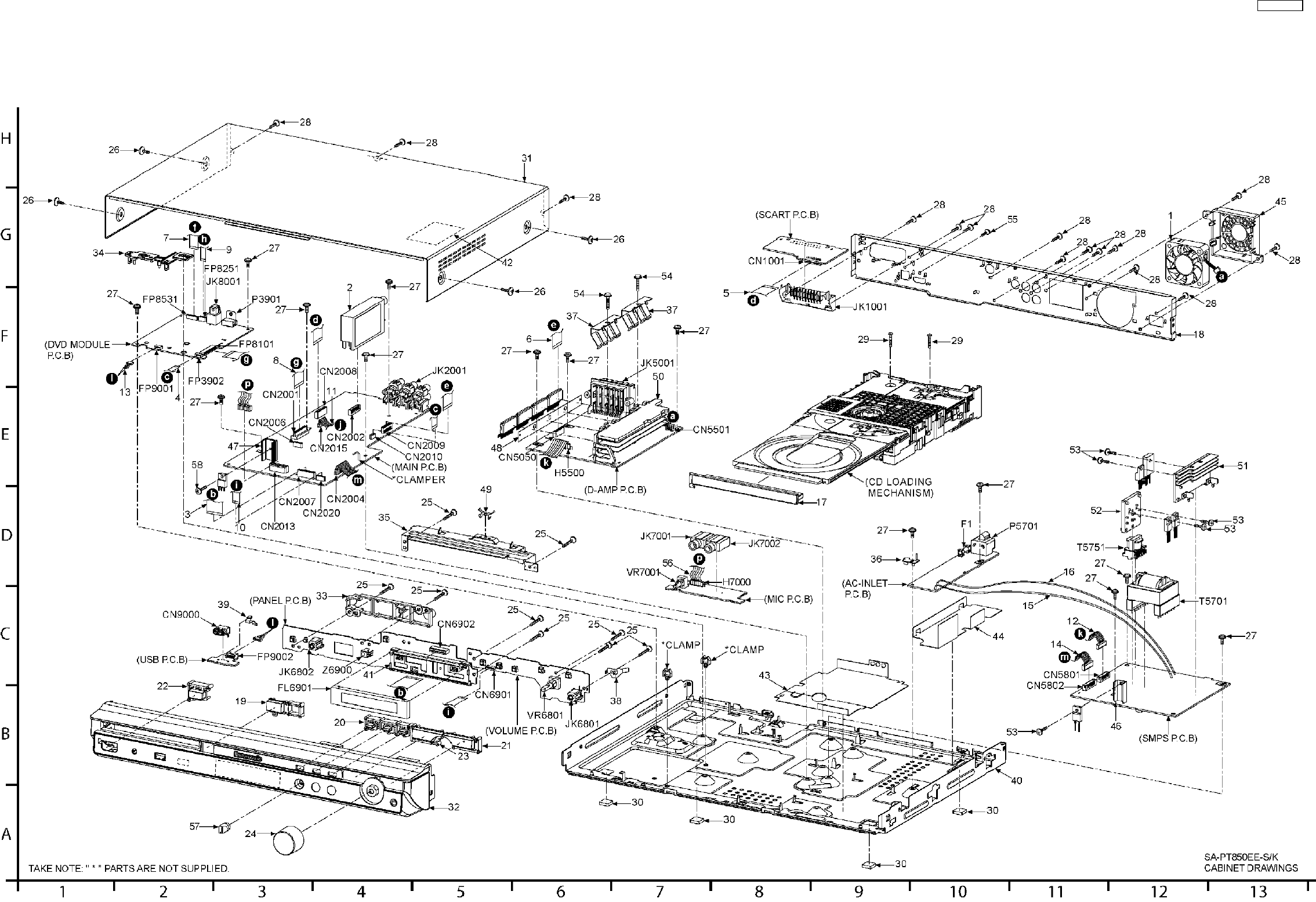
25.1. Cabinet Parts Location
SA-PT850EE
115
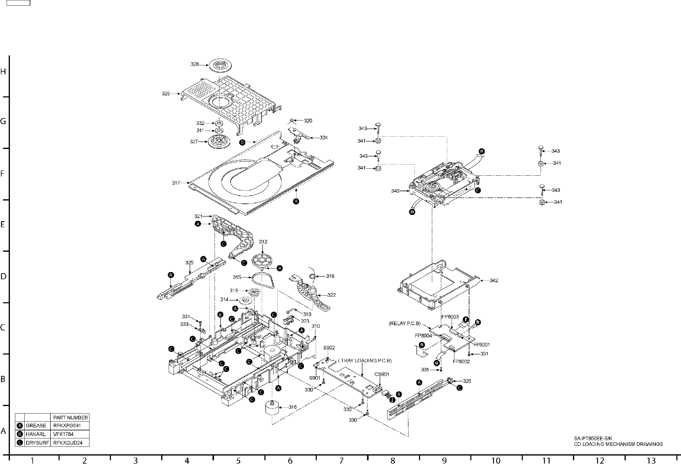
SA-PT850EE
116
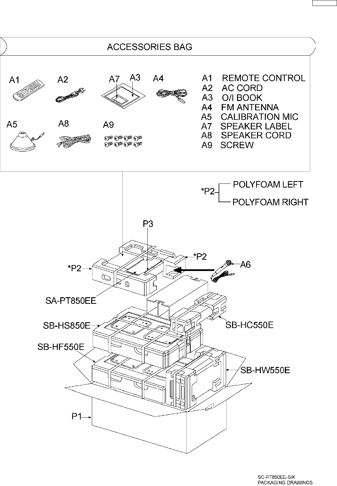
25.2. Packaging
SA-PT850EE
117

Notes:
26 Replacement Parts List
·
Important safety notice:
Components identified by mark have special characteristics important for safety purpose.
Furthermore, special parts which have purposes of fire-retardant (resistors), high-quality sound (capacitors), low-noise
(resistors), etc. are used.
When replacing any of components, be sure to use only manufacture’s specified parts shown in the parts list.
·
Warning: This product uses a laser diode. Refer to caution statements.
·
Capacity values are in microfarads (µF) unless specified otherwise, P=Pico-farads (pF), F=Farads (F).
·
Resistance values are in ohms, unless specified otherwise, 1K=1,000 (OHM), 1M=1,000K (OHM).
·
The parenthesized indications in the Remarks columns specify the model names and areas. (Refer to the cover page)
·
The marking (RTL) indicates the retention time is limited for this item. After the discontinuation of this assembly in production,
it will no longer be available.
·
Parts mentioned [M] are supplied from PAVCSG.
·
Parts mentioned [SPG] are supplied from PAVC.
·
Reference for O/I book languages are as follows:
Ar: Arablic Du: Dutch It: Italian Sp: Spanish
Cf: Canadian French En: English Ko: Korean Sw: Swedish
Cz: Czech Fr: French Po: Polish Co: Traditional Chinese
Da: Danish Ge: German Ru: Russian Cn Simplified Chinese
Pe: Persian Ur: Ukrainian Pr: Portuguese
118
SA-PT850EE

26.1. Component Parts List
Ref.
No.
Part No. Part Name & Description Remarks
CABINET AND CHASSIS
1L6FAJCCH0007 SMALL DC FAN MOTOR [M]
2J3CBBB000001 TUNER PACK [M]
3REEX0671 19P FFC (PANEL) [M]
4REEX0672 7P FFC (HDMI) [M]
5REEX0673 19P FFC (SCART) [M]
6REEX0675 17P FFC (D-AMP) [M]
7REEX0676 26P FFC WIRE (MECHA) [M]
8REEX0677 50P FFC (HDMI) [M]
9REEX0678 6P FFC (MECHA) [M]
10 REEX0758 8P FFC WIRE (VOLUME) [M]
11 REXX0384 7P FLAT WIRE (DVD) [M]
12 REXX0559 8P FLAT WIRE (D-AMP) [M]
13 REXX0560-1 USB SHIELD WIRE [M]
14 REXX0561 11P FLAT WIRE [M]
15 REXX0563-J WIRE (WHITE) [M]
16 REXX0564-J WIRE (GREY) [M]
17 RGKX0383-K DVD LID [M]
18 RGRX0060A-F REAR PANEL [M]
19 RGUX0692-K OPEN/CLOSE BUTTON [M]
20 RGUX0693-K REV/FWD BUTTON [M]
21 RGUX0694-K PLAY BUTTON [M]
22 RGUX0702-K POWER BUTTON [M]
23 RGUX0728-K STOP BUTTON [M]
24 RGWX0106-K VOLUME KNOB [M]K
24 RGWX0106-S VOLUME KNOB [M]S
25 RHD26046 SCREW [M]
26 RHD30007-1SJ SCREW [M]S
26 RHD30007-K2J SCREW [M]K
27 RHD30111-3 SCREW [M]
28 RHD30119-S SCREW [M]
29 RHDC0023 SCREW [M]
30 RKA0059-K LEG RUBBER [M]
31 RKMX0107A-K3 TOP CABINET [M]K
31 RKMX0107A-S3 TOP CABINET [M]S
32 RFKGAPT850EE FRONT PANEL ASS’Y [M]S
32 RFKGAPT850EK FRONT PANEL ASS’Y [M]K
33 RMAX0102 MECHA HOLDER [M]
34 RMAX0103 MECHA CHASSIS [M]
35 RMAX0104 PANEL ANGLE [M]
36 RMAX0109 D-AMP PCB BRACKET [M]
37 RMC0465 TR SPRING [M]
38 RMCX0042 EARTH SPRING [M]
39 RMCX0046 USB EARTH SPRING [M]
40 RMKX0125 BOTTOM CHASSIS [M]
41 RMNX0149 FL HOLDER [M]
42 RMNX0207 SMPS PCB INSULATOR [M]
43 RMNX0208 SMPS PCB INSULATOR [M]
44 RMNX0209 AC-IN PCB INSULATOR [M]
45 RMQX0233-K FAN COVER [M]
46 RMY0285A SMALL HEATSINK [M]
47 RMYX0191 HEATSINK EXTRUSSION [M]
48 RMZX0038 IC INSULATOR [M]
49 RSC0706 EARTH PART [M]
50 RXXX0085-J HEATSINK UNIT A [M]
51 RXXX0088 HEATSINK UNIT B [M]
52 RXXX0089 HEATSINK UNIT C [M]
53 XTB3+10JFJ SCREW [M]
54 XTW3+8TFJ SCREW [M]
55 XSN3+4FJ SCREW [M]
56 REXX0562 9P FLAT WIRE (MIC) [M]
57 RGW0352A-K MIC KNOB [M]
58 XTB3+8JFJ SCREW [M]
TRAVERSE UNIT
310 RMK0591A MECHA CHASSIS [M]
311 RHM0003-J MAGNET [M]
312 RDG0547 PULLEY GEAR [M]
313 RDG0548-1 RELAY GEAR [M]
Ref.
No.
Part No. Part Name & Description Remarks
314 RDG0549 DRIVE GEAR [M]
315 RDV0070 BELT [M]
316 REM0133 MOTOR UNIT [M]
317 RGQ0395-K1 TRAY [M]
318 RME0350 CHANGE LEVER SPRING [M]
319 RME0351A LOCK LEVER SPRING [M]
320 RME0353 TRAY SLIDER SPRING [M]
321 RML0627-2 DRIVE ARM [M]
322 RML0628 CHANGE LEVER [M]
323 RML0629 LOCK LEVER [M]
324 RML0631 TRAY SLIDER [M]
325 RMM0247-3 DRIVE RACK [M]
326 RMM0248 SUB RACK [M]
327 RMR1446-X CLAMPER [M]
328 RMR1447-X MAGNET HOLDER [M]
329 RMR1468-K CLAMP PLATE [M]
330 XTN26+6GFJ SCREW [M]
331 XTV2+6GFJ SCREW [M]
332 XWG6FFJ WASHER [M]
333 RMC0387 SUPPORT SPRING [M]
340 RAE2024Z-S TRAVERSE UNIT [M]
341 RMG0598A-K FLOATING RUBBER [M]
342 RMR1596-X2 MIDDLE CHASSIS [M]
343 RMS0789 FIXED PIN [M]
PRINTED CIRCUIT BOARDS
REP4238A TRAY LOADING P.C.B. [M]
(RTL)
REPX0560D D-AMP P.C.B. [M]
(RTL)
REPX0563D DVD MODULE P.C.B. [M]
(RTL)
REPX0569A SMPS/AC-INLET P.C.B. [M]
(RTL)
REPX0587F MAIN/PANEL/VOLUME/MIC/USB/SCA
RT P.C.B.
[M]
(RTL)
REPX0604A RELAY P.C.B. [M]
(RTL)
INTEGRATED CIRCUITS
IC904 C0GAY0000013 IC TRAY LOADING MOTOR DRIVE [M]
IC1101 C9ZB00000461 IC VIDEO BUFFER [M]
IC1102 C1AB00001731 IC VIDEO BUFFER [M]
IC2001 C2CBYY000418 IC SYSTEM CONTROL [M]
IC2101 C1AB00002735 IC AUDIO SIGNAL PROCESSOR [M]
IC2102 C0AABB000125 IC HEADPHONE AMP [M]
IC2751 C0ABBB000350 IC OP AMP [M]
IC2801 C9ZB00000461 IC VIDEO BUFFER [M]
IC2802 C1AB00001731 IC VIDEO BUFFER [M]
IC2900 C0DAAYY00042 IC SWITCHING REGULATOR [M]
IC2903 C0DAAMH00012 IC SWITCHING REGULATOR [M]
IC3901 MN864702A IC HDMI TRANSMITTER [M]
IC3952 C0CBCDC00063 IC TERMINAL VOLTAGE REGULATOR [M]
IC5000 C1BA00000487 IC AUDIO DIGITAL POWER AMP [M]
IC5200 C1BA00000487 IC AUDIO DIGITAL POWER AMP [M]
IC5300 C1BA00000487 IC AUDIO DIGITAL POWER AMP [M]
IC5400 C1BA00000487 IC AUDIO DIGITAL POWER AMP [M]
IC5500 C0JBAB000902 IC INVERTER GATE (CLOCK
GENERATOR)
[M]
IC5501 C0JBAF000716 IC D-TYPE FLIP-FLOP [M]
IC5701 C5HACYY00003 IC SWITCHING REGULATOR [M]
IC5799 MIP4110MSSCF IC SWITCHING REGULATOR [M]
IC5801 C0DABFC00002 IC SHUNT REGULATOR [M]
IC6106 C0ABBB000230 IC OP AMP [M]
IC6107 C0ABBB000230 IC XM AUDIO AMP [M]
IC6901 C0HBB0000057 IC DISPLAY DRIVER [M]
IC7000 C0ABBB000230 IC MIC AMP [M]
IC7100 C1BB00001061 IC DIGITAL DELAY WITH ECHO
VOLUME
[M]
IC7200 C0ABBB000230 IC MIC AMP [M]
IC8001 MN2DS0018MP IC DV5.0 LSI [M]
IC8051 C3ABPG000145 IC 64M SDRAM [M]
IC8111 C0DBZYY00018 IC +3.3V DC-DC CONVERTER [M]
119
SA-PT850EE

Ref.
No.
Part No. Part Name & Description Remarks
IC8151 C0DBEHG00006 IC +1.2V REGULATOR [M]
IC8251 C0GBG0000048 IC MOTOR DRIVE [M]
IC8421 C0FBBK000050 IC AUDIO DAC [M]
IC8601 C0EBA0000029 IC RESET [M]
IC8606 C0EBE0000456 IC RESET [M]
IC8651 RFKWMHB0E321 IC 32M FLASH MEMORY [SPG]
IC8691 C0JBAA000502 IC AND GATE [M]
IC8695 C0JBAA000502 IC AND GATE [M]
IC8701 C0JBAB000907 IC INVERTER GATE [M]
IC8901 C0JBAA000501 IC AND GATE [M]
IC9001 C0JBAZ001251 IC LATCH [M]
IC9002 C0JBAZ001251 IC LATCH [M]
IC9003 C0JBAB000908 IC INVERTER GATE [M]
IC9005 C0DBZYE00002 IC REGULATOR [M]
TRANSISTORS
Q1002 UNR221200L TRANSISTOR [M]
Q1003 2SD0601AHL TRANSISTOR [M]
Q1004 UNR211H00L TRANSISTOR [M]
Q1005 UNR221200L TRANSISTOR [M]
Q1006 XN0460100L TRANSISTOR [M]
Q1007 2SB0709AHL TRANSISTOR [M]
Q1008 UNR221200L TRANSISTOR [M]
Q1009 B1GDCFGA0018 TRANSISTOR [M]
Q1100 B1ABGC000005 TRANSISTOR [M]
Q1200 B1ABGC000005 TRANSISTOR [M]
Q2003 B1GBCFLL0037 TRANSISTOR [M]
Q2006 B1GBCFJN0033 TRANSISTOR [M]
Q2007 UNR211H00L TRANSISTOR [M]
Q2008 B1GBCFJN0033 TRANSISTOR [M]
Q2030 B1GBCFJN0033 TRANSISTOR [M]
Q2096 2SD0601AHL TRANSISTOR [M]
Q2097 2SD0601AHL TRANSISTOR [M]
Q2101 B1GFGCAA0001 TRANSISTOR [M]
Q2102 B1GFGCAA0001 TRANSISTOR [M]
Q2103 B1GFGCAA0001 TRANSISTOR [M]
Q2201 B1GDCFGA0018 TRANSISTOR [M]
Q2202 B1GFGCAA0001 TRANSISTOR [M]
Q2302 B1GFGCAA0001 TRANSISTOR [M]
Q2502 B1GFGCAA0001 TRANSISTOR [M]
Q2801 B1GBCFJN0033 TRANSISTOR [M]
Q2804 B1GBCFJN0033 TRANSISTOR [M]
Q2805 B1GBCFJN0033 TRANSISTOR [M]
Q2900 B1BABK000001 TRANSISTOR [M]
Q2901 B1BCCG000002 TRANSISTOR [M]
Q2902 B1ADCF000001 TRANSISTOR [M]
Q2903 B1BACD000018 TRANSISTOR [M]
Q2904 B1BACG000023 TRANSISTOR [M]
Q2906 B1ABCF000176 TRANSISTOR [M]
Q2907 B1ABCF000176 TRANSISTOR [M]
Q2908 B1ACKD000006 TRANSISTOR [M]
Q2909 B1GBCFJN0033 TRANSISTOR [M]
Q2910 B1ACKD000006 TRANSISTOR [M]
Q2911 B1AAKD000012 TRANSISTOR [M]
Q2916 B1BACG000023 TRANSISTOR [M]
Q2919 B1ABCF000176 TRANSISTOR [M]
Q2921 B1ADCF000001 TRANSISTOR [M]
Q2922 B1GBCFJJ0051 TRANSISTOR [M]
Q3901 2SD1819A0L TRANSISTOR [M]
Q3902 B1CFHA000002 TRANSISTOR [M]
Q3903 B1CFHA000002 TRANSISTOR [M]
Q3941 2SD1819A0L TRANSISTOR [M]
Q3942 2SD1819A0L TRANSISTOR [M]
Q3943 2SD1819A0L TRANSISTOR [M]
Q5101 B1ABCF000176 TRANSISTOR [M]
Q5102 B1ABCF000176 TRANSISTOR [M]
Q5601 B1ABCF000176 TRANSISTOR [M]
Q5602 B1ABCF000176 TRANSISTOR [M]
Q5603 B1ADCE000012 TRANSISTOR [M]
Q5604 B1ABCF000176 TRANSISTOR [M]
Q5640 B1BACD000018 TRANSISTOR [M]
Q5641 B1ABCF000011 TRANSISTOR [M]
Ref.
No.
Part No. Part Name & Description Remarks
Q5642 B1ABCF000011 TRANSISTOR [M]
Q5644 B1ABCF000011 TRANSISTOR [M]
Q5720 2SC3940ARA TRANSISTOR [M]
Q5721 B1ADCF000001 TRANSISTOR [M]
Q5722 B1ABCF000176 TRANSISTOR [M]
Q5802 B1ABCF000176 TRANSISTOR [M]
Q5860 B1ADCF000001 TRANSISTOR [M]
Q5861 B1ABCF000176 TRANSISTOR [M]
Q5862 B1ABCF000176 TRANSISTOR [M]
Q5898 B1ABCF000176 TRANSISTOR [M]
Q5899 B1ABCF000176 TRANSISTOR [M]
Q6102 B1ABEB000002 TRANSISTOR [M]
Q6105 B1ADCE000012 TRANSISTOR [M]
Q6110 UNR221200L TRANSISTOR [M]
Q6111 UNR221200L TRANSISTOR [M]
Q6201 B1ADCE000012 TRANSISTOR [M]
Q6202 B1GDCFGA0018 TRANSISTOR [M]
Q7100 B1GBCFJJ0051 TRANSISTOR [M]
Q7101 B1GBCFJJ0051 TRANSISTOR [M]
Q7102 B1GBCFJJ0051 TRANSISTOR [M]
Q8321 2SB1218ARL TRANSISTOR [M]
Q8325 2SB1218ARL TRANSISTOR [M]
Q8331 2SB1218ARL TRANSISTOR [M]
Q8335 2SB1218ARL TRANSISTOR [M]
Q8341 2SB1218ARL TRANSISTOR [M]
Q8551 2SD1819A0L TRANSISTOR [M]
Q8552 B1ADGB000008 TRANSISTOR [M]
Q8561 2SD1819A0L TRANSISTOR [M]
Q8562 B1ADGB000008 TRANSISTOR [M]
QR5801 B1GBCFJN0033 TRANSISTOR [M]
QR5810 B1GBCFLL0037 TRANSISTOR [M]
QR8111 XP0621400L CHIP TRANSISTOR [M]
QR8420 UNR521100L CHIP TRANSISTOR [M]
QR8571 UNR511V00L CHIP TRANSISTOR [M]
PC5701 B3PBA0000402 PHOTO COUPLER [M]
PC5702 B3PBA0000402 PHOTO COUPLER [M]
PC5720 B3PBA0000402 PHOTO COUPLER [M]
PC5799 B3PBA0000402 PHOTO COUPLER [M]
DIODES
D1001 B0BC6R100010 DIODE [M]
D1002 B0BC01200019 DIODE [M]
D1010 B0JCAE000001 DIODE [M]
D2005 B0ACCK000005 DIODE [M]
D2007 B0ACCK000005 DIODE [M]
D2008 B0ACCK000005 DIODE [M]
D2009 B0ACCK000005 DIODE [M]
D2010 B0ACCK000005 DIODE [M]
D2601 B0ACCK000005 DIODE [M]
D2602 B0ACCK000005 DIODE [M]
D2751 B0BC5R000009 DIODE [M]
D2752 B0ACCK000005 DIODE [M]
D2753 B0ACCK000005 DIODE [M]
D2810 B0JCAE000001 DIODE [M]
D2901 B0BC035A0007 DIODE [M]
D2903 B0EAMM000057 DIODE [M]
D2904 B0JCPD000025 DIODE [M]
D2906 B0JAME000029 DIODE [M]
D2908 B0EAMM000057 DIODE [M]
D2909 MAZ82400HL DIODE [M]
D2912 B0BC3R400001 DIODE [M]
D2913 B0JCPD000025 DIODE [M]
D2915 B0ACCK000005 DIODE [M]
D2919 B0BC5R600003 DIODE [M]
D2920 B0BC035A0007 DIODE [M]
D2935 B0EAKM000117 DIODE [M]
D2936 B0EAKM000117 DIODE [M]
D2937 B0BC4R600016 DIODE [M]
D2938 B0BC5R000009 DIODE [M]
D2939 B0ACCK000005 DIODE [M]
120
SA-PT850EE

Ref.
No.
Part No. Part Name & Description Remarks
D2940 B0ACCK000005 DIODE [M]
D2941 B0ACCK000005 DIODE [M]
D2942 B0ACCK000005 DIODE [M]
D2943 B0ADCJ000020 DIODE [M]
D2944 B0ACCK000005 DIODE [M]
D2945 B0ACCK000005 DIODE [M]
D2946 B0BC7R500001 DIODE [M]
D2947 B0BC010A0007 DIODE [M]
D3901 MA2J72800L DIODE [M]
D5503 B0BC5R000009 DIODE [M]
D5640 B0BC01200019 DIODE [M]
D5643 B0ACCK000005 DIODE [M]
D5644 B0ACCK000005 DIODE [M]
D5645 B0ACCK000005 DIODE [M]
D5701 B0FBAR000041 DIODE [M]
D5702 B0ZAZ0000052 DIODE [M]
D5721 B0BC01700015 DIODE [M]
D5722 B0BC01700015 DIODE [M]
D5723 B0ACCK000005 DIODE [M]
D5724 B0ACCK000005 DIODE [M]
D5725 B0BC6R100010 DIODE [M]
D5726 B0EAKM000117 DIODE [M]
D5727 B0ACCK000005 DIODE [M]
D5728 B0ACCK000005 DIODE [M]
D5729 B0EAMM000057 DIODE [M]
D5730 B0ACCK000005 DIODE [M]
D5731 B0EAMM000057 DIODE [M]
D5732 B0BC035A0007 DIODE [M]
D5793 B0EAKB000004 DIODE [M]
D5797 MA2J72800L DIODE [M]
D5798 B0EAMM000057 DIODE [M]
D5801 B0HBSM000043 DIODE [M]
D5802 B0HBSM000043 DIODE [M]
D5803 B0HFRJ000012 DIODE [M]
D5804 B0EAMM000057 DIODE [M]
D5805 B0EAMM000057 DIODE [M]
D5806 B0BC7R500001 DIODE [M]
D5807 B0ACCK000005 DIODE [M]
D5896 B0EAMM000057 DIODE [M]
D5897 B0BC3R700004 DIODE [M]
D6100 B0ACCK000005 DIODE [M]
D6101 B0ACCK000005 DIODE [M]
D6102 B0BC5R000009 DIODE [M]
D6901 B3AAA0000803 DIODE [M]
D6902 B0ACCK000005 DIODE [M]
D6910 B0BC2R4A0006 DIODE [M]
D7100 B0BC5R000009 DIODE [M]
D8211 MA2J11100L DIODE [M]
D8571 MA2J72800L DIODE [M]
DZ5701 ERZV10V511CS ZENER [M]
VARIABLE RESISTORS
VR6801 EVEKE2F3024M VR VOLUME JOG [M]
VR7001 EVUE27FK3B53 VR MIC VOLUME [M]
VA3901 EZAEG2A50AX ESD SUPRESSOR [M]
VA3902 EZAEG2A50AX ESD SUPRESSOR [M]
VA3903 EZAEG2A50AX ESD SUPRESSOR [M]
VA3904 EZAEG2A50AX ESD SUPRESSOR [M]
VA3905 EZAEG2A50AX ESD SUPRESSOR [M]
VA3906 EZAEG2A50AX ESD SUPRESSOR [M]
VA3907 EZAEG2A50AX ESD SUPRESSOR [M]
VA3908 EZAEG2A50AX ESD SUPRESSOR [M]
VA3909 EZJZ0V800AA VARISTOR [M]
VA3910 EZJZ0V800AA VARISTOR [M]
VA3911 EZJZ0V800AA VARISTOR [M]
VA3912 EZJZ0V800AA VARISTOR [M]
VA3913 EZJZ0V800AA VARISTOR [M]
VA9001 EZJZ1V171AA CHIP VARISTOR [M]
VA9002 EZJZ1V171AA CHIP VARISTOR [M]
Ref.
No.
Part No. Part Name & Description Remarks
SWITCHES
S901 RSH1A044-1A SW PLAY [M]
S902 RSH1A044-1A SW OPEN [M]
S6801 EVQ21405R SW SELECTOR [M]
S6802 EVQ21405R SW REVERSE [M]
S6803 EVQ21405R SW FORWARD [M]
S6804 EVQ21405R SW STOP [M]
S6901 EVQ21405R SW POWER [M]
S6902 EVQ21405R SW OPEN/CLOSE [M]
S6907 EVQ21405R SW PLAY [M]
CONNECTORS
CN1001 K1MN19B00072 19P CONNECTOR [M]
CN2001 K1MY50AA0029 50P CONNECTOR [M]
CN2002 K1KA10AA0031 10P CONNECTOR [M]
CN2004 K1YZ11000002 11P CABLE HOLDER [M]
CN2006 K1MN08AA0003 8P CONNECTOR [M]
CN2007 K1MN19AA0004 19P CONNECTOR [M]
CN2008 K1MN19AA0004 19P CONNECTOR [M]
CN2009 K1MN17AA0004 17P CONNECTOR [M]
CN2010 K1MN07AA0003 7P FFC CONNECTOR [M]
CN2013 K1KA09A00150 9P CONNECTOR [M]
CN2015 K1YZ07000001 7P WIRE HOLDER [M]
CN2020 K1MN08AA0003 8P CONNECTOR [M]
CN5050 K1MN17AA0004 17P CONNECTOR [M]
CN5501 K1KA03AA0301 3P CONNECTOR [M]
CN5801 K1KA08AA0180 8P CONNECTOR [M]
CN5802 K1KA11AA0194 11P CONNECTOR [M]
CN6901 K1MN08AA0003 8P CONNECTOR [M]
CN6902 K1MN19AA0004 19P CONNECTOR [M]
CN9000 K1FY104B0011 4P CONNECTOR [M]
CS901 K1KA07BA0061 7P CONNECTOR [M]
FP3902 K1MN07BA0148 7P CONNECTOR [M]
FP8001 K1MN06BA0147 6P CONNECTOR [M]
FP8002 K1MN06BA0148 6P CONNECTOR [M]
FP8003 K1MY26BA0053 26P CONNECTOR [M]
FP8004 K1MY26BA0030 26P FFC CONNECTOR [M]
FP8101 K1MN50BA0173 50P CONNECTOR [M]
FP8251 K1MN06AA0076 6P CONNECTOR [M]
FP8531 K1MY26AA0021 26P CONNECTOR [M]
FP9001 K1KA05BA0014 5P CONNECTOR [M]
FP9002 K1KA05BA0061 5P CONNECTOR [M]
THERMISTORS
TH5701 D4CAC8R00002 THERMISTOR [M]
TH5860 D4CC11040013 THERMISTOR [M]
COILS & TRANSFORMERS
L1001 J0JBC0000015 CHIP INDUCTOR [M]
L1002 J0JBC0000015 CHIP INDUCTOR [M]
L1003 J0JBC0000015 CHIP INDUCTOR [M]
L1004 J0JBC0000015 CHIP INDUCTOR [M]
L1005 J0JBC0000015 CHIP INDUCTOR [M]
L1007 J0JBC0000015 CHIP INDUCTOR [M]
L1008 J0JBC0000015 CHIP INDUCTOR [M]
L2008 G0C3R3JA0027 COIL [M]
L2009 G0C220JA0055 COIL [M]
L2101 J0JBC0000015 CHIP INDUCTOR [M]
L2201 J0JBC0000015 CHIP INDUCTOR [M]
L2801 G0C220JA0055 COIL [M]
L2802 J0JBC0000015 CHIP INDUCTOR [M]
L2803 J0JBC0000015 CHIP INDUCTOR [M]
L2804 J0JBC0000015 CHIP INDUCTOR [M]
L2902 G0A101G00022 COIL [M]
L2903 G0A101G00022 COIL [M]
L2905 G0A100HA0023 INDUCTOR [M]
L2907 G0A220GA0026 INDUCTOR [M]
121
SA-PT850EE
Ref.
No.
Part No. Part Name & Description Remarks
L2908 G0A200D00002 COIL [M]
L2909 G0A200D00002 COIL [M]
L2910 G0A200D00002 COIL [M]
L2911 G0A200D00002 COIL [M]
L3903 J0MAB0000170 FILTER [M]
L3904 J0MAB0000170 FILTER [M]
L3905 J0MAB0000170 FILTER [M]
L3906 J0MAB0000170 FILTER [M]
L5000 G0A150L00003 LINE CHOKE COIL [M]
L5001 G0B9R5K00003 LINE CHOKE COIL [M]
L5002 G0B9R5K00003 LINE CHOKE COIL [M]
L5200 G0A150L00003 LINE CHOKE COIL [M]
L5201 G0B9R5K00003 LINE CHOKE COIL [M]
L5300 G0A150L00003 LINE CHOKE COIL [M]
L5301 G0B9R5K00003 LINE CHOKE COIL [M]
L5400 G0A150L00003 LINE CHOKE COIL [M]
L5401 G0B9R5K00003 LINE CHOKE COIL [M]
L5402 G0B9R5K00003 LINE CHOKE COIL [M]
L5500 J0JKB0000020 EMI BEAD CORE [M]
L5501 J0JKB0000020 EMI BEAD CORE [M]
L5701 ELF15N035AN LINE FILTER [M]
L5702 ELF22V035B COIL [M]
L5703 ELF22V020A LINE FILTER COIL [M]
L6101 J0JBC0000019 CHIP INDUCTOR [M]
L6201 J0JBC0000019 CHIP INDUCTOR [M]
L6801 J0JBC0000019 CHIP INDUCTOR [M]
L6903 J0JBC0000041 CHIP INDUCTOR [M]
L6904 J0JBC0000019 CHIP INDUCTOR [M]
L6905 J0JBC0000019 CHIP INDUCTOR [M]
L6906 J0JBC0000019 CHIP INDUCTOR [M]
L6907 J0JBC0000019 CHIP INDUCTOR [M]
L6908 J0JBC0000019 CHIP INDUCTOR [M]
L6909 J0JBC0000019 CHIP INDUCTOR [M]
L7001 J0JBC0000019 CHIP INDUCTOR [M]
L7002 J0JBC0000030 CHIP BEEZ [M]
L7003 J0JBC0000019 CHIP INDUCTOR [M]
L7004 J0JBC0000019 CHIP INDUCTOR [M]
L7005 J0JBC0000030 CHIP BEEZ [M]
L7101 J0JBC0000019 CHIP INDUCTOR [M]
L7202 J0JBC0000019 CHIP INDUCTOR [M]
L7303 J0JBC0000019 CHIP INDUCTOR [M]
L8001 G1C100K00019 CHIP COIL [M]
L8201 G1C100K00019 CHIP COIL [M]
L8301 G1C100K00019 CHIP COIL [M]
L8302 G1C100K00019 CHIP COIL [M]
L8303 G1C100K00019 CHIP COIL [M]
L8330 G1C100K00019 CHIP COIL [M]
L8501 G1C100K00019 CHIP COIL [M]
L8550 G1C100KA0055 CHIP INDUCTOR [M]
L9005 G1BYYYB00009 MODE CHOKE COIL [M]
CHIP INDUCTORS
LB3901 J0JHC0000045 CHIP INDUCTOR [M]
LB3902 J0JHC0000045 CHIP INDUCTOR [M]
LB3903 J0JCC0000119 CHIP INDUCTOR [M]
LB3904 J0JCC0000119 CHIP INDUCTOR [M]
LB3905 J0JCC0000119 CHIP INDUCTOR [M]
LB3906 J0JCC0000119 CHIP INDUCTOR [M]
LB3907 J0JHC0000045 CHIP INDUCTOR [M]
LB3908 J0JHC0000045 CHIP INDUCTOR [M]
LB8001 J0JHC0000045 CHIP INDUCTOR [M]
LB8011 J0JHC0000045 CHIP INDUCTOR [M]
LB8257 ERJ3GEY0R00V CHIP RESISTOR [M]
LB8258 ERJ3GEY0R00V CHIP RESISTOR [M]
LB8259 ERJ3GEY0R00V CHIP RESISTOR [M]
LB8260 ERJ3GEY0R00V CHIP RESISTOR [M]
LB8301 J0JBC0000042 CHIP BEAD [M]
LB8302 J0JBC0000042 CHIP BEAD [M]
LB8303 J0JBC0000042 CHIP BEAD [M]
LB8304 J0JBC0000042 CHIP BEAD [M]
LB8305 J0JBC0000042 CHIP BEAD [M]
LB8401 J0JBC0000042 CHIP BEAD [M]
Ref.
No.
Part No. Part Name & Description Remarks
LB8421 ERJ2GE0R00X CHIP RESISTOR [M]
LB8422 ERJ2GE0R00X CHIP RESISTOR [M]
LB8423 ERJ2GE0R00X CHIP RESISTOR [M]
LB8424 ERJ2GE0R00X CHIP RESISTOR [M]
LB8425 ERJ2GE0R00X CHIP RESISTOR [M]
LB8426 ERJ2GE0R00X CHIP RESISTOR [M]
LB8427 ERJ2GE0R00X CHIP RESISTOR [M]
LB8428 ERJ2GE0R00X CHIP RESISTOR [M]
LB8429 ERJ2GE0R00X CHIP RESISTOR [M]
LB8431 ERJ2GE0R00X CHIP RESISTOR [M]
LB8491 ERJ2GE0R00X CHIP RESISTOR [M]
LB8530 J0JHC0000045 CHIP INDUCTOR [M]
LB8531 ERJ2GE0R00X CHIP RESISTOR [M]
LB8551 J0JBC0000042 CHIP BEAD [M]
LB8561 J0JBC0000042 CHIP BEAD [M]
LB8571 J0JBC0000042 CHIP BEAD [M]
LB8690 J0JBC0000044 HIGH LOSS INDUCTOR [M]
LB8691 ERJ2GEJ101X CHIP RESISTOR [M]
LB8692 ERJ2GEJ101X CHIP RESISTOR [M]
LB8693 ERJ2GEJ101X CHIP RESISTOR [M]
LB8701 J0JBC0000044 HIGH LOSS INDUCTOR [M]
LB8702 J0JBC0000044 HIGH LOSS INDUCTOR [M]
LB9001 J0JCC0000119 CHIP INDUCTOR [M]
LB9001 J0JHC0000034 CHIP FERRITE BEAD [M]
LB9002 J0JHC0000034 CHIP FERRITE BEAD [M]
TRANSFORMERS
T2900 G4D1A0000117 SWITCHING TRANSFORMER [M]
T5701 ETS42BN1A6AD MAIN TRANSFORMER [M]
T5751 ETS19AB236AG BACK-UP TRANSFORMER [M]
COMPONENT COMBINATION
Z6900 B3RAD0000143 RADA RESISTOR [M]
FUSE HOLDERS
ZA5701 EYF52BCY FUSE HOLDER [M]
ZA5702 EYF52BCY FUSE HOLDER [M]
TERMINALS
ZJ5400 K4CZ01000027 TERMINAL [M]
ZJ5410 K4CZ01000027 TERMINAL [M]
ZJ5702 K4CZ01000027 TERMINAL [M]
ZJ5801 K4CZ01000027 TERMINAL [M]
ZJ5803 K4CZ01000027 TERMINAL [M]
OSCILLATORS
X2001 H2B100500004 CERAMIC RESONATOR [M]
X5500 H2A6023A0011 CERAMIC RESONATOR [M]
X8621 H0J270500085 CRYSTAL [M]
X9004 H1A4805B0027 CRYSTAL [M]
DISPLAY TUBE
FL6901 A2BD00000170 FL DISPLAY [M]
FL8101 F1H0J1050018 INDUCTOR [M]
FL8102 F1H0J1050018 INDUCTOR [M]
FL8103 F1H0J1050018 INDUCTOR [M]
FL8104 F1J1E1040022 INDUCTOR [M]
FL8421 F1H0J1050018 INDUCTOR [M]
FUSE
F1 K5D502BNA005 FUSE [M]
FUSE PROTECTOR
FP2900 K5G401A00008 FUSE PROTECTOR [M]
122
SA-PT850EE

Ref.
No.
Part No. Part Name & Description Remarks
HOLDERS
H5500 K1YF08000003 8P WIRE HOLDER [M]
H7000 K1YZ09000002 9P WIRE HOLDER [M]
JACKS
JK1001 K1FB121B0012 JACK AV [M]
JK2001 K2HA3YYB0007 JACK COMPONENT VIDEO OUT [M]
JK5001 K4AC12B00010 JACK SPEAKER [M]
JK6801 K2HC103A0024 JACK HEADPHONE [M]
JK6802 K2HC103A0024 JACK MUSIC PORT [M]
JK7001 K2HB102J0038 JACK MIC 1 [M]
JK7002 K2HB102J0038 JACK MIC 2 [M]
JK8001 B3RAB0000056 JACK OPTICAL IN [M]
P3901 K1FY119E0002 JACK HDMI CONNECTOR [M]
P5701 K2AA2B000015 JACK AC INLET [M]
EARTH TERMINALS
E2900 K4CZ01000027 TERMINAL [M]
E2901 K4CZ01000027 TERMINAL [M]
PACKING MATERIALS
P1 RPGX1704 PACKING CASE [M]K
P1 RPGX1819 PACKING CASE [M]S
P2 RPNX0460 POLYFOAM [M]
P3 RPFX0058-1J MIRAMAT [M]
ACCESSORIES
A1 N2QAYB000096 REMOTE CONTROL [M]
A1-1 RKK-HTR0051K R/C BATTERY COVER [M]
A2 K2CQ2CA00007 AC CORD [M]
A3 RQTX0041-1R OI BOOK (RU/UR) [M]
A4 RSA0007-M ANTENNA WIRE [M]
A5 L0CBAB000125 CALIBRATION MIC [M]
A6 RP-VK21E-K MIC [M]
A7 RQCXA0013-1 SPEAKER LABEL [M]
A8 REEX0449B-2L SPEAKER CORD [M]
A9 XSN5+12FJ SCREW [M]
RESISTORS
R1004 ERJ3GEYJ472V 4.7K 1/16W [M]
R1006 ERJ3GEYJ223V 22K 1/16W [M]
R1007 ERJ3GEYJ223V 22K 1/16W [M]
R1008 ERJ3GEYJ472V 4.7K 1/16W [M]
R1009 ERJ3GEYJ472V 4.7K 1/16W [M]
R1010 ERJ3GEYJ223V 22K 1/16W [M]
R1011 ERJ3GEYJ102V 1K 1/16W [M]
R1012 ERJ3GEYJ102V 1K 1/16W [M]
R1013 ERJ3GEYF750V 75 1/16W [M]
R1014 ERJ3GEYF750V 75 1/16W [M]
R1015 ERJ3GEYF750V 75 1/16W [M]
R1016 ERJ3GEYF750V 75 1/16W [M]
R1017 ERJ3GEYF750V 75 1/16W [M]
R1018 ERJ3GEYF750V 75 1/16W [M]
R1019 ERJ3GEYJ471V 470 1/16W [M]
R1020 ERJ3GEYJ102V 1K 1/16W [M]
R1021 ERJ3GEYJ102V 1K 1/16W [M]
R1022 ERJ3GEYJ273V 27K 1/16W [M]
R1023 ERJ3GEYJ563V 56K 1/16W [M]
R1100 ERJ3GEYJ471V 470 1/16W [M]
R1101 ERJ3GEYJ821V 820 1/16W [M]
R1102 ERJ3GEYJ272V 2.7K 1/16W [M]
R1103 ERJ3GEYJ221V 220 1/16W [M]
R1104 ERJ3GEYJ103V 10K 1/16W [M]
R1200 ERJ3GEYJ471V 470 1/16W [M]
R1201 ERJ3GEYJ821V 820 1/16W [M]
R1202 ERJ3GEYJ272V 2.7K 1/16W [M]
Ref.
No.
Part No. Part Name & Description Remarks
R1203 ERJ3GEYJ221V 220 1/16W [M]
R1204 ERJ3GEYJ103V 10K 1/16W [M]
R2000 ERJ3GEYJ221V 220 1/16W [M]
R2001 ERJ3GEYJ273V 27K 1/16W [M]
R2003 ERJ3GEYJ221V 220 1/16W [M]
R2004 ERJ3GEYJ221V 220 1/16W [M]
R2005 ERJ3GEYJ221V 220 1/16W [M]
R2006 ERJ3GEYJ221V 220 1/16W [M]
R2008 ERJ3GEYJ103V 10K 1/16W [M]
R2010 ERJ3GEY0R00V 0 1/16W [M]
R2014 ERJ3GEYJ273V 27K 1/16W [M]
R2015 ERJ3GEYJ221V 220 1/16W [M]
R2016 ERJ3GEYJ221V 220 1/16W [M]
R2017 ERJ3GEYJ273V 27K 1/16W [M]
R2019 ERJ3GEYJ273V 27K 1/16W [M]
R2021 ERJ3GEYJ563V 56K 1/16W [M]
R2022 ERJ3GEYJ221V 220 1/16W [M]
R2023 ERJ3GEYJ221V 220 1/16W [M]
R2024 ERJ3GEYJ102V 1K 1/16W [M]
R2027 ERJ3GEYJ221V 220 1/16W [M]
R2030 ERJ3GEYJ102V 1K 1/16W [M]
R2031 ERJ3GEYJ221V 220 1/16W [M]
R2032 ERJ3GEYJ473V 47K 1/16W [M]
R2034 ERJ3GEYJ473V 47K 1/16W [M]
R2037 ERJ3GEYJ473V 47K 1/16W [M]
R2040 ERJ3GEYJ103V 10K 1/16W [M]
R2041 ERJ3GEYJ472V 4.7K 1/16W [M]
R2043 ERJ3GEYJ103V 10K 1/16W [M]
R2045 ERJ3GEYJ103V 10K 1/16W [M]
R2051 ERJ3GEYJ563V 56K 1/16W [M]
R2052 ERJ3GEYJ221V 220 1/16W [M]
R2053 ERJ3GEYJ103V 10K 1/16W [M]
R2054 ERJ3GEYJ221V 220 1/16W [M]
R2055 ERJ3GEYJ102V 1K 1/16W [M]
R2060 ERJ3GEYJ221V 220 1/16W [M]
R2062 ERJ3GEYJ221V 220 1/16W [M]
R2068 ERJ3GEYJ221V 220 1/16W [M]
R2069 ERJ3GEYJ221V 220 1/16W [M]
R2077 ERJ3GEYJ103V 10K 1/16W [M]
R2079 ERJ3GEYJ103V 10K 1/16W [M]
R2080 ERJ3GEYJ103V 10K 1/16W [M]
R2081 ERJ3GEYJ103V 10K 1/16W [M]
R2082 ERJ3GEYJ472V 4.7K 1/16W [M]
R2084 ERJ3GEYJ473V 47K 1/16W [M]
R2085 ERJ3GEYJ472V 4.7K 1/16W [M]
R2086 ERJ3GEYJ223V 22K 1/16W [M]
R2087 ERJ3GEYJ223V 22K 1/16W [M]
R2088 ERJ3GEYJ182V 1.8K 1/16W [M]
R2089 ERJ3GEYJ682V 6.8K 1/16W [M]
R2092 ERJ3GEYJ221V 220 1/16W [M]
R2093 ERJ3GEYJ103V 10K 1/16W [M]
R2094 ERJ3GEYJ221V 220 1/16W [M]
R2095 ERJ3GEYJ563V 56K 1/16W [M]
R2096 ERJ3GEYJ473V 47K 1/16W [M]
R2097 ERJ3GEYJ472V 4.7K 1/16W [M]
R2098 ERJ3GEYJ225V 2.2M 1/16W [M]
R2099 ERJ3GEYJ104V 100K 1/16W [M]
R2100 ERJ3GEYJ332V 3.3K 1/16W [M]
R2101 ERJ3GEYJ103V 10K 1/16W [M]
R2102 ERJ3GEYJ332V 3.3K 1/16W [M]
R2103 ERJ3GEYJ273V 27K 1/16W [M]
R2104 ERJ3GEYJ272V 2.7K 1/16W [M]
R2105 ERJ3GEYJ152V 1.5K 1/16W [M]
R2106 ERJ3GEYJ563V 56K 1/16W [M]
R2112 ERJ3GEYJ472V 4.7K 1/16W [M]
R2113 ERJ3GEY0R00V 0 1/16W [M]
R2114 ERJ3GEYJ562V 5.6K 1/16W [M]
R2115 ERJ3GEYJ272V 2.7K 1/16W [M]
R2119 ERJ3GEYJ392V 3.9K 1/16W [M]
R2120 ERJ3GEYJ102V 1K 1/16W [M]
R2133 ERJ3GEYJ103V 10K 1/16W [M]
R2140 ERJ3GEYJ102V 1K 1/16W [M]
R2141 ERJ3GEYJ104V 100K 1/16W [M]
123
SA-PT850EE

Ref.
No.
Part No. Part Name & Description Remarks
R2142 ERJ3GEYJ102V 1K 1/16W [M]
R2143 ERJ3GEYJ104V 100K 1/16W [M]
R2145 ERJ3GEYJ273V 27K 1/16W [M]
R2160 ERJ3GEYJ102V 1K 1/16W [M]
R2161 ERJ3GEYJ473V 47K 1/16W [M]
R2164 ERJ3GEYJ103V 10K 1/16W [M]
R2165 ERJ3GEYJ103V 10K 1/16W [M]
R2170 ERJ3GEYJ222V 2.2K 1/16W [M]
R2171 ERJ3GEYJ273V 27K 1/16W [M]
R2172 ERJ3GEYJ182V 1.8K 1/16W [M]
R2175 ERJ3GEYJ122V 1.2K 1/16W [M]
R2176 ERJ3GEYJ223V 22K 1/16W [M]
R2177 ERJ3GEYJ220V 22 1/16W [M]
R2178 ERJ3GEYJ220V 22 1/16W [M]
R2179 ERJ3GEYJ220V 22 1/16W [M]
R2180 ERJ3GEYJ220V 22 1/16W [M]
R2181 ERJ3GEYJ472V 4.7K 1/16W [M]
R2182 ERJ3GEYJ100V 10 1/16W [M]
R2183 ERJ3GEYJ102V 1K 1/16W [M]
R2184 ERJ3GEYJ472V 4.7K 1/16W [M]
R2185 ERJ3GEYJ122V 1.2K 1/16W [M]
R2186 ERJ3GEYJ152V 1.5K 1/16W [M]
R2190 ERJ3GEYJ103V 10K 1/16W [M]
R2191 ERJ3GEYJ392V 3.9K 1/16W [M]
R2192 ERJ3GEYJ332V 3.3K 1/16W [M]
R2193 ERJ3GEYJ152V 1.5K 1/16W [M]
R2195 ERJ3GEYJ151V 150 1/16W [M]
R2196 ERJ3GEYJ222V 2.2K 1/16W [M]
R2197 ERJ3GEYJ104V 100K 1/16W [M]
R2198 ERJ3GEYJ222V 2.2K 1/16W [M]
R2199 ERJ3GEY0R00V 0 1/16W [M]
R2200 ERJ3GEYJ332V 3.3K 1/16W [M]
R2201 ERJ3GEYJ103V 10K 1/16W [M]
R2202 ERJ3GEYJ332V 3.3K 1/16W [M]
R2203 ERJ3GEYJ273V 27K 1/16W [M]
R2204 ERJ3GEYJ272V 2.7K 1/16W [M]
R2205 ERJ3GEYJ152V 1.5K 1/16W [M]
R2206 ERJ3GEYJ563V 56K 1/16W [M]
R2212 ERJ3GEYJ472V 4.7K 1/16W [M]
R2213 ERJ3GEY0R00V 0 1/16W [M]
R2214 ERJ3GEYJ562V 5.6K 1/16W [M]
R2215 ERJ3GEYJ272V 2.7K 1/16W [M]
R2219 ERJ3GEYJ392V 3.9K 1/16W [M]
R2220 ERJ3GEYJ102V 1K 1/16W [M]
R2233 ERJ3GEYJ103V 10K 1/16W [M]
R2240 ERJ3GEYJ102V 1K 1/16W [M]
R2241 ERJ3GEYJ104V 100K 1/16W [M]
R2242 ERJ3GEYJ102V 1K 1/16W [M]
R2243 ERJ3GEYJ104V 100K 1/16W [M]
R2244 ERJ3GEYJ563V 56K 1/16W [M]
R2260 ERJ3GEYJ102V 1K 1/16W [M]
R2261 ERJ3GEYJ473V 47K 1/16W [M]
R2264 ERJ3GEYJ103V 10K 1/16W [M]
R2265 ERJ3GEYJ103V 10K 1/16W [M]
R2270 ERJ3GEYJ222V 2.2K 1/16W [M]
R2271 ERJ3GEYJ563V 56K 1/16W [M]
R2275 ERJ3GEYJ122V 1.2K 1/16W [M]
R2276 ERJ3GEYJ223V 22K 1/16W [M]
R2277 ERJ3GEYJ220V 22 1/16W [M]
R2278 ERJ3GEYJ220V 22 1/16W [M]
R2279 ERJ3GEYJ220V 22 1/16W [M]
R2280 ERJ3GEYJ220V 22 1/16W [M]
R2281 ERJ3GEYJ472V 4.7K 1/16W [M]
R2282 ERJ3GEYJ100V 10 1/16W [M]
R2283 ERJ3GEYJ102V 1K 1/16W [M]
R2284 ERJ3GEYJ472V 4.7K 1/16W [M]
R2285 ERJ3GEYJ122V 1.2K 1/16W [M]
R2286 ERJ3GEYJ152V 1.5K 1/16W [M]
R2290 ERJ3GEYJ103V 10K 1/16W [M]
R2291 ERJ3GEYJ392V 3.9K 1/16W [M]
R2292 ERJ3GEYJ332V 3.3K 1/16W [M]
R2296 ERJ3GEYJ222V 2.2K 1/16W [M]
R2297 ERJ3GEYJ104V 100K 1/16W [M]
Ref.
No.
Part No. Part Name & Description Remarks
R2298 ERJ3GEYJ222V 2.2K 1/16W [M]
R2299 ERJ3GEY0R00V 0 1/16W [M]
R2300 ERJ3GEYJ123V 12K 1/16W [M]
R2301 ERJ3GEYJ822V 8.2K 1/16W [M]
R2302 ERJ3GEYJ562V 5.6K 1/16W [M]
R2303 ERJ3GEYJ822V 8.2K 1/16W [M]
R2304 ERJ3GEYJ123V 12K 1/16W [M]
R2310 ERJ3GEYJ103V 10K 1/16W [M]
R2312 ERJ3GEYJ152V 1.5K 1/16W [M]
R2320 ERJ3GEYJ102V 1K 1/16W [M]
R2321 ERJ3GEYJ104V 100K 1/16W [M]
R2339 ERJ3GEYJ472V 4.7K 1/16W [M]
R2400 ERJ3GEYJ123V 12K 1/16W [M]
R2401 ERJ3GEYJ822V 8.2K 1/16W [M]
R2402 ERJ3GEYJ562V 5.6K 1/16W [M]
R2403 ERJ3GEYJ822V 8.2K 1/16W [M]
R2404 ERJ3GEYJ123V 12K 1/16W [M]
R2410 ERJ3GEYJ103V 10K 1/16W [M]
R2412 ERJ3GEYJ152V 1.5K 1/16W [M]
R2420 ERJ3GEYJ102V 1K 1/16W [M]
R2421 ERJ3GEYJ104V 100K 1/16W [M]
R2439 ERJ3GEYJ472V 4.7K 1/16W [M]
R2500 ERJ3GEYJ123V 12K 1/16W [M]
R2501 ERJ3GEYJ822V 8.2K 1/16W [M]
R2502 ERJ3GEYJ562V 5.6K 1/16W [M]
R2503 ERJ3GEYJ822V 8.2K 1/16W [M]
R2504 ERJ3GEYJ103V 10K 1/16W [M]
R2510 ERJ3GEYJ272V 2.7K 1/16W [M]
R2512 ERJ3GEYJ222V 2.2K 1/16W [M]
R2520 ERJ3GEYJ102V 1K 1/16W [M]
R2521 ERJ3GEYJ104V 100K 1/16W [M]
R2600 ERJ3GEYJ102V 1K 1/16W [M]
R2601 ERJ3GEYJ123V 12K 1/16W [M]
R2609 ERJ3GEYJ122V 1.2K 1/16W [M]
R2610 ERJ3GEYJ153V 15K 1/16W [M]
R2611 ERJ3GEYJ273V 27K 1/16W [M]
R2612 ERJ3GEYJ563V 56K 1/16W [M]
R2613 ERJ3GEYJ682V 6.8K 1/16W [M]
R2614 ERJ3GEYJ273V 27K 1/16W [M]
R2617 ERJ3GEYJ332V 3.3K 1/16W [M]
R2620 ERJ3GEYJ102V 1K 1/16W [M]
R2621 ERJ3GEYJ104V 100K 1/16W [M]
R2626 ERJ3GEYJ392V 3.9K 1/16W [M]
R2627 ERJ3GEYJ473V 47K 1/16W [M]
R2661 ERJ3GEYJ680V 68 1/16W [M]
R2662 ERJ3GEYJ680V 68 1/16W [M]
R2664 ERJ3GEY0R00V 0 1/16W [M]
R2751 ERJ3GEYJ471V 470 1/16W [M]
R2752 ERJ3GEYJ103V 10K 1/16W [M]
R2753 ERJ3GEYJ472V 4.7K 1/16W [M]
R2754 ERJ3GEYJ102V 1K 1/16W [M]
R2755 ERJ3GEYJ472V 4.7K 1/16W [M]
R2756 ERJ3GEYJ101V 100 1/16W [M]
R2757 ERJ3GEYJ473V 47K 1/16W [M]
R2758 ERJ3GEYJ223V 22K 1/16W [M]
R2759 ERJ3GEYJ223V 22K 1/16W [M]
R2760 ERJ3GEYJ824V 820K 1/16W [M]
R2761 ERJ3GEYJ824V 820K 1/16W [M]
R2762 ERJ3GEYJ103V 10K 1/16W [M]
R2763 ERJ3GEYJ103V 10K 1/16W [M]
R2764 ERJ3GEYJ474V 470K 1/16W [M]
R2765 ERJ3GEYJ474V 470K 1/16W [M]
R2803 ERJ3GEYJ102V 1K 1/16W [M]
R2804 ERJ3GEYJ102V 1K 1/16W [M]
R2807 ERJ3GEYJ102V 1K 1/16W [M]
R2809 ERJ3GEYJ750V 75 1/16W [M]
R2812 ERJ3GEYJ750V 75 1/16W [M]
R2813 ERJ3GEYJ750V 75 1/16W [M]
R2862 ERJ3GEYJ103V 10K 1/16W [M]
R2863 ERJ3GEYJ103V 10K 1/16W [M]
R2864 ERJ3GEYJ821V 820 1/16W [M]
R2865 ERJ3GEYJ472V 4.7K 1/16W [M]
R2869 ERJ3GEYJ221V 220 1/16W [M]
124
SA-PT850EE

Ref.
No.
Part No. Part Name & Description Remarks
R2870 ERJ3GEYJ103V 10K 1/16W [M]
R2871 ERJ3GEYJ103V 10K 1/16W [M]
R2872 ERJ3GEYJ103V 10K 1/16W [M]
R2900 ERJ3GEYJ562V 5.6K 1/16W [M]
R2902 ERJ3GEYJ470V 47 1/16W [M]
R2903 ERJ3GEYJ182V 1.8K 1/16W [M]
R2905 ERJ3GEYJ390V 39 1/16W [M]
R2906 ERJ3GEYF682V 6.8K 1/16W [M]
R2907 ERJ3GEYJ272V 2.7K 1/16W [M]
R2908 ERJ3GEYJ561V 560 1/16W [M]
R2913 ERG2SJ220E 22 1/32W [M]
R2914 ERJ3GEYJ392V 3.9K 1/16W [M]
R2915 ERJ3GEYJ272V 2.7K 1/16W [M]
R2919 ERJ3GEYF102V 1K 1/16W [M]
R2920 ERJ3GEYF102V 1K 1/16W [M]
R2921 ERJ3GEYF332V 3.3K 1/16W [M]
R2922 ERJ3GEYF102V 1K 1/16W [M]
R2923 ERJ3GEYF122V 1.2K 1/16W [M]
R2924 ERJ3GEYJ821V 820 1/16W [M]
R2925 ERX2SJ1R5E 1.5 1/32W [M]
R2926 ERJ3GEYJ473V 47K 1/16W [M]
R2927 ERX2SJ1R5E 1.5 1/32W [M]
R2929 ERJ3GEYJ151V 150 1/16W [M]
R2930 ERJ3GEYJ472V 4.7K 1/16W [M]
R2931 ERJ3GEYJ331V 330 1/16W [M]
R2932 ERJ3GEYJ103V 10K 1/16W [M]
R2933 ERJ3GEYJ331V 330 1/16W [M]
R2934 ERJ3GEYJ103V 10K 1/16W [M]
R2935 ERJ3GEYJ472V 4.7K 1/16W [M]
R2936 ERJ3GEYJ331V 330 1/16W [M]
R2937 ERJ3GEYJ393V 39K 1/16W [M]
R2938 ERJ3GEYJ153V 15K 1/16W [M]
R2939 ERJ3GEYJ1R0V 1 1/16W [M]
R2941 ERJ3GEYJ223V 22K 1/16W [M]
R2942 ERJ3GEYJ222V 2.2K 1/16W [M]
R2943 ERJ3GEYJ272V 2.7K 1/16W [M]
R2946 ERJ3GEYJ330V 33 1/16W [M]
R2947 ERJ3GEYJ472V 4.7K 1/16W [M]
R2948 ERJ3GEYJ472V 4.7K 1/16W [M]
R2949 ERJ3GEYJ1R0V 1 1/16W [M]
R2951 ERDS1FVJ3R9T 3.9 1/2W [M]
R2952 ERJ3GEYJ392V 3.9K 1/16W [M]
R2953 ERJ3GEYJ561V 560 1/16W [M]
R2954 ERG2SJ220E 22 1/32W [M]
R2971 ERJ3GEYJ222V 2.2K 1/16W [M]
R2972 ERJ3GEYJ220V 22 1/16W [M]
R2974 ERG2SJ910E 91 1/32W [M]
R2975 ERJ3GEYJ153V 15K 1/16W [M]
R2976 ERJ3GEYJ103V 10K 1/16W [M]
R2982 ERJ3GEYJ471V 470 1/16W [M]
R2984 ERJ3GEYJ471V 470 1/16W [M]
R2985 ERJ6GEY0R00V 0 1/10W [M]
R2990 ERJ3GEY0R00V 0 1/16W [M]
R2991 ERJ3GEY0R00V 0 1/16W [M]
R2992 ERJ3GEY0R00V 0 1/16W [M]
R2993 ERJ3GEY0R00V 0 1/16W [M]
R2994 ERJ3GEY0R00V 0 1/16W [M]
R2995 ERJ3GEY0R00V 0 1/16W [M]
R2999 ERJ3GEY0R00V 0 1/16W [M]
R3901 ERJ2GEJ511X 510 1/32W [M]
R3902 ERJ2GEJ103X 10K 1/32W [M]
R3903 ERJ2GEJ103X 10K 1/32W [M]
R3904 ERJ2GEJ472X 4.7K 1/32W [M]
R3905 ERJ2GEJ202X 2K 1/32W [M]
R3906 ERJ2GEJ472X 4.7K 1/32W [M]
R3907 ERJ2GEJ222X 2.2K 1/32W [M]
R3921 ERJ2GE0R00X 0 1/32W [M]
R3924 ERJ2GE0R00X 0 1/32W [M]
R3925 ERJ2GEJ103X 10K 1/32W [M]
R3941 ERJ2GEJ273X 27K 1/32W [M]
R3942 ERJ2GEJ224X 220K 1/32W [M]
R3943 ERJ2GEJ104X 100K 1/32W [M]
R3944 ERJ2GEJ221X 220 1/32W [M]
Ref.
No.
Part No. Part Name & Description Remarks
R3945 ERJ2GEJ103X 10K 1/32W [M]
R3946 ERJ2GEJ272X 2.7K 1/32W [M]
R3947 ERJ2GEJ103X 10K 1/32W [M]
R5000 ERJ3GEYJ562V 5.6K 1/16W [M]
R5001 ERJ3GEYJ562V 5.6K 1/16W [M]
R5002 ERJ3GEYJ562V 5.6K 1/16W [M]
R5003 ERJ3GEYJ562V 5.6K 1/16W [M]
R5004 ERJ8GEYJ100V 10 1/8W [M]
R5005 ERJ8GEYJ100V 10 1/8W [M]
R5006 ERJ1TYJ220U 22 1W [M]
R5007 ERJ1TYJ220U 22 1W [M]
R5008 ERJ3GEYJ101V 100 1/16W [M]
R5010 ERJ8GEYJ100V 10 1/8W [M]
R5011 ERJ8GEYJ100V 10 1/8W [M]
R5019 ERJ3GEYJ683V 68K 1/16W [M]
R5020 ERJ3GEYJ124V 120K 1/16W [M]
R5021 ERJ3GEYJ122V 1.2K 1/16W [M]
R5022 ERJ3GEYJ122V 1.2K 1/16W [M]
R5023 ERJ3GEYJ122V 1.2K 1/16W [M]
R5030 ERJ3GEYJ562V 5.6K 1/16W [M]
R5031 ERJ3GEYJ562V 5.6K 1/16W [M]
R5032 ERJ3GEYJ562V 5.6K 1/16W [M]
R5033 ERJ3GEYJ562V 5.6K 1/16W [M]
R5034 ERJ3GEYJ562V 5.6K 1/16W [M]
R5035 ERJ3GEYJ562V 5.6K 1/16W [M]
R5036 ERJ3GEYJ562V 5.6K 1/16W [M]
R5037 ERJ3GEYJ562V 5.6K 1/16W [M]
R5103 ERJ3GEYJ562V 5.6K 1/16W [M]
R5104 ERJ3GEYJ562V 5.6K 1/16W [M]
R5110 ERJ3GEYJ223V 22K 1/16W [M]
R5111 ERJ3GEYJ124V 120K 1/16W [M]
R5113 ERJ3GEYJ683V 68K 1/16W [M]
R5114 ERJ3GEYJ122V 1.2K 1/16W [M]
R5115 ERJ3GEYJ122V 1.2K 1/16W [M]
R5118 ERJ3GEYJ562V 5.6K 1/16W [M]
R5119 ERJ3GEYJ562V 5.6K 1/16W [M]
R5200 ERJ8GEYJ100V 10 1/8W [M]
R5201 ERJ8GEYJ100V 10 1/8W [M]
R5204 ERJ3GEYJ101V 100 1/16W [M]
R5205 ERJ3GEYJ562V 5.6K 1/16W [M]
R5206 ERJ3GEYJ562V 5.6K 1/16W [M]
R5207 ERJ3GEYJ562V 5.6K 1/16W [M]
R5208 ERJ3GEYJ562V 5.6K 1/16W [M]
R5209 ERJ1TYJ220U 22 1W [M]
R5210 ERJ8GEYJ100V 10 1/8W [M]
R5211 ERJ8GEYJ100V 10 1/8W [M]
R5217 ERJ1TYJ220U 22 1W [M]
R5218 ERJ3GEYJ683V 68K 1/16W [M]
R5228 ERJ3GEYJ124V 120K 1/16W [M]
R5300 ERJ1TYJ220U 22 1W [M]
R5302 ERJ8GEYJ100V 10 1/8W [M]
R5304 ERJ3GEYJ101V 100 1/16W [M]
R5305 ERJ8GEYJ100V 10 1/8W [M]
R5306 ERJ3GEYJ562V 5.6K 1/16W [M]
R5307 ERJ3GEYJ562V 5.6K 1/16W [M]
R5308 ERJ3GEYJ562V 5.6K 1/16W [M]
R5309 ERJ3GEYJ562V 5.6K 1/16W [M]
R5310 ERJ8GEYJ100V 10 1/8W [M]
R5311 ERJ8GEYJ100V 10 1/8W [M]
R5317 ERJ3GEYJ122V 1.2K 1/16W [M]
R5318 ERJ3GEYJ124V 120K 1/16W [M]
R5319 ERJ1TYJ220U 22 1W [M]
R5327 ERJ3GEYJ122V 1.2K 1/16W [M]
R5328 ERJ3GEYJ683V 68K 1/16W [M]
R5400 ERJ1TYJ220U 22 1W [M]
R5402 ERJ8GEYJ100V 10 1/8W [M]
R5404 ERJ3GEYJ101V 100 1/16W [M]
R5405 ERJ8GEYJ100V 10 1/8W [M]
R5410 ERJ8GEYJ100V 10 1/8W [M]
R5411 ERJ8GEYJ100V 10 1/8W [M]
R5419 ERJ1TYJ220U 22 1W [M]
R5505 ERJ3GEYJ101V 100 1/16W [M]
R5507 ERJ3GEYJ105V 1M 1/16W [M]
125
SA-PT850EE

Ref.
No.
Part No. Part Name & Description Remarks
R5508 ERJ3GEYJ105V 1M 1/16W [M]
R5510 ERG2SJ271E 270 1/32W [M]
R5511 ERJ3GEYJ220V 22 1/16W [M]
R5602 ERJ3GEYJ103V 10K 1/16W [M]
R5603 ERJ3GEYJ103V 10K 1/16W [M]
R5604 ERJ3GEYJ122V 1.2K 1/16W [M]
R5606 ERJ3GEYJ103V 10K 1/16W [M]
R5607 ERJ3GEYJ122V 1.2K 1/16W [M]
R5608 ERJ3GEYJ103V 10K 1/16W [M]
R5609 ERJ3GEYJ103V 10K 1/16W [M]
R5610 ERJ3GEYJ122V 1.2K 1/16W [M]
R5611 ERJ3GEYJ122V 1.2K 1/16W [M]
R5636 ERDS1FVJ392T 3.9K 1/2W [M]
R5637 ERJ3GEYJ100V 10 1/16W [M]
R5639 ERJ3GEYJ332V 3.3K 1/16W [M]
R5640 ERJ3GEY0R00V 0 1/16W [M]
R5654 ERJ3GEYJ563V 56K 1/16W [M]
R5655 ERJ3GEYJ103V 10K 1/16W [M]
R5656 ERJ3GEYJ103V 10K 1/16W [M]
R5657 ERJ3GEYJ103V 10K 1/16W [M]
R5658 ERJ3GEYJ185V 1.8M 1/16W [M]
R5659 ERJ3GEYJ104V 100K 1/16W [M]
R5660 ERJ3GEYJ103V 10K 1/16W [M]
R5670 ERJ3GEY0R00V 0 1/16W [M]
R5701 ERDS1TJ474B 470K 1/2W [M]
R5702 ERJ1TYJ683U 68K 1/8W [M]
R5703 ERJ1TYJ683U 68K 1/8W [M]
R5704 ERJ8GEYJ394V 390K 1/8W [M]
R5705 ERJ8GEYJ394V 390K 1/8W [M]
R5706 ERJ1TYJ683U 68K 1/8W [M]
R5720 ERJ6GEYJ220V 22 1/10W [M]
R5721 ERJ6GEYJ103V 10K 1/10W [M]
R5722 ERJ6GEYJ102V 1K 1/10W [M]
R5723 ERJ3GEYJ102V 1K 1/16W [M]
R5724 ERJ6GEYJ121V 120 1/10W [M]
R5725 ERJ3GEY0R00V 0 1/16W [M]
R5726 ERX2LJ82MP 0.82 1/32W [M]
R5728 ERJ3GEYJ104V 100K 1/16W [M]
R5729 ERJ6GEYJ103V 10K 1/10W [M]
R5730 ERJ6GEYJ102V 1K 1/10W [M]
R5731 ERJ3GEY0R00V 0 1/16W [M]
R5732 ERJ6GEYJ101V 100 1/10W [M]
R5733 ERJ3GEYJ473V 47K 1/16W [M]
R5750 ERJ3GEY0R00V 0 1/16W [M]
R5786 ERG2SJ683E 68K 1/32W [M]
R5787 ERJ3GEYJ753V 75K 1/16W [M]
R5795 ERJ6GEYJ433V 43K 1/10W [M]
R5796 ERJ6GEYJ222V 2.2K 1/10W [M]
R5797 ERJ6GEYJ472V 4.7K 1/10W [M]
R5798 ERJ6GEYJ100V 10 1/10W [M]
R5800 ERJ6GEYJ103V 10K 1/10W [M]
R5801 ERJ3GEYJ123V 12K 1/16W [M]
R5802 ERJ3RBD272V 2.7K 1/16W [M]
R5803 ERJ3GEYJ271V 270 1/16W [M]
R5804 ERJ6RBD473V 47K 1/10W [M]
R5805 ERJ3RBD222V 2.2K 1/16W [M]
R5806 ERJ3GEYJ153V 15K 1/16W [M]
R5807 ERJ6GEYJ331V 330 1/10W [M]
R5808 ERJ6GEYJ222V 2.2K 1/10W [M]
R5809 ERJ6GEYJ331V 330 1/10W [M]
R5810 ERJ3GEYJ331V 330 1/16W [M]
R5811 ERJ8GEYJ152V 1.5K 1/8W [M]
R5812 ERJ3RBD822V 8.2K 1/16W [M]
R5813 ERJ3RBD243V 24K 1/16W [M]
R5814 ERJ3GEYJ822V 8.2K 1/16W [M]
R5815 ERJ3GEYJ272V 2.7K 1/16W [M]
R5816 ERJ8GEYJ152V 1.5K 1/8W [M]
R5817 ERJ3GEYJ331V 330 1/16W [M]
R5832 ERJ1TYJ222U 2.2K 1/8W [M]
R5834 ERJ1TYJ222U 2.2K 1/8W [M]
R5860 ERJ6GEYF103V 10K 1/10W [M]
R5861 ERJ6GEYF302V 3K 1/10W [M]
R5862 ERJ6GEYF103V 10K 1/10W [M]
Ref.
No.
Part No. Part Name & Description Remarks
R5863 ERJ6GEYF103V 10K 1/10W [M]
R5864 ERJ6GEYF103V 10K 1/10W [M]
R5890 ERJ3GEYJ222V 2.2K 1/16W [M]
R5891 ERJ3RBD472V 4.7K 1/16W [M]
R5892 ERJ3RBD561V 560 1/16W [M]
R5893 ERJ3RBD122V 1.2K 1/16W [M]
R5894 ERJ3GEYJ331V 330 1/16W [M]
R5895 ERJ3GEYJ681V 680 1/16W [M]
R5896 ERJ3GEYJ104V 100K 1/16W [M]
R5897 ERJ3GEYJ101V 100 1/16W [M]
R6100 ERJ3GEYJ153V 15K 1/16W [M]
R6188 ERJ3GEYJ472V 4.7K 1/16W [M]
R6190 ERJ3GEYJ102V 1K 1/16W [M]
R6191 ERJ3GEYJ221V 220 1/16W [M]
R6192 ERJ3GEYJ473V 47K 1/16W [M]
R6193 ERJ3GEYJ182V 1.8K 1/16W [M]
R6194 ERJ3GEYJ563V 56K 1/16W [M]
R6196 ERJ3GEYJ103V 10K 1/16W [M]
R6202 ERJ3GEYJ103V 10K 1/16W [M]
R6210 ERJ3GEYJ222V 2.2K 1/16W [M]
R6231 ERJ3GEY0R00V 0 1/16W [M]
R6290 ERJ3GEYJ154V 150K 1/16W [M]
R6291 ERJ3GEYJ184V 180K 1/16W [M]
R6292 ERJ3GEYJ101V 100 1/16W [M]
R6293 ERJ3GEYJ273V 27K 1/16W [M]
R6294 ERJ3GEYJ222V 2.2K 1/16W [M]
R6803 ERJ3GEYJ122V 1.2K 1/16W [M]
R6804 ERJ3GEYJ102V 1K 1/16W [M]
R6805 ERJ3GEYJ102V 1K 1/16W [M]
R6807 ERJ3GEYJ223V 22K 1/16W [M]
R6809 ERJ3GEYJ223V 22K 1/16W [M]
R6812 ERJ3GEYJ182V 1.8K 1/16W [M]
R6914 ERJ3GEYJ563V 56K 1/16W [M]
R6916 ERJ3GEYJ680V 68 1/16W [M]
R6917 ERJ3GEYJ680V 68 1/16W [M]
R6918 ERJ3GEYJ223V 22K 1/16W [M]
R6919 ERJ3GEYJ472V 4.7K 1/16W [M]
R6920 ERJ3GEYJ102V 1K 1/16W [M]
R6923 ERJ3GEYJ102V 1K 1/16W [M]
R6927 ERJ3GEYJ680V 68 1/16W [M]
R6934 ERJ3GEYJ470V 47 1/16W [M]
R6935 ERJ3GEYJ100V 10 1/16W [M]
R6948 ERJ3GEYJ221V 220 1/16W [M]
R6949 ERJ3GEYJ221V 220 1/16W [M]
R6950 ERJ3GEYJ122V 1.2K 1/16W [M]
R6951 ERJ3GEYJ122V 1.2K 1/16W [M]
R6960 ERJ3GEYJ222V 2.2K 1/16W [M]
R6961 ERJ3GEYJ102V 1K 1/16W [M]
R6962 ERJ3GEYJ102V 1K 1/16W [M]
R6965 ERJ3GEYJ473V 47K 1/16W [M]
R6966 ERJ3GEYJ473V 47K 1/16W [M]
R6967 ERJ3GEYJ103V 10K 1/16W [M]
R6968 ERJ3GEYJ103V 10K 1/16W [M]
R6970 ERJ3GEYJ473V 47K 1/16W [M]
R6971 ERJ3GEYJ473V 47K 1/16W [M]
R7001 ERJ3GEYJ681V 680 1/16W [M]
R7002 ERJ3GEYJ561V 560 1/16W [M]
R7003 ERJ3GEYJ102V 1K 1/16W [M]
R7004 ERJ3GEYJ103V 10K 1/16W [M]
R7005 ERJ3GEYJ102V 1K 1/16W [M]
R7006 ERJ3GEYJ683V 68K 1/16W [M]
R7007 ERJ3GEYJ102V 1K 1/16W [M]
R7008 ERJ3GEYJ332V 3.3K 1/16W [M]
R7009 ERJ3GEYJ823V 82K 1/16W [M]
R7010 ERJ3GEYJ102V 1K 1/16W [M]
R7011 ERJ3GEYJ222V 2.2K 1/16W [M]
R7100 ERJ3GEYJ153V 15K 1/16W [M]
R7101 ERJ3GEYJ153V 15K 1/16W [M]
R7102 ERJ3GEYJ153V 15K 1/16W [M]
R7103 ERJ3GEYJ153V 15K 1/16W [M]
R7104 ERJ3GEYJ153V 15K 1/16W [M]
R7105 ERJ3GEYJ153V 15K 1/16W [M]
R7106 ERJ3GEYJ124V 120K 1/16W [M]
126
SA-PT850EE

Ref.
No.
Part No. Part Name & Description Remarks
R7107 ERJ3GEYJ680V 68 1/16W [M]
R7109 ERJ3GEYJ472V 4.7K 1/16W [M]
R7110 ERJ3GEYJ152V 1.5K 1/16W [M]
R7112 ERJ3GEYJ272V 2.7K 1/16W [M]
R7113 ERJ3GEYJ103V 10K 1/16W [M]
R7114 ERJ3GEYJ562V 5.6K 1/16W [M]
R7116 ERJ3GEYJ681V 680 1/16W [M]
R7119 ERJ3GEYJ223V 22K 1/16W [M]
R7120 ERJ3GEYJ103V 10K 1/16W [M]
R7122 ERJ3GEYJ473V 47K 1/16W [M]
R7123 ERJ3GEYJ123V 12K 1/16W [M]
R8001 ERJ2GEJ103X 10K 1/32W [M]
R8003 ERJ2GEJ103X 10K 1/32W [M]
R8011 ERJ2GEJ220X 22 1/32W [M]
R8012 ERJ2GEJ220X 22 1/32W [M]
R8013 ERJ2GEJ220X 22 1/32W [M]
R8025 ERJ3GEY0R00V 0 1/16W [M]
R8041 ERJ2GEJ330X 33 1/32W [M]
R8153 ERJ2RHD621X 620 1/32W [M]
R8154 ERJ2RHD102X 1K 1/32W [M]
R8211 ERJ2GEJ103X 10K 1/32W [M]
R8221 ERJ2GEJ822X 8.2K 1/32W [M]
R8225 ERJ2GEJ822X 8.2K 1/32W [M]
R8230 ERJ2GEJ222X 2.2K 1/32W [M]
R8231 ERJ2GEJ223X 22K 1/32W [M]
R8232 ERJ2GEJ752X 7.5K 1/32W [M]
R8251 ERJ6GEYJ6R8V 6.8 1/10W [M]
R8261 ERJ2GEJ823X 82K 1/32W [M]
R8262 ERJ2GEJ153X 15K 1/32W [M]
R8263 ERJ2GEJ823X 82K 1/32W [M]
R8264 ERJ2GEJ153X 15K 1/32W [M]
R8311 ERJ2RHD242X 2.4K 1/32W [M]
R8312 ERJ2RHD102X 1K 1/32W [M]
R8313 ERJ2RHD153X 15K 1/32W [M]
R8314 ERJ2RHD153X 15K 1/32W [M]
R8315 ERJ2RKD240X 24 1/32W [M]
R8316 ERJ2RKD240X 24 1/32W [M]
R8317 ERJ2GEJ153X 15K 1/32W [M]
R8318 ERJ2GEJ153X 15K 1/32W [M]
R8321 ERJ3RBD201V 200 1/16W [M]
R8322 ERJ3GEY0R00V 0 1/16W [M]
R8323 ERJ2GEJ330X 33 1/32W [M]
R8324 ERJ2GEJ102X 1K 1/32W [M]
R8325 ERJ3RBD201V 200 1/16W [M]
R8326 ERJ3GEY0R00V 0 1/16W [M]
R8327 ERJ2GEJ330X 33 1/32W [M]
R8328 ERJ2GEJ102X 1K 1/32W [M]
R8331 ERJ3RBD201V 200 1/16W [M]
R8332 ERJ3GEY0R00V 0 1/16W [M]
R8333 ERJ2GEJ330X 33 1/32W [M]
R8334 ERJ2GEJ102X 1K 1/32W [M]
R8335 ERJ3RBD201V 200 1/16W [M]
R8336 ERJ2GEJ330X 33 1/32W [M]
R8337 ERJ2GEJ102X 1K 1/32W [M]
R8341 ERJ3RBD201V 200 1/16W [M]
R8342 ERJ2GEJ330X 33 1/32W [M]
R8343 ERJ2GEJ102X 1K 1/32W [M]
R8401 ERJ2GEJ101X 100 1/32W [M]
R8402 ERJ2GEJ100X 10 1/32W [M]
R8420 ERJ2GEJ222X 2.2K 1/32W [M]
R8421 ERJ2GE0R00X 0 1/32W [M]
R8531 ERJ2GEJ152X 1.5K 1/32W [M]
R8532 ERJ2GEJ222X 2.2K 1/32W [M]
R8533 ERJ2GE0R00X 0 1/32W [M]
R8541 ERJ2GEJ153X 15K 1/32W [M]
R8551 ERJ2GE0R00X 0 1/32W [M]
R8552 ERJ2GEJ102X 1K 1/32W [M]
R8553 ERJ2GEJ102X 1K 1/32W [M]
R8554 ERJ2GEJ680X 68 1/32W [M]
R8555 ERJ2GEJ2R2X 2.2 1/32W [M]
R8556 ERJ3GEYJ560V 56 1/16W [M]
R8557 ERJ3GEYJ510V 51 1/16W [M]
R8558 ERJ2GEJ473X 47K 1/32W [M]
Ref.
No.
Part No. Part Name & Description Remarks
R8559 ERJ2GEJ153X 15K 1/32W [M]
R8561 ERJ2GE0R00X 0 1/32W [M]
R8562 ERJ2GEJ102X 1K 1/32W [M]
R8563 ERJ2GEJ102X 1K 1/32W [M]
R8564 ERJ2GEJ220X 22 1/32W [M]
R8565 ERJ2GEJ2R2X 2.2 1/32W [M]
R8566 ERJ3GEYJ560V 56 1/16W [M]
R8567 ERJ3GEYJ510V 51 1/16W [M]
R8568 ERJ2GEJ473X 47K 1/32W [M]
R8601 ERJ2GEJ104X 100K 1/32W [M]
R8611 ERJ2GEJ101X 100 1/32W [M]
R8613 ERJ2GEJ101X 100 1/32W [M]
R8621 ERJ2GEJ105X 1M 1/32W [M]
R8622 ERJ2RHD102X 1K 1/32W [M]
R8901 ERJ2GEJ470X 47 1/32W [M]
R9007 ERJ2GEJ103X 10K 1/32W [M]
R9008 ERJ2GEJ105X 1M 1/32W [M]
R9009 ERJ2GEJ102X 1K 1/32W [M]
R9011 ERJ2GE0R00X 0 1/32W [M]
R9012 ERJ2GE0R00X 0 1/32W [M]
R9013 ERJ2GE0R00X 0 1/32W [M]
R9014 ERJ2GE0R00X 0 1/32W [M]
R9015 ERJ2GE0R00X 0 1/32W [M]
R9016 ERJ2GE0R00X 0 1/32W [M]
R9017 ERJ2GE0R00X 0 1/32W [M]
R9022 ERJ2GE0R00X 0 1/32W [M]
R9023 ERJ2GE0R00X 0 1/32W [M]
R9024 ERJ2GEJ103X 10K 1/32W [M]
R9025 ERJ2GEJ103X 10K 1/32W [M]
R9026 ERJ2GEJ103X 10K 1/32W [M]
R9027 ERJ2GEJ103X 10K 1/32W [M]
R9028 ERJ2GEJ103X 10K 1/32W [M]
R9029 ERJ2GEJ103X 10K 1/32W [M]
R9035 ERJ2GE0R00X 0 1/32W [M]
R9036 ERJ2GEJ103X 10K 1/32W [M]
R9037 ERJ2GEJ103X 10K 1/32W [M]
R9040 ERJ2GEJ103X 10K 1/32W [M]
R9041 ERJ2GEJ103X 10K 1/32W [M]
R9042 ERJ2GEJ103X 10K 1/32W [M]
R9045 ERJ2GEJ103X 10K 1/32W [M]
R9055 ERJ2GEJ103X 10K 1/32W [M]
R9080 ERJ2GEJ103X 10K 1/32W [M]
R9083 ERJ2GEJ470X 47 1/32W [M]
R9084 ERJ2GEJ470X 47 1/32W [M]
R9085 ERJ2GEJ470X 47 1/32W [M]
R9086 ERJ2GEJ470X 47 1/32W [M]
R9087 ERJ2GEJ470X 47 1/32W [M]
R9088 ERJ2GEJ470X 47 1/32W [M]
RX3707 D1H84714A024 CHIP RESISTOR [M]
RX3708 D1H84714A024 CHIP RESISTOR [M]
RX3901 D1H410120001 CHIP RESISTOR [M]
RX8001 D1H410320002 CHIP RESISTOR [M]
RX8011 D1H88204A024 CHIP RESISTOR [M]
RX8012 D1H88204A024 CHIP RESISTOR [M]
RX8013 D1H88204A024 CHIP RESISTOR [M]
RX8014 D1H88204A024 CHIP RESISTOR [M]
RX8015 D1H88204A024 CHIP RESISTOR [M]
RX8016 D1H88204A024 CHIP RESISTOR [M]
RX8017 D1H88204A024 CHIP RESISTOR [M]
RX8018 D1H422020001 CHIP RESISTOR [M]
RX8019 D1H422020001 CHIP RESISTOR [M]
RX8020 D1H422020001 CHIP RESISTOR [M]
RX8031 D1H447220001 CHIP RESISTOR [M]
RX8032 D1H447220001 CHIP RESISTOR [M]
RX8111 D1H422320002 CHIP RESISTOR [M]
RX8401 D1H410120001 CHIP RESISTOR [M]
RX8402 D1H410120001 CHIP RESISTOR [M]
RX8531 D1H456020001 CHIP RESISTOR [M]
RX8532 D1H85604A024 CHIP RESISTOR [M]
RX8533 D1H456020001 CHIP RESISTOR [M]
RX8534 D1H456020001 CHIP RESISTOR [M]
RX8611 D1H447220001 CHIP RESISTOR [M]
127
SA-PT850EE

Ref.
No.
Part No. Part Name & Description Remarks
RX8691 D1H410320002 CHIP RESISTOR [M]
RX9014 D1H85604A024 CHIP RESISTOR [M]
RX9015 D1H85604A024 CHIP RESISTOR [M]
RX9016 D1H85604A024 CHIP RESISTOR [M]
RX9017 D1H85604A024 CHIP RESISTOR [M]
RX9018 D1H447220001 CHIP RESISTOR [M]
RX9019 D1H8R0040009 CHIP RESISTOR [M]
RX9020 D1H447220001 CHIP RESISTOR [M]
K1001 ERJ3GEY0R00V CHIP RESISTOR [M]
K2600 ERJ3GEY0R00V CHIP RESISTOR [M]
K2811 ERJ6GEY0R00V CHIP RESISTOR [M]
K2812 ERJ3GEY0R00V CHIP RESISTOR [M]
K3903 ERJ3GEY0R00V CHIP RESISTOR [M]
K3905 ERJ2GE0R00X CHIP RESISTOR [M]
K3908 ERJ3GEY0R00V CHIP RESISTOR [M]
K5004 ERJ6GEY0R00V CHIP RESISTOR [M]
K5252 ERJ3GEY0R00V CHIP RESISTOR [M]
K5253 ERJ3GEY0R00V CHIP RESISTOR [M]
K5406 ERJ3GEY0R00V CHIP RESISTOR [M]
K5500 ERJ3GEY0R00V CHIP RESISTOR [M]
K8003 ERJ2GE0R00X CHIP RESISTOR [M]
K8008 ERJ2GE0R00X CHIP RESISTOR [M]
K8251 ERJ3GEY0R00V CHIP RESISTOR [M]
W1020 ERJ3GEY0R00V CHIP RESISTOR [M]
W1021 ERJ3GEY0R00V CHIP RESISTOR [M]
W1022 ERJ3GEY0R00V CHIP RESISTOR [M]
W1023 ERJ6GEY0R00V CHIP RESISTOR [M]
W1025 ERJ3GEY0R00V CHIP RESISTOR [M]
W1027 ERJ6GEY0R00V CHIP RESISTOR [M]
W1028 ERJ3GEY0R00V CHIP RESISTOR [M]
W1029 ERJ6GEY0R00V CHIP RESISTOR [M]
W1031 ERJ6GEY0R00V CHIP RESISTOR [M]
W1032 ERJ3GEY0R00V CHIP RESISTOR [M]
W1033 ERJ6GEY0R00V CHIP RESISTOR [M]
W2265 ERJ6GEY0R00V CHIP RESISTOR [M]
W2303 ERJ6GEY0R00V CHIP RESISTOR [M]
W2415 ERJ3GEY0R00V CHIP RESISTOR [M]
W2501 ERJ3GEY0R00V CHIP RESISTOR [M]
W2511 ERJ3GEY0R00V CHIP RESISTOR [M]
W2519 ERJ6GEY0R00V CHIP RESISTOR [M]
W2523 ERJ6GEY0R00V CHIP RESISTOR [M]
W2524 ERJ6GEY0R00V CHIP RESISTOR [M]
W2526 ERJ6GEY0R00V CHIP RESISTOR [M]
W2527 ERJ6GEY0R00V CHIP RESISTOR [M]
W2531 ERJ3GEY0R00V CHIP RESISTOR [M]
W2532 ERJ3GEY0R00V CHIP RESISTOR [M]
W2533 ERJ3GEY0R00V CHIP RESISTOR [M]
W2534 ERJ6GEY0R00V CHIP RESISTOR [M]
W2536 ERJ6GEY0R00V CHIP RESISTOR [M]
W2539 ERJ6GEY0R00V CHIP RESISTOR [M]
W2540 ERJ6GEY0R00V CHIP RESISTOR [M]
W2542 ERJ6GEY0R00V CHIP RESISTOR [M]
W2557 ERJ6GEY0R00V CHIP RESISTOR [M]
W2558 ERJ6GEY0R00V CHIP RESISTOR [M]
W2571 ERJ6GEY0R00V CHIP RESISTOR [M]
W2572 ERJ3GEY0R00V CHIP RESISTOR [M]
W2573 ERJ6GEY0R00V CHIP RESISTOR [M]
W2574 ERJ6GEY0R00V CHIP RESISTOR [M]
W2576 ERJ3GEY0R00V CHIP RESISTOR [M]
W2577 ERJ6GEY0R00V CHIP RESISTOR [M]
W2578 ERJ6GEY0R00V CHIP RESISTOR [M]
W2579 ERJ6GEY0R00V CHIP RESISTOR [M]
W2593 ERJ3GEY0R00V CHIP RESISTOR [M]
W2599 ERJ6GEY0R00V CHIP RESISTOR [M]
W2606 ERJ3GEY0R00V CHIP RESISTOR [M]
W2609 ERJ3GEY0R00V CHIP RESISTOR [M]
W2610 ERJ6GEY0R00V CHIP RESISTOR [M]
W2611 ERJ6GEY0R00V CHIP RESISTOR [M]
W2612 ERJ3GEY0R00V CHIP RESISTOR [M]
W2613 ERJ3GEY0R00V CHIP RESISTOR [M]
W2614 ERJ3GEY0R00V CHIP RESISTOR [M]
Ref.
No.
Part No. Part Name & Description Remarks
W2615 ERJ6GEY0R00V CHIP RESISTOR [M]
W2616 ERJ6GEY0R00V CHIP RESISTOR [M]
W2617 ERJ6GEY0R00V CHIP RESISTOR [M]
W2618 ERJ6GEY0R00V CHIP RESISTOR [M]
W2619 ERJ6GEY0R00V CHIP RESISTOR [M]
W2620 ERJ6GEY0R00V CHIP RESISTOR [M]
W2621 ERJ6GEY0R00V CHIP RESISTOR [M]
W2622 ERJ3GEY0R00V CHIP RESISTOR [M]
W2623 ERJ3GEY0R00V CHIP RESISTOR [M]
W2625 ERJ6GEY0R00V CHIP RESISTOR [M]
W2626 ERJ3GEY0R00V CHIP RESISTOR [M]
W2629 ERJ3GEY0R00V CHIP RESISTOR [M]
W2630 ERJ3GEY0R00V CHIP RESISTOR [M]
W2631 ERJ6GEY0R00V CHIP RESISTOR [M]
W2632 ERJ3GEY0R00V CHIP RESISTOR [M]
W2633 ERJ3GEY0R00V CHIP RESISTOR [M]
W2634 ERJ6GEY0R00V CHIP RESISTOR [M]
W2637 ERJ3GEY0R00V CHIP RESISTOR [M]
W2640 ERJ6GEY0R00V CHIP RESISTOR [M]
W2641 ERJ3GEY0R00V CHIP RESISTOR [M]
W2642 ERJ6GEY0R00V CHIP RESISTOR [M]
W2643 ERJ6GEY0R00V CHIP RESISTOR [M]
W2647 ERJ6GEY0R00V CHIP RESISTOR [M]
W2648 ERJ3GEY0R00V CHIP RESISTOR [M]
W2649 ERJ6GEY0R00V CHIP RESISTOR [M]
W2650 ERJ6GEY0R00V CHIP RESISTOR [M]
W2651 ERJ3GEY0R00V CHIP RESISTOR [M]
W2652 ERJ3GEY0R00V CHIP RESISTOR [M]
W2653 ERJ6GEY0R00V CHIP RESISTOR [M]
W2654 ERJ6GEY0R00V CHIP RESISTOR [M]
W2655 ERJ6GEY0R00V CHIP RESISTOR [M]
W2656 ERJ6GEY0R00V CHIP RESISTOR [M]
W2658 ERJ6GEY0R00V CHIP RESISTOR [M]
W2659 ERJ3GEY0R00V CHIP RESISTOR [M]
W2660 ERJ3GEY0R00V CHIP RESISTOR [M]
W5000 ERJ3GEY0R00V CHIP RESISTOR [M]
W5001 ERJ3GEY0R00V CHIP RESISTOR [M]
W5002 ERJ3GEY0R00V CHIP RESISTOR [M]
W5004 ERJ3GEY0R00V CHIP RESISTOR [M]
W5006 ERJ3GEY0R00V CHIP RESISTOR [M]
W5007 ERJ3GEY0R00V CHIP RESISTOR [M]
W5009 ERJ3GEY0R00V CHIP RESISTOR [M]
W5010 ERJ3GEY0R00V CHIP RESISTOR [M]
W5011 ERJ3GEY0R00V CHIP RESISTOR [M]
W5012 ERJ3GEY0R00V CHIP RESISTOR [M]
W5032 ERJ8GEY0R00V CHIP RESISTOR [M]
W5706 ERJ3GEY0R00V CHIP RESISTOR [M]
W5707 ERJ3GEY0R00V CHIP RESISTOR [M]
W5708 ERJ3GEY0R00V CHIP RESISTOR [M]
W5710 ERJ3GEY0R00V CHIP RESISTOR [M]
W6101 ERJ3GEY0R00V CHIP RESISTOR [M]
W6102 ERJ3GEY0R00V CHIP RESISTOR [M]
W6103 ERJ3GEY0R00V CHIP RESISTOR [M]
W6106 ERJ6GEY0R00V CHIP RESISTOR [M]
W6110 ERJ3GEY0R00V CHIP RESISTOR [M]
W6111 ERJ3GEY0R00V CHIP RESISTOR [M]
W6113 ERJ6GEY0R00V CHIP RESISTOR [M]
W6114 ERJ3GEY0R00V CHIP RESISTOR [M]
W6115 ERJ6GEY0R00V CHIP RESISTOR [M]
W6117 ERJ3GEY0R00V CHIP RESISTOR [M]
W6118 ERJ3GEY0R00V CHIP RESISTOR [M]
W6119 ERJ3GEY0R00V CHIP RESISTOR [M]
W6122 ERJ6GEY0R00V CHIP RESISTOR [M]
W6123 ERJ6GEY0R00V CHIP RESISTOR [M]
W6124 ERJ6GEY0R00V CHIP RESISTOR [M]
W6125 ERJ6GEY0R00V CHIP RESISTOR [M]
W6126 ERJ3GEY0R00V CHIP RESISTOR [M]
W6127 ERJ3GEY0R00V CHIP RESISTOR [M]
W6128 ERJ3GEY0R00V CHIP RESISTOR [M]
W6129 ERJ3GEY0R00V CHIP RESISTOR [M]
W6130 ERJ3GEY0R00V CHIP RESISTOR [M]
W7006 ERJ6GEY0R00V CHIP RESISTOR [M]
W7007 ERJ3GEY0R00V CHIP RESISTOR [M]
128
SA-PT850EE

Ref.
No.
Part No. Part Name & Description Remarks
CAPACITORS
C984 ECA1EAK100XE 10 25V [M]
C1001 ECA1CM221B 220 16V [M]
C1002 ECJ1VB1H104K 0.1 50V [M]
C1004 ECJ1VB1H103K 0.01 50V [M]
C1005 ECJ1VB1H103K 0.01 50V [M]
C1006 ECJ1VB1H104K 0.1 50V [M]
C1007 ECEA1AKA330B 33 10V [M]
C1008 ECJ1VB1C105K 1 16V [M]
C1009 ECJ1VB1C105K 1 16V [M]
C1010 ECJ1VB1C105K 1 16V [M]
C1011 ECJ1VB1H103K 0.01 50V [M]
C1012 ECEA1EKS220B 22 25V [M]
C1014 ECEA1EKS220B 22 25V [M]
C1015 ECEA1EKS220B 22 25V [M]
C1016 ECEA1EKS220B 22 25V [M]
C1017 ECJ1VB1H104K 0.1 50V [M]
C1018 ECJ1VB1H104K 0.1 50V [M]
C1019 ECJ1VB1H104K 0.1 50V [M]
C1020 ECEA1HKA4R7B 4.7 50V [M]
C1021 ECEA0JKS101B 100 6.3V [M]
C1022 ECEA0JKS101B 100 6.3V [M]
C1023 ECEA0JKS101B 100 6.3V [M]
C1024 ECEA0JKS101B 100 6.3V [M]
C1025 ECJ1VB1H471K 470P 50V [M]
C1026 ECJ1VC1H101J 100P 50V [M]
C1027 ECJ1VC1H101J 100P 50V [M]
C1028 ECJ1VC1H101J 100P 50V [M]
C1029 ECJ1VC1H101J 100P 50V [M]
C1030 ECJ1VB1H104K 0.1 50V [M]
C1031 ECA1AM221B 220 10V [M]
C1033 ECJ1VB1H102K 1000P 50V [M]
C1034 ECJ1VB1H102K 1000P 50V [M]
C1035 ECJ1VB1H102K 1000P 50V [M]
C1036 ECJ1VB1H102K 1000P 50V [M]
C1100 ECJ1VC1H101J 100P 50V [M]
C1200 ECJ1VC1H101J 100P 50V [M]
C2000 ECJ1VB1H104K 0.1 50V [M]
C2001 ECJ1VB1H104K 0.1 50V [M]
C2003 ECEA1EKS220B 22 25V [M]
C2006 ECEA1HKS2R2B 2.2 50V [M]
C2007 ECJ1VB1C104K 0.1 16V [M]
C2008 ECEA0JKS101B 100 6.3V [M]
C2009 ECJ1VB1C104K 0.1 16V [M]
C2010 ECJ1VB1H331K 330P 50V [M]
C2011 ECJ1VB1H331K 330P 50V [M]
C2012 ECJ1VB1H331K 330P 50V [M]
C2013 ECJ1VB1H223K 0.022 50V [M]
C2014 ECEA1HKA100B 10 50V [M]
C2015 ECJ1VB1H221K 220P 50V [M]
C2016 ECJ1VB1H221K 220P 50V [M]
C2017 ECJ1VB1H103K 0.01 50V [M]
C2018 ECEA1AKA470B 47 10V [M]
C2019 ECEA1AKA470B 47 10V [M]
C2020 ECJ1VB1H103K 0.01 50V [M]
C2021 ECA1AM221B 220 10V [M]
C2025 ECJ1VB1H221K 220P 50V [M]
C2101 ECJ1VB1A105K 1 10V [M]
C2102 ECJ1VB1C473K 0.047 16V [M]
C2103 ECJ1VB1A105K 1 10V [M]
C2104 ECJ1VB1C393K 0.039 16V [M]
C2106 ECJ1VB1H681K 680P 50V [M]
C2108 ECJ1VB1H222K 2200P 50V [M]
C2111 ECJ1VB1A105K 1 10V [M]
C2113 ECJ1VB1H681K 680P 50V [M]
C2114 ECJ1VB1H562K 5600P 50V [M]
C2115 ECJ1VB1H331K 330P 50V [M]
C2117 ECJ1VB1C104K 0.1 16V [M]
C2118 ECJ1VB1C104K 0.1 16V [M]
C2121 ECJ1VB1C104K 0.1 16V [M]
C2130 ECJ1VB1H333K 0.033 50V [M]
Ref.
No.
Part No. Part Name & Description Remarks
C2140 ECEA1HKA4R7B 4.7 50V [M]
C2161 ERJ3GEY0R00V 0 1/16W [M]
C2162 ECJ1VB1H681K 680P 50V [M]
C2164 ECJ1VB1H221K 220P 50V [M]
C2169 ECJ1VB1H103K 0.01 50V [M]
C2171 ECEA1EKS4R7B 4.7 25V [M]
C2177 ECEA1HKS010B 1 50V [M]
C2178 ECJ1VC1H101J 100P 50V [M]
C2179 ECJ1VC1H151J 150P 50V [M]
C2180 ECJ1VB1C104K 0.1 16V [M]
C2181 ECJ1VB1H102K 1000P 50V [M]
C2182 ECJ1VB1C105K 1 16V [M]
C2183 ECJ1VB1H471K 470P 50V [M]
C2191 ECJ1VB1C105K 1 16V [M]
C2192 ERJ3GEY0R00V 0 1/16W [M]
C2193 ECJ1VB1C105K 1 16V [M]
C2194 ECJ1VB1C105K 1 16V [M]
C2195 ECJ1VB1C105K 1 16V [M]
C2196 ECEA1CKA101B 100 16V [M]
C2197 ERJ3GEY0R00V 0 1/16W [M]
C2198 ECJ1VB1C105K 1 16V [M]
C2199 ECJ1VB1H102K 1000P 50V [M]
C2201 ECJ1VB1A105K 1 10V [M]
C2202 ECJ1VB1C473K 0.047 16V [M]
C2203 ECJ1VB1A105K 1 10V [M]
C2204 ECJ1VB1C393K 0.039 16V [M]
C2206 ECJ1VB1H681K 680P 50V [M]
C2208 ECJ1VB1H222K 2200P 50V [M]
C2211 ECJ1VB1A105K 1 10V [M]
C2213 ECJ1VB1H681K 680P 50V [M]
C2214 ECJ1VB1H562K 5600P 50V [M]
C2215 ECJ1VB1H331K 330P 50V [M]
C2217 ECJ1VB1C104K 0.1 16V [M]
C2218 ECJ1VB1C104K 0.1 16V [M]
C2221 ECJ1VB1C104K 0.1 16V [M]
C2230 ECJ1VB1H333K 0.033 50V [M]
C2261 ERJ3GEY0R00V 0 1/16W [M]
C2262 ECJ1VB1H681K 680P 50V [M]
C2264 ECJ1VB1H221K 220P 50V [M]
C2277 ECEA1HKS010B 1 50V [M]
C2278 ECJ1VC1H101J 100P 50V [M]
C2279 ECJ1VC1H151J 150P 50V [M]
C2280 ECJ1VB1C104K 0.1 16V [M]
C2281 ECJ1VB1H102K 1000P 50V [M]
C2282 ECJ1VB1C105K 1 16V [M]
C2283 ECJ1VB1H471K 470P 50V [M]
C2291 ECJ1VB1C105K 1 16V [M]
C2292 ERJ3GEY0R00V 0 1/16W [M]
C2293 ECJ1VB1C105K 1 16V [M]
C2294 ECJ1VB1C105K 1 16V [M]
C2295 ECJ1VB1C105K 1 16V [M]
C2296 ECEA1CKA101B 100 16V [M]
C2297 ERJ3GEY0R00V 0 1/16W [M]
C2300 ECJ1VB1A105K 1 10V [M]
C2301 ECJ2YB0J475K 4.7 6.3V [M]
C2302 ECJ1VB1C473K 0.047 16V [M]
C2303 ECJ1VB1C683K 0.068 16V [M]
C2304 ECJ3YB1C106K 10 16V [M]
C2305 ECJ1VB1H332K 3300P 50V [M]
C2306 ECJ1VB1A154K 0.15 10V [M]
C2307 ECJ1VB1C105K 1 16V [M]
C2308 ECJ1VB1H223K 0.022 50V [M]
C2309 ECJ1VB1C823K 0.082 16V [M]
C2310 ECJ1VB1H223K 0.022 50V [M]
C2312 ECJ1VB1C105K 1 16V [M]
C2313 ECJ1VB1H272K 2700P 50V [M]
C2315 ECJ1VB1H681K 680P 50V [M]
C2320 ERJ3GEY0R00V 0 1/16W [M]
C2321 ERJ3GEY0R00V 0 1/16W [M]
C2400 ECJ1VB1A105K 1 10V [M]
C2401 ECJ2YB0J475K 4.7 6.3V [M]
C2402 ECJ1VB1C473K 0.047 16V [M]
C2403 ECJ1VB1C683K 0.068 16V [M]
129
SA-PT850EE

Ref.
No.
Part No. Part Name & Description Remarks
C2404 ECJ3YB1C106K 10 16V [M]
C2405 ECJ1VB1H332K 3300P 50V [M]
C2406 ECJ1VB1A154K 0.15 10V [M]
C2407 ECJ1VB1C105K 1 16V [M]
C2408 ECJ1VB1H223K 0.022 50V [M]
C2412 ECJ1VB1C105K 1 16V [M]
C2413 ECJ1VB1H272K 2700P 50V [M]
C2415 ECJ1VB1H681K 680P 50V [M]
C2420 ERJ3GEY0R00V 0 1/16W [M]
C2421 ERJ3GEY0R00V 0 1/16W [M]
C2500 ECJ1VB1A105K 1 10V [M]
C2501 ECJ2YB0J475K 4.7 6.3V [M]
C2502 ECJ1VB1C473K 0.047 16V [M]
C2503 ECJ1VB1C473K 0.047 16V [M]
C2504 ECJ1VB1H681K 680P 50V [M]
C2506 ECJ1VB1C105K 1 16V [M]
C2509 ECJ1VB1H103K 0.01 50V [M]
C2515 ERJ3GEY0R00V 0 1/16W [M]
C2520 ERJ3GEY0R00V 0 1/16W [M]
C2600 ECJ1VB1A105K 1 10V [M]
C2601 ECEA1HKA220B 22 50V [M]
C2602 ECEA1EKS4R7B 4.7 25V [M]
C2603 ECJ1VB1H223K 0.022 50V [M]
C2604 ECEA1HKA100B 10 50V [M]
C2605 ECJ1VB1H682K 6800P 50V [M]
C2609 ECJ1VB1A334K 0.33 10V [M]
C2610 ECJ1VB1A474K 0.47 10V [M]
C2611 ECJ1VB1A224K 0.22 10V [M]
C2612 ECJ1VB1H562K 5600P 50V [M]
C2617 ECJ1VB1A184K 0.18 10V [M]
C2619 ECEA1HKA100B 10 50V [M]
C2640 ERJ3GEY0R00V 0 1/16W [M]
C2751 ECJ1VB1A105K 1 10V [M]
C2752 ECJ1VB1H103K 0.01 50V [M]
C2753 ECJ1VB1H103K 0.01 50V [M]
C2754 ECJ1VC1H101J 100P 50V [M]
C2755 ECJ1VC1H101J 100P 50V [M]
C2756 ECJ1VB1H104K 0.1 50V [M]
C2757 ECJ1VB1H104K 0.1 50V [M]
C2801 ECA0JM102B 1000 6.3V [M]
C2805 ECEA0JKS101B 100 6.3V [M]
C2806 ECEA0JKS101B 100 6.3V [M]
C2807 ECJ1VB1H103K 0.01 50V [M]
C2808 ECA1AM221B 220 10V [M]
C2809 ECEA1EKS220B 22 25V [M]
C2810 ECJ1VB1H103K 0.01 50V [M]
C2811 ECJ1VB1C104K 0.1 16V [M]
C2812 ECJ1VB1C104K 0.1 16V [M]
C2817 ECJ1VB1A105K 1 10V [M]
C2818 ECJ1VB1A105K 1 10V [M]
C2823 ECJ1VC1H101J 100P 50V [M]
C2825 ECJ1VC1H101J 100P 50V [M]
C2826 ECJ1VC1H101J 100P 50V [M]
C2834 ECEA1EKS220B 22 25V [M]
C2835 ECEA1EKS220B 22 25V [M]
C2836 ECJ3YB1C106K 10 16V [M]
C2837 ECJ1VB1C104K 0.1 16V [M]
C2838 ECJ1VB1C104K 0.1 16V [M]
C2839 ECJ3YB1C106K 10 16V [M]
C2900 ECA1EM101B 100 25V [M]
C2901 ECA1EM102B 1000 25V [M]
C2903 ECQB1H392KF3 3900P 50V [M]
C2904 F2A1V330A379 33 35V [M]
C2906 ECJ1VB1H103K 0.01 50V [M]
C2907 ECJ1VB1C104K 0.1 16V [M]
C2908 ECEA1CKA101B 100 16V [M]
C2909 ECA1CM470B 47 16V [M]
C2910 ECJ1VB1H103K 0.01 50V [M]
C2913 ECEA1CKA101B 100 16V [M]
C2914 ECEA1AKA330B 33 10V [M]
C2915 ECJ1VB1H103K 0.01 50V [M]
C2916 ECA0JAK221XB 220 6.3V [M]
C2918 ECEA1CKS101B 100 16V [M]
Ref.
No.
Part No. Part Name & Description Remarks
C2920 ECJ1VB1H102K 1000P 50V [M]
C2921 ECJ1VB1C104K 0.1 16V [M]
C2922 EEUFC0J821B 820 6.3V [M]
C2923 ECA1EM221B 220 25V [M]
C2924 ECJ1VB1C104K 0.1 16V [M]
C2925 ECA0JAK221XB 220 6.3V [M]
C2926 ECJ1VB1C104K 0.1 16V [M]
C2927 ECJ1VB1H103K 0.01 50V [M]
C2929 ECJ1VB1H103K 0.01 50V [M]
C2930 EEUFM1A681B 680 10V [M]
C2932 ECEA1CKA101B 100 16V [M]
C2933 ECA0JM101B 100 6.3V [M]
C2937 ECJ1VB1H103K 0.01 50V [M]
C2938 ECA1CM221B 220 16V [M]
C2939 ECJ1VB1H103K 0.01 50V [M]
C2940 ECJ1VB1H103K 0.01 50V [M]
C2955 ECA1EM221B 220 25V [M]
C2958 ECJ1VB1H103K 0.01 50V [M]
C2960 ECJ1VB1C105K 1 16V [M]
C2961 ECJ1VB1H103K 0.01 50V [M]
C2962 ECJ1VB1C104K 0.1 16V [M]
C2963 ECEA1CKA101B 100 16V [M]
C2968 ECJ1VB1C104K 0.1 16V [M]
C2969 ECJ1VB1C104K 0.1 16V [M]
C2970 ECJ1VB1C105K 1 16V [M]
C2975 ECJ1VB1H104K 0.1 50V [M]
C3901 EEE0GA331WP 330 4V [M]
C3902 EEE0GA331WP 330 4V [M]
C3904 EEE0GA331WP 330 4V [M]
C3906 EEE0GA331WP 330 4V [M]
C3907 ECJ0EB1A104K 0.1 10V [M]
C3908 ECJ0EB1A104K 0.1 10V [M]
C3909 ECJ1VB0J105K 1 6.3V [M]
C3910 ECJ0EB1A104K 0.1 10V [M]
C3911 ECJ1VB0J105K 1 6.3V [M]
C3913 ECJ0EB1A104K 0.1 10V [M]
C3914 ECJ0EB1A104K 0.1 10V [M]
C3915 ECJ1VB0J105K 1 6.3V [M]
C3916 ECJ0EB1A104K 0.1 10V [M]
C3917 ECJ1VB0J105K 1 6.3V [M]
C3918 ECJ0EB1A104K 0.1 10V [M]
C3919 ECJ1VB0J105K 1 6.3V [M]
C3920 ECJ1VB0J105K 1 6.3V [M]
C3921 ECJ0EB1A104K 0.1 10V [M]
C3922 ECJ0EB1A104K 0.1 10V [M]
C3923 ECJ1VB0J105K 1 6.3V [M]
C3924 ECJ1VB0J105K 1 6.3V [M]
C3925 ECJ0EB1A104K 0.1 10V [M]
C3926 ECJ0EB1A104K 0.1 10V [M]
C3927 ECJ1VB0J105K 1 6.3V [M]
C3928 ECJ0EB1A104K 0.1 10V [M]
C3929 ECJ0EB1A104K 0.1 10V [M]
C3930 ECJ1VB0J105K 1 6.3V [M]
C3932 ECJ1VB0J105K 1 6.3V [M]
C3940 ECJ0EB1A104K 0.1 10V [M]
C3941 ECJ0EC1H221J 220P 50V [M]
C3954 ECJ0EF1C104Z 0.1 16V [M]
C3955 ECJ0EB1C103K 0.01 16V [M]
C3956 ECJ1VB0J105K 1 6.3V [M]
C3964 ECJ0EB1A104K 0.1 10V [M]
C5000 ECJ1VB1H102K 1000P 50V [M]
C5001 ECJ1VB1H102K 1000P 50V [M]
C5002 ECJ1VB1A474K 0.47 10V [M]
C5003 ECJ1VB1A474K 0.47 10V [M]
C5004 ECJ1VB1A474K 0.47 10V [M]
C5005 ECJ1VB1A474K 0.47 10V [M]
C5006 ECJ1VB1H331K 330P 50V [M]
C5007 ECJ1VB1H331K 330P 50V [M]
C5008 ECJ1VB1H153K 0.015 50V [M]
C5009 ECJ1VB1H153K 0.015 50V [M]
C5010 ECJ2VC2A221J 220P 100V [M]
C5011 ECJ2VC2A221J 220P 100V [M]
C5012 ECJ2VC2A221J 220P 100V [M]
130
SA-PT850EE

Ref.
No.
Part No. Part Name & Description Remarks
C5013 ECJ2VC2A221J 220P 100V [M]
C5014 ECQV1H684JL3 0.68 50V [M]
C5015 ECQV1H684JL3 0.68 50V [M]
C5016 ECJ1VB1H104K 0.1 50V [M]
C5017 ECJ1VB1H104K 0.1 50V [M]
C5018 ECJ3YB2A104K 0.1 100V [M]
C5019 ECJ1VB1H104K 0.1 50V [M]
C5020 ECJ1VB1H104K 0.1 50V [M]
C5021 ECJ1VB1H104K 0.1 50V [M]
C5022 ECJ1VB1H104K 0.1 50V [M]
C5023 ECJ3YB2A104K 0.1 100V [M]
C5024 ECJ1VB1H104K 0.1 50V [M]
C5025 ECJ1VB1H104K 0.1 50V [M]
C5027 ECJ1VB1H104K 0.1 50V [M]
C5028 ECJ1VB1H104K 0.1 50V [M]
C5030 ECJ1VC1H221J 220P 50V [M]
C5031 ECJ1VB1C224K 0.22 16V [M]
C5032 ECJ1VB1H102K 1000P 50V [M]
C5033 ECJ1VB1H104K 0.1 50V [M]
C5040 F2A1J470A050 47 63V [M]
C5050 ECJ1VB1H104K 0.1 50V [M]
C5051 ECJ1VB1H104K 0.1 50V [M]
C5052 ECJ1VB1H104K 0.1 50V [M]
C5053 ECJ1VB1H104K 0.1 50V [M]
C5106 ECJ1VB1A474K 0.47 10V [M]
C5107 ECJ1VB1A474K 0.47 10V [M]
C5117 ECJ1VB1H102K 1000P 50V [M]
C5119 ECJ1VB1H102K 1000P 50V [M]
C5120 ECJ1VB1A474K 0.47 10V [M]
C5121 ECJ1VB1A474K 0.47 10V [M]
C5133 ECA0JAK101XB 100 6.3V [M]
C5150 ECJ1VB1H102K 1000P 50V [M]
C5151 ECJ1VB1H102K 1000P 50V [M]
C5152 ECJ1VB1H102K 1000P 50V [M]
C5153 ECJ1VB1H102K 1000P 50V [M]
C5154 ECJ1VB1H102K 1000P 50V [M]
C5155 ECJ1VB1H102K 1000P 50V [M]
C5200 ECJ1VB1H104K 0.1 50V [M]
C5201 ECJ1VB1H153K 0.015 50V [M]
C5202 ECJ1VB1C224K 0.22 16V [M]
C5203 ECJ2VC2A221J 220P 100V [M]
C5204 ECJ1VB1H153K 0.015 50V [M]
C5205 ECJ2VC2A221J 220P 100V [M]
C5206 ECJ1VB1H104K 0.1 50V [M]
C5207 ECJ3YB2A104K 0.1 100V [M]
C5208 ECJ1VB1H104K 0.1 50V [M]
C5209 ECJ1VB1H104K 0.1 50V [M]
C5211 ECJ2VC2A221J 220P 100V [M]
C5212 ECJ1VC1H221J 220P 50V [M]
C5213 ECJ1VB1H104K 0.1 50V [M]
C5214 ECJ1VB1H104K 0.1 50V [M]
C5216 ECJ1VB1H331K 330P 50V [M]
C5217 ECJ1VB1H104K 0.1 50V [M]
C5218 ECJ2VC2A221J 220P 100V [M]
C5219 ECJ3YB2A104K 0.1 100V [M]
C5220 ECJ1VB1H104K 0.1 50V [M]
C5221 ECJ1VB1H102K 1000P 50V [M]
C5222 ECJ1VB1A474K 0.47 10V [M]
C5223 ECJ1VB1A474K 0.47 10V [M]
C5224 ECJ1VB1H331K 330P 50V [M]
C5225 ECQV1H684JL3 0.68 50V [M]
C5226 ECJ1VB1H104K 0.1 50V [M]
C5227 ECJ1VB1H104K 0.1 50V [M]
C5228 ECQV1H684JL3 0.68 50V [M]
C5231 ECJ1VB1H102K 1000P 50V [M]
C5232 ECJ1VB1A474K 0.47 10V [M]
C5233 ECJ1VB1A474K 0.47 10V [M]
C5234 ECJ1VB1H102K 1000P 50V [M]
C5240 F2A1J470A050 47 63V [M]
C5250 ECJ1VB1H104K 0.1 50V [M]
C5251 ECJ1VB1H104K 0.1 50V [M]
C5300 ECQV1H684JL3 0.68 50V [M]
C5301 ECJ1VB1H104K 0.1 50V [M]
Ref.
No.
Part No. Part Name & Description Remarks
C5302 ECJ1VB1H104K 0.1 50V [M]
C5303 ECJ1VB1H104K 0.1 50V [M]
C5304 ECJ1VB1H331K 330P 50V [M]
C5305 ECJ1VB1H104K 0.1 50V [M]
C5306 ECJ1VB1H104K 0.1 50V [M]
C5307 ECJ2VC2A221J 220P 100V [M]
C5309 ECJ1VB1H104K 0.1 50V [M]
C5310 ECJ3YB2A104K 0.1 100V [M]
C5311 ECJ2VC2A221J 220P 100V [M]
C5312 ECJ1VB1H331K 330P 50V [M]
C5313 ECJ1VB1H104K 0.1 50V [M]
C5314 ECJ1VB1A474K 0.47 10V [M]
C5315 ECJ1VB1H102K 1000P 50V [M]
C5316 ECJ1VB1H104K 0.1 50V [M]
C5317 ECJ1VB1A474K 0.47 10V [M]
C5318 ECJ1VB1H104K 0.1 50V [M]
C5319 ECJ3YB2A104K 0.1 100V [M]
C5321 ECJ1VB1C224K 0.22 16V [M]
C5322 ECJ1VB1H153K 0.015 50V [M]
C5323 ECJ1VC1H221J 220P 50V [M]
C5324 ECJ1VB1H153K 0.015 50V [M]
C5325 ECJ2VC2A221J 220P 100V [M]
C5326 ECJ2VC2A221J 220P 100V [M]
C5327 ECJ1VB1H104K 0.1 50V [M]
C5328 ECQV1H684JL3 0.68 50V [M]
C5331 ECJ1VB1H102K 1000P 50V [M]
C5332 ECJ1VB1A474K 0.47 10V [M]
C5333 ECJ1VB1H102K 1000P 50V [M]
C5334 ECJ1VB1A474K 0.47 10V [M]
C5350 ECJ1VB1H104K 0.1 50V [M]
C5351 ECJ1VB1H104K 0.1 50V [M]
C5400 ECQV1H684JL3 0.68 50V [M]
C5401 ECJ1VB1H104K 0.1 50V [M]
C5402 ECJ1VB1H104K 0.1 50V [M]
C5403 ECJ1VB1H104K 0.1 50V [M]
C5404 ECJ1VB1H331K 330P 50V [M]
C5405 ECJ1VB1H104K 0.1 50V [M]
C5406 ECJ1VB1H104K 0.1 50V [M]
C5407 ECJ2VC2A221J 220P 100V [M]
C5409 ECJ1VB1H104K 0.1 50V [M]
C5410 ECJ3YB2A104K 0.1 100V [M]
C5411 ECJ2VC2A221J 220P 100V [M]
C5412 ECJ1VB1H331K 330P 50V [M]
C5413 ECJ1VB1H104K 0.1 50V [M]
C5416 ECJ1VB1H104K 0.1 50V [M]
C5418 ECJ1VB1H104K 0.1 50V [M]
C5419 ECJ3YB2A104K 0.1 100V [M]
C5421 ECJ1VB1C224K 0.22 16V [M]
C5422 ECJ1VB1H153K 0.015 50V [M]
C5423 ECJ1VC1H221J 220P 50V [M]
C5424 ECJ1VB1H153K 0.015 50V [M]
C5425 ECJ2VC2A221J 220P 100V [M]
C5426 ECJ2VC2A221J 220P 100V [M]
C5427 ECJ1VB1H104K 0.1 50V [M]
C5428 ECQV1H684JL3 0.68 50V [M]
C5431 ECJ1VB1H102K 1000P 50V [M]
C5440 F2A1J470A050 47 63V [M]
C5445 ECJ1VB1H104K 0.1 50V [M]
C5450 ECJ1VB1H104K 0.1 50V [M]
C5451 ECJ1VB1H104K 0.1 50V [M]
C5452 ECJ1VB1H104K 0.1 50V [M]
C5453 ECJ1VB1H104K 0.1 50V [M]
C5454 ECJ1VB1H104K 0.1 50V [M]
C5508 F2A1V4710036 470 35V [M]
C5509 F2A1V4710036 470 35V [M]
C5510 F2A1V4710036 470 35V [M]
C5511 F2A1V4710036 470 35V [M]
C5512 F2A1V1020084 1000 35V [M]
C5513 F2A1V1020084 1000 35V [M]
C5514 ECJ1VB1H104K 0.1 50V [M]
C5515 ECJ1VB1H104K 0.1 50V [M]
C5516 F2A1V4710036 470 35V [M]
C5517 F2A1V4710036 470 35V [M]
131
SA-PT850EE

Ref.
No.
Part No. Part Name & Description Remarks
C5518 ECJ1VB1H104K 0.1 50V [M]
C5519 ECJ1VB1H104K 0.1 50V [M]
C5520 ECJ1VB1H104K 0.1 50V [M]
C5521 ECJ1VB1H104K 0.1 50V [M]
C5522 ECJ1VB1H104K 0.1 50V [M]
C5523 ECJ1VB1H104K 0.1 50V [M]
C5524 ECJ1VB1H104K 0.1 50V [M]
C5525 ECJ1VB1H104K 0.1 50V [M]
C5540 F2A1J470A050 47 63V [M]
C5552 ECJ1VB1H391K 390P 50V [M]
C5553 ECJ1VC1H101J 100P 50V [M]
C5554 ECJ1VB1H104K 0.1 50V [M]
C5555 ECJ3YB1C106K 10 16V [M]
C5558 ECJ1VC1H470J 47P 50V [M]
C5560 ECJ1VB1H104K 0.1 50V [M]
C5561 ECJ1VC1H101J 100P 50V [M]
C5562 ECA0JM102B 1000 6.3V [M]
C5601 ECA1CAK100XB 10 16V [M]
C5602 ECA1CAK100XB 10 16V [M]
C5690 ECJ1VB1H102K 1000P 50V [M]
C5691 ECA1EAK100XB 10 25V [M]
C5692 ECA0JAK221XB 220 6.3V [M]
C5693 ECJ1VB1H104K 0.1 50V [M]
C5694 ECA1CAK330XB 33 16V [M]
C5695 ECJ1VB1H104K 0.1 50V [M]
C5696 ECEA1EKS220B 22 25V [M]
C5697 ECA1HAK010XB 1 50V [M]
C5700 F1BAF1020020 1000P [M]
C5701 ECQU2A334MLA 0.33 [M]
C5703 ECQU2A104MLC 0.1 [M]
C5706 F1BAF1020020 1000P [M]
C5707 F1BAF1020020 1000P [M]
C5712 F2B2G1810011 180 400V [M]
C5713 ECQP6103JUB 0.01 630V [M]
C5720 ECJ1VB1H104K 0.1 50V [M]
C5721 ECJ1VB1H221K 220P 50V [M]
C5722 ECJ1VB1H102K 1000P 50V [M]
C5723 ECJ1VB1H471K 470P 50V [M]
C5724 F2A1H5600009 56 50V [M]
C5725 ECJ1VB1H104K 0.1 50V [M]
C5726 ECJ1VB1H104K 0.1 50V [M]
C5727 F1A3A471A035 470P 1000V [M]
C5728 ECJ1VB1H102K 1000P 50V [M]
C5730 ECEA1HKS010B 1 50V [M]
C5790 ECJ3YB2J222K 2200P 250V [M]
C5791 ECEA1HKA2R2B 2.2 50V [M]
C5794 ECJ1VC1H220J 22P 50V [M]
C5795 ECJ2VC1H102J 1000P 50V [M]
C5796 ECJ2FB1H104K 0.1 50V [M]
C5797 ECCN3A470KGE 47P 1000V [M]
C5798 F2A1H5600009 56 50V [M]
C5800 F1J2E1030004 0.01 250V [M]
C5805 F2A1V222A061 2200 35V [M]
C5808 F2A1V222A061 2200 35V [M]
C5810 ECJ1VB1H104K 0.1 50V [M]
C5812 ECJ1VB1H104K 0.1 50V [M]
C5813 F2A1V102B074 1000 35V [M]
C5815 ECJ1VB1H104K 0.1 50V [M]
C5816 F2A1V4710036 470 35V [M]
C5817 F2A2AR22A358 0.22 100V [M]
C5818 ECJ1VB1H104K 0.1 50V [M]
C5819 F1J2E1030004 0.01 250V [M]
C5820 F1J2E1030004 0.01 250V [M]
C5821 F1J2E1030004 0.01 250V [M]
C5822 F1J2E1030004 0.01 250V [M]
C5823 ECJ1VB1H104K 0.1 50V [M]
C5824 F2A1V4710036 470 35V [M]
C5825 ECJ1VB1H104K 0.1 50V [M]
C5826 F1J2E1030004 0.01 250V [M]
C5831 ECJ1VB1H104K 0.1 50V [M]
C5832 ECJ1VB1H104K 0.1 50V [M]
C5869 ECJ1VB1H104K 0.1 50V [M]
C5896 ECJ1VB1H104K 0.1 50V [M]
Ref.
No.
Part No. Part Name & Description Remarks
C5897 ECJ1VB1H104K 0.1 50V [M]
C5898 ECJ1VB1H104K 0.1 50V [M]
C5899 F2A1C221A104 220 16V [M]
C6101 ECJ1VB1H473K 0.047 50V [M]
C6183 ECJ1VB1C105K 1 16V [M]
C6184 ECJ2FB0J106K 10 6.3V [M]
C6185 ECJ1VB1C105K 1 16V [M]
C6186 ECJ1VB1C105K 1 16V [M]
C6187 ECJ1VC1H151J 150P 50V [M]
C6189 ECJ1VB1C105K 1 16V [M]
C6201 ECJ1VB1H473K 0.047 50V [M]
C6283 ECJ1VB1H104K 0.1 50V [M]
C6284 ECJ1VB1C105K 1 16V [M]
C6288 ECJ1VC1H151J 150P 50V [M]
C6801 ECJ1VB1H104K 0.1 50V [M]
C6805 ECJ1VC1H101K 100P 50V [M]
C6806 ECJ1VC1H101K 100P 50V [M]
C6903 ECEA1HKA220B 22 50V [M]
C6904 ECJ1VB1H102K 1000P 50V [M]
C6905 ECEA1HKA220B 22 50V [M]
C6906 ECJ1VC1H101K 100P 50V [M]
C6909 ECJ1VB1H103K 0.01 50V [M]
C6910 ECEA0JKS101B 100 6.3V [M]
C6911 ECJ1VB1H103K 0.01 50V [M]
C6913 ECEA1HKS3R3B 3.3 50V [M]
C6916 ECJ1VC1H101K 100P 50V [M]
C6917 ECJ1VC1H101K 100P 50V [M]
C6918 ECEA1AKA470B 47 10V [M]
C6919 ECJ1VC1H101K 100P 50V [M]
C6920 ECJ1VB1H333K 0.033 50V [M]
C6921 ECJ1VB1H333K 0.033 50V [M]
C6923 ECJ1VB1H103K 0.01 50V [M]
C6924 ECJ1VB1H103K 0.01 50V [M]
C6925 ECJ1VB1H103K 0.01 50V [M]
C6929 ECJ1VB1H103K 0.01 50V [M]
C6930 ECJ1VB1H103K 0.01 50V [M]
C6931 ECJ1VB1H104K 0.1 50V [M]
C6933 ECJ1VB1C105K 1 16V [M]
C6934 ECJ1VB1H104K 0.1 50V [M]
C6935 ECJ1VB1H104K 0.1 50V [M]
C6936 ECJ1VB1H331K 330P 50V [M]
C6937 ECJ1VB1H331K 330P 50V [M]
C6938 ECJ1VB1C105K 1 16V [M]
C6940 ECJ1VB1H331K 330P 50V [M]
C6941 ECJ1VB1H331K 330P 50V [M]
C7002 ECJ1VB1H472K 4700P 50V [M]
C7003 ECJ1VB1C105K 1 16V [M]
C7004 ECJ1VB1H472K 4700P 50V [M]
C7005 ECJ1VC1H470J 47P 50V [M]
C7006 ECJ1VB1H221K 220P 50V [M]
C7007 ECJ1VB1H104K 0.1 50V [M]
C7008 ECJ1VB1A474K 0.47 10V [M]
C7009 ECJ1VC1H101J 100P 50V [M]
C7010 ECJ1VC1H470J 47P 50V [M]
C7011 ECJ1VB1H104K 0.1 50V [M]
C7012 ECJ1VB1C105K 1 16V [M]
C7101 ECJ1VB1C105K 1 16V [M]
C7102 ECJ1VB1H682K 6800P 50V [M]
C7103 ECJ1VB1H152K 1500P 50V [M]
C7104 ECJ1VB1C683K 0.068 16V [M]
C7105 ECJ1VB1C224K 0.22 16V [M]
C7106 ECJ1VB1C224K 0.22 16V [M]
C7107 ECJ1VB1H682K 6800P 50V [M]
C7108 ECJ1VB1H152K 1500P 50V [M]
C7109 ECJ1VB1C683K 0.068 16V [M]
C7110 ECEA1AKA470B 47 10V [M]
C7111 ECJ3YB1C106K 10 16V [M]
C7112 ECJ1VB1H104K 0.1 50V [M]
C7113 ECEA1HKA010B 1 50V [M]
C7115 ECJ3YB1C106K 10 16V [M]
C7119 ECJ1VB1H221K 220P 50V [M]
C7120 ECJ1VB1C105K 1 16V [M]
C7121 ECJ1VB1H104K 0.1 50V [M]
132
SA-PT850EE

Ref.
No.
Part No. Part Name & Description Remarks
C7122 ECJ1VB1H104K 0.1 50V [M]
C7123 ECJ1VB1H221K 220P 50V [M]
C7124 ECJ1VB1H104K 0.1 50V [M]
C8001 EEE0GA331WP 330 4V [M]
C8002 F2G0J330A031 33 6.3V [M]
C8003 ECJ0EF1C104Z 0.1 16V [M]
C8004 ECJ0EF1C104Z 0.1 16V [M]
C8005 ECJ0EF1C104Z 0.1 16V [M]
C8006 ECJ0EF1C104Z 0.1 16V [M]
C8007 ECJ0EF1C104Z 0.1 16V [M]
C8011 F2G0J101A066 100 6.3V [M]
C8012 ECJ0EF1C104Z 0.1 16V [M]
C8013 ECJ0EF1C104Z 0.1 16V [M]
C8014 ECJ0EF1C104Z 0.1 16V [M]
C8015 ECJ0EF1C104Z 0.1 16V [M]
C8016 ECJ0EF1C104Z 0.1 16V [M]
C8018 ECJ0EF1C104Z 0.1 16V [M]
C8020 ECJ0EF1C104Z 0.1 16V [M]
C8021 ECJ0EF1C104Z 0.1 16V [M]
C8022 ECJ0EF1C104Z 0.1 16V [M]
C8023 ECJ0EF1C104Z 0.1 16V [M]
C8026 ECJ0EF1C104Z 0.1 16V [M]
C8051 ECJ1VB0J105K 1 6.3V [M]
C8052 ECJ0EB1A104K 0.1 10V [M]
C8053 ECJ0EF1C104Z 0.1 16V [M]
C8054 ECJ0EC1H221J 220P 50V [M]
C8055 ECJ1VB0J105K 1 6.3V [M]
C8056 ECJ0EB1E222K 2200P 25V [M]
C8057 ECJ1VB0J105K 1 6.3V [M]
C8111 ECJ0EB1A104K 0.1 10V [M]
C8112 ECJ1VB0J105K 1 6.3V [M]
C8113 ECJ0EB1E471K 470P 25V [M]
C8151 ECJ1VB0J475K 4.7 6.3V [M]
C8152 ECJ1VB1C105K 1 16V [M]
C8201 F2G0J101A066 100 6.3V [M]
C8202 ECJ0EB1A104K 0.1 10V [M]
C8203 ECJ0EB1A104K 0.1 10V [M]
C8211 ECJ0EB1E122K 1200P 25V [M]
C8221 ECJ0EB1E102K 1000P 25V [M]
C8222 ECJ0EB1E821K 820P 25V [M]
C8225 ECJ0EB1E102K 1000P 25V [M]
C8226 ECJ0EB1E102K 1000P 25V [M]
C8231 ECJ0EB1A104K 0.1 10V [M]
C8232 ECJ0EB1A104K 0.1 10V [M]
C8251 F2G0J221A065 220 6.3V [M]
C8252 ECJ0EF1C104Z 0.1 16V [M]
C8253 ECJ0EF1C104Z 0.1 16V [M]
C8255 F2G1C220A037 22 16V [M]
C8256 ECJ0EF1C104Z 0.1 16V [M]
C8257 F2G1C470A076 47 16V [M]
C8258 ECJ0EF1C104Z 0.1 16V [M]
C8261 ECJ0EF1C104Z 0.1 16V [M]
C8262 ECJ0EF1C104Z 0.1 16V [M]
C8301 F2G0J221A031 220 6.3V [M]
C8302 F2G0J330A031 33 6.3V [M]
C8303 ECJ0EB1A104K 0.1 10V [M]
C8304 ECJ0EB1A104K 0.1 10V [M]
C8305 ECJ0EB1A104K 0.1 10V [M]
C8306 ECJ0EB1A104K 0.1 10V [M]
C8311 ECJ0EB1A104K 0.1 10V [M]
C8312 ECJ1VB0J105K 1 6.3V [M]
C8313 ECJ1VB0J105K 1 6.3V [M]
C8320 ECJ0EF1C104Z 0.1 16V [M]
C8321 ECJ0EB1A104K 0.1 10V [M]
C8325 ECJ0EB1A104K 0.1 10V [M]
C8330 F2G0J470A031 47 6.3V [M]
C8331 ECJ0EB1A104K 0.1 10V [M]
C8335 ECJ0EB1A104K 0.1 10V [M]
C8340 ECJ0EF1C104Z 0.1 16V [M]
C8341 ECJ0EB1A104K 0.1 10V [M]
C8401 ECJ0EC1H150J 15P 50V [M]
C8421 F2G0J101A083 100 6.3V [M]
C8422 ECJ0EF1C104Z 0.1 16V [M]
Ref.
No.
Part No. Part Name & Description Remarks
C8423 F2G0J330A083 33 6.3V [M]
C8424 ECJ0EF1C104Z 0.1 16V [M]
C8426 ECJ0EF1C104Z 0.1 16V [M]
C8427 ECJ0EF1C104Z 0.1 16V [M]
C8428 ECJ0EF1C104Z 0.1 16V [M]
C8429 ECJ0EF1C104Z 0.1 16V [M]
C8430 ECJ0EF1C104Z 0.1 16V [M]
C8501 F2G0J101A031 100 6.3V [M]
C8502 ECJ0EF1C104Z 0.1 16V [M]
C8503 ECJ0EF1C104Z 0.1 16V [M]
C8504 ECJ0EF1C104Z 0.1 16V [M]
C8505 ECJ0EF1C104Z 0.1 16V [M]
C8506 ECJ0EF1C104Z 0.1 16V [M]
C8511 ECJ1VB0J105K 1 6.3V [M]
C8512 ECJ1VB0J105K 1 6.3V [M]
C8513 ECJ0EB1A104K 0.1 10V [M]
C8514 ECJ0EB1A104K 0.1 10V [M]
C8515 ECJ0EB1A104K 0.1 10V [M]
C8516 ECJ0EB1A104K 0.1 10V [M]
C8521 ECJ0EB1A104K 0.1 10V [M]
C8522 ECJ0EB1A104K 0.1 10V [M]
C8523 ECJ0EF1C104Z 0.1 16V [M]
C8524 ECJ0EF1C104Z 0.1 16V [M]
C8525 ECJ0EB1C562K 5600P 16V [M]
C8526 ECJ0EB1C183K 0.018 16V [M]
C8527 ECJ0EB1A333K 0.033 10V [M]
C8528 ECJ1VB0J105K 1 6.3V [M]
C8529 ECJ1VB0J105K 1 6.3V [M]
C8530 ECJ0EF1C104Z 0.1 16V [M]
C8531 ECJ0EC1H101J 100P 50V [M]
C8532 ECJ0EC1H221J 220P 50V [M]
C8533 ECJ0EF1C104Z 0.1 16V [M]
C8537 ECJ0EF1C104Z 0.1 16V [M]
C8538 ECJ0EF1C104Z 0.1 16V [M]
C8541 ECJ0EB1E472K 4700P 25V [M]
C8550 F2G0J330A031 33 6.3V [M]
C8551 ECJ0EF1C104Z 0.1 16V [M]
C8552 F2G1C100A072 10 16V [M]
C8553 F2G0J470A031 47 6.3V [M]
C8554 ECJ1VB0J105K 1 6.3V [M]
C8561 ECJ0EF1C104Z 0.1 16V [M]
C8562 F2G1C100A072 10 16V [M]
C8563 F2G0J470A031 47 6.3V [M]
C8564 ECJ1VB0J105K 1 6.3V [M]
C8571 ECJ3YB1A106M 10 10V [M]
C8572 ECJ0EF1C104Z 0.1 16V [M]
C8601 ECJ0EF1C104Z 0.1 16V [M]
C8602 ECJ0EB1C153K 0.015 16V [M]
C8606 ECJ0EF1C104Z 0.1 16V [M]
C8611 ECJ0EF1C104Z 0.1 16V [M]
C8621 ECJ0EC1H070D 7P 50V [M]
C8622 ECJ0EC1H080D 8P 50V [M]
C8651 ECJ0EF1C104Z 0.1 16V [M]
C8652 ECJ0EF1C104Z 0.1 16V [M]
C8691 ECJ0EF1C104Z 0.1 16V [M]
C8695 ECJ0EF1C104Z 0.1 16V [M]
C8701 ECJ0EB1A104K 0.1 10V [M]
C8901 ECJ0EF1C104Z 0.1 16V [M]
C9002 ECJ0EF1C104Z 0.1 16V [M]
C9003 ECJ0EF1C104Z 0.1 16V [M]
C9004 ECJ0EC1H080D 8P 50V [M]
C9005 ECJ0EC1H090D 9P 50V [M]
C9006 ECJ0EB1A104K 0.1 10V [M]
C9007 ECJ0EF1C104Z 0.1 16V [M]
C9017 ECJ0EB1A104K 0.1 10V [M]
133
SA-PT850EE
MMH0705
