SCDV290
User Manual: SCDV290
Open the PDF directly: View PDF ![]() .
.
Page Count: 268 [warning: Documents this large are best viewed by clicking the View PDF Link!]
- msc_03.pdf
- mwc_01.pdf
- mbl_01.pdf
- mpc_01.pdf
- msc_01.pdf
- msc_02.pdf
- msc_03.pdf
- msc_04.pdf
- mbl_all.pdf
- mpc_01.pdf
- mpc_02.pdf
- msc_01.pdf
- msc_02.pdf
- mpc_01.pdf
- mpc_02.pdf
- msc_01.pdf
- msc_02.pdf
- msc_03.pdf
- msc_04.pdf
- mbl_all.pdf
- msc_04.pdf
- msc_05.pdf
- msc_06.pdf
- msc_07.pdf
- msc_08.pdf
- msc_09.pdf
- msc_10.pdf
- mbl_all.pdf
- 11 Block Diagram
- IC1 MOTOR DRIVE
- IC2 CONVERTER
- IC3 REGULATOR
- IC4 REGULATOR
- IC401 SYSTEM CONTROL
- IC501 VIDEO BUFFER
- IC601 LED DRIVE
- IC801 SIGNAL SELECTOR
- IC802 BUFFER AMP
- IC803 BUFFER AMP
- IC804 BUFFER AMP
- IC805 VREF
- IC891 SIGNAL SELECTOR
- IC2001 OPTICAL DISC CONTROL
- IC2101 LOGIC CONTROL
- IC2501 FOCUS/TRACKING COIL,SPINDLE/TRAVERSE MOTOR DRIVE
- IC3001 AV DECODER
- IC3061, IC3062 MEMORY
- IC4211 8CH AUDIO D/A CONVERTER
- IC5201 FRONT END PROCESSOR
- IC6201 CPU
- IC6211 RESET
- IC6221 EE PROM
- IC6222 AND GATE
- IC6223 AND GATE
- IC6251 REGULATOR
- IC6252 REGULATOR
- IC6253 REGULATOR
- IC6301 32M FLASH MEMORY
- IC6561 CLOCK GENERATOR
- 11 Block Diagram
- mpc_01.pdf
- mpc_02.pdf
- mpc_03.pdf
- mpc_04.pdf
- mpc_05.pdf
- msc_01.pdf
- msc_02.pdf
- msc_03.pdf

AD0303010C8
Cassette Deck
RS-DV290EG
Colour
(S)..........Silver Type
SPECIFICATIONS
1. Note
Refer to the service manual for Model No. SA-EH590EG, SA-EH590EP (Order No. AD0302008C8)
for information on Accessories and Packaging.
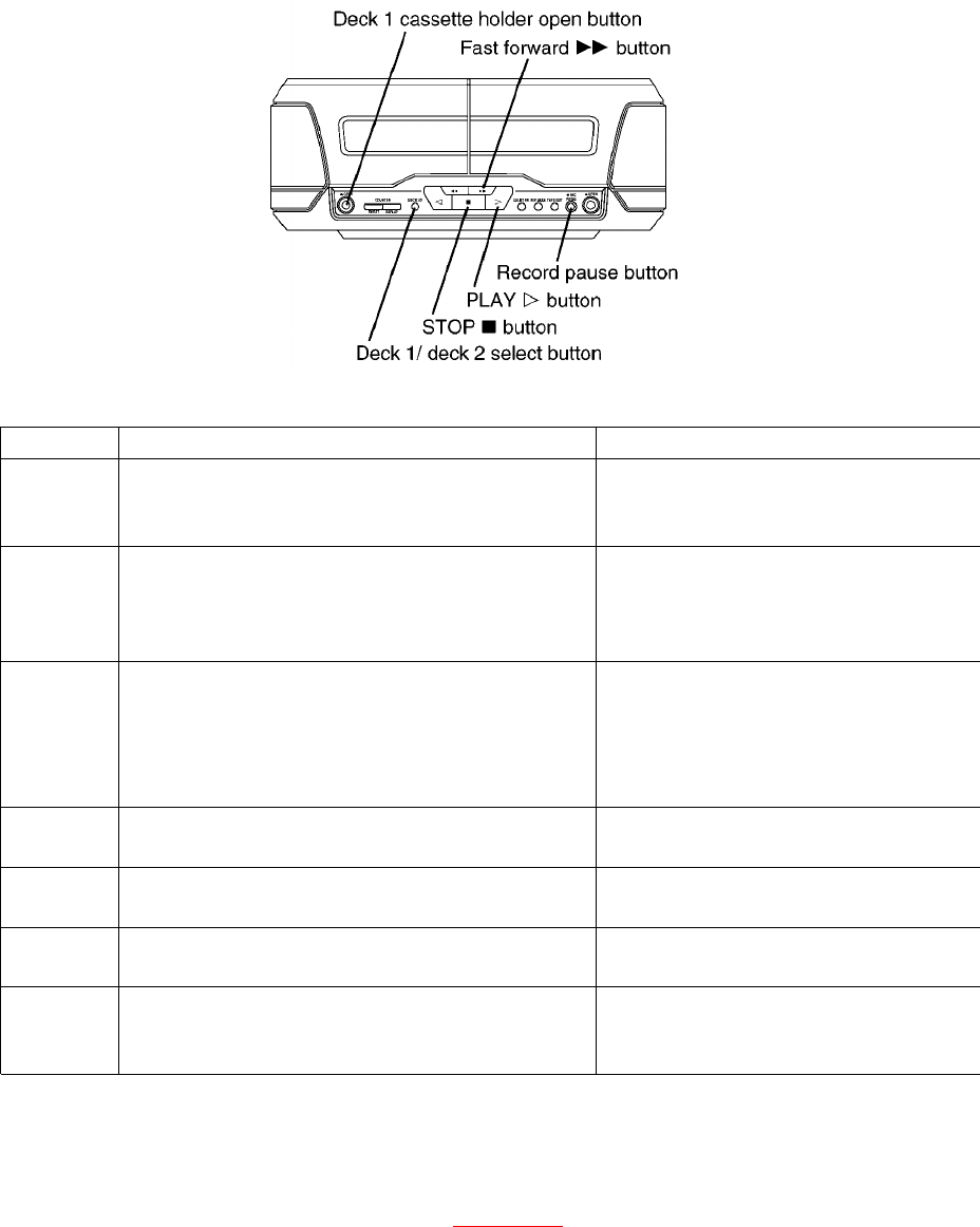
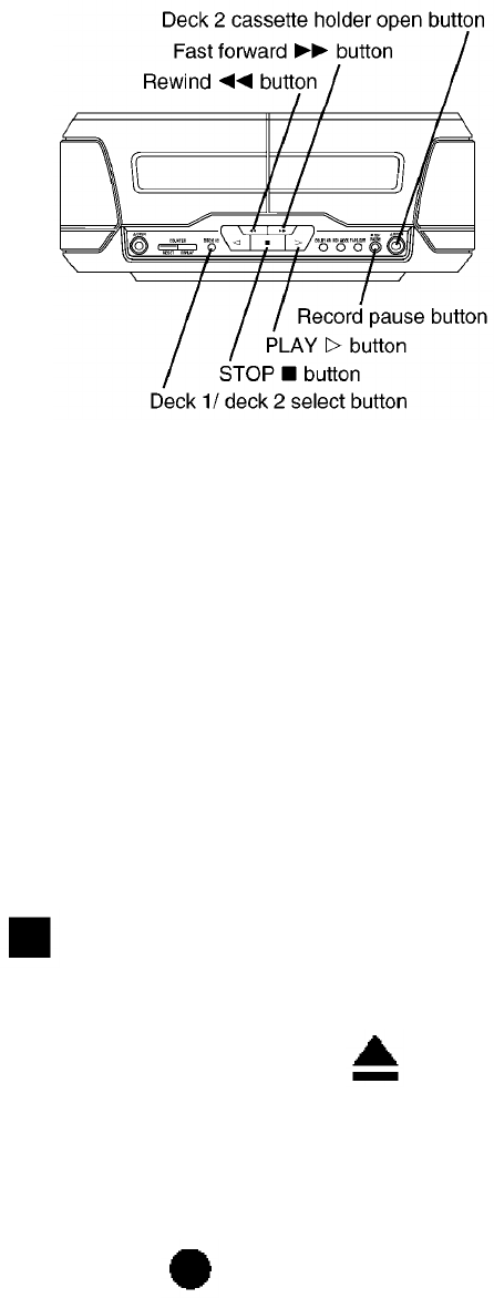
2. Location of Controls
3. Operation Checks and Component Replacement /
Procedures
- This section describes procedures for checking the operation of
the major printed circuit boards and replacing the main
components.
- For reassembly after operation checks or replacement, reverse the
respective procedures. Special reassembly procedures are
described only when required.
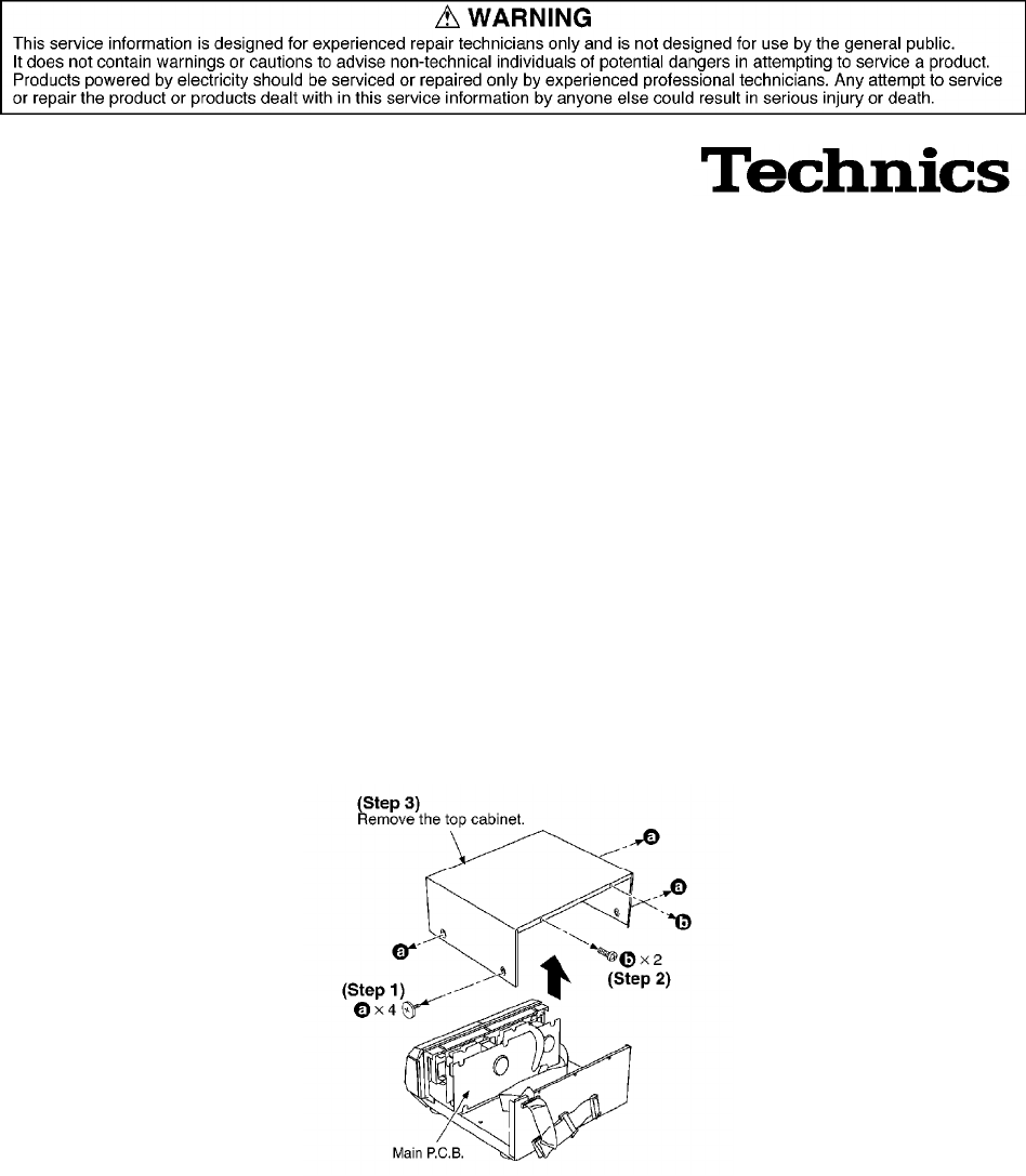
3.1. Checking for the main P.C.B.
- Check the main P.C.B. as shown above.
3.2. Checking for the operation P.C.B.
- Follow the (Step 1) - (Step 3) of item 3.1.
2

3

- Check the operation P.C.B. as shown below.
3.3. Replacement for the motor ass’y, capstan belt and winding belt
- Follow the (Step 1) - (Step 3) of item 3.1.
4

- Follow the (Step 1) - (Step 7) of item 3.2.
5

6
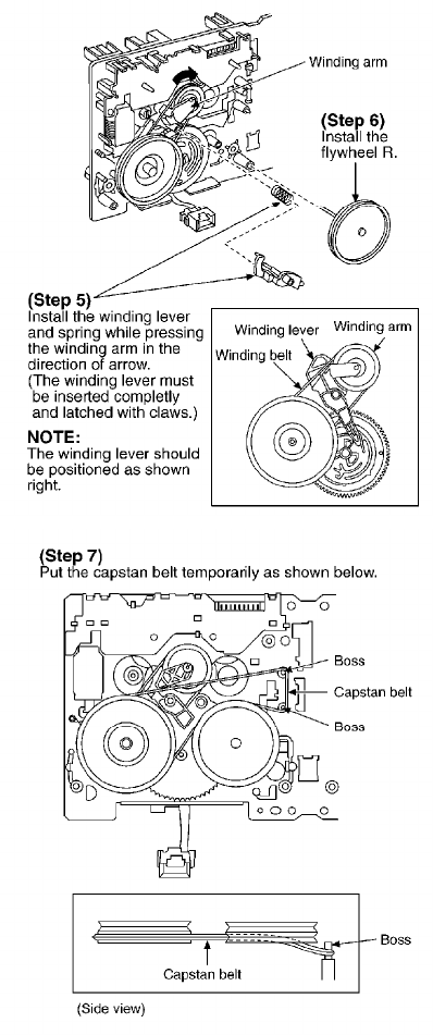
7

3.4. Replacement for the components parts on the mechanism P.C.B.
- Follow the (Step 1) - (Step 3) of item 3.1.
- Follow the (Step 1) - (Step 7) of item 3.2.
- Follow the (Step 1) - (Step 4) of item 3.3.
8
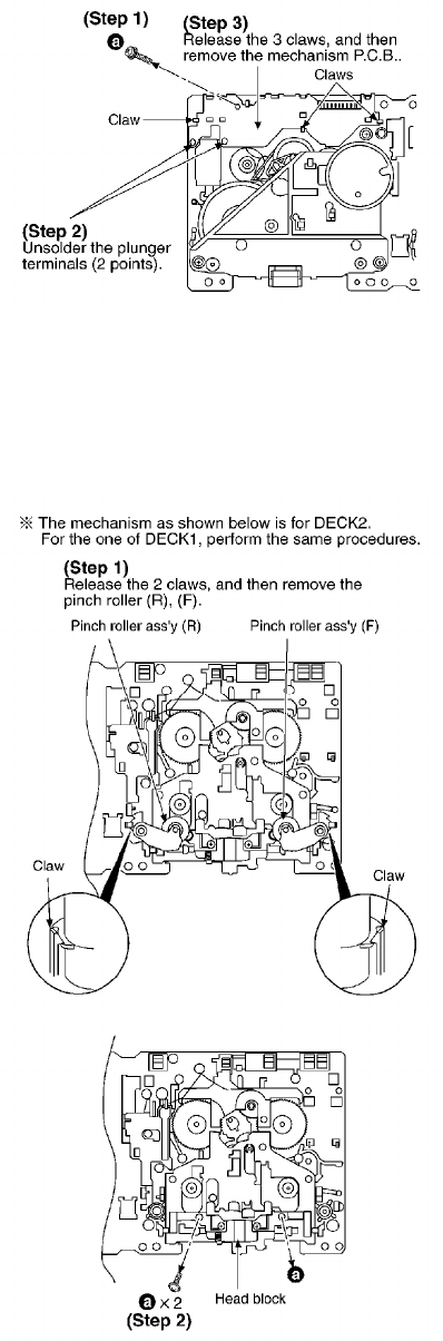
3.5. Replacement for the pinch roller ass’y and head block
- Follow the (Step 1) - (Step 3) of item 3.1.
- Follow the (Step 1) - (Step 7) of item 3.2.
- Follow the (Step 1) - (Step 5) of item 3.3.
3.6. Replacement for the cassette lid ass’y
- Follow the (Step 1) - (Step 3) of item 3.1.
9

3.7. Replacement for the cassette holder
- Follow the (Step 1) - (Step 3) of item 3.1.
- Follow the (Step 1) - (Step 11) of item 3.2.
10

4. To Supply Power Source
This unit is designed to operate on power supplied from system connected. / When a component
requires service, use the system connections to supply power source. / For system connections,
refer to Fig.4-1.
Fig. 4-1.
5. Service Mode Function of Cassette Mechanism
This unit is equipped with a service mode function of cassette mechanism, so that if the unit
operates incorrectly, the fault displayed using an error code on the FL display of the Tuner/
Amplifier (SA-EH590). The system control IC and FLdisplay are part of the Tuner/Amplifier so
make sure the system has been connected properly before using this function. Use this function
during maintenance to check faults of items below.
5.1. Cassette tape to be prepared
Metal tape:
Recorded music tape with only one erasure prevention tab intact. /
(use middle portion of tape)
Normal tape: / CrO2 tape:
Recorded music tape with both erasure prevention tabs intact. /
(use middle portion of tape)
11

5.2. Selecting service mode
1. Turn on the power to the unit.
2. Make sure that no tape is inserted in the cassette deck. (Service
mode cannot be selected with a tape inserted in the cassette deck.)
3. Press the DOLBY NR button for about 2 seconds, and keep
pressing it, also press the STOP button for about 2 seconds. Refer
to Fig. 5-1.
Fig. 5-1.
5.3. Deck 1 mechanism check
1. Press the Deck 1/deck 2 select button to change the flashing Deck
2 indicator to Deck 1. Refer to Fig. 5-2. / (No change required if
Deck 1 indicator already flashing.)
2. Press the Deck 1 cassette holder open button to open the Deck 1
cassette holder. Refer to Fig. 5-2.
3. Insert a CrO2 tape into the Deck 1 and close the cassette holder.
4. Press the Fast forward button. Refer to Fig. 5-2. / (Tape fast
forwards for about 2 seconds then stops.)
5. Press the PLAY button. Refer to Fig. 5-2. / (After TPS operation
and check, the tape stops.)
6. Open the Deck 1 cassette holder and replace the tape with a
normal tape.
7. Close the Deck 1 cassette holder.
8. Press the Record pause button. Refer to Fig. 5-2. / (No record
operation.)
9. Press the STOP button. Refer to Fig. 5-2. A mechanism error code
is displayed. Refer to Table 5-1. Each time the STOP button is
12
pressed, the fault items are displayed in sequence.
Fig. 5-2.
Table 5-1.
FL display Symptom Cause
H01 Cassette deck does not operate correctly. Faulty cassette deck mechanism
mode
switch (Deck 1: S951, Deck 2: S971),
plunger
and capstan motor. / (Check and
replace)
H02 Unit does not record or the unit goes into
recording mode even when the erasure
prevention tabs have been removed from the
cassette.
Faulty erasure prevention tabs detect
switch
(S974, S975) or short-circuit. (Check
and
replace)
H03 Tape does not play even when the tape deck
play button is pressed.
The motor operates when the tape deck play
button is pressed even if cassette is loaded in
the deck.
Faulty tape detect switch (Deck 1:
S952
S972) or short-circuit. (Check and
replace)
H06 Cassette deck does not detect CrO2 tape. Faulty CrO2 tape detect switch (Deck
1
Deck 2: S973). / (Check and replace)
H07 Cassette deck does not detect Metal tape. Faulty Metal tape detect switch (
S976).
and replace)
F01 When the tape play button is pressed, tape
advances only slightly and then stops.
Reel pulse error (Faulty Hall IC). (
Check
replace)
F02 TPS (tape program search) does not work. Faulty TPS signal detection or faulty
plunger
control. / (Check and replace
mechanism
control IC)
5.4. Deck 2 mechanism check
1. Press the Deck 1/deck 2 select button to change the flashing Deck
1 indicator to Deck 2. Refer to Fig. 5-3.
2. Press the Deck 2 cassette holder open button to open the Deck 2
13

cassette holder. Refer to Fig. 5-3.
3. Insert a metal tape into the Deck 2 with an intact erasure
prevention tab on the right side.
4. Close the Deck 2 cassette holder.
5. Press the Fast forward button. Refer to Fig. 5-3. / (Tape fast
forwards for about 2 seconds then stops.)
6. Open the Deck 2 cassette holder and turn over the metal tape.
(intact erasure prevention tab on the left side.)
7. Close the Deck 2 cassette holder.
8. Press the Rewind button. Refer to Fig. 5-3. / (Tape rewinds for
about 2 seconds then stops.)
9. Open the Deck 2 cassette holder and replace the metal tape with a
CrO2 tape.
10. Close the Deck 2 cassette holder.
11. Press the PLAY button. Refer to Fig. 5-3. / (After TPS operation
and check, the tape stops.)
12. Open the Deck 2 cassette holder and replace the CrO2 tape with a
normal tape.
13. Close the Deck 2 cassette holder.
14. Press the Record pause button. Refer to Fig. 5-3. / (No record
operation.)
15. Press the STOP button. Refer to Fig. 5-3. A mechanism error
code is displayed. Refer to Table 5-1. Each time the STOP button is
pressed, the fault items are displayed in sequence.
Fig. 5-3.
14
5.5. Exiting service mode
1. Press the STOP button for more than 5 seconds. (Diagnostic
contents stored in memory for both Deck 1 and 2 are erased.)
2. Remove the cassette tape from the cassette holder.
3. Turn off the unit.
6. Schematic Diagram Notes
- This schematic diagram may be modified at any time with the
development of new technology.
Notes:
S900:
Stop switch ( )
S901:
Deck 2 cassette holder open switch ( OPEN)
S903:
Tape edit switch (TAPE EDIT)
S904:
Record pause switch / ( REC PAUSE)
S905:
Dolby noise reduction switch / (DOLBY NR)
S906:
15

Fast forward, TPS switch ( )
S907:
Forward side playback switch ( )
S909:
Reverse side playback switch ( )
S910:
Rewind, TPS switch ( )
S911:
Reverse mode switch / (REV MODE)
S912:
Deck 1/deck 2 select switch / (DECK 1/2)
S913:
Counter display switch / (COUNTER DISPLAY)
S914:
Counter reset switch / (COUNTER RESET)
S915:
Deck 1 cassette holder open switch ( OPEN)
S951:
Deck 1 mode detect switch
S952:
Deck 1 half detect switch
S953:
Deck 1 CrO2 tape detect switch
S971:
Deck 2 mode detect switch
S972:
Deck 2 half detect switch
S973:
Deck 2 CrO2 tape detect switch
16

S974:
Deck 2 reverse side record prevention tab detect switch
S975:
Deck 2 forward side record prevention tab detect switch
S976:
Deck 2 METAL tape detect switch
VR101:
Deck 1 playback gain adjustment VR / (R ch)
VR102:
Deck 2 playback gain adjustment VR / (L ch)
VR103:
Deck 2 playback gain adjustment VR / (R ch)
VR104:
Deck 1 playback gain adjustment VR / (L ch)
VR801:
Deck 1 tape speed adjustment VR (normal)
VR803:
Deck 2 tape speed adjustment VR (normal)
- Indicated voltage values are the standard values for the unit
measured by the DC electronic circuit tester (high-impedance) with
the chassis taken as standard. Therefore, there may exist some
errors in the voltage values, depending on theinternal impedance
of the DC circuit tester.
No mark
: Playback
( )
: Recording
- Important safety notice:
Components identified by mark have special characteristics
important for safety.
Furthermore, special parts which have purposes of fire-retardant
(resistors), high-quality sound (capacitors), low-noise (resistors),
etc. are used.
17
When replacing any of components, be sure to use only
manufacturer’s specified parts shown in the parts list.
- The supply part number is described alone in the replacement parts
list.
- Caution!
IC and LSI are sensitive to static electricity.
Secondary trouble can be prevented by taking care during repair.
Cover the parts boxes made of plastics with aluminum foil.
Ground the soldering iron.
Put a conductive mat on the work table.
Do not touch the legs of IC or LSI with the fingers directly.
- Voltage and signal line
: Positive voltage line
: Playback signal line
: Recording signal line
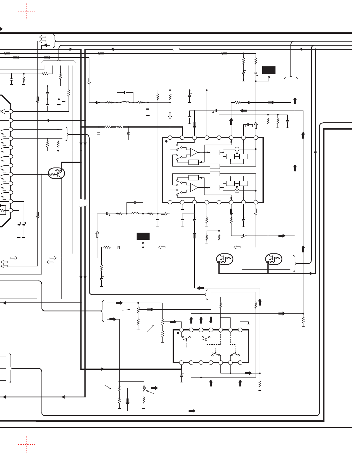
7. Schematic Diagram
8. Printed Circuit Board Diagram
9. Type Illustration of ICs, Transistors and Diodes
10. Wiring Connection Diagram
11. Block Diagram
12. Terminal Function of ICs
12.1. IC701 (M38503M2406F): / System Control
18

Pin
No.
Terminal
Name
I/O Function
1VCC IPower supply terminal
2VREF I Reference voltage input
3AVSS -GND terminal
4LMT O Muting control signal output
5PL1 O Deck 1 solenoid control signal
output
6M1 O Deck 1 motor drive control
signal output
7HALT I Power failure detect signal input
8REQ I Serial communication request
signal input
9CS I Serial communication complete
signal input
10 CLK O Serial communication clock
signal output
11 DATA
OUT
OSerial communication data
signal output
12 DATA IN I Serial communication data
signal input
13 METAL 2 I Deck 2 tape detect switch signal
(METAL) input
14 CRO2 2 IDeck 2 tape detect switch signal
(CrO2) input
15 VSS -GND terminal
16 FWD LED O LED drive control signal (FWD)
output
17 REV LED O LED drive control signal (REV)
output
18 RESET I Reset signal input
19 XIN I Oscillator connected terminal (F
=8 MHz)
20 XOUT O
21 VSS -GND terminal
22 CRO2 1 IDeck 1 tape detect switch signal
(CrO2) input
23 MODE I Deck 1 mechanism switch
signal (MODE) input
24 HALF1 I Deck 1 mechanism switch
signal (Half) input
25 TPS I TPS signal input
26 A DATA O Serial data signal output for IC
101
27 A CLK O Serial clock signal output for IC
101
28 A LATCH OSerial latch signal output for IC
101
19

101
Pin
No.
Terminal
Name
I/O Function
29 PL2 O Deck 2 solenoid control signal
output
30 M2 O Deck 2 motor drive control
signal output
31 ENC/DEC O Dolby NR record/playback mode
select signal output
32 DOLBY
ON/OFF
ODolby NR ON/OFF control signal
output
33 E CS - EEPROM chip select signal
output
(Not used, open)
34
|
36
NC
-
Not used, open
37 LED CNT O LED color control signal output
38 PHOTO2T IDeck 2 reel pulse detect signal
input
39 AD SW I Deck 2 mechanism switch
signal input
(Half, Mode, F REC INH., R REC
INH.)
40 PHOTO1T IDeck 1 reel pulse detect signal
input
41 KEY2 I Operation key signal input
42 KEY1 I Operation key signal input
13. Measurements and Adjustments
Note:
This unit RS-DV290 is designed to operate on power supplied from
system connected.
13.1. Measurement condition
- Dolby NR switch is OFF
- Make sure heads are clean
- Make sure capstan and pressure roller are clean
- Temperature is 20 ± 5 °C
13.2. Measurement instrument and special tool
- Electronic Voltmeter
- Frequency Counter
20
- AF Oscillator
- Test tape
- Head azimuth adjustment (8 kHz, -20 dB): QZZCFM
- Tape speed adjustment (3 kHz, -10 dB): QZZCWAT
- Playback gain adjustment (315 Hz, 0 dB): QZZCFM
- Recording/playback frequency response check:
QZZCFM / (315 Hz, -20 dB, 12.5 kHz~63 Hz, -20 dB)
QZZCRA4 (Normal blank tape)
QZZCRX2 (CrO2 blank tape)
QZZCRZ6 (Metal blank tape)
13.3. Head azimuth adjustment (Deck 1/2)
1. Connect the measuring instrument as shown in Fig. 13-1.
2. Replace azimuth screws for both forward and reverse directions
after removing the screw-locking bond left on the head base.
(Supply part No. of azimuth screw: RHD17015 )
3. Playback the azimuth adjustment portion (8 kHz, -20 dB) of test
tape (QZZCFM). Adjust the azimuth screw until the outputs of the L/
R ch are maximized. Refer to Fig. 13-2. Make sure that
thedifference in the peak level between the left and right channels
does not exceed 0.5 dB.
4. Perform the same adjustment in reverse playback mode.
Check of the level difference forward and reverse directions.
5. Playback the playback gain adjustment portion (315 Hz, 0 dB) of
test tape (QZZCFM). Check if level difference between forward and
reverse direction is within 1.5 dB.
6. After the adjustment, apply screw lock to the azimuth screw.
Fig. 13-1.
Fig. 13-2.
21

13.4. Tape speed adjustment / (Deck 1/2)
Note:
When connecting the unit to other system components for test,
short the section between the test point TP604 and TP609 and turn
on the entire system. (The unit is set to the TEST mode, and either
Deck 1 or Deck 2 indicatorwill blink.)
Normal speed (Standard value: 3000 ± 45 Hz)
1. Connect the measuring instrument as shown in Fig. 13-3.
2. Playback the middle portion of test tape. (QZZCWAT)
3. Adjust VR801 (Deck 1) and VR803 (Deck 2) for output value shown
below. (For adjustment point, refer to Fig. 13-11. )
Adjustment target: 3000 ± 15 Hz (Normal speed)
Standard value: 3000 ± 45 Hz (Normal speed)
Fig. 13-3.
Note:
When the unit is finished for adjusting, disconnect the short section
between TP604 and TP609 .
13.5. Playback gain adjustment (Deck 1/2)
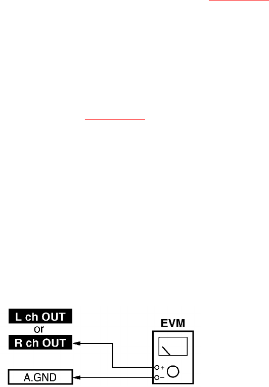
1. Connect the measuring instrument as shown in Fig. 13-4.
2. Find the start of the 315 Hz, 0 dB section of test tape (QZZCFM),
insert the tape into Deck 1 and 2, and play it back (FWD).
3. Adjust Deck 2: VR102 (L ch) [VR103 (R ch)] and Deck 1: VR104 (L
ch) [VR101 (R ch)] so that the output is within the standard value
shown below. (For adjustment point, refer to Fig. 13-11. )
22

[Standard value:265 mV ~ 300 mV]
Fig. 13-4.
13.6. Erase current confirmation (Deck 2)
1. Connect the measuring instrument as shown in Fig. 13-5.
2. Insert the blank tape into Deck 2, and press the Record pause
button.
3. Check if the output at this time between the erase current
confirmation point TP301 and TP302 (the output on both edged of
R313) is within the standard value shown below. (For the erase
current confirmation point, referto Fig. 13-11. )
Standard Value EVM reading
Normal tape
:
85 ± 25 mA (85 ± 25 mV)
CrO2 tape: 150 ± 25 mA (150 ± 25
mV)
Metal tape: 185 ± 25 mA (185 ± 25
mV)
Fig. 13-5.
Note:
The test tape is not required when confirming the erase current.
13.7. Playback frequency response check (Deck 1/2)
1. Connect the measuring instrument as shown in Fig. 13-6.
2. Playback the 315 Hz, -20 dB and 12.5 kHz to 63 Hz, -20 dB sections
of test tape (QZZCFM) and then, using the 315 Hz, -20 dB playback
23

output as a reference (0 dB).
3. Confirm the playback frequency response is within the range
shown in Fig. 13-7.
Fig. 13-6.
Fig. 13-7.
13.8. Recording/playback / frequency response and gain check
(Deck 2)
13.8.1. Normal tape check
1. Connect the measuring instrument as shown in Fig. 13-8.
2. Insert a Normal type blank tape (QZZCRA4) into Deck 2.
3. Record signals at 50 Hz, 100 Hz, 200 Hz, 500 Hz, 1 kHz, 2 kHz, 10
kHz and 12.5 kHz (28 mV).
4. Set the playback frequency of recorded signals at 1 kHz as a
reference response (0 dB).
5. Playback the recorded signal to confirm that the output is within
the range of the overall frequency response shown in Fig. 13-9.
Fig. 13-8.
Fig. 13-9.
24
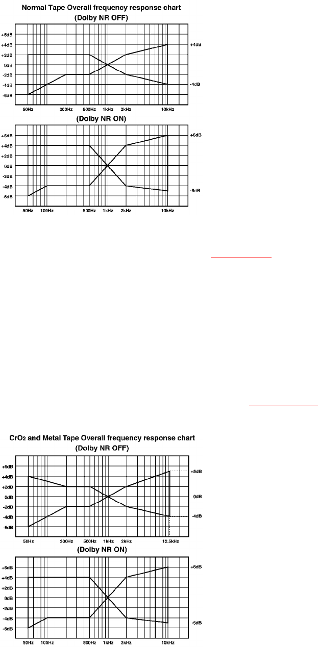
13.8.2. CrO2/Metal tape check
1. Connect the measuring instrument as shown in Fig. 13-8.
2. Insert a CrO2/Metal tape into Deck 2.
3. Record signals at 50 Hz, 100 Hz, 200 Hz, 500 Hz, 1 kHz, 2 kHz, 10
kHz and 12.5 kHz (28 mV).
4. Set the playback frequency of recorded signals at 1 kHz as a
reference response (0 dB).
5. Playback the recorded signal to confirm that the output is within
the range of the overall frequency response shown in Fig. 13-10.
Fig. 13-10.
13.9. Adjustment point and test point
25

Fig. 13-11.
14. Checking Procedure for Self-operation of
Cassette Mechanism Ass’y
- This procedure describes simple methods independent of
mechanism controller or governor circuit.
14.1. Operation Check Providing with Cassette Tape
1. Push up the EJECT lever with rubber band. (Refer to Fig. 14-2. )
2. Apply DC 5V to the MOTOR. (MOTOR will be rotated) (Refer to Fig.
14-1. )
3. Provide the cassette tape with mechanism ass’y.
4. Apply DC 9V to the plunger, and then operate it by switching
power ON/OFF. (Power: +PL, -PL) (Refer to Fig. 14-1. )
A. FWD PLAY: Supply power to the plunger momentary. (Duration:
approx. 50msec.)
B. FWD FF: At FWD PLAY mode, supply power to the plunger
momentary. (Duration: approx. 50msec.)
C. STOP: At FWD FF mode, supply power to the plunger
momentary. (Duration: approx. 50msec.)
D. REV PLAY: At STOP mode, supply power to the plunger for
ordinary duration. (Duration: approx. 200msec.)
E. REV REW: At REV PLAY mode, supply power to the plunger
momentary. (Duration: approx. 50msec.)
F. STOP: At REV REW mode, supply power to the plunger
momentary. (Duration: approx. 50msec.)
26

Repeat the above operation to FWD PLAY mode.
Note: Incorrect duration for power supply may be operated to other mode.
14.1.1. Connection Diagram Between the Mechanism Ass’y and Power Supply /
(MOTOR and Plunger)
Fig. 14-1.
14.1.2. Detail View of EJECT Lever / (EJECT lever fixed by rubber band, Plunger
rib operation)
Fig. 14-2.
14.2. Operation Check Not Provided with Cassette Tape
1. Push up the EJECT lever with rubber band. (Refer to Fig. 14-2. )
2. Apply DC 5V to the MOTOR. (MOTOR will be rotated)
3. Lift up the plunger rib of mechanism ass’y with the tip of minus
screwdriver, and then operate it same as power supply duration.
(Refer toFig. 14-3. )
Note: Operation order is same as the “Operation Check Providing with
Cassette Tape” item 4. above.
Fig. 14-3.
27

15. Replacement Parts List
Notes:
- Important safety notice:
Components identified by mark have special characteristics
important for safety.
Furthermore, special parts which have purposes of fire-retardant
(resistors), high-quality sound (capacitors), low-noise (resistors),
etc. are used.
When replacing any of components, be sure to use only
manufacture’s specified parts shown in the parts list.
- The marking [RTL] indicates the retention time is limited for this
Item. After the discontinuation of this assembly in production, it
will no longer available.
- All parts are supplied by SPC.
28

Ref. No. Part No. Part Name & Description Pcs Remarks
1RKM0392-S1 CABINET 1
2RHD30007-1S SCREW 4
3 XTBS3+10JFZ1 SCREW 2
4RGR0287A-P REAR PANEL 1
5RKA0105-K RUBBER 4
6RKA0106-N FOOT RING 4
7RMN0539 CABLE HOLDER 1
8RDG0129-1 DAMPER GEAR 2
9REX0966-1 WIRE ASS'Y 1
10 RGB0025-A TECHNICS BADGE 1
11 RGK1131-2S ORNAMENT(L) 1
12 RGK1132-2S ORNAMENT(R) 1
13 RGL0441-Q PANEL LIGHT 1
14 REZ1194 WIRE ASS'Y 1
15 RKF0462-K2 CASSETTE HOLDER(L) 1
16 RKF0463-K2 CASSETTE HOLDER(R) 1
17 RKF0587G-2S CASSETTE LID(L) 1
18 RKF0588-2S CASSETTE LID(R) 1
19 RKW0577-Q CASSETTE WINDOW(L) 1
20 RKW0578-Q CASSETTE WINDOW(R) 1
21 RMB0474 SPRING 2
22 RMQ0577A-3 FRAME 1
23 RUS757ZA SPRING 4
24 RYP1179-S FRONT PANEL 1
25 XTBS26+10J SCREW 7
26 XTB3+10JFZ SCREW 5
27 XTBS3+8JFZ1 SCREW 3
28 RMG0161 RUBBER 1
29

Ref. No. Part No. Part Name & Description Pcs Remarks
29 RMR0909-X PCB HOLDER 1
101 RED0037 HEAD BLOCK ASS'Y / (R/P) 1 L1AA00000008
101-1 RHD17015 SCREW 2
102 RED0038 HEAD BLOCK ASS'Y / (P.B) 1
102-1 RHD17015 SCREW 2
103 RDG0300 REEL TABLE BASE 4
104 RDG0301 GEAR 2
105 RDK0026 GEAR 2
107 RDV0033-4 BELT1 2
108 RDV0034-1 BELT2 2
110 RUW147ZA SPRING 2
111 RMB0400 SPRING 4
112 RMB0403 SPRING 2
113 RMB0404 SPRING 2
114 RMB0406 SPRING 2
115 RMB0408 SPRING 2
116 RML0370-J LEVER 2
117 RML0371 LEVER 2
118 RML0372 LEVER 2
119 RML0374 LEVER 2
120 RMM0131 ROD 2
121 RMM0133-1 ROD 2
122 RMQ0519 REEL CAP 4
123 RMS0398-1 SHAFT 2
124 RSJ0003 PLUNGER ASS'Y 2
125 RUS609ZC SPRING 2
126 RXF0049 FLY WHEEL ASS'Y 2
127 RXF0050 FLY WHEEL ASS'Y 2
128 RXG0040 GEAR 4
129 RMK0283A-J SUB CHASSIS 2
130 RXL0124 PINCH ROLLER ASS'Y 2
130-1 RMB0401 SPRING 2
131 RXL0125 PINCH ROLLER ASS'Y 2
131-1 RMB0402 SPRING 2
132 RXL0126 ARM GEAR 2
133 RXQ0412 CHASSIS ASS'Y 2
133-1 RMB0405 SPRING 2
133-2 RMM0132-J FR ROD 2
134 REM0055-1 MOTOR ASS'Y 2
135 RHD26022 SCREW 4
136 XTW2+5L SCREW 4
137 XTW26+10S SCREW 6
138 XYC2+JF17 SCREW 2
140 RFKJSCH770EK MAIN CHASSIS ASS'Y 1
C101-04 ECUV1H681KBN 50V 680P 4 F1J1H681A021
C109,10 ECQB1H183JF3 50V 0.018U 2
C111,12 ECEA0JKS470 6.3V 47U 2
C113,14 ECEA1HKS2R2 50V 2.2U 2
C115,16 ECJ2VB1H471K 50V 470P 2
C117,18 ECUX1H331KBX 50V 330P 2
C119,20 ECA1HAK010XI 50V 1U 2
C123,24 ECEA1EKS4R7 25V 4.7U 2
C125,26 ECJ2VB1H332K 50V 3300P 2
30

Ref. No. Part No. Part Name & Description Pcs Remarks
C129 ECEA1AKS220 10V 22U 1
C130 F2A1C101A133 16V 100U 1
C131-34 ECJ2VB1H471K 50V 470P 4
C135,36 ECA1HAK010XI 50V 1U 2
C137 ECEA1HKS0R1 50V 0.1U 1
C138 F1J1E4730004 25V 0.047U 1
C139 ECEA0JKS470 6.3V 47U 1
C140 ECEA1CKS100 16V 10U 1
C141 ECA1HAK010XI 50V 1U 1
C142 ECUVNE104ZFN 25V 0.1U 1 F1J1E1040017
C143,44 ECJ2VB1H471K 50V 470P 2
C150 RCE1AKA101BG 10V 100U 1 F2A1A1010020
C203,04 ECEA1EKS4R7 25V 4.7U 2
C205,06 ECA1HAK010XI 50V 1U 2
C207,08 ECUV1H271KBN 50V 270P 2
C211,12 ECUV1H152KBN 50V 1500P 2 ECJ2VB1H152K
C213,14 ECEA1EKS4R7 25V 4.7U 2
C215,16 ECEA1CKS100 16V 10U 2
C217,18 ECEA1HKS0R1 50V 0.1U 2
C219 F2A1C101A133 16V 100U 1
C220 RCE1ARS471BJ 10V 470U 1 F2A1A471A111
C221,22 ECEA1HKAR68B 50V 0.68U 2
C223 ECEA1EKS4R7 25V 4.7U 1
C225,26 ECEA1EKS4R7 25V 4.7U 2
C239,40 ECUV1H681KBN 50V 680P 2 F1J1H681A021
C241 ECJ2VB1H103K 50V 0.01U 1
C301 ECA1CAM471XB 16V 470U 1
C302 ECEA2AN2R2S 100V 2.2U 1
C303 ECQP2E682JZT 250V 6800P 1 F0A2E682A002
C304 F2A1C101A133 16V 100U 1
C305 ECEA1HKS0R1 50V 0.1U 1
C306 ECQB1H393JF3 50V 0.039U 1
C307 ECUV1H102KBN 50V 1000P 1 ECJ2VB1H102K
C308 ECJ2VB1H332K 50V 3300P 1
C309 ECEA0JKS470 6.3V 47U 1
C310,11 ECJ2VB1H103K 50V 0.01U 2
C323 ECUV1H102KBN 50V 1000P 1 ECJ2VB1H102K
C602 ECA1CAM221XB 16V 220U 1
C603 RCE1CKA470BG 16V 47U 1 F2A1C470A017
C604 ECUV1E103ZFN 25V 0.01U 1 F1J1E103A007
C605 ECA1CAM221XB 16V 220U 1
C701 ECJ2VB1H103K 50V 0.01U 1
C702 ECEA0JKS101 6.3V 100U 1
C705 ECUV1E103ZFN 25V 0.01U 1 F1J1E103A007
C706 RCE1HKA3R3BG 50V 3.3U 1 F2A1H3R3A015
C707 ECUV1E103ZFN 25V 0.01U 1 F1J1E103A007
CN601 RJS2A5520-1 CONNECTOR(20P) 1 K1MP20A00005
CN901 RJS8T6ZA CONNECTOR(8P) 1 K1MP08B00006
CP101,02 RJS1A6805 CONNECTOR(5P) 2
CP901,02 RJT071K09A CONNECTOR(9P) 2 K1KA09B00058
CS951 RJU071H09M CONNECTOR(9P) 1 K1KB09C00001
31

Ref. No. Part No. Part Name & Description Pcs Remarks
CS971 RJU071H09M CONNECTOR(9P) 1 K1KB09C00001
D101,02 MA2J11100L DIODE 2
D301 MA2J11100L DIODE 1
D606 MAZ40560MF DIODE 1
D651,52 MA165TA5 DIODE 2 MA2C16500E
D701 MA2J11100L DIODE 1
D705,06 MA2J11100L DIODE 2
D707 MA4051M DIODE 1 MAZ40510M
D708-10 MA2J11100L DIODE 3
D904 MA2J11100L DIODE 1
D905 B3AHA0000012 LED 1
D907 B3AHA0000012 LED 1
D951 MA165TA5 DIODE 1 MA2C165
D971 MA165TA5 DIODE 1 MA2C165
IC101 CXA1998BQT6 IC 1 C1BB00000319
IC102 MC14066BFEL IC 1 C0JBAR000248
IC103 BA7755AF IC 1 C1AB00001381
IC201 CXA1552M-T4 IC 1 C1BB00000311
IC202 MC14066BFEL IC 1 C0JBAR000248
IC701 M38503M2406F IC 1 C2BBDD000003
IC951 0N2180RLC1 IC 1
IC971 0N2180RLC1 IC 1
L201,02 ELELN103KA COIL 2
L301 RL08B006-K COIL 1 G2A142C00002
L302 RLQZB101KT-D COIL 1 G0C101K00017
L701 G0C100JA0019 COIL 1
L702 J0JBC0000041 COIL 1
PCB1 REP2827E-M MAIN P.C.B. 1 [RTL]
PCB2 REPX0108A MECHA.SW.P.C.B. / (P.B.) 1 [RTL]
PCB3 REPX0108B MECHA.SW.P.C.B. / (R/P) 1 [RTL]
Q101,02 2SJ164RTA TRANSISTOR 2 2SJ01640RA
Q103,04 2SJ164QTA TRANSISTOR 2 2SJ01640QA
Q105,06 2SD1819ARTX TRANSISTOR 2 2SD1819ARL
Q107 DTA143EUT106 TRANSISTOR 1 B1GDCFGG0008
Q108 DTC143EUT106 TRANSISTOR 1 B1GBCFGG0006
Q201,02 DTA143EUT106 TRANSISTOR 2 B1GDCFGG0008
Q301 2SD1819ARTX TRANSISTOR 1 2SD1819ARL
Q302 2SD1328STW TRANSISTOR 1 2SD13280S2RA
Q303,04 2SD14500HA TRANSISTOR 2
Q305,06 DTC144EUT106 TRANSISTOR 2 B1GBCFNN0013
Q602 2SD2144S TRANSISTOR 1 B1AAGC000006
Q604 2SC3940AQSTA TRANSISTOR 1 2SC3940ARA
Q701-03 2SD1819ARTX TRANSISTOR 3 2SD1819ARL
Q706 DTC114EUT106 TRANSISTOR 1 B1GBCFJJ0009
Q803,04 2SD592AR TRANSISTOR 2 2SD0592AR
Q805,06 DTA143EUT106 TRANSISTOR 2 B1GDCFGG0008
Q807,08 2SB0621AHA TRANSISTOR 2
Q809,10 DTC143EUT106 TRANSISTOR 2 B1GBCFGG0006
Q901 DTA143EUT106 TRANSISTOR 1 B1GDCFGG0008
32

Ref. No. Part No. Part Name & Description Pcs Remarks
Q902-04 DTC143EUT106 TRANSISTOR 3 B1GBCFGG0006
R101,02 ERJ6GEYJ562V 1/10W 5.6K 2
R103,04 ERJ6GEYJ104V 1/10W 100K 2
R105,06 ERJ6GEYJ334V 1/10W 330K 2
R107,08 ERJ6GEYJ103V 1/10W 10K 2
R109,10 ERJ6GEYJ102V 1/10W 1K 2
R111 ERJ6GEYJ820V 1/10W 82 1 D0GD820JA012
R112 ERJ8GEYJ820V 1/8W 82 1
R113 ERJ6GEYJ123V 1/10W 12K 1
R114 ERJ6GEYJ273V 1/10W 27K 1
R117 ERJ6GEYJ102V 1/10W 1K 1
R118,19 ERDS2FJ220 1/4W 22 2
R120 ERJ6GEYJ104V 1/10W 100K 1
R121,22 ERJ6GEYJ103V 1/10W 10K 2
R125 ERJ6GEYJ104V 1/10W 100K 1
R126 ERJ6GEYJ223V 1/10W 22K 1
R127 ERJ6GEYJ472V 1/10W 4.7K 1
R130 ERJ6GEYJ475V 1/10W 4.7M 1
R131 ERJ6GEYJ334V 1/10W 330K 1
R132 ERJ6GEYJ273V 1/10W 27K 1
R133 ERJ6GEYJ333V 1/10W 33K 1
R134 ERJ6GEYJ392V 1/10W 3.9K 1
R135 ERJ6GEYJ682V 1/10W 6.8K 1
R136,37 ERJ6GEYJ222V 1/10W 2.2K 2
R138 ERJ6GEYJ472V 1/10W 4.7K 1
R139,40 ERJ6GEYF473 1/10W 47K 2
R141 ERJ8GEYJ101V 1/8W 100 1
R142 ERJ6GEYJ101V 1/10W 100 1
R143 ERDS2FJ101 1/4W 100 1
R144 ERJ6GEYJ101V 1/10W 100 1
R147-50 ERJ6GEYJ562V 1/10W 5.6K 4
R151,52 ERJ6GEYJ104V 1/10W 100K 2
R153,54 ERJ6GEYJ272V 1/10W 2.7K 2
R157,58 ERJ6GEYJ223V 1/10W 22K 2
R207,08 ERJ6GEYF473 1/10W 47K 2
R209,10 ERJ6GEYJ102V 1/10W 1K 2
R211,12 ERJ6GEYJ103V 1/10W 10K 2
R213,14 ERJ6GEYJ302V 1/10W 3K 2
R215,16 ERJ6GEYJ123V 1/10W 12K 2
R217,18 ERJ6GEYJ222V 1/10W 2.2K 2
R219 ERJ6GEYJ183V 1/10W 18K 1
R220 ERDS2FJ220 1/4W 22 1
R221,22 ERJ6GEYJ101V 1/10W 100 2
R223,24 ERJ6GEYJ103V 1/10W 10K 2
R225,26 ERJ6GEYF473 1/10W 47K 2
R230,31 ERJ6GEYJ102V 1/10W 1K 2
R232 ERJ6GEYJ103V 1/10W 10K 1
R233,34 ERJ6GEYJ101V 1/10W 100 2
R237 ERDS2FJ220 1/4W 22 1
R301 ERJ6GEYJ103V 1/10W 10K 1
R302 ERJ6GEYJ182V 1/10W 1.8K 1
R303 ERJ6GEYJ222V 1/10W 2.2K 1
R304 ERJ6GEYJ153V 1/10W 15K 1
33

Ref. No. Part No. Part Name & Description Pcs Remarks
R305 ERJ6GEYJ183V 1/10W 18K 1
R306 ERJ6GEYJ333V 1/10W 33K 1
R307 ERDS1FJ2R2 1/2W 2.2 1
R308 ERJ6GEYJ102V 1/10W 1K 1
R309-11 ERJ6GEYJ472V 1/10W 4.7K 3
R313 ERDS2TJ1R0 1/4W 1.0 1
R602 ERQ16NKWR33E 1/6W 0.33 1
R603 ERD2FCG100 1/4W 10 1
R604 ERJ6GEYJ331V 1/10W 330 1
R606 ERJ6GEYJ152V 1/10W 1.5K 1
R609 ERDS2FJ101 1/4W 100 1
R630 ERQ16NKWR33E 1/6W 0.33 1
R632 ERDS2FJ473 1/4W 47K 1
R701,02 ERJ6GEYJ103V 1/10W 10K 2
R703 ERJ6GEYJ562V 1/10W 5.6K 1
R704 ERJ6GEYJ472V 1/10W 4.7K 1
R705 ERJ6GEYF473 1/10W 47K 1
R708 ERJ6GEYJ472V 1/10W 4.7K 1
R710 ERJ6GEYJ102V 1/10W 1K 1
R711 ERJ6GEYJ104V 1/10W 100K 1
R712 ERJ8GEYJ683V 1/8W 68K 1
R718 ERJ8GEYJ683V 1/8W 68K 1
R721 ERJ6GEYJ472V 1/10W 4.7K 1
R722 ERJ6GEYJ101V 1/10W 100 1
R723,24 ERJ6GEYJ102V 1/10W 1K 2
R725,26 ERJ6GEYJ222V 1/10W 2.2K 2
R727 ERJ6GEYJ472V 1/10W 4.7K 1
R728 ERJ6GEYJ103V 1/10W 10K 1
R729 ERJ6GEYJ472V 1/10W 4.7K 1
R730 ERJ6GEYJ222V 1/10W 2.2K 1
R732 ERJ6GEYJ104V 1/10W 100K 1
R735 ERJ6GEYJ472V 1/10W 4.7K 1
R736 ERJ6GEYJ103V 1/10W 10K 1
R737 ERJ8GEYJ103V 1/8W 10K 1
R738 ERJ6GEYJ102V 1/10W 1K 1
R741 ERJ6GEYJ223V 1/10W 22K 1
R743 ERJ6GEYF473 1/10W 47K 1
R744 ERJ6GEYJ102V 1/10W 1K 1
R745 ERJ6GEYJ101V 1/10W 100 1
R747 ERJ8GEYJ102V 1/8W 1K 1
R802 ERJ6GEYJ561V 1/10W 560 1
R803 ERJ6GEYJ103V 1/10W 10K 1
R805 ERJ6GEYJ392V 1/10W 3.9K 1
R806 ERJ6GEYJ103V 1/10W 10K 1
R808 ERJ6GEYJ392V 1/10W 3.9K 1
R810,11 ERJ6GEYJ103V 1/10W 10K 2
R812 ERJ6GEYJ561V 1/10W 560 1
R813,14 ERJ6GEYJ471V 1/10W 470 2
R818 ERDS2FJ2R2 1/4W 2.2 1
R820 ERDS2FJ2R2 1/4W 2.2 1
R823,24 ERJ6GEYJ561V 1/10W 560 2
R900 ERJ6GEYJ821V 1/10W 820 1
R901 ERJ6GEYJ102V 1/10W 1K 1
R902 ERJ6GEYJ122V 1/10W 1.2K 1 D0GD122JA003
34

Ref. No. Part No. Part Name & Description Pcs Remarks
R903 ERJ6GEYJ152V 1/10W 1.5K 1
R904 ERJ6GEYJ182V 1/10W 1.8K 1
R905 ERJ6GEYJ222V 1/10W 2.2K 1
R906 ERJ6GEYJ332V 1/10W 3.3K 1 D0GD332JA003
R908 ERJ6GEYJ122V 1/10W 1.2K 1 D0GD122JA003
R909 ERJ6GEYJ152V 1/10W 1.5K 1
R910 ERJ6GEYJ182V 1/10W 1.8K 1
R911 ERJ6GEYJ222V 1/10W 2.2K 1
R914 ERJ6GEYJ331V 1/10W 330 1
R915 ERJ6GEYJ681V 1/10W 680 1
R916 ERJ6GEYJ331V 1/10W 330 1
R917 ERJ6GEYJ681V 1/10W 680 1
R924 ERJ6GEYJ821V 1/10W 820 1
R925 ERJ6GEYJ102V 1/10W 1K 1
R952 ERDS2FJ821 1/4W 820 1
R953 ERDS2FJ393 1/4W 39K 1
R972 ERDS2FJ821 1/4W 820 1
R973 ERDS2FJ393 1/4W 39K 1
RJ504 ERJ6GEY0R00V CHIP JUMPER 1
RJ507-09 ERJ8GEY0R00V CHIP JUMPER 3 D0YFR0000002
S900,01 EVQ11G05R SW,PUSH 2
S903-07 EVQ11G05R SW,PUSH 5
S909-15 EVQ11G05R SW,PUSH 7
S951 RSH1A018-3U SW,MECHA DET 1
S952,53 RSH1A019-2U SW,MECHA DET 2
S971 RSH1A018-3U SW,MECHA DET 1
S972-76 RSH1A019-2U SW,MECHA DET 5
VR101-04 EVNDCAA03B24 V.R.,PLAYBACK GAIN / ADJ. 4
VR801 EVNDCAA03B53 V.R.,TAPE SPEED / ADJ. 1
VR803 EVNDCAA03B53 V.R.,TAPE SPEED / ADJ. 1
X701 RSXY8M00D01T OSCILLATOR 1 H2B800400005
Z971 EXBF7L355SYV COMPONENT / COMBINATION 1
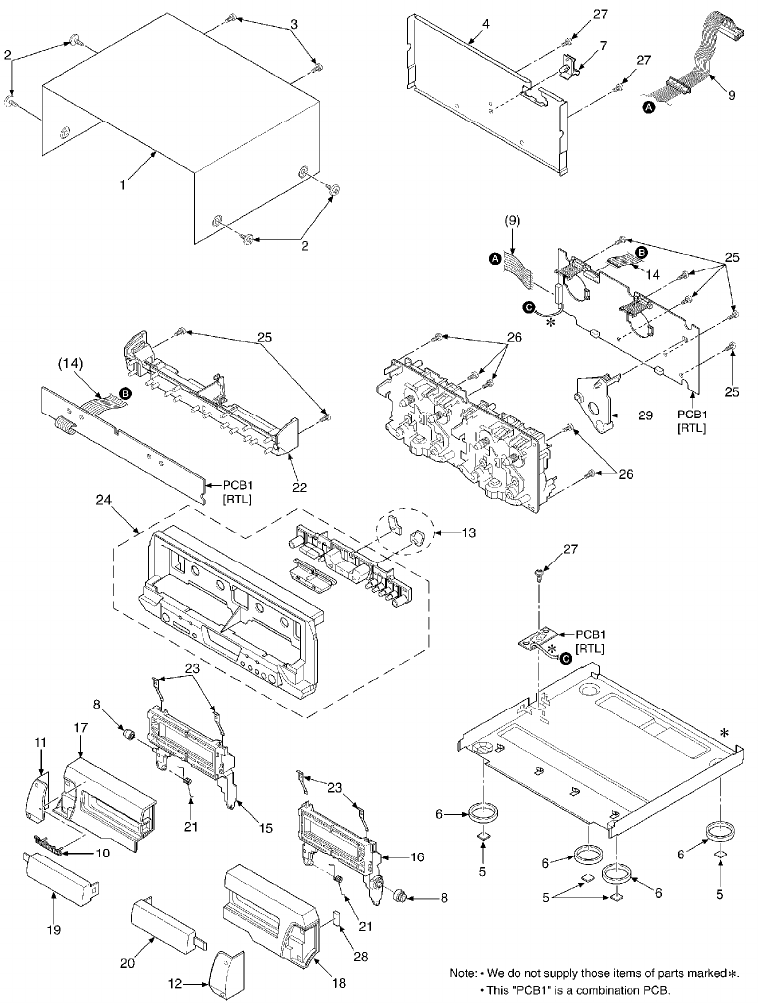
16. Cabinet Parts Location
35
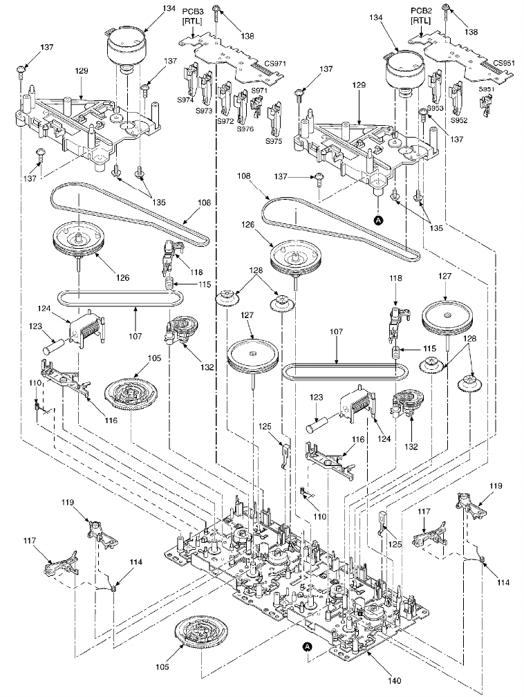
17. Mechanism Parts Location
36
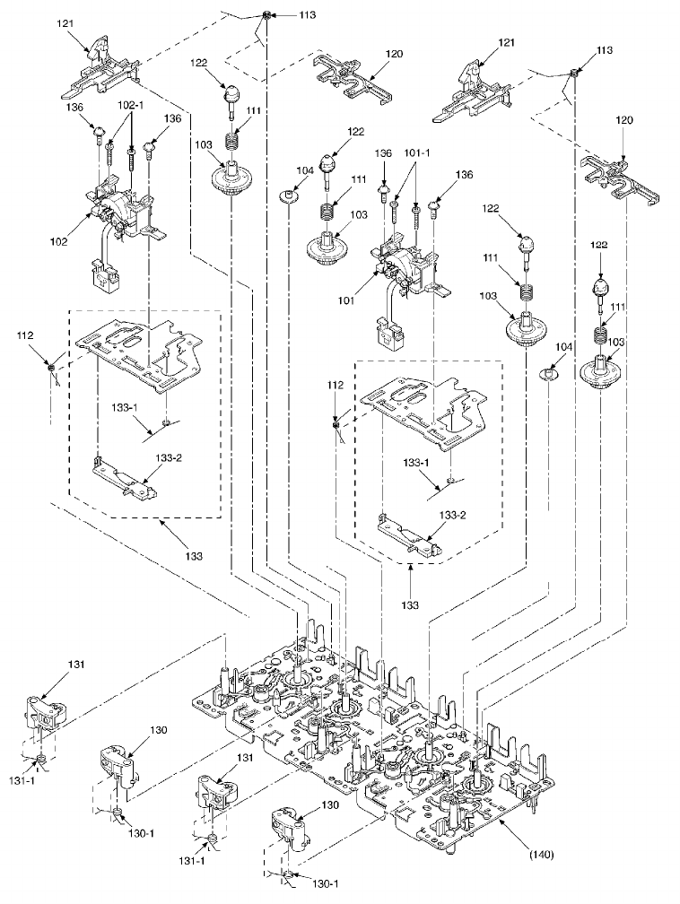
37
18. Schematic Diagram for printing with letter size
F0302KH
38
A
B
C
D
E
F
G
H
25 26 27 28 29 30 31 32 33 34 35 36
FW901
OPERATION CIRCUIT
E
1
2
3
4
5
6
7
8
D907
SML79455C
()
Q901
DTA143EUT106
LED DRIVE
D905
SML79455C
()
Q902
DTC143EUT106
LED DRIVE
S907
()
S906
()
S905
(DOLBY NR)
S904
(REC PAUSE)
S903
(TAPE EDIT)
S901
(OPEN)
S900
()
S915
(OPEN)
S909
()
S910
()
S912
(DECK 1/2)
S911
(REV MODE)
S914
(COUNTER
RESET)
S913
(COUNTER
DISPLAY)
R911
2.2K
R910
1.8K
R909
1.5K
R908
1.2K
R925
1K
R924
820
R905
2.2K
R904
1.8K
R903
1.5K
R902
1.2K
R901
1K R906
3.3K
R900
820
R915
680
R914
330
R916
330
Q904
DTC143EUT106
LED DRIVE(REV)
Q903
DTC143EUT106
LED DRIVE(FWD)
R917
680
D904
MA111TX
IC202
MC14066BFEL
SIGNAL CONT.
8 9 10 11 12 13
7654321
14
MAIN CIRCUIT
A
A
B
C
D
E
F
G
Q108
DTC143EUT106
SWITCHING
R126
22K
R234
100 C216
16V10
C215
16V10
R233
100
R226
47K
R208
47K
R225
47K
R207
47K
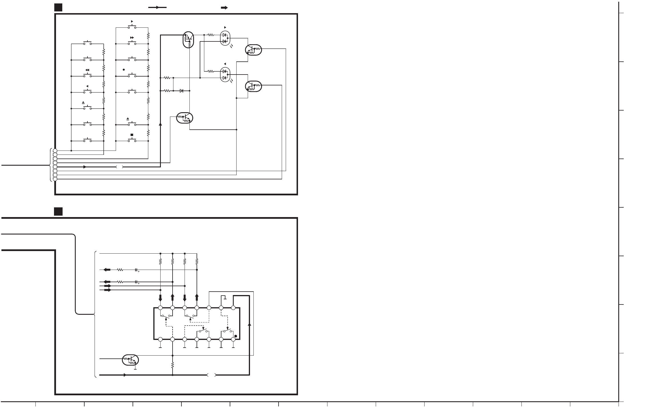
RS-DV290(EG) OPERATION, MAIN CIRCUIT DIAGRAM
:POSITIVE VOLTAGE LINE
5V
5V
0V
5V
0V
0V
STOP : 0V
5V
4.2V
0V
0V
0V
2.6V
0V
4.7V 8.3V
(0V) 9.6V4.7V 4.7V 4.7V
8.3V
(0V)
8.3V (0V)
(5V) 0V
9.6V
:PLAYBACK SIGNAL LINE

121110987654321
A
B
C
D
E
F
G
H
3
6
4
MAIN CIRCUIT
A
B
A
C
B
A
CP101
1
2
3
4
5
CP102
1
2
3
4
5
IC103
BA7755AF
R/P SELECT
1 2 4
678
3
5
Q301
2SD1819ARTX
BIAS OSC CONT.
Q306
DTC144EUT106
BIAS OSC CONT.
Q305
DTC144EUT106
BIAS OSC CONT.
Q302
2SD1328STXRA
SWITCHING
(REC:ON) Q303,304
2SD1450RSTA
BIAS OSC
Q303
Q304
Q102
2SJ164RTA
HEAD SELECT
(REC:ON)
Q106
Q103,104
2SJ164QTA
HEAD SELECT
(PLAY:ON)
Q104
Q103
Q105,106
2SD1819ARTX
MUTING
Q105
Q101
2SJ164RTA
HEAD SELECT
(REC:ON)
S
G
D
S
G
D
D
G
S
D
G
S
L301
IC101
CXA1998BQT6
R/P EQ AMP
1
25
Lch
Rch
PLAYBACK
HEAD
DECK1
Lch
ERASE
HEAD
DECK2
Rch
R/P HEAD
R106
330K
C102
680P
C101
680P
R105
330K
C143
470P C115
470P
R101
5.6K
R103
100K
C150
10V100
C123
25V4.7
R119
22
R118
22
C130
16V100
C119
50V1
C140
16V10
C131
470P
C129
10V22 R117
1K
C117
330P
R111
82 R113
12K
C111
6.3V47
R109
1K
C109
0.018
R141
100
R142
100
R144
100
C144
470P
C104
680P
C110
0.018
C112
6.3V47
R112
82
R114
27K
R110
1K
C114
50V2.2
C113
50V2.2
R102
5.6K
R104
100K
C116
470P
C125
3300P
C126
3300P
C118
330P
R154
2.7K
C120
50V1
R133 33K
R130 4.7M
C139 6.3V47
R132
27K
C301
16V470
C303
6800P C302
100V2.2
N
R313
1
TP302TP301
R302
1.8K
R301
10K D301
MA111TX
C305
50V0.1
C304
16V100
R303
2.2K
R304
15K
R305
18K
R306
33K
R138
4.7K
R137
2.2K
C309
6.3V47
R308
1K
C311
0.01
C310
0.01 C308
3300P
R307
2.2
C323
1000P
C307
1000P
R309
4.7K
R310
4.7K
R311
4.7K
L302
100 H
R134
3.9K
R135
6.8K
D102
MA111TX
D101
MA111TX
R158 22K
R127
4.7K
R125
100K
C138
0.047
C137
50V0.1
C135 50V1
C136 50V1
R120
100K
C132
470P
R153
2.7K
R157
22K
C103
680P
R143
100
R107
10K
R131
330K
R108
10K
LATCHES
SHIFT
REGISTERS
PBEQ
CTL
AGC
AMSRECEQ
20K 20K
10K
MUTE
40K
AGC
GAIN
210K
210K
210K 210K
IREF
40K
AGC
GAIN
10K
RECEQ
RFS
12345678910 11 12
13
23
2437
38
39
40
41
42
43
44
45
46
47
48 20K 20K
252627282930313233343536
REQEQ
CTL
22
21
20
19
18
17
16
15
14
C306
0.039
R136
2.2K
C124
25V4.7
DOLBY
Rch
F
D
E
CNRMO
B
A
IC201
CXA1552M-T4
DOLBY B NR
1 2 3 4 5 8
912131415
ATT2
ATT2
ATT3
ATT3
ATT1
ATT1
SC DET
SC DET
6 7
101116
ON/OFF
R/P
BA
J
I
A
B
A
B
IC102
MC14066BFEL
DECK 1/2 SELECT
1234567
891011121314
Q107
DTA143EUT106
R/P SELECT
Q202
DTA143EUT106
R/P SELECT
Q201
DTA143EUT106
DOLBY ON/OFF
R209
1K
R725
2.2K
R730
2.2K
R726
2.2K
C134
470P
C133
470P
C142
0.1
C203
25V4.7 R211
10K
C207
270P
L201
R218
2.2K
R217
2.2K
C211
1500P
C220
10V470
C219
16V100
C241
0.01
R237
22 R220
22
C239
680P
C205
50V1
R221
100
R230
1K
R223
10K
C223
25V4.7
C221
50V0.68 R213
3K
R215
12K
C213
25V4.7
C225
25V4.7
C217
50V0.1
R222
100
R219
18K
C206
50V1
C240
680P
C212
1500P
R212
10K
R210
1K
C204
25V4.7
C208
270P
L202
C214
25V4.7
R216
12K
C226
25V4.7
R224
10K
R231
1K
R151
100K
R140
47K
R152
100K
R139
47K
C141
50V1
R148
5.6K VR102
20K(B)
R150
5.6K VR104
20K(B)
R214
3K
C222
50V0.68
R149
5.6K VR103
20K(B)
R147
5.6K VR101
20K(B)
C218
50V0.1
DOLBY
Lch
C
R122
10K
R121
10K
RS-DV290(EG) MAIN CIRCUIT DIAGRAM
9.6V
:POSITIVE VOLTAGE LINE : PLAYBACK SIGNAL LINE: RECORDING SIGNAL LINE
9.6V
0V0V
(0.2V)
9V
0V0V
0V0V
(8.9V)
0V
(0.7V)
0V
0V
0V
0V
(0.7V)
0V
(8.9V)
(0.2V)
9V
0V0V
6V
9.6V 0V 0V
(9.5V)
0V
(0.7V)
0V
0V
(0.6V)
0V 0V
(0.6V)
0V
(0.7V)
0V
(0.8V)
0V
(0.6V)
0V
9.5V
9.5V (0.6V)
0V
0V
(0.1V)
(0.1V)
0V
ERASE CURRENT
CHECK POINT
5V 0V 4.5V 4.5V 4.5V 4.5V 4.5V 8.6V 5V0V
(1.6V) 0V
(0.2V)
5V
5V
(9.6V)
0.1V
(0.1V)
9.6V
(0.2V)
9.6V
(0.2V)
5V
(5V)
0.2V
4.5V9V9V 4.5V 4.5V 4.5V 4.5V 0V5V 0V
1.2V
2.6V
2.6V
1.3V
0V
0V
0V
0V
1.3V
2.6V
2.6V
1.2V
5V
5V
9.6V
9.6V
(0.2V)
9.6V
0V
(9.5V)
4.8V 9.6V 4.7V 4.7V 4.6V 4.7V 0.4V 4.8V
4.8V 4.7V 1.2V 4.7V 0.4V 4.8V4.6V
(0V)
0V
5V
5V5V
(0V)
5V (5V)
0V
PLAYBACK
GAIN ADJ.
(DECK1/Lch)
PLAYBACK
GAIN ADJ.
(DECK2/Lch)
PLAYBACK
GAIN ADJ.
(DECK1/Rch)
PLAYBACK
GAIN ADJ.
(DECK2/Rch)
9.6V 9.6V
(0.1V) 0V0V0V 0V9.6V
(0.1V)
0V0V0V 0V (9.6V)
0.1V (9.6V)
0.1V
DOLBY
ON : 0V

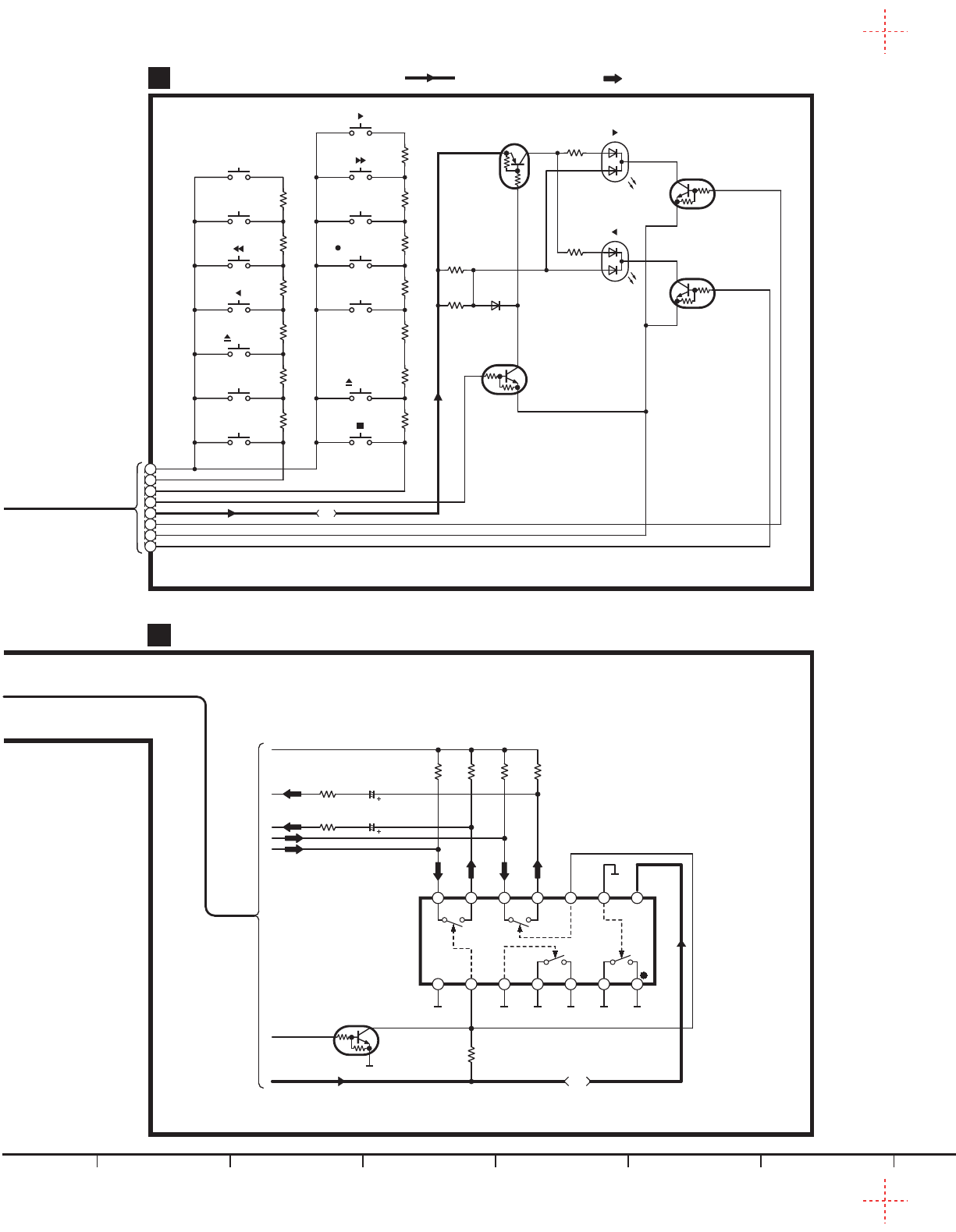
13 14 15 16 17 18 19 20 21 22 23 24
MAIN CIRCUIT
A
MECHANISM CIRCUIT (DECK1)
B
MECHANISM CIRCUIT (DECK2)
C
CP901
CS951
CP902CS971
Q806
DTA143EUT106
MOTOR DRIVE
Q804
2SD592ARSTA
MOTOR DRIVE
CP305
1
2
3
4
Z971
1234567
4.7K
50K
25K
4.7K
4.7K
4.7K
50K
50K
50K
50K
25K 25K
A
B
D
C
IC971
0N2180RLC1
PHOTO
INTERRUPTER
C
A
B
Q803
2SD592ARSTA
MOTOR DRIVE
Q805
DTA143EUT106
MOTOR DRIVE
CP306
1
2
3
4
1
2
3
4
5
6
7
8
9
1
2
3
4
5
6
7
8
9
Q807
2SB621ARSTA
SOLENOID DRIVE
Q809
DTC143EUT106
SOLENOID DRIVE
Q810
DTC143EUT106
SOLENOID DRIVE
Q808
2SB621ARSTA
SOLENOID DRIVE
DL
CAPSTAN
MOTOR
(DECK1)
A
B
M
CAPSTAN
MOTOR
(DECK2)
A
B
M
1
2
3
4
5
6
7
8
9
1
2
3
4
5
6
7
8
9
R806
10K
R802
560 R823
560 R824
560 R812
560
R811
10K
R814
470
R818
2.2
R805
3.9K R803
10K
R810
10K R808
3.9K
VR803
5K(B)
VR801
5K(B)
R820
2.2
R813
470
B
A
C
R952
820
D951
MA165TA
SOLENOID
S951
(MODE)
S953
(CrO2)
S952
(HALF)
S973
(CrO2)
S976
(METAL)
S972
(HALF)
S971
(MODE)
S974
(R.REC.INH.)
S975
(F.REC.INH.)
R972
820
D971
MA165TA
SOLENOID
D
IC951
0N2180RLC1
PHOTO
INTERRUPTER
R953
39K
12
34
AGHB
Q
S
P
F
R973
39K
1 2
3 4
TP609
CN601
CN901
IC701
M38503M2406F
SYSTEM CONTROL
E
C
A
B
D
J
I
H
G
F
PQR
JEDG
AC E
E
D
A
C
B
I
H
F
Q701
Q703
Q702
2SD1819ARTX
INTERFACE
13
2
X701
(8MHz)
CBAFIOJKLMNGH
Q604
2SC3940AQSTA
REGULATOR R603
10
TP604
+10V
(D.GND)
R602
0.33
R630
0.33
Q602
2SD2144STA
POWER SUPPLY
1
2
3
4
5
6
7
8
9
10
11
12
13
14
15
16
20
17
18
19
SYNC
CS
+B (10V)
D.GND
SCLK
DATA
DECK REQ
NC
TAPE Lch IN
A.GND
TAPE Rch IN
TAPE Lch OUT
TAPE Rch OUT
RS A.GND
EARTH
TERMINAL
CIRCUIT
D
W601 E1
1
2
3
4
5
6
7
8
Q701,703
2SD1819ARTX
INTERFACE
Q706
DTC114EUT106
RESET
C707
0.01
D706
MA111TX
D710
MA111TX
BD
R745
100
R710 1K
R724 1K
R723 1K
D707
MA4051MTA
L702
R738
1K R747
1K
R704
4.7K
R744
1K
R727
4.7K
R708
4.7K
R729
4.7K
R741
22K
D708
MA111TX
R743
47K
R705
47K
D709
MA111TX
R728
10K
R722
100
R703
5.6K
R732 100K
R721 4.7K
R735 4.7K
R632
47K
R609
100
D651
MA165TA
D652
MA165TA
R604
330
C602
16V220
C605
16V220
C603
16V47
D606
MA4056MTA C604
0.01
R606
1.5K
R712 68K
R718 68K
R701 10K
R702 10K
C705
0.01
C701
0.01
R711
100K
C702
6.3V100
C706
50V3.3
D705
MA111TX
R737 10K
R736 10K
D701
MA111TX
NC
NC
NC
NC
NC
NC
To DVD CHANGER(SL-DV290)
CD CHANGER (SL-EH790)
CD PLAYER(SL-EH590) &
SOUND PROCESSOR
(SH-DV290,SH-EH790,590)
CT.GND
Rch
OUT Lch
OUT Rch
IN Lch
IN
A.GND
1 2 3 4 5 6 7 8 9 10 11 12 13 14 15 16 17 18 19 20 21
313233343536373839404142 222324252627282930
KEY1 VCC
VREF
AVSS
LMT
PL1
M1
HALT
REQ
CS
CLK
VSS
VSS
XOUT
XIN
RESET
REV LED
FWD LED
CRO2 2
METAL 2
DATA IN
DATA OUT
CRO2 1
MODE
HALF1
TPS
A LATCH
PL2
M2
ENC/DEC
DOLBY ON/OFF
ECS
NC
KEY2
NC
NC
A CLK
A DATA
LED CNT
AD SW
PHOTO1 T
PHOTO2 T
F
EDABC
R232
10K
F
G
S
L701
10 H
RS-DV290(EG) MAIN,MECHANISM(DECK1,2), EARTH TERMINAL CIRCUIT DIAGRAM
E
K
:POSITIVE VOLTAGE LINE
5V
10.3V
5V
10.3V
5V
10.3V
5V
5V
10.3V
0V
10.3V
0V
0V
10.2V 0V 10.2V
0V
10.3V
0V
10.3V
0V
0V
9.8V 5V0V
5V
TAPE SPEED
ADJ.(DECK1)
0V
5V
5V
0V 0V
0.8V
TAPE SPEED
ADJ.(DECK2)
: PLAYBACK SIGNAL LINE: RECORDING SIGNAL LINE
5V
1.9V
0.1V
0V
1.8V
0V
0V
0.6V
0.2V
0V
5V
0V
0V
9.4V5V
5.7V
10.3V9.6V
10.3V
10.3V
5V
9.6V
5V
0V
5V
2.9V
5V
5V
5V
5V
5V
2.7V
0V
0V
0V
0V
0V
(5V) 0V
0V
5V
STOP : 0V
5V
5V
0V
5V
1.4V
2.2V
2.5V
0V
0V
0V
0V
0V
0.5V
1.6V
1V
5V
5V
2V
2.3V
1.2V
P-P
F=8MHz
2.4V
P-P
F=8MHz
4.8V
0V
T16ms.
3.6V
0V
T16ms.
3V
0V
T16ms.
0V
4.8V
T16ms.
5ms. 2V/DIV. 0V
4.8V
0V (5V)
A
B
C
D
E
F
G
H
25 26 27 28 29 30 31 32 33 34 35 36
FW901
OPERATION CIRCUIT
E
1
2
3
4
5
6
7
8
D907
SML79455C
()
Q901
DTA143EUT106
LED DRIVE
D905
SML79455C
()
Q902
DTC143EUT106
LED DRIVE
S907
()
S906
()
S905
(DOLBY NR)
S904
(REC PAUSE)
S903
(TAPE EDIT)
S901
(OPEN)
S900
()
S915
(OPEN)
S909
()
S910
()
S912
(DECK 1/2)
S911
(REV MODE)
S914
(COUNTER
RESET)
S913
(COUNTER
DISPLAY)
R911
2.2K
R910
1.8K
R909
1.5K
R908
1.2K
R925
1K
R924
820
R905
2.2K
R904
1.8K
R903
1.5K
R902
1.2K
R901
1K R906
3.3K
R900
820
R915
680
R914
330
R916
330
Q904
DTC143EUT106
LED DRIVE(REV)
Q903
DTC143EUT106
LED DRIVE(FWD)
R917
680
D904
MA111TX
IC202
MC14066BFEL
SIGNAL CONT.
8 9 10 11 12 13
7654321
14
MAIN CIRCUIT
A
A
B
C
D
E
F
G
Q108
DTC143EUT106
SWITCHING
R126
22K
R234
100 C216
16V10
C215
16V10
R233
100
R226
47K
R208
47K
R225
47K
R207
47K
RS-DV290(EG) OPERATION, MAIN CIRCUIT DIAGRAM
:POSITIVE VOLTAGE LINE
5V
5V
0V
5V
0V
0V
STOP : 0V
5V
4.2V
0V
0V
0V
2.6V
0V
4.7V 8.3V
(0V) 9.6V4.7V 4.7V 4.7V
8.3V
(0V)
8.3V (0V)
(5V) 0V
9.6V
:PLAYBACK SIGNAL LINE

A
B
C
D
E
F
G
H
25 26 27 28 29 30 31 32 33 34 35 36
FW901
OPERATION CIRCUIT
E
1
2
3
4
5
6
7
8
D907
SML79455C
()
Q901
DTA143EUT106
LED DRIVE
D905
SML79455C
()
Q902
DTC143EUT106
LED DRIVE
S907
()
S906
()
S905
(DOLBY NR)
S904
(REC PAUSE)
S903
(TAPE EDIT)
S901
(OPEN)
S900
()
S915
(OPEN)
S909
()
S910
()
S912
(DECK 1/2)
S911
(REV MODE)
S914
(COUNTER
RESET)
S913
(COUNTER
DISPLAY)
R911
2.2K
R910
1.8K
R909
1.5K
R908
1.2K
R925
1K
R924
820
R905
2.2K
R904
1.8K
R903
1.5K
R902
1.2K
R901
1K R906
3.3K
R900
820
R915
680
R914
330
R916
330
Q904
DTC143EUT106
LED DRIVE(REV)
Q903
DTC143EUT106
LED DRIVE(FWD)
R917
680
D904
MA111TX
IC202
MC14066BFEL
SIGNAL CONT.
8 9 10 11 12 13
7654321
14
MAIN CIRCUIT
A
A
B
C
D
E
F
G
Q108
DTC143EUT106
SWITCHING
R126
22K
R234
100 C216
16V10
C215
16V10
R233
100
R226
47K
R208
47K
R225
47K
R207
47K
RS-DV290(EG) OPERATION, MAIN CIRCUIT DIAGRAM
:POSITIVE VOLTAGE LINE
5V
5V
0V
5V
0V
0V
STOP : 0V
5V
4.2V
0V
0V
0V
2.6V
0V
4.7V 8.3V
(0V) 9.6V4.7V 4.7V 4.7V
8.3V
(0V)
8.3V (0V)
(5V) 0V
9.6V
:PLAYBACK SIGNAL LINE

BA7755AF CXA1998BQT6 0N2180RLC1 2SD1450RSTA
2SB621ARSTA
2SD592ARSTA 2SD1819ARTX
2SD1328STXRA
DTA143EUT106
DTC114EUT106
DTC143EUT106
DTC144EUT106
2SC3940AQSTA 2SD2144STA 2SJ164QTA
2SJ164RTA
MA165TA MA4051MTA
MA4056MTA SML79455C MA111TX
16PIN
14PIN
42PIN
CXA1552M-T4
MC14066BFEL
M38503M2406F
14
5
8
12
13
1
25
36
24
37
48
No.1
4
3
2
1
3
2
4
1
ECB
DGS
E
C
B
ECB
E
C
B
ECB
A
Ca
Anode
Cathode
A
Ca
Anode
Cathode
A
Ca
Anode
Cathode
Ca
A
A
Anode
CathodeAnode

AMAIN P.C.B.
DEARTH TERMINAL P.C.B.
EOPERATION P.C.B.
W601
W601
CP102 CP101
[DECK 2]
R/P HEAD,
ERASE HEAD
[DECK 1]
PLAYBACK
HEAD
CP305 CAPSTAN
MOTOR
[DECK 2]
CP306 CAPSTAN
MOTOR
[DECK 1]
To DVD CHANGER, CD CHANGER,
CD PLAYER & SOUND PROCESSOR
CP902 CP901
CMECHANISM P.C.B. (DECK 2) BMECHANISM P.C.B. (DECK 1)
FW901
CN901
BLACK
1 . . . 5
2
4
1 . 5
1 . . . 5
2
4
1 . 5
1
.
.
4
1
.
.
4
1 . . . . . . . 91 . . . . . . . 9
1 . . . . . . 8
1 . . . . . . 8
CS951
1 . . . . . . . 9
CS971
1 . . . . . . . 9


CXA1552M-T4
IC201
DOLBY B NR
REC
EQ
5
4
3
21
R101,
C115
(R102,
C116)
Q103
(Q104)
11
42
(43)
41
(44)
40
(45)
39
(46)
29
(8) REC
EQ AMP
35 36 34 448 1 2 15 16
17 18
24
25
26
27
LATCH
SHIFT
REGISTER
REC EQ
CONT.
P.B. EQ
CONT.
AGC
38
(47)
31
(6) 30
(7)
22 21 20 19
32
(5)
12
15
R/P
5124
+B1
2
+B1
+B1
VR102(VR103)
PLAYBACK GAIN ADJ.
(DECK2)
DECK2
R/P HEAD
+B1
Q101
(Q102)
ATT2
ATT1
ATT3
SC DET
ON/OFF
CXA1998BQT6
IC101
R/P EQ AMP
BA7755AF
IC103
R/P SELECT
TPS
25
S975(F. REC. INH.)
S971(MODE)
AD SW 3
4
5
Z971
LADDER
RESISTOR
+B3
2
1
7
39
M38503M2406F
IC701
SYSTEM CONTROL
18 RESET
26 A DATA
27 A CLK
A LATCH
28
Q706,
D705 +B3
SYNC1
8
CN601
2
3
4
5
6
7
9
12
CS
+B(10V)
D.GND
SCLK
DATA
11
10
DECK REQ
NC
TAPE Rch OUT
RS A.GND13
14
15
16
17
18
RCH
CLK 10
8
REQ
Q701
7
HALT
CS 9
+B3
TAPE Lch OUT
TAPE Rch IN
TAPE Lch IN
RCH
DATA IN
DATA OUT
12
11
Q702,703
TP604
Q604,D606
D710
20
19
X OUT
XIN
X701
(8MHz)
Q107
Q303,304
BIAS
OSC
D301
DECK2
ERASE HEAD
+B1
L301 Q301,305,306
BIAS OSC
CONTROL
(CrO2/
METAL)
Q302
TP301 TP302
Q105
(Q106)
AMS
23
+B3
RFS MUTE
3
DECK1
PLAYBACK HEAD
+B1
714
MC14066BFEL
IC102
DECK 1/2 SELECT
VR104(VR101)
PLAYBACK GAIN ADJ.
(DECK1)
1
(11)
4
(8)
13
(12)
2
(10)
5
(6)
3
(9)
3
(14)
1
(16)
6
(11)
7
(10)
8
(9)
AVss
Vss
15,21
3
Q201
DOLBY
ON/OFF
31
32 DOLBY
ON/OFF
ENC/DEC
S953(CrO2,DECK1)
S973(CrO2,DECK2)
S976(METAL,DECK2)
CRO2 1
22
S951(MODE)
S952(HALF)
METAL 2
14
MODE
23
HALF1
24
6M1
S972(HALF)
S974(R. REC. INH.)
6
D951
SOLENOID
Q807,809
CAPSTAN
MOTOR
(DECK1)
VR801
(TAPE SPEED ADJ.)
M
Q803,805
+B2
D971 SOLENOID
Q808,810
CAPSTAN
MOTOR
(DECK2)
VR803
(TAPE SPEED ADJ.) M
Q804,806
+B2
M2 30
PL2 29
KEY2 41
KEY SWITCH
(S900,901,903~907,
909~915)
KEY1 42
To DVD CHANGER,
CD CHANGER,
CD PLAYER
BLOCK DIAGRAM &
SOUND PROCESSOR
BLOCK DIAGRAM
NC
NC
A.GND
NC
NC
+B2
TP609
VREF
+B3 Vcc
2
1
D707
5PL1
D101
D102
CRO2 2
13
+B3
Q903,904
D905,907
()
Q901,902
16
FWD LED 17
REV LED
37
LED CNT
PHOTO2 T 38
40 PHOTO1 T
19
20
NC
NC
+B1
Q602
DOLBY
L(R)ch
Rch IN
Lch IN
Rch OUT
Lch OUT
+B3
(D.GND)
A.GND
+10V
+B1
714
MC14066BFEL
IC202
SIGNAL CONT.
10
(8)
12
(6)
11
(9)
Q108
4
LMT
SOLENOID
DRIVE CAPSTAN
MOTOR
DRIVE
REGULATOR
INTERFACE
INTERFACE
LED
DRIVE
LED
DRIVE
CAPSTAN
MOTOR
DRIVE
SOLENOID
DRIVE
POWER
SUPPLY
0N2180RLC1
IC971
PHOTO
INTERRUPTER
0N2180RLC1
IC951
PHOTO
INTERRUPTER
Q202
R/P
SELECT
+B3
RS-DV290(EG) BLOCK DIAGRAM
CT.GND
SWITCH-
ING
RESET
R/P
SELECT
+B1
NOTES : PLAYBACK SIGNAL LINE
: RECORDING SIGNAL LINE
( ) indicates pin No. Right channel.
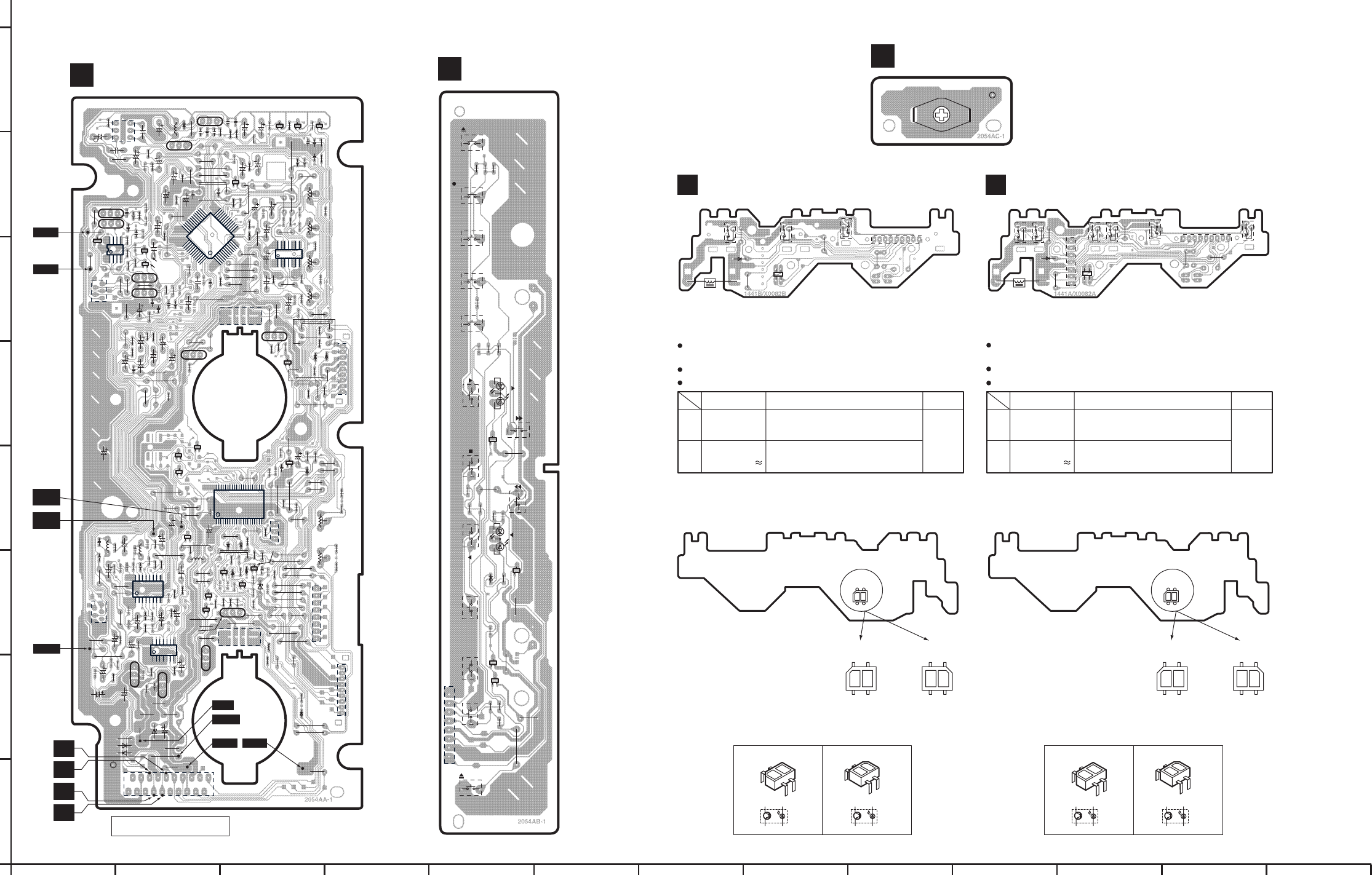
123456789101112
13
A
B
C
D
E
F
G
H
RS-DV290(EG) MAIN, OPERATION,EARTH TERMINAL, MECHANISM(DECK1,2) P.C.B.
Note: This printed circuit board diagram may be modified at any time with the development of new technology.
N
C302 6
5
41
2
3
L301
J
C303
C306
C304
C140
C305
C309
C114
C135
C136
C141
C205
C139
C112
C137
C113
C129
C111
C150
C213
C221
C301
C214
C222
C204
C206
C130
C124
C123
J
J
J
J
JJ
J
ECB
Q304
ECB
Q303
L302
R307
J
J
J
J
J
J
J
J
JJ
J
J
J
J
J
J
J
JR118 R119
J
J
J
J
J
J
J
J
J
J
J
J
J
J
J
J
J
J
J
J
J
J
J
J
J
J
J
J
J
J
J
JJ
J
J
J
J
J
C110
C109
SGD
Q101
SGDQ104
SGD
Q103
ECB
Q804
ECB
Q808
SGD
Q102
J
J
J
J
J
J
J
J
J
J
J
J
R313
R143
R820
VR102
VR103
VR104
VR101
1
2
3
4
5
6
7
8
9
CP902
1
23
45
CP102
C706
J
J
J
VR803
VR801
J
J
J
J
J
J
J
JJJ
J
J
J
J
J
J
J
J
J
J
1
2
3X701
1
2
3
4
5
6
7
8
9
CP901
1
2
3
4
5
6
7
8
CN901
J
J
J
D707
B
C
E
Q807 R818
L701
C702
C223
C217
C226
C218
C225
C220
C119
C120
C605
C603
C203
C219
L202
L201
J
R220
R237
1
23
45
CP101
C602
Q803
E
C
B
Q604
E
C
B
Q602
E
C
B
R630
R602
R609
R632
D606
R603
D651
D652
1
2
3
4
5
6
7
8
9
10
11
12
13
14
15
16
17
18
19
20
CN601
158
10
16
IC201
IC701
9
15
1510
15 2021
22
25
303540
42
157
810
14
IC102
IC101
IC103
15
10
12
13
15
20
2425
30
35
36
37
40
45 48
14
58
R309
R308
R310
R303
R110
R306
R305
R304
R120
R148
R149
R140
R139
R125
R127
R122
R121
R113
R117
R111
R105
R106
R144
R215
R213
R152
R813
R216
R214
R141
R142
R114
R133
R811
R812
R824
R136
R137
R721
R735
R703
R701
R722
R737
R736
R723
R724
R710
R747
R712
R745
R738
R728
R741
R727
R708
R744
R802
R806
R823
R814
R223
R153
R217
R154
R157
R604
R234
R606
R233
R158
R222
R224
R219
R212
R218
R211
R230
R221
R705
R704
R729
R743
R711
R702
R810
R808
R803
R805
R718 R134
R138
R732
R130
R151
R730
R147
R135
R112
R102
R132
R302
R107
R108
R131
R101
R150
R726
R725
R311
R109
R301
R103
R104
D301
C307
C323
C308
C132
C134
C126
C138
C142
C117
C102
C104
C118
C103
C101
C131
C143
C115
C116
C144
C125
C133
C311
C310
C
EB
Q107
C
E
B
Q810
C
E
BQ105
C
EB Q106
C
EB
Q301
C
EB
Q306 C
EB Q305
C
EB
Q302
RJ507
D102
D705
D706
D709
D708
D701
D101
1234
CP305
1234
CP306
C
EB
Q806
C
EB
Q202
C
EB
Q201
C
EB
Q706
RJ508
RJ509
C705
C707
C
E
B
Q702
C
E
B
Q703
C
EB
Q701
C
E
B
Q805
C
EB
Q809
L702
D710
RJ504
R231
R210
R209
C240
C239
C211
C604
C212
C208
C207
C241
MAIN P.C.B.
A
(REP2827E-M)
W601
J
TP302
TP301
C701
TP604
+10V
A.GND
DOLBY
L ch
DOLBY
R ch
R ch
OUT
L ch
IN
R ch
IN
L ch
OUT
(D.GND)
TP609
CT.GND
To DVD CHANGER, CD CHANGER,
CD PLAYER & SOUND PROCESSOR
C215
IC202
157
810
14
C216
R126
R225
R207
R208
R226
C
E
B
Q108
R232
1
2
3
4
5
6
7
8
FW901
J
J
J
J
J
J
R901
R902
R903
R904
R906
R900
R909
R915
R914
R916
R908
R924
R925 R917
R911
R905
R910
C
E
B
Q903
C
E
BQ904
D904
C
E
B
Q901
C
E
BQ902
OPERATION P.C.B.
E
(REP2827E-M)
S913
(COUNTER
DISPLAY)
S912
(DECK1/2)
S914
(COUNTER
RESET)
S909
( )
S905
(DOLBY NR)
S911
(REV MODE)
S903
(TAPE EDIT)
S904
( REC PAUSE)
S901
( OPEN)
S907
( ) D907
( )
S906
( )
S910
( )
S900
( )
D905
( )
S915
( OPEN)
E1
W601
EARTH TERMINAL P.C.B.
D
(REP2827E-M)
J
R952
J
D951
R953
1
2
3
4IC951
1
CS951
23456789
S953 S952 S951
SOLENOID
J
J
7
6
5
4
3
2
1
Z971
41
32
IC971
D971
S974 S973
SOLENOID
S972 S976 S971 123456789
CS971
R972
J
S975
R973
MECHANISM P.C.B. (DECK1)
BMECHANISM P.C.B. (DECK2)
C
14
23
14
23
4
3
2
1
0N2180RLC
IC971
0N2180RLC 1
14
23
14
23
14
23
14
23
14
23
4
3
2
1
0N2180RLC
IC951
0N2180RLC 1
14
23
14
23
14
23
(REPX0108A) (REPX0108B)
Note for IC951 replacement
Two different types (old or new) parts are mounted on P.C.B.
as for IC951.
When servicing, care to replace the parts due to those shape.
Replacement procedures
Old
New
Mount the parts on given position.
(Printed pattern on P.C.B.)
For IC951: Mount the parts so the cut
corner is located upper right.
Refer to
the figure
below.
0N2180RLC
0N2180RLC1
Parts No. Direction Remarks
Note for IC971 replacement
Two different types (old or new) parts are mounted on P.C.B.
as for IC971.
When servicing, care to replace the parts due to those shape.
Replacement procedures
Old
New
Mount the parts on given position.
(Printed pattern on P.C.B.)
For IC971: Mount the parts so the cut
corner is located upper right.
Refer to
the figure
below.
0N2180RLC
0N2180RLC1
Parts No. Direction Remarks
(Component side) (Component side)
Old
Old Old
Old
New
New New
New
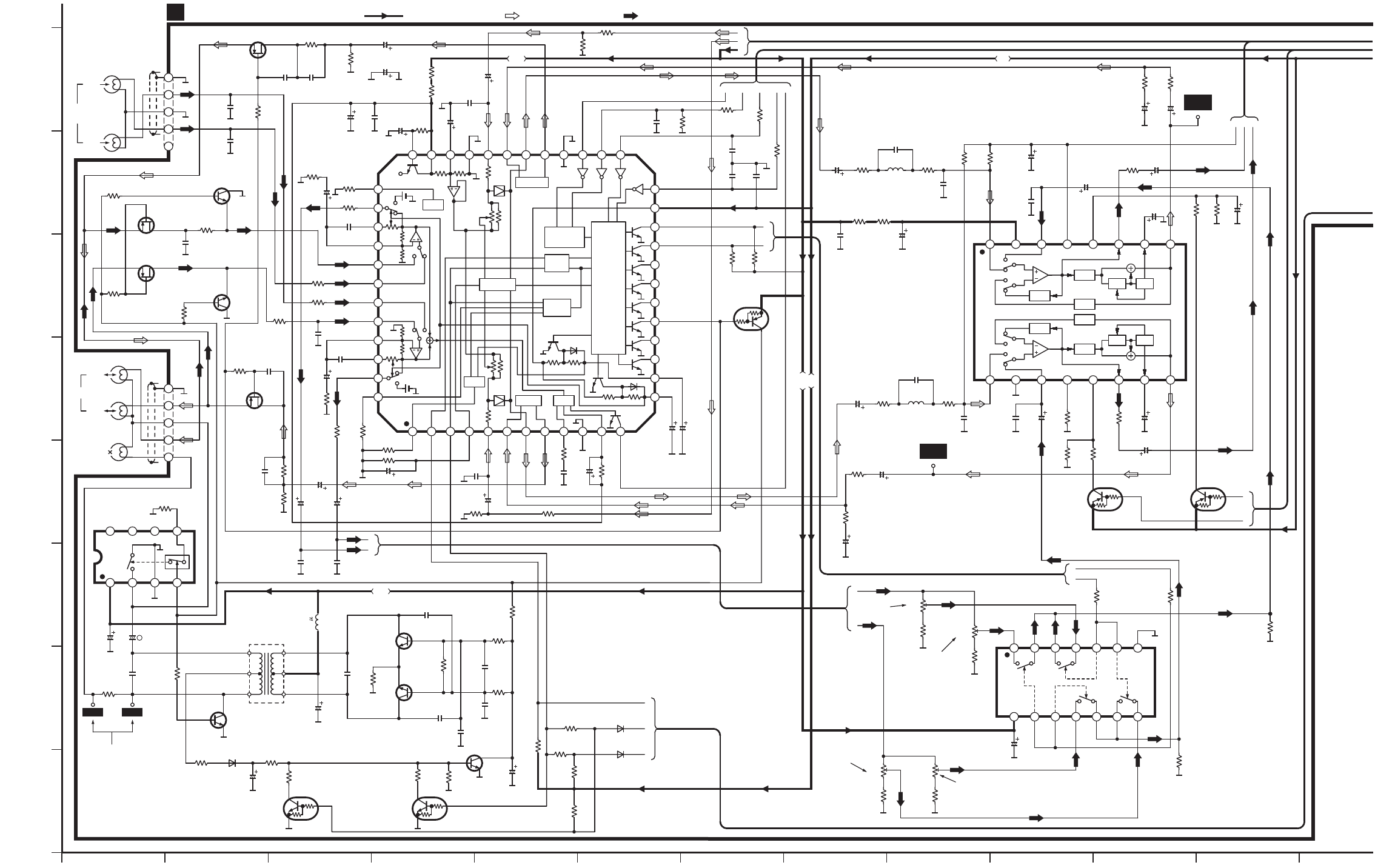
121110987654321
A
B
C
D
E
F
G
H
3
6
4
MAIN CIRCUIT
A
B
A
C
B
A
CP101
1
2
3
4
5
CP102
1
2
3
4
5
IC103
BA7755AF
R/P SELECT
1 2 4
678
3
5
Q301
2SD1819ARTX
BIAS OSC CONT.
Q306
DTC144EUT106
BIAS OSC CONT.
Q305
DTC144EUT106
BIAS OSC CONT.
Q302
2SD1328STXRA
SWITCHING
(REC:ON) Q303,304
2SD1450RSTA
BIAS OSC
Q303
Q304
Q102
2SJ164RTA
HEAD SELECT
(REC:ON)
Q106
Q103,104
2SJ164QTA
HEAD SELECT
(PLAY:ON)
Q104
Q103
Q105,106
2SD1819ARTX
MUTING
Q105
Q101
2SJ164RTA
HEAD SELECT
(REC:ON)
S
G
D
S
G
D
D
G
S
D
G
S
L301
IC101
CXA1998BQT6
R/P EQ AMP
1
25
Lch
Rch
PLAYBACK
HEAD
DECK1
Lch
ERASE
HEAD
DECK2
Rch
R/P HEAD
R106
330K
C102
680P
C101
680P
R105
330K
C143
470P C115
470P
R101
5.6K
R103
100K
C150
10V100
C123
25V4.7
R119
22
R118
22
C130
16V100
C119
50V1
C140
16V10
C131
470P
C129
10V22 R117
1K
C117
330P
R111
82 R113
12K
C111
6.3V47
R109
1K
C109
0.018
R141
100
R142
100
R144
100
C144
470P
C104
680P
C110
0.018
C112
6.3V47
R112
82
R114
27K
R110
1K
C114
50V2.2
C113
50V2.2
R102
5.6K
R104
100K
C116
470P
C125
3300P
C126
3300P
C118
330P
R154
2.7K
C120
50V1
R133 33K
R130 4.7M
C139 6.3V47
R132
27K
C301
16V470
C303
6800P C302
100V2.2
N
R313
1
TP302TP301
R302
1.8K
R301
10K D301
MA111TX
C305
50V0.1
C304
16V100
R303
2.2K
R304
15K
R305
18K
R306
33K
R138
4.7K
R137
2.2K
C309
6.3V47
R308
1K
C311
0.01
C310
0.01 C308
3300P
R307
2.2
C323
1000P
C307
1000P
R309
4.7K
R310
4.7K
R311
4.7K
L302
100 H
R134
3.9K
R135
6.8K
D102
MA111TX
D101
MA111TX
R158 22K
R127
4.7K
R125
100K
C138
0.047
C137
50V0.1
C135 50V1
C136 50V1
R120
100K
C132
470P
R153
2.7K
R157
22K
C103
680P
R143
100
R107
10K
R131
330K
R108
10K
LATCHES
SHIFT
REGISTERS
PBEQ
CTL
AGC
AMSRECEQ
20K 20K
10K
MUTE
40K
AGC
GAIN
210K
210K
210K 210K
IREF
40K
AGC
GAIN
10K
RECEQ
RFS
12345678910 11 12
13
23
2437
38
39
40
41
42
43
44
45
46
47
48 20K 20K
252627282930313233343536
REQEQ
CTL
22
21
20
19
18
17
16
15
14
C306
0.039
R136
2.2K
C124
25V4.7
DOLBY
Rch
F
D
E
CNRMO
B
A
IC201
CXA1552M-T4
DOLBY B NR
1 2 3 4 5 8
912131415
ATT2
ATT2
ATT3
ATT3
ATT1
ATT1
SC DET
SC DET
6 7
101116
ON/OFF
R/P
BA
J
I
A
B
A
B
IC102
MC14066BFEL
DECK 1/2 SELECT
1234567
891011121314
Q107
DTA143EUT106
R/P SELECT
Q202
DTA143EUT106
R/P SELECT
Q201
DTA143EUT106
DOLBY ON/OFF
R209
1K
R725
2.2K
R730
2.2K
R726
2.2K
C134
470P
C133
470P
C142
0.1
C203
25V4.7 R211
10K
C207
270P
L201
R218
2.2K
R217
2.2K
C211
1500P
C220
10V470
C219
16V100
C241
0.01
R237
22 R220
22
C239
680P
C205
50V1
R221
100
R230
1K
R223
10K
C223
25V4.7
C221
50V0.68 R213
3K
R215
12K
C213
25V4.7
C225
25V4.7
C217
50V0.1
R222
100
R219
18K
C206
50V1
C240
680P
C212
1500P
R212
10K
R210
1K
C204
25V4.7
C208
270P
L202
C214
25V4.7
R216
12K
C226
25V4.7
R224
10K
R231
1K
R151
100K
R140
47K
R152
100K
R139
47K
C141
50V1
R148
5.6K VR102
20K(B)
R150
5.6K VR104
20K(B)
R214
3K
C222
50V0.68
R149
5.6K VR103
20K(B)
R147
5.6K VR101
20K(B)
C218
50V0.1
DOLBY
Lch
C
R122
10K
R121
10K
RS-DV290(EG) MAIN CIRCUIT DIAGRAM
9.6V
:POSITIVE VOLTAGE LINE : PLAYBACK SIGNAL LINE: RECORDING SIGNAL LINE
9.6V
0V0V
(0.2V)
9V
0V0V
0V0V
(8.9V)
0V
(0.7V)
0V
0V
0V
0V
(0.7V)
0V
(8.9V)
(0.2V)
9V
0V0V
6V
9.6V 0V 0V
(9.5V)
0V
(0.7V)
0V
0V
(0.6V)
0V 0V
(0.6V)
0V
(0.7V)
0V
(0.8V)
0V
(0.6V)
0V
9.5V
9.5V (0.6V)
0V
0V
(0.1V)
(0.1V)
0V
ERASE CURRENT
CHECK POINT
5V 0V 4.5V 4.5V 4.5V 4.5V 4.5V 8.6V 5V0V
(1.6V) 0V
(0.2V)
5V
5V
(9.6V)
0.1V
(0.1V)
9.6V
(0.2V)
9.6V
(0.2V)
5V
(5V)
0.2V
4.5V9V9V 4.5V 4.5V 4.5V 4.5V 0V5V 0V
1.2V
2.6V
2.6V
1.3V
0V
0V
0V
0V
1.3V
2.6V
2.6V
1.2V
5V
5V
9.6V
9.6V
(0.2V)
9.6V
0V
(9.5V)
4.8V 9.6V 4.7V 4.7V 4.6V 4.7V 0.4V 4.8V
4.8V 4.7V 1.2V 4.7V 0.4V 4.8V4.6V
(0V)
0V
5V
5V5V
(0V)
5V (5V)
0V
PLAYBACK
GAIN ADJ.
(DECK1/Lch)
PLAYBACK
GAIN ADJ.
(DECK2/Lch)
PLAYBACK
GAIN ADJ.
(DECK1/Rch)
PLAYBACK
GAIN ADJ.
(DECK2/Rch)
9.6V 9.6V
(0.1V) 0V0V0V 0V9.6V
(0.1V)
0V0V0V 0V (9.6V)
0.1V (9.6V)
0.1V
DOLBY
ON : 0V
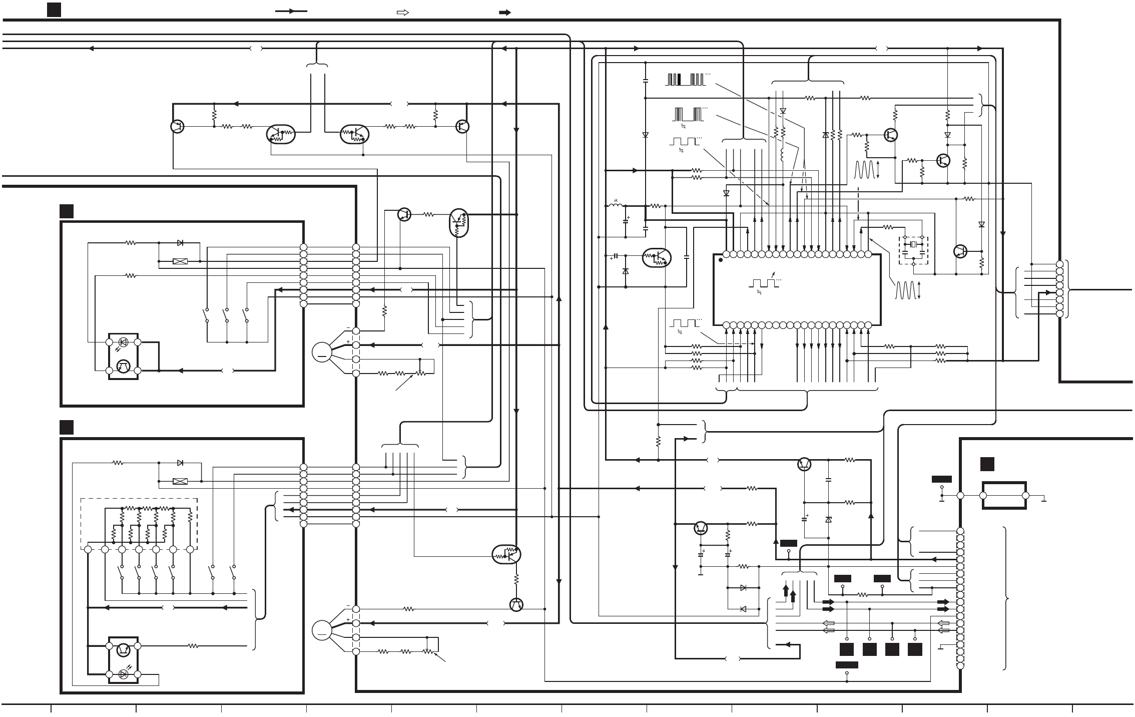
13 14 15 16 17 18 19 20 21 22 23 24
MAIN CIRCUIT
A
MECHANISM CIRCUIT (DECK1)
B
MECHANISM CIRCUIT (DECK2)
C
CP901
CS951
CP902CS971
Q806
DTA143EUT106
MOTOR DRIVE
Q804
2SD592ARSTA
MOTOR DRIVE
CP305
1
2
3
4
Z971
1234567
4.7K
50K
25K
4.7K
4.7K
4.7K
50K
50K
50K
50K
25K 25K
A
B
D
C
IC971
0N2180RLC1
PHOTO
INTERRUPTER
C
A
B
Q803
2SD592ARSTA
MOTOR DRIVE
Q805
DTA143EUT106
MOTOR DRIVE
CP306
1
2
3
4
1
2
3
4
5
6
7
8
9
1
2
3
4
5
6
7
8
9
Q807
2SB621ARSTA
SOLENOID DRIVE
Q809
DTC143EUT106
SOLENOID DRIVE
Q810
DTC143EUT106
SOLENOID DRIVE
Q808
2SB621ARSTA
SOLENOID DRIVE
DL
CAPSTAN
MOTOR
(DECK1)
A
B
M
CAPSTAN
MOTOR
(DECK2)
A
B
M
1
2
3
4
5
6
7
8
9
1
2
3
4
5
6
7
8
9
R806
10K
R802
560 R823
560 R824
560 R812
560
R811
10K
R814
470
R818
2.2
R805
3.9K R803
10K
R810
10K R808
3.9K
VR803
5K(B)
VR801
5K(B)
R820
2.2
R813
470
B
A
C
R952
820
D951
MA165TA
SOLENOID
S951
(MODE)
S953
(CrO2)
S952
(HALF)
S973
(CrO2)
S976
(METAL)
S972
(HALF)
S971
(MODE)
S974
(R.REC.INH.)
S975
(F.REC.INH.)
R972
820
D971
MA165TA
SOLENOID
D
IC951
0N2180RLC1
PHOTO
INTERRUPTER
R953
39K
12
34
AGHB
Q
S
P
F
R973
39K
1 2
3 4
TP609
CN601
CN901
IC701
M38503M2406F
SYSTEM CONTROL
E
C
A
B
D
J
I
H
G
F
PQR
JEDG
AC E
E
D
A
C
B
I
H
F
Q701
Q703
Q702
2SD1819ARTX
INTERFACE
13
2
X701
(8MHz)
CBAFIOJKLMNGH
Q604
2SC3940AQSTA
REGULATOR R603
10
TP604
+10V
(D.GND)
R602
0.33
R630
0.33
Q602
2SD2144STA
POWER SUPPLY
1
2
3
4
5
6
7
8
9
10
11
12
13
14
15
16
20
17
18
19
SYNC
CS
+B (10V)
D.GND
SCLK
DATA
DECK REQ
NC
TAPE Lch IN
A.GND
TAPE Rch IN
TAPE Lch OUT
TAPE Rch OUT
RS A.GND
EARTH
TERMINAL
CIRCUIT
D
W601 E1
1
2
3
4
5
6
7
8
Q701,703
2SD1819ARTX
INTERFACE
Q706
DTC114EUT106
RESET
C707
0.01
D706
MA111TX
D710
MA111TX
BD
R745
100
R710 1K
R724 1K
R723 1K
D707
MA4051MTA
L702
R738
1K R747
1K
R704
4.7K
R744
1K
R727
4.7K
R708
4.7K
R729
4.7K
R741
22K
D708
MA111TX
R743
47K
R705
47K
D709
MA111TX
R728
10K
R722
100
R703
5.6K
R732 100K
R721 4.7K
R735 4.7K
R632
47K
R609
100
D651
MA165TA
D652
MA165TA
R604
330
C602
16V220
C605
16V220
C603
16V47
D606
MA4056MTA C604
0.01
R606
1.5K
R712 68K
R718 68K
R701 10K
R702 10K
C705
0.01
C701
0.01
R711
100K
C702
6.3V100
C706
50V3.3
D705
MA111TX
R737 10K
R736 10K
D701
MA111TX
NC
NC
NC
NC
NC
NC
To DVD CHANGER(SL-DV290)
CD CHANGER (SL-EH790)
CD PLAYER(SL-EH590) &
SOUND PROCESSOR
(SH-DV290,SH-EH790,590)
CT.GND
Rch
OUT Lch
OUT Rch
IN Lch
IN
A.GND
1 2 3 4 5 6 7 8 9 10 11 12 13 14 15 16 17 18 19 20 21
313233343536373839404142 222324252627282930
KEY1 VCC
VREF
AVSS
LMT
PL1
M1
HALT
REQ
CS
CLK
VSS
VSS
XOUT
XIN
RESET
REV LED
FWD LED
CRO2 2
METAL 2
DATA IN
DATA OUT
CRO2 1
MODE
HALF1
TPS
A LATCH
PL2
M2
ENC/DEC
DOLBY ON/OFF
ECS
NC
KEY2
NC
NC
A CLK
A DATA
LED CNT
AD SW
PHOTO1 T
PHOTO2 T
F
EDABC
R232
10K
F
G
S
L701
10 H
RS-DV290(EG) MAIN,MECHANISM(DECK1,2), EARTH TERMINAL CIRCUIT DIAGRAM
E
K
:POSITIVE VOLTAGE LINE
5V
10.3V
5V
10.3V
5V
10.3V
5V
5V
10.3V
0V
10.3V
0V
0V
10.2V 0V 10.2V
0V
10.3V
0V
10.3V
0V
0V
9.8V 5V0V
5V
TAPE SPEED
ADJ.(DECK1)
0V
5V
5V
0V 0V
0.8V
TAPE SPEED
ADJ.(DECK2)
: PLAYBACK SIGNAL LINE: RECORDING SIGNAL LINE
5V
1.9V
0.1V
0V
1.8V
0V
0V
0.6V
0.2V
0V
5V
0V
0V
9.4V5V
5.7V
10.3V9.6V
10.3V
10.3V
5V
9.6V
5V
0V
5V
2.9V
5V
5V
5V
5V
5V
2.7V
0V
0V
0V
0V
0V
(5V) 0V
0V
5V
STOP : 0V
5V
5V
0V
5V
1.4V
2.2V
2.5V
0V
0V
0V
0V
0V
0.5V
1.6V
1V
5V
5V
2V
2.3V
1.2V
P-P
F=8MHz
2.4V
P-P
F=8MHz
4.8V
0V
T16ms.
3.6V
0V
T16ms.
3V
0V
T16ms.
0V
4.8V
T16ms.
5ms. 2V/DIV. 0V
4.8V
0V (5V)

ORDER NO. AD0305100C8
Tuner/ Amplifier
SA-DV290EE / SA-DV290GN
Colour
(S).......................Silver Type
System: SC-DV290
Because of unique interconnecting cables, when a
compact requires service, send or bring in the entire
system.
SPECIFICATIONS
Specification
1
Amplifier section
Power output (L/R both channel driven)
Stereo Mode
DIN 1 kHz THD 1%/6 (High) 2×25 W
100 Hz THD 1%/8 (Low) 2×45 W
RMS 1 kHz THD 10%/6 (High) 2×35 W
100 Hz THD 10%/8 (Low) 2×65 W
PRO LOGIC mode
DIN FRONT
1 kHz THD 1%/6 (High) 2×25 W
100 Hz THD 1%/8 (Low) 2×45 W
SURROUND 1 kHz THD 1%/8 2×30 W
CENTER 1 kHz THD 1%/8 60 W
RMS FRONT
1 kHz THD 10%/6 (High) 2×35 W
100 Hz THD 10%/8 (Low) 2×65 W
SURROUND 1 kHz THD 10%/8 2×40 W
CENTER 1 kHz THD 10%/8 80 W
PMPO 1 kHz/High 6 , Low 8 ,
CENT. 8 , SURR. 8 3000 W
Total harmonic distortion
Rated power at 1 kHz 1% (6 )
Half power at 1 kHz 0.1% (6 )
Load impedance
FRONT (High) 6
FRONT (Low) 8
SURROUND 8
CENTER 8
DIGITAL S. WOOFER
Center frequency 60 Hz
LEVEL (VOL -20 db) MID +3 db
MAX +6 db
FM tuner section
Frequency range 87.50—108.00 MHz
(0.05 MHz steps)
Sensitivity 1.8 V (IHF usable)
S/N 26 db 1.5 V
S/N
MONO 70 db (75 db, IHF)
Antenna terminal(s) 75 (unbalanced)
AM tuner section
Frequency range 522—1629 kHz (9 kHz steps)
520—1630 (10 kHz steps)
Sensitivity (S/N 20 db) 500 V/m
Timer section
Clock Quartz-lock type
Function Play timer (1 time, daily),
2
Function
Play
timer
(
1
time,
daily),
Rec timer (1 time, daily)
Sleep (120 min, 30 min intervals)
Setting intervals (Play/Rec) 1 minute—23 hours 59 minutes
(1 min intervals)
General
Power supply
(For (GN) area) AC 230—240V 50Hz
(For (EE) area) AC 230V 50Hz
Power consumption 230 W
Standby 0.5 W
Dimensions (W×H×D) 293×118.5×345 mm
Mass 5.3 kg
Nots 1.Design and specifications are subject to
change without notice.
2.Dimensions and weight are approximate.
3.Total harmonic distortion is measured by the
digital spectrum analyzer.
System/SC-DV290
Sound processor: SH-DV290, DVD/ Video CD/ CD
changer: SL-DV290, Tuner/ Amplifier: SA-DV290 ,
Cassette Deck: RS-DV290, Speakers: Front* (SB-
DV290),Center* (SB-PC95),Surround* (SB-PS95)
(*Madein MESA.)
1. Accessories
- AC mains lead for (EE) areas
(RJA0019-2X)....................1 pc.
- AC mains lead for (GN) area
3
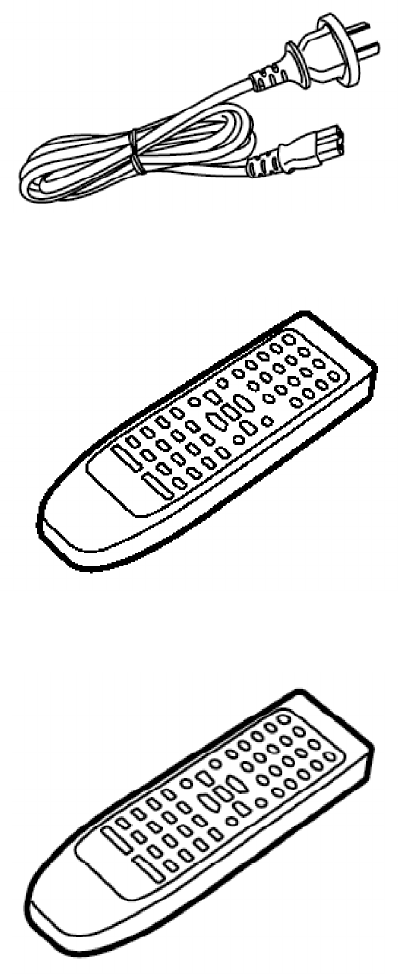
(RJA0035-2X)....................1 pc.
- Remote control for (EE) area
(EUR7702290)....................1 pc.
- Remote control for (GN) area
(EUR7702300)....................1 pc.
- Remote control batteries
(R6/LR6,”AA”,UM-3)....................1 pc.
Note: These are available on sales route.
4

- FM indoor antenna for (EE) area
(N1EAYY000002)....................1 pc.
- FM indoor antenna for (GN) area
(N1EAYY000001)....................1 pc.
- AM loop antenna set
(N1DAEYA00008)....................1 pc.
- Speaker leads
(REE1234-1)....................2 pc.
(Red/Black)
(REE1233-1)....................2 pc.
(Gray/Blue)
5

- Video cord
(K2JA2A000018)....................1 pc.
- RCAJ adaptor for (EE) area
(K1JZ24D00002)....................1 pc.
2. Before Repair and Adjustment
1. Turn off the power supply. Using a 10 , 10W resistor, connect
both ends of power supply capacitors (C701-704) in order to
discharge the voltage.
2. Before turning the power supply on, after completion of repair,
slowly apply the primary voltage by using a power supply voltage
controller to make sure that the consumed current at 50 Hz in NO
SIGNAL mode should be shown below with respectto
supplyvoltage230 V/240 V.
Areas (EE) (GN)
Power supply voltage AC 230V AC 230-240V
Consumed current 50 Hz 130-380 mA 50 Hz 130-380 mA
3. About the Protection Circuitry
The protection circuitry may have operated if either of the following conditions is noticed:
6
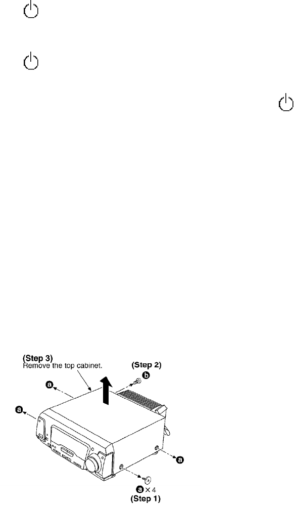
*No sound is heard when the power is supplied.
*Sound stops during a performance.
The functions of this circuitry is to prevent circuitry damage, for example, the positive and
negative speaker connection wires are “shorted”, or if speaker systems with an impedande less
than the indicated rated impedance of thisunitareused.
If this occurs, follow the procedure outlined below:
1. Press the STANDBY /ON button, switch to STANDBY mode.
2. Determine the cause of the problem and correct it.
3. Press the STANDBY /ON button once again, supply the power.
Note:
When the protection circuitry functions, the unit will not operate unless the STANDBY /ON
button is first switched STANDBY and then ON again.
4. Operating Instructions
5. Operation Checks and Component Replacement
Procedures
- This section describes procedures for checking the operation of
the major printed circuit boards and replacing the main
components.
- For reassembly after operation checks or replacement, reverse the
respective procedures. Special reassembly procedures are
described only when required.
5.1. Checking for the AC IN P.C.B.
- Check the AC IN P.C.B. as shown below.
7

5.2. Checking for the operation P.C.B.
- Follow the (Step 1) - (Step 3) of item 5.1.
- Check the operation P.C.B. as shown below.
5.3. Checking for the main P.C.B.
8

- Follow the (Step 1) - (Step 3) of item 5.1.
9

- Check the main P.C.B. as shown below.
5.4. Replacement for the regulator transistor
10
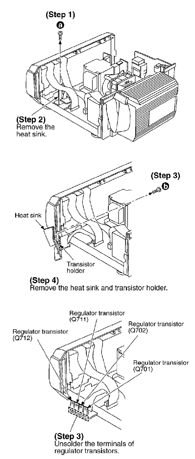
- Follow the (Step 1) - (Step 3) of item 5.1.
5.5. Replacement for the power IC
- Follow the (Step 1) - (Step 3) of item 5.1.
- Follow the (Step 1) - (Step 6) of item 5.2.
- Follow the (Step 1) - (Step 10) of item 5.3.
11
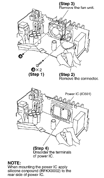
6. Self-Diagnostic Function
This unit equipped with a self-diagnostic function which, in the event of a malfunction,
automatically displays a code indicating the nature of the malfunction.
Use this self-diagnostic function when servicing the unit.
6.1. To display the malfunction code
U70 DVD: Automatically displays on the
U70 DECK:tuner/amplifier when a
malfunction occurs. Refer to
Fig. 6-1.
F61: Automatically displays on the
tuner/amplifier when a
malfunction occurs. Refer to
Fig. 6-1.
Fig. 6-1
12

6.2. To return to the normal display
1. For U70 DVD/U70 DECK
- Press an any operation button on the tuner/amplifier.
- To re-display the code, switch the power off (POWER
STANDBY button), and then switch power back on again.
2. For F61
- If F61 is displayed, the power will automatically be switched
off and the standby indicator will light up.
- F61 will be displayed for 3 seconds, and then the clock will be
displayed.
- To re-display the code, switch the power on. F61 will be re-
displayed, and then after 3 seconds the clock will be displayed
and the power will automatically switch off.
6.3. Display contents
6.3.1. U70 DVD, U70 DECK / (displayed automatically)
- Problem or condition
A bus-line communications error has occurred as a result of the
flat cables being inserted incorrectly, thus preventing the system
from operating.
13

- If U70 is displayed on the tuner/amplifier, the Cassette deck or DVD
Changer cannot be operated by remote control.
- Correction Procedure
1. To check for correct insertion of the flat cables.
- Insert each connectors until you hear a click.
- Insert the flat cables at the back of the unit in the order
indicated. Refer to Fig. 6-2.
Make sure the white side of the cables is on your right side.
Refer to Fig. 6-3.
Fig. 6-2.
Fig. 6-3.
2. Breakage of the flat cables. (Check and replace.)
3. If the problem is not corrected by items 1 and 2 above, this
indicates a faulty IC.
SA-DV290:
IC901 (C2BBFD000404)
SL-DV290:
IC401 (C2BBFD000402)
RS-DV290:
IC701 (M38503M2406F)
Check these ICs and replace.
6.3.2. F61
- Problem or condition
When the power switch is switched on, it automatically switches
back off, making it impossible to switch power on.
14
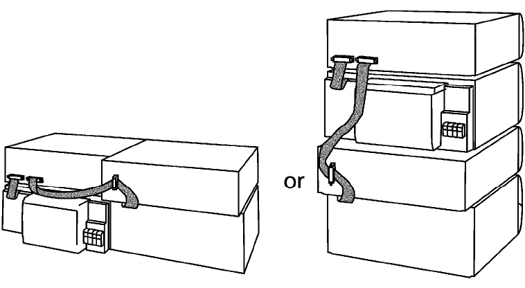
- Correction procedure
Faulty Tuner/Amplifier (SA-DV290) output IC (IC601).
(When a DC voltage is applied to speaker terminals.)
7. To Supply Power Source
This unit SA-DV290 is designed to operate on power supplied form system connected.
For system connection, refer to Fig. 7-1.
Fig. 7-1.
When the unit SA-DV290 has to test and service alone, use the following method to supply power
source.
1. Short the section between W902A Pin 3 and C740 (-) (GND). (Refer
to Fig. 7-2.)
2. Connect this unit to an AC power supply cord.
(This unit come to stand-by mode.)
3. Turn the unit ON.
Fig. 7-2.
15
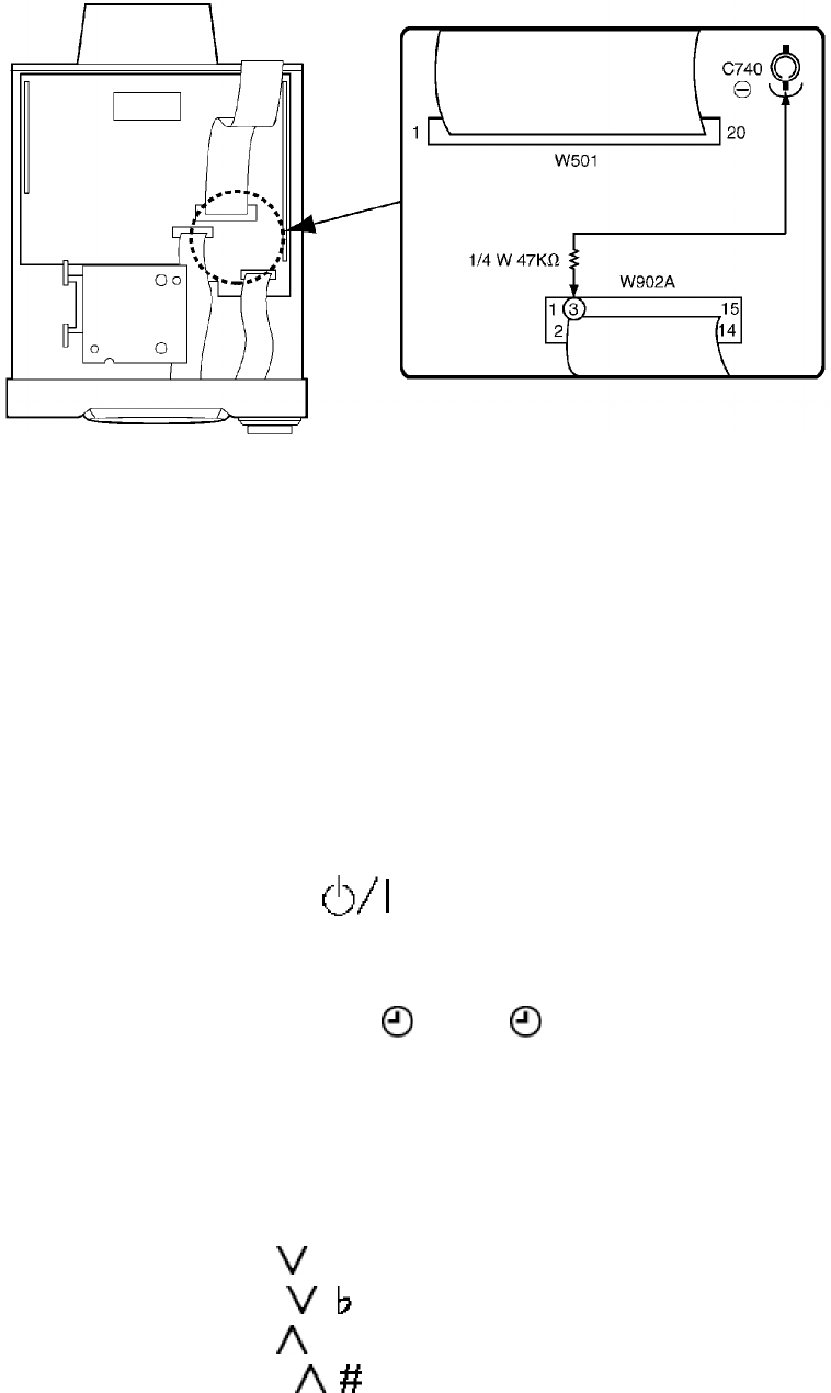
Notes:
Use only this method when checking the voltage etc..
In case of checking operations, use the system connections to supply power source.
8. Schematic Diagram Notes
8.1. Type Illustration of IC's, Transistors and Diodes
8.2. Schematic Diagram Notes
- This schematic diagram may be modified at any time with the
development of new technology.
Notes:
- S901: Power Standby/on ( ) switch.
- S902: Clock/timer (CLOCK/TIMER) switch.
- S903: Demo (-DEMO) switch.
- S904: Play timer/record timer ( PLAY/ REC) switch.
- S905: FM mode (FM AUTO/MONO) switch.
- S906: Tuning mode (TUNING MODE) switch.
- S907: Set (SET) switch.
- S908: Source input (INPUT SELECTOR) switch.
- S909: Echo (ECHO) switch. For [GN] area.
- S910: Tuning (TUNING, ) switch. For [EE] area.
S910: Tuning (TUNING,,) switch. For [GN] area.
- S911: Tuning (TUNING, ) switch. For [EE] area.
S911: Tuning (TUNING,,) switch. For [GN] area.
- S912: Tuner/band (TUNER/BAND) switch.
16
- S913: Digital super woofer (DIGITAL S. WOOFER) switch.
- S914, 915: RDS display mode (RDS, PS-DISP, MODE-PTY) switches.
For [EE] area.
S914, 915: KARAOKE, Voice mute (KARAOKE, V.MUTE) switch.
For [GN] area.
- S916: Key control (KEY CON) switch. For [GN] area.
- S917: MIC effect (MIC EFFECT, LOUNGE) switch. For [GN] area.
- S918: MIC effect (MIC EFFECT, CHORUS) switch. For [GN] area.
- VR901: Main volume V.R..
- Indicated voltage values are the standard values for the unit
measured by the DC electronic circuit tester (high-impedance)with
the chassis taken as standard. Therefore, there may exist some
errors in the voltage values, depending on the
internalimpedanceofthe DC circuit tester.
No mark: Power ON
- Important safety notice:
Components identified by mark have special characteristics
important for safety.
Furthermore, special parts which have purposes of fire-retardant
(resistors), high-quality sound (capacitors), low-noise (resistors),
etc. are used.
When replacing any of components, be sure to use only
manufacture's specified parts shown in the parts list.
Caution!
- Secondary trouble can be prevented by taking care during repair.
- IC and LSI are sensitive to static electricity.
- Cover the parts boxes made of plastics with aluminum foil.
- Ground the soldering iron.
- Put a conductive mat on the work table.
- Do not touch the legs of IC or LSI with the fingers directly.
- Voltage and signal lines
: Positive voltage line
: Negative voltage line
: Audio signal line
: Tuner signal line
: MIC signal line
17

9. Schematic Diagram
10. Printed Circuit Board Diagram
11. Block Diagram
12. Wiring Connection Diagram
13. Terminal Function of ICs
13.1. IC901 (C2BBFD000404): System Control/FL Drive
Pin
No.
Terminal
Name
I/O Function
1CHECK I Clock check signal input
2 LC72 DO O PLL data signal output for
tuner unit (Z101)
3LC72 CE O Chip enable signal output
for tuner unit (Z101)
4LC72 DI/
ST
IIF count data/stereo detect
signal input from tuner unit
(Z101)
5LC72 CK O Clock signal output for
tuner unit (Z101)
6ST/
AV.6CH
OSignal select output
7NC — Not used, open
8
9SEL
TUNER
—Not used, open
10 SEL/
TUNER
—Not used, connected to GND
11 AC IN I Power failure detect signal
input
12 RESET I Reset signal input
13 X IN I Oscillator connected
terminal (32.7kHz)
14 X OUT O
15 VSS —GND terminal
16 XC IN I Oscillator connected
terminal (6 MHz)
17 XC OUT O
18 VDD 1 I Power supply terminal
19 KEY TU I Operation key signal input
20 KEY
KARAOKE
IOperation key signal input
18

Pin
No.
Terminal
Name
I/O Function
21 SH REQ O Request signal output to
Sound Processor
22 NC(GND) — Not used, connected to GND
23 VR
JOGB
IVolume control signal input
24 VR
JOGA
25 MIC DET I Microphone connecting
detect signal input (Not
used, connected to VDD )
26 HP SW I Headphone connecting
detect signal input
27 RDS
CLK
IRDS clock signal input
28 RDS
DATA
IRDS data signal input
29 REMOCON IRemote control signal input
30-
37
8G-1G O Grid signal output
38-
45
P1-P8 O Segment signal output
46 VDD 3 I Power supply terminal
47-
50
P9-P12 O Segment signal output
51 -VP I Power supply terminal
(Negative)
52-
71
P13-P32 O Segment signal output
72 VDD 4 I Power supply terminal
73-
78
P33-P38 O Segment signal output
79 REGIN0 — Not used, connected to GND
80 REGIN1
81 STANDBY OLED (STANDBY) drive
signal output
82 TIMER O LED (TIMER) drive signal
output
83 S.W.LED O LED (DIGITAL S.WOOFER)
drive signal output
84 LOUNGE — LED (LOUNGE) drive signal
output (Not used,
connected to GND)
19

Pin
No.
Terminal
Name
I/O Function
85 CHORUS — LED (CHORUS) drive signal
output (Not used,
connected to VDD )
86 MUTE O Muting signal output
87 NC — Not used, oppen
88 POWER O Power control signal output
89 VSS 2 — GND terminal
90 VDD 2 I Power supply terminal
91 MUTE2 O Muting signal output
92 NC — Not used, open
93 MUTE3 O Muting signal output
94 SH CS I/O Chip select signal for Sound
Processor
95 SH DO O Serial communication
signal to Sound Processor
(Data signal output)
96 SH DI I Serial communication
signal to Sound Proccessor
(Data signal input)
97 SH CK I Serial communication
signal to Sound Processor
(Clock signal input)
98 E DET I Unusual condition detect
signal input
99 CR
TIMER
—Not used, open
100 SD I Station detector signal
input from tuner unit (Z101)
14. Replacement Parts List
Notes:
* Important safety notice:
Components identified by mark have special characteristics
important for safety. / Furthermore, special parts which have
purposes of fire-retardant (resistors), high-quality sound
(capacitors), low-noise (resistors), etc. are used. /
Whenreplacinganyof components, be sure to use only
manufacture's specified parts shown in the parts list.
* The parenthesized indications in the Remarks columns specify the
areas. / Parts without these indications can be used for all areas.
20

* Remote Control Ass'y: Supply period for three years from terminal
of production.
* Capacity values are in microfarads (uF) unless specified
otherwise, P=Pico-farads(pF), F=Farads (F)
* Resistance values are in ohms, unless specified otherwise, 1K=
1,000 (OHM), 1M=1,000K (OHM)
*The markings (RTL) indicate that the retention time is limited for
these items. After the discontinuation of these assemblies in
production, it will no longer be available.
*All parts are supplied by SPC.
Ref. No. Part No. Part Name & Description Pcs Remarks
1RGN2398-K NAME PLATE 1 (EE)
1RGN2399-K NAME PLATE 1 (GN)
2RMQ1018 GASKET 1
3REM0115 FAN UNIT 1
4REX0967 SYSTEM CONNECT.ASS’Y(20P) 1
5J0KD00000028 FERRITE CORE 1
6RGW0386-S KNOB,VOLUME 1
7RHN90001 NUT 1
8RKA0106-N FOOT RING 4
9RKF0606AD-K1 BACK COVER 1 (EE)
9RKF0606AE-K1 BACK COVER 1 (GN)
10 RKW0581-1V FL WINDOW 1
11 RMF0284 CUSHION 1 (GN)
12 RMN0427A CABLE HOLDER 1
13 RYP1168-S FRONT PANEL ASS’Y 1 (EE)
13 RYP1168A-S FRONT PANEL ASS’Y 1 (GN)
13-1 RGB0025-A TECHNICS BADGE 1
13-2 RGU1748-Q BUTTON,MIC EFFECT 1 (GN)
14 SHG1654 RUBBER 4
15 XTB3+10JFZ SCREW 12
16 XTB3+20JFZ SCREW 1
17 XTB3+8JFZ SCREW 12
18 XTW3+15T SCREW 2
19 XTB3+12FFZ SCREW 1
20 XTBS3+8JFZ1 SCREW 2
21 RHD30007-1S SCREW 4
22 RKM0395G-2S TOP CABINET 1
23 XTBS3+10JFZ1 SCREW 1
24 RAN0005EM-2 TUNER PACK(Z101) 1 (EE)
24 ENG06502Q TUNER PACK(Z101) 1 (GN)
25 RMN0526 FL HOLDER 1
26 RMN0744 FAN SUPPORTER 1
27 RMN0745 FAN SUPPORTER 1
28 REZ1300 WIRE ASS’Y 1
29 REZ1205 WIRE ASS’Y 1 (GN)
30 RGW0178-1S KNOB,MIC VOL 1 (GN)
31 XTB3+8JFZ SCREW 1 (GN)
21

Ref. No. Part No. Part Name & Description Pcs Remarks
A1 EUR7702290 REMOTE CONTROL 1 (EE)
A1 EUR7702300 REMOTE CONTROL 1 (GN)
A1-1 UR64EC2337E BATTERY COVER 1
A2 K2JA2A000018 VIDEO CORD 1
A3 REE1233-1 SPEAKER LEADS(GRAY/BLUE) 1
A4 REE1234-1 SPEAKER LEADS(RED/BLACK) 1
A5 RJA0019-2X AC MAINS LEAD 1 (EE)
A5 RJA0035-2X AC MAINS LEAD 1 (GN)
A7 RQCA0801 QUICK SET-UP GUIDE 1
A8 RQT6895-R O/I BOOK 1 (EE) Russian
A9 RQT6894-B O/I BOOK 1 English
A10 N1EAYY000002 FM INDOOR ANTENNA 1 (EE)
A10 N1EAYY000001 FM INDOOR ANTENNA 1 (GN)
A11 N1DAEYA00008 AM LOOP ANTENNA 1
A13 K1JZ24D00002 RCAJ ADAPTOR 1 (EE)
C151 ECA1CAK100XB 16V 10U 1 (EE)
C152 ECBT1H331KB3 50V 330P 1 (EE)
C153 ECBT1H102KB3 50V 1000P 1 (EE)
C154 ECBT1H561KB3 50V 560P 1 (EE)
C155 ECBT1H102KB3 50V 1000P 1 (EE)
C156,57 ECBT1H470J3 50V 47P 2 (EE)
C158,59 ECEA0JKS470 6.3V 47U 2 (EE)
C160 ECBT1H102KB3 50V 1000P 1 (EE)
C201,02 F1D1H1040002 50V 0.1U 2
C371 ECA0JAK101XB 6.3V 100U 1
C395,96 F1D1H473A012 50V 0.047U 2
C401 ECBT1H223KB5 50V 0.022U 1 F1D1H223A012 (GN)
C403 ECBT1C472KR5 16V 4700P 1 F1D1C472A010 (GN)
C404 RCE1HKA3R3BG 50V 3.3U 1 F2A1H3R3A015 (GN)
C405 ECBT1H102KB3 50V 1000P 1 (GN)
C406 ECEA1EKS4R7 25V 4.7U 1 (GN)
C407 ECBT1H103KB5 50V 0.01U 1 F1E1H1030001 (GN)
C408 ECBT1H223KB5 50V 0.022U 1 F1D1H223A012 (GN)
C409 ECEA1HKS010 50V 1U 1 (GN)
C410 F2A1C100A034 16V 10U 1 (GN)
C411 ECBA1H101KB3 50V 100P 1 (GN)
C412 ECBT1H102KB3 50V 1000P 1 (GN)
C413 ECEA1HKS010 50V 1U 1 (GN)
C414 ECA1CAM471XB 16V 470U 1 (GN)
C415 ECEA1HKS010 50V 1U 1 (GN)
C416 ECA1CAK100XB 16V 10U 1 (GN)
C417 ECBT1H223KB5 50V 0.022U 1 F1D1H223A012 (GN)
C421 F1D1H1040002 50V 0.1U 1 (GN)
C509,10 ECBT1H103KB5 50V 0.01U 2 F1E1H1030001
C550 ECBT1H103KB5 50V 0.01U 1 F1E1H1030001
C551 ECA1HAK2R2XB 50V 2.2U 1
C552 ECBT1H103KB5 50V 0.01U 1 F1E1H1030001
C554 ECA1CAM221XB 16V 220U 1
C555 ECEA1HSN010 50V 1U 1
C556 ECEA1CKN100 16V 10U 1
C559 ECBT1H103KB5 50V 0.01U 1 F1E1H1030001
22

Ref. No. Part No. Part Name & Description Pcs Remarks
C601,02 ECA1CAK100XB 16V 10U 2
C603,04 ECBT1H471KB3 50V 470P 2
C605,06 ECBT1H102KB3 50V 1000P 2
C607,08 ECBT1H471KB3 50V 470P 2
C609,10 ECBT1H560J3 50V 56P 2
C611 F1D1H390A006 50V 39P 1
C612 ECBT1H150JC3 50V 15P 1
C613,14 ECBT1H470J3 50V 47P 2
C616 ECEA1HKNR47B 50V 0.47U 1
C617,18 ECKR2H103ZU 500V 0.01U 2
C619-21 F1D1H1040002 50V 0.1U 3
C622 F2A1A1010020 10V 100U 1
C624-31 F1D1H1040002 50V 0.1U 8
C632 F1D1H473A012 50V 0.047U 1
C633,34 F1D1H1040002 50V 0.1U 2
C635-37 F1D1H473A012 50V 0.047U 3
C639-44 ECBT1H102KB3 50V 1000P 6
C645,46 F1D1H473A012 50V 0.047U 2
C647-50 ECBT1H102KB3 50V 1000P 4
C651 F1D1H473A012 50V 0.047U 1
C652 ECBT1H102KB3 50V 1000P 1
C655,56 ECA1CAK100XB 16V 10U 2
C659,60 ECA1CAK100XB 16V 10U 2
C664 ECA1CAK100XB 16V 10U 1
C701-04 ECA1VM472E 35V 4700U 4
C705 ECBT1H103KB5 50V 0.01U 1 F1E1H1030001
C706 RCE1VKA100BG 35V 10U 1 F2A1V1000011
C707,08 F1D1H473A012 50V 0.047U 2
C709 ECQV1H104JM3 50V 0.1U 1
C710 F1D1H473A012 50V 0.047U 1
C714 ECBT1H102KB3 50V 1000P 1
C715 ECA1EAM682XE 25V 6800U 1
C717 ECA1CAK330XB 16V 33U 1
C718 ECA1EAM101XB 25V 100U 1
C719,20 F1D1H473A012 50V 0.047U 2
C721 F2A1A1010020 10V 100U 1
C722 ECA1EAM101XB 25V 100U 1
C723,24 F1D1H473A012 50V 0.047U 2
C725 ECA1CAK470XB 16V 47U 1
C731 ECBT1H102KB3 50V 1000P 1
C732 ECBT1H223KB5 50V 0.022U 1 F1D1H223A012
C733 F1D1H473A012 50V 0.047U 1
C734 RCE1HKA3R3BG 50V 3.3U 1 F2A1H3R3A015
C735 F1D1H473A012 50V 0.047U 1
C737 ECA1HAM101XB 50V 100U 1
C740 ECA1CAK100XB 16V 10U 1
C741 ECQE1104KF3 100V 0.1U 1
C753 F1B1H1030001 50V 0.01U 1
C754 ECBT1H103KB5 50V 0.01U 1 F1E1H1030001
C755 ECA1CAM102X 16V 1000U 1
C758 ECBT1H103KB5 50V 0.01U 1 F1E1H1030001
C759 RCE1AKA470BG 10V 47U 1 F2A1A470A011
C761 ECQE1104KF3 100V 0.1U 1
C791 ECKWRS102MBC 250V 1000P 1
23

24

Ref. No. Part No. Part Name & Description Pcs Remarks
C901 EEAFC0J101B 6.3V 100U 1
C902 F2A1A102A018 10V 1000U 1
C903,04 ECBT1H103KB5 50V 0.01U 2 F1E1H1030001
C905 ECBT1H102KB3 50V 1000P 1
C907,08 ECBT1H471KB3 50V 470P 2
C909 ECBT1H102KB3 50V 1000P 1
C910 ECBT1H200JC5 50V 20P 1 F1D1H200A015
C911 F1D1H180A006 50V 18P 1
C912 F1D1H1040002 50V 0.1U 1
C914 ECA1HAK2R2XB 50V 2.2U 1
C915 ECBT1H103KB5 50V 0.01U 1 F1E1H1030001
C916 EEAFC0J101B 6.3V 100U 1
C917 ECBT1H103KB5 50V 0.01U 1 F1E1H1030001
C918 ECA0JAK101XB 6.3V 100U 1
C919,20 ECA1EAK220XB 25V 22U 2
C921 ECBT1H102KB3 50V 1000P 1
C922 ECA1VAK330XB 35V 33U 1
C923,24 F1D1H1040002 50V 0.1U 2
C925,26 ECBT1H102KB3 50V 1000P 2
C927,28 ECA1EAK220XB 25V 22U 2
C931 ECEA1CKN100 16V 10U 1
CN601 RJU057W012 CONNECTOR(12P) 1 K1KB12B00033
CN602 RJU057W008 CONNECTOR(8P) 1 K1KB08B00034
CN701-13 RJS1A1101T1 CONNECTOR(1P) 13
CN781 RJS10T5ZA CONNECTOT(10P) 1 K1MP10A00007
CN904 RJS4T5ZA CONNECTOR(4P) 1 K1MP04A00007 (GN)
CP101 K1KA11A00093 CONNECTOR(11P) 1
CP601 RJT057W012-1 CONNECTOR(12P) 1 K1KA12A00160
CP602 RJT057W008-1 CONNECTOR(8P) 1 K1KA08A00187
D151 MA4051M DIODE 1 MAZ40510M (EE)
D201 MAZ40560MF DIODE 1
D306 SELS5223C LED 1 B3AAA0000486
D500 MA165TA5 DIODE 1 MA2C16500E
D551,52 MA165TA5 DIODE 2 MA2C16500E
D553 MA700 DIODE 1 MA2C700
D554 MA165TA5 DIODE 1 MA2C16500E
D555 MA4100M DIODE 1 MAZ41000MF
D558 MA165TA5 DIODE 1 MA2C16500E
D581-83 B0AAMM000009 DIODE 3
D601,02 SB360L6508 DIODE 2 B0JAPG000014
D607 1SS291TA DIODE 1
D611 MA4051M DIODE 1 MAZ40510M
D657-59 MA165TA5 DIODE 3 MA2C16500E
D701-04 1N5402BF DIODE 4
D705 B0AAMM000009 DIODE 1
D711 B0AAMM000009 DIODE 1
D718 B0JANG000008 DIODE 1
D720 B0JANG000008 DIODE 1
D721 MA4300M DIODE 1 MAZ43000M
D723 MA4150-M DIODE 1 MAZ41500M
D725 MA4082LTA DIODE 1 MAZ40820LF
25
Ref. No. Part No. Part Name & Description Pcs Remarks
D730 MA4091H DIODE 1 MAZ40910H
D737 MA4082LTA DIODE 1 MAZ40820LF
D738-40 MA165TA5 DIODE 3 MA2C16500E
D741-44 B0AAMM000009 DIODE 4
D745 MA4051M DIODE 1 MAZ40510M
D746 B0AAMM000009 DIODE 1
D747 MA4068L DIODE 1 MAZ40680L
D751,52 1N5402BF DIODE 2
D753-55 B0AAMM000009 DIODE 3
D756,57 MA700 DIODE 2 MA2C700
D758 MA165TA5 DIODE 1 MA2C16500E
D761 B0AAMM000009 DIODE 1
D901,02 1SS291TA DIODE 2
D904 MA165TA5 DIODE 1 MA2C16500E
D905 1SS291TA DIODE 1
D906,07 MA165TA5 DIODE 2 MA2C16500E
D931 MA165TA5 DIODE 1 MA2C16500E
D933 MA165TA5 DIODE 1 MA2C16500E (EE)
D935 MA165TA5 DIODE 1 MA2C16500E (GN)
D951 LNJ301MPUJAD LED 1
D952,53 LNJ301MPUJAD LED 2 (GN)
D954 SELS5923C LED 1 B3ADA0000083
D961 MA4075M DIODE 1 MAZ40750M
D973 MA4030M DIODE 1 MAZ40300M
D974 MA165TA5 DIODE 1 MA2C16500E
F1 K5D202BL0001 FUSE 1
FL901 A2BB00000115 FL DISPLAY TUBE 1
FP791,92 K5G502AA0002 FUSE PROTECTOR 2
IC151 C1BB00000527 IC 1 (EE)
IC201 C0JBAR000292 IC 1
IC401 C1BA00000152 IC 1 (GN)
IC601 RSN311W64B IC 1
IC901 C2BBFD000404 IC 1
JK551 K1KA02A00008 CONNECTOR(2P) 1
JK601,02 K4BC04B00028 JACK,SPEAKERS 2
JK603 K2HA103B0015 JACK,SPEAKERS 1
JK701 K2AA2B000002 JACK,AC INLET 1
JK901,02 RJJ65MA01 JACK,MIC 2 K2HB102J0032 (GN)
JK903 RJJ37TN02-C JACK,HEADPHONES 1 K2HC103A0009
L151,52 ELEXT101KA9 COIL 2 (EE)
L153 G0C1R0JA0019 COIL 1 (EE)
L401 RLQA3R3JT1-Y COIL 1 G0C3R3JA0019 (GN)
L601-06 RLQYR73MW1-0 COIL 6 G0ZZ00001606
L701 ELF15N035AN COIL 1
L901 G0C100JA0019 COIL 1
L902 G0C1R0JA0019 COIL 1
26

27

Ref. No. Part No. Part Name & Description Pcs Remarks
P1 RPG4396 PACKING CASE(SA) 1
P1 RPG4397 PACKING CASE(RS) 1
P1 RPG4398 PACKING CASE(SH) 1
P1 RPG4399 PACKING CASE(SL) 1
P2 RPN1194 POLYFOAM(SA) 1
P2 RPN1195-2 POLYFOAM(RS) 1
P2 RPN1196 POLYFOAM(SH) 1
P2 RPN1197 POLYFOAM(SL) 1
P3 SPP740-1 PROTECTION COVER 4
P4 RPF0139-1 PROTECTION BAG(ACCESS.) 1
P5 RPG6349 PACKING CASE(SYSTEM) 1 (EE)
P5 RPG6350 PACKING CASE(SYSTEM) 1 (GN)
P6 RPQ0951 PAD 1
PCB1 REP3337K-M MAIN P.C.B. ASS’Y 1 [RTL](EE)
PCB1 REP3337L-M MAIN P.C.B. ASS’Y 1 [RTL](GN)
PCB2 REP3338A-S SUB P.C.B. ASS’Y 1 [RTL](EE)
PCB2 REP3338B-S SUB P.C.B. ASS’Y 1 [RTL](GN)
Q401 2SC5398RSTA TRANSISTOR 1 B1AACF000059 (GN)
Q503 2SC5398RSTA TRANSISTOR 1 B1AACF000059
Q551 2SA1995RSTA TRANSISTOR 1 B1ACDF000006
Q553 B1AAGC000006 TRANSISTOR 1
Q554 2SA1995RSTA TRANSISTOR 1 B1ACDF000006
Q555 B1AAGC000006 TRANSISTOR 1
Q556 2SC5398RSTA TRANSISTOR 1 B1AACF000059
Q557 2SA1995RSTA TRANSISTOR 1 B1ACDF000006
Q601,02 2SC5398RSTA TRANSISTOR 2 B1AACF000059
Q605-10 B1AAGC000006 TRANSISTOR 6
Q612 UN411FTA TRANSISTOR 1 UNR411F00A
Q701 2SD2374PQAU TRANSISTOR 1 2SD23740J1AU
Q702 2SB1548PQAU TRANSISTOR 1 2SB15480J1AU
Q703,04 2SD2137PQTA TRANSISTOR 2 2SD21370PA
Q705 2SA1995RSTA TRANSISTOR 1 B1ACDF000006
Q707 2SB14170JA TRANSISTOR 1
Q708 UN4211 TRANSISTOR 1 UNR4211
Q709 B1AAGC000006 TRANSISTOR 1
Q711,12 2SB1548PQAU TRANSISTOR 2 2SB15480J1AU
Q723 2SC3940AQSTA TRANSISTOR 1 2SC3940ARA
Q725 2SC5398RSTA TRANSISTOR 1 B1AACF000059
Q726 2SC3940AQSTA TRANSISTOR 1 2SC3940ARA
Q791 B1AAGC000006 TRANSISTOR 1
Q901 UN4212 TRANSISTOR 1 UNR4212
Q902 UN411FTA TRANSISTOR 1 UNR411F00A
R151,52 ERDS2FJ102 1/4W 1K 2 (EE)
R153,54 ERDS2FJ104 1/4W 100K 2 (EE)
R155 ERDS2FJ121 1/4W 120 1 (EE)
R157,58 ERDS2FJ102 1/4W 1K 2 (EE)
R202-05 ERDS2FJ104 1/4W 100K 4
R211 ERDS2FJ271 1/4W 270 1
R229,30 ERDS2FJ102 1/4W 1K 2
R401,02 ERDS2FJ681 1/4W 680 2 (GN)
R403 ERDS2FJ223 1/4W 22K 1 (GN)
28

Ref. No. Part No. Part Name & Description Pcs Remarks
R404 ERDS2FJ471 1/4W 470 1 (GN)
R405 ERDS2FJ472 1/4W 4.7K 1 (GN)
R406 ERDS2FJ474 1/4W 470K 1 (GN)
R407 ERDS2FJ472 1/4W 4.7K 1 (GN)
R409 ERDS2FJ472 1/4W 4.7K 1 (GN)
R410 ERDS2FJ222 1/4W 2.2K 1 (GN)
R411 ERDS2FJ331 1/4W 330 1 (GN)
R412 ERDS2TJ105 1/4W 1M 1 (GN)
R415 ERDS2FJ471 1/4W 470 1 (GN)
R416 ERDS2FJ331 1/4W 330 1 (GN)
R421 ERDS2FJ223 1/4W 22K 1 (GN)
R509-12 ERDS2FJ470 1/4W 47 4
R544 ERDS2FJ103 1/4W 10K 1
R546,47 ERDS2TJ183 1/4W 18K 2
R551 ERDS2TJ183 1/4W 18K 1
R552 ERDS2FJ473 1/4W 47K 1
R555 ERDS2FJ223 1/4W 22K 1
R556 ERDS2FJ104 1/4W 100K 1
R557 ERDS2FJ103 1/4W 10K 1
R558 ERDS2FJ222 1/4W 2.2K 1
R559 ERDS2FJ472 1/4W 4.7K 1
R560,61 ERDS2FJ104 1/4W 100K 2
R563,64 ERDS2TJ272T 1/4W 2.7K 2
R566 ERDS2FJ683 1/4W 68K 1
R567 ERG1SJ220 1W 22 1
R568 ERDS2FJ101 1/4W 100 1
R569 ERDS2FJ103 1/4W 10K 1
R570 ERDS2TJ225 1/4W 2.2M 1
R572 ERDS2FJ153 1/4W 15K 1
R591 ERDS2FJ472 1/4W 4.7K 1
R597,98 ERDS2FJ222 1/4W 2.2K 2
R601-04 ERDS2FJ332 1/4W 3.3K 4
R605,06 ERDS2FJ472 1/4W 4.7K 2
R607-09 ERDS2FJ563 1/4W 56K 3
R610 ERDS2FJ154 1/4W 150K 1
R611,12 ERDS2FJ563 1/4W 56K 2
R614,15 ERDS2FJ472 1/4W 4.7K 2
R617,18 ERDS2FJ472 1/4W 4.7K 2
R619,20 ERDS2TJ124 1/4W 120K 2
R621 ERDS2FJ154 1/4W 150K 1
R622,23 ERDS2TJ124 1/4W 120K 2
R624 ERDS2FJ154 1/4W 150K 1
R627 ERDS2FJ474 1/4W 470K 1
R628 ERDS2FJ223 1/4W 22K 1
R631,32 ERDS2TJ392 1/4W 3.9K 2
R635 ERDS2FJ222 1/4W 2.2K 1
R637 ERDS2FJ153 1/4W 15K 1
R638 ERDS2FJ683 1/4W 68K 1
R639,40 ERDS1FJ100 1/2W 10 2
R641,42 ERDS2FJ100 1/4W 10 2
R643,44 ERDS1FJ100 1/2W 10 2
R645,46 ERDS2FJ100 1/4W 10 2
R647 ERDS2FJ271 1/4W 270 1
R648 ERD2FCG121 1/4W 120 1
29

Ref. No. Part No. Part Name & Description Pcs Remarks
R649-52 ERDS1FJ100 1/2W 10 4
R683-86 ERDS2FJ102 1/4W 1K 4
R687,88 ERDS2FJ152 1/4W 1.5K 2
R691 ERDS1FJ680 1/2W 68 1
R692,93 ERDS2FJ102 1/4W 1K 2
R694 ERDS2FJ223 1/4W 22K 1
R695 ERDS2FJ471 1/4W 470 1
R696 ERDS2FJ473 1/4W 47K 1
R708 ERDS2FJ472 1/4W 4.7K 1
R712 ERDS2FJ222 1/4W 2.2K 1
R719 ERDS2FJ332 1/4W 3.3K 1
R720 ERDS2TJ392 1/4W 3.9K 1
R721 ERD2FCJ4R7 1/4W 4.7 1
R722 ERQ16NKW2R2E 1/6W 2.2 1
R723 ERDS2FJ562 1/4W 5.6K 1
R724 ERDS2TJ392 1/4W 3.9K 1
R725 ERDS2FJ100 1/4W 10 1
R727 ERDS2TJ392 1/4W 3.9K 1
R729 ERDS2FJ221 1/4W 220 1
R738 ERDS2TJ392 1/4W 3.9K 1
R739 ERDS2FJ473 1/4W 47K 1
R749 ERDS2FJ102 1/4W 1K 1
R753,54 ERX1SJR47 1W 0.47 2
R761 ERG1SJ221 1/2W 220 1
R763 ERDS2FJ472 1/4W 4.7K 1
R764 ERDS2FJ331 1/4W 330 1
R765 ERDS1FJ471 1/2W 470 1
R767 ERG1SJ270 1W 27 1
R768 ERDS2FJ101 1/4W 100 1
R769 ERG1SJ270 1W 27 1
R771 ERDS2FJ222 1/4W 2.2K 1
R772 ERDS2FJ223 1/4W 22K 1
R773,74 ERDS1FJ180 1/2W 18 2
R776 ERDS2FJ103 1/4W 10K 1
R777 ERDS2FJ102 1/4W 1K 1
R793 ERDS2TJ1R0 1/4W 1.0 1 (EE)
R794 ERDS2FJ473 1/4W 47K 1
R794A ERQ16NKW1R0E 1/6W 1 1 (GN)
R795 ERDS2TJ392 1/4W 3.9K 1
R796,97 ERDS2FJ2R2 1/4W 2.2 2
R798 ERQ16NKW2R2E 1/6W 2.2 1
R901 ERDS2FJ821 1/4W 820 1
R902 ERDS2FJ102 1/4W 1K 1
R903 ERDS2FJ122 1/4W 1.2K 1
R904 ERDS2FJ152 1/4W 1.5K 1
R905 ERDS2FJ182 1/4W 1.8K 1
R906 ERDS2FJ222 1/4W 2.2K 1
R907 ERDS2FJ332 1/4W 3.3K 1
R908 ERDS2FJ472 1/4W 4.7K 1 (GN)
R909 ERDS2FJ182 1/4W 1.8K 1
R910 ERDS2FJ222 1/4W 2.2K 1
R911 ERDS2FJ332 1/4W 3.3K 1
R912 ERDS2FJ472 1/4W 4.7K 1
R913 ERDS2FJ821 1/4W 820 1
30

Ref. No. Part No. Part Name & Description Pcs Remarks
R914 ERDS2FJ102 1/4W 1K 1
R915 ERDS2FJ122 1/4W 1.2K 1
R916 ERDS2FJ152 1/4W 1.5K 1
R918 ERDS2FJ103 1/4W 10K 1
R919 ERDS2FJ153 1/4W 15K 1
R921,22 ERDS2FJ103 1/4W 10K 2
R924,25 ERDS2FJ102 1/4W 1K 2
R926 ERDS2FJ222 1/4W 2.2K 1
R928 ERDS2FJ473 1/4W 47K 1
R929-32 ERDS2FJ102 1/4W 1K 4
R934-36 ERDS2FJ101 1/4W 100 3
R937 ERDS2FJ103 1/4W 10K 1
R939 ERDS2FJ152 1/4W 1.5K 1
R940,41 ERDS2FJ102 1/4W 1K 2
R942 ERDS2FJ222 1/4W 2.2K 1
R943 ERDS2FJ101 1/4W 100 1
R944 ERDS2FJ222 1/4W 2.2K 1
R945 ERDS2FJ101 1/4W 100 1
R946 ERDS2FJ102 1/4W 1K 1
R947,48 ERDS2FJ104 1/4W 100K 2 (GN)
R949 ERDS2FJ472 1/4W 4.7K 1
R950 ERDS2FJ101 1/4W 100 1
R951 ERDS2FJ334 1/4W 330K 1
R952 ERDS2TJ106T 1/4W 10M 1
R953 ERDS2FJ101 1/4W 100 1
R954 ERDS2FJ104 1/4W 100K 1
R956-58 ERDS2FJ102 1/4W 1K 3
R959 ERDS2FJ470 1/4W 47 1
R960 ERDS2FJ152 1/4W 1.5K 1
R961,62 ERDS2FJ223 1/4W 22K 2
R965,66 ERDS2TJ392 1/4W 3.9K 2
R969 ERDS2TJ272T 1/4W 2.7K 1
R974 ERDS2FJ102 1/4W 1K 1
R975 ERDS2FJ223 1/4W 22K 1
R976 ERDS2FJ104 1/4W 100K 1
R986 ERDS2FJ152 1/4W 1.5K 1
R987,88 ERDS2FJ102 1/4W 1K 2
R990 ERDS2FJ104 1/4W 100K 1
R991 ERDS2FJ473 1/4W 47K 1
R992 ERDS2FJ221 1/4W 220 1 (GN)
R993,94 ERDS2FJ104 1/4W 100K 2
R995 ERDS2FJ221 1/4W 220 1
R996,97 ERDS2FJ151 1/4W 150 2
R998 ERDS2FJ221 1/4W 220 1 (GN)
R999 ERDS2FJ104 1/4W 100K 1
RL702 K6B1AEA00003 RELAY 1
S901-08 EVQ11G05R SW,OPERATION 8
S909 EVQ11G05R SW,OPERATION 1 (GN)
S910-15 EVQ11G05R SW,OPERATION 6
S916-18 EVQ11G05R SW,OPERATION 3 (GN)
31
Ref. No. Part No. Part Name & Description Pcs Remarks
T701 ETP76VST617A POWER TRANSFORMER 1
T702 ETP28KBZ21BG POWER TRANSFORMER 1
VR401 EVUE27FK3B53 V.R.,MIC VOLUME 1 (GN)
VR901 EVQVBXFK124B V.R.,VOLUME 1
X151 H0H433400001 OSCILLATOR 1 (EE)
X901 EF0EC6004T4 OSCILLATOR 1 EFOEC6004T4
X902 H0A327200027 OSCILLATOR 1
Z701 ENC471D5A ZNR 1 J0LG00000008
Z901 B3RAD0000028 REMOTE SENSOR 1
15. Cabinet Parts Location
15.1. SA-DV290EE
32
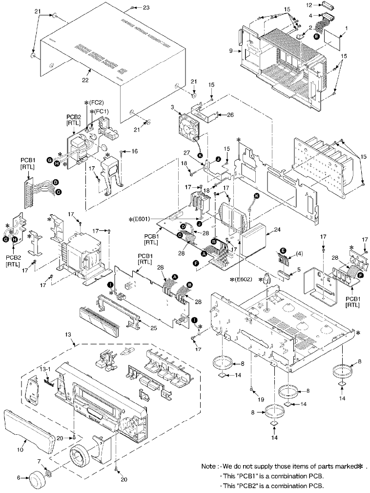
15.2. SA-DV290GN
33
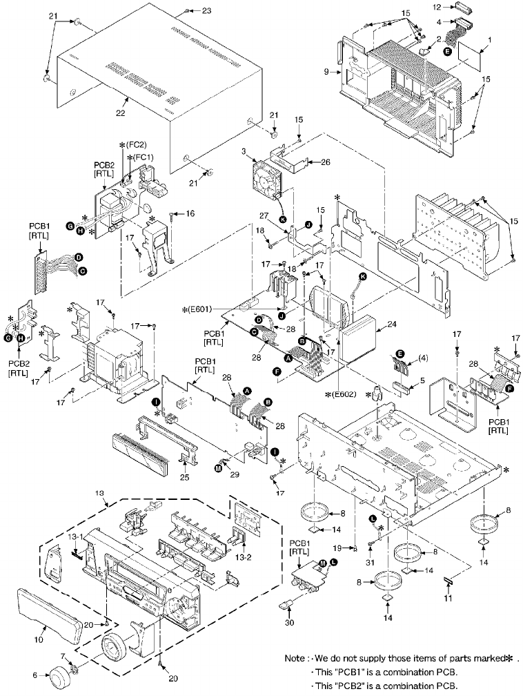
16. Packaging
34
17. Schematic Diagram for printing with A4 size
K0305 YH/HM
35
25 26 27 28 29 30 31 32 33 34 35 36
SA-DV290(EE,GN) MAIN,POWER SUPPLY CIRCUIT DIAGRAM
M
Q708
UN4211TA
SWITCHING
(POWER)
Q601 Q602
D756
MA700ATA
C603 470P
C604 470P
C607 470P
C608 470P
C649 1000P
C650 1000P
C605 1000P
C606 1000P
C648
1000P
C617
0.01
R637
15K
R638
68K
R619 120K
R622 120K
R621 150K
R624 150K
R620
120K
R612 56K
R611 56K
R610 150K
R609 56K
R608 56K
R607 56K
C610 56P
C609 56P
C612 15P
C611 39P
C614 47P
C613 47P
R627
470K
C616
50V0.47
N
D601
SB360L6508
D602
SB360L6508
D754
RL1N4003N02
C761
0.1
D701
1N5402BM21 C709
0.1
IC601
RSN311W64B
POWER AMP
D757
MA700ATA
123456789101112131415181920212223242526 1617
R604
3.3K
R601
3.3K
R602
3.3K
R618
4.7K
Q601,602
2SC5398RSTA
PROTECTOR
D607
1SS291TA
L
K
D658
MA165TA
D657
MA165TA
B
A
R685
1K
R686
1K
Q605,607,608
2SD2144STA
MUTING
Q607
Q608
C705
0.01
G
R776
10K
Q709
2SD2144STA
SWITCHING
(POWER)
R738
3.9K
R739
47K
C622
10V100
D659
MA165TA
D751
1N5402BM21
D703
1N5402BM21
D753
RL1N4003N02
D761
RL1N4003N02
D755
RL1N4003N02
D752
1N5402BM21
D702
1N5402BM21
D704
1N5402BM21
G
F
E
D
AB C
D558
MA165TA
R544
10K
R572
15K
R648
120
C618
0.01
R635
2.2K
C619
0.1
Q503
2SC5398RSTA
SWITCHING
C704
35V4700
C702
35V4700
C703
35V4700
C701
35V4700
R761
220
R628
22K
R691
68
R647
270
R623
120K
CN781
F
C
A
B
D
E
Q551
2SA1995RSTA
SIGNAL LEVEL DET.
Q555
2SD2144STA
SIGNAL LEVEL DET.
Q702
2SB1548PQAU
REGULATOR
Q725
2SC5398RSTA
STABILIZER Q705
2SA1995RSTA
STABILIZER
Q701
2SD2374PQAU
REGULATOR
R556
100K
R557
10K
C721
10V100
D725
MA4082LTA
R729
220
C723
0.047
C639
1000P
C640
1000P
C641
1000P
C642
1000P
C732
0.022
C647
1000P
D738
MA165TA
D730
MA4091HTA
R768
100
R724
3.9K
C718
25V100
D723
MA4150HTA
R723
5.6K
C719
0.047
R725
10
C724
0.047
C710
0.047
R546
18K
R551
18K
R552
47K
R555
22K
C550
0.01
D552
MA165TA D555
MA4100MTA
R547
18K
E602
E601
R749
1K
D739
MA165TA
POWER SUPPLY CIRCUIT
C
11032 4 5 6 7 8 9
W701B
11032 4 5 6 7 8 9
R720
3.9K
C734
50V3.3
D758
MA165TA
C722
25V100
C720
0.047
C717
16V33
MAIN CIRCUIT
B
G
R765
470
N
R569
10K
D554
MA165TA
C371
6.3V100
Q556
2SC5398RSTA
MOTOR DRIVE
R568
100
D553
MA700ATA
C556
16V10
C555
50V1
Q557
2SA1995RSTA
MOTOR DRIVE
Q553
2SD2144STA
MOTOR DRIVE
R570
2.2M
R560
100K
C559
0.01
D581
RL1N4003N02
R567
22
FAN MOTOR
JK551
R566
68K
Q554
2SA1995RSTA
SIGNAL LEVEL DET.
M
R719
3.3K
Q703,704
2SD2137PQTA
REGULATOR
R796
2.2
Q703
Q704
R769
27
R727
3.9K
C554
16V220
R561
100K
C552
0.01 R559
4.7K
R591
4.7K
C551
50V2.2
D551
MA165TA
12
D583
RL1N4003N02
N
R721
4.7
R722
2.2
AB
R753
0.47
R754
0.47
Q711,712
2SB1548PQAU
REGULATOR
Q711
R797
2.2 R767
27
R558
2.2K
D582
RL1N4003N02
Q712
R683
1K
Q605 N
R603
3.3K
: POSITIVE VOLTAGE LINE
: NEGATIVE VOLTAGE LINE :AUDIO SIGNAL LINE
7.6V
-
10.4V
0V0V59.5V
-
59.5V
0V28.9V
-
29.3V
0V0V0V0V
-
0.2V
29.4V
-
29.7V
0V0V54.1V
-
51.4V
0V0V0V0V
0V
0V
4.7V4.7V
0V 0V
0.7V
0V 0V
2.1V
14.7V
0.7V
0V
0.7V
0V
29.2V
29.2V14.7V
15.2V
-
30.1V
-
11V
-
10.4V
-
11V
-
0.6V
14.1V
13.6V
9.6V
10.2V
10.4V
-
10.4V
14.7V
7.6V
7V
0V
7.6V
0.3V
-
10.4V
-
10.4V
-
10.4V
7.6V
7.6V
6.8V
FAN ON:1.6V
0V
FAN ON:0V
0.5V
FAN ON:0V4.7V
0V
0.5V
8.1V
8.1V
30.1V
30.1V7.6V
7.6V
0V
10.4V
13.6V
10.4V 14.1V
13.6V
0.7V
0V
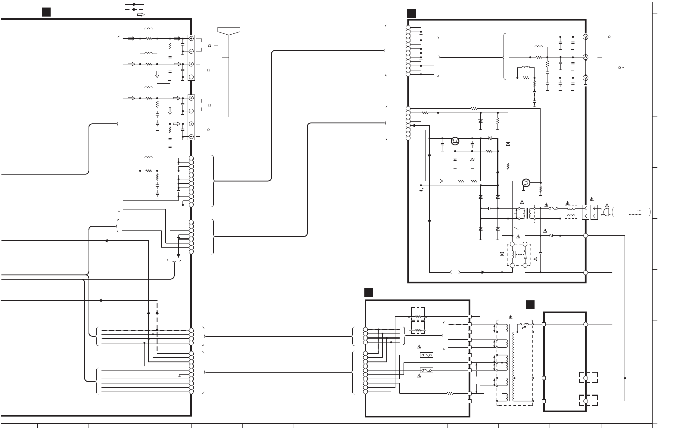
A
B
C
D
E
F
G
H
37 38 39 40 41 42 43 44 45 46 47 48
SA-DV290(EE,GN) MAIN, AC IN, POWER TRANSFORMER(A)&(B) CIRCUIT DIAGRAM
L601
2
1
3
4
5
6
7
8
9
10
11
12
2
1
3
4
5
6
7
8
R639
10
C621
0.1
E
F
D
CP601
CP602
R641
10
A
B
IJ
C
C631
0.1
G
Lch
JK601
HF(6 )
LF(8 )
Rch
JK602
HF(6 )
LF(8 )
A
B
C
R651
10
C627
0.1
C629
0.1
C635
0.047
R649
10
L605
R642
10
C620
0.1
C630
0.1
R640
10
L602
C637
0.047
C636
0.047
R652
10
C626
0.1
C628
0.1
R650
10
L606
C632
0.047
SPEAKERS
GND
GND
C OUT
C OUT
GND
GND
GND
GND
SUR L OUT
SUR L OUT
SUR R OUT
SUR R OUT
ECO
SH SYNC
SA SYNC
D.GND
BU5V
RS13V
+B
NC
W722A
W721A
2
1
3
4
5
6
7
8
9
10
2
1
3
4
E
F
H
D
C
G
F
E
D
S1
S2
S3
S4
AC1
CT
AC2
S7
FL2
FL1
S1
S2
S3
S4
MAIN CIRCUIT
B
C
A
D
B
T701
CN701
CN702
CN703
CN704
CN705
CN706
CN707
CN708
CN709
CN710
CN601
C652
1000P
C644
1000P
C643
1000P
C651
0.047
C646
0.047
C645
0.047
Rch
Lch
JK701
L701
F1 T2A
T702
Z701
C791
1000P
3 1
24 RL702
R794
47K
Q791
2SD2144STA
RELAY DRIVE
D745
MA4051MTA
C753
0.01
C755
16V1000
Q726
2SC3940AQSTA
REGULATOR D746
RL1N4003N02
D747
MA4068LTA C758
0.01
C759
10V47
C754
0.01
D500
MA165TA
W2/W3
W1
CN602
FP791
K5G502AA0002
JK603
CENTER(8 )
SURROUND(8 )
R646
10
C624
0.1
C634
0.1
R644
10
L604
R645
10
C625
0.1 C633
0.1
R643
10
L603
DAC IN CIRCUIT
2
1
3
4
5
6
7
8
9
10
11
12
2
1
3
4
5
6
7
8
R777
1K
R774
18
D711
RL1N4003N02 R773
18
R712 2.2K
A
B
C
A
C
B
R795
3.9K
D743
RL1N4003N02
D741
RL1N4003N02
D742
RL1N4003N02
D744
RL1N4003N02
R771
2.2K D740
MA165TA
POWER TRANSFORMER
(B) CIRCUIT
F
POWER TRANSFORMER
(A) CIRCUIT
E
W722B
W721B
10
2
1
3
4
5
6
7
8
9
CN713
CN712
CN711 W1
W2
2
1
3
4
R772
22K
A
B
C
D
FP792
K5G502AA0002
SPEAKERS
GND
GND
C OUT
C OUT
GND
GND
GND
GND
SUR L IN
SUR L IN
SURRIN
SURRIN
ECO
SH SYNC
SA SYNC
D.GND
BU5V
RS13V
+B
NC
S1
S2
S3
S4
AC1
CT
AC2
S7
FL2
FL1
S1
S2
S3
S4
R798
2.2
R793
1
W3
For [EE] area.
R794A
1
AC IN
230-240V 50Hz [GN]
230 50Hz [EE]
For [GN] area.
For [GN] area.
For
[EE]
area.
: POSITIVE VOLTAGE LINE
: NEGATIVE VOLTAGE LINE
: AUDIO SIGNAL LINE
0.7V
0V
6V
10.7V6V
6.7V
AC22.6V
AC22.6V
AC11.7V
AC11.7V
AC4.7V
AC
29.2V
AC9.4V
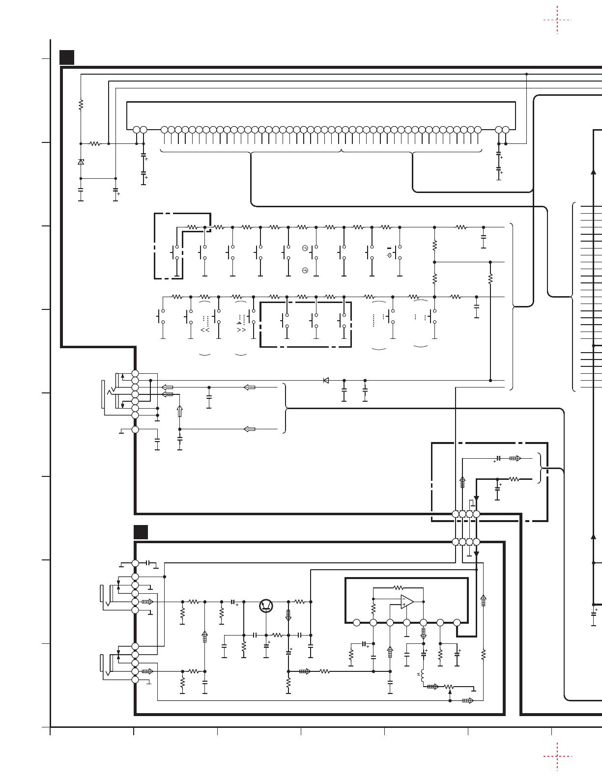
121110987654321
A
B
C
D
E
F
G
H
R922
10K
R921
10K
SA-DV290(EE,GN) OPERATION,MIC JACK CIRCUIT DIAGRAM
S904
(PLAY/ REC)
FL901 (A2BB00000115)
1
7
5
4
6
3
2
T
S
S908
(INPUT SELECTOR)
S907
(SET)
S906
(TUNING MODE)
S905
(FM AUTO/MONO)
JK903
PHONES
3.5mm STEREO
R997
150
R996
150
D973
MA4030MTA
C921
1000P
C922
35V33
C920
25V22
R944
2.2K
R912
4.7K R911
3.3K R910
2.2K R909
1.8K R916
1.5K R915
1.2K R914
1K R913
820
R907
3.3K R906
2.2K R905
1.8K R904
1.5K R903
1.2K R902
1K R901
820
FL DISPLAY
1 6 8 10 11 12 13 14 15 16 17 18 19 20 21 22 23 24 25 26 27 28 29 30 31 32 33 34 35 36 37 38 39 40 41 42 43 44 45 46 47 48 49 50 53 542 5 7 9
W905
S901
(/)
C928
25V22
AOPERATION CIRCUIT
C919
25V22
C927
25V22
C396
0.047
C923
0.1
C395
0.047
D974
MA165TA
C907
470P
C924
0.1
C904
0.01
R924
1K
C908
470P
R925
1K
S912
(TUNER/ BAND)
S913
(DIGITAL
S.WOOFER)
ABCD
E
FGH I JKLMNOPQRSTU
X
W
V
ABCDEFGHIJKLMNOPQRSTUVWXYZ
S902
(CLOCK/ TIMER)
S903
(
-
DEMO)
IC901
C2BBFD000404
SYSTEM CONTROL/
FL DRIVE
C
B
A
Q901
UN4212TA
RESET
R936
100
R919
15K
R991
47K
R918 10K
R928 47K
L902 1 H
D901
1SS291TA
L901
10 H
R951
330K
R952
10M
A
B
C
D
E
F
G
H
I
J
K
L
M
N
O
P
Q
R
S
T
U
V
W
X
Y
Z
R993
100K D931
MA165TA
D935 MA165TA
R990
100K
C916
6.3V100
D951
LNJ301MPUJAD
(DIGITAL S.WOOFER)
R995
220
R986
1.5K
D306
SELS5223C
( ) R939
1.5K
C905
1000P
C901
6.3V100
R935 100
R934 100
R988 1K
R937 10K
R987 1K
R926
2.2K
C912
0.1
R954
100K
C926
1000P
R960 1.5K
R958 1K
R999
100K
R959 47
R969
2.7K
D902
1SS291TA
C903
0.01
C902
10V1000
X902
(32.7kHz)
C911
18P
C910
20P
X901
(6MHz)
1
3
2
D905 1SS291TA
EFIKLMNO Q
R940
1K
R929 1K
R930 1K
R932 1K
R931 1K
R976
100K
R956
1K R957
1K
C915
0.01
C925
1000P
R953
100
A
B
C
D
G
H
J
C914
50V2.2
D904
MA165TA
A
B
C
ABCDE FGH I J K LMNOPQRS T UVWX
1
11
21
2
12
22
3
13
23
4
14
24
5
15
25
6
16
26
7
17
27
8
18
28
9
19
29
10
20
30
3132333435363738394041424344454647484950
51
52
53
54
55
56
57
58
59
60
61
62
63
64
65
66
67
68
69
70
71
72
73
74
75
76
77
78
79
80
81 82 83 84 85 86 87 88 89 90 91 92 93 94 95 96 97 98 99
100
-
VP
P13
P14
P15
P16
P17
P18
P19
P20
P21
P22
P23
P24
P25
P26
P27
P28
P29
P30
P31
P32
VDD4
P33
P34
P35
P36
P37
P38
REGIN0
REGIN1
8G
REMOCON
RDS DATA
RDS CLK
HP SW
MIC DET
VR JOGA
VR JOGB
NC(GND)
SH REQ
KEY KARAOKE
KEY TU
VDD1
XC OUT
XC IN
Vss
X OUT
XIN
RESET
AC IN
SEL/ TUNER
SEL TUNER
ST/ AV.6CH
LC72 CK
LC72 DI/ ST
LC72 CE
LC72 DO
CHECK
STAND-BY
TIMER
S.W.LED
LOUNGE
CHORUS
MUTE
NC
POWER
Vss2
VDD2
MUTE2
NC
MUTE3
SHCS
SHDO
SHDI
SHCK
E DET
CR TIMER
SD
VDD3
P12
P11
P10
P9
P8
P7
P6
P5
P4
P3
P2
P1
1G
2G
3G
4G
5G
6G
7G
R994 100K
U
R949
4.7K
R950
100
Y
D953
LNJ301MPUJAD
(MIC EFFECT CHORUS) R998
220
R992
220
D952
LNJ301MPUJAD
(MIC EFFECT LOUNGE)
S918
(MIC EFFECT
CHORUS)
S917
(MIC EFFECT
LOUNGE)
S916
(KEY CON)
1 2 3 4
W904B
MIC JACK CIRCUIT
IC401
TA2011S
MIC AMP
JK902
MIC2
6.3mm
MONAURAL 1
2
4
5
6
JK901
MIC1
6.3mm
MONAURAL 1
2
4
5
6
6712345
C403
4700P
Q401
2SC5398RSTA
MIC AMP
C406
25V4.7
R415
470
C413
50V1
R412
1M
C416
16V10
C412
1000P
C410
16V10
C411
100P
R411
330
R410
2.2K
R409
4.7K
C407
0.01
C409
50V1
C408
0.022
R406
470K
R407
4.7K
C405
1000P
R405
4.7K
C417
0.022
R404
470
C404
50V3.3
R402
680
R421
22K
C401
0.022
R403
22K
R401
680
L401
3.3 H
VR401
5K(B)
(MIC VOL)
W401
C421
0.1
G
1 2 3 4
C414
16V470
CN904
C415
50V1
R416
330
P
R
Y
R947 100K
R948
100K
For [GN] area.
D933 MA165TA
For [EE] area.
For [GN] area.
D
E
For [GN] area.
S911
TUNING, ,# [GN]
TUNING, [EE]
S910
TUNING, , [GN]
TUNING, [EE]
S909
(ECHO)
R908
4.7K
For [GN] area.
For [GN] area.
D954
SELS5923C
(PLAY/ REC)
For [GN] area.
S914
KARAOKE [GN]
RDS DISP
MODE PS [EE]
S915
V.MUTE [GN]
RDS DISP
MODE PTY [EE]
For
[GN]
area.
:AUDIO SIGNAL LINE: POSITIVE VOLTAGE LINE : NEGATIVE VOLTAGE LINE
5.1V
5.1V
2V/2ms.DIV.
5V
0V
5V
0V
T10ms.
2V/2ms.DIV. 0V
5V
-
30.1V
-
30.1V
-
29.3V
-
29.3V
-
29.3V
-
26.3V
-
20.5V
-
29.3V
-
29.3V
-
29.3V
-
23.5V
-
20.5V
-
23.4V
-
23.4V
-
23.7V
-
20.7V
-
29.6V
-
29.6V
-
29.6V
-
23.7V
-
26.6V
-
26.5V
5.1V
-
29.5V
-
29.5V
-
26.5V
-
17.2V
-
5.3V
-
10.3V
0.4V
0V
-
23.4V
-
20.5V
-
26.3V
-
26.3V
5.1V
-
23.4V
-
20.5V
-
26.2V
-
29.2V
-
26.2V
-
26.2V
-
26.1V
-
26.3V
-
23.5V
-
23.5V
-
25.6V
-
27.5V
-
27.5V
-
25.5V
-
23.5V
-
25.6V
5.1V
0V:GN
2.6V:EE
0.6V
5.1V
0V
0V
1.4V
5.1V
5.1V
5.1V
2.3V
2.3V
2.7V
1.6V
5V
2.2V
0V
5.1V
5.1V
4.6V
0V
0V
2.5V
0V
5V
0V
5.1V
3.3V
1.9V
1.9V
1.4V
0V
5.1V
5.1V
4.8V
0V
0V
0V
0V
0V
0V
FM / AM
-
30V
4V
T 5.5ms.
0V
0V
4V
T 5.5ms.
-
30V
FM / AM
3.3V
P-P
F=6MHz
FM / AM
4.2V
P-P
F=6MHz
FM / AM
5.2V
P-P
F=32.7kHz
FM / AM
5.2V
P-P
F=32.7kHz
FM / AM
2V
P-P
F=32.7kHz
FM / AM
:MIC SIGNAL LINE
1.3V 0V 1.9V 0.8V 5.2V
3.3V
1.8V
2.3V
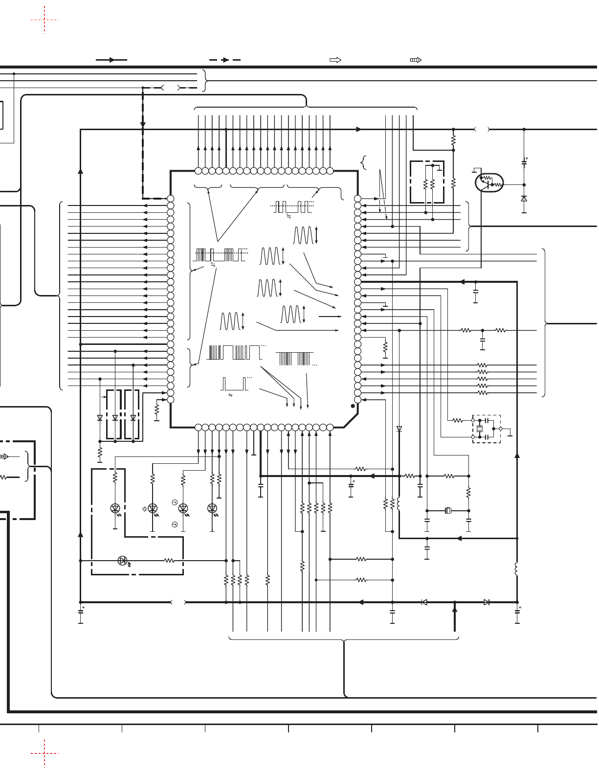
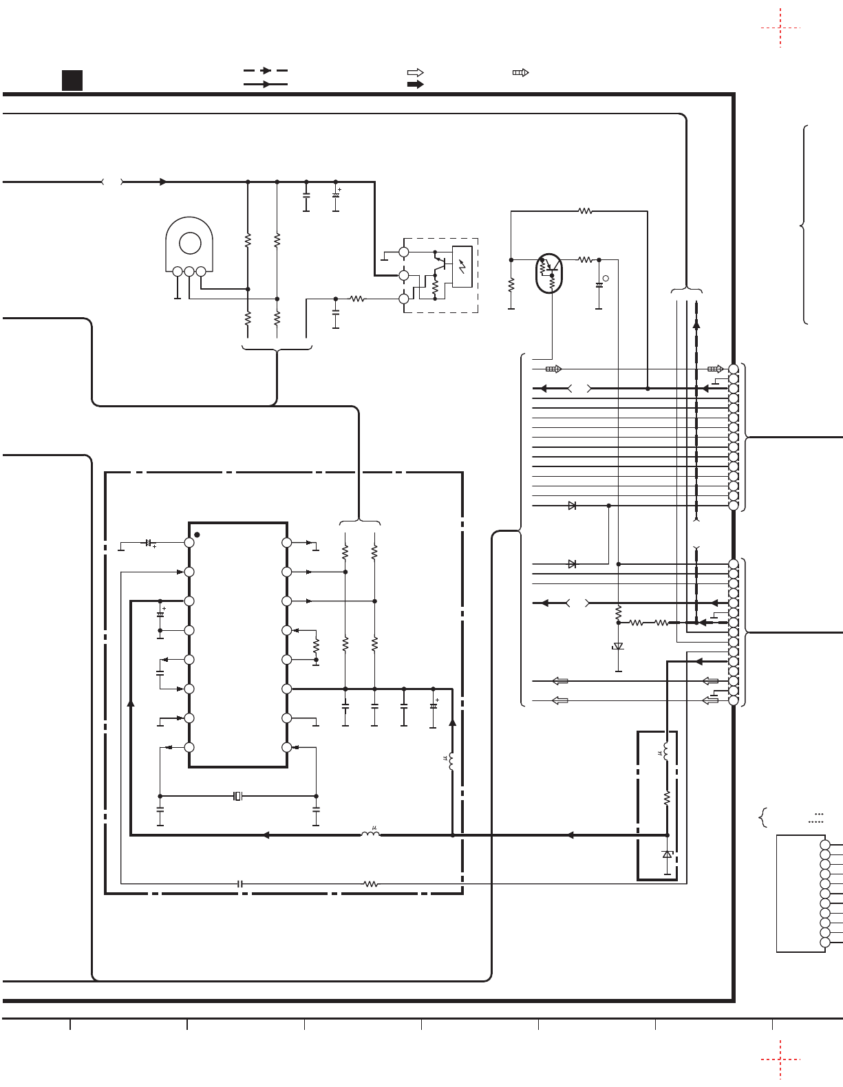
13 14 15 16 17 18 19 20 21 22 23 24
DET
Rch
CE
Lch
DI
DO
CL
+B(2)
SD
+B(1)
T.GND 1
2
3
4
5
6
7
8
9
10
11
Z101
RAN0005EM-2 [EE]
ENG06502Q [GN]
(TUNER PACK)
SA-DV290(EE,GN) OPERATION, MAIN CIRCUIT DIAGRAM
W901B
W902B
123
1
2
3
4
5
6
7
8
9
10
11
12
13
14
15
BA
COM
1
2
3
4
5
6
7
8
9
10
11
12
13
14
15
Q902
UN411FTA
MUTING CONT.
ABC
R962
22K
VR901
EVQVBXFK124B
(VOLUME)
R945
100
R961
22K
R943
100
C917
0.01
D907
MA165TA
M
R946
1K
C909
1000P C918
6.3V100
DEA
R941
1K
A
B
C
D
E
F
G
H
I
J
K
L
N
O
Q
S
T
AOPERATION CIRCUIT
R942
2.2K
R974
1K
C931
16V10
R965
3.9K
R966
3.9K
D961
MA4075MTA R975
22K
D906
MA165TA
U
N
1
2
3
Z901
B3RAD0000028
(REMOTE SENSOR)
W902A
W901A
CP101
C
F
G
B
A
E
D
Q707
2SB1417PQTA
REGULATOR
Q723
2SC3940AQSTA
REGULATOR
R763
4.7K
R230 1K
R229 1K
D721
MA4300MTA R708
4.7K
C707
0.047
C706
35V10
C737
50V100
To
SOUND
PROCESSOR
(SH-DV290)
C735
0.047
B
A
R563
2.7K
R564
2.7K
C660
16V10
C659
16V10
R615
4.7K
R614
4.7K
R631
3.9K
R632
3.9K C202
0.1
R203
100K
R204
100K
C201
0.1
C602
16V10
C708
0.047
R211
270
D201
MA4056MTA
R687
1.5K
R688
1.5K
Q606
R617
4.7K
2
1
3
4
5
6
7
8
9
10
11
C
B
A
X0X1VDD
G
Vss
INHZ0Z1Y1 Y0
16 15 14 13 12 11 10 9
12345678
IC201
BU4053BCFE2
SIGNAL SELECTOR
C655
16V10
C656
16V10
R606
4.7K
R605
4.7K
2
15
3
4
5
6
7
8
9
10
11
12
13
14
1
2
15
3
4
5
6
7
8
9
10
11
12
13
14
1
20
2
1
3
4
5
6
7
8
9
10
11
12
13
14
15
16
17
18
19
K
L
M
I
J
E
F
C
D
E
F
G
E
F
G
A
B
C
D
A
B
G
H
C601
16V10
R598
2.2K
R597
2.2K
R205
100K
H
G
R202
100K
B
C
D
E
F
C509
0.01
C510
0.01
R693
1K
R692
1K
C664
16V10
C725
16V47
A
R696
47K
Q606,609,610
2SD2144STA
MUTING
Q609
Q610
Q612
UN411FTA
MUTING CONT.
B
AR694
22K
R511
47 R509
47
R512 47 R510 47
W501
D720
B0JANG000008
D718
B0JANG000008
H
D
C
R695
470
D611
MA4051MTA
C740
16V10
C733
0.047
D737
MA4082LTA
R764
330
MAIN CIRCUIT
B
C731
1000P
C741
0.1
TUNER Lch/C
TUNER Rch
A.GND
Lch IN
Rch IN
+B(10V)
SUR L
SUR R
S.W
MIC
-
B(
-
10V)
V.GND
D.GND
CS/ REQ
CLK
DATA
CT GND
SH FL1
SH FL2
SYNC
A
B
B
R684
1K
C715
25V6800
C714
1000P
D705
RL1N4003N02
A
R
P
For [EE] area.
IC151
C1BB00000527
RDS SIGNAL
DEMODULATOR
R158
1K
R154
100K
R153
100K
1
2
3
4
5
6
7
8 9
10
11
12
13
14
15
16
VREF
HPX IN
VDDA
VssA
FL OUT
CIN
TEST
X OUT
IDR
RDCL
RDDA
RST
MODE
VDDD
VssD
XIN
C155
1000P
C153
1000P
C160
1000P
C159
6.3V47
R152
1K
R151
1K
C154
560P C158
6.3V47
C151
16V10 BC
L151
100 H
L152
100 H
C156
47P
C157
47P
R157
1K
C152
330P
X151
(4.332MHz)
L153
1 H
R155
120
D151
MA4051MTA
For [EE] area.
N
: POSITIVE VOLTAGE LINE
: NEGATIVE VOLTAGE LINE
-30.1V
5.1V
:AUDIO SIGNAL LINE
6V
7.6V
3.3V
0V
3.3V
14.7V
10.4V
-
37.3V
-
30.1V
-
30.7V
14.7V7.2V
7.8V
-
10V
-
10V
0V
0V
-
10.2V
5.1V
4.9V
0V
-
10V
5.7V0V0V0V0V0V
6V
7.2V
7.6V
-
10.4V
0V 0V
-
10.4V
:TUNER SIGNAL LINE
:MIC SIGNAL LINE
2.6V
2.6V
0V
5.1V
2.5V2.7V
2.5V
2.5V
5.1V
2.5V
2.5V
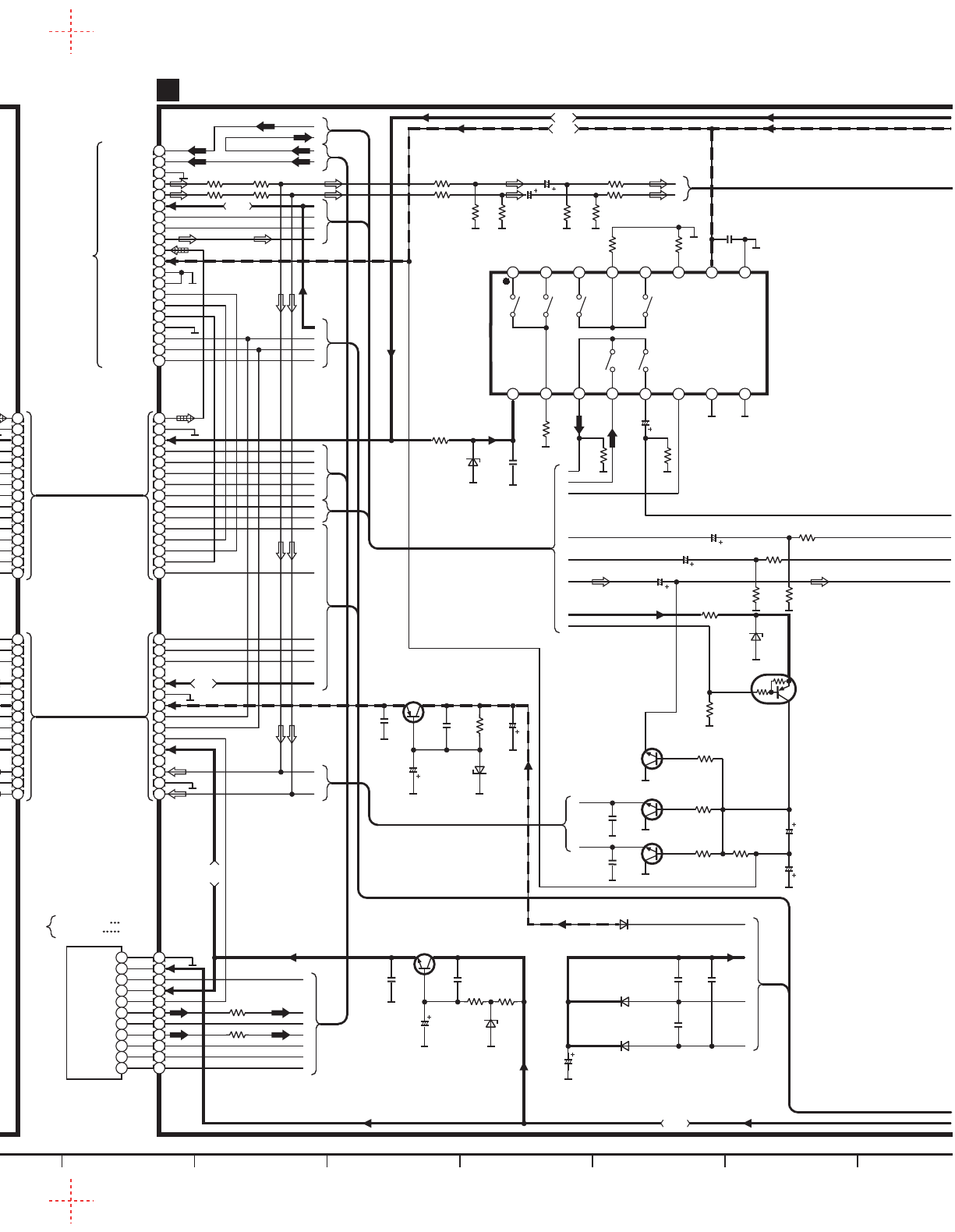
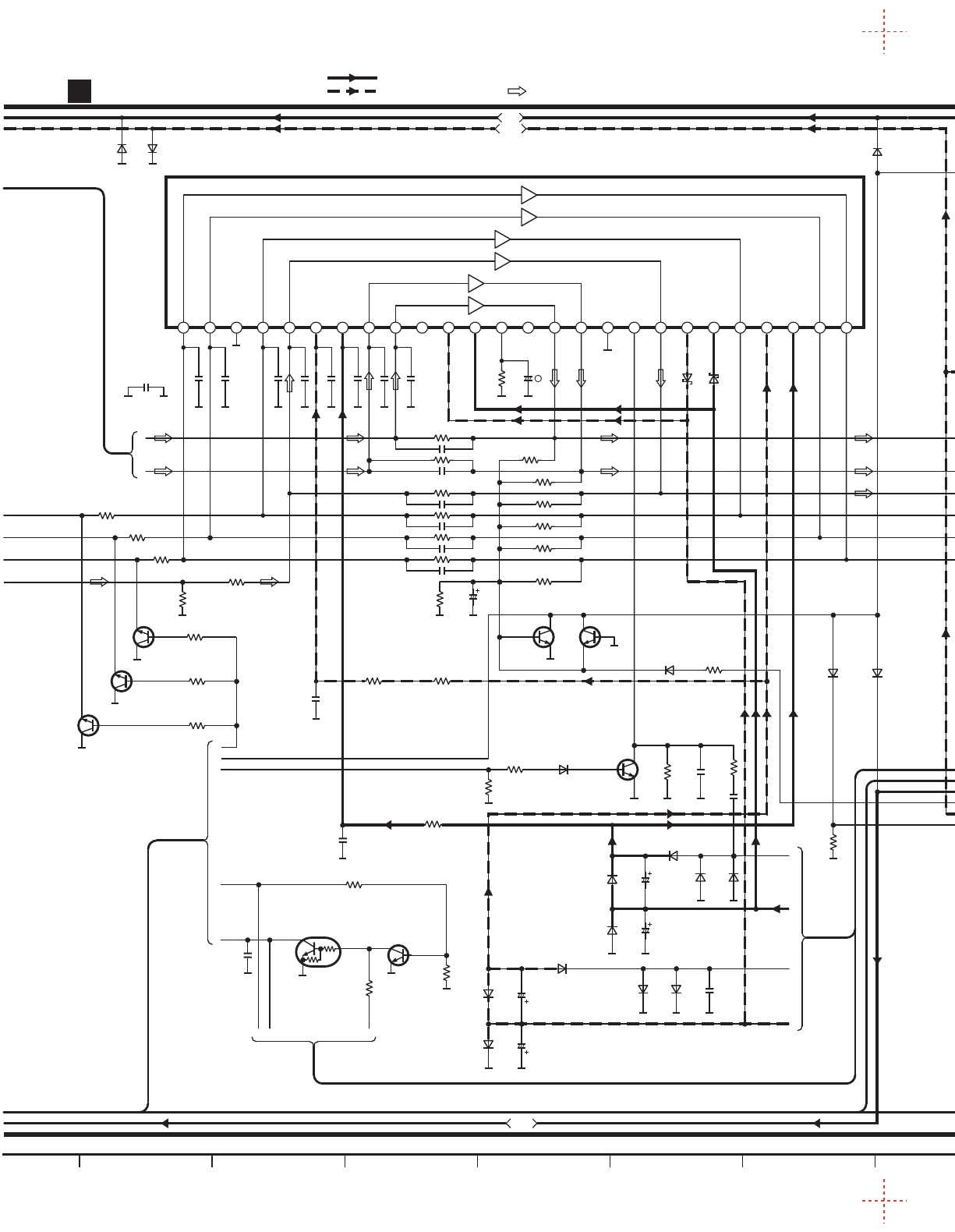
25 26 27 28 29 30 31 32 33 34 35 36
SA-DV290(EE,GN) MAIN,POWER SUPPLY CIRCUIT DIAGRAM
M
Q708
UN4211TA
SWITCHING
(POWER)
Q601 Q602
D756
MA700ATA
C603 470P
C604 470P
C607 470P
C608 470P
C649 1000P
C650 1000P
C605 1000P
C606 1000P
C648
1000P
C617
0.01
R637
15K
R638
68K
R619 120K
R622 120K
R621 150K
R624 150K
R620
120K
R612 56K
R611 56K
R610 150K
R609 56K
R608 56K
R607 56K
C610 56P
C609 56P
C612 15P
C611 39P
C614 47P
C613 47P
R627
470K
C616
50V0.47
N
D601
SB360L6508
D602
SB360L6508
D754
RL1N4003N02
C761
0.1
D701
1N5402BM21 C709
0.1
IC601
RSN311W64B
POWER AMP
D757
MA700ATA
123456789101112131415181920212223242526 1617
R604
3.3K
R601
3.3K
R602
3.3K
R618
4.7K
Q601,602
2SC5398RSTA
PROTECTOR
D607
1SS291TA
L
K
D658
MA165TA
D657
MA165TA
B
A
R685
1K
R686
1K
Q605,607,608
2SD2144STA
MUTING
Q607
Q608
C705
0.01
G
R776
10K
Q709
2SD2144STA
SWITCHING
(POWER)
R738
3.9K
R739
47K
C622
10V100
D659
MA165TA
D751
1N5402BM21
D703
1N5402BM21
D753
RL1N4003N02
D761
RL1N4003N02
D755
RL1N4003N02
D752
1N5402BM21
D702
1N5402BM21
D704
1N5402BM21
G
F
E
D
AB C
D558
MA165TA
R544
10K
R572
15K
R648
120
C618
0.01
R635
2.2K
C619
0.1
Q503
2SC5398RSTA
SWITCHING
C704
35V4700
C702
35V4700
C703
35V4700
C701
35V4700
R761
220
R628
22K
R691
68
R647
270
R623
120K
CN781
F
C
A
B
D
E
Q551
2SA1995RSTA
SIGNAL LEVEL DET.
Q555
2SD2144STA
SIGNAL LEVEL DET.
Q702
2SB1548PQAU
REGULATOR
Q725
2SC5398RSTA
STABILIZER Q705
2SA1995RSTA
STABILIZER
Q701
2SD2374PQAU
REGULATOR
R556
100K
R557
10K
C721
10V100
D725
MA4082LTA
R729
220
C723
0.047
C639
1000P
C640
1000P
C641
1000P
C642
1000P
C732
0.022
C647
1000P
D738
MA165TA
D730
MA4091HTA
R768
100
R724
3.9K
C718
25V100
D723
MA4150HTA
R723
5.6K
C719
0.047
R725
10
C724
0.047
C710
0.047
R546
18K
R551
18K
R552
47K
R555
22K
C550
0.01
D552
MA165TA D555
MA4100MTA
R547
18K
E602
E601
R749
1K
D739
MA165TA
POWER SUPPLY CIRCUIT
C
11032 4 5 6 7 8 9
W701B
11032 4 5 6 7 8 9
R720
3.9K
C734
50V3.3
D758
MA165TA
C722
25V100
C720
0.047
C717
16V33
MAIN CIRCUIT
B
G
R765
470
N
R569
10K
D554
MA165TA
C371
6.3V100
Q556
2SC5398RSTA
MOTOR DRIVE
R568
100
D553
MA700ATA
C556
16V10
C555
50V1
Q557
2SA1995RSTA
MOTOR DRIVE
Q553
2SD2144STA
MOTOR DRIVE
R570
2.2M
R560
100K
C559
0.01
D581
RL1N4003N02
R567
22
FAN MOTOR
JK551
R566
68K
Q554
2SA1995RSTA
SIGNAL LEVEL DET.
M
R719
3.3K
Q703,704
2SD2137PQTA
REGULATOR
R796
2.2
Q703
Q704
R769
27
R727
3.9K
C554
16V220
R561
100K
C552
0.01 R559
4.7K
R591
4.7K
C551
50V2.2
D551
MA165TA
12
D583
RL1N4003N02
N
R721
4.7
R722
2.2
AB
R753
0.47
R754
0.47
Q711,712
2SB1548PQAU
REGULATOR
Q711
R797
2.2 R767
27
R558
2.2K
D582
RL1N4003N02
Q712
R683
1K
Q605 N
R603
3.3K
: POSITIVE VOLTAGE LINE
: NEGATIVE VOLTAGE LINE :AUDIO SIGNAL LINE
7.6V
-
10.4V
0V0V59.5V
-
59.5V
0V28.9V
-
29.3V
0V0V0V0V
-
0.2V
29.4V
-
29.7V
0V0V54.1V
-
51.4V
0V0V0V0V
0V
0V
4.7V4.7V
0V 0V
0.7V
0V 0V
2.1V
14.7V
0.7V
0V
0.7V
0V
29.2V
29.2V14.7V
15.2V
-
30.1V
-
11V
-
10.4V
-
11V
-
0.6V
14.1V
13.6V
9.6V
10.2V
10.4V
-
10.4V
14.7V
7.6V
7V
0V
7.6V
0.3V
-
10.4V
-
10.4V
-
10.4V
7.6V
7.6V
6.8V
FAN ON:1.6V
0V
FAN ON:0V
0.5V
FAN ON:0V4.7V
0V
0.5V
8.1V
8.1V
30.1V
30.1V7.6V
7.6V
0V
10.4V
13.6V
10.4V 14.1V
13.6V
0.7V
0V
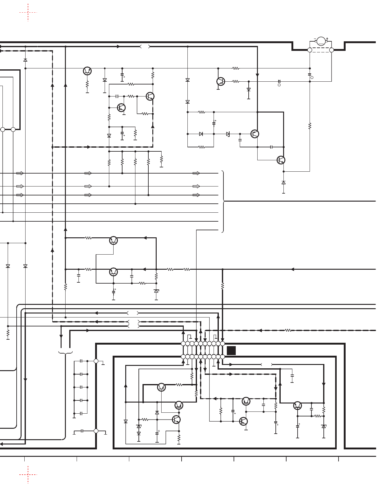
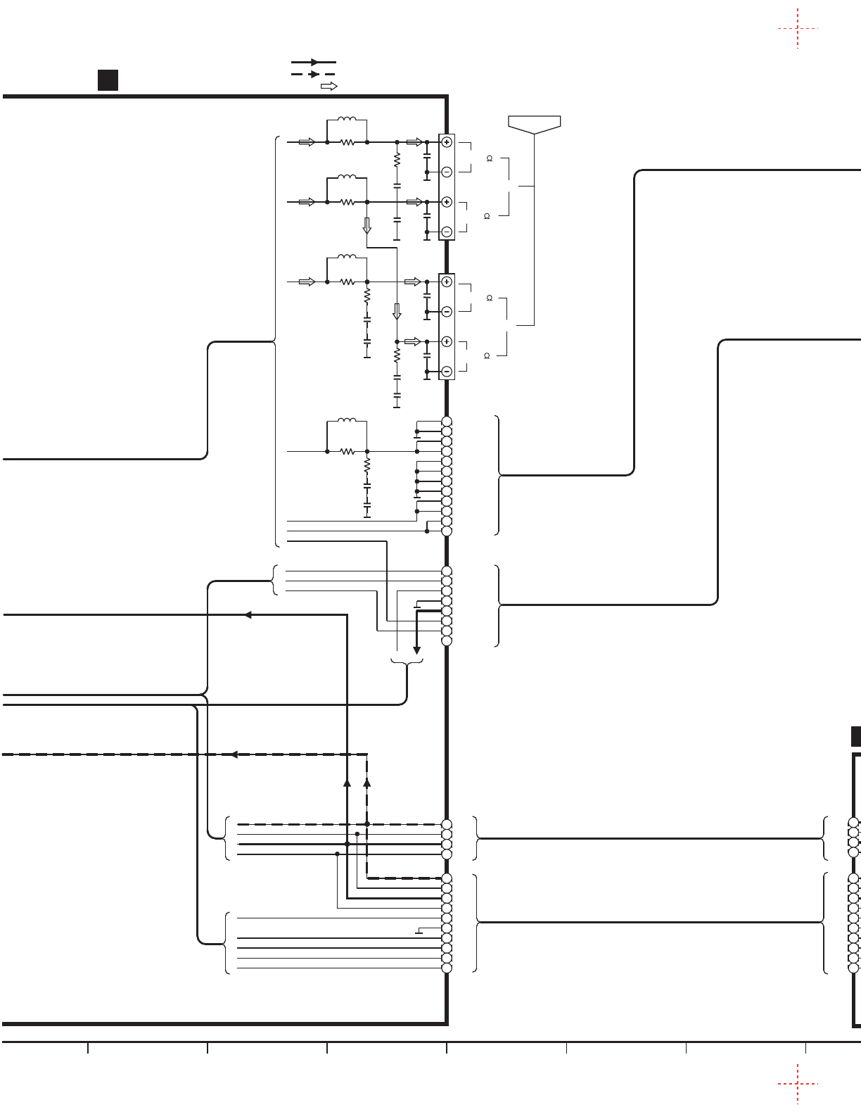
A
B
C
D
E
F
G
H
37 38 39 40 41 42 43 44 45 46 47 48
SA-DV290(EE,GN) MAIN, AC IN, POWER TRANSFORMER(A)&(B) CIRCUIT DIAGRAM
L601
2
1
3
4
5
6
7
8
9
10
11
12
2
1
3
4
5
6
7
8
R639
10
C621
0.1
E
F
D
CP601
CP602
R641
10
A
B
IJ
C
C631
0.1
G
Lch
JK601
HF(6 )
LF(8 )
Rch
JK602
HF(6 )
LF(8 )
A
B
C
R651
10
C627
0.1
C629
0.1
C635
0.047
R649
10
L605
R642
10
C620
0.1
C630
0.1
R640
10
L602
C637
0.047
C636
0.047
R652
10
C626
0.1
C628
0.1
R650
10
L606
C632
0.047
SPEAKERS
GND
GND
C OUT
C OUT
GND
GND
GND
GND
SUR L OUT
SUR L OUT
SUR R OUT
SUR R OUT
ECO
SH SYNC
SA SYNC
D.GND
BU5V
RS13V
+B
NC
W722A
W721A
2
1
3
4
5
6
7
8
9
10
2
1
3
4
E
F
H
D
C
G
F
E
D
S1
S2
S3
S4
AC1
CT
AC2
S7
FL2
FL1
S1
S2
S3
S4
MAIN CIRCUIT
B
C
A
D
B
T701
CN701
CN702
CN703
CN704
CN705
CN706
CN707
CN708
CN709
CN710
CN601
C652
1000P
C644
1000P
C643
1000P
C651
0.047
C646
0.047
C645
0.047
Rch
Lch
JK701
L701
F1 T2A
T702
Z701
C791
1000P
3 1
24 RL702
R794
47K
Q791
2SD2144STA
RELAY DRIVE
D745
MA4051MTA
C753
0.01
C755
16V1000
Q726
2SC3940AQSTA
REGULATOR D746
RL1N4003N02
D747
MA4068LTA C758
0.01
C759
10V47
C754
0.01
D500
MA165TA
W2/W3
W1
CN602
FP791
K5G502AA0002
JK603
CENTER(8 )
SURROUND(8 )
R646
10
C624
0.1
C634
0.1
R644
10
L604
R645
10
C625
0.1 C633
0.1
R643
10
L603
DAC IN CIRCUIT
2
1
3
4
5
6
7
8
9
10
11
12
2
1
3
4
5
6
7
8
R777
1K
R774
18
D711
RL1N4003N02 R773
18
R712 2.2K
A
B
C
A
C
B
R795
3.9K
D743
RL1N4003N02
D741
RL1N4003N02
D742
RL1N4003N02
D744
RL1N4003N02
R771
2.2K D740
MA165TA
POWER TRANSFORMER
(B) CIRCUIT
F
POWER TRANSFORMER
(A) CIRCUIT
E
W722B
W721B
10
2
1
3
4
5
6
7
8
9
CN713
CN712
CN711 W1
W2
2
1
3
4
R772
22K
A
B
C
D
FP792
K5G502AA0002
SPEAKERS
GND
GND
C OUT
C OUT
GND
GND
GND
GND
SUR L IN
SUR L IN
SURRIN
SURRIN
ECO
SH SYNC
SA SYNC
D.GND
BU5V
RS13V
+B
NC
S1
S2
S3
S4
AC1
CT
AC2
S7
FL2
FL1
S1
S2
S3
S4
R798
2.2
R793
1
W3
For [EE] area.
R794A
1
AC IN
230-240V 50Hz [GN]
230 50Hz [EE]
For [GN] area.
For [GN] area.
For
[EE]
area.
: POSITIVE VOLTAGE LINE
: NEGATIVE VOLTAGE LINE
: AUDIO SIGNAL LINE
0.7V
0V
6V
10.7V6V
6.7V
AC22.6V
AC22.6V
AC11.7V
AC11.7V
AC4.7V
AC
29.2V
AC9.4V
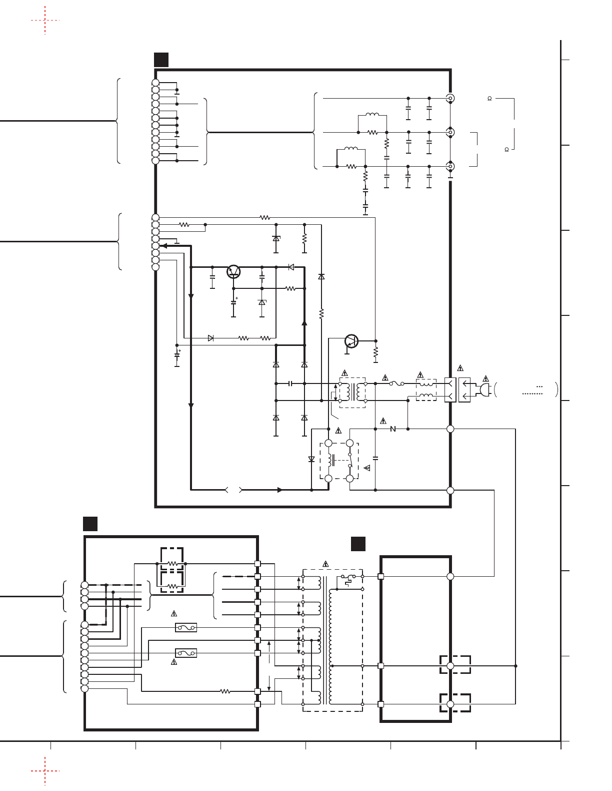
A
B
C
D
E
F
G
H
37 38 39 40 41 42 43 44 45 46 47 48
SA-DV290(EE,GN) MAIN, AC IN, POWER TRANSFORMER(A)&(B) CIRCUIT DIAGRAM
L601
2
1
3
4
5
6
7
8
9
10
11
12
2
1
3
4
5
6
7
8
R639
10
C621
0.1
E
F
D
CP601
CP602
R641
10
A
B
IJ
C
C631
0.1
G
Lch
JK601
HF(6 )
LF(8 )
Rch
JK602
HF(6 )
LF(8 )
A
B
C
R651
10
C627
0.1
C629
0.1
C635
0.047
R649
10
L605
R642
10
C620
0.1
C630
0.1
R640
10
L602
C637
0.047
C636
0.047
R652
10
C626
0.1
C628
0.1
R650
10
L606
C632
0.047
SPEAKERS
GND
GND
C OUT
C OUT
GND
GND
GND
GND
SUR L OUT
SUR L OUT
SUR R OUT
SUR R OUT
ECO
SH SYNC
SA SYNC
D.GND
BU5V
RS13V
+B
NC
W722A
W721A
2
1
3
4
5
6
7
8
9
10
2
1
3
4
E
F
H
D
C
G
F
E
D
S1
S2
S3
S4
AC1
CT
AC2
S7
FL2
FL1
S1
S2
S3
S4
MAIN CIRCUIT
B
C
A
D
B
T701
CN701
CN702
CN703
CN704
CN705
CN706
CN707
CN708
CN709
CN710
CN601
C652
1000P
C644
1000P
C643
1000P
C651
0.047
C646
0.047
C645
0.047
Rch
Lch
JK701
L701
F1 T2A
T702
Z701
C791
1000P
3 1
24 RL702
R794
47K
Q791
2SD2144STA
RELAY DRIVE
D745
MA4051MTA
C753
0.01
C755
16V1000
Q726
2SC3940AQSTA
REGULATOR D746
RL1N4003N02
D747
MA4068LTA C758
0.01
C759
10V47
C754
0.01
D500
MA165TA
W2/W3
W1
CN602
FP791
K5G502AA0002
JK603
CENTER(8 )
SURROUND(8 )
R646
10
C624
0.1
C634
0.1
R644
10
L604
R645
10
C625
0.1 C633
0.1
R643
10
L603
DAC IN CIRCUIT
2
1
3
4
5
6
7
8
9
10
11
12
2
1
3
4
5
6
7
8
R777
1K
R774
18
D711
RL1N4003N02 R773
18
R712 2.2K
A
B
C
A
C
B
R795
3.9K
D743
RL1N4003N02
D741
RL1N4003N02
D742
RL1N4003N02
D744
RL1N4003N02
R771
2.2K D740
MA165TA
POWER TRANSFORMER
(B) CIRCUIT
F
POWER TRANSFORMER
(A) CIRCUIT
E
W722B
W721B
10
2
1
3
4
5
6
7
8
9
CN713
CN712
CN711 W1
W2
2
1
3
4
R772
22K
A
B
C
D
FP792
K5G502AA0002
SPEAKERS
GND
GND
C OUT
C OUT
GND
GND
GND
GND
SUR L IN
SUR L IN
SURRIN
SURRIN
ECO
SH SYNC
SA SYNC
D.GND
BU5V
RS13V
+B
NC
S1
S2
S3
S4
AC1
CT
AC2
S7
FL2
FL1
S1
S2
S3
S4
R798
2.2
R793
1
W3
For [EE] area.
R794A
1
AC IN
230-240V 50Hz [GN]
230 50Hz [EE]
For [GN] area.
For [GN] area.
For
[EE]
area.
: POSITIVE VOLTAGE LINE
: NEGATIVE VOLTAGE LINE
: AUDIO SIGNAL LINE
0.7V
0V
6V
10.7V6V
6.7V
AC22.6V
AC22.6V
AC11.7V
AC11.7V
AC4.7V
AC
29.2V
AC9.4V
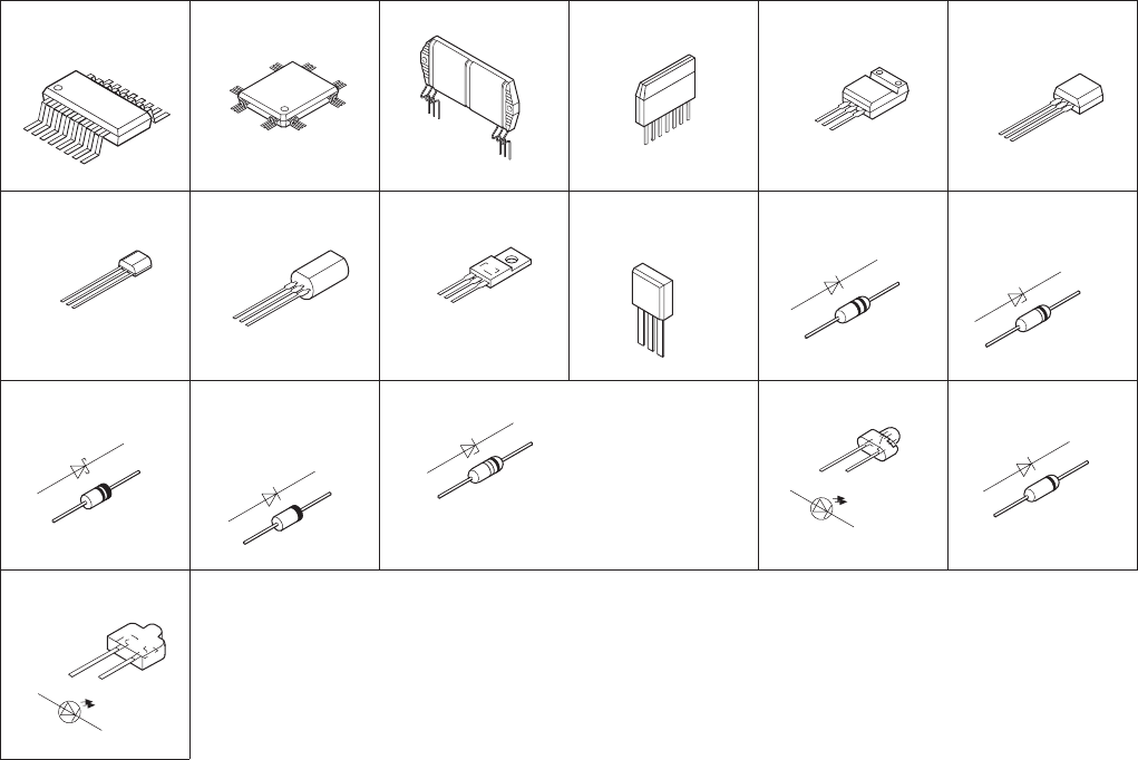
BU4053BCFE2
C1BB00000527 C2BBFD000404 RSN311W64B
UN411FTA
UN4211TA
UN4212TA
2SB1417PQTA
2SD2137PQTA 2SD2144STA
2SA1995RSTA
2SC5398RSTA 2SC3940AQSTA 2SB1548PQAU
2SD2374PQAU 1SS291TA
MA700ATA MA4100MTA
MA4150HTA
MA4300MTA
MA165TASB360L6508 1N5402BM21
RL1N4003N02
B0JANG000008
MA4030MTA
MA4051MTA
MA4056MTA
MA4068LTA
MA4075MTA
MA4082LTA
MA4091HTA
LNJ301MPUJAD
SELS5223C
SELS5923C
1
8
9
16
.
.
.
.
.
.
.
.
.
.
.
50
51
1
............30
31
100
..
.
.
.
.
.
..
.
.
.
.
.
80
81 1
..................
26
ECB
CB
E
E
C
B
E
C
BECB
C
B
EA
Ca
A
Ca
A
Ca
Anode
Cathode
A
Ca
Anode
Cathode A
Ca
A
Ca
A
Ca
Anode
Cathode
Anode
Cathode
Anode
Cathode
A
Ca
Anode
Cathode
Anode
Cathode
Anode
Cathode
TA2011S
7
1
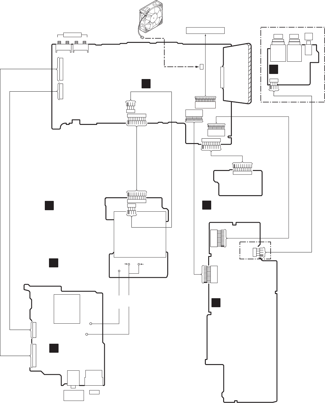
BMAIN P.C.B.
AOPERATION P.C.B.
W902B
14
.
.
.
.
.
2
15
.
.
.
.
.
.
1
W901B
14
.
.
.
.
.
2
15
.
.
.
.
.
.
1
W902A 1 . . . . . . 15
2 . . . . . 14
1. . . . . . . .10
CN781
2 . . . . . 14
1 . . . . . . 15
W901A
2 . . . . . . . . 20
1 . . . . . . . . 19
W501
To SOUND PROCESSOR
1 . . 4
W722A
1. . . . . . . .10
W721A
12
.
.
.
.
.
.
.
.
.
.
1
CP601
8
.
.
.
.
.
.
1
CP602
SPEAKERS
CPOWER SUPPLY P.C.B.
W701B
1. . . . . . . .10
T702
(Power
transformer)
DAC IN P.C.B.
W1
W2/W3
1
.
.
.
.
.
.
8
CN602
1
.
.
.
.
.
.
.
.
.
.
12
CN601
AC IN
CENTER/
SURROUND
SPEAKERS
EPOWER
TRANSFORMER
(A) P.C.B.
1 . . 4
W722B
1. . . . . . . .10
T701
(Power transformer)
W721B
W2 W3
W1
FPOWER
TRANSFORMER
(B) P.C.B.
1
.
.
.
.
.
.
.
.
.
11
CP101
Z101
TUNER
PACK
BROWN
BLUE
JK551
2
1GMIC JACK
P.C.B.
4
.
.
1
CN904
MIC2MIC1
1 . . 4
W904B
MIC
VOL
For [GN] area.
For
[GN] area.
For
[GN] area. For
[EE] area.
FAN MOTOR
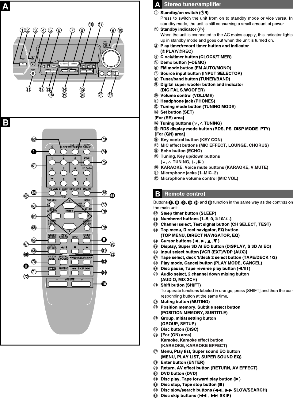
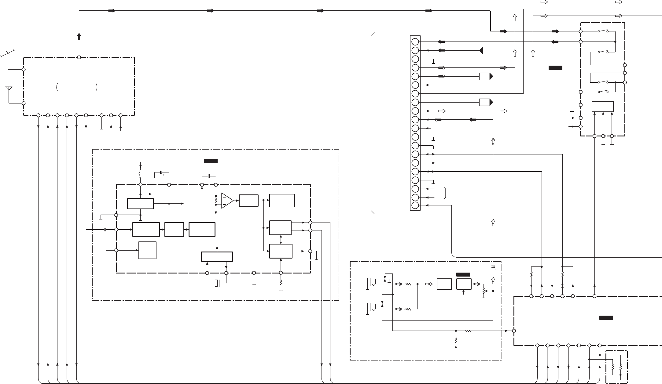
From POWER
TRANSFORMER
1
8
W501
2
3
4
5
6
7
9
12
13
14
15
16
17
18
A.GND
+B(10V)
SUR L
SUR R
19
11
10
CT.GND
SH FL1
DATA
D.GND
TUNER L/C
TUNER Rch
Lch IN
Rch IN
S.W
MIC
-B(-10V)
V.GND
CS/REQ
CLK
SH FL2
20
SYNC
+B5
Rch
Rch
-B3
To SOUND PROCESSOR
BLOCK DIAGRAM
LC72 CE
LC72 DI/ST
LC72 CK
DATA1
CLK1
DATA IN
CE1
345
LC72 DO
2
C2BBFD000404
IC901
SYSTEM CONTROL / FL DRIVE
Rch
94
SH CS
97
SH CK
9596
SH DO
SH DI
SHSYNC
100
SD
21
SH REQ
SW CONT.
12
X0
X1
14
ABC
11 10 9
G
8
2
13
BU4053BCFE2
IC201
SIGNAL SELECTOR 1
15
Y1
Y0
VDD
16
+B4
VSS
7
-B3
6
ST/AV.
6CH
SD
SA-DV290(EE,GN) BLOCK DIAGRAM
+B8
Q401
TA2011S
IC401
MIC2
MIC1
VR401
(MIC VOL)
+B4
MIC
AMP
MIC
AMP
25 MIC DET
AM ANT
FM ANT
Z101 TUNER PACK
RAN0005EM-2:EE
ENG06502Q:GN
8
(6)
3791110
DO
CL
DI
CE
SD
Lch
(Rch)
DATA1
CLK1
DATA IN
CE1
SD
C1BB00000527
IC151
RDS SIGNAL DEMODULATOR
CLOCK
RECOVERY
(1187.5kHz)
RDDR
RDCL
IDR
RDS-ID
DETECT/
RAM
57kHz
BPF
(SCF)
PLL
(57kHz)
VREF
CINFLOUTVREF
VDDA/D
VssA/D
MPX IN
TEST
XOUTXIN
OSC/DIVIDER
CLK(4.332MHz)
89
7
2
4,10
3,11
+B2
156
14
15
16
X151
(4.332MHz)
REFERENCE
VOLTAGE
TEST
ANTIALIASING
FILTER SMOOTHING
FILTER
DATA
DECODER
MODE
12 13
RST
4
+B2
12
+B1
GND
+15V
+7V
DET
5
RDS DATA
RDDR
RDS CLK
RDCL
28 27
RDDR
RDCL
For [EE] area.
FL1
FL2
For [GN] area.
For [GN] area.
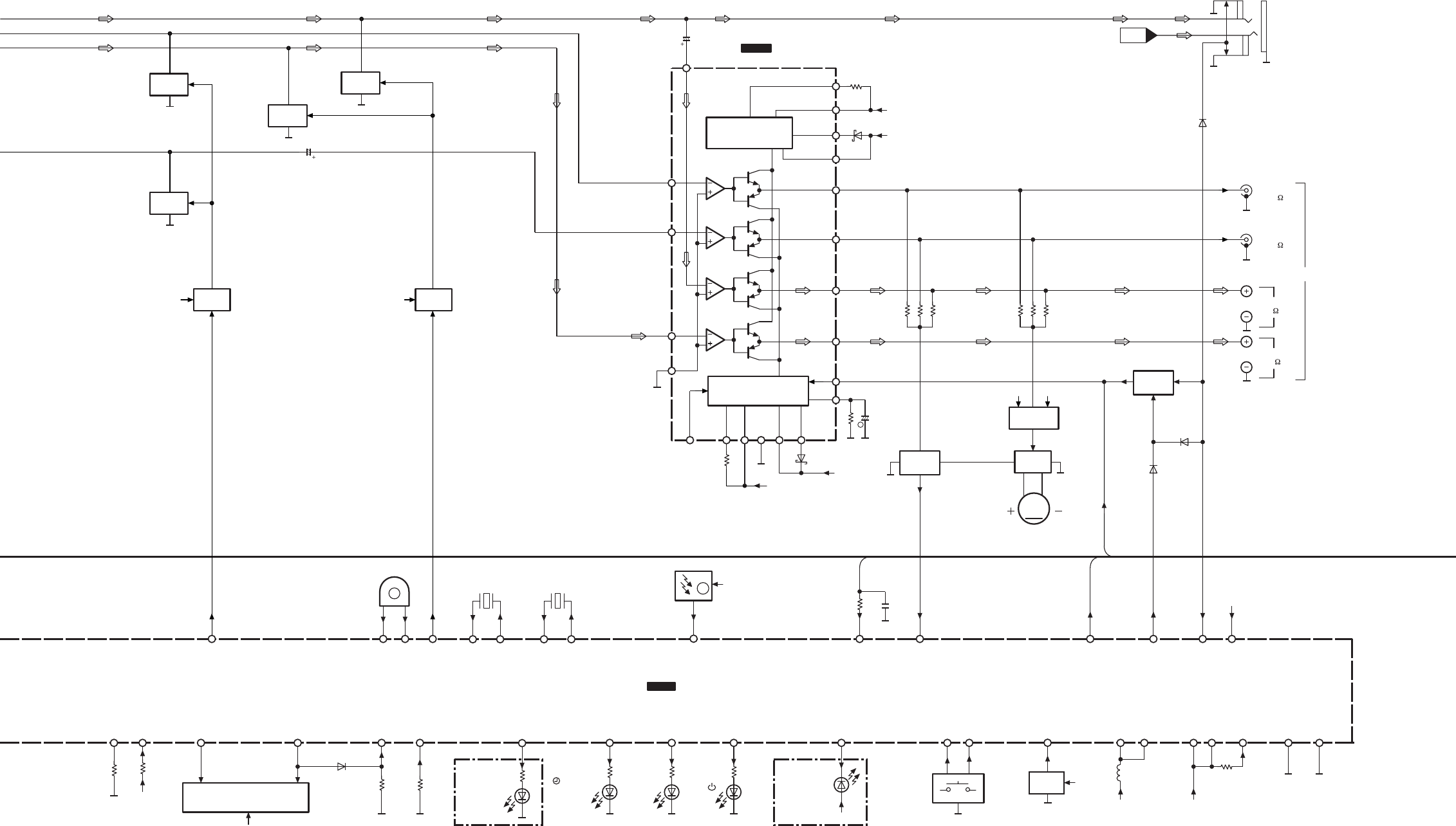
SPEAKERS
Rch PHONES
VR901
(VOLUME)
24 23
VR JOGA
VR JOGB
KEY
SWITCH
19 20
KEY TU
KEY
KARAOKE
Q901,
D904 RESET
12
RESET
+B8
90
VDD2
+B9
VDD1
VDD3
VDD4
18 46 72
C2BBFD000404
IC901
SYSTEM CONTROL / FL DRIVE
1~8G
30~37
P1~38
38~45,
47~50
52~71,
73~78
FL901 FL DISPLAY
D931
D933 ... [EE]
D935 ... [GN]
79
REGIN0
82
TIMER
83
S.W LED
D951
(DIGITAL
S.WOOFER)
81
STAND-BY
D954
( PLAY/REC) D306
()
1621
GND
1047
5
1
(2)
6
3
20
15
19
(18)
26
(25)
23
24
RSN311W64B
IC601
POWER AMP
+B3
D601
-B1
D602
-B2
Q601,602
9
+B7
13
98
E DET
HP SW
26
SASYNC
AC IN
88
POWER
POWER
11
+B8
1
CHECK
14
N
Q503,D558
51
-VP
-VP
86
MUTE
D906
PRO-
TECTOR
D974
SWITCH-
ING
D907
REGIN1
22 8
11
(12)
16 17
X901
(6MHz)
XC IN
XC OUT
13 14
X902
(32.7kHz)
XIN
X OUT
80
MUTING
Q606
AC IN
POWER CONTROL
CIRCUIT
POWER CONTROL/
PROTECTION CIRCUIT
MUTING
Q605
MUTING
Q607
(Q608)
93
MUTE3
MUTING
CONT.
+B4
Q902
91
MUTE2
MUTING
CONT.
+B5
Q612
MUTING
Q609
(Q610)
10
SEL/
TUNER
MIC DET
25
+B8
SURROUND
(8 )
CENTER
(8 )
HF
(6 )
LF
(8 )
Q551,554,
555 SIGNAL
LEVEL DET.
-B3 +B4
M
FAN MOTOR
MOTOR
DRIVE
Q553,556,
557
15
Vss
89
Vss2
SA-DV290(EE,GN) BLOCK DIAGRAM
85
CHORUS
+B8
D953
(MIC EFFECT
CHORUS)
84
LOUNGE
D952
(MIC EFFECT
LOUNGE)
29
REMO-
CON
Z901
(REMOTE
SENSOR)
+B8
FL1,2 For [GN] area. For [GN] area.
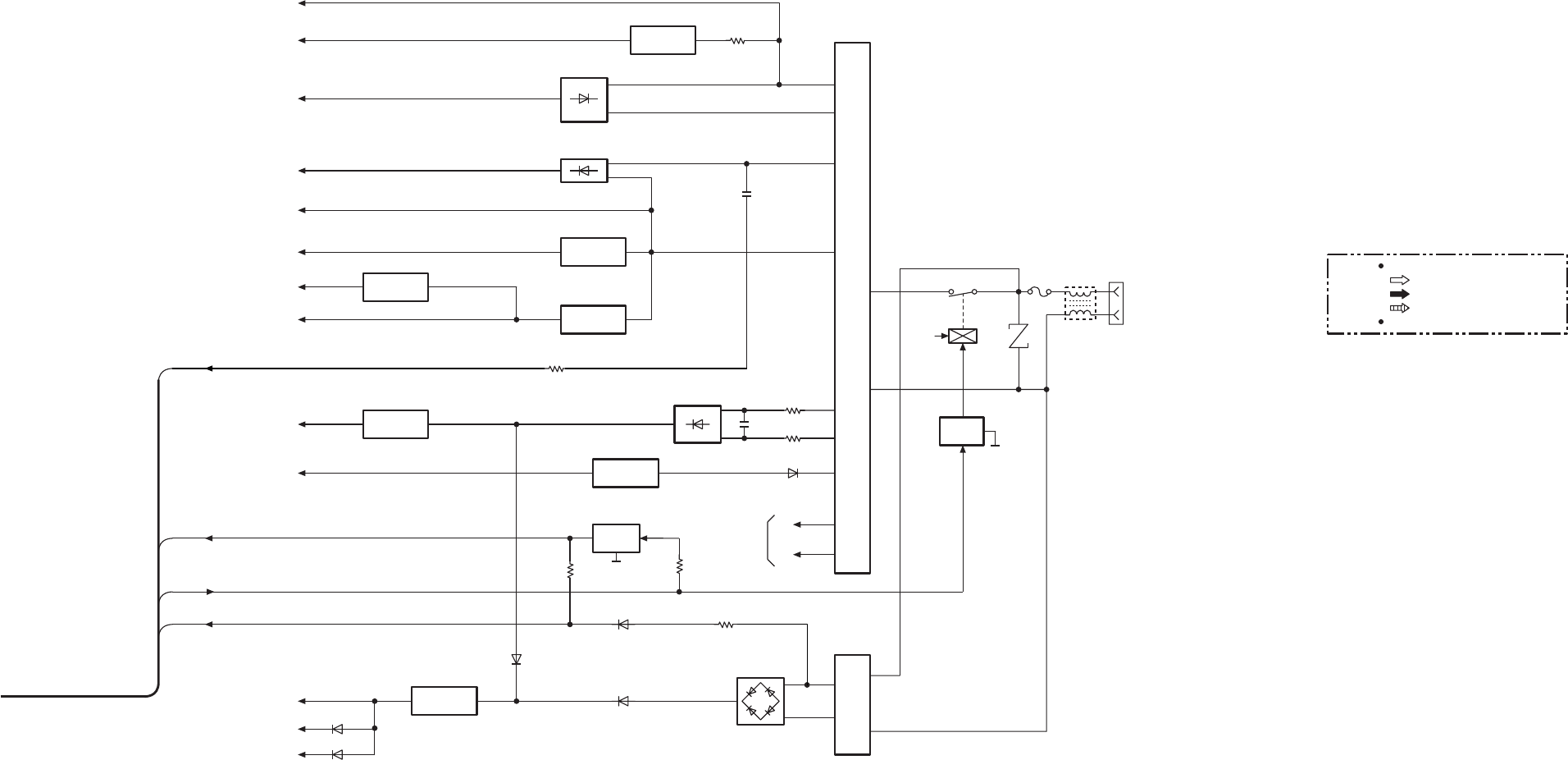
POWER TRANSFORMER
F1
AC IN
L701
T701
D702,704,
752,754,755
Q707
+B4
-B3
Q702,705
Z701
RL702
Q791
POWER
TRANSFORMER
T702
D741~744
-B1
-B2
Q703,704
+B7
D701,703,
751,753,761
Q701
+B1
Q723
+B2
Q711,712,725 D718,720
+B5
D705
-VP
FL1
FL2
FL DISPLAY
(FL901)
Q708,709
+B3
AC IN
SHSYNC
POWER
Q726
+B6
+B8
+B9
D902
D901
SASYNC
D746
REGULATOR
/STABILIZER
REGULATOR
REGULATOR
REGULATOR
SWITCH-
ING
REGULATOR
REGULATOR
RELAY
DRIVE
+B6
D740
REGULATOR
/STABILIZER
SA-DV290(EE,GN) BLOCK DIAGRAM
FP791
FP792
D711
NOTES : SIGNAL LINE
: AUDIO SIGNAL
: TUNER SIGNAL
: MIC SIGNAL
( ) indicates pin No. Right channel.
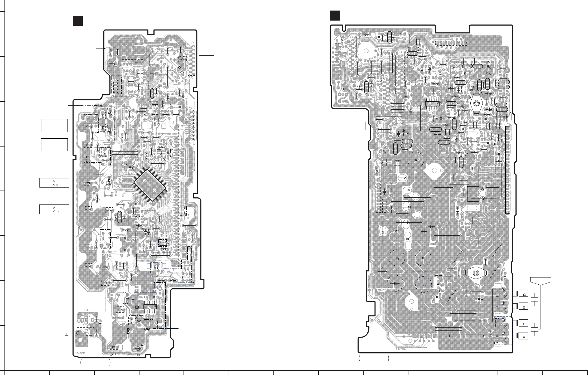
123456789101112
13
A
B
C
D
E
F
G
H
SA-DV290(EE,GN) OPERATION, MAIN P.C.B.
Note: This printed circuit board diagram may be modified at any time with the development of new technology.
OPERATION P.C.B.
A
VR901
(VOLUME)
C902
C928
C922
C920
R929
R988
R991
R975
R974
R934
R937
R930
R931
R918
R957
R919
R932
R956
R987
C915
D906
J
J
J
J
J
J
J
J
J
J
J
J
J
J
J
JJ
J
J
J
J
R995
R942
R941
R912
W902B
15
13
11
9
7
5
3
1
14
12
10
8
6
4
2
S913
D951
W901B
15
13
11
9
7
5
3
1
14
12
10
8
6
4
2
D902
D901
J
R926
R993
R958
R969
R959 R997
R996
R990
R936
R935
R999
R954
C921
C903
D973
R939
R960
R986
J
J
J
J
J
J
C926
C905
D935
D933
D931
D905
J
L901
L902
J
J
C901
FL901
1
2
5
6
7
8
9
10
11
12
13
14
15
16
17
18
19
20
21
22
23
24
25
26
27
28
29
30
31
32
33
34
35
36
37
38
39
40
41
42
43
44
45
46
47
48
49
50
53
54
J
J
J
1510152025 30 35
404550
55
60
31
51
65
7570
80
81
85
90
95
100
IC901
R953
R951
R943
R961
R924
R925
R922
R921
J
J
J
R952
R976
R928
R950
R948
R947
R945
R962 R949
C912
C908
C907
C925
C909
C904
C911
C910
D907
J
J
J
J
J
3
2
1X901
J
J
X902
C914
C916
C918
B
C
E
Q901
J
C919 C927
Z901
(SENSOR)
R944
R946
C924
C917
D974
S901
( / ) D306
( )
R901
J
S904
( PLAY/
REC)
R904
R903
R902
S902
(CLOCK/
TIMER)
C923
JK903
(PHONES)
2
143
56
7
W905
C395
C396
JR906
R905
S907
(SET)
S909
(ECHO)
S906
(TUNING
MODE)
S905
(FM AUTO/
MONO)
S903
(—DEMO)
J
J
J
R908
J
J
R910
R909
S908
(INPUT
SELECTOR
)
S910
S911
D904
R911
R994
R992
R998
R940
R907
S912
(TUNER/
BAND)
J
R914
R915
R916
R913
J
S915
S914
J
DIGITAL
S.WOOFER
D954
( PLAY/
REC)
3
2
1
1
2
3
E
C
B
Q902
D961
R966R965
N
C931
S916
(KEY CON)
S917
(MIC EFFECT
LOUNGE)
S918
(MIC EFFECT
CHORUS)
D952
D953
C414
C415
R416
4
3
2
1
CN904
C152
C153
C154
C151
C160
C155
C156
X151
IC151
158
910 16
15
C157
C159
C158
R157
For
[EE] area.
For
[EE] area.
For
[EE] area.
For
[GN] area.
For
[EE] area.
For
[GN] area.
R155
R151
R152
R153
R154
L152 L153
R158
L151
D151
REP3337K-M ..... [EE]
REP3337L-M ..... [GN]
For
[GN] area.
For
[GN] area.
For
[GN] area.
For
[GN] area.
For
[GN] area.
. TUNING ... [EE]
. TUNING , ... [GN]
. RDS
DISP MODE
PTY ... [EE]
. V.MUTE ... [GN]
. RDS
DISP MODE
PS ... [EE]
. KARAOKE ... [GN]
. TUNING ... [EE]
. TUNING , ... [GN]
MAIN P.C.B.
B
10
9
8
7
6
5
4
3
2
1
D607
R635
R719
J
J
W902A
JJ
J
J
J
J
J
15
13
11
9
7
5
3
1
14
12
10
8
6
4
2
C664
C725
JJ
J
J
J
J
J
J
J
J
J
J
J
J
J
J
J
R230
C740
C733
C735
R764
R763
D737 B
C
E
Q723
W901A
W501
20
18
16
14
12
10
8
6
4
2
19
17
15
13
11
9
7
5
3
1
15
13
11
9
7
5
3
1
14
12
10
8
6
4
2
R694
R761
R696
R695
J
J
J
J
J
J
D657
D659
C705
D611
B
C
E
Q612
J
J
J
J
J
J
J
J
J
J
J
J
C737
C706
J
R776
R738
R739
R708
ECB Q708
ECB Q709
E
C
B
Q707
D721
C707
C708
C509
C510
C202
C714
C731
C741
D720
D718
D705
C715
C602
C656
C655
C554
C601
C555
C622
C660
C659
C371
C551
ECB
Q609
ECB
Q610
ECB
Q554
ECB
Q607 ECB
Q608
ECB
Q606
ECB
Q605
ECB
Q555
B
C
E
Q602
B
C
E
Q551
B
C
E
Q503
B
C
E
Q601
JJ
J
J
1234567891011
CP101
E602
R605
R606
R617
R618
R684
R683
R604R603
R686
R685
R601
R614
R602
J
J
J
J
JJ
J
J
J
J
J
J
J
J
J
J
R693
R692
R564
R229
R628
R688
R687
R512
R511
R509
R204
R203
R727
R211
R510
R563
R558
R607
R608
R560
R569
R598
R597
R570
R561
R591
R559
R557
D555
D552
D757
D658
D551
D756
C550
C647
C605
C606
C610
J
J
J
J
J
J
ECB
Q704
ECB
Q703
C721
R572
R544
R610
R619
R612
R691
R624
R620
R546
R547
R638
J
J
C604
C608
C603
C607
C649
C609
C650
C612
R627
C613
R555
C614
C723
C552
C648
C619
C611
C724
R621
R615
R631
R632
R552
R551
R609
R611
R637
R769
R721
R722
R648
R647
R767
R622
R556
R623
R797
R796
R729
R202
R205
J
J
C616
C617
C618
J
D558
J
J
D725
IC601
26
25
24
23
22
21
20
19
18
17
16
15
14
13
12
11
10
9
8
7
6
5
4
3
2
1
J
J
J
J
J
J
J
J
J
J
JJ
J
J
J
J
J
J
J
J
J
J
J
J
J
JJ
J
J
J
W721A
W722A
10
9
8
7
6
5
4
3
2
1
4
3
2
1
J
J
J
C709
C761
D755
D754
D761
D753
D702
D704
D752
D701
D751
D703
D601
D602
C704 C701
C703
C702
J
J
J
J
J
J
J
J
J
J
J
J
J
J
J
J
E601
L602
L601
L605
L606
C639
C637
C635 C636 C632
JK601
JK602
1234
CP602
5678
J
JJ
C626
C620
C630
C621
C631
C642
R651
R642
R652
R650
R649
R639
R641
R640
C627
C629
C628
C732
C641
C640
To SOUND PROCESSOR
LF
(8 )
HF
(6 )
LF
(8 )
HF
(6 )
CN781
N
Rch
Lch
SPEAKERS
D582
D581
D583
D553
D554
ECB
Q553
ECB
Q557
C559 R568
R566
R567
12
JK551
ECB
Q556
C201
15
8
910 1516
IC201
D201
1 2 3 4 5 6 8 910 1112
CP601
7
NN
C556
NN
REP3337K-M ..... [EE]
REP3337L-M ..... [GN]
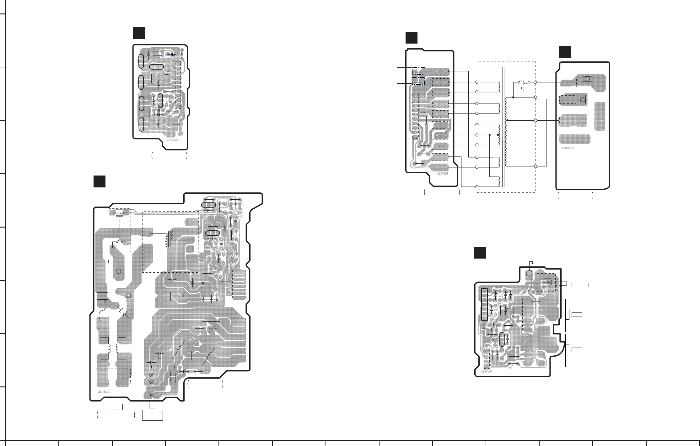
123456789101112
13
A
B
C
D
E
F
G
H
SA-DV290(EE,GN) POWER SUPPLY, AC IN, POWER TRANSFOMER(A)&(B), MIC JACK P.C.B.
POWER SUPPLY P.C.B.
C
B
C
E
Q701
B
C
E
Q702
B
C
E
Q711
B
C
E
Q712
B
C
E
Q725
ECB
Q705
R725
R723
C719
C717
C710
C720
W701B
D723
C718
C722
C734 R720
R724
R768
R749
R765
R753
R754
D758
D739
D738
J
D730
10
9
8
7
6
5
4
3
2
1
REP3337K-M ..... [EE]
REP3337L-M ..... [GN]
JK701 JK603
L701
FC1 FC2
F1 T2A
Z701
C791
RL702
1
2
43
1
2
3
4
CN601
5
6
7
8
9
10
11
12
1
2
3
4
CN602
5
6
7
8
T702(Power transformer)
R794
R773
R774
R795
R771
R772
R712
ECB
Q791
ECB
Q726
D500
D711
D746
D740
J
J
C754
C758
D745
C759
R777
D742
D743
D741
D744
J
J
J
J
J
J
J
C755
C753
C634
W1
W2/W3
D747
AC IN P.C.B.
D
AC IN
C644
C646
C651
C652
C624
C633
C625
C645
C643
R646
R645
R644
R643
L603
L604
C
SR
SL
CENTER/
SURROUND
SPEAKERS
REP3338A-S ..... [EE]
REP3338B-S ..... [GN]
230V 50Hz ..... [EE]
230-240V 50Hz ..... [GN]
POWER TRANSFORMER
(A) P.C.B.
E
W722B
W721B
1
2
3
4
5
6
7
8
9
10
1
2
3
4
R794A
R793
CN710
CN709
CN708
CN707
CN706
CN705
CN704
CN703
CN702
CN701
FP792
R798
FP791
J
POWER TRANSFORMER
(B) P.C.B.
F
CN711
CN713
CN712
W1
W2
J
J
J
J
J
J
T701(Power transformer)
REP3338A-S ..... [EE]
REP3338B-S ..... [GN]
REP3337K-M ..... [EE]
REP3337L-M ..... [GN]
For
[GN] area.
For
[EE] area.
1
2
3
4
5
6
7
4
3
2
1
IC401
W904B
C409
C406
C410
C416
C413
C404
R411
R412
R405 R410
R421
C403
C417
C405
C407
C411
C412
C421
C408 C401
R409
R407
R406
R415
R401
R404
R402
R403
B
C
E
Q401
L401
VR401
J
J
J
JK902
JK901
W401
1
2
6
4
5
1
2
6
4
5
(REP3337L-M)
MIC VOL
MIC2
MIC1
MIC JACK P.C.B.
For [GN] area.
G
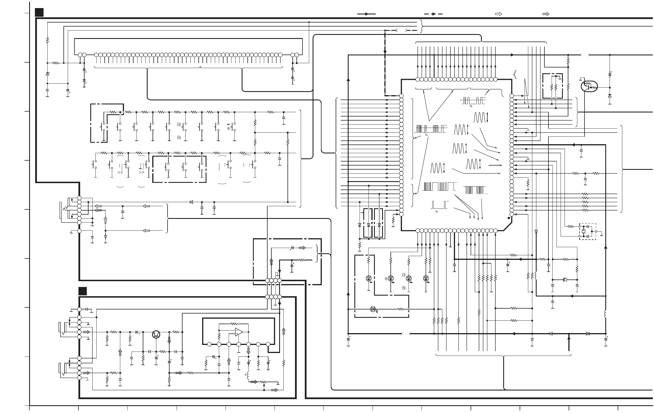
121110987654321
A
B
C
D
E
F
G
H
R922
10K
R921
10K
SA-DV290(EE,GN) OPERATION,MIC JACK CIRCUIT DIAGRAM
S904
(PLAY/ REC)
FL901 (A2BB00000115)
1
7
5
4
6
3
2
T
S
S908
(INPUT SELECTOR)
S907
(SET)
S906
(TUNING MODE)
S905
(FM AUTO/MONO)
JK903
PHONES
3.5mm STEREO
R997
150
R996
150
D973
MA4030MTA
C921
1000P
C922
35V33
C920
25V22
R944
2.2K
R912
4.7K R911
3.3K R910
2.2K R909
1.8K R916
1.5K R915
1.2K R914
1K R913
820
R907
3.3K R906
2.2K R905
1.8K R904
1.5K R903
1.2K R902
1K R901
820
FL DISPLAY
1 6 8 10 11 12 13 14 15 16 17 18 19 20 21 22 23 24 25 26 27 28 29 30 31 32 33 34 35 36 37 38 39 40 41 42 43 44 45 46 47 48 49 50 53 542 5 7 9
W905
S901
(/)
C928
25V22
AOPERATION CIRCUIT
C919
25V22
C927
25V22
C396
0.047
C923
0.1
C395
0.047
D974
MA165TA
C907
470P
C924
0.1
C904
0.01
R924
1K
C908
470P
R925
1K
S912
(TUNER/ BAND)
S913
(DIGITAL
S.WOOFER)
ABCD
E
FGH I JKLMNOPQRSTU
X
W
V
ABCDEFGHIJKLMNOPQRSTUVWXYZ
S902
(CLOCK/ TIMER)
S903
(
-
DEMO)
IC901
C2BBFD000404
SYSTEM CONTROL/
FL DRIVE
C
B
A
Q901
UN4212TA
RESET
R936
100
R919
15K
R991
47K
R918 10K
R928 47K
L902 1 H
D901
1SS291TA
L901
10 H
R951
330K
R952
10M
A
B
C
D
E
F
G
H
I
J
K
L
M
N
O
P
Q
R
S
T
U
V
W
X
Y
Z
R993
100K D931
MA165TA
D935 MA165TA
R990
100K
C916
6.3V100
D951
LNJ301MPUJAD
(DIGITAL S.WOOFER)
R995
220
R986
1.5K
D306
SELS5223C
( ) R939
1.5K
C905
1000P
C901
6.3V100
R935 100
R934 100
R988 1K
R937 10K
R987 1K
R926
2.2K
C912
0.1
R954
100K
C926
1000P
R960 1.5K
R958 1K
R999
100K
R959 47
R969
2.7K
D902
1SS291TA
C903
0.01
C902
10V1000
X902
(32.7kHz)
C911
18P
C910
20P
X901
(6MHz)
1
3
2
D905 1SS291TA
EFIKLMNO Q
R940
1K
R929 1K
R930 1K
R932 1K
R931 1K
R976
100K
R956
1K R957
1K
C915
0.01
C925
1000P
R953
100
A
B
C
D
G
H
J
C914
50V2.2
D904
MA165TA
A
B
C
ABCDE FGH I J K LMNOPQRS T UVWX
1
11
21
2
12
22
3
13
23
4
14
24
5
15
25
6
16
26
7
17
27
8
18
28
9
19
29
10
20
30
3132333435363738394041424344454647484950
51
52
53
54
55
56
57
58
59
60
61
62
63
64
65
66
67
68
69
70
71
72
73
74
75
76
77
78
79
80
81 82 83 84 85 86 87 88 89 90 91 92 93 94 95 96 97 98 99
100
-
VP
P13
P14
P15
P16
P17
P18
P19
P20
P21
P22
P23
P24
P25
P26
P27
P28
P29
P30
P31
P32
VDD4
P33
P34
P35
P36
P37
P38
REGIN0
REGIN1
8G
REMOCON
RDS DATA
RDS CLK
HP SW
MIC DET
VR JOGA
VR JOGB
NC(GND)
SH REQ
KEY KARAOKE
KEY TU
VDD1
XC OUT
XC IN
Vss
X OUT
XIN
RESET
AC IN
SEL/ TUNER
SEL TUNER
ST/ AV.6CH
LC72 CK
LC72 DI/ ST
LC72 CE
LC72 DO
CHECK
STAND-BY
TIMER
S.W.LED
LOUNGE
CHORUS
MUTE
NC
POWER
Vss2
VDD2
MUTE2
NC
MUTE3
SHCS
SHDO
SHDI
SHCK
E DET
CR TIMER
SD
VDD3
P12
P11
P10
P9
P8
P7
P6
P5
P4
P3
P2
P1
1G
2G
3G
4G
5G
6G
7G
R994 100K
U
R949
4.7K
R950
100
Y
D953
LNJ301MPUJAD
(MIC EFFECT CHORUS) R998
220
R992
220
D952
LNJ301MPUJAD
(MIC EFFECT LOUNGE)
S918
(MIC EFFECT
CHORUS)
S917
(MIC EFFECT
LOUNGE)
S916
(KEY CON)
1 2 3 4
W904B
MIC JACK CIRCUIT
IC401
TA2011S
MIC AMP
JK902
MIC2
6.3mm
MONAURAL 1
2
4
5
6
JK901
MIC1
6.3mm
MONAURAL 1
2
4
5
6
6712345
C403
4700P
Q401
2SC5398RSTA
MIC AMP
C406
25V4.7
R415
470
C413
50V1
R412
1M
C416
16V10
C412
1000P
C410
16V10
C411
100P
R411
330
R410
2.2K
R409
4.7K
C407
0.01
C409
50V1
C408
0.022
R406
470K
R407
4.7K
C405
1000P
R405
4.7K
C417
0.022
R404
470
C404
50V3.3
R402
680
R421
22K
C401
0.022
R403
22K
R401
680
L401
3.3 H
VR401
5K(B)
(MIC VOL)
W401
C421
0.1
G
1 2 3 4
C414
16V470
CN904
C415
50V1
R416
330
P
R
Y
R947 100K
R948
100K
For [GN] area.
D933 MA165TA
For [EE] area.
For [GN] area.
D
E
For [GN] area.
S911
TUNING, ,# [GN]
TUNING, [EE]
S910
TUNING, , [GN]
TUNING, [EE]
S909
(ECHO)
R908
4.7K
For [GN] area.
For [GN] area.
D954
SELS5923C
(PLAY/ REC)
For [GN] area.
S914
KARAOKE [GN]
RDS DISP
MODE PS [EE]
S915
V.MUTE [GN]
RDS DISP
MODE PTY [EE]
For
[GN]
area.
:AUDIO SIGNAL LINE: POSITIVE VOLTAGE LINE : NEGATIVE VOLTAGE LINE
5.1V
5.1V
2V/2ms.DIV.
5V
0V
5V
0V
T10ms.
2V/2ms.DIV. 0V
5V
-
30.1V
-
30.1V
-
29.3V
-
29.3V
-
29.3V
-
26.3V
-
20.5V
-
29.3V
-
29.3V
-
29.3V
-
23.5V
-
20.5V
-
23.4V
-
23.4V
-
23.7V
-
20.7V
-
29.6V
-
29.6V
-
29.6V
-
23.7V
-
26.6V
-
26.5V
5.1V
-
29.5V
-
29.5V
-
26.5V
-
17.2V
-
5.3V
-
10.3V
0.4V
0V
-
23.4V
-
20.5V
-
26.3V
-
26.3V
5.1V
-
23.4V
-
20.5V
-
26.2V
-
29.2V
-
26.2V
-
26.2V
-
26.1V
-
26.3V
-
23.5V
-
23.5V
-
25.6V
-
27.5V
-
27.5V
-
25.5V
-
23.5V
-
25.6V
5.1V
0V:GN
2.6V:EE
0.6V
5.1V
0V
0V
1.4V
5.1V
5.1V
5.1V
2.3V
2.3V
2.7V
1.6V
5V
2.2V
0V
5.1V
5.1V
4.6V
0V
0V
2.5V
0V
5V
0V
5.1V
3.3V
1.9V
1.9V
1.4V
0V
5.1V
5.1V
4.8V
0V
0V
0V
0V
0V
0V
FM / AM
-
30V
4V
T 5.5ms.
0V
0V
4V
T 5.5ms.
-
30V
FM / AM
3.3V
P-P
F=6MHz
FM / AM
4.2V
P-P
F=6MHz
FM / AM
5.2V
P-P
F=32.7kHz
FM / AM
5.2V
P-P
F=32.7kHz
FM / AM
2V
P-P
F=32.7kHz
FM / AM
:MIC SIGNAL LINE
1.3V 0V 1.9V 0.8V 5.2V
3.3V
1.8V
2.3V
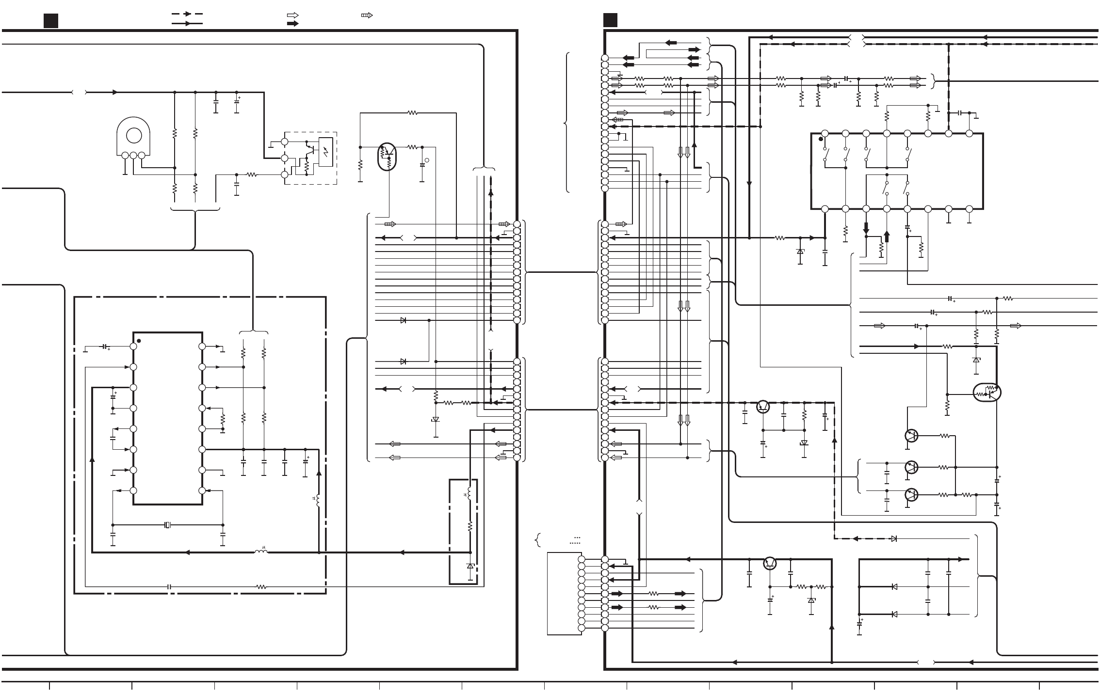
13 14 15 16 17 18 19 20 21 22 23 24
DET
Rch
CE
Lch
DI
DO
CL
+B(2)
SD
+B(1)
T.GND 1
2
3
4
5
6
7
8
9
10
11
Z101
RAN0005EM-2 [EE]
ENG06502Q [GN]
(TUNER PACK)
SA-DV290(EE,GN) OPERATION, MAIN CIRCUIT DIAGRAM
W901B
W902B
123
1
2
3
4
5
6
7
8
9
10
11
12
13
14
15
BA
COM
1
2
3
4
5
6
7
8
9
10
11
12
13
14
15
Q902
UN411FTA
MUTING CONT.
ABC
R962
22K
VR901
EVQVBXFK124B
(VOLUME)
R945
100
R961
22K
R943
100
C917
0.01
D907
MA165TA
M
R946
1K
C909
1000P C918
6.3V100
DEA
R941
1K
A
B
C
D
E
F
G
H
I
J
K
L
N
O
Q
S
T
AOPERATION CIRCUIT
R942
2.2K
R974
1K
C931
16V10
R965
3.9K
R966
3.9K
D961
MA4075MTA R975
22K
D906
MA165TA
U
N
1
2
3
Z901
B3RAD0000028
(REMOTE SENSOR)
W902A
W901A
CP101
C
F
G
B
A
E
D
Q707
2SB1417PQTA
REGULATOR
Q723
2SC3940AQSTA
REGULATOR
R763
4.7K
R230 1K
R229 1K
D721
MA4300MTA R708
4.7K
C707
0.047
C706
35V10
C737
50V100
To
SOUND
PROCESSOR
(SH-DV290)
C735
0.047
B
A
R563
2.7K
R564
2.7K
C660
16V10
C659
16V10
R615
4.7K
R614
4.7K
R631
3.9K
R632
3.9K C202
0.1
R203
100K
R204
100K
C201
0.1
C602
16V10
C708
0.047
R211
270
D201
MA4056MTA
R687
1.5K
R688
1.5K
Q606
R617
4.7K
2
1
3
4
5
6
7
8
9
10
11
C
B
A
X0X1VDD
G
Vss
INHZ0Z1Y1 Y0
16 15 14 13 12 11 10 9
12345678
IC201
BU4053BCFE2
SIGNAL SELECTOR
C655
16V10
C656
16V10
R606
4.7K
R605
4.7K
2
15
3
4
5
6
7
8
9
10
11
12
13
14
1
2
15
3
4
5
6
7
8
9
10
11
12
13
14
1
20
2
1
3
4
5
6
7
8
9
10
11
12
13
14
15
16
17
18
19
K
L
M
I
J
E
F
C
D
E
F
G
E
F
G
A
B
C
D
A
B
G
H
C601
16V10
R598
2.2K
R597
2.2K
R205
100K
H
G
R202
100K
B
C
D
E
F
C509
0.01
C510
0.01
R693
1K
R692
1K
C664
16V10
C725
16V47
A
R696
47K
Q606,609,610
2SD2144STA
MUTING
Q609
Q610
Q612
UN411FTA
MUTING CONT.
B
AR694
22K
R511
47 R509
47
R512 47 R510 47
W501
D720
B0JANG000008
D718
B0JANG000008
H
D
C
R695
470
D611
MA4051MTA
C740
16V10
C733
0.047
D737
MA4082LTA
R764
330
MAIN CIRCUIT
B
C731
1000P
C741
0.1
TUNER Lch/C
TUNER Rch
A.GND
Lch IN
Rch IN
+B(10V)
SUR L
SUR R
S.W
MIC
-
B(
-
10V)
V.GND
D.GND
CS/ REQ
CLK
DATA
CT GND
SH FL1
SH FL2
SYNC
A
B
B
R684
1K
C715
25V6800
C714
1000P
D705
RL1N4003N02
A
R
P
For [EE] area.
IC151
C1BB00000527
RDS SIGNAL
DEMODULATOR
R158
1K
R154
100K
R153
100K
1
2
3
4
5
6
7
8 9
10
11
12
13
14
15
16
VREF
HPX IN
VDDA
VssA
FL OUT
CIN
TEST
X OUT
IDR
RDCL
RDDA
RST
MODE
VDDD
VssD
XIN
C155
1000P
C153
1000P
C160
1000P
C159
6.3V47
R152
1K
R151
1K
C154
560P C158
6.3V47
C151
16V10 BC
L151
100 H
L152
100 H
C156
47P
C157
47P
R157
1K
C152
330P
X151
(4.332MHz)
L153
1 H
R155
120
D151
MA4051MTA
For [EE] area.
N
: POSITIVE VOLTAGE LINE
: NEGATIVE VOLTAGE LINE
-30.1V
5.1V
:AUDIO SIGNAL LINE
6V
7.6V
3.3V
0V
3.3V
14.7V
10.4V
-
37.3V
-
30.1V
-
30.7V
14.7V7.2V
7.8V
-
10V
-
10V
0V
0V
-
10.2V
5.1V
4.9V
0V
-
10V
5.7V0V0V0V0V0V
6V
7.2V
7.6V
-
10.4V
0V 0V
-
10.4V
:TUNER SIGNAL LINE
:MIC SIGNAL LINE
2.6V
2.6V
0V
5.1V
2.5V2.7V
2.5V
2.5V
5.1V
2.5V
2.5V
ORDER NO.AD0303068C8
Sound Processor
SH-DV290EG
Colour
(S) ...................Silver Type
System: SC-DV290
Because of unique interconnecting cables,when a
component requires servise,send or bring in the entire
system.
Note: Refer to the service manual for Model No.
SA-DV290E/EG/EB (ORDER NO.AD0303067C2) for
information on “ACCESSORIES”and “PACKAGING”.
SPECIFICATIONS
Specification
1

EQ/SFP section
MANUAL GEQ
5-Band EQ
Center frequency 70/300/1 k/3.15 k/10 kHz
Level control ±2.0, 4.0, 6.0 dB
EQ/Space mode
4 modes HEAVY, CLEAR, SOFT, HALL
SUPER 3D AI EQ
3 modes AI EQ, SUPER 3D AI 1, SUPER 3D AI 2
Pre-amplifier section
Input sensitivity/impedance
VCR (EXT) 250 mV/15 k
VDP (AUX) 250 mV/15 k
Output level
VCR REC OUT 150 mV/1.5 k
DOLBY PRO LOGIC section
PRO LOGIC mode SURROUND
CENTER mode NORMAL
DELAY TIME 20 ms (Fixed)
AV SURROUND section
AV surround mode
SUPER SURROUND (MUSIC, MOVIE)
DSP CONTROL section
DSP control mode SUPER SOUND EQ
CENTER FOCUS
VIRTUAL REAR SURROUND
MULTI REAR SURROUND
SEAT POSITION
Spectrum analyzer section
Display mode NORMAL, PEAKHOLD, AURORA
General
Dimensions (W×H×D) 293×89×270 mm
Mass 1.5 kg
Power Supply DC±10V/ -25V, AC4.6V
Power Consumption 7W
Nots 1.Design and specifications are subject to
change without notice.
2.Dimensions and weight are approximate.
3.Total harmonic distortion is measured by the
digital spectrum analyzer.
System/SC-DV290
Sound processor: SH-DV290, DVD/ Video CD/ CD
changer: SL-DV290, Tuner/ Amplifier: SA-DV290 ,
Cassette Deck: RS-DV290, Speakers: Front* (SB-
DV290),Center* (SB-PC95),Surround* (SB-PS95)
(*Made in MAES.)
Manufactured under license from Dolby Laboratories. /
“Dolby”,”Pro Logic” and the double-D symbol are
trademarks of Dolby Laboratories.
2
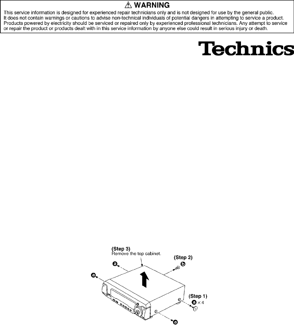
1. Before Repair
This equipment (SH-DV290), which is the component of the system, is supplied with power from
the amplifier (SA-DV290).When repairing this equipment or checking operation of the system, be
sure to connect the amplifier with it.
Power supply and operation check in the state of it as a single equipmenet are impracticable.
2. Operating Instructions
3. Operation Checks and Component Replacement
Procedures
- This section describes procedures for checking the operation of
the major printed circuit boards and replacing the main
components.
- For reassembly after operation checks or replacement, reverse the
respective procedures. Special reassembly procedures are
described only when required.
3.1. Checking for the FL P.C.B.
3
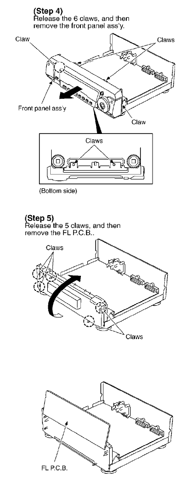
- Check the FL P.C.B. as shown below.
3.2. Checking for the main P.C.B.
- Follow the (Step 1) - (Step 3) of item 3.1.
4
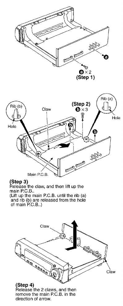
- Check the main P.C.B. as shown below.
5
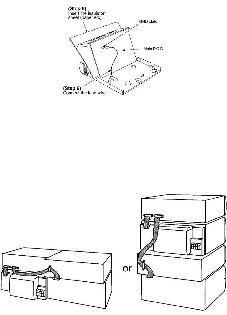
4. Wiring Connection Diagram
5. Block Diagram
6. To Supply Power Source
This unit is designed to operate on power supplied from system connected.
When a component requires service, use the system connections to supply power source.
For system connections. (Refer to Fig. 1)
Fig. 1
7. Schematic Diagram Notes
7.1. Type Illustrations of IC’s, Transistors and Diodes
7.2. Schematic Diagram Notes
- This schematic diagram may be modified at any time with
development of new technology.
Notes:
6

- S601: Display mode (DISPLAY MODE) switch.
- S602: DOLBY PRO LOGIC ( PRO LOGIC, OFF/ ON) switch.
- S603: Super surround (SUPER SURROUND) switch .
- S604: Super sound EQ (SUPER SOUND EQ) switch .
- S605: Center focus (CENTER FOCUS) switch.
- S606: Virtual rear surround (VIRTUAL REAR SURROUND) switch.
- S607: Multi rear surround (MULTI REAR SURROUND) switch.
- S608: Jog control ( ) switch.
- S609: Jog control ( ) switch.
- S610: Jog control ( ) switch.
- S611: Jog control ( ) switch.
- S612: Super 3D AI EQ (SUPER 3D AI EQ) switch.
- S613: Seat position (SEAT POSITION) switch.
- S614: Joystick (MULTI JOG) switch.
- Indicated voltage values are the standard values for the unit
measured by the DC electronic circuit tester (high-impedance) with
the chassis taken as standard. Therefore, there may exist some
errors in the voltage values, depending on the internalimpedanceof
the DC circuit tester. /
No mark: Power on
Important safety notice:
Components identified by mark have special characteristics impotant for safety.
Furthermore, special parts which have purpose of fire-retardant (resistors), high-quality sound
(capacitors), low-noise (resistors), etc. are used. When replacing any of components, be sure to
use only manufacture’s specified parts showninthe parts list.
Caution!
- IC and LSI are sensitive to static electricity.
- Secondary trouble can be prevented by taking care during repair.
- Cover the parts boxes made of plastics with aluminum foil.
- Ground the soldering iron.
- Put a conductive mat on the work table.
- Do not touch the legs of IC or LSI with the fingers directly.
Voltage and signal line
7

: Positive voltage line
: CD Playback signal line
: Negative voltage line
8. Schematic Diagram
9. Printed Circuit Board Diagram
10. Terminal Function of IC's
10.1. IC601(C2BBGF000425):System control/FL drive
Pin
No.
Mark I/O /
Division
Function
1KEY1 I Operation key1 signal input
terminal
2KEY2 I Operation key2 signal input
terminal
3SP IN I A/D signal input terminal
from IC602
4SP A O Band select signal output
terminal for IC602
5SP B O Band select signal output
terminal for IC602
6SP C O Band select signal output
terminal for IC602
7SA CS I Chip select signal input
terminal
8DSP RST O Reset signal output terminal
for IC401
9DSP CS O Chip select signal output
terminal for IC401
10 DSP SNS I Sense signal input terminal
from IC401
11 DSP
ACK
IAcknowledge signal input
terminal from IC401
12 DSP CK O Clock signal output terminal
for IC401
8

Pin
No.
Mark I/O /
Division
Function
13 DSP DO O Data signal output terminal
for IC401
14 DSP DI I Data signal input terminal
for IC401
15 JOGA I JOG A signal input terminal
16 JOGB I JOG B signal input terminal
17 CNVSS I Connected to GND through
resistor
18 RESET I System reset signal input
terminal
19 NC - Not used, open
20 NC - Not used, open
21 VSS - GND terminal
22 XIN I Ceramic oscillator input
terminal (f=4MHz)
23 XOUT O Ceramic oscillator output
terminal (f=4MHz)
24 VCC I Power supply input terminal
25 NC - Not used, open
26 NC - Not used, open
27 LED CFO O ORANGE LED(CENTER
FOCUS) signal output
terminal
28 LED CFG O GREEN LED(CENTER
FOCUS) signal output
terminal
29 BR93
DATA
IData signal input terminal
from EEPROM
30 BR93 CS - Not used, open
31 BR93 CK - Not used, open
32 SYNC I Power failure detect signal
input terminal
33 SA REQ O Request signal output
terminal for Tuner/Amplifier
34 SA CK O Serial communication
signal output terminal for
Tuner/Amplifier
35 SA DO O Serial communication
signal output terminal for
Tuner/Amplifier
36 SA DI I Serial communication
signal input terminal from
Tuner/Amplifier
9

Pin
No.
Mark I/O /
Division
Function
37 LED SSS O LED(SUPER
SURROUND)signal output
terminal
38 LED DPL O LED(DOLBY PRO LOGIC)
signal output terminal
39 LED
SPO
O ORANGE LED (SEAT
POSITION) signal output
terminal
40 LED SPG O GREEN LED (SEAT
POSITION) signal output
terminal
41 LED 3DO O ORANGE LED (3D
ENHANCED SURROUND)
signal output terminal
42 LED 3DG O GREEN LED (3D
ENHANCED SURROUND)
signal output terminal
43 LED
MRO
OORANGE LED (MULTI REAR
SURROUND) signal output
terminal
44 LED
MRG
OGREEN LED (MULTI REAR
SURROUND) signal output
terminal
45 LED
VRO
OORANGE LED (VIRTUAL
REAR SURROUND) signal
output terminal
46 LED
VRG
OGREEN LED (VIRTUAL
REAR SURROUND) signal
output terminal
47-
80
P1-P34 O Segment signal output
terminal
81 --- - Not used, open
82-
88
7G-1G O Grid signal output terminal
89 VEE I Power supply input terminal
90 CD&
DECK DI
I Data signal input terminal
(DVD and deck machanism)
91 CD&
DECK
DO
O Data signal output terminal
(DVD and deck machanism)
92 CD&
DECK
CK
I Clock signal input terminal
(DVD and deck machanism)
93 NC - Not used, open
10

Pin
No.
Mark I/O /
Division
Function
94 CD REQ O Serial data request signal
output terminal for DVD
95 DECK
REQ
O Serial data request signal
output terminal for deck
machanism
96 CD&
DECK
CS
I Chip select signal input
terminal (DVD and deck
machanism)
97 AVSS - GND terminal
98 VREF I Reference voltage input
terminal
99 REG IN0 I Destination select signal
input terminal
100 REG IN1 I Destination select signal
input terminal
11. Replacement Parts List
Note:
*Important safety notice:
Components identified by mark have special characteristics
important for safety.
Furthermore, special parts which have purposes of fireretardant
(resistors), high-quality sound (capacitors), lownoise (resistors),
etc. are used.
When replacing any of components, be sure to use only
manufacture’s specified parts shown in the parts list.
*The markings (RTL) indicate the retention time is limited for this
items. After the discontinuation of this assemblies in production, it
will no longer be available.
*Capacity values are in microfarads (uF) unless specified otherwise,
P=Pico-farads (pF) F=Farads (F)
*Resistance values are in ohms, unless specified otherwise, 1K=
1,000 (OHM), 1M=1,000K (OHM)
*All parts are supplied by SPC.
11

Ref. No. Part No. Part Name & Description Pcs Remarks
1RKA0105-K RUBBER 4
2RKA0106-N FOOT RING 4
3RYP1176-S FRONT PANEL ASS’Y 1
3-1 RGB0025-A TECHNICS BADGE 1
3-2 RKW0576A-1V FL WINDOW 1
3-3 RGK1242-S JOG RING ORNAMENT 1
3-4 RGW0344-S1 JOG KNOB 1
3-5 RGW0345-S JOY KNOB 1
3-6 RMB0594 JOY SPRING 1
3-7 RMQ0882 JOY LEVER 1
3-8 RMQ0883 JOY SUPPORT 1
3-9 RMQ0884 JOY BASE 1
3-10 RMQ0885 JOG KNOB BASE 1
3-11 RMX0169 RING 1
4XTB3+8JFZ SCREW 11
5RHD30007-1S SCREW 4
6RKM0400-S1 TOP CABINET 1
7RMN0526 FL HOLDER 1
8REZ1299 WIRE ASS’Y 1
9RGR0285E-F REAR PANEL 1
C109 ECA1CAK100XB 16V 10U 1
C131-36 ECUV1H101KCV 50V 100P 6 ECJ1VC1H101K
C143 ECUV1H101KCV 50V 100P 1 ECJ1VC1H101K
C201-04 ECBT1H331KB3 50V 330P 4
C205,06 ECBT1H330J5 50V 33P 2 F1D1H330A006
C207,08 ECEA1HKA4R7 50V 4.7U 2
C209,10 ECBT1C103MS5 16V 0.01U 2 F1D1C103A004
C211,12 ECBT1H104KB5 50V 0.1U 2 F1D1H1040002
C213-15 ECBT1H470J3 50V 47P 3
C216,17 ECBT1C103MS5 16V 0.01U 2 F1D1C103A004
C221,22 ECBA1H101KB5 50V 100P 2
C223,24 ECA1CAK100XB 16V 10U 2
C225-33 ECBA1H101KB5 50V 100P 9
C288,89 ECA1CAK100XB 16V 10U 2
C301-04 ECEA1HKA4R7 50V 4.7U 4
C305,06 ECBA1H101KB5 50V 100P 2
C307,08 ECBT1H100JC5 50V 10P 2 F1D1H100A015
C309,10 ECBT1C103MS5 16V 0.01U 2 F1D1C103A004
C311 ECA1CAK100XB 16V 10U 1
C312 ECA1CAK220XB 16V 22U 1
C313,14 ECA1CAK100XB 16V 10U 2
C315,16 ECBA1H101KB5 50V 100P 2
C317 ECBT1C562KR5 16V 5600P 1 F1D1C562A010
C318 ECBT1H270J5 50V 27P 1 ECBT1H270J3
C319-22 ECA1CAK100XB 16V 10U 4
C323,24 ECBT1C103MS5 16V 0.01U 2 F1D1C103A004
C327 ECBT1H333KB5 50V 0.033U 1 ECBT1H333KB3
C328,29 ECA1CAK220XB 16V 22U 2
C343,44 ECA1CAK100XB 16V 10U 2
C345,46 ECBA1H101KB5 50V 100P 2
C347,48 ECBT1H220J5 50V 22P 2 F1D1H220A006
C349,50 ECA1CAK100XB 16V 10U 2
12

Ref. No. Part No. Part Name & Description Pcs Remarks
C351,52 ECBT1C103MS5 16V 0.01U 2 F1D1C103A004
C354 ECA1CAK100XB 16V 10U 1
C356 ECA1CAK100XB 16V 10U 1
C401 ECJ1VB1E223K 25V 0.022U 1
C402,03 ECUVNH103KBV 50V 0.01U 2 F1H1H103A748
C404 ECA0JAK470XH 6.3V 47U 1
C501 ECBT1C103MS5 16V 0.01U 1 F1D1C103A004
C502 ECBT1H331KB3 50V 330P 1
C503,04 ECBA1H101KB5 50V 100P 2
C505 ECBT1C103MS5 16V 0.01U 1 F1D1C103A004
C506 ECA1CAK330XB 16V 33U 1
C507 RCE1HKAR47BG 50V 0.47U 1 F2A1HR47A015
C508 ECA1CAK100XB 16V 10U 1
C509,10 ECA1CAK220XB 16V 22U 2
C511 ECA1CAK100XB 16V 10U 1
C512 ECA1CAK330XB 16V 33U 1
C601 ECBT1H104KB5 50V 0.1U 1 F1D1H1040002
C602 ECA0JM102 6.3V 1000U 1
C603,04 ECBT1H102KB3 50V 1000P 2
C605 ECA1VAK330XB 35V 33U 1
C606,07 ECBT1H471KB3 50V 470P 2
C608 ECBT1H221KB3 50V 220P 1
C609,10 ECBT1C103MS5 16V 0.01U 2 F1D1C103A004
C611 ECA1HAK3R3XB 50V 3.3U 1
C612,13 F2A1C220A034 16V 22U 2
C614 ECA1CAK100XB 16V 10U 1
C615 ECA1VAK330XB 35V 33U 1
C616 ECEA1VKS330Q 35V 33U 1
C618,19 ECBT1C103MS5 16V 0.01U 2 F1D1C103A004
C620,21 ECA1HAK0R1XB 50V 0.1U 2
C622,23 ECBT1H104KB5 50V 0.1U 2 F1D1H1040002
C624 ECBT1C103MS5 16V 0.01U 1 F1D1C103A004
C625 ECA0JAK101XB 6.3V 100U 1
C626 ECBT1H473KB5 50V 0.047U 1 F1D1H473A012
C627,28 F2A1C220A034 16V 22U 2
C753,54 ECBT1C103MS5 16V 0.01U 2 F1D1C103A004
C761-63 ECBT1C103MS5 16V 0.01U 3 F1D1C103A004
C764 ECA1AAK221XH 10V 220U 1
C765 ECBT1C103MS5 16V 0.01U 1 F1D1C103A004
C766 ECA1CAK100XB 16V 10U 1
C767 ECBT1C103MS5 16V 0.01U 1 F1D1C103A004
C768 ECA1CAK100XB 16V 10U 1
C769 ECBT1C103MS5 16V 0.01U 1 F1D1C103A004
C770 ECA1CAK100XB 16V 10U 1
C771,72 ECBT1C103MS5 16V 0.01U 2 F1D1C103A004
C773 ECA1AAK221XH 10V 220U 1
C774 ECA1CAM221XB 16V 220U 1
C801 ECJ1VC1H120J 50V 12P 1
C802 ECJ1VC1H050C 50V 5P 1
C803 ECJ1VB1H102K 50V 1000P 1
C804 ECJ1VB1C104K 16V 0.1U 1
C805 ECJ1VB0J105K 6.3V 1U 1
C806,07 ECJ1VB1H222K 50V 2200P 2
C808-10 ECUVNH103KBV 50V 0.01U 3 F1H1H103A748
13

Ref. No. Part No. Part Name & Description Pcs Remarks
C811 ECJ1VB1E223K 25V 0.022U 1
C812 ECJ1VB1C104K 16V 0.1U 1
C813 ECUVNH103KBV 50V 0.01U 1 F1H1H103A748
C814 ECJ1VB0J105K 6.3V 1U 1
C815 ECJ1VB1E223K 25V 0.022U 1
C816 ECJ1VB1C104K 16V 0.1U 1
C818,19 ECJ1VB1H681K 50V 680P 2
C820,21 ECEA1HKA4R7 50V 4.7U 2
C822 ECA0JAK470XH 6.3V 47U 1
C823 EEAFC0J101B 6.3V 100U 1
C824 ECA0JAK470XH 6.3V 47U 1
C825-32 ECEA1HKA4R7 50V 4.7U 8
C833-35 ECA0JAK470XH 6.3V 47U 3
C836,37 ECA1CAK100XB 16V 10U 2
C838,39 ECA1HAK010XI 50V 1U 2
C851,52 ECJ1VB1H222K 50V 2200P 2
C853,54 ECA1CAK100XB 16V 10U 2
C855,56 ECEA1HKA4R7 50V 4.7U 2
C857,58 ECJ1VB1C104K 16V 0.1U 2
C859 ECEA1HKA4R7 50V 4.7U 1
C860 ECJ1VB1H222K 50V 2200P 1
C861 ECJ1VB1H561K 50V 560P 1
C862 ECUV1H471KBV 50V 470P 1 F1H1H471A013
C863,64 ECA0JAK470XH 6.3V 47U 2
C865 ECJ1VB0J105K 6.3V 1U 1
C866-68 ECA1HAK010XI 50V 1U 3
C869 ECUVNH103KBV 50V 0.01U 1 F1H1H103A748
C870 EEAFC0J101B 6.3V 100U 1
C871,72 ECJ1VB1H222K 50V 2200P 2
C873-76 ECA1HAK010XI 50V 1U 4
C877,78 ECUVNH103KBV 50V 0.01U 2 F1H1H103A748
C879,80 ECJ1VB1H222K 50V 2200P 2
C881,82 ECA1HAK010XI 50V 1U 2
C883 ECA0JAK470XH 6.3V 47U 1
C884 ECJ1VB1H222K 50V 2200P 1
C886 EEAFC0J101B 6.3V 100U 1
C887,88 ECA0JAK470XH 6.3V 47U 2
C891 ECUVNH103KBV 50V 0.01U 1 F1H1H103A748
C892 ECA0JAK470XH 6.3V 47U 1
C893 ECUVNH103KBV 50V 0.01U 1 F1H1H103A748
C894-97 ECJ1VB1E223K 25V 0.022U 4
C898 EEAFC0J101B 6.3V 100U 1
C899 ECA0JAK470XH 6.3V 47U 1
CN201 RJT065A20 SYSTEM CONNECTOR(20P) 1 K1FA220B0007
CN202 RJT065K20 SYSTEM CONNECTOR(20P) 1 K1FA220B0006
D201 MAZ40560MF DIODE 1
D203 MA165TA5 DIODE 1 MA2C16500E
D204 MA719 DIODE 1 MA2C719
D301 MA700 DIODE 1 MA2C700
D302 MA165TA5 DIODE 1 MA2C16500E
D304,05 MA719 DIODE 2 MA2C719
D601-04 1SS291TA DIODE 4
14

Ref. No. Part No. Part Name & Description Pcs Remarks
D605-10 MA165TA5 DIODE 6 MA2C16500E
D611,12 LNJ301MPUJAD LED 2
D613-17 B3AHA0000012 LED 5
D653 MA165TA5 DIODE 1 MA2C16500E
D761 MA4082LTA DIODE 1 MAZ40820LF
D762 B0AAMM000009 DIODE 1
D763-66 MA165TA5 DIODE 4 MA2C16500E
D767 MA4051M DIODE 1 MAZ40510M
D770 MA4062H DIODE 1 MAZ40620H
D771 MA4051-L DIODE 1 MAZ40510L
D772 MA165TA5 DIODE 1 MA2C16500E
FL601 A2BD00000041 FL DISPLAY TUBE 1
IC201 NJU7313AMT2 IC 1 C0JZAS000002
IC202 NJM4558MTE1 IC 1 C0ABBB000109
IC203 C0JBAR000292 IC 1
IC301 M5218AP IC 1 C0AABB000055
IC302,03 NJM4558MTE1 IC 2 C0ABBB000109
IC401 C2BBFD000246 IC 1
IC501 NJM4558MTE1 IC 1 C0ABBB000109
IC601 C2BBGF000425 IC 1
IC602 M62457AFPE1 IC 1 C1BB00000486
IC801 C2HBZC000010 IC 1
IC802 C2HBZC000008 IC 1
JK101 SJF3068-7N JACK,VDP(AUX) 1 K2HA102B0046
JK102 SJF3069-5N JACK,VCR(EXT)IN/OUT 1 K2HA204B0083
JK103 SJFD7 JACK,SUB WOOFER OUT 1 K4BK01B00002
L101 RLBV252AV-Y COIL 1 J0JBC0000019
L301,02 RLQA3R3JT1-Y COIL 2 G0C3R3JA0019
L401 RLQB100JTD-D COIL 1 G0C100JA0030
L502 RLBV252AV-Y COIL 1 J0JBC0000019
L601 G0C100JA0019 COIL 1
L801 J0JCC0000077 COIL 1
L802 RLBV102V-Y COIL 1 J0JBC0000014
L804 RLBV102V-Y COIL 1 J0JBC0000014
L806 RLBV102V-Y COIL 1 J0JBC0000014
L807 G0A200D00002 COIL 1
L808 RLQB100JTD-D COIL 1 G0C100JA0030
L811 RLBV102V-Y COIL 1 J0JBC0000014
L814 G0A200D00002 COIL 1
L821,22 RLBV252AV-Y COIL 2 J0JBC0000019
PCB1 REP3073H-M MAIN P.C.B. ASS’Y 1 [RTL]
Q301-04 2SD2144S TRANSISTOR 4
Q305,06 UN411FTA TRANSISTOR 2 UNR411F00A
Q307-10 2SD2144S TRANSISTOR 4
Q313-16 2SD2144S TRANSISTOR 4
Q501,02 UN411FTA TRANSISTOR 2 UNR411F00A
Q503-05 2SD2144S TRANSISTOR 3
15

Ref. No. Part No. Part Name & Description Pcs Remarks
Q506 UN411FTA TRANSISTOR 1 UNR411F00A
Q507 2SD2144S TRANSISTOR 1
Q601 UN4211 TRANSISTOR 1 UNR4211
Q602-04 2SC3311A TRANSISTOR 3 2SC3311AW
Q605,06 UN5211TX TRANSISTOR 2 UNR521100L
Q761,62 2SD2137PQTA TRANSISTOR 2 2SD21370PA
Q763 2SD592A TRANSISTOR 1 2SD0592AW
Q764 2SB0621AHA TRANSISTOR 1
Q765 2SC3311A TRANSISTOR 1 2SC3311AW
Q766 2SA1309ATA TRANSISTOR 1 2SA1309AWA
Q767 2SC3311A TRANSISTOR 1 2SC3311AW
Q768 2SC3940AQSTA TRANSISTOR 1 2SC3940ARA
R101,02 ERDS2FJ104 1/4W 100K 2
R103,04 ERDS2FJ102 1/4W 1K 2
R105,06 ERDS2FJ123 1/4W 12K 2
R107,08 ERDS2FJ332 1/4W 3.3K 2
R111,12 ERDS2FJ332 1/4W 3.3K 2
R113,14 ERDS2FJ123 1/4W 12K 2
R127 ERDS2FJ104 1/4W 100K 1
R128 ERDS2FJ102 1/4W 1K 1
R129,30 ERDS2T0 1/4W 0 2
R131 ERJ3GEY0R00V 1/16W 0 1
R203,04 ERDS2FJ222 1/4W 2.2K 2
R205,06 ERDS2FJ563 1/4W 56K 2
R207,08 ERDS2FJ273 1/4W 27K 2
R209,10 ERDS2FJ104 1/4W 100K 2
R211-14 ERDS2FJ222 1/4W 2.2K 4
R219 ERDS2FJ391 1/4W 390 1
R220 ERDS2FJ104 1/4W 100K 1
R221,22 ERDS2FJ221 1/4W 220 2
R223,24 ERDS2FJ223 1/4W 22K 2
R225,26 ERDS2FJ102 1/4W 1K 2
R227,28 ERDS2TJ682 1/4W 6.8K 2
R229,30 ERDS2FJ822 1/4W 8.2K 2
R233-36 ERDS2FJ102 1/4W 1K 4
R237,38 ERDS2FJ822 1/4W 8.2K 2
R239 ERDS2FJ473 1/4W 47K 1
R240 ERDS2FJ102 1/4W 1K 1
R249,50 ERDS2FJ152 1/4W 1.5K 2
R255,56 ERDS2FJ472 1/4W 4.7K 2
R257,58 ERDS2FJ822 1/4W 8.2K 2
R259,60 ERDS2T0 1/4W 0 2
R284,85 ERDS2T0 1/4W 0 2
R286,87 ERDS2FJ393 1/4W 39K 2
R288-91 ERDS2T0 1/4W 0 4
R295,96 ERDS2T0 1/4W 0 2
R297,98 ERDS2FJ471 1/4W 470 2
R303,04 ERDS2FJ223 1/4W 22K 2
R305-08 ERDS2FJ102 1/4W 1K 4
R309,10 ERDS2FJ561 1/4W 560 2
R311 ERDS2FJ223 1/4W 22K 1
R312 ERDS2FJ182 1/4W 1.8K 1
R313,14 ERDS2TJ392 1/4W 3.9K 2
16

Ref. No. Part No. Part Name & Description Pcs Remarks
R315,16 ERDS2FJ274 1/4W 270K 2
R317 ERDS2FJ223 1/4W 22K 1
R318 ERDS2FJ101 1/4W 100 1
R319 ERDS2FJ154 1/4W 150K 1
R322 ERJ3GEYJ822V 1/16W 8.2K 1 D0GB822JA002
R323,24 ERDS2FJ120 1/4W 12 2
R325,26 ERDS2FJ102 1/4W 1K 2
R327,28 ERDS2FJ561 1/4W 560 2
R329 ERDS2FJ564 1/4W 560K 1
R330 ERDS2TJ184T 1/4W 180K 1
R331,32 ERDS2FJ222 1/4W 2.2K 2
R333,34 ERDS2FJ563 1/4W 56K 2
R335,36 ERDS2FJ102 1/4W 1K 2
R337 ERDS2FJ391 1/4W 390 1
R338 ERDS2FJ471 1/4W 470 1
R345-47 ERDS2FJ102 1/4W 1K 3
R348 ERDS2FJ222 1/4W 2.2K 1
R349 ERDS2FJ123 1/4W 12K 1
R350 ERDS2FJ103 1/4W 10K 1
R351 ERDS2FJ224 1/4W 220K 1
R352 ERDS2FJ103 1/4W 10K 1
R353 ERDS2FJ224 1/4W 220K 1
R354 ERDS2FJ562 1/4W 5.6K 1
R357,58 ERDS2FJ223 1/4W 22K 2
R359,60 ERDS2FJ821 1/4W 820 2
R361,62 ERDS2TJ682 1/4W 6.8K 2
R363,64 ERDS2FJ102 1/4W 1K 2
R365,66 ERDS2TJ184T 1/4W 180K 2
R367,68 ERDS2FJ471 1/4W 470 2
R372 ERDS2T0 1/4W 0 1
R374 ERDS2T0 1/4W 0 1
R402 ERJ3GEYJ104 1/16W 100K 1
R403 ERJ3GEYJ681V 1/16W 680 1 D0GB681JA002
R404 ERJ3GEYJ104 1/16W 100K 1
R405-10 ERJ3GEYJ221V 1/16W 220 6
R411 ERDS2FJ102 1/4W 1K 1
R414,15 ERDS2FJ102 1/4W 1K 2
R417 ERJ3GEYJ221V 1/16W 220 1
R419 ERDS2FJ101 1/4W 100 1
R420 ERDS2FJ102 1/4W 1K 1
R421 ERDS2FJ101 1/4W 100 1
R424 ERDS2FJ102 1/4W 1K 1
R425,26 ERDS2FJ472 1/4W 4.7K 2
R429 ERDS2FJ472 1/4W 4.7K 1
R430,31 ERJ3GEYJ103V 1/16W 10K 2 D0GB103JA002
R432 ERDS2FJ102 1/4W 1K 1
R501 ERDS2FJ152 1/4W 1.5K 1
R502 ERDS2FJ102 1/4W 1K 1
R503 ERDS2FJ122 1/4W 1.2K 1
R504 ERDS2TJ124 1/4W 120K 1
R505 ERDS2FJ102 1/4W 1K 1
R506 ERDS2TJ272T 1/4W 2.7K 1
R507 ERDS2TJ105 1/4W 1M 1
R508 ERDS2FJ104 1/4W 100K 1
17

Ref. No. Part No. Part Name & Description Pcs Remarks
R509 ERDS2FJ222 1/4W 2.2K 1
R510 ERDS2FJ104 1/4W 100K 1
R511 ERDS2TJ105 1/4W 1M 1
R512 ERDS2FJ154 1/4W 150K 1
R513 ERDS2FJ102 1/4W 1K 1
R514 ERDS2FJ101 1/4W 100 1
R515 ERDS2FJ223 1/4W 22K 1
R517 ERDS2FJ821 1/4W 820 1
R518 ERDS2FJ222 1/4W 2.2K 1
R519 ERDS2FJ154 1/4W 150K 1
R520 ERDS2FJ122 1/4W 1.2K 1
R601-03 ERDS2FJ102 1/4W 1K 3
R604,05 ERDS2FJ103 1/4W 10K 2
R606 ERDS2FJ102 1/4W 1K 1
R607,08 ERDS2FJ221 1/4W 220 2
R609 ERDS2FJ222 1/4W 2.2K 1
R610 ERDS2FJ332 1/4W 3.3K 1
R611 ERDS2FJ101 1/4W 100 1
R612 ERDS2FJ102 1/4W 1K 1
R613 ERDS2FJ562 1/4W 5.6K 1
R614-17 ERDS2FJ102 1/4W 1K 4
R618 ERDS2FJ104 1/4W 100K 1
R619 ERDS2FJ681 1/4W 680 1
R622,23 ERDS2FJ104 1/4W 100K 2
R624-29 ERDS2TJ181 1/4W 180 6
R631 ERDS2FJ821 1/4W 820 1
R632 ERDS2FJ102 1/4W 1K 1
R633 ERDS2FJ122 1/4W 1.2K 1
R634 ERDS2FJ152 1/4W 1.5K 1
R635 ERDS2FJ182 1/4W 1.8K 1
R636 ERDS2FJ222 1/4W 2.2K 1
R637 ERDS2FJ821 1/4W 820 1
R638 ERDS2FJ102 1/4W 1K 1
R639 ERDS2FJ122 1/4W 1.2K 1
R640 ERDS2FJ152 1/4W 1.5K 1
R641 ERDS2FJ182 1/4W 1.8K 1
R642 ERDS2FJ222 1/4W 2.2K 1
R647 ERDS2FJ223 1/4W 22K 1
R648-50 ERDS2FJ104 1/4W 100K 3
R651 ERDS2FJ102 1/4W 1K 1
R652,53 ERDS2FJ472 1/4W 4.7K 2
R654-56 ERDS2FJ103 1/4W 10K 3
R657 ERDS2FJ473 1/4W 47K 1
R658,59 ERDS2FJ472 1/4W 4.7K 2
R660 ERDS2FJ473 1/4W 47K 1
R661 ERDS2FJ223 1/4W 22K 1
R662 ERDS2FJ102 1/4W 1K 1
R663,64 ERDS2FJ331 1/4W 330 2
R665-67 ERDS2FJ473 1/4W 47K 3
R668 ERDS2FJ222 1/4W 2.2K 1
R671-80 ERJ6GEYJ104V 1/10W 100K 10
R681 ERJ3GEYJ222V 1/16W 2.2K 1
R682 ERJ3GEY0R00V 1/16W 0 1
R686 ERJ3GEY0R00V 1/16W 0 1
18

Ref. No. Part No. Part Name & Description Pcs Remarks
R691,92 ERDS2FJ221 1/4W 220 2
R716 ERDS2FJ821 1/4W 820 1
R761,62 ERDS2FJ2R2 1/4W 2.2 2
R763 ERQ16NKWR33E 1/6W 0.33 1
R764 ERDS2FJ821 1/4W 820 1
R765 ERDS2FJ221 1/4W 220 1
R766 ERDS2FJ182 1/4W 1.8K 1
R767 ERDS2FJ102 1/4W 1K 1
R768,69 ERDS2FJ122 1/4W 1.2K 2
R770 ERD2FCJ4R7 1/4W 4.7 1
R771 ERDS2FJ102 1/4W 1K 1
R772 ERDS2FJ122 1/4W 1.2K 1
R773 ERDS2FJ102 1/4W 1K 1
R774 ERDS2FJ221 1/4W 220 1
R801 ERJ3GEYJ221V 1/16W 220 1
R802 ERJ3GEYJ105V 1/16W 1M 1
R803 ERJ3GEYJ101 1/16W 100 1 D0GB101JA002
R804-07 ERJ3GEYJ271V 1/16W 270 4
R808-10 ERJ3GEYJ331V 1/16W 330 3
R811 ERJ3GEYJ472V 1/16W 4.7K 1
R812 ERJ3GEYJ331V 1/16W 330 1
R813 ERJ3GEYJ472V 1/16W 4.7K 1
R814 ERJ3GEYJ104 1/16W 100K 1
R815-20 ERJ3GEYJ102V 1/16W 1K 6
R821 ERJ3GEYJ331V 1/16W 330 1
R823 ERJ3GEYJ331V 1/16W 330 1
R824,25 ERDS2TJ823 1/4W 82K 2
R827 ERJ3GEY0R00V 1/16W 0 1
R829 ERJ3GEYJ222V 1/16W 2.2K 1
R830 ERJ3GEYJ472V 1/16W 4.7K 1
R833,34 ERJ3GEYJ223V 1/16W 22K 2 D0GB223JA002
R835,36 ERJ3GEYJ152V 1/16W 1.5K 2
R851,52 ERJ3GEYJ102V 1/16W 1K 2
R854 ERJ3GEYJ183V 1/16W 18K 1 D0GB183JA002
R855 ERJ3GEYJ393V 1/16W 39K 1 D0GB393JA002
R856 ERJ3GEY0R00V 1/16W 0 1
R857-59 ERJ3GEYJ103V 1/16W 10K 3 D0GB103JA002
R860 ERJ3GEYJ560V 1/16W 56 1
R861 ERJ3GEYJ104 1/16W 100K 1
R863,64 MCR03PZHJ561 1/16W 560 2
R866 ERJ3GEYJ223V 1/16W 22K 1 D0GB223JA002
R867,68 MCR03PZHJ561 1/16W 560 2
R869-72 ERJ3GEYJ271V 1/16W 270 4
R873,74 ERJ3GEYJ331V 1/16W 330 2
R875,76 ERJ3GEYJ271V 1/16W 270 2
R877,78 ERJ3GEYJ223V 1/16W 22K 2 D0GB223JA002
R879,80 ERJ3GEYJ222V 1/16W 2.2K 2
R881 ERJ3GEYJ101 1/16W 100 1 D0GB101JA002
R882 ERJ3GEYJ105V 1/16W 1M 1
R888,89 ERJ3GEYJ331V 1/16W 330 2
R890 ERJ3GEYJ103V 1/16W 10K 1 D0GB103JA002
R891,92 ERJ3GEYJ222V 1/16W 2.2K 2
R898 ERJ3GEY0R00V 1/16W 0 1
R900 ERJ3GEY0R00V 1/16W 0 1
19

Ref. No. Part No. Part Name & Description Pcs Remarks
R903 ERDS2TJ124 1/4W 120K 1
S601-07 EVQ11G05R SW,PUSH 7
S608-11 EVQ11G07K SW,JOY STICK 4
S612,13 EVQ11G05R SW,PUSH 2
S614 ESE24SV7 SW,MULTI JOG 1
X401 RSXY8M00D01T OSCILLATOR 1 H2B800400005
X601 H2B400400013 OSCILLATOR 1
X801 RSXZ36M8M01T OSCILLATOR 1
12. Cabinet Parts Location
20
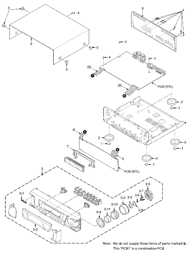
13. Schematic Diagram for printing with A4 size
K0304YH/HM
21
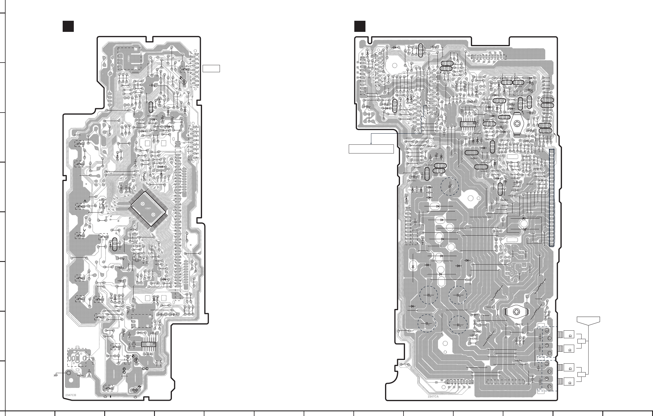
123456789101112
13
A
B
C
D
E
F
G
H
SA-DV290(E,EB,EG) OPERATION, MAIN P.C.B.
Note: This printed circuit board diagram may be modified at any time with the development of new technology.
MAIN P.C.B.
B
10
9
8
7
6
5
4
3
2
1
D607
R635
R719
J
J
W902A
JJ
J
J
J
J
J
15
13
11
9
7
5
3
1
14
12
10
8
6
4
2
C664
C725
JJ
J
J
J
J
J
J
J
J
J
J
J
J
J
J
J
R230
C740
C733
C735
R764
R763
D737 B
C
E
Q723
W901A
W501
20
18
16
14
12
10
8
6
4
2
19
17
15
13
11
9
7
5
3
1
15
13
11
9
7
5
3
1
14
12
10
8
6
4
2
R694
R761
R696
R695
J
J
J
J
J
J
D657
D659
C705
D611
B
C
E
Q612
J
J
J
J
J
J
J
J
J
J
J
J
C737
C706
J
R776
R738
R739
R708
ECB Q708
ECB Q709
E
C
B
Q707
D721
C707
C708
C509
C510
C202
C714
C731
C741
D720
D719
D718
D705
D717
C715
C602
C656
C655
C554
C601
C555
C622
C660
C659
C371
C551
ECB
Q609
ECB
Q610
ECB
Q554
ECB
Q607 ECB
Q608
ECB
Q606
ECB
Q605
ECB
Q555
B
C
E
Q602
B
C
E
Q551
B
C
E
Q503
B
C
E
Q601
JJ
J
J
1234567891011
CP101
E602
R605
R606
R617
R618
R684
R683
R604R603
R686
R685
R601
R614
R602
J
J
J
J
JJ
J
J
J
J
J
J
J
J
J
J
R693
R692
R564
R229
R628
R688
R687
R512
R511
R509
R204
R203
R727
R211
R510
R563
R558
R607
R608
R560
R569
R598
R597
R570
R561
R591
R559
R557
D555
D552
D757
D658
D551
D756
C550
C647
C605
C606
C610
J
J
J
J
J
J
ECB
Q704
ECB
Q703
C721
R572
R544
R610
R619
R612
R691
R624
R620
R546
R547
R638
J
J
C604
C608
C603
C607
C649
C609
C650
C612
R627
C613
R555
C614
C723
C552
C648
C619
C611
C724
R621
R615
R631
R632
R552
R551
R609
R611
R637
R769
R721
R722
R648
R647
R767
R622
R556
R623
R797
R796
R729
R202
R205
J
J
C616
C617
C618
J
D558
J
J
D725
IC601
26
25
24
23
22
21
20
19
18
17
16
15
14
13
12
11
10
9
8
7
6
5
4
3
2
1
J
J
J
J
J
J
J
J
J
J
JJ
J
J
J
J
J
J
J
J
J
J
J
J
J
JJ
J
J
J
W721A
W722A
10
9
8
7
6
5
4
3
2
1
4
3
2
1
J
J
J
C709
C761
D755
D754
D761
D753
D702
D704
D752
D701
D751
D703
D601
D602
C704 C701
C703
C702
J
J
J
J
J
J
J
J
J
J
J
J
J
J
J
J
E601
L602
L601
L605
L606
C639
C637
C635 C636 C632
JK601
JK602
1234
CP602
5678
J
JJ
C626
C620
C630
C621
C631
C642
R651
R642
R652
R650
R649
R639
R641
R640
C627
C629
C628
C732
C641
C640
To SOUND PROCESSOR
LF
(8 )
HF
(6 )
LF
(8 )
HF
(6 )
CN781
N
Rch
Lch
SPEAKERS
D582
D581
D583
D553
D554
ECB
Q553
ECB
Q557
C559 R568
R566
R567
12
JK551
ECB
Q556
C201
15
8
910 1516
IC201
D201
1 2 3 4 5 6 8 910 1112
CP601
7
(REP3337K-M)
NN
C556
NN
OPERATION P.C.B.
A
VR901
(VOLUME)
C902
C928
C922
C920
R929
R988
R991
R975
R974
R934
R937
R930
R931
R918
R957
R919
R932
R956
R987
C915
D906
J
J
J
J
J
J
J
J
J
J
J
J
J
J
J
JJ
J
J
J
J
R995
R942
R941
R912
W902B
15
13
11
9
7
5
3
1
14
12
10
8
6
4
2
S913
D951
W901B
15
13
11
9
7
5
3
1
14
12
10
8
6
4
2
D902
D901
J
R926
R993
R958
R969
R959 R997
R996
R990
R936
R935
R999
R954
C921
C903
D973
R939
R960
R986
J
J
J
J
J
J
C926
C905
D933
D931
D905
J
L901
L902
J
J
C901
FL901
1
2
5
6
7
8
9
10
11
12
13
14
15
16
17
18
19
20
21
22
23
24
25
26
27
28
29
30
31
32
33
34
35
36
37
38
39
40
41
42
43
44
45
46
47
48
49
50
53
54
L153
J
J
J
R155
1510152025 30 35
404550
55
60
31
51
65
7570
80
81
85
90
95
100
IC901
R953
R951
R943
R961
R924
R925
R922
R921
J
J
J
R952
R976
R928
R950
R945
R962 R949
C912
C908
C907
C925
C909
C904
C911
C910
D907
J
J
J
J
J
3
2
1X901
J
J
X902
C914
C916
C918
B
C
E
Q901
R151
R152
R153
R154
L152
R158
C152
C153
C154
L151
J
C919
C151
C927
Z901
(SENSOR)
D151
C160
C155
C156
X151
IC151
158
910 16
15
C157
C159 R944
R946
C924
C917
D974
C158
S901
( / ) D306
( )
R901
J
S904
( PLAY/
REC)
R904
R157
R903
R902
S902
(CLOCK/
TIMER)
C923
JK903
(PHONES)
2
143
56
7
W905
C395
C396
JR906
R905
S907
(SET)
S906
(TUNING
MODE)
S905
(FM AUTO/
MONO)
S903
(—DEMO)
J
J
J
J
J
R910
R909
S908
(INPUT
SELECTOR
)
S910
(TUNING )
D904
R911
R994
R940
R907
S912
(TUNER/
BAND)
J
S911
(TUNING )
R914
R915
R916
R913
J
S915
(RDS
DISP MODE
PTY)
S914
(RDS
DISP MODE
PS) J
DIGITAL
S.WOOFER
D954
( PLAY/
REC)
3
2
1
1
2
3
E
C
B
Q902
D961
R966R965
(REP3337K-M)
N
C931
123456789101112
13
A
B
C
D
E
F
G
H
SA-DV290(E,EB,EG) AC IN, POWER TRANSFOMER(A)&(B), POWER SUPPLY P.C.B.
POWER SUPPLY P.C.B.
C
B
C
E
Q701
B
C
E
Q702
B
C
E
Q711
B
C
E
Q712
B
C
E
Q725
ECB
Q705
R725
R723
C719
C717
C710
C720
W701B
D723
C718
C722
C734 R720
R724
R768
R749
R765
R753
R754
D758
D739
D738
J
D730
10
9
8
7
6
5
4
3
2
1
(REP3337K-M)
JK701 JK603
L701
FC1 FC2
F1 T2A
Z701
C791
RL702
1
2
43
1
2
3
4
CN601
5
6
7
8
9
10
11
12
1
2
3
4
CN602
5
6
7
8
T702(Power transformer)
R794
R773
R774
R795
R771
R772
R712
ECB
Q791
ECB
Q726
D500
D711
D746
D740
J
J
C754
C758
D745
C759
R777
D742
D743
D741
D744
J
J
J
J
J
J
J
C755
C753
C634
W1
W2/W3
D747
AC IN P.C.B.
D
AC IN
C644
C646
C651
C652
C624
C633
C625
C645
C643
R646
R645
R644
R643
L603
L604
C
SR
SL
230V 50Hz . . . . . [E,EG]
230-240V 50Hz . . . [EB]
REP3338A-S . . . [E,EG]
REP3338B-S . . . [EB]
CENTER/
SURROUND
SPEAKERS
POWER TRANSFORMER
(A) P.C.B.
E
W722B
W721B
1
2
3
4
5
6
7
8
9
10
1
2
3
4
R793
CN710
CN709
CN708
CN707
CN706
CN705
CN704
CN703
CN702
CN701
FP792
R798
FP791
J
POWER TRANSFORMER
(B) P.C.B.
F
CN711
CN713
CN712
W1
W2
W3
J
J
J
J
J
J
T701(Power transformer)
(REP3337K-M) REP3338A-S . . . [E,EG]
REP3338B-S . . . [EB]
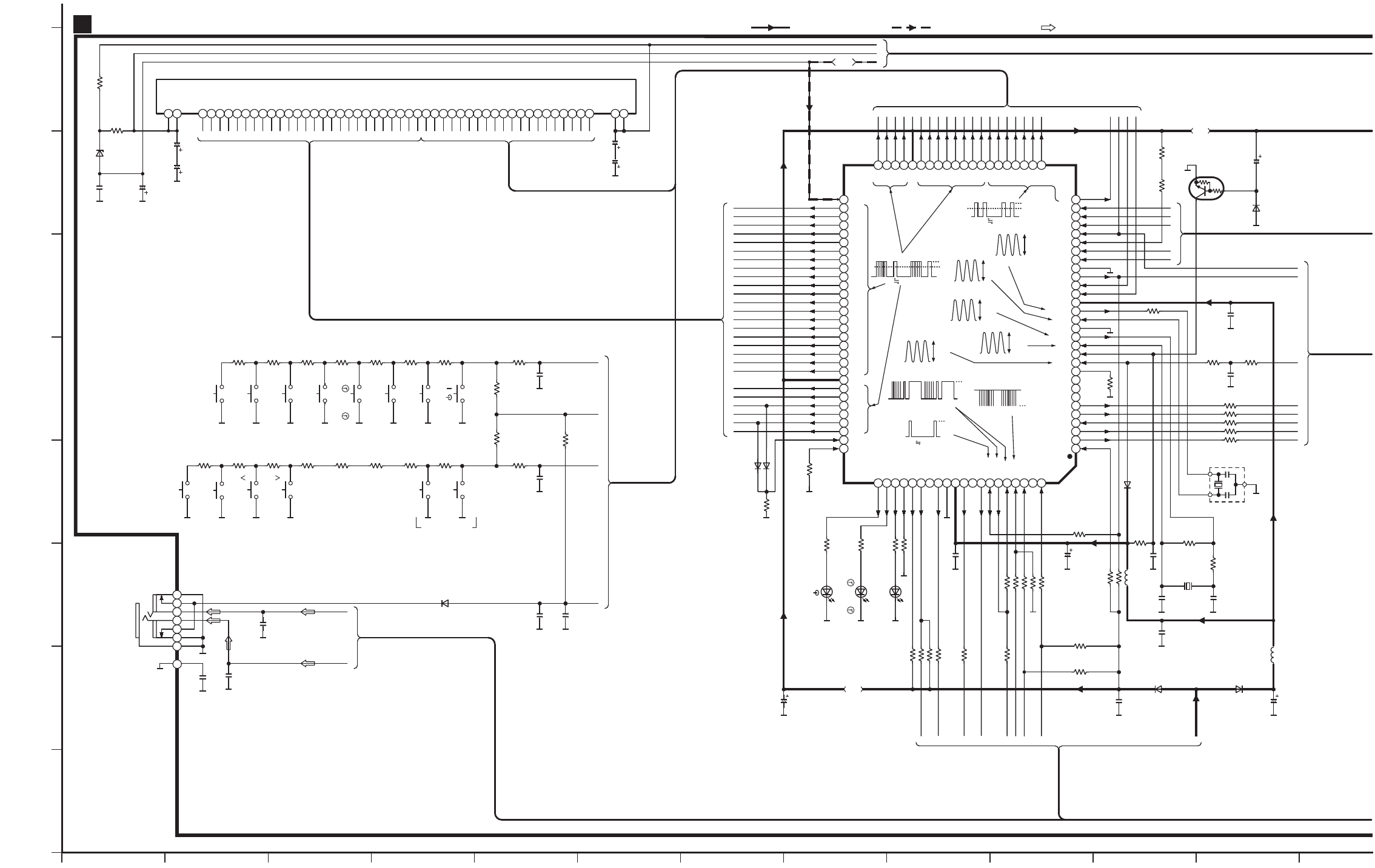
121110987654321
A
B
C
D
E
F
G
H
SA-DV290(E,EB,EG) OPERATION CIRCUIT DIAGRAM
S904
(PLAY/ REC)
FL901 (A2BB00000115)
1
7
5
4
6
3
2
P
S
S908
(INPUT SELECTOR)
S907
(SET)
S906
(TUNING MODE)
S905
(FM AUTO/MONO)
JK903
PHONES
3.5mm STEREO
R997
150
R996
150
D973
MA4030MTA
C921
1000P
C922
35V33
C920
25V22
R922
10K
R921
10K
R944
2.2K
R912
4.7K R911
3.3K R910
2.2K R909
1.8K R916
1.5K R915
1.2K R914
1K R913
820
R907
3.3K R906
2.2K R905
1.8K R904
1.5K R903
1.2K R902
1K R901
820
FL DISPLAY
1 6 8 10 11 12 13 14 15 16 17 18 19 20 21 22 23 24 25 26 27 28 29 30 31 32 33 34 35 36 37 38 39 40 41 42 43 44 45 46 47 48 49 50 53 542 5 7 9
W905
S901
(/)
C928
25V22
AOPERATION CIRCUIT
C919
25V22
C927
25V22
C396
0.047
C923
0.1
C395
0.047
D974
MA165TA
C907
470P
C924
0.1
C904
0.01
R924
1K
C908
470P
R925
1K
S914
(PS)
S915
(PTY)
S910
(TUNING, )
S911
(TUNING, )
S912
(TUNER/ BAND)
S913
(DIGITAL
S.WOOFER)
(RDS DISP MODE)
ABCD
E
FGH I JKLMNOPQRSTU
X
W
V
ABCDEFGHIJKLMNOPQRSTUVWXYZ
S902
(CLOCK/ TIMER)
S903
(
-
DEMO)
IC901
C2BBFD000404
SYSTEM CONTROL/
FL DRIVE
C
B
A
Q901
UN4212TA
RESET
R936
100
R919
15K
R991
47K
R918 10K
R928 47K
L902 1 H
D901
1SS291TA
L901
10 H
R951
330K
R952
10M
A
B
C
D
E
F
G
H
I
J
K
L
M
N
O
P
Q
R
S
T
U
V
W
X
Y
Z
R993
100K
D931
MA165TA
D933 MA165TA
R990
100K
C916
6.3V100
D951
LNJ301MPUJAD
(DIGITAL S.WOOFER)R995
220
D954
SELS5923C
(PLAY/ REC)R986
1.5K
D306
SELS5223C
( ) R939
1.5K
C905
1000P
C901
6.3V100
R935 100
R934 100
R988 1K
R937 10K
R987 1K
R926
2.2K
C912
0.1
R954
100K
C926
1000P
R960 1.5K
R958 1K
R999
100K
R959 47
R969
2.7K
D902
1SS291TA
C903
0.01
C902
10V1000
X902
(32.7kHz)
C911
18P
C910
20P
X901
(6MHz)
1
3
2
D905 1SS291TA
EFIKLMNO Q
R940
1K
R929 1K
R930 1K
R932 1K
R931 1K
R976
100K
R956
1K R957
1K
C915
0.01 C925
1000P
R953 100
A
B
C
D
G
H
J
C914
50V2.2
D904
MA165TA
A
B
C
D
E
ABCDE FGH I J K LMNOPQRS T UVWX
1
11
21
2
12
22
3
13
23
4
14
24
5
15
25
6
16
26
7
17
27
8
18
28
9
19
29
10
20
30
3132333435363738394041424344454647484950
51
52
53
54
55
56
57
58
59
60
61
62
63
64
65
66
67
68
69
70
71
72
73
74
75
76
77
78
79
80
81 82 83 84 85 86 87 88 89 90 91 92 93 94 95 96 97 98 99
100
-
VP
P13
P14
P15
P16
P17
P18
P19
P20
P21
P22
P23
P24
P25
P26
P27
P28
P29
P30
P31
P32
VDD4
P33
P34
P35
P36
P37
P38
REGIN0
REGIN1
8G
REMOCON
RDS DATA
RDS CLK
HP SW
MIC DET
VR JOGA
VR JOGB
NC(GND)
SH REQ
KEY KARAOKE
KEY TU
VDD1
XC OUT
XC IN
Vss
X OUT
XIN
RESET
AC IN
SEL/ TUNER
SEL TUNER
ST/ AV.6CH
LC72 CK
LC72 DI/ ST
LC72 CE
LC72 DO
CHECK
STAND-BY
TIMER
S.W.LED
LOUNGE
CHORUS
MUTE
NC
POWER
Vss2
VDD2
MUTE2
NC
MUTE3
SHCS
SHDO
SHDI
SHCK
E DET
CR TIMER
SD
VDD3
P12
P11
P10
P9
P8
P7
P6
P5
P4
P3
P2
P1
1G
2G
3G
4G
5G
6G
7G
R994 100K
R
R949
4.7K
R950
100
:AUDIO SIGNAL LINE
: POSITIVE VOLTAGE LINE : NEGATIVE VOLTAGE LINE
5.1V
5.1V
2V/2ms.DIV.
5V
0V
5V
0V
T10ms.
2V/2ms.DIV. 0V
5V
-
30.1V
-
30.1V
-
29.3V
-
29.3V
-
29.3V
-
26.3V
-
20.5V
-
29.3V
-
29.3V
-
29.3V
-
23.5V
-
20.5V
-
23.4V
-
23.4V
-
23.7V
-
20.7V
-
29.6V
-
29.6V
-
29.6V
-
23.7V
-
26.6V
-
26.5V
5.1V
-
29.5V
-
29.5V
-
26.5V
-
17.2V
-
5.3V
-
10.3V
0.4V
0V
-
23.4V
-
20.5V
-
26.3V
-
26.3V
5.1V
-
23.4V
-
20.5V
-
26.2V
-
29.2V
-
26.2V
-
26.2V
-
26.1V
-
26.3V
-
23.5V
-
23.5V
-
25.6V
-
27.5V
-
27.5V
-
25.5V
-
23.5V
-
25.6V
5.1V
2.6V
2.6V
0.6V
5.1V
0V
0V
1.4V
5.1V
5.1V
5.1V
2.3V
2.3V
2.7V
1.6V
5V
2.2V
0V
5.1V
5.1V
4.6V
0V
0V
2.5V
0V
5V
0V
5.1V
3.3V
1.9V
1.9V
1.4V
0V
5.1V
5.1V
4.8V
0V
0V
0V
0V
0V
0V
FM / AM
-
30V
4V
T 5.5ms.
0V
0V
4V
T 5.5ms.
-
30V
FM / AM
3.3V
P-P
F=6MHz
FM / AM
4.2V
P-P
F=6MHz
FM / AM
5.2V
P-P
F=32.7kHz
FM / AM
5.2V
P-P
F=32.7kHz
FM / AM
2V
P-P
F=32.7kHz
FM / AM
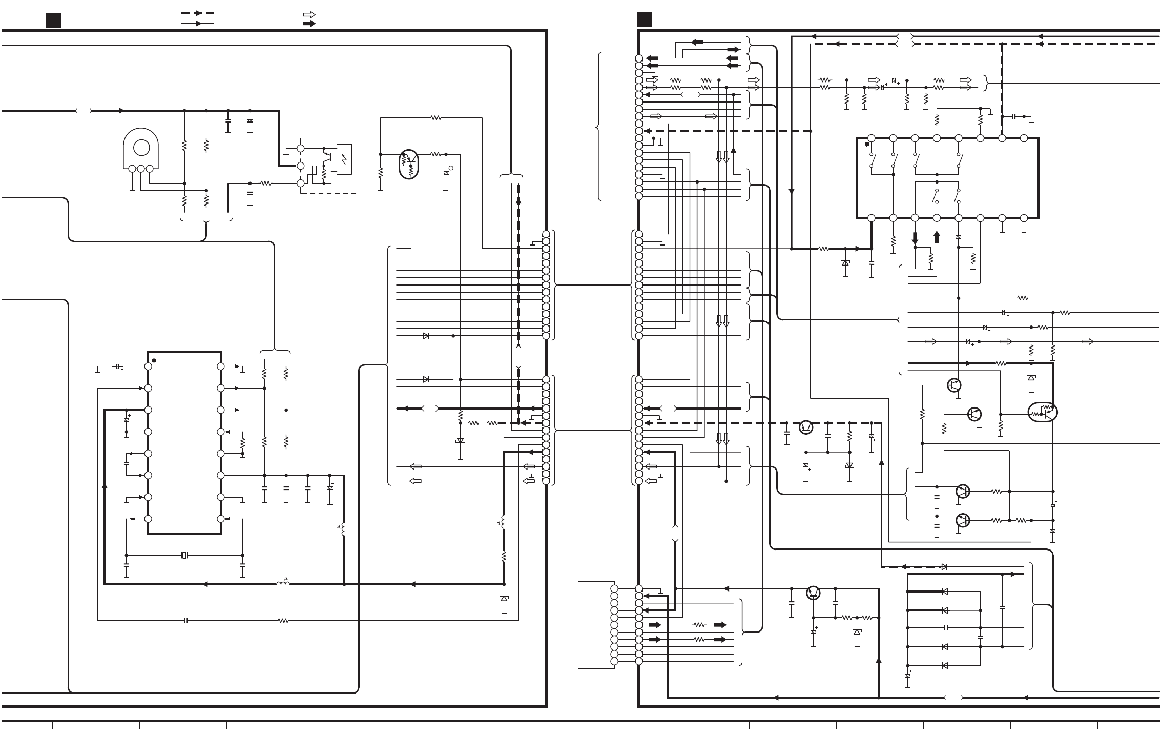
13 14 15 16 17 18 19 20 21 22 23 24
DET
Rch
CE
Lch
DI
DO
CL
+B(2)
SD
+B(1)
T.GND 1
2
3
4
5
6
7
8
9
10
11
Z101
RAN0005EM-2
(TUNER PACK)
SA-DV290(E,EB,EG) OPERATION, MAIN CIRCUIT DIAGRAM
W901B
W902B
IC151
C1BB00000527
RDS SIGNAL
DEMODULATOR
123
R158
1K
R154
100K
R153
100K
1
2
3
4
5
6
7
8
9
10
11
12
13
14
15
BA
COM
1
2
3
4
5
6
7
8
9
10
11
12
13
14
15
Q902
UN411FTA
MUTING CONT.
ABC
1
2
3
4
5
6
7
8 9
10
11
12
13
14
15
16
VREF
HPX IN
VDDA
VssA
FL OUT
CIN
TEST
X OUT
IDR
RDCL
RDDA
RST
MODE
VDDD
VssD
XIN
R962
22K
VR901
EVQVBXFK124B
(VOLUME)
R945
100
R961
22K
R943
100
C917
0.01
C155
1000P
C153
1000P
C160
1000P
C159
6.3V47
R152
1K
R151
1K
C154
560P C158
6.3V47
C151
16V10
D907
MA165TA
M
BC
R946
1K
C909
1000P C918
6.3V100
DEA
R941
1K
L153
1 H
R155
120
D151
MA4051MTA
L151
100 H
L152
100 H
C156
47P
C157
47P
A
B
C
D
E
F
G
H
I
J
K
L
N
O
Q
S
P
AOPERATION CIRCUIT
R942
2.2K
R974
1K
C931
16V10
R965
3.9K
R966
3.9K
D961
MA4075MTA R975
22K
D906
MA165TA
R
N
1
2
3
Z901
B3RAD0000028
(REMOTE SENSOR)
R157
1K
C152
330P
W902A
W901A
CP101
C
F
G
B
A
E
D
Q707
2SB1417PQTA
REGULATOR
Q723
2SC3940AQSTA
REGULATOR
R763
4.7K
R229 1K
D721
MA4300MTA R708
4.7K
C707
0.047
C706
35V10
C737
50V100
To
SOUND
PROCESSOR
(SH-DV290)
C735
0.047
B
A
R563
2.7K
R564
2.7K
C660
16V10
C659
16V10
R615
4.7K
R614
4.7K
R631
3.9K
R632
3.9K C202
0.1
R203
100K
R204
100K
C201
0.1
C602
16V10
C708
0.047
R211
270
D201
MA4056MTA
R687
1.5K
R688
1.5K
Q605,606
2SD2144STA
MUTING Q605
Q606
R683
1K
R617
4.7K
2
1
3
4
5
6
7
8
9
10
11
C
B
A
X0X1VDD
G
Vss
INHZ0Z1Y1 Y0
16 15 14 13 12 11 10 9
12345678
IC201
BU4053BCFE2
SIGNAL SELECTOR
C655
16V10
C656
16V10
R606
4.7K
R605
4.7K
2
15
3
4
5
6
7
8
9
10
11
12
13
14
1
2
15
3
4
5
6
7
8
9
10
11
12
13
14
1
20
2
1
3
4
5
6
7
8
9
10
11
12
13
14
15
16
17
18
19
K
L
M
I
J
E
F
C
D
E
F
G
E
F
G
A
B
C
D
A
B
G
H
C601
16V10
R598
2.2K
R597
2.2K
R205
100K
H
G
R202
100K
B
C
D
E
F
C509
0.01
C510
0.01
R693
1K
R692
1K
C664
16V10
C725
16V47
A
C
R696
47K
Q609,610
2SD2144STA
MUTING
Q609
Q610
Q612
UN411FTA
MUTING CONT.
B
CR694
22K
R511
47 R509
47
R512 47 R510 47
W501
D719
RL1N4003N02
D720
RL1N4003N02
D717
RL1N4003N02
D718
RL1N4003N02
H
D
C
R695
470
D611
MA4051MTA
C740
16V10
C733
0.047
D737
MA4082LTA
R764
330
MAIN CIRCUIT
B
C731
1000P
C741
0.1
TUNER Lch/C
TUNER Rch
A.GND
Lch IN
Rch IN
+B(10V)
SUR L
SUR R
S.W
MIC
-
B(
-
10V)
V.GND
D.GND
CS/ REQ
CLK
DATA
CT GND
SH FL1
SH FL2
SYNC
R603
3.3K
A
B
B
R684
1K
A
C715
25V6800
C714
1000P
D705
RL1N4003N02
A
X151
(4.332MHz)
R230
1K
: POSITIVE VOLTAGE LINE
: NEGATIVE VOLTAGE LINE
-30.1V
5.1V
: AUDIO SIGNAL LINE
6V
3.3V
0V
3.3V
2.6V
2.6V
0V
5.1V
2.5V2.7V
2.5V
2.5V
5.1V
2.5V
2.5V
14.7V
10.4V
-
37.3V
-
30.1V
-
30.7V
14.7V7.2V
7.8V
-
10V
-
10V
0V
0V
-
10.2V
5.1V
4.9V
0V
-
10V
0V
0.7V
5.7V0V0V0V0V0V
6V
7.2V
7.6V
-
10.4V
0V 0V
-
10.4V
: TUNER SIGNAL LINE
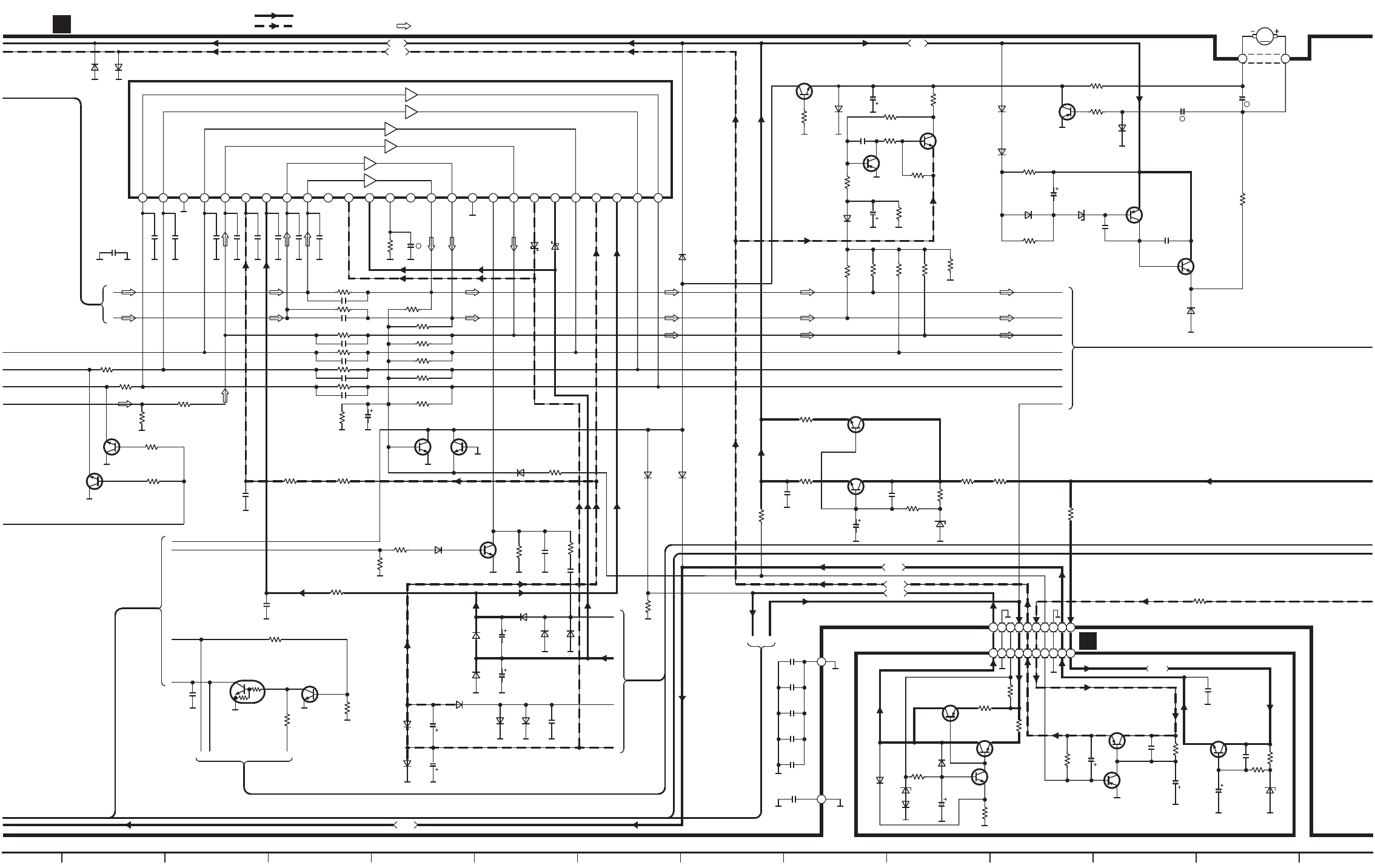
25 26 27 28 29 30 31 32 33 34 35 36
SA-DV290(E,EB,EG) MAIN,POWER SUPPLY CIRCUIT DIAGRAM
M
Q708
UN4211TA
SWITCHING
(POWER)
Q601 Q602
D756
MA700ATA
C603 470P
C604 470P
C607 470P
C608 470P
C649 1000P
C650 1000P
C605 1000P
C606 1000P
C648
1000P
C617
0.01
R637
15K
R638
68K
R619 120K
R622 120K
R621 150K
R624 150K
R620
120K
R612 56K
R611 56K
R610 150K
R609 56K
R608 56K
R607 56K
C610 56P
C609 56P
C612 15P
C611 39P
C614 47P
C613 47P
R627
470K
C616
50V0.47
N
D601
SB360L6508
D602
SB360L6508
D754
RL1N4003N02
C761
0.1
D701
1N5402BM21 C709
0.1
IC601
RSN311W64B
POWER AMP
D757
MA700ATA
123456789101112131415181920212223242526 1617
R604
3.3K
R601
3.3K
R602
3.3K
R618
4.7K
Q601,602
2SC5398RSTA
PROTECTOR
D607
1SS291TA
L
K
D658
MA165TA
D657
MA165TA
B
A
R685
1K
R686
1K
Q607, 608
2SD2144STA
MUTING
Q607
Q608
C705
0.01
G
R776
10K
Q709
2SD2144STA
SWITCHING
(POWER)
R738
3.9K
R739
47K
C622
10V100
D659
MA165TA
D751
1N5402BM21
D703
1N5402BM21
D753
RL1N4003N02
D761
RL1N4003N02
D755
RL1N4003N02
D752
1N5402BM21
D702
1N5402BM21
D704
1N5402BM21
G
F
E
D
AB C
D558
MA165TA
R544
10K
R572
15K
R648
120
C618
0.01
R635
2.2K
C619
0.1
Q503
2SC5398RSTA
SWITCHING
C704
35V4700
C702
35V4700
C703
35V4700
C701
35V4700
R761
220
R628
22K
R691
68
R647
270
R623
120K
CN781
F
C
A
B
D
E
Q551
2SA1995RSTA
SIGNAL LEVEL DET.
Q555
2SD2144STA
SIGNAL LEVEL DET.
Q702
2SB1548PQAU
REGULATOR
Q725
2SC5398RSTA
STABILIZER Q705
2SA1995RSTA
STABILIZER
Q701
2SD2374PQAU
REGULATOR
R556
100K
R557
10K
C721
10V100
D725
MA4082LTA
R729
220
C723
0.047
C639
1000P
C640
1000P
C641
1000P
C642
1000P
C732
0.022
C647
1000P
D738
MA165TA
D730
MA4091HTA
R768
100
R724
3.9K
C718
25V100
D723
MA4150HTA
R723
5.6K
C719
0.047
R725
10
C724
0.047
C710
0.047
R546
18K
R551
18K
R552
47K
R555
22K
C550
0.01
D552
MA165TA D555
MA4100MTA
R547
18K
E602
E601
R749
1K
D739
MA165TA
POWER SUPPLY CIRCUIT
C
11032 4 5 6 7 8 9
W701B
11032 4 5 6 7 8 9
R720
3.9K
C734
50V3.3
D758
MA165TA
C722
25V100
C720
0.047
C717
16V33
MAIN CIRCUIT
B
G
R765
220
N
R569
10K
D554
MA165TA
C371
6.3V100
Q556
2SC5398RSTA
SWITCHING
R568
100
D553
MA700ATA
C556
16V10
C555
50V1
Q557
2SA1995RSTA
MOTOR DRIVE
Q553
2SD2144STA
MOTOR DRIVE
R570
2.2M
R560
100K
C559
0.01
D581
RL1N4003N02
R567
22
FAN MOTOR
JK551
R566
68K
Q554
2SA1995RSTA
SIGNAL LEVEL DET.
M
R719
3.3K
Q703,704
2SD2137PQTA
REGULATOR
R796
2.2
Q703
Q704
R769
27
R727
3.9K
C554
16V220
R561
100K
C552
0.01 R559
4.7K
R591
4.7K
C551
50V2.2
D551
MA165TA
12
D583
RL1N4003N02
N
R721
4.7
R722
2.2
AB
R753
0.47
R754
0.47
Q711,712
2SB1548PQAU
REGULATOR
Q711
R797
2.2 R767
27
R558
2.2K
D582
RL1N4003N02
Q712
: POSITIVE VOLTAGE LINE
: NEGATIVE VOLTAGE LINE :AUDIO SIGNAL LINE
7.6V
-
10.4V
0V0V59.5V
-
59.5V
0V28.9V
-
29.3V
0V0V0V0V
-
0.2V
29.4V
-
29.7V
0V0V54.1V
-
51.4V
0V0V0V0V
0V
0V
5.1V5.1V
0V 0V
0.7V
0V 0V
2.1V
14.7V
0.7V
0V
0.7V
0V
29.2V
29.2V14.7V
15.2V
-
30.1V
-
11V
-
10.4V
-
11V
-
0.6V
14.1V
13.6V
9.6V
10.2V
10.4V
-
10.4V
14.7V
7.6V
7V
0V
7.6V
0.3V
-
10.4V
-
10.4V
-
10.4V
7.6V
7.6V
6.8V
FAN ON:1.6V
0V
FAN ON:0V
0.5V
FAN ON:0V4.7V
0V
0.5V
8.1V
8.1V
30.1V
30.1V7.6V
7.6V
0V
10.4V
13.6V
10.4V 14.1V
13.6V
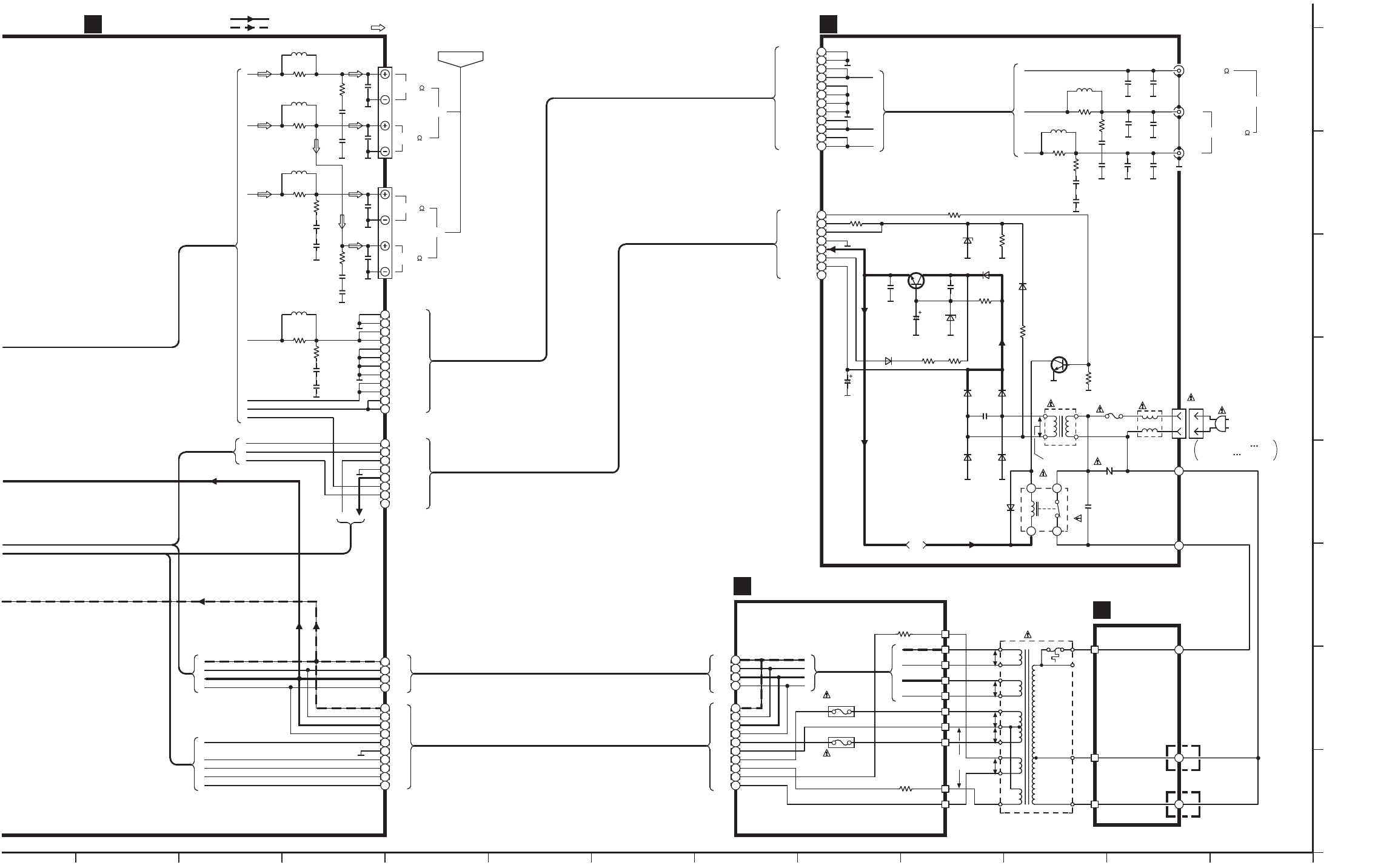
A
B
C
D
E
F
G
H
37 38 39 40 41 42 43 44 45 46 47 48
SA-DV290(E,EB,EG) MAIN, AC IN, POWER TRANSFORMER(A)&(B) CIRCUIT DIAGRAM
L601
2
1
3
4
5
6
7
8
9
10
11
12
2
1
3
4
5
6
7
8
R639
10
C621
0.1
E
F
D
CP601
CP602
R641
10
A
B
IJ
C
C631
0.1
G
Lch
JK601
HF(6 )
LF(8 )
Rch
JK602
HF(6 )
LF(8 )
A
B
C
R651
10
C627
0.1
C629
0.1
C635
0.047
R649
10
L605
R642
10
C620
0.1
C630
0.1
R640
10
L602
C637
0.047
C636
0.047
R652
10
C626
0.1
C628
0.1
R650
10
L606
C632
0.047
SPEAKERS
GND
GND
C OUT
C OUT
GND
GND
GND
GND
SUR L OUT
SUR L OUT
SUR R OUT
SUR R OUT
ECO
SH SYNC
SA SYNC
D.GND
BU5V
RS13V
+B
NC
W722A
W721A
2
1
3
4
5
6
7
8
9
10
2
1
3
4
E
F
H
D
C
G
F
E
D
S1
S2
S3
S4
AC1
CT
AC2
S7
FL2
FL1
S1
S2
S3
S4
MAIN CIRCUIT
B
C
A
D
B
T701
CN701
CN702
CN703
CN704
CN705
CN706
CN707
CN708
CN709
CN710
R793
1
CN601
C652
1000P
C644
1000P
C643
1000P
C651
0.047
C646
0.047
C645
0.047
Rch
Lch
AC IN
JK701
L701
F1 T2A
T702
Z701
C791
1000P
3 1
24 RL702
R794
47K
Q791
2SD2144STA
RELAY DRIVE
D745
MA4051MTA
C753
0.01
C755
16V1000
Q726
2SC3940AQSTA
REGULATOR D746
RL1N4003N02
D747
MA4068LTA C758
0.01
C759
10V47
C754
0.01
D500
MA165TA
W2/W3
W1
CN602
FP791
K5G502AA0002
JK603
CENTER(8 )
SURROUND(8 )
R646
10
C624
0.1
C634
0.1
R644
10
L604
R645
10
C625
0.1 C633
0.1
R643
10
L603
DAC IN CIRCUIT
2
1
3
4
5
6
7
8
9
10
11
12
2
1
3
4
5
6
7
8
R777
1K
R774
18
D711
RL1N4003N02 R773
18
R712 2.2K
A
B
C
A
C
B
R795
3.9K
D743
RL1N4003N02
D741
RL1N4003N02
D742
RL1N4003N02
D744
RL1N4003N02
R771
2.2K D740
MA165TA
POWER TRANSFORMER
(B) CIRCUIT
F
POWER TRANSFORMER
(A) CIRCUIT
E
W722B
W721B
10
2
1
3
4
5
6
7
8
9
CN713
CN712
CN711 W1
W3
W2
2
1
3
4
R772
22K
A
B
C
D
FP792
K5G502AA0002
SPEAKERS
GND
GND
C OUT
C OUT
GND
GND
GND
GND
SUR L IN
SUR L IN
SURRIN
SURRIN
ECO
SH SYNC
SA SYNC
D.GND
BU5V
RS13V
+B
NC
S1
S2
S3
S4
AC1
CT
AC2
S7
FL2
FL1
S1
S2
S3
S4
R798
2.2
For [EB] area.
For
[E,EG]
areas.
230-240V 50Hz [EB]
230V 50Hz [E,EG]
: POSITIVE VOLTAGE LINE
: NEGATIVE VOLTAGE LINE :AUDIO SIGNAL LINE
0.7V
0V
6V
10.7V6V
6.7V
AC22.6V
AC22.6V
AC11.7V
AC11.7V
AC4.7V
AC
29.2V
AC9.4V
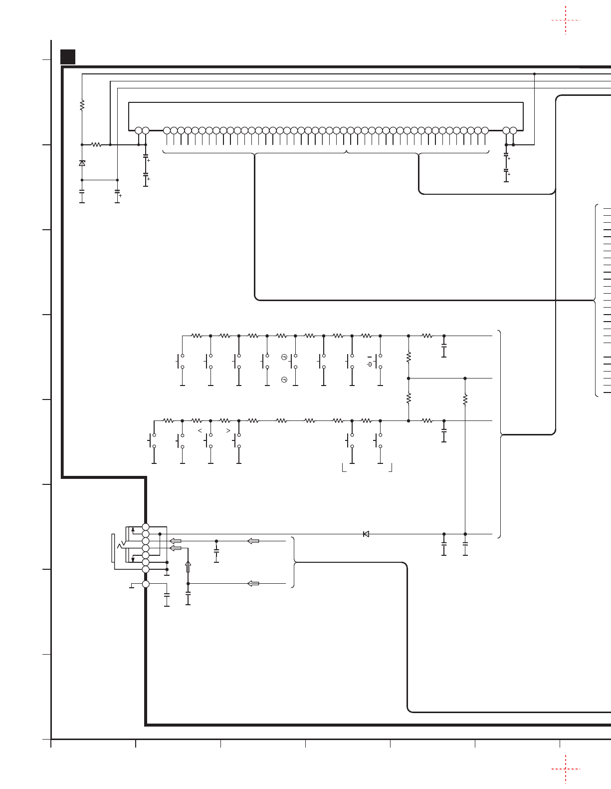
121110987654321
A
B
C
D
E
F
G
H
SA-DV290(E,EB,EG) OPERATION CIRCUIT DIAGRAM
S904
(PLAY/ REC)
FL901 (A2BB00000115)
1
7
5
4
6
3
2
P
S
S908
(INPUT SELECTOR)
S907
(SET)
S906
(TUNING MODE)
S905
(FM AUTO/MONO)
JK903
PHONES
3.5mm STEREO
R997
150
R996
150
D973
MA4030MTA
C921
1000P
C922
35V33
C920
25V22
R922
10K
R921
10K
R944
2.2K
R912
4.7K R911
3.3K R910
2.2K R909
1.8K R916
1.5K R915
1.2K R914
1K R913
820
R907
3.3K R906
2.2K R905
1.8K R904
1.5K R903
1.2K R902
1K R901
820
FL DISPLAY
1 6 8 10 11 12 13 14 15 16 17 18 19 20 21 22 23 24 25 26 27 28 29 30 31 32 33 34 35 36 37 38 39 40 41 42 43 44 45 46 47 48 49 50 53 542 5 7 9
W905
S901
(/)
C928
25V22
AOPERATION CIRCUIT
C919
25V22
C927
25V22
C396
0.047
C923
0.1
C395
0.047
D974
MA165TA
C907
470P
C924
0.1
C904
0.01
R924
1K
C908
470P
R925
1K
S914
(PS)
S915
(PTY)
S910
(TUNING, )
S911
(TUNING, )
S912
(TUNER/ BAND)
S913
(DIGITAL
S.WOOFER)
(RDS DISP MODE)
ABCD
E
FGH I JKLMNOPQRSTU
X
W
V
ABCDEFGHIJKLMNOPQRSTUVWXYZ
S902
(CLOCK/ TIMER)
S903
(
-
DEMO)
IC901
C2BBFD000404
SYSTEM CONTROL/
FL DRIVE
C
B
A
Q901
UN4212TA
RESET
R936
100
R919
15K
R991
47K
R918 10K
R928 47K
L902 1 H
D901
1SS291TA
L901
10 H
R951
330K
R952
10M
A
B
C
D
E
F
G
H
I
J
K
L
M
N
O
P
Q
R
S
T
U
V
W
X
Y
Z
R993
100K
D931
MA165TA
D933 MA165TA
R990
100K
C916
6.3V100
D951
LNJ301MPUJAD
(DIGITAL S.WOOFER)R995
220
D954
SELS5923C
(PLAY/ REC)R986
1.5K
D306
SELS5223C
( ) R939
1.5K
C905
1000P
C901
6.3V100
R935 100
R934 100
R988 1K
R937 10K
R987 1K
R926
2.2K
C912
0.1
R954
100K
C926
1000P
R960 1.5K
R958 1K
R999
100K
R959 47
R969
2.7K
D902
1SS291TA
C903
0.01
C902
10V1000
X902
(32.7kHz)
C911
18P
C910
20P
X901
(6MHz)
1
3
2
D905 1SS291TA
EFIKLMNO Q
R940
1K
R929 1K
R930 1K
R932 1K
R931 1K
R976
100K
R956
1K R957
1K
C915
0.01 C925
1000P
R953 100
A
B
C
D
G
H
J
C914
50V2.2
D904
MA165TA
A
B
C
D
E
ABCDE FGH I J K LMNOPQRS T UVWX
1
11
21
2
12
22
3
13
23
4
14
24
5
15
25
6
16
26
7
17
27
8
18
28
9
19
29
10
20
30
3132333435363738394041424344454647484950
51
52
53
54
55
56
57
58
59
60
61
62
63
64
65
66
67
68
69
70
71
72
73
74
75
76
77
78
79
80
81 82 83 84 85 86 87 88 89 90 91 92 93 94 95 96 97 98 99
100
-
VP
P13
P14
P15
P16
P17
P18
P19
P20
P21
P22
P23
P24
P25
P26
P27
P28
P29
P30
P31
P32
VDD4
P33
P34
P35
P36
P37
P38
REGIN0
REGIN1
8G
REMOCON
RDS DATA
RDS CLK
HP SW
MIC DET
VR JOGA
VR JOGB
NC(GND)
SH REQ
KEY KARAOKE
KEY TU
VDD1
XC OUT
XC IN
Vss
X OUT
XIN
RESET
AC IN
SEL/ TUNER
SEL TUNER
ST/ AV.6CH
LC72 CK
LC72 DI/ ST
LC72 CE
LC72 DO
CHECK
STAND-BY
TIMER
S.W.LED
LOUNGE
CHORUS
MUTE
NC
POWER
Vss2
VDD2
MUTE2
NC
MUTE3
SHCS
SHDO
SHDI
SHCK
E DET
CR TIMER
SD
VDD3
P12
P11
P10
P9
P8
P7
P6
P5
P4
P3
P2
P1
1G
2G
3G
4G
5G
6G
7G
R994 100K
R
R949
4.7K
R950
100
:AUDIO SIGNAL LINE
: POSITIVE VOLTAGE LINE : NEGATIVE VOLTAGE LINE
5.1V
5.1V
2V/2ms.DIV.
5V
0V
5V
0V
T10ms.
2V/2ms.DIV. 0V
5V
-
30.1V
-
30.1V
-
29.3V
-
29.3V
-
29.3V
-
26.3V
-
20.5V
-
29.3V
-
29.3V
-
29.3V
-
23.5V
-
20.5V
-
23.4V
-
23.4V
-
23.7V
-
20.7V
-
29.6V
-
29.6V
-
29.6V
-
23.7V
-
26.6V
-
26.5V
5.1V
-
29.5V
-
29.5V
-
26.5V
-
17.2V
-
5.3V
-
10.3V
0.4V
0V
-
23.4V
-
20.5V
-
26.3V
-
26.3V
5.1V
-
23.4V
-
20.5V
-
26.2V
-
29.2V
-
26.2V
-
26.2V
-
26.1V
-
26.3V
-
23.5V
-
23.5V
-
25.6V
-
27.5V
-
27.5V
-
25.5V
-
23.5V
-
25.6V
5.1V
2.6V
2.6V
0.6V
5.1V
0V
0V
1.4V
5.1V
5.1V
5.1V
2.3V
2.3V
2.7V
1.6V
5V
2.2V
0V
5.1V
5.1V
4.6V
0V
0V
2.5V
0V
5V
0V
5.1V
3.3V
1.9V
1.9V
1.4V
0V
5.1V
5.1V
4.8V
0V
0V
0V
0V
0V
0V
FM / AM
-
30V
4V
T 5.5ms.
0V
0V
4V
T 5.5ms.
-
30V
FM / AM
3.3V
P-P
F=6MHz
FM / AM
4.2V
P-P
F=6MHz
FM / AM
5.2V
P-P
F=32.7kHz
FM / AM
5.2V
P-P
F=32.7kHz
FM / AM
2V
P-P
F=32.7kHz
FM / AM
13 14 15 16 17 18 19 20 21 22 23 24
DET
Rch
CE
Lch
DI
DO
CL
+B(2)
SD
+B(1)
T.GND 1
2
3
4
5
6
7
8
9
10
11
Z101
RAN0005EM-2
(TUNER PACK)
SA-DV290(E,EB,EG) OPERATION, MAIN CIRCUIT DIAGRAM
W901B
W902B
IC151
C1BB00000527
RDS SIGNAL
DEMODULATOR
123
R158
1K
R154
100K
R153
100K
1
2
3
4
5
6
7
8
9
10
11
12
13
14
15
BA
COM
1
2
3
4
5
6
7
8
9
10
11
12
13
14
15
Q902
UN411FTA
MUTING CONT.
ABC
1
2
3
4
5
6
7
8 9
10
11
12
13
14
15
16
VREF
HPX IN
VDDA
VssA
FL OUT
CIN
TEST
X OUT
IDR
RDCL
RDDA
RST
MODE
VDDD
VssD
XIN
R962
22K
VR901
EVQVBXFK124B
(VOLUME)
R945
100
R961
22K
R943
100
C917
0.01
C155
1000P
C153
1000P
C160
1000P
C159
6.3V47
R152
1K
R151
1K
C154
560P C158
6.3V47
C151
16V10
D907
MA165TA
M
BC
R946
1K
C909
1000P C918
6.3V100
DEA
R941
1K
L153
1 H
R155
120
D151
MA4051MTA
L151
100 H
L152
100 H
C156
47P
C157
47P
A
B
C
D
E
F
G
H
I
J
K
L
N
O
Q
S
P
AOPERATION CIRCUIT
R942
2.2K
R974
1K
C931
16V10
R965
3.9K
R966
3.9K
D961
MA4075MTA R975
22K
D906
MA165TA
R
N
1
2
3
Z901
B3RAD0000028
(REMOTE SENSOR)
R157
1K
C152
330P
W902A
W901A
CP101
C
F
G
B
A
E
D
Q707
2SB1417PQTA
REGULATOR
Q723
2SC3940AQSTA
REGULATOR
R763
4.7K
R229 1K
D721
MA4300MTA R708
4.7K
C707
0.047
C706
35V10
C737
50V100
To
SOUND
PROCESSOR
(SH-DV290)
C735
0.047
B
A
R563
2.7K
R564
2.7K
C660
16V10
C659
16V10
R615
4.7K
R614
4.7K
R631
3.9K
R632
3.9K C202
0.1
R203
100K
R204
100K
C201
0.1
C602
16V10
C708
0.047
R211
270
D201
MA4056MTA
R687
1.5K
R688
1.5K
Q605,606
2SD2144STA
MUTING Q605
Q606
R683
1K
R617
4.7K
2
1
3
4
5
6
7
8
9
10
11
C
B
A
X0X1VDD
G
Vss
INHZ0Z1Y1 Y0
16 15 14 13 12 11 10 9
12345678
IC201
BU4053BCFE2
SIGNAL SELECTOR
C655
16V10
C656
16V10
R606
4.7K
R605
4.7K
2
15
3
4
5
6
7
8
9
10
11
12
13
14
1
2
15
3
4
5
6
7
8
9
10
11
12
13
14
1
20
2
1
3
4
5
6
7
8
9
10
11
12
13
14
15
16
17
18
19
K
L
M
I
J
E
F
C
D
E
F
G
E
F
G
A
B
C
D
A
B
G
H
C601
16V10
R598
2.2K
R597
2.2K
R205
100K
H
G
R202
100K
B
C
D
E
F
C509
0.01
C510
0.01
R693
1K
R692
1K
C664
16V10
C725
16V47
A
C
R696
47K
Q609,610
2SD2144STA
MUTING
Q609
Q610
Q612
UN411FTA
MUTING CONT.
B
CR694
22K
R511
47 R509
47
R512 47 R510 47
W501
D719
RL1N4003N02
D720
RL1N4003N02
D717
RL1N4003N02
D718
RL1N4003N02
H
D
C
R695
470
D611
MA4051MTA
C740
16V10
C733
0.047
D737
MA4082LTA
R764
330
MAIN CIRCUIT
B
C731
1000P
C741
0.1
TUNER Lch/C
TUNER Rch
A.GND
Lch IN
Rch IN
+B(10V)
SUR L
SUR R
S.W
MIC
-
B(
-
10V)
V.GND
D.GND
CS/ REQ
CLK
DATA
CT GND
SH FL1
SH FL2
SYNC
R603
3.3K
A
B
B
R684
1K
A
C715
25V6800
C714
1000P
D705
RL1N4003N02
A
X151
(4.332MHz)
R230
1K
: POSITIVE VOLTAGE LINE
: NEGATIVE VOLTAGE LINE
-30.1V
5.1V
: AUDIO SIGNAL LINE
6V
3.3V
0V
3.3V
2.6V
2.6V
0V
5.1V
2.5V2.7V
2.5V
2.5V
5.1V
2.5V
2.5V
14.7V
10.4V
-
37.3V
-
30.1V
-
30.7V
14.7V7.2V
7.8V
-
10V
-
10V
0V
0V
-
10.2V
5.1V
4.9V
0V
-
10V
0V
0.7V
5.7V0V0V0V0V0V
6V
7.2V
7.6V
-
10.4V
0V 0V
-
10.4V
: TUNER SIGNAL LINE
25 26 27 28 29 30 31 32 33 34 35 36
SA-DV290(E,EB,EG) MAIN,POWER SUPPLY CIRCUIT DIAGRAM
M
Q708
UN4211TA
SWITCHING
(POWER)
Q601 Q602
D756
MA700ATA
C603 470P
C604 470P
C607 470P
C608 470P
C649 1000P
C650 1000P
C605 1000P
C606 1000P
C648
1000P
C617
0.01
R637
15K
R638
68K
R619 120K
R622 120K
R621 150K
R624 150K
R620
120K
R612 56K
R611 56K
R610 150K
R609 56K
R608 56K
R607 56K
C610 56P
C609 56P
C612 15P
C611 39P
C614 47P
C613 47P
R627
470K
C616
50V0.47
N
D601
SB360L6508
D602
SB360L6508
D754
RL1N4003N02
C761
0.1
D701
1N5402BM21 C709
0.1
IC601
RSN311W64B
POWER AMP
D757
MA700ATA
123456789101112131415181920212223242526 1617
R604
3.3K
R601
3.3K
R602
3.3K
R618
4.7K
Q601,602
2SC5398RSTA
PROTECTOR
D607
1SS291TA
L
K
D658
MA165TA
D657
MA165TA
B
A
R685
1K
R686
1K
Q607, 608
2SD2144STA
MUTING
Q607
Q608
C705
0.01
G
R776
10K
Q709
2SD2144STA
SWITCHING
(POWER)
R738
3.9K
R739
47K
C622
10V100
D659
MA165TA
D751
1N5402BM21
D703
1N5402BM21
D753
RL1N4003N02
D761
RL1N4003N02
D755
RL1N4003N02
D752
1N5402BM21
D702
1N5402BM21
D704
1N5402BM21
G
F
E
D
AB C
D558
MA165TA
R544
10K
R572
15K
R648
120
C618
0.01
R635
2.2K
C619
0.1
Q503
2SC5398RSTA
SWITCHING
C704
35V4700
C702
35V4700
C703
35V4700
C701
35V4700
R761
220
R628
22K
R691
68
R647
270
R623
120K
CN781
F
C
A
B
D
E
Q551
2SA1995RSTA
SIGNAL LEVEL DET.
Q555
2SD2144STA
SIGNAL LEVEL DET.
Q702
2SB1548PQAU
REGULATOR
Q725
2SC5398RSTA
STABILIZER Q705
2SA1995RSTA
STABILIZER
Q701
2SD2374PQAU
REGULATOR
R556
100K
R557
10K
C721
10V100
D725
MA4082LTA
R729
220
C723
0.047
C639
1000P
C640
1000P
C641
1000P
C642
1000P
C732
0.022
C647
1000P
D738
MA165TA
D730
MA4091HTA
R768
100
R724
3.9K
C718
25V100
D723
MA4150HTA
R723
5.6K
C719
0.047
R725
10
C724
0.047
C710
0.047
R546
18K
R551
18K
R552
47K
R555
22K
C550
0.01
D552
MA165TA D555
MA4100MTA
R547
18K
E602
E601
R749
1K
D739
MA165TA
POWER SUPPLY CIRCUIT
C
11032 4 5 6 7 8 9
W701B
11032 4 5 6 7 8 9
R720
3.9K
C734
50V3.3
D758
MA165TA
C722
25V100
C720
0.047
C717
16V33
MAIN CIRCUIT
B
G
R765
220
N
R569
10K
D554
MA165TA
C371
6.3V100
Q556
2SC5398RSTA
SWITCHING
R568
100
D553
MA700ATA
C556
16V10
C555
50V1
Q557
2SA1995RSTA
MOTOR DRIVE
Q553
2SD2144STA
MOTOR DRIVE
R570
2.2M
R560
100K
C559
0.01
D581
RL1N4003N02
R567
22
FAN MOTOR
JK551
R566
68K
Q554
2SA1995RSTA
SIGNAL LEVEL DET.
M
R719
3.3K
Q703,704
2SD2137PQTA
REGULATOR
R796
2.2
Q703
Q704
R769
27
R727
3.9K
C554
16V220
R561
100K
C552
0.01 R559
4.7K
R591
4.7K
C551
50V2.2
D551
MA165TA
12
D583
RL1N4003N02
N
R721
4.7
R722
2.2
AB
R753
0.47
R754
0.47
Q711,712
2SB1548PQAU
REGULATOR
Q711
R797
2.2 R767
27
R558
2.2K
D582
RL1N4003N02
Q712
: POSITIVE VOLTAGE LINE
: NEGATIVE VOLTAGE LINE :AUDIO SIGNAL LINE
7.6V
-
10.4V
0V0V59.5V
-
59.5V
0V28.9V
-
29.3V
0V0V0V0V
-
0.2V
29.4V
-
29.7V
0V0V54.1V
-
51.4V
0V0V0V0V
0V
0V
5.1V5.1V
0V 0V
0.7V
0V 0V
2.1V
14.7V
0.7V
0V
0.7V
0V
29.2V
29.2V14.7V
15.2V
-
30.1V
-
11V
-
10.4V
-
11V
-
0.6V
14.1V
13.6V
9.6V
10.2V
10.4V
-
10.4V
14.7V
7.6V
7V
0V
7.6V
0.3V
-
10.4V
-
10.4V
-
10.4V
7.6V
7.6V
6.8V
FAN ON:1.6V
0V
FAN ON:0V
0.5V
FAN ON:0V4.7V
0V
0.5V
8.1V
8.1V
30.1V
30.1V7.6V
7.6V
0V
10.4V
13.6V
10.4V 14.1V
13.6V
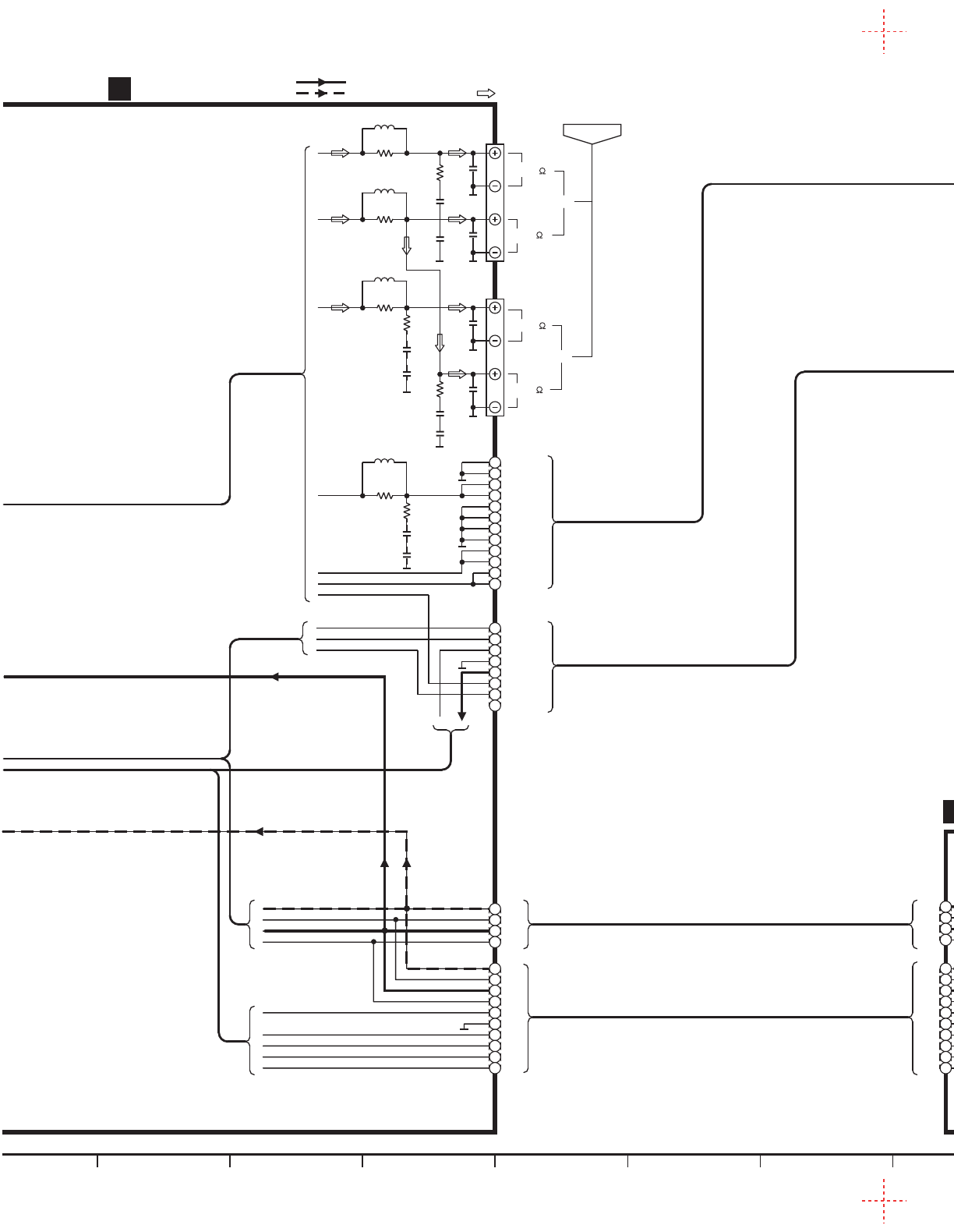
A
B
C
D
E
F
G
H
37 38 39 40 41 42 43 44 45 46 47 48
SA-DV290(E,EB,EG) MAIN, AC IN, POWER TRANSFORMER(A)&(B) CIRCUIT DIAGRAM
L601
2
1
3
4
5
6
7
8
9
10
11
12
2
1
3
4
5
6
7
8
R639
10
C621
0.1
E
F
D
CP601
CP602
R641
10
A
B
IJ
C
C631
0.1
G
Lch
JK601
HF(6 )
LF(8 )
Rch
JK602
HF(6 )
LF(8 )
A
B
C
R651
10
C627
0.1
C629
0.1
C635
0.047
R649
10
L605
R642
10
C620
0.1
C630
0.1
R640
10
L602
C637
0.047
C636
0.047
R652
10
C626
0.1
C628
0.1
R650
10
L606
C632
0.047
SPEAKERS
GND
GND
C OUT
C OUT
GND
GND
GND
GND
SUR L OUT
SUR L OUT
SUR R OUT
SUR R OUT
ECO
SH SYNC
SA SYNC
D.GND
BU5V
RS13V
+B
NC
W722A
W721A
2
1
3
4
5
6
7
8
9
10
2
1
3
4
E
F
H
D
C
G
F
E
D
S1
S2
S3
S4
AC1
CT
AC2
S7
FL2
FL1
S1
S2
S3
S4
MAIN CIRCUIT
B
C
A
D
B
T701
CN701
CN702
CN703
CN704
CN705
CN706
CN707
CN708
CN709
CN710
R793
1
CN601
C652
1000P
C644
1000P
C643
1000P
C651
0.047
C646
0.047
C645
0.047
Rch
Lch
AC IN
JK701
L701
F1 T2A
T702
Z701
C791
1000P
3 1
24 RL702
R794
47K
Q791
2SD2144STA
RELAY DRIVE
D745
MA4051MTA
C753
0.01
C755
16V1000
Q726
2SC3940AQSTA
REGULATOR D746
RL1N4003N02
D747
MA4068LTA C758
0.01
C759
10V47
C754
0.01
D500
MA165TA
W2/W3
W1
CN602
FP791
K5G502AA0002
JK603
CENTER(8 )
SURROUND(8 )
R646
10
C624
0.1
C634
0.1
R644
10
L604
R645
10
C625
0.1 C633
0.1
R643
10
L603
DAC IN CIRCUIT
2
1
3
4
5
6
7
8
9
10
11
12
2
1
3
4
5
6
7
8
R777
1K
R774
18
D711
RL1N4003N02 R773
18
R712 2.2K
A
B
C
A
C
B
R795
3.9K
D743
RL1N4003N02
D741
RL1N4003N02
D742
RL1N4003N02
D744
RL1N4003N02
R771
2.2K D740
MA165TA
POWER TRANSFORMER
(B) CIRCUIT
F
POWER TRANSFORMER
(A) CIRCUIT
E
W722B
W721B
10
2
1
3
4
5
6
7
8
9
CN713
CN712
CN711 W1
W3
W2
2
1
3
4
R772
22K
A
B
C
D
FP792
K5G502AA0002
SPEAKERS
GND
GND
C OUT
C OUT
GND
GND
GND
GND
SUR L IN
SUR L IN
SURRIN
SURRIN
ECO
SH SYNC
SA SYNC
D.GND
BU5V
RS13V
+B
NC
S1
S2
S3
S4
AC1
CT
AC2
S7
FL2
FL1
S1
S2
S3
S4
R798
2.2
For [EB] area.
For
[E,EG]
areas.
230-240V 50Hz [EB]
230V 50Hz [E,EG]
: POSITIVE VOLTAGE LINE
: NEGATIVE VOLTAGE LINE :AUDIO SIGNAL LINE
0.7V
0V
6V
10.7V6V
6.7V
AC22.6V
AC22.6V
AC11.7V
AC11.7V
AC4.7V
AC
29.2V
AC9.4V
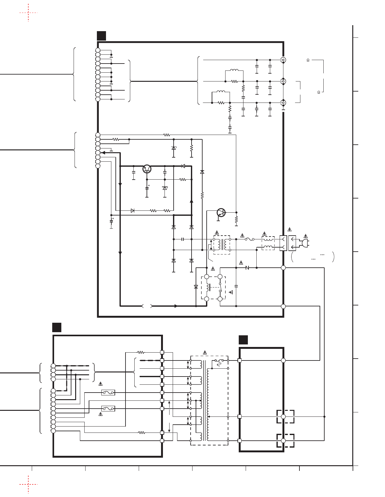
A
B
C
D
E
F
G
H
37 38 39 40 41 42 43 44 45 46 47 48
SA-DV290(E,EB,EG) MAIN, AC IN, POWER TRANSFORMER(A)&(B) CIRCUIT DIAGRAM
L601
2
1
3
4
5
6
7
8
9
10
11
12
2
1
3
4
5
6
7
8
R639
10
C621
0.1
E
F
D
CP601
CP602
R641
10
A
B
IJ
C
C631
0.1
G
Lch
JK601
HF(6 )
LF(8 )
Rch
JK602
HF(6 )
LF(8 )
A
B
C
R651
10
C627
0.1
C629
0.1
C635
0.047
R649
10
L605
R642
10
C620
0.1
C630
0.1
R640
10
L602
C637
0.047
C636
0.047
R652
10
C626
0.1
C628
0.1
R650
10
L606
C632
0.047
SPEAKERS
GND
GND
C OUT
C OUT
GND
GND
GND
GND
SUR L OUT
SUR L OUT
SUR R OUT
SUR R OUT
ECO
SH SYNC
SA SYNC
D.GND
BU5V
RS13V
+B
NC
W722A
W721A
2
1
3
4
5
6
7
8
9
10
2
1
3
4
E
F
H
D
C
G
F
E
D
S1
S2
S3
S4
AC1
CT
AC2
S7
FL2
FL1
S1
S2
S3
S4
MAIN CIRCUIT
B
C
A
D
B
T701
CN701
CN702
CN703
CN704
CN705
CN706
CN707
CN708
CN709
CN710
R793
1
CN601
C652
1000P
C644
1000P
C643
1000P
C651
0.047
C646
0.047
C645
0.047
Rch
Lch
AC IN
JK701
L701
F1 T2A
T702
Z701
C791
1000P
3 1
24 RL702
R794
47K
Q791
2SD2144STA
RELAY DRIVE
D745
MA4051MTA
C753
0.01
C755
16V1000
Q726
2SC3940AQSTA
REGULATOR D746
RL1N4003N02
D747
MA4068LTA C758
0.01
C759
10V47
C754
0.01
D500
MA165TA
W2/W3
W1
CN602
FP791
K5G502AA0002
JK603
CENTER(8 )
SURROUND(8 )
R646
10
C624
0.1
C634
0.1
R644
10
L604
R645
10
C625
0.1 C633
0.1
R643
10
L603
DAC IN CIRCUIT
2
1
3
4
5
6
7
8
9
10
11
12
2
1
3
4
5
6
7
8
R777
1K
R774
18
D711
RL1N4003N02 R773
18
R712 2.2K
A
B
C
A
C
B
R795
3.9K
D743
RL1N4003N02
D741
RL1N4003N02
D742
RL1N4003N02
D744
RL1N4003N02
R771
2.2K D740
MA165TA
POWER TRANSFORMER
(B) CIRCUIT
F
POWER TRANSFORMER
(A) CIRCUIT
E
W722B
W721B
10
2
1
3
4
5
6
7
8
9
CN713
CN712
CN711 W1
W3
W2
2
1
3
4
R772
22K
A
B
C
D
FP792
K5G502AA0002
SPEAKERS
GND
GND
C OUT
C OUT
GND
GND
GND
GND
SUR L IN
SUR L IN
SURRIN
SURRIN
ECO
SH SYNC
SA SYNC
D.GND
BU5V
RS13V
+B
NC
S1
S2
S3
S4
AC1
CT
AC2
S7
FL2
FL1
S1
S2
S3
S4
R798
2.2
For [EB] area.
For
[E,EG]
areas.
230-240V 50Hz [EB]
230V 50Hz [E,EG]
: POSITIVE VOLTAGE LINE
: NEGATIVE VOLTAGE LINE :AUDIO SIGNAL LINE
0.7V
0V
6V
10.7V6V
6.7V
AC22.6V
AC22.6V
AC11.7V
AC11.7V
AC4.7V
AC
29.2V
AC9.4V
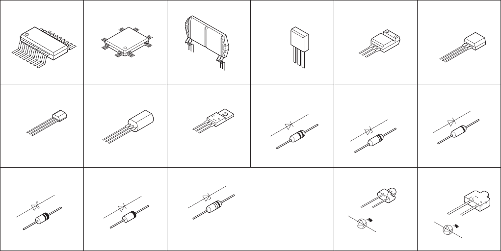
BU4053BCFE2
C1BB00000527 C2BBFD000404 RSN311W64B UN411FTA
UN4211TA
UN4212TA
2SB1417PQTA
2SD2137PQTA 2SD2144STA
2SA1995RSTA
2SC5398RSTA 2SC3940AQSTA 2SB1548PQAU
2SD2374PQAU 1SS291TA
MA700ATA MA4100MTA
MA4150HTA
MA4300MTA
MA165TA
SB360L6508 1N5402BM21
RL1N4003N02 MA4030MTA
MA4051MTA
MA4056MTA
MA4068LTA
MA4075MTA
MA4082LTA
MA4091HTA
LNJ301MPUJAD SELS5223C
SELS5923C
1
8
9
16
.
.
.
.
.
.
.
.
.
.
.
50
51
1
............30
31
100
..
.
.
.
.
.
..
.
.
.
.
.
80
81 1
..................
26
ECB
CB
E
E
C
B
E
C
BECB
C
B
EA
Ca
A
Ca
A
Ca
Anode
Cathode
A
Ca
Anode
Cathode
A
Ca
A
Ca
A
Ca
Anode
Cathode
Anode
Cathode
Anode
Cathode
A
Ca
Anode
Cathode
Anode
Cathode
BMAIN P.C.B.
AOPERATION P.C.B.
W902B
14
.
.
.
.
.
2
15
.
.
.
.
.
.
1
W901B
14
.
.
.
.
.
2
15
.
.
.
.
.
.
1
W902A 1 . . . . . . 15
2 . . . . . 14
1. . . . . . . .10
CN781
2 . . . . . 14
1 . . . . . . 15
W901A
2 . . . . . . . . 20
1 . . . . . . . . 19
W501
To SOUND PROCESSOR
1 . . 4
W722A
1. . . . . . . .10
W721A
12
.
.
.
.
.
.
.
.
.
.
1
CP601
8
.
.
.
.
.
.
1
CP602
SPEAKERS
CPOWER SUPPLY P.C.B.
W701B
1. . . . . . . .10
T702
(Power
transformer)
DAC IN P.C.B.
W1
W2/W3
1
.
.
.
.
.
.
8
CN602
1
.
.
.
.
.
.
.
.
.
.
12
CN601
AC IN
CENTER/
SURROUND
SPEAKERS
EPOWER
TRANSFORMER
(A) P.C.B.
1 . . 4
W722B
1. . . . . . . .10
T701
(Power transformer)
W721B
W3
W2
W1
For [E,EG]
areas.
For [EB]
area.
FPOWER
TRANSFORMER
(B) P.C.B.
1
.
.
.
.
.
.
.
.
.
11
CP101
Z101
TUNER
PACK
BROWN
BLUE
JK551
2
1
FAN MOTOR
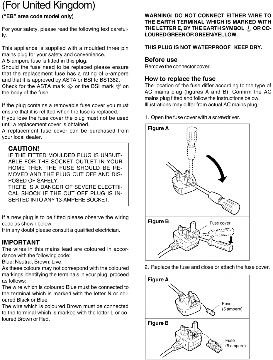
-
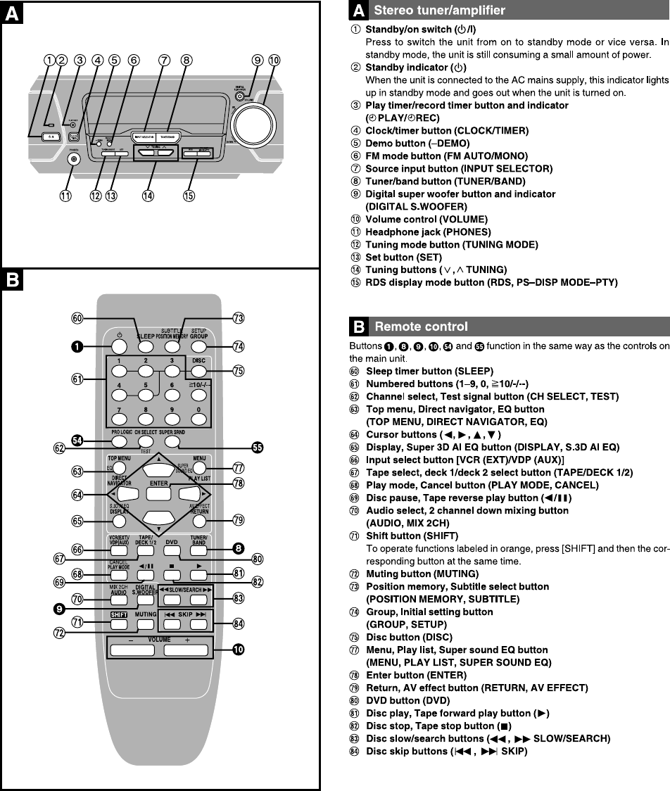
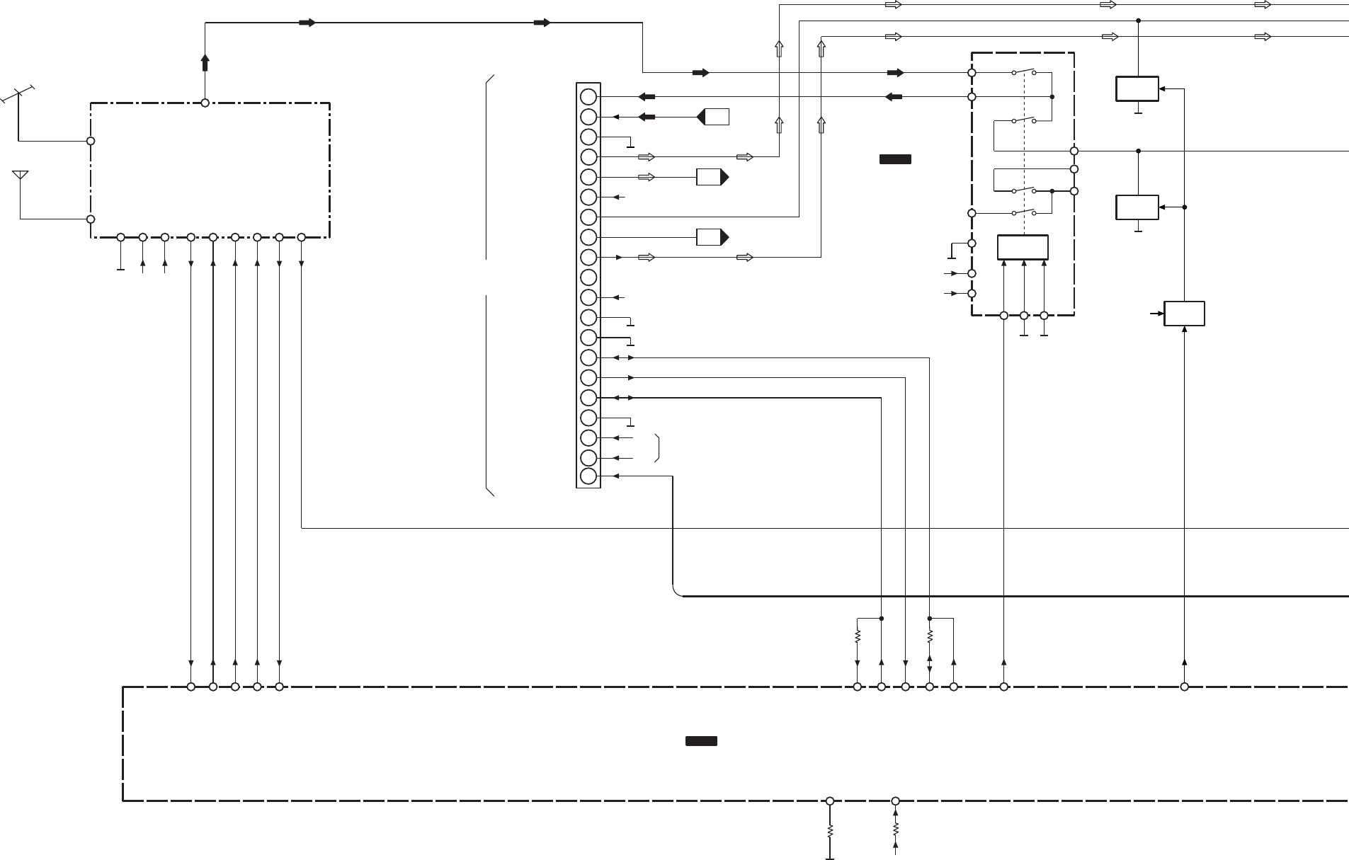
From POWER
TRANSFORMER
1
8
W501
2
3
4
5
6
7
9
12
13
14
15
16
17
18
A.GND
+B(10V)
SUR L
SUR R
19
11
10
CT.GND
SH FL1
DATA
D.GND
TUNER L/C
TUNER Rch
Lch IN
Rch IN
S.W
MIC
-B(-10V)
V.GND
CS/REQ
CLK
SH FL2
20
SYNC
+B5
Rch
Rch
-B3
To SOUND PROCESSOR
BLOCK DIAGRAM
C2BBFD000404
IC901
SYSTEM CONTROL / FL DRIVE
Rch
94
SH CS
97
SH CK
9596
SH DO
SH DI
SHSYNC
21
SH REQ
SW CONT.
12
X0
X1
14
ABC
11 10 9
G
8
2
13
BU4053BCFE2
IC201
SIGNAL SELECTOR 1
15
Y1
Y0
VDD
16
+B4
VSS
7
-B3
6
ST/AV.
6CH
MUTING
Q605
MUTING
Q607
(Q608)
93
MUTE3
MUTING
CONT.
+B4
Q902
10
SEL/
TUNER
MIC DET
25
+B8
SA-DV290(E,EB,EG) BLOCK DIAGRAM
AM ANT
FM ANT
Z101 TUNER PACK
(RAN0005EM-2)
8
(6)
3791110
DO
4
+B2
15
DET
2
+B1
CL
DI
CE
SD
LC72 CE
LC72 DI/ST
345
LC72 DO
2100
SD
LC72 CK
FL1
FL2
Lch
(Rch)
GND
+15V
+7V
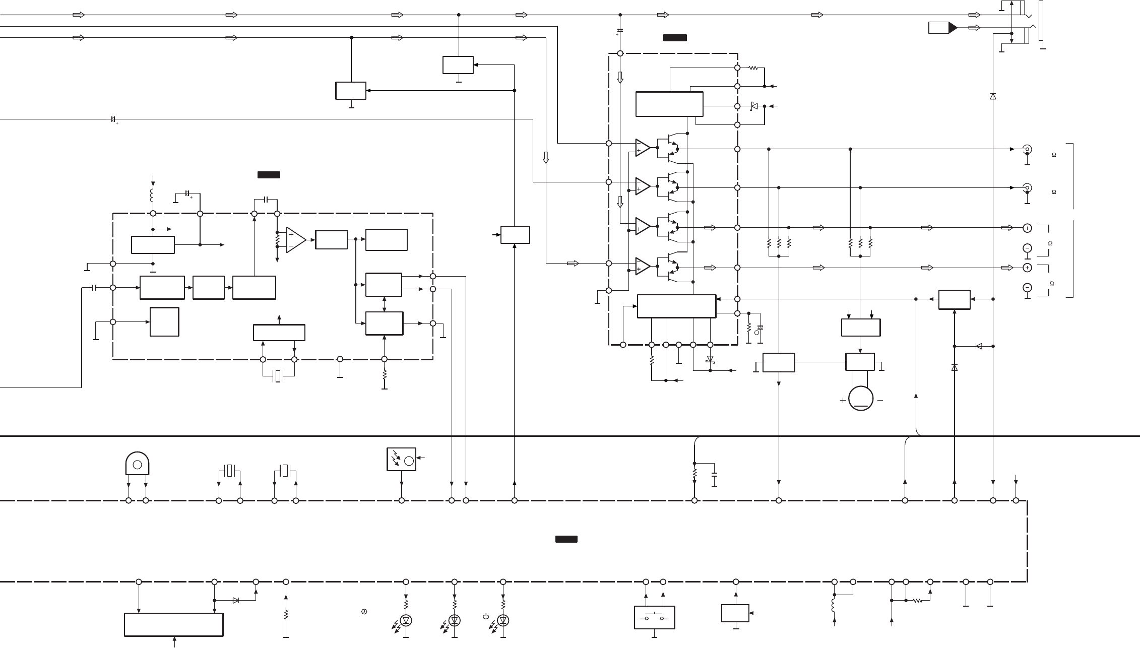
SPEAKERS
Rch PHONES
VR901
(VOLUME)
24 23
VR JOGA
VR JOGB
KEY
SWITCH
(S901~908,
910~915)
19 20
KEY TU
KEY
KARAOKE
Q901,
D904 RESET
12
RESET
+B8
90
VDD2
+B9
VDD1
VDD3
VDD4
18 46 72
C2BBFD000404
IC901
SYSTEM CONTROL / FL DRIVE
29
REMO-
CON
Z901
(REMOTE
SENSOR)
+B8
1~8G
30~37
P1~38
38~45,
47~50
52~71,
73~78
FL901 FL DISPLAY
D931,933
79
REGIN0
82
TIMER
83
S.W LED
D951
(DIGITAL
S.WOOFER)
81
STAND-BY
D954
( PLAY/REC) D306
()
1621
GND
1047
5
1
(2)
6
3
20
15
19
(18)
26
(25)
23
24
RSN311W64B
IC601
POWER AMP
+B3
D601
-B1
D602
-B2
Q601,602
9
+B7
13
98
E DET
HP SW
26
SASYNC
AC IN
88
POWER
POWER
11
+B8
1
CHECK
28
RDS DATA
RDS CLK
27
14
N
Q503,D558
51
-VP
-VP
86
MUTE
D906
PRO-
TECTOR
D974
SWITCH-
ING
D907
REGIN1
22 8
11
(12)
16 17
X901
(6MHz)
XC IN
XC OUT
13 14
X902
(32.7kHz)
XIN
X OUT
80
MUTING
Q606
AC IN
POWER CONTROL
CIRCUIT
POWER CONTROL/
PROTECTION CIRCUIT
C1BB00000527
IC151
RDS SIGNAL DEMODULATOR
CLOCK
RECOVERY
(1187.5kHz)
RDDR
RDCL
IDR
RDS-ID
DETECT/
RAM
57kHz
BPF
(SCF)
PLL
(57kHz)
VREF
CINFLOUTVREF
VDDA/D
VssA/D
MPX IN
TEST
XOUTXIN
OSC/DIVIDER
CLK(4.332MHz)
89
7
2
4,10
3,11
+B2
156
14
15
16
X151
(4.332MHz)
REFERENCE
VOLTAGE
TEST
ANTIALIASING
FILTER SMOOTHING
FILTER
DATA
DECODER
MODE
12 13
RST
91
MUTE2
MUTING
CONT.
+B5
Q612
MUTING
Q609
(Q610)
SURROUND
(8 )
CENTER
(8 )
HF
(6 )
LF
(8 )
Q551,554,
555 SIGNAL
LEVEL DET.
-B3 +B4
M
FAN MOTOR
MOTOR
DRIVE
Q553,556,
557
15
Vss
89
Vss2
SA-DV290(E,EB,EG) BLOCK DIAGRAM
FL1,2
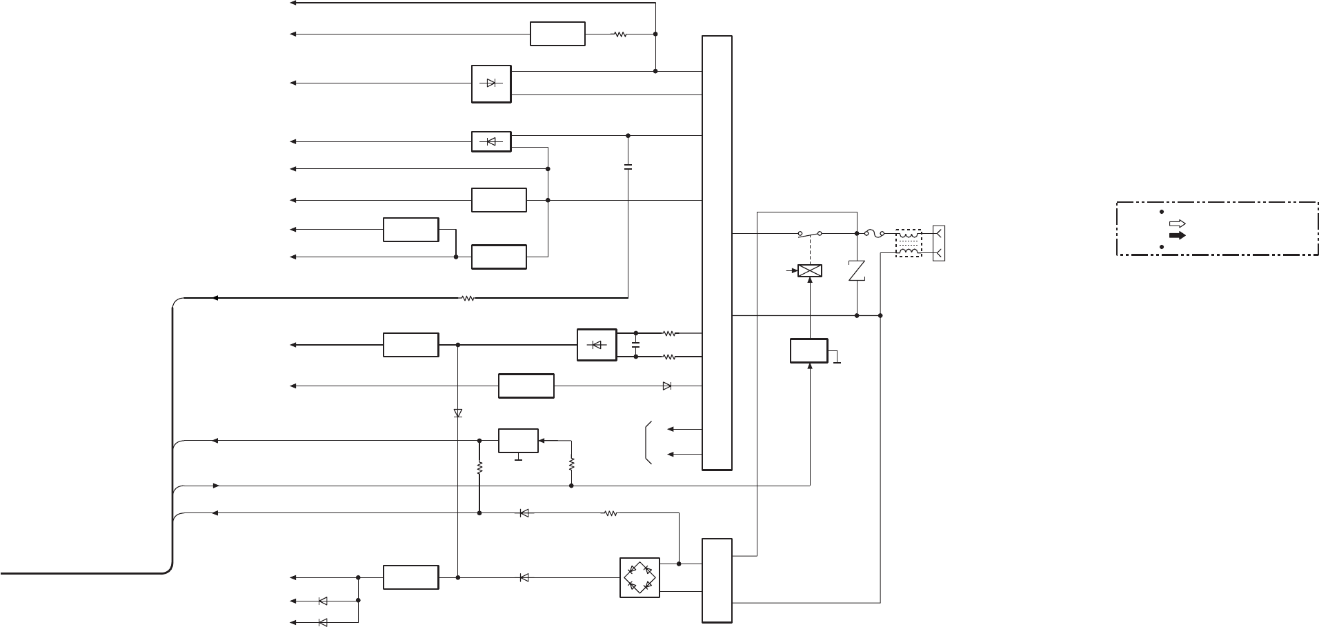
POWER TRANSFORMER
F1
AC IN
L701
T701
D702,704,
752,754,755
Q707
+B4
-B3
Q702,705
Z701
RL702
Q791
POWER
TRANSFORMER
T702
D741~744
-B1
-B2
Q703,704
+B7
D701,703,
751,753,761
Q701
+B1
Q723
+B2
Q711,712,725 D717~720
+B5
D705
-VP
FL1
FL2
FL DISPLAY
(FL901)
Q708,709
+B3
AC IN
SHSYNC
POWER
Q726
+B6
+B8
+B9
D902
D901
SASYNC
D746
REGULATOR
/STABILIZER
REGULATOR
REGULATOR
REGULATOR
SWITCH-
ING
REGULATOR
REGULATOR
RELAY
DRIVE
+B6
D740
REGULATOR
/STABILIZER
SA-DV290(E,EB,EG) BLOCK DIAGRAM
FP791
FP792
D711
NOTES : SIGNAL LINE
: AUDIO SIGNAL
: TUNER SIGNAL
( ) indicates pin No. Right channel.
ORDER NO.AD0305101C8
DVD/Video CD/CD changer
SL-DV290EE / SL-DV290GN
Colour
(s)....................Silver Type
System:SC-DV290
Because of unique interconnecting cables, when a
component requires service, send or bring in the entire
system.
Note: Refer to the service manual for Model No.SA-
DV290EE/GN (ORDER NO.AD0305100C8) for
information on “ACCESSORIES” and “PACKAGING”.
SPECIFICATIONS
Specification
1
Discs played (8 cm or 12 cm)
DVD-Video/DVD-Audio
DVD-RAM/R (DVD-Video format discs)
Video CD, CD (CD-DA)
MP3/WMA/JPEG format discs)
Audio
No. of channels 5.1 channel (FL, FR, SL, SR, C, SW)
Video
Signal system PAL 625/50, PAL 525/60, NTSC
Output level
Composite video 1 Vp-p (75 )
S-video Y 1 Vp-p (75 )
S-video C 0.300 Vp-p (75 ) PAL
0.286 Vp-p (75 ) NTSC
Pickup
Beam source Semiconductor laser
Wavelength 658/790 nm
General
Dimensions (W×H×D) 293×89×288 mm
Mass 2.5 kg
Power Supply: DC10V
Power Consumption: 12W
Nots 1.Design and specifications are subject to
change without notice.
2.Dimensions and weight are approximate.
3.Total harmonic distortion is measured by the
digital spectrum analyzer.
System/SC-DV290
Sound processor: SH-DV290, DVD/ Video CD/ CD
changer: SL-DV290, Tuner/ Amplifier: SA-DV290 ,
Cassette Deck: RS-DV290, Speakers: Front* (SB-
DV290),Center* (SB-PC95),Surround* (SB-PS95)
(*Madein MESA.)
1. Before Repair
This equipment (SL-DV290),which is the component of this system, is supplied with power from
the tuner/amplifier (SA-DV290) through the sound processor (SH-DV290). When repairing this
equipment or checking operation of the system, be suretoconnectthe tuner/amplifier and sound
2
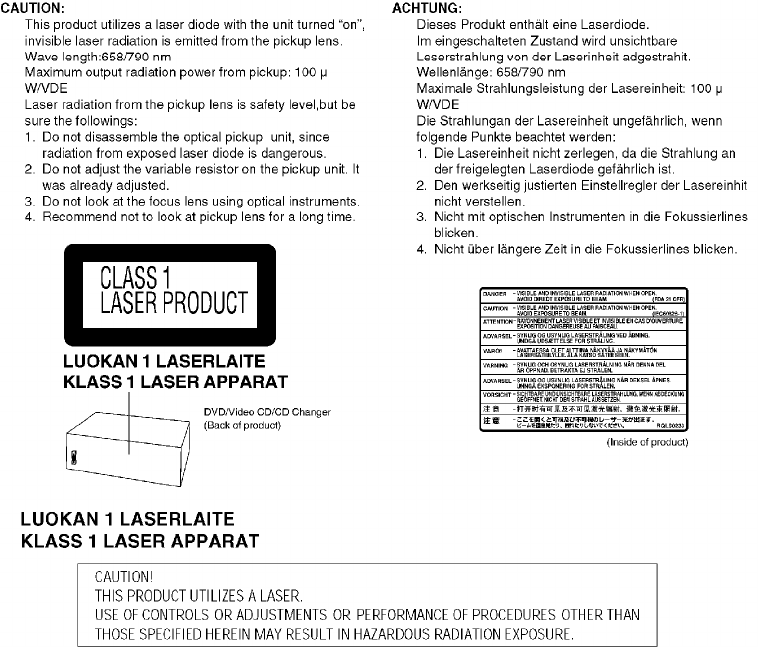
processor with it.
This equipment, even in the state of it as a single equipment, permits power supply and operation
check. When operating it as a single equipment without the tuner/amplifierand sound processor,
refer to the paragraph of "Measurements and Adjustments.
2. Precaution of Laser Diode
3. Operating Instructions
4. Handling Precautions for Traverse Deck
The laser diode in the traverse deck (optical pickup) may break down due to potential difference
caused by static electricity of clothes or human body.So, be careful of electrostatic breakdown
during repair of the traverse deck (optical pickup).
4.1. Handling of traverse deck (optical pickup)
1. Do not give considerable shock to the traverse unit (optical
pickup) as it has an extremely high-precise structure.
2. When replacing the optical pickup, install the flexible cable and cut
its short land with a nipper. See the optical pickup replacement
procedure in this Technical Guide. Before replacing the traverse
unit, remove the short pin for preventingstaticelectricity andinstall
3
a new unit. Connect the connector as short time as possible.
3. The flexible cable may be cut off if an excessive force is applied to
it. Use caution when handling the cable.
4. The half-fixed resistor for laser power adjustment cannot be
adjusted. Do not turn the resistor.
Fig. 1
4.2. Replacement procedure for the optical pickup
1. Connect the Flexible cable to the connector on the terminal P.C.B..
2. Cut the optical unit FPC at the point shown below. (As shown in
Fig. 2.)
Fig. 2
4
4.3. Grounding for electrostatic breakdown prevention
1. Human body grounding
Use the anti-static wrist strap to discharge the static electricity
from your body. (As shown in Fig. 3 .)
2. Work table grounding
Put a conductive material (sheet) or steel sheet on the area where
the optical pickup is placed, and ground the sheet.
Caution:
The static electricity of your clothes will not be grounded through
the wrist strap. So, take care not to let your clothes touch the
traverse deck (optical pickup).
Fig. 3
5. Operation Checks and Component Replacement
Procedures
- This section describes procedures for checking the operation of
the major printed circuit boards and replacing the main
components.
- For reassembly after operation checks or replacement, reverse the
respective procedures. Special reassembly procedures are
described only when required.
5
5.1. Checking for the DVD module (1) P.C.B.
- Check the DVD module (1) P.C.B. (A side) as shown below.
6
- Check the DVD module (1) P.C.B. (B side) as shown below.
5.2. Checking for the operation P.C.B.
- Follow the (Step 1) - (Step 3) of item 5.1.
7
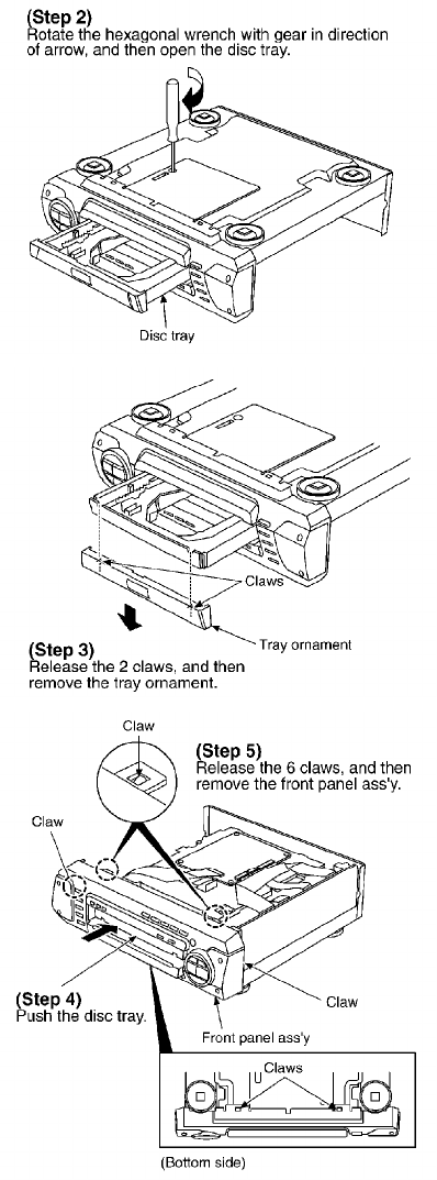
8
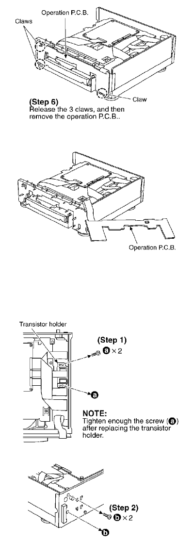
- Check the operation P.C.B. as shown below.
5.3. Checking for the main P.C.B.
- Follow the (Step 1) - (Step 3) of item 5.1.
- Follow the (Step 1) - (Step 5) of item 5.2.
- Check the main P.C.B. as shown below.
9
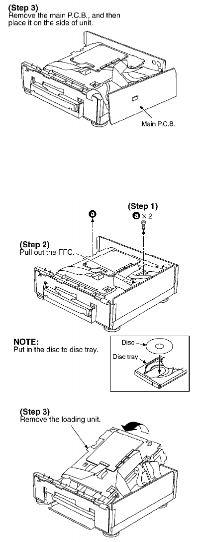
5.4. Checking for the DVD module (2) P.C.B.
- Follow the (Step 1) - (Step 3) of item 5.1.
- Follow the (Step 1) - (Step 5) of item 5.2.
- Check the DVD module (2) P.C.B. as shown below.
10
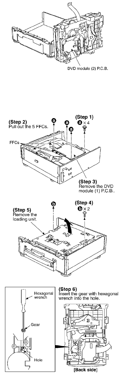
5.5. Replacement for the traverse unit
- Follow the (Step 1) - (Step 3) of item 5.1.
- Follow the (Step 1) - (Step 5) of item 5.2.
11
12
13
5.6. Replacement for the disc tray
- Follow the (Step 1) - (Step 3) of item 5.1.
- Follow the (Step 1) - (Step 5) of item 5.5.
14
15
16
5.7. Disassembly and reassembly for mechanism base drive unit
- Follow the (Step 1) - (Step 3) of item 5.1.
- Follow the (Step 1) - (Step 11) of item 5.5.
- Follow the (Step 1) - (Step 9) of item 5.6.
17
18
19
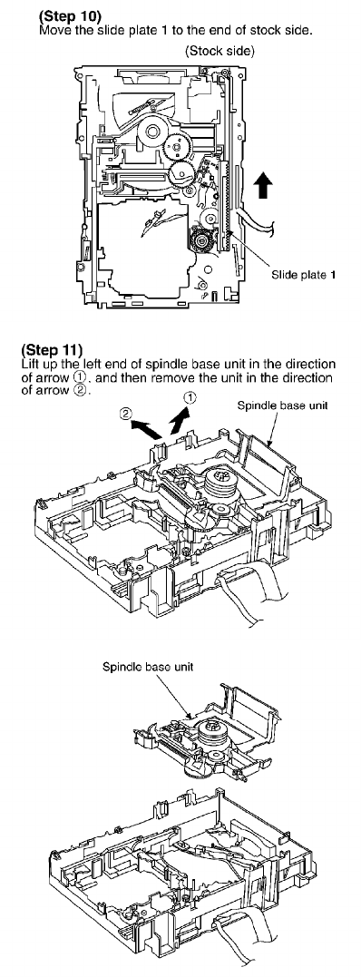
20
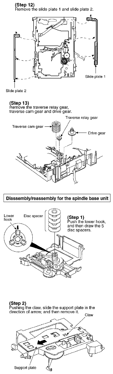
21

22
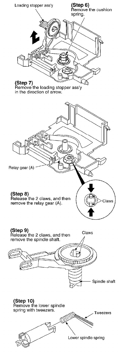
23
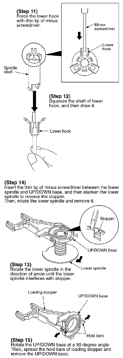
24
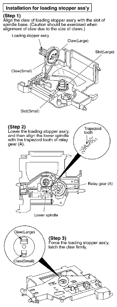
25
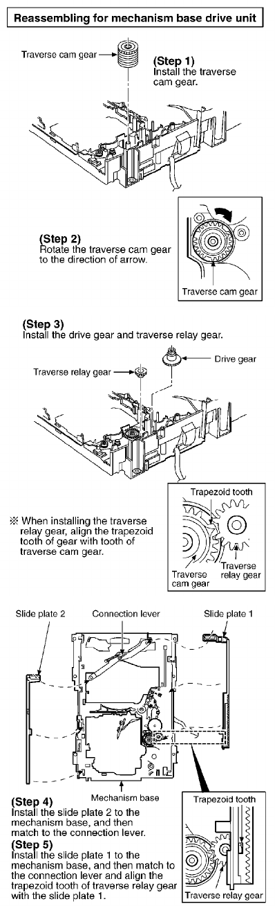
26
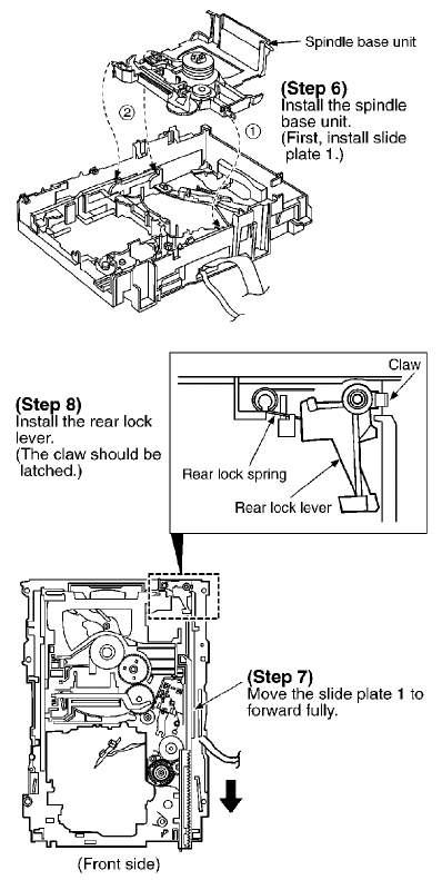
27
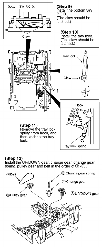
28
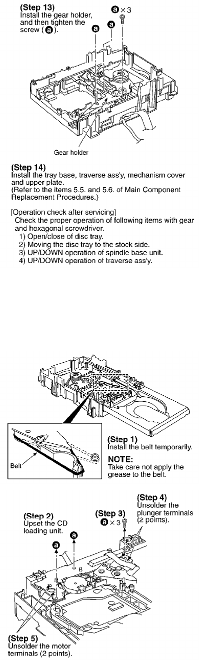
5.8. Replacement for the motor ass’y
- Follow the (Step 1) - (Step 3) of item 5.1.
- Follow the (Step 1) - (Step 5) of item 5.5.
- Follow the (Step 1) - (Step 7) of item 5.6.
29
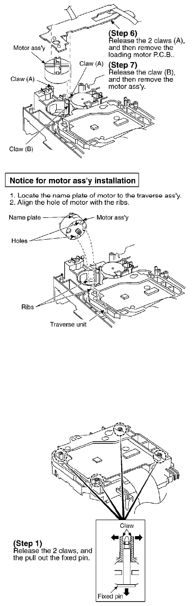
5.9. Replacement for the optical pick-up
- Follow the (Step 1) - (Step 3) of item 5.1.
- Follow the (Step 1) - (Step 5) of item 5.2.
- Follow the (Step 1) - (Step 11) of item 5.5.
30
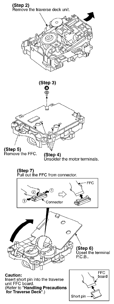
31
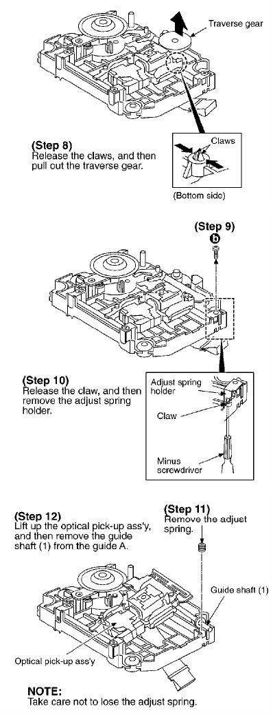
32
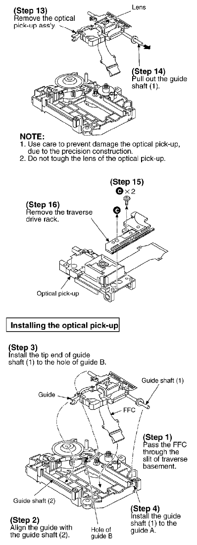
6. Optical Pickup Self-Diagnosis and Replacement
Procedure
6.1. Self-diagnosis
The optical pickup self-diagnosis function and tilt adjustment check function have been included
in this unit. When repairing, use the following procedure for effective Self-diagnosis and tilt
33
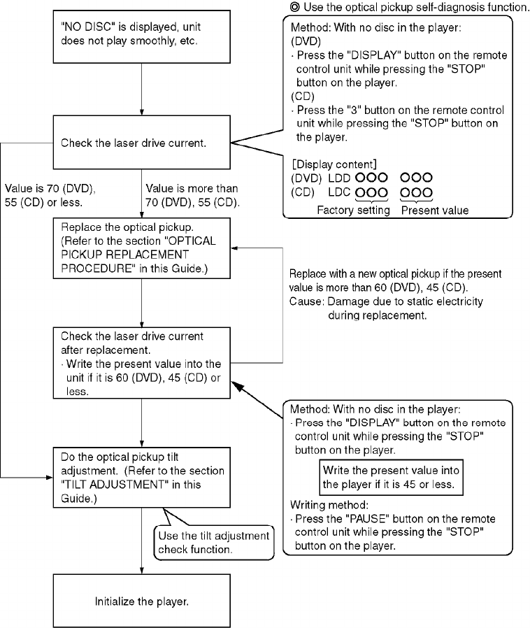
adjustment.Be sure to use the self-diagnosis functionbeforereplacingthe optical pickup when
"NO DISC" is displayed. As a guideline, you should replace the optical pickup when the value of
the laser drive current is more than 55.
Note:
Press the power button to turn on the power, and check the value within three minutes before the
unit warms up. (Otherwise, the result will be incorrect.)
6.2. Cautions to Be Used Before Replacing the Optical Pickup Unit
and Spindle Motor Assembly
Before replacing the optical pickup unit and spindle motor assembly, check the total using hours
for each of them. The checking method is as follows:
34
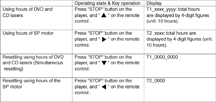
Cautions to be taken when replacing the optical pickup
The optical pickup may break down due to the static electricity of human body. Take proper
protection measures against static electricity before repairing the parts around the optical pickup.
1. Do not touch the areas around the laser diode and actuator.
2. Do not judge the laser diode with a tester. (The tester will be
damaged easily.)
3. It is recommended to use a destaticized soldering iron for short-
circuiting or removing the laser diode. (Recommended soldering
iron) HAKKO ESD Product
4. Solder the land of the flexible cable in the optical pickup.
Note:
- When using a soldering iron which is not destaticized, short-circuit
the terminal face of the flexible case with a clip. After that, short-
circuit the land.
- After the repairing work is completed, remove the solder according
to the correct procedure shown in this Technical Guide.
35
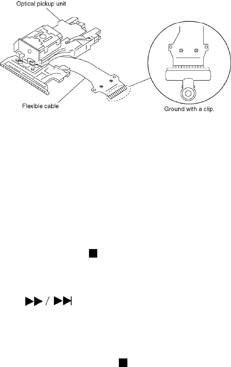
7. Self-Diagnosis Function and Service Modes
Each results of self-diagnostic function and service mode is displayed on the LCD of Tuner /
Amplifier (SA-DV290). When using these function, confirm the unit to be connected by system
cable.
7.1. Self-diagnostic function for loading mechanism
7.1.1. How to enter the mode and display
1. Turn on the power.
2. Press “SELECT” button on the Tuner / Amplifier (SA-DV290) to
select DVD.
3. With no disc on the unit, hold down REPEAT button for at least 2
seconds, and then press (STOP) button for at least 2 seconds.
4. A loading mechanism error code is displayed if any. (No error is
detected, “-- T-- ------- ” is displayed. - indicates a space.) Refer to
Table 7-1. If there are multiple error, they canbesuccessivelyby
pressing (F-SKIP) button.
7.1.2. Canceling self-diagnostic function
- Press “Standby/on” button to turn off. And then press “Standby/on”
button again to turn it on again.
7.1.3. Clearing self-diagnostic function
- After repairing, continue to press (STOP) button for at least 5
seconds in the situation of having displayed the error code. /
(Clearing the contents of self-diagnostic function)
- Always be sure to clear memories after completing repair.
36
Table 7-1
Display code Cause
H15 Disc tray open detect switch (S3) fault. /
(Check and replace)
F16 Clamp switch (S4) fault. / (Check and
replace)
F17 Bottom switch (S5) fault. / (Check and
replace)
F27 Tray position detect switch (S1, S2) fault.
/ (Check and replace)
F28 Disc load error.
F29 Disc unload error.
7.2. Service mode table 1
Pressing various button combinations on the unit and remote control can activate the service
modes.
Unit button Remote control
button
Application
0Displaying the error code. (Refer to the item 7.3. “DVD/CD error
display”.)
5Jitter check, optical pick-up tilt adjustment.
6Checking the region numbers and broadcast system.
7Checking the program version.
DISPLAY Checking DVD laser drive current measurement.
3Checking CD laser drive current measurement.
Writing the laser drive current value after replacing the optical
pick
(Do not perform this mode except for replacing the optical pick-
up.)
Initialization (Restore factory preset settings) / Perform this
mode
replacing the microcomputer, its peripheral parts and P.C.B..
7.3. DVD Self Diagnostic Function-Error Code
37

Error
Code
Error Content Additional error explanation Defect 1 Defect 2 Defect 3
U, H error
U11 Focus error
H01 Tray loading error
H02 Spindle servo
error
(Spindle servo, DSC SP motor, CLV
servo error)
H03 Traverse servo
error
H04 Tracking servo
error
H05 Seek error
H06 Power error Cannot switch off the power because
of the panel and system computer
communication error
DSC related
F500 DSC error DSC stops in the occurence of servo
error (starup, focus error, etc)
OPU ADSC FEP
F501 DSC not Ready DSC-system computer
communication error
(Communication failure caused by
idling of DSC)
ADSC CPU
F502 DSC Time out
error
Similar disposal as F500 OPU ADSC FEP
F503 DSC
communication
Failure
Communication error (result error
occured although communication
command was sent)
ADSC FEP EEPROM
F505 DSC Attention
error
Similar disposal as F500 OPU ADSC FEP
F506 Invalid media Disc is flipped over, TOC unreadable,
incompatible disc
DISC FEP ADSC
ODC related
F600 Access failure to
management
information
caused by
demodulation
error
Operation stopped because
navigation data is not accessible
caused by the demodulation defect
ODC FEP ADSC
F601 Indeterminate
sector ID
requested
Operation stopped caused by the
request to access abnormal ID data
ODC FEP ADSC
F602 Access failure to
LEAD-IN caused
by demodulation
error
LEAD IN data unreadable
38

Error
Code
Error Content Additional error explanation Defect 1 Defect 2 Defect 3
F603 Access failure to
KEYDET caused
by demodulation
error
Access failure to CSS data of disc
F610 ODC abnormality No permission for command
execution
ODC
F611 6626 QCODE
don’t read Error
Access failure to seek address in CD
series
ODC
F612 No CRC OK for a
specific time
Access failure to ID data in DVD
series
ODC
F630 No reply to KEY
DET enquiry
(for internal use only)
F631 CPPM KEY DET
is not available
till the FILE
terminal
(CPPM file system is unreadable
caused by scratches)
DISC CPPM
F632 CPPM KEY DET
is not available
Been revoked or falsified DISC EEPROM CPPM
Disc code
F103 Illegal highlight
Position
Big possibility of disc specification
violation during highlight display
DISC
HIC Error
F4FF Force initialize
failure (time out)
EEPROM CPU FEP
Micro computer
error
F700 MBX overflow When replying message to disc
manager
F701 Message
command does
not end
Next message is sent before replying
to disc manager
F702 Message
command
changes
Message is changed before it is sent
as a reply to disc manager
F880 Task number is
not appropriate
Message coming from a non-existing
task
F890 Sending message
when message is
being sent to AV
task
Sending message to AV task
F891 Message couldn’t
be sent to AV task
Begin sending message to AV task
F893 FROM falsification FROM CPU
39

Error
Code
Error Content Additional error explanation Defect 1 Defect 2 Defect 3
F894 EEPROM
abnormality
EEPROM Serial /
communication
on lone
F8A0 Message
command is not
appropriate
Begin sending message to AV task
7.4. Last Error Code saved during NO PLAY
Error
code
Error Content System computer Setting task System computer
internal
error code
F0BF 6) Cannot playback
because physical layer is
not recoginizable
PCND_NOPLAY
PHYSICAL 0x50
DriveManager 0xDOBF
F0C0 8) DVD: Cannot playback
because it is not DVD Video
/Adio/VR
PCND_NOPLAY VIDEO
0x70
DiscManager 0xDOC0
F0C1 9) DVD: Prohibited by the
restricted region code
PCND_NOPLAY RCD
0x80
DiscManager 0xDOC1
F0C2 A) DVD: PAL restricted
playback
PCND_NOPLAY PAL
0x90
DiscManager 0xDOC2
F0C3 B) DVD: Parental lock
setting prohibits the
playback of the entire title
PCND_NOPLAY PTL
0xA0
DiscManager 0xDOC3
F0C4 C) VCD: Prohibited
because it is in PHOTO CD
fromat
PCND_NOPLAY PHOTO
CD 0xB0
DiscManager 0xDOC4
F0C5 VCD/CD: Prohibited
because it is CDROM
without CD-DA
PCND_NOPLAY
CDROM 0xC0
DiscManager 0xDOC5
7.5. Service mode table 2
Pressing various button combinations on the player and remote control unit can activate the
service modes.
40
41

7.6. Sales demonstration lock function
This function prevents discs from being lost when the unit is used for sales demonstrations by
disabling the disc eject function. "LOCKED" is displayed on the unit, and ordinary operation is
disabled.
7.6.1. Setting
The sales demonstration lock is set by simultaneously pressing “STOP” button on the player and
“PLAY” button on the remote control unit.
7.6.2. Cancellation
The lock can be cancelled by the same procedure as used in setting. ("UNLOCKED" is displayed
on cancellation. Disconnecting the power cable from power outlet does not cancel the lock.)
7.7. Handling After Completing Repairs
Use the following procedure after completing repairs.
7.7.1. Method
Confirm that the power is turned on:
1. Press the “OPEN/CLOSE” button to close the tray.
2. Press the “POWER” button to turn off the power.
3. Disconnect the power plug from the outlet.
7.7.2. Precautions
42
Do not disconnect the power plug from the outlet with the tray still open, then close the tray
manually.
8. Service Precautions
8.1. Recovery after the DVD player is repaired
- When a FROM or module P.C.B. is replaced, carry out the recovery
processing to optimize the drive.
Playback the recovery disc to process the recovery automatically.
- Recovery disc (Product number: RFKZD5TR006 or RFKZD03R004 )
- Performing recovery
1. Load the recovery disc (RFKZD5TR006 or RFKZD03R004 ) on to
the unit and run it.
2. Recovery is performed automatically. When it is finished, a
message appears on the screen.
3. Remove the recovery disc.
4. Turn off the power.
Note:
This unit requires no initialization process carried out after the traditional DVD players were
repaired.
When the recovery measure are taken, the customer setting will return to the factory preset
settings as same as the procedure described in item of “Initialization” in 7.6. is carried out. Write
down the contents of the settingbeforerecoveryprocessing, and reset the unit.
8.2. Firmware version-up of the DVD player
- The firmware of the DVD player may be renewed to improve the
quality including operationality and playback ability to the
substandard discs processing to optimize the drive.
The recovery disc has also firmware version-up.
- After version-up, recovery processing is executed automatically.
- Part number of the recovery disc for version-up will be noticed
when it is supplied.
- Updating firmware
1. Load the recovery disc that is supplied to the unit and run it.
2. Firmware version of the unit is automatically checked.
Appropriate message appears whenever necessary.
3. Using remote control cursor key, select whether version updating
is to be done or not. (Selection of Yes/No)
4. a. If Yes is selected, version updating is performed.
43
b. If No is selected, only recovery is performed.
5. a. When updating is finished, remove the disc according to the
message appearing on the screen.
b. Remove the disc according to the message appearing on the
screen.
6. Turn off the power.
Note:
If the AC power supply is shut down during version-up due to a power failure, the version-up is
improperly carried out.
In such a case, replace the FROM and carry out the version-up again.
8.3. Overview of each function
8.3.1. Cumulative operation time display
44
1. Operation/display
Key operations are as follows.
Laser operation time ............. In STOP mode, main unit [STOP]+
remote controller [ ]
Spindle motor operation time ..... In STOP mode, main unit [STOP]+
remote controller [ ]
To reset the timer, perform the following while displaying the time
with above key operation.
Laser operation time ............. In STOP mode, main unit [STOP]+
remote controller [ ]
Spindle motor operation time ..... In STOP mode, main unit [STOP]+
remote controller [ ]
2. How to utilize
Reference information in fault diagnosis of laser or spindle motor
system
Review of faulty point in repeated repair
9. Adjustment Procedures
9.1. Service Tools and Equipment
Application Name Number
Tilt adjustment DVD test disc DVDT-S15 or DVDT-S01
Hex wrench Commercially available hex
wrench
Others Screw lock RZZ0L01
Grease RFKXGAK152
Oil RFKXGA1280, JZS0648
Confirmation
CD test disc PVCD-K06 or any other
commercially available disc
VCD test disc PVCD-K06 or any other
commercially available disc
Recovery disc RFKZD5TR006 or
RFKZD03R004
45
9.2. Important points in adjustment
9.2.1. Important points in optical adjustment
- Before starting optical adjustment, be sure to take anti-static
measures.
- Optical pickup tilt adjustment is needed after replacement of the
following components.
1. Optical pickup unit
2. Spindle motor unit
3. Optical pickup peripheral parts (such as rail)
Notes
Adjustment is generally unnecessary after replacing other parts of the traverse unit. However,
make adjustment if there is a noticeable degradation in picture quality. Optical adjustments
cannot be made inside the optical pickup. Adjustment isgenerally unnecessaryafterreplacing the
traverse unit.
9.2.2. Important points in electrical adjustment
- Follow the adjustment procedures described in this Manual.
9.3. Storing and Handling Test Discs
- Surface precision is vital for DVD test discs. Be sure to store and
handle them carefully.
1. Do not place discs directly onto the workbench, etc., after use.
2. Handle discs carefully in order to maintain their flatness. Place
them into their case after use and store them vertically. Store
discs in a cool place where they are not exposed to direct sunlight
or air from air conditioners.
3. Accurate adjustment will not be possible if the disc is warped
when placed on a surface made of glass, etc. If this happens, use a
new test disc to make optical adjustments.
4. If adjustment is done using a warped disc, the adjustment will be
incorrect and some discs will not be playable.
9.4. Optical adjustment
9.4.1. Optical pickup tilt adjustment
46

Measurement point Adjustment point Mode Disc
Tangential adjustment
screw
Tilt adjustment screw
T01 (inner periphery) play
T43 (outer periphery) play
DVDR-S15 or
DVDT
Measuring equipment Adjustment value
None (Main unit display for servicing is used.) Adjust to the minimum jitter value.
9.4.1.1. Adjustment procedure
1. While pressing “STOP” button on the main unit, press "5" on the
remote control unit.
2. Confirm that "J_xxx_yyy_zz" is shown on the front display.
For your information:
"yyy" and "zz" shown to the right have nothing to do with the jitter value. "yyy" is the error
counter, while "zz" is the focus drive value.
Note:
Jitter value appears on the front display.
3. Play test disc T01 (inner periphery).
4. Adjust tangential adjustment screw so that the jitter value is
minimized.
5. Play test disc T43 (outer periphery).
6. Adjust tilt adjustment screw 1 so that the jitter value is minimized.
7. Play test disc T43 (outer periphery).
8. Adjust tilt adjustment screw 2 so that the jitter value is minimized.
9. Repeat adjusting tilt adjustment screws 1 and 2 alternately until
the jitter value is minimized.
9.4.1.2. Important points
1. Make tangential adjustment first, and then make tilt adjustment.
2. Repeat adjusting two or three times to find the optimum point.
3. Finish the procedure with tilt adjustment.
47
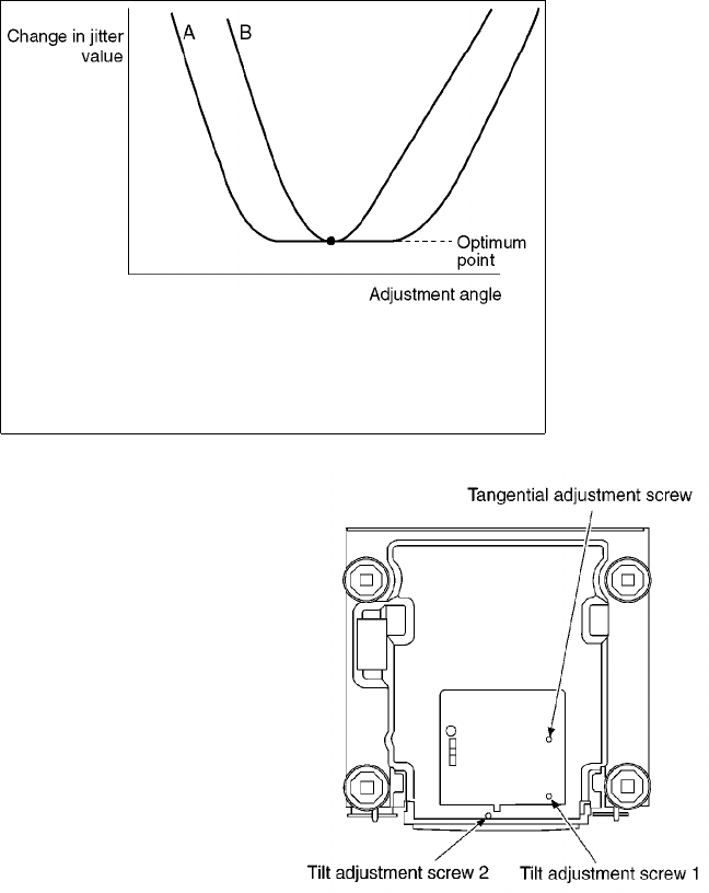
Jitter value depends on the model:
1. If the jitter value changes like B, the optimum point is easy to find.
2. If the jitter value changes like A, set the optimum point near the
middle.
9.4.1.3. Check after adjustment
Play test disc or any other disc to make sure there is no picture degradation in the inner, middle
and outer peripheries, and no audio skipping. After adjustment is finished, lock each adjustment
screw in position using screw lock.
9.4.1.4. Procedure for screw lock
1. After adjustment, remove top cover, tray, clamper base and
traverse unit in this sequence.
2. Lay the traverse unit upside down, and fix adjustment screw with
screw lock.
3. After fixing, reassemble traverse unit, clamper base, tray and top
cover.
48
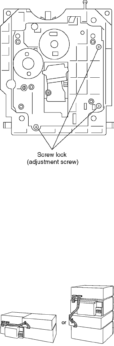
10. To Supply Power Source
Cautions:
- It is very dangerous to look at or touch the laser beam. (Laser
radiation is invisible.)
With the unit turned “on”, laser radiation is emitted from the
pickup lens.
- Avoid exposure to the lase beam, especially when performing
adjustments.
This unit SL-DV290 is designed to operate on power supplied from the system connected. (For
system connection, refer to Fig. 4.)
Fig. 4
When the unit SL-DV290 has to test and service alone, use the following method to supply power
source.
49
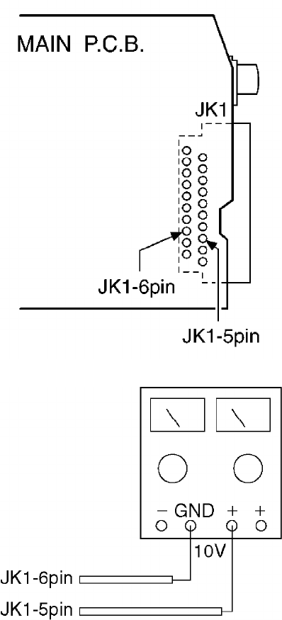
1. Connect a DC power supply to JK1-5pin and JK1-6pin and .
Then adjust the outputs to 10V for 5pin (refer to Fig. 5 and Fig. 6)
Fig. 5
Fig. 6
Note:
Use only this method when checking the voltage etc..
In case of checking operations, use the system connections to supply power source.
11. Block Diagram
12. Schematic Diagram Notes
50

12.1. Type Illustration of IC's, Transistors and Diodes
12.2. Schematic Diagram Notes
This schematic diagram may be modified at any time with the development of new technology.
Notes:
- S1 : Tray position 1 detect switch.
- S2 : Tray position 2 detect switch.
- S3 : Tray open detect switch.
- S4 : Clamp detect switch.
- S5 : Bottom detect switch.
- S601 : Disc select (DISC5) switch.
- S602 : Disc select (DISC4) switch.
- S603 : Disc select (DISC3) switch.
- S604 : Disc select (DISC2) switch.
- S605 : Disc select (DISC1) switch.
- S606 : Disc direct open (DIRECT OPEN, DISC1) switch.
- S607 : Disc direct open (DIRECT OPEN, DISC2) switch.
- S608 : Disc direct open (DIRECT OPEN, DISC3) switch.
- S609 : Disc direct open (DIRECT OPEN, DISC4) switch.
- S610 : Disc direct open (DIRECT OPEN, DISC5) switch.
- S611 : Disc tray open/close ( , OPEN/CLOSE) switch.
- S612 : A-B repeat (A-B REPEAT) switch.
- S613 : Repeat (REPEAT) switch.
- S614 : CD edit (CD EDIT) switch.
- S615 : Cinema mode (CINEMA MODE) switch.
- S616 : Double re-master (DOUBLE RE-MASTER) switch.
- S617 : Pause ( ) switch.
- S618 : Stop ( ) switch.
- S619 : Play ( ) switch.
- S620 : R. skip/search ( ) switch.
- S621 : F. skip/search ( ) switch.
- Indicated voltage values are the standard values for the unit
measured by the DC electronic circuit tester (high-impedance) with
the chassis taken as standard. Therefore, there may exist some
errors in the voltage values, depending on the
internalimpedanceofthe DC circuit tester.
No mark: CD STOP
51
( ): CD play [1kHz, L+R, 0dB]
Important safety notice:
Components identified by mark have special characteristics important for safety.
Furthermore, special parts which have purpose of fire-retardant (resistors), high-quality sound
(capacitors), low-noise (resistors), etc. are used. When replacing any of components, be sure to
use only manufacture's specified parts shownintheparts list.
Caution!
- IC and LSI are sensitive to static electricity.
- Secondary trouble can be prevented by taking care during repair.
- Cover the parts boxes made of plastics with aluminum foil.
- Ground the soldering iron.
- Put a conductive mat on the work table.
- Do not touch the legs of IC or LSI with the fingers directly.
Voltage and signal lines
: Positive voltage line
: AUDIO signal line
: AUDIO/VIDEO signal line
: VIDEO signal line
: Surround SP. signal line
: Center SP. signal line
: Sub woofer signal line
13. Schematic Diagram
14. Abbreviations
52

INITIAL/LOGO ABBREVIATIONS
AA0~UP
ACLK
AD0~UP
ADATA
ALE
AMUTE
AREQ
ARF
ASI
ASO
ASYNC
ADDRESS
AUDIO CLOCK
ADDRESS BUS
AUDIO PES PACKET DATA
ADDRESS LATCH ENABLE
AUDIO MUTE
AUDIO PES PACKET REQUEST
AUDIO RF
SERVO AMP INVERTED INPUT
SERVOAMPOUTPUT
AUDIOWORDDISTINCTION
SYNC
B BCK
BCKIN
BDO
BLKCK
BOTTOM
BYP
BYTCK
BIT CLOCK (PCM)
BIT CLOCK INPUT
BLACK DROP OUT
SUB CODE BLOCK CLOCK
CAP. FOR BOTTOM HOLD
BYPATH
BYTE CLOCK
C CAV
CBDO
CD
CDSCK
CDSRDATA
CDRF
CDV
CHNDATA
CKSL
CLV
COFTR
CPA
CPCS
CPDT
CPUADR
CPUADT
CPUIRQ
CPRD
CPWR
CS
CSYNCIN
CSYNCOUT
CONSTANT ANGULAR
VELOCITY
CAP. BLACK DROP OUT
COMPACT DISC
CD SERIAL DATA CLOCK
CD SERIAL DATA
CD RF (EFM) SIGNAL
COMPACT DISC-VIDEO
CHANNEL DATA
SYSTEMCLOCKSELECT
CONSTANTLINEARVELOCITY
CAP. OFF TRACK
CPU ADDRESS
CPU CHIP SELECT
CPU DATA
CPU ADDRESS LATCH
CPU ADDRESS DATA BUS
CPU INTERRUPT REQUEST
CPU READ ENABLE
CPU WRITE ENABLE
CHIPSELECT
COMPOSITESYNCIN
COMPOSITESYNC OUT
53

INITIAL/LOGO ABBREVIATIONS
D DACCK
DEEMP
DEMPH
DIG0~UP
DIN
DMSRCK
DMUTE
DO
DOUT0~UP
DRF
DRPOUT
DREQ
DRESP
DSC
DSLF
DVD
D/A CONVERTER CLOCK
DEEMPHASIS BIT ON/OFF
DEEMPHASIS SWITCHING
FL DIGIT OUTPUT
DATA INPUT
DM SERIAL DATA READ CLOCK
DIGITAL MUTE CONTROL
DROPOUT
DATAOUTPUT
DATASLICERF (BIAS)
DROP OUT SIGNAL
DATA REQUEST
DATA RESPONSE
DIGITAL SERVO CONTROLLER
DATA SLICE LOOP FILTER
DIGITAL VIDEO DISC
INITIAL/LOGO ABBREVIATIONS
EEC
ECR
ENCSEL
ETMCLK
ETSCLK
ERROR TORQUE CONTROL
ERROR TORQUE CONTROL
REFERENCE
ENCODER SELECT
EXTERNAL M CLOCK (81MHz/
40.5MHz)
EXTERNAL S CLOCK (54MHz)
FFBAL
FCLK
FE
FFI
FEO
FG
FSC
FSCK
FOCUS BALANCE
FRAME CLOCK
FOCUS ERROR
FOCUS ERROR AMP INVERTED
INPUT
FOCUS ERROR AMP OUTPUT
FREQUENCY GENERATOR
FREQUENCY SUB CARRIER
FS (384 OVER
SAMPLING)CLOCK
GGND COMMON GROUNDING
(EARTH)
H HA0~UP
HD0~UP
HINT
HRXW
HOST ADDRESS
HOST DATA
HOST INTERRUPT
HOST READ/WRITE
54

INITIAL/LOGO ABBREVIATIONS
IIECOUT
IPFRAG
IREF
ISEL
IEC958 FORMAT DATA OUTPUT
INTERPOLATION FLAG
I (CURRENT) REFERENCE
INTERFACE MODE SELECT
LLDON
LPC
LRCK
LASER DIODE CONTROL
LASER POWER CONTROL
L CH/R CH DISTINCTION
CLOCK
MMA0~UP
MCK
MCKI
MCLK
MDATA
MDQ0~UP
MDQM
MLD
MPEG
MEMORY ADDRESS
MEMORY CLOCK
MEMORY CLOCK INPUT
MEMORY SERIAL COMMAND
CLOCK
MEMORY SERIAL COMMAND
DATA
MEMORY DATA INPUT/OUTPUT
MEMORY DATA I/OMASK
MEMORYSERIALCOMMANDLOAD
MOVING PICTURE EXPERTS
GROUP
OODC
OFTR
OSCI
OSCO
OSD
OPTICAL DISC CONTROLLER
OFF TRACKING
OSCILLATOR INPUT
OSCILLATOR OUTPUT
ON SCREEN DISPLAY
PP1~UP
PCD
PCK
PDVD
PEAK
PLLCLK /
PLLOK
PWMCTL
PWMDA
PWMOA, B
PORT
CD TRACKING PHASE
DIFFERENCE
PLL CLOCK
DVD TRACKING PHASE
DIFFERENCE
CAP. FOR PEAK HOLD
CHANNEL PLL CLOCK
PLL LOCK
PWM OUTPUT CONTROL
PULSEWAVEMOTORDRIVEA
PULSE WAVE MOTOR OUT A, B
55

INITIAL/LOGO ABBREVIATIONS
R RE
RFENV
RFO
RS
RSEL
RST
RSV
READ ENABLE
RF ENVELOPE
RF PHASE DIFFERENCE
OUTPUT
(CD-ROM) REGISTER SELECT
RF POLARITY SELECT
RESET
RESERVE
S SBI0, 1
SBO0
SBT0, 1
SCK
SCKR
SCL
SCLK
SDA
SEG0~UP
SELCLK
SEN
SIN1, 2
SOUT1, 2
SPDI
SPDO
SPEN
SPRCLK
SPWCLK
SQCK
SQCX
SRDATA
SRMADR
SRMDT0~7
SS
STAT
STCLK
STD0~UP
STENABLE
STSEL
STVALID
SUBC
SBCK
SUBQ
SYSCLK
SERIAL DATA INPUT
SERIAL DATA OUTPUT
SERIAL CLOCK
SERIAL DATA CLOCK
AUDIO SERIAL CLOCK
RECEIVER
SERIAL CLOCK
SERIAL CLOCK
SERIAL DATA
FL SEGMENTOUTPUT
SELECTCLOCK
SERIALPORTENABLE
SERIAL DATA IN
SERIAL DATA OUT
SERIAL PORT DATA INPUT
SERIAL PORT DATA OUTPUT
SERIAL PORT R/W ENABLE
SERIAL PORT READ CLOCK
SERIALPORT WRITE CLOCK
SUB CODE Q CLOCK
SUBCODEQDATA READ CLOCK
SERIAL DATA
SRAM ADDRESS BUS
SRAM DATA BUS 0~7
START/STOP
STATUS
STREAM DATA CLOCK
STREAM DATA
STREAMDATA INPUT ENABLE
STREAM DATA POLARITY
SELECT
STREAMDATAVALIDITY
SUBCODE SERIAL
SUB CODE CLOCK
SUB CODE Q DATA
SYSTEM
CLOCK
56

SYSTEM
CLOCK
INITIAL/LOGO ABBREVIATIONS
TTE
TIBAL
TID
TIN
TIP
TIS
TPSN
TPSO
TPSP
TRCRS
TRON
TRSON
TRACKING ERROR
BALANCE CONTROL
BALANCE OUTPUT 1
BALANCE INPUT
BALANCE INPUT
BALANCE OUTPUT 2
OP AMP INPUT
OP AMP OUTPUT
OP AMP INVERTED INPUT
TRACKCROSSSIGNAL
TRACKINGON
TRAVERSESERVO ON
INITIAL/LOGO ABBREVIATIONS
VVBLANK
VCC
VCDCONT
VDD
VFB
VREF
VSS
V BLANKING
COLLECTOR POWER SUPPLY
VOLTAGE
VIDEO CD CONTROL
(TRACKING
BALANCE)
DRAIN POWER SUPPLY
VOLTAGE
VIDEO FEED BACK
VOLTAGE REFERENCE
SOURCEPOWERSUPPLYVOLTAGE
WWAIT
WDCK
WEH
WSR
BUS CYCLE WAIT
WORD CLOCK
WRITE ENABLE HIGH
WORD SELECT RECEIVER
57

INITIAL/LOGO ABBREVIATIONS
XX
XALE
XAREQ
XCDROM
XCS
XCSYNC
XDS
XHSYNCO
XHINT
XI
XINT
XMW
XO
XRE
XSRMCE
XSRMOE
XSRMWE
XVCS
XVDS
XVSYNCO
X' TAL
X ADDRESS LATCH ENABLE
X AUDIO DATA REQUEST
X CD ROM CHIP SELECT
X CHIP SELECT
X COMPOSITE SYNC
X DATA STROBE
X HORIZONTAL SYNC OUTPUT
XHINTERRUPTREQUEST
X' TALOSCILLATORINPUT
X INTERRUPT
X MEMORY WRITE ENABLE
X' TAL OSCILLATOR OUTPUT
X READ ENABLE
X SRAM CHIP ENABLE
X SRAM OUTPUT ENABLE
X SRAM WRITE ENABLE
XV-DEC CHIPSELECT
XV-DEC CONTROLBUS
STROBE
X VERTICAL SYNC OUTPUT
15. Printed Circuit Board Diagram
16. Wiring Connection Diagram
17. Terminal Function of IC's
17.1. IC401 (C2BBFD000402): SYSTEM CONTROL
58

Pin
No.
Mark I/O
Division
Function
1VCC I Connected to power supply
2 VREF
3AVSS — Connected to GND
4MUTE O Mute control output terminal
5PWCONT O DVD module power supply
control output terminal
6SYNC I Power failure detect signal
input terminal
7C/SW
SEL
OCenter/sub woofer speaker
select signal output terminal
8B_REQ I Serial communication
request signal input terminal
9B_CS O Serial communication chip
select signal output terminal
10 B_CLK O Serial communication clock
signal output terminal
11 DATA
O
OSerial communication data
signal output terminal
12 DATA I I Serial communication data
signal input terminal
13 MIXSEL O Select control output
terminal for wide picture
14 WIDE1
15 CNVSS —Connected to GND
16 TEST I Test mode input terminal
17 E-CS — Connected to GND
18 RESET I Reset signal input terminal
19 XIN I Crystal oscillator input
terminal (f=8MHz)
20 XOUT O Crystal oscillator output
terminal (f=8MHz)
21 VSS —Connected to GND
22 LED-
STB
OSerial signal output to LED
drive
23 LED/ /
E-CLK
OSerial signal output terminal
to LED drive or EEPROM
24 LED/ /
E-
DATA
OSerial signal output terminal
to LED drive or EEPROM
25 LED-
CLR
O Latch clear signal output
terminal to LED drive
26 PLG O Plunger control signal output
terminal
27 SW5 IBottom switch detect signal
input
terminal
59
input terminal
Pin
No.
Mark I/O
Division
Function
28 PSTN I Position sensor detect signal
input terminal
29 SW2 I Disc tray position 2 detect
signal input terminal
30 SW1 I Disc tray position 1 detect
signal input terminal
31 SW3 I Disc tray open detect signal
input terminal
32 CCW O Motor drive control signal
output terminal (forward
direction)
33 CW O Motor drive control signal
output terminal (reverse
direction)
34 HALF O Motor drive control signal
output terminal (speed)
35 DVD-
CLK
ISerial communication signal
input terminal for DVD main
micro-computer
36 DVD-
CMD
OSerial communication signal
output terminal for DVD main
micro-computer
37 DVD-
STAT
ISerial communication signal
input for DVD main micro-
computer
38 DISC
CS
— Connected to GND through
resistor
39 SW4 I Clamp switch detect signal
input terminal
40 KEY2 I Operation key signal input
terminal
41 KEY1
42 RGN
CS
IArea select signal input
terminal
18. Replacement Parts List
Notes:
*Important safety notice: / Components identified by mark have special characteristics
important for safety. / Furthermore, special parts which have purposes of fire-retardant
(resistors), high-quality sound (capacitors),low-noise(resistors),etc. are used. / When replacing
any of components, be sure to use only manufacture’s specified parts shown in the parts list. / *
Warning: This product uses a laser diode. Refer to caution statements.
*ACHTUNG:Die lasereinheit nicht zerlegen. Die lasereinheit darf nur gegen einc vom hersteller
spezifizierte einheit ausgetauscht werden. / *Capacity values are in microfarads (uF) unless
60

specified otherwise, P=Pico-farads(pF)F=Farads(F) / *Resistance values are in ohms, unless
specified otherwise, 1K=1,000 (OHM), 1M=1,000K (OHM)
*The markings (RTL) indicate that the retention time is limited for these items. After the
discontinuation of these assemblies in production, it will no longer be available.
*All parts are supplied by SPC.
Ref. No. Part No. Part Name & Description Pcs Remarks
1REZ1225-1J FFC(14P) 1
2REZ1390-J FFC(15P) 1
3REZ1391-J FFC(17P) 1
4REZ1392-J FFC(26P) 1
5RMX0210 SPACER 1
6RYF0592-1S TRAY ORNAMENT 1
7RKA0105-K RUBBER 4
8RKA0106-N FOOT RING 4
9RYP1174-S1 FRONT PANEL ASS’Y 1
9-1 RGB0025-A TECHNICS BADGE 1
10 XTB3+5JFZ SCREW 2
11 XTBS3+8JFZ1 SCREW 5
12 XTW3+8T SCREW 2
13 RHD30007-1S SCREW 4
14 RKM0399-S1 TOP CABINET 1
15 REZ1377-J FFC(50P) 1
16 RHD30090 SCREW 4
17 REZ1314 FLAT CABLE 1
18 RGR0315A-J1 REAR PANEL 1 (EE)
18 RGR0315A-K1 REAR PANEL 1 (GN)
19 RQLS0233 LASER CAUTION LABEL 1
301 RML0517 TIMING LEVER 1
302 RML0516 LEVER 1
303 RMB0551 UPPER SPINDLE SPRING 1
304 RMQ0744 LOWER HOOK 1
305 RDV0056 BELT 1
306 RML0525 FRONT LOCK LEVER 1
307 RML0526 DISC LEVER 1
308 RDG0424 DRIVE GEAR 1
309 RDG0425 CHANGE GEAR 1
310 RDG0427 TRAVERSE CAM GEAR 1
311 RDG0428 TRAVERSE RELAY GEAR 1
312 RDG0426 UP/DOWN GEAR 1
313 RDG0429 PULLEY GEAR 1
314 RMB0549-1 CHANGE GEAR SPRING 1
315 RMQ0748 GEAR HOLDER 1
316 RMB0553 SPRING 1
317 RML0530 LEVER 1
318 RML0518 CONNECTION LEVER 1
319 RMM0201 SLIDE PLATE(1) 1
320 RME0258 REAR LOCK SPRING 1
321 RML0521 REAR LOCK LEVER 1
322 RME0257 TRAY LOCK LEVER SPRING 1
323 RML0520 TRAY LOCK 1
324 RMM0202 SLIDE PLATE(2) 1
61

Ref. No. Part No. Part Name & Description Pcs Remarks
325 XTB3+10J SCREW 9
326 RMR0624-W5 CLAMPER 1
327 RMR1367-K FIXED PLATE 1
328 RMB0561 ASSIST LEVER SPRING 1
329 RMR1121-K MECHANISM COVER 1
330 RMQ0742 SPINDLE BASE 1
331 RXQ0561 DISC TRAY 1
332 RME0261 FRONT LOCK SPRING 1
333 RMX0140 DISC SPACER 5
334 RHM0001 MAGNET 1
335 RMQ0749 UPPER SPINDLE 1
336 RMX0141 SPACER 1
337 XTW3+10T SCREW 4
339 RXQ0595 MOTOR ASS’Y 1
341 RSJ0003 SOLENOLD 1
342 RHM212ZD MOVING CORE 1
344 RML0519 CD LEVER 1
346 RML0522 LOADING STOPPER 1
347 RMQ0745 LOWER SPINDLE 1
348 RMQ0746 UP/DOWN BASE 1
349 RMB0550 LOWER SPINDLE SPRING 1
350 RMQ0747 UPPER HOOK 1
351 RME0263 SPRING 1
352 RMQ0743 SPINDLE SHAFT 1
353 RMB0552 CUSHION SPRING 1
354 RDG0430 RELAY GEAR(A) 1
355 RDG0431 RELAY GEAR(B) 1
356 RME0262 DISC LEVER SPRING 1
376 RMC0387 SUPPORT SPRING 1
377 RMA1003 BACK YOKE 1
378 XTV2+6G SCREW 1
401 RDG0499 TRAVERSE GEAR(A) 1
402 RHD17045 SCREW 2
404 RMC0415 ADJUST SPRING HOLDER 3
407 RME0320 ADJUST SPRING 3
408 RMM0234-1 TRV DRIVE RACK 1
409 RMS0710-1 GUIDE SHAFT(1) 1
410 RMS0711-1 GUIDE SHAFT(2) 1
411 RDG0500 TRAVERSE GEAR(B) 1
412 RDG0501 TRAVERSE GEAR(C) 1
413 RME0319 TRAVERSE GEAR SPRING 1
414 RAF3023A-1 OPTICAL PICK-UP 1
415 RJB2308A-1 INTERFACE FPC 1
417 RHD14095 SCREW 1
418 VHD1224 SCREW 4
419 RMX0192 INNER STOPPER 1
420 RMG0561-T CUSHION RUBBER 1
422 RMG0545-A1 FLOATING RUBBER 4
423 RXQ1028 SPINDLE MOTOR ASS’Y 1
424 RMR1366-K1 TRAVERSE CHASSIS 1
425 RMS0712-1 FIXED PIN 4
428 RHD20060 SCREW 1
429 RMG0558-K RUBBER 4
62

63

Ref. No. Part No. Part Name & Description Pcs Remarks
C1 ECEA1CKS101 16V 100U 1
C2 ECBA1E103ZF5 25V 0.01U 1
C3 ECA1CM332 16V 3300U 1
C4 ECA1CM471 16V 470U 1
C7 EEUFC0J821B 6.3V 820U 1
C10 ECJ1VB1H102K 50V 1000P 1
C11 ECEA1CKS100 16V 10U 1
C12 ECJ1VB1H102K 50V 1000P 1
C13 F1H1H103A748 50V 0.01U 1
C14 ECEA1AKS101 10V 100U 1
C15 ECEA1AKS221 10V 220U 1
C16 ECA0JM222 6.3V 2200U 1
C19 ECJ1VB1H102K 50V 1000P 1
C20 ECEA1AKS470 10V 47U 1
C21 ECJ1VB1H102K 50V 1000P 1
C22 ECEA1CKS100 16V 10U 1
C23 ECEA1AKS470 10V 47U 1
C24 ECJ1VB1H102K 50V 1000P 1
C26 ECEA1CKS100 16V 10U 1
C27 F1J1C474A091 16V 0.47U 1
C28 ECJ1VF1C104Z 16V 0.1U 1
C29 F1H1H103A748 50V 0.01U 1
C30 ECJ1VB1H102K 50V 1000P 1
C80 F1H1H470A736 50V 47P 1
C305 F1H1H103A748 50V 0.01U 1
C308 ECEA1HKS010 50V 1U 1
C401 F2A0J4700007 6.3V 47U 1
C402 ECEA1HKS3R3 50V 3.3U 1
C403 F1H1H103A748 50V 0.01U 1
C404 ECJ1VB1H102K 50V 1000P 1
C405 ECJ1VF1C104Z 16V 0.1U 1
C406 EEAFC0J101B 6.3V 100U 1
C407 F1H1H101A004 50V 100P 1
C408,09 F1H1H471A736 50V 470P 2
C410 F1H1H101A004 50V 100P 1
C411,12 ECJ1VF1C104Z 16V 0.1U 2
C501,02 F1H1H103A748 50V 0.01U 2
C503,04 ECA1HAK010XI 50V 1U 2
C505 F1H1H470A736 50V 47P 1
C506,07 F1H1H103A748 50V 0.01U 2
C508 ECA0JAK101XB 6.3V 100U 1
C509 ECA0JAM102XB 6.3V 1000U 1
C510 ECJ1VF1C104Z 16V 0.1U 1
C511 ECA0JAK101XB 6.3V 100U 1
C512 ECA0JAM102XB 6.3V 1000U 1
C513,14 F1H1H103A748 50V 0.01U 2
C515 ECA0JAK221XH 6.3V 220U 1
C601-04 F1H1H101A004 50V 100P 4
C605 ECJ1VF1C104Z 16V 0.1U 1
C801,02 ECEA1CKS100 16V 10U 2
C803,04 F1H1H471A736 50V 470P 2
C806 F1H1H470A736 50V 47P 1
C807 F2A0J4700007 6.3V 47U 1
C808 ECJ1VF1C104Z 16V 0.1U 1
64

Ref. No. Part No. Part Name & Description Pcs Remarks
C809,10 ECEA1CKS220 16V 22U 2
C811,12 ECJ1VB1H222K 50V 2200P 2
C813-16 ECEA1CKS100 16V 10U 4
C817 ECJ1VF1C104Z 16V 0.1U 1
C818 F2A0J4700007 6.3V 47U 1
C819 ECEA1AKS101 10V 100U 1
C821,22 ECEA1CKS100 16V 10U 2
C823,24 F1H1H471A736 50V 470P 2
C825,26 F1H1H470A736 50V 47P 2
C827 F2A0J4700007 6.3V 47U 1
C828 ECJ1VF1C104Z 16V 0.1U 1
C829,30 F2A0J4700007 6.3V 47U 2
C831,32 ECJ1VB1H222K 50V 2200P 2
C833,34 F2A0J4700007 6.3V 47U 2
C835,36 ECEA1CKS100 16V 10U 2
C837,38 F1H1H471A736 50V 470P 2
C839,40 F1H1H470A736 50V 47P 2
C841 F2A0J4700007 6.3V 47U 1
C842 ECJ1VF1C104Z 16V 0.1U 1
C843,44 F2A0J4700007 6.3V 47U 2
C845,46 ECJ1VB1H222K 50V 2200P 2
C847-49 F2A0J4700007 6.3V 47U 3
C892 ECJ1VF1C104Z 16V 0.1U 1
C2001,02 EEE0JA101SP 6.3V 100U 2
C2003-18 ECJ1ZF1C104Z 16V 0.1U 16
C2021 EEE0JA101SP 6.3V 100U 1
C2022-25 ECJ1ZF1C104Z 16V 0.1U 4
C2031,32 ECJ1VB1C104K 16V 0.1U 2
C2034 ECJ1VB1C393K 16V 0.039U 1
C2035 ECJ1VB1H822K 50V 8200P 1
C2036 ECJ1VB1C104K 16V 0.1U 1
C2038 ECJ1VB1C104K 16V 0.1U 1
C2039 ECJ1VB1H103K 50V 0.01U 1
C2040 ECJ1VC1H102J 50V 1000P 1
C2041,42 ECJ1VC1H331J 50V 330P 2
C2043 ECJ1VC1H101J 50V 100P 1
C2044 ECJ1VC1H391J 50V 390P 1
C2045,46 ECJ1VC1H102J 50V 1000P 2
C2047 ECJ1VB1H103K 50V 0.01U 1
C2048 ECJ1VB1C153K 16V 0.015U 1
C2050 ECJ1VB1C333K 16V 0.033U 1
C2051 ECJ1VC1H680J 50V 68P 1
C2052,53 ECJ1ZF1C104Z 16V 0.1U 2
C2054 ECJ1VC1H681J 50V 680P 1
C2055 ECJ1VB1H682K 50V 6800P 1
C2056,57 ECJ1VB1H272K 50V 2700P 2
C2058 ECJ1VC1H102J 50V 1000P 1
C2059 ECJ1VC1H821J 50V 820P 1
C2060 ECJ1VC1H102J 50V 1000P 1
C2061,62 ECJ1VC1H331J 50V 330P 2
C2063-65 ECJ1VC1H102J 50V 1000P 3
C2066,67 ECJ1VB1H472K 50V 4700P 2
C2073 ECJ1ZF1C104Z 16V 0.1U 1
C2101,02 ECJ1ZF1C104Z 16V 0.1U 2
65

Ref. No. Part No. Part Name & Description Pcs Remarks
C2501 EEVFC0J221P 6.3V 220U 1
C2502 ECEV1CA101WP 16V 100U 1
C2503 ECEV1CA220WR 16V 22U 1
C2504-08 ECJ1VF1C104Z 16V 0.1U 5
C2509 EEVFC1C100R 16V 10U 1
C2510-13 ECJ1VF1C104Z 16V 0.1U 4
C3001,02 F2G0J331A015 6.3V 330U 2
C3003-18 ECJ1ZF1C104Z 16V 0.1U 16
C3019 F1H0J1050013 6.3V 1U 1
C3020 ECJ1ZF1C104Z 16V 0.1U 1
C3021 F1H0J1050013 6.3V 1U 1
C3022-36 ECJ1ZF1C104Z 16V 0.1U 15
C3037 F2G0J331A015 6.3V 330U 1
C3038,39 ECJ1ZF1C104Z 16V 0.1U 2
C3051 ECJ1VC1H220J 50V 22P 1
C3061-74 ECJ1ZF1C104Z 16V 0.1U 14
C3110 EEE0JA101SP 6.3V 100U 1
C4207-10 ECJ1ZF1C104Z 16V 0.1U 4
C4211 F3F1A1060002 10V 10U 1
C4215 ECJ1ZF1C104Z 16V 0.1U 1
C4216 F2G0J101A015 6.3V 100U 1
C4217 ECJ1ZF1C104Z 16V 0.1U 1
C4219,20 F3F1A1060002 10V 10U 2
C4222,23 F2G0J331A015 6.3V 330U 2
C4234-37 ECJ1ZF1C104Z 16V 0.1U 4
C5101 EEVHB1C100R 16V 10U 1
C5102,03 ECJ1VF1C104Z 16V 0.1U 2
C5111 EEVHB0J470R 6.3V 47U 1
C5115 EEVHB0J470R 6.3V 47U 1
C5123 ECJ1VF1C104Z 16V 0.1U 1
C5151 ECJ1VF1C104Z 16V 0.1U 1
C5152 F3K1A1060001 10V 10U 1
C5201,02 EEE1CA100SR 16V 10U 2
C5203-05 ECJ1ZF1C104Z 16V 0.1U 3
C5221 ECJ1ZF1C104Z 16V 0.1U 1
C5232-34 ECJ1ZF1C104Z 16V 0.1U 3
C5235,36 ECJ1VB1C104K 16V 0.1U 2
C5254 ECJ1VB1H391K 50V 390P 1
C5256 ECJ1VB1H222K 50V 2200P 1
C5262 ECJ1VC1H181J 50V 180P 1
C5264 ECJ1VB1C183K 16V 0.018U 1
C5271 ECJ1VB1H102K 50V 1000P 1
C5272 ECJ1VB1A224K 10V 0.22U 1
C5273 ECJ1VB1H182K 50V 1800P 1
C5274 ECJ1VB1C104K 16V 0.1U 1
C5282 ECJ1VB1H103K 50V 0.01U 1
C5283 ECJ1VC1H561J 50V 560P 1
C5290 ECJ1VB1H102K 50V 1000P 1
C5291 ECJ1VB1H272K 50V 2700P 1
C5292 ECJ1VC1H101J 50V 100P 1
C5299 ECJ1VC1H331J 50V 330P 1
C6201 EEE0JA330WR 6.3V 33U 1
C6202-06 ECJ1ZF1C104Z 16V 0.1U 5
C6211 ECJ1VC1H101J 50V 100P 1
66

Ref. No. Part No. Part Name & Description Pcs Remarks
C6215 ECJ1VB1C104K 16V 0.1U 1
C6221-23 ECJ1ZF1C104Z 16V 0.1U 3
C6251-53 F3F1A1060002 10V 10U 3
C6254,55 ECJ1ZF1C104Z 16V 0.1U 2
C6256 ECJ1VB1C104K 16V 0.1U 1
C6257 EEE0JA101SP 6.3V 100U 1
C6301,02 ECJ1ZF1C104Z 16V 0.1U 2
C6503 ECJ1VC1H120J 50V 12P 1
C6505 ECJ1VC1H150J 50V 15P 1
C6561 EEE0GA470SR 4V 47U 1
C6563 EEE0GA470SR 4V 47U 1
C6564 ECJ1ZF1C104Z 16V 0.1U 1
C6566 ECJ1ZF1C104Z 16V 0.1U 1
C6568 ECJ1ZF1C104Z 16V 0.1U 1
CN1 K1MN14A00049 CONNECTOR(14P) 1
CN2 K1MN17B00037 CONNECTOR(17P) 1
CN3 RJS1A6714-Q CONNECTOR(14P) 1 K1MN14B00054
CN301 K1MN26B00045 CONNECTOR(26P) 1
CN501 K1MN15B00057 CONNECTOR(15P) 1
D1 GP1S94 PHOTO COUPLER 1
D2 B0BA4R600003 DIODE 1
D3 B0JCPC000004 DIODE 1
D4 MA2J11100L DIODE 1
D6 MA2J11100L DIODE 1
D7 MA2J72800L DIODE 1
D8 MA2J11100L DIODE 1
D10 MA2J11100L DIODE 1
D11 MAZ80910ML DIODE 1
D12,13 MA2J11100L DIODE 2
D14 MAZ80820ML DIODE 1
D17,18 MA2J11100L DIODE 2
D301 MA2J11100L DIODE 1
D302-04 B0AAMM000009 DIODE 3
D305-07 MA2J11100L DIODE 3
D401-06 MA2J11100L DIODE 6
D601,02 B3ADA0000083 LED 2
D603-07 LNJ301MPUJAD LED 5
D608 B3AHA0000012 LED 1
D801-06 MA2J11100L DIODE 6
D2001 MA2J72800L DIODE 1
D5151 MA2J72800L DIODE 1
D6215 MA2J72800L DIODE 1
E1 RSC0540-1 GROUND PLATE 1
FL4201 F1H0J1050018 CHIP FILTER 1
FL6251 F1H0J1050018 CHIP FILTER 1
FL6253,54 F1H0J1050018 CHIP FILTER 2
FL6255 F1J1E1040022 CHIP FILTER 1
FP2501 K1MN04B00036 CONNECTOR(4P) 1
FP3202 K1MN17B00041 CONNECTOR(17P) 1
67
Ref. No. Part No. Part Name & Description Pcs Remarks
FP3203 K1MN15B00037 CONNECTOR(15P) 1
FP4202 K1MN26B00037 CONNECTOR(26P) 1
FP5101 K1MN30B00098 CONNECTOR(30P) 1
FP5102 K1MN50B00010 CONNECTOR(50P) 1
FP5201 K1MN50B00010 CONNECTOR(50P) 1
IC1 C0GAM0000005 IC 1
IC2 C0DBAJG00002 IC 1
IC3 C0CAADG00019 IC 1
IC4 C0CAADE00007 IC 1
IC401 C2BBFD000402 IC 1
IC501 C9ZB00000431 IC 1
IC601 C0ZBZ0000040 IC 1
IC801 C0JBAS000138 IC 1
IC802-04 C0ABBB000125 IC 3
IC805 C0ABBB000210 IC 1
IC891 C0JBAR000292 IC 1
IC2001 MN103S26EGA IC 1
IC2101 C0JBAS000116 IC 1
IC2501 C0GBG0000033 IC 1
IC3001 MN6775511 IC 1
IC3061,62 C3ABPG000102 IC 2
IC4211 C0FBBK000036 IC 1
IC5201 AN22030A-VT IC 1
IC6201 MN102H60GFD IC 1
IC6211 C0EBE0000070 IC 1
IC6221 C3EBGC000033 IC 1
IC6222,23 C0JBAA000001 IC 2
IC6251 C0DBEZG00011 IC 1
IC6252 C0DBFFG00004 IC 1
IC6253 C0DBCGE00002 IC 1
IC6301 RFKFMA66M320 IC 1
IC6561 C1DB00000582 IC 1
JK1 K1FA220B0006 SYSTEM CONNECTOR(20P) 1
JK501 K1U208B00003 JK,VIDEO OUT 1
K2004 ERJ3GEY0R00Z 1/16W 0 1
K3002,03 ERJ3GEY0R00Z 1/16W 0 2
K3007 ERJ3GEY0R00Z 1/16W 0 1
K3009 ERJ3GEY0R00Z 1/16W 0 1
K3011 ERJ3GEY0R00Z 1/16W 0 1
K3101 ERJ3GEY0R00Z 1/16W 0 1
K3106 ERJ3GEY0R00Z 1/16W 0 1
K4202-05 ERJ3GEY0R00Z 1/16W 0 4
K4207 ERJ3GEYJ470V 1/16W 47 1
K6201 ERJ3GEY0R00Z 1/16W 0 1
K6301 ERJ3GEY0R00Z 1/16W 0 1
K6303 ERJ3GEY0R00Z 1/16W 0 1
L1 G0A200D00002 COIL 1
L2 G0ZZ00001930 COIL 1
L4 G0A200D00002 COIL 1
68

Ref. No. Part No. Part Name & Description Pcs Remarks
L501,02 G0BYYYY00016 COIL 2
L503 ELJFCR68KF COIL 1
L2001,02 G1C100K00020 COIL 2
L2021 G1C100K00020 COIL 1
L3001 G1C100K00020 COIL 1
L3091 G1C100K00020 COIL 1
L4211 G1C220KA0038 COIL 1
L5101 ELJEA100KF COIL 1
L5201,02 G1C100K00020 COIL 2
L6561,62 G1C220KA0038 COIL 2
LB3001,02 J0JHC0000045 COIL 2
LB3201-03 ERJ3GEYJ101 1/16W 100 3 D0GB101JA002
LB3205,06 J0JBC0000015 COIL 2
LB4200 J0JBC0000015 COIL 1
LB4201 J0JCC0000119 COIL 1
LB4207-12 J0JCC0000119 COIL 6
LB4214,15 ERJ3GEY0R00Z 1/16W 0 2
LB5101 J0JHC0000045 COIL 1
LB5105,06 J0JBC0000015 COIL 2
LB5202,03 J0JHC0000045 COIL 2
LB5205-10 J0JBC0000015 COIL 6
LB5213 J0JBC0000015 COIL 1
LB5217-19 J0JBC0000015 COIL 3
LB5221-24 J0JCC0000119 COIL 4
LB5225 J0JBC0000015 COIL 1
LB5226 J0JCC0000119 COIL 1
LB5227 J0JBC0000015 COIL 1
LB5228-31 J0JCC0000119 COIL 4
LB5232 J0JBC0000015 COIL 1
LB5233 J0JCC0000119 COIL 1
LB5235-38 J0JCC0000119 COIL 4
LB5239,40 J0JBC0000015 COIL 2
LB6201 J0JBC0000015 COIL 1
LB6202 J0JCC0000119 COIL 1
LB6221 J0JBC0000015 COIL 1
LB6561 J0JBC0000015 COIL 1
LB6562,63 J0JCC0000119 COIL 2
LB6564 ERJ3GEYJ470V 1/16W 47 1
LB6565 J0JCC0000077 COIL 1
LB6566 J0JCC0000119 COIL 1
LB6567 J0JBC0000015 COIL 1
PCB1 REP3384G-N DVD MODULE P.C.B. 1 [RTL]
PCB2 REP3513B-M MAIN P.C.B. 1 [RTL](GN)
PCB2 REP3513C-M MAIN P.C.B. 1 [RTL](EE)
PCB3 REP2578A-N LOADING MOTOR P.C.B. 1 [RTL]
PCB4 REP3406A-1N TERMINAL P.C.B. 1 [RTL]
PCB5 REP3383A FG P.C.B. 1 [RTL]
PS6201 K1MN10A00030 CONNECTOR(10P) 1
Q1 B1GACFGG0004 TRANSISTOR 1
Q3 B1GBCFJJ0007 TRANSISTOR 1
69

Ref. No. Part No. Part Name & Description Pcs Remarks
Q6 FMW1T98 TRANSISTOR 1
Q7 2SB14170JA TRANSISTOR 1
Q8 FMW1T98 TRANSISTOR 1
Q9 2SB14170JA TRANSISTOR 1
Q11 FMW1T98 TRANSISTOR 1
Q12 2SB14170JA TRANSISTOR 1
Q13 2SB1218A TRANSISTOR 1
Q14 FMW1T98 TRANSISTOR 1
Q15 2SB0766A0L TRANSISTOR 1
Q16 2SD08740WL TRANSISTOR 1
Q303 B1GBCFJJ0007 TRANSISTOR 1
Q304 2SB0621AHA TRANSISTOR 1
Q305 UNR521N00L TRANSISTOR 1
Q307,08 B1GBCFJJ0007 TRANSISTOR 2
Q401 UNR521400L TRANSISTOR 1
Q402-04 2SD1819A0L TRANSISTOR 3
Q501 B1GBCFJJ0007 TRANSISTOR 1
Q801-06 2SD132800L TRANSISTOR 6
Q807 UNR511100L TRANSISTOR 1
Q891 B1GBCFJJ0007 TRANSISTOR 1
Q2001 2SD1819A0L TRANSISTOR 1
Q5111 B1BDBF000004 TRANSISTOR 1
Q5115 B1BDBF000004 TRANSISTOR 1
Q5271 UN5211 TRANSISTOR 1 UNR5211
Q6215 UNR521200L TRANSISTOR 1
QR5221 UNR212100L TRANSISTOR 1
QR5241 UNR511M00L TRANSISTOR 1
R1 ERDS2FJ102 1/4W 1K 1
R2 ERJ3GEYJ822V 1/16W 8.2K 1 D0GB822JA002
R3 ERJ3GEYJ222V 1/16W 2.2K 1
R4 ERJ3GEYJ103V 1/16W 10K 1 D0GB103JA002
R16 ERJ3GEYJ471V 1/16W 470 1
R17 ERJ3GEYJ223V 1/16W 22K 1 D0GB223JA002
R20 ERJ3GEYJ151V 1/16W 150 1
R21,22 ERJ3GEYJ222V 1/16W 2.2K 2
R27 ERJ6GEYJ122V 1/10W 1.2K 1
R28 ERJ3GEYJ473V 1/16W 47K 1 D0GB473JA002
R29 ERJ3GEYJ223V 1/16W 22K 1 D0GB223JA002
R30 ERJ3GEYJ101 1/16W 100 1 D0GB101JA002
R31 ERJ6GEYJ681V 1/10W 680 1
R32 ERJ3GEYJ473V 1/16W 47K 1 D0GB473JA002
R33 ERJ3GEYJ472V 1/16W 4.7K 1
R34 ERJ3GEYJ471V 1/16W 470 1
R35 ERJ6GEYJ122V 1/10W 1.2K 1
R36 ERJ3GEYJ223V 1/16W 22K 1 D0GB223JA002
R37 ERJ3GEYJ101 1/16W 100 1 D0GB101JA002
R38 ERD2FCG100 1/4W 10 1
R39 ERJ3GEYJ102V 1/16W 1K 1
R40 ERJ3GEY0R00V 1/16W 0 1
R41,42 ERJ3GEYJ101 1/16W 100 2 D0GB101JA002
R43 ERQ16NKWR33E 1/6W 0.33 1
R44 ERJ3GEYJ122 1/16W 1.2K 1
70

Ref. No. Part No. Part Name & Description Pcs Remarks
R305,06 ERJ3GEYJ103V 1/16W 10K 2 D0GB103JA002
R307 ERJ3GEYJ102V 1/16W 1K 1
R308 ERJ3GEYJ221V 1/16W 220 1
R312 ERJ3GEYJ103V 1/16W 10K 1 D0GB103JA002
R314 ERJ3GEYJ103V 1/16W 10K 1 D0GB103JA002
R401 ERJ3GEYJ681V 1/16W 680 1 D0GB681JA002
R402 ERJ3GEYJ104 1/16W 100K 1
R403 ERJ3GEYJ472V 1/16W 4.7K 1
R404 ERJ3GEYJ103V 1/16W 10K 1 D0GB103JA002
R405 ERJ3GEYJ471V 1/16W 470 1
R406 ERJ3GEYJ472V 1/16W 4.7K 1
R407 ERJ3GEYJ473V 1/16W 47K 1 D0GB473JA002
R408 ERJ3GEYJ472V 1/16W 4.7K 1
R409 ERJ3GEYJ103V 1/16W 10K 1 D0GB103JA002
R410,11 ERJ3GEYJ472V 1/16W 4.7K 2
R412 ERJ3GEYJ223V 1/16W 22K 1 D0GB223JA002
R413 ERJ3GEYJ473V 1/16W 47K 1 D0GB473JA002
R414 ERJ3GEYJ221V 1/16W 220 1
R415 ERJ3GEYJ472V 1/16W 4.7K 1
R416 ERJ3GEYJ103V 1/16W 10K 1 D0GB103JA002
R417 ERJ3GEYJ102V 1/16W 1K 1
R418 ERJ3GEYJ473V 1/16W 47K 1 D0GB473JA002
R419 ERJ3GEYJ102V 1/16W 1K 1
R420 ERJ3GEYJ472V 1/16W 4.7K 1
R421 ERJ3GEYJ473V 1/16W 47K 1 D0GB473JA002
R422-24 ERJ3GEYJ472V 1/16W 4.7K 3
R425,26 ERJ3GEYJ103V 1/16W 10K 2 D0GB103JA002
R427 ERJ3GEYD153V 1/16W 15K 1 D0HB153ZA002 (EE)
R427 ERJ3GEYJ682V 1/16W 6.8K 1 D0GB682JA002 (GN)
R428 ERJ3GEYJ103V 1/16W 10K 1 D0GB103JA002
R429-32 ERJ3GEYJ101 1/16W 100 4 D0GB101JA002
R433-35 ERJ3GEYJ221V 1/16W 220 3
R436 ERJ3GEYJ472V 1/16W 4.7K 1
R438,39 ERJ3GEYJ821V 1/16W 820 2
R440-42 ERJ3GEYJ102V 1/16W 1K 3
R443 ERJ3GEYJ223V 1/16W 22K 1 D0GB223JA002
R444 ERJ3GEYJ104 1/16W 100K 1
R445 ERJ3GEYJ223V 1/16W 22K 1 D0GB223JA002
R446 ERJ3GEYJ472V 1/16W 4.7K 1
R447,48 ERJ3GEYJ221V 1/16W 220 2
R450,51 ERJ3GEYJ103V 1/16W 10K 2 D0GB103JA002
R452 ERJ3GEYJ821V 1/16W 820 1
R454,55 ERJ3GEYJ472V 1/16W 4.7K 2
R456 ERJ3GEYJ222V 1/16W 2.2K 1
R501,02 ERJ3GEYJ1R0V 1/16W 1 2
R503 ERJ3EKF75R0 1/16W 75 1
R504,05 ERJ3GEYJ1R0V 1/16W 1 2
R506,07 ERJ3EKF75R0 1/16W 75 2
R508-10 ERJ3GEYJ104 1/16W 100K 3
R512 ERJ3GEYJ822V 1/16W 8.2K 1 D0GB822JA002
R513 ERJ3GEYJ222V 1/16W 2.2K 1
R601-04 ERJ3GEYJ101 1/16W 100 4 D0GB101JA002
R605,06 ERJ3GEYJ271V 1/16W 270 2
R607-11 ERJ3GEYJ221V 1/16W 220 5
71

Ref. No. Part No. Part Name & Description Pcs Remarks
R612 ERJ3GEYJ181V 1/16W 180 1
R613 ERJ3GEYJ223V 1/16W 22K 1 D0GB223JA002
R614 ERJ3GEYJ123V 1/16W 12K 1
R615 ERJ3GEYJ682V 1/16W 6.8K 1 D0GB682JA002
R616 ERJ3GEYJ472V 1/16W 4.7K 1
R617 ERJ3GEYJ332V 1/16W 3.3K 1 D0GB332JA002
R618 ERJ3GEYJ222V 1/16W 2.2K 1
R619 ERJ3GEYJ182V 1/16W 1.8K 1
R620 ERJ3GEYJ152V 1/16W 1.5K 1
R621 ERJ3GEYJ122 1/16W 1.2K 1
R622 ERJ3GEYJ102V 1/16W 1K 1
R623 ERJ3GEYJ123V 1/16W 12K 1
R624 ERJ3GEYJ682V 1/16W 6.8K 1 D0GB682JA002
R625 ERJ3GEYJ472V 1/16W 4.7K 1
R626 ERJ3GEYJ332V 1/16W 3.3K 1 D0GB332JA002
R627 ERJ3GEYJ222V 1/16W 2.2K 1
R628 ERJ3GEYJ182V 1/16W 1.8K 1
R629 ERJ3GEYJ152V 1/16W 1.5K 1
R630 ERJ3GEYJ122 1/16W 1.2K 1
R631 ERJ3GEYJ102V 1/16W 1K 1
R801 ERJ3GEYJ102V 1/16W 1K 1
R802 ERJ3GEYJ182V 1/16W 1.8K 1
R803,04 ERJ3GEYJ104 1/16W 100K 2
R805,06 ERJ3GEYJ103V 1/16W 10K 2 D0GB103JA002
R807,08 ERJ3GEYJ223V 1/16W 22K 2 D0GB223JA002
R809 ERJ3GEYD153V 1/16W 15K 1 D0HB153ZA002
R810 ERJ3GEYJ223V 1/16W 22K 1 D0GB223JA002
R811,12 ERJ3GEYJ103V 1/16W 10K 2 D0GB103JA002
R813,14 ERJ3GEYJ332V 1/16W 3.3K 2 D0GB332JA002
R815 ERJ3GEYJ102V 1/16W 1K 1
R816 ERJ3GEYJ471V 1/16W 470 1
R817,18 ERJ3GEYJ473V 1/16W 47K 2 D0GB473JA002
R819-24 ERJ3GEYJ104 1/16W 100K 6
R825 ERJ3GEYJ122 1/16W 1.2K 1
R826 ERJ3GEYJ562V 1/16W 5.6K 1 D0GB562JA002
R827,28 ERJ3GEYJ101 1/16W 100 2 D0GB101JA002
R829,30 ERJ3GEYJ104 1/16W 100K 2
R831,32 ERJ3GEYD153V 1/16W 15K 2 D0HB153ZA002
R833,34 ERJ3GEYJ223V 1/16W 22K 2 D0GB223JA002
R835,36 ERJ3GEYJ103V 1/16W 10K 2 D0GB103JA002
R837,38 ERJ3GEYD153V 1/16W 15K 2 D0HB153ZA002
R839,40 ERJ3GEYJ332V 1/16W 3.3K 2 D0GB332JA002
R841,42 ERJ3GEYJ102V 1/16W 1K 2
R843,44 ERJ3GEYJ473V 1/16W 47K 2 D0GB473JA002
R845,46 ERJ3GEYJ104 1/16W 100K 2
R847,48 ERJ3GEYJ102V 1/16W 1K 2
R849,50 ERJ3GEYJ104 1/16W 100K 2
R851,52 ERJ3GEYJ103V 1/16W 10K 2 D0GB103JA002
R853,54 ERJ3GEYJ223V 1/16W 22K 2 D0GB223JA002
R855,56 ERJ3GEYJ103V 1/16W 10K 2 D0GB103JA002
R857,58 ERJ3GEYD153V 1/16W 15K 2 D0HB153ZA002
R859,60 ERJ3GEYJ332V 1/16W 3.3K 2 D0GB332JA002
R861,62 ERJ3GEYJ102V 1/16W 1K 2
R863,64 ERJ3GEYJ473V 1/16W 47K 2 D0GB473JA002
72

Ref. No. Part No. Part Name & Description Pcs Remarks
R865,66 ERJ3GEYJ104 1/16W 100K 2
R867 ERJ3GEYJ473V 1/16W 47K 1 D0GB473JA002
R891,92 ERJ3GEYJ104 1/16W 100K 2
R893 ERJ3GEYJ103V 1/16W 10K 1 D0GB103JA002
R899 ERJ3GEY0R00V 1/16W 0 1
R2021 ERJ3GEYJ473V 1/16W 47K 1 D0GB473JA002
R2022,23 ERJ3GEYJ752V 1/16W 7.5K 2
R2025,26 ERJ3GEYJ223V 1/16W 22K 2 D0GB223JA002
R2027,28 ERJ3GEYJ563V 1/16W 56K 2
R2029 ERJ3GEYJ103V 1/16W 10K 1 D0GB103JA002
R2030 ERJ3GEYJ102V 1/16W 1K 1
R2031 MCR03PZHJ561 1/16W 560 1
R2032 ERJ3GEYJ103V 1/16W 10K 1 D0GB103JA002
R2033 ERJ3GEYJ472V 1/16W 4.7K 1
R2034 ERJ3GEYJ473V 1/16W 47K 1 D0GB473JA002
R2035 ERJ3GEYJ272V 1/16W 2.7K 1
R2036 ERJ3GEY0R00Z 1/16W 0 1
R2037 ERJ3GEYJ683V 1/16W 68K 1 D0GB683JA002
R2038 ERJ3GEYD153V 1/16W 15K 1 D0HB153ZA002
R2039 ERJ3GEYJ105V 1/16W 1M 1
R2040,41 ERJ3GEYJ822V 1/16W 8.2K 2 D0GB822JA002
R2042-47 ERJ3GEYD153V 1/16W 15K 6 D0HB153ZA002
R2048 ERJ3GEYJ475V 1/16W 4.7M 1
R2049 ERJ3GEYJ102V 1/16W 1K 1
R2051,52 ERJ3GEYJ101 1/16W 100 2 D0GB101JA002
R2053,54 ERJ3GEYJ473V 1/16W 47K 2 D0GB473JA002
R2501 ERJ3GEYJ101 1/16W 100 1 D0GB101JA002
R2502,03 ERJ3GEYD153V 1/16W 15K 2 D0HB153ZA002
R2504,05 ERJ3GEYJ823V 1/16W 82K 2 D0GB823JA002
R2507 ERJ6GEYJ6R8V 1/8W 6.8 1
R3001 ERJ3GEYJ220V 1/16W 22 1
R3006 ERJ3RBD153 1/16W 15K 1
R3007 ERJ3RBD202 1/16W 2K 1
R3008 ERJ3RBD132V 1/16W 1.3K 1
R3009,10 ERJ3GEYJ101 1/16W 100 2 D0GB101JA002
R3051,52 ERJ3GEYJ101 1/16W 100 2 D0GB101JA002
R3101 ERJ3RED620V 1/16W 62 1
R3102 ERJ3RED150V 1/16W 15 1
R3106 ERJ3RED620V 1/16W 62 1
R3107 ERJ3RED180 1/16W 18 1
R5101-03 ERJ3GEYJ560V 1/16W 56 3
R5105 ERJ12Y0R00U 1/12W 0 1
R5107-09 ERJ3GEY0R00V 1/16W 0 3
R5111 ERJ3GEYJ2R2V 1/16W 2.2 1 D0GB2R2JA002
R5112 ERJ12YJ270H 1/2W 27 1
R5113 ERJ3GEYJ473V 1/16W 47K 1 D0GB473JA002
R5114 ERJ3GEYJ223V 1/16W 22K 1 D0GB223JA002
R5115 ERJ3GEYJ2R2V 1/16W 2.2 1 D0GB2R2JA002
R5116 ERJ12YJ270H 1/2W 27 1
R5117 ERJ3GEYJ473V 1/16W 47K 1 D0GB473JA002
R5120 ERJ3GEY0R00V 1/16W 0 1
R5121-23 ERJ3GEYJ560V 1/16W 56 3
R5124 ERJ3GEYJ472V 1/16W 4.7K 1
R5152 ERJ3GEYJ102V 1/16W 1K 1
73

Ref. No. Part No. Part Name & Description Pcs Remarks
R5201 ERJ3GEY0R00Z 1/16W 0 1
R5203 ERJ3GEY0R00Z 1/16W 0 1
R5204 ERJ3GEYJ102V 1/16W 1K 1
R5221 ERJ3GEY0R00Z 1/16W 0 1
R5231,32 ERJ3GEYJ822V 1/16W 8.2K 2 D0GB822JA002
R5241 ERJ3GEYJ221V 1/16W 220 1
R5242 ERJ3GEYJ823V 1/16W 82K 1 D0GB823JA002
R5257 ERJ3GEY0R00Z 1/16W 0 1
R5262 ERJ3GEY0R00Z 1/16W 0 1
R5281 ERJ3GEYJ105V 1/16W 1M 1
R5294 ERJ3GEYJ123V 1/16W 12K 1
R5295 D0GB243JA002 1/16W 24K 1
R5320 ERJ3GEY0R00Z 1/16W 0 1
R6201 ERJ3GEYJ473V 1/16W 47K 1 D0GB473JA002
R6202 ERJ3GEYJ103V 1/16W 10K 1 D0GB103JA002
R6206 ERJ3GEYJ103V 1/16W 10K 1 D0GB103JA002
R6207,08 ERJ3GEYJ472V 1/16W 4.7K 2
R6210 ERJ3GEYJ101 1/16W 100 1 D0GB101JA002
R6211 ERJ3GEYJ472V 1/16W 4.7K 1
R6215 ERJ3GEYJ103V 1/16W 10K 1 D0GB103JA002
R6216 ERJ3GEYJ102V 1/16W 1K 1
R6251,52 ERJ3RBD101 1/16W 100 2 ERJ3RBD101V
R6253 ERJ3RBD102V 1/16W 1K 1
R6503 ERJ3RBD331 1/16W 330 1
R6504,05 ERJ3GEY0R00Z 1/16W 0 2
R6563 ERJ3GEYJ103V 1/16W 10K 1 D0GB103JA002
R6565 ERJ3GEYJ470V 1/16W 47 1
R6566 ERJ3GEYJ100 1/16W 10 1
RA2021 EXBV4V102JV 1/32W 1K 1
RA2022 EXBV4V472JV 1/32W 4.7K 1
RA2501 EXBV8V473JV 1/16W 47K 1
RA3001 EXBV4V102JV 1/32W 1K 1
RA3002-12 EXBV8V820J 1/16W 82 11
RA3013 EXBV4V220JV 1/32W 22 1
RA3051 EXBV4V101JV 1/32W 100 1
RA3053 EXBV4V101JV 1/32W 100 1
RA5101 EXBV4V560J 1/32W 56 1
RA5102 EXBV8V560JV 1/16W 56 1
RA5103 EXBV4V560J 1/32W 56 1
RA5201 EXBV8V101JV 1/16W 100 1
RA6201,02 EXBV4V103JV 1/32W 10K 2
RA6203 EXBV4V472JV 1/32W 4.7K 1
RA6204 EXBV4V103JV 1/32W 10K 1
RA6205 EXBV8V103J 1/16W 10K 1
RA6206 EXBV4V473JV 1/32W 47K 1
S1,S2 RSH1A032-U SW,TRAY POSITION DET. 2 K0F111B00057
S3 RSH1A005 SW,OPEN/CLOSE DET. 1
S4 RSH1A91ZA-A SW,CLAMP 1 K0L1BA000007
S5 K0L1BB000005 SW,BOTTOM 1
S601-21 EVQ11G05R SW,OPERATION 21
S2501 RSH1A048-A SW,REST DET. 1
74
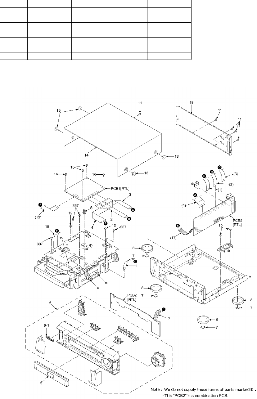
Ref. No. Part No. Part Name & Description Pcs Remarks
SJ313 ERJ3GEY0R00V 1/16W 0 1
X401 H2B800400005 OSCILLATOR 1
X6501 H0J368600005 OSCILLATOR 1
Z501-03 J0JBC0000015 COIL 3
19. Cabinet parts Location
75
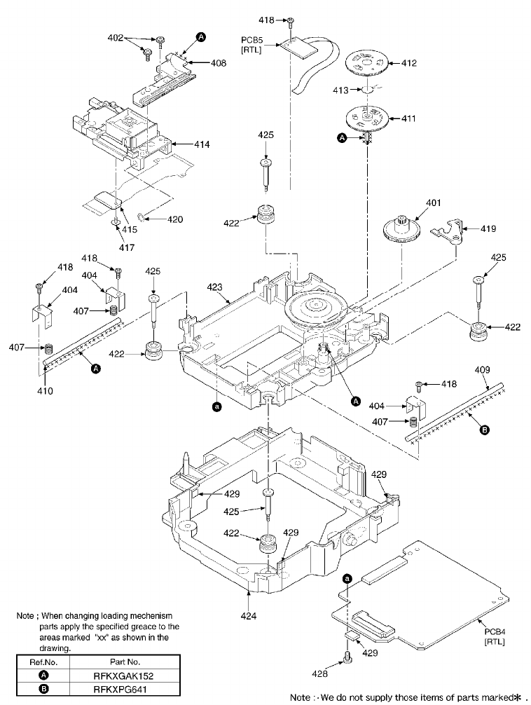
20. Loading Mechanism Parts Location
21. Traverse Mechanism Parts Location
76
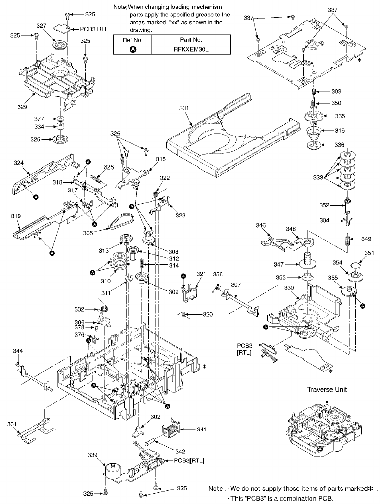
22. Schematic Diagram for printing with A4 size
K0305 YH/HM
77
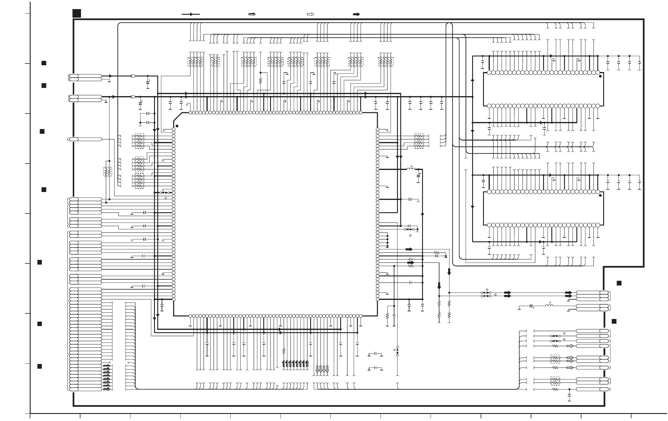
121110987654321
A
B
C
D
E
F
G
H
DVD MODULE(AVDEC) CIRCUIT
SCHEMATIC DIAGRAM
-
4
SL-DV290(EE,GN) DVD MODULE(AVDEC) CIRCUIT DIAGRAM
IC3001
MN6775511
AV DECODER
RA3004
82
AV1IRQCD1
NRSTFS18
AV2IRQCD2
RA3001
1K
LB3001
J0JHC0000045
RA3012
82
WAITSC27 NWEHCD3 NWELSC29
NRDSC28 NAVCSCD4 SYSCLKCD5
CPUADR1SC10 CPUADR2SC11
CPUADR3SC12 CPUADR4SC13 CPUADR5SC14 CPUADR6SC15
CPUADR7SC16 CPUADR8SC17 CPUADR9SC18 CPUADR10SC19
CPUADR11SC20 CPUADR12SC21 CPUADR13SC22
CPUADR14SC23 CPUADR15SC24 CPUADR16SC25 CPUADR17SC26 CPUDT0SC1 CPUDT1SC2 CPUDT2SC3 CPUDT3SC4 CPUDT4SC5
C3006 0.1
C3004 0.1
C3008 0.1
C3009 0.1
CPUDT5SC6 CPUDT6SC7 CPUDT7SC8
RA3051
100
F9
F8
F7
F6
F5
F4
F3
CPUDT8CD6 CPUDT9CD7 CPUDT10CD8 CPUDT11CD9 CPUDT12CD10 CPUDT13CD11 CPUDT14CD12 CPUDT15CD13 STVALIDSD10 STCLKSD11 STENABLESD1 STD7SD9 STD6SD8 STD5SD7 STD4SD6 STD3SD5 STD2SD4 STD1SD3 STD0SD2
D+3.3VDB1 D.GNDDG1
C3001
6.3V330
C3002
6.3V330
LB3002
J0JHC0000045
D+1.5VDB2
MDQ22
RA3008
82
RA3009 82
RA3006
82
RA3007
82
RA3005
82
C3035
0.1
AOUT1 AD4
AOUT0 AD5
SRCK AD7
LRCK AD8
AUDIO DIGITAL AD9
DMIXOUT AD6
F9
F8
F7
F6
F5
F4
MA3
A+5V AB1
CLK27M AD2
F2
B
C3010
0.1
EXTCLK1 AD1
CLK54M AD10
F10
F2
F10
F1
F3
R3051 100
C3011 0.1
C3012 0.1
R3052 100
RA3053
100
R3009 100
AOUT2 AD3
C3051
22P
F1
D.GNDDG1
VDD
28
VSS VDD
29
A4
30
A5
31
A6
32
A7
33
A8
34
A9
35
A11
36
NC
37
CKE
38
CLK
39
UDQM
40
NC
41
VSS
42
DQ8
43
VDDQ
44
DQ9
45
DQ10
46
VSSQ
47
DQ11
48
DQ12
49
VDDQ
50
DQ13
51
DQ14
52
VSSQ
53
DQ15
54
VSS
A3
A2
A1
A0
A10/AP
BA1
BA0
/CS
/RAS
/CAS
/WE
LDQM
VDD
DQ7
VSSQ
DQ6
DQ5
VDDQ
DQ4
DQ3
VSSQ
DQ2
DQ1
VDDQ
DQ0
127 26 25 24 23 22 21 20 19 18 17 16 15 14 13 12 11 10 98765432
RA3003
82
RA3002
82
RA3013
22
RA3011 82
MDQ23
MDQ21
MDQ20
MDQ19
MDQ18
MDQ17
MDQ16
MDQ24
MDQ25
MDQ26
MDQ27
MDQ28
MDQ29
MDQ30
MDQ31
MDQ22
MDQ25
MDQ23
MDQ24
MDQ26
MDQ21
MDQ27
MDQ20
MDQ28
MDQ19
MDQ29
MDQ18
MDQ30
MDQ17
MDQ31
MDQ16
MA2
MA1
MA0
MA10
MA4
MA5
MA6
MA7
MA8
MA9
MA11
RA3010
82
MA0
MA1
MA2
MA3
MA4
MA5
MA6
MA7
MA8
MA9
MA11
MA10
R3001 22
CLK
CLK
DQM3
DQM2
XWE
XCAS
XRAS
XCSM
BA0
BA1
BA1
DQM3
DQM2
XWE
XCAS
XRAS
XCSM
BA0
VDD
28
VSS VDD
29
A4
30
A5
31
A6
32
A7
33
A8
34
A9
35
A11
36
NC
37
CKE
38
CLK
39
UDQM
40
NC
41
VSS
42
DQ8
43
VDDQ
44
DQ9
45
DQ10
46
VSSQ
47
DQ11
48
DQ12
49
VDDQ
50
DQ13
51
DQ14
52
VSSQ
53
DQ15
54
VSS
A3
A2
A1
A0
A10/AP
BA1
BA0
/CS
/RAS
/CAS
/WE
LDQM
VDD
DQ7
VSSQ
DQ6
DQ5
VDDQ
DQ4
DQ3
VSSQ
DQ2
DQ1
VDDQ
DQ0
127 26 25 24 23 22 21 20 19 18 17 16 15 14 13 12 11 10 98765432
MA4
MA5
MA6
MA7
MA8
MA9
MA11
MA3
MA2
MA1
MA0
MA10
XWE
XCAS
XRAS
XCSM
BA0
BA1
CLK
DQM0
MDQ7
MDQ6
MDQ5
MDQ4
MDQ3
MDQ2
MDQ1
MDQ0
DQM0
DQM1
MDQ8
MDQ9
MDQ10
MDQ11
MDQ12
MDQ13
MDQ14
MDQ15
C3031 0.1
C3036
0.1
C3025
0.1
C3033
0.1
C3024
0.1
C3026
0.1
C3034 0.1
C3007 0.1
C3003
0.1
C3030 0.1
C3032
0.1
C3027
0.1
C3028
0.1
K3003
0
C3068
0.1
C3070
0.1
C3072
0.1
C3073
0.1
C3074
0.1
C3071
0.1
C3069
0.1
C3067
0.1
C3066
0.1
C3064
0.1
C3062
0.1
C3061
0.1
C3063
0.1
C3065
0.1
MDQ5
MDQ10
MDQ4
MDQ11
MDQ3
MDQ12
MDQ2
MDQ13
MDQ1
MDQ14
MDQ0
MDQ15
DQM1
MDQ7
MDQ8
MDQ6
MDQ9
YVD4
CVD5
C3110
6.3V100
R3006 15K
C3022 0.1
C3021 1
L3001
10 H
C3019 1
C3018
0.1
R3007 2K
C3038
0.1
R3008
1.3K
C3023 0.1
C3017 0.1
C3015 0.1
C3016 0.1
C3014 0.1
R3010 100
L3091
10 H
C3037
6.3V330
A.GND AG1
CPUDT0
CPUDT1
CPUDT2
CPUDT3
CPUDT4
CPUDT5
CPUDT6
CPUDT7
CPUDT8
CPUDT9
CPUDT10
CPUDT11
CPUDT12
CPUDT13
CPUDT14
CPUDT15
STVALID
STCLK
STENABLE
STD7
STD6
STD5
STD4
STD3
STD2
STD1
STD0
CPUDT0
CPUDT1
CPUDT2
CPUDT3
CPUDT4
CPUDT5
CPUDT6
CPUDT7
CPUDT8
CPUDT9
CPUDT10
CPUDT11
CPUDT12
CPUDT13
CPUDT14
CPUDT15
STVALID
STCLK
STD7
STD6
STD5
STD4
STD3
STD2
STD1
STD0
STENABLE
Vss
157
12
HMD
22
XWR
64
VSS
77
VDD
AVss
113
VREF
115
AVDD
118
Vss
122
TESTSEL1
125
VCLK
128
VDD
131
VDIN5
132
VDIN3
134
Vss
139
VDOUT1
141
MDQ19
161
MDQ29
167
MDQ17
175
MA4
178
Vss
182
MCK
185
MA1
187
53
VSS
PLLAVDD
105
1
VDD
2MDQ9
3MDQ5
4MDQ10
5
LVDD
6MDQ4
7MDQ11
8MDQ3
9Vss
10
MDQ12
11
VDD
13
XRST
14
MDQ2
15
Vss
16
LVDD
17
XHINT
18
XHINT2
19
XDK
20
Vss
21
XWRH
23
XRD
24
XCS
25
VDD
26
HCLK
27
HA1
28
HA2
29
HA3
30
HA4
31
Vss
32
HA5
33
HA6
34
HA7
35
HA8
36
HA9
37
LVDD
38
HA10
39
HA11
40
HA12
41
HA13
42
HA14
43
Vss
44
HA15
45
HA16
46
HA17
47
HD0
48
VDD
49
HD1
50
HD2
51
HD3
52
HD4
54
HD5
55
HD6
56
HD7
57
LVDD
58
HD8
59
HD9
60
HD10
61
VDD
62
HD11
63
HD12
65
HD13
66
HD14
67
HD15
68
VDD
69
DSTR
70
MDQ1
71
MDQ13
72
VSS
73
STD7
74
STD6
75
STD5
76
STD4
78
STD3
79
STD2
80
STD1
81
STD0
82
VDD
83
IECOUT
84
MDQ14
85
VDD
86
DVALID
87
MDQ0
88
MDQ15
89
VSS
90
STRQ
91
ADOUT0
92
ADOUT1
93
ADOUT2
94
ADOUT3
95
Vss
96
SRCK
97
LRCK
98
LVDD
99
PHCOMPO
100
EXTCK
101
CLK121
102
PCLK
103
VDD
104
VSS
TCPOUT
106
PLLVss
107
DAC3OUT
108
DAC1OUT
109
COMP2
110
IREF2
111
AVDD
112
DAC2OUT
114
DAC4OUT
116
COMP1
117
IREF1
119
DAC5OUT
120
AVss
121
DCTEST
123
TESTSEL2
124
TESTSEL0
126
LVDD
127
VDIN7
129
VDIN6
130
VDIN4
133
LVDD
135
VDIN2
136
VDIN1/XVSYNCO
137
VDIN0/XHSYNCO
138
VDOUT0
140
VDOUT2
142
VDOUT3
143
VDD
144
VDOUT4
145
VDOUT5
146
VDOUT6
147
Vss
148
VDOUT7
149
MDQ24
150
MDQ23
151
VDD
152
MDQ25
153
MDQ22
154
MDQ26
155
Vss
156
MDQ16
158
MDQ27
159
VDD
160
MDQ20
162
Vss
163
MDQ31
164
MDQ28
165
VDD
166
MDQ30
168
Vss
169
MDQ18
170
DQM3
171
VDD
172
DQM2
173
LVDD
174
MDQ21
176
MA3
177
VDD
179
MA2
180
MA5
181
MCKI
183
LVDD
184
MA10
186
VDD
188
MA6
189
MA0
190
MA8
191
MA7
192
XWE
193
MA11
194
XCAS
195
XRAS
196
VDD
197
BA0
198
XCSM
199
Vss
200
BA1
201
MA9
202
DQM0
203
DQM1
204
MDQ7
205
MDQ8
206
MDQ6
207
Vss
208
C3013 0.1
C3039
0.1
C3020
0.1
R3106
62
R3107
18
K3106
0
K3101 0
R3101
62
R3102
15 C3029
0.1
K3002
0
C3005
0.1
To DVD MODULE
(CPU) CIRCUIT on
B
To DVD MODULE
(VIDEO DAC)
CIRCUIT on
B
To DVD MODULE
(AUDIO DAC) CIRCUIT on
B
SCHEMATIC
DIAGRAM-6/1-C
K3011 0
K3009 0
K3007
0
SCHEMATIC
DIAGRAM-7/1-H
SCHEMATIC
DIAGRAM-5/1-D
SCHEMATIC
DIAGRAM-5/1-G
To DVD MODULE
(CPU) CIRCUIT on
B
SCHEMATIC
DIAGRAM-7/1-G
SCHEMATIC
DIAGRAM-7/1-E,F
SCHEMATIC
DIAGRAM-7/1-D
To DVD MODULE
(CPU) CIRCUIT on
B
SCHEMATIC
DIAGRAM-7/12-D
To DVD MODULE
(CPU) CIRCUIT on
B
SCHEMATIC
DIAGRAM-7/12-A,B
To DVD MODULE
(SODC) CIRCUIT on
B
SCHEMATIC
DIAGRAM-3/12-H
To DVD MODULE
(VIDEO DAC)
CIRCUIT on
B
SCHEMATIC
DIAGRAM-5/12-D
SCHEMATIC
DIAGRAM-5/1-F
SCHEMATIC
DIAGRAM-6/12-A
SCHEMATIC
DIAGRAM-6/1-F
SCHEMATIC
DIAGRAM-6/1-F
SCHEMATIC
DIAGRAM-6/12-E
SCHEMATIC
DIAGRAM-6/1-H
To DVD MODULE
(VIDEO DAC)
CIRCUIT on
B
IC3061
C3ABPG000121
MEMORY
IC3062
C3ABPG000121
MEMORY
V.GND VG1
:POSITIVE VOLTAGE LINE :AUDIO/VIDEO SIGNAL LINE
2.3V
2.3V
2.3V
3.3V
3V
2.3V
2.5V
2.8V
2.4V
1.5V
2V
2.3V
3.3V
2V
2.7V
2.6V
3.3V
3.3V
3.3V
3.3V
3.3V
3.3V
3.3V
3.3V
2.8V
3.3V
1.5V
1.7V
2.9V
2.9V
2.8V
2.9V
2.7V
2.9V
3.3V
2.7V
2.6V
2.5V
2.6V
2.8V
2.8V
2.5V
1.5V
2.8V
2.6V
2.4V
3.3V
2.7V
3.1V
3.1V
3.1V
3.3V
3.1V
3.1V
3.1V
3.1V
3.1V
3.3V
3.3V
3.3V
3.3V
1.5V
3.3V
3.3V
3.3V
3.3V
3.3V
3.3V
0V
0V
0V
0V
2.2V
0V
0V
0V
0V
0V
0V
3.3V
1.6V
0V
0V
0V
0V
1.7V
1.7V
1.5V
1.5V
1.6V
3.3V
(1.2V)
(1.2V)
(3.1V)
(3.1V)
(3.1V)
3.3V
2.3V
3.3V
1.3V
0.3V
2.2V
3.3V
1.3V
0.9V
0V
1.5V
1.6V
3.3V
1.5V
3.3V
2.7V
2.3V
3.3V
2.3V
2.3V
2.3V
3.3V
2.3V
2.3V
3V
2.8V
2.5V
2V
3.3V
2.4V
2V
2.3V
2.6V
2.7V
1.5V
2.1V
2.1V
3.3V
1.6V
1.6V
0.3V
1.7V
0V
1.6V
0V
3.3V
1.7V
1.5V
1.7V
0V
0V
0V
0V
3.2V
3.3V
1.5V
0V
1.6V
3V
3.2V
3.1V
2.1V
3.3V
2.1V
2.3V
2.7V
2.3V
1.6V
1.7V
1.6V
0V
0V
0V
0V
3.3V
1.7V
2.1V
2.7V
3.3V
2.3V
2.3V
2.3V
2.8V
3.3V
2V
2V
2.6V
3.3V
2.7V
3.3V
2.3V
2.4V
2.5V
3V
3.3V
2.3V
2.3V
2.3V
3.3V
2.1V
3.2V
3.1V
3.2V
3V
1.5V
1.6V
0V
0V
0V
0.3V
1.6V
3.3V
3.3V
2.7V
3.3V
2.3V
2.4V
2.5V
3V
3.3V
2.3V
2.3V
2.3V
3.3V
2.1V
3.2V
3.1V
3.2V
3V
1.5V
1.6V
0V
0V
0V
0.3V
1.6V
3.3V
1.6V
1.7V
1.6V
0V
0V
0V
0V
3.3V
1.7V
2.1V
2.7V
3.3V
2.3V
2.3V
2.3V
2.8V
3.3V
2V
2V
2.6V
(1.6V)
(2V)
(2.3V)
(2.3V)
(2.2V)
(1.8V)
(2.2V)
(1.7V)
(1.9V)
(2.2V)
(2.2V)
(2.2V)
(2.2V)
(2V)
(2.2V)
(2.1V)
(2.8V)
(2V)
(3.1V)
(3.1V)
(3.1V)
(3.1V)
(2.6V)
(3.3V)
(1.6V)
(0.6V)
(2.5V)
(2.5V)
(2.4V)
(2.4V)
(2.3V)
(2.4V)
(2.3V)
(2.4V)
(2.3V)
(2.3V) (1.8V)
:AUDIO SIGNAL LINE :VIDEO SIGNAL LINE
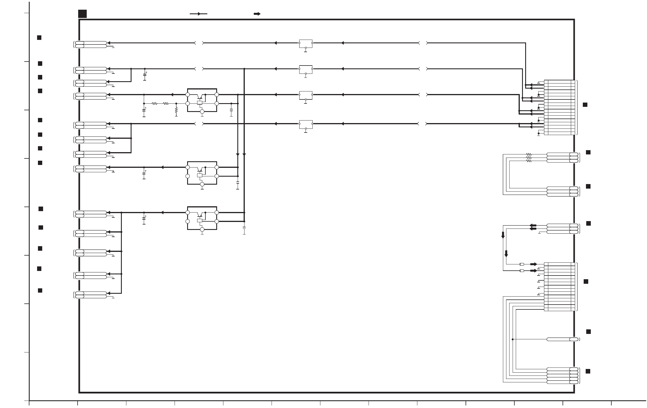
121110987654321
A
B
C
D
E
F
G
H
YVD4
CVD5
SCHEMATIC DIAGRAM-4/12-C
To DVD MODULE
(AVDEC) CIRCUIT on
B
TRV-SW+ VD9
TRV-SW+ VD9
TRAY REF VD6
TRAY/ TRV VD10
MUTE4 VD8
TRAY DRV VD7
To DVD MODULE
(FEP) CIRCUIT on
B
SCHEMATIC DIAGRAM-2/12-H
SCHEMATIC DIAGRAM-3/1-C
To DVD MODULE
(SODC) CIRCUIT on
B
To MAIN CIRCUIT(CN2)
on SCHEMATIC
DIAGRAM
-
8/11,12-H
C
10
D+2.5V 9D.GND 8
D.GND
7
D+5V
6
D+5V
5
M.GND
4
M.GND
3
M+9V
2
M+9V
1
D.GND
FP3202
16
A.GND
15
A+5V
14
A+5V
13
D.GND
12
D.GND
11
D+2.5V
17
A.GND
A+5VAB1 A.GNDAG1
B
DSPCLK CV6
STATUS CV5
CMD CV4
100LB3201 100LB3202
LB3203
100
FL6254
F1H0J1050018
FL6253
F1H0J1050018
D+5VDB3 D.GNDDG1
C6257
6.3V100
FL6255
VLF1491S104T
M+9VMB1 M.GNDMG1
FL6251
F1H0J1050018
D+1.5VDB2
IC6251
C0DBEZG00011
REGULATOR
D.GNDDG1 R6251
100
R6253
1K
R6252
100
C6251
10V10
C6254
0.1
IC6252
C0DBFFG00004
REGULATOR
C6255
0.1
D+1.8VDB4 D.GNDDG1
C6252
10V10
IC6253
C0DBCGE00002
REGULATOR
C6256
0.1
D+3.3VDB1 D.GNDDG1
D+3.3VDB1 D.GNDDG1
D+3.3VDB1 D.GNDDG1
D+3.3VDB1 D.GNDDG1
D+3.3VDB1 D.GNDDG1
C6253
10V10
LB3206
VLP0146-T
A+5VAB1 A.GNDAG1
A+5VAB1 A.GNDAG1
D+5VDB3 D.GNDDG1
OUT IN
ON/OFF
GND 5
2
13
4NC
OUT IN
ON/OFF
GND 5
2
13
4NC
OUT IN
ON/OFF
GND 5
2
13
4VR
DVD MODULE(VIDEO DAC) CIRCUIT
SCHEMATIC DIAGRAM
-
5
SL-DV290(EE,GN) DVD MODULE(VIDEO DAC) CIRCUIT DIAGRAM
SCHEMATIC DIAGRAM-7/1-A
To DVD MODULE
(CPU) CIRCUIT on
B
To DVD MODULE
(FEP) CIRCUIT on
B
To DVD MODULE
(AUDIO DAC) CIRCUIT on
B
SCHEMATIC DIAGRAM-4/1-G
To DVD MODULE
(AVDEC) CIRCUIT on
B
SCHEMATIC DIAGRAM-2/12-G
To DVD MODULE
(FEP) CIRCUIT on
B
SCHEMATIC DIAGRAM-2/12-H
To DVD MODULE
(FEP) CIRCUIT on
B
SCHEMATIC DIAGRAM-2/12-G
SCHEMATIC DIAGRAM-4/12-C
To DVD MODULE
(AVDEC) CIRCUIT on
B
To DVD MODULE
(SODC) CIRCUIT on
B
SCHEMATIC DIAGRAM-3/12-E
SCHEMATIC DIAGRAM-3/1-H
To DVD MODULE
(SODC) CIRCUIT on
B
To DVD MODULE
(FEP) CIRCUIT on
B
SCHEMATIC DIAGRAM-2/12-G
SCHEMATIC DIAGRAM-3/1-H
To DVD MODULE
(SODC) CIRCUIT on
B
SCHEMATIC DIAGRAM-4/1-G
To DVD MODULE
(AVDEC) CIRCUIT on
B
SCHEMATIC DIAGRAM-6/1-F
SCHEMATIC DIAGRAM-7/12-H
To DVD MODULE
(CPU) CIRCUIT on
B
9
8
7
CB/ PB/ B
6
5
YC-OUT/CR/PR/R
4
3
C-OUT
2
V.GND
1
Y-OUT 15
TRAY/ TRV
14
TRV-SW+
13
TRAY MUT
12
TRAY DRV
11
TRAY REF
10
V.GND
V.GND
V.GND
Y/ PY/ G
D.GND
To MAIN CIRCUIT
(CN501) on
SCHEMATIC DIAGRAM-9/15,16-H
C
FP3203
DSPCLK CV6
STATUS CV5
CMD CV4
SCHEMATIC DIAGRAM-7/1-C
To DVD MODULE
(CPU) CIRCUIT on
B
To DVD MODULE
(AUDIO DAC) CIRCUIT on
B
SCHEMATIC DIAGRAM-6/12-E
LB3205
VLP0146-T
V.GND VG1
10
9
8
7
6
5
4
3
2
1
16
15
14
13
12
11
17
9
8
7
6
5
4
3
2
1
15
14
13
12
11
10
9V9V
5V
2.5V
2.5V
1.5V
1.3V
2.5V
2.5V
1.8V
5V
5V
3.3V
5V
2.5V
5V5V
:POSITIVE VOLTAGE LINE :VIDEO SIGNAL LINE
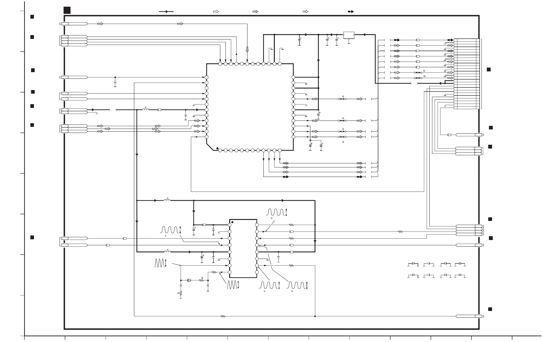
121110987654321
A
B
C
D
E
F
G
H
DMIXOUTAD6
D+3.3VDB1
C4216
6.3V100
C4219
10V10
C4220
10V10
C4215
0.1
C4210
0.1
37 RSTB
38 SCLKI
39 SCLKO
40 BCKIN
41 LRCIN
42 TEST
43 VDD
44 D.GND
45 DIN1
46 DIN2
47 DIN3
48 ZFLGA
1
ZFLG1
2
ZFLG2
3
ZFLG3
4
ZFLG4
5
ZFLG5
6
ZFLG6
7
N.C.
8
N.C.
9
VOUT6
10
VOUT5
11
VOUT4
12
VOUT3
13
VOUT2
14
VOUT1
15
VCOM
16
VOUT7
17
A.GND
18
VCC
19
A.GND
20
VOUT8
21
A.GND
22
VCC
23
A.GND
24
VCC
25
A.GND
26
VCC
27
A.GND
28
VCC
29
N.C.
30
ZERO7
31
DATA4
32
ZERO8
33
MDO
34
MDI
35
MC
36
ML
LB4200
VLP0146-T
L4211
22 H
C4217
0.1
SBI1AC1 SBO1AC2 SBT1AC3 STBDAC2AC4
NRSTFS18
SRCKAD7
LRCKAD8
AOUT0AD5 AOUT1AD4 AOUT2AD3
LB4207
LB4208
LB4210
LB4211
LB4212
LB4215
FL4201
F1H0J1050018
C4222
6.3V330
C4223
6.3V330
IC4211
C0FBBK000036
8ch AUDIO D/A CONVERTER
C6566
0.1
C6564
0.1
C6563
4V47
L6562
22 H
LB6561
VLP0146-T
LB6563
VLP0155-T
C6561
4V47
IC6561
C1DB00000582
CLOCK GENERATOR
L6561
22 H
C6568
0.1
LB6567
LB6566
R6563
10K
R6565 47
LB6564
47
X6501
(36.864MHz)
C6505
15P
C6503
12P
R6503
330
CLK27MAD2
D.GNDDG1
R6566
10
CLK33M AC8
CLKSEL AC5
CLK16M1 SA1
B
AC3H AC6
AMUT AC7
EXTCLK1 AD1
C4211
10V10
1VDD1
2VSS1
3CLK54
4CLK27
5VDD2
6VSS2
7XTI
8XTO
16
CE
15
CLK33
14
FSEL
13
CLK16
12
VDD3
11
VSS3
10
768fs
9
384fs
C4208
0.1
C4209
0.1
LB6562
VLP0155-T
CLK54MAD10
C4234
0.1
C4207
0.1 C4235
0.1
C4236
0.1 C4237
0.1
0
VLP0155-T
K4202
0
K4203
0
K4204
0
K4205
0
VLP0155-T
RLBV601AV-Y
VLP0146-T
LB6565
DSPCLK CV6
STATUS CV5
CMD CV4
DVD MODULE(AUDIO DAC) CIRCUIT
SCHEMATIC DIAGRAM
-
6
SL-DV290(EE,GN) DVD MODULE(AUDIO DAC) CIRCUIT DIAGRAM
To DVD MODULE
(CPU) CIRCUIT on
B
To DVD MODULE
(VIDEO DAC)
CIRCUIT on
B
SCHEMATIC DIAGRAM-5/1-C
To DVD MODULE
(SODC) CIRCUIT on
B
SCHEMATIC DIAGRAM-7/12-G
SCHEMATIC DIAGRAM-4/12-A
To DVD MODULE
(AVDEC) CIRCUIT on
B
To DVD MODULE
(CPU) CIRCUIT on
B
SCHEMATIC DIAGRAM-7/1-H
SCHEMATIC DIAGRAM-4/12-A
To DVD MODULE
(AVDEC) CIRCUIT on
B
SCHEMATIC DIAGRAM-4/12-A
To DVD MODULE
(AVDEC) CIRCUIT on
B
To DVD MODULE
(VIDEO DAC) CIRCUIT on
B
SCHEMATIC DIAGRAM-5/12-E
SCHEMATIC DIAGRAM-4/12-B
To DVD MODULE
(AVDEC) CIRCUIT on
B
K4207
47
To DVD MODULE
(CPU) CIRCUIT on
B
SCHEMATIC DIAGRAM-7/12-G
SCHEMATIC DIAGRAM-7/1-E
SCHEMATIC DIAGRAM-7/1-D
SCHEMATIC DIAGRAM-7/1-E
SCHEMATIC DIAGRAM-3/1-A
To DVD MODULE
(AVDEC) CIRCUIT on
B
SCHEMATIC DIAGRAM-4/12-B
17
ADAC5V
18
AC3H/DACMUT
19
AMUT
20
ZFLAG
21
22
23
24
CMD
STAT
CLK
11
FL
12
13
MIX R 14
15
16
10
9
FR
8
7
6
5
SR
4
3
CNT
2
A.GND
1
SW
A.GND
A.GND
SL
A.GND
A.GND
A.GND
A.GND
MIX L
ADAC5V
D.GND
FP4202
25
26
AUDIO DIGITAL
D.GND
To MAIN CIRCUIT
(CN301)
on SCHEMATIC
DIAGRAM
-
8/9,10-H
C
R6505
0
R6504
0
LB4209
LB4201
VLP0155-T AUDIO DIGITAL AD9
To DVD MODULE
(AVDEC) CIRCUIT on
B
SCHEMATIC DIAGRAM-4/12-A
LB4214 0
VLP0155-T
VLP0155-T
VLP0155-T
VLP0155-T
VLP0155-T
A
B
C
D
E
F
G
H
A
B
D
C
E
F
H
G
17
18
19
20
21
22
23
24
11
12
13
14
15
16
10
9
8
7
6
5
4
3
2
1
25
26
5V
1.4V
1.5V
3.3V
1.5V
3.3V
1.7V
3.3V
1.5V
3.3V
1.6V
3.3V
3.3V
1.7V
1.7V
3.3V
(1.2V) 0V
0V
0V
(3.2V) 0V
2.5V
2.5V
2.5V
2.5V
2.5V
2.5V
2.5V
2.5V
5V
2.5V
5V
5V
5V
5V
0V(1.2V)
3.3V
3.3V
2.8V
3.3V
1.0V
P-P
F=36.864MHz
1.0V
P-P
F=36.864MHz
3.2V
P-P
0.2 s. 1V/DIV.
3.0V
P-P
0.2 s. 1V/DIV.
3.1V
P-P
0.2 s. 1V/DIV.
3.4V
P-P
0.2 s. 1V/DIV.
3.3V
1.5V
1.6V
:POSITIVE VOLTAGE LINE :AUDIO SIGNAL LINE :SURROUND SP. SIGNAL LINE :CENTER SP. SIGNAL LINE :SUB WOOFER SIGNAL LINE
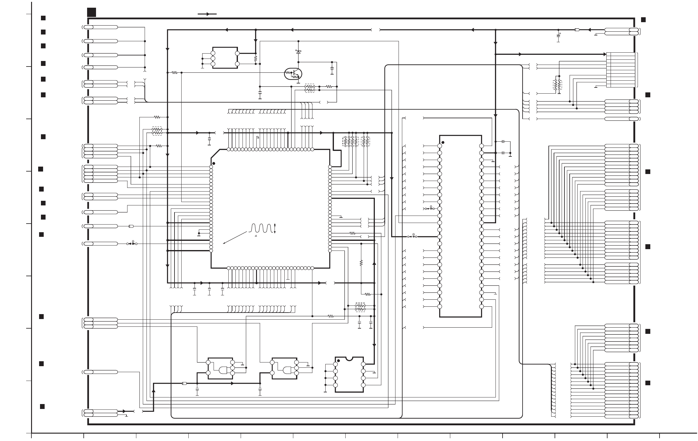
121110987654321
A
B
C
D
E
F
G
H
CPUDT15 CD13
CPUDT14 CD12
CPUDT13 CD11
CPUDT12 CD10
CPUDT11 CD9
CPUDT10 CD8
CPUDT9 CD7
CPUDT8 CD6
CPUDT7 SC8
CPUDT6 SC7
CPUDT5 SC6
CPUDT4 SC5
CPUDT3 SC4
CPUDT2 SC3
CPUDT1 SC2
CPUDT0 SC1
CPUDT7 SC8
CPUDT6 SC7
CPUDT5 SC6
CPUDT4 SC5
CPUDT3 SC4
CPUDT2 SC3
CPUDT1 SC2
CPUDT0 SC1
CPUADR17 SC26
CPUADR16 SC25
CPUADR15 SC24
CPUADR14 SC23
CPUADR13 SC22
CPUADR12 SC21
CPUADR11 SC20
CPUADR10 SC19
CPUADR9 SC18
CPUADR8 SC17
CPUADR7 SC16
CPUADR6 SC15
CPUADR5 SC14
CPUADR4 SC13
CPUADR3 SC12
CPUADR2 SC11
CPUADR1 SC10
CPUADR17 SC26
CPUADR16 SC25
CPUADR15 SC24
CPUADR14 SC23
CPUADR13 SC22
CPUADR12 SC21
CPUADR11 SC20
CPUADR10 SC19
CPUADR9 SC18
CPUADR8 SC17
CPUADR7 SC16
CPUADR6 SC15
CPUADR5 SC14
CPUADR4 SC13
CPUADR3 SC12
CPUADR2 SC11
CPUADR1 SC10
CPUADR0 SC9
STBDAC2 AC4
SBT1 AC3
SBO1 AC2
SBI1 AC1
D.GND DG1
D+3.3V DB1
CPUADR0
CPUADR1
CPUADR2
CPUADR3
CPUADR4
CPUADR5
CPUADR6
CPUADR7
CPUADR8
CPUADR9
CPUADR10
CPUADR11
CPUADR12
CPUADR13
CPUADR14
CPUADR15
CPUADR16
CPUADR17
CPUDT0
CPUDT1
CPUDT2
CPUDT3
CPUDT4
CPUDT5
CPUDT6
CPUDT7
CPUDT8
CPUDT9
CPUDT10
CPUDT11
CPUDT12
CPUDT13
CPUDT14
CPUDT15
I7
I6
I5
I4
I3
I2
I1
LB6201
VLP0146-T
CPUDT0
CPUDT1
CPUDT2
CPUDT3
CPUDT4
CPUDT5
CPUDT6
CPUDT7
CPUDT8
CPUDT9
CPUDT10
CPUDT11
CPUDT12
CPUDT13
CPUDT14
CPUDT15
G3
G4
G5
G6
I4
I3
I5
I1
I2
I7
CPUADR4
CPUADR5
CPUADR6
CPUADR7
CPUADR8
CPUADR9
CPUADR10
CPUADR11
CPUADR12
CPUADR13
CPUADR14
CPUADR15
CPUADR16
CPUADR17
CPUADR18
CPUADR19
CPUADR20
CPUADR21
RA6202
10K
CPUADR3
CPUADR2
CPUADR1
CPUADR0
RA6205
10K
RA6204
10K
IC6301
C3FBND000098
32M FLASH MEMORY
CPUDT15
CPUDT7
CPUDT14
CPUDT6
CPUDT13
CPUDT5
CPUDT12
CPUDT4
CPUDT11
CPUDT3
CPUDT10
CPUDT2
CPUDT9
CPUDT1
CPUDT8
CPUDT0
CPUADR16
CPUADR17
CPUADR15
CPUADR14
CPUADR13
CPUADR12
CPUADR11
CPUADR10
CPUADR9
CPUADR20
CPUADR19
CPUADR18
CPUADR8
CPUADR7
CPUADR6
CPUADR5
CPUADR4
CPUADR3
CPUADR2
CPUADR1
IC6211
PST596JNR
RESET
Q6215
UN5212TX
RESET
RA6206
47K
G1
C6215
0.1
R6216
1K
D6215
MA728TX
GND3
SUB
2
M/R1
4VOUT
5VCC
C6211
100P
NRSTFS18
AV2IRQCD2 G3
AV1IRQCD1 G4
ODCIRQSC32 G5
ADSCIRQSC31 G6
AMUTAC7 CLKSELAC5
HFMONFC1
NAVCSCD4 NWEHCD3 NWELSC29 NRDSC28 WAITSC27
NSODCCSSC30 NWELSC29 NRDSC28 WAITSC27
R6201
47K
RA6201
10K
R6202
10K
C6206
0.1
SYSCLKCD5
LB6202
VLP0155-T
CLK33MAC8
IC6201
MN102H60GFD
CPU
1WAIT
2NRE
3NWEL/P62
4NWEH/P63
5NCS0/P50
6NCS1/P51
7NCS2/P52
8NCS3/P53
9P54/NBREQ
10
P55/NBRACK
11
P56
12
NWORD
13
A0
14
A1
15
A2
16
A3
17
VDD
18
BOSC/PB0
19
VSS
20
XI/PB1
21
XO
22
VDD
23
OSCI
24
OSCO
25
MODE
26
A4
27
A5
28
A6
29
A7
30
A8
31
A9
32
A10
33
A11
34
AVDD
35
A12
36
A13
37
A14
38
A15
39
A16
40
A17
41
A18
42
A19/P43
43
VREF-
44
A20/P44/AN4
45
A21/P45/AN5
46
A22/P46/AN6
47
A23/P47/AN7
48
P80/DAC0
49
P81/DAC1
50
P82/SBT3
P83/SBI3
51
P84/SBO3
52
P85/SBT4
53
VREF+
54
P86/SBI4
55
P87/SBO4
56
P90
57
P91
58
P92
59
P93
60
AVSS
61
P94/AN0
62
P95/AN1
63
P96/AN2
64
P97/AN3
65
VDD
66
P70/SBT0/RAS
67
P71/SBI0/LCAS
68
P72/SBO0/UCAS
69
P73/SBT1
70
P74/SBI1
71
P75/SBO1
72
PULLUP0
73
PULLUP1
74
NNMI
75
NIRQ0/PA0
76
NIRQ1/PA1
77
NIRQ2/PA2
78
NIRQ3/PA3
79
NIRQ4/PA4
80
ADSEP
81
NRST
82
VDD
83
D0
84
D1
85
D2
86
D3
87
D4
88
D5
89
D6
90
D7
91
VSS
92
D8
93
D9
94
D10
95
D11
96
D12
97
D13
98
D14
99
D15
100
8VCC
A01
A1
2
A2
3
GND
4
7WP
6SCL
5SDA
C6221
0.1
IC6221
C3EBGC000033
EE PROM
LB6221
VLP0146-T
C6222
0.1
IC6222
C0JBAA000001
AND GATE
C6223
0.1
IC6223
C0JBAA000001
AND GATE
D+5VDB3
STATUSCV5 CMDCV4
DSPCLKCV6
DCFLTFC3
C6202
0.1
C6203
0.1
C6205
0.1
1A15 48
A16
2A14
3A13
4A12
5A11
6A10
7A9
8A8
9A19
10 A20
11 XWE
12 XRESET
13 N.C.
14 WP/Acc
15 RDY/XBSY
16 A18
17 A17
18 A7
19 A6
20 A5
21 A4
22 A3
23 A2
24 A1
47
XBYTE
46
VSS
45
DQ15/A-1
44
DQ7
43
DQ14
42
DQ6
41
DQ13
40
DQ5
39
DQ12
38
DQ4
37
VDD
36
DQ11
35
DQ3
34
DQ10
33
DQ2
32
DQ9
31
DQ1
30
DQ8
29
DQ0
28
XOE
27
VSS
26
XCE
25
A0
C6301
0.1
RA6203
4.7K C6201
6.3V33
B
R6211
4.7K
D.GNDDG1
R6206
10K
R6207
4.7K
R6208
4.7K
NRSTFS18
NRSTFS18
G1
K6303
0
CPUADR21
K6301
0
C6302
0.1
I8
I6
NRSTFS18 R6215
10K
C6204
0.1
R6210
100
10 D+3.3V
9RESERVED
8KMODE
7SCSIEN
6258SY
51968SY
4SBI1
3SBO1
2SBT1
1D.GND
PS6201
DVD MODULE(CPU) CIRCUIT
SCHEMATIC DIAGRAM
-
7
SL-DV290(EE,GN) DVD MODULE(CPU) CIRCUIT DIAGRAM
To DVD MODULE
(SODC) CIRCUIT on
B
SCHEMATIC DIAGRAM-4/1-E
To DVD MODULE
(AVDEC) CIRCUIT on
B
To DVD MODULE
(VIDEO DAC)
CIRCUIT on
B
SCHEMATIC DIAGRAM-5/12-F
SCHEMATIC
DIAGRAM-3/1-D,E
To DVD MODULE
(AVDEC) CIRCUIT on
B
SCHEMATIC
DIAGRAM-4/1-B,C
To DVD MODULE
(AUDIO DAC) CIRCUIT on
B
SCHEMATIC DIAGRAM-6/12-C
To DVD MODULE
(FEP) CIRCUIT on
B
SCHEMATIC DIAGRAM-2/12-B
To DVD MODULE
(VIDEO DAC)
CIRCUIT on
B
SCHEMATIC DIAGRAM-5/1-G
To DVD MODULE
(AUDIO DAC) CIRCUIT on
B
SCHEMATIC DIAGRAM-6/12-C
SCHEMATIC DIAGRAM-4/1-D,E
To DVD MODULE
(AVDEC) CIRCUIT on
B
To DVD MODULE
(FEP) CIRCUIT on
B
SCHEMATIC DIAGRAM-2/1-B
SCHEMATIC DIAGRAM-3/1-G
To DVD MODULE
(SODC) CIRCUIT on
B
SCHEMATIC DIAGRAM-3/1-E
SCHEMATIC DIAGRAM-3/1-G
To DVD MODULE
(SODC) CIRCUIT on
B
SCHEMATIC DIAGRAM-3/1-D
To DVD MODULE
(SODC) CIRCUIT on
B
SCHEMATIC DIAGRAM-4/1-F
To DVD MODULE
(AVDEC) CIRCUIT on
B
SCHEMATIC
DIAGRAM-6/1-H
To DVD MODULE
(AUDIO DAC) CIRCUIT on
B
SCHEMATIC DIAGRAM-6/1-G
To DVD MODULE
(FEP) CIRCUIT on
B
SCHEMATIC DIAGRAM-2/1-D
SCHEMATIC DIAGRAM-4/1-D
To DVD MODULE
(AVDEC) CIRCUIT on
B
K6201
0
To DVD MODULE
(AVDEC) CIRCUIT on
B
SCHEMATIC
DIAGRAM-4/1-C,D
To DVD MODULE
(SODC) CIRCUIT on
B
SCHEMATIC
DIAGRAM-3/1-E,F
To DVD MODULE
(AUDIO DAC)
CIRCUIT on
B
SCHEMATIC
DIAGRAM-6/12-C
AC3H AC6
I8
TEST TERMINAL
To DVD MODULE
(VIDEO DAC)
CIRCUIT on
B
SCHEMATIC
DIAGRAM-5/1-C
2
1
4
5
3
Vcc
GND
2
1
4
5
3
Vcc
GND
5V
3V
3V
5V
4.5V
2.7V
2.7V
5V
4.1V 3.3V
3.3V
3.3V
3.3V
3.3V
3.3V
3.3V
3.3V
3.3V
0V
3.3V
2.8V
3.3V
3.3V
3.3V
3.3V
2.8V
3.3V
3.3V
0V
3.3V
2.3V
2.9V
2.9V
2.8V
3.3V
1.7V
3.3V
1.7V
3.3V
(2V)
(2.8V)
(2V)
(1.2V)
(2.1V)
(2.2V)
(2V)
2.9V
2.7V
2.9V
2.7V
2.6V
2.5V
2.6V
2.8V
3.3V
2.8V
2.5V
2.8V
2.6V
2.4V
2.7V
2.6V
2.3V
2.5V
2.3V
3V
(1.6V)
(1.8V)
(1.6V)
(2V)
(3.3V)
(1.8V)
(2.2V)
(2.3V)
(2.2V)
(1.7V)
(1.9V)
(2.2V)
(2.2V)
(2.2V)
(1V)
(1V)
0V
2.7V
3.3V
3.3V
3.3V
3.3V
0V
0V
3.3V
3.3V
3.3V
2.8V
3.3V
3.3V
3.3V
3.3V
3.3V
3.3V
3.3V
3.3V
3.3V
3.3V
3.3V
3.3V
3.1V
3.1V
3.1V
3.1V
3.1V
3.1V
3.1V
3.1V
3.3V
3.3V
3.3V
3.3V
3.3V
3.3V
3.3V
3.3V
(2.3V)
(2.3V)
(2.4V)
(2.3V)
(2.4V)
(2.3V)
(2.4V)
(2.4V)
(2.5V)
(2.5V)
(2V)
2.6V
(1.6V)
2.4V
(3.3V)
2.8V
(1.8V)
2.5V
(2.2V)
2.8V
(2.3V)
2.8V
(2.2V)
2.6V
(1.7V)
2.5V
(1.3V)
2.5V
3.3V
(1V)
2.3V
(1.6V)
2.6V
(1.9V)
2.6V
(2.2V)
2.7V
(2.2V)
2.9V
(2.2V)
2.7V
(2.2V)
2.9V
(2V)
2.8V
(2.2V)
2.9V
3.3V
3.3V
(1.8V)
2.7V
3.3V
3.1V
3.3V
3.1V
(2V)
2.8V
(2V)
2.8V
(2.1V)
2.9V
3.3V
1.5V
P-P
0.2 s. 0.5V/DIV.
3.3V
(1.3V)
(2.2V)
(0V) (1V)
2.3V
3.3V
3.1V
3.3V
3.1V
3.3V
3.1V
3.3V
3.3V
3.1V
3.3V
3.1V
3.3V
3.1V
(0V)
(2.5V)
(2.3V)
(2.4V)
(2.3V)
(2.4V)
(2.3V)
(2.5V)
(2.4V)
(2.3V)
(2.4V)
:POSITIVE VOLTAGE LINE
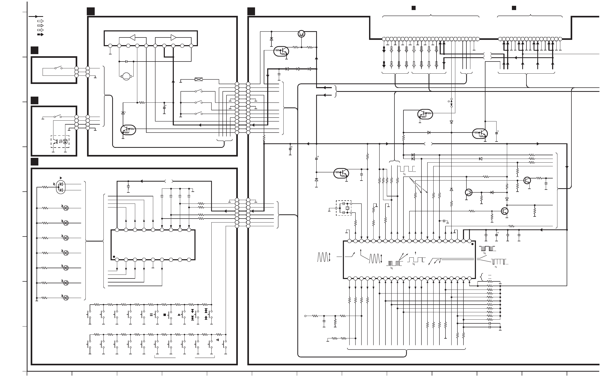
121110987654321
A
B
C
D
E
F
G
H
SL-DV290(EE,GN) LOADING MOTOR,CLAMP SW,BOTTOM SW,OPERATION,MAIN CIRCUIT DIAGRAM
Q307
DTC114EUA106
MUTING CONT.
Q304
2SB621ARSTA
PLUNGER DRIVE
Q305
UN521NTX
PLUNGER DRIVE
Q402
Q403
Q404
C406
6.3V100
To MODULE CIRCUIT (FP3202)
on SCHEMATIC DIAGRAM
-
5/12-F,G
Q401
UN5214TX
RESET
C408 470P
C409 470P
R452 820
R451 10K
C401
6.3V47
R448 220
R447 220
R455 4.7K
R454 4.7K
SJ313
0
BB
C404
1000P
17 112131415161718
19
26 3 2456789101124 23 22 21 20 125
C308
50V1
D307
MA111TX
M9V CTL
M+9V
M+9V
M.GND
M.GND
D+5V
D+5V
D.GND
D.GND
D+2.5V
D+2.5V
D.GND
D.GND
A+5V
A+5V
A.GND
A.GND
OPN
SW
A.GND
CNT
A.GND
SR
A.GND
SL
A.GND
FR
A.GND
FL
A.GND
MIXL
A.GNDA.GND
MIXR
ADAC5V
ADAC5V
AC3H/ DACMUT
To MODULE CIRCUIT (FP4202)
on SCHEMATIC DIAGRAM
-
6/12-D,E
A MUTE
Z FLAG
WIDE1
CMD
STAT
CLK
D.GND
AUDIO DIGITAL
R405
470
R406
4.7K
R402
100K
S620
(/)
4
3
2
1
4
3
2
1
ECa
CA
D1
GP1S94
(POSITION
SENSOR)
3
2
1
3
2
1
IC1
TA7291P
MOTOR DRIVE
12345678910
M
RM1
(LOADING
MOTOR)
Q1
RVTDTC143EST
MOTOR DRIVE
IC601
NJU3713GTE1
LED DRIVE
(DIRECT OPEN)
R611
220
DBA C
D304D303D302
LOADING MOTOR CIRCUIT
OPERATION CIRCUIT
R631
1K
R630
1.2K
R629
1.5K
R628
1.8K
R627
2.2K
R626
3.3K
R625
4.7K
R624
6.8K
R623
12K
8
2
1
3
4
5
6
7
8
2
1
3
4
5
6
7
2
1
3
4
5
6
7
8
9
10
11
12
13
14
2
14
3
4
5
6
7
8
9
10
11
12
13
1
E
F
G
D
C305
0.01
R1
1K
MAIN CIRCUIT
C
R603
100
R610
220
D605
(DISC3)
D606
(DISC2)
R609
220
D604
(DISC4)
R607
220
R608
220
D603
(DISC5)
D602
SELS5923C
(DOUBLE RE-MASTER)
R606
270
A
B
C
D
E
F
G
H
I
D601
SELS5923C
(CINEMA)
R605
270
D608
SML79455C
()
R612
180
D607
(DISC1)
S621
(/ )
S619
()
S618
()
S617
()
S615
(CINEMA)
S616
(DOUBLE
RE-MASTER)
S614
(CD EDIT)
S613
(REPEAT)
S612
(A-B REPEAT)
S611 (
OPEN
/
CLOSE
)
R622
1K
S610
(DISC5)
R621
1.2K
S609
(DISC4)
R620
1.5K
S608
(DISC3)
R619
1.8K
S607
(DISC2)
R618
2.2K
S606
(DISC1)
R617
3.3K
S605
(DISC1)
R616
4.7K
S604
(DISC2)
R615
6.8K
S603
(DISC3)
R614
12K
S602
(DISC4)
R613
22K
S601
(DISC5)
S2
(TRAY POSITION 2 DET.)
S1
(TRAY POSITION 1 DET.)
S3
(OP/ CL DET.)
D603-607
LNJ301MPUJAD
R308
220
E
F
G
H
I
J
K
Q
M
L
D302-304
RL1N4003N02
R306
10K
R307
1K
D301
MA111TX
D401
MA111TX
ABCDC EDF E
Q308
DTC114EUA106
MUTING CONT.
D306
MA111TX
FG HIJ
K
L
M
N
O
P
Q
D406 MA111TXD403 MA111TX
D402
MA111TX
R413
47K
R312
10K
D404
MA111TX
R419
1K
R415
4.7K
C407
100P
Q402-404
2SD1819ATX
INTERFACE
R411
4.7K
R408
4.7K
R409
10K
D305
MA111TX
R450
10K
R410
4.7K
R403 4.7K
R404 10K
R418
47K
R412
22K
R407
47K
R417 1K
R414 220
R416
10K
C402
50V3.3
X401
(8MHz) 3
1
2
R456 2.2K
R401
680
C412
0.1
C405
0.1
IC401
C2BBFD000402
SYSTEM CONTROL
R436 4.7K
R420 4.7K
R421 47K
R422 4.7K
R423 4.7K
R424 4.7K
R425 10K
R426 10K
R439 820
R438 820
R435 220
R434 220
R433 220
R429 100
R432 100
R431 100
R430
100
123456789101112131415161718192021
31 32 33 34 35 36 37 38 39 40 41 4222 23 24 25 26 27 28 29 30
Vss
XOUT
XIN
RESET
ECS
TEST
CNVss
WIDE1
MIXSEL
DATA I
DATA O
BCLK
BCS
BREQ
C/SW SEL
SYNC
PWCONT
MUTE
AVss
VREF
Vcc
LED STB
LED/ECLK
LED/EDTA
LED CLR
PLG
SW5
PSTN
SW2
SW1
SW3
CCW
CW
HALF
DVD CLK
DVD CMD
DVD STAT
DISC CS
SW4
KEY2
KEY1
RGN CS
B
C
A
D
R
S
WA601
CN3CN1
PLUNGER
C1
16V100
D2
MTZJ4R7BTA
C2
0.01
S5
(BOTTOM)
S4
(CLAMP)
CLAMP SW
CIRCUIT
BOTTOM
SW CIRCUIT
W2
W1
D
A
B
C
A
B
C
D
E
F
G
H
I
123456789
101112131415161718
DISC5
DISC4
DISC3
DISC2
Vss
DISC1
NC
NC
NC DATA
CLK
/STB
/CLR
PLAY
STOP
KEY1
KEY2
VDD
R601 100
R604 100
R602 100
C602
100P
C603
100P
C604
100P
C601
100P
C605
0.1
AB
ABCDEF GH I J KL MNOP QRS
SCHEMATIC DIAGRAM
-
8
CN2CN301
C403
0.01
G
H
1213141516 3 24567891011
I
D405
MA111TX
C411
0.1
WB601
R440 1K R445 22K
R446
4.7K R442
1K
R441
1K
R443
22K
R444
100K
C410
100P
R428 10K
R427
15K [EE]
6.8K [GN]
5V
4.9V
0V
0V 4.7V
: POSITIVE VOLTAGE LINE
: AUDIO SIGNAL LINE
:SUB WOOFER SIGNAL LINE
:SURROUND SP. SIGNAL LINE
:CENTER SP. SIGNAL LINE
5V
5V
5V
1.7V
P
-
P
F=8MHz
PLAY
PLAY
0V
5V
T 27ms.
PLAY
0V
5V
T 27ms.
PLAY
0V
5V
T 24ms.
1.8V
P
-
P
F=8MHz
PLAY
0V
4.6V
T 27ms.
PLAY
0.4V 7.8V 5V 5V 7.8V 7.8V 0.4V
5.8V 0V
5V 0V 4.7V 4.7V 0V 5V 5V 0V 0V
(0V) (4.7V)
0V 4.7V 0V
10V
10V
0V
10V
0V
5V
5V
5V
(0V)
2V
0V
2.9V
3.5V
1.1V
2.2V
2.1V
4.9V
0V
4.9V
0V
3.8V
3.8V
0.9V
0.3V
5V
0V
0V
5V
0V
5V
0.2V
0V
0V
5V
5V
5V
0V
4.5V
0V(2.5V)
4.1V
0.3V
5V
5V
5V
1.8V
0.9V 0.6V
0V 0.7V
0.8V 1.5V
0V
(7.5V)
3.3V(0V)
0V (3.2V)
7.5V
(0V)
5V
3.3V
0V
T24ms.
PLAY
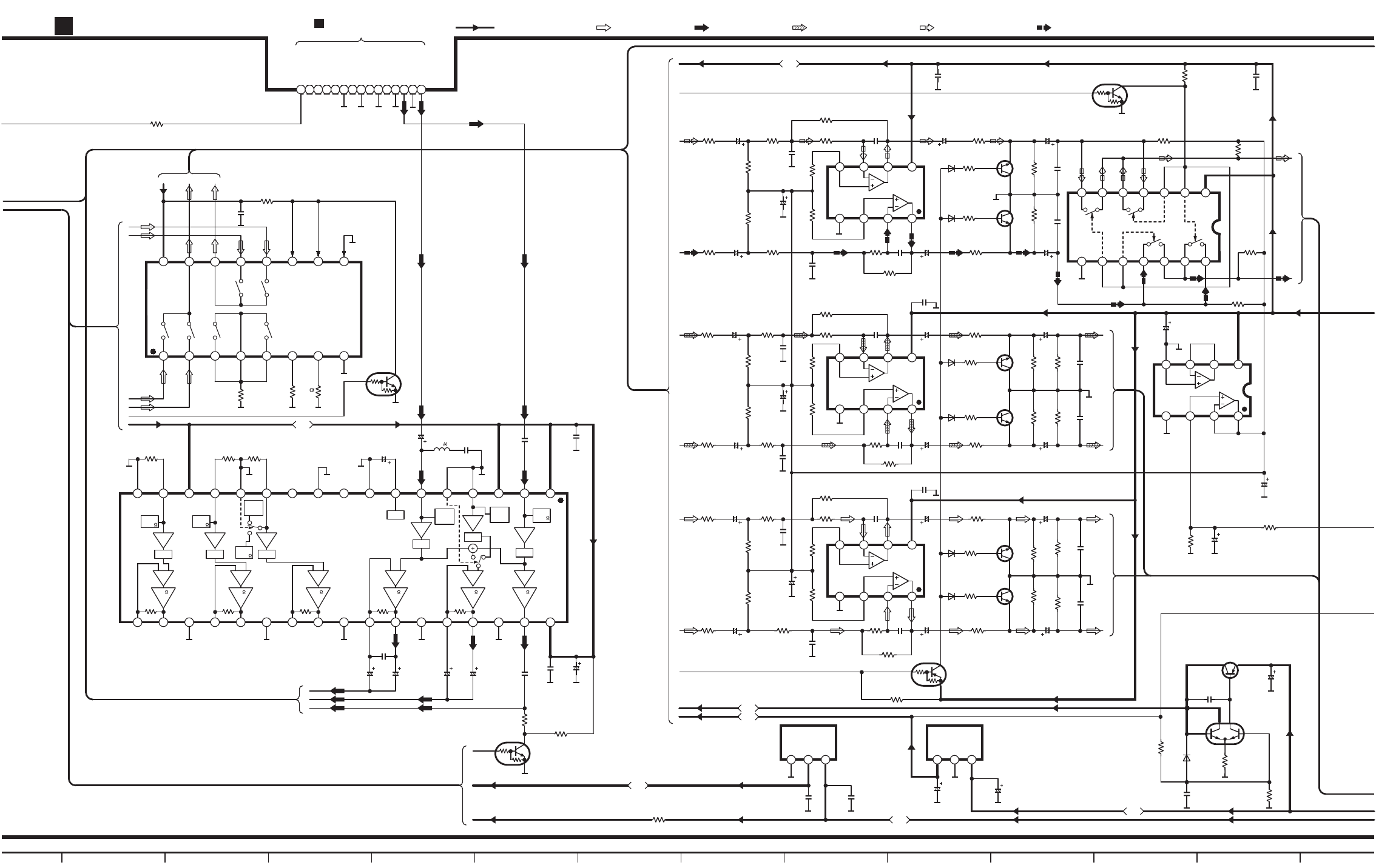
13 14 15 16 17 18 19 20 21 22 23 24
C892
0.1
R893
10K
IC802
NJM4580EDTE1
BUFFER AMP(C/SW)
CN501
11532 4 5 6 7 8 9 10 11
Y-IN
V.GND
C-IN
V.GND
C-OUT/ CR/ R
V.GND
CD/ B
V.GND
V.GND
12 13 14
TRAY/ TRV
TRV-SW+
TRAYMUT
TRAYDRV
TRAYREF
To MODULE CIRCUIT(FP3203)
on SCHEMATIC DIAGRAM
-
5/12-C
B
G
R314
10K
SCHEMATIC DIAGRAM
-
9
SL-DV290(EE,GN) MAIN CIRCUIT DIAGRAM
1234
5 6 7 8
1234
5 6 7 8
1234
5 6 7 8
1234
5 6 7 8
Q806
Q805
Q804
Q803
C15
10V220
3 12
INGNDOUT
R20
150
C13
0.01
R21
2.2K
C16
6.3V2200
R808
22K
R810
22K
R817
47K
R818
47K
R834
22K
R838
15K
R843
47K
R844
47K
R864
47K R863
47K
R854
22K
R858
15K
C28
0.1
C27
0.47
IC891
BU4053BCFE2
SIGNAL SELECTOR
IC501
C9ZB00000431
VIDEO BUFFER
2 13
GND OUT IN
C
B
A
X0X1
VDD
G
Vss
INHZ0Z1Y1 Y0
16 15 14 13 12 11 10 9
12345678
LPF
123456789101112
24232221201918
17 16 15 14 13
GND2
25 26 27 28 29 30 31 32
Vcc2
Vcc1MUTE1YC MIX
GND1NCMUTE2
33 34
GND2
6.75MHz 6.75MHz 6.75MHzLPF LPFLPF
SYNC
TIP
CLAMP
75
Driver
6.75MHzLPF
75
Driver
6.75MHz
LPF
Bias
150K
SYNC
TIP
CLAMP
SYNC
TIP
CLAMP
4dB
6.75MHz
BIAS
4dB
4dB
2dB2dB2dB2dB2dB
75
Driver 75
Driver 75
Driver
75
Driver
2dB
4dB 4dB 4dB
Bias
150K Bias
150K
Bias
150K
GND2 GND2 GND2 GND2
GND1NC
MAIN CIRCUIT
C
Q501
DTC114EUA106
SWITCHING(WIDE)
Q891
DTC114EUA106
SWITCHING
R513
2.2K
R512
8.2K C513
0.01
C514
0.01
C515
6.3V220
C512
6.3V1000
C511
6.3V100
C509
6.3V1000
C508
6.3V100
C510
0.1
A
B
C507
0.01
C506
0.01
C505
47P
L503
0.68 H
C504
50V1
C503
50V1
R509
100K R510
100K
R508
100K
R892
100K
R891
100K
R
S
T
F
D
C
E
N
B
A
D
C
V
U
E
I
H
R801
1K C801
16V10 R805
10K R807
22K
R809
15K
C80
47P
R803
100K
C803
470P
R811
10K
C807
6.3V47
R804
100K
R812
10K
C802
16V10
R802
1.8K R806
8.2K
C804
560P
C806
47P C810
16V22
C809
16V22 R815
1K
R813
3.3K
D801
D802 R814
3.3K
R816
470
Q802
Q801
C811
2200P
C812
2200P
C813
16V10
C814
16V10
Q801,802
2SD1328TX
MUTING
C808
0.1
Q303
DTC114EUA106
SIGNAL SELECTOR
CONT.
R305
10K
R821
100K
C817
0.1
R820
100K
R822
100K
IC803
NJM4580EDTE1
BUFFER AMP(SL/SR)
R827
100 C821
16V10 R831
15K
C823
470P
R829
100K
R830
100K
C827
6.3V47
R837
15K
R833
22K C825
47P
C828
0.1
R835
10K
R836
10K
R828
100 C822
16V10 R832
15K
C824
470P
C826
47P C830
6.3V47
C829
6.3V47
Q803,804
2SD1328TX
MUTING
R841
1K
R839
3.3K
D803,804
MA111TX
D803
D804
D801,802
MA111TX
R840
3.3K
R842
1K
R845
100K
C831
2200P
C833
6.3V47
R846
100K
C832
2200P
C834
6.3V47
F
E
C819
10V100
8 9 10 11 12 13 14
1234567
SIGNAL SELECTOR
IC801
C0JBAS000138
VREF
IC805
BA4558FHTT1
C849
6.3V47
R825
1.2K
C818
6.3V47
R826
5.6K
IC804
NJM4580EDTE1
BUFFER AMP(FL/FR)
Q805,806
2SD1328TX
MUTING
R847
1K C835
16V10 R851
10K
C837
470P
R849
100K
R855
10K
C841
6.3V47
R850
100K
R856
10K
R852
10K
C836
16V10
R848
1K
C838
470P
R857
15K
R853
22K C839
47P
C842
0.1
C840
47P C844
6.3V47
C843
6.3V47 R861
1K
D805,806
MA111TX
D805
D806
R859
3.3K
R860
3.3K
R862
1K
R865
100K
C845
2200P
C847
6.3V47
C848
6.3V47
R866
100K
C846
2200P
C
R867
47K
MUTING CONT.
Q807
UN5111TX
REGULATOR
IC4
NJM78M05FA REGULATOR
IC3
LM2940T5M
R22
2.2K
D8
MA111TX
C14
10V100
C12
1000P Q8
FMW1T98
POWER SUPPLY
CONT.
Q9
2SB1417PQTA
POWER SUPPLY
R819
100K
B
A
D
W
WU V
I
H
G
R43
0.33
R899
0
6V
: POSITIVE VOLTAGE LINE : AUDIO SIGNAL LINE : VIDEO SIGNAL LINE :SUB WOOFER SIGNAL LINE:SURROUND SP. SIGNAL LINE :CENTER SP. SIGNAL LINE
7.5V
5V
10V
6V
6V
5.2V
5.2V
2.5V
1.8V
2.5V
2.5V
2.5V
5V10V5V
5V
2.5V
7.5V 0V 0V 0V 0V 0V 0V
0V 0V 0V 0V 0V 0V 0V 0V
3.8V
0V 5V 0V 0V 2.5V 1.8V 5V 2.5V 5V
5V2.5V1.8V2V1.8V2V
5V
3.8V 0.2V
0V 0V 0V 7.5V
0V 0V 0V
0V
0.7V
(
-
0.5V)
0V
0.7V
(
-
0.5V)
0V 0V 0V 0V 7.5V 7.5V 7.5V
7.5V 7.5V 0V 0V 0V 0V
7.5V
0V
0V 0V 0V 7.5V
0V 0V 0V
0V
0.7V
(
-
0.5V)
0V
0.7V
(
-
0.5V)
7.5V7V7V
4.2V 4.2V 4.2V
0V 0V 0V 7.5V
0V 0V 0V
0V
0.7V
(
-
0.5V)
0V
0.7V
(
-
0.5V)
7.5V
7.5V
(
-
0.6V)
0V(7.5V)
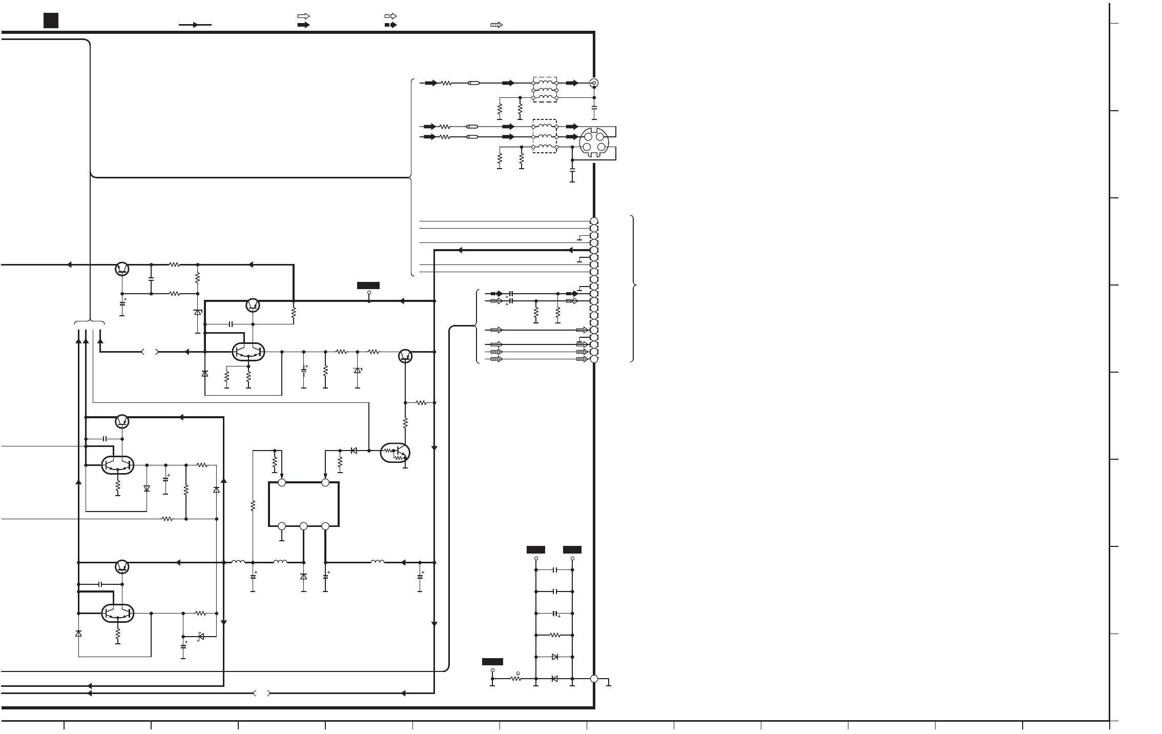
A
B
C
D
E
F
G
H
25 26 27 28 29 30 31 32 33 34 35 36
SL-DV290(EE,GN) MAIN CIRCUIT DIAGRAM
SCHEMATIC DIAGRAM-10
MAIN CIRCUIT
C
JK1
Q11
FMW1T98
P. SUPPLY CONT.
R29
22K
R30
100
D7
MA728TX
R37
100
R39
1K
C23
10V47
IC2
PQ1CZ31H2ZP
DC-DC
CONVERTER
C20
10V47
R28
47K
R31
680
4 5
321
ADJ ON/ OFF
GND VOUT VIN
D4
MA111TX
C4
16V470
L1
D3
SFPB-72V
C7
6.3V820 R2
8.2K
R3
2.2K
R4
10K
L501 JK501
VIDEO OUT
R505
1
R504
1R501
1
R502
1
L502
V.GND
S.WOOFER
CENTER
NC
NC
NC
CD Rch OUT
CD A.GND
CD Lch OUT
SUR R
SUR L
DATA
NC
SCLK
D.GND
+B (10V)
CS
CT.GND
CD REQ
SYNC
To SOUND PROCESSOR(SH-DV290)
& CASSETTE DECK(RS-DV290)
JK501
S-VIDEO OUT
R503
75
C501
0.01
C502
0.01
R27
1.2K
R35
1.2K
D.GND A.GND
CT.GND D18
MA111TX
D17
MA111TX
R41
100
C26
16V10
C29
0.01
C30
1000P
R40
0
Z501
VLP0146-T
R506
75 Z502
VLP0146-T
Z503
VLP0146-T
R507
75
S
T
R
1
2
20
3
4
5
6
7
8
9
10
11
12
13
14
15
16
17
18
19
DC+10V
R823
100K
R824
100K
C816
16V10
C815
16V10
K
M
L
O
P
F
E
A
B
C
D
L2L4
Q3
DTC114EUA106
SWITCHING
C3
16V3300
R33
4.7K
R32
47K
D11
MA8091MTX
POWER SUPPLY
CONT.
Q13
2SB1218TX
D10
MA111TX
C19
1000P
POWER SUPPLY
Q12
2SB1417PQTA
D14
MA8082MTX
R38
10
C24
1000P
REGULATOR
Q16
2SD874QRSTX
JFQG
POWER SUPPLY
Q15
2SB766ATX
C21
1000P
P. SUPPLY CONT.
Q14
FMW1T98
R34
470
D12
MA111TX
C22
16V10
R36
22K
D13
MA111TX
R44
1.2K
R42
100
POWER SUPPLY
Q7
2SB1417PQTA
C10
1000P
R16
470
D6
MA111TX
C11
16V10
R17
22K
Q6
FMW1T98
P. SUPPLY CONT.
E1
GG
Y C
9.2V
10V9V
: POSITIVE VOLTAGE LINE
: AUDIO SIGNAL LINE
: VIDEO SIGNAL LINE :SUB WOOFER SIGNAL LINE :SURROUND SP. SIGNAL LINE
:CENTER SP. SIGNAL LINE
9V
10V
9.2V
10V9V
9V 9.2V
9V
8.5V
9V
0V
5V
4V1V
6V 10V
6V5V
5.2V
5.2V
5V
4.5V
5V
5V
6V5V
5.2V
5.2V
4.5V
5V
5V
5V
8.2V
9.8V7.5V
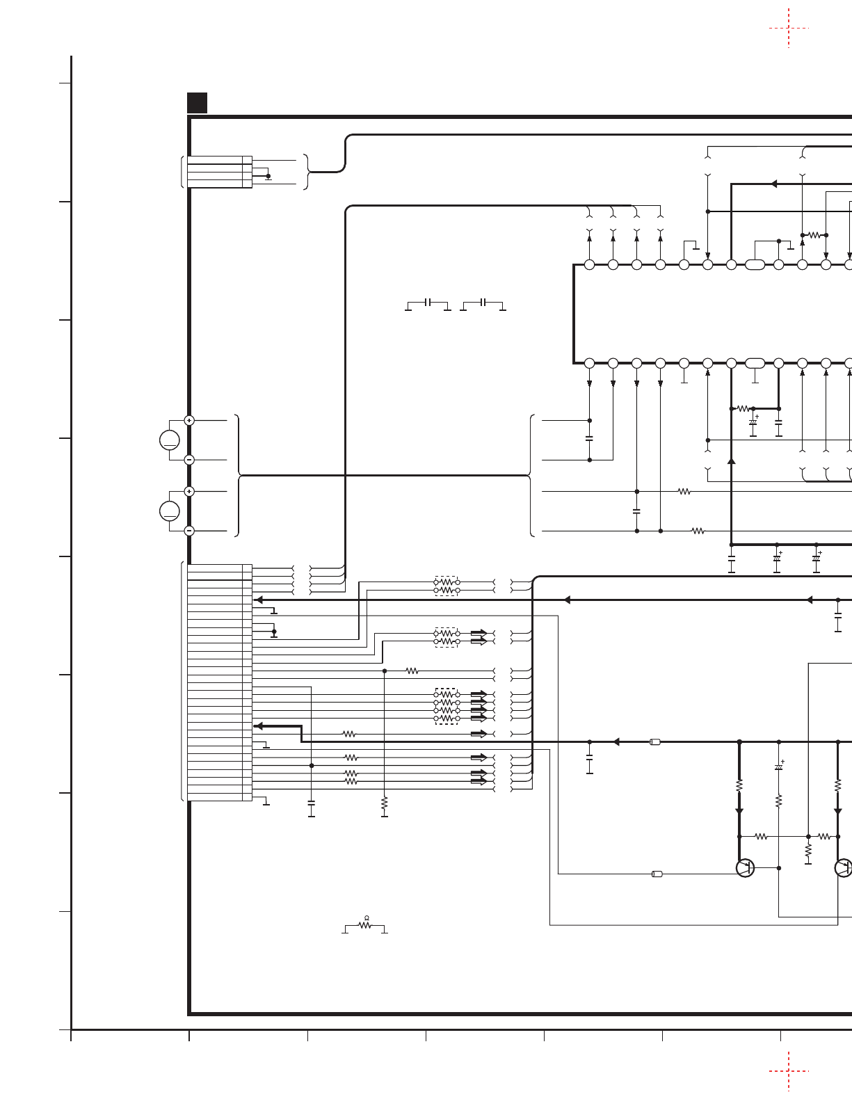
121110987654321
A
B
C
D
E
F
G
H
M
SL-DV290(EE,GN) INTERFACE CIRCUIT DIAGRAM
To FG UNIT
INTERFACE CIRCUIT
A
NOTE:
The number which noted at the connectors on the schematic diagram as
"SCHEMATIC DIAGRAM-1" or "SCHEMATIC DIAGRAM-2"
indicates the schematic diagram serial number located on the left corner in the schematic diagram.
To DVD MODULE
(FEP) CIRCUIT(FP5201) on
SCHEMATIC DIAGRAM-2/1,2-E~H
B
To OPTICAL PICK-UP
UNIT
T2(CD)
GND
PIN(CD)
FE2(CD)
VREF2.2V(CD)
T1(CD)
GND
FE1(CD)
VCC5V
LD+(DVD)
GND
RFN
F2(DVD)
TB(DVD)
TC(DVD)
TD(DVD)
TA(DVD)
VREF2.2V(DVD)
PIN(DVD)
GAIN H/L
F1(DVD)
RFP
GND
3.3VHFM
T-
F-
F+
T+
LD+(CD)
30
29
28
27
26
24
23
22
21
25
20
19
18
16
15
14
13
12
11
10
17
9
7
5
3
2
1
4
6
8
GND
FP5101
LB5106
VLP0146-T
RA2501
47K
R2507
6.8
M2502
(TRAVERSE MOTOR)
M2501
(SPINDLE MOTOR)
S2501 (REST DET.)
IC2501
C0GBG0000033
FOCUS/TRACKING COIL,
SPINDLE/ TRAVERSE
MOTOR DRIVE
14 13 12 11 10 9 8
15 16 17 18 19 20 21
654321
23 24 25 26 27 28
BIAS1
VIN1
VIN2
OPIN+
OPIN
-
GND
Vcc
MUTE12
GND
VO2+
VO2
-
VO1+
VO1
-
LDCNT
MUTE3
BIAS2
TRIN
LDIN
VIN3
PREVcc
MUTE4
GND
Vcc
VO3
-
VO3+
VO4
-
VO4+
7
22
OPOUT
C2503
16V22
C2513
0.1
A
C2511
0.1
R2505
82K
R2504
82K
C2507
0.1
R2503
15K
B
C
D
C5152
10V10
C5151
0.1
C5123
0.1
R5124
4.7K
R5111
2.2 C5111
6.3V47
R5117
47K
R5114
22K
R5113
47K
Q5111
2SB1115-T
LASER POWER
DRIVE(DVD)
R5112
27
R5115
2.2 C5115
6.3V47
R5116
27
Q5115
2SB1115-T
LASER POWER
DRIVE(CD)
C5103
0.1
C5101
16V10
A15
A14
A12
A10
A9
A8
A13
A6
A5
A4
A2
A1
LB5105
VLP0146-T
B9
B8
B7
B6
B5
B4
B3
B10
A16
A5
A6
A7
A8
A9
A11
A12
A13
A14
A10
LB5101
J0JHC0000045
D5151
MA728TX
A15
A16
R5102
56
R5121 56
R5123 56
A
B
C
D
B4B1
B6
B7
B8
R2502
15K
B9
B2
B3
B10
B5
B12
50
49
48
47
45
44
43
42
41
40
39
38
36
35
34
33
46
37
TRAYREF
M+9V
M+9V
FG3
FG1
D.GND
D.GND
MUTE4
D+5V
D+5V
TRAYIN
M+9V
M.GND
M.GND
M.GND
MUTE12
MUTE3
DMV 32
31
30
28
27
26
25
24
23
22
21
18
19A.GND
FE1 (CD)
29
20
T2 (CD)
A.GND
FOIN
TRIN
SPIN
TRVIN
IN-SW
LDCUR
VHALF
PIN (CD)
FE2 (CD)
T1 (CD)
LPCO2
17VCC 5V 16TB (DVD) 15TC (DVD) 14TD (DVD) 13TA (DVD)
FP5102
12TRAY/TRV 11
VREF2.2V 10PIN (DVD) 9GAIN H/L 8F2 (DVD) 7F1 (DVD) 6RFN 5RFP 4A.GND 3LPCO1 2A.GND 1
3.3VHFM
1
2
3
4
5
6
7
8
9
10
11
12
13
14
15
16
17
18
19
20
21
22
23
24
25
26
27
28
29
30
31
32
33
34
35
36
37
38
39
40
41
42
43
44
45
46
47
48
49
50
B1
A7
A3
A11
R5103
56
RA5102 56
RA5101
56
A2
A1
A3
A4
RA5103 56
R5152
1K
C5102
0.1
R5101 56
R5122 56
B2
B11
B12 R5120 0
B11
FG3 1
FP2501
FG2 2
FG2 3
FG1 4
R5107
0
R5108 0
R5109
0
R2501
100
C2510
0.1
C2502
16V100
C2509
16V10
C2505
0.1
C2504
0.1
C2501
6.3V220
C2506
0.1 C2508
0.1
R5105
0
L5101
10 H
C2512
0.1
M
A
B
C
D
A
B
C
D
SCHEMATIC DIAGRAM
-
1
A
B
A
B
:POSITIVE VOLTAGE LINE :AUDIO/VIDEO SIGNAL LINE
9V
5V
2.9V 2.9V 2.9V 2.9V 0V
(3.3V) 5V 1.7V 1.7V 1.7V 1.7V 1.7V 1.7V
4.1V 4.1V 4.1V 4.1V 0V 9V 9V 1.7V 0V 0V 1.7V 0V 5V
(3.3V)
4.9V
5V
0V
4.9V
5V
0V(2.2V) (3.2V)
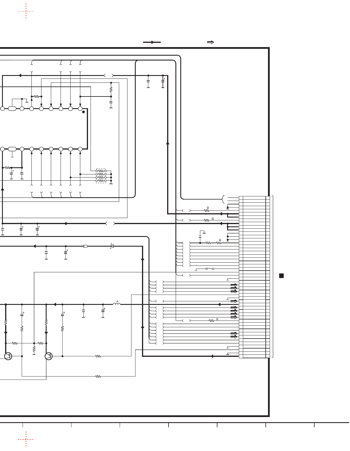
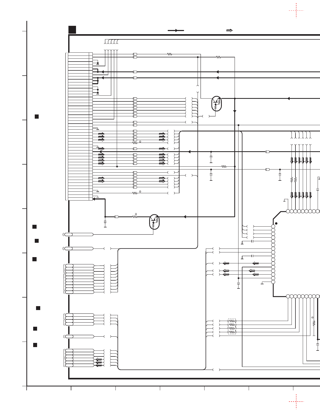
121110987654321
A
B
C
D
E
F
G
H
C5272 0.22
C5254 390P
C5282 0.01
C5274
0.1
B8
B7
B5
B4
B3
B6
C2
38
37
36
35
33
32
31
30
29
28
27
26
24
23
22
21
34
25
LDCUR
T2(CD)
SPDIN
M.GND
M.GND
TRAYREF
MUTE3
DMV
FOIN
INSW
PIN(CD)
FE2(CD)
VHALF
T1(CD)
FE1(CD)
Vcc+5V
20
19
18
16
15
14
13
12
11
10
9
6
7
A.GND
17
8
RFN
F2(DVD)
TB(DVD)
TC(DVD)
TD(DVD)
TA(DVD)
VREF2.2V
PIN(DVD)
GAIN H/L
F1(DVD)
RFP
A.GND 5
3.3VHFM
4
3
2
1
LB5239
VLP0146-T
C5221
0.1
GAINH/LFS5
LDCURFS6 MUTE12FS1 MUTE3FS2 FODRVFS3 TRDRVFS10 SPDRVFS11 TRVSDRVFS12
C1
C8
A+5V AB1
A.GND AG1
RFENV FS27
BDO FS28
OFTR FS29
VHALF FS32
VREF2 FS33
TSTSG FS26
D+3.3V DB1
Q5271
UN5211TX
SWITCHING
IC5201
AN22030A-VT
FRONT END PROCESSOR
B
C5283
560P
FP5201
17
STANBY
18
SEN
19
SCK
20
STDIO
21
OFTR
22
BDO
23
DTRD
24
SHOLD
25
VDD
26
NC2
27
RSCL
28
GND2
29
BDOSL
30
MIRSL
31
DCAGC
32
BRCA
LPC11
LPCO12
LPC2
3
LPCO2
4
POFLT
5
NC1
6
FBAL
7
TBAL
8
TEFLT
9
MONI2
10
TE
11
RFTE
12
FS
13
FE
14
VHALF
15
Vss
16 33
34
35
36
37
38
39
40
41
42
43
44
45
46
47
48
49
RFENV
50
Vcc1
51
VIN5
52
VIN6
53
VIN7
54
VIN8
5556
VREF
57
MONI
58
VIN1
59
VIN2
60
VIN3
61
VIN4
62
VIN9
63
VIN10
64
GND
Vcc2
FLTOP
FLTON
DCFLT
SAG
AGCG1
AGCG2
NC3
SHORT
IDGT
TESTSG
CRFHP1
CRFHP2
RFINP
RFINN
PEAK
VREFRF
C5292
100P
C5262 180P
C5204
0.1
39M.GND 40
41M+9V 42M+9V 43TRAYIN 44D+5V 45D+5V 46MUTE4 47D.GND 48D.GND 49FG3 50FG1
LPCO1
TRAY/TRV
A.GND
LPCO2
A.GND
TRVIN
TRIN
MUTE12
R5201 0
LB5221
LB5222
LB5223
LB5224
LB5225
LB5226
LB5228
LB5229
LB5230
LB5231
LB5233
R5203 0
LB5235
LB5236
LB5237
LB5238
LB5219
LB5218
VLP0146-T
LB5202
J0JHC0000045
LB5203
J0JHC0000045
LB5205
VLP0146-T
LB5206
LB5217
LB5213
LB5210
LB5209
LB5208
A1
A2
A3
A5
A6
A7
A8
A4
A1
D.GND DG1
D+5V DB3
M+9V MB1
M.GND MG1
FGFS8
A10
A10
C11
TBALFS14 FBALFS15 DTRDFS16 IDGTFS17
FEPENBFS19 FEPCLKFS20 FEPDATAFS21 TEFS23 ASFS24 FEFS25 C10
C9
C8
C7
C6
C4
C3
C2
C1
NRSTFS18
C7
C6
C5
C5
C9
C3
RFDIF FS31
C10
C11
R5262 0
R5294
12K
C5256 2200P
R5295 24K
C5273
1800P
DCFLT FC3
R5221
0
QR5221
UN2121-TX
POWER SUPPLY
C5205
0.1
C5202
16V10
HFMONFC1
C5264 0.018
C5271 1000P
C5290 1000P
C5299 330P
R5281
1M
C5201
16V10
C5233
0.1
B9
B10
B11
B12
B13
B14
NARF FS35
ARF FS36
VFOSHORT FS37
R5257
0
C5234
0.1
C5291 2700P
R5231
8.2K
R5232 8.2K
B1
B2
B15
B16
C5235
0.1
C5236 0.1
B1
B2
B14
B5
B6
B13
B7
B8
B9
B10
B3
B16
B11
B4
B12
B15
D.GND DG1
M+9V
VLP0146-T
VLP0155-T
C5232
0.1
LB5232
VLP0146-T
LB5227
VLP0146-T
RA5201
100
C4
L5202
10 H
R5320
0
L5201 10 H
C5203
0.1
TRV-SW+ VD9
TRAY REF VD6
TRAY/ TRV VD10
MUTE4 VD8
TRAY DRV VD7
SCHEMATIC DIAGRAM-5/1-G
SCHEMATIC DIAGRAM-5/1-H
SCHEMATIC DIAGRAM-5/1-F
SCHEMATIC DIAGRAM-3/12-D
SCHEMATIC DIAGRAM-3/12-F
LB5240
VLP0146-T
QR5241
UN511MTX
POWER SUPPLY
R5241
220
A4
A9
R5242
82K
A11
LB5207
DVD MODULE(FEP) CIRCUIT
SCHEMATIC DIAGRAM
-
2
DMVFS44 A8
A7
A5
A6
A3
A2
A9
SCHEMATIC DIAGRAM-3/12-D
SCHEMATIC DIAGRAM-3/1-C
SL-DV290(EE,GN) DVD MODULE(FEP) CIRCUIT DIAGRAM
SCHEMATIC DIAGRAM-3/12-F
SCHEMATIC DIAGRAM-3/1-C
To DVD MODULE
(SODC) CIRCUIT on
B
To DVD MODULE
(SODC) CIRCUIT on
B
SCHEMATIC DIAGRAM-3/1-B
SCHEMATIC DIAGRAM-3/1-A
To DVD MODULE
(CPU) CIRCUIT on
SCHEMATIC DIAGRAM-7/1-H
B
To DVD MODULE
(SODC) CIRCUIT on
B
SCHEMATIC DIAGRAM-3/1-B
SCHEMATIC DIAGRAM-3/12-F
SCHEMATIC DIAGRAM-3/12-A
SCHEMATIC DIAGRAM-3/12-F
SCHEMATIC DIAGRAM-3/1-C
To DVD MODULE
(SODC) CIRCUIT on
B
FGENBFS38 A11
To DVD MODULE
(CPU) CIRCUIT on
SCHEMATIC DIAGRAM-7/1-E
B
To DVD MODULE
(VIDEO DAC) CIRCUIT on
B
To DVD MODULE
(VIDEO DAC) CIRCUIT on
SCHEMATIC DIAGRAM-5/1-D
B
To DVD MODULE
(SODC) CIRCUIT on
B
To DVD MODULE
(VIDEO DAC) CIRCUIT on
SCHEMATIC DIAGRAM-5/12-A
B
To DVD MODULE
(SODC) CIRCUIT on
SCHEMATIC DIAGRAM-3/1-A
B
To DVD MODULE
(SODC) CIRCUIT on
SCHEMATIC DIAGRAM-3/12-F
B
To DVD MODULE(CPU)
CIRCUIT on
SCHEMATIC DIAGRAM-7/1-B
B
To DVD MODULE(SODC)
CIRCUIT on
B
A
To INTERFACE
CIRCUIT(FP5102)
on SCHEMATIC
DIAGRAM
-
1/11,12-B~D
D1
D2
D3
D4
D5
D1
D2
D3
D4
D5
R5204
1K
VLP0155-T
VLP0155-T
VLP0155-T
VLP0155-T
VLP0155-T
VLP0155-T
VLP0155-T
VLP0155-T
VLP0155-T
VLP0155-T
VLP0155-T
VLP0155-T
VLP0155-T
VLP0146-T
VLP0146-T
VLP0146-T
VLP0146-T
VLP0146-T
VLP0146-T
VLP0146-T
VLP0146-T
3.3V
3.3V
0V
(0.5V)0V
(3.2V)5V
0V
5V
(1.4V)2.6V
1.7V
1.7V
1.7V
1.7V
0V
1.7V
1.7V
1.7V
3.3V
3.3V
0V
0V
0V
0V
3.3V
0V
0.5V
3.3V
1.2V
2V
1.2V
1.2V
3.3V
1.6V
1.6V
1.8V
1.1V
0.7V
0V
0V
0V
0.7V
0V
2.2V
2.2V
1.7V
1.7V
5V
2.2V
2.2V
2.3V
2.3V
2.2V
1.8V
2.3V
2.3V
2.3V
2.3V
2.3V
2.3V
5V
9V
5V
3.3V
0V
0V
:POSITIVE VOLTAGE LINE :AUDIO/VIDEO SIGNAL LINE
3.3V
(3.3V)
(0V)
0V 3.3V
3.3V
(0V)
(3.3V)
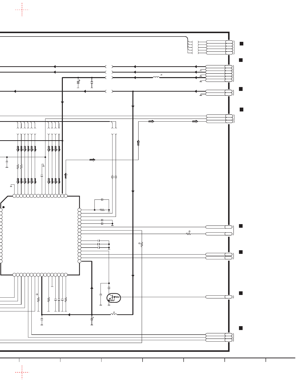
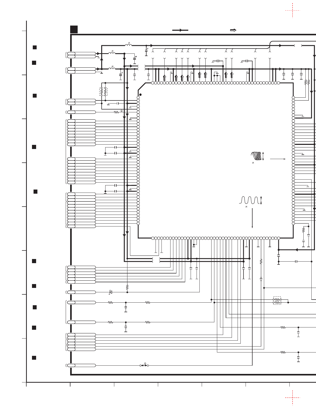
121110987654321
A
B
C
D
E
F
G
H
D.GNDDG1
1NINT0
2NINT1
3VDD3
4VSS
5NINT2
6WAITODC
7NMRST
8DASPST
9CPUADR17
10
CPUADR16
11
CPUADR15
12
CPUADR14
13
CPUADR13
14
CPUADR12
15
CPUADR11
16
CPUADR10
17
CPUADR9
18
VDD18
19
VSS
20
DRAMVDD18
21
DRAMVSS
22
CPUADR8
23
CPUADR7
24
CPUADR6
25
CPUADR5
26
CPUADR4
27
CPUADR3
28
CPUADR2
29
CPUADR1
30
CPUADR0
31
VDD3
32
VSS
33
DRAMVDD33
34
NCS
35
NWR
36
NRD
37
CPUDT7
38
CPUDT6
39
CPUDT5
40
CPUDT4
41
CPUDT3
42
CPUDT2
43
CPUDT1
44
CPUDT0
45
CLKOUT1
46
MMOD
47
NRST
48
MSTPOL
49
SCLOCK
50
SDATA
51
OFTR
52
BDO
53
PWM1
54
PWM2
55
PWM3
56
PWM4
57
VDD3
58
DRAMVDD18
59
DRAMVSS
60
VSS
61
PWM5
62
PWM6
63
PWM7
64
PWM8
65
TBAL
66
FBAL
67
TRSDRV
68
SPDRV
69
FG
70
TILTP
71
TILT
72
TILTN
73
TX
74
DTRD
75
IDGT/TEMUTE
76
VDD18
77
VSS
78
VDD3
79
OSCI1
80
ODCO1
81
VSS
82
TSTSG
83
VFOSHORT
84
JLINE
85
AVSS
86
ROUT
87
LOUT
88
AVDD
VCOF
89
TRCRS
90
CMPIN
91
LPFOUT
92
LPFIN
93
AVSS
94
HPFOUT
95
HPFIN
96
CSLFLT
97
RFDIF
98
AVDD
99
PLFLT2
100
PLFLT1
101
AVSS
102
RVI
103
VREFH
104
PLPG
105
VHALF
106
DSLF2
107
DSLF1
108
AVDD
109
NARF
110
ARF
111
JITOUT
112
AVSS
113
DAC0
114
DAC1
115
AVDD
116
AD0
117
AD1
118
AD2
119
AD3
120
AD4
121
AD5/CAPAC2
122
AD6/CAPAC1
123
TECAPA
124
VDD3
125
VSS
126
MONI0
127
MONI1
128
MONI2
129
MONI3
130
NEJECT
131
NTRYCL
132
NDASP
133
NCS3FX
134
NCS1FX
135
DA2
136
DA0
137
NPDIAG
138
DA1
139
NOSCS16
140
INTRQ
141
NDMACK
142
VDD3
143
VSS
144
IORDY
145
NIORD
146
NIOWR
147
DMARQ
148
HDD15
149
HDD0
150
HDD14
151
VDD18
152
PD
153
UATASEL
154
VSS
155
VDD3
156
HDD1
157
HDD13
158
HDD2
159
HDD12
160
HDD3
161
VDD3
162
VSS
163
HDD11
164
HDD4
165
HDD10
166
HDD5
167
HDD9
168
VDD3
169
VSS
170
HDD6
171
HDD8
172
HDD7
173
VDDH
174
NRESET
175
MASTER
176
C2003 0.1
CPUADR15SC24 CPUADR16SC25 CPUADR17SC26
WAITSC27
CPUADR14SC23 CPUADR13SC22
CPUADR11SC20 CPUADR12SC21
CPUADR10SC19 CPUADR9SC18 C2004 0.1
C2005 0.1
CPUADR6SC15 CPUADR7SC16 CPUADR8SC17
CPUADR5SC14 CPUADR4SC13
CPUADR2SC11 CPUADR3SC12
CPUADR1SC10 CPUADR0SC9
NRDSC28 NWELSC29 NSODCCSSC30
CPUDT7SC8 CPUDT6SC7
CPUDT4SC5 CPUDT5SC6
CPUDT3SC4 CPUDT2SC3 CPUDT1SC2 CPUDT0SC1
C2006 0.1
C2007 0.1
E1
E2
E3
E4
E5
E6
E7
E8
E9
E10
E11
C2014
0.1
ODCIRQSC32 ADSCIRQSC31
RA2021
1K
D+3.3VDB1
L2001
10 H
C2001
6.3V100
C2002
6.3V100
L2002
10 H
D+1.8VDB4
C2018
0.1
L2021
10 H
C2021
6.3V100
C2016
0.1
C2017
0.1
C2015
0.1
C2013
0.1
C2010 0.1
C2011 0.1
C2009 0.1
C2008 0.1
NRSTFS18
BDOFS28 OFTRFS29
FEPDATAFS21 FEPCLKFS20 FEPENBFS19
TRV-SW+VD9
R2021
47K
C2034
0.039
R2025
22K
R2026
22K
RA2022
4.7K
TBALFS14
C2035
8200P
R2027
56K
R2028
56K
FBALFS15
FGFS8 GAINH/LFS5 DTRDFS16 IDGTFS17 TSTSGFS26
CLK16M1SA1
R2029
10K
C2036
0.1
C2022
0.1
C2031
0.1
R2022
7.5K
C2032
0.1
R2023
7.5K
R2053 47K
R2054 47K
C2039 0.01
R2030
1K
C2102
0.1
C2058 1000P
R2038 15K
R2039
1M
C2054
680P
C2055 6800P
C2051 68P
C2050 0.033
R2037
68K
C2048
0.015
Q2001
2SD1819ATX
RF AMP
C2044
390P
C2043
100P
R2034
47K
C2045
1000P
R2033
4.7K
R2035
2.7K
R2031
560
C2041
330P
R2032
10K
C2042
330P
C2040
1000P
C2047
0.01
R2049
1K
C2046
1000P
VHALF FS32
VREF2 FS33
C2053
0.1
A+5V AB1
RFDIF FS31
C2059
820P
R2040
8.2K
C2060
1000P
R2041
8.2K
C2062
330P
R2042
15K
C2061
330P
R2043
15K
C2057 2700P
C2056 2700P ARF FS36
NARF FS35
C2063
1000P
STENABLE SD1
STD0 SD2
STD1 SD3
STD2 SD4
STD3 SD5
STD4 SD6
STD5 SD7
STD6 SD8
STD7 SD9
STVALID SD10
STCLK SD11
E1
E2
E3
E4
E5
E6
E7
E8
E9
E10
E11
FE FS25
TE FS23
RFENV FS27
AS FS24
LDCUR FS6
R2044
15K
C2064
1000P
R2045
15K
C2065
1000P
R2046
15K
C2066
4700P
C2067
4700P
R2047
15K
R2048
4.7M
A.GND AG1
C2025
0.1
C2024
0.1
C2023
0.1
IC2001
MN103S26EGA
OPTICAL DISC CONTROL
C2038
0.1
B
R2036 0
VFO SHORTFS37 TRVSDRV FS12
SPDRV FS11
MUTE3 FS2
MUTE12 FS1
FODRV FS3
TRDRV FS10
IC2101
C0JBAS000116
LOGIC CONTROL
GND3
B
2
A1
4C
5VCC
R2052
100
R2051
100
C2073
0.1
D.GNDDG1
C2101
0.1
C2052
0.1
C2012
0.1
DVD MODULE(SODC) CIRCUIT
SCHEMATIC DIAGRAM
-
3
SL-DV290(EE,GN) DVD MODULE(SODC) CIRCUIT DIAGRAM
To DVD MODULE
(VIDEO DAC) CIRCUIT on
B
SCHEMATIC DIAGRAM-5/1-D
SCHEMATIC DIAGRAM-5/1-E
SCHEMATIC DIAGRAM-7/1-G
To DVD MODULE
(CPU) CIRCUIT on
B
SCHEMATIC DIAGRAM-7/1-F
SCHEMATIC DIAGRAM-7/12-E,F
To DVD MODULE
(CPU) CIRCUIT on
B
SCHEMATIC DIAGRAM-7/1-F
To DVD MODULE
(CPU) CIRCUIT on
B
SCHEMATIC DIAGRAM-7/1-H
SCHEMATIC DIAGRAM-7/12-B
To DVD MODULE
(FEP) CIRCUIT on
B
FGENBFS38
SCHEMATIC DIAGRAM-2/1-D
SCHEMATIC DIAGRAM-2/1-A
SCHEMATIC DIAGRAM-2/12-A
To DVD MODULE
(VIDEO DAC) CIRCUIT on
B
To DVD MODULE
(VIDEO DAC) CIRCUIT on
B
SCHEMATIC DIAGRAM-5/12-B
To DVD MODULE
(FEP) CIRCUIT on
B
SCHEMATIC DIAGRAM-2/1-B
To DVD MODULE
(FEP) CIRCUIT on
B
SCHEMATIC DIAGRAM-2/1-B
SCHEMATIC DIAGRAM-2/1-C
SCHEMATIC DIAGRAM-2/12-C
To DVD MODULE
(AUDIO DAC) CIRCUIT on
B
SCHEMATIC DIAGRAM-6/12-C
K2004
0
To DVD MODULE
(FEP) CIRCUIT on
B
SCHEMATIC DIAGRAM-2/1-C
To DVD MODULE
(FEP) CIRCUIT on
B
SCHEMATIC DIAGRAM-2/12-A
To DVD MODULE
(VIDEO DAC) CIRCUIT on
B
SCHEMATIC DIAGRAM-2/12-F
SCHEMATIC DIAGRAM-5/1-F
SCHEMATIC DIAGRAM-2/12-C
SCHEMATIC DIAGRAM-2/1-A
SCHEMATIC DIAGRAM-2/12-F
SCHEMATIC DIAGRAM-2/1-C
To DVD MODULE
(FEP) CIRCUIT on
B
DMV FS44
SCHEMATIC DIAGRAM-4/1-A
To DVD MODULE
(AVDEC) CIRCUIT on
B
D2001
MA728TX
5V
1.8V
3.3V
3.3V
3.3V
1.8V
3.3V
3.3V
3.3V
3.3V
2.7V
2.4V
2.6V
2.8V
2.5V
2.8V
2.8V
2.6V
2.5V 1.8V
1.8V
2.6V
2.7V
2.9V
2.7V
2.9V
2.8V
2.9V
2.9V
2.3V 3.3V
3.3V
3.3V
3.3V
2.8V
3.1V
(1.8V)
(1.6V)
(2V)
(3.3V)
(1.8V)
(2.2V)
(2.3V)
(2.2V)
(1.7V)
(1.9V)
(2.2V)
(2.2V)
(2.2V)
(2.2V)
(2V)
(2.2V)
(2.1V)
(1.2V)
(2V)
(2.4V)
(2.3V)
(2.4V)
(2.3V)
(2.4V)
(2.3V)
(2.3V)
3.3V
0V
0V
0V
0V
3.3V
3.3V
1.8V
3.3V
1.7V
1.7V
1.7V
1.7V
3.3V
0V
0V
0V
3.3V
0V
1.8V
3.3V
1.5V
0V
3.3V
(1.7V)
(3.3V)
(3.3V)
0V
1.6V
1.6V
0V
0V
1.7V
1.7V
1.4V
1.7
3.3V
1.5V
2.2V
1.7V
1.4V
1.7V
3.3V
1.6V
1.6V
2.1V
1.7V
1.7V
3.3V
1.7V
1.7V
1.7V
1.7V
2.4V
1.7V
1.2V
3.3V
3.3V
3.3V
3.3V
3.3V
0V(1.6V)
0V (0.6V)
3.3V
3.3V
0V (2.6V)
2.2V(3.1V)
1.8V
3.3V
3.3V
0V(3.1V)
3.3V
0V(3.1V)
3.3V
3.3V
0V(3.3V)
0V
0V
0.5 s. 0.2V/DIV.
PLAY
0.3V
P-P
3.5V
P-P
0.5 s. 1V/DIV.
5V
0V(3.1V)
0V(3.1V)
0V(3.1V)
0V(3.1V)
0V
0V
5V
0V
1.6V
1.6V
3.1V
3.1V
3.1V
3.1V
3.1V
3.1V
3.1V
:POSITIVE VOLTAGE LINE :AUDIO/VIDEO SIGNAL LINE
3.3V(0V)
(1.3V)
0V (1.3V)
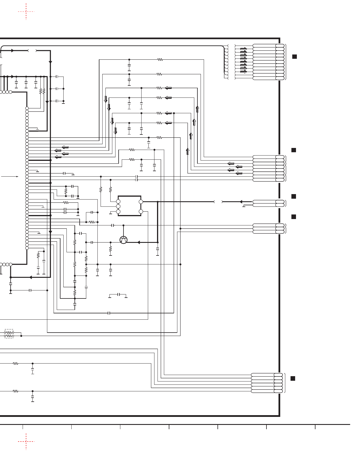
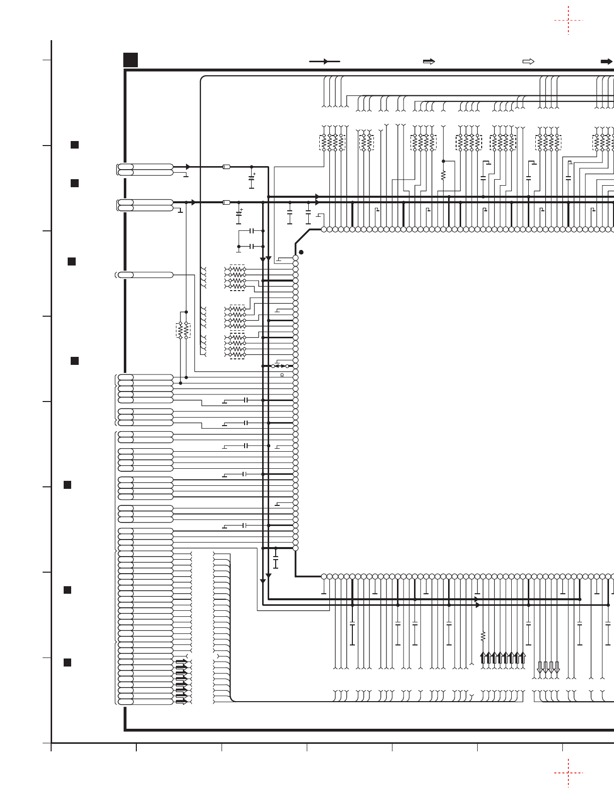
121110987654321
A
B
C
D
E
F
G
H
DVD MODULE(AVDEC) CIRCUIT
SCHEMATIC DIAGRAM
-
4
SL-DV290(EE,GN) DVD MODULE(AVDEC) CIRCUIT DIAGRAM
IC3001
MN6775511
AV DECODER
RA3004
82
AV1IRQCD1
NRSTFS18
AV2IRQCD2
RA3001
1K
LB3001
J0JHC0000045
RA3012
82
WAITSC27 NWEHCD3 NWELSC29
NRDSC28 NAVCSCD4 SYSCLKCD5
CPUADR1SC10 CPUADR2SC11
CPUADR3SC12 CPUADR4SC13 CPUADR5SC14 CPUADR6SC15
CPUADR7SC16 CPUADR8SC17 CPUADR9SC18 CPUADR10SC19
CPUADR11SC20 CPUADR12SC21 CPUADR13SC22
CPUADR14SC23 CPUADR15SC24 CPUADR16SC25 CPUADR17SC26 CPUDT0SC1 CPUDT1SC2 CPUDT2SC3 CPUDT3SC4 CPUDT4SC5
C3006 0.1
C3004 0.1
C3008 0.1
C3009 0.1
CPUDT5SC6 CPUDT6SC7 CPUDT7SC8
RA3051
100
F9
F8
F7
F6
F5
F4
F3
CPUDT8CD6 CPUDT9CD7 CPUDT10CD8 CPUDT11CD9 CPUDT12CD10 CPUDT13CD11 CPUDT14CD12 CPUDT15CD13 STVALIDSD10 STCLKSD11 STENABLESD1 STD7SD9 STD6SD8 STD5SD7 STD4SD6 STD3SD5 STD2SD4 STD1SD3 STD0SD2
D+3.3VDB1 D.GNDDG1
C3001
6.3V330
C3002
6.3V330
LB3002
J0JHC0000045
D+1.5VDB2
MDQ22
RA3008
82
RA3009 82
RA3006
82
RA3007
82
RA3005
82
C3035
0.1
AOUT1 AD4
AOUT0 AD5
SRCK AD7
LRCK AD8
AUDIO DIGITAL AD9
DMIXOUT AD6
F9
F8
F7
F6
F5
F4
MA3
A+5V AB1
CLK27M AD2
F2
B
C3010
0.1
EXTCLK1 AD1
CLK54M AD10
F10
F2
F10
F1
F3
R3051 100
C3011 0.1
C3012 0.1
R3052 100
RA3053
100
R3009 100
AOUT2 AD3
C3051
22P
F1
D.GNDDG1
VDD
28
VSS VDD
29
A4
30
A5
31
A6
32
A7
33
A8
34
A9
35
A11
36
NC
37
CKE
38
CLK
39
UDQM
40
NC
41
VSS
42
DQ8
43
VDDQ
44
DQ9
45
DQ10
46
VSSQ
47
DQ11
48
DQ12
49
VDDQ
50
DQ13
51
DQ14
52
VSSQ
53
DQ15
54
VSS
A3
A2
A1
A0
A10/AP
BA1
BA0
/CS
/RAS
/CAS
/WE
LDQM
VDD
DQ7
VSSQ
DQ6
DQ5
VDDQ
DQ4
DQ3
VSSQ
DQ2
DQ1
VDDQ
DQ0
127 26 25 24 23 22 21 20 19 18 17 16 15 14 13 12 11 10 98765432
RA3003
82
RA3002
82
RA3013
22
RA3011 82
MDQ23
MDQ21
MDQ20
MDQ19
MDQ18
MDQ17
MDQ16
MDQ24
MDQ25
MDQ26
MDQ27
MDQ28
MDQ29
MDQ30
MDQ31
MDQ22
MDQ25
MDQ23
MDQ24
MDQ26
MDQ21
MDQ27
MDQ20
MDQ28
MDQ19
MDQ29
MDQ18
MDQ30
MDQ17
MDQ31
MDQ16
MA2
MA1
MA0
MA10
MA4
MA5
MA6
MA7
MA8
MA9
MA11
RA3010
82
MA0
MA1
MA2
MA3
MA4
MA5
MA6
MA7
MA8
MA9
MA11
MA10
R3001 22
CLK
CLK
DQM3
DQM2
XWE
XCAS
XRAS
XCSM
BA0
BA1
BA1
DQM3
DQM2
XWE
XCAS
XRAS
XCSM
BA0
VDD
28
VSS VDD
29
A4
30
A5
31
A6
32
A7
33
A8
34
A9
35
A11
36
NC
37
CKE
38
CLK
39
UDQM
40
NC
41
VSS
42
DQ8
43
VDDQ
44
DQ9
45
DQ10
46
VSSQ
47
DQ11
48
DQ12
49
VDDQ
50
DQ13
51
DQ14
52
VSSQ
53
DQ15
54
VSS
A3
A2
A1
A0
A10/AP
BA1
BA0
/CS
/RAS
/CAS
/WE
LDQM
VDD
DQ7
VSSQ
DQ6
DQ5
VDDQ
DQ4
DQ3
VSSQ
DQ2
DQ1
VDDQ
DQ0
127 26 25 24 23 22 21 20 19 18 17 16 15 14 13 12 11 10 98765432
MA4
MA5
MA6
MA7
MA8
MA9
MA11
MA3
MA2
MA1
MA0
MA10
XWE
XCAS
XRAS
XCSM
BA0
BA1
CLK
DQM0
MDQ7
MDQ6
MDQ5
MDQ4
MDQ3
MDQ2
MDQ1
MDQ0
DQM0
DQM1
MDQ8
MDQ9
MDQ10
MDQ11
MDQ12
MDQ13
MDQ14
MDQ15
C3031 0.1
C3036
0.1
C3025
0.1
C3033
0.1
C3024
0.1
C3026
0.1
C3034 0.1
C3007 0.1
C3003
0.1
C3030 0.1
C3032
0.1
C3027
0.1
C3028
0.1
K3003
0
C3068
0.1
C3070
0.1
C3072
0.1
C3073
0.1
C3074
0.1
C3071
0.1
C3069
0.1
C3067
0.1
C3066
0.1
C3064
0.1
C3062
0.1
C3061
0.1
C3063
0.1
C3065
0.1
MDQ5
MDQ10
MDQ4
MDQ11
MDQ3
MDQ12
MDQ2
MDQ13
MDQ1
MDQ14
MDQ0
MDQ15
DQM1
MDQ7
MDQ8
MDQ6
MDQ9
YVD4
CVD5
C3110
6.3V100
R3006 15K
C3022 0.1
C3021 1
L3001
10 H
C3019 1
C3018
0.1
R3007 2K
C3038
0.1
R3008
1.3K
C3023 0.1
C3017 0.1
C3015 0.1
C3016 0.1
C3014 0.1
R3010 100
L3091
10 H
C3037
6.3V330
A.GND AG1
CPUDT0
CPUDT1
CPUDT2
CPUDT3
CPUDT4
CPUDT5
CPUDT6
CPUDT7
CPUDT8
CPUDT9
CPUDT10
CPUDT11
CPUDT12
CPUDT13
CPUDT14
CPUDT15
STVALID
STCLK
STENABLE
STD7
STD6
STD5
STD4
STD3
STD2
STD1
STD0
CPUDT0
CPUDT1
CPUDT2
CPUDT3
CPUDT4
CPUDT5
CPUDT6
CPUDT7
CPUDT8
CPUDT9
CPUDT10
CPUDT11
CPUDT12
CPUDT13
CPUDT14
CPUDT15
STVALID
STCLK
STD7
STD6
STD5
STD4
STD3
STD2
STD1
STD0
STENABLE
Vss
157
12
HMD
22
XWR
64
VSS
77
VDD
AVss
113
VREF
115
AVDD
118
Vss
122
TESTSEL1
125
VCLK
128
VDD
131
VDIN5
132
VDIN3
134
Vss
139
VDOUT1
141
MDQ19
161
MDQ29
167
MDQ17
175
MA4
178
Vss
182
MCK
185
MA1
187
53
VSS
PLLAVDD
105
1
VDD
2MDQ9
3MDQ5
4MDQ10
5
LVDD
6MDQ4
7MDQ11
8MDQ3
9Vss
10
MDQ12
11
VDD
13
XRST
14
MDQ2
15
Vss
16
LVDD
17
XHINT
18
XHINT2
19
XDK
20
Vss
21
XWRH
23
XRD
24
XCS
25
VDD
26
HCLK
27
HA1
28
HA2
29
HA3
30
HA4
31
Vss
32
HA5
33
HA6
34
HA7
35
HA8
36
HA9
37
LVDD
38
HA10
39
HA11
40
HA12
41
HA13
42
HA14
43
Vss
44
HA15
45
HA16
46
HA17
47
HD0
48
VDD
49
HD1
50
HD2
51
HD3
52
HD4
54
HD5
55
HD6
56
HD7
57
LVDD
58
HD8
59
HD9
60
HD10
61
VDD
62
HD11
63
HD12
65
HD13
66
HD14
67
HD15
68
VDD
69
DSTR
70
MDQ1
71
MDQ13
72
VSS
73
STD7
74
STD6
75
STD5
76
STD4
78
STD3
79
STD2
80
STD1
81
STD0
82
VDD
83
IECOUT
84
MDQ14
85
VDD
86
DVALID
87
MDQ0
88
MDQ15
89
VSS
90
STRQ
91
ADOUT0
92
ADOUT1
93
ADOUT2
94
ADOUT3
95
Vss
96
SRCK
97
LRCK
98
LVDD
99
PHCOMPO
100
EXTCK
101
CLK121
102
PCLK
103
VDD
104
VSS
TCPOUT
106
PLLVss
107
DAC3OUT
108
DAC1OUT
109
COMP2
110
IREF2
111
AVDD
112
DAC2OUT
114
DAC4OUT
116
COMP1
117
IREF1
119
DAC5OUT
120
AVss
121
DCTEST
123
TESTSEL2
124
TESTSEL0
126
LVDD
127
VDIN7
129
VDIN6
130
VDIN4
133
LVDD
135
VDIN2
136
VDIN1/XVSYNCO
137
VDIN0/XHSYNCO
138
VDOUT0
140
VDOUT2
142
VDOUT3
143
VDD
144
VDOUT4
145
VDOUT5
146
VDOUT6
147
Vss
148
VDOUT7
149
MDQ24
150
MDQ23
151
VDD
152
MDQ25
153
MDQ22
154
MDQ26
155
Vss
156
MDQ16
158
MDQ27
159
VDD
160
MDQ20
162
Vss
163
MDQ31
164
MDQ28
165
VDD
166
MDQ30
168
Vss
169
MDQ18
170
DQM3
171
VDD
172
DQM2
173
LVDD
174
MDQ21
176
MA3
177
VDD
179
MA2
180
MA5
181
MCKI
183
LVDD
184
MA10
186
VDD
188
MA6
189
MA0
190
MA8
191
MA7
192
XWE
193
MA11
194
XCAS
195
XRAS
196
VDD
197
BA0
198
XCSM
199
Vss
200
BA1
201
MA9
202
DQM0
203
DQM1
204
MDQ7
205
MDQ8
206
MDQ6
207
Vss
208
C3013 0.1
C3039
0.1
C3020
0.1
R3106
62
R3107
18
K3106
0
K3101 0
R3101
62
R3102
15 C3029
0.1
K3002
0
C3005
0.1
To DVD MODULE
(CPU) CIRCUIT on
B
To DVD MODULE
(VIDEO DAC)
CIRCUIT on
B
To DVD MODULE
(AUDIO DAC) CIRCUIT on
B
SCHEMATIC
DIAGRAM-6/1-C
K3011 0
K3009 0
K3007
0
SCHEMATIC
DIAGRAM-7/1-H
SCHEMATIC
DIAGRAM-5/1-D
SCHEMATIC
DIAGRAM-5/1-G
To DVD MODULE
(CPU) CIRCUIT on
B
SCHEMATIC
DIAGRAM-7/1-G
SCHEMATIC
DIAGRAM-7/1-E,F
SCHEMATIC
DIAGRAM-7/1-D
To DVD MODULE
(CPU) CIRCUIT on
B
SCHEMATIC
DIAGRAM-7/12-D
To DVD MODULE
(CPU) CIRCUIT on
B
SCHEMATIC
DIAGRAM-7/12-A,B
To DVD MODULE
(SODC) CIRCUIT on
B
SCHEMATIC
DIAGRAM-3/12-H
To DVD MODULE
(VIDEO DAC)
CIRCUIT on
B
SCHEMATIC
DIAGRAM-5/12-D
SCHEMATIC
DIAGRAM-5/1-F
SCHEMATIC
DIAGRAM-6/12-A
SCHEMATIC
DIAGRAM-6/1-F
SCHEMATIC
DIAGRAM-6/1-F
SCHEMATIC
DIAGRAM-6/12-E
SCHEMATIC
DIAGRAM-6/1-H
To DVD MODULE
(VIDEO DAC)
CIRCUIT on
B
IC3061
C3ABPG000121
MEMORY
IC3062
C3ABPG000121
MEMORY
V.GND VG1
:POSITIVE VOLTAGE LINE :AUDIO/VIDEO SIGNAL LINE
2.3V
2.3V
2.3V
3.3V
3V
2.3V
2.5V
2.8V
2.4V
1.5V
2V
2.3V
3.3V
2V
2.7V
2.6V
3.3V
3.3V
3.3V
3.3V
3.3V
3.3V
3.3V
3.3V
2.8V
3.3V
1.5V
1.7V
2.9V
2.9V
2.8V
2.9V
2.7V
2.9V
3.3V
2.7V
2.6V
2.5V
2.6V
2.8V
2.8V
2.5V
1.5V
2.8V
2.6V
2.4V
3.3V
2.7V
3.1V
3.1V
3.1V
3.3V
3.1V
3.1V
3.1V
3.1V
3.1V
3.3V
3.3V
3.3V
3.3V
1.5V
3.3V
3.3V
3.3V
3.3V
3.3V
3.3V
0V
0V
0V
0V
2.2V
0V
0V
0V
0V
0V
0V
3.3V
1.6V
0V
0V
0V
0V
1.7V
1.7V
1.5V
1.5V
1.6V
3.3V
(1.2V)
(1.2V)
(3.1V)
(3.1V)
(3.1V)
3.3V
2.3V
3.3V
1.3V
0.3V
2.2V
3.3V
1.3V
0.9V
0V
1.5V
1.6V
3.3V
1.5V
3.3V
2.7V
2.3V
3.3V
2.3V
2.3V
2.3V
3.3V
2.3V
2.3V
3V
2.8V
2.5V
2V
3.3V
2.4V
2V
2.3V
2.6V
2.7V
1.5V
2.1V
2.1V
3.3V
1.6V
1.6V
0.3V
1.7V
0V
1.6V
0V
3.3V
1.7V
1.5V
1.7V
0V
0V
0V
0V
3.2V
3.3V
1.5V
0V
1.6V
3V
3.2V
3.1V
2.1V
3.3V
2.1V
2.3V
2.7V
2.3V
1.6V
1.7V
1.6V
0V
0V
0V
0V
3.3V
1.7V
2.1V
2.7V
3.3V
2.3V
2.3V
2.3V
2.8V
3.3V
2V
2V
2.6V
3.3V
2.7V
3.3V
2.3V
2.4V
2.5V
3V
3.3V
2.3V
2.3V
2.3V
3.3V
2.1V
3.2V
3.1V
3.2V
3V
1.5V
1.6V
0V
0V
0V
0.3V
1.6V
3.3V
3.3V
2.7V
3.3V
2.3V
2.4V
2.5V
3V
3.3V
2.3V
2.3V
2.3V
3.3V
2.1V
3.2V
3.1V
3.2V
3V
1.5V
1.6V
0V
0V
0V
0.3V
1.6V
3.3V
1.6V
1.7V
1.6V
0V
0V
0V
0V
3.3V
1.7V
2.1V
2.7V
3.3V
2.3V
2.3V
2.3V
2.8V
3.3V
2V
2V
2.6V
(1.6V)
(2V)
(2.3V)
(2.3V)
(2.2V)
(1.8V)
(2.2V)
(1.7V)
(1.9V)
(2.2V)
(2.2V)
(2.2V)
(2.2V)
(2V)
(2.2V)
(2.1V)
(2.8V)
(2V)
(3.1V)
(3.1V)
(3.1V)
(3.1V)
(2.6V)
(3.3V)
(1.6V)
(0.6V)
(2.5V)
(2.5V)
(2.4V)
(2.4V)
(2.3V)
(2.4V)
(2.3V)
(2.4V)
(2.3V)
(2.3V) (1.8V)
:AUDIO SIGNAL LINE :VIDEO SIGNAL LINE
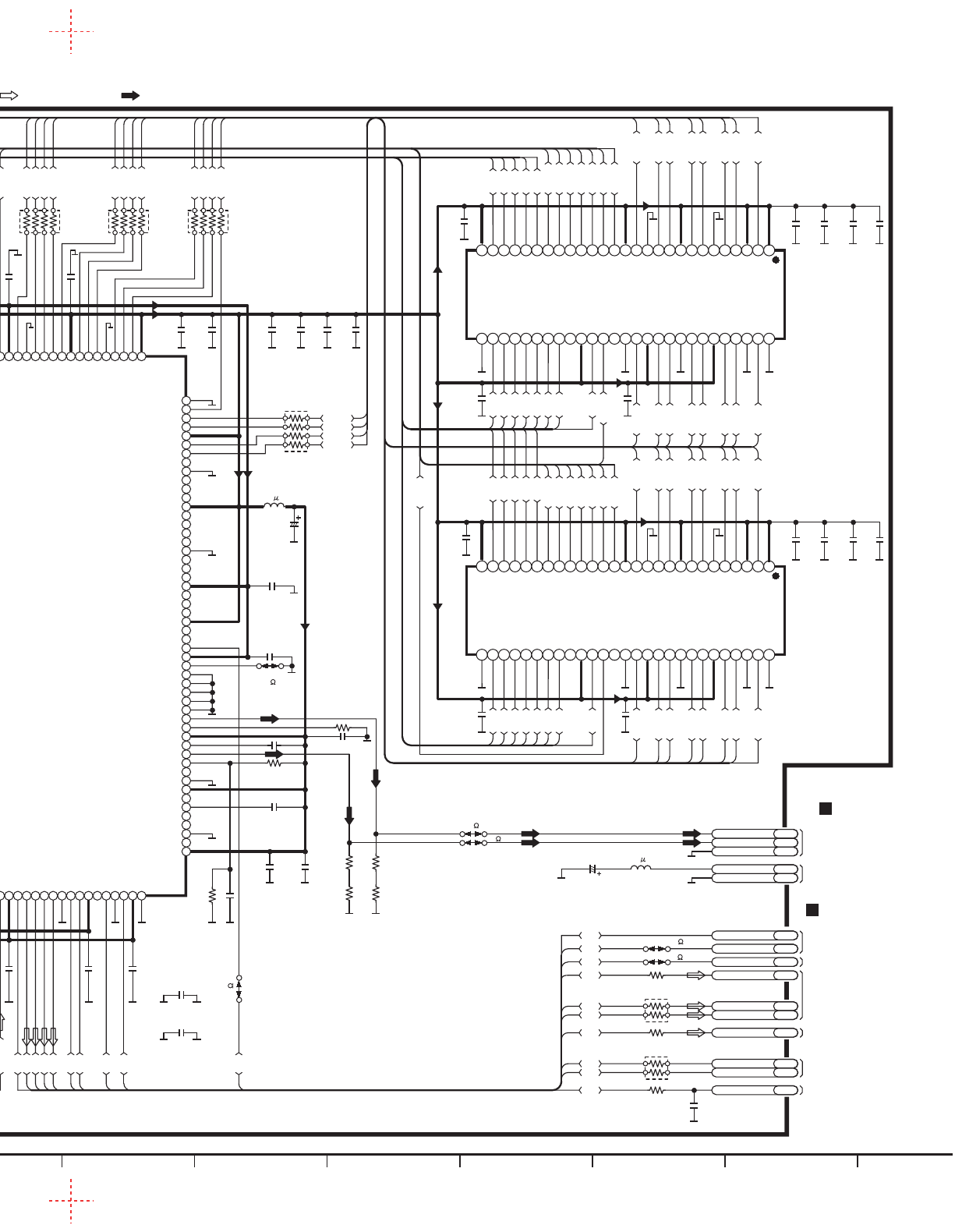
121110987654321
A
B
C
D
E
F
G
H
DVD MODULE(AVDEC) CIRCUIT
SCHEMATIC DIAGRAM
-
4
SL-DV290(EE,GN) DVD MODULE(AVDEC) CIRCUIT DIAGRAM
IC3001
MN6775511
AV DECODER
RA3004
82
AV1IRQCD1
NRSTFS18
AV2IRQCD2
RA3001
1K
LB3001
J0JHC0000045
RA3012
82
WAITSC27 NWEHCD3 NWELSC29
NRDSC28 NAVCSCD4 SYSCLKCD5
CPUADR1SC10 CPUADR2SC11
CPUADR3SC12 CPUADR4SC13 CPUADR5SC14 CPUADR6SC15
CPUADR7SC16 CPUADR8SC17 CPUADR9SC18 CPUADR10SC19
CPUADR11SC20 CPUADR12SC21 CPUADR13SC22
CPUADR14SC23 CPUADR15SC24 CPUADR16SC25 CPUADR17SC26 CPUDT0SC1 CPUDT1SC2 CPUDT2SC3 CPUDT3SC4 CPUDT4SC5
C3006 0.1
C3004 0.1
C3008 0.1
C3009 0.1
CPUDT5SC6 CPUDT6SC7 CPUDT7SC8
RA3051
100
F9
F8
F7
F6
F5
F4
F3
CPUDT8CD6 CPUDT9CD7 CPUDT10CD8 CPUDT11CD9 CPUDT12CD10 CPUDT13CD11 CPUDT14CD12 CPUDT15CD13 STVALIDSD10 STCLKSD11 STENABLESD1 STD7SD9 STD6SD8 STD5SD7 STD4SD6 STD3SD5 STD2SD4 STD1SD3 STD0SD2
D+3.3VDB1 D.GNDDG1
C3001
6.3V330
C3002
6.3V330
LB3002
J0JHC0000045
D+1.5VDB2
MDQ22
RA3008
82
RA3009 82
RA3006
82
RA3007
82
RA3005
82
C3035
0.1
AOUT1 AD4
AOUT0 AD5
SRCK AD7
LRCK AD8
AUDIO DIGITAL AD9
DMIXOUT AD6
F9
F8
F7
F6
F5
F4
MA3
A+5V AB1
CLK27M AD2
F2
B
C3010
0.1
EXTCLK1 AD1
CLK54M AD10
F10
F2
F10
F1
F3
R3051 100
C3011 0.1
C3012 0.1
R3052 100
RA3053
100
R3009 100
AOUT2 AD3
C3051
22P
F1
D.GNDDG1
VDD
28
VSS VDD
29
A4
30
A5
31
A6
32
A7
33
A8
34
A9
35
A11
36
NC
37
CKE
38
CLK
39
UDQM
40
NC
41
VSS
42
DQ8
43
VDDQ
44
DQ9
45
DQ10
46
VSSQ
47
DQ11
48
DQ12
49
VDDQ
50
DQ13
51
DQ14
52
VSSQ
53
DQ15
54
VSS
A3
A2
A1
A0
A10/AP
BA1
BA0
/CS
/RAS
/CAS
/WE
LDQM
VDD
DQ7
VSSQ
DQ6
DQ5
VDDQ
DQ4
DQ3
VSSQ
DQ2
DQ1
VDDQ
DQ0
127 26 25 24 23 22 21 20 19 18 17 16 15 14 13 12 11 10 98765432
RA3003
82
RA3002
82
RA3013
22
RA3011 82
MDQ23
MDQ21
MDQ20
MDQ19
MDQ18
MDQ17
MDQ16
MDQ24
MDQ25
MDQ26
MDQ27
MDQ28
MDQ29
MDQ30
MDQ31
MDQ22
MDQ25
MDQ23
MDQ24
MDQ26
MDQ21
MDQ27
MDQ20
MDQ28
MDQ19
MDQ29
MDQ18
MDQ30
MDQ17
MDQ31
MDQ16
MA2
MA1
MA0
MA10
MA4
MA5
MA6
MA7
MA8
MA9
MA11
RA3010
82
MA0
MA1
MA2
MA3
MA4
MA5
MA6
MA7
MA8
MA9
MA11
MA10
R3001 22
CLK
CLK
DQM3
DQM2
XWE
XCAS
XRAS
XCSM
BA0
BA1
BA1
DQM3
DQM2
XWE
XCAS
XRAS
XCSM
BA0
VDD
28
VSS VDD
29
A4
30
A5
31
A6
32
A7
33
A8
34
A9
35
A11
36
NC
37
CKE
38
CLK
39
UDQM
40
NC
41
VSS
42
DQ8
43
VDDQ
44
DQ9
45
DQ10
46
VSSQ
47
DQ11
48
DQ12
49
VDDQ
50
DQ13
51
DQ14
52
VSSQ
53
DQ15
54
VSS
A3
A2
A1
A0
A10/AP
BA1
BA0
/CS
/RAS
/CAS
/WE
LDQM
VDD
DQ7
VSSQ
DQ6
DQ5
VDDQ
DQ4
DQ3
VSSQ
DQ2
DQ1
VDDQ
DQ0
127 26 25 24 23 22 21 20 19 18 17 16 15 14 13 12 11 10 98765432
MA4
MA5
MA6
MA7
MA8
MA9
MA11
MA3
MA2
MA1
MA0
MA10
XWE
XCAS
XRAS
XCSM
BA0
BA1
CLK
DQM0
MDQ7
MDQ6
MDQ5
MDQ4
MDQ3
MDQ2
MDQ1
MDQ0
DQM0
DQM1
MDQ8
MDQ9
MDQ10
MDQ11
MDQ12
MDQ13
MDQ14
MDQ15
C3031 0.1
C3036
0.1
C3025
0.1
C3033
0.1
C3024
0.1
C3026
0.1
C3034 0.1
C3007 0.1
C3003
0.1
C3030 0.1
C3032
0.1
C3027
0.1
C3028
0.1
K3003
0
C3068
0.1
C3070
0.1
C3072
0.1
C3073
0.1
C3074
0.1
C3071
0.1
C3069
0.1
C3067
0.1
C3066
0.1
C3064
0.1
C3062
0.1
C3061
0.1
C3063
0.1
C3065
0.1
MDQ5
MDQ10
MDQ4
MDQ11
MDQ3
MDQ12
MDQ2
MDQ13
MDQ1
MDQ14
MDQ0
MDQ15
DQM1
MDQ7
MDQ8
MDQ6
MDQ9
YVD4
CVD5
C3110
6.3V100
R3006 15K
C3022 0.1
C3021 1
L3001
10 H
C3019 1
C3018
0.1
R3007 2K
C3038
0.1
R3008
1.3K
C3023 0.1
C3017 0.1
C3015 0.1
C3016 0.1
C3014 0.1
R3010 100
L3091
10 H
C3037
6.3V330
A.GND AG1
CPUDT0
CPUDT1
CPUDT2
CPUDT3
CPUDT4
CPUDT5
CPUDT6
CPUDT7
CPUDT8
CPUDT9
CPUDT10
CPUDT11
CPUDT12
CPUDT13
CPUDT14
CPUDT15
STVALID
STCLK
STENABLE
STD7
STD6
STD5
STD4
STD3
STD2
STD1
STD0
CPUDT0
CPUDT1
CPUDT2
CPUDT3
CPUDT4
CPUDT5
CPUDT6
CPUDT7
CPUDT8
CPUDT9
CPUDT10
CPUDT11
CPUDT12
CPUDT13
CPUDT14
CPUDT15
STVALID
STCLK
STD7
STD6
STD5
STD4
STD3
STD2
STD1
STD0
STENABLE
Vss
157
12
HMD
22
XWR
64
VSS
77
VDD
AVss
113
VREF
115
AVDD
118
Vss
122
TESTSEL1
125
VCLK
128
VDD
131
VDIN5
132
VDIN3
134
Vss
139
VDOUT1
141
MDQ19
161
MDQ29
167
MDQ17
175
MA4
178
Vss
182
MCK
185
MA1
187
53
VSS
PLLAVDD
105
1
VDD
2MDQ9
3MDQ5
4MDQ10
5
LVDD
6MDQ4
7MDQ11
8MDQ3
9Vss
10
MDQ12
11
VDD
13
XRST
14
MDQ2
15
Vss
16
LVDD
17
XHINT
18
XHINT2
19
XDK
20
Vss
21
XWRH
23
XRD
24
XCS
25
VDD
26
HCLK
27
HA1
28
HA2
29
HA3
30
HA4
31
Vss
32
HA5
33
HA6
34
HA7
35
HA8
36
HA9
37
LVDD
38
HA10
39
HA11
40
HA12
41
HA13
42
HA14
43
Vss
44
HA15
45
HA16
46
HA17
47
HD0
48
VDD
49
HD1
50
HD2
51
HD3
52
HD4
54
HD5
55
HD6
56
HD7
57
LVDD
58
HD8
59
HD9
60
HD10
61
VDD
62
HD11
63
HD12
65
HD13
66
HD14
67
HD15
68
VDD
69
DSTR
70
MDQ1
71
MDQ13
72
VSS
73
STD7
74
STD6
75
STD5
76
STD4
78
STD3
79
STD2
80
STD1
81
STD0
82
VDD
83
IECOUT
84
MDQ14
85
VDD
86
DVALID
87
MDQ0
88
MDQ15
89
VSS
90
STRQ
91
ADOUT0
92
ADOUT1
93
ADOUT2
94
ADOUT3
95
Vss
96
SRCK
97
LRCK
98
LVDD
99
PHCOMPO
100
EXTCK
101
CLK121
102
PCLK
103
VDD
104
VSS
TCPOUT
106
PLLVss
107
DAC3OUT
108
DAC1OUT
109
COMP2
110
IREF2
111
AVDD
112
DAC2OUT
114
DAC4OUT
116
COMP1
117
IREF1
119
DAC5OUT
120
AVss
121
DCTEST
123
TESTSEL2
124
TESTSEL0
126
LVDD
127
VDIN7
129
VDIN6
130
VDIN4
133
LVDD
135
VDIN2
136
VDIN1/XVSYNCO
137
VDIN0/XHSYNCO
138
VDOUT0
140
VDOUT2
142
VDOUT3
143
VDD
144
VDOUT4
145
VDOUT5
146
VDOUT6
147
Vss
148
VDOUT7
149
MDQ24
150
MDQ23
151
VDD
152
MDQ25
153
MDQ22
154
MDQ26
155
Vss
156
MDQ16
158
MDQ27
159
VDD
160
MDQ20
162
Vss
163
MDQ31
164
MDQ28
165
VDD
166
MDQ30
168
Vss
169
MDQ18
170
DQM3
171
VDD
172
DQM2
173
LVDD
174
MDQ21
176
MA3
177
VDD
179
MA2
180
MA5
181
MCKI
183
LVDD
184
MA10
186
VDD
188
MA6
189
MA0
190
MA8
191
MA7
192
XWE
193
MA11
194
XCAS
195
XRAS
196
VDD
197
BA0
198
XCSM
199
Vss
200
BA1
201
MA9
202
DQM0
203
DQM1
204
MDQ7
205
MDQ8
206
MDQ6
207
Vss
208
C3013 0.1
C3039
0.1
C3020
0.1
R3106
62
R3107
18
K3106
0
K3101 0
R3101
62
R3102
15 C3029
0.1
K3002
0
C3005
0.1
To DVD MODULE
(CPU) CIRCUIT on
B
To DVD MODULE
(VIDEO DAC)
CIRCUIT on
B
To DVD MODULE
(AUDIO DAC) CIRCUIT on
B
SCHEMATIC
DIAGRAM-6/1-C
K3011 0
K3009 0
K3007
0
SCHEMATIC
DIAGRAM-7/1-H
SCHEMATIC
DIAGRAM-5/1-D
SCHEMATIC
DIAGRAM-5/1-G
To DVD MODULE
(CPU) CIRCUIT on
B
SCHEMATIC
DIAGRAM-7/1-G
SCHEMATIC
DIAGRAM-7/1-E,F
SCHEMATIC
DIAGRAM-7/1-D
To DVD MODULE
(CPU) CIRCUIT on
B
SCHEMATIC
DIAGRAM-7/12-D
To DVD MODULE
(CPU) CIRCUIT on
B
SCHEMATIC
DIAGRAM-7/12-A,B
To DVD MODULE
(SODC) CIRCUIT on
B
SCHEMATIC
DIAGRAM-3/12-H
To DVD MODULE
(VIDEO DAC)
CIRCUIT on
B
SCHEMATIC
DIAGRAM-5/12-D
SCHEMATIC
DIAGRAM-5/1-F
SCHEMATIC
DIAGRAM-6/12-A
SCHEMATIC
DIAGRAM-6/1-F
SCHEMATIC
DIAGRAM-6/1-F
SCHEMATIC
DIAGRAM-6/12-E
SCHEMATIC
DIAGRAM-6/1-H
To DVD MODULE
(VIDEO DAC)
CIRCUIT on
B
IC3061
C3ABPG000121
MEMORY
IC3062
C3ABPG000121
MEMORY
V.GND VG1
:POSITIVE VOLTAGE LINE :AUDIO/VIDEO SIGNAL LINE
2.3V
2.3V
2.3V
3.3V
3V
2.3V
2.5V
2.8V
2.4V
1.5V
2V
2.3V
3.3V
2V
2.7V
2.6V
3.3V
3.3V
3.3V
3.3V
3.3V
3.3V
3.3V
3.3V
2.8V
3.3V
1.5V
1.7V
2.9V
2.9V
2.8V
2.9V
2.7V
2.9V
3.3V
2.7V
2.6V
2.5V
2.6V
2.8V
2.8V
2.5V
1.5V
2.8V
2.6V
2.4V
3.3V
2.7V
3.1V
3.1V
3.1V
3.3V
3.1V
3.1V
3.1V
3.1V
3.1V
3.3V
3.3V
3.3V
3.3V
1.5V
3.3V
3.3V
3.3V
3.3V
3.3V
3.3V
0V
0V
0V
0V
2.2V
0V
0V
0V
0V
0V
0V
3.3V
1.6V
0V
0V
0V
0V
1.7V
1.7V
1.5V
1.5V
1.6V
3.3V
(1.2V)
(1.2V)
(3.1V)
(3.1V)
(3.1V)
3.3V
2.3V
3.3V
1.3V
0.3V
2.2V
3.3V
1.3V
0.9V
0V
1.5V
1.6V
3.3V
1.5V
3.3V
2.7V
2.3V
3.3V
2.3V
2.3V
2.3V
3.3V
2.3V
2.3V
3V
2.8V
2.5V
2V
3.3V
2.4V
2V
2.3V
2.6V
2.7V
1.5V
2.1V
2.1V
3.3V
1.6V
1.6V
0.3V
1.7V
0V
1.6V
0V
3.3V
1.7V
1.5V
1.7V
0V
0V
0V
0V
3.2V
3.3V
1.5V
0V
1.6V
3V
3.2V
3.1V
2.1V
3.3V
2.1V
2.3V
2.7V
2.3V
1.6V
1.7V
1.6V
0V
0V
0V
0V
3.3V
1.7V
2.1V
2.7V
3.3V
2.3V
2.3V
2.3V
2.8V
3.3V
2V
2V
2.6V
3.3V
2.7V
3.3V
2.3V
2.4V
2.5V
3V
3.3V
2.3V
2.3V
2.3V
3.3V
2.1V
3.2V
3.1V
3.2V
3V
1.5V
1.6V
0V
0V
0V
0.3V
1.6V
3.3V
3.3V
2.7V
3.3V
2.3V
2.4V
2.5V
3V
3.3V
2.3V
2.3V
2.3V
3.3V
2.1V
3.2V
3.1V
3.2V
3V
1.5V
1.6V
0V
0V
0V
0.3V
1.6V
3.3V
1.6V
1.7V
1.6V
0V
0V
0V
0V
3.3V
1.7V
2.1V
2.7V
3.3V
2.3V
2.3V
2.3V
2.8V
3.3V
2V
2V
2.6V
(1.6V)
(2V)
(2.3V)
(2.3V)
(2.2V)
(1.8V)
(2.2V)
(1.7V)
(1.9V)
(2.2V)
(2.2V)
(2.2V)
(2.2V)
(2V)
(2.2V)
(2.1V)
(2.8V)
(2V)
(3.1V)
(3.1V)
(3.1V)
(3.1V)
(2.6V)
(3.3V)
(1.6V)
(0.6V)
(2.5V)
(2.5V)
(2.4V)
(2.4V)
(2.3V)
(2.4V)
(2.3V)
(2.4V)
(2.3V)
(2.3V) (1.8V)
:AUDIO SIGNAL LINE :VIDEO SIGNAL LINE
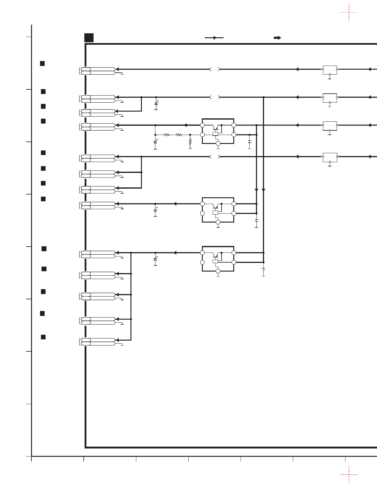
121110987654321
A
B
C
D
E
F
G
H
YVD4
CVD5
SCHEMATIC DIAGRAM-4/12-C
To DVD MODULE
(AVDEC) CIRCUIT on
B
TRV-SW+ VD9
TRV-SW+ VD9
TRAY REF VD6
TRAY/ TRV VD10
MUTE4 VD8
TRAY DRV VD7
To DVD MODULE
(FEP) CIRCUIT on
B
SCHEMATIC DIAGRAM-2/12-H
SCHEMATIC DIAGRAM-3/1-C
To DVD MODULE
(SODC) CIRCUIT on
B
To MAIN CIRCUIT(CN2)
on SCHEMATIC
DIAGRAM
-
8/11,12-H
C
10
D+2.5V 9D.GND 8
D.GND
7
D+5V
6
D+5V
5
M.GND
4
M.GND
3
M+9V
2
M+9V
1
D.GND
FP3202
16
A.GND
15
A+5V
14
A+5V
13
D.GND
12
D.GND
11
D+2.5V
17
A.GND
A+5VAB1 A.GNDAG1
B
DSPCLK CV6
STATUS CV5
CMD CV4
100LB3201 100LB3202
LB3203
100
FL6254
F1H0J1050018
FL6253
F1H0J1050018
D+5VDB3 D.GNDDG1
C6257
6.3V100
FL6255
VLF1491S104T
M+9VMB1 M.GNDMG1
FL6251
F1H0J1050018
D+1.5VDB2
IC6251
C0DBEZG00011
REGULATOR
D.GNDDG1 R6251
100
R6253
1K
R6252
100
C6251
10V10
C6254
0.1
IC6252
C0DBFFG00004
REGULATOR
C6255
0.1
D+1.8VDB4 D.GNDDG1
C6252
10V10
IC6253
C0DBCGE00002
REGULATOR
C6256
0.1
D+3.3VDB1 D.GNDDG1
D+3.3VDB1 D.GNDDG1
D+3.3VDB1 D.GNDDG1
D+3.3VDB1 D.GNDDG1
D+3.3VDB1 D.GNDDG1
C6253
10V10
LB3206
VLP0146-T
A+5VAB1 A.GNDAG1
A+5VAB1 A.GNDAG1
D+5VDB3 D.GNDDG1
OUT IN
ON/OFF
GND 5
2
13
4NC
OUT IN
ON/OFF
GND 5
2
13
4NC
OUT IN
ON/OFF
GND 5
2
13
4VR
DVD MODULE(VIDEO DAC) CIRCUIT
SCHEMATIC DIAGRAM
-
5
SL-DV290(EE,GN) DVD MODULE(VIDEO DAC) CIRCUIT DIAGRAM
SCHEMATIC DIAGRAM-7/1-A
To DVD MODULE
(CPU) CIRCUIT on
B
To DVD MODULE
(FEP) CIRCUIT on
B
To DVD MODULE
(AUDIO DAC) CIRCUIT on
B
SCHEMATIC DIAGRAM-4/1-G
To DVD MODULE
(AVDEC) CIRCUIT on
B
SCHEMATIC DIAGRAM-2/12-G
To DVD MODULE
(FEP) CIRCUIT on
B
SCHEMATIC DIAGRAM-2/12-H
To DVD MODULE
(FEP) CIRCUIT on
B
SCHEMATIC DIAGRAM-2/12-G
SCHEMATIC DIAGRAM-4/12-C
To DVD MODULE
(AVDEC) CIRCUIT on
B
To DVD MODULE
(SODC) CIRCUIT on
B
SCHEMATIC DIAGRAM-3/12-E
SCHEMATIC DIAGRAM-3/1-H
To DVD MODULE
(SODC) CIRCUIT on
B
To DVD MODULE
(FEP) CIRCUIT on
B
SCHEMATIC DIAGRAM-2/12-G
SCHEMATIC DIAGRAM-3/1-H
To DVD MODULE
(SODC) CIRCUIT on
B
SCHEMATIC DIAGRAM-4/1-G
To DVD MODULE
(AVDEC) CIRCUIT on
B
SCHEMATIC DIAGRAM-6/1-F
SCHEMATIC DIAGRAM-7/12-H
To DVD MODULE
(CPU) CIRCUIT on
B
9
8
7
CB/ PB/ B
6
5
YC-OUT/CR/PR/R
4
3
C-OUT
2
V.GND
1
Y-OUT 15
TRAY/ TRV
14
TRV-SW+
13
TRAY MUT
12
TRAY DRV
11
TRAY REF
10
V.GND
V.GND
V.GND
Y/ PY/ G
D.GND
To MAIN CIRCUIT
(CN501) on
SCHEMATIC DIAGRAM-9/15,16-H
C
FP3203
DSPCLK CV6
STATUS CV5
CMD CV4
SCHEMATIC DIAGRAM-7/1-C
To DVD MODULE
(CPU) CIRCUIT on
B
To DVD MODULE
(AUDIO DAC) CIRCUIT on
B
SCHEMATIC DIAGRAM-6/12-E
LB3205
VLP0146-T
V.GND VG1
10
9
8
7
6
5
4
3
2
1
16
15
14
13
12
11
17
9
8
7
6
5
4
3
2
1
15
14
13
12
11
10
9V9V
5V
2.5V
2.5V
1.5V
1.3V
2.5V
2.5V
1.8V
5V
5V
3.3V
5V
2.5V
5V5V
:POSITIVE VOLTAGE LINE :VIDEO SIGNAL LINE
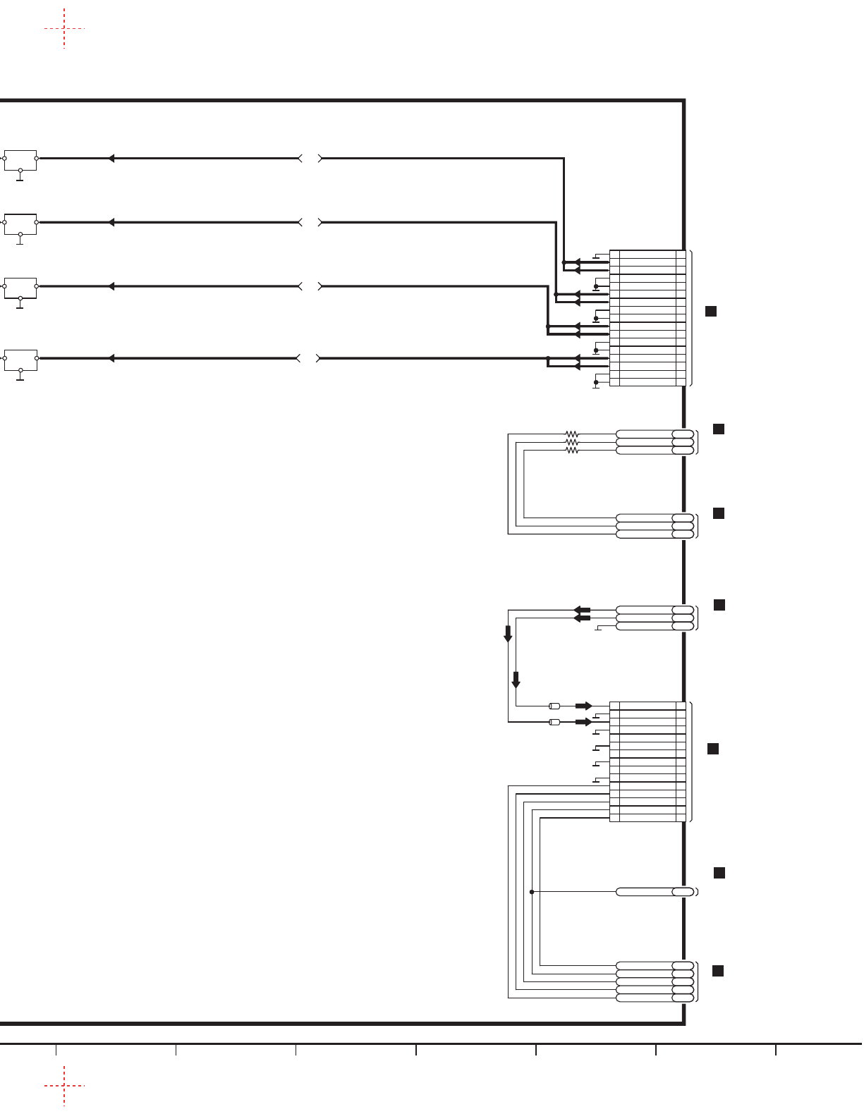
121110987654321
A
B
C
D
E
F
G
H
YVD4
CVD5
SCHEMATIC DIAGRAM-4/12-C
To DVD MODULE
(AVDEC) CIRCUIT on
B
TRV-SW+ VD9
TRV-SW+ VD9
TRAY REF VD6
TRAY/ TRV VD10
MUTE4 VD8
TRAY DRV VD7
To DVD MODULE
(FEP) CIRCUIT on
B
SCHEMATIC DIAGRAM-2/12-H
SCHEMATIC DIAGRAM-3/1-C
To DVD MODULE
(SODC) CIRCUIT on
B
To MAIN CIRCUIT(CN2)
on SCHEMATIC
DIAGRAM
-
8/11,12-H
C
10
D+2.5V 9D.GND 8
D.GND
7
D+5V
6
D+5V
5
M.GND
4
M.GND
3
M+9V
2
M+9V
1
D.GND
FP3202
16
A.GND
15
A+5V
14
A+5V
13
D.GND
12
D.GND
11
D+2.5V
17
A.GND
A+5VAB1 A.GNDAG1
B
DSPCLK CV6
STATUS CV5
CMD CV4
100LB3201 100LB3202
LB3203
100
FL6254
F1H0J1050018
FL6253
F1H0J1050018
D+5VDB3 D.GNDDG1
C6257
6.3V100
FL6255
VLF1491S104T
M+9VMB1 M.GNDMG1
FL6251
F1H0J1050018
D+1.5VDB2
IC6251
C0DBEZG00011
REGULATOR
D.GNDDG1 R6251
100
R6253
1K
R6252
100
C6251
10V10
C6254
0.1
IC6252
C0DBFFG00004
REGULATOR
C6255
0.1
D+1.8VDB4 D.GNDDG1
C6252
10V10
IC6253
C0DBCGE00002
REGULATOR
C6256
0.1
D+3.3VDB1 D.GNDDG1
D+3.3VDB1 D.GNDDG1
D+3.3VDB1 D.GNDDG1
D+3.3VDB1 D.GNDDG1
D+3.3VDB1 D.GNDDG1
C6253
10V10
LB3206
VLP0146-T
A+5VAB1 A.GNDAG1
A+5VAB1 A.GNDAG1
D+5VDB3 D.GNDDG1
OUT IN
ON/OFF
GND 5
2
13
4NC
OUT IN
ON/OFF
GND 5
2
13
4NC
OUT IN
ON/OFF
GND 5
2
13
4VR
DVD MODULE(VIDEO DAC) CIRCUIT
SCHEMATIC DIAGRAM
-
5
SL-DV290(EE,GN) DVD MODULE(VIDEO DAC) CIRCUIT DIAGRAM
SCHEMATIC DIAGRAM-7/1-A
To DVD MODULE
(CPU) CIRCUIT on
B
To DVD MODULE
(FEP) CIRCUIT on
B
To DVD MODULE
(AUDIO DAC) CIRCUIT on
B
SCHEMATIC DIAGRAM-4/1-G
To DVD MODULE
(AVDEC) CIRCUIT on
B
SCHEMATIC DIAGRAM-2/12-G
To DVD MODULE
(FEP) CIRCUIT on
B
SCHEMATIC DIAGRAM-2/12-H
To DVD MODULE
(FEP) CIRCUIT on
B
SCHEMATIC DIAGRAM-2/12-G
SCHEMATIC DIAGRAM-4/12-C
To DVD MODULE
(AVDEC) CIRCUIT on
B
To DVD MODULE
(SODC) CIRCUIT on
B
SCHEMATIC DIAGRAM-3/12-E
SCHEMATIC DIAGRAM-3/1-H
To DVD MODULE
(SODC) CIRCUIT on
B
To DVD MODULE
(FEP) CIRCUIT on
B
SCHEMATIC DIAGRAM-2/12-G
SCHEMATIC DIAGRAM-3/1-H
To DVD MODULE
(SODC) CIRCUIT on
B
SCHEMATIC DIAGRAM-4/1-G
To DVD MODULE
(AVDEC) CIRCUIT on
B
SCHEMATIC DIAGRAM-6/1-F
SCHEMATIC DIAGRAM-7/12-H
To DVD MODULE
(CPU) CIRCUIT on
B
9
8
7
CB/ PB/ B
6
5
YC-OUT/CR/PR/R
4
3
C-OUT
2
V.GND
1
Y-OUT 15
TRAY/ TRV
14
TRV-SW+
13
TRAY MUT
12
TRAY DRV
11
TRAY REF
10
V.GND
V.GND
V.GND
Y/ PY/ G
D.GND
To MAIN CIRCUIT
(CN501) on
SCHEMATIC DIAGRAM-9/15,16-H
C
FP3203
DSPCLK CV6
STATUS CV5
CMD CV4
SCHEMATIC DIAGRAM-7/1-C
To DVD MODULE
(CPU) CIRCUIT on
B
To DVD MODULE
(AUDIO DAC) CIRCUIT on
B
SCHEMATIC DIAGRAM-6/12-E
LB3205
VLP0146-T
V.GND VG1
10
9
8
7
6
5
4
3
2
1
16
15
14
13
12
11
17
9
8
7
6
5
4
3
2
1
15
14
13
12
11
10
9V9V
5V
2.5V
2.5V
1.5V
1.3V
2.5V
2.5V
1.8V
5V
5V
3.3V
5V
2.5V
5V5V
:POSITIVE VOLTAGE LINE :VIDEO SIGNAL LINE
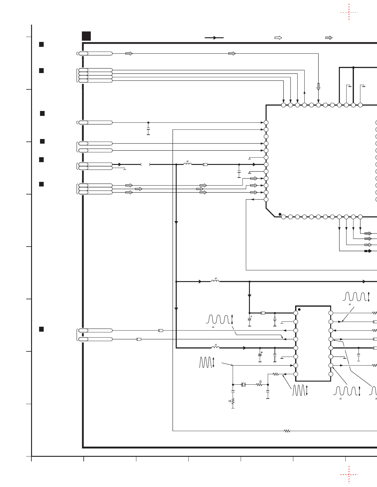
121110987654321
A
B
C
D
E
F
G
H
DMIXOUTAD6
D+3.3VDB1
C4216
6.3V100
C4219
10V10
C4220
10V10
C4215
0.1
C4210
0.1
37 RSTB
38 SCLKI
39 SCLKO
40 BCKIN
41 LRCIN
42 TEST
43 VDD
44 D.GND
45 DIN1
46 DIN2
47 DIN3
48 ZFLGA
1
ZFLG1
2
ZFLG2
3
ZFLG3
4
ZFLG4
5
ZFLG5
6
ZFLG6
7
N.C.
8
N.C.
9
VOUT6
10
VOUT5
11
VOUT4
12
VOUT3
13
VOUT2
14
VOUT1
15
VCOM
16
VOUT7
17
A.GND
18
VCC
19
A.GND
20
VOUT8
21
A.GND
22
VCC
23
A.GND
24
VCC
25
A.GND
26
VCC
27
A.GND
28
VCC
29
N.C.
30
ZERO7
31
DATA4
32
ZERO8
33
MDO
34
MDI
35
MC
36
ML
LB4200
VLP0146-T
L4211
22 H
C4217
0.1
SBI1AC1 SBO1AC2 SBT1AC3 STBDAC2AC4
NRSTFS18
SRCKAD7
LRCKAD8
AOUT0AD5 AOUT1AD4 AOUT2AD3
LB4207
LB4208
LB4210
LB4211
LB4212
LB4215
FL4201
F1H0J1050018
C4222
6.3V330
C4223
6.3V330
IC4211
C0FBBK000036
8ch AUDIO D/A CONVERTER
C6566
0.1
C6564
0.1
C6563
4V47
L6562
22 H
LB6561
VLP0146-T
LB6563
VLP0155-T
C6561
4V47
IC6561
C1DB00000582
CLOCK GENERATOR
L6561
22 H
C6568
0.1
LB6567
LB6566
R6563
10K
R6565 47
LB6564
47
X6501
(36.864MHz)
C6505
15P
C6503
12P
R6503
330
CLK27MAD2
D.GNDDG1
R6566
10
CLK33M AC8
CLKSEL AC5
CLK16M1 SA1
B
AC3H AC6
AMUT AC7
EXTCLK1 AD1
C4211
10V10
1VDD1
2VSS1
3CLK54
4CLK27
5VDD2
6VSS2
7XTI
8XTO
16
CE
15
CLK33
14
FSEL
13
CLK16
12
VDD3
11
VSS3
10
768fs
9
384fs
C4208
0.1
C4209
0.1
LB6562
VLP0155-T
CLK54MAD10
C4234
0.1
C4207
0.1 C4235
0.1
C4236
0.1 C4237
0.1
0
VLP0155-T
K4202
0
K4203
0
K4204
0
K4205
0
VLP0155-T
RLBV601AV-Y
VLP0146-T
LB6565
DSPCLK CV6
STATUS CV5
CMD CV4
DVD MODULE(AUDIO DAC) CIRCUIT
SCHEMATIC DIAGRAM
-
6
SL-DV290(EE,GN) DVD MODULE(AUDIO DAC) CIRCUIT DIAGRAM
To DVD MODULE
(CPU) CIRCUIT on
B
To DVD MODULE
(VIDEO DAC)
CIRCUIT on
B
SCHEMATIC DIAGRAM-5/1-C
To DVD MODULE
(SODC) CIRCUIT on
B
SCHEMATIC DIAGRAM-7/12-G
SCHEMATIC DIAGRAM-4/12-A
To DVD MODULE
(AVDEC) CIRCUIT on
B
To DVD MODULE
(CPU) CIRCUIT on
B
SCHEMATIC DIAGRAM-7/1-H
SCHEMATIC DIAGRAM-4/12-A
To DVD MODULE
(AVDEC) CIRCUIT on
B
SCHEMATIC DIAGRAM-4/12-A
To DVD MODULE
(AVDEC) CIRCUIT on
B
To DVD MODULE
(VIDEO DAC) CIRCUIT on
B
SCHEMATIC DIAGRAM-5/12-E
SCHEMATIC DIAGRAM-4/12-B
To DVD MODULE
(AVDEC) CIRCUIT on
B
K4207
47
To DVD MODULE
(CPU) CIRCUIT on
B
SCHEMATIC DIAGRAM-7/12-G
SCHEMATIC DIAGRAM-7/1-E
SCHEMATIC DIAGRAM-7/1-D
SCHEMATIC DIAGRAM-7/1-E
SCHEMATIC DIAGRAM-3/1-A
To DVD MODULE
(AVDEC) CIRCUIT on
B
SCHEMATIC DIAGRAM-4/12-B
17
ADAC5V
18
AC3H/DACMUT
19
AMUT
20
ZFLAG
21
22
23
24
CMD
STAT
CLK
11
FL
12
13
MIX R 14
15
16
10
9
FR
8
7
6
5
SR
4
3
CNT
2
A.GND
1
SW
A.GND
A.GND
SL
A.GND
A.GND
A.GND
A.GND
MIX L
ADAC5V
D.GND
FP4202
25
26
AUDIO DIGITAL
D.GND
To MAIN CIRCUIT
(CN301)
on SCHEMATIC
DIAGRAM
-
8/9,10-H
C
R6505
0
R6504
0
LB4209
LB4201
VLP0155-T AUDIO DIGITAL AD9
To DVD MODULE
(AVDEC) CIRCUIT on
B
SCHEMATIC DIAGRAM-4/12-A
LB4214 0
VLP0155-T
VLP0155-T
VLP0155-T
VLP0155-T
VLP0155-T
A
B
C
D
E
F
G
H
A
B
D
C
E
F
H
G
17
18
19
20
21
22
23
24
11
12
13
14
15
16
10
9
8
7
6
5
4
3
2
1
25
26
5V
1.4V
1.5V
3.3V
1.5V
3.3V
1.7V
3.3V
1.5V
3.3V
1.6V
3.3V
3.3V
1.7V
1.7V
3.3V
(1.2V) 0V
0V
0V
(3.2V) 0V
2.5V
2.5V
2.5V
2.5V
2.5V
2.5V
2.5V
2.5V
5V
2.5V
5V
5V
5V
5V
0V(1.2V)
3.3V
3.3V
2.8V
3.3V
1.0V
P-P
F=36.864MHz
1.0V
P-P
F=36.864MHz
3.2V
P-P
0.2 s. 1V/DIV.
3.0V
P-P
0.2 s. 1V/DIV.
3.1V
P-P
0.2 s. 1V/DIV.
3.4V
P-P
0.2 s. 1V/DIV.
3.3V
1.5V
1.6V
:POSITIVE VOLTAGE LINE :AUDIO SIGNAL LINE :SURROUND SP. SIGNAL LINE :CENTER SP. SIGNAL LINE :SUB WOOFER SIGNAL LINE

121110987654321
A
B
C
D
E
F
G
H
CPUDT15 CD13
CPUDT14 CD12
CPUDT13 CD11
CPUDT12 CD10
CPUDT11 CD9
CPUDT10 CD8
CPUDT9 CD7
CPUDT8 CD6
CPUDT7 SC8
CPUDT6 SC7
CPUDT5 SC6
CPUDT4 SC5
CPUDT3 SC4
CPUDT2 SC3
CPUDT1 SC2
CPUDT0 SC1
CPUDT7 SC8
CPUDT6 SC7
CPUDT5 SC6
CPUDT4 SC5
CPUDT3 SC4
CPUDT2 SC3
CPUDT1 SC2
CPUDT0 SC1
CPUADR17 SC26
CPUADR16 SC25
CPUADR15 SC24
CPUADR14 SC23
CPUADR13 SC22
CPUADR12 SC21
CPUADR11 SC20
CPUADR10 SC19
CPUADR9 SC18
CPUADR8 SC17
CPUADR7 SC16
CPUADR6 SC15
CPUADR5 SC14
CPUADR4 SC13
CPUADR3 SC12
CPUADR2 SC11
CPUADR1 SC10
CPUADR17 SC26
CPUADR16 SC25
CPUADR15 SC24
CPUADR14 SC23
CPUADR13 SC22
CPUADR12 SC21
CPUADR11 SC20
CPUADR10 SC19
CPUADR9 SC18
CPUADR8 SC17
CPUADR7 SC16
CPUADR6 SC15
CPUADR5 SC14
CPUADR4 SC13
CPUADR3 SC12
CPUADR2 SC11
CPUADR1 SC10
CPUADR0 SC9
STBDAC2 AC4
SBT1 AC3
SBO1 AC2
SBI1 AC1
D.GND DG1
D+3.3V DB1
CPUADR0
CPUADR1
CPUADR2
CPUADR3
CPUADR4
CPUADR5
CPUADR6
CPUADR7
CPUADR8
CPUADR9
CPUADR10
CPUADR11
CPUADR12
CPUADR13
CPUADR14
CPUADR15
CPUADR16
CPUADR17
CPUDT0
CPUDT1
CPUDT2
CPUDT3
CPUDT4
CPUDT5
CPUDT6
CPUDT7
CPUDT8
CPUDT9
CPUDT10
CPUDT11
CPUDT12
CPUDT13
CPUDT14
CPUDT15
I7
I6
I5
I4
I3
I2
I1
LB6201
VLP0146-T
CPUDT0
CPUDT1
CPUDT2
CPUDT3
CPUDT4
CPUDT5
CPUDT6
CPUDT7
CPUDT8
CPUDT9
CPUDT10
CPUDT11
CPUDT12
CPUDT13
CPUDT14
CPUDT15
G3
G4
G5
G6
I4
I3
I5
I1
I2
I7
CPUADR4
CPUADR5
CPUADR6
CPUADR7
CPUADR8
CPUADR9
CPUADR10
CPUADR11
CPUADR12
CPUADR13
CPUADR14
CPUADR15
CPUADR16
CPUADR17
CPUADR18
CPUADR19
CPUADR20
CPUADR21
RA6202
10K
CPUADR3
CPUADR2
CPUADR1
CPUADR0
RA6205
10K
RA6204
10K
IC6301
C3FBND000098
16M FLASH MEMORY
CPUDT15
CPUDT7
CPUDT14
CPUDT6
CPUDT13
CPUDT5
CPUDT12
CPUDT4
CPUDT11
CPUDT3
CPUDT10
CPUDT2
CPUDT9
CPUDT1
CPUDT8
CPUDT0
CPUADR16
CPUADR17
CPUADR15
CPUADR14
CPUADR13
CPUADR12
CPUADR11
CPUADR10
CPUADR9
CPUADR20
CPUADR19
CPUADR18
CPUADR8
CPUADR7
CPUADR6
CPUADR5
CPUADR4
CPUADR3
CPUADR2
CPUADR1
IC6211
PST596JNR
RESET
Q6215
UN5212TX
RESET
RA6206
47K
G1
C6215
0.1
R6216
1K
D6215
MA728TX
GND3
SUB
2
M/R1
4VOUT
5VCC
C6211
100P
NRSTFS18
AV2IRQCD2 G3
AV1IRQCD1 G4
ODCIRQSC32 G5
ADSCIRQSC31 G6
AMUTAC7 CLKSELAC5
HFMONFC1
NAVCSCD4 NWEHCD3 NWELSC29 NRDSC28 WAITSC27
NSODCCSSC30 NWELSC29 NRDSC28 WAITSC27
R6201
47K
RA6201
10K
R6202
10K
C6206
0.1
SYSCLKCD5
LB6202
VLP0155-T
CLK33MAC8
IC6201
MN102H60GFD
CPU
1WAIT
2NRE
3NWEL/P62
4NWEH/P63
5NCS0/P50
6NCS1/P51
7NCS2/P52
8NCS3/P53
9P54/NBREQ
10
P55/NBRACK
11
P56
12
NWORD
13
A0
14
A1
15
A2
16
A3
17
VDD
18
BOSC/PB0
19
VSS
20
XI/PB1
21
XO
22
VDD
23
OSCI
24
OSCO
25
MODE
26
A4
27
A5
28
A6
29
A7
30
A8
31
A9
32
A10
33
A11
34
AVDD
35
A12
36
A13
37
A14
38
A15
39
A16
40
A17
41
A18
42
A19/P43
43
VREF-
44
A20/P44/AN4
45
A21/P45/AN5
46
A22/P46/AN6
47
A23/P47/AN7
48
P80/DAC0
49
P81/DAC1
50
P82/SBT3
P83/SBI3
51
P84/SBO3
52
P85/SBT4
53
VREF+
54
P86/SBI4
55
P87/SBO4
56
P90
57
P91
58
P92
59
P93
60
AVSS
61
P94/AN0
62
P95/AN1
63
P96/AN2
64
P97/AN3
65
VDD
66
P70/SBT0/RAS
67
P71/SBI0/LCAS
68
P72/SBO0/UCAS
69
P73/SBT1
70
P74/SBI1
71
P75/SBO1
72
PULLUP0
73
PULLUP1
74
NNMI
75
NIRQ0/PA0
76
NIRQ1/PA1
77
NIRQ2/PA2
78
NIRQ3/PA3
79
NIRQ4/PA4
80
ADSEP
81
NRST
82
VDD
83
D0
84
D1
85
D2
86
D3
87
D4
88
D5
89
D6
90
D7
91
VSS
92
D8
93
D9
94
D10
95
D11
96
D12
97
D13
98
D14
99
D15
100
8VCC
A01
A1
2
A2
3
GND
4
7WP
6SCL
5SDA
C6221
0.1
IC6221
C3EBGC000033
EE PROM
LB6221
VLP0146-T
C6222
0.1
IC6222
C0JBAA000001
AND GATE
C6223
0.1
IC6223
C0JBAA000001
AND GATE
D+5VDB3
STATUSCV5 CMDCV4
DSPCLKCV6
DCFLTFC3
C6202
0.1
C6203
0.1
C6205
0.1
1A15 48
A16
2A14
3A13
4A12
5A11
6A10
7A9
8A8
9A19
10 A20
11 XWE
12 XRESET
13 N.C.
14 WP/Acc
15 RDY/XBSY
16 A18
17 A17
18 A7
19 A6
20 A5
21 A4
22 A3
23 A2
24 A1
47
XBYTE
46
VSS
45
DQ15/A-1
44
DQ7
43
DQ14
42
DQ6
41
DQ13
40
DQ5
39
DQ12
38
DQ4
37
VDD
36
DQ11
35
DQ3
34
DQ10
33
DQ2
32
DQ9
31
DQ1
30
DQ8
29
DQ0
28
XOE
27
VSS
26
XCE
25
A0
C6301
0.1
RA6203
4.7K C6201
6.3V33
B
R6211
4.7K
D.GNDDG1
R6206
10K
R6207
4.7K
R6208
4.7K
NRSTFS18
NRSTFS18
G1
K6303
0
CPUADR21
K6301
0
C6302
0.1
I8
I6
NRSTFS18 R6215
10K
C6204
0.1
R6210
100
10 D+3.3V
9RESERVED
8KMODE
7SCSIEN
6258SY
51968SY
4SBI1
3SBO1
2SBT1
1D.GND
PS6201
DVD MODULE(CPU) CIRCUIT
SCHEMATIC DIAGRAM
-
7
SL-DV290(EE,GN) DVD MODULE(CPU) CIRCUIT DIAGRAM
To DVD MODULE
(SODC) CIRCUIT on
B
SCHEMATIC DIAGRAM-4/1-E
To DVD MODULE
(AVDEC) CIRCUIT on
B
To DVD MODULE
(VIDEO DAC)
CIRCUIT on
B
SCHEMATIC DIAGRAM-5/12-F
SCHEMATIC
DIAGRAM-3/1-D,E
To DVD MODULE
(AVDEC) CIRCUIT on
B
SCHEMATIC
DIAGRAM-4/1-B,C
To DVD MODULE
(AUDIO DAC) CIRCUIT on
B
SCHEMATIC DIAGRAM-6/12-C
To DVD MODULE
(FEP) CIRCUIT on
B
SCHEMATIC DIAGRAM-2/12-B
To DVD MODULE
(VIDEO DAC)
CIRCUIT on
B
SCHEMATIC DIAGRAM-5/1-G
To DVD MODULE
(AUDIO DAC) CIRCUIT on
B
SCHEMATIC DIAGRAM-6/12-C
SCHEMATIC DIAGRAM-4/1-D,E
To DVD MODULE
(AVDEC) CIRCUIT on
B
To DVD MODULE
(FEP) CIRCUIT on
B
SCHEMATIC DIAGRAM-2/1-B
SCHEMATIC DIAGRAM-3/1-G
To DVD MODULE
(SODC) CIRCUIT on
B
SCHEMATIC DIAGRAM-3/1-E
SCHEMATIC DIAGRAM-3/1-G
To DVD MODULE
(SODC) CIRCUIT on
B
SCHEMATIC DIAGRAM-3/1-D
To DVD MODULE
(SODC) CIRCUIT on
B
SCHEMATIC DIAGRAM-4/1-F
To DVD MODULE
(AVDEC) CIRCUIT on
B
SCHEMATIC
DIAGRAM-6/1-H
To DVD MODULE
(AUDIO DAC) CIRCUIT on
B
SCHEMATIC DIAGRAM-6/1-G
To DVD MODULE
(FEP) CIRCUIT on
B
SCHEMATIC DIAGRAM-2/1-D
SCHEMATIC DIAGRAM-4/1-D
To DVD MODULE
(AVDEC) CIRCUIT on
B
K6201
0
To DVD MODULE
(AVDEC) CIRCUIT on
B
SCHEMATIC
DIAGRAM-4/1-C,D
To DVD MODULE
(SODC) CIRCUIT on
B
SCHEMATIC
DIAGRAM-3/1-E,F
To DVD MODULE
(AUDIO DAC)
CIRCUIT on
B
SCHEMATIC
DIAGRAM-6/12-C
AC3H AC6
I8
TEST TERMINAL
To DVD MODULE
(VIDEO DAC)
CIRCUIT on
B
SCHEMATIC
DIAGRAM-5/1-C
2
1
4
5
3
Vcc
GND
2
1
4
5
3
Vcc
GND
5V
3V
3V
5V
4.5V
2.7V
2.7V
5V
4.1V 3.3V
3.3V
3.3V
3.3V
3.3V
3.3V
3.3V
3.3V
3.3V
0V
3.3V
2.8V
3.3V
3.3V
3.3V
3.3V
2.8V
3.3V
3.3V
0V
3.3V
2.3V
2.9V
2.9V
2.8V
3.3V
1.7V
3.3V
1.7V
3.3V
(2V)
(2.8V)
(2V)
(1.2V)
(2.1V)
(2.2V)
(2V)
2.9V
2.7V
2.9V
2.7V
2.6V
2.5V
2.6V
2.8V
3.3V
2.8V
2.5V
2.8V
2.6V
2.4V
2.7V
2.6V
2.3V
2.5V
2.3V
3V
(1.6V)
(1.8V)
(1.6V)
(2V)
(3.3V)
(1.8V)
(2.2V)
(2.3V)
(2.2V)
(1.7V)
(1.9V)
(2.2V)
(2.2V)
(2.2V)
(1V)
(1V)
0V
2.7V
3.3V
3.3V
3.3V
3.3V
0V
0V
3.3V
3.3V
3.3V
2.8V
3.3V
3.3V
3.3V
3.3V
3.3V
3.3V
3.3V
3.3V
3.3V
3.3V
3.3V
3.3V
3.1V
3.1V
3.1V
3.1V
3.1V
3.1V
3.1V
3.1V
3.3V
3.3V
3.3V
3.3V
3.3V
3.3V
3.3V
3.3V
(2.3V)
(2.3V)
(2.4V)
(2.3V)
(2.4V)
(2.3V)
(2.4V)
(2.4V)
(2.5V)
(2.5V)
(2V)
2.6V
(1.6V)
2.4V
(3.3V)
2.8V
(1.8V)
2.5V
(2.2V)
2.8V
(2.3V)
2.8V
(2.2V)
2.6V
(1.7V)
2.5V
(1.3V)
2.5V
3.3V
(1V)
2.3V
(1.6V)
2.6V
(1.9V)
2.6V
(2.2V)
2.7V
(2.2V)
2.9V
(2.2V)
2.7V
(2.2V)
2.9V
(2V)
2.8V
(2.2V)
2.9V
3.3V
3.3V
(1.8V)
2.7V
3.3V
3.1V
3.3V
3.1V
(2V)
2.8V
(2V)
2.8V
(2.1V)
2.9V
3.3V
1.5V
P-P
0.2 s. 0.5V/DIV.
3.3V
(1.3V)
(2.2V)
(0V) (1V)
2.3V
3.3V
3.1V
3.3V
3.1V
3.3V
3.1V
3.3V
3.3V
3.1V
3.3V
3.1V
3.3V
3.1V
(0V)
(2.5V)
(2.3V)
(2.4V)
(2.3V)
(2.4V)
(2.3V)
(2.5V)
(2.4V)
(2.3V)
(2.4V)
:POSITIVE VOLTAGE LINE
121110987654321
A
B
C
D
E
F
G
H
CPUDT15 CD13
CPUDT14 CD12
CPUDT13 CD11
CPUDT12 CD10
CPUDT11 CD9
CPUDT10 CD8
CPUDT9 CD7
CPUDT8 CD6
CPUDT7 SC8
CPUDT6 SC7
CPUDT5 SC6
CPUDT4 SC5
CPUDT3 SC4
CPUDT2 SC3
CPUDT1 SC2
CPUDT0 SC1
CPUDT7 SC8
CPUDT6 SC7
CPUDT5 SC6
CPUDT4 SC5
CPUDT3 SC4
CPUDT2 SC3
CPUDT1 SC2
CPUDT0 SC1
CPUADR17 SC26
CPUADR16 SC25
CPUADR15 SC24
CPUADR14 SC23
CPUADR13 SC22
CPUADR12 SC21
CPUADR11 SC20
CPUADR10 SC19
CPUADR9 SC18
CPUADR8 SC17
CPUADR7 SC16
CPUADR6 SC15
CPUADR5 SC14
CPUADR4 SC13
CPUADR3 SC12
CPUADR2 SC11
CPUADR1 SC10
CPUADR17 SC26
CPUADR16 SC25
CPUADR15 SC24
CPUADR14 SC23
CPUADR13 SC22
CPUADR12 SC21
CPUADR11 SC20
CPUADR10 SC19
CPUADR9 SC18
CPUADR8 SC17
CPUADR7 SC16
CPUADR6 SC15
CPUADR5 SC14
CPUADR4 SC13
CPUADR3 SC12
CPUADR2 SC11
CPUADR1 SC10
CPUADR0 SC9
STBDAC2 AC4
SBT1 AC3
SBO1 AC2
SBI1 AC1
D.GND DG1
D+3.3V DB1
CPUADR0
CPUADR1
CPUADR2
CPUADR3
CPUADR4
CPUADR5
CPUADR6
CPUADR7
CPUADR8
CPUADR9
CPUADR10
CPUADR11
CPUADR12
CPUADR13
CPUADR14
CPUADR15
CPUADR16
CPUADR17
CPUDT0
CPUDT1
CPUDT2
CPUDT3
CPUDT4
CPUDT5
CPUDT6
CPUDT7
CPUDT8
CPUDT9
CPUDT10
CPUDT11
CPUDT12
CPUDT13
CPUDT14
CPUDT15
I7
I6
I5
I4
I3
I2
I1
LB6201
VLP0146-T
CPUDT0
CPUDT1
CPUDT2
CPUDT3
CPUDT4
CPUDT5
CPUDT6
CPUDT7
CPUDT8
CPUDT9
CPUDT10
CPUDT11
CPUDT12
CPUDT13
CPUDT14
CPUDT15
G3
G4
G5
G6
I4
I3
I5
I1
I2
I7
CPUADR4
CPUADR5
CPUADR6
CPUADR7
CPUADR8
CPUADR9
CPUADR10
CPUADR11
CPUADR12
CPUADR13
CPUADR14
CPUADR15
CPUADR16
CPUADR17
CPUADR18
CPUADR19
CPUADR20
CPUADR21
RA6202
10K
CPUADR3
CPUADR2
CPUADR1
CPUADR0
RA6205
10K
RA6204
10K
IC6301
C3FBND000098
32M FLASH MEMORY
CPUDT15
CPUDT7
CPUDT14
CPUDT6
CPUDT13
CPUDT5
CPUDT12
CPUDT4
CPUDT11
CPUDT3
CPUDT10
CPUDT2
CPUDT9
CPUDT1
CPUDT8
CPUDT0
CPUADR16
CPUADR17
CPUADR15
CPUADR14
CPUADR13
CPUADR12
CPUADR11
CPUADR10
CPUADR9
CPUADR20
CPUADR19
CPUADR18
CPUADR8
CPUADR7
CPUADR6
CPUADR5
CPUADR4
CPUADR3
CPUADR2
CPUADR1
IC6211
PST596JNR
RESET
Q6215
UN5212TX
RESET
RA6206
47K
G1
C6215
0.1
R6216
1K
D6215
MA728TX
GND3
SUB
2
M/R1
4VOUT
5VCC
C6211
100P
NRSTFS18
AV2IRQCD2 G3
AV1IRQCD1 G4
ODCIRQSC32 G5
ADSCIRQSC31 G6
AMUTAC7 CLKSELAC5
HFMONFC1
NAVCSCD4 NWEHCD3 NWELSC29 NRDSC28 WAITSC27
NSODCCSSC30 NWELSC29 NRDSC28 WAITSC27
R6201
47K
RA6201
10K
R6202
10K
C6206
0.1
SYSCLKCD5
LB6202
VLP0155-T
CLK33MAC8
IC6201
MN102H60GFD
CPU
1WAIT
2NRE
3NWEL/P62
4NWEH/P63
5NCS0/P50
6NCS1/P51
7NCS2/P52
8NCS3/P53
9P54/NBREQ
10
P55/NBRACK
11
P56
12
NWORD
13
A0
14
A1
15
A2
16
A3
17
VDD
18
BOSC/PB0
19
VSS
20
XI/PB1
21
XO
22
VDD
23
OSCI
24
OSCO
25
MODE
26
A4
27
A5
28
A6
29
A7
30
A8
31
A9
32
A10
33
A11
34
AVDD
35
A12
36
A13
37
A14
38
A15
39
A16
40
A17
41
A18
42
A19/P43
43
VREF-
44
A20/P44/AN4
45
A21/P45/AN5
46
A22/P46/AN6
47
A23/P47/AN7
48
P80/DAC0
49
P81/DAC1
50
P82/SBT3
P83/SBI3
51
P84/SBO3
52
P85/SBT4
53
VREF+
54
P86/SBI4
55
P87/SBO4
56
P90
57
P91
58
P92
59
P93
60
AVSS
61
P94/AN0
62
P95/AN1
63
P96/AN2
64
P97/AN3
65
VDD
66
P70/SBT0/RAS
67
P71/SBI0/LCAS
68
P72/SBO0/UCAS
69
P73/SBT1
70
P74/SBI1
71
P75/SBO1
72
PULLUP0
73
PULLUP1
74
NNMI
75
NIRQ0/PA0
76
NIRQ1/PA1
77
NIRQ2/PA2
78
NIRQ3/PA3
79
NIRQ4/PA4
80
ADSEP
81
NRST
82
VDD
83
D0
84
D1
85
D2
86
D3
87
D4
88
D5
89
D6
90
D7
91
VSS
92
D8
93
D9
94
D10
95
D11
96
D12
97
D13
98
D14
99
D15
100
8VCC
A01
A1
2
A2
3
GND
4
7WP
6SCL
5SDA
C6221
0.1
IC6221
C3EBGC000033
EE PROM
LB6221
VLP0146-T
C6222
0.1
IC6222
C0JBAA000001
AND GATE
C6223
0.1
IC6223
C0JBAA000001
AND GATE
D+5VDB3
STATUSCV5 CMDCV4
DSPCLKCV6
DCFLTFC3
C6202
0.1
C6203
0.1
C6205
0.1
1A15 48
A16
2A14
3A13
4A12
5A11
6A10
7A9
8A8
9A19
10 A20
11 XWE
12 XRESET
13 N.C.
14 WP/Acc
15 RDY/XBSY
16 A18
17 A17
18 A7
19 A6
20 A5
21 A4
22 A3
23 A2
24 A1
47
XBYTE
46
VSS
45
DQ15/A-1
44
DQ7
43
DQ14
42
DQ6
41
DQ13
40
DQ5
39
DQ12
38
DQ4
37
VDD
36
DQ11
35
DQ3
34
DQ10
33
DQ2
32
DQ9
31
DQ1
30
DQ8
29
DQ0
28
XOE
27
VSS
26
XCE
25
A0
C6301
0.1
RA6203
4.7K C6201
6.3V33
B
R6211
4.7K
D.GNDDG1
R6206
10K
R6207
4.7K
R6208
4.7K
NRSTFS18
NRSTFS18
G1
K6303
0
CPUADR21
K6301
0
C6302
0.1
I8
I6
NRSTFS18 R6215
10K
C6204
0.1
R6210
100
10 D+3.3V
9RESERVED
8KMODE
7SCSIEN
6258SY
51968SY
4SBI1
3SBO1
2SBT1
1D.GND
PS6201
DVD MODULE(CPU) CIRCUIT
SCHEMATIC DIAGRAM
-
7
SL-DV290(EE,GN) DVD MODULE(CPU) CIRCUIT DIAGRAM
To DVD MODULE
(SODC) CIRCUIT on
B
SCHEMATIC DIAGRAM-4/1-E
To DVD MODULE
(AVDEC) CIRCUIT on
B
To DVD MODULE
(VIDEO DAC)
CIRCUIT on
B
SCHEMATIC DIAGRAM-5/12-F
SCHEMATIC
DIAGRAM-3/1-D,E
To DVD MODULE
(AVDEC) CIRCUIT on
B
SCHEMATIC
DIAGRAM-4/1-B,C
To DVD MODULE
(AUDIO DAC) CIRCUIT on
B
SCHEMATIC DIAGRAM-6/12-C
To DVD MODULE
(FEP) CIRCUIT on
B
SCHEMATIC DIAGRAM-2/12-B
To DVD MODULE
(VIDEO DAC)
CIRCUIT on
B
SCHEMATIC DIAGRAM-5/1-G
To DVD MODULE
(AUDIO DAC) CIRCUIT on
B
SCHEMATIC DIAGRAM-6/12-C
SCHEMATIC DIAGRAM-4/1-D,E
To DVD MODULE
(AVDEC) CIRCUIT on
B
To DVD MODULE
(FEP) CIRCUIT on
B
SCHEMATIC DIAGRAM-2/1-B
SCHEMATIC DIAGRAM-3/1-G
To DVD MODULE
(SODC) CIRCUIT on
B
SCHEMATIC DIAGRAM-3/1-E
SCHEMATIC DIAGRAM-3/1-G
To DVD MODULE
(SODC) CIRCUIT on
B
SCHEMATIC DIAGRAM-3/1-D
To DVD MODULE
(SODC) CIRCUIT on
B
SCHEMATIC DIAGRAM-4/1-F
To DVD MODULE
(AVDEC) CIRCUIT on
B
SCHEMATIC
DIAGRAM-6/1-H
To DVD MODULE
(AUDIO DAC) CIRCUIT on
B
SCHEMATIC DIAGRAM-6/1-G
To DVD MODULE
(FEP) CIRCUIT on
B
SCHEMATIC DIAGRAM-2/1-D
SCHEMATIC DIAGRAM-4/1-D
To DVD MODULE
(AVDEC) CIRCUIT on
B
K6201
0
To DVD MODULE
(AVDEC) CIRCUIT on
B
SCHEMATIC
DIAGRAM-4/1-C,D
To DVD MODULE
(SODC) CIRCUIT on
B
SCHEMATIC
DIAGRAM-3/1-E,F
To DVD MODULE
(AUDIO DAC)
CIRCUIT on
B
SCHEMATIC
DIAGRAM-6/12-C
AC3H AC6
I8
TEST TERMINAL
To DVD MODULE
(VIDEO DAC)
CIRCUIT on
B
SCHEMATIC
DIAGRAM-5/1-C
2
1
4
5
3
Vcc
GND
2
1
4
5
3
Vcc
GND
5V
3V
3V
5V
4.5V
2.7V
2.7V
5V
4.1V 3.3V
3.3V
3.3V
3.3V
3.3V
3.3V
3.3V
3.3V
3.3V
0V
3.3V
2.8V
3.3V
3.3V
3.3V
3.3V
2.8V
3.3V
3.3V
0V
3.3V
2.3V
2.9V
2.9V
2.8V
3.3V
1.7V
3.3V
1.7V
3.3V
(2V)
(2.8V)
(2V)
(1.2V)
(2.1V)
(2.2V)
(2V)
2.9V
2.7V
2.9V
2.7V
2.6V
2.5V
2.6V
2.8V
3.3V
2.8V
2.5V
2.8V
2.6V
2.4V
2.7V
2.6V
2.3V
2.5V
2.3V
3V
(1.6V)
(1.8V)
(1.6V)
(2V)
(3.3V)
(1.8V)
(2.2V)
(2.3V)
(2.2V)
(1.7V)
(1.9V)
(2.2V)
(2.2V)
(2.2V)
(1V)
(1V)
0V
2.7V
3.3V
3.3V
3.3V
3.3V
0V
0V
3.3V
3.3V
3.3V
2.8V
3.3V
3.3V
3.3V
3.3V
3.3V
3.3V
3.3V
3.3V
3.3V
3.3V
3.3V
3.3V
3.1V
3.1V
3.1V
3.1V
3.1V
3.1V
3.1V
3.1V
3.3V
3.3V
3.3V
3.3V
3.3V
3.3V
3.3V
3.3V
(2.3V)
(2.3V)
(2.4V)
(2.3V)
(2.4V)
(2.3V)
(2.4V)
(2.4V)
(2.5V)
(2.5V)
(2V)
2.6V
(1.6V)
2.4V
(3.3V)
2.8V
(1.8V)
2.5V
(2.2V)
2.8V
(2.3V)
2.8V
(2.2V)
2.6V
(1.7V)
2.5V
(1.3V)
2.5V
3.3V
(1V)
2.3V
(1.6V)
2.6V
(1.9V)
2.6V
(2.2V)
2.7V
(2.2V)
2.9V
(2.2V)
2.7V
(2.2V)
2.9V
(2V)
2.8V
(2.2V)
2.9V
3.3V
3.3V
(1.8V)
2.7V
3.3V
3.1V
3.3V
3.1V
(2V)
2.8V
(2V)
2.8V
(2.1V)
2.9V
3.3V
1.5V
P-P
0.2 s. 0.5V/DIV.
3.3V
(1.3V)
(2.2V)
(0V) (1V)
2.3V
3.3V
3.1V
3.3V
3.1V
3.3V
3.1V
3.3V
3.3V
3.1V
3.3V
3.1V
3.3V
3.1V
(0V)
(2.5V)
(2.3V)
(2.4V)
(2.3V)
(2.4V)
(2.3V)
(2.5V)
(2.4V)
(2.3V)
(2.4V)
:POSITIVE VOLTAGE LINE
121110987654321
A
B
C
D
E
F
G
H
SL-DV290(EE,GN) LOADING MOTOR,CLAMP SW,BOTTOM SW,OPERATION,MAIN CIRCUIT DIAGRAM
Q307
DTC114EUA106
MUTING CONT.
Q304
2SB621ARSTA
PLUNGER DRIVE
Q305
UN521NTX
PLUNGER DRIVE
Q402
Q403
Q404
C406
6.3V100
To MODULE CIRCUIT (FP3202)
on SCHEMATIC DIAGRAM
-
5/12-F,G
Q401
UN5214TX
RESET
C408 470P
C409 470P
R452 820
R451 10K
C401
6.3V47
R448 220
R447 220
R455 4.7K
R454 4.7K
SJ313
0
BB
C404
1000P
17 112131415161718
19
26 3 2456789101124 23 22 21 20 125
C308
50V1
D307
MA111TX
M9V CTL
M+9V
M+9V
M.GND
M.GND
D+5V
D+5V
D.GND
D.GND
D+2.5V
D+2.5V
D.GND
D.GND
A+5V
A+5V
A.GND
A.GND
OPN
SW
A.GND
CNT
A.GND
SR
A.GND
SL
A.GND
FR
A.GND
FL
A.GND
MIXL
A.GNDA.GND
MIXR
ADAC5V
ADAC5V
AC3H/ DACMUT
To MODULE CIRCUIT (FP4202)
on SCHEMATIC DIAGRAM
-
6/12-D,E
A MUTE
Z FLAG
WIDE1
CMD
STAT
CLK
D.GND
AUDIO DIGITAL
R405
470
R406
4.7K
R402
100K
S620
(/)
4
3
2
1
4
3
2
1
ECa
CA
D1
GP1S94
(POSITION
SENSOR)
3
2
1
3
2
1
IC1
TA7291P
MOTOR DRIVE
12345678910
M
RM1
(LOADING
MOTOR)
Q1
RVTDTC143EST
MOTOR DRIVE
IC601
NJU3713GTE1
LED DRIVE
(DIRECT OPEN)
R611
220
DBA C
D304D303D302
LOADING MOTOR CIRCUIT
OPERATION CIRCUIT
R631
1K
R630
1.2K
R629
1.5K
R628
1.8K
R627
2.2K
R626
3.3K
R625
4.7K
R624
6.8K
R623
12K
8
2
1
3
4
5
6
7
8
2
1
3
4
5
6
7
2
1
3
4
5
6
7
8
9
10
11
12
13
14
2
14
3
4
5
6
7
8
9
10
11
12
13
1
E
F
G
D
C305
0.01
R1
1K
MAIN CIRCUIT
C
R603
100
R610
220
D605
(DISC3)
D606
(DISC2)
R609
220
D604
(DISC4)
R607
220
R608
220
D603
(DISC5)
D602
SELS5923C
(DOUBLE RE-MASTER)
R606
270
A
B
C
D
E
F
G
H
I
D601
SELS5923C
(CINEMA)
R605
270
D608
SML79455C
()
R612
180
D607
(DISC1)
S621
(/ )
S619
()
S618
()
S617
()
S615
(CINEMA)
S616
(DOUBLE
RE-MASTER)
S614
(CD EDIT)
S613
(REPEAT)
S612
(A-B REPEAT)
S611 (
OPEN
/
CLOSE
)
R622
1K
S610
(DISC5)
R621
1.2K
S609
(DISC4)
R620
1.5K
S608
(DISC3)
R619
1.8K
S607
(DISC2)
R618
2.2K
S606
(DISC1)
R617
3.3K
S605
(DISC1)
R616
4.7K
S604
(DISC2)
R615
6.8K
S603
(DISC3)
R614
12K
S602
(DISC4)
R613
22K
S601
(DISC5)
S2
(TRAY POSITION 2 DET.)
S1
(TRAY POSITION 1 DET.)
S3
(OP/ CL DET.)
D603-607
LNJ301MPUJAD
R308
220
E
F
G
H
I
J
K
Q
M
L
D302-304
RL1N4003N02
R306
10K
R307
1K
D301
MA111TX
D401
MA111TX
ABCDC EDF E
Q308
DTC114EUA106
MUTING CONT.
D306
MA111TX
FG HIJ
K
L
M
N
O
P
Q
D406 MA111TXD403 MA111TX
D402
MA111TX
R413
47K
R312
10K
D404
MA111TX
R419
1K
R415
4.7K
C407
100P
Q402-404
2SD1819ATX
INTERFACE
R411
4.7K
R408
4.7K
R409
10K
D305
MA111TX
R450
10K
R410
4.7K
R403 4.7K
R404 10K
R418
47K
R412
22K
R407
47K
R417 1K
R414 220
R416
10K
C402
50V3.3
X401
(8MHz) 3
1
2
R456 2.2K
R401
680
C412
0.1
C405
0.1
IC401
C2BBFD000402
SYSTEM CONTROL
R436 4.7K
R420 4.7K
R421 47K
R422 4.7K
R423 4.7K
R424 4.7K
R425 10K
R426 10K
R439 820
R438 820
R435 220
R434 220
R433 220
R429 100
R432 100
R431 100
R430
100
123456789101112131415161718192021
31 32 33 34 35 36 37 38 39 40 41 4222 23 24 25 26 27 28 29 30
Vss
XOUT
XIN
RESET
ECS
TEST
CNVss
WIDE1
MIXSEL
DATA I
DATA O
BCLK
BCS
BREQ
C/SW SEL
SYNC
PWCONT
MUTE
AVss
VREF
Vcc
LED STB
LED/ECLK
LED/EDTA
LED CLR
PLG
SW5
PSTN
SW2
SW1
SW3
CCW
CW
HALF
DVD CLK
DVD CMD
DVD STAT
DISC CS
SW4
KEY2
KEY1
RGN CS
B
C
A
D
R
S
WA601
CN3CN1
PLUNGER
C1
16V100
D2
MTZJ4R7BTA
C2
0.01
S5
(BOTTOM)
S4
(CLAMP)
CLAMP SW
CIRCUIT
BOTTOM
SW CIRCUIT
W2
W1
D
A
B
C
A
B
C
D
E
F
G
H
I
123456789
101112131415161718
DISC5
DISC4
DISC3
DISC2
Vss
DISC1
NC
NC
NC DATA
CLK
/STB
/CLR
PLAY
STOP
KEY1
KEY2
VDD
R601 100
R604 100
R602 100
C602
100P
C603
100P
C604
100P
C601
100P
C605
0.1
AB
ABCDEF GH I J KL MNOP QRS
SCHEMATIC DIAGRAM
-
8
CN2CN301
C403
0.01
G
H
1213141516 3 24567891011
I
D405
MA111TX
C411
0.1
WB601
R440 1K R445 22K
R446
4.7K R442
1K
R441
1K
R443
22K
R444
100K
C410
100P
R428 10K
R427
15K [EE]
6.8K [GN]
5V
4.9V
0V
0V 4.7V
: POSITIVE VOLTAGE LINE
: AUDIO SIGNAL LINE
:SUB WOOFER SIGNAL LINE
:SURROUND SP. SIGNAL LINE
:CENTER SP. SIGNAL LINE
5V
5V
5V
1.7V
P
-
P
F=8MHz
PLAY
PLAY
0V
5V
T 27ms.
PLAY
0V
5V
T 27ms.
PLAY
0V
5V
T 24ms.
1.8V
P
-
P
F=8MHz
PLAY
0V
4.6V
T 27ms.
PLAY
0.4V 7.8V 5V 5V 7.8V 7.8V 0.4V
5.8V 0V
5V 0V 4.7V 4.7V 0V 5V 5V 0V 0V
(0V) (4.7V)
0V 4.7V 0V
10V
10V
0V
10V
0V
5V
5V
5V
(0V)
2V
0V
2.9V
3.5V
1.1V
2.2V
2.1V
4.9V
0V
4.9V
0V
3.8V
3.8V
0.9V
0.3V
5V
0V
0V
5V
0V
5V
0.2V
0V
0V
5V
5V
5V
0V
4.5V
0V(2.5V)
4.1V
0.3V
5V
5V
5V
1.8V
0.9V 0.6V
0V 0.7V
0.8V 1.5V
0V
(7.5V)
3.3V(0V)
0V (3.2V)
7.5V
(0V)
5V
3.3V
0V
T24ms.
PLAY
13 14 15 16 17 18 19 20 21 22 23 24
C892
0.1
R893
10K
IC802
NJM4580EDTE1
BUFFER AMP(C/SW)
CN501
11532 4 5 6 7 8 9 10 11
Y-IN
V.GND
C-IN
V.GND
C-OUT/ CR/ R
V.GND
CD/ B
V.GND
V.GND
12 13 14
TRAY/ TRV
TRV-SW+
TRAYMUT
TRAYDRV
TRAYREF
To MODULE CIRCUIT(FP3203)
on SCHEMATIC DIAGRAM
-
5/12-C
B
G
R314
10K
SCHEMATIC DIAGRAM
-
9
SL-DV290(EE,GN) MAIN CIRCUIT DIAGRAM
1234
5 6 7 8
1234
5 6 7 8
1234
5 6 7 8
1234
5 6 7 8
Q806
Q805
Q804
Q803
C15
10V220
3 12
INGNDOUT
R20
150
C13
0.01
R21
2.2K
C16
6.3V2200
R808
22K
R810
22K
R817
47K
R818
47K
R834
22K
R838
15K
R843
47K
R844
47K
R864
47K R863
47K
R854
22K
R858
15K
C28
0.1
C27
0.47
IC891
BU4053BCFE2
SIGNAL SELECTOR
IC501
C9ZB00000431
VIDEO BUFFER
2 13
GND OUT IN
C
B
A
X0X1
VDD
G
Vss
INHZ0Z1Y1 Y0
16 15 14 13 12 11 10 9
12345678
LPF
123456789101112
24232221201918
17 16 15 14 13
GND2
25 26 27 28 29 30 31 32
Vcc2
Vcc1MUTE1YC MIX
GND1NCMUTE2
33 34
GND2
6.75MHz 6.75MHz 6.75MHzLPF LPFLPF
SYNC
TIP
CLAMP
75
Driver
6.75MHzLPF
75
Driver
6.75MHz
LPF
Bias
150K
SYNC
TIP
CLAMP
SYNC
TIP
CLAMP
4dB
6.75MHz
BIAS
4dB
4dB
2dB2dB2dB2dB2dB
75
Driver 75
Driver 75
Driver
75
Driver
2dB
4dB 4dB 4dB
Bias
150K Bias
150K
Bias
150K
GND2 GND2 GND2 GND2
GND1NC
MAIN CIRCUIT
C
Q501
DTC114EUA106
SWITCHING(WIDE)
Q891
DTC114EUA106
SWITCHING
R513
2.2K
R512
8.2K C513
0.01
C514
0.01
C515
6.3V220
C512
6.3V1000
C511
6.3V100
C509
6.3V1000
C508
6.3V100
C510
0.1
A
B
C507
0.01
C506
0.01
C505
47P
L503
0.68 H
C504
50V1
C503
50V1
R509
100K R510
100K
R508
100K
R892
100K
R891
100K
R
S
T
F
D
C
E
N
B
A
D
C
V
U
E
I
H
R801
1K C801
16V10 R805
10K R807
22K
R809
15K
C80
47P
R803
100K
C803
470P
R811
10K
C807
6.3V47
R804
100K
R812
10K
C802
16V10
R802
1.8K R806
8.2K
C804
560P
C806
47P C810
16V22
C809
16V22 R815
1K
R813
3.3K
D801
D802 R814
3.3K
R816
470
Q802
Q801
C811
2200P
C812
2200P
C813
16V10
C814
16V10
Q801,802
2SD1328TX
MUTING
C808
0.1
Q303
DTC114EUA106
SIGNAL SELECTOR
CONT.
R305
10K
R821
100K
C817
0.1
R820
100K
R822
100K
IC803
NJM4580EDTE1
BUFFER AMP(SL/SR)
R827
100 C821
16V10 R831
15K
C823
470P
R829
100K
R830
100K
C827
6.3V47
R837
15K
R833
22K C825
47P
C828
0.1
R835
10K
R836
10K
R828
100 C822
16V10 R832
15K
C824
470P
C826
47P C830
6.3V47
C829
6.3V47
Q803,804
2SD1328TX
MUTING
R841
1K
R839
3.3K
D803,804
MA111TX
D803
D804
D801,802
MA111TX
R840
3.3K
R842
1K
R845
100K
C831
2200P
C833
6.3V47
R846
100K
C832
2200P
C834
6.3V47
F
E
C819
10V100
8 9 10 11 12 13 14
1234567
SIGNAL SELECTOR
IC801
C0JBAS000138
VREF
IC805
BA4558FHTT1
C849
6.3V47
R825
1.2K
C818
6.3V47
R826
5.6K
IC804
NJM4580EDTE1
BUFFER AMP(FL/FR)
Q805,806
2SD1328TX
MUTING
R847
1K C835
16V10 R851
10K
C837
470P
R849
100K
R855
10K
C841
6.3V47
R850
100K
R856
10K
R852
10K
C836
16V10
R848
1K
C838
470P
R857
15K
R853
22K C839
47P
C842
0.1
C840
47P C844
6.3V47
C843
6.3V47 R861
1K
D805,806
MA111TX
D805
D806
R859
3.3K
R860
3.3K
R862
1K
R865
100K
C845
2200P
C847
6.3V47
C848
6.3V47
R866
100K
C846
2200P
C
R867
47K
MUTING CONT.
Q807
UN5111TX
REGULATOR
IC4
NJM78M05FA REGULATOR
IC3
LM2940T5M
R22
2.2K
D8
MA111TX
C14
10V100
C12
1000P Q8
FMW1T98
POWER SUPPLY
CONT.
Q9
2SB1417PQTA
POWER SUPPLY
R819
100K
B
A
D
W
WU V
I
H
G
R43
0.33
R899
0
6V
: POSITIVE VOLTAGE LINE : AUDIO SIGNAL LINE : VIDEO SIGNAL LINE :SUB WOOFER SIGNAL LINE:SURROUND SP. SIGNAL LINE :CENTER SP. SIGNAL LINE
7.5V
5V
10V
6V
6V
5.2V
5.2V
2.5V
1.8V
2.5V
2.5V
2.5V
5V10V5V
5V
2.5V
7.5V 0V 0V 0V 0V 0V 0V
0V 0V 0V 0V 0V 0V 0V 0V
3.8V
0V 5V 0V 0V 2.5V 1.8V 5V 2.5V 5V
5V2.5V1.8V2V1.8V2V
5V
3.8V 0.2V
0V 0V 0V 7.5V
0V 0V 0V
0V
0.7V
(
-
0.5V)
0V
0.7V
(
-
0.5V)
0V 0V 0V 0V 7.5V 7.5V 7.5V
7.5V 7.5V 0V 0V 0V 0V
7.5V
0V
0V 0V 0V 7.5V
0V 0V 0V
0V
0.7V
(
-
0.5V)
0V
0.7V
(
-
0.5V)
7.5V7V7V
4.2V 4.2V 4.2V
0V 0V 0V 7.5V
0V 0V 0V
0V
0.7V
(
-
0.5V)
0V
0.7V
(
-
0.5V)
7.5V
7.5V
(
-
0.6V)
0V(7.5V)
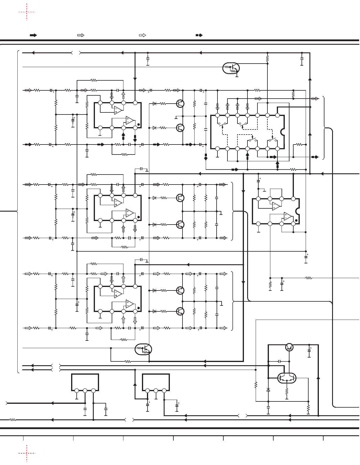
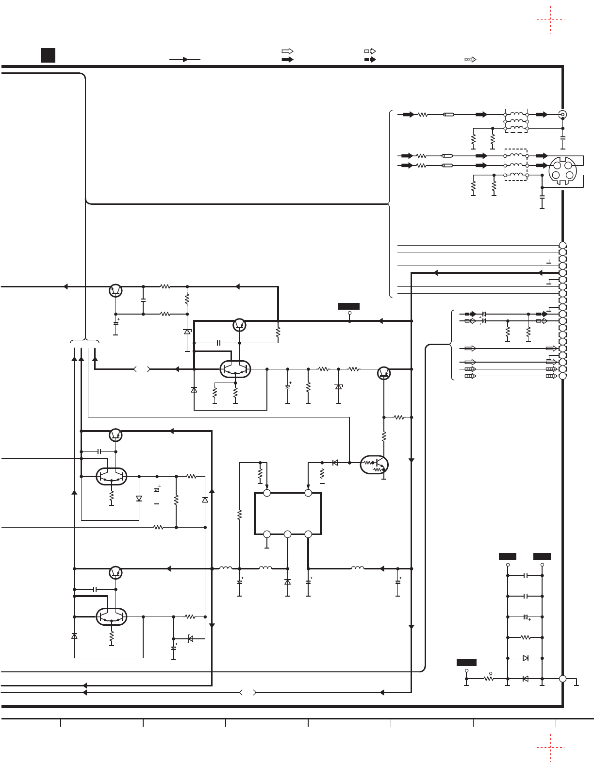
A
B
C
D
E
F
G
H
25 26 27 28 29 30 31 32 33 34 35 36
SL-DV290(EE,GN) MAIN CIRCUIT DIAGRAM
SCHEMATIC DIAGRAM-10
MAIN CIRCUIT
C
JK1
Q11
FMW1T98
P. SUPPLY CONT.
R29
22K
R30
100
D7
MA728TX
R37
100
R39
1K
C23
10V47
IC2
PQ1CZ31H2ZP
DC-DC
CONVERTER
C20
10V47
R28
47K
R31
680
4 5
321
ADJ ON/ OFF
GND VOUT VIN
D4
MA111TX
C4
16V470
L1
D3
SFPB-72V
C7
6.3V820 R2
8.2K
R3
2.2K
R4
10K
L501 JK501
VIDEO OUT
R505
1
R504
1R501
1
R502
1
L502
V.GND
S.WOOFER
CENTER
NC
NC
NC
CD Rch OUT
CD A.GND
CD Lch OUT
SUR R
SUR L
DATA
NC
SCLK
D.GND
+B (10V)
CS
CT.GND
CD REQ
SYNC
To SOUND PROCESSOR(SH-DV290)
& CASSETTE DECK(RS-DV290)
JK501
S-VIDEO OUT
R503
75
C501
0.01
C502
0.01
R27
1.2K
R35
1.2K
D.GND A.GND
CT.GND D18
MA111TX
D17
MA111TX
R41
100
C26
16V10
C29
0.01
C30
1000P
R40
0
Z501
VLP0146-T
R506
75 Z502
VLP0146-T
Z503
VLP0146-T
R507
75
S
T
R
1
2
20
3
4
5
6
7
8
9
10
11
12
13
14
15
16
17
18
19
DC+10V
R823
100K
R824
100K
C816
16V10
C815
16V10
K
M
L
O
P
F
E
A
B
C
D
L2L4
Q3
DTC114EUA106
SWITCHING
C3
16V3300
R33
4.7K
R32
47K
D11
MA8091MTX
POWER SUPPLY
CONT.
Q13
2SB1218TX
D10
MA111TX
C19
1000P
POWER SUPPLY
Q12
2SB1417PQTA
D14
MA8082MTX
R38
10
C24
1000P
REGULATOR
Q16
2SD874QRSTX
JFQG
POWER SUPPLY
Q15
2SB766ATX
C21
1000P
P. SUPPLY CONT.
Q14
FMW1T98
R34
470
D12
MA111TX
C22
16V10
R36
22K
D13
MA111TX
R44
1.2K
R42
100
POWER SUPPLY
Q7
2SB1417PQTA
C10
1000P
R16
470
D6
MA111TX
C11
16V10
R17
22K
Q6
FMW1T98
P. SUPPLY CONT.
E1
GG
Y C
9.2V
10V9V
: POSITIVE VOLTAGE LINE
: AUDIO SIGNAL LINE
: VIDEO SIGNAL LINE :SUB WOOFER SIGNAL LINE :SURROUND SP. SIGNAL LINE
:CENTER SP. SIGNAL LINE
9V
10V
9.2V
10V9V
9V 9.2V
9V
8.5V
9V
0V
5V
4V1V
6V 10V
6V5V
5.2V
5.2V
5V
4.5V
5V
5V
6V5V
5.2V
5.2V
4.5V
5V
5V
5V
8.2V
9.8V7.5V
A
B
C
D
E
F
G
H
25 26 27 28 29 30 31 32 33 34 35 36
SL-DV290(EE,GN) MAIN CIRCUIT DIAGRAM
SCHEMATIC DIAGRAM-10
MAIN CIRCUIT
C
JK1
Q11
FMW1T98
P. SUPPLY CONT.
R29
22K
R30
100
D7
MA728TX
R37
100
R39
1K
C23
10V47
IC2
PQ1CZ31H2ZP
DC-DC
CONVERTER
C20
10V47
R28
47K
R31
680
4 5
321
ADJ ON/ OFF
GND VOUT VIN
D4
MA111TX
C4
16V470
L1
D3
SFPB-72V
C7
6.3V820 R2
8.2K
R3
2.2K
R4
10K
L501 JK501
VIDEO OUT
R505
1
R504
1R501
1
R502
1
L502
V.GND
S.WOOFER
CENTER
NC
NC
NC
CD Rch OUT
CD A.GND
CD Lch OUT
SUR R
SUR L
DATA
NC
SCLK
D.GND
+B (10V)
CS
CT.GND
CD REQ
SYNC
To SOUND PROCESSOR(SH-DV290)
& CASSETTE DECK(RS-DV290)
JK501
S-VIDEO OUT
R503
75
C501
0.01
C502
0.01
R27
1.2K
R35
1.2K
D.GND A.GND
CT.GND D18
MA111TX
D17
MA111TX
R41
100
C26
16V10
C29
0.01
C30
1000P
R40
0
Z501
VLP0146-T
R506
75 Z502
VLP0146-T
Z503
VLP0146-T
R507
75
S
T
R
1
2
20
3
4
5
6
7
8
9
10
11
12
13
14
15
16
17
18
19
DC+10V
R823
100K
R824
100K
C816
16V10
C815
16V10
K
M
L
O
P
F
E
A
B
C
D
L2L4
Q3
DTC114EUA106
SWITCHING
C3
16V3300
R33
4.7K
R32
47K
D11
MA8091MTX
POWER SUPPLY
CONT.
Q13
2SB1218TX
D10
MA111TX
C19
1000P
POWER SUPPLY
Q12
2SB1417PQTA
D14
MA8082MTX
R38
10
C24
1000P
REGULATOR
Q16
2SD874QRSTX
JFQG
POWER SUPPLY
Q15
2SB766ATX
C21
1000P
P. SUPPLY CONT.
Q14
FMW1T98
R34
470
D12
MA111TX
C22
16V10
R36
22K
D13
MA111TX
R44
1.2K
R42
100
POWER SUPPLY
Q7
2SB1417PQTA
C10
1000P
R16
470
D6
MA111TX
C11
16V10
R17
22K
Q6
FMW1T98
P. SUPPLY CONT.
E1
GG
Y C
9.2V
10V9V
: POSITIVE VOLTAGE LINE
: AUDIO SIGNAL LINE
: VIDEO SIGNAL LINE :SUB WOOFER SIGNAL LINE :SURROUND SP. SIGNAL LINE
:CENTER SP. SIGNAL LINE
9V
10V
9.2V
10V9V
9V 9.2V
9V
8.5V
9V
0V
5V
4V1V
6V 10V
6V5V
5.2V
5.2V
5V
4.5V
5V
5V
6V5V
5.2V
5.2V
4.5V
5V
5V
5V
8.2V
9.8V7.5V
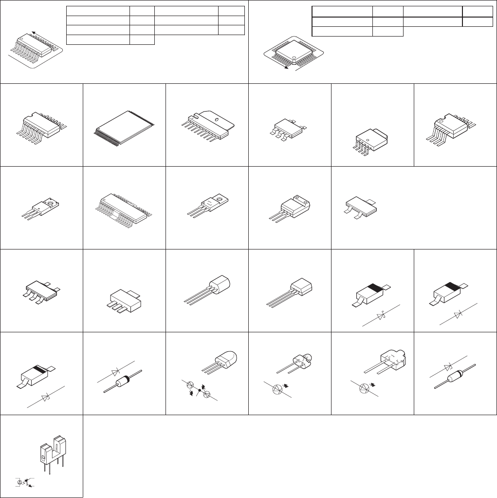
No.1
No.1
1
24
25
48
1
3
4
5
2
1
5
E
C
B
A
Ca
14
5
8
2SB1218TX
2SD1328TX
2SD1819ATX
DTC114EUA106
UN511MTX
UN5211TX
PST596JNR
C0JBAA000001
C0JBAS000116
C3FBND000098 TA7291P PQ1CZ31H2ZP
C0DBEZG00011
C0DBFFG00004
C0DBCGE00002
BA4558FHTT1
C3EBGC000033
C0JBAS000138
NJM78M05FA C0GBG0000033
RVTDTC143ESTFMW1T98 2SB1115-T
2SB766ATX
2SD874QRSTX
2SB621ARSTA MA728TX MA111TX
SFPB-72V
MA8082MTX
MA8091MTX RL1N4003N02
GP1S94
C1DB00000582
C2BBFD000402
NJM4580EDTE1
NJU3713GTE1
16PIN
42PIN
8PIN
18PIN
C0FBBK000036
MN102H60GFD
MN6775511
48PIN
100PIN
208PIN
Anode
Cathode
UN2121-TX
UN5111TX
UN5212TX
UN5214TX
UN521NTX
1
10
1
7
8
14
2
13
E
C
B
C
B
C
E
B
C
B
C
EECB
A
Ca
Anode
Cathode
2SB1417PQTA
CE
B
A
Ca
Anode
Cathode
LNJ301MPUJAD SELS5923C
ACa
EC
Ca
A
E
C
SML79455C
Ca
A
A
Anode
Cathode Anode
A
Ca
Anode
Cathode
A
Ca
Anode
Cathde
2
1
3
MTZJ4R7BTA
LM2940T5M
C9ZB00000431
BU4053BCFE2
C3ABPG000121
34PIN
16PIN
54PIN
MN103S26EGA
AN22030A-VT
176PIN
64PIN
C
B
E
1
28
15
14
7
21
22
8
Anode
Cathode
A
Ca
Anode Cathode
A
Ca
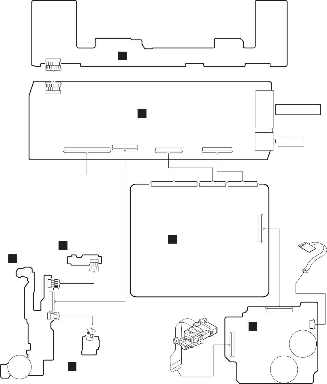
AINTERFACE P.C.B.
OPTICAL PICK-UP
UNIT
50
.
.
.
.
.
.
.
.
.
.
.
.
.
1
FP5201
1. . . . . . . . . . . . . 50
FP5102
30
.
.
.
.
.
.
.
.
.
.
.
1
FP5101
M2501
(SPINDLE
MOTOR)
M2502
(TRAVERSE
MOTOR)
VIDEO OUT/
S-VIDEO OUT
To SOUND PROCESSOR&
CASSETTE DECK
FP4202
BDVD MODULE P.C.B.
CMAIN P.C.B.
DOPERATION P.C.B.
FP3203 FP3202
17. . . . . . . . . . . . . . .1
17. . . . . . . . . . . . . . .1
26. . . . . . . . . . . . . . . . . . . . . . . .1
26. . . . . . . . . . . . . . . . . . . . . . . .1
15. . . . . . . . . . . . .1
15. . . . . . . . . . . . .1
CN2
CN501
FCLAMP SW P.C.B.
ELODAING
MOTOR P.C.B.
GBOTTOM SW
P.C.B.
W2
W2
CN1
W1
W1
RM1
(LOADING
MOTOR)
1 . . 4
4
.
.
1
3
.
1
1
.
3
CN301 1. . . . . . . . . . . .14
CN3
1
.
.
.
.
.
.
.
.
.
.
.
.
14
1 . . . . . . 8
WA601
1 . . . . . . 8
WB601
4
.
.
1
FP2501
FG UNIT
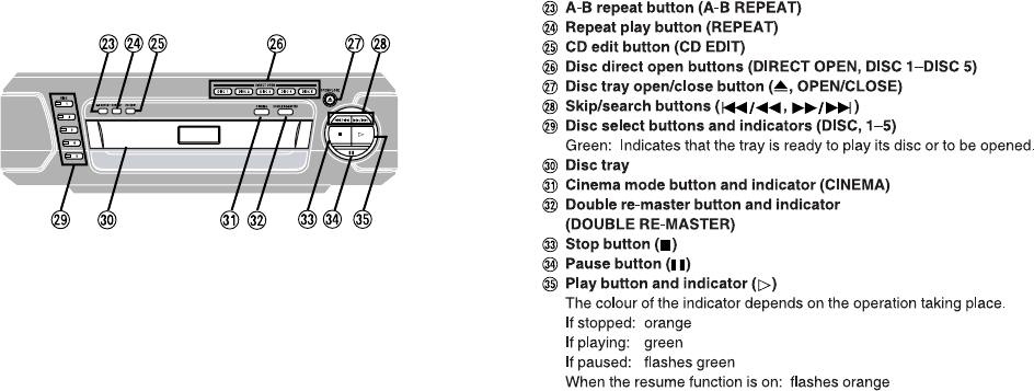
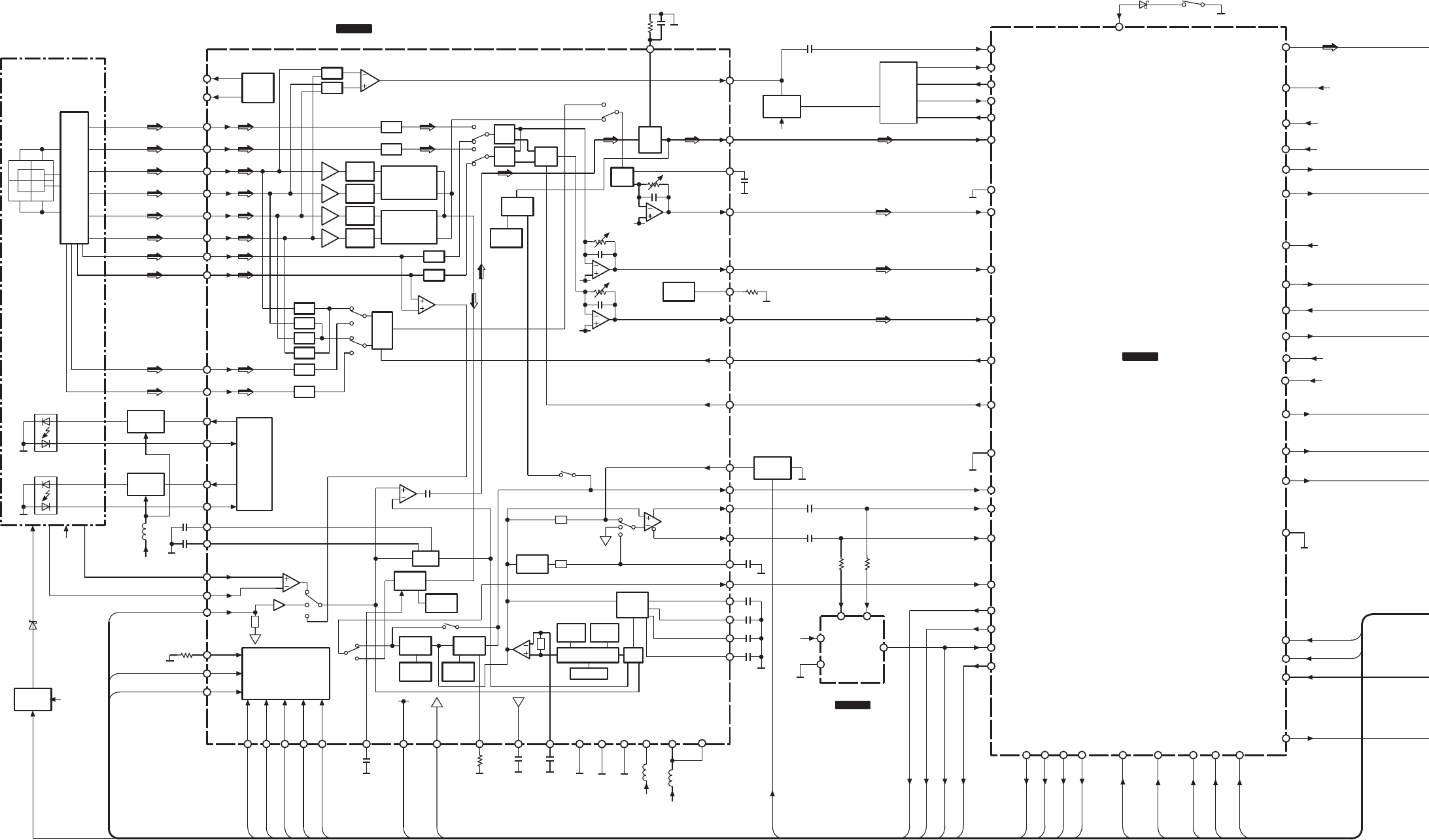
AGC
CONT.
LASER
P.DRIVE
EQ HPF
COMP
OPTICAL PICK-UP UNIT
53
13
TBAL
VIN7
EQ HPF
COMP
58 VIN1
59 VIN2
EQ HPF
COMP
EQ HPF
COMP
60 VIN3
61 VIN4
DEFFERENTIAL
PHASE DET.
DEFFERENTIAL
PHASE DET.
LPC AMP
Q5111
LASER
P.DRIVE
Q5115
LASER DIODE
LASER DIODE
HEAD
AMP
A2
B2
A3
B3
B1
B4
A1
A4
PHOTO
DETECTOR
REG-LOGIC
AMP
AMP
AMP
AMP
AMP
AMP FBAL
2
8
11
TE
HOLD
PEAK
DPDOFT
DET.
LEVEL
CONT.
MIRROR
DET.
LEVEL
CONT.
BDO
DET. EQ
FC
CONT. BOOST
CONT.
GD CONT.
LEVEL
CONT.
VGA
AGCG2
DCAGC
ENV
DET.
SAG
54 VIN8
51 VIN5
52 VIN6
62 VIN9
63 VIN10
1
4
3
46
47
RFINP
RFINN
AN22030A-VT
IC5201
FRONT END PROCESSOR
LPCO1
LPC1
LPCO2
LPC2
42 17 19
IDGT
STANBY
SCK
35
FLTON
34
FLTOP
22
BDO
14
FE
7
FBAL
FS
49
RFENV 120
MN103S26EGA
IC2001
OPTICAL DISC
CONTROL
118
65
119
117
66
52
111
110
S LINE RSCL
21
OFTR 51
AD3
AD1
TBAL
AD2
AD0
FBAL
BDO
ARF
NARF
OFTR
149,151,158,160,
164,166,168,172
HDD8~15
FEPCLK
67
114
68
115
70
71
DAC1
TILT
TIL TP
SPDRV
DAC0
TRSDRV
VDD18 D+1.8V
18,76,
152
AVDD D+3.3V
88,99,
109,116
VDD3 D+3.3V
3,31,57,
78,125,143,
156,162,169
AVSS
85,94,
102,113
4,19,32,
60,77,81,
126,144,
155,163,170 VSS
CPUADR0~17
9~17,
22~30
DRAMVDD18 D+1.8V
20,58
DRAMVDD33 D+3.3V
33
CPUDT0~7
37~44 35
55
PWM3
NWR
FEPENB
NWEL
C0JBAS000116
IC2101
LOGIC CONTROL
NRST
IDGT
54
PWM2
FEPCLK
53
PWM1
FEPDATA
NRD
36
TSTSG
TSTSG
82
TE
FLT
TE FLT 9
48
27
37
31
AGCG1
BDOSL
MIRSL
39
38
29
30
36
DCFLT SWITCH-
ING
Q5271
DCFLT
32
RBCA
NW
DET.
LEVEL
CONT.
5
POFLT
18 20
SEN
STDIO
FEPDATA
FEPENB
23
24
41
DTRD
SHOLD
SHORT
DTRD
VFOSHORT
L.P.F.
43 TESTSG
TSTSG
44
45
CRFHP1
CRFHP2
TBAL
AMP
AMP
AMP
AMP
AMP
AMP
ADD
ADD
12
RFTE
MONI
57
10
MONI
MONI2
GND
64
GND2
28
VSS
16
VCC1
VCC2
50 33
VDD
25
15
VHALF
55
VREF
A+5V
56
VREFRF
VHALF
VREF2
D+3.3V
2
AB
1
C
A+5V VCC 83 VFOSHORT
VFOSHORT
CPUADR0~17
CPUDT0~7
NRD
OSCI1
79
CLK16M
106
VHALF
69
FG
98 RFDIF
RF
AMP
Q2001
A+5V
CRnet.
96
95
92
93
HPFIN
HPFOUT
LPFOUT
LPFIN
A+5V
A+5V
POWER
SUPPLY
QR5221
D+3.3V
D5151
HFMON
104 VREF2
IDGT
75
DTRD
74
VREF2
IDGT
DTRD
21
DRAMVSS
4
5
3GND
6
WAITODC WAIT
47
NRST NRST
VDDH D+3.3V
174
SL-DV290(EE,GN) BLOCK DIAGRAM
56
PWM4
122
CAPAC2
D2001 S2501
(REST DET.)
61
PWM5
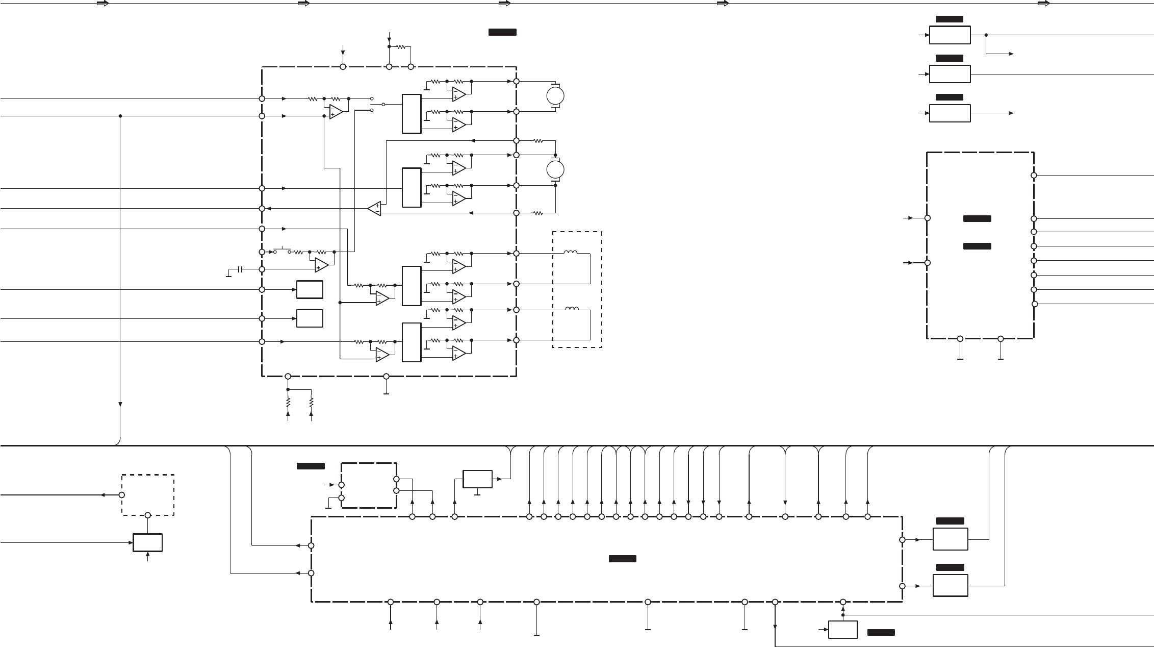
AND
GATE
50
C0JBAA000001
IC6223
AND
GATE
52
C0JBAA000001
IC6222
SBT3
SBO3
MN102H60GFD
IC6201
CPU
26 TRIN
2VIN1
15
LEVEL
SHIFT
16
17
LEVEL
SHIFT
18
14
LEVEL
SHIFT
13
12
LEVEL
SHIFT
11
VO1+
TRACKING
COIL
FOCUS
COIL
OPTICAL
PICKUP UNIT
M
MM2502
(TRAVERSE MOTOR)
M2501
(SPINDLE MOTOR)
4
5
23
6
24
3
CH3
MUTE
CH1,2
MUTE
27
9
VIN3
OPOUT
LDIN
VO1-
VO2+
VO2-
OPIN-
VO3-
VO3+
OPIN+
VO4+
VO4-
C0GBG0000033
IC2501
FOCUS/TRACKING
COIL,SPINDLE/TRAVERSE
MOTOR DRIVE
MUTE3
MUTE12
VIN2
C3ABPG000121
IC3061
MEMORY
A0~11
22~26,
29~35
DQ0~15
2,4,5,7,8,
10,11,13,42,
44,45,47,48,
50,51,53
15
18
17
16
19
LDQM
/RAS
/CAS
/WE
/CS
D0~15
84~91,
93~100
A0~21
13~16,
26~33,
35~42,
44,45
718 2 3
NCS2 NAVCS
BOSC SYSCLK
NRE NRD
NWEL
NWEL
SBT1
SBO1
SBI1
11
P56
RESET
Q6215
NRST
70
SBT1
72
SBO1
71
SBI1
CLK33M
23
OSCI
REGULATOR
C0DBFFG00004
IC6252
D+2.5V
REGULATOR
C0DBCGE00002
IC6253
D+2.5V
REGULATOR
C0DBEZG00011
IC6251
D+5V
7,10,
19
GND
VDD
17,22,
66,83
D+3.3V
AVDD
34
D+3.3V
VSS
19,92
AVSS
61
VREF+
54
D+3.3V
43
VREF-
1,14,27
D+3.3V VDD
VSS
VSSQ
6,12,
46,52
3,9,43,
49,
D+3.3V VDDQ
28,41,
54
51
SBI3
VCC
8
D+5V
VCC
21
M+9V
22
PREVCC
D+3.3V
D+1.8V
38
CLK
PST596JNR
IC6211
D+3.3V
82
NRST
RESET
53
SBO4
SBT4
56
5
6
SDA
SCL
GND
4
C3EBGC000033
IC6221
EE PROM
VCCD+3.3V 8
WAIT
1
WAIT
9
NBREQ
28
LDCNT
4
NWEH NWEH
10
NBRACK CLKSEL
68
LCAS STBDAC2
78
NIRQ2 AV1IRQ
79
NIRQ3 AV2IRQ
1BIAS1
VHALF
CPUADR0~21
CPUDT0~15
25 BIAS2
C3ABPG000121
IC3062
MEMORY
67
12
RAS
NWORD
DCFLT
HFMON
EXTCLK
100
EXTCK
8
NCS3
SL-DV290(EE,GN) BLOCK DIAGRAM
DCLK
DCMD
DSTAT
AMUT
FG UNIT
POWER
SUPPLY
QR5241
D+3.3V
D+5V D+3.3V
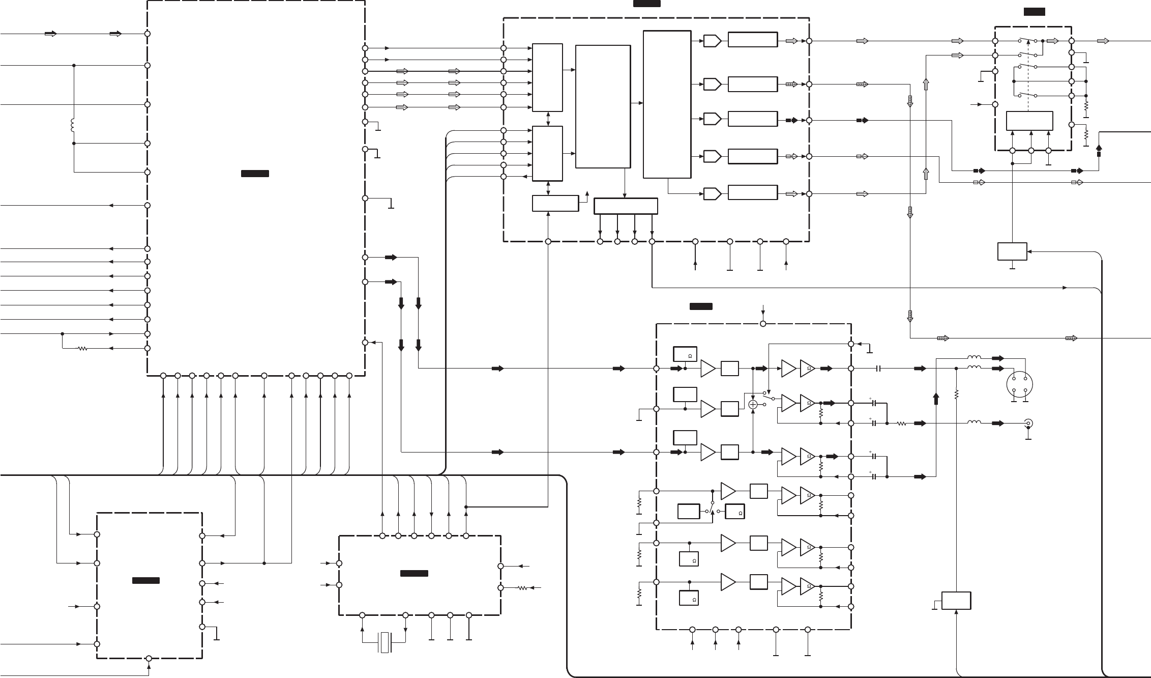
MN6775511
IC3001
AV DECODER
81~88 STD0~7
HD0~15
55~57,
59~61,
63~65,
67,68
70,76,
72~74
HA1~17
32,33,
35~38,
40~43,
45~47,
49~51,
54
MA0~11
176~179,181~183,
189,191,192,196
MDQ0~31
2~4,6~9,11,13,14,16~18,
150,151,153~155,158~160,
162~164,166~169,171,205~207
174,204
200
201
193
198
DQM1,2
XRAS
XCAS
XWE
XCSM
NAVCS
SYSCLK
NRD
NWEL
29
XCS
31
HCLK
28
XRD
27
XWR
21
XRST
NRST
C3FBND000098
IC6301
32M FLASH
MEMORY
DQ0~15
29~36,
38~45
A0~20
1~10,
16~25,
48
11
28
XWE
XOE
96
97
91
92
93
SRCK
LRCK
ADOUT0
ADOUT1
ADOUT2
SERIAL
INPUT
I/F
40 BCKIN
41
45
46
47
C0FBBK000036
IC4211
8CH AUDIO D/A CONVERTER
LRCIN
DIN1
DIN2
DIN3
FUNCTION
CONTROL
I/F
37 RSTB
36
35
34
33
ML
MC
MDI
MDO
NRST
STBDAC2
SBT1
SBO1
SBI1
SYSTEM CLOCK
MANAGER
C1DB00000582
IC6561
CLOCK GENERATOR
87
XTO
XTI
X6561
(36.864MHz)
4
CLK27
38
128
VCLK
13 14 15
CLK16
FSEL
CLK33 CLK33M
CLKSEL
CLK16M
OVERSAMPLING
DIGITAL FILTER
WITH FUNCTION
CONTROLLER
ENHANCED
MULTI-LEVEL
DELTA-SIGMA
MODULATOR
DAC OUTPUT AMP AND
LOW-PASS FILTER
DAC OUTPUT AMP AND
LOW-PASS FILTER
DAC OUTPUT AMP AND
LOW-PASS FILTER
DAC OUTPUT AMP AND
LOW-PASS FILTER
14
(13)
12
(11)
10
9
ZERO DETECT
SYSTEM CLOCK
SCLKI
VOUT1
(VOUT2)
VOUT3
(VOUT4)
VOUT5
VOUT6
PLLAVDD
105
LVDD
12,30,48,69,98,
127,135,172,186
VDD
5,15,26,39,52,58,
66,75,89,103,131,
144,152,157,165,
175,184,194,203
VDD 37 D+3.3V
VSS
27,
46
VDD1
1
D+3.3V
VDD2
5
D+3.3V
2
VSS1
6
VSS2
11
VSS3
VCC
18,22,
24,26,
28
ADAC5V
AGND
17,19,
21,23,
25,27
10
768fs EXTCLK
48
ZFLGA
NRD
NWEL
185 MCKI
22
XHINT
AV1IRQ
23
XHINT2
AV2IRQ
24
XDK
WAIT
25
XWRH
NWEH
DGND
44
12 XRESET
DAC OUTPUT AMP AND
LOW-PASS FILTER
16
(20)
VOUT7
(VOUT8)
CLK27M
30
ZERO7
32
ZERO8
1~6
ZFLG1~6
CPUADR1~21
CPUDT0~15 CPUADR1~17
CLK27M
120
DAC5OUT
116
DAC4OUT
AVDD
112,118
MCK
187 PCLK 102
3
CLK54
VDD3 D+3.3V
12
CE D+3.3V
16
WP/ACC 14 D+3.3V
XCE
26
47 XBYTED+3.3V
31 DATA4
94
ADOUT3
107
PLLVSS
113,
121
AVSS
VSS
1,10,19,34,44,
53,62,71,80,95,
104,122,139,148,
156,161,170,180,
190,199,208
VDD
43
D+3.3V
SL-DV290(EE,GN) BLOCK DIAGRAM
2CIN LPF
VIN
4
2dB 75
2dB 75
33
31
30
2dB 75 28
27
C OUT
VOUT
VSAG
Y OUT
YSAG
8,10
GND1
Driver
4dB
LPF4dB
Sync tip
clamp
6.75MHz
6.75MHz
Driver
YIN
6LPF4dB
Sync tip
clamp
6.75MHz
2dB 75 25
24
CY OUT
CYSAG
CY IN
12 LPF4dB
6.75MHz
Sync tip
clamp
Bias
150k
Bias
150k
CLP
13
2dB 75 22
21
Cb OUT
Cb SAG
Cb IN
14 LPF4dB
6.75MHz
Bias
150k
2dB 75 19
18
Cr OUT
Cr SAG
Cr IN
16 LPF4dB
6.75MHz
Bias
150k
1
VCC1
A+5V
34
VCC2
A+5V
3
MUTE1
A+5V
17,20,
23,26,
29,32
GND2
C9ZB00000431
IC501
VIDEO BUFFER
5
YC-MIX
15
MUTE2
S-VIDEO OUT
VIDEO OUT
SWITCH-
ING
WIDE1
Q501
A+5V
BU4053BCFE2
IC891
SIGNAL SELECTOR
13(1)
12(2)
7
16
14(15)
3
5
4
SW CONT.
ABC
INH 6
GND 8
VSS
+B2
Q891
SWITCH-
ING
MIXSEL
ZFLAG
11 10 9
SL-DV290(EE,GN) BLOCK DIAGRAM
C2BBFD000402
IC401
SYSTEM CONTROL
DVD CMD
DVD STAT
8
BREQ
9
BCS D406
Q404
BCLK
10
DATA O
11
DATA I
12
Q402,
403
XOUT
XIN
20
19
X401
(8MHz)
SYNC20
CS
13
JK1
19
18
17
16
15
14
12
9
8
7
6
5
4
3
CD REQ
CT.GND
+B(10V)
D.GND
SCLK
DATA
10
11
NC
CD A.GND
CD Lch OUT
SUR R
To SOUND PROCESSOR
&CASSETTE DECK
BLOCK DIAGRAM
CD Rch OUT
NC
DCMD
35
DVD CLK
DCLK
DSTAT
V.GND
S.WOOFER
CENTER
NC
NC
WIDE1
C/SW SEL
MUTE
7
36
14
37
13
4
2
1 SUR L
6
SYNC
16
TEST
+B3
+B1
+B3
Q401
18
RESET
24
LED/EDTA
23
LED/ECLK
Rch
Rch
Q16
+B2
L1
A+5V
Q6,7 L2,4
LM2940T5M
IC3
PQ1CZ31H2ZP
IC2
D+2.5V
Q8,9
Q14,15
D+5V
ADAC5V
MUTE
1
VCC
+B3
VREF
2
C/SW SEL
MIXSEL
WIDE1
LED STB
22
LED CLR
25
21 315
AVSS
CNVSS
VSS
+B3
42
RGN CS
M
RM1
(LOADING
MOTOR) 1
2
10
5
6
7,8
+B1
TA7291P
IC1
MOTOR DRIVE 4
D2
Q1
34
HALF
33
CW
32
CCW
KEY SWITCH
(S601~621)
KEY2
40
KEY1
41
SW5
S5
(BOTTOM)
27
S1
(TRAY POSITION 1
DET.)
30
SW1
29
SW2
S2
(TRAY POSITION 2
DET.)
31
SW3
S3
(OPEN DET.)
39
SW4
S4
(CLAMP)
+B1
Q304,
305
PLUNGER
+B3
D1
(POSITION
SENSOR)
26
PLG
PSTN
28
D302~304
CT.GND
DC+10V
A.GND D.GND
LCLR
LSTB
LCLK
LDATA
MOTOR
DRIVE
PLUNGER
DRIVE
RESET
INTER-
FACE
INTER-
FACE
REGULATOR
REGULATOR
DC-DC
CONVERTER
M+9V
Q11~13
Q3 SWITCH-
ING
+B3
NJM78M05FA
IC4
REGULATOR
5
PWCONT
BA4558FHTT1
IC805
C0JBAS000138
IC801
SIGNAL SELECTOR
NJM4580EDTE1
IC802
Q802
1
4
8
11
VREF +B2
2
3
9
10
13
5
6
12
S.SELECTOR
CONT.
Q303
NJM4580EDTE1
IC804
NJM4580EDTE1
IC803
Q805
(Q806)
Q803
(Q804)
C/SW SEL
ZFLAG
AMUTE
Q308,807
MUTE
NJM4580EDTE1
IC802
BUFFER
AMP
BUFFER
AMP
MUTING
BUFFER
AMP
BUFFER
AMP
MUTING
MUTING
MUTING
CONT.
DATA
CLK
VDD
Vss 5
18 +B3
14 15
STOP
PLAY
10 11
/STB
12
/CLR
13
KEY1,2
16,17
DISC1~5
1~4,
6
NJU3713GTE1
IC601
LED DRIVE
LDATA
LCLK
LSTB
LCLR
D802
D805
(D806)
D803
(D804)
D305
(1/2)
(1/2)
POWER
SUPPLY/
CONT.
POWER
SUPPLY/
CONT.
POWER
SUPPLY/
CONT.
POWER
SUPPLY/
CONT.
VDD+B2
VSS
7
D608
()
D601~607
(CINEMA/DOUBLE
RE-MASTER/DISC1~5)
MIXSEL
14
MUTING
D801
Q801
MUTING
CONT.
D307
D306
Q307
: VIDEO/AUDIO SIGNAL LINE
: VIDEO SIGNAL LINE
: AUDIO SIGNAL LINE
: SUB WOOFER SIGNAL LINE
: CENTER SP. SIGNAL LINE
: SURROUND SP. SIGNAL LINE
Notes)
( ) indicates pin No. Right channel.
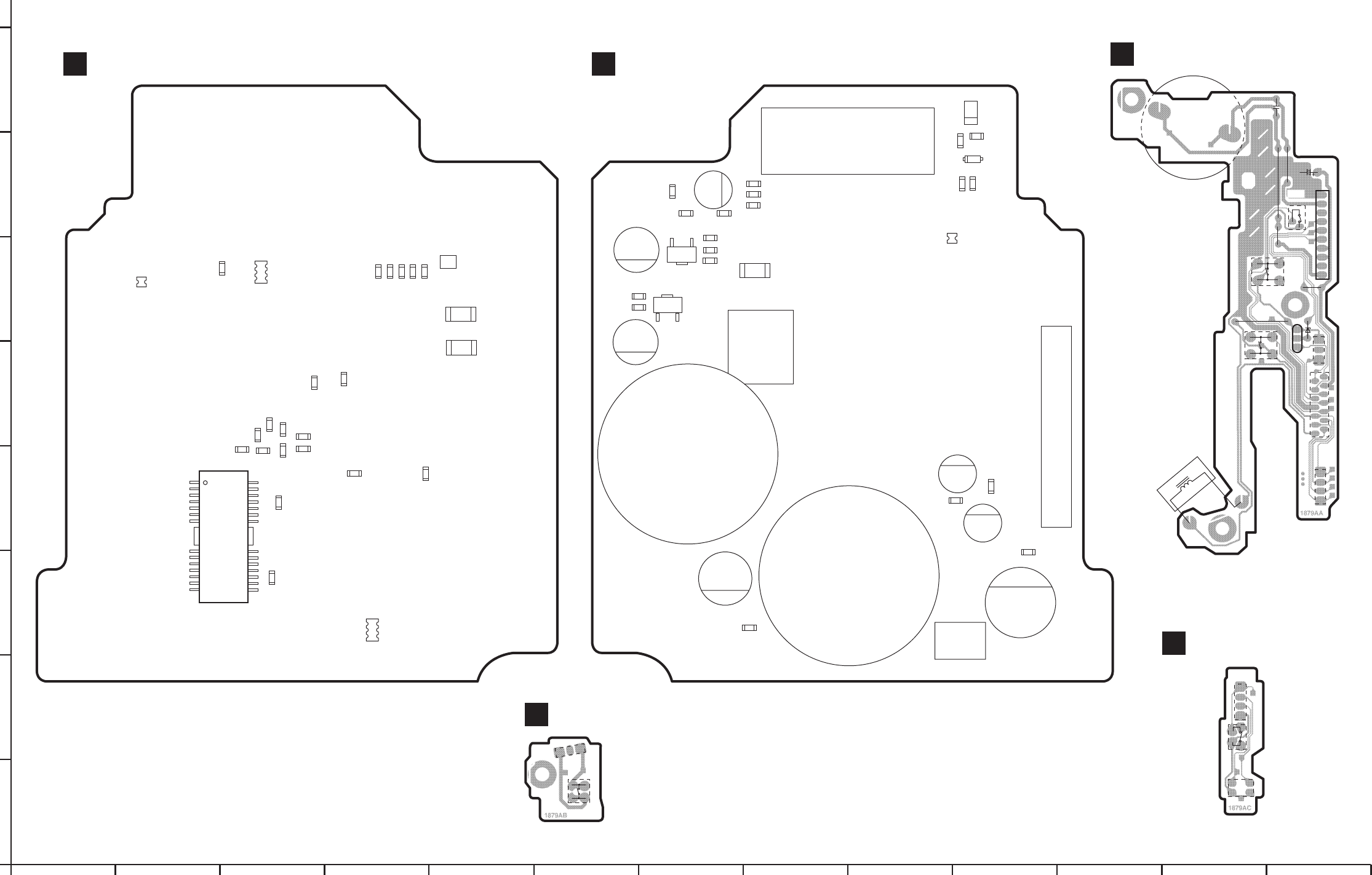
123456789101112
13
A
B
C
D
E
F
G
H
SL-DV290(EE,GN) INTERFACE,LOADING MOTOR,CLAMP SW,BOTTOM SW P.C.B.
Note: This printed circuit board diagram may be modified at any time with the development of new technology.
C5115
+
C5101
+
C5111
+
+
C2502
+
C2501
M2501
(SPINDLE MOTOR)
M2502
(TRAVERSE MOTOR)
S2501
FP5101
1 . . . . . . . . . . . . . . . . . . . . . . . . . . . . 30
50
.
.
.
.
.
.
.
.
.
.
.
.
.
.
.
.
.
.
.
.
.
.
.
.
.
.
.
.
.
.
.
.
.
.
.
.
.
.
.
.
.
.
.
.
.
.
.
..
1
FP5102
Q5115
B
C
E
Q5111
E
C
B
+
C5152
R5102
R5111
C2505
C2506
C2504
C2508
1
8
14 15
21
22
28
7
IC2501
C2507
C2510
C2512
R5101
R5107
R2503
R2505
R2501
R2502
R5108
R2504
R5109
R5103
R5121
R5122
R5123
C2513
R5116
R5112
C2511
R2507
RA5103
R5105
D5151
C2503
+
C2509
+
1..4
FP2501
RA5101
RA5102
R5120
L5101
RA2501
R5152 LB5106
R5124
C5151
LB5105
R5115
C5103
C5123
LB5101
C5102
R5113
R5117
R5114
INTERFACE P.C.B. (SIDE : B)
A
INTERFACE P.C.B. (SIDE : A)
A
(REP3406A-1N)
1
2
3
4
5
6
7
8
9
10
IC1
14
12
10
8
6
4
2
13
11
9
7
5
3
1
CN1
1
2
3
4
W1
1
2
3
W2
Q1
E
C
B
D2
J
J
J
J
C1
C2
S1
S2
RM1
(LOADING MOTOR)
S3
R1
LOADING MOTOR P.C.B.
E
PLUNGER
(REP2578A-N)
321
W2
S4
CLAMP SW P.C.B.
F
(REP2578A-N)
4
3
2
1
W1
D1
Ca
AC
E
BOTTOM SW P.C.B.
G
(REP2578A-N)
S5
2608A
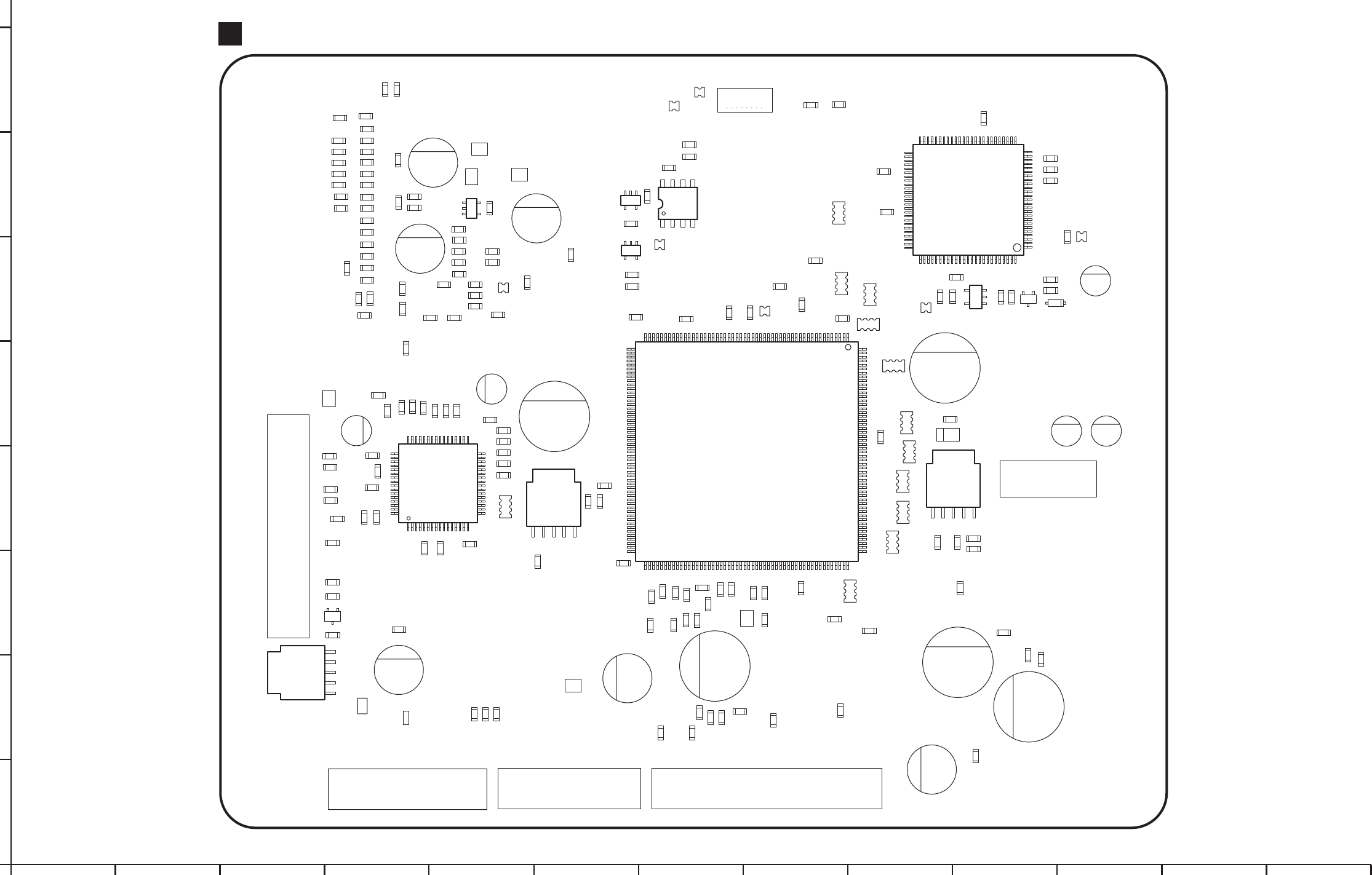
123456789101112
13
A
B
C
D
E
F
G
H
SL-DV290(EE,GN) DVD MODULE(SIDE: A) P.C.B.
1
26
25
50
51
75
76 100
IC6201
1..............17
FP3202
1............17
FP3203
1........................26
FP4202
LB4211
R6251
R6253
R6252
C6254
C4236
C4207
C4234
C4237
K6301
K3002
K6303
R6210
R6211
R6216
C3003
C6206
C6211
C6215
R2046
R2047
R2053
R2054
R2039
R3010
C2073
R6206
R2045
R2044
R2043
R2042
R2038
R2030
C2050
C2038
C2039
R2029
C5283
C5234
C5292
C3018
C3038
C3021
C3022
C3019
C3024
C3025
C3039
C3027
C3026
C3023
C3020
C6255
C3051
C5262
C5299
C5290
C5264
C5282
C5271
K2004
C2036
C2067
C2012
C2102
C2066
C2055
C2054
C2031
C2035
C2034
C2009
C2032
C6222
C6221
C3010 C3008
C3007
C3006
C6301
C6205
C6203
LB6202
C6202
R6202
R6201
R6215
LB3001
C6204
C3005
R3001
LB6221
C6223
C2065
C2064
C2063
C2062
C2061
C2025
C2058
C2024
C2052
C2053
C2023
C2047
C2010
C5203
R5241
C5232
C5233
LB5227
LB5219
LB5207
LB5203
LB5202
LB5232 C5291
C5205
C5272
C5256
C3015
C3017
C5204
C2101
C5254
C2060
C2059
R2052
R2023
R6207
R6208
R2022
R2028
R2026
R5320
R5232
R3008
R3006
R3007
K3003
K4204
K4207
K4205
K4202
K4203
R3009
R5231
R5281
R5295
R5294
R2027
R2025
R2051
LB3203
LB3202
LB3201
LB4208
LB4207LB4210
LB4209
LB4212
L2001
L2021
L2002
C2001
+
C2002
+
C2021
+
RA2022
RA6202
RA3001
RA6204
RA6203
13
45
IC6223
1
34
5
IC2101
13
45
IC6222
110
PS6201
RA6205
RA3004
RA3003
RA3010
RA3009
RA3008
RA3007
RA3006
RA3005
RA3002
RA3012
14
5
8
IC6221
RA6201
RA6206
34
51
IC6211 Q6215
B
C
E
D6215
C6561
+
C6201
+
C6563
+
X6501
+
C3002
1
208
52
53
104
105 156
157
+
C6251
15
IC6251
IC3001
+
C3001
15
IC6252
C5202
+
C5201
+
L5201
L3091
L3001
FP5201
1
.
.
.
.
.
.
.
.
.
.
.
.
.
.
.
.
.
.
.
.
.
.
.
.
.
.
.
.
.
.
.
.
.
.
.
.
.
.
.
.
.
.
.
.
.
.
.
.
50
116
17
32
3348
49
64
IC5201
RA5201
FL6255
FL6253
1
5
IC6253
BE
C
QR5241
C6257
+
C3110
+
+
C3037
C4216
+
+
C4222
+
C4223
DVD MODULE P.C.B. (SIDE : A)
B
(REP3384G-N)
2592A
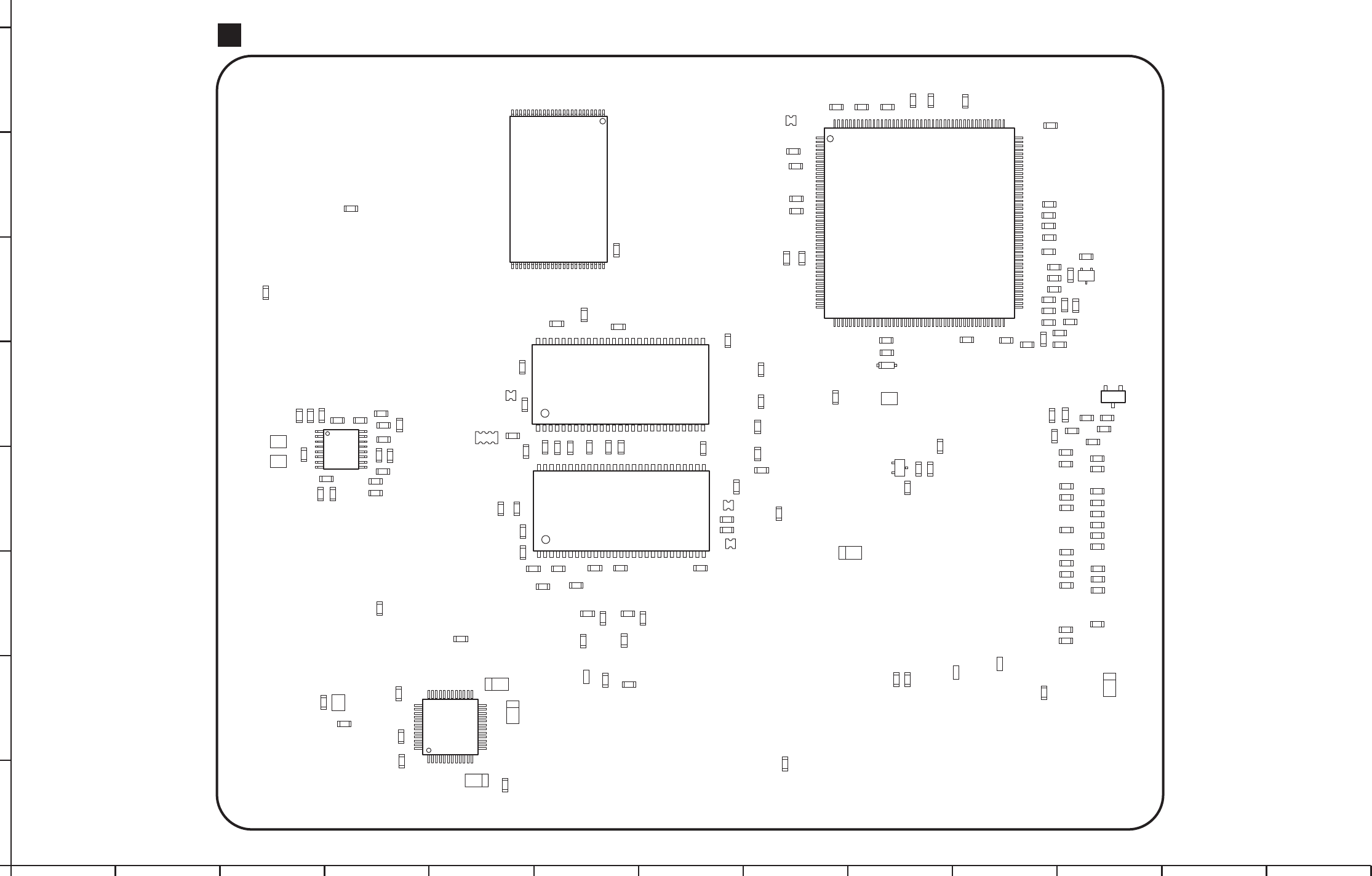
123456789101112
13
A
B
C
D
E
F
G
H
C6302
C3004
C3065 C3063
K6201
1
24
4825
IC6301
LB6561
LB6563
LB6562
LB6565
LB6566
LB6564
LB4200
LB6567
LB6201
R6566
R6565
R6504
R6503
R6505
R6563
1
89
16
IC6561
C6566
C6564
C6505
C4235
C4217
C4215
C4210
C6503
C6568
L6561
L6562
1
54 28
27
IC3061
1
54 28
27
IC3062
1
176
44
45 88
89
132
133
C2018
C2003
C2004
C2007
C3009
C3011
C3012
C3014 C3013
C3062
C3070
C3064
C3072
C3066
C3067
C3033
C3032
C3031
C3074
C4208
C3028
C3073 C3071 C3069 C3068
C3030
C3029
C4209
C3035
C3036
C3034
C2006
C2005
C2017 C2016
C2015
C2014
C2013
IC2001
RA2021
R2036
RA3013
RA3011
L4211
+
C4220
+
C4211
+
C4219
112
13
24
25
36
37
48
IC4211
LB4201
K3007
R3106 R3101
R3107
R3102
K3106
K3101
FL4201
LB4215
LB4214
K3011
K3009
RA3053
RA3051
R3052
R3051
+
C6252
B
EC
Q5271
LB3002
C2008
R2021
D2001
R5257
R5262
C5274
C5273
C3016
C3061
L5202
C2011 C2022 C2040
R2032
R2048
R2041
R2040
R2037
R2033 R2031
R2034
R2049
C2045
C2044
C5235
C5236
C5221
C2057
C2056
C2046
C2048
C2041
C2042
C2043
C2051
R2035
B
EC
Q2001
BE C
QR5221
R5221
R5201
LB5239
LB5222
LB5223
LB5225
LB5228
LB5230
LB5233
LB5217
LB5213
LB5209
LB5206
LB5240
LB5236
LB5221
LB5224
LB5226
LB5229
LB5231
R5203
LB5235
LB5238
LB5210
LB5208
LB5205
LB5218
LB5237
R5242
+
C6253
C6256
FL6251
FL6254
LB3205
LB3206
R5204
DVD MODULE P.C.B. (SIDE : B)
B
SL-DV290(EE,GN) DVD MODULE(SIDE: B) P.C.B.
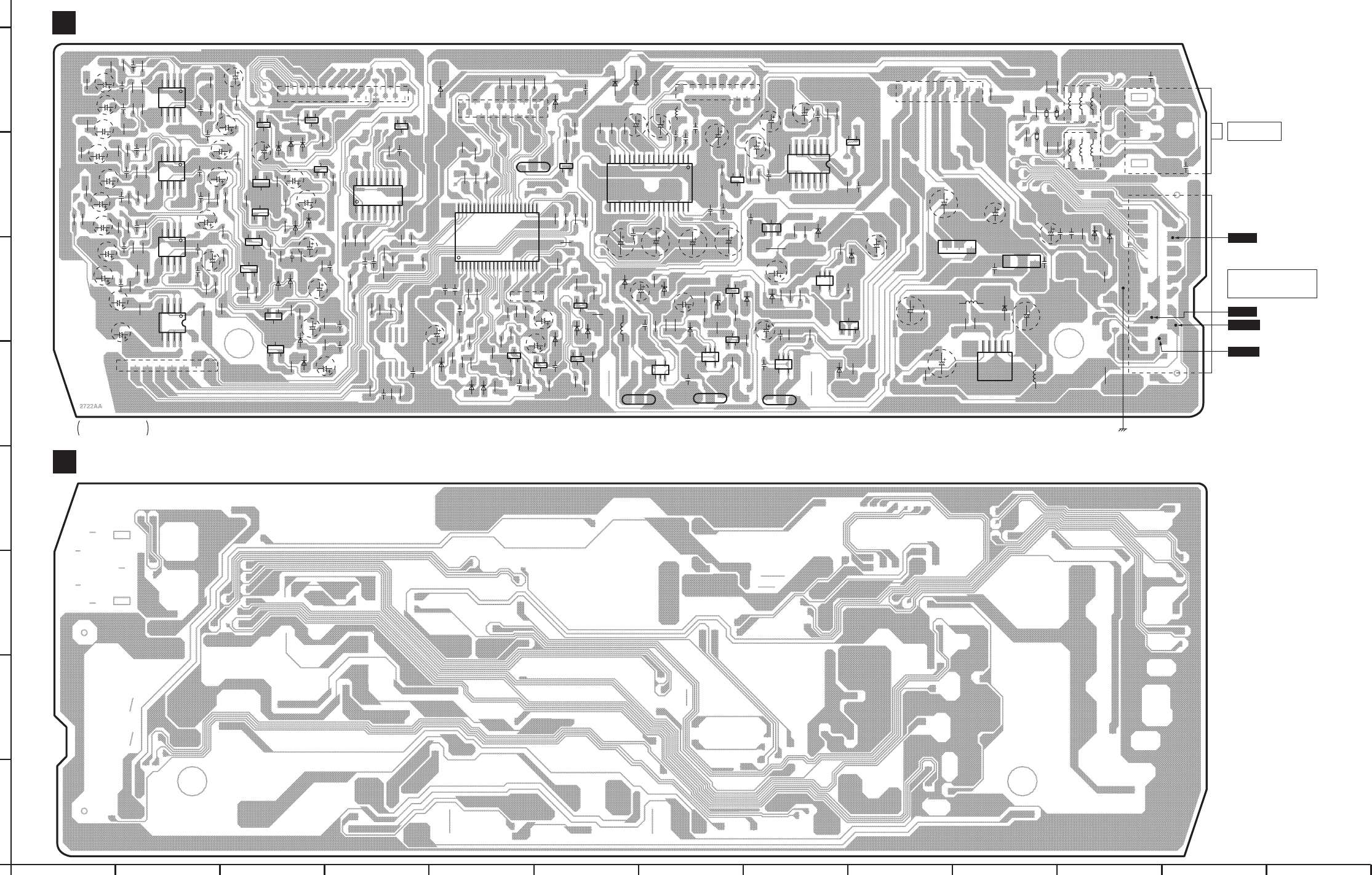
123456789101112
13
A
B
C
D
E
F
G
H
SL-DV290(EE,GN) MAIN P.C.B.
MAIN P.C.B. (SIDE :B)
C
MAIN P.C.B. (SIDE : A)
C
C806
C804
R802
R806
R810
R812
R804
C803
C826
C824
C823
C840
C838
C837
R811
R803
R834
R832
R836
R830
R831
R852
R854
R850
R856
R849
R851
R826 R855 R829
R835
R858
R805
R838
R808
R801
R828
R827
R848
R847
C802
C807
C801
C822
C827
C80
C808
C828
C825
C842
C831
C832
C845 C846
C839
R807
R809
R815
R816
SJ313
R312
R867
R814
R818
R813
R844
R846
R860
R865
C410
C411
C405
C404
C403
C10
C19
C12
C13
C21
C24
C514
C811
C812
C817
C513
C510
C407
C412
C892
C408
C409
R442
R446
R444
R441
R440
R425
R426
R451
R452
R406
R404
R403
R413
R414
R417
R416
R405
R450
R454
R455
R447
R410
R415
R419
R402
R412
R407
R408
R411
R17
R16
R28
R30
R33
R36
R44
R20
R22
R4
R3
R43
R2
R21 R42
R38
R34
R39
R37
R32
R29
R35
R27
R31
R418
R409
R448
R428
R427
R892
R891
R899
R893
R436
R307
R429
R401
R456
R430
R431
R432
R306
R508
R509
R510
R512
R819
R821
R823
R824
R822
R820
R305
R513
R421
R308
R422
R423
R420
R424
R435
R434
R433
R445
R443
R866
R859 R864
R840
R845
R439
R438
R842
R833
R837
R841
R817
R862
R861
R853
R825
R839
R843
R863 R857
C809
C830
C844
C843
C406
C308
C848 C833
C834
C814
C813
C847
C829
C810
C836
C821
C841
C835
C818
C819
1
4
58
IC802
1
158
9
16 10
15
4
58
IC803
IC891
1
4
58
IC804
1
4
58
IC805
C
BE
BE
Q805
C
BE
Q806
C
Q803
C
BE
Q804
BE
C
Q801
C
BE
Q802
C
BE
Q307
C
BE
Q807
C
BE
Q308
C
BE
Q891
D307
D306
D802
D801
D804
D806
D805
D803
D305
D302
1
2
3
4
5
68
9
10
11
12
13
14
15
16
19
20 18
1721
22
23
24
25
26
7
CN301
IC401
IC501
IC801
1510 15 20 21
22
25
30
35
40
42
1
5
10
15
2018
17
25 30 34
1
2
3
4
5
68
9
10
11
12
13
14
7
CN3 1
2
3
4
5
68
9
10
11
12
13
14
15 7
CN501 1
2
3
4
5
68
9
10
11
12
13
14
15
16
17 7
CN2
1
5
810 14
7
123456 87
WA601
1
123
5
IC2
IC3
123
IC4
L502
L501
ECB
Q304 C
BE
Q305
D301
D303
D304
C503
C504
C515
C507
C505
C506
L503
D401
D404
D405
D6
D7
D10
D11
D4
D13
D8
D12
D14
D402
D406
D403
X401
C
BE
Q404
C
B
EQ401
C
BE
Q402
C
B
E
Q403
C401
C20
C23
C11
C14
C22
C26
C15
C815
C849
C816
C402
C305
C509
C508
C512
C511
CC
B
E
B
Q6 C
C
BEB
Q11
C
C
BEB
Q8
C
C
BEB
Q14
C
BE
Q15
C
BE
Q16
C
BE
Q13
C
BE Q3
C
BE
Q303
C
BE
Q501
C3
C7
C4
C16
L1
L2
D3
C28
C27
C29C30
R40
R41
D17
D18
R503
Z501
R502
R501
R505
R504
Z502
Z503
R507
R314
R506
C502
C501
1
3
5
7
9
11
13
15
17
19
E1
2
4
6
8
10
12
14
16
18
20
JK1
JK501
1
2
3
4
5
6
8
9
7
123
L4
BCE
Q7 BCE
Q12
BCE
Q9
VIDEO OUT/
S-VIDEO OUT
D.GND
DC+10V
CT.GND
A.GND
TO
SOUND PROCESSOR &
CASSETE DECK
REP3513B-M ..... [GN]
REP3513C-M ..... [EE]
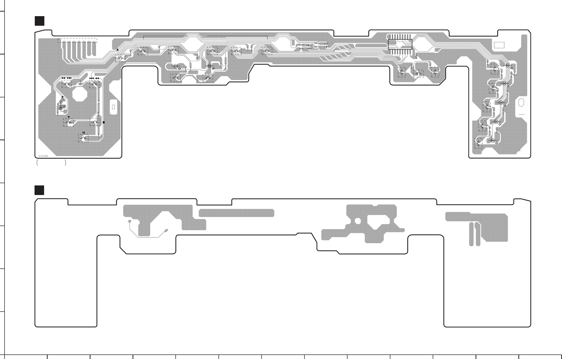
123456789101112
13
A
B
C
D
E
F
G
H
SL-DV290(EE,GN) OPERATION P.C.B.
OPERATION P.C.B. (SIDE : B)
D
OPERATION P.C.B. (SIDE : A)
D
123456 87
WB601
S621
( / ) S620
( / )
S611
( OPEN/
CLOSE)
S610
(DISC5)
S609
(DISC4)
S616
(DOUBLE
RE-MASTER) S615
(CINEMA)
S608
(DISC3) S607
(DISC2) S606
(DISC1)
S619
( ) S618
( )
S617
( )
R631
R630
R622
R621
R620
R606
R627
R626
R605
R625
R619
R618
R629
R628
R612
D608
( )
C605
C601
C604
C602
C603
R623
R624
R602
R604
R601
R603
S613
(REPEAT)
S614
(CD EDIT)
S612
(A-B
REPEAT)
S605
(DISC1)
S604
(DISC2)
S603
(DISC3)
S602
(DISC4)
S601
(DISC5)
1
5
9
10 15 18
IC601
D602
(DOUBLE
RE-MASTER) D601
(CINEMA)
D607
(DISC1)
D606
(DISC2)
D604
(DISC4)
D605
(DISC3)
D603
(DISC5)
R616
R617
R615
R609
R608
R614
R613
R607
R610
R611
DIRECT OPEN
REP3513B-M ..... [GN]
REP3513C-M ..... [EE]
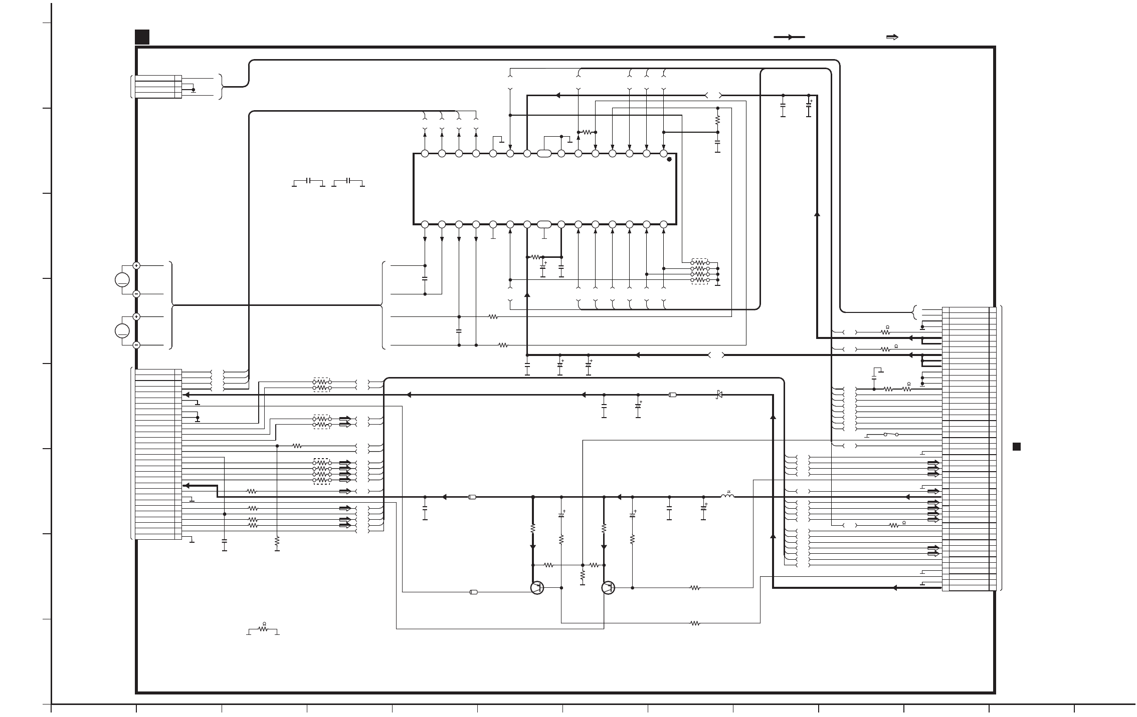
121110987654321
A
B
C
D
E
F
G
H
M
SL-DV290(EE,GN) INTERFACE CIRCUIT DIAGRAM
To FG UNIT
INTERFACE CIRCUIT
A
NOTE:
The number which noted at the connectors on the schematic diagram as
"SCHEMATIC DIAGRAM-1" or "SCHEMATIC DIAGRAM-2"
indicates the schematic diagram serial number located on the left corner in the schematic diagram.
To DVD MODULE
(FEP) CIRCUIT(FP5201) on
SCHEMATIC DIAGRAM-2/1,2-E~H
B
To OPTICAL PICK-UP
UNIT
T2(CD)
GND
PIN(CD)
FE2(CD)
VREF2.2V(CD)
T1(CD)
GND
FE1(CD)
VCC5V
LD+(DVD)
GND
RFN
F2(DVD)
TB(DVD)
TC(DVD)
TD(DVD)
TA(DVD)
VREF2.2V(DVD)
PIN(DVD)
GAIN H/L
F1(DVD)
RFP
GND
3.3VHFM
T-
F-
F+
T+
LD+(CD)
30
29
28
27
26
24
23
22
21
25
20
19
18
16
15
14
13
12
11
10
17
9
7
5
3
2
1
4
6
8
GND
FP5101
LB5106
VLP0146-T
RA2501
47K
R2507
6.8
M2502
(TRAVERSE MOTOR)
M2501
(SPINDLE MOTOR)
S2501 (REST DET.)
IC2501
C0GBG0000033
FOCUS/TRACKING COIL,
SPINDLE/ TRAVERSE
MOTOR DRIVE
14 13 12 11 10 9 8
15 16 17 18 19 20 21
654321
23 24 25 26 27 28
BIAS1
VIN1
VIN2
OPIN+
OPIN
-
GND
Vcc
MUTE12
GND
VO2+
VO2
-
VO1+
VO1
-
LDCNT
MUTE3
BIAS2
TRIN
LDIN
VIN3
PREVcc
MUTE4
GND
Vcc
VO3
-
VO3+
VO4
-
VO4+
7
22
OPOUT
C2503
16V22
C2513
0.1
A
C2511
0.1
R2505
82K
R2504
82K
C2507
0.1
R2503
15K
B
C
D
C5152
10V10
C5151
0.1
C5123
0.1
R5124
4.7K
R5111
2.2 C5111
6.3V47
R5117
47K
R5114
22K
R5113
47K
Q5111
2SB1115-T
LASER POWER
DRIVE(DVD)
R5112
27
R5115
2.2 C5115
6.3V47
R5116
27
Q5115
2SB1115-T
LASER POWER
DRIVE(CD)
C5103
0.1
C5101
16V10
A15
A14
A12
A10
A9
A8
A13
A6
A5
A4
A2
A1
LB5105
VLP0146-T
B9
B8
B7
B6
B5
B4
B3
B10
A16
A5
A6
A7
A8
A9
A11
A12
A13
A14
A10
LB5101
J0JHC0000045
D5151
MA728TX
A15
A16
R5102
56
R5121 56
R5123 56
A
B
C
D
B4B1
B6
B7
B8
R2502
15K
B9
B2
B3
B10
B5
B12
50
49
48
47
45
44
43
42
41
40
39
38
36
35
34
33
46
37
TRAYREF
M+9V
M+9V
FG3
FG1
D.GND
D.GND
MUTE4
D+5V
D+5V
TRAYIN
M+9V
M.GND
M.GND
M.GND
MUTE12
MUTE3
DMV 32
31
30
28
27
26
25
24
23
22
21
18
19A.GND
FE1 (CD)
29
20
T2 (CD)
A.GND
FOIN
TRIN
SPIN
TRVIN
IN-SW
LDCUR
VHALF
PIN (CD)
FE2 (CD)
T1 (CD)
LPCO2
17VCC 5V 16TB (DVD) 15TC (DVD) 14TD (DVD) 13TA (DVD)
FP5102
12TRAY/TRV 11VREF2.2V 10PIN (DVD) 9GAIN H/L 8
F2 (DVD) 7F1 (DVD) 6RFN 5RFP 4A.GND 3LPCO1 2A.GND 13.3VHFM
1
2
3
4
5
6
7
8
9
10
11
12
13
14
15
16
17
18
19
20
21
22
23
24
25
26
27
28
29
30
31
32
33
34
35
36
37
38
39
40
41
42
43
44
45
46
47
48
49
50
B1
A7
A3
A11
R5103
56
RA5102 56
RA5101
56
A2
A1
A3
A4
RA5103 56
R5152
1K
C5102
0.1
R5101 56
R5122 56
B2
B11
B12 R5120 0
B11
FG3 1
FP2501
FG2 2
FG2 3
FG1 4
R5107
0
R5108 0
R5109
0
R2501
100
C2510
0.1
C2502
16V100
C2509
16V10
C2505
0.1
C2504
0.1
C2501
6.3V220
C2506
0.1 C2508
0.1
R5105
0
L5101
10 H
C2512
0.1
M
A
B
C
D
A
B
C
D
SCHEMATIC DIAGRAM
-
1
A
B
A
B
:POSITIVE VOLTAGE LINE :AUDIO/VIDEO SIGNAL LINE
9V
5V
2.9V 2.9V 2.9V 2.9V 0V
(3.3V) 5V 1.7V 1.7V 1.7V 1.7V 1.7V 1.7V
4.1V 4.1V 4.1V 4.1V 0V 9V 9V 1.7V 0V 0V 1.7V 0V 5V
(3.3V)
4.9V
5V
0V
4.9V
5V
0V(2.2V) (3.2V)
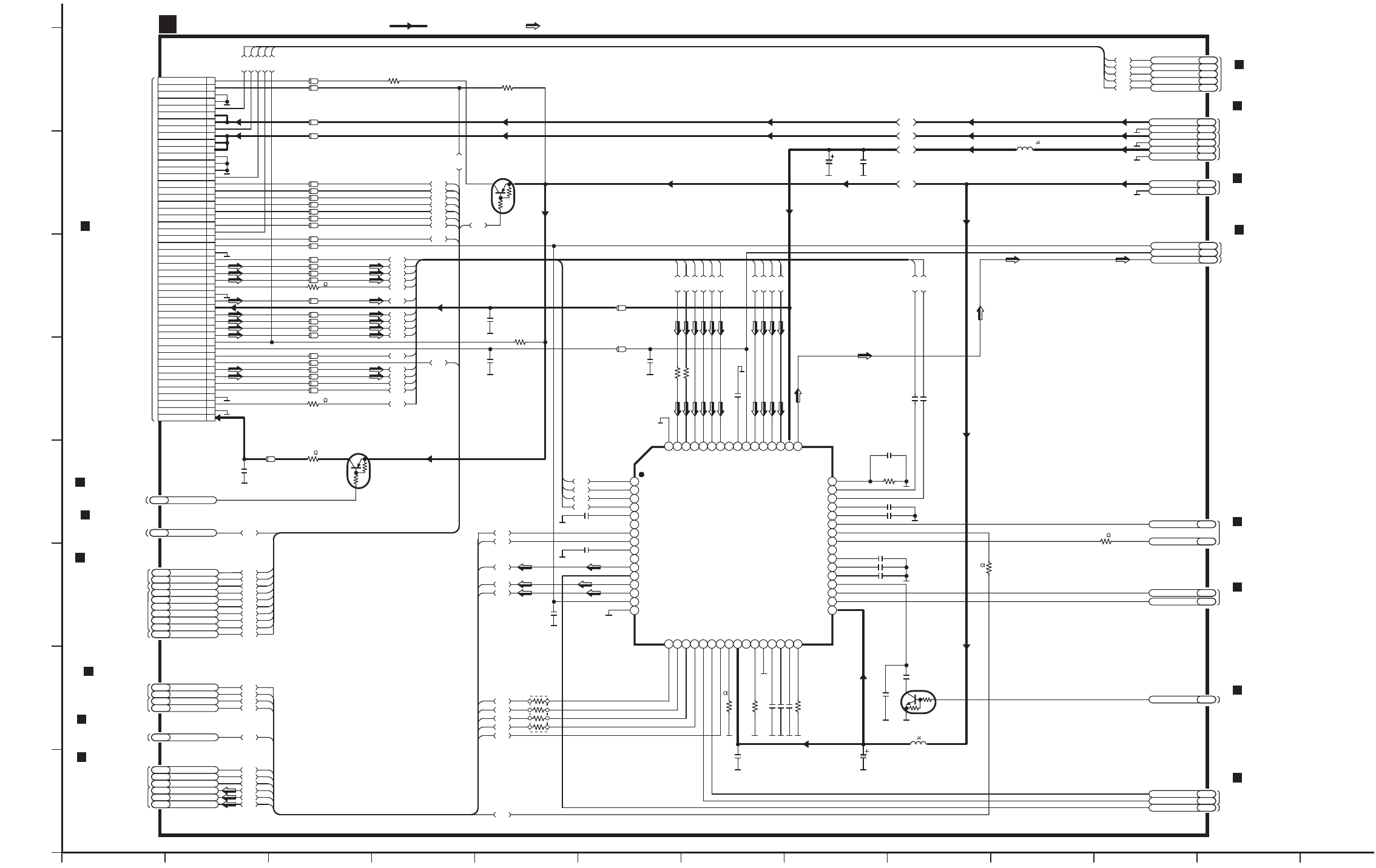
121110987654321
A
B
C
D
E
F
G
H
C5272 0.22
C5254 390P
C5282 0.01
C5274
0.1
B8
B7
B5
B4
B3
B6
C2
38
37
36
35
33
32
31
30
29
28
27
26
24
23
22
21
34
25
LDCUR
T2(CD)
SPDIN
M.GND
M.GND
TRAYREF
MUTE3
DMV
FOIN
INSW
PIN(CD)
FE2(CD)
VHALF
T1(CD)
FE1(CD)
Vcc+5V
20
19
18
16
15
14
13
12
11
10
9
6
7
A.GND
17
8
RFN
F2(DVD)
TB(DVD)
TC(DVD)
TD(DVD)
TA(DVD)
VREF2.2V
PIN(DVD)
GAIN H/L
F1(DVD)
RFP
A.GND 5
3.3VHFM
4
3
2
1
LB5239
VLP0146-T
C5221
0.1
GAINH/LFS5
LDCURFS6 MUTE12FS1 MUTE3FS2 FODRVFS3 TRDRVFS10 SPDRVFS11 TRVSDRVFS12
C1
C8
A+5V AB1
A.GND AG1
RFENV FS27
BDO FS28
OFTR FS29
VHALF FS32
VREF2 FS33
TSTSG FS26
D+3.3V DB1
Q5271
UN5211TX
SWITCHING
IC5201
AN22030A-VT
FRONT END PROCESSOR
B
C5283
560P
FP5201
17
STANBY
18
SEN
19
SCK
20
STDIO
21
OFTR
22
BDO
23
DTRD
24
SHOLD
25
VDD
26
NC2
27
RSCL
28
GND2
29
BDOSL
30
MIRSL
31
DCAGC
32
BRCA
LPC11
LPCO12
LPC2
3
LPCO2
4
POFLT
5
NC1
6
FBAL
7
TBAL
8
TEFLT
9
MONI2
10
TE
11
RFTE
12
FS
13
FE
14
VHALF
15
Vss
16 33
34
35
36
37
38
39
40
41
42
43
44
45
46
47
48
49
RFENV
50
Vcc1
51
VIN5
52
VIN6
53
VIN7
54
VIN8
5556
VREF
57
MONI
58
VIN1
59
VIN2
60
VIN3
61
VIN4
62
VIN9
63
VIN10
64
GND
Vcc2
FLTOP
FLTON
DCFLT
SAG
AGCG1
AGCG2
NC3
SHORT
IDGT
TESTSG
CRFHP1
CRFHP2
RFINP
RFINN
PEAK
VREFRF
C5292
100P
C5262 180P
C5204
0.1
39M.GND 40
41M+9V 42M+9V 43TRAYIN 44D+5V 45D+5V 46MUTE4 47D.GND 48D.GND 49FG3 50FG1
LPCO1
TRAY/TRV
A.GND
LPCO2
A.GND
TRVIN
TRIN
MUTE12
R5201 0
LB5221
LB5222
LB5223
LB5224
LB5225
LB5226
LB5228
LB5229
LB5230
LB5231
LB5233
R5203 0
LB5235
LB5236
LB5237
LB5238
LB5219
LB5218
VLP0146-T
LB5202
J0JHC0000045
LB5203
J0JHC0000045
LB5205
VLP0146-T
LB5206
LB5217
LB5213
LB5210
LB5209
LB5208
A1
A2
A3
A5
A6
A7
A8
A4
A1
D.GND DG1
D+5V DB3
M+9V MB1
M.GND MG1
FGFS8
A10
A10
C11
TBALFS14 FBALFS15 DTRDFS16 IDGTFS17
FEPENBFS19 FEPCLKFS20 FEPDATAFS21 TEFS23 ASFS24 FEFS25 C10
C9
C8
C7
C6
C4
C3
C2
C1
NRSTFS18
C7
C6
C5
C5
C9
C3
RFDIF FS31
C10
C11
R5262 0
R5294
12K
C5256 2200P
R5295 24K
C5273
1800P
DCFLT FC3
R5221
0
QR5221
UN2121-TX
POWER SUPPLY
C5205
0.1
C5202
16V10
HFMONFC1
C5264 0.018
C5271 1000P
C5290 1000P
C5299 330P
R5281
1M
C5201
16V10
C5233
0.1
B9
B10
B11
B12
B13
B14
NARF FS35
ARF FS36
VFOSHORT FS37
R5257
0
C5234
0.1
C5291 2700P
R5231
8.2K
R5232 8.2K
B1
B2
B15
B16
C5235
0.1
C5236 0.1
B1
B2
B14
B5
B6
B13
B7
B8
B9
B10
B3
B16
B11
B4
B12
B15
D.GND DG1
M+9V
VLP0146-T
VLP0155-T
C5232
0.1
LB5232
VLP0146-T
LB5227
VLP0146-T
RA5201
100
C4
L5202
10 H
R5320
0
L5201 10 H
C5203
0.1
TRV-SW+ VD9
TRAY REF VD6
TRAY/ TRV VD10
MUTE4 VD8
TRAY DRV VD7
SCHEMATIC DIAGRAM-5/1-G
SCHEMATIC DIAGRAM-5/1-H
SCHEMATIC DIAGRAM-5/1-F
SCHEMATIC DIAGRAM-3/12-D
SCHEMATIC DIAGRAM-3/12-F
LB5240
VLP0146-T
QR5241
UN511MTX
POWER SUPPLY
R5241
220
A4
A9
R5242
82K
A11
LB5207
DVD MODULE(FEP) CIRCUIT
SCHEMATIC DIAGRAM
-
2
DMVFS44 A8
A7
A5
A6
A3
A2
A9
SCHEMATIC DIAGRAM-3/12-D
SCHEMATIC DIAGRAM-3/1-C
SL-DV290(EE,GN) DVD MODULE(FEP) CIRCUIT DIAGRAM
SCHEMATIC DIAGRAM-3/12-F
SCHEMATIC DIAGRAM-3/1-C
To DVD MODULE
(SODC) CIRCUIT on
B
To DVD MODULE
(SODC) CIRCUIT on
B
SCHEMATIC DIAGRAM-3/1-B
SCHEMATIC DIAGRAM-3/1-A
To DVD MODULE
(CPU) CIRCUIT on
SCHEMATIC DIAGRAM-7/1-H
B
To DVD MODULE
(SODC) CIRCUIT on
B
SCHEMATIC DIAGRAM-3/1-B
SCHEMATIC DIAGRAM-3/12-F
SCHEMATIC DIAGRAM-3/12-A
SCHEMATIC DIAGRAM-3/12-F
SCHEMATIC DIAGRAM-3/1-C
To DVD MODULE
(SODC) CIRCUIT on
B
FGENBFS38 A11
To DVD MODULE
(CPU) CIRCUIT on
SCHEMATIC DIAGRAM-7/1-E
B
To DVD MODULE
(VIDEO DAC) CIRCUIT on
B
To DVD MODULE
(VIDEO DAC) CIRCUIT on
SCHEMATIC DIAGRAM-5/1-D
B
To DVD MODULE
(SODC) CIRCUIT on
B
To DVD MODULE
(VIDEO DAC) CIRCUIT on
SCHEMATIC DIAGRAM-5/12-A
B
To DVD MODULE
(SODC) CIRCUIT on
SCHEMATIC DIAGRAM-3/1-A
B
To DVD MODULE
(SODC) CIRCUIT on
SCHEMATIC DIAGRAM-3/12-F
B
To DVD MODULE(CPU)
CIRCUIT on
SCHEMATIC DIAGRAM-7/1-B
B
To DVD MODULE(SODC)
CIRCUIT on
B
A
To INTERFACE
CIRCUIT(FP5102)
on SCHEMATIC
DIAGRAM
-
1/11,12-B~D
D1
D2
D3
D4
D5
D1
D2
D3
D4
D5
R5204
1K
VLP0155-T
VLP0155-T
VLP0155-T
VLP0155-T
VLP0155-T
VLP0155-T
VLP0155-T
VLP0155-T
VLP0155-T
VLP0155-T
VLP0155-T
VLP0155-T
VLP0155-T
VLP0146-T
VLP0146-T
VLP0146-T
VLP0146-T
VLP0146-T
VLP0146-T
VLP0146-T
VLP0146-T
3.3V
3.3V
0V
(0.5V)0V
(3.2V)5V
0V
5V
(1.4V)2.6V
1.7V
1.7V
1.7V
1.7V
0V
1.7V
1.7V
1.7V
3.3V
3.3V
0V
0V
0V
0V
3.3V
0V
0.5V
3.3V
1.2V
2V
1.2V
1.2V
3.3V
1.6V
1.6V
1.8V
1.1V
0.7V
0V
0V
0V
0.7V
0V
2.2V
2.2V
1.7V
1.7V
5V
2.2V
2.2V
2.3V
2.3V
2.2V
1.8V
2.3V
2.3V
2.3V
2.3V
2.3V
2.3V
5V
9V
5V
3.3V
0V
0V
:POSITIVE VOLTAGE LINE :AUDIO/VIDEO SIGNAL LINE
3.3V
(3.3V)
(0V)
0V 3.3V
3.3V
(0V)
(3.3V)
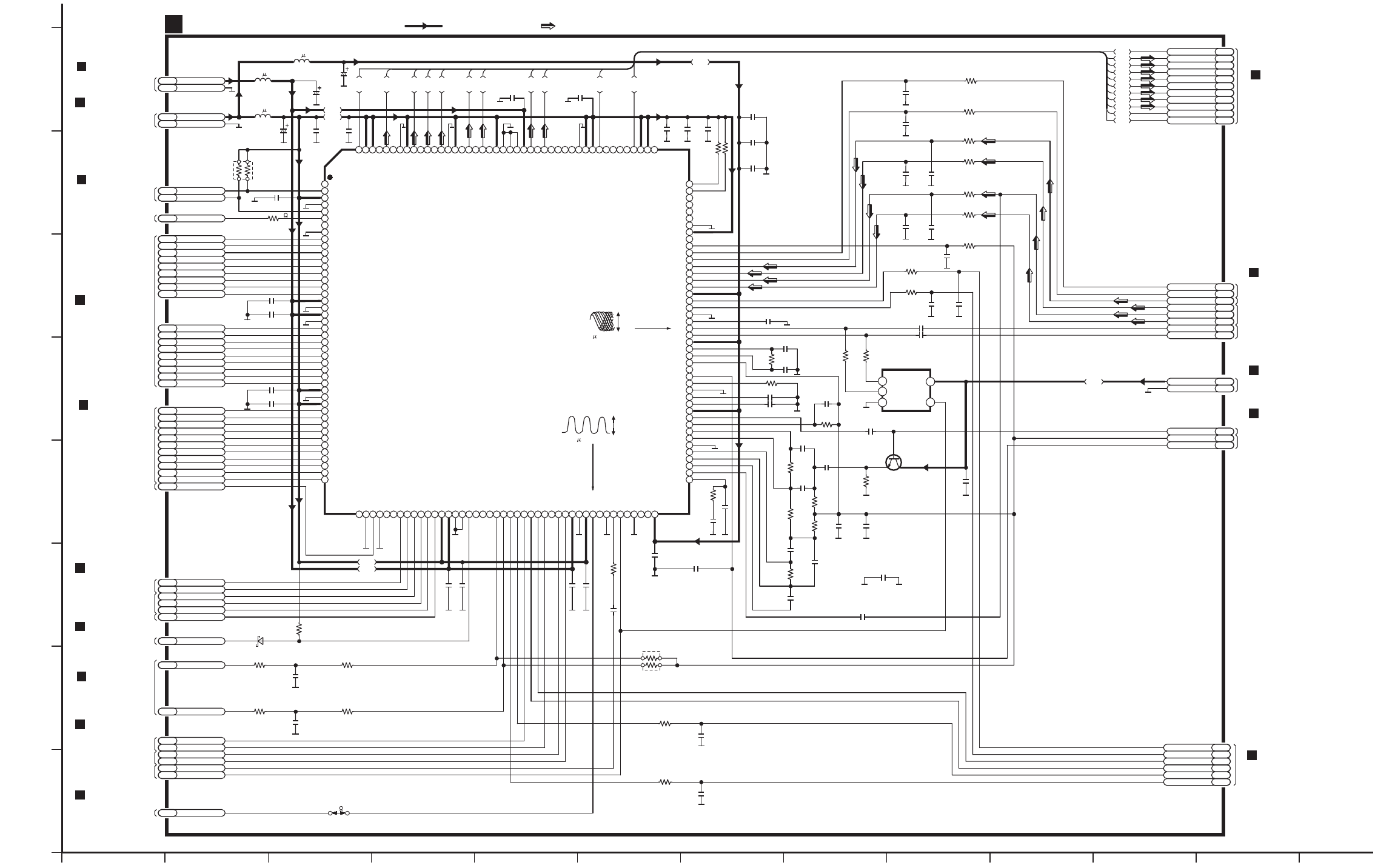
121110987654321
A
B
C
D
E
F
G
H
D.GNDDG1
1NINT0
2NINT1
3VDD3
4VSS
5NINT2
6WAITODC
7NMRST
8DASPST
9CPUADR17
10
CPUADR16
11
CPUADR15
12
CPUADR14
13
CPUADR13
14
CPUADR12
15
CPUADR11
16
CPUADR10
17
CPUADR9
18
VDD18
19
VSS
20
DRAMVDD18
21
DRAMVSS
22
CPUADR8
23
CPUADR7
24
CPUADR6
25
CPUADR5
26
CPUADR4
27
CPUADR3
28
CPUADR2
29
CPUADR1
30
CPUADR0
31
VDD3
32
VSS
33
DRAMVDD33
34
NCS
35
NWR
36
NRD
37
CPUDT7
38
CPUDT6
39
CPUDT5
40
CPUDT4
41
CPUDT3
42
CPUDT2
43
CPUDT1
44
CPUDT0
45
CLKOUT1
46
MMOD
47
NRST
48
MSTPOL
49
SCLOCK
50
SDATA
51
OFTR
52
BDO
53
PWM1
54
PWM2
55
PWM3
56
PWM4
57
VDD3
58
DRAMVDD18
59
DRAMVSS
60
VSS
61
PWM5
62
PWM6
63
PWM7
64
PWM8
65
TBAL
66
FBAL
67
TRSDRV
68
SPDRV
69
FG
70
TILTP
71
TILT
72
TILTN
73
TX
74
DTRD
75
IDGT/TEMUTE
76
VDD18
77
VSS
78
VDD3
79
OSCI1
80
ODCO1
81
VSS
82
TSTSG
83
VFOSHORT
84
JLINE
85
AVSS
86
ROUT
87
LOUT
88
AVDD
VCOF
89
TRCRS
90
CMPIN
91
LPFOUT
92
LPFIN
93
AVSS
94
HPFOUT
95
HPFIN
96
CSLFLT
97
RFDIF
98
AVDD
99
PLFLT2
100
PLFLT1
101
AVSS
102
RVI
103
VREFH
104
PLPG
105
VHALF
106
DSLF2
107
DSLF1
108
AVDD
109
NARF
110
ARF
111
JITOUT
112
AVSS
113
DAC0
114
DAC1
115
AVDD
116
AD0
117
AD1
118
AD2
119
AD3
120
AD4
121
AD5/CAPAC2
122
AD6/CAPAC1
123
TECAPA
124
VDD3
125
VSS
126
MONI0
127
MONI1
128
MONI2
129
MONI3
130
NEJECT
131
NTRYCL
132
NDASP
133
NCS3FX
134
NCS1FX
135
DA2
136
DA0
137
NPDIAG
138
DA1
139
NOSCS16
140
INTRQ
141
NDMACK
142
VDD3
143
VSS
144
IORDY
145
NIORD
146
NIOWR
147
DMARQ
148
HDD15
149
HDD0
150
HDD14
151
VDD18
152
PD
153
UATASEL
154
VSS
155
VDD3
156
HDD1
157
HDD13
158
HDD2
159
HDD12
160
HDD3
161
VDD3
162
VSS
163
HDD11
164
HDD4
165
HDD10
166
HDD5
167
HDD9
168
VDD3
169
VSS
170
HDD6
171
HDD8
172
HDD7
173
VDDH
174
NRESET
175
MASTER
176
C2003 0.1
CPUADR15SC24 CPUADR16SC25 CPUADR17SC26
WAITSC27
CPUADR14SC23 CPUADR13SC22
CPUADR11SC20 CPUADR12SC21
CPUADR10SC19 CPUADR9SC18 C2004 0.1
C2005 0.1
CPUADR6SC15 CPUADR7SC16 CPUADR8SC17
CPUADR5SC14 CPUADR4SC13
CPUADR2SC11 CPUADR3SC12
CPUADR1SC10 CPUADR0SC9
NRDSC28 NWELSC29 NSODCCSSC30
CPUDT7SC8 CPUDT6SC7
CPUDT4SC5 CPUDT5SC6
CPUDT3SC4 CPUDT2SC3 CPUDT1SC2 CPUDT0SC1
C2006 0.1
C2007 0.1
E1
E2
E3
E4
E5
E6
E7
E8
E9
E10
E11
C2014
0.1
ODCIRQSC32 ADSCIRQSC31
RA2021
1K
D+3.3VDB1
L2001
10 H
C2001
6.3V100
C2002
6.3V100
L2002
10 H
D+1.8VDB4
C2018
0.1
L2021
10 H
C2021
6.3V100
C2016
0.1
C2017
0.1
C2015
0.1
C2013
0.1
C2010 0.1
C2011 0.1
C2009 0.1
C2008 0.1
NRSTFS18
BDOFS28 OFTRFS29
FEPDATAFS21 FEPCLKFS20 FEPENBFS19
TRV-SW+VD9
R2021
47K
C2034
0.039
R2025
22K
R2026
22K
RA2022
4.7K
TBALFS14
C2035
8200P
R2027
56K
R2028
56K
FBALFS15
FGFS8 GAINH/LFS5 DTRDFS16 IDGTFS17 TSTSGFS26
CLK16M1SA1
R2029
10K
C2036
0.1
C2022
0.1
C2031
0.1
R2022
7.5K
C2032
0.1
R2023
7.5K
R2053 47K
R2054 47K
C2039 0.01
R2030
1K
C2102
0.1
C2058 1000P
R2038 15K
R2039
1M
C2054
680P
C2055 6800P
C2051 68P
C2050 0.033
R2037
68K
C2048
0.015
Q2001
2SD1819ATX
RF AMP
C2044
390P
C2043
100P
R2034
47K
C2045
1000P
R2033
4.7K
R2035
2.7K
R2031
560
C2041
330P
R2032
10K
C2042
330P
C2040
1000P
C2047
0.01
R2049
1K
C2046
1000P
VHALF FS32
VREF2 FS33
C2053
0.1
A+5V AB1
RFDIF FS31
C2059
820P
R2040
8.2K
C2060
1000P
R2041
8.2K
C2062
330P
R2042
15K
C2061
330P
R2043
15K
C2057 2700P
C2056 2700P ARF FS36
NARF FS35
C2063
1000P
STENABLE SD1
STD0 SD2
STD1 SD3
STD2 SD4
STD3 SD5
STD4 SD6
STD5 SD7
STD6 SD8
STD7 SD9
STVALID SD10
STCLK SD11
E1
E2
E3
E4
E5
E6
E7
E8
E9
E10
E11
FE FS25
TE FS23
RFENV FS27
AS FS24
LDCUR FS6
R2044
15K
C2064
1000P
R2045
15K
C2065
1000P
R2046
15K
C2066
4700P
C2067
4700P
R2047
15K
R2048
4.7M
A.GND AG1
C2025
0.1
C2024
0.1
C2023
0.1
IC2001
MN103S26EGA
OPTICAL DISC CONTROL
C2038
0.1
B
R2036 0
VFO SHORTFS37 TRVSDRV FS12
SPDRV FS11
MUTE3 FS2
MUTE12 FS1
FODRV FS3
TRDRV FS10
IC2101
C0JBAS000116
LOGIC CONTROL
GND3
B
2
A1
4C
5VCC
R2052
100
R2051
100
C2073
0.1
D.GNDDG1
C2101
0.1
C2052
0.1
C2012
0.1
DVD MODULE(SODC) CIRCUIT
SCHEMATIC DIAGRAM
-
3
SL-DV290(EE,GN) DVD MODULE(SODC) CIRCUIT DIAGRAM
To DVD MODULE
(VIDEO DAC) CIRCUIT on
B
SCHEMATIC DIAGRAM-5/1-D
SCHEMATIC DIAGRAM-5/1-E
SCHEMATIC DIAGRAM-7/1-G
To DVD MODULE
(CPU) CIRCUIT on
B
SCHEMATIC DIAGRAM-7/1-F
SCHEMATIC DIAGRAM-7/12-E,F
To DVD MODULE
(CPU) CIRCUIT on
B
SCHEMATIC DIAGRAM-7/1-F
To DVD MODULE
(CPU) CIRCUIT on
B
SCHEMATIC DIAGRAM-7/1-H
SCHEMATIC DIAGRAM-7/12-B
To DVD MODULE
(FEP) CIRCUIT on
B
FGENBFS38
SCHEMATIC DIAGRAM-2/1-D
SCHEMATIC DIAGRAM-2/1-A
SCHEMATIC DIAGRAM-2/12-A
To DVD MODULE
(VIDEO DAC) CIRCUIT on
B
To DVD MODULE
(VIDEO DAC) CIRCUIT on
B
SCHEMATIC DIAGRAM-5/12-B
To DVD MODULE
(FEP) CIRCUIT on
B
SCHEMATIC DIAGRAM-2/1-B
To DVD MODULE
(FEP) CIRCUIT on
B
SCHEMATIC DIAGRAM-2/1-B
SCHEMATIC DIAGRAM-2/1-C
SCHEMATIC DIAGRAM-2/12-C
To DVD MODULE
(AUDIO DAC) CIRCUIT on
B
SCHEMATIC DIAGRAM-6/12-C
K2004
0
To DVD MODULE
(FEP) CIRCUIT on
B
SCHEMATIC DIAGRAM-2/1-C
To DVD MODULE
(FEP) CIRCUIT on
B
SCHEMATIC DIAGRAM-2/12-A
To DVD MODULE
(VIDEO DAC) CIRCUIT on
B
SCHEMATIC DIAGRAM-2/12-F
SCHEMATIC DIAGRAM-5/1-F
SCHEMATIC DIAGRAM-2/12-C
SCHEMATIC DIAGRAM-2/1-A
SCHEMATIC DIAGRAM-2/12-F
SCHEMATIC DIAGRAM-2/1-C
To DVD MODULE
(FEP) CIRCUIT on
B
DMV FS44
SCHEMATIC DIAGRAM-4/1-A
To DVD MODULE
(AVDEC) CIRCUIT on
B
D2001
MA728TX
5V
1.8V
3.3V
3.3V
3.3V
1.8V
3.3V
3.3V
3.3V
3.3V
2.7V
2.4V
2.6V
2.8V
2.5V
2.8V
2.8V
2.6V
2.5V 1.8V
1.8V
2.6V
2.7V
2.9V
2.7V
2.9V
2.8V
2.9V
2.9V
2.3V 3.3V
3.3V
3.3V
3.3V
2.8V
3.1V
(1.8V)
(1.6V)
(2V)
(3.3V)
(1.8V)
(2.2V)
(2.3V)
(2.2V)
(1.7V)
(1.9V)
(2.2V)
(2.2V)
(2.2V)
(2.2V)
(2V)
(2.2V)
(2.1V)
(1.2V)
(2V)
(2.4V)
(2.3V)
(2.4V)
(2.3V)
(2.4V)
(2.3V)
(2.3V)
3.3V
0V
0V
0V
0V
3.3V
3.3V
1.8V
3.3V
1.7V
1.7V
1.7V
1.7V
3.3V
0V
0V
0V
3.3V
0V
1.8V
3.3V
1.5V
0V
3.3V
(1.7V)
(3.3V)
(3.3V)
0V
1.6V
1.6V
0V
0V
1.7V
1.7V
1.4V
1.7
3.3V
1.5V
2.2V
1.7V
1.4V
1.7V
3.3V
1.6V
1.6V
2.1V
1.7V
1.7V
3.3V
1.7V
1.7V
1.7V
1.7V
2.4V
1.7V
1.2V
3.3V
3.3V
3.3V
3.3V
3.3V
0V(1.6V)
0V (0.6V)
3.3V
3.3V
0V (2.6V)
2.2V(3.1V)
1.8V
3.3V
3.3V
0V(3.1V)
3.3V
0V(3.1V)
3.3V
3.3V
0V(3.3V)
0V
0V
0.5 s. 0.2V/DIV.
PLAY
0.3V
P-P
3.5V
P-P
0.5 s. 1V/DIV.
5V
0V(3.1V)
0V(3.1V)
0V(3.1V)
0V(3.1V)
0V
0V
5V
0V
1.6V
1.6V
3.1V
3.1V
3.1V
3.1V
3.1V
3.1V
3.1V
:POSITIVE VOLTAGE LINE :AUDIO/VIDEO SIGNAL LINE
3.3V(0V)
(1.3V)
0V (1.3V)
