Sx_ds12 3 SCENIX
User Manual: SCENIX
Open the PDF directly: View PDF ![]() .
.
Page Count: 43
© 1998 Scenix Semiconductor, Inc. All rights reserved. - 1 - www.scenix.com
Scenix™ and the Scenix logo are trademarks of Scenix Semiconductor, Inc.
I2C™ is a trademark of Philips Corporation
PIC® is a registered trademark of Microchip Technology, Inc.
Microchip® is a registered trademark of Microchip Technology, Inc.
SX-Key™ is a trademark of Parallax, Inc.
Microwire™ is a trademark of National Semiconductor Corporation
All other trademarks mentioned in this document are property of their respec-
tive companies.
PRELIMINARY
December 3, 1998
SX18AC / SX20AC / SX28AC
High-Performance 8-Bit Microcontrollers with EE/Flash Program
Memory and In-System Programming Capability
1.0PRODUCT OVERVIEW
1.1Introduction
The SX18AC, SX20AC, and SX28AC are members of
the SX family of high-performance 8-bit microcontrollers
fabricated in an advanced CMOS process technology.
The advanced process, combined with a RISC-based
architecture, allows high-speed computation, flexible I/O
control, and efficient data manipulation. Throughput is
enhanced by operating the device at frequencies up to 50
MHz and by optimizing the instruction set to include
mostly single-cycle instructions.
On-chip functions include a general-purpose 8-bit timer
with prescaler, an analog comparator, a brown-out detec-
tor, a watchdog timer, a power-save mode with multi-
source wakeup capability, an internal R/C oscillator, user-
selectable clock modes, and high-current outputs.
1.2Key Features
•50 MIPS performance at 50 MHz oscillator frequency
•2048 x 12 bits EE/Flash program memory rated for
10,000 rewrite cycles
•136 x 8 bits SRAM
•In-system programming capability through OSC pins
•Internal RC oscillator with configurable rate from 31.25
KHz to 4 MHz, +8% accuracy
•User selectable clock modes:
–Internal RC oscillator
–External oscillator
–Crystal/resonator options
–External RC oscillator (continued on page 3)
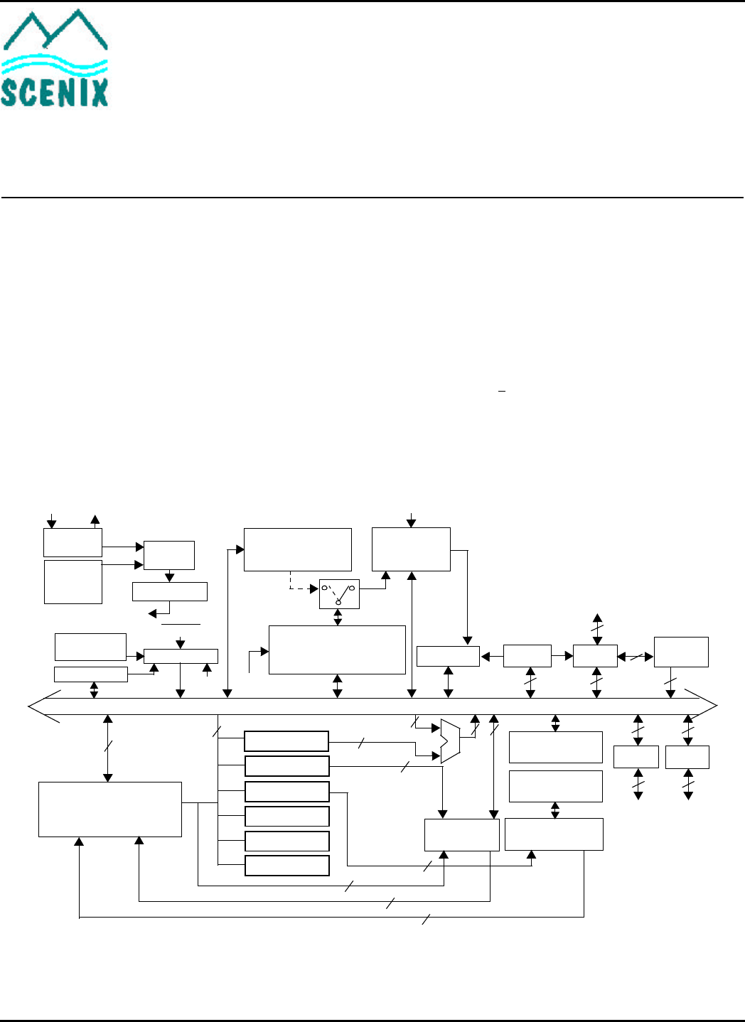
Figure1-1. Block Diagram
Interrupt MIWU Port B Comp
Power-On
Reset RESET
8-bit Watchdog
Timer (WDT) 8-bit Timer
RTCC
888
Port C
8
8
Port A
8
4
Internal Data Bus
In-System
Debugging
In-System
Programming
2k x 12
EEPROM
System
Clock
Brown-Out MIWU
MCLR
OSC
Driver
4MHz
Internal
RC OSC
Clock
Select
÷ 4 or ÷ 1
136 Bytes
SRAM
Address
Write Data
Read Data
Instruction
W
FSR
STATUS
PC
MODE
OPTION
System Clock
OSC1 OSC2
Instruction Pipeline
Four - Stage
8
8
12
Address 12
8
8
88
ALU
8
8
8
3
RTCC
Analog
8
Prescaler for RTCC
Postscaler for WDT
or

© 1998 Scenix Semiconductor, Inc. All rights reserved. - 2 - www.scenix.com
SX18AC / SX20AC / SX28AC
Table of Contents
11.0 Product Overview . . . . . . . . . . . . . . . . . . . . . . . . . . . . . . . . . . 1
1.1 Introduction . . . . . . . . . . . . . . . . . . . . . . . . . . . . . . . 1
1.2 Key Features . . . . . . . . . . . . . . . . . . . . . . . . . . . . . . 1
1.2.1 CPU Features . . . . . . . . . . . . . . . . . . . . . 3
1.2.2 I/O Features . . . . . . . . . . . . . . . . . . . . . . . 3
1.3 Architecture . . . . . . . . . . . . . . . . . . . . . . . . . . . . . . . 3
1.4 Programming and Debugging Support . . . . . . . . . . 3
1.5 Applications . . . . . . . . . . . . . . . . . . . . . . . . . . . . . . . 3
2.0 Connection Diagrams . . . . . . . . . . . . . . . . . . . . . . . . . . . . . . . 4
2.1 Pin Assignments . . . . . . . . . . . . . . . . . . . . . . . . . . . 4
2.2 Pin Descriptions . . . . . . . . . . . . . . . . . . . . . . . . . . . . 4
2.3 Part Numbering . . . . . . . . . . . . . . . . . . . . . . . . . . . . 5
3.0 Port Descriptions . . . . . . . . . . . . . . . . . . . . . . . . . . . . . . . . . . 6
3.1 Reading and Writing the Ports . . . . . . . . . . . . . . . . . 7
3.2 Port Configuration . . . . . . . . . . . . . . . . . . . . . . . . . . 8
3.2.1 MODE Register . . . . . . . . . . . . . . . . . . . . 8
3.2.2 Port Configuration Registers . . . . . . . . . . 8
3.2.3 Port Configuration Upon Power-Up . . . . . 9
4.0 Special-Function Registers . . . . . . . . . . . . . . . . . . . . . . . . . 10
4.1 PC Register (02h) . . . . . . . . . . . . . . . . . . . . . . . . . 10
4.2 STATUS Register (03h) . . . . . . . . . . . . . . . . . . . . . 10
4.3 OPTION Register . . . . . . . . . . . . . . . . . . . . . . . . . . 11
5.0 Device Configuration Registers . . . . . . . . . . . . . . . . . . . . . 12
5.1 FUSE Word (Read/Program at FFFh in main memory
map) 12
5.2 FUSEX Word (Read/Program via Programming
Command) 13
5.3 DEVICE Word (Hard-Wired Read-Only) . . . . . . . . 13
6.0 Memory Organization . . . . . . . . . . . . . . . . . . . . . . . . . . . . . . 14
6.1 Program Memory . . . . . . . . . . . . . . . . . . . . . . . . . . 14
6.1.1 Program Counter . . . . . . . . . . . . . . . . . . 14
6.1.2 Subroutine Stack . . . . . . . . . . . . . . . . . . 14
6.2 Data Memory . . . . . . . . . . . . . . . . . . . . . . . . . . . . .14
6.2.1 File Select Register (04h) . . . . . . . . . . . 14
7.0 Power Down Mode . . . . . . . . . . . . . . . . . . . . . . . . . . . . . . . . 16
7.1 Multi-Input Wakeup . . . . . . . . . . . . . . . . . . . . . . . . 16
7.2 Port B MIWU/Interrupt Configuration . . . . . . . . . . . 17
8.0 Interrupt Support . . . . . . . . . . . . . . . . . . . . . . . . . . . . . . . . . 18
9.0 Oscillator Circuits . . . . . . . . . . . . . . . . . . . . . . . . . . . . . . . . . 20
9.1 XT, LP or HS modes . . . . . . . . . . . . . . . . . . . . . . . 20
9.2 External RC Mode . . . . . . . . . . . . . . . . . . . . . . . . . 21
9.3 Internal RC Mode . . . . . . . . . . . . . . . . . . . . . . . . . . 21
10.0 Real Time Clock (RTCC)/Watchdog Timer . . . . . . . . . . . . .22
10.1 RTCC . . . . . . . . . . . . . . . . . . . . . . . . . . . . . . . . . . .22
10.2 Watchdog Timer . . . . . . . . . . . . . . . . . . . . . . . . . . .22
10.3 The Prescaler . . . . . . . . . . . . . . . . . . . . . . . . . . . . .22
11.0 Comparator . . . . . . . . . . . . . . . . . . . . . . . . . . . . . . . . . . . . . .23
12.0 Reset . . . . . . . . . . . . . . . . . . . . . . . . . . . . . . . . . . . . . . . . . . . .24
13.0 Brown-Out Detector . . . . . . . . . . . . . . . . . . . . . . . . . . . . . . .25
14.0 Register States Upon Reset . . . . . . . . . . . . . . . . . . . . . . . . .26
15.0 Instruction Set . . . . . . . . . . . . . . . . . . . . . . . . . . . . . . . . . . . .27
15.1 Instruction Set Features . . . . . . . . . . . . . . . . . . . . .27
15.2 Instruction Execution . . . . . . . . . . . . . . . . . . . . . . .27
15.3 Addressing Modes . . . . . . . . . . . . . . . . . . . . . . . . .27
15.4 RAM Addressing . . . . . . . . . . . . . . . . . . . . . . . . . .28
15.5 The Bank Instruction . . . . . . . . . . . . . . . . . . . . . . .28
15.6 Bit Manipulation . . . . . . . . . . . . . . . . . . . . . . . . . . .28
15.7 Input/Output Operation . . . . . . . . . . . . . . . . . . . . . .28
15.7.1 Read-Modify-Write Considerations . . . .28
15.8 Increment/Decrement . . . . . . . . . . . . . . . . . . . . . . .28
15.9 Loop Counting and Data Pointing Testing . . . . . . .28
15.10 Branch and Loop Call Instructions . . . . . . . . . . . . .28
15.10.1 Jump Operation . . . . . . . . . . . . . . . . . . .28
15.10.2 Page Jump Operation . . . . . . . . . . . . . .29
15.10.3 Call Operation . . . . . . . . . . . . . . . . . . . .29
15.10.4 Page Call Operation . . . . . . . . . . . . . . . .29
15.11 Return Instructions . . . . . . . . . . . . . . . . . . . . . . . . .29
15.12 Subroutine Operation . . . . . . . . . . . . . . . . . . . . . . .29
15.12.1 Push Operation . . . . . . . . . . . . . . . . . . .29
15.12.2 Pop Operation . . . . . . . . . . . . . . . . . . . .30
15.13 Comparison and Conditional Branch Instructions .30
15.14 Logical Instruction . . . . . . . . . . . . . . . . . . . . . . . . .30
15.15 Shift and Rotate Instructions . . . . . . . . . . . . . . . . .30
15.16 Complement and SWAP . . . . . . . . . . . . . . . . . . . .30
15.17 Key to Abbreviations and Symbols . . . . . . . . . . . . .30
16.0 Instruction Set Summary Table . . . . . . . . . . . . . . . . . . . . . .31
16.1 Equivalent Assembler Mnemonics . . . . . . . . . . . . .34
17.0 Electrical Characteristics . . . . . . . . . . . . . . . . . . . . . . . . . . .35
17.1 Absolute Maximum Ratings . . . . . . . . . . . . . . . . . .35
17.2 DC Characteristics . . . . . . . . . . . . . . . . . . . . . . . . .36
17.3 AC Characteristics . . . . . . . . . . . . . . . . . . . . . . . . .37
17.4 Comparator DC and AC Specifications . . . . . . . . .37
17.5 Typical Performance Characteristics . . . . . . . . . . .38
18.0 Package Dimensions . . . . . . . . . . . . . . . . . . . . . . . . . . . . . .39

© 1998 Scenix Semiconductor, Inc. All rights reserved. - 3 - www.scenix.com
SX18AC / SX20AC / SX28AC
1.2 Key Features (Continued)
•Analog comparator
•Brown-out detector (4.2V, on/off)
•Multi-Input Wakeup (MIWU) on eight pins
•Fast lookup capability through run-time readable code
•Complete development tool support available through
Parallax
1.2.1 CPU Features
•Fully static design – DC to 50 MHz operation
•20 ns instruction cycle time
•Mostly single-cycle instructions
•Selectable 8-level deep hardware subroutine stack
•Single-level interrupt stack
•Fixed interrupt response time: 60 ns internal, 100 ns
external at 50 MHz
•Hardware context save/restore for interrupt
•Designed to be pin-compatible and upward code-com-
pitable with the PIC165x®
1.2.2 I/O Features
•Software-selectable I/O configuration
–Each pin programmable as an input or output
–TTL or CMOS level selection on inputs
–Internal weak pull-up selection on inputs (~20 kΩ to
Vdd)
•Schmitt trigger inputs on Port B and Port C
•All outputs capable of sinking/sourcing 30 mA
•Symmetrical drive on Port A outputs (same Vdrop +/-)
1.3Architecture
The SX devices use a modified Harvard architecture.
This architecture uses two separate memories with sepa-
rate address buses, one for the program and one for
data, while allowing transfer of data from program mem-
ory to SRAM. This ability allows accessing data tables
from program memory. The advantage of this architec-
ture is that instruction fetch and memory transfers can be
overlapped with a multi-stage pipeline, which means the
next instruction can be fetched from program memory
while the current instruction is being executed using data
from the data memory.
The SX family implements a four-stage pipeline (fetch,
decode, execute, and write back), which results in execu-
tion of one instruction per clock cycle. At the maximum
operating frequency of 50 MHz, instructions are executed
at the rate of one per 20-ns clock cycle.
1.4Programming and Debugging Support
The SX devices are currently supported by the SX-Key™
offered by Parallax, Inc. This tool provides an integrated
development environment including editor, macro assem-
bler, debugger, and programmer.
1.5Applications
Emerging applications and advances in existing ones
require higher performance while maintaining low cost
and fast time-to-market.
The SX devices provide solutions for many familiar appli-
cations such as process controllers, electronic appli-
ances/tools, security/monitoring systems, and personal
communication devices. In addition, the enhanced
throughput allows efficient development of software mod-
ules called Virtual Peripherals to replace on-chip hard-
ware peripherals. The concept of Virtual Peripherals
provides benefits such as using a more simple device,
reduced component count, fast time to market, increased
flexibility in design, and ultimately overall system cost
reduction.
Some examples of Virtual Peripheral modules are:
•Serial, Parallel, I2C™, Microwire™ (µ-Wire), Dallas µ-
Wire, SPI, DMX-512, X-10, IR transceivers
•Frequency generation and measurement
•Spectrum analysis
•Multi-tasking, interrupts, and networking
•Resonance loops
•DRAM drivers
•Music and voice synthesis
•PPM/PWM output
•Delta/Sigma ADC
•DTMF I/O and call progress
•300/1200 baud modem
•Quadrature encoder/decoder
•Peripheral Interface Device (PID) and servo control
•Video controller
© 1998 Scenix Semiconductor, Inc. All rights reserved. - 4 - www.scenix.com
SX18AC / SX20AC / SX28AC
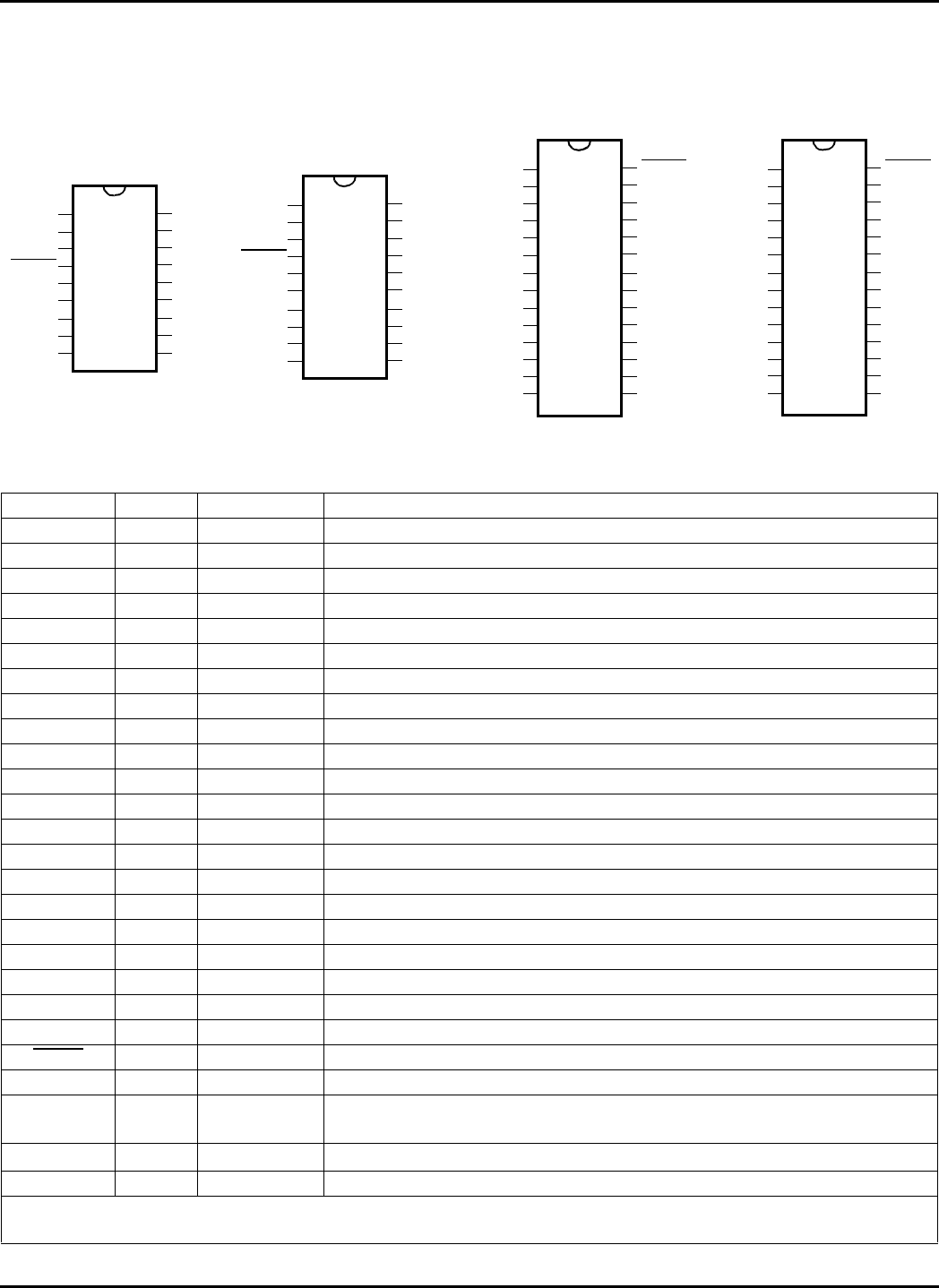
2.0CONNECTION DIAGRAMS
2.1Pin Assignments
2.2Pin Descriptions
SSOP
1
2
3
4
5
6
7
8
16
15
RC4
RC3
RB6
RB5
SX 28-PIN
OSC2
RC7
RC6
RC5
Vdd
Vdd
RA2
RA3
RB0
RB1
RB2
RB3
RB4
Vss
MCLR
OSC1
RC2
RC1
RC0
RB7
9
10
11
12
13
14
28
27
26
25
24
23
22
21
20
19
18
17
Vss
RTCC
RA0
RA1
1
2
3
4
5
6
7
8
16
15
RC4
RC3
RB6
RB5
SX 28-PIN
OSC2
RC7
RC6
RC5
n.c.
Vss
RA2
RA3
RB0
RB1
RB2
RB3
RB4
MCLR
OSC1
RC2
RC1
RC0
RB7
9
10
11
12
13
14
28
27
26
25
24
23
22
21
20
19
18
17
RTCC
Vdd
RA0
RA1
n.c.
SDIP/SOIC
1
2
3
4
5
6
7
8
16
15
RB5
RB4
SX 20-PIN
OSC2
RTCC RA0
RB0
RB1
RB2
RB3
MCLR
OSC1
Vdd
Vdd
RB7
RB6
9
10
14
13
12
11
20
19
18
17
RA2
RA3
Vss
RA1
Vss
SSOP
1
2
3
4
5
6
7
8
16
15
RB5
RB4
SX 18-PIN
OSC2
RTCC RA0
RB0
RB1
RB2
RB3
MCLR
OSC1
Vdd
RB7
RB6
910
14
13
12
11
18
17
RA2
RA3 RA1
Vss
SDIP/SOIC
Name Pin Type Input Levels Description
RA0 I/O TTL/CMOS Bidirectional I/O Pin; symmetrical source / sink capability
RA1 I/O TTL/CMOS Bidirectional I/O Pin; symmetrical source / sink capability
RA2 I/O TTL/CMOS Bidirectional I/O Pin; symmetrical source / sink capability
RA3 I/O TTL/CMOS Bidirectional I/O Pin; symmetrical source / sink capability
RB0 I/O TTL/CMOS/ST Bidirectional I/O Pin; comparator output; MIWU input
RB1 I/O TTL/CMOS/ST Bidirectional I/O Pin; comparator negative input; MIWU input
RB2 I/O TTL/CMOS/ST Bidirectional I/O Pin; comparator positive input; MIWU input
RB3 I/O TTL/CMOS/ST Bidirectional I/O Pin; MIWU input
RB4 I/O TTL/CMOS/ST Bidirectional I/O Pin; MIWU input
RB5 I/O TTL/CMOS/ST Bidirectional I/O Pin; MIWU input
RB6 I/O TTL/CMOS/ST Bidirectional I/O Pin; MIWU input
RB7 I/O TTL/CMOS/ST Bidirectional I/O Pin; MIWU input
RC0 I/O TTL/CMOS/ST Bidirectional I/O pin
RC1 I/O TTL/CMOS/ST Bidirectional I/O pin
RC2 I/O TTL/CMOS/ST Bidirectional I/O pin
RC3 I/O TTL/CMOS/ST Bidirectional I/O pin
RC4 I/O TTL/CMOS/ST Bidirectional I/O pin
RC5 I/O TTL/CMOS/ST Bidirectional I/O pin
RC6 I/O TTL/CMOS/ST Bidirectional I/O pin
RC7 I/O TTL/CMOS/ST Bidirectional I/O pin
RTCC IST Input to Real-Time Clock/Counter
MCLR IST Master Clear reset input – active low
OSC1/In/Vpp IST Crystal oscillator input – external clock source input
OSC2/Out OCMOS Crystal oscillator output – in R/C mode, internally pulled to Vdd through weak
pull-up
Vdd P–Positive supply pin
Vss P–Ground pin
Note:I = input, O = output, I/O = Input/Output, P = Power, TTL = TTL input, CMOS = CMOS input, ST = Schmitt Trigger
input, MIWU = Multi-Input Wakeup input
© 1998 Scenix Semiconductor, Inc. All rights reserved. - 5 - www.scenix.com
SX18AC / SX20AC / SX28AC
2.3Part Numbering
Table2-1. Ordering Information
Device Pins I/O EE/Flash (Words) RAM (Bytes)
SX18AC/SO 18 12 2K 136
SX18AC/DP 18 12 2K 136
SX20AC/SS 20 12 2K 136
SX28AC/SO 28 20 2K 136
SX28AC/DP 28 20 2K 136
SX28AC/SS 28 20 2K 136
Figure2-1. Part Number Reference Guide
SX18AC-LI/SO
Package Type
Extended Temperature
Low Voltage
Memory Size
Feature Set
Pin Count
SceniX
A = 512 word
B = 1k word
C = 2k word
D = 4k word
E = 8k word
F = 16k word
G = 24k word
H = 32k word
I = 48k word
J = 64k word
© 1998 Scenix Semiconductor, Inc. All rights reserved. - 6 - www.scenix.com
SX18AC / SX20AC / SX28AC
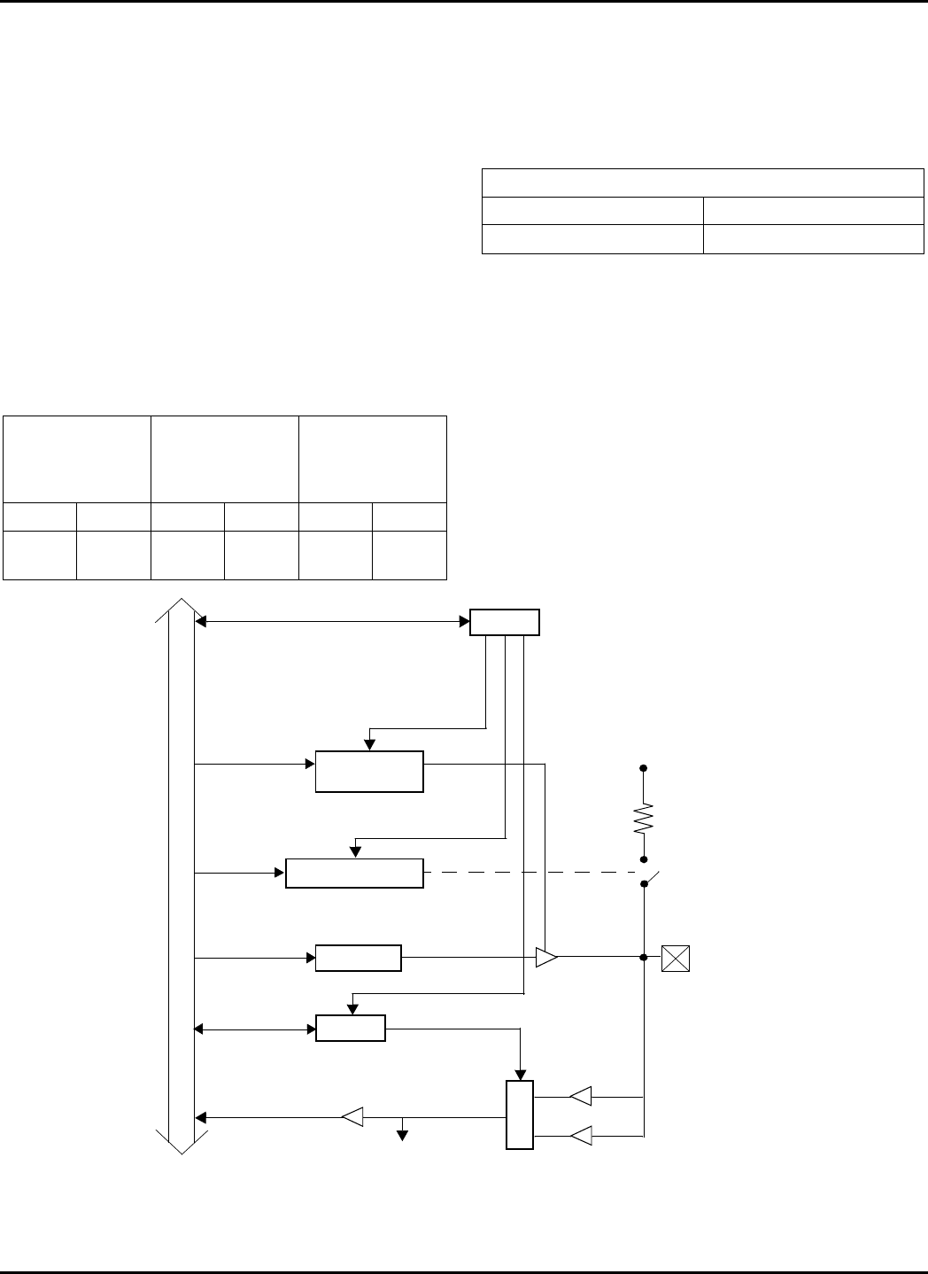
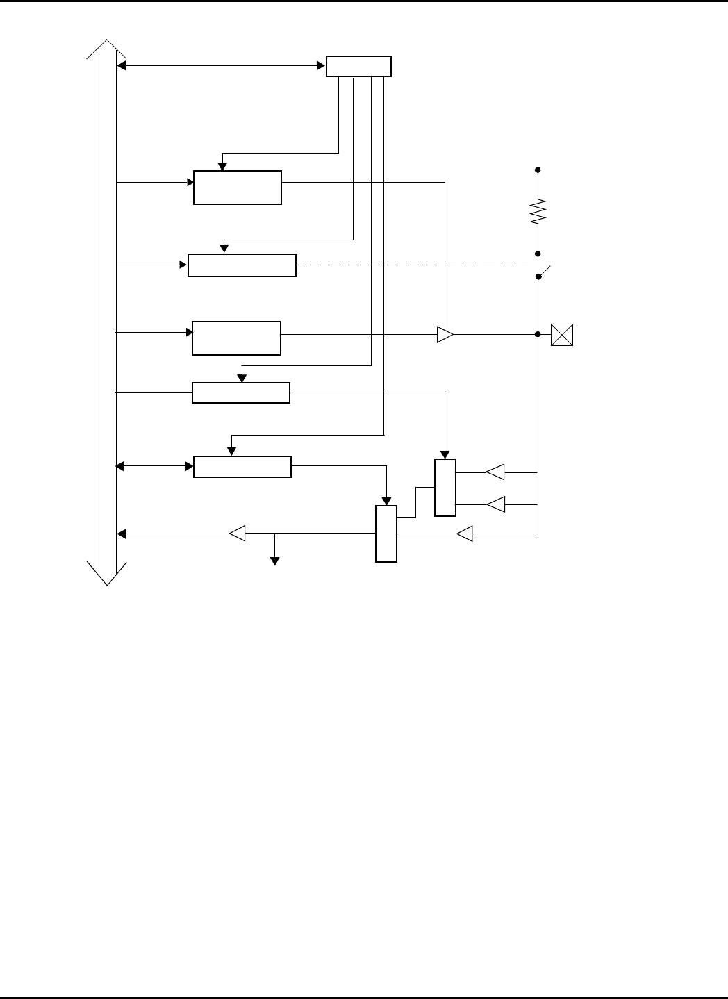
3.0PORT DESCRIPTIONS
The device contains a 4-bit I/O port (Port A) and two 8-bit
I/O ports (Port B, Port C). Port A provides symmetrical
drive capability. Each port has three associated 8-bit reg-
isters (Direction, Data, TTL/CMOS Select, and Pull-Up
Enable) to configure each port pin as Hi-Z input or output,
to select TTL or CMOS voltage levels, and to enable/dis-
able the weak pull-up resistor. The upper four bits of the
registers associated with Port A are not used. The least
significant bit of the registers corresponds to the least
significant port pin. To access these registers, an appro-
priate value must be written into the MODE register.
Upon power-up, all bits in these registers are initialized to
“1”.
The associated registers allow for each port bit to be indi-
vidually configured under software control as shown
below:
Port B and Port C have additional associated registers
(Schmitt-Trigger Enable Registers ST_B and ST_C) to
enable or disable the Schmitt Trigger function on each
individual port pin as indicated in table below.
Port B also supports the on-chip differential comparator.
Ports RB1 and RB2 are the comparator negative and
positive inputs, respectively, while Port RB0 is the com-
parator output pin. Port B also supports the Multi-Input
Wakeup feature on all eight pins.
Figure3-1 shows the internal hardware structure and
configuration registers for each pin of Port A. Figure3-2
shows the same for each pin of Port B or Port C.
Table3-1. Port Configuration
Data Direction
Registers:
RA, RB, RC
TTL/CMOS
Select Registers:
LVL_A, LVL_B,
LVL_C
Pullup Enable
Registers:
PLP_A, PLP_B,
PLP_C
010101
Output Hi-Z
Input CMOS TTL Enable Disable
Table3-2. Schmitt Trigger Select
Schmitt Trigger Enable Registers: ST_B, ST_C
0 1
Enable Disable
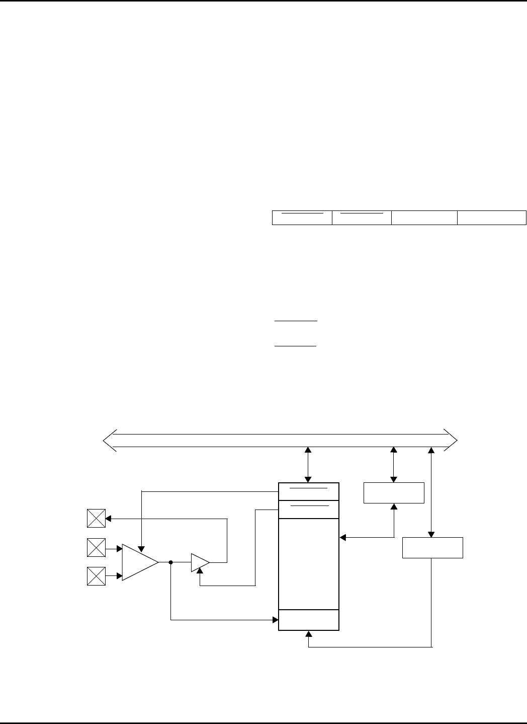
Figure3-1. Port A Configuration
MODE
RA
RA Data
LV_A
0 = Output
1 = Hi-Z Input
WR
WR
0 = CMOS
1 = TTL
RD
TTL Buffer
CMOS Buffer
Vdd
Pullup
(~20kΩ)
Port A PIN
Internal Data Bus
M
U
X
Mode = 0F
Mode = 0E
Mode = 0D
WR
Direction
PLP_A
WR
0 = Pullup Enable
1 = Pullup Disable
Port A INPUT
© 1998 Scenix Semiconductor, Inc. All rights reserved. - 7 - www.scenix.com
SX18AC / SX20AC / SX28AC
3.1Reading and Writing the Ports
The three ports are memory-mapped into the data mem-
ory address space. To the CPU, the three ports are avail-
able as the RA, RB, and RC file registers at data memory
addresses 05h, 06h, and 07h, respectively. Writing to a
port data register sets the voltage levels of the corre-
sponding port pins that have been configured to operate
as outputs. Reading from a register reads the voltage lev-
els of the corresponding port pins that have been config-
ured as inputs.
For example, suppose all four Port A pins are configured
as outputs and with RA0 and RA1 to be high, and RA2
and RA3 to be low:
The second “mov” instruction in this example writes the
Port A data register (RA), which controls the output levels
of the four Port A pins, RA0 through RA3. Because Port
A has only four I/O pins, only the four least significant bits
of this register are used. The four high-order register bits
are “don’t care” bits. Port B and Port C are both eight bits
wide, so the full widths of the RB and RC registers are
used.
When a write is performed to a bit position for a port that
has been configured as an input, a write to the port data
register still needs to be performed, but it has no immedi-
ate effect on the pin. If later that pin is configured to
operate as an output, it will reflect the value that has
been written to the data register.
When a read is performed from a bit position for a port,
the operation is actually reading the voltage level on the
pin itself, not necessarily the bit value stored in the port
data register. This is true whether the pin is configured to
operate as an input or an output. Therefore, with the pin
configured to operate as an input, the data register con-
tents have no effect on the value that you read. With the
pin configured to operate as an output, what is read gen-
erally matches what has been written to the register.
Figure3-2. Port B, Port C Configuration
MODE
RB or RC
PLP_B or PLP_C
LV_B or LV_C
0 = Output
1 = Hi-Z Input
WR
0 = Pullup Enable
1 = Pullup Disable
RD/WR
0 = CMOS
1 = TTL
RD
Port B: Input, MIWU, Comparator
Vdd
Pullup Resistor
(~20kΩ)
Port B or
Internal Data Bus
M
U
X
Mode = 0F
Mode = 0E
Mode = 0D
Mode = 0C
WR
ST_B or ST_C
RD/WR
0 = Schmitt Trigger Enable
1 = Schmitt Trigger Disable
Port C: Input Only
TTL Buffer
CMOS Buffer
M
U
X
Port C PIN
Schmitt Trigger Buffer
Direction
RB or RC
WR
Data
~
~
mov W,#$03 ;load W with the value 03h
;(bits 0 and 1 high)
mov $05,W ;write 03h to Port A data
;register

© 1998 Scenix Semiconductor, Inc. All rights reserved. - 8 - www.scenix.com
SX18AC / SX20AC / SX28AC
When two successive read-modify-write instructions are
used on the same I/O port with a very high clock rate, the
“write” part of one instruction might not occur soon
enough before the “read” part of the very next instruction,
resulting in getting “old” data for the second instruction.
To ensure predictable results, avoid using two successive
read-modify-write instructions that access the same port
data register if the clock rate is high.
3.2Port Configuration
Each port pin offers the following configuration options:
•data direction
•input voltage levels (TTL or CMOS)
•pullup type (pullup resistor or open collector)
•Schmitt trigger input (for Port B and Port C only)
Port B offers the additional option to use the port pins for
the Multi-Input Wakeup/Interrupt function and/or the ana-
log comparator function.
Port configuration is preformed by writing to a set of con-
trol registers associated with the port. A special-purpose
instruction is used to write these control registers:
•mov !RA,W (move W to Port A control register)
•mov !RB,W (move W to Port B control register)
•mov !RC,W (move W to Port C control register)
Each one of these instructions writes a port control regis-
ter for Port A, Port B, or Port C. There are multiple control
registers for each port. To specify which one you want to
access, you use another register called the MODE regis-
ter.
3.2.1 MODE Register
The MODE register controls access to the port configura-
tion registers. Because the MODE register is not mem-
ory-mapped, it is accessed by the following special-
purpose instructions:
•mov M, #lit (move literal to MODE register)
•mov M,W (move W to MODE register)
•mov W,M (move MODE register to W)
The value contained in the MODE register determines
which port control register is accessed by the “mov !rx,W”
instruction as indicated in Table3-3. MODE register val-
ues not listed in the table are reserved for future expan-
sion and should not be used. Therefore, the MODE
register should always contain a value from 08h to 0Fh.
Upon power-up, the MODE register is initialized to 0Fh,
which enables access to the port direction registers.
After a value is written to the MODE register, that setting
remains in effect until it is changed by writing to the
MODE register again. For example, you can write the
value 0Eh to the MODE register just once, and then write
to each of the three pullup configuration registers using
the three “mov !rx,W” instructions.
The following code example shows how to program the
pullup control registers.
First the MODE register is loaded with 0Eh to select
access to the pullup control registers (PLP_A, PLP_B,
and PLP_C). Then the MOV !rx,W instructions are used
to specify which port pins are to be connected to the
internal pullup resistors. Setting a bit to 1 disconnects the
corresponding pullup resistor, and clearing a bit to 0 con-
nects the corresponding pullup resistor.
3.2.2 Port Configuration Registers
The port configuration registers that you control with the
MOV !rx,W instruction operate as described below.
RA, RB, and RC Data Direction Registers (MODE=0Fh)
Each register bit sets the data direction for one port pin.
Set the bit to 1 to make the pin operate as a high-imped-
ance input. Clear the bit to 0 to make the pin operate as
an output.
PLP_A, PLP_B, and PLP_C: Pullup Enable Registers
(MODE=0Eh)
Each register bit determines whether an internal pullup
resistor is connected to the pin. Set the bit to 1 to discon-
nect the pullup resistor or clear the bit to 0 to connect the
pullup resistor.
Table3-3. MODE Register and Port
Control Register Access
MODE Reg. mov !RA,W mov !RB,W mov !RC,W
08h not used CMP_B not used
09h not used WKPND_B not used
0Ah not used WKED_B not used
0Bh not used WKEN_B not used
0Ch not used ST_B ST_C
0Dh LVL_A LVL_B LVL_C
0Eh PLP_A PLP_B PLP_C
0Fh RA Direction RB Direction RC Direction
mov M,#$0E ;MODE=0Eh to access port pullup
;registers
mov W,#$03 ;W = 0000 0011
mov !RA,W ;disable pullups for A0 and A1
mov W,#$FF ;W = 1111 1111
mov !RB,W ;disable all pullups for B0-B7
mov W,#$00 ;W = 0000 0000
mov !RC,W ;enable all pullups for C0-C7

© 1998 Scenix Semiconductor, Inc. All rights reserved. - 9 - www.scenix.com
SX18AC / SX20AC / SX28AC
LVL_A, LVL_B, and LVL_C: Input Level Registers
(MODE=0Dh)
Each register bit determines the voltage levels sensed on
the input port, either TTL or CMOS, when the Schmitt
trigger option is disabled. Program each bit according to
the type of device that is driving the port input pin. Set the
bit to 1 for TTL or clear the bit to 0 for CMOS.
ST_B and ST_C: Schmitt Trigger Enable Registers
(MODE=0Ch)
Each register bit determines whether the port input pin
operates with a Schmitt trigger. Set the bit to 1 to disable
Schmitt trigger operation and sense either TTL or CMOS
voltage levels; or clear the bit to 0 to enable Schmitt trig-
ger operation.
WKEN_B: Wakeup Enable Register (MODE=0Bh)
Each register bit enables or disables the Multi-Input
Wakeup/Interrupt (MIWU) function for the corresponding
Port B input pin. Clear the bit to 0 to enable MIWU opera-
tion or set the bit to 1 to disable MIWU operation. For
more information on using the Multi-Input Wakeup/Inter-
rupt function, see Section 7.1.
WKED_B: Wakeup Edge Register (MODE=0Ah)
Each register bit selects the edge sensitivity of the Port B
input pin for MIWU operation. Set the bit to 1 to sense ris-
ing (low-to-high) edges. Clear the bit to 0 to sense falling
(high-to-low) edges.
WKPND_B: Wakeup Pending Flag Register
(MODE=09h)
When you access the WKPND_B register using MOV
!RB,W, the CPU does an exchange between the contents
of W and WKPND_B. This feature lets you read the
WKPND_B register contents. Each bit indicates the sta-
tus of the corresponding MIWU pin. A bit set to 1 indi-
cates that a valid edge has occurred on the
corresponding MIWU pin, triggering a wakeup or inter-
rupt. A bit set to 0 indicates that no valid edge has
occurred on the MIWU pin.
CMP_B: Comparator Register (MODE=08h)
When you access the CMP_B register using MOV
!RB,W, the CPU does an exchange between the contents
of W and CMP_B. This feature lets you read the CMP_B
register contents. Clear bit 7 to enable operation of the
comparator. Clear bit 6 to place the comparator result on
the RB0 pin. Bit 0 is a result flag that is set to 1 when the
voltage on RB2 is greater than RB1, or cleared to 0 oth-
erwise. (For more information using the comparator, see
Section 11.0.)
3.2.3 Port Configuration Upon Power-Up
Upon power-up, all the port control registers are initial-
ized to FFh. Thus, each pin is configured to operate as a
high-impedance input that senses TTL voltage levels,
with no internal pullup resistor connected. The MODE
register is initialized to 0Fh, which allows immediate
access to the data direction registers using the “MOV
!rx,W” instruction.
© 1998 Scenix Semiconductor, Inc. All rights reserved. - 10 - www.scenix.com
SX18AC / SX20AC / SX28AC
4.0SPECIAL-FUNCTION REGISTERS
The CPU uses a set of special-function registers to con-
trol the operation of the device.
The CPU registers include an 8-bit working register (W),
which serves as a pseudo accumulator. It holds the sec-
ond operand of an instruction, receives the literal in
immediate type instructions, and also can be program-
selected as the destination register.
A set of 31 file registers serves as the primary accumula-
tor. One of these registers holds the first operand of an
instruction and another can be program-selected as the
destination register. The first eight file registers include
the Real-Time Clock/Counter register (RTCC), the lower
eight bits of the 11-bit Program Counter (PC), the 8-bit
STATUS register, three port control registers for Port A,
Port B, Port C, and the 8-bit File Select Register (FSR).
The five low-order bits of the FSR register select one of
the 31 file registers in the indirect addressing mode. Call-
ing for the file register located at address 00h (INDF) in
any of the file-oriented instructions selects indirect
addressing, which uses the FSR register. It should be
noted that the file register at address 00h is not a physi-
cally implemented register. The CPU also contains an 8-
level, 11-bit hardware push/pop stack for subroutine link-
age.
*In the SX18 package, Port C is not used, and address
07h is available as a general-purpose RAM location.
4.1PC Register (02h)
The PC register holds the lower eight bits of the program
counter. It is accessible at run time to perform branch
operations.
4.2STATUS Register (03h)
The STATUS register holds the arithmetic status of the
ALU, the page select bits, and the reset state. The
STATUS register is accessible during run time, except
that bits PD and TO are read-only. It is recommended
that only SETB and CLRB instructions be used on this
register. Care should be exercised when writing to the
STATUS register as the ALU status bits are updated
upon completion of the write operation, possibly leaving
the STATUS register with a result that is different than
intended.
Table4-1. Special-Function Registers
Addr Name Function
00h INDF Used for indirect addressing
01h RTCC Real Time Clock/Counter
02h PC Program Counter (low byte)
03h STATUS Holds Status bits of ALU
04h FSR File Select Register
05h RA Port RA Control register
06h RB Port RB Control register
07h RC* Port RC Control register
PA2 PA1 PA0 TO PD Z DC C
Bit 7 Bit 0
Bit 7-5: Page select bits PA2:PA0
000 = Page 0 (000h – 01FFh)
001 = Page 1 (200h – 03FFh)
010 = Page 2 (400h – 05FFh)
011 = Page 3 (600h – 07FFh)
Bit 4: Time Out bit, TO
1 = Set to 1 after power up and upon exe-
cution of CLRWDT or SLEEP instructions
0 = A watchdog time-out occurred
Bit 3: Power Down bit, PD
1= Set to a 1 after power up and upon ex-
ecution of the CLRWDT instruction
0 = Cleared to a ‘0’ upon execution of
SLEEP instruction
Bit 2: Zero bit, Z
1 = Result of math operation is zero
0 = Result of math operation is non-zero
Bit 1: Digit Carry bit, DC
After Addition:
1 = A carry from bit 3 occurred
0 = No carry from bit 3 occurred
After Subtraction:
1 = No borrow from bit 3 occurred
0 = A borrow from bit 3 occurred
Bit 0: Carry bit, C
1 = A carry or borrow from the MSB of the
result occurred. For rotate (RR and RL) in-
structions, this bit is loaded with the low or
high order bit, respectively.
0 = No carry from the MSB as a result of
Add operation, or borrow as a result of
Subtract operation.

© 1998 Scenix Semiconductor, Inc. All rights reserved. - 11 - www.scenix.com
SX18AC / SX20AC / SX28AC
4.3OPTION Register
When the OPTIONX bit in the FUSE word is cleared, bits
7 and 6 of the OPTION register are implemented.
When the OPTIONX bit is set, bits 7 and 6 of the
OPTION register read as ‘1’s.
Upon reset, all bits in the OPTION register are set to 1.
RTW RTE
_IE RTS RTE
_ES PSA PS2 PS1 PS0
Bit 7 Bit 0
RTW RTCC/W register selection:
0 = Register 01h addresses W
1 = Register 01h addresses RTCC
RTE_IE RTCC edge interrupt enable:
0 = RTCC roll-over interrupt is enabled
1 = RTCC roll-over interrupt is disabled
RTS RTCC increment select:
0 = RTCC increments on internal instruction
cycle
1 = RTCC increments upon transition on
RTCC pin
RTE_ES RTCC edge select:
0 = RTCC increments on low-to-high transi-
tions
1 = RTCC increments on high-to-low transi-
tions
PSA Prescaler Assignment:
0 = Prescaler is assigned to RTCC, with di-
vide rate determined by PS0-PS2 bits
1 = Prescaler is assigned to WDT, and divide
rate on RTCC is 1:1
PS2-PS0 Prescaler divider (see Table4-2)
Table4-2. Prescaler Divider Ratios
PS2, PS1, PS0 RTCC
Divide Rate Watchdog Timer
Divide Rate
000 1:2 1:1
001 1:4 1:2
010 1:8 1:4
011 1:16 1:8
100 1:32 1:16
101 1:64 1:32
110 1:128 1:64
111 1:256 1:128

© 1998 Scenix Semiconductor, Inc. All rights reserved. - 12 - www.scenix.com
SX18AC / SX20AC / SX28AC
5.0DEVICE CONFIGURATION REGISTERS
The SX device has three registers (FUSE, FUSEX,
DEVICE) that control functions such as operating the
device in Turbo mode, extended (8-level deep) stack
operation, and speed selection for the internal RC oscilla-
tor. These registers are not programmable “on the fly”
during normal device operation. Instead, the FUSE and
FUSEX registers can only be accessed when the SX
device is being programmed. The DEVICE register is a
read-only, hard-wired register, programmed during the
manufacturing process.
5.1FUSE Word (Read/Program at FFFh in main memory map)
TURBO SYNC OPTIONX STACKX IRC DIV2 DIV1 DIV0 CP WDTE FOSC1 FOSC0
Bit 11 Bit 0
TURBO Turbo mode enable:
0 = turbo (instruction clock = osc/1)
1 = instr clock = osc/4
SYNC Synchronous input enable (for turbo mode):
0 = enabled
1 = disabled
OPTIONX OPTION register extension enable:
0 = OPTION register increased from six to eight bits for RTW and RTW_IE
1 = OPTION register is six bits (two most significant bits forced to 1)
STACKX Stack extension enable:
0 = 8 levels (stack extension enabled)
1 = 2 levels (stack extension disabled)
IRC Internal RC oscillator enable:
0 = enabled - OSC1 weakly pulled low, OSC2 weakly pulled high
1 = disabled - OSC1 and OSC2 behave according to FOSC1: FOSC0
DIV2: DIV0 Internal RC oscillator divider:
000b =4 MHz
001b =2 MHz
010b =1 MHz
011b =500 KHz
100b =250 KHz
101b =125 KHz
110b =62.5 KHz
111b =31.25 KHz
CP Code protect enable:
0 = enabled (FUSE, code, and ID memories read back as garbled data)
1 = disabled (FUSE, code, and ID memories can be read normally)
WDTE Watchdog timer enable:
0 = disabled
1 = enabled
FOSC1: FOSC0 External oscillator configuration (valid when IRC = 1):
00b = LP – low power crystal
10b = HS – high speed crystal
01b = XT – normal crystal
11b = RC network - OSC2 is weakly pulled high (no CLKOUT output)

© 1998 Scenix Semiconductor, Inc. All rights reserved. - 13 - www.scenix.com
SX18AC / SX20AC / SX28AC
5.2FUSEX Word (Read/Program via Programming Command)
5.3DEVICE Word (Hard-Wired Read-Only)
Preset Preset Preset Preset Preset CF BOR1 BOR0 RAM1 RAM0 MEM1 MEM0
Bit 11 Bit 0
Preset bitsFactory preset values, not intended to be user configurable. These bits should not be altered by the pro-
gramming equipment.
CF active low – makes carry flag input to ADD and SUB instructions.
BOR1: BOR0 Brown-Out Reset; factory preset values. Bits should not be changed unless brown-out feature is to be
disabled. Set bits to “11b” to disable.
RAM1: RAM0 Configured number of RAM banks on chip:
00b = 1 bank
01b = 2 bank
10b = 4 bank
11b = 8 banks
MEM1:MEM0 Configured memory size on chip
Pages Banks
00b = 11
01b = 12
10b = 44
11b = 48 (default configuration)
Res. Res. Res. Res. Res. Res. Res. Res. RAM1 RAM0 MEM1 MEM0
Bit 11 Bit 0
Res. Reserved bit that reads “1”
RAM1:RAM0 Absolute number of RAM banks on chip:
00b = 1
01b = 2
10b = 4
11b = 8 banks
MEM1:MEM0 Absolute memory size on chip:
00b = 512 words
01b = 1024 words
10b = 2048 words
11b = 4096 words (Reserved)

© 1998 Scenix Semiconductor, Inc. All rights reserved. - 14 - www.scenix.com
SX18AC / SX20AC / SX28AC
6.0MEMORY ORGANIZATION
6.1Program Memory
The program memory is organized as 2K, 12-bit wide
words. The program memory words are addressed
sequentially by a binary program counter. The program
counter starts at zero. If there is no branch operation, it
will increment to the maximum value possible for the
device and roll over and begin again.
Internally, the program memory has a semi-transparent
page structure. A page is composed of 512 contiguous
program memory words. The lower nine bits of the pro-
gram counter are zeros at the first address of a page and
ones at the last address of a page. This page structure
has no effect on the program counter. The program
counter will freely increment through the page bound-
aries.
6.1.1 Program Counter
The program counter contains the 11-bit address of the
instruction to be executed. The lower eight bits of the pro-
gram counter are contained in the PC register (02h) while
the upper bits come from the upper three bits of the STA-
TUS register (PA0, PA1, PA2). This is necessary to cause
jumps and subroutine calls across program memory
page boundaries. Prior to the execution of a branch oper-
ation, the user program must initialize the upper bits of
the STATUS register to cause a branch to the desired
page. An alternative method is to use the PAGE instruc-
tion, which automatically causes branch to the desired
page, based on the value specified in the operand field.
Upon reset, the program counter is initialized with 07FFh.
6.1.2 Subroutine Stack
The subroutine stack consists of eight 11-bit save regis-
ters. A physical transfer of register contents from the pro-
gram counter to the stack or vice versa, and within the
stack, occurs on all operations affecting the stack, prima-
rily calls and returns. The stack is physically and logically
separate from data RAM. The program cannot read or
write the stack.
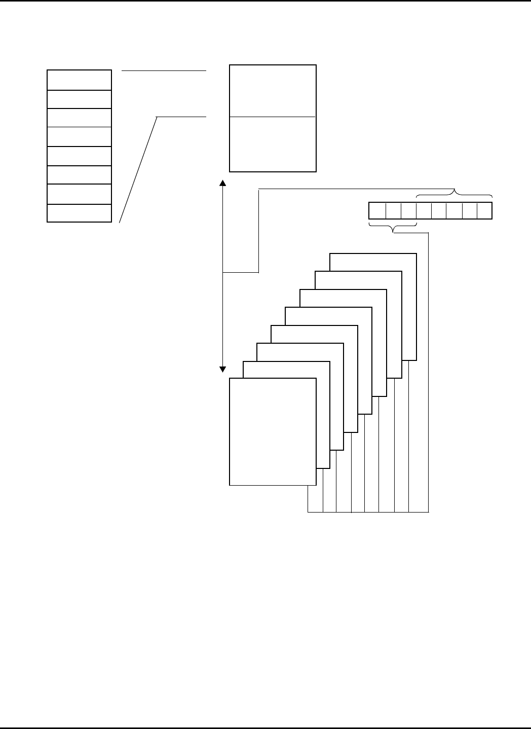
6.2Data Memory
The data memory consists of 136 bytes of RAM, orga-
nized as eight banks of 16 registers plus eight registers
which are not banked. Both banked and non-banked
memory locations can be addressed directly or indirectly
using the FSR (File Select Register). The special-func-
tion registers are mapped into the data memory.
6.2.1 File Select Register (04h)
Instructions that specify a register as the operand can
only express five bits of register address. This means
that only registers 00h to 1Fh can be accessed. The File
Select Register (FSR) provides the ability to access reg-
isters beyond 1Fh.
Figure6-1 shows how FSR can be used to address RAM
locations. The three high-order bits of FSR select one of
eight SRAM banks to be accessed. The five low-order
bits select one of 32 SRAM locations within the selected
bank. For the lower 16 addresses, Bank 0 is always
accessed, irrespective of the three high-order bits. Thus,
RAM register addresses 00h through 0Fh are “global” in
that they can always be accessed, regardless of the con-
tents of the FSR.
The entire data memory (including the dedicated-function
registers) consists of the lower 16 bytes of Bank 0 and
the upper 16 bytes of Bank 0 through Bank 7, for a total
of (1+8)*16 = 144 bytes. Eight of these bytes are for the
function registers, leaving 136 general-purpose memory
locations. In the 18-pin SX packages, register RC is not
used, which makes address 07h available as an addi-
tional general-purpose memory location.
Below is an example of how to write to register 10h in
Bank 4:
mov FSR,#$90 ;Select Bank 4 by
;setting FSR<7:5>
mov 10h,#$64 ;load register 10h with
;the literal 64h
© 1998 Scenix Semiconductor, Inc. All rights reserved. - 15 - www.scenix.com
SX18AC / SX20AC / SX28AC
Figure6-1. Data Memory Organization
Function Registers
INDF
RTCC
PC
STATUS
FSR
RA
RB
RC
SRAM
(8 bytes)
Bank 7
Bank 6
Bank 5
Bank 4
Bank 3
Bank 2
Bank 1
Bank 0
30
50
70
90
B0
D0
F0
3F
5F
7F
9F
BF
DF
FF
000
001
010
011
100
101
110
111
00
07
0F
10
1F
FSR
SRAM
(16 bytes
each bank
128 bytes
total)
7 6 5 432 1 0
Bank 0 is always accessed for
the lower 16 addresses,
irrespective of the three high-
order bits of FSR.
Registers
(8 bytes)
Bank 0
© 1998 Scenix Semiconductor, Inc. All rights reserved. - 16 - www.scenix.com
SX18AC / SX20AC / SX28AC
7.0POWER DOWN MODE
The power down mode is entered through the execution
of the SLEEP instruction while the SLEEP mode is
enabled.
In SLEEP mode, only the Watchdog Timer (WDT) is
active. If the Watchdog Timer is enabled, upon execution
of the SLEEP instruction, the Watchdog Timer is cleared,
the TO bit is set in the STATUS register, and the PD bit is
cleared in the STATUS register.
There are three different ways to exit from the low power
sleep mode: a timer overflow signal from the Watchdog
Timer (WDT), a valid transition on any of the Multi-Input
Wakeup pins (Port B pins), or through an external reset
input on the MCLR pin.
To achieve the lowest possible power consumption, the
Watchdog Timer should be disabled and the device
should exit the SLEEP mode through the MIWU pins or
an external reset.
7.1Multi-Input Wakeup
Multi-Input Wakeup is one way of causing the device to
exit the power down mode. Port B is used to support this
feature. The WKEN_B register (Wakeup Enable Regis-
ter) allows any Port B pin or combination of pins to cause
the wakeup. Clearing a bit in the WKEN_B register
enables the wakeup on the corresponding Port B pin. If
multi-input wakeup is selected to cause a wakeup, the
trigger condition on the selected pin can be either rising
edge (low to high) or falling edge (high to low). The
WKED_B register (Wakeup Edge Select) selects the
desired transition edge. Setting a bit in the WKED_B reg-
ister selects the falling edge on the corresponding Port B.
Resetting the bit selects the rising edge. The WKEN_B
and WKED_B registers are set to FFh upon reset.
Once a valid transition occurs on the selected pin, the
WKPND_B register (Wakeup Pending Register) latches
the transition in the corresponding bit position. A logic ‘1’
indicates the occurrence of the selected trigger edge on
the corresponding Port B pin.
Upon exiting the power down mode, the Multi-Input
Wakeup logic causes program counter to branch to the
maximum program memory address (same as reset).
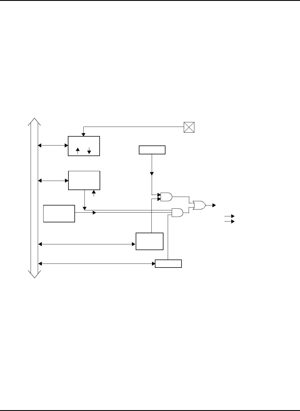
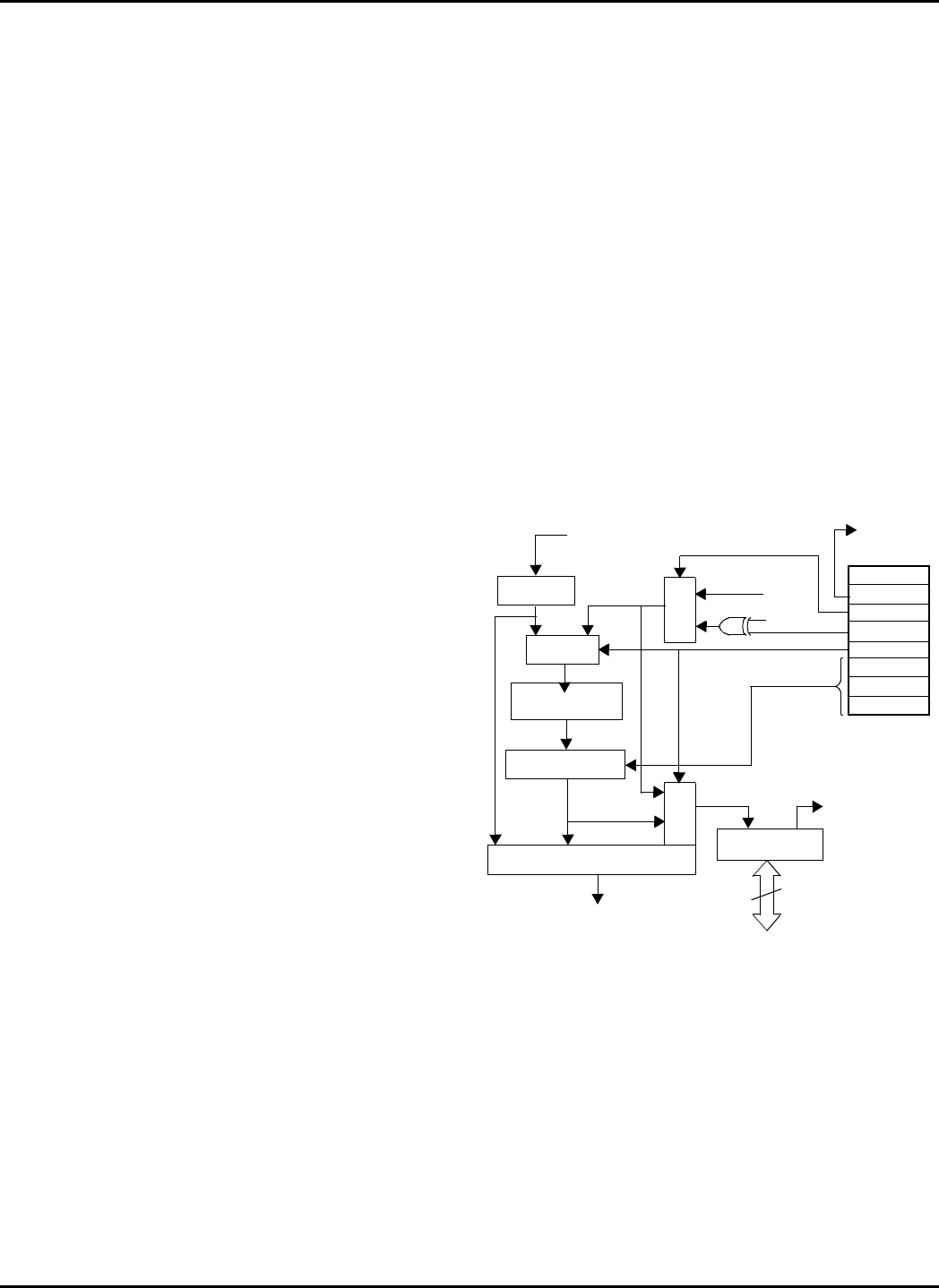
Figure7-1 shows the Multi-Input Wakeup block diagram.
Figure7-1. Multi-Input Wakeup Block Diagram
W
Internal Data Bus
MODE
Wake-up : Exit Power Down
8
8
RB7 RB6 RB1 RB0
WKED_B
WKPND_B
WKEN_B
MODE = 09
MODE = 0B
MODE = 0A
Port B
Configured
as Input
0 1
8
0 = Enable
1 = Disable

© 1998 Scenix Semiconductor, Inc. All rights reserved. - 17 - www.scenix.com
SX18AC / SX20AC / SX28AC
7.2Port B MIWU/Interrupt Configuration
The WKPND_B register comes up with a random value
upon reset. The user program must clear the register
prior to enabling the wake-up condition or interrupts. The
proper initialization sequence is:
1. Clear the WKPND_B register
2. Select the desired edge (through WKED_B register)
3. Enable the Wakeup condition (through WKEN_B regis-
ter)
Below is an example how to read the WKPND_B register
to determine which Port B pin caused the wakeup or
interrupt, and to clear the WKPND_B register:
The final “mov” instruction in this example performs an
exchange of data between the working register (W) and
the WKPND_B register. This exchange occurs only with
Port B accesses. Otherwise, the “mov” instruction does
not perform an exchange, but only moves data from the
source to the destination.
Here is an example of a program segment that config-
ures the RB0, RB1, and RB2 pins to operate as Multi-
Input Wakeup/Interrupt pins, sensitive to falling edges:
To prevent false interrupts, the enabling step (clearing
bits in WKEN_B) should be done as the last step in a
sequence of Port B configuration steps.
After this program segment is executed, the device can
receive interrupts on the RB0, RB1, and RB2 pins. If the
device is put into the power down mode (by executing a
“sleep” instruction), the device can then receive wakeup
signals on those same pins.
mov M,#$09
clr W
mov !RB,W ;W contains WKPND_B
;contents of W exchanged
;with contents of WKPND_B
mov M,#$09 ;prepare to access WKPND_B
;(pending) register
mov W,#$00 ;clear W
mov !RB,W ;clear all wakeup pending flags
mov M,#$0F ;prepare to write port data
;direction registers
mov W,#$07 ;load W with the value 07h
mov !RB,W ;configure RB0-RB2 to be inputs
mov M,#$0A ;prepare to write WKED_B
;(edge) register
;W contains the value 07h
mov !RB,W ;configure RB0-RB2 to sense
;falling edges
mov M,#$0B ;prepare to write WKEN_B (enable)
;register
mov W,#$F8h ;load W with the value F8h
mov !RB,W ;enable RB0-RB2 to operate as
;wakeup inputs
© 1998 Scenix Semiconductor, Inc. All rights reserved. - 18 - www.scenix.com
SX18AC / SX20AC / SX28AC
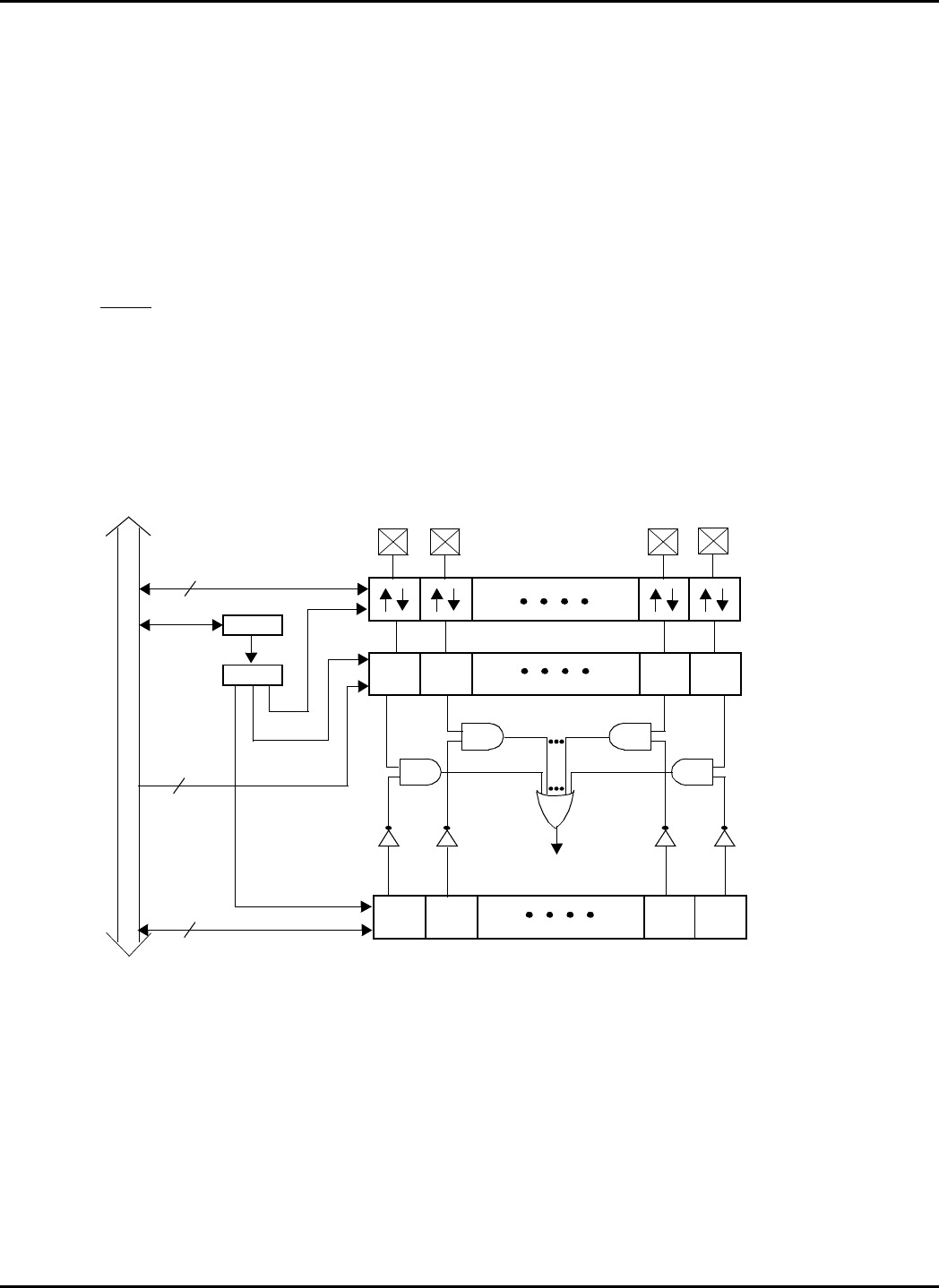
8.0INTERRUPT SUPPORT
The device supports both internal and external maskable
interrupts. The internal interrupt is generated as a result
of the RTCC rolling over from 0FFh to 00h. This interrupt
source has an associated enable bit located in the
OPTION register. There is no pending flag associated
with this interrupt.
Port B provides the source for eight external software
selectable, edge sensitive interrupts, when the device is
not in the SLEEP mode. These interrupt sources share
logic with the Multi-Input Wakeup circuitry. The WKEN_B
register allows interrupt from Port B to be individually
enabled or disabled. Clearing a bit in the WKEN_B regis-
ter enables the interrupt on the corresponding Port B pin.
The WKED_B selects the transition edge to be either
positive or negative. The WKEN_B and WKED_B regis-
ters are cleared upon reset. Setting a bit in the WKED_B
register selects the falling edge while resetting the bit
selects the rising edge on the corresponding Port B pin.
The WKPND_B register serves as the external interrupt
pending register.
The WKPND_B register comes up a with random value
upon reset. The user program must clear the WKPND_B
register prior to enabling the interrupt. The proper
sequence is described in Section 7.2.
Figure8-1 shows the structure of the interrupt logic.
All interrupts are global in nature; that is, no interrupt has
priority over another. Interrupts are handled sequentially.
Figure8-2 shows the interrupt processing sequence.
Once an interrupt is acknowledged, all subsequent global
interrupts are disabled until return from servicing the cur-
rent interrupt. The PC is pushed onto the single level
interrupt stack, and the contents of the FSR, STATUS,
and W registers are saved in their corresponding shadow
registers. The interrupt logic has its own single-level
stack and is not part of the CALL subroutine stack. The
vector for the interrupt service routines is address 0.
Once in the interrupt service routine, the user program
must poll all external interrupt pending bits to determine
the source of the interrupt. The interrupt service routine
should clear the corresponding interrupt pending flag.
The user program may also need to read the contents of
RTCC to determine any recent RTCC rollover. This is
needed since there is no interrupt pending flag associ-
ated with the RTCC rollover.
Upon return from the interrupt service routine, the con-
tents of PC, FSR, STATUS, and W registers are restored
from their corresponding shadow registers. The interrupt
service routine should end with instructions such as RETI
and RETIW. RETI pops the interrupt stack and the spe-
cial shadow registers used for storing W, STATUS, and
FSR (preserved during interrupt handling). RETIW
behaves like RETI but also writes the literal to RTCC.
The interrupt return instruction enables the global inter-
rupts.
Figure8-1. Interrupt Structure
RTCC
WKED_B
Internal Data Bus
WKED_B
WKPND_B
WKPND_B
From MODE
(Mode = 09)
OPTION
RTE_IE
WKEN_B
1 = Ext Interrupt through Port B
0 = Sleep Mode, no Ext Interrupt
STATUS PD
Port B PIN
0
Interrupt
PC Interrupt Stack
PC
000
Overflow
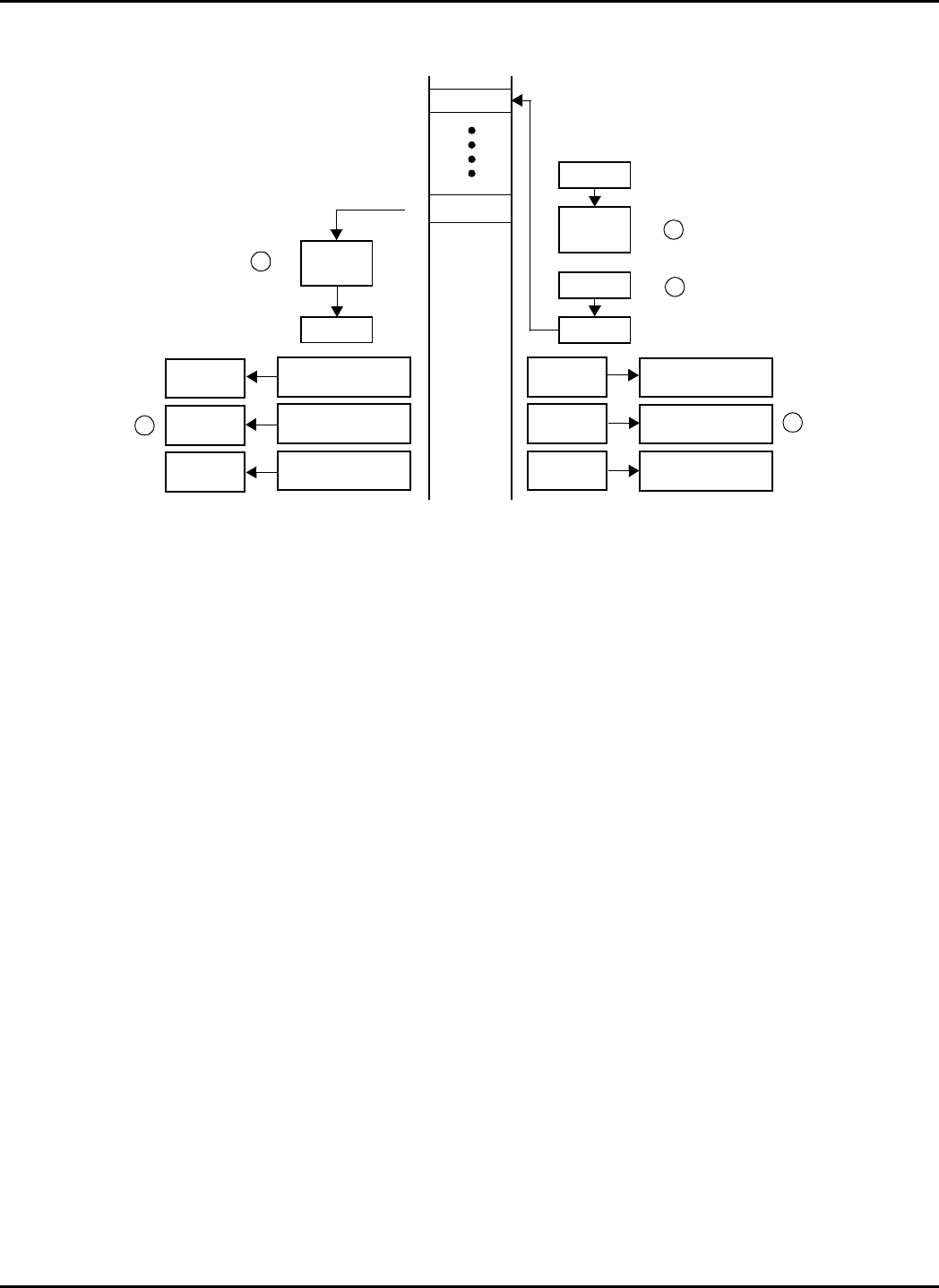
© 1998 Scenix Semiconductor, Inc. All rights reserved. - 19 - www.scenix.com
SX18AC / SX20AC / SX28AC
Figure8-2. Interrupt Processing
Interrupt
PC
RETI
PC PC
4
5
1
2
3
W
Register
0000h
Address 0000h
Program
Memory Interrupt
Service
Routine
STATUS
Register
FSR
Register
W
Shadow Register
STATUS
Shadow Register
FSR
Shadow Register
W
Register
STATUS
Register
FSR
Register
W
Shadow Register
STATUS
Shadow Register
FSR
Shadow Register
Stack
Interrupt
Stack
Note:The interrupt logic has its own single-level
stack and is not part of the CALL subroutine stack.
© 1998 Scenix Semiconductor, Inc. All rights reserved. - 20 - www.scenix.com
SX18AC / SX20AC / SX28AC
9.0OSCILLATOR CIRCUITS
The device supports several user-selectable oscillator
modes. The oscillator modes are selected by program-
ming the appropriate values into the FUSE Word register.
These are the different oscillator modes offered:
9.1XT, LP or HS modes
In XT, LP or HS, modes, you can use either an external
resonator network or an external clock signal as the
device clock.
To use an external resonator network, you connect a
crystal or ceramic resonator to the OSC1/CLKIN and
OSC2/CLKOUT pins according to the circuit configura-
tion shown in Figure9-1. Table9-1 shows the recom-
mended capacitor values to be used with ceramic
resonators. Table9-2 shows the recommended compo-
nent values to be used at different crystal frequencies. A
parallel resonant crystal type is recommended. Use of a
series resonant crystal may result in a frequency that is
outside the crystal manufacturer specifications.
If the XT, LP, or HS mode is selected, the OSC1/CLKIN
pin can driven by an external clock source rather than a
resonator network, as long as the clock signal meets the
specified duty cycle, rise and fall times, and input levels
(Figure9-2). In this case, the OSC2/CLKOUT pin should
be left open.
Note:Series resistor (RS) is not required for frequencies
higher than 1 MHz; use a direct connection instead.
LP: Low Power Crystal
XT: Crystal/Resonator
HS: High Speed Crystal/Resonator
RC: External Resistor/Capacitor
Internal Resistor/Capacitor
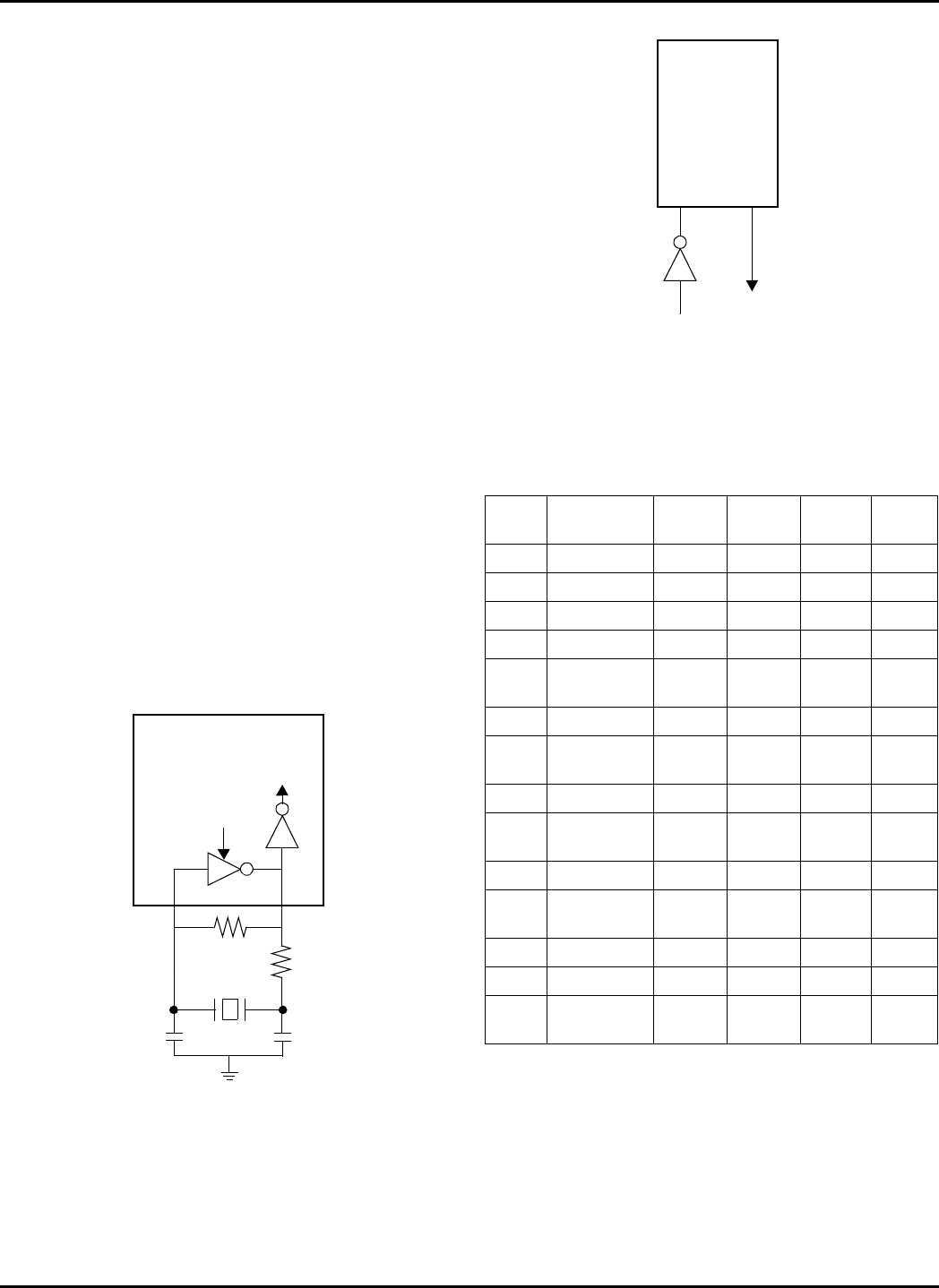
Figure9-1. Crystal Operation (or Ceramic Resonator)
(HS, XT or LP OSC Configuration)
SX Device
RF
XTAL
OSC2
OSC1
C1C2
Internal
Circuitry
SLEEP
RS
Figure9-2. External Clock Input Operation
(HS, XT or LP OSC Configuration)
Table9-1. Capacitor Selection for
Ceramic Resonators
Clock
Mode Resonator
Frequency C1 C2 RFRS
XT 455 kHz 220 pF 220 pF 1 MΩ6.8 kΩ
XT 1 MHz 100 pF 100 pF 1 MΩ6.8 kΩ
XT 2 MHz 100 pF 100 pF 100 kΩ680 Ω
HS 4 MHz 100 pF 100 pF 100 kΩ0
HS 4 MHz Internal
(47 pF) Internal
(47 pF) 100 kΩ470 Ω
HS 8 MHz 30 pF 30 pF 1 MΩ0
HS 8 MHz Internal
(47 pF) Internal
(47 pF) 1 MΩ470 Ω
HS 12 MHz 30 pF 30 pF 1 MΩ0
HS 12 MHz Internal
(22 pF) Internal
(22 pF) 1 MΩ0
HS 16 MHz 15 pF 15 pF 1 MΩ0
HS 16 MHz Internal
(15 pF) Internal
(15 pF) 1 MΩ0
HS 20 MHz 10 pF 10 pF 1 MΩ0
HS 33 MHz 10 pF 10 pF 33 kΩ0
HS 50 MHz* Internal
(5 pF) Internal
(5 pF) 33 kΩ0
* Note: Resonator with built-in capacitors.
Externally
Generated Clock
OSC1 OSC2
Open
SX Device
© 1998 Scenix Semiconductor, Inc. All rights reserved. - 21 - www.scenix.com
SX18AC / SX20AC / SX28AC
Note:Resistor Rf is not required for the Version 2.1 device
(both crystal and resonator circuits.)
9.2External RC Mode
The external RC oscillator mode provides a cost-effective
approach for applications that do not require a precise
operating frequency. In this mode, the RC oscillator fre-
quency is a function of the supply voltage, the resistor (R)
and capacitor (C) values, and the operating temperature.
In addition, the oscillator frequency will vary from unit to
unit due to normal manufacturing process variations. Fur-
thermore, the difference in lead frame capacitance
between package types also affects the oscillation fre-
quency, especially for low C values. The external R and
C component tolerances contribute to oscillator fre-
quency variation as well.
Figure9-3 shows the external RC connection diagram.
The recommended R value is from 3kΩ to 100kΩ. For R
values below 2.2kΩ, the oscillator may become unstable,
or may stop completely. For very high R values (such as
1 MΩ), the oscillator becomes sensitive to noise, humid-
ity, and leakage.
Although the oscillator will operate with no external
capacitor (C = 0pF), it is recommended that you use val-
ues above 20 pF for noise immunity and stability. With no
or small external capacitance, the oscillation frequency
can vary significantly due to variation in PCB trace or
package lead frame capacitances.
In the external RC mode, the OSC2/CLKOUT pin pro-
vides an output frequency, which the input frequency
divided by four.
9.3Internal RC Mode
The internal RC mode uses an internal oscillator, so the
device does not need any external components. At 4
MHz, the internal oscillator provides +/–8% accuracy
over the allowed temperature range. The internal clock
frequency can be divided down to provide one of eight
lower-frequency choices by selecting the desired value in
the FUSE Word register. The frequency range is from
31.25 KHz to 4 MHz.
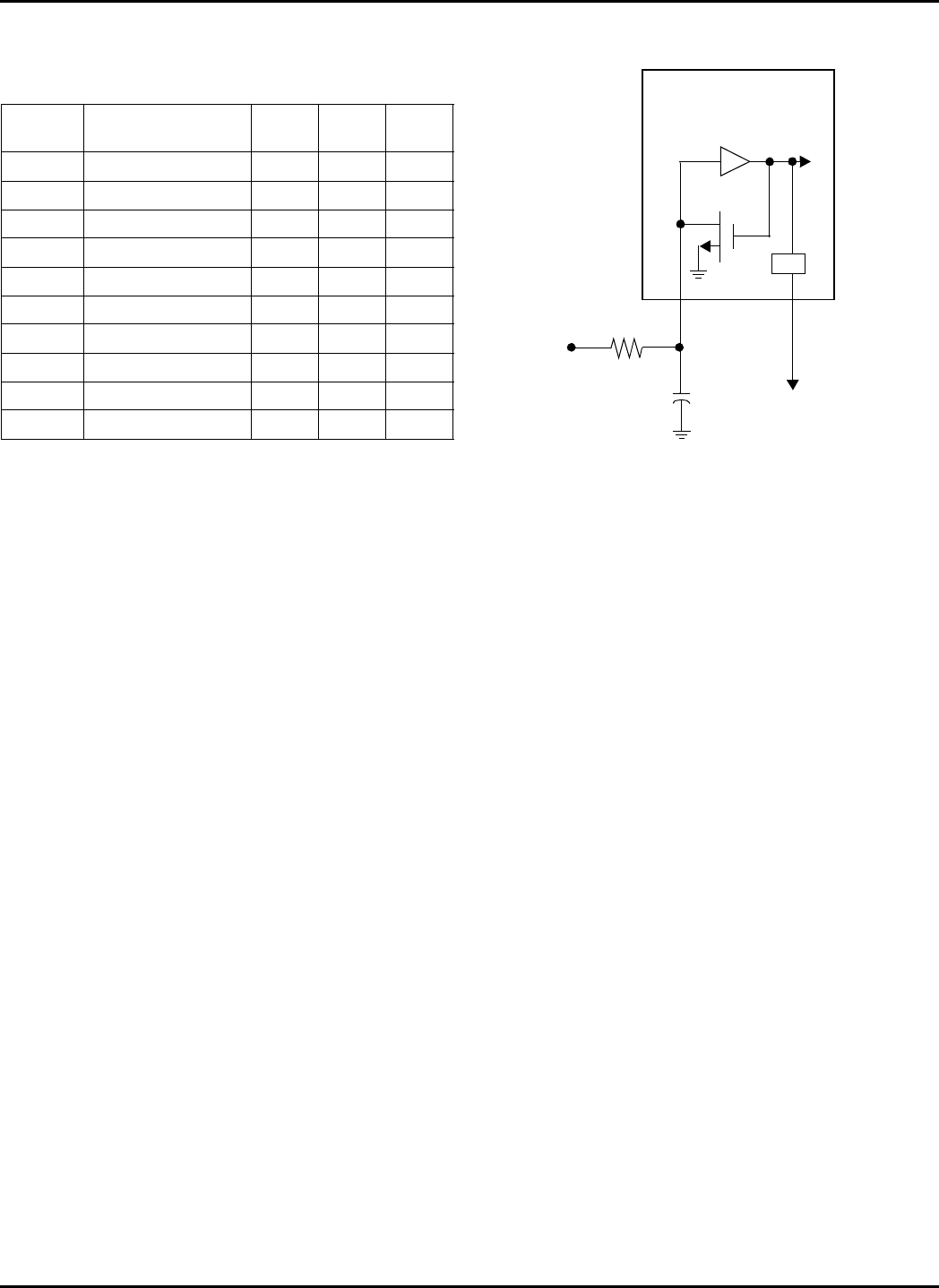
Table9-2. Component Selection for
Crystal Oscillator
Osc
Type Resonator
Frequency C1
(pF) C2
(pF) RF
XT 4 20 47 1M
HS 8 20 47 1M
HS 12 20 47 1M
HS 16 15 30 1M
HS 20 15 30 1M
HS 25 5 20 10k
HS 30 5 20 4.7k
HS 36 5 15 3.3k
HS 40 5 15 3.3k
HS 50 5 10 3.3k
Figure9-3. RC Oscillator Mode
Vdd R
C
Internal
Circuitry
OSC2
OSC1
N
÷ 4
~
~
SX Device
© 1998 Scenix Semiconductor, Inc. All rights reserved. - 22 - www.scenix.com
SX18AC / SX20AC / SX28AC
10.0REAL TIME CLOCK
(RTCC)/WATCHDOG TIMER
The device contains an 8-bit Real Time Clock/Counter
(RTCC) and an 8-bit Watchdog Timer (WDT). An 8-bit
programmable prescaler extends the RTCC to 16 bits. If
the prescaler is not used for the RTCC, it can serve as a
postscaler for the Watchdog Timer. Figure10-1 shows
the RTCC and WDT block diagram.
10.1RTCC
RTCC is an 8-bit real-time timer that is incremented once
each instruction cycle or from a transition on the RTCC
pin. The on-board prescaler can be used to extend the
RTCC counter to 16 bits.
The RTCC counter can be clocked by the internal instruc-
tion cycle clock or by an external clock source presented
at the RTCC pin.
To select the internal clock source, bit 5 of the OPTION
register should be cleared. In this mode, RTCC is incre-
mented at each instruction cycle unless the prescaler is
selected to increment the counter.
To select the external clock source, bit 5 of the OPTION
register must be set. In this mode, the RTCC counter is
incremented with each valid signal transition at the RTTC
pin. By using bit 4 of the OPTION register, the transition
can be programmed to be either a falling edge or rising
edge. Setting the control bit selects the falling edge to
increment the counter. Resetting the bit selects the rising
edge.
The RTCC generates an interrupt as a result of an RTCC
rollover from 0FF to 000. There is no interrupt pending bit
to indicate the overflow occurrence. The RTCC register
must be sampled by the program to determine any over-
flow occurrence.
10.2Watchdog Timer
The watchdog logic consists of a Watchdog Timer which
shares the same 8-bit programmable prescaler with the
RTCC. The prescaler actually serves as a postscaler if
used in conjunction with the WDT, in contrast to its use as
a prescaler with the RTCC.
10.3The Prescaler
The 8-bit prescaler may be assigned to either the RTCC
or the WDT through the PSA bit (bit 3 of the OPTION reg-
ister). Setting the PSA bit assigns the prescaler to the
WDT. If assigned to the WDT, the WDT clocks the pres-
caler and the prescaler divide rate is selected by the
PS0, PS1, and PS2 bits located in the OPTION register.
Resetting the PSA bit assigns the prescaler to the RTCC.
Once assigned to the RTCC, the prescaler clocks the
RTCC and the divide rate is selected by the PS0, PS1,
and PS2 bits in the OPTION register. The prescaler is not
mapped into the data memory, so run-time access is not
possible.
The prescaler cannot be assigned to both the RTCC and
WDT simultaneously.
Figure10-1. RTCC and WDT Block Diagram
WDTE (from FUSE Word)
RTCC pin
MUX
8-Bit Prescaler
MUX (8 to 1)
8-Bits
WDT Time-out
Data Bus
WDT
MUX
M
U
XRTCC
M
U
X
FOSC RST
RTE_ES
PSA
PS2
PS1
PS0
OPTION
Register
RTCC Rollover
Interrupt
RTE_IE
RTW
RTCC
Interrupt
Enable
© 1998 Scenix Semiconductor, Inc. All rights reserved. - 23 - www.scenix.com
SX18AC / SX20AC / SX28AC
11.0COMPARATOR
The device contains an on-chip differential comparator.
Ports RB0-RB2 support the comparator. Ports RB1 and
RB2 are the comparator negative and positive inputs,
respectively, while Port RB0 serves as the comparator
output pin. To use these pins in conjunction with the com-
parator, the user program must configure Ports RB1 and
RB2 as inputs and Port RB0 as an output. The CMP_B
register is used to enable the comparator, to read the out-
put of the comparator internally, and to enable the output
of the comparator to the comparator output pin.
The comparator enable bits are set to “1” upon reset,
thus disabling the comparator. To avoid drawing addi-
tional current during the SLEEP mode, the comparator
should be disabled before entering the SLEEP mode.
Here is an example of how to setup the comparator and
read the CMP_B register.
The final “mov” instruction in this example performs an
exchange of data between the working register (W) and
the CMP_B register. This exchange occurs only with Port
B accesses. Otherwise, the “mov” instruction does not
perform an exchange, but only moves data from the
source to the destination.
The following figure shows the format of the CMP_B reg-
ister.
CMP_B - Comparator Enable/Status Register
mov M,#$08 ;set MODE register to access
;CMP_B
mov W,#$00 ;clear W
mov !RB,W ;enable comparator and its
;output
... ;delay after enabling
;comparator for response
mov M,#$08 ;set MODE register to access
;CMP_B
mov W,#$00 ;clear W
mov !RB,W ;enable comparator and its
;output and also read CMP_B
;(exchange W and CMB_B)
and W,#$01 ;set/clear Z flag based on
;comparator result
snb $03.2 ;test Z flag in STATUS reg
;(0 => RB2<RB1)
jmp rb2_hi ;jump only if RB2>RB1
...
CMP_EN CMP_OE Reserved CMP_RES
Bit 7 Bit 6 Bits 5–1 Bit 0
CMP_RES Comparator result: 1 for RB2>RB1 or 0
for RB2<RB1. Comparator must be en-
abled (CMP_EN = 0) to read the result.
The result can be read whether or not the
CMP_OE bit is cleared.
CMP_OE When cleared to 0, enables the compar-
ator output to the RB0 pin.
CMP_EN When cleared to 0, enables the compar-
ator.
Figure11-1. Comparator Block Diagram
W
MODE
CMP_EN
CMP_OE
R
E
S
E
R
V
E
D
CMP_RES
RB0
RB1
RB2
CMP_B
MODE = 08h
Point to CMP_B
Internal Data Bus
7
6
0
© 1998 Scenix Semiconductor, Inc. All rights reserved. - 24 - www.scenix.com
SX18AC / SX20AC / SX28AC
12.0RESET
Power-On-Reset, Brown-Out reset, watchdog reset, or
external reset initializes the device. Each one of these
reset conditions causes the program counter to branch to
the top of the program memory. For example, on the
device with 2K of program memory, the program counter
is initialized to 07FF.
The device incorporates an on-chip Power-On Reset
(POR) circuit that generates an internal reset as Vdd rises
during power-up. Figure12-1 is a block diagram of the
circuit. The circuit contains an 8-bit Delay Reset Timer
(DRT) and a reset latch. The DRT controls the reset time-
out delay. The reset latch controls the internal reset sig-
nal. Upon power-up, the reset latch is set (device held in
reset), and the DRT starts counting once it detects a valid
logic high signal at the MCLR pin. Once DRT reaches the
end of the timeout period (typically 72 msec), the reset
latch is cleared, releasing the device from reset state.
Figure12-2 shows a power-up sequence where MCLR is
not tied to the Vdd pin and Vdd signal is allowed to rise
and stabilize before MCLR pin is brought high. The
device will actually come out of reset Tdrt msec after
MCLR goes high.
The brown-out circuitry resets the chip when device
power (Vdd) dips below its minimum allowed value, but
not to zero, and then recovers to the normal value.
Figure12-3 shows the on-chip Power-On Reset
sequence where the MCLR and Vdd pins are tied
together. The Vdd signal is stable before the DRT time-
out period expires. In this case, the device will receive a
proper reset. However, Figure12-4 depicts a situation
where Vdd rises too slowly. In this scenario, the DRT will
time-out prior to Vdd reaching a valid operating voltage
level (Vdd min). This means the device will come out of
reset and start operating with the supply voltage not at a
valid level. In this situation, it is recommended that you
use the external RC circuit shown in Figure12-5. The RC
delay should exceed the time period it takes Vdd to reach
a valid operating voltage.
Note1:The external Power-On Reset circuit is required
only if Vdd power-up is too slow. The diode D helps dis-
charge the capacitor quickly when Vdd powers down.
Note2:R < 40 kΩ is recommended to make sure that
voltage drop across R does not violate the device electri-
cal specifications.
Note3:R1 = 100Ω to 1kΩ will limit any current flowing
into MCLR from external capacitor C. This helps prevent
MCLR pin breakdown due to Electrostatic Discharge
(ESD) or Electrical Overstress (EOS).
Note:Ripple counter is 10 bits for Power on Reset (POR)
only.
Figure12-1. Block Diagram of On-Chip Reset Circuit
POR
BROWN-OUT
MIWU
MCLR/Vpp pin wdt_time_out
10-Bit Asynch
Ripple
Counter
(DRT Start-Up
Timer)
Vdd
rc_clk drt_time
_out
S
R
Q
QN RESET
POR
enable
Figure12-2. Time-Out Sequence on Power-Up
(MCLR not tied to Vdd)
Figure12-3. Time-out Sequence on Power-up
(MCLR tied to Vdd): Fast Vdd Rise Time
Figure12-4. Time-out Sequence on Power-up
(MCLR tied to Vdd): Slow Rise Time
Vdd
MCLR
POR
drt_time_out
RESET
Tdrt
Vdd
MCLR
POR
drt_time_out
RESET
Tdrt
Vdd
MCLR
POR
drt_time_out
RESET
Tdrt
V1
© 1998 Scenix Semiconductor, Inc. All rights reserved. - 25 - www.scenix.com
SX18AC / SX20AC / SX28AC
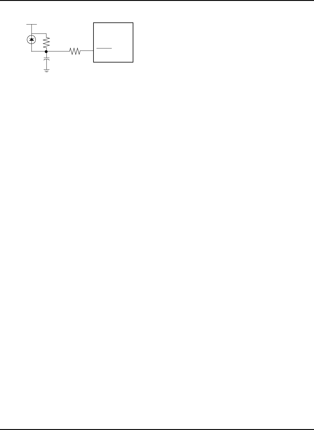
13.0BROWN-OUT DETECTOR
The on-chip brown-out detection circuitry resets the
device when Vdd dips below the specified brown-out volt-
age. The device is held in reset as long as Vdd stays
below the brown-out voltage. The device will come out of
reset when Vdd rises above the brown-out voltage. The
brown-out level is preset to approximately 4.2V at the
factory. The brown-out circuit can be disabled through
BOR0 and BOR1 bits contained in the FUSEX Word reg-
ister.
Figure12-5. External Power-On Reset Circuit
(For Slow Vdd Power-up)
Vdd
R
C
MCLR
DR1

© 1998 Scenix Semiconductor, Inc. All rights reserved. - 26 - www.scenix.com
SX18AC / SX20AC / SX28AC
14.0REGISTER STATES UPON RESET
The effect of a reset operation on a register depends on
the register and the type of reset operation. Some regis-
ters are initialized to specific values, some are left
unchanged (for wakeup and brown-out resets), and some
are initialized to an unknown value. A register that starts
with an unknown value should be initialized by the soft-
ware to a known value; you cannot simply test the initial
state and rely on it starting in that state consistently.
Table14-1 lists the SX registers and shows the state of
each register upon different reset.
Table14-1. Register States Upon Reset
Register Power-On Wakeup Brown-out Watchdog
Timeout MCLR
WUndefined Unchanged Undefined Unchanged Unchanged
OPTION FFh FFh FFh FFh FFh
MODE 0Fh 0Fh 0Fh 0Fh 0Fh
RTCC (01h) Undefined Unchanged Undefined Unchanged Unchanged
PC (02h) 0Fh 0Fh 0Fh 0Fh 0Fh
STATUS (03h) Bits 0-2: Unde-
fined
Bits 3-4: 1
Bits 5-7: 0
Bits 0-2: Unde-
fined
Bits 3-4: Unch.
Bits 5-7: 0
Bits 0-4: Unde-
fined
Bits 5-7: 0
Bits 0-2: Unde-
fined
Bits 3-4: (Note 1)
Bits 5-7: 0
Bits 0-2: Unde-
fined
Bits 3-4: (Note 2)
Bits 5-7: 0
FSR (04h) Undefined Bits 0-6: Unde-
fined
Bit 7: 1
Bits 0-6: Unde-
fined
Bit 7: 1
Bits 0-6: Unde-
fined
Bit 7: 1
Bits 0-6: Unde-
fined
Bit 7: 1
RA/RB/RC
Direction
FFh FFh FFh FFh FFh
RA/RB/RC Data Undefined Unchanged Undefined Unchanged Unchanged
Other File Registers -
SRAM Undefined Unchanged Undefined Unchanged Unchanged
CMP_B Bits 0, 6-7: 1
Bits 1-5: Unde-
fined
Bits 0, 6-7: 1
Bits 1-5: Unde-
fined
Bits 0, 6-7: 1
Bits 1-5: Unde-
fined
Bits 0, 6-7: 1
Bits 1-5: Unde-
fined
Bits 0, 6-7: 1
Bits 1-5: Unde-
fined
WKPND_B FFh Unchanged Undefined Unchanged Unchanged
WKED_B FFh FFh FFh FFh FFh
WKEN_B FFh FFh FFh FFh FFh
ST_B/ST_C FFh FFh FFh FFh FFh
LVL_A/LVL_B/LVL_C FFh FFh FFh FFh FFh
PLP_A/PLP_B/PLP_C FFh FFh FFh FFh FFh
Watchdog Counter Undefined Unchanged Undefined Unchanged Unchanged
NOTE: 1. Watchdog reset during SLEEP mode: 00
Watchdog reset during Active mode: 01
NOTE: 2. External reset during SLEEP mode: 10
External reset during Active mode: Unchanged
© 1998 Scenix Semiconductor, Inc. All rights reserved. - 27 - www.scenix.com
SX18AC / SX20AC / SX28AC
15.0INSTRUCTION SET
As mentioned earlier, the SX family of devices uses a
modified Harvard architecture with memory-mapped
input/output. The device also has a RISC type architec-
ture in that there are 43 single-word basic instructions.
The instruction set contains byte-oriented file register, bit-
oriented file register, and literal/control instructions.
Working register W is one of the CPU registers, which
serves as a pseudo accumulator. It is a pseudo accumu-
lator in a sense that it holds the second operand,
receives the literal in the immediate type instructions, and
also can be program-selected as the destination register.
The bank of 31 file registers can also serve as the pri-
mary accumulators, but they represent the first operand
and may be program-selected as the destination regis-
ters.
15.1Instruction Set Features
1. All single-word (12-bit) instructions for compact code
efficiency.
2. All instructions are single cycle except the jump type in-
structions (JMP, CALL) and failed test instructions
(DECSZ fr, INCSZ fr, SB bit, SNB bit), which are two-
cycle.
3. A set of File registers can be addressed directly or indi-
rectly, and serve as accumulators to provide first oper-
and; W register provides the second operand.
4. Many instructions include a destination bit which se-
lects either the register file or the accumulator as the
destination for the result.
5. Bit manipulation instructions (Set, Clear, Test and Skip
if Set, Test and Skip if Clear).
6. STATUS Word register memory-mapped as a register
file, allowing testing of status bits (carry, digit carry, ze-
ro, power down, and timeout).
7. Program Counter (PC) memory-mapped as register file
allows W to be used as offset register for indirect ad-
dressing of program memory.
8. Indirect addressing data pointer FSR (file select regis-
ter) memory-mapped as a register file.
9. IREAD instruction allows reading the instruction from
the program memory addressed by W and upper four
bits of MODE register.
10.Eight-level, 11-bit push/pop hardware stack for sub-
routine linkage using the Call and Return instructions.
11.Six addressing modes provide great flexibility.
15.2Instruction Execution
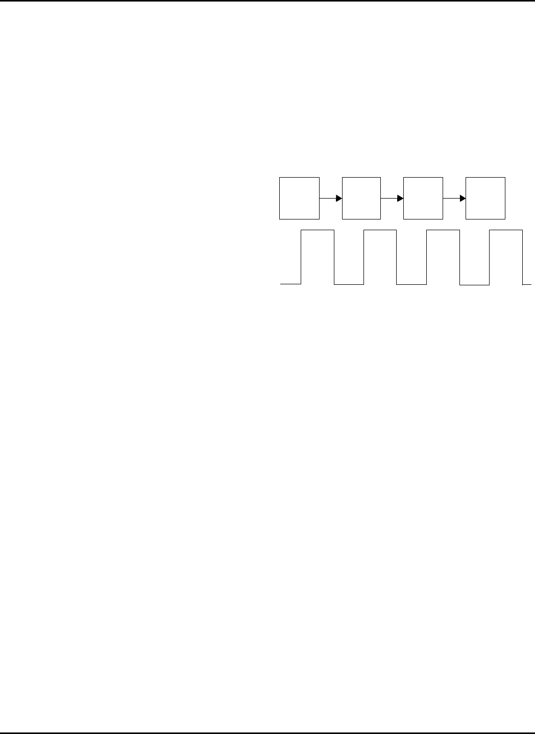
An instruction goes through a four-stage pipeline to be
executed (Figure15-1). The first instruction is fetched
from the program memory on the first clock cycle. On the
second clock cycle, the first instruction is decoded and
the second instruction is fetched. On the third clock cycle,
the first instruction is executed, the second instruction is
decoded, and the third instruction is fetched. On the
fourth clock cycle, the first instruction’s results are written
to its destination, the second instruction is executed, the
third instruction is decoded, and the fourth instruction is
fetched. Once the pipeline is full, instructions are exe-
cuted at the rate of one per clock cycle.
Instructions that directly affect the contents of the pro-
gram counter (such as jumps and calls) require that the
pipeline be cleared and subsequently refilled. Therefore,
these instruction take more than one clock cycle.
The instruction execution time is derived by dividing the
oscillator frequency by either one (turbo mode) or four
(non-turbo mode). The divide-by factor is selected
through the FUSE Word register.
15.3Addressing Modes
The device support the following addressing modes:
Data Direct
Data Indirect
Immediate
Program Direct
Program Indirect
Relative
Both direct and indirect addressing modes are available.
The INDF register, though physically not implemented, is
used in conjunction with the indirect data pointer (FSR) to
perform indirect addressing. An instruction using INDF as
its operand field actually performs the operation on the
register pointed by the contents of the FSR. Conse-
quently, processing two multiple-byte operands requires
alternate loading of the operand addresses into the FSR
pointer as the multiple byte data fields are processed.
Examples:
Direct addressing:
Indirect Addressing:
Figure15-1. Pipeline and Clock Scheme
mov RA,#01 ;move “1” to RA
mov FSR,#RA ;FSR = address of RA
mov INDF,#$01 ;move “1” to RA
Fetch Decode Execute Write
Clock
Cycle
1
Clock
Cycle
1
Clock
Cycle
1
Clock
Cycle
1
© 1998 Scenix Semiconductor, Inc. All rights reserved. - 28 - www.scenix.com
SX18AC / SX20AC / SX28AC
15.4RAM Addressing
Direct Addressing
The FSR register must initialized with an appropriate
value in order to address the desired RAM register. The
following table and code example show how to directly
access the banked registers.
Indirect Addressing
To access any register via indirect addressing, simply
move the eight-bit address of the desired register into the
FSR and use INDF as the operand. The example below
shows how to clear all RAM locations from 10h to 1Fh in
all eight banks:
15.5The Bank Instruction
Often it is desirable to set the bank select bits of the FSR
register in one instruction cycle. The Bank instruction
provides this capability. This instruction sets the upper
bits of the FSR to point to a specific RAM bank without
affecting the other FSR bits.
Example:
15.6Bit Manipulation
The instruction set contains instructions to set, reset, and
test individual bits in data memory. The device is capable
of bit addressing anywhere in data memory.
15.7Input/Output Operation
The device contains three registers associated with each
I/O port. The first register (Data Direction Register), con-
figures each port pin as a Hi-Z input or output. The sec-
ond register (TTL/CMOS Register), selects the desired
input level for the input. The third register (Pull-Up Regis-
ter), enables a weak pull-up resistor on the pin configured
as a input. In addition to using the associated port regis-
ters, appropriate values must be written into the MODE
register to configure the I/O ports.
15.7.1 Read-Modify-Write Considerations
Caution must be exercised when performing successive
SETB or CLRB operations on I/O port pin. Input data
used for an instruction must be valid during the time the
instruction is executed, and the output result from an
instruction is valid only after that instruction completes its
operation. Unexpected results from successive read-
modify-write operations on I/O pins can occur when the
device is running at extremely high speeds. Although the
device has an internal write-back section to prevent such
conditions, it is still recommended that the user program
include a NOP instruction as a buffer between succes-
sive read-modify-write instructions performed on I/O pins
of the same port.
Also note that reading an I/O port is actually reading the
pins, not the output data latches. That is, if the pin output
driver is enabled and driven high while the pin is held low
externally, the port pin will read low.
15.8Increment/Decrement
The bank of 31 registers serves as a set of accumulators.
The instruction set contains instructions to increment and
decrement the register file. The device also includes both
INCSZ fr (increment file register and skip if zero) and
DECSZ fr (decrement file register and skip if zero)
instructions.
15.9Loop Counting and Data Pointing
Testing
The device has specific instructions to facilitate loop
counting. The DECSZ fr (decrement file register and skip
if zero) tests any one of the file registers and skips the
next instruction (which can be a branch back to loop) if
the result is zero.
15.10Branch and Loop Call Instructions
The device contains an 8-level hardware stack where the
return address is stored with a subroutine call. Multiple
stack levels allow subroutine nesting. The instruction set
supports absolute address branching.
15.10.1 Jump Operation
When a JMP instruction is executed, the lower nine bits
of the program counter is loaded with the address of the
specified label. The upper two bits of the program
counter are loaded with the page select bits, PA1:PA0,
contained in the STATUS register. Therefore, care must
be exercised to ensure the page select bits are pointing
to the correct page before the jump occurs.
Bank FSR Value
0010h
1030h
2050h
3070h
4090h
50B0h
60D0h
70F0h
mov FSR,#$070 ;Select RAM Bank 3
clr $010 ;Clear register 10h on
;Bank 3
mov FSR,#$D0 ;Select RAM Bank 6
clr $010 ;Clear register 10h on
;Bank 6
clr FSR ;clear FSR to 00h (at address
;04h)
:loop setb SFR.4 ;set bit 4: address 10h-1Fh,
;30-3Fh, etc
clr INDF ;clear register pointed to by
;FSR
incsz FSR ;increment FSR and test, skip
;jmp if 00h
jmp :loop ;jump back and clear next
;register
bank $F0 ;Select Bank 7 in FSR
inc $1F ;increment file register
;1Fh in Bank 7
© 1998 Scenix Semiconductor, Inc. All rights reserved. - 29 - www.scenix.com
SX18AC / SX20AC / SX28AC
15.10.2 Page Jump Operation
When a JMP instruction is executed and the intended
destination is on a different page, the page select bits
must be initialized with appropriate values to point to the
desired page before the jump occurs. This can be done
easily with SETB and CLRB instructions or by writing a
value to the STATUS register. The device also has the
PAGE instruction, which automatically selects the page in
a single-cycle execution.
Note:“N” must be 0, 1, 2, or 3.
15.10.3 Call Operation
The following happens when a CALL instruction is exe-
cuted:
•The current value of the program counter is increment-
ed and pushed onto the top of the stack.
•The lower eight bits of the label address are copied into
the lower eight bits of the program counter.
•The ninth bit of the Program Counter is cleared to zero.
•The page select bits (in STATUS register) are copied
into the upper two bits of the Program Counter.
This means that the call destination must start in the
lower half of any page. For example, 00h-0FFh, 200h-
2FFh, 400h-4FFh, etc.
15.10.4 Page Call Operation
When a subroutine that resides on a different page is
called, the page select bits must contain the proper val-
ues to point to the desired page before the call instruction
is executed. This can be done easily using SETB and
CLRB instructions or writing a value to the STATUS reg-
ister. The device also has the PAGE instruction, which
automatically selects the page in a single-cycle execu-
tion.
Note:“N” must be 0, 1, 2, or 3.
15.11Return Instructions
The device has several instructions for returning from
subroutines and interrupt service routines. The return
from subroutine instructions are RET (return without
affecting W), RETP (same as RET but affects PA1:PA0),
RETI (return from interrupt), RETIW (return that affects
W), and RETW #literal (return and place literal in W). The
literal serves as an immediate data value from memory.
This instruction can be used for table lookup operations.
To do table lookup, the table must contain a string of
RETW #literal instructions. The first instruction just in
front of the table calculates the offset into the table. The
table can be used as a result of a CALL.
15.12Subroutine Operation
15.12.1 Push Operation
When a subroutine is called, the return address is
pushed onto the subroutine stack. Specifically, each
address in the stack is moved to the next lower level in
order to make room for the new address to be stored.
Stack 1 receives the contents of the program counter.
Stack 8 is overwritten with what was in Stack 7. The con-
tents of stack 8 are lost.
STATUS<6:5> JMP LABEL
PC<10:9> PC<8:0>
PAGE N
STATUS<6:5> JMP LABEL
PC<10:9> PC<8:0>
STATUS<6:5> 0 CALL LABEL
PC<10:9> PC<8> PC<7:0>
PAGE N
STATUS<6:5> 0 CALL LABEL
PC<10:9> PC<8> PC<7:0>
PC<10:0>
STACK 1
STACK 2
STACK 3
STACK 4
STACK 5
STACK 6
STACK 7
STACK 8
© 1998 Scenix Semiconductor, Inc. All rights reserved. - 30 - www.scenix.com
SX18AC / SX20AC / SX28AC
15.12.2 Pop Operation
When a return instruction is executed the subroutine
stack is popped. Specifically, the contents of Stack 1 are
copied into the program counter and the contents of each
stack level are moved to the next higher level. For exam-
ple, Stack 1 receives the contents of Stack 2, etc., until
Stack 7 is overwritten with the contents of Stack 8. Stack
8 is left unchanged, so the contents of Stack 8 are dupli-
cated in Stack 7.
15.13Comparison and Conditional Branch
Instructions
The instruction set includes instructions such as DECSZ
fr (decrement file register and skip if zero), INCSZ fr
(increment file register and skip if zero), SNB bit (bit test
file register and skip if bit clear), and SB bit (bit test file
register and skip if bit set). These instructions will cause
the next instruction to be skipped if the tested condition is
true.
15.14Logical Instruction
The instruction set contain a full complement of the logi-
cal instructions (AND, OR, Exclusive OR), with the W
register and a selected memory location (using either
direct or indirect addressing) serving as the two oper-
ands.
15.15Shift and Rotate Instructions
The instruction set includes instructions for left or right
rotate-through-carry.
15.16Complement and SWAP
The device can perform one’s complement operation on
the file register (fr) and W register. The MOV W,<>fr
instruction performs nibble-swap on the fr and puts the
value into the W register.
15.17Key to Abbreviations and Symbols
PC<10:0>
STACK 1
STACK 2
STACK 3
STACK 4
STACK 5
STACK 6
STACK 7
STACK 8
Symbol Description
WWorking register
fr File register (memory-mapped register in the
range of 00h to FFh)
PC Lower eight bits of program counter (file regis-
ter 02h)
STATUS STATUS register (file register 03h)
FSR File Select Register (file register 04h)
CCarry flag in STATUS register (bit 0)
DC Digit Carry flag in STATUS register (bit 1)
ZZero flag in STATUS register (bit 2
PD Power Down flag in STATUS register (bit 3)
TO Watchdog Timeout flag in STATUS register
(bit 4)
PA2:PA0 Page select bits in STATUS register (bits 7:5)
OPTION OPTION register (not memory-mapped)
WDT Watchdog Timer register (not memory-
mapped)
MODE MODE register (not memory-mapped)
rx Port control register pointer (RA, RB, or RC)
!Non-memory-mapped register designator
fFile register address bit in opcode
kConstant value bit in opcode
nNumerical value bit in opcode
bBit position selector bit in opcode
.File register / bit selector separator in assem-
bly language instruction
#Immediate literal designator in assembly lan-
guage instruction
lit Literal value in assembly language instruction
addr8 8-bit address in assembly language instruction
addr9 9-bit address in assembly language instruction
addr12 12-bit address in assembly language instruc-
tion
/Logical 1’s complement
|Logical OR
^Logical exclusive OR
&Logical AND
<> Swap high and low nibbles (4-bit segments)
<< Rotate left through carry flag
>> Rotate right through carry flag
- - Decrement file register
++ Increment file register

© 1998 Scenix Semiconductor, Inc. All rights reserved. - 31 - www.scenix.com
SX18AC / SX20AC / SX28AC
16.0INSTRUCTION SET SUMMARY TABLE
Table16-1 list all of the instructions, organized by cate-
gory. For each instruction, the table shows the instruction
mnemonic (as written in assembly language), a brief
description of what the instruction does, the number of
instruction cycles required for execution, the binary
opcode, and the status flags affected by the instruction.
The “Cycles” column typically shows a value of 1, which
means that the overall throughput for the instruction is
one per clock cycle. In some cases, the exact number of
cycles depends on the outcome of the instruction (such
as the test-and-skip instructions) or the clocking mode
(Compatible or Turbo). In those cases, all possible num-
bers of cycles are shown in the table.
The instruction execution time is derived by dividing the
oscillator frequency by either one (Turbo mode) or four
(Compatible mode). The divide-by factor is selected
through the FUSE Word register.
Table16-1. The SX Instruction Set
Mnemonic,
Operands Description Cycles
(Compatible) Cycles
(Turbo) Opcode Flags
Affected
Logical Operations
AND fr, W AND of fr and W into fr (fr = fr & W) 1 1 0001 011f ffff Z
AND W, fr AND of W and fr into W (W = W & fr) 1 1 0001 010f ffff Z
AND W,#lit AND of W and Literal into W (W = W & lit) 1 1 1110 kkkk kkkk Z
NOT fr Complement of fr into fr (fr = fr ^ FFh) 1 1 0010 011f ffff Z
OR fr,W OR of fr and W into fr (fr = fr | W) 1 1 0001 001f ffff Z
OR W,fr OR of W and fr into fr (W = W | fr) 1 1 0001 000f ffff Z
OR W,#lit OR of W and Literal into W (W = W | lit) 1 1 1101 kkkk kkkk Z
XOR fr,W XOR of fr and W into fr (fr = fr ^ W) 1 1 0001 010f ffff Z
XOR W,fr XOR of W and fr into W (W = W ^ fr) 1 1 0001 100f ffff Z
XOR W,#lit XOR of W and Literal into W (W = W ^ lit) 1 1 1111 kkkk kkkk Z
Arithmetic and Shift Operations
ADD fr,W Add W to fr (fr = fr + W); carry flag is added if CF
bit in FUSEX register is cleared to 0 1 1 0001 111f ffff C, DC, Z
ADD W,fr Add fr to W (W = W + fr); carry flag is added if
CF bit in FUSEX register is cleared to 0 1 1 0001 110f ffff C, DC, Z
CLR fr Clear fr (fr = 0) 1 1 0000 011f ffff Z
CLR W Clear W (W = 0) 1 1 0000 0100 0000 Z
CLR !WDT Clear Watchdog Timer 1 1 0000 0000 0100 TO, PD
DEC fr Decrement fr (fr = fr - 1) 1 1 0000 111f ffff Z
DECSZ fr Decrement fr and Skip if Zero (fr = fr - 1 and skip
next instruction if result is zero) 1 or
2 (skip)
1 or
2 (skip)
0010 111f ffff none
INC fr Increment fr (fr = fr + 1) 1 1 0010 101f ffff Z
INCSZ fr Increment fr and Skip if Zero (fr = fr + 1 and skip
next instruction if result is zero) 1 or
2 (skip)
1 or
2 (skip)
0011 111f ffff none
RL fr Rotate fr Left through Carry (fr = << fr) 1 1 0011 011f ffff C
RR fr Rotate fr Right through Carry (fr = >> fr) 1 1 0011 001f ffff C
SUB fr,W Subtract W from fr (fr = fr - W); complement of
the carry flag is subtracted if CF bit in FUSEX
register is cleared to 0
1 1 0000 101f ffff C, DC, Z
SWAP fr Swap High/Low Nibbles of fr (fr = <> fr) 1 1 0011 101f ffff none

© 1998 Scenix Semiconductor, Inc. All rights reserved. - 32 - www.scenix.com
SX18AC / SX20AC / SX28AC
Bitwise Operations
CLRB fr.bit Clear Bit in fr (fr.bit = 0) 1 1 0100 bbbf ffff none
SB fr.bit Test Bit in fr and Skip if Set (test fr.bit and skip
next instruction if bit is 1) 1 or
2 (skip)
1 or
2 (skip)
0111 bbbf ffff none
SETB fr.bit Set Bit in fr (fr.bit = 1) 1 1 0101 bbbf ffff none
SNB fr.bit Test Bit in fr and Skip if Clear (test fr.bit and skip
next instruction if bit is 0) 1 or
2 (skip)
1 or
2 (skip)
0110 bbbf ffff none
Data Movement Instructions
MOV fr,W Move W to fr (fr = W) 1 1 0000 001f ffff none
MOV W,fr Move fr to W (W = fr) 1 1 0010 000f ffff Z
MOV W,fr-W Move (fr-W) to W (W = fr - W); complement of
carry flag is subtracted if CF bit in FUSEX regis-
ter is cleared to 0
1 1 0000 100f ffff C, DC, Z
MOV W,#lit Move Literal to W (W = lit) 1 1 1100 kkkk kkkk none
MOV W,/fr Move Complement of fr to W (W = fr ^ FFh) 1 1 0010 010f ffff Z
MOV W,--fr Move (fr-1) to W (W = fr - 1) 1 1 0000 110f ffff Z
MOV W,++fr Move (fr+1) to W (W = fr + 1) 1 1 0010 100f ffff Z
MOV W,<<fr Rotate fr Left through Carry and Move to W
(W = << fr) 1 1 0011 010f ffff C
MOV W,>>fr Rotate fr Right through Carry and Move to W
(W = >> fr) 1 1 0011 000f ffff C
MOV W,<>fr Swap High/Low Nibbles of fr and move to W
(W = <> fr) 1 1 0011 100f ffff none
MOV W,M Move MODE Register to W (W = MODE) 1 1 0000 0100 0010 none
MOVSZ W,--fr Move (fr-1) to W and Skip if Zero (W = fr -1 and
skip next instruction if result is zero) 1 or
2 (skip)
1
2 (skip)
0010 110f ffff none
MOVSZ W,++fr Move (fr+1) to W and Skip if Zero (W = fr + 1 and
skip next instruction if result is zero) 1 or
2 (skip)
1
2 (skip)
0011 110f ffff none
MOV M,W Move W to MODE Register (MODE = W) 1 1 0000 0100 0011 none
MOV M,#lit Move Literal to MODE Register (MODE = lit) 1 1 0000 0101 kkkk none
MOV !rx,W Move W to Port Rx Control Register:
rx <=> W
(exchange W and WKPND_B or CMP_B) or
rx = W
(move W to rx for all other port control registers)
1 1 0000 0000 0fff none
MOV !OPTION, W Move W to OPTION Register (OPTION = W) 1 1 0000 0000 0010 none
TEST fr Test fr for Zero (fr = fr to set or clear Z flag) 1 1 0010 001f ffff Z
Table16-1. The SX Instruction Set (Continued)
Mnemonic,
Operands Description Cycles
(Compatible) Cycles
(Turbo) Opcode Flags
Affected

© 1998 Scenix Semiconductor, Inc. All rights reserved. - 33 - www.scenix.com
SX18AC / SX20AC / SX28AC
Program Control instruction
CALL addr8 Call Subroutine:
top-of-stack = program counter + 1
PC(7:0) = addr8
program counter (8) = 0
program counter (10:9) = PA1:PA0
2 3 1001 kkkk kkkk none
JMP addr9 Jump to Address:
PC(7:0) = addr9(7:0)
program counter (8) = addr9(8)
program counter (10:9) = PA1:PA0
2 3 101k kkkk kkkk none
NOP No Operation 1 1 0000 0000 0000 none
RET Return from Subroutine
(program counter = top-of-stack) 2 3 0000 0000 1100 none
RETP Return from Subroutine Across Page Boundary
(PA1:PA0 = top-of-stack (10:9) and
program counter = top-of-stack)
2 3 0000 0000 1101 none
RETI Return from Interrupt (restore W, STATUS,
FSR, and program counter from shadow regis-
ters)
2 3 0000 0000 1110 all STA-
TUS
RETIW Return from Interrupt and Adjust RTCC with W
(restore W, STATUS, FSR, and program
counter from shadow registers; and subtract W
from RTCC register)
2 3 0000 0000 1111 all STA-
TUS
RETW lit Return from Subroutine with Literal in W
(W = lit and program counter = top-of-stack) 2 3 1000 kkkk kkkk none
System Control Instructions
BANK addr8 Load Bank Number into FSR(7:5)
FSR(7:5) = addr8(7:5) 1 1 0000 0001 1nnn none
IREAD Read Word from Instruction Memory
MODE:W = data at (MODE:W) 1 4 0000 0100 0001 none
PAGE addr12 Load Page Number into STATUS(7:5)
STATUS(7:5) = addr12(11:9) 1 1 0000 0001 0nnn none
SLEEP Power Down Mode
WDT = 00h, TO = 1, PD = 1, stop oscillator 1 1 0000 0000 0011 TO, PD
Table16-1. The SX Instruction Set (Continued)
Mnemonic,
Operands Description Cycles
(Compatible) Cycles
(Turbo) Opcode Flags
Affected

© 1998 Scenix Semiconductor, Inc. All rights reserved. - 34 - www.scenix.com
SX18AC / SX20AC / SX28AC
16.1Equivalent Assembler Mnemonics
Some assemblers support additional instruction mne-
monics that are special cases of existing instructions or
alternative mnemonics for standard ones. For example,
an assembler might support the mnemonic “CLC” (clear
carry), which is interpreted the same as the instruction
“clrb $03.0” (clear bit 3 in the STATUS register). Some of
the commonly supported equivalent assembler mnemon-
ics are described in
Table16-2. Equivalent Assembler Mnemonics
Syntax Description Equivalent Cycles
CLC Clear Carry Flag CLRB $03.0 1
CLZ Clear Zero Flag CLRB $03.2 1
JMP W Jump Indirect W MOV $02,W 4 or 3 (note 1)
JMP PC+W Jump Indirect W Relative ADD $02,W 4 or 3 (note 1)
MODE imm4 Move Immediate to MODE
Register MOV M,#lit 1
NOT W Complement W XOR W,#$FF 1
SC Skip if Carry Flag Set SB $03.0 1 or 2 (note 2)
SKIP Skip Next Instruction SNB $02.0 or SB $02.0 4 or 2 (note 3)
Note1:The JMP W or JMP PC+W instruction takes 4 cycles in the “compatible” clocking mode or 3 cycles in the
“turbo” clocking mode.
Note2:The SC instruction takes 1 cycle if the tested condition is false or 2 cycles if the tested condition is true.
Note3:The assembler converts the SKIP instruction into a SNB or SB instruction that tests the least significant bit
of the program counter, choosing SNB or SB so that the tested condition is always true. The instruction takes 4 cycles
in the “compatible” clocking mode or 2 cycles in the “turbo” clocking mode.

© 1998 Scenix Semiconductor, Inc. All rights reserved. - 35 - www.scenix.com
SX18AC / SX20AC / SX28AC
17.0ELECTRICAL CHARACTERISTICS
17.1Absolute Maximum Ratings
Ambient temperature under bias -40° C to +85° C (to +125° C at 4V to 6.25V)
Storage temperature -65° C to +150° C
Voltage on Vdd with respect to Vss 0 V to +7.5V
Voltage on OSC1 with respect to Vss 0 V to +12.5V
Voltage on MCLR with respect to Vss 0 V to +14V
Voltage on all other pins with respect to Vss 0.6 V to (Vdd + 0.6V)V
Total power dissipation TBD mW
Max. current out of Vss pin 100mA
Max. current into Vdd pin 100mA
Max. DC current into an input pin (with internal protection diode forward
biased) +500µA
Max. allowable sink current per I/O pin 45mA
Max. allowable source current per I/O pin 45 mA

© 1998 Scenix Semiconductor, Inc. All rights reserved. - 36 - www.scenix.com
SX18AC / SX20AC / SX28AC
17.2DC Characteristics
Operating Temperature 0° C <= Ta <= +70° C (Commercial)
Symbol Parameter Conditions Min Typ Max Units
Vdd Supply Voltage RC
XT
HS
LP
3.3
3.3
3.3
3.3
–6.25
6.25
6.25
6.25
V
V
V
V
Vpor Vdd start voltage to ensure
Power-On Reset
–Vss – – V
SVdd Vdd rise rate –0.05 – – V/ms
Idd Supply Current, active Vdd = 5.0V, Fosc = 50 MHz
Vdd = 5.0V, Fosc = 4 MHz internal
Vdd = 3.3V, Fosc = 20 MHz
-60
7.5
21
–mA
mA
mA
Ipd Supply Current, power down Vdd = 4.5V, WDT enabled
Vdd = 4.5V, WDT disabled
-TBD
50
–µA
µA
Vih, Vil Input Levels
MCLR, OSC1, RTCC
Logic High
Logic Low
All Other Inputs
CMOS
Logic High
Logic Low
TTL
Logic High
Logic Low
0.8Vdd
Vss
0.7Vdd
Vss
2.0
Vss
Vdd
0.2Vdd
Vdd
0.3Vdd
Vdd
0.8
V
V
V
V
V
V
Iil Input Leakage Current Vin = Vdd or Vss -1.0 +1.0 µA
Ipup Weak Pullup Current Vdd = 5.5V, Vin = 0V
Vdd = 3.3V, Vin = 0V
400
180
µA
µA
Voh Output High Voltage
OSC2, Ports B, C
Port A
Ioh = 20mA, Vdd = 4.5V
Ioh = 12mA, Vdd = 3.3V
Ioh = 30mA, Vdd = 4.5V
Ioh = 20mA, Vdd = 3.3V
Vdd-0.7
Vdd-0.7
Vdd-0.7
Vdd-0.7
V
V
V
V
Vol Output Low Voltage
OSC2, All Ports
Iol = 30mA, Vdd = 4.5V
Iol = 20mA, Vdd = 3.3V
0.6
0.6
V
V

© 1998 Scenix Semiconductor, Inc. All rights reserved. - 37 - www.scenix.com
SX18AC / SX20AC / SX28AC
17.3AC Characteristics
Operating Temperature 0° C <= Ta <= +70° C (Commercial)
Note:Data in the Typical (“TYP”) column is at 5V, 25° C unless otherwise stated.
Internal RC Oscillator AC specs are still being characterized. Specification is 4MHz ± 8% over commercial temp (0° C-
70° C) range.
17.4Comparator DC and AC Specifications
Symbol Parameter Min Typ Max Units Conditions
Fosc External CLKIN Frequency DC –4.0
4.0
50
200
MHz
MHz
MHz
KHz
RC
XT
HS
LP
Oscillator Frequency DC
0.1
4
5
–4.0
4.0
50
200
MHz
MHz
MHz
KHz
RC
XT
HS
LP
Tosc External CLKIN Period 250
250
20
5.0
– – ns
ns
ns
µs
RC
XT
HS
LP
Oscillator Period 250
250
20
5.0
– –
10,000
250
200
ns
ns
ns
µs
RC
XT
HS
LP
TosL, TosH Clock in (OSC1) Low or High Time 50
8.0
2.0
– – ns
ns
µs
XT
HS
LP
TosR, TosF Clock in (OSC1) Rise or Fall Time – – 25
25
50
ns
ns
µs
XT
HS
LP
Parameter Conditions Min Typ Max Units
Input Offset Voltage 0.4V < Vin < Vcc – 1.5V +/- 10 +/- 25 mV
Input Common Mode Voltage Range 0.4 Vcc – 1.3 V
Voltage Gain 300k V/V
DC Supply Current (enabled) Vcc = 5.5V 120 µA
Response Time Voverdrive = 25mV 250 ns
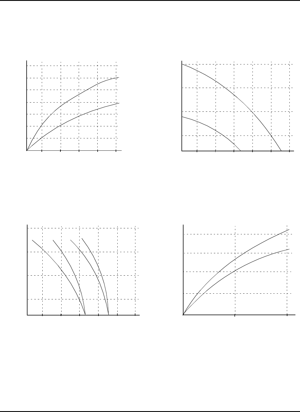
© 1998 Scenix Semiconductor, Inc. All rights reserved. - 38 - www.scenix.com
SX18AC / SX20AC / SX28AC
17.5Typical Performance Characteristics
Active Supply Current (External Clock)
Operating Frequency (MHz)
Idd (mA)
Vdd = 5.5V
Vdd = 3.3V
70
60
50
40
30
20
10
_
_
_
_
_
_
_
10 20 30 40 50
Port A/B/C Weak Pull-Up Source Current
Voh (V)
Ipup (µA)
Vdd = 5.5V
Vdd = 3.3V
400
300
200
100
_
_
_
_
1 2 3 4 5 6
OSC2, Port A/B/C Source Current
Voh (V)
Ioh (mA)
40
30
20
10
_
_
_
_
1 2 3 4 5 6
Vol (V)
Iol (mA)
Vdd = 4.5V
40
30
20
10
_
_
_
_
0.5 1.0
Vdd = 3.3V
OSC2, Port A/B/C Sink Current
Vdd = 4.5V
Vdd = 4.5V
OSC2, Port B/C
OSC2, Port A
Vdd = 3.3V
Vdd = 3.3V
OSC2, Port B/C
OSC2, Port A
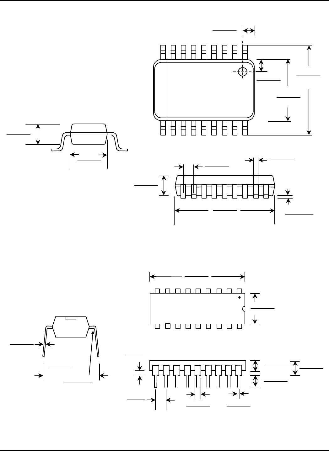
© 1998 Scenix Semiconductor, Inc. All rights reserved. - 39 - www.scenix.com
SX18AC / SX20AC / SX28AC
18.0PACKAGE DIMENSIONS
28
10
91
SX18AC/SO
0.090 - 0.094
(2.29 - 2.39)
0.292 - 0.299
(7.42 - 7.59)
0.451 - 0.461
(11.46 - 11.71)
0.090 - 0.094
(2.29 - 2.39)
0.014 - 0.019
(0.35 - 0.48)
0.0050 - 0.0115
(0.127 - 0.292)
0.400 - 0.410
(10.16 - 10.41)
0.292 - 0.299
7.42 - 7.59)
0.045 - 0.055
(1.143 - 1.397)
0.035 - 0.045
(0.890 - 1.143)
0.050 BSC
(1.27 BSC)
SX18AC/DP
18
1
10
9
0.008 - 0.012
(0.20 - 0.31)
0.895 - 0.905
(22.73 - 22.99)
0.430 max.
(10.92 max.)
0.300 BSC at 90o
(7.62 BSC at 90o)
[ ]
0.240 - 0.260
(6.10 -6.60)
0.130 nom.
(3.3 nom.)
0.125 - 0.135
(3.17 - 3.43)
0.015 min.
(0.38 min.)
0.100 BSC
(2.54 BSC) 0.055 -0.065
(1.39 - 1.65) 0.015 - 0.022
(0.38 - 0.56)
0.170 max.
(4.32 max.)
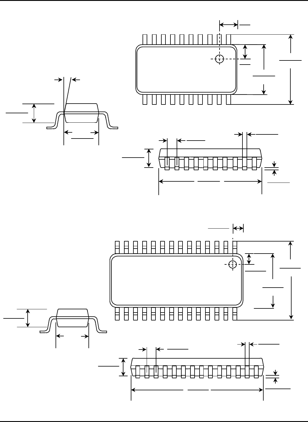
© 1998 Scenix Semiconductor, Inc. All rights reserved. - 40 - www.scenix.com
SX18AC / SX20AC / SX28AC
20
1
10
11
SX20AC/SS
0.205 - 0.212
(5.20 - 5.38)
0.066 - 0.070
(1.68 - 1.78)
12o - 16o
0.066 - 0.070
(1.68 - 1.78)
0.0256 BSC
(0.65 BSC)
0.010 - 0.015
(0.25 - 0.38)
0.002 - 0.008
(0.05 - 0.21)
0.278 - 0.289
(7.07 - 7.33)
0.301 - 0.311
(7.65 - 7.90)
0.205 - 0.212
(5.20 - 5.38)
0.039
(1.00)
0.039
(1.00)
28
15
14 1
SX28AC/SO
0.090 - 0.094
(2.29 - 2.39)
0.292 - 0.299
(7.42 - 7.59)
0.701 - 0.710
(17.81 - 18.06)
0.090 - 0.094
(2.29 - 2.39)
0.014 - 0.019
(0.35 - 0.48)
0.0050 - 0.0115
(0.127 - 0.292)
0.40 - 0.41
(10.16 - 10.41)
0.292 - 0.299
7.42 - 7.59)
0.045 - 0.055
(1.143 - 1.397)
0.035 - 0.045
(0.890 - 1.143)
0.050 BSC
(1.27 BSC)
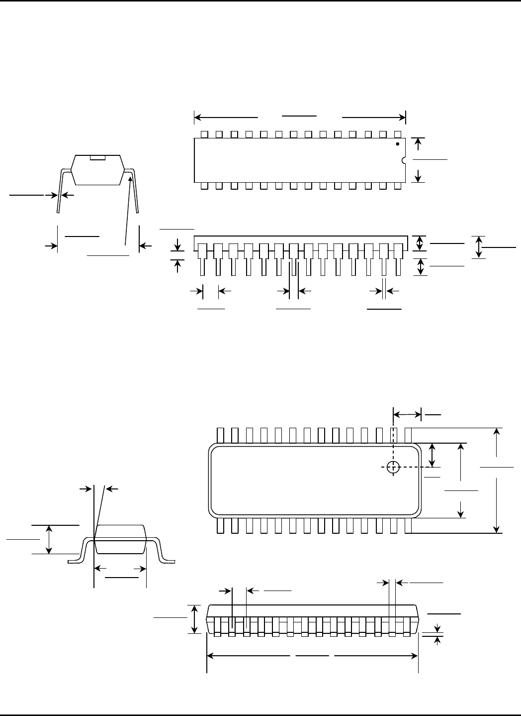
© 1998 Scenix Semiconductor, Inc. All rights reserved. - 41 - www.scenix.com
SX18AC / SX20AC / SX28AC
28
15
1
14
SX28AC/DP
0.430 max.
(10.92 max.)
0.009 - 0.014
(0.23 - 0.36)
1.360 - 1.370
(34.54 - 34.80)
0.280 - 0.295
(7.11 - 7.49)
0.130 nom.
(3.3 nom.)
0.120 - 0.135
(3.05 - 3.43)
0.015 - 0.021
(0.38 - 0.53)
0.045 - 0.055
(1.14 - 1.40)
0.100 BSC
(2.54 BSC)
0.180 max.
(4.57 max.)
0.020 min.
(0.51 min.)
0.300 BSC at 90o
(7.62 BSC at 90o)
[ ]
2815
14 1
SX28AC/SS
0.205 - 0.212
(5.20 - 5.38)
0.066 - 0.070
(1.68 - 1.78)
0.066 - 0.070
(1.68 - 1.78)
0.0256 BSC
(0.65 BSC)
0.010 - 0.015
(0.25 - 0.38)
0.002 - 0.008
(0.05 - 0.21)
0.397 - 0.407
(10.07 - 10.33)
0.301 - 0.311
(7.65 - 7.90)
0.205 - 0.212
(5.20 - 5.38)
0.039
(1.00)
0.039
(1.00)
12o - 16o

© 1998 Scenix Semiconductor, Inc. All rights reserved. - 42 - www.scenix.com
For the latest contact and support information on SX devices, please visit the Scenix Semiconductor website at
www.scenix.com. The site contains technical literature, local sales contacts, tech support and many other features.
Scenix Semiconductor, Inc. 3160 De La Cruz Blvd., Suite #200
Santa Clara, CA 95054
(408) 327-8888
http://www.scenix.com
SX18AC / SX20AC / SX28AC
Sales and Tech Support Contact Information
US DISTRIBUTOR
Unique Technologies
9980 Huennekens Street
San Diego, CA 92121
(800) 677-5664 Corporate Headquarters
(800) 556-0225 Direct to Local Office
DEVELOPMENT TOOLS
Parallax Inc.
3805 Atherton Road, Suite 102
Rocklin, CA 95765
(916) 624-8333
http://www.parallaxinc.com
MANUFACTURERS REPRESENTATIVES
South Nevada; Utah,
Idaho; Montana;
Wyoming; Colorado;
New Mexico;
Arizona
Nelco Electronix
Chandler
Tel: (602) 726-2334
Email: nelcoaz@aol.com
9725 E. Hampden Avenue
Suite 100
Denver, CO 80231
Tel: (303) 671-7677
Email: nelcoelect@aol.com
Boise
Tel: (208) 343-9171
Email: nelcotd@aol.com
Albuquerque
Tel: (505) 293-1399
Email: nelco@swcp.com
El Paso
Tel: (915) 833-7300
Email: nelco@dzn.com
Utah
Tel: (208) 343-9171
Email: nelcotd@aol.com
New York; East
Pennsylvania;
South New Jersey
Quality Components, Inc.
4211 Anita Drive
Collegeville, PA 19426
Tel: (800) 965-8885
Email: brogers@quality-compo-
nent.com
116 Fayette Street
Manilus, NY 13104
Tel: (315) 682-8885
Tennesse; N. Carolina;
S. Carolina; Georgia;
Alabama; Mississippi
STG
101 Washington Street
Suite 6
Huntsville, AL 35801
Tel: (205) 534-2376
Email: hstokes@stghsv.com
6045 Atlantic Boulevard
Norcross, GA 30071
Tel: (770) 239-7576
Email: hstokes@stghsv.com
207 New Edition Court
Cary, NC 27511
Tel: (919) 468-1524
Email: hstokes@stghsv.com
North California
Impact Technical Sales, Inc.
1150 N. First St. #205
San Jose, CA 95112
Tel: (408) 291-5100
Email: info@impactTSI.com
South California
Spectrum Rep Company
30 Fairbanks
Suite 115
Irvine, CA 92618
Tel: (949) 461-5280
Email: paulscarbo@spectrum-
rep.com
http://www.spectrumrep.com
31368 Via Colinas
Suite 101
Westlake Village, CA 91362
Tel: (818) 706-2919
Email: larryclark@spectrum-
rep.com
http://www.spectrumrep.com
N. Dakota; S. Dakota;
Minnesota
Com-Tek Sales, Inc
3502 Shoreline Drive
Navarre, MN 55392-0017
Tel: (612) 471-7181
Email: comtek@comtek-
sales.com
Michigan; Indiana; Ohio;
Kentucky;
West Pennsylvania
Schillinger Associates, Inc.
2297 East Boulevard
Kokomo, IN 46902
Tel: (765) 457-7241
Email: saicorp@msn.com
Southeast New York;
North New Jersey
ERA
354 Veterans Memorial Highway
Commack, NY 11725
Tel NY: (516) 543-0510
Tel NJ: (800) 645-5500
Email: info.era@erareps.com
http://www.erareps.com
Texas; Oklahoma;
Arizona; Louisiana
M-Rep
12801 Stemmons Freeway
Suite 825
Dallas, TX 75234
Tel: (972) 484-5711
Email: sales@mrep.com
http://www.mrep.com
7605 Parkway Circle
Austin, TX 78731
Tel: (512) 502-9962
Email: howard@mrep.com
http://www.mrep.com
Wisconsin; Illinois
Dynamic Technical Sales
416 East State Parkway
Suite 212
Schaumberg, IL 60173
Tel: (847) 755-5490
Email: dts@dtsrep.com
553 Industrial Drive
Suite 6
Hartland, WI 53029
Tel: (414) 367-1821
Email: dtsinc@execpc.com

© 1998 Scenix Semiconductor, Inc. All rights reserved. - 43 - www.scenix.com
For the latest contact and support information on SX devices, please visit the Scenix Semiconductor website at
www.scenix.com. The site contains technical literature, local sales contacts, tech support and many other features.
Scenix Semiconductor, Inc. 3160 De La Cruz Blvd., Suite #200
Santa Clara, CA 95054
(408) 327-8888
http://www.scenix.com
SX18AC / SX20AC / SX28AC
MANUFACTURERS REPRESENTATIVES
Benelux
Memec Benelux
Gen. De Wittelaan, 17 B10
2800 Mechelen
Tel: (32) 15-400-0800
Email:
BdeVries@meb.memec.com
France
A2M
5 rue Carle Vernet
92315 Sevres Cedex
Tel: (33) 1-4623-7900
Email: mgadreau@tekelec.fr
Germany
Topas Electronic GmbH
Fliegerstrasse 1
30179 Hannover
Tel: (49) 898-991-430
Email: ulf.Topas@t-online.de
Scantec Mikroelektronik GmbH
Behringstrasse 10
82152 Planegg
Tel: (49) 511-968-640
Email: stenwaldo@com-
puserve.com
United Kingdom
Ambar Components
Rabans Close
Aylesbury
HP19 3RS Bucks
Tel: (944) 129-639-7396
Email:
rthomson@acp.memec.com
Ireland
Curragh Technology
Block H, Lock Quay
Clare Street
Limerick
Tel: (353) 6-131-6116
Email: jburton@ctl.memec.com
Italy
Silverstar-Celdis
Viale Fulvio Testi, 280
20126 Milano
Tel: (39) 2-661-251
Email: rbaldoni@arrowitaly.com
Norway
BIT Elektronikk
Smedsvingen 4
PO BOX 194
1360 Nesbru
Tel: (47) 66-776-599
Email: njh@bit.no
Switzerland
Computer Components AG
Neunbrunnenstrasse 55
8050 Zurich
Tel: (41) 13-086-655
Email: kolbicz@ccontrols.ch
China/Hong Kong
Sunrise Technology, Ltd.
Room 907, Tower 1, Silvercord
30 Canton Road, TST
Kowloon, Hong Kong
Tel: (852) 2376-1882
Email:
sunadmin@sunrise.com.hk
Room 3113, Everbright ITIC
Bldg.
15 Bai Shi Qiao Road
Hai Dian Dist., Beijing, 100081
Tel: (010) 6848-6895
Email:
sunadmin@sunrise.com.hk
Room 519, Changning S&T
Bldg.
No. 201 Tian Shan Zhi Road
Shanghai, 200051
Tel: (201) 6259-4939
Email:
sunadmin@sunrise.com.hk
8/F, Block B, Overseas Decora-
tion Bldg.
11 Zhenhua Road
Shenzhen, 518031
Tel: (0755) 332-5656
Email:
sunadmin@sunrise.com.hk
Taiwan
Promate Electronic Co., Ltd.
4F 32m Sec.1, Huan Shan Road
Nei Hu, Taipei 114
Tel: (886) 2-2659-0303
Email: irving@promate.com.tw
Pinnacle Technology Co.
4F, 270, Sec. 3, Nan-Kang Road
Taipei
Tel: (886) 2-2788-4800
Email: pinnacle@ms1.hinet.net
Japan
Sumisho Electronic Devices
Corp.
1 Kandamitoshirocho
Chiyoda-ku, Tokyo 101
Tel: (81) 3-5282-7225
Email:
masayuki_kobayashi@sed.co.jp
Korea
Comfile Technology
30-1 Shingae-Dong
Youngsan-Gu, Seoul 140-090
Tel: (82) 2-711-2592
Email:
comfile@soback.kornet.nm.kr
Team Korea
292-6 Yatap-Dong, Bundang-Ku
Sungam-Si, Kyungki-Do
Tel: (82) 342-705-1825
Email:
mikechoi@teamkorea.com
http://www.teamkorea.com
