00 Cover(1.02) SCX1100
User Manual: SCX1100
Open the PDF directly: View PDF ![]() .
.
Page Count: 109 [warning: Documents this large are best viewed by clicking the View PDF Link!]
- Cover.pdf
- 1.pdf
- 2.pdf
- 3.pdf
- 4.pdf
- 5.pdf
- 6.pdf
- 7.pdf
- Schematic Diagram.pdf
- Cover
- 1. Block Diagram
- 2. Connection Diagram
- 3. Circuit Description
- MAIN PBA
- 3-1. GENERAL DESCRIPTION
- 3-2. MEMORY MAP
- 3-3.DETAILED DESCRIPTION
- 3-3-1 BLOCK DIAGRAM and MAIN CONTROLLER description
- 3-3-2 S3C46MOX(Jupiter3) FUNCTION DESCRIPTION
- 3-3-2-1 SYSTEM CLOCK
- 3-3-2-2 DATA AND ADDRESS BUS CINTRIL
- 3-3-2-3 EXTERNAL DMA part
- 3-3-2-4 DRAM control part
- 3-3-2-5 RTC (REAL TIME CLOCK) part
- 3-3-2-6 PARALLEL PORT INTERFACE division
- 3-3-2-7 USB INTERFACE PART
- 3-3-2-8 HEAD control part
- 3-3-2-9 SYNCHRONOUS SERIAL INTERFACE part
- 3-3-2-10 MOTOR control part
- 3-3-2-11 GENERAL PURPOSE I/O PORT of S3C46MOX(Jupiter3)
- 3-3-3 RESET CIRCUIT
- 3-4 MEMORY
- 3-5 Image processing part (U21)
- 3-5-1 GENERAL DESCRIPTION
- 3-5-2 OA-980 DESCRIPTION BY FUNCTIONS
- 3-5-2-1 Clock Control Section
- 3-5-2-2 Internal Microcontroller
- 3-5-2-3 Host Interface Section
- 3-5-2-4 Scanner Interface Section(PI)
- 3-5-2-5 Image Processing Section(IP)
- 3-5-2-6 Memory Interface Section(MI)
- 3-5-2-7 JBIG Comp & Decomp Section
- 3-5-2-8 Rotate and Inkjet Engine Section
- 3-5-2-9 Printer Interface Section(PO)
- 3-5-3 COPY DATA FLOW FOR OA-980
- 3-5-4 OA-980 I/O POR
- 3-6 CCD MODULE and ADC Part
- 3-7 THUNDERBOL ASIC DESCRIPTION
- OPE
- MAIN PBA
- 4.Schematic Diagrams
SERVICE
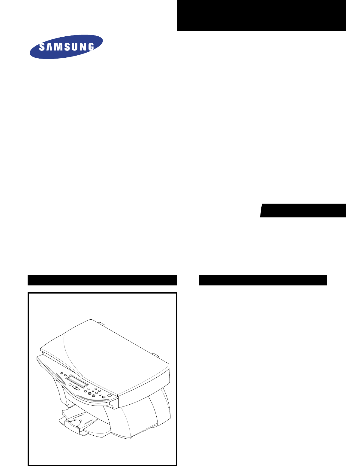
SAMSUNG
INKJET PRINTER(MFP)
SCX-1100
Manual
INKJET PRINTER(MFP) CONTENTS
1. Precautions
2. Specifications
3. Disassembly and Reassembly
4. Troubleshooting
5. Exploded Views and Parts List
6. Block Diagram
7. Connection Diagram

ELECTRONICS
© Samsung Electronics Co.,Ltd. March
2001
Printed in Korea.
VERSION NO. : 1.02 CODE : JB-0023A
This service manual is also provided on the web,
the ITSELF system Samsung Electronics Co., Ltd.
“http://itself.sec.samsung.co.kr”
- This Service Manual is a property of Samsung Electronics Co.,Ltd.
Any unauthorized use of Manual can be punished under applicable
International and/or domestic law. -

This manual is stated and
provided for service description.
All rights reserved. Any parts of the
information in this manual are prohibited
from free duplication, use or translation
without prior written approval except in
cases allowed by the Copyright Act.
Specifications are subject to change without
prior notice.
Copyright (c) 2002. 3.
Samsung Electronics Digital Printing CS Group
1-1
Samsung Electronics
1. Precautions
Please read the following carefully to prevent any accidents and not to damage the unit during service.
1-1 Safety Precautions
1-2 Precautions on Disassembly and Reassembly
1. Safety Precautions
There are some electric or machinery parts with safety
related property. If the parts replaced are different from
the original, the safety may not function. Even if the part
could allow higher voltage than that of the part used, do
not replace it and use a regular product clarified in spec-
ifications.
2. Be careful not to leave a switch, a cover or a safety device
out when reinstalling or assembling the product after
repair.
3. Replacing Precautions
Do not change or add parts as you like. You cannot ben-
efit from such a remodeled product at your will during the
term of guarantee.
4. You must replace overheated or damaged parts or cords
with regular products. Please solve the problem causing
any damage or overheating and troubles beforehand.
Especially mind the safety on the part with this
mark.
You must use regular parts described in specifica-
tions for the parts inflammable and where the cur-
rent can be flown. Otherwise any hazard such as
an electric shock or a fire could occur.
Very careful precautions should be taken when replacing
parts. Before replacing, please check cables because you
cannot put the cables that you removed for replacing parts
into the proper place if you would not make sure of where
they were connected and in which condition.
Please do the following before disassembling
for a repair or replacement of parts.
1. Pull out paper cassette, printer cartridge installed.
Especially careful not to be scratched by the surface of
developer or not to expose them to light.
2. Turn the power switch off.
3. Take out the power plug, printer cable from the printer.
4. Use only the same type of part as original when replacing
parts.
5. Do not force to open or fasten plastic material compo-
nents.
6. Be careful that small parts such as screws should not get
in the printer.
7. When disassembling, assembling, also observe small
components are located in place.
8. If you uncover and turn the machine over to replace some
parts, toner or paper particles may contaminate the LSU
window. Protect the LSU window with clean paper.
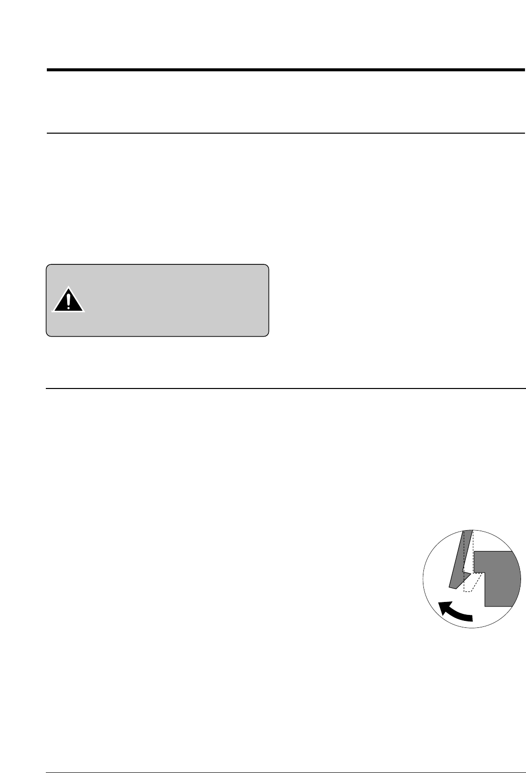
Releasing Plastic Latches
Many of parts are held in
place with plastic latches.
The latches break easily :
release them carefully.
To remove such parts, press
the hook end of the latch
away from the part to which
it is latched.

Certain semiconductor devices can be easily damaged by
static electricity. Such components are commonly called
“Electrostatically Sensitive (ES) Devices”, or ESDs.
Examples of typical ESDs are: integrated circuits, some field
effect transistors, and semiconductor “chip” components.
The techniques outlined below should be followed to help
reduce the incidence of component damage caused by sta-
tic electricity.
1. Immediately before handling a semiconductor compo-
nent or semiconductor-equipped assembly, drain off any
electrostatic charge on your body by touching a known
earth ground. Alternatively, employ a commercially avail-
able wrist strap device, which should be removed for your
personal safety reasons prior to applying power to the unit
under test.
2. After removing an electrical assembly equipped with
ESDs, place the assembly on a conductive surface, such
as aluminum or copper foil, or conductive foam, to pre-
vent electrostatic charge buildup in the vicinity of the
assembly.
3. Use only a grounded tip soldering iron to solder or desol-
der ESDs.
4. Use only an “anti-static” solder removal device. Some sol-
der removal devices not classified as “anti-static” can
generate electrical charges sufficient to damage ESDs.
5. Do not use Freon-propelled chemicals. When sprayed,
these can generate electrical charges sufficient to dam-
age ESDs.
6. Do not remove a replacement ESD from its protective
packaging until immediately before installing it. Most
replacement ESDs are packaged with all leads shorted
together by conductive foam, aluminum foil, or a compa-
rable conductive material.
7. Immediately before removing the protective shorting
material from the leads of a replacement ESD, touch the
protective material to the chassis or circuit assembly into
which the device will be installed.
8. Maintain continuous electrical contact between the ESD
and the assembly into which it will be installed, until com-
pletely plugged or soldered into the circuit.
9. Minimize bodily motions when handling unpackaged
replacement ESDs. Normal motions, such as the brush-
ing together of clothing fabric and lifting one’s foot from a
carpeted floor, can generate static electricity sufficient to
damage an ESD.
1-3 ESD Precautions
Precautions
1-2 Samsung Electronics
CAUTION:
Be sure no power is applied to the chassis or cir-
cuit, and observe all other safety precautions.
Precautions
1-3
Samsung Electronics
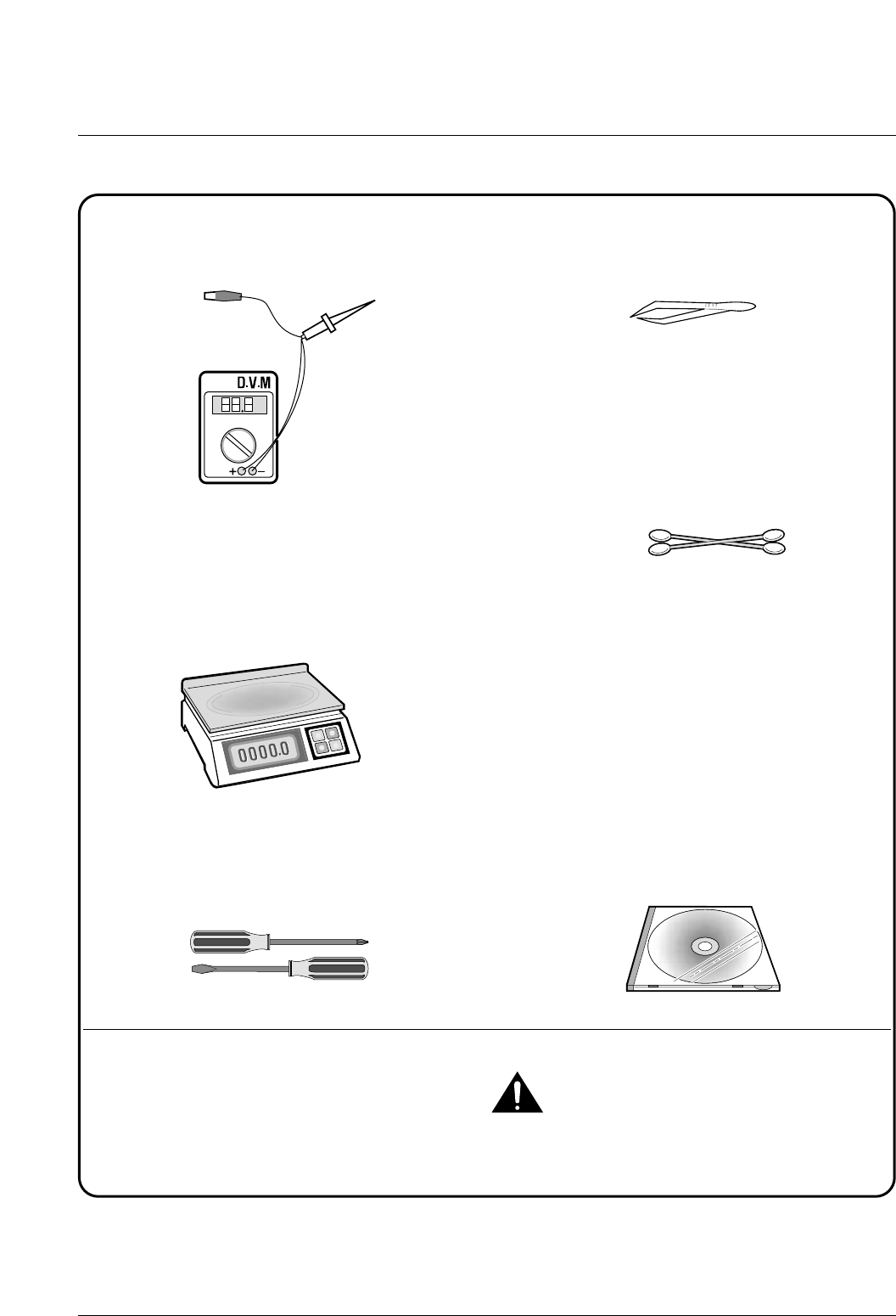
1-4 Tools for Troubleshooting
The following tools are recommended for safe and smooth troubleshooting described in this service manual.
DVM(Digital Volt Meter)
Standard: Indicates more than 3 digits.
Electronic Scale
Standard: Equipment to check the weight of con-
sumables supplied by Samsung Electronics.
(The gram unit can be measured.)
Driver
Standard: "-" type, "+" type (M3 long, M3 short,
M2 long, M2 short).
Pinset
Standard: For general home use, small type.
Cotton Swab
Standard : For general home use, for medical ser-
vice.
Cleaning Equipments a IPA(Isopropyl
Alcohol)dry cloth or a soft stuff neutral
detergent.
Software(Driver) installation CD ROM
Mind your hands not to be touched when you
disassemble and reassemble PBAASS'Y, such as
the main board.
Note
1
2
3
4
5
6
7
Samsung Electronics 2-1
2. Specifications
2-1 Printer Engine
2-2 Ink Cartridge
Babbage mono standard Birch color
Model No. M50 C60
Print Head 208 nozzles 192 nozzles
Ink type Pigment Dye
Ink Color Black (Babbage) Color (Birch)
Ink Yield about 1075 sheets (5% Pattern, A4) about 275 sheets (15% Pattern, A4)
Technology Color Thermal Inkjet
Engine Type 2-Pen (K and CMY)
Operating System Windows 95/98/2000/Me/XP
Interface USB (without HUB Mode), Centronics 1284
Emulation HBP(GDI)
Print Speed (2) Mono 14 ppm Draft / 10 ppm Normal
Color 7 ppm Draft / 2 ppm Normal
Print Resolution (H x V) Quick 300 x 600 dpi
Normal 600 x 600 dpi
High Quality 2400(H) x 1200(V) dpi (Addressable)
Maximum Paper Size A4, Letter, Legal, Banner
Effective Printing Width 8.0'' (203 ± 1mm)
Feeding Method Automatic 100 Sheets (Maximum stacking height : 9mm)
Manual Tray No
Output Tray Capacity Maximum 30 sheets
Maximum Cable Length USB Cable, Max 6ft (3)
Note:
(2) Speed claims based on the test files: spdtstc.sam(mono), spdtstc2.sam(color)/Letter size
(3) Non-standard cable can cause misoperations.

Samsung Electronics
Specifications
2-2
2-3 Copier
Scanner Type Flat-bed without ADF (Automatic Document Feeder)
Maximum Original Size A4/Letter
Maximum Paper Size A4/Letter/Legal
Maximum Scan Width 216 mm
Optical Resolution (HxV) 600 x 600 dpi
Copy Quality Draft, Normal, Best
Paper Type Selection Plain, Glossy, Transparency
Mono Copy Speed (1) Draft: 10cpm
Color Copy Speed (1) Draft: 5cpm
Effective Print-edge Margin Top: 3.4mm, Bottom: 19.05mm, Each Side: 6.5mm(LTR), 3.5mm(A4)
Multi copy 99 pages (Memory Multi copy)
Zoom Rate 25 % ~ 400 % (1 % Step)
Contrast Control 3 Steps
Ink Saver Mode Use Draft Mode (<20 % Savings)
Auto Sensing Check Paper Jam , Low Ink
Note:
(1) Speed claims based on the test chart : Printed spdtstc.sam(mono), Printed spdtstc2.sam(color)/Letter size
2-4 Scanner
Operation System Windows 98/Me/2000/XP
Interface USB (without HUB Mode) and Centronics 1284
Compatibility TWAIN Standard.
Device Platen Color CCD
Scan Width Max.: 8.5” (216 mm), Effective: 8.2” (210 mm)
Color Depth Internal 36 bit, External 24 bit
Optical Resolution (H x V) 600 x 1200 dpi
Interpolation Resolution Max. 4800 dpi
Pre-scan Mode Yes, 75 dpi
Scan Speed about 2'30 sec/A4 True Color
(Pentium II 300M, 64MB Memory, 300dpi)
Samsung Electronics
Specifications
2-3
2-5 Power Supply
Rated AC Input Voltage 110 ~ 240 VAC (Universal)
Rated Input Frequency 50 ~ 60 Hz
Minimum/Maximum AC Input 90 VAC/265 VAC
Maximum Input Current 0.5 A
DC Channels (4) (2 Channels) +3.3V +5%, +30V +10%
External Power On/Off Key Power Down Key (It does not cut the primary power input off)
2-6 Dimension
Machine Size (W x D x H, mm) 477(W) X 415(D) X 252(H)
Machine Weight About 8.5 Kg (Machine itself)
Note:
(4) No load condition.
2-7 Environmental Condition
Absolute Storage Temperature(5) -20oC ~ 55oC
Absolute Storage Humidity(5) 10% RH ~ 90% RH
Recommended Temperature 5oC ~ 40oC
Operating Condition Humidity 15% RH ~ 85% RH
Note:
(5) Packing Condition
3. Disassembly and Reassembly
3-1 General Precautions on Disassembly
When you disassemble and reassemble components, you
must use extreme caution.
The close proximity of cables to moving parts makes proper
routing a must. If components are removed or replaced, any
cables disturbed by the procedure must be replaced as close
as possible to their original positions.
Before removing any component from the machine, note the
cable routing that will be affected.
Whenever servicing the machine, you must perform as fol-
lows:
1. Check to verify that documents are not stored in memory.
2. Unplug the power cord.
3. Use a flat and clean surface.
4. Replace only with authorized components.
5. Do not force to remove or planten plastic-material compo-
nents.
6. Make sure all components are in their proper position.
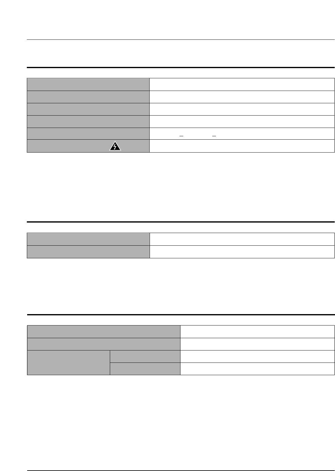
3-2 Scanner Ass'y
1. Remove two screws securing the rear cover.
2. Open the front door from the main cover.
3. Remove two screws securing the main cover.
4. Pull the scanner ass'y upward then, unplug the two
connectors and CCD cable.
Note :
You should connect or remove the CCD cable verti-
cally to avoid the CCD cable pin damage.
3-1samsung Electronics
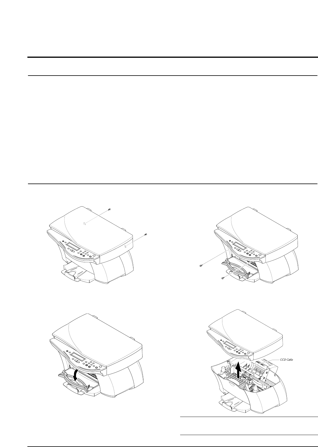
5. Pull the platen cover upward and remove it.
6. Pull the OPE cover upward and remove it.
7. Remove five screws securing the OPE upper and
unplug the one connector from the OPE panel.
8. Remove two screws securing the scan upper and
remove it.
9. Unlatch the scan lawer securing the scan upper and
remove it.
10. Remove the two screws securing the scan upper.
3-2 samsung Electronics
Disassembly and Reassembly
11. Unlatch the scan dummy and take out the glass
from the scan upper.
12. Remove the CCD cabl.
13. Push the belt holder and take out the belt, as
shown below.
14. Pull up the CCD shaft and take out the scanner
module.
1
5. Remove two screws and take out the motor bracket.
16. Remove two screws securing the scan motor and
remove it.
samsung Electronics 3-3
Disassembly and Reassembly
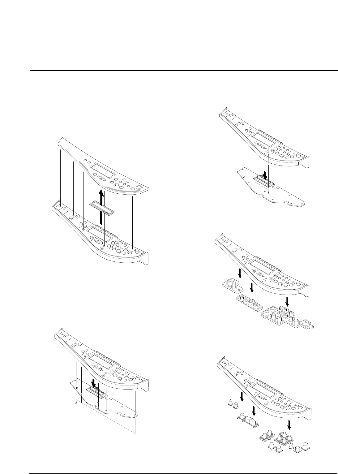
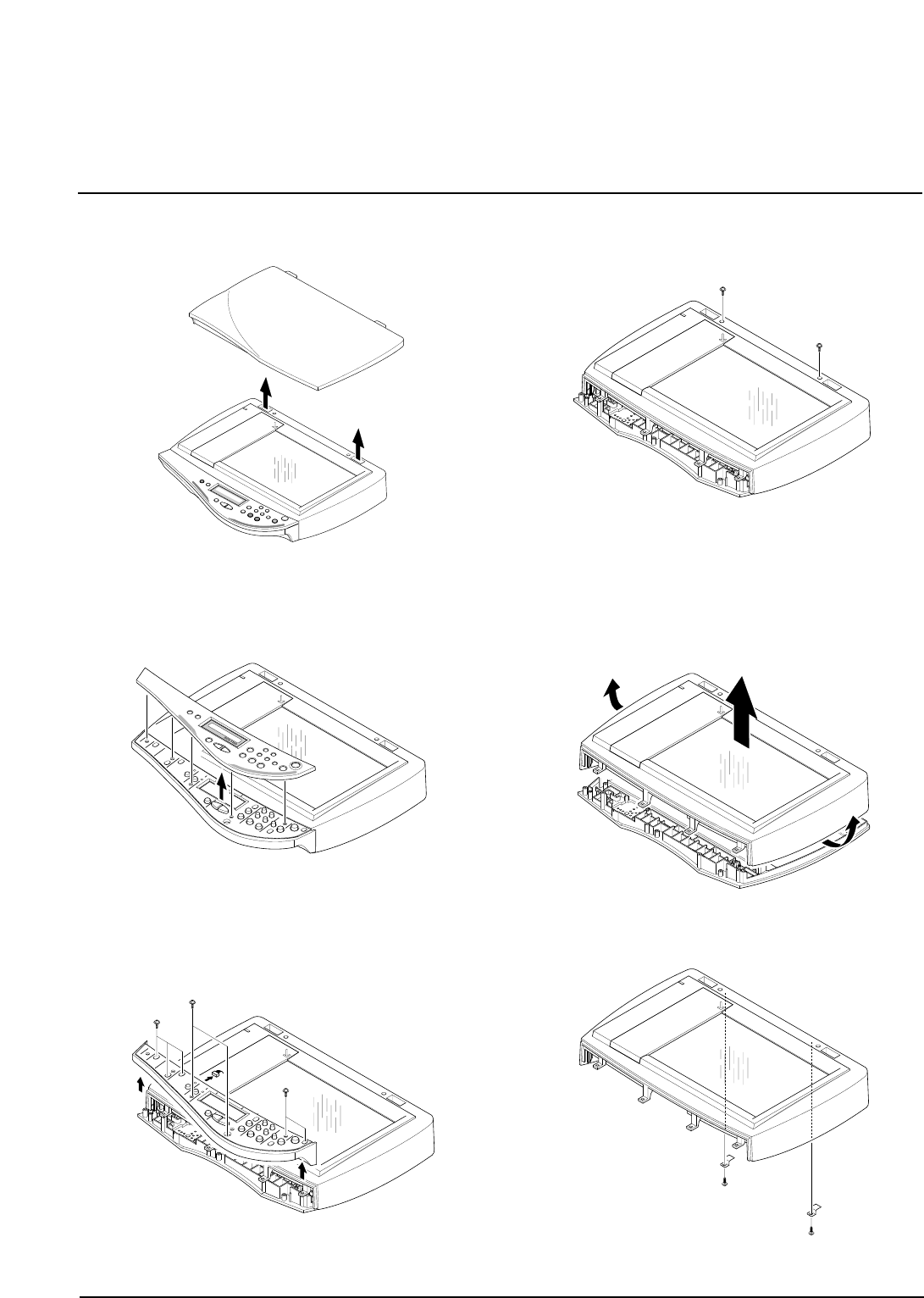
3-3 OPE Unit
1. Before you remove the ope unit, you should remove:
• Scanner Ass'y (see page 3-1)
2. Pull the OPE cover upward and remove it.
Take out the LCD window from the OPE cover.
3. Remove five screws securing the OPE upper to the
OPE PBA.
4. Remove two screws securing the OPE upper to the
LCD board.
5. Remove the contact rubber from the OPE upper.
6. Remove the Key pad from the OPE upper.
3-4 samsung Electronics
Disassembly and Reassembly
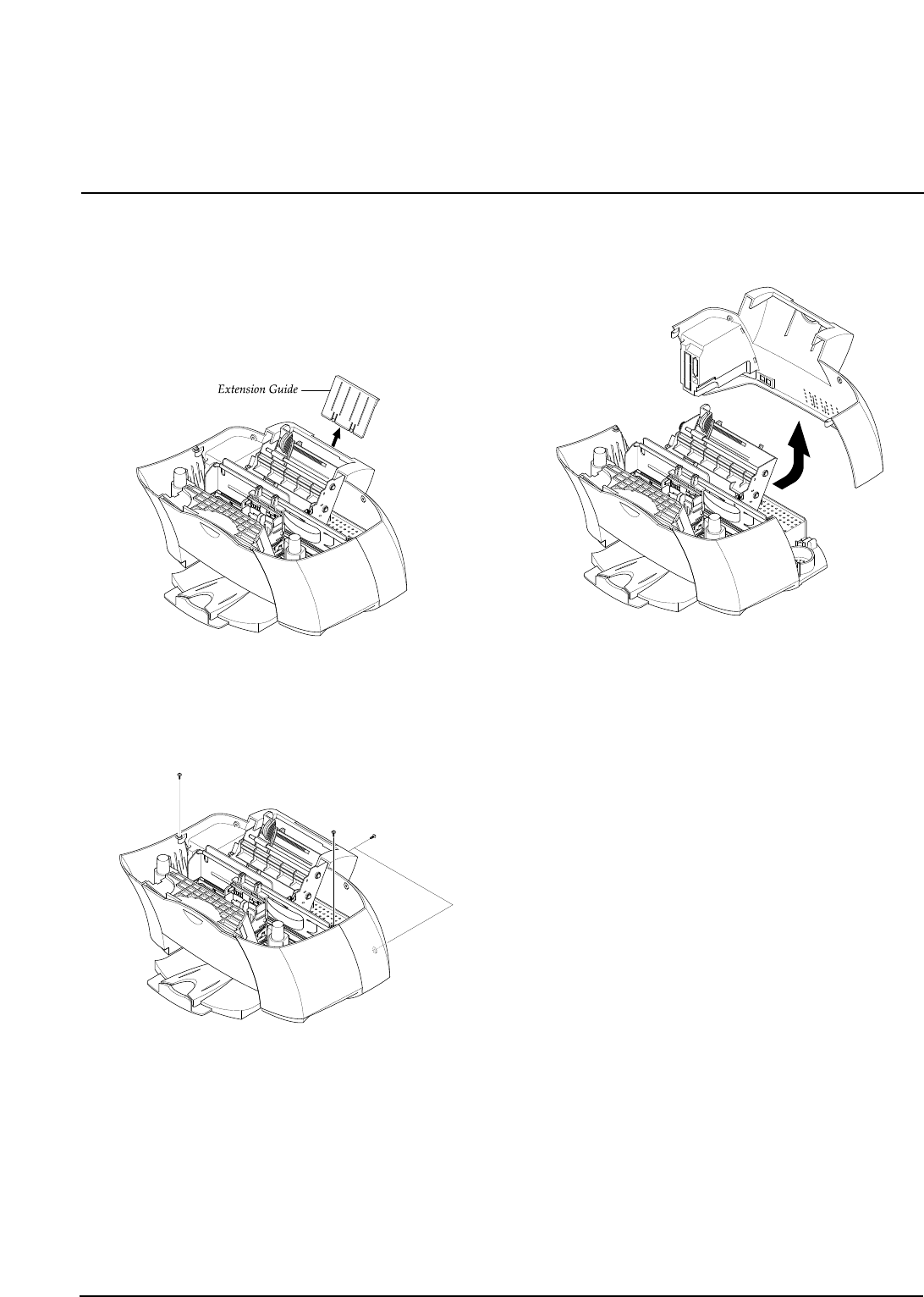
3-4 Rear Cover
1. Before you remove the rear cover, you should
remove:
• Scanner Ass'y (see page 3-1)
2. Pull the extension guide upward and remove it.
3. Remove four screws securing the rear cover.
4. Remove the rear cover, as shown below.
samsung Electronics 3-5
Disassembly and Reassembly
samsung Electronics
Disassembly and Reassembly
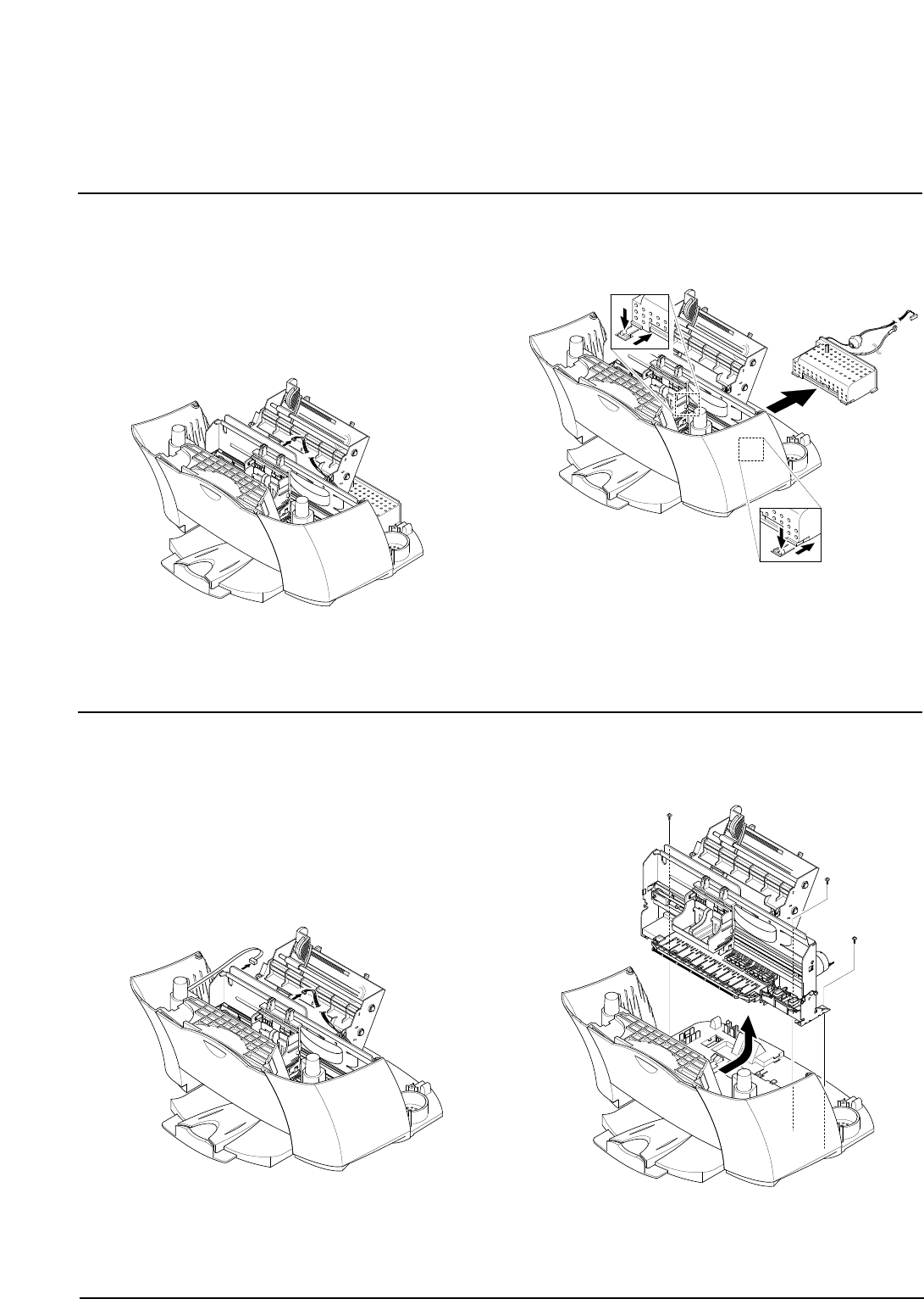
3-5 SMPS
1. Before you remove the SMPS, you should remove:
• Scanner Ass'y (see page 3-1)
• Rear Cover (see page 3-5)
2. Unplug the one connector from the main PBA.
3. Pushing down the hooks on both ends, pullout the
SMPS.
3-6
3-6 Engine Ass'y
1. Before you remove the engine ass'y you should
remove:
• Scanner Ass'y (see page 3-1)
• Rear Cover (see page 3-5)
2. Unplug the SMPS connector and cover open sensor
connector from the main PBA.
3. Remove the three screws securing the engine ass'y
and remove it.
samsung Electronics
Disassembly and Reassembly
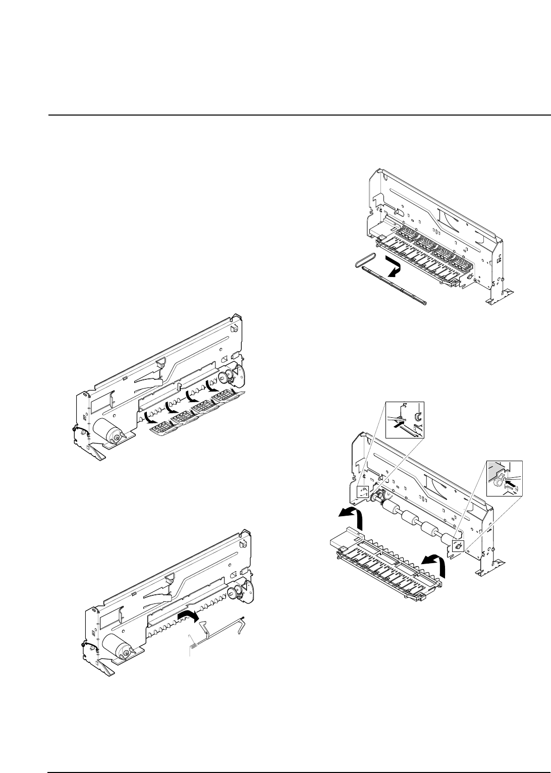
3-7 ASF Feeder
1. Before you remove the asf feeder, you should
remove:
• Scanner Ass'y (see page 3-1)
• Rear Cover (see page 3-5)
• SMPS (see page 3-6)
2. Make sure the harness is released from the hooks,
as shown below.
3. Remove three screws securing the ASF feeder to the
main cover.
Take out the ASF feeder.
3-7
3-8 Cartridge Ass'y
1. Before you remove the cartridge ass'y you should
remove:
• Scanner Ass'y (see page 3-1)
• Rear Cover (see page 3-5)
• Engine Ass'y (see page 3-6)
• ASF Feeder (see page 3-7)
2. Rotate to remove both springs securing the carrier
shaft. Then take out the carrier shaft.
3. Remove the C-cab.
4. Take out the emcoder strip, as shown below.
5. Push the holder pulley to the right and take out the
belt.
6. Take out the cartridge carrier from the main frame.
3-8 samsung Electronics
Disassembly and Reassembly
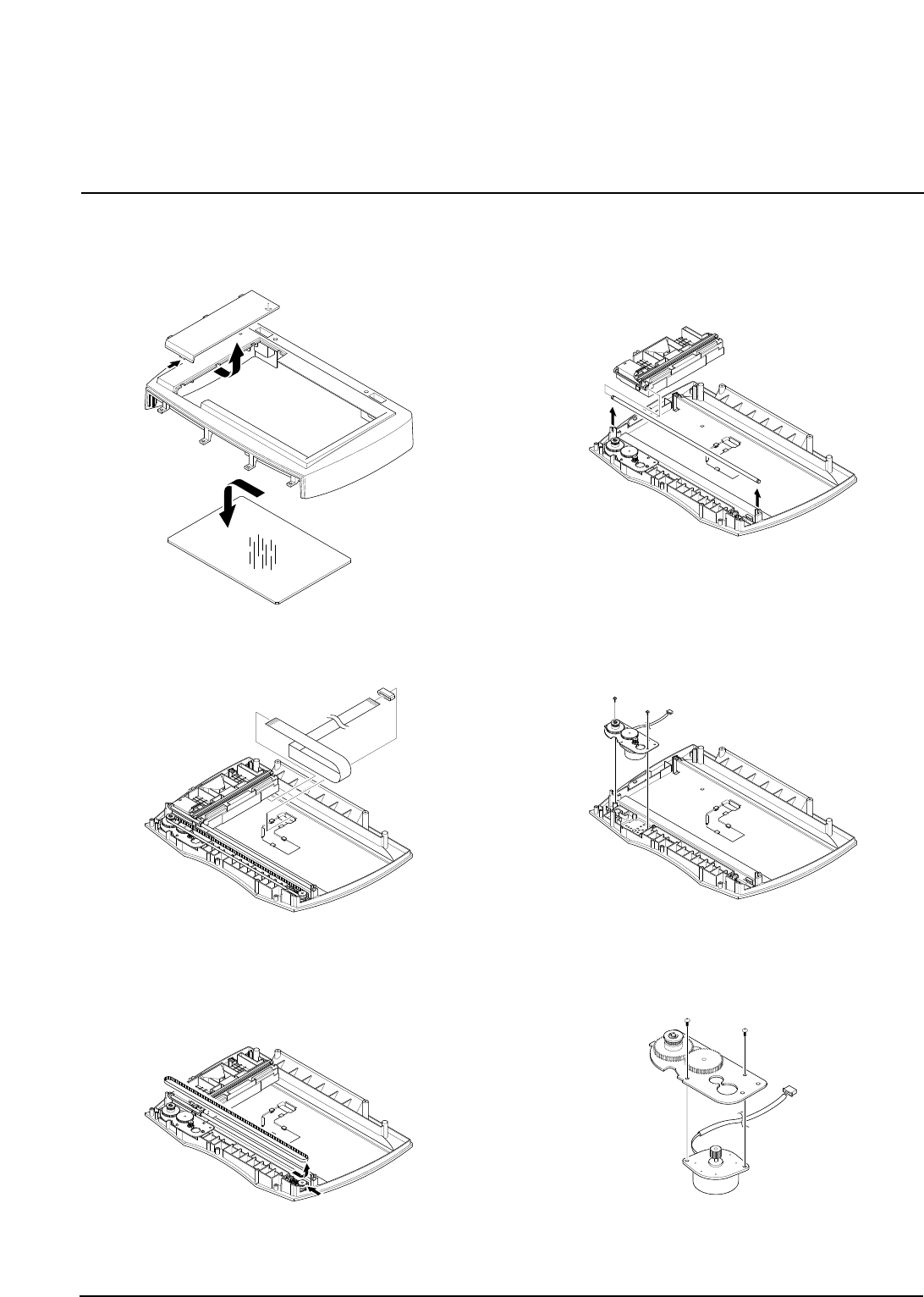
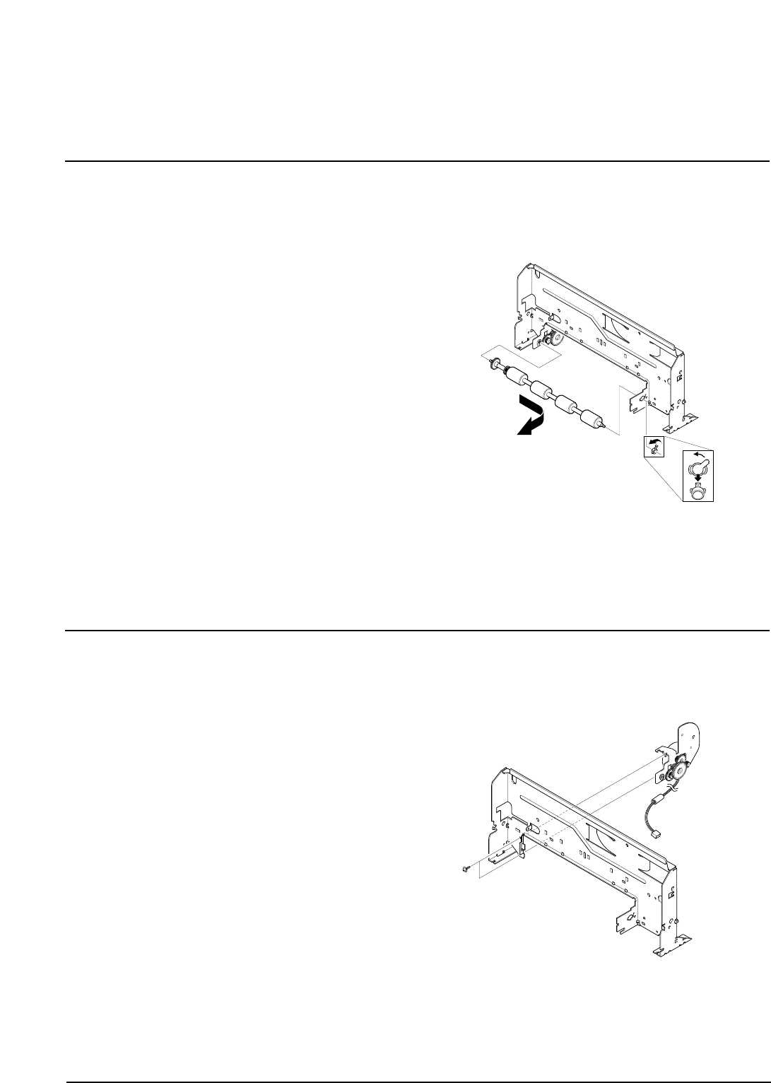
3-9 Carrier Motor
1. Before you remove the carrier motor, you should
remove:
• Scanner Ass'y (see page 3-1)
• Rear Cover (see page 3-5)
• Engine Ass'y (see page 3-6)
• ASF Feeder (see page 3-7)
• Cartridge Ass'y (see page 3-8)
2. Unplug the one connector from the main PBA.
3. Remove two screws securing the carrier motor and
take out the motor from the main frame.
samsung Electronics 3-9
Disassembly and Reassembly
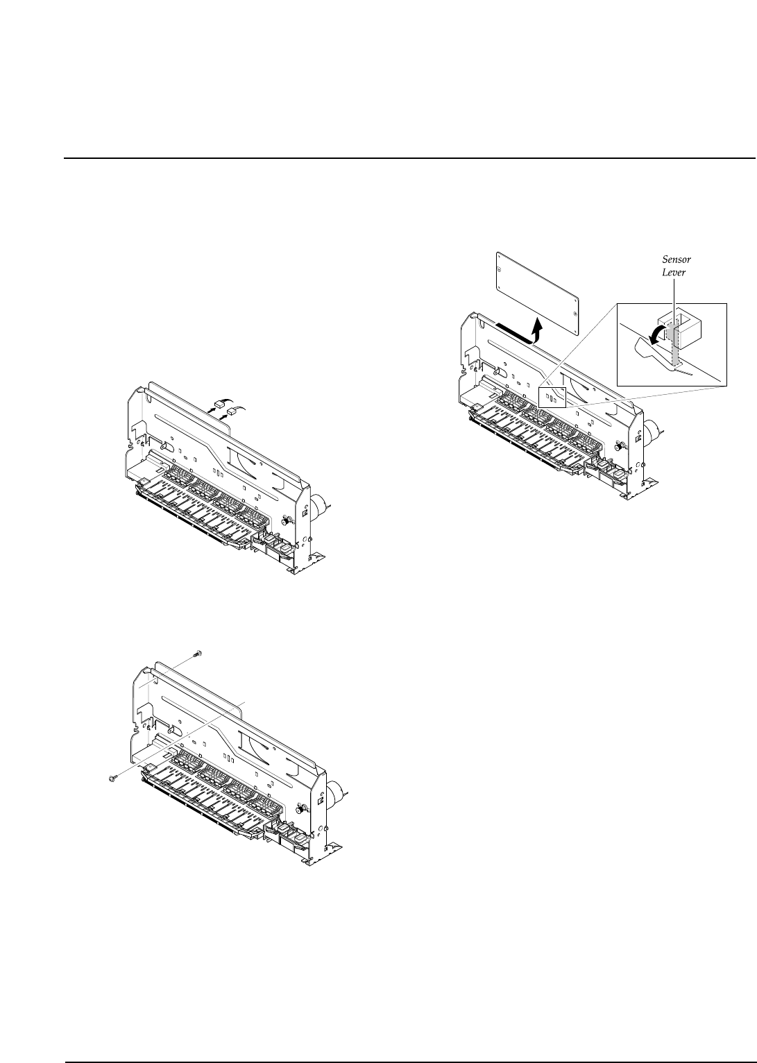
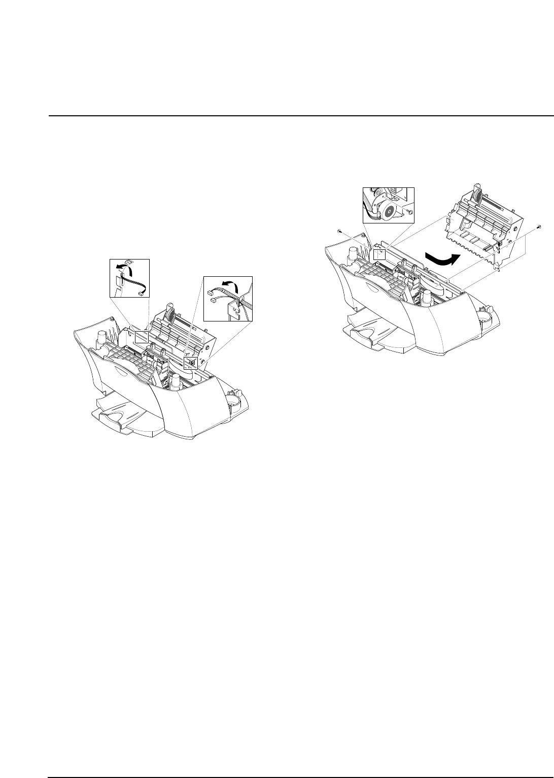
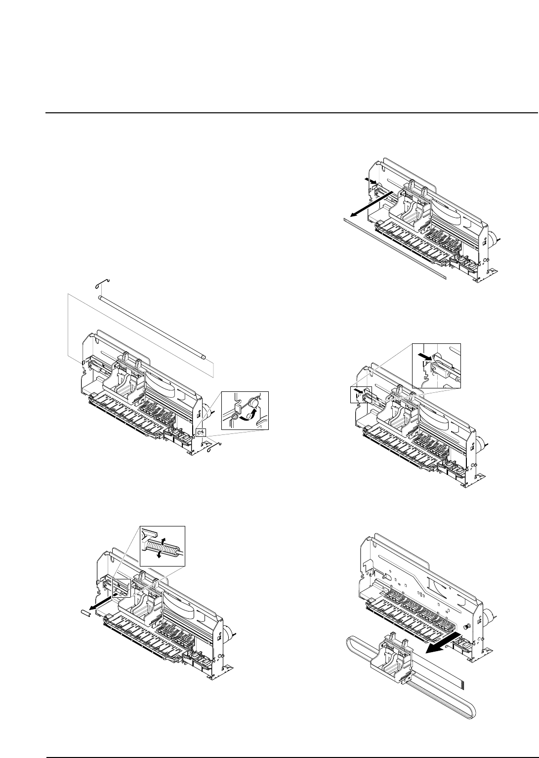
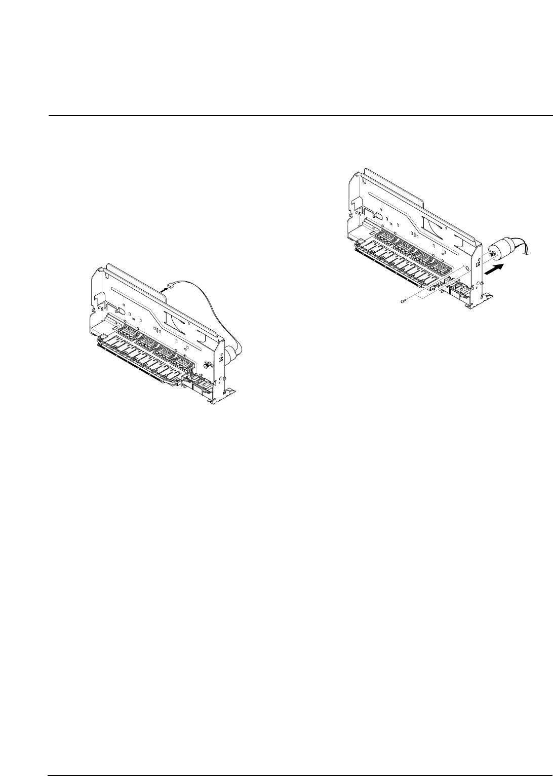
3-10 Main PBA
1. Before you remove the main PBA, you should
remove:
• Scanner Ass'y (see page 3-1)
• Rear Cover (see page 3-5)
• Engine Ass'y (see page 3-6)
• ASF Feeder (see page 3-7)
• Cartridge Ass'y (see page 3-8)
2. Unplug all connectors from the main PBA.
3. Remove the two screws securing the main PBA.
4. Pull the sensor lever backward and take out the main
PBA, as shown below.
3-10 samsung Electronics
Disassembly and Reassembly
samsung Electronics
Disassembly and Reassembly
3-11
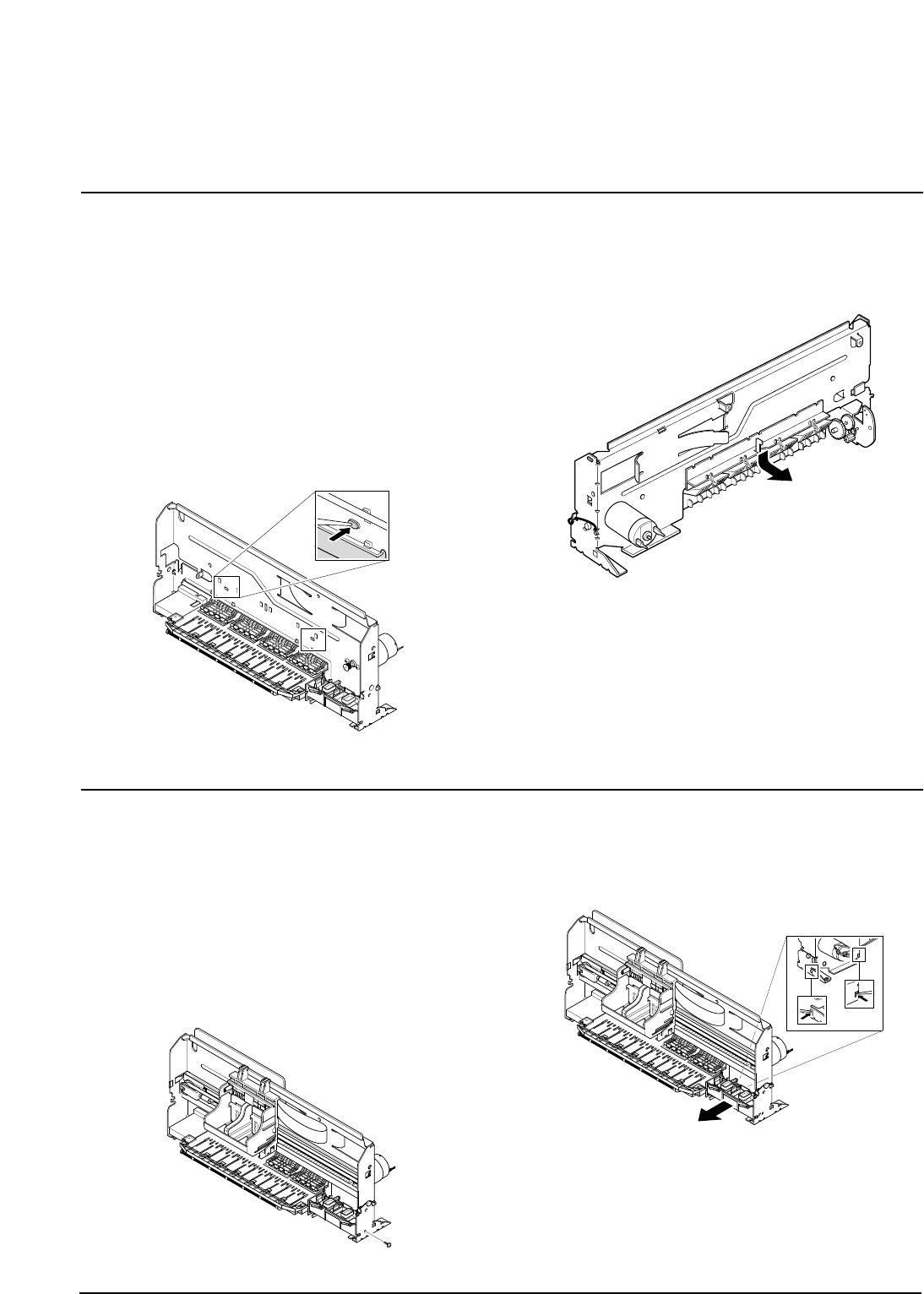
3-11 Holder Roller
1. Before you remove the holder roller, you should
remove:
• Scanner Ass'y (see page 3-1)
• Rear Cover (see page 3-5)
• Engine Ass'y (see page 3-6)
• ASF Feeder (see page 3-7)
• Cartridge Ass'y (see page 3-8)
• Main PBA (see page 3-10)
2. Unlatch the holder by pushing the parts hooked to
the main frame using a sharp tool.
3. Pull the holder downward and take it out from the
main frame.
3-12 Home Ass'y
1. Before you remove the home ass'y you should
remove:
• Scanner Ass'y (see page 3-1)
• Rear Cover (see page 3-5)
• Engine Ass'y (see page 3-6)
• ASF Feeder (see page 3-7)
2. Remove one screw securing the home ass'y.
3. Unlatch the home ass'y by pushing the parts hooked
to the main frame using a sharp tool. Take out the
home ass'y from the main frame.
samsung Electronics
Disassembly and Reassembly
3-12
3-13 Base Frame
1. Before you remove the base frame, you should
remove:
• Scanner Ass'y (see page 3-1)
• Rear Cover (see page 3-5)
• Engine Ass'y (see page 3-6)
• ASF Feeder (see page 3-7)
• Cartridge Ass'y (see page 3-8)
• Main PBA (see page 3-10)
• Hold Roller (see page 3-11)
• Home Ass'y (see page 3-11)
2. Remove the four springs and take out the four roller
frictions, as shown below.
3. Take out the actuator feed from the main frame, as
shown below.
4. Remove the exit roller from the main frame and take
out the exit belt.
5. Unlatch the base frame ass'y by pushing the parts
hooked to the main frame using a sharp tool, as
shown below.
samsung Electronics
Disassembly and Reassembly
3-13
3-14 Feed Roller
1. Before you remove the feed roller, you should
remove:
• Scanner Ass'y (see page 3-1)
• Rear Cover (see page 3-5)
• Engine Ass'y (see page 3-6)
• ASF Feeder (see page 3-7)
• Cartridge Ass'y (see page 3-8)
• Main PBA (see page 3-10)
• Hold Roller (see page 3-11)
• Home Ass'y (see page 3-11)
• Base Frame (see page 3-12)
2. Turn the bearing feed counterclockwise and take out
the base frame and feed roller from the main frame.
3-15 Line Feed Bracket Ass'y
1. Before you remove the LF bracket ass'y, you should
remove:
• Scanner Ass'y (see page 3-1)
• Rear Cover (see page 3-5)
• Engine Ass'y (see page 3-6)
• ASF Feeder (see page 3-7)
• Cartridge Ass'y (see page 3-8)
• Main PBA (see page 3-10)
• Hold Roller (see page 3-11)
• Home Ass'y (see page 3-11)
• Base Frame (see page 3-12)
• Feed Roller (see page 3-13)
2. Remove two screws and take out the LF bracket
ass'y from the main frame.
4-1
Samsung Electronics
4. Troubleshooting
4-1 Setting-up System in User Mode
FUNCTION ITEM DEFAULT
LANGUAGE ENG/GER/FRE/ITA/SPA/POR/DUT ENGLISH
POWER SAVE MODE 1/4/8/12 HOUR 1
PAPER SIZE LETTER/A4/LEGAL A4
PAPER TYPE PLAIN/INKJET/PHOTO/TRANSPARENCY PLAIN PAPER
MAINTENANCE CLEAN CARTRIDGE
ALIGN CARTRIDGE
VIEW INK LEVEL "COLOR : _/8 , BLOCK : _/8"
HELP LIST
DEFAULT SETUP CONTRAST
QUALITY
COPY PAGE
ZONE RATE
RESOLUTION
ADJUST SHADING
KEY SOUND ON/OFF ON
4-2 Setting-up System in Service Mode
• How to enter service mode
In service (tech) mode, the technician can check the machine and perform various tests to isolate the cause of a malfunc-
tion.
To enter the service mode, press ENTER, LEFT, RIGHT, LEFT, SETUP in sequence, and the LCD displays ‘ T ’, the machine
has entered service (Tech) mode.
To return to normal user mode, press ENTER, LEFT, RIGHT, LEFT, SETUP in sequence again, or turn the power off, then
on by unplugging and plugging the power cord.
Because the explanation of the User Mode items is already mentioned at the User guide in detail, It will not be described at
Service manual.
4-2
Troubleshooting
Samsung Electronics
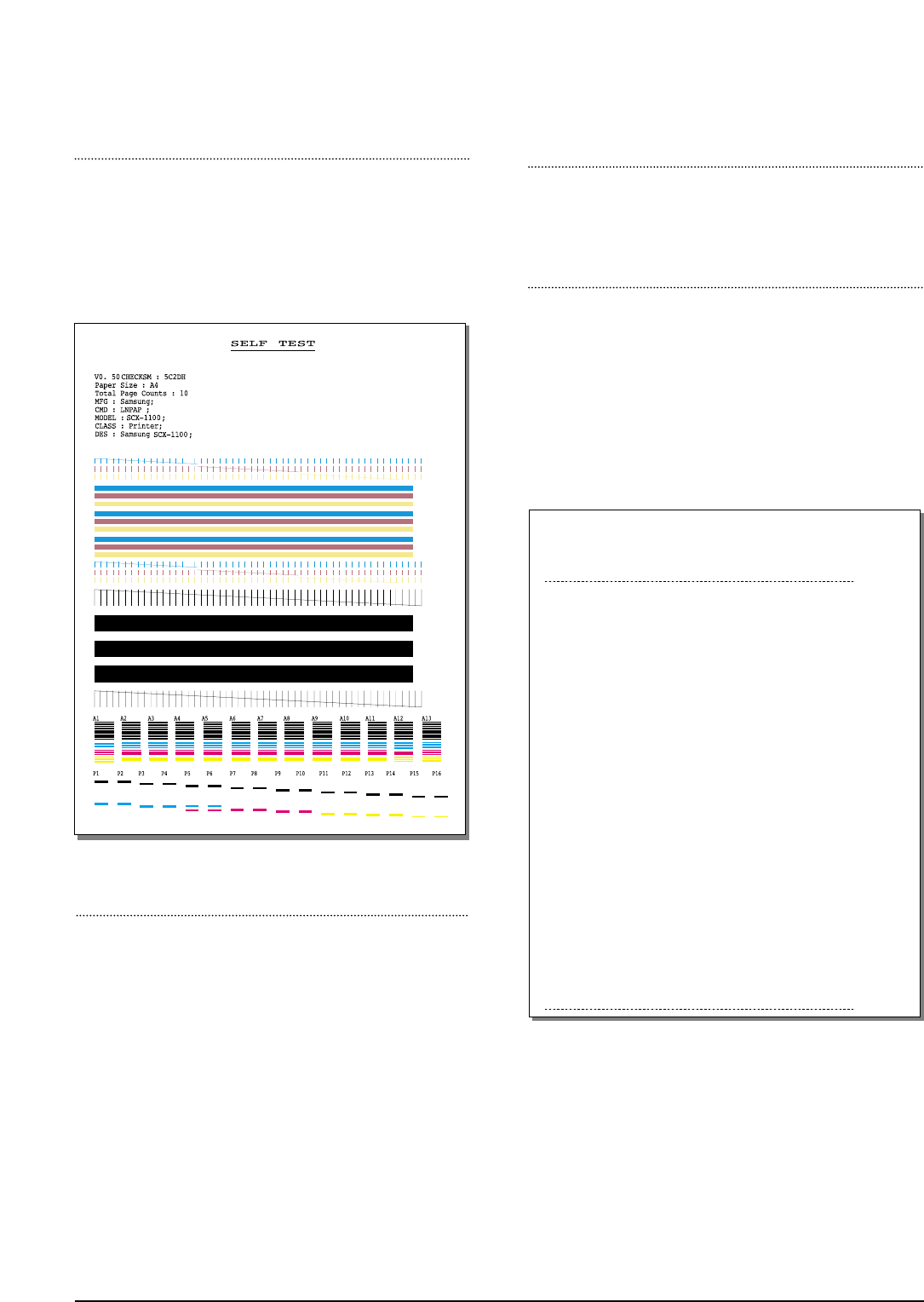
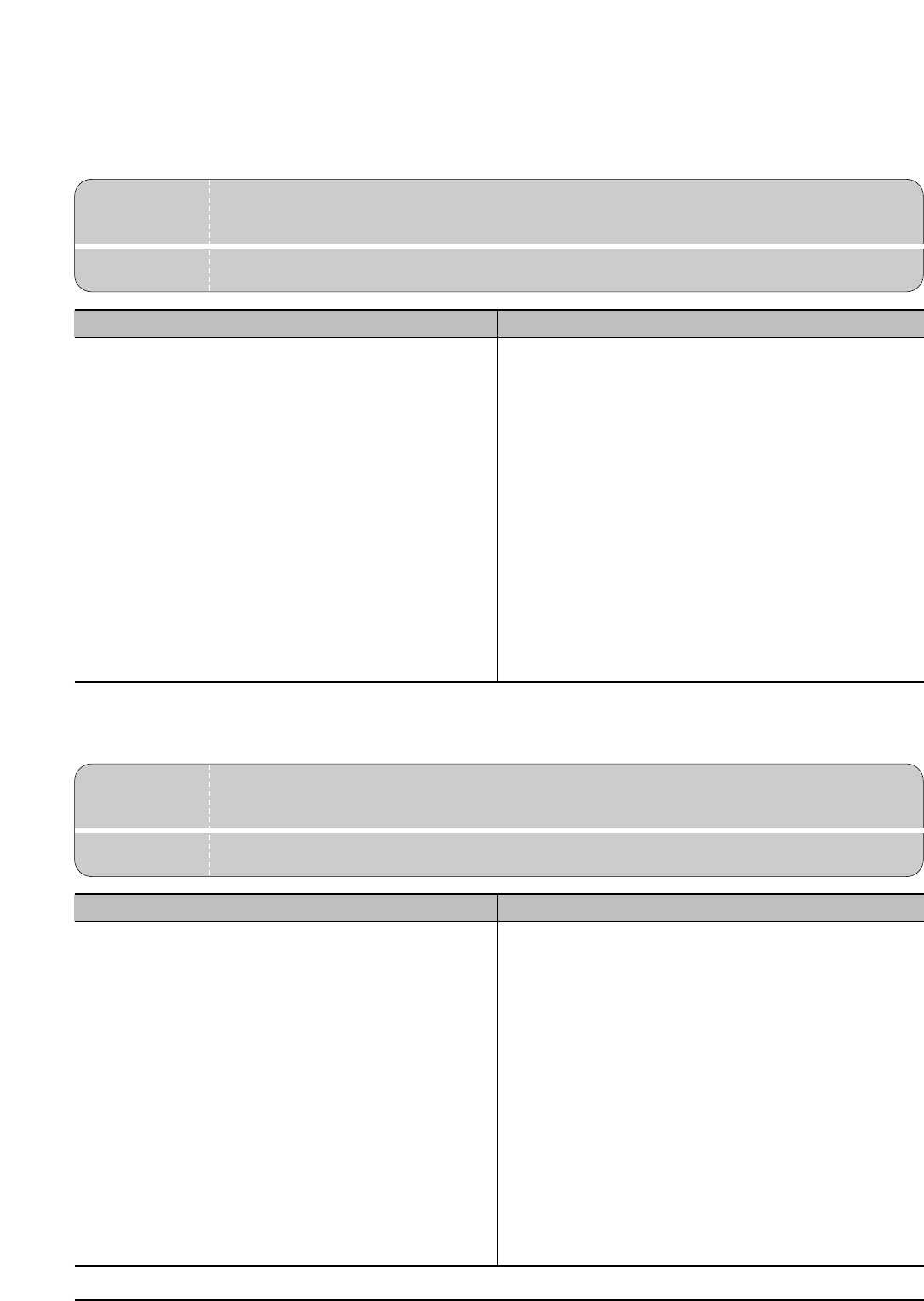
FACTORY SELFTEST
Using this pattern printout, you can check if the printer
mechanism is functioning properly. Examine the pattern
and look for a break in the diagonal line. If the diagonal
lines are not broken, the printer mechanism is functioning
properly.
ROM TEST
Use this feature to test the machine'S ROM. The result and the
software version appear in the LCD display.
PRINT NVRAM TEST
1. Press the SETUP button until “PRINT NVRAM DUMP”
is displayed in LCD.
2. Press the START button when the NVRAM Test opera-
tion menu displayed. And then the machine prints the
list for NVRAM testing.
The Remote Test feature can be enabled in order to allow
a remote location to call up and run a diagnostic test on
your machine. You may be instructed by a service repre-
sentative to enable this feature.
NVRAM DUMP LIST
LIST Left Head Detect : 1c
Right Head Detect : 7
Left Head Type : 1c
Right Head Type : 7
< Device Identification >
MFG:Samsung;
CMD:LNPAP;
MODEL:SCX-1100;
CLASS :Printer;
DES:Samsung SCX-1100;
< Dot Count Variables >
Black Dot Count : 2436256
Color Cyan Dot Count : 1368128
Color Magenta Dot Count : 1368128
Color Yellow Dot Count : 1368128
Photo Black Dot Count : 0
Photo Cyan Dot Count : 0
Photo Magenta DotCount : 0
Total Black Dot Count : 2436256
Total Color Cyan Dot Count : 1368128
Total Color Magenta Dot Count : 1368128
Total Color Yellow Dot Count : 1368128
Total Photo Cyan Dot Count : 0
Total Photo Magenta Dot Count : 0
Total Photo Black Dot Count : 0
< Page Count Variables >
Total Page Count : 2
< Cartridge Types >
Left Cartridge Type : Color Standard Capacity
Right Cartridge Type : Black High Capacity
< Alignment Variables >
Horizontal Align Value : 15
Vertical Align Value : 8
Quick Black Bidi Align Value : 15
Quick Color Bidi Align Value : 15
Normal Black Bidi Align Value : 15
Normal Color Bidi Align Value : 15
Photo Horizontal Align Value : 15
Photo Vertical Align Value : 8
Photo Normal Black Bidi Align Value : 15
Photo Normal Color Bidi Align Value : 15
PROGRAM DOWNLOAD
Use this feature to download a new upgraded ROM file from
a PC which is connected to the machine with a parallel cable
(IEEE 1284).
< Download >
1. Connect printer to PC with a parallel cable(IEEE 1284.)
2. Select the PROGRAM DOWNLOAD function at the TECH
MODE.
3. Input COPY/B FILENAME PRN at the MS-DOS and push
the ENTER key.
(filename : the latest ROM file name when the downloading)
4. After the download is completed, the system will be auto-
matically initialized.
4-3
Troubleshooting
Samsung Electronics
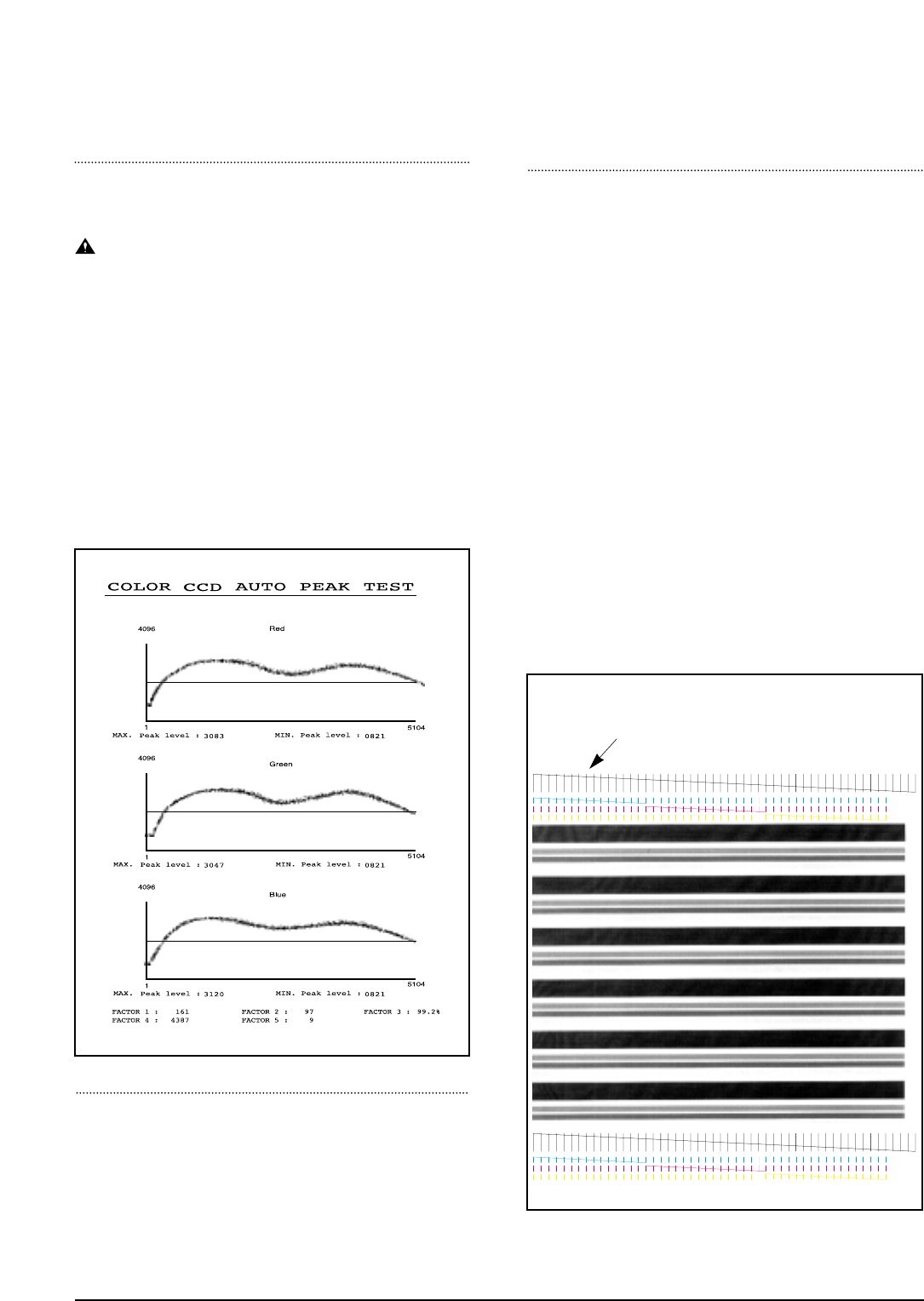
PRINT CCD PATTERN
It is used to adjust the light of CCD. It is already set at
CCD Test to get optimum quality.
NOTICE
When you test CCD, make sure that the cover is
closed.
1. Press the SETUP button until “Print CCD Pattern” is
displayed in LCD.
2. Press the START button when the CCD Test operation
menu displayed.
3. After scanner calibrating, wave form will be automatical-
ly printed out.
All the wave forms should be similar each other. CCD
problems may occur, if:
• More than one of the wave forms are straight lines.
• All wave forms are positioned under the center line.
WHITE LINES ON LETTERS OR GRAPHICS
• Cause
If nozzles in print head has a problem, white lines are
marked on the print.
‘CARTRIDGE MAINTENANCE’ will let you know if noz-
zles have fallen problems.
• Solution
1) Run ‘print control panel’ to “clean print nozzles” and check if
nozzles have been blocked.
2) Wipe
with soft cloth the contact surfaces of ink cartridge and car-
riage, and check if nozzles have been cleaned properly.
3) Separate ink cartridge from carriage and combine them.
Repeat it about 5 to 6 times and check if connection is proper.
4) Replace ink cartridge and check whether there’s a problem
with the head.
5) Check if head cable is inserted well into the main circuit board
and then check if nozzles have problems.
6) Check if head cable is broken or torn and then check if nozzles
have problems.
7) Replace the main circuit board with a new one and
check if nozzles have problems.
MEMORY ALL CLEAR
Initiating this function will put the system into the factory
shipping state. The procedure is as follows :
1. Unplug power
2. Press and hold " SETUP" button
3. Plug power in
4. Continue holding " SETUP" button until CLEARING
MEMORY message appears on LCD
5. Unplug power
If this line is broken, it confirms that nozzles
have problems.

4-4
Troubleshooting
Samsung Electronics
4-3. Troubleshooting
4-3-1 Defective PC Scan . . . . . . . . . . . . . . . . . . . . . . . . . . . . . . . . . . . . . . . . . . . . . . . .page(4-5)
4-3-2 Defective Image quality of PC Scan . . . . . . . . . . . . . . . . . . . . . . . . . . . . . . . . . . .page(4-5)
4-3-3 Defective Operation (LCD WINDOW ) Display . . . . . . . . . . . . . . . . . . . . . . .page(4-6)
4-3-4 No Power . . . . . . . . . . . . . . . . . . . . . . . . . . . . . . . . . . . . . . . . . . . . . . . . . . . . . .page(4-6)
4-3-5 Defective LCD Operation . . . . . . . . . . . . . . . . . . . . . . . . . . . . . . . . . . . . . . . . . . .page(4-7)
4-3-6 Defective Operation of Key Button . . . . . . . . . . . . . . . . . . . . . . . . . . . . . . . . . . . .page(4-7)
4-3-7 Paper Jam . . . . . . . . . . . . . . . . . . . . . . . . . . . . . . . . . . . . . . . . . . . . . . . . . . . . . .page(4-8)
4-3-8 Defective Paper Feed (1) . . . . . . . . . . . . . . . . . . . . . . . . . . . . . . . . . . . . . . . . . . .page(4-8)
4-3-9 Defective Paper Feed (2) -Display of NO PAPER . . . . . . . . . . . . . . . . . . . . . . . . .page(4-9)
4-3-10 Multi-Feeding . . . . . . . . . . . . . . . . . . . . . . . . . . . . . . . . . . . . . . . . . . . . . . . . . . . .page(4-9)
4-3-11 Defective Sensing-ink . . . . . . . . . . . . . . . . . . . . . . . . . . . . . . . . . . . . . . . . . . . .page(4-10)
4-3-12 Defective Sensing-paper . . . . . . . . . . . . . . . . . . . . . . . . . . . . . . . . . . . . . . . . . .page(4-10)
4-3-13 Defective Motor Drive (LF) . . . . . . . . . . . . . . . . . . . . . . . . . . . . . . . . . . . . . . . . .page(4-11)
4-3-14 Defective Motor Drive (CR) . . . . . . . . . . . . . . . . . . . . . . . . . . . . . . . . . . . . . . . .page(4-11)
4-3-15 Defective Motor Drive (Scan) . . . . . . . . . . . . . . . . . . . . . . . . . . . . . . . . . . . . . . .page(4-12)
4-3-16 Blank Page Print Out (When Copying) . . . . . . . . . . . . . . . . . . . . . . . . . . . . . . . .page(4-12)
4-3-17 Vertical Black Line (When Copying) . . . . . . . . . . . . . . . . . . . . . . . . . . . . . . . . . .page(4-13)
4-3-18 Contaminated Stains on Paper . . . . . . . . . . . . . . . . . . . . . . . . . . . . . . . . . . . . . .page(4-13)
4-3-19 Bad printed Image . . . . . . . . . . . . . . . . . . . . . . . . . . . . . . . . . . . . . . . . . . . . . . .page(4-14)
4-3-20 Vertical Lines are printed crookedly . . . . . . . . . . . . . . . . . . . . . . . . . . . . . . . . . .page(4-14)
4-3-21 Bad Color (Intensity) . . . . . . . . . . . . . . . . . . . . . . . . . . . . . . . . . . . . . . . . . . . . .page(4-15)
4-3-22 The Printer is Not Working (1) . . . . . . . . . . . . . . . . . . . . . . . . . . . . . . . . . . . . . .page(4-15)
4-3-23 The Printer is Not Working (2) . . . . . . . . . . . . . . . . . . . . . . . . . . . . . . . . . . . . . .page(4-16)
4-3-24 Abnormal Printing . . . . . . . . . . . . . . . . . . . . . . . . . . . . . . . . . . . . . . . . . . . . . . .page(4-17)
4-3-25 Spool Error and Release of Spool Error . . . . . . . . . . . . . . . . . . . . . . . . . . . . . . .page(4-18)
• The solutions of troubleshooting in this 'Service Manual' explain the expected causes and
how to check according to each problem and describe how to replace the defected parts (unit
of ASS'Y) if necessary.
• The contents of this 'Service Manual' describe general ones only among many kinds of prob-
lems and causes while using the Product.
• The contents of this 'Service Manual' describe mainly technical explanations of the Product
H/W and parts on the assumption that there is no problem in S/W.

4-5
Troubleshooting
Samsung Electronics
4-3-1 Defective PC Scan
4-3-2 Defective Image Quality of PC Scan
• Description
• Location 1.UBS Cable of the Printer or Centronics Cable 2.Driver 3.Main B’d
The PC Scan is not functioning at all.
Check and Cause Solution
1. Check the Cable (USB or Parallel)
2. Check if the driver is installed properly.
1. If the PC and the cable are not connected properly,
reconnect it.
2. After confirming that it is proper by performing a PC
printing test related to driver setup, if it is not so, reinstall
it. (Refer to User's Manual.)
• Description
• Location 1. CCD ASS'Y 2.Main B’d
The image PC scanned is not clear or bad.
Check and Cause Solution
1. Check the waveform form by performing a CCD test
in TECH mode. (Refer to 4-1-3)
2. Check if the resolution is set too low in PC Scan
options. (Refer to User's Manual.)
1. If the CCD waveform form is abnormal, try to replace
CCD ASS'Y.
2. If the resolution is set to low, let the user be acquainted
with the using method well.

4-6
Troubleshooting
Samsung Electronics
4-3-3 Defective Operation (LCD WINDOW ) Display
4-3-4 No Power
• Description
• Location 1.OPE ASS'Y 2.Connection between the Main B'D and OPE ASS'Y 3.Main B'D.
Strange characters are displayed on the OPE Panel and buttons are not operated.
Check and Cause Solution
1. Clear the memory.
2. Check if OPE HARNESS is connected to the Main
Board correctly.
1. Try again after clearing the memory.
2. After confirming that OPE HARNESS is connected to
the Main Board correctly, if it is so, then replace the
OPE ASS'Y and Main Board in sequence.
• Description
• Location
1.Power code 2.Connection between the Main B'D and Power HARNESS
3.Power ASS'Y 4.Main B'D. 5.OPE Ass’y
While the power S/W is turned on, it does not work at all.
Check and Cause Solution
1. Check if the connection of power code is normal.
2. Check if DC +3.3V and +30V is supplied to POWER
ASS'Y from MAIN B'd.
3. Check if POWER DOWN KEY in OPE ASS'Y is
working regularly.
1. Try to replace the power code.
2. If all the connections are correct, try to replace the
power ASS'Y and the Main B/D in sequence.
( +3.3V and +30V is supplied to POWER ASS'Y from
MAIN B'd)
3. Replace OPE ASS'Y

4-7
Troubleshooting
Samsung Electronics
4-3-5 Defective LCD Operation
4-3-6 Defective Operation of Key Button
• Description The LCD screen is not turned on or has a strange display.
Check and Cause Solution
1. Clear the memory. (Refer to page 4-1).
2. Confirm to catch a click sound, while a key on the
OPE panel is pressed on.
3. Check the status of Harness between LCD and OPE
Panel, replace in order of Main B'd/LE Motor.
1. The key is wrong itself or wrongly assembled.
2. Even after the key or harness has been replaced, it is
still wrong, try to replace the OPE ASS'Y and the Main
B'D in sequence.
• Description
• Location 1. OPE ASS'Y 2. Main Board
The button of the OPE Panel is not operated..
Check and Cause Solution
1. Confirm to catch a click sound while the key is
pressed on.
2. Check if a specific key is pressed by another equip-
ment.
1. If you cannot catch a click sound, the key is wrong itself
or wrongly assembled.
2. Even after the key has been replaced, it is still wrong,
try to replace the OPE ASS'Y and the Main B'D in
sequence.
• Location 1.LCD 2.OPE Ass’y 3.Main B’d

4-8
Troubleshooting
Samsung Electronics
4-3-7 Paper Jam
4-3-8 Defective Paper Feed (1)
• Description
• Location ASF ASS'Y
The paper is jammed inside the set and not exited from.
Check and Cause Solution
1. Check if the paper is crumpled or preprinted.
2. Check if too many sheets of recording paper are put
into ASF (Automatic Sheet Feeder).
(Standard : up to 100 sheets).
3. Check if the remaining papers are stuck in the frame
base.
1. If the papers jammed or pieces of the paper are stuck
inside the set, remove them and then try it again.
2. If the problem still exists, try to replace ASF ASS'Y.
• Description
• Location ASF ASS'Y
A recording paper is tilted while feeding.
Check and Cause Solution
1. Check if the paper guide of ASF (Automatic Sheet
Feeder) is set up properly with the width of recording
paper.
2. Check if too many sheets of recording paper are put
into ASF (Automatic Sheet Feeder).
(Standard: up to 100 sheets).
3. Check if the recording paper is crumpled or preprint-
ed.
1. After all have been checked, the problem still exists, try
to replace the ASF ASS'Y.

4-9
Troubleshooting
Samsung Electronics
4-3-9 Defective Paper Feed (2)-Display of NO PAPER
• Description
• Location 1. ASF ASS'Y 2. Main B’d 3. LF Motor
paper does not feed into the printer.
Check and Cause Solution
1. Press ENTER button to check. 1. Even if the ENTER button is pressed, a recording paper
is not drawn into, then try to replace the ASF ASS'Y.
2. Even if the ASF Ass’y or harness has been replaced, it
is still wrong, try to replace the Main B’d and the LF
Motor in sequence.
4-3-10 Multi-Feeding
• Description
• Location ASF ASS'Y
Multiple-sheets of recording paper are fed at once.
Check and Cause Solution
1. Adjust the paper guide of ASF to the width of paper
correctly.
2. Check if the recording paper is preprinted or crum-
pled.
3. Check if too many sheets of recording paper are put
into ASF (Automatic Sheet Feeder).
(Standard: up to 100 sheets).
1. Blow several times of puff into the paper in order to pre-
vent static electricity.
2. Even after the papers are loaded correctly, if multiple
sheets of paper are still fed at once, then try to replace
the ASF ASS'Y.

4-10
Troubleshooting
Samsung Electronics
4-3-11 Defective Sensing-ink
4-3-12 Defective Sensing-paper
• Description
• Location 1.Cartridge ASS'Y 2.Main B'D
The ink is put in the set, but it cannot sensed.
Check and Cause Solution
1. Check if the cartridge is installed in the cartridge box
properly.
(It makes a click sound normally when it is normal.)
2. Check if the cartridge box is operated normally.
3. Check if there is an alien matter in the Dimple contact
point of HEAD of CARTRIDGE BOX
1. Even after the cartridge is installed normally, it still can-
not sense, then try to replace the Main B'D.
2. In case the cartridge box is not moved from side to side,
check the Flat Cable connection between the Main PBA
& Frame Home Unit, and even after being connected
properly, if it is still not improved, then try to replace the
cartridge ASS'Y.
• Description
• Location 1.Main B'D 2. LF Motor
The recording papers are put in already, but it cannot be sensed.
Check and Cause Solution
1. Check if the ENTER key on the OPE panel is pressed. 1. Refer to "Defective Paper Feed".
2. Even if the ENTER key on the OPE panel is pressed, it
still cannot sense, then try to replace the Main B'D and
LF Motor in sequence.
Notes:
The SCX-1100 Product has no paper sensor, instead it
displays ERROR when it cannot pick up the paper.

4-11
Troubleshooting
Samsung Electronics
4-3-13 Defective Motor Drive (LF)
4-3-14 Defective Motor Drive (CR)
• Description
• Location 1.Main B'D 2.LF Motor
The motor drive of Line Feeder is not working.
Check and Cause Solution
1. Check if the connector of LF Motor is connected to
the Main B'D normally. 1. Try to replace the Main B'D and the LF Motor ASS'Y in
sequence.
• Description
• Location 1.Main B'D 2.CR Motor
The drive of CR Motor is not working.
Check and Cause Solution
1. Check if the connector of CR Motor is connected to
the Main B'D normally. 1. Try to replace the Main B'D, the CR Motor ASS'Y in
sequence.

4-12
Troubleshooting
Samsung Electronics
4-3-15 Defective Motor Drive (SCAN)
4-3-16 Blank Page Print Out (When Copying)
• Description
• Location 1.Main B'D 2.Scan Motor
The Scan Motor is not driven.
Check and Cause Solution
1. Check if the connector of Scan Motor is connected to
the Main B'D normally. 1. Try to replace the Main B'D and the Scan Motor ASS'Y
in sequence.
• Description
• Location 1.CCD ASS'Y 2.Main B'D
Blank page is printed out when copying.
Check and Cause Solution
1. Check if the recording papers are inserted reversely.
2. Perform the CCD test in the service mode.
(Refer to 4-1-3)
1. Insert the paper with the copy side to be faced down.
2. In case the output waveform is abnormal in the CCD
test, replace the CCD ASS'Y, while replace the Main
B'D in normal.
4-13
Troubleshooting
Samsung Electronics
4-3-17 Vertical Black Line (When Copying)
• Description
• Location 1.CCD ASS'Y 2.Main B'D.
Vertical black lines occur in the printing.
Check and Cause Solution
1. Check the alien matter of flat glass face.
2. Perform a CCD Test to check if the waveform is nor-
mal. (Refer to 4-1-3.)
3. Clean the cartridge nozzle.
1. If there are some stains on the surface of CCD, wipe
them off with alcohol (IPA).
2. If the CCD waveform is abnormal, replace the CCD
ASS'Y.
3. Clean the nozzle and confirm again.
4. After confirming the CCD waveform and cleaning the
nozzle, if the vertical black lines still occur, then try to
replace the Main B'D.
4-3-18 Contaminated Stains on Paper
• Description
• Location 1.CCD ASS'Y 2.Main B'D.
Contaminated stains on the copied paper occur in the printing.
Check and Cause Solution
1. Check the status of document.
2. Check the waveform by performing a CCD test.
(Refer to 4-1-3)
1. If the CCD waveform is abnormal, try to replace the
CCD ASS'Y.
2. In case the CCD waveform is normal but the print quali-
ty is bad, try to replace the Main B'D.

4-14
Troubleshooting
Samsung Electronics
4-3-19 Bad Printed Image
4-3-20 Vertical Lines are printed crookedly
• Description
• Location 1.CCD ASS'Y
The copied image is light or bad.
Check and Cause Solution
1. Check the CCD waveform.
(Refer to 4-1-3)
2. Test and check the cartridge arrangement.
(Refer to 4-2)
3. Clean the cartridge nozzle.
(Refer to 4-2)
1. In case the CCD waveform is good, clean the outlet of
cartridge.
2. In case the CCD waveform is abnormal, try to replace
the CCD ASS'Y.
3. Even after cleaning the outlet of nozzle, the received
data image is still bad, then replace the cartridge.
4. Try to replace the Main B'D.
• Description
• Location Cartridge
The vertical lines are printed crookedly.
Check and Cause Solution
1. Test and check the cartridge arrangement.
(Refer to 4-2) 1. Perform the cartridge arrangement to set up black/color
newly. Repeat it several times until you get the sufficient
condition.

4-15
Troubleshooting
Samsung Electronics
4-3-21 Bad Color (Intensity)
• Description
• Location 1.Capacity of Ink Cartridge 2.CCD ASS'Y.
The color is different from the original document in the printing.
Check and Cause Solution
1. It may occur when the amount of specific ink in the
ink cartridge (color) is deficient.
2. Check the waveform by performing a CCD test.
(Refer to 4-1-3)
1. After checking if the capacity of ink cartridge is deficient,
try to replace it.
2. After having performed a CCD shading test, if it is not
still improved, then try to replace the CCD ASS'Y.
4-3-22 The Printer is Not Working (1)
• Description While the power is turned on, the printer is not working at all by the PRINT command from the com-
puter.
Check and Cause Solution
1. Perform the Printer Self-Test.
2. Check if the PC and the printer cable are properly
connected.
3. Check if the printer driver is correctly installed.
1. Check the power source of the printer first and perform the
Printer Self-Test. If the test results in printing, it is considered
as there is no problem in the printer itself. If the printer is not
working, the function may be defective (not due to S/W), so
take another proper measure.
2. Check the status of the printer connection, and if it is defec-
tive, replace the printer cable (USB or Parallel).
3. Check the connection between PC and printer port (USB port
or LPT port). Check if the printer driver at the Printers on the
Control Panel is installed. If the printer driver is properly setup,
check in which program the printing is not working. The best
way is to try printing from the Memo pad, the WINDOWS
basic program. Sometimes, the print out is normal within the
WINDOWS basic programs, but it may not work in a specific
program. In such case, reinstall the printer driver.

4-16
Troubleshooting
Samsung Electronics
4-3-23 The Printer is Not Working (2)
• Description Even after the Print command, there is no response at all or the printing speed is low.
Check and Cause Solution
It may due to wrong setup of the environment rather
than malfunction of the printer itself. And in case that
abnormal characters are printed out, also check the
environment setup.
1. Secure the hard disk space.
2. Printing error occurs even if there is enough space in
the hard disk.
3. Reboot the system, and try printing again.
1. Not working with the message 'Insufficient memory' means
that the hard disk space to store the print information is insuf-
ficient rather than the RAM insufficiency. In this case, secure
more space for the hard disk.
Secure more space for C drive by using the Disk utilities pro-
gram at 'PROGRAM - ACCESSORIES - SYSTEM TOOL'
from the Start menu.
2. The connection of the cable or printer port is not properly
setup.
3. If characters are printed abnormally, the cable or the printer
driver may be defective. Turn the PC and printer off, and
reboot the system to try printing again. If the problem still
exists, double click to install the printer from My Computer
and right-click the mouse, then click 'Test Print' button at the
bottom of the file information tab. If normal characters are not
printed again, the cable must be defective so replace the
cable with a new one.

4-17
Troubleshooting
Samsung Electronics
4-3-24 Abnormal Printing
• Description The printing is not working properly even when the cable has no problem.
(even after the cable is replaced)
If the printer won't work at all or strange characters are only printed,
it may be the printer driver problem.
Check and Cause Solution
1. Printer driver error
2. Error due to insufficient memory.
(The printing job sometimes stops during proceeding
or not completed due to insufficient memory.)
1. Check 'My Computer - Printers'.
(If the printer driver is installed not compatible with the
printer currently installed or an error occurs in the driver
file, remove the existing driver and reinstall the printer
driver by using the 'Printer Add' menu.
2. This is because of an insufficient virtual memory.
(It does not mean the actual capacity of RAM but the
space of hard disk.)
Delete unnecessary files to secure enough space of the
hard disk and try printing again.
Name of Printer Port :
To reinstall the printer driver, do after removing the current driver.
• While installing the driver, Set and PC should be connected.
(The printer setup may be wrong if they are not connected during installing.)
• The SCX-1100 Model supports all the USB/Parallel Print, select the USB Port when using
the USB, while select the LPT Port when using the Parallel.

4-18
Troubleshooting
Samsung Electronics
4-3-25 Spool Error and Release of Spool Error
• Description pool (Simultaneous Peripheral Operations Online) refers to process the document to be read and
stored in the hard disk or the mass storage media, and then to be printed at more convenient time.
While the printer is outputting other file, the file requested to output is undergone to be spooled in the
hard disk, the spool error may occur if a problem occurs in this process.
First, delete the Spool Data if the Spool Error occurs.
Check and Cause Solution
I. Insufficient space of the hard disk set as the default
spool directory.
2. If the previous printing out error is not solved.
3. In case a collision with other program is expected.
4. When an application program or the printer driver file
is damaged.
5. If some of OS related files are damaged or malfunc-
tioning due to virus infections.
6. The memory is less than that recommended by the
OS.
1. Delete unnecessary files to provide more hard disk
space and try printing job.
2. Since there may be some journal files with the exten-
sion ***.jnl, delete them and reboot the WINDOWS to
restart printing job.
3. Exit all other programs except the program currently
using, if possible, and print again.
4. Delete the printer driver completely and reinstall it.
5. After rebooting the computer, check viruses, restore the
damaged files and reinstall the program, then try print
ing again.
6. Add memory to the PC.
How to delete the data in the spool manager :
In the spool manager, the installed drivers and the list of all the documents waiting to be
printed are shown. Select the data of the document to be deleted and select Document menu
--> Delete.
If you intend to delete the current document being printed, the data being transferred to the
printer will be printed out and then the document will be removed. Before choosing the docu-
ment data, the document menu is still inactive.
Or Hold the document in the waiting list and repeat the routine as the above or exit the Spool
manager
Samsung Electronics 5-1
5. Exploded View and Parts List
• Deal drawings and service parts are declared for the items with higher rate
of inferiority and replaceable in the level of service description only.
• If inferiority occurs, you can replace the parts by the unit declared in deal
drawings and service items.
DIVISION PART CODE DESCRIPTION
A/S Private **81-****** AS-*****
(JB81-00039A) (AS-USE)
ASS’Y Part **75-****** MEC-*****
(JB75-00068A) (MEC-CHUTE)
ASS’Y Part **92-****** PBA ******
(JB92-01131A) (PBA MAIN-CONTROLLER)
ASS’Y Part **97-****** MEA ******
(JB97-01089A) (MEA UNIT-PULLEY IDLE)
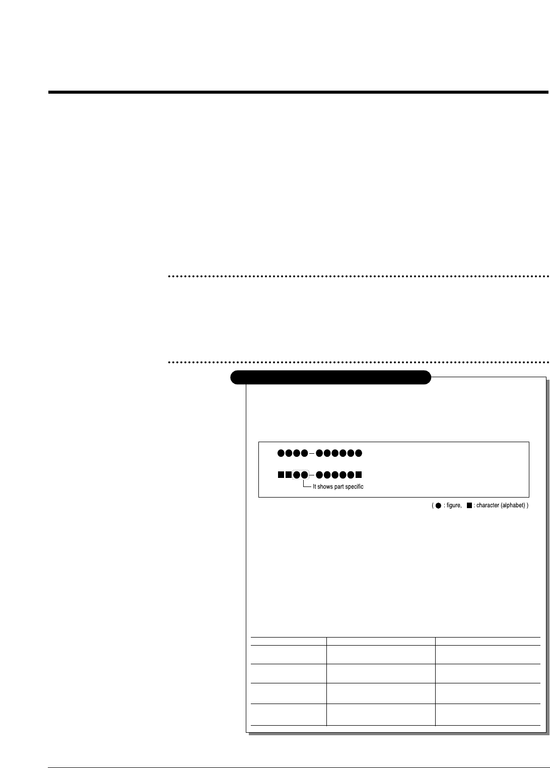
Part code and Description is quoted and controlled by determined standard. Refer to this determined
standard, it will help with ordering Part.
• There are two kinds of Part code inscription type.
Type 1 : Controlled by Company : It can be commonly used for all kinds of product SEC produce.
Mostly, electronics Parts.
Type 2 : Controlled by Division : It is used or one produce. Mostly, Mostly, mechanical Parts.
• A/S privately used part : It is only used for A/S .
• Ass’y part :
Assembled by more than 2 Parts. If necessary part is not A/S Part, Ass’y part including
necessary par can be used. It is shown in the diagram and drawing of SVC manual.
• Ass’y part and A/S privately used Part is distinguished by part Code and Description.
The are inscription type 2. It is recognized by Part character and front side of description.
Way to observe Part Code & Description
ex ) 2007-007961
ex ) JB96-01268A
R-CHIP
ELA UNIT-COVER TOP
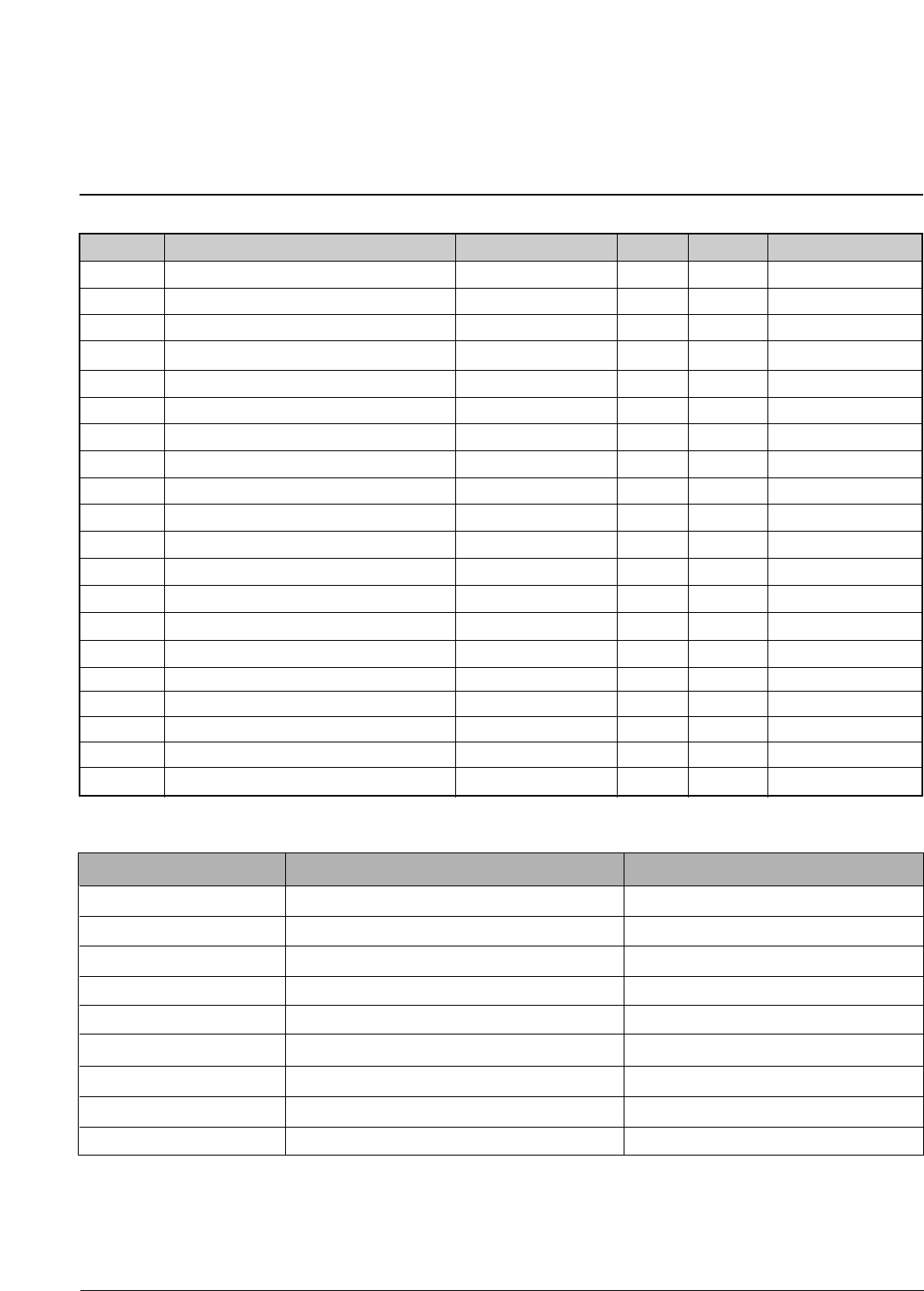
5-1 Main Assembly Exploded view .......................................................... page(5-2)
5-2 Main Cover Assembly Exploded view............................................... page(5-4)
5-3 Scanner Assembly Exploded view ................................................... page(5-6)
5-4 OPE Unit Exploded view...................................................................... page(5-8)
5-5 Engine Ass’y Exploded view............................................................... page(5-10)
5-6 ASF Unit Exploded view ..................................................................... page(5-12)
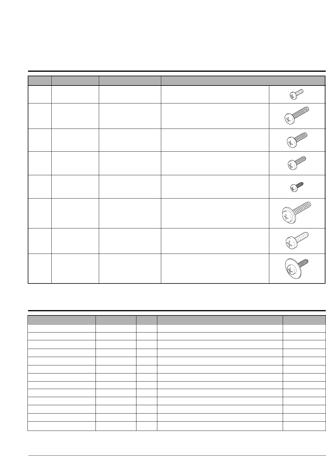
5-7 Screw ..................................................................................................... page(5-14)
5-8 SMPS Parts Lists ................................................................................ page(5-14)
5-2 Samsung Electronics
Exploded View and Parts List
5-1 Main Assembly Exploded view
0
13
1-1
1-2
8
7
7-1
7-2
10
11
9
S6 S3
12
6
5
4
S7
S7
S6
S6
S6
S6
13
Samsung Electronics 5-3
Exploded View and Parts List
NO DESCRIPTION SEC CODE Q’TY SA REMARK
< Main Assembly Parts List >
SA. : Service Available
0 SCX-1100 X
1 ELA-UNIT-OPE/SCANNER ASS’Y Refer to table below 1 O
1-1 ELA UNIT-OPE ASS’Y(1100) Refer to table below 1 O
1-2 ELA-UNIT-UNIT SCANNER(1100) * 1 X
3 MEA UNIT-FEEDER JB97-01535A 1 O
4 PBA MAIN-MAIN JB92-01201A 1 O
5 ELA UNIT-ENGINE ASS’Y JB96-01330A 1 O
6 MEA-COVER MAIN JB97-01539A 1 O
7 MEA-COVER REAR * 1 X
7-1 PMO-COVER REAR * 1 X
7-2 PMO-DOOR SIDE * 1 X
8 PMO-GUIDE EXTENSION JB72-01140A 1 O
9 SMPS-MAGIC JB44-00017A 1 O 110/220 VAC
10 LABEL SHEET-SMPS * 1 X
11 PMO-COVER SMPS JB72-01146A 1 O
12 CBF HARNESS-POWER GND * 1 X
13 CBF HARNESS-MAIN POWER JB39-00129A 1 O
S3 SCREW-TAPPING * 2 X M 3 X 8 mm
S6 SCREW-TAPTITE * 9 X M 3 X 10 mm
S7 SCREW-TAPTITE * 5 X M 3 X 6 mm
O: Service available X: Service not available
MODEL ELA-UNIT-OPE/SCANNER ASS’Y ELA UNIT-OPE ASS’Y
SCX-1100/XEF JB96-01343D JB96-01342D
SCX-1100/XEP JB96-01343E JB96-01342E
SCX-1100/XEU JB96-01343A JB96-01342A
SCX-1100/XFA JB96-01343F JB96-01342A
SCX-1100/XIL JB96-01343B JB96-01342B
SCX-1100/XIP JB96-01343F JB96-01342F
SCX-1100/XSH JB96-01343F JB96-01342F
SCX-1100/XSS JB96-01343F JB96-01342F
SCX-1100D/XSH JB96-01343F JB96-01342F
5-4 Samsung Electronics
Exploded View and Parts List
5-2 Main Cover Assembly Exploded view
3
2
1
3-2
3-1
3-3
6
5
0
4
S8 7
Samsung Electronics 5-5
Exploded View and Parts List
NO DESCRIPTION SEC CODE Q’TY SA REMARK
< Main Cover Assembly Parts List >
SA. : Service Available
O: Service available X: Service not available
0 MEA-COVER MAIN JB97-01539A 1 O
1 PMO-DOOR FRONT JB72-01144A 1 O
2 PM-COVER MAIN * 1 X
3 MEA-STACKER * 1 X
3-1 PMO-BASE STACKER JB72-01143A 1 O
3-2 PMO-EXIT TRAY MIDDLE JB72-00978C 1 O
3-3 PMO-EXIT TRAY EXTENSION JB72-00982C 1 O
4 FOOT-RUBBER JB61-40901A 2 O
5 MPR-FELT UPPER JB74-00014A 1 O
6 MPR-FELT LOWER JB74-00015A 1 O
7
CBF HARNESS-MAIN_COVER OPEN
JB39-00116A 1 O
S8 SCREW-SPECIAL * 1 X M3 X 8 mm
5-6 Samsung Electronics
Exploded View and Parts List
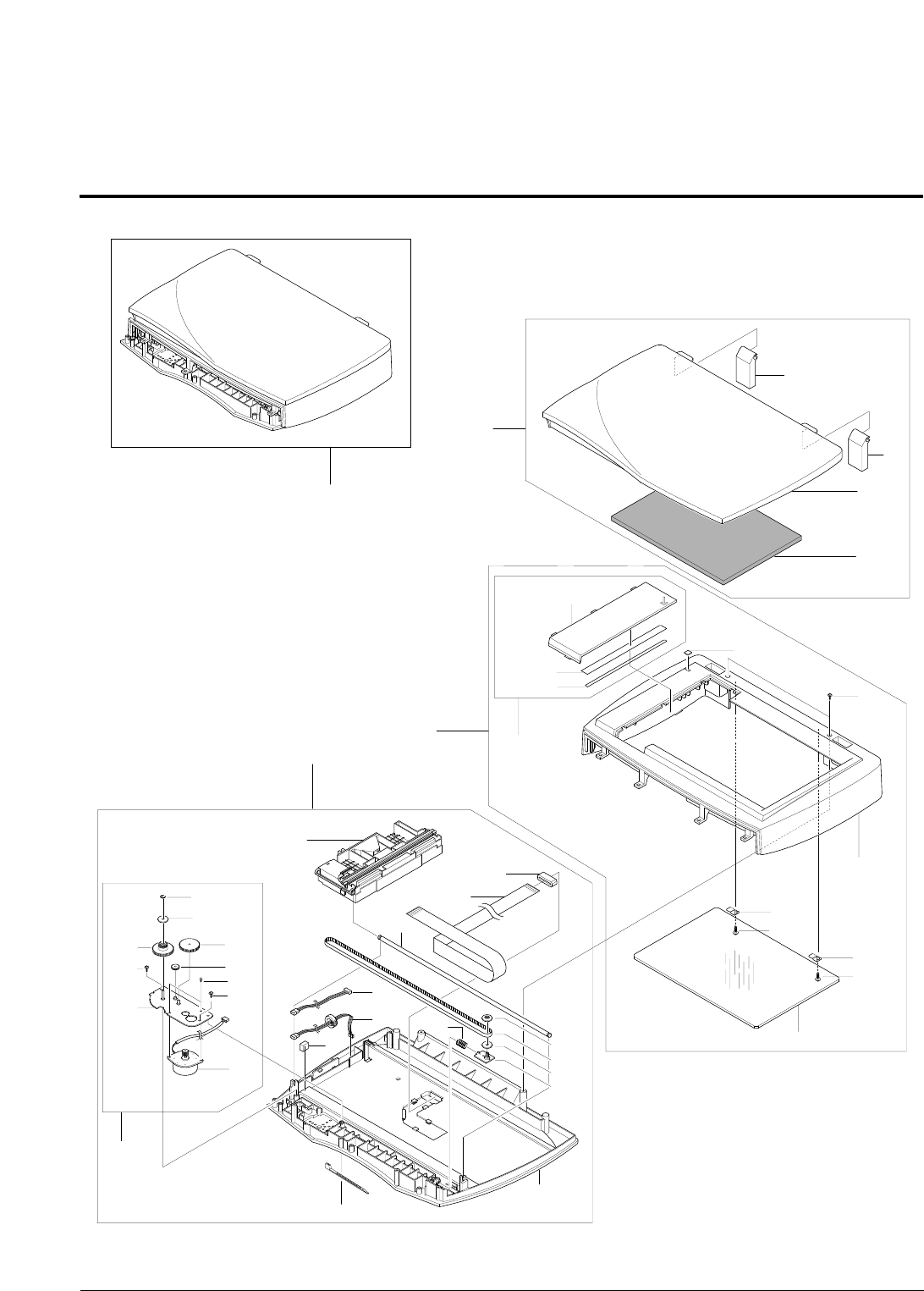
5-3 Scanner Assembly Exploded view
1-1
1-2
1-3
1-3
1
22-4
2-2
2-4-3
2-4-2
2-4-1
2-5
2-3
2-1
2-1
S3
S3
3
0
3-8
3-8-1
3-8-7
3-8-5
3-8-3
3-8-2
3-8-6
3-8-4
S7
S6
3-12
3-11
3-10
3-3
3-13
3-14
3-5
3-1
3-2
3-4
3-7
3-6
3-9
S6
S6
3-15

Samsung Electronics 5-7
Exploded View and Parts List
< Scanner Assembly Parts List >
SA. : Service Available
NO DESCRIPTION SEC CODE Q’TY SA REMARK
0 ELA UNIT-SCANNER * 1 X
1 MEA-COVER PLATEN JB97-01560A 1 O
1-1 MPR-WHITE SPONGE SHEET * 1 X
1-2 PMO-COVER PLATEN(1100) * 1 X
1-3 PMO-HINGE (3 IN 1) * 2 X
2 MEA-SCAN UPPER * 1 X
2-1 IPR-HOLDER GLASS * 2 X
2-2 PMO-SCAN UPPER * 1 X
2-3 MCT-SCAN GLASS * 1 X
2-4 MEA-DUMMY (3 IN 1) * 1 X
2-4-1 TAPE-DOUBLE FACE * 1 X
2-4-2 LABEL(P)-SHADING * 1 X
2-4-3 PMO-SCAN DUMMY(3IN1) * 1 X
2-5 LABEL(P)-ACTUATOR (3 IN 1) * 1 X
3 MEA-SCAN LOWER * 1 X
3-1 BELT-TIMING GEAR 6602-001067 1 O
3-2 SPRING-BELT * 1 X
3-3 ICT-SHAFT CCD * 1 X
3-4 PMO-PULLEY * 1 X
3-5 PMO-HOLDER BELT * 1 X
3-6 PMO-SCAN LOWER * 1 X
3-7 PMO-HOLDER BELT * 1 X
3-8 ELA ETC-BRKT SCAN MOTOR JB96-01344A 1 O
3-8-1 RING-E * 2 X
3-8-2 MOTOR-SCAN JB31-00011A 1 O
3-8-3 GEAR-TIMING * 1 X
3-8-4 GEAR-IDLE * 1 X
3-8-5 GEAR-REDUCTION * 1 X
3-8-6 IPR-BRKT SCAN MOTOR * 1 X
3-8-7 PMO-HOLDER BELT * 1 X
3-9 CABLE-TIE * 1 X
3-10 ELA MODULE-SCANNER(MUAX) JB96-01317A 1 O
3-11 CBF-FLAT CBL-CCD JB39-00132A 1 O
3-12 CORE-FERRITE * 1 X
3-13 CBF-HARNESS-MAIN OPE JB39-00148A 1 O
3-14 CUSHION PAD-DAMPER JB69-00186A 1 X
3-15 CBF-HARNESS-SCAN MOTOR JB39-00147A 1 O
S3 SCREW-TAPPING * 2 X M3 X 8 mm
S6 SCREW-TAPTITE * 4 X M3 X 10 mm
S7 SCREW-TAPTITE * 2 X M3 X 6 mm
O: Service available X: Service not available
5-8 Samsung Electronics
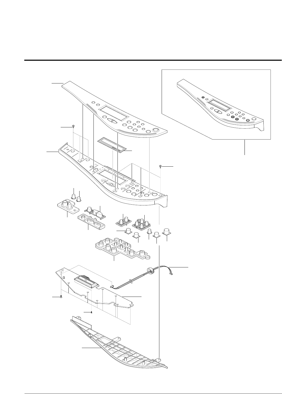
Exploded View and Parts List
5-4 OPE Unit Exploded view
0
19
3
S6
S6
1
5
4
2
S3
S5
15
67
16
17
8
9
11
18
12 13
10
14
Samsung Electronics 5-9
Exploded View and Parts List
< OPE Unit Parts List >
SA. : Service Available
NO DESCRIPTION SEC CODE Q’TY SA REMARK
0 ELA UNIT-OPE ASS’Y(1100) Refer to table below 1 O
1 PMO-OPE UPPER * 1 X
2 PMO-OPE LOWER * 1 X
3 PMO-OPE PANEL(1100) Refer to table below 1 O
4 PBA-MAIN-OPE JB92-01202A 1 O
5 CBF HARNESS-MAN OPE * 1 X
6 PMO-KEY ANSWER * 1 X
7 PMO-KEY SAVE(1100) * 1 X
8 PMO-KEY SCROLL * 1 X
9 PMO-KEY ENTER(1100) * 1 X
10 PMO-KEY ZOOM * 1 X
11 PMO-KEY BLACK * 1 X
12 PMO-KEY COLOR * 1 X
13 PMO-KEY SPECIAL(1100) * 1 X
14 PMO-KEY SCAN * 1 X
15 PMO-KEY POWER(1100) * 1 X
16 RMO-RUBBER SAVE(1100) * 1 X
17 RMO-RUBBER SETUP(1100) * 1 X
18 RMO-RUBBER COPY(1100) * 1 X
19 SHEET-LCD * 1 X
S3 SCREW-TAPPING * 8 X M 3 X 8 mm
S5 SCREW-TAPPING * 2 X M 2.5 X 5 mm
S6 SCREW-TAPTITE * 6 X M 3 X 10 mm
O: Service available X: Service not available
MODEL ELA-UNIT-OPE ASS’Y PMO-OPE APANEL
SCX-1100/XEF JB96-01342A JB72-01196A
SCX-1100/XEP JB96-01342B JB72-01196B
SCX-1100/XEU JB96-01342D JB72-01196D
SCX-1100/XFA JB96-01342E JB72-01196E
SCX-1100/XIL JB96-01342A JB72-01196A
SCX-1100/XIP JB96-01342F JB72-01196F
SCX-1100/XSH JB96-01342F JB72-01196F
SCX-1100/XSS JB96-01342F JB72-01196F
SCX-1100D/XSH JB96-01342F JB72-01196F
5-10 Samsung Electronics
Exploded View and Parts List
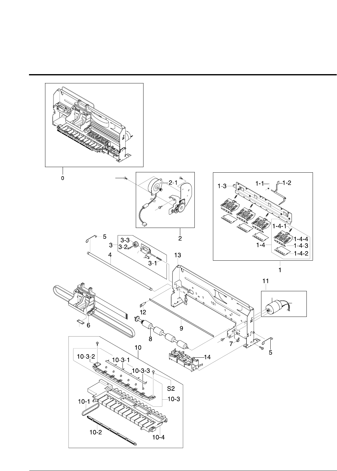
5-5 Engine Ass’y Exploded view
3-5
3-4
S7
S7
15
S7
11-1 11-2

Samsung Electronics 5-11
Exploded View and Parts List
< Engine Ass’y Parts List >
SA. : Service Available
NO DESCRIPTION SEC CODE Q’TY SA REMARK
O: Service available X: Service not available
0 ELA UNIT-ENGINE ASSY JB96-01330A 1 O
1 MEC-HOLDER ROLLER JB75-11111A 1 O
1-1 SPRING-ES ACTUATOR JB61-70919A 1 O
1-2 PMO-ACTUATOR FEED JB72-40993A 1 O
1-3 PMO-HOLDER ROLLER SUB * 1 X
1-4 MEC-FRIC ROLLER * 4 X
1-4-1 SPRING-ES FRICTION * 1 X
1-4-2 IPR-DEFLECTOR * 1 X
1-4-3 ICT-FRICTION ROLLER * 1 X
1-4-4 PMO-HOLDER F/R * 1 X
2 MEA UNIT-BRKT LF JB97-01536A 1 O
2-1 MOTOR-STEP LF(V) JB31-00007A 1 O
3 MEC-PULLEY IDLE JB75-11110A 1 O
3-1 SPRING-CS PULLEY * 1 X
3-2 ICT-SHAFT PULLEY IDLE * 1 X
3-3 PMO-PULLEY IDLER * 1 X
3-4 PMO-HOLDER PULLEY * 1 X
3-5 PMO-STOPPER PULLEY JB72-41212A 1 O
4 ICT-SHAFT CR JB70-40906A 1 O
5 SPRING-SHAFT CR JB61-70913A 2 O
6 MEA UNIT-C/R/SEC JB96-01303A 1 O
7 BEARING-FEED R JB66-10002A 1 O
8 MEC-ROLLER FEED JB75-11112A 1 O
9 PRP-ENCODER STRIP(V) JB72-00662A 1 O
10 MEC-FRAME BASE JB75-00170A 1 O
10-1 BELT-EXIT JB75-00171A 1 O
10-2 MEC-EXIT ROLLER JB75-10917A 1 O
10-3 MEC-HOLDER EXIT * 1 X
10-3-1 IPR-SPRING WHEEL * 1 X
10-3-2 PMO-HOLDER WHEEL * 1 X
10-3-3 MEA UNIT-WHEEL STAR * 6 X
10-4 MEC-SUB FRAME BASE JB75-11126A 1 O
11 ELA UNIT-C/R MOTOR JB96-01312A 1 O
11-1 MOTOR-DC CARRIAGE JB31-00005A 1 O
11-2 CBF-HARNESS-DC MOTOR JB39-00094A 1 O
12 SPRING-PS ENCODER JB61-70917A 1 O
13 MEC-FRAME MAIN JB75-00349A 1 O
14 MEC-FRAME HOME JB75-00174A 1 O
15 MPR-SHEET ENCODER JB74-00024A 1 O
S1 SCREW-MACHINE * 1 X
S2 SCREW-TAPPING * 3 X M3 X 10 mm
S6 SCREW-TAPTITE * 1 X M3 X 10 mm
S7 SCREW-TAPTITE * 2 X M3 X 6 mm
5-12 Samsung Electronics
Exploded View and Parts List
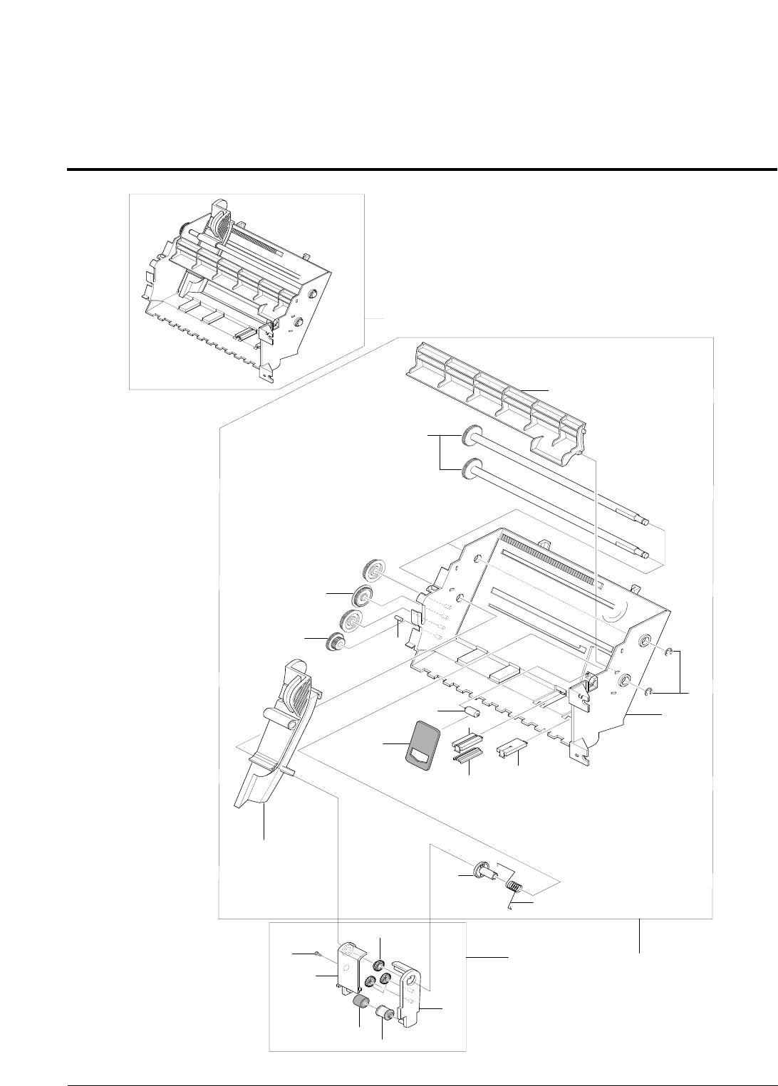
5-6 Feeder Unit Exploded view
1
2
2-5
1-11
1-4 1-5
1-3
S4
1-12
1-2
2-2
2-1
2-6 2-4
2-3
1-14 1-7
1-15 1-8
1-1
1-10
1-13
1-9
1-16
0

Samsung Electronics 5-13
Exploded View and Parts List
< Feeder Unit Parts List >
SA. : Service Available
NO DESCRIPTION SEC CODE Q’TY SA REMARK
0 MEA UNIT-FEEDER JB97-01535A 1 O
1 MEA UNIT-ASF W/O PICKUP * 1 X
1-1 RING-E * 2 X
1-2 SPRING-TORSION AC * 1 X
1-3 GEAR-IDLER ASF * 3 X
1-4 GEAR-DRIVER ASF * 1 X
1-5 ICT-PIN ASF BOSS * 1 X
1-6 PMO-COVER PCB * 1 X
1-7 PMO-HOUSING BUCKLER * 1 X
1-8 PMO-BUCKLER JAG * 1 X
1-9 PMO-COVER ASF * 1 X
1-10 PMO-ASF FRAME * 1 X
1-11 PMO-PAPER GUIDE * 1 X
1-12 PMO-PAPER CAPACITY * 1 X
1-13 PMO-SHAFT PICKUP * 2 X
1-14 PMO-ROLLER IDLER * 1 X
1-15 RMO-BUCKLER FRICTION JB73-00019A 1 O
1-16 MPR-PAD FRICTION * 1 X
2 MEA UNIT-PICKUP ROLL JB97-00965A 1 O
2-1 GEAR-PICKUP IDLER * 2 X
2-2 GEAR-DRIVE PICKUP * 1 X
2-3 PMO-HOUSING R * 1 X
2-4 PMO-PICKUP ROLL * 1 X
2-5 PMO-HOUSING L * 1 X
2-6 RMO-PICKUP RUBBER * 1 X
S4 SCREW-TAPPING * 1 X M2.6 X 6 mm
O: Service available X: Service not available
5-14 Samsung Electronics
Exploded View and Parts List
S1 6001-000485 SCREW-MACHINE PH,+,M2.6,L4,ZPC(YEL),SM20
S2 6002-000101 SCREW-TAPPING BH,+,2,M3,L10,ZPC(BLK),SM2
S3 6002-000175 SCREW-TAPPING PWH,+,2,M3,L8,ZPC(YEL),SM2
S4 6002-000308 SCREW-TAPPING PH,+,2,M2.6,L6,ZPC(YEL),SM
S5 6002-001065 SCREW-TAPPING PWH,+,2,M2.5,L5,ZPC(YEL),SM2
S6 6003-000196 SCREW-TAPTITE PWH,+,B,M3,L10,NI PLT,SWRC
S7 6003-000269 SCREW-TAPTITE BH,+,S,M3,L6,ZPC(YEL),SWRC
S8 6009-001251 SCREW-SPECIAL SM20C,P12,+,M3,L8,ZPC(YEL),MACHIN
5-7 Screw
5-8 SMPS Parts Lists
NO DESCRIPTION SEC CODE SPEC
DESCRIPTION SEC. CODE Q'TY SPECIFICATION LOCATION NO.
TR-SMALL SIGNAL 0501-000010 2 "KSC1008,NPN,800mW,TO-92,TP,120-240" "Q3,Q4"
AS-FET JB81-00229A 1 "SCX-1100,FQU2N60,600V, 2A ,-,-,-,-,-" Q2
AS-DIODE_SCHOTTKY JB81-00231A 1 "SCX-1100,SR204,40V, 2A,-,-,-,-,-" D4
AS-DIODE_FR JB81-00232A 1 "SCX-1100,ER502,200V, 5A,-,-,-,-,-" D5
AS-DIODE_ZENER JB81-00233A 1 "SCX-1100,MTZ9.1B,500MW (8.57V~9.01V),-,-,-,-,-" ZD1
AS-DIODE_ZENER JB81-00234A 1 "SCX-1100,1N4753A,1W 36V,-,-,-,-,-" ZD4
AS-DIODE_BRIDGE JB81-00235A 1 "SCX-1100,2KBP06M,600V, 2A,-,-,-,-,-" BD1
AS-TRANSFORMER JB81-00237A 1 "SCX-1100,MAGIC-V3,EE2525W ; MAGIC-V3,-,-,-,-,-" T1
AS-FUSE JB81-00239A 1 "SCX-1100,50T,250V 2.0A,-,-,-,-,-" F1
AS-FET CHIP SILICON JC81-00020A 1 "ML-7000,IRF9540(N),TO-220,-100V,-17A,0.2OHM,-,-" FOR_Q1
REACTOR-INR 10D-561K JC81-00407A 1 "SF-5100,INR 10D-561K,VARISTOR,-,-,-,-,-" TNR1
AS-R WIRE WOUND JC81-11404A 2 "SF6000,RWN1W 0.42J,-,-,-,-,-" "R17,R4"
AS-Q1 JF81-10908A 1 "ALPS-V2,SSP5N80A,800V,5A,-,-,-" Q1
6-1
Samsung Electronics
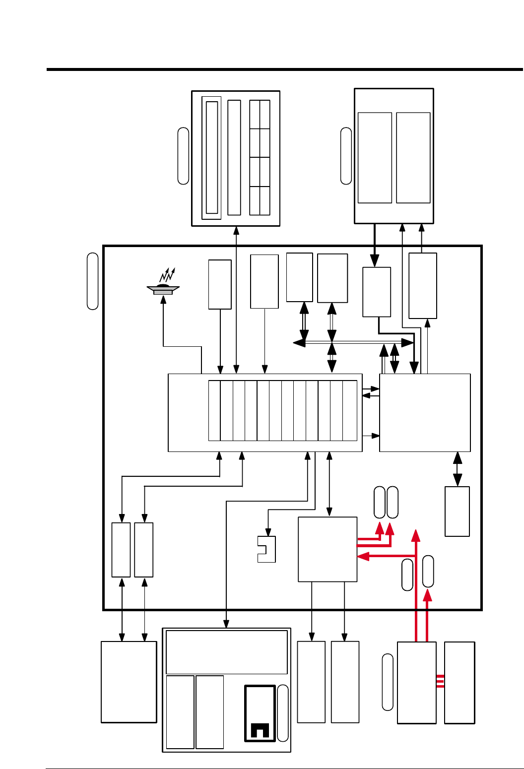
6. Block Diagram
SMPS
(15)
Main
Controller
(U21)
Image
Processor
OA-980
Main Clock
10MHz
RESET
CONTROLLER
FLASH ROM
ADC
16bit
(U16)
SDRAM
1M* 16bit
(U9)
CARRIER
MOTOR
LINE FEED
MOTOR
(30V, 3.3V)
AC
(110~240V)
CCD Module
( COLOR 600DPI )
SCAN MOTOR
( Bi-POLAR STEP )
SCAN STEPPER
MOTOR DRIVER
COLOR
CARTRIDGE
MONO
CARTRIDGE
PRINT HEAD(2PEN)
60DPI DOUBLE HEIGHT
ENCORDER
SENSOR
ENCODER
USB CONN
PC
48MHz
(AU1)
BUZZER
(U27)
SDRAM
(4M 16bit)
1284 CONN
(U1)
HEAD
Driver
IC
/REQ /ACK
KEY PANNEL
LCD
Mcro Controller (U1)
(U5)
(U10,U14)
POWER
MAIN
OPE
SCANNER
+30V
+5V
+12V
+3.3V
PAPER EXIT
SENSOR
(U4)
Motor
Driver
& Regul at or
(U13)
(U7)
ARM7TDM
MEM CNTR
Head Control I/F
SCAN CNTR
DERASTERIZER
UART 3
IEEE 1284
TIMERS
I/O PORT
INT. CNTR
USEB
DM 2
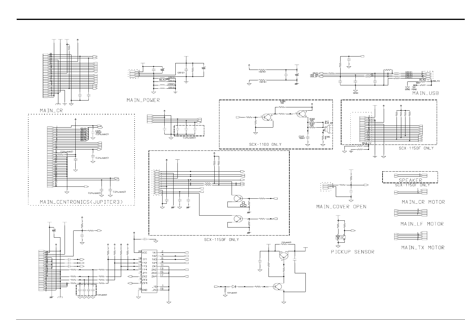
7. Connection Diagram
7-1
R26
Q7
KSA1203_YTF
0
R30
100 R27
CN4-3
0
CN14-10
CCD
BE
(UNUSED)
C
(UNUSED)
(UNUSED)
R35 0
OPE_MAGIC
CN16-15
LIU
CN16-7
CN16-8
5V
DGND
10K
CN16-12
CN1-7
R153
CN16-3
5V
R375
C333
680
100nF
DGND
100nF
CN14-6
C334
Q1
2SC2812L6-TA
13
2
1K
R366
3.3V
CN5-11
0
R209
CN1-17
L8 0
3.3V
5V 5V
0L7
3
2
Q4
2SC2812L6-TA 1
C194
100pF
13
100pF
C81
DGND
11.75V
100nF
C209
2
14
0
L10
L9
11
100 R36
CN12-2
0
R37
R33R28
10K 10K TP365
10KR149
CN1-8
50V
330uF
C50
47KR136
R138 47K
L12 0
FGND
0
L11
CN14-35
FGND
CN5-22
CN5-23
CN1-3
CN5-4
CN1-1
CN5-3
100pF
C337
DGND
R135
R137 1K
1K
5
C39 47pF
CN16-5
CN1-6
CN5-10
DGND
4
DGND
CN8-4
DGND
CN5-9
CN14-28
DGND
DGND
CN14-31
C98
CN1-15
C95
10nF
3
10nF
CN7-1
1
R144
100nF
C205
DGND
CN1-26
DGND DGND
5V
CN4-2
C204
22pF
0L6
DGND
L5
R380 180K
5045-03A
CN3-1
30V
CN1-22
DGND
CN5-7
C338
100pF
100nF
C197
DIN15
CN16-1
CN14-27
C33
100nF
22pF
C203
CN5-12
CN5-13
GND30
CN13-2
CN16-6
C49
100nF
3.3V
CN1-25
U6
CD74HCT244M
CN1-13
AGND
CN16-9
CN4-1
5045-04A
30V
USB20-4W2100
CN8-1
5V
CN11-4
CN14-17
CN14-8
INV_POWER
CN6-1
3711-000225
CN4-4
DGND
CN1-20
R147
R148 10K
10K
11.75V
R44
22
CN6-3
CN6-4
CN6-2
C80
100pF
2K
R126
DGND
2K
C35 47pF
1
R123
47pF
C32
DGND
3711-002815
CN9-1
CN14-16
1.5K
16V
100uF
C118
R384
8
CN14-3
CN5-14
CN14-15
DGND
BD10
1.5K
CN1-10
R155
CN14-2
5V
DGND
CN14-20
100pF
C181
100R145
CN14-23
CN14-33
GND12
CN14-11
CN16-2
100nF
C119
C58
220pF
9
R383
CN14-34
3
68K
44.7K
R146
KSA1182-Y
Q9
DGND
100nF
C66
100
1/8W
R24
DGND
CN14-7
CN1-18
5.1K
R8
R23
47K
DGND
CN14-22
47pF
C38
5V
DGND
100 R29
CN1-12
INV_POWER
CN16-14
CN1-14
2SC2812L6-TA
Q10
GND12
7
CN5-16
CN5-17
CN5-15
R378
TP366
5V
CN14-9
0
CN1-24
11.75VA
CN5-2
FPC_24
CN5-1
BD6 0,5%
TP230
6
RPI-441C1
U5
CN1-4
BD12
CN14-25
100nF
C208
CN14-1
CN14-32
100 R34
5V
CN11-2
TP77
CN14-36
12
5VA
BD13
DGND
CN14-21
CN1-16
BD11
C82
100pF
10K
10K
R377
R25
CN5-8
CN14-4
CN1-5
5V
AGND
CN1-21
CN14-26
CN14-13
CN14-5
CN5-5
DGND
C336
100pF
TP78
CN14-29
TP367
1
3
2
DGND
2SC2812L6-TA
Q5
C3
3.3V
CN11-1
R152
25V
100uF
CN1-19
2
CN8-2
DGND
5V
4.7K
R373
CN16-4
DGND
11.75V
RB420D T147
D8
100nF
C97
CN1-11
AGND
CN13-1
CN1-23
AGND
5V
CN5-24
AGND
3K
R125
10
R207 10K
10K
R154
CN14-12
R38
10K
CN16-13
CN1-9
CN14-18
220pF
C7
CN5-18
CN5-19
CN5-6
10K
DGND
5
5V
R43
CN3-3
5V
220pF
C1
CN12-3
C67
CN14-19
16V
100uF
CN6-5
CN16-11
TP363
TP364
CN14-30
CN5-21
CN14-14
30V
DGND
CN5-20
0,5%BD7
C182
100nF
CN8-3
DGND
5V
AGND
CN11-3
CN1-2
CN16-10
R45
22K
GND30
CN12-1
10nFC96
GND30
CN14-24
3K
R124
_ERROR
_INIT
KEYTONE
CN3-2
3711-000198|scon_pin3_2.5mm
_P_PICKUP
REG1_SEN
LAMP_ON
_STB
_CML_ON
E_DP
ADF_IA0
ADF_PHA
_D_SCAN
_D_DET
_ADF_DET
VOUT_G
VOUT_R
VOUT_B
CCD_RS
HOME
OPE_TXD
OPE_TXDD
_OPE_RST
_OPE_RES
OPE_RXD
_OPE_RES
OPE_TXDD
ADF_IB1
ADF_IB0
ADF_PHB
ADF_IA1
_HOOK_OFF
_RING_DET
MODEM_RX
DP
RECALL
MODEM_TX1
REMOTE
MODEM_TX2
CCD_TG
CCD_CLK1
CCD_CLK2
CR_NA
CD(0:7)
SLCT
PE
BUSY
_ACK
_SLCTIN
_AUTOFD
LF_NB
LF_A
LF_NA
LF_B
SCAN_NB
SCAN_B
SCAN_NA
SCAN_A
COVER_OPEN
PH_ID2
PENABLE
PLOAD
PDATA3
PDATA2
PDATA1
PDATA0
PCLK
LDCS
LATCHCTL
ACLK
AGATE
_SF_POR
OK2PRT
CHY
CHX
SPK_OUT-
SPK_OUT+
CR_A
PULLUP
PH_ID1
Samsung Electronics

Repair Manual
Repair Manual
1. Block Diagram
2. Connection Diagram
3. Circuit Description
4. Schematic Diagrams
CONTENTS
INKJET RINTER(MFP)
SCX-1100
1
1-1
Samsung Electronics
BLOCK DIAGRAM
Repair Manual
1. Block Diagram
SMPS
(15)
Main
Controller
(U21)
Image
Processor
OA-980
Main Clock
10MHz
RESET
CONTROLLER
FLASH ROM
ADC
16bit
(U16)
SDRAM
1M* 16bit
(U9)
CARRIER
MOTOR
LINE FEED
MOTOR
(30V, 3.3V)
AC
(110~240V)
CCD Module
( COLOR 600DPI )
SCAN MOTOR
( Bi-POLAR STEP )
SCAN STEPPER
MOTOR DRIVER
COLOR
CARTRIDGE
MONO
CARTRIDGE
PRINT HEAD(2PEN)
60DPI DOUBLE HEIGHT
ENCORDER
SENSOR
ENCODER
USB CONN
PC
48MHz
(AU1)
BUZZER
(U27)
SDRAM
(4M 16bit)
1284 CONN
(U1)
HEAD
Driver
IC
/REQ /ACK
KEY PANNEL
LCD
Mcro Controller (U1)
(U5)
(U10,U14)
POWER
MAIN
OPE
SCANNER
+30V
+5V
+12V
+3.3V
PAPER EXIT
SENSOR
(U4)
Motor
Driver
& Regul at or
(U13)
(U7)
ARM7TDM
MEM CNTR
Head Control I/F
SCAN CNTR
DERASTERIZER
UART 3
IEEE 1284
TIMERS
I/O PORT
INT. CNTR
USEB
DM 2
- This Document can not be used without Samsung's authorization -

2
2-1
Samsung Electronics
CONNECTION DIAGRAM
Repair Manual
2. Connection Diagram
• Reffer to the Schematic diagram(see page 4-2)
- This Document can not be used without Samsung's authorization -
3
3-1
Samsung Electronics
CIRCUIT DESCRIPTION
Repair Manual
3. Circuit Description
3-1. GENERAL DESCRIPTION
Main circuit consists of mainly consists of CPU and the controller part with various types of built-in I/O device driver(built-in
RISC Processor Core: ARM7TDMI), system memory part, OA980 controlling input of image received from media and con-
version, CF(COMPACT storage card) interface part. The following nomenclatures by section is the same as those listed in
the circuit diagram.
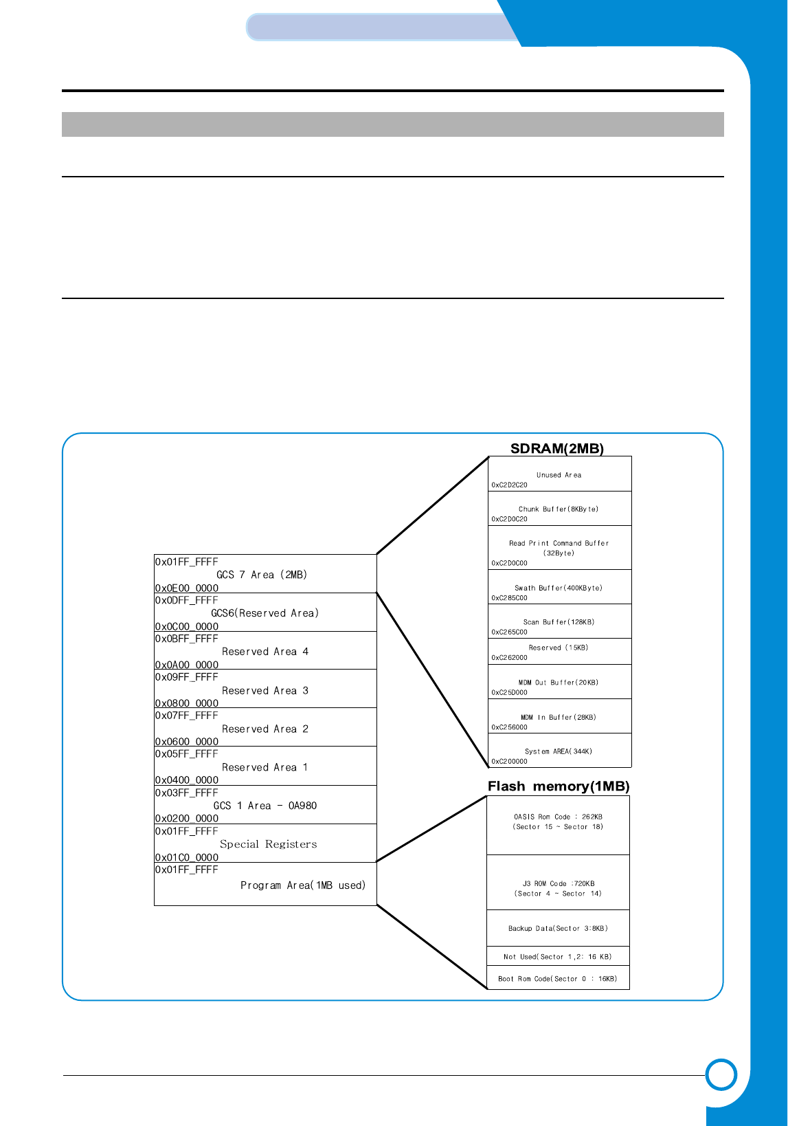
3-2. MEMORY MAP
The entire Addressing area provided by MAIN CONTROLLER(S3C46MOX(Jupiter3)) is 256MBytes from 0x00000000 to
0x10000000, and the Max. Address Range for each External Chip Select is 32M Byte or Half word from 0x000000 to
0x01FFFFFF and embodied with Big-Endian Bus interface. MEMORY area is divided into EXTERNAL ROM and RAM
areas(See (Figure 1)), and the areas actually used are 2M/8M BYTES SDRAM and 1M BYTES ROM(FLASH MEMORY).
In case of SDRAM, it uses 0xC200000h ~ 0xC3FFFFFh(2MB), and ROM uses 0x0000000h ~ 0x0FFFFFh area.
<Figure 1. S3C46MOX(Jupiter3) MEMORY MAP>
◊MAIN PBA
- This Document can not be used without Samsung's authorization -

3-2
CIRCUIT DESCRIPTION
Samsung Electronics
Repair Manual
3-3.DETAILED DESCRIPTION
3-3-1 BLOCK DIAGRAM and MAIN CONTROLLER description
3-3-1-1 GENERAL DESCRIPTION
MAIN CONTROLLER(S3C46MOX(Jupiter3),U15) consists of this system consists of CPU(ARM7TDMI RISC PROCES-
SOR), 8K BYTES CACHE, DATA and ADDRESS BUS, PLL deriding input frequency and CLOCK CONTROL part,
SERIAL COMMUNICATION part supporting UART, PRINT HEAD control part, PARALLEL PORT INTERFACE part,
USB INTERFACE part, External DMA part for receiving data from external COLOR IMAGE PROCESSOR(OA-
980,U21), MEMORY and EXTERNAL BANK control part, SYNCHRONOUS SERIAL INTERFACE control part for inter-
facing Thunderbolt, and LF/CR Motor drive control and general purpose I/O control parts.(See Figure 2 )
3-3-2 S3C46MOX(Jupiter3) FUNCTION DESCRIPTION
3-3-2-1 SYSTEM CLOCK
There are two ways of Clock input method. One is the method to make Master Clock(MCLK) at the internal PLL by con-
necting X-tal and Capacitor to the outside, and another method is to use MCLK(When inputting 40MHz) directly, which
supplies maximum 40MHz Clock to the EXTCLK terminal(PIN65). The range of frequency being input in case of using
X-tal is limited to 4MHz~10MHz. This system uses SSCG(FS781) with a 10MHZ X-tal outside to make MCLK, and sup-
plies Clock to the XIN terminal(PIN67) of ASIC by expanding Spectrum with bandwidth about 1.5% in comparison with
the basic frequency by using this IC. Inside the ASIC, the PLL makes 66MHz MCLK signal, which is the basic operation
frequency of the System. Also, this PLL makes 48MHz, the operation frequency of USB Controller.
3-3-2-2 DATA AND ADDRESS BUS CONTROL
1. /RD & /WR
/RD & /WR SIGNAL are synchronized with the inside MCLK(66MHZ) and becomes active to Low.
These signal are Strobe Signal used to Read or Write data when each Chip Select becomes active connected to
/RD,/WR PIN of RAM, ROM, OA-980.
2. CHIP SELECT (/ROMCS, /IP_CS,/MED_CS,/SCS0,/SCS1)
- /ROMCS : FLASH MEMORY(U7) CHIP SELECT (LOW ACTIVE)
- /IP_CS : OA-980(U21) CHIP SELECT
(LOW ACTIVE)
- /SCS1 : SDRAM(OPTION)(U12) CHIP SELECT (LOW ACTIVE)
In case each Chip Select is low, it may Read or Write data.
3. D0 ~ D15
- 16BIT DATA BUS
4. A0 ~ A24
- ADDRESS BUS (A23 ~ A24 RESERVED)
- This Document can not be used without Samsung's authorization -
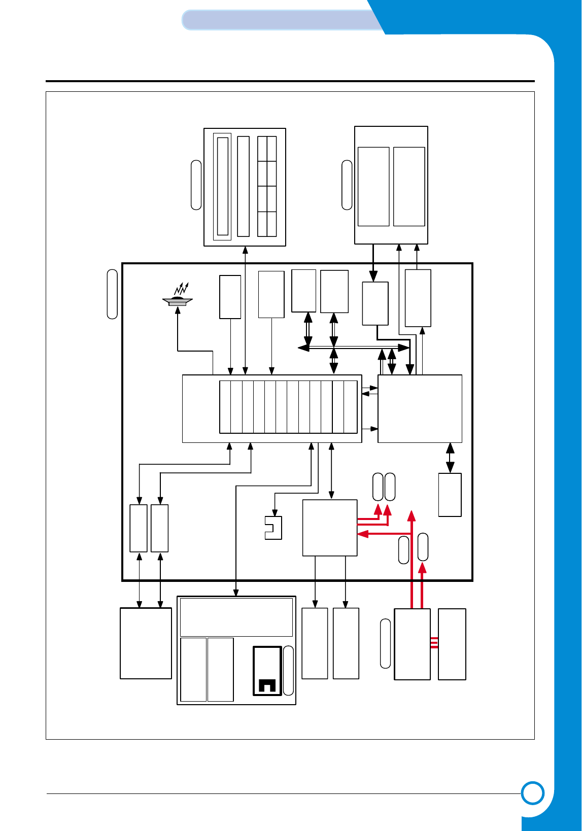
3-3
Samsung Electronics
CIRCUIT DESCRIPTION
Repair Manual
<Figure 2. Block Diagram of Main Part>
SMPS
(15)
Main
Controller
(U21)
Image
Processor
OA-980
Main Clock
10MHz
RESET
CONTROLLER
FLASH ROM
ADC
16bit
(U16)
SDRAM
1M* 16bit
(U9)
CARRIER
MOTOR
LINE FEED
MOTOR
(30V, 3.3V)
AC
(110~240V)
CCD Module
( COLOR 600DPI )
SCAN MOTOR
( Bi-POLAR STEP )
SCAN STEPPER
MOTOR DRIVER
COLOR
CARTRIDGE
MONO
CARTRIDGE
PRINT HEAD(2PEN)
60DPI DOUBLE HEIGHT
ENCORDER
SENSOR
ENCODER
USB CONN
PC
48MHz
(AU1)
BUZZER
(U27)
SDRAM
(4M 16bit)
1284 CONN
(U1)
HEAD
Driver
IC
/REQ /ACK
KEY PANNEL
LCD
Mcro Controller (U1)
(U5)
(U10,U14)
POWER
MAIN
OPE
SCANNER
+30V
+5V
+12V
+3.3V
PAPER EXIT
SENSOR
(U4)
Motor
Driver
& Regul at or
(U13)
(U7)
ARM7TDM
MEM CNTR
Head Control I/F
SCAN CNTR
DERASTERIZER
UART 3
IEEE 1284
TIMERS
I/O PORT
INT. CNTR
USEB
DM 2
- This Document can not be used without Samsung's authorization -
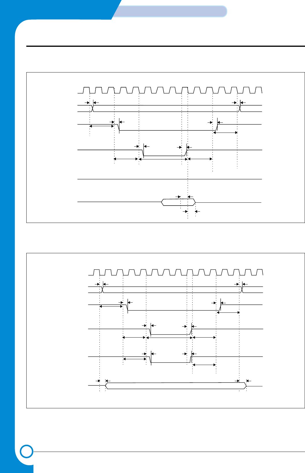
3-4
CIRCUIT DESCRIPTION
Samsung Electronics
Repair Manual
<Figure 3. Flash Memory Read Timing>
<Figure 4. Flash Memory Write Timing>
EXTCLK
nGCSx
nGCSx
ADDR
tRWD
tRAD
Tacs
tRCD
nWE
DATA
nBEx
Tacc Toch
Tcah
Tocs
tRCD
tRWD
tRDD
tRAD
tRDH
’1’
EXTCLK
nGCSx
nGCSx
ADDR
tRWD
tRAD
Tacs
tRCD
nWE
DATA
nBEx
Tacc Toch
Toch
Tcah
Tocs
tRWBED
Tcos
tRDD
tRWBED
tRCD
tRWD
tRDD
tRAD
- This Document can not be used without Samsung's authorization -
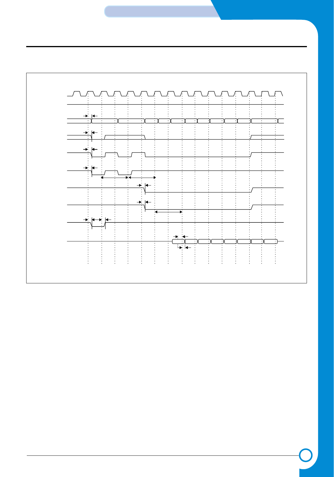
3-5
Samsung Electronics
CIRCUIT DESCRIPTION
Repair Manual
<Figure 5. SDRAM Read Timing>
SCLK
SCKE
ADDR/BA
AP/A10
nGCSx
nSRAS
nSCAS
nBEx
nWE
DATA
’1’tSAD
tSAD
tSCSD
tSRD
Trp Trcd tSCD
tSBED
Tcl
tSWD
tSDS
tSDH
- This Document can not be used without Samsung's authorization -
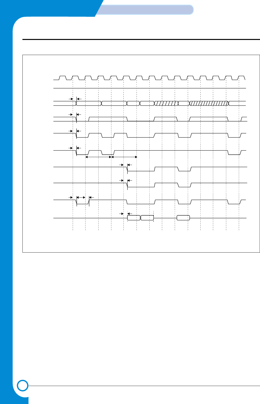
3-6
CIRCUIT DESCRIPTION
Samsung Electronics
Repair Manual
<Figure 6. SDRAM Write Timing>
SCLK
’1’
SCKE
ADDR/BA
AP/A10
nGCSx
nSRAS
nSCAS
nBEx
nWE
DATA
tSAD
tSAD
tSCSD
tSRD
Trp Trcd
tSWD
tSDD
tSDD
tSBED
tSCD
- This Document can not be used without Samsung's authorization -
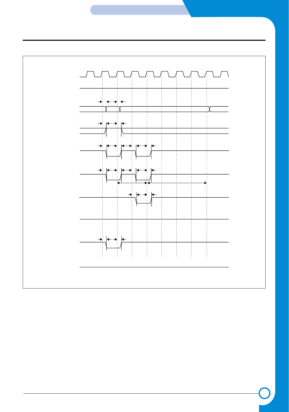
3-7
Samsung Electronics
CIRCUIT DESCRIPTION
Repair Manual
<Figure 7. SDRAM Write Timing>
SCLK
SCKE
ADDR/BA
AP/A10
nGCSx
nSRAS
nSCAS
nBEx
nWE
DATA
tSAD
’1’
’1’
’HZ’
tSAD
tSCSD
tSRD tSRD
tSCD
tSWD
tSCSD
tSAD
Trp Trc
- This Document can not be used without Samsung's authorization -
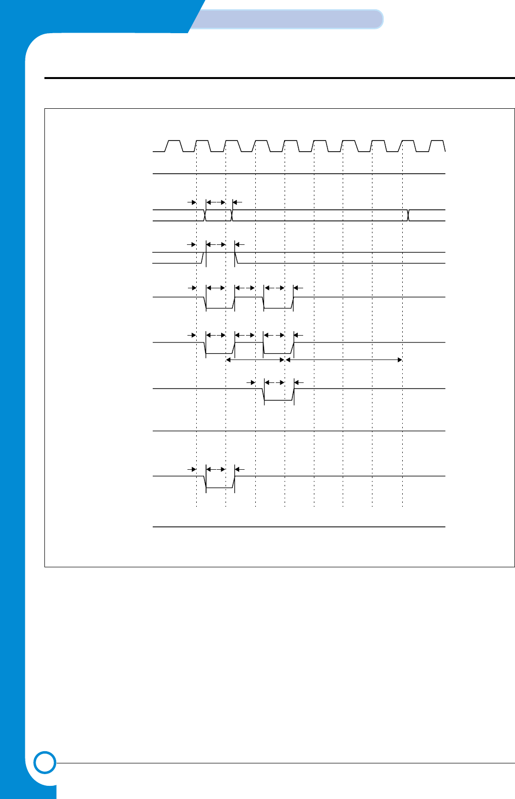
3-8
CIRCUIT DESCRIPTION
Samsung Electronics
Repair Manual
<Figure 8. SDRAM auto Refresh Timing>
SCLK
SCKE
ADDR/BA
AP/A10
nGCSx
nSRAS
nSCAS
nBEx
nWE
DATA
tSAD
’1’
’1’
’HZ’
tSAD
tSCSD
tSRD tSRD
tSCD
tSWD
tSCSD
tSAD
Trp Trc
- This Document can not be used without Samsung's authorization -
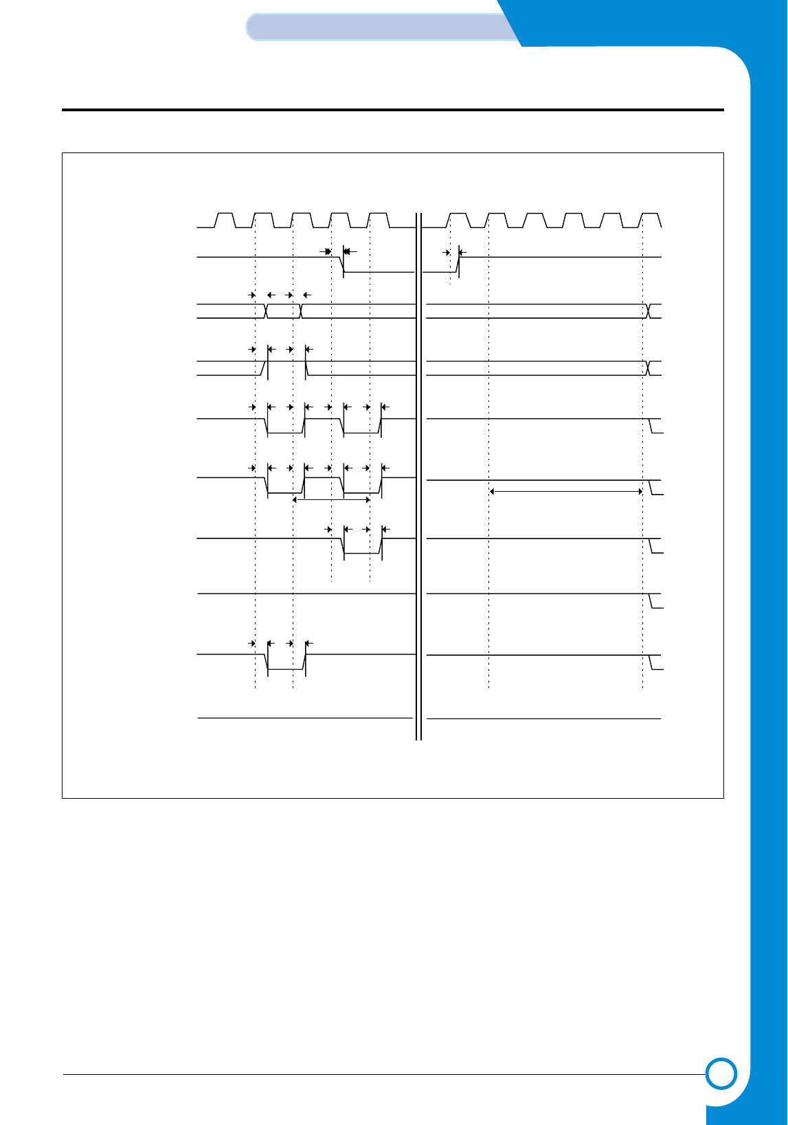
3-9
Samsung Electronics
CIRCUIT DESCRIPTION
Repair Manual
<Figure 9. SDRAM Self Refresh Timing>
SCLK
SCKE
ADDR/BA
AP/A10
nGCSx
nSRAS
nSCAS
nBEx
nWE
DATA ’HZ’
tSWD
’HZ’
’1’
’1’’1’
’1’
’1’
’1’
’1’
tCKED
tSAD
tSAD
tSCSD
tSRD tSRD
tSCD
tSCSD
tSAD
tCKED
Trc
Trp
- This Document can not be used without Samsung's authorization -
3-10
CIRCUIT DESCRIPTION
Samsung Electronics
Repair Manual
Parameter Symbol Min Typ. Max Unit
ROM/SRAM Address Delay tRAD - 12 - ns
ROM/SRAM Chip select Delay tRCD - 11 - ns
ROM/SRAM Output enable Delay tROD - 11 - ns
ROM/SRAM read Data Setup time tRDS - 1 - ns
ROM/SRAM read Data Hold time tRDH - 5 - ns
ROM/SRAM Byte Enable Dalay tRBED - 13 - ns
ROM/SRAM Write Byte Enable Delay tRWBED - 14 - ns
ROM/SRAM output Data Delay tRDD - 14 - ns
ROM/SRAM external Wait Setup time tWS - 1 - ns
ROM/SRAM external Wait Hold time tWH - 5 - ns
ROM/SRAM Write enable Delay tRWD - 14 - ns
DRAM Address Delay tDAD - 12 - ns
DRAM Row active Delay tDRD - 11 - ns
DRAM Read Column active Delay tDRCD - 11 - ns
DRAM Output enable Delay tDOD - 12 - ns
DRAM read Data Setup time tDDS - 1 - ns
DRAM read Data Hold time tDDH - 5 - ns
DRAM Write Cas active Delay tDWCD - 14 - ns
DRAM Cbr Cas active Delay tDCCD - 12 - ns
DRAM Write enable Delay tDWD - 13 - ns
DRAM output Data Delay tDDD - 14 - ns
SDRAM Address Delay tSAD - 4 - ns
SDRAM Chip Select Delay tSCSD - 4 - ns
SDRAM Row active Delay tSRD - 4 - ns
SDRAM Column active Delay tSCD - 4 - ns
SDRAM Byte Enable Delay tSBED - 5 - ns
SDRAM Write enable Delay tSWD - 5 - ns
SDRAM read Data Setup time tSDS - 4 - ns
SDRAM read Data Hold time tSDH - 0 - ns
SDRAM output Data Delay tSDD - 8 - ns
SDRAM Clock Eable Delay tCKED - 5 - ns
< ROM/SRAM Bus Timing Constants >
(VDDP : 3.3V, VDDI : 2.5V, Ta =25˚C, PLCAP=70pf, Max/Min=typ. ±30%)
- This Document can not be used without Samsung's authorization -

3-11
Samsung Electronics
CIRCUIT DESCRIPTION
Repair Manual
3-3-2-3 EXTERNAL DMA part
The function of this part is to bring data from external
DEVICE(OASIS:U21) by using GENERAL DMA. If DMA
REQUEST(/IP_REQ) is sent from external DEVICE to
S3C46MOX(JUPITER3:U15), DMA ACKNOWLEDGE
SIGNAL(/IP_ACK) is activated and the GENERAL DMA is
driven, so READ STROBE(/RD) in the external DEVICE to
bring data from the external DEVICE requiring CHANNEL.
To transfer this DATA to the DESTINATION MEMORY, the
ADDRESS of the DESTINATION MEMORY, CHIP
SELECT and WRITE STROBE(/WR) are generated to
store.
That is, if the EXTERNAL DMA is required by the external
DEVICE, S3C46MOX(Jupiter3:U15) responds to drive the
inside DMA CONTROLLER and then allocate GENERAL
DMA to external CHANNEL so that the data may be trans-
ferred to MEMORY TO MEMORY or external DEVICE TO
MEMORY.
• For more details, see the circuit description, see the circuit
description part of IMAGE PROCESSOR (5.3).
3-3-2-4 DRAM control part
Since S3C46MOX(Jupiter3) has the DRAM CON-
TROLLER build-in, it may be used by connecting DRAM
with external memory.
The Control mode of DRAM CONTROLLER provided by
S3C46MOX(Jupiter3) is available for EARLY WRITE,
NORMAL READ, PAGE MODE, and BYTE/HALF WORD
ACCESS, and is supported even by EDO DRAM,and
SDRAM as well as, Fast page DRAM.
This system uses SDRAM, and the signal used for
READ/WRITE uses /RD,/WR signal used for SYSTEM
BUS CONTROL. It is supported with auto REFRESH and
also by the Self-refresh mode for DRAM
BACK UP. It con-
sists of 2 Banks connected to co
mmon /SCS[1:0], /SCAS,
/SRAS, /SCLK, /SCKE, /DQM[1:0], each of them may use
up to 2M ~ 32M HALF WORD.
In this system, 2 MB is applied as system memory. The
area of DRAM is specified in the DRAM MEMORY MAP of
Fig. 1, while the related TIMING DIAGRAM in Fig. 5, 6, 7,
8, 9.
3-3-2-5 RTC (REAL TIME CLOCK) part
The RTC related circuit part is not applied because the fax
function is not applied, in this system.
3-3-2-6 PARALLEL PORT INTERFACE division
S3C46MOX(Jupiter3) has the Parallel Port Interface part
enabling Parallel Interface with PC.
This part is connected to PC through Centronics Connector
in this system, which consists of /ERROR, PE, BUSY,
/ACK, SLCT, /INIT, /SLCTIN, /AUTOFD, /STB and 245DIR
as the part generating the main control signal used to drive
PARALLEL COMMUNICATION. Data transmission
method between this part and PC supports the method
specified in P1284 Parallel Port Standard
(http://www.fapo.com/ieee1284.html) of IEEE.
That is, the Compatibility mode, the fundamental transmis-
sion method of print data, supports the Nibble Mode(4bits
data) supporting the Data Uploading to PC, Byte
Mode(8bits data), and ECP(Enhanced Capabilities Port : 8
bits data transmission & receiving) supporting two-way
high speed transmission to PC. The Compatibility mode
and ECP mode may be simply explained as follows.
The Compatibility mode is generally called Centronics
mode and is the protocol used for transmitting data by most
of PC. The ECP mode provides two-way high speed com-
munication as the protocol suggested for improved com-
munication with peripheral equipments such as printer and
scanner.
The ECP mode provides two types of cycles in two-way
transmission. They are data and command cycles.
Command cycle again has Run-length count and Channel
addressing types.
First, RLE (Run Length Encoding) type, having 64-fold
compressibility, is available for the real time data compres-
sion, and is used usefully for printer and scanner, which
have to transmit large capacity of raster image having a
series of same data. Next, Channel Addressing is pro-
posed for addressing single structure of multi-device.
For example, although the printer channel is processing
the printer image when the fax/printer/scanner have one
structure like this system, they may use parallel port for
another use. This system does not apply to the parallel port
Interface.
- This Document can not be used without Samsung's authorization -
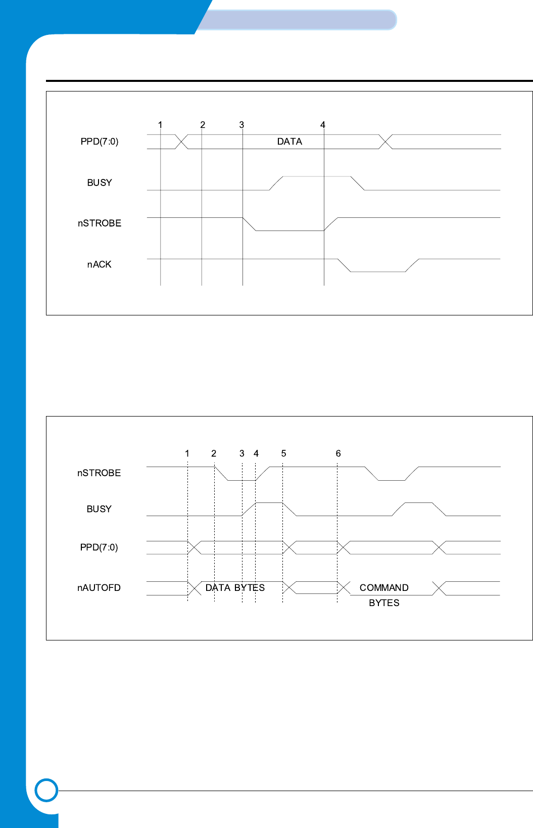
3-12
CIRCUIT DESCRIPTION
Samsung Electronics
Repair Manual
<Figure 10. Compatibility Hardware Handshaking Timing>
1. Write the data to the data register.
2. Program reads the status register to check that the printer is not BUSY.
3. If not BUSY, then Write to the Control Register to assert the STROBE line.
4. Write to the Control register to de-assert the STROBE line.
<Figure 10-1. ECP Hardware Handshaking Timing (forward)>
1. The host places data on the data lines and indicates a data cycle by setting nAUTOFD.
2. Host asserts nSTROBE low to indicate valid data.
3. Peripheral acknowledges host by setting BUSY high.
4. Host sets nSTROBE high. This is the edge that should be used to clock the data into the Peripheral.
5. Peripheral sets BUSY low to indicate that it is ready for the next BYTES.
6. The cycle repeats, but this time it is a command cycle because nAUTOFD is low.
BYTE 0 BYTE 1
- This Document can not be used without Samsung's authorization -
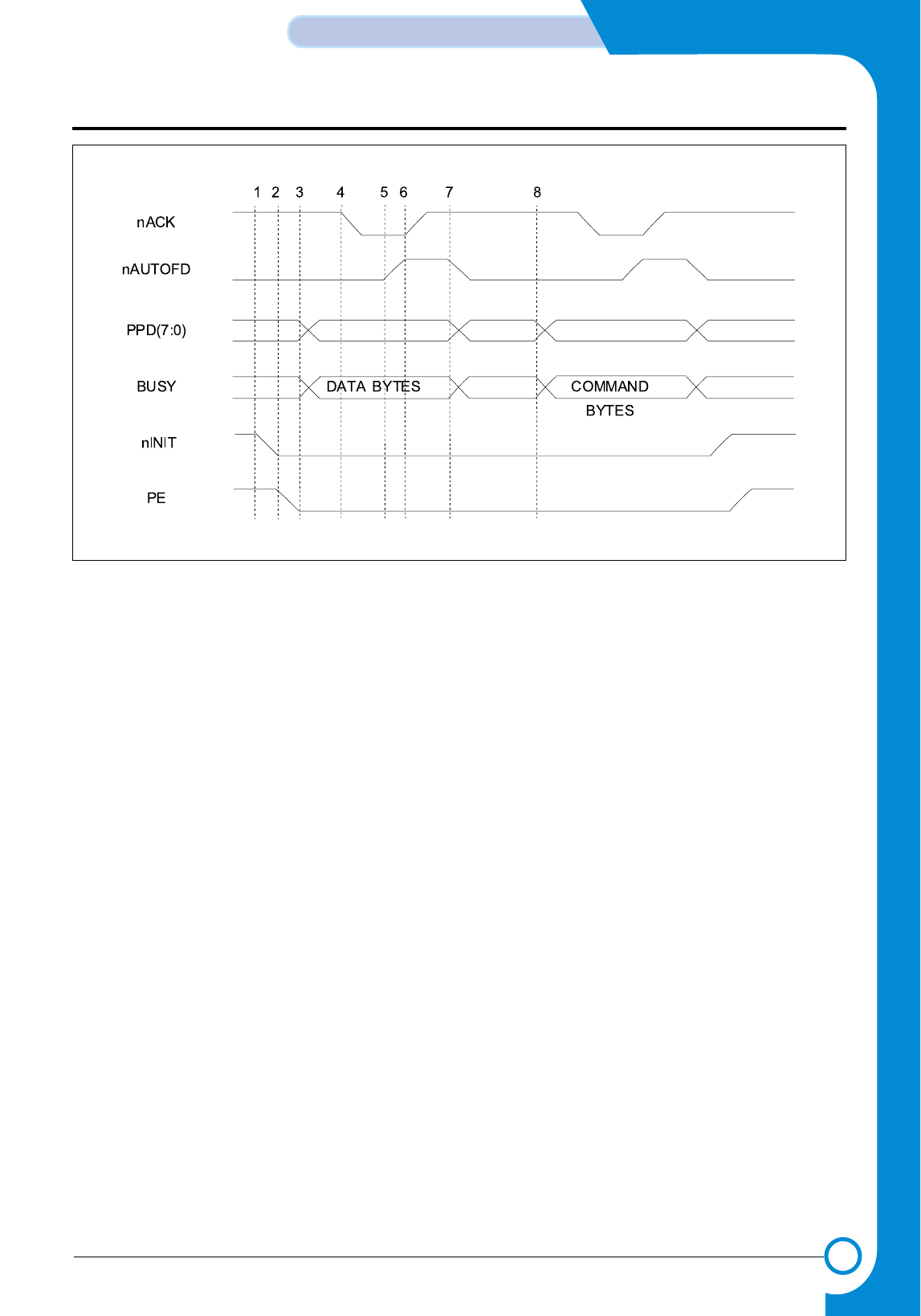
3-13
Samsung Electronics
CIRCUIT DESCRIPTION
Repair Manual
<Figure 10-2. ECP Hardware Handshaking Timing (reverse)>
1. The host request a reverse channel transfer by setting nINIT low.
2. The peripheral signals that it is OK to proceed by setting PE low.
3. The peripheral places data on the data lines and indicates a data cycle by setting BUSY high.
4. Peripheral asserts nACK low to indicate valid data.
5. Host acknowledges by setting nAUTOFD high.
6. Peipheral sets nACK high. This is the edge that should be used to clock the data into the host.
7. Host sets nAUTOFD low to indicate that it is ready for the next BYTES.
8. The cycle repeats, but this time it is a command cycle because BUSY is low.
BYTE 0 BYTE 1
- This Document can not be used without Samsung's authorization -
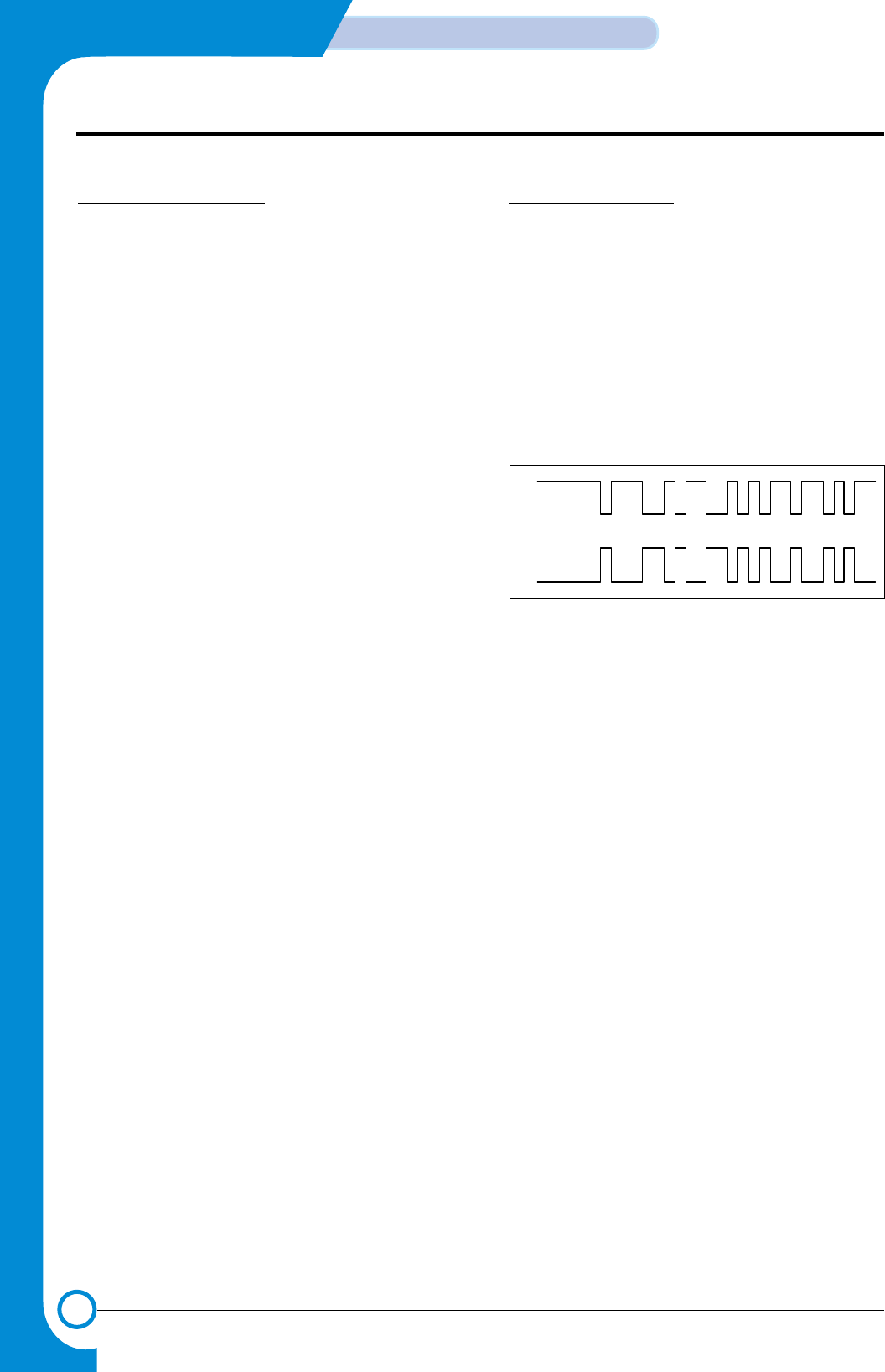
3-14
CIRCUIT DESCRIPTION
Samsung Electronics
Repair Manual
3-3-2-7 USB INTERFACE PART
1. USB function description
As the mode of implementing low cost express PC
Interface, USB was applied. At USB, PC plays the role of
route hub simultaneously by existing in the highest level as
the host. That is, the device supporting each USB is con-
nected centering on PC.
The device is available for Interface for the maximum of
127. USB cable is composed of total of a set of twisted pair
and 2 power lines. Cables have two types.
One is used for express transmission of 12Mbps and may
be extended as long as 5m. The part for implementing USB
function is included in S3C46MOX(Jupiter3).
For Interface of USB, pull-up of 15KΩis interfaced to the
data line of high level instruments, and, among data lines
of lower level instruments, pull-up resistance of 1.5KΩis
interfaced to any one.
At this time, D+ line is pulled up for Full Speed device, and,
for Low Speed device, D-line is pulled up. For upper level
instruments(Host, HUB) speed of device is classified inter-
faced to low level by detecting any one among D+ and D-.
If both lines are in the level of GND at the same time, device
is judged that low device is not interfaced. In the transmis-
sion mode of USB, there are
(1) Control transmission,
(2) Interrupt transmission,
(3) Bulk transmission, isochronous transmission
.
Control transmission is for Host to find out configuration
information from USB device. This is conducted when
device is interfaced. Interrupt transmission is used when
small quantity of data is sent periodically. Interval value
may be known from device in the case of initial setting. Bulk
transmission is valid in case of trying to transmit data in
large quantities or in case of transmitting them accurately.
Isochronous transmission should be assured of bandwidth,
and is used when transmitting large quantities of informa-
tion. Data in voice is used where delay is not allowed but
small error is allowed. At USB coding mode and bit stup-
ping are being conducted. First, in case original data is 1,
bit shall not change, and only when original data is 001, it
shall be inverted. Only while data is 1, 1 and 0 shall be
repeated. Also, in case 1, original data, is continued in 6 bit,
0 shall be inserted, Also, in the 1st phase of packet, data in
the synchronized pattern shall be sent. About more
detailed information regarding USB, see
http//:www.usb.org.
2. operation description
This system, when Host and USB cables are connected,
and when +5V is detected in power detector inside chip
and Vbus(U15-98), 3.3V comes out through Pull-uP termi-
nal. This is also connected to D+ in pattern of hardware and
supports Full-speed. Utilizing Configuration Endpoint,
EPO, in USB controller, Plug & Play function is operated.
Exchange of information between PCs is accomplished
through D+(U15-95) and D-(U15-96) terminals. This termi-
nal decides transmission speed depending on connection
of regulator output in USB controller, and decides size of
signal following USB and SPFC. Signal of general D+ and
D- terminals are same as Figure 10-3.
D+
D-
< Figure 10-3. USB Signal Line DIAGRAM >
- This Document can not be used without Samsung's authorization -
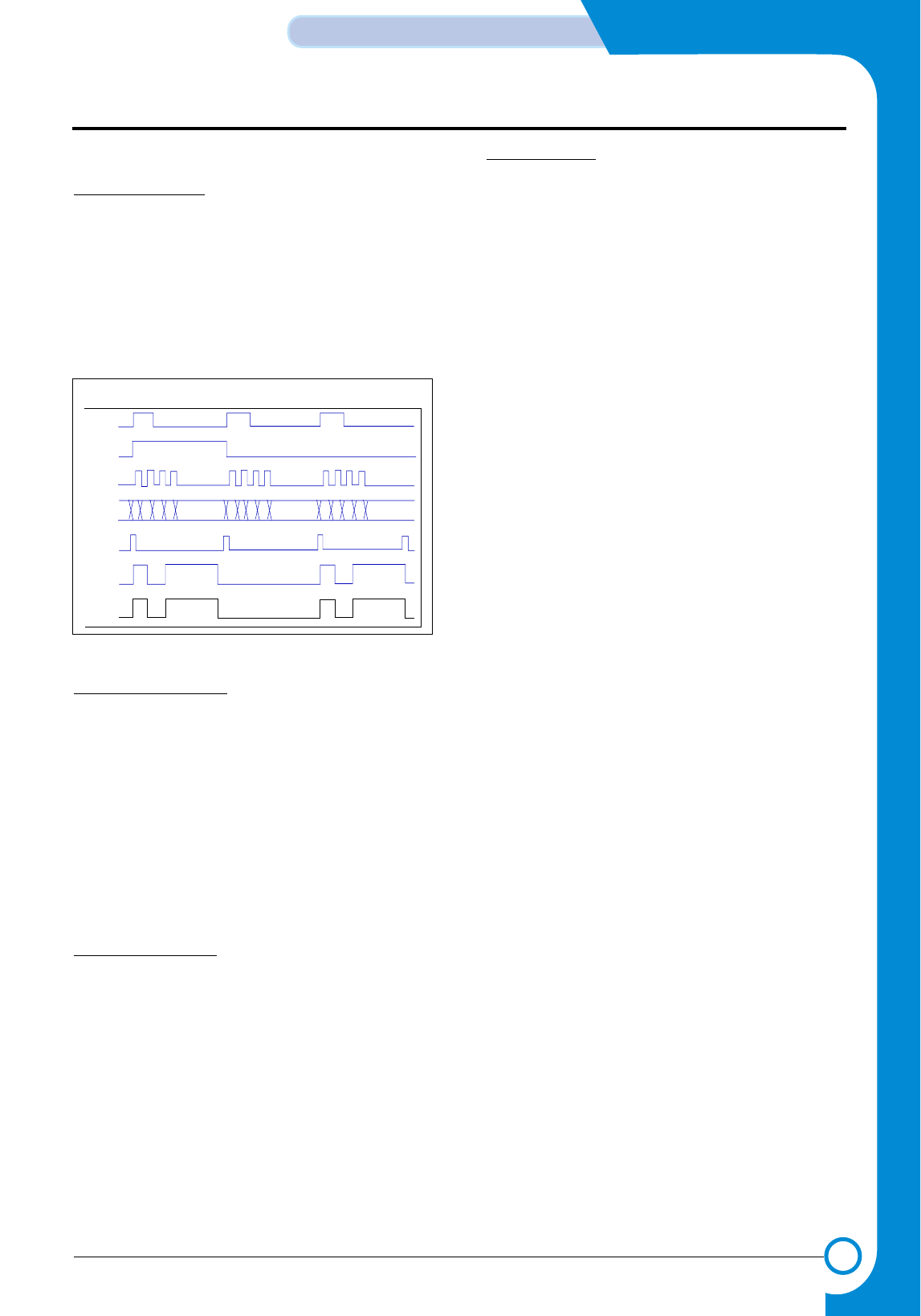
3-15
Samsung Electronics
CIRCUIT DESCRIPTION
Repair Manual
3-3-2-8 HEAD control part
1. Entire description
As part to drive INKJET HEAD, it is composed of ACLK,
AGATE, LDCS, LATCHCTL, PCLK, PDATA[3:0], PLOAD,
PENABLE signals for controlling Spitfire of CR B’D gener-
ating signal, which is driving Nozzle of Head, and
PH_ID[1:0] and OK2Print signals receiving from Spitfire.
Here,HEAD being used here is DOUBLE HEIGHT PRINT
HEAD, and MONO is configured with 208 NOZZLE, and
COLOR is with 192 NOZZLE.
<Figure 11 HEAD Control Part Timing Diagram>
2. A-LINE driving circuit
13 Address Lines are input into 13 Address Counters in
sequence at Rising edge of ACLK signal, which is input
serially into Spitfire. Output of this Counter was connected
to each A-line driver, and this driver output becomes A-line
signal. The sequence of signal input into Address Counter
is decided by ADIR, and if it is ADIR=0, it is input in
sequence of A13A1, and if it is ADIR=1, in sequence of A1
=> A13. AGATE signal is used to reset Address Counter. If
it becomes AGATE=1, A-Line output becomes Low state.
The cycle of ACLK is 1.5ß¡ in minimum, and Sink current of
each Driver is 60mA.
3. P-LINE drive circuit
P-Line values are clocked to 4-bit Serial to Parallel Shift
Register Clock in Spitfire ASIC, and ASIC shall clock-in P-
line NO. of fitting value at Rising Edge of PCLK. These val-
ues are latched to Holding register at Rising Edge of
PLOAD. PLOAD Pulse Duration is 50n, and P-line value of
Holding Register is done AND with PENABLE signal in
order to generate appropriate Fire Pulse. PLCK is available
for handling as much as 4MHz. Drive Current of P-line is
400mA. Data of P1°≠P4 is shifted to PDATAO, that of P5-
P8 shifted to PDATA1, that of P9-P12 shifted to PDATA2,
and that of P13-P16 shifted to PDATA3.
4. Control Signal
• The signal loaded on PDATAO - PDATA2 at Rising edge
of LATCHCTL(Latch Control Nibble) is used as function
as follows in Spitfire.
- PDATA0 == ADIR —> Low : ACLK is operated in Count
Down, High : ACLK is operated in Count
Up.
- PDATA1 == When Fault Test —> High, check whether
P-Line of Head became short with GND.
- PDATA2 == When Print Head ID Check —> high,
make sure that Check mode is set, and,
after that, by using the PDATA0~PDATA2
LIne, make A1-A3 signal for sending, and
Head ID shall come out with PH_IDn out-
put. At this time ID could be displayed only
if each Substrate heater is turned on.
• The signal loaded into PDATAO-PDATA3 at Rising
edge of LDCS(LoadHtrcs) signal is used in the follow-
ing functions in Spitfire.
- PDATA0 == BLKHTR—> High : Turn on Substrate
Heater of Mono Head.
- PDATA1 == COLHTR—> High : Turn on Substrate
Heater of Color Head.
- PDATA2 == nHSM—> Low : Enable Select Signal of
Mono Head.
- PDATA3 == nHSC—> Low : Enable Select Signal of
Color Head.
When Substrate Heater is turned on, Over-current Check
circuit is operated, automatically, and,if the current is above
750mA, the printer stops operation after OK2PRT
becomes low.
The Timing diagam below shows signal timin for the P-line block
ACLK
An
PCLK
PDATA
PLOAD
PENABLE
Pn
- This Document can not be used without Samsung's authorization -
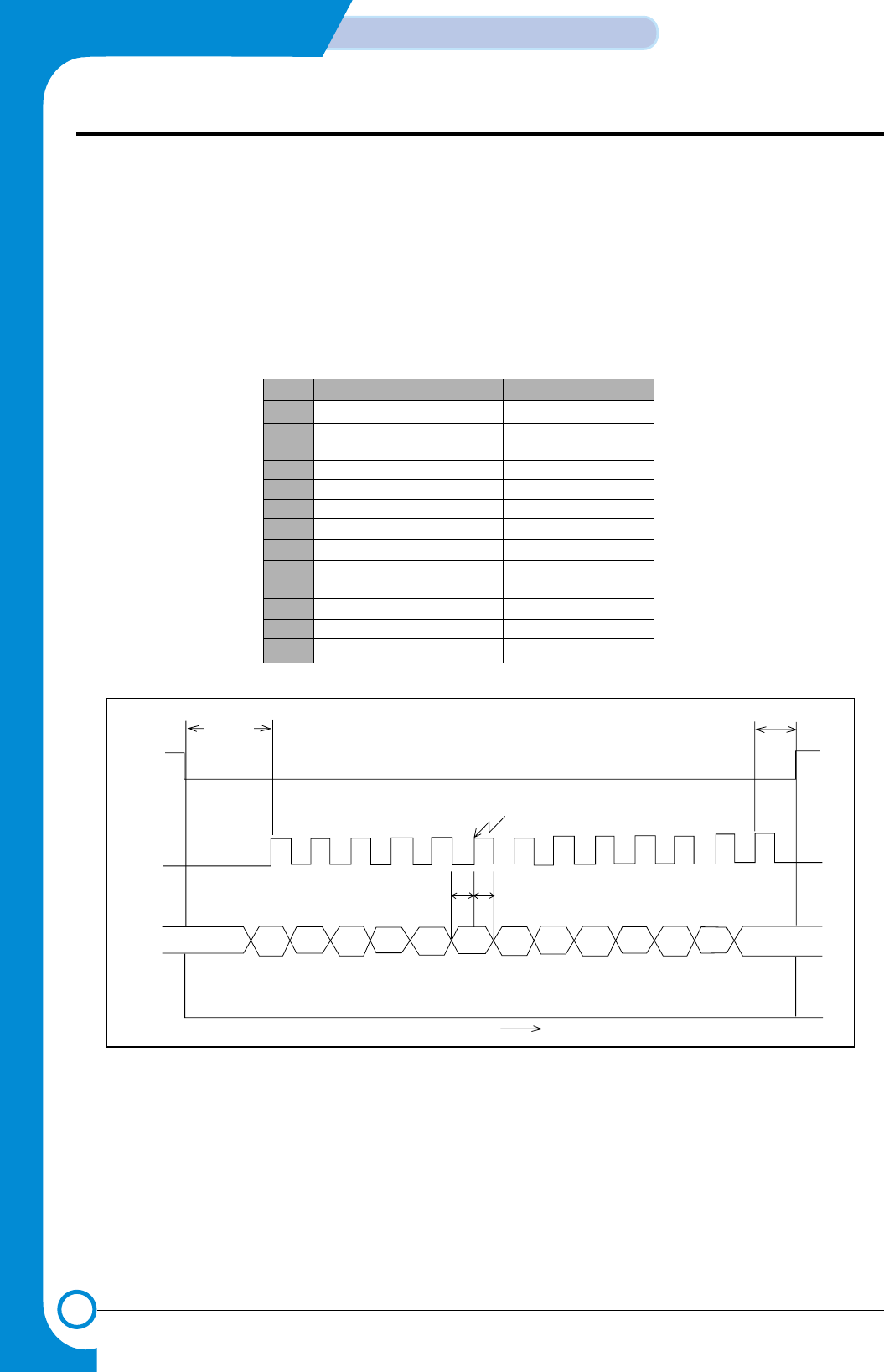
3-16
CIRCUIT DESCRIPTION
Samsung Electronics
Repair Manual
3
-3-2-9 SYNCHRONOUS SERIAL INTERFACE part
As the part interfacing with THUNDERBOLT ASIC, it con-
sists of /TBCS,TBCLK,TBDO. In sending SERIAL DATA
of 13 BIT to Thunderbolt ASIC, meaning of each bit is as
follows. BIT 1 is the bit to do On/Off VPH(+11.82V), BIT
[2:7] is the bit for driving MOTOR 1, BIT [8:13] is the bit to
drive MOTOR 2. MOTORs are available for being used as
STEPPER MOTOR and DC MOTOR respectively.
3-3-2-10 MOTOR control part
(DIR, PWM, LFPHA,LFPHB, LFIA[0:1],
LFIB[0:1])
S3C46MOX(Jupiter3) is arranged to support one Step
motor and one DC motor. This system does not use the
Motor control part provided by S3C46MOX(Jupiter3).
< Figure 12 SYNCHRONOUS SERIAL INTERFACE TIMING DIAGRAM >
/TBCS
TBCLK
TBDO
Tcs-sclk Tcs-sclk
bit 1 bit 2 bit 3 bit 4 bit 5 bit 6 bit 7 bit 8 bit 9 bit 10 bit 11 bit 12 bit 13
SDI stays at
last value
MSBLSB
Data Latcked on the rising edge of SCLK
time
Tdhd
Tdsu
STEPPER MOTOR DC MOTOR
BIT 1 VPH_ENABLE VPH_ENABLE
BIT 2 MOTOR1_CURR_I1_PHASEB Not used in this mode.
BIT 3 MOTOR1_CURR_I0_PHASEB Not used in this mode.
BIT 4 MOTOR1_DIR_PH_B Not used in this mode.
BIT 5 MOTOR1_CURR_I1_PHASEA Not used in this mode.
BIT 6 MOTOR1_CURR_I0_PHASEA Not used in this mode.
BIT 7 MOTOR1_DIR_PH_A MOTOR1_DIRECTION
BIT 8 MOTOR2_CURR_I1_PHASEB Not used in this mode.
BIT 9 MOTOR2_CURR_I0_PHASEB Not used in this mode.
BIT 10 MOTOR2_DIR_PH_B Not used in this mode.
BIT 11 MOTOR2_CURR_I1_PHASEA Not used in this mode.
BIT 12 MOTOR2_CURR_I0_PHASEA Not used in this mode.
BIT 13 MOTOR2_DIR_PH_A MOTOR2_DIRECTION
- This Document can not be used without Samsung's authorization -
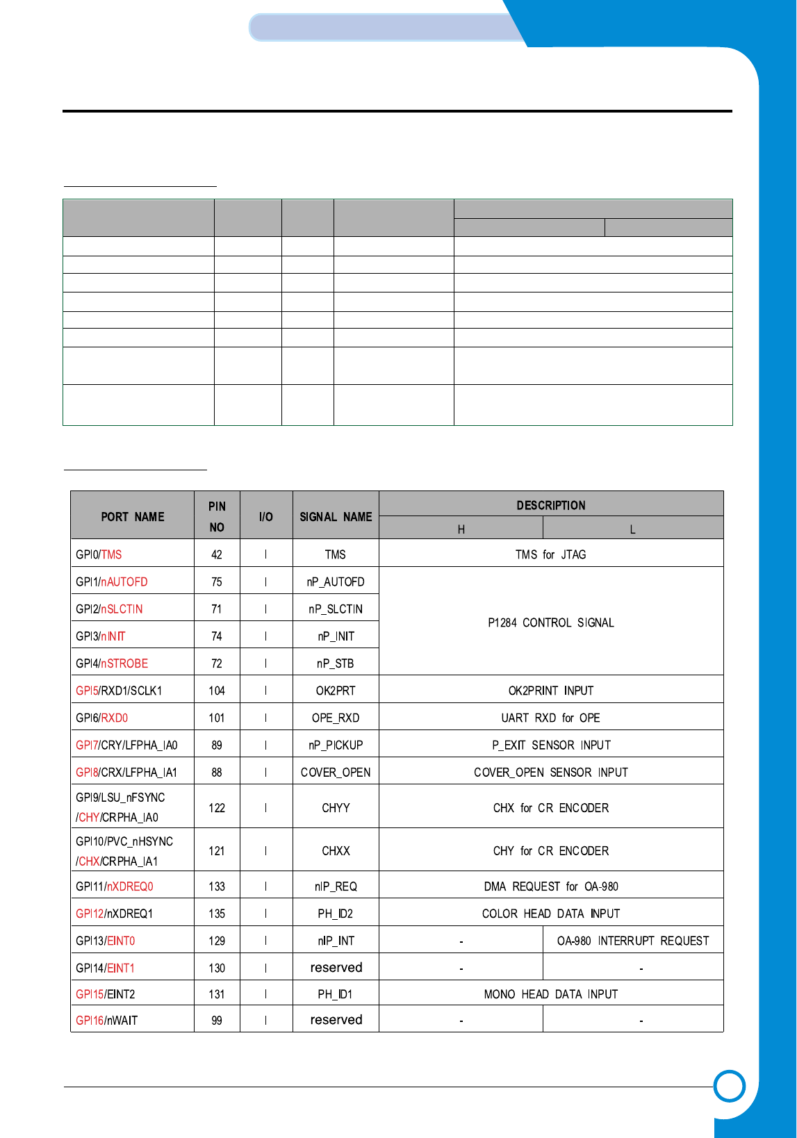
3-17
Samsung Electronics
CIRCUIT DESCRIPTION
Repair Manual
3-3-2-11 GENERAL PURPOSE I/O PORT of S3C46MOX(Jupiter3)
1. J3 Assigned GCS Ports
2. J3 Assigned GPI Ports
PORT NAME PIN NO I/O SIGNAL NAME DESCRIPTION
HL
nGCS0 136 O nROM_CS FLASH MEMORY CHIP SELECT
nGCS1/GOP16 137 O nIP_CS OA-980 CHIP SELECT
nGCS2/GOP17 138 O reserved -
nGCS3/GOP18 139 O reserved -
nGCS4/GOP19 141 O reserved -
nGCS5/GOP15/PDE 142 O 245DIR P1284 DIRECTION CONTROL
nGCS6:nRAS0:nSCS0 34 O reserved -
/GOP13
nGCS7:nRAS1:nSCS1 35 O nSCS1 SDRAM1(16Mb) CHIP SELECT
/GOP14
- This Document can not be used without Samsung's authorization -
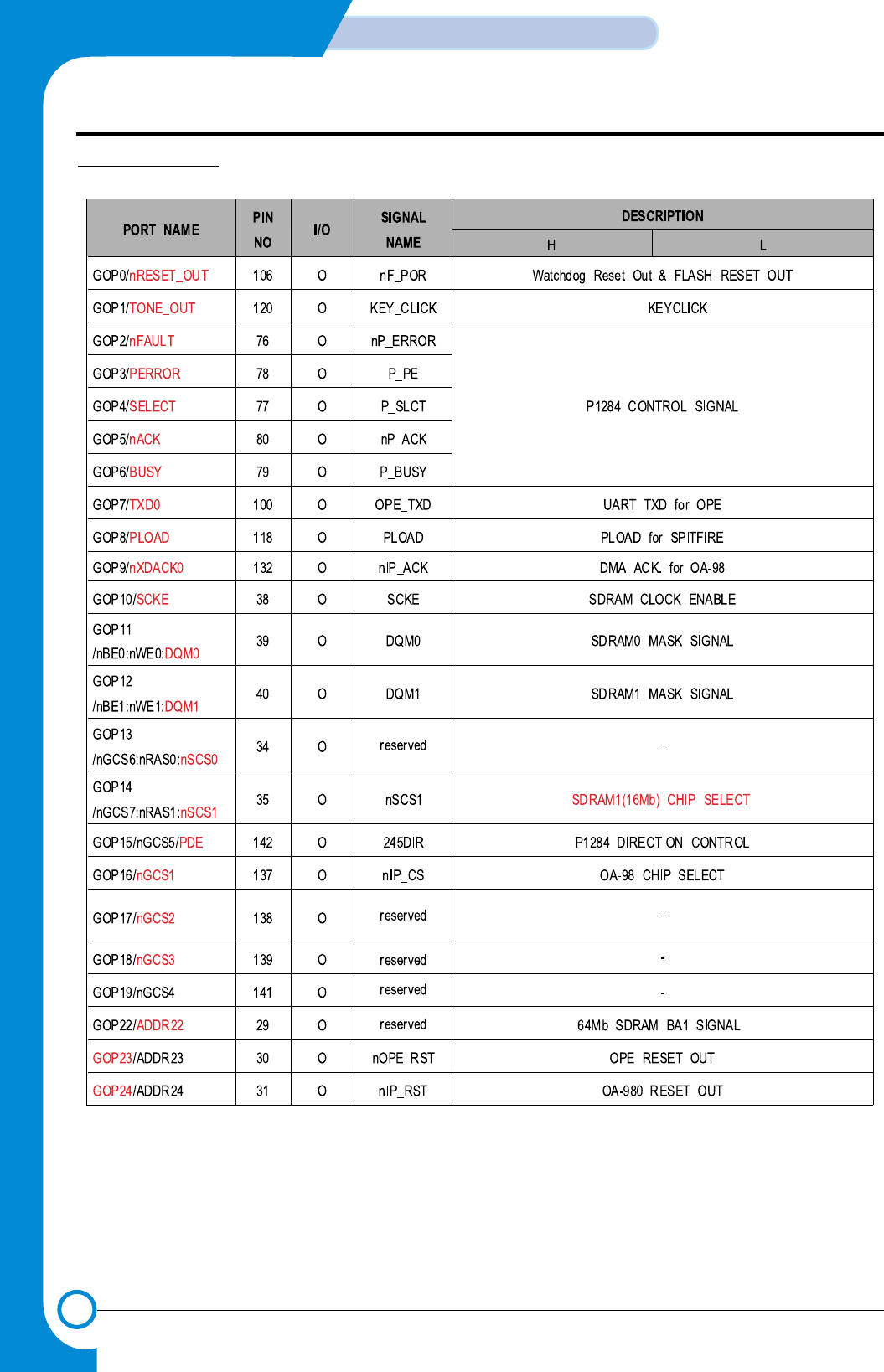
3-18
CIRCUIT DESCRIPTION
Samsung Electronics
Repair Manual
3. J3 Assigned GPO
- This Document can not be used without Samsung's authorization -
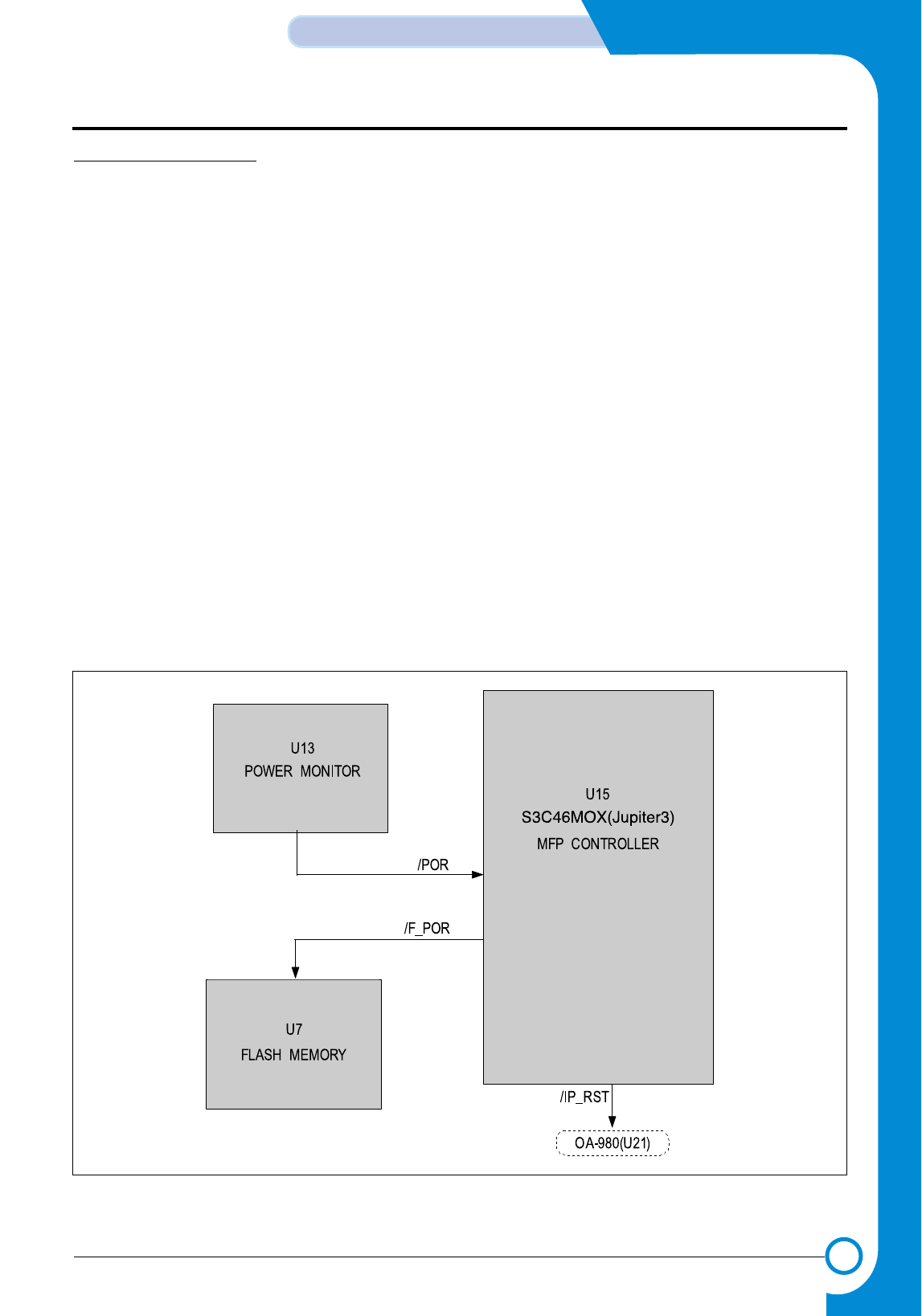
3-19
Samsung Electronics
CIRCUIT DESCRIPTION
Repair Manual
3-3-3 RESET CIRCUIT
This system is configured with PRIMARY RESET(/POR) of
Power Reset, Reset by WATCH DOG TIMER, external
PRIMARY RESET, and SECOND RESET(/_F_POR)
which was done AND. PRIMARY RESET SYSTEM is used
for resetting MAIN CONTROLLER(U15) when System
Power is authorized, and SECOND RESET resets FLASH
MEMORY(U7). Figure 15 below is BLOCK DIAGRAM
related to the reset of entire system.
When +3.3V reaches 3.1V so that system may operate,
POWER MONITOR(U13) moves to High(+3.3V) after
maintaining low(OV) in the degree of 50mS-200mS output
while monitoring it. This Reset signal is input into MFP
CONTROLLER(S3C46MOX(Jupiter3 : U15) right away,
and MFP CONTROLLER becomes awake. And it releases
/F_POR after MCLK 1 clock.
3-3-3-1 POWER MONITOR ( U13 )
Since +3.3V power supplied to XC61FN3112MR is unsta-
ble, when it becomes 3.1V(3.038V~3.162V), it is checked
as the POWER FAILURE. And the output terminal of
XC61FN3112MRF becomes LOW(0V),it is applied to
S3C46MOX(Jupiter3)(U15), and RESET(LOW ACTIVE) is
operated When S3C46MOX(Jupiter3) Reset is cancelled,
FLASH MEMORY connected to /F_POR of
S3C46MOX(Jupiter3) is Reset together. Output terminal of
XC61FN3112MRF is pulled up 100KΩin the structure of
Open drain.
3-3-3-2 WATCH DOG OUTPUT (/F_POR)
Since WATCH DOG TIMER, which is Programmable
Counter in S3C46MOX(Jupiter3) is set as disable for INI-
TIAL STATE, it shall be set as Disable so that it won’t oper-
ate, and after it is initialized for operation, it shall be reused
by setting it Enable. When Watch Dog Reset occurs, it is
about 10mS depending on the value set at the initial stage.
And Counter value of Watch Dog Timer is changed by the
program. Reset signal (/F_POR,UI5-106) shall be generat-
ed, and entire system shall be Reset and initialized.
< Figure 13. POWER RESET BLOCK DIAGRAM >
- This Document can not be used without Samsung's authorization -
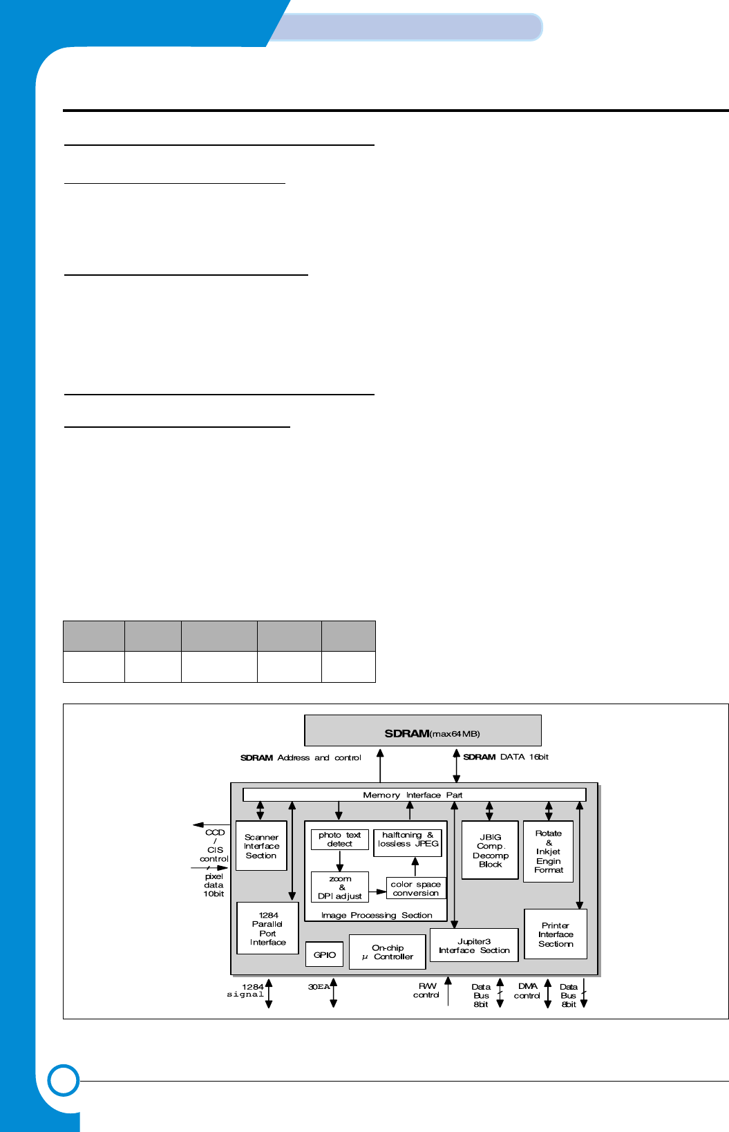
3-20
CIRCUIT DESCRIPTION
Samsung Electronics
Repair Manual
3-4 MEMORY
3-4-1 GENERAL DESCRIPTION
MEMORY applied in this system are FLASH MEMORY(U7)
of 1MB, SDRAM(U9) of 2MB.
3-4-2 MEMORY CONFIGURATION
By each CHIP SELECT (/ROM_CS, /SCS1, /SCS0,
/SD_RAS ,/SD_CAS ), FLASH MEMORY and SDRAM are
selected, and DATA is accessed by HALF WORD unit.
3-5 Image processing part (U21)
3-5-1 GENERAL DESCRIPTION
Image Processor OA-980(U21) is mainly configured with
On-chip µ Controller(8bit), Scanner Interface Section(PI),
Image Processing Section(IP), Memory Interface
Section(MI), JBIG Comp & Decomp Section, Rotate and
Inkjet Engine Section, Printer Interface Section(PO), 1284
Parallel Port Interfaced and Host Interface Section(HI).
(See Figure 14 )
3-5-1-1 Physical
3-5-1-2 Features & Functions
• 10bit scanning interface
: Supports CIS and CCD interface.
Needs external ADC(up to 16bit).
• Image processing Section
: Full quality RGB to CMYK or 6 color conversion
Photo/Text detect allows mixed documents.
Arbitrary image scaling using true interpolation.
Automatic contrast and brightness correction.
Error diffusion or programmable dither arrays.
• JBIG compression block
: JBIG/MH/MR/MMR Comp. & Decomp.
•Inkjet engin format
: Rotates data to suit the Lexmark engin format
• Printer Interface section
: Supports a single byte DMA with 150MHz clock speed.
• Microcontroller interface part
: 8bit multiplexed bus acts as address and data bus
• General purpose input and output port
: 30 GPIO pins.
Core Process Drive power Package Design
/frequency
8bit Micro- 0.35U 3.3V 208pin OASIS
controller CMOS 75MHz QFP
<Figure 14. OA-980 Block Diagram>
- This Document can not be used without Samsung's authorization -
3-21
Samsung Electronics
CIRCUIT DESCRIPTION
Repair Manual
3-5-2 OA-980 DESCRIPTION BY FUNC-
TIONS
3-5-2-1 Clock Control Section
Internal drive frequency operates classified into two parts.
Almost all On-chip µ Controller(8bit) Module drives by
Main_clock, and Printer Interface Section(PO) only drives
by Base_clock. Main_clock and Base_clock may be set
with frequency each desires by receiving Clock supplied
from outside by PLL Logic.
At present, system Main_clock and Base_clock are each
set in 48MHz, and may be checked at SDRAM_CLK of
SDRAM(U27). Clock supplied from outside does not use
separate crystal, but 48MHz is supplied by IP_CLK,
CLK_Out of Jupiter3(U15).
The one which pulled up Main_EXT(pin46) and
Base_EXT(pin43) is the Option using internal PLL, and, at
the time of Pull-up, it does not use internal PLL, but just use
Clock supplied to Main_CLK(pin45) and Base_CLK(pin42)
as Main_clock and Base_clock.
3-5-2-2 Internal Microcontroller
8bit RISC Microcontroller is built-in, and Address area
which Micro-controller control is 64kbyte. At the same time
when cache is built in for control of more efficient SDRAM,
it possesses Hook function, namely the internal Boot ROM
256byte required for self-initialization function, too.
1. Memory Map
2. Power On/Off Reset
• Power On Reset
Depending on the signal state of Reset_L(pin35), OA-
980 may be reset in the manner of hardware. Reset is on
at “Low” state and, at “High” state, Reset is Off.
Accordingly, in order for OA-980 to operate normally,
after the System initialization, the /IP_RST of
Jupiter3(U15-31) shall be converted to “High” state. In
order for safe Hardware Reset to be accomplished, it
should be maintained in “Low” state for more than 1000
Main_clock(10uS).
• Power Off Reset
PWR_down(pin107), for SDRAM(U27) to advance to the
Self Refresh Mode Reset_L(pin35) at the Power Safe
Mode, shall advance to the Reset Mode earlier than the
minimum of 1uS. This System does not use it.
3. Hook function : Self-initialization function
In case self ROM is connected to OA-980 as in Figure (15),
although the execution file is downloaded to SDRAM, the
execution file is initialized by receiving download from
Memory. This execution file is the ROM File supporting so
that all functions of Image processing related to OA-980 as
well as register setting value required for initialization(Copy,
PC scan, MultiMediaCard Print) may operate normally.
0x0000 .... 0x00ff Boot ROM
0x0100 SDRAM program store
.... and
0xfbff SDRAM stack
0xfc00 .... 0xffff HW registers
- This Document can not be used without Samsung's authorization -
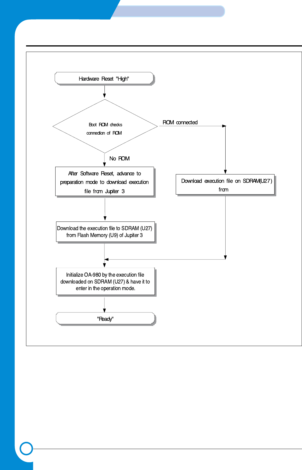
3-22
CIRCUIT DESCRIPTION
Samsung Electronics
Repair Manual
<Figure 15. Boot Code Flow Diagram>
- This Document can not be used without Samsung's authorization -
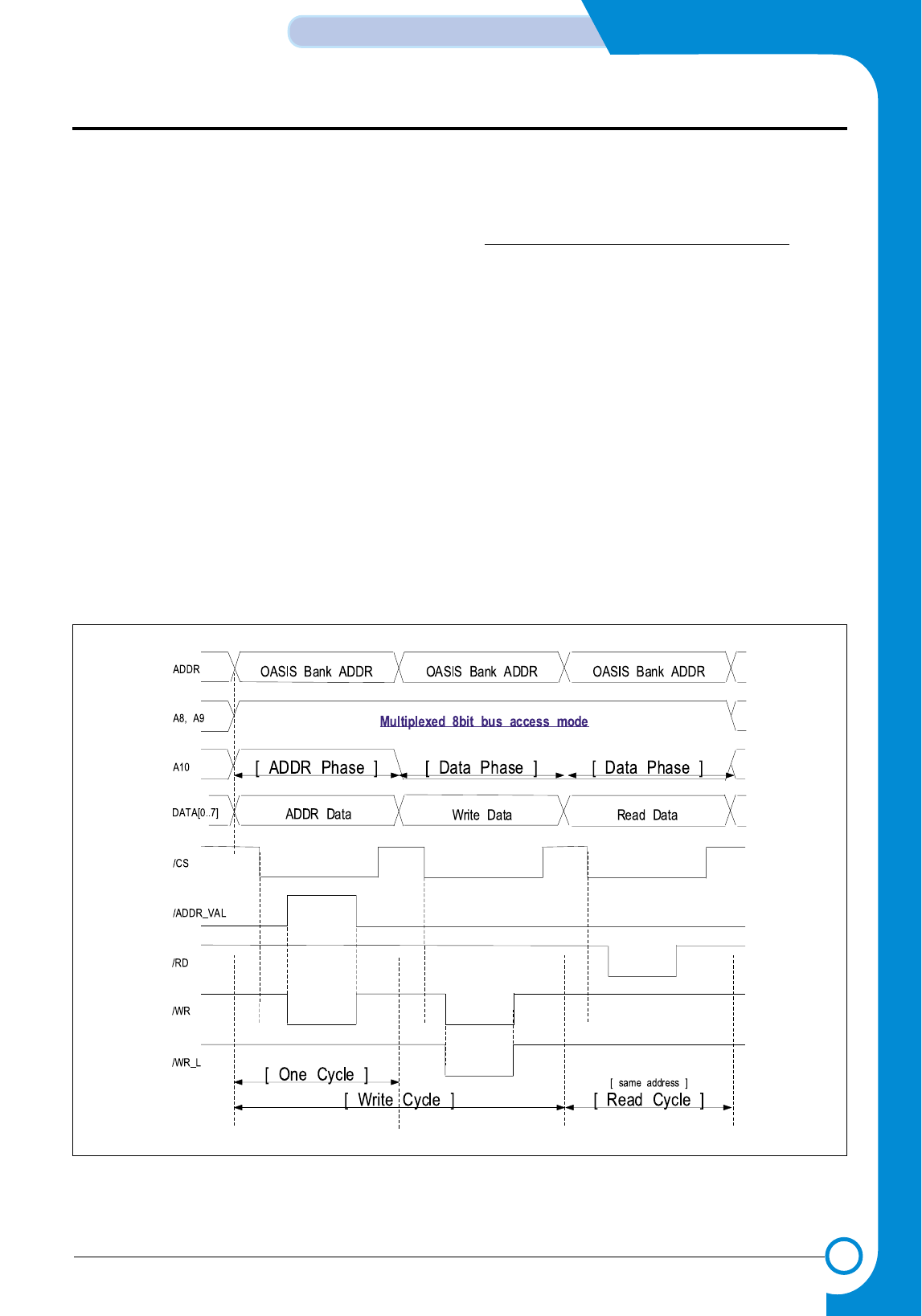
3-23
Samsung Electronics
CIRCUIT DESCRIPTION
Repair Manual
3-5-2-3 Host Interface Section
(HI : Jupiter3 interface section)
Unlike the existing DuoIP sequence, OA-980 exchanges
Command and data with Jupiter 3 in the Multiplexed 8bit
Bus(data & address) mode. Namely, it does not receive
Address and Data simultaneously, but receive data after
receiving Address first using Data Bus of Jupiter3.
HI Section also supports the data movement in the DMA
mode. Accordingly, when transmitting large capacity of
Image data(RGB data of MultiMedCard), it uses the DMA
mode.
1. Multiplexed 8bit Bus(data & address) mode
nce Jupiter3 may not support Multiplexed 8bit Bus(data &
address) mode used by OA-980, it configured a circuit addi-
tionally so that mutual Interface may be possible by making
required signal using two NOR GATE(UR16) and one OR
Gate(U40).
As REG_ADDR_VAL(pin27) signal is the signal for OA-980
to play a role of informing that value input into 8bit of OA-
980 Bus is not Data but Address value, when ADDR(10) is
“High” and /IP_CS, /WR “Low,” “High” shall be generated as
shown in the circuit diagram. See figure (16). At this time,
since /WR_L(pin31), the Write signal of OA-980, should be
maintained in “High,” the signal shall be generated in case
actual Write is accomplished with one OR Gate(U18),
namely, only when ADDR(10) is “Low,” When
REG_ADDR_VAL (pin27) is “High,” input the Address value
of OA-980, and when “Low, from the standpoint of Jupiter3,
it may Read or Write One Byte Data using two Cycles by
Reading or Writing relevant Data of (to) Address.
<Figure 16. Hi Block Timing diagram(1)>
- This Document can not be used without Samsung's authorization -
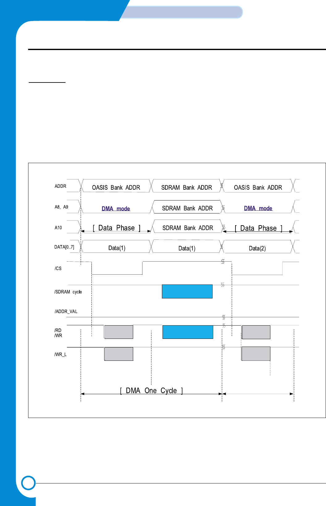
3-24
CIRCUIT DESCRIPTION
Samsung Electronics
Repair Manual
2. DMA mode
DMA mode is the method of Reading or Writing Data in
Block unit by activating two DMA Channels of OA-980
respectively. When A8 or A9 is “Low” and when /IP_CS is
“Low,” GDMA of Jupiter3 Reads or Writes in Memory to
Memory mode, as the appropriate DMA Channel is activat-
ed. See Figure (17). Of course, it performs required DMA
register setting in Multiplexed 8bit Bus(data & address)
mode before DMA is accomplished.
3-5-2-4 Scanner Interface Section(PI)
It directly controls 16bit ADC and 600dpi color CCD con-
nected to CCD, processes Shading and Gamma correc-
tion, the basic course required for Image process of RGB
12bit(8+4bit) data transferred from ADC, then performs the
function of storing the data in SDRAM of OA-980 through
MI Block.
<Figure 17. Hi Block Timing diagram(2)>
- This Document can not be used without Samsung's authorization -
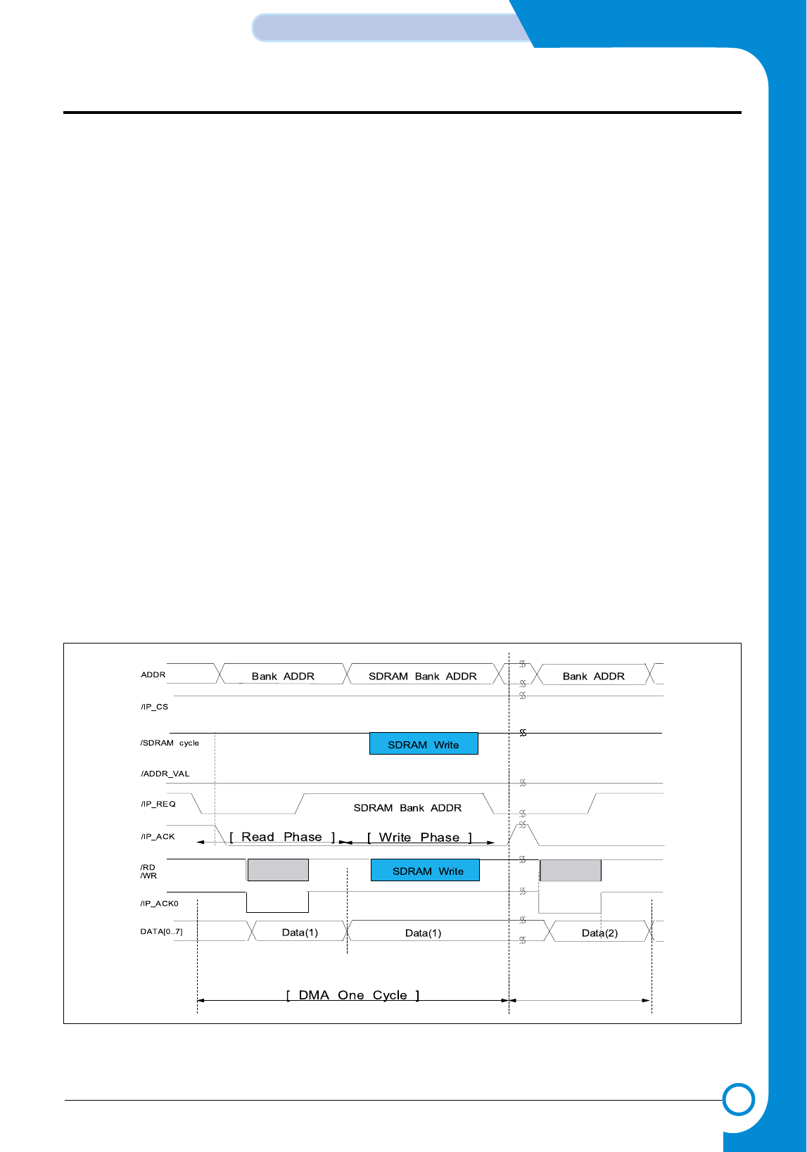
3-25
Samsung Electronics
CIRCUIT DESCRIPTION
Repair Manual
3-5-2-5 Image Processing Section(IP)
After performing color compensating required for the
System
for RGB digital data input, it conducts the role of
converting to
CMYK data printable. IP Block consists of four
Modules mainly.
- Photo text detect
- Zoom and dpi adjust
- Color space conversion
- Half toning and loss less JPEG
3-5-2-6 Memory Interface Section(MI)
MI Block consists of four Channels, located between exter-
nal SDRAM(U27) and blocks inside OA-980, and is con-
trolled so that the flow of all data may be accomplished more
efficiently.
3-5-2-7 JBIG Comp & Decomp Section
By condensing Image data processed at Blocks into JBIG
algorithm and save them in external SDRAM(U27), it shall
have Memory domain used more efficiently. Naturally, even
when moving Image data which was condensed to JBIG, to
other block, it is conveyed to Image data freed from conden-
sation.
3-5-2-8 Rotate and Inkjet Engine Section
After Image CMYK Data which ended all image processing
is converted to Format so that Inkjet Printer Engine may
print, it plays the role of saving them on the external
SDRAM(U27).
The Data stored in the external SDRAM(U27) is transferred
to Head Control Part of Jupiter3 through MI and HI Block of
OA-980 by DMA of Jupiter3, and then printed by Spitfire.
3-5-2-9 Printer Interface Section(PO)
When the Image process required for PC Scan (See Fig.
19) is completed, OA-980 requests that /IP_REQ signal in
PO_Block should take the Scan Image Data from the
External DMA Block of Jupiter3(U15). The External DMA
Block of Jupiter3(U15) generates not only /IP_ACK signal
to bring Data by Byte as the unit but also /RD signal to bring
the Data. The External DMA Block of Jupiter3(U15) stores
the Data in SDRAM(U9) and then restore /IP_ACK as
"High" to receive a next Data/.
As DMA Timing properties between Jupiter and OA-980 do
not match, /IP_ACK0 is separately created to prevent BUS
collision by using one OR-Gate(U18-3) so that OA-980 may
use the BUS only in /RD in the way of inputting the /ACK
signal into OA-980 only when /RD is actually produced,
while Jupiter3 may use in /WR, as shown in the Timing of
Fig. 18. That is, since OA-980 sends Data to BUS during
/ACK signal section, BUS collision occurs between DMA of
Jupiter3 and /WR section, where /RD, /WR are all carried
out during /ACK.
<Figure 18. PO Block DMA Timing Diagram>
- This Document can not be used without Samsung's authorization -
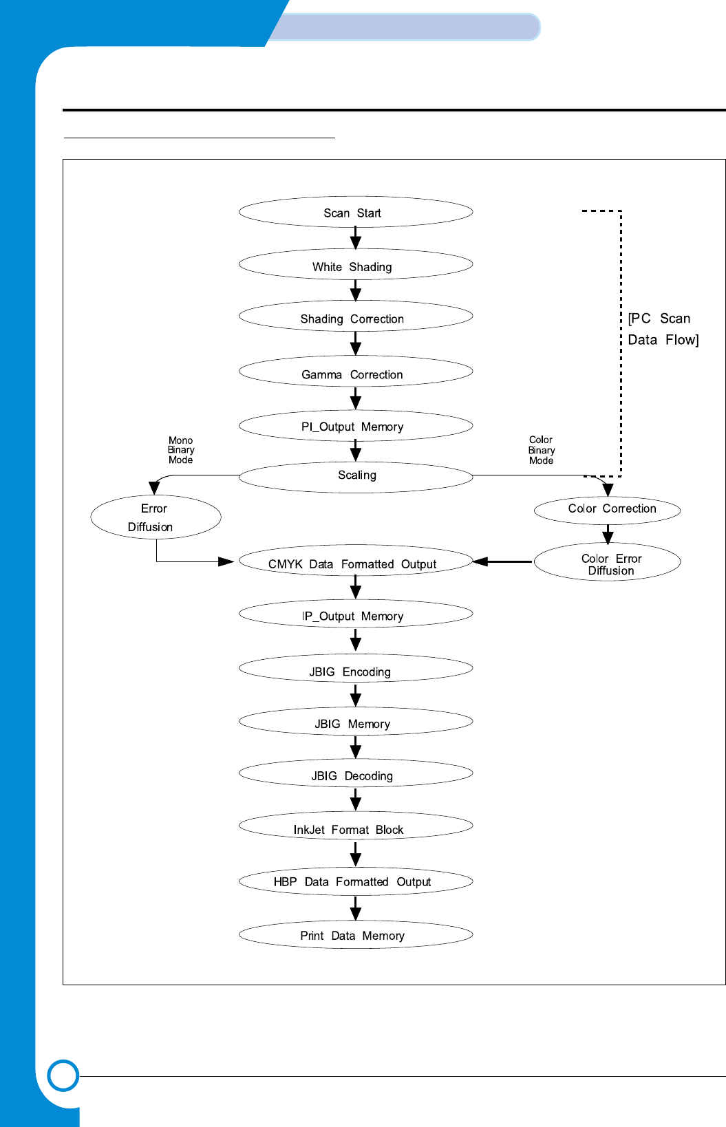
3-26
CIRCUIT DESCRIPTION
Samsung Electronics
Repair Manual
3-5-3 COPY DATA FLOW FOR OA-980
- This Document can not be used without Samsung's authorization -
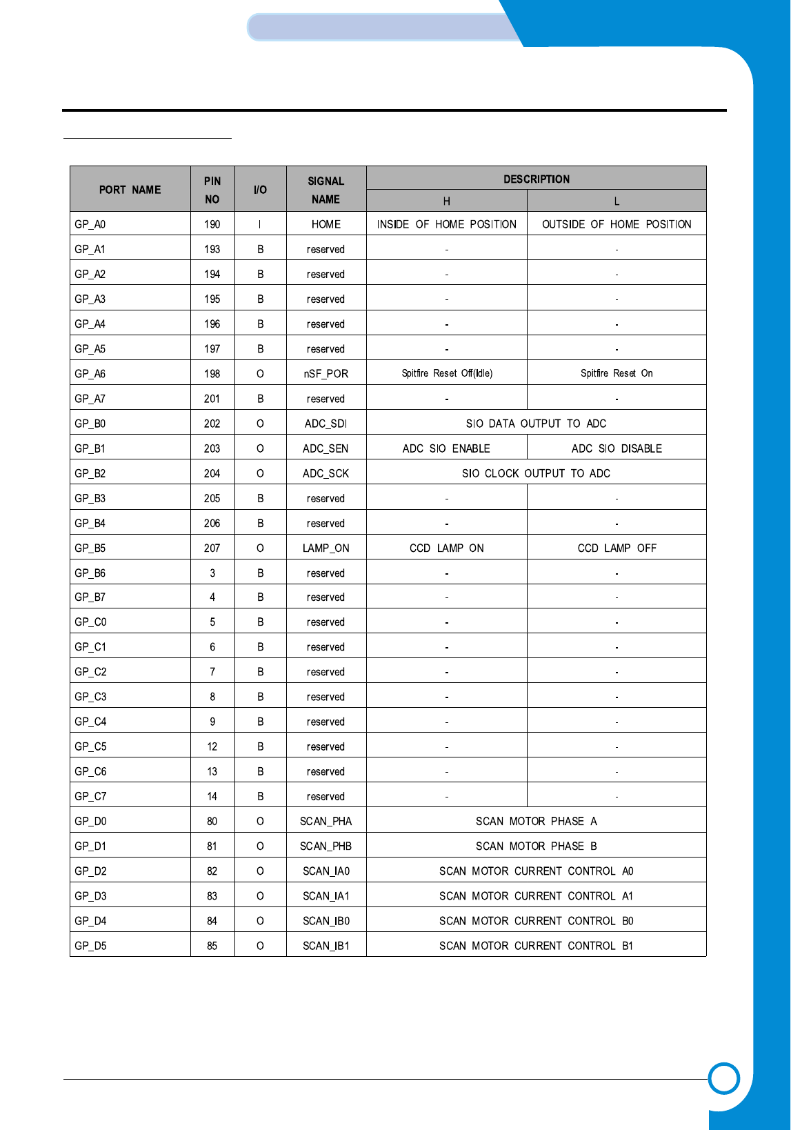
3-27
Samsung Electronics
CIRCUIT DESCRIPTION
Repair Manual
3-5-4 OA-980 I/O PORT
- This Document can not be used without Samsung's authorization -
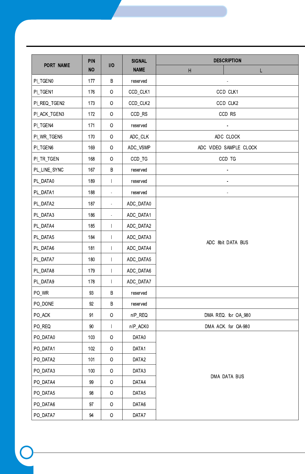
3-28
CIRCUIT DESCRIPTION
Samsung Electronics
Repair Manual
- This Document can not be used without Samsung's authorization -
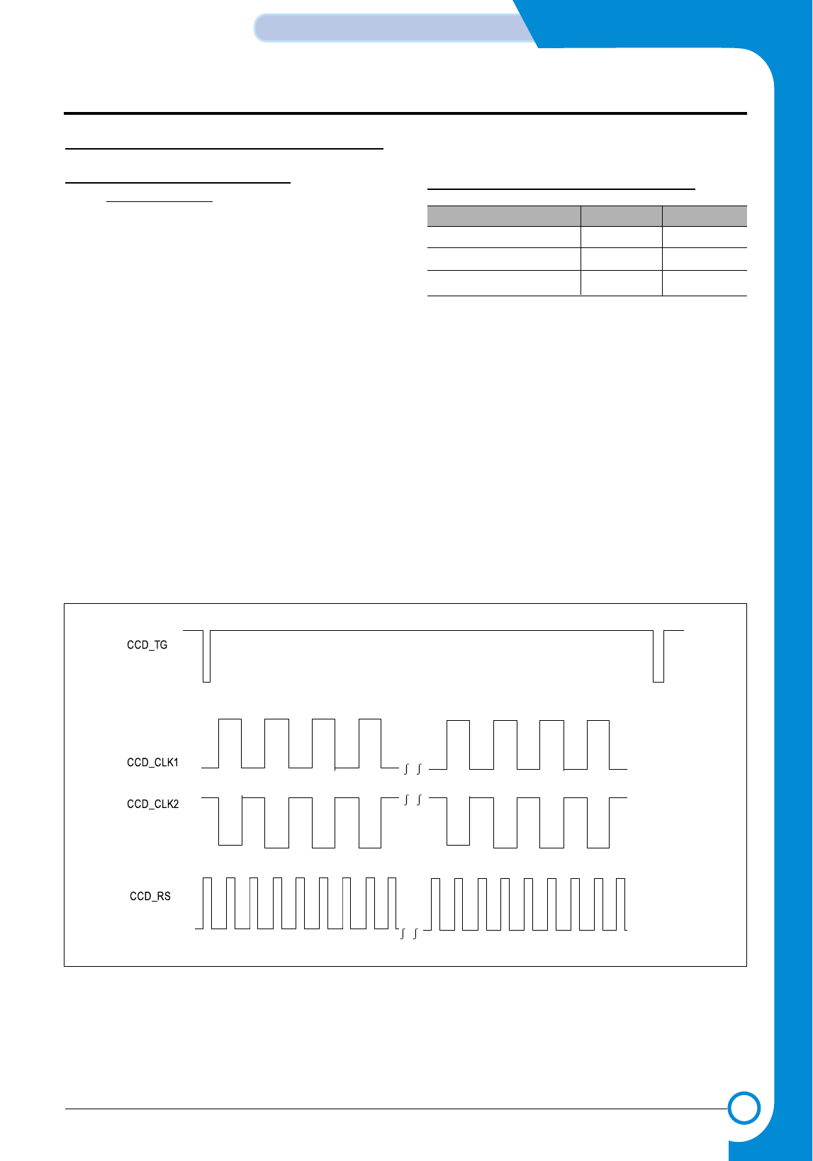
3-29
Samsung Electronics
CIRCUIT DESCRIPTION
Repair Manual
3-6 CCD MODULE and ADC Part
3-6-1 CCD MODULE GENERAL
DESCRIPTION
CCD Module has the structure transferring RGB data to
be converted into the digital signal through ADC on the
basis of the level of analog signal to OA-980, the Image
Processor, which divides the signals reflected by emitting
light to document into R, G, B data according to each fre-
quency.
The voltage used in the CCD Module are 11.75V for ana-
log signal of RGB, 5V as input for CCD and other ele-
ments. The input part of CCD Module consists of
CCD_TG, CCD_CLK1,CCD_CLK2 and CCD_RS, the
output of OA-980(U21), CCD_TG controls the scan line,
which is set variously according to copy mode, color and
mono, and scan resolution. CCD_CLK1 and CCD_CLK2
are clocks by each pixel, CD_RS is reset signal of each
pixel. Since the pixel of 1/2 cycle of CCD_CLK1 and
CCD_CLK2 is sampled, color signal sends RGB data to
output for 1/2 cycle, and controls the pixel of 1/2 cycle for
mono. Therefore, the output signal from the CCD Module
classifies the signals received by RGB channel according
to each frequency band and uses each video
signal(CN1) as the input data of ADC(U16).
TG, CLK,RS TO BE USED ARE AS FOLLOWS.
< TG, CLK,RS >
Color Copy Mono Copy
CCD_TG 5mS 2.5mS
CCD_CLK1,CCD_CLK2 1.6uS 800uS
CCD_RS 800uS 400uS
< TG, CLK,RS >
- This Document can not be used without Samsung's authorization -
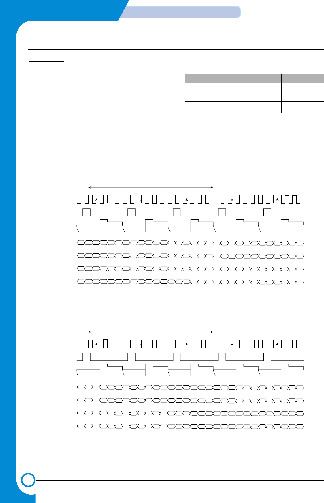
3-30
CIRCUIT DESCRIPTION
Samsung Electronics
Repair Manual
3-6-2 ADC
Description ADC(U16) is the input data that change the
analog signal of RGB to the digital signal of 16bit (8bit +
8bit) so that it may be used as the input of OA-980(U21),
image processor, while VSMP(_ADC_VSMP) is used as a
sampling signal for each pixel of RGB. That is, it controls
the signal for one pixel like CLK1,CLK2 of CCD and its
maximum sampling rate is of color 2MHz mono 4MHz.
MCLK(ADC_CLK) is CLK for the signal of VSMP, the rela-
tion between MCLK and VSMP is as follows. The relations among SCK(ADC_SCK), SDI(ADC_SDI) and
SEN(ADC_SEN) are equivalent to the control bit for regis-
ter setting to mode, output signal appears in 8bit unit from
OP0 to OP7, and 5V/3.3V will be used as the power source.
Color Mono
VSMP 800ns(1.25MHz) 400ns(2.5MHz)
ADC_CLK 133ns(7.5MHz) 133ns(7.5MHz)
VSMP:MCLK 1:6 1:3
RARBGAGBBABBRARBGAGBBABBRARBGAGBBABBRARBGAGBBABBRARBGAGBBABB
BABBRARBGAGBBABBRARBGAGBBABBRARBGAGBBABBRARBGAGBBABBRARBGAGB
GAGBBABBRARBGAGBBABBRARBGAGBBABBRARBGAGBBABBRARBRARB
GAGBBABB
RARBGAGBBABBRARBGAGBBABBRARBGAGBBABBRARBGAGBBABBRARBGAGBBABB
16.5 MCLK PERIODS
ADC_CLK
VSMP
OP[7:0]
(DEL = 00)
OP[7:0]
(DEL = 01)
OP[7:0]
(DEL = 10)
OP[7:0]
(DEL = 11)
RARBGAGBBABBRARBGAGBBABBRARBGAGBBABBRARBGAGBBABBRARBGAGBBABB
BABBRARBGAGBBABBRARBGAGBBABBRARBGAGBBABBRARBGAGBBABBRARBGAGB
GAGBBABBRARBGAGBBABBRARBGAGBBABBRARBGAGBBABBRARBRARB
GAGBBABB
RARBGAGBBABBRARBGAGBBABBRARBGAGBBABBRARBGAGBBABBRARBGAGBBABB
16.5 MCLK PERIODS
ADC_CLK
VSMP
OP[7:0]
(DEL = 00)
OP[7:0]
(DEL = 01)
OP[7:0]
(DEL = 10)
OP[7:0]
(DEL = 11)
<Figure 20. Color mode MCLK, VSMP>
<Figure 20-1. Color mode MCLK, VSMP>
- This Document can not be used without Samsung's authorization -
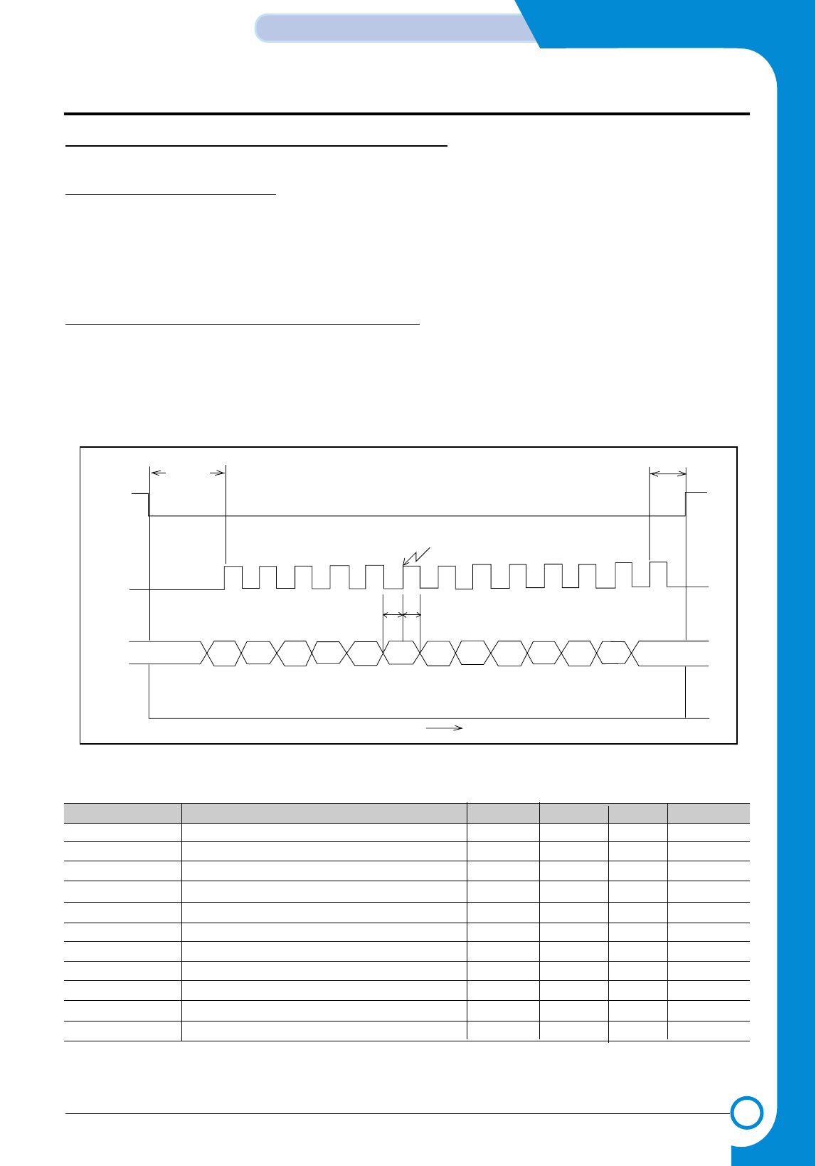
3-31
Samsung Electronics
CIRCUIT DESCRIPTION
Repair Manual
3-7 THUNDERBOLTASIC DESCRIPTION
3-7-1 ENTIRE DESCRIPTION
THUNDERBOLT ASIC is configured with SERIAL INTERFACE INPUT PORT interfacing Main controller, 2 DC-DC Converter
Controllers, Power On Reset Generation Circuit, and Motor drive part.
3-7-2 THUNDERBOLT FUNCTION DESCRIPTION
3-7-2-1 SERIAL INTERFACE INPUT PORT
To MAIN CONTROLLER(S3C46MOX(Jupiter3)), /TBCS,TBCLK,TBDO are connected with MAIN CONTROLLER (S3C46MOX
(Jupiter3)), and see the figure for Timing.
/TBCS
TBCLK
TBDO
Tcs-sclk Tcs-sclk
bit 1 bit 2 bit 3 bit 4 bit 5 bit 6 bit 7 bit 8 bit 9 bit 10 bit 11 bit 12 bit 13 SDI stays at
last value
MSBLSB
Data Latcked on the rising edge of SCLK
time
Tdhd
Tdsu
< Figure 21. SERIAL INTERFACE INPUT Timing Diagram >
Parameter Description Min Typ Max Units
Fclk Serial clock frequency 2.5 4 MHz
Tclh SCLK high width 125 200 - nsec
Tcll SCLK low width 125 200 - nsec
Tcs-sclk Delay nCS falling to first SCLK rising 250 800 - nsec
Tsclk-cs Delay last SCLK rising edge to nCS rising 250 400 - nsec
Tdsu Data valid to SCLK set up time 125 200 - nsec
Tdhd Data hold time 125 200 - nsec
Trd SDI rise time 5 20 nsec
Tfd SDI fall time 5 20 nsec
Trc SCLK rise time 5 20 nsec
Tfc SCLK fall time 5 20 nsec
< Figure 21-1. SERIAL INTERFACE INPUT Timing Specification >
- This Document can not be used without Samsung's authorization -
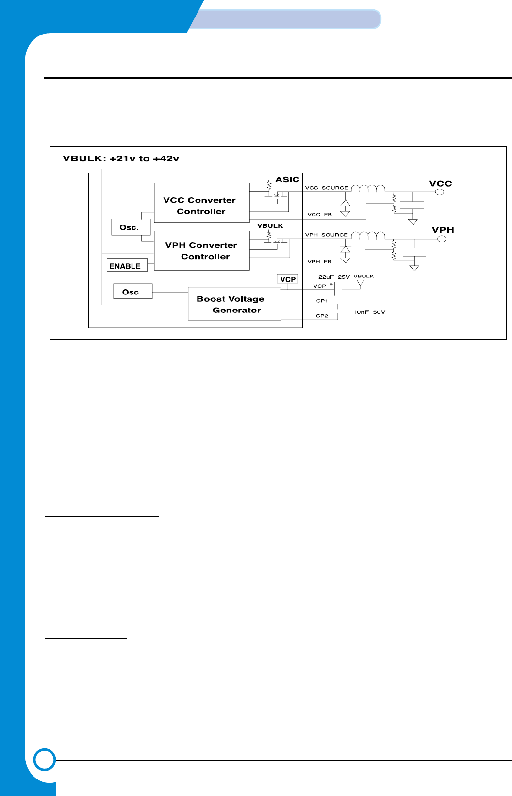
3-32
CIRCUIT DESCRIPTION
Samsung Electronics
Repair Manual
3-7-2-2 DC-DC Converter Controller
This System uses VCC by converting it to +5V, and +3.3V, the power source of the system, is obtained from the +5V convert-
ed by using REGULATOR IC to use. VPH is used as the head power by converting it to +11.82V.
3-7-2-3 Power On Reset Generation Circuit
This System does not use Power On Reset Generation Circuit.
3-7-2-4 Motor drive part
This System uses DC Motor for CR(Carriage Return) MOTOR, and Stepper motor for LF(Line Feed) motor.
• CR(Carriage Return) MOTOR drive circuit description
1 CR MOTOR specification
CR MOTOR performs reciprocating movement of CARRIAGE from side to side so that INK CARTRIDGE may print on the
paper.
• MOTOR TYPE : PM DC MOTOR “declination”
• Drive voltage : +30VDC
• Winding line resistance : 12Ω±2Ω
• Driver IC : Thunderbolt
2. CR MOTOR drive
2-1. DC Motor operation
DC Motor drive uses positive phase terminal(+) and anti-phase terminal(-) bound together respectively using 2nd Motor
Driver(MD2) of Thunderbolt ASIC inside, and controls two-way operation of DC motor, by receiving input of "DIR_DCM,"
7th bit among "PWM"(DC-motor Pulse Width Modulation) signal, output of Jupiter-III, and 13Bit Serial Port Inputs("TBDO"
Signal) coming into Thunderbolt ASIC transmitted from Jupiter-III. This Driver is driven by VBULK power source(+30V),
and on terms of Motor Stall not being generated, it is designed to supply 750mA current, and 2.4A current to output ter-
minal for maximum length of 100ms.
< Figure 22. DC-DC Converter Controller Diagram>
- This Document can not be used without Samsung's authorization -
3-33
Samsung Electronics
CIRCUIT DESCRIPTION
Repair Manual
2-2. Driver Spec.
1) Absolute Maximum Rating
2) DC Specification
3) AC/Transient Specifications
4) Truth Table
3. LF(Line Feed) MOTOR drive circuit description
3-1. LF MOTOR
• MOTOR TYPE : 2-2 Bi-polar Stepper Motor
• Drive Voltage : +30V
• Spherical line resistance : 5Ω± 7%
• Driver IC : Thunderbolt
3-2. LF Motor Operation
LF Motor(Stepper Motor) drive uses the first Motor Driver(MD1) in Thunderbolt ASIC, and Drive Pulse is output from 4
terminals of A+, A-, B+,and B-. two H letter type Drivers. Drive Pulse controls size and flow direction of current(A+ =>
A- or A- => A+) according to bit7-bit No.13 signals among 13Bit Serial Port Inputs("TBDO" Signal) coming into
Thunderbolt ASIC transmitted from Jupiter-III. This Driver is driven by VBULK power source (+30V), and on terms of
motor stall not being generated, it is designed to supply current of 600mA, maximum 700A current to each phase of
motor.
Name Description Condition Min Max Units
Vout DC Motor Driver Output Voltage 42 Volts
Iout DC Motor Driver Output Current 2.4 A
Name Description Condition Min Nom Max Units
f
PWM
PWM frequency Ta = 25C 19 20 21 KHz
DIR_DCM PWM #NAME? #NAME? #NAME? #NAME?
00On Off On Off
01Off On On Off
10On Off On Off
1 1 Off Off Off On
Name Description Condition Min Max Units
I peak Peak DC Motor Driver Output Current Not Stalled 0.75A Volts
I out DC Motor Driver Sustaining Current On Time=100ms 1.6 2.4 A
- This Document can not be used without Samsung's authorization -

3-34
CIRCUIT DESCRIPTION
Samsung Electronics
Repair Manual
3-3. Driver Spec.
1) Absolute Maximum Rating
2) DC Specification
Name Description Condition Min Max Units
V out DC Motor Driver Output Voltage 42 Volts
I out DC Motor Driver Output Current 0.7 A
Name Description Condition Min Max Units
I peak
Peak DC Motor Driver Output Current
Not Stalled 0.6A Volts
- This Document can not be used without Samsung's authorization -
3-35
Samsung Electronics
CIRCUIT DESCRIPTION
Repair Manual
3-8-1 OVERVIEW
OPE BOARD is separated from the Main Board functional-
ly, and operates entire Micom(HT48C5A-000Z) in the
Board. OPE and Main exchange mutual information using
UART(universal asynchronous receiver/transmitter) chan-
nel. Also, Resetting of OPE is designed to control at the
Main. Micom in OPE performs key-scanning and LCD, LED
display control, and senses document detect, Scan position
and so on. When information is generated from OPE(key
touch, sensor level change, etc.), it sends specific code
coping with the situation to Main, and the Main operates
system by analyzing this code. If the Main tries to display
data on OPE, the Main sends data to OPE via UART line
on the basis of the format specified, and OPE displays it to
LCD.
• This system does not apply document detect and SCAN
position.
3-8-2 UART
OPE and MAIN exchange information mutually by using
asynchronous communication mode(UART), and in full
duplex. Band rate is 9600bps, and uses 7.37MHz resonator
as oscillating element. It engages in communication with
8bit data without parity bit. UART line has two lines for Tx
and Rx, and the default level is in the 'high' state. For com-
munication, the start bit(low level) is transmitted before 8bit
data. When the data transmission(8bit) is completed, the
high state is maintained as the stop bit(high level) is trans-
mitted. Data is transmitted from LSB(DO), and MSB(D7) is
transmitted lastly.
3-9-1 UART COMMUNICATION
1) UART TX FORMAT
Codes for change of KEY, TOUCH, SENSOR LEVEL and
so on are transmitted in single code without PRE/POST
DATA, and OK or Error messages to check if communica-
tion is performed properly are also transmitted in single
code. Provided that, in case the Main requested a certain
value(LCD, other register) particularly, data requested is
transmitted followed by sending Post Data('EOH') first.
2) UART RX FORMAT
Data being received will be arranged to be received accord-
ing to the following specified format to know what data they
are.
DATA are received in the sequence of A,B,C, and D, and
the Check sum to check if the transmission is made prop-
erly will be found by doing XOR data from A to C.
◊OPE
3-8 Basic concept
3-9 UART operation
start stopbit data 8bit (D0 ~ D7) bit
D0 D1 D2 D3 D4 D5 D6 D7
a) Type of data received
b) Number of data (n+1) received after.
----------
c) DATA(N)
----------
d) Check sum(1)
- This Document can not be used without Samsung's authorization -
3-36
CIRCUIT DESCRIPTION
Samsung Electronics
Repair Manual
3-9-2 UART COMMUNICATION DATA
1) UART transmission DATA(received by the Main side)
(Note) 1. After this, keep waiting until there is response from the Main.
2. The case of longer time(longer than 10ms) elapsed longer than waiting time required for Interface is regarded as fail
3. After this code went out, then data requested it goes out.
• KEY MATRIX
Types Status DATA used port Level Remarks
key data ON 11H~ 88H PORT PC0~PORT PC7 L
OFF af H H
SCAN POSITION sensor ON a5 H PORT PB3 H SCX-1100 not applied
OFF a4 H L
DOC. detector sensor ON a1 H PORT PB-5 L SCX-1100 not applied
OFF a0 H H
For initial use of initial OPE ee H After power on, generated only once
UART communication OK b0 H (Note 2)
ERR c0 H
LCD interface of OPE OK df H When failed in the interface once &
when succeeded first(Note 2)
ERR d0 H
Self initial generation of OPE e2 H LCD data keeps status quo
Send data requested by the Main e0 H Data types:LCD, other(Note 3)
(1_H) (2_H) (3_H) (4_H) (5_H) (6_H) (7_H) (8_H)
(_1H) INK RESERVED RESERVED RESERVED CONTRAST RESERVED RESERVED RESERVED
(_2H) PAPER RESERVED RESERVED RESERVED COPY PAGE RESERVED RESERVED RESERVED
(_3H) SET UP RESERVED RESERVED RESERVED ZOME RETE RESERVED RESERVED RESERVED
(_4H) SCROLL NOLUM-UP RESERVED RESERVED RESERVED BLACK COPY RESERVED RESERVED RESERVED
(_5H) SCROLL NOLUM-DOWN RESERVED RESERVED RESERVED COLOR COPY RESERVED RESERVED RESERVED
(_6H) CANCEL RESERVED RESERVED RESERVED SPECIAL RESERVED RESERVED RESERVED
(_7H) ENTER RESERVED RESERVED RESERVED SCAN TO RESERVED RESERVED RESERVED
(_8H) QUALITY RESERVED RESERVED RESERVED POWER RESERVED RESERVED RESERVED
<SCX-1100 OPE B’D KEY MATRIX>
- This Document can not be used without Samsung's authorization -
3-37
Samsung Electronics
CIRCUIT DESCRIPTION
Repair Manual
2) Received DATA(transmitted by MAIN)
1. DATA TYPE
2. NO. OF DATA
• In case DATA is N BYTE, N+1
3. DATA
In case DATA TYPE is LCD DATA, it is configured with ASCII CODE to be displayed.
In case DATA TYPE is LED DATA, it is 1 BYTE.
LED DATA BIT ASSIGNMENT:
4. CHECK SUM
The value done XOR all of them from DATA TYPE to DATA.
5. Change of LCD types
<2 LINE * Change to 16 character LCD>
DATA TYPE : b1 H
NO. OF DATA : 2
DATA : 26 H
CHECK SUM : b1h XOR 2 XOR 16h = a5 h
<1 LINE * Change to 16 character LCD>
DATA TYPE : b1 H
NO. OF DATA : 2
DATA : 26 H
CHECK SUM : b1h XOR 2 XOR 26h = 95 h
DEFAULT : 2 LINE 16 Character LCD
In case the MAIN does not change the LCD types, it is the Default LCD state of OPE MICOM.
* SCX-1100 uses 1 LINE LCD.
DATA types Meaning Remarks
a1 H LCD DISPLAY DATA(FULL LINE)
a2 H LCD DISPLAY DATA(1'ST LINE)
a3 H LCD DISPLAY DATA(2'ST LINE)
a4 H LED DATA
b1 H Change of LCD types
DATA BIT BIT 0 BIT 1 BIT 2 BIT 3 BIT 4 BIT 5 BIT 6 BIT 7
LED NO. LED 0 LED 1 LED 2 LED 3 LED 4 LED 5 LED 6 LED 7
- This Document can not be used without Samsung's authorization -

3-38
CIRCUIT DESCRIPTION
Samsung Electronics
Repair Manual
3-10 I/O PORT configuration and use usage
It has 32 I/O Ports, and 24 Ports of them are arranged to decide I/O direction with Software Control, and the rest 8 Ports are
arranged to be used for Input or Output only. All of I/O Ports are classified into four Blocks according to the characteristics of
I/O Control, and each Block consists of 8 Ports.
1) Assignment of Port PAX
-. PA0 : LCD VCC CONTROL SIGNAL (POWER ON/OFF)
-. PA1 : LED 1
-. PA2 : RESERVED
-. PA3 : RESERVED
-. PA4 : RESERVED
-. PA5 : RESERVED
-. PA6 : RESERVED
-. PA7 : RESERVED
2) Assignment of port PBX
-. PB0(Output) : LCD Enable
-. PB1(Output) : LCD R/W
-. PB2(Output) : LCD RS
-. PB3(Input) : GND
-. PB4(Input) : Unused (Pull-up)
-. PB5(Input) : GND
-. PB6(Output) : UART TXD in Main UART
-. PB7(Input) : UART RXD from Main UART
LCD ON/OFF
In case of VCC applied to LCD No. 3 PIN (BACKGROUND LEVEL), all the LCD screen will be erased. When the power is
applied, MICOM PA0~7 are Default High LEVEL, so LCD will be OFF. From Jupiter3, LCD will be ON simultaneously with OPE
reset.
Q1, Q2 have the function of simply doing On/off only.
When pressing the Power Key, actual power is not turned Off but 11.75V terminal of Thundervolt Off in the Main, while simply
the LCD DISPLAY should not appear in OPE. At this point, Micom should be operated normally to recognize the Key when
pressing the Power key again. [The same effect as Power save]
Type I/O Control I/O direction USE Remarks
PA X Byte Control I/O => Output LED Control
Used as LCD VCCCONTROL in SCX-1100.
PB X Byte Control In : 4, Out : 4 UART, LCD, Sensor SCX-1100 SENSOR not applied.
PC X Byte Control I/O => Input Key Input
PD X Byte Control I/O => Output LCD Data, Key Scan
- This Document can not be used without Samsung's authorization -
4
4-1
Samsung Electronics
SCHEMATIC DIAGRAMS
Repair Manual
4. Schematic Diagrams
4-1 Main Circuit Diagram (1/8)
Main Board
REV 0.2
SCX-1100
6DIAGRAM
B
5
SHEET 7
7
D
12
ALL RIGHTS RESERVED
4
SHEET 2
SHEET 3
SHEET 4
MODEM PART
JUPITER.SCH MODEM.SCH
DRIV.SCH
SCANIP.SCH
SAMSUNG ELECTRONICS CO., LTD.
G
A
REF NO
C
D
E
PARALLEL PORT PART
G
PARA.SCH
1/8
234
P
6
C
A
B
C
3
E
5
E
ED. DATE
SHEET 8
2
1
SIGN
A
R
DRIVER PART
.
SHEET 5
H
E
C
K
CONN.SCH
N
MEM.SCH
.
D
W
1
.
3
CONNETOR PART
CONTROLLER PART
MEMORY PART
SEC
IMAGE PROCESSING PART
01.08.06
SHEET 6
- This Document can not be used without Samsung's authorization -
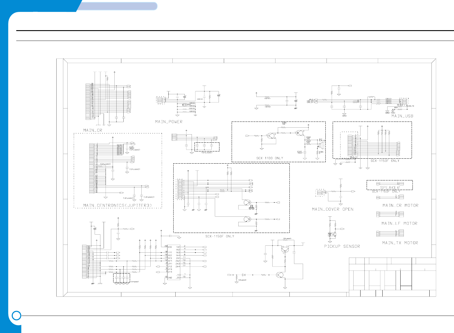
4-2
SCHEMATIC DIAGRAMS
Samsung Electronics
Repair Manual
Main Circuit Diagram (2/8)
SCX-1100
R26
Q7
KSA1203_YTF
0
R30
100 R27
CN4-3
0
CN14-10
K
REF NO
G
.
P
A
.
SIGN
CCD
A
B
CONNECTION
E
B
01.08.06
4
1
E
C
3
7
D
4
B
Main Board
1
C
E
(UNUSED)
5
2
C
C
(UNUSED)
(UNUSED)
D
6
A
H
R35 0
W
OPE_MAGIC
ED.
6
ALL RIGHTS RESERVED
N
2/8
3
G
D
REV 0.2
DATE
2
E
SAMSUNG ELECTRONICS CO., LTD.
2 3
SEC
51
RE
CN16-15
C
.
LIU
CN16-7
CN16-8
5V
DGND
10K
CN16-12
CN1-7
R153
CN16-3
5V
R375
C333
680
100nF
DGND
100nF
CN14-6
C334
Q1
2SC2812L6-TA
13
2
1K
R366
3.3V
CN5-11
0
R209
CN1-17
L8 0
3.3V
5V 5V
0L7
3
2
Q4
2SC2812L6-TA 1
C194
100pF
13
100pF
C81
DGND
11.75V
100nF
C209
2
14
0
L10
L9
11
100 R36
CN12-2
0
R37
R33R28
10K 10K TP365
10KR149
CN1-8
50V
330uF
C50
47KR136
R138 47K
L12 0
FGND
0
L11
CN14-35
FGND
CN5-22
CN5-23
CN1-3
CN5-4
CN1-1
CN5-3
100pF
C337
DGND
R135
R137 1K
1K
5
C39 47pF
CN16-5
CN1-6
CN5-10
DGND
4
DGND
CN8-4
DGND
CN5-9
CN14-28
DGND
DGND
CN14-31
C98
CN1-15
C95
10nF
3
10nF
CN7-1
1
R144
100nF
C205
DGND
CN1-26
DGND DGND
5V
CN4-2
C204
22pF
0L6
DGND
L5
R380 180K
5045-03A
CN3-1
30V
CN1-22
DGND
CN5-7
C338
100pF
100nF
C197
DIN15
CN16-1
CN14-27
C33
100nF
22pF
C203
CN5-12
CN5-13
GND30
CN13-2
CN16-6
C49
100nF
3.3V
CN1-25
U6
CD74HCT244M
CN1-13
AGND
CN16-9
CN4-1
5045-04A
30V
USB20-4W2100
CN8-1
5V
CN11-4
CN14-17
CN14-8
INV_POWER
CN6-1
3711-000225
CN4-4
DGND
CN1-20
R147
R148 10K
10K
11.75V
R44
22
CN6-3
CN6-4
CN6-2
C80
100pF
2K
R126
DGND
2K
C35 47pF
1
R123
47pF
C32
DGND
3711-002815
CN9-1
CN14-16
1.5K
16V
100uF
C118
R384
8
CN14-3
CN5-14
CN14-15
DGND
BD10
1.5K
CN1-10
R155
CN14-2
5V
DGND
CN14-20
100pF
C181
100R145
CN14-23
CN14-33
GND12
CN14-11
CN16-2
100nF
C119
C58
220pF
9
R383
CN14-34
3
68K
44.7K
R146
KSA1182-Y
Q9
DGND
100nF
C66
100
1/8W
R24
DGND
CN14-7
CN1-18
5.1K
R8
R23
47K
DGND
CN14-22
47pF
C38
5V
DGND
100 R29
CN1-12
INV_POWER
CN16-14
CN1-14
2SC2812L6-TA
Q10
GND12
7
CN5-16
CN5-17
CN5-15
R378
TP366
5V
CN14-9
0
CN1-24
11.75VA
CN5-2
FPC_24
CN5-1
BD6 0,5%
TP230
6
RPI-441C1
U5
CN1-4
BD12
CN14-25
100nF
C208
CN14-1
CN14-32
100 R34
5V
CN11-2
TP77
CN14-36
12
5VA
BD13
DGND
CN14-21
CN1-16
BD11
C82
100pF
10K
10K
R377
R25
CN5-8
CN14-4
CN1-5
5V
AGND
CN1-21
CN14-26
CN14-13
CN14-5
CN5-5
DGND
C336
100pF
TP78
CN14-29
TP367
1
3
2
DGND
2SC2812L6-TA
Q5
C3
3.3V
CN11-1
R152
25V
100uF
CN1-19
2
CN8-2
DGND
5V
4.7K
R373
CN16-4
DGND
11.75V
RB420D T147
D8
100nF
C97
CN1-11
AGND
CN13-1
CN1-23
AGND
5V
CN5-24
AGND
3K
R125
10
R207 10K
10K
R154
CN14-12
R38
10K
CN16-13
CN1-9
CN14-18
220pF
C7
CN5-18
CN5-19
CN5-6
10K
DGND
5
5V
R43
CN3-3
5V
220pF
C1
CN12-3
C67
CN14-19
16V
100uF
CN6-5
CN16-11
TP363
TP364
CN14-30
CN5-21
CN14-14
30V
DGND
CN5-20
0,5%BD7
C182
100nF
CN8-3
DGND
5V
AGND
CN11-3
CN1-2
CN16-10
R45
22K
GND30
CN12-1
10nFC96
GND30
CN14-24
3K
R124
_ERROR
_INIT
KEYTONE
CN3-2
3711-000198|scon_pin3_2.5mm
_P_PICKUP
REG1_SEN
LAMP_ON
_STB
_CML_ON
E_DP
ADF_IA0
ADF_PHA
_D_SCAN
_D_DET
_ADF_DET
VOUT_G
VOUT_R
VOUT_B
CCD_RS
HOME
OPE_TXD
OPE_TXDD
_OPE_RST
_OPE_RES
OPE_RXD
_OPE_RES
OPE_TXDD
ADF_IB1
ADF_IB0
ADF_PHB
ADF_IA1
_HOOK_OFF
_RING_DET
MODEM_RX
DP
RECALL
MODEM_TX1
REMOTE
MODEM_TX2
CCD_TG
CCD_CLK1
CCD_CLK2
CR_NA
CD(0:7)
SLCT
PE
BUSY
_ACK
_SLCTIN
_AUTOFD
LF_NB
LF_A
LF_NA
LF_B
SCAN_NB
SCAN_B
SCAN_NA
SCAN_A
COVER_OPEN
PH_ID2
PENABLE
PLOAD
PDATA3
PDATA2
PDATA1
PDATA0
PCLK
LDCS
LATCHCTL
ACLK
AGATE
_SF_POR
OK2PRT
CHY
CHX
SPK_OUT-
SPK_OUT+
CR_A
PULLUP
PH_ID1
(Unused)
(U nused)
(Unused)
- This Document can not be used without Samsung's authorization -
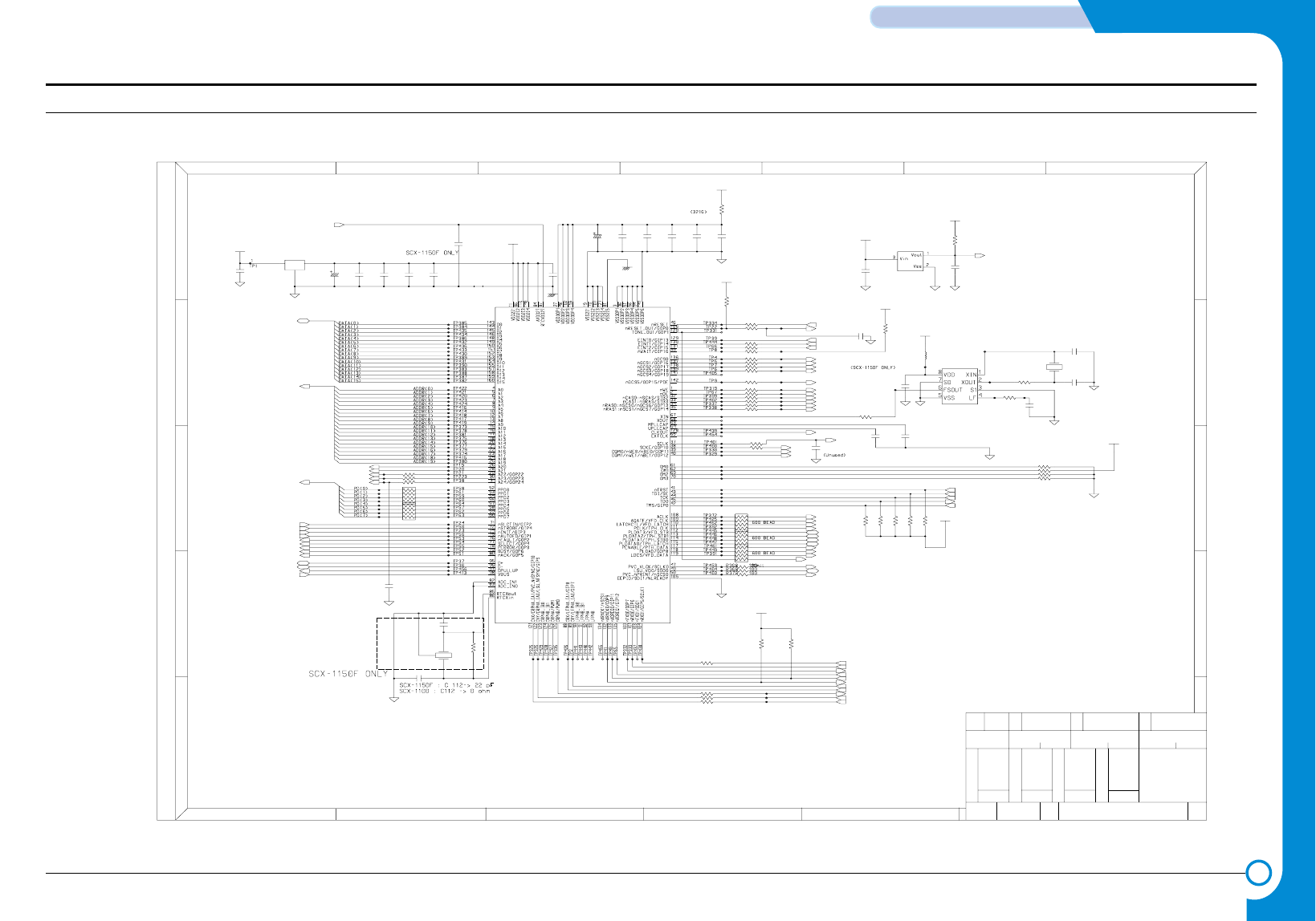
4-3
Samsung Electronics
SCHEMATIC DIAGRAMS
Repair Manual
Main Circuit Diagram (3/8)
Main Board
REV 0.2
SCX-1100
E
G
3/8
B
D
RE
P
6
CONTROLLER
2
DATE
ED.
A
SEC
CG
6
C
2
13
D
.
A
REF NO
.
C
1
SAMSUNG ELECTRONICS CO., LTD.
01.08.06
5
7
H
3
5
E
4
D
N
1
W
ALL RIGHTS RESERVED
A
2
B
SIGN
.
4
E
K
C
3
R3
10K
1nF
C215
DGND
100
R208
R100 0
R77
100nF
100K
100nF
C110C87
3.3V
100nF
C216
100
R102
R89
R91
10M
DGND
100
R59 100
R85 100
PLLGND
C220
1nF
4.7K
R94
DGND
4.7K
R101
R55 100
4.7K
R84
R64
4.7K
100R11
U15
S3C46MOX
DGND
R92 4.7K
1/16W
100
RA1
2
GND
I0
13
OUT
100
R80
LF25CDT
U11
3.3V
C89
820pF
DGND
50V
C65
1uF
R93 100
4.7K
R88
R83 100
3.3V
0,5%
BD4
100uF
C76
16V
XC61FN3112MR
U13
DGND
100nF
C78
R51 100
R50
820pF
C93
2.5V
100
1/16W
RA5
1/16W
RA4
100nF
C113
PLLGND
DGND
100nF
C99
3.3V
C79
100nF
C112 22pF
DGND
TP3
100
1/16W
RA2
100R95
100
R60
22pF
C219
100nF
C111
100
100
R86
R73
R56
100nF
C91
100nF
C92
100
C77
100nF
DGND
4.7K
R74
DGND
R71 100
100
R72
3.3V
DGND
SD16150J7-10.000M
X1
22pF
C218
C70
100pF
C217
0.68nF
R63
4.7K
22pFC125
0.32768MHz
X3
3.3V
0R76
4.7K
R75
DGND
4.7K
R78
3.3V
R90 100
DGND
3.3V
FS781BZB
U37
100nF
C64
1/16W
RA3
DGND
R61 100
C90
10nF
4.7K
R65
3.3V
R87 100
R58 100
100R57
3.3V
C109
100nF
100nF
C88
BD14
CIM21J121NES
DGND
3.3K
R204
4.7K
R62
DGND
100R107
DGND
TBCLK
TBDO
_TBCS
VB2
PENABLE
245DIR
KEYCLICK
_IP_RST
_ROM_CS
_IP_CS
_MODEM_CS
_GPIO_CS
_SCAS
_SRAS
_SCS0
_SCS1
TDO
_F_POR
PCLK
LATCHCTL
AGATE
ACLK
PDATA0
PDATA1
PDATA2
PDATA3
LDCS
PLOAD
PH_ID1
_MODEM_IRQ
_IP_INT
PD(0:7)
OPE_RXD
OPE_TXD
_IP_ACK
_IP_REQ
CHXX
CHYY
ADDR(0:19)
DATA(0:15)
_P_INIT
_P_ERROR
P_PE
_P_ACK
DQM1
DQM0
_POR
PH_ID2
SCLK
SCKE
PWM
OK2PRT
_POR
_P_STB
_P_AUTOFD
P_SLCT
_P_SLCTIN
P_BUSY
_RD
_TRST
TDI
TCK
TMS
A20
A21
IPCLK
VBUS
USB_DP
USB_DM
PULLUP
_WR
_OPE_RST
A22
_P_PICKUP
COVER_OPEN
(Unused)
- This Document can not be used without Samsung's authorization -
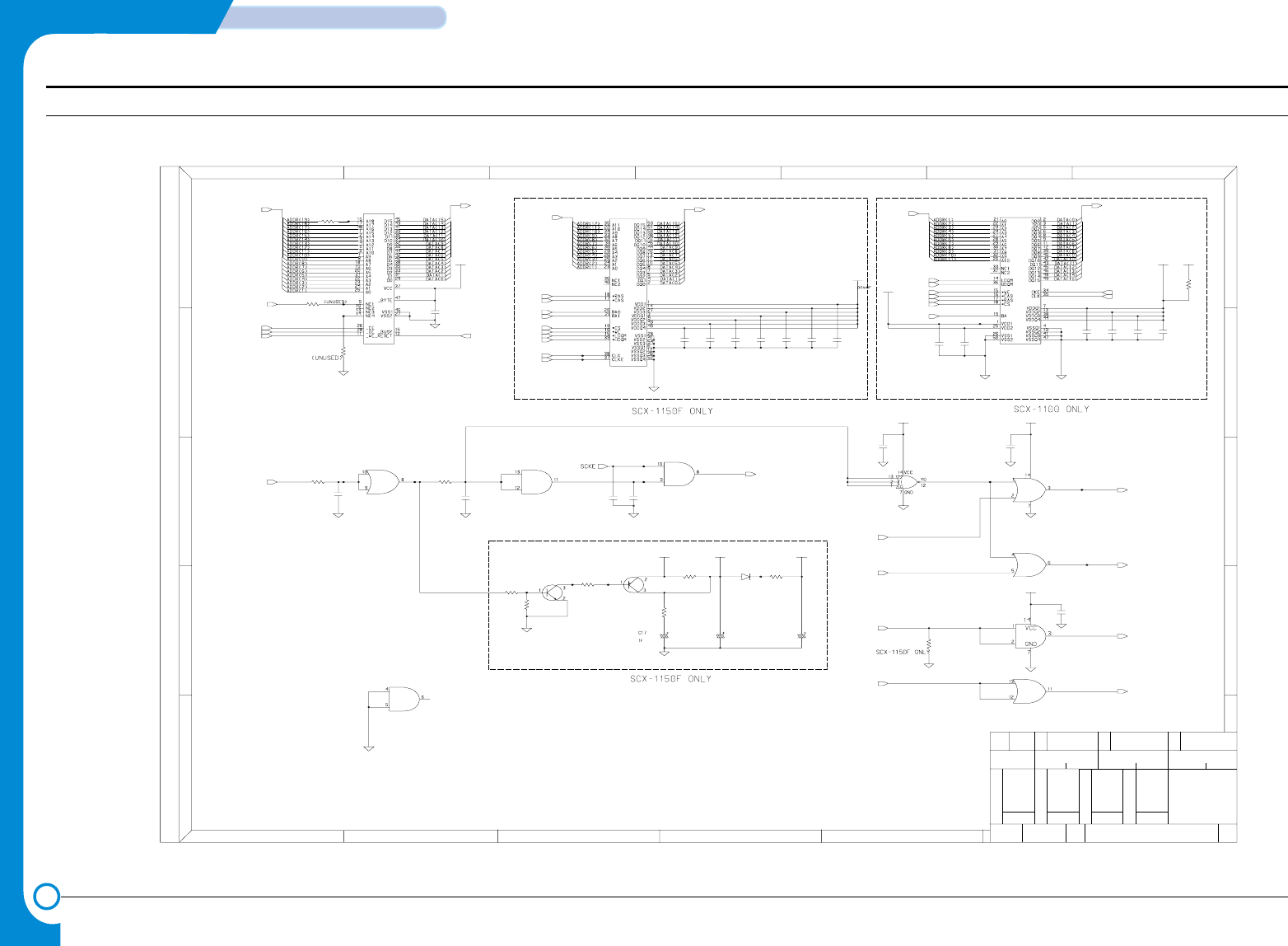
4-4
SCHEMATIC DIAGRAMS
Samsung Electronics
Repair Manual
Main Circuit Diagram (4/8)
Main Board
REV 0.2
SCX-1100
ALL RIGHTS RESERVED
2 5
2
01.08.06
W
B
K
G
ED.
(UNUSED)
E
743
G
5
SEC
P
1
D
REF NO
.
3
200
.
6
1
4/8
SIGN
E
SAMSUNG ELECTRONICS CO., LTD.
AC
E
B
E
2
H
1
N
C
4
A
R
3
3.3V
DGND
100K
R371
6
DATE
MEMORY
C.
C
D
A
D
R21
C68
100nF
U2-1
74VHC08MX
U2-2
74VHC08MX
100nF
C42
C45
100nF
16V
3VB
DGND
C31
10uF
3.3V
16V
10uF
C30
C57
100nF
100nF
C54
R13 180K
C37
100nF
C53
100nF
DGND
100pF
C8
100nF
C69
VB
MC74VHC32DR2
U1-3
MC74VHC32DR2
U1-4
DGND
68K
R12
VB
DGND
U8
K4S641632D-TC75
U1-1
MC74VHC32DR2
5.5V,5V
R32 0
1.5KR17
3.3V
C56
U2-4
74VHC08MX
DGND
100nF
100nF
C4
100nF
100nF
C43
C18
C5
100nF
DGND
VB
DGND
DGND
U9
K4S161622D-TC70
MMSD914T1
D2
R9 10K R10 10K
0
R41
DGND
0R22
R42
0
DGND
VB2
DGND
100nF
C51
C10
100pF
DGND
Q2
KSA1182-Y
DGND
100nF
C52
U7
1107-001302
DGND
3VB
MC74VHC32DR2
U1-2
3.3V
C44
100nF
DGND
C55
100nF
2SC2812L6-TA
Q8
U3-1
74VHC27
R40
DGND
C9
0
1nF
200
C6
1nF
R16
DGND
74VHC08MX
U2-3
3.3V
CHX
CHXX
CHYY
CHY
ADDR(1:19)
SD_CKE
_SD_RAS
_SRAS
_SD_CAS
_SCAS
DATA(0:15)
_ROM_CS
_RD
_WR
A20
_F_POR
DQM0
DQM1
_SD_CAS
_SD_RAS
_SCS1
_WR
A20
SCLK
SD_CKE
_F_POR
ADDR(1:11)
DATA(0:15)
ADDR(1:12)
DATA(0:15)
_SD_RAS
_SD_CAS
A21
A22
_SCS0
_WR
DQM0
DQM1
SCLK
SD_CKE
(Unused)
(Unused)
- This Document can not be used without Samsung's authorization -
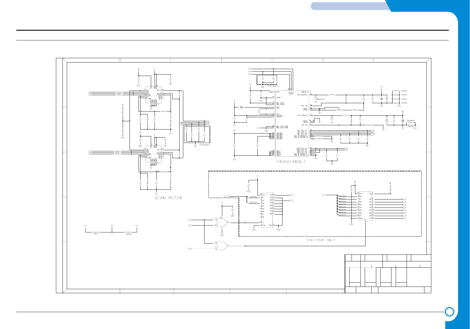
4-5
Samsung Electronics
SCHEMATIC DIAGRAMS
Repair Manual
Main Circuit Diagram (5/8)
Main Board
REV 0.2
SCX-1100
64
B
2
PE
01.08.06
B
E
6
ALL RIGHTS RESERVED
3
5
DATE
D
1
.G
SIGN
DRIVER
C
5/8
3
W
2
.
4
AD
REF NO
C
A
5
C
SAMSUNG ELECTRONICS CO., LTD.
N
K
1
A
ED.
G
H
C
D
SEC
E
1
R
3
E
2
.
7
22pF
C75
22pF
C15
30VA
C84
100nF
2007-007004
R15
12K
2K
5V
2007-000669
R18
U22
C74LCX245FT-ELP
C85
100nF
GND30
56K
R66
DGND
47nF
C13
DGND
0
R39
R387
R388 0
0
GND30
2007-000669
R19 2K
U4
17E0201
U14
TEA3718S
R20
1K
150uH
L2
JB27-00001A
C22
47nF
GND30
ZD2
1N4735A
0403-000141
0403-000150
1N4743A
ZD1
0R389
22pF
C12
R81
10K
R5 0.68
0.68R31
2007-007845|R6432_RES
DGND
DGND
C27
100nF
1KR67
DGND
30VA
100
R47
2007-000842
R14 3K
BD3
CIB32P600NES
100nF
C121
GND30
3.3V
DGND
TEA3718S
U10
0.5
R79
C59
5V
GND30
GND30
22pF
56K
R46
GND30
R4 0
C34
R70
1nF
10K
C16
22pF
C72
22pF
820pF
C83
GND30
30VB
MC74VHC32DR2
U18-2
GND30
DGND
5V
DGND
30VB
3.3V
C24
47nF
C23
47nF
30VA
C63
5V
820pF
2401-000880
3.3V
MC74VHC32DR2
U18-1
50V
220uF
C28
22pF
C73
GND30
2.7K
R54
C41
2401-001363
GND30
11.75V
DGND
16V
470uF
5V
0R6
GND30
100
R48
C152
100nF
22pF
C71
47nF
C36
R53 1K
GND12
D1
SS26
GND30
100R68
GND30
30VB
100
R69
1nF
C21
2203-000440
47nF
C14
2203-000989
DGND
0402-001212
SS26
D3
2203-000626
22pF
30V
1nF
GND30
C11
C108
C19
100nF
22pF
C61
100nF
GND30
C74
GND30
C29 22uF50V
C25
10nF
C26
100nF
100R82
GND30
5V
C62
DGND
0,5%
BD1
100nF
JB27-00001A
L1 150uH
DGND
C20
1nF
100nF
C40
GND30
R49 100
MM74HCT273WM
U17
BD2 0,5%
GND30
C86
DGND
231
820pF
2103-001041
R7
500ohm
820pF
C60 R52
0.5
CIB32P600NES
BD5
LF_A
LF_NA
LF_B
LF_NB
E_DP
RECALL
_GPIO_CS
_SPK_CTL
RX_CTL
TX_CTL
_CML_ON
DP
TONE_CTL
DATA(0:7)
SCAN_NA
SCAN_B
SCAN_NB
SCAN_A
PWM
CR_A
CR_NA
SCAN_IB0
SCAN_IB1
SCAN_IA1
DATA(0:3) _HOOK_OFF
_RING_DET
_WR
_RD
TBCLK
TBDO
_TBCS
SCAN_PHA
SCAN_PHB
SCAN_IA0
(Unused)
- This Document can not be used without Samsung's authorization -
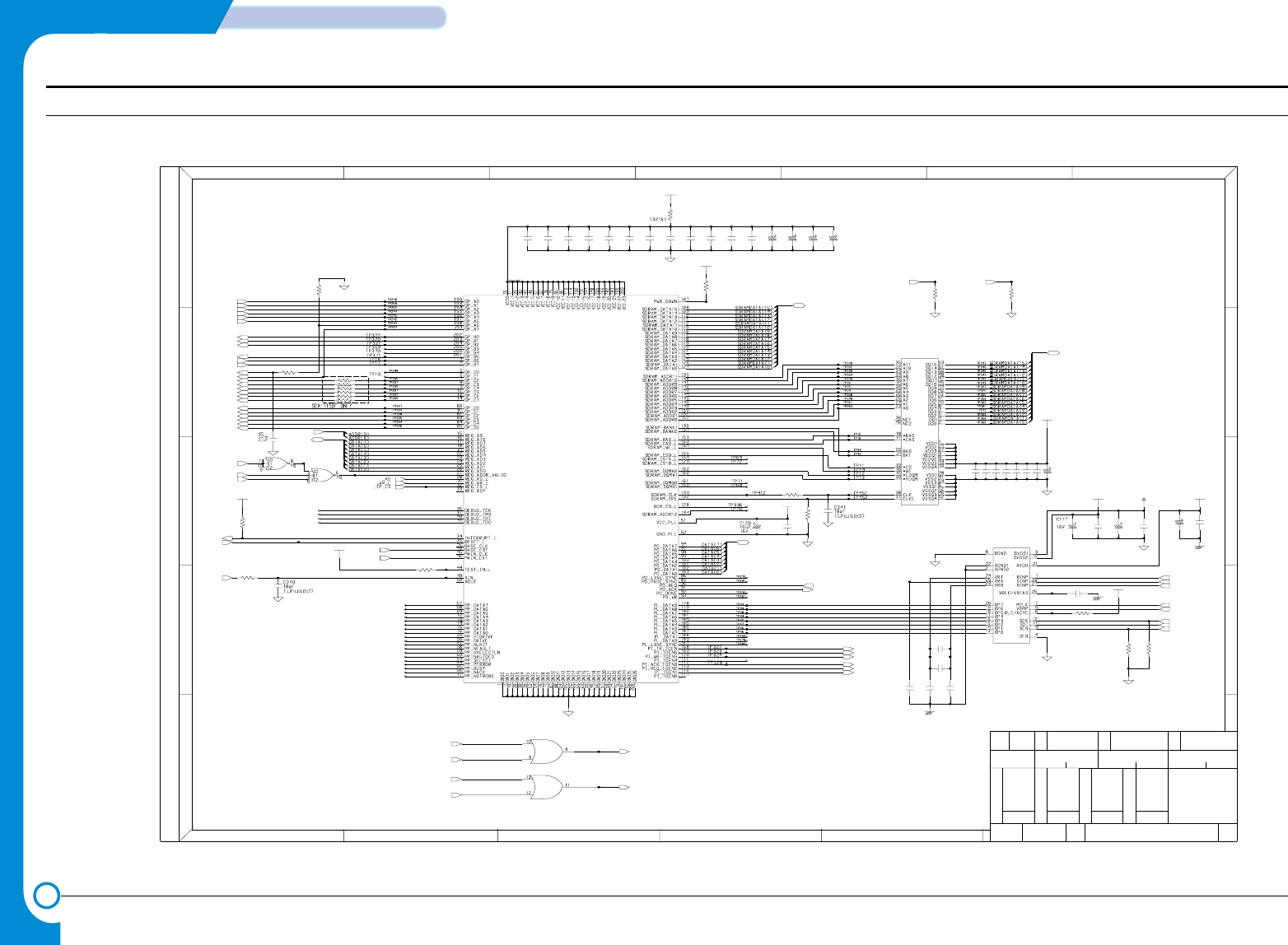
4-6
SCHEMATIC DIAGRAMS
Samsung Electronics
Repair Manual
Main Circuit Diagram (6/8)
Main Board
REV 0.2
SCX-1100
3
2
C
D
7
.
2
ALL RIGHTS RESERVED
SIGN
6/8
D
E
01.08.06
6
E
4
G
E
4
B
5
5
C
C
P
1
K
6
1
W
.
N
2
A
SAMSUNG ELECTRONICS CO., LTD.
C
ED.
IMAGE PROCESS
.
B
A
DATE
3
H
1
3
DA
SEC
R
REF NO
G
E
R374
DGND
100nF
C201
33
1
TP233
1
R98
TP268
R104
4.7K
100
RA6
100
1/16W
C162
100nF
TP231
1
TP32
1
TP234
1
C196
100nF
C128
100nF
3.3V
R115 100
C198
10uF
16V
TP30
1
100nF
C164
U16
WM8192
100nF
C151
TP232
1
C177
100nF
TP29
1
TP460
DGND
TP235
1
100nF
C103
10nF
C102
3.3V
TP459
U3-2
DGND
74VHC27
R117 100
100nF
C165
C139
100nF
C105 100nF
100nF
C200
3.3V
C143
10uF
16V
R105
4.7K
3.3V
1TP238
C116
100nF
R134
AGND
4.7K
C131
100nF
100nF
C130
16V
10uF
C180
DGND
100
R205
AGND
C114
100nF
C202
100nF
U18-4
MC74VHC32DR2
1000nF
C104
100nF
C94
3.3V
R118 1K
0,5%
100nF
BD8
C178
0
R119
1
TP33
1
TP26
MC74VHC32DR2
U18-3
1TP236
16V
C127
10uF
100nF
DGND
C179
OA-980
U21
R116
4.7K
DGND
100nF
DGND
C142
16V
10uF
C129
3.3V
5V
3.3V
TP25
1
TP457
C176
10uF
16V
C153
DGND
C163
100nF
100nF
TP28
1
10uF
16V
C107
DGND
DGND
74VHC27
U3-3
TP458 10uF
47KR97
100nF
C106
TP31
1
DGND
5VA
TP269
1
DGND
TP27
1
DGND
DGND
U27
K4S641632C
R128
4.7K
100nF
C115
TP450
100nF
C193
0
AGND
4.7K R120
R206
TP237
1
3.3V
100nF
C140
VOL_00
VOL_20
VOL_10
LAMP_ON
_SF_POR
_MODEM_RST
_IP_RST
_WR_L
_IP_ACK0
ADDR(10)
_WR
_IP_ACK
_RD
HOME
ADF_PHA
ADF_PHB
ADDR(10)
MAINEXT
CCD_RS
CCD_CLK1
VOUT_B
VOUT_G
ADF_IB1
ADF_IB0
ADF_IA1
ADF_IA0
_ADF_DET
REG1_SEN
_IP_INT
_IP_REQ
_IP_ACK0
_ADC_VSMP
ADC_SEN
ADC_SDI
ADC_CLK
SCAN_PHA
SCAN_PHB
SCAN_IA1
SCAN_IA0
SCAN_IB1
SCAN_IB0
ADC_SCK
ADC_SEN
ADC_SDI
_D_DET
_D_SCAN
VOUT_R
ADC_SCK
CCD_CLK2
SDRAMDATA(0:15)
SDRAMDATA(0:15)
DATA(0:7)
_IP_CS
_WR
BASEEXT
ADDR(9:8)
DATA(0:7)
BASEEXT
MAINEXT
IPCLK
CCD_TG
_ADC_VSMP
ADC_CLK
(Unused)
- This Document can not be used without Samsung's authorization -
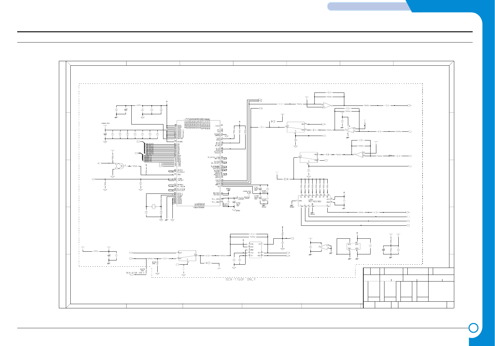
4-7
Samsung Electronics
SCHEMATIC DIAGRAMS
Repair Manual
Main Circuit Diagram (7/8)
Main Board
REV 0.2
SCX-1100
.
7/8
E
G
D
P
SIGN
SEC
DATE 1
01.08.06
C
SAMSUNG ELECTRONICS CO., LTD.
4
1
R
4
3
MODEM
D
E
D
G
3
A
B
ED.
R167
H
5
A
.
C
W
5
2
A
B
REF NO
6
6
.K
ALL RIGHTS RESERVED
E
2
2
1 7
E
N
C
C
3
R142
C188 100nF
47KR163
100nFC184
47K
C213 1nF
R130 120K
R166
MC14053BD
U23-2
150K
U24-2
KA358D-T/F
100nF
C146
U25-2
KA358D-T/F
C210
3.3V
5V
1nF
300K
DGND
330KR164
3.3V
MMSD914T1
D6
DGND
100nF
C136
11.75V
AGND
MC34119DR2
U34
R160
5V
330K
+3.0V
DGND
R141
47K
AGND
100nF
C187
130KR143
0R157
+3.0V
+3.0V
DGND
MC14053BD
U23-3
100nFC214
11.75VA
C147
100nF
AGND
5V
+3.0V
R159 4.7K
C212
1uF
DGND
11.75VA
10uHL4
R140 3K
U25-1
KA358D-T/F
R139 120K
DGND
AGND
MC14053BD
U23-4
U19
FM336R6719-12
MMSD914T1
D7
DGND
C155
100nF
27pF
C122
1nF
C166
10K
R114
AGND
DGND
DGND
100nFC199
1nFC175
C149
100nF
C134
5V
100nF
C135
1nF
11.75VA
100nFC183
100nF
C169
8.2K
R129
AGND
C132 100nF
1nFC189
R109
10K
10K
R113
5V
C170
100nF
C138
22uF
16V
R165
10K
C145
AGND
100nF
11.75VA
150KR162
C174 100nF
+3.0V
R121
10K
330KR131
R372
10K
AGND
C133
100nF
R158 1M
C173
100nF
1MR379
DGND
16V
22uF
C150
AGND
R112 10K
100nF
C168
27pF
C154
C123
1nF
C172
100nF
25V
22uF
C156
1uF
C211
R122
4.7K
24K
R127
91KR132
BD9
CIM21J121NES
+3.0V
AGND
28.224MHz
X2
R110
100
C144
1nF
C186 1nF
C148
100nF
100nFC185
47KR133
Q3
2SC2812L6-TA
16V
10uF
C167
DGND
5V
KA358D-T/F
U24-1
DGND
5V
C206
100nF
R156 1M
AGND
C171 100nF
0
DGND
+3.0V
C137
R161
100nF
U23-1
MC14053BD
C157
100nF
KEYTONE
MMSD914T1
D4
DGND
_SPK_CTL
TONE_CTL
TX
_MODEM_RST
TX_CTL
TONE_OUT
VOL_2
VOL_1
VOL_0
REMOTE
SPK_OUT+
SPK_OUT-
TONE_OUT
KEYCLICK
RX
_WR
_RD
_MODEM_CS
MODEM_TX2
MODEM_TX1
MODEM_RX
DATA(0:7)
ADDR(0:4)
_MODEM_IRQ
RX_CTL
RX
TX
(Unused)
- This Document can not be used without Samsung's authorization -
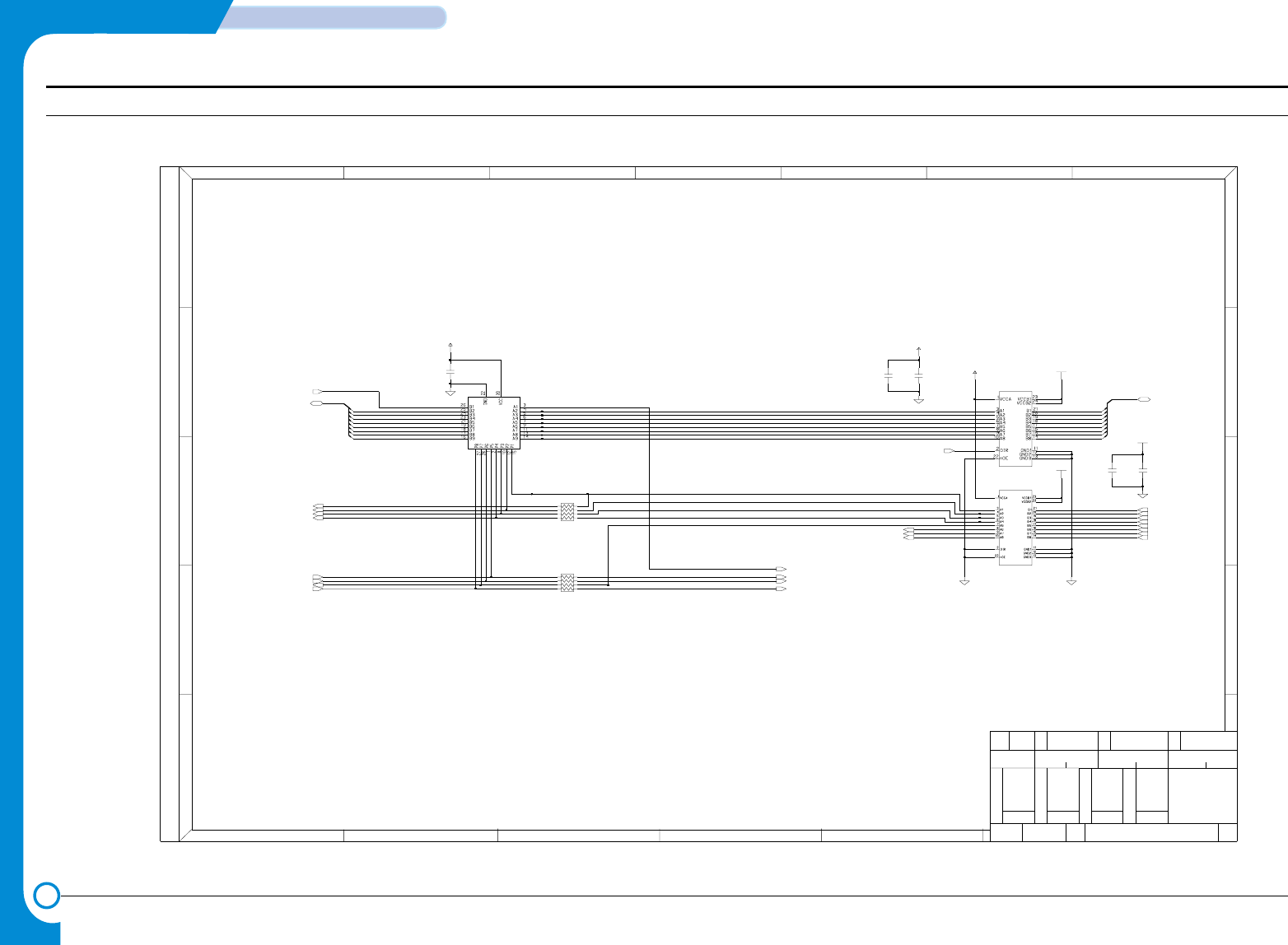
4-8
SCHEMATIC DIAGRAMS
Samsung Electronics
Repair Manual
Main Circuit Diagram (8/8)
Main Board
REV 0.2
SCX-1100
3.3V
W
3
5
C
DATE
5
.
P
2
SEC
A
D
D
C
H
3
G
4
2
1
01.08.06
E
2
SAMSUNG ELECTRONICS CO., LTD.
K
ED.
G
.
ALL RIGHTS RESERVED
RE
6
A
71
A
C
N
8/8
D
E
6
.
B
REF NO
E
13
B
C
PARALLEL PORT PART
SIGN
4
DGND
5V
100nF
C192C191
100nF
3.3V
DGND
U26
TC74LVX4245MTCX
3.3V
HIC1
SUPER1284
RA8 39
100nF
C195 5V
U33
TC74LVX4245MTCX
C190
100nF
5V
100nF
C207
DGND
DGND
RA739
CD(2)
CD(3)
_P_STB
_P_ACK
P_BUSY
P_PE
P_SLCT
_P_ERROR
VOL_00
VOL_10
VOL_20VOL_2
VOL_1
VOL_0
DGND
CD(1)
CD(0)
_STB
_INIT
_ERROR
_SLCTIN
_AUTOFD
SLCT
PE
BUSY
_ACK
_P_SLCTIN
_P_AUTOFD
245DIR
PD(0:7)
PD(0)
PD(1)
PD(2)
PD(3)
PD(4)
PD(5)
PD(6)
PD(7)
_P_INIT
CD(0:7)
CD(4)
CD(5)
CD(6)
CD(7)
- This Document can not be used without Samsung's authorization -
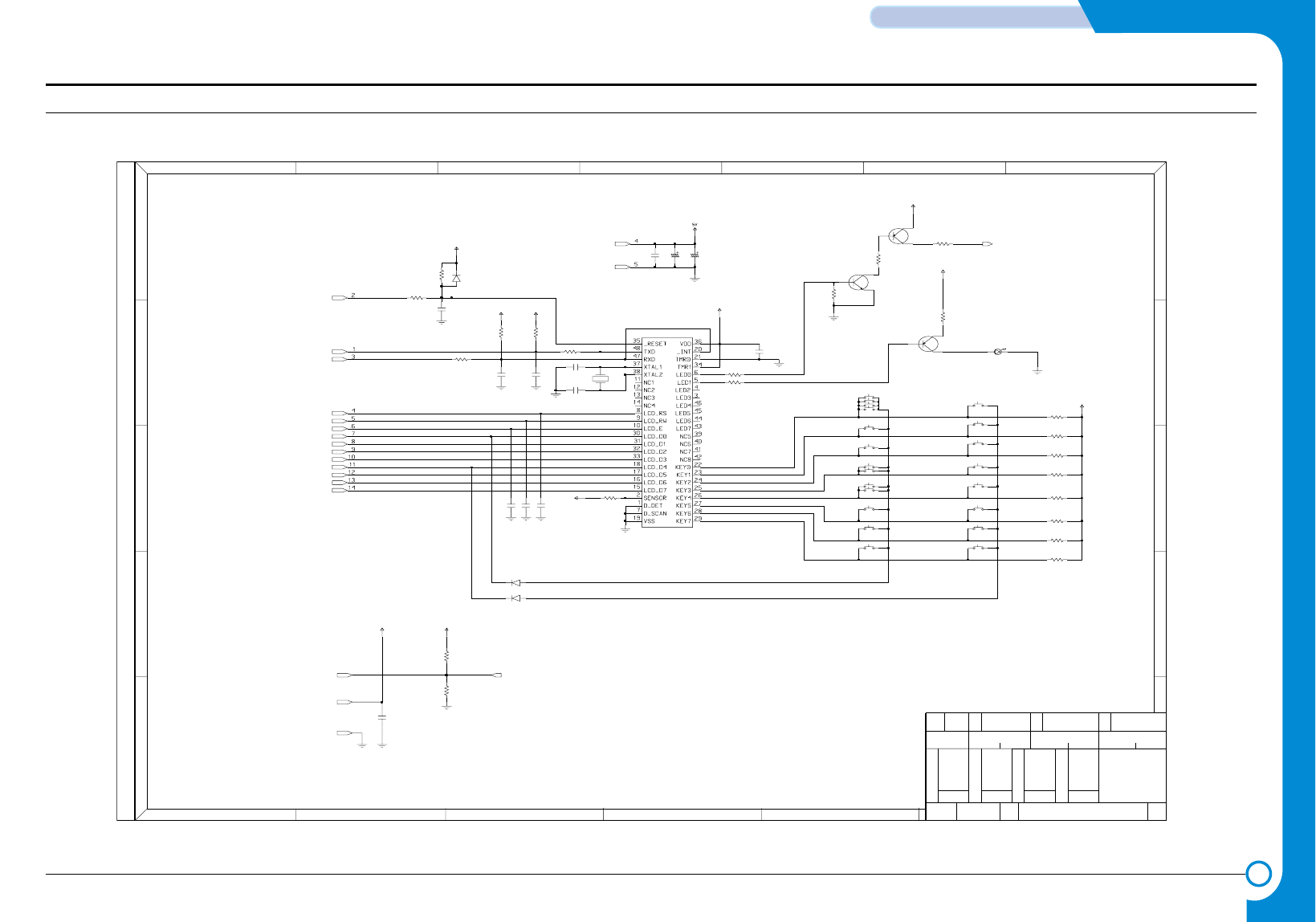
4-9
Samsung Electronics
SCHEMATIC DIAGRAMS
Repair Manual
4-2 OPE Circuit Diagram
1
01.07.2
1/1
3456
23
SIGN
A
C
D
B
E
12
OPE_TXD
OPE_RXD
+5V
67
A
NR
P
.
C
G
GND
REF NO SEC
H
E
C
K
SAMSUNG ELECTRONICS CO., LTD.
SCX-1100
LCD_RS
LCD_RW
OPE Board
MAGIC SEC OPE PART
LCD_E
ALL RIGHTS RESERVED
A
B
C
D
E
LCD_D0
LCD_D1
LCD_D2
LCD_D3
LCD_D4
LCD_D5
LCD_D6
LCD_D7
E
ED. DATE 1
2345
REV 0 .3
.
D
W
G
.
/OPE_RST
R13
GND5
OSC1
CSACS_7.37MHz
22K
22K
200
5V5V
R12
R22
22K
R18
100nF
1000nF
C4
100nF
C3
680
C2
10K
R17
GND5
GND5
5V
5V
R16
MMSD914T1
D3
5V
scroll/volume_down
power
R7
22K
GND5
5V
GND5
5V
GND5
U1
HT48R50
22K
R5
CN2-4
CN2-5
special
scroll/volume_up
CN1-8
GND5 GND5
zoomrete
CN1-7
scan to
CN1-6
GND5
CN1-5
GND5
16V
10uF
C1
CN2-1
CN1-4
GND5 GND5
ink
CN1-3 3
1
CN1-2 2
GND5
CN1-1
1
3
2
R8
22K
Q2
2SC2812L6-TA
13
2
KSA1182-Y
Q1
MMSD914T1
D1
5V
SLS-NNGR202TS
LED1
5V
R24
150
22K
R23
C13
10uF
16V R20
1.5K
MMSD914T1D2
180KR19
22K
R11
R9
R10
22K
100nF
22K
Q3
KSA1182-Y
1
3
2
GND5
C5
setup
5V
paper
cancel
CN2-2
color copy
CN2-3
R6
22K
C9 C10
22pF22pF
C8
22pF
R14
22K
contrast
enter
quality
200
GND5
R3
200
R2
CN1-14
R1
200
CN1-13
CN1-11
CN1-12
CN1-10
R21
68K
CN1-9
copy page
1K
black copy
R25100pF
C7C6
100pF
47pF
C12
C11
47pF
OPE_POW
OPE_POW
- This Document can not be used without Samsung's authorization -
4-10
SCHEMATIC DIAGRAMS
Samsung Electronics
Repair Manual
4-3 SMPS Circuit Diagram
{Doc} 01
MAGIC POWER SUPPLY CIRCUIT DIAGRAM (Magic-V3)
B
11
Friday, July 20, 2001
Title
Size Document Number Rev
Date: Sheet of
F1 LF1
SQH0350 BD1
PC1
H
NT1
TNR1
+3.3V0.8A
+30V1.3A
IL1
CON1-1
CON1-2
CON1-3
CON1-4
PE
4
7
6
T1
EE2525W
N
U2
D4=SR204
C14=16V47uF
C11=50V470uF/KMG
ZD4=1W36V
3
R-30190
AC250V T 2A
R1=1W560K
10D561K
C1=224
C3=222
2KBP06M
DSC10D9
C5=400V120uF
R3=1/4W/180K
SSP5N80A
C6=1KV331
R5=47K
R4=1W0.42(MINI)
Q3=C1008-Y
C8=103 D2=1N4148
PC1=PC123B
ZD2=4.3VB
C13=10V1000uF
R14=6.8K
R13=510
R15=6.8KF
C10=1uF
PC123B
Magic-V3 POWER
SUPPLY(100-240Vac)
KA78R33
R10=330
Q4=C1008
C7=PC630V103
Q1
X
3
4
1
2
10
C4=222
C2=104
R2=1/4W180K
Q2=FQU2N60
ZD1=9.1V
C9=103
R6=510
R11=180
D1=1N4148
D3=1N4148
R8=330
R7=3.3KF
R9=33
B1=BEAD
9
D5=ER502
C12=50V47uF/KMG
R12=1K
ZD3=5.6V
R16=1.8KF
10D471K
R20=1/4W68K
R17=1W0.42(MINI)
R18=2W2.2K
132
B2=BEAD
3t
48t =550uH
3t
12t 2t
ZD5=27V
C15=1KV102
R19=1/4W/180K
R21=1/4W22
2
1
8
-+
t
CH1
CH3
GND
GND
- This Document can not be used without Samsung's authorization -

Electronics
- This Service Manual is a property of Samsung Electronics Co.,Ltd.
Any unauthorized use of Manual can be punished under applicable
International and/or domestic law. -

Samsung Electronics Digital Printing
CS Group
Copyright (c) 2001. 10
This manual is made and
described centering around
circuit diagram
and circuit description needed
in the repair center
in the form of appendix.
SAMSUNG
