SF530
User Manual: SF530
Open the PDF directly: View PDF ![]() .
.
Page Count: 141 [warning: Documents this large are best viewed by clicking the View PDF Link!]
- SF-530_XAA.0000051600.E.16.pdf
- SF-530/531P
- 1.Block Diagram
- 2. Connection Diagram
- 3. Circuit Description
- 4.Schematic Diagrams
- 4-1 Main Circuit Diagram (1/6)
- 4-2 Main Circuit Diagram (2/6)
- 4-3 Main Circuit Diagram (3/6)
- 4-4 Main Circuit Diagram (4/6)
- 4-5 Main Circuit Diagram (5/6)
- 4-6 Main Circuit Diagram (6/6)
- 4-7 LIU Circuit Diagram (1/2)
- 4-8 LIU Circuit Diagram (2/2)
- 4-9 OPE Circuit Diagram
- 4-10 Scan Circuit Diagram (200DPI)
- 4-11 Scan Circuit Diagram (300DPI)
- 4-12 HVPS Circuit Diagram (1/2)
- 4-13 HVPS Circuit Diagram (2/2)
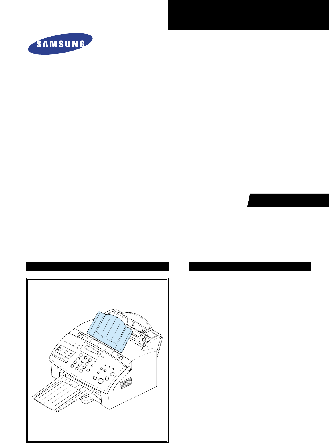
SERVICE
SAMSUNG FACSIMILE
SF-530/531P
Manual
FACSIMILE CONTENTS
1. Precautions
2. Specifications
3. Disassembly and Reassembly
4. Troubleshooting
5. Exploded Views and Parts List
6. Block Diagram
7. Connection Diagram

ELECTRONICS
© Samsung Electronics Co.,Ltd. September
2001
Printed in Korea.
VERSION NO. : 1.00 CODE : JC-0059A
This service manual is also provided on the web,
the ITSELF system Samsung Electronics Co., Ltd.
http://itself.sec.samsung.co.kr

This manual is stated and
provided for service description.
All rights reserved. Any parts of the
information in this manual are prohibited
from free duplication, use or translation
without prior written approval except in
cases allowed by the Copyright Act.
Specifications are subject to change without
prior notice.
Copyright (c) 2001. 9.
Samsung Electronics Digital Printing CS Group
Precautions
1-1
Samsung Electronics
1. Precautions
Please read the following carefully to prevent any accidents and not to damage the unit during service.
1-1 Safety Precautions
1-2 Precautions on Disassembly and Reassembly
1. Safety Precautions
There are some electric or machinery parts with safety
related property. If the parts replaced are different from
the original, the safety may not function. Even if the part
could allow higher voltage than that of the part used, do
not replace it and use a regular product clarified in spec-
ifications.
2. Be careful not to leave a switch, a cover or a safety device
out when reinstalling or assembling the product after
repair.
3. Replacing Precautions
Do not change or add parts as you like. You cannot ben-
efit from such a remodeled product at your will during the
term of guarantee.
4. You must replace overheated or damaged parts or cords
with regular products. Please solve the problem causing
any damage or overheating and troubles beforehand.
Especially mind the safety on the part with this
mark.
You must use regular parts described in specifica-
tions for the parts inflammable and where the cur-
rent can be flown. Otherwise any hazard such as
an electric shock or a fire could occur.
LASER STATEMENT (LASERTURVALLISUUS)
WARNING : NEVER OPERATE AND SERVICE THE PRINTER
WITH THE PROTECTIVE COVER REMOVED
FROM LASER/SCANNER ASSEMBLY. THE
REFLECTIVE BEAM, ALTHOUGH INVISIBLE, CAN
DAMAGE YOUR EYES.
Class 1 laser product
Luokan 1 laserlaite
Klass 1 laser apparat
Allonpituus 770-795nm
Teho 0.3mW±0.03mW
CAUTION
VORSICHT
ATTENTION
ATTENZIONE
PRECAUCION
CAUTION : Avoid exposure to invisible laser radiation when the
development unit is not installed.
INVISIBLE LASER RADIATION WHEN
THIS COVER OPEN. DO NOT OPEN
THIS COVER.
UNSICHTBARE LASERSTRAHLUNG,
WENN ABDECKUNG GEOFFNET.
NIGHT DEM STRAHL AUSSETZEN.
REYONNEMENT LASER INVISIBLE EN CAS
D’OUVERTURE. EXPOSITION DANGERUSE AU
FAISCEAU.
RADIAZIONE LASER INVISIBLE IN CASO DI
APERTURA. EVITARE L’ESPOSIZONE LA FASCIO.
REDIACION LASER INVISIBLE CUANDO SE
ABRE. EVITAR EXPONERSE AL RAYO.
Very careful precautions should be taken when replacing
parts. Before replacing, please check cables because you
cannot put the cables that you removed for replacing parts
into the proper place if you would not make sure of where
they were connected and in which condition.
Please do the following before disassembling
for a repair or replacement of parts.
1. Pull out paper cassette, printer cartridge installed.
Especially careful not to be scratched by the surface of
developer or not to expose them to light.
2. Turn the power switch off.
3. Take out the power plug, printer cable from the printer.
4. Use only the same type of part as original when replacing
parts.
5. Do not force to open or fasten plastic material compo-
nents.
6. Be careful that small parts such as screws should not get
in the printer.
7. When disassembling, assembling, also observe small
components are located in place.
8. If you uncover and turn the machine over to replace some
parts, toner or paper particles may contaminate the LSU
window. Protect the LSU window with clean paper.
Releasing Plastic Latches
Many of parts are held in
place with plastic latches.
The latches break easily :
release them carefully.
To remove such parts, press
the hook end of the latch
away from the part to which
it is latched.

Certain semiconductor devices can be easily damaged by
static electricity. Such components are commonly called
“Electrostatically Sensitive (ES) Devices”, or ESDs.
Examples of typical ESDs are: integrated circuits, some field
effect transistors, and semiconductor “chip” components.
The techniques outlined below should be followed to help
reduce the incidence of component damage caused by sta-
tic electricity.
1. Immediately before handling a semiconductor compo-
nent or semiconductor-equipped assembly, drain off any
electrostatic charge on your body by touching a known
earth ground. Alternatively, employ a commercially avail-
able wrist strap device, which should be removed for your
personal safety reasons prior to applying power to the unit
under test.
2. After removing an electrical assembly equipped with
ESDs, place the assembly on a conductive surface, such
as aluminum or copper foil, or conductive foam, to pre-
vent electrostatic charge buildup in the vicinity of the
assembly.
3. Use only a grounded tip soldering iron to solder or desol-
der ESDs.
4. Use only an “anti-static” solder removal device. Some sol-
der removal devices not classified as “anti-static” can
generate electrical charges sufficient to damage ESDs.
5. Do not use Freon-propelled chemicals. When sprayed,
these can generate electrical charges sufficient to dam-
age ESDs.
6. Do not remove a replacement ESD from its protective
packaging until immediately before installing it. Most
replacement ESDs are packaged with all leads shorted
together by conductive foam, aluminum foil, or a compa-
rable conductive material.
7. Immediately before removing the protective shorting
material from the leads of a replacement ESD, touch the
protective material to the chassis or circuit assembly into
which the device will be installed.
8. Maintain continuous electrical contact between the ESD
and the assembly into which it will be installed, until com-
pletely plugged or soldered into the circuit.
9. Minimize bodily motions when handling unpackaged
replacement ESDs. Normal motions, such as the brush-
ing together of clothing fabric and lifting one’s foot from a
carpeted floor, can generate static electricity sufficient to
damage an ESD.
1-3 ESD Precautions
Precautions
1-2 Samsung Electronics
CAUTION:
Be sure no power is applied to the chassis or cir-
cuit, and observe all other safety precautions.
Precautions
1-3
Samsung Electronics
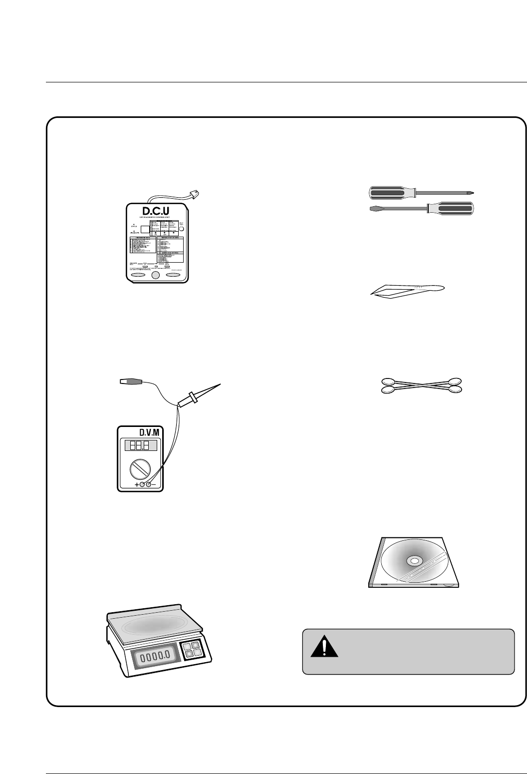
1-4 Tools for Troubleshooting
The following tools are recommended for safe and smooth troubleshooting described in this service manual.
DCU(Diagnostic Control Unit)
Standard: Test equipment to diagnose the Laser
printer supplied by Samsung Electronics.
DVM(Digital Volt Meter)
Standard: Indicates more than 3 digits.
Electronic Scale
Standard: Equipment to check the weight of con-
sumables(toner cartridge) supplied by Samsung
Electronics. (The gram unit can be measured.)
Driver
Standard: "-" type, "+" type (M3 long, M3 short,
M2 long, M2 short).
Pinset
Standard: For general home use, small type.
Cotton Swab
Standard: For general home use, for medical ser-
vice.
Cleaning Equipments a IPA(Isopropyl
Alcohol)dry cloth or a soft stuff neutral
detergent.
Software(Driver) installation CD ROM
Mind your hands not to be touched when
you disassemble and reassemble PBAASS'Y,
such as the main board, SMPS, HVPS.
Note
1
2
3
4
5
6
7
8

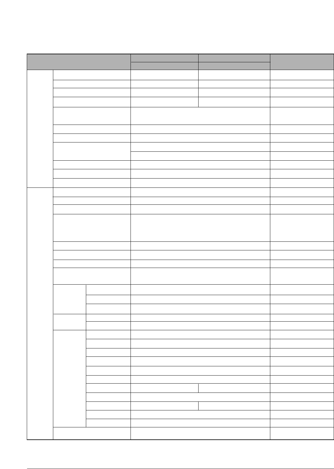
ITEMS FAX MFP REMARKS
SF-530 SF-531P
2.Specifications
Samsung Electronics 2-1
General Size(W*D*H) 370 X 356 X 195 mm
Weight 6.9 Kg (With accessories)
Power Rating AC 110V ~ 120V ± 15%, 50/60Hz ± 3Hz
AC 220V ~ 240V ± 15%, 50/60Hz ± 3Hz
Operating Environment Temperature : 10 ~ 32˚C
Humidity : 20 ~ 85% RH
LCD 16*1 Char 16*1 Char
Interface NA ECP(IEEE1284), USB
Halftone 64 Level 64 Level
Life 50000 Pages 50000 Pages
Power Power Button No No
Input Voltage 110V~120V, 220V~240V 110V~120V, 220V~240V
Power Idle 10 W/H 10 W/H
Consumption Max 140 W/H 140 W/H
Power Save Mode OFF, 15, 30, 60 Min OFF, 15, 30, 60 Min
Print Print Method Laser Laser
Speed 8ppm (FAX Print Out) 8ppm (
PC Print & Fax Print)
Resolution Normal NA 600 x 600 DPI
Print language No PrinThru
Toner Save 30 ~ 50 % 30 ~ 50 %
Scan Scan Method CIS CIS
Quick Scan Speed 6 sec 3 sec
Resolution 200 x 200 DPI 300 x 300 DPI
Scan Width Max 216 mm 216 mm
Effective 210 mm 210 mm
Scan Length Max 1000 mm 1000 mm
(Std Mode : 365 mm) (Std Mode : 365 mm)
Copy Speed 8 ppm 8 ppm
Resolution 600 x 600 DPI 600 x 600 DPI
Zoom Range 50 ~ 130 % 50 ~ 200%
Collate/Reverse Yes Yes
Multi Copy 1 ~ 99 1 ~ 99
2-2 Samsung Electronics
Specifications
ITEMS FAX MFP REMARKS
SF-530 SF-531P
Telephone
Handset Yes Yes
1-Touch Dial 20 EA 20 EA
Speed Dial 80 EA 80 EA
Group Dial 20 EA 20 EA
Caller ID Yes
(Germany, France, Canada, Australia, New Zealand, US)
TAD No
TAD I/F Yes
Tone/Pulse Tone : US, UK, Korea
Tone/Pulse : ETC
No Power Operation No
Earth/Recall Yes
External Phone Transfer Yes
FAX Compatibility ITU G3
Communication System PSTN/PABX
Modem Speed 33.6Kbps Fax Modem
TX Speed 3sec Using CCitt #1 Chart
with Standard Resolution
Compression MH/MR/MMRc
Rcv. Mode TEL, FAX, AUTO, ANS/FAX
ECM Yes
DRPD Yes USA, New Zealand,
Australia, SEMI only
Resolution Std 203*98dpi
Fine 203*196dpi
S.Fine 203*392dpi
Memory Capacity 2MB
Optional Memory None
Functions Voice Request Yes
TTI Yes
RTI Yes
Polling Yes
Flash Yes
Auto Reduction Yes
Broadcasting 20 EA (99 locations) 20 EA(98 locations)
Forced Memory Yes
Delay TX 20 Locations 19 locations
Memory RX Yes
RDC Yes
Battery B/U Yes (Max 20 Min)
Paper ASF Type BIN
Handling Input Capacity 150 Sheets / 20Ib
Optional Cassette No
Output Capacity 100Sheets / 20Ib
Output Control Face up
Bypass No Yes
Media Type Plain Paper Plain, Coated, Transparency,
Envelop, Card, Post Card,
Label
Media Size A4, Letter, Legal • Paper : A4, Letter, Legal, Envelop : Manual
Folio, Executive, feeding only
B5, A5
• Envelop : 6 3/4, 7 3/4, #9,
#10, DL, C5,
B5, Baronial
Media Weight 16~24Ib 16~43Ib
ADF Input Capacity 20 Sheets / 20Ib
Media Weight 12.5 ~32Ib
Software Compatibility DOS No
Win 3.x No
Win 95 No Yes
Win 98 No Yes
Win NT 4.0 No Yes
Win 2000 No
Provide After Launch Win 2000
Driver Printer No Samsung PrinThru
TWAIN No Samsung ScanThru (TWAIN)
PC-FAX No Samsung FaxThru
Media CD-ROM No Yes
Diskette No No
Y2K Compliant Yes Yes
Including Software No Print/Scan/Copy/Driver,
PC-Fax/ E-mail/ OCR Software
Special Direct E-mail Send No Yes
Features Fax Forward Yes
Toner Save Yes
Reprint No Yes (Only Last PC Print)
2-up FAX Receive Yes
Scan to PC-FAX No Yes
Toner Life Initial 1,000 Pages
Using 4% Coverage Pattern
Cartridge Running 2,500 Pages
Using 4% Coverage Pattern
Toner Sensor
Support Yes
Method Software Dot Counting
Lock Key (With Printer & OEM) Yes
Maintena ADF Rubber 10K Pages Scan
nce Cycle Paper Feeding Roller 50K Pages Printer
Transfer Roller 60K Pages Print
Fuser Unit 50K Pages Print
Samsung Electronics 2-3
Specifications
ITEMS FAX MFP REMARKS
SF-530 SF-531P

3-1
Samsung Electronics
3. Disassembly and Reassembly
3-1 General Precautions on Disassembly
When you disassemble and reassemble compo-
nents, you must use extreme caution. The close
proximity of cables to moving parts makes proper
routing a must.
If components are removed, any cables disturbed
by the procedure must be restored as close as
possible to their original positions. Before removing
any component from the machine, note the cable
routing that will be affected.
Whenever servicing the machine, you must per-
form as follows:
1. Check to verify that documents are not stored in
memory.
2. Be sure to remove the toner cartridge before you
disassemble parts.
3. Unplug the power cord.
4. Use a flat and clean surface.
5. Replace only with authorized components.
6. Do not force plastic-material components.
7. Make sure all components are in their proper
position.
Releasing Plastic Latches
Many of the parts are held in place with plastic
latches. The latches break easily; release them
carefully.
To remove such parts, press the hook end of the
latch away from the part to which it is latched.
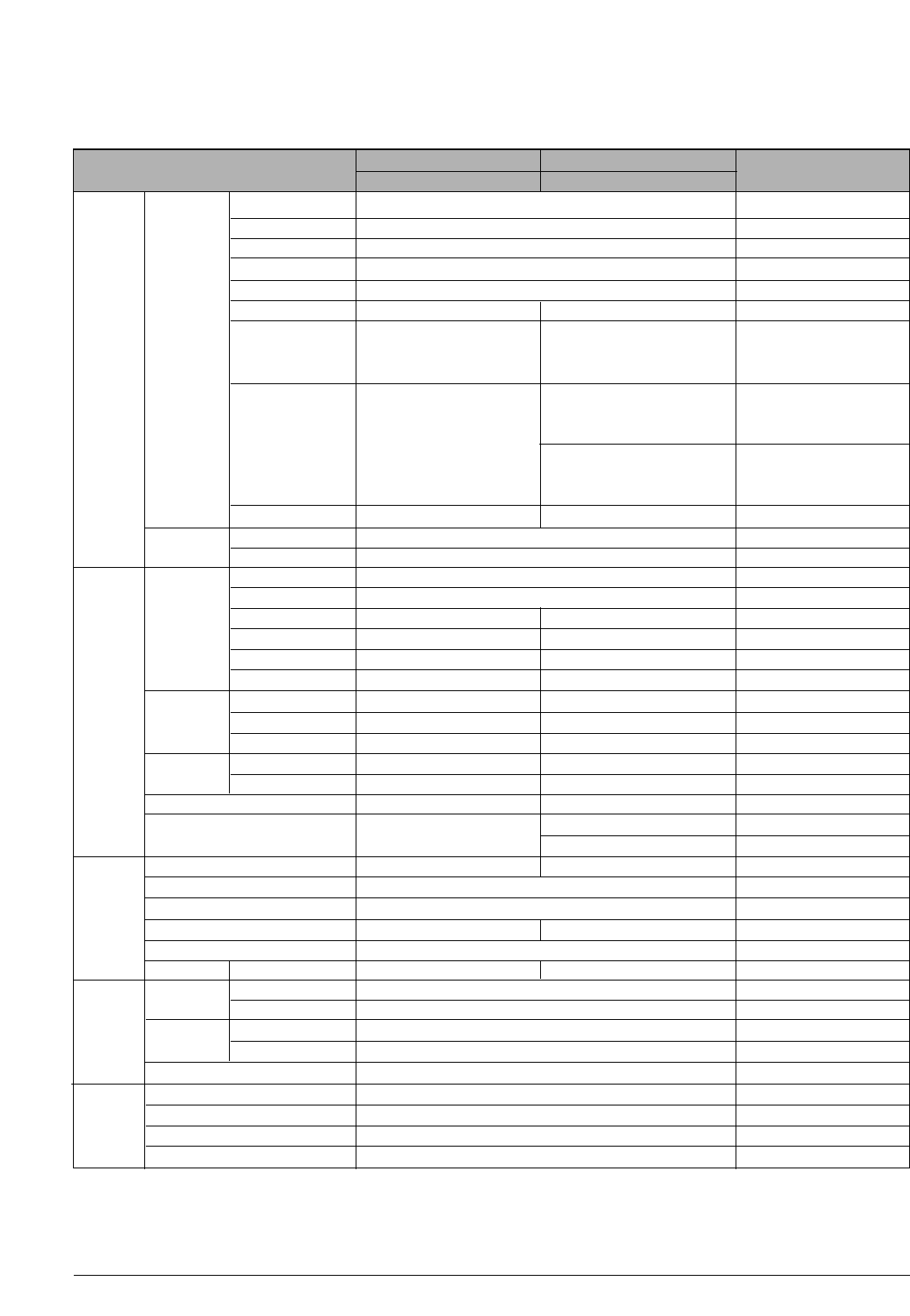
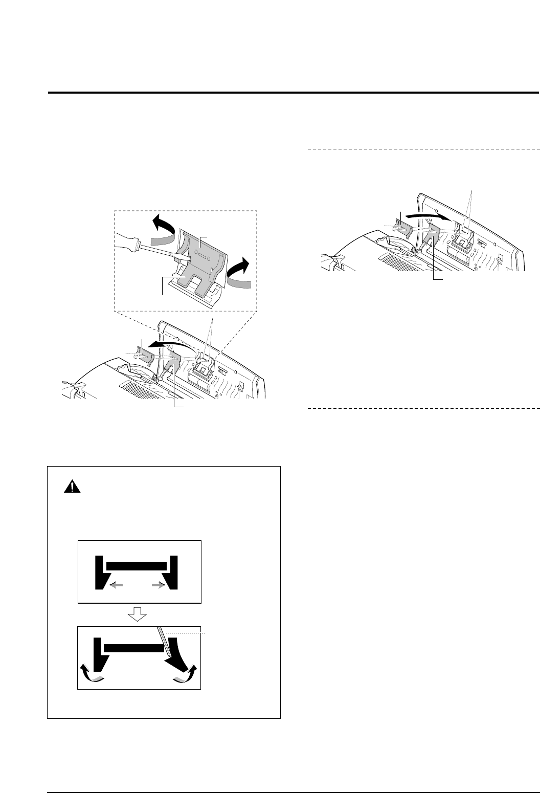
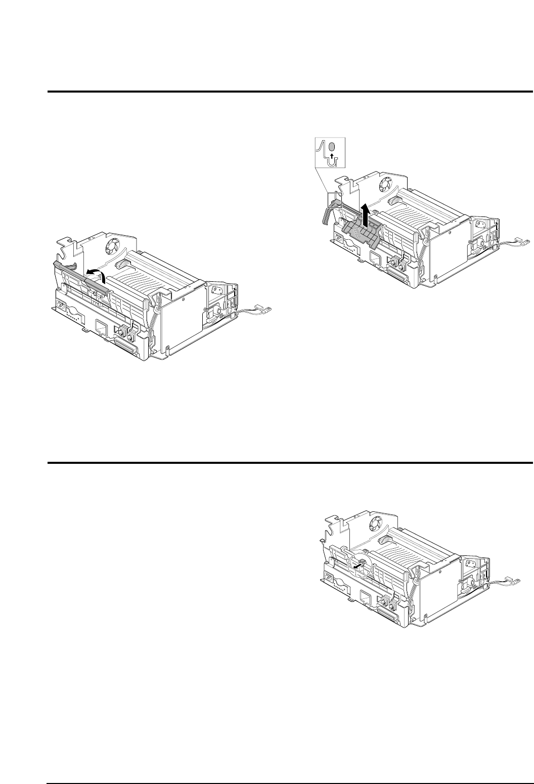
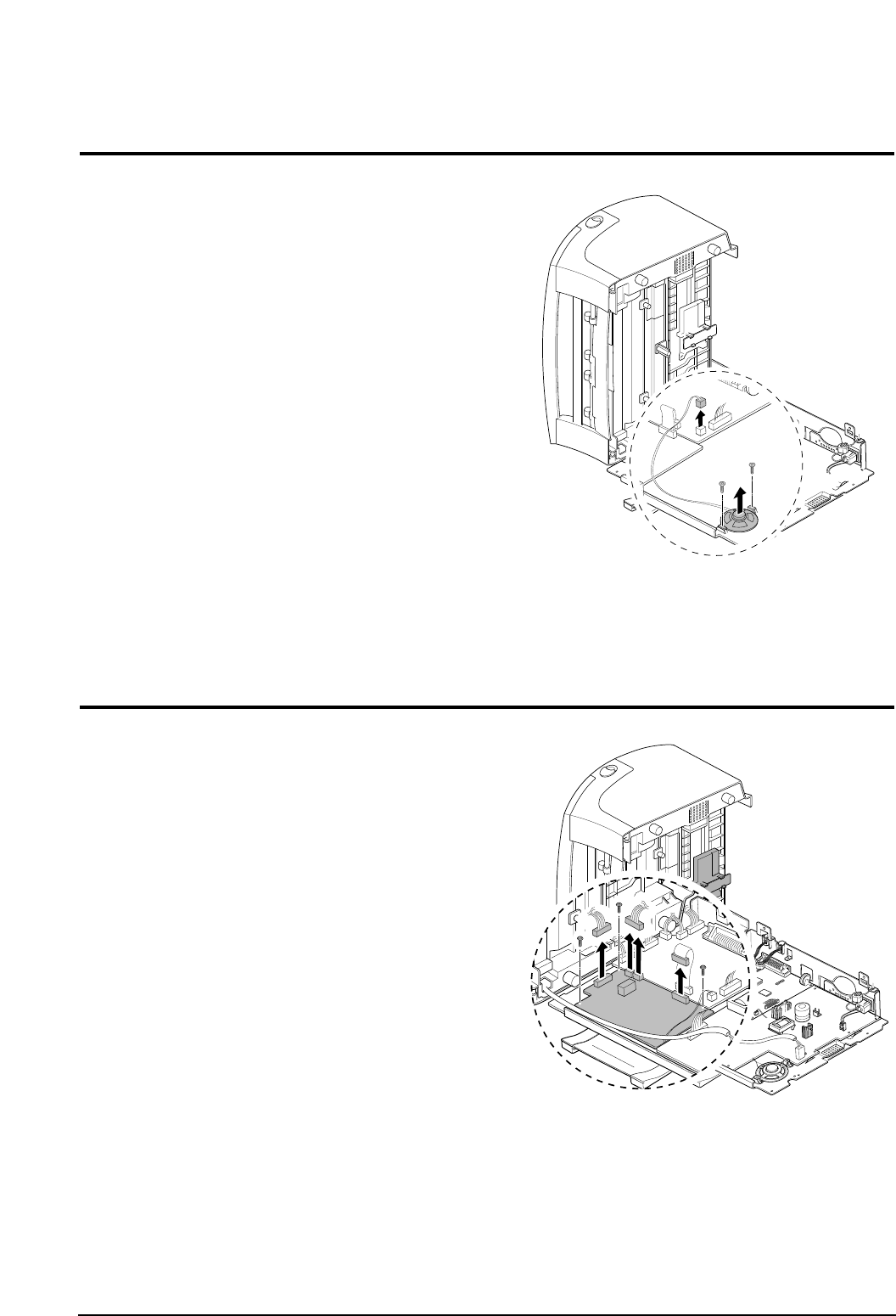
3-2 Cradle
1. Push the lever and remove the cradle as shown
below.
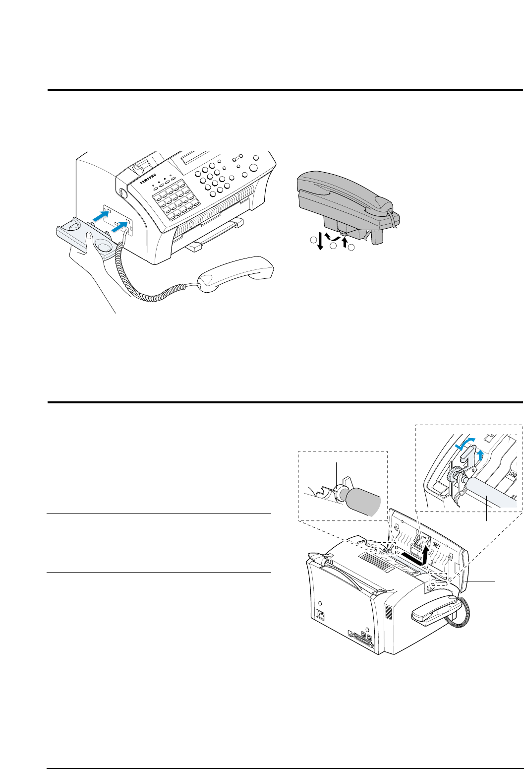
3-3 White Roller
1. Open the OPE cover.
2. Push the bushing on the end of the Roller slightly
inward, then rotate it until it reaches the slot.
Then lift, the Roller out.
Note : Check the Roller for any dirt. If dirty, wipe it off with
soft cloth dampened with water. If the Roller is
heavily worn, replace it with a new one.
3-2
Samsung Electronics
Disassembly and Reassembly
0
0
0
0
0
0
0
0
0
0
0
0
0
0
0
0
0
0
0
0
0
0
0
0
0
0
0
0
0
0
0
0
0
0
0
0
0
0
0
0
0
0
0
0
0
0
0
0
0
0
0
0
0
0
0
0
0
0
0
0
0
0
0
0
0
0
0
0
0
0
0
0
0
0
0
0
0
0
0
0
0
0
0
0
0
0
0
0
0
0
0
0
0
0
0
0
0
0
0
0
0
0
0
0
0
0
0
0
0
0
0
0
0
0
0
0
0
0
0
0
0
0
0
0
0
0
0
0
0
0
0
0
0
0
1
2
3
Control Panel
Bushing
White Roller
A
B
3-4 OPE Cover
1. Pull the cover release button on both sides of the
machine, and open the front cover.
2. Remove two stoppers holding the front cover unit and
unplug one connector and one wire.
3. Pull the bottom left end of the cover downward to
unlatch the front cover unit and remove the cover
from the main frame.
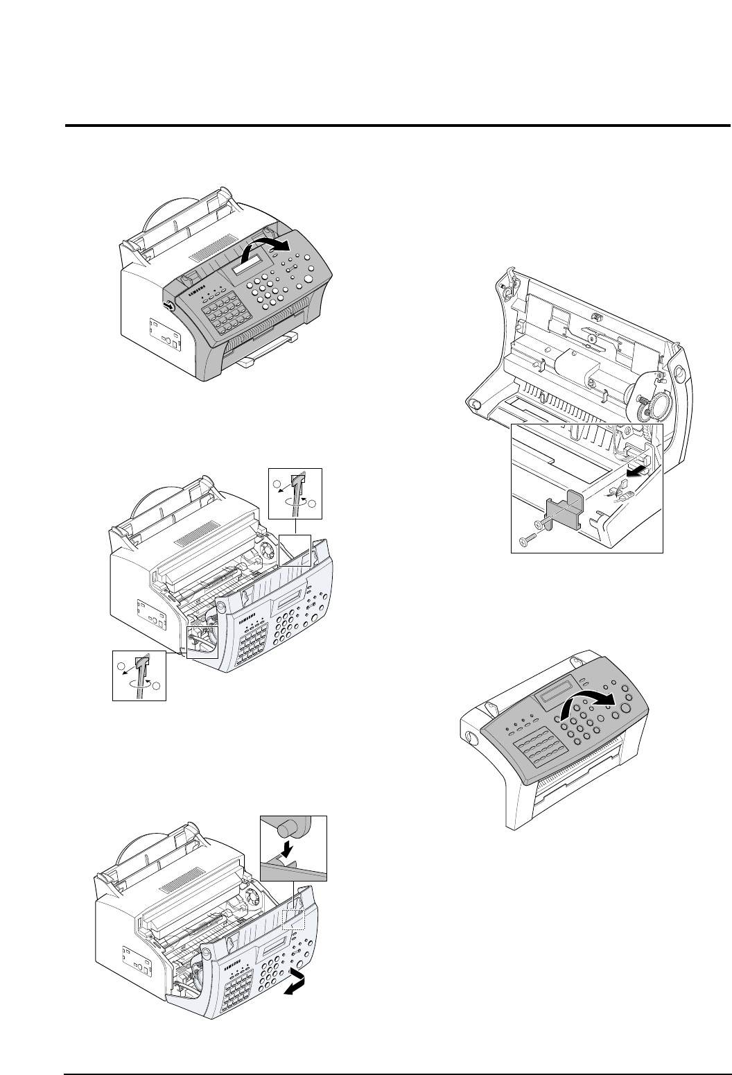
4. Remove two screws securing bracket scan board,
then take out the bracket scan board.
5. Unplug two connectors and one wire from the scan
board.
6. Lift the OPE cover.
Samsung Electronics
3-3
Disassembly and Reassembly
1
2
1
2
7. Remove the stopper holding the OPE cover.
8. Unlatch the bottom ends, then remove the OPE
cover.
3-4
Samsung Electronics
Disassembly and Reassembly
1
2
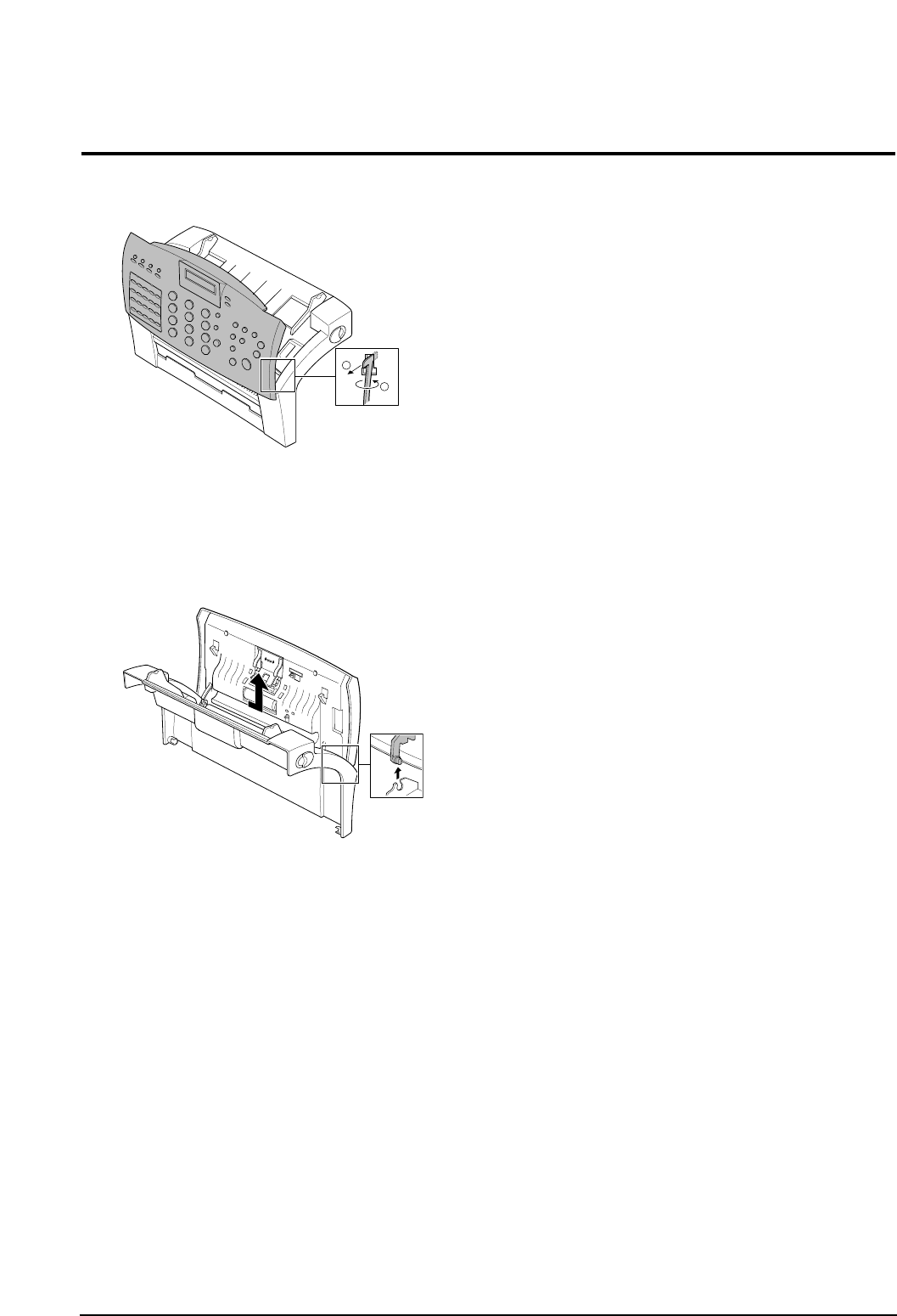
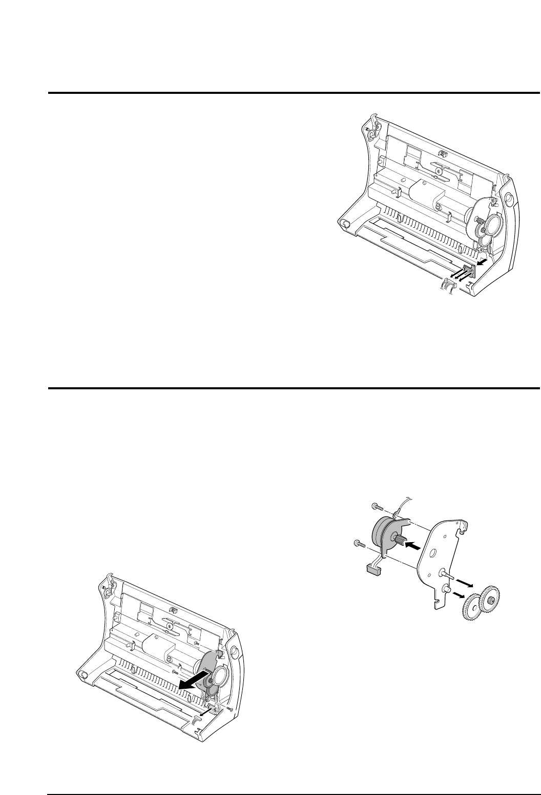
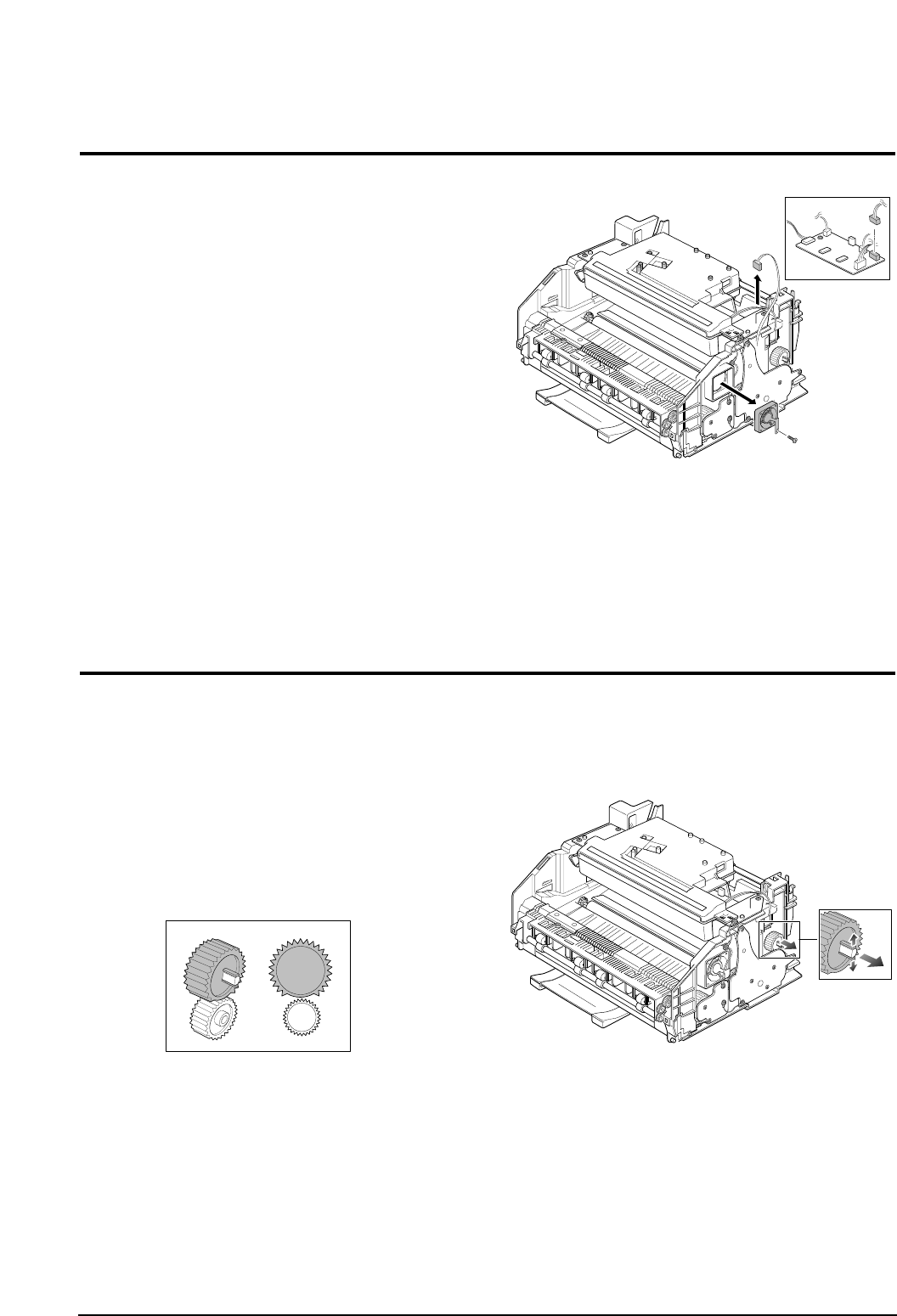
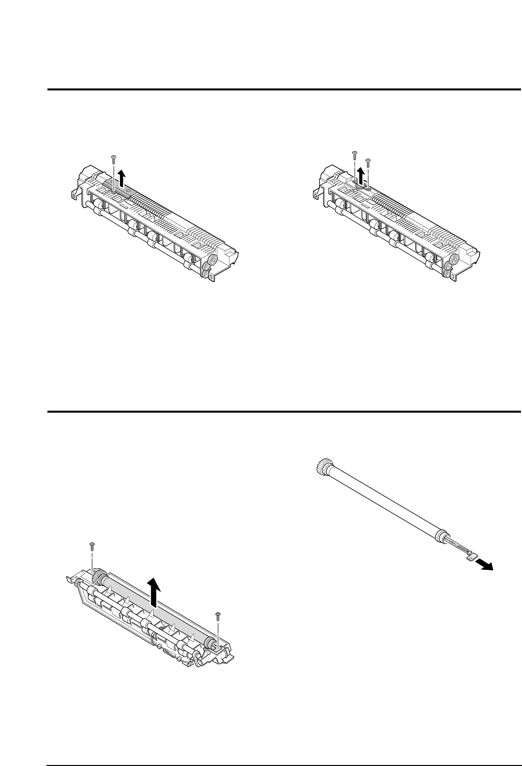
3-5 ADF Rubber
1. Open the OPE unit.
2. Insert a flat blade screw driver and pinset into the slot
as shown below, and release the latches. Take out the
Holder Rubber, Sheet ADF and the Rubber ADF.
Notes : • When you reassemble the them, be sure that
the Rubber ADF and Holder Rubber fit into the
guide boss and the Holder Rubber latches fit
into the corresponding hole. Then push firmly
until it clicks.
3. Clean the surface of the rubber pad with IPA (Isopropyl
Alcohol). After wiping it, be sure to dry it. Check the rub-
ber wear. If the wear reaches 1/2 its original thickness,
replace it with a new one.
Samsung Electronics
3-5
Disassembly and Reassembly
0
0
0
0
0
0
0
0
0
0
0
0
0
0
0
0
0
0
0
0
0
0
0
0
0
0
0
0
0
0
0
0
0
0
0
0
0
0
0
0
0
0
0
0
0
0
0
0
0
0
0
0
0
0
0
0
0
0
0
0
0
0
0
0
0
0
0
0
0
Holder Rubber
Rubber ADF
Guide Boss
Holder Rubber
Rubber ADF
Pinset or
Screw Driver
Safely Precautions :
Do not force to open or fasten plastic material
components.
0
0
0
0
0
0
0
0
0
0
0
0
0
0
0
0
0
0
0
0
0
0
0
0
0
0
0
0
0
0
0
0
0
0
0
0
0
0
0
0
0
0
0
0
0
0
0
0
0
0
0
0
0
0
0
0
0
0
0
0
0
0
0
0
0
0
0
0
0
Rubber ADF
Guide Boss
Holder Rubber
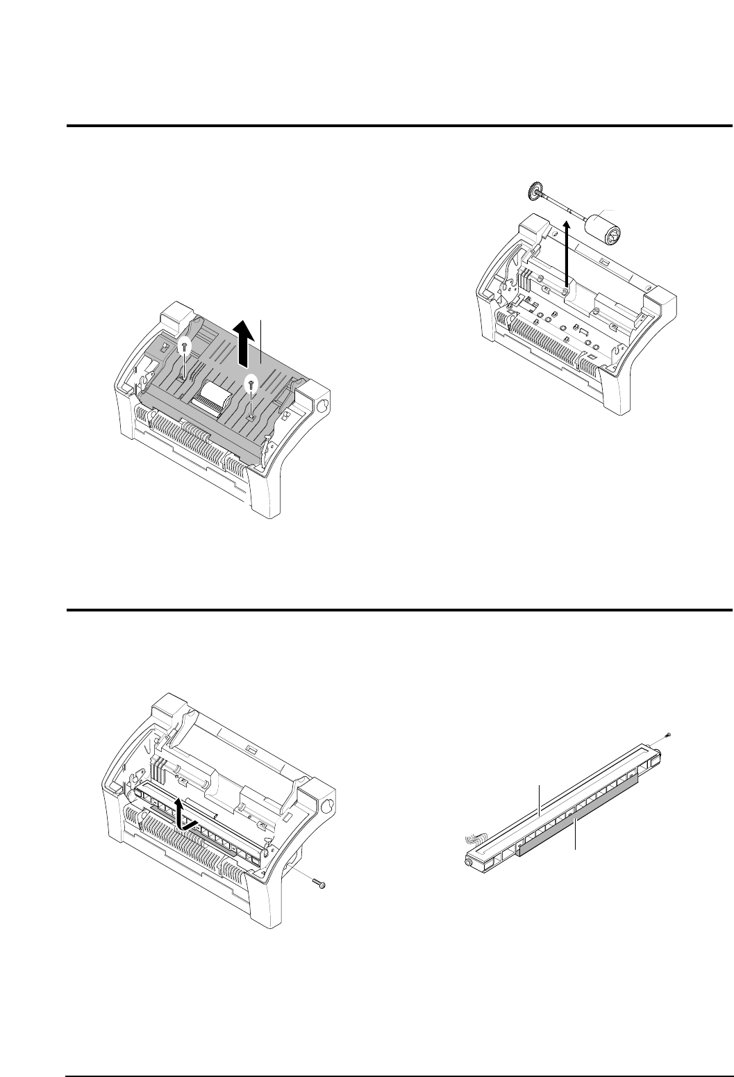
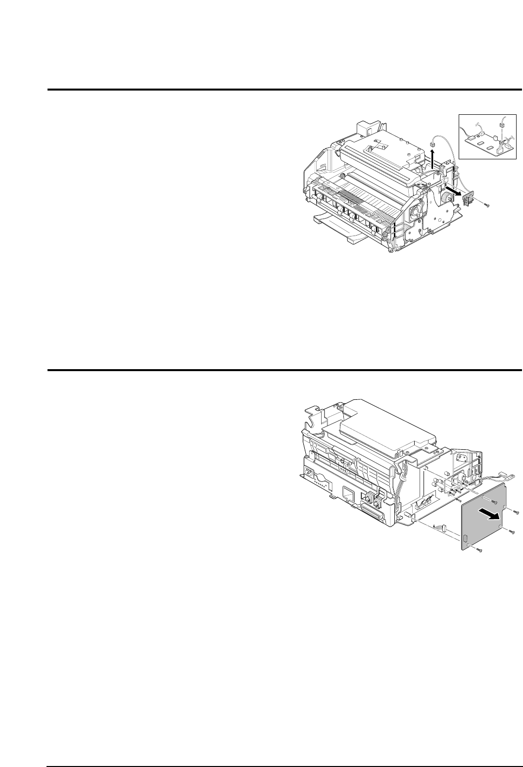
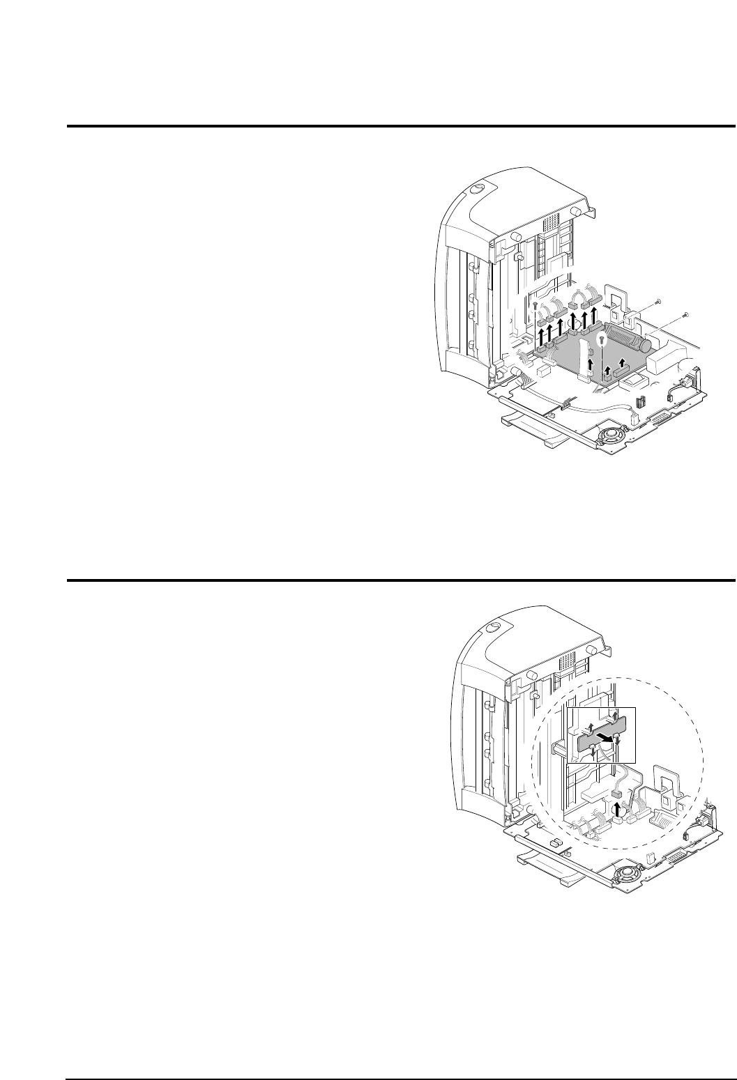
3-6 OPE Board
1. Before you remove the OPE board, you should
remove:
– OPE cover (see page 3-3)
2. Remove four screws securing the OPE board.
3. Release two latches securing the both side of the
LCD and the two of four latches securing the board.
Then remove the OPE board.
3-6
Samsung Electronics
Disassembly and Reassembly
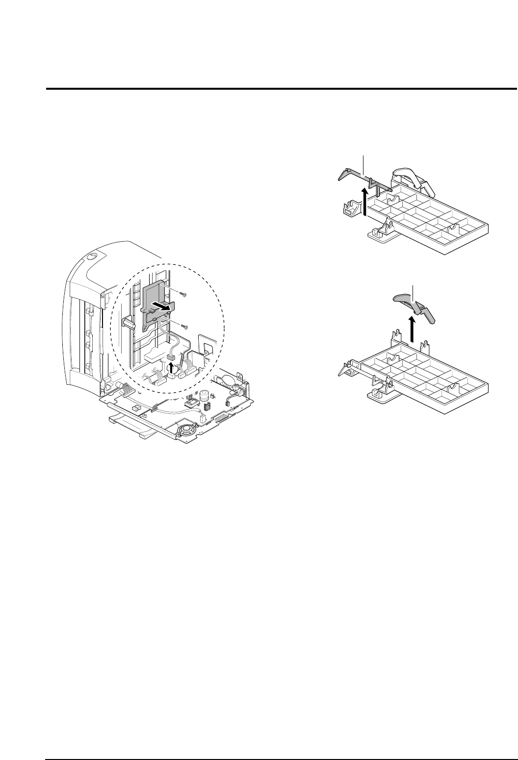
3-7 Lever Sensor Doc.
1. Unlatch the lever sensor Doc from the scan upper
frame and take it out.
3-8 Lever Sensor Scan
1. Push the both sides of Lever sensor Scan inward,
then unlatch and take out the sensor Scan from the
scan upper frame.
3-9 Scan Board
1. Before you remove Scan board, you should remove:
– Bracket scam board (see page 3-3)
2. Unplug all the connectors from the scan board and
remove the board.
Samsung Electronics
3-7
Disassembly and Reassembly
3-10 Scan Motor
1. Before you disassemble Scan Motor, you should
remove:
– OPE cover (see page 3-3)
– Bracket scan board (see page 3-3)
2. Unplug one connector from the scan board.
3. Remove three screws, then remove the motor Ass’y
from the main frame.
4. Take out the gear from the Motor Ass’y.
5. Remove two screws and remove the motor.
3-11 ADF Roller
1. Before you remove the ADF Roller, you should
remove:
– OPE cover (see page 3-3)
2. Remove two screws securing the guide paper and
remove the guide paper.
3. Remove ADF Roller from the scan front frame.
3-8
Samsung Electronics
Disassembly and Reassembly
Guide Paper
ADF Roller
3-12 CIS
1. Remove one screw and push CIS as shown below
and lift it. 2. Separate the Dummy CIS from CIS.
CIS
tape
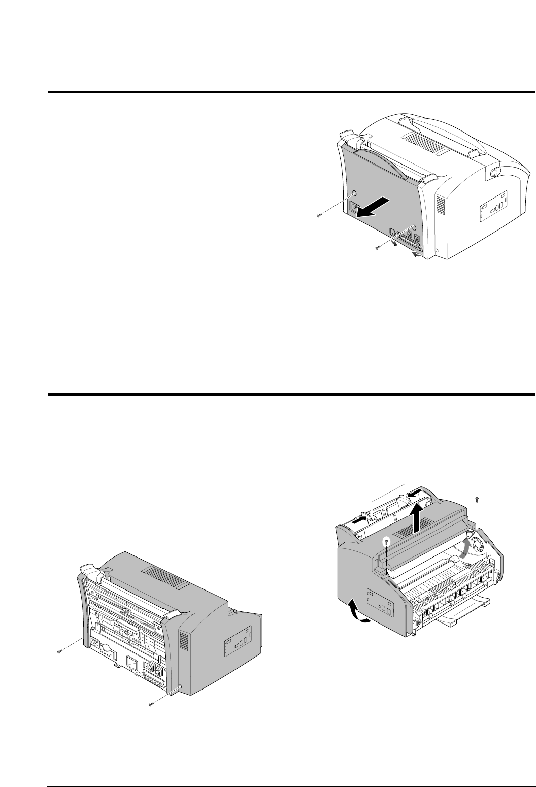
3-13 Rear Cover
1. Remove two screws.
2. Push the metal clip on the parallel port down and
remove the rear cover from the main frame.
Samsung Electronics
3-9
Disassembly and Reassembly
3-14 Top Cover
1. Before you remove the ADF Roller, you should
remove:
– OPE cover (see page 3-3)
– Rear cover (see above)
2. Remove two screws securing the top cover from the
back side of the machine.
3. Remove two screws and slide the left and right paper
guides fully inward. Then spread the bottom of the top
cover and lift the cover to remove.
Paper guides
3-15 Tray
1. Before you remove the tray, you should remove:
– OPE cover (see page 3-3)
– Rear cover (see page 3-9)
– Top cover (see page 3-9)
2. Take out the tray from the main frame.
3-10
Samsung Electronics
Disassembly and Reassembly
3-16 LSU
1. Before you remove the LSU, you should remove:
– All covers (see page 3-3, 3-9)
2. Remove three screws securing the LSU.
3. Unplug two connectors from the LSU and remove the
LSU.
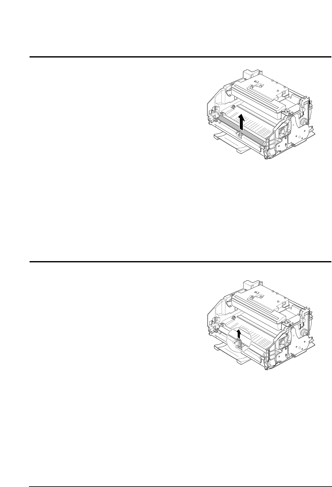
3-17 Transfer Roller
1. Pull the cover release button on both sides of the
machine, and open the front cover.
2. Lift the transfer Roller using a proper tool (-Driver) and
take out the Roller.
Samsung Electronics
3-11
Disassembly and Reassembly
3-18 Engine Board
1. Before you remove the Engine board, you should
remove:
– All covers (see page 3-3, 3-9)
– LSU (see page 3-10)
2. Unplug five connectors and remove one screw from
the engine board, then remove the board.
3-19 Pick-up Roller Ass’y
1. Before you remove the pick-up Roller Ass’y, you
should remove:
– All covers (see page 3-3, 3-9)
– LSU (see page 3-10)
2. Unplug all the connectors from the engine board.
3. Remove four screws securing the plate upper and
remove the plate upper as below.
4. Remove two screws and remove the Roller from the
plate.
Note : When you reassemble the pick-up Roller, make
sure that the right end of the pick-up Roller fits
into the pick-up gear shaft.
3-12
Samsung Electronics
Disassembly and Reassembly
Pick-up gear shaft
3-20 Knock-up Ass’y
1. Before you remove the knock-up Ass’y, you should
remove:
– All covers (see page 3-3, 3-9)
– LSU (see page 3-10)
– Plate upper (see page 3-12)
2. Pull the knock-up Ass’y fully backward.
3. Remove the knock-up Ass’y from the main frame.
Samsung Electronics
3-13
Disassembly and Reassembly
3-21 Cap-Pad
1. Before you remove the cap-pad, you should remove:
– All covers (see page 3-3, 3-5)
– LSU (see page 3-10)
– Plate upper (see page 3-12)
– Knock-up Ass’y (see above)
2. Take out the cap-pad from the main frame.
3-22 Holder-Pad
1. Before you remove the holder-pad, you should
remove:
– All covers (see page 3-3, 3-9)
– LSU (see page 3-10)
– Plate upper (see page 3-12)
– Knock-up Ass’y (see 3-13)
– Cap-Pad (see 3-13)
2. Remove the holder-pad from the main frame.
3-14
Samsung Electronics
Disassembly and Reassembly
3-23 Motor Ass’y
1. Before you remove the motor Ass’y, you should
remove:
– All covers (see page 3-3, 3-9)
2. Remove four screws securing the motor Ass’y and
unplug one connector from the engine board, then
remove the motor Ass’y.
Note : When you reassemble the motor Ass’y, make
sure that the boss shown in the figure below fit
into the corresponding screw holes on the motor
Ass’y to allow the screws to be fastened properly.
Boss
3-24 Fan
1. Before you remove the fan, you should remove:
– All covers (see page 3-0)
– Motor Ass’y (see page 3-15)
2. Unplug one connector from the engine board and
remove the fan.
Samsung Electronics
3-15
Disassembly and Reassembly
3-25 Gear pick-up Ass’y
1. Before you remove the gear pick-up Ass’y, you
should remove:
– All covers (see page 3-3, 3-9)
Note: When reassembling, make sure that the direction
of the gear is correct.
2. Release two snap-fits and remove the gear pick-up
Ass’y from the main frame.
3-26 Solenoid
1. Before you remove the solenoid, you should remove:
– All covers (see page 3-3, 3-9)
2. Unplug one connector from the engine board and
remove one screw, then remove the solenoid.
3-16
Samsung Electronics
Disassembly and Reassembly
3-27 HVPS Board
1. Before you remove the HVPS board, you should
remove:
– All covers (see page 3-3, 3-9)
2. Remove three screws and one connector from the
HVPS board, then remove the board.
Note : when reassembling, make sure that the terminal
is five.
3-28 Hook Board
1. Before you remove the hook board, you should
remove:
– All covers (see page 3-3, 3-9)
2. Unplug one connector from the main board and
remove two screws, then remove the hook board from
the main frame.
Samsung Electronics
3-17
Disassembly and Reassembly
3-29 Fuser Ass’y
1. Before you remove the fuser Ass’y, you should
remove:
– All covers (see page 3-3, 3-9)
2. Remove two wires after remove two screws from the
main frame and one connector from the inter connec-
tor.
3. Remove two screws and unlatch the fuser Ass’y using
a proper tool.
3-30 Thermostat
1. Remove one screw and remove the cover thermostat
from the fuser Ass’y. 2. Remove two screws and take out thermostat from the
fuser Ass’y.
3-18
Samsung Electronics
Disassembly and Reassembly
3-31 Halogen Lamp
1. Before you remove the thermostat, you should
remove:
– All covers (see page 3-3, 3-9)
– Fuser Ass’y (see page 3-17)
2. On the fuser Ass’y, remove the two screws, then
remove the heat Roller.
3. Remove the halogen lamp from the heat Roller.
3-32 Pressure Roller
1. Before you remove the pressure Roller, you should
remove:
– All covers (see page 3-3, 3-9)
– Fuser Ass’y (see page 3-17)
2. Lift and remove the pressure Roller from the main
frame.
Samsung Electronics
3-19
Disassembly and Reassembly
3-33 Actuator-Exit
1. Before you remove the actuator-exit, you should
remove:
– All covers (see page 3-3, 3-9)
– Fuser Ass’y (see page 3-17)
2. Lift and remove the actuator-exit from the main
frame.
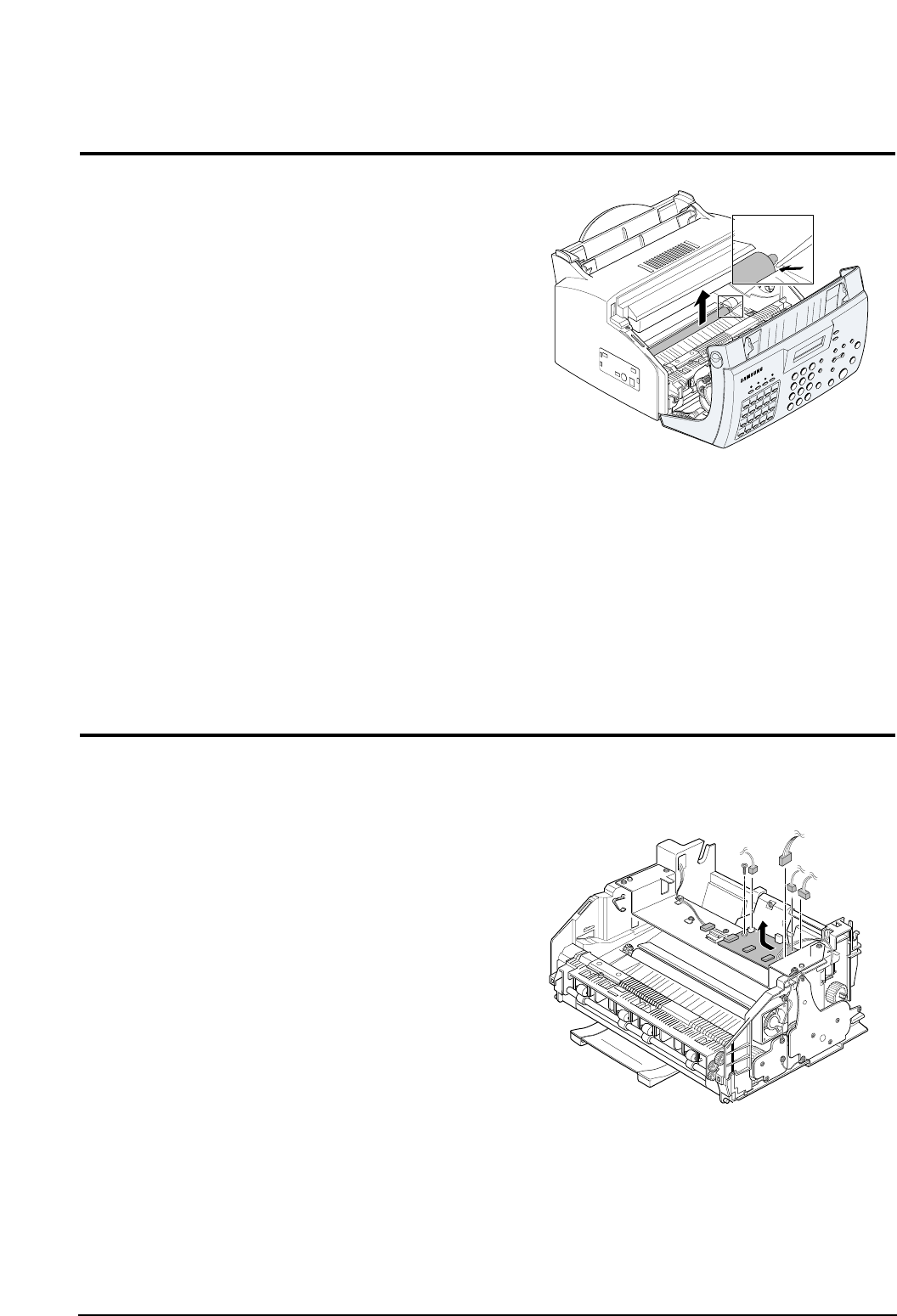
3-34 SMPS Board
1. Before you remove the SMPS board, you should
remove:
– Rear cover (see page 3-9)
– Shield Engine Ass’y (see page 3-19)
2. Remove four screws and three connectors, then
remove the SMPS board from the main frame.
3-20
Samsung Electronics
Disassembly and Reassembly
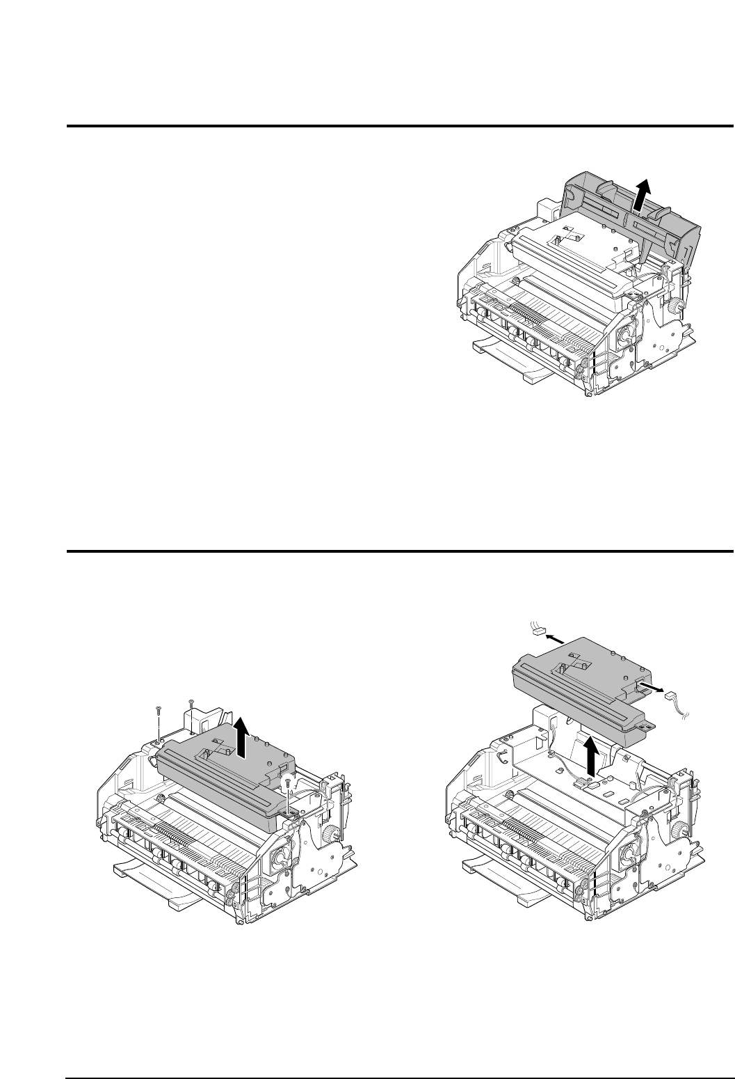
3-34 Shield Engine Ass’y
1. Before you remove the shield engine Ass’y, you
should remove:
– Rear cover (see page 3-9)
2. Remove eight screws securing the shield engine
Ass’y and remove the shield engine Ass’y from the
main frame.
Samsung Electronics
3-21
Disassembly and Reassembly
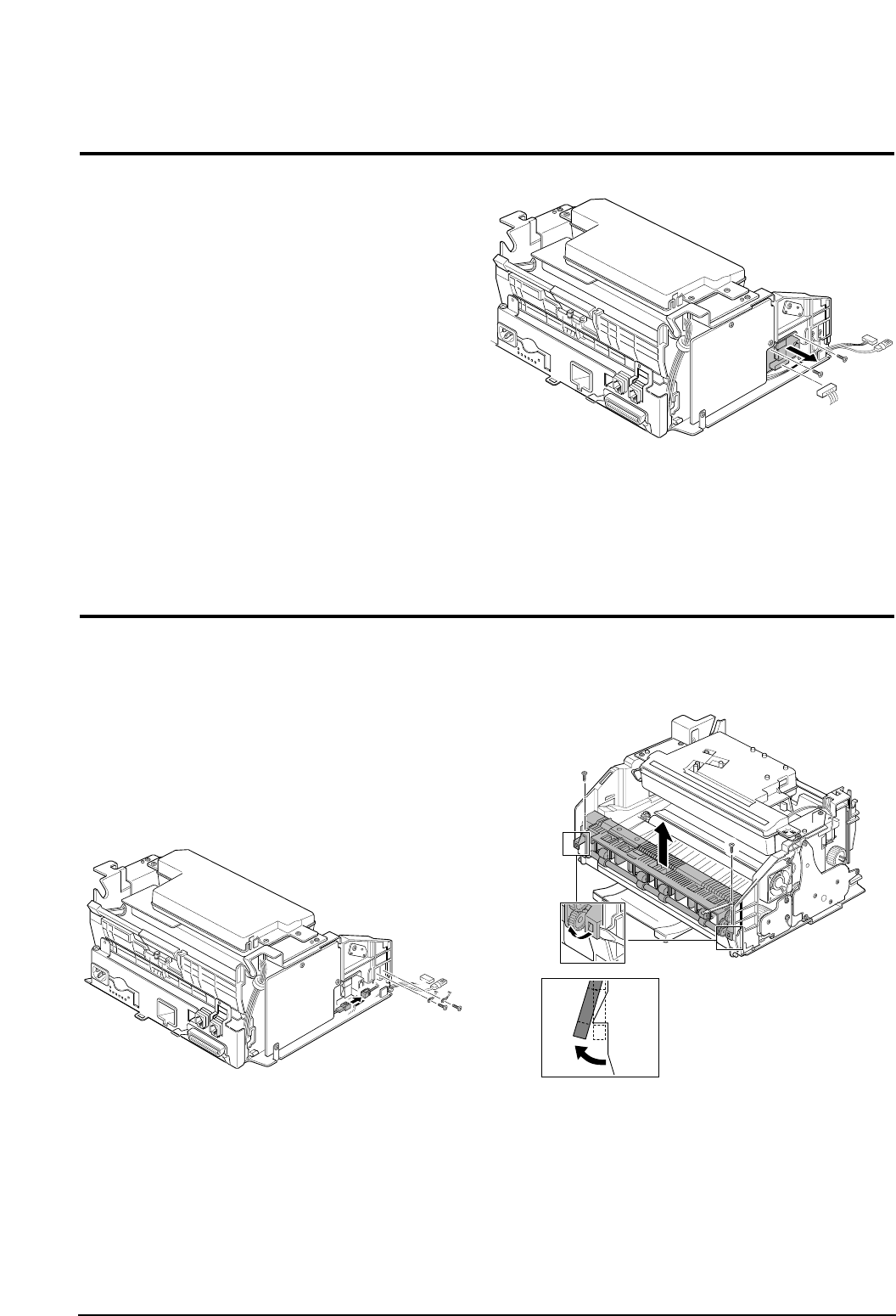
3-36 Speaker
1. Before you remove the speaker, you should remove:
– Rear cover (see page 3-9)
– Shield Engine Ass’y (see page 3-19)
– SMPS board (see above)
2. Remove one connector that connects the speaker to
the main board and two screws securing the speaker,
then remove the speaker.
3-37 LIU Board
1. Before you remove the LIU board, you should
remove:
– Rear cover (see page 3-9)
– Shield Engine Ass’y (see page 3-19)
2. Remove three screws and three connectors from the
LIU board, then remove the board from the main
frame.
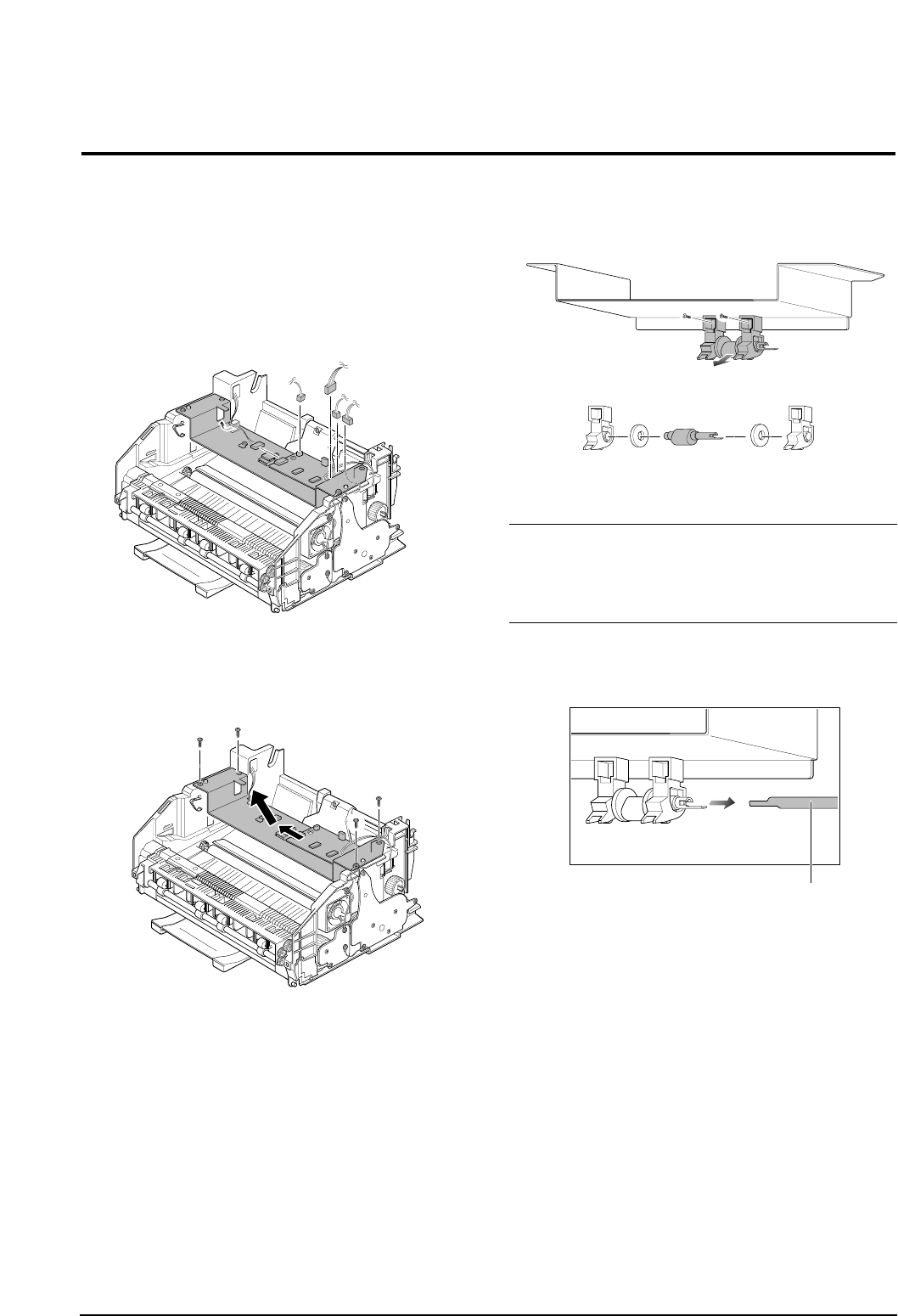
3-39 Sensor Board
1. Before you remove the sensor board, you should
remove:
– Rear cover (see page 3-9)
– Shield Engine Ass’y (see page 3-19)
2. Release four snap-fits securing the sensor board and
unplug one connector from the main board, then
remove the sensor board.
3-22
Samsung Electronics
Disassembly and Reassembly
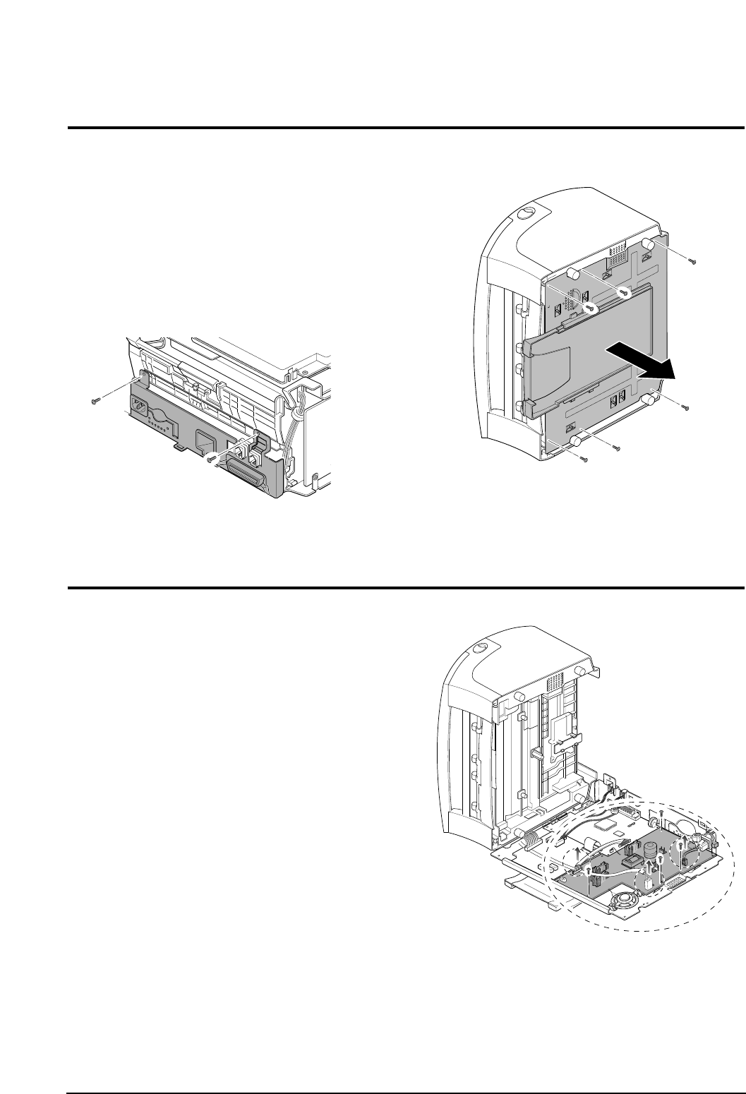
3-38 Main Board
1. Before you remove the main board, you should
remove:
– Rear cover (see page 3-9)
– Shield Engine Ass’y (see page 3-19)
2. Remove four screws and all the connectors (9) from
the main board, then remove the board.
Samsung Electronics
3-23
Disassembly and Reassembly
3-40 Actuator Empty/Feeder
1. Before you remove the actuator empty/feeder, you
should remove:
– Rear cover (see page 3-9)
– Shield Engine Ass’y (see page 3-19)
2. Remove one connector from the main board and two
screws securing the holder feed Ass’y, then remove
the holder feeder Ass’y.
3. Remove the Feed sensor and the Empty sensor.
Feed Sensor
Empty Sensor
3-24
Samsung Electronics
Disassembly and Reassembly
3-41 Roller Feeder
1. Before you remove the actuator empty/feeder, you
should remove:
– All covers (see page 3-0)
– Motor Ass’y (see page 3-15)
2. Release two snap-fits and remove the gear-feed,
clutch-feed, and the spring-clutch.
3. Rotate the pick-up bushing as shown below and
remove holder feeder Ass’y and Roller feeder.
4. Separate the Roller Feeder from the Holder Feeder
Ass’y.
Spring-clutch
Clutch-feed
Gear-feed
Roller Feed
Holder Feed
4-1
Samsung Electronics
4. Troubleshooting
4-1 Preventative Maintenance
The cycle period outlined below is a general guideline for maintenance. The example list is for an average usage of 50 trans-
mitted and received documents per day.
Environmental conditions and actual use will vary these factors. The cycle period given below is for reference only.
COMPONENT CLEANING CYCLE REPLACEMENT CYCLE SOLUTION
SCANNER
PRINTER
ADF Rubber
ADF Roller
White Roller
CIS
Cartridge
Pickup Roller
Feed Roller
Transfer Roller
Fuser
6 Months
1 Year
As Needed
As Needed
10,000 Pages
20,000 Pages
10,000 Pages
2,500 Pages
60,000 Pages
50,000 Pages
60,000 Pages
50,000 Pages
4-2 Tech Mode
In Tech mode, the technician can perform various tests to isolate the causes of a malfunction, and set the technical option fea-
tures to customize the machine depending on the user’s operation environment.
To access TECH mode
: Press SETUP, #, 1, 9, 3, 4 in sequence, and the LCD displays ‘TECH’ in the standby mode screen. While in TECH mode,
the machine still performs all normal operations.
To return to the normal user mode
: Turn the power off, then back on.
The technical options you have set in TECH mode are not changed unless you clear the machine’s memory in TECH mode.
To communicate via direct connection with another fax machine, press OHD/V.REQ followed by Start/Enter.
• Caution :
When you finish operating in Tech Mode, you must turn the power Off/On.

Troubleshooting
4-2 Samsung Electronics
Function Item Content Default
FAX NUMBER/NAME FAX NUMBER
FAX NAME
TIME/DATE SETUP DATE FORMAT EUROPE/USA EUROPE
TIME/DATE
SYSTEM SETUP LANGUAGE ENG/GER/FRE/ITA/SPA/POR/DUT ENGLISH
SENDING MEMORY ON/OFF ON
SEND FROM CONFIRM ON/OFF/ERROR ERROR
FAX PAPER SIZE LETTER/A4/LEGAL A4
AUTO REDUCTION ON/OFF ON
DISCARD SIZE 0~30mm 20MM
RINGS TO ANSWER 1~7 2
STAMP RCV.NAME ON/OFF OFF
RCV.START CODE 0~9 * 9 *
ECM MODE ON/OFF ON
CALLER ID ON/OFF OFF
JUNK FAX BARRIER ON/OFF OFF
DRPD MODE ON/OFF OFF
TECH MODE MODEM SPEED 2.4/4.8/7.2/9.6/12.0/14.4/28.8/33.6 26.4 KBPS
DIALING MODE TONE/PULSE TONE
SEND FAX LEVEL 0~15 -12 DBM
RCV. FAX LEVEL 40~50 -43DBM
FLASH TIME(RECALL TIME) 80/280/600 80 MS
PAUSE TIME 1~9 4 SEC
REDIAL INTERVAL 1~15 3 MIN
REDIAL COUNT 0~5 2
DP MAKE/BREAK 40/60~33/67 33/67
SILENCE TIME UNLIMITED/12SEC UNLIMITED ERROR
RATE 5%/10% 10%
IGNORE TONER EMPTY ON/OFF OFF
GROUP DIAL SETUP GROUP NO[1-20]
VOLUM SETUP ALARM VOLUM ON/OFF ON
KEY VOLUM ON/OFF ON
MEMORY CLEAR FAX NUMBER/NAME
DIAL/SCHEDULE
JOURNAL
DEFAULT SETUP
MAINTENANCE CLEANING DRUM
ADJUST SHADING
REMOTE TEST OFF/ON
NOTIFY TONER LOW OFF/ON
ROM TEST ROM OK! (VERSION)
CIS TEST
DRAM TEST DRAM OK
SWITCH TEST
DTMF TEST
TONER COUNT
PRINTING INFO OFF/ON
PROGRAM DOWNLODE
SCAN COUNT CLEAR COUNT CLEARING ..
4-2-1 System Data List in TECH MODE
: Only Tech Mode

Troubleshooting
4-3
Samsung Electronics
In TECH mode, press SETUP, then press or until
‘TECH MODE’ appears in the display. Press Start/Enter.
The following technical options are available.
Note : If necessary, print System Data List in TECH mode.
The list shows all current system data settings
including the TECH MODE options. To print the sys-
tem data list, press Report/Help, then press
or until ‘SYSTEM DATA’ appears in the dis-
play, and press Start/Enter.
Modem Speed
• You can set the maximum modem speed.
• Communication is done with modem speed automatically
set at lower speed when communicating with the modem
with lower speed since communication is done on the stan-
dard of the side where modem speed is low for transmis-
sion/reception. It is better set 26.4KBPS as default setting.
DIALING MODE
• Select the dialing mode according to the user's line status.
• TONE: Electrical type of dial
• PULSE: Mechanical type of dial
SEND FAX LEVEL
• You can set the level of the transmission signal. Typically,
the Tx level should be under -12 dBm. The level within the
range of 1 to -15 dBm is acceptable.
• Caution: The Send Fax Level is set at the best condition
in the shipment from factory. Never change set-
tings arbitrarily.
RCV FAX LEVEL
• You can set the level of the receiving signal.
•
The reception level may be too low due to the cable losses.
• If it is set to -43 dBm, the reception sensitivity will be
between 0 and -43 dBm. If it is set to -48 dBm, the recep-
tion sensitivity will be between 0 and -48 dBm.
• Caution: The Send Fax Level is set at the best condition
in the shipment from factory. Never change set-
tings arbitrarily.
FLASH TIME
• Set the flash time to 80, 280, or 600 milliseconds.
PAUSE TIME
• Pause time mean delay time (unit: second) inserted
between dial number signal and the next number of signal
in the automatic dial (One touch, Speed dial, Redial) and
the manual dial.
• Caution: The Send Fax Level is set at the best condition
in the shipment from factory. Never change set-
tings arbitrarily.
REDIAL INTERVAL
• If the remote machine is busy when the machine sends a
fax using automatic dialing, the machine automatically
redials the number. Select the time interval between auto-
matic redial attempts. Enter the desired redial interval
using the number keypad: 1 - 15 minutes.
REDIAL COUNT
• You can set times that redial automatically attempts when
automatic transmission is done or when the remote
machine is busy or when the machine send a fax. If there
is no response after redialing by the times already set,
redial is no longer attempted. No redial is attempted if the
settings is 0. Enter the desired times from 1 through 5.
DP Make/Break
• Select the dial pulse make and break time: 40-60 or 33-67
• Caution: Send Fax Level is set at the best condition in the ship-
ment from factory. Never change settings arbitrarily.
SILENCE TIME
• In ANS/FAX mode, after a call is picked up by the answer-
ing machine, the machine monitors the line.
• If a period of silence is detected on the line at any time, the
call will be treated as a fax message and the machine
begins receiving.
• Silence detection time is selectable between limited (about
12 seconds) and unlimited time.
• When '2 sec' is selected, the machine switches to receiv-
ing mode as soon as it detects a period of silence. When
'unlimited'is selected, the machine waits until the answer-
ing operation is concluded even though a period of silence
is detected. After the answering operation is concluded,
the machine switches to receiving mode.
ERROR RATE
• When the error rate is about to be over the setting value,
the Baud rate automatically lowers up to 2400 bps to make
the error rate remain below the setting value.
• You can select the rate between 5% and 10%.
IGNORE TONER EMP
• You can set this function ON if desiring to drive the engine
continuously even though the life of toner is run out and it
becomes Toner Empty status.
4-2-2 Tech Mode Options

Troubleshooting
4-4 Samsung Electronics
In TECH mode, press SETUP, then press or until
‘MAINTENANCE’ appears in the display. Press Start/Enter.
The following technical options are available
CLEAN DRUM
• Use this feature to get rid of the toner remained in the
development unit, so you can get a clean printout.Perform
this feature if stains or specks appear on the printing mate-
rials and print quality falls.
• Perform this feature several times until a clean printing
material appears.
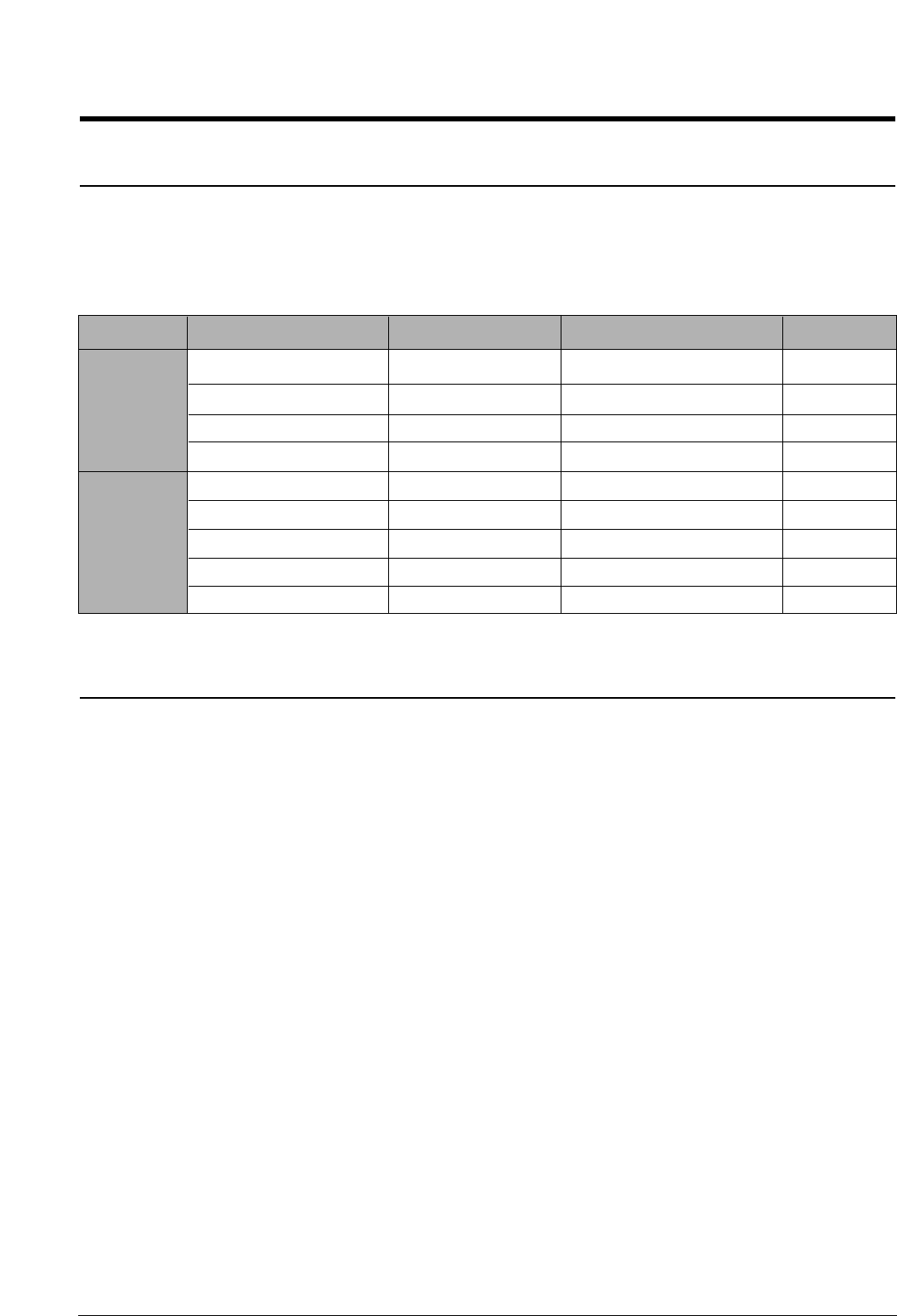
ADJUST SHADING
• Use this feature to correct the white reference of the scan-
ner if you experience bad copy images. When using this
feature, a white paper should be used to get clean copy
images.
• Use this adjustment feature to achieve best image (scan)
quality depending on the characteristics of the CIS (Contact
Image Sensor) parts.
1. Select [ADJUST SHADING] from the Service Mode.
2. Insert a clean white original [Letter Size] into the paper
loading part.
3. Original is scanned if pressing the Setting button.
4. If the original scan is completed, message is displayed
on the LCD window and CIS SHADING PROFILE is
output.
• If the output image is different from the normal screen, the
CIS is poor.
Caution:
1. Always perform the CIS TEST after downloading
Firmware. Otherwise, the system may not operate prop-
erly.
2. Always perform ADJUST SHADING after replacing the
CIS.
3. Always use a clean white paper in ADJUST SHADING
(Maximum paper width: Letter Size).
4. ADJUST SHADING may be performed even in the User
Mode but ADJUST SHADING profile is output only in the
TECH MODE.
REMOTE TEST
• The Remote Test feature can be enabled in order to allow
a remote location to call up and run a diagnostic test on
your machine. You may be instructed by a service repre-
sentative to enable this feature.
NOTIFY TONER LOW
• With this feature enabled, when the toner becomes low, the
toner low information will be sent to ta specified contact
point, for example, the service company. After you access
this menu, select ON, and when the LCD prompts, enter
the name and the number of the contact point, the cus-
tomer's fax number, the model name, and the serial num-
ber.
ROM TEST
• Use this feature to test the machine'S ROM. The result and
the software version appear in the LCD display.
CIS TEST
• This test checks the operation of the Contact Image Sensor
(CIS). Each time the number changes by one increment,
the average ADC value of CIS prints out.
DRAM TEST
• Use this feature to test the machine's DRAM. The result
appears in the LCD display.
SWITCH TEST
Use this feature to test all keys on the operation control
panel. The result is displayed on the LCD window each time
you press a key.
MODEM TEST
• Use this feature to hear various transmission signals to the
telephone line from the modem and to check the modem.
• If no transmission signal sound is heard, it means that the
modem part of the main board is poor.
DTMF TEST
• DTMF (Dual Tone Multi Frequency) signal. When you
press any key on the number keypad including • and #, you
will hear the corresponding key tone.
TONER COUNT
•This feature shows the current state of the toner cartridge.
•TONER CNT: The total number of the dots used to print up
to current time.
•CRU STATE: The page number which the toner cartridge
can print.
• Caution : After replacing Main board to new one, you
should update the information to the new board.
4-2-3 Maintenance Options
Troubleshooting
4-5
Samsung Electronics
PRINTING INFO
• This feature allows the machine to automatically print vari-
ous information, like toner count, transfer voltage, fusing
temperature and so on, at the bottom of each printed page.
• PAGE TONER CNT: prints the number of dots used to print
the page.
• TOTAL TONER CNT: prints the total number of the dots
used to print up to current time.
• THV ON DUTY: prints ADC value of transfer voltage.
• THERMISTER: prints ADC value of fusing temperature.
• P: prints the page number.
PROGRAM DOWNLOAD
• Use this feature to download a new upgraded ROM file
from a PC that is connected to the machine with a parallel
cable (IEEE 1284).
SCAN COUNT CLEAR
• If performing this feature, the value of scanning original until
now is initialized (0). (Total scan count value on the system
data list becomes 0.)
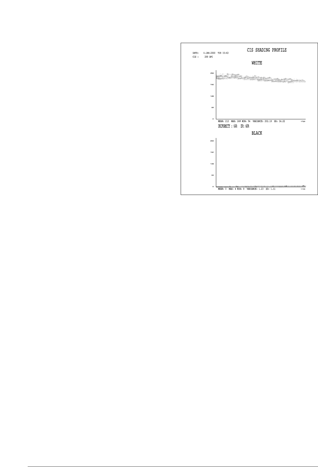
Adjust Shading Sample Pattern

Troubleshooting
4-6 Samsung Electronics
In TECH mode, press Report/Help, then select the desired
list or report by using or key, then press Start/Enter.
The following options are available
HELP
• It shows a brief description on the machine's basic func-
tions and commands.Use it as a quick reference guide
SENT JOURNAL
• This journal shows a specific information concerning trans-
mission activities, the time and dates of up to 40 of the
most recent transmissions.
RECEIVED JOURNAL
• This journal shows a specific information concerning
reception activities, the time and dates of up to 40 of the
most recent receptions.
PHONEBOOK
• It lists all telephone numbers that have been stored in the
machine.
SENDING CONFIRM
• It shows the result of the last send operation.
SCHEDULE INFORM
• This list shows a specific information on the documents
currently stored for delayed transmission. It provides the
operation number, starting time, type of operation, etc.
SYSTEM DATA
• This list provides a list of the user system data settings and
tech mode settings.
PROTOCOL LIST
• This list shows the sequence of the CCITT group 3 T.30
protocol during the most recent sending or receiving oper-
ation. Use this list to check for send and receive errors. If
a communication error occurs while the machine is in
TECH mode, the protocol list will print automatically.
PATTERN PRINT
• Using this pattern printout, you can check if the printer
mechanism is functioning properly. Examine the pattern
and look for a break in the diagonal line. If the diagonal
lines are not broken, the printer mechanism is functioning
properly.
SHADING PRIN
• With this print, you can check the scanning elements of the
CIS (Contact Image Sensor).
The Engine test mode is used to check the operation of the
components related to the printer engine.
The following test are available.
To access the Engine Test Mode:
1. Press Setup, #, 1, 9, 3, 1 in sequence.
2. When ‘ENGINE TEST?’ appears, press Start/Enter.
3. Scroll the options by pressing or repeatedly find
the one you want.
4. Press Start/Enter to start the test.
5. Press Stop to exit the Engine test mode.
• Caution :
When you finish operating in Engine Test Mode, you must turn
the power Off/On.
Engine Test Mode Options :
1. MAIN MOTOR TEST
2 PTL TEST
3. FAN TEST
4. FUSER TEST
( FUSER ON : 145˚C , FUSER OFF : 145˚C )
5. LSU MOTOR TEST
6. LD(LASER DIODE) TEST
7. HSYNC TEST (NG/OK)
8. LSU OPERATION TEST (NG/OK)
9.
SENSOR TEST ( FEED , EXIT , PAPER EMPTY , COVER OPEN)
10. SOLENOID TEST
11. MHV TEST ( -1550 V )
12. DEV TEST ( - 430 V )
13. THV(+) TEST ( +1300 V )
14. THV(-) TEST
15. THV TRIGGER TEST
16. ALL FUNCTION TEST :
This function is for a manufacturing press . You can test
all function(1~15)
• When you push the “Start” button, the Main Motor runs.
• If you push the “Start” button again , the current test
stops, and the next test starts.
4-2-4 Printout Report
4-2-5 Engine Test Mode
S NSF 61005820003380140200001302090018010000
S/R FCF FIF DATA ASCII
S CSI 2020202020202020202020202O20202020202020
S CSI 202020202020202020202022O202020220202020
R TSI 2020202020202020202020202O20202020202020
S DIS 00000000 01110111 00010111 00100010
S DIS 00000000 01110111 00010111 00100010
R DCS 00000000 01100001 00010101 00000000
R TSI 2020202020202020202020202O20202020202020
R DCS 00000000 01100001 00010101 00000000
S CFR
R MPS
S MCF
S DCN
S FTT
S NSF 61005020003380140200001302090018010000
PROTOCOL DUMP LIST OCT-20-1999 06:35
Sending/Receiving Name of signal
(Facsimile Control Field)
Facsimile Information Field
data described in hexdecmal code
FIF data described
in ASCII code
Troubleshooting
4-7
Samsung Electronics
< SAMPLE OF A PROTOCOL DUMP LIST >
A number of reports can be printed from the fax machine
within the test mode. The protocol list all contain detailed
information which may be required when contacting techni-
cal support.
To printout the protocol list :
1. Get into the Tech mode by pressing Setup, #, 1, 9, 3, 4.
2. In Tech mode, press Report/Help.
3. Press or repeatedly until you find the Protocol
List. When you find ‘PROTOCOL LIST’, press ENTER.
SAMPLE OF A PROTOCOL DUMP LIST
4-2-6 Maintenance List

Troubleshooting
4-8 Samsung Electronics
4-3 Diagnostics
This section describes methods and procedures to isolate the cause of a malfunction in the machine. This machine displays diag-
nostic information on the LCD. In addition, it can perform a series of tests that allow the machine to observe individual machine
functions.
4-3-1 Error Messages
DOCUMENT JAM
DOOR OPEN
LINE ERROR
LOAD DOCUMENT
LSU ERROR
The loaded document has jammed in the feeder. Clear the document jam.
The top cover is not securely latched. Press down on the cover until it clicks in
place.
Your unit cannot connect with the remote
machine, or has lost contact because of a prob-
lem on the phone line.
Try again. If failure persists, wait an hour
or so for the line to clear, then try again.
Or, turn the ECM mode on.
You have attempted to set up a sending oper-
ation with no document loaded. Load a document and try again.
There occurs a problem in the LSU
(Laser Scanning Unit). Unplug the power code and plug it back
in. If the problem still persists, please call
for service.
FUSER ERROR There occurs a problem in the fuser unit. Unplug the power code and plug it back
in. If the problem still persists, please call
for service.
MEMORY FULL The memory is full. Either delete unnecessary documents, or
retransmit after more memory becomes
available, or split the transmission into
more than one operation.
JAM/NO CARTRIDGE Recording paper has jammed inside the unit, or
the toner cartridge is not installed.
Clear the jam, or install the cartridge
NO ANSWER The remote machine has not answered after all
the redial attempts. Try again. Make sure the remote machine
is operational.
NO. NOT ASSIGNED The one-touch or speed dial location you tried
to use has no number assigned to it. Dial the number manually with the key-
pad, or assign a number.
Error Message Description Solution

Troubleshooting
4-9
Samsung Electronics
NO PAPER
OVER HEAT
POLLING ERROR
POWER FAILURE
RECEIVE ERROR
The recording paper has run out. Load the recording paper.
The printer part in your unit has overheated. Please wait until it cools down.
If you cannot solve the problem, please
call for service.
The remote fax machine you want to poll is not
ready to respond to your poll.
Or When setting up to poll another fax machine,
you have used an incorrect poll code.
The remote operator should know in
advance that you are polling and have
their fax unit loaded with the original doc-
ument. Enter the correct poll code.
A power failure has occurred. If documents have been stored in the
memory, a ‘Power Failure Report’ will be
printed automatically when the power is
restored.
A fax has not been received successfully. A problem with the facsmile communica-
tions has occurred. Ask the sender to try
again.
PAPER JAM 0 Recording paper has jammed in the paper feed-
ing area.
Clear the jam.
RETRY REDIAL ? The machine is waiting for a specified time inter-
val to redial a previously busy station. You can press Start to immediately redi-
al, or Stop to cancel the redial operation.
PAPER JAM 2 Jammed paper still remains inside the unit. Clear the jam, or install the cartridge
SEND ERROR Your fax has not gone through successfully. A problem with the facsmile communica-
tions has occurred. Try again.
TONER EMPTY
TONER LOW
WARMING UP
The toner cartridge has run out. The machine
stops.
The toner is almost empty.
The printer is warming up and is off-line.
Replace with a new toner cartridge.
Take out the toner cartridge and gently
shake it. Using this way, you can tem-
porarily re-establish the print quality.
Wait until the printer is on-line.
Error Message Description Solution

Troubleshooting
4-10 Samsung Electronics
When you replace the main board to new one, the informa-
tion on the toner state is cleared. Therefore, you should
update the information to the new board by entering the
exact value of total toner count and specifying the toner car-
tridge installed currently is shipped with the machine or new.
If not, ‘TONER LOW/EMPTY’ message may not appear
when the toner is run out.
1. In Tech mode, print ‘SYSTEM DATA LIST’. The list
includes the total toner count and CRU state information.
• TOTAL TONER COUNT: The total number of the dots
used to print up to current time.
• CRU STATE: The page number which the toner car-
tridge can print. (The yield of a new toner cartridge is
approximately 2,500 pages and that of the cartridge
supplied with the machine is approximately 1.000
pages.)
2. Replace Main board.
3. In Tech mode,
3-1) Press Setup, and find ‘MAINTENANCE’ by pressing
repeatedly or , then press Start/Enter.
3-2) When ‘TONER COUNT’ is displayed in LCD, press
Start/Enter, and enter the value of the total toner
count in the system data list.
3-3) When you are prompted to enter CRU STATE, press
Start/Enter.
3-4) When you see ‘[1.1000 2.2300]’ in LCD, select the
value of the CRU state in the system data list.
4. In Tech mode, print ‘SYSTEM DATA LIST’ and make sure
that the toner information is updated.
4-4 Print Quality
4-5 Note for replacing Main board
No Roller Abnormal image period Kind of abnormal image
1 OPC Drum 75.4mm •White spot on black image
•Black spot
2 Charge Roller 37.7mm Black spot
3 Supply Roller 26.8mm Horizontal density band
4 Develope Roller 31.6mm Horizontal density band
5 Transfer Roller 47.1mm Black side contamination/transfer fault
6 Heat Roller 50.1mm Black spot, White spot
7 Pressure Roller 50.2mm Black side contamination
Troubleshooting
4-11
Samsung Electronics
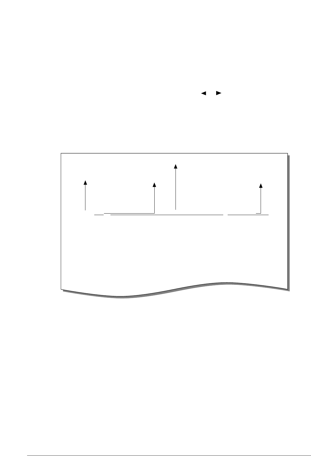
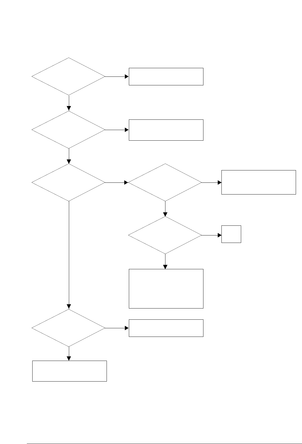
Vertical black line and band
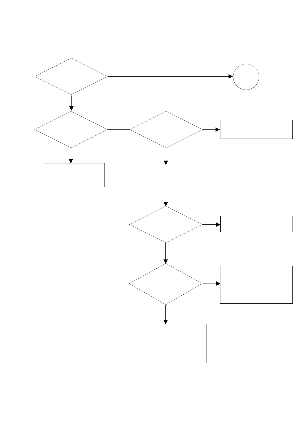
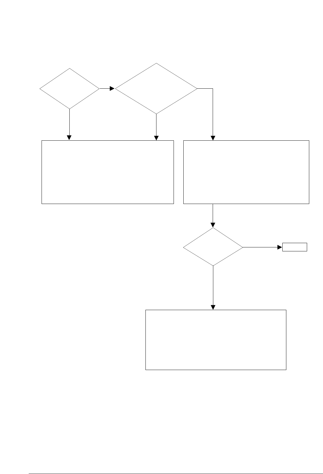
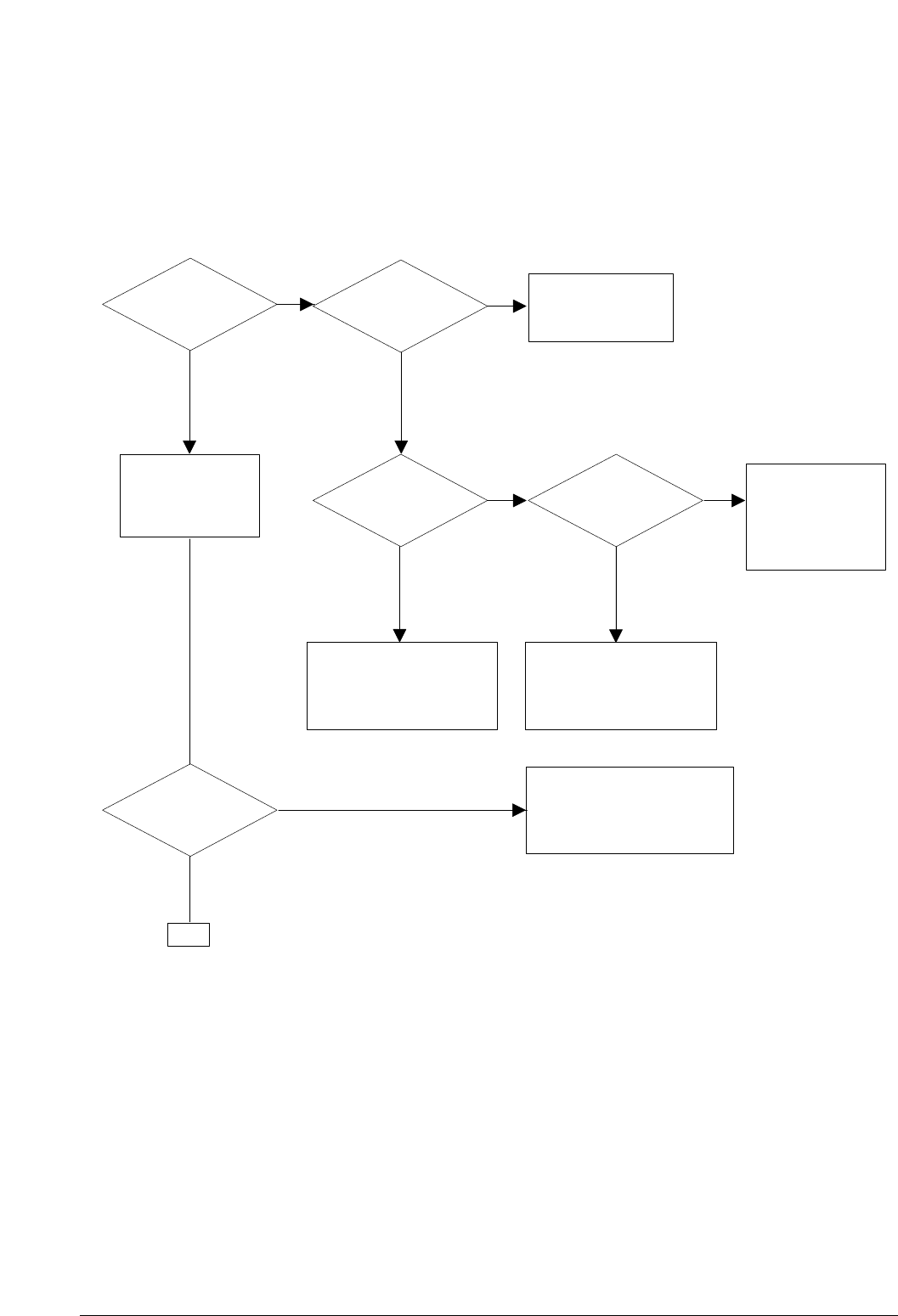
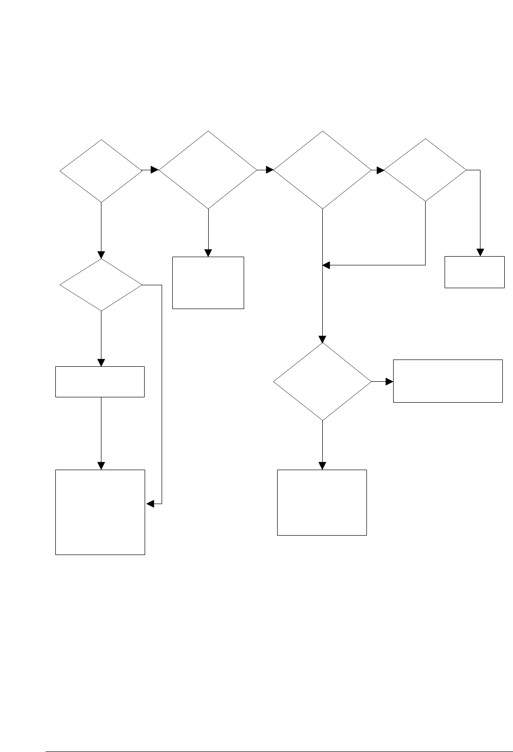
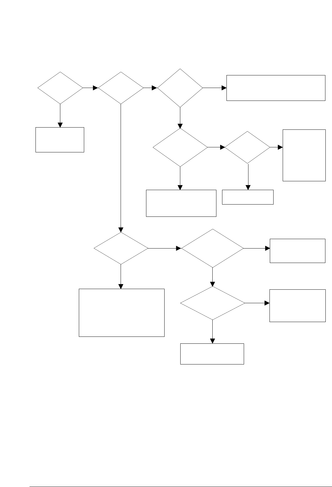
YES
NO
YES
OK after
replacing the LSU? Remove part on the paper
path causing the trouble
NO
OK after replacing
developer?
Any obstacles on
the developer blocking
the laser beam.
OK after
removing the
obstacles?
Any obstacles ON
mirror lens of LSU and
laser path?
Remove the obstacles.
Replace the LSU
Replace the developer
END
YES
YES
YES
NO
NO
NO
4-6 Troubleshooting Flow Chart
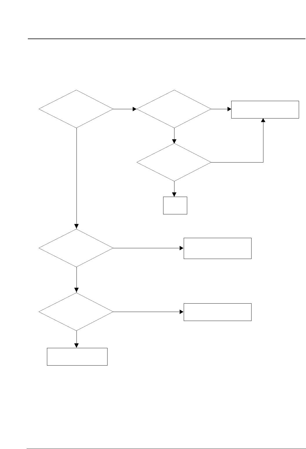
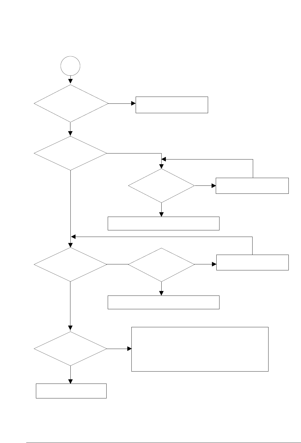
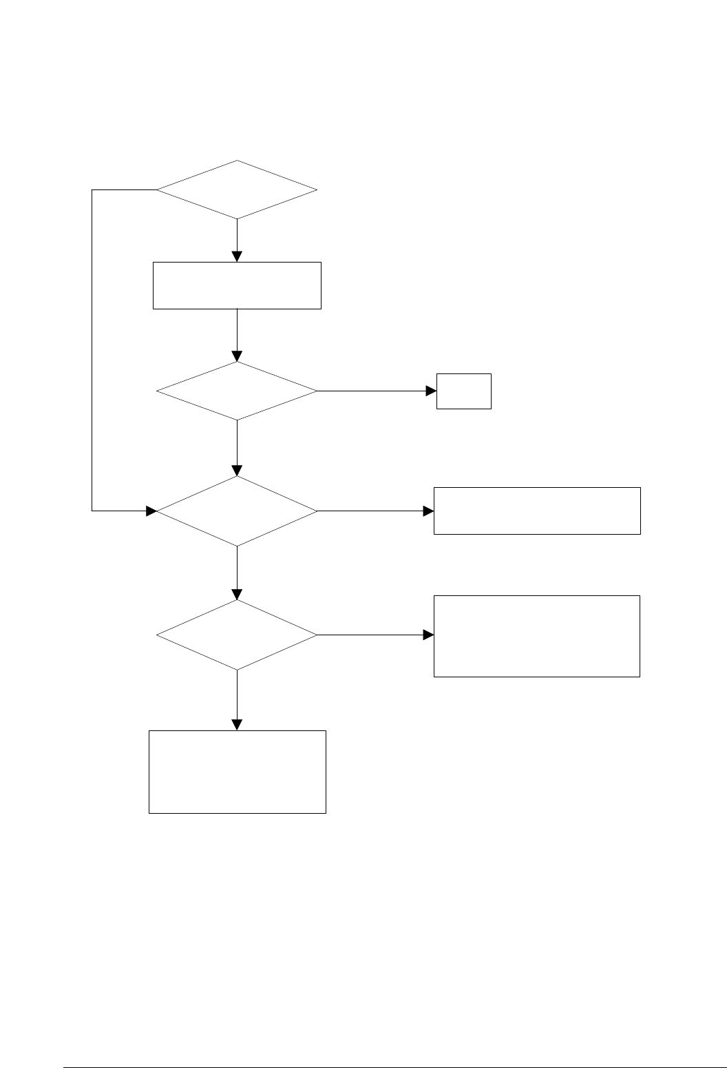
Troubleshooting
4-12 Samsung Electronics
Check connection to
computer or replace
controller
Take out the cartridge
and prepare the tester
for electronic connection
Repair or replace the GND
terminal
Check the path between
video controller, engine board
and HVPS. Repair or replace
the defective component
or board
The mirror in LSU might be
misplaced so the light path to the
OPC deviates ->Repair or replace
LSU or remove any deffective
matters in the machine
Self test
pattern prints?
No image?
Self testing
is possible via
Tech Mode?
Is the OPC
terminal of machine
is well-connected
to Frame?
Does the
video data line to
LSU transit to High/Low
when printing?
Re-test after replacing the
conector or Main board
A on
next page
NO
NO NO
NO
NO
YES
YES YES
YES
YES
No Image
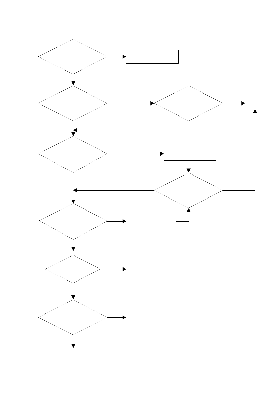
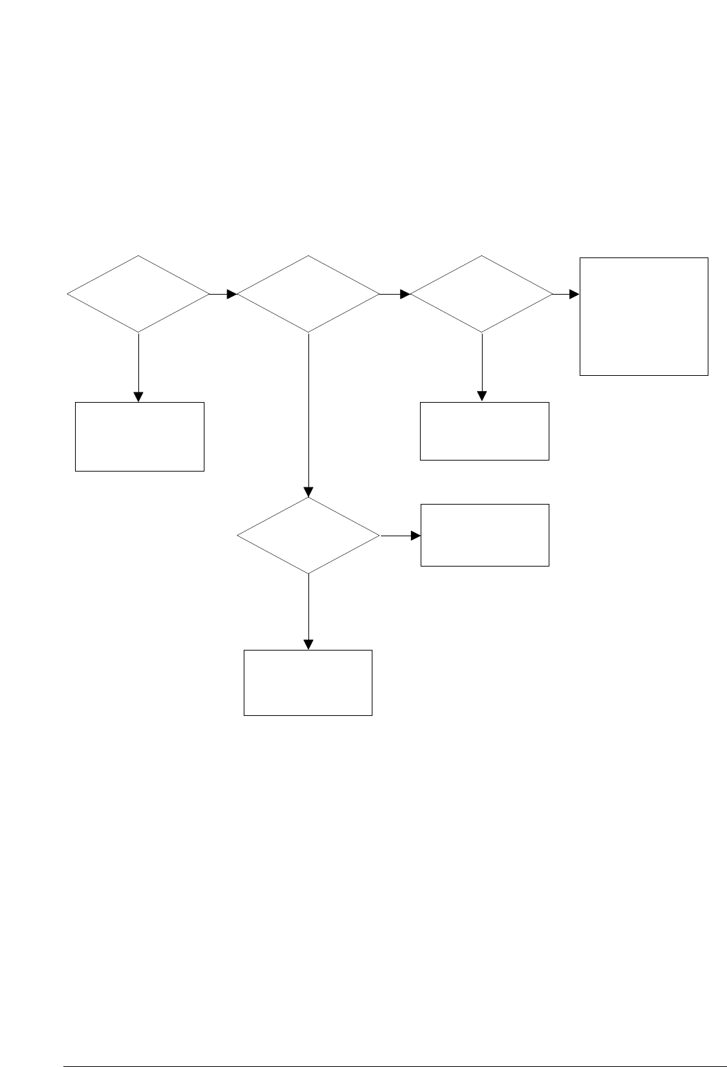
Troubleshooting
4-13
Samsung Electronics
Transfer roller might be out of its location
-> Locate the roller into its place
This could occurrs when he power of LSU is low or
the density is low due to the obstacles on the window
-> Replace LSU or clean the window
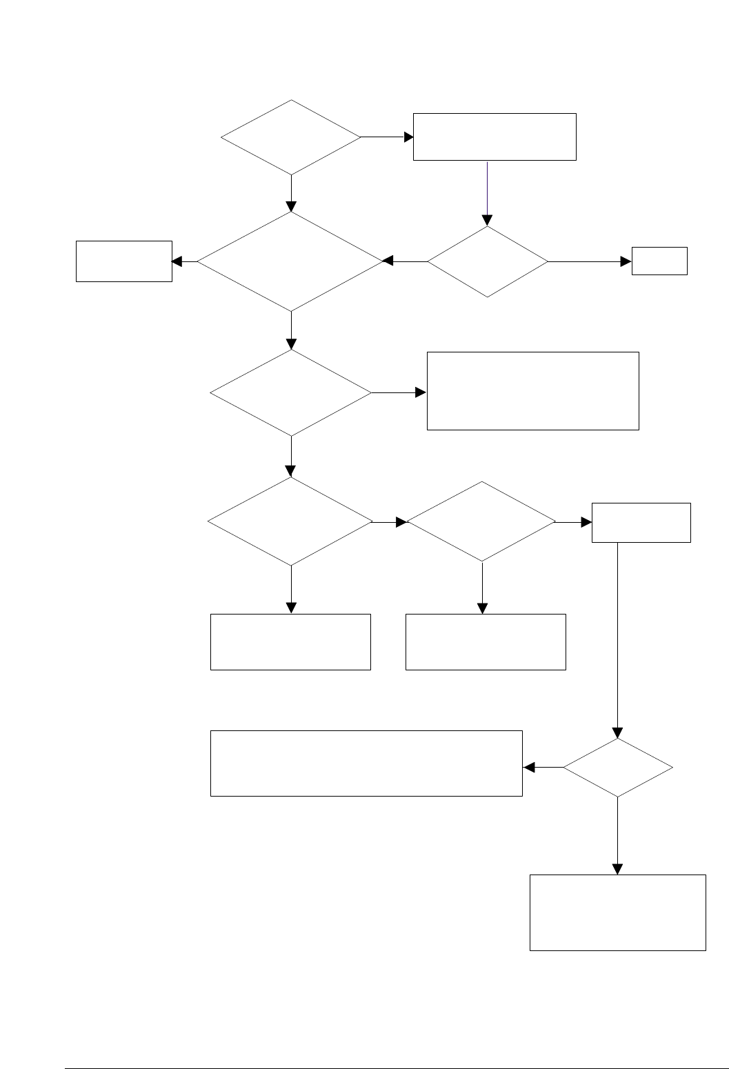
A
Trnasfer
voltage OK? (on the
transfer roller
shaft)
Is the
connection of
OPC GND and Frame Ground
correct? (less than
10 ‰)
Are the
connection terminal
and connection
correct?
Repair or replace terminal
Replace HVPS or repair defective component
Is the connection
terminal OK?
Check the connection of
frame Ground and OPC GND
Replace HVPS or repair defective component
Repair or replace terminal
Developing
(-350V) and supplying
(-550V) voltage
are OK?
Does the
counter indicate over
the toner’s guarranty
life
Replace the toner cartridge
NO
NO
NO NO
NO
YES
YES
YES
YES
YES
YES
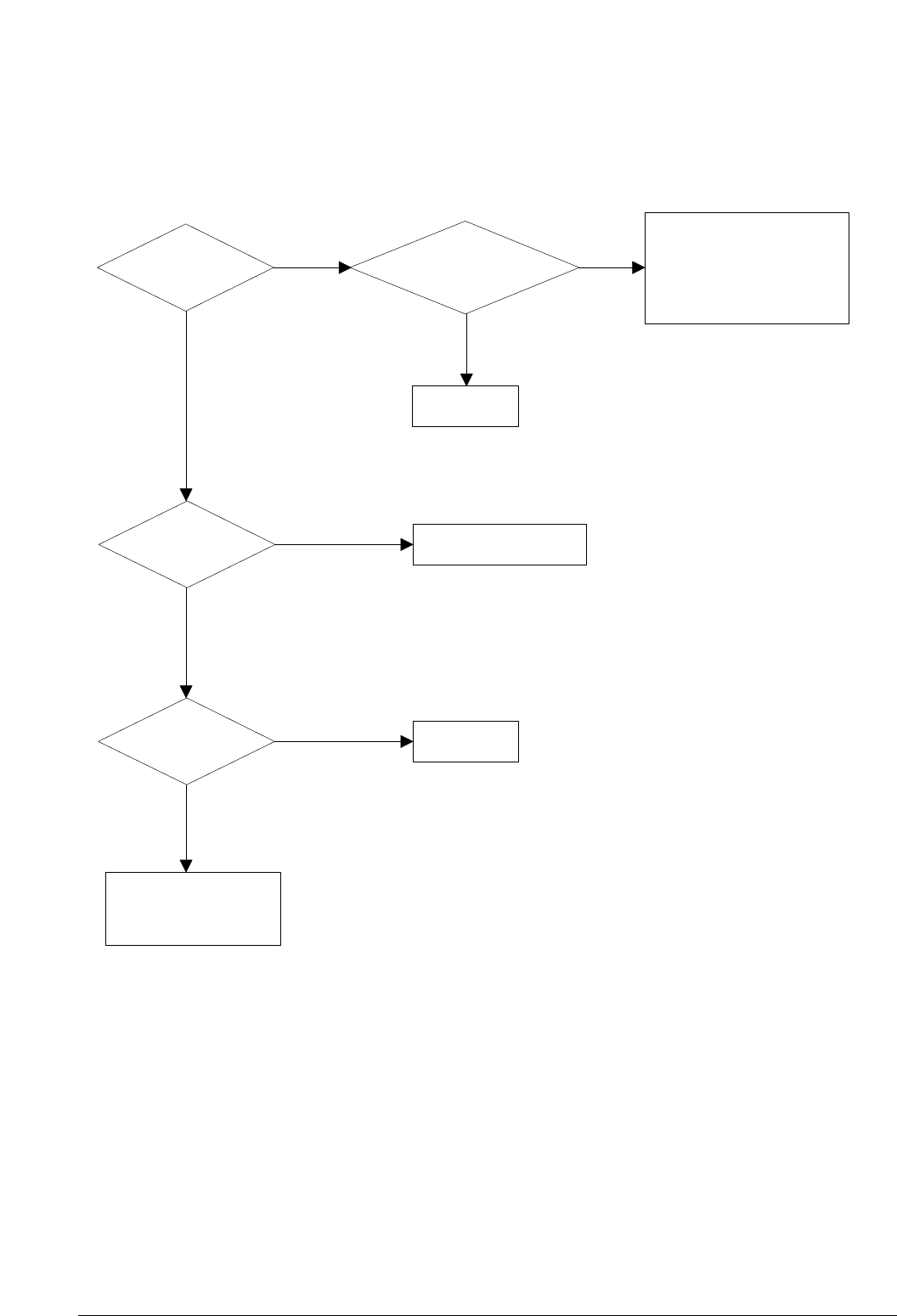
Troubleshooting
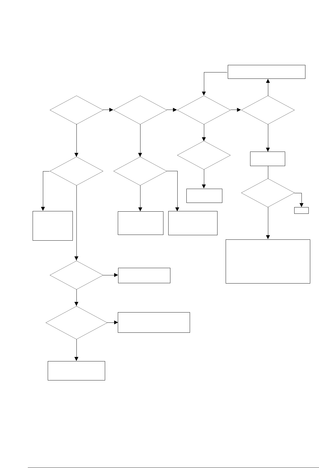
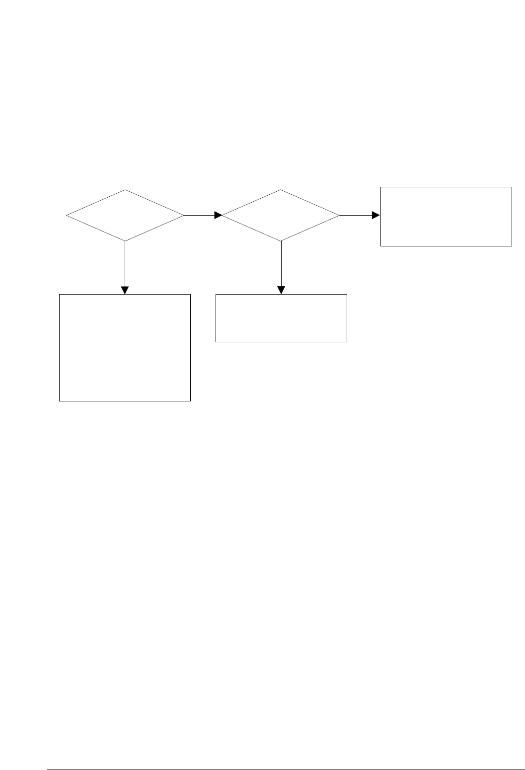
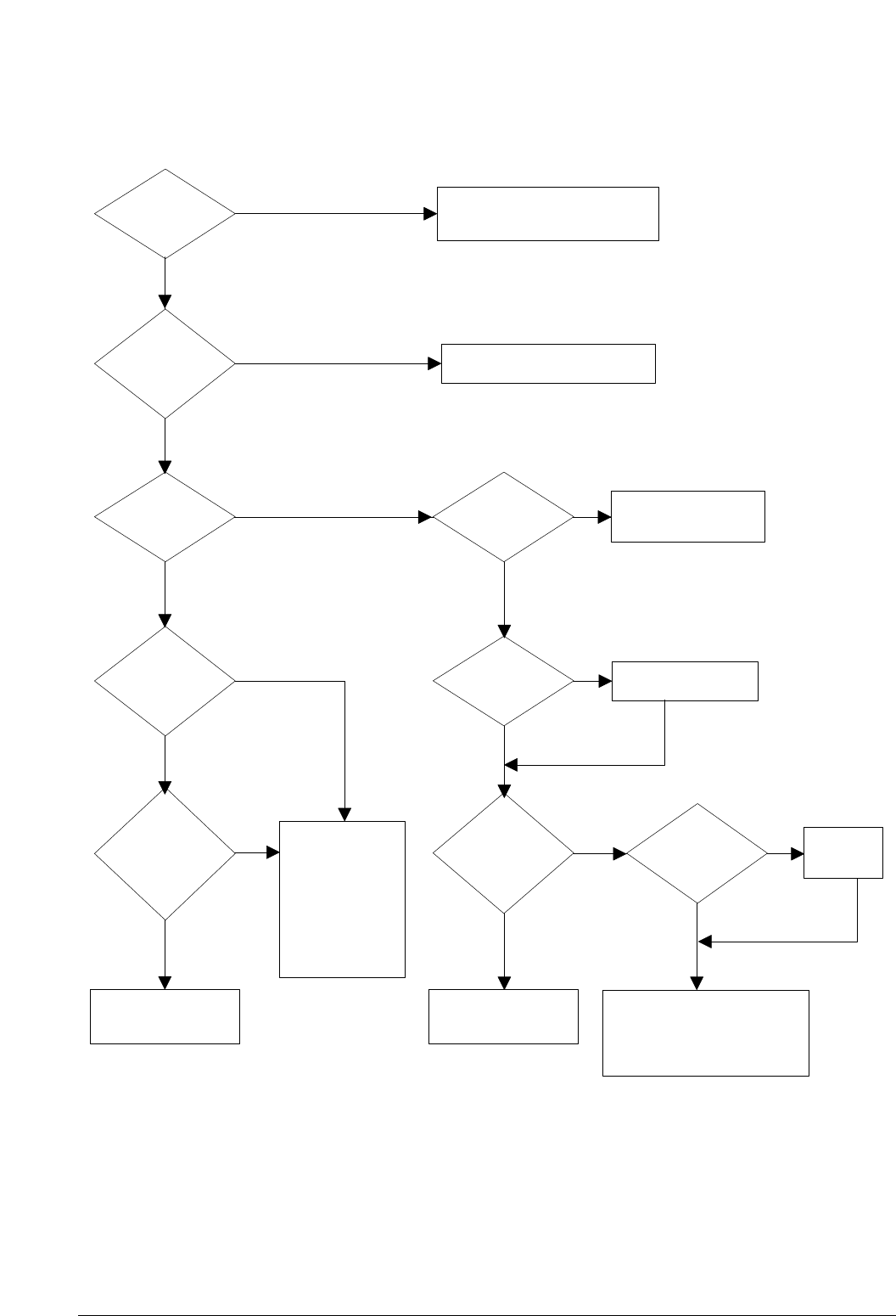
4-14 Samsung Electronics
Replace the developer
NO
YES
YES
END
YESYES
NO NO
NO
YES
YES
NO
Replace the HVPS
Ok after setting to the
normal mode?
YES
NO
Remove the obstacles
NO
YES
Clean transfer roller
and gear holder
YES
NO
Replace the LSU
Replace the developer
Is it not over
the guaranty life of dot
counter?
Is the toner save
mode or the light mode
is selected?
Is the high voltage
normal? (charging,
developing,
transfer)
Any obstacles on the
gab between high voltage
terminal and
developer?
Transfer roller
works OK?
OK after replacing
LSU?
HVPS works OK?
Light image
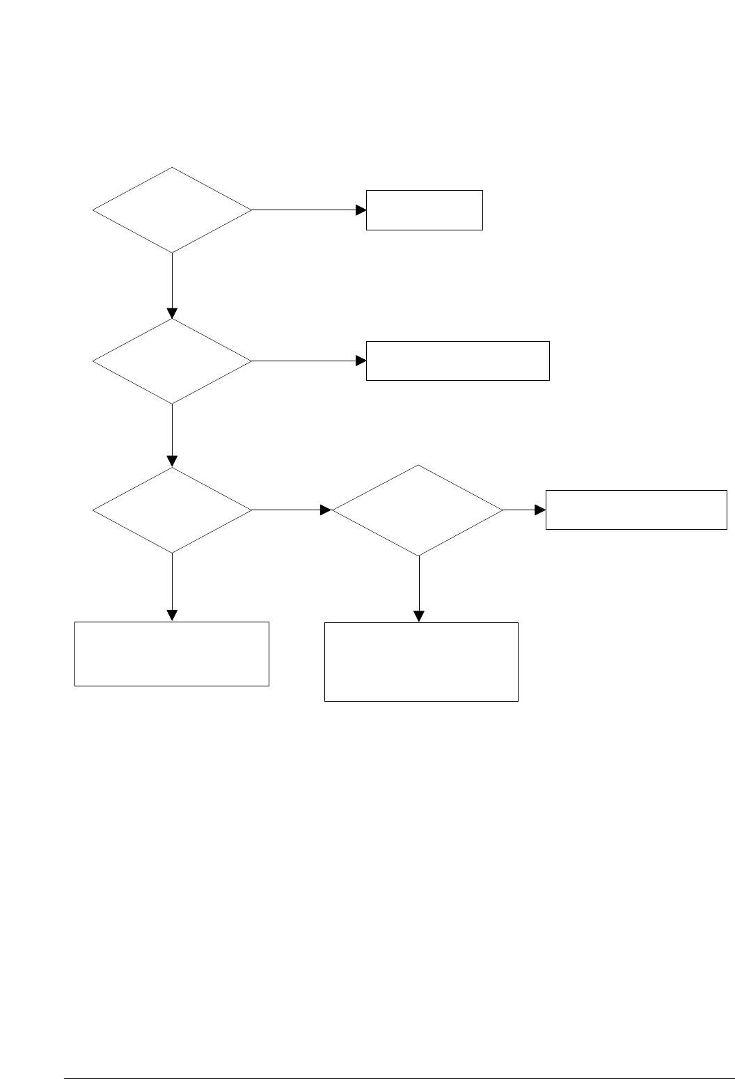
Troubleshooting
4-15
Samsung Electronics
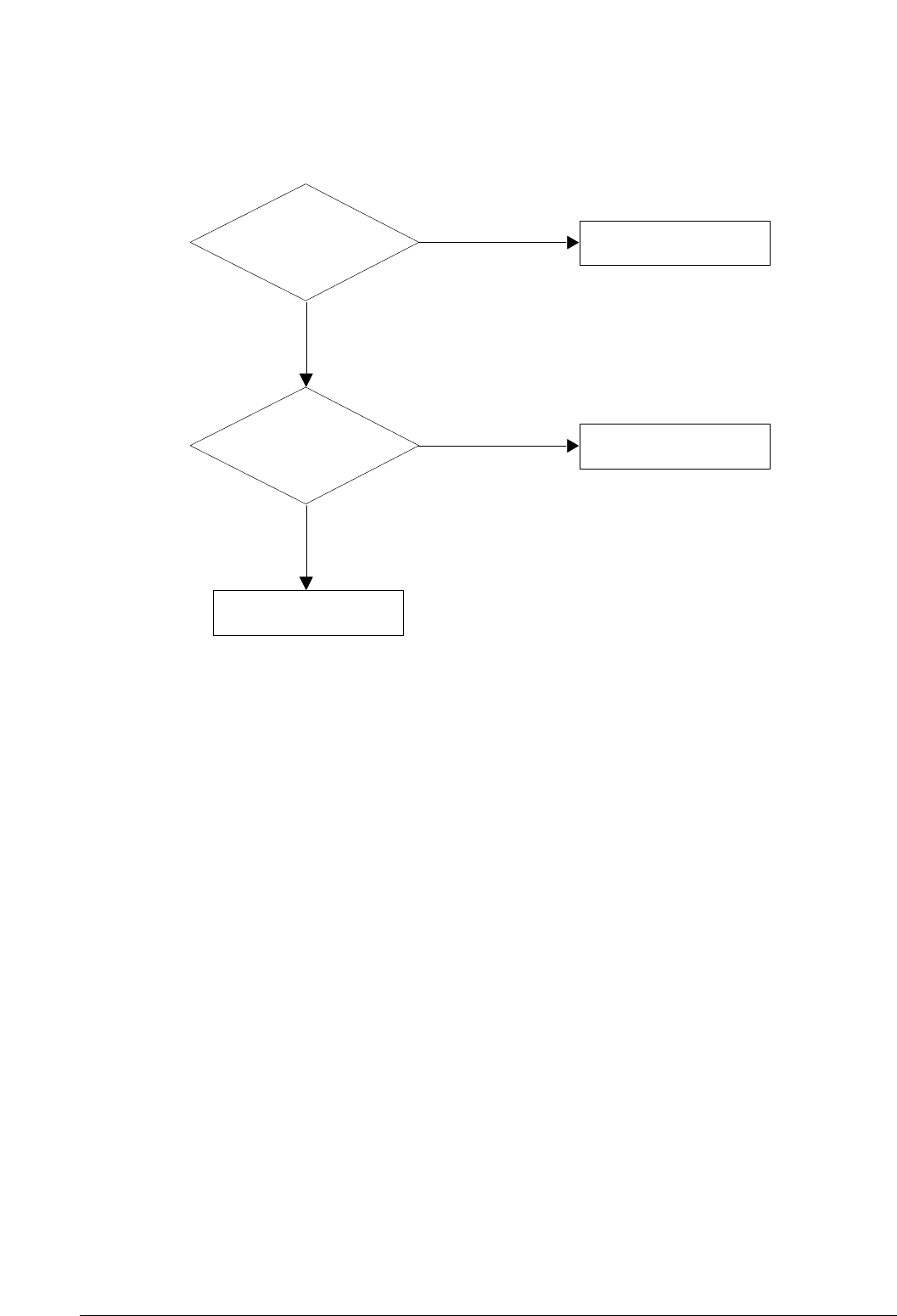
All black in
printing area?
Is transfer
voltage supplied
(-1.55 KV)?
Is the
Hsync/ signal received
in LSU?
Transfer part’s contact
is bad -> Repair or
replace toner cartridge
Does the
video data line to LSU
transit to High/Low when
printing?
Replace LSU
Check the path among video
controller, engine board,
HVPS, LSU for the shortage
or open -> Repair or replace
the boards
Repair or replace HVPS
Replace LSU
NO
NO
NO
NO
YES
YES
YES
YES
All Black
Troubleshooting
4-16 Samsung Electronics
White line
missing definitely?
Dirt of dust stuck onto the window of internal
lens of LSU
-> Clean it or replace LSU
Preventive obstacles through the path between
OPC of developer and LSU prevent the path
-> Remove the obstacles
Check if the
printout is still has the
same problem even right after
passed through the
transfer roller
Toner material might be stuck to blade in the developer
inside and it prevents toner supply
-> Replace the toner cartridge
Check both if the toner cartridge’s counter is over its
guaranty and amount of the toner material
-> Replace the toner cartridge
The ribs in fuser or toner on the roller may invoke
the image problem
-> Replace the fuser cover or the defective part
The image is originally black or the black part is
far close to the top
-> Use the pattern which has the image below bigger
than 10mm from the top
NO
NO
END
NO
YES
Does the problem
persist?
YES
YES
Vertical White Line (Band)
Troubleshooting
4-17
Samsung Electronics
Dark selected
via RCP?
Change to
Normal and test
Works cor
with -350V of Bias
voltage?
Works
correctly after
replaced LSU?
Repair or replace the defective
component
The power of LSU is set
high or internal problem
-> Replace LSU or adjust
voluem
Same at Normal? END
NO
NO
NO
Toner over supply due to the
adjustment fault of metering
blade in developer
-> Replace developer
NO
YES
YES
YES
YES
Dark Image
Troubleshooting
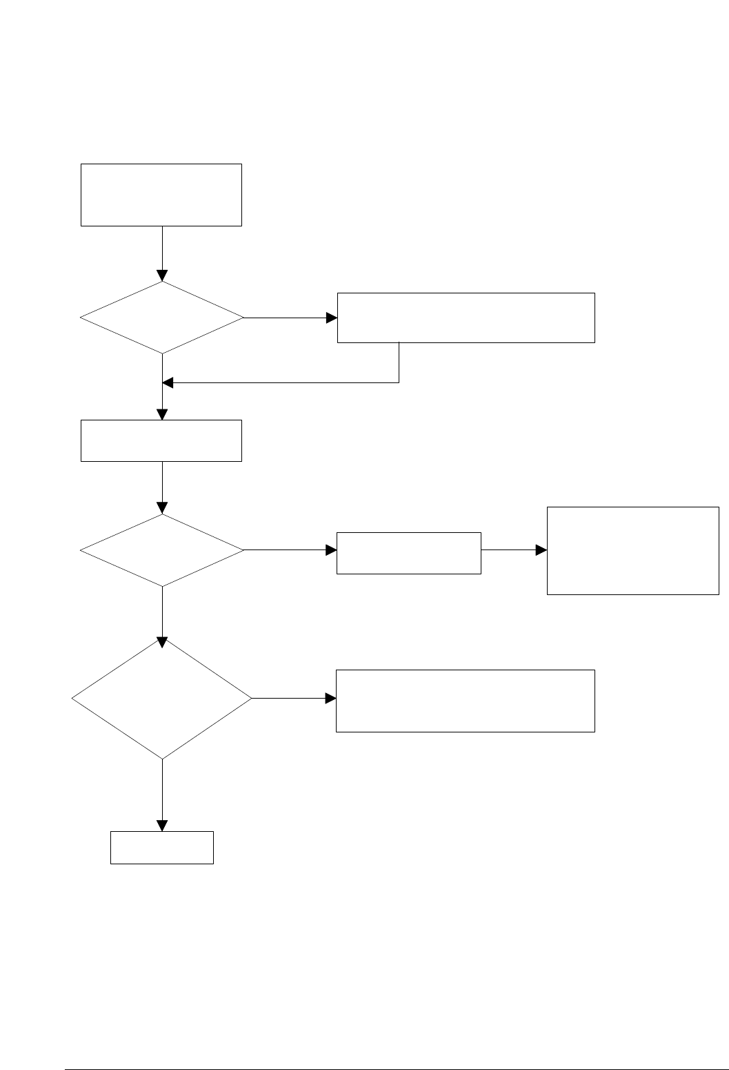
4-18 Samsung Electronics
Recommended
paper used?
Is pressure of
transfer roller too high?
Does the operation of
TR work properly?
Transfer,
charge and developing
voltage are OK?
Operating/
storage atmosphere is
too high temperature
/humidity?
Solve the problem under
the recommended condition
(10-32 degree Centigrade)
Dirt or
dust around the
charge roller?
Clean the charge roller
or replace step-up device
/terminal after check
Work OK?
Internal blade or suppying
part of the developer is
defective
-> Replace the toner cartridge
Check Terminals or contacts and ’Guide-Deve Spring’
are misplaced
-> Repair or replace transfer roller etc.
Print 20 to 30 pages using
the recommended paper
Same problem
occurs?
- Adjust voltage or replace HVPS
- Repair or replace after checking the
terminals’ contacts
Replace transfer
roller’s holder END
Replace the
toner cartridge
NO
NO
NO
NO
NO
NO
NO YES
YES
YES
YES
YES YES
YES
Background
Troubleshooting
4-19
Samsung Electronics
Is it regular
interval of 75.4mm?
Irregularity of NIP
between rollers in
developer
-> Replace developer
Clean heat roller
or replace it
Clean transfer roller’s holder and
TR drive gearor replace TR holder ass’y
Clean TR drive
and OPC gear
END
A specific part of the transfer roller has
ruined or its resistance value is changed
-> Replace transfer roller
Transfer roller cannot force regularly due
to the gears eccentricity of transfer roller
-> Replace the defective component
Adjust the Bias
voltage or replace HVPS
There may be a problem in toner
layer control in toner cartridge
-> Replace the developer
Use the machine with
recommended paper and
at condition
NO
NO
NO
NO
NO
NO
YES YES
YES
YES
YES
YES
NO
YES
YES
YES
YES
Check HVPS
contacts and
HVPS’s self-output
-> If failed, repair/
replace HVPS
- Repair or replace HVPS
- Check and Repair or
replace the terminal
contacts
NO
NO
Is it regular
interval of 31.6mm?
Is it regular
interval of 47mm?
(as transfer roller
interval)
Is it regular interval of
50.4 mm?
Does
the operation
of TR work properly?
Transfer
voltage is set to
standard?
Does the same
problem persist?
Developing
/suppying voltage
normal? (-350V/
-550V)
Bias voltage
is OK? (-350V)
Operating/storage
temperature is too low or
not recommended
paper used?
Ghost
Troubleshooting
4-20 Samsung Electronics
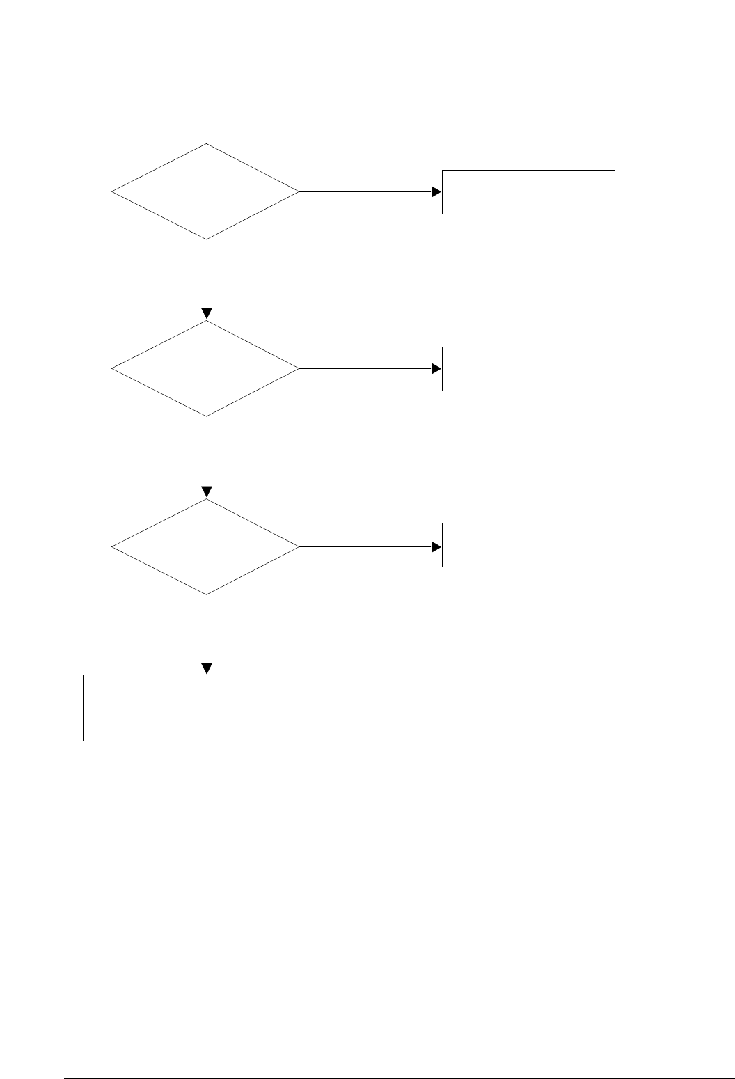
The problem occured
since the obstacles
stuck to charge roller
-> Replace toner cartridge
When taking
out the cartridge,
toner leaks?
Toner leaks and toner
material dropped onto
the paper -> Replace the
developer
Bad image
removes by
scratching?
Check toner is stuck onto
the P/R or H/R in fuser
-> Clean it or replace
The problem
randomly occured
due to the toner
fallen -> Clean the
machine
Remove obstacles
stuck on OPC
drum’s surface
Perform the OPC
cleaning using
the control panel
buttons.
END
NO
YES
NO
NO
YES
NO
YES
Does the same
problesm
persist?
Is it regular
interval of 37.7mm? Is it regular
interval of 75.4 mm?
NO
YES YES
Black Spot
Troubleshooting
4-21
Samsung Electronics
NO
Black band?
The black
band has regular
interval?
Black band
is far about 10mm from
white band?
Problem of internal
contacts in OPC
-> Replace developer
The OPC is damaged under the
direct sunlight for around 5
minutes -> If the same problem
persists in 10 hours, replace
the developer
This occurs when no
Hsync/ at LSU
-> Replace LSU
75.4 mm interval?
Heat roller is ruined
-> Replace the roller
The OPC is damaged due to
the irregular transfer voltage
of HVPS
-> Repair/replace HVPS
-> If the same problem persists,
replace the developer
Does it appear
at every 56.1mm at
specific place?
Problems of terminal contact,
transfer voltage supplying,
and transfer roller’s due to the
charge roller is ruined (37.7mm)
-> Repair/replace HVPS,
developer
NO
NO NO
NO
YES
YES
YES
YES
Horizontal Band
Troubleshooting
4-22 Samsung Electronics
Transfer roller
is clear ? Clean the transfer roller
NO
YES
Paper path is
clear ? Clean the paper path
Clean the pressure roller
NO
YES
Toner Contaminations on Back of Paper
Troubleshooting
4-23
Samsung Electronics
Is it not over
the guaranty life of dot
counter? Replace the toner cartridge
NO
YES
YES
YES
Is toner cartridge
installed correctly? Install the toner cartridge correctly
NO
Transfer roller
works properly? Clean the TR holder, the TR gear,
OPC roller gear and the transfer roller
NO
- Clean the contact point of transfer roller
- Check the output of high voltage terminal
and adjust or replace if required
Partial Blank Image (not Periodic)
Troubleshooting
4-24 Samsung Electronics
Is it not over
the guaranty life of dot
counter? Replace the toner cartridge
NO
YES
YES
NO
NO
Is toner
cartridge installed
correctly?
Install the toner cartridge
correctly
NO
Is it regular
interval of 47.1mm? Transfer roller
works properly?
OK after
replacing the transfer
roller?
Is it regular
interval of 75.4mm, 31.6mm
or 37.7mm?
Replace the fuser
(50.2mm, 45.2mm or exit roller
- Clean the contact point of
transfer roller.
- Check the output of high
voltage terminal and adjust or
replace if required.
Replace the toner cartidge
END
YES
YES
NO
YES
NO
YES
Clean the TR holder, the TR
gear OPC roller gear and the
transfer roller
Partial Blank Image (Periodic)
Troubleshooting
4-25
Samsung Electronics
It is over the guaranty
life of toner cartridge
(Check the counter
and replace it)
Defective agitator in
the toner supplying part
of developer
->Replace the developer
Check if the ’guide deve
spring’ works OK and
repair/repalce
Check high voltage
output and repair/
replace terminals, HVPS
Irregualrity of toner
suppy from developer
-> Repalce developer
Light distortion due to
the mirror ruined or
LSU’s diffused reflection
-> Replace LSU
NO
NO
YES YES
YES
YES
NO NO
OK after
taking out and
rocking the toner
cartridge?
When gray
pattern printing,
irregular density
persists?
transfer/
charge/developing
voltage drops while
printing?
Bad images
aroung the no image
area?
Irregular Density
Troubleshooting
4-26 Samsung Electronics
Is it regular
interval of 75.4mm?
Obstacles stuck on OPC’s
surface
-> Clean the OPC and
machine or replace
developer
When putting in/out the
developer, scratch is made
-> Replace the developer
Transfer
voltage is normal?
D/R in developing unit has
the defect
-> Replace the developer
Too high voltage supplied
due to the setting error of
transfer voltage
-> Adjust/replace HVPS
NO NO
YES YES
White Spot
Troubleshooting
4-27
Samsung Electronics
When multi-page OHP printng,
less than 10 films are
guranteed.
Use the recommended film
When OHP
printing, does the fan
temporarily stops
and revolves?
Use the recommended film
Other parts are touching the
fan and prevents it from
revolution
-> Check and repair
NO
NO NO
YES
Set to OHP mode
NO
YES
YES YES
Is the OPC
mode selected using
the software
application?
Recommended
OHP film used?
Inserted over
than 10 films into
the MPF?
Trembling at the End When OHP Printing
Troubleshooting
4-28 Samsung Electronics
After printing
completed, any error
related fuser?
Both ends
of thermostat
open?
Replace thermostat
and re-test
Replace the contol
component on engine
board
Check any contact
problem in thermistor
and repair
The machine
placed under the
severe low tempera
ture for a long
time?
Place the machine
at normal
temperature and
re-test
While printing,
the voltage of pin 208
of U5 (CPU) on Main
board is 2.0V
~2.3V?
Thermistor’s
contact is OK?
Open the top
cover. When black
printing, is the fuser NIP
width is 1.2~
3.0mm?
The paper used is too
thick or contains too
much cotton in it
-> Re-test with the
recommended paper
Check if the hardness of
P/R, and spring force is OK?
(spring’s force: 2.5 Kg)
Re-assemble
thermistor
NO
NO
NO NO
NO
NO
YES
YES
YES
YES YES YES
Poor Fusing Grade
Troubleshooting
4-29
Samsung Electronics
Plug in the
power cord?
The power
voltage supplying is
the same as
rating?
The fan
revolves when
powered on?
LEDs blink
once when
powered on?
The On-Line
key is being pressed
or shortage on
the panel
board?
Repair/replace the
board
Check the voltage first and plug
the power cord
Supply the power as the rating
Connections
on board are OK?
Re-connect firmly
and re-test
The connection
error between
controller board
and panel board
or malfunction
of boards.
-> Replace the
boards
Fuse of SMPS
if open?
Shortage
between 5V and
GND, or between
24V and
GND?
Replace the fuse
Toner cartridge
is in the set?
Detect failure due to the
board which detects top
cover open or switch error
-> Replace the board or switch
Put in the
cartridge
Remove the shortage
or replace the board
NO
NO
NO
NO
NO
NO
NO NO
NO
YES
YES
YES YES
YES
YES YES
YES
YES
No Power (LCD NO display LED Off)
Troubleshooting
4-30 Samsung Electronics
Less than 10W?
AC is being supplied?
The voltage
of pin #208 of U5
(CPU) on the Main board
is about 2.3V when
printing?
END
Thermostat is open due to the heat etc.
-> Replace the thermostat
Check the PCI and fusing
control part and CN502
on the SMPS
-> Replace the component
or replace the SMPS
Measure the resistance
at the both ends of AC
Line with covers open
Remove the covers
Re-assemble the top
cover and close it
Thermistor, connecting point or engine
board defect -> Repair/replace the
component/board
NO
NO
NO
YES
YES
YES
Fuser Error
Troubleshooting
4-31
Samsung Electronics
Sounds the
solenoid on when starts
print?
Does the
paper move?
Does the
paper move more than
100mm?
The Engine board defected
-> Replace boards
The solenoid defected
-> Replace it
The pick-up unit is
assembled wrong
-> Re-assemble or replace
the unit
Feeder
sensor and paper
width detect sensor
are assembled
reverse?
Switch them
The Sensor board
defected
-> Repair/replace
Too many
papers in the
feeder?
Paper guides
fit the paper width?
Paper end curled? Does the
extender pulled out?
<Recommendation>
Use the MPF for the thick
paper such as envelope
and cardstock
Reduce the amount
and re-test
Take out the paper
and re-insert
Use the recommended
and quality paper
Pull out the
extender
NO
NO
NO
NO
NO
NO NO
YES
YES
YES
YES
YES
YES
YES YES
Paper Jam (Mis-feeding)
Troubleshooting
4-32 Samsung Electronics
Paper
stopped before
the OPC?
Check the LSU and
if it has the defect
replace it
Paper
stopped before
the fuser?
Severe skew
when feeding?
Adjust the paper guides to fit the
paper width
The force of springs pressing the
developer is weak
-> Check guide-DEVE
The paper
came out through
between fuser and
developer?
Too thin
or sensitive paper to
static electricity?
Use the recommended
paper
Check guide transfer
is grounded Check
the shutter prevents
feeding
Check the input path
to the fuser (such as
mis-assembly)
The
actuator of
paper exit sensor
works OK?
Check the actuator exists and its
operation and around the engine board
-> Replace
Is the paper
rolled around the
presseure
roller?
Remove the fuser, remove
the paper and replace the
pressure roller, if necessary
Feeds
multiple pages?
Remove any factors
Check the roller
and ribs of fuser
are in place, and
remove burrs, if
any
-> Remove the
factors of jam
NO NO NO
NO
NO NO
NO
NO
YES YES YES
YES
YES YES
YES
YES
Paper Jam (Jam1)
Troubleshooting
4-33
Samsung Electronics
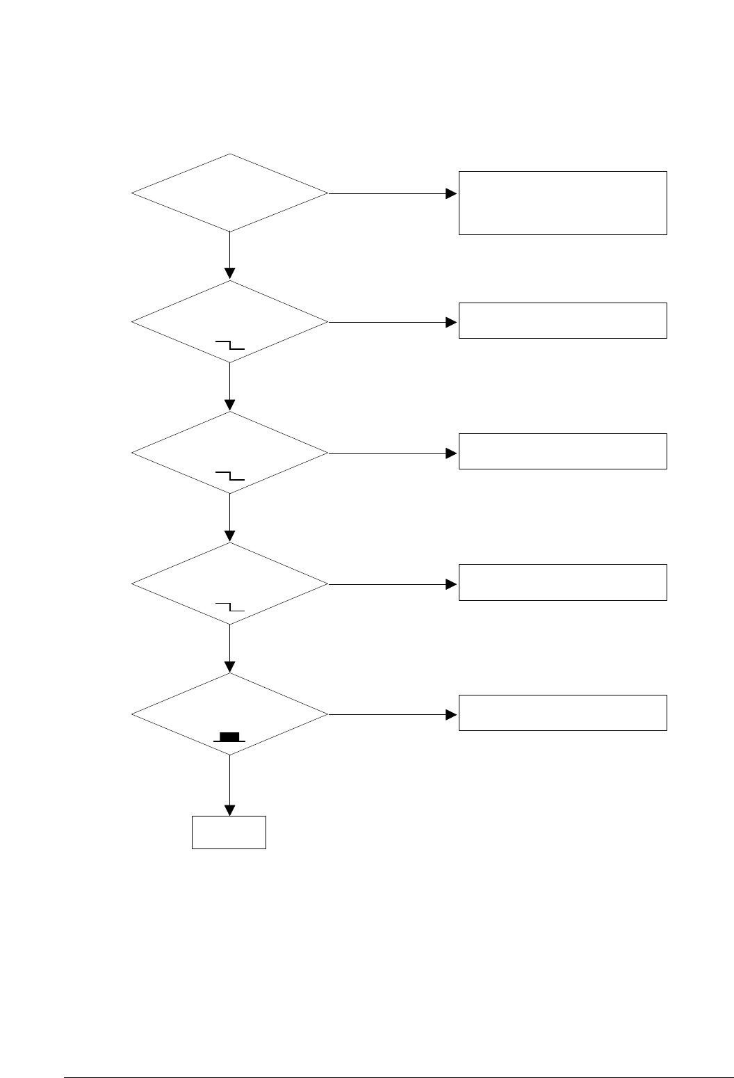
Try again to connector
or
Replace connector
END
NO
Check
CBF Harness28P
(MAIN B’D to ENGINE
B’D)
YES
Check
MAIN B’D CN9-6,
HSYNC Signal
( )
Replace LSU
NO
YES
Check
MAIN B’D CN9-3,
P_MOTOR Signal
( )
Replace MAIN B’D
NO
YES
Check
MAIN B’D CN9-4,
LREDADY Signal
( )
Replace LSU
NO
YES
Check
MAIN B’D CN9-9,
LDON Signal
( )
Replace MAIN B’D
NO
YES
LSU Error

5-1
Samsung Electronics
5. Exploded Views and Parts List
5-1 Main Assembly
5-2 Shield Engine Unit Assembly
5-3 Engine Assembly
5-4 Frame Lower Assembly
5-5 Fuser Assembly
5-6 Plate-Upper Unit Assembly
5-7 OPE Unit
5-8 Scan Upper Assembly
5-9 Front Assembly
5-10 RX Drive Unit Assembly
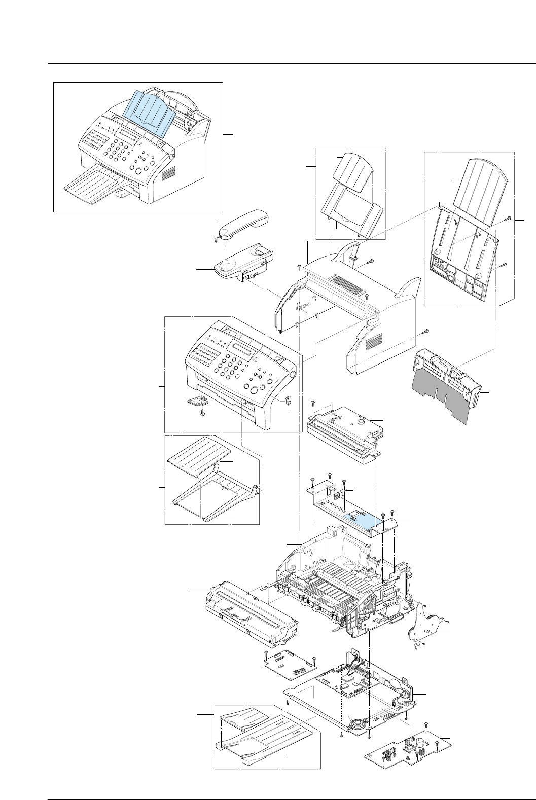
Exploded Views and Parts List
Samsung Electronics5-2
5-1 Main Assembly
2
9
17
10 &12
3
4
13
11
15
16
5
16-2
16-1
7
18
0
19
17-1
17-2
19-1
19-2
18-1
18-2
8
6
14
14-1
14-2
1
Exploded Views and Parts List
5-3
Samsung Electronics
O : Service available X: Service not available
No. Description SEC.Code Q’ty SA Remark
SF-530 / 531P
1 SMPS-V1 JC44-00032A 1 O 110V
SMPS-V2(4CH) JC44-00023A 1 O 220V
2 UNIT-LSU JC59-00006A 1 O
3 IPR-PLATE_CHANNEL JC70-00058A 1 O
4 MEC-PLATE UPPER JC75-00057A 1 O
5 MEC-TRAY JC75-00062A 1 O SF-530
MEC-TRAY(P) JC75-00075A 1 O SF-531P
6 MEC-CRADLE JC75-00083A 1 O
7 PBA MAIN-LIU PBA JC92-01379A 1 O
8 ELA HOU-HANDSET JC96-01629B 1 O
9 ELA-UNIT DEV APO6 E * 1 X
10 ELA HOU-ENGINE ASS’Y * 1 X
11 ELA HOU-SHIELD ENGINE * 1 X SF-530
ELA HOU-SHIELD ENGINE * 1 X SF-531P
12 ELA HOU-FRAME LOWER JC96-02094B 1 O 110V
ELA HOU-FRAME LOWER JC96-02094A 1 O 220V
13 ELA HOU-RX DRIVE JC96-01755A 1 O
14 MEA HOU-OPE FRONT JC97-01463L 1 O SF-530
MEA HOU-OPE FRONT TBD 1 O SF-531P
14-1 PBA MAIN-SCAN JC81-00441A 1 O
14-2 PMO-BASHING WHITE JF72-41306A 1 O
15 PMO-COVER TOP JC72-00128A 1 O
16 MEC-COVER REAR JC75-00059A 1 O
16-1 PMO-COVER_REAR * 1 X
16-2 PMO-TRAY_LARGE * 1 X
17 MEC-STCKER JC75-00060A 1 O
17-1 PMO-STACKER_MAIN * 1 X
17-2 PMO-STACKER_SUB * 1 X
18 MEA UNIT-CHUTE ASS’Y JC97-01187E 1 O
18-1 PMO-CHUTE * 1 X
18-2 PMO-DUMMY CHUTE * 1 X
19 MEC-STACKER JC75-00084A 1 O
19-1 PMO-STACKER TX(APOLLO) JC72-00223A 1 O
19-2 PMO-STACKER TX(B) * 1 X
Main Assembly Parts List
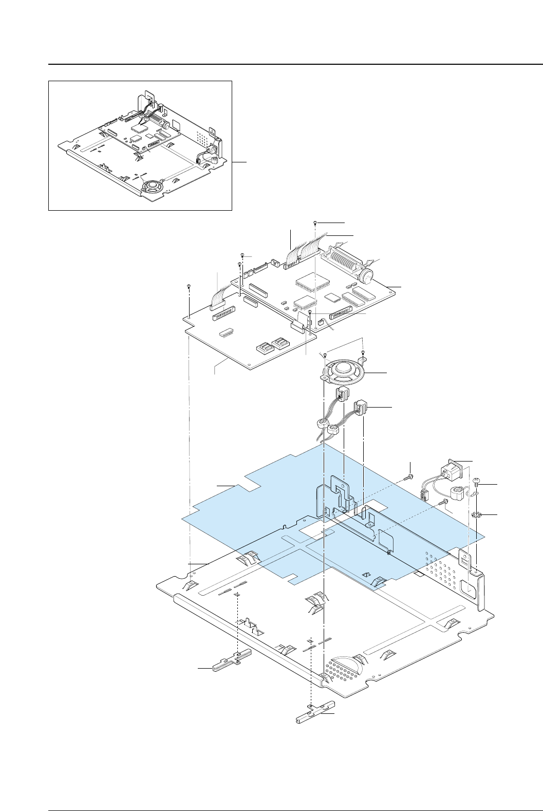
Exploded Views and Parts List
Samsung Electronics5-4
5-2 Shield Engine Unit Assembly
2
9
9
7
6
8
5
11
3
10
0
S8
12
S2
S2
S-9
4
S-9
1
S-9
S-9
LIU B’d
Exploded Views and Parts List
5-5
Samsung Electronics
O : Service available X: Service not available
No. Description SEC.Code Q’ty SA Remark
0 ELA HOU-SHIELD ENGINE * 1 X SF-530
ELA HOU-SHIELD ENGINE * 1 X SF-531P
1 CABLE-FLAT 3809-001161 1 O
2 CBF HARNESS-LSU JC39-00043A 1 O
3 CBF HARNESS-MAIN-HVPS JC39-00193A 1 O
4 CBF HARNESS-LIU/HOOK 2 JC39-00174A 1 O
5 CBF HARNESS-MODULA 2 JC39-00175A 1 O
6 CBF HARNESS JC39-40022A 1 O INLET
7 IPR-SHIELD ENGINE JC70-00200A 1 O
8 IPR-SHILED SMPS JC70-00263A 1 O
9 MEC-GUIDE STAKE ASS’Y JC75-00087A 2 O
10 PBA MAIN-MAIN JC92-01308B 1 O SF-530
PBA MAIN-MAIN JC92-01308D 1 O SF-531P
11 ELA M/MEDIO AUD-SPEAKER JC96-01607A 1 O
12 WASHER-E.T * 1 X
13 CBF HARNESS-THERMISTOR JC39-00045A 1 O
S2 SCREW-MACHINE 6001-000568 2 O
S8 SCREW-TAPTITE 6003-000221 1 O
S9 SCREW-TAPTITE 6003-000264 11 O
Shield Engine Unit Assembly Parts List
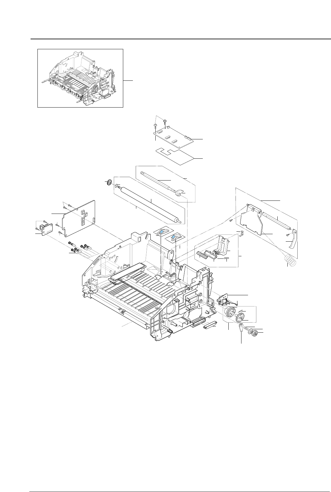
Exploded Views and Parts List
Samsung Electronics5-6
5-3 Engine Assembly
18
8
5
12
21
7
21-1
21-3
21-2
14 13-1
13-2
3
22
22-2
22-3 22-1
10
11
6
16
S-1
15
9
S-1
20
19 S-6 S-10
S-1
S-1
S-1
S-1
1-2
1-1
1
17
17-4
17-3
17-1
17-2
13
0
Frame Lawer Ass’y
Bushing-Shaft

Exploded Views and Parts List
5-7
Samsung Electronics
O : Service available X: Service not available
No. Description SEC.Code Q’ty SA Remark
0 ELA HOU-ENGINE ASS’Y*1X
1 MEC-CAM PICK UP JC75-00072A 1 O
1-1 PMO-CAM_PICKUP * 1 X
1-2 PMO-SHAFT_PICKUP * 1 X
2 CBF HARNESS-EARTH (TX MOTOR) JB39-00017A 1 O
3 SOLENOID-(APOLLO) JC33-00002A 1 O
5 SMPS-HVPS JC44-00017A 1 O
6 SPRING-CLUTCH JC61-00012A 1 O
7 SPRING-KNOCK UP JC61-00023A 1 O
8 PBA MAIN-HOOK 2 JC92-01378A 1 O
9 PBA MAIN-ENGINE JC92-01320A 1 O
10 PMO-GEAR_FEED JC72-00115A 1 O
11 PMO-CLUTCH_FEED JC72-00116A 1 O
12 PMO-CAP_PAD JC72-00124A 1 O
13 MEA RACK-TR ASS’Y*1X
13-1 PPR-SPACER DR * 1 X
13-2 MEC-TRANSFER ROLLER JC75-00035A 1 O
14 PMO-GEAR_TRANSFER JC72-00179A 1 O
15 PCT-INSULATOR ENG BD * 1 X
16 PMO-DUMMY SIDE * 1 X
17 MEC-HOLDER PAD JC75-00156A 1 O
17-1 SPRING-PAD JC61-00054A 2 O
17-2 PMO-HOLDER PAD JC72-00535A 1 O
17-3 PMO-HOLDER PAD LARGE JC72-00536A 1 O
17-4 RPR-PAD FRICTION * 1 X
18 MEC-TERMINAL JC75-00049A 5 O
19 MEC-SIDE PAD(L) JC75-00050B 1 O
20 MEC-SIDE PAD(R) JC75-00051B 1 O
21 MEC-KNOCKUP ASS’Y JC75-00053A 1 O
21-1 IPR-BAR_KNOCKUP * 1 X
21-2 PMO-PLATE-KNOCKUP * 1 X
21-3 PMO-CAM-KNOCKUP * 1 X
22 MEC-GEAR PICK UP JC75-00056A 1 O
22-1 SPRING-PICK UP GEAR * 1 X
22-2 PMO-GEAR_PICKUP,1 * 1 X
22-3 PMO-GEAR_PICKUP,2 * 1 X
S7 SCREW-TAPTITE 6003-000196 7 O
S10 SCREW-TAPTITE 6003-000266 2 O
S11 SCREW-TAPTITE 6003-000119 17 O
Engine Assembly Parts List
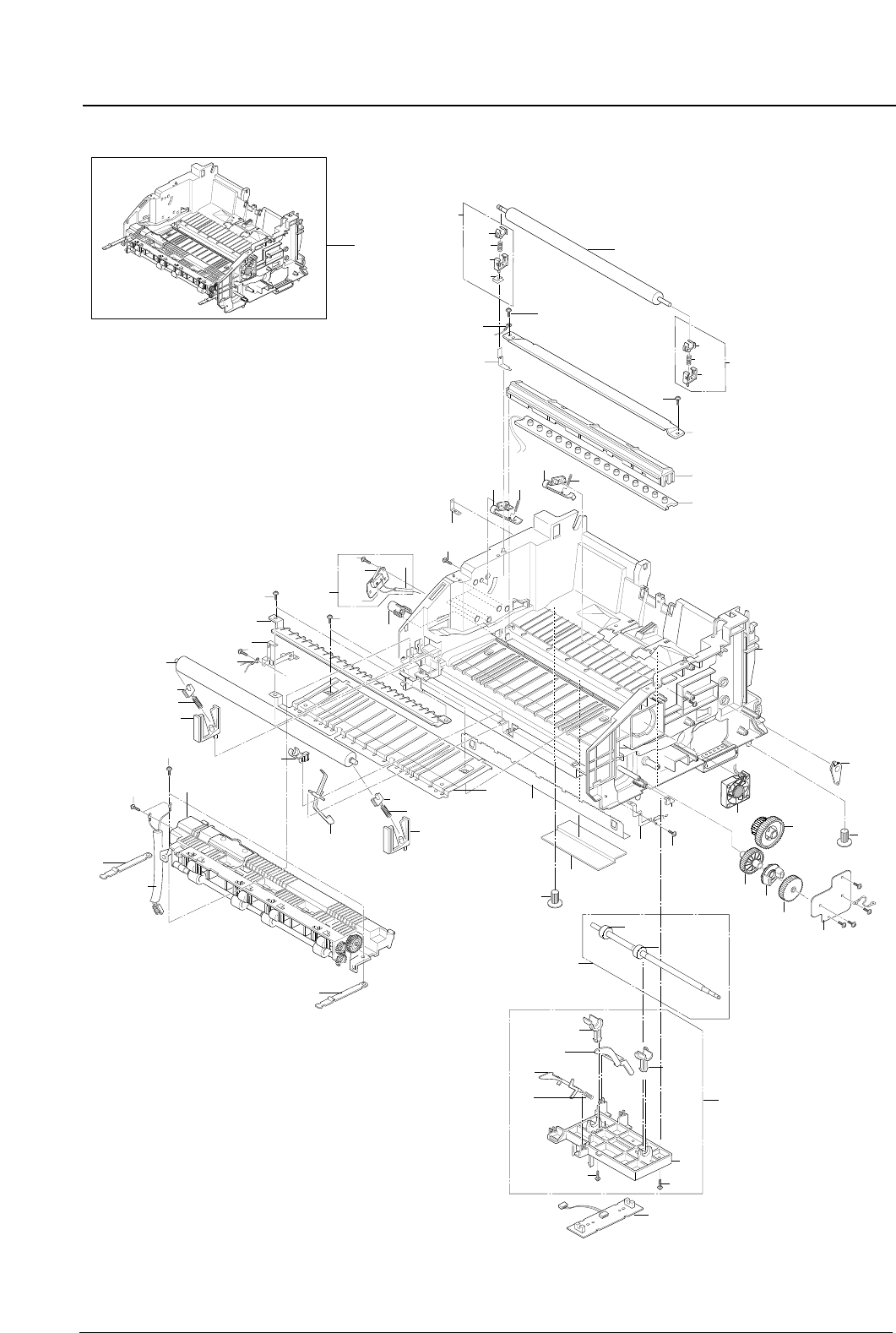
Exploded Views and Parts List
Samsung Electronics5-8
5-4 Frame Lower Assembly
32
S-2
S-2
28-3
28-3
28-4
28-5
28-1
28-2
28
17
18
5
5
3
18
3
31
19
15
1
8
16
11
34-2 34-1
14
34
9
4
24 4
23
37
26
0
20
S-1
S-1
S-1
S-1
S-6
S-1
26
33
13
10
6
36
25
2
S-2
S-2
S-6
27
27-1
27-2
25
12
7
21
35
29
29-3
30-2
29-4
29-1
29-2
30-3
30
30-1
S-1
S-1
1
41
38
40
42
39
Transfer Roller
43

Exploded Views and Parts List
5-9
Samsung Electronics
O : Service available X: Service not available
No. Description SEC.Code Q’ty SA Remark
0 ELA HOU-FRAME LOWER JC96-02094B 1 O 110V
ELA HOU-FRAME LOWER JC96-02094A 1 O 220V
1 CBF HARNESS-OPE GND * 1 X
2 CBF HARNESS-FUSER JC39-00061A 1 O
3 SPRING-P/R (APOLLO) * 2 X
4 SPRING-GUIDE DEVE * 2 X
5 BEARING-PRESSURE R * 2 X
6 IPR-SAW_PLATE * 1 X
7 IPR-EARTH_TRANS * 1 X
8 IPR-GROUND_GUIDE * 1 X
9 IPR-GROUND_HVPS * 1 X
10 IPR-GROUND_FUSER * 1 X
11 IPR-GUIDE-TR * 1 X
12 IPR-PLATE-TERMINAL * 1 X
13 IPR-GROUND DRIVE * 1 X
14 PMO-BUSHING_TERMINAL * 1 X
15 PMO-ACTUATOR_EXIT JC72-00130A 1 O
16 PMO-GUIDE_INPUT * 1 X
17 PCT-FILM SAW * 1 X
18 PMO-HOLDER PR JC72-00531A 2 O
19 PMO-HOLDER EXIT JC72-00532A 2 O
20 PMO-FRAME LOWER JC72-00533A 1 O
21 PMO-COVER PTL JC72-00534A 1 O
23 PMO-CAP PLTE G/DEV R JC72-41135A 1 O
24 PMO-CAP PLTE G/DEV L JC72-41173A 1 O
25 PMO-STOPPER EXIT * 2 X
26 RMO-RUBBER_FOOT * 2 X
27 MEC-ROLLER FEED JC75-00054A 1 O
27-1 RPR-ROLLER FEED * 2 X
27-2 MEC-SHAFT FEED * 1 X
28 MEC-HOLDER FEED JC75-00055A 1 O
28-1 SPRING-ACT, FEED * 1 X
28-2 PMO-HOLDER_FEED * 1 X
28-3 PMO-BUSHING_FEED * 2 X
28-4 PMO-ACTUATOR_EMPTY * 1 X
28-5 PMO-ACTUATOR_FEED JC72-00119A 1 O
29 MEC-HOLDER TR L JC75-00106C 1 O
29-1 SPRING-TR(300) * 1 X
29-2 IPR-PLATE_TR * 1 X
29-3 PMO-HOLDER TR JC72-00100C 1 O
29-4 PMO-BUSHING_TR(L) JC72-00102A 1 O
30 MEC-HOLDER TR R JC75-00107C 1 O
30-1 SPRING-TR(300) * 1 X
30-2 PMO-HOLDER TR JC72-00100C 1 O
30-3 PMO-BUSHING_TR(R) JC72-00101A 1 O
31 MEC-ROLLER_PR 1210 JC75-00130A 1 O
32 PBA MAIN-SENSOR JC92-01197A 1 O
33 ELA HOU-MOTOR GND JC96-01579A 1 O
34 ELA HOU-OPEN SENSOR JC96-01584A 1 O
34-1 CBF HARNESS-COVER JC39-00041A 1 O
34-2 IPR-BRKT-SENSOR * 1 X
35 ELA HOU-PTL ASS’Y JC96-02312A 1 O
36 ELA HOU-FUSER 110V JC81-00439A 1 O 110V
ELA HOU-FUSER 220V(531P) JC81-00440A 1 O 220V
37 PMO-BUSHING SHAFT JG72-40849A 1 O
38 GEAR-FU_IN 47 JC66-00306A 1 O
39 PMO-HUB GEAR JC72-00676A 1 O
40 GEAR-FU_OUT 47 * 1 X
41 PMO-GEAR_83/35 JC72-00154A 1 O
42 IPR-BRACKET FUSER DRV * 1 X
43 FAN-DC 3103-001085 1 O
S6 SCREW-TAPTITE 6003-000152 1 O
S7 SCREW-TAPTITE 6003-000196 2 O
S11 SCREW-TAPTITE 6003-000119 17 O
Frame Lower Assembly Parts List
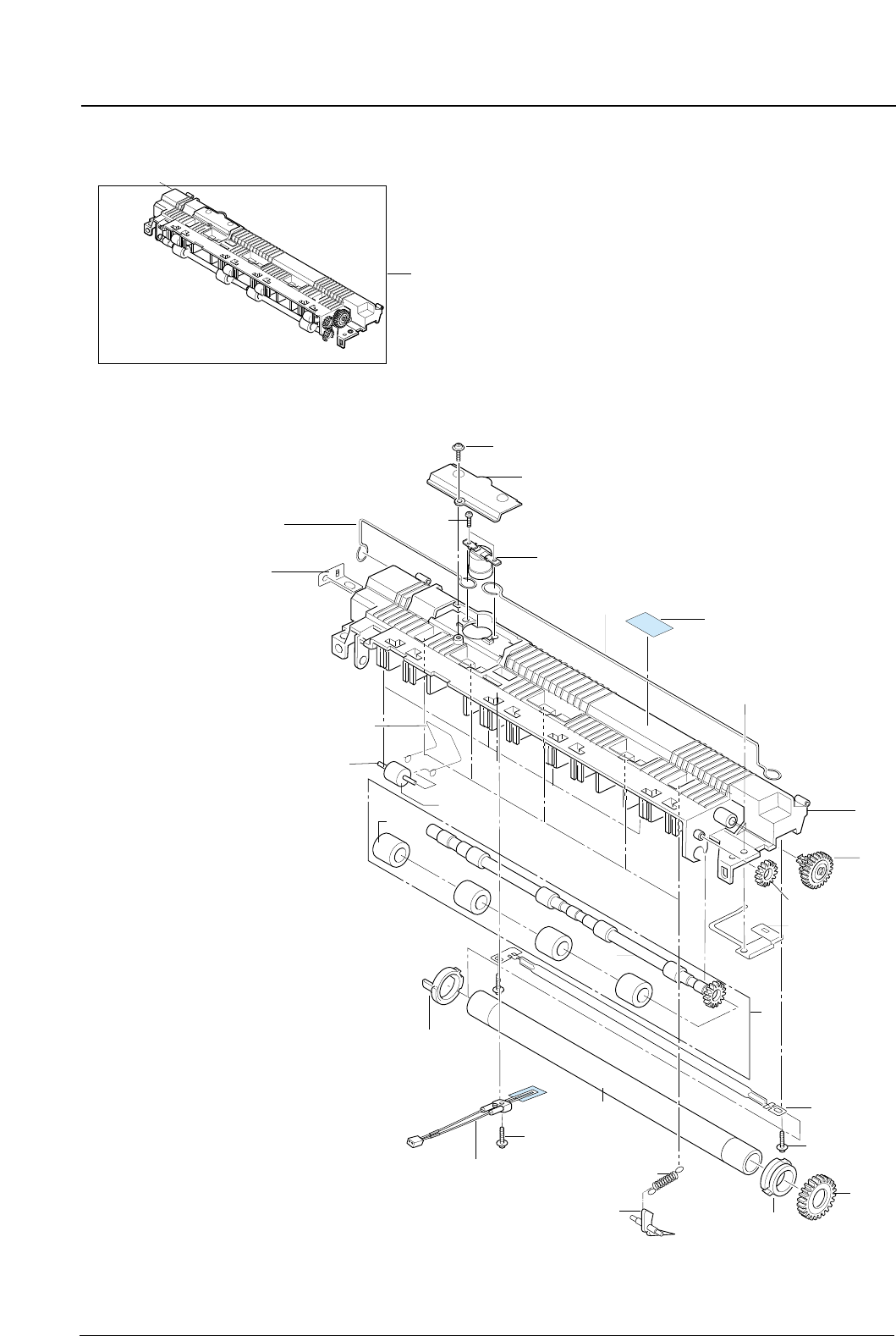
Exploded Views and Parts List
Samsung Electronics5-10
5-5 Fuser Assembly
16
11
15
14
14-1
14-2
10
17
18
4
12
2
7
13
9
5
1
8
6
19
3
0
S
S
S
S
S
21
22
20
Exploded Views and Parts List
5-11
Samsung Electronics
O : Service available X: Service not available
No. Description SEC.Code Q’ty SA Remark
0 ELA HOU-FUSER 110V JC81-00439A 1 O 110V
ELA HOU-FUSER 220V(531P) JC81-00440A 1 O 220V
1 THERMISTOR-NTC 1404-001188 1 O
2 THERMOSTAT 4712-000001 1 O
3 LAMP-HALOGEN 4713-001120 1 O 110V
LAMP-HALOGEN 4713-001121 1 O 220V
4 PMO-FUSER_UPPER * 1 X
5 PMO-BUSHING H/R L JC72-00530A 1 O
6 PMO-BUSHING H/R R JC72-00529A 1 O
7 PMO-COVER_THERMOSTAT * 1 X
8 NPR-ROLLER HEAT JC71-00012B 1 O
9 IPR-ELECTRODE_PLATE * 1 X
10 IPR-GROUND_FU * 1 X
11 IPR-PIN ROLLER EXIT * 4 X
12 IPR-ELECTRODE WIRE1 * 1 X
13 IPR-ELECTRODE WIRE,S * 1 X
14 MEA ETC-SHAFT EXIT * 1 X
14-1 PMO-SHAFT_EXIT(Z15) JC72-00150A 1 O
14-2 RMO-RUBBER_EXIT * 4 X
15 PMO-ROLLER_IDLE EXIT JC72-00567A 4 O
16 SPRING-EXIT JC61-00017A 4 O
17 PMO-GEAR_EXIT_DRV16 * 1 X
18 PMO-GEAR_EXIT_IDLE * 1 X
19 GEAR-FUSER 1210 JC66-00037B 1 O
20 LABEL(R)-CAU_HOT_FU * 1 X
21 SPRING-CLAW * 5 X
22 PMO-GUIDE CLAW * 5 X
S SCREW-TAPTITE 6003-000119 5 O
S SCREW-TAPTITE 6003-000196 1 O
Fuser Assembly Parts List
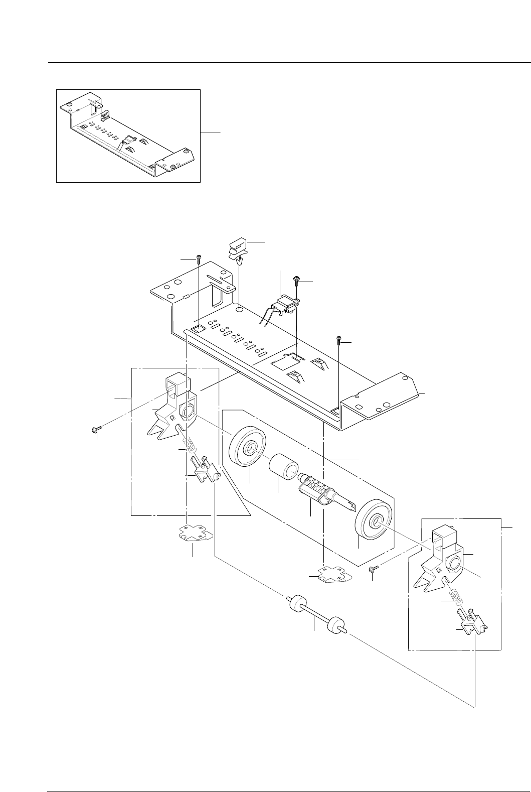
Exploded Views and Parts List
Samsung Electronics5-12
5-6 Plate-Upper Unit Assembly
6-1
6-2
6-3
S
2
6
6-1
6-2
6-3
S-1
6
4
0
4-1
4-2
4-2
4-3
1
7
3
S
S
S
2
8
Exploded Views and Parts List
5-13
Samsung Electronics
O : Service available X: Service not available
No. Description SEC.Code Q’ty SA Remark
0 MEC-PLATE UPPER JC75-00057A 1 O
1 IPR-UPPER-PLATE * 1 X
2 IPR-PLATE SPRING DEV JC70-10223A 2 O
3 ELA UNIT-FUSE DEVE * 1 X
4 MEA ETC-ROLLER PICK UP * 1 X
4-1 PMO-HOUSING_PICKUP JC72-00109A 1 O
4-2 RMO-ROLLER_PICKUP * 1 X
4-3 PMO-IDLE_PICKUP * 2 X
6 MEA ETC-IDLE FEED * 2 X
6-1 PMO-HOLDER_PICKUP * 1 X
6-2 SPRING-FEED * 1 X
6-3 PMO-HOLDER_IDLE,FEED * 1 X
7 CABLE CLAMP 6502-000130 1 O
8 ICT-ROLLER IDEL FEED * 1 X
S5 SCREW-TAPTITE * 2 X
S10 SCREW-TAPTITE 6003-000266 1 O
S10 SCREW-TAPTITE 6003-000266 2 O
Plate-Upper Unit Assembly Parts List
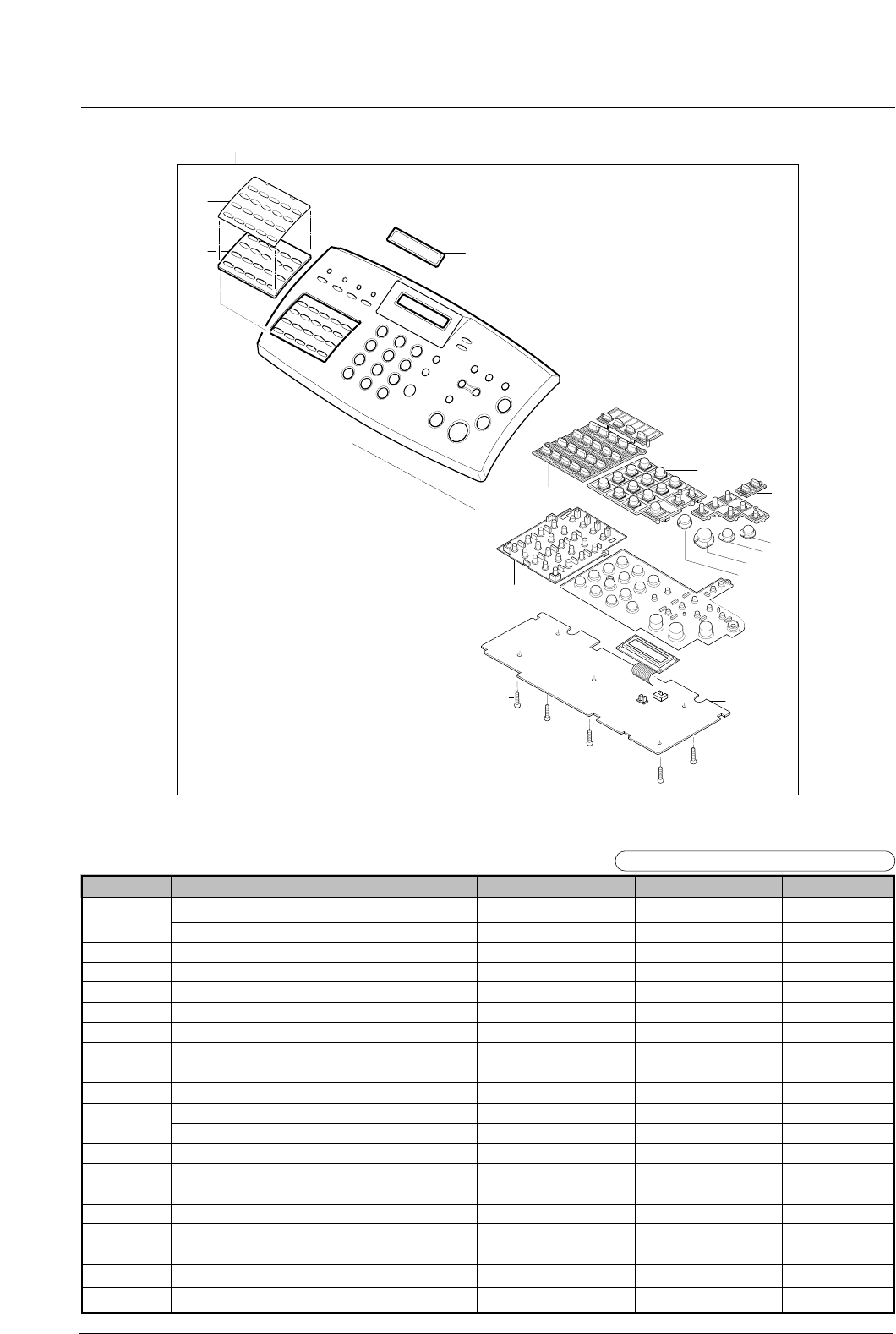
Exploded Views and Parts List
Samsung Electronics5-14
O : Service available X: Service not available
No. Description SEC.Code Q’ty SA Remark
0 ELA HOU-OPE ASS’Y JC81-00442A 1 O SF-530
ELA HOU-OPE ASS’Y JC81-00468A 1 O SF-531P
1 SCREW-TAPTITE 6003-000119 6 O
2 MPR-COVER ADRESS JG74-10543A 1 O
3 PMO-KEY COPY JB72-00102A 1 O
4 PMO-KET STOP JB72-00108A 1 O
5 LABEL(P)-ONE TOUCH * 1 X
6 PMO-KEY OT JC72-00275A 1 O
7 PMO-KEY FUNCTION * 1 X
8 PMO-KEY START * 1 X
9 PMO-OPE COVER JC72-00665L 1 O SF-530
PMO-OPE COVER TBD 1 O SF-531P
10 PMO-KEY TEL JC72-00667A 1 O
11 PMO-KEY SAVE JC72-00668A 1 O
12 PCT-LCD WINDOW JC72-00672A 1 O
13 PMO-KEY FOWARD JC72-00886A 1 O
14 PMO-KEY MODE(B) JC72-41320A 1 O
15 RMO-TEL JC73-00072A 1 O
16 RMO-ONE TOUCH JC73-00073A 1 O
17 PBA MAIN-OPE JC81-00456A 1 O
OPE Unit Parts List
5-7 OPE Unit
11
10
13
14
7
3
8
4
15
17
1
16
6
12
2
5
9
0
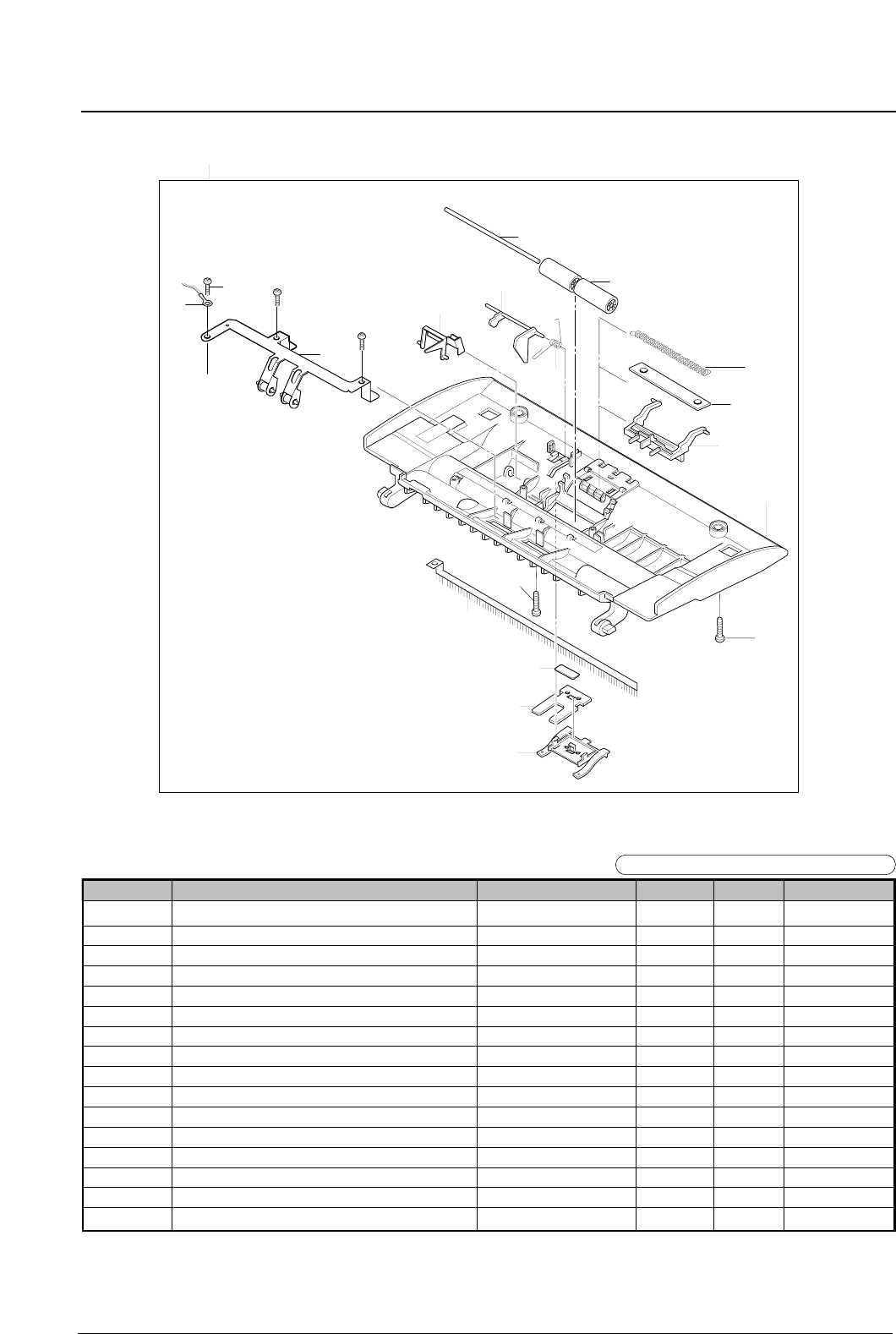
Exploded Views and Parts List
5-15
Samsung Electronics
O : Service available X: Service not available
No. Description SEC.Code Q’ty SA Remark
0 ELA HOU-SCAN UPPER JC81-00457A 1 O
1 MEC-PINCH JG75-10015A 1 O
2 RPR-SPONGE ADF * 1 X
3 MPR-TAPE ADF * 1 X
4 CBF HARNESS-SCAN GND JC39-00101A 1 O
5 SPRING-SENSOR * 1 X
6 SPRING-COIL ADF JC61-00040A 1 O
7 PMO-SCAN UPPER JC72-00671A 1 O
8 PMO-LEVER SENSOR DOC JC72-00823A 1 O
9 PMO-LEVER SENSOR JC72-41322A 1 O
10 ICT-SHAFT PINCH JF70-40521B 1 O
11 PMO-HOLDER RUBBER JG72-40044A 1 O
12 PMO-ROLL PINCH JG72-40663A 2 O
13 PMO-SUPPORT ADF JG72-41083A 1 O
14 RPR-RUBBER ADF JC73-00032A 1 O
15 MEC-BRUSH ANTISTATIC JG75-10004A 1 O
Scan Upper Assembly Parts List
5-8 Scan Upper Assembly
13
11
14
7
15
3
S
S
6
8
9
4S
5
10
12
1
2
0
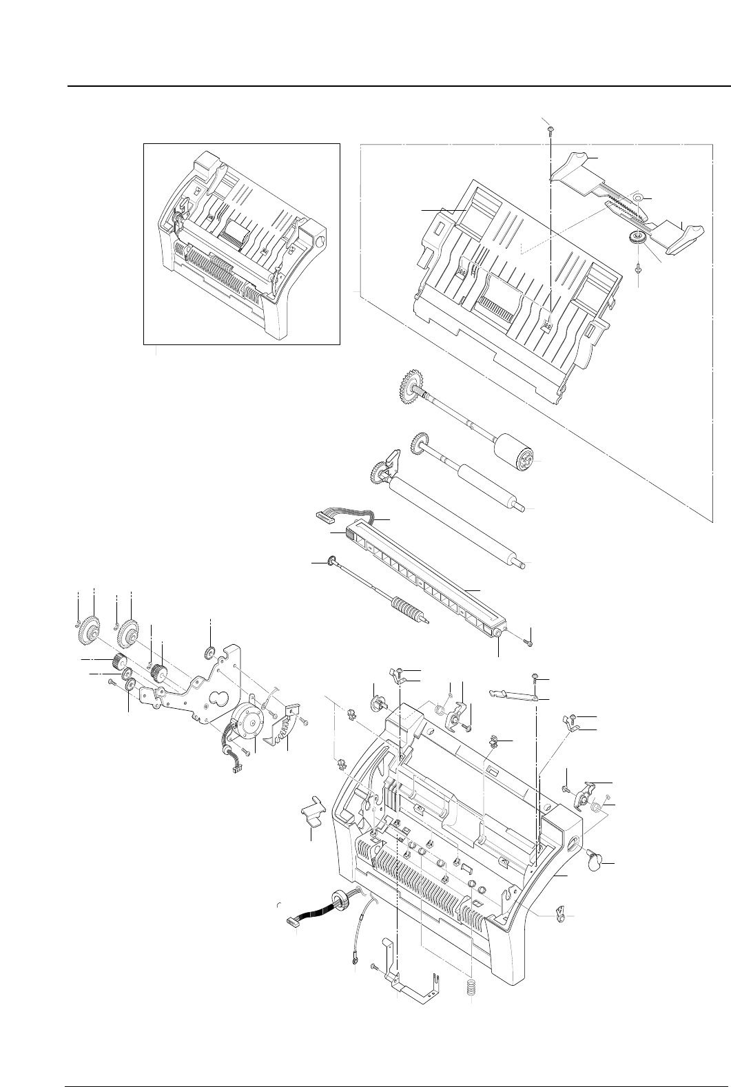
Exploded Views and Parts List
Samsung Electronics5-16
5-9 Front Assembly
1
1-4
1-2
1-5
1-3
1-1
0
15
9
18
18
16
8
31
20
S3
S
S
S
14
4
26
22
5
Bushing White
21
29
31
319
17
7
6
24
25
27
S
33
27
S3
2
23
S
28
28
28
30
11
30
32 32
32
10

Exploded Views and Parts List
5-17
Samsung Electronics
O : Service available X: Service not available
No. Description SEC.Code Q’ty SA Remark
0 ELA HOU-FRONT ASS’Y JC81-00458A 1 O
1 MEA ETC-GUIDE PAPER * 1 X
1-1 PMO-GUIDE PAPER * 1 X
1-2 PMO-GUIDE DOC L * 1 X
1-3 PMO-GUIDE DOC R * 1 X
1-4 GEAR-PINION JG66-40003A 1 O
1-5 IPR-WASHER SPRING CU JF70-10616A 1 O
2 CONTACT IMAGE SENSOR 0609-001127 1 O SF-530
CONTACT IMAGE SENSOR 0609-001125 1 O SF-531P
3 MOTOR STEP-SCAN JC31-00011A 1 O
4 MEC-ROLLER WHITE JC75-00126A 1 O
5 CBF HARNESS-SCAN/CIS(200) JC39-00049A 1 O SF-530
CBF HARNESS-SCAN/CIS(300) JC39-00136A 1 O SF-531P
6 CBF HARNESS-MAIN/SCAN JC39-00192A 1 O
7 CBF HARNESS-SCAN GND JC39-00101A 1 O
8 SPRING-LOCKER R JC61-00027A 1 O
9 SPRING-LOCKER L JC61-00028A 1 O
10 GEAR- 39/20 JC66-00304A 1 O
11 GEAR- IDLE 30 JC66-00305A 1 O
13 IPR-BRKT MOTOR * 1 X
14 NPR-GROUND CIS * 1 X
15 PMO-OPEN LOCKER L * 1 X
16 PMO-OPEN LOCKER R * 1 X
17 PMO-BRKT SCAN B’D JC72-00222A 1 O
18 PMO-OPEN BUTTON JC72-00273A 2 O
19 PMO-COVER MOTOR JC72-00670A 1 O
20 PMO-COVER FRONT JC72-00673A 1 O
21 PMO-DUMMY CIS L SF-530 JC72-00880A 1 O SF-530
PMO-DUMMY CIS L JC72-00495A 1 O SF-531P
22 PMO-DUMMY CIS R SF-530 JC72-00881A 1 O SF-530
PMO-DUMMY CIS R JC72-00496A 1 O SF-531P
23 PMO-STOPPER EXIT * 1 X
24 MEC-ROLLER DRIVE JC75-00123A 1 O
25 MEA ETC-ROLLER ADF * 1 X
26 SPECIAL SCREW JG60-10001A 2 O
27 LOCKER-TX JG64-30001A 2 O
28 GEAR-IDLE25 JG66-40036A 3 O
29 PMO-SHAFT EXIT JG72-40042A 1 O
30 PMO-GEAR TRANS(B4) JG72-40741A 2 O
31 PMO-BUSHING TX(B4) JG72-40744A 9 O
32 RING-C 6044-000159 3 O
33 SPRING CIS JG61-70533A 2 O
S1 SCREW-MACHINE 6001-000131 2 O
S3 SCREW-TAPPING 6002-000175 2 O
S4 SCREW-TAPPING 6002-001078 1 O
S7 SCREW-TAPTITE 6003-000196 2 O
S11 SCREW-TAPTITE 6003-000119 2 O
S11 SCREW-TAPTITE 6003-000119 6 O
Front Assembly Parts List
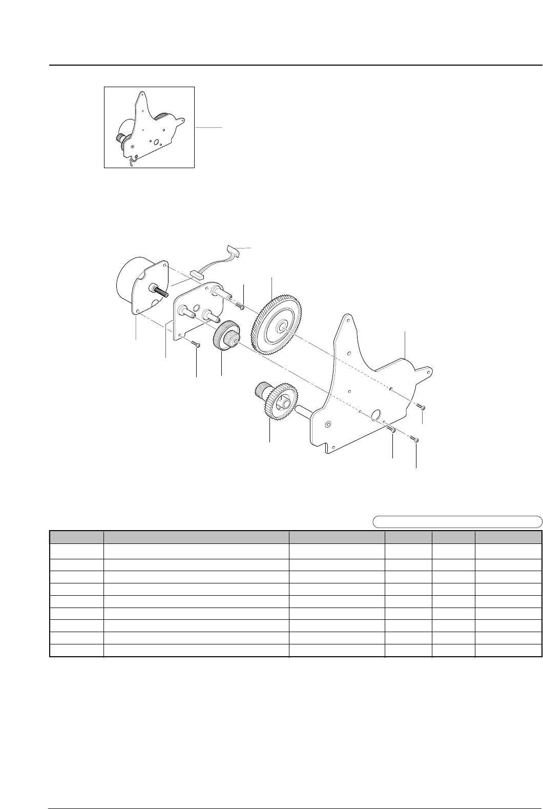
Exploded Views and Parts List
Samsung Electronics5-18
O : Service available X: Service not available
No. Description SEC.Code Q’ty SA Remark
0 ELA HOU-RX DRIVE JC96-01755A 1 O
1 MOTOR-STEP JC31-00005A 1 O
2 PMO-GEAR_71/28 * 1 X
3 PMO-GEAR_73/22 * 1 X
4 PMO-GEAR_132/19 * 1 X
5 IPR-BRKT_MOTOR * 1 X
6 IPR-BRKT_GEAR JC70-00129A 1 O
7 CBF-HARNESS_MOTOR JC39-00110A 1 O
S-7 SCREW-MACHINE 6001-000131 5 O YELLOW
5-10 RX Drive Unit Assembly
RX Drive Assembly Parts List
1
4
2
S7
S7
3
5
6
7
S-7 S-7
S-7
0
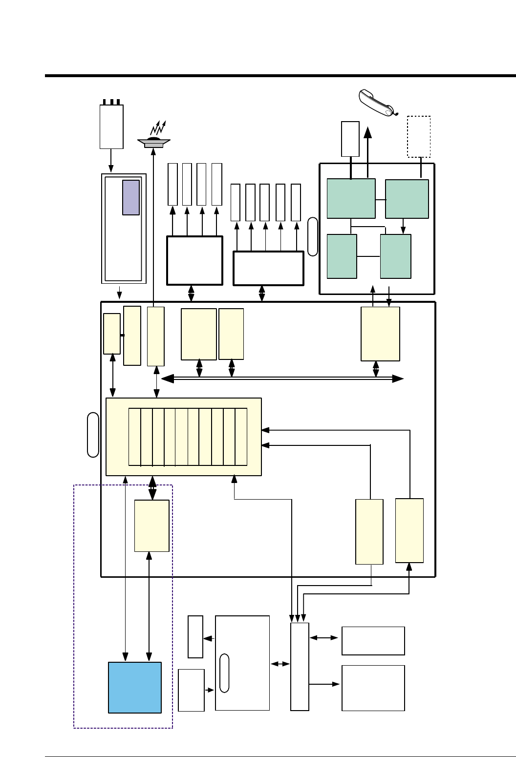
6-1
Samsung Electronics
6. Block Diagram
MA I N
POWER
CORD
KS32C65100
ARM7 T
GEU
P1284
ITU
I/O I/F
CACHE( 6 K)
DMAC
PVC
UART* 2
ME MO R Y I / F
MODEM
DRAM
(8MB)
CI S I NTERFACE
PART
HOST
(P
C)
CI S
CENTRONI CS
USB
TX MOTOR
DRI VER
TX
MOTOR
RT C
Bac k - u p Par t
LI U
MO DE M &
EXT_ PHONE
SEPER ATI NG
PA RT
600/ / 600
Tx : Rx
TRANSFORMER
EXTER NAL
PHONE
DET ECT I ON
PAR T
EXTERNAL
PHONE
LI NE
HAND SET
600/ / 600
Tx : Rx
TRANSFORMER
FLASH
MEMORY
(2MB)
+5V
UART
-5V
SCAN B o a r d
MI COM
- L CD Dr i v e
- Key Scan
OPE
LCD
DOC
SE N SO R
SM P S
HVPS
+24V
MOTOR
OLEN OIDE
ENGINE
B’D
FAN
OPC_FUSE
Audi o Par t
EX IT
SEN SOR
MHV
OPC GND
SUPPLY
DEV
THV
UNI CON
(USB IC)
Note. -. SF-530 : Fax Functio n Only
-. SF-531P : Printer Function with Fax
*Note
33600 bps

Repair Manual
Repair Manual
1. Block Diagram
2. Connection Diagram
3. Circuit Description
4. Schematic Diagrams
CONTENTS
SAMSUNG FACSIMILE
SF-530/531P


Samsung Electronics Digital Printing
CS Group
Copyright (c) 2001. 10
This manual is made and
described centering around
circuit diagram
and circuit description needed
in the repair center
in the form of appendix.
SAMSUNG
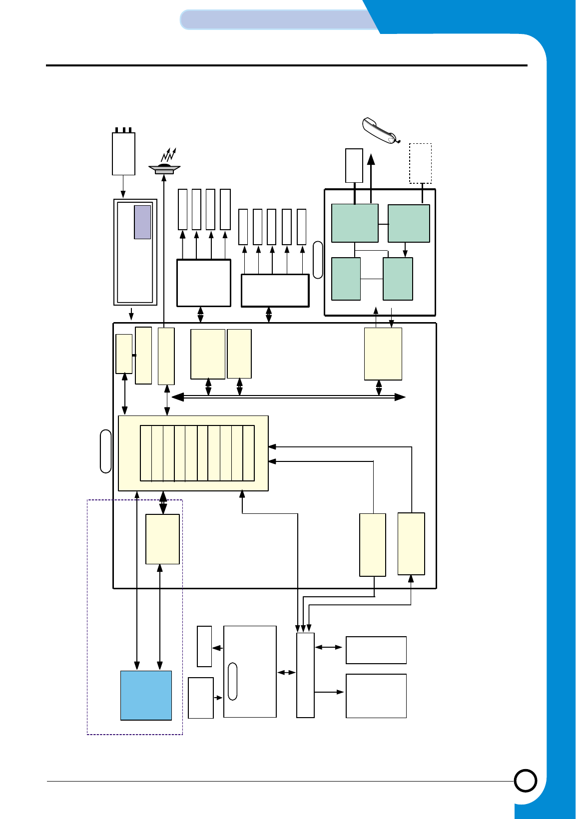
1
1-1
Samsung Electronics
BLOCK DIAGRAM
Repair Manual
1. Block Diagram
MAI N
POWER
CORD
KS32C65100
ARM7T
GEU
P1284
ITU
I/OI/F
CACHE( 6K)
DMAC
PVC
UART* 2
MEMORY I / F
MODEM
DRAM
(8MB)
CI S I NTERFACE
PART
HOST
(P
C)
CI S
CENTRONI CS
USB
TX MOTOR
DRI VER
TX
MOTOR
RTC
Back- up Par t
LI U
MO DEM &
EXT_PHONE
SEPERATI NG
PART
600/ / 600
Tx: Rx
TRANSFORMER
EXTERNAL
PHONE
DETECTI ON
PART EXTERNAL
PHONE
LI NE
HANDSET
600/ / 600
Tx: Rx
TRANSFORMER
FLASH
MEMORY
(2MB)
+5V
UART
-5V
SCAN Boar d
MI COM
- LCD Dr ive
- Key Scan
OPE
LCD
DOC
SEN SOR
SMPS
HVPS
+24V
MOTOR
OLENOIDE
ENGINE
B'D
FAN
OPC_FUSE
Audi o Part
EXIT
SEN SOR
MHV
OPC GND
SUPPLY
DEV
THV
UNI CON
(USB IC)
Note. -. SF-530 : Fax Function Only
-. SF-531P : Printer Function with Fax
*Note
33600 bps
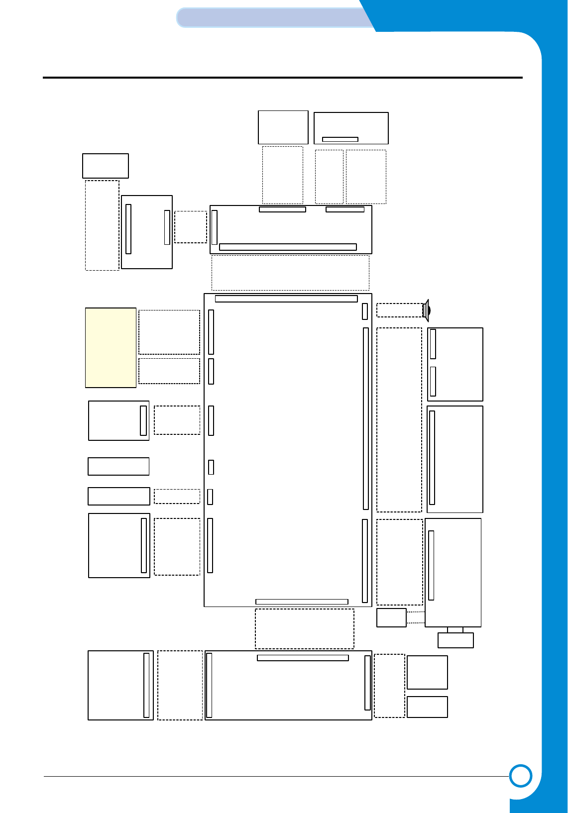
2
2-1
Samsung Electronics
CONNECTION DIAGRAM
Repair Manual
2. Connection Diagram
5GND5
4+5V
3OPE_TXD
2OPE_RST
1OPERXD
LCD
CN1
OP E
CN 3
SCAN B’ D
18+24V
17+24V
16SCNM
OTA
15+5V
14SCNM
OT*B
13SCNM
OT*A
12SCNM
OTB
11G
ND
10O
PERXD
9GND5
8OP
E
TXD
7OPERST
6GND5
5+5V
4CISSIG
3CISLCD
2CISSI
1CISCLK
CN1
214365871091211141316151817
CN1 6
1 2 34 5 678 91011 121314 15161718
HOST
(PC)
IEEE1284 I/F
(36PIN)
USB PORT
(4PIN)
CN2
CN19
1+5V
2/PEMPTY
3/FEED
4GND5
SENSOR
B’ D
COVER
SWIT CH 1+24V
2+24VS
HVPS
CN1 1+24VS1
2GND24
3THVPWM
4/THV_EA
5THVREAD
6MHVPWM
7BIASPWM
8+5V
9GND
5
CN8 - 1
THER- MI STOR 1THERM_A
2THERM_B CN7
CN1 8
CN15- 1
CN1 3 - 1
CN7
CN9
ENG INE
B’ d
LSU
LD DIODE
POLY GO N
MOT OR
1+24VS
2GND24
3PMOTOR
4/LREADY
5EXTCLK
6/USYNC
7+5V
8CND5
9/LD_ON
10 VD0
11 /APC_SH
12 SLUTCH
13 FAN
14 PTL
15 DEV_FUSE
16 /NEW_DEVE
17 /EGMOT_A0
18 /EGMOT_ A1
19 EGMOT_PHA
20 /EGMOT_B0
21 /EGMOT_B1
22 GND5
23 +5V
24 EGMOT_PHA
25 +24VS
26 +24VS
27 GND24
28 GND24
CN1 2 SPK
1SPKOUT
2AGND
14M
O
DEMTXA1
13M
O
DEMTXA2
12AGND
11NC
10M
O
DEMRX
9/EXTP
HONE
8CML1
7REMOTE
6CM
L2
5/DP
4/HOOK1
3+5V
2GND5
1/RING
CN1 4
1+24VS
2FUSER_ON
3+5V
4/EXIT
5+5V
6GND5
7+5V
8GND5
9-5V
10 GND5
11 24V
12 GND24
13 24V
14 GND24
15 24V
16 GND24
CN5 0 3
SMPS
A
Heat Lamp
(Fuser)
HOT
Neutral
CLINE
MAIN B’d
1GND5
2+5V
3V0
4LCD_RS
5LCD_RW
6LCD_F
7LED_0
8LED_1
9LED_2
10 LED_3
11 LED_4
12 LED_5
13 LED_6
14 LED_7
HOOK B’d CN2 CN1
CN3 MJ 1
1LINE_2
2LINE_3
3LINR_4
4LINR_5
5LINR_6
6EXT_3
7EXT_4
8EXT_5
1MIC1
2 RCV3
3MIC2
4 RCV1
5 HOOK2
6 HOOK2 _NC
7 HOOK2 _NO
10 HOOK1
11 HOOK1_NO
12 HOOK1_NC
LIU B’d
MJ 1
1 CIS_SIG
2 GND
3 +5V
4 GND
5 GND
6 START PULSE
7 GND
8 CIS MAIN CLOCK
9 LED B
10 LED G
11 LED R
12 V LED
1 CIS_SIG
2 GND
3 +5V
4 CIS_SI
5 CIS_CLK
6 CIS_LED
7 +24V
200 DPI 300 DPI
1 +24
2 +24
3 SCNMOT_A
4 SCNMOT_*A
5 SCNMOT_B
6 SCNMOT_*B
SCAN
MOTOR
CN 2 C N4
CIS
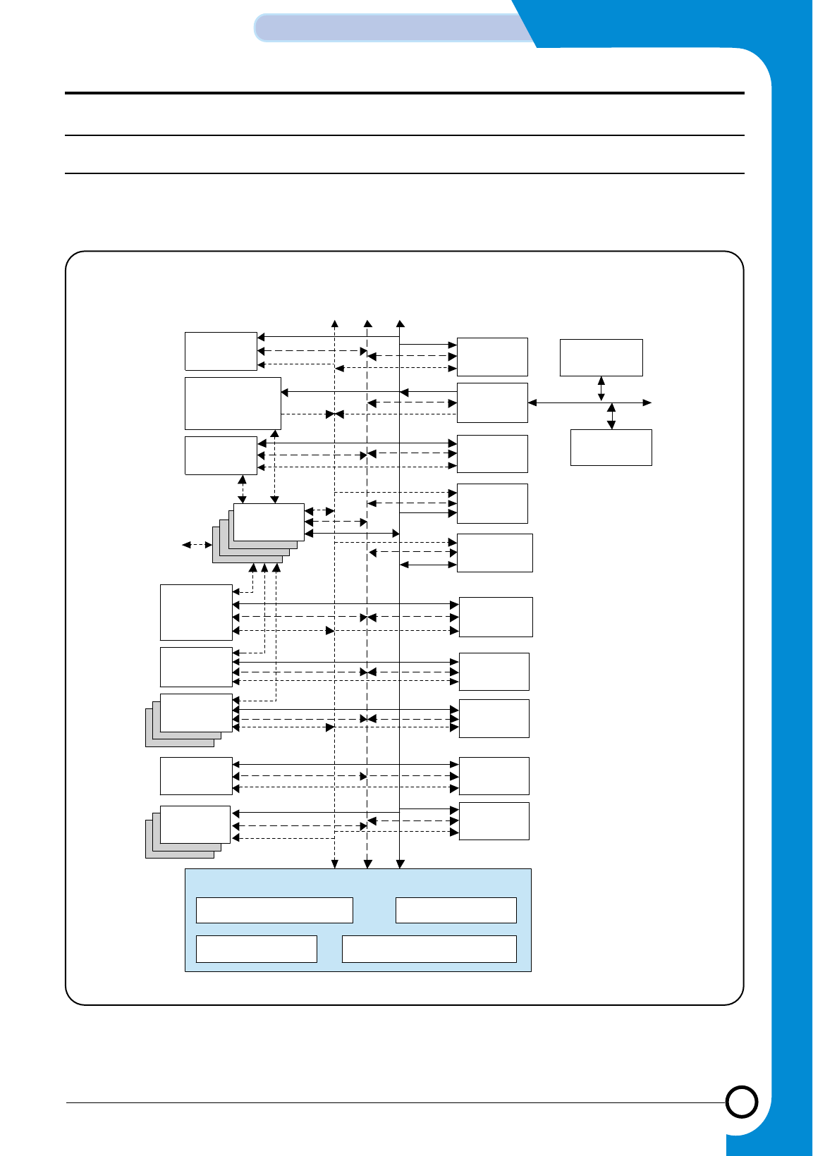
3
3-1
Samsung Electronics
CIRCUIT DESCRIPTION
Repair Manual
3. Circuit Description
3-1 Main PBA
3-1-1 Summary
The main circuit that consists of CPU, MFP controller including various I/O device drivers, system memory, scanner, print-
er, motor driver, PC I/F, and FAX transceiver controls the whole system. The entire structure of the main circuit is as follows:
I/O Ports
Controller
Scan Image &
Scan Motor
Controller
Ink Head
Controller
DMA
Controller
Parallel
Port
Interface
Video Data
Controller
UART/
Serial I/O
LSU
Control
PWM &
Gen. Timer
System Bus Controller Bus Arbitration
Bus Interface
ROM/SRAM/DRAM Controller
System Manager
Bus Router
PLL & Clock
Save
Interrupt
Controller
A/D
Converter
Derasterizer
Carrier Motor
Control
Position &
Fire Control
Paper Motor
Control
Real Time
Clock
Watch Dog
Timer
CPU
(ARM7TDMI)
I/D Cache
(2-KB)
LBUS
ADDR
DATA
CNTR

3-2
CIRCUIT DESCRIPTION
Samsung Electronics
Repair Manual
3-1-2 Circuit Operation
• CLOCK
1) System Clock
Device Oscillator
Frequency 9.500132 MHz
KS32C65100 RISC PROCESSOR: drives PLL internally and uses 37.17 MHz.
2) Video Clock
Device Oscillator
Frequency 28.7448 MHz
3) USB Clock
Device Oscillator
Frequency 48 MHz±%
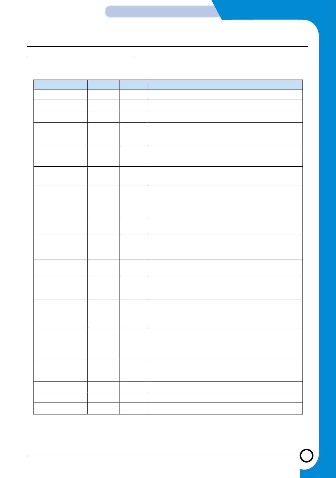
3-3
Samsung Electronics
CIRCUIT DESCRIPTION
Repair Manual
• KS32C65100 MICROPROCESSOR
1) KS32C65100 MICROPROCESSOR PIN & INTERFACE
Signal Pin No. I/O Type Description
OSCI 184 I7 KS32C65100 master clock input.
OSCO 185 O7 KS32C65100 master clock output.
PLL_FILTER 183 I5 PLL filter
nRESET 182 I4
Not reset. nRESET is the global reset input for the
KS32C65100. For a system reset, nRESET must be held to
low level for at least 65 machine cycles.
nSLCTIN/GIP[16] 152 I1 Not select information. This input signal is used by parallel
port interface to request 'on-line' status information.
nSTROBE 151 I1 Not strobe. The nSTROBE input indicates when valid data is
on parallel port data bus, PPD[7:0]
nAUTOFD/GIP[17] 154 I1
Not auto feed. The nAUTOFD input indicates whether data
on the parallel port data bus, PPD[7:0], is an auto feed
command. Otherwise, the bus signals are interpreted as data
only.
nINIT/GIP[15] 153 I1 Not initialization. The nINIT input signal initializes the parallel
port's input control.
nACK 159 I1
Not parallel port acknowledge. The nACK output signal is
issued whenever a transfer on the parallel port data bus is
completed.
BUSY 158 O1 Parallel port busy. The BUSY output signal indicates that the
KS32C65100 parallel port is currently busy.
SELECT 156 O1
Parallel port select. The SELECT output signal indicates
whether the device connected to the KS32C65100 parallel
port is 'on-line' or 'off-line'.
PERROR 157 O1
Parallel port paper error. PERROR output indicates that a
problem exists with the paper in the ink-jet printer. It could
indicate that the printer has a paper jam or that the printer
isoutofpaper.
nFAULT 155 O1
Not fault. The nFAULT output indicates that an error
condition exists with the printer. This signal can be used to
indicate that the printer is out of ink or to inform the user
that the printer is not turned on.
PPD[7:0] 142~149 I/O2
arallel port data bus. This 8-bit, tri-state bus is used to
exchange data between the KS32C65100 and an external
host(peripheral).
SAVRT 2 I6 Top reference voltage for IP ADC
SAIN 3 I6 Analog input for IP ADC
SAVRB 4 I6 Bottom reference voltage for IP ADC
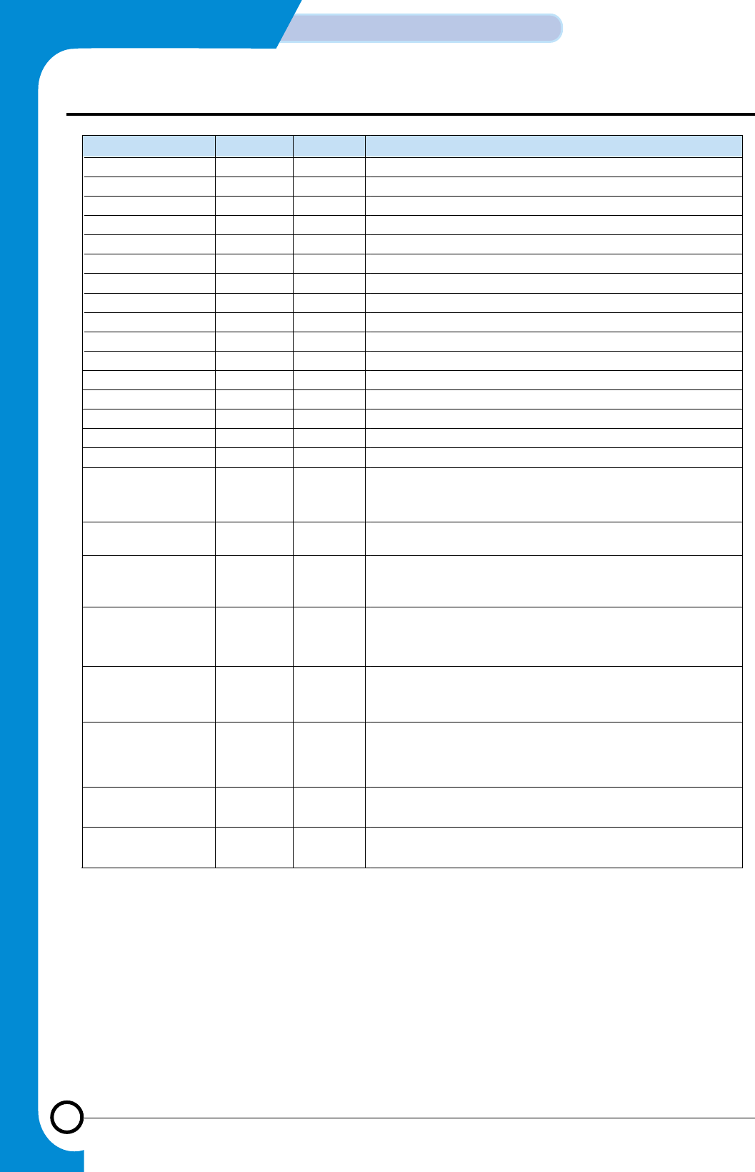
3-4
CIRCUIT DESCRIPTION
Samsung Electronics
Repair Manual
Signal Pin No. I/O Type Description
CIS_CLK 6 O1 CIS shift clock
CIS_SI 7 O1 CIS latch signal
PHA_IA0 164 O1 Line feed motor phase signal A
PHA_IA1 165 O1 Line feed motor phase signal AZ
PHB_IB0 167 O1 Line feed motor phase signal B
PHB_IB1 168 O1 Line feed motor phase signal BZ
LF_PH0/GOPA[21] 163 O1 Line feed motor control signal 0
LF_PH1/GOPA[22] 166 O1 Line feed motor control signal 1
CR_PHA/GOPA[23] 110 O1 Direction control line for phase A
CR_PHB/GOPA[24] 113 O1 Direction control line for phase B
CRIA0/GOPA[25] 109 O1 Current control line 0 for phase A
CRIA1/GOPA[26] 111 O1 Current control line 1 for phase A
CRIB0/GOPA[27] 112 O1 Current control line 0 for phase B
CRIB1/GOPA[28] 114 O1 Current control line 1 for phase B
CHX/GIP[8] 116 I3 Encode sensor
CHY/GIP[9] 117 I3 Encode sensor
ADDR[21:0]
77~80,
82~88,
90~100 O5
Address bus. The 22bit address bus, ADDR[21:0], covers
the full 4M half-words address range of each ROM/SRAM,
DRAM, and external I/O bank
DATA[15:0] 59~66,
68~75 I/O3 External bi-directional 16-bit data bus.
nRAS[1:0] 52,53 O1
Not row address strobe for DRAM. The KS32C65100
supports up to two DRAM banks. One nRAS output is
provided for each bank.
nCAS[1:0] 54,55 O1
Not column address strobe for DRAM. The two nCAS
outputs indicate the byte selections whenever a DRAM bank
is accessed.
nOE 56 O1
Not output enable. Whenever a memory access occurs, the
nOE output controls the output enable port of the specific
memory device.
nWE 57 O6
Not write enable. Whenever a memory access occurs, the
nWE output controls the write enable port of the specific
memory device.
nPHGA[13:1]/
GOPB[12:0]
16~24,
26~29 O1 Gate control line for print head.
PHOE[16:1]/
GIOP[26:11]
31~38,
40~47 I/O1 Drain control line for print head.
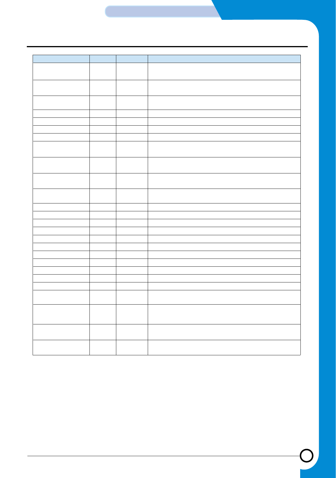
3-5
Samsung Electronics
CIRCUIT DESCRIPTION
Repair Manual
Signal Pin No. I/O Type Description
RXD0/GIP[0] 194 I1 Receive data input for the UART0. RXD0 is the UART0
channel's input signal for receiving serial data.
RXD1/GIP[1] 192 I1 Receive data input for the UART1. RXD1 is the UART1
channel's input signal for receiving serial data.
RXD2/GIP[2] 190 I1 Receive data input for the UART2. RXD2 is the UART2
channel's input signal for receiving serial data.
nEINT0/GIP[3] 8I3 External interrupt request input nEINT0.
nEINT1/GIP[4] 9I3 External interrupt request input nEINT1.
nEINT2/GIP[5] 10 I3 External interrupt request input nEINT2.
nXDREQ/GIP[6] 199 I3 External DMA request.
TXD0/GOPA[0] 193 O1 Transmit data output for the UART0. TXD0 is the UART0
channel's output for transmitting serial data.
TXD1/GOPA[1] 191 O1 Transmit data output for the UART1. TXD1 is the UART1
channel's output for transmitting serial data.
TXD2/GOPA[2] 189 O1 Transmit data output for the UART2. TXD2 is the UART2
channel's output for transmitting serial data.
nXDACK/GOPA[5] 200 O1 External DMA acknowledge. This active low output signal is
generated whenever a DMA transfer is completed.
TONEOUT/GOPA[3] 188 O1 Tone generator output.
nWDTO/GOPA[4] 187 P3 Reset out by watch dog timer.
nIOWR/GOPA[10] 161 O1 External output write strobe
nIORD/GOPA[9] 162 O1 External output read strobe
CLKOUT/GOPA[6] 180 O1 Clock for external chip
nECS2/GOPA[8] 14 O1 External memory chip select 2.
TCK 132 I2 JTAG TCK interface in MDS mode.
TMS 135 I2 JTAGTMSinterfaceinMDSmode.
TDI 133 I2 JTAG TDI interface in MDS mode.
nTRST 136 I2 JTAG nTRST interface in MDS mode.
TDO 134 O1 JTAG TDO interface in MDS mode.
GIOP[10:0] 137~140,
173~179 I/O4 General I/O port.
TEST0 169 I2 Test 0 pin. At normal operation this pin must be connected
to GND.
TEST1 170 I2 Test 1 pin. At normal operation this pin must be connected
to GND.
TEST2 171 I2 Test 2 pin. At normal operation this pin must be connected
to GND.
3-6
CIRCUIT DESCRIPTION
Samsung Electronics
Repair Manual
Signal Pin No. I/O Type Description
nECS[1:0] 12,13 O1
Not external chip select. Three I/O banks are provided for
external memory-mapped I/O operations. Each I/O bank
contains up to 4M half-word. The nECS signals indicate that
an external I/O bank is selected.
nRCS[2] 51 O2 Not ROM/SRAM chip select. The KS32C65100 can access
up to three external ROM/SRAM banks. nRCS[0]
corresponds to ROM/SRAM bank 0, nRCS[1] to bank 1, and
nRCS[2] to bank 2. By controlling the nRCS signals, CPU
addresses can be mapped into the physical memory banks.
nRCS[1]/GOPA[7] 50 O1
nRCS[0] 49 O1
SC_CONPHA/
GOPA[19] 102 O1 Scan motor control/Bi-phase
SC_CONPHB/
GOPA[20] 105 O1 Scan motor control/Bi-phase
SC_CUR[3:0] 103, 104,
106, 107 O1 Scan motor bi-current/uni-phase
PWMO[2:0]/
GOPA[13:11] 118~120 O1 PWM out signal
VDO2/GOPA[29] 121 O4 Video out from PIFC
VDO1/GOPA[14] 122 O5 Video out from LSU control
LSU_CLK/
GOPA[15] 123 O1 Clock for LSU motor
nHSYNC1/GIP[10] 125 I1 HSYNC1
nLREADY/GIP[11] 126 I1 LSU ready
nHSYNC2/GIP[12] 127 I1 HSYNC2
VDI/GIP[13] 128 I2 Video data input from RET
VCLK/GIP[14] 129 I2 External video clock
nEXTWAIT/GIP[7] 130 I3 External wait
RTCXIN 202 I7 RTC oscillator clock input.
RTCXOUT 203 O7 RTC oscillator clock output.
SLED[2:0]/
GOPA[18:16] 196~198 O1 CIS LED signals
GAVRT 205 I5 Top reference voltage for general ADC
GAIN[2:0] 206~208 I5 Analog inputs for general ADC
RTC_VDD 201 RTC VDD.
Signal Pin No. I/O Type Description
VDD_PLL 186 PLL power (3.3V).
SAVDD 1Analog power for scan ADC and general ADC (3.3V).
SAVSS 5Scan ADC ground.
GAVSS 204 General ADC ground
3VDD
15, 30, 81,
115, 131,
160
3.3V internal power.
Externally connected to the 3.3V regulator.
5VDD 48, 67, 89,
141, 195
5V I/O power.
Externally connected to the VCC board plane.
VSS
11, 25, 39,
58, 76, 101,
108, 124,
150, 172,
181
System ground.
Externally connected to the ground board plane.

3-7
Samsung Electronics
CIRCUIT DESCRIPTION
Repair Manual
3-1-3 PROGRAM ROM (FLASH MEMORY)
1) DEVICE
TYPE No. AM29F800B
CAPACITY 2 Mbit (512K * 16bit * 2)
2) PROGRAMMING
BEFORE ASS’Y EPROM PROGRAMMER or PROGRAMMING at the factory
AFTER ASS’Y DOWNLOAD from PC
3-1-4 DRAM CONTROL
1) DEVICE
TYPE NO. K4E641611D-TC50(EDO Type)
CAPACITY 64 Mbit (4M * 16bit)
2) OPERATING PRINCIPLE
DRAM can either read or write. The data can be stored in the DRAM only when the power is on. It stores data white the
CPU processes data. The address to read and write the data is specified by RAS SIGNAL and CAS SIGNAL.
DRAMWE*SIGNAL is activated when writing data and DRAMOE*SIGNAL, when reading.
3-1-5 USB (Universal Serial Bus)
SAMSUNG’S UNICON is used as the interface IC and 48MHz clock is used.
When the data is received through the USB port, USBIRQ SIGNAL is activated to send interrupt to CPU, then it directly
sends the data to DRAM by USB_CS SIGNAL through D(0;7).
3-1-6 Modem and TX-and RX Related Circuits
MODEM
The Conexant™ FM336 modem is a V.34 half-duplex modem that supports Group 3 facsimile send and receive speeds
up to 33600 bps using the V.34 half-duplex mode. Using a V.34 technique to optimize modem configuration for line condi-
tions, the modem connects at the optimal selected data rate that the channel can support from 33600 bps to 2400 bps.
The modem can operate over the public switched telephone network (PSTN) through a line terminator provided by a Data
Access rrangement (DAA). The modem satisfies the requirements specified inITU-T recommendations V.34, V.17, V.29,
V.27 ter, V.23, V.21, and meets the binary signal ingrequirements of V.8 and T.30. Internal HDLC support eliminates the
need for an external serial input/output (SIO) device in the DTE for products incorporating error detection and T.30 proto-
col. The modem can perform HDLC framing per T.30 at all data speeds. CRC generation/checking along with zero inser-
tion/deletion enhances DLC/HDLC frame operations. An FSK flag pattern detector facilitates FSK detection during high
speed reception.The modem features a programmable DTMF transmitter/receiver and three programmable tone detectors
which operate in the tone mode.
The modem offers lower power consumption and small size to allow the design of compact system enclosures for use in
industrial, office, and home environments.The modem is available in a 100-pin PQFP package.

3-8
CIRCUIT DESCRIPTION
Samsung Electronics
Repair Manual
FM336 FEATURES
• 2-wire half
- duplex fax modem modes with send and receive data rates up to 33600 bps.
- V.34, V.17, V.29, V.27 ter, and V.21 channel 2
- Short train option in V.17 and V.27 ter
• 2-wire full
- duplex data modem modes
- V.21, V.23 (75 bps TX/1200 bps RX or 1200 bps TX/ 75 bps RX)
• PSTN session starting
- V.8 signaling
• HDLC support at all speeds
- Flag generation, 0 bit stuffing, ITU CRC
- 16 or CRC
- 32 calculation and generation
- Flag detection, 0 bit deletion, ITU CRC
- 16 or CRC
- 32 check sum error detection
-
FSK flag pattern detection during high speed receiving
• Tone modes and features
- Programmable single or dual tone generation
- DTMF receive
- Tone detection with three programmable tone detectors
• Serial synchronous data
• Parallel synchronous data
• Automatic Rate Adaptation (ARA) in V.34 Half-Duplex
• TTL and CMOS compatible DTE interface
- ITU-T V.24 (EIA/TIA-232-E) (data/control)
- Microprocessor bus (data/configuration/control)
• Receive dynamic range: 0 dBm to –43 dBm for V.17, V.33, V.29, V.27terand V.21, –9 dBm to –43 dBm for V.34 half-duplex
• Programmable RLSD turn-on and turn-off thresholds
• Programmable transmit level: 0 to -15 dBm
• Adjustable speaker output to monitor received signal
• DMA support interrupt lines
• Two 16-byte FIFO data buffers for burst data transfer with extension up to 255 bytes
• NRZI encoding/decoding
• Diagnostic capability
• +3.3V operation with +5V tolerant inputs
• +5V analog signal interface
• Typical power consumption:- Sleep mode: 20 mW
- Normal mode: 250 mWa
• 100-pin PQFP package
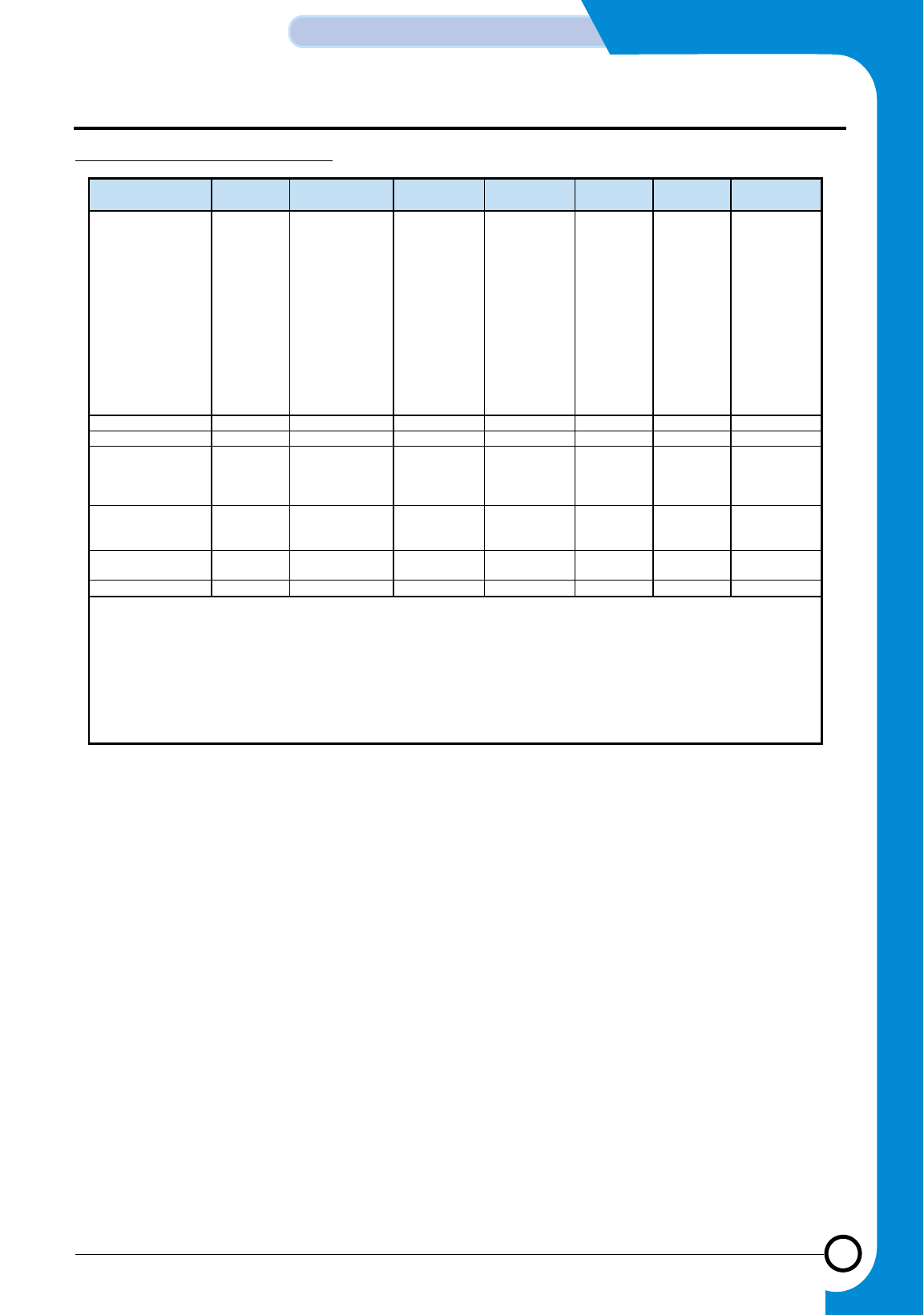
3-9
Samsung Electronics
CIRCUIT DESCRIPTION
Repair Manual
Signaling Rates, and Data Rates
Configuration Modulation1Carrier Frequency
(Hz) –0.01%
Data Rate (bps)
–0.01%
Symbol Rate
(Symbols/Sec.)
Bits/Symbol -
Data
Bits/Symbol -
TCM
Constellation
Points
V.34 33600 TCM TCM Note 2 33600 3429 only Note 2 Note 2 Note 2
V.34 31200 TCM TCM Note 2 31200 3200 min Note 2 Note 2 Note 2
V.34 28800 TCM TCM Note 2 28800 3000 min Note 2 Note 2 Note 2
V.34 26400 TCM TCM Note 2 26400 2800 min Note 2 Note 2 Note 2
V.34 24000 TCM TCM Note 2 24000 2800 min Note 2 Note 2 Note 2
V.34 21600 TCM TCM Note 2 21600 2400 min Note 2 Note 2 Note 2
V.34 19200 TCM TCM Note 2 19200 2400 to 3429 Note 2 Note 2 Note 2
V.34 16800 TCM TCM Note 2 16800 2400 to 3429 Note 2 Note 2 Note 2
V.34 14400 TCM TCM Note 2 14400 2400 to 3429 Note 2 Note 2 Note 2
V.34 12000 TCM TCM Note 2 12000 2400 to 3429 Note 2 Note 2 Note 2
V.34 9600 TCM TCM Note 2 9600 2400 to 3429 Note 2 Note 2 Note 2
V.34 7200 TCM TCM Note 2 7200 2400 to 3429 Note 2 Note 2 Note 2
V.34 4800 TCM TCM Note 2 4800 2400 to 3429 Note 2 Note 2 Note 2
V.34 2400 TCM TCM Note 2 2400 2400 only Note 2 Note 2 Note 2
V.23 1200/75 FSK 1700/420 1200/75 1200 1 0 —
V.21 FSK 1080/1750 Up to300 300 1 0 —
V.17 14400 TCM TCM 1800 14400 2400 6 1 128
V.17 12000 TCM TCM 1800 12000 2400 5 1 64
V.17 9600 TCM TCM 1800 9600 2400 4 1 32
V.17 7200 TCM TCM 1800 7200 2400 3 1 16
V.29 9600 QAM 1700 9600 2400 4 0 16
V.29 7200 QAM 1700 7200 2400 3 0 8
V.29 4800 QAM 1700 4800 2400 2 0 4
V.27 ter 4800 DPSK 1800 4800 1600 3 0 8
V.27 ter 2400 DPSK 1800 2400 1200 2 0 4
V.21 Channel 2 FSK 1750 300 300 1 0 —
Notes:
1. Modulation legend: TCM:Trellis-Coded Modulation QAM: Quadrature Amplitude Modulation
FSK:Frequency Shift Keying DPSK: Differential Phase Shift Keying
2. Adaptive; established during handshake:
Carrier Frequency (Hz)
Symbol Rate (Baud) V.34 Low Carrier V.34 High Carrier
2400 1600 1800
2800 1680 1867
3000 1800 2000
3200 1829 1920
3429 1959 1959
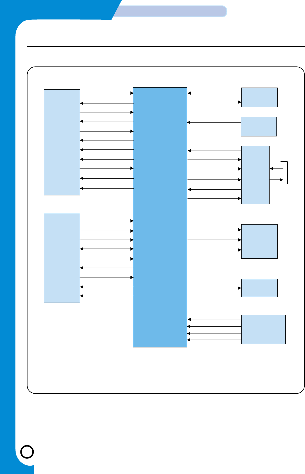
3-10
CIRCUIT DESCRIPTION
Samsung Electronics
Repair Manual
V.24
Interface
Host
Processor
FM336
Modem
Crystal
Power Supply
Speaker
Amplifier
Optional
Eye Pattern
Generator
Line
Interface
/RTS
TXD
/CTS
TDCLK
XTCLK
/RLSD
RXD
/RDCLK
/DTR
/RI*
/DSR**
/RD
/CS
/WR
D[7:0]
RS[4:0]
IRQ
/RESET
TXRQ*
RXRQ**
XTL0
XTLI
TXA1
RIN
OH
TXA2
/TALK
RINGD
EYEXY
EYESYNC
EYECLK
+5V
AGND
DGND
SPKR
* Selectable; TXRQ output replaces /RI output.
** Selectable; RXRQ output replaces /DSR output.
1176DG F2-1
TIP
RING
telephone
line
+3.3V
Oscillator
CLKIN
OR
Modem Functions Interface Signals
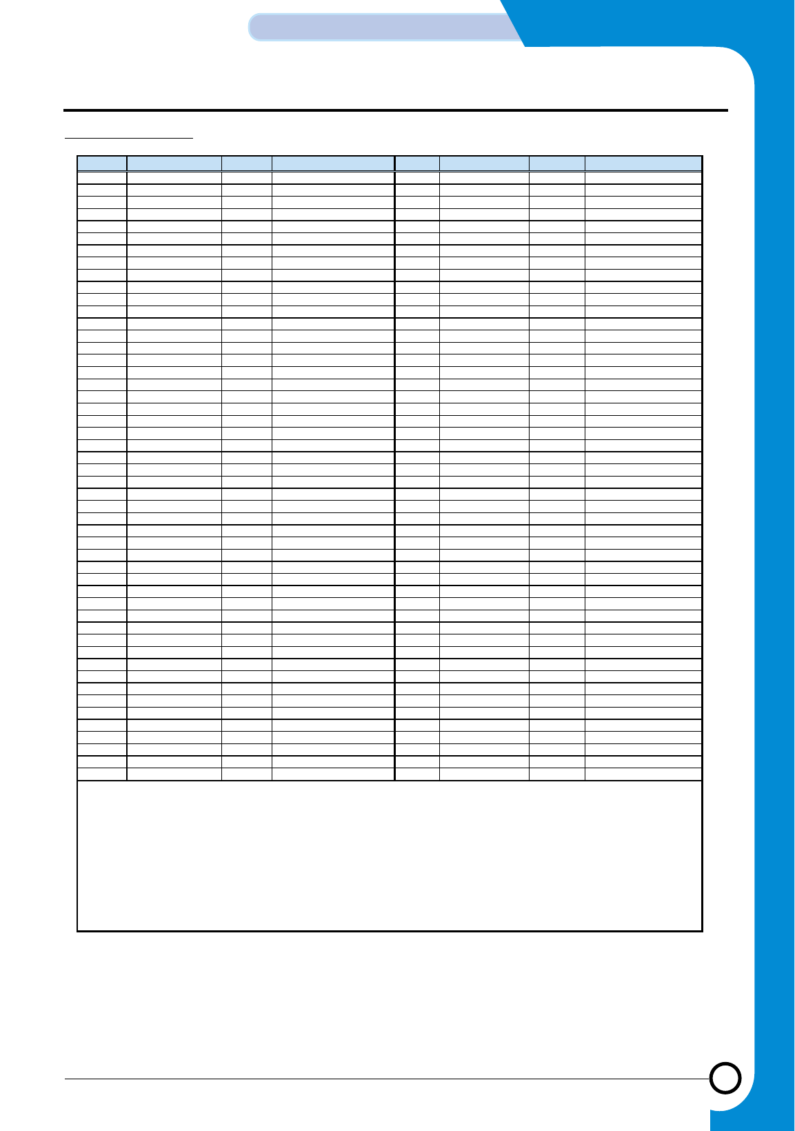
3-11
Samsung Electronics
CIRCUIT DESCRIPTION
Repair Manual
Pin Signal Label I/O Type 1Interface3Pin Signal Label I/O Type1Interface 3
1 RESERVED - - 51 RESERVED - -
2 RS2 IA HOST Interface 52 VSUB GND -
3 RS3 IA HOST Interface 53 VSS GND -
4 RS4 IA HOST Interface 54 NC - NC
5 /CS IA HOST Interface 55 NC - NC
6 /WR IA HOST Interface 56 Sleep MI Modem Interconnect
7 /RD IA HOST Interface 57 VDD1 PWR -
8 /RDCLK OA DTE Serial Interface 58 RESERVED - -
9 /RLSD OA DTE Serial Interface 59 RESERVED - -
10 TDCLK OA DTE Serial Interface 60 NC - NC
11 TXD IA DTE Serial Interface 61 SR1IO MI Modem Interconnect
12 /CTS OA DTE Serial Interface 62 VCORE PWR -
13 VDD1 PWR - 63 VDD1 PWR -
14 RESERVED - - 64 XTCLK IA DTE Serial Interface
15 RESERVED - - 65 VSS GND -
16 VSS GND - 66 RESERVED - -
17 NC - NC 67 RXD OA DTE Serial Interface
18 /RESET OA Modem Interconnect 68 /DTR IA DTE Serial Interface
19 SR4OUT OA Modem Interconnect 69 VDD1 PWR -
20 NC - NC 70 IA_SLEEP MI Modem Interconnect
21 SR4IN IA Modem Interconnect 71 VGG PWR -
22 CLK_OUT OA Modem Interconnect 72 YCLK OA Overhead Signal
23 EYESYNC OA Diagnostic Signal 73 XCLK OA Overhead Signal
24 EYECLK OA Diagnostic Signal 74 EYEXY OA Diagnostic Signal
25 MAVSS GND - 75 /DSR OA DTE Serial Interface
26 MAVDD PWR - 76 /RI OA Telephone Line Interface
27 SPKR O(DF) Telephone Line Interface 77 RINGD IA Telephone Line Interface
28 TXA2 O(DD) Telephone Line Interface 78 /RTS IA DTE Serial Interface
29 TXA1 O(DD) Telephone Line Interface 79 IRQ OA HOST Interface
30 VREF MI Modem Interconnect 80 VSS GND -
31 VC MI Modem Interconnect 81 GPO0 MI Modem Interconnect
32 RIN I(DA) Telephone Line Interface 82 RESERVED - -
33 MAVSS AGND - 83 RESERVED - -
34 /POR IA Modem Interconnect 84 VDD1 PWR -
35 RESERVED - - 85 XTALI/CLKIN I Overhead Signal
36 RESERVED - - 86 XTALO O Overhead Signal
37 /TALK O(DD) Telephone Line Interface 87 D0 IA/OB HOST Interface
38 VDD PWR - 88 D1 IA/OB HOST Interface
39 RESERVED - - 89 D2 IA/OB HOST Interface
40 RESERVED - - 90 D3 IA/OB HOST Interface
41 NC - NC 91 D4 IA/OB HOST Interface
42 M_CNTRL_SIN IA Modem Interconnect 92 VDD1 PWR -
43 M_CLKIN IA Modem Interconnect 93 D5 IA/OB HOST Interface
44 M_TXSIN IA Modem Interconnect 94 D6 IA/OB HOST Interface
45 M_SCK IA Modem Interconnect 95 D7 IA/OB HOST Interface
46 M_RXOUT IA Modem Interconnect 96 RS0 IA/OB HOST Interface
47 M_STROBE IA Modem Interconnect 97 RS1 IA/OB HOST Interface
48 RESERVED - - 98 PLL_VDD PWR -
49 OH O(DD) Telephone Line Interface 99 VSS GND -
50 VDD PWR - 100 PLL_GND GND -
Notes:
1. I/O types:
MI = Modem interconnect.
IA, IB = Digital input.
OA, OB = Digital output.
I(DA) = Analog input.
O(DD), O(DF) = Analog output.
2. NC = No external connection required.
RESERVED = No external connection allowed.
3. Interface Legend:
HOST = Modem Control Unit (Host)
DTE = Data Terminal Equipment
FM336 Pin Signals
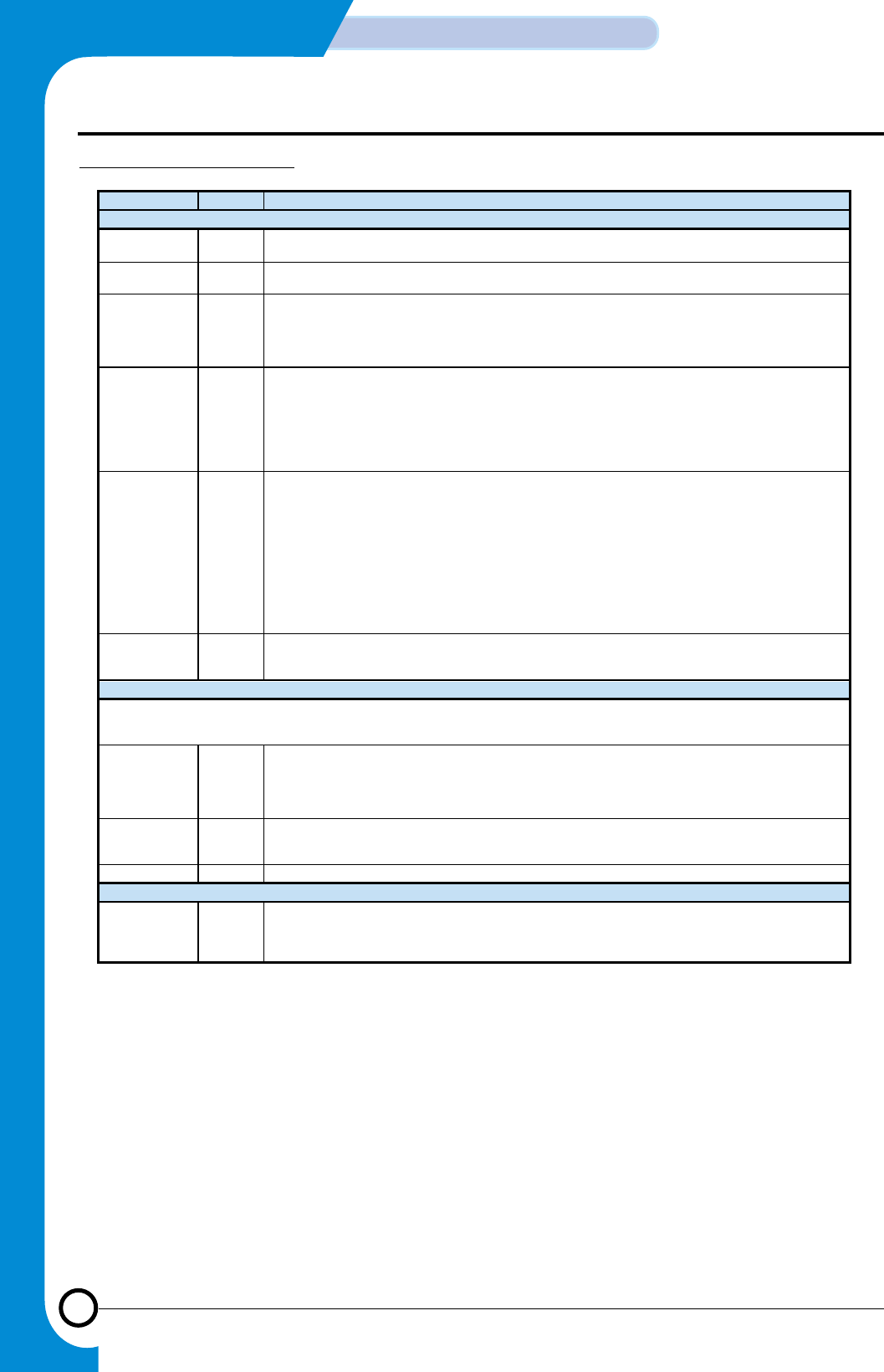
3-12
CIRCUIT DESCRIPTION
Samsung Electronics
Repair Manual
Label I/O Type Signal Name/Description
TELEPHONE LINE INTERFACE/AUXILIARY
TXA1, TXA2 O(DD) Transmit Analog 1 and 2. The TXA1 and TXA2 outputs are differential outputs 180 degrees out of phase
with each other. Each output can drive a 300 load.
RIN O(DA) Receive Analog. RIN is a single-ended receive data input from the telephone line interface or an optional
external hybrid circuit.
RINGD IA Ring Detect. The RINGD input is monitored for pulses in the range of 15 Hz to 68 Hz. The frequency
detection range may be changed by the host in DSP RAM. The circuit driving RINGD should be a 4N35
optoisolator or equivalent. The circuit driving RINGD should not respond to momentary bursts of ringing
less than 125 ms in duration, or less than 40 VRMS (15 Hz to 68 Hz) across TIP and RING. Detected ring
signals are reflected on the /RI output signal as well as the RI bit.
/TALK O(DD) Relay B Control. The /TALK open collector output can directly drive a +5V reed relay coil with a minimum
resistance of 360 ohms (13.9 mA max. @ 5.0V) and a must-operate voltage no greater than 4.0 VDC. A
clamp diode, such as a 1N4148, should be installed across the relay coil. An external transistor can be
used to drive heavier loads (electro-mechanical relays). /TALK is controlled by host setting/resetting of the
RB bit.
In a typical application, /TALK is connected to the normally closed Talk/Data relay (/TALK). In this case,
/TALK active opens the relay to disconnect the handset from the telephone line.
OH O(DD) Relay A Control. The OH open collector output can directly drive a +5V reed relay coil with a minimum
resistance of 360 ohms (13.9 mA max. @ 5.0V) and a must-operate voltage no greater than 4.0 VDC. A
clamp diode, such as a 1N4148, should be installed across the relay coil. An external transistor can be
used to drive heavier loads (electro-mechanical relays). OH is controlled by host setting/resetting of the RA
bit.
In a typical application, OH is connected to the normally open Off-Hook relay (OHRC). In this case, OH
active closes the relay to connect the modem to the telephone line.
Alternatively, in a typical application, OH is connected to the normally open Caller ID relay (CALLID). When
the modem detects a Calling Number Delivery (CND) message, the OH output is asserted to close the
CALLID relay in order to AC couple the CND information to the modem RIN input (without closing the off-
hook relay and allowing loop current flow which would indicate an off-hook condition).
/RI OA Ring Indicator. /RI output follows the ringing signal present on the line with a low level (0 V) during the ON
time, and a high level (+3.3 V) during the OFF time coincident with the ringing signal. The RI status bit
reflects the state of the /RI output.
DIAGNOSTIC SIGNALS
Three signals provide the timing and data necessary to create an oscilloscope quadrature eye pattern. The
eye pattern is a display of received baseband constellation. By observing this constellation, common line
disturbances can usually be identified.
EYEXY OA Serial Eye Pattern X/Y Output. EYEXY is a serial output containing two 11-bit diagnostic words (EYEX
and EYEY) for display on the oscilloscope X axis (EYEX) and Y axis (EYEY). EYEX is the first word clocked
out; EYEY follows. Each word has 8-bits of significance. EYEXY is clocked by the rising edge of EYECLK.
This serial digital data must be converted to parallel digital form by a serial-to-parallel converter, and then to
analog form by two digital-to-analog (D/A) converters.
EYECLK OA Serial Eye Pattern Clock. EYECLK is a 336 kHz output clock for use by the serial-to-parallel converters.
The low-to-high transitions of RDCLK coincide with the low-to-high transitions of EYECLK. EYECLK,
therefore, can be used as a receiver multiplexer clock.
EYESYNC OASerial Eye Pattern Strobe. EYESYNC is a strobe for loading the D/A converters.
SPEAKER INTERFACE
SPKR O(DF) Speaker Analog Output. The SPKR output reflects the received analog input signal. The SPKR on/off and
three levels of attenuation are controlled by bits in DSP RAM. When the speaker is turned off, the SPKR
output is clamped to the voltage at the VC pin. The SPKR output can drive an impedance as low as 300
ohms. In a typical application, the SPKR output is an input to an external LM386 audio power amplifier.
FM336 Signals Definitions
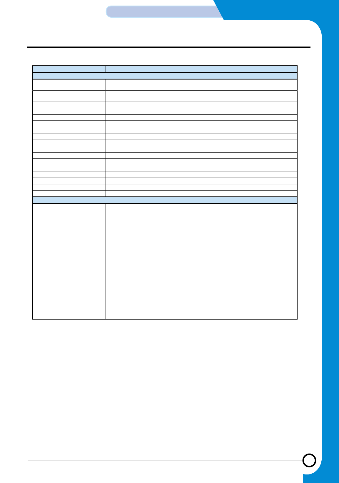
3-13
Samsung Electronics
CIRCUIT DESCRIPTION
Repair Manual
Label I/O Type Signal Name/Description
REFERENCE SIGNALS AND MODEM INTERCONNECT
VC MI Low Voltage Reference. Connect to analog ground through 10 F (polarized, + terminal to VC)
and 0.1 F (ceramic) in parallel.
VREF MI High Voltage Reference. Connect to VC through 10 F (polarized, + terminal to VREF) and 0.1 F
(ceramic) in parallel.
/POR IA Power-On-Reset. Connects to /RESET.
/RESET OA Reset. Connects to /POR.
CLK_OUT MI IA Clock. Connect to M_CLKIN.
SR4OUT OA SR4OUT. Connect to M_TXSIN.
SR4IN IA SR4IN. Connect to M_RXOUT.
SR1IO OA SR1IO. Connect to M_CNTRL_SIN.
M_CNTRL_SIN IA M_CNTRL_SIN. Connect to SR1IO.
M_CLKIN IA M_CLKIN. Connect to CLK_OUT.
M_TXSIN IA M_TXSIN. Connect to SR4OUT.
M_SCK IA M_SCK. Connect to EYECLK.
M_RXOUT IA M_RXOUT. Connect to SR4IN.
M_STROBE IA M_STROBE. Connect to EYESYNC.
SLEEP MI SLEEP. Connect to IA_SLEEP.
IA_SLEEP MI IA_SLEEP. Connect to SLEEP
GPO0 MI GPO0. Connect to /RDCLK.
DTE SERIAL INTERFACE
/RDCLK OA Receive Data Clock. The modem outputs a synchronous Receive Data Clock (/RDCLK) for USRT
timing. The /RDCLK frequency is the data rate (–0.01%) with a duty cycle of 50 –1%. The /RDCLK
low-to-high transitions coincide with the center of the received data bits.
/RLSD OA Received Line Signal Detector. For V.17, V.33, V.29, and V.27 ter; RLSD goes active at the end
of the training sequence. If energy is above the turn-on threshold and training is not detected, the
/RLSD off-to-on response time is 816 baud times for V.17/V.33, V.29, and V.27 ter long train; 492
baud times for V.17/V.33; and 486 baud times for V.27 ter short train. The /RLSD on-to-off time is
40 – 5 ms for V.17/V.33, 35 – 5 ms for V.29 or 11.6 – 5 ms for V.27 ter. The /RLSD on-to-off time
ensures that all valid data bits have appeared on RXD.
The /RLSD programmable threshold levels default to —43 dBm for off-to-on and to —48 dBm for on-
to-off. A minimum hysteresis of 2 dBm exists between the actual off-to-on and on-to-off transition
levels. The threshold level and hysteresis are measured with an unmodulated 2100 Hz tone applied
to the Receiver Analog (RXA) input.
Note: Performance may be degraded when the received signal level is less than —43 dBm.
TDCLK OA Data Clock. The modem outputs a synchronous Data Clock (DCLK) for USRT timing. The DCLK
frequency is the data rate (–0.01%) with a duty cycle of 50 –1%. The DCLK low-to-high transitions
coincide with the center of the data bits. Transmit Data (TXD) must be stable during the one
microsecond period immediately preceding the rising edge of DCLK and following the rising edge of
DCLK.
TXD IA Transmit Data. The modem obtains serial data to be transmitted from the local DTE on the
Transmit Data (TXD) input in serial data mode (TPDM bit = 0), or from the interface memory
Transmit Data Register (TBUFFER) in parallel data mode (TPDM bit = 1).
FM336 Signals Definitions (Cont’d)
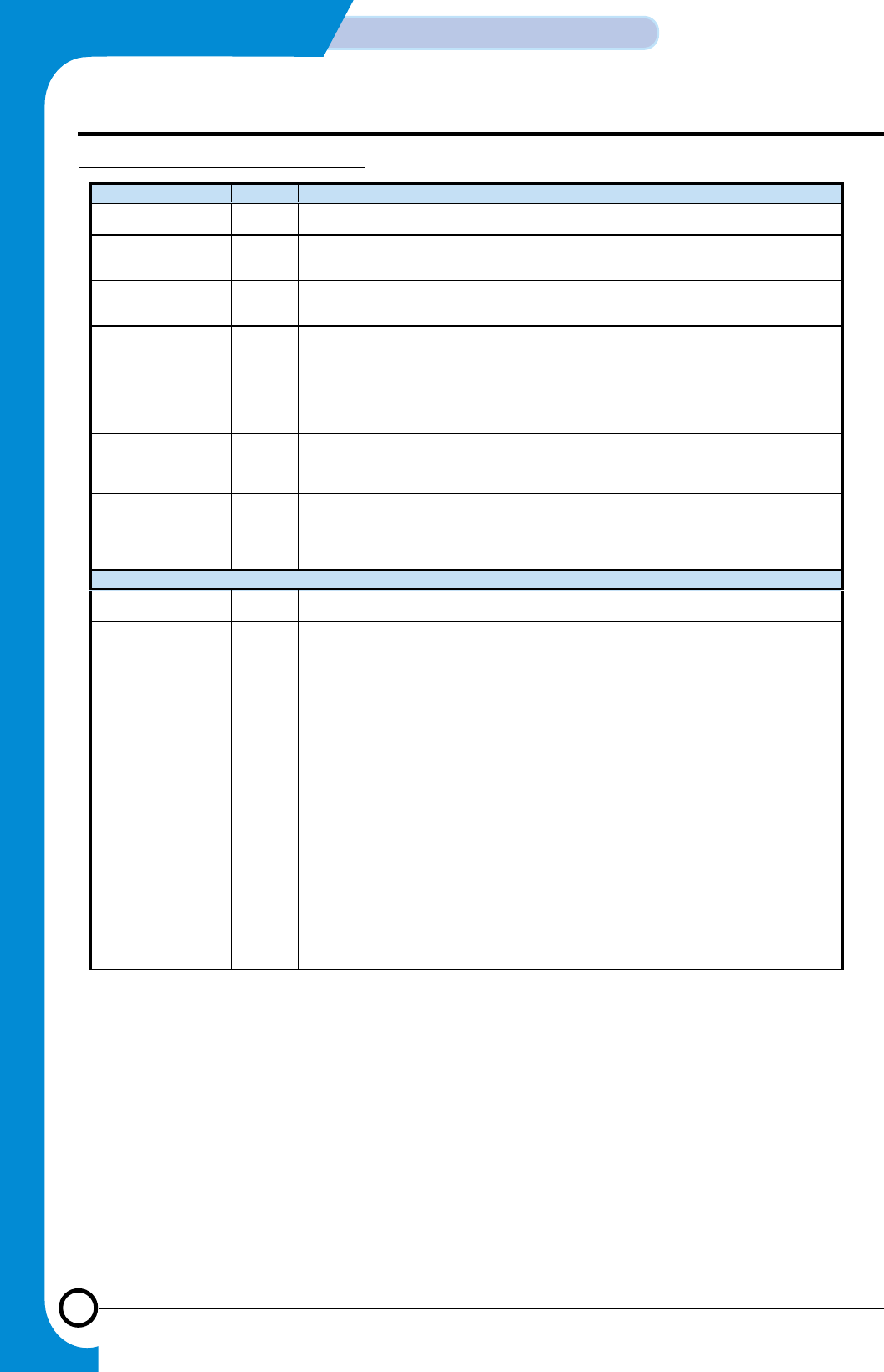
3-14
CIRCUIT DESCRIPTION
Samsung Electronics
Repair Manual
Label I/O Type Signal Name/Description
/CTS OA Clear To Send. /CTS active indicates to the local DTE that the modem will transmit any data
present on TXD. /CTS response times from an active condition of /RTS are shown in Table 1-3.
XTCLK IA External Transmit Clock. In synchronous communication, an external transmit data clock can be
connected to the modem XTCLK input. The clock supplied at XTCLK must exhibit the same
characteristics as TDCLK. The XTCLK input is then reflected at the TDCLK output.
RXD OA Received Data. The modem presents received serial data to the local DTE on the Received Data
(RXD) output and to the interface memory Receive Data Register (DBUFFER) in parallel data
mode.
/DTR IA Data Terminal Ready. In V.8 and V.34 configuration, activating /DTR initiates the handshake
sequence. The DATA bit must be set to complete the handshake.
In V.21 or V.23 configuration, activating /DTR causes the modem to enter the data state provided
that the DATA bit is a 1. If in answer mode, the modem immediately sends answer tone. During the
data mode, deactivating /DTR causes the transmitter and receiver to turn off and return to the idle
state.
The /DTR input and the /DTR control bit are logically ORed.
/DSR OA Data Set Ready. DSR ON indicates that the modem is in the data transfer state. DSR OFF
indicates that the DTE is to disregard all signals appearing on the interchange circuits except Ring
Indicator (/RI). /DSR is OFF when the modem is in a test mode (local analog or remote digital
loopback). The /DSR status bit reflects the state of the /DSR output.
/RTS IA Request to Send. The active low /RTS input allows the modem to transmit data present at TXD in
the serial data mode (TPDM bit = 0), or in DBUFFER in the parallel data mode (TPDM bit = 1),
when /CTS becomes active.
The /RTS hardware control input is logically ORed with the /RTSP bit by the modem to form the
resultant control signal.
HOST INTERFACE
/CS IA Chip Select. The active low /CS input selects and enables the modem DSP for parallel data
transfer between the DSP and the host over the microprocessor bus.
/WR IA Write. Writing is controlled by the host pulsing /WR input low during the microprocessor bus access
cycle. The write timing is:
Parameter Symbol Min. Max. Units
CS Setup Time TCS 0 —ns
RSi Setup Time TRS 10 —ns
Control Hold Time THC 10 —ns
Write Data Setup Time TWDS 20 —ns
Write Data Hold Time TDHW 10 —ns
Note: A read or write operation following a write operation must be delayed by at least 4 XCLK
cycles.
/RD IA Read Enable. Reading is controlled by the host pulsing /RD input low during the microprocessor
bus access cycle. The read timing is:
Parameter Symbol Min. Max. Units
CS Setup Time TCS 0 —ns
RSi Setup Time TRS 10 —ns
Data Access Time TDA —45 ns
Data Hold Time TDHR 10 —ns
Control Hold Time THC 10 —ns
Notes:
1. /CS and /RD must not both be continuously active.
A read or write operation following a read operation must be delayed by at least 2 XCLK cycle.
FM336 Signals Definitions (Cont’d)
3-15
Samsung Electronics
CIRCUIT DESCRIPTION
Repair Manual
Label I/O Type Signal Name/Description
IRQ OA Interrupt Request. Interrupt request outputs may be connected to the host processor interrupt
request input in order to interrupt host program execution for immediate modem service. The IRQ
output can be enabled in DSP interface memory to indicate immediate change of conditions in the
modem. The use of IRQ is optional depending upon modem application.
The IRQ output structure is an open-drain field-effect-transistor (FET). The IRQ output can be wire-
ORed with other IRQ lines in the application system. Any of these sources can drive the host
interrupt input low, and the host interrupt servicing process normally continues until all interrupt
requests have been serviced (all IRQ lines have returned high).
Because of the open-drain structure of IRQ#, an external pull-up resistor to +3.3V is required at
some point on the IRQ line. The resistor value should be small enough to pull the IRQ line high
when all IRQ drivers are off (it must overcome the leakage currents). The resistor value should be
large enough to limit the driver sink current to a level acceptable to each driver. If only the modem
IRQ# output is used, a resistor value of 5.6K ohms, 20%, 0.25 W, is sufficient.
D0-D7 IA/OB Data Lines. Eight bi-directional data lines (D0—D7) provide parallel transfer of data between the
host and the modem. The most significant bit is D7. Data direction is controlled by the Read Enable
(READ#-¿2) and Write Enable (WRITE#-R/W#) signals.
During a read cycle, data from the DSP interface memory register is gated onto the data bus via
three-state drivers in the DSP. These drivers force the data lines high for a one bit, or low for a zero
bit. When not read, the three-state drivers assume their high-impedance (off) state.
During a write cycle, data from the data bus is copied into the selected DSP interface memory
register, with high and low bus levels representing one and zero bit states, respectively.
RS0-RS4 IA/OB Register Select Lines. Five active high Register Select inputs (RS0—RS4) address interface
memory registers within the DSP when /CS is low. These lines are typically connected to address
lines A0-A4.
When selected by /CS low, the DSP decodes RS0 through RS4 to address one of 32 8-bit internal
interface memory registers (00-1F). The most significant address bit is RS4 while the least
significant address bit is RS0. The selected register can be read from, or written into, via the 8-bit
parallel data bus (D0—D7).
OVERHEAD SIGNALS
VDD1 PWR 3.3V Supply Voltage for DSP Digital Circuits.
VSS DGND Digital ground.
VGG PWR 5V Supply Voltage for DSP Digital Circuits.
MAVSS AGND Analog ground.
MAVDD PWR 5V Supply Voltage for IA Analog Circuits.
VDD PWR 5V Supply Voltage for IA Digital Circuits.
VSUB GND Connect to analog ground.
XCLK OA XCLK Output. Output clock at 63.5045 MHz, which runs during normal operational mode and
turned off during Sleep Mode.
YCLK OA YCLK. Output clock at 28.224 MHz, which runs during normal operational mode and turned off
during Sleep Mode..
Label I/O Type Signal Name/Description
XTALI/CLKIN I/O Crystal In/Clock In. Connect to an external 28.224 MHz crystal circuit or an external 28.224 MHz
oscillator circuit.
Label Crystal Oscillator
XTALI/CLKIN XTALI CLKIN
XTALO/NC I/O Crystal Out/NC. Connect to the external crystal circuit return or leave open.
Label Crystal Oscillator
XTALO/NC XTALO NC
PLL_VDD PWR PLL Supply Voltage.
PLL_GND DGND PLL Supply Voltage return.
VCORE PWR 3.3V Supply Voltage. Connect to VDD1.
RESERVED - Reserved pins are used for future development and should not be connected to any circuitry.
FM336 Signals Definitions (Cont’d)
3-16
CIRCUIT DESCRIPTION
Samsung Electronics
Repair Manual
3-1-7 Scanner Part
CIS DRIVER, INPUT PROCESSOR
CIS contacl signal is consist of BLED, RLED, GLED, CIS_CLK CIS_SI. CIS driver power supply is +5v, LED driver power
supply is +5v also. As CIS input signal, minc-Vref values O, MAXC+Vref Values is about 1.2V.
SPECIFICATION
PIN FUNCTION DESCRIPTION
No. Signature Name Description
1 SIG signal output Video output signal
2 GND Ground 0V DC ; reference point
3 VDD Supply voltage +5V DC supply (ref. to GND)
4 GND Ground 0V DC ; reference point
5 GND Ground 0V DC ; reference point
6 SI Start pulse Start pulse
7 GND Ground 0V DC ; reference point
8 CLK Clock CIS main clock
9 LEDB LED Ground (blue) LED POWER SUPPLY BLUE
10 LEDG LED Ground (green) LED POWER SUPPLY GREEN
11 LEDR LED Ground (red) LED POWER SUPPLY RED
12 VLED Supply voltage LED POWER SUPPLY
Readable width 216mm
Number of sensor elements 2552 dots(21~2572 dots available)
Resolution 75 ms/line
Scanning speed 7.5 ms/line
Light source Color LEDs
Red (640 mm)
Green(525mm)
Blue(470mm)
Data output 1 analogue
Outward dimension(WXHXL) 18.0 X 12.2 X 231.0 mm (attachment)
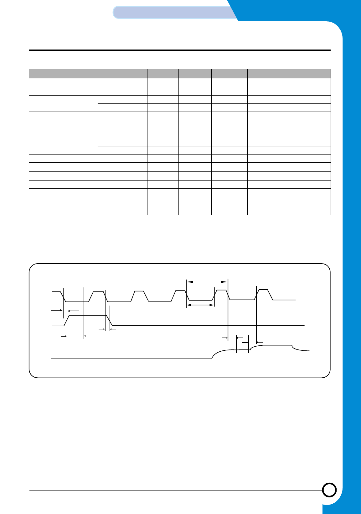
3-17
Samsung Electronics
CIRCUIT DESCRIPTION
Repair Manual
ELECTRICAL CHARACTERISTICS (TA=25˚C)
CIS Driver Clock Timing
Item SYMBOL MIN. TYP. MAX. UNIT NOTE
Power Supply VDD 4.75 5.0 5.25 V
VLED 4.75 5.0 5.25 V
Input Voltage VIH 3.2 V SI & CLK
VIL 0.8 V
Input Current IIH 20 µA. SI & CLK
IIH 0.2 mA.
LED Current ILEDr 30 mA. REF.
ILEDg 60 mA. REF.
ILEDb 60 mA. REF.
Clock Frequency. CLK 2 MHz
Clock Pulse “L” Duty 15 % tw/to
Setup Time tsu 0 tw/2 ns
Hold Time th tw/2 ns
SIG Delay Time tpd 1 250 ns
tpd 2 30 ns
Sampling Reriod ts 90 ns
CLK
SIG
S1
tpd2
tpd1
tw
th
tsu
to
2nd1st
ts
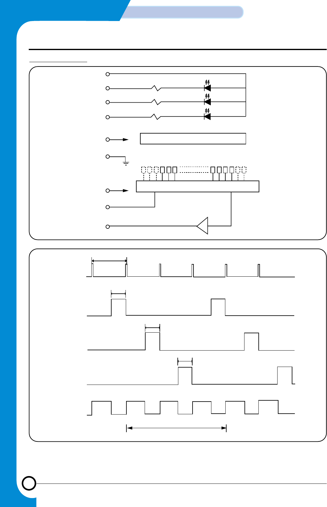
3-18
CIRCUIT DESCRIPTION
Samsung Electronics
Repair Manual
ROD LENS ARRAY
SHIFT REGISER & ANALOG SWITCH
VLED
LEDR
LEDG
LEDB
VDD
GND
S1
OP AMP
SENSOR
CLK
SIG
12021
ST
2.5ms
1.2ms
1.2ms
1.2ms
1.2ms
7.5ms/line
OFF
OFF
OFF
B O/P R O/P G O/P B O/P R O/P G O/P
OFF
OFF
OFF
ON
ON
ON
LED_R
LED_G
LED_B
SIG O/P
CIS Block Diagram

3-19
Samsung Electronics
CIRCUIT DESCRIPTION
Repair Manual
3-1-8 HOST INTERFACE:
Parallel Port Interface
PARALLEL PORT INTERFACE PART KS32C61100 has the Parallel Port Interface Part that enables Parallel Interface with
PC. This part is connected to PC through Centronics connector. It generates major control signals that are used to actu-
ate parallel communication. It is comprised of/ERROR, PE, BUSY, /ACK, SLCT, /INIT, /SLCTIN, /AUTOFD and /STB. This
part and the PC data transmission method support the method specified in IEEE P1283 Parallel Port Standard
(http://www.fapo.com/ieee1284.html). In other words, it supports both compatibility mode (basic print data transmitting
method), the nibble mode (4bit data; supports data uploading to PC) and ECP (enhanced capabilities port: 8bits data - high
speed two-way data transmission with PC). Compatibility mode is generally referred to as the Centronics mode and this is
the protocol used by most PC to transmit data to the printer. ECP mode is an improved protocol for the communication
between PC and peripherals such as printer and scanner, and it provides high speed two-way data communication. ECP
mode provides two cycles in the two-way data transmission; data cycle and command cycle. The command cycle has two
formats; Run-Length Count and Channel Addressing. RLE (Run-Length Count) has high compression rate (64x) and it
allows real-time data compression that it is useful for the printer and scanner that need to transmit large raster image that
has a series of same data. Channel Addressing was designed to address multiple devices with single structure. For exam-
ple, like this system, when the fax/printer/scanner have one structure, the parallel port can be used for other purposes while
the printer image is being processed.This system uses RLE for high speed data transmission. PC control signals and data
send/receive tasks such as PC data printing, high speed uploading of scanned data to PC, upload/download of the fax
data to send or receive and monitoring the system control signal and overall system from PC are all processed through
this part.
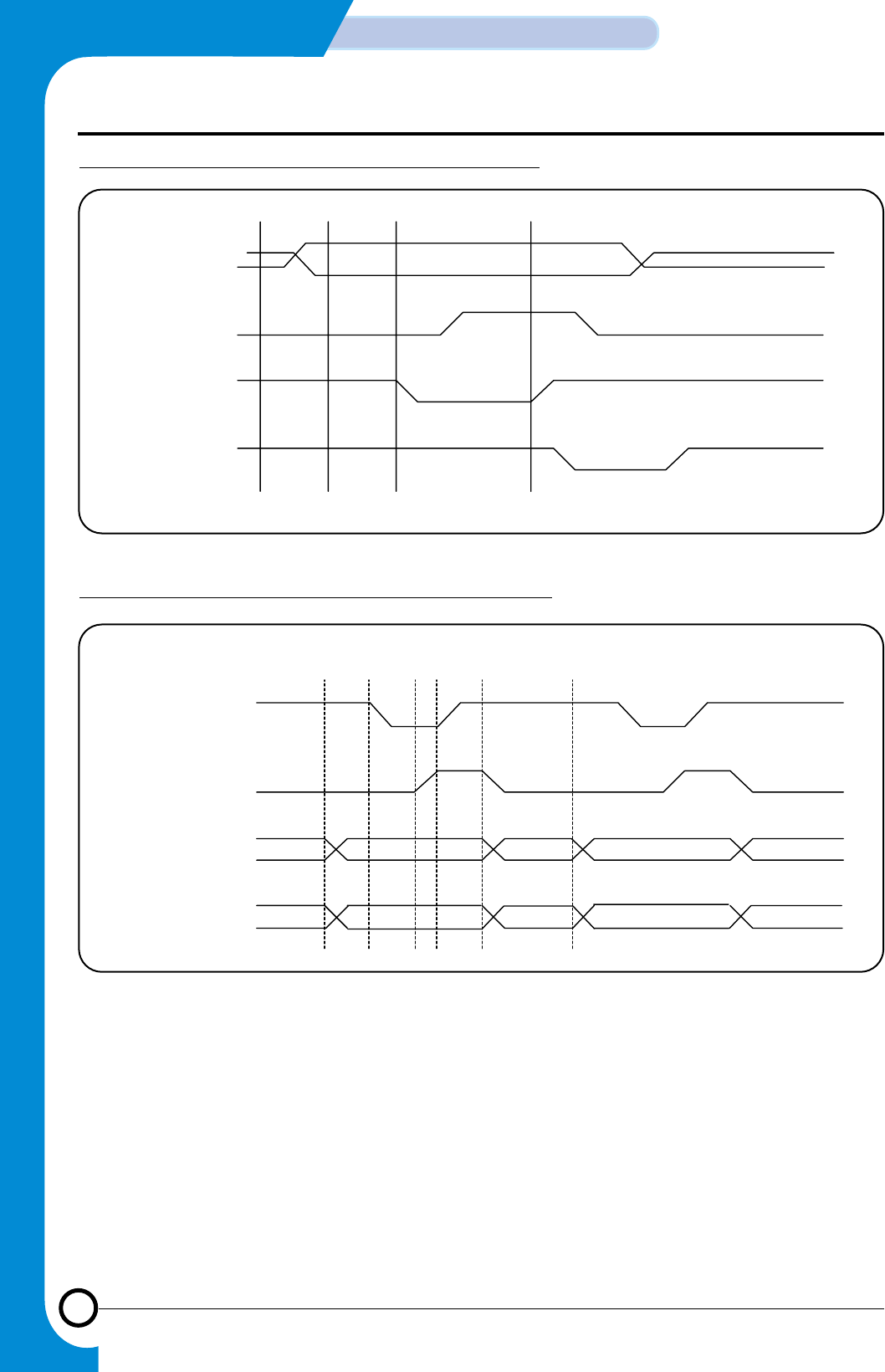
3-20
CIRCUIT DESCRIPTION
Samsung Electronics
Repair Manual
1. The host places data on the data lines and indicates a data cycle by setting nAUTOFD
2. Host asserts nSTROBE low to indicate valid data
3. Peripheral acknowledges host by setting BUSY high
4. Host sets nSTROBE high. This is the edge that should be used to clock the data into the Peripheral
5. Peripheral sets BUSY low to indicate that it is ready for the next byte
6. The cycle repeats, but this time it is a command cycle because nAUTOFD is low
PPD( 7: 0)
nSTROBE
BUSY
nACK
DATA
COMPATIBILITY HARDWARE HANDSHAKING TIMING
PPD( 7: 0)
nAUTOFD
nSTROBE
BUSY
BYTE0 BYTE1
COMMAND BYTE
DATA BYTE
12345 6
ECP HARDWARE HANDSHAKING TIMING (FORWARD)
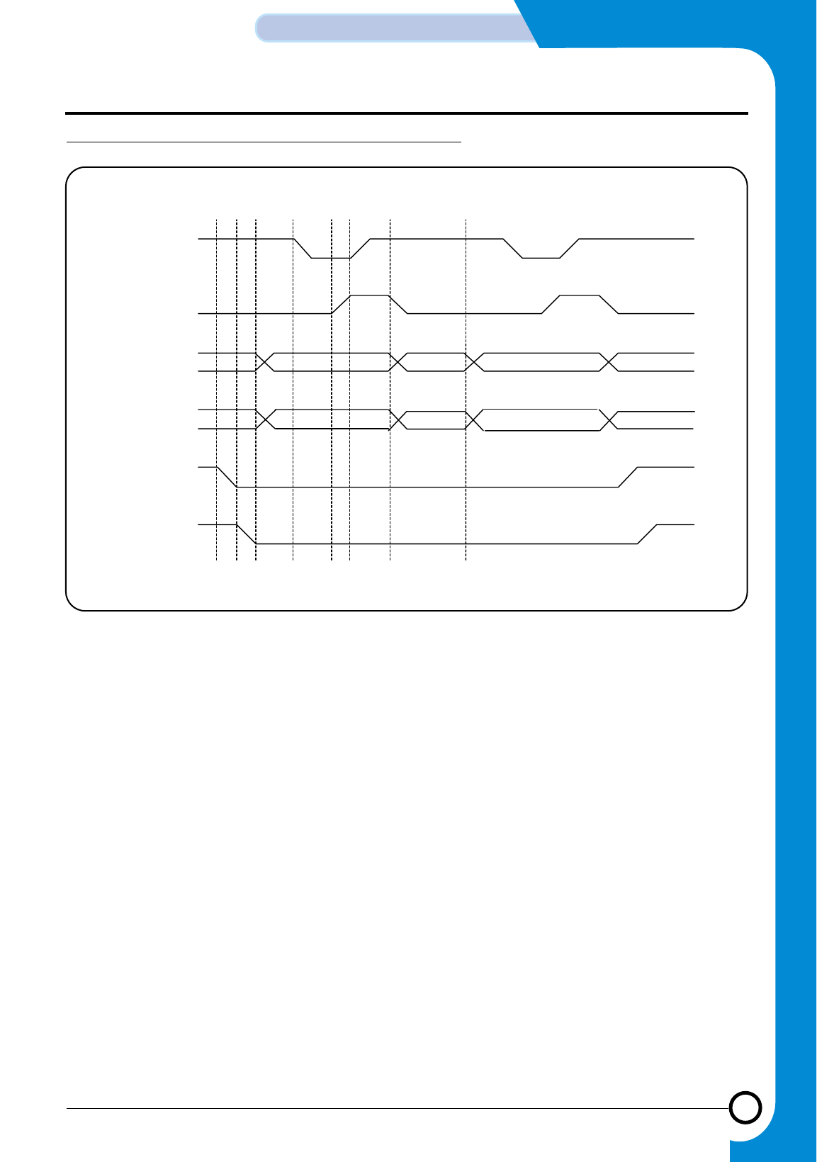
3-21
Samsung Electronics
CIRCUIT DESCRIPTION
Repair Manual
PPD(7:0)
BUSY
nACK
nAUTOFD
BYTE0 BYTE1
COMMAND BYTE
DATA BYTE
12 3 4 56
nINIT
PE
78
ECP HARDWARE HANDSHAKING TIMING (REVERSE)
1. The host request a reverse channel transfer by setting nINIT low
2. The peripheral signals that it is OK to proceed by setting PE low
3. The peripheral places data on the data lines and indicates a data cycle by setting BUSY high
4. Peripheral asserts nACK low to indicate valid data
5. Host acknowledges by setting nAUTOFD high
6. Peripheral sets nACK high. This is the edge that should be used to clock the data into the host
7. Host sets nAUTOFD low to indicate that it is ready for the next byte
8. The cycle repeats, but this time it is a command cycle because BUSY is low
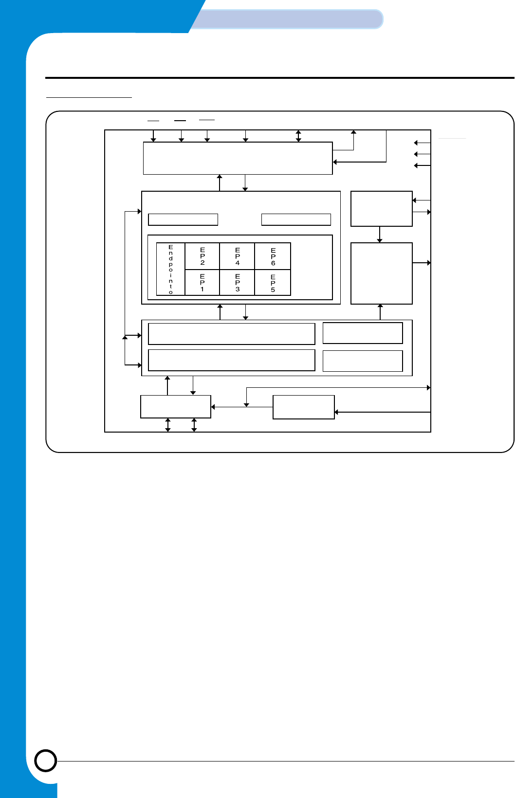
3-22
CIRCUIT DESCRIPTION
Samsung Electronics
Repair Manual
CS RD VVR A0/ALE D[7:0]/AD[7:0] INTR MODE[1:0]
Microcontroller Interface
Endpoint/Contol FIFOs
Control Status
RX
TX
RESET
Vcc
GND
XIN
XOUT
CLKOUT
48 MHz
Oscillator
Clock
Generator
SIE
Media Access Controller[MAC]
Physical Layer interface[PHY]
Trans ceiver VReg
Clock
Recovery
USB Event
Detect
V3.3
AGND
D+ D- Upstream Port
USB INTERFACE
• Full-Speed USB Node Device
• USB transceiver
• 3.3V signal voltage regulator
• 48 MHz oscillator circuit
• Programmable clock generator
• Serial Interface Engine consisting of Physical Layer In-terrace (PHY) and Media Access Controller (MAC), USB
Specification 1.0 compliant
• Control/Status Register File
• USB Function Controller with seven FIFO-based End-points :
- One bidirectional Control Endpoint 0 (8bytes)
- Three Transmit Endpoints (2*32 and 1*64 bytes)
- Three Receive Endpoints (2*32 and 1*64 bytes)
• 8-bit parallel interface with two selectable modes :
- non-multiplexed
- multiplexed (Inter compatible)
• DMA support for parallel interface
• MICROWIRE/PLUS Interface
• 28-pin SO package
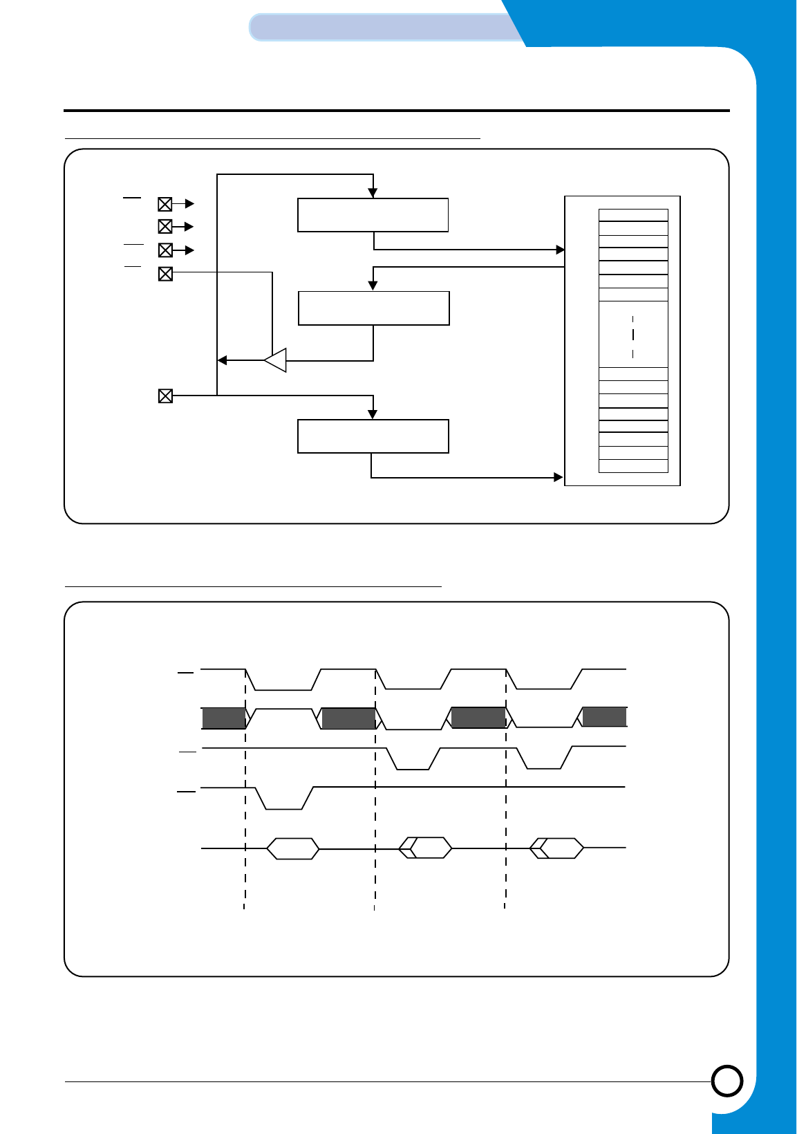
3-23
Samsung Electronics
CIRCUIT DESCRIPTION
Repair Manual
CS
A0
VVR
RD
D[7:0]
DATA_IN
DATA_OUT
ADDR
DATA_IN
DATA_OUT
ADDRESS
0x00
0x3F
REGISTERFILE
NON-MULTIPLEXED MODE INTERFACE BLOCK DIAGRAM
NON-MULTIPLEXED MODE BASIC TIMING DIAGRAM
cs
A0
RD
VVR
D[7:0] input out
vvrte Address Read Data
out
Burst Read Data
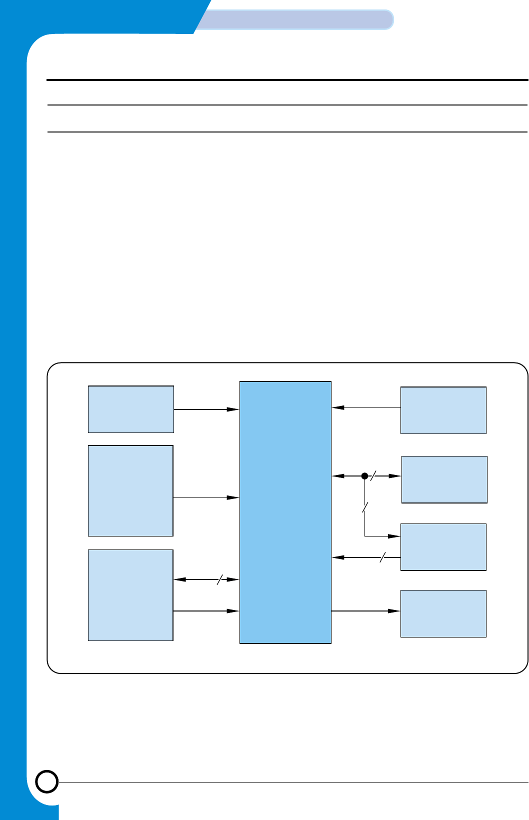
3-24
CIRCUIT DESCRIPTION
Samsung Electronics
Repair Manual
3-2 OPE PBA
3-2-1 SUMMARY
Scan
Position
Sensor
Document
Detect
Sensor
Connector
MICOM
HT48C5A
UART
Reset
11
7
X
Y8
RESONATOR
7.37 MHz
LCD
16x 1Line
Key Matrix
LEDs
OPE Board is separated functionally from the main board
and operated by the micom(HT48C5A) in the board. OPE
and the main use UART (universal asynchronous receiv-
er/transmitter) channel to exchange information. OPE
reset can be controlled by the main.
OPE micom controls key-scanning and LCD and LED dis-
play, detects documents and senses SCAN position. If
there occurs an event in OPE (such as key touch and sen-
sor level change), it sends specific codes to the main to
respond to the situation and the main analyzes these
codes and operates the system.
For example, it the main is to display messages in OPE,
the main transmits data through UART line to OPE
according to the designated format and OPE displays this
on LCD, LED. OPE’s sensing is also transmitted to the
main through UART line and then the main drives neces-
sary operation.
OPE PBA consists of U1(MICOM, HT48C5A),LCD, key
matrix, LED indicators, SCAN position sensor and the
document detect sensor. Refer to OPE Schematic
Diagram and Wiring Diagram sections of this manual.
• Display from the controller is received at U2 pin 47
(RX DATA).
• LCD drive signals are sent from P1-x pin group, P1-
4~P1-14 pins.
• Machine status LED drive signals are sent from U2
LED0~LED4.
• Document detect sensor output is received at U2 pin 1.
• Scan position sensor output is received at U2 pin7
<OPE BLOCK DIAGRAM>

3-25
Samsung Electronics
CIRCUIT DESCRIPTION
Repair Manual
3-3 LIU PBA
The LIU (Line Interface Unit) using the discrete method is comprised of the following.
(1) Tel_line Interface Circuit that connects the PSTN(exchange) and the system (Facsimile)
(2) Telephone circuit composed of dial/speech circuit.
3-3-1 Tel_Line interface Circuit
Tel_Line Interface is the path that connects the signals between PSTN(exchange) and the system (Facsimile) and it is com-
prised of Tel-Line Interface Circuit and Impedance Matching Trans Circuit.
(1) TEL_LINE Interface Circuit
(2) TRANS Circuit for IMPEDANCE MATCHING
3-3-2 Telephone Circuit (Ringer/Dial/Speech Circuit, etc)
The telephone circuit is comprised of ring detect circuit, dialer circuit, speech circuit, external hook detect circuit and recall
circuit.
(1) Ring Detect Circuit
(2) Dialling Circuit (including MF Dialling Signal Transmitting Circuit)
(3) Speech Circuit
(4) External Hook Detect Circuit
(5) Recall Circuit
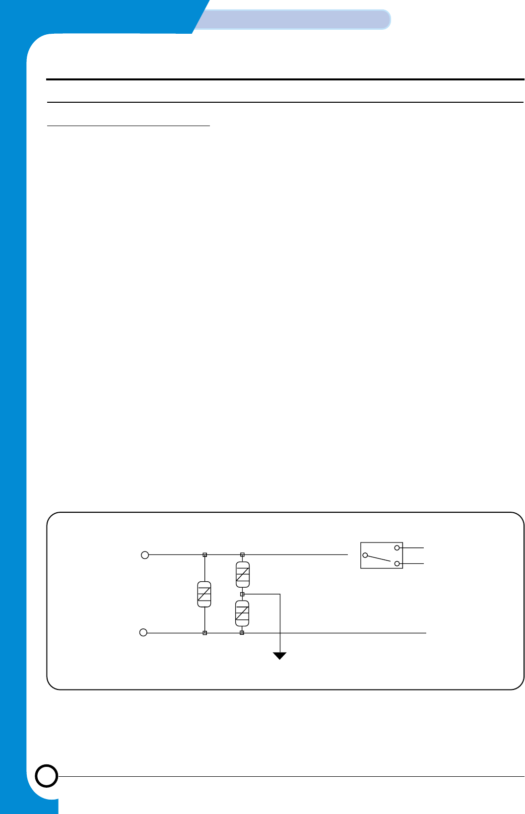
3-26
CIRCUIT DESCRIPTION
Samsung Electronics
Repair Manual
3-3-3 Detailed Spec.
TEL_LINE INTERFACE CIRCUIT
1) TEL_LINE INTERFACE CIRCUIT
• It is an interface that physically connects facsimile to the PSTN (public switching telephone network) through TIP and
RING as in fig. 1.
• ARS 1-3 protects the system from voltage overload such as the surge coming through PSTN. ARS 2 and ARS 3 are
used as overload protection in common mode (between TIP/RING and FRAME GROUND). ARS 1 is used as over-
load protection in normal mode (between TIN and RING) and it uses ARRESTOR for 600V. However, arrestor’s rated
voltage differs from European and USA(400v).
• CML (CONNECT MODEM to LINE) RELAY K1 is a switch designed to selectively connect the PSTN to system voice
communication path and fax communication path. In STAND_BY MODE and voice communication mode, it is con-
nected to TEL PART and FAX PART while communicating and dialing.
• CML Relay (K1): CML relay interfaces with T2(600:600) TRANS in communication mode.
• DC Impedance: DC impedance is determined in the DC Feeding Unit. It represents DC characteristic of the comput-
er connected through -48V DC power of the switch and lines. The DC characteristic of required by the communica-
tion standards of a number of countries is the DC resistance of 50Ω~300Ωto the current range of 20mA~120mA.
(value varies depend on countries).
• AC Impedance or Return Loss: AC impedance is determined by the peripheral circuits of T2 Transformer. It is the stan-
dard required for optimum signal transmission between computer and switch. When the AC impedance of the com-
puter for AC signal transmission and the AC impedance of the switch matches, the signal can be transmitted without
loss. Therefore, communication standards specifies the AC impedance of the computer and it implies the return loss.
The communication standards of each country, considering the characteristic of their lines, requires 600Ωor the return
loss of 14dB and higher against the AC impedance of Complex and the AC signals of 300Hz~400Hz. The AC imped-
ance of transformer changes depending on the load resistance, the core material, coil inductance and resistance, but
generally its characteristic against load resistance is considered.
TIP
RING
ARS1
ARS2
ARS3
K1 to FAX
to TEL
FG
<TEL_LINE INTERFACE CIRCUIT>

3-27
Samsung Electronics
CIRCUIT DESCRIPTION
Repair Manual
RINGER DIAL CIRCUIT
1) Ringer Circuit
• The ring detect circuit detects the ring signal by sending the bell signal sent from PSTN to the primary photo coupler
(PC814). At this point, C(1uF/250V) is used to match the ring impedance and R is coupled directly in order to prevent
any damage to the photo coupler due to ring voltage.
2) Dialing Circuit
• Dialing circuit is initiated only when the power is on and it is transmitted to line through the modem of main part (T2
trans)
3) External Hook Detect Circuit
• In the discrete LIU method, the external hook detect circuit is designed to use both the photo coupler and current
detector in order to be used in all countries including the countries with low series resistance (Germany, Switzerland,
Belgium, Austria, etc.). To use photo coupler (PC814), you must carefully select the resister connected parallel (75Ω)
to the photo coupler in order to satisfy the voltage drop standards of England and a few other countries. The diode
connected to the current detector pin (5/6) was used to detect the external hook all through when the line parity turns
over.
4) Recall Circuit
• In the discrete LIU method, we used the recalling method using low cost photo coupler instead of using photo MOS
relay in order to initiate the recalling for handset hook off dialling after the power is turned on. In this case, the time
break recall was enabled by switching the power transistor of the telephone circuit using the secondary CPU control.

3-28
CIRCUIT DESCRIPTION
Samsung Electronics
Repair Manual
3-4 Engine PPA
3-4-1 Engine Configuration
3-4-1-1. Video Controller Board
Video Controller Board receives image data from the host computer and converts it into bitmap (binary) image or receives
bitmap image directly from the host computer and sends it to the engine controller board.
3-4-1-2. SMPS Board
It basically receives AC input and generates ripple-free DC level +5V and -5V +24V. Next, it supplies these voltages to each
unit appropriately.
It also supplies AC power to heat lamp of fixing unit.
3-4-1-3. HVPS Board
HVPS board generates high voltages of THV/MHV/Supply/Dev and supplies them to the developing unit to create images.
It is designed to realize optimum conditions for the images.
This board includes LSU interface unit and cover open sensing unit that it intercepts +24V voltage to the main motor, LSU,
fan, clutch and fixing unit when you open the front cover.
3-4-1-4. Developer
Using the digital picture process, developing unit generates visible images. It is comprised of charge roller, OPC drum,
developer roller, supply roller and toner.
3-4-1-5. LSU (Laser Scanning Unit)
This is controlled by engine controller. Using laser beam control, exposure of OPC drum and the rotational principle of poly-
gon mirror, it forms electro-static latent image in the OPC drum with the video data received from engine. It is the core part
of LBP. OPC drum synchronizes with the feeding speed of the paper and rotates. When the laser beam inside LSU reach-
es at the end of polygon mirror, it generates /HSYNC signal and send it to engine. Then the engine detects /HSYNC sig-
nal and adjusts the lengthwise row of the image on the paper. After detecting /HSYNC and after set time period, it sends
the video data to LSU to adjust the left margin on the paper.
The one side of the polygon mirror is the one line scanned.
3-4-1-6. Transfer
Transcribing unit is comprised of PTL(pre-transfer lamp) and transcribing roller. PTL detects the beam of the OPC drum,
lowers the electric potential of the developing unit and lower the adhesiveness of toner to enhance transcription coefficient.
And the transcribing roller transfers the toner (constituting element of video image) on OPC drum to the paper.
3-4-1-7. Fixer
It is comprised of heat lamp, heat roller, pressure roller, thermistor and thermostat. It fixes the toner powder transferred to
the paper on the paper using pressure and high heat in order to finish the final printing job.
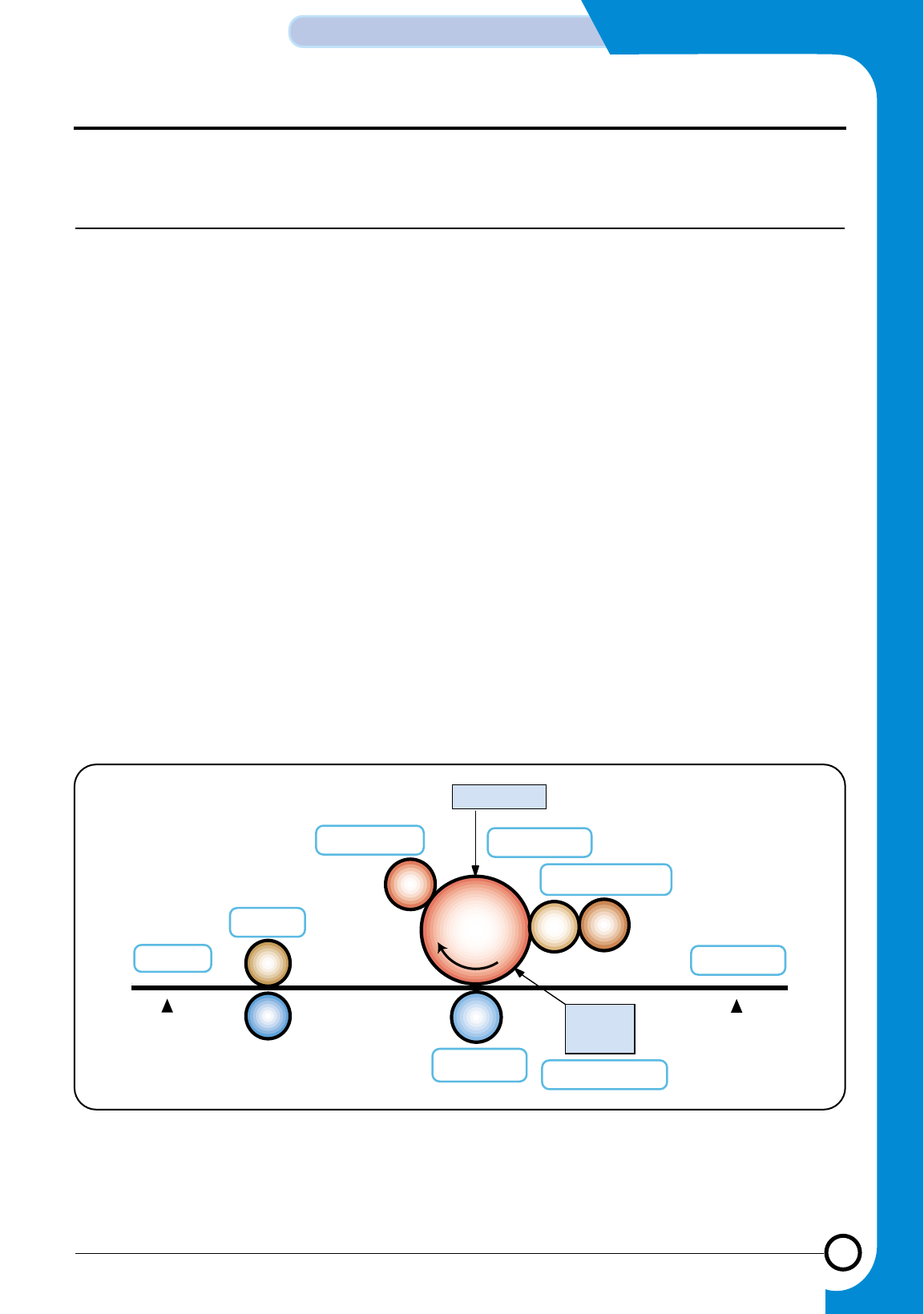
3-29
Samsung Electronics
CIRCUIT DESCRIPTION
Repair Manual
3-4-2. Developing Process
3-4-2-1 Feeder
Engine operates this unit. Solenoid rotates the feed roller and feeds one paper. Then the paper is fed into the set and hits
the actuator of the feed sensor. At this point, the engine detects the signal and prepares to spray according to the image
data. If any problem happens to this feed sensor operation, the system displays “paper jam error” on the OP panel.
Also, feed sensor unit is closely related to the paper margin.
3-4-2-2. Electrifier
This unit electrifies consistent negative voltage to OPC. When the high negative voltage (-1550V) is allowed to charge roller,
the OPC drum surface will be consistently electrified with approximately +1300V. This is the first process in generating the
digital picture.
3-4-2-3. Exposer
After receiving bitmap image data from engine board, LSU turns the laser diode either on or off depending on whether the
digital data is present or absent in order to expose the OPC drum with the switched laser beam data. The difference
between the voltages generated at this point is presented above. In other words, the part exposed to the laser will have -
50V and its relative electric potential will increase and form electrostatic latent image.
The part unexposed to the laser as it did not have the video data will consistently retain -800V. Eventually, the image will
form in the part electrified and rose to -50V(forms black dot) and the part retaining -800V will be white in order to make the
basic condition to form the video data.
LSU
2.Charging
7.Fixing
8.Exit
EXIT
SENSOR 6.Transfer 5.Pre-Transfer
FEED
SENSOR
3.Exposure
4.Development
1.Feeding
H/R
P/R
C/R
OPC
T/R PTL
D/R S/R
< Engine Operating Description >
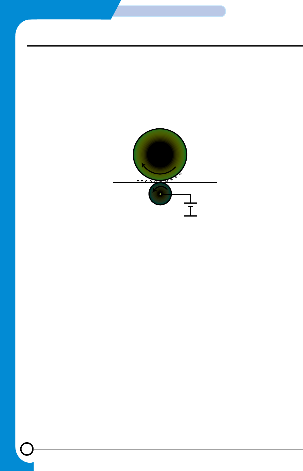
3-30
CIRCUIT DESCRIPTION
Samsung Electronics
Repair Manual
3-4-2-4. Developer Unit
On the surface where OPC drum and developer roller (rotate in opposite direction) meet, the toner that has negative elec-
tric characteristic moves to the exposed part (-50V) due to the electric potential difference, but it will not move to the unex-
posed part (-800V).
3-4-2-5. Transfer Unit
Toner on the OPC drum is transferred to paper by transfer unit. In other words, the toner on the OPC drum surface is induct-
ed by the transfer roller electrified to approximately +1.3KV(600~2800V variable) to the paper.
At this point, the voltage (600~2800V variable) is determined by temperature and humidity.
The above process is called “transfer”.
OPC
T/R
GND
1.3 KV

3-31
Samsung Electronics
CIRCUIT DESCRIPTION
Repair Manual
3-4-2-6. Anchorage unit
The toner transferred on to the paper is at the electronically low state and it can be easily scattered. Considering this fact,
we used heat (180°C) and pressure (4kg) to fix the toner on the paper permanently. Then the image formed will remain on
the paper permanently. Heat roller transfers the heat from the heat lamp inside to the paper. The surface of the heat roller
specially coated with Teflon repels toner melted by the heat from the surface.
The pressure roller on the bottom of the heat roller is made of silicon resin and its surface is also coated with Teflon. The
thermistor of the fixer unit detects the surface temperature of the heat roller and feeds this information back in order to retain
180°C while printing and 135°C, while on standby. The thermostat is used as the secondary safety device and it prevents
overheat by shutting the main power when the heat lamp
is overheated.
3-4-2-7. Exit
After the digital picture process is finished, the printed paper will come out of the set through the exit sensor. The signal
detected will be transferred to the engine and provide the position information. If the actuator and the sensor do not work
normally, the system will display “Paper Jam 2 Error”.
Heat Lamp
Heat Roller
Paper
Toner
Pressure
Roller
Spring
Thermistor
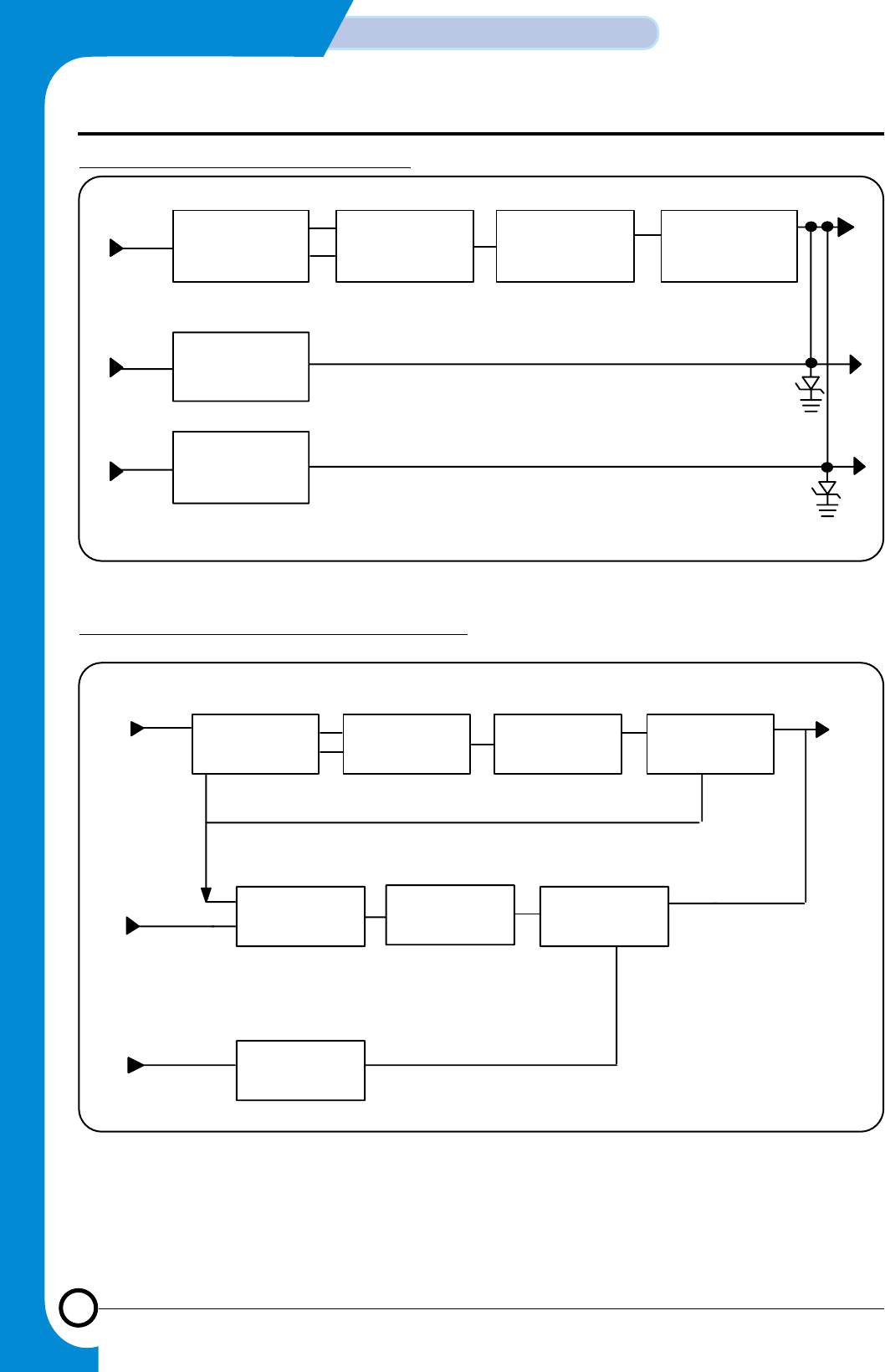
3-32
CIRCUIT DESCRIPTION
Samsung Electronics
Repair Manual
SWITCHING
CONTROL UNIT
TRANS
SWITCHING
CONTROL UNIT
SWITCHING
CONTROL UNIT
MHV-PWM
DEV-EA
SUPPLY-EA
REGULATION
CIRCUIT
OUTPUT
CIRCUIT
FEEDBACK
THVPWM
THVEA
THVREAD
PWM
CONTROL UNIT SWITCHING
CONTROL UNIT TRANS
SWITCHING
CONTROL UNIT TRANS
FEED BACK
THV
REGULATION
CIRCUIT
REGULATION
CIRCUIT
THV
ENVIRONMENT
RECOGNITION
CIRCUIT
BIAS OUTPUT UNIT BLOCK DIAGRAM
TRANSFER OUTPUT UNIT BLOCK DIAGRAM
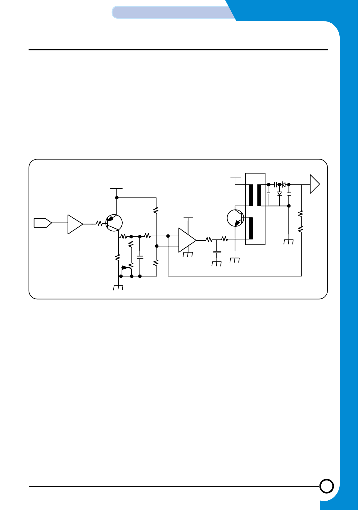
3-33
Samsung Electronics
CIRCUIT DESCRIPTION
Repair Manual
3-4-2-8. MHV (Electrification Output Enable)
Electrification Output Enable is the electrification output control signal 'PWM-LOW ACTIVE'.
When MHV-PWM LOW signal is received, Q401 turns on and the steady voltage will be accepted to the non-inverting ter-
minal of OP-AMP 324. As the voltage higher than the inverting reference voltage of OP-AMP, which is set to R405 and
R406, OP-AMP output turns high.
This output sends IB to the TRANS auxiliary wire through current-restricting resistance Q402 via R408 and C403 and Q402
turns on. When the current is accepted to Q402, Ic increases to the current proportional to time through the T401 primary
coil, and when it reaches the Hfe limit of Q402, it will not retain the "on" state, but will turn to "off". As Q402 turns 'off', TRANS
N1 will have counter-electromotive force, discharge energy to the secondary unit, sends current to the load and outputs
MHV voltage through the high voltage output enable, which is comprised of Regulation– circuit.
MHV-PWM U2 7407
R411 2.2K
18V
Q401 A708
R403 130K
R402
82K
R412 2K
R404
27K
C408
104 R406
2.2K
R405 220K
24VS
+
_
R408
47K R409
390
KA324 C403
333
Q402
D526
24VS
T401
C404
3K/471
D402
4KV
C406
3K/471
R416
15M
R417
15M
MHV OUTPUT
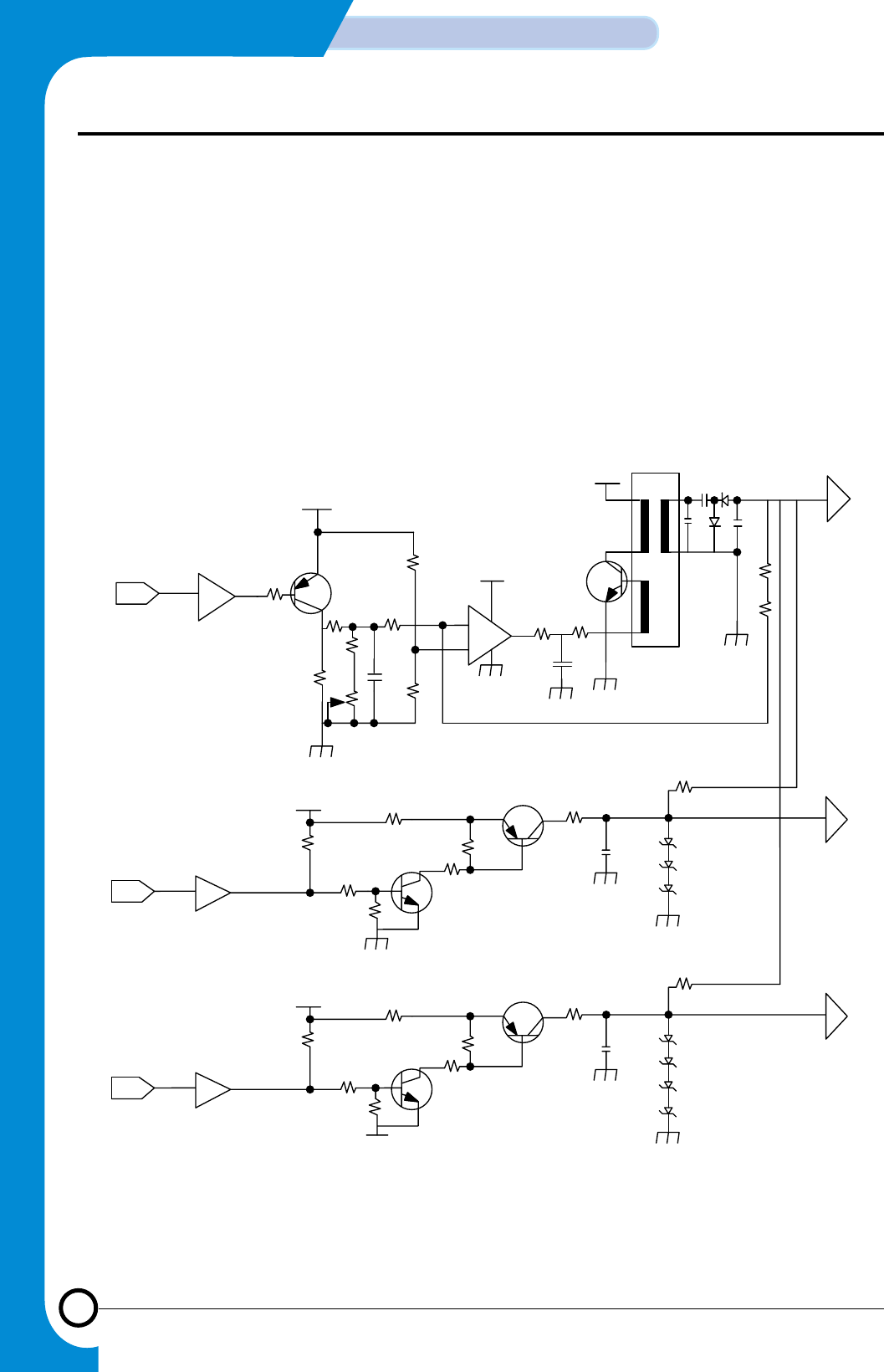
3-34
CIRCUIT DESCRIPTION
Samsung Electronics
Repair Manual
3-4-2-9. BIAS (supply/dev output unit)
BIAS voltage output is generated only when electrification voltage is set to output. In the circuit presented above, it orga-
nizes enough zener-diodes required to output dev/supply voltage from electrification output.
Supply voltage is output when the supply-ea signal is 'L'. When supply-ea is 'L', Q104 turns off and as Q105 does not turn
on, the electric potential of the output unit retains the electric potential of zener and thus -500V is output as the supply volt-
age.
In case supply-ea signal is 'H', both Q104 and Q105 will turn on and the electric potential of the output unit will not retain
the electric potential of zener and become GND level and thus the output voltage will become .
The output condition of developer voltage is the same as that of the supply voltage.
MHV-PWM U2 7407
R411 2.2K
18V
Q401 A708
R403 130K
R402
82K
R412 2K
R404
27K
C408
104 R406
2.2K
R405 220K
24VS
+
_
R408
47K R409
390
KA324 C403
333
Q402
D526
24VS
T401
C404
3K/471
D402
4KV
C406
3K/471
R416
15M
R417
15M
MHV
OUTPUT
DEV-EA
24VS
R114
33K
R113
10K
R115 3.3K
R117 10K
R116
2.2K
Q106
C3198
Q107 A1413 R118
33K
C107
1K/101
ZD401 150V
ZD402 150V
ZD403 51V
DEV
OUTPUT
SUPPLY
OUTPUT
SUPPLY-EA
24VS
R107
33K
R106
10K
R108 33K
R112
2K
Q104
C3198
Q105 A1413
R109 10K
R110
2.2K
R111
33K C106
1K/101
ZD404 150V
ZD405 150V
ZD406 100V
ZD407 100V
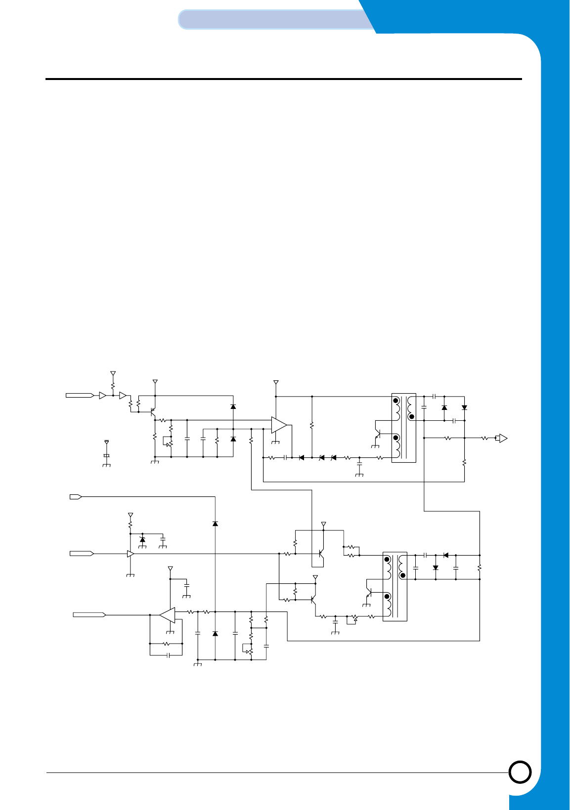
3-35
Samsung Electronics
CIRCUIT DESCRIPTION
Repair Manual
3-4-2-10. THV(THV(+)/THV(-) Output Unit)
Transfer(+) output unit is the transfer output control signal 'PWM-LOW ACTIVE'.
When THV-PWM LOW signal is received, Q203 turns on and the steady voltage will be accepted to the non-inverting ter-
minal of OP-AMP 324. As the voltage is higher than the inverting reference voltage of OP-AMP, OP-AMP output turns high.
The 24V power adjusts the electric potential to ZD201 and ZD202, sends IB to TRANS auxiliary wire through current-
restricting resistance R215 via R212 and C204, and eventually Q204 will turn on. When the current is accepted to Q402,
Ic increases to the current proportional to time through the T201 primary coil, and when it reaches the Hfe limit of Q204, it
will not retain the "on" state, but will turn to "off". As Q402 turns 'off', TRANS N1 will have counter-electromotive force, dis-
charge energy to the secondary coil, sends current to the load and outputs THV voltage through the high voltage output
enable, which is comprised of Regulation– circuit. The output voltage is determined by the DUTY width. Q203 switches
with PWM DUTY cycle to fluctuate the output by fluctuating the OP-AMP non-inverting end VREF electric potential, and
the maximum is output at 0% and the minimum, at 100%.Transfer(-) output unit is THV-EA 'L' enable.
When THV-EA is 'L', Q302 turns on and the VCE electric potential of Q302 will be formed and sends IB to TRANS auxil-
iary wire through R311, C305 and VR302 via current-restricting resistance R314, and eventually Q303 will turn on. When
the current is accepted to Q303, Q303's Ic increases to the current proportional to time through the T301 primary coil, and
when it reaches the Hfe limit of Q303, it will not retain the "on" state, but will turn to "off". As Q303 turns 'off', TRANS N1
will have counter-electromotive force, discharge energy to the secondary coil, send current to load and output THV(-) volt-
age through the high voltage output enable, which is comprised of Regulation– circuit.
#7 TEV-PWM
5V
U2
12
3
R201
10K
U2
R205
1.8K
R206
100
Q203
A708Y
R208
30K
18V
R209
100KF
VR201
50K
R207
2K C201
103 C202
121 R210
845KF
D202
1N4148 R211
1MF
5
6
7
+
_U1
11 KA324
24VS
+C101
35V47UF
D201
1N4148
24VS
R213
2.2K
R212
680K C203
472 D203
1N4148 ZD201
5.65V ZD202
705V
R214
2.2K
C204
333Z
Q204
D526
T201
KAB-007 C206
3KV470pF
C205
2KV68pF D204
4KV D205
4KV
R215
390
C207
3KV470pF
R216
SBR306 R218
MGR1/2W100KF
R217
SBR207
#17
#19
#5
#24
5V
TEV-EA
TEV-READ
18V
R3
1/2W560
ZD1
5.6V
C7
104
D301
1N4148
56
7U2
7407
D-GND
24VS
C4
103
8
9
10
U1
+
_
KA324
R301
470K
C301
222
R302
33K R303
100KF
C302
102 D302
1N4148
C303
103
R304
389KF
R305
10KF
VR301
5K
R306
26.1KF
C304
500V103Z
18V
R309
202K
R307
33K
Q301
A708Y
18V
R310
2.2K
R308
33K
Q302
A708Y
R312
1W56
R313
1W56
Q303
D526
R311
100KF
C305
333Z
VR302
2K
R314
1.7K
KAB-006
T301
1
5
2
4
6
7
1
5
2
4
7
6
C307
3KW470pF D304
4KV
C306
2KV68pF D303
4KV C308
3KV470pF R315
SBR306

3-36
CIRCUIT DESCRIPTION
Samsung Electronics
Repair Manual
3-4-2-11. Environment Recognition
THV voltage recognizes changes in transfer roller environment and allows the voltage suitable for the environment in order
to realize optimum image output. The analog input is converted to digital output by the comparator that recognizes the envi-
ronmental changes of the transfer roller. It is to allow the right transfer voltage to perform appropriate environmental
response considering the environment and the type of paper depending on this digital output by the programs that can be
input to the engine controller ROM.
For ML-5000 or ML-5200 series, this environment recognition setting is organized as follows: First, set the THV(+) stan-
dard voltage. Allow 200MΩload to transfer output, enable output and set the standard voltage 800V using VR201. Then
set 78 (CPU's recognition index value) as the standard using VR302. This standard value with CPU makes sure that the
current feedback is 4µA when output voltage is 800V and load is
200MΩ.If the load shows different resistance value when 800V is output, the current feedback will also be different and
thus the index value will also be different. according to the index value read by CPU, the transfer voltage output will differ
according to the preset transfer table.
The changes in transfer output required by each load is controlled by PWM-DUTY.
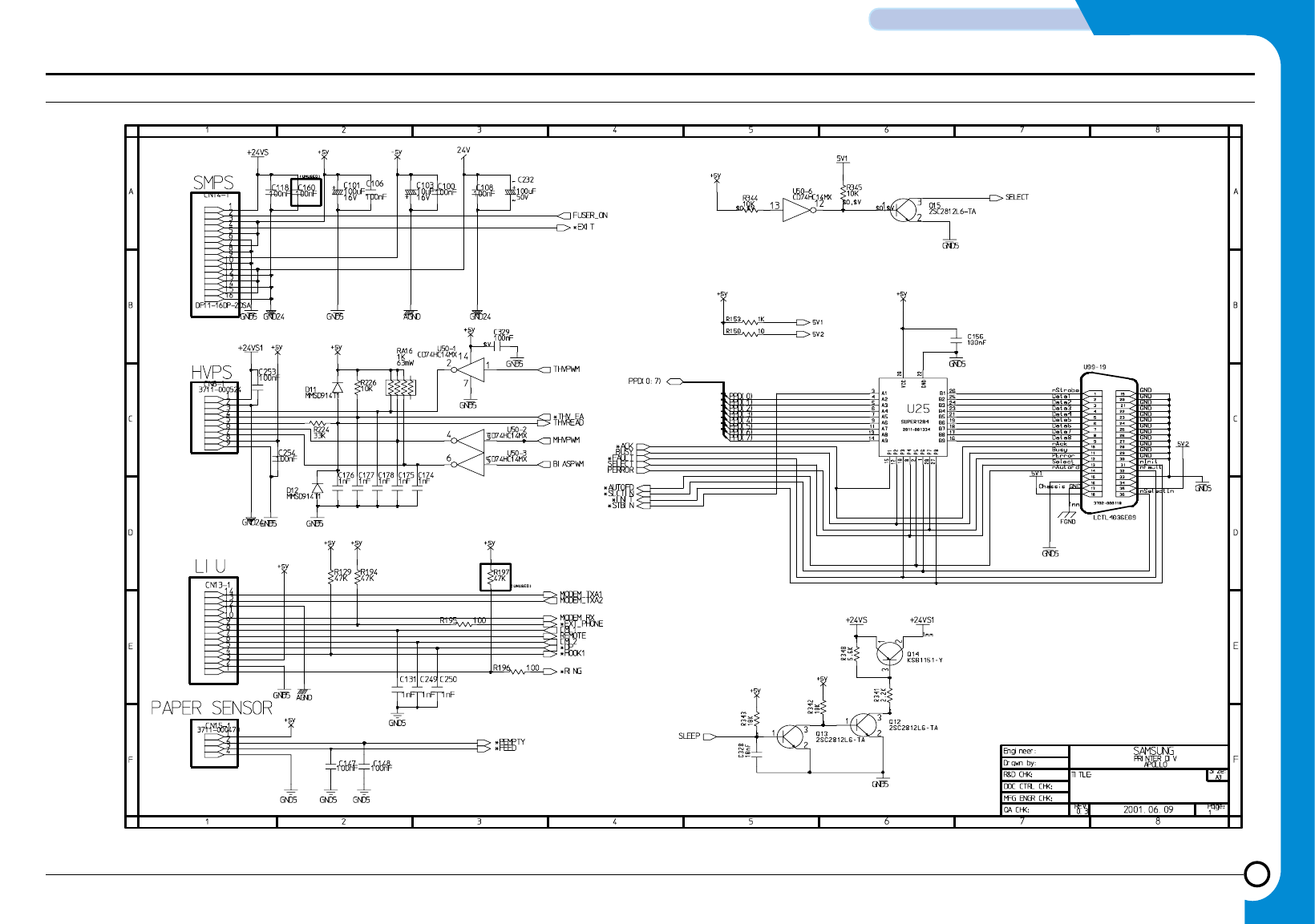
4
4-1
Samsung Electronics
SCHEMATIC DIAGRAMS
Repair Manual
4.Schematic Diagrams
4-1 Main Circuit Diagram (1/6)
APOLLO2(MAIN)
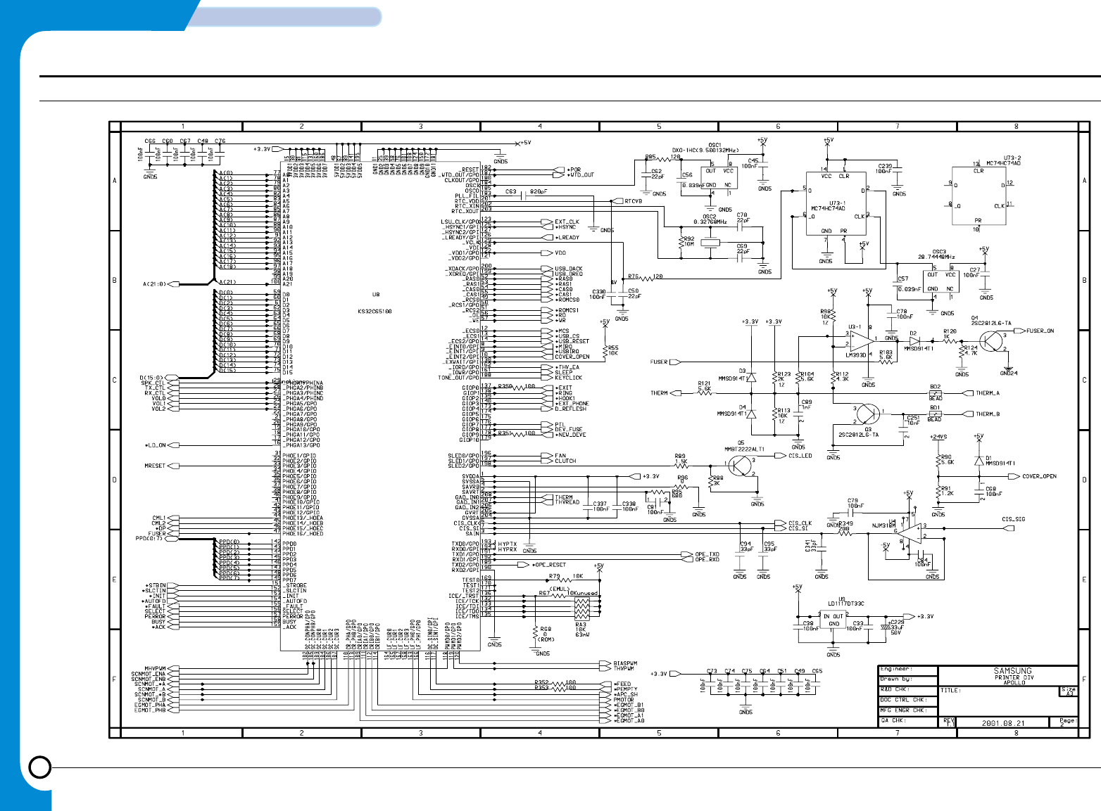
4-2
SCHEMATIC DIAGRAMS
Samsung Electronics
Repair Manual
4-2 Main Circuit Diagram (2/6)
APOLLO2(MAIN)
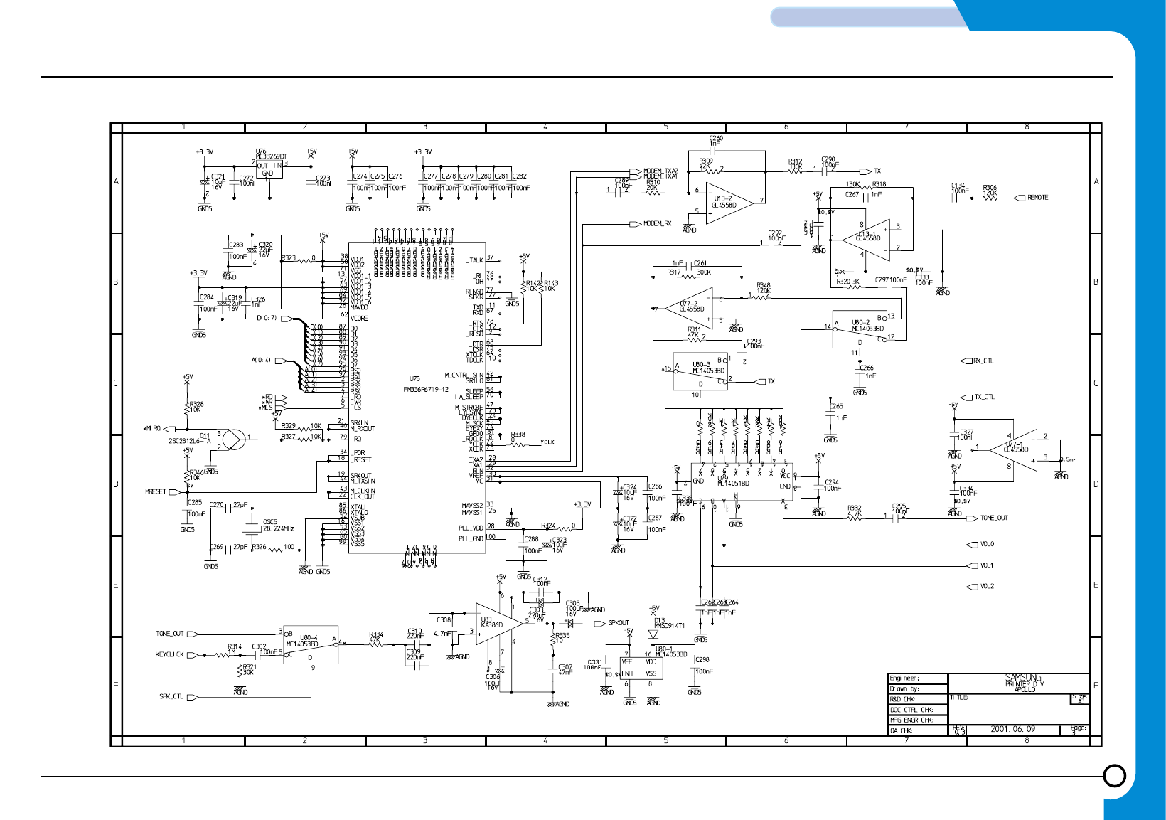
4-3
Samsung Electronics
SCHEMATIC DIAGRAMS
Repair Manual
4-3 Main Circuit Diagram (3/6)
APOLLO2(MAIN)
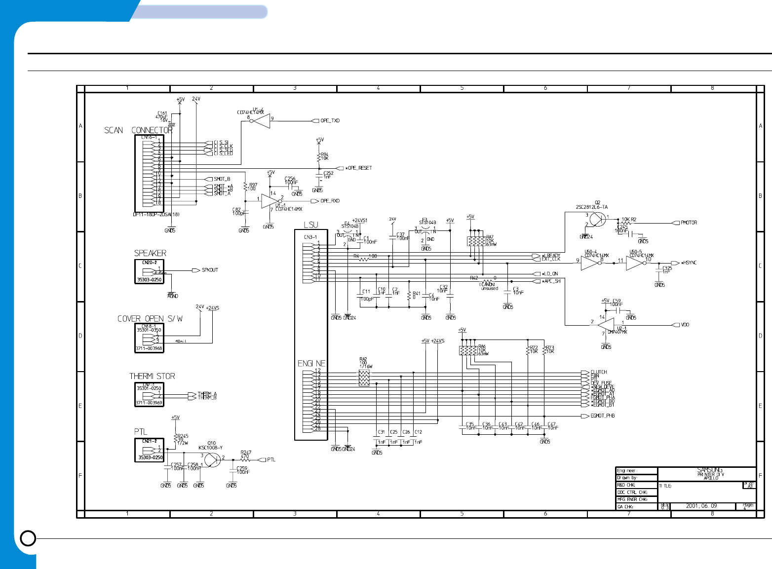
4-4
SCHEMATIC DIAGRAMS
Samsung Electronics
Repair Manual
4-4 Main Circuit Diagram (4/6)
APOLLO2(MAIN)
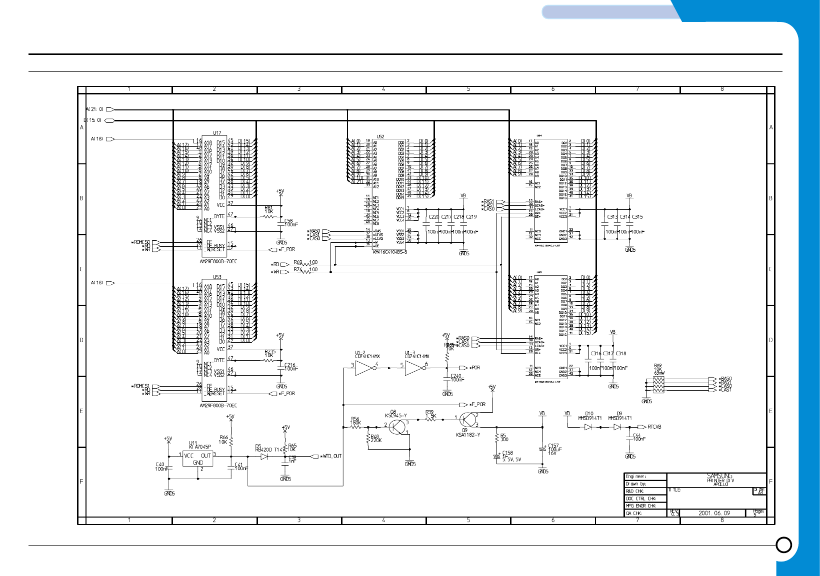
4-5
Samsung Electronics
SCHEMATIC DIAGRAMS
Repair Manual
4-5 Main Circuit Diagram (5/6)
APOLLO2(MAIN)
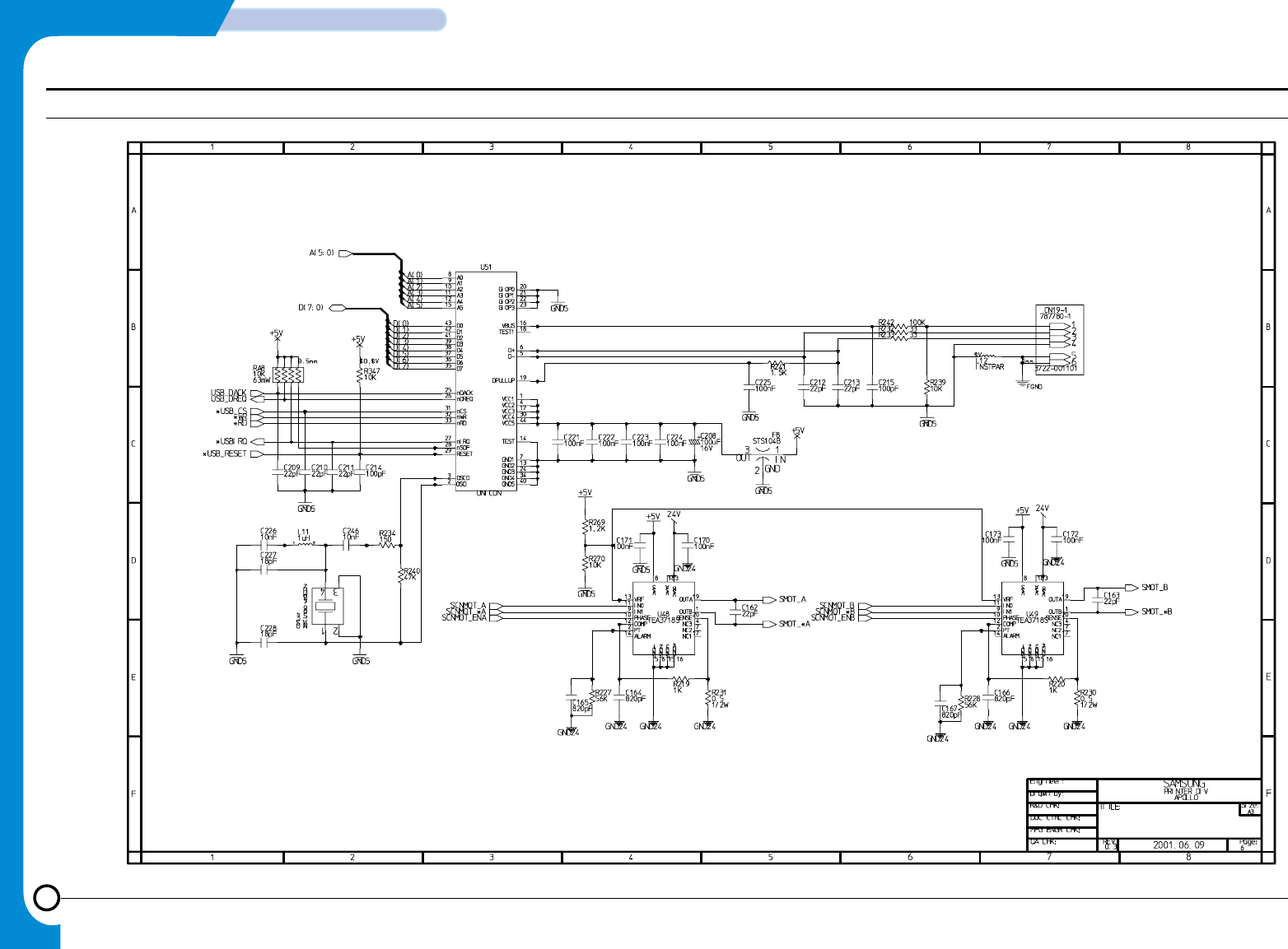
4-6
SCHEMATIC DIAGRAMS
Samsung Electronics
Repair Manual
4-6 Main Circuit Diagram (6/6)
APOLLO2(MAIN)
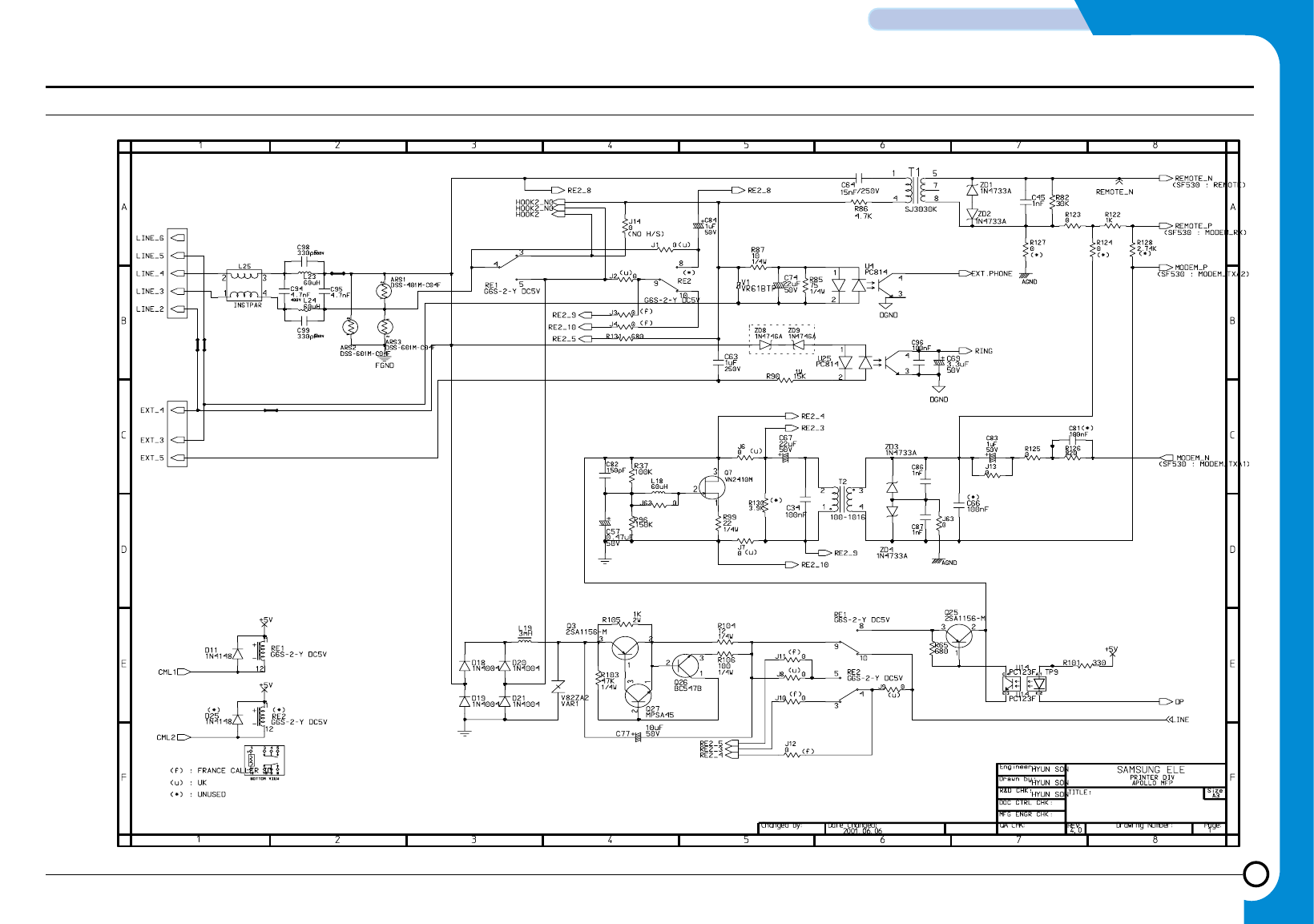
4-7
Samsung Electronics
SCHEMATIC DIAGRAMS
Repair Manual
4-7 LIU Circuit Diagram (1/2)
APOLLO2(LIU)
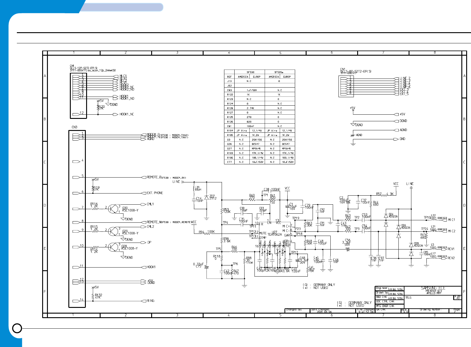
4-8
SCHEMATIC DIAGRAMS
Samsung Electronics
Repair Manual
4-8 LIU Circuit Diagram (2/2)
APOLLO2(LIU)
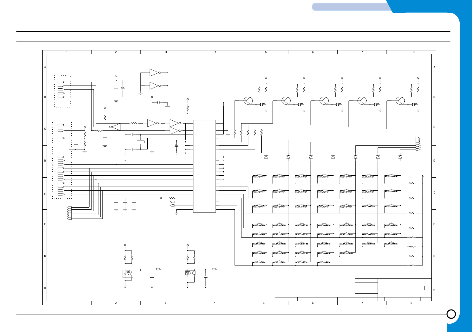
4-9
Samsung Electronics
SCHEMATIC DIAGRAMS
Repair Manual
4-9 OPE Circuit Diagram
14
1
6
5
11
07
STOP
Drawn by:
15
9
PAPER
/DELETE
>
ADVANCED FAX
SETUP
2.0
0
REDIAL
REPRINT
Page:
03
SAMSUNG ELECTRONICS
TITLE: Size:
05
02
18
17
DOC CTRL CHK:
Drawing Number:
TONER
POWER
3
13
04
08
START/
Date Changed:Changed by:
R&D CHK:
QA CHK:
TOLL PAPER POWER TONER E-MAIL
COPY/ SEARCHOHD/
09
10
RECALL
4 *
V-REQUEST
HELP
CONTRAST
19
8
7
#
Engineer:
MFG ENGR CHK:
REPORT/
<
2
16
E
Ho-Jin Park
Ho-Jin Park
Son-Hyun 1
12
REV:
20
RESOLUTION
Time Changed:
RCV-MODE/
E-MAIL
TOLL
01 06
R46
1
3
2
200
V17
Q5
KSA1182-Y
SLS-NNGR202TS
LED5
SW10 SW16
GND5
GND5
C1
100pF
10
P1 12
V15
GND5
P1
SW22
SW15
SW14
SW32
SW31
SW29
SW30
SW28
SW27
P1 14
SW26
13
P1 2
P1
3K
C18
220pF
R48
SW41
SW42
100nF
C6
35 _RESET
D6
MMSD914T1
21
TMR0
TMR1 34
48 TXD
36
VDD
VSS
19
37 XTAL1
XTAL2
38
_INT 20
NC3
13
NC4
14
NC5 39
40
NC6
NC7 41
42
NC8
47 RXD
SENSOR
2
LED2 4
3
LED3
LED4 46
45
LED5
LED6 44
43
LED7
NC1
11
NC2
12
LCD_D6
16
LCD_D7
15
LCD_D0
30
LCD_E
10
LCD_RS
8
9LCD_RW
LED0 6
5
LED1
27
KEY5
KEY6 28
29
KEY7
LCD_D1
31
LCD_D2
32
LCD_D3
33
18 LCD_D4
LCD_D5
17
U2
HT48R50
D_DET
1
D_SCAN
7
KEY0 22
23
KEY1
KEY2 24
25
KEY3
KEY4 26
+5V
GND5
R34
680
3K
R49
R36
22K
R7
22K
SW39
SW25 SW40
SW24
GND5
SW23
R3
22K
V3
SW6
SW4
V2
D1
MMSD914T1
SW11
22K
R4
R5
22K
13 12
P1 6
SLS-NNGR202TS
+5V
CD74HC14MX
U3
LED4
R47
200
SW53
GND5
200
R40
22K
R37
SW52
KSA1182-Y
1
3
2
C17
10uF
16V
Q2
22K
+5V
R9
GND5
+5V
R41
200
300
R21
SW34
SW5
2
GND5
SW33
D3
MMSD914T1
P1 7
+5V
R51
3K
SW48
GND5
SW47
+5V
GND5
+5V
GND5
LED3
SLS-NNGR202TS
R8
22K
+5V
GND5
CSA7.37MTZ-TF01
X1
GND5
D5
MMSD914T1
+5V
C14
100nF
SW37
SW38
SW36
3K
R15
SW44
SW19
SW18 SW21
SW20
R19
300
GND5
V16
22K
C5
100nF
P1 9
R2
6
U3
CD74HC14MX
11 10
+5V
U3
CD74HC14MX
5
220pF
C19
3
2
+5V
MMSD914T1
D7
200
KSA1182-Y
Q3
1
R42
200
GND5
V10
Q4
1
3
2
R44
GND5
KSA1182-Y
V11
V13
SW54
3
R22
300
P1 3
SW49
V12
SW12
SW3
14
2
V1
SW2
CD74HC14MX
U3
7
1
200R38
V4
2
SW7
KSA1182-Y
Q1
1
3
U3
CD74HC14MX
9
8
200
R45
100nF
C21
R50
+5V
+5V
3K
C16
47pF
R18
SW13
P1 11
300
GND5
SW1
R10
SLS-NNGR202TS
LED1
200 200
R11
SW45
MMSD914T1
D4
1
2
3
4
A
1
C
3
E
42
K
KPI-L05
U4
ITR-9702/F2
U5
GND5
+5V
C20
220pF
4
R1 200
GND5
P1
22K
R6
4
CN1
GILS-5P-S2T2-EF
1
MMSD914T1
D2
GND5
GND5
16V
10uF
C13
4
R35
10K
U3
CD74HC14MX
3
200
R43
V9
C12
100nF
22K
C15
47pF
P1 8
R39
P1 1
5
P1 5
KA2-14P8-2.54DSA
SW9
SW35
SW8
V14
GND5
+5V
SW43
SLS-NNGR202TS
LED2
D_SCAND_DET
SW17
D(5)
D(6)
D(5)
D(1)
D(0)
D_SCAN
D(1)
D(3)
D(6)
D_DET
D(0)
D(2)
D(4)
D(2)
D(3)
D(4)
APOLLO2 (OPE)
APOLLO2 (OPE)
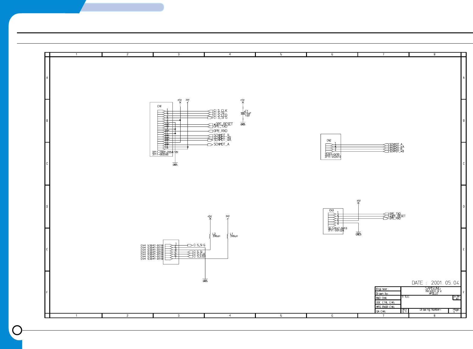
4-10
SCHEMATIC DIAGRAMS
Samsung Electronics
Repair Manual
4-10 Scan Circuit Diagram (200DPI)
APOLLO2(200DPI)
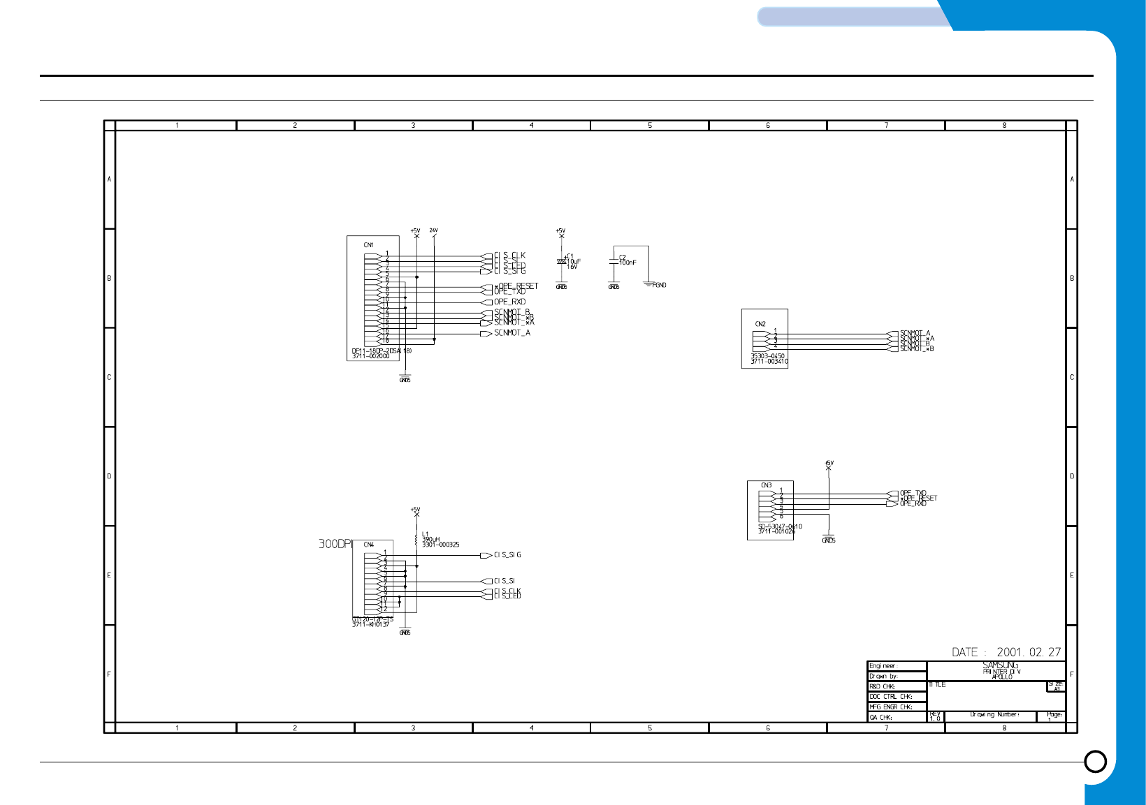
4-11
Samsung Electronics
SCHEMATIC DIAGRAMS
Repair Manual
4-11 Scan Circuit Diagram (300DPI)
APOLLO2(300DPI)
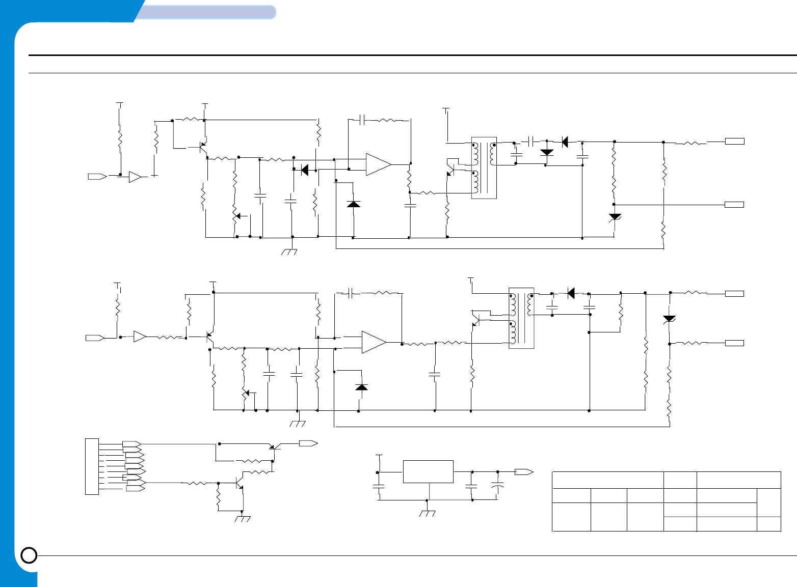
4-12
SCHEMATIC DIAGRAMS
Samsung Electronics
Repair Manual
4-12 HVPS Circuit Diagram (1/2)
R512
430
1
2
5V
24VS
R405
220KF
MHV-PWM
SIZE A4
U3
R503
100
ZD401
1W 130V
R416
MGR1/2W 15MF
R515
MGR1/2W 6MF
+
-
U1-C
KA324
10
9
8
D501
1N4148
R508
86.6KF
R504
2K
C405
2KV 680
OUT
R516
MGR1/2W 50K
+
C3
35V 47uF
D402
4KV
MHV
R505
100KF
VR501
50K
R514
MGR1/2W 15MF
DRW. NO
C501
104
R520
MGR1/2W 9MF
D-GND
18V
Q501
A708-Y
R502
2.2K
APPROVED
GND
R519
MGR1/2W 50K
R506
86.6KF
Q1
B1151-Y
REV.
IN
R513
1W 3
Q502
D526-Y
R510
47K
Q401
A708-Y
THV-EA
C403
333
5V
R422
5.6K
R2
1K
R401
100
THV-PWM
CHECKED
D502
4KV
R4
1W 1K
24VS
C404
3KV 471
Q402
D526-Y
R1
5.6K
DESIGNED
R410
1W 3
R509
12KF
D404
1N4148
R403
110KF
D401
4KV
+
-
U1-D
KA324
12
13
14
Q2
C1008-Y
R411
2.2K
DEV
THV-READ
R3
100
R414
MGR1/2W 6MF
T501
T1167
1
4
2
5
7
6
J.S.YOUN
C504
333
1 OF 2
R413
MGR1/2W 6MF
SUPPLY
18V
C503
104
2.0
D403
1N4148
C1
104
C402
103
R408
47K
T401
KAB-006
1
4
2
5
7
6
R507
27K
R409
430
U2-A
R407
240K
C408
104
MHV-PWM
OPC
C2
104
C506
3KV 471
18V
R501
5.6K
R402
56KF
CN1-#7
REF. NO
C401
331
5V
R517
MGR1/2W 6MF
C505
2KV 680
U2-B
BIAS-PWM
TITLE
R404
33K
A-GND
7407
C406
3KV 471
VR401
50K
BIAS-PWM
3
4
GIL-S-9P-S2T2-EF
CN1
1
2
3
4
5
6
7
8
9
CN1-#6 7407
24V
R518
MGR1/2W 9MF
R426
MGR1/2W 100KF
24VS
R511
47K
KA7818
C502
222
24VS
R406
2.2KF
ZD501
1W 200V
R417
MGR1/2W 15MF
R412
2K
DONGYANG INSTRUMENTS
APOLLO2 (HVPS)
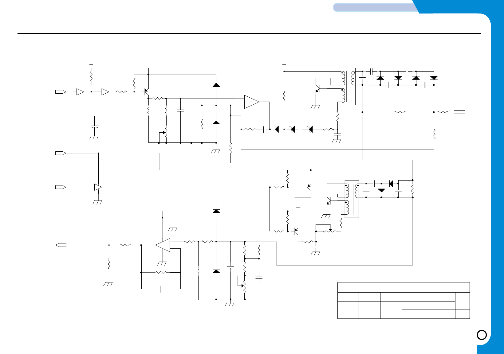
4-13
Samsung Electronics
SCHEMATIC DIAGRAMS
Repair Manual
4-13 HVPS Circuit Diagram (2/2)
C301
222
C4
104
APPROVED
R218
MGR1/2W 100KF
R309
2.2K
TITLE
18V
7407
R316
1KF
R211
1MF
VR302
5K
11 10
CHECKED
ZD202
7.5V
R305
6.2KF
CN1-#8
7407
+C101
35V 47uF
R304
200KF
DESIGNED
CN1-#4
R303
100KF
U2-E
Q302
A708-Y
+
-
U1-B
KA324
5
67
R314
3KF
R315
BR1/2W 30MJ
2 OF 2
CN1-#5
Q203
A708-Y
Q303
D526-Y
R215
430
D301
1N4148
R206
100
C207
6KV 471
THV-EA
R214
1.2K
R217
BR1/2W 200MG
5V
U2-F
R301
470K
R307
33K
C305
333
J.S.YOUN
D204
6KV
C209
6KV 471
R306
26.1KF
3.0
24VS
R216
BR1/2W 30MJ
VR301
10K
R311
100KF
7407
VR201
50K
D304
4KV
REV.
D201
1N4148
C308
3KV 471
D-GND
R209
110KF
ZD201
5.6V
THV
CN1-#3
Q301
A708-Y
C302
102
R205
1K
D202
1N4148
T201
HVT-2A
1
4
2
5
7
6
D303
4KV
C205
6KV 101
D302
1N4148
D203
1N4148
R210
510KF
C306
2KV 680
R201
10K D207
6KV
C208
6KV 471
C304
500V 103
13 12
C307
3KV 471
D206
6KV
R308
33K
SIZE A4
C203
472
+
-
U1-A
KA324
3
2
1
4
11
C201
103
5V
C303
333
THV-PWM
R317
2KF
R208
30KF
THV-READ
R212
470K
R207
2K
R213
2.2K
24VS
C202
331 1/2W
D205
6KV
REF. NO
U2-C
9 8
14
7
C206
6KV 471
18V
T301
KAB-006
1
4
2
5 6
7
24VS
R302
33K
500V
DRW. NO
18V
DONGYANG INSTRUMENTS
C204
473
Q204
D526-Y
R310
2.2K
APOLLO2 (HVPS)

Contents
Samsung Electronics
CONTENTS
1. Precautions . . . . . . . . . . . . . . . . . . . . . . . . . . . . . . . . . . . . . . . . . . . . . . . . . .1-1
1-1 Safety Precautions . . . . . . . . . . . . . . . . . . . . . . . . . . . . . . . . . . . . . . . . . .1-1
1-2 Precautions on Disassembly and Reassembly . . . . . . . . . . . . . . . . . . . .1-1
1-3 ESD Precautions . . . . . . . . . . . . . . . . . . . . . . . . . . . . . . . . . . . . . . . . . . .1-2
1-4 Tools for Troubleshooting . . . . . . . . . . . . . . . . . . . . . . . . . . . . . . . . . . . . .1-3
2. Specification . . . . . . . . . . . . . . . . . . . . . . . . . . . . . . . . . . . . . . . . . . . . . . . . .2-1
3. Disassembly and Reassembly . . . . . . . . . . . . . . . . . . . . . . . . . . . . . . . . . .3-1
3-1 General Precautions on Disassembly . . . . . . . . . . . . . . . . . . . . . . . . . . . .3-1
3-2 Cradle . . . . . . . . . . . . . . . . . . . . . . . . . . . . . . . . . . . . . . . . . . . . . . . . . . . .3-2
3-3 White Roller . . . . . . . . . . . . . . . . . . . . . . . . . . . . . . . . . . . . . . . . . . . . . . .3-2
3-4 OPE Cover . . . . . . . . . . . . . . . . . . . . . . . . . . . . . . . . . . . . . . . . . . . . . . . .3-3
3-5 ADF Rubber . . . . . . . . . . . . . . . . . . . . . . . . . . . . . . . . . . . . . . . . . . . . . . .3-5
3-6 OPE Board . . . . . . . . . . . . . . . . . . . . . . . . . . . . . . . . . . . . . . . . . . . . . . . .3-6
3-7 Lever Sensor Doc. . . . . . . . . . . . . . . . . . . . . . . . . . . . . . . . . . . . . . . . . . .3-6
3-8 Lever Sensor Scan . . . . . . . . . . . . . . . . . . . . . . . . . . . . . . . . . . . . . . . . . .3-6
3-9 Scan Board . . . . . . . . . . . . . . . . . . . . . . . . . . . . . . . . . . . . . . . . . . . . . . . .3-7
3-10 Scan Motor . . . . . . . . . . . . . . . . . . . . . . . . . . . . . . . . . . . . . . . . . . . . . . . .3-7
3-11 ADF Roller . . . . . . . . . . . . . . . . . . . . . . . . . . . . . . . . . . . . . . . . . . . . . . . .3-8
3-12 CIS . . . . . . . . . . . . . . . . . . . . . . . . . . . . . . . . . . . . . . . . . . . . . . . . . . . . . .3-8
3-13 Rear Cover . . . . . . . . . . . . . . . . . . . . . . . . . . . . . . . . . . . . . . . . . . . . . . . .3-9
3-14 Top Cover . . . . . . . . . . . . . . . . . . . . . . . . . . . . . . . . . . . . . . . . . . . . . . . . .3-9
3-15 Tray . . . . . . . . . . . . . . . . . . . . . . . . . . . . . . . . . . . . . . . . . . . . . . . . . . . . . .3-10
3-16 LSU . . . . . . . . . . . . . . . . . . . . . . . . . . . . . . . . . . . . . . . . . . . . . . . . . . . . . .3-10
3-17 Transfer Roller . . . . . . . . . . . . . . . . . . . . . . . . . . . . . . . . . . . . . . . . . . . . .3-11
3-18 Engine Board . . . . . . . . . . . . . . . . . . . . . . . . . . . . . . . . . . . . . . . . . . . . . .3-11
3-19 Pick-up Roller Ass'y . . . . . . . . . . . . . . . . . . . . . . . . . . . . . . . . . . . . . . . . .3-12
3-20 Knock-up Ass'y . . . . . . . . . . . . . . . . . . . . . . . . . . . . . . . . . . . . . . . . . . . . .3-13
3-21 Cap-pad . . . . . . . . . . . . . . . . . . . . . . . . . . . . . . . . . . . . . . . . . . . . . . . . . .3-13
3-22 Holder-pad . . . . . . . . . . . . . . . . . . . . . . . . . . . . . . . . . . . . . . . . . . . . . . . .3-14
3-23 Motor Ass'y . . . . . . . . . . . . . . . . . . . . . . . . . . . . . . . . . . . . . . . . . . . . . . . .3-14
3-24 Fan . . . . . . . . . . . . . . . . . . . . . . . . . . . . . . . . . . . . . . . . . . . . . . . . . . . . . .3-15
3-25 Gear Pick-up Ass'y . . . . . . . . . . . . . . . . . . . . . . . . . . . . . . . . . . . . . . . . . .3-15
3-26 Solenoid . . . . . . . . . . . . . . . . . . . . . . . . . . . . . . . . . . . . . . . . . . . . . . . . . .3-16
3-27 HVPS Board . . . . . . . . . . . . . . . . . . . . . . . . . . . . . . . . . . . . . . . . . . . . . . .3-16
3-28 Hook Board . . . . . . . . . . . . . . . . . . . . . . . . . . . . . . . . . . . . . . . . . . . . . . . .3-17
3-29 Fuser Ass'y . . . . . . . . . . . . . . . . . . . . . . . . . . . . . . . . . . . . . . . . . . . . . . . .3-17
3-30 Thermostat . . . . . . . . . . . . . . . . . . . . . . . . . . . . . . . . . . . . . . . . . . . . . . . .3-18
3-31 Halogen Lamp . . . . . . . . . . . . . . . . . . . . . . . . . . . . . . . . . . . . . . . . . . . . .3-18
3-32 Pressure Roller . . . . . . . . . . . . . . . . . . . . . . . . . . . . . . . . . . . . . . . . . . . . .3-19
3-33 Actuator-Exit . . . . . . . . . . . . . . . . . . . . . . . . . . . . . . . . . . . . . . . . . . . . . . .3-19
3-34 Shield Engine Ass'y . . . . . . . . . . . . . . . . . . . . . . . . . . . . . . . . . . . . . . . . .3-20
3-34 SMPS Board . . . . . . . . . . . . . . . . . . . . . . . . . . . . . . . . . . . . . . . . . . . . . . .3-20
3-36 Speaker . . . . . . . . . . . . . . . . . . . . . . . . . . . . . . . . . . . . . . . . . . . . . . . . . .3-21
3-37 LIU Board . . . . . . . . . . . . . . . . . . . . . . . . . . . . . . . . . . . . . . . . . . . . . . . . .3-21
3-38 Main Board . . . . . . . . . . . . . . . . . . . . . . . . . . . . . . . . . . . . . . . . . . . . . . . .3-22
3-39 Sensor Board . . . . . . . . . . . . . . . . . . . . . . . . . . . . . . . . . . . . . . . . . . . . . .3-22
3-40 Actuator Empty/Feeder . . . . . . . . . . . . . . . . . . . . . . . . . . . . . . . . . . . . . . .3-23
3-41 Roller Feeder . . . . . . . . . . . . . . . . . . . . . . . . . . . . . . . . . . . . . . . . . . . . . .3-24

Contents
Samsung Electronics
4. Troubleshooting . . . . . . . . . . . . . . . . . . . . . . . . . . . . . . . . . . . . . . . . . . . . . .4-1
4-1 Preventative Maintenance . . . . . . . . . . . . . . . . . . . . . . . . . . . . . . . . . . . .4-1
4-2 Tech Mode . . . . . . . . . . . . . . . . . . . . . . . . . . . . . . . . . . . . . . . . . . . . . . . .4-1
4-2-1 System Data List in TECH MODE . . . . . . . . . . . . . . . . . . . . . . . . . .4-2
4-2-2 Tech Mode Options . . . . . . . . . . . . . . . . . . . . . . . . . . . . . . . . . . . . . .4-3
4-2-3 Maintenance Options . . . . . . . . . . . . . . . . . . . . . . . . . . . . . . . . . . . .4-4
4-2-4 Printout Report . . . . . . . . . . . . . . . . . . . . . . . . . . . . . . . . . . . . . . . . .4-6
4-2-5 Engine Test Mode . . . . . . . . . . . . . . . . . . . . . . . . . . . . . . . . . . . . . . .4-6
4-2-6 Maintenance List . . . . . . . . . . . . . . . . . . . . . . . . . . . . . . . . . . . . . . . .4-7
4-3 Diagnostics . . . . . . . . . . . . . . . . . . . . . . . . . . . . . . . . . . . . . . . . . . . . . . . .4-8
4-3-1 Error Messages . . . . . . . . . . . . . . . . . . . . . . . . . . . . . . . . . . . . . . . . .4-8
4-4 Print Quality . . . . . . . . . . . . . . . . . . . . . . . . . . . . . . . . . . . . . . . . . . . . . . .4-10
4-5 Note for replacing Main board . . . . . . . . . . . . . . . . . . . . . . . . . . . . . . . . . .4-10
4-6 Troubleshooting Flow Chart . . . . . . . . . . . . . . . . . . . . . . . . . . . . . . . . . . .4-11
5. Exploded Views and Parts List . . . . . . . . . . . . . . . . . . . . . . . . . . . . . . . . . .5-1
5-1 Main Assembly . . . . . . . . . . . . . . . . . . . . . . . . . . . . . . . . . . . . . . . . . . . . .5-2
5-2 Shield Engine Unit Assembly . . . . . . . . . . . . . . . . . . . . . . . . . . . . . . . . . .5-4
5-3 Engine Assembly . . . . . . . . . . . . . . . . . . . . . . . . . . . . . . . . . . . . . . . . . . .5-6
5-4 Frame Lower Assembly . . . . . . . . . . . . . . . . . . . . . . . . . . . . . . . . . . . . . .5-8
5-5 Fuser Assembly . . . . . . . . . . . . . . . . . . . . . . . . . . . . . . . . . . . . . . . . . . . .5-10
5-6 Plate-Upper Unit Assembly . . . . . . . . . . . . . . . . . . . . . . . . . . . . . . . . . . . .5-12
5-7 OPE Unit . . . . . . . . . . . . . . . . . . . . . . . . . . . . . . . . . . . . . . . . . . . . . . . . . .5-14
5-8 Scan Upper Assembly . . . . . . . . . . . . . . . . . . . . . . . . . . . . . . . . . . . . . . .5-15
5-9 Front Assembly . . . . . . . . . . . . . . . . . . . . . . . . . . . . . . . . . . . . . . . . . . . .5-16
5-10 RX Drive Unit Assembly . . . . . . . . . . . . . . . . . . . . . . . . . . . . . . . . . . . . . .5-18
6. Block Diagram . . . . . . . . . . . . . . . . . . . . . . . . . . . . . . . . . . . . . . . . . . . . . . . .6-1
7. Connection Diagram . . . . . . . . . . . . . . . . . . . . . . . . . . . . . . . . . . . . . . . . . . .7-1
