SMA2503_GUI_User_Manual_Rev0.0.0x SMA2503 GUI User Manual Rev0.0.0
User Manual:
Open the PDF directly: View PDF ![]() .
.
Page Count: 30
© 2018 Silicon Mitus, Inc. www.siliconmitus.com
September 2018 – Rev0.0.0 1 / 30
GUI User Manual
Revision 0.0.0
*Technology by
GUI User Manual
www.siliconmitus.com © 2018 Silicon Mitus, Inc.
2 / 30 September 2018 – Rev0.0.0
1. Purpose
Graphic User Interface (GUI) is a software program that verifies and tests the function of the Silicon Mitus product. This
document is based on SMA2503 GUI.
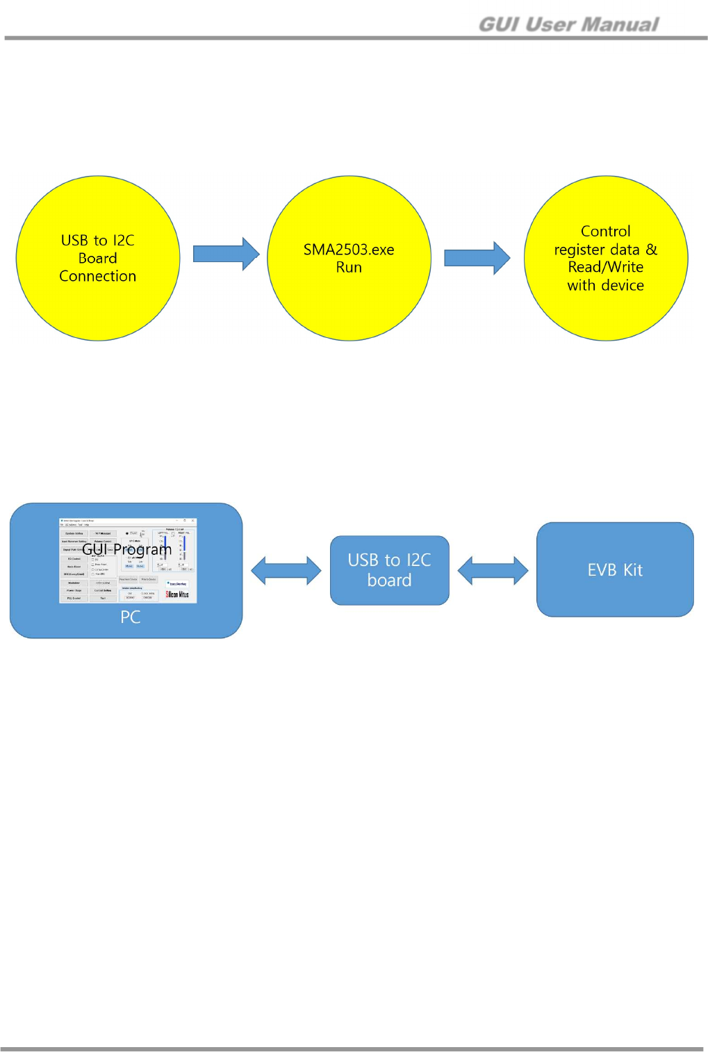
Figure 1. Active Flow
The Silicon Mitus evaluation system has an I2C port, so the user can control the action via the GUI program. The diagram
below describes the connection for the Silicon Mitus evaluation system using the GUI Program with test equipment, USB to
I2C Board, PC, USB cable and Silicon Mitus Evaluation Board (EVB) Kit.
Figure 2. Connection Diagram
GUI User Manual
© 2018 Silicon Mitus, Inc. www.siliconmitus.com
September 2018 – Rev0.0.0 3 / 30
2. Installation
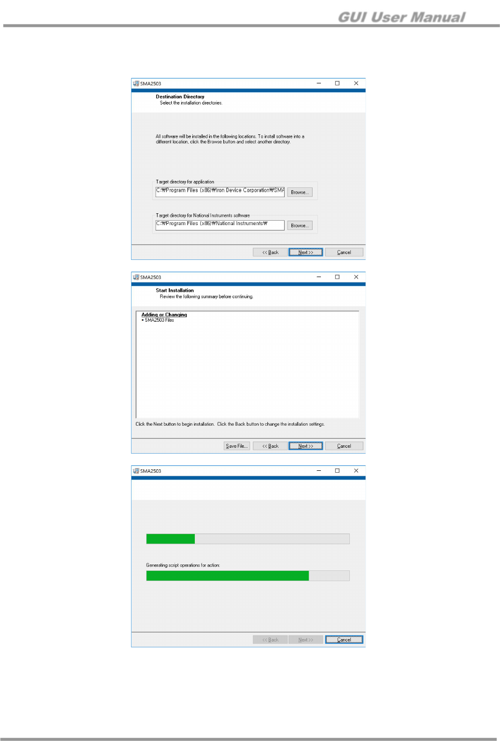
Unzip SMA2503_Control_Panel.zip to a local PC. To install the program, run “Setup.exe” file.
GUI User Manual
www.siliconmitus.com © 2018 Silicon Mitus, Inc.
4 / 30 September 2018 – Rev0.0.0
Installation Path
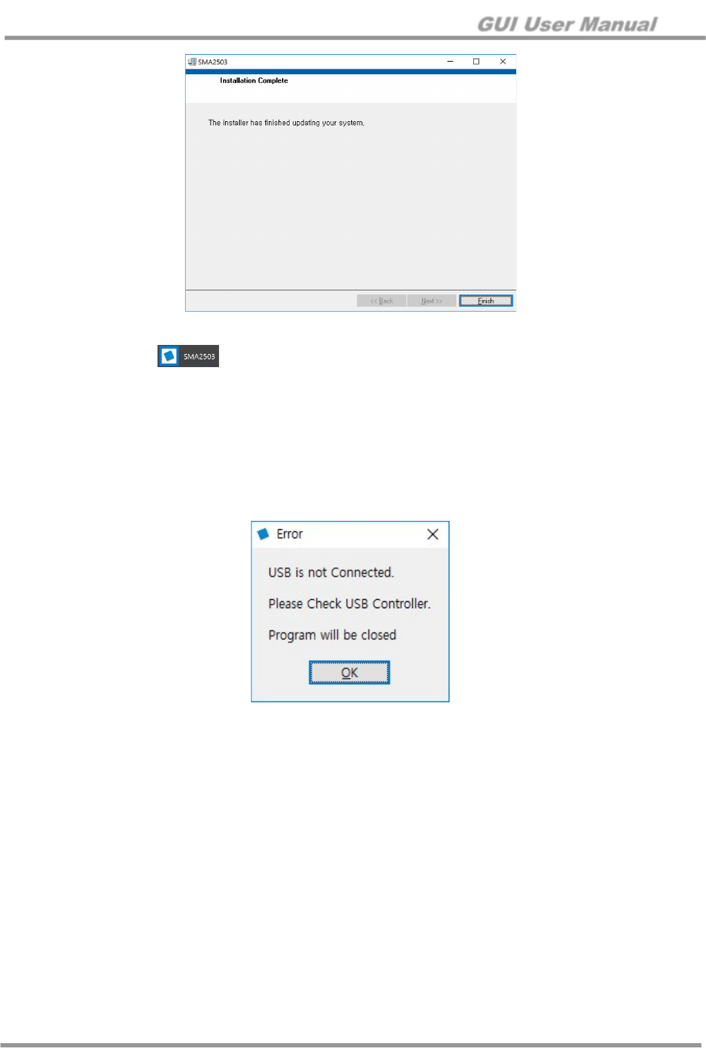
1. Windows Start → Click “ “ SMA2503
2. C:\Program Files (x86)\Iron Device Corporation\SMA2503 folder. Run with SMA2503.exe
3. Device Configuration
Connect ‘USB to I2C Board’ to the Evaluation Board Kit.
1. Run SMA2503 GUI Program
2. If the USB to I2C Board is not connected normally, an error message pop-up window will appear.
Figure 3. Error Message Pop-up
GUI User Manual
© 2018 Silicon Mitus, Inc. www.siliconmitus.com
September 2018 – Rev0.0.0 5 / 30
4. Board Manual
4.1 Introduction
The SMA2503 Evaluation (EV) Board is a demonstration and evaluation board that shows the capabilities and features
of SMA2503 chipset designed by Silicon Mitus (Iron Device). This board has an I2S interface for digital. Implementation
of an amplifier with 2 x 150 W at 4 Ω (BTL mode) on four layers PCB.
4.2 Board Package Content
The SMA2503 EV Board package includes the following:
1. SMA2503 EV Board
2. USB to I2C Control Board
3. Cable set to connect the board in lab conditions.
4. Control S/W (Released by e-mail. Please contact Silicon Mitus separately.)
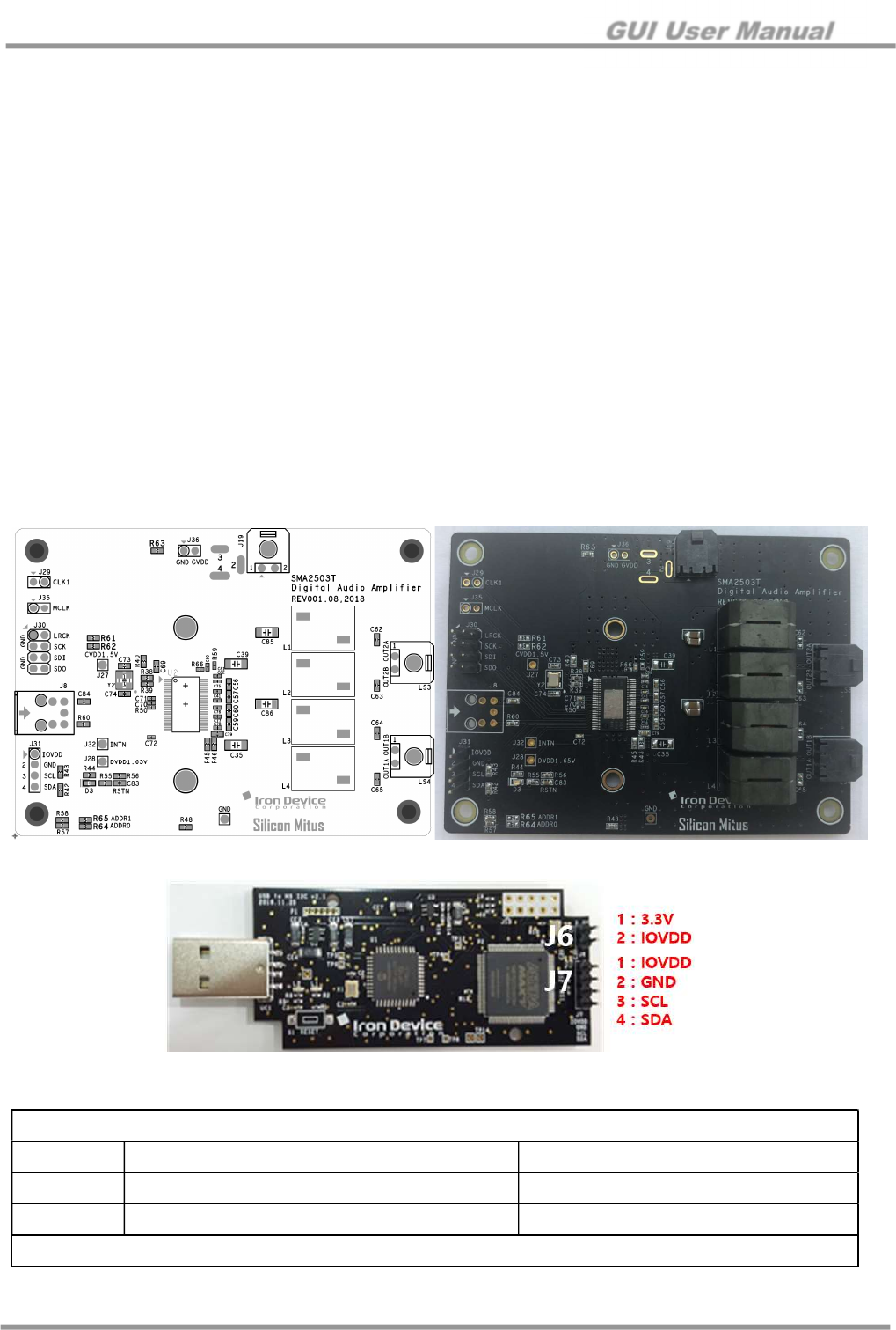
4.3 EV Board Overview
Figure 4. SMA2503-T EV Board Placement and EV Board
Figure 5. USB to High Speed I2C Control Board
Type: 2.54 mm Pitch Pin Header for J6
Pin Description Value
1 3.3 V LDO Output +3.3 V
2 IOVDD IOVDD
Connect Pin 1 and Pin 2 if IO voltage is +3.3 V

GUI User Manual
www.siliconmitus.com © 2018 Silicon Mitus, Inc.
6 / 30 September 2018 – Rev0.0.0
Type: 2.54 mm Pitch Pin Header for J7
Pin Description Value
1 IOVDD IOVDD (+3.3 V)
2 GND GND
3 SCL 0 V to +3.3 V
4 SDA 0 V to +3.3 V
GUI User Manual
© 2018 Silicon Mitus, Inc. www.siliconmitus.com
September 2018 – Rev0.0.0 7 / 30
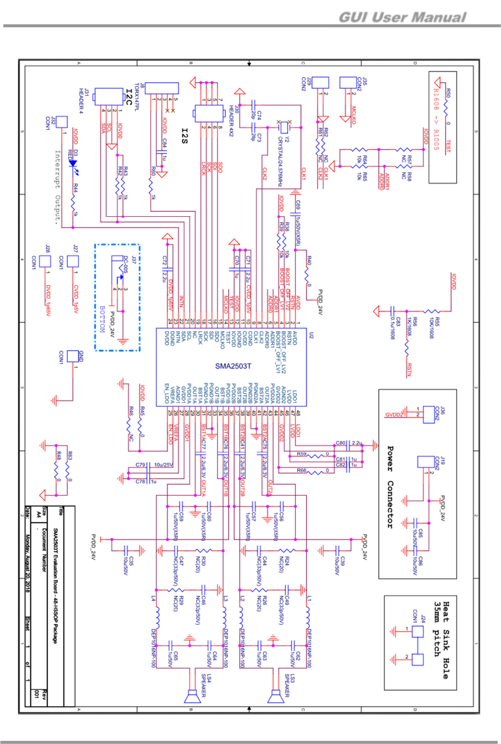
4.4 Board Schematic
Figure 6. SMA2503-T EV Board Schematic
GUI User Manual
www.siliconmitus.com © 2018 Silicon Mitus, Inc.
8 / 30 September 2018 – Rev0.0.0
4.5 Connectors
J19[SMA2503-T]: Power Stage and Analog Power Supply
LS4[SMA2503-T]: Left Speaker Output
LS3[SMA2503-T]: Right Speaker Output
J31[SMA2503-T]: I2C Control Pin
J30[SMA2503-T]: I2S Input Port
J29[SMA2503-T]: External Clock(MCLK) Input
J35[SMA2503-T]: Master Clock(MCLKO) Output
Type: Micro-Fit 3.0™ Right Angle Header (43650-0200, Molex)
Pin Description Value
1 PGND GND
2 PVDD Maximum +40 V / 8.5 A
Type: Micro-Fit 3.0™ Right Angle Header (43650-0200, Molex)
Pin Description Value
1 SPK Output1 P Maximum +40 V
2 SPK Output1 N Maximum +40 V
Type: Micro-Fit 3.0™ Right Angle Header (43650-0200, Molex)
Pin Description Value
1 SPK Output2 N Maximum +40 V
2 SPK Output2 P Maximum +40 V
Type: 2.54 mm Pitch Pin Header
Pin Description Value
1 IOVDD 0 V to +3.3 V
2 GND GND
3 SCL 0 V to +3.3 V
4 SDA 0 V to +3.3 V
Type: 2.54 mm Pitch Pin Header
Pin Description Value
1, 3, 5, 7 GND GND
2 LRCK 0 V to +3.3 V
4 SCK 0 V to +3.3 V
6 SDI (input data from source) 0 V to +3.3 V
8 SDO (output data from chipset) 0 V to +3.3 V
Type: 2.54 mm Pitch Pin Header
Pin Description Value
1 GND GND
2 MCLK 24.576MHz
Type: 2.54 mm Pitch Pin Header

GUI User Manual
© 2018 Silicon Mitus, Inc. www.siliconmitus.com
September 2018 – Rev0.0.0 9 / 30
Pin Description Value
1 GND GND
2 MCLKO 24.576MHz
GUI User Manual
www.siliconmitus.com © 2018 Silicon Mitus, Inc.
10 / 30 September 2018 – Rev0.0.0
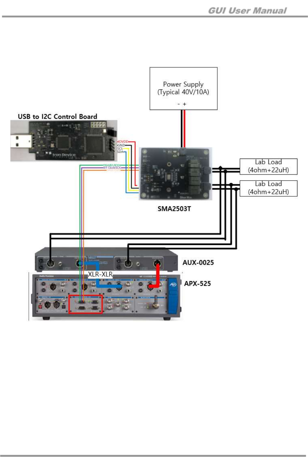
4.6 Measurement Set Up (APX525)
This set up is for the evaluation of SMA2503. Reference equipment is APX-525 from Audio Precision.
4.6.1 Connection
Figure 7. Measurement Connection (I2S input)
GUI User Manual
© 2018 Silicon Mitus, Inc. www.siliconmitus.com
September 2018 – Rev0.0.0 11 / 30
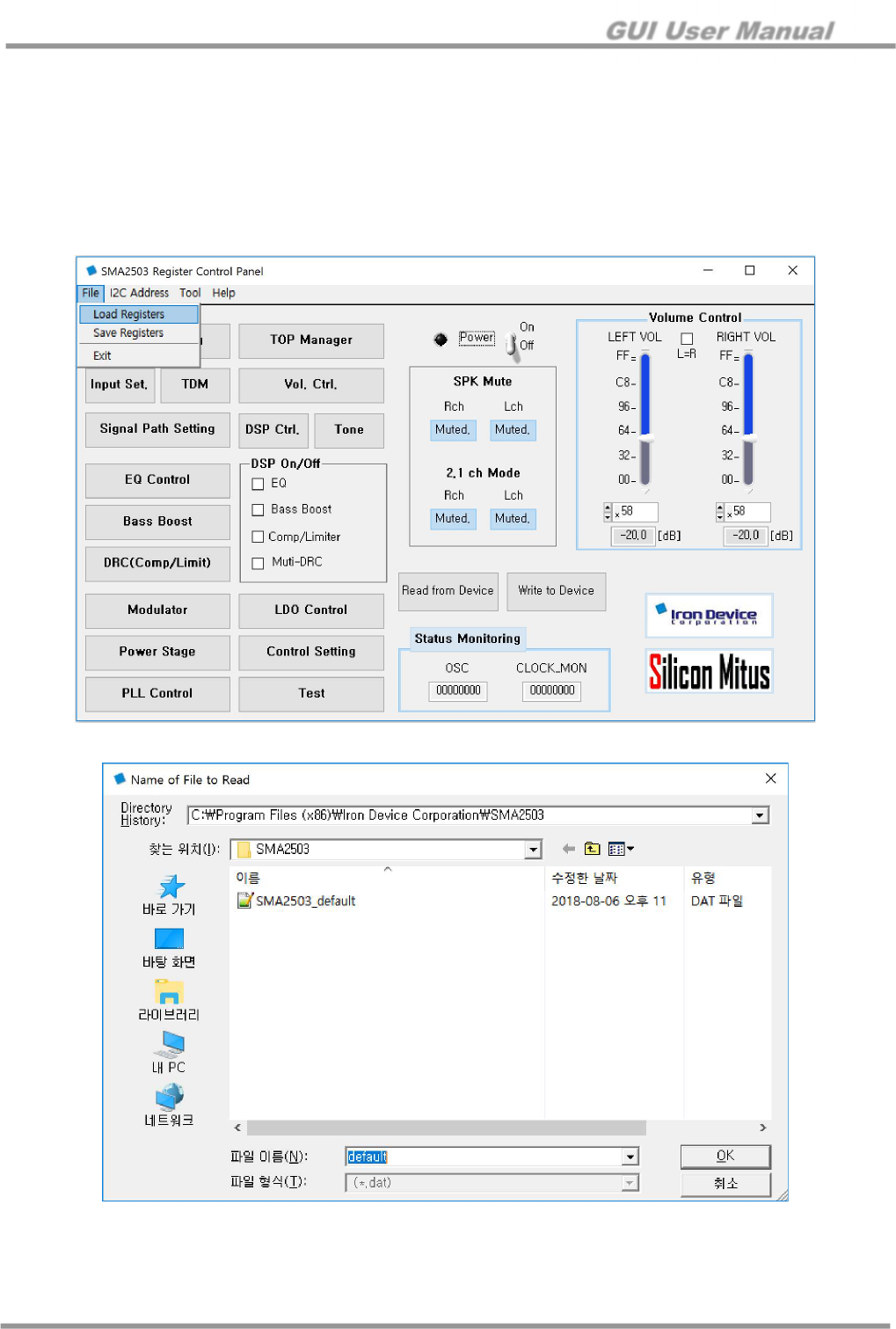
4.6.2 Control S/W (GUI) – Quick Start (Register File Download)
This is a quick start initiated by downloading the device register file. Test steps are as the following:
1. Setup the H/W connection, and use the register file for device operation
2. Install SMA2503 Control Panel, and run SMA2503.exe
3. Click on “Load Registers” from “File”
4. Select the provided register file (.dat) for device operation
5. The device on the EVB will run
6. You can control other functionalities as desired
Figure 8. Loading Register File
Figure 9. Selecting Register File
GUI User Manual
www.siliconmitus.com © 2018 Silicon Mitus, Inc.
12 / 30 September 2018 – Rev0.0.0
5. Detail Controls
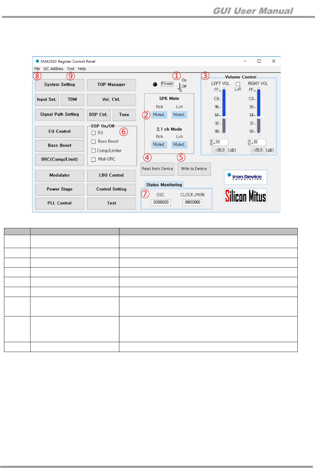
5.1 Control Panel Overview (Main Panel)
Figure 10. SMA2503 Register Control Panel
No. Item Description
①
Power On/Off with Sequence Power On: Power-up Speaker Output On De-mute
Power Off: Mute Speaker Output Off Power Off
②
Mute Control Mute and De-mute Control
③
Volume Control Master Volume Control
④
Read from Device Read I2C from DUT and Set Panel
⑤
Write to Device Read Set Value from Panels and Write to DUT
⑥
DSP On/Off DSP block on/off – this is the same control at Signal Setting Panel
⑦
Status Monitoring
Click on “Status Monitoring”
Reads status register and updates display every 0.2 seconds
Stops monitoring when clicked again
⑧
Menu Bar – File
Load Register: Register Load from .dat file
Save Register: Register Save to .dat file and .datx file
Export Filter Parameters: Structure of coefficients for C file to .datx
file
⑨
Menu Bar – Tool Direct Register Control Panel – Open Direct Register Control Panel

GUI User Manual
© 2018 Silicon Mitus, Inc. www.siliconmitus.com
September 2018 – Rev0.0.0 13 / 30
5.2 Initialization
5.2.1 System CLK
1. System Setting Panel
2. Select the System CLK depending on the system
- Internal OSC using an internal oscillator
- Crystal OSC (24.576 MHz)
- Ext. CLK 19.2 MHz: External clock with IOVDD Level
- Ext. CLK 24.576 MHz: External clock with IOVDD Level
5.2.2 CVDD EN (Clock VDD)
1. LDO Control Panel
- LDO_CVDD Enable: Enable
5.2.2 Change the Default Value (these values were tuned)
1. Power Stage Panel
- FLT_VDD_GAIN: b’01111 to b’00101
- Dead time HS: b’0010 to b’0001
- Dead time LS: b’0010 to b’0110
- Slope Control HS: b’10 to b’01
- Slope Control LS: b’10 to b’00
2. Feedback Control
- SPK_BDELAY: b’100000 to b’011101
5.2.2 Input Mode Selection
1. Case 1) I2S (fs = 48 kHz): Using Default Value
2. Case 2) I2S (fs = 192 kHz)
- Use a PLL setting
- Or use Down Conversion
Top Management Panel
DAC Down Conversion: Down Conversion
GUI User Manual
www.siliconmitus.com © 2018 Silicon Mitus, Inc.
14 / 30 September 2018 – Rev0.0.0
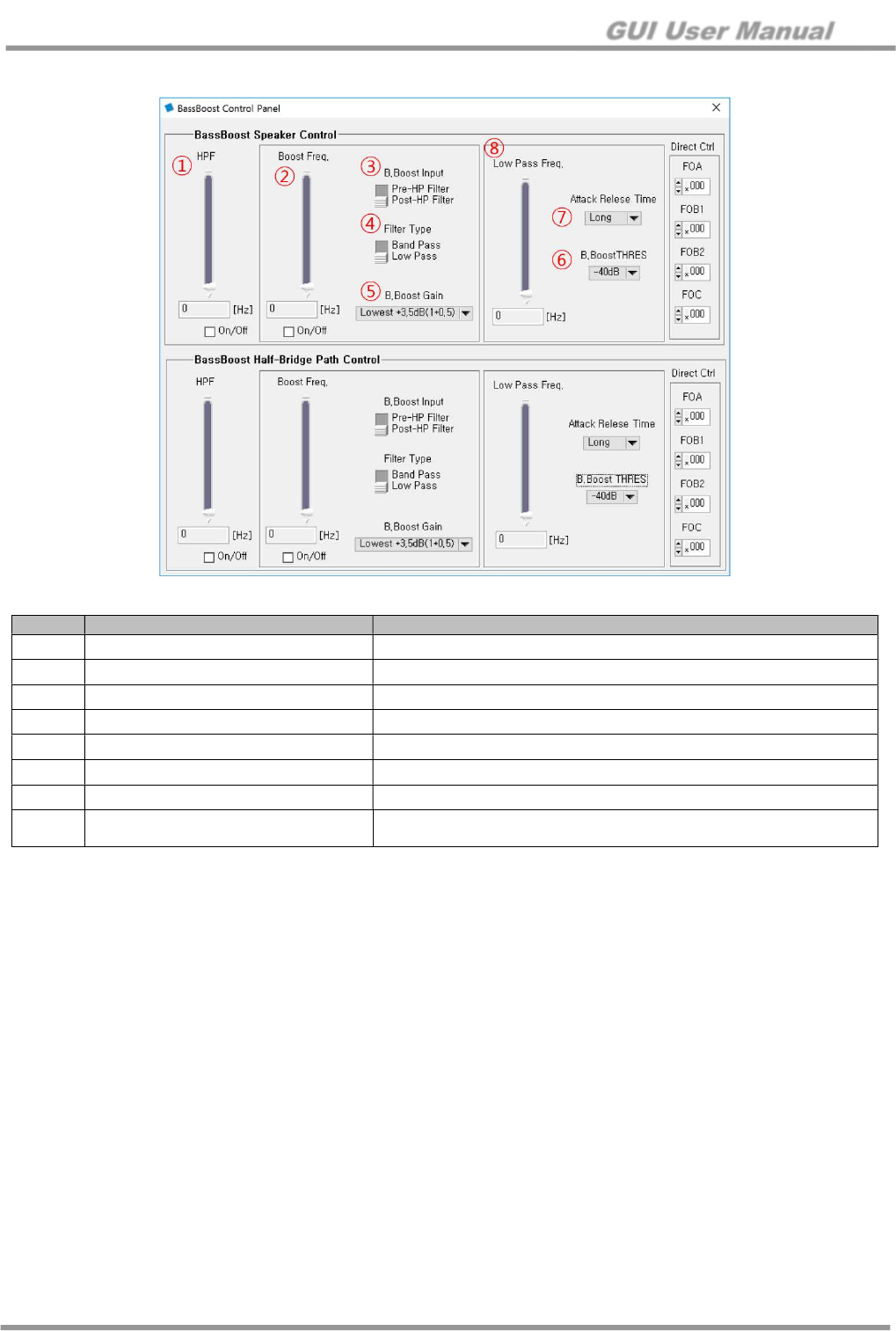
5.3 BassBoost
Figure 11. BassBoost Control Panel
No. Item Description
①
HPF Frequency 1st Order High Pass Filter Frequency Setting. “0” is off
②
Boost Frequency Boost Frequency Setting: 20 Hz to 1 kHz
③
B.Boost Input Select input of Bass Boost Block (Pre or Post HPF)
④
Filter Type Band Pass Filter or Low Pass Filter Type
⑤
B.Boost Gain Bass Boost Gain Setting
⑥
B.BoostTHRES (Boost Trigger) Set the starting limit of Bass Boost
⑦
Attack Release Time (Boost Trigger) Set the attack/release time limit of Bass Boost
⑧
Low Pass Frequency (Boost Trigger) Low pass filter of the signal that controls the attack release function
Should be set above boost frequency
GUI User Manual
© 2018 Silicon Mitus, Inc. www.siliconmitus.com
September 2018 – Rev0.0.0 15 / 30
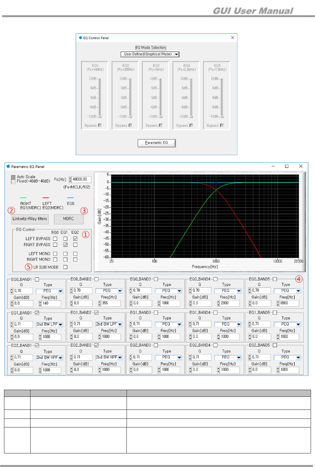
5.4 EQ Control
Figure 12. Parametric EQ Panel
No. Item Description
①
EQ There are three EQ BANKs in cascade
EQ is bypassed if checked
②
Linkwitz-Riley filters Open Linkwitz-Riley filter panel and pre-set
③
MDRC Open MDRC panel and pre-set for MDRC
④
EQ Band
Q Factor
Biquad Filter Type
PEQ
2nd BW (Butter Worth) HPF

GUI User Manual
www.siliconmitus.com © 2018 Silicon Mitus, Inc.
16 / 30 September 2018 – Rev0.0.0
2
nd
BW (Butter Worth) LPF
LSF (Low Shelf Filter)
HSF (High Shelf Filter)
Piezo Tune
Notch
Gain
-20 dB to +20 dB
Frequency
20 Hz to 20 kHz
Check Box
Checked: On
⑤
LR SUB MODE Test purpose register
GUI User Manual
© 2018 Silicon Mitus, Inc. www.siliconmitus.com
September 2018 – Rev0.0.0 17 / 30
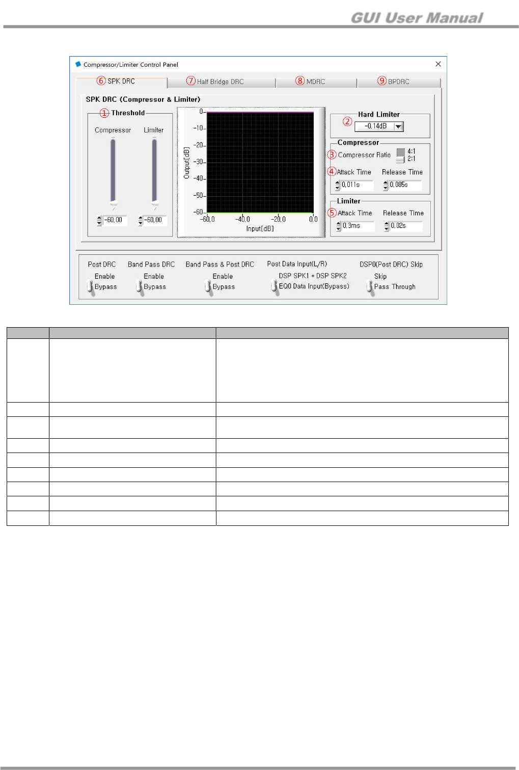
5.5 DRC (Comp/Limit)
Figure 13. Compressor/Limiter Control Panel
No. Item Description
①
Threshold
Compressor Threshold
Maximum high level: - 0.1 dB
Compressor off: 0.0 dB
Limiter Threshold
Maximum high level: - 0.3 dB
Limiter off: 0.0 dB
②
Hard Limiter Clip the signal when it exceeds the threshold
③
Compressor Compressor Ratio
Amount of compression
④
Attack / Release Time for Compressor
Attack / Release Time
⑤
Attack / Release Time for Limiter Attack / Release Time
⑥
SPK DRC Compressor/Limiter setting for speaker path
⑦
Half Bridge DRC Compressor/Limiter setting for half-bridge path
⑧
MDRC Compressor/Limiter setting for speaker multi-band
⑨
BPDRC Compressor/Limiter setting for speaker band-pass post

GUI User Manual
www.siliconmitus.com © 2018 Silicon Mitus, Inc.
18 / 30 September 2018 – Rev0.0.0
5.6 2-Way Speaker – Mono (use L-R filter)
Figure 14. LR Filter Control Panel
5.6.1 Signal Mono Set
1. Signal Path Setting
- Mono Mix: On
2. EQ Setting
- Main Panel
DSP EQ: Check
- Linkwitz-Riley Filter Set
No. Item Description
①
LR Filter Order Recommended 4th Order
②
Type HPF: EQ for Tweeter
LPF: EQ for Woofer
③
LR Filter Frequency Cross Over Frequency Set
GUI User Manual
© 2018 Silicon Mitus, Inc. www.siliconmitus.com
September 2018 – Rev0.0.0 19 / 30
5.7 2.1ch Mode
Figure 15. Power Stage Control Panel for 2.1ch
5.7.1 Mode Control
No. Item Description
①
Mode Control 1 x BTL + 2 x SE
GUI User Manual
www.siliconmitus.com © 2018 Silicon Mitus, Inc.
20 / 30 September 2018 – Rev0.0.0
5.7.2 System Setting
Figure 16. System Setting for 2.1ch
5.7.3 H/W Connection
1. Left Output: BTL mode – Woofer
2. Right Output: SE mode – Left/Right
No. Item Description
①
Speaker Mode Mono signal at left terminals
②
Half Bridge Path Mode Stereo
GUI User Manual
© 2018 Silicon Mitus, Inc. www.siliconmitus.com
September 2018 – Rev0.0.0 21 / 30
5.8 DOUT (SDO)
5.8.1 I2S Input to DOUT (SDO)
1. TOP Manager Panel
- Master Mode: Master Mode Selection
2. Signal Path Setting Panel
- Port Config: OUT: Port3, IN: Port1, 2
- Port Select: (See Figure 20. Signal Path Setting)
Figure 17. TOP Manager Panel for I2S Input to DOUT
GUI User Manual
www.siliconmitus.com © 2018 Silicon Mitus, Inc.
22 / 30 September 2018 – Rev0.0.0
6. Other Control Panels
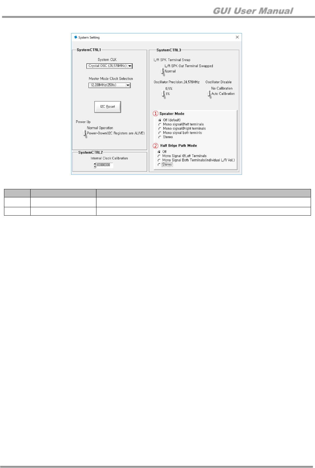
6.1 System Setting
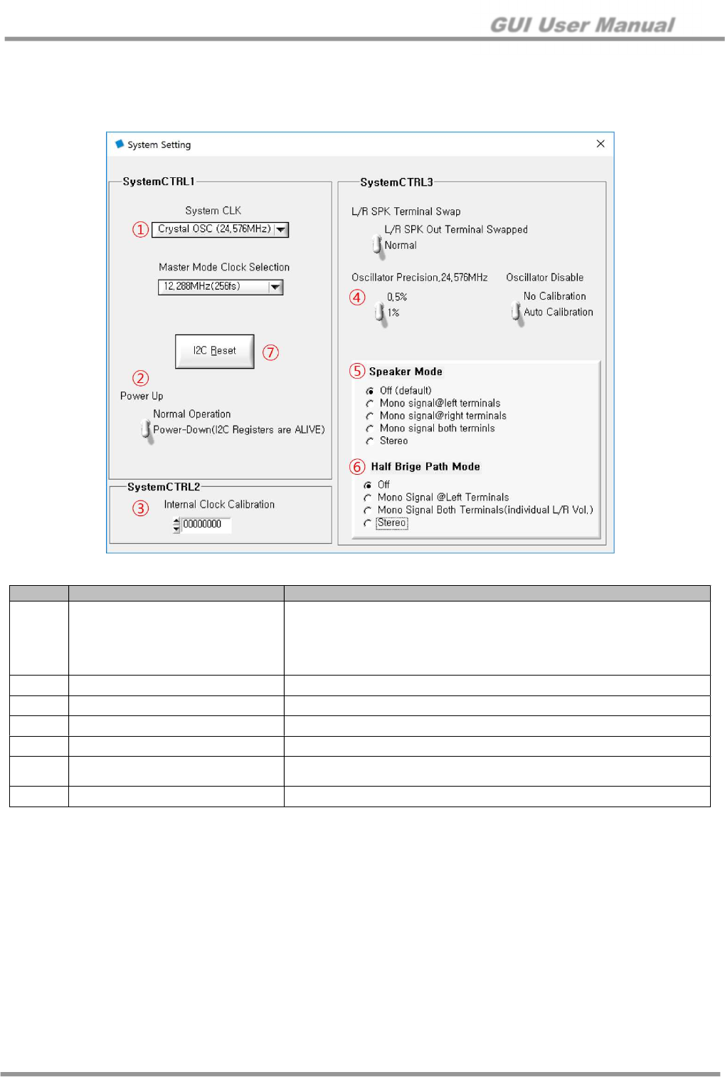
Figure 18. System Setting for Other Control Panel
No. Item Description
①
System CLK
Internal OSC
Crystal OSC (24.576 MHz)
FLL
Ext. CLK 19.2 MHz
Ext. CLK 24.576 MHz
②
Power Up Analog Block Power On
③
Internal Clock Calibration Internal OSC Frequency Calibration
④
Oscillator Precision Precision setting in case of Audio Calibration mode
⑤
Speaker Mode Speaker Output selection mode after DSP
⑥
Half Bridge Path Mode Normally Off
This should be set to “Stereo” in case of half bridge path mode (2.1ch)
⑦
I2C Reset Reset for I2C register
GUI User Manual
© 2018 Silicon Mitus, Inc. www.siliconmitus.com
September 2018 – Rev0.0.0 23 / 30
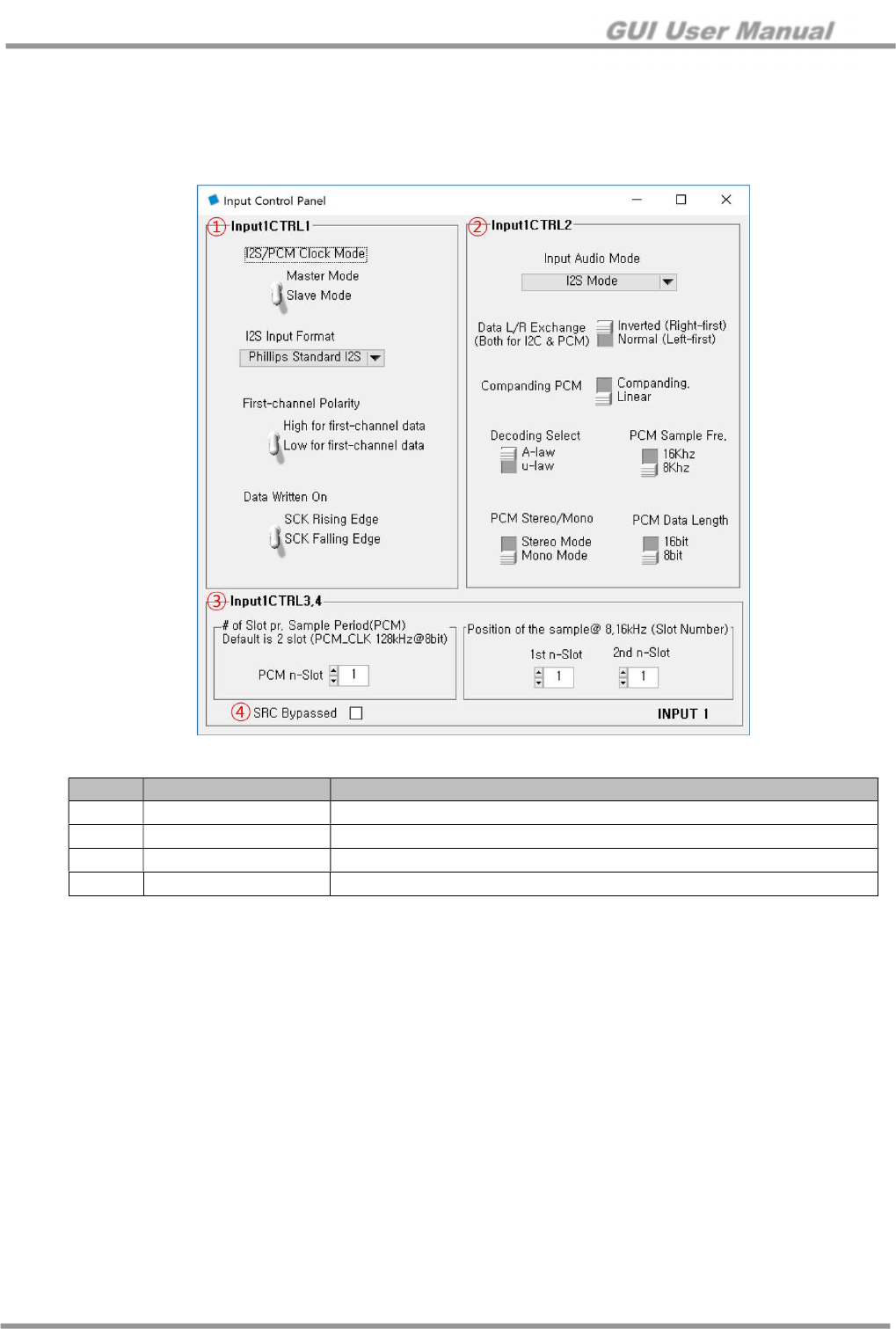
6.2 Input Receiver Control
6.2.1 Input Receiver Control Panel
1. Digital input format setting
2. It is recommended to use the default in case of I2S signal
Figure 19. Input Receiver Control Panel
No. Item Description
①
Input1 CTRL 1 I2S input format settings
②
Input1 CTRL 2 PCM input format settings
③
Input1 CTRL 3,4 PCM slot setting
④
SRC Bypass Sample Rate Converter turns off if checked
GUI User Manual
www.siliconmitus.com © 2018 Silicon Mitus, Inc.
24 / 30 September 2018 – Rev0.0.0
6.3 Signal Path Setting
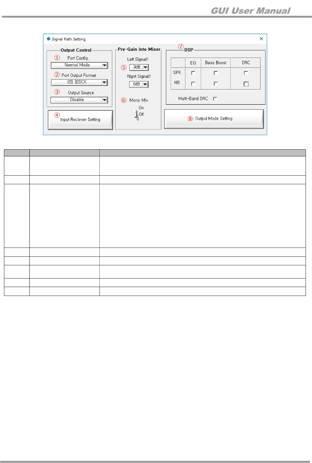
Figure 20. Signal Path Setting
No. Item Description
①
Port Config
Port Configuration
Normal Mode: Not used for SDO output
Audio Data Output: Used for SDO output
②
Port Output Format I2S format for SDO
③
Output Source
Select signal to output in case of only master/slave mode (see the TOP Manager
Panel)
Disable
Format Convert Input
Mixer Output@48kHz
SPK Path after DSP(48kHz)
Half Bridge Path after DSP(48kHz)
For Test (LR Mixing Before DSP)
For Test (Tone & Fine Vol.)
For Test (LR Mixing after Tone & Fine)
④
Input Receiver Setting Open the Input Receiver Control Panel
⑤
Pre-Gain into Mixer Mixer Gain of Digital Input signal
⑥
Mono Mix (Left Signal + Right signal) / 2
This function should be used for 2-way speaker application
⑦
DSP DSP On/Off – it is the same control as DSP On/Off in Main Panel
⑧
Output Mode Setting Open the System Setting Panel
GUI User Manual
© 2018 Silicon Mitus, Inc. www.siliconmitus.com
September 2018 – Rev0.0.0 25 / 30
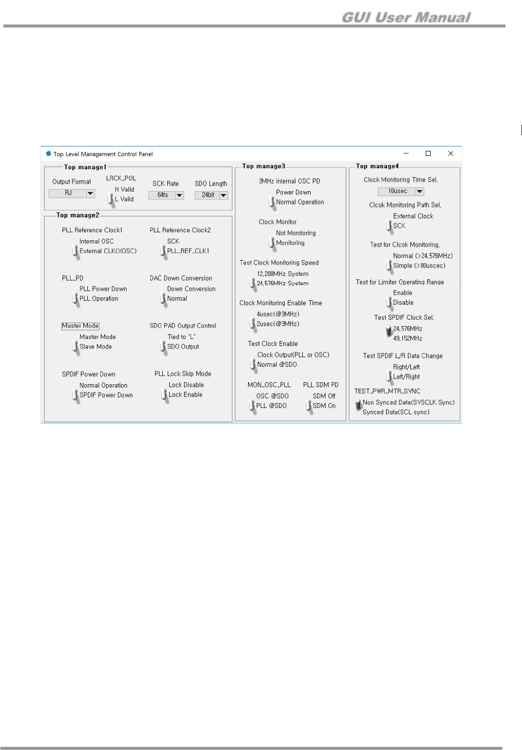
6.4 TOP Manager
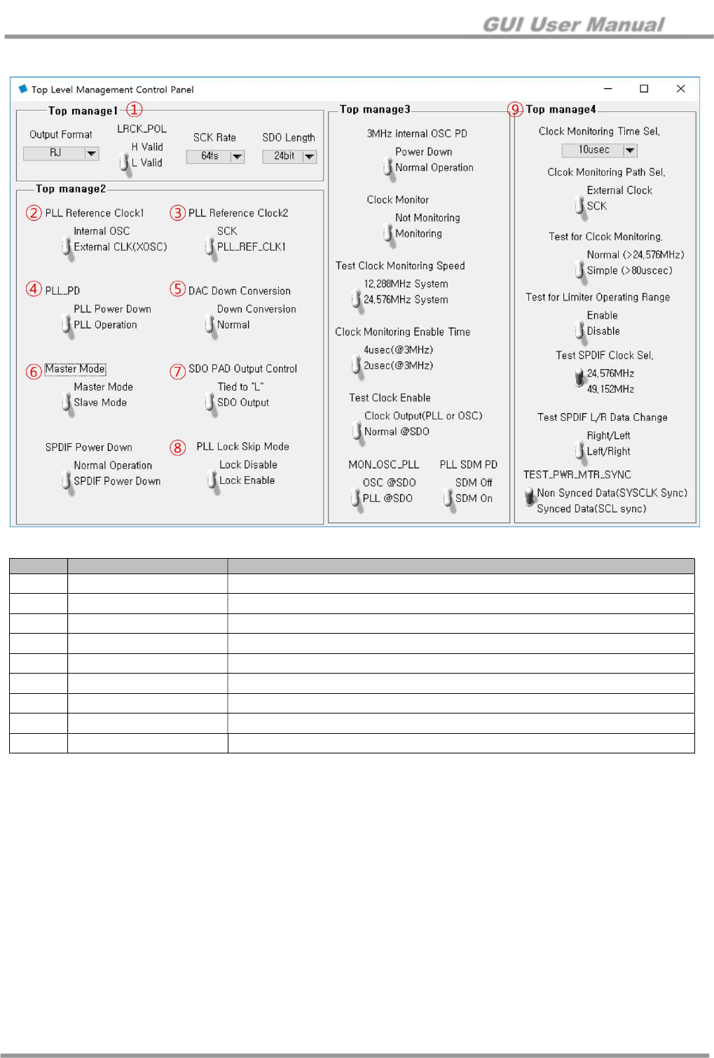
Figure 21. TOP Manager Panel
No. Item Description
①
Top manage1 I2S format for SDO output
②
PLL Reference Clock1 PLL Reference clock selection
③
PLL Reference Clock1 PLL Reference clock selection
④
PLL_PD PLL power-down On/Off
⑤
DAC Down Conversion DAC down conversion for 192kHz input signal
⑥
Master Mode Master or Slave mode selection
⑦
SDO PAD Output Control
Normal or SDO Output
⑧
PLL Lock Skip Mode PLL Lock Skip disable or enable
⑨
Top manager3/4 Register setting for test purpose
GUI User Manual
www.siliconmitus.com © 2018 Silicon Mitus, Inc.
26 / 30 September 2018 – Rev0.0.0
6.5 Volume Control
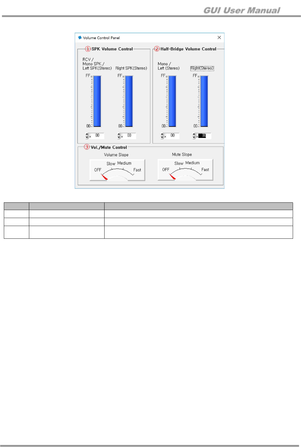
Figure 22. Volume Control Panel
No. Item Description
①
SPK Volume Control Speaker Left / Right Volume
②
Half-Bridge Volume Control Left / Right Volume in 2.1ch mode
③
Vol./Mute Control Volume and Mute Slope Control
Fade in / Fade out effect
GUI User Manual
© 2018 Silicon Mitus, Inc. www.siliconmitus.com
September 2018 – Rev0.0.0 27 / 30
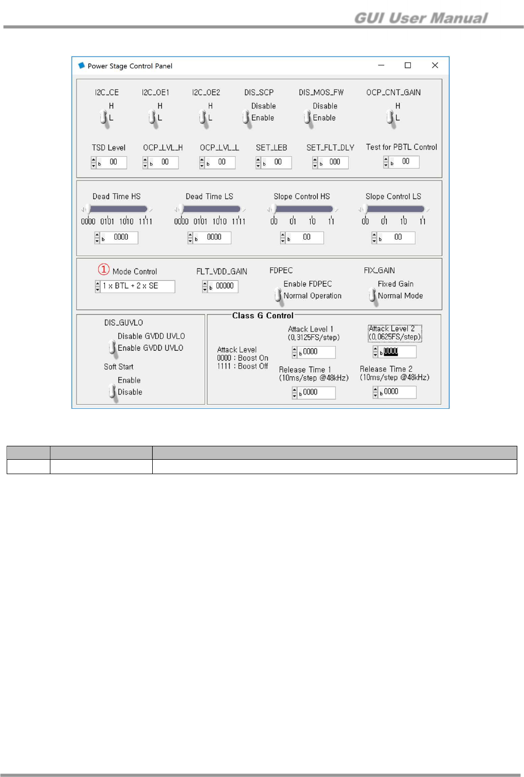
6.6 Power Stage
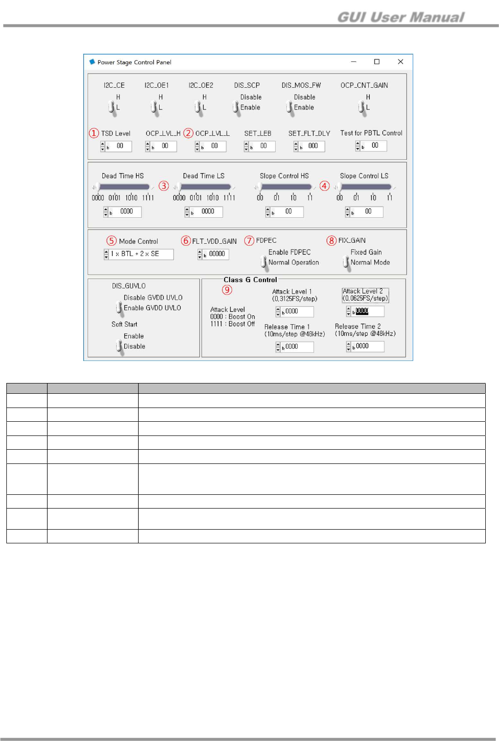
Figure 23. Power Stage Control Panel
No. Item Description
①
TSD Level Thermal shut down level (high temperature: b’11)
②
OCP Level Over current protection level: High (b’11) to Low (b’00), 0.5 A/Step
③
Dead Time PWM Dead time control (b’1111: short to b’0000: long)
④
Slope Control PWM Slope Control (b’11: fast to b’00: slow)
⑤
Mode Control Output Mode: BTL x 2 or 1BTL + 2 x SE (2.1ch)
⑥
FLT_VDD_GAIN
Normally this value should be set as b’100
This should be set in Fixed Gain Mode and Class G operation with Boost converter
(SMA6021)
⑦
FDPEC Output Feedback Loop On/Off
⑧
FIX_GAIN Fixed gain mode makes fixed FS (full scale)
FS depends on PVDD Level in normal mode
⑨
Class G Control This function is only for class G operation with SMA6021 Boost Converter
GUI User Manual
www.siliconmitus.com © 2018 Silicon Mitus, Inc.
28 / 30 September 2018 – Rev0.0.0
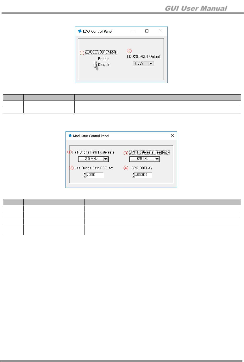
6.7 LDO Control
Figure 24. LDO Control Panel
6.8 Feedback Control
Figure 25. Modulator Control Panel
No. Item Description
①
LDO_CVDD Enable Internal LDO enable for CVDD (clock power)
②
LDO2(DVDD) Output Internal LDO voltage for DVDD (digital power)
No. Item Description
①
Half-Bridge Path Hysteresis PWM frequency of SE output in 2.1ch mode
②
Half-Bridge Path BDELAY Do not control
③
SPK Hysteresis Feedback PWM frequency of speaker output
④
SPK_BDELAY Do not control this value. This value should be provided by and used as
accordingly to Silicon Mitus
GUI User Manual
© 2018 Silicon Mitus, Inc. www.siliconmitus.com
September 2018 – Rev0.0.0 29 / 30
6.9 Control Setting
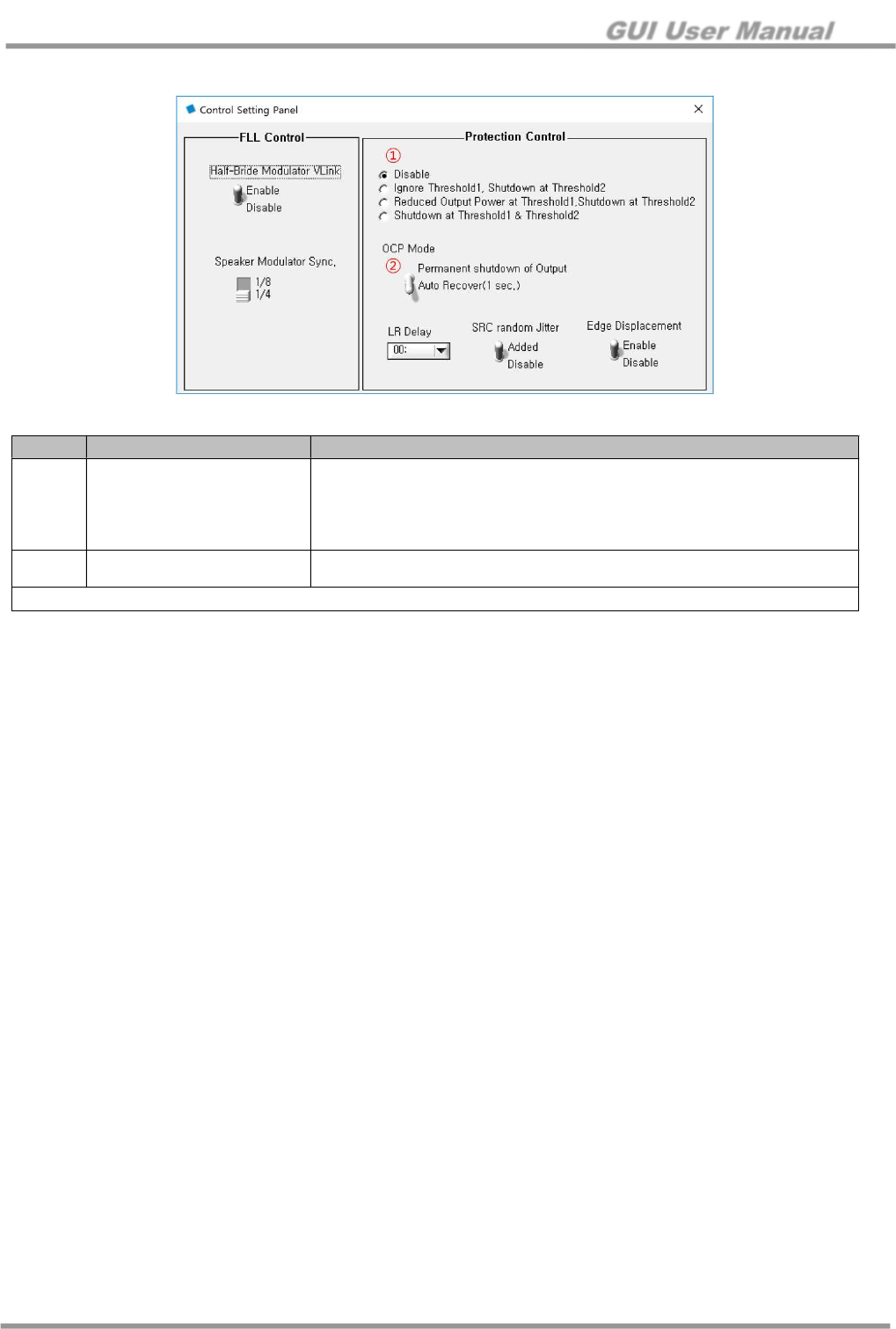
Figure 26. Control Setting Panel
No. Item Description
①
Thermal protection option
Disable
Ignore Threshold1 (TSDW), Shutdown at Threshold2 (TSD)
Reduced 6 dB output at Threshold1 (TSDW), shutdown at Threshold2
(TSD)
Shutdown at Threshold1 (TSDW) and Threshold2 (TSD)
②
OCP Mode Permanent shutdown of output
Auto recover (1 second)
Other controls are not used

GUI User Manual
www.siliconmitus.com © 2018 Silicon Mitus, Inc.
30 / 30 September 2018 – Rev0.0.0
Revision History
Rev
DATE
CHANGES
Issued by
Notes
0.0
.0
09/07
/201
8
Initial
Release and reviewed with IronDevice
Gyuhwa
─────────────────────────────────────────────────────────────────────────────
Silicon Mitus cannot assume any responsibility for the consequence of use of information furnished nor for any infringement of patents or
other rights of third parties which may result from its use. No circuit patent licenses are implied. Silicon Mitus reserves the right to change the
circuitry and specifications without notice at any time. This publication supersedes and replaces all information previously supplied. Silicon
Mitus products are not authorized for use as critical components in life support devices or systems without the express written approval of
Silicon Mitus.
© 2018 Silicon Mitus, Inc. - Printed in Korea - All Rights Reserved
