SMA6101_GUI_User_Manual_Rev0.0.2x SMA6101 GUI User Manual Rev0.0.2
User Manual:
Open the PDF directly: View PDF ![]() .
.
Page Count: 28
© 2017 Silicon Mitus, Inc. www.siliconmitus.com
October 2018 – Rev0.0.1 1 / 28
GUI User Manual
Revision 0.0.2
*Technology by
GUI User Manual
www.siliconmitus.com © 2017 Silicon Mitus, Inc.
2 / 28 October 2018 – Rev0.0.2
1. Purpose
Graphic User Interface (GUI) is a software program that verifies and tests the function of the Silicon Mitus product. This
document is based on SMA6101 GUI.
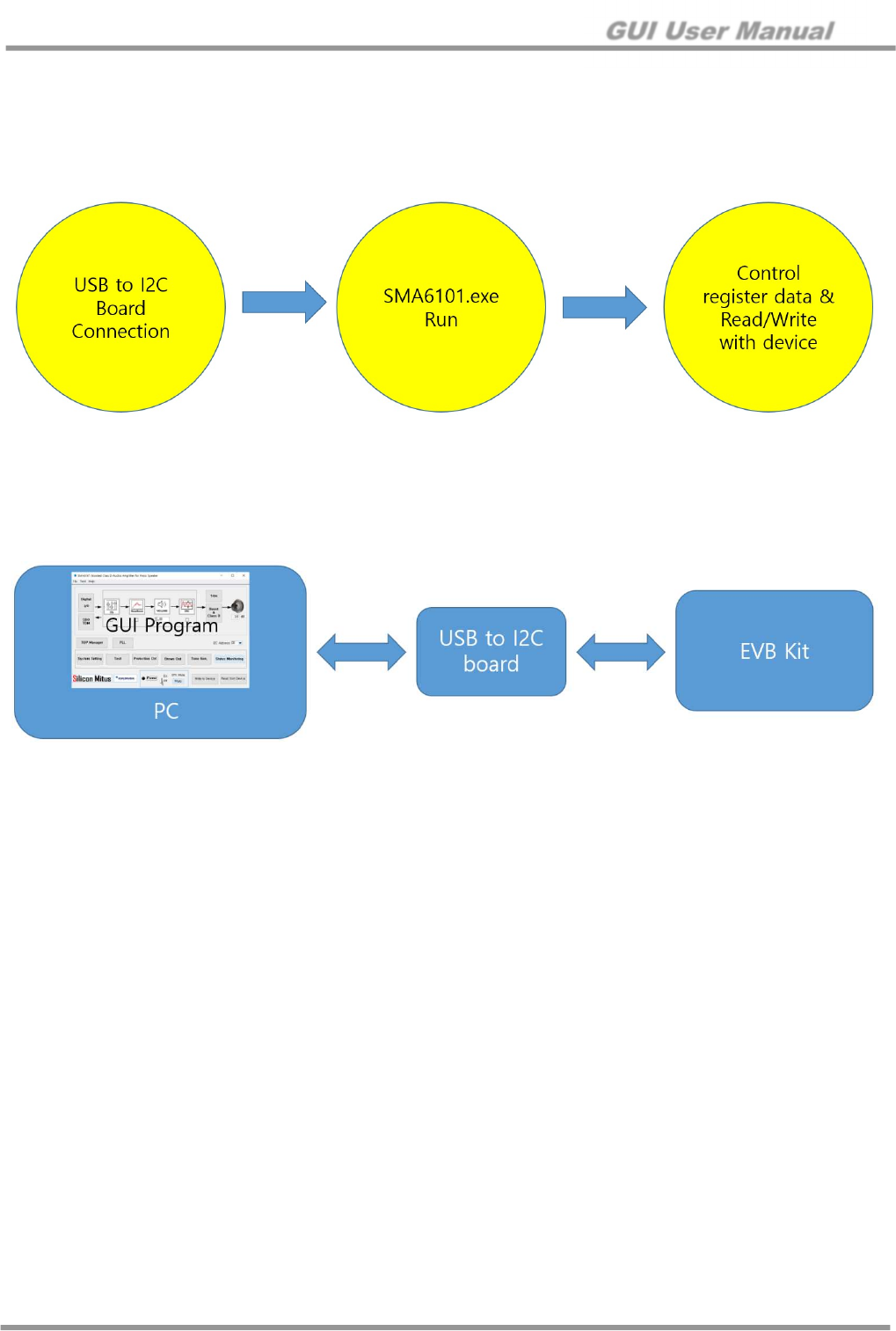
Figure 1. Active Flow
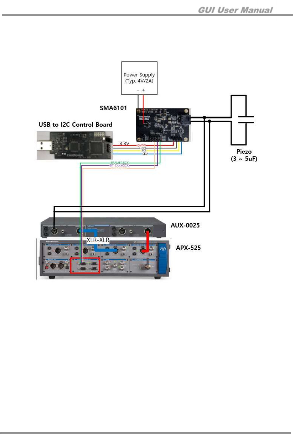
The Silicon Mitus evaluation system has an I2C port, so the user can control the action via the GUI program. The diagram
below describes the connection for the Silicon Mitus evaluation system using the GUI Program with test equipment, USB to
I2C Board, PC, USB cable and Silicon Mitus Evaluation Board (EVB) Kit.
Figure 2. Connection Diagram
GUI User Manual
© 2017 Silicon Mitus, Inc. www.siliconmitus.com
October 2018 – Rev0.0.2 3 / 28
2. Installation
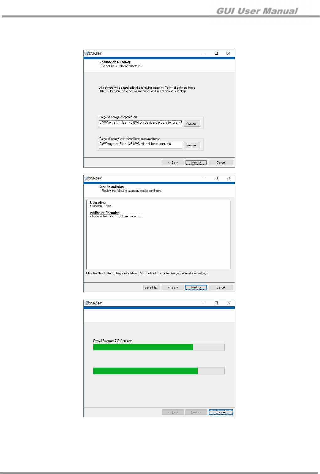
Unzip SMA6101_Control_Panel.zip to a local PC. To install the program, run “Setup.exe” file.
GUI User Manual
www.siliconmitus.com © 2017 Silicon Mitus, Inc.
4 / 28 October 2018 – Rev0.0.2
Installation Path
1. Windows Start → Click “ “ SMA6101
2. C:\Program Files (x86)\Iron Device Corporation\SMA6101 folder. Run with SMA6101.exe
3. Device Configuration
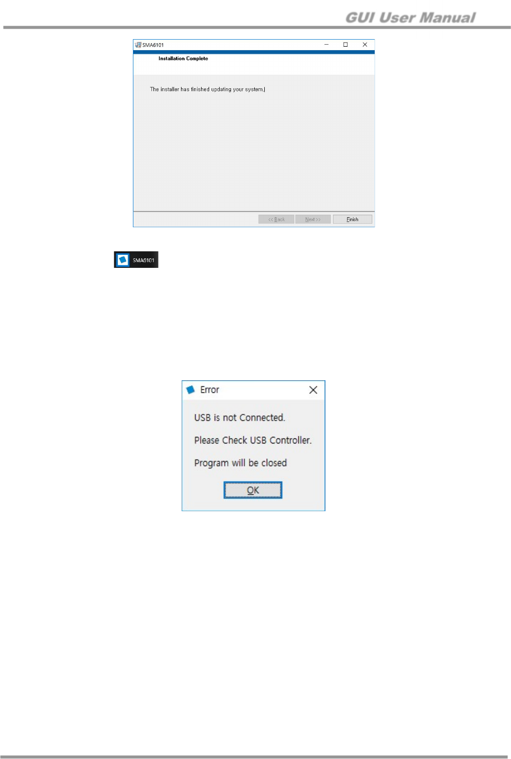
Connect ‘USB to I2C Board’ to the Evaluation Board Kit.
1. Run SMA6101 GUI Program
2. If the USB to I2C Board is not connected normally, an error message pop-up window will appear.
Figure 3. Error Message Pop-up
GUI User Manual
© 2017 Silicon Mitus, Inc. www.siliconmitus.com
October 2018 – Rev0.0.2 5 / 28
4. Board Manual
4.1 Introduction
The SMA6101 Evaluation (EV) Board is a demonstration and evaluation board that shows the capabilities and features
of SMA6101 chipset designed by Silicon Mitus (Iron Device). This board has a digital class-D audio amplifier with an
integrated boost converter. From input voltage or a single cell Li-ion battery power supply, the boost converter converts
boosted output voltage into full digital amplifier to make large signal of outputs stable for the piezo speaker drive.
Maximum output voltage level is 40 Vpp.
4.2 Board Package Content
The SMA6101 EV Board package includes the following:
1. SMA6101 EV Board
2. USB to I2C Control Board
3. Cable set to connect the board in lab conditions.
4. Control S/W (Released by e-mail. Please contact Silicon Mitus separately.)
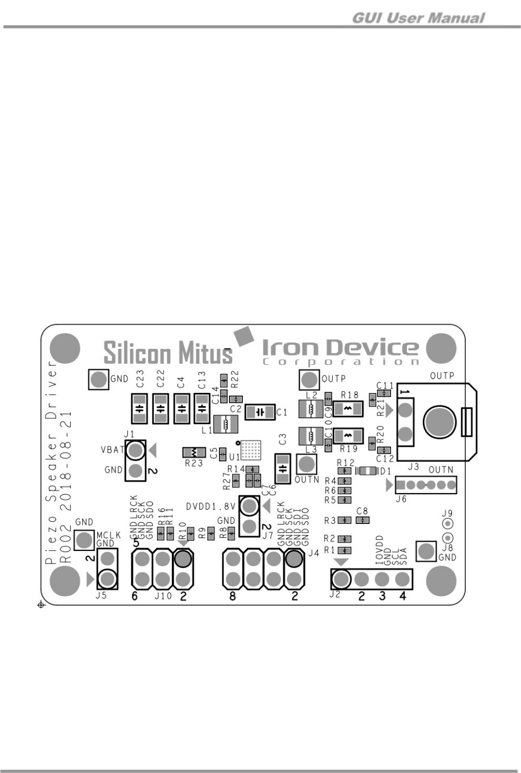
4.3 EV Board Overview
Figure 4. SMA6101 EV Board Placement
GUI User Manual
www.siliconmitus.com © 2017 Silicon Mitus, Inc.
6 / 28 October 2018 – Rev0.0.2
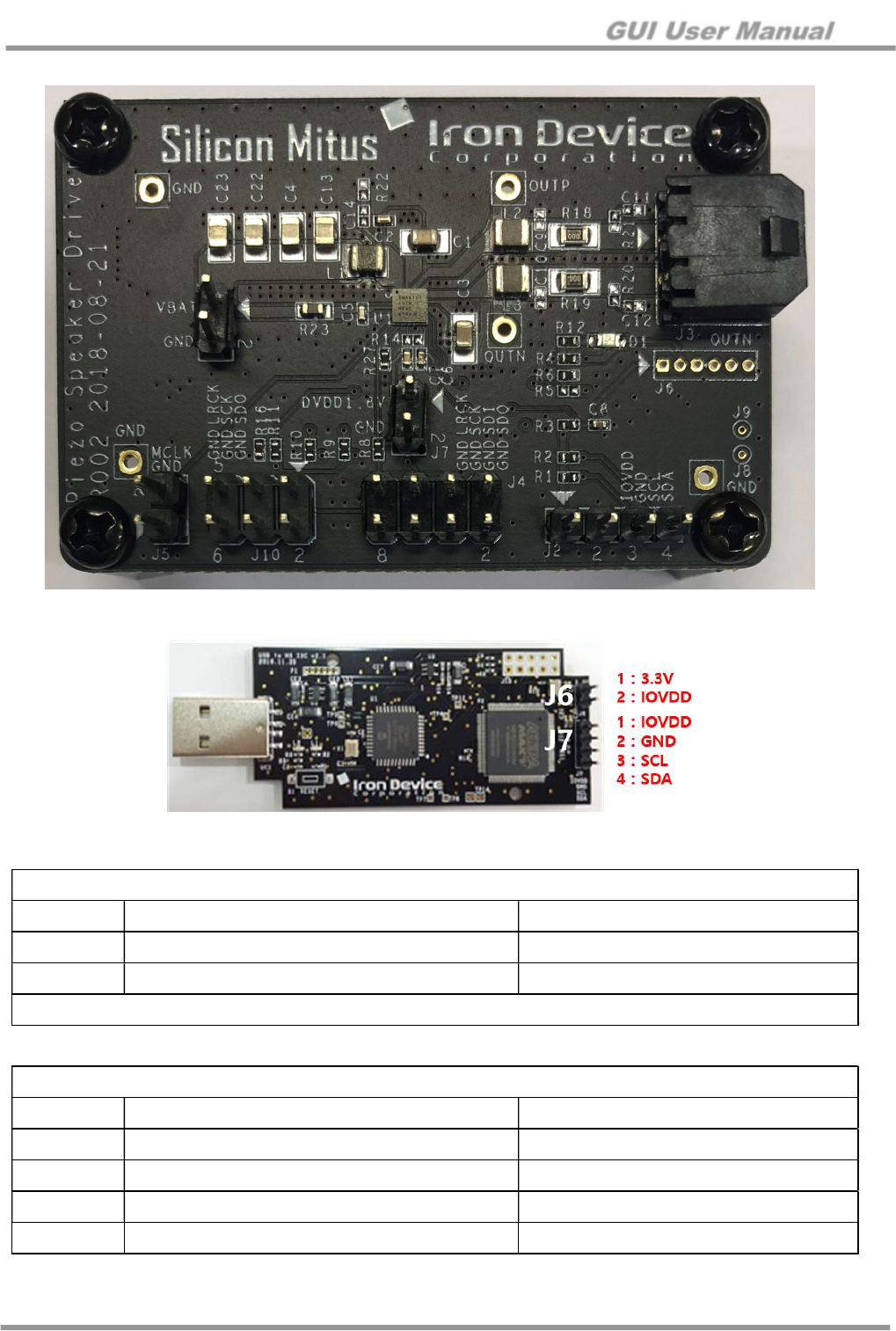
Figure 5. SMA6101 EV Board
Figure 6. USB to High Speed I2C Control Board
Type: 2.54 mm Pitch Pin Header for J6
Pin Description Value
1 3.3 V LDO Output +3.3 V
2 IOVDD IOVDD
Connect Pin 1 and Pin 2 for SMA6101 if IO voltage is +3.3 V
Type: 2.54 mm Pitch Pin Header for J7
Pin Description Value
1 IOVDD IOVDD (+3.3 V)
2 GND GND
3 SCL 0 V to +3.3 V
4 SDA 0 V to +3.3 V
GUI User Manual
© 2017 Silicon Mitus, Inc. www.siliconmitus.com
October 2018 – Rev0.0.2 7 / 28
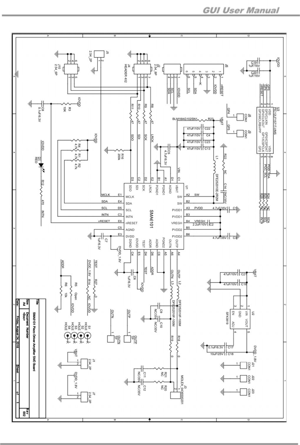
4.4 Board Schematic
Figure 7. SMA6101 EV Board Schematic
GUI User Manual
www.siliconmitus.com © 2017 Silicon Mitus, Inc.
8 / 28 October 2018 – Rev0.0.2
4.5 Connectors
J1: Power Stage and Analog Power Supply
J7: DVDD Power Supply
J3: Piezo Output
J2: I2C Control Pin
J4: I2S Input Port
J5: MCLK input (If external clock is providing using SCK, MCLK input does not need)
Type: 2.54 mm Pitch Pin Header
Pin Description Value
1 VBAT +4V / 2 A
2 GND GND
Type: 2.54 mm Pitch Pin Header
Pin Description Value
1 DVDD +1.8V / 200 mA
2 GND GND
Type: Micro-Fit 3.0™ Right Angle Header (43650-0200, Molex)
Pin Description Value
1 Piezo Output P Maximum +42 Vpp
2 Piezo Output N Maximum +42 Vpp
Type: 2.54 mm Pitch Pin Header
Pin Description Value
1 IOVDD 0 V to +3.3 V
2 GND GND
3 SCL 0 V to +3.3 V
4 SDA 0 V to +3.3 V
Type: 2.54 mm Pitch Pin Header
Pin Description Value
2, 4, 6, 8 GND GND
1 SDO (output data from chipset) 0 V to +3.3 V
3 SDI (input data from source) 0 V to +3.3 V
5 SCK 0 V to +3.3 V
7 LRCK 0 V to +3.3 V
Type: 2.54 mm Pitch Pin Header
Pin Description Value
1 GND GND
2 MCLK 19.2 or 24.576 MHz
GUI User Manual
© 2017 Silicon Mitus, Inc. www.siliconmitus.com
October 2018 – Rev0.0.2 9 / 28
4.6 Measurement Set Up (APX525)
This set up is for the evaluation of SMA6101. Reference equipment is APX-525 from Audio Precision.
4.6.1 Connection
Figure 8. Measurement Connection (I2S input)
GUI User Manual
www.siliconmitus.com © 2017 Silicon Mitus, Inc.
10 / 28 October 2018 – Rev0.0.2
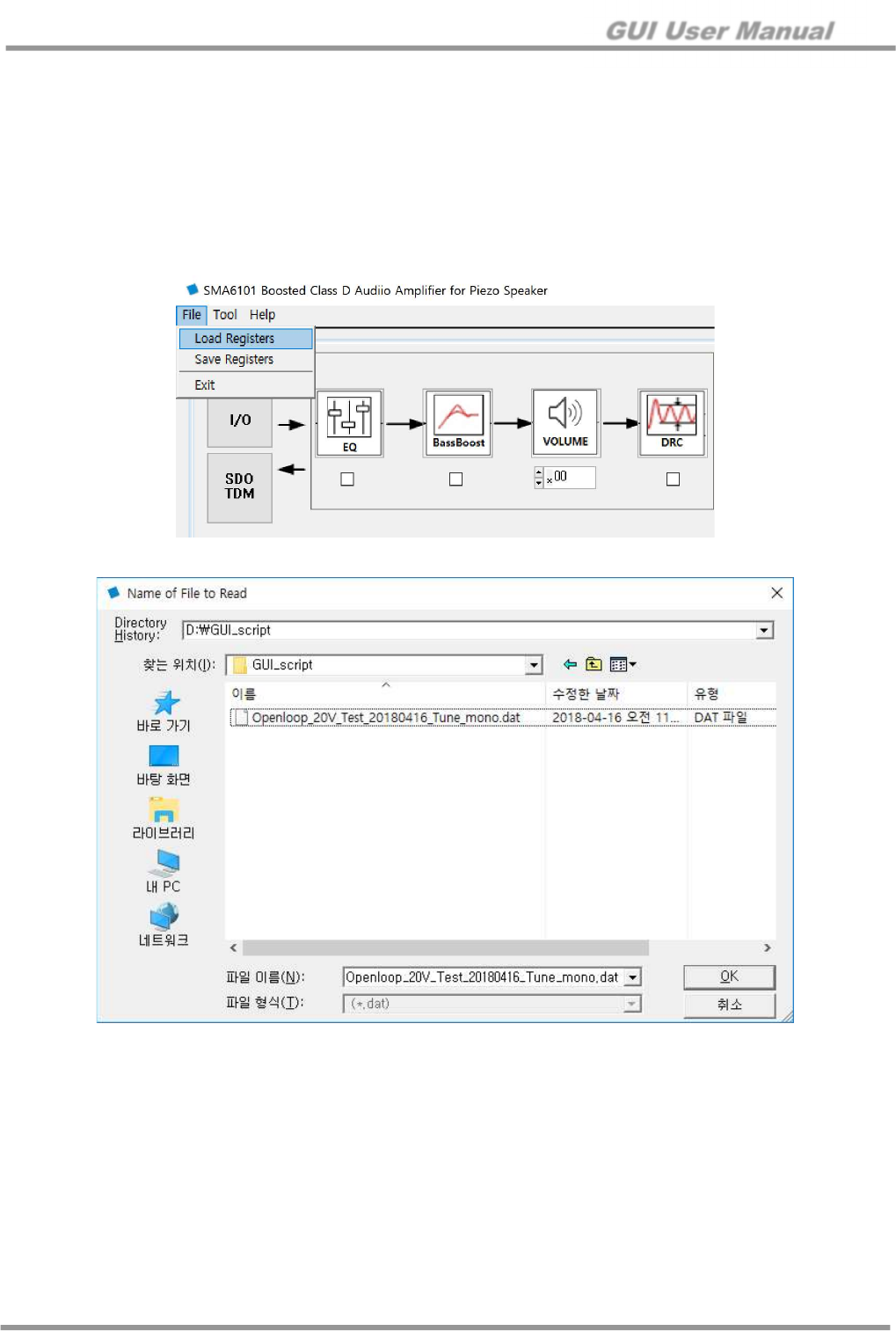
4.6.2 Control S/W (GUI) – Quick Start (Register File Download)
This is a quick start initiated by downloading the device register file. Test steps are as the following:
1. Setup the H/W connection, and use the register file for device operation
2. Install SMA6101 Control Panel, and run SMA6101.exe
3. Click on “Load Registers” from “File”
4. Select the provided register file (.dat) for device operation
5. The device on the EVB will run
6. You can control other functionalities as desired
Figure 9. Loading Register File
Figure 10. Selecting Register File
GUI User Manual
© 2017 Silicon Mitus, Inc. www.siliconmitus.com
October 2018 – Rev0.0.2 11 / 28
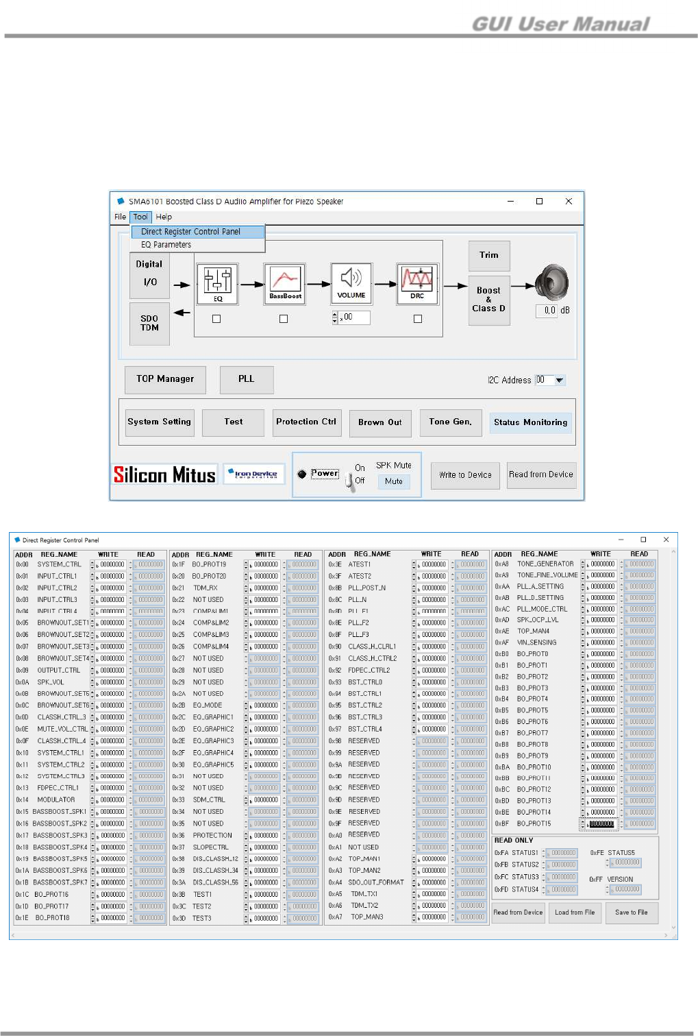
5. Direct Register Control Panel and EQ parameters
5.1 Direct Register Control Panel
You can check all register values of SMA6101 from Direct Register Control Panel
1. Open “Direct Register Control Panel.” Menu bar “Tool > Direct Register Control Panel”
Figure 11. Menu Bar (Tool > Direct Register Control Panel)
Figure 12. Direct Register Control Panel
GUI User Manual
www.siliconmitus.com © 2017 Silicon Mitus, Inc.
12 / 28 October 2018 – Rev0.0.2
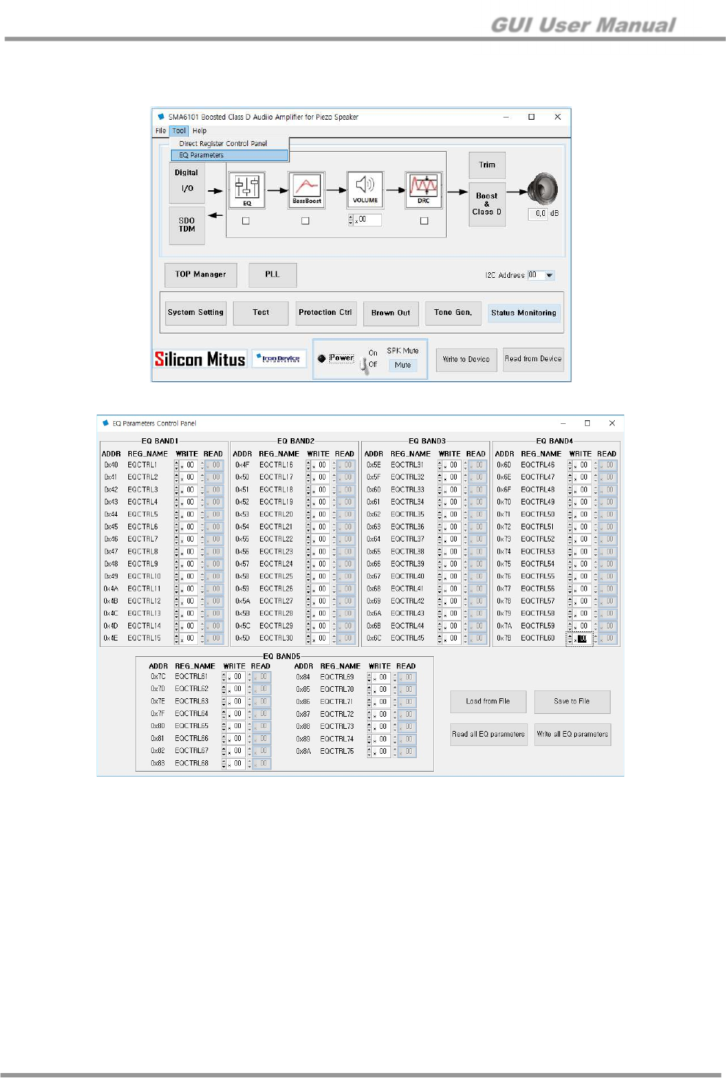
5.2 EQ parameters
You can check register values of EQ.
Figure 13. Menu Bar (Tool > EQ Parameters)
Figure 14. EQ Parameters Control Panel
GUI User Manual
© 2017 Silicon Mitus, Inc. www.siliconmitus.com
October 2018 – Rev0.0.2 13 / 28
6. Detail Controls
6.1 Control Panel Overview (Main Panel)
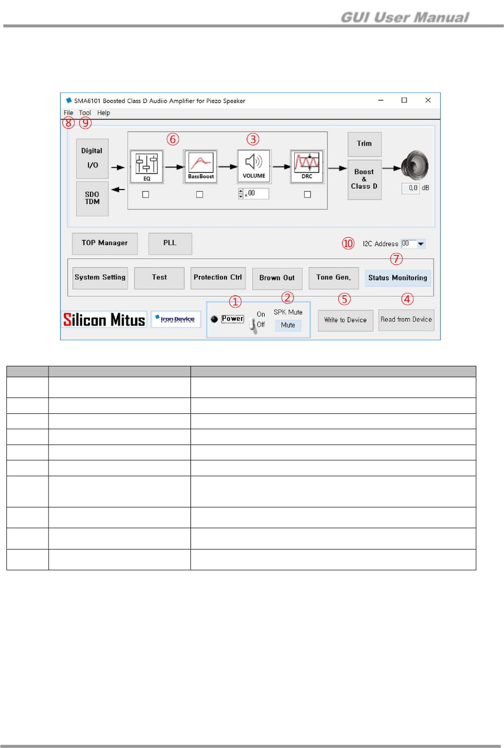
Figure 15. SMA6101 Register Control Panel
No. Item Description
①
Power On/Off with Sequence Power On: Power-up Speaker Output On De-mute
Power Off: Mute Speaker Output Off Power Off
②
Mute Control Mute and De-mute Control
③
Volume Control Digital Volume Control
④
Read from Device Read I2C from DUT and Set Panel
⑤
Write to Device Read Set Value from Panels and Write to DUT
⑥
DSP On/Off DSP block (EQ, BassBoost and DRC) on/off
⑦
Status Monitoring
Click on “Status Monitoring”
Reads status register and updates display every 0.2 seconds
Stops monitoring when clicked again
⑧
Menu Bar – File Load Register: Register Load from .dat file
Save Register: Register Save to .dat file
⑨
Menu Bar – Tool Direct Register Control Panel – Open Direct Register Control Panel
EQ Parameters – Open EQ Parameters Panel
⑩
I2C Address 00 : ADDR is connected to GND
01 : ADDR is connected to IOVDD
GUI User Manual
www.siliconmitus.com © 2017 Silicon Mitus, Inc.
14 / 28 October 2018 – Rev0.0.2
6.2 BassBoost
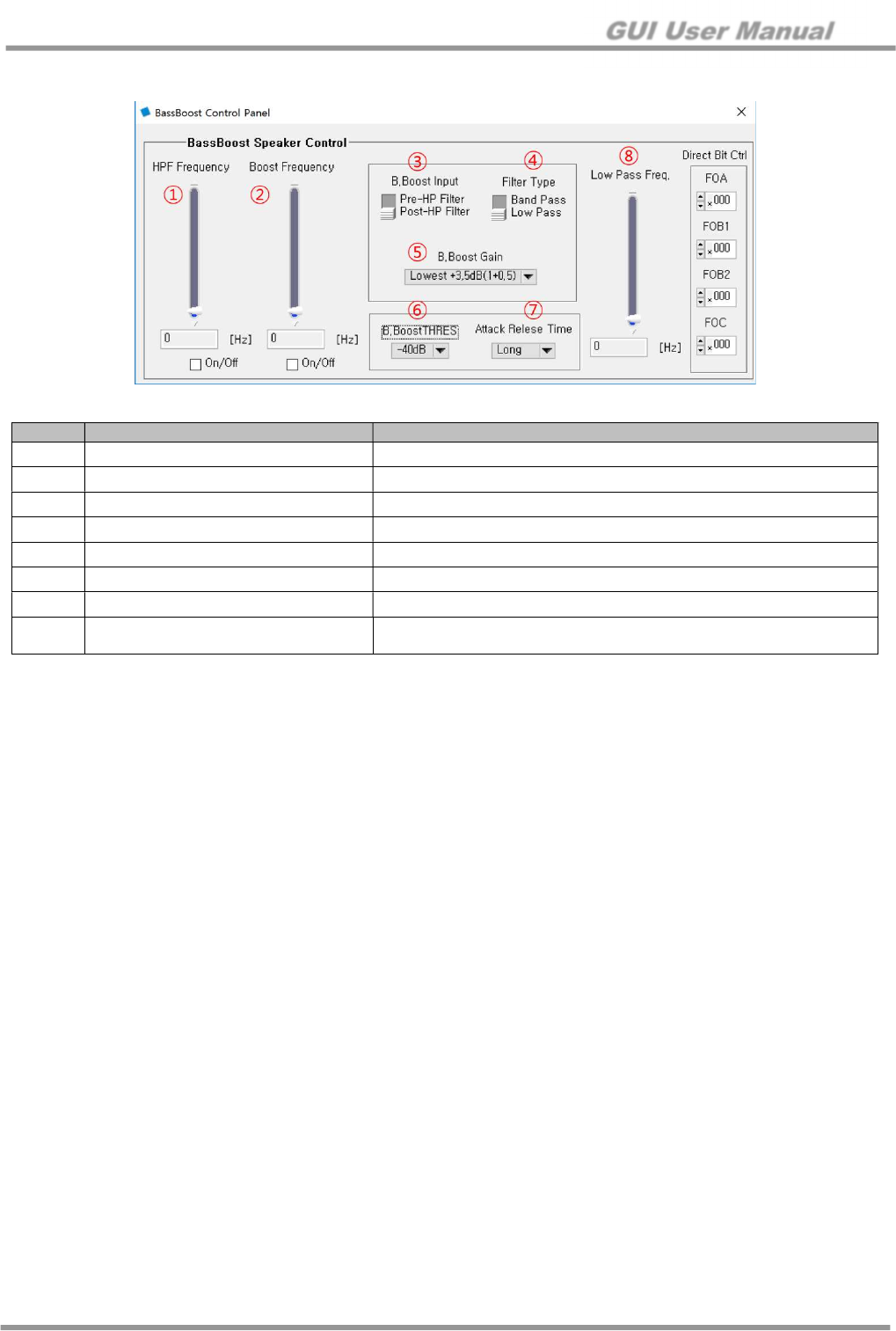
Figure 16. BassBoost Control Panel
No. Item Description
①
HPF Frequency 1st Order High Pass Filter Frequency Setting. “0” is off
②
Boost Frequency Boost Frequency Setting: 20 Hz to 1 kHz
③
B.Boost Input Select input of Bass Boost Block (Pre or Post HPF)
④
Filter Type Band Pass Filter or Low Pass Filter Type
⑤
B.Boost Gain Bass Boost Gain Setting
⑥
B.BoostTHRES (Boost Trigger) Set the starting limit of Bass Boost
⑦
Attack Release Time (Boost Trigger) Set the attack/release time limit of Bass Boost
⑧
Low Pass Frequency (Boost Trigger) Low pass filter of the signal that controls the attack release function
Should be set above boost frequency
GUI User Manual
© 2017 Silicon Mitus, Inc. www.siliconmitus.com
October 2018 – Rev0.0.2 15 / 28
6.3 EQ Control
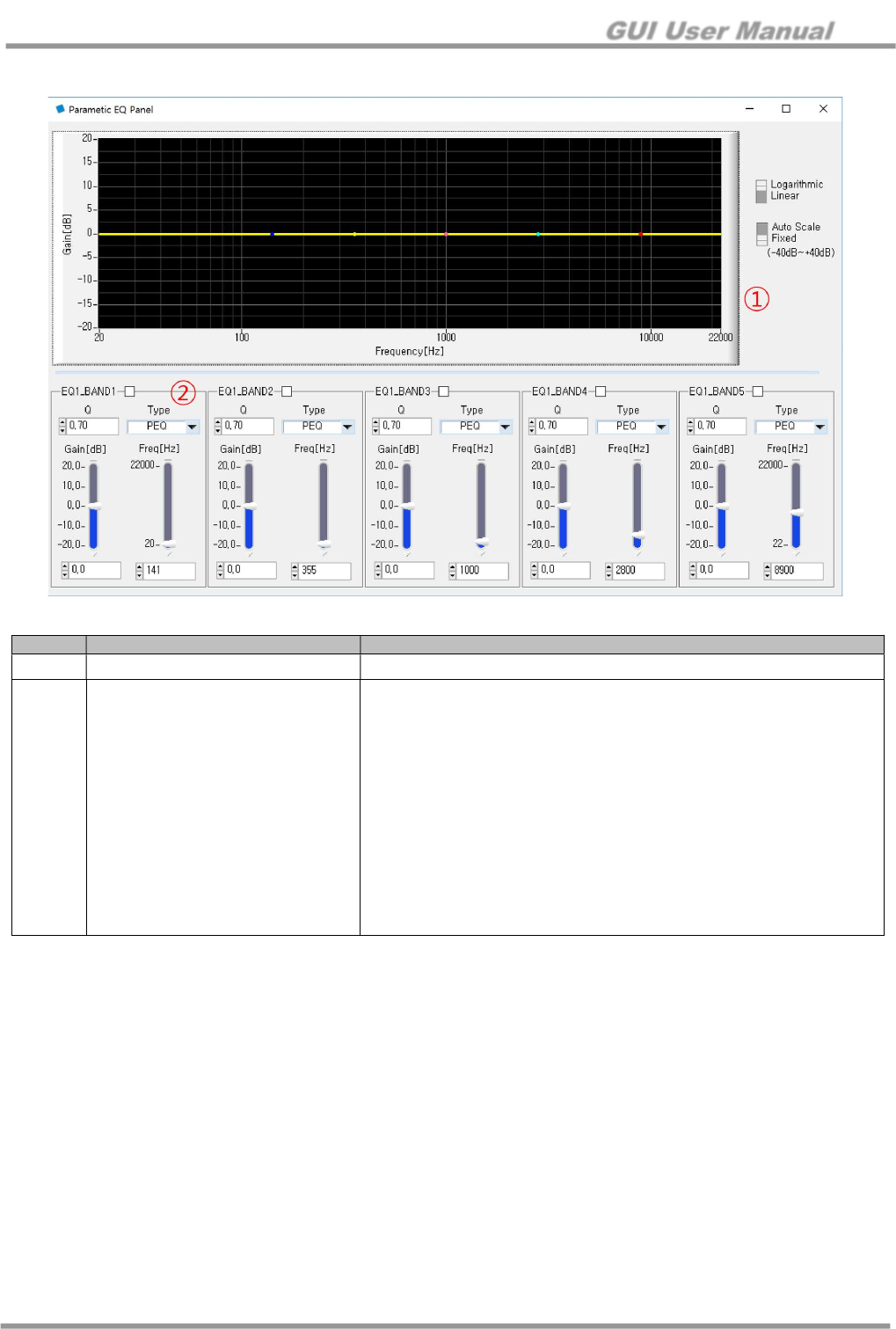
Figure 17. Parametric EQ Panel
No. Item Description
①
EQ EQ graphic (5 bands can be adjusted)
②
EQ Band
Q Factor
Biquad Filter Type
PEQ
2nd BW (Butter Worth) HPF
2nd BW (Butter Worth) LPF
LSF (Low Shelf Filter)
HSF (High Shelf Filter)
Piezo Tune
Gain
-20 dB to +20 dB
Frequency
20 Hz to 22 kHz
Check Box
Checked: EQ band enable
GUI User Manual
www.siliconmitus.com © 2017 Silicon Mitus, Inc.
16 / 28 October 2018 – Rev0.0.2
6.4 DRC (Comp/Limit)
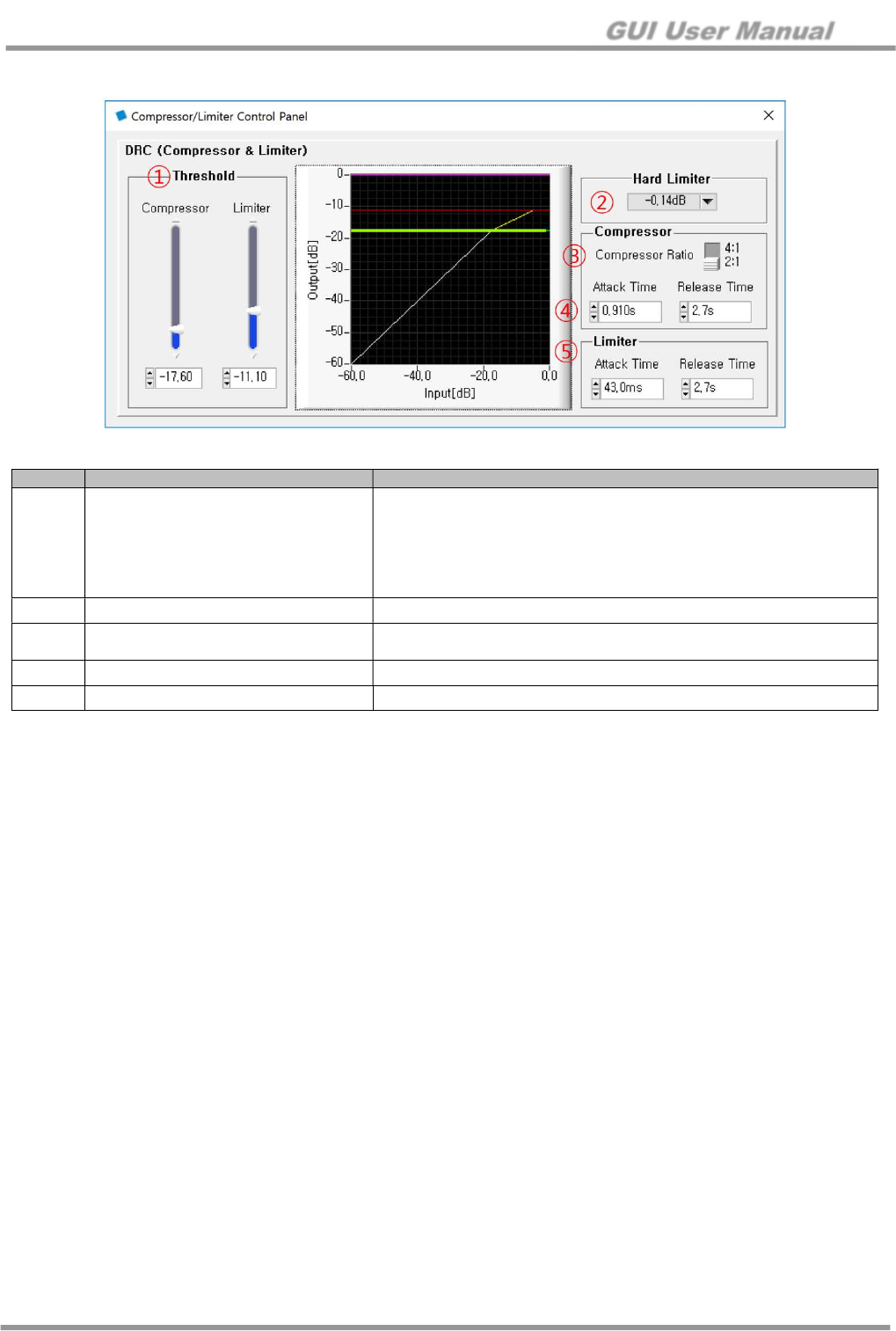
Figure 18. Compressor/Limiter Control Panel
No. Item Description
①
Threshold
Compressor Threshold
Maximum high level: - 0.1 dB
Compressor off: 0.0 dB
Limiter Threshold
Maximum high level: - 0.3 dB
Limiter off: 0.0 dB
②
Hard Limiter Clip the signal when it exceeds the threshold
③
Compressor Compressor Ratio
Amount of compression
④
Attack / Release Time for Compressor
Attack / Release Time
⑤
Attack / Release Time for Limiter Attack / Release Time
GUI User Manual
© 2017 Silicon Mitus, Inc. www.siliconmitus.com
October 2018 – Rev0.0.2 17 / 28
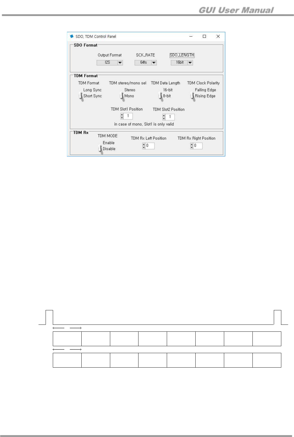
6.5 SDO/TDM
Figure 19. SDO/TDM Control Panel for SDO Format
1. TDM RX Setting
- When TDM format is used with SCK 6.144MHz (128bit, 8channel), TDM_MODE_EN_RX setting is required.
- Select the position of left signal(TDM Rx Left Position) and right signal(TDM Rx Right Position) as TDM slot.
(It is standard when using two chip solution, and only one slot is valid in one chip solution)
2. TDM TX Setting
- SDA pin should be set to SDM format TDM in order to output at the location corresponding to TDM mode.
(When using 8 channel 16bit, set SCK_RATE 32fs and SDO_LENGTH 16bit)
- TX is designed to allow both short and long sync, but only short sync is currently supported on RX (TDM 8ch).
If you want to use RTX at the same time, set it to short sync.
- Considering the settings based on RTX, one channel (TDM Slot1 Position) is selected for Mono, and two
channels (TDM Slot1 Position) for Stereo.
(For example, when using 8 channel mode, short sync, Mono, 16bit, Rising Edge, 8 slots)
3. AP Test environment
- Create a test bench using LRCK 192kHz I2S 64fs signal
- LRCK 192kHz is divided by 1/4 to make 48kHz and PCM (DSP) format
- SCK is divided into 8 channels (16bit / channel) with 6.144MHz 128bit
- I2C settings are used to set RX valid data, and TX can be used as well
- Related I2C register is 0x21(TDM RX), 0xA5/A6(TDM TX) and 0xA4(TDM SOUT)
0 1 2 3 4 5 6 7
16
LRCK
SDIN(RX)
"input"
SDO(TX)
"output"
TDM, 128 SCK, Short Sync
0 1 2 3 4 5 6 7
16
Figure 20. TDM Format
GUI User Manual
www.siliconmitus.com © 2017 Silicon Mitus, Inc.
18 / 28 October 2018 – Rev0.0.2
7. Other Control Panels
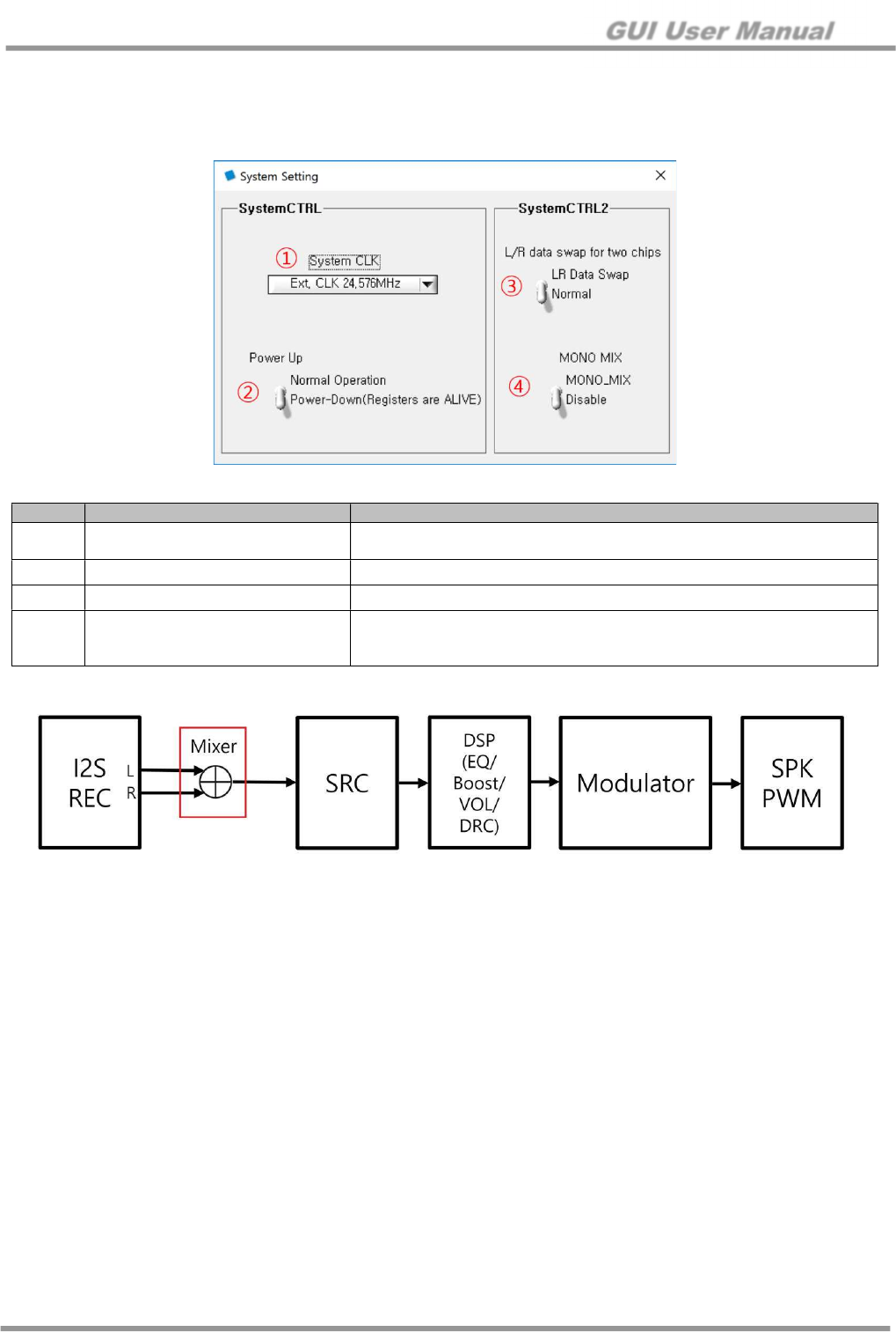
7.1 System Setting
Figure 21. System Setting for Other Control Panel
No. Item Description
①
System CLK Ext. CLK 19.2 MHz
Ext. CLK 24.576 MHz
②
Power Up Analog Block Power On
③
L/R data swap for two chips It basically handles Left data, but change it to handle Right data.
④
MONO MIX
When setting mono mix, add Left and Right and divide 2
(Left Signal + Right signal) / 2
See below figure for more details
Figure 22. MONO MIX Block Diagram
GUI User Manual
© 2017 Silicon Mitus, Inc. www.siliconmitus.com
October 2018 – Rev0.0.2 19 / 28
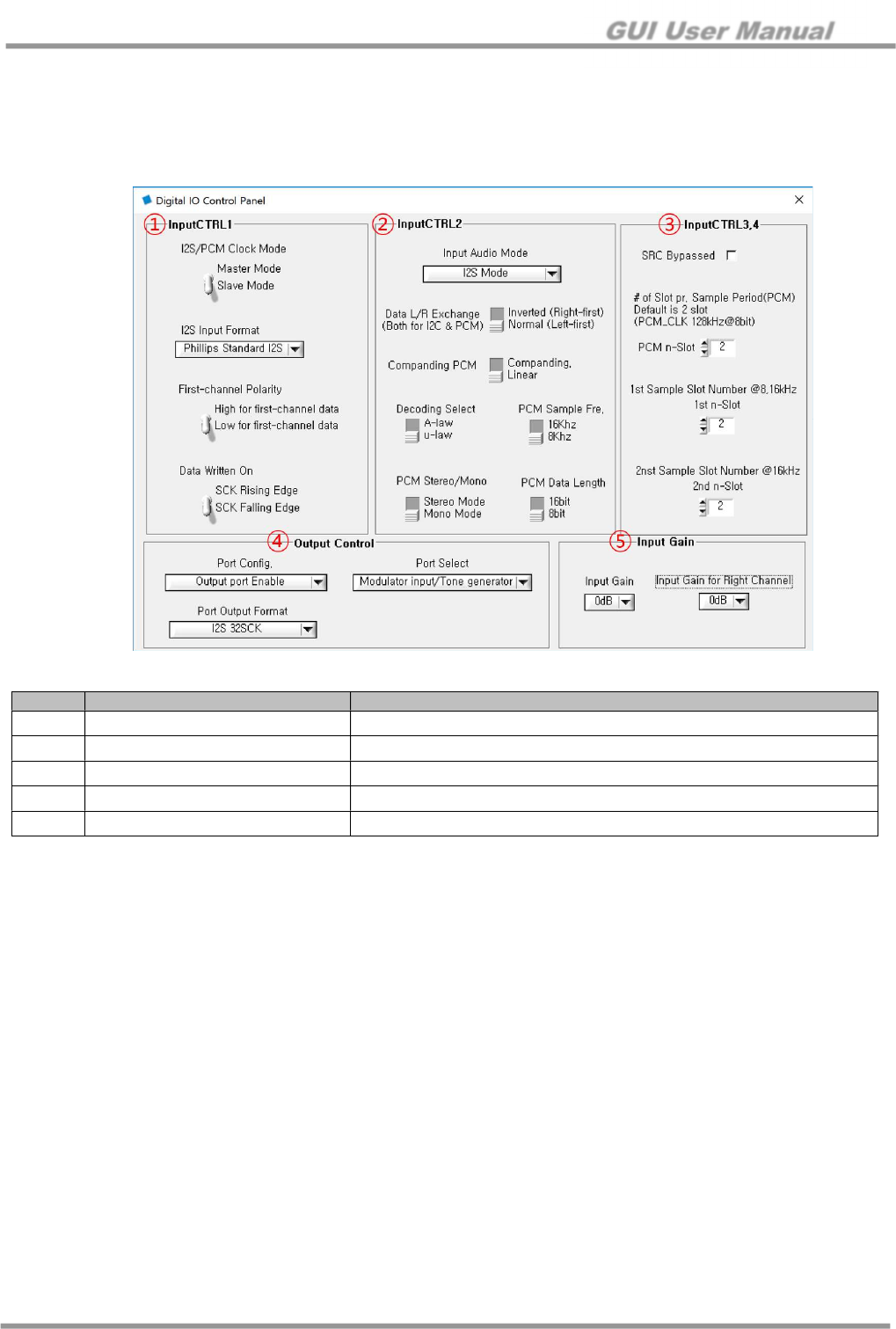
7.2 Digital IO Control
7.2.1 Digital IO Control Panel
1. Digital input format setting
2. It is recommended to use the default in case of I2S signal
Figure 23. Input Receiver Control Panel
No. Item Description
①
Input1 CTRL 1 I2S input format settings
②
Input1 CTRL 2 PCM input format settings
③
Input1 CTRL 3,4 PCM slot setting
④
Output Control Output port config/Select/Format settings
⑤
Input Gain Apply input gain to left and right in I2S receiver
GUI User Manual
www.siliconmitus.com © 2017 Silicon Mitus, Inc.
20 / 28 October 2018 – Rev0.0.2
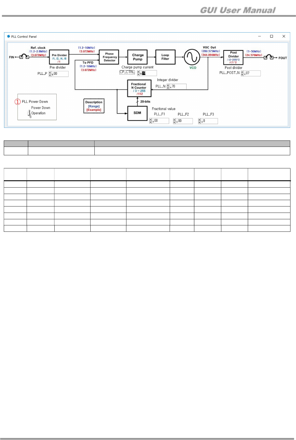
7.3 PLL Setting
Figure 24. PLL Setting Control Panel
No. Item Description
①
PLL Power Down PLL Power Down on/off
Recommended Setting for PLL
Data
format
Sample
rate
Input
Frequency
Output
Frequency PLL_POST_N PLL_N
PLL_F1 PLL_F2 PLL_F3,P,CP
16bit 8KHz 3.072MHz 24.576MHz 0x07 0x70 0x00 0x00 0x02
16bit 16KHz 3.072MHz 24.576MHz 0x07 0x70 0x00 0x00 0x02
16bit 48KHz 1.536MHz 24.576MHz 0x07 0xE0 0x00 0x00 0x03
16bit 96KHz 3.072MHz 24.576MHz 0x07 0x70 0x00 0x00 0x02
16bit 192KHz 6.144MHz 24.576MHz 0x07 0x70 0x00 0x00 0x06
32bit 48KHz 3.072MHz 24.576MHz 0x07 0x70 0x00 0x00 0x02
32bit 96KHz 6.144MHz 24.576MHz 0x07 0x70 0x00 0x00 0x06
32bit 192KHz 12.288MHz 24.576MHz 0x07 0x70 0x00 0x00 0x0A
When using PLL clock with bit clock, Input Frequency = Data format X Sample rate X 2(Channel)
For normal operation, the PLL input frequency should be greater than 1MHz. Therefore, when the data format is 16bit and
sample rate is 8kHz or 16kHz, an external clock of 3.072MHz should be used by using MCLK.
GUI User Manual
© 2017 Silicon Mitus, Inc. www.siliconmitus.com
October 2018 – Rev0.0.2 21 / 28
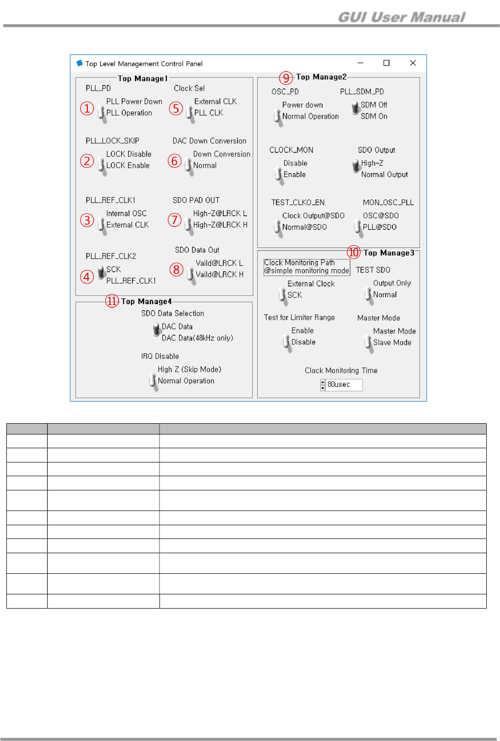
7.4 TOP Manager
Figure 25. TOP Manager Panel
No. Item Description
①
PLL_PD PLL On/Off
②
PLL_LOCK_SKIP PLL Lock monitoring Enable/Disable (Monitor the PLL clock to lock)
③
PLL_REF_CLK1 Select Internal OSC or External CLK as the PLL reference clock
④
PLL_REF_CLK2 Select SCK or PLL_REF_CLK1 as the PLL reference clock
⑤
Clock Sel Determines the clock to be used as the internal system clock of the chip
(External clock or PLL clock)
⑥
DAC Down Conversion For 192 kHz input signal
⑦
SDO PAD OUT Determines the state value of the SDO PAD
⑧
SDO Data Out Select the valid data when output DAC data with SDO
⑨
Top Manage2 Monitoring the clock used inside the chip clock (The chip designer will deliver the
tuning value)
⑩
Top Manage3 Monitoring the clock used inside the chip clock (The chip designer will deliver the
tuning value)
⑪
Top Manage4 Determine generation of interrupt pin in case of TSD, OCP, UVLO and clock fault
GUI User Manual
www.siliconmitus.com © 2017 Silicon Mitus, Inc.
22 / 28 October 2018 – Rev0.0.2
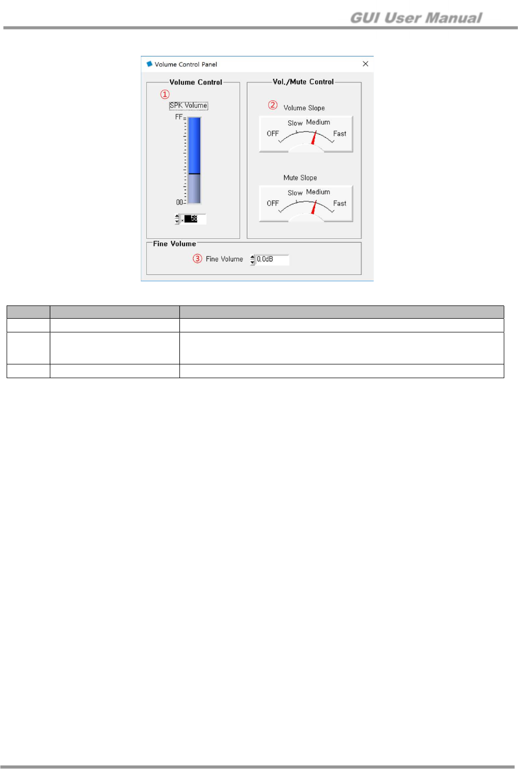
7.5 Volume Control
Figure 26. Volume Control Panel
No. Item Description
①
SPK Volume Control Speaker Volume (- 60 dB ~ + 24 dB)
②
Volume/Mute Slope
Volume and Mute Slope Control
Fade in / Fade out effect
Volume slope is ramping up/down every 20 dB as per datasheet
③
Fine Volume Fine Volume (- 3.375 dB ~ + 3 dB)
GUI User Manual
© 2017 Silicon Mitus, Inc. www.siliconmitus.com
October 2018 – Rev0.0.2 23 / 28
7.6 Boost & Output Control
7.6.1 Boost & Class D control
Figure 27. Boost & Class D Control Panel
No. Item Description
①
SPK Mode Speaker Output selection mode after DSP
②
Class D Amp Control FDPEC & Feedback Gain
③
Class H & Boost
Voltage Control
SMA6101 can be supporting 5 steps of Class-H
Each boost level will be operating when input signal touch ATTACK_LVL
GUI User Manual
www.siliconmitus.com © 2017 Silicon Mitus, Inc.
24 / 28 October 2018 – Rev0.0.2
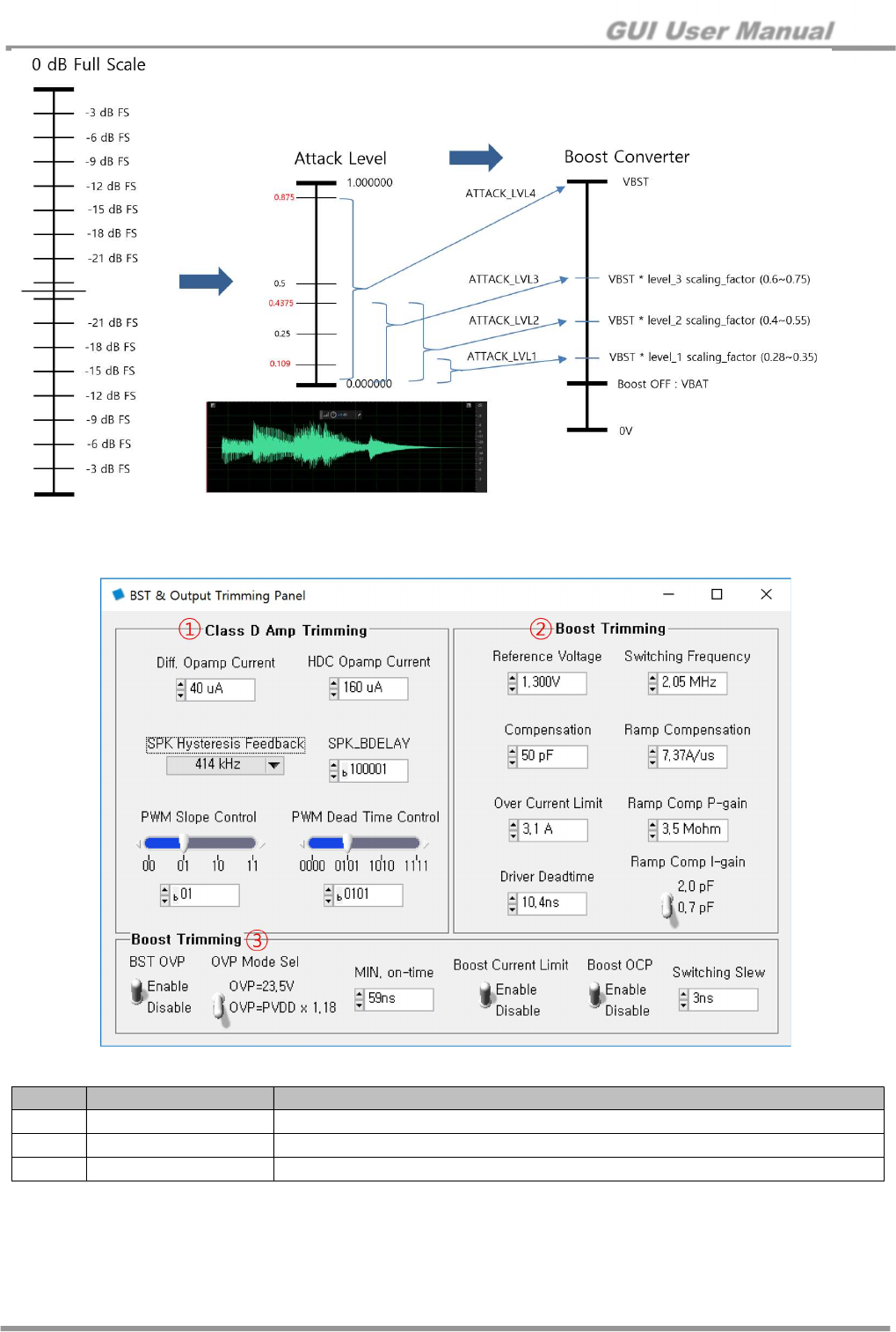
Figure 28. Class-H Boost Control Operation Concept
7.6.2 Boost & Output Trimming control
Figure 29. Boost & Output trimming Control Panel
No. Item Description
①
Class D Amp Trimming
Class D amp tuning parameter (The chip designer will deliver the tuning value)
②
Boost Trimming Boost amp tuning parameter (The chip designer will deliver the tuning value)
③
Boost Trimming Boost amp tuning parameter (The chip designer will deliver the tuning value)
GUI User Manual
© 2017 Silicon Mitus, Inc. www.siliconmitus.com
October 2018 – Rev0.0.2 25 / 28
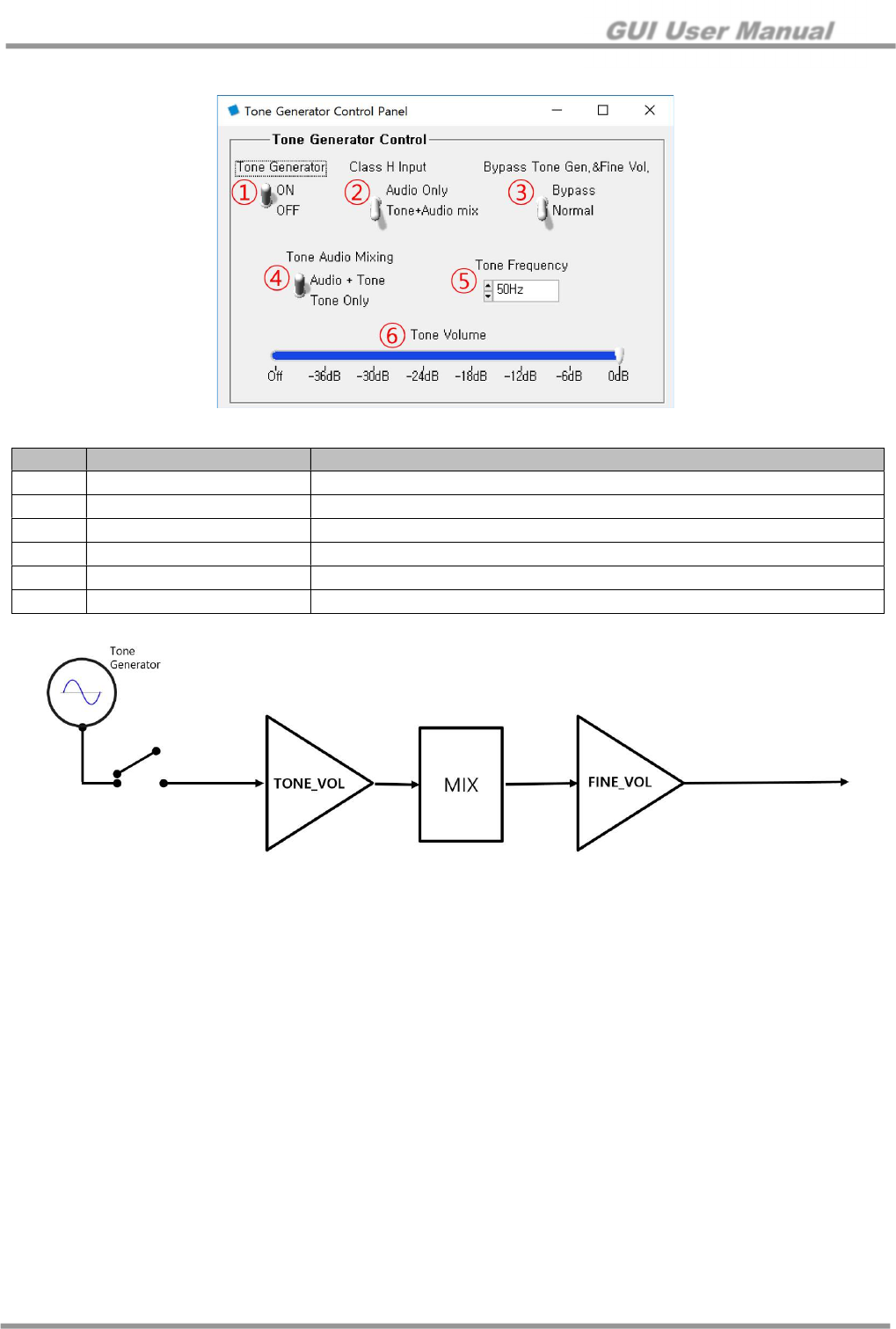
7.7 Tone Generator Control
Figure 30. Tone Generator Control Panel
Figure 31. Tone Generator Block Diagram
No. Item Description
①
Tone generator Tone generator On/Off
②
Class H Input Audio Only or Tone+Audio mix is selected
③
Bypass Tone Gen & Fine Vol
Bypass tone Generator and fine volume
④
Tone Audio Mixing Select Audio+Tone or Tone only by applying fine volume
⑤
Tone Frequency 15 different frequencies can be selected for the tone
⑥
Tone Volume Adjust the tone volume
GUI User Manual
www.siliconmitus.com © 2017 Silicon Mitus, Inc.
26 / 28 October 2018 – Rev0.0.2
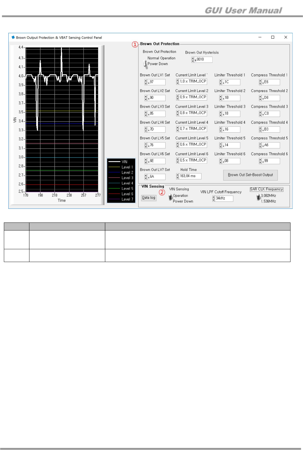
7.8 Brown Output Protection & VBAT Sensing Control
Figure 32. Brown Output Protection & VBAT Sensing Control Panel
No. Item Description
①
Brown Out Protection
The Digital Block controls the audio output and the BST output using the
result of digitizing the VBAT power.
Digitize result in seven stages of BOP (Brown Out Protection) state
②
VIN Sensing The VBAT power is detected by using the SAR ADC and the result is
transmitted to the digital block
GUI User Manual
© 2017 Silicon Mitus, Inc. www.siliconmitus.com
October 2018 – Rev0.0.2 27 / 28
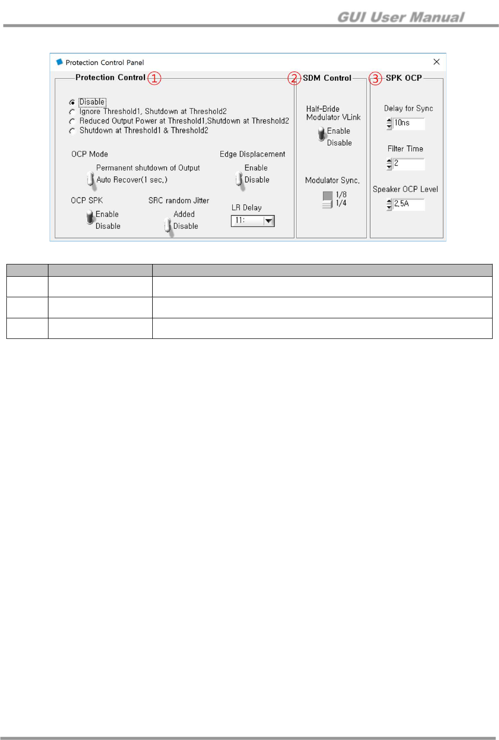
7.9 Protection Control
Figure 33. Brown Output Protection & VBAT Sensing Control Panel
No. Item Description
①
Protection Control TSD (Thermal Shutdown) Threshold and OCP (Over Current Protection) tuning
parameter (The chip designer will deliver the tuning value)
②
SDM Control Sigma Delta Modulation tuning parameter (The chip designer will deliver the tuning
value)
③
SPK OCP OCP (Over Current Protection) tuning parameter (The chip designer will deliver the
tuning value)

GUI User Manual
www.siliconmitus.com © 2017 Silicon Mitus, Inc.
28 / 28 October 2018 – Rev0.0.2
Revision History
Rev
DATE
CHANGES
Issued by
Notes
0.0
.0
05
/
02
/201
8
Initial
Release
.
Review
ed
with
GH
and SM
Gyuhwa
Park
0.0.1
10/10/2018
A
pply the latest GUI
(Ver. 1.1.6)
update
Gyuhwa Park
0.0.2
10/12/2018
Updating of EVB schematic and layout
Brian Pyun
─────────────────────────────────────────────────────────────────────────────
Silicon Mitus cannot assume any responsibility for the consequence of use of information furnished nor for any infringement of patents or
other rights of third parties which may result from its use. No circuit patent licenses are implied. Silicon Mitus reserves the right to change the
circuitry and specifications without notice at any time. This publication supersedes and replaces all information previously supplied. Silicon
Mitus products are not authorized for use as critical components in life support devices or systems without the express written approval of
Silicon Mitus.
© 2018 Silicon Mitus, Inc. - Printed in Korea - All Rights Reserved
