DVP NS305/NS310/NS315/NS405/NS410/NS415 NS405 SONY NS315
User Manual: DVP-NS405
Open the PDF directly: View PDF ![]() .
.
Page Count: 47
DVP-NS305/NS310/NS315/
NS405/NS410/NS415
RMT-D141A/D142A/D142O/D142P
US Model
Canadian Model
DVP-NS315/NS415
AEP Model
DVP-NS305/NS310/NS405/NS410
UK Model
DVP-NS305/NS405
Russian Model
Hong Kong Model
Korea Model
Taiwan Model
Saudi Arabia Model
GA Model
Indian Model
Pakistan Model
Malaysia Model
DVP-NS305
Middle East Model
Oceania Model
DVP-NS305/NS415
PX Model
Mexico Model
Latin Model
Argentina Model
Brazilian Model
DVP-NS315
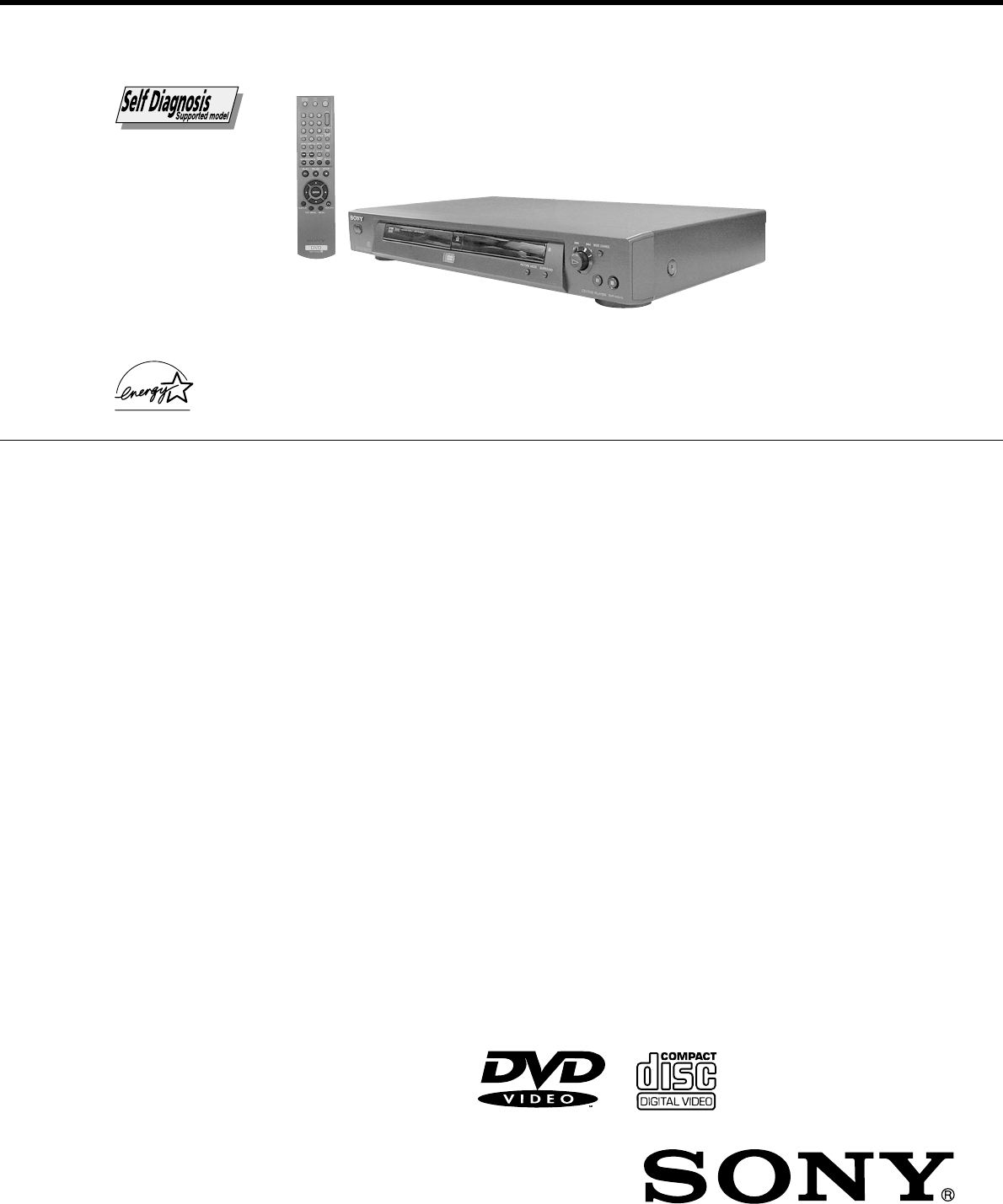
SERVICE MANUAL
CD/DVD PLAYER
System
Laser: Semiconductor laser
Signal format system: NTSC/PAL
Audio characteristics
Frequency response: DVD VIDEO (PCM
96 kHz): 2 Hz to 44 kHz (±1.0 dB)/DVD
VIDEO (PCM 48 kHz): 2 Hz to 22 kHz
(±0.5dB)/CD: 2Hz to 20kHz (±0.5 dB)
Signal-to-noise ratio (S/N ratio): 115 dB
(LINE OUT (L/R) AUDIO jacks only)
Harmonic distortion: 0.003 %
Dynamic range: DVD VIDEO: 103 dB/CD:
99 dB
Wow and flutter: Less than detected value
(±0.001% W PEAK)
The signals from LINE OUT L/R (AUDIO)
jacks are measured. When you play PCM
sound tracks with a 96 kHz sampling
frequency, the output signals from the
DIGITAL OUT (OPTICAL or COAXIAL)
jack are converted to 48 kHz sampling
frequency.
Outputs/Inputs
(Jack name: Jack type/Output or Input level/
Load impedance)
LINE IN (AUDIO)*: Phono jack/–/47
kilohms (DVP-NS315/NS415)
(DVP-NS315/NS415)
Outputs
(DVP-NS305/NS310/NS405/NS410)
LINE OUT (AUDIO): Phono jack/2 Vrms/
Over 10 kilohms
DIGITAL OUT (OPTICAL)*: Optical
output jack/–18 dBm (wave length:
660 nm)
DIGITAL OUT (COAXIAL): Phono jack/
0.5 Vp-p/75 ohms
COMPONENT VIDEO OUT(Y, P
B
, P
R
):
Phono jack/Y: 1.0 Vp-p/P
B
, P
R
: 0.7 Vp-p/
75 ohms (DVP-NS315/NS415)
(DVP-NS315/NS415)
LINE IN (VIDEO)*: Phono jack/1.0 Vp-p/
75 ohms
LINE OUT (VIDEO): Phono jack/1.0 Vp-p/
75 ohms
S VIDEO OUT: 4-pin mini DIN/Y:
1.0 Vp-p, C: 0.286 Vp-p/75 ohms
* DVP-NS405/NS410/NS415 only
General
Power requirements: 120 V AC, 60 Hz/
110 to 240V AC, 50/60 Hz
See page 1-1 for further information.
Power consumption: 12 W/13 W
See page 1-1 for further information.
Dimensions (approx.): 430 × 62 × 255 mm
(17 × 2
1
/
2
× 10
1
/
8
in.) (width/height/
depth) incl. projecting parts
Mass (approx.): 2.3 kg (5
5
/
64
lb)
Operating temperature: 5°C to 35 °C
(41
°
F to 95
°
F)
Operating humidity: 25 % to 80 %
Supplied accessories
See page 1-3.
Specifications and design are subject to
change without notice.
E
NERGY
S
TARR is a U.S. registered mark.
As an
E
NERGY
S
TARR Partner, Sony
Corporation has determined that this product
meets the
E
NERGY
S
TARR guidelines for
energy efficiency.
(To change the color system)
SPECIFICATIONS
Photo : DVP-NS415
RMT-D142A
DVP-NS305/NS310/NS315/NS405/NS410/NS415
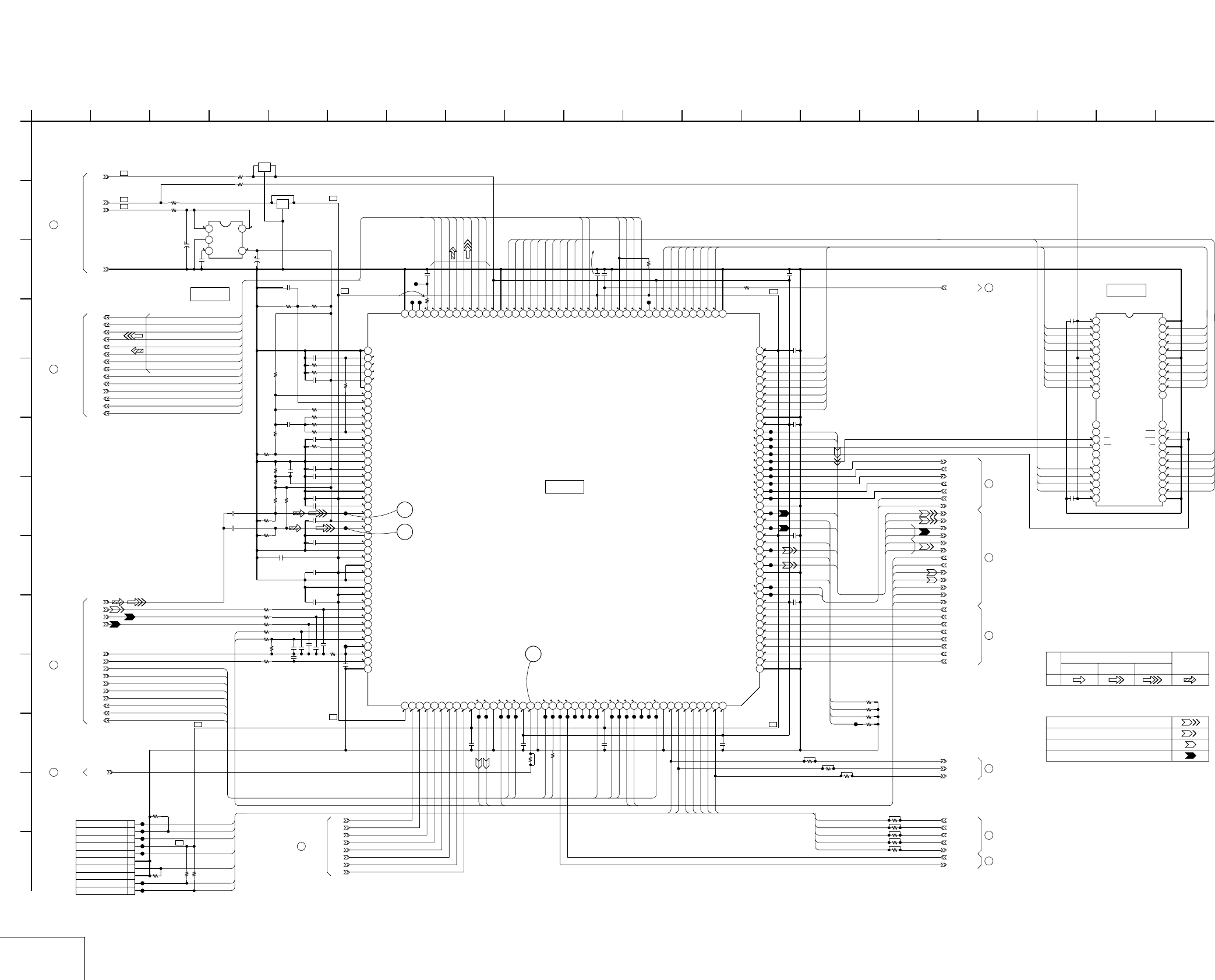
SECTION 3
BLOCK DIAGRAMS
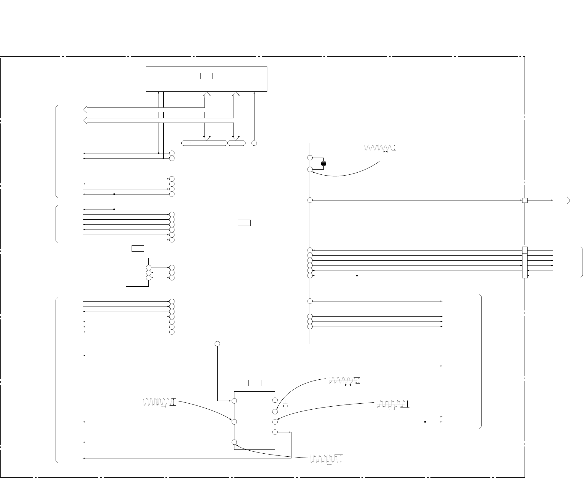
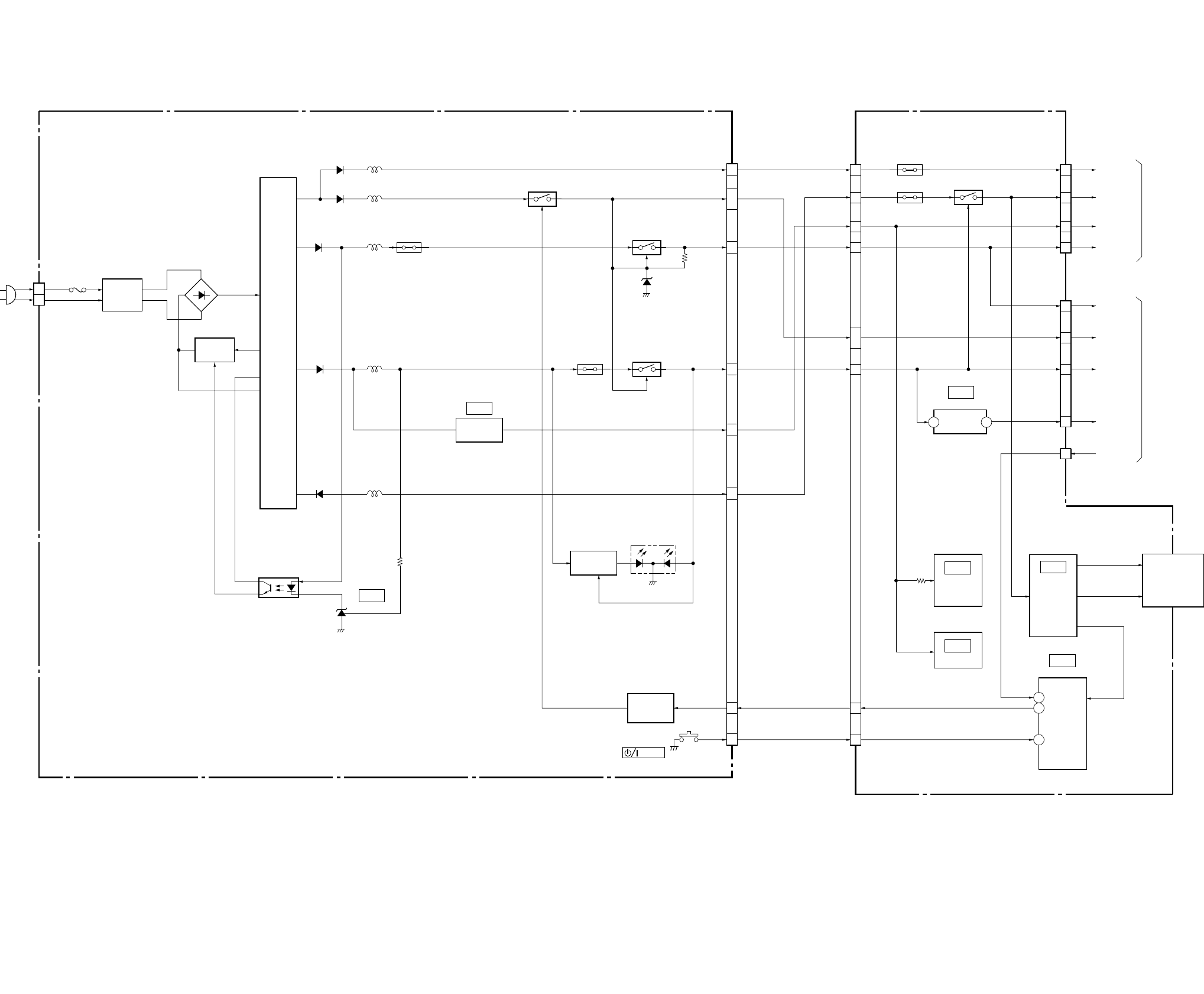
3-1. OVERALL BLOCK DIAGRAM
3-1 3-2
IC201
IC301
IC403
IC303
IC101
IC601
IC404
IC404
IC102
J104 (1/2)
J101 (2/2)
J103
CN103
IC202
BASE UNIT
KHM-270AAA/J1RP
MS-81 BOARD
(SEE PAGE 4-17)
MB-103 BOARD
(SEE PAGE 4-15 to 4-28)
AV-61 BOARD
(SEE PAGE 4-31 to 4-34)
IF-89 BOARD
(SEE PAGE 4-9)
OPTICAL DEVICE
DVD/CD
PD IC
RF
DVD/CD RF AMP,
DIGITAL SERVO
RF+
ARP,
SERVO DSP
FOCUS
COIL
TRACKING
COIL
FOCUS/TRACKING
COIL DRIVE,
SPINDLE/SLED/
LOADING
MOTOR DRIVE
MM
MM
MM
SPINDLE
MOTOR
SLED
MOTOR
M001
LOADING
MOTOR
FUNCTION
KEY
ND401
FLUORESCENT
INDICATOR TUBE
IF COM
P CON
POWER
SERIAL BUS
EEPROM
PARALLEL BUS
CDDOUT, CDDATA,
CDBCK, CDLRCK
SDI 0 – 7 AV DECODER
SPDIF, ACH12,
ACH34, ACH56,
BCK, LRCK
16M DRAM
16M SDRAM
V, Y, C
Y, Cb, Cr
VIDEO
BUFFER
SPDIF IC204
AUDIO
D/A CONVERTER
IC201
AUDIO
AMP
EVER+3.3V
+11V
+5V
SW+3.3V
+1.8V
SW+3.3V
+5V
SW+11V
EVER–13V
INLIMIT
SENSOR
CHUCK/TRAY
DETECT
SWITCHING REGULATOR
(SRV1246JUC)
(SEE PAGE 4-37)
SWITCHING
REG
AC IN
16
LINE OUT
VIDEO 1VIDEO 2
S VIDEO OUT
L
R
LINE OUT
AUDIO 2
L
R
AUDIO 1
OPTICAL
DIGITAL
OUT
COAXIAL
J201
D101-104
F101
2A
100V 50/60Hz
AI+5V
EVER+3.3V
AU+11V
SW–13V
REG
IC104
IC403
SYSTEM
CONTROL
S001
D1 VIDEO
OUT
AU+5V
REG
IC106
FLASH
MEMORY
SW801
POWER
DVP-NS305/NS310/NS315/NS405/NS410/NS415
3-3 3-4
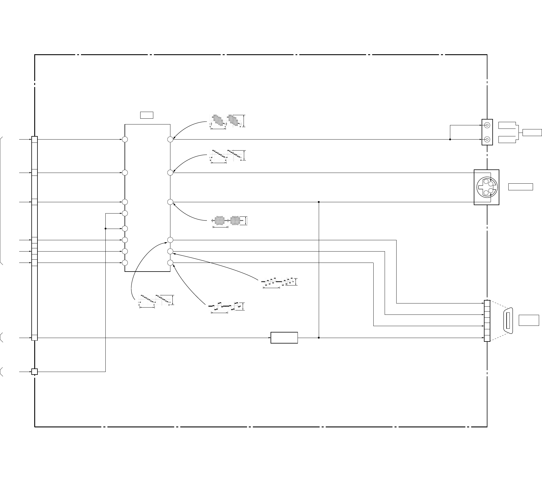
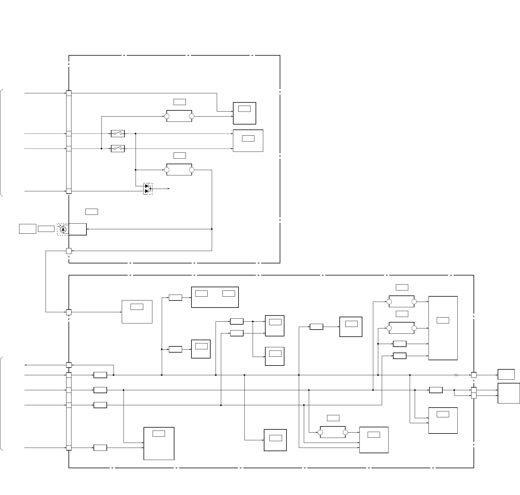
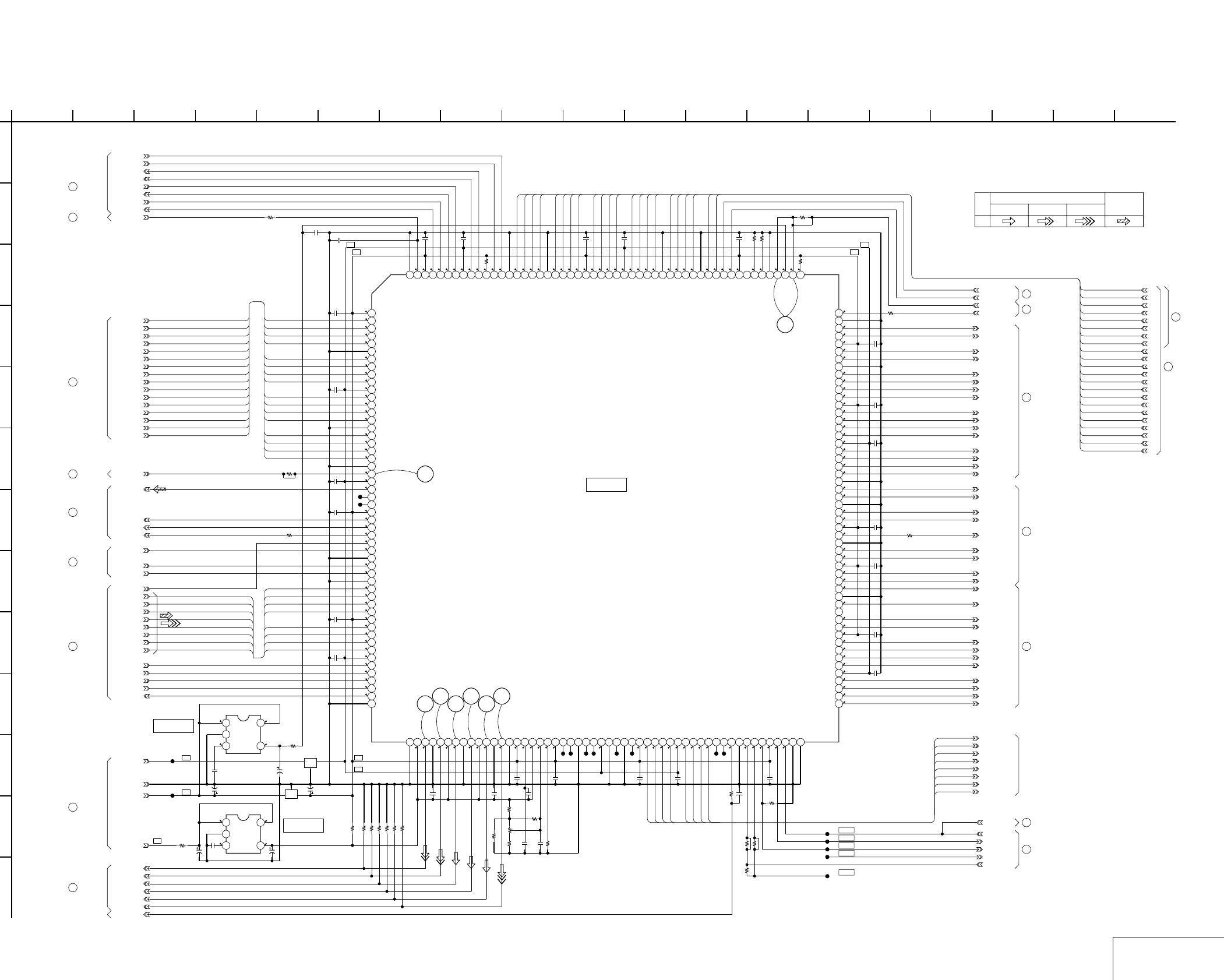
3-2. RF/SERVO BLOCK DIAGRAM
2
19
25
27
59
42
41
36
38
44
13
15
21
33
37
14
ı
11
7
ı
10
45
ı
48
32
ı
29
125
124
126
147
131
148
152
15
ı
18
37
36
21
22
48
1
47
46
20
22
15
17
35
34
27
28
7
10
25
24
3
4
45
5
128
153
154 146
61
12
11
143 14432 33
MB-103 BOARD (1/4)
(SEE PAGE 4-15, 17, 19)
BASE UNIT
KHM-250AAA/J1RP
OPTICAL DEVICE
24
25
17
16
22
20
13
8
6
12
4
3
15
23
18
26
2
1
Q201
DVD LD DRIVE
IC201
IC301
DVD/CD
PD IC
DVD/CD
LD MODULE
CN203
DVD/CD RF AMP,
DIGITAL SERVO
RF IN
A – D
E – H
A2 – D2
VC
DVDPD
CDPD
DVD LD
SIGO
FE
TE
PI
DFT
MON
MIRR
TZC
SRD
SWD
SCLK
SDEN
SERVO DSP
ADC1
ADC0
ADC2
DFCTI
ADC7
POM 2, 3
129
130 ADC5, 6
MIRR
TZC
ADC4
SIGNAL PROCESSOR
(SEE PAGE 3-5)
SYSTEM CONTROL
(SEE PAGE 3-7)
XRESET
HCS
HINT
MDSO
MDPO
163 164
GIO9/FGREF
GIO10/FGIN
GIO1/INT3
PWM2
PWM0, 1
POM 0, 1
GIO0/INT2
SPINDLE
MOTOR
DRIVE
FOCUS
COIL
DRIVE
TRACKING
COIL
DRIVE
LOADING
MOTOR
DRIVE
SLED
MOTOR
DRIVE
7
1
ı
4
9
8
1
5
4
IC202
5
24
1
2
CN402
CN001
LDM±
CKSW1
OCSW1
INLIMIT
SENSOR
TRACKING
COIL
FOCUS
COIL
M001
LOADING
MOTOR MM
MM
MM
MS-81 BOARD
(SEE PAGE 4-17)
SLED
MOTOR
SPINDLE
MOTOR
CN204
39VCI
19
39
20
22
16
17
155
GIO2/INT4
16
CHUCK/TRAY
DETECT
S001
(1/2)
RF
A – D
E – H
VC
PD
DVD LD
26
Q202
CD LD DRIVE CD LD
CD LD
VR
SLA±, SLB±
SPM±
INLIM
TRK±
127 ADC3
FCS±
PS
TSD-M
4042
43
VREF
+3.3V
LDON
159
161
162
167
GIO6/SDI
GIO7/SDO
GIO8/SCK
GIO13
XSDPIT
XSDPCS
XRST
XDRVMUTE
OCSW1
RF+
CKSW1
XLDON
FE
TE
PI
SSDFCTI
SS MON
MDSO, MDPO
SPMUTE
SLDA, SLDB
LMP, LMM
TSD
LMCTL
TDRV±
FDRV±
SPFG
SLE
640mVp-p
0.2usec/div 40usec/div
6
CN202 1 (DVD PB)
6
CN202 1 (CD PB)
440mVp-p
7
CN202 3
(DVD PLAY)
210mVp-p
20ms/div
7
CN202 3
(CD PLAY)
210mVp-p
20ms/div
8
CN202 4
(DVD PLAY)
1.9Vp-p
40ms/div
8
CN202 4
(CD PLAY)
1.8Vp-p
200ms/div
DVP-NS305/NS310/NS315/NS405/NS410/NS415
3-5 3-6
3-3. SIGNAL PROCESSOR BLOCK DIAGRAM
SDCK, XSHD,
XSRQ, XSAK, SDEF
SDCK
XSHD
XSRQ
XSAK
SDEF
DATA
BCLK
LRCK
DOUT
CDIN2I
CDIN1I
CDBCKI
CDLRKI
ICLKI
IERRI
ISTARTI
IVALI
IREQO
111
113
24
25
26
27
28
150
196
197
207
22
70
24
25
63
55
65
61
59
57
26
28
29
166
167
158
160
134
ı
141
2
ı
9
37
ı
40
42
ı
45
169
170
175
56
57
ı
59
63
64
47
ı
51
77
ı
84
65 – 74
MEMA 0 – 9
MEMD 0 – 15
ADAD 0 – 11
ADDT 0 – 15
105-108 110-113
115 116 118 120
135-138 140-143
145-148 150
151 153 154
168-169
171-174
176-179
181-184
186-189
191-194
2 – 5
7 – 10
12 – 15
17 – 20
122 124 125
127 129 130
132 133
36 – 43
46 – 53
29 31
30
IC303
16M DRAM
IC301
ARP
IC403
AV DECODER
IC404
16M SDRAM
31
32
34
35
202 – 205
MB-98 BOARD (2/4)
(SEE PAGE 4-19 to 4-23)
RF+
RF/SERVO
(SEE PAGE 3-4)
SYSTEM CONTROL
(SEE PAGE 3-7)
16
RFIN1
RFIN2
SD 0 – 7 SDI 0 – 7 DTI 0 – 7
MA 0 – 9 MD 0 – 15
SDDQ 0 – 15
CDDATA, CDBCK,
CDLRCK, CDDOUT
CLK, CKE,
DQML, DQMU,
CS, WE,
CAS, RAS
WE, RAS
LCAS, UCAS
C OUT
Y OUT
COMPOUT
B OUT
R OUT
G OUT
C
Y
V
Cr/B
Cb/R
Y/G
COUT
YOUT
COMPOUT
CR/B
CB/R
Y/G
VIDEO
(SEE PAGE 3-9)
AUDIO
(SEE PAGE 3-11)
VREFI
ACH12
ACH34
ACH56 LAND
LRCKO
BCKO
ACH12
LRCK
BCK
VIDEO
LEVEL
ADJ
RV401
HD 0 – 15
HAD 0 – 21HA 0 – 21
HD 0 – 15D 0 – 7
A 0 – 7 HA 0 – 7
HD 8 – 15
XRD
XWRH
RSTn
DM ACK1
DM REQ1
DM ACK0
DM REQ0
ACLK
HAD23
HAD22
CLKI
SCLKI
200
199
HWAIT0n
HIREQ0
HA 0 – 21
HD 0 – 15
HA 0 – 21
HD 0 – 15
XRST
512FSAVD
33MARP
XWRH
XRD
TRST
XARPIT
XARPCS
XWAIT
XAVDCS2
XAVDCS3
27MAVD
XAVDIT
DREQ0
DACK0
DREQ1
DACK1
XWR
XRD
XINT
XCS
XWAT
CLKIN
30DO SPDIF
175
174
173
172
TDO
TCK
TDI
TMS
171
97
99
98
101
102TRST
TDI
TCK
TDO
TMS
TRST
HCSn
HRWn
LAND
(FOR J TAG)
(2/2)
3
CN601 (1/3)
1
11
7
9
5
qj
IC403 yd
850mVp-p
H
qd
IC403 tg
H950mVp-p
qk
IC403 yg
1.1Vp-p
H
qh
IC403 ya
650mVp-p
H
qg
IC403 tl
650mVp-p
H
950mVp-p
H
qf
IC403 tj
qs
IC403 ws
4.8Vp-p
40.8nsec
ql
IC403 <zb, <zn/
5.1Vp-p
37nsec
q;
IC301 <zzz (CL301)
(DVD PLAY)
1.2Vp-p
40ns/div
qa
IC301 <zzc (CL302)
(CD PLAY)
1.4Vp-p
0.2µs/div
DVP-NS305/NS310/NS315/NS405/NS410/NS415
3-7 3-8
3-4. SYSTEM CONTROL BLOCK DIAGRAM
17
62
67
48
18
57
82
63
56
36
915
10
20
76
51
83
7
39
26
27
38
25
7
6
5
70
58
71
46
16
81
47
60
61
49
50
8
7
1 – 5 102 – 109 111 – 118 120 85 – 100
14
MB-103 BOARD (3/4)
(SEE PAGE 4-25 to 4-28)
IC104
SYSTEM
CONTROL
IC103
PLL
IC101
EEPROM
HD 0 – 15
HA 0 – 21
SIGNAL PROCESSOR
(SEE PAGE 3-5)
XARPIT
XARPCS
XWAIT
HA0 – 21 HA1 – 20
HD0 – 15 HD0 – 15
CSOX
SO0
SCO
SI0
INTERFACE
CONTROL
(SEE PAGE 3-13)
SI0
SO0
SC0
XIFCS
XIFBUSY
XFRRST
MAMUTE
XRST
INT4
XFRRST
XIFCS
MAMUTE
48/44.1k
54
53
X101
16.5MHz
XDRVMUTE
INT2
WIDE
CS5X
CKSW1
XDRVMUTE
XSDPIT
OCSW1
XLDON
XSDPCS
CKSW1
DREQ0
INTO
DACK0
CS2X
CS3X
DREQ1
DACK1
DREQ0
XAVDIT
DACK0
XAVDCS2
XAVDCS3
DREQ1
DACK1
VIDEO
(SEE PAGE 3-9)
SIGNAL PROCESSOR
(SEE PAGE 3-5)
RF/SERVO
(SEE PAGE 3-4)
16
33MARP
512FSAVD
X102
27MHz
33-1OUT
FSEL
512FS6CH
512FS2CH
TRST
29 SO1
SO1
30 SC1
SC1
79 XDACS
XDACS
INT1
CS4X
XWAIT
35
XRST
XRST
XRST
XRD
XWRH
512-2OUT
512-1OUT
XTI
XTO
3
27MAVD 27-1OUT
X1
X2
HD 0 – 15
HA 0 – 21
XRD
XWRH
3
CN101
5
6
8
4
1
CN601 (2/3)
2
WP
SCL
SDA
OCSW1
SCL
SDA
WP
WIDE
XARPRST
SI0
SO0
SC0
XIFCS
IFBSY
TRST
WIDE
AUDIO
(SEE PAGE 3-11)
HA 0 – 21 HD 0 – 15
IC106
FLASH
29.5nsec
3 IC103 qg
5.0Vp-p
37nsec
2 IC103 3
5.5Vp-p
40.8nsec 5.0Vp-p
4 IC103 9q;
37nsec
1 IC103 8
4.4Vp-p
60.6nsec
5 IC104 tf
1.8Vp-p
DVP-NS305/NS310/NS315/NS405/NS410/NS415
3-9 3-10
3-5. VIDEO BLOCK DIAGRAM
3
8
6
29
33
31
7
IC102
VIDEO BUFFER
12
15
17
24
22
20
19
15
25
23
21
17
AV-61 BOARD (1/2)
(SEE PAGE 4-33)
CN203 (1/2)
CN202 (1/2)
V
Y
C
Y/G
Cb/R
Cr/B
WIDE
VMUTE
SIGNAL PROCESSOR
(SEE PAGE 3-6)
16
SYSTEM CONTROL
(SEE PAGE 3-8)
INTERFACE CONTROL
(SEE PAGE 3-13)
J104 (2/2)
J103
16
5
11
3
1
CN103
Y
Cb
Cr
LINE3
LINE OUT
VIDEO 1
VIDEO 2
Y
CS VIDEO OUT
VIDEO IN
Y IN
C IN
MUTE1
Y IN
Cb IN
Cr IN
MUTE2
VIDEO OUT
Y OUT
C OUT
Y OUT
Cb OUT
Cr OUT
V
Y
C
Y
Cb
Cr
Q104, 105
WIDE SWITCH
1
24
D1 VIDEO
OUT
1
IC102 ed
2.5Vp-p
H
2
IC102 ea
1.8Vp-p
H
3
IC102 wl
2.0Vp-p
H
4
IC102 wf
2.0Vp-p
H
5
IC102 ws
1.4Vp-p
H
6
IC102 w;
1.4Vp-p
H
DVP-NS305/NS310/NS315/NS405/NS410/NS415
3-11 3-12
3-6. AUDIO BLOCK DIAGRAM
3
2
5
6
12
11
10
9
IC201
AUDIO AMP
IC601
AUDIO D/A CONVERTER
9
CN203 (2/2)
SDTI AOUTL+
AOUTL–
AOUTR+
AOUTR–
16DZFL
SYSTEM
CONTROL
(SEE PAGE 3-8)
SIGNAL PROCESSOR
(SEE PAGE 3-6)
INTERFACE
CONTROL
(SEE PAGE 3-13)
ALT+
16
J104 (2/2)
3
BICK2
LRCK4
MCLK1
CSN6
PDN5
CCLK7
CDTI8
17
CN601 (3/3)
11
ALT–
15
5
ART+
21
3
ART–
23
4
LMUTE
22
2
MAMUTE
24
MB-103 BOARD (4/4)
(SEE PAGE 4-27)
AV-61 BOARD (2/2)
(SEE PAGE 4-33)
10
IC204
OPTICAL
DIGITAL
OUT
COAXIAL
SPDIF J201
16
CN202 (2/2)
2
SPDIF
1D IN
ACH12
LRCK
BCK
SO1
SC1
XRST
512FS2CH
XDACS
MAMUTE
D202
Q211
BUFFER
Q208
MUTE
Q207
MUTE
1
7
+
–
+
–
Q202, 204, 205
MUTE DRIVE
L
R
AUDIO 1
LINE OUT
AUDIO 2
R
L
A MUTE
w;
IC601 1
40.8nsec 5.2Vp-p
DVP-NS305/NS310/NS315/NS405/NS410/NS415
3-13 3-14
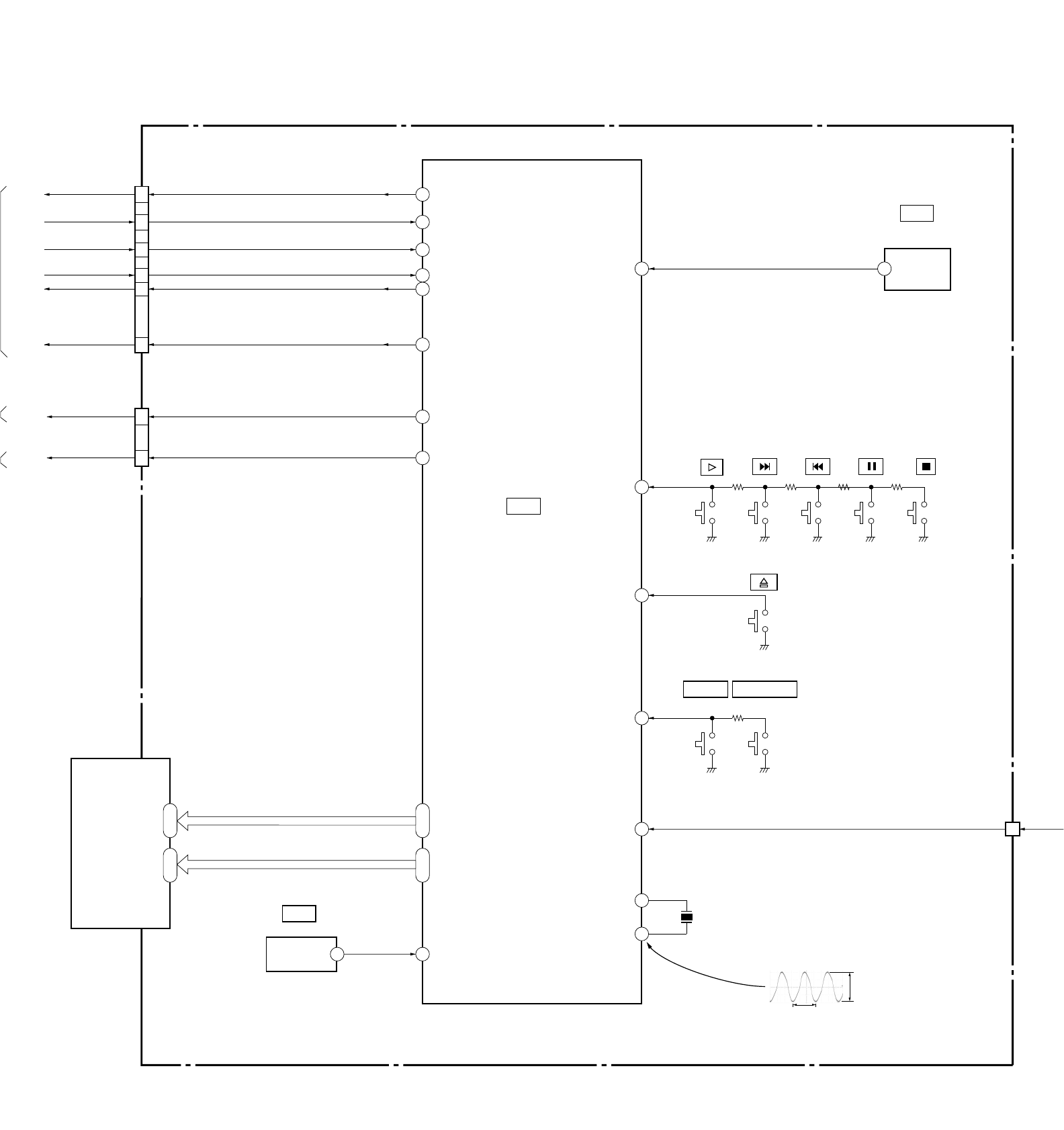
3-7. INTERFACE CONTROL BLOCK DIAGRAM
17
16
15
27
14
23
3
24
7
2
11
37
47
ı
69
77
ı
71
34
ı
12
5
ı
11
IF-89 BOARD
(SEE PAGE 4-9)
6
4
7
8
4
5
SYSTEM CONTROL
(SEE PAGE 3-8)
AUDIO
(SEE PAGE 3-12)
VIDEO
(SEE PAGE 3-9)
IC404
IF CON
IC405
RESET
CN404
SC0
SI0
SO0
XIFBUSY
XIFCS
XFRRST
/SC
SO
SI
BUSY
/CS
/FRRST
16
A MUTE
VMUTE
/AMUTE
/VMUTE
IR OUT
PICTURE MODESURRUND
S406
S405
S404
S402
S408
POWER
SEG 1 – 23
DIG 1 – 7
X401
8MHz
ND401
FLUORESCENT
INDICATOR TUBE
CN401
POWER
1
IC406
REMOTE COMMANDER
RECEIVER
2
1
CN402
SC0
SI0
SO0
XIFBUSY
XIFCS
XFRRST
34PLAY
35O/C
S401
S407 S403
36TVS
XIN
XOUT
1
VOUT 8/RST
SWITCHING REGULATOR
1
1
IC404 3
125nsec 3.9Vp-p
DVP-NS305/NS310/NS315/NS405/NS410/NS415
3-15 3-16
3-8. POWER BLOCK DIAGRAM (1/2)
12
6
•
7
SWITCHING REGULATOR
(SRV1246JUC)
(SEE PAGE 4-37)
CN201
EVER–13V
P311
T101
POWER
TRANSFORMER
D211
D311
D611
D511
D314
D101-104
AC IN F101
CN101
16
IF-89 BOARD
(SEE PAGE 4-37)
POWER 2
(SEE PAGE 3-17)
POWER 2
(SEE PAGE 3-17)
SW–13V
SW–13V
D621/D622
STANDBY/ON
Q621, 622
LED DRIVE
PC101
PHOTO COUPLER
IC101
SWITCH
8
11
3
2
1
13
1
2
Q211
Q311
Q611
Q404, 405
PS401
L102
LINE
FILTER
D221
P611
+3.3V REG
Q712
POWER
CONTROL
L211
L221
L311
L611
L512
26
37
IC404
IF CON
IC406
REMOTE
COMMANDER
RECEIVER
IC405
RESET
IC412
IC611
SHUNT REG
PCONT
IC403
+1.8V REG
POWER
30 PONCHK VKK
F2
F1
EVER+3.3V
EVER+3.3V
EVER+3.3V
AI+5V
+3.3V
+5V
+1.8V
SW+11V +11V
3.3V MNT
ND401
FLUORESCENT
INDICATOR TUBE
POWER
SUPPLY
AU+11V
PS402
3VIN 2VOUT
CN401
2
CN403
CN404
13
3
11
12
8 4
1
5
7
5
CN402
7
3
6
2
1
6
•
7
SW+11V
EVER+11V
+5V
SW+3.3V
EVER+3.3V
EVER–13V
P-CONT
POWER
SW801
POWER
IC407
DVP-NS305/NS310/NS315/NS405/NS410/NS415
3-17 3-18
3-9. POWER BLOCK DIAGRAM (2/2)
1
11
19
AV-61 BOARD
(SEE PAGE 4-31 to 4-34)
OPTICAL
DEVICE
16
MB-103 BOARD
(SEE PAGE 4-15 to 4-28)
CN101
CN102
CN203
INLIMIT
SENSOR
5
CN204
IC102
VIDEO
BUFFER
IC103
–5V REG
3OUT
IC601
AUDIO
D/A CONVERTER
IC101
EEPROM
IC202
FOCUS/TRACKING
COIL DRIVE,
SPINDLE/SLED/
LOADING
MOTOR DRIVE
IC404
16M SDRAM
AI+5V
2IN
IC203
+5V REG
1OUT
3IN
IC402
+3.3V REG
4VOUT
5VIN
IC401
+1.8V REG
4VOUT
5VIN
IC302
+3.3V REG
4VOUT
5VIN
MUTE V
SW–13V
EVER+3.3V
AU+11V
D201
IC204
OPTICAL DIGITAL
OUT
CN203
25
CN601
POWER 1
(SEE PAGE 3-16)
POWER 1
(SEE PAGE 3-16)
IC201
AUDIO AMP
Q201
Q203, 216
OPTICAL
DIGITAL
OUT
FILTER
FL110
7
4
IC104
SYSTEM
CONTROL
FILTER
FL103
FILTER
FL201
+3.3V
FILTER
FL105
2
+5V
FILTER
FL104
1
+1.8V
FILTER
FL109
5
CN202
6
5
7
3
+11V
3.3V MNT
IC303
16M DRAM
IC201
DVD/CD RF AMP,
DIGITAL
SERVO
IC403
AV DECODER
IC301
ARP,
SERVO DSP
VCC
MOD
LED
FILTER
FL404
FILTER
FL403
FILTER
FL402
AU+5V
IC103
PLL
FILTER
FL101
IC106
FLASH
MEMORY
IC107
OTP
FILTER
FL106
or
FILTER
FL102
DVP-NS305/NS310/NS315/NS405/NS410/NS415
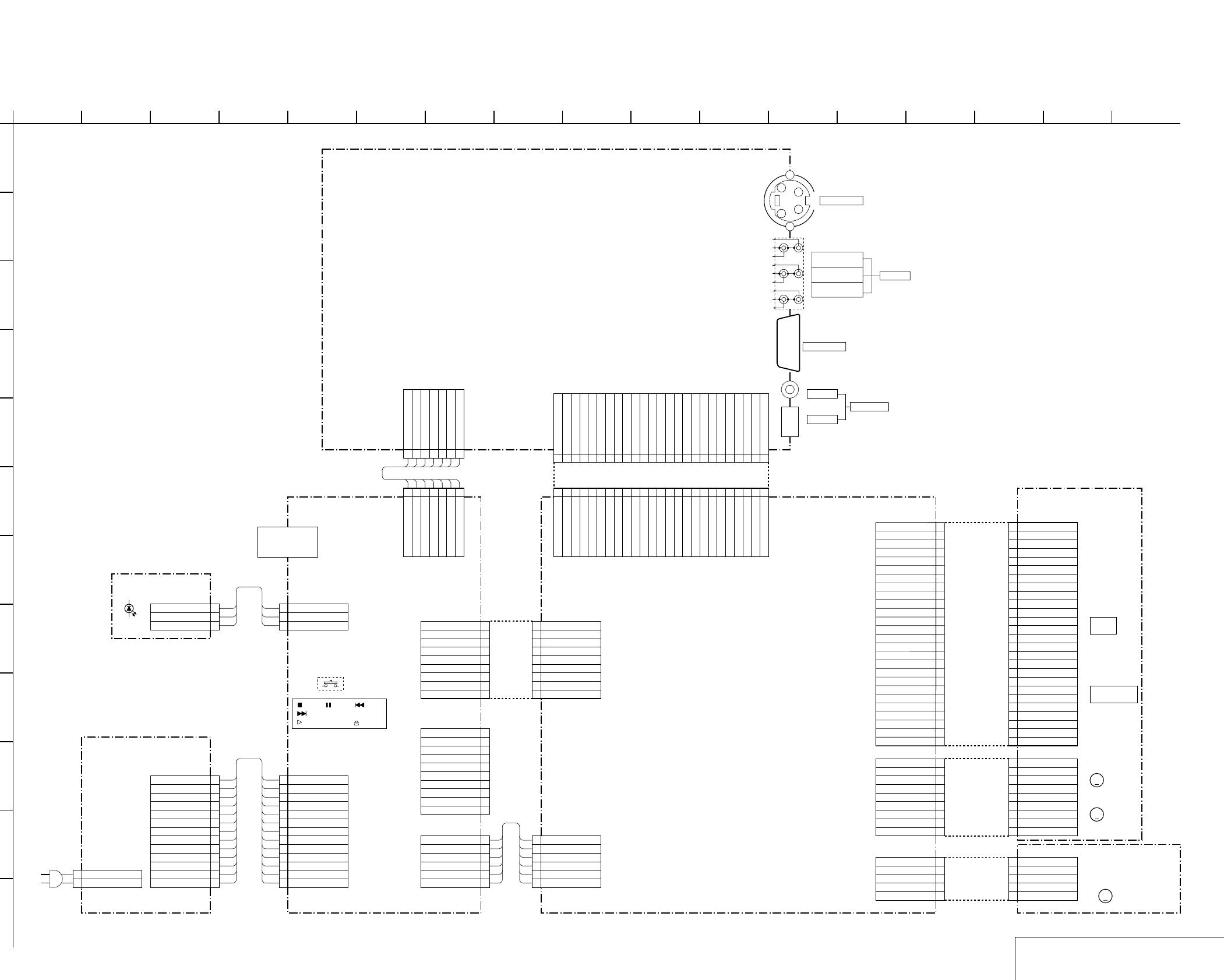
4-1 4-2
SECTION 4
PRINTED WIRING BOARDS AND SCHEMATIC DIAGRAMS
4-1. FRAME SCHEMATIC DIAGRAM
FRAME SCHEMATIC DIAGRAM
2P
CN101
1 AC_IN(L)
2 AC_IN(N)
26P
1
2
3
4
5
6
7
8
9
10
11
12
13
14
15
16
17
18
19
20
21
22
23
24
25
26
9P
1
2
3
4
5
6
7
8
9
5P
CN001
1
2
3
4
5
6PCN102
1
2
3
4
5
6
CN101 9P
1
2
3
4
5
6
7
8
9
CN203 26P
1
2
3
4
5
6
7
8
9
10
11
12
13
14
15
16
17
18
19
20
21
22
23
24
25
26
CN204 9P
1
2
3
4
5
6
7
8
9
CN601
1
2
3
4
5
6
7
8
9
10
11
12
13
14
15
16
17
18
19
20
21
22
23
24
25
CN201 5P
1
2
3
4
5
7PCN202
1
2
3
4
5
6
7
CN203 25P
1 AU+5V
2 MAMUTE
3ART-
4 LMUTE
5ART+
6 RMUTE
7 P_GND_AUDIO
8 P_GND_SPDIF
9ALT+
10 SPDIF
11 ALT-
12 RGBSEL
13 D_GND_VIDEO
14 EUROVY
15 V
16 DISC/EXT
17 C
18 D_GND_VIDEO
19 Y
20 D_GND_VIDEO
21 Y/G
22 D_GND_VIDEO
23 Cb/R
24 WIDE
25 Cr/B
CN403
1
2
3
4
5
6
CN402
1
2
3
4
5
6
7
3PCN406
1 +5V
2 N.C.
3 LED PORT
13PCN401
1
2
3
4
5
6
7
8
9
10
11
12
13
CN404 9P
1
2
3
4
5
6
7
8
9
10PCN405
1
2
3
4
5
6
7
8
9
10
3PCN301
1+5V
2N.C.
3LED PORT
13PCN201
1P-DET
2P-CONT
3EVER-13V
4M_GND
5M_GND
6SW+11V
7SW+11V
8SW+3.3V
9D_GND
10D_GND
11EVER+3.3V
12+5V
13+11V(AUDIO)
J104
Y
C
GG
S
S
J103
D301
S401-408
1
A
CD LD
GND
FCS-
TRK+
SW
LD GND
VC
B
GND
A
C
D
CKSW1
GND
LDM-
LDM+
OCSW1
VCC
PD
N.C
INLIM
N.C
GND
DVD LD
SLA+
H
SLA-
SPM-
SLB-
MOD
FMS-017
LED
RF
SPM+
E
G
FMO-004
F
FCS+
VR
TRK-
SLB+
FMM-041
GND
3.3V_MNT
XIFCS
XIFBUSY
SO0
SI0
SC0
+5V
+3.3V
M_GND
+1.8V
XFRRST
GND
+11V
GND
LDM-
OCSW1
LDM+
CKSW1
GND
VR
GND
FCS+
VC
TRK-
SW/N.C
RF
A
N.C
H
G
FCS-
F
CD LD/N.C
VCC
E
N.C
B
PD
D
C
TRK+
DVD LD
GND
MOD
LD GND
SPM-
SLA-
INLIM
SLA+
SPM+
SLB+
GND
LED
SLB-
MAMUTE
ART+
ALT+
GND
DISCEXT
RGBSEL
ART-
25P
RMUTE
SPDIF
Y/G
C
GND
P_GND_2CH
WIDE
ALT-
GND
GND
EUROVY
AU+5V
LMUTE
Cr/B
P_GND_SPDIF
Cb/R
Y
V
EVER+3.3V
D_GND_VIDEO
SW_-13V
VMUTE
AI+5V
AU+11V
A_MUTE
AU+11V
A_MUTE
+1.8V
GND
V_MUTE
+5V
SW-13V
EVER+3.3V
+11V
GND
AI+5V
M_GND
SW+3.3V
POWER
EVER+3.3V
SW+11V
P-CONT
SW+3.3V
M_GND
D_GND
M_GND
EVER-13V
+11V(AUDIO)
D_GND
+5V
SW+11V
XIFBUSY
XFRRST
IFRST
GND
XIFCS
PCONT
SIO
GND
GND
SIO
XIFCS
3.3V_MNT
3.3V_MNT
SOO
XIFBUSY
SOO
XFRRST
SC0
SCO
B to B
AUDIO2
AUDIO2
AUDIO1
L
R
AUDIO1
LINE OUT
VIDEO2VIDEO1
R
S1 VIDEO OUT
L
D1 VIDEO OUT
M
7
14 8
1
COAXIAL
DIGITAL OUT
OPTICAL
J201
IC204
AV-61 BOARD
ND401
FLUORESCENT
INDICATOR TUBE
MB-103 BOARD
IF-89 BOARD
FL-126 BOARD
SWITCHING REGURATOR
(SRV1246JUC)
PF-127
HARNESS
MF-128
HARNESS
(FOR MF-128 HARNESS)
(FOR CHECK)
FLAT CABLE
FLAT CABLE
FLAT CABLE
OPTICAL PICK-UP
UNIT
MS-81 BOARD
CHUCK/TRAY
DETECT
M001
LOADING
MOTOR
M
SPINDLE
MOTOR
M
SLED
MOTOR
FOCUS/TRACKING
COIL
DVD/CD
PD IC
B to B
AF-121
HARNESS
(DVD LED)
(STOP), (PAUSE), (PREV),
(NEXT), PICTURE MODE,
(PLAY), SURROUND,
AC IN
100V 50/60Hz
16
H
23 12
J
179
G
11
E
C
10
K
14136
B
7
I
D
F
155
L
84 16
(FOR AF-121
HARNESS)
(O/C)
FF-206
HARNESS
DVP-NS305/NS310/NS315/NS405/NS410/NS415
4-4
(For printed wiring boards)
•X : indicates a lead wire mounted on the component side.
•x : indicates a lead wire mounted on the printed side.
•a : Through hole.
•b : Pattern from the side which enables seeing.
(The other layers' patterns are not indicated.)
THIS NOTE IS COMMON FOR WIRING BOARDS AND SCHEMATIC DIAGRAMS
(In addition to this, the necessary note is printed in each block)
When indicating parts by reference number, pleas include
the board name.
Caution:
Pattern face side: Parts on the pattern face side seen from
(Side B) the pattern face are indicated.
Parts face side: Parts on the parts face side seen from
(Side A) the parts face are indicated.
(For schematic diagrams)
• All capacitors are in µF unless otherwise noted. pF : µµF.
50V or less are not indicated except for electrolytics and
tantalums.
• All resistors are in ohms, 1/4 W (Chip resistors : 1 /10 W) un-less
otherwise specified.
kΩ=1000Ω, MΩ=1000kΩ.
• Caution when replacing chip parts.
New parts must be attached after removal of chip.
Be careful not to heat the minus side of tantalum capacitor, be-
cause it is damaged by the heat.
• All variable and adjustable resistors have characteristic curve B,
unless otherwise noted.
•2: non flammable resistor
•5: fusible resistor
•C: panel designation
• f : internal component.
•C: adjustment for repair.
•U: B+ Line
•V: B– Line
• Circled numbers refer to waveforms.
• Voltages are dc between measurement point.
• Readings are taken with a color-bar signals on DVD refer-ence
disc and when playing CD reference disc.
• Readings are taken with a digital multimeter (DC 10MW).
• Voltage variations may be noted due to normal production toler-
ances.
4-2. PRINTED WIRING BOARDS AND SCHEMATIC DIAGRAMS
Note :
The components identified by
mark 0 or dotted line with mark
0 are critical for safety.
Replace only with part number
specified.
Note :
Les composants identifiés par
une marque 0 sont critiques
pour la sécurité.
Ne les remplacer que par une
pièce portant le numéro spécifié.
DVP-NS305/NS310/NS315/NS405/NS410/NS415
4-5
IF-089 BOARD
1 IC404 3
125nsec 3.9Vp-p
37nsec
37nsec
29.5nsec
60.6nsec
MB-103 BOARD
2
IC103 3
1
IC103 8
5.5Vp-p
4.4Vp-p
640mVp-p
3
IC103 qg
5.0Vp-p
40.8nsec 5.0Vp-p
5
IC104 tf
0.2usec/div
40usec/div
1.8Vp-p
6
CN202 1 (DVD PB)
6
CN202 1 (CD PB)
440mVp-p
4
IC103 9q;
7
CN202 3
(DVD PLAY)
210mVp-p
20ms/div
7
CN202 3
(CD PLAY)
210mVp-p
20ms/div
8
CN202 4
(DVD PLAY)
1.9Vp-p
40ms/div
8
CN202 4
(CD PLAY)
1.8Vp-p
200ms/div
qs
IC403 ws
4.8Vp-p
40.8nsec
9
IC301 <zb/
4.6Vp-p
30nsec
q;
IC301 <zzz (CL301)
(DVD PLAY)
1.2Vp-p
40ns/div
qa
IC301 <zzc (CL302)
(CD PLAY)
1.4Vp-p
0.2µs/div
qd
IC403 tg
H950mVp-p
w;
IC601 1
40.8nsec 5.2Vp-p
qj
IC403 yd
850mVp-p
H
qg
IC403 tl
650mVp-p
H
qk
IC403 yg
1.1Vp-p
H
qh
IC403 ya
650mVp-p
H
950mVp-p
H
qf
IC403 tj
ql
IC403 <zb, <zn/
5.1Vp-p
37nsec
WAVEFORMS
IF-089/MB-103/AV-61
AV-61
BOARD
2
IC102 ea
3
IC102 wl
1
IC102 ed
2.5Vp-p
H
1.8Vp-p
2.0Vp-p
H
H
4
IC102 wf
2.0Vp-p
H
5
IC102 ws
1.4Vp-p
H
6
IC102 w;
1.4Vp-p
H
4-6
DVP-NS305/NS310/NS315/NS405/NS410/NS415
4-9 4-10
IF COM
IF-89
For Schematic Diagram
• Refer to page 4-7 for printed wiring board.
• Refer to page 4-5 for waveform.
JL475
10k
R430
22k
R458
JL451
2700
R411
JL465
10k
R414
100
R444
10k
R429
100
R428
JL467
R437
XX
JL446
XX
R421
JL432
S-80830ANUP-EDT-T2
IC405
123
0.01u
B
C414
JL450
XX
C419
JL458
100
R442
0.01u
B
C417
JL409
10k
R441
JL426
JL448
XX
C413
8200
R406
0.01u
B
C405
S403
100
R445
JL469
S404
0.1u
B
C424
1800
R417
0.001u B
C415
JL416
R453
10
10k
R424
2SD1766-T100-QR
Q404
PS401
JL449
JL454
ET402
XX
JL468
JL442
JL473
10k
R438
100
R443
JL408
XX
R439
120R456
JL437
JL406
CN404 9P
1
2
3
4
5
6
7
8
9
JL419
16V
100u
C408
JL460
2700
R412
3900
R409
XX
R410
JL402
100
R448
JL476
JL421
IC406 GP1UD24SYK
123
JL413
ND401
1
F1
2
F1
5
G7
6
G6
7
G5
8
G4
9
G3
10
G2
11
G1
12
P1
13
P2
14
P3
15
P4
16
P5
17
P6
18
P7
19
P8
20
P9
21
P10
22
P11
23
P12
24
P13
25
P14
26
P15
27
P16
28
P17
29
P18
30
P19
31
P20
32
P21
33
P22
34
P23
37
F2
38
F2
25V
22u
C425
JL438
JL405
JL464
PS402
JL472
33
R407
XX
C406
JL455
LMS8117ADTX-1.8/NOPB
IC403
1
GND
2
Vout
3
Vin
S401
JL443
JL452
S405
25V
22u
C421
S409
XX
JL471
0.01u
B
C423
100
R447
100
R446
JL404
JL477
XX
R457
UN2111-TX
Q405
JL429
0.01u
B
C418
100k
R434
0.01u
B
C402
CN402 FOR AF-121 HARNESS
1
2
3
4
5
6
7
120
R418
JL430
JL407
JL462
JL417
XX
R431
JL423
JL478
X401
XX
C412
JL466
1800
R416
JL435
JL474
JL425
C416
100u
25V
S402
0.01u
B
C411
XX
R452
S407
0.01u
B
C409
10k
R425
0.01u
B
C404
FOR MF-128 HARNESSCN403
1
2
3
4
5
6
47
R401
JL445
16V
47u
C401
0.01u
B
C420
JL457
JL420
JL433
10k
R413
JL424
XX
C403
JL428
S406
AN13990-NML
IC407
1234
5678
JL422
JL463
JL479
JL414
120R455
JL470
JL453JL412
10k
R436
JL403
S408
10k
R432
JL440
JL439
0.01u
B
C407
100k
R402
IC404
12345678
910111213141516171819202122
2324
25 26 27 28 29 30 31 32 33 34 35 36 37 38 39 40
41 42 43 44 45 46 47 48 49 50 51 52 53 54 55 56 57 58 59 60 61 62 63 64
6566676869707172737475767778
7980
JL431
13P
CN401
1
2
3
4
5
6
7
8
9
10
11
12
13
10k
R415
JL459
JL461
JL410
JL401
JL441
JL418
JL434
JL411
22k
R405
10PCN405
1
2
3
4
5
6
7
8
9
10
10k
R408
JL444
JL447
XX
D402
JL436
3P
CN406
1+5V
2N.C
3LED PORT
JL415
10k
R426
2.2
R459
0.01u
C426
0.1u
C427
10k
R460
0.1u
B
C428
3PCN301
1 +5V
2N.C
3 LED PORT
D301
EB3804X-TP
220
R301
1
A
SEG16
SEG15
SEG20
SEG19
SEG18
SEG17
SEG14
SEG13
SEG6
SEG7
SEG8
SEG9
SEG12
SEG11
SEG10
DIG3
DIG2
DIG1
SEG21
SEG22
DIG4
DIG5
DIG6
DIG7
SEG1
SEG2
SEG3
SEG4
SEG5
DIG7
DIG6
DIG5
DIG4
DIG3
DIG2
DIG1
SEG1
SEG2
SEG3
SEG4
SEG5
SEG6
SEG7
SEG8
SEG9
SEG10
SEG11
SEG12
SEG13
SEG14
SEG15
SEG16
SEG17
SEG18
SEG19
SEG20
SEG21
SEG22
SEG23
SEG23
POWER
(PLAY)
VCC
GND
VOUT
XIFCS
SC0
SOO
SIO
XIFBUSY
XFRRST
3.3V_MNT
GND
IFRST
B TO B
P-CONT
POWER
D_GND
D_GND
SW+3.3V
EVER+3.3V
+11V(AUDIO)
(NEXT)
PCONT
DIG1
DIG2
DIG3
DIG4
DIG5
DIG6
DIG7
SEG1
SEG2
SEG3
SEG4
SEG7
SEG8
SEG9
SEG10
SEG11
SEG12
SEG13
SEG14
SEG15
SEG16
SEG17
SEG18
SEG19
SEG20
SEG21
SEG22
SEG6
SEG5
SEG23
N.C
TVS
BNRKEY
AN6
AVSS
PLAY
PONCHK
VREF
VKK
AN11
SEL1
SEL0
PCONT
STATUS
BUSY
VSS
XIN
XOUT
VDD
/FRRST
IR
/RST
N.C
SELF_CHECK
/STOP
SO
SI
/SC
/CS
/VMUTE
PDET
SEL2
TEST
/AMUTE
VCC
N.C
N.C
N.C
N.C
M_GND
M_GND
SW+11V
SW+11V
EVER-13V
8MHz
SURROUND
+5V
SW-13V
V_MUTE
A_MUTE
AI+5V
EVER+3.3V
AU+11V
GND
0.7A
SOO
GND
SCO
SIO
XIFBUSY
XIFCS
3.3V_MNT
XFRRST
GND
(PREV)
O/C
(OPEN/CLOSE)
(PAUSE)
(STOP)
MODE
POWER
N.C
N.C
N.C
N.C
N.C
N.C
+11V
+5V
SW+3.3V
GND
+1.8V
M_GND
DVD LED
TMP86CK74F
1.0A
RED
GREEN
PICTURE
MODE
SWITCH
SWITCH
TO MB-103 BOARD(7/7)
CN101
(SEE PAGE4-28)
FOR
CHECK
FLUORESCENT INDICATOR TUBE
IC404
IF COM
IC405
RESET
IC406
REMOTE COMMANDER
RECEIVER
IC407
DC/DC CONVERTER
FL-126
BOARD
LED
FF-206
HARNESS
IC403
+1.8V REG
(SEE PAGE4-32)
TO AV-61 BOARD
CN202
TO MB-103 BOARD
CN202
(SEE PAGE4-28)
B+
B+
B+
B+
B+
B+
B+
B+
B+
B-
B-
B+
B-
B+
B+
B+
B+
TO SWITCHING REGURATOR
(SEE PAGE4-42)
B+
B+
IF COM
IF-89 BOARD
XX MARK:NO MOUNT
-REF.NO.:3000 SERIES-
16
19
H
M
23 12
J
179
G
11
E
C
10
K
14136
B
7
I
D
18
F
155
L
84 2016
1
0.1
3.5
-10.0
-10.0
-10.0
-10.0
-10.0
-10.0
-10.0
-11.9
-11.9
-5.2
-11.9
1.3
-11.9
-9.6
-11.9
-0.9
-7.4
-5.3
-7.4
-7.4
-5.3
-11.9
-9.7
-11.9
-9.6
-5.3
-11.9
-0.9
-9.7
-9.7
-0.3
-0.5
0
3.5
3.5
3.5
3.5
-12.0
3.5
3.5
3.5
3.5
3.5
0
2.7
0
*
1.6
0
3.4
1.5
3.1
3.5
3.3
3.4
3.4
3.4
3.5
0
3.4
3.5
-6.9
-5.7
0
-12.0
-11.0
3.5
3.5
3.5
3.4
3.3
3.5
-12.0 -12.0
-11.3
1.8
3.5
NO MARK:PB MODE
* :Cannot be measured
Note :
The components identified by
mark 0 or dotted line with mark
0 are critical for safety.
Replace only with part number
specified.
Note :
Les composants identifiés par
une marque 0 sont critiques
pour la sécurité.
Ne les remplacer que par une
pièce portant le numéro spécifié.
DVP-NS305/NS310/NS315/NS405/NS410/NS415
4-15 4-16
For Schematic Diagram
• Refer to page 4-11 for printed wiring board.
• Refer to page 4-5 for waveforms.
DVD/CD RF AMP, DIGITAL SERVO
MB-103 (1/7)
XLDON
47uH
L201
0.1u
B
C262
2200p B
C212
TE
6.3V
47u
C242
4700
R206
XX
R209
SSDFCTI
0.01u
B
C243
33
R249
CN203 26P
1
2
3
4
5
6
7
8
9
10
11
12
13
14
15
16
17
18
19
20
21
22
23
24
25
26
XX
C267
100
R211
XX
R247
SSWD
SSRD
330p
C261
2200p B
C211
0.01u
B
C260
0.1u
B
C241
SSCK
RF+
100
R235
4700p
B
C233
47k
R251
0.1u
B
C244
100
R246
SSCS
0.001u
C253
+3.3V
0.01u
B
C248
RFMON
33
R248
CN202 XX
1
2
3
4
5
0.1u
B
C265
2SB1132-T100-QR
Q202
MIRR
XX
R268
CN204
1
2
3
4
5
6
7
8
9
2.2M
R263
2200p B
C213
GND
0.01u
B
C201
100
R256
0.047u B
C256
16V
10u
C238
100
R212
0.01u
B
C235
0.01u
B
C266
560p
C236
0.1u
B
C251
TZC
XX
C239
XX
R267
0.01u
B
C202
0.047u B
C257
4700p
B
C232
100k
R264
27k
R265
47k
R245
2200p B
C210
0.01u
B
C247
2SB1132-T100-QR
Q201
0.1u
B
C252
16V
10u
C221
XX
C269
SS_MON
0.01u
B
C245
1k
R244
0.1u
B
C255
XX
D201
0.01u
B
C254
FE
330
R210
6.3V
47u
C234
+5V
12k
R260
33
R234
47uH
L202
XX
D202
33
R236
16V
10u
C263
PI
0.01u
B
C264
FL201
XX
C237
SP3728ACB
IC201
12345678
910111213141516
17 18 19 20 21 22 23 24 25 26 27 28 29 30 31 32
33 34 35 36 37 38 39 40 41 42 43 44 45 46 47 48
4950515253545556575859606162
6364
JL201
JL202
JL203
JL205
JL204
JL206
JL207
JL208
JL209
JL210
JL211
JL213
JL212
0
R273
XX
R266
XX
R272
XX
C224
CN203 26P
1
2
3
4
5
6
7
8
9
10
11
12
13
14
15
16
17
18
19
20
21
22
23
24
25
26
CN204 9P
1
2
3
4
5
6
7
8
9
INLIM
TRK-
FCS+
FCS-
SVC
TRK+
SVC
1
A
SPM+
SLA-
SLB+
SPM-
SLB-
SLA+
SSCS
B
SSDFCTI
H
SSWD
F
TE
SSDFCTI
D
DVD_LD
FE
G
SLA-
H
FCS+
SLB+
TRK+
A
B
FCS-
CD_LD
D
DVD_LD
SSCS
G
PI
SSCK
MIRR
SPM+
C
C
SPM-
TRK-
E
SLA+
FE
CD_LD
PI
SLB-
TE
FE
SSCK
SSWD
SSRD
TZC
E
F
SSRD
A
MIRR
TZC
TE
PI
INLIM
SLA+
SLB-
SLB+
SPM+
SLA-
SPM-
FCS+
FCS-
TRK+
TRK-
INLIM
CDPD
N.C
DVDPD
RFIN
MEVO
CDLD
MIRR
VPA
DVD LD
RF
TZIN
F
GND
E
MB
SLA-
MEV
AIP
RFIP
DIP
FE
D
LDON
TPA
ATON
BYP2
VCC
LD GND
F
INLIM
A
SLB-
C2
FE
MIN
G
MON
RF
AIN
SLB+
LDSELO
TE
D
SRD
C
SCLK
GND
PI
RX
PII
BYP
A
GND
N.C
FCS+
GND
E
H
D2
WIN
SWD
C TZC
B2
VC
B
MLPF
FNP
H
TRK-
VNA
FCS-
VR
TRK+
CN
SW/N.C
WPP
SLA+
CD LD
B
LED
VPB
CP
VNB
DFT
TPH
SDEN
PI
DVDLD
VCI
SIGO
MP
V33
ATOP
DIN
FNN
VC
G
TE
MOD
SPM+
PD
A2
SPM-
9P
SW/N.C.
VR
C
D
VCC
FCS+
A
TRK-
F
RF
MOD
N.C.
N.C.
VC
LD GND
DVD LD
CD LD
TRK+
FCS-
H
GND
PD
GND
B
G
E
SLA-
GND
SLA+
INLIM
SLB-
SPM+
SPM-
SLB+
LED
DVD/CD
PD IC
DVD/CD
LD MODULE
FOCUS
COIL
TRACKING
COIL
OPTICAL DEVICE
BASE UNIT
KHM-270AAA/Z-NP
M
M
INLIMIT
SENSOR
FMO-004
FLAT CABLE
FMM-041
FLAT CABLE
DVD LD DRIVE
CD LD DRIVE
IC201
DVD/CD RF AMP
DIGITAL SERVO
5
TO(2/7)
4
TO(2/7)
1
TO(7/7)
2
TO(7/7)
TO(3/7)
3
6
TO(6/7)
B+
B+
B+
B+
B+
B+
DVD/CD RF AMP DIGITAL SERVO
-REF.NO.:1000 SERIES-
XX MARK:NO MOUNT
MB-103 BOARD(1/7)
H
23 12 179
G
11
E
C
10 14136
B
7
I
D
F
15584 16
16
67
8
3.3
3.3
1.3
3.4
2.5
3.4
2.5
1.3
2.5
2.5
2.5
2.5
2.5
2.5
2.5
2.5
2.5
2.5
2.5
4.8
0.2
0.2
4.8
0
3.8
4.7
2.2
2.5
0
2.4
2.6
0
3.4
3.4
0
3.4
1.7
1.7
3.2
2.5
0
1.7
3.0
1.8
0
0
2.6
3.6
3.6
4.1
4.1
2.4
3.3
4.8
2.7
2.2
3.3
2.1
3.4
3.2
3.3
0.6
4.8
4.8
0.5
2.2
3.8
4.5
SLED MOTOR
SPINDLE MOTOR
NO MARK:PB MODE
TRACKING SERVO DVD/CD CDV
SPINDLE SERVO (SPEED AND PHASE)
FOCUS SERVO
SLED SERVO DVD/CD
PB
AUDIO
SIGNAL PATH
YSIGNAL
CHROMA
VIDEO SIGNAL
Y/CHROMA
SIGNAL PATH
DVP-NS305/NS310/NS315/NS405/NS410/NS415
4-17 4-18
For Schematic Diagram
• Refer to page 4-11 for printed wiring board.
MOTOR DRIVE
MB-103 (2/7)
GND
TRMP
MDSO
XX
C208
10k
R229
0.1u
B
C272
R202
XX
10k
R259
JL248
XX
R203
CKSW1
XX
R228
120k
R218
FDRV+
10k
R214
0.1u
B
C220
150k
R220 C215
100p
±0.5%
100k
R254 0.01u
B
C249
10k
R269
TSENSU
+11V
150k
R221
0.001u
B
C259
120k
R227
SPMUTE
0.1u
B
C219
33k
R252
XX
R215
M_GND
±0.5%
56k
R255
0.01u
B
C258
0.01u
B
C250
TDRV+
10k
R225
1k
R216
470k
R233
680k
R231
FAN8034L
IC202
12345
6
14 15 16 17 18 19 20 21 22 23 24
27 28 29 30 31 32 33 34 35 36
40414243444546
4748
50
51
52
49
13
25 26
373839
1112 910 78
33k
R230
10k
R261
±0.5%
100k
R250
0.001u B
C204
C216
220p
XDRVMUTE
XX
R208
33k
R240
+3.3V
33k
R232
+5V
10k
R213
XX
R204
TDRV-
TRMM
SPFG
470k
R243
56k
R222
XX
C268
R201
XX
JL247
FDRV-
XX
C227
SLE
XX
C217
0.001u
B
C229
XX
C207
0.001u
B
C228
LMM
0.01u
B
C270
1k
R217
TSD
0.033u
B
C246
SLDA
XX
C205
B
C206
XX
XX
R205
470k
R226
LMP
1500p
C218
270k
R224
33k
R239
33k
R238
SVC
OCSW1
0.015u
C214
16V
47u
C271
XX
R237
220p
C226
LMCTL
120k
R219
DSENS
±0.5%56k
R253
0.033u
B
C240
33k
R241
4700p
B
C230
OCSW2
XX
C209
0.001u B
C203
56k
R223
220k
R242
SLDB
100p
C225
MDPO
100
R207
330
R262
0.1u
B
C273
XX
R280
TSENSD
CL201
CL202
CL203
CL204
CL205
XX
R271
XX
R274
XX
R270
XX
C276
TSENSO
XX
C223
XX
R257
XX
C274
XX
R276
XX
R275
XX
R258
XX
C231
XX
C222
5P
1
2
3
4
5
CN201 5P
1
2
3
4
5
6
7
8
9
10
11
FCS+
FCS-
TRK+
TRK-
1
A
SLA-
SLB+
SLA+
SPM+
SPM-
SLB-
CKSW1
SPM-
LDM+
LDM+
FCS+
TRK+
FCS-
OCSW1
SPM+
SLA-
SLB+
TRK-
CKSW1
LDM-
OCSW1
LDM-
SLB-
SLA+
TRK+
TRK-
FCS+
SPM-
SLA+
SLB+
SPM+
SLA-
SLB-
FCS-
OPIN2-
FWD
OUT5
PGND1
IN5+
IN4- DO5-
SW
IN3+
DO4+
MUTE12
IN2-
OUT4
MUTE34
D
IN2+
REV
DO1-
CTL
DO3-
IN5-
OUT2
DO5+
DO2-
IN1+
TMP
DO2+
DO6+
OPIN1+
MUTE34
DO3+
DSENS
TSENS
TMM
OCSW1
PVCC2
GND
TSD-M
GND
OCSW2
VREF
LDM+
DO6-
LDM-
MUTE5
OUT3
CKSW1
POWER SAVE
OPIN1-
OUT1
D
IN4+
-
PGND2
MSC
MUTE12
MUTE5
OPOUT1
SVCC
OPIN2+
PVCC1
SGND
IN3-
OPOUT2
+
DO1+
DO4-
PS
IN1-
TSD-M
OCSW1
CKSW1
LDM+
LDM-
GND
CHUCK/TRAY
DETECT
M001
LOADING MOTOR
MS-81 BOARD
NOT USE
7
TO(7/7)
TO(6/7)
8
9
TO(3/7)
TO(7/7)
10
4
TO(1/7)
5
TO(1/7)
TO(3/7)
11
12
TO(6/7)
XX MARK:NO MOUNT
MOTOR DRIVE
-REF.NO.:1000 SERIES-
MB-103 BOARD(2/7)
16
H
23 12 179
G
11
E
C
10 14136
B
7
D
18
F
15584 16
IC202
MOTOR DRIVE
B+
B+ B+
B+
B+
1.7
1.7
1.7
1.7
1.7
1.7
1.7
1.7
1.7
1.7
1.7
1.7
1.7
1.4
0
3.4
3.4
3.4
3.4
3.4
3.4
5.1
10.5
1.7
3.4
3.4
3.2
1.7
4.8
1.7
1.7
10.5
3.4
5.1
5.2
5.1
5.1
5.3
5.2
5.2
5.1
6.5
3.7
5.1
S001
NO MARK:PB MODE
M
SPINDLE SERVO (SPEED AND PHASE)
SIGNAL PATH
FOCUS SERVO
TRACKING SERVO DVD/CD CDV
SLED SERVO DVD/CD
DVP-NS305/NS310/NS315/NS405/NS410/NS415
4-19 4-20
For Schematic Diagram
• Refer to page 4-11 for printed wiring board.
• Refer to page 4-5 for waveforms.
SERVO
MB-103 (3/7)
XSRQ
XSDPCS
XWAIT
XARPCS
XSDPIT
XARPIT
CDDOUT
HA7
HA2
HA6
CDLRCK/TDOKT
HA5
HA3
XSAK
HA4
HA0
HA1
HD14
+5V
SVC
HD15
SPFG
HD10
+3.3V
TCK
SLE
HD12
GND
TDIKT
PI
HD13
TMS
FE
HD8
RF+
XFRRST
XSHD
HD11
SDCK
HD9
SDEF
TE
2200
R323
XX
R305
470
R313
4700p
B
C305
0.01u
B
C304
0.01u
B
C321
±0.5%
22k
R321
10k
R326
4700p
B
C318
XX
R304
0.068u
B
C312
±0.5%
10k
R327
470
R315
100p
C310
XX
R341
4700
R335
100
R311
10k
R324
0.1u
B
C324
XX
R342
0.01u
B
C314 0.01u
B
C328
XX
R345
4700
R316
0.01u
B
C315
±0.5%
1800
R334
XX
R309
0.01u
B
C325
4700p
B
C330
27k
R328
0.01u
B
C329
±0.5%
10k
R319
JL317
2200
R329
CN301 XX
1
2
3
4
5
6
7
8
9
10
XX
R343
2200
R330
470
R314
0.01u
B
C322
JL310
6800
R325
JL309
150k
R333
0.01u
B
C319
±0.5%
220
R312
0.01u
B
C326
0
R302
JL318
C302
XX
0
R301
±0.5%
1k
R322
XX
R344
2200
R332
2200
R331
4700p
B
C320
0.01u
B
C311
0.01u
B
C323
XX
R308
0.01u B
C327
0.1u
B
C317
0.033u
B
C313
100u
C308
6.3V
CXD9703R
IC301
1 2 3 4 5 6 7 8 9 1011121314151617181920212223242526272829303132333435363738394041424344
45464748495051525354555657585960616263646566676869707172
73
747576777879808182838485868788
8990919293949596979899100101102103104105106107108109110111112113114115116117118119120121122123124125126127128129130131132
133 134 135 136 137 138 139 140 141 142 143 144 145 146 147 148 149 150 151 152 153 154 155 156 157 158 159 160 161 162 163 164 165 166 167 168 169 170 171 172 173 174 175 176
±0.5%
33k
R320
470
R318
4700p
B
C316
JL335
JL337
JL333
JL336
JL334
JL319
JL325
JL326
CDDATA/EMU1
CDBCK/EMU0
CDLRCK/TDOKT
XX
R338
XX
R339
XX
R340
SSCS
LMM
SSCK
LMP
SSWD
SSRD
JL322
JL321
JL324
JL323
JL320
JL327
TSD
INLIM
SPMUTE
JL314
JL316
JL315
SLDB
SLDA
JL312
JL311
LMCTL
JL313
33MARP
SSDFCTI
MIRR
TZC
SDI0
SDI1
SDI2
SDI3
SDI4
SDI5
SDI6
SDI7
10k
R336
0.1u
B
C331
10k
R346
10k
R347
10k
R348
10k
R349
FDRV-
FDRV+
TDRV+
TDRV-
JL338
JL339
JL341
JL340
+1.8V
0
R352
0
R351
0.01u
B
C332
0.01u
B
C333
XX
R337
100
R360
B
C335
0.01u
JL328
JL332
JL331
JL330
JL329
JL342
JL343
JL308
JL301
JL303
JL306
JL304
JL305
JL302
JL307
0.01u
B
C334
10k
R358
10k
R359
10k
R317
0.01u
B
C338
0.01u
B
C340
XX
C342
0.01u
B
C343
B
C344
0.01u
XX
C345
0.01u
B
C339
XX
C341
0.01u
B
C337
XX
C336
XX
R363
CL301
CL302
CL308
CL309
CL313
CL314
CL315
B
C309
0.01u
IC303 K4F151612D-UL60T
12345678
91016171819202122
23
26 27 28 29 30 31 32 33 34 35 41 42 43 44 45 46
1115
36 40
24
25
47 48 49 50
FL301
XX
XX
FL302
IC302
MM1385ENLE
123
45
1k
R303
XRST
SS_MON
JL344
XRD
XWRH
1
A
MDSO
MDPO
TCK
TCK
TDIKT
TMS
TMS
XFRRST
TDIKT
RAMD15
RAMD13
RAMD14
RAMD10
RAMD9
SDI2
RAMD11
RAMD12
RAMD8
CDLRCK/TDOKT
SDI7
SDI6
SDI5
SDI3
SDI4
SDI1
RAMD6
RAMD5
RAMD4
RAMD3
RAMD2
RAMD1
RAMD7
RAMD0
RAMA9
RAMA8
RAMA7
RAMA6
RAMA5
RAMA4
RAMA3
RAMA2
RAMA1
RAMA0
MDPO
SDEF
XSAK
XSHD
SDCK
CDDOUT
SSCS
LMM
LMP
SSCK
SSWD
SSRD
CDBCK/EMU0
CDDATA/EMU1
SDEF
XSAK
XSRQ
XSHD
SDCK
CDDOUT
SDI0
SDI1
SDI2
SDI3
SDI4
SDI5
SDI6
SDI7
MDSO
TESTK3
TESTK2
TESTK1
TESTK0
TESTK3
TESTK2
TESTK1
TESTK0
XSDPIT
XSDPCS
XSDPCS
FDRV-
FDRV+
TDRV-
TDRV+
MDPO
MDSO
FDRV-
FDRV+
TDRV-
TDRV+
XSDPIT
SLE
SPFG
RAMD0
RAMD1
RAMD2
RAMD3
RAMD4
RAMD5
RAMD6
RAMD7 RAMD8
RAMD9
RAMD10
RAMD11
RAMD12
RAMD13
RAMD14
RAMD15
RAMA0
RAMA1
RAMA2
RAMA3 RAMA4
RAMA5
RAMA6
RAMA7
RAMA8
RAMA9
XFRRST
XFRRST
TMS
TCK
TDIKT
CDLRCK/TDOKT
CDDATA/EMU1
CDBCK/EMU0
CDLRCK/TDOKT
INLIM
LMCTL
SLDB
SLDA
SLE
SPFG
SLDA
SLDB
LMM
LMP
LMCTL
SSDFCTI
MIRR
TZC
SSDFCTI
MIRR
TZC
INLIM
SSRD
SSWD
SSCK
SSCS
XSRQ
SDI0
TCK
TRST
EMU0
TO JIG
EMU1
3.3V
GND
GND
TDO
TMS
TDI
TDI
VDDA2 3.3V
MD4
GIO5/PGIN
VDDD0 3.3V
XRD
DATA/EMU1
MA2
VSSA5
GIO11/TMC2
A2
LRCK/TDO
VSS
MD9
VSSD1
D6
XMWR
MD14
VDDA3 3.3V
PWM1
MIRR
VSS
TZC
A6
VRBA TESTK0
SD5
VDD3.3V
ADC4
PDM3
MA1
VDDA5 3.3V
SD1
ADC0
A0
VDD3.3V
FR2
GIO7/SDO
XSHD
DOUT
MD3VSSA1
JITPWM
IREF
TMS
GIO4/PGREF
BIAS
VSS
MDP0
MA7
TCK
VSS
VDD1.8V
MD8
D5
MD15
GIO2/INT4
TESTK1
GIO10/FGIN
RFIN2
PWM0
PDM1
MD5
DFCTI
VDDD1 3.3V
VSS
A5
VSS
ADC5
XWAT
D3
VSSA4 HCS
MA4
VSSA0
SD2
ADC3
GIO3/INT5
R1
XSAK
FR3
VDD3.3V
XSRQ
SDCK
MD2INM
RFD
AOUT
TRST
MDS0
VREF
MD13
MA6
D7
VDD1.8VGIO13
VSS
VRT
MD6
VSSA3
XCS
VDD3.3V
GIO1/INT3
PWM2
TESTK3
VSSD2
MA3
GIO9/GREF
VDD3.3V
CLKIN
A4
ADC6
D1
HINT
MD1
MD11
VCO
SD0
ADC2
R2
SDEF
VDD1.8V
XRAS
Y
VDDA4 3.3V
VSS
INP
PLCKO
A3
VSSA2
MA8
SD6
D2
GIO6/SDI
LOCK
VSSD0
XWR
BCLK/EMU0
GIO12
MD7
XINT
RFIN1
PDM2
MA5
TESTK2VRB
ADC7
D4
A7
VDD1.8V
VSS
MD0
MD10
VDD1.8V
D0
XCAS
GIO0/INT2
MD12
VDD1.8V
VDDD2 3.3V
PDM0
GIO8/SCK
SD4
ADC1
MA9
MA0
SD3
VRTA
XRESET
FR1
VSS
A1
VSS
VDDA0 3.3V
SD7
VDDA1 3.3V
I/O13
I/O15
I/O10
A3
N.C
I/O3
I/O14
RAS
I/O11I/O4
A4
I/O5
N.C
WE
GND
N.C
N.C
N.C
I/O6
GND
I/O8
A7A0
A9
A1
I/O12
A6
LCAS
I/O0
I/O2
UCAS
GND
N.C
I/O1
I/O9
VDD
N.C
I/O7
A8
VDD
A5
OE
A2
VDD
(2012)
(2012)
CONT
GND
NOISE
VIN
VOUT
TO(7/7)
13
TO(4/7)
16
TO(1/7)
3
TO(7/7)
14
TO(6/7)
17
TO(4/7,6/7,7/7)
15
TO(2/7)
9
18 TO(4/7,6/7)
19 TO(4/7)
20 TO(4/7)
TO(2/7)
11
XX MARK:NO MOUNT
SERVO
MB-103 BOARD(3/7)
-REF.NO.:1000 SERIES-
16
19
H
M
23 12
J
179
G
11
E
C
10
K
14136
B
7
I
D
18
F
155
L
84 2016
SERVO
IC301
16M D RAM
IC303
IC302
3.3V REG
21 TO(6/7)
1.7
0.7
3.3
2.4
1.7
1.7
1.7
1.7
3.3
1.0
1.7
1.7
2.5
3.3
1.0
0.5
3.4
2.7
1.6
3.3
1.6
0.6
3.4
3.4
3.4
3.4
1.7
1.6
2.3
1.7
1.8
1.7
0
1.7
0.6
1.5
1.5
2.0
1.7
1.7
1.5
1.7
1.7
1.7
0.3
0.3
0.3
0.3
0.3
0.3
0.3
0.3
2.6
0.3
3.4
0.3
3.4
3.4
3.4
2.5
1.7
1.7
3.0
1.7
0
0
3.0
0
0
0
3.0
3.4
2.8
2.9
3.0
2.7
3.0
2.8
2.7
3.2
1.7
3.4
2.8
3.4
3.2
1.6
2.3
3.4
2.7
3.4
3.4
3.4
1.7
1.7
1.7
3.4
0
3.4
0
0
0
1.7
1.2
0.9
2.6
1.2
1.5
2.2
3.0
0
3.4
2.9
2.8
2.9
2.5
2.7
2.5
2.6
2.9
3.4
1.6
1.7
0
1.7
3.4
2.7
1.7
0.7
1.7
0
3.4
3.0
0
3.4
3.4
3.4
3.4
3.4
3.4
3.4
0
1.7
1.7
1.7
0
0
0
9
10
11
3.4
3.02.8
2.8 2.8
2.8
2.8 3.0
3.0
2.83.0
2.83.0
3.0 2.8
3.0 2.8
3.4
2.8
3.03.1
3.0
0.5
0.3
0.3
0.3
0.3
0.30.3
0.3
0.3
0.3
3.4
4.8 4.8
3.31.3
B+
B+
B+
B+ B+
B+
B+
B+
B+
NO MARK:PB MODE
Y/CHROMA
AUDIO
SIGNAL PATH
SLED SERVO DVD/CD
SPINDLE SERVO (SPEED AND PHASE)
SIGNAL
FOCUS SERVO
Y
TRACKING SERVO DVD/CD CDV
CHROMA
VIDEO SIGNAL
PB
SIGNAL PATH
B+
DVP-NS305/NS310/NS315/NS405/NS410/NS415
4-21 4-22
For Schematic Diagram
• Refer to page 4-11 for printed wiring board.
• Refer to page 4-5 for waveforms.
AV DECODER
MB-103 (4/7)
DREQ1
TDIKT
SDI2
CDLRCK/TDOKT
DREQ0
SDI1
HD7
XWAIT
SDI0
HD8
HD6
XAVDIT
HD5
HA4
XWRH
SDCK
HD4
HA5
HA20
SDEF
HD3 HA7
HA19
XSHD
HD2 HA6
HA21
XSAK
HD1
HA3
HA18
XSRQ
HA2
HA16
27MAVD
HA0
HA17
XRST
HA1
HA15
+1.8V
512FSAVD
HA14
SPDIF1
HA13
+3.3V
BCK
XRD
XAVDCS2
HA12
LRCK
XAVDCS3
HA11
HD12
HA8
HD11
HA9
ACH12
HD10
CDDOUT
HD9
CDDATA/EMU1
HD0
CDBCK/EMU0
HD15
HD14
HD13
SDI7
SDI6
HA10
SDI5
TMS
DACK0
SDI4
DACK1
CDLRCK/TDOKT
SDI3
TCK
GND
JL401
JL402
10
R430
XX
C414
10k
R412
10k
R426
0.01u
B
C416
0.01u
B
C422 0.01u
B
C423
0.01u
B
C426
XX
C430
0.01u
B
C431
0.01u
B
C432
XX
C433
XX
C434
0.01u
B
C435
0.01u
B
C436
0.01u
B
C429
0.01u
B
C425
XX
C424
XX
C421
0.01u
B
C418
0.01u
B
C413
0.01u
B
C412
XX
C411
0.01u
B
C410
XX
C409
0.01u
B
C408
XX
R425
0.01u
B
C428
XX
R404
R417
XX
JL408
JL409
JL410
JL411
JL412
10k
R423
XX
C427
0.01u
B
C415
0.01u
B
C417
YOUT
Y/G
CB/R
CR/B
COUT
COMPOUT
0
R402
16V
10u
C402
16V
10u
C406
50V
1u
C404
0.01u
B
C403
4V
220u
C405
16V
10u
C401
0
R401
+5V 1200
R414
6800
R413 0.1u
B
C419
0.1u
B
C420
1k
RV401
±
0.5%R407 220
±
0.5%
R406 220
±
0.5%R408 220
±
0.5%R409 220
±
0.5%
R410 220
±
0.5%
R411 220
DVD4
DVD7
DVD0
DVD2
DVD6
DVD1
DVD5
DVD3
27MCLK
100
R405
0.01u
B
C407
XFRRST
R416
XX
R420
XX
XX
R415
33MAVD
XX
R429
XX
R418 XX
R421
JL404
JL403
JL405
JL406
JL413
JL407
JL414
JL415
JL417
JL416
0.01u
B
C449
FL402
FL403
R436
XX R437
XX
R438
XX
0
R439
TK11118CS
IC401
123
45
MM1385ENLE
IC402
123
45
XX
C450
IC403
CXD1935Q
12345678
910111213141516171819202122
2324252627282930313233343536
53 54 55 56 57 58 59 60 61 62 63 64 65 66 67 68 69 70 71 72 73 74 75 76 77 78 79 80 81 82 83 84 85 86 87 88 89 90 91 92 93 94 95 96 97 98 99 100 101 102 103 104
105 106 107 108 109 110 111 112 113 114 115 116 117 118 119 120 121 122 123 124 125 126 127 128 129 130 131 132 133 134 135 136 137 138 139 140 141 142 143 144
44
52 4351 4250 4149 4048 3947 3846 3745
145 146 147 148 149 150 151 152 153 154 155 156
157158159160161162163
164165166167168169170171172173174175176177
178179180181182183184185186187188189190191192
193194195196197198199200201202203204205206
207208
470
R403
ADDT6
ADDT7
ADDT12
ADDT5
ADDT1
ADDT2
ADDT0
ADDT14
ADDT14
ADDT13
ADDT3
ADDT8
ADDT15
ADDT11
ADDT10
ADDT9
DQML
DQMU
XWE
XCAS
CLK
XRAS
CKE
XCS2
XCS
ADAD11
ADAD9
ADAD10
ADAD8
ADAD0
ADAD7
ADAD6
ADAD1
ADAD2
ADAD5
ADAD3
ADAD4
1
A
XFRRST
SDI4
SDI5
SDI6
SDI7
SDI0
SDI1
SDI2
SDI3
HD0
HD15
HD14
HD13
HD12
HD11
HD10
HD1
HD9
HD8
HD7
HD6
HD5
HD4
HD3
HD2
HA1
HA2
HA3
HA4
HA5
HA6
HA7
HA8
HA9
HA10
HA11
HA12
HA13
HA14
HA15
HA16
HA17
HA18
HA19
HA20
HA21
HA0
DVD7
DVD6
DVD5
DVD4
DVD3
DVD2
DVD1
DVD0
HA1
HA2
HA3
HA4
HA5
HA6
HA7
HA8
HA9
HA10
HA11
HA12
HA13
HA14
HA15
HA16
HA17
HA18
HA19
HA20
HA21
HD0
HD1
HD2
HD3
HD4
HD5
HD6
HD7
HD8
HD9
HD10
HD11
HD12
HD13
HD14
HD15
SDI0
SDI1
SDI2
SDI3
SDI4
SDI5
SDI6
SDI7
DVD0
DVD1
DVD2
DVD3
DVD4
DVD5
DVD6
DVD7
HA0
SDAD11O
CVD07
HAD14I
CVD03
SDDQ4
SDDQ1
DT5I
DO
ACH56O
IVALIn
HAD18I
IOVSS07
DVO4
TDI
CVD01
DVSS33
HAD22I
SDRASOn
COUT
SDCS1On
IOVDD12
IOVSS01
CVD06
TRST
CDBCKI
SDAD5O
TCK MBIST_EN
BF_ID
HAD5I
DMACK1In
IOVDD00
SDDQ0
HAD3I
HCPUMDI
ICLKI
HRWn
DT0I
HAD7I
SDDQM1O
SDCS0On
YOUT
HSYNCOn
I2C_DATA
SDDQ13
HAD15IDVO1
IOVSS03
ROUT
IOVDD09
IOVDD10
DT4I
ACH12O
BCKO
ACH34O
ISTARTIn
HAD19I
SDDQ8
DVDD33
HAD23I
AVSS02
HAD8I
CDIN1I
CVS01
SDDQ10
CVS05
SDAD2O
IOVDD05 PAVSS18G
IOVSS00
IOVSS10
CVD00
SDAD12O
CVD02
HCSn
CVS00
IOVSS13
SDDQM0O
AVSS00
CVS03
IOVDD04
SDDQ2
IOVSS11
SCLKIN
SDAD8O
DVO2
NC
SDAD0O
IOVDD08
AVSS01
LRCKO
SDDQ12
IOVDD02
IERRIn
CVS07
SDDQ7
VGO
IOVDD11
COMPOUT
DVO5
CDIN2I
DMRQ0On
IOVSS05
SDCLKO
SDCKEO
CVD08
TMS
SDCASOn
CRPCLKI
IREFI
HAD11I
SDAD9O
DT7I
IOVSS12
HAD12I
RSTn
IOVSS08
GOUT
DSPACK0
DVO0
SDDQ5
IOVSS09
HAD16I
PAVDD18P
SDAD10O
DVO3
D1CLKO
IOVDD06
BOUT
IOVDD01
SDDQ3
DT3I
HAD20I
SDDQ9
HAD9I
SDAD4O
SDAD1O
CVS02
TESTIn
IOAVDD00
CLKI
SCAN_EN
DVO6
CVS08
DMACK0In
IOVSS02
HAD1I
HWAITOn
CVD05
DT2I
SDWEOn
IOAVSS00
IOVDD03
I2C_CLK
ACLK
DT6I
HAD0I
IOVSS06
HAD13I
IOVDD13
AVDD01
DSPACK1
SDDQ11
SDDQ14
IREQON
HAD17ICVD04
IOVSS04
AVDD02
HAD21I
SDDQ6
HAD10I
SDAD3O
SDAD7O
CDLRKI
VREFI
TDO SCAN_MODE
HDATA0
DVO7
HAD4I
DMRQ1On
IOVDD07
SDDQ15
HAD2I
HIRQOn
SDAD6O
DT1I
HAD6I
CVS06
AVDD00
FLDO
CVS04
TRST
TMS
TCK
TDI
TDO
VIN
NOISE
GND
CONT
VOUT
HDATA1
HDATA2
HDATA3
HDATA6
HDATA4
HDATA5
HDATA7
HDATA8
HDATA9
HDATA10
HDATA11
HDATA13
HDATA12
HDATA15
HDATA14
GND
NOISE VOUT
CONT VIN
(2012)
(2012)
19
H
M
23 12
J
179
G
11
E
C
10
K
14136
B
7
I
D
18
F
155
L
84 16
AV DECODER
MB-103 BOARD(4/7)
XX MARK:NO MOUNT
TO(6/7)
22
15
TO(3/7,6/7,
7/7)
23
TO(6/7)
TO(7/7)
24
TO(7/7)
25
19
TO(3/7)
16
TO(3/7)
TO(7/7)
26
TO(7/7)
27
NOT USE
28
TO(6/7)
29
TO(6/7)
30
TO(6/7)
TO(3/7)
18
32
TO(5/7)
TO(5/7)
33
34
TO(5/7)
NOT USE
TO(6/7)
31
20
TO(3/7)
IC403
AD DECODER
+1.8V REG
IC401
IC402
+3.3V REG
B+
B+
B+
B+
B+
B+
B+ B+
B+
-REF.NO.:1000 SERIES-
16
3.4
1.1
1.1
0.6
0.9
0.8
0.9
1.0
1.8
3.0
2.9
2.9
2.7
1.1
3.0
2.6
2.6
2.7
1.6
1.7
0
3.4
1.7
1.7
1.7
0
1.7
1.8
2.0
2.0
1.5
3.4
1.6
1.7
1.5
1.6
3.4
1.7
1.7
2.6
3.4
2.6
1.7
1.7
3.4
3.4
3.4
3.4
1.7
3.4
3.4
3.4
3.4
3.4
3.4
2.7
1.4
0
3.0
1.5
1.4
2.6
0.9
2.3
1.0
2.2
3.4
0.8
1.7
1.9
1.1
2.1
1.8
1.5
1.9
0.5
0.8
2.6
3.4
3.4
1.7
3.4
1.7
1.8
3.4
0
0
1.0
1.5
3.0
1.8
2.2
2.0
3.4
2.0
1.2
2.0
1.9
1.9
3.4
2.0
2.0
1.9
1.7
1.1
2.0
1.9
2.2
1.7
0.1
0.1
0
2.7
1.4
3.4
2.5
3.4
2.6
3.4
3.3
1.6
0.1
0.1
0.1
3.4
0.7
1.8
1.7
2.1
1.6
1.5
1.6
1.4
0.1
3.3
1.5
3.3
0.5
0.6
3.3
0.6
0.6
0.5
3.4
3.3
1.8
0.4
0.4
3.4
1.7
3.4
1.7
0.9
1.0
1.2
0.4
1.8
1.7
1.1
1.1
0.8
0
3.4
1.7
2.6
3.4
1.5
13 14 15 16 17 18
12
19
3.43.4
1.8
4.8
3.3
1.3
4.8
1.3
NO MARK:PB MODE
Y
PB
SIGNAL PATH
SIGNAL
VIDEO SIGNAL AUDIO
Y/CHROMACHROMA
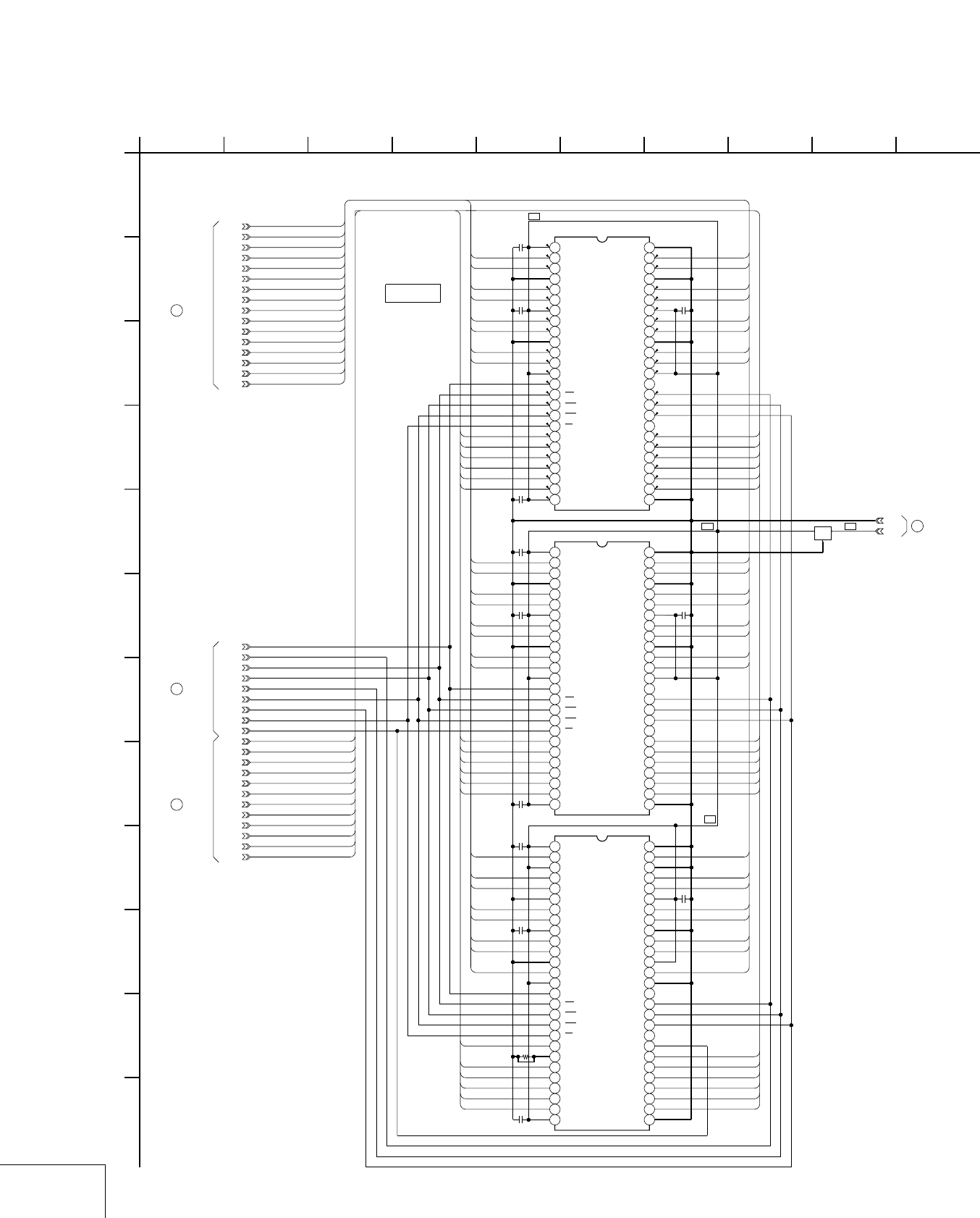
DVP-NS305/NS310/NS315/NS405/NS410/NS415
4-23 4-24
For Schematic Diagram
• Refer to page 4-11 for printed wiring board.
SDRAM
MB-103 (5/7)
+3.3V
GND
IC406 XX
123456789101112131415161718192021222324252627
28 29 30 31 32 33 34 35 36 37 38 39 40 41 42 43 44 45 46 47 48 49 50 51 52 53 54
C447
XX
C441
XX
R431
XX
0.01u
B
C438
B
C448
XX
B
C444
XX
XX
C437
C440
XX
B
C445
XX
C442
XX
C443
XX
0.01u
B
C439
0.01u
B
C446
FL404
IC405 XX
12345678
910111213141516171819202122
232425
26 27 28 29 30 31 32 33 34 35 36 37 38 39 40 41 42 43 44 45 46 47 48 49 50
IC404 MT48LC1M16A1TG-6STR
12345678
910111213141516171819202122
232425
26 27 28 29 30 31 32 33 34 35 36 37 38 39 40 41 42 43 44 45 46 47 48 49 50
ADDT12
ADDT6
ADDT1
ADDT0
ADDT8
ADDT14
ADDT7
ADDT3
ADDT14
ADDT15
ADDT13
ADDT2
ADDT5
ADDT10
ADDT9
ADDT11
XWE
CKE
ADAD9
ADAD6
ADAD10
DQMU
ADAD2
CLK
XCAS
XCS2
ADAD8
DQML
ADAD3
ADAD5
ADAD1
ADAD11
ADAD0
XRAS
XCS
ADAD4
ADAD7
1
A
ADAD6
ADDT2
ADDT6
ADAD6
ADDT14
ADAD11
ADDT2
ADAD2
ADAD1
ADDT11
ADDT3
ADAD0
ADDT1
ADAD3
ADAD5
ADDT8
ADAD5
ADDT12
ADAD0
ADDT10
ADAD9
ADAD7
ADDT12
ADAD2
ADAD4
ADAD3 ADAD4
ADAD10
ADDT5
ADAD1
ADDT7
ADDT6
ADDT9
ADAD8
ADDT4
ADDT5
ADDT13
ADAD11
ADDT15
ADDT15
ADDT3
ADDT7
ADAD7
ADAD10
ADDT0
ADAD8
ADDT1
ADAD9
ADDT14
ADDT8
ADDT4
ADDT13
ADDT10
ADDT0
ADDT9
ADDT11
ADAD3
ADAD2
ADAD1
ADAD0
ADAD10
ADDT7
ADDT6
ADDT5
ADDT4
ADDT3
ADDT2
ADDT1
ADDT0
ADAD4
ADAD5
ADAD6
ADAD7
ADAD8
ADAD9
ADDT8
ADDT9
ADDT10
ADDT11
ADDT12
ADDT13
ADDT14
ADDT15
ADAD11
ADDT0
ADDT15
ADDT1
ADDT14
ADDT2
ADDT13
ADDT3
ADDT12
ADDT14
ADDT11
ADDT5
ADDT10
ADDT6
ADDT9
ADDT7
ADDT8
ADAD11
ADAD9
ADAD10
ADAD8
ADAD0
ADAD7
ADAD1
ADAD6
ADAD2
ADAD5
ADAD3
ADAD4
VCC
DQ0
DQ1
VSSQ
DQ2
DQ3
VCCQ
DQ4
DQ5
VSSQ
DQ6
DQ7
VCCQ
DQML
WE
CAS
RAS
CS
A11(BA)
A10/AP
A0
A1
A2
A3
VCC
VSS
DQ15
DQ14
VSSQ
DQ13
DQ12
VCCQ
DQ11
DQ10
VSSQ
DQ9
DQ8
VCCQ
N.C.
DQMU
CLK
CKE
N.C.
A9
A8
A7
A6
A5
A4
VSS
A1
DQ10
DQ7
A11(BA)
VSSQ
RAS
DQ4
N.C.
A0
DQ11
VSSQ
DQML
VCCQ
VCC
N.C.
VCC
CAS
A9
VCCQ
CKE
A10/AP
DQ13
A7
DQ6
VSSQ
A3
VCCQ
A5
WE
DQ14
DQ2
DQ9
DQ15
A6
DQ3
VSS
VSSQ
A2
DQ12
A4
VCCQ
A8
DQ0
VSS
DQMU
CS
DQ8
DQ1
DQ5
CLK
VDD
DQ0
VDDQ
DQ1
DQ2
VSSQ
DQ3
DQ4
VDDQ
DQ5
DQ6
VSSQ
DQ7
VDD
LDQM
WE
CAS
RAS
CS
BA0
BA1
A10/AP
A0
A1
A2
A3
VDD
VSS
DQ15
VSSQ
DQ14
DQ13
VDDQ
DQ12
DQ11
VSSQ
DQ10
DQ9
VDDQ
DQ8
VSS
N.C.
UDQM
CLK
LKE
N.C.
A11
A9
A8
A7
A6
A5
A4
VSS
32
34
33
TO(4/7)
TO(4/7)
TO(4/7)
16M SDRAM
IC404
TO(7/7)
35
-REF.NO.:1000 SERIES-
XX MARK:NO MOUNT
MB-103 BOARD(5/7)
SDRAM
16
H
23
J
9
G
E
C
10
K
6
B
7
I
D
F
5
L
84
B+B+
B+
B+
3.4
2.21.8
2.0 1.9
2.01.9
1.2 2.0
3.43.4
2.0 1.9
1.72.2
1.9 2.0
0.13.1
1.42.7
2.6
1.1
2.5 3.4
0
0.11.6
0.1
0.8
0.1 1.8
2.2
1.61.4
1.6 1.5
3.4
3.4
0.1
2.0
3.4
NO MARK:PB MODE
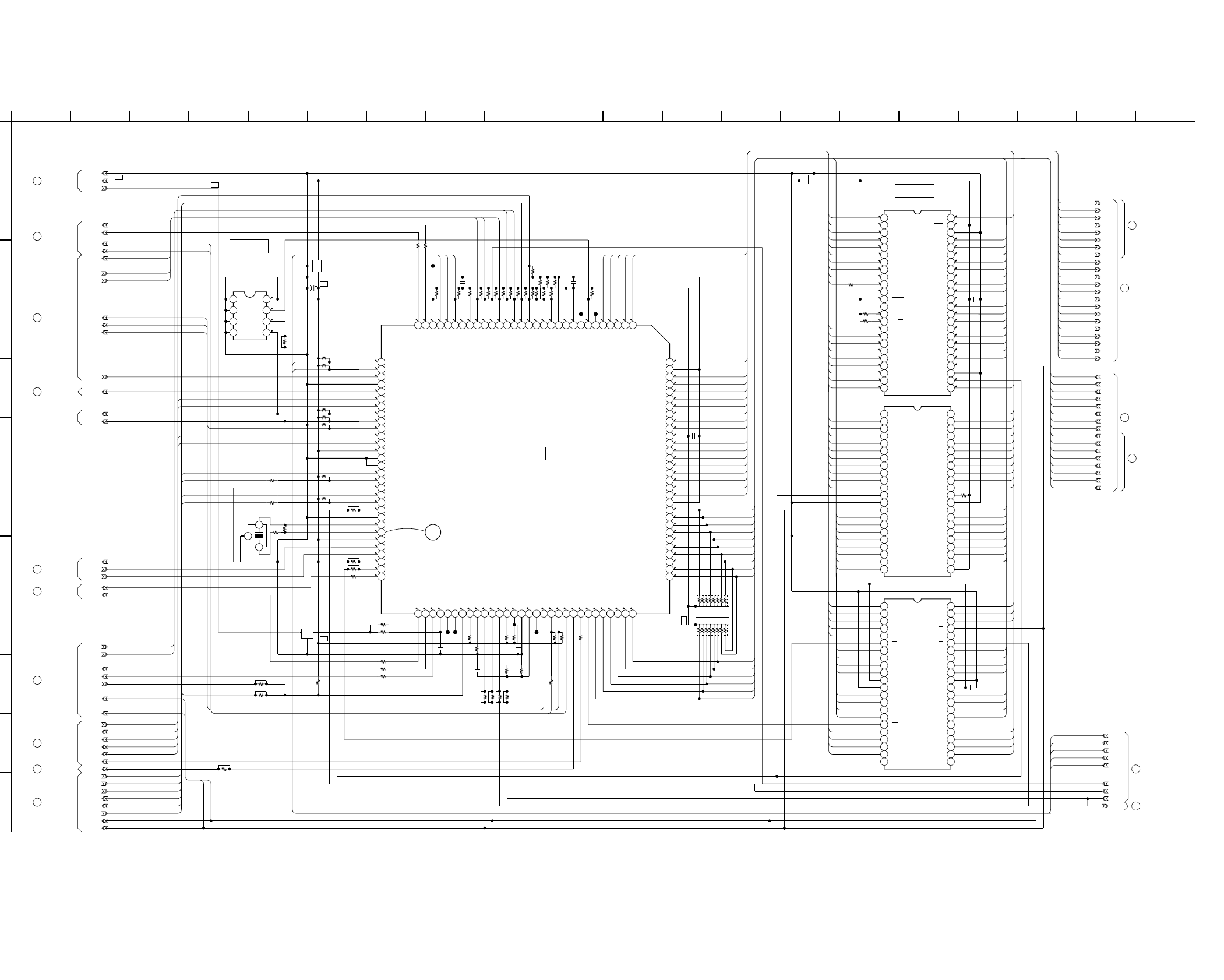
DVP-NS305/NS310/NS315/NS405/NS410/NS415
4-25 4-26
For Schematic Diagram
• Refer to page 4-11 for printed wiring board.
• Refer to page 4-5 for waveform.
SYSTEM CONTROL
MB-103 (6/7)
HA15
HA21
R133
0
MBM29LV160BE-90TN
IC106
12345678
910111213141516171819202122
2324
25 26 27 28 29 30 31 32 33 34 35 36 37 38 39 40 41 42 43 44 45 46 47 48
0.01u
B
C111
0.01u
B
C129
XWAIT
1k
R117
XAVDCS2
XWRH
R161
XX
XRST
3300
R139
XSDPIT
SO1
XX
R148
0.01u
B
C122
XAVDCS3
HA17
0.01u
B
C102
100k
R119
HD12
HA18
JL109
3300
R165
R132
0
XX
R155
XX
R154
HA12
TRMM
HA16
HA4
100
R128
DREQ1
JL108
DACK1
10k
R124
XX
R102
XX
R151
SCL
HA19
R145
XX
HA11
HD15
MA_MUTE
XX
R144
3300
R162
X101
1
2
3
HD2
10k
R156
0.01u
B
C121
XX
R143
R169
47k
10k
R141
XSDPCS
XDACS
R164
47k
HA3
HA20
0.01u
B
C114
C130
XX
4V
100u
C109
HD4
100
R111
1k
R120
XX
R126
XLDON
HD7
HD14
XX
R142
HA14
10k
R123
XARPIT
100
R131
XX
R170
XX
R152
22k
R113
XDRVMUTE
+3.3V
HD6
XX
R122
HD0
HA13
CL101
0.01u
B
C108
HD1
XX
R138
HA8
XX
R146
HA7
10k
R150
100
R130
HA9
XX
R177
0.01u
B
C118
HA0
DREQ0
HA6
HD11
HD5
XAVDIT
1k
R121
XX
R125
XARPCS
SDA
+1.8V
XX
R153
XX
R147
OCSW1
HD3
XRD
HD13
XX
R149
100
R129
DACK0
R166
47k
IC108 XX
12345678
9101314151617181920
21
22
23 24 25 26 27 28 29 30 31 32 35 36 37 38 39 40
1112
33 34 41 42 43 44
CKSW1
HA10
XWAIT
R127
XX
HD10
MB91307RPFV-G-BND-E1
IC104
12345678
910111213141516171819202122
2324252627282930
3132
3334353637383940414243444546
4748495051525354555657585960
61 62 63 64 65 66 67 68 69 70 71 72 73 74 75 76 77 78 79 80 81 82 83 84 85 86 87 88 89 90
91 92 93 94 95 96 97 98 99 100 101 102 103 104105 106 107 108 109 110 111 112 113 114 115 116 117 118 119 120
XX
R172
SC1
HD8
HD9
100k
R118
1k
R110
3300
R168
3300
R163
HA5
TRMP
XX
R140
XX
R109
100
R112
XX
R175
GND
HA1
XX
R101
10k
R178
HA2
M24C16-WMN6T
IC101
1234
5678
B
C120
0.01u
WIDE
OCSW2
10k
R184
XXIC107
12345678
9101314151617181920
21
22
23 24 25 26 27 28 29 30 31 32 35 36 37 38 39 40
1112
33 34 41 42 43 44
JL107
TSENSD
TSENSU
IPSW
RGBSEL
DSENS
EUROVY
EXT/DSEL
R107
XX
TSENSO
JL127
XX
R187
XX
R188
FL103
FL102
FL106
FL108
XX
JL128
100
R103
100
R104
100
R105
RB102
1
2
3
4
5
7
8
9
10
6
RB101 XX
1
2
3
4
5
7
8
9
10
6
100
R106
FSEL
XWRH
XRD
XIFBUSY
XIFCS
XFRRST
XFRRST
SO2
SI2
SI0
SC0
SO0
1
A
HA12
HA14
HA10
HD8
HA17
HA5
HA10
HA19
HA1
HD1
HA16
HA11
HA4
HA8
HD4
HD12
HD9
HA9
HA10
HA20
HD10
HA5
HD2
HD3
HD11
HA8
HD15
HD5
HD13
HA12
HA15
SI0
HA21
HD8
HA18
HA6
HD13
HA17
HD10
HD15
HA21
HA1
HD7
HA4
HA5
HA6
HA7
HD7
HD15
HA0
HA6
HA1
HD5
HD14
HD9
HA2
HD12
HA9
HA18
SO0
HD10
HA20
HA4
HA13
HD11
HD13
HA9
HD0
HA2
HD14
HD11
HA7
HD7
HA15
HD3
HD1
HD4
HD6
HA7
HA14
HA3
HD8
HD4
HD0
HA14
HD2
HA12
HA16
HD12
SC0
HA15
HA11
HA3
HA13
HD6
HD6
HA3
HD9
HD3
HD1
HA11
HD5
HD2
HA16
HD14
HD0
HA8
HA13
HA2
HA19
SI2
SO2
SI0
SO0
SC0
XSDPIT
XARPIT
XAVDIT
IPSW
RGBSEL
TRMP
EUROVY
EXT/DSEL
FSEL
HA21
HA20
HA19
HA18
HA17
HA16
HA15
HA14
HA13
HA12
HA11
HA10
HA9
HA8
HA7
HA6
HA5
HA4
HA3
HA2
HA1
HA0
OCSW2
WIDE
TRMM
XWAIT
XDACS
HD8
HD9
HD10
HD11
HD12
HD13
HD14
HD15
HD7
HD6
HD5
HD4
HD3
HD2
HD1
HD0
IPSW
WIDE
RGBSEL
EUROVY
EXT/DSEL
DACK1
DREQ1
DACK0
DREQ0
XAVDIT
DREQ0
DACK1
XWAIT
XARPIT
XSDPIT
TSENSO
TSENSD
TSENSU
TSENSO
TSENSU
TSENSD
TRMP
OCSW2
TRMM
XDACS
FSEL
XWRH
XRD
DACK0
DREQ1
SO2
SI2
HA21
HA20
HA9
HA10
HA11
HA12
HA13
HA14
HA15
HA16
HA17
HD15
HD7
HD14
HD11
HD3
HD10
HD2
HD9
HD1
HD8
HD0
HA1
HA2
HA3
HA4
HA5
HA6
HA7
HA8
HA18
HA19
HD4
HD12
HD5
HD13
HD6
XRD
XWRH
HA8
WE
N.C.
DREQ0
MD2
HA16
DQ11
DQ15/A-1
A13
A2
VSS
CS1X
A15
VCC
DQ5
DQ13
VSS
A3
DQ6
GND
A0
BYTE
INT3
A4
CS7X
DQ14
A6
VCCI
CE
A16
HA22
48/44.1K
HD0
DQ7
VSS
HA19
A12
I/O5
HA14
SDA
I/O12
EUROVY
HA17
SCL
A0
AVCC
I/O3
GND
HA12
A7
A5
HA20HD2
XFRRST
AVSS
XDRVMUTE
INT6
HD1
A3
SI0
AN0
CS6X
XIFCS
A4
XWAIT
HA3
CPUCK
X2
GND
A20
HA6
A17
HA1
SC1
X1 HD13
A19
TRM+
MA_MUTE
HA0
OE
OE
VSS
EXT/DSEL
HD12
XDACS
A6
A8
HA11
DQ0
INT0
AVRH
HD11
A9
INT7
WP
HA15
A10
INT4
VSS
TRM-
A11
CS2X
BGRNTX
HD15
NMIX
SC0
INT2
A12
A1
MD0
HD14
SO2
A5
HA5
VCC
DQ12
INT5
OCSW2
A11
A13
SRAMWE
XWRL
I/O11
AN1
SO1
INT1
A10
VCC
CS0X
A18
DQ9
AN2
VSS
HA4
RY/BY
DQ2
HA9
I/O14
HD8
WP/ACC
A14
HD9
DACK1
I/O2
N.C.
DACK0
A14
A15
HD4
I/O1
RESET
HA7
VCC
DSENS
OCSW1/TSW2
I/O7
HD5
I/O0
BRQ
WE
VCCI
I/O9
CS3X
LB
A1
CKSW1/TSW1
HD3
VSS
AN3
HA13
I/O10
A2
VCC
XARPRST
MD1
DREQ1
DQ8
WP
A7
SI2
DQ1
CS4X
I/O15
XRST
A9
DQ4
I/O6
A8
I/O4
RGBSEL
HD6
SI1
HD10
A2 SCL
CS5X
UB
HD7
WIDE
CS
XWRH
N.C.
N.C.
HA18
A0
SDA HA10
I/O8
HA21
VCC
A1
XSACS
DQ10
SO0
HA2
DQ3
XRD
I/O13
VCC
D10
BYTE
A2
OE
D14
N.C.
VCC
D1
A17
D2
A16
A3
VSS
D7
A15
D4
CE
A12A4
D5
A14
D12
HA21
A9
D15/A-1
A0
A11
D8
A5
D9 D13
A6
A13
D11
A8
D3
VSS
A1
A10
D0
D6
A18
A7
A19
(2012)
(2012)
(2012)
10k
16.5MHz
IC101
EEP ROM
IC104
SYSTEM CONTROL
FLASH MEMORY
IC106
36
TO(7/7)
TO(7/7)
37
TO(2/7)
8
TO(3/7,4/7,
7/7)
15
NOT USE
TO(2/7)
12
TO(4/7)
28
TO(3/7)
17
TO(7/7)
38
6
TO(1/7)
22
TO(4/7)
TO(3/7,4/7)
18
30
TO(4/7)
23
TO(4/7)
21
TO(3/7)
B+
B+
B+
B+
B+
19
H
23 12
J
179
G
11
E
C
10
K
14136
B
7
I
D
18
F
155
L
84 2016
SYSTEM CONTROL
MB-103 BOARD(6/7)
-REF.NO.:1000 SERIES-
XX MARK:NO MOUNT
16
TO(7/7)
39
31
TO(4/7)
3.4
3.4
3.4
3.4
3.2
3.2
0
3.4
0
3.4
3.4
3.4
3.4
3.4
3.4
0
3.4
3.4
3.4
3.4
3.4
3.1
0
3.4
2.4
0
1.6
1.7
3.4
3.4
3.4
3.4
1.7
3.4
3.4
3.4
1.7
3.4
2.6
0
3.4
3.4
3.4
3.4
3.4
3.4
3.4
3.4
3.4
0
0.6
1.1
0.9
1.0
1.1
0.9
1.8
1.0
1.4
2.1
1.2
2.2
1.8
1.1
0.8
0.8
2.6
3.4
1.2
1.5
1.4
3.0
2.2
3.0
2.7
2.5
2.5
2.6
3.0
2.8
2.9
1.0
0.7
0
3.4
3.4
3.4
3.4
3.3
1.5
3.4
3.4
3.4
3.4
3.4
3.4
3.4
3.4
3.4
3.4
3.4
3.4
3.2
2.5
0.8
1.8
1.5
0.5
3.4
3.4
3.4
5
1.9 0.5
1.0 3.4
1.2
1.02.2
3.0
2.5
2.2 0.8
1.9
1.5
1.1 2.6
2.5
2.70
0.9
3.4
2.7
3.4
0.93.4
0 1.0
3.4
1.01.5
2.9
1.8
0.6
1.2 2.9
0.7
2.9
2.6 1.0
0.8
2.2
2.7
1.3
3.0
2.6
1.5
NO MARK:REC/PB MODE
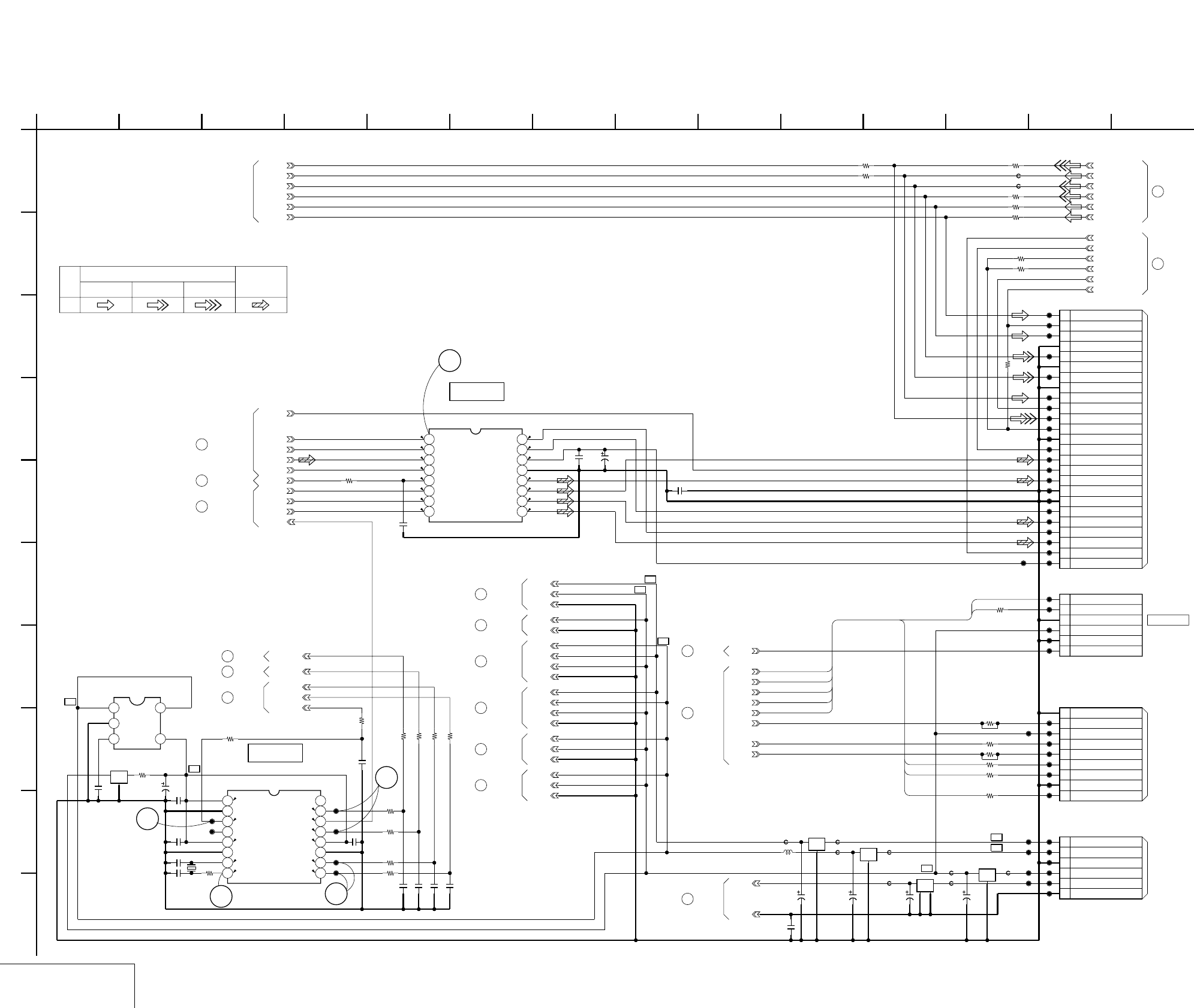
DVP-NS305/NS310/NS315/NS405/NS410/NS415
4-27 4-28
For Schematic Diagram
• Refer to page 4-11 for printed wiring board.
• Refer to page 4-5 for waveforms.
AUDIO DAC, PLL
MB-103 (7/7)
LRCK
ACH12
BCK
SC1
XDACS
SO1
XRST
SPDIF1
EXT/DSEL
RGBSEL
MA_MUTE
512FS2CH
CR/B
EUROVY
CB/R
Y/G
YOUT
COUT
COMPOUT
WIDE
JL609
JL618
JL613
JL603
100
R601
JL602
JL615
JL601
JL614
JL604
JL619
16V
10u
C603
JL605
CXD9627A-E2
IC601
12345678
910 11 12 13 14 15 16
JL617
JL610
JL611
JL606
JL607
B
C601
0.001u
JL616
0.22u
B
C602
JL621
JL612
JL608
0.01u
B
C604
JL620
R613
XX
R614
XX
IPSW
R619
XX
PR_CB/R
PR_CR/B
PR_Y/G
PR_Y
PR_C
PR_V
R621
XX
CN601
1
2
3
4
5
6
7
8
9
10
11
12
13
14
15
16
17
18
19
20
21
22
23
24
25
R623
XX
JL622
JL623
0uH
FB603
0uH
FB602
0
R609
0
R607
0
R608
0
R612
FB108
0uH
SM8707AV-E2
IC103
12345678
9 10111213141516
100u
C126
6.3V
4V
47u
C125
FB107 0uH
JL115
22
R116
FL105
0
R160
FB111
0uH
16V
C127
47u
0
R157
JL110
XX
R135
+1.8V
100
R180
XX
C101
JL118
XX
C113
JL132
JL103
0.01u
B
C104
IC102 XX
123
45
FB105
0uH
M_GND
JL131
XX
C117
JL113
JL120
JL133
JL121
JL101
FB104
0uH
9p
C107
22
R134
4V
220u
C128
FL104
JL111
JL105
0
R181
XX
R179
JL134
FB109
0uH
22
R136 JL117
JL116
4V
100u
C103
9p
C106
512FSAVD
FL110
22
R137
512FS2CH
JL112
JL102
JL135
JL130
33MARP
XX
C116
0.01u
B
C105
0
R114
FB103
0uH
0
R176
JL104
0.01u
B
C110
+5V
XX
C124
XX
R186
JL119
33MAVD
6PCN102
1
2
3
4
5
6
FL109
X102
FB106
0uH
XX
R158
2.2
R108
XX
C119
27MAVD
JL114
JL122
100
R183
CN101 9P
1
2
3
4
5
6
7
8
9
+11V
0
R159
4.7uH
L101
FL101
100
R182
JL106
XX
C112
6P
CN103
1
2
3
4
5
6
1k
R185
RFMON
JL123
JL124
JL125
JL126
JL129
FSEL
XIFBUSY
SI2
SI0
SC0
XIFCS
XFRRST
SO0
SO2
+1.8V
+3.3V
GND
+3.3V
GND
GND
+3.3V
+1.8V
GND
+3.3V
+5V
GND
+3.3V
+5V
+5V
+3.3V
GND
1
A
SO0
SC0
SI0
SO2
SI0
SI2
SC0
SO0
SO2
SI2
MCLK
BICK
SDTI
LRCK
PDN
CSN
CCLK
CDTI
DZFL
DZFR
VDD
VSS
AOUTL+
AOUTL-
AOUTR+
AOUTR-
Cr/B
WIDE
Cb/R
GND
Y/G
GND
Y
GND
C
DISCEXT
V
EUROVY
GND
RGBSEL
ALT-
SPDIF
ALT+
P_GND_SPDIF
P_GND_2CH
RMUTE
ART+
LMUTE
ART-
MAMUTE
AU+5V
NOT USE
25P
+5V
27MHz
N.C
VSS
GND
33-1OUT
XIFBUSY
VOUT
VSS
SO0
VIN
SI0
SC0
NOISE
XTI
FSEL
3.3V_MNT
GND
VDD
GND
XIFCS
512-2OUT
XFRRST
CONT
33-2OUT
+3.3V
27-2OUT
XTO
M_GND
VSS
VDD
27-1OUT
+1.8V
+11V
VDD
GND512-1OUT
+3.3V
TXD
GND
RXD
RF MON
GND
16
36
TO(6/7)
35
TO(5/7)
TO(4/7)
26
13
TO(3/7)
7
TO(2/7)
1
TO(1/7)
2
TO(1/7)
TO(6/7)
39
TO(2/7)
10
25
TO(4/7)
TO(3/7,4/7,
6/7)
15
TO(6/7)
37
TO(3/7)
14
TO(4/7)
24
29
TO(4/7)
TO(4/7)
27
34
TO(6/7)
B TO B
TO AV-61 BOARD
CN203
(PAGE 4-31)
FOR CHECK
(PAGE 4-10)
TO IF-89 BOARD
CN404
(PAGE 4-9)
TO IF-89 BOARD
(CN403)
(MF-128 HARNESS)
IC601
AUDIO D/A CONVERTER
IC103
PLL
B+
B+
B+
B+
B+
B+
B+
B+
B TO B
XX MARK:NO MOUNT
-REF.NO.:1000 SERIES-
AUDIO DAC,PLL
MB-103 BOARD(7/7)
H
23 12
J
9
G
11
E
C
10 14136
B
7
I
D
F
584
20
1.6
1.7
1.7
0
3.4
3.4
3.4
3.4
0
0
4.9
2.5
2.5
2.5
2.5
2
3.4
1.7
3.4
*
1.5
1.7
3.4
1.7
3.4
0
0
4
3
1
CHROMA SIGNAL
PB
AUDIO
SIGNAL PATH
VIDEO SIGNAL
Y Y/CHROMA
NO MARK:PB MODE
* :Cannot be measured
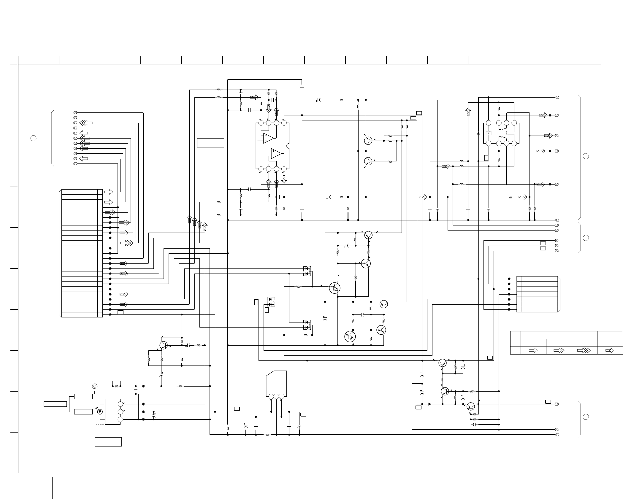
DVP-NS305/NS310/NS315/NS405/NS410/NS415
4-31 4-32
For Schematic Diagram
• Refer to page 4-29 for printed wiring board.
AUDIO OUT
AV-61 (1/2)
Q210
XX
EUROVY
LCH_OUT
D203
XX
R232
XX
0.01u
B
C222
470
R240
0.01u
B
C207
JL221
JL209
Q209
XX
XX
C240
JL239
TRANSISTOR2SD1938(F)-ST(TX).SO
Q207
5600
±0.5%
R211
P_GND
ERAUDIOR
10k
R222
Y/G
JL201
XX
R281
J201
NJM78L05UA-TE1
IC203
OUT
1
GND
2
IN
3
R214
XX
5600
±0.5%
R206
1SS355TE-17
D205
JL238
SW_-13V
AU+11V
JL218
180p
CH
C206
R235
4700
2SB709A-QRS-TX
Q205
R236
XX
JL202
2200
R210
JL208
JL240
330u
6.3V
C242
1k
R256
JL231
10k
R217
47k
R225
4700
±0.5%
R204
10k
R252
4700
R213
JL212
JL210
R237
XX
JL232
XX
C221
47k
R229
5600
±0.5%
R212
50V
1u
C209
5600
R216
10k
R224
RCH_OUT
JL217
JL233
D_GND_VIDEO
2SB710A-RTX
Q201
UN2213-TX
Q202
JL206
JL236
AI+5V
1k
R253
100k
R238
C215
XX
2SC2712-YG-TE85L
Q211
180p
CH
C204
470
R227
TRANSISTOR2SD1938(F)-ST(TX).SO
Q208
47k
R230
C
XX
C217
DTC124TKA-T146
Q204
CR/B
JL216
2SB709A-QRS-TX
Q216
R231
XX
JL214
RGBSEL
WIDE
JL220
XX
C243
P_GND
Y
220k
R219
2200
R208
DAP202K-T-146
D202
R285
0
4700
R234
BA4558F-E2
IC201
1234
5678
DISCEXT
4700
±0.5%
R201
R233
XX
JL205
Q206
XX
180p
CH
C203
JL203
0.01u
B
C223
C212
XX
16V
47u
C228
R284
0
D206
XX
220
R249
R239
XX
JL213
XX
R283
IC204
GP1FA550TZ
D IN
1
VCC
2
GND
3
10k
R221
JL224
2200
R209
560p
CH
C201
2200
R207
560p
CH
C202
470
R241
4700
±0.5%
R203
100k
R218
7P
CN202
1
2
3
4
5
6
7
V
5600
±0.5%
R205
JL223
JL204
JL237
D_GND_VIDEO
JL235
VMUTE
16V
47u
C227
ERAUDIOL
180p
CH
C205
470
R226
4700
±0.5%
R202
1k
R254
470
R220
D_GND_VIDEO
JL207
DAN202K-T-146
D201
XX
C218
JL234
JL222
CB/R
10k
R228
C216
XX
0.01u
B
C208
JL211
XX
C241
68
R251
2SC2712-YG-TE85L
Q203
JL215
R242
470
R243
470
XX
R287 XX
C226
16V
47u
C210
16V
47u
C211
16V
47u
C224
16V
47u
C229
16V
47u
C244
RY201
XX
12
1356
10 87
16V
220u
C213
XX
R244
XX
R245
CN203 25P
1AU+5V
2MAMUTE
3ART-
4LMUTE
5ART+
6RMUTE
7
P_GND_AUDIO
8
P_GND_SPDIF
9ALT+
10SPDIF
11ALT-
12RGBSEL
13
D_GND_VIDEO
14EUROVY
15
V
16
DISC/EXR
17
C
18
D_GND_VIDEO
19
Y
20
D_GND_VIDEO
21
Y/G
22
D_GND_VIDEO
23
Cb/R
24
WIDE
25
Cr/B
1
A
LCH_OUT2
RCH_OUT2
P_GND
D_GND_VIDEO
A_MUTE
AI+5V
EVER+3.3V
AU+11V
VMUTE
SW_-13V
AUDIO
AUDIO
COAXIAL
OPTICAL
DIGITAL OUT
59
J
F
12
D
3
I
27
H
B
6
AUDIO OUT
13
XX MARK:NO MOUNT
14
-REF.NO.:2000 SERIES-
10
AV-61 BOARD(1/2)
C
E
4 118
G
16
IC204
OPTICAL DIGITAL OUT
BUFFER
MUTE DRIVE
MUTE DRIVE
MUTE DRIVE
RCH MUTE
LCH MUTE
AUDIO AMP
IC201
TO IF-89 BOARD
CN402
(SEE PAGE 4-9)
TO(2/2)
2
TO(2/2)
3
4
TO(2/2)
TO(2/2)
1
(SEE PAGE 4-28)
TO MB-103 BOARD(7/7)
CN601
AU+5V REG
IC203
SWITCH
SWITCH
SWITCH
B+
B+
B+
B+
B+
B+
B+
B+
B+
B-
B-
B-
B-
1.3-10.1
1.3 1.3
1.3
10.60
0
9.910.0
1.7
4.9
2.4
1.7
4.9
4.9
10.6
0.8
0
0.8
0
0.6
0.6
9.2
0
6.0
10.6 10.7
10.0
-10.6
-10.8
-10.1
-10.8
-12.0
--11.4
NO MARK:PB MODE
Y/CHROMA
VIDEO SIGNAL
Y
PB
SIGNAL
SIGNAL PATH
CHROMA
AUDIO
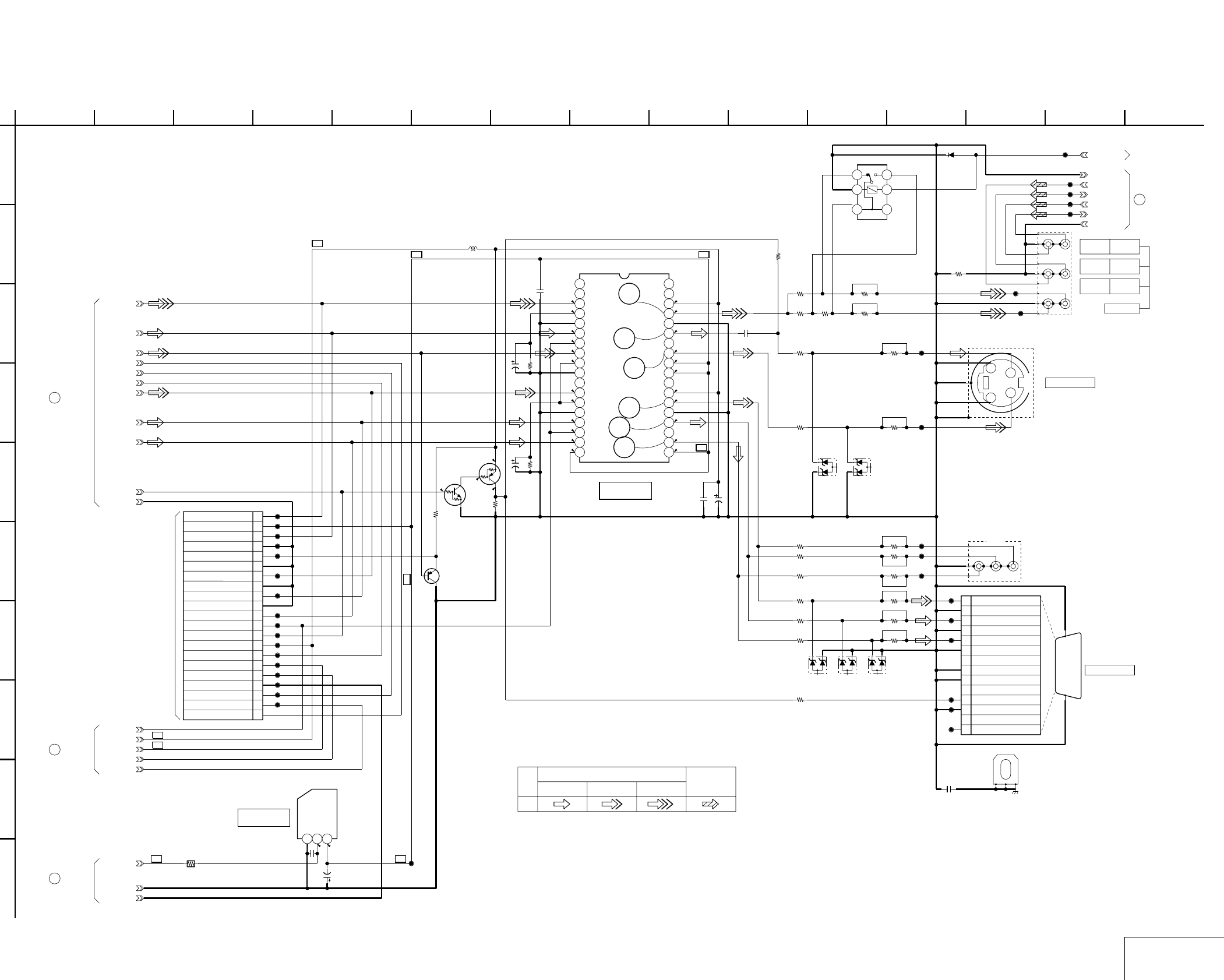
DVP-NS305/NS310/NS315/NS405/NS410/NS415
4-33 4-34
VIDEO OUT
AV-61 (2/2)
For Schematic Diagram
• Refer to page 4-29 for printed wiring board.
• Refer to page 4-6 for waveforms.
JL115
UN2111-TX
Q105
WIDE
JL109
JL106
R148
68
LCH_OUT2
D103
HZM6.8ZWA1TL
RCH_OUT2
1
7
8
14
CN103
14P
Y
1
D_GND_VIDEO
2
Cb
3
D_GND_VIDEO
4
Cr
5
D_GND_VIDEO
6
N.C.
7
LINE1
8
LINE2
9
N.C.
10
LINE3
11
SW_GND
12
N.C.
13
SW
14
JL113
JL120
JL131
R122
XX
Y
C
GG
J103
JL105
R150
68
XX
C115
D102
HZM6.8ZWA1TL
0.047u
B
C109
JL117
JL133
J104
JL126
ET101
XX
JL121
VMUTE
R146
68
68
R133
CN102 21P
1RGBSEL
2ERAUDIOL
3EUROVY
4P_GND_AUDIO
5ERAUDIOR
6+11V
7DISCEXT
8+5V
9WIDE
10VMUTE
11cR/B
12D_GND_VIDEO
13Cb/R
14D_GND_VIDEO
15Y/G
16D_GND_VIDEO
17Y
18D_GND_VIDEO
19C
20-5V
21V
R127
XX
JL103
CR/B
JL134
ERAUDIOL
68
R134
Q106
XX
JL116
C
D104
HZM6.8ZWA1TL
JL118
ERAUDIOR
Y/G
CB/R
JL129
JL104
R154
0
JL122
Y
P_GND
XX
D101
68
R130
JL119
100uH
L101
JL111
LCH_OUT
JL128
JL107
RCH_OUT
0
R286
JL130
R128
XX
D_GND_VIDEO
SW_-13V
D_GND_VIDEO
JL101
JL127
EUROVY
10k
R121
R126
XX
JL102
R152
10k
V
P_GND
JL124
JL125
0.1u
B
C112
JL137
JL123
JL110
HZM6.8ZWA1TL
D105
10k
R129
JL136
AU+11V
0.01u
B
C101
XX
R124
SW_-13V
0.1u
B
C114
JL112
IC102 LA73050-TLM
NC
1
NC
2
VIDEO_IN
3
DCCNT1
4
GND
5
C_IN
6
MUTE1
7
Y_IN
8
NC(DCCNT2)
9
NC(GND)
10
NC
11
Y_IN(NC)
12
DCCNT2
13
GND
14
Cb_IN
15
MUTE2
16
Cr_IN
17
-5V
18
-5V
19
CB_OUT
22
GND
23
Y_OUT
24
+5V(NC)
25
NC
26
-5V
27
-5V
28
Y_OUT
29
NC
30
C_OUT
31
GND
32
VIDEO_OUT
33
+5V
34
NC
35
NC
36
NC
21
Cr_OUT
20
HZM6.8ZWA1TL
D106
DISCEXT
RGBSEL
D_GND_VIDEO
JL114
UN2213-TX
Q104
XX
R123
JL132
JL108
33
R153
XX
R141
XX
R142
XX
R144
XX
R143
XXR145
XX
R147
XX
R149
XX
R151
XX
R155
16V
47u
C110
16V
47u
C111
16V
47u
C113
16V
47u
C102
XX
R140
RY102
XX
1
2
3
456
68
R131
NJM79M05DL1A(TE2)
IC103
1
GND
2
IN
3
OUT
J102
XX
AI+5V
1
A
D_GND_VIDEO
AUDIO
AUDIO
WIDE SWITCH
WIDE SWITCH
2TO(1/2)
NOT USE
AUDIO1 AUDIO2
RR
AUDIO2
LL
AUDIO1
VIDEO1 VIDEO2
LINE OUT
S1 VIDEO OUT
D1 VIDEO OUT
IC102
VIDEO BUFFER
-5V REG
IC103
1TO(1/2)
TO(1/2)
3
TO(1/2)
4
AV-61 BOARD(2/2)
-REF.NO.:2000 SERIES-
XX MARK:NO MOUNT
VIDEO OUT
16
H
23 12
J
9
G
11
E
C
10 14136
B
7
I
D
F
15584
B+
B- B+
B+
B-
B+
B- B-
B-
4.50.5
0.6 0.6
0.6 0.1
0.6
3.4
0.5
-5.0
-5.0
4.5
1.1
1.1 0.6
0.10.6
0.6 0.1
-5.0 -5.0
3.4
0.5
1
2
3
4
5
6
4.5
4.5
0
0
-9.8
-5.0
NO MARK:PB MODE
AUDIO
Y/CHROMA
VIDEO SIGNAL
SIGNAL
Y
SIGNAL PATH
PB
CHROMA
(SEE PAGE 4-37)
TO ER-14 BOARD
CN901
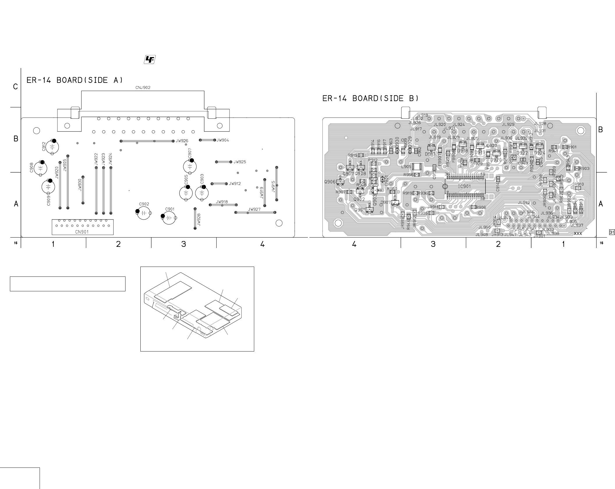
DVP-NS305/NS310/NS315/NS405/NS410/NS415
4-35 4-36
AV AMP
ER-14
ER-14 (AV AMP) PRINTED WIRING BOARD
For printed wiring board
There are a few cases that the part printed on
this diagram isn’t mounted in this model.
• : Uses unleaded solder.
MB-103 board
(DVD/CD RF AMP, SERVO,
MOTOR DRIVE, AD DECODER,
SYSTEM CONTROL,
AUDIO ADC, PLL)
AV-61 board
(AUDIO/VIDEO OUT)
IF-89 board
(IF COM)
FL-126 board
(LED)
MS-81 board
(LOADING MOTOR)
ER-14 board
(AV AMP)
Power block
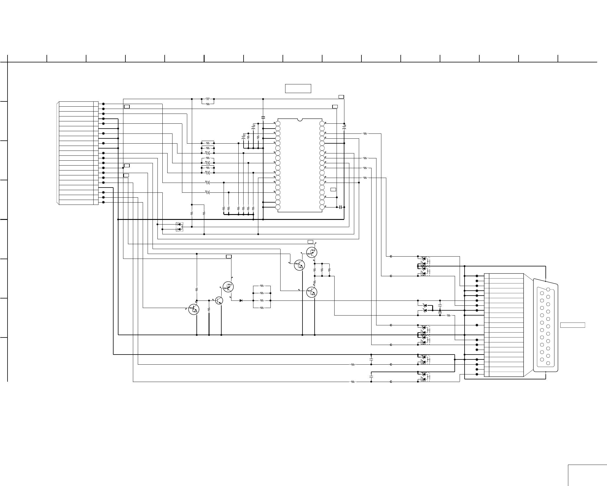
DVP-NS305/NS310/NS315/NS405/NS410/NS415
4-37 4-38
AV AMP
ER-14
0
R902
220k
R908
JL939
21PCN901
1
2
3
4
5
6
7
8
9
10
11
12
13
14
15
16
17
18
19
20
21
JL923
JL945
16V
47u
C902
100p
C945
XX
R903
XX
R956
HZM6.8ZWA1TL
D918
100p
C963
XX
D922
JL918
JL937
XX
R936
0.22u
B
C914
16V
47u
C905
JL933
68
R918
470
R926
XX
R944
XX
C912
JL948
HZM6.8ZWA1TL
D917
JL942
1SS355TE-17
D901
XX
R913
68
R928
JL932
JL927
JL936
XX
C908
JL943
47k
R907
UDZ-TE-17-13B
D930
JL919
0.22u
B
C913
XX
R942
FB909
0uH
HZM6.8ZWA1TL
D920
UN2111-TX
Q903
UDZ-TE-17-6.2B
D929
16V
47u
C903
XX
D924
LA73052-TLMIC901
12345678
9101112131415161718
19 22 23 24 25 26 27 28 29 30 31 32 33 34 35 36
2120
UN2211-TX
Q908
XX
C909
100p
C943
FB907
0uH
330
R909
JL946
Q901
UN2213-TX
68
R927
DAP202K-T-146
D907
JL930
330
R910
JL920
16V
47u
C907
CNJ902
A(R)OUT1
A(R)IN2
A(L)OUT3
GND(A)4
GND(E)5
A(L)IN6
B_OUT7
FUNCTION_SW_OUT8
GND(E)
9
AVLINKO10
G_OUT11
N.C.12
GND(E)13
GND(E)14
R/C_OUT15
BLANKING_OUT16
GND(E)17
GND(E)18
V/Y_OUT19
V_IN20
GND(E)21
XX
R941
JL950
2200
R914
R958
0uH
JL949
330
R911
JL947
47k
R905
JL944
100p
C962
68
R929
JL934
JL935
470
R924
100uH
L905
FB908
0uH
XX
R940
XX
R901
2SD601A-QRS-TX
Q902
2200
R917
HZM6.8ZWA1TL
D919
1k
R915
UN2111-TX
Q907
JL938
XX
R919
JL925
JL941
UN2213-TX
Q906
JL928
330
R912
R957
0uH
JL924
JL917
JL931
16V
47u
C901
47
R939
JL926
JL929
47k
R906
JL921
FB910
0uH
JL922
XX
R943
2200
R916
22k
R950
1
A
RGBSEL
G_IN
NC
Y_IN
V
V/Y_OUT
NC
GND
NC
GND
NC
DCCNT3
21P
Y/G
NC
WIDE
GND
ERAUDIOL -5V
+5V
+5V
-5V
NC
DISCEXT
NC
GND(AU)
-5V
+11V
DCCNT1
R/C_OUT
GND
ERAUDIOR
GND
MUTE1
MUTE3
Cr/B
DCCNT2
GND
Y
GND
NC
C
C_IN
SW1
B_IN
Cb/R
NC
G_OUT
SW2
GND
R_IN
MUTE2
V_IN
EUROVY
VMUTE NC
B_OUT
NC
Q906-908
FUNCTION SWITCH
Q902,903
BLANKING SWITCH
SWITCH
IC901
VIDEO BUFFER
(SEE PAGE 4-33)
TO AV-61 BOARD(2/2)
CN102
LINE(RGB)-TV
B+
B+
B- B-
B+
B-
B+
B+
XX MARK:NO MOUNT
ER-14 BOARD
LINE OUT
-REF.NO.: SERIES-
16
H
23 129
G
11
E
C
10 14136
B
7
D
F
15584
4.71.1
0.6 -0.6
3.40
0 3.4
3.3 -0.1
3.40.1
0
-5.1
0
0.5
3.4
-0.6
-0.6
-5.1
11.7
0.5
11.7
0
0.5
0
4.9
4.9
0
0
0
3.4
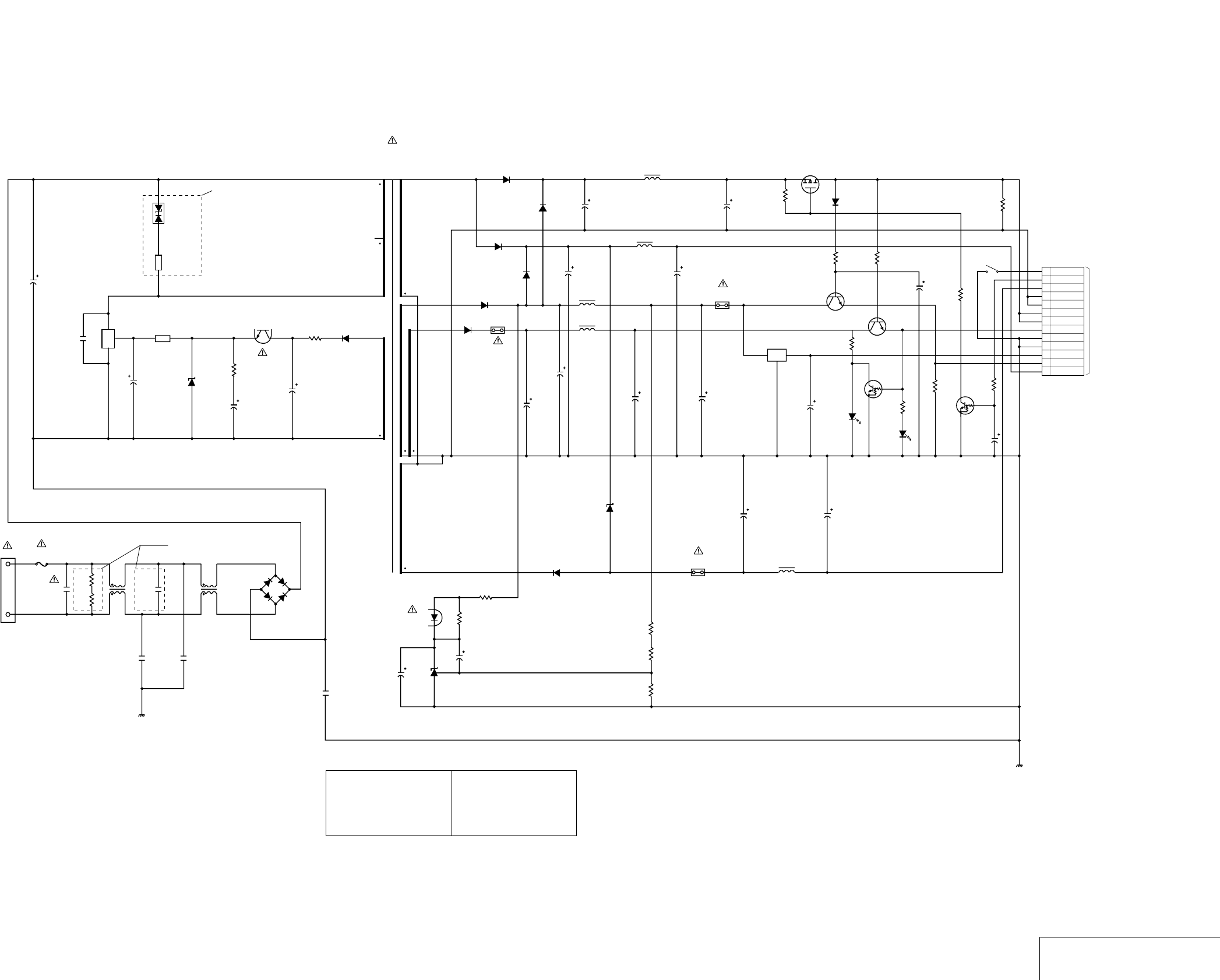
DVP-NS305/NS310/NS315/NS405/NS410/NS415
4-41 4-42
SWITCHING REGULATOR
POWER BLOCK (HS11S1, HS11S1F)
1
2
3
4
5
6
7
8
9
10
11
12
13
POWER
P-CONT
EVER-13V
MGND
MGND
SW+11V
SW+11V
SW+3.3V
GND
GND
EVER+3.3V
SW+5V
EVER+11V
CN201 13P
SW201
EVQPC005K
R213
680
C314
22u
50V
R711
1.8k
Q712
DTC143ESA
C711
47u
35V
R311
1k
R622
120
D622
SLR-343MC
Q621
DTC143ESA
Q611
2SC2655
R621
390
Q311
2SD1768S
R613
220
R313
270
IC411
XC6201P352TH
C413
47u
35V
C313
47u
35V
C613
47u
35V
C513
47u
35V
D621
SLR-343VC
C511
100u
35V
L511
100uH
P511
1.5A/125V
R304
1.2k
R305
300(270-360)
R306
1.6k
D511
D1NL20U:HS11S1F
D2L20U:HS11S1U
R301
68
R303
2.2k
C301
1u
50V
IC301
AN1431T
PC101B
TLP421F
C302
10u
50V
13
11
12
10
9
81
2
3
5
6
D110
D1NL20U
R110
10
C111
10u
50V
PC101A
TLP421F
R113
100
C112
47u
35V
D103
0.8W
33V
C117
1u
50V
IC101
M1P2E4 L110
45
C151
100p:HS11S1F
150p:HS11S1U
2kV
C110
150u
400V
L150
(SHORT)
D
SC
Z150
ST02D-170
T101
TR010032:HS11S1F
TR011019:HS11S1U
POWER TRANSFORMER
D211
D2L20U
D213
D1NS4/6
D221
D1NL20U
D312
D1N60
D311
D1NS4
D611
D1NS4 P611
2.0A/125V
C221
100u35V
L311
39uH
L611
10uH
C311
150u
35V
C611
330u
35V
P311
1A/125V
C223
47u
35V
C213
47u
35V
L221
100uH
C211
150u
35V
L211
10u R212
47k
Q211
2SJ525
D313
1SS270A R211
1.5k
FG201
TPOO370-41
C107
680p:HS11S1F
1000p:HS11S1U
250V
D104
S1WBA60
L102
18mH
C102
(OPEN)
C104
100p
250V
L101
18mH
C103
100p
250V
FG101
TP00370-41
R101
1M
R102
1M
F101
2A/250V
C101
0.22u
250V
CN101 2P
1
2
D212
0.8W
33V
HS11S1F
HS11S1F
IO
G
SWITCHING REGULATOR
TO IF-89 BOARD
CN401
(SEE PAGE 4-9)
Note :
The components identified by
mark 0 or dotted line with mark
0 are critical for safety.
Replace only with part number
specified.
Note :
Les composants identifiés par
une marque 0 sont critiques
pour la sécurité.
Ne les remplacer que par une
pièce portant le numéro spécifié.

6-1
DVP-NS305/NS310/NS315/NS405/NS410/NS415
SECTION 6
TEST MODE
6-1. GENERAL DESCRIPTION
The Test Mode allows you to make diagnosis and adjustment eas-
ily using the remote commander and monitor TV. The instructions,
diagnostic results, etc. are given on the on-screen display (OSD).
6-2. STARTING TEST MODE
Press the [TITLE], [CLEAR], [POWER] keys on the remote com-
mander in this order with the power of main unit in OFF status,
and the Test Mode starts, then “DIAG START” will be displayed
on the fluorescent display tube and the menu shown below will be
displayed on the TV screen. At the bottom of menu screen, the
model name and revision number are displayed. Last Off at the
lower right of screen indicates the information code concerning
the last power off. To execute each function, select the desired
menu and press its number on the remote commander. To exit from
the Test Mode, press the [POWER] key.
6-3. SYSCON DIAGNOSIS
The same contents as board detail check by serial interface can be
checked from the remote commander. On the Test Mode Menu
screen, press [0] key on the remote commander, and the following
check menu will be displayed.
Power Off Information Code List
00: Primary Power Off
01: Power Off Request from SYSTEM CONTROL
02: Power Off by Emergency Power Off Command from
SYSTEM CONTROL
(if information is sent from SYSTEM CONTROL)
03: IF CON Judged that SYSTEM CONTROL is Faulty
04: Power Off from Diagnosis Mode of IF CON
05: Forced Power Off by the User
06: Power Off by Power Supply Voltage Monitor
0. (Quit)
Quit the Syscon Diagnosis and return to the Test Mode Menu.
1. (All items continuous check)
This menu checks all diagnostic items continuously. Normally, all
items are checked successively one after another automatically
unless an error is found, but at a certain item that requires judg-
ment through a visual check to the result, the following screen is
displayed for the key entry.
For the ROM Check, the check sum calculated by the Syscon is
output, and therefore you must compare it with the specified value
for confirmation.
Following the message, press > key to go to the next item, or
. key to repeat the same check again.
Test Mode Menu
0. Syscon Diagnosis
1. Drive Auto Adjustment
2. Drive Manual Operation
3. Mecha Aging
4. Emargency Hisory
5. Version Information
6. Video Level Adjustment
Exit: Power Key
_
Model : DPX-6xxxx
Revision : x.xxx Last Off: xx
### Syscon Diagnosis ###
Check Menu
0. Quit
1. All
2. Version
3. Peripheral
4. Servo
5. Supply
6. AV Decoder
7. Video
8. Audio
_
### Syscon Diagnosis ###
Diag All Check
No. 2 Version
2-3. ROM Check Sum
Check Sum = 2005
Press NEXT Key to Continue
Press PREV key to Repeat
_

6-2
To quit the diagnosis and return to the Check Menu screen, press
x or [ENTER] key. If an error occurred, the diagnosis is suspended
and the error code is displayed as shown below.
Press x key to quit the diagnosis, or . key to repeat the
same item where an error occurred, or > key to continue the
check from the item next to faulty item.
Selecting [2] and subsequent items call the submenu screen of each
item. When “———” is displayed in the submenu, it means that
the test is not supported in the model.
For example, if “5. Supply” is selected, the following submenu
will be displayed.
0. (Quit)
Quit the submenu and return to the main menu.
1. (All submenu items continuous check.)
This menu checks 2 and subsequent items successively. At the item
where visual check is required for judgment or an error occurred,
the checking is suspended and the message is output for key entry.
Normally, all items are checked successively one after another
automatically unless an error is found.
Selecting [2] and subsequent items executes respective menus and
outputs the results.
For the contents of each submenu, see “General Description of
Checking Method” and “Check Items List”.
General Description of Checking Method
2. Version
(2-2) Revision
ROM revision number is displayed.
Error: Not detected.
The revision number defined in the source file is displayed
with four digits.
(2-3) ROM Check Sum
Check sum is calculated.
Error: Not detected.
8-bit data are added up to the ROM address 0x000F0000 to
0x002EFFFF, and the result is displayed with 4-digit hexa-
decimal number. Error is not detected. Compare the result
with the specified value.
(2-4) Model Type
Model code is displayed.
Error: Not detected.
The model code read from the EEPROM is displayed with
2-digit hexadecimal number.
(2-5) Region
Region code is displayed.
Error: Not detected.
The region code determined from the model code is dis-
played.
(2-6) M’t Check
Mount resistance is checked.
Error 22: The region code does not accord.
Check whether the region code that is deduced from model
resistance and destination resistance accords with the re-
gion code that is deduced from region resistance value.
3. Peripheral
(3-2) EEPROM Check
Data write t read, and accord check
Error 03: EEPROM write/read discord
0x9249, 0x2942 and 0x4294 are written to the address 0x00
to 0xFF of the EEPROM and then read for checking. Be-
fore writing, the data are saved, then after checking, they
are written to restore the contents of EEPROM.
(3-3) Gate Array Check (Machine only in which Gate Array is
installed)
Data write t read, and accord check
Error 02: Gate array write/read discord
Data of 0x00 to 0xFF is written sequentially to the address
0xF and then read for checking.
(3-4) HAND FLASH Check (HAND Flash installed model only)
Data clear t write t read, and accord check
Error 04: Clear error
05: Write error
06: Read data discord
21: Number of defective block exceeds 10.
Clear 0th block of flash memory and write. Then read for
checking.
When defective block exists, the address is displayed.
When the number of defective block exceeds 10, it is error.
(3-5) SACD Check (SACD Decoder installed model only)
Device reset t Built-in RAM check
Error 50: Write/read data discord
### Syscon Diagnosis ###
3-2. EEPROM Check
Error 03: EEPROM Write/Read N
Address : 00000001
Write Data : 2492
Read Data : 2490
Press NEXT Key to Continue
Press PREV key to Repeat
_
### Syscon Diagnosis ###
Check Menu
No. 5 Supply
0. Quit
1. All
2. ARP Register Check
3. ARP to RAM Data Bus
4. ARP to RAM Address Bus
5. ARP RAM Check
_

6-3
(3-6) Venc Check (Progressive support model only)
Data write t read, and accord check
Error: 52: Write/read data discord
Error may occur due to defect of access with syscon.
(3-7) ————— (Not supported)
(3-8) External RAM Check (External RAM installed model only)
Test data write t read, and accord check
Error
Check the external RAM used in syscon.
4. Servo
(4-2) Servo DSP Check
Data write t read, and accord check
Error 12: Read data discord
0x9249, 0x2942 and 0x4294 are written to the RAM ad-
dress 0x602 of the Servo DSP and then read for checking.
(4-3) —————
Check no support.
(4-4) RF Amp Register Check
Data write t read, and accord check
Error xx: RF Amp register write, and read data discord
Implement 8-bit shift operation of the xx to the readable/
writable register of the RF Amp. If once write data do not
accord with read data, it is NG.
5. Data Supply System
(5-2) ARP Register Check
Data write t read, and accord check
Error 08: ARP register write, and read data discord
Data 0x00 to 0xFF is written sequentially to the ARP TMAX
register (address 0xC6) and then read for checking.
(5-3) ARP to RAM Data Bus
Data write t read, and accord check
Error 09: ARP Tt RAM data bus error
Data 0x0001 to 0x8000 where one bit each is set to 1 are
written to the address 0 of RAM (IC303) connected to the
ARP (IC302) through the bus, then they are read and
checked. In case of discord, written bit pattern and read
data are displayed. If data where multiple bits are 1 are
read, the bits concerned may touch each other. Further, if
data where certain bit is always 1 or 0 regardless of written
data, the line could be disconnected or shorted.
(5-4) ARP to RAM Address Bus
Data write t other address read discord check
Error 10: ARP Tt RAM address bus error
Caution: Address and data display in case of an error is
different from the display of other diagnosis (described
later).
Before starting the test, all addresses of RAM (IC303) are
cleared to 0x0000.
First, 0xA55A is written to the address 0x00000, and the
address data are read and checked from addresses 0x00001
to 0x80000 while shifting 1 bit each. Next, the data at that
address is cleared, and it is written to the address 0x00001,
and read and checked in the same manner. This check is
repeated up to the address 0x80000 while shifting the ad-
dress data by 1 bit each.
If data other than 0 is read at the addresses except written
address, an error is given because all addresses were al-
ready cleared to 0. In this check, the error display pattern is
different from that of other diagnosis; read data, written
address, and read address are displayed in this order. How-
ever, the message uses same template, and accordingly ex-
change Address and Data when reading. The following dis-
play, for example,
shows the data 0xA55A was read from address 0x00080000 though
it was written to the address 0x00000000. This implies that these
addresses are in the form of shadow. Also, if the read data is not
0xA55A, another error will be present.
(5-5) ARP RAM Check
Data write t read, and accord check
Error 11: ARP RAM read data discord
The program code data stored in ROM are copied to all
areas of RAM (IC303) connected to the ARP through the
bus, then they are read and checked if they accord. If the
detail check was selected initially, the data are written to
all areas and read, then the same test is conducted once
again with the data where all bits are inverted between 1
and 0. If discord is detected, faulty address, written data,
and read data are displayed following the error code 11,
and the test is suspended.
### Syscon Diagnosis ###
5-4. ARP to RAM Address Bus
Error 10: ARP - RAM Address B
Address : 0000A55A
Write Data : 00000000
Read Data : 00080000
Press NEXT Key to Continue
Press PREV key to Repeat
_
6-4
6. AV Decoder
(6-2) 1935 RAM
Data write t read, and accord check
Error 13: AVD RAM read data discord
The program code data stored in ROM (IC107) are copied
to all areas of RAM (IC504, IC505) connected to the AVD
through the bus, then they are read and checked if they ac-
cord. Further, the same test is conducted once again with
the data where all bits are inverted between 1 and 0. If dis-
cord is detected, faulty address, written data, and read data
are displayed following the error code 13, and the test is
suspended.
During the test, OSD display becomes blank as the OSD
area is also checked.
(6-3) 1935 SP
ROM t AVD RAM t Video OUT
Error: Not detected.
The data including sub picture streams in ROM are trans-
ferred to the RAM in AVD, and output as video signals
from the AVD.
Though OSD display becomes blank, the output of video
signals continues until the key is pressed.
7. Video Output
(7-2) Color Bar
AVD color bar command write t Video OUT
Error: Not detected.
The command is transferred to the AVD, and the color bar
signals are output from video terminals.
(7-3) Composite Out (European model only)
EURO-AV video output check
AVD color bar command write t Video (EURO-AV) OUT
Error: Not detected.
With the component of video output turned off, the color
bar signals are output from the EURO-AV terminal.
This check is performed for European model only.
(7-4) Y/C Out (European model only)
Y/C video output check
AVD color bar command write t Video (Y/C) OUT
Error: Not detected.
With the Y/C of video output turned on, the color bar sig-
nals are output.
This check is performed for European model only.
(7-5) RGB Out (European model only)
RGB video output check
AVD color bar command write t Video (RGB) OUT
Error: Not detected.
With the RGB of video output turned on, the color bar sig-
nals are output.
This check is performed for European model only.
(7-6) Component Out (European model only)
Component video output check
AVD color bar command write t Video (Component) OUT
Error: Not detected.
With the component of video output turned on, the color
bar signals are output.
This check is performed for European model only.
(7-7) Euro AV Through (European model only)
AV Through output On/Off
Error: Not detected.
AV Through output is turned on.
This check is performed for European model only.
8. Audio Output
(8-2) ARP t1935
Data flow from supply system DRAM to SDRAM of AV
Decoder is tested.
Error 14: ARP t 1935 video NG
15: ARP t 1935 audio NG
(8-3) Test Tone
Pink noise output
Error: Not detected.
In the models without DD output, the test tone is output
from L and R of 2-channel only, and in the models with
DD output, the test tone is output from L and R of 2-chan-
nel, and all channels of 5.1 output.
After turning on all outputs, each time the [NEXT] key is
pressed, the output channel is switched for individual chan-
nel checking.
Diagnosis Check Items List
2. Version Display
(2-2) Revision
(2-3) ROM Check Sum
(2-4) Model Type
(2-5) Region
(2-6) M’t Check
3. Peripheral
(3-2) EEPROM Check
(3-3) Gate Array Check
(3-4) NAND FLASH Check (NAND Flash installed model only)
(3-5) SACD Check (SACD decoder installed model only)
(3-6) Venc Check (Video encoder installed model only)
(3-7) ———— (Function not supported)
(3-8) External RAM Check (External RAM installed model only)
4. Servo
(4-2) Servo DSP Check
(4-3) ———— (Function not supported)
(4-4) RF Amp Register Check
5. Data Supply System
(5-2) ARP Register Check
(5-3) ARP to RAM Data Bus
(5-4) ARP to RAM Address Bus
(5-5) ARP RAM Check
6. AV Decoder
(6-2) 1935 RAM
(6-3) 1935 SP
7. Video Output
(7-2) Color Bar
(7-3) Composite Out (European model only)
(7-4) Y/C Out (European model only)
(7-5) RGB Out (European model only)
(7-6) Component Out (European model only)
(7-7) Euro AV Through (European model only)
8. Audio Output
(8-2) ARP t1935
(8-3) Test Tone

6-5
Error Codes List
00: Error not detected
01: RAM write/read data discord
02: Gate array NG
03: EEPROM NG
04: Flash memory clear error
05: Flash memory write error
06: Flash memory read data discord
07: 2725 read data discord
08: ARP register read data discord
09: ARP Tt RAM data bus error
10: ARP Tt RAM address bus error
11: ARP RAM read data discord
12: Servo DSP NG
13: RF Amp NG
14: 1935 SDRAM NG
15: ARP t1935 video NG
16: ARP t1935 audio NG
19: 1910 UCODE download NG
1A: System call error (Function not supported)
1B: System call error (Parameter error)
1C: System call error (Illegal ID number)
20: System call error (Time out)
21: NAND Flash faulty blocks exceed 10
22: Resistor installation error
50: SACD Decoder W/R NG
52: Video Encoder W/R NG
55: External RAM W/R NG
90: Error occurred
91: User verification NG
92: Diagnosis cancelled
6-4. DRIVE AUTO ADJUSTMENT
On the Test Mode Menu screen, press [1] key on the remote com-
mander, and the drive auto adjustment menu will be displayed.
Normally, [0] is selected to adjust DVD (single layer), CD, and
DVD (dual layer) in this order. But, individual items can be ad-
justed for the case where adjustment is suspended due to an error.
In this mode, the adjustment can be made easily through the op-
eration following the message displayed on the screen. Which disc
is currently adjusted is displayed on the fluorescent display tube.
0. ALL
You will be asked if EEPROM data are initialized or not, and for
this prompt, select [0] and press the [ENTER] key. First, the servo
setting data in EEPROM, Emergency History and Hour Meter are
cleared to initialize. Then, [1] DVD-SL disc, [2] CD disc, and [3]
DVD-DL disc are adjusted in this order. Each time one disc was
adjusted, it is ejected, and therefore exchange the disc following
the message. You can exit the adjustment by pressing the x but-
ton. In adjusting each disc, the mirror time is measured to check
the disk type. In the auto adjustment, whether the disc type is cor-
rect is not checked unlike conventional models, and accordingly,
take care not to insert a different type of disc.
## Drive Auto Adjustment ##
Adjustment Menu
0. ALL
1. DVD-SL
2. CD
3. DVD-DL
4. LCD
Exit: RETURN
6-6
1. DVD Single Layer Disc
Select [1], insert DVD single layer disc, and press [ENTER] key,
and the adjustment will be made through the following steps, then
adjusted values will be written to the EEPROM. The table No. 1 is
used in the changer type model. If there is no disc on the table No.
1, the tray will be open to wait for closing. If there is a disc on the
table, the adjustment starts immediately. If you put a disc prior to
adjustment, confirm that the SL disc is set on the table 1.
DVD Single Layer Disc Adjustment Steps
1. SLED Reset
2. Disc Check Memory SL
3. Set Disc Type SL
4. Spdl Start
5. Ld ON
6. Focus Error Check
7. Focus ON 0 with PI Level measure
8. Auto Track Offset Adjust L0
9. Trv Level Check
10. Tracking ON
11. CLVA ON
12. Sled ON
13. Auto Focus Balance Adjust
14. Auto Loop Filter Offset Adjust
15. Auto Focus Gain Adjust L0
16. Auto Focus Balance Adjust L0
17. EQ Boost Adjust
18. Auto Loop Filter Offset Adjust
19. Auto Tracking Gain Adjust
20. RF Level Measure
21. Jitter measure
22. Eep Copy Loop Filter Offset
23. All Servo Stop
2. CD Disc
Select [2], insert CD disc, and press [ENTER] key, and the adjust-
ment will be made through the following steps, then adjusted val-
ues will be written to the EEPROM. The table No. 2 is used in the
changer type model. If there is no disc on the table No. 2, the tray
will be open to wait for closing. If there is a disc on the table, the
adjustment starts immediately. If you put a disc prior to adjust-
ment, confirm that the CD is set on the table 2.
CD Adjustment Steps
1. Sled Reset
2. Disc Check Memory CD
3. Set Disc Type CD
4. Spdl Start
5. LD ON
6. Focus Error Check
7. Fcs ON 1 with PI Level measure
8. Auto Track Offset Adjust L0
9. Trv Level Check
10. Tracking ON
11. CLVA ON
12. Sled ON
13. Auto Focus Balance Adjust
14. Auto Loop Filter Offset Adjust
15. Auto Focus Gain Adjust L0
16. Auto Focus Balance Adjust L0
17. Eq Boost Adjust
18. Auto Loop Filter Offset Adjust
19. Auto Track Gain Adjust
20. Copy Adjustment Data to LCD
21. RF Level Measure
22. Jitter measure
23. All Servo Stop
3. DVD Dual Layer Disc
Select [3], insert DVD dual layer disc, and press [ENTER] key, and
the adjustment will be made through the following steps, then ad-
justed values will be written to the EEPROM. The table No. 3 is
used in the changer type model. If there is no disc on the table No.
3, the tray will be open to wait for closing. If there is a disc on the
table, the adjustment starts immediately. If you put a disc prior to
adjustment, confirm that the DL disc is set on the table 3.
DVD Dual Layer Disc Adjustment Steps
1. Sled Reset
2. Disc Check Memory DL
3. Set Disc Type DL
DVD DL Layer 1 Adjust
4. Spdl Start
5. LD ON
6. Fcs ON 1 with PI Level measure
7. Auto Track Offset Adjust L1
8. Tracking ON
9. Clva ON
10. Sled ON
11. Auto Focus Balance Adjust
12. Auto Focus Gain Adjust L1
13. Auto Focus Balance Adjust L1
14. Eq Boost Adjust L1
15. Auto Track Gain Adjust L1
16. Jitter measure
DVD DL Layer 0 Adjust
17. Focus Jump (L1 t L0)
18. Auto Track Offset Adjust L0
19. Tracking ON
20. Clva ON
21. Sled ON
22. Auto Focus Balance Adjust
23. Auto Focus Gain Adjust L0
24. Auto Focus Balance Adjust
25. Eq Boost Adjust L0
26. Auto Track Gain Adjust L0
27. Jitter measure
28. All Servo Stop
4. LCD
LCD disc is not adjusted because the adjusted data of CD are re-
flected, and SACD (hybrid disc) is not adjusted because the ad-
justed data of CD and DVD-DL are reflected.

6-7
6-5. DRIVE MANUAL OPERATION
On the Test Mode Menu screen, select [2], and the manual opera-
tion menu will be displayed. For the manual operation, each servo
on/off control and adjustment can be executed manually.
In using the Manual Operation menu, take care of the following
points. These commands do not provide protection, thus requiring
correct operation. The sector address or time code field is dis-
played when a disc is loaded.
1. Set correctly the disc type to be used on the Disc Type
setting screen.
The Disc Type setting must be performed after a disc
was loaded.
The set Disc Type is cleared when the tray is opened.
2. After power ON, if the Manual Operation was selected,
first perform “Reset SLED TILT” by opening 1. Disc Type
screen.
3. In case of an alarm, immediately press the x button to
stop the servo operation, and turn the power OFF.
Basic operation (controllable from front panel or remote com-
mander)
[POWER] : Power OFF
x : Servo stop
A (Open/Close) : Stop+Eject/Loading
O : Return to Operation Menu or Test Mode Menu
> , . : Transition between sub modes of menu
[1] to [9], [0] : Selection of menu and items
Cursor [Q]/[q] : Increase/Decrease in manually adjusted value
0. Disc Check Memory
On this screen, the mirror time is measured and written to the
EEPROM to check the disc type. First, set a DVD SL disc and
press [1], then set a CD disc and press [2], and finally set a DVD
DL disc and press [3]. The measured mirror time is displayed re-
spectively.
The adjustment must be executed more than once after default
data were written.
From this screen, you can go to another mode by pressing >
or . key, but you cannot enter this mode from another mode.
You can enter this mode from the Operation Menu screen only.
1. Disc Type
On this screen, select the disc type. To select the disc type, press
the number of the loaded disc. The selected disc type is displayed
at the bottom. Selecting [1] automatically selects and displays the
disc type. In case of wrong display, retry “Disc Check Memory”.
Also, opening the tray causes the set disc type to be cleared. In
this case, set the disc type again after loading.
In performing manual operation, the disc type must be set.
## Drive Manual Operation ##
Operation Menu
1. Disc Type
2. Servo Control
3. Track/Layer Jump
4. Manual Adjustment
5. Auto Adjustment
6. Memory Check
0. Disc Check Memory
Exit: RETURN
Disc Check
1. SL Disc Check
2. CD Disc Check
3. DL Disc Check
0. Reset SLED TILT
Disc Type
1. Disc Type Auto Check
2. DVD SL 12cm
3. DVD DL 12cm
4. CD 12cm
5. SACD 12cm
6. DVD SL 8cm
7. DVD DL 8cm
8. CD 8cm
9. LCD 8cm
0. Reset SLED TILT
EMG. 00

6-8
Once the disc type has been selected, the sector address or time
code display field will appear as shown below. These values are
displayed when PLL is locked.
Display when DVD SL 12cm disc was selected
Display when CD 12cm disc was selected
[0] Reset SLED TILT: Reset the Sled and Tilt to initial position.
(Reset the Sled only to initial position be-
cause the Tilt mechanism is not available
in this model.)
[1] Disc Type Check: Judge automatically the loaded disc. As the
judged result is displayed at the bottom of
screen, make sure that it is correct.
If Disc Check Memory menu has not been
executed after EEPROM default setting,
the disc type cannot be judged. In this case,
return to the initial menu and make a check
for three types of discs (SL, DL, CD).
[2] to [9]: Select the loaded disc. The adjusted value
is written to the address of selected disc.
No further entry is necessary if [1] was se-
lected.
2. Servo Control
On this screen, the servo on/off control necessary for replay is
executed. Normally, turn on each servo from 1 sequentially and
when CLVA is turned on, the usual trace mode becomes active. In
the trace mode, DVD sector address or CD time code is displayed.
This is not displayed where the spindle is not locked.
The spindle could run overriding the control if the spindle system
is faulty or RF is not present. In such a case, do not operate CLVA.
[0] Reset SLED TILT: Reset the Sled and Tilt to initial position.
(Reset the Sled only to initial position be-
cause the Tilt mechanism is not available
in this model.)
[1] LD: Turn ON/OFF the laser.
[2] SP: Turn ON/OFF the spindle.
[3] Focus: Search the focus and turn on the focus.
[4] TRK.: Turn ON/OFF the tracking servo.
[5] Sled: Turn ON/OFF the sled servo. When PLL
is not locked (cannot be locked), the sled
servo is not turned ON. The display keeps
ON.)
[6] CLVA: Turn ON/OFF normal servo of spindle
servo.
[7] FCS. Srch: Apply same voltage as that of focus search
to the focus drive to check the focus drive
system.
5 Sled FWD: Move the sled outward. Perform this op-
eration with the tracking servo turned off.
% Sled REV: Move the sled inward. Perform this opera-
tion with the tracking servo turned off.
Disc Type
1. Disc Type Auto Check
2. DVD SL 12cm
3. DVD DL 12cm
4. CD 12cm
5. SACD 12cm
6. DVD SL 8cm
7. DVD DL 8cm
8. CD 8cm
9. LCD 8cm
0. Reset SLED TILT
TC. :: EMG.00
CD 12cm
Disc Type
1. Disc Type Auto Check
2. DVD SL 12cm
3. DVD DL 12cm
4. CD 12cm
5. SACD 12cm
6. DVD SL 8cm
7. DVD DL 8cm
8. CD 8cm
9. LCD 8cm
0. Reset SLED TILT
SA. SI. EMG.00
DVD SL 12cm
Servo Control
1. LD Off R. Sled FWD
2. SP Off L. Sled REV
3. Focus Off
4. TRK. Off
5. Sled Off
6. CLVA Off
7. FCS. Srch Off
0. Reset SLED TILT
SA. SI. EMG.00
DVD SL 12cm

6-9
3. Track/Layer Jump
On this screen, track jump, etc. can be performed. Only for the
DVD-DL, the focus jump and layer jump are displayed in the right
field.
[1] 1Tj FWD: 1-track jump forward.
[2] 1Tj REV: 1-track jump reverse.
[3] 2Tj FWD: 2-track jump forward.
[4] 2Tj REV: 2-track jump reverse.
[5] NTj FWD: N-track jump forward.
[6] NTj REV: N-track jump reverse.
[7] 500Tj FWD: Fine search forward.
[8] 500Tj REV: Fine search reverse.
[9] 10k/20k FWD: Direct search forward.
[0] 10k/20k REV: Direct search reverse.
– The following commands are valid for DVD-DL disc only –
5 (L1 t L0): Focus jump (Trk/Sled Servo OFF) forward.
% (L0 t L1): Focus jump (Trk/Sled Servo OFF) reverse.
$ (L1 t L0): Layer jump (Trk/Sled Servo ON) forward.
4 (L0 t L1): Layer jump (Trk/Sled Servo ON) reverse.
4. Manual Adjustment
On this screen, each item can be adjusted manually. Select the
desired number [1] to [0] from the remote commander, and cur-
rent setting for the selected item will be displayed, then increase
or decrease numeric value with $ key or 4 key. This value is
stored in the EEPROM. If CLV has been applied, the jitter is dis-
played for reference for the adjustment.
[1] TRK. Offset: Adjusts tracking offset.
[2] Focus Gain: Adjusts focus gain.
[3] TRK. Gain: Adjusts track gain.
[4] Focus Offset: Adjusts focus offset.
[5] Focus Balance: Adjusts focus balance.
[6] L.F. Offset: Adjusts loop filter offset.
[7] Analog FRSW: Sets select switch of analog feedback circuit.
[8] PLL Dac Gain: Adjusts D/A converter gain of PLL.
[9] EQ BOOST: Adjusts boost amount of equalizer.
[0] GD ADJ: Adjusts group delay amount.
Track/Layer Jump
1. 1Tj FWD R. Fj (L1->L0)
2. 1Tj REV L. Fj (L0->L1)
3. 2Tj FWD U. Lj (L1->L0)
4. 2Tj REV D. Lj (L0->L1)
5. NTj FWD
6. NTj REV
7. 500Tj FWD
8. 500Tj REV
9. 10k/20k FWD
0. 10k/20k REV
SA. SI. EMG.00
DVD DL 12cm
Manual Adjustment:Up/Down
1. TRK. Offset
2. Focus Gain
3. TRK. Gain
4. Focus Offset
5. Focus Balance
6. L.F. Offset
7. Analog FRSW
8. PLL Dac Gain
9. EQ BOOST
0. GD ADJ
Adjustment: Up/Down
SA. ------ SI. -- EMG. 00
DVD SL 12cm Jitter FF

6-10
5. Auto Adjustment
On this screen, each item can be adjusted automatically. Select the
desired number [1] to [8] from the remote commander, and se-
lected item is adjusted automatically.
[1] Auto TRK. Offset: Adjusts tracking offset.
[2] Auto Focus Balance: Adjusts focus balance.
[3] Auto Focus Offset: Adjusts focus offset.
[4] Auto Focus Gain: Adjusts focus gain.
[5] Auto TRK. Gain: Adjusts track gain.
[6] Auto EQ
[7] Auto L.F. Offset: Adjusts loop filter offset.
[8] Auto Group Delay
6. Memory Check
The display image is shown below and three screens in total can
be selected.
On this screen, current servo adjusted data stored in the EEPROM
are displayed. The adjusted data are initialized by pressing the
[CLEAR] key, but be careful that they are not recoverable after
initialization.
Before clearing the adjusted data, make a note of the set data. This
screen will also appear if [0] All is selected in the Drive Auto
Adjustment. In this case, default setting cannot be made.
“THR A&L” data on the second page cannot be changed if default
setting is once made.
Auto Adjustment
1. Auto TRK. Offset
2. Auto Focus Balance
3. Auto Focus Offset
4. Auto Focus Gain
5. Auto TRK. Gain
6. Auto EQ.
7. Auto L.F. Offset
8. Auto Group Delay
SA.04EF905 SI.00 EMG.00
DVD SL 12cm
EEPROM DATA 1 DL
CD LCD SL L0 L1
Focus Gain xx xx xx xx xx
TRK. Gain xx xx xx xx xx
FCS Balnce xx xx xx xx xx
Focus Bias xx xx xx xx xx
TRV Offset xx xx xx xx xx
L.F. Offset xx xx xx xx xx
EQ. Boost xx xx xx xx xx
_
UP : Last Data
DOWN : Next Data
CLEAR : Default Set page.1/3
EEPROM DATA 2 DL
CD LCD SL L0 L1
RF Jitter xx -- xx xx xx
RF Level xx -- xx -- --
FE Level xx -- xx -- --
FE Balance xx -- xx -- --
TRV.Level xx -- xx -- --
TE Gain xx xx -- -- --
PI Level xx -- xx xx --
_
UP : PREV Data
DOWN : Next Data
CLEAR : Default Set page.2/3
EEPROM DATA 3 DL
CD LCD SL L0 L1
Analog FRSW xx xx xx xx xx
PLL Dac Gain xx xx xx xx xx
Mirror Time xx xx xx xx xx
_ THR A&L xx xx
xx/xx
xx xx
UP : PREV Data
DOWN : First Data
CLEAR : Default Set page.3/3
6-11
6-6. MECHA AGING
On the Test Mode Menu screen, selecting [3] executes the aging
of mechanism. First, open the tray and load a disc. Press the H
key, and the aging will start. When the tray is closed, the disc type
and size are judged and displayed. During aging, the number of
the repeat cycle is displayed. Aging can be aborted at any time by
pressing the x key. After the operation has stopped, unload the
disc and press again the x key or the O key to return to the Test
Mode Menu.
6-7. EMERGENCY HISTORY
On the Test Mode Menu screen, selecting [4] displays the infor-
mation such as servo emergency history. The history information
from last “1” up to “10” can be scrolled with $ key or 4 key.
Also, specific information can be displayed by directly entering
that number with the ten-key pad from [1] to [9].
(Emergency history code is shown separately.)
The upper two lines display the laser ON total hours. Data below
minutes are omitted.
Clearing History Information
Clearing laser hours
Press [DISPLAY] and [CLEAR] keys in this order.
Both CD and DVD data are cleared.
Clearing emergency history
Press [TITLE] and [CLEAR] keys in this order.
Initializing setup data
Press [DVD menu] and [CLEAR] keys in this order.
The data have been initialized when “Set Up Initialized” mes-
sage is displayed.
The EMG. History display screen will be restored soon.
6-8. VERSION INFORMATION
The ROM version, region code, OPT type, etc. are displayed if [5]
is selected in the Test Mode Menu. The parenthesized hexadeci-
mal number in the version number field indicates the checksum
value of the ROM.
* Note after Downloading
After downloading ROM data, sometimes it happens that checksum
is not the same as that of ROM data that has been downloaded.
In such a case, go back to the menu screen and select “0. Syscon
Diagnosis”, then select “1. All” in “2. Version”. If the result of this
operation does not give an agreement, it must be either Download
error or ROM error.
6-9. VIDEO LEVEL ADJUSTMENT
On the Test Mode Menu screen, selecting [6] displays color bars
for video level adjustment. During display of color bars, OSD dis-
appears but the menu screen will be restored if pressing any key.
### Mecha Aging ###
Press OPEN key
Abort : STOP key
### EMG. History ###
Laser Hours CD xxhxxm
DVD xxhxxm
1. 00 00 00 00 00 00 00 00
00 00 00 00 00 00 00 00
2. 00 00 00 00 00 00 00 00
00 00 00 00 00 00 00 00
Select : 1-9 Scroll :UP/DOWN
(1: Last EMG.) Exit :RETURN
### Version Infomation ###
IF con. Ver.x.xxx(xxxx)
Group xx
SYScon. Ver.x.xxx(xxxx)
Model xx
Region 0x
Servo DSP Ver:x.xxx
AVD ucode Ver:xxxxxxxx
OPT TYPE : x LASER
Exit : RETURN

6-12
6-10. IF CON SELF DIAGNOSTIC FUNCTION
1. IF-89 BOARD (IF CON) TEST MODE
The IF-89 board (IF CON) test mode is the IF CON self-diagnosis
mode. The IF CON can diagnose the functions of the IF-89 board
that the IF CON controls. Normally, the IF CON makes a serial
communication with the SYSTEM CONTROL and operates fol-
lowing the commands from the SYSTEM CONTROL, but in the
Test mode, the IF CON operates independently from the SYS-
TEM CONTROL.
In the test mode, the following functions can be checked.
1. Button function
2. Remote commander receiving function
3. SYSTEM CONTROL-IF CON serial communication
4. Click shuttle function
5. Fluorescent display tube lighting check
Grid check
Anode check
6. LED control function
In the test mode, the main unit operates same as usual, except
voltage monitoring, communication monitoring, display of fluo-
rescent display tube, and LED control.
1. The routine that monitors +3.3 V (PCONT) of MB-103 board
is not provided.
2. The monitoring timer for serial communication with the SYS-
TEM CONTROL is not provided. The main unit is not placed
in the Standby mode, even if the communication with SYS-
TEM CONTROL is normal.
3. Display of fluorescent display tube.
(Normally, display is made following the commands from SYS-
TEM CONTROL)
4. LED control.
(Normally, control is made following the commands from SYS-
TEM CONTROL)
2. OPERATION OF SELF CHECK MODE
The Self Check mode is the function to conduct the basic test to
the FL display and DVD panel section.
2-1. Self Check Mode Transition Processing
At the AC Power ON after reset of IF CON is released with the
MB-103 board are not connected to the AV-61 board, or while
pressing the x key on the main unit with the IF CON in
STANDBY mode, enter [RETURN] t [DISPLAY] (or [SET UP])
on the remote commander, and the main unit transits to the Self
Check Mode.
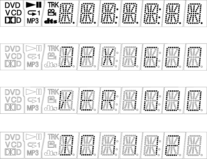
6-13
2-2. Operation of Auto Self Check
When the Self Check mode becomes active at the AC Power ON or by key input, the test display of the following steps (1) to (4) is
repeated.
(1) FLD and LED all ON (for 5 seconds)
(2) MODEL display (for 2 seconds)
(3) Version display (for 2 seconds)
(4) ROM creation date display (for 2 seconds)
6-14
2-3. Each Self Check Function
Each Self Check function tests the FLD display, LED display, and
key input.
2-3-1. FLD and LED All ON
2-3-1-1. Transition Keys in Self Check Mode
• x key and Z key on the main unit
• % key on the main unit and the remote commander
2-3-1-2. Operation and Display
In this mode, all LEDs except STANDBY LED and all segments of
FLD turn ON.
• Example of FLD all ON
2-3-2. Main Unit Key Name Display and Key Code Display
2-3-2-1. Transition Keys in Self Check Mode
• Keys on the main unit except keys transited in Self Check Mode
2-3-2-2. Operation and Display
When a key on the main unit is pressed in the Self Check mode, the
name of that key is displayed on the FLD. Also, the key name display
and the key code display can be switched with the [DISPLAY] key on
the remote commander. “NOTHING” is displayed when nothing is
entered. Also, VIDEO CD, DVD, and CD segments turn on when a
communication error occurred.
• FLD display (at input of H key on the main unit)
Input IC404: Pin No. (Signal)
Voltage [V] Pin ed (BNRKEY) Pin ef (PLAY) Pin eg (O/C) Pin eh (TVS)
0 – 0.2 –PLAY OPEN/CLOSE TVS
0.6 – 0.82 –NEXT –PIC MODE
1.16 – 1.47 –PREVIOUS –MODE
1.8 –2.12 –PAUSE ––
2.48 – 2.7 –STOP ––
6-15
• Key code display
(at input of H key, key code: 0 Ah)
• At input of faulty voltage
• Remote commander key code display
(at input of X key, key code: 39 h)
• When key is pressed double
2-3-3. Remote Commander Key Name Display and Key
Code Display
2-3-3-1. Transition Keys in Self Check Mode
• Remote commander keys except keys transited in Self Check Mode
2-3-3-2. Operation and Display
When a key on the remote commander is pressed in the Self Check
Mode, the name of that key is displayed on the FLD. Also, the key
name display and the key code display can be switched with the
[DISPLAY] key on the remote commander. “NOTHING” is displayed
when nothing is entered. Also, VIDEO CD, DVD, and CD segments
turn on when a communication error occurred.
• Remote commander key name display (at input of X key)
6-16
2-3-4. Communication Monitoring Display
The communication state is monitored and displayed while the
key name on the main unit and the remote commander is displayed.
When the communication to the System Controller failed, VIDEO
CD, DVD, and CD segments turn on.
2-3-5. FLD Anode Test Display and SHUTTLE Click
Operation Test
2-3-5-1. Transition Keys in Self Check Mode
• 5 key on the remote commander
• SHUTTLE on the remote commander during Anode Test display
(This unit does not provide JOG/SHUTTLE, and therefore use
another DVD remote commander having the JOG/SHUTTLE)
2-3-5-2. Operation and Display
The Self Check Mode transits to this mode when 5 key is en-
tered. This tests whether each segment turns on individually. Only
the first segment of each grid of FLD turns on, and each time the
SHUTTLE is entered, the segment of each grid is switched in or-
der. When SHUTTLE input is clockwise, the segment switches in
1 – 2 – 3 direction, or counterclockwise it switches in 3 – 2 – 1
direction.
• Display at the start of Anode Test
• Communication error display
(at no input of key and remote commander)
• Communication error display
(at code display without input of the remote commander)
r (Input in CW direction)
6-17
2-3-6. FLD Grid Test Display and SHUTTLE Click Opera-
tion Test
2-3-6-1. Transition Keys in Self Check Mode
• $ key on the remote commander
• SHUTTLE on the remote commander during Grid Test display
(This unit does not provide JOG/SHUTTLE, and therefore use an-
other DVD remote commander having the JOG/SHUTTLE)
2-3-6-2. Operation and Display
The Self Check Mode transits to this mode when $ key is entered.
This tests whether each grid turns on individually. The first grid only
of FLD turns on and other grids turn off. Each time the SHUTTLE is
entered, the grid is switched in order. When SHUTTLE input is clock-
wise, the grid switches in 1 – 2 – 3 direction, or counterclockwise it
switches in 3 – 2 – 1 direction.
• Display at the start of Grid Test
r (Input in CW direction)
2-3-7. LED Test Display
2-3-7-1. Transition Keys in Self Check Mode
• 4 key on the remote commander
• SHUTTLE on the remote commander during Grid Test display
(This model does not provide JOG/SHUTTLE, and therefore use
another DVD remote commander having the JOG/SHUTTLE)
2-3-7-2. Operation and Display
LED is switched in order by the input of JOG/SHUTTLE on the re-
mote commander. Also, LED ON/OFF is switched by the input of
same key as the function that turns on the LED concerned.
• FLD display during LED Test
6-18
a
f
h
g
e
r
p
n
s
c
col
m
dDp
j
kb
7G 6G 5G 4G 3G 2G 1G
P1 col col
P2
P3
P4
P5
P6
P7
P8
P9
P10
P11
P12
P13
P14
P15
P16
P17
P18
P19
P20
a
h
j
k
b
f
m
s
g
e
n
p
r
c
d
Dp
a
h
j
k
b
f
m
s
g
e
n
p
r
c
d
Dp
a
h
j
k
b
f
m
s
g
e
n
p
r
c
d
Dp
a
h
j
k
b
f
m
s
g
e
n
p
r
c
d
Dp
a
h
j
k
b
f
m
s
g
e
n
p
r
c
d
Dp
a
h
j
k
b
f
m
s
g
e
n
p
r
c
d
Dp
a
h
j
k
b
f
m
s
g
e
n
p
r
c
d
ANODE CONNECTION
( 7G-1G)
1G 7G 6G 5G 4G 3G 2G 1G2G
6-19
6-11. TROUBLESHOOTING
6-11-1. Cannot Enter Test Mode
You cannot enter the Test mode when either button has been pressed
by any reason with the board assembled in the front panel. In this
state, the power does not turn on even under normal condition (the
unit is kept in standby state), and also no button is active and the
remote commander is not accepted. In this case, disconnect the
MB-103 board and AV-61 board, and with the SELF CHECK (pin
0) of IF CON (IC404) on the IF-89 board kept in low state, sup-
ply AC, and the IF CON self-diagnosis mode will be forcibly acti-
vated. The IF CON (IC404) checks the SELF CHECK port only
after the power on reset (only at AC supply, not in standby state).
If any button is pressed, its name is displayed on the fluorescent
display tube. But, if other than “NOTHING” is displayed though
no button is pressed, it means that any button has been pressed.
6-11-2. Faults in Test Mode (MB-103 board)
1. The test mode menu is not displayed.
1-1. Board visual check
Check that the ICs of SYSCON (IC104), ROM (IC106 or
IC107), AVD (IC403), ARP & SERVO (IC301) are working
correctly.
Check that outside appearance of the ICs is normal.
Check that IC pins are not short-circuited.
Check that there is no soldering error.
Check that outside appearance of the capacitors and resistors
is normal.
1-2. Power supply voltage check
Check the power voltage of the power connector (CN102).
Check the power voltage of SYSCON (IC104).
Check the power voltage of ROM (IC106 or IC107).
Check the power voltage of AVD (IC403).
Check the power voltage of ARP & SERVO (IC301).
If the power voltage has any abnormality t
Check that the power supply lines are not shorted.
Check that there is no soldering error.
If any abnormality cannot be found still t
Check that each IC is working normally.
1-3. Clock signal check
Measure the clock signal frequency at CPUCK (CL101) of
SYSCON (IC104) with an oscilloscope.
If the 8.25 MHz signal appears. t Check the machine ac-
cording to section 1-3-1
If the 33 MHz signal appears. t Check the machine accord-
ing to section 1-3-2.
If other frequencies are output.
R110 and R113 have defective soldering, X101 crystal os-
cillator is defective.
If the measurement point is fixed to either “H” or “L”. t
Observe XFRRST (pin-uh) of SYSCON (IC104) with an
oscilloscope.
If the measurement point is “L”, check the following items.
If the IC has defective soldering, if the IC is short-circuited.
If the measurement point is “H”,
t Component X101 or SYSCON (IC104) is defective.
1-3-1. When the 8.25 MHz signal appears at CPUCK
• Check the XRD, XWRH and CS0X signal.
Observe XRD (pin-u;), XWRH (pin-ua), and CS0X (pin-tk)
of SYSCON (IC104) with an oscilloscope.
If these pins are fixed to either “L” (0V) or “H” (3.3V), or if
these pins stay in the center voltage, check the followings.
Check if the signal line does not have the defective solder-
ing.
Check if the signal line is short-circuited with other signal
lines.
If you cannot find any problem t SYSCON (IC104) is
defective.
• HA [0 to 21] signal and HD [0 to 15] signal check
Observe HA [0 to 21] (pins-<z/x to <z/. , <zzz to <zz, , <zx/ , 1 to 5)
of SYSCON (IC104) and HD [0 to 15] (pins-ig to <z// ) with
an oscilloscope.
If these pins are fixed to either “L” (0V) or “H” (3.3V), or if
the HA pin stays in the center voltage, check the followings.
(HD stays in the center voltage when it is normal.)
t Check if the signal line does not have the defective
soldering, or is short-circuited with other signal line or
SYSCON (IC104) is defective.
• Reset signal check
Check if XFRRST (pin-uh) of SYSCON (IC104) normal or
not.
The signal starts up at the same time as Vcc t Defective
soldering.
If the trouble does not apply to any of the above-described phe-
nomenon, SYSCON (IC104) or ROM (IC106 or IC107) is defec-
tive.
6-20
1-3-2. When the 33 MHz signal appears at CPUCK
• WAIT signal check
Observe XWAIT (pin-yj) of SYSCON (IC104) with an os-
cilloscope.
If it is fixed to “L” (0V). t Observe CS2X to CS5X (pins-
y; to yd).
If CS2X or CS3X is “L”. t AVD (IC403) has defective sol-
dering or AVD is defective.
If CS4x or CS5X is “L”. t ARP & SERVO (IC301) has
defective soldering or ARP & SERVO is defective.
If any one of the above is not “L”. t XWAIT or CSnX is
short-circuited or has the defective soldering or AVD (IC403)
is defective or ARP & SERVO (IC301) is defective.
Center voltage t The XWAIT line has defective soldering
or is short-circuited or AVD (IC403) is defective or ARP &
SERVO (IC301) is defective or SYSCON (IC104) is defec-
tive.
• CSnX signal check
Observe CS0X to CS5X (pins-tk to yd) of SYSCON (IC104)
with an oscilloscope.
If they are fixed to “L” (0V) or if to center voltage t Check
that the ICs do not have the defective soldering or is short-
circuited with the other signal lines or SYSCON (IC104) is
defective.
CS0X: ROM (IC106 or IC107)
CS2X, CS3X: AVD (IC403)
CS4X, CS5X: ARP & SERVO (IC301)
If the trouble symptom does not apply to any of the above phe-
nomenon, SYSCON (IC104) or ROM (IC106 or IC107) is defec-
tive.
2. Test mode menu is displayed but the machine stops
when menu is selected
2-1. AVD (IC403) check
Observe SDCLKO (pin-<zxm ) of AVD (IC403) with an oscillo-
scope.
95 MHz t No problem
27 MHz t Observe the XRST, HA, HD, XRD, XWRH INT
and CS signal waveform at the respective pins of AVDEC,
AVD (IC403) is defective.
If the signal is other than the above frequencies t AV D
(IC403) 27MHz signal line (CLKI (pin-<zb, ), SCLKIN (pin-
<zn/ )) is short-circuited, IC mount is defective, AVD (IC403) is
defective, PLL (IC103) is defective.
2-2. INT signal check
Observe INT0 to 2 (pins-qh to qk) of SYSCON (IC104) with
an oscilloscope.
If they are fixed to “L” (0V) or fixed to the center voltage t
Check that the ICs do not have the defective soldering, or are
short-circuited, SYSCON (IC104) is defective, or the follow-
ing ICs are not defective.
INT0: AVD (IC403)
INT1, INT2: ARP & SERVO (IC301)
2-3. If any abnormality cannot be confirmed by the
above-described checks, check the CS signal that
is currently output.
The CS signal other than CS0X is being output. t IC mount
is defective or the IC is defective depending on the moving
CS signal.
CS2X, CS3X: AVD (IC403)
CS4X, CS5X: ARP & SERVO (IC301)
If the trouble is not applicable to any of the above phenomenon,
SYSCON (IC104) or ROM (IC106 or IC107) is defective.
3. If the message “SDSP No Ack” appears after the menu
is displayed.
3-1. ARP & SERVO clock signal check
Check frequency of CLKIN (pin-<zb/ )
33 MHz t Normal
Frequency other than 33 MHz t CLKIN is short-circuited
or defective soldering or PLL (IC103) is defective or ARP &
SERVO (IC301) is defective
3-2. ARP & SERVO (IC301) PLL oscillation check
Observe PLCKO (pin-ij) of ARP & SERVO (IC301) with an
oscilloscope.
If the pin is fixed to either “L” (0V) or “H” (3.3V).
If XRST if fixed to “L”. XRST has the defective solder-
ing, In all other cases. ARP & SERVO (IC301) is defec-
tive
If it is oscillating.
HA [0 to 7] are HD [8 to 15] are short-circuited, check
XSDSPIT and XSDSPCS or ARP & SERVO (IC301) is
defective.
4. If trouble occurs at the specific item of the “Diag All
Check”.
IC mount of the NG item is defective or IC is defective.
5. Picture and sound are not output.
Check connection of CN601
Check for the defective connection of flat cable and check of
damage of the flat cable.
6. Picture is output but sound is not output.
Check the audio data output (at pins-wf, wk, and wl) of AVD
(IC403)
The audio data is not output. t AVD (IC403) or audio
DAC (IC601) mount is defective or power supply is defec-
tive or AVD (IC403) or audio DAC (IC601) is defective.
PLL (IC103) 512fs output check
If the frequency or waveform has abnormality. t The sig-
nal line has defective soldering or the signal line is short-
circuited with other signal lines or PLL (IC103) is defec-
tive.
7. Sound is output but picture is not output.
Observe pins-tg, tj, tl, ya, yd and yg of AVD (IC403) with
an oscilloscope.
If the analog signal is not output. t The signal line has the
defective soldering or is short-circuited or parts are defective
or AVD (IC403) is defective.
6-11-3. Drive Auto Adjustment stops due to error.
The ARP & SERVO (IC301) analog circuit of MB-103 board is
defective or RF-Amp (IC201) or M-Driver (IC202) peripheral cir-
cuit is defective or optical pickup block is defective or flat cable
connection is defective
6-21
6-11-4. The product itself is defective.
• If MB103 does not have any problem,
The board other than MB-103 board is defective or connec-
tion is defective or optical pickup block is defective or mecha-
nism deck is defective
1. The red LED does not light when the AC power is
turned on.
Check the EVER –13V (pin-3), EVER+3.3V (pin-qa),
EVER+11V (pin-qd) voltage of the power supply block
CN201.
If voltage is abnormal. t The power supply block is defec-
tive.
2. The LED does not light in green even once when the
POWER button is pressed. It remains lighting in red
(in the STANDBY mode).
2-1. Check the EVER -13V (pin-3), EVER+3.3V (pin-qa),
EVER+11V (pin-qd) voltage at CN201 of the power
supply block/
If voltage is abnormal. t The power supply block is defec-
tive.
2-2. Check if the fuse on the IF board has blown of not.
If the fuse has blown t Replace the fuse.
2-3. Check the P-CONT (pin-2) at CN401 of the IF-89
board when the POWER button is pressed.
If it remains at “L”,
t The signal line has the defective soldering or it is short-
circuited with other signal lines or capacitor or resistor is de-
fective or IFCON is defective or connection between the power
supply block and the IF-89 board is defective, or connector
installation is defective, or the power supply block is defec-
tive.
2-4. Check if the button is kept depressed in the IFCON
self mode.
If the button is kept depressed. t The front panel is defec-
tive, or IF-89 board is defective.
2-5. Check PONCHK (pin-e;) of IFCON (IC404) on the IF-
89 board.
If it is 0.5 V or more. t The power supply is defective, or IF-
89 board is defective.
3. If the LED lights in green but returns to red (STANDBY
mode) in several seconds when the POWER button is
pressed.
3-1. Check CN201 voltage of the power supply block
when the LED lights in green.
If voltage is abnormal. t The power supply block is defec-
tive, or the IF-89 board is defective, or MB103 is defective
3-2. Check XFRRST (pin-8) at CN101 on the MB-103
board.
If it is fixed to “L”. t The signal line has defective solder-
ing, or is short-circuited with other signal lines, or parts are
defective.
3-3. Check IFBSY (pin-5), XIFCS (pin-6), SI0 (pin-4),
SO0 (pin-1) and SC0 (pin-3) at CN101
If they are fixed to “H” or “L”.
t The signal line has defective soldering, or is short-cir-
cuited with other signal line, or parts are defective, or
SYSCON (IC104) is defective
If they change between “L/H”.
Connector installation is defective, or the IF-89 board is de-
fective, or SYSCON (IC104) is defective.
If they stay in the center voltage.
Poor connection of flexible wiring board such as it is inserted
in an angle diagonally, or defective soldering, or is short-cir-
cuited with other signal line.
3-4. Check PONCHK (pin-e;) of IFCON (IC404) on the
IF-89 board.
If rise-up time from 0.5 V to 1.5 V or more takes longer time,
or it does not exceed 1.5 V or more. t The IF board is defec-
tive.
4. The LED lights in green but the fluorescent display
tube does not light when the POWER button is pressed.
Connection between the power supply block and the IF-89
board is defective, or connector installation is defective, or
the IF-89 board is defective.
5. Both picture and sound are not output.
Connection between the power supply block and the IF-89
board is defective, or connection between the IF-89 board and
the AV-61 board is defective, or connection between the AV-
61 board and the MB-103 board is defective, or connector
installation is defective, or AV-61 board is defective.
6. Picture is not normal. (Block noise or others appear.)
The MB-103 board AVD (IC403) or SDRAM (IC404, IC405)
is defective, or ARP & SERVO (IC301) is defective.
