SPA2000 SPX2000
User Manual: SPX2000
Open the PDF directly: View PDF ![]() .
.
Page Count: 87
- English
- SPX2000 SM CONTENTS
- SPECIFICATIONS
- DIMENSIONS
- PANEL LAYOUT
- CIRCUIT BOARD LAYOUT
- DISASSEMBLY PROCEDURE
- 1. Rack Angle
- 2. Top Cover
- 3. Front Panel
- 4. JKIN Circuit Board, JKOUT Circuit Board
- 5. MAIN Circuit Board
- 6. Replacing the Lithium Battery
- 7. Power Supply Unit
- 8. VOL Circuit Board, FOOT SW Circuit Board, POWER Circuit Board
- 9. PN1 Circuit Board, PN2 Circuit Board, PN3 Circuit Board, LCD
- 10. AC Inlet Assembly
- LSI PIN DESCRIPTION
- IC BLOCK DIAGRAM
- CIRCUIT BOARDS
- INSPECTIONS
- TEST PROGRAM
- WRITING PROGRAM
- BULK OUT (ALL)
- INITIALIZING THE SPX2000
- ERROR MESSAGE LIST
- MIDI IMPLEMENTATION CHART
- MIDI DATA FORMAT
- PARTS LIST CONTENTS
- CIRCUIT DIAGRAM CONTENTS
- SPX2000 SM CONTENTS
- Japan
SERVICE MANUAL
■ CONTENTS
SPECIFICATIONS ............................................................ 4
DIMENSIONS ..................................................................... 7
PANEL LAYOUT ................................................. 8
CIRCUIT BOARD LAYOUT ........................... 10
DISASSEMBLY PROCEDURE ....................................... 11
LSI PIN DESCRIPTION ........................................ 16
IC BLOCK DIAGRAM ............................................ 20
CIRCUIT BOARDS ................................................. 23
INSPECTIONS ................................................................ 29/32
TEST PROGRAM ........................................ 35/42
WRINTING PROGRAM ............................. 49
BULK OUT (ALL) ............................................................................. 50
INITIALIZING THE SPX2000 ............................................ 50
ERROR MESSAGE LIST ............................. 51/52
MIDI IMPLEMENTATION CHART .................................................... 53
MIDI DATA FORMAT ........................................................................ 54
PARTS LIST
BLOCK DIAGRAM
OVERALL CONNECTOR CIRCUIT DIAGRAM
OVERALL CIRCUIT DIAGRAM
Copyright (c) Yamaha Corporation. All rights reserved. PDF-K2331 Printed in Japan ’03.07
PA 011695
200307-108000
(目次)
(総合仕様)
(寸法図)
(パネルレイアウト)
(ユニットレイアウト)
(分解手順)
(LSI 端子機能表)
(IC ブロック図)
(シート基板図)
(検査)
(テストプログラム)
(プログラムの書き込み)
(初期化)
(エラーメッセージ)
(ブロックダイアグラム)
(総コネクタ接続回路図)
(総回路図)

2
SPX2000
IMPORTANT NOTICE
This manual has been provided for the use of authorized Yamaha Retailers and their service personnel. It has been assumed
that basic service procedures inherent to the industry, and more specifically Yamaha Products, are already known and
understood by the users, and have therefore not been restated.
WARNING : Failure to follow appropriate service and safety procedures when servicing this product may result in
personal injury, destruction of expensive components and failure of the product to perform as
specified. For these reasons, we advise all Yamaha product owners that all service required should
be performed by an authorized Yamaha Retailer or the appointed service representative.
IMPORTANT : This presentation or sale of this manual to any individual or firm does not constitute authorization,
certification, recognition of any applicable technical capabilities, or establish a principal-agent
relationship of any form.
The data provided is believed to be accurate and applicable to the unit (s) indicated on the cover. The research engineering,
and service departments of Yamaha are continually striving to improve Yamaha products. Modifications are, therefore,
inevitable and changes in specification are subject to change without notice or obligation to retrofit. Should any discrepancy
appear to exist, please contact the distributor’s Service Division.
WARNING : Static discharges can destroy expensive components. Discharge any static electricity your body
may have accumulated by grounding yourself to the ground bus in the unit (heavy gauge black wires
connect to this bus).
IMPORTANT : Turn the unit OFF during disassembly and parts replacement. Recheck all work before you apply
power to the unit.
WARNING : CHEMICAL CONTENT NOTICE !
The solder used in the production of this product contains LEAD. In addition, other electrical/electronic and/or plastic
(where applicable) components may also contain traces of chemicals found by the California Health and Welfare Agency
(and possibly other entities) to cause cancer and/or birth defects or other reproductive harm.
DO NOT PLACE SOLDER, ELECTRICAL/ELECTRONIC OR PLASTIC COMPONENTS IN YOUR MOUTH FOR ANY
REASON WHAT SO EVER!
Avoid prolonged, unprotected contact between solder and your skin! When soldering, do not inhale solder fumes or expose
eyes to solder/flux vapor!
If you come in contact with solder or components located inside the enclosure of this product, wash your hands before
handling food.
■WARNING
Components having special characteristics are marked Z and must be replaced with parts having specification equal to
those originally installed.
WARNING: THIS APPARATUS MUST BE EARTHED
IMPORTANT
THE WIRES IN THIS MAINS LEAD ARE COLOURED IN ACCORDANCE WITH THE FOLLOWING CODE:
GREEN-AND-YELLOW : EARTH
BLUE : NEUTRAL
BROWN : LIVE
As the colours of the wires in the mains lead of this apparatus may not correspond with the coloured markings identifying the
terminals in your plug, proceed as follows:
The wire which is coloured GREEN and YELLOW must be connected to the terminal in the plug which is marked by the letter
E or by the safety earth symbol or coloured GREEN and YELLOW.
The wire which is coloured BLUE must be connected to the terminal which is marked with the letter N or coloured BLACK.
The wire which is coloured BROWN must be connected to the terminal which is marked with the letter L or coloured RED.
* This applies only to products distributed by YAMAHA KEMBLE MUSIC (U.K.) LTD.
Z印の部品は、安全を維持するために重要な部品です。交換する場合は、安全のために必ず指定の部品をご使用ください。

3
SPX2000
LITHIUM BATTERY HANDLING
This product uses a lithium battery for memory back-up.
WARNING : Lithium batteries are dangerous because they can be exploded by improper handling. Observe the following
precautions when handling or replacing lithium batteries.
• Leave lithium battery replacement to qualified service personnel.
• Always replace with batteries of the same type.
• When installing on the PC board by soldering, solder using the connection terminals provided on the battery cells.
• Never solder directly to the cells. Perform the soldering as quickly as possible.
• Never reverse the battery polarities when installing.
• Do not short the batteries.
• Do not attempt to recharge these batteries.
• Do not disasemble the batteries.
• Never heat batteries or throw them into fire.
ADVARSEL!
Lithiumbatteri-Eksplosionsfare ved fejlagtig handtering. Udskiftning ma kun ske med batteri af samme fabrikat og type. lever
det brugte batteri tilbage til leverandren.
VARNING
Explosionsfara vid felaktigt batteribyte.
Anvand samma batterityp eller en ekvivalent typ som rekommenderas av apparattillverkaren.
Kassera anvant batteri enligt fabrikantens instruktion.
VAROITUS
Paristo voi rajahtaa, jos se on virheellisesti asennettu.
Vaihda paristo ainoastaan laitevalmistajan suosittelemaan tyyppiiin.
Havita kaytetty paristo valmistajan ohjeiden mukaisesti.
The following information complies with Dutch official Gazette 1995. 45; ESSENTIALS OF ORDER ON THE COLLECTION OF
BATTERIES.
• Please refer to the diassembly procedure for the removal of Back-up Battery.
• Leest u voor het verwijderen van de backup batterij deze beschrijving.
リチウム電池の取り扱い
<注意>
リチウム電池を誤って交換すると爆発する危険があります。交換する場合は、サービスマニュアルで指定された部品を使用してく
ださい。
4
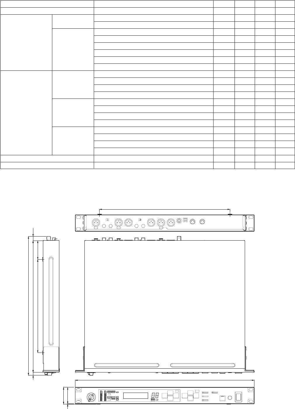
SPX2000
■ SPECIFICATIONS
Analog Input/Output
Digital Input/Output
Controls
Keys
LEDs
LCD
Effects
Power Requirements
Dimensions
Net Weight
Operating free-air temperature range
Storage temperature range
Accessories
Option
General Specifications
INPUT L,R XLR-3-31 Balanced
Phone jack Balanced
AD converter, 24-bit linear 128-times oversampling (@Fs=44.1, 48 kHz)
64-times oversampling (@Fs=88.2, 96 kHz)
Level SW +4/–10 dBu
OUTPUT L,R XLR-3-32 Balanced
Phone jack Balanced
DA converter, 24-bit linear 128-times oversampling (@Fs=44.1, 48 kHz)
64-times oversampling (@Fs=88.2, 96 kHz)
Level SW +4/–10 dBu
AES/EBU IN XLR-3-31 Balanced
AES/EBU OUT XLR-3-32 Balanced
WORD CLOCK IN
MIDI IN
MIDI OUT/THRU
USB TO HOST USB 1.1
INPUT L, R for VOLUME
FOOT SW for TAP
[INPUT MODE], [METER], [BANK]
MEMORY [UNDO], [▲], [▼], [RECALL], [STORE]
EDIT [COMPARE], [▲ INC], [▼ DEC], [NEXT], [BACK]
[PARAMETER], [FINE], [UTILITY]
[BYPASS], [TAP]
[POWER ON/OFF]
Level Meter L, R 2 x 12 Segments LED
Effect No. 2 x 7 Segments LED
INPUT MODE [MONO]/[STEREO]
METER [INPUT]/[OUTPUT]
INPUT SOURCE [ANALOG]/[DIGITAL]
CLOCK [INT]/[AES/EBU]/[WC]
kHz [96]/[88.2]/[48]/[44.1]
MIDI [MIDI]
BANK [PRESET]/[USER]/[CLASSIC]
16 characters x 2 rows back-lit LCD
Back-lit color Green, Yellow, Magenta, Cyan, White,
Red (Error Message only)
PRESET 97
USER 99
CLASSIC 25
U.S./Canada 120V 25W 60Hz
Japan 100V 25W 50/60Hz
Others 230V 25W 50Hz
Height 45 mm
Depth 372.5 mm
Width 480 mm
4kg
5 — 40°C
–20 — 60°C
Japan 電源コード、プラグ変換アダプター、取扱説明書、保証書
Others Owner’s Manual, Power cable
Foot Switch FC5
(総合仕様)
(一般仕様)
5
SPX2000
Input/Output Characteristics
Analog Input Characteristics
*1 Sensitivity is the lowest level that will produce an output of +4dB(1.23V) or the nominal output level when the unit is set to maximum gain.
(level control is maximum position.)
*2 XLR-3-31 type connectors are balanced. (1=GND, 2=HOT, 3=COLD)
*3 Phone jacks are balanced. (Tip=HOT, Ring=COLD, Sleeve=GND)
*4 In these specifications, when dBu represents are specific voltage, 0 dBu is referenced to 0.775 Vrms.
*5 AD converter is 24-bit linear,128-times oversampling @Fs=44.1, 48 kHz, 64-times oversampling @Fs=88.2, 96 kHz
Analog Output Characteristics
*1 XLR-3-32 type connectors are balanced. (1=GND, 2=HOT, 3=COLD)
*2 Phone jacks are balanced. (Tip=HOT, Ring=COLD, Sleeve=GND)
*3 In these specifications, when dBu represents are specific voltage, 0 dBu is referenced to 0.775 Vrms.
*4 DA converter is 24-bit, 128-times oversampling @Fs=44.1, 48 kHz, 64-times oversampling @Fs=88.2, 96 kHz
Control I/O Characteristics
Digital Input Characteristics
*1 XLR-3-31 type connectors are balanced. (1=GND, 2=HOT, 3=COLD)
Digital Output Characteristics
*1 channel status of AES/EBU OUT
type: 2 audio channels
emphasis: NO
sampling frequency: depends on the internal configuration
*2 dither: word length 16 - 24-bit
*3 XLR-3-32 type connector is balanced. (1=GND, 2=HOT, 3=COLD)
Input Terminals
INPUT L, R
Level SW
+4 dBu
–10 dBu
Input Level
VR.
Max.:
+10 dB
Max.:
+10 dB
Actual
Load
Impedance
10 k Ω
For Use With
Nominal
600 Ω
Lines
Input Level Connector
XLR-3-31 type
(Balanced)
Phone jack
(TRS: Balanced)
Sensitivity
–6 dBu
(0.388 V)
–20 dBu
(0.0775 V)
Nominal
—
—
Max.
before clip
+14 dBu
(3.88 V)
0 dBu
(0.775 V)
Input Terminals
INPUT L, R
Level SW
+4 dBu
–10 dBu
Input Level
VR.
Nrminal:
0 dB
Nrminal:
0 dB
Actual
Load
Impedance
10 k Ω
For Use With
Nominal
600 Ω
Lines
Input Level Connector
XLR-3-31 type
(Balanced)
Phone jack
(TRS: Balanced)
Sensitivity
—
—
Nominal
+4 dBu
(1.23 V)
–10 dBu
(0.245 V)
Max.
before clip
+24 dBu
(12.28 V)
+10 dBu
(2.45 V)
Output Terminals
OUTPUT L, R
Actual
Source
Impedance
150 Ω
For Use With
Nominal
600 Ω Lines
Level SW
+4 dBu
–10 dBu
Output Level Connector
XLR-3-31 type (Balanced)
Phone jack (TRS: Balanced)
Nominal
+4 dBu
(1.23 V)
–10 dBu
(0.245 V)
Max.
before clip
+24 dBu
(12.28 V)
+10 dBu
(2.45 V)
Input Terminals Format Data Length Level Connector
AES/EBU IN AES/EBU 24-bit RS422 XLR-3-31 type (Balanced)
Input Terminals Format Data Length Level Connector
AES/EBU OUT AES/EBU Professional use 24-bit RS422 XLR-3-31 type (Balanced)
Terminals Format Level Connector
USB TO HOST USB 1.1 0 to 3.3 V B type USB Connector
MIDI IN MIDI — DIN Connector 5P
OUT/THRU MIDI — DIN Connector 5P
WORD CLOCK IN — TTL/75 ΩBNC Connector
(入出力特性)
6
SPX2000
Electrical Characteristics
Input Level VR is nominal when measured. Output impedance of signal generator:600ohms
Frequency Response
Fs=48 kHz: @20 Hz-20 kHz, reference to the nominal output level @1 kHz
Fs=96 kHz: @20 Hz-40 kHz, reference to the nominal output level @1 kHz
Gain Error
@1 kHz
*1 In these specifications, when dBu represents are specific voltage, 0 dBu is referenced to 0.775 Vrms.
Total Harmonic Distortion
*1 In these specifications, when dBu represents are specific voltage, 0 dBu is referenced to 0.775 Vrms.
*2 Total Harmonic Distortion is measured with a 18 dB/octave filter @80 kHz.
Hum & Noise
Fs=48/96 kHz
*1 Hum & Noise are measured with a 6 dB/octave filter @12.7 kHz;
equivalent to a 20 kHz filter with infinite dB/octave attenuation.
*2 In these specifications, when dBu represents are specific voltage, 0 dBu is referenced to 0.775 Vrms.
Crosstalk
@1 kHz
Input Output RL Conditions Min Typ Max Units
INPUT L, R OUTPUT L, R 600 ΩINPUT LEVEL SW: +4, OUTPUT LEVEL SW: +4 +2.0 +4.0 +6.0 dBu
INPUT LEVEL SW: –10, OUTPUT LEVEL SW: –10 –12.0 –10.0 –8.0 dBu
Input Output RL Conditions Min Typ Max Units
INPUT L, R OUTPUT L, R 600 Ω— –3.0 0.0 +1.0 dB
Input Output RL Conditions Min Typ Max Units
INPUT L, R OUTPUT L, R 600 ΩFs=48 kHz: +14 dBu @20 Hz-20 kHz, 0.05 %
INPUT LEVEL SW: +4,
OUTPUT LEVEL SW: +4
Fs=96 kHz: +14 dBu @20 Hz-40 kHz, 0.05 %
INPUT LEVEL SW: +4,
OUTPUT LEVEL SW: +4
Input Output RL Conditions Min Typ Max Units
INPUT L, R OUTPUT L, R 600 ΩRs=600 Ω, INPUT LEVEL VR: nominal –80 dBu
INPUT LEVEL SW: +4 /OUTPUT LEVEL SW: +4
Dynamic Range
Fs=48/96 kHz
Input Output RL Conditions Min Typ Max Units
INPUT L, R OUTPUT L, R 600 ΩAD + DA, INPUT LEVEL VR: max 106 dB
*1 Dynamic range are measured with a 6 dB/octave filter @12.7 kHz;
equivalent to a 20 kHz filter with infinite dB/octave attenuation.
Maximum voltage gain
@1 kHz
Input Output Conditions Min Typ Max Units
INPUT L, R OUTPUT L, R INPUT to OUTPUT –80 dB
Input Output RL Conditions Min Typ Max Units
INPUT L, R OUTPUT L, R 600 ΩRs=600 Ω, INPUT LEVEL VR: nominal +10 dB
INPUT LEVEL SW: +4 /OUTPUT LEVEL SW: +4
(電気的特性)
7
SPX2000
PARAMETER CONDITIONS MIN TYP MAX UNITS
Sampling Frequency
External Clock Frequency Range Normal Rate 39.69 50.88 kHz
Double Rate 79.38 101.76 kHz
Jitter of PLL DIGITAL IN Fs=44.1 kHz, Jitter ≤ 2ns 10 ns
DIGITAL IN Fs=48 kHz, Jitter ≤ 2ns 10 ns
DIGITAL IN Fs=39.69-50.88 kHz, Jitter ≤ 2ns 20 ns
DIGITAL IN Fs=88.2 kHz, Jitter ≤ 2ns 10 ns
DIGITAL IN Fs=96 kHz, Jitter ≤ 2ns 10 ns
DIGITAL IN Fs=79.38-101.76 kHz, Jitter ≤ 2ns 20 ns
Internal Clock Frequency word clock: int 44.1 kHz 44.1 kHz
word clock: int 48 kHz 48 kHz
word clock int 88.2 kHz 88.2 kHz
word clock: int 96 kHz 96 kHz
accuracy word clock int 44.1 kHz 50 ppm
word clock: int 48 kHz 50 ppm
word clock: int 88.2 kHz 50 ppm
word clock: int 96 kHz 50 ppm
jitter word clock: int 44.1 kHz 5 ns
word clock: int 48 kHz 5 ns
word clock : int 88.2 kHz 5 ns
word clock: int 96 kHz 5 ns
Signal Delay INPUT to OUTPUT(@Delay time=0.0 ms / Fs=96 kHz) 426 ns
Idle tone AD converter, peak@20 Hz–20 kHz –130 dB
145
44
480
350
50250 11.8
352.7
8372.5
Units : mm
(単位)
■ DIMENSIONS
(寸法図)
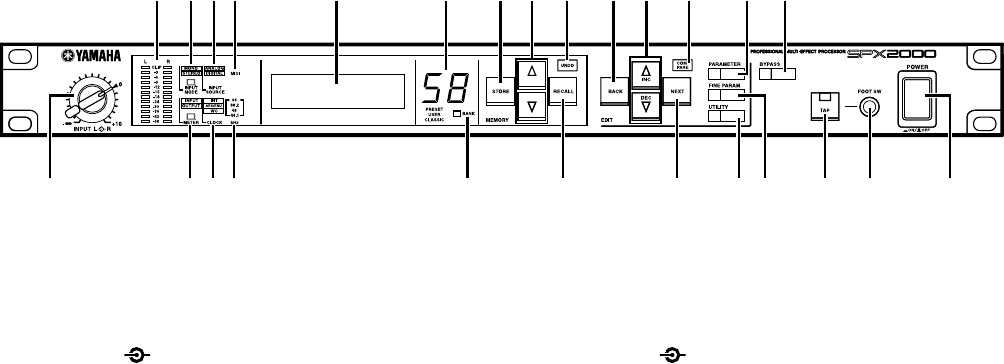
8
SPX2000
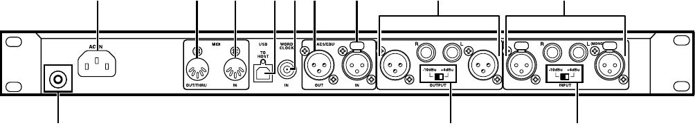
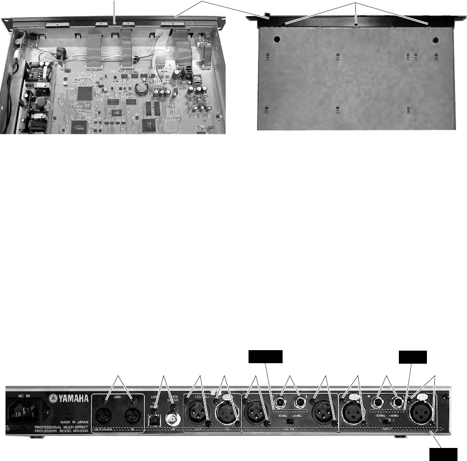
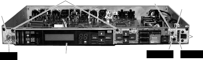
■ PANEL LAYOUT
■ Front Panel
w e tu o !0 !2 !5 !9 @0 @3!6!3 !7
!8 @4 @5
!4!1ryiq@6
@2 @1
q [INPUT L R] control
w Level meters
e [INPUT MODE] button/indicator
r [METER] button/indicator
t [INPUT SOURCE] indicator
y [CLOCK] indicator
u [MIDI] indicator
i [kHz] indicator
o Display
!0 Effect number indicator
!1 [BANK] button/indicator
!2 [STORE] button
!3 [▲]/[▼] buttons
!4 [RECALL] button
!5 [UNDO] button/LED
!6 [BACK] button
!7 [▲ INC]/[▼ DEC] buttons
!8 [NEXT] button
!9 [COMPARE] button/LED
@0 [PARAMETER] button/LED
@1 [FINE PARAM] button/LED
@2 [UTILITY] button/LED
@3 [BYPASS] button/LED
@4 [TAP] button/LED
@5 [FOOT SW] jack
@6 [POWER ON/OFF] button
q [INPUT L R]コントロール
w レベルメーター
e [INPUT MODE] ボタン/インジケーター
r [METER] ボタン/インジケーター
t [INPUT SOURCE]インジケーター
y [CLOCK]インジケーター
u [MIDI]インジケーター
i [kHz]インジケーター
o ディスプレイ
!0 エフェクト番号インジケーター
!1 [BANK] ボタン/インジケーター
!2 [STORE]ボタン
!3 [▲]/[▼]ボタン
!4 [RECALL]ボタン
!5 [UNDO] ボタン/LED
!6 [BACK]ボタン
!7 [▲INC] /[▼DEC]ボタン
!8 [NEXT]ボタン
!9 [COMPARE] ボタン/LED
@0 [PARAMETER] ボタン/LED
@1 [FINE PARAM] ボタン/LED
@2 [UTILITY] ボタン/LED
@3 [BYPASS] ボタン/LED
@4 [TAP] ボタン/LED
@5 [FOOT SW]端子
@6 [POWER ON/OFF]ボタン
(パネルレイアウト)
(フロントパネル)
9
SPX2000
@7 Grounding screw
@8 [AC IN] jack
@9 [MIDI OUT/THRU] connector
#0 [MIDI IN] connector
#1 [TO HOST USB] connector
#2 [WORD CLOCK IN] jack
#3 [AES/EBU OUT] jack
#4 [AES/EBU IN] jack
#5 [OUTPUT] jacks
#6 [OUTPUT –10 dBu/+4 dBu] switch
#7 [INPUT] jacks
#8 [INPUT –10 dBu/+4 dBu] switch
■ Rear Panel
(リアパネル)
@8 @9 #0 #3#1 #2
#6@7 #8
#7
#4 #5
@7 アース用ネジ
@8 [AC IN]端子
@9 [MIDI OUT/THRU]端子
#0 [MIDI IN]端子
#1 [TO HOST USB]端子
#2 [WORD CLOCK IN]端子
#3 [AES/EBU OUT]端子
#4 [AES/EBU IN]端子
#5 [OUTPUT]端子
#6 [OUTPUT ‐10dBu/+4dBu]スイッチ
#7 [INPUT]端子
#8 [INPUT ‐10dBu/+4dBu]スイッチ
10
SPX2000
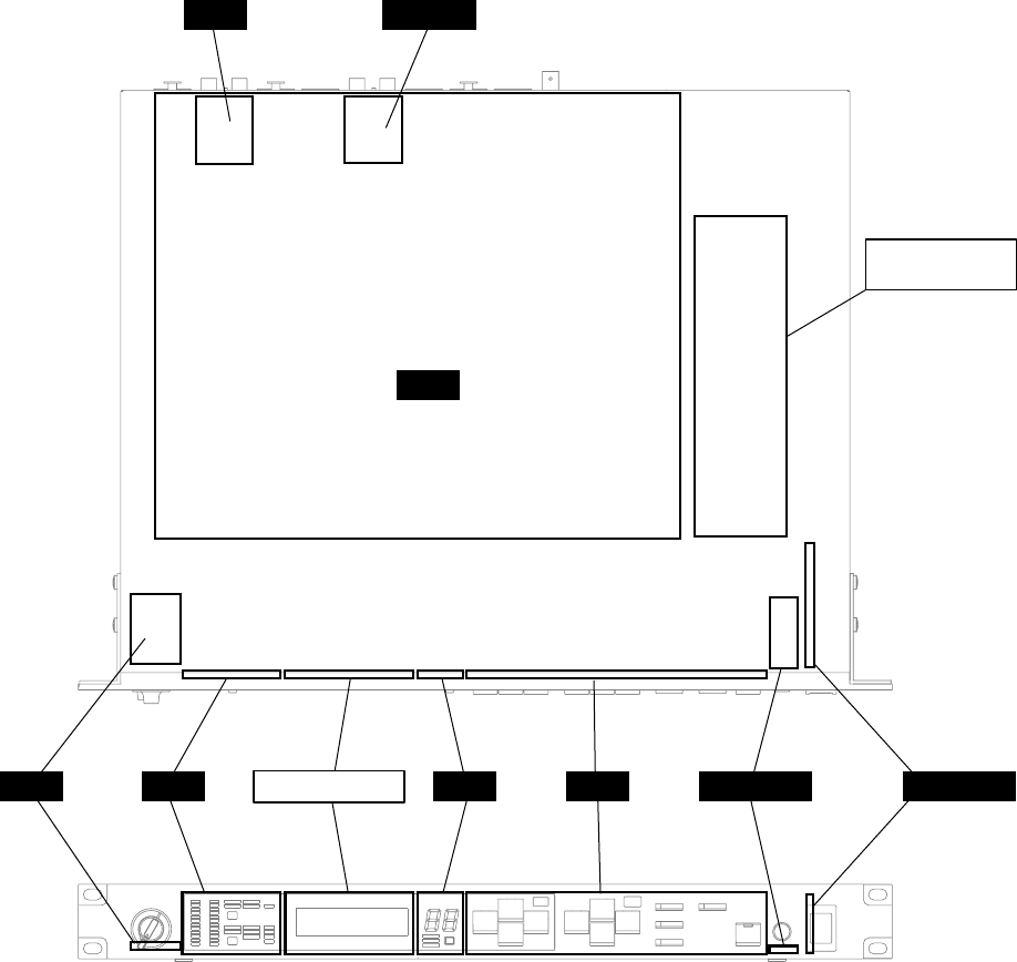
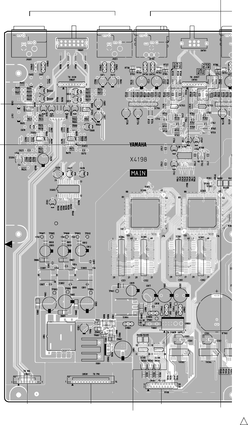
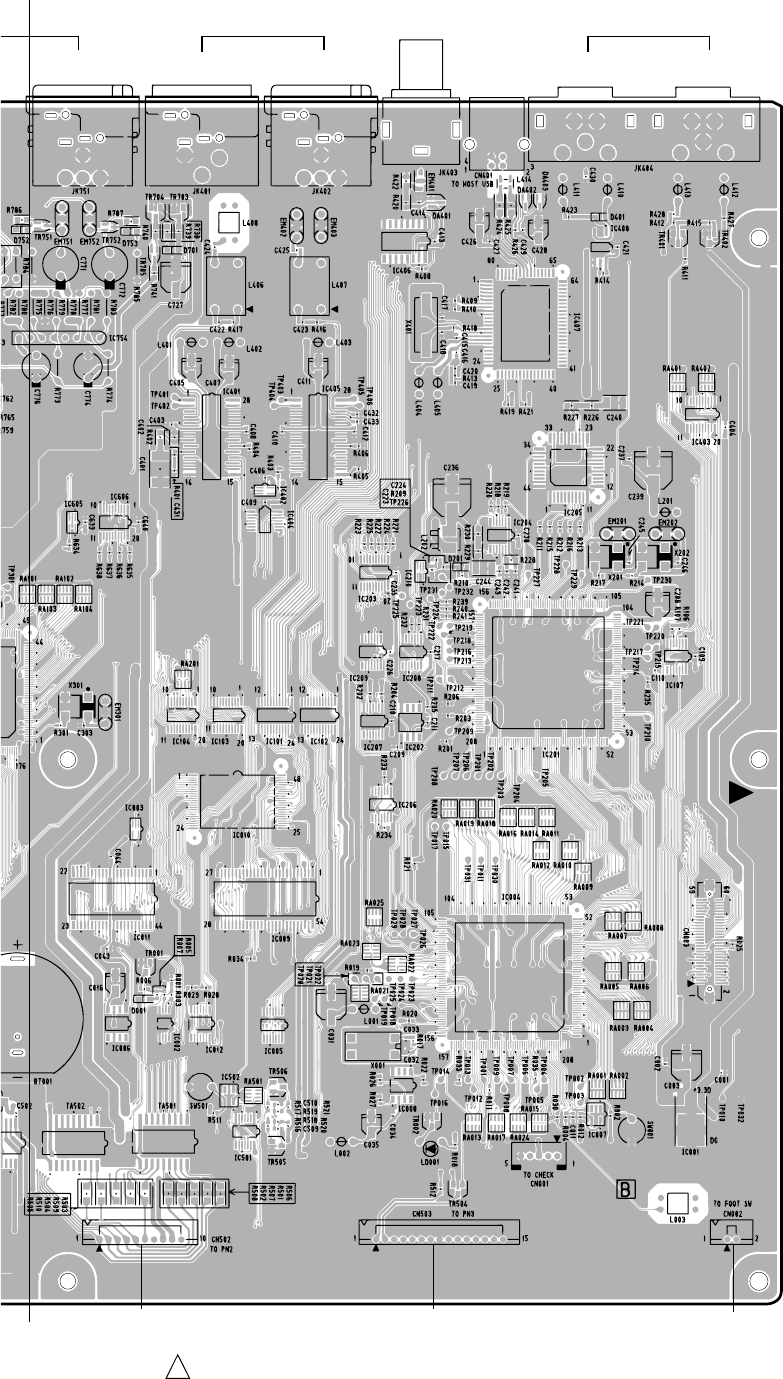
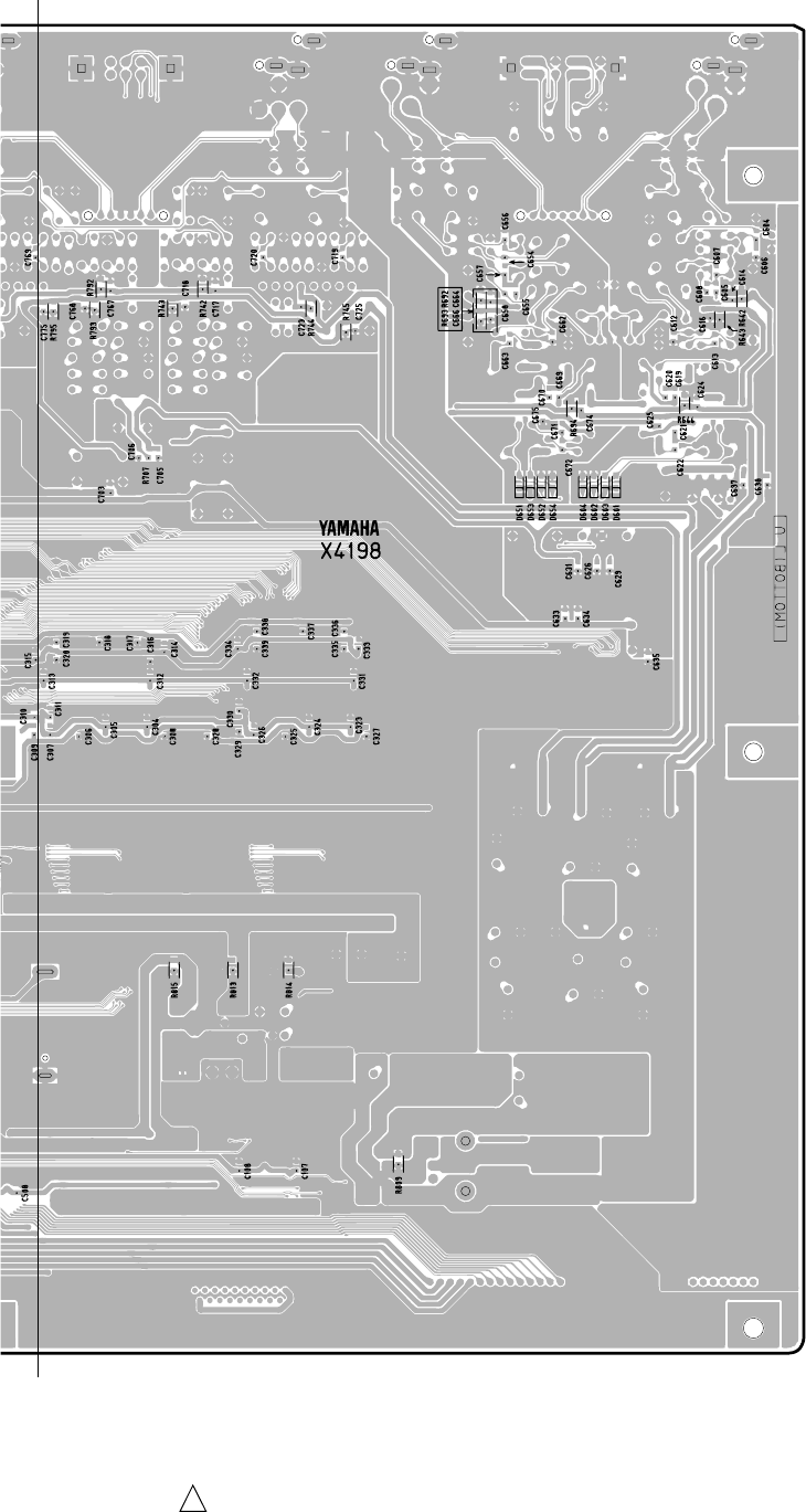
■ CIRCUIT BOARD LAYOUT
MAIN
FOOTSWPN3PN2
LCD MODULE
PN1VOL
JKOUTJKIN
POWER SUPPLY
UNIT
POWER
(ユニットレイアウト)
11
SPX2000
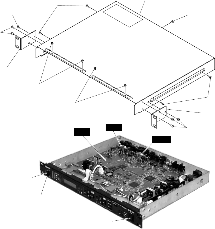
2. Top Cover
(Time required : About 2 min.)
2-1. Remove the rack angle L and R. (See procedure 1)
2-2. Remove the nine (9) screws marked [520]. The top cover
can then be removed. (Fig. 1)
1. Rack Angle
(Time required : About 1 min.)
1-1. Remove the three (3) screws marked [540A]. The rack
angle L can then be removed. (Fig. 1)
1-2. Remove the three (3) screws marked [540B]. The rack
angle R can then be removed. (Fig. 1)
Rack angle R
Rack angle L
(Fig. 1)
[520]: Bind Head Tapping Screw-S 3.0 x 6 MFZN2BL (EP630210)
[540]: Bind Head Tapping Screw-S 4.0 x 8 MFZN2BL (VI693100)
■ DISASSEMBLY PROCEDURE(分解手順)
[540A]
[540A]
[520]
[520]
[520]
[540B]
[520]
[520]
Top cover
Internal knob (INPUT L)
External knob (INPUT R)
JKIN
JKOUT
MAIN
POWER button
(ボタンPSW)
2. トップカバー (所要時間:約2分)
2-1. ラックアングルL、Rを外します。(1項参照)
2-2. [520]のネジ9本を外し、トップカバーを外します。
(図1)
1. ラックアングル (所要時間:約1分)
1-1. [540A]のネジ3本を外し、ラックアングルLを外しま
す。(図1)
1-2. [540B]のネジ3本を外し、ラックアングルRを外しま
す。(図1)
(ラックアングルL)
(トップカバー)
(ラックアングルR)
+バインドSタイト
+バインドSタイト
(図1)
(ノブ内)
(ノブ外)
12
SPX2000
3. Front Panel
(Time required : About 3 min.)
3-1. Remove the rack angle L and R. (See procedure 1)
3-2. Remove the top cover. (See procedure 2)
3-3. Pull out the internal knob (INPUT L) and the external
knob (INPUT R). (Fig. 1)
3-4. Remove the screw marked [420] and three (3) screws
marked [430]. The front panel can then be removed.
(Fig. 2)
[420] [430]
● Top view ● Bottom view
(Fig. 2)
[420]: Flat Head Tapping Screw-S 3.0 x 6 MFAN2Y (WB451000)
[430]: Bind Head Tapping Screw-S 3.0 x 6 MFZN2BL (EP630210)
Front panel
4. JKIN Circuit Board, JKOUT Circuit Board
(Time required : About 3 minutes each.)
4-1. Remove the rack angle L and R. (See procedure 1)
4-2. Remove the top cover. (See procedure 2)
4-3. Remove the two (2) hexagonal nuts marked [130A]. The
JKIN circuit board can then be removed. (Fig. 3)
4-4. Remove the two (2) hexagonal nuts marked [130B]. The
JKOUT circuit board can then be removed.
(Fig. 3)
[130A][130B] [40][40][30][30][30] [40][50][30]
● Rear view
[30]: Bind Head Tapping Screw-B 3.0 x 8 MFZN2BL (EP600190)
[40]: Bind Head Tapping Screw-B 2.6 x 8 MFZN2BL (VB096700)
[50]: Bind Head Tapping Screw-S 3.0 x 6 MFZN2BL (EP630210)
[130]: Hexagonal Nut 9.0 x 11 (V2431400)
(Fig. 3)
JKIN
JKOUT
MAIN
3. フロントパネル (所要時間:約3分)
3-1. ラックアングルL、Rを外します。(1項参照)
3-2. トップカバーを外します。(2項参照)
3-3. ノブ内(INPUT L)とノブ外(INPUT R)を外します。
(図1)
3-4. [420]のネジ1本と[430]のネジ3本を外し、フロントパネ
ルを外します。(図2)
(図2)
Sタイト平頭
+バインドSタイト
(フロントパネル)
4. JKIN、JKOUTシート (所要時間:各約3分)
4-1. ラックアングルL、Rを外します。(1項参照)
4-2. トップカバーを外します。(2項参照)
4-3. [130A]の特殊六角ナット2個を外し、JKINシートを外
します。(図3)
4-4. [130B]の特殊六角ナット2個を外し、JKOUTシートを
外します。(図3)
+バインドBタイト
+バインドBタイト
+バインドSタイト
特殊六角ナット
(図3)
13
SPX2000
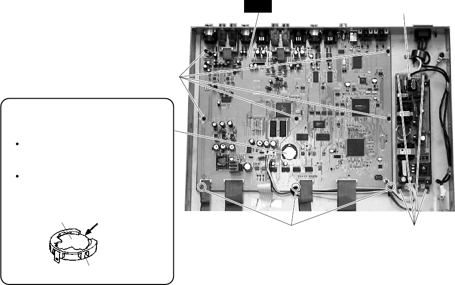
Battery VN103500
VN103600(Battery holder for VN103500)
Notice for back-up battery removal
Push the battery as shown in figure,
then the battery will pop up.
Druk de batterij naar beneden zoals
aangeven in de tekening, de batterij
springt dan naar voren.
Battery
Battery holder
(Fig. 4)
[60]: Bind Head Tapping Screw-S 3.0 x 6 MFZN2BL (EP630210)
[100]: Bind Head Tapping Screw-S 3.0 x 6 MFZN2BL (EP630210)
5. MAIN Circuit Board
(Time required : About 5 min.)
5-1. Remove the rack angle L and R. (See procedure 1)
5-2. Remove the top cover. (See procedure 2)
5-3. Remove the JKIN circuit board and JKOUT circuit
board. (See procedure 4)
5-4. Remove the eight (8) screws marked [30], the six (6)
screws marked [40] and the two (2) screws marked [50].
(Fig. 3)
5-5. Remove the eight (8) screws marked [60]. The MAIN
circuit board can then be removed. (Fig. 4)
6. Replacing the Lithium Battery
(Time required : About 3 min.)
6-1. Remove the rack angle L and R. (See procedure 1)
6-2. Remove the top cover. (See procedure 2)
6-3. You can replace the lithium battery from the MAIN
circuit board. (Fig. 4)
* The lithium battery is not part of the MAIN circuit board.
When you replace the MAIN circuit board, you should
remove the lithium battery from the board, and install in
the holder on the new circuit board.
* Important data should be backed up by BULK OUT (ALL)
function. (See page 50.)
7. Power Supply Unit
(Time required : About 3 min.)
7-1. Remove the rack angle L and R. (See procedure 1)
7-2. Remove the top cover. (See procedure 2)
7-3. Remove the four (4) screws marked [100]. The power
supply unit can then be removed. (Fig. 4)
[60]
[60]
MAIN
[100]
● Lithium Battery
Power supply unit
+バインドSタイト
+バインドSタイト
(図4)
5. MAINシート (所要時間:約5分)
5-1. ラックアングルL、Rを外します。(1項参照)
5-2. トップカバーを外します。(2項参照)
5-3. JKINシート、JKOUTシートを外します。(4項参照)
5-4. [30]のネジ8本、[40]のネジ6本、[50]のネジ2本を外しま
す。(図3)
5-5. [60]のネジ8本を外し、MAINシートを外します。(図4)
6. リチウム電池の交換 (所要時間:約3分)
6-1. ラックアングルL、Rを外します。(1項参照)
6-2. トップカバーを外します。(2項参照)
6-3. MAINシート上より、リチウム電池を交換することが
できます。(図4)
※ リチウム電池は、MAINシートの構成部品ではありません。
MAINシートを交換する際には、本体のシートからリチウム
電池を取り外して、新しいシートに取り付けてください。
※ 重要なデータは、あらかじめ「BULK OUT (ALL)」機能でバッ
クアップしてください。(50ページ参照)
7. 電源ユニット (所要時間:約3分)
7-1. ラックアングルL、Rを外します。(1項参照)
7-2. トップカバーを外します。(2項参照)
7-3. [100]のネジ4本を外し、電源ユニットを外します。(図4)
(リチウム電池)
(電源ユニット)
14
SPX2000
[300]: Bind Head Tapping Screw-S 3.0 x 10 MFZN2Y (EP630630)
[350]: Hexagonal Nut 9.0 x 11 (V2431400)
[360]: Bind Head Tapping Screw-S 3.0 x 6 MFZN2BL (EP630210)
[380]: Bind Head Tapping Screw-S 3.0 x 6 MFZN2BL (EP630210)
(Fig. 5)
LED guide
8. VOL Circuit Board, FOOT SW Circuit
Board, POWER Circuit Board
(Time required : About 4 minutes each.)
8-1. Remove the rack angle L and R. (See procedure 1)
8-2. Remove the top cover. (See procedure 2)
8-3. Remove the front panel. (See procedure 3)
8-4. VOL Circuit Board
Remove the nut and the washer. The VOL circuit board
can then be removed. (Fig. 5)
8-5. FOOT SW Circuit Board
Remove the screw marked [360] and the hexagonal nut
marked [350]. The FOOT SW circuit board can then be
removed. (Fig. 5)
8-6. POWER Circuit Board
8-6-1. Pull out the POWER button from the POWER circuit
board.
8-6-2. Remove the two (2) screws marked [380]. The POWER
circuit board can then be removed. (Fig. 5)
9. PN1 Circuit Board, PN2 Circuit Board,
PN3 Circuit Board, LCD
(Time required : About 5 minutes each.)
9-1. Remove the rack angle L and R. (See procedure 1)
9-2. Remove the top cover. (See procedure 2)
9-3. Remove the front panel. (See procedure 3)
9-4. Remove the two (2) screws marked [300]. The LED
guide can then be removed. (Fig. 5)
Nut & Washer
[300]
[350]
[360]
[380]
VOL FOOT SW POWER
(図5)
(LEDガイド)
8.
VOLシート、FOOT SWシート、POWERシート
(所要時間:各約4分)
8-1. ラックアングルL、Rを外します。(1項参照)
8-2. トップカバーを外します。(2項参照)
8-3. フロントパネルを外します。(3項参照)
8-4.
VOLシート
ナットとワッシャーを外し、VOLシートを外します。
(図5)
8-5.
FOOT SWシート
[360]のネジ1本と[350]の特殊六角ナット1個を外し、
FOOT SWシートを外します。(図5)
8-6.
POWERシート
8-6-1. POWERシートからボタンPSWを抜き取ります。
8-6-2. [380]のネジ2本を外し、POWERシートを外します。
(図5)
9.
PN1シート、PN2シート、PN3シート、LCD
(所要時間:各約5分)
9-1. ラックアングルL、Rを外します。(1項参照)
9-2. トップカバーを外します。(2項参照)
9-3. フロントパネルを外します。(3項参照)
9-4. [300]のネジ2本を外し、LEDガイドを外します。(図5)
+バインドSタイト
特殊六角ナット
+バインドSタイト
+バインドSタイト

15
SPX2000
Hooks
9-5. Remove the three (3) hooks from the LED guide. The
PN1 circuit board can then be removed. (Fig. 6)
9-6. Remove the two (2) hooks from the LED guide. The
PN2 circuit board can then be removed. (Fig. 6)
9-7. Remove the four (4) hooks from the LED guide. The
LCD can then be removed. (Fig. 6)
9-8. Remove the two (2) screws marked [200]. The PN3
circuit board can then be removed. (Fig. 7)
Hooks
Hooks
PN2
PN1
LCD
LED guide
(Fig. 6) (Fig. 7)
[200]
PN3
[200]: Bind Head Tapping Screw-S 3.0 x 6 MFZN2BL (EP630210)
10. AC Inlet Assembly
(Time required : About 3 min.)
10-1. Remove the rack angle L and R. (See procedure 1)
10-2. Remove the top cover. (See procedure 2)
10-3. Remove the two (2) screws marked [150], the screw
marked [160] and the cord holder marked [170]. The
AC inlet assembly can then be removed. (Fig. 8)
(Fig. 8)
[150]
[150]
[160]
[150]: Bind Head Tapping Screw-B 3.0 x 8 MFZN2BL (EP600190)
[160]: Bind Head Screw 4.0 x 8 MFZN2BL (EG340360)
[170]: Cord Holder BK-1 (CB069250)
[170]
AC inlet assembly
(フック)
9-5. フック3箇所を外し、LEDガイドからPN1シートを外し
ます。(図6)
9-6. フック2箇所を外し、LEDガイドからPN2シートを外し
ます。(図6)
9-7. フック4箇所を外し、LEDガイドからLCDを外します。
(図6)
9-8. [200]のネジ2本を外し、PN3シートを外します。(図7)
(フック)
(フック)
(LEDガイド)
(図6) (図7)
+バインドSタイト
10. ACインレットAss’y (所要時間:約3分)
10-1. ラックアングルL、Rを外します。(1項参照)
10-2. トップカバーを外します。(2項参照)
10-3. [150]のネジ2本、[160]のネジ1本、[170]のインシュロッ
クタイ1本を外し、ACインレットAss’yを外します。
(図8)
(図8)
+バインドBタイト
+バインド小ネジ
インシュロックタイ
(ACインレットAss’y)
16
SPX2000
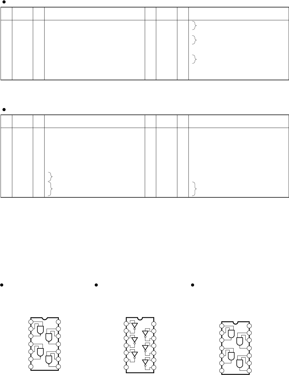
■ LSI PIN DESCRIPTION
AK4393-VF-E2 (XW029A00) DAC (Digital to Analog Converter) . . . . . . . . . . . . . . . . . . . . . . . . . . . . 20
CS5361-KS (X3447A00) ADC (Analog to Digital Converter) . . . . . . . . . . . . . . . . . . . . . . . . . . . . . . . 20
CS8405A-CS (XZ349A00) DIT (Digital Audio Interface Transmitter) . . . . . . . . . . . . . . . . . . . . . . . . . 19
CS8415A-CS (X2089A00) DIR (Digital Audio Interface Receiver) . . . . . . . . . . . . . . . . . . . . . . . . . . . 19
HD6417709SF133 (X2081A00) CPU (SH3) . . . . . . . . . . . . . . . . . . . . . . . . . . . . . . . . . . . . . . . . . . . . 17
M37641M8-141FP (X2485200) CPU (USB 32K) . . . . . . . . . . . . . . . . . . . . . . . . . . . . . . . . . . . . . . . . 16
YM3436DK (XG948E00) DIR2 (Digital Format Interface Receiver) . . . . . . . . . . . . . . . . . . . . . . . . . . 19
YSS910-S (XV988A00) DSP6 (Digital Signal Processor) . . . . . . . . . . . . . . . . . . . . . . . . . . . . . . . . . . 18
PIN
NO. I/O FUNCTION
NAME PIN
NO. I/O FUNCTION
NAME
1
2
3
4
5
6
7
8
9
10
11
12
13
14
15
16
17
18
19
20
21
22
23
24
25
26
27
28
29
30
31
32
33
34
35
36
37
38
39
40
P61/DQ1
P60/DQ0
P57//W/(R//W)
P56//R(E)
P55/A0
P54//S0
P53//IBF0
P52/OBF0
CNVSS/VPP
/RESET
P51/TOUT/XCOUT
P50/XCIN
VSS
XIN
XOUT
VCC
AVCC
LPF
AVSS
P44/CNTR1
P43/CNTR0
P42/INT1
P41/INT0
P40//EDMA
P87//RTS1
P86//CTS1
P85/URXD1
P84/UTXD1
P83//RTS2/STXD
P82//CTS2/SRXD
P81/URXD2/SCLK
P80/UTXD2//SRDY
P37//RD
P36//WR
P35/SYNCOUT
P34/ØOUT
P33/DMAOUT
P32
P31
P30/RDY
I/O
I/O
I/O
I/O
I/O
I/O
I/O
I/O
I
I
I/O
I/O
I
O
O
I/O
I/O
I/O
I/O
I/O
I/O
I/O
I/O
I/O
I/O
I/O
I/O
I/O
I/O
I/O
I/O
I/O
I/O
I/O
I/O
I/O
Port 6
Port 5
Chip operation mode
Reset input
Port 5
Ground
Quartz crystal input
Quartz crystal output
Power supply +5V
Analog power supply +5V
Loop filter for synthesizer
Analog ground
Port 4
Port 8
Port 3
41
42
43
44
45
46
47
48
49
50
51
52
53
54
55
56
57
58
59
60
61
62
63
64
65
66
67
68
69
70
71
72
73
74
75
76
77
78
79
80
P17/AB15
P16/AB14
P15/AB13
P14/AB12
P13/AB11
P12/AB10
P11/AB9
P10/AB8
P07/AB7
P06/AB6
P05/AB5
P04/AB4
P03/AB3
P02/AB2
P01/AB1
P00/AB0
P27/DB7
P26/DB6
P25/DB5
P24/DB4
P23/DB3
P22/DB2
P21/DB1
P20/DB0
P74/OBF1
P73//IBF1//HLDA
P72//S1
P71//HOLD
P70//SOF
USB D+
USB D-
Ext. Cap
VSS
VCC
P67/DQ7
P66/DQ6
P65/DQ5
P64/DQ4
P63/DQ3
P62/DQ2
I/O
I/O
I/O
I/O
I/O
I/O
I/O
I/O
I/O
I/O
I/O
I/O
I/O
I/O
I/O
I/O
I/O
I/O
I/O
I/O
I/O
I/O
I/O
I/O
I/O
I/O
I/O
I/O
I/O
I/O
I/O
I/O
I/O
I/O
I/O
I/O
I/O
I/O
Port 1
Port 0
Port 2
Port 7
USB +voltage line interface
USB -voltage line interface
Power supply +3.3V
Ground
Power supply +5V
Port 6
M37641M8-141FP (X2485200) CPU (USB 32K)
MAIN: IC407
(LSI 端子機能表)
17
SPX2000
PIN
NO. I/O FUNCTION
NAME PIN
NO. I/O FUNCTION
NAME
1
2
3
4
5
6
7
8
9
10
11
12
13
14
15
16
17
18
19
20
21
22
23
24
25
26
27
28
29
30
31
32
33
34
35
36
37
38
39
40
41
42
43
44
45
46
47
48
49
50
51
52
53
54
55
56
57
58
59
60
61
62
63
64
65
66
67
68
69
70
71
72
73
74
75
76
77
78
79
80
81
82
83
84
85
86
87
88
89
90
91
92
93
94
95
96
97
98
99
100
101
102
103
104
MD1
MD2
Vcc(RTC)
XTAL2
EXTAL2
Vss(RTC)
NMI
IRQ0/IRL0/PTH0
IRQ1/IRL1/PTH1
IRQ2/IRL2/PTH2
IRQ3/IRL3/PTH3
IRQ4/PTH4
D31/PTB7
D30/PTB6
D29/PTB5
D28/PTB4
D27/PTB3
D26/PTB2
VssQ
D25/PTB1
VccQ
D24/PTB0
D23/PTA7
D22/PTA6
D21/PTA5
D20/PTA4
Vss
D19/PTA3
Vcc
D18/PTA2
D17/PTA1
D16/PTA0
VssQ
D15
VccQ
D14
D13
D12
D11
D10
D9
D8
D7
D6
VssQ
D5
VccQ
D4
D3
D2
D1
D0
A0
A1
A2
A3
VssQ
A4
VccQ
A5
A6
A7
A8
A9
A10
A11
A12
A13
VssQ
A14
VccQ
A15
A16
A17
A18
A19
A20
A21
Vss
A22
Vcc
A23
VssQ
A24
VccQ
A25
BS/PTK4
RD
WE0/DQMLL
WE1/DQMLU/WE
WE2/DQMUL/ICIORD/PTK6
WE3/DQMUU/ISIOWR/PTK7
RD/WR
AUDSYNC/PTE7
VssQ
CS0/MCS0
VccQ
CS2/PTK0
CS3/PTK1
CS4/PTK2
CS5/CE1A/PTK3
CS6/CE1B
CE2A/PTE4
CE2B/PTE5
I
I
-
O
I
-
I
I
I
I
I
I
I/O
I/O
I/O
I/O
I/O
I/O
-
I/O
-
I/O
I/O
I/O
I/O
I/O
-
I/O
-
I/O
I/O
I/O
-
I/O
-
I/O
I/O
I/O
I/O
I/O
I/O
I/O
I/O
I/O
-
I/O
-
I/O
I/O
I/O
I/O
I/O
O
O
O
O
-
O
-
O
O
O
O
O
O
O
O
O
-
O
-
O
O
O
O
O
O
O
-
O
-
O
-
O
-
O
I/O
O
O
O
I/O
I/O
O
I/O
-
O
-
I/O
I/O
I/O
I/O
O
I/O
I/O
Mode control
Power supply +1.8 V
Crystal oscillator
Ground
Non-maskable interrupt request
Interrupt request / Port H
Data bus / Port B
Ground
Data bus / Port B
Power supply +3.3 V
Data bus / Port B
Data bus / Port A
Ground
Data bus / Port A
Power supply +1.8 V
Data bus / Port A
Ground
Data bus
Power supply +3.3 V
Data bus
Ground
Data bus
Power supply +3.3 V
Data bus
Address bus
Ground
Address bus
Power supply +3.3 V
Address bus
Ground
Address bus
Power supply +3.3 V
Address bus
Ground
Address bus
Power supply +1.8 V
Address bus
Ground
Address bus
Power supply +3.3 V
Address bus
Bus cycle / Port K
Read strobe
Select signal (D7-D0) / D QM (SDRAM)
Select signal (D15-D8) / D QM (SDRAM) / Write enable
Select signal (D23-D16) / D QM (SDRAM) / I/O read / Port K
Select signal (D31-D24) / D QM (SDRAM) / I/O write / Port K
Read / Write
AUD cycle / Port E
Ground
Chip select / Mask ROM chip select
Power supply +3.3V
Chip select / Port K
Chip select / Chip enable / Port K
Chip select / Chip enable
Chip enable / Port E
105
106
107
108
109
110
111
112
113
114
115
116
117
118
119
120
121
122
123
124
125
126
127
128
129
130
131
132
133
134
135
136
137
138
139
140
141
142
143
144
145
146
147
148
149
150
151
152
153
154
155
156
157
158
159
160
161
162
163
164
165
166
167
168
169
170
171
172
173
174
175
176
177
178
179
180
181
182
183
184
185
186
187
188
189
190
191
192
193
194
195
196
197
198
199
200
201
202
203
204
205
206
207
208
CKE/PTK5
RAS3L/PTJ0
PTJ1
CASL/PTJ2
VssQ
CASU/PTJ3
VccQ
PTJ4
PTJ5
DACK0/PTD5
DACK1/PTD7
PTE6
PTE3
RAS3U/PTE2
PTE1
TDO/PTE0
BACK
BREQ
WAIT
RESETM
ADTRG/PTH5
IOIS16/PTG7
ASEMD0/PTG6
ASEBRKAK/PTG5
PTG4/CKIO2
AUDATA3/PTG3
AUDATA2/PTG2
Vss
AUDATA1/PTG1
Vcc
AUDATA0/PTG0
TRST/PTF7/PINT15
TMS/PTF6/PINT14
TDI/PTF5/PINT13
TCK/PTF4/PINT12
IRLS3/PTF3/PINT11
IRL2/PTF2/PINT10
IRLS1/PTF1/PINT9
IRLS0/PTF0/PINT8
MD0
Vcc(PLL1)
CAP1
Vss(PLL1)
Vss(PLL2)
CAP2
VCC(PLL2)
AUDCK/PTH6
Vss
Vss
Vcc
XTAL1
EXTAL1
STATUS0/PTJ6
STATUS1/PTJ7
TCLK/PTH7
/IRQOUT
VssQ
CKIO
VccQ
TXD0/SCPT0
SCK0/SCPT1
TXD1/SCPT2
SCK1/SCPT3
TXD2/SCPT4
SCK2/SCPT5
RTS2/SCPT6
RXD0/SCPT0
RXD1/SCPT2
Vss
RXD2/SCPT4
Vcc
CTS2/IRQ5/SCPT7
MCS7/PTC7/PINT7
MCS6/PTC6/PINT6
MCS5/PTC5/PINT5
MCS4/PTC4/PINT4
VssQ
WAKEUP/PTD3
VccQ
RESETOUT/PTD2
MCS3/PTC3/PINT3
MCS2/PTC2/PINT2
MCS1/PTC1/PINT1
MCS0/PTC0/PINT0
DRAK0/PTD1
DRAK1/PTD0
DREQ0/PTD4
DREQ1/PTD6
RESETP
CA
MD3
MD4
MD5
AVss
AN0/PTL0
AN1/PTL1
AN2/PTL2
AN3/PTL3
AN4/PTL4
AN5/PTL5
AVcc
AN6/DA1/PTL6
AN7/DA0/PTL7
AVss
I/O
I/O
I/O
I/O
-
I/O
-
I/O
I/O
I/O
I/O
I/O
I/O
I/O
I/O
I/O
O
I
I
I
I
I
I
I/O
I/O
I/O
I/O
-
I/O
-
I/O
I
I
I
I
I
I
I
I
I
-
-
-
-
-
-
I
-
-
-
O
I
I/O
I/O
I/O
O
-
I/O
-
O
I/O
O
I/O
O
I/O
I/O
I
I
-
I
-
I
I/O
I/O
I/O
I/O
-
I/O
-
I/O
I/O
I/O
I/O
I/O
I/O
I/O
I
I
I
I
I
I
I
-
I
I
I
I
I
I
-
I/O
I/O
-
CK enable / Port K
RAS address bus / Port J
Port J
CAS address bus / Port J
Ground
CAS address bus / Port J
Power supply +3.3 V
Port J
DMA acknowledge / Port D
Port E
RAS address bus / Port E
Port E
Test data / Port E
Bus acknowledge
Bus request
Hardware wait request
Manual reset
Analog trigger / Port H
Write protect / Port G
ASE mode / Port G
ASE break acknowledge / Port G
Port G / Clock output
AUD data / Port G
Ground
AUD data / Port G
Power supply +1.8 V
AUD data / Port G
Test reset / Port F / Port interruption
Test mode switch / Port F / Port interruption
Test data / Port F / Port interruption
Test clock / Port F / Port interruption
Interrupt request / Port F / Port interruption
Mode control
Power supply +1.8 V
Capacitor
Ground
Ground
Capacitor
Power supply +1.8 V
AUD clock / Port H
Ground
Power supply +1.8 V
Crystal oscillator
Processor status / Port J
Timer clock / Port H
Interrupt request output
Ground
System clock input / output
Power supply +3.3 V
Data transmission / SCI port
Serial clock / SCI port
Data transmission / SCI port
Serial clock / SCI port
Data transmission / SCI port
Serial clock / SCI port
Transmit request / SCI port
Data reception / SCI port
Ground
Data reception / SCI port
Power supply +1.8 V
Transmit clear / Interrupt request / SCI port
Mask ROM chip select / Port C / Port interruption
Ground
Standby mode Interrupt request output / Port D
Power supply +3.3 V
Reset output / Port D
Mask ROM chip select / Port C / Port interruption
DMA acknowledge / Port D
DMA request / Port D
Power on reset
Chip active
Mode control
Analog ground
Analog input / Port L
Analog power supply +3.3 V
Analog input / Analog output / Port L
Analog ground
HD6417709SF133 (X2081A00) CPU (SH3)
MAIN: IC004
18
SPX2000
PIN
NO. I/O FUNCTIONNAME PIN
NO. I/O FUNCTIONNAME
1
2
3
4
5
6
7
8
9
10
11
12
13
14
15
16
17
18
19
20
21
22
23
24
25
26
27
28
29
30
31
32
33
34
35
36
37
38
39
40
41
42
43
44
45
46
47
48
49
50
51
52
53
54
55
56
57
58
59
60
61
62
63
64
65
66
67
68
69
70
71
72
73
74
75
76
77
78
79
80
81
82
83
84
85
86
87
88
Vdd
Vss
XI
XO
Vdd5
/SYNCI
/SYNCO
Vdd5
CKI
CKO
CKSEL
Vss
MCKS
/SSYNC
/IC
/TEST
BTYP
/IRQ
TRIG
Vdd5
Vss
/CS
/WR
/RD
CA7
CA6
CA5
CA4
CA3
CA2
CA1
Vss
Vdd
CD15
CD14
CD13
CD12
CD11
CD10
CD09
CD08
CD07
CD06
Vss
Vdd
Vdd5
CD05
CD04
CD03
CD02
CD01
CD00
/WAIT
Vss
SI0
SI1
SI2
SI3
SI4
SI5
SI6
SI7
Vss
Vdd5
SO0
SO1
SO2
SO3
SO4
SO5
SO6
SO7
Vss
DB00
DB01
DB02
DB03
DB04
DB05
DB06
DB07
DB08
DB09
DB10
DB11
DB12
Vdd5
Vdd
I
O
I
O
I
O
I
I
I
I
I
I
O
I/O
I
I
I
I/O
I/O
I/O
I/O
I/O
I/O
I/O
I/O
I/O
I/O
I/O
I/O
I/O
I/O
I/O
I/O
I/O
I/O
I/O
I/O
I/O
I/O
I/O
O
I
I
I
I
I
I
I
I
O
O
O
O
O
O
O
O
I/O
I/O
I/O
I/O
I/O
I/O
I/O
I/O
I/O
I/O
I/O
I/O
I/O
Power supply (3.3 V)
Ground
System master clock input (60 MHz or 30 MHz)
System master clock output (High or 30 MHz)
Power supply (5 V)
Sync. signal input
Sync. signal output
Power supply (5 V)
System clock input (30 MHz)
System clock output (30 MHz)
System master clock select (0: 60 MHz, 1: 30 MHz)
Ground
Serial I/O master clock input (128 x Fs)
Serial I/O Sync. signal output
Initial clear (RESET)
Test mode setting (0: Test, 1: Normal)
Data bus type select (0: 8 bit, 1: 16 bit)
IRQ output
Trigger signal input/output
Power supply (5 V)
Ground
chip select signal input
Write signal input
Read signal input
Address bus of internal register
Ground
Power supply (3.3 V)
Data bus of internal register
Ground
Power supply (3.3 V)
Power supply (5 V)
Data bus of internal register
WAIT output
Ground
Serial data input
Ground
Power supply (5 V)
Serial data output
Ground
Parallel data bus
Power supply (5 V)
Power supply (3.3 V)
89
90
91
92
93
94
95
96
97
98
99
100
101
102
103
104
105
106
107
108
109
110
111
112
113
114
115
116
117
118
119
120
121
122
123
124
125
126
127
128
129
130
131
132
133
134
135
136
137
138
139
140
141
142
143
144
145
146
147
148
149
150
151
152
153
154
155
156
157
158
159
160
161
162
163
164
165
166
167
168
169
170
171
172
173
174
175
176
Vss
DB13
DB14
DB15
DB16
DB17
DB18
DB19
DB20
DB21
DB22
Vss
Vdd
DB23
DB24
DB25
DB26
DB27
DB28
DB29
DB30
DB31
TIMO/DBOB
Vss
Vdd5
DA00
DA01
DA02
DA03
DA04
DA05
DA06
DA07
Vss
DA08
DA09
DA10
DA11
DA12
DA13
DA14
DA15
Vss
Vdd
(n.c)
Vdd5
DA16
DA17
DA18
DA19
DA20
DA21
DA22
DA23
Vss
DA24
DA25
DA26
DA27
DA28
DA29
DA30
DA31
Vdd5
Vss
A00
A01
A02
A03
A04
A05
A06
A07
A08
A09
Vss
Vdd
A10
A11
A12
A13
A14
A15/RAS
A16/CAS
A17/CE
/WE
/OE
Vdd5
I/O
I/O
I/O
I/O
I/O
I/O
I/O
I/O
I/O
I/O
I/O
I/O
I/O
I/O
I/O
I/O
I/O
I/O
I/O
I/O
I/O
I/O
I/O
I/O
I/O
I/O
I/O
I/O
I/O
I/O
I/O
I/O
I/O
I/O
I/O
I/O
I/O
I/O
I/O
I/O
I/O
I/O
I/O
I/O
I/O
I/O
I/O
I/O
I/O
I/O
I/O
I/O
O
O
O
O
O
O
O
O
O
O
O
O
O
O
O
O
O
O
O
O
Ground
Parallel data bus
Ground
Power supply (3.3 V)
Parallel data bus
Timing signal output/ Parallel data bus output/ input
Ground
Power supply (5 V)
Memory data bus
Ground
Memory data bus
Ground
Power supply (3.3 V)
Not used
Power supply (5 V)
Memory data bus
Ground
Memory data bus
Power supply (5 V)
Ground
Memory address (SRAM, PSRAM, DRAM)
Ground
Power supply (3.3 V)
Memory address (SRAM, PSRAM, DRAM)
Memory address (SRAM, PSRAM)
Memory address (SRAM, PSRAM), /RAS (DRAM)
Memory address (SRAM, PSRAM), /CAS (DRAM)
Memory address (SRAM), /CE (PSRAM)
Memory write enable signal
Memory output enable signal
Power supply (5 V)
YSS910-S (XV988A00) DSP6 (Digital Signal Processor) MAIN: IC303
19
SPX2000
PIN
NO. I/O FUNCTIONNAME PIN
NO. I/O FUNCTIONNAME
1
2
3
4
5
6
7
8
9
10
11
12
13
14
CDOUT
/CS
/EMPH
RXP0
RXN0
VA+
AGND
FILT
/RST
RMCK
RERR
RXP1
RXP2
RXP3
O
I
O
I
I
O
O
I/O
O
I
I
I
Data out (SPI)
Control port chip select (SPI)
Pre-emphasis
AES3/SPDIF receiver port
Positive analog power supply +5V
Analog ground
PLL loop filter
Reset
Input section recovered master clock
Receiver error
Additional AES3/SPDIF receiver port
15
16
17
18
19
20
21
22
23
24
25
26
27
28
RXP4
OSCLK
OLRCK
SDOUT
INT
U
OMCK
DGND
VL+
H//S
RXP5
RXP6
CDIN
CCLK
I
I/O
I/O
O
O
O
I
I
I
I
I
I
Additional AES3/SPDIF receiver port
Serial audio output bit clock
Serial audio output left/right clock
Serial audio output data
Interrupt
User data
System clock
Digital ground
Positive logic power supply +5V
Hardware/software mode control
Additional AES3/SPDIF receiver port
Serial control data in (SPI)
Control port clock
CS8415A-CS (X2089A00) DIR (Digital Audio Interface Receiver) MAIN: IC401
PIN
NO. I/O FUNCTIONNAME PIN
NO. I/O FUNCTIONNAME
1
2
3
4
5
6
7
8
9
10
11
12
13
14
15
16
17
18
19
20
21
22
DAUX
HDLT
DOUT
VFL
OPT
SYNC
MCC
WC
MCB
MCA
SKSY
XI
XO
P256
LOCK
Vss
TC
DIM1
DIM0
DOM1
DOM0
KM1
I
O
O
O
O
O
O
O
O
O
I
I
O
O
O
O
I
I
I
I
I
Auxiliary input for audio data
Asynchronous buffer operation flag
Audio data output
Parity flag output
Fs x 1 Synchronous output signal for DAC
Fs x 1 Synchronous output signal for DSP
Fs x 64 Bit clock output
Fs x 1 Word clock output
Fs x 128 Bit clock output
Fs x 256 Bit clock output
Clock synchronization control input
Crystal oscillator connection or external
clock input
Crystal oscillator connection
VCO oscillating clock connection
PLL lock flag
Logic section power (GND)
PLL time constant switching output
Data input mode selection
Data input mode selection
Data output mode selection
Data output mode selection
Clock mode switching input 1
23
24
25
26
27
28
29
30
31
32
33
34
35
36
37
38
39
40
41
42
43
44
RSTN
Vdda
CTLN
PCO
(NC)
CTLP
Vssa
TSTN
KM2
KM0
FS1
FS0
CSM
EXTW
DDIN
LR
Vdd
ERR
EMP
CD0
CCK
CLD
I
I
O
I
I
I
I
O
O
I
I
I
O
O
O
O
I
I
System reset input
VCO section power (+5V)
VCO control input N
PLL phase comparison output
VCO control input P
VCO section power (GND)
Test terminal. Open for normal use
Clock mode switching input 2
Clock mode switching input 0
Channel status sampling frequency
display output 1
Channel status sampling frequency
display output 0
Channel status output method selection
External synchronous auxiliary input
word clock
EIAJ (AES/EBU) data input
PLL word clock output
Logic section power (+5 V)
Data error flag output
Channel status emphasis control code
output
3-wire type microcomputer interface data
output
3-wire type microcomputer interface clock
input
3-wire type microcomputer interface load
input
YM3436DK (XG948E00) DIR2 (Digital Format Interface Receiver)
MAIN: IC205
PIN
NO. I/O FUNCTIONNAME PIN
NO. I/O FUNCTIONNAME
1
2
3
4
5
6
7
8
9
10
11
12
13
14
SDA/CDOUT
AD0//CS
AD2
RXP
DGND2
VD2+
DGND4
DGND3
/RST
NC1
NC2
ILRCK
ISCLK
SDIN
I/O
I/O
I
I
I
I/O
I/O
I
Serial control data I/O (I
2
C) / Data out (SPI)
Address bit 0 (I
2
C) / Control port chip select (SPI)
Address bit 2 (I2C)
Auxiliary AES3 Receiver port
Digital ground
Positive digital power supply (+5V)
Digital ground
Reset
Not used
Serial audio input left/right clock
Serial audio bit clock
Serial audio data port
15
16
17
18
19
20
21
22
23
24
25
26
27
28
TCBL
NC3
NC4
NC5
INT
U
OMCK
DGND
VD+
H//S
TXN
TXP
AD1/CDIN
SCL/CCLK
I/O
O
I/O
I
I
O
O
I
I
Transmit channel status block start
Not used
Interrupt
User data
Master clock
Digital ground
Positive digital power supply (+5V)
Hardware/software control mode select
Differential line drivers
Address bit 1 (I
2
C) / Serial control data in (SPI)
Control port clock
CS8405A-CS (XZ349A00) DIT (Digital Audio Interface Transmitter) MAIN: IC405
20
SPX2000
PIN
NO. I/O FUNCTIONNAME PIN
NO. I/O FUNCTIONNAME
1
2
3
4
5
6
7
8
9
10
11
12
/RST
M//S
LRCK
SCLK
MCLK
VD
GND
VL
SDOUT
DIV
/HPF
DIF
I
I
I/O
I/O
I
O
I
I
I
Reset
Master/slave mode
Left right clock
Serial clock
Master clock
Digital power supply +5V
Ground
Logic power supply +3.3V
Serial audio data output
Divider
High pass filter enable
Digital input format
13
14
15
16
17
18
19
20
21
22
23
24
M0
M1
TST
AINL+
AINL-
GND
VA
AINR-
AINR+
VCOM
REFGND
FILT+
I
I
I
I
I
I
I
O
O
Mode selection
Test
Differential left channel analog input
Ground
Analog power supply +5V
Differential right channel analog input
Common voltage
Reference ground
Positive voltage reference
CS5361-KS (X3447A00) ADC (Analog to Digital Converter) MAIN: IC603
PIN
NO. I/O FUNCTIONNAME PIN
NO. I/O FUNCTIONNAME
1
2
3
4
5
6
7
8
9
10
11
12
13
14
DVSS
DVDD
MCLK
/PD
BICK
SDATA
LRCK
SMUTE//CS
DFS
DEM0/CCLK
DEM1/CDTI
DIF0
DIF1
DIF2
-
-
I
I
I
I
I
I
I
I
I
I
I
I
Digital ground
Digital power supply
Master clock
Power down mode
Audio serial data clock
Audio serial data input
L/R clock
Soft mute
Double speed sampling mode
De-emphasis enable
Digital input format
15
16
17
18
19
20
21
22
23
24
25
26
27
28
BVSS
VREFL
VREFH
AVDD
AVSS
AOUTR-
AOUTR+
AOUTL-
AOUTL+
VCOM
P//S
CKS0
CKS1
CKS2
-
I
I
-
-
O
O
O
O
O
I
I
I
I
Substrate ground
Low level voltage reference
High level voltage reference
Analog power supply +5 V
Analog ground
Rch negative analog output
Rch positive analog output
Lch negative analog output
Lch positive analog output
Common voltage output
Parallel/serial select
Master clock select
AK4393-VF-E2 (XW029A00) DAC (Digital to Analog Converter)
MAIN: IC701
1
2
3
4
5
6
7
1A
1Y
2A
2Y
3A
3Y
Vss
14
13
12
11
10
9
8
VDD
6A
6Y
5A
5Y
4A
4Y
TC74VHC04FT (X0195A00)
Hex Inverter
MAIN: IC207, 501
TC74VHCT08AFT (X3586A00)
TC74VHC08FT (XV891A00)
Quad 2 Input AND
MAIN: IC404
IC005, 107
1
2
3
1A
1Y
4
2A
5
2B
6
2Y
7
VSS
1B
14
13
12
VDD
4A
11
4Y
10
3B
9
3A
8
3Y
4B
TC74VHC00FT
(X2313A00)
Quad 2 Input NAND
MAIN: IC209
1
2
3
1A
1Y
42A
52B
62Y
7Vss
1B
14
13
12
VDD
4A
11 4Y
10 3B
93A
83Y
4B
■ IC BLOCK DIAGRAM
(IC ブロック図)
21
SPX2000
TC74VHC32FT (XY945A00)
Quad 2 Input OR
MAIN: IC012
TC74VHC244FT (XW234A00)
Octal 3-State Bus Buffer
MAIN: IC403
TC74VHCT245AFT (XT744A00)
Octal 3-State Bus Transceiver
MAIN: IC103-106, 203, 606
TC74VHC74FT (XV892A00)
Dual D-Type Flip-Flop
MAIN: IC206
74LVX4245MTCX (X3097A00)
Dual Supply Octal Bus Transceiver
MAIN: IC101, 102
1
2
3
4
5
6
7
20
19
18
17
16
15
14
Vcc
G
B1
B2
B3
B4
B5
B6
B7
B8
8
9
10
12
11
GND
A8
A7
A6
A5
A4
A3
A2
A1
D1R
13
SN75124NSR (XV930A00)
Triple Line Receiver
MAIN: IC406
1
2
3
1A
1Y
4
2A
5
2B
6
2Y
7
GND
1B
14
13
12
Vcc
4A
11
4Y
10
3B
9
3A
8
3Y
4B
INPUTS OUTPUTS
PR CLR CLK D Q Q
L
H
H
L
H
Q
O
H
L
H
H
L
Q
O
X
X
X
H
L
X
X
X
X
f
f
L
H
L
L
H
H
H
L
H
L
H
H
H
1
2
3
4
5
6
7
1CLR
1D
1CK
1PR
1Q
1Q
GND
14
13
12
11
10
9
8
VCC
2CLR
CLR
2D
D
2CK
CK
2PR
PR
2Q
2Q
Q
Q
CLR
D
CK
PR
Q
Q
1G
1A1
2Y4
1A2
2Y3
1A3
2Y2
1A4
2Y1
120
219
318
417
516
615
714
813
912
10 11
VDD (Vcc)
2G
1Y1
2A4
1Y2
2A3
1Y3
2A2
1Y4
2A1
(GND) Vss
VCCA
DIR
A1
A2
A3
A4
A5
A6
A7
A8
GND
GND
VCCB
VCCB
/G
B1
B2
B3
B4
B5
B6
B7
B8
GND
1
2
3
4
5
6
7
0
1
2
3
4
5
6
7
8
9
10 12
13
14
15
G1
G2
D
D
B
A
11
24
23
22
21
20
19
18
8
9
10
11
12
16
15
14
13
17
1A
1B
2R
2S
2A
2B
2Y
GND
116
215
314
413
512
611
710
8 9
Vcc
1S
1R
1Y
3A
3S
3R
3Y
TC7SH04FU (XS775A00)
Inverter Gate
MAIN: IC003, 210, 402, 605
µPC4570G2 (XF291A00)
Dual Operational Amplifier
MAIN: IC601, 602, 651, 652, 703, 753
1
2
3
4-V
CH1
8
7
6
5
Output1
+V
CH2
-DC Voltage Supply
Inverting
Input 1
Non-Inverting
Input 1
+DC Voltage Supply
Non-Inverting
Input 2
Output2
Inverting
Input 2
+-
+-
1
2
3
5
4
NC
GND
VCC
OUT Y
IN A
TC74VHC14FT
(XV890A00)
Hex Inverter
MAIN: IC208
1
2
3
4
5
6
7
1A
1Y
2A
2Y
3A
3Y
GND
14
13
12
11
10
9
8
VDD
6A
6Y
5A
5Y
4A
4Y
22
SPX2000
NJM4556AL (XP844A00)
Dual Operational Amplifier
MAIN: IC704, 754
TLC2932IPWR (XV064A00)
PLL
MAIN: IC204
1
A
2345678
OUT
A-IN
A+IN
A+IN
B-IN
BOUT
B
-V +V
-
+
B
-
+
1
2
3
4
5
6
7
LOGIC V
DD
SELECT
VCO OUT
F
IN
-A
F
IN
-B
PFD OUT
LOGIC GND
14
13
12
11
10
9
8
VCO V
DD
R
BIAS
V
COIN
VCO GND
VCO INHBIT
PFD INHIBIT
NC
7
LOGIC GND
4
F
IN
-A
6
PFD OUT
12
V
COIN
13
R
BIAS
11
VCO GND
8
NC
1
LOGIC V
DD
5
F
IN
-B
CHARGE PUMPDETECTOR
9
PFD INHIBIT
10
VCO INHBIT
14
VCO V
DD
3
VCO OUT
2
SELECT
BLAS CONTROL
VCO OUTPUT
MUX
1/2
NJM2904V(TE1) (XR532A00)
Dual Operational Amplifier
MAIN: IC002
1
2
3
4-V
8
7
6
5
Output A
+V
Non-Inverting
Input A
-DC Voltage Supply
+DC Voltage
Supply
Output B
Inverting
Input B
Non-Inverting
Input B
Inverting
Input A
+-
+-
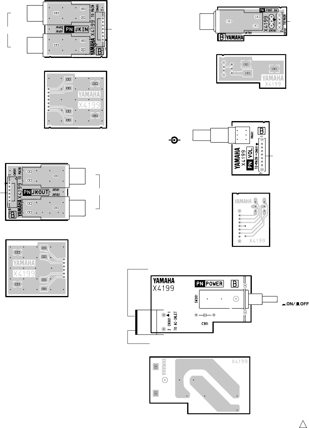
■ CIRCUIT BOARDS CONTENTS
FOOTSW (X4199B0) ............................................. 28
JKIN (X4199B0) ..................................................... 28
JKOUT (X4199B0) ................................................. 28
MAIN (X498B0) ................................................. 24/26
PN1 (X4199B0) ...................................................... 23
Note : See parts list for details of circuit board conponent parts.
PN2 (X4199B0) ...................................................... 23
PN3 (X4199B0) ...................................................... 23
POWER (X4199B0)................................................ 28
VOL (X4199B0) ...................................................... 28
(シート基板図目次)
注:シートの部品詳細は、パーツリストをご参照ください。
23
SPX2000
■ CIRCUIT BOARDS(シート基板図)
●PN3 Circuit Board
to MAIN-CN503
STORE
UNDO
RECALL BACK
NEXT
COM
PARE
INC
DEC
PARAMETER
FINE PARAM
UTILITY
BYPASS
TAP
to MAIN-CN501
●PN1 Circuit Board ●PN2 Circuit Board
Pattern side
(パターン側)
Pattern side
(パターン側)
Component side
(部品側)
Pattern side
(パターン側)
to MAIN-CN502
Component side
(部品側)
Component side
(部品側)
2NAP-WB05310-1
1

27
SPX2000
Pattern side
B
B'
2NAP-WB05300-2
1
(パターン側)
28
SPX2000
2NAP-WB05310-2
1
●JKIN Circuit Board
Component side
L
(MONO)
R
to MAIN-CN601
INPUT
L
R
to MAIN-CN701
OUTPUT
FOOT SW
to MAIN-CN002
POWER
to POWER SUPPLY UNIT-CN1
to AC inlet assembly
INPUT
LR
to MAIN-CN602
Pattern side
(パターン側)
Pattern side
(パターン側)
Pattern side
(パターン側)
Pattern side
(パターン側)
Pattern side
(パターン側)
Component side
(部品側)
Component side
(部品側)
Component side
(部品側)
Component side
(部品側)
●JKOUT Circuit Board
●FOOTSW Circuit Board
●VOL Circuit Board
●POWER Circuit Board
(部品側)
29
SPX2000
■ INSPECTIONS
1. Preparations
1-1. Conditions
Use following conditions unless otherwise specified.
• INPUT VOLUME: MAX
• Level select switch: +4dBu side (both input and output)
• Analog output load: 600 Ω
• Word clock (FS): 96kHz
To select the word clock, press the UTILITY key several
times and when "CLOCK SOURCE" appears on the
LCD, press the INC/DEC key.
• 0dBu = 0.775Vrms
• 0dBFS = 0dB, full scale
• Oscillator output impedance: 150 Ω.
A sine wave is output.
• Input impedance of oscilloscope, level meter, etc.: 100
kΩ or more
• Noise measurement is corrected with 12.7kHz, -6dB/
octave low pass filter. (Use average values instead of
effective values for measurement.)
• Cross talk and distortion ratio measurement is corrected
with 80kHz, -18dB/octave low pass filter.
• For check items other than “2-7”, turn on the BYPASS
key and keep the BYPASS LED lit while checking.
1-2. Measuring Instruments
• Use System Two CASCADE Control Software APWIN
Version 2.22 of Audio Precision Co. or its equivalent.
• Noise meter (Use LMV-1817 of READER Corp. or
the equivalent when measuring the noise.)
1-3. Writing Programs
If the main program is not the latest version, it must be
upgraded to the latest program. For the details, refer to
"Method for Writing the Program" on page 49.
[2] Frequency response (both L and R)
Condition:
1kHz is used as reference of the permissible range.
[3] Level difference between left and right
The range of difference in the gain measured in [1] above
is specified as follows.
[4] Residual noise (both L and R)
Condition: The input function should be turned off.
Permissible range
Within 1dB
Input frequency Input level Permissible range
20 Hz +4 dBu -1.5∼+0.5 dB
40 kHz +4 dBu -1.5∼+0.5 dB
Input frequency Input level Specified output level Permissible range
1 kHz +4 dBu +14 dBu +14±2 dBu
[5] Crosstalk between left and right
Condition:
The R channel input function should be turned off when
signals are inputted to the L channel.
The L channel input function should be turned off when
signals are inputted to the R channel.
Permissible range
-80 dBu or below
Input frequency Output level L(R) Permissible range R (L)
1 kHz +22 dBu -58 dBu or below
2-2. When ANALOG INPUT/OUTPUT WORD
CLOCK is INT 48kHz
Condition:
Signals are inputted through ANALOG INPUT L, R
(PHONE) and output from ANALOG OUTPUT L, R
(PHONE).
2. Check Items
2-1. When ANALOG INPUT/OUTPUT WORD
CLOCK is INT 96kHz
Condition:
Signals are inputted through ANALOG INPUT L, R
(XLR) and output from ANALOG OUTPUT L, R
(XLR).
[1] Gain (both L and R)
Connecting hot and cold terminals of OUTPUT L, R to
GND respectively provides the same result.
ANALOG IN
SPX2000
ANALOG OUT
AES/EBU IN
WCLK IN
USB TO HOST
AES/EBU OUT
MIDI IN
MIDI OUT
SYSTEM TWO
SP
SP
• Connect the powered
speaker to the ANALOG
OUT terminal when
executing Test item 2-8
Sound Check.
30
SPX2000
2-3. Checking ANALOG INPUT/OUTPUT Level
Select Switch
Condition:
Signals are inputted through ANALOG INPUT L, R
(PHONE) and output from ANALOG OUTPUT L, R
(PHONE).
The level select switch should be set to -10dBu side (both
input and output) and WORD CLOCK INT should be
set to 48kHz.
[1] Gain (both L and R)
2-4. Checking DIGITAL OUT
Condition: Use the System Two.
Signals are inputted through ANALOG INPUT L, R
(XLR) and output from AES/EBU OUT.
a. WORD CLOCK INT 96kHz
Condition: Set WORD CLOCK INT to 96kHz.
[1] Gain (AES/EBU OUT)
Input frequency Input level Specified output level Permissible range
1 kHz -10 dBu 0 dBu 0±2 dBu
Input frequency Input level Specified output level Permissible range
1 kHz +4 dBu -10 dBFS -10±2 dBFS
[2] Frequency response (AES/EBU OUT)
Condition:
1kHz is used as reference of the permissible range.
[3] Distortion ratio (AES/EBU OUT)
Input frequency Input level Permissible range
20 Hz +4 dBu -1.0∼+0.5 dB
40 kHz +4 dBu -1.0∼+0.5 dB
2-5. Checking DIGITAL IN
Condition: Use the System Two.
Signals are inputted through AES/EBU IN and output
from ANALOG OUT L, R (XLR).
Select AES/EBU for the word clock.
Setting: Input selection
Press the UTILITY key and when "INPUT SOURCE"
appears on the LCD, press the INC key.
Setting is completed when the asterisk (*) mark moves
to the "DIGITAL" position.
Press the BACK key and execute WORD CLOCK
selection.
a. 96kHz
Condition: Make frequency setting (Sample Rate) of the
System Two to 96kHz.
[1] Gain (both L and R)
[2] Frequency response (both L and R)
Condition:
1kHz is used as reference of the permissible range.
[3] Distortion ratio (both L and R)
b. 48kHz
Condition: Make frequency setting (Sample Rate) of the
System Two to 48kHz.
[1] Distortion ratio (both L and R)
Input frequency Output level Permissible range
1 kHz -1 dBFS 0.01 % or below
Input frequency Output level Permissible range
1 kHz -1 dBFS 0.02 % or below
Input frequency Input level Specified output level Permissible range
1 kHz -10 dBFS +14 dBu +14±2 dBu
Input frequency Input level Permissible range
20 Hz -10 dBFS -1.0∼+0.5 dB
40 kHz -10 dBFS -1.0∼+0.5 dB
Input frequency Output level Permissible range
1 kHz +22 dBu 0.01 % or below
Input frequency Output level Permissible range
1 kHz +23 dBu 0.02 % or below
[1] Distortion ratio (both L and R)
Permissible range
-80 dBu or below
b. WORD CLOCK INT 48kHz
Condition: Set WORD CLOCK INT to 48kHz.
[1] Distortion ratio (AES/EBU OUT)
Input frequency Output level Permissible range
1 kHz +23 dBu 0.02 % or below
[2] Residual noise (both L and R)
Condition: The input function should be turned off.
31
SPX2000
Supplementary)
After this test, press the UTILITY key again and when
"INPUT SOURCE" appears on the LCD, press the DEC
key. Setting is completed when the asterisk (*) mark
moves to the "ANALOG" position. Press the BACK key
and execute WORD CLOCK selection.
2-6. PLL Operation Range of WORD CLOCK
IN, DIGITAL IN
Condition: Use the System Two.
Signals are inputted through ANALOG INUT L, R
(XLR) and output from OUTPUT L, R (XLR).
The WORD CLOCK should be selected as follows.
When checking WORD CLOCK IN: WORD CLOCK
When checking DIGITAL IN: AES/EBU
a. 96kHz + 6% (101.76kHz)
Condition:
Make frequency setting (Sample Rate) of the System
Two to 96kHz + 6%
[1] Distortion ratio (both WORD CLOCK IN and
DIGITAL IN)
b. 44.1kHz - 10% (39.69kHz)
Condition:
Make frequency setting (Sample Rate) of the System
Two to 44.1kHz - 10%
[1] Distortion ratio (both WORD CLOCK IN and
DIGITAL IN)
2-7. Jitter Measurement
Condition: User the System Two.
Select Sec and PK.
Select BW: 700Hz to 100kHz.
Use AES/EBU OUT for checking.
a. WORD CLOCK INT
Condition:
Select the value of the WORD CLOCK according to the
following table.
[1] Jitter
Input frequency Output level Permissible range
1 kHz +23 dBu 0.03 % or below
b. WORD CLOCK EXT
Condition: Select the WORD CLOCK as follows.
When checking WORD CLOCK IN: WORD CLOCK
When checking DIGITAL IN: AES/EBU
For the System Two frequency setting (Sample Rate),
select the value for according to the table below.
[1] Jitter (both WORD CLOCK IN and DIGITAL IN)
2-8. Checking Produced Sound
Check EFFECT functions (DSP6 operation check) by listening.
ANALOG INPUT, ANALOG OUTPUT
Condition
• WORD CLOCK: INT96kHz
• Input sound signals through ANALOG INPUT L and R
(XLR), recall the PRESET programs listed below one
after another and adjust the INPUT VOLUME so that
the CLIP of the LEVEL METER does not light up with
any program.
To recall the PRESET programs, press the UP/DOWN
key to have a number flash in the 7-segment and press
the RECALL key.
PRESET programs to be checked
Program 08: AMBIENCE
Program 58: ROGER ON THE 12
Program 61: SYMPHONIC
Program 78: DYNA FILTER
Inspection:
Recall the PRESET programs and check the signal
through the speaker for at least 15 seconds. Perform this
check on all 4 types of the PRESET programs. Operate
the INPUT VOLUME and check that the output level
varies.
Judgment criteria 1: The EFFECT sounds are output.
Judgment criteria 2: No noise is included in the output.
WORD CLOCK Permissible range
EXT 44.1 kHz 4 nsec or below
EXT 48 kHz 4 nsec or below
EXT 88.2 kHz 4 nsec or below
EXT 96 kHz 4 nsec or below
Input frequency Output level Permissible range
1 kHz +23 dBu 0.03 % or below
WORD CLOCK Permissible range
INT 44.1 kHz 2 nsec or below
INT 48 kHz 2 nsec or below
INT 88.2 kHz 2 nsec or below
INT 96 kHz 2 nsec or below
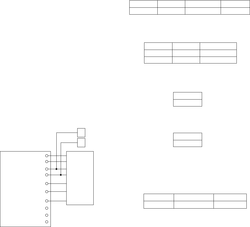
32
SPX2000
■ 検査
1.準備
1−1.条件
◇ 特に指定しないときは以下の条件とします。
・ INPUT VOLUME: MAX
・レベル切替SW: +4dBu側(入力、出力共)
・アナログ出力の負荷は、600Ωとします。
・ワードクロック(FS)は96kHzにします。
なお、ワードクロックの切り替えをするには、
UTILITYキーを何度か押しLCDに CLOCK SOURCE
が表示されたところで、INC/DECキーを押します。
・ 0dBu=0.775Vrms
・ 0dBFS=0デシベル・フルスケール
・発振器の出力インピーダンスは150Ωとします。
正弦波を出力します。
・オシロスコープ、レベル計等の入力インピーダンス
は100kΩ以上とします。
・ノイズ測定は12.7kHz、−6dB/OCTのLPFで補正し
ます。(実効値ではなく平均値での測定とします。)
・クロストークと歪率の測定は80kHz、−18dB/OCTの
LPFで補正します。
・検査項目2−7以外はBYPASSキーをオンにして、
BYPASSの LEDを点灯させた状態で検査します。
1−2.測定器
・Audio Precision社System Two CASCADE制御ソフト
ウェアAPWIN Version 2.22と同等品を使用します。
・ノイズメーター(READER社 LMV-1817または同等品
をノイズ測定時に使用します)
2.検査項目
2−1.ANALOG INPUT/OUTPUTのWORD CLOCK
INT96kHz時検査
条件 ANALOG INPUT L、R(XLR)から入力し、ANALOG
OUTPUT L、R(XLR)から出力します。
q利得 (L/R共)
OUTPUT L、Rのホット、コールド端子をそれぞれGND
に接続しても同様の結果が得られます。
wf 特 (L/R共)
条件 許容範囲は1kHzを基準とします。
eL/R 間のレベル差
qで測定した利得の差の範囲を以下の様に規定しま
す。
r残留ノイズ (L/R共)
条件 入力をOFFにします。
tL/R 間のクロストーク
条件 Lchに信号を入力した時は、Rchの入力をOFFに
します。
Rchに信号を入力した時は、Lchの入力をOFFに
します。
入力周波数 入力レベル 規定出力レベル 許容範囲
1kHz +4dBu +14dBu +14±2dBu
入力周波数 入力レベル 許容範囲
20Hz +4dBu −1.5∼+0.5dB
40kHz +4dBu −1.5∼+0.5dB
許容範囲
1dB以内
許容範囲
−80dBu以下
入力周波数 出力レベルL(R) 許容範囲R(L)
1kHz +22dBu −58dBu以下
ANALOG IN
SPX2000
ANALOG OUT
AES/EBU IN
WCLK IN
USB TO HOST
AES/EBU OUT
MIDI IN
MIDI OUT
SYSTEM TWO
SP
SP
1−3.プログラムの書き込み
本体プログラムが、最新バージョンになっていない場
合、最新のプログラムにバージョンアップする必要が
あります。詳しくは、49ページの「プログラムの書き込
み」を参照してください。
・パワードスピーカーは、検査項
目2 −8 の音だし検査時に
ANALOG OUTと接続します。

33
SPX2000
2−2.ANALOG INPUT/OUTPUTのWORD CLOCK
INT48kHz時検査
条件 ANALOG INPUT L、R(PHONE)から入力し、ANALOG
OUTPUT L、R(PHONE)から出力します。
q歪率 (L/R共)
w残留ノイズ (L/R共)
条件 入力をOFFにします。
2−3.
ANALOG INPUT/OUTPUTのレベル切替SWの検査
条件 ANALOG INPUT L、R(PHONE)から入力し、 ANALOG
OUTPUT L、R(PHONE)から出力します。
レベル切替SWは−10dBu側(入出力共)、WORD
CLOCK INTは48kHzです。
q利得 (L/R共)
2−4.DIGITAL OUTの検査
条件 System Twoを使用します。
ANALOG INPUT L、R(XLR)から入力し、AES/EBU
OUTから出力します。
a. WORD CLOCK INT96kHz
条件 WORD CLOCK INTは96kHzにします。
q利得 (AES/EBU OUT)
wf 特 (AES/EBU OUT)
条件 許容範囲は1kHzを基準とします。
e歪率 (AES/EBU OUT)
b. WORD CLOCK INT48kHz
条件 WORD CLOCK INTは48kHzにします。
q歪率(AES/EBU OUT)
2−5.DIGITAL INの検査
条件 System Twoを使用します。
AES/EBU INから入力し、ANALOG OUT L、R(XLR)か
ら出力します。
WORD CLOCKはAES/EBUを選択します。
設定 入力の切替
UTILITYキーを押しLCDに INPUT SOURCE が表示さ
れたところで INCキーを押します。
“*”マークが DIGITAL に移動したら設定完了です。
BACKキーを押し、ワードクロックの切り替え操作を
します。
a. 96kHz
条件
System Twoの周波数設定(Sample Rate)を96kHzにします。
q利得 (L/R共)
wf 特 (L/R共)
条件 許容範囲は1kHzを基準とします。
e歪率 (L/R共)
b. 48kHz
条件
System Twoの周波数設定(Sample Rate)を48kHzにします。
q歪率 (L/R共)
補足) このテスト後、再びUTILITYキーを押しLCDに INPUT
SOURCE が表示されたところでDECキーを押します。
“*”マークが ANALOG に移動したら設定完了です。
BACKキーを押し、ワードクロックの切り替え操作を
します。
入力周波数 出力レベル 許容範囲
1kHz +23dBu 0.02%以下
許容範囲
−80dBu以下
入力周波数 入力レベル 規定出力レベル 許容範囲
1kHz −10dBu 0dBu 0±2dBu
入力周波数 入力レベル 規定出力レベル 許容範囲
1kHz +4dBu −10dBFS −10±2dBFS
入力周波数 入力レベル 許容範囲
20Hz +4dBu −1.0∼+0.5dB
40kHz +4dBu −1.0∼+0.5dB
入力周波数 出力レベル 許容範囲
1kHz −1dBFS 0.01%以下
入力周波数 出力レベル 許容範囲
1kHz −1dBFS 0.02%以下
入力周波数 入力レベル 規定出力レベル 許容範囲
1kHz −10dBFS +14dBu +14±2dBu
入力周波数 入力レベル 許容範囲
20Hz −10dBFS −1.0∼+0.5dB
40kHz −10dBFS −1.0∼+0.5dB
入力周波数 出力レベル 許容範囲
1kHz +23dBu 0.01%以下
入力周波数 出力レベル 許容範囲
1kHz +23dBu 0.02%以下
34
SPX2000
2−6.WORD CLOCK IN,DIGITAL INのPLL動作範囲
条件 System Twoを使用します。
ANALOG INPUT L、R(XLR)から入力し、ANALOG
OUTPUT L、R(XLR)から出力します。
WORD CLOCKは以下を選択します。
WORD CLOCK INの検査時 : WORD CLOCK
DIGITAL INの検査時 : AES/EBU
a. 96kHz+6%(101.76kHz)
条件 System Twoの周波数設定(Sample Rate)を96kHz+6%
にします。
q歪率 (WORD CLOCK IN,DIGITAL IN共)
b. 44.1kHz−10%(39.69kHz)
条件 System Twoの周波数設定(Sample Rate)を44.1kHz−10
%にします。
q歪率 (WORD CLOCK IN,DIGITAL IN共)
2−7.ジッター測定
条件 System Twoを使用します。
Sec,PKを選択します。
BW:700Hz to 100kHz を選択します。
AES/EBU OUTで検査します。
a. WORD CLOCK INT
条件 WORD CLOCKは、下記表の値を選択します。
qジッター
b. WORD CLOCK EXT
条件 WORD CLOCKは以下を選択します。
WORD CLOCK INの検査時 : WORD CLOCK
DIGITAL INの検査時 : AES/EBU
System Twoの周波数設定(Sample Rate)は、下記表の値
を選択します。
qジッター (WORD CLOCK IN,DIGITAL IN共)
2−8.音だし
EFFECT機能(DSP6動作確認)を聴感で確認します。
ANALOG INPUT、ANALOG OUTPUT
条件 ・WORD CLOCK: INT96kHz
・ANALOG INPUT L,R(XLR) から音楽信号を入れ、下記
のPRESETプログラムを順にリコールし、どのプログ
ラムでも LEVEL METER の CLIP が点灯しないよう
にINPUT VOLUME を調整しておきます。
なお、PRESETプログラムのリコール方法は、UP/
DOWNキーを押し7セグに数字を点滅させ、RECALL
キーを押します。
確認するPRESETプログラム
プログラム08: AMBIENCE
プログラム58: ROGER ON THE 12
プログラム61: SYMPHONIC
プログラム78: DYNA FILTER
検査 PRESETプログラムをリコールし、スピーカーで信号
を最低15秒間確認します。
4種類のPRESETプログラム総てに対して行います。
INPUT VOLUMEを操作して出力レベルが変化するこ
とを確認します。
判定基準1: EFFECT音が出ていることを確認します。
判定基準2: ノイズが含まれていないことを確認します。
入力周波数 出力レベル 許容範囲
1kHz +23dBu 0.03%以下
入力周波数 出力レベル 許容範囲
1kHz +23dBu 0.03%以下
WORD CLOCK 許容範囲
INT 44.1 kHz 2nsec以下
INT 48 kHz 2nsec以下
INT 88.2 kHz 2nsec以下
INT 96 kHz 2nsec以下
WORD CLOCK 許容範囲
EXT 44.1 kHz 4nsec以下
EXT 48 kHz 4nsec以下
EXT 88.2 kHz 4nsec以下
EXT 96 kHz 4nsec以下
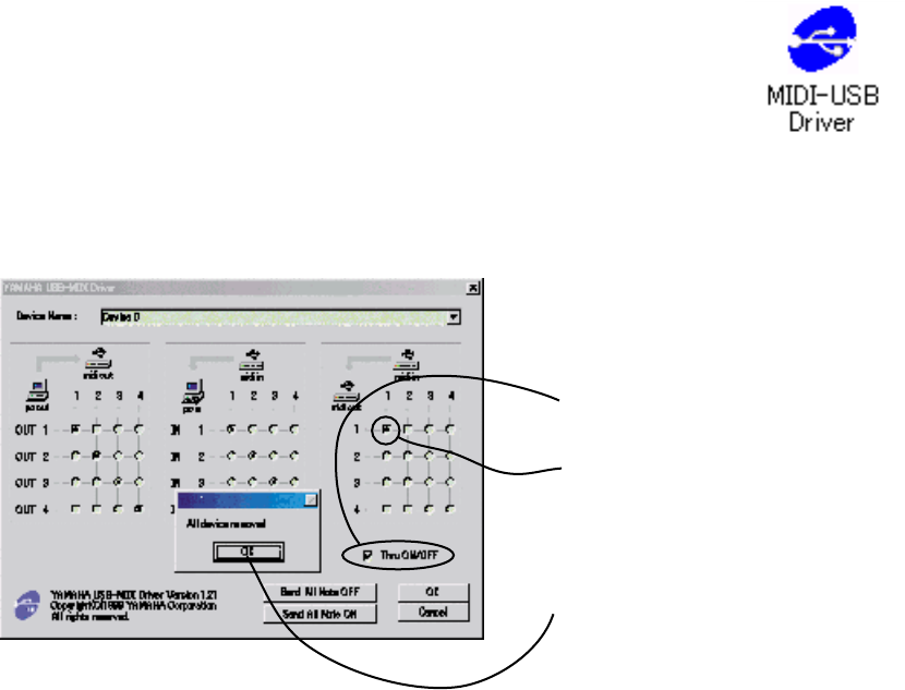
35
SPX2000
■ TEST PROGRAM
● Preparation
1) Cables
XLR (AES/EBU): 1 pc.
MIDI: 1 pc.
USB: 1 pc.
FC5 or OPEN JACK: 1 pc.
5) Program Version Check
If the main program is not the latest version, it must be upgraded to the latest program. For the methods to
check the program version and to write, refer to "Method for Writing the Program" on page 49.
(1) After starting the USB-MIDI driver
operation, click on "Thru ON/OFF".
(2) Clicking on this circle (1-1) will set
USB=MIDI to THRU.
If USB has become invalid by
SPX2000 USB initialization, press the
[OK] key to end the operation and sta
rt
up the USB-MIDI driver once again.
* Download the USB-MIDI driver from the YSISS Home Page.
(YSISS URL >>http://plaza.yamaha.co.jp/ysiss/exindex.nsf)
3) Personal Computer (PC): DOS/V machine
Using the USB cable, connect the USB connector of the main unit and the PC. Make settings
for the USB-MIDI driver on the PC.
For the USB driver, use a Windows 9x type one. (Use of the Windows 2000 or XP, USB
driver does not provide proper operation.)
4) Settings for USB-MIDI driver
In the "control panel" display on the PC, double click on "USB-MIDI Driver" to start up the
USB-MIDI driver and then make settings.
2) Measuring Instruments
Oscillator (output impedance: 150 Ω)
Oscilloscope (input impedance: 100 kΩ or more)
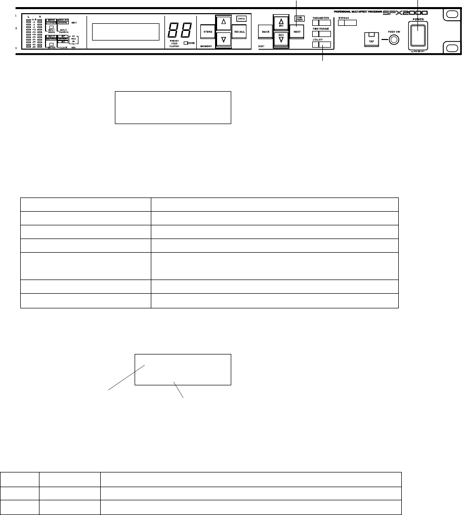
36
SPX2000
Example of panel display
MCS(PLLP2)
Ver.Check
● Starting Testing
Turn on the power while pressing "UTILITY" and "NEXT" keys
Entry screen
SERVICE TEST
SPX2000 V1.00
Displayed for a few seconds only.
NEXT POWER
UTILITY
● Operation Procedure
Key on panel Function
[MEMORY UP] Selection of test numbers in increasing direction
[MEMORY DOWN] Selection of test numbers in decreasing direction
[RECALL] Starting execution of the selected test number
[UNDO] Forcing to stop the test being executed.
* Stopping may not be available depending on test items.
[NEXT] Manual input of OK in the test judged by a testing person.
[BACK] Manual input of NG in the test judged by a testing person.
Test name
Test description and result
Test number
01
Meanings of displayed test results
OK Normal Details of the test that ended as normal are displayed on the left.
NG Error Details of the test in which an error occurred are displayed on the left.
-- Not tested yet
The test result is kept until the power is turned off. (It is cleared when the power is turned off.)
When re-testing, a new test result is written over the previous test result.
It is not possible to restore the "not tested" state for those items that have already been tested. ("not tested"
state is restored when the power is turned off.)
The LCD back light is white while testing. (this is applicable to tests other than the back light test)
37
SPX2000
● Outline of Tests
1. MCS (PLLP2) test
Reg. (00, 0f, 10, 16) of PLLP2 is read and written for
comparison check. Reg.12 (Ver.) is read and displayed.
A0..A4 and D0..D15 are checked.
Reg.12 cannot be checked automatically because it is a
read only Reg.
Example of execution screen
MCS(PLLP2)
OK
When testing starts, "testing..." appears on the screen.
"OK" is displayed when the MCS test ends with a
satisfactory result and "NG" when it ends with an
abnormality detected.
● List of check items
Item Test name Outline of check item Judgment
1 MCS(PLLP) Check the register of the gate array PLLP2 by reading/writing. Auto
2 BATT Check the voltage of the back-up battery/ Auto
4 DSP6,SIO Check the register of DSP6 by reading/writing and SIO connection. Auto
5MIDI Check MIDI OUT ➝ IN transmission and reception. Auto
6 USB MIDI Check the USB circuit by initializing it and then executing loopback on the external PC. Auto
7 AES/EBU IN/OUT Check AES/EBU IN/OUT DIGITAL by executing loopback. Semi-auto
(DIO)
8 WORD CLOCK Count the Fs of the oscillator using WCLK IN and check the lock state of PLL. Semi-auto
9 LCD
Check that the back-light lights up in each color and the entire screen is displayed in black and white.
Visual check
10 PANEL LED Check that LEDs (including 7-segment LEDs) light up in the specified order. Visual check
11 PANEL ALL LED Check that all LEDs light up in respective colors, Visual check
12 PANEL SW Check switches by pressing them in the specified order, Semi-auto
13 ANALOG IN/OUT Check analog input/output. Visual check
14 NG LOG Check that a list of test numbers resulted in NG is displayed.
2. BATT test
The back-up battery is checked automatically with its
voltage measured by A/D.
Example of execution screen
BATTERY
NG
When testing starts, "testing..." appears on the screen.
"OK" is displayed when the battery test ends with a
satisfactory result and "NG" when the measured battery
voltage is 2.8V or lower.
3.
There is no test program specified for No. 3.
4. DSP6, SIO test
The register of DSP6 is read and written to check the
condition of Data BUS and Address BUS.
The data is read and written in the DRAM of DSP6 via
the register for the comparative check.
The OUT METER SIO connection of DSP6 is checked
by sending and receiving the signal.
Example of execution screen
DSP6 bit23,3,0
NG
When testing starts, "testing..." appears on the screen.
"OK" is displayed when the DSP6 test ends with a
satisfactory result and "NG" when it ends with an
abnormality detected.
Caution
Cancellation of the test is invalid while it is being
executed.
38
SPX2000
5. MIDI test
The character string "SCI2: TEST¥n" (¥n=0Ah) is sent
from MIDI OUT to MIDI IN at 31.25 Kbps to check if
the sent string and the received one are identical.
Preparation
Connect the MIDI OUT and MIDI IN connectors of the
main unit.
Example of execution screen
MIDI
OK
If no signal is received, "NG" is displayed in about 2
seconds.
When testing starts, "testing..." appears on the screen.
"OK" is displayed when the MIDI test ends with a
satisfactory result and "NG" when it ends with an
abnormality detected.
Caution
Cancellation of the test is invalid while it is being
executed.
6. USB MIDI test
After initialization of the USB, it is checked automatically
using the loopback of the USB connected PC.
Preparation
Using the general purpose USB cable, connect the USB
connector of the main unit and the PC.
Make USB-MIDI driver settings on the PC. (Thru On)
Example of execution screen
USB MID
OK
If no signal is received, "NG" is displayed after about
10 seconds. (The waiting time is set longer than that for
the MIDI test because USB response may be slower
depending on PCs.)
When testing starts, "testing..." appears on the screen.
"OK" is displayed when the MIDI test ends with a
satisfactory result and "NG" when it ends with an
abnormality detected.
Caution
Cancellation of this test is invalid while it is being
executed.
7. AES/EBU IN/OUT (DIO) test
AES/EBU OUT DIGITAL ➝ AES/EBU IN DIGITAL
is checked by using SIO of DSP.
Preparation
Connect AES/EBU OUT DIGITAL and AES/EBU IN
DIGITAL of the main unit.
Example of execution screen
AES/EBU IN/OUT
OK
When testing starts, "testing..." appears on the screen.
When "DIO disconnect!" is displayed, disconnect the
AES/EBU signal which is connected IN -> OUT.
When preparation is completed, press the [NEXT]
switch. To cancel this test in this stage, press either
[UNDO] or [BACK] switch.
When the [NEXT] switch is pressed, testing starts again
and "testing..." appears on the screen.
"OK" is displayed when the DIO test ends with a
satisfactory result and "NG" when it ends with an
abnormality detected.
Caution
1) DIR Lock flag is read by Gate Array (and checked after
waiting for about 100mS after starting SIO
transmission/reception).
2) DIT, DIR, CDIN, CDOUT are read and written to check
RUN bit (0 x 40 of Reg4)

39
SPX2000
8. WORD CLOCK test
The external oscillator OUT -> WORD CLOCK IN is
counted by PLLP2 for automatic check.
(Fs=44.1/48/88.2/96kHz)
The lock condition of PLL is checked by reading the
UNLOCK signal when the clock has been stabilized after
the FS was changed (after about 200 ms).
The unlock condition of PLL is checked by pulling off
the cable connected to WORD CLOCK IN.
Preparation
Connect the external oscillator and WORD CLOCK IN
of the main unit.
Set the output clock of the external oscillator to 44.1kHz.
Example of execution screen
WORD CLOCK
OK
When testing starts, "testing..." appears on the screen.
When "Fs=48kHz OK?" appears on the screen, change
the output clock of the external oscillator to Fs=48kHz.
When preparation is completed, press the [NEXT]
switch.
To cancel testing in this stage, press either [UNDO] or
[BACK] switch.
When testing starts, "testing..." appears on the screen.
When "Fs=88.2kHz OK?" appears on the screen, change
the output clock of the external oscillator to Fs=88.2kHz.
When preparation is completed, press the [NEXT]
switch.To cancel testing in this stage, press either
[UNDO] or [BACK] switch.
When testing starts, "testing..." appears on the screen.
When "Fs=96kHz OK?" appears on the screen, change
the output clock of the external oscillator to Fs=96kHz.
When preparation is completed, press the [NEXT]
switch.To cancel testing in this stage, press either
[UNDO] or [BACK] switch.
When testing starts, "testing..." appears on the screen.
When "WC disconnect!" appears on the screen,
disconnect the WORD CLOCK OUT signal which is
connected IN -> OUT.
When preparation is completed, press the [NEXT]
switch.To cancel testing in this stage, press either
[UNDO] or [BACK] switch.
"OK is displayed when the WORD CLOCK test ends
with a satisfactory result and "NG" when it ends with an
abnormality detected.
Caution
1) Various types of FS for PLL LOCK test are produced
by the external oscillator.
FS=44.1kHz, 48kHz, 88.2kHz, 96kHz
9. LCD test
The LCD back-light (LED) is turned on in 3 colors
respectively and checked visually.
The entire LCD screen is displayed in black and white
alternately and checked visually.
Example of execution screen
PA
O
"Red" appears on the screen and the LCD back-color
lights in red.
"Green" appears on the screen and the LCD back-color
lights in green.
"Blue" appears on the screen and the LCD back-color
lights in blue.
"White" appears on the screen and the LCD back-color
lights in white.
If LCD back-color check result is satisfactory, press the
[NEXT] switch but if it is not, press the [BACK] switch
to make this test end.
When the above four colors have been confirmed and
the [NEXT] switch is pressed at the fourth color, dots
on the entire LCD screen are turned on and off repeatedly.
Check that the entire screen is displayed in black and
white.
Check that no dot is missing on the entire screen.
Check that the display contrast is in good condition.
When the check results of above 3 items are satisfactory,
press the [NEXT] switch but if they are not, press the
[BACK] switch.
"OK" appears on the screen when the LCD test ends
with a satisfactory result and "NG" when it ends with an
abnormality detected.
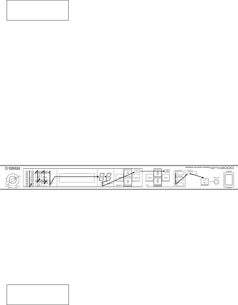
40
SPX2000
10. PANEL LED test
Whether the LEDs on the panel light up in the specified
order or not is checked visually.
Example of execution screen.
PANEL LED
OK
LEDs light up in the lighting order as specified.
All LEDs light up at the end or the lighting order.
If LEDs light properly, press the [NEXT] switch but if
not press the [BACK] switch.
"OK" appears on the screen when the PANEL LED test
ends with a satisfactory result and "NG" when it ends
with an abnormality detected.
Caution
1) For the lighting order, refer to Fig. 1.
2) Only the meter L/R segments light up at the same time.
All the others light up independently.
3) The 7 seg LEDs light up in the order of 0, 1, 2 on the
left and 0, 1, 2 on the right.
LED lighting order: Fig. 1
11. PANEL ALL LED test
When only red LEDs light up, check that no different
color exists.
When only green LEDs light up, check that no different
color exists.
When only orange LEDs light up, check that no different
color exists.
Example of execution screen
PANEL ALL LED
OK
"RED LEDs" appears on the screen and all red LEDs
light up.
"GREEN LEDs" appears on the screen and all red LEDs
light up.
"ORANGE LEDs" appears on the screen and all red
LEDs light up.
If LEDs light up by each color correctly, press the
[NEXT] switch but if not, press the [BACK] switch to
make this test end.
"OK" appears on the screen when the PANEL ALL LED
test ends with satisfactory test result but "NG" when it
ends with an abnormality detected.
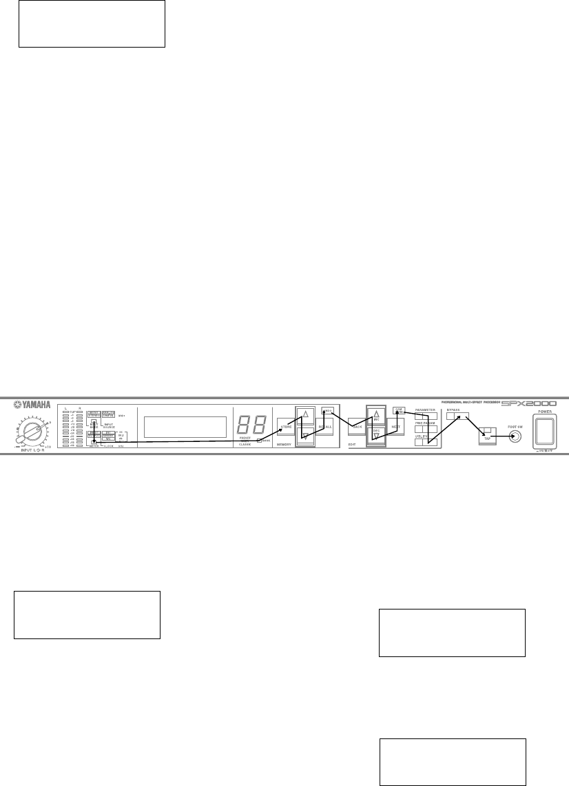
41
SPX2000
12. PANEL SW test
Press all the switches on the panel in the specified order,
and their response is checked automatically.
Example of execution screen
PANEL SW
OK
The name of the switch to be pressed is displayed on the
LCD. After confirmation of that switch being pressed,
the name of the switch to be pressed next is displayed.
When "FOOT SW" appears at the end, insert the OPEN
jack into the FOOT SW terminal.
The infinite loop is effective until the expected switch is
pressed. In order to force testing to end, press the
[BACK] switch to make the test in the NG state.
"OK" appears on the screen when the PANEL SW test
ends with satisfactory test result but "NG" when it ends
with an abnormality detected.
Caution
Refer to Fig. 2 for the operation procedure.
Button operation order: Fig. 2
14. NG LOG
The numbers of tests that ended as NG are displayed as a list.
Among all tests that have been executed, the numbers
of the tests whose final test result was NG are displayed.
Example of execution screen
NG 1,2,3,4,5,8,
10,12
When some tests have not been executed and the
executed tests have all resulted as OK, the numbers of
those that have not been executed are displayed.
NOT TESTED 3,5,
8,10
To return to the test menu number selection screen from
the NG LOG display screen, press one of [UNDO],
[RECALL] and [NEXT] switches.
13. ANALOG IN/OUT test
Enter the test waveform through the ANALOG input and
check the waveform at ANALOG output.
Example of execution screen
ANALOG IN/OUT
OK
As DSP6 is 96kHz through setting, the DSP input/output
waveforms should be identical.
If the check result is OK, press the [NEXT] switch and
if NG, press the [BACK] switch.
"OK" appears on the screen when the ANALOG IN/
OUT test ends with satisfactory test result but "NG" when
it ends with an abnormality detected.
42
SPX2000
● 準備
1) ケーブル類
XLR(AES/EBU): 1本
MIDI: 1本
USB: 1本
FC5またはOPEN JACK: 1個
■ テストプログラム
* USB-MIDIドライバーは、ヤマハCSセンターホームページのダウンロードページからダウンロードしてください。
(URL >>http://plaza.yamaha.co.jp/ysiss/index.nsf)
(1)起動後「Thru ON/OFF」をチェッ
クします。
(2)この○(1-1)をクリックすると、
USB-MIDIがTHRUになります。
SPX2000のUSB初期化で、一度USB
が無効になった場合、[OK]を押して終
了後、再度USB-MIDIドライバを起動
します。
5)プログラムバージョンの確認
本体プログラムが、最新バージョンになっていない場合、最新のプログラムにバージョンアップする必要がありま
す。プログラムのバージョンの確認および書き込み方法は、49ページの「プログラムの書き込み」を参照してくださ
い。
3) パーソナルコンピューター(PC): DOS/V機
本体のUSBコネクタとパソコンとをUSBケーブルで接続します。
パソコンに、USB-MIDIドライバの設定をします。
USBドライバーは、Windows9x系のものを用います。
(Windows2000,XPのUSBドライバーでは、正常に動作をしません。)
4)USB-MIDIドライバの設定
パソコンの「コントロールパネル」->「USB-MIDI Driver」をダブルクリックして、USB-MIDI
ドライバを起動した後、設定をします。
2) 測定器
発振器(出力インピーダンスは150Ωとします。)
オシロスコープ(入力インピーダンスは100kΩ以上とします。)
43
SPX2000
テスト結果表示の説明
OK 正常 左側に正常終了テスト詳細が表示されます
NG エラー 左側にエラーが発生したテスト詳細が表示されます
-- 未テスト
テスト結果は、電源OFFされるまで保持されます(電源OFFで揮発します)。
再テスト時は、以前のテスト結果に新しいテストが上書きされます。
既にテストした項目を、未テスト状態に戻すことはできません(電源OFFで未テストに戻ります)。
テスト中のLCDバックライトは、白です(但しバックライトテスト以外)。
テスト名
テスト詳細と結果表示
テスト番号
01
パネル表示例
MCS(PLLP2)
Ver.Check
● 操作方法
パネル上のキー 機能
[MEMORY UP] テスト番号の順方向選択
[MEMORY DOWN] テスト番号の逆方向選択
[RECALL] 選択したテスト番号の実行開始
[UNDO] 実行中のテストの強制中止
* 但しテスト項目によっては不可能なものもあります
[NEXT] テスト者(人間)が判定するテストでの手動OK入力
[BACK] テスト者(人間)が判定するテストでの手動NG入力
● 起動方法
「UTILITY」+「NEXT」を押しながら電源ONします。
エントリー画面
SERVICE TEST
SPX2000 V1.00
数秒だけ表示
NEXT POWER
UTILITY
44
SPX2000
● 検査項目一覧
項目 検査名称 検査項目の概要 判定
1 MCS(PLLP) ゲートアレー PLLP2 のレジスタをW/Rし判定 自動
2 BATT バックアップ用電池の電圧を判定 自動
4 DSP6,SIO DSP6のレジスタをW/Rし判定、SIO接続判定 自動
5 MIDI MIDI OUT-->INの送受信を判定 自動
6 USB MIDI USB回路の初期化、外部PCでLoopBackし判定 自動
7 AES/EBU IN/OUT AES/EBU IN/OUT DIGITALをLoopBackし判定 半自
(DIO)
8 WORD CLOCK オシレータのFsをWCLK INでカウント、PLLのLOCK判定 半自
9 LCD バックライト色別点灯、全画面を黒・白表示 目視
10 PANEL LED LED(7セグLEDを含む)が規定の順序で点灯 目視
11 PANEL ALL LED 全LEDの色別点灯 目視
12 PANEL SW SWを規定順に押して判定 半自
13 ANALOG IN/OUT アナログ入出力の検査 目視
14 NG LOG テスト結果、NGだったテスト番号の一覧表示
● 各テストの説明
1. MCS(PLLP2) test
内容 PLLP2のReg.(00, 0f, 10, 16)をW/Rして比較判定と、
Reg.12(Ver.)の読出し表示します。
A0..A4とD0..D15をチェックします。
Reg.12はReadOnlyのReg.なので自動判定できません。
実行画面例
MCS(PLLP2)
OK
テストが開始されると、“testing...” が表示されます。
MCS テストが正常終了すれば、“OK” が表示されます。
もし、異常終了すれば、“NG”' が表示されます。
2. BATT test
内容 バックアップ用電池の電圧をA/Dで測定し自動判定し
ます。
実行画面例
BATTERY
NG
テストが開始されると、“testing...” が表示されます。
バッテリーテストが正常終了すれば、“OK” が表示されま
す。もし、バッテリー電圧が2.8V以下ならば、“NG” が表示
されます。
3. N0. 3のテストプログラムはありません
45
SPX2000
6. USB MIDI test
内容 USBを初期化後、USB接続したパソコンのLoopBackで
自動判定をします。
準備 本体のUSBコネクタとパソコンとを汎用のUSBケー
ブルで接続します。
パソコンに、USB-MIDIドライバの設定をします。
(Thru On)
実行画面例
USB MID
OK
信号が受信できない場合、約10秒後にNGの判定になりま
す。(パソコンのUSB反応が遅いものがあるため、MIDI test
より待ち時間を長くしています)
テストが開始されると、“testing...” が表示されます。
USB テストが正常終了すれば、“OK” が表示されます。
もし、異常終了すれば、“NG” が表示されます。
注意事項
このテスト中のキャンセル操作は無効です。
7. AES/EBU IN/OUT(DIO) test
内容 AES/EBU OUT DIGITAL-->AES/EBU IN DIGITALを
DSPのSIOを使用して判定します。
準備 本体のAES/EBU OUT DIGITALと、AES/EBU IN
DIGITALを接続します。
実行画面例
AES/EBU IN/OUT
OK
テストが開始されると、“testing...” が表示されます。
“DIO disconnect!” と表示したら、IN->OUT 接続されてい
る AES/EBU 信号を切り離します。
準備が終わったら、[NEXT] スイッチを押します。
ここでキャンセルをする場合、[UNDO] [BACK] スイッチ
のどちらかを押します。
[NEXT] スイッチが押されると、引き続きテストが始ま
り、“testing...” が表示されます。
DIO テストが正常終了すれば、“OK” が表示されます。
もし、異常終了すれば、“NG” が表示されます。
4. DSP6, SIO test
内容 DSP6のRegisterをWrite/ReadしてDataBUS, Address
BUSの良否を判定します。
DSP6 のDRAMにRegister経由でWrite/Readして比較判
定します。
DSP6のOUT METER SIO結線を、信号の送受信で判定
します。
実行画面例
DSP6 bit23,3,0
NG
テストが開始されると、“testing...” が表示されます。
DSP6 テストが正常終了すれば、“OK” が表示されます。
もし、異常終了すれば、“NG” が表示されます。
注意事項
このテスト中のキャンセル操作は無効です。
5. MIDI test
内容 MIDI OUT-->MIDI IN に31.25Kbpsで文字列“SCI2:
TEST¥n”(¥n=0Ah)を送受信し、同一かどうかを検査
します。
準備 本体のMIDI OUTとMIDI INコネクタを接続します。
実行画面例
MIDI
OK
信号が受信できない場合、約2秒後にNGの判定になりま
す。
テストが開始されると、“testing...” が表示されます。
MIDI テストが正常終了すれば、“OK” が表示されます。
もし、異常終了すれば、“NG”' が表示されます。
注意事項
このテスト中のキャンセル操作は無効です。
46
SPX2000
注意事項
1) DIR Lock flagは、Gate Array にてReadします(SIO送受信開
始後約100mS待って判定)。
2) DIT,DIR,CDIN,CDOUTのWrite/ReadでRUN bit(Reg4の
0x40)を確認します。
8. WORD CLOCK test
内容 外部オシレータOUT --> WORD CLOCK INをPLLP2で
カウントして自動判定します。
(Fs=44.1/48/88.2/96kHz)
PLLのLOCKチェックは、FS変更後クロックが安定す
るのを待って(約200ms後)、UNLOCK信号をReadし判
定します。
PLLのUnLockチェックはWORD CLOCK INに接続さ
れているケーブルを抜いて検査します。
準備 外部のオシレータと、本体のWORD CLOCK INを接続
します。
外部オシレータの出力クロックを、44.1kHz に設定し
ます。
実行画面例
WORD CLOCK
OK
テストが開始されると、“testing...” が表示されます。
“Fs=48kHz OK?” と表示したら、外部オシレータの出力ク
ロックを、Fs=48kHz に変更します。
準備が終わったら、[NEXT] スイッチを押します。
ここでキャンセルをする場合、[UNDO] [BACK] スイッチ
のどちらかを押します。
テストが開始されると、“testing...” が表示される。
“Fs=88.2kHz OK?” と表示したら、外部オシレータの出力
クロックを、Fs=88.2kHz に変更します。
準備が終わったら、[NEXT] スイッチを押します。
ここでキャンセルをする場合、[UNDO] [BACK] スイッチ
のどちらかを押します。
テストが開始されると、“testing...” が表示されます。
“Fs=96kHz OK?” と表示したら、外部オシレータの出力ク
ロックを、Fs=96kHz に変更します。
準備が終わったら、[NEXT] スイッチを押します。
ここでキャンセルをする場合、[UNDO] [BACK] スイッチ
のどちらかを押します。
テストが開始されると、“testing...” が表示されます。
“WC disconnect!” と表示したら、IN->OUT 接続されてい
るWORD CLOCK OUT信号を切り離します。
準備が終わったら、[NEXT] スイッチを押します。
ここでキャンセルをする場合、[UNDO] か [BACK] スイッ
チのどちらかを押します。
WORD CLOCK テストが正常終了すれば、“OK” が表示さ
れます。もし、異常終了すれば、“NG” が表示されます。
注意事項
1) PLLのLOCK検査用各種FSは、外部のオシレータで発生させ
ます。
FS=44.1kHz, 48kHz, 88.2kHz, 96kHz
9. LCD test
内容 3色のLCDバックライト(LED)を、色別に点灯し、目視
で確認します。
LCDの画面全体を黒と白の繰り返し表示にし、目視判
定します。
実行画面例
PA
O
“Red” が表示されて、LCD のバックカラーが赤色に発色
します。
“Green” が表示されて、LCD のバックカラーが緑色に発色
します。
“Blue” が表示されて、LCD のバックカラーが青色に発色
します。
“White” が表示されて、LCD のバックカラーが白色に発色
します。
LCD のバックカラーの発光色に問題がなければ、[NEXT]
スイッチを押します。
異常があれば、[BACK] スイッチを押してこのテストを終
了します。
上記の4色が問題なく確認できて 4色目で [NEXT] スイッ
チを押すと、LCD の全ドットON, OFF を繰り返し表示し
ます。
全画面が、黒,白表示されることを確認します。
全画面に、ドット欠けがないことを確認します。
表示コントラストが正常であることを確認します。
上記3項目が正常に確認できたら、[NEXT] スイッチを押
します。
異常があれば、[BACK] スイッチを押します。
LCD テストが正常終了すれば、“OK” が表示されます。
もし、異常終了すれば、“NG” が表示されます。
47
SPX2000
11. PANEL ALL LED test
内容 赤色のLEDのみ点灯するので、違う色がないかを確認
します。
緑色のLEDのみ点灯するので、違う色がないかを確認
します。
橙(オレンジ)色のLEDのみ点灯するので、違う色がな
いかを確認します。
実行画面例
PANEL ALL LED
OK
“RED LEDs” が表示されて、赤色LED が全て発光します。
“GREEN LEDs” が表示されて、緑色LED が全て発光しま
す。
“ORANGE LEDs” が表示されて、橙(オレンジ)色LED が
全て発光します。
10. PANEL LED test
内容 パネル上のLEDが規定の順序で点灯するかを目視で
確認します。
実行画面例
PANEL LED
OK
点灯順序に従い、LED を点灯します。
最後に、全ての LED を点灯します。
正常に点灯する場合、OKとして、[NEXT]を押します。
NGの場合、[BACK]を押します。
PANEL LED テストが正常終了すれば、“OK” が表示され
ます。もし、異常終了すれば、“NG” が表示されます。
注意事項
1) 点灯順序は図1を参照してください。
2) メーターL/Rのみ、左右同時に点灯します。それ以外は、単独
点灯します。
3) 7segLEDは左0,1,2 右0,1,2の順で点灯します。
LED点灯順序:図1
色別にLED が発光するので、その都度、LED が正常に発光
していたら、[NEXT] スイッチを押します。
異常があれば、[BACK] スイッチを押してこのテストを終
了します。
PANEL ALL LED テストが正常終了すれば、“OK” が表示
されます。
もし、異常終了すれば、“NG” が表示されます。
48
SPX2000
12. PANEL SW test
内容 パネル上の全てのスイッチを規定順序通り押して反
応するか検査します(自動判定)。
実行画面例
PANEL SW
OK
LCDに、押すべきスイッチ名称を表示します。
押されたことが確認できたら、次の押すべきスイッチ名称
を表示します。
最後に、FOOT SWと表示されたら、OPEN JACKをFOOT
SW端子に挿入します。
期待するスイッチが押されるまで無限ループです。
テストを強制終了したい場合は、[BACK]を押し、テスト
NGとします。
PANEL SW テストが正常終了すれば、“OK” が表示され
ます。もし、異常終了すれば、“NG” が表示される。
注意事項
操作順序は図2を参照してください。
ボタン操作順序:図2
13. ANALOG IN/OUT test
内容 アナログ入力からテスト波形を入力し、アナログ出力
波形を測定します。
実行画面例
ANALOG IN/OUT
OK
DSP6 は96kHzのスルー設定となるため、DSP入出力波形
は同一です。
OKなら、[NEXT] を押します。
NGなら、[BACK] を押します。
ANALOG IN/OUT テストが正常終了すれば、“OK” が表示
されます。もし、異常終了すれば、“NG” が表示されます。
14. NG LOG
内容 テスト結果が、NGであったテスト番号を、列挙表示し
ます。
全テストが実施されて、テスト別に最後のテスト結果が
NGであったテスト番号を列挙します。
画面実行例
NG 1,2,3,4,5,8,
10,12
一部のテストが未テスト状態で、既に実施済みのテストが
全てOKだった場合、未テスト番号を列挙します。
NOT TESTED 3,5,
8,10
NG LOG 表示からテストメニュー番号選択に戻るには、
[UNDO], [RECALL], [NEXT]いずれかのスイッチを押しま
す。
49
SPX2000
■ WRITING PROGRAM
本体プログラムが、最新バージョンになっていない場合、最新
のプログラムにバージョンアップします。
最新のプログラムはYSISSホームページよりダウンロードし
てください。
(URL >>http://plaza.yamaha.co.jp/ysiss/index.nsf)
1. プログラムのバージョンの確認方法
UTILITYキーを押しながら SPX2000本体の電源を入
れるとLCD画面に本体プログラムのバージョンが表
示されます。
3) バージョンアッププログラム(VerUp.exe)を起動しま
す。
4) Browseボタンを押して書き込む本体プログラム(ファ
イル名は SPX2K.pgm)を選択します。
5) Loadボタンを押すとプログラムの書き込みが開始さ
れます。プログラム書き込み中は、本体電源を切った
り、ケーブルを抜いたりしないでください。
6) 1の方法で、プログラムのバージョンを確認します。
BYPASS
PARAMETER POWER
Example of panel display / エントリー画面
OS UPDATE
2. プログラムの書き込み方法
以下の手順に従い、本体プログラムを書き込みます。
1) PCと SPX2000を USBケーブルで接続します。
(PCに YAMAHA USB-MIDIドライバーがインストー
ルされていること。また、USB-MIDIドライバーの設定
が Through=Off であること。)
2) PARAMETERキーと BYPASSキーを押しながら
SPX2000本体の電源を入れます。
キーは、SPX2000本体の画面に"OS UPDATE"と表示さ
れるまで、押しつづけます。
POWER
UTILITY
If the main program is not the latest version, it must be upgraded
to the latest program.
Download the latest program from the YSISS Home Page.
(YSISS URL >>http://plaza.yamaha.co.jp/ysiss/exindex.nsf)
1. Confirming Program Version
While pressing the [UTILITY] key, turn on the main
power to the SPX2000. Then, the version of the main
program appears on the LCD screen.
2. Writing Program
Use the following procedure to write the main program.
1) Using the USB cable, connect the PC and SPX2000.
(The YAMAHA USB-MIDI driver must be installed in
the PC. Also, the setting of the USB-MIDI driver should
be Through=Off.)
2) While pressing the PARAMETER key and BYPASS key,
turn on the main power to SPX2000. Keep pressing these
keys until "OS UPDATE" appears on the screen of
SPX2000.
3) Start up the version upgrading program (VerUp.exe).
4) Press the [Browse] button and select the program of the
main unit to be written (file name: SPX2K.pgm)
5) Press the [Load] button to initiate writing of the program.
While the program is being written, do not turn off the
power to the main unit or disconnect the cable.
6) Check the version of the program according to the
method described in 1. Confirming Program Version
above.
(プログラムの書き込み)

50
SPX2000
■ BULK OUT (ALL)
■ INITIALIZING THE SPX2000
SPX2000 のシステム情報、MIDI プログラムチェンジテーブ
ル、エフェクト情報をまとめて他の機器に転送します。
情報の転送には「MIDI PORT GENERAL 」機能で設定したポー
トが使用されます。
1 「BULK OUT(ALL)」機能を選択する
[UTILITY]ボタンを何回か押して、「BULK OUT(ALL)」
を選択します。
(SPX2000 の情報を他の機器に転送する)
2 情報の転送を開始する
[▲INC] ボタンを押して、転送を開始します。
情報の転送中はディスプレイに「Transmitting..」の文字
が表示されます。
情報の転送が終了すると、ディスプレイに
「Completed!」の文字が約1 秒間表示されます。
NOTE: INPUT MODE 、METER の情報は転送される内容に含まれ
ません。
SPX2000 を工場出荷時の状態に戻します。
以下の操作をすると、USER バンクのエフェクトがすべて消
去されます。初期化の前に必要に応じて、「BULK OUT(ALL)」
機能でバックアップを取るなどしてください。
1 電源をOFFにする
SPX2000 の電源がON になっている場合は、一度電源
をOFF にします。
2 初期化の準備をする
[STORE] ボタンを押したまま、電源をON にします。
→以下の画面が表示されます。
(初期化)
3 初期化する
[▲INC] ボタンを押して、SPX2000 を初期化します。
初期化をキャンセルする場合には、[▲INC] 以外のボ
タンを押してください。
You can transmit the SPX2000’s system settings, MIDI program
change tables, and effect data to another device.
This data will be transmitted from the port specified by the
“MIDI PORT GENERAL” setting.
1 Select the “BULK OUT (ALL)” function
Press the [UTILITY] button several times to select
“BULK OUT (ALL).”
(Transmitting SPX2000 data to another device)
2 Start transmission
Press the [▲ INC] button to start transmission.
While the data is being transmitted, the display will
indicate “Transmitting...”
When transmission is completed, the display will indi-
cate “Completed!” for approximately one second.
NOTE: The INPUT MODE and METER settings are not included
with the transmitted data.
BULK OUT(ALL)
PUSH INC
BULK OUT(ALL)
PUSH INC
Here’s how to return the SPX2000 to its factory-set condi-tion.
The following procedure will erase all effects in the USER
bank. If necessary, use the “BULK OUT (ALL)” function
to back up your data before you proceed.
1 Turn off the power
If the SPX2000 is powered-on, turn the power off.
2 Prepare for initialization
While holding down the [STORE] button, turn on the
power.
➝The following screen will appear.
ZZ
3 Initialize
Press the [▲ INC] button to initialize the SPX2000.
If you decide not to initialize, press any button other
than [▲ INC].
Factory Preset?
PUSH INC
Factory Preset?
PUSH INC

51
SPX2000
■ ERROR MESSAGE LIST
Error message Message content/Action
Low Battery! The internal backup battery has run down.
If the battery goes dead, the internal data will be lost. Press any button to cancel the error message.
Then immediately use the “BULK OUT (ALL)” function to save the internal data on your computer
or on external device. After you have saved the data, replace the backup battery (lithium battery).
MIDI Framing Error! A MIDI framing error has occurred.
Press any button to cancel the error message. Then try transmitting the MIDI data once again.
MIDI OUT is NOT Selected! Since the “MIDI OUT/THRU” connector is set to “THRU,” MIDI messages cannot be transmitted.
If you want to transmit MIDI messages, use the “MIDI OUT SETUP” function to set the [MIDI
OUT/THRU] connector to “OUT.”
MIDI Overrun Error! A MIDI overrun error has occurred.
Press any button to cancel the error message. Then try transmitting the MIDI data once again.
MIDI Parity Error! A MIDI parity error has occurred.
Press any button to cancel the error message. Then try transmitting the MIDI data once again.
MIDI Rx Buffer Full! The MIDI reception buffer is full.
Press any button to cancel the error message. Then try transmitting the MIDI data once again. If
the error occurs again, try increasing the spacing between the MIDI data that is transmitted, or take
other measures to prevent a large amount of MIDI data from being transmitted at once.
NO FINE PARAMETER This effect has no Fine parameters.
Effects of the CLASSIC bank have no Fine parameters; this message will appear if you press the
[FINE PARAM] button for an effect of the CLASSIC bank. Use the [PARAMETER] button to
select Basic parameters.
Not Available in Compare Mode! You pressed an unavailable button while comparing the effect (while the [COMPARE] LED is
blinking). Press the [COMPARE] button to defeat Compare before you perform the desired
operation.
Operation Locked! The button etc. you attempted to operate has been disabled by the “OPERATION LOCK” function.
Defeat the restriction as necessary.
PORT GENERAL is Selected OFF! MIDI messages cannot be transmitted because the MIDI port (GENERAL) is turned OFF.
If you want to transmit MIDI messages, set the “MIDI PORT GENERAL” setting to the port that
you want to use for MIDI message transmission and reception.
U## Program is Empty! There is no effect to recall.
Please re-select an effect to recall.
Sync Error! The clock of the received digital input signal differs from the SPX2000’s operating clock.
This BANK is Protected! You selected the PRESET bank or CLASSIC bank as the effect store-destination.
Since the PRESET bank and CLASSIC bank are read-only, you cannot change store to these
effects, or change the effect name, protect setting, or display background color. Press any button to
cancel the error message. Then select a store-destination from the USER bank.
This Program is Protected! The effect store-destination is protected.
Press any button to cancel the error message. Then defeat the protect setting as desired.
USB Rx Buffer Full! The USB reception buffer is full.
Press any button to cancel the error message. Then try transmitting the MIDI data once again. If
the error occurs again, try increasing the spacing between the MIDI data that is transmitted, or take
other measures to prevent a large amount of MIDI data from being transmitted at once.
WRONG WORD CLOCK! The word clock signal from an external device has been interrupted, or is a frequency to which the
SPX2000 cannot synchronize. Check whether there are any problems with the connection from
the device supplying the word clock, and verify that the word clock settings are correct.

52
SPX2000
エラーメッセージ メッセージの内容/対処方法
Low Battery! 内蔵バックアップバッテリーが消耗しています。
バッテリーが切れると内部のデータが消えてしまいます。どれかボタンを押してエラーを解除
したあと、至急「BULK OUT(ALL)」機能」使って、コンピューターなどの外部機器にデータを保存
してください。また、データの保存が完了したら、バックアップバッテリー(リチウム電池)の交
換をしてください。
MIDI Framing Error! MIDI フレーミングエラーが発生しました。
どれかボタンを押してエラーを解除したあと、もう一度MIDIデータを送り直してみてください。
MIDI OUT is NOT Selected! [MIDI OUT/THRU] 端子が「THRU」に設定されているため、MIDIメッセージが送信できません。
MIDIメッセージを送信する場合は「MIDI OUT SETUP」機能で[MIDI OUT/THRU] 端子を「OUT」
に設定してください。
MIDI Overrun Error! MIDIオーバーランエラーが発生しました。
どれかボタンを押してエラーを解除したあと、もう一度MIDIデータを送り直してみてください。
MIDI Parity Error! MIDIパリティエラーが発生しました。
どれかボタンを押してエラーを解除したあと、もう一度MIDI データを送り直してみてください。
MIDI Rx Buffer Full! MIDI の受信バッファーが一杯になりました。
どれかボタンを押してエラーを解除したあと、もう一度MIDI データを送り直してみてください。
エラーが再発する場合にはMIDI データの送信間隔をあけるなどして、一度に大量のMIDI デー
タが送り込まれないようにしてください。
NO FINE PARAMETER FINE パラメーターがありません。
CLASSICバンクのエフェクトにはFINEパラメーターがありません。このため、CLASSICバンク
のエフェクトで[FINE PARAM]ボタンを押すと、このメッセージが表示されます。 [PARAMETER]
ボタンを使って基本パラメーターを選択してください。
Not Available in Compare Mode! エフェクト効果の比較中([COMPARE] LED 点滅中)に使用できないボタンを押しました。
[COMPARE] ボタンを押して比較を解除してからボタン操作をしてください。
Operation Locked! 今操作したボタン類は「OPERATION LOCK」機能によって、使用できなくなっています。必要に
応じて操作の制限を解除してください。
PORT GENERAL is Selected OFF! MIDIポート(GENERAL)の設定がOFFになっているため、MIDIメッセージが送信できません。
MIDIメッセージを送信する場合は「MIDI PORT GENERAL」機能でMIDIメッセージの送受信に
使うポートを設定してください。
U## Program is Empty! リコールするエフェクトがありません。リコールするエフェクトを選択しなおしてください。
Sync Error! 受信しているデジタル入力信号とSPX2000の動作しているCLOCKが違います。
This BANK is Protected! エフェクトのストア先がPRESETバンクまたはCLASSICバンクになっています。
PRESETバンクやCLASSICバンクは読み出し専用のためエフェクトのストアやエフェクト名の
変更、プロテクトの設定、ディスプレイ背景色の変更ができません。どれかボタンを押してエラー
を解除したあと、USERバンクからストア先を選択してください。
This Program is Protected! エフェクトのストア先にプロテクトがかかっています。
どれかボタンを押してエラーを解除したあと、必要に応じてプロテクトを解除してください。
USB Rx Buffer Full! USBの受信バッファーが一杯になりました。
どれかボタンを押してエラーを解除したあと、もう一度MIDIデータを送り直してみてください。
エラーが再発する場合にはMIDIデータの送信間隔をあけるなどして、一度に大量のMIDIデータ
が送り込まれないようにしてください。
WRONG WORD CLOCK! 外部からのワードクロック信号が途切れているか、SPX2000で同期可能な周波数ではありませ
ん。ワードクロックを供給する機器との接続やワードクロックの設定に問題がないかご確認く
ださい。
■ エラーメッセージリスト

53
SPX2000
■ MIDI IMPLEMENTATION CHART
YAMAHA [PROFESSIONAL MULTI-EFFECT PROCESSOR] Date: 12 MAY 2003
Model: SPX2000
MIDI Implementation Chart
Version: 1.0
Function... Transmitted Recognized Remarks
Basic
Channel
Default
Changed
X
X
1–16
1–16
Memorized
Mode
Default
Messages
Altered
X
X
**************
OMNI OFF/OMNI ON
X
X
Memorized
Note
Number True Voice X
**************
0–127*1
X
*4
Velocity Note On
Note Off
X
X
O 9nH, v=1-127*1
X
*4
After Key’s
Ch’s
X
X
X
X
Pitch Bend X X
Control
Change 0-32 X O*1
0:Bank Select MSB
1-30:*4
31:Mix Balance
32:Bank Select LSB
Program
Change :True#
X
**************
O 0–127*1 Assignable
Program Change
Table
System Exclusive O*2 O*2 *3
Common
:Song Pos.
:Song Sel.
:Tune
X
X
X
X
X
X
System
Real Time
:Clock
:Commands
X
X
O
X
*4
Aux
Messages
:All Sound Of
:Reset All Cntrls
:Local ON/OFF
:All Notes OFF
:Active Sense
:Reset
X
X
X
X
X
X
X
X
X
X
O
O
Notes
*1 receive if switch is on.
*2 transmit/receive if exclusive switch is on.
*3 Bulk Dump/Request, Parameter Change/Request
*4 Effect Control(Depend On Program)
Mode 1: OMNI ON, POLY
Mode 3: OMNI OFF, POLY
Mode 2: OMNI ON, MONO
Mode 4: OMNI OFF, MONO
O: Yes
X: No
54
SPX2000
■ MIDI DATA FORMAT
'tx' indicates that the SPX2000 can transmit the message. 'rx' indicates
that the SPX2000 can receive the message.
1.1 CHANNEL MESSAGE
1.2 SYSTEM REALTIME MESSAGE
1.3 EXCLUSIVE MESSAGE
■1.3.1 Bulk dump
The SPX2000 handles the following types of data as bulk dumps.
■1.3.2 Parameter Change
The SPX2000 handles the following types of data as parameter changes.
2.1 NOTE OFF (8n)
If the SPX2000 receives this message when a freeze-type effect has been
recalled, it will stop playing the sampled data.
• Reception conditions
This message is received if the following two conditions are satisfied.
1) The “MIDI RECEIVE” setting (page 23) is “NOTE ON/OFF = ON”.
2) The channel on which the MIDI message is transmitted matches the
SPX2000’s MIDI channel, or the SPX2000’s MIDI channel is set to
OMNI.
• Format
STATUS 1000nnnn 8n Note off message
DATA 0nnnnnnn nn Note number
0vvvvvvv vv Velocity (ignored)
2.2 NOTE ON (9n)
When the SPX2000 receives this message, it will control the recalled
effect.
The effects that respond to this message and the controlled content are as
follows.
• Reception conditions
This message is received if the following two conditions are satisfied.
1) The “MIDI RECEIVE” setting (page 23) is “NOTE ON/OFF = ON”.
2) The channel on which the MIDI message is transmitted matches the
SPX2000’s MIDI channel, or the SPX2000’s MIDI channel is set to
OMNI.
• Format
STATUS 1001nnnn 9n Note on message
DATA 0nnnnnnn nn Note number
0vvvvvvv vv Velocity (1-127:on, 0:off)
2.3 CONTROL CHANGE (Bn)
When the SPX2000 receives this message, it will operate in one of two
ways. The operation will depend on the content of the first two bytes of
data. If the data begins with a value of 01h-1Fh, the parameter specified
by the control change parameter list will be controlled. If the data begins
with a value of either 00h or 20h, the program change table (A/B/C) will
be switched.
• Reception conditions
This message is received if the following two conditions are satisfied.
1) The “MIDI RECEIVE” setting (page 23) is “CTL CHANGE = ON”.
2) The channel on which the MIDI message is transmitted matches the
SPX2000’s MIDI channel, or the SPX2000’s MIDI channel is set to
OMNI.
• Format
If the data begins with 01h-1Fh
STATUS 1011nnnn Bn Control change
DATA 000nnnnn nn Control number (1-31)
0vvvvvvv vv Control Value (0-127)
1. Format summary
Command rx/tx function
8n NOTE OFF rx Control internal effects
9n NOTE ON rx Control internal effects
Bn CONTROL CHANGE rx Control parameters
Cn PROGRAM CHANGE rx Change programs
Command rx/tx function
F8 TIMING CLOCK rx MIDI clock
FE ACTIVE SENSING rx Check MIDI cable connections
FF RESET rx Clear running status
Command rx/tx function
F0 43 0n 7E ...
F7 BULK DUMP DATA rx/tx Bulk dump data
F0 43 2n 7E ...
F7 BULK DUMP REQUEST rx Bulk dump request
Data name rx/tx function
S rx/tx System setup data and request
E rx/tx Effect program and request
P rx/tx Program change table and request
Command rx/tx function
F0 43 1n 1E 09 ...
F7 RARAMETER CHANGE rx/tx Parameter changes specific to the
SPX2000
F0 43 3n 1E 09 ...
F7 PARAMETER REQUEST rx Parameter requests specific to the
SPX2000
Type (HEX) rx/tx function
1 (01) rx/tx Edit buffer
3 (03) rx/tx System setup data
4 (04) rx/tx System backup data
16 (10) rx/tx Functions (recall, store, title, clear)
17 (11) rx/tx Functions (undo, compare)
18 (12) rx Functions (effect)
20 (14) rx/tx Functions (attribute (Protect), LCD Back
Color)
33 (21) rx/tx Remote Meter
2. Format details
DYNA.FILTER (P76)
DYNA.FLANGE (P77)
DYNA.PHASER (P78) Modulation
FREEZE (P97)
FREEZE A (C23)
FREEZE B (C24)
Start recording, playing the sam-
pled data
PITCH CHANGE A (C19)
PITCH CHANGE D (C22) Change pitch
REVERB & GATE (C18) Open the gate
This message is received if the following two conditions are satisfied.
1) The “MIDI RECEIVE” setting is “NOTE ON/OFF = ON”.
2) The channel on which the MIDI message is transmitted matches the
SPX2000’s MIDI channel, or the SPX2000’s MIDI channel is set to
OMNI.
This message is received if the following two conditions are satisfied.
1) The “MIDI RECEIVE” setting is “NOTE ON/OFF = ON”.
2) The channel on which the MIDI message is transmitted matches the
SPX2000’s MIDI channel, or the SPX2000’s MIDI channel is set to
OMNI.
This message is received if the following two conditions are satisfied.
1) The “MIDI RECEIVE” setting is “CTL CHANGE = ON”.
2) The channel on which the MIDI message is transmitted matches the
SPX2000’s MIDI channel, or the SPX2000’s MIDI channel is set to
OMNI.

55
SPX2000
Equation for converting the control value into parameter
data (CurValue)
paramSteps = paramMax - paramMin;
curValue = (Control Value * paramSteps)/127;
If the data begins with 00h or 20h
STATUS 1011nnnn Bn Control change
DATA 00000000 00 Bank Select MSB
00000000 00 Bank number MSB (0); fixed
at 0
STATUS 1011nnnn Bn Control change
DATA 00100000 20 Bank Select LSB
000000vv vv
Bank number LSB (0, 1, 2); 0:
table A, 1: table B, 2: table
C
STATUS 1100nnnn Cn Program change
DATA 0vvvvvvv vv Program number (0-127)
2.4 PROGRAM CHANGE (Cn)
When the SPX2000 receives this message, it will recall the effect specified
by the content of the program change table (page 22).
• Reception conditions
This message is received if the following two conditions are satisfied.
1) The “MIDI RECEIVE” setting (page 23) is “PGM CHANGE = ON”.
2) The channel on which the MIDI message is transmitted matches the
SPX2000’s MIDI channel, or the SPX2000’s MIDI channel is set to
OMNI.
• Format
STATUS 1100nnnn Cn Program change
DATA 0nnnnnnn nn Program number (0-127)
2.5 TIMING CLOCK (F8)
This message is used for tempo synchronization of the effect. Twenty-
four of these messages are received per quarter note.
• Reception conditions
This message is received if the “TEMPO SOURCE” setting (page 23) is
set to a tempo synchronization source of “MIDI.”
• Format
STATUS 11111000 F8 Timing clock
2.6 ACTIVE SENSING (FE)
Once the SPX2000 has received this message, failure to receive a message
of any kind for an interval longer than 400 ms will cause it to initialize
MIDI communication settings such as running status.
• Format
STATUS 11111110 FE Active sensing
2.7 SYSTEM RESET (FF)
When the SPX2000 receives this message, it will initialize MIDI commu-
nication settings such as running status.
• Format
STATUS 11111111 FF System reset
2.8 SYSTEM EXCLUSIVE MESSAGE (F0)
■2.8.1 BULK DUMP/BULK DUMP REQUEST
Bulk Dump messages are used to bulk dump SPX2000 data to a con-
nected MIDI device (see page 21) , or to receive data from a connected
MIDI device to overwrite internal settings of the SPX2000.
Bulk Dump Request messages request a bulk dump of data from the
SPX2000.
• Reception conditions
This message is received if the following two conditions are satisfied.
1) The “MIDI RECEIVE” setting (page 23) is “SYEX BLKDMP = ON”.
2) The device number within the MIDI message matches the
SPX2000’s MIDI channel, or the SPX2000’s MIDI channel is set to
OMNI.
• Transmission conditions
This message is transmitted when either of the following conditions
are met.
• The “BULK OUT (ALL)” function is executed to perform a bulk
dump.
• A Bulk Dump Request message is received.
• Data conversion
The data portion is handled by converting seven words of 8-bit data
into eight words of 7-bit data.
[Converting actual data into bulk data]
d[0~6]: Actual data
b[0~7]: Bulk data
b[0] = 0;
for( I=0; I<7; I++){
if( d[I]&0x80){
b[0] |= 1<<(6-I);
}
b[I+1] = d[I]&0x7F;
}
[Restoring bulk data into actual data
d[0~6]: Actual data
b[0~7]: Bulk data
for( I=0; I<7; I++){
b[0] <<= 1;
d[I] = b[I+1]+(0x80&b[0]);
}
■2.8.1.1 System Setup Data Bulk Dump Format
This bulk-dumps the SPX2000’s setup memory except for the program
change table.
• Format
STATUS 11110000 F0 System exclusive message
ID No. 01000011 43 Manufacture’s ID number
(YAMAHA)
SUB STATUS 0000nnnn 0n n=0-15 (Device number=Device
No-1)
FORMAT No. 01111110 7E Universal bulk dump
COUNT HIGH 0ccccccc ch data count = ch * 128 + cl
COUNT LOW 0ccccccc cl
01001100 4C ‘L’
01001101 4D ‘M’
00100000 20 ‘ ’
00100000 20 ‘ ’
00111000 38 ‘8’
01000100 44 ‘D’
00110001 31 ‘1’
00110001 31 ‘1’
DATA NAME 01010011 53 ‘S’
00000010 02
00000000 00 No.256 = Current
BLOCK INFO. 0ttttttt tt total block number(minimum
number is 0)
0bbbbbbb bb current block number(0-total
block number)
DATA 0ddddddd ds Setup data of block[bb]
::
0ddddddd de
CHECK SUM 0eeeeeee ee ee=(Invert(‘L’+ c+de)+1)&0x7F
EOX 11110111 F7 End of exclusive
■2.8.1.2 System Setup Data Bulk Dump request Format
• Format
STATUS 11110000 F0 System exclusive message
ID No. 01000011 43 Manufacture’s ID number
(YAMAHA)
SUB STATUS 0010nnnn 2n n=0-15 (Device number=Device
No-1)
FORMAT No. 01111110 7E Universal bulk dump
01001100 4C ’L’
01001101 4D ‘M’
00100000 20 ‘ ’
00100000 20 ‘ ’
00111000 38 ‘8’
01000100 44 ‘D’
00110001 31 ‘1’
00110001 31 ‘1’
DATA NAME 01010011 53 ‘S’
00000010 02
00000000 00 No.256 = Current
EOX 11110111 F7 End of exclusive
This message is received if the following two conditions are satisfied.
1) The “MIDI RECEIVE” setting is “PGM CHANGE = ON”.
2) The channel on which the MIDI message is transmitted matches the
SPX2000’s MIDI channel, or the SPX2000’s MIDI channel is set to
OMNI.
This message is received if the following two conditions are satisfied.
1) The “MIDI RECEIVE” setting is “SYEX BLKDMP = ON”.
2) The device number within the MIDI message matches the
SPX2000’s MIDI channel, or the SPX2000’s MIDI channel is set to
OMNI.
When the SPX2000 receives this message, it will recall the effect specified
by the content of the program change table.
This message is received if the “TEMPO SOURCE” setting is set to a
tempo synchronization source of “MIDI.”
Bulk Dump messages are used to bulk dump SPX2000 data to a con-
nected MIDI device, or to receive data from a connected MIDI device to
overwrite internal settings of the SPX2000.
Bulk Dump Request messages request a bulk dump of data from the
SPX2000.

56
SPX2000
■2.8.1.3 System Setup Data Bulk Dump request Format
This bulk-dumps the data of the specified effect.
• Format
STATUS 11110000 F0 System exclusive message
ID No. 01000011 43 Manufacture’s ID number
(YAMAHA)
SUB STATUS 0000nnnn 0n n=0-15 (Device number=Device
No-1)
FORMAT No. 01111110 7E Universal bulk dump
COUNT HIGH 00000000 00 data count = ch(0x00) * 128
+ cl(0x72) = 114
COUNT LOW 01110010 72
01001100 4C ‘L’
01001101 4D ‘M’
00100000 20 ‘ ’
00100000 20 ‘ ’
00111000 38 ‘8’
01000100 44 ‘D’
00110001 31 ‘1’
00110001 31 ‘1’
DATA NAME 01000101 45 ‘E’
0mmmmmmm mh 0-220(Program no.P1-97,C1-
25,U1-99),256(EDIT BUFFER)
0mmmmmmm ml
BLOCK INFO. 0ttttttt tt total block number(minimum
number is 0)
0bbbbbbb bb current block number(0-total
block number)
DATA 0ddddddd ds Effect Program data of
block[bb]
::
0ddddddd de
CHECK SUM 0eeeeeee ee ee=(Invert(‘L’+...de)
+1)&0x7F
EOX 11110111 F7 End of exclusive
The second and third byte of DATA NAME specify the program num-
ber.
0:PRESET1 – 96:PRESET97
97:CLASSIC1 – 121:CLASSIC25
122:USER1 – 220:USER99
256:EDIT BUFFER
For reception by the SPX2000, only USER 1-99 or EDIT BUFFER are
valid. (120-220, 256)
■2.8.1.4 Effect Program Bulk Dump request Format
The second and third byte of DATA NAME specify the program number.
• Format
STATUS 11110000 F0 System exclusive message
ID No. 01000011 43 Manufacture’s ID number
(YAMAHA)
SUB STATUS 0010nnnn 2n n=0-15 (Device number=Device
No-1)
FORMAT No. 01111110 7E Universal bulk dump
01001100 4C ‘L’
01001101 4D ‘M’
00100000 20 ‘ ’
00100000 20 ‘ ’
00111000 38 ‘8’
01000100 44 ‘D’
00110001 31 ‘1’
00110001 31 ‘1’
DATA NAME 01000101 45 ‘E’
0mmmmmmm mh 0-220(Program no.P1-97,C1-
25,U1-99),
256(EDIT BUFFER)
0mmmmmmm ml
EOX 11110111 F7 End of exclusive
The second and third byte of DATA NAME specify the program num-
ber.
122:USER1 – 220:USER99
256:EDIT BUFFER
■2.8.1.5 Program change table Bulk Dump Format
This bulk-dumps the program change table data.
• Format
STATUS 11110000 F0 System exclusive message
ID No. 01000011 43 Manufacture’s ID number
(YAMAHA)
SUB STATUS 0000nnnn 0n n=0-15 (Device number=Device
No-1)
FORMAT No. 01111110 7E Universal bulk dump
COUNT HIGH 0ccccccc ch data count = ch * 128 + cl
COUNT LOW 0ccccccc cl
01001100 4C ‘L’
01001101 4D ‘M’
00100000 20 ‘ ’
00100000 20 ‘ ’
00111000 38 ‘8’
01000100 44 ‘D’
00110001 31 ‘1’
00110001 31 ‘1’
DATA NAME 01010000 50 ‘P’
00000010 02
00000000 00 No.256 = Current
BLOCK INFO. 0ttttttt tt total block number
(minimum number is 0)
0bbbbbbb bb current block number
(0 - total block number)
DATA 0ddddddd ds Program change table data of
block[bb]
::
0ddddddd de
CHECK SUM 0eeeeeee ee ee=(Invert
(‘L’+...+de)+1) &0x7F
EOX 11110111 F7 End of exclusive
■2.8.1.6 Program change table Bulk Dump request
Format
• Format
STATUS 11110000 F0 System exclusive message
ID No. 01000011 43 Manufacture’s ID number
(YAMAHA)
SUB STATUS 0010nnnn 2n n=0-15 (Device number=Device
No-1)
FORMAT No. 01111110 7E Universal bulk dump
01001100 4C ‘L’
01001101 4D ‘M’
00100000 20 ‘ ’
00100000 20 ‘ ’
00111000 38 ‘8’
01000100 44 ‘D’
00110001 31 ‘1’
00110001 31 ‘1’
DATA NAME 01010000 50 ‘P’
00000010 02
00000000 00 No.256 = Current
EOX 11110111 F7 End of exclusive
■2.8.2 Program change table Bulk Dump request For-
mat
When the SPX2000 receives a Parameter Change message, the SPX2000
setting specified by the content will be controlled. When the SPX2000
receives a Parameter Change Request message, it will transmit a Parame-
ter Change message in reply.
• Reception conditions
This message is received if the following two conditions are satisfied.
1) The “MIDI RECEIVE” setting (page 23) is “SYEX PRMCHG = ON”.
2) The device number within the MIDI message matches the
SPX2000’s MIDI channel, or the SPX2000’s MIDI channel is set to
OMNI.
• Transmission conditions PARAMETER CHANGE only
This message is transmitted when either of the following conditions
are met.
• The SPX2000’s state has changed due to a received Parameter Change
• A Parameter Change Request message is received
■2.8.2.1 Parameter change (Edit Buffer)
This message modifies the value of a parameter in the edit buffer.
• Format
STATUS 11110000 F0 System exclusive message
ID No. 01000011 43 Manufacture’s ID number
(YAMAHA)
SUB STATUS 0001nnnn 1n n=0-15 (Device number=Device
No-1)
GROUP ID 00011110 1E MODEL ID (signal processor)
MODEL ID 00001001 09 SPX2000
ADDRESS 00000001 01 Edit Buffer
0eeeeeee ee Element no.(if 'ee' is 0,
'ee' will be expanded to two
bytes)
0ppppppp pp Parameter no.
0ccccccc cc Channel no.
DATA 0ddddddd dd data
::
EOX 11110111 F7 End of exclusive
This message is received if the following two conditions are satisfied.
1) The “MIDI RECEIVE” setting is “SYEX PRMCHG = ON”.
2) The device number within the MIDI message matches the
SPX2000’s MIDI channel, or the SPX2000’s MIDI channel is set to
OMNI.

57
SPX2000
■2.8.2.2 Parameter request (Edit Buffer)
• Format
STATUS 11110000 F0 System exclusive message
ID No. 01000011 43 Manufacture’s ID number
(YAMAHA)
SUB STATUS 0011nnnn 3n n=0-15 (Device number=
Device No-1)
GROUP ID 00011110 1E MODEL ID (signal processor)
MODEL ID 00001001 09 SPX2000
ADDRESS 00000001 01 Edit Buffer
0eeeeeee ee Element no.(if 'ee' is 0,
'ee' will be expanded to two
bytes)
0ppppppp pp Parameter no.
0ccccccc cc Channel no.
EOX 11110111 F7 End of exclusive
■2.8.2.3 Parameter change (System Setup Memory)
This message modifies the value of a parameter in system setup memory.
• Format
STATUS 11110000 F0 System exclusive message
ID No. 01000011 43 Manufacture’s ID number
(YAMAHA)
SUB STATUS 0001nnnn 1n n=0-15 (Device number=
Device No-1)
GROUP ID 00011110 1E MODEL ID (signal processor)
MODEL ID 00001001 09 SPX2000
ADDRESS 00000011 03 System Setup data
0eeeeeee ee Element no.(if 'ee' is 0,
'ee' will be expanded to two
bytes)
0ppppppp pp Parameter no.
0ccccccc cc Channel no.
DATA 0ddddddd dd data
::
EOX 11110111 F7 End of exclusive
■2.8.2.4 Parameter request (System Setup Memory)
STATUS 11110000 F0 System exclusive message
ID No. 01000011 43 Manufacture’s ID number
(YAMAHA)
SUB STATUS 0011nnnn 3n n=0-15 (Device number=
Device No-1)
GROUP ID 00011110 1E MODEL ID (signal processor)
MODEL ID 00001001 09 SPX2000
ADDRESS 00000011 03 System Setup data
0eeeeeee ee Element no.(if 'ee' is 0,
'ee' will be expanded to two
bytes)
0ppppppp pp Parameter no.
0ccccccc cc Channel no.
EOX 11110111 F7 End of exclusive
■2.8.2.5 Parameter change (System Backup Memory)
This message modifies the value of a parameter in system backup mem-
ory.
• Format
STATUS 11110000 F0 System exclusive message
ID No. 01000011 43 Manufacture’s ID number
(YAMAHA)
SUB STATUS 0001nnnn 1n n=0-15 (Device number=
Device No-1)
GROUP ID 00011110 1E MODEL ID (signal processor)
MODEL ID 00001001 09 SPX2000
ADDRESS 00000011 04 System Backup data
0eeeeeee ee Element no.(if 'ee' is 0,
'ee' will be expanded to two
bytes)
0ppppppp pp Parameter no.
0ccccccc cc Channel no.
DATA 0ddddddd dd data
::
EOX 11110111 F7 End of exclusive
■2.8.2.6 Parameter request (System Backup Memory)
• Format
STATUS 11110000 F0 System exclusive message
ID No. 01000011 43 Manufacture’s ID number
(YAMAHA)
SUB STATUS 0011nnnn 3n n=0-15 (Device number=
Device No-1)
GROUP ID 00011110 1E MODEL ID (signal processor)
MODEL ID 00001001 09 SPX2000
ADDRESS 00000011 04 System Backup data
0eeeeeee ee Element no.(if 'ee' is 0,
'ee' will be expanded to two
bytes)
0ppppppp pp Parameter no.
0ccccccc cc Channel no.
EOX 11110111 F7 End of exclusive
■2.8.2.7 Parameter change (Function call : Program
store/recall)
When the SPX2000 receives this message, it will store or recall the speci-
fied effect, and will then use this message to transmit the state following
the change. At this time, the device number will be the MIDI channel of
the SPX2000. If the MIDI channel is OMNI, the device number will be 1.
• Format
STATUS 11110000 F0 System exclusive message
ID No. 01000011 43 Manufacture’s ID number
(YAMAHA)
SUB STATUS 0001nnnn 1n n=0-15 (Device number=
Device No-1)
GROUP ID 00011110 1E MODEL ID (signal processor)
MODEL ID 00001001 09 SPX2000
ADDRESS 00010000 10 Function call
00ffffff ff function
0mmmmmmm mh number High
0mmmmmmm ml number Low
DATA 0ccccccc ch channel High
0ccccccc cl channel Low
EOX 11110111 F7 End of exclusive
■2.8.2.8 Parameter change (Function call : title)
When the SPX2000 receives this message, it will edit the specified effect
name, and will then use this message to transmit the state following the
change. At this time, the device number will be the MIDI channel of the
SPX2000. If the MIDI channel is OMNI, the device number will be 1.
• Format
STATUS 11110000 F0 System exclusive message
ID No. 01000011 43 Manufacture’s ID number
(YAMAHA)
SUB STATUS 0001nnnn 1n n=0-15 (Device number=
Device No-1)
GROUP ID 00011110 1E MODEL ID (signal processor)
MODEL ID 00001001 09 SPX2000
ADDRESS 00010000 10 Function call
01000100 44 Effect Program title
0mmmmmmm mh number High
0mmmmmmm ml number Low
DATA 0ddddddd dd title 1
:::
0ddddddd dd title x(depend on the pro-
gram)
EOX 11110111 F7 End of exclusive
■2.8.2.9 Parameter request (Function call : title)
• Format
STATUS 11110000 F0 System exclusive message
ID No. 01000011 43 Manufacture’s ID number
(YAMAHA)
SUB STATUS 0011nnnn 3n n=0-15 (Device number=Device
No-1)
GROUP ID 00011110 1E MODEL ID (signal processor)
MODEL ID 00001001 09 SPX2000
ADDRESS 00010000 10 Function call
01000100 44 Effect Program title
0mmmmmmm mh number High
0mmmmmmm ml number Low
EOX 11110111 F7 End of exclusive
For the function and number, refer to the table in “2.8.2.8 Parameter
change (Function call: title).”
function number channel rx/tx
Effect Program Recall 0x04 1-221 0 rx/tx
Effect Program Store 0x24 123-221 0 rx/tx
function number size
Effect Program Title 0x44
1-221
(1-122:response
only)
16
58
SPX2000
■2.8.2.10 Parameter change (Function call : Program
clear)
When the SPX2000 receives this message, it will erase the specified effect
name, and will then use this message to transmit the state following the
change. At this time, the device number will be the MIDI channel of the
SPX2000. If the MIDI channel is OMNI, the device number will be 1.
• Format
STATUS 11110000 F0 System exclusive message
ID No. 01000011 43 Manufacture’s ID number
(YAMAHA)
SUB STATUS 0001nnnn 1n n=0-15 (Device number=Device
No-1)
GROUP ID 00011110 1E MODEL ID (signal processor)
MODEL ID 00001001 09 SPX2000
ADDRESS 00010000 10 Function call
01100100 64 Effect Program clear func-
tion
0mmmmmmm mh number High
0mmmmmmm ml number Low
EOX 11110111 F7 End of exclusive
■2.8.2.11 Parameter change (Function call : Undo)
When the SPX2000 receives this message, it will perform the same opera-
tion as if the [UNDO] button had been pressed, and will then use this
message to transmit the state following the change. At this time, the
device number will be the MIDI channel of the SPX2000. If the MIDI
channel is OMNI, the device number will be 1.
• Format
STATUS 11110000 F0 System exclusive message
ID No. 01000011 43 Manufacture’s ID number
(YAMAHA)
SUB STATUS 0001nnnn 1n n=0-15 (Device number=Device
No-1)
GROUP ID 00011110 1E MODEL ID (signal processor)
MODEL ID 00001001 09 SPX2000
ADDRESS 00010001 11 Function call
00100010 24 Undo
00000000 00
00000000 00
DATA 00000000 00
00000000 00
EOX 11110111 F7 End of exclusive
■2.8.2.12 Parameter change (Function call : Compare)
When the SPX2000 receives this message, it will perform the same opera-
tion as if the [COMPARE] button had been pressed, and will then use this
message to transmit the state following the change. At this time, the
device number will be the MIDI channel of the SPX2000. If the MIDI
channel is OMNI, the device number will be 1.
• Format
STATUS 11110000 F0 System exclusive message
ID No. 01000011 43 Manufacture’s ID number
(YAMAHA)
SUB STATUS 0001nnnn 1n n=0-15 (Device number=Device
No-1)
GROUP ID 00011110 1E MODEL ID (signal processor)
MODEL ID 00001001 09 SPX2000
ADDRESS 00010001 11 Function call
01000100 44 Compare
00000000 00
00000000 00
DATA 00000000 00
00000000 00
EOX 11110111 F7 End of exclusive
■2.8.2.13 Parameter change (Function call : Event
Effect)
When the SPX2000 receives this message while a freeze-type effect is
recalled, it will perform the same operation as if the RECORD parameter
or PLAY parameter is selected and the [▼ DEC] button pressed. The con-
tents of the function will determine whether the RECORD parameter or
the PLAY parameter is selected.
• Format
STATUS 11110000 F0 System exclusive message
ID No. 01000011 43 Manufacture’s ID number
(YAMAHA)
SUB STATUS 0001nnnn 1n n=0-15 (Device number=Device
No-1)
GROUP ID 00011110 1E MODEL ID (signal processor)
MODEL ID 00001001 09 SPX2000
ADDRESS 00010010 12 Function call Effect Event
0000ffff 0f function
00000000 00
0ppppppp pp Release:0, Press:1
DATA 00000000 00
0eeeeeee ee Effect number (0)
EOX 11110111 F7 End of exclusive
*This will not function if the effect type is wrong.
■2.8.2.14 Parameter change (Function call:
attribute(Protect))
When the SPX2000 receives this message, it will switch Protect on/off for
the specified effect, and will then use this message to transmit the state
following the change. At this time, the device number will be the MIDI
channel of the SPX2000. If the MIDI channel is OMNI, the device num-
ber will be 1.
• Format
STATUS 11110000 F0 System exclusive message
ID No. 01000011 43 Manufacture’s ID number
(YAMAHA)
SUB STATUS 0001nnnn 1n n=0-15 (Device number=Device
No-1)
GROUP ID 00011110 1E MODEL ID (signal processor)
MODEL ID 00001001 09 SPX2000
ADDRESS 00010100 14 Function call
00000100 04 attribute
0mmmmmmm mh number High
0mmmmmmm ml number Low
DATA 0ttttttt tt attribute(protect:0x0001,
normal:0x0000)
0ttttttt tt
EOX 11110111 F7 End of exclusive
■2.8.2.15 Parameter request (Function call:
attribute(Protect))
• Format
STATUS 11110000 F0 System exclusive message
ID No. 01000011 43 Manufacture’s ID number
(YAMAHA)
SUB STATUS 0011nnnn 3n n=0-15 (Device number=Device
No-1)
GROUP ID 00011110 1E MODEL ID (signal processor)
MODEL ID 00001001 09 SPX2000
ADDRESS 00010100 14 Function call
00000100 04 attribute
0mmmmmmm mh number High
0mmmmmmm ml number Low
EOX 11110111 F7 End of exclusive
For the function and number, refer to the table in “2.8.2.14 Parameter
change (Function call: attribute (Protect)).”
■2.8.2.16 Parameter change (Function call: LCD Back
Color)
When the SPX2000 receives this message, it will change the display
background color of the specified effect, and will then use this message
to transmit the state following the change. At this time, the device
number will be the MIDI channel of the SPX2000. If the MIDI channel
is OMNI, the device number will be 1.
• Format
STATUS 11110000 F0 System exclusive message
ID No. 01000011 43 Manufacture’s ID number
(YAMAHA)
SUB STATUS 0001nnnn 1n n=0-15 (Device number=Device
No-1)
GROUP ID 00011110 1E MODEL ID (signal processor)
MODEL ID 00001001 09 SPX2000
ADDRESS 00010100 14 Function call
01100100 64 LCD Back Color
0mmmmmmm mh number High
0mmmmmmm ml number Low
DATA 0ccccccc cc color(0:Green,1:Yellow,
2:Magenta,3:Cyan,4:White)
0ccccccc cc
function number
Effect Program Clear 0x64 123-221
function channel
Freeze Play button 0x00 0
Freeze Record button 0x01 0
function number
Effect Program Attribute
0x04 1-221(1-122:response
only)

59
SPX2000
EOX 11110111 F7 End of exclusive
■2.8.2.17 Parameter request (Function call: LCD Back
Color)
• Format
STATUS 11110000 F0 System exclusive message
ID No. 01000011 43 Manufacture’s ID number
(YAMAHA)
SUB STATUS 0011nnnn 3n n=0-15 (Device number=Device
No-1)
GROUP ID 00011110 1E MODEL ID (signal processor)
MODEL ID 00001001 09 SPX2000
ADDRESS 00010100 14 Function call
01100100 64 LCD Back Color
0mmmmmmm mh number High
0mmmmmmm ml number Low
EOX 11110111 F7 End of exclusive
For the function and number, refer to the table in “2.8.2.16 Parameter
change (Function call: LCD Back Color).”
■2.8.2.18 Parameter change (Remote Meter)
When the SPX2000 receives a Parameter Request (Remote Meter) mes-
sage, it will transmit this message. The content is data for the specified
meter. This is transmitted at 50 msec intervals for ten seconds. If you
want meter data to continue being transmitted, you must transmit a
Request message at intervals of less than ten seconds. However if the port
is being used for other communication, transmission of meter data may
be interrupted.
The device number used when transmitting meter data will be the MIDI
channel of the SPX2000. If the MIDI channel is OMNI, the device num-
ber will be 1.
When the SPX2000 receives a Request message with an Address UL =
0x7F, transmission of all meter data will be halted immediately. Transmis-
sion will also stop if the power is turned off and on again while transmit-
ting meter data, or if the MIDI port setting is changed.
• Format
STATUS 11110000 F0 System exclusive message
ID No. 01000011 43 Manufacture’s ID number
(YAMAHA)
SUB STATUS 0001nnnn 1n n=0-15 (Device number=Device
No-1)
GROUP ID 00011110 1E MODEL ID (signal processor)
MODEL ID 00001001 09 SPX2000
ADDRESS 00100001 21 Remote meter
0mmmmmmm mm ADDRESS UL
0mmmmmmm mm ADDRESS LU
0mmmmmmm mm ADDRESS LL
DATA 0ddddddd dd Data1 H
0ddddddd dd Data1 L
::
EOX 11110111 F7 End of exclusive
■2.8.2.19 Parameter request (Remote Meter)
• Format
STATUS 11110000 F0 System exclusive message
ID No. 01000011 43 Manufacture’s ID number
(YAMAHA)
SUB STATUS 0011nnnn 3n n=0-15 (Device number=Device
No-1)
GROUP ID 00011110 1E MODEL ID (signal processor)
MODEL ID 00001001 09 SPX2000
ADDRESS 00100001 21 Remote meter
0mmmmmmm mm ADDRESS UL
0mmmmmmm mm ADDRESS LU
0mmmmmmm mm ADDRESS LL
0ccccccc ch Count H
0ccccccc cl Count L
EOX 11110111 F7 End of exclusive
function number
Effect Program LCD Back Color
0x64 1-221(1-
122:response only)
WARNING
Components having special characteristics are marked and must be replaced with parts having
specification equal to those originally installed.
Notes : DESTINATION ABBREVIATIONS
The numbers “QTY” show quantities for each unit.
The parts with “--” in “PART NO.” are not available as spare parts.
This mark “ } ” in the REMARKS column means these parts are interchangeable.
The second letter of the shaded ( ) part number is O, not zero.
The second letter of the shaded ( ) part number is I, not one.
M: South African model
O : Chinese model
Q : South-east Asia model
T : Taiwan model
U : U.S.A. model
V : General export model (110V)
W: General export model (220V)
N,X: General export model
Y : Export model
A : Australian model
B : British model
C : Canadian model
D : German model
E : European model
F : French model
H : North European model
I : Indonesian model
J : Japanese model
K : Korean model
CONTENTS
OVERALL ASSEMBLY ............................................... 2
ELECTRICAL PARTS ...................................... 5 – 15
PARTS LIST
(総組立)
(電気部品)
(目次)
印の部品は、安全を維持するために重要な部品です。交換する場合は、安全のために必ず指定の部品をご
使用ください。
部品価格ランクは、変更になることがあります。
QTY欄に記されている数字は、各ユニット当たりの使用個数です。
PART NO.が“--”の部品は、サービス用部品として準備されておりません。
REMARKS欄の「 }」マークの部品は、併用部品です。
網掛けの付いたPART NO. の2番目の文字は「ゼロ」ではなく「オー」です。
網掛けの付いたPART NO. の2番目の文字は「イチ」ではなく、「アイ」です。
SPX2000
2
OVERALL ASSEMBLY
500
520
410
430
430
400
430
570
380
390
210
300
550 560
300 350
360
330
260
180
180
200
250
420
220
60
140
10
160
50
40
30
30
30 150
130
80
90
100
20
510
530
530
540
540
40
40
30
10c
520
520
520
10a
10b
10a
10a
10a
110a
110b
110h
110f
110d
200
110e 110c
110g
Rubber cap
(ラバーキャップ)
WC049600
See page 5. PN3 circuit board
See page 3, 5.
Rubber cap
(ラバーキャップ)
WC049600
See page 5.
(総組立)
SPX2000
3
440 280 290 470
460
45070
• Pic. 1 MAIN-POWER SUPPLY wiring
MAIN
POWER SUPPLY UNIT
170 470
• Pic. 2 AC INLET-POWER wiring
POWER SUPPLY UNITAC INLET
POWER
PARAM button
WB435900 TAP button
WB436000
BRIGHT button
WB436100
MEMO button
WB435800
• PN3 circuit board (See page 5.)
PN3
A
BC
D
L
E
N
1
2
3
1
2
3
4
5
140a
140b
140c
140d
140e 140f
140g
140d
• AC inlet assembly
to POWER-CN301
to POWER SUPPLY UNIT

SPX2000
4
REF NO.
PART NO. DESCRIPTION REMARKS
QTY
: New Parts RANK: Japan only
RANK
OVERALL ASSEMBLY SPX2000 (WB42170)
*10 Bottom Chassis
10a Bind Head Tapping Screw-S 3.0X6 MFZN2BL 401
10b Bind Head Screw 4.0X8 MFZN2BL 01
10c Rubber Foot Black T1.6 401
*20 Circuit Board MAIN
30 Bind Head Tapping Screw-B 3.0X8 MFZN2BL 801
40 Bind Head Tapping Screw-B 2.6X8 MFZN2BL 601
50 Bind Head Tapping Screw-S 3.0X6 MFZN2BL 201
60 Bind Head Tapping Screw-S 3.0X6 MFZN2BL 801
70 Cord Binder S-72B L=50 01
*80 PS Cover
Z
90 Power Supply Unit ZWS50AF-5/J 19
100 Bind Head Tapping Screw-S 3.0X6 MFZN2BL 401
110 PN Circuit Board Assembly (WB43570)
*110a Circuit Board JKIN (WB42730)
*110b Circuit Board JKOUT (WB42740)
*110c Circuit Board PN3 with Button (WB42710)
*110d Circuit Board PN1 with Cap (WB42690)
*110e Circuit Board PN2 with Cap (WB42700)
*110f Circuit Board VOL (WB42750)
*110g Circuit Board FOOTSW (WB42760)
*110h Circuit Board POWER (WB42720)
130 Hexagonal Nut 9.0X11 401
*140 AC Inlet Assembly AC INLET VH 3P/5P
Z
140a AC Inlet 3P M1908-C 03
140b Connector Housing VH 3P 01
140c Connector Housing VH 5P 01
140d Connector Pin SVH-21T-P1.1 401
140e Tube Black M5.0 (CH00428)
140f Earth Lug (WA11050)
140g Ferrite Core FR25/15/12-1400L 04
150 Bind Head Tapping Screw-B 3.0X8 MFZN2BL 201
160 Bind Head Screw 4.0X8 MFZN2BL 01
170 Cord Holder BK-1 01
180 PCB Spacer KGPS-16RF DPX1000 2 01
200 Bind Head Tapping Screw-S 3.0X6 MFZN2BL 201
*210 LED Guide
*220 Film Red
*250 LCD EW10212YMR
260 Spacer (WB43100) 2
280 Cord Holder BK-1 01
290 Ferrite Core FR25/15/12-1400L 04
300 Bind Head Tapping Screw-S 3.0X10 MFZN2Y 201
330 JACK Angle (WB45090)
350 Hexagonal Nut 9.0X11 01
360 Bind Head Tapping Screw-S 3.0X6 MFZN2BL 01
380 Bind Head Tapping Screw-S 3.0X6 MFZN2BL 201
*390 Front Panel
*400 Button Guide
*410 Window
*420 Flat Head Screw-S 3.0X6 MFAN2Y
430 Bind Head Tapping Screw-S 3.0X6 MFZN2BL 301
*440 Connector Assembly VH&VH 4P 340L
*450 Cable 20P 180mm P=1.0
Z
460 Lithium Battery CR2032 03
470 Adhesive Tape 12X50 303
*500 Top Cover
510 Label MULTI (WB55000)
520 Bind Head Tapping Screw-S 3.0X6 MFZN2BL 901
*530 Angle Bracket, Rack 2
540 Bind Head Tapping Screw-S 4.0X8 MFZN2BL 601
*550 Knob Internal INPUT L
*560 Knob External INPUT R
*570 Button POWER ON/OFF
ACCESSORIES
Z
Adaptor, AC Cord KPR-24 J 06
Z
AC Cord J 7A 125V 3P 2.5m J 06
Z
AC Cord CSA U,C,V 08
Z
AC Cord VDE H,W,K 08
Z
AC Cord BS 3P B 10
--
WB424200
EP630210
EG340360
CB043750
WB053000
EP600190
VB096700
EP630210
EP630210
CB040540
WB451300
V9702900
EP630210
--
AAX51260
AAX51270
AAX51240
AAX51220
AAX51230
AAX51280
AAX51290
AAX51250
V2431400
WB440900
V5065200
LB015030
LB015050
LB101710
--
--
VC362700
EP600190
EG340360
CB069250
WA624500
EP630210
WB435200
WB550100
WB448400
--
CB069250
VC362700
EP630630
--
V2431400
EP630210
EP630210
WB423800
WB426500
WB424600
WB451000
EP630210
WB440800
WB639200
VN103500
VA126100
WB424400
--
EP630210
WB424500
VI693100
WB426700
WB426800
WB426600
VQ240200
VT119800
VB927800
VB928000
VP204400
総組立
ボトムシャーシAss’y
+バインドSタイト
+バインド小ネジ
ゴム脚
MAINシート
+バインドBタイト
+バインドBタイト
+バインドSタイト
+バインドSタイト
束線止め
PSカバー
電源ユニット
+バインドSタイト
PNシートAss’y
JKINシート
JKOUTシート
PN3シート
PN1シート
PN2シート
VOLシート
FOOTSWシート
POWERシート
特殊六角ナット
インレットAss’y
ACインレット 3P
ハウジング
ハウジング
圧着端子
スミチューブ クロ
アースラグ TI0432
フェライトコア
+バインドBタイト
+バインド小ネジ
インシュロックタイ
PCBスペーサ
+バインドSタイト
LEDガイド
カラーフィルム
液晶ディスプレイ
スペーサ
インシュロックタイ
フェライトコア
+バインドSタイト
JACKアングル
特殊六角ナット
+バインドSタイト
+バインドSタイト
フロントパネル印刷品
ボタンガイドPSW
ウインドウ印刷品
Sタイト平頭
+バインドSタイト
束線 #20
バンカード
リチウム電池
粘着テープ
トップカバープレス品
ラベル規格
+バインドSタイト
ラックアングル印刷品
+バインドSタイト
ノブ内印刷品
ノブ外印刷品
ボタンPSW
付属品
変換アダプター
電源コード
電源コード
電源コード
電源コード
部品名
SPX2000
5
REF NO.
PART NO. DESCRIPTION REMARKS
QTY
: New Parts RANK: Japan only
RANK
ELECTRICAL PARTS(電気部品)
ELECTRICAL PARTS SPX2000
*Circuit Board FOOTSW (WB42760)(X4199B0)
*Circuit Board JKIN (WB42730)(X4199B0)
*Circuit Board JKOUT (WB42740)(X4199B0)
*Circuit Board PN1 (WB42690)(X4199B0)
*Circuit Board PN2 (WB42700)(X4199B0)
*Circuit Board PN3 (WB42710)(X4199B0)
*Circuit Board POWER (WB42720)(X4199B0)
*Circuit Board VOL (WB42750)(X4199B0)
*Circuit Board MAIN (X4198B0)
*Circuit Board FOOTSW (WB42760)(X4199B0)
*Circuit Board JKIN (WB42730)(X4199B0)
*Circuit Board JKOUT (WB42740)(X4199B0)
*Circuit Board PN1 (WB42690)(X4199B0)
*Circuit Board PN2 (WB42700)(X4199B0)
*Circuit Board PN3 (WB42710)(X4199B0)
*Circuit Board POWER (WB42720)(X4199B0)
*Circuit Board VOL (WB42750)(X4199B0)
*A Button, MEMO STORE,RECALL,UP,DOWN,
UNDO/REDO
*B Button, PARAM BACK,NEXT,INC,DEC,
COMPARE
*C Button, TAP TAP
*D Button, BRIGHT PARAMETER,FINE PARAM, 4
UTILITY,BYPASS
*E Rubber Cap INPUT MODE,METER,BANK 3
*10 Jumper Wire FVP=2.0C26SB14-140
*20 Jumper Wire FVP=2.0C26SB10-140
*30 Jumper Wire FVP=2.0C26SB15-140
*40 Jumper Wire FVP=2.0C26SB7-100
*50 Jumper Wire FVP=2.0C26SB2-220
Z
C301 Capacitor 0.010 VA1 J.U.C.S 01
CN001 Cable Holder 51048 14P TE 01
CN101 Cable Holder 51048 10P TE 01
CN201 Cable Holder 51048 15P TE 01
CN301 Base Post Connector VA 2P SE 01
CN401 Wire Trap 52147 7P TE 01
CN501 Wire Trap 52147 6P TE 01
CN601 Cable Holder 51048 7P TE 01
CN701 Cable Holder 51048 2P TE 01
D001 Diode 1SS355 TE-17 01
D002 Diode 1SS355 TE-17 01
D101 Diode 1SS355 TE-17 01
D201 Diode 1SS355 TE-17 01
-214 Diode 1SS355 TE-17 01
EM701 LC Filter DSS6NB32A271Q93A 01
JK401 Phone Jack HLJ0544 STREO INPUT L 03
JK402 Phone Jack HLJ0544 STREO INPUT R 03
JK501 Phone Jack HLJ0544 STREO OUTPUT L 03
JK502 Phone Jack HLJ0544 STREO OUTPUT R 03
JK701 Phone Jack HLJ0544 MONO. FOOT SW 03
*LD001 LED (chip) Yellow TLYV1020 J,K MIDI
*LD002 LED (chip) Yellow TLYV1020 J,K CLOCK INT
LD003 LED (chip) Green TLGU1020 CLIP L -48 01
LD004 LED (chip) Green TLGU1020 CLIP L -24 01
*LD005 LED (chip) Yellow TLYV1020 J,K CLIP L -9
*LD006 LED (chip) Yellow TLYV1020 J,K METER INPUT
*LD007 LED (chip) Yellow TLYV1020 J,K CLOCK AES/EBU
LD008 LED (chip) Green TLGU1020 CLIP L -42 01
*LD009 LED (chip) Yellow TLYV1020 J,K CLIP L -18
*LD010 LED (chip) Yellow TLYV1020 J,K CLIP L -6
*LD011 LED (chip) Yellow TLYV1020 J,K METER OUTPUT
*LD012 LED (chip) Yellow TLYV1020 J,K CLOCK WC
LD013 LED (chip) Green TLGU1020 CLIP L -36 01
*LD014 LED (chip) Yellow TLYV1020 J,K CLIP L -15
*LD015 LED (chip) Yellow TLYV1020 J,K CLIP L -3
*LD016 LED (chip) Yellow TLYV1020 J,K INPUT SOURCE ANALOG
*LD017 LED (chip) Yellow TLYV1020 J,K 96kHz
LD018 LED (chip) Green TLGU1020 CLIP L -30 01
AAX51290
AAX51260
AAX51270
AAX51220
AAX51230
AAX51240
AAX51250
AAX51280
WB053000
AAX51290
AAX51260
AAX51270
AAX51220
AAX51230
AAX51240
AAX51250
AAX51280
WB435800
WB435900
WB436000
WB436100
WC049600
VU073800
WB639500
WB639600
VV153500
WC109500
V7682800
VI879200
VI878800
VI879300
VP245600
VK025100
VF728300
VI878500
VI878000
VT332900
VT332900
VT332900
VT332900
VT332900
VI243100
LB302070
LB302070
LB302070
LB302070
LB301800
WC153200
WC153200
WA588100
WA588100
WC153200
WC153200
WC153200
WA588100
WC153200
WC153200
WC153200
WC153200
WA588100
WC153200
WC153200
WC153200
WC153200
WA588100
電気部品
FOOTSWシート
JKINシート
JKOUTシート
PN1シート
PN2シート
PN3シート
POWERシート
VOLシート
MAINシート
FOOTSWシート
JKINシート
JKOUTシート
PN1シート
PN2シート
PN3シート
POWERシート
VOLシート
ボタンMEMO
ボタンPARAM
ボタンTAP
ボタン照光
ラバーキャップ
2678ジャンパーワイヤ
ジャンパーワイヤ
ジャンパーワイヤ
2678ジャンパーワイヤ
ジャンパーワイヤ
規格認定コン KH
ケーブルホルダー
ケーブルホルダー
ケーブルホルダー
ベースツキポスト
ワイヤートラップ
ワイヤートラップ
ケーブルホルダー
ケーブルホルダー
ダイオード
ダイオード
ダイオード
ダイオード
ダイオード
LCフィルター
ホーンコネクタ
ホーンコネクタ
ホーンコネクタ
ホーンコネクタ
ホーンコネクタ
チップLEDキ
チップLEDキ
チップLEDミド
チップLEDミド
チップLEDキ
チップLEDキ
チップLEDキ
チップLEDミド
チップLEDキ
チップLEDキ
チップLEDキ
チップLEDキ
チップLEDミド
チップLEDキ
チップLEDキ
チップLEDキ
チップLEDキ
チップLEDミド
部品名
SPX2000
6
REF NO.
PART NO. DESCRIPTION REMARKS
QTY
: New Parts RANK: Japan only
RANK
*LD019 LED (chip) Yellow TLYV1020 J,K CLIP L -12
LD020 LED (chip) Red TLSU1020 CLIP L 0 01
*LD021 LED (chip) Yellow TLYV1020 J,K INPUT SOURCE DIGITAL
*LD022 LED (chip) Yellow TLYV1020 J,K 88.2kHz
LD023 LED (chip) Green TLGU1020 CLIP R -48 01
LD024 LED (chip) Green TLGU1020 CLIP R -24 01
*LD025 LED (chip) Yellow TLYV1020 J,K CLIP R -9
*LD026 LED (chip) Yellow TLYV1020 J,K INPUT MODE MONO
*LD027 LED (chip) Yellow TLYV1020 J,K 48kHz
LD028 LED (chip) Green TLGU1020 CLIP R -42 01
*LD029 LED (chip) Yellow TLYV1020 J,K CLIP R -18
*LD030 LED (chip) Yellow TLYV1020 J,K CLIP R -6
*LD031 LED (chip) Yellow TLYV1020 J,K INPUT MODE STEREO
*LD032 LED (chip) Yellow TLYV1020 J,K 44.1kHz
LD033 LED (chip) Green TLGU1020 CLIP R -36 01
*LD034 LED (chip) Yellow TLYV1020 J,K CLIP R -15
*LD035 LED (chip) Yellow TLYV1020 J,K CLIP R -3
LD036 LED (chip) Green TLGU1020 CLIP R -30 01
*LD037 LED (chip) Yellow TLYV1020 J,K CLIP R -12
LD038 LED (chip) Red TLSU1020 CLIP R 0 01
*LD101 LED (chip) Yellow TLYV1020 J,K PRESET
LD102 LED Red LT1D40A 7 SEG. 01
LD103 LED Red LT1D40A 7 SEG. 01
*LD104 LED (chip) Yellow TLYV1020 J,K USER
LD105 LED Red LT1D40A 7 SEG. 01
LD106 LED Red LT1D40A 7 SEG. 01
*LD107 LED (chip) Yellow TLYV1020 J,K CLASSIC
LD108 LED Red LT1D40A 7 SEG. 01
LD109 LED Red LT1D40A 7 SEG. 01
LD110 LED Red LT1D40A 7 SEG. 01
LD111 LED Red LT1D40A 7 SEG. 01
LD112 LED Red LT1D40A 7 SEG. 01
LD113 LED Red LT1D40A 7 SEG. 01
LD114 LED Red LT1D40A 7 SEG. 01
LD115 LED Red LT1D40A 7 SEG. 01
LD116 LED Red LT1D40A 7 SEG. 01
LD117 LED Red LT1D40A 7 SEG. 01
LD201 LED GL3JV804BOPE UNDO/REDO 01
LD202 LED GL3JV804BOPE COMPARE 01
*LD203 LED (chip) Yellow TLYV1020 J,K PARAMETER
*LD204 LED (chip) Yellow TLYV1020 J,K FINE PARAM
*LD205 LED (chip) Yellow TLYV1020 J,K UTILITY
LD206 LED (chip) Red TLSU1020 BYPASS 01
LD207 LED Yellow LT1H40A TAP 01
SW001 Tact Switch SKQNAED010 METER 01
SW002 Tact Switch SKQNAED010 INPUT MODE 01
SW101 Tact Switch SKQNAED010 BANK 01
SW201 Tact Switch SKQNAED010 STORE 01
SW202 Tact Switch SKQNAED010 DOWN 01
SW203 Tact Switch SKQNAED010 UNDO/REDO 01
SW204 Tact Switch SKQNAED010 INC 01
SW205 Tact Switch SKQNAED010 NEXT 01
SW206 Tact Switch SKQNAED010 PARAMETER 01
SW207 Tact Switch SKQNAED010 UTILITY 01
SW208 Tact Switch SKQNAED010 UP 01
SW209 Tact Switch SKQNAED010 RECALL 01
SW210 Tact Switch SKQNAED010 BACK 01
SW211 Tact Switch SKQNAED010 DEC 01
SW212 Tact Switch SKQNAED010 COMPARE 01
SW213 Tact Switch SKQNAED010 FINE PARAM 01
SW214 Tact Switch SKQNAED010 BYPASS 01
SW215 Tact Switch SKQNAED010 TAP 01
Z
SW301 Push Switch ESB92S23B J.U.C.S POWER ON/OFF 02
VR601 Rotary Pot. A10.0K RK09722 INPUT L/R 06
*Circuit Board MAIN (X4198B0)
Vinyl Wire Black AWG30 UL1571 (V806100)
5 Bind Head Screw 3.0X8 MFZN2BL 01
10 Jumper Wire FVP=2.0C26SB7-60 01
*20 Jumper Wire FVP=2.0C26SB6-60
WC153200
WA587900
WC153200
WC153200
WA588100
WA588100
WC153200
WC153200
WC153200
WA588100
WC153200
WC153200
WC153200
WC153200
WA588100
WC153200
WC153200
WA588100
WC153200
WA587900
WC153200
V3670000
V3670000
WC153200
V3670000
V3670000
WC153200
V3670000
V3670000
V3670000
V3670000
V3670000
V3670000
V3670000
V3670000
V3670000
V3670000
V5710700
V5710700
WC153200
WC153200
WC153200
WA587900
V3670200
VV056000
VV056000
VV056000
VV056000
VV056000
VV056000
VV056000
VV056000
VV056000
VV056000
VV056000
VV056000
VV056000
VV056000
VV056000
VV056000
VV056000
VV056000
V3127000
V4441400
WB053000
--
VB659000
VT645200
VY689700
チップLEDキ
チップLEDアカ
チップLEDキ
チップLEDキ
チップLEDミド
チップLEDミド
チップLEDキ
チップLEDキ
チップLEDキ
チップLEDミド
チップLEDキ
チップLEDキ
チップLEDキ
チップLEDキ
チップLEDミド
チップLEDキ
チップLEDキ
チップLEDミド
チップLEDキ
チップLEDアカ
チップLEDキ
LED
LED
チップLEDキ
LED
LED
チップLEDキ
LED
LED
LED
LED
LED
LED
LED
LED
LED
LED
LED
LED
チップLEDキ
チップLEDキ
チップLEDキ
チップLEDアカ
LED
タクトSW
タクトSW
タクトSW
タクトSW
タクトSW
タクトSW
タクトSW
タクトSW
タクトSW
タクトSW
タクトSW
タクトSW
タクトSW
タクトSW
タクトSW
タクトSW
タクトSW
タクトSW
プッシュSW
二軸ロータリーVR
MAINシート
スズコート線 黒
+バインド小ネジ
2678ジャンパーワイヤ
2678ジャンパーワイヤ
部品名

SPX2000
7
REF NO.
PART NO. DESCRIPTION REMARKS
QTY
: New Parts RANK: Japan only
RANK
BT001 Battery Holder CR2032 03
C001 Ceramic Capacitor-F (chip) 0.1000 25V Z 01
C002 Ceramic Capacitor-F (chip) 0.1000 25V Z 01
C003 Electrolytic Cap. (chip) 100 6.3V 01
C004 Ceramic Capacitor-F (chip) 0.1000 25V Z 01
-010 Ceramic Capacitor-F (chip) 0.1000 25V Z 01
C011 Ceramic Capacitor-B (chip) 1000P 50V K 01
C012 Ceramic Capacitor-F (chip) 0.1000 25V Z 01
-015 Ceramic Capacitor-F (chip) 0.1000 25V Z 01
C016 Electrolytic Cap. (chip) 4.7 25V 01
C017 Ceramic Capacitor-F (chip) 0.1000 25V Z 01
-026 Ceramic Capacitor-F (chip) 0.1000 25V Z 01
C027 Ceramic Capacitor-SL(chip) 470P 50V J 01
C028 Ceramic Capacitor-SL(chip) 470P 50V J 01
C029 Monolithic Ceramic Cap. 1.0 10V K 01
C030 Monolithic Ceramic Cap. 1.0 10V K 01
C031 Electrolytic Cap. (chip) 100 6.3V 01
C032 Ceramic Capacitor-CH(chip) 22P 50V J 01
C033 Ceramic Capacitor-CH(chip) 22P 50V J 01
C036 Ceramic Capacitor-F (chip) 0.1000 25V Z 01
-045 Ceramic Capacitor-F (chip) 0.1000 25V Z 01
C101 Ceramic Capacitor-F (chip) 0.1000 25V Z 01
-109 Ceramic Capacitor-F (chip) 0.1000 25V Z 01
C201 Ceramic Capacitor-F (chip) 0.1000 25V Z 01
-207 Ceramic Capacitor-F (chip) 0.1000 25V Z 01
C208 Electrolytic Cap. (chip) 47 6.3V 01
C209 Ceramic Capacitor-F (chip) 0.3300 16V Z 01
C210 Ceramic Capacitor-F (chip) 0.1000 25V Z 01
C211 Ceramic Capacitor-F (chip) 0.3300 16V Z 01
C212 Ceramic Capacitor-F (chip) 0.1000 25V Z 01
-223 Ceramic Capacitor-F (chip) 0.1000 25V Z 01
C224 Ceramic Capacitor-SL(chip) 560P 50V J 01
C225 Ceramic Capacitor-F (chip) 0.1000 25V Z 01
-235 Ceramic Capacitor-F (chip) 0.1000 25V Z 01
C236 Electrolytic Cap. (chip) 220 6.3V UUR0J2 01
C237 Ceramic Capacitor-F (chip) 0.1000 25V Z 01
C238 Ceramic Capacitor-B (chip) 0.0220 25V K 01
C239 Electrolytic Cap. (chip) 330 6.3V UUR0J3 01
C240 Mylar Capacitor (chip) 0.0820 16V J 01
C241 Ceramic Capacitor-B (chip) 0.0220 25V K 01
C242 Ceramic Capacitor-B (chip) 0.0220 25V K 01
C243 Ceramic Capacitor-F (chip) 0.1000 25V Z 01
C244 Capacitor 1.0000 16V M 01
C245 Ceramic Capacitor-F (chip) 0.1000 25V Z 01
-247 Ceramic Capacitor-F (chip) 0.1000 25V Z 01
C301 Ceramic Capacitor-F (chip) 0.1000 25V Z 01
-320 Ceramic Capacitor-F (chip) 0.1000 25V Z 01
C401 Mylar Capacitor (chip) 0.15 50V J
C402 Mylar Capacitor (chip) 0.0039 16V G 01
C403 Ceramic Capacitor-F (chip) 0.1000 25V Z 01
C404 Ceramic Capacitor-F (chip) 0.1000 25V Z 01
C405 Electrolytic Cap. (chip) 1 50V 01
C406 Ceramic Capacitor-F (chip) 0.1000 25V Z 01
C407 Electrolytic Cap. (chip) 1 50V 01
C408 Ceramic Capacitor-F (chip) 0.1000 25V Z 01
-410 Ceramic Capacitor-F (chip) 0.1000 25V Z 01
C411 Electrolytic Cap. (chip) 1 50V 01
C412 Ceramic Capacitor-F (chip) 0.1000 25V Z 01
C413 Ceramic Capacitor-F (chip) 0.1000 25V Z 01
C414 Ceramic Capacitor-CH(chip) 33P 50V J 01
C415 Ceramic Capacitor-F (chip) 0.1000 25V Z 01
C416 Ceramic Capacitor-F (chip) 0.1000 25V Z 01
C417 Ceramic Capacitor-CH(chip) 10P 50V D 01
C418 Ceramic Capacitor-CH(chip) 10P 50V D 01
C419 Ceramic Capacitor-F (chip) 0.1000 25V Z 01
C420 Ceramic Capacitor-SL(chip) 680P 50V J 01
C421 Ceramic Capacitor-F (chip) 0.1000 25V Z 01
-425 Ceramic Capacitor-F (chip) 0.1000 25V Z 01
C426 Electrolytic Cap. (chip) 10 16V 01
C427 Ceramic Capacitor-F (chip) 0.1000 25V Z 01
VN103600
US145100
US145100
UF018100
US145100
US145100
US063100
US145100
US145100
UF046470
US145100
US145100
US062470
US062470
V4771700
V4771700
UF018100
US061220
US061220
US145100
US145100
US145100
US145100
US145100
US145100
UF017470
US135330
US145100
US135330
US145100
US145100
US062560
US145100
US145100
UF118220
US145100
US044220
UF118330
VR327300
US044220
US044220
US145100
V6200900
US145100
US145100
US145100
US145100
V9074200
VS026900
US145100
US145100
UF066100
US145100
UF066100
US145100
US145100
UF066100
US145100
US145100
US061330
US145100
US145100
US061100
US061100
US145100
US062680
US145100
US145100
UF037100
US145100
バッテリーホルダー
チップセラ(F)
チップセラ(F)
チップケミコン
チップセラ(F)
チップセラ(F)
チップセラ(B)
チップセラ(F)
チップセラ(F)
チップケミコン
チップセラ(F)
チップセラ(F)
チップセラ(SL)
チップセラ(SL)
チップ積層セラコン
チップ積層セラコン
チップケミコン
チップセラ(CH)
チップセラ(CH)
チップセラ(F)
チップセラ(F)
チップセラ(F)
チップセラ(F)
チップセラ(F)
チップセラ(F)
チップケミコン
チップセラ(F)
チップセラ(F)
チップセラ(F)
チップセラ(F)
チップセラ(F)
チップセラ(SL)
チップセラ(F)
チップセラ(F)
チップケミコン
チップセラ(F)
チップセラ(B)
チップケミコン
チップマイラー
チップセラ(B)
チップセラ(B)
チップセラ(F)
チップフィルムコン
チップセラ(F)
チップセラ(F)
チップセラ(F)
チップセラ(F)
チップマイラー
チップマイラー
チップセラ(F)
チップセラ(F)
チップケミコン
チップセラ(F)
チップケミコン
チップセラ(F)
チップセラ(F)
チップケミコン
チップセラ(F)
チップセラ(F)
チップセラ(CH)
チップセラ(F)
チップセラ(F)
チップセラ(CH)
チップセラ(CH)
チップセラ(F)
チップセラ(SL)
チップセラ(F)
チップセラ(F)
チップケミコン
チップセラ(F)
部品名
SPX2000
8
REF NO.
PART NO. DESCRIPTION REMARKS
QTY
: New Parts RANK: Japan only
RANK
C428 Electrolytic Cap. (chip) 10 16V 01
C429 Ceramic Capacitor-F (chip) 0.1000 25V Z 01
C430 Ceramic Capacitor-F (chip) 0.1000 25V Z 01
C431 Ceramic Capacitor-CH(chip) 10P 50V D 01
-433 Ceramic Capacitor-CH(chip) 10P 50V D 01
C501 Ceramic Capacitor-F (chip) 0.1000 25V Z 01
C502 Ceramic Capacitor-F (chip) 0.1000 25V Z 01
C503 Electrolytic Cap. (chip) 47 16V 01
C504 Electrolytic Cap. (chip) 47 16V 01
C505 Ceramic Capacitor-F (chip) 0.1000 25V Z 01
-508 Ceramic Capacitor-F (chip) 0.1000 25V Z 01
C509 Ceramic Capacitor-B (chip) 0.0100 50V K 01
C510 Ceramic Capacitor-B (chip) 0.0100 50V K 01
C601 Electrolytic Cap. 47.00 50.0V 01
C602 Electrolytic Cap. 47.00 50.0V 01
C603 Electrolytic Cap. 22.00 25.0V 01
C604 Ceramic Capacitor-SL(chip) 150P 50V J 01
C605 Ceramic Capacitor-CH(chip) 47P 50V J 01
C606 Ceramic Capacitor-CH(chip) 33P 50V J 01
C607 Ceramic Capacitor-SL(chip) 150P 50V J 01
C608 Ceramic Capacitor-CH(chip) 33P 50V J 01
C609 Electrolytic Cap. 22.00 25.0V 01
-611 Electrolytic Cap. 22.00 25.0V 01
C612 Ceramic Capacitor-SL(chip) 100P 50V J 01
C613 Ceramic Capacitor-SL(chip) 100P 50V J 01
C615 Electrolytic Cap. 100.00 25.0V 01
C617 Electrolytic Cap. 100.00 25.0V 01
C618 Electrolytic Cap. 22.00 25.0V 01
C619 Ceramic Capacitor-CH(chip) 47P 50V J 01
C620 Ceramic Capacitor-SL(chip) 120P 50V J 01
C621 Ceramic Capacitor-CH(chip) 47P 50V J 01
C622 Ceramic Capacitor-SL(chip) 120P 50V J 01
C623 Mylar Capacitor 1000P 50V J 01
C626 Ceramic Capacitor-F (chip) 0.1000 25V Z 01
C627 Electrolytic Cap. 22.00 25.0V 01
C628 Electrolytic Cap. 47.00 25.0V 01
C629 Ceramic Capacitor-F (chip) 0.1000 25V Z 01
C630 Electrolytic Cap. 100.00 25.0V 01
C631 Ceramic Capacitor-F (chip) 0.1000 25V Z 01
*C632 Electrolytic Cap. 22.00 50.0V
C633 Ceramic Capacitor-F (chip) 0.1000 25V Z 01
C634 Ceramic Capacitor-F (chip) 0.1000 25V Z 01
*C636 Electrolytic Cap. 220.00 25.0V
C639 Ceramic Capacitor-F (chip) 0.1000 25V Z 01
C640 Ceramic Capacitor-F (chip) 0.1000 25V Z 01
C651 Electrolytic Cap. 47.00 50.0V 01
C652 Electrolytic Cap. 47.00 50.0V 01
C653 Electrolytic Cap. 22.00 25.0V 01
C654 Ceramic Capacitor-SL(chip) 150P 50V J 01
C655 Ceramic Capacitor-CH(chip) 47P 50V J 01
C656 Ceramic Capacitor-CH(chip) 33P 50V J 01
C657 Ceramic Capacitor-SL(chip) 150P 50V J 01
C658 Ceramic Capacitor-CH(chip) 33P 50V J 01
C659 Electrolytic Cap. 22.00 25.0V 01
-661 Electrolytic Cap. 22.00 25.0V 01
C662 Ceramic Capacitor-SL(chip) 100P 50V J 01
C663 Ceramic Capacitor-SL(chip) 100P 50V J 01
C665 Electrolytic Cap. 100.00 25.0V 01
C667 Electrolytic Cap. 100.00 25.0V 01
C668 Electrolytic Cap. 22.00 25.0V 01
C669 Ceramic Capacitor-CH(chip) 47P 50V J 01
C670 Ceramic Capacitor-SL(chip) 120P 50V J 01
C671 Ceramic Capacitor-CH(chip) 47P 50V J 01
C672 Ceramic Capacitor-SL(chip) 120P 50V J 01
C673 Mylar Capacitor 1000P 50V J 01
C676 Ceramic Capacitor-CH(chip) 10P 50V D 01
C677 Ceramic Capacitor-CH(chip) 47P 50V J 01
C678 Ceramic Capacitor-CH(chip) 22P 50V J 01
*C701 Electrolytic Cap. 22.00 50.0V
C702 Mylar Capacitor 0.1000 50V J 01
UF037100
US145100
US145100
US061100
US061100
US145100
US145100
UF037470
UF037470
US145100
US145100
US064100
US064100
UU167470
UU167470
UU147220
US062150
US061470
US061330
US062150
US061330
UU147220
UU147220
US062100
US062100
UU148100
UU148100
UU147220
US061470
US062120
US061470
US062120
UA353100
US145100
UU147220
UU147470
US145100
UU148100
US145100
WC153700
US145100
US145100
WC153600
US145100
US145100
UU167470
UU167470
UU147220
US062150
US061470
US061330
US062150
US061330
UU147220
UU147220
US062100
US062100
UU148100
UU148100
UU147220
US061470
US062120
US061470
US062120
UA353100
US061100
US061470
US061220
WC153700
UA355100
チップケミコン
チップセラ(F)
チップセラ(F)
チップセラ(CH)
チップセラ(CH)
チップセラ(F)
チップセラ(F)
チップケミコン
チップケミコン
チップセラ(F)
チップセラ(F)
チップセラ(B)
チップセラ(B)
ケミコン FW
ケミコン FW
ケミコン FW
チップセラ(SL)
チップセラ(CH)
チップセラ(CH)
チップセラ(SL)
チップセラ(CH)
ケミコン FW
ケミコン FW
チップセラ(SL)
チップセラ(SL)
ケミコン FW
ケミコン FW
ケミコン FW
チップセラ(CH)
チップセラ(SL)
チップセラ(CH)
チップセラ(SL)
マイラーコン
チップセラ(F)
ケミコン FW
ケミコン FW
チップセラ(F)
ケミコン FW
チップセラ(F)
ケミコン SME
チップセラ(F)
チップセラ(F)
ケミコン SME
チップセラ(F)
チップセラ(F)
ケミコン FW
ケミコン FW
ケミコン FW
チップセラ(SL)
チップセラ(CH)
チップセラ(CH)
チップセラ(SL)
チップセラ(CH)
ケミコン FW
ケミコン FW
チップセラ(SL)
チップセラ(SL)
ケミコン FW
ケミコン FW
ケミコン FW
チップセラ(CH)
チップセラ(SL)
チップセラ(CH)
チップセラ(SL)
マイラーコン
チップセラ(CH)
チップセラ(CH)
チップセラ(CH)
ケミコン SME
マイラーコン
部品名
SPX2000
9
REF NO.
PART NO. DESCRIPTION REMARKS
QTY
: New Parts RANK: Japan only
RANK
*C704 Electrolytic Cap. 22.00 50.0V
C705 Ceramic Capacitor-F (chip) 0.1000 25V Z 01
C706 Ceramic Capacitor-F (chip) 0.1000 25V Z 01
C707 Mylar Capacitor 0.1000 50V J 01
C708 Electrolytic Cap. 22.00 25.0V 01
C709 Electrolytic Cap. 47.00 25.0V 01
C710 Mylar Capacitor 0.1000 50V J 01
C711 Mylar Capacitor 0.1000 50V J 01
C712 Mylar Capacitor 1200P 50V J 01
C714 Mylar Capacitor 180P 50V J 01
C715 Mylar Capacitor 180P 50V J 01
C719 Ceramic Capacitor-CH(chip) 33P 50V J 01
C720 Ceramic Capacitor-CH(chip) 33P 50V J 01
*C721 Electrolytic Cap. 100.00 50.0V
*C722 Electrolytic Cap. 100.00 50.0V
C724 Electrolytic Cap. 100.00 25.0V 01
C726 Electrolytic Cap. 100.00 25.0V 01
C727 Electrolytic Cap. (chip) 47 16V 01
*C728 Mylar Capacitor 270P 50V J
C729 Mylar Capacitor 680P 50V J 01
C762 Mylar Capacitor 1200P 50V J 01
C764 Mylar Capacitor 180P 50V J 01
C765 Mylar Capacitor 180P 50V J 01
C769 Ceramic Capacitor-CH(chip) 33P 50V J 01
C770 Ceramic Capacitor-CH(chip) 33P 50V J 01
*C771 Electrolytic Cap. 100.00 50.0V
*C772 Electrolytic Cap. 100.00 50.0V
C774 Electrolytic Cap. 100.00 25.0V 01
C776 Electrolytic Cap. 100.00 25.0V 01
*C778 Mylar Capacitor 270P 50V J
C779 Mylar Capacitor 680P 50V J 01
C780 Ceramic Capacitor-CH(chip) 22P 50V J 01
*C801 Electrolytic Cap. 470.00 50.0V
*C802 Mylar Capacitor (chip) 0.0056 50V J
*C803 Electrolytic Cap. 47.00 50.0V
*C804 Electrolytic Cap. 470.00 25.0V
*-806 Electrolytic Cap. 470.00 25.0V
*C807 Mylar Capacitor 0.1600 50V J
*C808 Mylar Capacitor 0.1600 50V J
*C809 Electrolytic Cap. 220.00 25.0V
*C810 Electrolytic Cap. 220.00 25.0V
*C811 Mylar Capacitor 0.1600 50V J
*C812 Electrolytic Cap. 330.00 16.0V
*C813 Mylar Capacitor 0.1800 50V J
*C814 Mylar Capacitor 0.1800 50V J
C815 Mylar Capacitor 0.1300 50V J 01
*C816 Electrolytic Cap. 470.00 25.0V
*C817 Electrolytic Cap. 470.00 25.0V
C818 Mylar Capacitor 0.1500 50V J
*C819 Electrolytic Cap. 220.00 25.0V
*C820 Electrolytic Cap. 470.00 25.0V
CN002 Wire Trap 52147 2P TE 01
*CN101 FFC Connector 52806 20P TE
CN401 USB Connector USB 4P SE TO HOST USB
CN501 Wire Trap 52147 14P TE 01
CN502 Wire Trap 52147 10P TE 01
CN503 Wire Trap 52147 15P TE 01
CN601 Cable Holder 51048 7P TE 01
CN602 Wire Trap 52147 7P TE 01
CN701 Cable Holder 51048 6P TE 01
CN801 Base Post Connector VH 4P TE 01
D001 Diode RB500V-40 01
D201 Diode 1SS355 TE-17 01
D401 Diode 1SS355 TE-17 01
D701 Diode 1SS355 TE-17 01
-703 Diode 1SS355 TE-17 01
D752 Diode 1SS355 TE-17 01
D753 Diode 1SS355 TE-17 01
D801 Diode 1SS355 TE-17 01
D802 Diode 1SS355 TE-17 01
WC153700
US145100
US145100
UA355100
UU147220
UU147470
UA355100
UA355100
UA353120
UA352180
UA352180
US061330
US061330
WC153900
WC153900
UU148100
UU148100
UF037470
UA352270
UA352680
UA353120
UA352180
UA352180
US061330
US061330
WC153900
WC153900
UU148100
UU148100
UA352270
UA352680
US061220
WB828700
VR330000
WC153800
WB879900
WB879900
UA355160
UA355160
WC153600
WC153600
UA355160
WC153500
UA355180
UA355180
UA355130
WB879900
WB879900
UA355150
WC153600
WB879900
VK024600
WA528800
V9020800
VK025800
VF728200
VF667600
VI878500
VK025100
VI878400
LB932040
V2376600
VT332900
VT332900
VT332900
VT332900
VT332900
VT332900
VT332900
VT332900
ケミコン SME
チップセラ(F)
チップセラ(F)
マイラーコン
ケミコン FW
ケミコン FW
マイラーコン
マイラーコン
マイラーコン
マイラーコン
マイラーコン
チップセラ(CH)
チップセラ(CH)
ケミコン SME
ケミコン SME
ケミコン FW
ケミコン FW
チップケミコン
マイラーコン
マイラーコン
マイラーコン
マイラーコン
マイラーコン
チップセラ(CH)
チップセラ(CH)
ケミコン SME
ケミコン SME
ケミコン FW
ケミコン FW
マイラーコン
マイラーコン
チップセラ(CH)
ケミコン ASF
チップマイラー
ケミコン SME
ケミコン ASF
ケミコン ASF
マイラーコン
マイラーコン
ケミコン SME
ケミコン SME
マイラーコン
ケミコン SME
マイラーコン
マイラーコン
マイラーコン
ケミコン ASF
ケミコン ASF
マイラーコン
ケミコン SME
ケミコン ASF
ワイヤートラップ
FFCコネクタ
USB コネクタ B
ワイヤートラップ
ワイヤートラップ
ワイヤートラップ
ケーブルホルダー
ワイヤートラップ
ケーブルホルダー
ベースポスト
ダイオード
ダイオード
ダイオード
ダイオード
ダイオード
ダイオード
ダイオード
ダイオード
ダイオード
部品名
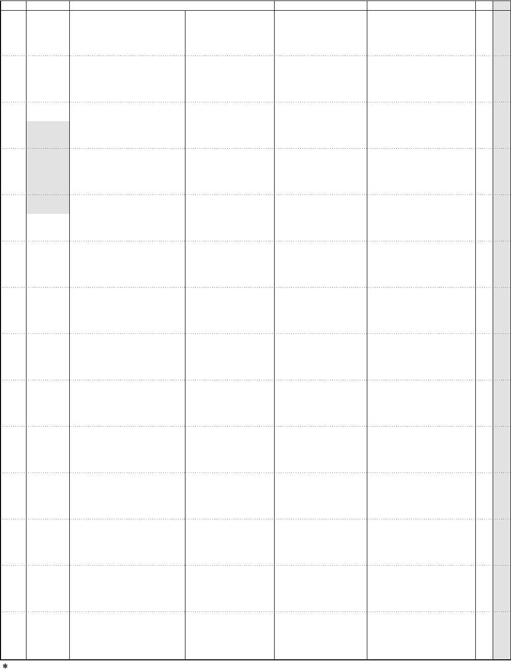
SPX2000
10
REF NO.
PART NO. DESCRIPTION REMARKS
QTY
: New Parts RANK: Japan only
RANK
D803 Diode RB160L-60 01
D804 Diode RB160L-40 TE25 01
D805 Diode RB160L-60 01
D806 Diode RB160L-40 TE25 01
-808 Diode RB160L-40 TE25 01
DA401 Diode Array DAN217 0.3A X2 01
DA402 Diode Array 1SS372 TE85L 01
DA403 Diode Array 1SS372 TE85L 01
EM201 LC Filter DSS6NF31C223Q93A 01
EM202 LC Filter DSS6NF31C223Q93A 01
EM301 LC Filter DSS6NF31C223Q93A 01
EM401 EMI Filter (chip) NFM3DCC101U1H3L 01
EM402 LC Filter DSS6NB32A271Q93A 01
EM403 LC Filter DSS6NB32A271Q93A 01
EM601 LC Filter DSS6NB32A271Q93A 01
EM602 LC Filter DSS6NB32A271Q93A 01
EM651 LC Filter DSS6NB32A271Q93A 01
EM652 LC Filter DSS6NB32A271Q93A 01
EM701 LC Filter DSS6NB32A271Q93A 01
EM702 LC Filter DSS6NB32A271Q93A 01
EM751 LC Filter DSS6NB32A271Q93A 01
EM752 LC Filter DSS6NB32A271Q93A 01
EM801 LC Filter DSS6NF31C223Q93A 01
EM805 LC Filter DSS6NF31C223Q93A 01
-807 LC Filter DSS6NF31C223Q93A 01
IC001 IC UPC2918T-E1 REGULATOR +1.8V 03
IC002 IC NJM2904V(TE1) OP AMP 02
IC003 IC TC7SH04FU INVERTER 01
IC004 IC HD6417709SF133 CPU 12
IC005 IC TC74VHC08FT AND 01
IC006 IC M62023FP SYSTEM RESET 03
IC007 IC S-80130ANMC-JCP-T2 SYSTEM RESET 01
IC009 IC W986416DH-7 SDRAM 64M 08
*IC010 IC MX29LV160ABTC-7 FL FLASH ROM 16M
*IC011 IC M5M5V216ATP-55HI SRAM 2M
IC012 IC TC74VHC32FT OR 01
IC101 IC 74LVX4245MTCX TRANSCEIVER 03
IC102 IC 74LVX4245MTCX TRANSCEIVER 03
IC103 IC TC74VHCT245AFT TRANSCEIVER 07
-106 IC TC74VHCT245AFT TRANSCEIVER 07
IC107 IC TC74VHC08FT AND 01
IC201 IC S1L51252F32S000 PLLP2(GATE ARRAY) 08
IC202 IC M51953AFP SYSTEM RESET 01
IC203 IC TC74VHCT245AFT TRANSCEIVER 07
IC204 IC TLC2932IPWR PLL 06
IC205 IC YM3436DK DIR2 11
IC206 IC TC74VHC74FT D-FF 01
IC207 IC TC74VHC04FT INVERTER 01
IC208 IC TC74VHC14FT INVERTER 02
*IC209 IC TC74VHC00FT NAND
IC210 IC TC7SH04FU INVERTER 01
IC301 IC MSM514260E-60JS DRAM 4M 07
IC302 IC MSM514260E-60JS DRAM 4M 07
IC303 IC YSS910-S DSP6 10
IC401 IC CS8415A-CS DIR 06
IC402 IC TC7SH04FU INVERTER 01
IC403 IC TC74VHC244FT BUFFER 03
IC404 IC TC74VHCT08AFT AND
IC405 IC CS8405A-CS DIT 06
IC406 IC SN75124NSR LINE RECEIVER 05
IC407 IC M37641M8-141FP CPU (USB 32K) 09
*IC408 Photo Coupler PC410L0NIP
IC501 IC TC74VHC04FT INVERTER 01
*IC502 IC S-80145ANMC-JC6-T2 SYSTEM RESET
IC601 IC UPC4570G2 OP AMP 03
IC602 IC UPC4570G2 OP AMP 03
IC603 IC CS5361-KS ADC 08
IC605 IC TC7SH04FU INVERTER 01
IC606 IC TC74VHCT245AFT TRANSCEIVER 07
IC651 IC UPC4570G2 OP AMP 03
V8409200
VS597600
V8409200
VS597600
VS597600
VV556300
V9424900
V9424900
VD542700
VD542700
VD542700
VQ761400
VI243100
VI243100
VI243100
VI243100
VI243100
VI243100
VI243100
VI243100
VI243100
VI243100
VD542700
VD542700
VD542700
X2157A00
XR532A00
XS775A00
X2081A00
XV891A00
X2163A00
X3848A00
XZ414B00
X4916A00
X3226A00
XY945A00
X3097A00
X3097A00
XT744A00
XT744A00
XV891A00
X3775A00
XW422A00
XT744A00
XV064A00
XG948E00
XV892A00
X0195A00
XV890A00
X2313A00
XS775A00
XV077B00
XV077B00
XV988A00
X2089A00
XS775A00
XW234A00
X3586A00
XZ349A00
XV930A00
X2485200
V9924900
X0195A00
X4069A00
XF291A00
XF291A00
X3447A00
XS775A00
XT744A00
XF291A00
ダイオード
ダイオード
ダイオード
ダイオード
ダイオード
ダイオードアレイ
ダイオードアレイ
ダイオードアレイ
LCフィルターEMI
LCフィルターEMI
LCフィルターEMI
エミフィル チップ
LCフィルター
LCフィルター
LCフィルター
LCフィルター
LCフィルター
LCフィルター
LCフィルター
LCフィルター
LCフィルター
LCフィルター
LCフィルターEMI
LCフィルターEMI
LCフィルターEMI
IC
IC
IC
IC
IC
IC
IC
IC
IC
IC
IC
IC
IC
IC
IC
IC
IC
IC
IC
IC
IC
IC
IC
IC
IC
IC
IC
IC
IC
IC
IC
IC
IC
IC
IC
IC
フォトカプラ
IC
IC
IC
IC
IC
IC
IC
IC
部品名

SPX2000
11
REF NO.
PART NO. DESCRIPTION REMARKS
QTY
: New Parts RANK: Japan only
RANK
IC652 IC UPC4570G2 OP AMP 03
IC701 IC AK4393-VF-E2 DAC 07
IC702 IC NJM78L05UA REGULATOR +5V 02
IC703 IC UPC4570G2 OP AMP 03
IC704 IC NJM4556AL OP AMP 02
IC753 IC UPC4570G2 OP AMP 03
IC754 IC NJM4556AL OP AMP 02
*IC801 IC NJM78M15DL1A REGULATOR +15V
*IC802 IC NJM79M15DL1A REGULATOR -15V
IC803 IC NJM78M05DL1A(TE1) REGULATOR +5V 02
IC804 IC PQ033Y3H3ZP REGULATOR +3.3V 04
JK401 Cannon Connector NC3FBH1 AES/EBU IN 06
JK402 Cannon Connector NC3MAH AES/EBU OUT 04
JK403 BNC Connector 1P YKS11-0067 WORD CLOCK IN 05
JK404 DIN Connector 5P3 YKF51-50 MIDI IN,OUT/THRU 04
JK601 Cannon Connector NC3FBH1 INPUT L 06
JK651 Cannon Connector NC3FBH1 INPUT R 06
JK701 Cannon Connector NC3MAH OUTPUT L 04
JK751 Cannon Connector NC3MAH OUTPUT R 04
K401 Cannon Angle 02
K402 Cannon Angle 02
K601 Cannon Angle 02
K651 Cannon Angle 02
K701 Cannon Angle 02
K751 Cannon Angle 02
K801 Heat Sink PUE16-30 (WB08520)
L001 Ferrite Bead BL02RN1-R62T4 01
L003 Noise Filter ZJY51R5-2P 04
L201 Ferrite Bead BL02RN1-R62T4 01
L202 Coil SSB44-331 330uH 03
L401 Ferrite Bead BL02RN1-R62T4 01
-405 Ferrite Bead BL02RN1-R62T4 01
L406 Pulse Transformer TB06A015 05
L407 Pulse Transformer TB06A015 05
L408 Noise Filter ZJY51R5-2P 04
L410 Ferrite Bead FL5R200QNT 20uH 01
-413 Ferrite Bead FL5R200QNT 20uH 01
L414 Common Mode Coil DLP31SN121SL2L 03
R001 Carbon Resistor (chip) 3.0K 63M J 01
R002 Carbon Resistor (chip) 10.0K 63M J 01
R003 Carbon Resistor (chip) 2.0K 63M J 01
R004 Carbon Resistor (chip) 100.0 63M J 01
R005 Carbon Resistor (chip) 100.0K 63M J 01
R006 Carbon Resistor (chip) 1.0M 63M J 01
R007 Carbon Resistor (chip) 10.0K 63M J 01
R011 Carbon Resistor (chip) 10.0K 63M J 01
R012 Carbon Resistor (chip) 10.0K 63M J 01
R017 Carbon Resistor (chip) 220.0 63M J 01
R020 Carbon Resistor (chip) 10.0K 63M J 01
R021 Carbon Resistor (chip) 10.0K 63M J 01
R022 Carbon Resistor (chip) 0 63M J 01
R026 Carbon Resistor (chip) 33.0 63M J 01
R027 Carbon Resistor (chip) 33.0 63M J 01
R028 Carbon Resistor (chip) 0 63M J 01
R029 Carbon Resistor (chip) 10.0K 63M J 01
R030 Carbon Resistor (chip) 1.0K 63M J 01
R033 Carbon Resistor (chip) 22.0 63M J 01
R034 Carbon Resistor (chip) 10.0 63M J 01
R035 Carbon Resistor (chip) 47.0 63M J 01
-051 Carbon Resistor (chip) 47.0 63M J 01
R052 Carbon Resistor (chip) 0 63M J 01
-056 Carbon Resistor (chip) 0 63M J 01
R102 Carbon Resistor (chip) 100.0 63M J 01
R103 Carbon Resistor (chip) 3.3K 63M J 01
R104 Carbon Resistor (chip) 10.0K 63M J 01
-108 Carbon Resistor (chip) 10.0K 63M J 01
R201 Carbon Resistor (chip) 10.0K 63M J 01
-204 Carbon Resistor (chip) 10.0K 63M J 01
R205 Carbon Resistor (chip) 100.0 63M J 01
R206 Carbon Resistor (chip) 0 63M J 01
XF291A00
XW029A00
XJ598A00
XF291A00
XP844A00
XF291A00
XP844A00
X3942A00
X3943A00
XS534A00
X2589A00
V9234300
VS133700
V6415900
VK519000
V9234300
V9234300
VS133700
VS133700
V7539800
V7539800
V7539800
V7539800
V7539800
V7539800
--
GE300610
VP246300
GE300610
V7716400
GE300610
GE300610
V7930100
V7930100
VP246300
VB835000
VB835000
V5239100
RD356300
RD357100
RD356200
RD355100
RD358100
RD359100
RD357100
RD357100
RD357100
RD355220
RD357100
RD357100
RD350000
RD354330
RD354330
RD350000
RD357100
RD356100
RD354220
RD354100
RD354470
RD354470
RD350000
RD350000
RD355100
RD356330
RD357100
RD357100
RD357100
RD357100
RD355100
RD350000
IC
IC
IC
IC
IC
IC
IC
IC
IC
IC
IC
キャノンコネクタ
キャノンコネクタ
1P BNCコネクタ
DINコネクタ2連
キャノンコネクタ
キャノンコネクタ
キャノンコネクタ
キャノンコネクタ
キャノン金具(横形)
キャノン金具(横形)
キャノン金具(横形)
キャノン金具(横形)
キャノン金具(横形)
キャノン金具(横形)
ヒートシンク
フェライトビーズ
ノイズフィルター
フェライトビーズ
コイル330U
フェライトビーズ
フェライトビーズ
パルストランス
パルストランス
ノイズフィルター
コイル 20U
コイル 20U
コモンモードコイル
チップ抵抗
チップ抵抗
チップ抵抗
チップ抵抗
チップ抵抗
チップ抵抗
チップ抵抗
チップ抵抗
チップ抵抗
チップ抵抗
チップ抵抗
チップ抵抗
チップ抵抗
チップ抵抗
チップ抵抗
チップ抵抗
チップ抵抗
チップ抵抗
チップ抵抗
チップ抵抗
チップ抵抗
チップ抵抗
チップ抵抗
チップ抵抗
チップ抵抗
チップ抵抗
チップ抵抗
チップ抵抗
チップ抵抗
チップ抵抗
チップ抵抗
チップ抵抗
部品名
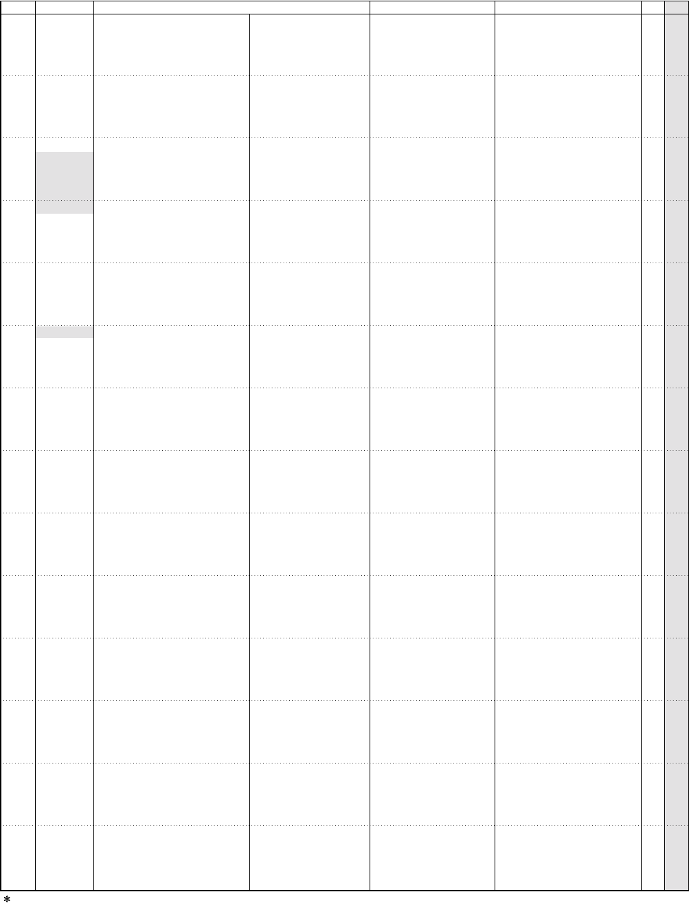
SPX2000
12
REF NO.
PART NO. DESCRIPTION REMARKS
QTY
: New Parts RANK: Japan only
RANK
R209 Carbon Resistor (chip) 150.0 63M J 01
R210 Carbon Resistor (chip) 1.5K 63M J 01
R211 Carbon Resistor (chip) 68.0 63M J 01
-217 Carbon Resistor (chip) 68.0 63M J 01
R218 Carbon Resistor (chip) 100.0 63M J 01
R219 Carbon Resistor (chip) 47.0 63M J 01
R220 Carbon Resistor (chip) 0 63M J 01
R221 Carbon Resistor (chip) 47.0 63M J 01
R222 Carbon Resistor (chip) 68.0 63M J 01
R223 Carbon Resistor (chip) 47.0 63M J 01
-225 Carbon Resistor (chip) 47.0 63M J 01
R226 Metal Film Resistor (chip) 750.0 1/10 D 01
R227 Metal Film Resistor (chip) 3.3K 1/10 D 01
R228 Metal Film Resistor (chip) 3.3K 1/10 D 01
R229 Metal Film Resistor (chip) 330.0 1/10 D 01
R230 Metal Film Resistor (chip) 3.0K 1/10 D 01
R231 Carbon Resistor (chip) 0 63M J 01
-235 Carbon Resistor (chip) 0 63M J 01
R236 Carbon Resistor (chip) 100.0 63M J 01
R237 Carbon Resistor (chip) 68.0 63M J 01
R238 Carbon Resistor (chip) 0 63M J 01
-241 Carbon Resistor (chip) 0 63M J 01
R301 Carbon Resistor (chip) 47.0 63M J 01
R302 Carbon Resistor (chip) 0 63M J 01
R401 Carbon Resistor (chip) 47.0 63M J 01
R402 Metal Film Resistor (chip) 3.9K 1/10 D 01
R403 Carbon Resistor (chip) 47.0 63M J 01
R404 Carbon Resistor (chip) 47.0K 63M J 01
-406 Carbon Resistor (chip) 47.0K 63M J 01
R408 Carbon Resistor (chip) 0 63M J 01
R409 Carbon Resistor (chip) 10.0K 63M J 01
R410 Carbon Resistor (chip) 10.0K 63M J 01
R411 Carbon Resistor (chip) 5.6K 63M J 01
R412 Carbon Resistor (chip) 4.7K 63M J 01
R413 Carbon Resistor (chip) 1.0K 63M J 01
R414 Carbon Resistor (chip) 1.0K 63M J 01
R415 Carbon Resistor (chip) 2.2K 63M J 01
R416 Carbon Resistor (chip) 110.0 63M J 01
R417 Carbon Resistor (chip) 110.0 63M J 01
R418 Carbon Resistor (chip) 680.0 63M J 01
R419 Carbon Resistor (chip) 22.0K 63M J 01
R420 Carbon Resistor (chip) 47.0 0.1 J 01
R421 Carbon Resistor (chip) 22.0K 63M J 01
R422 Carbon Resistor (chip) 75.0 0.1 J 01
R423 Carbon Resistor (chip) 220.0 63M J 01
R424 Carbon Resistor (chip) 33.0 1/4 J 01
R425 Carbon Resistor (chip) 33.0 1/4 J 01
R426 Carbon Resistor (chip) 1.5K 63M J 01
R427 Carbon Resistor (chip) 47.0 63M J 01
R428 Carbon Resistor (chip) 47.0 63M J 01
R501 Carbon Resistor (chip) 33.0 1/4 J 01
-510 Carbon Resistor (chip) 33.0 1/4 J 01
R511 Carbon Resistor (chip) 10.0K 63M J 01
R512 Carbon Resistor (chip) 220.0 63M J 01
R513 Carbon Resistor (chip) 150.0 1/4 J
R514 Carbon Resistor (chip) 180.0 1/4 J 01
R515 Carbon Resistor (chip) 180.0 1/4 J 01
R516 Carbon Resistor (chip) 10.0K 63M J 01
R517 Carbon Resistor (chip) 10.0K 63M J 01
R518 Carbon Resistor (chip) 1.0K 63M J 01
R519 Carbon Resistor (chip) 1.0K 63M J 01
R520 Carbon Resistor (chip) 10.0K 63M J 01
R521 Carbon Resistor (chip) 10.0K 63M J 01
R601 Carbon Resistor 82.0K 1/4 J 01
R602 Carbon Resistor 82.0K 1/4 J 01
R603 Metal Film Resistor 10.0K 1/4 F 01
R604 Metal Film Resistor 10.0K 1/4 F 01
R605 Metal Film Resistor 7.5K 1/4 F 01
*R606 Carbon Resistor 750.0K 1/4 J
*R607 Metal Film Resistor 30.0K 1/4 F
RD355150
RD356150
RD354680
RD354680
RD355100
RD354470
RD350000
RD354470
RD354680
RD354470
RD354470
VI194600
VI196100
VI196100
VI193700
VI196000
RD350000
RD350000
RD355100
RD354680
RD350000
RD350000
RD354470
RD350000
RD354470
VI196400
RD354470
RD357470
RD357470
RD350000
RD357100
RD357100
RD356560
RD356470
RD356100
RD356100
RD356220
RD355110
RD355110
RD355680
RD357220
RD254470
RD357220
RD254750
RD355220
RD154330
RD154330
RD356150
RD354470
RD354470
RD154330
RD154330
RD357100
RD355220
RD155150
RD155180
RD155180
RD357100
RD357100
RD356100
RD356100
RD357100
RD357100
HF757820
HF757820
VC328800
VC328800
VC328500
HF758750
VC329900
チップ抵抗
チップ抵抗
チップ抵抗
チップ抵抗
チップ抵抗
チップ抵抗
チップ抵抗
チップ抵抗
チップ抵抗
チップ抵抗
チップ抵抗
チップ金被抵抗
チップ金被抵抗
チップ金被抵抗
チップ金被抵抗
チップ金被抵抗
チップ抵抗
チップ抵抗
チップ抵抗
チップ抵抗
チップ抵抗
チップ抵抗
チップ抵抗
チップ抵抗
チップ抵抗
チップ金被抵抗
チップ抵抗
チップ抵抗
チップ抵抗
チップ抵抗
チップ抵抗
チップ抵抗
チップ抵抗
チップ抵抗
チップ抵抗
チップ抵抗
チップ抵抗
チップ抵抗
チップ抵抗
チップ抵抗
チップ抵抗
チップ抵抗
チップ抵抗
チップ抵抗
チップ抵抗
チップ抵抗
チップ抵抗
チップ抵抗
チップ抵抗
チップ抵抗
チップ抵抗
チップ抵抗
チップ抵抗
チップ抵抗
チップ抵抗
チップ抵抗
チップ抵抗
チップ抵抗
チップ抵抗
チップ抵抗
チップ抵抗
チップ抵抗
チップ抵抗
カーボン抵抗
カーボン抵抗
金属被膜抵抗
金属被膜抵抗
金属被膜抵抗
カーボン抵抗
金属被膜抵抗
部品名
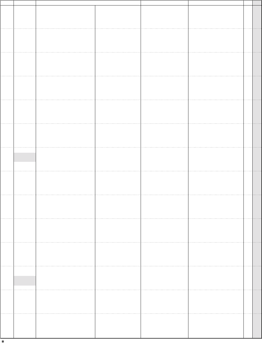
SPX2000
13
REF NO.
PART NO. DESCRIPTION REMARKS
QTY
: New Parts RANK: Japan only
RANK
R608 Metal Film Resistor 7.5K 1/4 F 01
*R609 Metal Film Resistor 30.0K 1/4 F
R610 Carbon Resistor 39.0 1/4 J 01
*R611 Carbon Resistor 750.0K 1/4 J
R612 Metal Film Resistor 56.0K 1/4 F 01
R613 Carbon Resistor 39.0 1/4 J 01
R614 Metal Film Resistor 4.7K 1/4 F 01
R615 Metal Film Resistor 10.0K 1/4 F 01
R616 Metal Film Resistor 22.0K 1/4 F 01
R617 Metal Film Resistor 2.7K 1/4 F 01
R618 Metal Film Resistor 3.0K 1/4 F 01
R619 Metal Film Resistor 2.2K 1/4 F 01
R620 Metal Film Resistor 1.0K 1/4 F 01
R621 Metal Film Resistor 2.2K 1/4 F 01
R622 Carbon Resistor 150.0 1/4 J 01
R623 Carbon Resistor 150.0 1/4 J 01
R624 Metal Film Resistor 22.0K 1/4 F 01
R625 Metal Film Resistor 1.5K 1/4 F
R626 Metal Film Resistor 4.7K 1/4 F 01
R629 Carbon Resistor (chip) 0 63M J 01
R630 Carbon Resistor (chip) 47.0 63M J 01
-632 Carbon Resistor (chip) 47.0 63M J 01
R633 Carbon Resistor (chip) 0 63M J 01
R634 Carbon Resistor (chip) 47.0 63M J 01
R635 Carbon Resistor (chip) 47.0 63M J 01
R636 Carbon Resistor (chip) 100.0 63M J 01
R637 Carbon Resistor (chip) 47.0 63M J 01
R638 Carbon Resistor (chip) 100.0 63M J 01
R639 Carbon Resistor (chip) 100.0 63M J 01
R640 Carbon Resistor (chip) 10.0K 63M J 01
R641 Carbon Resistor (chip) 10.0K 63M J 01
R642 Metal Film Resistor (chip) 75.0K 1/10 D 01
-645 Metal Film Resistor (chip) 75.0K 1/10 D 01
*R646 Carbon Resistor 750.0K 1/4 J
R651 Carbon Resistor 82.0K 1/4 J 01
R652 Carbon Resistor 82.0K 1/4 J 01
R653 Metal Film Resistor 10.0K 1/4 F 01
R654 Metal Film Resistor 10.0K 1/4 F 01
R655 Metal Film Resistor 7.5K 1/4 F 01
*R656 Carbon Resistor 750.0K 1/4 J
*R657 Metal Film Resistor 30.0K 1/4 F
R658 Metal Film Resistor 7.5K 1/4 F 01
*R659 Metal Film Resistor 30.0K 1/4 F
R660 Carbon Resistor 39.0 1/4 J 01
*R661 Carbon Resistor 750.0K 1/4 J
R662 Metal Film Resistor 56.0K 1/4 F 01
R663 Carbon Resistor 39.0 1/4 J 01
R664 Metal Film Resistor 4.7K 1/4 F 01
R665 Metal Film Resistor 10.0K 1/4 F 01
R666 Metal Film Resistor 22.0K 1/4 F 01
R667 Metal Film Resistor 2.7K 1/4 F 01
R668 Metal Film Resistor 2.2K 1/4 F 01
R669 Metal Film Resistor 3.0K 1/4 F 01
R670 Metal Film Resistor 1.0K 1/4 F 01
R671 Metal Film Resistor 2.2K 1/4 F 01
R672 Carbon Resistor 150.0 1/4 J 01
R673 Carbon Resistor 150.0 1/4 J 01
R692 Metal Film Resistor (chip) 75.0K 1/10 D 01
-695 Metal Film Resistor (chip) 75.0K 1/10 D 01
*R696 Carbon Resistor 750.0K 1/4 J
R701 Carbon Resistor (chip) 68.0 63M J 01
R702 Carbon Resistor (chip) 0 63M J 01
R703 Carbon Resistor (chip) 100.0 63M J 01
R704 Carbon Resistor (chip) 0 63M J 01
-706 Carbon Resistor (chip) 0 63M J 01
R708 Carbon Resistor (chip) 0 63M J 01
R709 Metal Film Resistor 1.5K 1/4 F
R710 Metal Film Resistor 1.5K 1/4 F
R711 Metal Film Resistor 6.8K 1/4 F 01
R713 Metal Film Resistor 1.5K 1/4 F
VC328500
VC329900
HF754390
HF758750
VC330600
HF754390
VC328000
VC328800
VC329600
VC327400
VC327500
VC327200
VC326500
VC327200
HF755150
HF755150
VC329600
VC326800
VC328000
RD350000
RD354470
RD354470
RD350000
RD354470
RD354470
RD355100
RD354470
RD355100
RD355100
RD357100
RD357100
VI199500
VI199500
HF758750
HF757820
HF757820
VC328800
VC328800
VC328500
HF758750
VC329900
VC328500
VC329900
HF754390
HF758750
VC330600
HF754390
VC328000
VC328800
VC329600
VC327400
VC327200
VC327500
VC326500
VC327200
HF755150
HF755150
VI199500
VI199500
HF758750
RD354680
RD350000
RD355100
RD350000
RD350000
RD350000
VC326800
VC326800
VC328400
VC326800
金属被膜抵抗
金属被膜抵抗
カーボン抵抗
カーボン抵抗
金属被膜抵抗
カーボン抵抗
金属被膜抵抗
金属被膜抵抗
金属被膜抵抗
金属被膜抵抗
金属被膜抵抗
金属被膜抵抗
金属被膜抵抗
金属被膜抵抗
カーボン抵抗
カーボン抵抗
金属被膜抵抗
金属被膜抵抗
金属被膜抵抗
チップ抵抗
チップ抵抗
チップ抵抗
チップ抵抗
チップ抵抗
チップ抵抗
チップ抵抗
チップ抵抗
チップ抵抗
チップ抵抗
チップ抵抗
チップ抵抗
チップ金被抵抗
チップ金被抵抗
カーボン抵抗
カーボン抵抗
カーボン抵抗
金属被膜抵抗
金属被膜抵抗
金属被膜抵抗
カーボン抵抗
金属被膜抵抗
金属被膜抵抗
金属被膜抵抗
カーボン抵抗
カーボン抵抗
金属被膜抵抗
カーボン抵抗
金属被膜抵抗
金属被膜抵抗
金属被膜抵抗
金属被膜抵抗
金属被膜抵抗
金属被膜抵抗
金属被膜抵抗
金属被膜抵抗
カーボン抵抗
カーボン抵抗
チップ金被抵抗
チップ金被抵抗
カーボン抵抗
チップ抵抗
チップ抵抗
チップ抵抗
チップ抵抗
チップ抵抗
チップ抵抗
金属被膜抵抗
金属被膜抵抗
金属被膜抵抗
金属被膜抵抗
部品名
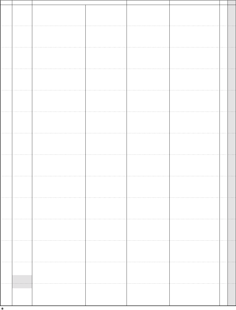
SPX2000
14
REF NO.
PART NO. DESCRIPTION REMARKS
QTY
: New Parts RANK: Japan only
RANK
R714 Metal Film Resistor 1.5K 1/4 F
R715 Metal Film Resistor 6.8K 1/4 F 01
R717 Carbon Resistor 39.0 1/4 J 01
R718 Metal Film Resistor 9.1K 1/4 F 01
R719 Metal Film Resistor 2.2K 1/4 F 01
R721 Metal Film Resistor 1.0K 1/4 F 01
R722 Carbon Resistor 39.0 1/4 J 01
R723 Metal Film Resistor 10.0K 1/4 F 01
R724 Metal Film Resistor 10.0K 1/4 F 01
R725 Metal Film Resistor 11.0K 1/4 F 01
*R726 Metal Film Resistor 82.00 1/4 F
R727 Metal Film Resistor 10.0K 1/4 F 01
R728 Metal Film Resistor 20.0K 1/4 F 01
R729 Metal Film Resistor 20.0K 1/4 F 01
R730 Metal Film Resistor 18.0K 1/4 F 01
R731 Metal Film Resistor 18.0K 1/4 F 01
R732 Metal Film Resistor 75.00 1/4 F 01
R733 Metal Film Resistor 75.00 1/4 F 01
R734 Carbon Resistor 47.0K 1/4 J 01
R735 Carbon Resistor 47.0K 1/4 J 01
R736 Carbon Resistor (chip) 6.8K 0.1 J 01
R737 Carbon Resistor (chip) 6.8K 0.1 J 01
R738 Carbon Resistor (chip) 10.0K 0.1 J 01
R739 Carbon Resistor (chip) 33.0K 0.1 J 01
R740 Carbon Resistor (chip) 100.0K 0.1 J 01
R741 Carbon Resistor (chip) 100.0K 0.1 J 01
R746 Metal Film Resistor 2.7K 1/4 F 01
R747 Metal Film Resistor 2.7K 1/4 F 01
R759 Metal Film Resistor 1.5K 1/4 F
R760 Metal Film Resistor 1.5K 1/4 F
R761 Metal Film Resistor 6.8K 1/4 F 01
R763 Metal Film Resistor 1.5K 1/4 F
R764 Metal Film Resistor 1.5K 1/4 F
R765 Metal Film Resistor 6.8K 1/4 F 01
R767 Carbon Resistor 39.0 1/4 J 01
R768 Metal Film Resistor 9.1K 1/4 F 01
R769 Metal Film Resistor 2.2K 1/4 F 01
R771 Metal Film Resistor 1.0K 1/4 F 01
R772 Carbon Resistor 39.0 1/4 J 01
R773 Metal Film Resistor 10.0K 1/4 F 01
R774 Metal Film Resistor 10.0K 1/4 F 01
R775 Metal Film Resistor 11.0K 1/4 F 01
*R776 Metal Film Resistor 82.00 1/4 F
R777 Metal Film Resistor 10.0K 1/4 F 01
R778 Metal Film Resistor 20.0K 1/4 F 01
R779 Metal Film Resistor 20.0K 1/4 F 01
R780 Metal Film Resistor 18.0K 1/4 F 01
R781 Metal Film Resistor 18.0K 1/4 F 01
R782 Metal Film Resistor 75.00 1/4 F 01
R783 Metal Film Resistor 75.00 1/4 F 01
R784 Carbon Resistor 47.0K 1/4 J 01
R785 Carbon Resistor 47.0K 1/4 J 01
R786 Carbon Resistor (chip) 6.8K 0.1 J 01
R787 Carbon Resistor (chip) 6.8K 0.1 J 01
R796 Metal Film Resistor 2.7K 1/4 F 01
R797 Metal Film Resistor 2.7K 1/4 F 01
R801 Carbon Resistor (chip) 1.0K 63M J 01
R802 Carbon Resistor (chip) 68.0 1/4 J 01
R803 Carbon Resistor (chip) 110.0 1/4 J 01
R804 Carbon Resistor (chip) 2.7K 63M J 01
R805 Carbon Resistor (chip) 110.0 1/4 J 01
R806 Carbon Resistor (chip) 68.0 63M J 01
R807 Carbon Resistor (chip) 10.0K 63M J 01
R808 Metal Film Resistor (chip) 39.0K 1/10 D 01
R809 Metal Film Resistor (chip) 75.0K 1/10 D 01
-815 Metal Film Resistor (chip) 75.0K 1/10 D 01
RA001 Resistor Array 10KX4 01
-025 Resistor Array 10KX4 01
RA101 Resistor Array 10KX4 01
-106 Resistor Array 10KX4 01
VC326800
VC328400
HF754390
VC328700
VC327200
VC326500
HF754390
VC328800
VC328800
VC328900
VC323700
VC328800
VC329500
VC329500
VC329400
VC329400
VC323600
VC323600
HF757470
HF757470
RD256680
RD256680
RD257100
RD257330
RD258100
RD258100
VC327400
VC327400
VC326800
VC326800
VC328400
VC326800
VC326800
VC328400
HF754390
VC328700
VC327200
VC326500
HF754390
VC328800
VC328800
VC328900
VC323700
VC328800
VC329500
VC329500
VC329400
VC329400
VC323600
VC323600
HF757470
HF757470
RD256680
RD256680
VC327400
VC327400
RD356100
RD154680
RD155110
RD356270
RD155110
RD354680
RD357100
VI198800
VI199500
VI199500
RE047100
RE047100
RE047100
RE047100
金属被膜抵抗
金属被膜抵抗
カーボン抵抗
金属被膜抵抗
金属被膜抵抗
金属被膜抵抗
カーボン抵抗
金属被膜抵抗
金属被膜抵抗
金属被膜抵抗
金属被膜抵抗
金属被膜抵抗
金属被膜抵抗
金属被膜抵抗
金属被膜抵抗
金属被膜抵抗
金属被膜抵抗
金属被膜抵抗
カーボン抵抗
カーボン抵抗
チップ抵抗
チップ抵抗
チップ抵抗
チップ抵抗
チップ抵抗
チップ抵抗
金属被膜抵抗
金属被膜抵抗
金属被膜抵抗
金属被膜抵抗
金属被膜抵抗
金属被膜抵抗
金属被膜抵抗
金属被膜抵抗
カーボン抵抗
金属被膜抵抗
金属被膜抵抗
金属被膜抵抗
カーボン抵抗
金属被膜抵抗
金属被膜抵抗
金属被膜抵抗
金属被膜抵抗
金属被膜抵抗
金属被膜抵抗
金属被膜抵抗
金属被膜抵抗
金属被膜抵抗
金属被膜抵抗
金属被膜抵抗
カーボン抵抗
カーボン抵抗
チップ抵抗
チップ抵抗
金属被膜抵抗
金属被膜抵抗
チップ抵抗
チップ抵抗
チップ抵抗
チップ抵抗
チップ抵抗
チップ抵抗
チップ抵抗
チップ金被抵抗
チップ金被抵抗
チップ金被抵抗
抵抗アレイ
抵抗アレイ
抵抗アレイ
抵抗アレイ
部品名
SPX2000
15
REF NO.
PART NO. DESCRIPTION REMARKS
QTY
: New Parts RANK: Japan only
RANK
RA201 Resistor Array 10KX4 01
RA401 Resistor Array 47KX4 01
RA402 Resistor Array 47KX4 01
RA501 Resistor Array 10KX4 01
SW601 Slide Switch SSSU141800 INPUT -10dBu/+4dBu 03
SW701 Slide Switch SSSU122-S09N0 OUTPUT -10dBU/+4dBu 01
*T801 Inverter Transformer 19LDH-132
TA501 Transistor Array TD62783AF(EL)
TA502 Transistor Array TD62783AF(EL)
TA503 Transistor Array TD62309F(EL) 04
TA504 Transistor Array TD62309F(EL) 04
TH801 Protector Switch RUE300 3.00A 30V 03
TR001 Digital Transistor DTC143XKA TP 01
TR401 Transistor 2SC2412K Q,R,S 01
TR402 Transistor 2SC2412K Q,R,S 01
TR501 Digital Transistor DTC114EKA TP 01
-506 Digital Transistor DTC114EKA TP 01
TR701 Transistor 2SD1979 S,T 01
TR702 Transistor 2SD1979 S,T 01
TR703 Digital Transistor DTC114EKA TP 01
TR704 Digital Transistor DTC114EKA TP 01
TR705 Transistor 2SA1576A T106 01
TR751 Transistor 2SD1979 S,T 01
TR752 Transistor 2SD1979 S,T 01
TR801 Transistor 2SC2712 GR 01
TR802 Transistor 2SC3709A O,Y 03
X001 Quartz Crystal Unit 11MHz MA-406 02
X201 Quartz Crystal Unit 49.152MHz DSO751SB
X202 Quartz Crystal Unit 45.1584M DSO751SB
X301 Quartz Crystal Unit 60MHz DSO751S 06
X401 Quartz Crystal Unit 16MHz SMD-49 04
ZD801 Zener Diode HZK3CTR 3.3V 01
ZD802 Zener Diode RLZ11B 11.0V 01
Z
AC Inlet 3P M1908-C 03
*LCD EW10212YMR
Z
Lithium Battery CR2032 03
Z
Power Supply Unit ZWS50AF-5/J 19
RE047100
RE047470
RE047470
RE047100
V8190000
VU120200
WB440600
V9615500
V9615500
VY703900
VY703900
VV458100
V3033500
VV556400
VV556400
VV655400
VV655400
V2993500
V2993500
VV655400
VV655400
VR936300
V2993500
V2993500
VV925400
V9702100
WA002000
V8904500
V8904400
VZ156100
VP864900
V9544100
VK040100
V5065200
WB448400
VN103500
V9702900
抵抗アレイ
抵抗アレイ
抵抗アレイ
抵抗アレイ
スライドSW
スライドSW
インバータトランス
トランジスタアレイ
トランジスタアレイ
トランジスタアレイ
トランジスタアレイ
ポリスイッチ
デジタルトランジスタ
トランジスタ
トランジスタ
デジタルトランジスタ
デジタルトランジスタ
トランジスタ
トランジスタ
デジタルトランジスタ
デジタルトランジスタ
トランジスタ
トランジスタ
トランジスタ
トランジスタ
トランジスタ
水晶振動子
水晶発振器
水晶発振器
水晶発振器
水晶振動子
ツェナーダイオード
ツェナーダイオード
ACインレット 3P
液晶ディスプレイ
リチウム電池
電源ユニット
部品名
CONTENTS
BLOCK DIAGRAM(ブロックダイアグラム) ..............................3
OVERALL CONNECTOR CIRCUIT DIAGRAM
(総コネクタ接続回路図)................................................................. 4
OVERALL CIRCUIT DIAGRAM(総回路図)
MAIN (001-009) ........................................................... 5 – 13
PN1-3, POWER, JKIN, JKOUT, VOL, FOOTSW .............. 14
CIRCUIT DIAGRAM
Note : See parts list for details of circuit board conponent parts.
Notation for Circuit Diagrams
How to identify inter-sheet connectors(シート間コネクタの読み方について)
The 3-digit number indicates the destination page.
Signal name
This indicates the location of the counter inter-sheet connector.
(The alphabet indicates horizontal direction and the number
indicates vertical direction.)
(目次)
注:シートの部品詳細は、パーツリストをご参照ください。
(回路図表記上の注意)
(3桁の数字は信号の行先ページを示します。)
対応するシート間コネクタのあるロケーションを示します。
(アルファベットが水平方向、数字が垂直方向)
(信号名)
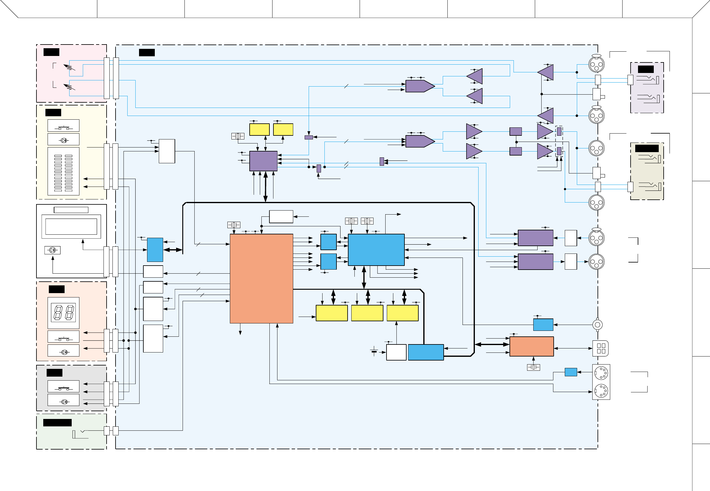
ABCDEFGH
1
2
3
4
5
6
SPX2000
3
■ BLOCK DIAGRAM
28CA1-8828882
MAIN
FOOTSW
PN3
PN2
PN1
JKIN
JKOUT
8
10
4
3
VOL
R
L
R
IN
OUT
WORD CLOCK
IN
USB
TO HOST
AES/EBU
L (MONO)
L (MONO)
R
L
R
INPUT
OUTPUT
+4dBu
-10dBu
+4dBu
-10dBu
IN
OUT/
THRU
MIDI
VR601
CN601 CN602
CN001 CN501
CN101
CN101
CN502
CN201
CN503
CN701 CN002
KEY x 2
LED x 14
METER (x 24)
BACK LIGHT LED
LCD 16 x 2
MEMORY
7 seg LED ( x 14)
KEY x 1
LED x 3
/SC [7-5]
KEY x 15 /SC [6-0]
LD [5-0]
LED x 7
LD [8]
JK701
FOOT SW
7P
7P
14P
14P20P
20P
10P
10P
15P
15P
2P
2P
CN601
CN701
CN401
CN501
7P
7P
6P
6P
/KD [0]
/KD [2-1], TKD /KD [2-0], TKD
+3.3D
IC501
TR505, 506
IC105
(20P)
TR501-503
INVERTER
+5D
+5D
+5D
/CSLCD
DB5V [7-0]
TRANSCEIVER
BLD [2-0]
PORT
PORT
PORT
PORT
PORT
PORT
/CS0
/CS2
/CS3
/CS5
/CS6
TAP LED
SC [7-0]
LED [9-0]
DRIVER
TR504
TA503, 504
DRIVER
Switch LED
SCAN
DRIVER
TA501, 502
LED DATA
DRIVER
xtal/extal
155,156
199-201,203
182,184,190
23-26,28,30-32
13-18,20,21,91,92
159
180
193
4
5
10
3
15
23
78
190
144
180
8,9
19 26 39,40
6
10
14,15
70,71
14
13
2,9
2,9 4,5
25,26
14
18
10
21,12,13
21,16,17
5
1,2,75-80
199 197 200
177
131
125
73,75,
101,63 149,150,
157-159
179
113
118
117
107
112
170
202
168 174
96,98,99,
101,102
X001
11MHz
X301
60MHz
+3.3D
+3.3D
+3.3D
+3.3D
+3.3D +3.3D +3.3B
+3.3B
+1.8D
CPU
SH7709S (X2081A00)
CPU 132MHz/BUS 44MHz
clock mode: 2 (PLL x 4)
CS0:16bit
CS2:16bit
CS3:16bit
CS4:16bit
CS5:16bit
CS6:16bit
big endian
IC004 (208P)
/SYSRES SYSTEM
RESET
IC007
CS_DIR
CS_DIT
PLLINH
/RESADA
/RES_2TR
/RESDSP
/RESDIR
/RESUSB
+5D
+5D 3
55
57
56
65
11
10 83
2
5,3,7
4-6
20,21
20
5,6
5,6
7
7
1
1
2
2
1,7
1,7
3
3
7
7
6
6
22,23
17
4
9
1
1
9
IC404
IC404
IC404
13 12
+5D +5D
IC204 (14P)
IC201 (208P)
IC009 (54P) IC010 (54P)
IC002
IC006 IC101, 102 (24P)
IC011 (44P)
+5D
CPUD [15-0]
/CS3
/CS0
/CS2
PLL
TLC2932 PLLP2
Clock Generator
IC205 (44P)
PLL
DIR2
X201
49MHz
X202
45MHz
/CSUSB
/CSLCD
/CSDSP601
CSIO5V
M265FS/M128FS/M64FS/MWC/MSYNC
M64FS/MWC/ANA256FS
M64FS/MWC/ANA256FS
ANA256FS
/ANAMUTE
/MUTE2TR01
/MUTEADDA
/CS5, /CS6
64Mbit
SDRAM
IC301 (40P)
4Mbit
DRAM
IC302 (40P)
4Mbit
DRAM
16Mbit
FLASH ROM 2Mbit
SRAM
Battery
Control
LEVEL CHANGE
LVX4245 x 2
/CSDSP6
/CSIO5V
RX_MIDI
TX_MIDI
/RESUSB
DB5V [7-0]
/CSUSB
+5D
+5D
+5D
+5D L406
L407
USB CPU
M37641M8
IC407 (80P)
X401
16MHz
Receiver
SN75124
IC406
PC
IC408
JK404
CN401
JK403
BNCWCIN
DB5V [15-0]
Pulse
Trans
Pulse
Trans
DIR
CS8415
IC401 (28P)
DIT
CS8405
IC405 (28P)
CS_DIT, /RES_2TR
M265FS/M64FS/MWC
M265FS/M64FS/MWC
AES_WC256
CS_DIR, /RES_2TR
JK751
SW701
SW601
JK701
JK501
JK401
JK402
JK502
JK651
JK601
JK401
JK402
/ANAMUTE
/POWERMUTE
+15A
+15A
+15A
+15A
+15A
+5D +5A
+5D +5A
+15A
+15A
IC601, 602 IC601
IC651
IC651, 652
+15A
-15A
-15A
-15A
-15A
-15A
-15A
-15A
-15A
IC703
IC704
IC753
IC754
ATT
BA
IC703
BA HA
HA
BA
BA
IC753
ATT
D/A
AK4393
A/D
CS5361
/RESADA
/RESADA
/MUTEADDA
MUTE
MUTE
MUTE
MUTE
2ch/line
2ch/line
2ch/line
2ch/line
/MUTE2TR01
/MUTEADDA
DSP6
#1
IC303 (176P)
/RESDSP
/CSDSP6_1
DB5V [15-0]
M128FS/MSYNC
IC701 (28P)
IC603 (24P)
INPUT
LCD MODULE
ANAIN
AESOUT
AESIN
CKIO1
(44MHz)
L
R
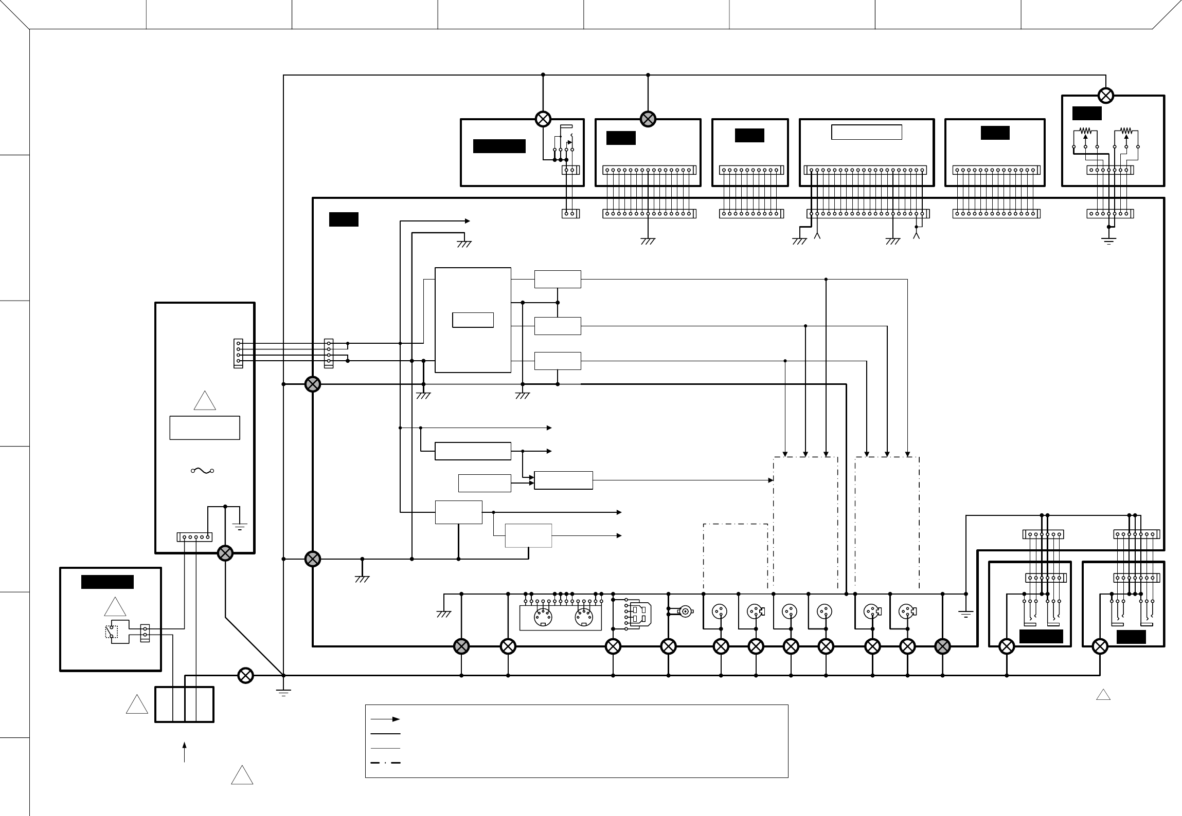
ABCDEFGH
1
2
3
4
5
6
SPX2000
4
VOL
CN601
CN602
CN001
CN501
CN101
CN101CN201
CN701
CN801
CN301
CN502
CN503
CN002
PN1
17
17
1
1
14
14
Metal fitting + nut
(金具 + ナット)
LCD MODULE
1
1
20
20
LDG LDG
+5LD
+5LD
1
110
10
DG
1
1
15
15
PN3
Metal fitting + nut
(金具 + ナット)
Metal fitting + nut
(金具 + ナット) Metal fitting + nut
(金具 + ナット)
Metal fitting + screw
(金具 + ネジ)
Metal fitting
+ screw
(金具 + ネジ)
FOOTSW
12
12
LDG
LED,LCD
+5LD
+5DA
DC/DC
+15V reg
IC801
+15A (Op Amp, DAC)
+5A (ADC/DAC)
-15A (Op Amp)
-15V reg
IC802
+5V reg
IC803
+1.8V reg
IC001
+3.3V reg
IC804
CPU
AG
+5D
+3.3D
+1.8D
Power off (CPU)
Power off DET
Mute Drive Audio-MUTE (Output Tr MUTE)
SH3, DSP6, ATSC2, memory
SH3
AES/EBU DA AD
FG
FG
CN701
CN501
CN601
CN401
DSP6, PLL, USB, AES/EBU, memory, ADC/DAC
GND
DAG
MAIN
41
41
POWER SUPPLY
UNIT
!
DG
DG
NL
15
21
!
POWER
!
AC INLET
3-core AC cord
(3芯ACコード)!
FG frame
(筐体)
FG
117
1716
6
JKIN
JKOUT
Power supply and Audio MUTE/Power Off signal(電源及びAudio MUTE/Power Off信号)
Ground (wiring between pattern in P.C.B. and sheet)(グランド(基板内パターン及びシート間配線))
Function block(機能ブロック)
Signal connection(信号接続)
PN2
P.C.B. installation
screw
(基板取付ネジ)
P.C.B. installation
screw
(基板取付ネジ)
P.C.B. installation
screw
(基板取付ネジ)
P.C.B. installation screw
(基板取付ネジ)
P.C.B. installation screw
(基板取付ネジ)
P.C.B. installation screw
(基板取付ネジ)
Toothed ground lug
+ screw
(歯付きアースラグ
+ ネジ)
Metal fitting
+ screw
(金具 + ネジ)
Metal fitting
+ screw
(金具 + ネジ)
Metal fitting
+ screw
(金具 + ネジ)
Metal fitting
+ screw
(金具 + ネジ)
Metal fitting
+ screw
(金具 + ネジ)
Metal fitting
+ screw
(金具 + ネジ)
Metal fitting
+ screw
(金具 + ネジ)
CN51
CN1
F1
■ OVERALL CONNECTOR CIRCUIT DIAGRAM
WARNING
Components having special characteristics are marked
Z
and must be
replaced with parts having specification equal to those originally installed.
28CA1-8828882 1
Z
印の部品は、安全を維持するために重要な部品です。
交換する場合は、安全のために必ず指定の部品をご使用ください。
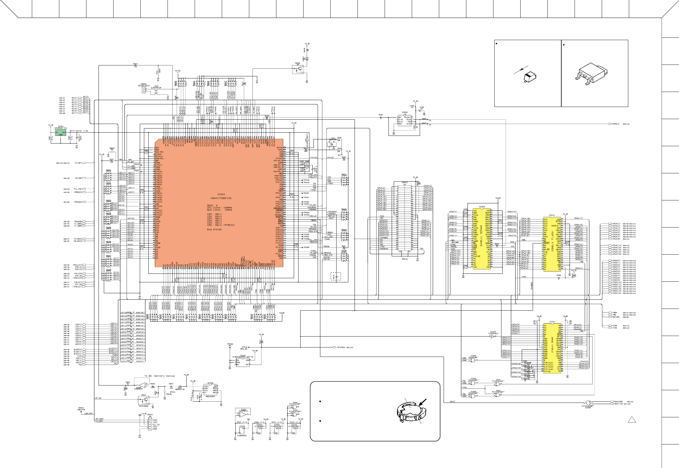
SPX2000
5
■ OVERALL CIRCUIT DIAGRAM 001 (MAIN 1/9)
XWVUTSRQPONMLKJ I HGFEDCBA
1
2
3
4
5
6
7
8
9
10
11
12
13
14
15
16
17
CPU
to FOOTSW-CN701
REGULATOR
+1.8V
SYSTEM RESET
BATTERY CONTROL
SDRAM
64M
FLASH ROM
16M
SRAM
2M
INVERTER
AND
OR
AND
not used
(for check)
Detection voltage: 2.7V
Detection voltage: 3.0V
socket
XX : not installed(未実装部品)
not installed
Battery VN103500
VN103600(Battery holder for VN103500)
Notice for back-up battery removal.
Push the battery as shown in figure,
then the battery will pop up.
Druk de batterij naar beneden zoals
aangeven in de tekening, de batterij
springt dan naar voren.
Battery
Battery holder
µPC2918T-E1(X2157A00)
REGULATOR +1.8V
1
4
3
21: INPUT
2: GND
3: OUTPUT
4: GND
RB500V-40 (V2376600)
DIODE
1: ANODE
2: CATHODE
2
1
Z
28CC1-8828883-1 2
■ OVERALL CIRCUIT DIAGRAM 001 (MAIN 1/9)
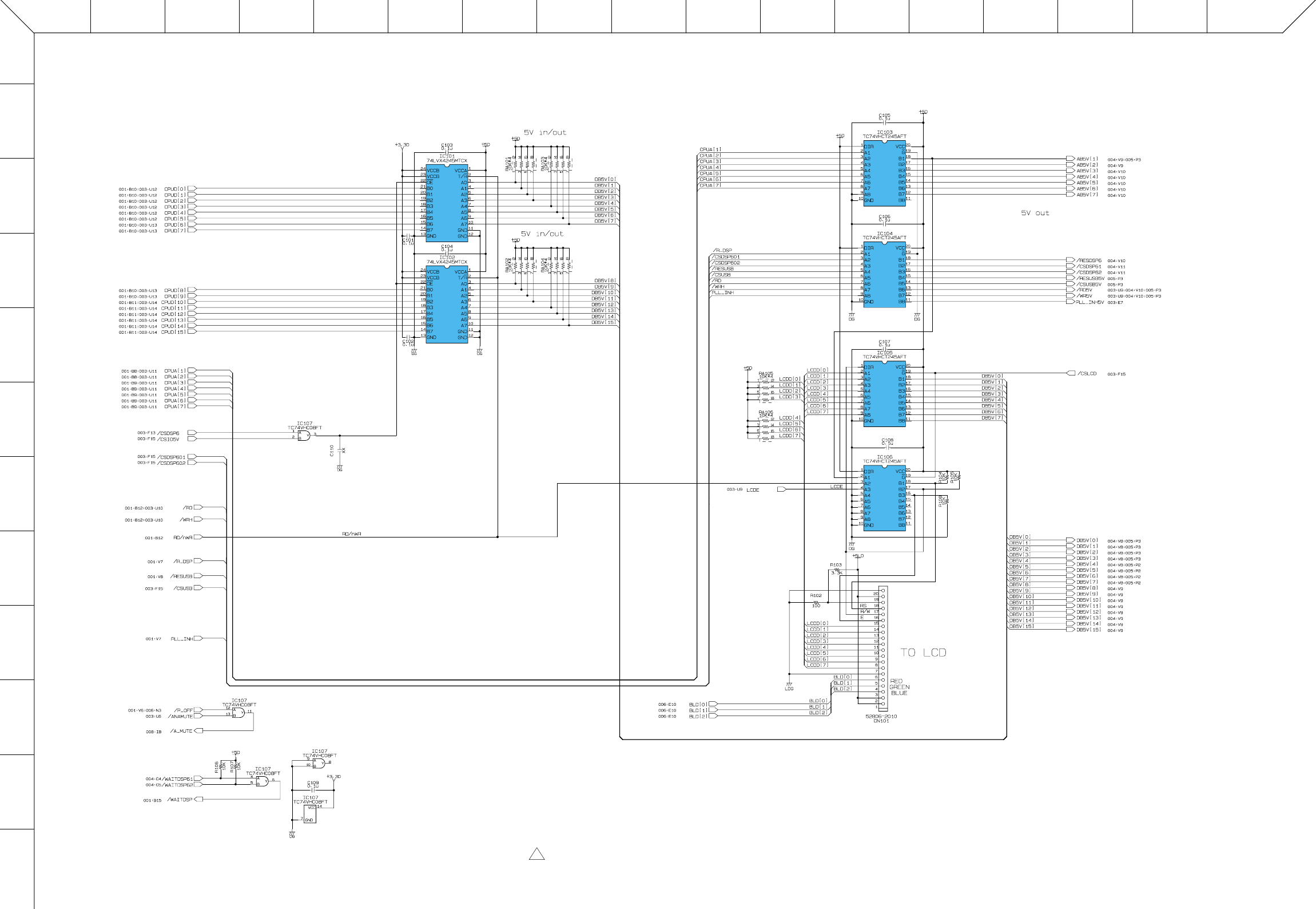
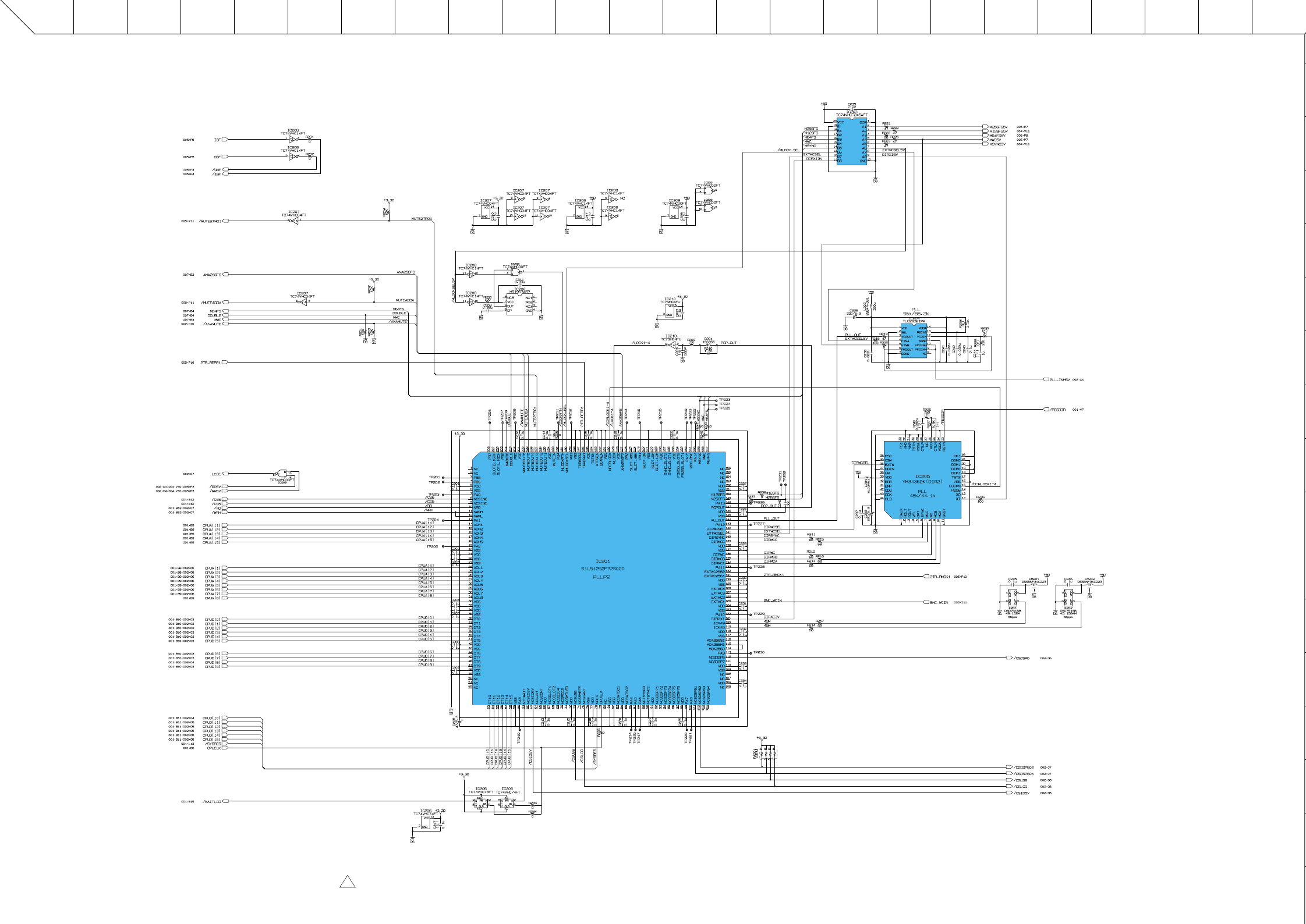
SPX2000
7
■ OVERALL CIRCUIT DIAGRAM 003 (MAIN 3/9)
XWVUTSRQPONMLKJ I HGFEDCBA
XX : not installed(未実装部品)
( F ) : Metal Film Resistor(金属皮膜抵抗)
(マ) : Mylar Capacitor(マイラコンデンサ)
(フ) : Film Capcitor(フィルムコンデンサ)
(セ) : Ceramic Capcitor(セラミックコンデンサ)
INVERTER
INVERTER
NAND
PLLP2
(Clock Generator)
INVERTER NAND
RESET
INVERTER
TRANSCEIVER
PLL
DIR2
D-FF
28CC1-8828883-3 1 ■ OVERALL CIRCUIT DIAGRAM 003 (MAIN 3/9)
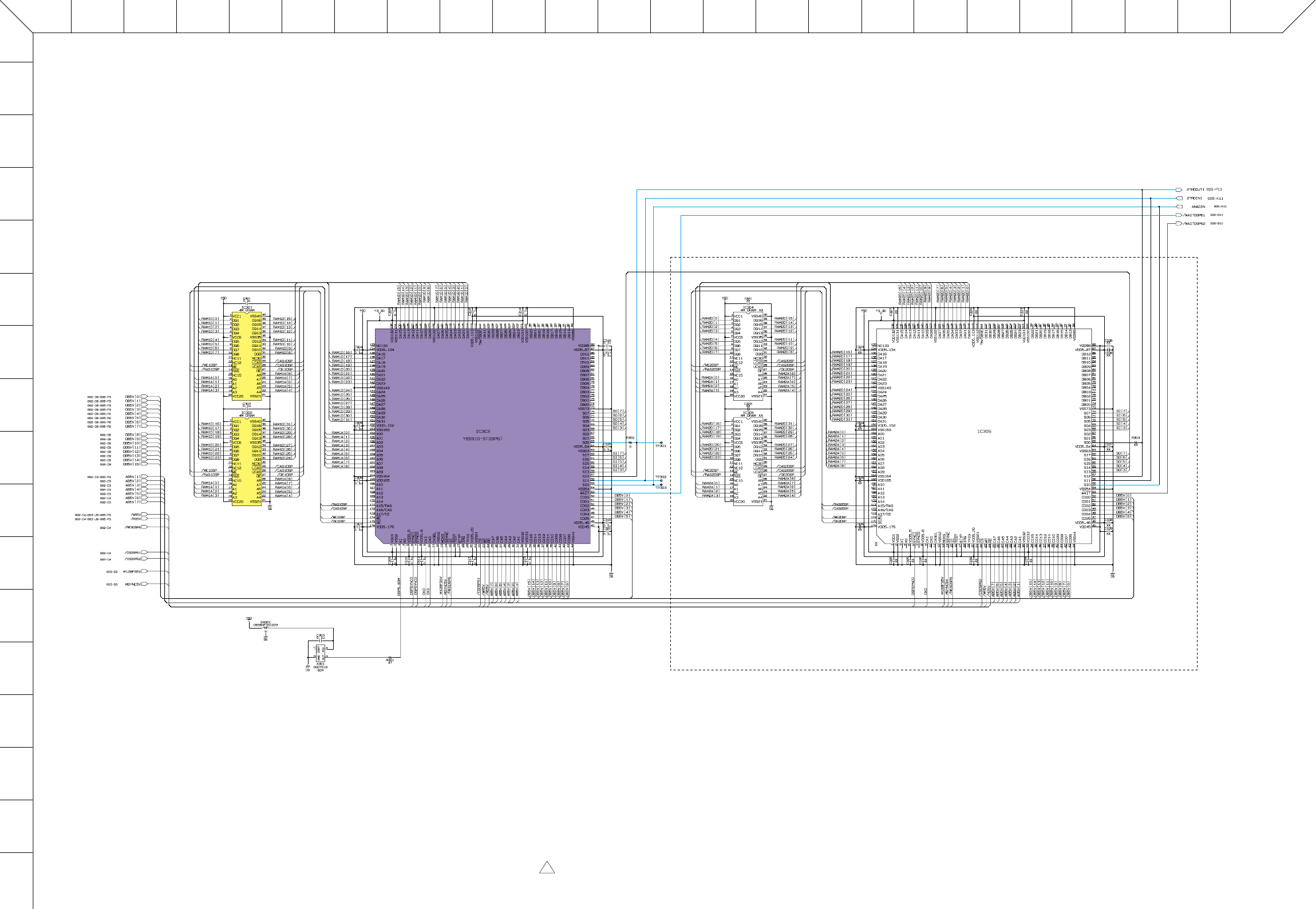
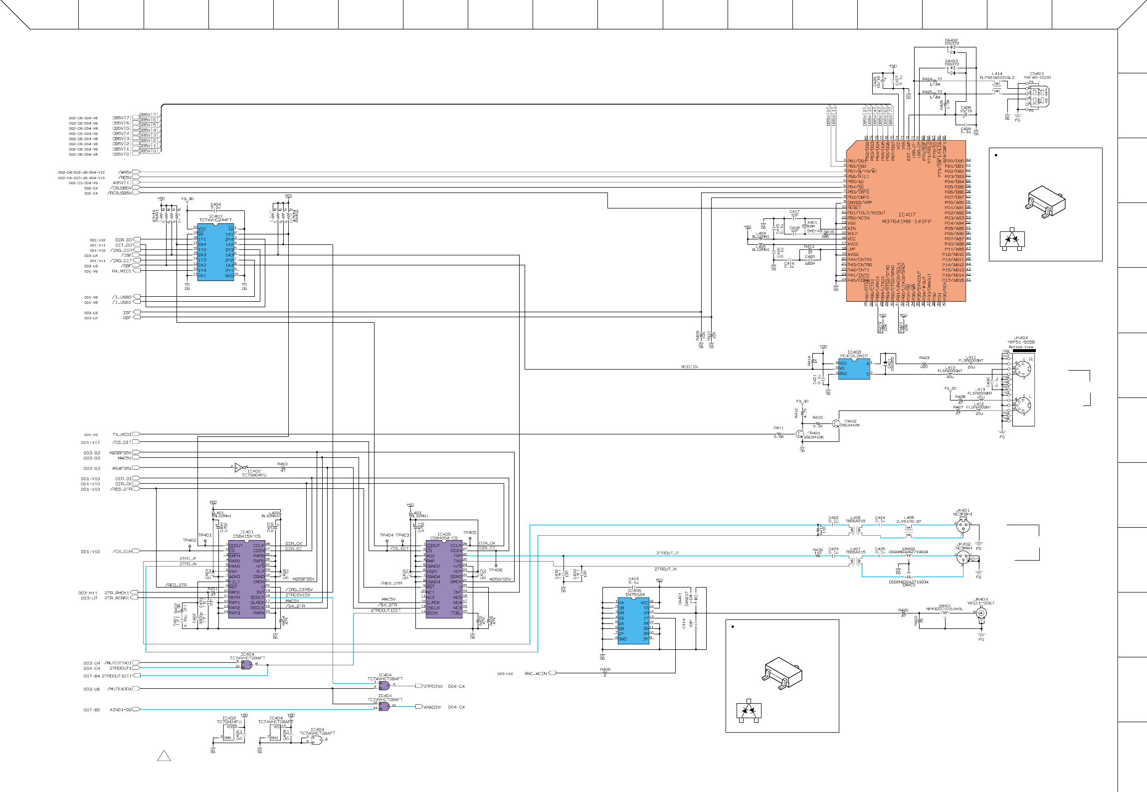
SPX2000
9
■ OVERALL CIRCUIT DIAGRAM 005 (MAIN 5/9)
PQONMLKJIHGFEDCBA
1
2
3
4
5
6
7
8
9
10
11
12
( F ) : Metal Film Resistor(金属皮膜抵抗)
(マ) : Mylar Capacitor(マイラコンデンサ)
(セ) : Ceramic Capcitor(セラミックコンデンサ)
BUFFER
INVERTER
DIR
MUTE
DIT
MUTE
LINE RECEIVER
Photo Coupler
USB CPU
USB
TO HOST
MIDI
IN
OUT/THRU
AES/EBU
WORD
CLOCK
IN
IN
OUT
DAN217 (VV556300)
DIODE ARRAY 0.3AX2
1: ANODE1
2: CATHODE2
3: CATHODE1,
1
3
2
ANODE2
12
3
1SS372 (V9424900)
DIODE ARRAY
1: ANODE1
2: CATHODE2
3: CATHODE1,
1
3
2
ANODE2
12
3
28CC1-8828883-5 1 ■ OVERALL CIRCUIT DIAGRAM 005 (MAIN 5/9)
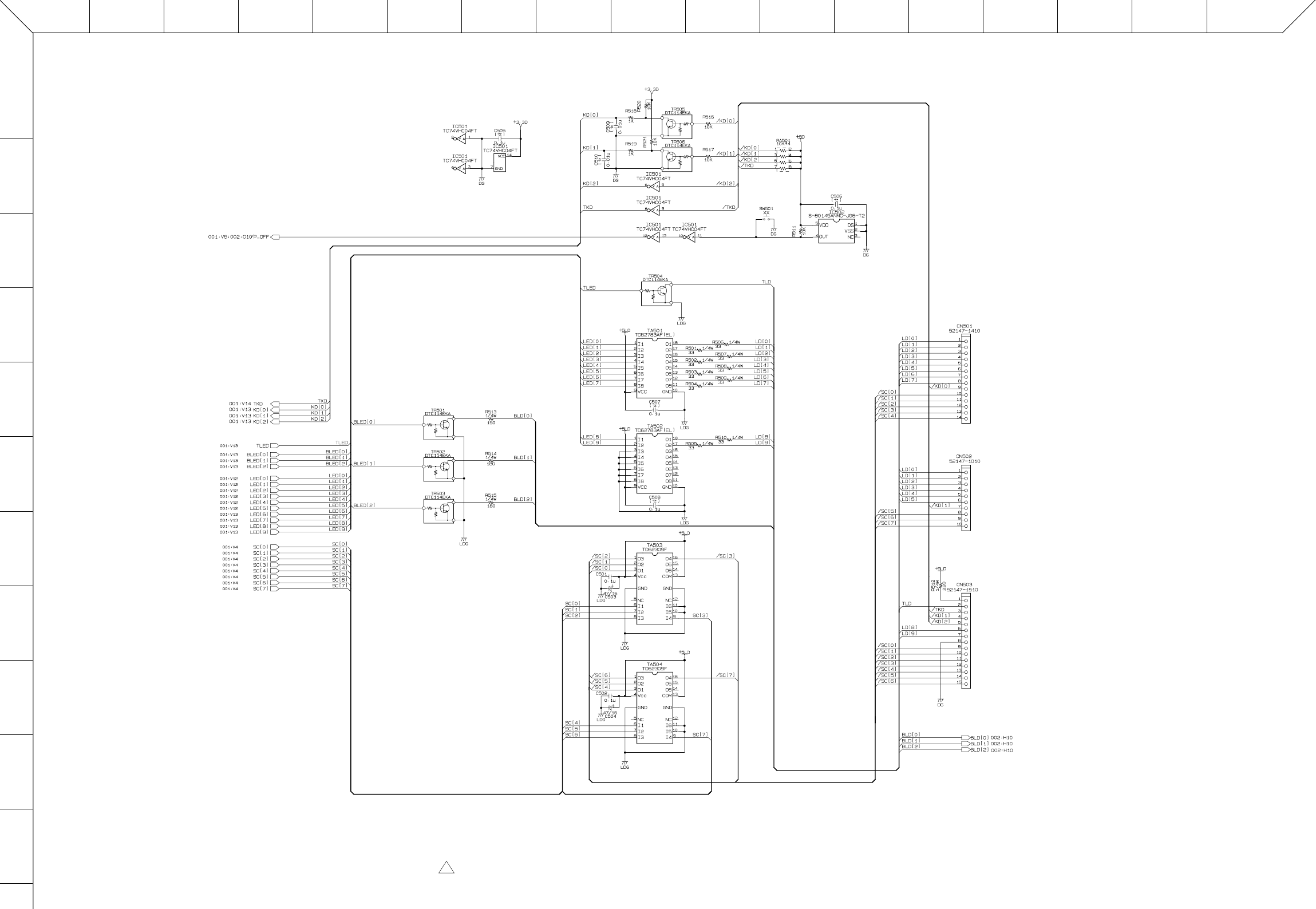
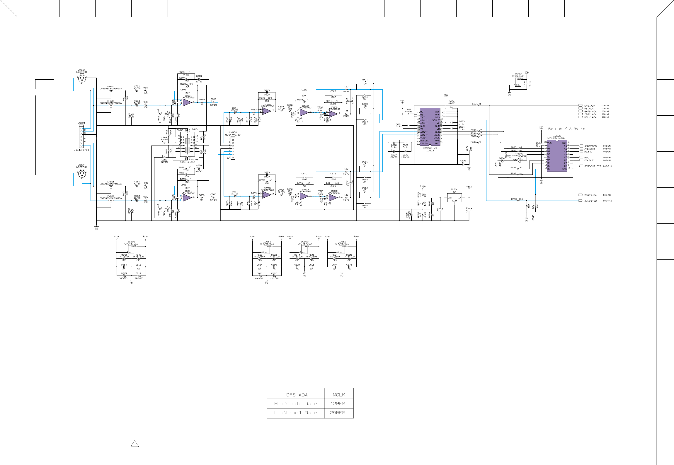
SPX2000
11
■ OVERALL CIRCUIT DIAGRAM 007 (MAIN 7/9)
PQ ONMLKJ I HGFEDCB A
1
2
3
4
5
6
7
8
9
10
11
12
XX : not installed(未実装部品)
( F ) : Metal Film Resistor(金属皮膜抵抗)
(マ) : Mylar Capacitor(マイラコンデンサ)
to JKIN-CN401
to VOL-CN601
INPUT
L
(MONO)
R
OP AMP
OP AMP OP AMP
ADC
INVERTER
TRANSCEIVER
OP AMP
OP AMP OP AMP
INPUT
28CC1-8828883-7 2 ■ OVERALL CIRCUIT DIAGRAM 007 (MAIN 7/9)

SPX2000
12
■ OVERALL CIRCUIT DIAGRAM 008 (MAIN 8/9)
PQ ONMLKJ I HGFEDCB A
1
2
3
4
5
6
7
8
9
10
11
12
NJM78L05UA(XJ598A00)
REGULATOR +5V
1: OUTPUT
2: COMMON
3: INPUT
123
XX : not installed(未実装部品)
( F ) : Metal Film Resistor(金属皮膜抵抗)
(マ) : Mylar Capacitor(マイラコンデンサ)
OP AMP OP AMP
OP AMP
OP AMP
MUTE
MUTE
OP AMP
OP AMP
DAC
REGULATOR
+5V
to JKOUT-CN501
OUTPUT
L
R
OUTPUT
28CC1-8828883-8 2 ■ OVERALL CIRCUIT DIAGRAM 008 (MAIN 8/9)
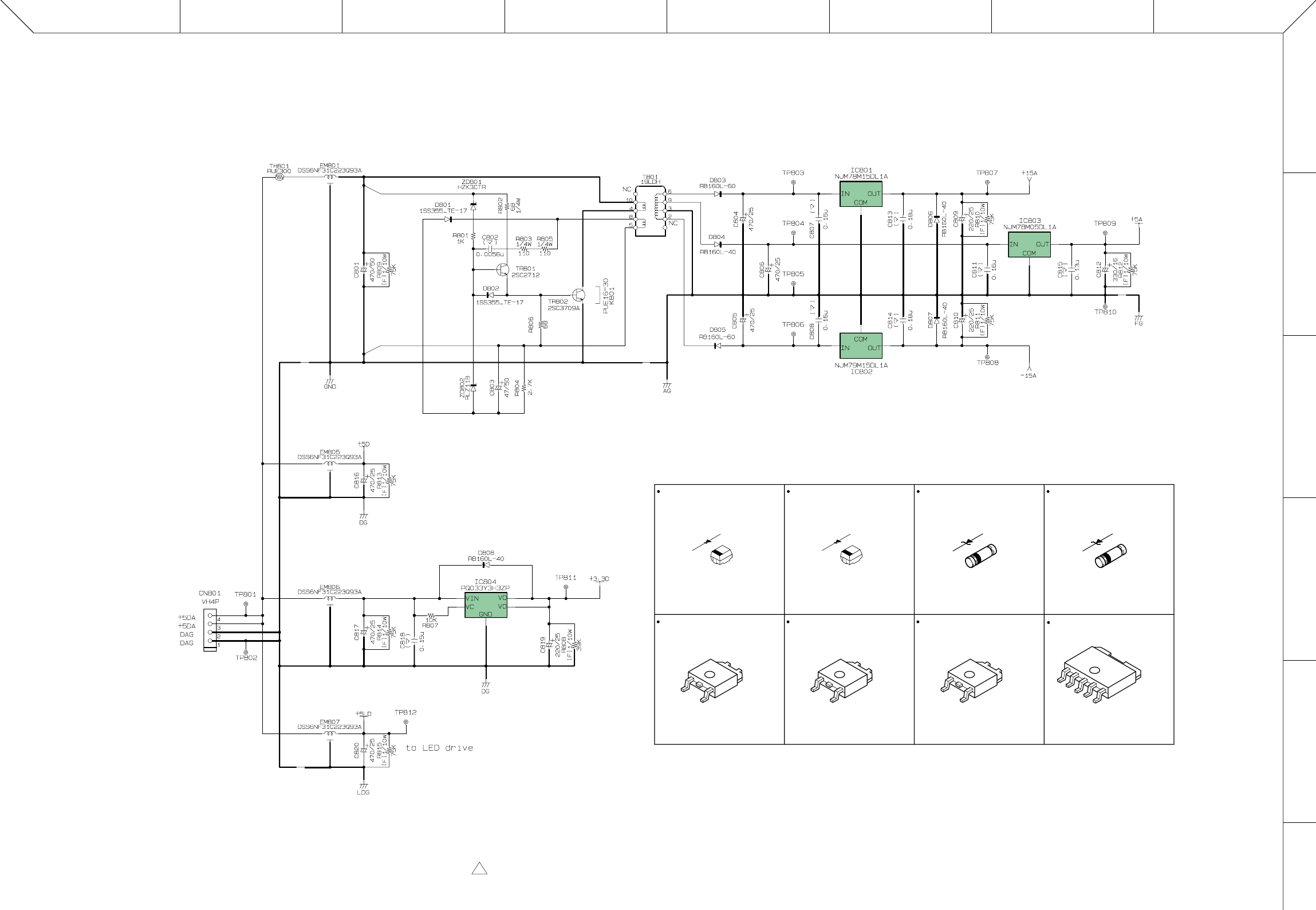
ABCDEFGH
1
2
3
4
5
6
SPX2000
13
■ OVERALL CIRCUIT DIAGRAM 009 (MAIN 9/9)
NJM78M15DL1A(X3942A00)
REGULATOR +15V
1: INPUT
2: GND
3: OUTPUT
1
2
3
NJM79M15DL1A(X3943A00)
REGULATOR -15V
1: COMMON
2: INPUT
3: OUTPUT
1
2
3
NJM78M05DL1A(XS534A00)
REGULATOR +5V
1: INPUT
2: GND
3: OUTPUT
1
2
3
REGULATOR
+15V
REGULATOR
+5V
REGULATOR
-15V
REGULATOR
+3.3V
( F ) : Metal Film Resistor(金属皮膜抵抗)
(マ) : Mylar Capacitor(マイラコンデンサ)
RB160L-60 (V8409200)
DIODE
1: ANODE
2: CATHODE
2
1
RB160L-40 (VS597600)
DIODE
1: ANODE
2: CATHODE
2
1
PQ033Y3H3ZP(X2589A00)
REGULATOR +3.3V
1: DC INPUT
2: DC OUTPUT
3: GND
4: VO (sense)
5: ON/OFF CONTROL
6: DC OUTPUT
1
5
6
HZK3CTR3.3V (V9544100)
ZENER DIODE
1: ANODE
2: CATHODE
2
1
RLZ11B11.0V (VK040100)
ZENER DIODE
1: ANODE
2: CATHODE
2
1
to POWER SUPPLY
UNIT-CN51
28CC1-8828883-9 2 ■ OVERALL CIRCUIT DIAGRAM 009 (MAIN 9/9)
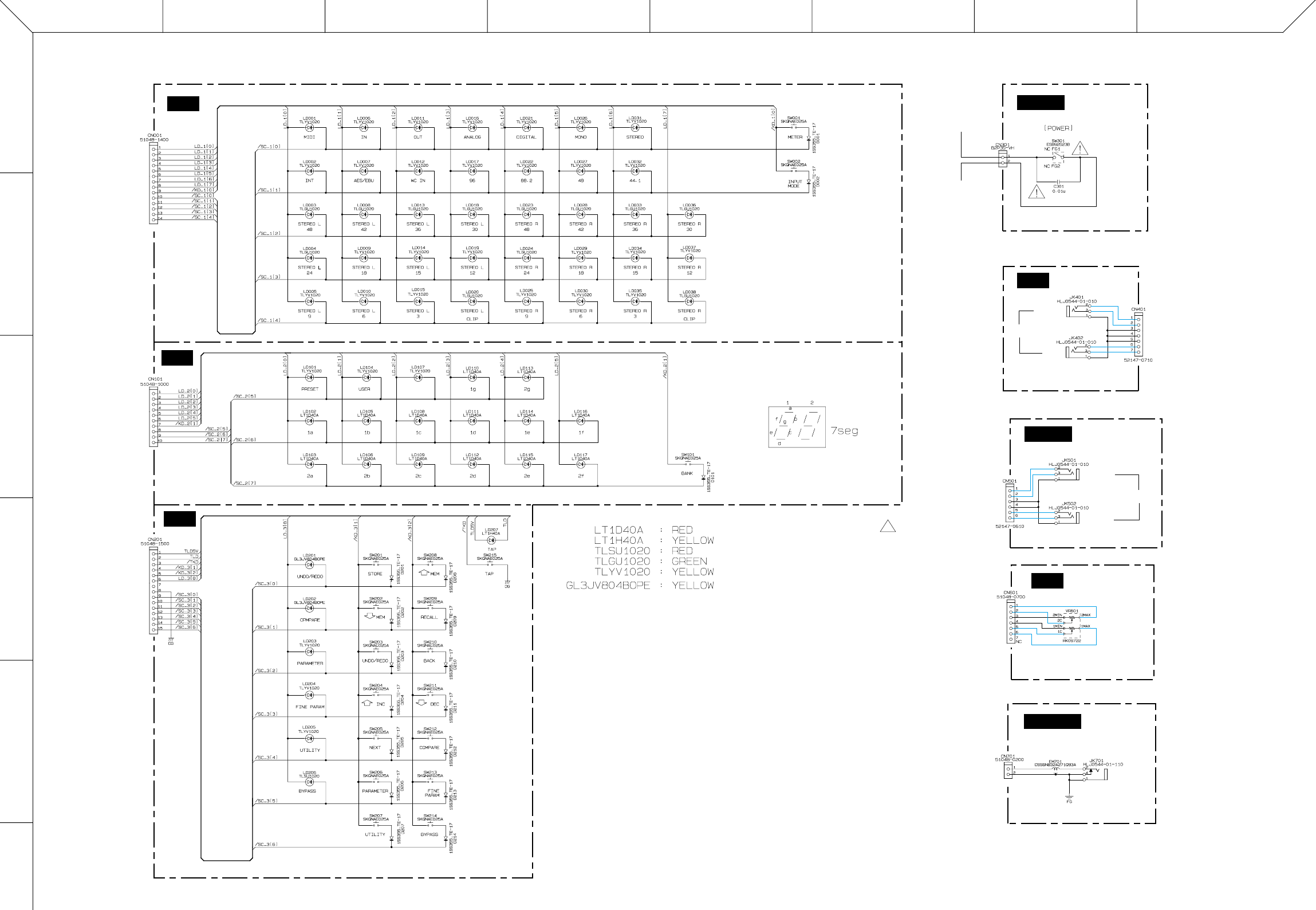
ABCDEFGH
1
2
3
4
5
6
SPX2000
14
■ OVERALL CIRCUIT DIAGRAM (PN1-3, POWER, JKIN, JKOUT, VOL, FOOTSW)
PN2
PN1
PN3
FOOTSW
VOL
POWER
JKOUT
JKIN
to MAIN-CN501
to MAIN-CN502
to MAIN-CN503
to MAIN-CN601
to MAIN-CN701
to MAIN-CN602
to MAIN-CN002
to POWER SUPPLY
UNIT-CN1
to AC INLET
OUTPUT
L
R
INPUT
L (MONO)
R
INPUT
FOOT
SW
CLASSIC
28CC1-8828884 2
■ OVERALL CIRCUIT DIAGRAM (PN1-3, POWER, JKIN, JKOUT, VOL, FOOTSW)
WARNING
Components having special characteristics are marked
Z
and must be
replaced with parts having specification equal to those originally installed.
Z
印の部品は、安全を維持するために重要な部品です。
交換する場合は、安全のために必ず指定の部品をご使用ください。
