Fast Integrated Tools For Circuit Design With FPGAs SRC TN 1997 031
SRC-TN-1997-031 SRC-TN-1997-031
User Manual: SRC-TN-1997-031
Open the PDF directly: View PDF ![]() .
.
Page Count: 20
SRC Technical Note
1997 - 031
December 16, 1997
Fast Integrated Tools for
Circuit Design with FPGAs
Stephan W. Gehring, Stefan H.-M. Ludwig
digital
Systems Research Center
130LyttonAvenue
Palo Alto, California 94301
http://www.research.digital.com/SRC/
To appear in the
1998 ACM/SIGDA Sixth International Symposium on
Field Programmable Gate Arrays (FPGA ’98)
February 22-24, 1998, Monterey, California, USA
Copyright c1998byACM,Inc.
All rights reserved. Republished by permission.
Stephan Gehring is at Interval Research, 1801 C Page Mill Road, Palo Alto, Cali-
fornia 94304. He can be reached at gehring@interval.com.
ii
Fast Integrated Tools for
Circuit Design with FPGAs
Stephan W. Gehring , Stefan H.-M. Ludwig
Institute for Computer Systems
Swiss Federal Institute of Technology (ETH)
Z¨urich, Switzerland
gehring@interval.com, ludwig@pa.dec.com
December 16, 1997
Abstract
To implement high-density and high-speed FPGA circuits, designers need
tight control over the circuit implementation process. However, current de-
sign tools are unsuited for this purpose as they lack fast turnaround times,
interactiveness, and integration. We present a system for the Xilinx XC6200
FPGA, which addresses these issues. It consists of a suite of tightly inte-
grated tools for the XC6200 architecture centered around an architecture-
independent tool framework. The system lets the designer easily intervene at
various stages of the design process and features design cycle times (from an
HDL specification to a complete layout) in the order of seconds.
Interval Research Corporation, Palo Alto, California
DEC Systems Research Center, Palo Alto, California
Copyright c1998 by the Association for Computing Machinery, Inc. Permission to make dig-
ital or hard copies of part or all of this work for personal or classroom use is granted without fee
provided that copies are not made or distributed for profit or direct commercial advantage and that
copies bear this notice and the full citation on the first page. Copyrights for components of this work
owned by others than ACM must be honored. Abstracting with credit is permitted. To copy oth-
erwise, to republish, to post on servers, or to redistribute to lists, requires prior specific permission
and/or a fee. Request permissions from Publications Dept., ACM Inc., fax +1 (212) 869-0481, or
(permissions@acm.org).
1
1 Introduction
Fully automatic circuit synthesis from an HDL description is a difficult and com-
putationally intensive task, especially for Field-Programmable Gate Arrays (FP-
GAs). Ideally, circuits are mapped, placed and routed without human intervention.
However, to implement high-density or high-speed circuits with FPGAs, today’s
designers are faced with the need to manually intervene in the design process and
reiterate the implementation cycle until the circuit implementation meets the re-
quirements [4, 20]. Unfortunately, designers cannot expect much support from
current design tools as the latter do not support fast iterative design cycles and of-
fer only limited interactivity. This effectively hinders the designer from controlling
the implementation process.
Developers of circuit design tools face yet a different problem: the still growing
number of new FPGA architectures pressures them to create new tool suites at a
rapid pace. Since the tools are typically tailored to a specific architecture, they are
rewritten almost completely for every new architecture. Over time this results in a
huge collection of difficult to maintain tools.
The system we present addresses these problems. It tightly integrates the circuit
design process in a single environment, from the initial circuit specification in an
HDL down to bitstream generation. At all stages of the process, the user can exert
control over the circuit implementation and thus efficiently guide the tools towards
the desired solution. The system targets the experienced user desiring complete
control over the circuit implementation and offers a highly interactive and fast de-
sign cycle. It consists of an architecture-independent framework (front-end) which
is complemented by architecture-dependent back-ends. This enhances tool mainte-
nance as the framework is reused for each back-end. A complete back-end includ-
ing layout synthesis has been developed for the Xilinx XC6200 architecture [23].
A further back-end for the Atmel AT6000 architecture [3] exists which comprises
a layout editor for manual circuit implementation and a bitstream generator.
In the following, we first describe how the tight integration of our tools is
achieved. Then we explain how the designer can influence the implementation
process and discuss the techniques used to achieve the necessary speedy design
cycle. We support our claims by measurements and compare our system with the
vendor-supplied development system for the XC6200. A more detailed presenta-
tion of the described system can be found in [8] and [14].
2
2 Tool Integration
One of the major goals of this work was to tightly integrate the various circuit de-
sign tools into a single development environment. Traditionally, the tools used in
the circuit design process are very loosely coupled and are often developed by a
variety of independent companies. For instance, the tools used to capture designs
may come from a CAD tool developer, while the layout synthesis and bitstream
generation tools are provided by the chip manufacturer. Typically, tool communi-
cation is achieved by exchanging disk files containing the design data in standard
formats.
We feel that this loose coupling bears several disadvantages. First, it makes the
seamless integration of the tools a difficult, if not impossible, task. This, however,
is a prerequisite to quickly switch back and forth between design tools during the
design process. Second, file-based inter-tool communication necessitates conver-
sions between internal and external formats on both ends, which often results in
design information loss and makes data exchange a slow and vulnerable process.
Third, decoupled tool development does not take into account that a significant part
of a tool suite is independent of any specific architecture and could thus profitably
be reused by several tools. Taking advantage of this reduces the size and memory
requirements of tools and eases system maintenance.
We have addressed these problems by capturing the common traits of design
tools in an application framework for circuit design tools [9, 8]. To create tools for
a specific FPGA architecture, this architecture-independent framework is extended
with architecture-specific components.
The foundation for the tight integration of the framework and its extensions
lies in the use of a single data structure to represent circuits throughout the sys-
tem [9, 8]. That is, all tools, whether architecture-independent or -dependent, use
auniversal circuit representation defined in the core of the framework (Figure 1).
The design tools operate in a shared memory environment and modify the data
structure in situ. Data exchange between tools can thus be realized efficiently just
by passing a reference to the data structure. This avoids data structure conversions
altogether and simplifies both framework and tool implementations considerably.
Keeping even large circuits entirely in main memory is possible due to the com-
pactness and simplicity of the representation.
The data structure represents circuits as a hierarchical forest of binary trees.
Each tree specifies the Boolean equation for a single circuit output. To accommo-
date for the needs of placers and routers, positional information and net lists can
be attached to the nodes. All tools involved in the implementation process support
and maintain the hierarchical circuit structure. We have found that this greatly
improves the efficiency and quality of the layout synthesis tools (see Section 4).
3
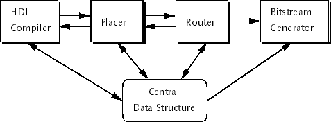
Figure 1: Single Circuit Representation Accessed by Multiple Design Tools
To describe the hierarchy of a circuit, the framework uses parameterizable tem-
plates. A template is a representation of a subcircuit. Every instance of such a tem-
plate is an exact copy of the template, i.e. it contains the same gates and net lists
and they are at the same (relative) positions as in the master copy. Tools, such as a
placer, can exploit this additional knowledge to efficiently produce regular layouts
for regular circuits, such as bit-sliced designs.
For textual design specification, the framework comprises a compiler for the
hardware description language Lola [21, 22]. The compiler translates a Lola cir-
cuit specification into the universal data structure ready to be processed further. The
Lola HDL supports parameterized descriptions of subcircuits, e.g. N-bit adders,
and allows the designer to pass placement hints to back-end tools, i.e. to constrain
the placement of circuit components.
Also provided is a layout editor framework, which can be customized to create
layout editors for specific FPGA architectures. The layout editors fully support hi-
erarchical layout and allow circuits to be constructed manually. The latter option is
typically used only for small to medium sized circuits and in education. The layout
editor framework has proven so versatile that a schematics editor was implemented
with the framework.
To aid in the secure manual construction of circuits, the framework features a
design checker, which checks two circuit descriptions, e.g. an HDL specification
and a layout, for Boolean equivalence. The design checker is mainly used in ed-
ucation, where circuits are laid out manually by the student and are then checked
against a Lola specification. It has also been used to prove the correctness of the
layout synthesis tools themselves. To prove equivalence between two Boolean ex-
pressions, the design checker uses ordered binary decision diagrams (OBDDs) [5].
In the course of our work, we have found that significant parts of design tools
are indeed architecture-independent and are therefore profitably implemented by
the framework. The framework-based approach also increases software reliability,
as common functionality is implemented once only and reused by several back-
ends. The use of a single circuit representation resulted in the desired tightly inte-
4
grated system with short response times and high interactivity.
3 Controlling the Design Process
A key issue in the implementation of high-speed and high-density circuits with
FPGAs is allowing the (experienced) designer complete control over the circuit
implementation. This is because, unlike in the software world, resources in an
FPGA are scarce and therefore need to be tightly managed. Being the creator of
the circuit, the designer has the most intimate knowledge of the circuit’s structure
and therefore knows best how it should be laid out. However, the complexity of
today’s circuits requires support by layout synthesis tools. The designer’s goal is
therefore to guide the synthesis tools towards the desired solution. To enable this,
our system allows the designer to influence the outcome of the tools at various
levels.
At the circuit specification level, the designer can specify the placement of cir-
cuit components using position assignments in the Lola HDL. These placement
hints are passed on to the automatic placer which pre-places the parts prior to plac-
ing the remaining circuit parts. After placement, the layout editor can be used to
enhance the placement manually. Since the hierarchy of the circuit is preserved by
all tools and visualized by the layout editor, the designer is able to quickly identify
and rearrange individual cells or entire subcircuits. As the layout editor is used fre-
quently, we have taken care to make circuit manipulation as simple and as fast as
possible. Once a satisfactory placement is achieved, more placements hints can be
added to the HDL specification to reflect the new placement. These will constrain
the placer during the next design iteration and will thus relieve the user from hav-
ing to make the same changes again during subsequent iterations. A compile-place
cycle takes only a few seconds and the design quickly converges to the desired
placement.
The designer can also influence the routing process. The router allows indi-
vidual nets to be routed and also supports the recording and playback of routing
scripts, which define the sequence in which the nets are routed. These scripts can
be conveniently appended to the HDL specification text. Furthermore, the router
can be constrained to only use certain types of routing resources, e.g. only use the
local interconnect. Should the automatic router fail to route a design successfully,
the designer can use the layout editor to route certain nets manually.
Typically, the final layout is achieved only after a number of iterations. The
ability to predict the outcome of changes made to the circuit specification is there-
fore of utmost importance. Our tools comply with this requirement by employing
only deterministic algorithms. Stochastic algorithms, such as simulated annealing,
5
are ruled out, as minor changes to the circuit specification may result in drastically
different layouts.
4 Speed of Design Cycle
Current CAD tools take a considerable amount of runtime (several minutes to
hours) to compile, place and route a design. One goal of the presented tools is
to achieve design cycle times that lie in the same range as those common in soft-
ware development, namely minutes at most. The Lola front-end and the XC6200
back-end [14] achieve this through various techniques discussed in this section.
4.1 Lola HDL Compilation
Due to the simplicity of the Lola language, most notably the restriction to a struc-
tural description style, the compilation process is straightforward. No elaboration
process has to be performed, i.e. the mapping of source language constructs to im-
plementable gates is obvious. A two-pass compiler is used, which first translates
the source code into a syntax tree and then interprets this syntax tree, generating
the universal data structure directly into main memory. The first pass takes time
linear in the size of the source code and the second pass takes time linear in the
size of the described circuit.
4.2 Technology Mapping to the XC6200
The Xilinx XC6200 FPGA consists of an array of simple cells and a hierarchical
routing network [23]. Each cell can implement any function of one or two inputs
or a multiplexer, and contains an optional register, possibly with feedback. The
match between the universal data structure and the possible cell configurations of
the XC6200 is almost perfect. Only simple transformation steps have to be per-
formed, such as translating an SR-latch into two cross-coupled Nand-gates. Pack-
ing multiple components into a single cell is deferred to the placement phase, which
deals with the geometric properties of the circuit. Therefore, no time-consuming
packing step has to be performed, as is the case for most coarse-grained FPGAs
like the XC4000 series. The mapping process takes time linear in the size of the
circuit.
4.3 Placement
The XC6200 back-end uses a constructive, deterministic placement algorithm.For
the same input it produces the same output, which is a very important and desirable
6
property of a tool that is used iteratively and interactively. It gives the designer the
least surprises when a design is recompiled. Stochastic placement algorithms such
as simulated annealing [12] are inappropriate for this task, as they typically produce
different results every time they are run and exhibit long runtimes.
The placing algorithm proceeds bottom-up, placing the innermost subcircuits
(templates) first. It is similar to the algorithm described in [15]. Within a template,
it proceeds as follows: first, instances and expression trees with associated posi-
tion hints are placed. Second, array structures areplacedusingasimpleheuristic
that places elements of an array either from left to right or from bottom to top,
depending on the aspect ratio of the element. A good heuristic for arrays is es-
sential for the placement of regular, bit-sliced designs which frequently occur in
data paths. Finally, individual instances and expression trees are placed using a
recursive algorithm: the root of an expression is placed into the first available cell.
The expression trees, from which the root cell reads, are placed recursively to the
right of the root cell and above it. The tree above is offset by the vertical height of
the tree to the right of the cell. Free space is managed using a bitmap. This sim-
ple placement strategy does not produce dense layouts, but is fast and guarantees a
routable design. If necessary, the user can optimize this initial placement manually.
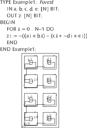
Figures 2 and 3 give two examples of how expressions and arrays are placed.
Figure 2: Compact Placement of Expressions and Arrays
Once a template is placed, the derived positional information is propagated to
7
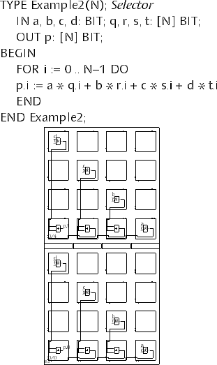
Figure 3: Placement Leaving Empty Cells
8
all instances of that same template. This preserves the invariant of the front-end,
which requires that all instances of the same template have the same structural,
placement, and wiring information. Moreover, it also speeds up the placement
algorithm, which uses time linear in the size of the circuit.
For larger circuits, which cannot be placed using this simple strategy, a floor-
planner can be used to place subcircuits by hand and optimize their layouts indi-
vidually.
4.4 Routing
The routing algorithm used in the back-end is a maze-running router based on
the algorithm presented in [13]. It finds a path between two cells (terminals) by
spreading a wave from the destination towards the source until it finds the source
cell or a wire segment driven by that source cell. A cost function determines the
shape of the spreading wave.
The router proceeds bottom-up, routing the innermost templates first. Since
all instances of a given template must have identical wiring, the router must take
into account the different positions of the instances when determining the routing
resources available for routing the given template. It sorts all nets according to
their length and routes the shortest nets first. This simple, but effective, scheduling
policy achieves quite satisfactory results.
Tolimitthesizeofthewaveexpansion,abounding rectangle is used, which
bounds the size of the wave. If a subcircuit is routed, the size of this rectangle is
the size of the subcircuit’s bounding box. If the net is in the top-level the rectangle
is made 1/4 larger on each side than the bounding box spanned by the source (S)
and destination (D) nodes (cf. Figure 4). If routing fails within this rectangle, it is
enlarged to the size of the chip and a new attempt is made. The effectiveness of
this two-phase approach is dramatic, as it can reduce the routing times by an order
of magnitude.
Once a template is routed, the routing information is propagated to all in-
stances of that template occurring in the design. This propagation process speeds
up the routing time of the whole design considerably, as the costly wave spreading
is only performed once for each net in each template. In designs with many repet-
itive structures, the speedup is directly proportional to the number of instances of
thesametemplate.
To allow for manual intervention by the user, the router takes already routed
nets into account by extracting the connectivity information prior to routing. Criti-
cal nets can therefore be pre-routed manually.
9
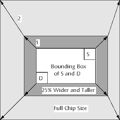
Figure 4: Two-Phase Growing of Router Bounding Box
5 Evaluation
We evaluate the Lola front-end and the XC6200 back-end and compare it to the
XACT Step 6000 V1.1.2 software available from the chip vendor. While our sys-
tem offers an integrated design flow from HDL specification to bitstream gener-
ation, XACT provides the back-end functionality and relies on third party front-
ends. The measurements were carried out on a Digital Celebris GL 5166ST PC,
equipped with a 166 MHz Intel Pentium processor, 256 KB of second-level cache,
128 MB of main memory, running Microsoft’s Windows NT operating system,
version 4.0. The Lola system is implemented in the Oberon-2 programming lan-
guage [16] and runs within ETH’s Oberon for Windows System V4.0 [11] using
the implementation from the University of Linz, version 2.0.
5.1 Architecture Independence
The usefulness of the framework approach with an architecture-independent front-
end and several architecture-dependent back-ends manifests itself in the size of the
tools. Table 1 lists the software complexity of the front-end and of two back-ends,
one for the Xilinx XC6200 and one for the Atmel AT6000 FPGA. The AT6000
back-end consists of a layout editor and bitstream generator. It was developed by a
student and proves that a layout editor back-end can be developed by a programmer
with no prior knowledge of the framework within reasonable time (3 months).
10

It is interesting to compare the sizes of the framework front-end to the XC6200
back-end. Note that in addition to the tools described in Section 4, the XC6200
back-end includes a bitstream generator and a timing analyzer, as well as hard-
ware driver software. The front-end is nearly of the same size as the back-end.
Put in another way, approximately 40% of the circuit design system is architecture-
independent. This fact clearly supports our proposition that a common architecture-
independent front-end substantially reduces the effort to develop new back-ends.
Subsystem Lines Object (KB)
Front-End 11300 199
XC6200 Back-End 18100 296
Total (Front-End+XC6200) 29400 495
AT6000 Layout Editor 4400 80
Table1:SoftwareSize
For comparison, the commercial tool XACT running under Windows NT has
an object code size of 1192 KB. It is more than twice as large as our system and fea-
tures neither an HDL compiler nor does it contain architecture-independent parts,
which may be reused for different architectures.
Memory requirements of our tools are modest. The biggest design of the next
section is compiled, placed and routed using no more than 16 MB, while the mem-
ory requirement of XACT for the same design is 46 MB.
5.2 Speed of Design Cycle
We use two designs to evaluate the tools. The first is a floating point adder for
16-bit operands. The second is a pattern matcher, which consists of a regular dat-
apath, and a small amount of random logic. It matches 5-bit characters stored in
the FPGA (the patterns) against a stream of 5-bit characters (the text) and signals
a match. Three design variants are evaluated: one with 2 parallel pattern matchers
of 4 characters each, one with 16 pattern matchers of 12 characters each and one
with 32 parallel pattern matchers of 24 characters each. Both designs are data-path
intensive circuits, for which the XC6200 is particularly well suited. Table 2 lists
the characteristics of the four designs after successful layout synthesis. The biggest
design is implemented on an XC6264 (128x128 cells) while all other designs are
implementedonanXC6216(64x64cells). Figures5and6showtheplacedand
11
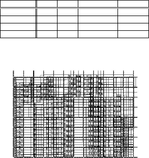
routed layouts of the floating point adder and the medium pattern matcher, respec-
tively.
CLBs Nets Bounding Box Utilization
FP-Adder 542 1283 64x34 25%
Small PM 248 630 18x46 30%
Medium PM 3048 6310 60x61 83%
Large PM 11748 23830 107 x 121 90%
Table 2: Design Characteristics
Figure 5: Layout of Floating Point Adder
Table 3 shows the time spent in each phase of the Lola system. Note that rout-
ing is not involved in the design cycle until the user is satisfied with the placement
of the circuit. Therefore the first column lists the combined times of HDL compila-
tion, mapping and placement. The (nh)-rows list the results for Lola code without
placement hints. The number of unrouted connections is listed as well and clearly
indicates how the quality of the routing is affected by the placement. The time for
routing dominates the total design cycle time.
Table 4 lists the times spent in the XACT tool. Since the HDL compiler is
not integrated into XACT, the first column lists the combined times for reading
the mapped netlist and placement. The mapped netlists were produced with our
Lola compiler and a conversion tool. With no hints, XACT uses more time in the
placement phase, trying to produce a good placement using stochastic algorithms.
12
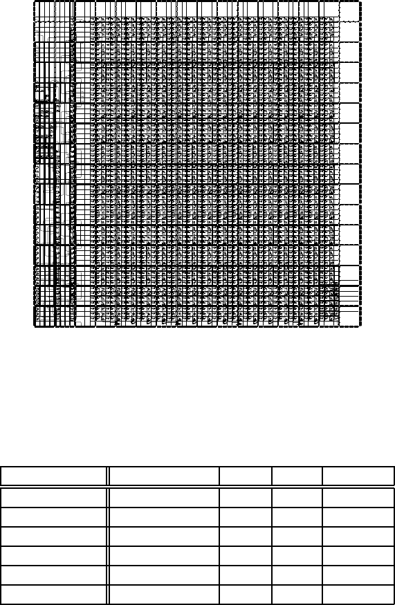
Figure 6: Layout of Medium Pattern Matcher
Compile+Place Route Total Unroutes
FP-Adder (nh) 1.1 16.3 17.4 32
FP-Adder 1.1 4.5 5.6 0
Small PM (nh) 0.2 6.4 6.6 21
Small PM 0.3 2.0 2.3 0
Medium PM 3.5 17.1 20.6 0
Large PM 33.5 162.6 196.1 0
Table 3: Speed of Lola System (Times in Seconds)
13
Repetitive runs on the same input do not yield the same result, which can affect
the result of the routing phase as well. Hence, little progress can be made between
iterations. The placement and the routing can be influenced by the user through
various switches. To produce the data presented in Table 4, those settings were
chosen that ran the fastest, or achieved a completed design.
Read+Place Route Total Unroutes
FP-Adder (nh) 58.4 1046.2 1104.6 81
FP-Adder 5.9 125.2 131.1 0
Small PM (nh) 6.6 683.1 689.7 9
Small PM 3.0 281.1 284.1 0
Medium PM 22.2 216.5 238.7 0
Large PM 273.9 2543.1 2817.0 0
Table 4: Speed of XACT (Times in Seconds)
Table 5 lists the total times and the speedup obtained by using the Lola system.
As the table shows, the Lola system is one to two orders of magnitude faster than
the commercial tool. In contrast to XACT, our router does not support the “Magic”
routing resource of the XC6200 — but still routes the designs — and only sup-
ports one global clock signal. However, this does not fully explain the difference
in execution time. Moreover, the times for our tools include HDL compilation.
Commercial HDL compilers are typically at least an order of magnitude slower
than our Lola compiler.
The tables do not show quantitative results of the layouts because our timing
analyzer is not yet fully functional. Inspection of the layouts, however, reveals
critical paths of similar lengths.
XACT Lola Speedup
FP-Adder (nh) 1104.6 17.4 63.5
FP-Adder 131.1 5.6 23.4
Small PM (nh) 689.7 6.6 104.5
Small PM 284.1 2.3 123.5
Medium PM 238.7 20.6 11.6
Large PM 2817.0 196.1 14.3
Table 5: Speed of Lola System vs. XACT (Times in Seconds)
14
Our system exhibits exceptionally fast turnaround times and is therefore well
suited for interactive circuit development. The fast turnaround times of compile,
map and place are especially noticeable when many design iterations are being
performed.
6 Related Work
Many different frameworks for circuit design are reported in the literature, and the
term “framework” is defined in various contexts. For instance, the CAD Frame-
work Initiative (CFI), an international consortium developing framework standards,
defines a framework as “a software infrastructure that provides a common operat-
ing environment for CAD tools” [6]. This definition targets the interoperability of
loosely coupled design tools through a standard layer which is separate from the
tools. It encapsulates existing tools which have been developed independently and
thus focuses on the management rather than the implementation of design tools.
Exemplary for this philosophy is the Nelsis framework [17, 19].
Our front-end differs from this approach in that it closely couples extensible
design tools. It does not need any data translators since a common data structure
is used. More in the spirit of our tools is the FACE environment [18], which is
a framework containing a design manager and a user interface toolkit centered
around a common design representation model.
Because the bitstream formats of most FPGAs are kept proprietary by their
respective vendors, CAD tools developed by third parties generate netlists that
are then read by commercial tools. Therefore, these third party tools suffer from
the lack of integration and speed and the design cycle times are slow, although
these times are seldom published in the literature. Examples for such tools are
PamDC from Digital’s Paris Research Laboratory [4] and the SPLASH-tools from
the Supercomputing Research Center in Maryland [2]. The only systems we know
of, which have comparably fast turnaround times are Tsutsuji [7] for the Tera-
mac custom computing machine from Hewlett-Packard Laboratories [1], and the
Debora/CALLAS tools for the Algotronix CAL architecture [10]. The bitstream
formats of both FPGAs were available to the tool developers. Compared to our
system, the CALLAS synthesis tools make no use of hierarchical information and
the Debora HDL can not be annotated with placement information.
7 Summary and Conclusions
We have developed circuit design tools for FPGAs which feature a very fast de-
sign cycle. They give the user tight control over the implementation process and
15
encourage an iterative, exploratory design style. This is particularly useful for ex-
perienced users who push the technology to its limits. Our tools should be seen
as complements, rather than replacements, to sophisticated design tools that offer
fully automatic synthesis at the expense of execution time.
The separation into an architecture-independent front-end and architecture-
dependent back-ends is beneficial, as it relieves the tool implementor from having
to (re)implement common behavior for each back-end anew.
By centering all tools around a universal data structure, the speed of the tools is
improved and the memory requirements are lowered. Preserving the hierarchical
information available on the HDL level throughout the system proved to be valu-
able both to enhance the predictability of the synthesized layouts and to reduce
execution times of the design tools.
The resulting design cycle is one to two orders of magnitude faster than what
can be achieved with vendor-supplied tools and approaches that of tools for soft-
ware development. We hope that this enabling technology will spark interest in the
software community to use FPGAs for custom computing applications.
Acknowledgments
We would like to thank Marco Sanvido for implementing a timing analyzer for the
XC6200 FPGA and Daniel Hofmann for the implementation of the Atmel AT6000
layout editor. We are grateful to Xilinx Development Corporation in Scotland for
their continuing support and to Virtual Computer Corporation in California for
making our tools available to a wider community.
The Lola tools can be downloaded free of charge from http://www.lola.ethz.ch and
a version supporting the H.O.T. Works development system of Virtual Computer
Corporation is available from http://www.vcc.com.
References
[1] R. Amerson, R. J. Carter, W. B. Culbertson, P. Kuekes, G. Snider. Teramac
— Configurable Custom Computing. Proc. IEEE Symposium on FPGAs for
Custom Computing Machines. IEEE Computer Society Press, 1995.
[2] J. M. Arnold, D. A. Buell, E. G. Davis. Splash 2. Proc. 4th Annual ACM
Symposium on Parallel Algorithms and Architectures, 1992.
[3] Atmel. Configurable Logic: Design & Application Book, 1995.
16
[4] P. Bertin, H. Touati. PAM Programming Environments: Practice and Expe-
rience. Proc. IEEE Symposium on FPGAs for Custom Computing Machines.
IEEE Computer Society Press, 1994.
[5] R. E. Bryant. Symbolic Boolean Manipulation with Ordered Binary Decision
Diagrams. ACM Computing Surveys, Vol. 24, 293–318, 1992.
[6] CFI Architecture Technical Subcommittee. CAD Framework Users, Goals,
and Objectives, Version 0.91, CAD Framework Initiative, 1990.
[7] B. Culbertson, T. Osame, Y. Otsuru, J. B. Shackleford, M. Tanaka. The HP
Tsutsuji Logic Synthesis System. Hewlett-Packard Journal, August 1993.
[8] S. Gehring. An Integrated Framework for Structured Circuit Design with
Field-Programmable Gate Arrays. Dissertation No. 12188, ETH Z¨
urich,
1997 (http://www.inf.ethz.ch/publications/diss.html).
[9] S. Gehring, S. Ludwig. The Trianus System and its Application to Custom
Computing.Proc. 6th Intl. Workshop on Field-Programmable Logic and Ap-
plications. LNCS 1142, Springer, 1996.
[10] B. Heeb and C. Pfister. Chameleon: A Workstation of a Different Colour. 2nd
Intl. Workshop on Field-Programmable Logic and Applications. LNCS 705,
Springer, 1992.
[11] Institute for Computer Systems. The Oberon Archive. ftp://ftp.inf.ethz.ch-
/pub/software/Oberon.
[12] S. Kirkpatrick, C. D. Gelatt, Jr., M. P. Vecci. Optimization by Simulated An-
nealing. Science,Vol.220,May,1983.
[13] C. Y. Lee. An Algorithm for Path Connections and its Applications. IRE
Trans. Electronic Computer, Vol. EC-10, September 1961.
[14] S. Ludwig. Hades — Fast Hardware Synthesis Tools and a Reconfigurable
Coprocessor. Dissertation No. 12276, ETH Z¨
urich, 1997 (http://www.inf.-
ethz.ch/publications/diss.html).
[15] L. M. Monier, J. Dion. Recursive Layout Generation. Proc. 16th Conference
on Advanced Research in VLSI. IEEE Computer Society Press, 1995.
[16] H. M¨
ossenb¨
ock, N. Wirth. The Programming Language Oberon-2. Structured
Programming. Vol. 12, No. 4, 1991.
17
[17] Technical University of Delft. The Nelsis CAD Framework. http://www.ddtc.-
dimes.tudelft.nl, 1996.
[18] W. Smith, D. Duff, M. Dragomirecky, J. Caldwell, M. Hartman, J. Jasica,
M. d’Abreu. FACE Core Environment: The Model and its Application in
CAE/CAD Tool Development.Proc. 23rd Design Automation Conference,
IEEE, 1989.
[19] P. van der Wolf. CAD Frameworks — Principles and Architecture. Kluwer
Academic Publishers, 1994.
[20] R. Woods, A. Cassidy, J. Gray. VLSI Architectures for Field Programmable
Gate Arrays: A Case Study.Proc. of the IEEE Symposium on FPGAs for Cus-
tom Computing Machines. IEEE Computer Society Press, 1996.
[21] N. Wirth. Digital Circuit Design. An Introductory Textbook. Springer, 1995.
[22] N. Wirth. The Language Lola and Programmable Devices in Teaching Digital
Circuit Design. Proc. of the 2nd Intl. Andrei Ershov Memorial Conference.
LNCS 1181, Springer, 1996.
[23] Xilinx. TheProgrammableLogicDataBook, September 1996.
18