SSM2000
User Manual: SSM2000
Open the PDF directly: View PDF ![]() .
.
Page Count: 10
Data
Sheet Solid State Music ssM
2000
DUAL
LII{EAR.ANTILOG VOTTAGE
CONTROTTED
AMPTIFIER
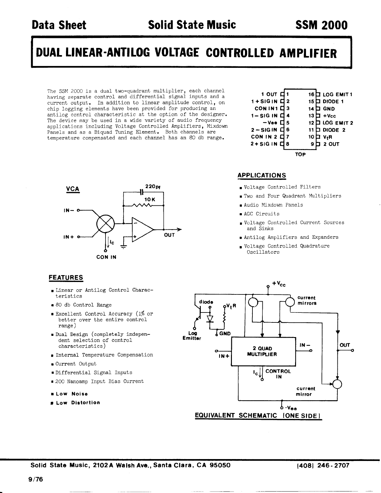
The SSM
20OO is a duaf two-quadrant multiplier, each channef
harring ,"eparate control and differential signal inputs and a
current output. ln addition to linear amplilude control, on
nhi n I nooinL plcment.q herre heen nnorrided for nrodtrcing an
vrrrP rv66rrr5
antilog control characterjstic at the option of the designer.
Tha rio:n.F aa\t he rrqpd in e nride rnriet.rr nf attdin fnenttencv
vrL! r"ui/
applications including Voltage Controlfed Amplifiersr Mixdown
Panels and as a Biquad T\rning Element. Both channefs are
temperature compensated and each channel has an 8O db range.
lil-
lN+
CON
IN
FEATURES
r Linear or Antilog Control- Charac-
teristi-cs
r BO
db Control Range
r Excelfent Control Accuracy (l% or
better over the entire control
range )
r Dral Design (completely indepen-
dent selection of controL
nhapa a-l ari ci _i
n e \
r Internal Temperature Compensation
r Current Output
r Differential Sigrtal Inputs
r 2OO Nanoamp Input Bias Current
Low Noise
Low Dlrtortion
APPLICATIONS
r Voltage Conlrolled Filters
r Two and Four Q-radrant Multi-pliers
r Audio l,Lixdown Panels
r AGC
Circuits
^^*r -^r '-' Current Sources
I VU!UdBC VUrrufUrasu
and Sinks
r Anlilog Amplifiers and Expanders
a Voltage Control-l-ed Quadrature
0sclflators
1 OUT
1+SIGIN
coN
tNl
1- SrG
rN
- Vcc
2-SrGlN
coN lN
2
2+stGtN
LOG
EMIT 1
DIODE 1
GND
+Vcc
toc EUtT 2
DIODE
2
vtR
2 OUT
I
a
116
215
314
413
512
611
710
89
TOP
lcfi
cotrnol
EOUTVALENT
SCHEMATTC
IONE StDE
I
Sof id State Music, 2102A Walsh
Ave.,
Santa
Clara, CA 95O5O
9/76
t4o8l 246-2707
ssil 2()0()
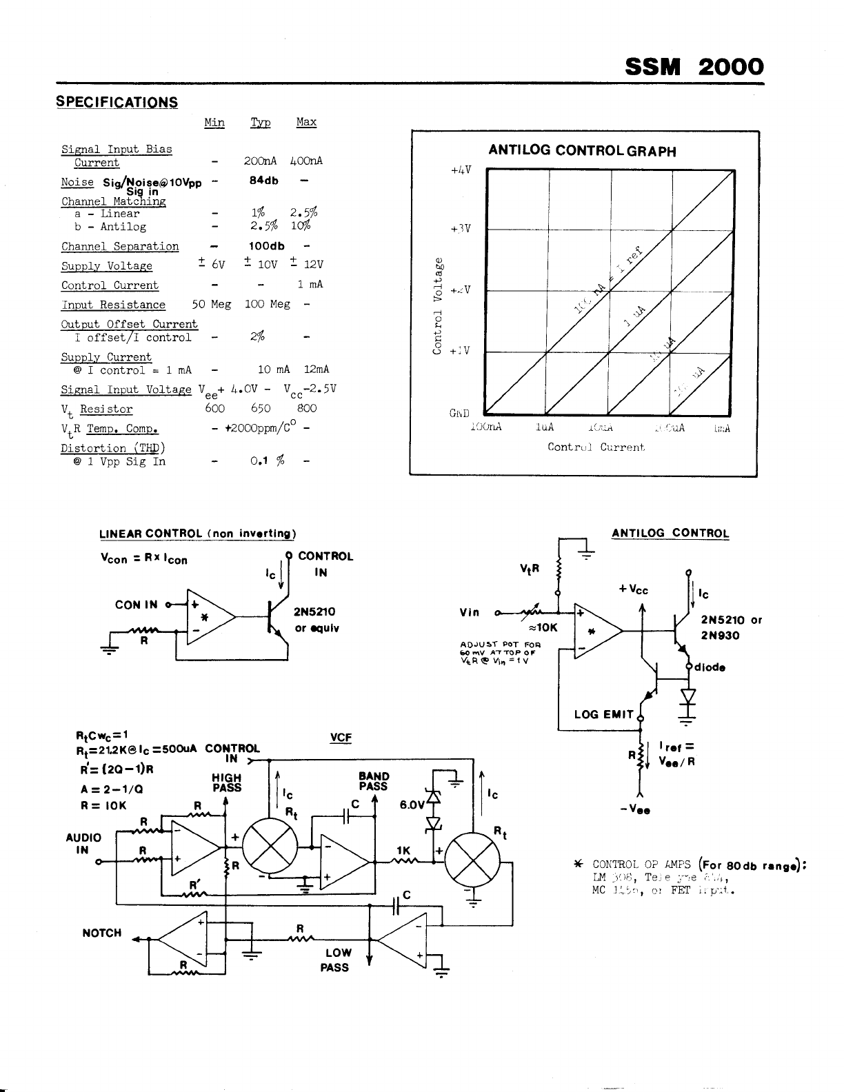
Signal Input Bias
Current
tttoise Siy'!.oise@1OVpp
-'Sig in
llhrnnpl Mal.nhi nq
a - Linear
b - Antilog
Channel Separation
Sunpl-v
Voltase 1
Conlrol- Current
Input Resistance 50 Meg
Output Offset Current
-I ^+'t'c6i / | ^^nt r^ |
q,'hhl r' Olroon*
@Icontrol-=1mA
Si enel Innrrt Vnl t.ase
V
V, Resi
slor
V.
R Temp. Comp.
Fri c* ar+ i ^- ,'THn )
@ 1 l/nn Sio Tn
SPECIFICATIONS
AUDIO
IN
Min wMax
20OnA 40OnA
84db
4 2.5%
2.5% rq"
100db
f 1ov = L2\l
- 1mA
1OO
Meg
- 10 mA 72nA
^^+ l+.OV
- V^^-2.5V
600 650 800
- +2OaoppnfCo -
o.1
%
OV
LINEAR
CONTROL
(non invcrtlng)
R1Cw"=1
colrTRoL
IN
2N5ZrO
or aquly
Low
PASS
Vin
ADJU5T 9oT Foc
60nV AlTOPOF
VtRQVtn=lV
ANTILOG
CONTROL
)€ CONTROL
OP TMPS
LM
-){)il, Te e ,'",e
MC 1i9:,, or FET
2N52'lO
or
2N930
dlodc
(For
aOdb
r.ns.);
1 .,11
r r
p':1,.
ANTILOG
CONTROLGRAPH
+/+V
O
bo
(!
+J
-l
o
o
o
+;V
luA r(,'r:,t
Control Current
Vcon
: Rx lcon
f
l'"
-Rt
LOG EMIT
- Vcc
NOTCH
Solid
State
Music
Dual
Linear-Antilog Voltage Controlled Amplifier Application Note
Control Circuits
To produce a linear control of arnpllfication in the SSM2000, a linear voltage to current converter is
used to supply an output control current from an lnput voltage. The circuit in Fig. A is used for a
positive control voltage (Vc/R" = Ic), and Fig. B for a negative voltage (-Vc/Rc = Ic). The resistor in
these circuigs should be chosen so that the maximurn
deslred input voltage will produce an outptit cLrrrent
of 1 Mi1. The Fig. A circuit has the advantage of hlgher input impedance and in Fig. B a larger co.ntrol
voltaqe can be used without running into the bias voltage on the control pin (Vsg - 4V). To "gang" the
sain 5f boEh halves of the I.C to the same control voltage, the circult in Flg. C is used. The 3.3K
resistors force a match in the control currents in both amps and also offer current liniting. For the
latter reason, lt may be a good idea to include such a resistor in clrcuit B, and also ilr circuit I if a
sma11
Rs is selected.
Atltilog control of gain ls achieved by the exponential vollage to current converters in Fig. D. lile graph
aL the bottom of the page shows the Antilog Is to Vg in relationship at varlous reference currents. As can
be seen from the graph, Ehe range of control is determined by the reference current which is set up by the
circuics in Figs. E and F; 80 db for lrs; = 100 nA etc. The scale factor, 1 decade per volt, is determined
1.y the allenuator which in this case gives 60 mV at the op amp non-lnvertlng input for 1 Volt at the control
input. In the more general case:
ln(rclrref) = Rt vin/(Rl + R2).vr vr = kT/q
Antitog Control iraPh
ssM
2000
rootion"rrl
Fis
A 3'3*ll
,"
<*
4V
v"fl /
M
:Rll
c
o
n
t
f
o
!
v
o
I
t
a
s
a
Vr"g=2v f'
2N521Or
3v
2V
1v
Gnd
tOOnA
1 out
1+Sig
in
Con in 1
1- Slg in
- vcc
2- Slg in
Con in 2
2*Sig in
luA lOuA IOOuA lll ll
A
Control Currcnt
Log cmit 1
Diodc
1
Gnd
*Vcc
Log cmit 2
Diodc
2
vtR
2
out
t/
i.>
lro
215
314
413
512
611
710
89
Top View
Sof
id State Music,
21O2A
Walsh Ave.,
Santa Clara,
CA
s/ ze
95050 14081
246
-2707
Page 2
As one can see this expression is temperature sensitive. This effect can be largely cancelled if the
Vr resistor provided on the chip is used for R1. Wlth this resistor an 80db conlrol range can be used
,ittt.1 102 .ttor due to Eemperature over the span from l0oC to 45oC. This worst case error will occur
for Ehe largest control current in the range. An ordlnary resistor can be used as R1 for room temPerature
applicacion" (ZSoC I fOoC) with only a LO% error lf the control range is restricted to 40db. (100 to 1).
An ideal temperature compensatlng reslstor would have a temperature coefficient of 330Oppm/Co. If extremely
precise Vt temperagure compensation is requlred in the antilog control mode, a Tel Labs Type Q81 resistor
o'. eq.,i,rai.nc can be used in place of the on chlp Va resi.stor. Another alternative is to use a Fairchild uA726
Ternperature controlled Differentlal pair 1n place of the on chip logging elements. In this case, no Va resistor
is required.
If a control range of 60db or greater is deslred, a low lnput blas op amp such as the LM 308 or the Teledyne 844
should be used in ttre V to I converter wlth a low leakage output transitor such as a 2N5210 or a 2N930. As with
che linear inverglng control clrcult, a 3,3K resistor is placed 1n a series wlth the collector of the output
transitor for current limlting. To gang both ampltflers to the same control voltage, the circuit in Fig. G is
used.
vq4
Fig, H shor^rs
half of the 5${2000 used as a voltage controlled arnpllfier. The output voltage is related to the
input voltages and control current by: .
Vout = Icon (V+ - V-) RF/1.06 x 10'
A linear or antilog voltage to current converler sets the control current and the op anp converts the outpul
current to an output voltage. The capacitor in paral1el with the feedback reslstor ls necessary to prevent
oscillatlon. For a lOK feedback resistor, 150 to 220pf should be sufflclent, giving a bandwidth of about 100KHz.
ANTILOG VCA WITH I30db CONTROL
MNGE
In Fig. | , both halves of the SSM200O
are cascaded to produce an antl-log arnplifler with a 130db control range.
The control current in each half of Ehe devlce varles only from 500r:A to 250nA, maklng it possible to maintain
a signal bandwidth in excess of 50KHz down to the extreme low end. Ttre control circuit is designed to provide
10db of galn per volt; the .02uf capacitor was found necessary to prevent oscilation. If the input signal level
is kepE at 3 volts peak to peak, the signal to nolse ratlo ls 68db and dlstortlon w111 be less Ehan 0.32.
Four Quadrant Multiplier
In Flg. J half of a SSM2000 ls used as a four quadrant multipller
ground 1s:
The outDut current into a virtual
rout = -v1v2/R"(1.06 x l0r)
To adjust the circuit for proper operatLon, a slgnal ls applled fo the V2 lnput with V1 gounded and RO
crinned for mlnlrnrm feedthrough. V2 ls then grounded, a slgnal applied to V1 and RF trlnmed for minimum
feedthrough which should occur when:
. ^l
Rr.=1.06x10'/Ir"6
A maxlmum bandwidth of about 25Ol41Z
will be obtalned with lr"g = 200 uA. ItLe op amp circuit used with
the vcA can be added to convert the output current to a buffered voltage.
voltase Controlled Filt er
Using the circuit In Flg. K a voltage controlled filter with a 10,000 to I control range can be implernented.
The ic'w and hlgh pass outputs have l2db/octave rolloffs, the band pass output has 6db/octave skirts and the
notch output has a sharp null at the cutoff frequency. Such clrcults can be serl-ed to produce more complex
filters, In this appllcatlon the SSM2000 can be thought of as a palr of natched voltage controlled reslstors.
The Rrln the deslgn equatlon for the cutoff frequency given next to the figure ts l0.6Kwhen the control
current in both hal-ves of the devl,ce 1s 1 Mil. At 100uA control current, the value of the R1will increase
to 106K and so forth. For control ranges of 1000 to 1 or greater, low input bias op amps should be used in
the control clrcuLt and signal section of the fllter. The MC1456 and the Teledyne 844 perform well in the
signal section offerlng J-ow
input bias, lovr nolse and wide power bandrsldth. If antllog control is used, the
greatest control accuracy for a 1000 to 1 range fu obtalned for control currents of 250nA Eo 250uA.
(For other filters that can be used wlth the 2000 see J Tor^r, "A Step by Step Active Filter Design"
IEEE Spectrum, pp64-58, Dec. 1969).
vtR
trct:vfr-
vcc 1,"
Y
,O2ul , 33Ks
l'" In-
Sis
Fig 1{ vcA
Page 3
220Pt
vcF
Dcrlgn Equrt
ionr
R= lOK
R1C
wo= 1
R.=
212K@1.= SOOUA
' R'J 12o
'llR
A= 2-1/Q
d
iodes
22Opt
Sig in
*
Pase
Sig in
Input Altcnuator
ionall +
Fig K
H
19h
Pase
Ban
d3'3K
6V Br
)l('
Low
Prss
916
Zeners needed
' latch uP wh€n
is overdriven.
to pr€Ycnt
circult
Fig J
f4-ury'^,
't'>T/ -f lK K-Y-R1
Notch
Pagc
4
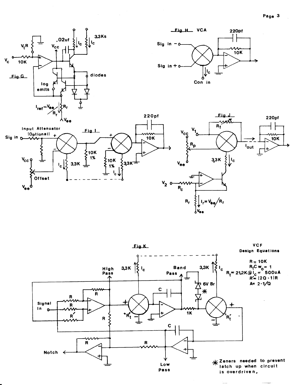
Voltape Controlled Quadrature Osclllator
The voltage controlled oscillator clrcult shown l-n Fig. L ls very siml-lar to the voltage controlled
filter. An extremely low dlstortion slnewave (approximately .O47.) car^ be produced using this circuit'
As.in the f11ter, the SSM2000 ls used as a pair of voltage controlled reslstors to tune a biquad sEage.
A11 dhe desigrr tlps given for the VCF also apply here. The deslgn procedure ls:
@fr-uandwidth product of op amps in Hz)
P^(Output power in dbm)
nl(cirluit impedance
in ohms)
t?(center frequency in Hz)
D"(Total harrnonic distortion in db)
+ lD /' .]\
1) Peak
output voltage; Vpo=(Ro/5oo)f
10"ou
-"'
2) Transfer ratio; r-10((D-9)/20)=84
l) Peak limiter voltage; Yro=2Yrotfr
4) Q setting resistorl R*f t6rfrf
o
5) C: fo capacitorg R2=n3=1/
(z.,cf )=27.2K@I.=5OOuA
6
) R7&RS
; R7=R8=100(Vcc-O.
6-V1p)/V]p
7) e
"i
cc=t+/(tutcB.\)
Noise, Di-storElon and Offset
The output signal to nolse ratio of the 2000 lnto a 10K nretal film reslstor with an lnput slgnal of
3 volts peak to peak 1s 72db tndependent of the control current.
The total harmonic dlstortlon is 1lnearly dependent on the lnput slgnal amplitude. Typical values are
12 with a 10 volt peak to peak signal and 0.12 with a 1 volt slgnal, etc.*
Offset in Lhe 2000 is best thought of referred to the output rather than the slgnal inputs. Due to the
nagure of the design, the D.C. offset appearing at the output w111 be a sma11 fractlon of the control
current. Tlplcally, 2% wiXh both signal lnputs grounded. Tf the control current ls kept under 500uA,
the offset can be trlmned out by a pot stretched between fhe supplles and l^Iith the wlper connected to
one of the slgnal inputs.
xhlnto. rf fha ^ircuits in figures C or G are used as control circuits to gang both sides of the
SSI12OOO
to the same controJ- voltage, the distortion figure is doubled and includes some second
harrnonic distortion. Using two control circuits with a conmon input will avoid this.
Voltagc
9ontrol
lc4
Quedratu
rc Osclllator
lG
ives*
tal
ed
justm.nt
or use 100K
I
ixcdl
t
I
I
I
I
I
I
I
I
I
I
I
t_ Slnclw^tl
Coelwotl
Rt=100/L
RECF-l\/[r
Ai:Fi
l] 5197?
THeG
r Lsenr
llulr I PL I ERIru ElrctRot'ttc
lvlustc
:
-by Dave Rossun, Ep Systems, 3046 Scott Blvd., Santa Clara, CA 95050
Most ELECTRON0TES
readens
are familiar with the RCA CA3080
and
its
uses
as a gain controlled stage in forming voltage controlled amplifjers
and
filters. The CA30B0
has its problems,
as many
readers
have
no doubt
discovered. Some of these
come
from
process
variations, mostly due
to the
fact that the PNP
trans'istors
used
in the positive rail current m'irrors
have
betas
of around
.|0,
which,',^lhen the processing
is poor, can
go to more
like 5. But even
at the'ir best,3080's used in VCA
applical,ions
are noisy
and
cause significant distorticin.
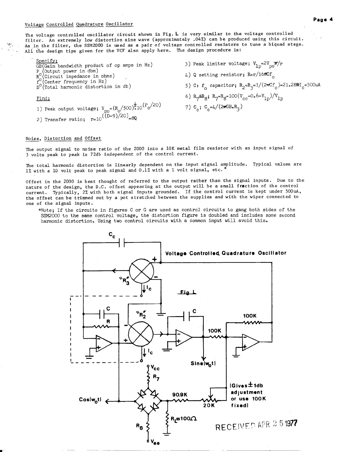
The 30BC type multjplier, vrhether discrete (see
ENS-73 design
for VCA
by Dave Rossum) or integrated, uses a differential input stage
such as that
shown
in figure 1. l'he
two output currents, Ii and
12 are then subtracted
and
converted
to a voltage, either by the current mirror arrangernent
in the
3080 chip or by a differentjal amplifier jn the discrete design. The resulting
_qlqglqt_Es]_
transfer equatjon
for the circuit is then:
Vo
= R t. 1 .r(v+ - v-)
;l / [ er(v+ - v-)+t] r = q/ttT
Thus
we see that the c"ircu'it
is by no means I inear, and
to avoid gross
distortion
the input voltagc to the transistor bases of the input stage
must be kept sma11.
l^le
have typ'ical
ly been
using the attenuation of l00K
to 220 ohms
'into
the stage;
at l0V p/p tlris clives
a distortion of l.3i(,. If we assume l0 mjcrovolts of no'ise
at the trarrsjstor base, this q'ives
also a worst case signal to noise ratjo of
66
dB, for the same
lOV
p/p signal.
Obviousiy,
if rre
could improve the theoretical transfer characteristic to
a more
I
irreal^
form, rve
could improve the d
jstort jon. If instead we chose
to
incre:se nur signal level to tl':e transistor bases,
we could use the improved
Cistcrtjclr 1-c
jn:tcad'lo',rer
the noisc. fn'tunately, a cjrcuit l;jih such
an
improvcd
transfer charactel'istic ex
jsts - it is cal led a G'ilbert rnul t
jpl
ier.
The
Gjlbert multiplier derives its improved
performance
by pre-distorting
the input si.qnal
to our already shown
gain control stage. This is cjone
by add'ing
a pair of matched diodes in front of the transistors, and making the input a
differentjal current, as shovrn
in figure 2. The transfer equation
is now:
vo
=
R r. [ (t* / i-) - 1)
/ [ (r* / r)+ t]
Note
that ir the diodes are on a common
substrate
w'ith
the differential pair,
the temperature
dependcnce
of the gain disappears!
IAS VOLTAGE
tt
to
va- V-, Fig 1
+
V', Fig I
Ic
I
F IGURE - BASiC
MULTIPLIER
EN#67
(3)
FIGURE
2 - PRE-DISTORTION
This
new
equation
looks
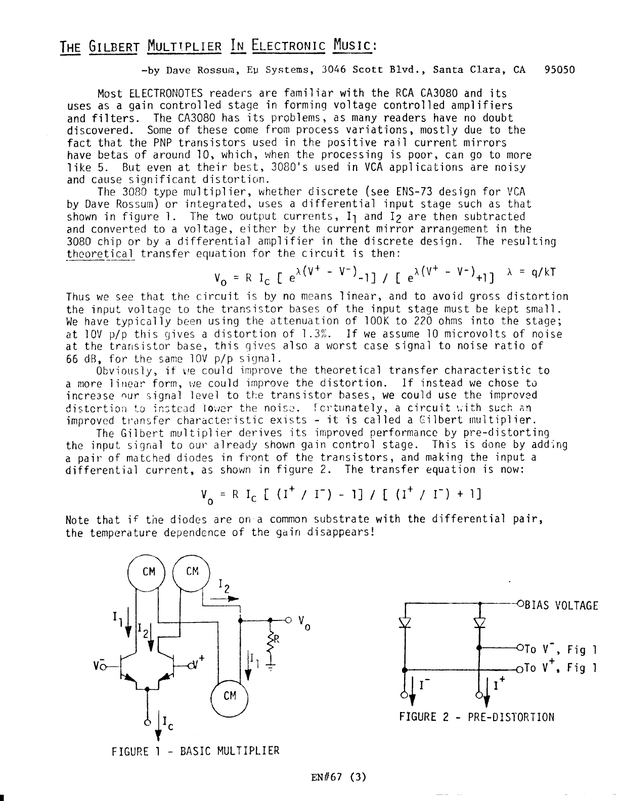
a lot more ljnear. In fact, using
the full circuit
of figure 3, we
f ind it is I
inear, 'ideal=ly
I
inear. The final equat'ion,
ignoring
the
viriation in Vbe of the input
tFansistors
(which
rea'lly is pretty small)
is:
ve=RI.(v+-u')/I'R'
In fact the Vgg
variatjon introduces a
for a 10Vp/p
signal. But
look
what
we
can do
transjstor
bases. The
fjrst input
stage
has
l0 microvolt
no'isy
transjstors
S/N
js .|20
dB.
can
also
have large signals,
like 200
mV,
for
very
small
distortion, about 0.2%
to the signals
at the various
the full l0V
p/p
across it; with
The
second
pair, our old friends,
another
20
dB
or 86
dB
S/N. Much
better.
BIAS
VOLTAGE
ll
rl
Y
i
What have
we
Dajd
for al'l this improvement?
Obviously
more
parts, 'including
some
matched
pairs. Also the inputs
to the amplifier
are
no
longer summing
nodes;
they
require
full level signals
and
any summing
must be
done by ex'ternal
op-amps.
The-control
jnput
to the input
pair no
longer
floats around
rvith common
mode, but
stays
put
and
can
be easjly supplied
with current
without another current
mirror.
The
addjtjonal
parts
vrould
be
a problem for us little folk, but on an IC they
are no
problem;
matched
transistors
are
cheap
and smal'i
on chips. A
dual 2 quadrant
(yes
Virginia,4 quadrant
Gilberts
have
been
used
for yeafs'in the .|495)
multiplier
i-nip
nas
been-developed
by
Ron Dow of Exar
and
is avajiable
for sale (see
below).
It's kind
of a neat
chip, as it not only has
two
independent
Gilbert VCA's on
it'
but the
extra
pins
are bonnected
to some
matched
parts that can
be
used
for
exponential
generators for controlling the channels,
very
useful
in VCF designs.
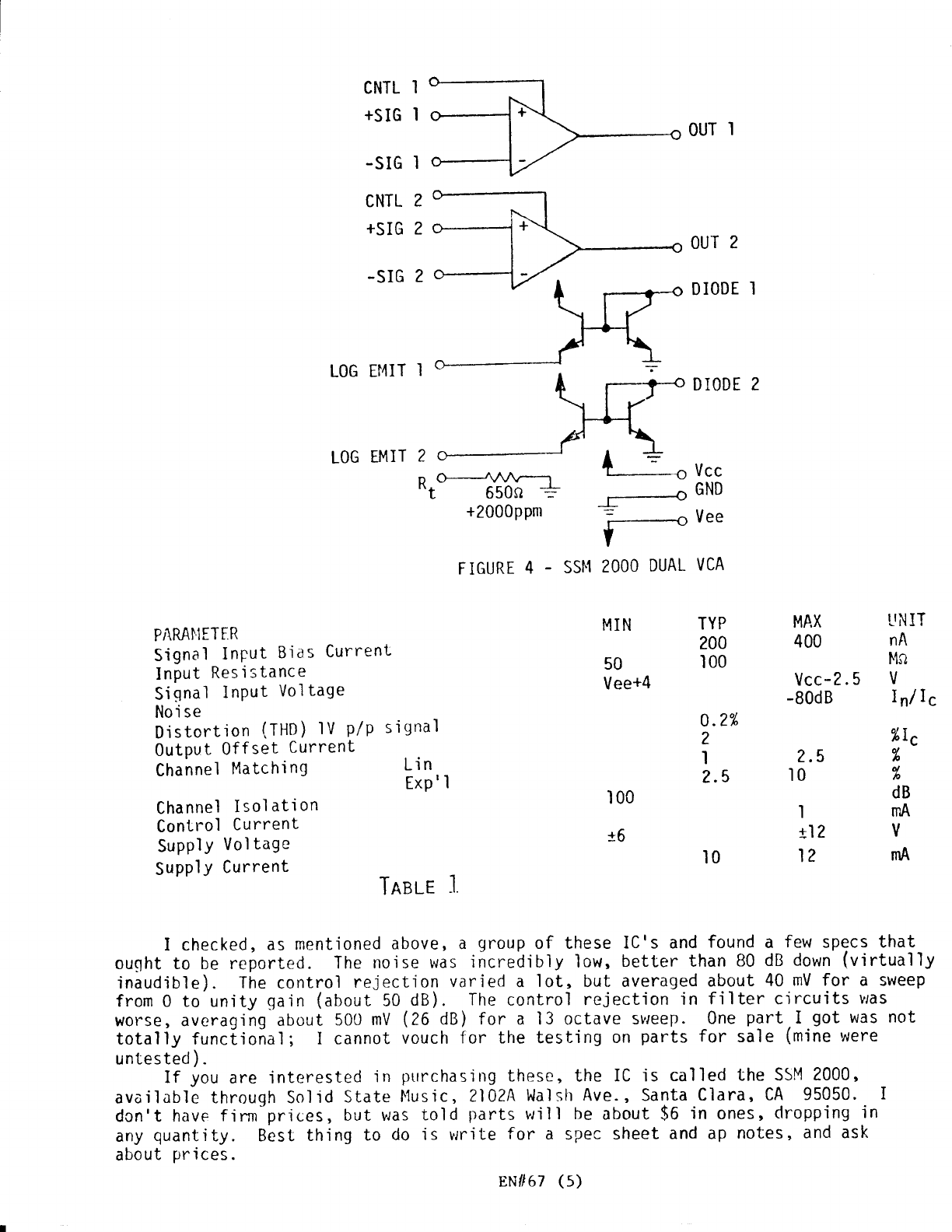
' Figure
{-shows
a basic
block
d"iagram
of the
chjp; the quoted
specs
are in table
l. Bad
nevrs:
the chip is designed
with 24
volt breakdown,
and
use
from tl5 volt
supplies isn't recommended.
Horiever,
I've spec
checked
8 chips
at the higher supply
voltage
and
a'll worked
fine with no
noticable
leakage. Talkjng this over
with Ron,
we deiided
that the things
"should"
work
0K
at tl5V for most applicat'ions,
as no
NPN collector in the device exceeds
23V'in
such
operat'ion
and
the spec
is 24V
min.
So use them,
but beware.
Figure
5 shows
a linear VCA, an
exponentia'l1y
controlled
VCA and
a VCF,
using
more
or less
trad'itjonal
techniques.
Note
for the biquad
VCF
shown,
some
limiting
diodes must
be added as the input
stage
to the
Gjlbert mult'ip'lier
is subject
to
latch-up
if overdriven. This
diodes won't
turn on in normal
operation.
FIGURE
3 - GILBERT
MULTIPLIER
EN/l67
(4)
CNTL
I
+SIG
I
-SIG
CNTL
+SIG
-SIG
2
LOG EMIT
I
LOG
EMIT
2
z
2
n HAAr---r
^t 650o
+
+2000ppm
FIGURE
4 - SSI'I
A?
L-- O
-E--------o
H
Y
2OOO
DUAL
MIN
50
Vee+4
.|00
*6
OUT
2
DIODE
1
DIODE 2
Vee
VCA
0.2%
2
I
?.5
Vcc
GND
PAMNTTER
Signal
InPut
Bias
Current
Input
Res
i stance
Siqnal InPut Voltage
Noi
se
Distortjon (tH0) lV P/P
0utput Offset Current
Channel
Matching
Channel
Isolation
Control Current
Supply
Vol
tage
Supply
Current
TYP
200
100
MA.X LINIT
400 nA
l,l5)
Vcc-2.5 V
-80d8 In/Ic
%rc
2.s %
t0 %
dB
I rnA
t12 V
12 mA
signal
L'in
Exp'
1
l0
TneLr
:l
I checked,
as
mentjoned
above, a group
of these
IC's and
found
a few
specs that
ouqht to be reported. The
nojse was
incredibiy 1ow,
better than
B0
dB
down
(virtually
inaud'ible).
The
control
rejection
varied a lot, but averaged
about
40
mV for a sweep
from 0 to un'ity
oain (about
50
dB). The
control
reiect'ion
jn filter circuits vras
worse, averaging
about
500
mV
(26
dB) for a l3 octave
svreep.
-0ne
part.i got
was not
totaliy tunclioial; I cannot
vouch
for the testing on
parts
for sale (mine
were
untested
).
If you
are interested
in prrrchas'ing
these, the IC is called
the SSM
2000,
available
through Sol
id State
ltlus
jc
, 2102A
Wal sh
Ave., Santa
Clara,
CA 95050. I
don't have
fjrm prices, but vlas
to'ld
parts
vrill be
about
$6 in ones,
dropp'ing
in
any
quantity. Best
thing to clo
is yrrite
for a spec
sheet
and ap
notes,
and
ask
about
prices.
ENil67
(s)
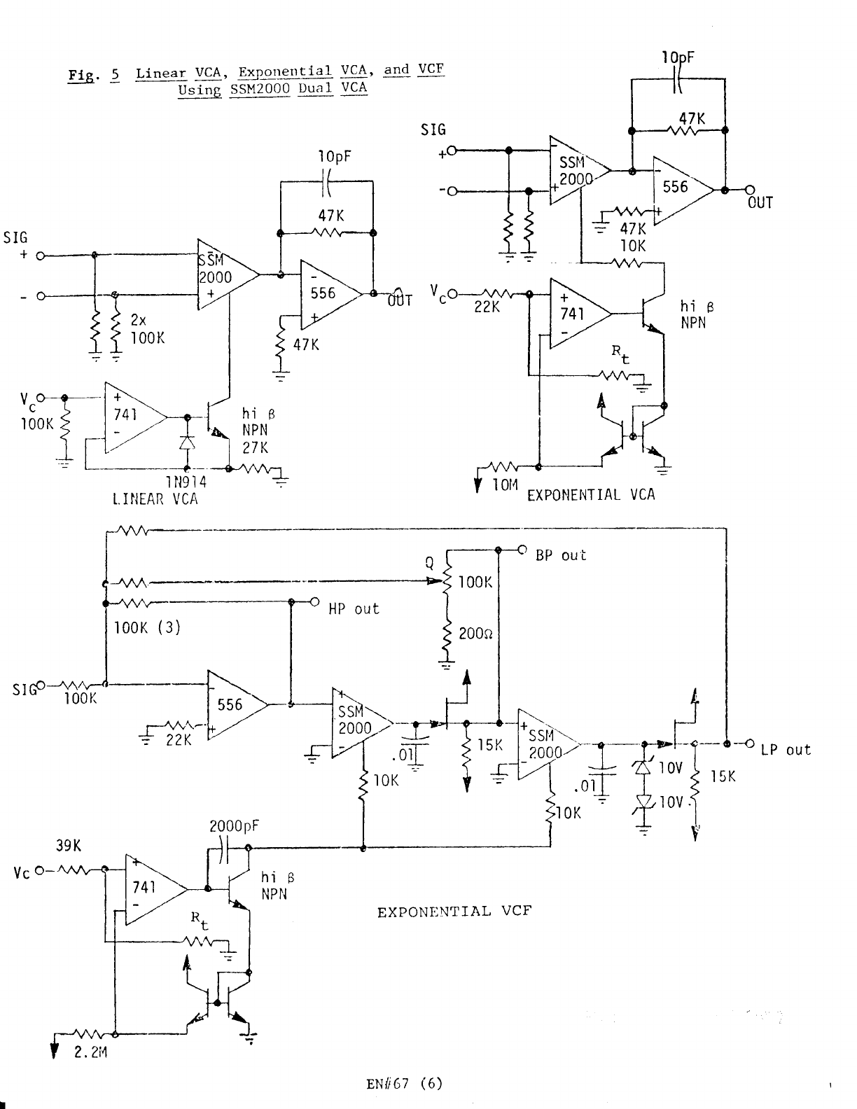
1 0pF
g.
l00K
Linear: VCA, !><lor1gff!-ial-
Usins SSI'12000
Dua
1vcA, and VCF
SIG
hi B
NPN
I..INEAR VCA
rooK
(3)
out
BP
-'l I
SIGO
'lIi
-{ Lp out
.Oil
t0K
K
Vc
o-
EXPONNNTIAL
VCF
EXPONENT
IAL
t 00K
HP out
2000
pF
741 hi
NPN
2.2i'1
EN#67
(6)
